PLC Application Manua(curve)l Programmable Logic Controller DVP SC Program O EN 20120416
Programmable Logic Controller DVP-SA MANUAL_PROGRAMACAO_CLP_FAMILIA_DVP_SV_revisao05
User Manual: Programmable Logic Controller DVP-SC
Open the PDF directly: View PDF ![]() .
.
Page Count: 695 [warning: Documents this large are best viewed by clicking the View PDF Link!]
- PLC-Application-Manua(curve)l.pdf
- PLC Application Manual_Programming.pdf
- Table of Contents
- Chapter 1 Basic Principles of PLC Ladder Diagram
- Foreword: Background and Functions of PLC
- 1.1 The Working Principles of Ladder Diagram
- 1.2 Differences Between Traditional Ladder Diagram and PLC Ladder Diagram
- 1.3 How to Edit Ladder Diagram
- 1.4 How to Edit a PLC Ladder Diagram
- 1.5 The Conversion of PLC Command and Each Diagram Structure
- 1.6 Simplified Ladder Diagram
- 1.7 Basic Program Designing Examples
- Chapter 2 Functions of Devices in DVP-PLC
- 2.1 All Devices in DVP-PLC
- 2.2 Values, Constants [K] / [H]
- 2.3 Numbering and Functions of External Input/Output Contacts [X] / [Y]
- 2.4 Numbering and Functions of Auxiliary Relays [M]
- 2.5 Numbering and Functions of Step Relays [S]
- 2.6 Numbering and Functions of Timers [T]
- 2.7 Numbering and Functions of Counters [C]
- 2.8 Numbering and Functions of Registers [D], [E], [F]
- 2.9 Pointer [N], Pointer [P], Interruption Pointer [I]
- 2.10 Special Auxiliary Relays and Special Data Registers
- 2.11 Functions of Special Auxiliary Relays and Special Registers
- 2.12 Communication Addresses of Devices in DVP Series PLC
- 2.13 Error Codes
- Chapter 3 Basic Instructions
- Chapter 4 Step Ladder Instructions
- Chapter 5 Categories & Use of Application Instructions
- Chapter 6 Application Instructions API 00-49
- Chapter 7 Application Instructions API 50-99
- Chapter 8 Application Instructions API 100-149
- Chapter 9 Applcation Instrcutions API 150-199
- Chapter 10 Application Instructions API 200-249
- Chapter 11 Appendix
DVP-PLC Application Manual:
Programming
Table of Contents
Chapter 1 Basic Principles of PLC Ladder Diagram
Foreword: Background and Functions of PLC.......................................................... 1-1
1.1 The Working Principles of Ladder Diagram........................................................ 1-1
1.2 Differences Between Traditional Ladder Diagram and PLC Ladder Diagram........ 1-2
1.3 Edition Explanation of Ladder Diagram ............................................................. 1-3
1.4 How to Edit Ladder Diagram............................................................................. 1-8
1.5 The Conversion of PLC Command and Each Diagram Structure ......................... 1-12
1.6 Simplified Ladder Diagram ............................................................................... 1-15
1.7 Basic Program Designing Examples.................................................................. 1-17
Chapter 2 Functions of Devices in DVP-PLC
2.1 All Devices in DVP-PLC.................................................................................... 2-1
2.2 Values, Constants [K] / [H] ............................................................................... 2-8
2.3 Numbering and Functions of External Input/Output Contacts [X] / [Y].................. 2-10
2.4 Numbering and Functions of Auxiliary Relays [M] .............................................. 2-13
2.5 Numbering and Functions of Step Relays [S]..................................................... 2-13
2.6 Numbering and Functions of Timers [T]............................................................. 2-15
2.7 Numbering and Functions of Counters [C]......................................................... 2-16
2.8 Numbering and Functions of Registers [D], [E], [F] ............................................ 2-31
2.8.1 Data register [D] ........................................................................................ 2-31
2.8.2 Index Register [E], [F]................................................................................ 2-32
2.8.3 Functions and Features of File Registers .................................................... 2-32
2.9 Pointer [N], Pointer [P], Interruption Pointer [I] .................................................. 2-33
2.10 Special Auxiliary Relays and Special Data Registers........................................ 2-36
2.11 Functions of Special Auxiliary Relays and Special Registers............................. 2-83
2.12 Communication Addresses of Devices in DVP Series PLC................................ 2-149
2.13 Error Codes ................................................................................................... 2-151
Chapter 3 Basic Instructions
3.1 Basic Instructions and Step Ladder Instructions ................................................ 3-1
3.2 Explanations on Basic Instructions ................................................................... 3-4
Chapter 4 Step Ladder Instructions
4.1 Step Ladder Instructions [STL], [RET]............................................................... 4-1
4.2 Sequential Function Chart (SFC) ...................................................................... 4-2
4.3 How does a Step Ladder Instruction Work? ....................................................... 4-3
4.4 Things to Note for Designing a Step Ladder Program......................................... 4-8
4.5 Types of Sequences......................................................................................... 4-10
4.6 IST Instruction ................................................................................................. 4-18
Chapter 5 Categories & Use of Application Instructions
5.1 List of Instructions ........................................................................................... 5-1
5.2 Composition of Application Instruction .............................................................. 5-7
5.3 Handling of Numeric Values.............................................................................. 5-12
5.4 E, F Index Register Modification ....................................................................... 5-15
5.5 Instruction Index.............................................................................................. 5-17
Chapter 6 Application Instructions API 00-49
● (API00 ~ 09)Loop Control.......................................................................... 6-1
● (API10 ~ 19)Transmission Comparison ...................................................... 6-19
● (API20 ~ 29)Four Arithmetic Operation ...................................................... 6-34
● (API30 ~ 39)Rotation & Displacement ........................................................ 6-48
● (API40 ~ 49)Data Processing .................................................................... 6-59
Chapter 7 Application Instructions API 50-99
● (API50 ~ 59)High Speed Processing .......................................................... 7-1
● (API60 ~ 69)Handy Instructions................................................................. 7-41
● (API70 ~ 79)Display of External Settings ................................................... 7-71
● (API80 ~ 88)Serial I/O............................................................................... 7-93
Chapter 8 Application Instructions API 100-149
● (API100 ~ 109)Communication .................................................................. 8-1
● (API110 ~ 119)Floating Point Operation ..................................................... 8-21
● (API120 ~ 129)Floating Point Operation..................................................... 8-29
● (API130 ~ 139)Floating Point Operatio....................................................... 8-39
● (API140 ~ 149)Others ............................................................................... 8-51
Chapter 9 Application Instructions API 150-199
● (API150 ~ 154)Others ............................................................................... 9-1
● (API155 ~ 159)Position Control ................................................................. 9-24
● (API160 ~ 169)Real Time Calendar............................................................ 9-54
● (API170 ~ 179)Gray Code Conversion/Floating Point Operation.................. 9-65
● (API180 ~ 199)Matrix................................................................................ 9-82
● (API190 ~ 197)Positioning Instruction........................................................ 9-98
Chapter 10 Application Instructions API 215-246
● (API202 ~ 207)Others. .............................................................................. 10-1
● (API215 ~ 223)Contact Type Logic Operation Instruction. ........................... 10-15
● (API224 ~ 269)Contact Type Compare Instruction ...................................... 10-18
● (API270 ~ 280)Contact Type Compare Instruction ...................................... 10-25
● (API281 ~ 292)Contact Type Compare Instruction ...................................... 10-31
Chapter 11 Appendix
11.1 Appendix A: Self Detection Table for Abnormality.......................................... 11-1
11.2 Appendix B: MPU Terminal Layout ............................................................... 11-2
11.3 Appendix C: Terminal Layout for Digital I/O Modules..................................... 11-6
11.4 Appendix D: Difference between EH2 and EH3 ............................................. 11-9
11.5 Appendix E: Revision History....................................................................... 11-10

The models that every series includes are as follows.
Series Model name
DVP-ES
DVP14ES00R2, DVP14ES00T2, DVP14ES01R2, DVP14ES01T2, DVP24ES00R,
DVP24ES00R2, DVP24ES00T2, DVP24ES01R2, DVP24ES01T2, DVP24ES11R2,
DVP30ES00R2, DVP30ES00T2, DVP32ES00R, DVP32ES00R2, DVP32ES00T2,
DVP32ES01R2, DVP32ES01T2, DVP40ES00R2, DVP40ES00T2, DVP60ES00R2,
DVP60ES00T2
DVP10EC00R3, DVP10EC00T3, DVP14EC00R3, DVP14EC00T3, DVP16EC00R3,
DVP16EC00T3, DVP20EC00R3, DVP20EC00T3, DVP24EC00R3, DVP24EC00T3,
DVP30EC00R3, DVP30EC00T3, DVP32EC00R3, DVP32EC00T3, DVP40EC00R3,
DVP40EC00T3, DVP60EC00R3, DVP60EC00T3,
DVP-EX DVP20EX00R2, DVP20EX00T2, DVP20EX11R2
DVP-SS DVP14SS11R2, DVP14SS11T2
DVP-SA DVP12SA11R, DVP12SA11T
DVP-SX DVP10SX11R, DVP10SX11T
DVP-SC DVP12SC11T
DVP-EH2
DVP16EH00R2, DVP16EH00T2, DVP20EH00R2, DVP20EH00T2, DVP32EH00M2,
DVP32EH00R2, DVP32EH00T2, DVP40EH00R2, DVP40EH00T2, DVP48EH00R2,
DVP48EH00T2, DVP60EH00T2, DVP64EH00R2, DVP64EH00T2, DVP80EH00R2,
DVP80EH00T2, DVP32EH00R2-L, DVP32EH00T2-L
DVP-SV DVP28SV11R, DVP28SV11T
DVP-EH3
DVP16EH00R3, DVP16EH00T3, DVP20EH00R3, DVP20EH00T3, DVP32EH00M3,
DVP32EH00R3, DVP32EH00T3, DVP40EH00R3, DVP40EH00T3, DVP48EH00R3,
DVP48EH00T3, DVP60EH00T3, DVP64EH00R3, DVP64EH00T3, DVP80EH00R3,
DVP80EH00T3, DVP32EH00R3-L, DVP32EH00T3-L
DVP-SV2 DVP28SV11R2, DVP28SV11T2

1 Basic Principles of PLC Ladder Diagram
Foreword: Background and Functions of PLC
PLC (Programmable Logic Controller) is an electronic device, previously called “sequence controller”. In 1978,
NEMA (National Electrical Manufacture Association) in the United States officially named it as “programmable logic
controller”. PLC reads the status of the external input devices, e.g. keypad, sensor, switch and pulses, and execute by
the microprocessor logic, sequential, timing, counting and arithmetic operations according the status of the input
signals as well as the pre-written program stored in the PLC. The generated output signals are sent to output devices
as the switch of a relay, electromagnetic valve, motor drive, control of a machine or operation of a procedure for the
purpose of machine automation or processing procedure. The peripheral devices (e.g. personal computer/handheld
programming panel) can easily edit or modify the program and monitor the device and conduct on-site program
maintenance and adjustment. The widely used language in designing a PLC program is the ladder diagram.
With the development of the electronic technology and wider applications of PLC in the industry, for example in
position control and the network function of PLC, the input/output signals of PLC include DI (digital input), AI (analog
input), PI (pulse input), NI (numeric input), DO (digital output), AO (analog output), and PO (pulse output). Therefore,
PLC will still stand important in the industrial automation field in the future.
1.1 The Working Principles of Ladder Diagram
The ladder diagram was a diagram language for automation developed in the WWII period, which is the oldest
and most widely adopted language in automation. In the initial stage, there were only A (normally open) contact, B
(normally closed) contact, output coil, timer and counter…the sort of basic devices on the ladder diagram (see the
power panel that is still used today). After the invention of programmable logic controllers (PLC), the devices
displayable on the ladder diagram are added with differential contact, latched coil and the application commands
which were not in a traditional power panel, for example the addition, subtraction, multiplication and division
operations.
The working principles of the traditional ladder diagram and PLC ladder diagram are basically the same. The
only difference is that the symbols on the traditional ladder diagram are more similar to its original form, and PLC
ladder diagram adopts the symbols that are easy to recognize and shown on computer or data sheets. In terms of the
logic of the ladder diagram, there are combination logic and sequential logic.
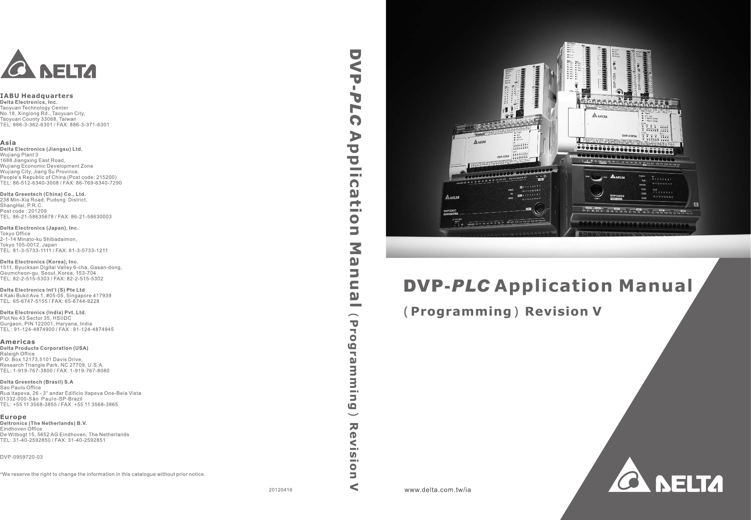
1. Combination Logic
Examples of traditional ladder diagram and PLC ladder diagram for combination logic:
Traditional Ladder Diagram PLC Ladder Diagram
X4
X0
X2
X3
X1
Y0
Y2
Y1
X0
Y0
X1
Y1
Y2
X2
X3
X4
Row 1: Using a normally open (NO) switch X0 (“A” switch or “A" contact). When X0 is not pressed, the contact
DVP-PLC Application Manual 1-1
1 Basic Principles of PLC Ladder Diagram
will be open loop (Off), so Y0 will be Off. When X0 is pressed, the contact will be On, so Y0 will be On.
Row 2: Using a normally closed (NC) switch X1 (“B” switch or “B” contact). When X1 is not pressed, the contact
will be On, so Y1 will be On. When X1 is pressed, the contact will be open loop (Off), so Y1 will be Off.
Row 3: The combination logic of more than one input devices. Output Y2 will be On when X2 is not pressed or
X3 and X4 are pressed.
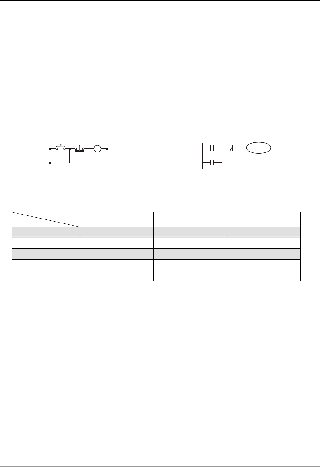
2. Sequential Logic
Sequential logic is a circuit with "draw back” structure, i.e. the output result of the circuit will be drawn back as an
input criterion. Therefore, under the same input criteria, different previous status or action sequence will follow by
different output results.
Examples of traditional ladder diagram and PLC ladder diagram for sequential logic:
Traditional Ladder Diagram PLC Ladder Diagram
Y3
X5
Y3
X6
Y3
X5
Y3
X6
When the circuit is first connected to the power, though X6 is On, X5 is Off, so Y3 will be Off. After X5 is pressed,
Y3 will be On. Once Y3 is On, even X5 is released (Off), Y3 can still keep its action because of the draw back (i.e.
the self-retained circuit). The actions are illustrated in the table below.
Device status
Action sequence X5 X6 Y3
1 No action No action Off
2 Action No action On
3 No action No action On
4 No action Action Off
5 No action No action Off
From the table above, we can see that in different sequence, the same input status can result in different output
results. For example, switch X5 and X6 of action sequence 1 and 3 do not act, but Y3 is Off in sequence 1 and
On in sequence 3. Y3 output status will then be drawn back as input (the so-called “draw back”), making the
circuit being able to perform sequential control, which is the main feature of the ladder diagram circuit. Here we
only explain contact A, contact B and the output coil. Other devices are applicable to the same method. See
Chapter 3 “Basic instructions” for more details.
1.2 Differences Between Traditional Ladder Diagram and PLC Ladder Diagram
Though the principles of traditional ladder diagram and PLC ladder diagram are the same, in fact, PLC adopts
microcomputer to simulate the motions of the traditional ladder diagram, i.e. scan-check status of all the input devices
and output coil and calculate to generate the same output results as those from the traditional ladder diagram based
on the logics of the ladder diagram. Due to that there is only one microcomputer, we can only check the program of
the ladder diagram one by one and calculate the output results according to the program and the I/O status before the
cyclic process of sending the results to the output interface Æ re-reading of the input status Æ calculation Æ output.
The time spent in the cyclic process is called the “scan time” and the time can be longer with the expansion of the
DVP-PLC Application Manual
1-2
1 Basic Principles of PLC Ladder Diagram
program. The scan time can cause delay from the input detection to output response of the PLC. The longer the delay,
the bigger the error is to the control. The control may even be out of control. In this case, you have to choose a PLC
with faster scan speed. Therefore, the scan speed is an important specification requirement in a PLC. Owing to the
advancement in microcomputer and ASIC (IC for special purpose), there has been great improvement in the scan
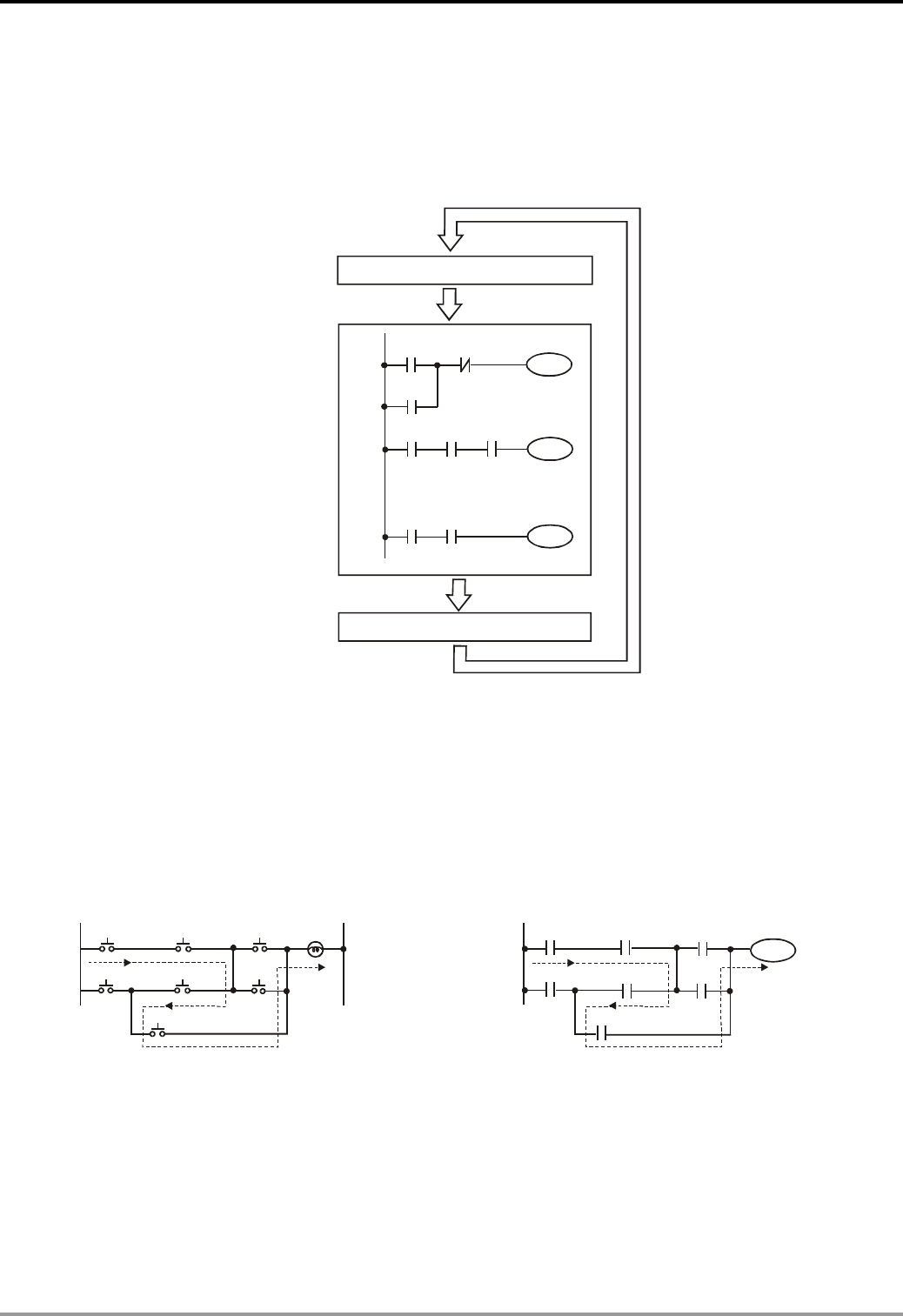
speed of PLC nowadays. See the figure below for the scan of the PLC ladder diagram program.
The output result is calculated
based on the ladder diagram.
(The result has not yet sent to the
external output point, but the
internal device will perform an
immediate output.)
Y0
X0 X1
Y0
Start
M100 X3
Y1
X10
:
:
X100 M505
Y126
End
Send the result to the output point
Read input status from outside
Executing in cycles
Besides the difference in the scan time, PLC ladder and traditional ladder diagram also differ in “reverse current”.
For example, in the traditional ladder diagram illustrated below, when X0, X1, X4 and X6 are On and others are Off,
Y0 output on the circuit will be On as the dotted line goes. However, the PLC ladder diagram program is scanned from
up to down and left to right. Under the same input circumstances, the PLC ladder diagram editing tool WPLSoft will be
able to detect the errors occurring in the ladder diagram.
Reverse current of traditional ladder diagram Reverse current of PLC ladder diagram
X6
X0
Y0
X1 X2 Y0
X3 X4 X5
ab
Error detected in the third row
X6
X0 X1 X2
X3 X4 X5
ab
Y0
1.3 How to Edit Ladder Diagram
Ladder diagram is a diagram language frequently applied in automation. The ladder diagram is composed of the
symbols of electric control circuit. The completion of the ladder diagram by the ladder diagram editor is the completion
of the PLC program design. The control flow illustrated by diagram makes the flow more straightforward and
DVP-PLC Application Manual 1-3

1 Basic Principles of PLC Ladder Diagram
acceptable for the technicians of who are familiar with the electric control circuit. Many basic symbols and actions in
the ladder diagram come from the frequently-seen electromechanical devices, e.g. buttons, switches, relay, timer and
counter, etc. in the traditional power panel for automation control.
Internal devices in the PLC: The types and quantity of the devices in the PLC vary in different brand names.
Though the internal devices in the PLC adopts the names, e.g. transistor, coil, contact and so on, in the traditional
electric control circuit, these physical devices do not actually exist inside the PLC. There are only the corresponding
basic units (1 bit) inside the memory of the PLC. When the bit is “1”, the coil will be On, and when the bit is “0”, the coil
will be Off. The normally open contact (NO or contact A) directly reads the value of the corresponding bit. The
normally close contact (NC or contact B) reads the opposite state of the value of the corresponding bit. Many relays
will occupy many bits. 8 bits equal a “byte”. 2 bytes construct a “word” and 2 words combined is “double word”. Byte,
word or double words are used when many relays are processed (e.g. addition/subtraction, displacement) at the
same time. The other two devices, timer and counter, in the PLC have coil, timer value and counter value and they
have to process some values in byte, word or double word.
All kinds of internal devices in the value storage area in the PLC occupy their fixed amount of storage units.
When you use these devices, you are actually read the contents stored in the form of bit, byte or word.
Introductions on the basic internal devices in the PLC (See Ch 2. Functions of Devices in DVP-PLC for more details.)
Device Functions
Input relay
The input relay is an internal memory (storage) unit in the PLC corresponding to a external
input point and is used for connecting to the external input switches and receiving external
input signals. The input relay will be driven by the external input signals which make it “0” or
“1". Program designing cannot modify the status of the relay, i.e. it cannot re-write the basic
unit of a relay, nor can it force On/Off of the relay by HPP/WPLSoft.
SA/SX/SC/EH2/SV/EH3/SV2 series MPU can simulate input relay X and force On/Off of the
relay. But the status of the external input points will be updated and disabled, i.e. the external
input signals will not be read into their corresponding memories inside PLC, but only the input
points on the MPU. The input points on the extension modules will still operate normally. There
are no limitations on the times of using contact A and contact B of the input relay. The input
relays without corresponding input signals can only be left unused and cannot be used for
other purposes.
& Device indication: X0, X1,…X7, X10, X11,… are indicated as X and numbered in octal
form. The No. of input points are marked on MPU and extension modules.
Output relay
The output relay is an internal memory (storage) unit in the PLC corresponding to a external
output point and is used for connecting to the external load. The output relay will be driven by
the contact of an input relay, contacts of other internal devices and the contacts on itself. A
normally open contact of the output relay is connected to the external load. Same as the input
contacts, there are no limitations on the times of using other contacts of the output relay. The
output relay without corresponding output signals can only be left unused and can be used as
input relay if necessary.
DVP-PLC Application Manual
1-4

1 Basic Principles of PLC Ladder Diagram
Device Functions
& Device indication: Y0, Y1,…Y7, Y10, Y11,…are indicated as Y and numbered in octal
form. The No. of output points are marked on MPU and extension modules.
Internal relay
The internal relay does not have connection with the external. It is an auxiliary relay inside the
PLC with the functions same as those of the auxiliary (middle) relay in the electric control
circuit. Every internal relay corresponds to a basic internal storage unit and can be driven by
the contacts of the input relay, contacts of the output relay and the contacts of other internal
devices. There are no limitations on the times of using the contacts of the internal relay and
there will be no output from the internal relay, but from the output point.
& Device indication: M0, M1,…, M4095 are indicated as M and numbered in decimal form.
Step
DVP series PLC offers a step-type control program input method. STL instruction controls the
transfer of step S, which makes it easy for the writing of the control program. If you do not use
any step program in the control program, step S can be used as a internal relay M as well as an
alarm point.
& Device indication: S0, S1,…S1023 are indicated as S and numbered in decimal form.
Timer
The timer is used for timing and has coil, contact and register in it. When the coil is On and the
estimated time is reached, its contact will be enabled (contact A closed, contact B open). Every
timer has its fixed timing period (unit: 1ms/10ms/100ms). Once the coil is Off, the contact iwlwl
be disabled (contact A open, contact B closed) and the present value on the timer will become
“0”.
& Device indication: T0, T1,…,T255 are indicated as T and numbered in decimal form.
Different No. refers to different timing period.
Counter
The counter is used for counting. Before using the counter, you have to give the counter a set
value (i.e. the number of pulses for counting). There are coil, contact and registers in the
counter. When the coil goes from Off to On, the counter will regard it as an input of 1 pulse and
the present value on the counter will plus “1”. We offer 16-bit and 32-bit high-speed counters
for our users.
& Device indication: C0, C1,…,C255 are indicated as C and numbered in decimal form.
Data register
Data processing and value operations always occur when the PLC conducts all kinds of
sequential control, timing and counting. The data register is used for storing the values or all
kinds of parameters. Every register is able to store a word (16-bit binary value). Double words
will occupy 2 adjacent data registers.
& Device indication: D0, D1,…,D11999 are indicated as D and numbered in decimal form.
File register
The file register is used for storing the data or all kinds of parameters when the data registers
required for processing the data and value operations are insufficient. Every file register is able
to store a 16-bit word. Double words will occupy 2 adjacent file registers. In SA/SX/SC series
DVP-PLC Application Manual 1-5
1 Basic Principles of PLC Ladder Diagram
Device Functions
MPU, there are 1,600 file registers. In EH2/SV/EH3/SV2 series MPU, there are 10,000 file
registers. There is not an actual device No. for a file register. The reading and writing of file
registers should be executed by instructions API 148 MEMR, API 149 MEMW, or through the
peripheral device HPP02 and WPLSoft.
& Device indication: K0 ~ K9,999, numbered in decimal form.
Index register
E and F index registers are 16-bit data registers as other data registers. They can be read and
written and can be used in word devices, bit devices or as a constant for index indication.
& Device indication: E0 ~ E7, F0 ~ F7 are indicated as E and F and numbered in decimal
form.
The structure of a ladder diagram:
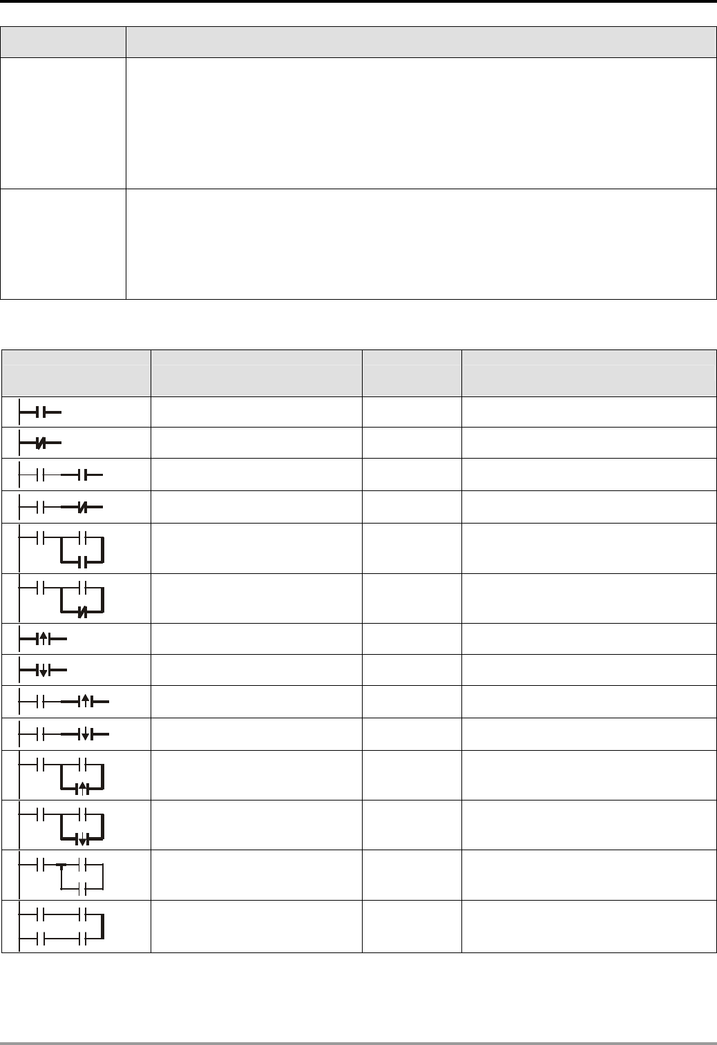
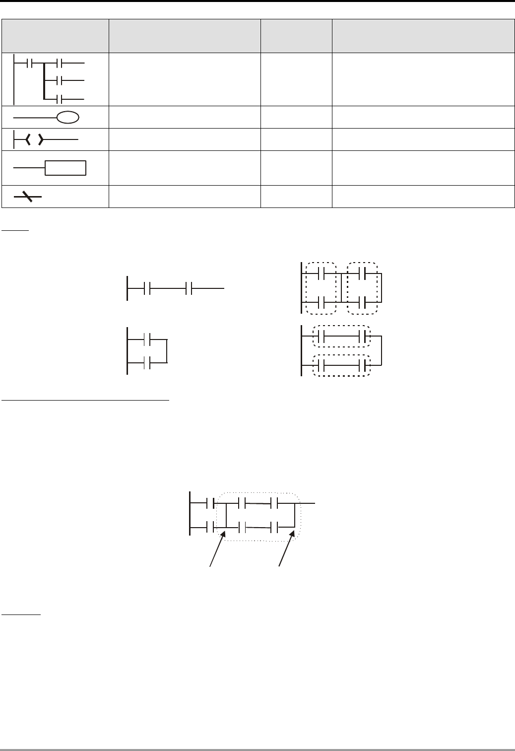
Structure Explanation Instruction Devices Used
Normally open, contact A LD X, Y, M, S, T, C
Normally closed, contact B LDI X, Y, M, S, T, C
Normally open in series
connection AND X, Y, M, S, T, C
Normally closed in series
connection ANI X, Y, M, S, T, C
Normally open in parallel
connection OR X, Y, M, S, T, C
Normally closed in parallel
connection ORI X, Y, M, S, T, C
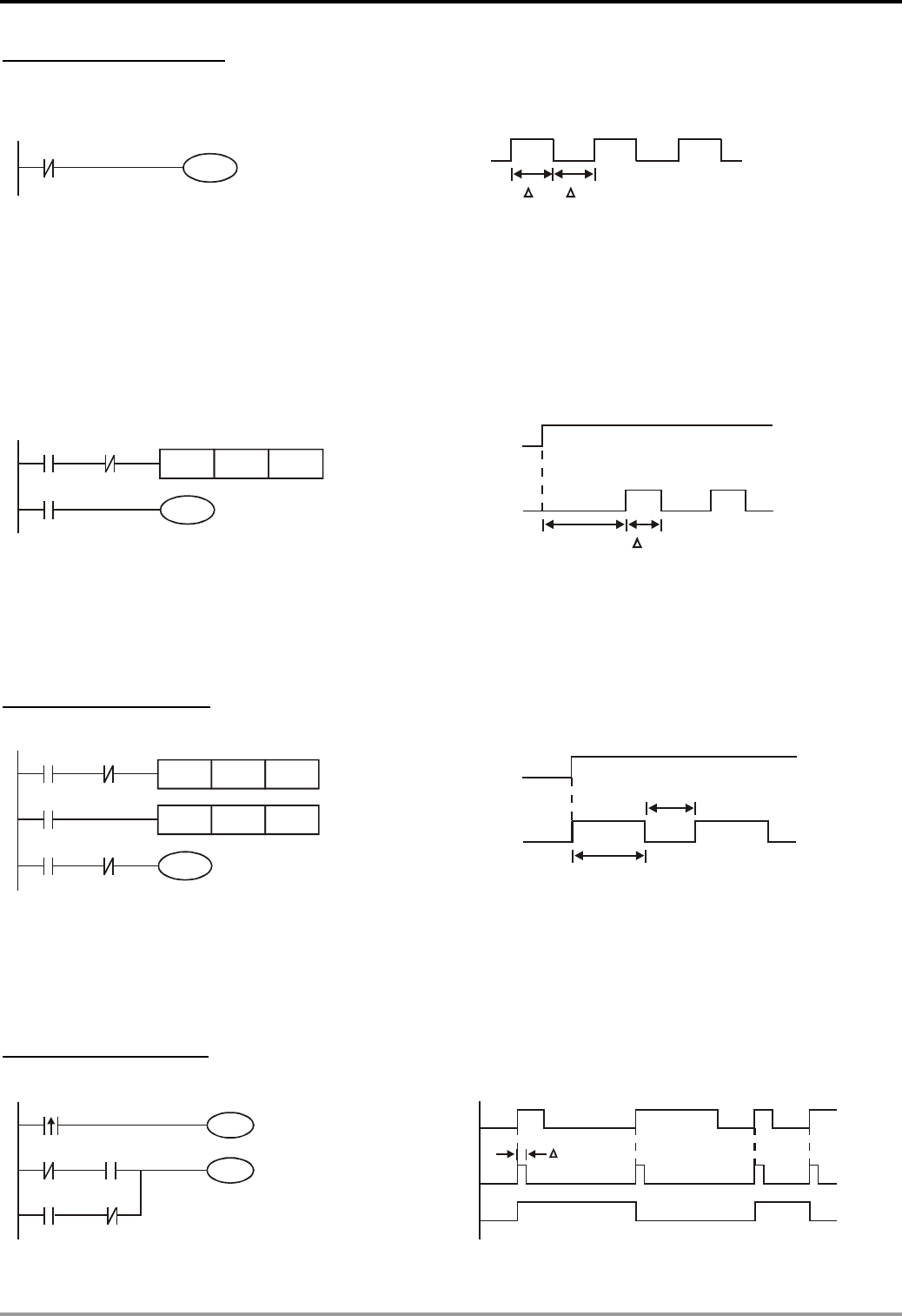
Rising-edge trigger switch LDP X, Y, M, S, T, C
Falling-edge trigger switch LDF X, Y, M, S, T, C
Rising-edge trigger in series
connection ANDP X, Y, M, S, T, C
Falling-edge trigger in series
connection ANDF X, Y, M, S, T, C
Rising-edge trigger in parallel
connection ORP X, Y, M, S, T, C
Falling-edge trigger in parallel
connection ORF X, Y, M, S, T, C
Block in series connection ANB -
Block in parallel connection ORB -
DVP-PLC Application Manual
1-6
1 Basic Principles of PLC Ladder Diagram
Structure Explanation Instruction Devices Used
Multiple output
MPS
MRD
MPP
-
Coil driven output instruction OUT Y, M, S
SS
Step ladder STL S
Basic instruction
Application instruction
Application
instructions
See Ch.3 for basic instructions
(RST/SET and CNT/TMR) and Ch.5 ~
10 for application instructions
Inverse logic INV -
Block:
A block is a series or parallel operation composed of more than 2 devices. There are series block and parallel block.
Series block
Parallel block
Separation line and combination line:
The vertical line is used for separating the devices. For the devices on the left, the vertical line is a combination line,
indicating that there are at least 2 rows of circuits on the left connected with the vertical line. For the devices on the
right, the vertical line is a separation line, indicating that there are at least 2 rows of circuits interconnected on the right
side of the vertical line).
12
Combination line for block 1
Separation line for block 2
Combination line for block 2
Network:
A complete block network is composed of devices and all kinds of blocks. The blocks or devices connectable by a
vertical line or continuous line belong to the same network.
DVP-PLC Application Manual 1-7
1 Basic Principles of PLC Ladder Diagram
An independent network
Network 1
Network 2
An incomplete network
1.4 How to Edit a PLC Ladder Diagram
The editing of the program should start from the left power line and ends at the right power line, a row after
another. The drawing of the right power line will be omitted if edited from WPLSoft. A row can have maximum 11
contacts on it. If 11 is not enough, you can continuously connect more devices and the continuous number will be
generated automatically. The same input points can be used repeatedly. See the figure below:
X0 X1 X2 X3 X4 X5
Y0
X11 X12 X13
X6 X7 X10 C0 C1
00000
00000
Continuous number
The operation of the ladder diagram program is scanning from top left to bottom right. The coil and the operation
frame of the application instruction belong to the output side in the program and are placed in the right if the ladder
diagram. Take the figure below for example, we will step by step explain the process of a ladder diagram. The
numbers in the black circles indicate the order.
X0 X1 Y1 X4
M0
X3 M1
T0 M3
Y1
TMR T0 K10
DVP-PLC Application Manual
1-8
1 Basic Principles of PLC Ladder Diagram
The order of the instructions:
1 LD X0
2 OR M0
3 AND X1
4 LD X3
AND M1
ORB
5 LD Y1
AND X4
6 LD T0
AND M3
ORB
7 ANB
8 OUT Y1
TMR T0 K10
Explanations on the basic structures in the ladder diagram:
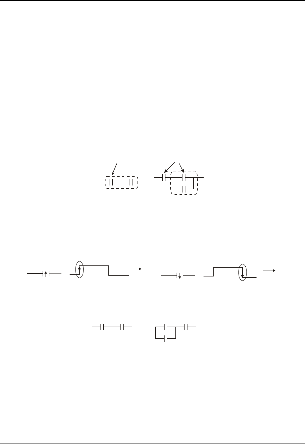
1. LD (LDI) instruction: Given in the start of a block.
AND block OR block
LD instruction LD instruction
The structure of LDP and LDF instructions are the same as that of LD instruction, and the two only differ in their
actions. LDP and LDF instructions only act at the rising edge or falling edge when the contact is On, as shown in the
figure below.
X0
OFF ON
Time
OFF
Falling edge
X0
OFF ON OFF
Time
Rising edge
2. AND (ANI) instruction: A single device connects to another single device or a block in series
AND instructio
n
AND instruction
The structure of ANDP and ANDF instructions are the same. ANDP and ANDF instructions only act at the rising
edge or falling edge.
3. OR (ORI) instruction: A single device connects to another single device or a block
DVP-PLC Application Manual 1-9
1 Basic Principles of PLC Ladder Diagram
OR instruction OR instruction OR instruction
The structure of ORP and ORF instructions are the same. ORP and ORF instructions only act at the rising edge
or falling edge.
4. ANB instruction: A block connects to a device or another block in series
ANB instruction
5. ORB instruction: A block connects to a device or another block in parallel
ORB instruction
If the ANB and ORB operations are with several blocks, the operation should be performed from up to down or
left to right, combining into a block or network.
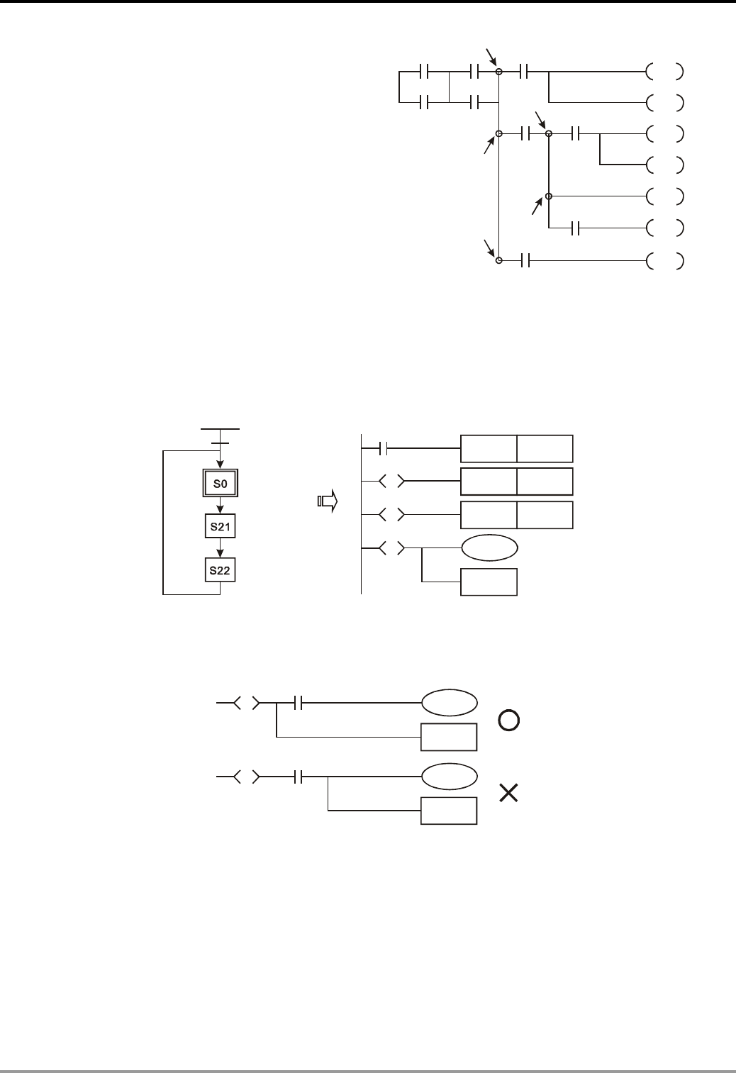
6. MPS, MRD, MPP instructions: Bifurcation point of multiple outputs, for generating many and diverse outputs.
MPS instruction is the start of the bifurcation point. The bifurcation point is the intersection of the horizontal line
and vertical line. We will have to determine whether to give a contact memory instruction by the contact status of the
same vertical line. Basically, every contact can be given a memory instruction, but considering the convenience of
operating the PLC and the limitation on its capacity, some parts in the ladder diagram will be omitted during the
conversion. We can determine the type of contact memory instruction by the structure of the ladder diagram. MPS is
recognized as “┬” and the instruction can be given continuously for 8 times.
MRD instruction is used for reading the memory of the bifurcation point. Due to that the same vertical line is of
the same logic status, in order to continue analyzing other ladder diagrams, we have to read the status of the original
contact again. MRD is recognized as “├”.
MPP instruction is used for reading the start status of the top bifurcation point and popping it out from the stack.
Since MPP is the last item on the vertical line, the vertical line ends at this point.
DVP-PLC Application Manual
1-10
1 Basic Principles of PLC Ladder Diagram
MPP is recognized as “└”. Using the method
given above for the analysis cannot be wrong.
However, sometimes the compiling program will ignore
the same output status, as shown in the figure.
MPS
MRD
MPP MPP
MPS
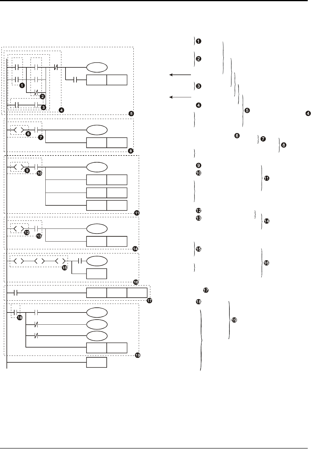
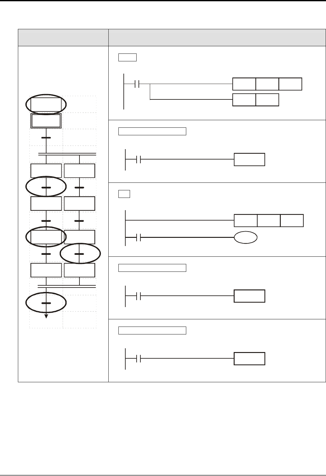
7. STL instruction: Used for designing the syntax of the sequential function chart (SFC).
STL instruction allows the program designer a clearer and readable picture of the sequence of the program as
when they draw a sequence chart. From the figure below, we can see clearly the sequence to be planned. When the
step S moves to the next step, the original S will be “Off". Such a sequence can then be converted into a PLC ladder
diagram and called “step ladder diagram”.
M1002
S0
SET S0
S0
SET S21
SET S22
S
S21
S
RET
S22
S
M1002
8. RET instruction: Placed after the completed step ladder diagram.
RET also has be placed after STL instruction. See the example below.
RET
S20
S
RET
S20
S
X1
X1
See step ladder instructions [STL], [RET] in Ch. 4 for the structure of the ladder diagram.
DVP-PLC Application Manual 1-11
1 Basic Principles of PLC Ladder Diagram
1.5 The Conversion of PLC Command and Each Diagram Structure
Ladder Diagram
X0 X2 X1
X1
M1
C0
Y0
SET S0
M2 Y0
M0
X10
Y10
SET S10
S0
S
X11
Y11
SET S11
S10
S
SET S12
SET S13
X12
Y12
SET S20
S11
S
X13
S0
RET
S20
S
S12
S
S13
S
X0
CNT C0 K10
X1
M0
C0
X1
M2
RST C0
M1
M2
END
LD X0
OR X1
LD X2
OR M0
ORI M1
ANB
LD M2
AND Y0
ORB
AN I X1
OUT Y0
AND C0
SET S0
STL S0
LD X10
OUT Y10
SET S10
STL S10
LD X11
OUT Y11
SET S11
SET S12
SET S13
STL S11
LD X12
OUT Y12
SET S20
STL S20
STL S12
STL S13
LD X13
OUT S0
RET
LD X0
CNT C0 K10
LD C0
MPS
AND X1
OUT M0
MRD
AN I X1
OUT M1
MPP
AN I M2
OUT M2
END
OR
block
ANI
Multiple
outputs
RST C0
OR
block
Series
connection blcok
AND
block
Parallel
connection block
The output will continue
following the status of
Step ladder Start
Status working item and
step point transfer
Withdraw S10 status
Withdraw X11 status
Status working item and
step point transfer
Withdraw S11 status
Withdraw X12 status
Status working item and
step point transfer
Bifurcation
convergence
End of step ladder
Status working item
and step point transfer
Return
Read C0
Multiple
outputs
End of program
Status S0 and X10 operation
Fuzzy Syntax
The correct ladder diagram analysis and combination should be conducted from up to down and left to right.
However, without adopting this principle, some instructions can make the same ladder diagram.
DVP-PLC Application Manual
1-12
1 Basic Principles of PLC Ladder Diagram
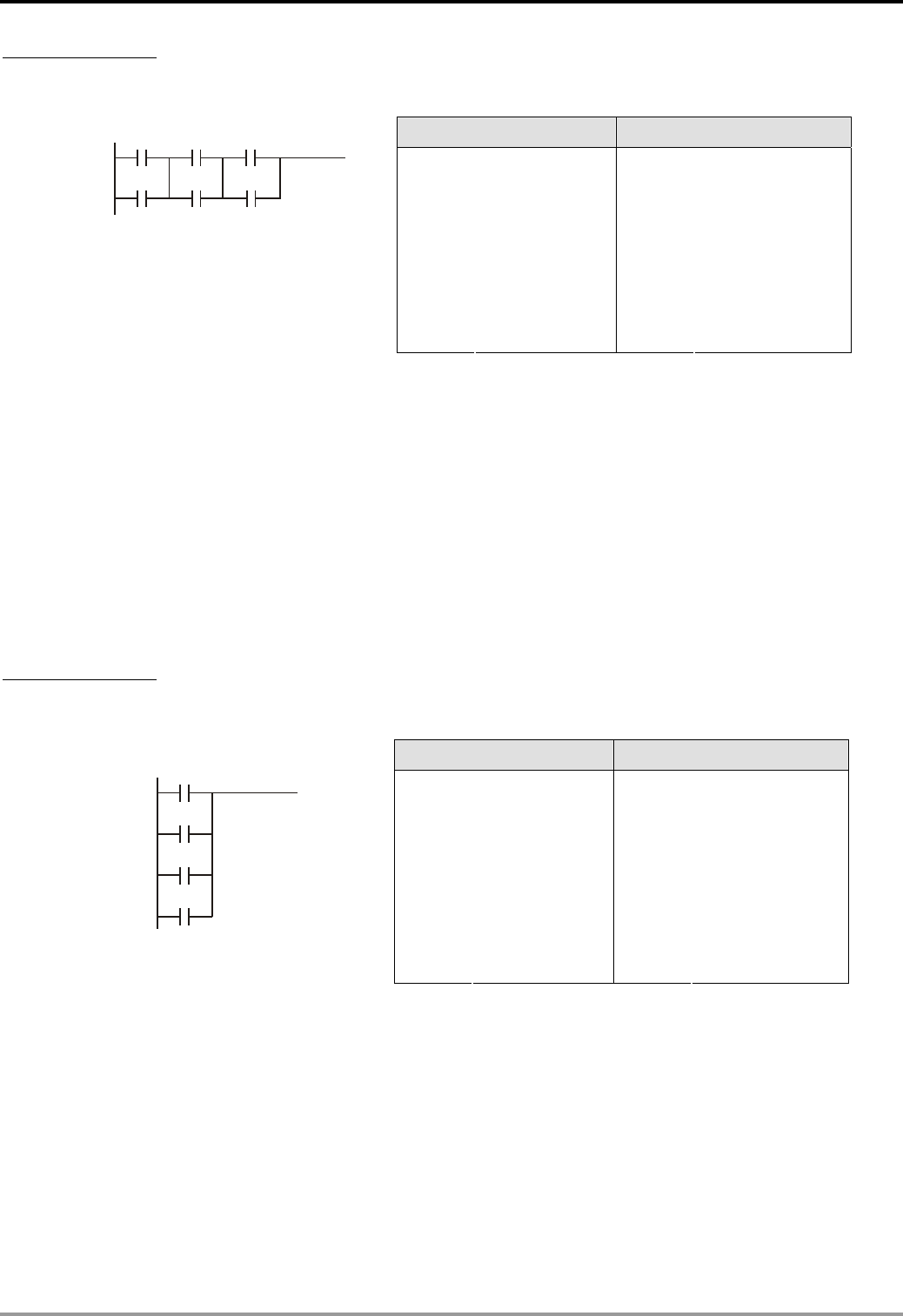
Example Program 1
See the ladder diagram below. There are 2 ways to indicate the ladder by instruction programs with the same result.
Ideal way Less ideal way
LD X0 LD X0
OR X1 OR X1
LD X2 LD X2
OR X3 OR X3
ANB LD X4
LD X4 OR X5
OR X5 ANB
X0 X2 X4
X5X3X1
ANB ANB
The two instruction programs will be converted into the same ladder diagram. The difference between the ideal
one and less ideal one is the operation done by the MPU. For the ideal way, the combination is done block by block
whereas the less idea way combines all the blocks combine with one another in the last step. Though the length of
the program codes of the two ways are equal, the combination done in the last step (by ANB instruction, but ANB
cannot be used continuously for more than 8 times) will have to store up the previous calculation results in advance.
In our case, there are only two blocks combined and the MPU allows such kind of combination. However, once the
number of blocks exceed the range that the MPU allows, problems will occur. Therefore, the best way is to execute
the block combination instruction after a block is made, which will also make the logic sequence planned by the
programmer more in order.
Example Program 2
See the ladder diagram below. There are 2 ways to indicate the ladder by instruction programs with the same result.
Ideal way Less ideal way
LD X0 LD X0
OR X1 LD X1
OR X2 LD X2
OR X3 LD X3
ORB
ORB
X0
X1
X2
X3
ORB
In this example, the program codes and the operation memory in the MPU increase in the less ideal way.
Therefore, it is better that you edit the program following the defined sequence.
Incorrect Ladder Diagram
PLC processes the diagram program from up to down and left to right. Though we can use all kinds of ladder
symbols to combine into various ladder diagrams, when we draw a ladder diagram, we will have to start the diagram
from the left power line and end it at the right power line (In WPLSoft ladder diagram editing area, the right power line
is omitted), from left to right horizontally, one row after another from up to down. See bellows for the frequently seen
incorrect diagrams:
DVP-PLC Application Manual 1-13
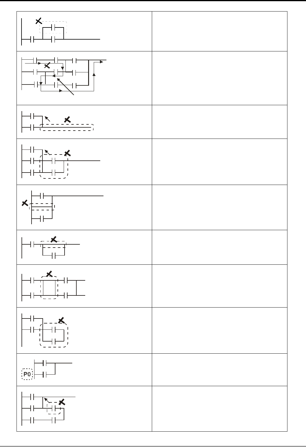
1 Basic Principles of PLC Ladder Diagram
OR operation upward is not allowed.
Reverse flow
“Reverse flow” exists in the signal circuit from the
beginning of input to output.
The up-right corner should output first.
Combining or editing should be done from the
up-left to the bottom-right. The dotted-lined area
should be moved up.
Parallel operation with empty device is not allowed.
Empty device cannot do operations with other
devices.
No device in the middle block.
Devices and blocks in series should be horizontally
aligned.
Label P0 should be in the first row of a complete
network.
Blocks connected in series should be aligned with
the upmost horizontal line.
DVP-PLC Application Manual
1-14
1 Basic Principles of PLC Ladder Diagram
1.6 Simplified Ladder Diagram
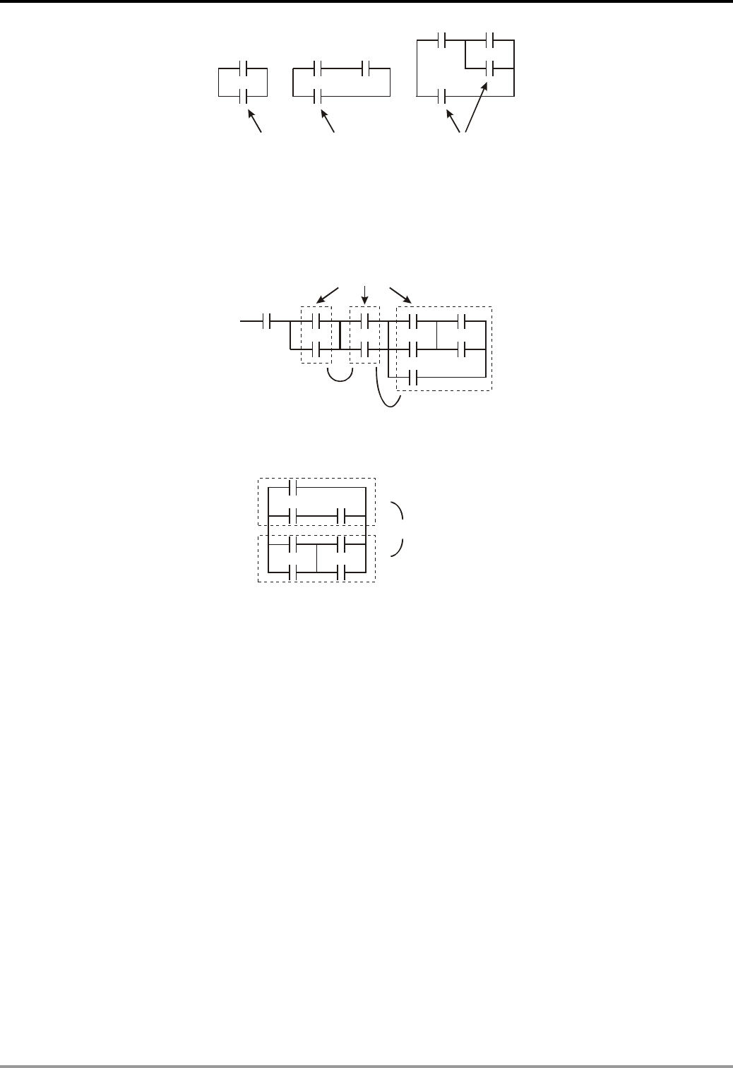
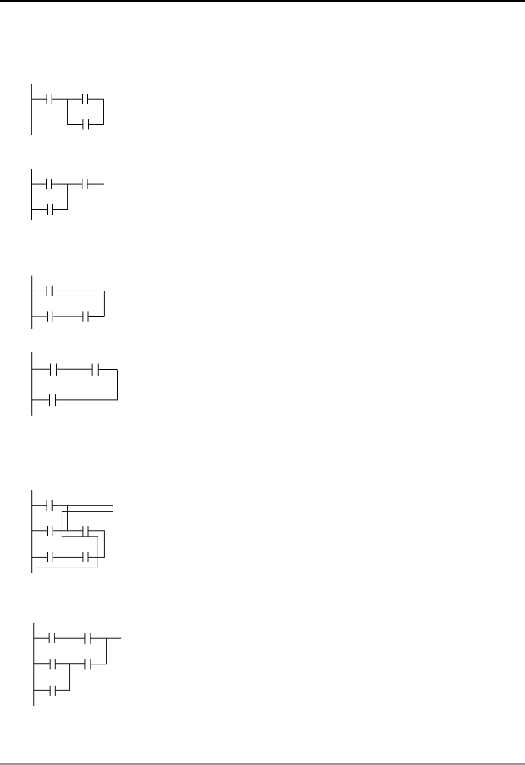
When a series block is connected to a parallel block in series, place the block in the front to omit ANB instruction.
Ladder diagram complied into instruction
X0 X1
X2
LD X0
LD X1
OR X2
Ø ANB
Ladder diagram complied into instruction
X0X1
X2
LD X1
OR X2
AND X0
When a single device is connected to a block in parallel, place the block on top to omit ORB instruction.
Ladder diagram complied into instruction
T0
X1 X2
LD T0
LD X1
AND X2
ORB
Ø
T0
X1 X2
Ladder diagram complied into instruction
LD X1
AND X2
OR T0
In diagram (a), the block on top is shorter than the block in the bottom, we can switch the position of the two
blocks to achieve the same logic. Due to that diagram (a) is illegal, there is a “reverse flow” in it.
Ladder diagram complied into instruction
X0
X1 X2
X3 X4
LD X0
OR X1
AND X2
LD X3
(a) AND X4
Ø ORB
Ladder diagram complied into instruction
X0
X1 X2
X3 X4
LD X3
AND X4
LD X1
OR X0
(b) AND X2
ORB
DVP-PLC Application Manual 1-15
1 Basic Principles of PLC Ladder Diagram
MPS and MPP instruction can be omitted when the multiple outputs in the same horizontal line do not need to
operate with other input devices.
Ladder diagram complied into instruction
X0
Y1
Y0
MPS
AND X0
OUT Y1
MPP
Ø
OUT Y0
Ladder diagram complied into instruction
Y0
Y1
X0
OUT Y0
AND X0
OUT Y1
Correct the circuit of reverse flow
In the following two examples, the diagram in the left hand side is the ladder diagram we desire. However, the illegal
“reverse flow” in it is incorrect according to our definition on the ladder diagram. We modify the diagram into the
diagram in the right hand side.
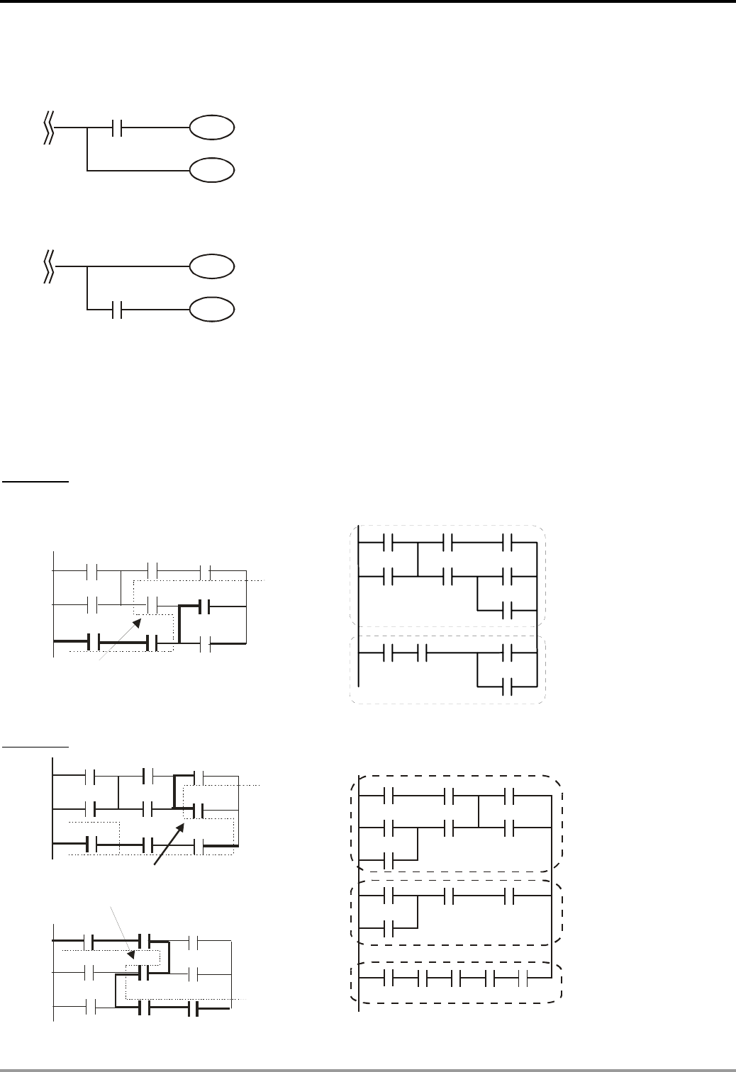
Example 1
X0 X1 X2
X3 X4 X5
X10
X6 X7 X5
X10 LOOP1
X0
X3
X6
X1
X4
X7
X2
X5
X10 LO OP1
Ö
rever se fl o
w
Example 2
X0
X3
X6
X1
X4
X7
X2
X5
X10 LO OP1
LOOP1
X0 X1 X2
X3 X4 X5
X6
X3 X7 X10
X6
X0 X1 X7 X10
LOOP
2
X4
rever se fl o
w
Ö
X0
X3
X6
X1
X4
X7
X2
X5
X10
LOOP2
Reverse fl ow
DVP-PLC Application Manual
1-16
1 Basic Principles of PLC Ladder Diagram
1.7 Basic Program Designing Examples
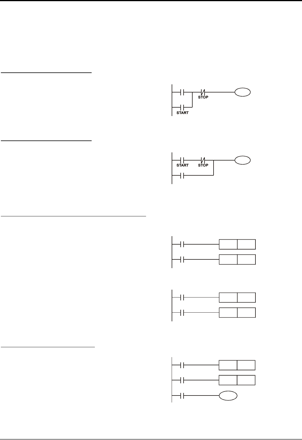
Start, Stop and Latched
In some application occasions, we need to use the transient close/open buttons for the start and stop of an equipment.
To maintain its continuous action, you have to design latched circuits.
Example 1: Stop first latched circuit
When the normally open contact X1 = On and the
normally closed contact X2 = Off, Y1 will be On. If you make
X2 = On at this time, Y1 will be Off. It is the reason why this is
called “stop first”.
X2
Y1
X1
Y1
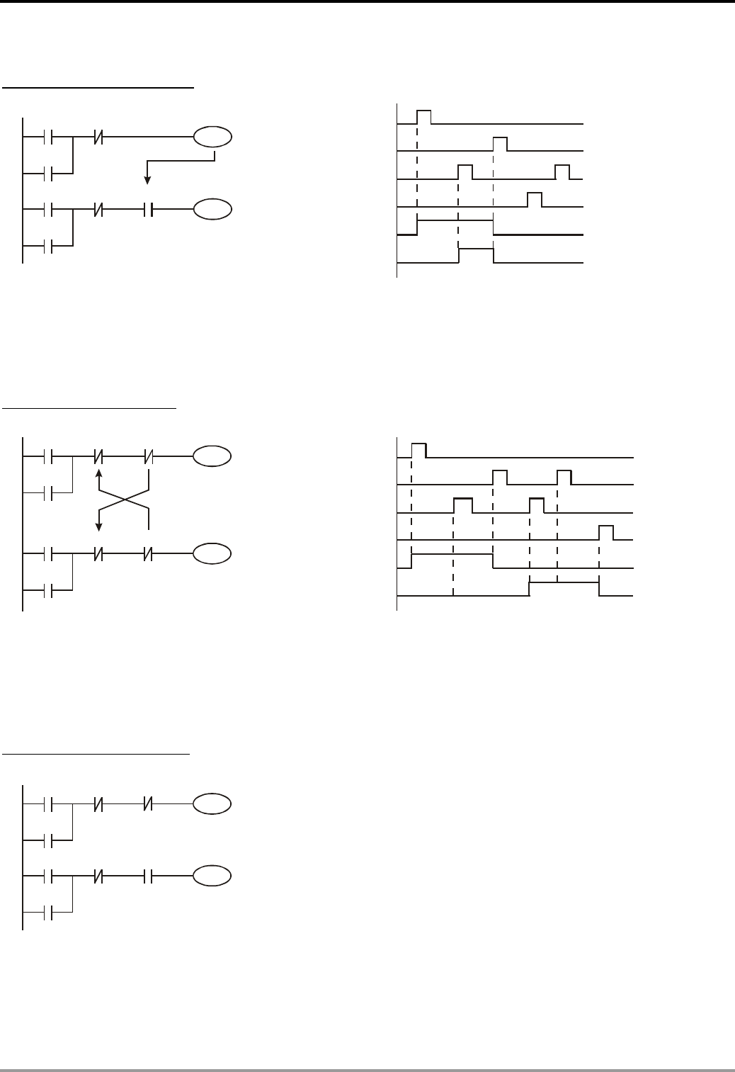
Example 2: Start first latched circuit
When the normally open contact X1 = On and the
normally closed contact X2 = Off, Y1 will be On and latched. If
you make X2 = On at this time, Y1 will continue to be On
because of the latched contact. It is the reason why this is
called “start first”.
X2
Y1
X1
Y1
Example 3: Latched circuit for SET and RST instructions
See the diagram in the right hand side for the latched
circuit consist of RST and SET instructions.
X2
Y1
X1
SET
Y1
RST
Stop first
In the stop first diagram, RST is placed after SET. PLC
executes the program from up to down, so the On/Off of Y1 will
be determined upon its status in the end of the program.
Therefore, when X1 and X2 are enabled at the same time, Y1
will be Off. It is the reason why this is called “stop first”.
X2
Y1
X1
SET Y1
RST
Start first
In the start first diagram, SET is placed after RST. When
X1 and X2 are enabled at the same time, Y1 will be On. It is
the reason why this is called “start first”.
Example 4: Power shutdown latched
X2
M512
X1
SET
RST M512
Y1
M512
The auxiliary relay M512 is latched (see instruction
sheets for DVP series PLC MPU). The circuit can not only be
latched when the power is on, but also keep the continuity of
the original control when the power is shut down and switched
on again.
DVP-PLC Application Manual 1-17
1 Basic Principles of PLC Ladder Diagram
Frequently Used Control Circuit
Example 5: Conditional control
X1
X3
X2
X4
Y1
Y2
X3
Y1
X1
Y1
X4
Y2
X2
Y2
Y1
X1 and X3 enables and disables Y1; X2 and X4 enables and disables Y2, and all are latched. Due to that the
normally open contact of Y1 is connected to the circuit of Y2 in series, Y1 becomes an AND condition for Y2.
Therefore, only when Y1 is enabled can Y2 be enabled.
Example 6: Interlock control
X3
Y1
X1
Y1
X4
Y2
X2
Y2
Y1
Y2
X1
X3
X2
X4
Y1
Y2
Which of the X1 and X2 is first enabled decides either the corresponding output Y1 or Y2 will be enabled first.
Either Y1 or Y2 will be enabled at a time, i.e. Y1 and Y2 will not be enabled at the same time (the interlock). Even X1
and X2 are enabled at the same time, Y1 and Y2 will not be enabled at the same time due to that the ladder diagram
program is scanned from up to down. In this ladder diagram, Y1 will be enabled first.
Example 7: Sequential control
If we serially connect the normally closed contact
of Y2 in example 5 to the circuit of Y1 as an AND
condition for Y1 (as the diagram in the left hand side),
the circuit can not only make Y1 as the condition for Y2,
but also allow the stop of Y1 after Y2 is enabled.
Therefore, we can make Y1 and Y2 execute exactly the
sequential control.
X3
Y1
X1
Y1
X4
Y2
X2
Y2
Y1
Y2
DVP-PLC Application Manual
1-18
1 Basic Principles of PLC Ladder Diagram
Example 8: Oscillating circuit
An oscillating circuit with cycle ΔT+ΔT
Y1
Y1
Y1
T T
The ladder diagram above is a very simple one. When the program starts to scan the normally closed contact
Y1, Y1 will be closed because coil Y1 is Off. When the program then scan to coil Y1 and make it On, the output will be
1. When the program scans to the normally closed contact Y1 again in the next scan cycle, because coil Y1 is On, Y1
will be open and make coil Y1 Off and output 0. The repeated scans will result in coil Y1 outputs oscillating pulses by
the cycle ΔT(On)+ΔT(Off).
An oscillating circuit with cycle nT+ΔT
Y1
n
X0
T0
X0
TMR
Y1
Y1
T0
Kn
TT
The ladder diagram program controls the On time of coil Y1 by timer T0 and disable timer T0 in the next scan
cycle, resulting in the oscillating pulses in the output of Y1. n refers to the decimal set value in the timer and T is the
cycle of the clock.
Example 9: Flashing circuit
T2TMR Kn2
T1
X0
TMR
Y1
T2
T1
Kn1
X0 T1
Y1
T
n1
X0
Tn2
*
*
The ladder diagram is an oscillating circuit which makes the indicator flash or enables the buzzer alarms. It
uses two timer to control the On/Off time of coil Y1. n1 and n2 refer to the set values in T1 and T2 and T is the cycle
of the clock.
Example 10: Trigger circuit
Y1
M0
X0
Y1
Y1
M0
M0
X0
M0
Y1
T
DVP-PLC Application Manual 1-19
1 Basic Principles of PLC Ladder Diagram
The rising-edge differential instruction of X0 makes coil M0 generate a single pulse of ΔT (one scan cycle).
Coil Y1 will be On during this scan period. In the next scan period, coil M0 will be Off and the normally closed contact
M0 and Y1 will all be closed, making coil Y1 continue to be On until another rising-edge arrives in input X0, making
coil M0 On for another scan period and Y1 Off. Such kind of circuit relies on an input to make two actions execute
interchangeably. Also from the timing diagram on the last page, we can see that input X0 are square pulse signals of
the cycle T and coil Y1 output are square pulse signals of the cycle 2T.
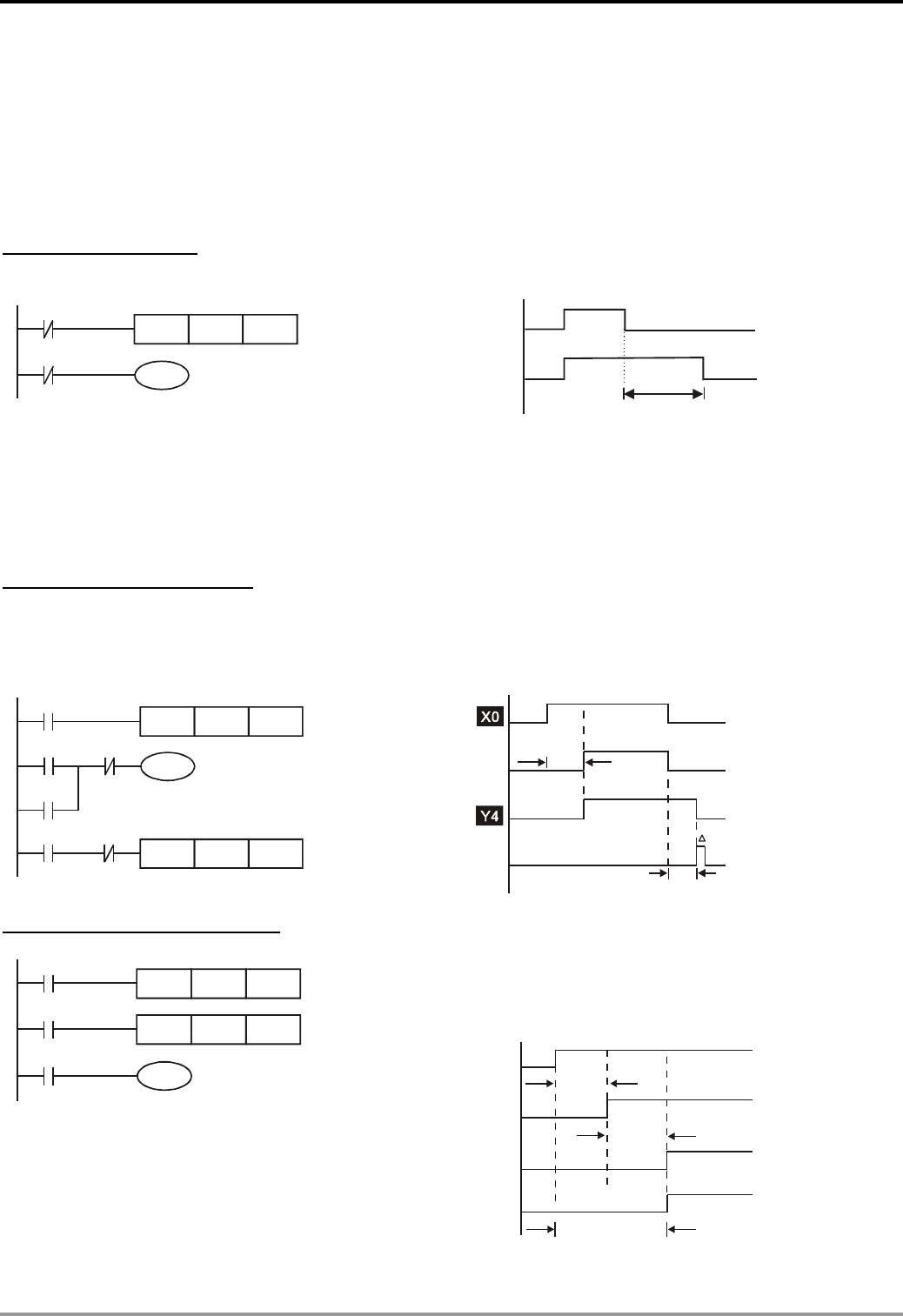
Example 11: Delay circuit
X0
Y1
100 seconds
T10
X0
TMR
Y1
T10
K1000
Time base: T = 0.1 sec
When input X0 is On, due to that its corresponding normally closed contact is Off, time T10 will be Off and the
output coil Y1 will be On. T10 will be On and start to count until input X0 is Off. Output coil Y1 will be delayed for
100 seconds (K1,000 × 0.1 sec = 100 secs) and be Off. See the timing diagram above.
Example 12: Output delay circuit
The output delay circuit is the circuit composed of two timers. When input X0 is On and Off, output Y4 will be
delayed.
T5
T5
TMR
Y4
T6
X0
K50
Y4
T6
Y4
TMR
X0
K30
3 secs
5 secs
T5
T6
T
Example13: Timing extension circuit
T12TMR Kn2
T11
X0
TMR
Y1
T11
Kn1
T12
The total delay time from input X0 is closed to output
Y1 is On = (n1+n2)* T. T refers to the clock cycle.
X0
Y1
T11
T12
n1*
n2*
T
T
(n1+n2)* T
Timer = T11, T12
Clock cycle: T
DVP-PLC Application Manual
1-20
1 Basic Principles of PLC Ladder Diagram
Example 14: How to enlarge the counting range
C6CNT Kn2
C5
X13
CNT
RST
C5
Kn1
X14
C5RST
Y1
C6
C6
The counting range of a 16-bit counter is 0 ~ 32,767. As
the circuit in the left hand side, using two counters can
increase the counting range to n1*n2. When the counting
of counter C5 reaches n1, C6 will start to count for one
time and reset for counting the pulses from X13. When
the counting of counter C6 reaches n2, the pulses from
input X13 will be n1*n2.
Example 15: Traffic light control (by using step ladder instruction)
Traffic light control
Vertical
Light
Horizontal
Light
Green
light
flashes
Yellow
light
Green
light
Red light
Vertical
light Y0 Y1 Y2 Y2
Horizontal
light Y10 Y11 Y12 Y12
On time 35 secs 5 secs 25 secs 5 secs
Timing Diagram:
Y0
Y1
Y2
Y10
Y11
Y12
Vertical
Light
Red
Yel low
Green
Horizontal
Light
Red
Yell ow
Green 25 secs
5 secs 5 secs
25 secs
5 secs 5 secs
DVP-PLC Application Manual 1-21
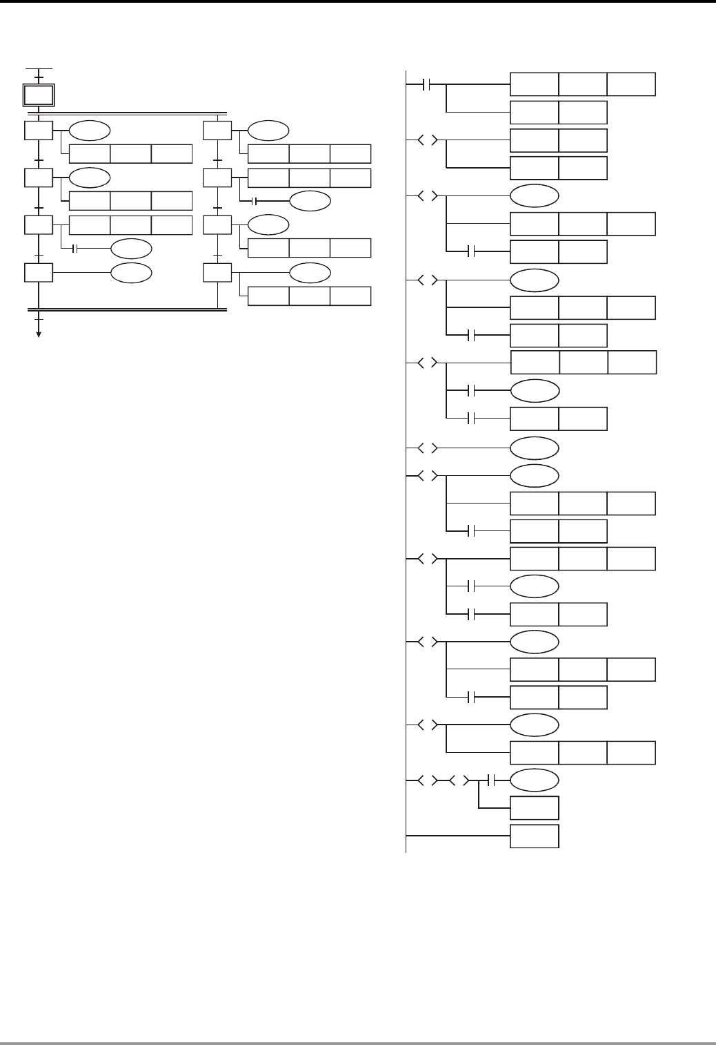
1 Basic Principles of PLC Ladder Diagram
SFC Figure: Ladder Diagram:
M1002
ZRST S0 S127
SET S0
SET S20
Y2
END
S0
S
S21
S
Y1
S23
S
Y12
S30
S
T13
S23
S
S33
S
SET S30
S20
S
TMR T0
SET S21
T0
Y0
K350
TMR T1
SET S22
T1
K250
Y2
S22
S
TMR T2
SET S23
T2
K50
M1013
TMR T10
SET S31
T10
K250
Y12
S31
S
TMR T11
SET S32
T11
K50
M1013
Y11
S32
S
TMR T12
SET S33
T12
K50
Y10
S33
S
TMR T13 K350
S0
RET
S0
S20
S21
S22
S0
M1002
T0
T1
T13
Y0
S23
T2
TMR T0 K350
Y2
TMR T1 K250
Y2
TMR T2 K50
M1013
Y1
S30
S31
S32
T10
T11
S33
T12
Y12
TMR T10 K250
Y11
TMR T12 K50
Y12
TMR T11 K50
M1013
Y10
TMR T13 K350
DVP-PLC Application Manual
1-22
1 Basic Principles of PLC Ladder Diagram
Drawing by SFC Editor (WPLSoft )
Drawn by SFC Internal Ladder Diagram
LAD-0
S0ZRST S127
M1002
S0
SET
Transferring Condition 1
TRANS*
T0
S22
Y2
T2TMR K50
M1013
Transferring Condition 4
TRANS*
T13
TRANS*
T13
TRANS*
T13
TRANS*
T13
TRANS*
T13
TRANS*
T13
TRANS*
T13
0
2
3
4
5
6
7
1
LAD-0
S0
S20
S21
S22
S23
S30
S31
S32
S33
S0
Transferring Condition 7
TRANS*
T12
TRANS*
T12
TRANS*
T12
TRANS*
T12
TRANS*
T12
TRANS*
T12
TRANS*
T12
DVP-PLC Application Manual 1-23

1 Basic Principles of PLC Ladder Diagram
MEMO
DVP-PLC Application Manual
1-24
2 Functions of Devices in DVP-PLC
2.1 All Devices in DVP-PLC
ES/EX/SS series MPU:
Type Device Item Range Function
X External input relay X0 ~ X177, 128 points, octal Corresponds to external
input points
Y External output relay Y0 ~ Y177, 128 points, octal
Total
256 points Corresponds to external
output points
General purpose M0 ~ M511, M768 ~ M999, 744
points
Latched* M512 ~ M767, 256 points
M Auxiliary
relay
Special purpose M1000 ~ M1279, 280 points
(some are latched)
Total
1,280 points
The contact can be
On/Off in the program.
100ms timer T0 ~ T63, 64 points
10ms timer (M1028 = On) T64 ~ T126, 63 points (M1028
= Off: 100ms)
T Timer
1ms timer T127, 1 points
Total
128 points
Timer indicated by TMR
instruction. If timing
reaches its target, the T
contact of the same No.
will be On.
16-bit counting up
(general purpose) C0 ~ C111, 112 points
16-bit counting up (latched*) C112 ~ C127, 16 points
Total
128 points
1-phase 1 input C235 ~ C238, C241, C242,
C244, 7 points
1-phase 2 inputs C246, C247, C249, 3 points
C Counter
32-bit
counting
up/down
high-speed
counter
(latched*)
2-phase 2 inputs C251, C252, C254, 3 points
Total
13 points
Counter indicated by
CNT (DCNT) instruction.
If counting reaches its
target, the C contact of
the same No. will be On.
Initial step (latched*) S0 ~ S9, 10 points
Zero return (latched*) S10 ~ S19, 10 points (used with
IST instruction)
Relay (bit)
S Step
Latched* S20 ~ S127, 108 points
Total
128 points Used for SFC.
T Present value of timer T0 ~ T127, 128 points
When the timing
reaches the target, the
contact of the timer will
be On.
C Present value of counter C0 ~ C127, 16-bit counter, 128 points
C235 ~ C254, 32-bit counter, 13 points
When the counting
reaches the target, the
contact of the counter
will be On.
General purpose D0 ~ D407, 408 points
Latched* D408 ~ D599, 192 points
Total
600 points
Special purpose D1000 ~ D1311, 312 points
Register (word data)
D Data
register
Index indication E, F, 2 points
Total
312 points
Memory area for data
storage; E, F can be
used for index
indication.
N For master control nested loop N0 ~ N7, 8 points Control point for main
control loop
P For CJ, CALL instructions P0 ~ P63, 64 points Position index for CJ
and CALL
External interruption I001, I101, I201, I301, 4 points
Timed interruption I6□□, 1 point (□□=10 ~ 99, time base =
1ms ) (for V5.7 and versions above)
Pointer
I Interruption
Communication interruption I150, 1 point
Position index for
interruption subroutine.
K Decimal form K-32,768 ~ K32,767 (16-bit operation)
K-2,147,483,648 ~ K2,147,483,647 (32-bit operation)
Constant
H Hexadecimal form H0000 ~ HFFFF (16-bit operation)
H00000000 ~ HFFFFFFFF (32-bit operation)
* The latched area is fixed and cannot be changed.
DVP-PLC Application Manual 2-1
2 Functions of Devices in DVP-PLC
SA/SX/SC series MPU:
Type Device Item Range Function
X External input relay X0 ~ X177, 128 points, octal Corresponds to external
input points
Y External output relay Y0 ~ Y177, 128 points, octal
Total
256
points Corresponds to external
output points
General purpose M0 ~ M511, 512 points (*1)
Latched* M512 ~ M999, 488 points (*3)
M2000 ~ M4095, 2,096 points (*3)
M Auxiliary
Relay
Special purpose M1000 ~ M1999, 1,000 points
(some are latched)
Total
4,096
points
The contact can be
On/Off in the program.
100ms
T0 ~ T199, 200 points (*1)
T192 ~ T199 for subroutine
T250 ~ T255, 6 accumulative points
(*4)
10ms
T200 ~ T239, 40 points (*1)
T240 ~ T245, 6 accumulative points
(*4)
T Timer
1ms T246 ~ T249, 4 accumulative points
(*4)
Total
256
points
Timer indicated by TMR
instruction. If timing
reaches its target, the T
contact of the same No.
will be On.
16-bit counting up C0 ~ C95, 96 points (*1)
C96 ~ C199, 104 points (*3)
32-bit counting up/down C200 ~ C215, 16 points (*1)
C216 ~ C234, 19 points (*3)
Total
235
points
For SA/SX, 32-bit
high-speed counter
C235 ~ C244, 1-phase 1 input, 9
points (*3)
C246 ~ C249, 1-phase 2 inputs, 3
points (*3)
C251 ~ C254, 2-phase 2 inputs, 4
points (*3)
Total
16
points
C Counter
For SC, 32-bit high-speed
counter
C235 ~ C245, 1-phase 1 input, 11
points (*3)
C246 ~ C250, 1-phase 2 inputs, 4
points (*3)
C251 ~ C255, 2-phase 2 inputs, 4
points (*3)
Total
19
points
Counter indicated by
CNT (DCNT) instruction.
If counting reaches its
target, the C contact of
the same No. will be On.
Initial step S0 ~ S9, 10 points (*1)
Zero return S10 ~ S19, 10 points (used with IST
instruction) (*1)
General purpose S20 ~ S511, 492 points (*1)
Latched* S512 ~ S895, 384 points (*3)
Relay (bit)
S Step point
Alarm S896 ~ S1023, 128 points (*3)
Total
1,024
points
Used for SFC.
T Present value of timer T0 ~ T255, 256 points
When the timing
reaches the target, the
contact of the timer will
be On.
C Present value of counter
C0 ~ C199, 16-bit counter, 200 points
C200 ~ C254, 32-bit counter, 50 points (SC: 53
points)
When the counting
reaches the target, the
contact of the counter
will be On.
General purpose D0 ~ D199, 200 points (*1)
Latched* D200 ~ D999, 800 points (*3)
D2000 ~ D4999, 3,000 points (*3)
Special purpose D1000 ~ D1999, 1,000 points
D Data
register
Index indication E0 ~ E3, F0 ~ F3, 8 points (*1)
Total
5,000
points
Memory area for data
storage; E, F can be
used for index
indication.
Register (word data)
N/A File register K0 ~ K1,599 (1,600 points) (*4) Expanded register for
data storage.
DVP-PLC Application Manual
2-2
2 Functions of Devices in DVP-PLC
Control point for main
control loop
N For Master control loop N0 ~ N7, 8 points
Position index for CJ
and CALL
P For CJ, CALL instructions P0 ~ P255, 256 points
External interruption I001, I101, I201, I301, I401, I501, total 6 points
Timed interruption I6□□, I7□□, 2 points (□□ = 1 ~ 99, time
base = 1ms)
Interruption inserted when
high-speed counter
reaches target
I010, I020, I030, I040, I050, I060, total 6 points
Pointer
Position index for
interruption subroutine.
I Interruption
Communication interruption I150, 1 point
K-32,768 ~ K32,767 (16-bit operation)
K Decimal form K-2,147,483,648 ~ K2,147,483,647 (32-bit operation)
Constant
H0000 ~ HFFFF (16-bit operation)
H Hexadecimal form H00000000 ~ HFFFFFFFF (32-bit operation)
*1. Non-latched area cannot be modified.
*2. The preset non-latched area can be modified into latched area by setting up parameters.
*3. The preset latched area can be modified into non-latched area by setting up parameters.
*4. The fixed latched area cannot be modified
Latched settings for all devices in SA/SX/SC series MPU:
General purpose Latched Special auxiliary relay Latched
M0 ~ M511 M512 ~ M999 M1000 ~ M1999 M2000 ~ M4095
Default: latched Default: latched
M
(Auxiliary relay) Some are latched and
cannot be modified
It is fixed to be non-latched Start: D1200 (K512) Start: D1202 (K2,000)
End: D1201 (K999) End: D1203 (K4,095)
100 ms 10 ms 10 ms 1 ms 100 ms
T0 ~ T199 T200 ~ T239 T240 ~ T245 T246 ~ T249 T250 ~ T255
T
(Timer)
Accumulative type
It is fixed to be non-latched It is fixed to be non-latched It is fixed to be latched
32-bit high-speed counting
up/down
16-bit counting up 32-bit counting up/down
C0 ~ C95 C96 ~ C199 C200 ~ C215 C216 ~ C234 C235 ~ C255
Default: latched Default: latched Default: latched
C
(Counter) It is fixed to be
non-latched
It is fixed to be
non-latched
Start: D1208 (K96) Start: D1210 (K216) Start: D1212 (K235)
End: D1209 (K199) End: D1211 (K234) End: D1213 (K255)
Initial Zero return General purpose Latched Alarm step
S0 ~ S9 S10 ~ S19 S20 ~ S511 S512 ~ S895 S896 ~ S1023
Default: latched
S
(Step relay) It is fixed to be non-latched It is fixed to be latched
Start: D1214 (K512)
End: D1215 (K895)
General purpose Latched Special register Latched
D0 ~ D199 D200 ~ D999 D1000 ~ D1999 D2000 ~ D4999
Default: latched Default: latched
D
(Register) Some are latched and
cannot be modified.
It is fixed to be non-latched Start: D1216 (K200) Start: D1218 (K2,000)
End: D1217 (K999) End: D1219 (K4,999)
K0 ~ K1599
File Register
It is fixed to be latched.
DVP-PLC Application Manual 2-3
2 Functions of Devices in DVP-PLC
EH2/SV series MPU:
Type Item Range Function
Device
Corresponds to external
input points
X External input relay X0 ~ X377, 256 points, octal Tota l
512
points Corresponds to external
output points
Y External output relay Y0 ~ Y377, 256 points, octal
General purpose M0 ~ M499, 500 points (*2)
Latched M500 ~ M999, 500 points (*3)
M2000 ~ M4095, 2,096 points (*3)
Total
Auxiliary
relay
The contact can be
On/Off in the program.
M 4,096
points
Special purpose M1000 ~ M1999, 1,000 points (some are latched)
T0 ~ T199, 200 points (*2)
100ms T192 ~ T199 is for subroutine
T250~T255, 6 accumulative points (*4)
10ms T200 ~ T239, 40 points (*2)
T240 ~ T245, 6 accumulative points (*4)
Timer indicated by TMR
instruction. If timing
reaches its target, the T
contact of the same No.
will be On.
Total
T Timer 256
points
1ms T246 ~ T249, 4 accumulative points (*4)
16-bit counting
up
C0 ~ C99, 100 points (*2)
C100 ~ C199, 100 points (*3)
Relay (bit)
32-bit counting
up/down
C200 ~ C219, 20 points (*2)
C220 ~ C234, 15 points (*3)
Counter indicated by
CNT (DCNT)
instruction. If counting
reaches its target, the C
contact of the same No.
will be On.
Total
253
points
C Counter
C235 ~ C244, 1-phase 1 input, 10 points (*3)
32-bit high-speed
counter C246 ~ C249, 1-phase 2 inputs, 4 points(*3)
C251 ~ C254, 2-phases 2 inputs, 4 points (*3)
Initial step point S0 ~ S9, 10 points (*2)
S10 ~ S19, 10 points (used with IST instruction)
(*2)
Zero return
General purpose S20 ~ S499, 480 points (*2)
Total
S Step Used for SFC.
Latched S500 ~ S899, 400 points (*3)
1,024
points
Alarm S900 ~ S1023, 124 points (*3)
When the timing
reaches the target, the
contact of the timer will
be On.
T Present value of timer T0 ~ T255, 256 points
C Present value of counter C0 ~ C199, 16-bit counter, 200 points
C200 ~ C254, 32-bit counter, 53 points
When the counting
reaches the target, the
contact of the counter
will be On.
General purpose D0 ~ D199, 200 points, (*2)
Latched D200 ~ D999, 800 points (*3)
D2000 ~ D9999, 8,000 points (*3)
Special purpose D1000 ~ D1999, 1,000 points
Register (word data)
Memory area for data
storage; E, F can be
used for index
indication.
Total
Data
register 10,000
points
D
Index indication E0 ~ E7, F0 ~ F7, 16 points (*1)
Expanded register for
data storage.
N/A File register K0 ~ K9,999 (10,000 points) (*4)
Control point for main
control loop
N For master control loop N0 ~ N7, 8 points
Position index for CJ
and CALL
P For CJ, CALL instructions P0~P255, 256 points
I00□(X0), I10□(X1), I20□(X2), I30□(X3), I40□(X4),
I50□(X5), 6 points (□ = 1, rising-edge trigger
External interruption , □ =
0, falling-edge trigger )
I
Timed interruption I6□□, I7□□, 2 points(□□ = 1~99ms) time base = 1ms
I8□□, 1 point (□□ = 1~99, time base = 0.1ms)
Pointer
Interruption inserted
when high-speed
counter reaches target
I010, I020, I030, I040, I050, I060, 6 points
Interruption
Position index for
interruption subroutine.
Pulse interruption I110, I120, I130, I140, 4 points
Communication
interrruption I150, I160, I170, 3 points
DVP-PLC Application Manual
2-4
2 Functions of Devices in DVP-PLC
Type Item Range Function
Device
Frequency
measurement card
interruption
I180, 1 point
K-32,768 ~ K32,767 (16-bit operation)
K Decimal form K-2,147,483,648 ~ K2,147,483,647 (32-bit operation)
Constant
H0000 ~ HFFFF (16-bit operation)
H Hexadecimal form H00000000 ~ HFFFFFFFF (32-bit operation)
*1. Non-latched area cannot be modified.
*2. The preset non-latched area can be modified into latched area by setting up parameters.
*3. The preset latched area can be modified into non-latched area by setting up parameters.
*4. The fixed latched area cannot be modified
Latched settings for all devices in EH2/SV series MPU:
General purpose Latched Special auxiliary relay Latched
*1: K-1 refers to the default setting is non-latched.
EH3/SV2 series MPU:
Type Device Item Range Function
X External input relay X0 ~ X377, 256 points, octal Corresponds to external
input points
Y External output relay Y0 ~ Y377, 256 points, octal
Total
512
points Corresponds to external
output points
General
purpose M0 ~ M499, 500 points (*2)
Latched M500 ~ M999, 500 points (*3)
M2000 ~ M4095, 2,096 points (*3)
Relay (bit)
M Auxiliary
relay
Special
purpose
M1000 ~ M1999, 1,000 points (some are
latched)
Total
4,096
points
The contact can be
On/Off in the program.
M0 ~ M499 M500 ~ M999 M1000 ~ M1999 M2000 ~ M4095
M
(Auxiliary relay) Start: D1200 (K500) Some are latched and
cannot be modified.
Start: D1202 (K2,000)
End: D1201 (K999) End: D1203 (K4,095)
100 ms 10 ms 10 ms 1 ms 100 ms
T0 ~ T199 T200 ~ T239 T240 ~ T245 T246 ~ T249 T250 ~ T255
Default: non-latched Default: non-latched
T
(Timer) Accumulative type
Start: D1204 (K-1)*1 Start: D1206 (K-1)*1 It is fixed to be latched.
End: D1205 (K-1)*1 End: D1207 (K-1)*1
16-bit counting up 32-bit counting up/down 32-bit high-speed counting up/down
C0 ~ C99 C100 ~ C199 C200 ~ C219 C220 ~ C234 C235 ~ C245 C246 ~ C255
Default:
non-latched Default: latched Default:
non-latched Default: latched Default: latched
C
(Counter)
Start: D1208 (K100) Start: D1210 (K220) Start: D1212 (K235)
End: D1209 (K199) End: D1211 (K234) End: D1213 (K255)
Initial Zero return
General
purpose Latched Step alarm
S0 ~ S9 S10 ~ S19 S20 ~ S499 S500 ~ S899 S900 ~ S1023
Non-latched (default) Latched (default)
S
(Step relay)
It is fixed to be latched.
Start: D1214 (K500)
End: D1215 (K899)
General purpose Latched Special register Latched
D0 ~ D199 D200 ~ D999 D1000 ~ D1999 D2000 ~ D9999
Default: non-latched Default: latched Default: latched
D
(Register) Some is latched and
cannot be modified.
Start: D1216 (K200) Start: D1218 (K2,000)
End: D1217 (K999) End: D1219 (K9,999)
K0 ~ K9,999
File register It is fixed to be latched.
DVP-PLC Application Manual 2-5
2 Functions of Devices in DVP-PLC
Type Item Range Function
Device
T0 ~ T199, 200 points (*2)
100ms T192 ~ T199 is for subroutine
T250~T255, 6 accumulative points (*4)
10ms T200 ~ T239, 40 points (*2)
T240 ~ T245, 6 accumulative points (*4)
Timer indicated by TMR
instruction. If timing
reaches its target, the T
contact of the same No.
will be On.
Total
256
points
T Timer
T246 ~ T249, 4 accumulative points (*4)
1ms
16-bit counting
up
C0 ~ C99, 100 points (*2)
C100 ~ C199, 100 points (*3)
32-bit counting
up/down
C200 ~ C219, 20 points (*2)
C220 ~ C234, 15 points (*3)
Counter indicated by
CNT (DCNT) instruction.
If counting reaches its
target, the C contact of
the same No. will be On.
Total
253
points
C Counter
32-bit
high-speed
counter
C235 ~ C244, 1-phase 1 input, 10 points (*3)
C246 ~ C249, 1-phase 2 inputs, 4 points(*3)
C251 ~ C254, 2-phases 2 inputs, 4 points (*3)
Initial step
point S0 ~ S9, 10 points (*2)
S10 ~ S19, 10 points (used with IST
instruction) (*2)
Zero return Total
General
purpose S20 ~ S499, 480 points (*2)
Latched S500 ~ S899, 400 points (*3)
1,024
points
Used for SFC.
S Step
Alarm S900 ~ S1023, 124 points (*3)
When the timing reaches
the target, the contact of
the timer will be On.
Present value of timer T0 ~ T255, 256 points
T
When the counting
reaches the target, the
contact of the counter
will be On.
C0 ~ C199, 16-bit counter, 200 points
Present value of counter
C C200 ~ C254, 32-bit counter, 53 points
General
purpose D0 ~ D199, 200 points, (*2)
Latched
D200 ~ D999, 800 points (*3)
D2000~D11999, 10,000 points (*3)
Special
purpose
D1000 ~ D1999, 1,000 points
Register (word data)
Total Memory area for data
storage; E, F can be
used for index indication.
Data
register
D 12,000
points
Index
indication
E0 ~ E7, F0 ~ F7, 16 points (*1)
Expanded register for
data storage.
N/A File register K0 ~ K9,999 (10,000 points) (*4)
Control point for main
control loop
N For master control loop N0 ~ N7, 8 points
Position index for CJ and
CALL
For CJ, CALL instructions P0~P255, 256 points
P
I00□(X0), I10□(X1), I20□(X2), I30□(X3), I40□(X4),
I50□(X5), I60□(X6), I70□(X7), I90□(X10), I91□(X11),
I92□(X12), I93□(X13), I94□(X14), I95□(X15),
I96□(X16), I97□(X17), 16 點 (□=1, rising-edge trigger
External
interruption
,□=0, falling-edge trigger )
Position index for
interruption subroutine.
I
Pointer
Timed interruption
I6□□, I7□□, 2 points (□□=2~99ms) time base=1ms)
I8□□, 1 point (□□=1~99,time base=0.1ms)
Interruption
Interruption
inserted when
high-speed counter
reaches target
I010, I020, I030, I040, I050, I060, 6 points
Pulse interruption I110, I120, I130, I140, 4 points
DVP-PLC Application Manual
2-6
2 Functions of Devices in DVP-PLC
Type Item Range Function
Device
Communication
interrruption I150, I160, I170, 3 points
K-32,768 ~ K32,767 (16-bit operation)
K Decimal form K-2,147,483,648 ~ K2,147,483,647 (32-bit operation)
Constant
H0000 ~ HFFFF (16-bit operation)
Hexadecimal form
H H00000000 ~ HFFFFFFFF (32-bit operation)
*1. Non-latched area cannot be modified.
*2. The preset non-latched area can be modified into latched area by setting up parameters.
*3. The preset latched area can be modified into non-latched area by setting up parameters.
*4. The fixed latched area cannot be modified
Latched settings for all devices in EH3/SV2 series MPU:
General purpose Latched Special auxiliary relay Latched
*1: K-1 refers to the default setting is non-latched.
Power On/Off or the MPU switches between RUN/STOP:
Memory of ES/EX/SS V5.5 (and versions above)
Memory type Power
Off→On STOP→RUN RUN→STOP Clear all non-latched
areas (M1031)
Clear all latched
areas (M1032)
Default
setting
Clear when M1033 = Off
Non-latched Clear
Remain unchanged when M1033 = On
Clear Unchanged 0
Latched Unchanged Unchanged Clear Unchanged
Special M,
Special D,
index register
Initial Unchanged Unchanged Initial setting
Memory of SA/SX/SC/EH2/SV/EH3/SV2 series MPU:
Memory type Power
Off→On STOP→RUN RUN→STOP Clear all non-latched
area (M1031)
Clear all latched
area (M1032)
Default
setting
M0 ~ M499 M500 ~ M999 M1000 ~ M1999 M2000 ~ M4095
M
(Auxiliary relay) Start: D1200 (K500) Some are latched and
cannot be modified.
Start: D1202 (K2,000)
End: D1201 (K999) End: D1203 (K4,095)
100 ms 10 ms 10 ms 1 ms 100 ms
T0 ~ T199 T200 ~ T239 T240 ~ T245 T246 ~ T249 T250 ~ T255
Default: non-latched Default: non-latched
T
(Timer) Accumulative type
Start: D1204 (K-1)*1 Start: D1206 (K-1)*1 It is fixed to be latched.
End: D1205 (K-1)*1 End: D1207 (K-1)*1
16-bit counting up 32-bit counting up/down 32-bit high-speed counting up/down
C0 ~ C99 C100 ~ C199 C200 ~ C219 C220 ~ C234 C235 ~ C245 C246 ~ C255
Default:
non-latched Default: latched Default:
non-latched Default: latched Default: latched
C
(Counter)
Start: D1208 (K100) Start: D1210 (K220) Start: D1212 (K235)
End: D1209 (K199) End: D1211 (K234) End: D1213 (K255)
Initial Zero return
General
purpose Latched Step alarm
S0 ~ S9 S10 ~ S19 S20 ~ S499 S500 ~ S899 S900 ~ S1023
Non-latched (default) Latched (default)
S
(Step relay)
It is fixed to be latched.
Start: D1214 (K500)
End: D1215 (K899)
General purpose Latched Special register Latched
D0 ~ D199 D200 ~ D999 D1000 ~ D1999 D2000 ~ D12000
Default: non-latched Default: latched Default: latched
D
(Register) Some is latched and
cannot be modified.
Start: D1216 (K200) Start: D1218 (K2,000)
End: D1217 (K999) End: D1219 (K9,999)
K0 ~ K9,999
File register It is fixed to be latched.
DVP-PLC Application Manual 2-7
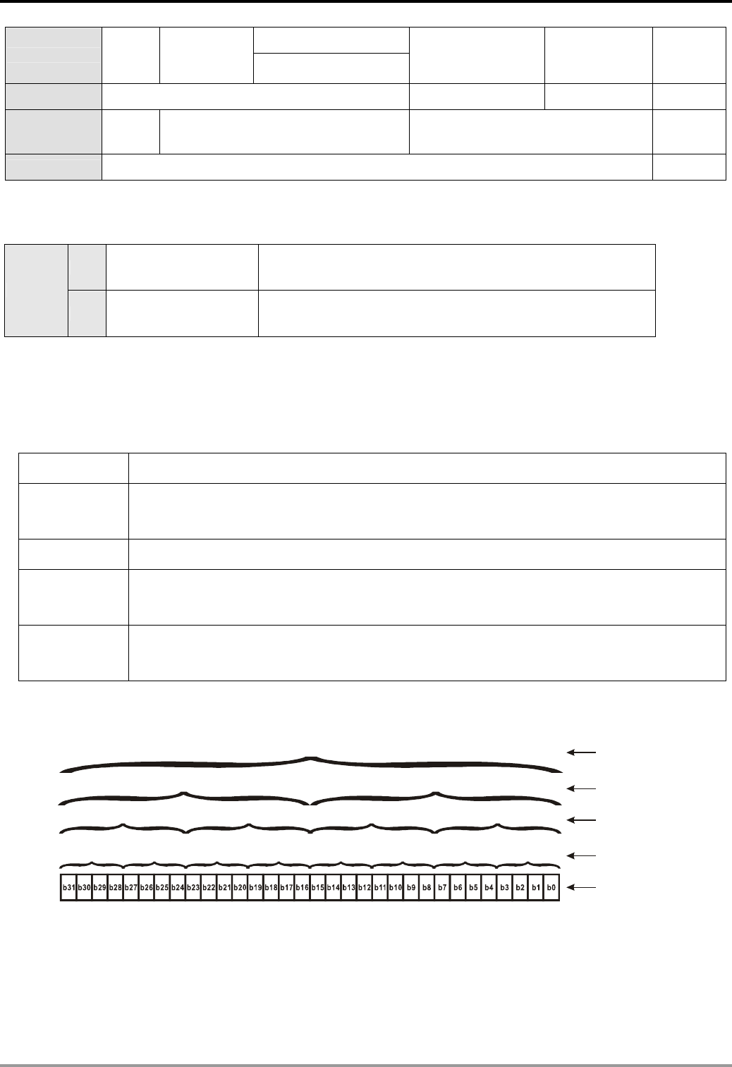
2 Functions of Devices in DVP-PLC
Clear when M1033 = Off
Non-latched Clear Unchanged Clear Unchanged 0
Remain unchanged when
M1033 = On
Latched Unchanged Unchanged Clear 0
Special M, Initial
setting
Special D, Initial Unchanged Unchanged
index register
File Register Unchanged 0
2.2 Values, Constants [K] / [H]
K-32,768 ~ K32,767 (16-bit operation)
K Decimal form K-2,147,483,648 ~ K2,147,483,647 (32-bit operation)
Constant
H0 ~ HFFFF (16-bit operation)
H Hexadecimal form H0 ~ HFFFFFFFF (32-bit operation)
For different control purposes, there are five types of values inside DVP-PLC for executing the operations. See
the explanations bellows for the functions and works of every type of value.
1. Binary value (BIN)
All the operations and storage of values in PLC are conducted in BIN. Belows are the terms for BIN values.
The basic unit for a BIN value, either 1 or 0.
Bit:
Composed of 4 continuous bits (e.g. b3 ~ b0). Presented as the decimal value 0 ~ 9 of a digit
or 0 ~ F in hex.
Nibble:
Composed of 2 continuous nibble (i.e. 8 bits, b7 ~ b0). Presented as 00 ~ FF in hex.
Byte:
Composed of 2 continuous bytes (i.e. 16 bits, b15 ~ b0). Presented as 4-digit 0000 ~ FFFF in
hex.
Word:
Composed of 2 continuous words (i.e. 32 bits, b31 ~ b0). Presented as 8 digit 00000000 ~
FFFFFFFF.
Double word:
Bit, nibble, byte, word, and double word in a binary system:
NB0NB1NB2NB3NB4NB5NB6NB7
BY3 BY2 BY1 BY0
W1
DW
W0
Double Word
Word
Byte
Nibble
Bit
2. Octal value (OCT)
The No. of external input and output terminals in DVP-PLC is numbered in octal system.
For example:
External input: X0 ~ X7, X10 ~ X17…(device No.)
External output: Y0 ~ Y7, Y10 ~ Y17…(device No.)
DVP-PLC Application Manual
2-8

2 Functions of Devices in DVP-PLC
3. Decimal value (DEC)
Occassions of using decimal values in DVP-PLC:
Set value in timer T and counter C, e.g. TMR C0 K50 (constant K)
No. of device S, M, T, C, D, E, F, P, I, e.g. M10, T30. (device No.)
Operands in application instructions, e.g. MOV K123 D0 (constant K)
4. Binary code decimal (BCD)
A decimal datum is presented by a nibble or 4 bits. Therefore, a continuous 16 bits can be presented as a 4-digit
decimal value. BCD is mainly used on reading the input value from the DIP switch or the data output to a 7-section
display.
5. Hexadecimal value (HEX)
Occassion of using hexadecimal values:
Operands in application instructions, e.g. MOV H1A2B D0 (constant H)
Constant K:
“K” is normally placed before a decimal value in the PLC. For example, K100 refers to a decimal value, 100.
Exception:
K and bit devices X, Y, M and S can combine into data in bit, byte, word or double word, e.g. K2Y10, K4M100.
Here K1 refers to a 4-bit data and K2 ~ K4 refer to 8-bit, 12-bit and 16-bit data.
Constant H:
“H” is normally placed before a hexadecimal value in the PLC. For example, H100 refers to a hexadecimal value,
100.
Reference table:
Binary Octal Decimal Binary Code Decimal Hexadecimal
(BIN) (OCT) (DEC) (BCD) (HEX)
Constant K, For DIP switch and 7-section
display
No. of device No. of device M, S, T, C,
D, E, F, P, I
Constant H
For PLC internal operation X, Y
0000 0000 0 0 0 0 0 0 0 0 0 0 0
0000 0001 1 1 0 0 0 0 0 0 0 1 1
0000 0010 2 2 0 0 0 0 0 0 1 0 2
0000 0011 3 3 0 0 0 0 0 0 11 3
0000 0100 4 4 0 0 0 0 0 1 0 0 4
0000 0101 5 5 0 0 0 0 0 1 0 1 5
0000 0110 6 6 0 0 0 0 0 11 0 6
0000 0111 7 7 0 0 0 0 0 1 1 1 7
0000 1000 10 8 0 0 0 0 1 0 0 0 8
0000 1001 11 9 0 0 0 0 1 0 0 1 9
0000 1010 12 10 0 0 0 1 0 0 0 0 A
0000 1011 13 11 0 0 0 1 0 0 0 1 B
0000 1100 14 12 0 0 0 1 0 0 1 0 C
0000 1101 15 13 0 0 0 1 0 0 11 D
0000 1110 16 14 0 0 0 1 0 1 0 0 E
0000 1111 17 15 0 0 0 1 0 1 0 1 F
0001 0000 20 16 0 0 0 1 0 11 0 10
0001 0001 21 17 0 0 0 1 0 1 1 1 11
: : : : :
DVP-PLC Application Manual 2-9
2 Functions of Devices in DVP-PLC
Binary Octal Decimal Binary Code Decimal Hexadecimal
(BIN) (OCT) (DEC) (BCD) (HEX)
Constant K, For DIP switch and 7-section
display
No. of device No. of device M, S, T, C,
D, E, F, P, I
Constant H
For PLC internal operation X, Y
: : : : :
: : : : :
0 1 1 0 0 0 1 1 143 99 1 0 0 1 1 0 0 1 63
2.3 Numbering and Functions of External Input/Output Contacts [X] / [Y]
No. of input/output contacts (in octal):
The No. of input and output contacts on the PLC MPU starts from X0 and Y0. The range of the No. varies upon
the number of points on the MPU. For I/O extension units, the No. of input and output contacts is calculated according
to its connection sequence with the MPU.
ES/EX/SS series MPU:
Model DVP-14ES DVP-14SS DVP-20EX DVP-24ES DVP-32ES DVP-40ES DVP-60ES I/O Extension Unit
X0 ~ X7
(8 points)
X0 ~ X7
(8 points)
X0 ~ X7
(8 points)
X0 ~ X17
(16 points)
X0 ~ X17
(16 points)
X0 ~ X27
(24 points)
X0 ~ X43
(36 points)
X20/30/50 ~ X177
(Note)
Input X
Y0 ~ Y5
(6 points)
Y0 ~ Y5
(6 points)
Y0 ~ Y5
(6 points)
Y0 ~ Y7
(8 points)
Y0 ~ Y17
(16 points)
Y0 ~ Y17
(16 points)
Y0 ~ Y27
(24 points)
Y20/30 ~ Y177
(Note)
Output Y
Note: The input points on I/O extension units start from X20 and output points from Y20, except input points on
DVP-40ES start from X30 and output from Y20; input points on DVP-60ES start from X50 and output from Y30. The No. of
input/output points on the I/O extension units increases by 8’s multiple. If the number of points is less than 8, it will be
counted as 8.
SA/SX/SC series MPU:
Model DVP-10SX (Note1) DVP-12SA DVP-12SC I/O Extension Unit (Note 2)
Input X X0 ~ X3 (4 points) X0 ~ X7 (8 points) X0 ~ X5, X10 ~ X11 (8 points) X20 ~ X177
Output Y Y0 ~ Y1 (2 points) Y0 ~ Y3 (4 points) Y0 ~ Y1, Y10 ~ Y11 (4 points) Y20 ~ Y177
Note 1: Besides 4DI and 2DO, SX series MPU has also 2AI (12-bit) and 2AO (12-bit) of analog input/output.
Note 2: SX/SA/SC series MPU share the extension units with SS series MPU. The input points on I/O extension units start
from X20 and output points start from Y20. The calculation on the No. of I/O points is the same as that in SS series.
EH series MPU:
Model DVP-16EH DVP-20EH
(Note 1)
DVP-32EH
(Note1, 2) DVP-40EH DVP-48EH DVP-64EH
I/O
DVP-80EH Extension
Unit (Note 3)
X0 ~ X7 X0 ~ X13 X0 ~ X17 X0 ~ X27 X0 ~ X27 X0 ~ X37 X0 ~ X47 X※~X377
Input X (8 points) (12 points) (16 points) (24 points) (24 points) (32 points) (40 points)
Y0 ~ Y7 Y0 ~ Y7 Y0 ~ Y17 Y0 ~ Y17 Y0 ~ Y27 Y0 ~ Y37 Y0 ~ Y47 Y※~Y377
Output Y (8 points) (8 points) (16 points) (16 points) (24 points) (32 points) (40 points)
Note 1: The output type of 20EH00T and 32EH00T is transistor, among which Y0 and Y2 are high-speed transistor output
(200kHz) and other outputs are normal transistor output (10kHz). The output type of other MPUs with 16/48/64/80 points
is transistor and all outputs are normal transistor output (10kHz).
Note 2: The terminal layouts of 32EH00T, 32EH00R and 32EH00M are different. See the instruction sheets of EH series
MPU. In 32EH00M, CH0 (Y0, Y1) and CH1 (Y2, Y3) are high-speed differential output (200kHz).
Note 3: The start No. of the input and output points on the I/O extension unit resumes from the last No. in the MPU. The
start No. of input points on the I/O extension unit of DVP-16EH and DVP-20EH start from X20 and output points start from
Y20. The No. on the I/O extension unit are in sequence, with max. input point No. X377 and max. output point No. Y377.
EH2 series MPU:
DVP-20EH2 DVP-32EH2 DVP-40EH2 I/O Extension
Model DVP-16EH2 DVP-48EH2 DVP-64EH2 DVP-80EH2
(Note 1) (Note1) (Note 2) Unit (Note 3)
DVP-PLC Application Manual
2-10

2 Functions of Devices in DVP-PLC
X0 ~ X7 X0 ~ X13 X0 ~ X17 X0 ~ X27 X0 ~ X27 X0 ~ X37 X0 ~ X47 X※~X377
Input X (8 points) (12 points) (16 points) (24 points) (24 points) (32 points) (40 points)
Y0 ~ Y7 Y0 ~ Y7 Y0 ~ Y17 Y0 ~ Y17 Y0 ~ Y27 Y0 ~ Y37 Y0 ~ Y47 Y※~Y377
Output Y (8 points) (8 points) (16 points) (16 points) (24 points) (32 points) (40 points)
Note 1: The output type of 20EH00T2 and 32EH00T2 is transistor, among which Y0 and Y2 are high-speed transistor
output (200kHz) and other outputs are normal transistor output (10kHz). The output type of other MPUs with 16/48/64/80
points is transistor and all outputs are normal transistor output (10kHz).
Note 2: The output type of 40EH00T2 is transistor, among which CH0 (Y0, Y1), CH1 (Y2, Y3), CH2 (Y4) and CH3 (Y6)
are high-speed transistor output (200kHz). The output type of other output points is normal transistor output (10kHz). The
high-speed inputs CH0 (X0, X1), CH1 (X4, X5), CH2 (X10, X11) and CH3 (X14, X15) are able to achieve max. frequency
200kHz.
Note 3: The I/O points on I/O extension units follow the I/O points on MPUs. The input points on DVP-16EH2 and
DVP-20EH2 start from X20 and output points from Y20. The I/O points on I/O extension units are numbered in sequence.
The maximal input number is X377, and the maximal output number is Y377.
SV/SV2 series MPU:
Model DVP-28SV (Note 1) I/O Extension Unit (Note 2)
Input X X0 ~ X17 (16 points) X20 ~ X377
Output Y Y0 ~ Y13 (12 points) Y20 ~ Y377
Note 1: The output type of 28SV11T is transistor output, among which CH0 (Y0, Y1), CH1 (Y2, Y3), CH2 (Y4) and CH3
(Y6) are high-speed transistor output (200kHz); others are normal transistor output (10kHz).
Note 2: The input points on I/O extension units start from X20 and output points start from Y20. The calculation on the No.
of I/O points is the same as that in SS series.
EH3 series MPU:
Model DVP-16EH3 DVP-20EH3 DVP-32EH3
(Note 3) DVP-40EH3 DVP-48EH3 I/O Extension
DVP-64EH3 DVP-80EH3 Unit (Note 4)
Input X X0~X7 X0~X13 X0~X17 X0~X27 X0~X27 X0~X37 X0~X47 X※~X377
(Note 1) (8 points) (12 points) (16 points) (24 points) (24 points) (32 points) (40 points)
Output Y Y0~Y7 Y0~Y7 Y0~Y17 Y0~Y17 Y0~Y27 Y0~Y37 Y0~Y47 Y※~Y377
(Note 2) (8 points) (8 points) (16 points) (16 points) (24 points) (32 points) (40 points)
Note 1: High-speed input points (X0~X17) on the MPU: The 200KHz input points on 16EH3 are Ch0(X0/X1) and
Ch1(X4/X5); the 200KHz input points on 20EH3 are Ch0(X0/X1) and Ch1(X4/X5); the 20KHz input point on 20EH3 is
Ch2(X10/X11); the 200KHz input points on other MPUs are Ch0(X0/X1), Ch1(X4/X5), Ch2(X10/X11) and Ch3(X14/X15).
X2~X17 which are not listed above are 10KHz input points.
Note 2: High-speed output points (Y0~Y17) on the MPU: The 200KHz output points on 16EH3, 20EH3 and 32EH3 are
Ch0(Y0) and Ch1(Y2); the 200KHz output points on 40EH3, 48EH3, 64EH3, and 80EH3 are Ch0(Y0/Y1), Ch1(Y2/Y3),
Ch2(Y4), and CH3(Y6). Other output points which are not listed are 10KHz output points.
Note 2: The high-speed input points Ch0(X0/X1) and Ch1(X4/X5) on DVP32EH00M3 are 200KHz differential input points;
Ch2(X10/X11) and Ch3(X14/X15) are 200KHz open collector input points; other input points are 10KHz open collector
input points. The high-speed output points Ch0(Y0/Y1) and Ch1(Y2/Y3) are 200KHz differential output points; other output
points are 10KHz open collector output points.
Note 4: The I/O points on I/O extension units follow the I/O points on MPUs. The input points on DVP-16EH3 and
DVP-20EH3 start from X20 and output points from Y20. The I/O points on I/O extension units are numbered in sequence.
The maximal input number is X377, and the maximal output number is Y377.
Input relay X0 ~ X377
The numbering of input relays (or input terminals) is in octal form. EH series MPU can have up to 256
points and the range is: X0 ~ X7, X10 ~ X17, …, X370 ~ X377.
Output relay Y0 ~ Y377
The numbering of output relays (or output terminals) is also in octal form. EH2 series MPU can have up to
256 points and the range is: Y0 ~ Y7, Y10 ~ Y17, …, Y370 ~ Y377.
Functions of input contact X
The input contact X is connected to the input device and reads the input signals into the PLC. There is no
DVP-PLC Application Manual 2-11
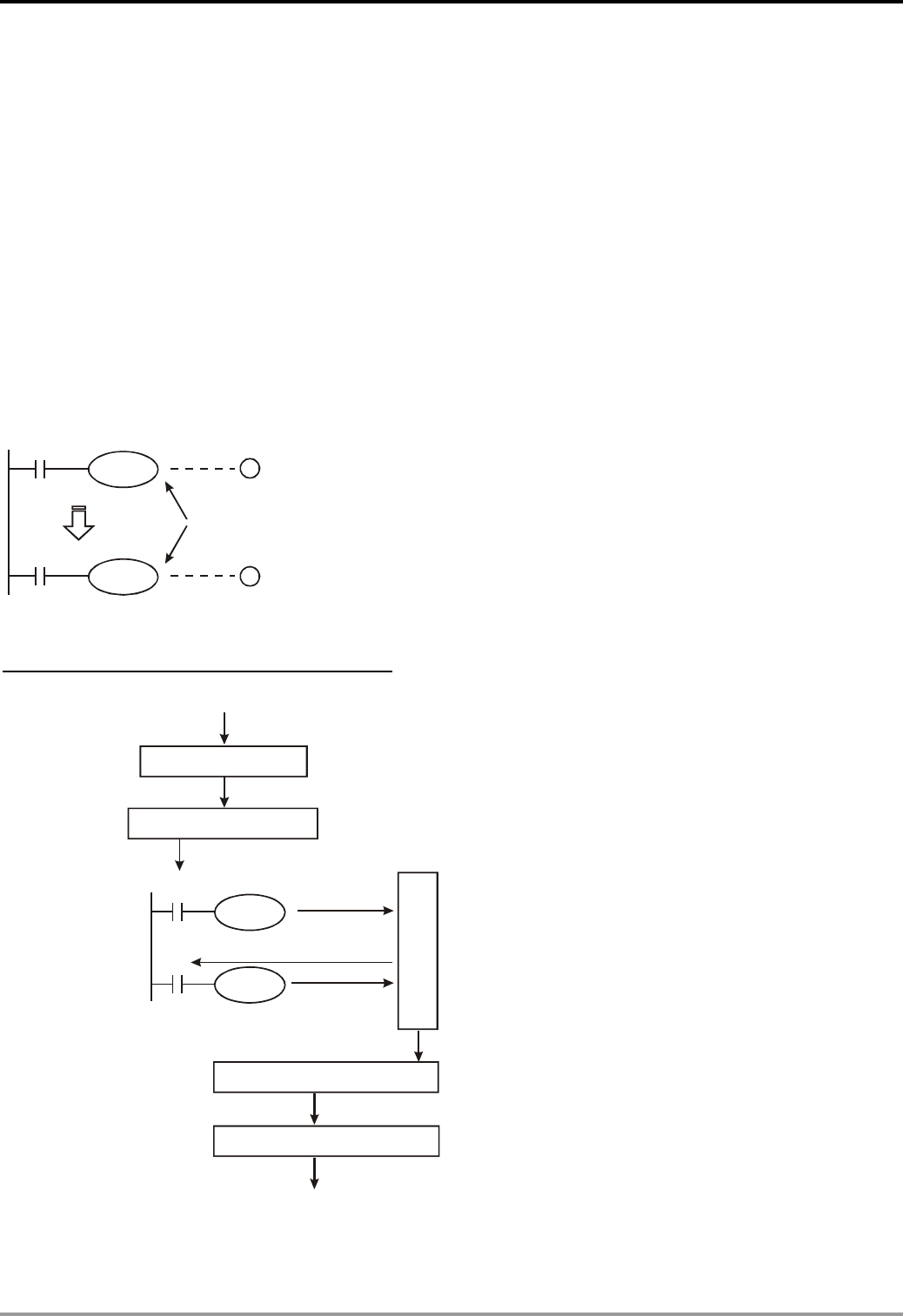
2 Functions of Devices in DVP-PLC
limitation on the times of using contact A or B of input contact X in the program. On/Off of the input contact X
only changes with On/Off of the input device. You cannot use the peripheral devices (HPP or WPLSoft) to force
On/Off of the input contact X.
The special relay M1304 in SS/ES/EX/SA/SX/SC/EH2/SV/EH3/SV2 series MPU allows the peripheral
devices HPP or WPLSoft to set up On/Off of the MPU input contact X, but the PLC will not be able to receive
external input signals at this time.
Functions of output contact Y
Output contact Y sends out On/Off signals to drive the load connected to output contact Y. There are two
types of output contacts, relay and transistor. Thereis no limitation on the times of using contact A or B of output
contact Y in the program, but the No. of output coil Y can only be used once in the program; otherwise
according to the scan principle of the PLC program, the output status will be determined by the circuit of the last
output Y in the program.
The output of Y0 will be determined by circuit 2, i.e. On/Off of X10 will
determine the output status of Y0.
X0
X10
Y0
Y0
1
2
Y0 is repeated
The Handling Process of PLC Program (Batch I/O)
X0
Y0
Y0
M0
X input
Input terminal
Read into memory
Input signal memory
Device Memory
Read X0 status from memory
Write in Y0 status
Read Y0 status from memory
Write in M0 status
Regenerate output
Program processing
Regenerate input signal
Output
Y output
Output terminal
Output latched memory
Regenerate input signal
1. Before the execution of the program, PLC reads the
On/Off status of the external input signals into the
input signal memory at a time.
2. The On/Off status of the input signal during the
execution of the program will not change the signal
status in the input signal memory. The new On/Off
status will be read in in the next scan.
3. There will be approximately a 10ms delay from the
On→Off or Off→On changes to the status being
recognized by the contact in the program. The delay
time may be affected by the scan time in the
program.
Program processing
After the PLC reads the On/Off status of every input
signal in the input signal memory, it will start to execute
every instruction in the program in order starting from
address 0. The execution result (On/Off of every output
coil) will be stored in order into the device memory.
DVP-PLC Application Manual
2-12

2 Functions of Devices in DVP-PLC
Regenerate output
1. When the program executes to END instruction, it
will send the On/Off status of Y in the device memory
to the output latched memory. The output latched
memory is the coil of the output relay.
2. There will be a 10ms delay from OnÆOff or OffÆOn
of the relay coil to the On/Off status of the contact.
3. There will be a 10 ~ 20us delay from OnÆOff or
OffÆOn of the transistor module to the On/Off status
of the contact.
2.4 Numbering and Functions of Auxiliary Relays [M]
No. of auxiliary relays (in decimal)
ES/EX/SS series MPU:
General purpose M0 ~ M511, M768 ~ M999, 744 points. Fixed to be non-latched.
Latched M512 ~ M767, 256 points. Fixed to be latched. Total 1,280
points
Auxiliary relay M
Special purpose M1000 ~ M1279, 280 points. Some are latched.
SA/SX/SC series MPU:
General purpose M0 ~ M511, 512 points. Fixed to be non-latched.
Latched M512 ~ M999, M2000 ~ M4095, 2,584 points. Can be modified to be
non-latched by setting up parameters.
Total 4,096
points
Auxiliary relay M
Special purpose M1000 ~ M1999, 1000 points. Some are latched.
EH2/SV/EH3/SV2 series MPU:
M0 ~ M499, 500 points. Can be modified to be latched by setting up
parameters.
General purpose
Latched M500 ~ M999, M2000 ~ M4095, 2,596 points. Can be modified to be
non-latched by setting up parameters.
Total 4,096
points
Auxiliary relay M
Special purpose M1000 ~ M1999, 1,000 points. Some are latched.
Functions of auxiliary relays:
Both auxiliary relay M and output relay Y have output coils and contact A, B, and there is no limitation on the
times of using the contact. You can use auxiliary relay M to assemble a control loop, but it cannot directly drive the
external load. There are three types of auxiliary relays:
1. General purpose auxiliary relay: If the relay encouters power cut during the operation of the PLC, its status will
be reset to Off and stay Off when the power is on again.
2. Latched auxiliary relay: If the relay encounters power cut during the operation of the PLC, its status will be
retained and stay at the status before the power cut when the power is on again.
3. Special purpose auxiliary relay: Every relay of this kind has its specific function. Do not use undefined special
purpose auxiliary relay. See 2.10 for special puspose auxiliary relay of all series MPU and 2.11 for its functions.
2.5 Numbering and Functions of Step Relays [S]
DVP-PLC Application Manual 2-13

2 Functions of Devices in DVP-PLC
No. of step relays (in decimal)
ES/EX/SS series MPU:
Initial latched S0 ~ S9, 10 points. Fixed to be latched.
Zero return
latched S10 ~ S19, 10 points, used with IST instruction. Fixed to be latched. Total 128
points
Step relay S
Latched S20 ~ S127, 108 points. Fixed to be latched.
SA/SX/SC series MPU:
Initial S0 ~ S9, 10 points. Fixed to be non-latched. Total
Step relay S 1,024 points
Zero return S10 ~ S19, 10 points, used with IST instruction. Fixed to be non-latched.
General purpose S20 ~ S511, 492 points. Fixed to be non-latched.
Latched S512 ~ S895, 384 points. Can be modified to be non-latched by setting
up parameters.
Total
Step relay S 1,024 points
Alarm S896 ~ S1023, 128 points. Fixed to be latched.
EH2/SV/EH3/SV2 series MPU:
S0 ~ S9, 10 points. Can be modified to be latched by setting up
parameters.
Initial
S10 ~ S19, 10 points, used with IST instruction. Can be modified to be
latched by setting up parameters.
Zero return
General purpose S20 ~ S499, 480 points. Can be modified to be latched by setting up
parameters.
Latched S500 ~ S899, 400 points. Can be modified to be non-latched by setting
up parameters.
Total
Step relay S 1,024 points
S900 ~ S1023, 124 points. Can be modified to be latched by setting up
parameters.
Alarm
Functions of step relays:
The step relay S can easily set up the procedure in the industrial automation, which is the most basic device in
the the sequential function chart (SFC) and has to be used with STL, RET instructions.
The device No. of S is S0 ~ S1023 (total 1,024 points) and both step relay S and output relay Y have output coils
and contact A, B, and there is no limitation on the times of using the contact. S cannot directly drive the external load.
When the step relay is not used in SFC, it can be used as a normal auxiliary relay. There are four types of step relays:
1. Initial step relay: S0 ~ S9, total 10 points, used for initial steps.
2. Zero return step relay: S10 ~ S19, total 10 points. S10 ~ S19 are planned for zero return when used with API 60
IST instruction in the program. If they are not used with IST, they will become normal step relays.
3. General purpose step relay: S20 ~ S511, total 492 points (for SA/SX/SC series MPU); S20 ~ S499, total 480
points (for EH2/SV/EH3/SV2 series MPU). Used for general purposes in SFC and their status will all be cleared
when the operation of the PLC encounters power cut.
4. Latched step relay: S512 ~ S895, total 384 points (for SA/SX/SC series MPU); S20 ~ S127, total 108 points (for
ES/EX/SS series MPU); S500 ~ S899, total 400 points (for EH2/SV/EH3/SV2 series MPU). Used for latched
function in SFC and their status will all be retained when the operation of the PLC encounters power cut. They will
remain at the status before the power cut when the PLC is powered again.
5. Alarm step relay: S896 ~ S1023, total 128 points (for SA/SX/SC series MPU); S900 ~ S1023, total 124 points
(for EH2/SV/EH3/SV2 series MPU). Used with alarm driving instruction API 46 ANS as an alarm contact for
DVP-PLC Application Manual
2-14
2 Functions of Devices in DVP-PLC
recording the alarm messages or eliminating external malfunctions.
2.6 Numbering and Functions of Timers [T]
No. of timers (in decimal)
ES/EX/SS series MPU:
100ms general purpose T0 ~ T63, 64 points
10ms general purpose T64 ~ T126, 63 points (M1028 = On:10ms; M1028 = Off:100ms) Total
Timer T 128 points
1ms general purpose T127, 1 point
SA/SX/SC series MPU:
T0 ~ T199, 200 points. T192 ~ T199 are the timers for subroutine. Fixed to
be non-latched
100ms general purpose
100ms accumulative T250 ~ T255, 6 points. Fixed to be latched.
10ms general purpose T200 ~ T239, 40 points. Fixed to be non-latched
10ms accumulative T240 ~ T245, 6 points. Fixed to be latched.
Total
Time T 256 points
1ms accumulative T246 ~ T249, 4 points. Fixed to be latched.
EH2/SV/EH3/SV2 series MPU:
T0 ~ T199, 200 points. Can be latched by setting up parameters.
100ms general purpose T192 ~ T199 are the timers for subroutine.
100ms accumulative T250 ~ T255, 6 points. Fixed to be latched.
10ms general purpose T200 ~ T239, 40 points. Can be latched by setting up parameters.
10ms accumulative T240 ~ T245, 6 points. Fixed to be latched.
Total
Timer T 256 points
1ms accumulative T246 ~ T249, 4 points. Fixed to be latched.
Functions of timers:
The units of the timer are 1ms, 10ms and 100ms and the counting method is counting up. When the present
value in the timer equals the set value, the output coil will be On. The set value should be a K value in decimal and the
data register D can also be a set value.
The actual set time in the timer = timing unit × set value
There are three types of timers:
1. General purpose timer:
For ES/SA series MPU: The timer executes once when the program reaches END instruction. When TMR
instruction is executed, the output coil will be On when the timing reaches its target.
For EH2/SV/EH3/SV2 series MPU: The timer executes once when the program reaches TMR instruction. When
TMR instruction is executed, the output coil will be On when the timing reaches its target.
T0
Y0
X0
TMR T0 K100
When X0 = On, The PV in timer T0 will count up by
100ms. When the PV = SV K100, the output coil T0
will be On.
DVP-PLC Application Manual 2-15
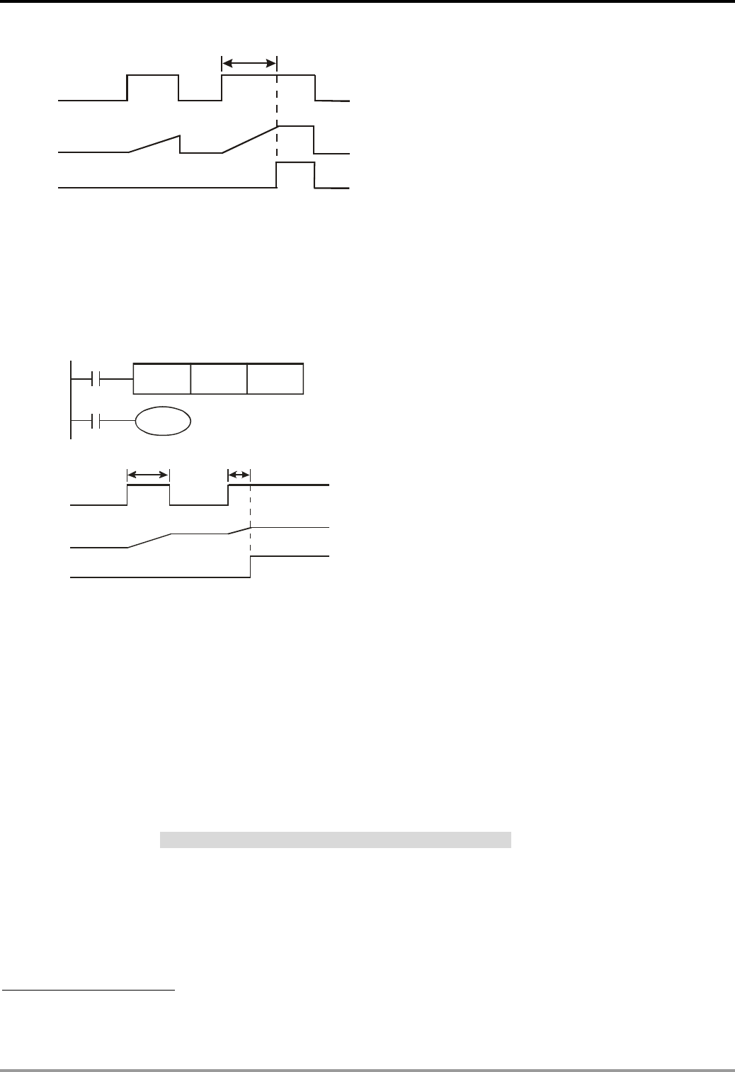
2 Functions of Devices in DVP-PLC
X0
Y0
T0
10 secs
PV
SV K100
When X0 = Off or the power is off, the PV in timer T0
will be cleared as 0, and the output coil T0 will be
Off.
2. Accumulative type timer:
For ES/SA series MPU: The timer executes once when the program reaches END instruction. When TMR
instruction is executed, the output coil will be On when the timing reaches its target.
For EH2/SV/EH3/SV2 series MPU: The timer executes once when the program reaches TMR instruction. When
TMR instruction is executed, the output coil will be On when the timing reaches its target.
T250
Y0
X0
TMR T250 K100
X0
T2
Y0
PV
SV K100
T1+T2=10sec
T250
T1
When X0 = On, The PV in timer T250 will count up
by 100ms. When the PV = SV K100, the output coil
T0 will be On.
When X0 = Off or the power is off, timer T250 will
temporarily stop the timing and the PV remain
unchanged. When X0 is On again, the timing will
resume and the PV will count up and when the PV =
SV K100, the output coil T0 will be On.
3. Subrountine timer:
Timer T192 ~ T199 are used in subrountines or interruption subroutines.
For SA series MPU: The timer executes once when the program reaches END instruction. When END instruction
is executed, the output coil will be On when the timing reaches its target.
For EH2/SV/EH3/SV2 series MPU: The timer executes once when the program reaches TMR or END instruction.
When TMR or END instruction is executed, the output coil will be On when the PV equals SV.
If the general purpose timer is used in a subroutine or interruption subroutine but the subroutine is not being
executed, the timer will not be able to time correctly.
How to designate SV: The actual set time in the timer = timing unit × set value
a) Designating constant K: SV is a constant K
b) Indirectly designating D: SV is data register D
2.7 Numbering and Functions of Counters [C]
No. of counters (in decimal)
ES/EX/SS series MPU:
DVP-PLC Application Manual
2-16

2 Functions of Devices in DVP-PLC
16-bit counting up, for
general purpose C0 ~ C111, 112 points. Fixed to be non-latched.
Counter C 16-bit counting up, for
latched C112 ~ C127, 16 points. Fixed to be latched.
1-phase 1 input C235 ~ C238, C241, C242, C244, 7 points. Fixed to be
latched.
1-phase 2 inputs C246, C247, C249, 3 points. Fixed to be latched.
Total
141 points
32-bit counting up/down
high-speed counter C
2-phase 2 inputs C251, C252, C254, 3 points. Fixed to be latched.
SA/SX/SC series MPU:
16-bit counting up, for
general purpose C0 ~ C95, 96 points. Fixed to be non-latched.
16-bit counting up, for
latched
C96 ~ C199, 104 points. Can be modified to be non-latched
by setting up parameters.
32-bit counting
up/down, for general
purpose
C200 ~ C215, 16 points. Fixed to be non-latched.
Total
Counter C 235 points
32-bit counting
up/down, for latched
C216 ~ C234, 19 points. Can be modified to be non-latched
by setting up parameters.
1-phase 1 input, for
latched C235 ~ C242, C244, 9 points
1-phase 2 inputs, for
latched C246, C247, C249, 3 points
(SA/SX) 32-bit counting Total 16
points
up/down high-speed
counter C 2-phase 2 inputs, for
latched C251 ~ C254, 4 points
1-phase 1 input, for
latched C235 ~ C245, 11 points
1-phase 2 inputs, for
latched C246 ~ C250, 4 points
Can be modified to be
non-latched by setting up
parameters.
(SC) 32-bit counting Total 19
points
up/down high-speed
counter C 2-phase 2 inputs, for
latched C251 ~ C255, 4 points
EH2/SV/EH3/SV2 series MPU:
16-bit counting up, for
general purpose
C0 ~ C99, 100 points. Can be modified to be latched by
setting up parameters.
16-bit counting up, for
latched
C100 ~ C199, 100 points. Can be modified to be non-latched
area by setting up parameters.
32-bit counting
up/down, for general
purpose
C200 ~ C219, 20 points. Can be modified to be latched by
setting up parameters.
Counter C
32-bit counting
up/down, for latched
C220 ~ C234, 15 points. Can be modified to be non-latched
by setting up parameters. Total
Software 1-phase 1
input C235 ~ C240, 6 points
Hardware 1-phase 1
input C241 ~ C244, 4 points
Hardware 1-phase 2
inputs C246 ~ C249, 4 points
253 points
Can be modified to be
non-latched by setting up
parameters.
32-bit counting up/down
high-speed counter C
Hardware 2-phase 2
inputs C251 ~ C254, 4 points
Features of counter:
16 bits counters 32 bits counters
Type General purpose General purpose High speed
Counting direction Counting up Counting up, counting down
Set value 0 ~ 32,767 -2,147,483,648 ~ +2,147,483,647
SV designation Constant K or data register D Constant K or data register D (designating 2 values)
DVP-PLC Application Manual 2-17
2 Functions of Devices in DVP-PLC
16 bits counters 32 bits counters
Counting will stop when the SV is
reached.
Present value Counter will continue when the SV is reached.
On and keeps being On when counting up reaches SV.
On and being retained when the
counting reaches SV.
Output contact Reset to Off when counting down reaches SV.
Reset PV will be return to 0 when RST instruction is executed and the contact will be reset to Off.
Acts immediately when the
counting reaches its target,
has nothing to do with the scan
period.
Acts when the scanning is
completed.
Contact action Acts when the scanning is completed.
Functions of counters:
When the pulse input signals of the counter go from Off to On and the present value in the counter equals the
set value, the output coil will be On. The set value should be a K value in decimal and the data register D can also be
a set value.
16-bit counters C0 ~ C199:
1. The setup range of 16-bit counter: K0 ~ K32,767. K0 is the same as K1. The output contact will be On
immediately when the first counting starts.
2. PV in the general purpose counter will be cleared when the power of the PLC is switched off. If the counter is a
latched type, the counter will retain the PV and contact status before the power is off and resume the counting
after the power is on again.
3. If you use MOV instruction, WPLSoft or HPP to send a value bigger than the SV to the present value register of
C0, next time when X1 goes from Off to On, the contact of counter C0 will be On and its PV will equal SV.
4. The SV in the counter can be constant K (set up directly) or the values in register D (set up indirectly, excluding
special data registers D1000~ D1999).
5. If you set up a constant K as the SV, it should be a positive value. Data register D as SV can be positive or
negative. When the PV reaches up to 32,767, the next PV will turn to -32,768.
Example:
LD X0
C0
Y0
X1
C0 K5CNT
X0
C0RST
RST C0
LD X1
CNT C0 K5
LD C0
OUT Y0
DVP-PLC Application Manual
2-18
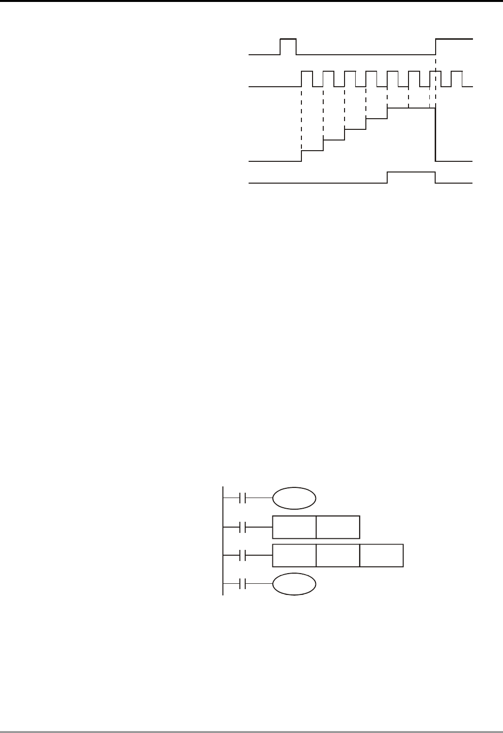
2 Functions of Devices in DVP-PLC
a) When X0 = On, RST instruction will be
executed, PV in C0 will be “0” and the
output contact will be reset to Off.
X0
X1
0
1
2
3
4
5
0
Contacts Y0, C0
PV in C0
SV
b) When X1 goes from Off to On, the PV in
the counter will count up (plus 1).
c) When the counting of C0 reaches SV K5,
the contact of C0 will be On and PV of C0
= SV = K5. The X1 trigger signal comes
afterwards will not be accepted by C0 and
the PV of C0 will stay at K5.
32-bit general purpose addition/subtraction counters C200 ~ C234:
1. The setup range of 32-bit counter: K-2,147,483,648 ~ K2,147,483,647 (not available for ES/EX/SS series MPU).
2. Addition or subtraction of the counters is designated by On/Off status of special auxiliary relays M1200 ~ M1234.
For example, when M1200 = Off, C200 will be an addition counter; when M1200 = On, C200 will be a subtraction
counter.
3. The SV can be constant K or data register D (excluding special data registers D1000 ~ D1999). Data register D as
SV can be a positive or negative value and an SV will occupy two consecutive data registers.
4. PV in the general purpose counter will be cleared when the power of the PLC is switched off. If the counter is a
latched type, the counter will retain the PV and contact status before the power is off and resume the counting
after the power is on again.
5. When the PV reaches up to 2,147,483,647, the next PV will turn to -2,147,483,648. When the PV reaches down to
-2,147,483,648, the next PV will turn to 2,147,483,647.
Example:
LD X10
C200
Y0
X12
C200 K-5DCNT
X11
C200RST
X10
M1200
OUT M1200
LD X11
RST C200
LD X12
CNT C200 K-5
LD C200
OUT Y0
DVP-PLC Application Manual 2-19
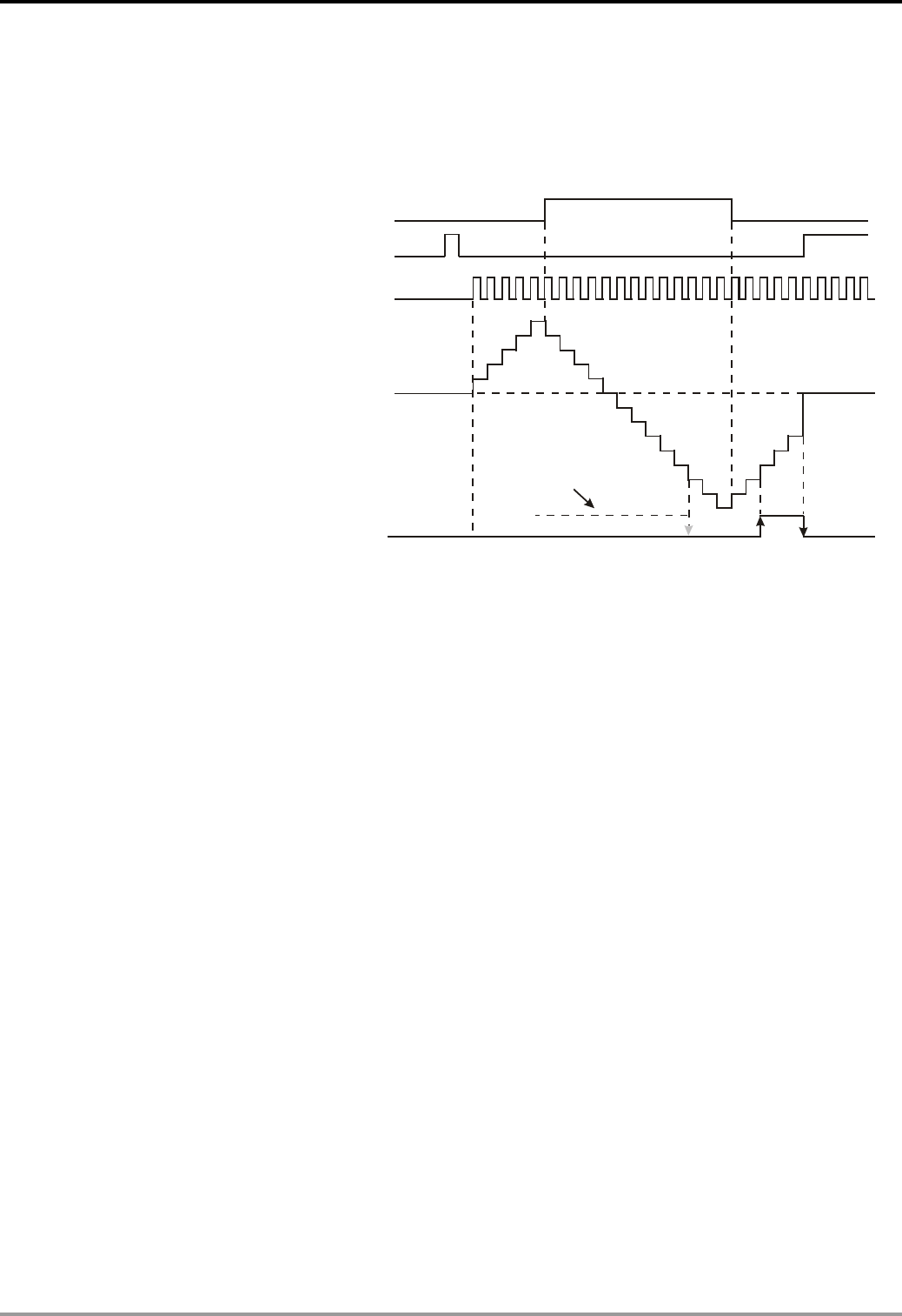
2 Functions of Devices in DVP-PLC
a) X10 drives M1200 to determine
whether C200 is an addition or
subtraction counter.
b) When X11 goes from Off to On, RST
instsruction will be executed and the
PV in C200 will be cleared to “0” and
the contact will be Off.
c) When X12 goes from Off to On, the PV
in the counter will count up (plus 1) or
count down (minus 1).
d) When the PV in C200 changes from
K-6 to K-5, the contact of C200 will go
from Off to On. When the PV in C200
changes from K-5 to K-6, the contact of
C200 will go from On to Off.
e) If you use MOV instruction, WPLSoft
or HPP to send a value bigger than the
SV to the present value register of C0,
next time when X1 goes from Off to
On, the contact of counter C0 will be
On and its PV will equal SV.
X10
X11
X12
01234543210-1-2-3-4-5-6-7-8
0
-7-6-5-4-3
Contacts
Y0, C0
Accumulatively
increasing
Accumulatively
increasing
Progressively
decreasing
PV in
C200
When the output contact
was On.
32-bit high-speed addition/subtraction counters C235 ~ C255:
1. The setup range of 32-bit counter: K-2,147,483,648 ~ K2,147,483,647
2. Addition or subtraction of C235 ~ C244 is designated by On/Off status of special auxiliary relays M1235 ~ M1244.
For example, when M1235 = Off, C235 will be an addition counter; when M1235 = On, C235 will be a subtraction
counter.
3. Addition or subtraction of C246 ~ C255 is designated by On/Off status of special auxiliary relays M1246 ~ M1255.
For example, when M1246 = Off, C246 will be an addition counter; when M1246 = On, C246 will be a subtraction
counter.
4. The SV can be constant K or data register D (excluding special data registers D1000 ~ D1999). Data register D
as SV can be a positive or negative value and an SV will occupy two consecutive data registers.
5. If using DMOV instruction, WPLSoft or HPP to send a value which is large than the setting to any high-speed
counter, next time when the input point X of the counter goes from Off to On, this contact will remain unchanged
and it will perform addition and subtraction with the present value.
6. When the PV reaches up to 2,147,483,647, the next PV will turn to -2,147,483,648. When the PV reaches down
to -2,147,483,648, the next PV will turn to 2,147,483,647.
DVP-PLC Application Manual
2-20
2 Functions of Devices in DVP-PLC
DVP-PLC Application Manual 2-21
High-speed counters for ES/EX/SS series MPU, total bandwidth: 20kHz
1-phase input 1-phase 2 inputs 2-phase 2 inputs Type
Input C235 C236 C237 C238 C241 C242 C244 C246 C247 C249 C251 C252 C254
X0 U/D U/D U/D U U U A A A
X1 U/D R R D D D B B B
X2 U/D U/D R R R R
X3 U/D R S S S
U: Progressively increasing input A: A phase input S: Input started
D: Progressively decreasing input B: B phase input R: Input cleared
1. Input points X0 and X1 can be planned as counters of higher speed with 1-phase 1 input reaching 20kHz. But the
two counting frequencies added together has to be smaller or equal 20kHz. If the input is a 2-phase 2 input signal,
the counting frequency will be approximately 4kHz. The 1-phase input of high-speed counters X2 and X3 and
reach 10kHz.
2. The use of DHSCS instruction together with DHSCR instruction in ES series MPU cannot exceed 4 times.
High-speed counters for SA/SX series MPU, total bandwidth: 40kHz
1-phase input 1-phase 2 inputs 2-phase 2 inputs Type
Input C235 C236 C237 C238 C239 C240 C241 C242 C244 C246 C247 C249 C251 C252 C253 C254
X0 U/D U/D U/D U U U A A B A
X1 U/D R R D D D B B A B
X2 U/D U/D R R R R
X3 U/D R S S S
X4 U/D
X5 U/D
U: Progressively increasing input A: A phase input S: Input started
D: Progressively decreasing input B: B phase input R: Input cleared
1. The frequency of input points X0 and X1 of 1-phase input can reach up to 20kHz, X2 ~ X5 can reach 10kHz. The
frequency of C251, C252 and C254 of 2-phase input (X0, X1) can reach up to 4kHz. The maximum frequency of
C253 is 25kHz (only supports 4 times frequency counting).
2. Input point X5 has two functions:
a) When M1260 = Off, C240 will be normal U/D high-speed counter.
b) When M1260 = On and DCNT instruction enables C240, X5 will be the shared reset signal for C235 ~ C239.
Counter C240 will continue to receive the input signals from X5.
High-speed counters for SC series MPU, total bandwidth: 130kHz
1-phase input 1-phase 2 inputs 2-phase 2 inputs Type
Input C235 C236 C237 C238 C239 C240 C241 C242 C243 C244 C245 C246 C247 C249 C250 C251 C252 C254 C255
X0 U/D U/D U/D U U U A A A
X1 U/D R R D D D B B B
X2 U/D U/D R R R R
X3 U/D R S S S
X4 U/D
X5 U/D
X10 U/D U A
X11 U/D D B
U: Progressively increasing input A: A phase input S: Input started
D: Progressively decreasing input B: B phase input R: Input cleared
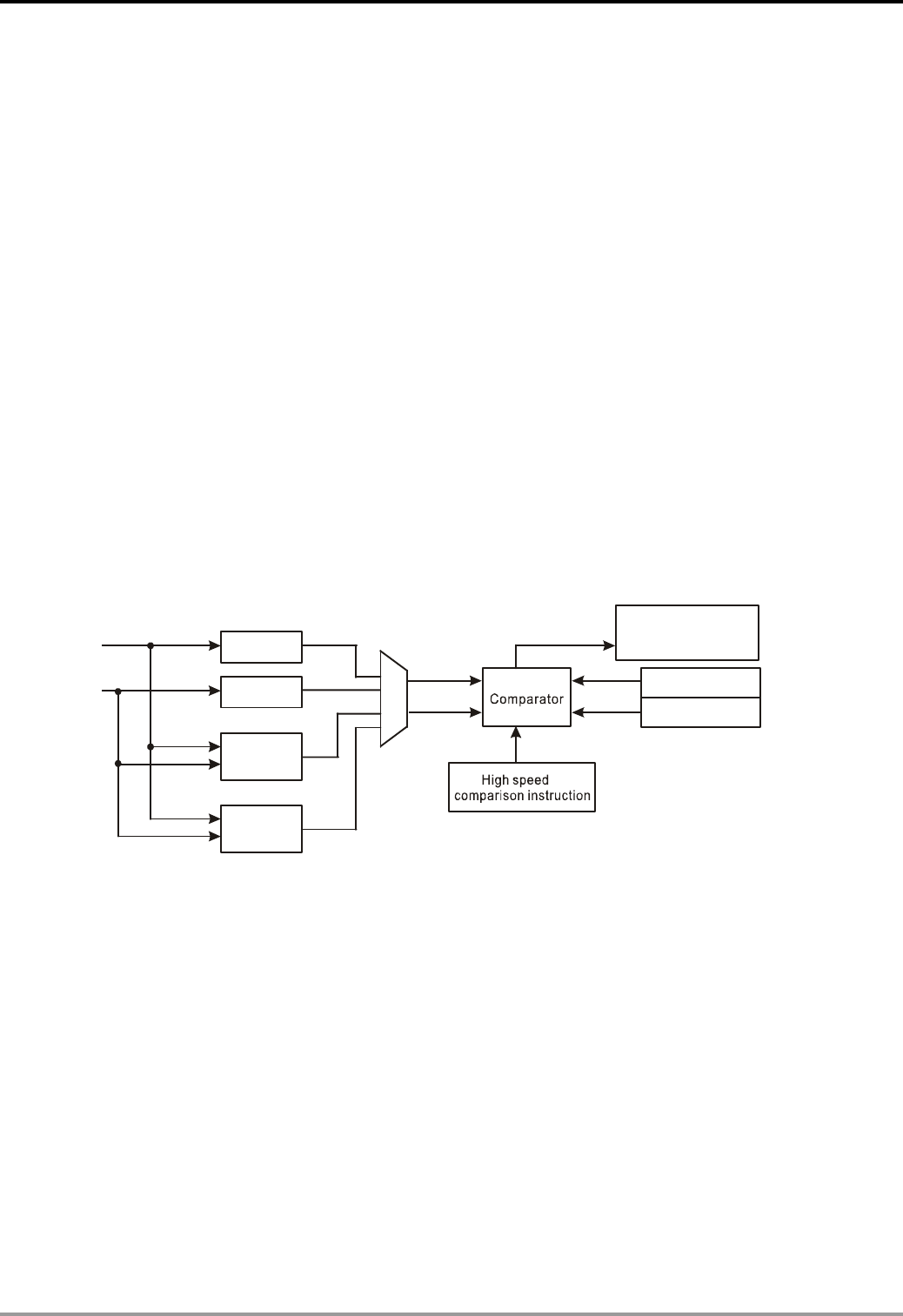
2 Functions of Devices in DVP-PLC
1. The functions of high-speed counters of input points X0 ~ X5 are the same of those in SA/SX series MPU.
2. The maximum frequency of the input points X10 (C243), X11 (C245) and (X10, X11)(C250) of 1-phase input is
100kHz. The total bandwidth of X10 ~ X11 high-speed counting is 130kHz. The maximum input frequency of
C255 (2-phase input X10, X11) is 35kHz.
3. The use of DHSCS instruction together with DHSCR instruction in SA/SX/SC series MPU cannot exceed 6 times.
The use of DHSZ instruction cannot exceed 6 times as well. When DHSCS instruction designates I interruption,
the designated high-speed counter cannot be used in DHSCS, DHSCR and DHSZ instruction.
4. Functions of high-speed counters X10 ~ X11 in SC series MPU:
a) When X10 and X11 are set to be 1-phase 1 input or 1-phase 2 outputs, the maximum frequency can reach
100kHz. When set to be 2-phase 2 inputs, the maximum frequency can reach 35kHz.
b) X10 and X11 can be set to be rising-edge or falling-edge counting. X10 is set by D1166 and X11 by D1167. K0:
rising-edge counting; K1: falling-edge counting; K2: rising-/falling-edge counting (only available in X10).
c) Counting up or down of C243 is determined by On/Off status of M1243 anc that of C245 is determined by
On/Off of M1245. Rising-edge and falling-edge countings cannot be performed at the same time. Rising edge
or falling edge of C250 is determined by the content (K0 or K1) in D1166. C255 can only be used in 4 times
frequency counting and rising-edge and falling-edge triggers are not available for C255.
d) When you use C243 or C245, you will not be able to use C250 or C255, and vice versa.
e) High-speed counter and high-speed comparator:
X10
X11
C243
C245
C250
Output reached
comparison value
S V 10
S V 11
C255
f) Explanations on high-speed counter and high-speed comparator:
(i) When DHSCS and DHSCR instructions use new added high-speed counters, they can only use two
groups of SVs in high speed comparison instruction. Assume you have used the comparison instruction
DHSCS D0 C243 Y10, you can only set another group of instruction DHSCR D2 C243 Y10 or DHSCS D4
C245 Y10.
(ii) When DHSZ instruction uses new added high-speed counters, it can only use one group of SV in the
comparator.
(iii) The number of SVs in high speed comparison instructions offered by SA/SX series MPU will not decrease
owing to the increasing of high-speed counters.
(iv) If the output device of the high-speed comparison instruction DHSCS requires high-speed output, it is
recommended you use Y10 or Y11 for the output. If you use other general devices, the output will delay
for 1 scan period for its setup or clearing. For example, if I0x0 interruption is set, C243 will correspond to
I020, C245 to I040, and C250 and C255 to I060.
(v) The high speed comparison instruction DHSCR is able to clear the counter, but only the counters used in
DVP-PLC Application Manual
2-22
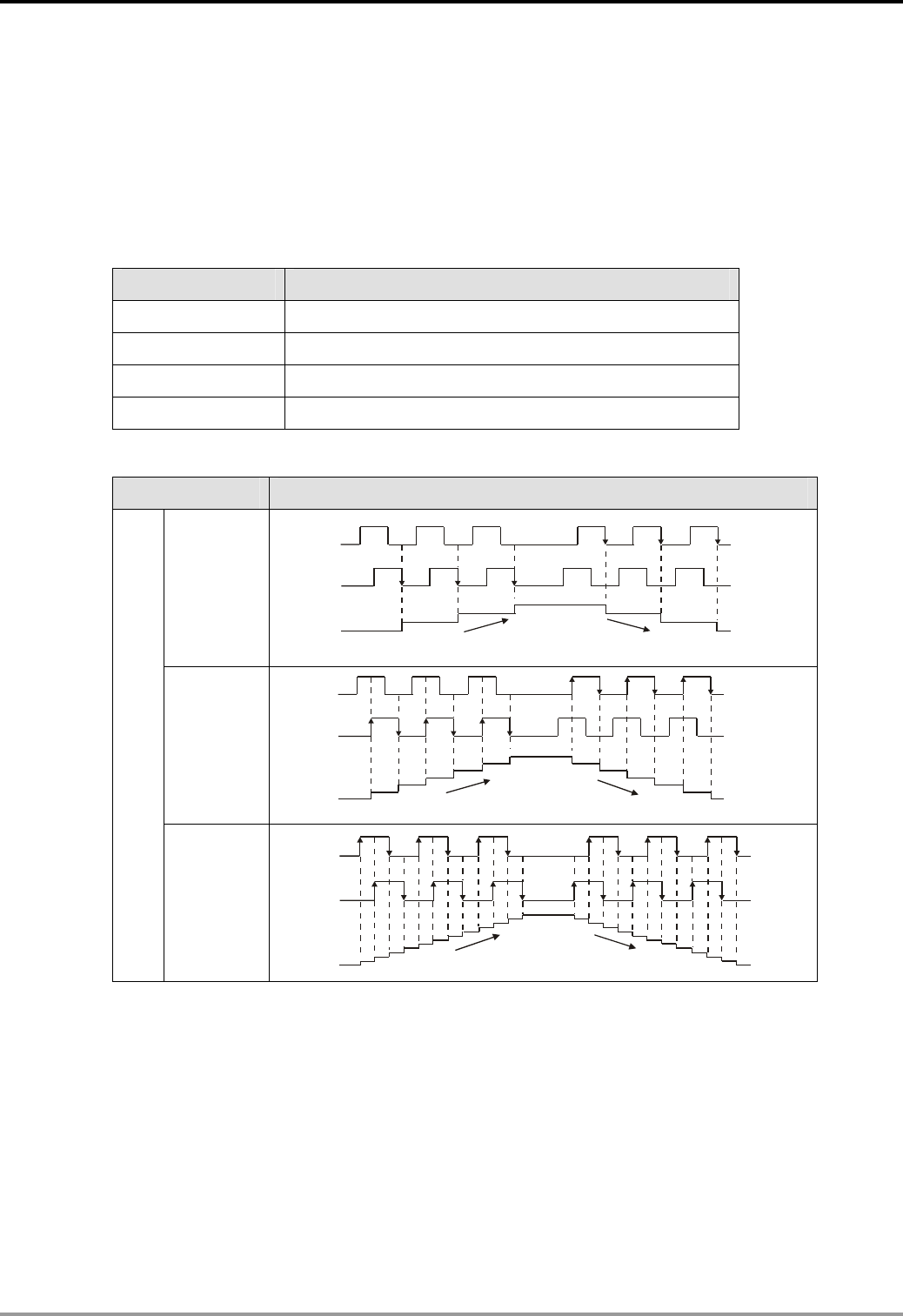
2 Functions of Devices in DVP-PLC
the same instruction, e.g. DHSCR K10 C243 C243. This function only applies to 4 special high-speed
counters C243, C245, C250 and C255.
5. Counting modes:
a) The 2-phase 2 inputs counting mode of the high speed counters in ES/EX/SS (V5.5 and versions above) and
SA/SX/SC series MPU is set by special D1022 with normal frequency, double frequency and 4 times
frequency modes. The contents in D1022 will be loaded in in the first scan when PLC is switched from STOP
to RUN.
Device No. Function
D1022 Setting up the multiplied frequency of the counter
D1022 = K1 Normal frequency mode selected
D1022 = K2 or 0 Double frequency mode selected (default)
D1022 = K4 4 times frequency mode selected
b) Multiplied frequency mode (qr indicates the occurrence of counting)
Counting mode Counting wave pattern
A-phase
B-phase
Counting up Counting down
1
(Normal
frequency)
A-phase
B-phase
Counting up Counting down
2
(Double
frequency)
2-phase 2 inputs
A-phase
B-phase
Counting up Counting down
4
(4 times
frequency)
EH2/SV series MPU supports high speed counters. C235 ~ C240 are program-interruption 1-phase high speed
counter with a total bandwidth of 20kHz, can be used alone with a counting frequency of up to 10kHz. EH3/SV2 series
MPU supports high speed counters. C235~C240 are program-interruption 1-phase high speed counter, and can be
used with a counting frequency of up to 10kHz. C241 ~ C254 are hardware high speed counter (HHSC). There are
four HHSC in EH2/SV/EH3/SV2 series MPU, HHSC0 ~ 3. The pulse input frequency of HHSC0 and HHSC1 can
reach 200kHz, and that of HHSC2 and HHSC3 can reach 20kHz (1 phase) or 5kHz (A-B phase). The pulse input
frequency of HHSC0 ~ 3 of 40EH2/40EH3 series MPU can reach 200kHz, among which:
C241, C246 and C251 share HHSC0
C242, C247 and C252 share HHSC1
C243, C248 and C253 share HHSC2
DVP-PLC Application Manual 2-23

2 Functions of Devices in DVP-PLC
DVP-PLC Application Manual
2-24
C244, C249 and C254 share HHSC3
1. Every HHSC can only be designated to one counter by DCNT instruction.
2. There are three counting modes in every HHSC (see the table below):
a) 1-phase 1 input refers to “pulse/direction” mode.
b) 1-phase 2 inputs refers to “clockwise/counterclockwise (CW/CCW)” mode.
c) 2-phase 2 inputs refers to “A-B phase” mode.
Counter type Program-interruption
high speed counter Hardware high speed counter
1-phase 1 input 1-phase 1 input 1-phase 2 inputs 2-phase 2 inputs
Type
Input
C235 C236 C237 C238 C239 C240 C241 C242 C243 C244 C246 C247 C248 C249 C251 C252 C253 C254
X0 U/D U/D U A
X1 U/D D B
X2 U/D
R R R
X3 U/D S S S
X4 U/D U/D U A
X5 U/D D B
X6 R R R
X7 S S S
X10 U/D U A
X11 D B
X12 R R R
X13 S S S
X14 U/D U A
X15 D B
X16 R R R
X17 S S S
U: Progressively increasing input A: A phase input S: Input started
B: Progressively decreasing input B: B phase input R: Input cleared
3. System structure of the hardware high speed counters:
a) HHSC0 ~ 3 have reset signals and start signals from external inputs. Settings in M1272, M1274, M1276 and
M1278 are reset signals of HHSC0, HHSC1, HHSC2 and HHSC3. Settings in M1273, M1275, M1277 and
M1279 are start signals of HHSC0, HHSC1, HHSC2 and HHSC3.
b) If the external control signal inputs of R and S are not in use, you can set M1264/M1266/M1268/M1270 and
M1265/M1267/M1269/M1271 as True and disable the input signals. The corresponding external inputs can
be used again as general input points (see the figure below).
c) When special M is used as a high speed counter, the inputs controlled by START and RESET will be affected
by the scan time.
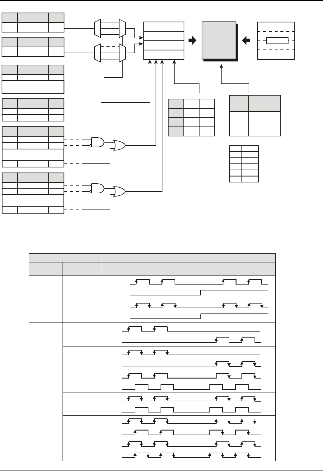
2 Functions of Devices in DVP-PLC
HHSC0
HHSC1
HHSC2
HHSC3
M1265
M1273
M1267
M1275
M1269
M1277
M1271
M1279
X3 X7 X17X13
M1272 M1274 M1276 M1278
M1264 M1266 M1268 M1270
X2 X6 X12 X16
M1241 M1242 M1243 M1244
C241 C242 C243 C244
D1225 D1226 D1227 D1228
X1 X5 X11 X15
X14X10X4X0
HHSC0 HHSC1 HHSC2 HHSC3
HHSC0 HHSC1 HHSC2 HHSC3
HHSC0 HHSC1 HHSC2 HHSC3
HHSC0 HHSC1 HHSC2 HHSC3
HHSC0 HHSC1 HHSC2 HHSC3
HHSC0 HHSC1 HHSC2 HHSC3
M1246
M1247
M1248
M1249 M1254
M1253
M1252
M1251
DHSCS
DHSCR
DHSCZ
I
010
I
020
I
030
I
040
I
050
I
060
M1289
M1290
M1291
M1292
M1293
M1294M1294
HHSC0
HHSC1
HHSC2
HHSC3
AND OR
AND OR
U/D
U
A
B
D
Counting pulses
Counting pulses
Present value in counter
Select counting modes
U/D mode setup flag
Reset signal R
Set values 1 ~ 4 indicate
Mode 1 ~ 4 (1 ~ 4 times frequency)
Start signal S
Interruption forbidden flag
High-speed
comparative
instruction
Output reaches
comparative value
Output reaches
comparative value
for outputs
Counting up/down
monitoring flag
Comparator
Counting reaches set value
8 set values
DHSCS occupies 1 group of set values
DHSCR occupies 1 group of set values
DHSCZ occupies 2 groups of set values
SET/RESET
010 ~ 060 clear
the present value
II
4. Counting modes:
The counting modes of the hardware high-speed counters in EH2/SV/EH3/SV2 series MPU can be set in D1225 ~
D1228.
Counting modes Wave pattern
Set value in
Type Counting up(+1) Counting down(-1)
special D
1
U/D
U/D FLAG
(Normal
frequency)
1-phase
1 input 2
U/D
U/D FLAG
(Double
frequency)
1
U
D
(Normal
frequency)
1-phase
2 inputs 2
U
D
(Double
frequency)
1
A
B
(Normal
frequency)
2
A
B
(Double
frequency)
3
(Triple
frequency)
A
B
2-phase
2 inputs
4
A
B
(4 times
frequency)
DVP-PLC Application Manual 2-25

2 Functions of Devices in DVP-PLC
5. Special registers for relevant flags and settings of high speed counters:
Flag Function
M1150 DHSZ instruction in multiple set values comparison mode
M1151 The execution of DHSZ multiple set values comparison mode is completed.
M1152 Set DHSZ instruction as frequency control mode
M1153 DHSZ frequency control mode has been executed.
Designating the counting direction of high speed counters C235 ~ C245
When M12□□ = Off, C2□□ will perform a counting up.
M1235 ~ M1244
When M12□□ = On, C2□□ will perform a counting down.
Designating the counting direction of high speed counters C246 ~ C255
When M12□□ = Off, C2□□ will perform a counting up.
M1245~ M1255
When M12□□ = On, C2□□ will perform a counting down.
M1160 X5 as the reset input signal of all high speed counters
M1261 High-speed comparison flag for DHSCR instruction
M1264 Disable the external control signal input point of HHSC0 reset signal point (R)
M1265 Disable the external control signal input point of HHSC0 start signal point (S)
M1266 Disable the external control signal input point of HHSC1 reset signal point (R)
M1267 Disable the external control signal input point of HHSC1 start signal point (S)
M1268 Disable the external control signal input point of HHSC2 reset signal point (R)
M1269 Disable the external control signal input point of HHSC2 start signal point (S)
M1270 Disable the external control signal input point of HHSC3 reset signal point (R)
M1271 Disable the external control signal input point of HHSC3 start signal point (S)
M1272 Internal control signal input point of HHSC0 reset signal point (R)
M1273 Internal control signal input point of HHSC0 start signal point (S)
M1274 Internal control signal input point of HHSC1 reset signal point (R)
M1275 Internal control signal input point of HHSC1 start signal point (S)
M1276 Internal control signal input point of HHSC2 reset signal point (R)
M1277 Internal control signal input point of HHSC2 start signal point (S)
M1278 Internal control signal input point of HHSC3 reset signal point (R)
M1279 Internal control signal input point of HHSC3 start signal point (S)
M1289 High speed counter I010 interruption forbidden
M1290 High speed counter I020 interruption forbidden
M1291 High speed counter I030 interruption forbidden
M1292 High speed counter I040 interruption forbidden
M1293 High speed counter I050 interruption forbidden
M1294 High speed counter I060 interruption forbidden
M1312 C235 Start input point control (not supported by EH3/SV2)
M1313 C236 Start input point control (not supported by EH3/SV2)
M1314 C237 Start input point control (not supported by EH3/SV2)
DVP-PLC Application Manual
2-26

2 Functions of Devices in DVP-PLC
Flag Function
M1315 C238 Start input point control (not supported by EH3/SV2)
M1316 C239 Start input point control (not supported by EH3/SV2)
M1317 C240 Start input point control (not supported by EH3/SV2)
M1320 C235 Reset input point control (not supported by EH3/SV2)
M1321 C236 Reset input point control (not supported by EH3/SV2)
M1322 C237 Reset input point control (not supported by EH3/SV2)
M1323 C238 Reset input point control (not supported by EH3/SV2)
M1324 C239 Reset input point control (not supported by EH3/SV2)
M1325 C240 Reset input point control (not supported by EH3/SV2)
M1328 Enable Start/Reset of C235 (not supported by EH3/SV2)
M1329 Enable Start/Reset of C236 (not supported by EH3/SV2)
M1330 Enable Start/Reset of C237 (not supported by EH3/SV2)
M1331 Enable Start/Reset of C238 (not supported by EH3/SV2)
M1332 Enable Start/Reset of C239 (not supported by EH3/SV2)
M1333 Enable Start/Reset of C240 (not supported by EH3/SV2)
Multiplied frequency of A-B phase counters for ES/EX/SS and SA/SX/SC
series MPU
D1022
D1150 Table counting register for DHSZ multiple set values comparison mode
D1151 Register for DHSZ instruction frequency control mode (counting by table)
D1152 (low word) In frequency control mode, DHSZ reads the upper and lower limits in the table
counting register D1153 and D1152.
D1153 (high word)
Switching between rising/falling edge counting modes of X10 (for SC_V1.4
series MPU only)
D1166
Switching between rising/falling edge counting modes of X11 (for SC_V1.4
series MPU only)
D1167
D1225 The counting mode of the 1st group counters (C241, C246, C251)
D1226 The counting mode of the 2nd group counters (C242, C247, C252)
D1227 The counting mode of the 3rd group counters (C243, C248, C253)
D1228 The counting mode of the 4th group counters (C244, C249, C254)
Counting modes of HHSC0 ~ HHSC3 in EH2/SV/EH3/SV2 series MPU
(default = 2)
1: Normal frequency counting mode
D1225 ~ D1228 2: Double frequency counting mode
3: Triple frequency counting mode
4: 4 times frequency counting mode
DVP-PLC Application Manual 2-27
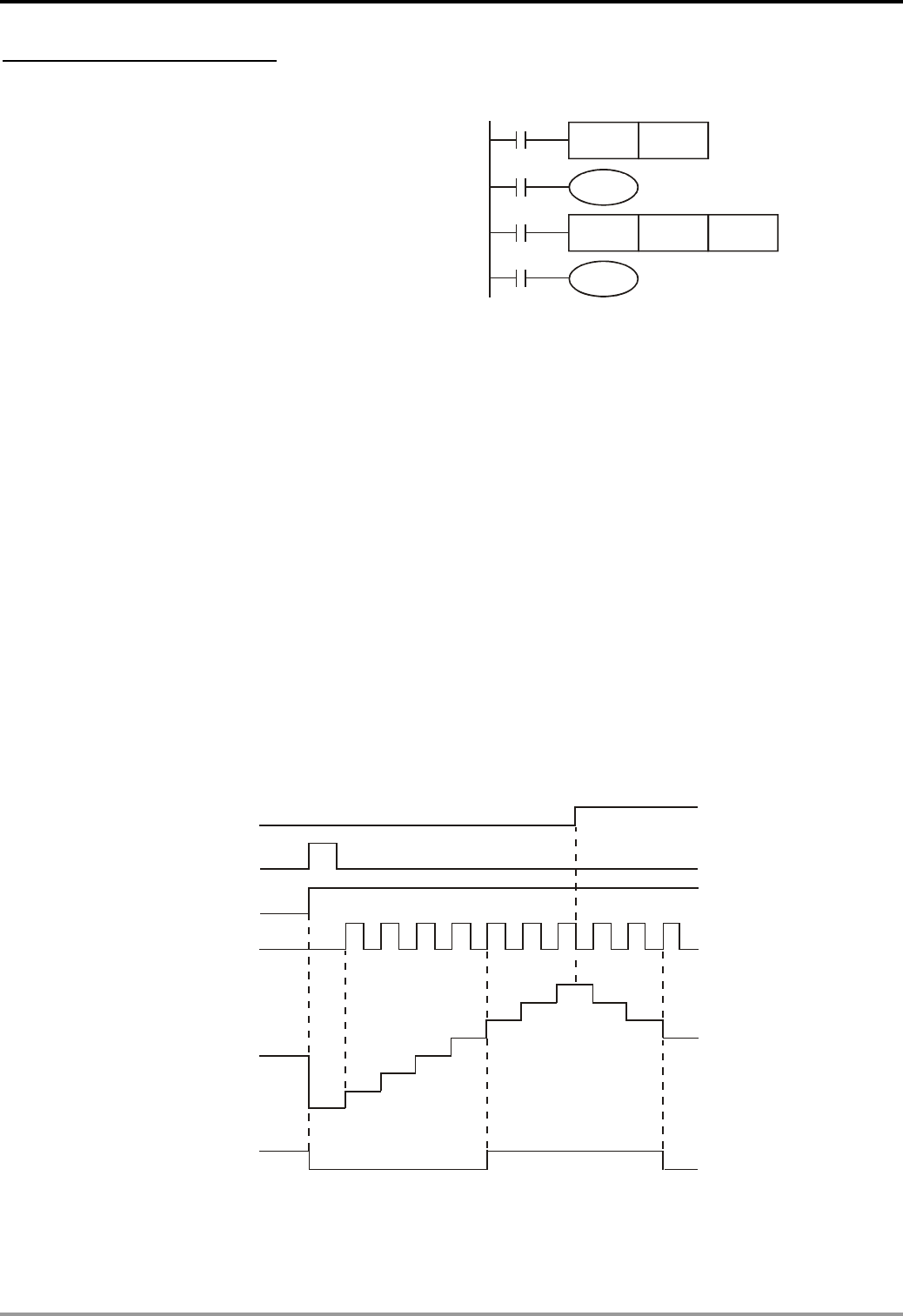
2 Functions of Devices in DVP-PLC
1-phase 1 input high-speed counter
Example:
LD X10
C241
Y0
X12
C241 K5DCNT
X11
C241RST
X10
M1241
RST C241
LD X11
OUT M1241
LD X12
DCNT C241 K5
LD C241
OUT Y0
1. X11 drives M1241 to determine whether C241 is an addition or subtraction counter.
2. When X10 is On, RST instsruction will be executed and the PV in C241 will be cleared to “0” and the contact will
be Off.
3. In C241, when X12 is On and C241 receives the signals from X0, the PV in the counter will count up (plus 1) or
count down (minus 1).
4. When the counting of C241 reaches SV K5, the contact of C241 will be On. If there are still input signals from X0,
the counting will continue.
5. C241 in ES/EX/SS and SA/SX/SC series MPU has external input signals to reset X1.
6. C241 in EH2/SV/EH3/SV2 series MPU has external input signals to reset X2 and start X3.
7. The external input contact of reset signal of C241 (HHSC0) in EH2/SV/EH3/SV2 series MPU is disabled by
M1264. The external input contact of start signal is disabled by M1265.
8. The internal input contact of reset signal of C241 (HHSC0) in EH2/SV/EH3/SV2 series MPU is disabled by M1272.
The internal input contact of start signal is disabled by M1273.
9. The counting modes (normal frequency or double frequency) of C246 (HHSC0) in EH2/SV/EH3/SV2 series MPU
can be set up by D1225. The default setting is double frequency mode.
X12
X0
0
1
2
3
4
5
0
X10
Contact X11, M1241
6
7
6
5
4
3
Counting up
Counting down
PV in C241
Contact Y0, C241
DVP-PLC Application Manual
2-28
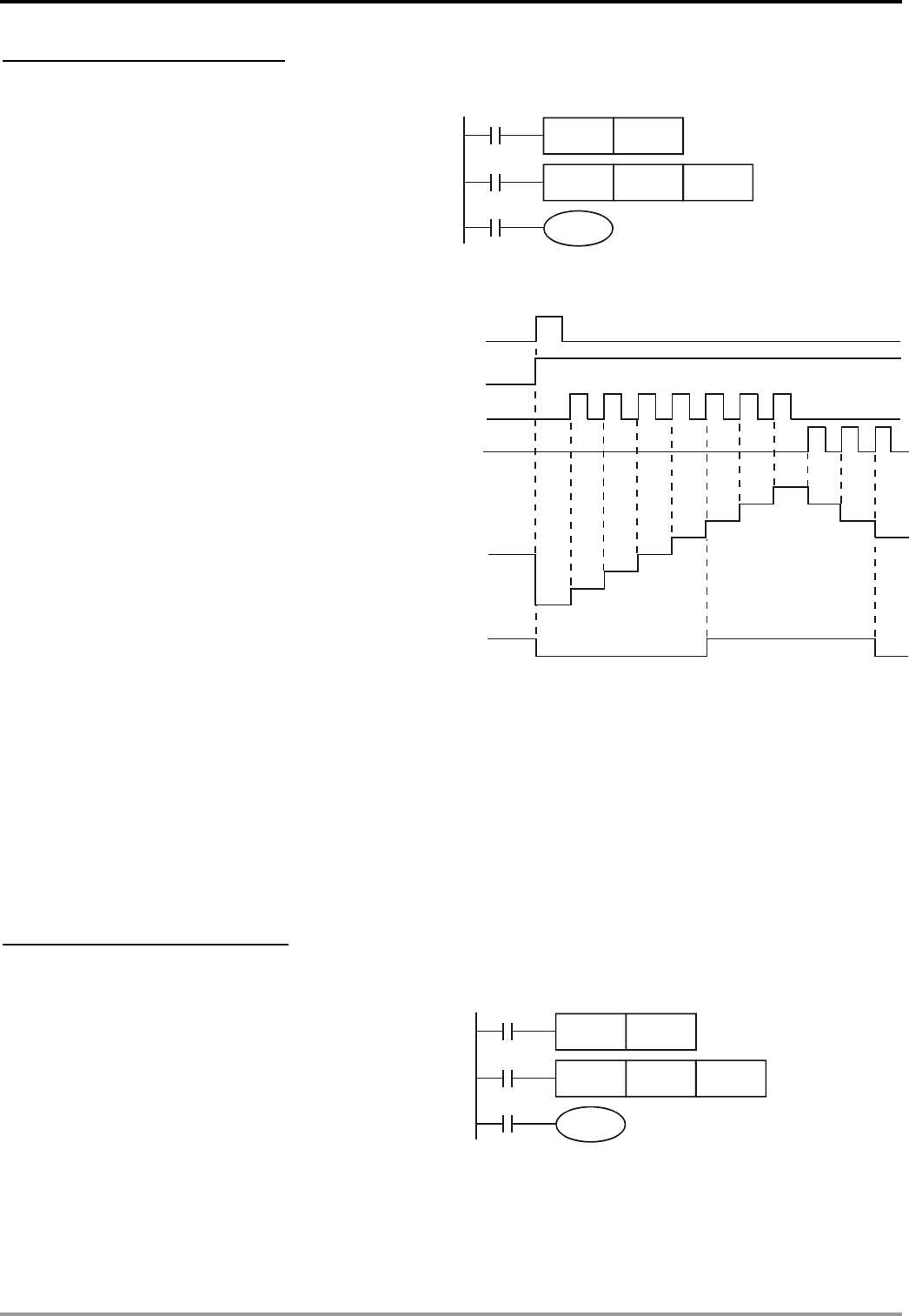
2 Functions of Devices in DVP-PLC
1-phase 2 inputs high-speed counter
Example:
LD X10
C246
Y0
X11
C246 K5DCNT
C246RST
X10
RST C246
LD X11
DCNT C246 K5
LD C246
OUT Y0
1. When X10 is On, RST instsruction will be
executed. The PV in C246 will be cleared to
“0” and the output contact will be reset to be
Off.
X11
0
1
2
3
4
5
0
X10
6
7
6
5
4
3
X1
Counting up
X0
Counting down
PV in
C246
Contact Y0, C246
2. In C246, when X11 is On and C246 receives
the signals from X0, the PV in the counter will
count up (plus 1) or count down (minus 1).
3. When the counting of C246 reaches SV K5,
the contact of C246 will be On. If there are
still input signals from X0, the counting will
continue.
4. C246 in EH2/SV/EH3/SV2 series MPU has
external input signals to reset X2 and start
X3.
5. The counting modes (normal frequency or double frequency) of C246 (HHSC0) in EH2/SV/EH3/SV2 series
MPU can be set up by D1225. The default setting is double frequency mode.
6. The external input contact of reset signal of C246 (HHSC0) in EH2/SV/EH3/SV2 series MPU is disabled by
M1264. The external input contact of start signal is disabled by M1265.
7. The internal input contact of reset signal of C246 (HHSC0) in EH2/SV/EH3/SV2 series MPU is disabled by
M1272. The internal input contact of start signal is disabled by M1273.
2-phase AB input high-speed counter
Example:
LD X10
C251
Y0
X11
C251 K5DCNT
C251RST
X10
RST C251
LD X11
DCNT C251 K5
LD C251
OUT Y0
1. When X10 is On, RST instsruction will be executed. The PV in C251 will be cleared to “0” and the output contact
will be reset to be Off.
2. In C251, when X11 is On and C251 receives the A-phase signals from X0 and B-phase signals from X1, the PV
in the counter will count up (plus 1) or count down (minus 1). You can select different counting modes if you use
DVP-PLC Application Manual 2-29
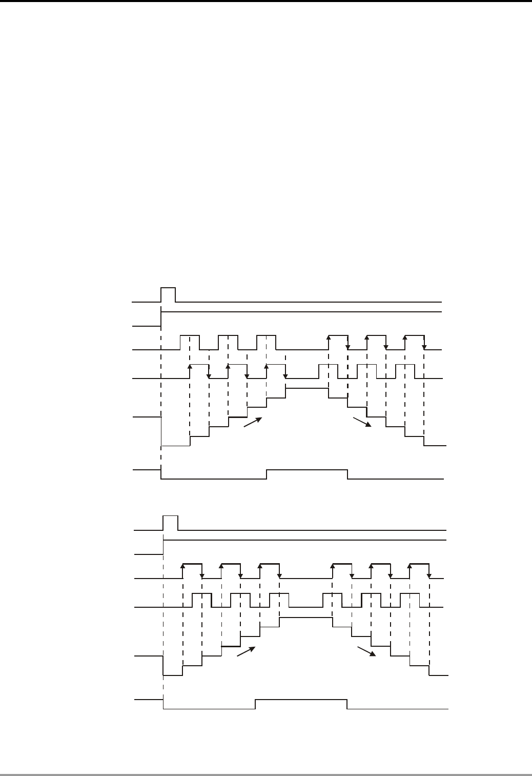
2 Functions of Devices in DVP-PLC
EH2/SV/EH3/SV2 series MPU.
3. When the counting of C251 reaches SV K5, the contact of C251 will be On. If there are still input signals coming
in, the counting will continue.
4. The counting modes (normal frequency, double frequency or 4 times frequency) of C251 (HHSC0) in ES/SA
series MPU can be set up by D1022. The default setting is double frequency mode.
5. C251 in EH2/SV/EH3/SV2 series MPU has external input signals to reset X2 and start X3.
6. The counting modes (normal frequency, double frequency, triple frequency or 4 times frequency) of C251
(HHSC0) in EH2/SV/EH3/SV2 series MPU can be set up by D1225. The default setting is double frequency
mode.
7. The external input contact of reset signal of C246 (HHSC0) in EH2/SV/EH3/SV2 series MPU is disabled by
M1264. The external input contact of start signal is disabled by M1265.
8. The internal input contact of reset signal of C246 (HHSC0) in EH2/SV/EH3/SV2 series MPU is disabled by
M1272. The internal input contact of start signal is disabled by M1273.
ES/EX/SS and SA/SX/SC series MPU (double frequency)
0
1
2
3
45
X11
X10
6
3
0
1
2
3
4
5
A-phase X0
B-phase X1
PV in C251
Contact Y0, C251
Counting up Counting down
EH2/SV/EH3/SV2 series MPU (double frequency)
0
1
2
3
45
X11
X10
6
2
0
1
2
3
4
5
A-phase X0
B-phase X1
PV in C251
Contact Y0, C251
Counting up Counting down
DVP-PLC Application Manual
2-30

2 Functions of Devices in DVP-PLC
2.8 Numbering and Functions of Registers [D], [E], [F]
2.8.1 Data register [D]
A data register is for storing a 16-bit datum of values between -32,768 to +32,767. The highest bit is “+” or “-"
sign. Two 16-bit registers can be combined into a 32-bit register (D + 1; D of smaller No. is for lower 16 bits). The
highest b it is “+” or “-” sign and it can store a 32-bit datum of values between -2,147,483,648 to +2,147,483,647.
ES/EX/SS series MPU:
General purpose D0 ~ D407, 408 points
Latched D408 ~ D599, 192 points. Fixed to be latched.
Special purpose D1000 ~ D1143, 144 points. Some are latched.
Total
Data register D 744 points
Index register E, F E, F, 2 points
SA/SX/SC series MPU:
General purpose D0 ~ D199, 200 points. Fixed to be non-latched.
D200 ~ D999, D2000 ~ D4999, 3,800 points.
Latched Can be modified to be non-latched by setting up parameter.
Special purpose D1000 ~ D1999, 1,000 points. Some are latched.
Total
Data register D 5,000
points
Index register E, F E0 ~ E3, F0 ~ F3, 8 points
1,600
points
File register K0 ~ K1,599, MPU 1,600 points. Fixed to be latched.
EH2/SV/EH3/SV2 series MPU:
D0 ~ D199, 200 points. Can be modified to be latched by setting up
parameters.
General purpose
D200 ~ D999, D2000 ~ D9999, 8,800 points.
Latched EH3/SV2: D200 ~ D999, D2000 ~ D11999, 10,800 points.
Can be modified to be non-latched by setting up parameters.
Special purpose D1000 ~ D1999, 1,000 pints. Some are latched.
Total
Data register D 10,000
points
Index register E, F E0 ~ E7, F0 ~ F7, 16 points.
10,000
points
File register K0 ~ K9,999, MPU 10,000 points. Fixed to be latched.
There are five types of registers:
1. General purpose register: When PLC goes from RUN to STOP or the power of the PLC is switched off, the data
in the register will be cleared to “0”. When M1033 = On and PLC goes from RUN to STOP, the data will not be
cleared, but will still be cleared to “0” when the power is off.
2. Latched register: When the power of PLC is switched off, the data in the register will not be cleared but will retain
at the value before the power is off. You can use RST or ZRST instruction to clear the data in the latched register.
3. Special purpose register: Every register of this kind has its special definition and purpose, mainly for storing the
system status, error messages and monitored status. See 2.10 and 2.11 for more details.
4. Index register E, F: The index register is a 16-bit register. There are 2 points of E, F in ES/EX/SS series MPU; 8
points (E0 ~ E3, F0 ~ F3) in SA/SX/SC series MPU; 16 points (E0 ~ E7, F0 ~ F7) in EH2/SV/EH3/SV2 series MPU.
If the index register is to be used as a 32-bit register, please designate E. When E is already designated in a
32-bit instruction, using also F will not be allowed.
5. File register: There are 1,600 file registers (K0 ~ K1,599) in SA/SX/SC series MPU and 10,000 file registers (K0
~ K9,999) in EH2/SV/EH3/SV2 series MPU. The file register does not have an exact device No.; therefore the
DVP-PLC Application Manual 2-31

2 Functions of Devices in DVP-PLC
read/write function of file registers has to be executed by instruction API 148 MEMR, API 149 MEMW or through
peripheral devices HPP and WPLSoft.
2.8.2 Index Register [E], [F]
Index registers E, F are 16-bit data registers and can be written and
read.
F0 E0
E0F0
16 bits 16 bits
32 bits
Higher 16 bits Lower 16 bits
If you need to use a 32-bit register, you have to designate E. In this
case, F will be covered by E and cannot be used anymore; otherwise,
the content in E (32-bit) will be incorrect. We suggest you use DMOVP
K0 E instruction, the content in E (including F) will be cleared to “0”
when the power of PLC is switched on.
The combination of E, F when you use a 32-bit index register:
(F0, E0), (F1, E1), (F2, E2), …(F7, E7)
K14 F0
X0
K8 E0MOV
D5E0 D10F0
MOV
MOV
When X0 = On, E0 = 8, F0 = 14, D5E0 = D (5 + 8) = D13, D10F0 = D
(10 + 14) = D24. At this moment, the content in D13 will be moved to
D24.
The index register is the same as normal operands, can be used for moving or comparison on word devicies (KnX,
KnY, KnM, KnS, T, C, D) and bit devices (X, Y, M, S). ES/SA series MPU does not support constant (K, H) index
register, but EH2/SV/EH3/SV2 series MPU supports constant (K, H) index register.
ES/EX/SS series MPU has 2 points of index registers E0, F0
SA/SX/SC series MPU has 8 points of index registers E0 ~ E3, F0 ~ F3
EH2/SV/EH3/SV2 series MPU has 16 points of index registers E0 ~ E7, F0 ~ F7
Some instructions do not support index registers. For how to use index register E, F to modify the operands, see
Chapter 5.4 for more details.
When you use the instruction mode in WPLSoft to generate constant (K, H) index register function, please use
symbol “@”. For example, “MOV K10@E0 D0F0”
When you use index register E, F to modify the operands, the modification range CANNOT exceed the range of
special purpose registers D1000 ~ D1999 and special auxiliary registers M1000 ~ M1999 in case errors may occur.
2.8.3 Functions and Features of File Registers
When the power of PLC is switched on, SA/SX/SC and EH2/SV/EH3/SV2 series MPU will check the following
devices:
1. M1101 (whether the file register is enabled)
2. D1101 (No. of file registers in SA/SX/SC series MPU: K0 ~ K1,599; No. of file registers in EH2/SV/EH3/SV2
series MPU: K0 ~ K9,999)
3. D1102 (Number of file registers to be read in SA/SX/SC series MPU: K0 ~ K1,600; number of file registers to be
DVP-PLC Application Manual
2-32

2 Functions of Devices in DVP-PLC
read in EH2/SV/EH3/SV2 series MPU: K0 ~ K8,000)
4. D1103 (devices for storing the data read from file registers; the No. of designated data register D starts from
K2,000 ~ K9,999; determining whether to automatically send the content in the file register to the designated data
register.)
Note:
1. When D1101 of SA/SX/SC series MPU is bigger than 1,600, D1101 of EH2/SV/EH3/SV2 series MPU is bigger
than 8,000 and D1103 is smaller than 2,000 or bigger than 9,999, the data read from file registers will not be sent
to data register D.
2. When the program starts to send the data read from the file register to data register D and the address of the file
register or the data register D exceed their ranges, PLC will stop the reading.
3. There are 1,600 file registers in SA/SX/SC series MPU and 10,000 in EH2/SV/EH3/SV2 series MPU. The file
register does not have an exact device No.; therefore the read/write function of file registers has to be executed
by instruction API 148 MEMR, API 149 MEMW or through peripheral devices HPP and WPLSoft.
4. If you tend to read a file register with an address that is not within the range, the read value will be “0”.
2.9 Pointer [N], Pointer [P], Interruption Pointer [I]
ES/EX/SS series MPU:
Control point of master
control loop
N For master control loop N0 ~ N7, 8 points
Position pointer of CJ,
CALL
P For CJ, CALL instructions P0 ~ P63, 64 points
External interruption I001, I101, I201, I301, 4 points
Timed interruption I6□□, 1 point (□□=10 ~ 99, time base = 1ms)
(for V5.7)
Pointer
Position pointer of
interruption subroutine
I Interruption
Communication
interrupt I150, 1 point
SA/SX/SC series MPU:
Control point of master
control loop
N Master control loop N0 ~ N7, 8 points
Position pointer of CJ,
CALL
P For CJ, CALL instructions P0 ~ P255, 256 points
External interruption I001, I101, I201, I301, I401, I501, 6 points
Timer interruption I6□□, I7□□, 2 points (□□ = 1 ~ 99, time
base = 1ms)
High-speed counter
interruption I010, I020, I030, I040, I050, I060, 6 points
Pointer
Position pointer of
interruption subroutine
I Interruption
Communication
interruption I150, 1 point
Note: Among the 6 pairs of interruption No. (I001, I010), (I101, I020), (I201, I030), (I301, I040), (I401, I050), (I501, I060), only 1 No.
in the pair is allowed to be used in the program. If you use both No. in the pair and write them into the program, there may be
syntax errors occurring.
EH2/SV series MPU:
Control point of master
control loop
N Master control loop N0 ~ N7, 8 points
Pointer
Position pointer of CJ,
CALL
P For CJ, CALL instructions P0 ~ P255, 256 points
DVP-PLC Application Manual 2-33
2 Functions of Devices in DVP-PLC
I00□(X0), I10□(X1), I20□(X2), I30□(X3), I40
□(X4), I50□(X5), 6 points
External interruption (□ = 1, rising-edge trigger , □ = 0,
falling-edge trigger )
I6□□, I7□□, 2 points (□□ = 1 ~ 99, time
base = 1ms)
I8□□, 1 point (□□ = 1 ~ 99, time base =
0.1ms)
Timed interruption
High-speed counter
interruption I010, I020, I030, I040, I050, I060, 6 points
Pulse interruption I110, I120, I130, I140, 4 points
Communication
interruption I150, I160, I170, 3 points
Position pointer of
interruption subroutine
I Interruption
Frequency
measurement card
triggered interruption
I180, 1 point
EH3/SV2 series MPU:
Control point of master
control loop
N Master control loop N0 ~ N7, 8 points
Position pointer of CJ,
CALL
P For CJ, CALL instructions P0 ~ P255, 256 points
I00□(X0), I10□(X1), I20□(X2), I30□(X3),
I40□(X4), I50□(X5), I60□(X6), I70□(X7),
I90□(X10), I91□(X11), I92□(X12),
I93□(X13), I94□(X14), I95□(X15),
I96□(X16), I97□(X17), 16 points (□=1,
rising-edge trigger
External interruption
, □=0, falling-edge
trigger )
Timed interruption
I6□□, I7□□, 2 points (□□ = 2 ~ 99, time
base = 1ms)
I8□□, 1 point (□□ = 1 ~ 99, time base =
0.1ms)
High-speed counter
interruption I010, I020, I030, I040, I050, I060, 6 points
Pulse interruption I110, I120, I130, I140, 4 points
Pointer
Position pointer of
interruption subroutine
I Interruption
Communication
interruption I150, I160, I170, 3 points
Note: Input point X as a high-speed counter cannot be used as an external interruption signal. For example, if C251 occupies X0,
X1, X2 and X3, the external input interruption No. I00□(X0), I10□(X1), I20□(X2), and I30□(X3) cannot be used.
Pointer N: Used with MC and MCR instructions. MC is the master control start instruction. When MC instruction is
executer, the instructions between MC and MCR will still be executed normally. See Chapter 3 explanations on MC
and MCR instructions for more details.
Pointer P: Used with API 00 CJ, API 01 CALL and API 02 SRET. See Chapter 6 explanations on CJ, CALL and SRET
instructions for more details.
DVP-PLC Application Manual
2-34
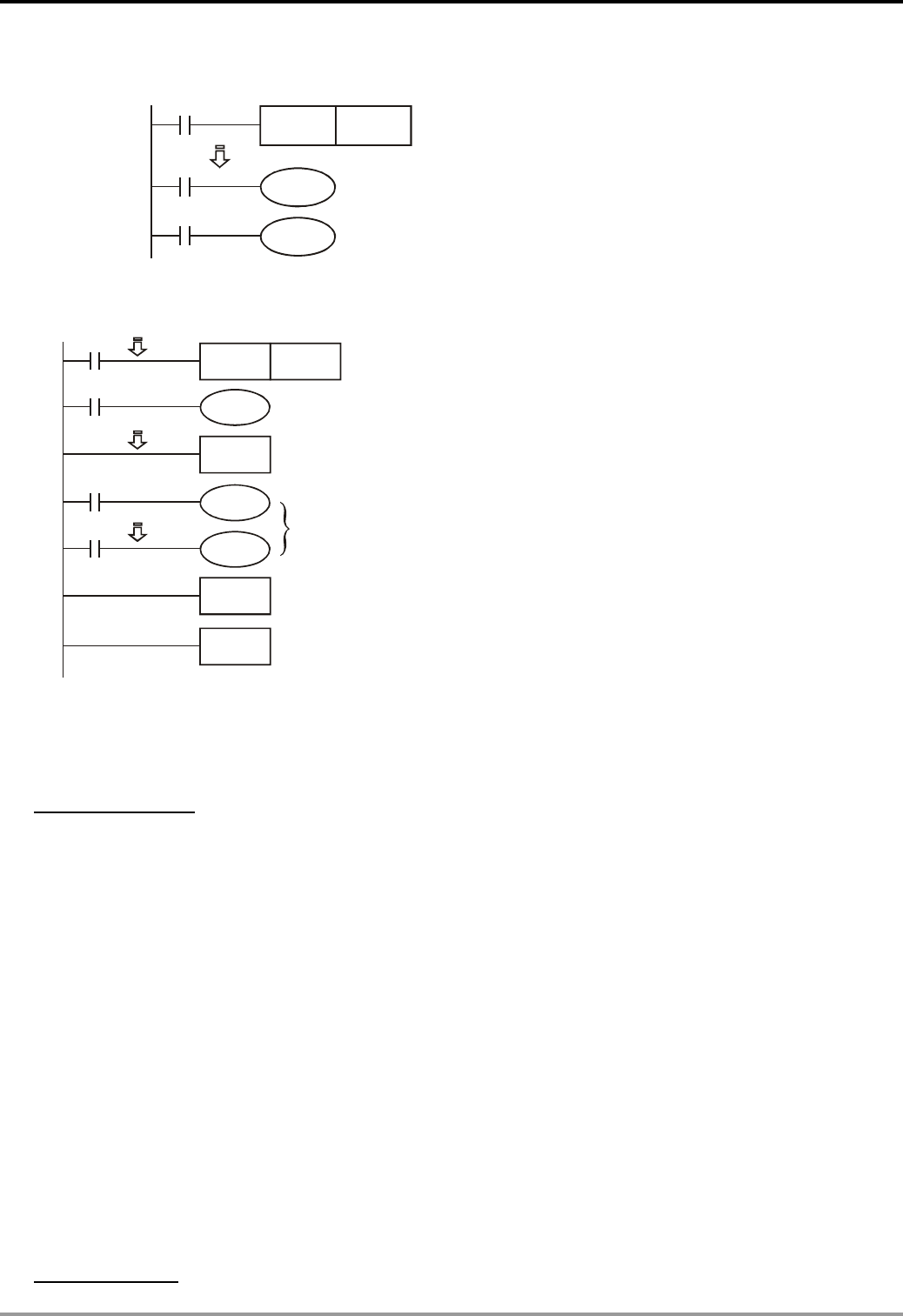
2 Functions of Devices in DVP-PLC
CJ Conditional Jump:
When X0 = On, the program will jump from
address 0 to N (designated label P1) and keep
on the execution. The addresses in the middle
will be ignored.
X2
Y2
X1
P1CJ
X0
Y1
P**
0
P1 N
When X0 = Off, the program will execute from
address 0 and keep on executing. At this time,
CJ instruction will not be executed.
CALL Call Subroutine, SRET Subroutine Return:
When X0 = On, CALL instruction will be
executed and the program will jump to P2 and
executed the designated subroutine. When
SRET instruction is executed, the program will
return to address 24 and keep on the execution.
Y0
X1
P2CALL
X0
Y1
P***
20
P2
FEND
Y0
SRET
24
Subroutine P2
Call subroutine P***
Subroutine return
END
Interruption Pointer I: Used with API 04 EI, API 05 DI, API 03 IRET. See Chapter 5.5 for more details. There are 6
types of interruption pointer. To insert an interruption, you have to combine the action with EI (enable interruption), DI
(disable interruption), IRET (interruption return) instructions.
External interruption:
1. Due to the special hardware design inside the MPU, the input signals coming in at input
terminals X0 ~ X5 (EH3/SV2: X0~X17) when rising-edge or falling-edge triggers will not be affected by the scan
cycle. The currently executed program will be interrupted immediately and the execution will jump to the
designated interruption subroutine pointer I00□(X0), I10□(X1), I20□(X2), I30□(X3), I40□(X4), I50□(X5). Till
the execution reaches IRET instruction, the program will return to the original position and keep on its execution.
In SA/SX series MPU, X0 (pulse input point) works with X4 (external interruption point), corresponding to C235,
C251 and C253 work with I401, which will be able to interrupt and intercept the present value in the high-speed
counter. D1181 is the device to store the 32-bit value. X1 (pulse input point) works with X5 (external interruption
point), corresponding to C236 works with I501, which will be able to interrupt and intercept the present value in
the high-speed counter. D1198 and D1199 are the devices to store the 32-bit value.
In SC series MPU, X10 (pulse input point) works with X4 (external interruption point), corresponding to C243 and
C255 work with I401, which will be able to interrupt and intercept the present value in the high-speed counter.
D1180 and D1181 are the devices to store the 32-bit value. X11 works with X5, corresponding to C245 works with
I501, which will be able to interrupt and intercept the present value in the high-speed counter. D1198 and D1199
are the devices to store the 32-bit value.
2. Timed interruption: PLC automatically interrupts the currently executed program every a fixed period of time and
DVP-PLC Application Manual 2-35

2 Functions of Devices in DVP-PLC
jumps to the execution of a designated interruption subroutine.
3. Interruption when the counting reaches the target: The high-speed counter comparison instruction API 53
DHSCS can designates that when the comparison reaches the target, the currently executed program will be
interrupted and jump to the designated interruption subrountine executing the interruption pointers I010, I020,
I030, I040, I050 and I060.
4. Pulse interruption: The pulse output instruction API 57 PLSY can be set up that the interruption signal is sent out
synchronously when the first pulse is sent out by enabling flags M1342 and M1343. The corresponding
interruptions are I130 and I140. You can also set up that the interruption signal is sent out after the last pulse is
sent out by enabling flags M1340 and M1341. The corresponding interruptions are I110 and I120.
5. Communication interruption:
I150: When the communication instruction RS is being used, you can send out interruption request when the
program receives a specific word by interruption I150. The specific word is set up in the low byte of D1168. This
function can be adopted when the PLC receives data of different length during the connection with the
communication device. Set up the end word in D1168 and write the interruption subroutine I150 and when the
PLC receives this end word, the program will execute I150.
I160: RS instruction sends out interruption request when receiving a specific length of data. When the data
received equals the low byte of D1169, I160 will be triggered. When D1169 = 0, I160 will not be triggered.
I170: In Slave mode, interruption I170 will be generated when the data receiving is completed. Normally when the
communication terminal of the PLC is in Slave mode, PLC will not immediately process the communication data
entered but process it after the END is executed. Therefore, when the scan time is very long and you need the
communication data to be processed immediately, you can use interruption I170 for this matter.
6. Frequency measurement card triggered interruption:
I180: When the PLC sets up the frequency measurement card in mode 1 (pulse cycle measurement) and mode 3
(pulse number counting) by M1019 and D1034, I180 will be supported as well.
2.10 Special Auxiliary Relays and Special Data Registers
The types and functions of special auxiliary relays (special M) and special data registers (special D) are listed in the
table below. Please be noted that some devices of the same No. may bear different meanings in different series
MPUs. Special M and special D marked with “*” will be further illustrated in the 2.11. Columns marked with “R” regers
to “read only”, “R/W” refers to “read and write”, “-“ refers to the status remains unchanged and “#” refers to the system
will set it up according to the status of the PLC.
Special
M Function
ES
EX
SS
SA
SX
SC
EH2
SV
EH3
SV2
Off
Ø
On
STOP
Ø
RUN
RUN
Ø
STOP
Attribute Latched Default
○
M1000* Monitoring normally open contact (A) Off On Off R NO Off
○ ○ ○
○
M1001* Monitoring normally closed contact (B) On Off On R NO On
○ ○ ○
M1002* Enabling positive pulses (On when RUN) Off On Off R NO Off
○
○ ○ ○
M1003* Enabling negative pulses (Off when RUN) On Off On R NO On
○
○ ○ ○
M1004* On when syntax errors occur Off Off - R NO Off
○
○ ○ ○
DVP-PLC Application Manual
2-36

2 Functions of Devices in DVP-PLC
DVP-PLC Application Manual 2-37
Special
M Function
ES
EX
SS
SA
SX
SC
EH2
SV
EH3
SV2
Off
Ø
On
STOP
Ø
RUN
RUN
Ø
STOP
Attribute Latched Default
M1005* Password of data backup memory card and
password of MPU do not match ╳ ╳ ○○Off - - R NO Off
M1006* Data backup memory card has not been
initialized ╳ ╳ ○○Off - - R NO Off
M1007* Data do not exist in the program area of data
backup memory card ╳ ╳ ○○Off - - R NO Off
M1008* Scanning watchdog timer (WDT) On ○○○○Off Off - R NO Off
M1009 Insufficient 24V DC supply, LV signal has
been occurred. ○○○○Off - - R NO Off
M1010
ES/SA: PLSY Y0 mode selection, continuous
output when On
EH2/SV/EH3/SV2: Pulse output when
reaching END instruction
○○○○Off - - R/W NO Off
M1011* 10ms clock pulse, 5ms On/5ms Off ○○○○Off - - R NO Off
M1012* 100ms clock pulse, 50ms On / 50ms Off ○○○○Off - - R NO Off
M1013* 1s clock pulse, 0.5s On / 0.5s Off ○○○○Off - - R NO Off
M1014* 1min clock pulse, 30s On / 30s Off ○○○○Off - - R NO Off
M1015* Enabling high-speed counter ╳○○○Off - - R/W NO Off
M1016* Displaying real time clock in A.D. ╳○○○Off - - R/W NO Off
M1017* ±30 seconds correction on real time clock ╳○○○Off - - R/W NO Off
M1018 Flag for radian/degree, On: for degree ╳○○○Off - - R/W NO Off
M1019 Enabling frequency measurement card ╳ ╳ ○○Off Off - R NO Off
M1020 Zero flag ○○○○Off - - R NO Off
M1021 Borrow flag ○○○○Off - - R NO Off
M1022 Carry flag ○○○○Off - - R NO Off
M1023 PLSY Y1 mode selection, continuous output
when On ○ ○ ╳╳Off - - R/W NO Off
M1024 Requesting COM1 monitoring ○○○○Off - - R NO Off
M1025* There is incorrect request for communication. ○○○○Off - - R NO Off
M1026 Enabling RAMP module ╳○○○Off - - R/W NO Off
M1027 Number of PR outputs ╳○○○Off - - R/W NO Off
M1028
10ms time switching flag.
Off: time base of T64 ~ T126 = 100ms
On: time base of T64 ~ T126 = 10ms
○╳ ╳ ╳Off - - R/W NO Off
M1029*
ES/SA: Y0 pulse output of PLSY, PLSR
instructions is completed, or other relevant
instructions complete their executions.
EH2/SV/EH3/SV2: the 1st group pulse output
○○○○Off - - R NO Off

2 Functions of Devices in DVP-PLC
DVP-PLC Application Manual
2-38
Special
M Function
ES
EX
SS
SA
SX
SC
EH2
SV
EH3
SV2
Off
Ø
On
STOP
Ø
RUN
RUN
Ø
STOP
Attribute Latched Default
CH0 (Y0, Y1) is completed, or other relevant
instructions complete their executions.
M1030*
ES/SA: Y1 pulse output of PLSY, PLSR
instructions is completed, or other relevant
instructions complete their executions.
EH2/SV/EH3/SV2: the 2nd group pulse output
CH1 (Y2, Y3) is completed, or other relevant
instructions complete their executions.
○ ○ ○ ○Off - - R NO Off
M1031* Clear all non-latched areas ○ ○ ○ ○Off - - R/W NO Off
M1032* Clear all latched areas ○ ○ ○ ○Off - - R/W NO Off
M1033* Memory latched when STOP ○ ○ ○ ○Off - - R/W NO Off
M1034* Disabling all Y outputs ○ ○ ○ ○Off - - R/W NO Off
M1035*
Enabling input point X as the RUN/STOP
switch, corresponding to D1035
(SA designates X7 only; SX designates X3
only; SC designates X5 only)
╳○ ○ ○- - - R/W YES Off
EH2/SV/EH3/SV2: the 3rd group pulse output
CH2 (Y4, Y5) is completed. (Not available in
EH)
╳ ╳ ○○Off - - R NO Off
M1036*
SPD instruction is able to use X0 ~ X5 to
detect the flag (only available in SC_V1.4 and
versions above)
╳○╳╳Off Off - R/W NO Off
M1037
EH2/SV/EH3/SV2: the 4th group pulse output
CH3 (Y6, Y7) is completed. (Not available in
EH)
╳ ╳ ○○Off - - R NO Off
M1038 Off: The time base of T200~T255 is 10ms.
On: The time base of T200~T255 is 1ms. ╳ ╳ ○ ○ Off - - R/W NO Off
M1039* Fixing time scan mode ○ ○ ○ ○Off - - R/W NO Off
M1040 Disabling step ○ ○ ○ ○Off - - R/W NO Off
M1041 Starting step ○ ○ ○ ○Off - Off R/W NO Off
M1042 Enabling pulses ○ ○ ○ ○Off - - R/W NO Off
M1043 Zero return completed ○ ○ ○ ○Off - Off R/W NO Off
M1044 Zero point condition ○ ○ ○ ○Off - Off R/W NO Off
M1045 Diabling all output reset ○ ○ ○ ○Off - - R/W NO Off
M1046 Setting STL status as On ○ ○ ○ ○Off - - R NO Off
M1047 Enabling STL monitoring ╳○ ○ ○Off - - R/W NO Off
M1048 Alarm status ╳○ ○ ○Off - - R NO Off
M1049 Setting up alarm monitoring ╳○ ○ ○Off - - R/W NO Off
M1050 Inhibiting I001 ○ ○ ╳╳Off - - R/W NO Off
M1051 Inhibiting I101 ○ ○ ╳╳Off - - R/W NO Off

2 Functions of Devices in DVP-PLC
DVP-PLC Application Manual 2-39
Special
M Function
ES
EX
SS
SA
SX
SC
EH2
SV
EH3
SV2
Off
Ø
On
STOP
Ø
RUN
RUN
Ø
STOP
Attribute Latched Default
M1052 Inhibiting I201 ○ ○ ╳╳Off - - R/W NO Off
Inhibiting I301 ○ ○ ╳╳Off - - R/W NO Off
M1053
Enabling X4 speed detection ╳ ╳ ○ ○ Off Off Off R/W NO Off
Inhibiting I401 ╳○╳╳Off - - R/W NO Off
M1054
Enabling X10 speed detection ╳ ╳ ○ ○ Off Off Off R/W NO Off
Inhibiting I501 ╳○╳╳Off - - R/W NO Off
M1055
Enabling X14 speed detection ╳ ╳ ○ ○ Off Off Off R/W NO Off
Inhibiting I6□□ ○ ○ ╳╳Off - - R/W NO Off
M1056 Enabling X1 interrupt to get the counting value
of C241 ╳ ╳ ╳ ○ Off Off Off R/W NO Off
Inhibiting I7□□ ╳○╳╳Off - - R/W NO Off
M1057 Enabling X2 interrupt to get the counting value
of C241 ╳ ╳ ╳ ○ Off Off Off R/W NO Off
M1058 COM3 monitoring request ╳ ╳ ╳ ○Off - - R/W NO Off
Inhibiting I010 ~ I060 ╳○╳╳Off - - R/W NO Off
M1059 Enabling X3 interrupt to get the counting value
of C241 ╳ ╳ ╳ ○ Off Off Off R/W 否 Off
M1060 System error message 1: The peripheral
circuit of the CPU breaks down. ○○○╳Off - - R NO Off
System error message 2: The CPU flag
register breaks down. ╳ ○ ○ ╳ Off - - R NO Off
M1061
System error message 2: An error occurs
when the data in the latched area is read. ○ ╳ ╳ ╳ Off - - R NO Off
M1062 System error message 3: The CPU BIOS
ROM breaks down. ○○○╳Off - - R NO Off
M1063 System error message 4: The RAM in the
CPU breaks down. ○○○╳Off - - R NO Off
M1064 Incorrect use of operands ○○○○Off Off - R NO Off
M1065 Syntax error ○○○○Off Off - R NO Off
M1066 Loop error ○○○○Off Off - R NO Off
M1067* Calculation error ○○○○Off Off - R NO Off
M1068* Calculation error locked (D1068) ○○○○Off - - R NO Off
M1070
ES/SA: Y1 time base switching for PWM
instruction (On: 100us; Off: 1ms)
EH3/SV2: Y0 time base switching for PWM
instruction (On: 100us; Off: 1ms)
EH2/SV/EH3/SV2: when On, D1371 will
decide the time base)
○○○○Off - - R/W NO Off
M1071 Y2 time base switching for PWM instruction ╳ ╳ ○○Off - - R/W NO Off

2 Functions of Devices in DVP-PLC
DVP-PLC Application Manual
2-40
Special
M Function
ES
EX
SS
SA
SX
SC
EH2
SV
EH3
SV2
Off
Ø
On
STOP
Ø
RUN
RUN
Ø
STOP
Attribute Latched Default
(On: 100us; Off: 1ms)
EH2/SV/EH3/SV2: when On, D1372 will
decide the time base)
M1072 Executing PLC RUN instruction ○ ○ ○ ○Off On Off R/W NO Off
M1074 SRAM access error ╳ ╳ ○ ○ Off - - R NO Off
M1075 Error occurring when writing FLASH card or
Flash ROM ╳ ╳ ○○Off - - R NO Off
M1076* Real time clock malfunction ╳○ ○ ○Off - - R NO Off
M1077 Battery in low voltage, malfunction or no
battery ╳○ ○ ○Off - - R NO Off
M1078 Immediately stopping Y0 pulse output for
PLSY instruction ○ ○ ╳╳Off - - R/W NO Off
M1079 Immediately stopping Y1 pulse output for
PLSY instruction ○ ○ ╳╳Off - - R/W NO Off
M1080 Requesting COM2 monitoring ○ ○ ○ ○Off - - R NO Off
M1081 Changing direction for FLT instruction ╳○ ○ ○Off - - R/W NO Off
M1082 Real time clock has been changed ╳○ ○ ○Off - - R NO Off
M1083 Allowing interruption subroutine in FROM/TO
instructions ╳○ ○ ○Off - - R/W NO Off
M1084*
Detecting bandwidth (only available in
ES/EX/SS_V6.4, SA/SX_V1.6, SC_V1.4 and
versions above)
○ ○ ╳╳Off Off Off R/W NO Off
M1085 Selecting DVP-PCC01 duplicating function ○ ○ ○ ○Off - - R/W NO Off
M1086 Setting up the switch for enabling password
function of DVP-PCC01 ○ ○ ○ ○Off - - R/W NO Off
M1087* Enabling LV signal ╳ ╳ ○○Off - - R/W NO Off
M1088
Matrix comparison.
Comparing between equivalent values
(M1088 = 1) or different values (M1088 = 0).
╳○ ○ ○Off Off - R/W NO Off
M1089 Matrix search end flag. When the comparison
reaches the last bit, M1089 = 1. ╳○ ○ ○Off Off - R NO Off
M1090 Matrix search start flag. Comparing from bit 0
(M1090 = 1). ╳○ ○ ○Off Off - R NO Off
M1091
Matrix bit search flag. When the comparison
is completed, the comparison will stop
immediately (M1091=1).
╳○ ○ ○Off Off - R NO Off
M1092 Matrix pointer error flag. When the pointer Pr
exceeds its range, M1092 = 1. ╳○ ○ ○Off Off - R NO Off
M1093 Matrix pointer increasing flag. Adding 1 to the
current value of the Pr. ╳○ ○ ○Off Off - R/W NO Off
M1094 Matrix pointer clear flag. Clearing the current
value of the Pr to 0. ╳○ ○ ○Off Off - R/W NO Off

2 Functions of Devices in DVP-PLC
DVP-PLC Application Manual 2-41
Special
M Function
ES
EX
SS
SA
SX
SC
EH2
SV
EH3
SV2
Off
Ø
On
STOP
Ø
RUN
RUN
Ø
STOP
Attribute Latched Default
M1095 Matrix rotation/displacement/output carry flag ╳○○○Off Off - R NO Off
M1096 Matrix displacement/input complement flag ╳○○○Off Off - R/W NO Off
M1097 Matrix rotation/displacement direction flag ╳○○○Off Off - R/W NO Off
M1098 Matrix counting the number of bits which are
“1” or “0” ╳○○○Off Off - R/W NO Off
M1099 On when the matrix counting result is “0” ╳○○○Off Off - R/W NO Off
M1100 SPD instruction sampling once ╳ ╳ ○○Off - - R/W NO Off
M1101* Whether to enable file registers ╳○○○- - - R/W Yes Off
M1102* Y10 pulse output ends (For SC) ╳○╳╳Off - - R/W NO Off
M1103* Y11 pulse output ends (For SC) ╳○╳╳Off - - R/W NO Off
M1104*
Status of SW1 on digital switch card/AX0
input point on 4DI card (photpcoupler
isolation)
╳ ╳ ○╳Off Off - R NO Off
M1105*
Status of SW2 on digital switch card/AX1
input point on 4DI card (photpcoupler
isolation)
╳ ╳ ○╳Off Off - R NO Off
M1106*
Status of SW3 on digital switch card/AX2
input point on 4DI card (photpcoupler
isolation)
╳ ╳ ○╳Off Off - R NO Off
M1107*
Status of SW4 on digital switch card/AX3
input point on 4DI card (photpcoupler
isolation)
╳ ╳ ○╳Off Off - R NO Off
M1108* Status of SW5 on digital switch card ╳ ╳ ○╳Off Off - R NO Off
M1109* Status of SW6 on digital switch card ╳ ╳ ○╳Off Off - R NO Off
M1110* Status of SW7 on digital switch card ╳ ╳ ○╳Off Off - R NO Off
M1111* Status of SW8 on digital switch card ╳ ╳ ○╳Off Off - R NO Off
M1112* AY0 output point on 2DO card (transistor) ╳ ╳ ○╳Off - Off R/W NO Off
M1113* AY1 output point on 2DO card (transistor) ╳ ╳ ○╳Off - Off R/W NO Off
M1115*
Switch for enabling pulse
accelerating/decelerating output (not
available in SC_V1.4 and versions above)
○ ○ ╳╳Off Off Off R/W NO Off
M1116* Pulse output is accelerating (not available in
SC_V1.4 and versions above) ○ ○ ╳╳Off Off Off R/W NO Off
M1117*
Accelerating/decelerating pulse output
reaches its target (not available in SC_V1.4
and versions above)
○ ○ ╳╳Off Off Off R/W NO Off
M1118* Pulse output is decelerating (not available in
SC_V1.4 and versions above) ○ ○ ╳╳Off Off Off R/W NO Off
M1119*
Accelerating/decelerating pulse output is
completed (not available in SC_V1.4 and
versions above)
○ ○ ╳╳Off Off Off R/W NO Off

2 Functions of Devices in DVP-PLC
DVP-PLC Application Manual
2-42
Special
M Function
ES
EX
SS
SA
SX
SC
EH2
SV
EH3
SV2
Off
Ø
On
STOP
Ø
RUN
RUN
Ø
STOP
Attribute Latched Default
Using the instruction DDRVI/DDRVA to enable
two target frequencies. ╳ ╳ ○ ○ Off Off Off R/W NO Off
M1120*
Retaining the communication setting of COM2
(RS-485), modifying D1120 will be invalid
when M1120 is set.
○ ○ ○ ○Off Off - R/W NO Off
M1121 Waiting for the sending of COM2 (RS-485)
communication data ○ ○ ○ ○Off On - R NO Off
M1122 COM2 (RS-485) sending request ○ ○ ○ ○Off Off - R/W NO Off
M1123 Receiving through COM2 (RS-485) is
completed ○ ○ ○ ○Off Off - R/W NO Off
M1124 Waiting for receiving through COM2 (RS-485) ○ ○ ○ ○Off Off - R NO Off
M1125 COM2 (RS-485) communication reset ○ ○ ○ ○Off Off - R/W NO Off
M1126 Selecting COM2 (RS-485) STX/ETX user
defined or system defined ○ ○ ○ ○Off Off - R/W NO Off
M1127
Sending/receiving data of COM2 (RS-485)
communication instruction is completed (RS
instruction not included)
○ ○ ○ ○Off Off - R/W NO Off
M1128 Sending COM2 (RS-485)/receiving COM2
(RS-485) indication ○ ○ ○ ○Off Off - R NO Off
M1129 COM2 (RS-485) receiving time-out ○ ○ ○ ○Off Off - R/W NO Off
M1130 Selecting COM2 (RS-485) STX/ETX user
defined or system defined ○ ○ ○ ○Off Off - R/W NO Off
M1131
On during COM2 (RS-485)
MODRD/RDST/MODRW data are converted
to hex data
○ ○ ○ ○Off Off - R NO Off
M1132 On when there are no communication related
instructions in the program ○ ○ ○ ○Off - - R NO On
M1133*
Enabling special high-speed pulse output Y0
(50kHz)
SC_V1.4 and versions above: 2-axis
synchronous control, enabling Y10 output
╳○╳╳Off Off Off R/W NO Off
M1134*
Special high-speed pulse output Y0 (50kHz)
On: continuous output
(Not available in SC_V1.4 and versions
above)
╳○╳╳Off Off - R/W NO Off
M1135*
Special high-speed pulse output Y0 (50kHz)
reaches the target number of pulses.
SC_V1.4 and versions above: 2-axis
synchronous control, enabling Y11 output
╳○╳╳Off Off Off R/W NO Off
M1136* Retaining the communication setting of COM3 ╳ ╳ ○○Off - - R/W NO Off
M1137 DNET mapping data are retained in STOP
status. ╳ ╳ ○ ○ -- - R/W
NO Off

2 Functions of Devices in DVP-PLC
DVP-PLC Application Manual 2-43
Special
M Function
ES
EX
SS
SA
SX
SC
EH2
SV
EH3
SV2
Off
Ø
On
STOP
Ø
RUN
RUN
Ø
STOP
Attribute Latched Default
M1138*
Retaining the communication setting of COM1
(RS-232), modifying D1036 will be invalid
when M1138 is set.
○○○○Off - - R/W NO Off
M1139*
Selecting ASCII or RTU mode of COM1
(RS-232) when in Slave mode
Off: ASCII; On: RTU
○○○○Off - - R/W NO Off
M1140 MODRD/MODWR/MODRW data receiving
error ○○○○Off Off - R NO Off
M1141 MODRD/MODWR/MODRW parameter error ○○○○Off Off - R NO Off
M1142 Data receiving of VFD-A commands error ○○○○Off Off - R NO Off
M1143*
Selecting ASCII or RTU mode of COM2
(RS-485) when in Slave mode
Off: ASCII; On: RTU
Selecting ASCII or RTU mode of COM2
(RS-485) when in Master mode (used
together with MODRD/ MODWR/MODRW
instructions)
Off: ASCII; On: RTU
○○○○Off - - R/W NO Off
M1144* Switch for enabling adjustable pulse
accelerating/decelerating output Y0 ╳○╳╳Off Off Off R/W NO Off
M1145* Adjustable pulse output Y0 is accelerating ╳○╳╳Off Off - R/W NO Off
M1146* Adjustable pulse output Y0 reaches the target
frequency ╳○╳╳Off Off - R/W NO Off
M1147* Adjustable pulse output Y0 is decelerating ╳○╳╳Off Off - R NO Off
M1148* Adjustable pulse output Y0 is completed ╳○╳╳Off Off Off R/W NO Off
M1149* Adjustable pulse output Y0 temporarily stops
counting the number of pulses. ╳○╳╳Off Off - R/W NO Off
M1150 DHSZ instruction in multiple set values
comparison mode ╳ ╳ ○○Off - - R/W NO Off
M1151 The execution of DHSZ multiple set values
comparison mode is completed. ╳ ╳ ○○Off - - R NO Off
M1152 Setting up DHSZ instruction as frequency
control mode ╳ ╳ ○○Off - - R/W NO Off
M1153 DHSZ frequency control mode has been
executed. ╳ ╳ ○○Off - - R NO Off
Enabling the deceleration function of
adjustable pulse output Y0 ╳○╳╳Off - - R/W NO Off
M1154*
PWD bandwidth detection duty-off/duty-on ╳ ╳ ○ ○ Off Off - R/W
NO Off
M1155 The instruction DCIMA or DCIMR enables the
automatic acceleration/deceleration. ╳ ╳ ○ ○ Off - - R/W
NO Off
M1156*
Enabling X0 interruption, immediate
deceleration and stopping CH0 high-speed
output (When M1156 is enabled and M1538 =
On, clear M1156 to send the remaining output
╳╳○○Off Off - R/W
NO Off

2 Functions of Devices in DVP-PLC
DVP-PLC Application Manual
2-44
Special
M Function
ES
EX
SS
SA
SX
SC
EH2
SV
EH3
SV2
Off
Ø
On
STOP
Ø
RUN
RUN
Ø
STOP
Attribute Latched Default
pulses.)
M1157*
Enabling X1 interruption, immediate
deceleration and stopping CH1 high-speed
output ╳ ╳ ○ ○ Off Off - R/W
NO Off
M1158*
Enabling X2 interruption, immediate
deceleration and stopping CH2 high-speed
output
╳ ╳ ○ ○ Off Off - R/W
NO Off
M1159*
Enabling X3 interruption, immediate
deceleration and stopping CH3 high-speed
output ╳ ╳ ○ ○Off Off - R/W
NO Off
M1160 SA/SX: X4, X5 bandwidth detection flag ╳ ○ ╳ ╳Off Off Off R/W NO Off
M1161 8-bit mode
On: in 8-bit mode ○ ○ ○ ○Off - - R/W NO Off
M1162
Switching between decimal integer and binary
floating point for SCLP instruction
On: binary floating point; Off: decimal integer
○ ○ ○ ○Off - - R/W NO Off
M1163
Read/write memory card according to value in
D1063 (automatically Off once the execution
is completed) ╳ ╳ ○ ○ Off - - R/W
NO Off
M1164
Read/write internal Flash ROM according to
value in D1064 (automatically Off once the
execution is completed) ╳ ╳ ○ ○ Off - - R/W
NO Off
M1165
When On, the program and password on flash
will be copied to the PLC when PLC is
powered. (Not available in EH2)
╳ ╳ ○╳- - - R/W YES Off
M1166
When On, the recipe on flash will be copied to
the PLC when PLC is powered. (Not available
in EH2)
╳ ╳ ○╳- - - R/W YES Off
M1167 16-bit mode for HKY input ╳○ ○ ○Off - - R/W NO Off
M1168 Designating work mode of SMOV ╳○ ○ ○Off - - R/W NO Off
M1169 Selecting PWD modes ╳ ╳ ○○Off - - R/W NO Off
M1170* Enabling single step execution ╳ ╳ ○○Off - - R/W NO Off
M1171* Single step execution ╳ ╳ ○○Off - - R/W NO Off
M1172* Switch for 2-phase pulse output
On: switch on ╳○╳╳Off Off Off R/W NO Off
M1173* On: continuous output ╳○╳╳Off - - R/W NO Off
M1174* The number of output pulses reaches the
target ╳○╳╳Off Off - R/W NO Off
M1175 Losing PLC parameter data (not available in
EH2) ╳ ╳ ○○- - - R YES Off
M1176 Losing the data in PLC program (not available
in EH2) ╳ ╳ ○○- - - R YES Off
M1178* Enabling VR0 rotary switch ╳○ ○ ○Off - - R/W NO Off
M1179* Enabling VR1 rotary switch ╳○ ○ ○Off - - R/W NO Off

2 Functions of Devices in DVP-PLC
Special
M Function
ES
EX
SS
SA
SX
SC
EH2
SV
EH3
SV2
Off
Ø
On
STOP
Ø
RUN
RUN
Ø
STOP
Attribute Latched Default
Enabling X2 interruption (I201) followed by
immediately clearing X0 high-speed counting
input value.
PS1: Only supports SA/SX_V1.8 and versions
above.
M1181 Off Off - R/W Off
NO
╳ ○ ╳ ╳
PS2: After the high-speed counting value is
obtained, the high-speed counting present
value will be cleared immediately.
Enabling X3 interruption (I301) followed by
immediately clearing X1 high-speed counting
input value. Off Off - R/W Off
M1182 NO
╳ ○ ╳ ╳
PS1: Only supports SA/SX_V1.8 and versions
above.
PS2: After the high-speed counting value is
obtained, the high-speed counting present
value will be cleared immediately.
Off Off - R/W Off
NO
M1182 ╳ ○ ╳ ╳
On: The automatic matchimg read/write
function of the special module is enabled.
# - - R/W #
NO
PS1: Matching D11800~
M1183 ╳ ╳ ╳ ○
PS2: The right side module should support
this function.
Enabling modem function (not available in
SV)
M1184* Off - - R/W NO Off
○
○
╳ ╳
Enabling initialization of modem (not available
in SV)
M1185* Off - - R/W NO Off
○
○
╳ ╳
Initialization of modem fails (not available in
SV)
M1186* Off - - R/W NO Off
○
○
╳ ╳
Initialization of modem is completed (not
available in SV)
M1187* Off - - R/W NO Off
○
○
╳ ╳
Displaying whether modem is connecting
currently (not available in SV)
M1188* Off - - R/W NO Off
○
○
╳ ╳
Read/write of Memory card/Flash ROM
completed flag (Automatically reset to Off
every time when enabled)
M1189 Off - - R/W NO Off
╳ ╳ ○ ○
Enabling PLSY for Y0 high-speed output of
0.01 ~ 500Hz Off Off - R/W Off
M1190 NO
╳ ╳ ○ ○
Enabling PLSY for Y2 high-speed output of
0.01 ~ 500Hz Off Off - R/W Off
M1191 NO
╳ ╳ ○ ○
Enabling PLSY for Y4 high-speed output of
0.01 ~ 500Hz Off Off - R/W Off
M1192 NO
╳ ╳ ○ ○
Enabling PLSY for Y6 high-speed output of
0.01 ~ 500Hz Off Off - R/W Off
M1193 NO
╳ ╳ ○ ○
I40X, I50X interruptions is able to immediately
update the present pulse output value at CH0.
M1194 Off Off - R/W Off
NO
╳ ╳ ○ ○
Available in EH2_V1.4 and versions above,
DVP-PLC Application Manual 2-45

2 Functions of Devices in DVP-PLC
DVP-PLC Application Manual
2-46
Special
M Function
ES
EX
SS
SA
SX
SC
EH2
SV
EH3
SV2
Off
Ø
On
STOP
Ø
RUN
RUN
Ø
STOP
Attribute Latched Default
EH2-L, EH3, and SV2
M1195
I40X, I50X interruptions is able to immediately
update the present pulse output value at CH1.
Available in EH2_V1.4 and versions above,
EH2-L EH3, and SV2
╳ ╳ ○ ○ Off Off - R/W
NO Off
M1196
Setting up the content type in the display (for
SX)
On: hex; Off: decimal
╳○╳╳Off - - R/W NO Off
M1197 Setting up the display of the 100ths digit (for
SX) ╳○╳╳Off - - R/W NO Off
M1198 Setting up the display of the 10ths digit (for
SX) ╳○╳╳Off - - R/W NO Off
M1200 Counting mode of C200 (On: counting down) ╳○ ○ ○Off - - R/W NO Off
M1201 Counting mode of C201 (On: counting down) ╳○ ○ ○Off - - R/W NO Off
M1202 Counting mode of C202 (On: counting down) ╳○ ○ ○Off - - R/W NO Off
M1203 Counting mode of C203 (On: counting down) ╳○ ○ ○Off - - R/W NO Off
M1204 Counting mode of C204 (On: counting down) ╳○ ○ ○Off - - R/W NO Off
M1205 Counting mode of C205 (On: counting down) ╳○ ○ ○Off - - R/W NO Off
M1206 Counting mode of C206 (On: counting down) ╳○ ○ ○Off - - R/W NO Off
M1207 Counting mode of C207 (On: counting down) ╳○ ○ ○Off - - R/W NO Off
M1208 Counting mode of C208 (On: counting down) ╳○ ○ ○Off - - R/W NO Off
M1209 Counting mode of C209 (On: counting down) ╳○ ○ ○Off - - R/W NO Off
M1210 Counting mode of C210 (On: counting down) ╳○ ○ ○Off - - R/W NO Off
M1211 Counting mode of C211 (On: counting down) ╳○ ○ ○Off - - R/W NO Off
M1212 Counting mode of C212 (On: counting down) ╳○ ○ ○Off - - R/W NO Off
M1213 Counting mode of C213 (On: counting down) ╳○ ○ ○Off - - R/W NO Off
M1214 Counting mode of C214 (On: counting down) ╳○ ○ ○Off - - R/W NO Off
M1215 Counting mode of C215 (On: counting down) ╳○ ○ ○Off - - R/W NO Off
M1216 Counting mode of C216 (On: counting down) ╳○ ○ ○Off - - R/W NO Off
M1217 Counting mode of C217 (On: counting down) ╳○ ○ ○Off - - R/W NO Off
M1218 Counting mode of C218 (On: counting down) ╳○ ○ ○Off - - R/W NO Off
M1219 Counting mode of C219 (On: counting down) ╳○ ○ ○Off - - R/W NO Off
M1220 Counting mode of C220 (On: counting down) ╳○ ○ ○Off - - R/W NO Off
M1221 Counting mode of C221 (On: counting down) ╳○ ○ ○Off - - R/W NO Off
M1222 Counting mode of C222 (On: counting down) ╳○ ○ ○Off - - R/W NO Off
M1223 Counting mode of C223 (On: counting down) ╳○ ○ ○Off - - R/W NO Off

2 Functions of Devices in DVP-PLC
DVP-PLC Application Manual 2-47
Special
M Function
ES
EX
SS
SA
SX
SC
EH2
SV
EH3
SV2
Off
Ø
On
STOP
Ø
RUN
RUN
Ø
STOP
Attribute Latched Default
M1224 Counting mode of C224 (On: counting down) ╳○○○Off - - R/W NO Off
M1225 Counting mode of C225 (On: counting down) ╳○○○Off - - R/W NO Off
M1226 Counting mode of C226 (On: counting down) ╳○○○Off - - R/W NO Off
M1227 Counting mode of C227 (On: counting down) ╳○○○Off - - R/W NO Off
M1228 Counting mode of C228 (On: counting down) ╳○○○Off - - R/W NO Off
M1229 Counting mode of C229 (On: counting down) ╳○○○Off - - R/W NO Off
M1230 Counting mode of C230 (On: counting down) ╳○○○Off - - R/W NO Off
M1231 Counting mode of C231 (On: counting down) ╳○○○Off - - R/W NO Off
M1232 Counting mode of C232 (On: counting down) ╳○○○Off - - R/W NO Off
M1233 Counting mode of C233 (On: counting down) ╳○○○Off - - R/W NO Off
M1234 Counting mode of C234 (On: counting down) ╳○○○Off - - R/W NO Off
M1235 Counting mode of C235 (On: counting down) ○○○○Off - - R/W NO Off
M1236 Counting mode of C236 (On: counting down) ○○○○Off - - R/W NO Off
M1237 Counting mode of C237 (On: counting down) ○○○○Off - - R/W NO Off
M1238 Counting mode of C238 (On: counting down) ○○○○Off - - R/W NO Off
M1239 Counting mode of C239 (On: counting down) ╳○○○Off - - R/W NO Off
M1240 Counting mode of C240 (On: counting down) ╳○○○Off - - R/W NO Off
M1241 Counting mode of C241 (On: counting down) ○○○○Off - - R/W NO Off
M1242 Counting mode of C242 (On: counting down) ○○○○Off - - R/W NO Off
M1243 Counting mode of C243 (On: counting down) ╳○○○Off - - R/W NO Off
M1244 Counting mode of C244 (On: counting down) ○○○○Off - - R/W NO Off
M1245 Counting mode of C245 (On: counting down) ╳○╳╳Off - - R/W NO Off
M1246 C246 counter monitoring (On: counting down) ○○○○Off - - R NO Off
M1247 C247 counter monitoring (On: counting down) ○○○○Off - - R NO Off
M1248 C248 counter monitoring (On: counting down) ╳ ╳ ○○Off - - R NO Off
M1249 C249 counter monitoring (On: counting down) ○○○○Off - - R NO Off
M1250 C250 counter monitoring (On: counting down) ╳○╳╳Off - - R NO Off
M1251 C251 counter monitoring (On: counting down) ○○○○Off - - R NO Off
M1252 C252 counter monitoring (On: counting down) ○○○○Off - - R NO Off
M1253 C253 counter monitoring (On: counting down) ╳ ╳ ○○Off - - R NO Off
M1254 C254 counter monitoring (On: counting down) ○○○○Off - - R NO Off
M1255 C255 counter monitoring (On: counting down) ╳○╳╳Off - - R NO Off
M1257
The acceleration/deceleration of The
high-speed pulse output Y0 and Y2 is an S
curve.
╳ ╳ ○ ○ Off Off - R NO Off

2 Functions of Devices in DVP-PLC
DVP-PLC Application Manual
2-48
Special
M Function
ES
EX
SS
SA
SX
SC
EH2
SV
EH3
SV2
Off
Ø
On
STOP
Ø
RUN
RUN
Ø
STOP
Attribute Latched Default
M1258 Y0 pulse output signal reversing for PWM
instruction ╳ ╳ ○○Off - - R/W NO Off
M1259 Y2 pulse output signal reversing for PWM
instruction ╳ ╳ ○○Off - - R/W NO Off
M1260 X5 as the reset input signal for all high-speed
counters ╳○╳╳Off - - R/W NO Off
M1261 High-speed comparator comparison flag for
DHSCR instruction ╳ ╳ ○○Off - - R/W NO Off
M1262 Enabling the instruction DPTPO to output the
circulatory pulse output. ╳ ╳ ╳ ○ Off Off - R/W NO Off
M1264 Enabling reset function of HHSC0 ╳ ╳ ○○Off - - R/W NO Off
M1265 Enabling start function of HHSC0 ╳ ╳ ○○Off - - R/W NO Off
M1266 Enabling reset function of HHSC1 ╳ ╳ ○○Off - - R/W NO Off
M1267 Enabling start function of HHSC1 ╳ ╳ ○○Off - - R/W NO Off
M1268 Enabling reset function of HHSC2 ╳ ╳ ○○Off - - R/W NO Off
M1269 Enabling start function of HHSC2 ╳ ╳ ○○Off - - R/W NO Off
M1270 Enabling reset function of HHSC3 ╳ ╳ ○○Off - - R/W NO Off
M1271 Enabling start function of HHSC3 ╳ ╳ ○○Off - - R/W NO Off
M1272 Reset control of HHSC0 ╳ ╳ ○○Off - - R/W NO Off
M1273 Start control of HHSC0 ╳ ╳ ○○Off - - R/W NO Off
M1274 Reset control of HHSC1 ╳ ╳ ○○Off - - R/W NO Off
M1275 Start control of HHSC1 ╳ ╳ ○○Off - - R/W NO Off
M1276 Reset control of HHSC2 ╳ ╳ ○○Off - - R/W NO Off
M1277 Start control of HHSC2 ╳ ╳ ○○Off - - R/W NO Off
M1278 Reset control of HHSC3 ╳ ╳ ○○Off - - R/W NO Off
M1279 Start control of HHSC3 ╳ ╳ ○○Off - - R/W NO Off
M1280 Inhibiting I00□ ╳ ╳ ○○Off - - R/W NO Off
M1281 Inhibiting I10□ ╳ ╳ ○○Off - - R/W NO Off
M1282 Inhibiting I20□ ╳ ╳ ○○Off - - R/W NO Off
M1283 Inhibiting I30□ ╳ ╳ ○○Off - - R/W NO Off
M1284 Inhibiting I40□ ╳ ╳ ○○Off - - R/W NO Off
M1285 Inhibiting I50□ ╳ ╳ ○○Off - - R/W NO Off
M1286 Inhibiting I6□□ ╳ ╳ ○○Off - - R/W NO Off
M1287 Inhibiting I7□□ ╳ ╳ ○○Off - - R/W NO Off
M1288 Inhibiting I8□□ ╳ ╳ ○○Off - - R/W NO Off
M1289 Inhibiting I010 ╳ ╳ ○○Off - - R/W NO Off

2 Functions of Devices in DVP-PLC
DVP-PLC Application Manual 2-49
Special
M Function
ES
EX
SS
SA
SX
SC
EH2
SV
EH3
SV2
Off
Ø
On
STOP
Ø
RUN
RUN
Ø
STOP
Attribute Latched Default
M1290 Inhibiting I020 ╳ ╳ ○○Off - - R/W NO Off
M1291 Inhibiting I030 ╳ ╳ ○○Off - - R/W NO Off
M1292 Inhibiting I040 ╳ ╳ ○○Off - - R/W NO Off
M1293 Inhibiting I050 ╳ ╳ ○○Off - - R/W NO Off
M1294 Inhibiting I060 ╳ ╳ ○○Off - - R/W NO Off
M1295 Inhibiting I110 ╳ ╳ ○○Off - - R/W NO Off
M1296 Inhibiting I120 ╳ ╳ ○○Off - - R/W NO Off
M1297 Inhibiting I130 ╳ ╳ ○○Off - - R/W NO Off
M1298 Inhibiting I140 ╳ ╳ ○○Off - - R/W NO Off
M1299 Inhibiting I150 ╳○○○Off - - R/W NO Off
M1300 Inhibiting I160 ╳ ╳ ○○Off - - R/W NO Off
M1301 Inhibiting I170 ╳ ╳ ○○Off - - R/W NO Off
M1302 Inhibiting I180 ╳ ╳ ○○Off - - R/W NO Off
M1303 High/low bits exchange for XCH instruction ╳○○○Off - - R/W NO Off
M1304* Enabling set On/Off of MPU input point X ○○○○Off - - R/W NO Off
M1305
Reverse operation of the 1st group pulse CH0
(Y0, Y1) for
PLSV/DPLSV/DRVI/DDRVI/DRVA/DDRVA
instruction
╳ ╳ ○○Off - - R NO Off
M1306
Reverse operation of the 2nd group pulse CH1
(Y2, Y3) for
PLSV/DPLSV/DRVI/DDRVI/DRVA/DDRVA
instruction
╳ ╳ ○○Off - - R NO Off
M1307 The instruction ZRN enables the negative
limit switch. ╳ ╳ ╳ ○ Off Off - R/W NO Off
M1308
Off->On: The 1st pulse group CH0 (Y0, Y1)
high-speed output immediately stops.
On->Off: Completing remaining number of
output pulses
╳╳○○
Off Off Off R/W NO Off
M1309
Off->On: The 1st pulse group CH1 (Y2, Y3)
high-speed output immediately stops.
On->Off: Completing remaining numbe of
output pulses
╳╳○○
Off Off Off R/W NO Off
M1310* Immediately disabling Y10 pulse output (for
SC_V1.4 and versions above) ╳○╳╳Off Off - R/W NO Off
M1310*
Off->On: The 1st pulse group CH2 (Y4, Y5)
high-speed output immediately stops.
On->Off: Completing remaining numbe of
output pulses
╳╳○○
Off Off Off R/W NO Off
M1311* Disabling Y11 pulse output (for SC_V1.4 and
versions above) ╳○╳╳Off Off - R/W NO Off

2 Functions of Devices in DVP-PLC
Special
M Function
ES
EX
SS
SA
SX
SC
EH2
SV
EH3
SV2
Off
Ø
On
STOP
Ø
RUN
RUN
Ø
STOP
Attribute Latched Default
Off->On: The 1st pulse group CH3 (Y6, Y7)
high-speed output immediately stops. Off
On->Off: Completing remaining numbe of
output pulses
╳╳○○
Off Off Off R/W NO
╳Off - - R/W NO Off
Controlling start input point of C235 ○
╳ ╳
Sending reuqest of COM1 (RS-232)
communication instruction (only available in
the instructions MODRW and RS)
M1312
Off Off - R/W NO Off
╳ ╳ ╳ ○
╳Off - - R/W NO Off
Controlling start input point of C236 ○
╳ ╳
Waiting to receive the data of COM1 (RS-232)
communication instruction is completed (only
available in the instructions MODRW and RS)
M1313
Off Off - R NO Off
╳ ╳ ╳ ○
╳Off - - R/W NO Off
Controlling start input point of C237 ○
╳ ╳
Receiving the data of COM1 (RS-232)
communication instruction is completed (only
available in the instructions MODRW and RS)
M1314
Off Off - R/W NO Off
╳ ╳ ╳ ○
╳Off - - R/W NO Off
Controlling start input point of C238 ○
╳ ╳
An error occurs when receiving the data of
COM1 (RS-232) communication instruction
(only available in the instructions MODRW
and RS)
M1315
Off Off - R/W NO Off
╳ ╳ ╳ ○
╳Off - - R/W NO Off
Controlling start input point of C239 ○
╳ ╳
Sending reuqest of COM3 (RS-485)
communication instruction (only available in
the instructions MODRW and RS)
M1316
Off Off - R/W NO Off
╳ ╳ ╳ ○
╳Off - - R/W NO Off
Controlling start input point of C240 ○
╳ ╳
Waiting to receive the data of COM3 (RS-485)
communication instruction is completed (only
available in the instructions MODRW and RS)
M1317
Off Off - R NO Off
╳ ╳ ╳ ○
Receiving data of COM3 (RS-485)
communication instruction is completed (only
available in the instructions MODRW and RS)
Off Off - R/W NO Off
M1318 ╳ ╳ ╳ ○
An error occurs when receiving the data of
COM3 (RS-485) communication instruction
(only available in the instructions MODRW
and RS)
Off Off - R/W NO Off
M1319 ╳ ╳ ╳ ○
╳Off - - R/W NO Off
Controlling reset input point of C235 ○
╳ ╳
Slave mode: COM3 (RS-485) is in the
ASCII/RTU mode. (Off: ASCII mode; On: RTU
mode)
M1320
Off - - R/W NO Off
╳ ╳ ╳ ○
Master mode: COM3 (RS-485) is in the
ASCII/RTU mode. (Off: Off: ASCII mode; On:
RTU mode) M1320 is used with the
instruction MODRW/FWD.
DVP-PLC Application Manual
2-50

2 Functions of Devices in DVP-PLC
DVP-PLC Application Manual 2-51
Special
M Function
ES
EX
SS
SA
SX
SC
EH2
SV
EH3
SV2
Off
Ø
On
STOP
Ø
RUN
RUN
Ø
STOP
Attribute Latched Default
M1321 Controlling reset input point of C236 ╳ ╳ ○╳Off - - R/W NO Off
M1322 Controlling reset input point of C237 ╳ ╳ ○╳Off - - R/W NO Off
M1323 Controlling reset input point of C238 ╳ ╳ ○╳Off - - R/W NO Off
M1324 Controlling reset input point of C239 ╳ ╳ ○╳Off - - R/W NO Off
M1325 Controlling reset input point of C240 ╳ ╳ ○╳Off - - R/W NO Off
M1328 Enabling start/reset of C235 ╳ ╳ ○╳Off - - R/W NO Off
M1329 Enabling start/reset of C236 ╳ ╳ ○╳Off - - R/W NO Off
M1330 Enabling start/reset of C237 ╳ ╳ ○╳Off - - R/W NO Off
M1331 Enabling start/reset of C238 ╳ ╳ ○╳Off - - R/W NO Off
M1332 Enabling start/reset of C239 ╳ ╳ ○╳Off - - R/W NO Off
M1333 Enabling start/reset of C240 ╳ ╳ ○╳Off - - R/W NO Off
M1334*
EH2/SV/EH3/SV2: stopping the 1st group
pulse output CH0 (Y0, Y1)
SC_V1.4 and versions above: selecting Y10
pulse output stop modes
╳○○○Off - - R/W NO Off
M1335*
EH2/SV/EH3/SV2: stopping the 2nd group
pulse output CH1 (Y2, Y3)
SC_V1.4 and versions above: selecting Y11
pulse output stop modes
╳○○○Off - - R/W NO Off
M1336 Sending out the 1st group pulse output CH0
(Y0, Y1) ╳ ╳ ○○Off Off Off R NO Off
M1337 Sending out the 2nd group pulse output CH1
(Y2, Y3) ╳ ╳ ○○Off Off Off R NO Off
M1338 Enabling offset pulses of the 1st group pulse
output CH0 (Y0, Y1) ╳ ╳ ○○Off - - R/W NO Off
M1339 Enabling offset pulses of the 2nd group pulse
output CH1 (Y2, Y3) ╳ ╳ ○○Off - - R/W NO Off
M1340 Generating interruption I110 after the 1st
group pulse output CH0 (Y0, Y1) is sent out ╳ ╳ ○○Off - - R/W NO Off
M1341 Generating interruption I120 after the 2nd
group pulse output CH1 (Y2, Y3) is sent out ╳ ╳ ○○Off - - R/W NO Off
M1342 Generating interruption I130 when the 1st
group pulse output CH0 (Y0, Y1) is sent out ╳ ╳ ○○Off - - R/W NO Off
M1343 Generating interruption I140 when the 2nd
group pulse output CH1 (Y2, Y3) is sent out ╳ ╳ ○○Off - - R/W NO Off
M1344 Enabling the offset of the 1st group pulse
output CH0 (Y0, Y1) ╳ ╳ ○○Off - - R/W NO Off
M1345 Enabling the offset of the 2nd group pulse
output CH1 (Y2, Y3) ╳ ╳ ○○Off - - R/W NO Off
M1346 Enabling ZRN CLEAR output signal ╳ ╳ ○○Off - - R/W NO Off

2 Functions of Devices in DVP-PLC
DVP-PLC Application Manual
2-52
Special
M Function
ES
EX
SS
SA
SX
SC
EH2
SV
EH3
SV2
Off
Ø
On
STOP
Ø
RUN
RUN
Ø
STOP
Attribute Latched Default
M1347
EH2/SV/EH3/SV2: Reset after the 1st group
pulse output CH0 (Y0, Y1) is completed.
SA/SX/SC: Automatic zero return after Y0
high-speed pulse output is completed.
╳○○○Off - - R/W NO Off
M1348
EH2/SV/EH3/SV2: Reset after the 2nd group
pulse output CH1 (Y2, Y3) is completed.
SA/SX/SC: Automatic zero return after Y1
high-speed pulse output is completed.
╳○○○Off - - R/W NO Off
M1350* Enabling PLC LINK ╳○ ○ ○Off - - R/W NO Off
M1351* Enabling auto mode on PLC LINK ╳○ ○ ○Off - - R/W NO Off
M1352* Enabling manual mode on PLC LINK ╳○ ○ ○Off - - R/W NO Off
M1353* Enable 32 slave unit linkage and up to 100
data length of data exchange on PLC LINK ╳ ╳ ○○Off - - R/W NO Off
M1354* Enable simultaneous data read/write in a
polling of PLC LINK ╳○ ○ ○Off - - R/W NO Off
M1355
When M1355 = Off, enable PLC LINK for
slave connection detection. When M1355 =
On, M1360 ~ M1375 (M1440 ~ M1455) will be
the flag designating connection, not for slave
connection detection.
╳ ○ ○ ○ Off - - R/W NO Off
M1356
When the PLC link is enabled and M1356 is
ON, the values in D1900~D1931 are taken as
the station address. The default station
address in D1399 is not used.
╳ ╳ ╳ ○ -- - R/W NO Off
M1360* Slave ID#1 status on PLC LINK network ╳○ ○ ○Off - - R NO Off
M1361* Slave ID#2 status on PLC LINK network ╳○ ○ ○Off - - R NO Off
M1362* Slave ID#3 status on PLC LINK network ╳○ ○ ○Off - - R NO Off
M1363* Slave ID#4 status on PLC LINK network ╳○ ○ ○Off - - R NO Off
M1364* Slave ID#5 status on PLC LINK network ╳○ ○ ○Off - - R NO Off
M1365* Slave ID#6 status on PLC LINK network ╳○ ○ ○Off - - R NO Off
M1366* Slave ID#7 status on PLC LINK network ╳○ ○ ○Off - - R NO Off
M1367* Slave ID#8 status on PLC LINK network ╳○ ○ ○Off - - R NO Off
M1368* Slave ID#9 status on PLC LINK network ╳○ ○ ○Off - - R NO Off
M1369* Slave ID#10 status on PLC LINK network ╳○ ○ ○Off - - R NO Off
M1370* Slave ID#11 status on PLC LINK network ╳○ ○ ○Off - - R NO Off
M1371* Slave ID#12 status on PLC LINK network ╳○ ○ ○Off - - R NO Off
M1372* Slave ID#13 status on PLC LINK network ╳○ ○ ○Off - - R NO Off
M1373* Slave ID#14 status on PLC LINK network ╳○ ○ ○Off - - R NO Off
M1374* Slave ID#15 status on PLC LINK network ╳○ ○ ○Off - - R NO Off
M1375* Slave ID#16 status on PLC LINK network ╳○ ○ ○Off - - R NO Off

2 Functions of Devices in DVP-PLC
DVP-PLC Application Manual 2-53
Special
M Function
ES
EX
SS
SA
SX
SC
EH2
SV
EH3
SV2
Off
Ø
On
STOP
Ø
RUN
RUN
Ø
STOP
Attribute Latched Default
M1376* Indicating Slave ID#1 data transaction status
on PLC LINK ╳○○○Off - - R NO Off
M1377* Indicating Slave ID#2 data transaction status
on PLC LINK ╳○○○Off - - R NO Off
M1378* Indicating Slave ID#3 data transaction status
on PLC LINK ╳○○○Off - - R NO Off
M1379* Indicating Slave ID#4 data transaction status
on PLC LINK ╳○○○Off - - R NO Off
M1380* Indicating Slave ID#5 data transaction status
on PLC LINK ╳○○○Off - - R NO Off
M1381* Indicating Slave ID#6 data transaction status
on PLC LINK ╳○○○Off - - R NO Off
M1382* Indicating Slave ID#7 data transaction status
on PLC LINK ╳○○○Off - - R NO Off
M1383* Indicating Slave ID#8 data transaction status
on PLC LINK ╳○○○Off - - R NO Off
M1384* Indicating Slave ID#9 data transaction status
on PLC LINK ╳○○○Off - - R NO Off
M1385* Indicating Slave ID#10 data transaction status
on PLC LINK ╳○○○Off - - R NO Off
M1386* Indicating Slave ID#11 data transaction status
on PLC LINK ╳○○○Off - - R NO Off
M1387* Indicating Slave ID#12 data transaction status
on PLC LINK ╳○○○Off - - R NO Off
M1388* Indicating Slave ID#13 data transaction status
on PLC LINK ╳○○○Off - - R NO Off
M1389* Indicating Slave ID#14 data transaction status
on PLC LINK ╳○○○Off - - R NO Off
M1390* Indicating Slave ID#15 data transaction status
on PLC LINK ╳○○○Off - - R NO Off
M1391* Indicating Slave ID#16 data transaction status
on PLC LINK ╳○○○Off - - R NO Off
M1392* Slave ID#1 linking error ╳○○○Off - - R NO Off
M1393* Slave ID#2 linking error ╳○○○Off - - R NO Off
M1394* Slave ID#3 linking error ╳○○○Off - - R NO Off
M1395* Slave ID#4 linking error ╳○○○Off - - R NO Off
M1396* Slave ID#5 linking error ╳○○○Off - - R NO Off
M1397* Slave ID#6 linking error ╳○○○Off - - R NO Off
M1398* Slave ID#7 linking error ╳○○○Off - - R NO Off
M1399* Slave ID#8 linking error ╳○○○Off - - R NO Off

2 Functions of Devices in DVP-PLC
DVP-PLC Application Manual
2-54
Special
M Function
ES
EX
SS
SA
SX
SC
EH2
SV
EH3
SV2
Off
Ø
On
STOP
Ø
RUN
RUN
Ø
STOP
Attribute Latched Default
M1400* Slave ID#9 linking error ╳○ ○ ○Off - - R NO Off
M1401* Slave ID#10 linking error ╳○ ○ ○Off - - R NO Off
M1402* Slave ID#11 linking error ╳○ ○ ○Off - - R NO Off
M1403* Slave ID#12 linking error ╳○ ○ ○Off - - R NO Off
M1404* Slave ID#13 linking error ╳○ ○ ○Off - - R NO Off
M1405* Slave ID#14 linking error ╳○ ○ ○Off - - R NO Off
M1406* Slave ID#15 linking error ╳○ ○ ○Off - - R NO Off
M1407* Slave ID#16 linking error ╳○ ○ ○Off - - R NO Off
M1408* Indicating reading from Salve ID#1 is
completed ╳○ ○ ○Off - - R NO Off
M1409* Indicating reading from Salve ID#2 is
completed ╳○ ○ ○Off - - R NO Off
M1410* Indicating reading from Salve ID#3 is
completed ╳○ ○ ○Off - - R NO Off
M1411* Indicating reading from Salve ID#4 is
completed ╳○ ○ ○Off - - R NO Off
M1412* Indicating reading from Salve ID#5 is
completed ╳○ ○ ○Off - - R NO Off
M1413* Indicating reading from Salve ID#6 is
completed ╳○ ○ ○Off - - R NO Off
M1414* Indicating reading from Salve ID#7 is
completed ╳○ ○ ○Off - - R NO Off
M1415* Indicating reading from Salve ID#8 is
completed ╳○ ○ ○Off - - R NO Off
M1416* Indicating reading from Salve ID#9 is
completed ╳○ ○ ○Off - - R NO Off
M1417* Indicating reading from Salve ID#10 is
completed ╳○ ○ ○Off - - R NO Off
M1418* Indicating reading from Salve ID#11 is
completed ╳○ ○ ○Off - - R NO Off
M1419* Indicating reading from Salve ID#12 is
completed ╳○ ○ ○Off - - R NO Off
M1420* Indicating reading from Salve ID#13 is
completed ╳○ ○ ○Off - - R NO Off
M1421* Indicating reading from Salve ID#14 is
completed ╳○ ○ ○Off - - R NO Off
M1422* Indicating reading from Salve ID#15 is
completed ╳○ ○ ○Off - - R NO Off
M1423* Indicating reading from Salve ID#16 is
completed ╳○ ○ ○Off - - R NO Off

2 Functions of Devices in DVP-PLC
DVP-PLC Application Manual 2-55
Special
M Function
ES
EX
SS
SA
SX
SC
EH2
SV
EH3
SV2
Off
Ø
On
STOP
Ø
RUN
RUN
Ø
STOP
Attribute Latched Default
M1424* Indicating writing to Salve ID#1 is completed ╳○○○Off - - R NO Off
M1425* Indicating writing to Salve ID#2 is completed ╳○○○Off - - R NO Off
M1426* Indicating writing to Salve ID#3 is completed ╳○○○Off - - R NO Off
M1427* Indicating writing to Salve ID#4 is completed ╳○○○Off - - R NO Off
M1428* Indicating writing to Salve ID#5 is completed ╳○○○Off - - R NO Off
M1429* Indicating writing to Salve ID#6 is completed ╳○○○Off - - R NO Off
M1430* Indicating writing to Salve ID#7 is completed ╳○○○Off - - R NO Off
M1431* Indicating writing to Salve ID#8 is completed ╳○○○Off - - R NO Off
M1432* Indicating writing to Salve ID#9 is completed ╳○○○Off - - R NO Off
M1433* Indicating writing to Salve ID#10 is completed ╳○○○Off - - R NO Off
M1434* Indicating writing to Salve ID#11 is completed ╳○○○Off - - R NO Off
M1435* Indicating writing to Salve ID#12 is completed ╳○○○Off - - R NO Off
M1436* Indicating writing to Salve ID#13 is completed ╳○○○Off - - R NO Off
M1437* Indicating writing to Salve ID#14 is completed ╳○○○Off - - R NO Off
M1438* Indicating writing to Salve ID#15 is completed ╳○○○Off - - R NO Off
M1439* Indicating writing to Salve ID#16 is completed ╳○○○Off - - R NO Off
╳ ╳ ○╳Off - - R NO Off
M1440* Slave ID#17 status on PLC LINK network ╳ ╳ ╳ ○ - - - R Yes Off
╳ ╳ ○╳Off - - R NO Off
M1441* Slave ID#18 status on PLC LINK network ╳ ╳ ╳ ○ - - - R Yes Off
╳ ╳ ○╳Off - - R NO Off
M1442* Slave ID#19 status on PLC LINK network ╳ ╳ ╳ ○ - - - R Yes Off
╳ ╳ ○╳Off - - R NO Off
M1443* Slave ID#20 status on PLC LINK network ╳ ╳ ╳ ○ - - - R Yes Off
╳ ╳ ○╳Off - - R NO Off
M1444* Slave ID#21 status on PLC LINK network ╳ ╳ ╳ ○ - - - R Yes Off
╳ ╳ ○╳Off - - R NO Off
M1445* Slave ID#22 status on PLC LINK network ╳ ╳ ╳ ○ - - - R Yes Off
╳ ╳ ○╳Off - - R NO Off
M1446* Slave ID#23 status on PLC LINK network ╳ ╳ ╳ ○ - - - R Yes Off
╳ ╳ ○╳Off - - R NO Off
M1447* Slave ID#24 status on PLC LINK network ╳ ╳ ╳ ○ - - - R Yes Off
╳ ╳ ○╳Off - - R NO Off
M1448* Slave ID#25 status on PLC LINK network ╳ ╳ ╳ ○ - - - R Yes Off
M1449* Slave ID#26 status on PLC LINK network ╳ ╳ ○╳Off - - R NO Off

2 Functions of Devices in DVP-PLC
DVP-PLC Application Manual
2-56
Special
M Function
ES
EX
SS
SA
SX
SC
EH2
SV
EH3
SV2
Off
Ø
On
STOP
Ø
RUN
RUN
Ø
STOP
Attribute Latched Default
╳ ╳ ╳ ○ - - - R Yes Off
╳ ╳ ○╳Off - - R NO Off
M1450* Slave ID#27 status on PLC LINK network ╳ ╳ ╳ ○ - - - R Yes Off
╳ ╳ ○╳Off - - R NO Off
M1451* Slave ID#28 status on PLC LINK network ╳ ╳ ╳ ○ - - - R Yes Off
╳ ╳ ○╳Off - - R NO Off
M1452 Slave ID#29 status on PLC LINK network ╳ ╳ ╳ ○ - - - R Yes Off
╳ ╳ ○╳Off - - R NO Off
M1453* Slave ID#30 status on PLC LINK network ╳ ╳ ╳ ○ - - - R Yes Off
╳ ╳ ○ Off - - R NO Off
M1454* Slave ID#31 status on PLC LINK network ╳ ╳ ╳ ○ - - - R Yes Off
╳ ╳ ○ Off - - R NO Off
M1455* Slave ID#32 status on PLC LINK network ╳ ╳ ╳ ○ - - - R Yes Off
M1456* Indicating Slave ID#17 data transaction status
on PLC LINK ╳ ╳ ○○Off - - R NO Off
M1457* Indicating Slave ID#18 data transaction status
on PLC LINK ╳ ╳ ○○Off - - R NO Off
M1458* Indicating Slave ID#19 data transaction status
on PLC LINK ╳ ╳ ○○Off - - R NO Off
M1459* Indicating Slave ID#20 data transaction status
on PLC LINK ╳ ╳ ○○Off - - R NO Off
M1460* Indicating Slave ID#21 data transaction status
on PLC LINK ╳ ╳ ○○Off - - R NO Off
M1461* Indicating Slave ID#22 data transaction status
on PLC LINK ╳ ╳ ○○Off - - R NO Off
M1462* Indicating Slave ID#23 data transaction status
on PLC LINK ╳ ╳ ○○Off - - R NO Off
M1463* Indicating Slave ID#24 data transaction status
on PLC LINK ╳ ╳ ○○Off - - R NO Off
M1464* Indicating Slave ID#25 data transaction status
on PLC LINK ╳ ╳ ○○Off - - R NO Off
M1465* Indicating Slave ID#26 data transaction status
on PLC LINK ╳ ╳ ○○Off - - R NO Off
M1466* Indicating Slave ID#27 data transaction status
on PLC LINK ╳ ╳ ○○Off - - R NO Off
M1467* Indicating Slave ID#28 data transaction status
on PLC LINK ╳ ╳ ○○Off - - R NO Off
M1468* Indicating Slave ID#29 data transaction status
on PLC LINK ╳ ╳ ○○Off - - R NO Off
M1469* Indicating Slave ID#30 data transaction status
on PLC LINK ╳ ╳ ○○Off - - R NO Off

2 Functions of Devices in DVP-PLC
DVP-PLC Application Manual 2-57
Special
M Function
ES
EX
SS
SA
SX
SC
EH2
SV
EH3
SV2
Off
Ø
On
STOP
Ø
RUN
RUN
Ø
STOP
Attribute Latched Default
M1470* Indicating Slave ID#31 data transaction status
on PLC LINK ╳ ╳ ○○Off - - R NO Off
M1471* Indicating Slave ID#32 data transaction status
on PLC LINK ╳ ╳ ○○Off - - R NO Off
M1472* Slave ID#17 linking error ╳ ╳ ○○Off - - R NO Off
M1473* Slave ID#18 linking error ╳ ╳ ○○Off - - R NO Off
M1474* Slave ID#19 linking error ╳ ╳ ○○Off - - R NO Off
M1475* Slave ID#20 linking error ╳ ╳ ○○Off - - R NO Off
M1476* Slave ID#21 linking error ╳ ╳ ○○Off - - R NO Off
M1477* Slave ID#22 linking error ╳ ╳ ○○Off - - R NO Off
M1478* Slave ID#23 linking error ╳ ╳ ○○Off - - R NO Off
M1479* Slave ID#24 linking error ╳ ╳ ○○Off - - R NO Off
M1480* Slave ID#25 linking error ╳ ╳ ○○Off - - R NO Off
M1481* Slave ID#26 linking error ╳ ╳ ○○Off - - R NO Off
M1482* Slave ID#27 linking error ╳ ╳ ○○Off - - R NO Off
M1483* Slave ID#28 linking error ╳ ╳ ○○Off - - R NO Off
M1484* Slave ID#29 linking error ╳ ╳ ○○Off - - R NO Off
M1485* Slave ID#30 linking error ╳ ╳ ○○Off - - R NO Off
M1486* Slave ID#31 linking error ╳ ╳ ○○Off - - R NO Off
M1487* Slave ID#32 linking error ╳ ╳ ○○Off - - R NO Off
M1488* Indicating reading from Salve ID#17 is
completed ╳ ╳ ○○Off - - R NO Off
M1489* Indicating reading from Salve ID#18 is
completed ╳ ╳ ○○Off - - R NO Off
M1490* Indicating reading from Salve ID#19 is
completed ╳ ╳ ○○Off - - R NO Off
M1491* Indicating reading from Salve ID#20 is
completed ╳ ╳ ○○Off - - R NO Off
M1492* Indicating reading from Salve ID#21 is
completed ╳ ╳ ○○Off - - R NO Off
M1493* Indicating reading from Salve ID#22 is
completed ╳ ╳ ○○Off - - R NO Off
M1494* Indicating reading from Salve ID#23 is
completed ╳ ╳ ○○Off - - R NO Off
M1495* Indicating reading from Salve ID#24 is
completed ╳ ╳ ○○Off - - R NO Off
M1496* Indicating reading from Salve ID#25 is
completed ╳ ╳ ○○Off - - R NO Off

2 Functions of Devices in DVP-PLC
DVP-PLC Application Manual
2-58
Special
M Function
ES
EX
SS
SA
SX
SC
EH2
SV
EH3
SV2
Off
Ø
On
STOP
Ø
RUN
RUN
Ø
STOP
Attribute Latched Default
M1497* Indicating reading from Salve ID#26 is
completed ╳ ╳ ○○Off - - R NO Off
M1498* Indicating reading from Salve ID#27 is
completed ╳ ╳ ○○Off - - R NO Off
M1499* Indicating reading from Salve ID#28 is
completed ╳ ╳ ○○Off - - R NO Off
M1500* Indicating reading from Salve ID#29 is
completed ╳ ╳ ○○Off - - R NO Off
M1501* Indicating reading from Salve ID#30 is
completed ╳ ╳ ○○Off - - R NO Off
M1502* Indicating reading from Salve ID#31 is
completed ╳ ╳ ○○Off - - R NO Off
M1503* Indicating reading from Salve ID#32 is
completed ╳ ╳ ○○Off - - R NO Off
M1504* Indicating writing to Salve ID#17 is completed ╳ ╳ ○○Off - - R NO Off
M1505* Indicating writing to Salve ID#18 is completed ╳ ╳ ○○Off - - R NO Off
M1506* Indicating writing to Salve ID#19 is completed ╳ ╳ ○○Off - - R NO Off
M1507* Indicating writing to Salve ID#20 is completed ╳ ╳ ○○Off - - R NO Off
M1508* Indicating writing to Salve ID#21 is completed ╳ ╳ ○○Off - - R NO Off
M1509* Indicating writing to Salve ID#22 is completed ╳ ╳ ○○Off - - R NO Off
M1510* Indicating writing to Salve ID#23 is completed ╳ ╳ ○○Off - - R NO Off
M1511* Indicating writing to Salve ID#24 is completed ╳ ╳ ○○Off - - R NO Off
M1512* Indicating writing to Salve ID#25 is completed ╳ ╳ ○○Off - - R NO Off
M1513* Indicating writing to Salve ID#26 is completed ╳ ╳ ○○Off - - R NO Off
M1514* Indicating writing to Salve ID#27 is completed ╳ ╳ ○○Off - - R NO Off
M1515* Indicating writing to Salve ID#28 is completed ╳ ╳ ○○Off - - R NO Off
M1516* Indicating writing to Salve ID#29 is completed ╳ ╳ ○○Off - - R NO Off
M1517* Indicating writing to Salve ID#30 is completed ╳ ╳ ○○Off - - R NO Off
M1518* Indicating writing to Salve ID#31 is completed ╳ ╳ ○○Off - - R NO Off
M1519* Indicating writing to Salve ID#32 is completed ╳ ╳ ○○Off - - R NO Off
M1520
EH2/SV/EH3/SV2: stopping the 3rd group
pulse output CH2 (Y4, Y5) (Not available in
EH)
╳ ╳ ○○Off - - R/W NO Off
M1521
EH2/SV/EH3/SV2: stopping the 4th group
pulse output CH3 (Y6, Y7) (Not available in
EH)
╳ ╳ ○○Off - - R/W NO Off
M1522
EH2/SV/EH3/SV2: sending out the 3rd group
pulse output CH2 (Y4, Y5) (Not available in
EH)
╳ ╳ ○○Off - OffR NO
Off

2 Functions of Devices in DVP-PLC
Special
M Function
ES
EX
SS
SA
SX
SC
EH2
SV
EH3
SV2
Off
Ø
On
STOP
Ø
RUN
RUN
Ø
STOP
Attribute Latched Default
EH2/SV/EH3/SV2: sending out the 4th group
pulse output CH3 (Y6, Y7) (Not available in
EH)
NO Off M1523 Off - Off R
○
○
╳ ╳
EH2/SV/EH3/SV2: reset after the 3rd group
pulse output CH2 (Y4, Y5) is completed (Not
available in EH)
M1524
SC: reset after Y10 high-speed pulse output is
completed
╳○○○Off - - R/W NO Off
EH2/SV/EH3/SV2: reset after the 4th group
pulse output CH3 (Y6, Y7) is completed (Not
available in EH)
M1525
SC: reset after Y11 high-speed pulse output is
completed
╳○○○Off - - R/W NO Off
EH2/SV/EH3/SV2: reversing Y4 pulse output
signal for PWM instruction (Not available in
EH)
M1526 ╳ ╳ ○○Off - - R/W NO Off
EH2/SV/EH3/SV2: reversing Y6 pulse output
signal for PWM instruction (Not available in
EH)
M1527 ╳ ╳ ○○Off - - R/W NO Off
Enabling the instruction DICF to execute the
constant speed output section Off
Off Off R/W NO Off
M1528 ╳ ╳ ╳ ○
Enabling the instruction DICF to execute the
final output section Off
Off Off R/W NO Off
M1529 ╳ ╳ ╳ ○
EH2/SV/EH3/SV2: switching time base unit of
Y4 output for PWM instruction
M1530
On: 100us; Off: 1ms (Not available in EH)
╳ ╳ ○○Off - - R/W NO Off
EH2/SV/EH3/SV2: switching time base unit of
Y6 output for PWM instruction
M1531
On: 100us; Off: 1ms (Not available in EH)
╳ ╳ ○○Off - - R/W NO Off
rd
EH2/SV/EH3/SV2: reverse operation of the 3
group pulse CH2 (Y4, Y5) for
PLSV/DPLSV/DRVI/DDRVI/DRVA /DDRVA
instruction (Not available in EH)
M1532 ╳ ╳ ○○Off - - R/W NO Off
th
EH2/SV/EH3/SV2: reverse operation of the 4
group pulse CH3 (Y6, Y7) for
PLSV/DPLSV/DRVI/DDRVI/DRVA /DDRVA
instruction
M1533 ╳ ╳ ○○Off - - R/W NO Off
Off
EH2/SV/EH3/SV2: CH0 being able to
designate deceleration time. Has to be used
with D1348.
M1534 ╳ ╳ ○○Off - - R/W NO
Off
EH2/SV/EH3/SV2: CH1 being able to
designate deceleration time. Has to be used
with D1349.
M1535 ╳ ╳ ○○Off - - R/W NO
Off
EH2/SV/EH3/SV2: CH2 being able to
designate deceleration time. Has to be used
with D1350.
M1536 ╳ ╳ ○○Off - - R/W NO
DVP-PLC Application Manual 2-59

2 Functions of Devices in DVP-PLC
DVP-PLC Application Manual
2-60
Special
M Function
ES
EX
SS
SA
SX
SC
EH2
SV
EH3
SV2
Off
Ø
On
STOP
Ø
RUN
RUN
Ø
STOP
Attribute Latched Default
M1537
EH2/SV/EH3/SV2: CH3 being able to
designate deceleration time. Has to be used
with D1351.
╳ ╳ ○○Off - - R/W NO Off
M1538* Displaying CH0 high-speed output paused
flag ╳ ╳ ○ ○ Off Off - R/W
NO Off
M1539* Displaying CH1high-speed output paused flag ╳ ╳ ○ ○ Off Off - R/W
NO Off
M1540* Displaying CH2 high-speed output paused
flag ╳ ╳ ○ ○ Off Off - R/W
NO Off
M1541* Displaying CH3 high-speed output paused
flag ╳ ╳ ○ ○ Off Off - R/W
NO Off
M1542
CH0 executes the function that the constant
speed output section reaches the target
frequency.
╳ ╳ ╳ ○ Off Off - R/W NO Off
M1543
CH0 executed the function that the constant
speed output section reaches the target
number.
╳ ╳ ╳ ○ Off Off - R/W NO Off
M1544
CH1 executes the function that the constant
speed output section reaches the target
frequency.
╳ ╳ ╳ ○ Off Off - R/W NO Off
M1545
CH1 executed the function that the constant
speed output section reaches the target
number.
╳ ╳ ╳ ○ Off Off - R/W NO Off
M1546
CH2 executes the function that the constant
speed output section reaches the target
frequency.
╳ ╳ ╳ ○ Off Off - R/W NO Off
M1547
CH2 executed the function that the constant
speed output section reaches the target
number.
╳ ╳ ╳ ○ Off Off - R/W NO Off
M1548
CH3 executes the function that the constant
speed output section reaches the target
frequency.
╳ ╳ ╳ ○ Off Off - R/W NO Off
M1549
CH3 executed the function that the constant
speed output section reaches the target
number.
╳ ╳ ╳ ○ Off Off - R/W NO Off
M1550 Used with the instruction DCIF to clear the
high-speed output couting number ╳ ╳ ╳ ○ Off Off - R/W NO Off
M1560 Inhibiting I900 and I901 ╳ ╳ ╳ ○ Off - - R/W NO Off
M1561 Inhibiting I910 and I911 ╳ ╳ ╳ ○ Off - - R/W NO Off
M1562 Inhibiting I920 and I921 ╳ ╳ ╳ ○ Off - - R/W NO Off
M1563 Inhibiting I930 and I931 ╳ ╳ ╳ ○ Off - - R/W NO Off
M1564 Inhibiting I940 and I941 ╳ ╳ ╳ ○ Off - - R/W NO Off
M1565 Inhibiting I950 and I951 ╳ ╳ ╳ ○ Off - - R/W NO Off
M1566 Inhibiting I960 and I961 ╳ ╳ ╳ ○ Off - - R/W NO Off

2 Functions of Devices in DVP-PLC
Special
M Function
ES
EX
SS
SA
SX
SC
EH2
SV
EH3
SV2
Off
Ø
On
STOP
Ø
RUN
RUN
Ø
STOP
Attribute Latched Default
M1567 Inhibiting I970 and I971 ╳ ╳ ╳ ○ Off - - R/W NO Off
Enabling the negative limit function of the
high-speed output CH0
M1570 ╳ ╳ ╳ ○ Off Off - R/W NO Off
Enabling the negative limit function of the
high-speed output CH1
M1571 ╳ ╳ ╳ ○ Off Off - R/W NO Off
Enabling the negative limit function of the
high-speed output CH2
M1572 ╳ ╳ ╳ ○ Off Off - R/W NO Off
Enabling the negative limit function of the
high-speed output CH3
M1573 ╳ ╳ ╳ ○ Off Off - R/W NO Off
The DOG of CH0 in the instruction ZRN is
positive stop function.
M1574 ╳ ╳ ╳ ○ Off Off - R/W NO Off
The DOG of CH1 in the instruction ZRN is
positive stop function.
M1575 ╳ ╳ ╳ ○ Off Off - R/W NO Off
The DOG of CH2 in the instruction ZRN is
positive stop function.
M1576 ╳ ╳ ╳ ○ Off Off - R/W NO Off
The DOG of CH3 in the instruction ZRN is
positive stop function.
M1577 ╳ ╳ ╳ ○ Off Off - R/W NO Off
Off: Number of times the instruction ZRN
search for the Z phase
M1578 On: The output designates the displacement.
The flag is used with D1312.
╳ ╳ ╳ ○ Off Off - R/W NO Off
DVP-PLC Application Manual 2-61

2 Functions of Devices in DVP-PLC
DVP-PLC Application Manual
2-62
Special D Function
ES
EX
SS
SA
SX
SC
EH2
SV
EH3
SV2
Off
Ø
On
STOP
Ø
RUN
RUN
Ø
STOP
Attribute Latched Default
D1000* Scanning watchdog timer (WDT) (Unit: ms) ○ ○ ○ ○200 - - R/W NO 200
EH2 # # #
D1001 Displaying the program version of
DVP-PLC (initial factory setting) ES/S
A
○ ○ ○○- - -
R NO #
D1002*
Program capacity
# -> EH2:15,872; SA: 7,920; ES: 3,792;
EH3/SV2: 30000
○ ○ ○ ○# - - R NO #
D1003
Sum of program memory
# -> EH2: -15,873; SA: -7,920; ES: -3,792;
EH3/SV2: -30000
○ ○ ○ ○- - - R YES #
D1004* Syntax check error code ○ ○ ○ ○0 0 - R NO 0
D1007 Number of times the low voltage of the battery is
recorded (EH2 and V1.8 above) ╳ ╳ ○ ○ - - - R Yes 0
D1008* STSC address when WDT is On ○ ○ ○ ○0 - - R NO 0
D1009
ES/SA: recording number of occurrances of LV
signals
EH2/SV/EH3/SV2: register for SRAM lost data
error code
○ ○ ○ ○- - - R YES 0
D1010* Current scan time (Unit: 0.1ms) ○ ○ ○ ○0 - - R NO 0
D1011* Minimum scan time (Unit: 0.1ms) ○ ○ ○ ○0 - - R NO 0
D1012* Maximum scan time (Unit: 0.1ms) ○ ○ ○ ○0 - - R NO 0
D1015* 0~32,767 (unit: 0.1ms) accumulative high-speed
timer ╳○ ○ ○0 - - R/W NO 0
D1018* πPI (low byte) ○ ○ ○ ○H’0FDB H’0FDB H’0FDB R/W NO H’0FDB
D1019* πPI (high byte) ○ ○ ○ ○H’4049 H’4049 H’4049 R/W NO H’4049
D1020* X0 ~ X7 input filter (Unit: ms); modulation range:
2~20ms ○ ○ ○ ○10 - - R/W NO 10
D1021*
ES/EH/EH2/SV: X10 ~ X17 input filter (Unit: ms)
SC: X10 ~ X17 input filter (time base: scan
cycle), range: 0 ~ 1,000 (Unit: times)
○ ○ ○ ○10 - - R/W NO 10
D1022 Multiplied frequency of A-B phase counters for
ES/SA ○ ○ ╳╳0 - - R/W NO 0
D1023*
Register for detected pulse width, Unit: 0.1ms
(Available in ES/EX/SS_V6.4, SA/SX_V1.6,
SC_V1.4 and versions above)
○ ○ ╳╳0 - - R/W NO 0
D1025* Code for communication request error ○ ○ ○ ○0 - - R NO 0
D1026* Low
word
╳ ╳ ○ ○ 0 0 -- R/W NO 0
D1027*
When ≠ 0, enabling DRVI, PLSR
instructions to work with X0 mask
interruption High
word
╳ ╳ ○ ○ 0 0 -- R/W NO 0

2 Functions of Devices in DVP-PLC
DVP-PLC Application Manual 2-63
Special D Function
ES
EX
SS
SA
SX
SC
EH2
SV
EH3
SV2
Off
Ø
On
STOP
Ø
RUN
RUN
Ø
STOP
Attribute Latched Default
D1028 Index register E0 ○ ○ ○ ○0 - - R/W NO 0
D1029 Index register F0 ○ ○ ○ ○0 - - R/W NO 0
D1030* Number of Y0 output pulses (low word) ○ ○ ╳╳0 - - R NO 0
D1031* Number of Y0 output pulses (high word) ○ ○ ╳╳0 - - R NO 0
D1032 Number of Y1 output pulses (low word) ○ ○ ╳ ╳ 0- - R/W NO 0
D1033 Number of Y0 output pulses (high word) ○ ○ ╳ ╳ 0- - R/W NO 0
D1034 Work mode of frequency measurement card ╳ ╳ ○○- - - R YES 1
D1035* No. of input point X as RUN/STOP ╳ ╳ ○○- - - R/W YES 0
D1036* COM1 communication protocol ○ ○ ○ ○H’86 - - R/W NO H’86
D1037 Repetition time of HKY key ╳ ╳ ○○- - - R/W NO 0
D1038*
Delay time of data response when PLC MPU as
slave in RS-485 communication, range: 0 ~
10,000 (unit: 0.1ms)
SA: delay time for sending the next
communication data in PLC LINK (unit for
SA/SX/SC: 1 scan cycle; EH2/SV/EH3/SV2:
0.1ms)
○ ○ ○ ○- - - R/W YES 0
D1039* Fixed scan time (ms) ○ ○ ○ ○0 - - R/W NO 0
D1040 On status of step No. 1 ╳○ ○ ○0 - - R NO 0
D1041 On status of step No. 2 ╳○ ○ ○0 - - R NO 0
D1042 On status of step No. 3 ╳○ ○ ○0 - - R NO 0
D1043 On status of step No. 4 ╳○ ○ ○0 - - R NO 0
D1044 On status of step No. 5 ╳○ ○ ○0 - - R NO 0
D1045 On status of step No. 6 ╳○ ○ ○0 - - R NO 0
D1046 On status of step No. 7 ╳○ ○ ○0 - - R NO 0
D1047 On status of step No. 8 ╳○ ○ ○0 - - R NO 0
D1049 No. of alarm On ╳○ ○ ○0 - - R NO 0
D1050
↓
D1055
Process of data for Modbus communication
instruction. PLC automatically converts the
ASCII data in D1070 ~ D1085 in to hex data.
○ ○ ○ ○0 - - R NO 0
D1056* Present value at analog input channel CH0 in
SX/EX or at CH0 on AD card in EH2/EH3/SV2 ○ ○ ○ ○0 - - R NO 0
D1057* Present value at analog input channel CH1 in
SX/EX or at CH1 on AD card in EH2/EH3/SV2 ○ ○ ○ ○0 - - R NO 0
Present value at analog input channel CH2 in EX ○╳ ╳ ╳0 - - R NO 0
D1058* Enabling X1 interrupt tp get the counting value of
C241 (M1056 is On)-Low word ╳ ╳ ╳ ○ 0 0 - R NO 0
Present value at analog input channel CH3 in EX ○╳ ╳ ╳0 - - R NO 0
D1059*
Enabling X1 interrupt tp get the counting value of ╳ ╳ ╳ ○ 0 0 - R NO 0

2 Functions of Devices in DVP-PLC
Special D Function
ES
EX
SS
SA
SX
SC
EH2
SV
EH3
SV2
Off
Ø
On
STOP
Ø
RUN
RUN
Ø
STOP
Attribute Latched Default
C241 (M1056 is On)-High word
System error message: number of errors
recorded in latched area
D1061 - - - R YES 0
╳
○╳ ╳
D1062 Average times of AD0, AD1 in SX (2 ~ 4 times) 2 - - R/W NO 2
╳
○
╳ ╳
PLC reads/writes all programs (and password)
and all latched data in the memory card.
PLC reads all programs (and password) in the
memory card: H55AA
PLC writes all programs (and password) in the
memory card: HAA55
D1063* 0- - R/W 0
NO
○ ○
╳ ╳
PLC reads all latched data in the memory card:
H55A9
PLC writes all latched data in the memory card:
HA955
PLC reads/writes all programs (and password)
and recipe in the internal FLASH ROM.
PLC reads FLASH: H55AA; PLC writes FLASH:
HAA55
D1064* 0- - R/W 0
NO
○ ○
╳ ╳
H55A9/ H99AB/ HA955/ HAB55/ H8888 are
added in EH3/SV2.
D1067* Error code for operational error 0 0 - R NO 0
○
○ ○ ○
D1068* Locking the address of operational error 0 - - R NO 0
○
○ ○ ○
Process of data for Modbus communication
instruction. When the RS-485 communication
instruction built-in the PLC sent out is received,
the response messages will be stored in D1070
~ D1085. You can view the response messages
by checking these registers.
D1070
↓ 0 - - R NO 0
○
○ ○ ○
D1085
High word of the set password in DVP-PCC01
(displayed in hex corresponded by its ASCII
characters)
D1086 0 - - R/W NO 0
○
○ ○ ○
Low word of the set password in DVP-PCC01
(displayed in hex corresponded by its ASCII
characters)
D1087 0 - - R/W NO 0
○
○ ○ ○
Process of data for Modbus communication
instruction. When the RS-485 communication
instruction built-in the PLC is executed, the
words of the instruction will be stored in D1089 ~
D1099. You can check whether the instruction is
correct by the contents in these registers.
D1089
↓ 0 - - R NO 0
○
○ ○ ○
D1099
D1100 Corresponding status after LV signal is enabled 0 - - R/W NO 0
○
○
╳ ╳
D1101* Start address of file registers - - - R/W YES 0
○
○ ○
╳
D1102* Number of data copied in file register - - - R/W YES 1,600
○
○ ○
╳
Start No. of file register D for storing data (has to
be bigger than 2,000)
D1103* - - - R/W YES 2,000
○
○ ○
╳
DVP-PLC Application Manual
2-64

2 Functions of Devices in DVP-PLC
DVP-PLC Application Manual 2-65
Special D Function
ES
EX
SS
SA
SX
SC
EH2
SV
EH3
SV2
Off
Ø
On
STOP
Ø
RUN
RUN
Ø
STOP
Attribute Latched Default
D1104*
Start No. of register D for Y0 acceleration/
deceleration pulse output (Not available in
SC_V1.4 and versions above)
○ ○ ╳╳0 - - R/W NO 0
D1109* COM3 communication protocol setting (for
EH2/EH3/SV2) ╳ ╳ ○○H86 - - R/W NO H86
D1110* Average value at analog input channel CH0 in
SX/EX or at CH0 on AD card in EH2/EH3/SV2 ○ ○ ○ ○0 - - R NO 0
D1111* Average value at analog input channel CH1 in
SX/EX or at CH1 on AD card in EH2/EH3/SV2 ○ ○ ○ ○0 - - R NO 0
D1112* Average value at analog input channel CH2 in EX ○╳ ╳ ╳0 - - R NO 0
D1113* Average value at analog input channel CH3 in EX ○╳ ╳ ╳0 - - R NO 0
D1116* CH0 of analog output in SX/EX
CH0 of DA card in EH2/EH3/SV2 ○ ○ ○ ○0 0 0 R/W NO 0
D1117* CH1 of analog output in SX/EX
CH1 of DA card in EH2/EH3/SV2 ○ ○ ○ ○0 0 0 R/W NO 0
D1118*
Sampling time of analog/digital converstion in
SX/EX/EH2/EH3/SV2 (ms)
PS1: Only when the AD/DA card is in
EH2/EH3/SV2 is the function supported.
○ ○ ○ ○5 - - R/W NO 5
D1120* COM2 (RS-485) communication protocol ○ ○ ○ ○H’86 - - R/W NO H’86
D1121 PLC communication address (latched) ○ ○ ○ ○- - - R/W YES 1
D1122 Remaining number of words of sent data ○ ○ ○ ○0 0 - R NO 0
D1123 Remaining number of words of received data ○ ○ ○ ○0 0 - R NO 0
D1124 Definition of start word (STX) ○ ○ ○ ○H’3A - - R/W NO H’3A
D1125 Definition of the first end word ○ ○ ○ ○H’0D - - R/W NO H’0D
D1126 Defunition of the second end word ○ ○ ○ ○H’0A - - R/W NO H’0A
Interruption request for receiving specific word in
RS instruction (I150) ○╳ ╳ ╳0 - - R/W NO 0
D1127
Number of pulses in the acceleration area of the
positioning instruction (Low word) ╳ ╳ ○ ○ 0 - - R NO 0
D1128 Number of pulses in the acceleration area of the
positioning instruction (High word) ╳ ╳ ○ ○ 0 - - R NO 0
D1129 Abnormal communication time-out (time: ms) ○ ○ ○ ○0 - - R/W NO 0
D1130 Error code returning from Modbus ○ ○ ○ ○0 - - R NO 0
Low 16 bytes of high-speed counter value
extracted by interruption I501 ╳○╳╳0 - - R NO 0
D1131* Output/input ratio of CH0 close-loop control
(for EH2/SV/EH3/SV2) ╳ ╳ ○ ○ 100 - - R/W NO 100
D1132* High 16 bytes of high-speed counter value
extracted by interruption I501 ╳○╳╳0 - - R NO 0

2 Functions of Devices in DVP-PLC
Special D Function
ES
EX
SS
SA
SX
SC
EH2
SV
EH3
SV2
Off
Ø
On
STOP
Ø
RUN
RUN
Ø
STOP
Attribute Latched Default
Output/input ratio of CH1 close-loop control 100 - - R/W NO 100
╳ ╳ ○ ○
(for in EH2/SV/EH3/SV2)
SA/SX: start No. of register D for Y0 special
high-speed pulse output (50kHz) 0 - - R/W NO 0
╳
○
╳ ╳
SC_V1.4 and versions above: start No. of register
D for Y10 2-axis synchronous control output
D1133*
Number of pulses in the deceleration area of the
positioning instruction (Low word) 0 - - R NO 0
╳ ╳ ○ ○
Number of sections in Y10 output for 2-axis
synchronous control (available in SC_V1.4 and
versions above)
0 - - R/W NO 0
╳
○
╳ ╳
D1134*
Number of pulses in the deceleration area of the
positioning instruction (High word) 0 - - R NO 0
╳ ╳ ○ ○
SC_V1.4 and versions above: start No. of register
D for Y11 2-axis synchronous control output 0 - - R/W NO 0
╳
○
╳ ╳
Pulse number for masking Y2 (Low word)
D1135* When M1158 = ON and the pulse number for
masking Y2 is not 0, enabling Y2 in the
instruction DDRVI/DPLSR and masking X6
interrupt.
0 - - R/W NO 0
╳ ╳ ╳ ○
Number of sections in Y11 output for 2-axis
synchronous control (available in SC_V1.4 and
versions above)
0 - - R/W NO 0
╳
○
╳ ╳
Pulse number for masking Y2 (High word)
D1136*
When M1158 = ON and the pulse number for
masking Y2 is not 0, enabling Y2 in the
instruction DDRVI/DPLSR and masking X6
interrupt
0 - - R/W NO 0
╳ ╳ ╳ ○
D1137* Address where incorrect use of operand occurs 0 0 - R NO 0
○
○ ○ ○
Number of right-side special extension modules
(max. 8)
D1140* 0 - - R NO 0
○
○ ○ ○
D1142* Number of points X in digital extension unit 0 - - R NO 0
○
○ ○ ○
D1143* Number of points Y in digital extension unit 0 - - R NO 0
○
○ ○ ○
SA: Start No. of register D for Y0 adjustable
acceleration/deceleration pulse output
D1144* 0 - - R/W NO 0
╳
○
╳ ╳
EH2/SV: The instruction DRVI calculates in
advance the value in the data register for Y0.
Number of left-side special extension modules
(max. 8) (only available in SV)
D1145* 0 - - R NO 0
╳
○
╳ ╳
Type of memory card
b0 = 0: no card existing (H0000)
b0 = 1: with memory card
D1147 0 - - R NO 0
○
○
╳ ╳
b8 = 0: memory card Off (HFFFF)
b8 = 1: memory card On (H0101)
D1149 Type of function extension card 0 - - R NO 0
○
○
╳ ╳
DVP-PLC Application Manual
2-66

2 Functions of Devices in DVP-PLC
Special D Function
ES
EX
SS
SA
SX
SC
EH2
SV
EH3
SV2
Off
Ø
On
STOP
Ø
RUN
RUN
Ø
STOP
Attribute Latched Default
0: no card
1: RS-232 card, DU-01
2: RS-422 card
3: COM3 card
4: analog rotary switch card
5: digital switch card
6: transistor output card
8: 2AD card
9: 2DA card
10: frequency measurement card
Table count register in multi-group setting
comparison mode of DHSZ commnad
D1150 0 0 0 R NO 0
○
○
╳ ╳
Table counting register for DHSZ multiple set
values comparison mode
D1151 0 0 0 R NO 0
○
○
╳ ╳
High word of changed D value for DHSZ
instruciton
D1152 0 0 0 R NO 0
○
○
╳ ╳
Low word of changed D value for DHSZ
instruction
D1153 0 0 0 R NO 0
○
○
╳ ╳
Suggested deceleration time interval (10 ~
32,767ms) for adjustable
acceleration/deceleration pulse output Y0
200 - - R/W NO 200
╳
○
╳ ╳
D1154*
0 0 - R/W NO 0
Pulse number for masking Y4 (Low word) ╳ ╳ ○ ○
Suggested deceleration frequency (-1 ~
-32,700Hz) for adjustable
acceleration/deceleration pulse output Y0
-1,00
0 - - R/W NO -1,000
╳
○
╳ ╳
D1155*
0 0 - R/W NO 0
Pulse number for masking Y4 (High word) ╳ ╳ ○ ○
D1156
Designated special D for RTMU, RTMD
instructions
↓ 0 - - R/W NO 0
○
○
╳ ╳
D1165
Switching rising-/falling-edge counting mode of
X10 (available in SC_V1.4 and versions above)
D1166* 0 - - R/W NO 0
╳
○
╳ ╳
Switching rising-/falling-edge counting mode of
X11 (available in SC_V1.4 and versions above)
D1167* 0 - - R/W NO 0
╳
○
╳ ╳
Interruption request for receiving specific word in
RS instruction (I150)
D1168 0 - - R/W NO 0
○
○ ○
╳
Interruption request for receiving specific word in
RS instruction (I160)
D1169 0 - - R/W NO 0
○
○
╳ ╳
D1170* PC value when executing single step 0 0 0 R NO 0
○
○
╳ ╳
Frequency of 2-phase pulse output (12Hz ~
20kHz)
D1172* 0 - - R/W NO 0
╳
○
╳ ╳
Modes of 2-phase pulse output (K1 and K2) 0 - - R/W NO 0
╳
○
╳ ╳
D1173*
0 0 - R/W NO 0
X4 speed detecting value ╳ ╳ ○ ○
DVP-PLC Application Manual 2-67

2 Functions of Devices in DVP-PLC
DVP-PLC Application Manual
2-68
Special D Function
ES
EX
SS
SA
SX
SC
EH2
SV
EH3
SV2
Off
Ø
On
STOP
Ø
RUN
RUN
Ø
STOP
Attribute Latched Default
Low 16 bits of target numbers of 2-phase output
pulses ╳○╳╳0 - - R/W NO 0
D1174*
X10 speed detecting time ╳ ╳ ○ ○ 0 0 - R/W NO 0
High 16 bits of target numbers of 2-phase output
pulses ╳○╳╳0 - - R/W NO 0
D1175*
X10 speed detecting value ╳ ╳ ○ ○ 0 0 - R/W NO 0
Low 16 bits of current numbers of 2-phase output
pulses ╳○╳╳0 - - R/W NO 0
D1176*
X14 speed detecting time ╳ ╳ ○ ○ 0 0 - R/W NO 0
High 16 bits of current numbers of 2-phase
output pulses ╳○╳╳0 - - R/W NO 0
D1177*
X14 speed detecting value ╳ ╳ ○ ○ 0 0 - R/W NO 0
D1178* VR0 value ╳○ ○ ○0 - - R NO 0
D1179* VR1 value ╳○ ○ ○0 - - R NO 0
SA/SX: When X2 interruption (I201) occurs,
immediately extracting the low 16 bytes from X0
high-speed counting value. (Only supports V1.8
and above versions.)
SC: When X4 interrupttion (I401) occurs,
extracting the low 16 bytes from high-speed
counting value. (Only supports V1.8 and above
versions.)
╳○╳╳00 - R/W NO 0
D1180*
Enabling X2 to get the counting value of the
high-speed counter C241 (M1057 is On)(Low
word) ╳ ╳ ╳ ○ 00 - R NO 0
SA/SX: When X2 interruption (I201) occurs,
immediately extracting the high 16 bytes from X0
high-speed counting value.
SC: When X4 interruption (I401) occurs,
extractingthe high 16 bytes from high-speed
counting value.
╳○╳╳00 - R/W NO 0
D1181*
Enabling X2 to get the counting value of the
high-speed counter C241 (M1057 is On)(High
word) ╳ ╳ ╳ ○ 00 - R NO 0
D1182 Index register E1 ╳○ ○ ○0 - - R/W NO 0
D1183 Index register F1 ╳○ ○ ○0 - - R/W NO 0
D1184 Index register E2 ╳○ ○ ○0 - - R/W NO 0
D1185 Index register F2 ╳○ ○ ○0 - - R/W NO 0
D1186 Index register E3 ╳○ ○ ○0 - - R/W NO 0
D1187 Index register F3 ╳○ ○ ○0 - - R/W NO 0
D1188 Index register E4 ╳ ╳ ○○0 - - R/W NO 0

2 Functions of Devices in DVP-PLC
Special D Function
ES
EX
SS
SA
SX
SC
EH2
SV
EH3
SV2
Off
Ø
On
STOP
Ø
RUN
RUN
Ø
STOP
Attribute Latched Default
D1189 Index register F4 0 - - R/W NO 0
○
○
╳ ╳
D1190 Index register E5 0 - - R/W NO 0
○
○
╳ ╳
D1191 Index register F5 0 - - R/W NO 0
○
○
╳ ╳
D1192 Index register E6 0 - - R/W NO 0
○
○
╳ ╳
D1193 Index register F6 0 - - R/W NO 0
○
○
╳ ╳
D1194 Index register E7 0 - - R/W NO 0
○
○
╳ ╳
D1195 Index register F7 0 - - R/W NO 0
○
○
╳ ╳
D1196 Content in the display (available in SX) 0 - - R/W NO 0
╳
○
╳ ╳
5 - - R/W NO 5
D1197 Refreshing the display (unit: 100ms) (for SX) ╳ ○ ╳ ╳
SA/SX: When X3 interruption (I301) occurs,
immediately extracting the low 16 byte from X1
high-speed counting value. (Only supports V1.8
and above versions.)
SC: When X5 interruption (I501) occurs,
extracting the low 16 byte from high-speed
counting value. (Only supports V1.8 and above
versions.)
D1198* 00 - R 0
NO
○ ○
╳ ╳
EH3/SV2: Enabling X3 to get the counting value
of the high-speed counter C241 (M1058 is On)
(Low word)
SA/SX: When X3 interruption (I301) occurs,
immediately extracting the high 16 byte from X1
high-speed counting value. (Only supports V1.8
and above versions.)
SC: When X5 interruption (I501) occurs,
extracting the high 16 byte from high-speed
counting value. (Only supports V1.8 and above
versions.)
D1199* 00 - R 0
NO
○ ○
╳ ╳
EH3/SV2: Enabling X3 to get the counting value
of the high-speed counter C241 (M1058 is On)
(High word)
Start latched address for auxiliary relays M0 ~
M999
D1200* - - - R/W YES #
○
○ ○
╳
# -> EH2/EH3/SV2: 500; SA/SX/SC: 512
End latched address for auxiliary relays M0 ~
M999 YES
D1201* - - - R/W 999
○
○ ○
╳
Start latched address for auxiliary relays M2000
~ M4095 YES
D1202* - - - R/W 2,000
○
○ ○
╳
End latched address for auxiliary relays M2000 ~
M4095 YES
D1203* - - - R/W 4,095
○
○ ○
╳
Start latched address for 100ms timers T0 ~
T199 YES
D1204* - - - R/W H'FFFF
○
○
╳ ╳
YES
D1205* End latched address for 100ms timers T0 ~ T199 - - - R/W H’FFFF
○
○
╳ ╳
DVP-PLC Application Manual 2-69

2 Functions of Devices in DVP-PLC
DVP-PLC Application Manual
2-70
Special D Function
ES
EX
SS
SA
SX
SC
EH2
SV
EH3
SV2
Off
Ø
On
STOP
Ø
RUN
RUN
Ø
STOP
Attribute Latched Default
D1206* Start latched address for 10ms timers T200 ~ T23
9
╳ ╳ ○○- - - R/W YES H’FFFF
D1207* End latched address for 10ms timers T200 ~
T239 ╳ ╳ ○○- - - R/W YES H’FFFF
D1208*
Start latched address for16-bit counters C0 ~
C199
# -> EH2/EH3/SV2: 100; SA/SX/SC: 96
╳○ ○ ○- - - R/W YES #
D1209* End latched address for 16-bit counters C0 ~
C199 ╳○ ○ ○- - - R/W YES 199
D1210*
Start latched address for 32-bit counters C200 ~
C234
# -> EH2/EH3/SV2: 220; SA/SX/SC: 216
╳○ ○ ○- - - R/W YES #
D1211* End latched address for 32-bit counters C200 ~
C234 ╳○ ○ ○- - - R/W YES 234
D1212* Start latched address for 32-bit high-speed
counters C235 ~ C255 ╳○ ○ ○- - - R/W YES 235
D1213* End latched address for 32-bit high-speed
counters C235 ~ C255 ╳○ ○ ○- - - R/W YES 255
D1214* Start latched address for steps S0 ~ S899
# -> EH2/EH3/SV2: 500; SA/SX/SC: 512 ╳○ ○ ○- - - R/W YES #
D1215* End latched address for steps S0 ~ S899
# -> EH2/EH3/SV2: 899; SA/SX/SC: 895 ╳○ ○ ○- - - R/W YES #
D1216* Start latched address for registers D0 ~ D999 ╳○ ○ ○- - - R/W YES 200
D1217* End latched address for registers D0 ~ D999 ╳○ ○ ○- - - R/W YES 999
D1218* Start latched address for registers D2000 ~
D9999 ╳○ ○ ○- - - R/W YES 2,000
D1219*
End latched address for registers D2000 ~
D9999(# -> EH2/EH3/SV2: 11999; EH2: 9999;
SA/SX/SC: 4999)
╳○ ○ ○- - - R/W YES #
D1220 Phase of the 1st group pulse output CH0 (Y0, Y1) ╳ ╳ ○○0 - - R/W NO 0
D1221 Phase of the 2nd group pulse output CH1 (Y2,
Y3) ╳ ╳ ○○0 - - R/W NO 0
D1222
Time difference between direction signal and
pulse output for the 1st group pulse CH0 (Y0, Y1)
in DRVI, DDRVI, DRVA, DDRVA, PLSV, DPLSV
╳ ╳ ○○0 - - R/W NO 0
D1223
Time difference between direction signal and
pulse output for the 2nd group pulse CH1 (Y2,
Y3) in DRVI, DDRVI, DRVA, DDRVA, PLSV,
DPLSV
╳ ╳ ○○0 - - R/W NO 0
D1225 Counting mode of the counter HHSC0 ╳ ╳ ○○2 - - R/W NO 2
D1226 Counting mode of the counter HHSC1 ╳ ╳ ○○2 - - R/W NO 2
D1227 Counting mode of the counter HHSC2 ╳ ╳ ○○2 - - R/W NO 2
D1228 Counting mode of the counter HHSC3 ╳ ╳ ○○2 - - R/W NO 2

2 Functions of Devices in DVP-PLC
DVP-PLC Application Manual 2-71
Special D Function
ES
EX
SS
SA
SX
SC
EH2
SV
EH3
SV2
Off
Ø
On
STOP
Ø
RUN
RUN
Ø
STOP
Attribute Latched Default
D1229 Phase of the 3rd group pulse output CH2 (Y4, Y5)
(available in EH2/SV/EH3/SV2) ╳ ╳ ○○0 - - R/W NO 0
D1230 Phase of the 4th group pulse output CH3 (Y6, Y7)
(available in EH2/SV/EH3/SV2) ╳ ╳ ○○0 - - R/W NO 0
D1232* Designating number of output pulses for CH0
deceleration and stop (low 16 bits) ╳ ╳ ○○0- - R/W NO 0
D1233* Designating number of output pulses for CH0
deceleration and stop (high 16 bits) ╳ ╳ ○○0- - R/W NO 0
D1234* Designating number of output pulses for CH1
deceleration and stop (low 16 bits) ╳ ╳ ○○0- - R/W NO 0
D1235* Designating number of output pulses for CH1
deceleration and stop (high 16 bits) ╳ ╳ ○○0- - R/W NO 0
D1236* Designating number of output pusles for CH2
deceleration and stop (low 16 bits) ╳ ╳ ○○0- - R/W NO 0
D1237* Designating number of output pulses for CH2
deceleration and stop (high 16 bits) ╳ ╳ ○○0- - R/W NO 0
D1238* Designating number of output pulses for CH3
deceleration and stop (low 16 bits) ╳ ╳ ○○0- - R/W NO 0
D1239* Designating number of output pulses for CH3
deceleration and stop (high 16 bits) ╳ ╳ ○○0- - R/W NO 0
D1240
The low 16 bits of the end frequency of CH0
(available when the acceleration and the
deceleration are separate) ╳ ╳ ○ ○ 0 0 - R/W NO 0
D1241
The high 16 bits of the end frequency of CH0
(available when the acceleration and the
deceleration are separate)
╳ ╳ ○ ○ 0 0 - R/W NO 0
D1244 Number of idle speed output from CH0 in the
instruction DCLLM ╳ ╳ ○ ○ 0 0 - R/W NO 0
D1245 Number of idle speed output from CH1 in the
instruction DCLLM ╳ ╳ ○ ○ 0 0 - R/W NO 0
D1246 Number of idle speed output from CH2 in the
instruction DCLLM ╳ ╳ ○ ○ 0 0 - R/W NO 0
D1247 Number of idle speed output from CH3 in the
instruction DCLLM ╳ ╳ ○ ○ 0 0 - R/W NO 0
D1249
Communication timeout of COM1 instruction
(unit: 1ms; the maximum value is 50ms; the
value less than 50ms is count as 50ms.) (Only
the instruction MODRW and RS are supported.)
RS: 0 indicates that the timeout is not set.
╳ ╳ ╳ ○ 0 - - R/W NO 0
D1250 Communication error in COM1 instruction (Only
the instruction MODRW and RS are supported.) ╳ ╳ ╳ ○ 0 - - R/W NO 0
D1252
Communication timeout of COM3 instruction
(unit: 1ms; the maximum value is 50ms; the
value less than 50ms is count as 50ms.) (Only
the instruction MODRW and RS are supported.)
RS: 0 indicates that the timeout is not set.
╳ ╳ ╳ ○ 0 - - R/W NO 0

2 Functions of Devices in DVP-PLC
DVP-PLC Application Manual
2-72
Special D Function
ES
EX
SS
SA
SX
SC
EH2
SV
EH3
SV2
Off
Ø
On
STOP
Ø
RUN
RUN
Ø
STOP
Attribute Latched Default
D1253 Communication error in COM3 instruction (Only
the instruction MODRW and RS are supported.) ╳ ╳ ╳ ○ 0 - - R/W NO 0
D1255 COM3 station address ╳ ╳ ╳ ○ - - - R/W NO 0
D1256
↓
D1295
When the RS-485 communication instruction
MODRW built-in the PLC is executed, the words
of sent out by the instruction will be stored in
D1256 ~ D1259. You can check whether the
instruction is correct by the contents in these
registers.
○ ○ ○ ○0 - - R NO 0
D1296
↓
D1311
The RS-485 communication instruction MODRW
built in the PLC automatically converts the ASCII
data received in the designated register into hex
and store the hex data into D1296 ~ D1311.
○ ○ ○ ○0 - - R NO 0
D1312 Number of times the instruction ZRN searches
for Z phase and the number of displacement ╳ ╳ ╳ ○ 00 - R/W NO 0
D1313* Second in RTC: 00 ~ 59
#: read RTC and write ╳○ ○ ○# - - R/W NO 0
D1314* Minute in RTC: 00 ~ 59
#: read RTC and write ╳○ ○ ○#- - R/W NO 0
D1315* Hour in RTC: 00 ~ 23
#: read RTC and write ╳○ ○ ○#- - R/W NO 0
D1316* Day in RTC: 01 ~ 31
#: read RTC and write ╳○ ○ ○#- - R/W NO 1
D1317* Month in RTC: 01 ~ 12
#: read RTC and write ╳○ ○ ○#- - R/W NO 1
D1318* Week in RTC: 1 ~ 7
#: read RTC and write ╳○ ○ ○#- - R/W NO 6
D1319* Year in RTC: 00 ~ 99 (A.D.)
#: read RTC and write ╳○ ○ ○#- - R/W NO 0
D1320* ID of the 1st right-side extension module
(available in EH2/EH3/SV2) ╳ ╳ ○○0 - - R NO 0
D1321* ID of the 2nd right-side extension module
(available in EH2/EH3/SV2) ╳ ╳ ○○0 - - R NO 0
D1322* ID of the 3rd right-side extension module
(available in EH2/EH3/SV2) ╳ ╳ ○○0 - - R NO 0
D1323* ID of the 4th right-side extension module
(available in EH2/EH3/SV2) ╳ ╳ ○○0 - - R NO 0
D1324* ID of the 5th right-side extension module
(available in EH2/EH3/SV2) ╳ ╳ ○○0 - - R NO 0
D1325* ID of the 6th right-side extension module
(available in EH2/EH3/SV2) ╳ ╳ ○○0 - - R NO 0
D1326* ID of the 7th right-side extension module
(available in EH2/EH3/SV2) ╳ ╳ ○○0 - - R NO 0

2 Functions of Devices in DVP-PLC
DVP-PLC Application Manual 2-73
Special D Function
ES
EX
SS
SA
SX
SC
EH2
SV
EH3
SV2
Off
Ø
On
STOP
Ø
RUN
RUN
Ø
STOP
Attribute Latched Default
D1327* ID of the 8th right-side extension module
(available in EH2/EH3/SV2) ╳ ╳ ○○0 - - R NO 0
D1328 Low word of offset pulse the 1st group pulses
CH0 (Y0, Y1) ╳ ╳ ○○0 - - R/W NO 0
D1329 High word of offset pulse the 1st group pulses
CH0 (Y0, Y1) ╳ ╳ ○○0 - - R/W NO 0
D1330 Low word of offset pulse the 2nd group pulses
CH1 (Y2, Y3) ╳ ╳ ○○0 - - R/W NO 0
D1331 High word of offset pulse the 2nd group pulses
CH1 (Y2, Y3) ╳ ╳ ○○0 - - R/W NO 0
D1332 Low word of the remaining number of pulses of
the 1st group pulses CH0 (Y0, Y1) ╳ ╳ ○○0 - - R NO 0
D1333 High word of the remaining number of pulses of
the 1st group pulses CH0 (Y0, Y1) ╳ ╳ ○○0 - - R NO 0
D1334 Low word of the remaining number of pulses of
the 2nd group pulses CH1 (Y2, Y3) ╳ ╳ ○○0 - - R NO 0
D1335 High word of the remaining number of pulses of
the 2nd group pulses CH1 (Y2, Y3) ╳ ╳ ○○0 - - R NO 0
D1336
Low word of the present value of the 1st group
pulses CH0 (Y0, Y1)
(EH2/SV/EH3/SV2 are latached)
╳ ╳ ○○- - - R YES 0
D1337
High word of the present value of the 1st group
pulses CH0 (Y0, Y1)
(EH2/SV/EH3/SV2 are latached)
╳ ╳ ○○- - - R YES 0
D1338
Low word of the present value of the 2nd group
pulses CH1 (Y2, Y3)
(EH2/SV/EH3/SV2 are latached)
╳ ╳ ○○- - - R YES 0
D1339
High word of the present value of the 2nd group
pulses CH1 (Y2, Y3)
(EH2/SV/EH3/SV2 are latached)
╳ ╳ ○○- - - R YES 0
EH2/SV/EH3/SV2: start/end frequency of the 1st
group pulse output CH0 (Y0, Y1) ○- YES
D1340
SC: start/end frequency of Y10 output
╳○ ○
╳200
- - R/W
NO
200
D1341 Low word of max. output frequency ╳ ╳ ○○- - - R YES H’04D0
D1342 High word of max. output frequency
Fixed
as
200k
Hz ╳ ╳ ○○- - - R YES 3
EH2/SV/EH3/SV2: acceleration/deceleration
time for the 1st group pulse output CH0 (Y0, Y1) ○- YES 100
D1343*
SC: acceleration/deceleration time of Y10 output
╳○ ○
╳200
- - R/W
NO 200
D1344 Low word of the number of compensation pulses
of the 1st group pulses CH0 (Y0, Y1) ╳ ╳ ○○- - - R/W YES 0
D1345 High word of the number of compensation pulses
of the 1st group pulses CH0 (Y0, Y1) ╳ ╳ ○○- - - R/W YES 0

2 Functions of Devices in DVP-PLC
DVP-PLC Application Manual
2-74
Special D Function
ES
EX
SS
SA
SX
SC
EH2
SV
EH3
SV2
Off
Ø
On
STOP
Ø
RUN
RUN
Ø
STOP
Attribute Latched Default
D1346 Low word of the number of compensation pulses
of the 2nd group pulses CH1 (Y2, Y3) ╳ ╳ ○○- - - R/W YES 0
D1347 High word of the number of compensation pulses
of the 2nd group pulses CH1 (Y2, Y3) ╳ ╳ ○○- - - R/W YES 0
SC: low word of present value of Y10 pulse
output ╳○╳╳0 - - R NO 0
D1348
EH2/SV/EH3/SV2: CH0 pulse output. When
M1534 = On, it refers to the deceleration time ╳ ╳ ○○- - - R/W YES 100
SC: high word of present value of Y10 pulse
output ╳○╳╳0 - - R NO 0
D1349
EH2/SV/EH3/SV2: CH1 pulse output. When
M1535 = On, it refers to the deceleration time ╳ ╳ ○○- - - R/W YES 100
SC: low word of present value of Y11 pulse
output ╳○╳╳0 - - R NO 0
D1350
EH2/SV/EH3/SV2: CH2 pulse output. When
M1536 = On, it refers to the deceleration time ╳ ╳ ○○- - - R/W YES 100
SC: high word of present value of Y11 pulse
output ╳○╳╳0 - - R NO 0
D1351
EH2/SV/EH3/SV2: CH3 pulse output. When
M1537 = On, it refers to the deceleration time ╳ ╳ ○○- - - R/W YES 100
SC: start/end frequency of Y11 output ╳ ○ ╳ ╳ 200 - - R/W NO 200
D1352 EH2/SV/EH3/SV2: start/end frequency of the 2nd
group pulse output CH1 (Y2, Y3) ╳ ╳ ○ ○ - - - R/W YES 200
SC: acceleration/deceleration time of Y11 output ╳ ○ ╳ ╳ 200 - - R/W NO 200
D1353* EH2/SV/EH3/SV2: acceleration/deceleration
time of the 2nd group pulse output CH1 (Y2, Y3) ╳ ╳ ○ ○ - - - R/W YES 100
D1354
Scan cycle for the PLC link (unit: 1ms)
PS1: The maximum value is K32000
PS2: K0: The PLC link stops or the first detection
is complete.
╳ ╳ ╳ ○ 0 0 0 R NO 0
D1355* Starting reference for Master to read from Salve
ID#1 ╳○ ○ ○- - - R/W YES H’1064
D1356* Starting reference for Master to read from Salve
ID#2 ╳○ ○ ○- - - R/W YES H’1064
D1357* Starting reference for Master to read from Salve
ID#3 ╳○ ○ ○- - - R/W YES H’1064
D1358* Starting reference for Master to read from Salve
ID#4 ╳○ ○ ○- - - R/W YES H’1064
D1359* Starting reference for Master to read from Salve
ID#5 ╳○ ○ ○- - - R/W YES H’1064
D1360* Starting reference for Master to read from Salve
ID#6 ╳○ ○ ○- - - R/W YES H’1064

2 Functions of Devices in DVP-PLC
DVP-PLC Application Manual 2-75
Special D Function
ES
EX
SS
SA
SX
SC
EH2
SV
EH3
SV2
Off
Ø
On
STOP
Ø
RUN
RUN
Ø
STOP
Attribute Latched Default
D1361* Starting reference for Master to read from Salve
ID#7 ╳○ ○ ○- - - R/W YES H’1064
D1362* Starting reference for Master to read from Salve
ID#8 ╳○ ○ ○- - - R/W YES H’1064
D1363* Starting reference for Master to read from Salve
ID#9 ╳○ ○ ○- - - R/W YES H’1064
D1364* Starting reference for Master to read from Salve
ID#10 ╳○ ○ ○- - - R/W YES H’1064
D1365* Starting reference for Master to read from Salve
ID#11 ╳○ ○ ○- - - R/W YES H’1064
D1366* Starting reference for Master to read from Salve
ID#12 ╳○ ○ ○- - - R/W YES H’1064
D1367* Starting reference for Master to read from Salve
ID#13 ╳○ ○ ○- - - R/W YES H’1064
D1368* Starting reference for Master to read from Salve
ID#14 ╳○ ○ ○- - - R/W YES H’1064
D1369* Starting reference for Master to read from Salve
ID#15 ╳○ ○ ○- - - R/W YES H’1064
D1370* Starting reference for Master to read from Salve
ID#16 ╳○ ○ ○- - - R/W YES H’1064
D1371 Time unit of PWM Y0 pulse output when
M1070=On ╳ ╳ ○○1 - - R/W NO 1
D1372 Time unit of PWM Y2 pulse output when
M1071=On ╳ ╳ ○○1 - - R/W NO 1
D1373
Time unit of PWM Y4 pulse output when
M1530=On
(available in EH2/SV/EH3/SV2)
╳ ╳ ○○1 - - R/W NO 1
D1374
Time unit of PWM Y6 pulse output when
M1531=On
(available in EH2/SV/EH3/SV2)
╳ ╳ ○○1 - - R/W NO 1
D1375
Low word of the present value of the 3rd group
pulses CH2 (Y4, Y5) (available in
EH2/SV/EH3/SV2)
╳ ╳ ○○- - - R/W YES 0
D1376
High word of the present value of the 3rd group
pulses CH2 (Y4, Y5) (available in
EH2/SV/EH3/SV2)
╳ ╳ ○○- - - R/W YES 0
D1377
Low word of the present value of the 4th group
pulses CH3 (Y6, Y7) (available in
EH2/SV/EH3/SV2)
╳ ╳ ○○- - - R/W YES 0
D1378
High word of the present value of the 4th group
pulses CH3 (Y6, Y7) (available in
EH2/SV/EH3/SV2)
╳ ╳ ○○- - - R/W YES 0
D1379 Start frequency of the 1st section and end
frequency of the last section for the 3rd group ╳ ╳ ○○- - - R/W YES 200

2 Functions of Devices in DVP-PLC
Special D Function
ES
EX
SS
SA
SX
SC
EH2
SV
EH3
SV2
Off
Ø
On
STOP
Ø
RUN
RUN
Ø
STOP
Attribute Latched Default
pulse output CH2 (Y4, Y5) (available in
EH2/SV/EH3/SV2)
Start frequency of the 1st section and end
frequency of the last section for the 4th group
pulse output CH3 (Y6, Y7) (available in
EH2/SV/EH3/SV2)
D1380 - - - R/W YES 200
○
○
╳ ╳
Acceleration/deceleration time for the 3rd pulse
output CH2 (Y4, Y5) (available in
EH2/SV/EH3/SV2)
D1381 - - - R/W YES 100
○
○
╳ ╳
Acceleration/deceleration time for the 4th pulse
output CH3 (Y6, Y7) (available in
EH2/SV/EH3/SV2)
D1382 - - - R/W YES 100
○
○
╳ ╳
Setting up the time difference between direction
signal and pulse output point for the 1st set of
pulses CH2 (Y4, Y5) for DRVI, DDRVI, DRVA,
DDRVA, PLSV, DPLSV instructions. (for
EH2/SV/EH3/SV2)
D1383* 0 - - R/W NO 0
○ ○
╳ ╳
Setting up the time difference between direction
signal and pulse output point for the 1st set of
pulses CH3 (Y6, Y7) for DRVI, DDRVI, DRVA,
DDRVA, PLSV, DPLSV instructions. (for
EH2/SV/EH3/SV2)
D1384* 0 - - R/W NO 0
○ ○
╳ ╳
ID of the 1st left-side extension module
D1386* 0 - - R NO 0
╳
○
╳ ╳
(available in SV)
ID of the 2nd left-side extension module
D1387* 0 - - R NO 0
╳
○
╳ ╳
(available in SV)
ID of the 3rd left-side extension module
D1388* 0 - - R NO 0
╳
○
╳ ╳
(available in SV)
ID of the 4th left-side extension module
D1389* 0 - - R NO 0
╳
○
╳ ╳
(available in SV)
ID of the 5th left-side extension module
D1390* 0 - - R NO 0
╳
○
╳ ╳
(available in SV)
ID of the 6th left-side extension module
D1391* 0 - - R NO 0
╳
○
╳ ╳
(available in SV)
ID of the 7th left-side extension module
D1392* 0 - - R NO 0
╳
○
╳ ╳
(available in SV)
ID of the 8th left-side extension module
D1393* 0 - - R NO 0
╳
○
╳ ╳
(available in SV)
D1399* Starting Salve ID designated by PLC LINK - - - R/W YES 1
○
○ ○
╳
Starting reference for Master to write in Salve
ID#1 YES
D1415* - - - R/W H’10C8
○
○ ○
╳
Starting reference for Master to write in Salve
ID#2 YES D1416* H’10C8
- - - R/W
○
○ ○
╳
DVP-PLC Application Manual
2-76

2 Functions of Devices in DVP-PLC
DVP-PLC Application Manual 2-77
Special D Function
ES
EX
SS
SA
SX
SC
EH2
SV
EH3
SV2
Off
Ø
On
STOP
Ø
RUN
RUN
Ø
STOP
Attribute Latched Default
D1417* Starting reference for Master to write in Salve
ID#3 ╳○ ○ ○- - - R/W YES H’10C8
D1418* Starting reference for Master to write in Salve
ID#4 ╳○ ○ ○- - - R/W YES H’10C8
D1419* Starting reference for Master to write in Salve
ID#5 ╳○ ○ ○- - - R/W YES H’10C8
D1420* Starting reference for Master to write in Salve
ID#6 ╳○ ○ ○- - - R/W YES H’10C8
D1421* Starting reference for Master to write in Salve
ID#7 ╳○ ○ ○- - - R/W YES H’10C8
D1422* Starting reference for Master to write in Salve
ID#8 ╳○ ○ ○- - - R/W YES H’10C8
D1423* Starting reference for Master to write in Salve
ID#9 ╳○ ○ ○- - - R/W YES H’10C8
D1424* Starting reference for Master to write in Salve
ID#10 ╳○ ○ ○- - - R/W YES H’10C8
D1425* Starting reference for Master to write in Salve
ID#11 ╳○ ○ ○- - - R/W YES H’10C8
D1426* Starting reference for Master to write in Salve
ID#12 ╳○ ○ ○- - - R/W YES H’10C8
D1427* Starting reference for Master to write in Salve
ID#13 ╳○ ○ ○- - - R/W YES H’10C8
D1428* Starting reference for Master to write in Salve
ID#14 ╳○ ○ ○- - - R/W YES H’10C8
D1429* Starting reference for Master to write in Salve
ID#15 ╳○ ○ ○- - - R/W YES H’10C8
D1430* Starting reference for Master to write in Salve
ID#16 ╳○ ○ ○- - - R/W YES H’10C8
D1431* Times of PLC LINK polling cycle ╳○ ○ ○0 - - R/W NO 0
D1432* Current times of PLC LINK polling cycle ╳○ ○ ○0 - - R/W NO 0
D1433* Number of salve units linked to PLC LINK ╳○ ○ ○0 - - R/W NO 0
D1434* Data length to be read on Salve ID#1 ╳○ ○ ○- - - R/W YES 16
D1435* Data length to be read on Salve ID#2 ╳○ ○ ○- - - R/W YES 16
D1436* Data length to be read on Salve ID#3 ╳○ ○ ○- - - R/W YES 16
D1437* Data length to be read on Salve ID#4 ╳○ ○ ○- - - R/W YES 16
D1438* Data length to be read on Salve ID#5 ╳○ ○ ○- - - R/W YES 16
D1439* Data length to be read on Salve ID#6 ╳○ ○ ○- - - R/W YES 16
D1440* Data length to be read on Salve ID#7 ╳○ ○ ○- - - R/W YES 16
D1441* Data length to be read on Salve ID#8 ╳○ ○ ○- - - R/W YES 16

2 Functions of Devices in DVP-PLC
DVP-PLC Application Manual
2-78
Special D Function
ES
EX
SS
SA
SX
SC
EH2
SV
EH3
SV2
Off
Ø
On
STOP
Ø
RUN
RUN
Ø
STOP
Attribute Latched Default
D1442* Data length to be read on Salve ID#9 ╳○ ○ ○- - - R/W YES 16
D1443* Data length to be read on Salve ID#10 ╳○ ○ ○- - - R/W YES 16
D1444* Data length to be read on Salve ID#11 ╳○ ○ ○- - - R/W YES 16
D1445* Data length to be read on Salve ID#12 ╳○ ○ ○- - - R/W YES 16
D1446* Data length to be read on Salve ID#13 ╳○ ○ ○- - - R/W YES 16
D1447* Data length to be read on Salve ID#14 ╳○ ○ ○- - - R/W YES 16
D1448* Data length to be read on Salve ID#15 ╳○ ○ ○- - - R/W YES 16
D1449* Data length to be read on Salve ID#16 ╳○ ○ ○- - - R/W YES 16
D1450* Data length to be written on Slave ID#1 ╳○ ○ ○- - - R/W YES 16
D1451* Data length to be written on Slave ID#2 ╳○ ○ ○- - - R/W YES 16
D1452* Data length to be written on Slave ID#3 ╳○ ○ ○- - - R/W YES 16
D1453* Data length to be written on Slave ID#4 ╳○ ○ ○- - - R/W YES 16
D1454* Data length to be written on Slave ID#5 ╳○ ○ ○- - - R/W YES 16
D1455* Data length to be written on Slave ID#6 ╳○ ○ ○- - - R/W YES 16
D1456* Data length to be written on Slave ID#7 ╳○ ○ ○- - - R/W YES 16
D1457* Data length to be written on Slave ID#8 ╳○ ○ ○- - - R/W YES 16
D1458* Data length to be written on Slave ID#9 ╳○ ○ ○- - - R/W YES 16
D1459* Data length to be written on Slave ID#10 ╳○ ○ ○- - - R/W YES 16
D1460* Data length to be written on Slave ID#11 ╳○ ○ ○- - - R/W YES 16
D1461* Data length to be written on Slave ID#12 ╳○ ○ ○- - - R/W YES 16
D1462* Data length to be written on Slave ID#13 ╳○ ○ ○- - - R/W YES 16
D1463* Data length to be written on Slave ID#14 ╳○ ○ ○- - - R/W YES 16
D1464* Data length to be written on Slave ID#15 ╳○ ○ ○- - - R/W YES 16
D1465* Data length to be written on Slave ID#16 ╳○ ○ ○- - - R/W YES 16
D1466 Number of pulses required per revolution of
motor at CH0 (low word) ╳ ╳ ○○- - - R YES 2,000
D1467 Number of pulses required per revolution of
motor at CH0 (high word) ╳ ╳ ○○- - - R YES 0
D1468 Number of pulses required per revolution of
motor at CH1 (low word) ╳ ╳ ○○- - - R YES 2,000
D1469 Number of pulses required per revolution of
motor at CH1 (high word) ╳ ╳ ○○- - - R YES 0
D1470 Distance created for 1 revolution of motor at CH0
(low word) ╳ ╳ ○○- - - R YES 1,000
D1471 Distance created for 1 revolution of motor at CH0
(high word) ╳ ╳ ○○- - - R YES 0

2 Functions of Devices in DVP-PLC
Special D Function
ES
EX
SS
SA
SX
SC
EH2
SV
EH3
SV2
Off
Ø
On
STOP
Ø
RUN
RUN
Ø
STOP
Attribute Latched Default
Distance created for 1 revolution of motor at CH1
(low word) YES
D1472 - - - R 1,000
○
○
╳ ╳
Distance created for 1 revolution of motor at CH1
(high word) YES
D1473 - - - R 0
○
○
╳ ╳
YES
D1474 Machine unit of CH0 movement (low word) - - - R 0
○
○
╳ ╳
YES
D1475 Machine unit of CH0 movement (high word) - - - R 0
○
○
╳ ╳
YES
D1476 Machine unit of CH1 movement (low word) - - - R 0
○
○
╳ ╳
YES
D1477 Machine unit of CH1 movement (high word) - - - R 0
○
○
╳ ╳
Output/input ratio of CH2 close-loop control NO 100 - - R/W 100
D1478 ○○
╳ ╳
(for EH2/SV/EH3/SV2)
Output/input ratio of CH3 close-loop control NO 100 - - R/W 100
D1479 ○○
╳ ╳
(for EH2/SV/EH3/SV2)
Data buffer to store the data read from Slave
ID#1 when M1353 = Off.
D1480*
↓ - - - R YES 0
○
○ ○
╳
When M1353 = On, the starting D register No. to
store data read from ID#1~16 by Master
(available in EH2/SV/EH3/SV2).
D1495*
Data buffer to store the data written on Slave
ID#1 when M1353 = Off.
D1496*
↓ - - - R/W YES 0
○
○ ○
╳
When M1353 = On, the starting D register No. to
store data written on ID#1~16 by Master
(available in EH2/SV/EH3/SV2).
D1511*
Data buffer to store the data read from Slave
ID#2 when M1353 = Off.
D1512*
↓ - - - R YES 0
○
○ ○
╳
When M1353 = On, the starting D register No. to
store data read from ID#17~32 by Master
(available in EH2/SV/EH3/SV2).
D1527*
Data buffer to store the data written on Slave
ID#2 when M1353 = Off.
D1528*
YES
↓ - - - R/W 0
○
○ ○
╳
When M1353 = On, the starting D register No. to
store data written on ID#17~32 by Master
(available in EH2/SV/EH3/SV2).
D1543*
Data buffer to store the data read from Slave
ID#3 when M1353 = Off.
D1544*
YES
↓ - - - R 0
○
○ ○
╳
When M1353 = On, the length of data read from
ID#17~32 by Master (available in
EH2/SV/EH3/SV2).
D1559*
Data buffer to store the data written on Slave
ID#2 when M1353 = Off.
D1560*
YES
↓ - - - R/W 0
○
○ ○
╳
When M1353 = On, the length of data written on
ID#17~32 by Master (available in
EH2/SV/EH3/SV2).
D1575*
DVP-PLC Application Manual 2-79

2 Functions of Devices in DVP-PLC
Special D Function
ES
EX
SS
SA
SX
SC
EH2
SV
EH3
SV2
Off
Ø
On
STOP
Ø
RUN
RUN
Ø
STOP
Attribute Latched Default
Data buffer to store the data read from Slave
ID#4 when M1353 = Off.
D1576*
YES
↓ - - - R 0
○
○ ○
╳
When M1353=On, the starting D register No. to
store data read from ID#17~32 by EH2 Master
(available in EH2/SV/EH3/SV2).
D1591*
Data buffer to store the data to be written on
Slave ID#4 when M1353 = Off.
D1592*
YES
↓ - - - R/W 0
○
○ ○
╳
When M1353=On, the starting D register No. to
store data to be written on ID#17~32 by EH2
Master (available in EH2/SV/EH3/SV2).
D1607*
D1608*
Data buffer to store the data read from Slave
ID#5 YES
↓ - - - R 0
○
○ ○
╳
D1623*
D1624*
Data buffer to store the data to be written on
Slave ID#5 YES
↓ - - - R/W 0
○
○ ○
╳
D1639*
D1640*
Data buffer to store the data read from Slave
ID#6 YES
↓ - - - R 0
○
○ ○
╳
D1655*
D1656*
Data buffer to store the data to be written on
Slave ID#6 YES
↓ - - - R/W 0
○
○ ○
╳
D1671*
D1672*
Data buffer to store the data read from Slave
ID#7 YES
↓ - - - R 0
○
○ ○
╳
D1687*
D1688*
Data buffer to store the data to be written on
Slave ID#7 YES
↓ - - - R/W 0
○
○ ○
╳
D1703*
D1704*
Data buffer to store the data read from Slave
ID#8
↓ - - - R YES 0
○
○ ○
╳
D1719*
D1720*
Data buffer to store the data to be written on
Slave ID#8 YES
↓ - - - R/W 0
○
○ ○
╳
D1735*
D1736*
Data buffer to store the data read from Slave
ID#9 YES
↓ - - - R 0
○
○ ○
╳
D1751*
D1752*
Data buffer to store the data to be written on
Slave ID#9 YES
↓ - - - R/W 0
○
○ ○
╳
D1767*
D1768* Data buffer to store the data read from Slave
ID#10 YES
- - - R 0
○
○ ○
╳
↓
DVP-PLC Application Manual
2-80

2 Functions of Devices in DVP-PLC
Special D Function
ES
EX
SS
SA
SX
SC
EH2
SV
EH3
SV2
Off
Ø
On
STOP
Ø
RUN
RUN
Ø
STOP
Attribute Latched Default
D1783*
D1784*
Data buffer to store the data to be written on
Slave ID#10 YES
↓ - - - R/W 0
○
○ ○
╳
D1799*
D1800*
Data buffer to store the data read from Slave
ID#11 YES
↓ - - - R 0
○
○ ○
╳
D1815*
D1816*
Data buffer to store the data to be written on
Slave ID#11 YES
↓ 0
- - - R/W
○
○ ○
╳
D1831*
D1832*
Data buffer to store the data read from Slave
ID#12 YES
↓ 0
- - - R
○
○ ○
╳
D1847*
D1848*
Data buffer to store the data to be written on
Slave ID#12 YES
↓ 0
- - - R/W
○
○ ○
╳
D1863*
D1864*
Data buffer to store the data read from Slave
ID#13 YES
↓ 0
- - - R
○
○ ○
╳
D1879*
D1880*
Data buffer to store the data to be written on
Slave ID#13 YES
↓ 0
- - - R/W
○
○ ○
╳
D1895*
D1896*
Data buffer to store the data read from Slave
ID#14 YES
↓ 0
- - - R
○
○ ○
╳
D1911*
When M1356 is ON, the values in these registers
are defined as the station address (ID1~ID16).
The default station address in D1399 is not used.
Only when M1356 is ON is rhe latched function
available.
D1900 1~1
6
- - R/W NO 1~16
↓ ╳ ╳ ╳ ○
D1915
When M1356 is ON, the values in these registers
are defined as the station address (ID17~ID32).
The default station address in D1399 is not used.
Only when M1356 is ON is rhe latched function
available.
D1916 17~3
2
- - R/W NO 17~32
↓ ╳ ╳ ╳ ○
D1931
D1912*
Data buffer to store the data to be written on
Slave ID#14 YES
↓ 0
- - - R/W
○
○ ○
╳
D1927*
D1928*
Data buffer to store the data read from Slave
ID#15 YES
↓ 0
- - - R
○
○ ○
╳
D1943*
DVP-PLC Application Manual 2-81

2 Functions of Devices in DVP-PLC
Special D Function
ES
EX
SS
SA
SX
SC
EH2
SV
EH3
SV2
Off
Ø
On
STOP
Ø
RUN
RUN
Ø
STOP
Attribute Latched Default
D1944*
Data buffer to store the data to be written on
Slave ID#15 YES
↓ 0
- - - R/W
○
○ ○
╳
D1959*
D1960*
Data buffer to store the data read from Slave
ID#16 YES
↓ 0
- - - R
○
○ ○
╳
D1975*
D1976*
Data buffer to store the data to be written on
Slave ID#16 YES
↓ 0
- - - R/W
○
○ ○
╳
D1991*
0 - - R NO 0
Code of the ninth right side extension module ╳ ╳ ╳ ○
D1992
NO
0 - - R 0
Code of the tenth right side extension module ╳ ╳ ╳ ○
D1993
NO
0 - - R 0
Code of the eleventh right side extension module ╳ ╳ ╳ ○
D1994 DVP-PCC01 records the number of times the
PLC code can be entered. NO
0 - - R/W 0
╳ ○ ○ ○
NO
0 - - R 0
Code of the twelfth right side extension module ╳ ╳ ╳ ○
D1995 NO
0 - - R/W 0
DVPPCC01 records the length of PLC ID. ╳ ○ ○ ○
st
The 1 word of PLC ID in DVPPCC01 (indicated
by the hex value corresponding to ASCII word) NO 0 - - R/W 0
╳ ○ ○ ○
D1996
nd
The 2 word of PLC ID in DVPPCC01 (indicated
by the hex value corresponding to ASCII word) NO 0 - - R/W 0
╳ ○ ○ ○
D1997
rd
The 3 word of PLC ID in DVPPCC01 (indicated
by the hex value corresponding to ASCII word) NO 0 - - R/W 0
╳ ○ ○ ○
D1998
th
The 4 word of PLC ID in DVPPCC01 (indicated
by the hex value corresponding to ASCII word) NO 0 - - R/W 0
╳ ○ ○ ○
D1999
DVP-PLC Application Manual
2-82
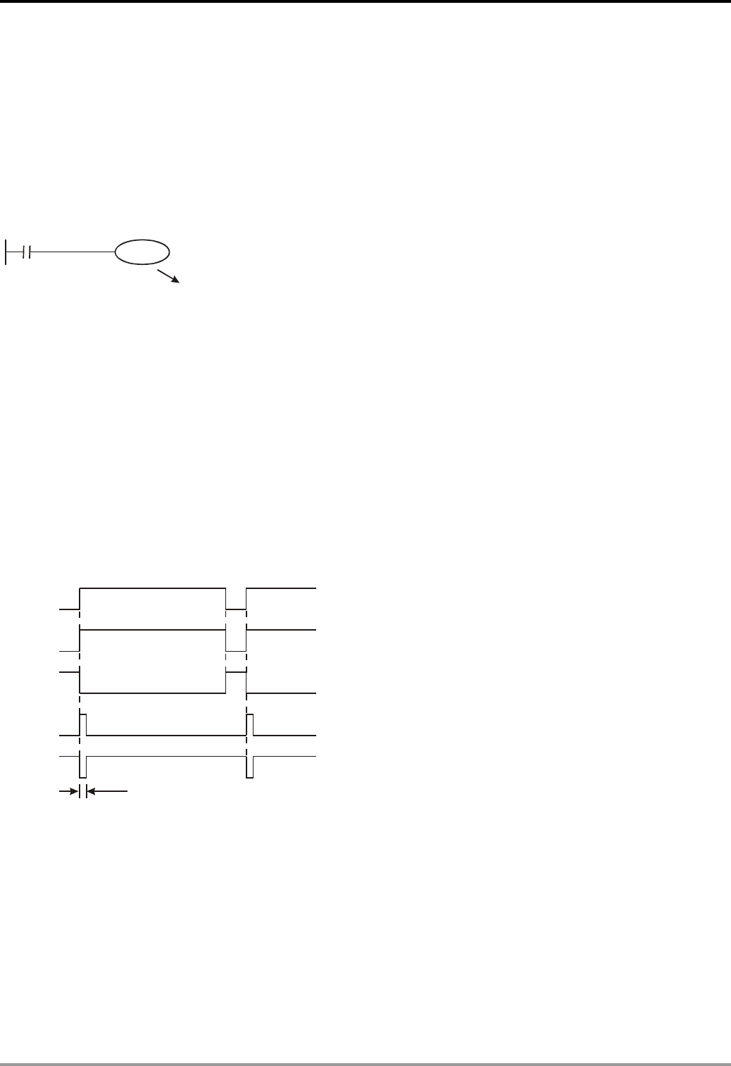
2 Functions of Devices in DVP-PLC
2.11 Functions of Special Auxiliary Relays and Special Registers
PLC Operation Flag
Function Group
M1000 ~ M1003
Number
M1000:
M1000 (A contact) is constantly “On” during operation and detection. When PLC is in RUN status, M1000 remains
“On”.
M1000
Y0 PLC is running
Keeps being On
Normally On contact
in PLC RUN
M1001:
M1001 (B contact) is constantly “On” during operation and detection. When PLC is in RUN status, M1001 remains
“On”.
M1002:
M1002 is “On” during the first scan when PLC starts to RUN and remains “Off” afterward. The pulse width = 1 scan
time. Use this contact for all kinds of initial settings.
M1003:
M1003 is “Off” during the first scan when PLC starts to RUN and remains “On” afterward. M1003 enables
negative-direction (“Off” immediately when RUN) pulses.
PLC RUN
M1000
M1001
M1002
M1003
scan time
Monitor Timer
Function Group
D1000
Number
Contents:
1. Monitor timer is used for moitoring PLC scan time. When the scan time exceeds the set time in the moitor timer,
the red ERROR LED indicator remains beaconing and all outputs will be “Off”.
2. The initial set value of the time in the monitor timer is 200ms. If the program is long or the operation is too
complicated, MOV instruction can be used for changing the set value. See the example below for SV = 300ms.
DVP-PLC Application Manual 2-83

2 Functions of Devices in DVP-PLC
M1002
0MOV K300 D1000
Initial pulse
3. The maximum set value in the monitor timer is 32,767ms. Please be noted that if the SV is too big, the timing of
detecting operational errors will be delayed. Therefore, it is suggested that you remain the scan time of shorter
than 200ms.
4. Complicated instruction operations or too many extension modules being connected to the MPU will result in the
scan time being too long. Check D1010 ~ D1012 to see if the scan time exceeds the SV in D1000. In this case,
besides modifying the SV in D1000, you can also add WDT instruction (API 07) into the PLC program. When the
CPU execution progresses to WDT instruction, the internal monitor timer will be cleared as “0” and the scan time
will not exceed the set value in the monitor timer.
Program Capacity
Function Group
D1002
Number
Contents:
The program capacity differs in different series of MPUs.
1. ES/EX/SS series MPU: 3,792 Steps
2. SA/SX/SC series MPU: 7,920 Steps
3. EH2/SV series MPU: 15,872 Steps
4. EH3/SV2 series MPU: 30000 Steps
Syntax Check
Function Group
M1004, D1004, D1137
Number
Contents:
1. When errors occur in syntax check, ERROR LED indicator will flash and special relay M1004 = On.
2. Timings for PLC syntax check:
a) When the power goes from “Off” to “On”.
b) When the program is written into PLC by means of WPLSoft, ISPSoft or HPP.
c) When on-line editing is being conducted.
3. The syntax check may start due to illegal use of instruction operands (devices) or incorrect program syntax loop.
The error can be detected by the error code in D1004 and error table. The address where the error exists will be
stored in D1137. (The address value in D1137 will be invalid if the error is a general loop error.)
4. See Chapter 2.13 for error codes for syntax check.
DVP-PLC Application Manual
2-84

2 Functions of Devices in DVP-PLC
Data Backup Memory
Function Group
M1005~M1007
Number
Contents:
When the data backup memory card is installed in EH2 MPU, MPU will operate according to the On/Off of switch on
the card. If the switch is “On”, the following comparisons will be conducted and the card will be copied to MPU. If the
switch is “Off”, MPU will not perform any action.
1. M1005 = On: An error occurs in the comparison between the ciphers of MPU and the data backup memory card
and MPU does not perform any action.
2. M1006 = On: The data backup memory card has not been initialized.
3. M1007 = On: Data in the program area of the data backup memory card do not exist, it means data doesn’t exist
in the program area of data backup memory card.
Scan Time-out Timer
Function Group
M1008, D1008
Number
Contents:
1. M1008 = On: Scan time-out occurs during the execution of the program, and PLC ERROR LED indicator
remains beaconing.
2. Users can use WPLSoft, ISPSoft, or HPP to monitor the content (STEP address when WDT timer is “On”).
Checking Lost PLC SRAM Data
Function Group
D1009, M1175, M1176
Number
Contents:
1. bit0 ~ bit7 record the types of data lost. bit = 1 refers to losing data; bit = 0 refers to correct data.
2. What are lost
bit8 ~ 15 bit 7 bit 6 bit 5 bit 4 bit 3 bit 2 bit 1 bit 0
PLC
program
File
register
Reserved D register T register C register M relay S step password
3. After the PLC is powered, the data in SRAM will be verified. If the SRAM data are lost, the PLC will record the
error in D1009 and set on M1175 or M1176 according to the content of the data.
Scan Time Monitor
Function Group
D1010 ~ D1012
Number
Contents:
The present value, minimum value and maximum value of scan time are stored in D1010 ~ D1012.
1. D1010: Present scan time value
2. D1011: Minimum scan time value
3. D1012: Maximum scan time value
DVP-PLC Application Manual 2-85
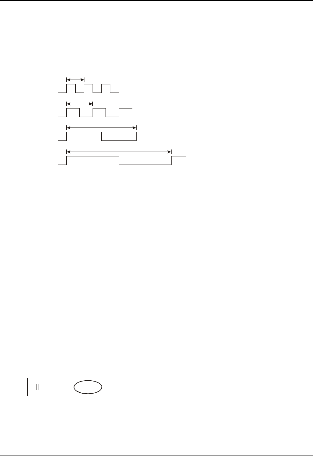
2 Functions of Devices in DVP-PLC
Internal Clock Pulse
Function Group
M1011 ~ M1014
Number
Contents:
1. All PLC MPUs provide four different clock pulses. When PLC is powered, the four clock pulses will start
automatically.
M1011 (10 ms)
M1012 (100 ms)
M1013 (1 sec)
M1014 (60 sec)
100 Hz
10 Hz
1 Hz
10 ms
100 ms
1 sec
1 min
2. The clock pulses also start when PLC is in STOP status. The activation timing of clock pulses and that of RUN
will not happen synchronously.
High-Speed Timer
Function Group
M1015, D1015
Number
Contents:
1. The steps for using special M and special D directly:
a) High-speed counter is valid only when PLC is in RUN status for EH2/SVEH3/SV2, but is valid when PLC is
in RUN or STOP stauts for SA/SX/SC.
b) M1015 = On: High-speed counter D1015 is enabled only whtn PLC scans to END instruction. (Min. timing
unit of D1015: 100us)
c) Timing range of D1015: 0~32,767. When the timing reaches 32,767, the next timing restarts from 0.
d) M1015 = Off: D1015 stops timing immediately.
2. EH2/SVEH3/SV2 series MPU offers high-speed timer instruction HST. See API 196 HST for more details.
3. Example:
a) When X10 = On, M1015 will be On. The high-speed timer will start to time and record the present value in
D1015.
b) When X10 = Off, M1015 will be Off. The high-speed timer will be disabled.
X10
M1015
DVP-PLC Application Manual
2-86

2 Functions of Devices in DVP-PLC
Real Time Clock
Function Group
M1016, M1017, M1076, D1313 ~ D1319
Number
Contents:
1. Special M and special D relevant to RTC
No. Name Function
Off: display the last 2 digits of year in A.D.
M1016 Year (in A.D.) in RTC On: display the last 2 digits of year in A.D. plus 2,000
From “Off” to “On”, the correction is enabled.
±30 seconds
correction 0 ~ 29 second: minute intact; second reset to 0
M1017
30~ 59 second: mimute + 1; second reset to 0
M1076 RTC malfunction Set value exceeds the range; dead battery
M1082 Flag change on RTC On: Modification on RTC
D1313 Second 0 ~ 59
D1314 Minute 0 ~ 59
D1315 Hour 0 ~ 23
D1316 Day 1 ~ 31
D1317 Month 1 ~ 12
D1318 Week 1 ~ 7
D1319 Year 0 ~ 99 (last 2 digits of Year in A.D.)
2. If the set value in RTC is incorrect, the time will be recovered as “Saturday, 00:00 Jan. 1, 2000” when PLC is
powered and restarted.
D1313 ~ D1319 will immediately update the RTC only when in TRD instruction or WPLSoft monitoring mode. 3.
How to make corrections on RTC:
4.
a) Use TWR instruction fir SA/SX/SX/EH2/SVEH3/SV2 series MPU. See API 167 TWR for more details.
b) Use WPLSoft, ISPSoft, or digital display panel DU-01.
π(PI)
Function Group
D1018, D1019
Number
Contents:
1. D1018 and D1019 are combined as 32-bit data register for storing the floating point value ofπ(PI)
2. loating point value = H 40490FDB
Adjustment on Input Terminal Response Time
Function Group
D1020, D1021
Number
Contents:
1. D1020 can be used for setting up the response time of receiving pulses at X0 ~X7 for SS/ES/EX/SA/SX/SC
series MPU. (Setup range: 0 ~ 20; Unit: ms)
2. D1021 can be used for setting up the response time of receiving pulses at X10 ~X17 for ES series MPU. (Setup
range: 0 ~ 20; Unit: ms)
DVP-PLC Application Manual 2-87
2 Functions of Devices in DVP-PLC
3. D1021 can be used for setting up the response time of receiving pulses at X10 ~X11 for SC series MPU. (Setup
range: 0 ~ 1,000; Unit: time)
4. D1020 can be used for setting up the response time of receiving pulses at X0 ~X7 for EH2/SVEH3/SV2 series
MPU. (Setup range: 0 ~ 60; Unit: ms)
5. D1021 can be used for setting up the response time of receiving pulses at X10 ~X17 for EH2/SVEH3/SV2 series
MPU. (Setup range: 0 ~ 60; Unit: ms)
6. When the power of PLC goes from “Off” to “On”, the content of D1020 and D1021 turn to 10 automatically.
X0
X17
0ms
1ms
10ms
15ms
0
1
10
15
Termi na l response time
Status
memory
Regenerating input
Set by D1020 (default: 10)
7. If the following programs are executed during the program, the response time of X0 ~ X7 will be set to 0ms. The
fastest response time of input terminals is 50μs due to that all terminals are connected with RC filter loop.
M1000
MOV K0 D1020
normally ON contact
8. There is no need to make adjustment on response time when using high-speed counters and interruptions
during the program.
9. Using API 51 REFF instruction has the same effect as modifying D1020 and D1021.
Execution Completed Flag
Function Group
M1029, M1030, M1036, M1037, M1102, M1103
Number
Contents:
Using execution completed flag:
1. API 52 MTR, API 71 HKY, API 72 DSW, API 74 SEGL, API 77 PR: M1029 = On whenever the instruction
completes one scan period.
2. API 57 PLSY, API 59 PLSR:
a) M1029 will be “On” after Y0 pulse output of SA/SX/SC/ES/EX/SS is completed. M1030 will be “On” after Y1
pulse output is compeleted. When PLSY and PLSR instruction is “Off”, M1029 and M1030 turn “Off”. You
have to reset M1029 and M1030 after the action is completed.
b) M1029 will be “On” after Y0 and Y1 pulse output of EH2/SVEH3/SV2 is completed. M1030 will be “On” after
Y2 and Y3 pulse output is compeleted. M1036 will be “On” after Y4 and Y5 pulse output of EH2/SV is
completed. M1037 will be “On” after Y6 and Y7 pulse output is completed.When PLSY and PLSR
instruction is “Off”, M1029, M1030, M1036 and M1037 turn “Off”. When the instruction is re-executed for the
DVP-PLC Application Manual
2-88

2 Functions of Devices in DVP-PLC
next time, M1029, M1030, M1036 and M1037 will turn “Off” and “On” again when the execution is
completed.
API 63 INCD: M1029 will be “On” for a scan period when the assigned group numbers of data are compared.
3.
4. API 67 RAMP, API 69 SORT:
a) When the execution of the instruction is completed, M1029= On. You have to reset M1029.
b) M1029 turns “Off” when the instruction is “Off”.
5. API 155 DABSR, API 156 ZRN, API 158 DRVI, API 159 DRVA for EH2/SVEH3/SV2 series MPU:
a) M1029 = On when the 1st output group Y0 and Y1 of EH2/SVEH3/SV2 is completed. M1030 = On when the
2nd output group Y2 and Y3 is completed.
b) M1036 = On when the 3rd output group Y4 and Y5 of EH2/SV is completed. M1037 = On when the 4th output
group Y6 and Y7 is completed.
c) When the instruction is re-executed for the next time, M1029 or M1030 will turn “Off” and “On” again when
the execution is completed.
6. In API 57 PLSY, API 156 DZRN, API 158 DDRVI and API 159 DDRVA for SC series MPU: M1102 will be set On
when Y10 pulse output is completed. M1103 will be set On when Y11 pulse output is completed. After PLSY
instruction is disabled,M1102 and M1103 will be set Off. In DDRVA, DDRVI and DZRN, M1102 and M1103 will
be set Off when next time these instructions are enabled.
Communication Error Code
Function Group
M1025, D1025
Number
Contents:
When HPP, PC or HMI is connected to the PLC and the PLC receives illegal communication request during the
transmission of data, M1025 will be On and the error code will be written in D1025. See the error codes below.
01: Illegal instruction code
02: Illegal device address
03: Requested data exceed the range
07: Checksum error
Clear Instruction
Function Group
M1031, M1032
Number
Contents:
M1031 (clearing non-latched area) , M1032 (clearing latched area)
Device No. Cleared Device
Contact status of Y, general-purpose M and general-purpose S
General-purpose contact and timing coil of T
M1031 General-purpose contact, counting coil reset coil of C
General-purpose present value register of D
DVP-PLC Application Manual 2-89

2 Functions of Devices in DVP-PLC
Device No. Cleared Device
General-purpose present value register of T
M1031 General-purpose present value register of C
Contact status of M and S for latched
Contact and timing coil of accumulative timer T
Contac and timing coil of high-speed counter C for latched
M1032 Present value register of D for latched
Present value register of accumulative timer T
Present value register of high-speed counter C for latched
Output Latched During STOP
Function Group
M1033
Number
Contents:
When M1033 = On and PLC goes from “RUN” to “STOP”, the On/Off status of output will be ratained.
Assume the output contact load of the PLC is a heater, when PLC switches from RUN to STOP, the status of the
heater will be retained. After the PLC program is modified, the PLC will RUN again.
All Output Y Inhibited
Function Group
M1034
Number
Contents:
When M1034 = On, all Y outputs will turn “Off”.
M1034 all outputs inhibited
RUN/STOP Switch
Function Group
M1035, D1035
Number
Contents:
1. When M1035 = On, EH2/SVEH3/SV2 series MPU will determine the content (K0 ~ K15) in D1035 to enable
input points X0 ~ X17 as the RUN/STOP switch.
2. When M1035 = On, SA/SX/SC series MPU will enable the input point X7 (in SA), X3 (in SX) and X5 (in SC) as
the RUN/STOP switch.
Detecting Speed of X0 ~ X5
Function Group
M1036
Number
Contents:
1. For SC_V1.4 and versions above, SPD can detect the speed of X0 ~ X5 at the same time. The total bandwidth is
40kHz.
2. Program example:
DVP-PLC Application Manual
2-90
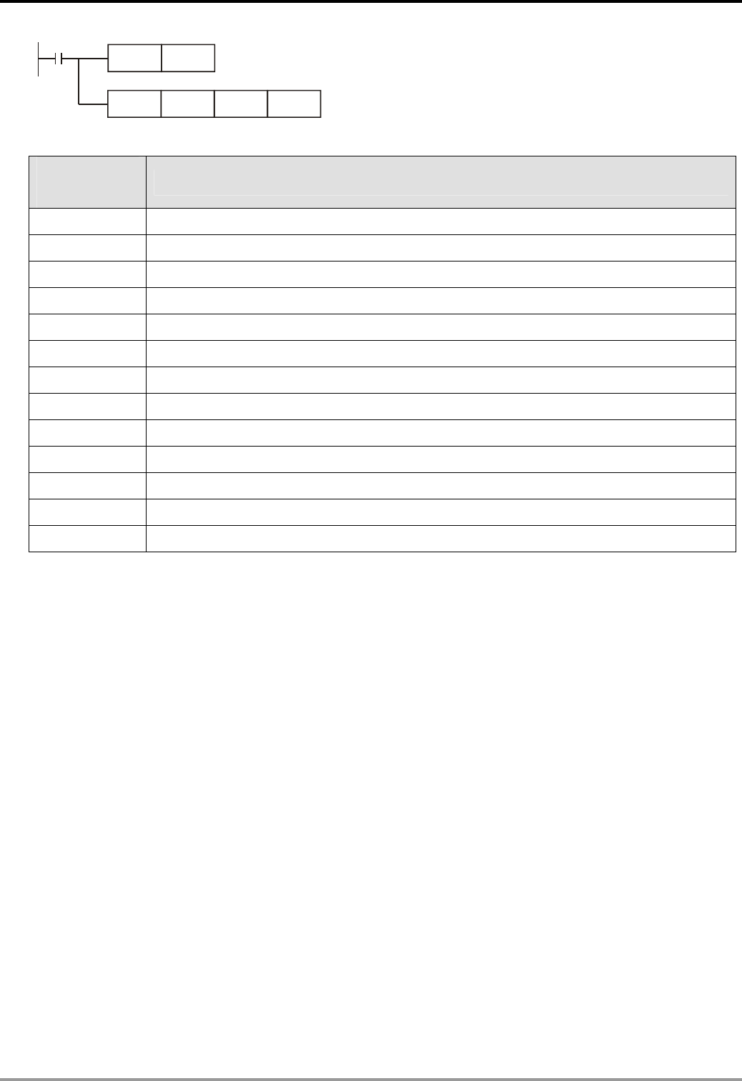
2 Functions of Devices in DVP-PLC
X7
SPD X1 K1000 D0
SET M1036
3. Parameter D0 when X7 = On
Start No. of D0 Functions
+ index value
+0 Low 16 bits of the 32-bit speed detected at input point X0.
+1 High 16 bits of the 32-bit speed detected at input point X0.
+2 Low 16 bits of the 32-bit speed detected at input point X1.
+3 High 16 bits of the 32-bit speed detected at input point X1.
+4 Low 16 bits of the 32-bit speed detected at input point X2.
+5 High 16 bits of the 32-bit speed detected at input point X2.
+6 Low 16 bits of the 32-bit speed detected at input point X3.
+7 High 16 bits of the 32-bit speed detected at input point X3.
+8 Low 16 bits of the 32-bit speed detected at input point X4.
+9 High 16 bits of the 32-bit speed detected at input point X4.
+10 Low 16 bits of the 32-bit speed detected at input point X5.
+11 High 16 bits of the 32-bit speed detected at input point X5.
+12 Remaining time for speed detection (unit: ms)
X0 Detecting Pulse Width
Function Group
M1084, D1023
Number
Contents:
When M1084 = On, X0 of ES/EX/SS_V6.4/SA/SX_V1.6/SC_V1.4 can detect pulse width. Whenever X0 turns from
“On” to “Off”, the value is updated once and stored in D1023 (unit: 0.1ms). The minimum detectable width is 0.1ms
and maximum 1,000ms.
Two speeds
Function Group
M1119
Number
Contents:
1. Supports EH2/SV_V2.2/EH3/SV2_V1.0 and versions above.
2. Before the instruction is enabled, M1119 has to be set to On. After the instruction is enabled, M1119 is set to Off
automatically.
3. S1 and S1+1 in DDRVI/DDRVA designates the position of the first speed and the position of the second speed
respectively, S2 and S2+1 designates the fist speed and the second speed respectively.
4. The second speed must be less than the first speed. Otherwise, the first speed is taken.
DVP-PLC Application Manual 2-91
2 Functions of Devices in DVP-PLC
Speed
(Hz)
Time(ms)
T1 T2 T3
V(1)
P(1
Vbas Vbas
P(2)
V(2)
Vbase T1 T2+T3 P(1) V(1) P(2) V(2)
Position of
the first
speed
Initial Acceleration Deceleration Position of the
second speed
First speed Second speed
frequency time time
Example:
Explanation:
1. Set P(1) to 1000 pulse, P(2) to 2000 pulse, V(1) to 20kHz, and V(2) to 10kHz.
2. Set M1119 to On.
3. Execute DDRVI/DDRVA.
Communication Port Function
Function Group
M1120, M1136, M1138, M1139, M1143, D1036, D1109, D1120
Number
Contents:
1. Supports ES/EX/SS_V6.0/SA/SX_V1.2/SC_V1.0/SV_V1.0/EH2_V1.0/EH3/SV2_V1.0 and versions above.
2. COM ports (COM1: RS-232; COM2: RS-485) in SA/SX/SC series MPU and COM ports (COM1: RS-232; COM2:
RS-232/RS-485/RS-422) in EH2/EH3/SV2 series MPU support Modbus ASCII/RTU communication format with
speed of up to 115,200bps. COM1 and COM2 can be used at the same time. COM3: RS-232/RS-485 in EH/EH2
DVP-PLC Application Manual
2-92

2 Functions of Devices in DVP-PLC
series MPU supports Modbus ASCII communication format with speed of up to 38,400bps. The communication
port (COM3: F232RS-232/RS-422) in EH3/SV2 series MPU supports ASCII/RTU communication format with
speed of up to 115,200bps.
COM1: For slave stations only. Supports ASCII/RTU communication format, adjustable baud rate with
speed of up to 115,200bps, and modification on data length (data bits, parity bits, stop bits).
EH3/SV2 series MPUs can be as a masters or slaves, and supports ASCII/RTU communication
format, adjustable baud rate with speed of up to 115,200bps, and modification on data length (data
bits, parity bits, stop bits).
COM2: For master or slave stations. Supports ASCII/RTU communication format, adjustable baud rate
with speed of up to 115,200bps, and modification on data length (data bits, parity bits, stop bits).
COM3: EH2 series MPUs can be used as slaves stations only. Supports ASCII communication format
(data bits, parity bits, stop bits) 7, E, 1, adjustable baud rate with speed of up to 38,400bps. COM2
or COM3 cannot be used for slave stations at the same time.
EH3/SV2 series MPUs can be as a masters or slaves, and supports ASCII/RTU communication
format, adjustable baud rate with speed of up to 115,200bps, and modification on data length (data
bits, parity bits, stop bits).
Communication Format Settings:
COM1: 1. Communication format is set in D1036. b8 ~ b15 do not support the communication protocol of
COM1 (RS-232) Slave.
2. The communication format in EH3/SV2 series MPU is set in D1036. b8 ~ b15 do not support
the communication protocol of COM1 (RS-232) Slave/Master.
3. Communication setting in M1138 remains.
4. M1139 is set in ASCII/RTU mode
COM2: 1. Communication format is set in D1120. Communication protocol of COM2
(RS-232/RS-485/RS-422) Master or Slave
2. The communication format in EH2 series MPU is set in D1120. COM2 (RS-485 or DVP-F232
card/DVP-F422 card) will occupies the communication protocol of original COM2 (RS-485)
Master or Slave.
3. Communication setting in M1120 remains
4. M1143 is set in ASCII/RTU mode
COM3: 1. Communication format is set in D1109. b0 ~ b3 and b8 ~ b15 do not support the
communication protocol of COM3 (DVP-F232 card/DVP-F485S card) Slave
2. The communication format in EH3-SV2 is set in D1109. b0 ~ b3 and b8 ~ b15 do not support
the communication protocol of COM3 Slave or Master.
3. Communication setting in M1136 remains
DVP-PLC Application Manual 2-93
2 Functions of Devices in DVP-PLC
Communication protocols and how to set:
Content 0 1
b0 Data length b0 = 0:7 b0 = 1:8
b2, b1 = 00 : None
b2, b1 = 01 : Odd
b1 parity bit
b2 b2, b1 = 11 : Even
b3 stop bits b3 = 0:1 bit b3 = 1:2 bit
:
b7 ~ b4 = 0001 (H1) 110 bps
:
b7 ~ b4 = 0010 (H2) 150 bps
:
b7 ~ b4 = 0011 (H3) 300 bps
:
b7 ~ b4 = 0100 (H4) 600 bps
:
b7 ~ b4 = 0101 (H5) 1,200 bps
:
b7 ~ b4 = 0110 (H6) 2,400 bps
b7 ~ b4 = 0111 (H7) : 4,800 bps
b7 ~ b4 = 1000 (H8) : 9,600 bps
b7 ~ b4 = 1001 (H9) : 19,200 bps
b7 ~ b4 = 1010 (HA) : 38,400 bps
b7 ~ b4 = 1011 (HB) : 57,600 bps
b7 ~ b4
:
b7 ~ b4 = 1100 (HC) 115,200 bps
b8 Select start bit b8 = 0:None b8 = 1:D1124
b9 Select the 1st end bit b9 = 0:None b9 = 1:D1125
b10 Select the 2nd end bit b10 = 0:None b10 = 1:D1126
b15 ~ b11 Not defined
Example 1: Modifying communication format of COM2
1. Add the program code below on top of the program to modify the communication format of COM2. When PLC
switches from STOP to TUN, the program will detect whether M1120 is On in the first scan time. If M1120 is On,
the program will modify the relevant settings of COM2 according to the value set in D1120.
2. Modify the communication format of COM2 into ASCII mode, 57,600bps, 7 data bits, even parity, 1 stop bit
(57,600, 7, E, 1)
MOV H86 D1120
SET M1120
M1002
Notes:
1. If COM2 is to be used as a Slave terminal, make sure there is no communication instruction existing in the
program.
2. After the communication format is modified, the format will stay intact when PLC switches from RUN to
STOP.
3. If you shut down the power of the PLC and repower it again, the modified communication format will return
DVP-PLC Application Manual
2-94

2 Functions of Devices in DVP-PLC
to default setting.
Example 2: Modifying the communication format of COM1
1. Add the program code below on top of the program to modify the communication format of COM1. When PLC
switches from STOP to TUN, the program will detect whether M1138 is On in the first scan time. If M1138 is On,
the program will modify the relevant settings of COM1 according to the value set in D1036.
2. Modify the communication format of COM1 into ASCII mode, 115,200bps, 7 data bits, even parity, 1 stop bit
(115,200, 7, E, 1)
MOV H86 D1036
SET M1138
M1002
Notes:
1. After the communication format is modified, the format will stay intact when PLC switches from RUN to
STOP.
2. If you shut down the power of the PLC and repower it again, the modified communication format will return
to default setting.
Example 3: Modifying the communication format of COM3
1. The communication format of COM3 is fixed as 7 data bits, even parity, 1 stop bit. Add the program code below
on top of the program to modify the baud rate of COM3 into 38,400bps. When PLC switches from STOP to TUN,
the program will detect whether M1136 is On in the first scan time. If M1136 is On, the program will modify the
relevant settings of COM3 according to the value set in D1109.
2. Modify the baud rate of COM3 into 38,400bps
MOV HA0 D1109
SET M1136
M1002
Notes:
1. After the communication format is modified, the format will stay intact when PLC switches from RUN to
STOP.
2. If you shut down the power of the PLC and repower it again, the modified communication format will return
to default setting.
Example 4: Setting up RTU mode of COM1 and COM2
1. COM1 and COM2 support ASCII/RTU mode. COM1 is set by M1139 and COM2 is set by M1143. When the flags
are On, they are in RTU mode; when the flags are Off, they are in ASCII mode.
DVP-PLC Application Manual 2-95
2 Functions of Devices in DVP-PLC
2. How to set up RTU mode
COM1: (9,600, 8, E, 1, RTU)
MOV H86 D1036
SET M1138
M1002
SET M1139
COM2: (9,600, 8, E, 1, RTU)
MOV H86 D1120
SET M1120
M1002
SET M1143
3. EH2/SV/EH3/SV2 series MPU supports the generation of interruption I170 when the data receiving is completed
in Slave mode.
4. Normally when the communication terminal of the PLC is in Slave mode, PLC will not immediately process the
communication data entered but process it after the END is executed. Therefore, when the scan time is very long
and you need the communication data to be processed immediately, you can use interruption I170 for this matter.
5. Example of interruption I170 (after the data receiving is completed in Slave mode)
MOV H86 D1120
SET M1120
M1002
SET M1143
FEND
IRET
END
I170
EI
With I170 in the program, when COM2 is in Slave mode and there are communication data coming in, PLC will
process the data and respond immediately.
Notes:
1. DO NOT updat program on-line when using I170.
2. The scan time of PLC will be slightly longer.
DVP-PLC Application Manual
2-96
2 Functions of Devices in DVP-PLC
Communication Response Delay
Function Group
D1038
Number
Contents:
1. When PLC is used as slave station, in RS-485 communication interface, users can set up communication
response delay time ranging from 0 to 10,000 (0 ~ 1 second). If the time is without the range, D1038 = O (time
unit: 0.1ms). The set value of time must be less than that in D1000(scan time-out timer WDT).
2. In PLC LINK, you can set up delayed transmission of the next communication data (unit: 1 scan period for
SA/SX/SC; 0.1ms for EH2/SV/EH3/SV2).
Fixed Scan Time
Function Group
M1039, D1039
Number
Contents:
1. When M1039 = On, the scan time of program is determined by the content in D1039. When the execution of the
program is completed, the next scan will take place when the fixed scan time is reached. If the content in D1039
is less than the actual scan time of the program, the scan time will follow the actual scan time of the program.
M1000
Normally On
contact MOV P K20 D1039
M1039 Fixed scan time
Scan time is fixed to 20ms
2. Instructions related to scan time, RAMP (API 67), HKY (API 71), SEGL (API 74), ARWS (API 75) and PR (API
77) should be used together with “fixed scan time” or “constant interruption”.
3. Particularly for HKY instruction, when the 16-digit button input is operated by 4x4 matrix, the scan time has to be
fixed to longer than 20ms.
4. The scan time in D1010 ~ D1012 also includes fixed scan time.
Analog Function
Function Group
D1056 ~ D1059, D1062, D1110 ~ D1113, D1116 ~ D1118
Number
Contents:
1. Resolution of analog input channel: 10 bits for EX, corresponding to 0 ~ ±10 V (-512 ~ +511) or 0 ~ ±20 mA
(-512 ~ +511); 12 bits for SX, corresponding to 0 ~ ±10 V (-2,000 ~ +2,000) or 0 ~ ± 20 mA (-1,000 ~ +1,000).
2. Resolution of analog output channel: 8 bits for EX, corresponding to 0 ~ 10 V (0 ~ 255) or 0 ~ 20 mA (0 ~ 255);
12 bits for SX, corresponding to 0 ~ ±10 V (-2,000 ~ +2,000) or 0 ~ ±20 mA (-2,000 ~ +2,000).
3. Sampling time of analog/digital conversion. Default setting = 5; unit: ms. If D1118 ≤ 5, it will be regarded as 5ms.
4. Resolution of EH2/SV/EH3/SV2 analog input AD card (DVP-F2AD): 12 bits 0 ~ 10 V (0 ~ +4,000) or 11 bits 0 ~
20 mA (0~+2,000)
5. Resolution of EH2/SV/EH3/SV2 analog input DA card (DVP-F2DA): 12 bits 0 ~ 10 V (0 ~ +4,000) or 0 ~ 20 mA
(0 ~ +4,000)
DVP-PLC Application Manual 2-97
2 Functions of Devices in DVP-PLC
Device No. Function
D1056 Present value of EX/SX analog input channel CH0 and EH2/EH3/SV2 AD card channel CH0
D1057 Present value of EX/SX analog input channel CH1 and EH2/EH3/SV2 AD card channel CH1
D1058 Present value of EX analog input channel CH 2
D1059 Present value of EX analog input channel CH 3
D1062 Average times (2 ~ 4) of SX AD0 and AD1
D1110 Average value of EX/SX analog input channel CH0 and EH2/EH3/SV2 AD card channel CH0
D1111 Average value of EX/SX analog input channel CH1 and EH2/EH3/SV2 AD card channel CH1
D1112 Average value of EX analog input channel CH2
D1113 Average value of EX analog input channel CH3
D1116 EX/SX analog output channel CH0 and EH2/EH3/SV2 DA card channel CH0
D1117 EX/SX analog output channel CH1 and EH2/EH3/SV2 DA card channel CH1
D1118 Sampling time (ms) of SX/EX/EH2/EH3/SV2 analog/digital conversion
Reading/Writing the data from/into the memory card
Function Group
M1163, D1063
Number
Contents:
The reading/writing of the data between the EH2 series MPU and the memory card:
M1163 state D1063 code Function
The program is read from the memory card, and
copied to the main operation area in the MPU.
0x55AA
The data is read from the memory card, and copied to
the main operation area in the MPU.
0x55A9
0xAA55 The program in the main operation area in the MPU is
copied to the memory card.
On
The data in the main operation area in the MPU is
copied to the memory card.
0xA955
Note:
1. After the reading/writing of the data is complete, M1163 is automatically set to Off. After the reading/writing of the
data is complete, the following flags are On.
M1189 Æ The data which is read/written is correct.
M1075 Æ An error occurs when the data is written into the memory card. Please check if the memory card is
inserted or damaged.
M1005 Æ The PLC ID on the MPU or the main password is different from the memory card.
M1006 Æ No data or program is in the memory card.
2. Enter the function code in D1063 first, and then set M1163 to On. Otherwise, M1163 is automatically reset to Off.
3. If an error occurs during the reading/writing of the data, the specila M will be set. No error LED indicator will flash
or no situation in which the MPU can not run occurs. Therefore, if customers need an alarm, please make the
warning message on the device or superior machine according to the flags above.
DVP-PLC Application Manual
2-98

2 Functions of Devices in DVP-PLC
4. Owing to the fact that the storage material of the memory card is Flash ROM, it takes some execution time to
write the data into the memory card.
5. When the program is copied, the MPU automatically copies the password function (including the main password,
the limit on the number of errors, the subroutine password, and the PLC ID).
6. The reading/writing of the data between the EH3/SV2 series MPU and the memory card:
M1163 state D1063 code Function
The data is read from the memory card, and copied to
the main operation area in the MPU.
0x55AB
The program code is read from the memory card, and
copied to the main operation area in the MPU.
0x55AA
The data in D2000~D11999 and file registers 0~4999
are read and copied to the main operation area in the
MPU.
0x55A9
On
The data in the main operation area in the MPU is
copied to the memory card.
0xAB55
0xAA55 The program in the MPU is copied to the memory card.
The data in D2000~D11999 in the main operation area
in the MPU is copied to the memory card.
0xA955
0x8888 Clearing the data in the memory card
Note:
1. After the reading/writing of the data is complete, M1163 is automatically set to Off. After the reading/writing of the
data is complete, the following flags are On.
M1189 Æ The data which is read/written is correct.
M1075 Æ An error occurs when the data is written into the memory card. Please check if the memory card is
inserted or damaged.
M1005 Æ The PLC ID on the MPU or the main password is different from the memory card.
M1006 Æ No data or program is in the memory card.
2. Enter the function code in D1063 first, and then set M1163 to On. Otherwise, M1163 is automatically reset to Off.
3. If an error occurs during the reading/writing of the data, the specila M will be set. No error LED indicator will flash
or no situation in which the MPU can not run occurs. Therefore, if customers need an alarm, please make the
warning message on the device or superior machine according to the flags above.
4. Owing to the fact that the storage material of the memory card is Flash ROM, it takes some execution time to
write the data into the memory card.
5. When the program is copied, the MPU automatically copies the password function (including the main password,
the limit on the number of errors, the subroutine password, and the PLC ID).
DVP-PLC Application Manual 2-99

2 Functions of Devices in DVP-PLC
Reading/Writing the data from/into the backup area
Function Group
M1067 ~ M1068, D1067 ~ D1068
Number
Contents:
1. The reading/writing of the data between the EH2 series MPU and the backup area:
M1164 state D1064 code Function
The program and the data in D2000~D9999 are read
from the backup area, and copied to the main
operation area.
0x55AA
On
The program and the data in D2000~D9999 in the main
operation area are copied to the backup area.
0xAA55
Note:
1. After the reading/writing of the data is complete, M1164 is automatically set to Off. After the reading/writing of the
data is complete, the following flags are On.
M1189 Æ The data which is read/written is correct.
M1075 Æ An error occurs when the data is written into the backup area. Before replacing the PLC, please read
the program and the data form the main operation area first.
2. Enter the function code in D1064 first, and then set M1164 to On. Otherwise, M1164 is automatically reset to Off.
3. If an error occurs during the reading/writing of the data, the specila M will be set. No error LED indicator will flash
or no situation in which the MPU can not run occurs. Therefore, if customers need an alarm, please make the
warning message on the device or superior machine according to the flags above.
4. Owing to the fact that the storage material of the backup area is Flash ROM, it takes some execution time to write
the data into the memory card.
5. When the program is copied, the MPU automatically copies the password function (including the main password,
the limit on the number of errors, the subroutine password, and the PLC ID).
6. The reading/writing of the data between the EH3/SV2 series MPU and the backup area:
M1164 state D1064 code Function
On 0x55AA
The program and the data in D2000~D9999 are read
from the backup area, and copied to the main
operation area.
The program is read from the backup area, and copied
to the main operation area in the MPU.
0x55A9
On
The data is read from D2000~D11999 in the backup
area, and copied to the main operation area in the
MPU.
0x55AB
The program and the data in D2000~D9999 in the main
operation area are copied to the backup area.
0xAA55
The program in the main operation area is copied to
the backup area.
0xA955
DVP-PLC Application Manual
2-100
2 Functions of Devices in DVP-PLC
M1164 state D1064 code Function
The data in D2000~D11999 in the operation area is
copied to the backup area.
0xAB55
0x8888 The data in the bakup area is cleared.
Note:
1. After the reading/writing of the data is complete, M1164 is automatically set to Off. After the reading/writing of the
data is complete, the following flags are On.
M1189 Æ The data which is read/written is correct.
M1075 Æ An error occurs when the data is written into the backup area. Before replacing the PLC, please read
the program and the data form the main operation area first.
M1006 Æ No data or program is in the memory card.
2. Enter the function code in D1064 first, and then set M1164 to On. Otherwise, M1164 is automatically reset to Off.
3. If an error occurs during the reading/writing of the data, the specila M will be set. No error LED indicator will flash
or no situation in which the MPU can not run occurs. Therefore, if customers need an alarm, please make the
warning message on the device or superior machine according to the flags above.
4. Owing to the fact that the storage material of the backup area is Flash ROM, it takes some execution time to write
the data into the memory card.
5. When the program is copied, the MPU automatically copies the password function (including the main password,
the limit on the number of errors, the subroutine password, and the PLC ID).
Operational Error Flag
Function Group
M1067 ~ M1068, D1067 ~ D1068
Number
Contents:
1. Operational error flag:
Device Description Latched STOP → RUN RUN → STOP
M1067 Operational error flag None Cleared Latched
M1068 Operational error locked flag None Latched Latched
D1067 Operational error code None Cleared Latched
STEP value when operational error occurs
D1068 None Latched Latched
2. Error code explanation:
D1067 error code Cause
H’ 0E18 BCD conversion error
H’ 0E19 Divisor is 0
H’ 0E1A Use of device exceeds the range (including E, F index register modification)
H’ 0E1B Square root value is negative
H’ 0E1C FROM/TO instruction communication error
DVP-PLC Application Manual 2-101

2 Functions of Devices in DVP-PLC
Low Voltage
Function Group
M1087, D1100
Number
Contents:
1. When PLC detects LV (Low Voltage) signal, it will check if M1087 is “On” or not. If M1087 is “On”, the content in
D1100 will be stored in Y0 ~ Y17.
2. bit0 (LSB) of D1100 corresponds to Y0, bit1 corresponds to Y1, bit8 corresponds to Y10 and so on.
File Register
Function Group
M1101, D1101 ~ D1103
Number
Contents:
1. When the power of PLC turns from “Off” to “On”, PLC determines whether to automatically send the content in
the file register to the assigned data register by checking M1101, D1101 ~ D1103 (for SA/SX/SC/
EH2/SV/EH3/SV2).
Whether to automatically downland data from file register
M1101:
Start No. of file register K0 ~ K1,599 (for SA/SX/SC)
D1101: Start No. of file register K0 ~ K9,999 (for EH2/SV/EH3/SV2)
Number of data read from file register K0 ~ K1,600 (for SA/SX/SC)
D1102: Number of data read from file register K0 ~ K8,000 (for EH2/SV/EH3/SV2)
Location for storing data read from file register
D1103: Start No. of assigned data register D K2,000 ~ K4,999 (for SA/SX/SC)
Start No. of assigned data register D K2,000 ~ K9,999 (for EH2/SV/EH3/SV2)
2. See API 148 MEMR and API 149 MEMW for more details.
DIP Switch Function Card
Function Group
M1104 ~ M1111
Number
Contents:
1. When PLC is in RUN status with digital switch function card inserted, the 8 DIP switches amd their status
orrespond respectively to M1104 ~ M1111.
2. See API 109 SWRD for more details.
3. When PLC is in RUN status with 4DI card inserted into the input AX0 (photocoupler isolation), the status of AX0
~ AX3 correspond respectively to M1104 ~ M1107.
Transistor Output Function Card
Function Group
M1112, M1113
Number
Contents:
When PLC is in RUN status with 2DO function card inserted, M1112 and M1113 will correspond respectively to 2
transistors output points, AY0 and AY1.
DVP-PLC Application Manual
2-102
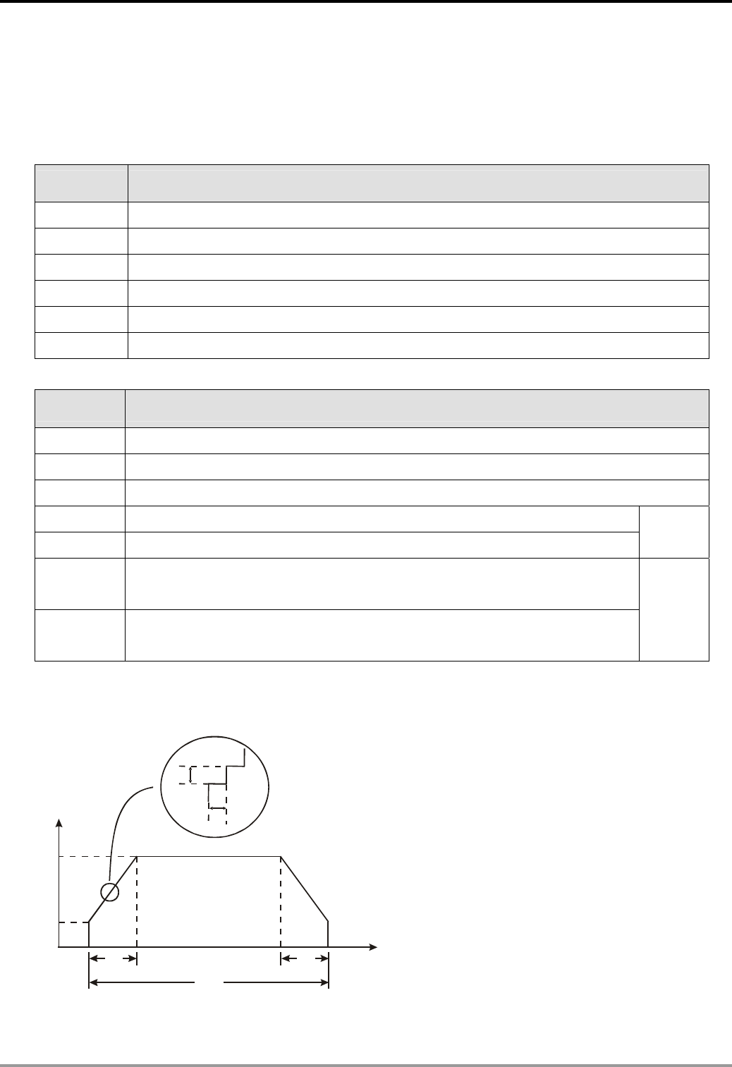
2 Functions of Devices in DVP-PLC
Pulse Output With Speed Acceleration/Deceleration
Function Group
M1115 ~ M1119, D1104
Number
Contents:
1. Special D and special M for acceleration/ deceleration of speed pulse output for ES/EX/SS/SA/SX/SC (not
applicable to SC_V1.4 and versions above):
Device No. Function
M1115 Activation switch
M1116 “Accelerating” flag
M1117 “Target frequency reached” flag
M1118 “Decelerating” flag
M1119 “Function completed” flag
D1104 Start No. of control register (D)
2. Parameters for D1104 (frequency range: 25Hz ~ 10kHz)
Index Function
+ 0 Start frequency (SF)
+ 1 Gap frequency (GF)
+ 2 Target frequency (TF)
+ 3 The lower 16 bits of the 32 bits for the total number of output pulses (TP)
+ 4 The higher 16 bits of the 32 bits for the total number of output pulses
The lower 16 bits of the 32 bits for the total number of output pulses in
accelerating/decelerating section
+ 5
(AP)
The higher 16 bits of the 32 bits for the total number of output pulses in
accelerating/decelerating section
+ 6
3. No instruction is needed, users need only to fill out the parameter table and enable M1115 (in RUN mode). This
functio only supports Y0 output and the timing chart is as below.
GF
GP
TF
SF
AP AP
Frequency
Number of pulses
Number of accel/decel sections = (TF-SF)/GF
Number of output pulses in every section:
GP = AP/Number of accel/decel sections
AP = number of accel/decel pulses
4. Note: this function is applicable only when “all” the conditions below are met.
a) Start frequency < target frequency.
DVP-PLC Application Manual 2-103
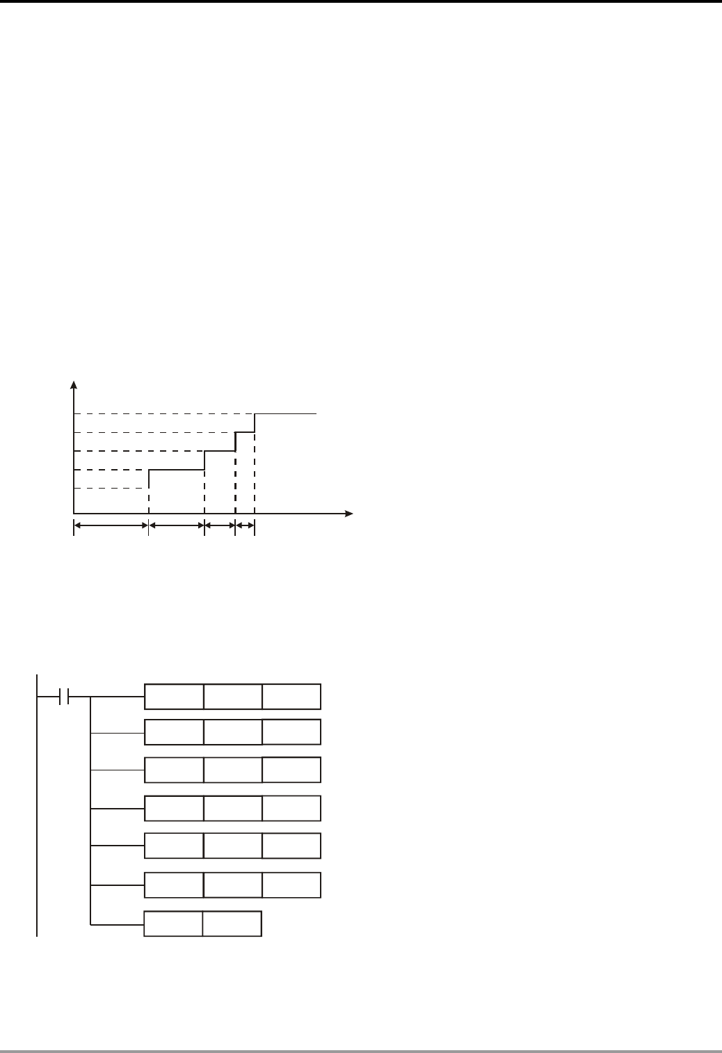
2 Functions of Devices in DVP-PLC
b) Gap frequency ≤ (target frequency – start frequency)
c) Total number of pulses > (accel/decel number of pulses × 2)
d) For start frequency and target frequency: Min. 25Hz; Max. 10kHz
e) Number of accel/decel pulses > number of accel/decel sections
When M1115 turns from “On” to “Off”, M1119 will be reset and M1116, M1117 and M1118 remain unchanged. When
PLC goes from “STOP” to “RUN”, M1115 ~ M1119 will be reset as “Off”. D1104 will only be cleared as “0” when it
turns from “Off” to “On”.
Either accel/decel pulse output function or PLSY Y0 output can be executed at a time when PLC is operating.
5. How to calculate the action time of each section
Assume the start frequency is set as 1kHz, gap frequency as 1kHz, target frequency as 5kHz, total number of
pulses as 100 and number of acceleration pulses as 40, the timing diagram of the acceleration sections is as the
figure below.
5,000
4,000
3,000
2,000
1,000
tttt
1234
Frequency (Hz)
Time (sec)
From the conditions above, we can obtain the number of acceleration/deceleration sections is (5K – 1K)/1K = 4
and the number of output pulses in each section is 40/4 = 10. Therefore, in the diagram, t1 = (1/1K) × 10 = 10ms,
t2 = (1/2K) × 10 = 5ms, t3 = (1/3K) × 10 = 3.33ms, t4 = (1/4K) × 10 = 2.5ms.
6. Program example: Forward/reverse acceleration/deceleration step motor control
K500
MOV
M1002
D1104
K1000MOV D500
K100MOV D501
MOV D502
K80000
DMOV D503
K10000
DMOV D505
K10000
M1115SET
D500 ~ D506 as parameter addresses
Start frequency: 1KHz
Interval frequency: 100Hz
Target frequency: 10KHz
Number of output pulses: 80,000
Number of pulses in accel/decel section: 10,000
a) When PLC is in RUN status, store all parameter settings into the registers designated in D1104.
b) When M1115 = On, the acceleration/deceleration pulse output will start.
DVP-PLC Application Manual
2-104
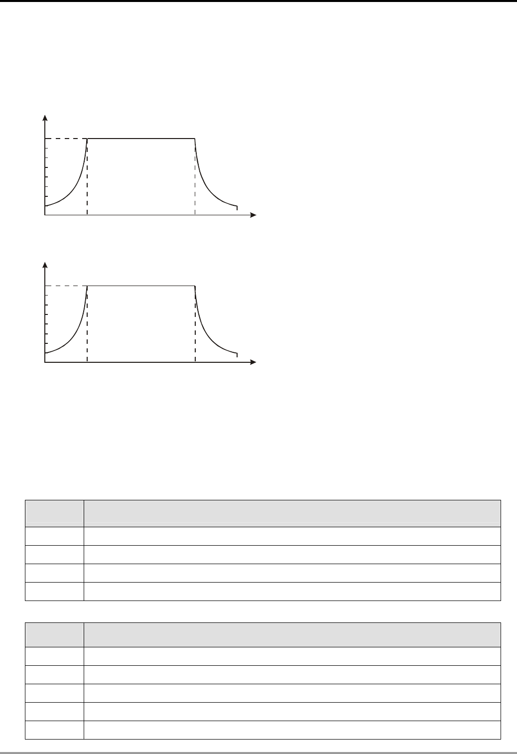
2 Functions of Devices in DVP-PLC
c) M1116 = On in the acceleration process. When the speed reaches its target, M1117 will be On. M1118 = On
in the deceleration process. When the speed reaches its target, M1119 will be On.
d) M1115 will not be reset automatically. You have to check the conditions during the process and reset it.
e) Pulse output curves:
10K
1K
10,000 70,000 80,000
Frequency (Hz)
Number
of pulses
10K
1K
2,606 8,606 11,213
Frequency (Hz)
Time (ms)
Special High-Speed Pulse Output
Function Group
M1133 ~ M1135, D1133
Number
Contents:
1. Special D and special M for special high-speed pulse Y0 (50kHz)for SA/SX/SC (not applicable to SC_V1.4 and
versions above):
No. Function
M1133 Output switch for special high-speed pulse Y0 (50kHz) (On = enabled)
M1134 On = Continuous output switch for special high-speed pulse Y0 (50kHz)
M1135 “Number of pulses reached” flag for special high-speed pulse Y0 (50kHz)
D1133 Start No. of control register (D) for special high-speed pulse Y0 (50kHz)
2. Parameters for D1133:
Index Function
+ 0 The lower 16 bits of the 32 bits for output frequency of special high-speed pulse Y0
+ 1 The higher 16 bits of the 32 bits for output frequency of special high-speed pulse Y0
+ 2 The lower 16 bits of the 32 bits for number of output pulses of special high-speed pulse Y0
+ 3 The higher 16 bits of the 32 bits for number of output pulses of special high-speed pulse Y0
+ 4 The lower 16 bits of the 32 bits of the present number of special high-speed pulses Y0
DVP-PLC Application Manual 2-105
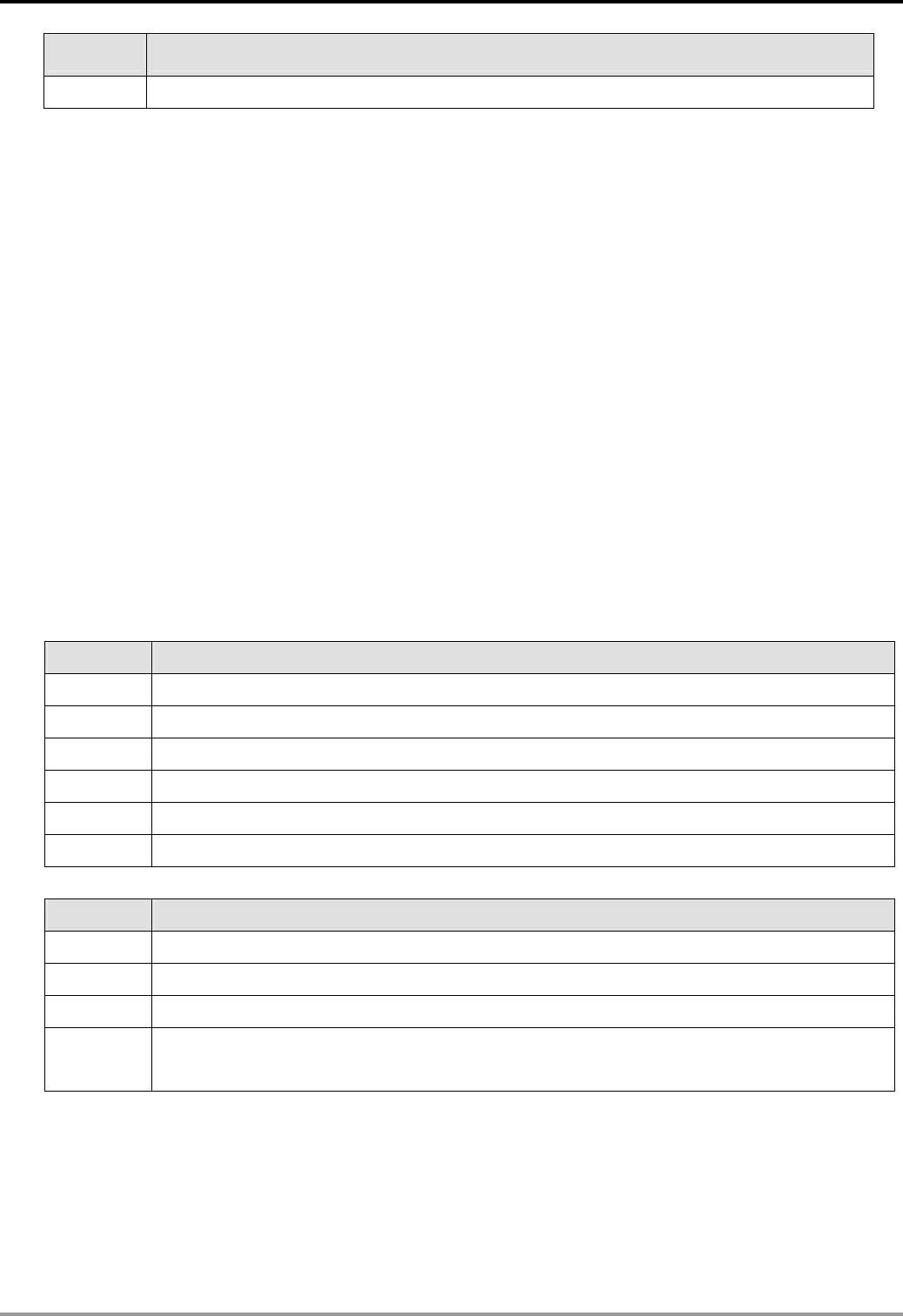
2 Functions of Devices in DVP-PLC
Index Function
+ 5 The higher 16 bits of the 32 bits of the present number of special high-speed pulses Y0
3. The function:
All output frequency and number of pulses stated in the table above can be modified when M1133 = On and
M1135 = On. The modification will not affect the present output pulses. The present number of output pulses is
updated in every scan time. When M1133 turns from “Off” to “on”, the number will be cleared as “0”. When 1133
turns from “On” to “Off”, the last numner of output pulses will be shown.
Note:
The special high-speed pulse output function can only be used on specific Y0 output point when PLC is in RUN status.
It can coexist with PLSY (Y0) in the program and PLSY (Y1) will not be affected. If PLSY (Y0) instruction is executed
prior to this function, the function cannot be used and vice versa. When the function is executed, the general function,
general Y0 output will be invalid but Y1 ~ Y7 can be used.
The output frequency of this function is higher (max. 50kHz) than that of PLSY instruction.
2-axis Synchronous Control (PH)
Function Group
M1133, M1135, D1133 ~ D1136
Number
Contents:
1. Special D and special M for 2-axis synchronous drawing oblique and arc for SC_V1.4 and versions above:
Device No. Function
M1133 Start flag for Y10 output for two-axis synchronous control
M1135 Start flag for Y11 output for two-axis synchronous control
D1133 Start No. of control register (D) for Y10 output for two-axis synchronous control
D1134 Number of sections for Y10 output for two-axis synchronous control
D1135 Start No. of control register (D) for Y11 output for two-axis synchronous control
D1136 Number of sections for Y11 output for two-axis synchronous control
2. Parameters for D1133, D1135:
Index Function
+ 0 Y10, Y11 2-axis synchronous control; output frequency of 1st section = low 16 bits of 32 bits
+ 1 Y10, Y11 2-axis synchronous control; output frequency of 1st section = high 16 bits of 32 bits
+ 2 Y10, Y11 2-axis synchronous control; output pulse number of 1st section = low 16 bits of 32 bits
Y10, Y11 2-axis synchronous control; output pulse number of 1st section = high 16 bits of 32
bits
+ 3
3. The functions:
a) Definition of the 2 axes:
X axis: Y0 (direction output) and Y10 (pulse output)
Y axis: Y1 (direction output) and Y11 (pulse output)
b) Define the format of output table:
Assume D1133 = K100 and D1134 = K3 and the output table has to be set as:
DVP-PLC Application Manual
2-106
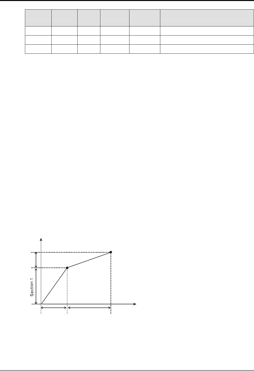
2 Functions of Devices in DVP-PLC
Output Number of
Section No. Device D Device D Description
frequency Output pulses
1 D101,D100 K10,000 D103,D102 K1,000 Section 1 outputs 1,000 pulses in 10kHz
2 D105,D104 K15,000 D107,D106 K2,000 Section 2 outputs 2,000 pulses in 15kHz
3 D109,D108 K5,000 D111,D110 K3,000 Section 3 outputs 3,000 pulses in 5kHz
Note: The frequency and number of output pulses are all in 32-bit. Thus, the 3 sections will continuously
occupy 12 D devices (3 × 2 × 2 = 12).
4. Note:
a) Make sure that the output frequency and the number of pulses have been set before using this function.
The output frequency and the number of pulses cannot be modified during the execution of the function.
b) When PLC program scans to END instruction, it will auto-check whether this function needs to be enabled.
c) When M1133 and M1135 are set in the same scan period, the two axes will output pulses synchronously.
d) When the output frequency < 100Hz, the output will be executed in 100Hz. When the output frequency >
100kHz, the output will be executed by 100kHz.
e) Only device D (D0 ~ D999 and D2000 ~ D4999) can be used for this function. DO NOT use other devices
or exceed the range of device D.
f) The maximum number of segments for this function is 50. When the number of segments < 1 or > 50, this
function will be disabled.
g) After this function is enabled, M1102 = “On” indicates Y10 output is completed and M1103 = “On” indicates
Y11 output is completed.
5. Examples:
a) Draw oblique lines in 2 axes
Destination: Draw 2 oblique lines (as figure 1)
Program explanation: Y0 and Y10 belong to X axis, and Y1 and Y11 belong to Y axis (as figure 2)
Output frequency and number of pulses: see table 1
(0,0)
X
(1,000, 3,000)
(5,000, 4,000)
Y
Section 2
Section 2Section 1
(Figure 1)
DVP-PLC Application Manual 2-107
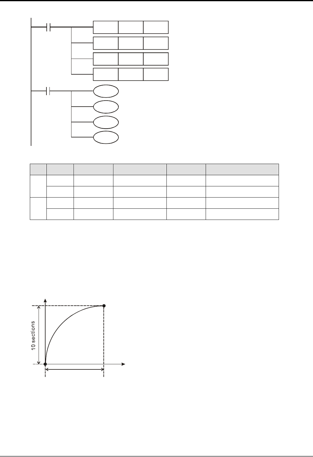
2 Functions of Devices in DVP-PLC
M1002
M0
MOV K200
K2
K300
Y0
M1133
Y1
M1135
MOV
MOV
MOV K2
D1133
D1134
D1135
D1136
(Figure 2)
Axis Section Device D Output frequency Device D Number of output pulses
1 D201, D200 K1,000 D203, D202 K1,000
X 2 D205, D204 K4,000 D207, D206 K4,000
1 D301, D300 K3,000 D303, D302 K3,000
Y 2 D305, D304 K1,000 D307, D306 K1,000
(Table 1)
b) Draw an arc in 2 axes
Destination: Draw a 90° arc (see Figure 3)
Program explanation: Same as the the example of draw oblique lines, except that D1134 and D1136 are
modified as K10 (output 10 sections)
Output frequency and number of pulses: see table 2
(0,0)
X
Y
(50,000, 50,000)
10 sections
(Figure 3)
DVP-PLC Application Manual
2-108
2 Functions of Devices in DVP-PLC
Axis Section Device D Output frequency Device D Number of output pulses
1 D201, D200 K1,230 D203, D202 K615
2 D205, D204 K3,664 D207, D206 K1,832
3 D209, D208 K6,004 D211, D210 K3,002
4 D213, D212 K8,200 D215, D214 K4,100
5 D217, D216 K10,190 D219, D218 K5,095
6 D221, D220 K11,932 D223, D222 K5,966
X
7 D225, D224 K13,380 D227, D226 K6,690
8 D229, D228 K14,498 D231, D230 K7,249
9 D233, D232 K15,258 D235, D234 K7,629
10 D237, D236 K15,644 D239, D238 K7,822
1 D301, D300 K15,644 D303, D302 K7,822
2 D305, D304 K15,258 D307, D306 K7,629
3 D309, D308 K14,498 D311, D310 K7,249
4 D313, D312 K13,380 D315, D314 K6,690
5 D317, D316 K11,932 D319, D318 K5,966
6 D321, D320 K10,190 D323, D322 K5,095
Y
7 D325, D324 K8,200 D327, D326 K4,100
8 D329, D328 K6,004 D331, D330 K3,002
9 D333, D332 K3,664 D335, D334 K1,832
10 D337,D336 K1,230 D339, D338 K615
(Table 2)
c) Draw arcs in the four quadrants
Destination: Draw four 90° arcs (see Figure 4)
Program explanation: When the direction signal is On, the direction will be a positive one; when the
direction signal is Off, the direction will be a negative one (see Figure 5)
Output frequency and number of pulses: see Table 2
(0,0)
X
Y
(50,000, 50,000)
(-50,000, 50,000)
(-50,000, -50,000) (50 000, -50,000)
Y0=On
Y1=On
Y0=On
Y1=On
Y1=Off
Y1=Off
Y0=Off
Y0=Off
Quadrant I
Quadrant IV
Quadrant II
Quadrant III
(Figure 4)
DVP-PLC Application Manual 2-109
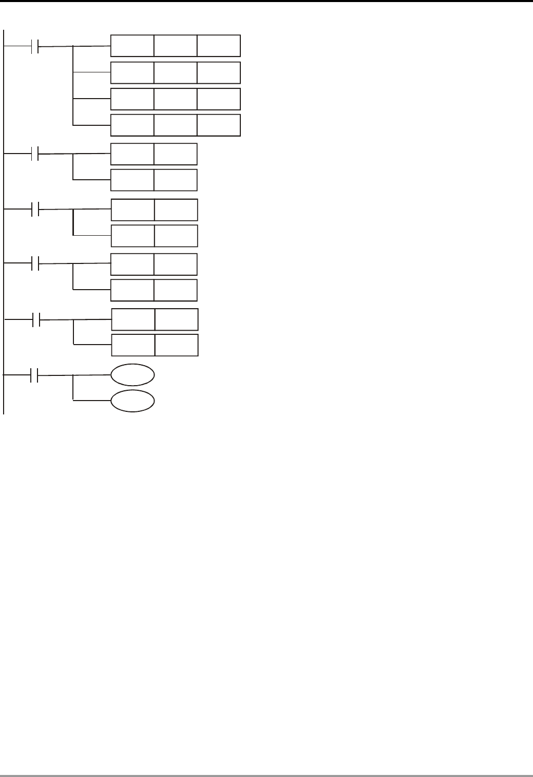
2 Functions of Devices in DVP-PLC
M1002
M0
MOV K200
K300
M1133
M1135
MOV
MOV
MOV
D1133
D1134
D1135
D1136
M1
SET Y0
Y1
K10
K10
SET
RST
SET Y0
Y1
Y0
Y1
RST
RST
Y0
Y1
RST
SET
M2
M3
M4
(Figure 5)
M0, M1 = On refers to drawing a 90° arc in Quadrant I; M0, M2 = On refers to drawing a 90° arc in Quadrant II;
M0, M3 = On refers to drawing a 90° arc in Quadrant III; M0, M4 = On refers to drawing a 90° arc in Quadrant
IV.
The four 90° arcs are drawn when acceleration in X and deceleration in Y. To draw the arcs when
deceleration in X and acceleration in X, modify the program into Figure 6, i.e. D1333 = K300 and D1335 =
K200.
DVP-PLC Application Manual
2-110
2 Functions of Devices in DVP-PLC
M1002
M0
MOV
K200
K300
M1133
M1135
MOV
MOV
MOV
D1133
D1134
D1135
D1136
M1
SET Y0
Y1
K10
K10
SET
RST
SET Y0
Y1
Y0
Y1
RST
RST
Y0
Y1
RST
SET
M2
M3
M4
(Figure 6)
M0, M1 = On refers to drawing a 90° arc in Quadrant I; M0, M2 = On refers to drawing a 90° arc in Quadrant II;
M0, M3 = On refers to drawing a 90° arc in Quadrant III; M0, M4 = On refers to drawing a 90° arc in Quadrant
IV. (See Figure 7)
(0,0)
X
Y
(50,000, 50,000)
(-50,000, 50,000)
(-50,000, -50,000) (50,000, -50,000)
Y0=On
Y1=On
Y0=On
Y1=On
Y1=Off
Y1=Off
Y0=Off
Y0=Off
Quadrant I
Quadrant III
Quadrant II
Quadrant IV
(Figure 7)
d) Draw a circle
Destination: Extract four 90° arcs from Ffigure 4 and Figure 7 and combine them into a circle (see Figure
8).
DVP-PLC Application Manual 2-111
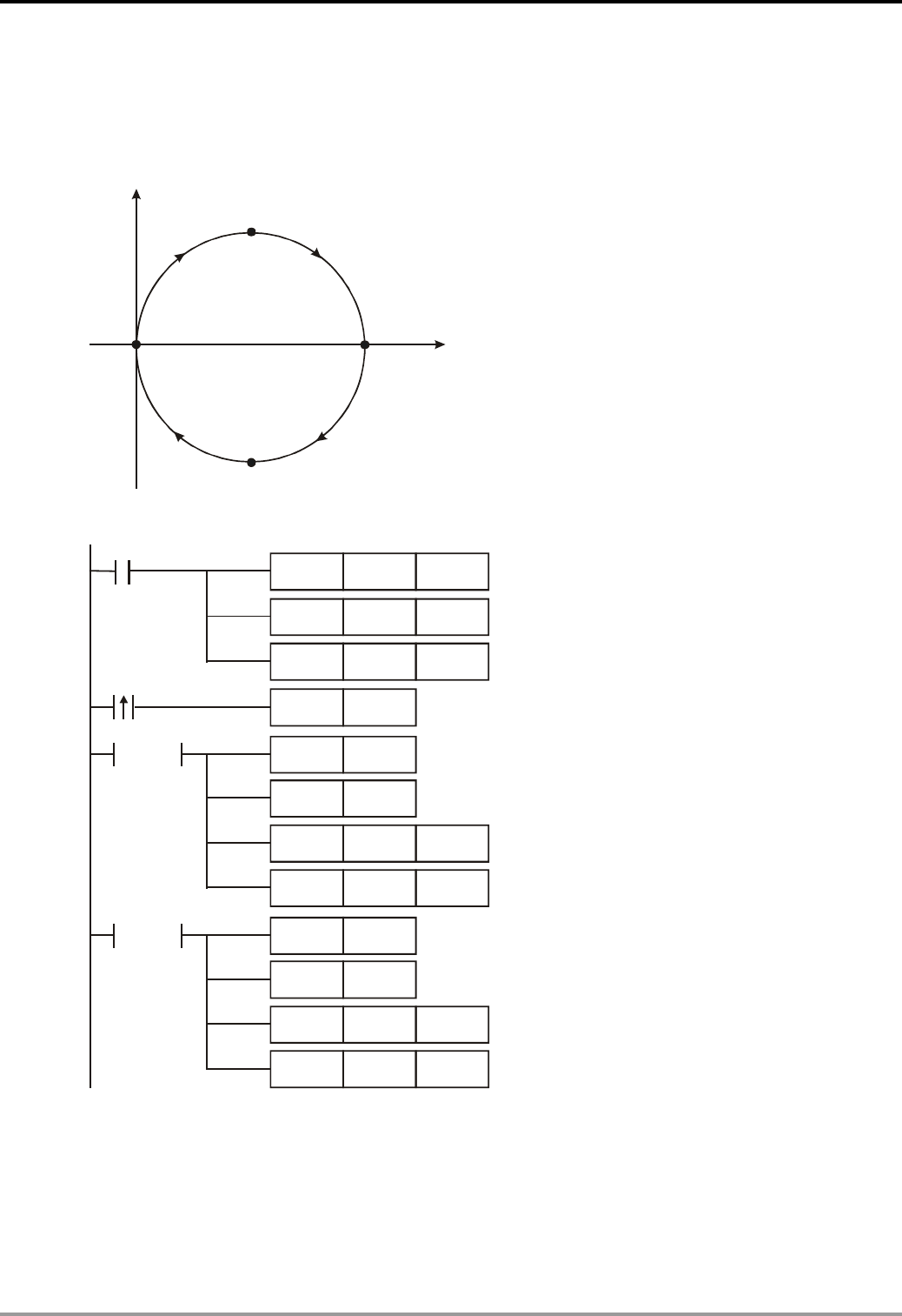
2 Functions of Devices in DVP-PLC
Program explanation: When the direction control pin is On, the direction will be a positive one; otherwier, it
will be a negative one (see Figure 9). When X0 = On, D0 will accumulate once and the 2 axes will draw a
90° arc.
Output frequency and number of pulses: see Table 2.
(0,0)
X
Y
(50,000, 50,000)
(50,000, -50,000)
(10,000, 0)
D0=K1 D0=K2
D0=K3
D0=K4
(Figure 8)
M1002
MOV
K0
MOV
MOV
D1134
SET Y0
Y1
K10
SET
K10
MOV
MOV
SET Y0
Y1
MOV
MOV
= D0 K2
= D0 K1
D1136
D0
D0
INC
K200
K300
D1133
D1135
RST
K300
K200
D1133
D1135
X0
DVP-PLC Application Manual
2-112
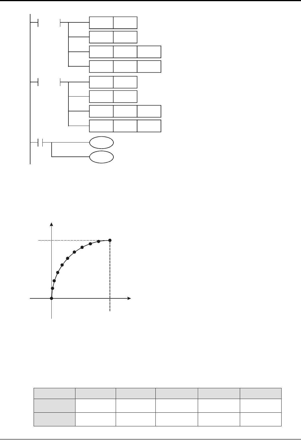
2 Functions of Devices in DVP-PLC
M1133
M1135
Y0
Y1
MOV
MOV
Y0
Y1
SET
MOV
MOV
= D0 K4
= D0 K3
D1133
D1135
RST
RST
K200
K300
K300
K200
RST
D1133
D1135
X0
(Figure 9)
e) Calculate the frequency and number of output pulses in each section
Destination: Draw 10 sections of arcs clockwise until they reach (50,000, 50,000) (see Figure 10)
Rx = target value in X; Ry = target value in Y; N = number of sections; π = 3.1416
(0,0)
X
Y
(0,Ry)
(Rx,0)
(x10,y10)
(x1,y1)
(x2,y2)
(x3,y3)
(x4,y4)
(x5,y5)
(x6,y6)
(x7,y7) (x8,y8)
(x9,y9)
(Figure 10)
Step 1: Calculate the position for each section
= Rx – Rx × sin [(N-1) × π ÷ (2 × N)]
x
1
= Rx – Rx × sin [(N-2) × π ÷ (2 × N)] …. See Table 3
x
2
= Ry × sin [1 × π ÷ (2 × N)]
y
1
= Ry × sin [2 × π ÷ (2 × N)]…. See Table 4
y
2
Position x x x x x
1 2 3 4 5
With decimal 615.55 2,447.12 5,449.61 9,549.08 14,464.59
point
Without 615 2,447 5,449 9,549 14,464
decimal point
DVP-PLC Application Manual 2-113
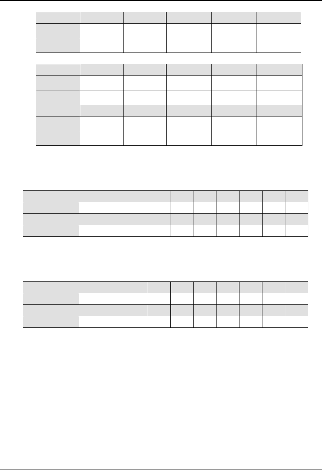
2 Functions of Devices in DVP-PLC
DVP-PLC Application Manual
2-114
Position x6x7x8x9x10 (RX)
With decimal
point 20,610.67 27,300.42 34,549.11 42,178.25 50,000
Without
decimal point 20,610 27,300 34,549 42,178 50,000
(Table 3)
Position y1y2y3y4y5
With decimal
point 7,821.74 15,450.88 22,699.57 29,389.32 35,355.40
Without
decimal point 7,821 15,450 22,699 29,389 35,355
Position y6y7y8y9y10 (Ry)
With decimal
point 40,450.91 44,550.38 47,552.87 49,384.44 50,000
Without
decimal point 40,450 44,550 47,552 49,384 50,000
(Table 4)
Step 2: Calculate the distance (number of pulses) between every section
In X axis: x1 = x1 – 0, x2 = x2 – x1, ... x10 = x10 – x9 (see Table 5)
In Y axis: y1 = y1 – 0, y2 = y2 – y1, … y10 = y10 – y9 (see Table 5)
Position x1x2x3x4x5x6x7x8x9x10
Number of pulses 615 1,832 3,002 4,100 5,095 5,966 6,690 7,249 7,629 7,822
Position y1y2y3y4y5y6y7y8y9y10
Number of pulses 7,821 7,629 7,249 6,690 5,966 5,095 4,100 3,002 1,832 616
(Table 5)
Step 3: Decide the execution time of every section and obtain the frequency of every section by Table 5
Assume every section executes for 500ms, the equation for frequency (Hz) of each section is: fx1 = 1÷0.5 ×
x1、fx2 =1÷0.5 × x2…(see Table 6)
Position fx1fx2fx3fx4fx5fx6fx7fx8fx9fx10
Frequency 1,230 3,664 6,004 8,200 10,190 11,932 13,380 14,498 15,258 15,644
Position fy1fy2fy3fy4fy5fy6fy7fy8fy9fy10
Frequency 15,642 15,258 14,498 13,380 11,932 10,190 8,200 6,004 3,644 1,232
(Table 6)
Step 4: Fill Device D into table 2 and complete all steps.
Reminder 1: When Rx=Ry, you can calculate X axis, and copy X axis to Y axis (as fy1 = fx10, fy2 =
fx9, …fy10 = fx1,and y1 = x10, y2 = x9,…y10 = x1 )
Reminder 2: When drawing a counterclockwise arc, switch the index value of X axis with that of Y axis.
Function Group Detecting Extension
Number D1140, D1142, D1143, D1145
Contents:
1. D1140: Number of special right-side extension modules (AD, DA, XA, PT, TC…); Max. 8
2. D1142: Number of X input points on digital extension device
3. D1143: Number of Y output points on digital extension device

2 Functions of Devices in DVP-PLC
4. D1145: Number of special left-side extension modules (AD, DA, XA, PT, TC…); Max. 8 (available in SV only)
Adjustable Pulse Speed Acceleration/Deceleration
Function Group
M1144 ~ M1149, M1154, D1030, D1031, D1144, D1154, D1155
Number
Contents:
1. Special D and special M of Y0 adjustable pulse speed acceleration/deceleration for SA/SX/SC:
Device No. Function
M1144 Activation switch for Y0 adjustable pulse speed acceleration/deceleration
M1145 Accerlerating flag for Y0 adjustable pulse speed acceleration/deceleration
M1146 “Target frequency reached” flag for Y0 adjustable pulse speed acceleration/deceleration
M1147 “Decerlerating” flag for Y0 adjustable pulse speed acceleration/deceleration
M1148 “Function completed” flag for Y0 adjustable pulse speed acceleration/deceleration
M1149 “Counting temporarily stops” flag for Y0 adjustable pulse speed acceleration/deceleration
M1154 “Enabling deceleration” flag for Y0 adjustable pulse speed acceleration/deceleration
D1030 The lower 16 bits in the 32-bit data register for accumulative Y0 output pulses
D1031 The higher 16 bits in the 32-bit data register for accumulative Y0 output pulses
D1144 Starting No. of the register (D) for Y0 adjustable pulse speed acceleration/deceleration
D1154 Recommended value for indicated gap time of deceleration(10 ~ 32,767 ms)
D1155 Recommended value for indicated gap frequency of deceleration (-1 ~ -32,700 Hz)
2. Parameters for D1144:
Index Function
+ 0 Total number of sections (n) (max. 10)
+ 1 Currently executed section (read only)
st
+ 2 Start frequency of the 1 section (SF1)
+ 3 Gap time of the 1st section (GT1)
st
+ 4 Gap frequency of the 1 section (GF1)
st
+ 5 Target frequency of the 1 section (TF1)
+ 6 The lower 16 bits of the 32 bits for the target number of output pulses in the 1st section (SE1)
+ 7 The higher 16 bits of the 32 bits for the target number of output pulses in the 1st section (SE1)
nd
+ 8 Start frequency of the 2 section (SF2); Cannot be the same as TF1
+ 9 Gap time of the 2nd section (GT2)
nd
+ 10 Gap frequency of the 2 section (GF2)
nd
+ 11 Target frequency of the 2 section (TF2)
+ 12 The lower 16 bits of the 32 bits for the target number of output pulses in the 2nd section (SE2)
+ 13 The higher 16 bits of the 32 bits for the target number of output pulses in the 2nd section (SE2)
: :
+ n*6 + 2 Start frequency of the nth section (SFn); Cannot be the same as the start frequency of the n-1th
section (TFn-1)
+ n*6 + 3 Gap time of the nth section (GTn)
DVP-PLC Application Manual 2-115
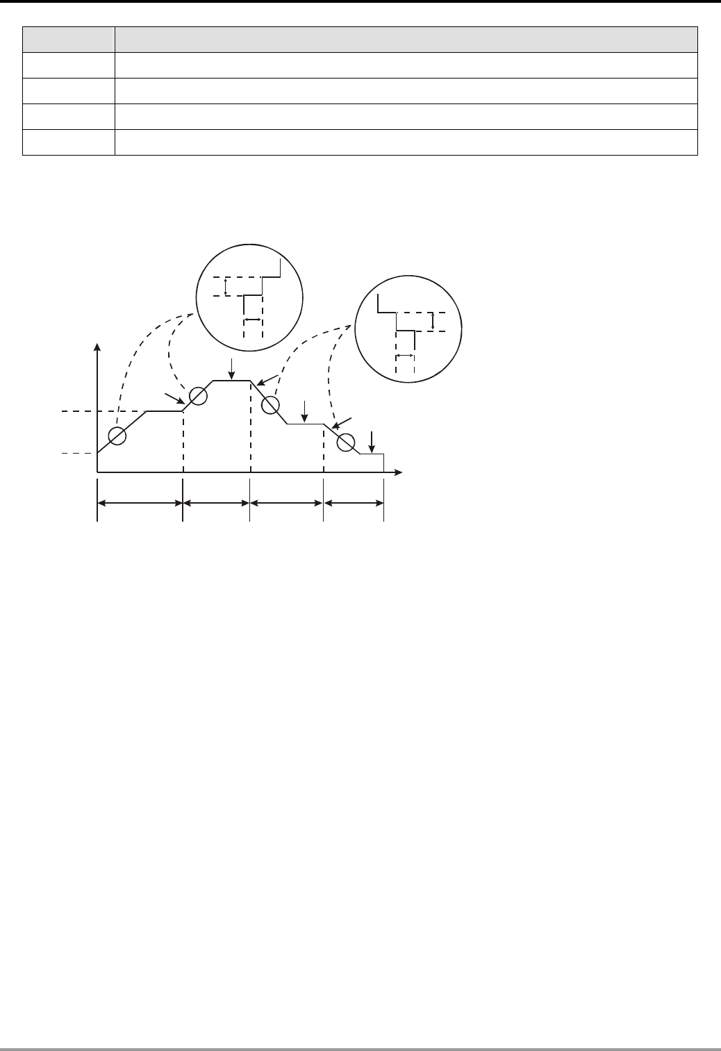
2 Functions of Devices in DVP-PLC
Index Function
th
+ n*6 + 4 Gap frequency of the n section (GFn)
th
+ n*6 + 5 Target frequency of the n section (TFn)
+ n*6 + 6 The lower 16 bits of the 32 bits for the target number of output pulses in the nth section (SEn)
+ n*6 + 7 The higher 16 bits of the 32 bits for the target number of output pulses in the nth section (SEn)
3. The functions:
This function can only be used on Y0 output point and the timing chart is as follows. After filling out the
parameter table, setup M1144 to start the function (should be applied in RUN mode).
SF2
TF2
SF3
TF3
TF4
SF4
TF1
SF1
GF
GT
GT
GF
Frequency(Hz)
Time(ms)
1st section
number of
pulses
(SE1)
2nd section
number of
pulses
(SE2)
3rd section
number of
pulses
(SE3)
4th section
number of
pulses
(SE4)
4. How to use and the restrictions:
a) The start frequency and target frequency have to be ≥ 200Hz; otherwise, the function will not be executed or
complete execution.
b) The start frequency and target frequency have to be < 32,700Hz. Frequency > 32,700Hz will be executed in
32,700Hz.
c) Range of gap time: 1 ~ 32,767ms (Min. unit: ms)
d) The range of gap frequency within acceleration section: 1Hz ~ 32,700Hz; within deceleration section: -1 ~
-32,700Hz. If the gap frequency is set as 0Hz, it will fail to reach target frequency in the executed section but
in the next section when the target number of pulses is reached.
e) The target number of pulses in a section has to be > (GF × GT/1,000) × [(TF - SF)/GF]; otherwise the target
may not be reached. To correct it, the user may extend gap time or increase the target number of pulses.
f) When PLC is in RUN status and there is a high-speed instruction assigning Y0 input, the instruction will be
executed prior to other instructions.
g) After M1144 = On, if M1148 has not be reached and M1144 is “Off”, deceleration will be enabled. And if
M1154 = Off at the moment, the deceleration rule will be “decelerating 200Hz every 200ms” and M1147 will
be set. The pulse output will stop when the frequency falls under 200Hz. If M1154 = On at the moment, the
output will be executed following the gap time and frequency as set by the user. The time shall not be ≤ 0 (if ≤
DVP-PLC Application Manual
2-116

2 Functions of Devices in DVP-PLC
0, it will follow the initial setting 200ms) and the frequency shall not be ≥ 0 (if = 0, it will follow the initial setting
-1kHz; if > 0, negative sign comes before the value).
h) When M1148 = On but M1144 = Off, deceleration will not be enabled and M1148 will be reset. Whenever
M1144 = Off, M1149 will be reset.
i) The number of sections being executed is determined upon the total number of sections. (Max. number of
sections = 10)
j) Acceleration or deceleration is determined upon the start frequency of the next section. That is, if the target
frequency of the current section < the start frequency of the next section, acceleration will take place in the
next section and the target frequency of the next section must > its start frequency. If the target frequency of
the current section > the start frequency of the next section, deceleration will take place in the next section
and the target frequency of the next section must < its start frequency. Correct pulse output cannot be
guaranteed if the user does not follow the rules.
k) When PLC goes from STOP to RUN, M1144 ~ M1149 will be reset to “Off”. When PLC goes from RUN to
STOP, only M1144 will be reset, not M1145 ~ M1149.
l) SA/SX/SC uses parameter table D0 ~ D999 and D2000 ~ D4999. If the used parameter table (including all
the used section parameters) falls off the range, the instruction will not be executed and M1144 will be “Off”.
5. Example 1: Calculate the number of output pulses in every acceleration/deceleration section
Assume you set the start frequency of a section as 200Hz, gap time as 100ms, gap frequency as 100Hz, target
frequency as 500Hz, and target number of pulses as 1,000:
The number of output pulses at start frequency = 200 × 100 / 1,000 = 20
The number of output pulses in the first acceleration gap = 300 × 100 / 1,000 = 30
The number of output pulses in the second acceleration gap = 400 × 100 / 1,000 = 40
The number of output pulses at target frequency = 1,000 – (40 + 30 + 20) = 910
(Please be noted that we suggest this number be bigger than 10.)
Output time for target frequency = 1 / 500 × 910 = 1,820 ms
Total time spent for this section = 1,820 + 3 × 100 = 2,120 ms
6. Example 2: Pulse output program for 1 acceleration section and 1 deceleration section
DVP-PLC Application Manual 2-117
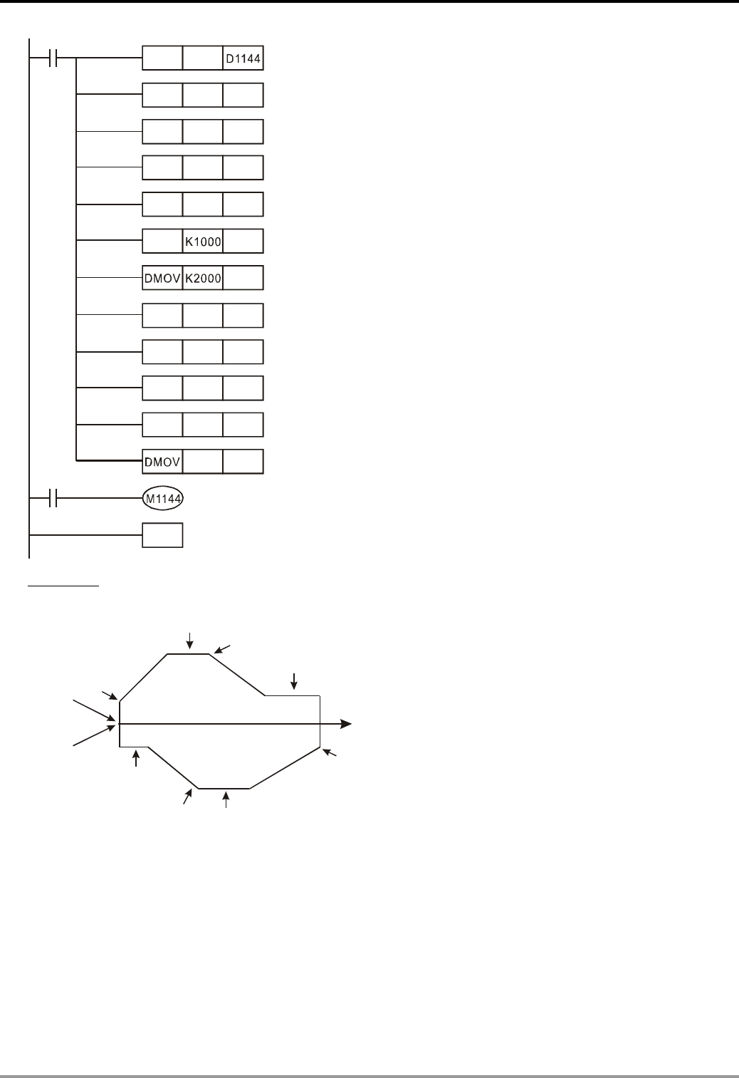
2 Functions of Devices in DVP-PLC
M1002
MOV K2 D200
MOV K200
MOV K250 D202
MOV K500 D203
MOV K250 D204
MOV D205
D206
MOV K750 D208
MOV K500 D209
MOV K-250 D210
MOV K250 D211
K200 D212
END
M0
7. Example 3: Acceleration and deceleration in 1 section and the pulse output program with direction switch
TF1
TF2
TF2
TF1
SF2
SF2
SF1
SF1
X0=ON
Y7=OFF
Position
Zero point
Y7=O
n
Explanation:
a) See example 2 for the settings for acceleration and deceleration. The acceleration/deceleration frequency is
stored in the latched area; therefore, you do not have to write it in in the program.
b) The figure above is the example of the motion. When X0 = On, it will start the motion back and forth; when X0
= Off, the motion will stop. Y7 is a direction switch.
c) The program:
DVP-PLC Application Manual
2-118
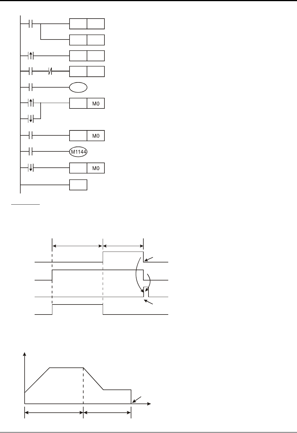
2 Functions of Devices in DVP-PLC
M1002
RST M0
SET
END
RST M1
SET M0
ALT M1
Y7
RST
RST
X0
X0
M0
M1
M1
M1
M1148
M0
X0
8. Example 4: Program of zero return for 1 acceleration section and 1 deceleration section
The timing diagram of relevant flags:
M1149
M1148
M1144
X0
Zero return stops
Pulse output stops
Accelerating t
o
zero point
Decelerating t
o
zero point
Frequency and the positions:
Frequency (Hz)
A
ccelerating to
zero point
Decelerating to
zero point
Zero point
Position
DVP-PLC Application Manual 2-119
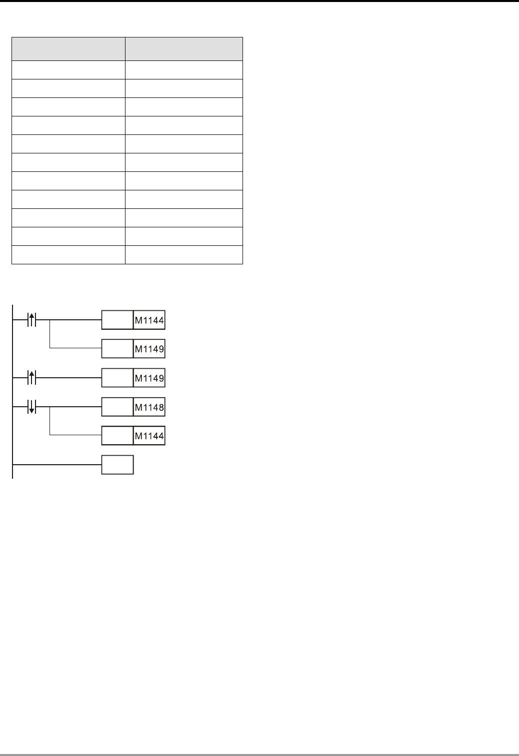
2 Functions of Devices in DVP-PLC
Settings of acceleration/deceleration time, frequency and number of pulses:
Started No. D Setting
+ index value
+0 2
+2 250 (Hz)
+3 100 (ms)
+4 500 (Hz)
+5 10,000 (Hz)
+6, +7 10 (pulses)
+8 9,750 (Hz)
+9 50 (ms)
+10 -500 (Hz)
+11 250 (Hz)
+12, +13 30,000 (pulses)
The program: (Assume X7 is the switch for triggering zero return)
X7
SET
END
SET
X0
RST
X0
SET
RST
Program explanations:
a) When X7 is triggered, M1144 will enable an acceleration. Set M1149 (counting temporarily stops) and 10
pulses will be sent out before the deceleration switch X0 is triggered and the program will enter the
deceleration section.
b) When X0 is disabled (i.e. zero return is completed), set M1148 to disable this function.
Note: The example offered here is one of the applications. Please adjust the settings of the parameters according to
the features of and restrictions on your machines.
PWD Pulse Width Detection Duty-Off/Duty-On
Function Group
M1144, D1144
Number
Application:
Before the instruction DDRVI is used to drive the servo, the acceleration/deceleration operation is performed on the
target position and the target frequency. After the instruction DDRVI is enabled, the operation can not be performed
on the same target position and target frequency. The advantage is that the production can be enhanced.
DVP-PLC Application Manual
2-120
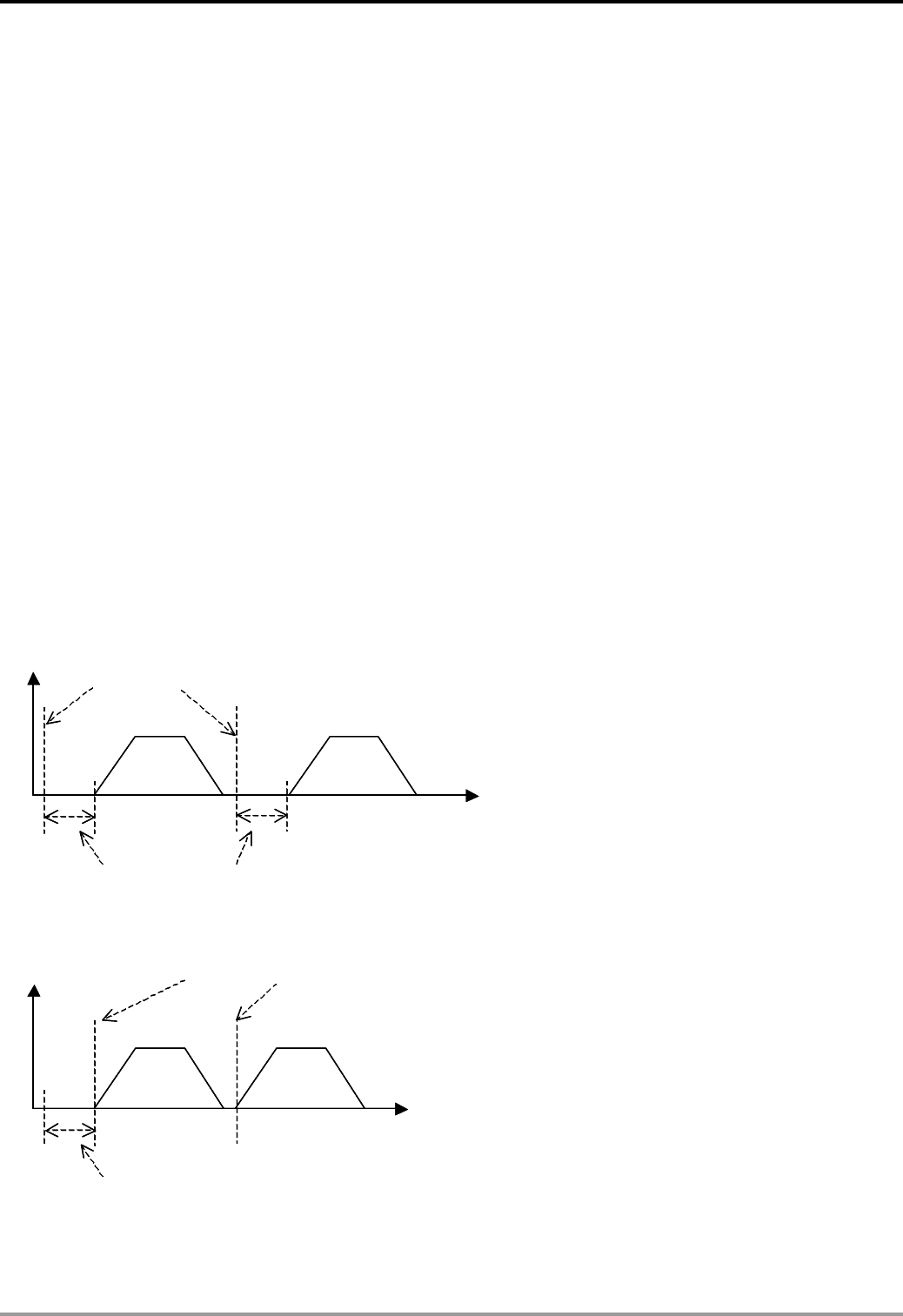
2 Functions of Devices in DVP-PLC
Device:
If M1144 is On, the function is enable. If M1144 is Off, the function is disabled.
D1144→Using the index valule of the data register
For example, k0 represents D0, k100 represents D100.
Usage: (Firmware version above 2.0)
1. Suppose the value in D1144 is k0. The value in (D0, D1) represents the number of targets, the value in (D2, D3)
represents the target frequency of Y0, the value in D1343 represents the acceleration time, the value in D1348
represents the deceleration time, and the value in D1340 represents the acceleration/deceleration frequency .
2. When M1144 is ON and the instruction DDRVI is not enabled, the operation is performed on the
acceleration/deceleration frequency and the number of targets. After DDRVI is enabled, the pulses are
generated.
3. If M1144 is On, the previous output value is executed whenever DDRVI is enabled. If users want to change the
target frequency or the number of targets, users have to reset M1144 to Off when DDRVI is disabled.
4. When this function is used, the default acceleration time and deceleration time are the values in D1343 and
D1348. Therefore, the acceleration sections and decelerations section can occupy 30 sections respectively.
5. This function can be used with the designated deceleration number function (D1232, D1233), and the
masking/marking function (M1156).
Timing chart:
1. The function is disabled:
Time
Freq.
Start DDRVI
Calc ula t io n time
Time
Freq.
Start DDRVI
Calc ula t io n time
2. The function is enabled:
Time
Freq. Start DDRVI
Calc ula tio n time
Time
Freq. Start DDRVI
Calc ula tio n time
DVP-PLC Application Manual 2-121
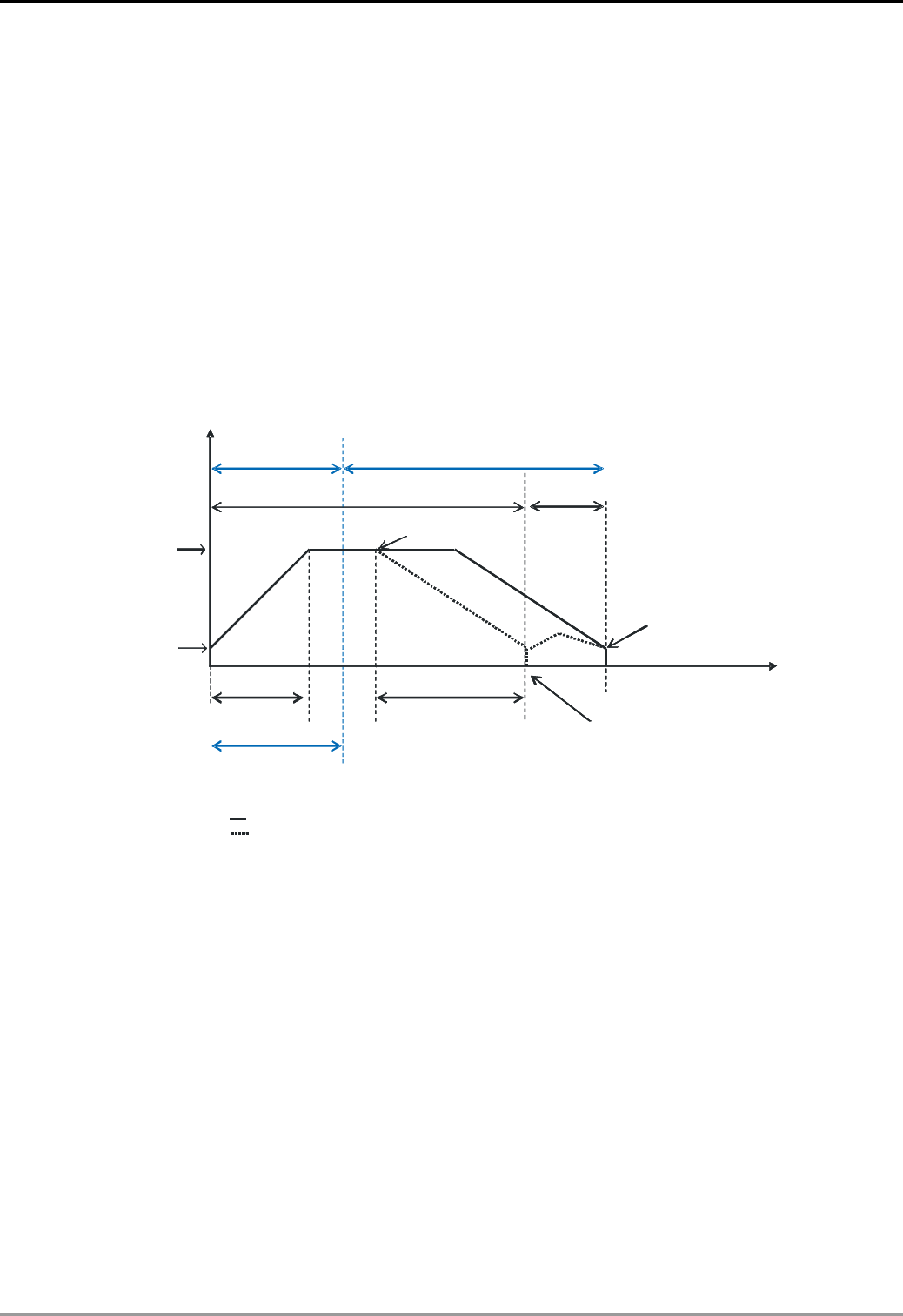
2 Functions of Devices in DVP-PLC
PWD Pulse Width Detection Duty-Off/Duty-On
Function Group
M1154
Number
Contents:
1. PWD pulse width detection function of M1154 is only available in EH2/SV/EH3/SV2 series V1.6 and later
versions.
2. M1154 = Off: Detecting the width time when duty-off. M1154 = On: Detecting the width time when duty-on.
Pulse Output Pause, Mask, Mark
Function Group
M1156 ~ M1159, M1538 ~ M1541, D1026, D1027
Number
Contents:
1. Actions of interruption type pulse output pause function (with deceleration):
D1340
Frequenc
y
Target frequency
Start/end frequency
Disable I001 Enable I001
Set M1156 = ON Reset M1156 = OFF
I001 interruption occurs.
I001 interruption does not occur.
Number of
output pulses
D1343: Acceleration time D1348: Deceleration time
or D1233/1232: Number of
deceleration pulses
Pause stop, M1158 = ON (Note #1)
D1027/1026: Number of
shielded pulses
Note #1: After M1538 = ON and the user reset M1156 = OFF, PLC will complete the remaining
number of output pulses automatically.
Note: Actual line ( ) -> Action when I001 interruption does not occur.
Dotted line ( ) -> A ction when I001 interruption occurs in unmasked area.
Applicable instructions: DRVI/DDRVI/PLSR/DPLSR
Usage restriction: Has to work with external interruptions, special M and special D.
Other explanations:
a) When this function is enabled, PLC will start to decelerate according to the set deceleration time. Even if the
user does not set up the number of deceleration pulses (i.e. special D = 0), or the set number of pulses is
less than the number planned for the deceleration time, PLC will still decelerate within the deceleration time.
On the contrary, if the number of deceleration pulses is more than the planned number for the deceleration
time, PLC will decelerate according to the number set in the special D.
b) Range for deceleration time: 10 ~ 10,000ms
c) There is mask interruption in CH0 high-speed output. When D1027/D1026 (32-bit) ≠ 0, the mask function
will be enabled, i.e. X0 external interruption will not be activated when the number of output pulses is within
the mask area.
DVP-PLC Application Manual
2-122

2 Functions of Devices in DVP-PLC
High-speed output CH0 ~ CH3 v.s. pause function of external input points X0 ~ X3:
Parameter Deceleration Deceleration Mask
Interruption External Pause status
Channel paused flag input point time paulses interruption flag
function
Special D Special D
D1026,
D1027
CH0 (Y0,Y1) M1156 X0 D1348 D1232~D1233 M1538
CH1 (Y2,Y3) M1157 X1 D1349 D1234~D1235 No M1539
CH2 (Y4,Y5) M1158 X2 D1350 D1236~D1237 No M1540
CH3 (Y6,Y7) M1159 X3 D1351 D1238~D1239 No M1541
EH3/SV2
Parameter Mask
Deceleration Deceleration
Interruption External Pause status
Channel paused flag input point
time paulses interruption flag
Special D Special D function
D1026,
D1027
CH0 (Y0,Y1) M1156 X0 D1348 D1232~D1233 M1538
D1135~
CH1 (Y2,Y3) M1157 X1 D1349 D1234~D1235 M1539
D1136
D1154~
CH2 (Y4,Y5) M1158 X2 D1350 D1236~D1237 M1540
D1155
No
CH3 (Y6,Y7) M1159 X3 D1351 D1238~D1239 M1541
Application examples:
¾ When M0 turns from Off to On, Y0 will start to output pulses and wait for the external input interruption
X0 to take place. When interruption signals occur in the acceleration section or the highest speed
section during the output, Y0 will immediately decelerate and stop the output after 100ms, and M1538 =
On.
¾ When M1538 = On, the user can reset (RST) M1156, and PLC will start to output the remaining pulses.
When all the target pulses are completed, M1029 will be On.
¾ If the external interruption occurs in the planned deceleration area, the output will not decelerate or set
M1538 to On.
b) Example 1: Immediately decelerate and pause within deceleration time
¾ Application: When external interruptions occur, the high-speed output has to achieve deceleration and
pause within the designated deceleration time. It is generally applied in the searching mark function in
single-axis motion control.
¾ The program:
DVP-PLC Application Manual 2-123
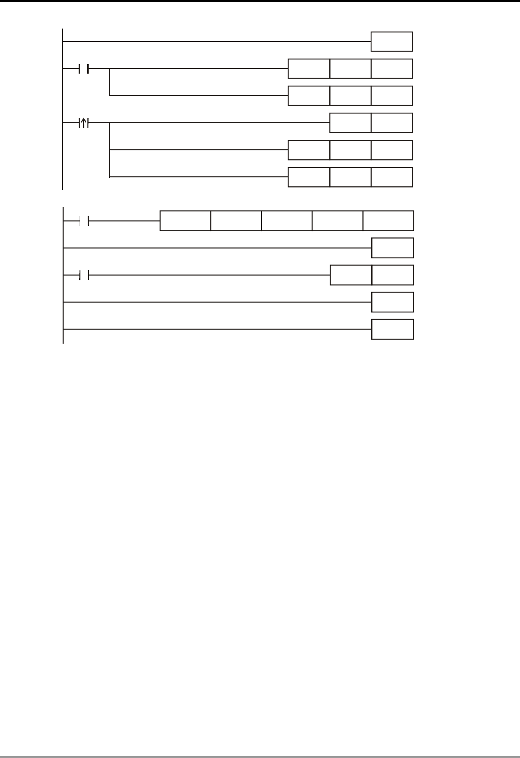
2 Functions of Devices in DVP-PLC
EI
M1002
MOV K100 D1343
M0
SET M1156
MOV K100 D1348
DMOV K50000 D1232
DMOV K0 D1026
I001
DDRVI K100000
M0
K100000 Y0 Y1
FEND
M1000
INCP D100
IRET
END
c) Program explanation:
¾ When M0 turns from Off to On, Y0 will start to output pulses and wait for the external input interruption
X0 to take place. When interruption signals occur in the acceleration section or the highest speed
section during the output, Y0 will immediately decelerate and stop the output after 100ms, and M1538 =
On.
¾ When M1538 = On, the user can reset (RST) M1156, and PLC will start to output the remaining pulses.
When all the target pulses are completed, M1029 will be On.
¾ If the external interruption occurs in the planned deceleration area, the output will not decelerate or set
M1538 to On.
d) Example 2: Immediately decelerate and pause within the number of deceleration pulses
¾ Application: When external interruptions occur, the high-speed output has to achieve deceleration and
pause within the designated number of deceleration pulses. It is generally applied in the searching mark
function in single-axis motion control.
¾ The program:
DVP-PLC Application Manual
2-124
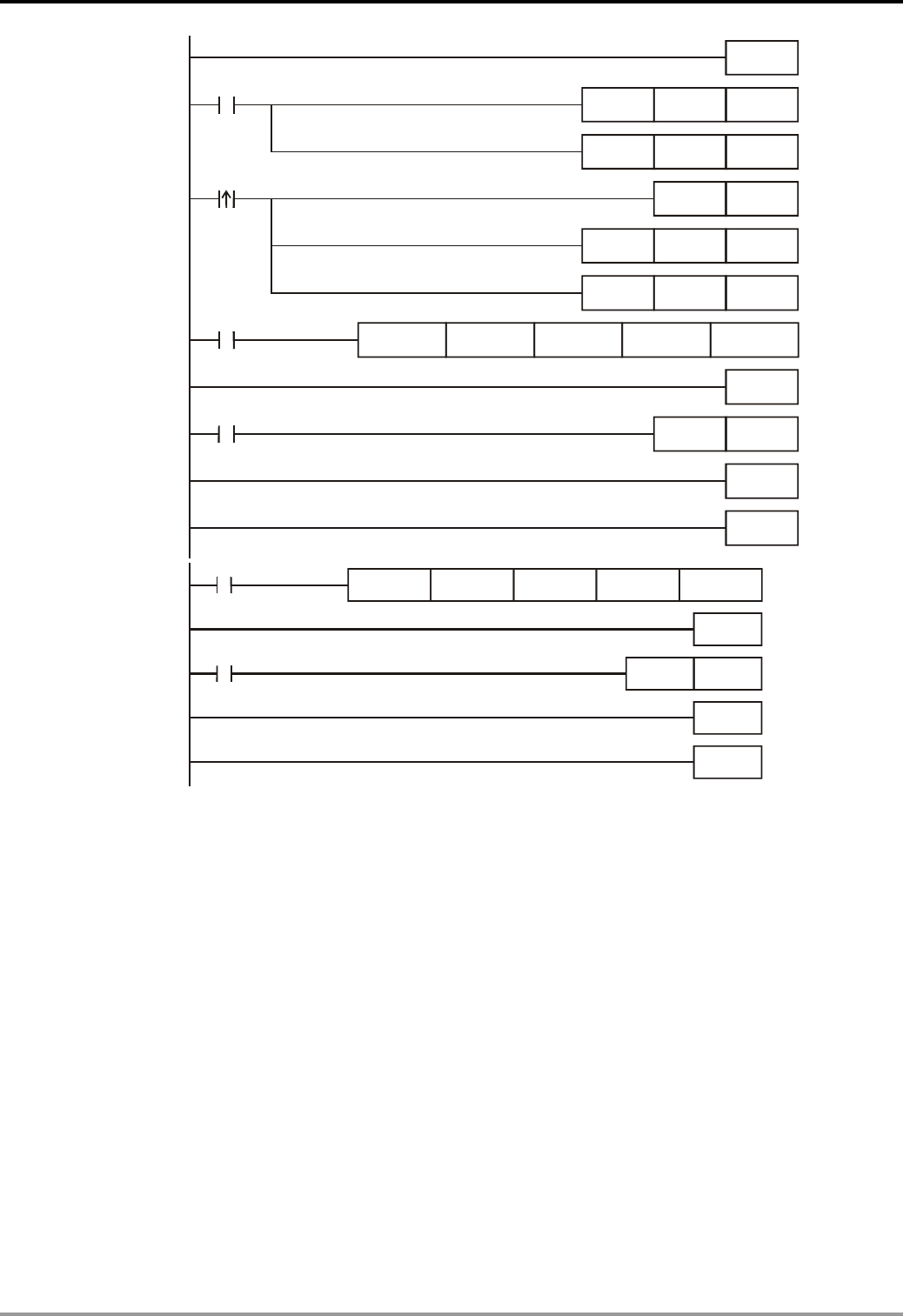
2 Functions of Devices in DVP-PLC
EI
M1002
MOV K100 D1343
M0
I001
DDRVI K100000
M0
K100000 Y0 Y1
SET M1156
FEND
M1000
INCP D100
IRET
END
MOV K100 D1348
DMOV K50000 D1232
DMOV K40000 D1026
I001
DDRVI K100000
M0
K100000 Y0 Y1
FEND
M1000
INCP D100
IRET
END
e) Program explanation:
¾ When M0 turns from Off to On, Y0 will start to output pulses. After the external input interruption X0
occurs during the output, Y0 will immediately decelerate and output 50,000 pulses before it stops and
set M1538 (pause status flag) to On.
¾ When M1538 = On, the user can reset (RST) M1156, and PLC will start to output the remaining pulses.
When all the target pulses are completed, M1029 will be On.
¾ If the external interruption occurs in the planned deceleration area, the output will not decelerate or set
M1538 to On.
2. Actions of program type pulse output pause function (with no deceleration):
DVP-PLC Application Manual 2-125
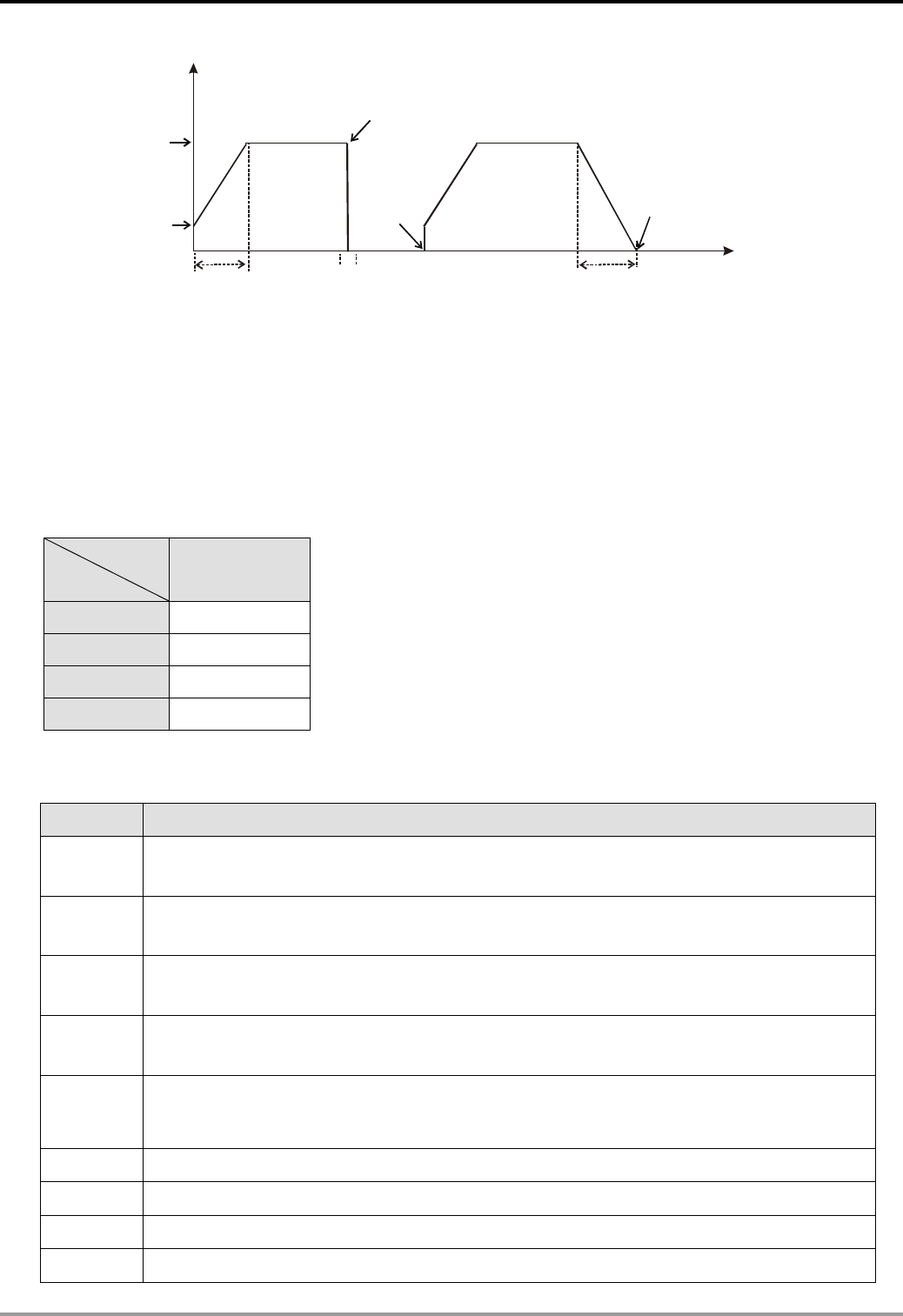
2 Functions of Devices in DVP-PLC
M1308=ON
M1308=OFF
Frequency
Target frequency
Start/end frequency
Acceleration
time
Max. stop time:
1 scan cycle
Pulse output completed
M1029 = On
Deceleration
time
Time
Number of pulses
Applicable instructions: DRVI/DDRVI/DRVA/DDRVA/PLSR/DPLSR
Applicable model/firmware version: EH2, EH3/SV2 v1.4, SV v1.5 (and their later versions)
During the pulse output, force On M1308 will pause the output, and force Off M1308 will start the output of
remaining pulses.
The max. stop time inaccuracy in this pause function is 1 scan cycle.
High-speed output CH0 ~ CH3 v.s. pause function of pause flags:
Flag Pause flag
Channel
CH0 M1308
CH1 M1309
CH2 M1310
CH3 M1311
3. Special M and special D registers for SV V1.4 and later versions when conducting deceleration to pausing output
(for the ongoing high-speed pulse output encountering interruption signals), mask and mark.
Device No. Function
Off -> On: 1st group of CH0 (Y0, Y1) high-speed pulse output immediately pauses.
M1308 On -> Off: Complete the remaining number of output pulses
Off -> On: 1st group of CH1 (Y2, Y3) high-speed pulse output immediately pauses.
M1309 On -> Off: Complete the remaining number of output pulses
Off -> On: 1st group of CH2 (Y4, Y5) high-speed pulse output immediately pauses.
M1310 On -> Off: Complete the remaining number of output pulses
Off -> On: 1st group of CH3 (Y6, Y7) high-speed pulse output immediately pauses.
M1311 On -> Off: Complete the remaining number of output pulses
Enable X0 interruption to trigger immediate decelerating and pausing CH0 high-speed output.
(When M1156 is enabled and M1538 = On, simply clear M1156 to finish sending out the
remaining output pulses.)
M1156
M1157 Enable X1 interruption to trigger immediate decelerating and pausing CH1 high-speed output
M1158 Enable X2 interruption to trigger immediate decelerating and pausing CH2 high-speed output
M1159 Enable X3 interruption to trigger immediate decelerating and pausing CH3 high-speed output
M1538 CH0 pause status
DVP-PLC Application Manual
2-126
2 Functions of Devices in DVP-PLC
Device No. Function
M1539 CH1 pause status
M1540 CH2 pause status
M1541 CH3 pause status
D1026 Low word
When ≠ 0, enabling DRVI and PLSR instructions to work with X0 (mask)
interruption.
D1027 High word
D1232 Low word
Number of CH0 output pulses after mark
D1233 High word
D1234 Low word
Number of CH1 output pulses after mark
D1235 High word
D1236 Low word
Number of CH2 output pulses after mark
D1237 High word
D1238 Low word
Number of CH3 output pulses after mark
D1239 High word
Single Step Execution
Function Group
M1170, M1171, D1170
Number
Contents:
1. Special D and special M for single step execution for EH2/SV/EH3/SV2:
Device No. Function
M1170 Start flag
M1171 Action flag
D1170 STEP No. of the currently executed instruction
2. The function:
a) Execution timing: The flag is valid only when PLC is in RUN status.
b) Action steps:
i) When M1170 is enabled, PLC enters the single step execution mode. PLC stays at a specific instruction,
stores the location of STEP in D1170 and executes the instsruction once.
ii) When M1171 is forced “On”, PLC executes the next instruction and stops. At the same time, PLC
auto-force “O ff” M1171 and stops at the next instruction. D1170 stores the present STEP value.
iii) When Y output is in single step execution mode, Y outputs immediately without having to wait until END
instruction is being executed.
3. Note:
a) Instruction that will be affected by scan time will be executed incorrectly due to the single step execution. For
example, when HKY instruction is executed, it takes 8 scan times to obtain a valid input value from a key.
Therefore, the single step execution will result in incorrect actions.
DVP-PLC Application Manual 2-127
2 Functions of Devices in DVP-PLC
b) High-speed pulse input/output and high-speed counter comparison instructions are executed by hardware;
therefore, they will not be affected by the single step execution.
2-phase Pulse Output
Function Group
M1172 ~ M1174, D1172 ~ D1177
Number
Contents:
1. Special D and special M for two-phase pulse output for SA/SX/SC:
Device No. Function
M1172 Switch for two-phase pulse output (On = enabled)
M1173 On = Continuous output switch
M1174 “Number of pulses reached” flag
D1172 Output frequency (12Hz ~ 20kHz)
D1173 Output mode (K1 and K2)
D1174 The lower 16 bits of the 32 bits for the target number of pulses
D1175 The higher 16 bits of the 32 bits for the target number of pulses
D1176 The lower 16 bits of the 32 bits for the present number of pulses
D1177 The higher 16 bits of the 32 bits for the present number of pulses
2. The function:
Output frequency = 1/1 pulse cycle period (i.e. 1/T; as the figure below)
There are two output modes. K1 refers to “A-phase ahead of B-phase” and K2 refers to “B-phase ahead of
A-phase”. The number of pulses accumulates once whenever a phase gap occurs. For example, the number of
pulses in the figure below = 8, and when the number is reached, M1174 turns “On”. To clear the number, simply
turn “Off” M1172.
12 78
Y0(A)
Y1(B)
T
3456
The output frequency, target number of pulses and selection of modes can be modified when M1172 = On and
M1174 = Off. Modification on output frequency and target number of pulses will not affect the present number of
pulses, but when the mode is modified, the present number of pulses will be cleared as “0”. The present number
of output pulses is updated in every scan time. When M1133 turns from “Off” to “on”, the number will be cleared
as “0”. When M1172 is cleared as “0” when PLC goes from STOP to RUN. When PLC goes from RUN to STOP,
the last number of pulses will be shown.
3. Note:
DVP-PLC Application Manual
2-128

2 Functions of Devices in DVP-PLC
This function can only be used when PLC is in RUN status and can coexist with PLSY instruction in the program.
If PLSY instruction is executed prior to this function, the function cannot be used and vice versa.
VR Volume
Function Group
M1178 ~ M1179, D1178 ~ D1179
Number
Contents:
1. Special D and special M for built-in 2-point VR volume for EH2/SV/EH3/SV2 and SA/SC:
Device No. Function
M1178 Enable VR0 volume
M1179 Enable VR1 volume
D1178 VR0 value
D1179 VR1 value
2. The function:
This function should be used when PLC is in RUN status. When M1178 = On, VR0 value will be converted into a
value of 0 ~ 255 and stored in D1178. When M1179 = On, VR1 value will be converted into a value of 0 ~ 255 and
stored in D1179.
3. See API 85 VRRD for more details.
Interruption Instruction for Reading the Number of Pulses
Function Group
D1180 ~ D1181,D1198 ~ D1199
Number
Contents:
1. SA/SX/SC can use external interruption to store the present value in the middle-high-speed counter into D1180 ~
D1181, D1198 ~ D1199
2. The function:
a) For SA/SX, X0 (pulse input point) has to work with X4 (external interruption point), C235/C251/C253 (high-speed
counter) and I401 (interruption No.). D1180 and D1181 are the registers to store the 32-bit values.
Condition: When the program enables I401 (X4 is the external interruption input), and C235, C251, and C253 are
used, the function is enabled.
b) For SA/SX, X1 (pulse input point) has to work with X5 (external interruption point), C236 and I501. D1198 and
D1199 are the registers to store the 32-bit values.
Condition: When the program enables I501 (X5 is the external interruption input), and C236 is used, the function
is enabled.
c) For SC, X10 (pulse input point) has to work with X4 (external interruption point), C243/C255 (high-speed counter)
and I401 (interruption No.). D1180 and D1181 are the registers to store the 32-bit values. X11 (pulse input point)
has to work with X5 (external interruption point), C245 and I501. D1198 and D1199 are the registers to store the
32-bit values.
Condition 1: When the program enables I401 (X4 is the external interruption input), and C235, C241 and C251
are used, the function is enabled. Once the high-speed counting value is acquired, the present value of
DVP-PLC Application Manual 2-129
2 Functions of Devices in DVP-PLC
high-speed counting will be cleared immediately. When the program enables I501 (X5 is the external interruption
input), and C236 is used, the function is enabled. Once the high-speed counting value is acquired, the present
value of high-speed counting will be cleared immediately.
Condition 2: When the program enables I401 (X4 is the external interruption input), and C243 and C255 are used,
the function is enabled, but the high-speed counting value will not be cleared. When the program enables I501
(X5 is the external interruption input), and C245 is used, the function is enabled, but the high-speed counting
value will not be cleared.
MODEM Connection Function
Function Group
M1184 ~ M1188
Number
Contents:
1. The system connection
PC
WPLSoft is executing.
MODEM MODEM
Telecommunication
network
DVP-EH/EH2 series MPU
DVP-F232 interface
2. Special M for MODEM connection for EH2/EH3/SV2:
Device No. Function Note
M1184 Enable MODEM On: The following actions are valid
M1185 Initialize MODEM Off: Initialization is completed
M1186 Fail to initialize MODEM Off: M1185 = On
M1187 MODEM initialization is completed Off: M1185 = On
M1188 Shows if MODEM is connected On: Connecting
Note: The special Ms are both applicable when PLC is in RUN or STOP status.
3. How to conntect (Please follow the steps below):
a) Set “On” M1184 (Enable PLC MODEM connection).
b) Set “On” M1185 (Enable initialization of MODEM from PLC).
c) Check if the initialization of MODEM is successful from M1186, M1187.
d) Wait for the connection.
4. Note:
a) When PLC is to be connected with MODEM, a RS-232 extension card is required. If there is no RS-232
extension card, all special M above will be invalid.
b) After enabling MODEM (M1184 = On), PLC has to initialize MODEM first (M1185 = On). If PLC fails to
initialize MODEM, the auto-answering function of the MODEM will not be enabled.
c) After MODEM is initialized, it will enter auto-answering mode automatically.
d) If the remote PC is disconnected, MODEM will enter stand-by mode automatically and if the user turns off
MODEM now, MODEM will have to be initialized again when it is turned on again.
DVP-PLC Application Manual
2-130

2 Functions of Devices in DVP-PLC
e) The connection speed is set by PLC as 9,600bps fixed and modification on the speed is not allowed.
MODEM has to be able to support the speed of 9,600bps and versions above.
f) The initialization format from PLC to MODEM are ATZ and ATS0 = 1.
g) If PLC fails to initialize MODEM, use the super terminal in PC to initialize it by the format ATZ and ATS0 = 1.
Latched Area
Function Group
D1200 ~ D1219
Number
Contents:
1. The latched area for EH2/SV/EH3/SV2 and SA/SX/SC is from the start address No. to the end address No.
2. See the tables in Chapter 2.1 for more details.
Set On/Off of Input Point X on MPU
Function Group
M1304
Number
Contents:
1. For SS/ES/EX, when M1304 = On, the X input points (X0 ~ X17) on MPU can be set On/Off by peripheral
devices, e.g. WPLSoft or DVP-HPP. However, the LED indicators will not respond to the setup.
2. For SA/SX/SC, when M1304 = On, peripheral devices, e.g. WPLSoft or DVP-HPP, can set On/Off of X0 ~ X17
on the MPU, but the LED indicators will not respond to it.
3. For EH2/SV/EH3/SV2, when M1304 = On, peripheral devices, e.g. WPLSoft or DVP-HPP, can set On/Off of X
input points on the MPU, but the LED indicators will not respond to it.
High-speed Output Pulse Stop Mode
Function Group
M1310 ~ M1311, M1334 ~ M1335, D1166 ~ D1167, D1343 ~ D1353
Number
Contents:
1. Special D and special M for high-speed pulse output stop mode: (SC_V1.4 and versions above are with an
additional mode 3)
Device No. Function
M1334 Select stop mode for Y10 pulse
M1335 Select stop mode for Y11 pulse
M1310 Immediately stop Y10 pulse output
M1311 Immediately stop Y11 pulse output
D1166 X10 rising-edge/falling-edge counting mode switch
D1167 X11 rising-edge/falling-edge counting mode switch
D1343 Acceleration/deceleration time for Y10 pulse output
D1353 Acceleration/deceleration time for Y11 pulse output
2. How do Y10 pulse output stop modes work:
a) Using Y10 pulse output
Mode 1 – Planned deceleration
DVP-PLC Application Manual 2-131
2 Functions of Devices in DVP-PLC
Applicable to: DDRVI and DDRVA instructions
Criteria for executing planned deceleration: Shut down the criteria contact for pulse output instruction and
turn “Off” M1334.
The time from executing planned deceleration to the end of pulse output: The time set in D1343 (for
acceleration/deceleration)
The solid lines in the figure below are the originally planned routes and the dotted lines refer to the routes
after planned deceleration is executed.
Frequency
Target frequency
Start frequency
D1340
Instruction shut down and M1334 = Off
Time
Acceleration/deceleration time
D1343
Mode 2 – Output shutdown
Applicable to: DDRVI, DDRVA, PLSY instructions
Criteria for executing output shutdown: Shut down the criteria contact for pulse output instruction and turn
“On” M1334.(Because PLSY does not have acceleration/deceleration setting, M1334 does not need to
be set in PLSY)
The time from executing output shutdown to the end of pulse output: Max. 1 scan cycle.
The solid lines in the figure below are the originally planned routes and the dotted lines refer to the routes
after output shutdown is executed.
Frequency
Target frequency
Start frequency
D1340
Instruction shut down and M1334 = On
Time
Mode 3 – Immediate output shutdown
Applicable to: DDRVI, DDRVA, PLSY instructions
Criteria for executing immediate output shutdown: M1310 = On (set before executing the instruction) and
the criteria triggers set in X10 (D1166 = K0 refers to rising-edge; D1166 = K1 refers to falling-edge)
The time from executing immediate output shutdown to the end of pulse output: Max. 1 pulse time.
The solid lines in the figure below are the originally planned routes and the dotted lines refer to the
routes after X10 is triggered.
DVP-PLC Application Manual
2-132

2 Functions of Devices in DVP-PLC
X10 triggered
Frequency
Target frequency
Start frequency
D1340
Time
Max. Stop time = 1 pulse time
b) Using Y11 pulse output
Mode 1 – Planned deceleration
Applicable to: DDRVI and DDRVA instructions
Criteria for executing planned deceleration: Shut down the criteria contact for pulse output instruction and
turn “Off” M1335.
The time from executing planned deceleration to the end of pulse output: The time set in D1353 (for
acceleration/deceleration)
Mode 2 – Output shutdown
Applicable to: DDRVI, DDRVA, PLSY instructions
Criteria for executing output shutdown: Shut down the criteria contact for pulse output instruction and turn
“On” M1335. (Because PLSY does not have acceleration/deceleration setting, M1335 does not need to be
set in PLSY)
The time from executing output shutdown to the end of pulse output: Max. 1 scan cycle.
Mode 3 – Immediate output shutdown
Applicable to: DDRVI, DDRVA, PLSY instructions
Criteria for executing immediate output shutdown: M1311 = On (set before executing the instruction) and
the criteria triggers set in X11 (D1167 = K0 refers to rising-edge; D1167 = K1 refers to falling-edge)
The time from executing immediate output shutdown to the end of pulse output: Max. 1 pulse time.
3. Note:
a) The execution criteria M1334 and M1335 for mode 1 and 2 have to be set before executing pulse output
shutdown instruction. The execution criteria M1310, M1311 and trigger criteria D1166, D1167 for mode 3
have to be set before the pulse output instruction is executed.
b) In mode 3 (immediate output shutdown), Y10 can only be used with X10 and Y11 with X11.
c) When using X10 or X11 in mode 3, DO NOT use X10 or X11 as the input high-speed counter.
Right-Side Special Extension Module ID
Function Group
D1320 ~ D1327
Number
Contents:
1. The ID of right-side special extension module, if any, connected to EH2/EH3/SV2 are stored in D1320 ~ D1327
in sequence.
2. Special extension module ID for EH:
DVP-PLC Application Manual 2-133
2 Functions of Devices in DVP-PLC
Module ID Module ID
Module Name Module Name
(hex) (hex)
DVP04AD-H H’0400 DVP01PU-H H’0110
DVP04DA-H H’0401 DVP01HC-H H’0120
DVP04PT-H H’0402 DVP02HC-H H’0220
DVP04TC-H H’0403 DVP01DT-H H’0130
DVP06XA-H H’0604 DVP02DT-H H’0230
3. Special extension module ID for EH2 (EH3 can be connected to the special extension module of EH2):
Module ID Module ID
Module Name Module Name
(hex) (hex)
DVP04AD-H2 H’6400 DVP01HC-H2 H’6120
DVP04DA-H2 H’6401 DVP02HC-H2 H’6220
DVP04PT-H2 H’6402 DVPDT02-H2 H’0230
DVP04TC-H2 H’6403 DVPCP02-H2 H’0240
DVP06XA-H2 H’6604 DVPPF02-H2 H’0250
DVP01PU-H2 H’6110
4. Special extension module ID for EH3:
Module ID
Module Name (hex)
DVP04AD-H3 H’6407
DVP06XA-H3 H’6608
DVP04DA-H3 H’6409
Left-Side High-Speed Special Extension Module ID
Function Group
D1386 ~ D1393
Number
Contents:
1. The ID of left-side special extension module, if any, connected to SV/SV2/EH2-L are stored in D1386 ~ D1393
in sequence.
2. Left-side special extension module ID for SV/SV2/EH2-L:
Module ID Module ID
Module Name Module Name
(hex) (hex)
DVP04AD-SL H’4400 DVP01HC-SL H’4120
DVP04DA-SL H’4401 DVP02HC-SL H’4220
DVP04PT-SL H’4402 DVPDNET-SL H’4131
DVP04TC-SL H’4403 DVPEN01-SL H'4050
DVP06XA-SL H’6404 DVPMDM-SL H’4040
DVP01PU-SL H’4110 DVPCOPM-SL H’4133
DVP-PLC Application Manual
2-134

2 Functions of Devices in DVP-PLC
DVP-PLC Application Manual 2-135
Function Group PLC LINK
Number M1350 ~ M1354, M1360 ~ M1519, D1399, D1355 ~ D1370, D1415 ~ D1465, D1480 ~ D1991
Contents:
1. Special D and special M for ID1 ~ ID8 of the 16 stations in PLC LINK (M1353 = Off) for
SA/SX/SC/EH2/SV/EH3/SV2:
MASTER PLC
SLAVE ID 1 SLAVE ID 2 SLAVE ID 3 SLAVE ID 4 SLAVE ID 5 SLAVE ID 6 SLAVE ID 7 SLAVE ID 8
Read
out
Write
in
Read
out
Write
in
Read
out
Write
in
Read
out
Write
in
Read
out
Write
in
Read
out
Write
in
Read
out
Write
in
Read
out
Write
in
M1353 = Off: Disable 32 stations in the Link and the function of reading/writing more than 16 data (RST M1353); the
No. of special D for storing the 16 read/written data.
D1480
│
D1495
D1496
│
D1511
D1512
│
D1527
D1528
│
D1543
D1544
│
D1559
D1560
│
D1575
D1576
│
D1591
D1592
│
D1607
D1608
│
D1623
D1624
│
D1639
D1640
│
D1655
D1656
│
D1671
D1672
│
D1687
D1688
│
D1703
D1704
│
D1719
D1720
│
D1735
Number
of data
Number
of data Number
of data Number
of data Number
of data Number
of data Number
of data
Number
of data
Number
of data
Number
of data
Number
of data
Number
of data Number
of data Number
of data
Number
of data
Number
of data
D1434 D1450 D1435 D1451 D1436 D1452 D1437 D1453 D1438 D1454 D1439 D1455 D1440 D1456 D1441 D1457
Start Communication Address
D1355 D1415 D1356 D1416 D1357 D1417 D1358 D1418 D1359 D1419 D1360 D1420 D1361 D1421 D1362 D1422
LINK in SLAVE PLC?
M1360 M1361 M1362 M1363 M1364 M1365 M1366 M1367
Action flag for SLAVE PLC from MASTER PLC
M1376 M1377 M1378 M1379 M1380 M1381 M1382 M1383
“Read/write error” flag
M1392 M1393 M1394 M1395 M1396 M1397 M1398 M1399
“Reading completed” flag (turns “Off” whenever read/write a station is completed)
M1408 M1409 M1410 M1411 M1412 M1413 M1414 M1415
“Writing completed” flag (turns “Off” whenever read/write a station is completed)
M1424 M1425 M1426 M1427 M1428 M1429 M1430 M1431
↓ ↓ ↓ ↓ ↓ ↓ ↓ ↓
SLAVE ID 1 SLAVE ID 2 SLAVE ID 3 SLAVE ID 4 SLAVE ID 5 SLAVE ID 6 SLAVE ID 7 SLAVE ID 8
Read
out
Write
in
Read
out
Write
in
Read
out
Write
in
Read
out
Write
in
Read
out
Write
in
Read
out
Write
in
Read
out
Write
in
Read
out
Write
in
D100
│
D115
D200
│
D215
D100
│
D115
D200
│
D215
D100
│
D115
D200
│
D215
D100
│
D115
D200
│
D215
D100
│
D115
D200
│
D215
D100
│
D115
D200
│
D215
D100
│
D115
D200
│
D215
D100
│
D115
D200
│
D215
Default start communication address D1355 ~ D1362 to be read = H1064 (D100)
Default start communication address D1415 ~ D1422 to be written = H10C8 (D200)
2 Functions of Devices in DVP-PLC
DVP-PLC Application Manual
2-136
2. Special D and special M for ID9 ~ ID16 of the 16 stations in PLC LINK (M1353 = Off) for
SA/SX/SC/EH2/SV/EH3/SV2:
MASTER PLC
SLAVE ID 9 SLAVE ID 10 SLAVE ID 11 SLAVE ID 12 SLAVE ID 13 SLAVE ID 14 SLAVE ID 15 SLAVE ID 16
Read
out
Write
in
Read
out
Write
in
Read
out
Write
in
Read
out
Write
in
Read
out
Write
in
Read
out
Write
in
Read
out
Write
in
Read
out
Write
in
M1353 = Off: Disable 32 stations in the Link and the function of reading/writing more than 16 data (RST M1353); the
No. of special D for storing the 16 read/written data.
D1736
│
D1751
D1752
│
D1767
D1768
│
D1783
D1784
│
D1799
D1800
│
D1815
D1816
│
D1831
D1832
│
D1847
D1848
│
D1863
D1864
│
D1879
D1880
│
D1895
D1896
│
D1911
D1912
│
D1927
D1928
│
D1943
D1944
│
D1959
D1960
│
D1975
D1976
│
D1991
Number
of data
Number
of data Number
of data Number
of data Number
of data
Number
of data Number
of data
Number
of data
Number
of data
Number
of data
Number
of data
Number
of data
Number
of data Number
of data Number
of data
Number
of data
D144
2
D145
8 D1443 D1459 D1444 D1460 D1445 D1461 D1446 D1462 D1447 D1463 D1448 D1464 D1449 D1465
Start Communication Address
D1363 D1423 D1364 D1424 D1365 D1425 D1366 D1426 D1367 D1427 D1368 D1428 D1369 D1429 D1370 D1430
LINK in SLAVE PLC?
M1368 M1369 M1370 M1371 M1372 M1373 M1374 M1375
Action flag for SLAVE PLC from MASTER PLC
M1384 M1385 M1386 M1387 M1388 M1389 M1390 M1391
“Read/write error” flag
M1400 M1401 M1402 M1403 M1404 M1405 M1406 M1407
“Reading completed” flag (turns “Off” whenever read/write a station is completed)
M1416 M1417 M1418 M1419 M1420 M1421 M1422 M1423
“Writing completed” flag (turns “Off” whenever read/write a station is completed)
M1432 M1433 M1434 M1435 M1436 M1437 M1438 M1439
↓ ↓ ↓ ↓ ↓ ↓ ↓ ↓
SLAVE ID 9 SLAVE ID 10 SLAVE ID 11 SLAVE ID 12 SLAVE ID 13 SLAVE ID 14 SLAVE ID 15 SLAVE ID 16
Read
out
Write
in
Read
out
Write
in
Read
out
Write
in
Read
out
Write
in
Read
out
Write
in
Read
out
Write
in
Read
out
Write
in
Read
out
Write
in
D100
│
D115
D200
│
D215
D100
│
D115
D200
│
D215
D100
│
D115
D200
│
D215
D100
│
D115
D200
│
D215
D100
│
D115
D200
│
D215
D100
│
D115
D200
│
D215
D100
│
D115
D200
│
D215
D100
│
D115
D200
│
D215
Default start communication address D1363 ~ D1370 to be read = H1064 (D100)
Default start communication address D1423 ~ D1430 to be written = H10C8 (D200)
2 Functions of Devices in DVP-PLC
3. Special D and special M for ID1 ~ ID8 of the 32 stations in PLC LINK (M1353 = On) for EH2/SV/EH3/SV2:
MASTER PLC
SLAVE ID 1 SLAVE ID 2 SLAVE ID 3 SLAVE ID 4 SLAVE ID 5 SLAVE ID 6 SLAVE ID 7 SLAVE ID 8
Read Write Read Write Read Write Read Write Read Write Read Write Read Write Read Write
out in out in out in out in out in out in out in out in
M1353 = On: Enable 32 stations in the Link and the function of reading/writing more than 16 data (SET M1353); the
No. of D registers for storing the read/written data.
D1480 D1496 D1481 D1497 D1482 D1498 D1483 D1499 D1484 D1500 D1485 D1501 D1486 D1502 D1487 D1503
Number
of data
Number
of data Number
of data Number
of data Number
of data Number
of data Number
of data
Number
of data
Number
of data
Number
of data
Number
of data
Number
of data Number
of data Number
of data
Number
of data
Number
of data
D1434 D1450 D1435 D1451 D1436 D1452 D1437 D1453 D1438 D1454 D1439 D1455 D1440 D1456 D1441 D1457
Start Communication Address
D1355 D1415 D1356 D1416 D1357 D1417 D1358 D1418 D1359 D1419 D1360 D1420 D1361 D1421 D1362 D1422
LINK in SLAVE PLC?
M1360 M1361 M1362 M1363 M1364 M1365 M1366 M1367
Action flag for SLAVE PLC from MASTER PLC
M1376 M1377 M1378 M1379 M1380 M1381 M1382 M1383
“Read/write error” flag
M1392 M1393 M1394 M1395 M1396 M1397 M1398 M1399
“Reading completed” flag (turns “Off” whenever read/write a station is completed)
M1408 M1409 M1410 M1411 M1412 M1413 M1414 M1415
“Writing completed” flag (turns “Off” whenever read/write a station is completed)
M1424 M1425 M1426 M1427 M1428 M1429 M1430 M1431
SLAVE ID 1 SLAVE ID 2 SLAVE ID 3 SLAVE ID 4 SLAVE ID 5 SLAVE ID 6 SLAVE ID 7 SLAVE ID 8
Read Write Read Write Read Write Read Write Read Write Read Write Read Write Read Write
out in out in out in out in out in out in out in out in
D100 D200 D100 D200 D100 D200 D100 D200 D100 D200 D100 D200 D100 D200 D100 D200
│ │ │ │ │ │ │ │ │ │ │ │ │ │ │ │
D115 D215 D115 D215 D115 D215 D115 D215 D115 D215 D115 D215 D115 D215 D115 D215
Default start communication address D1355 ~ D1362 to be read = H1064 (D100)
Default start communication address D1415 ~ D1422 to be written = H10C8 (D200)
DVP-PLC Application Manual 2-137
2 Functions of Devices in DVP-PLC
4. Special D and special M for ID9 ~ ID16 of the 32 stations in PLC LINK (M1353 = On) for EH2/SV/EH3/SV2:
MASTER PLC
SLAVE ID 9 SLAVE ID 10 SLAVE ID 11 SLAVE ID 12 SLAVE ID 13 SLAVE ID 14 SLAVE ID 15 SLAVE ID 16
Read Write Read Write Read Write Read Write Read Write Read Write Read Write Read Write
out in out in out in out in out in Out in out in out in
M1353 = On: Enable 32 stations in the Link and the function of reading/writing more than 16 data (SET M1353); the
No. of D registers for storing the read/written data.
D1488 D1504 D1489 D1505 D1490 D1506 D1491 D1507 D1492 D1508 D1493 D1509 D1494 D1510 D1495 D1511
Number
of data
Number
of data Number
of data Number
of data Number
of data
Number
of data Number
of data
Number
of data
Number
of data
Number
of data
Number
of data
Number
of data
Number
of data Number
of data Number
of data
Number
of data
D1442 D1458 D1443 D1459 D1444 D1460 D1445 D1461 D1446 D1462 D1447 D1463 D1448 D1464 D1449 D1465
Start Communication Address
D1363 D1423 D1364 D1424 D1365 D1425 D1366 D1426 D1367 D1427 D1368 D1428 D1369 D1429 D1370 D1430
LINK in SLAVE PLC?
M1368 M1369 M1370 M1371 M1372 M1373 M1374 M1375
Action flag for SLAVE PLC from MASTER PLC
M1384 M1385 M1386 M1387 M1388 M1389 M1390 M1391
“Read/write error” flag
M1400 M1401 M1402 M1403 M1404 M1405 M1406 M1407
“Reading completed” flag (turns “Off” whenever read/write a station is completed)
M1416 M1417 M1418 M1419 M1420 M1421 M1422 M1423
“Writing completed” flag (turns “Off” whenever read/write a station is completed)
M1432 M1433 M1434 M1435 M1436 M1437 M1438 M1439
SLAVE ID 9 SLAVE ID 10 SLAVE ID 11 SLAVE ID 12 SLAVE ID 13 SLAVE ID 14 SLAVE ID 15 SLAVE ID 16
Read Write Read Write Read Write Read Write Read Write Read Write Read Write Read Write
out in out in out in out in out in out in out in out in
D100 D200 D100 D200 D100 D200 D100 D200 D100 D200 D100 D200 D100 D200 D100 D200
│ │ │ │ │ │ │ │ │ │ │ │ │ │ │ │
D115 D215 D115 D215 D115 D215 D115 D215 D115 D215 D115 D215 D115 D215 D115 D215
Default start communication address D1363 ~ D1370 to be read = H1064 (D100)
Default start communication address D1423 ~ D1430 to be written = H10C8 (D200)
DVP-PLC Application Manual
2-138
2 Functions of Devices in DVP-PLC
5. Special D and special M for ID17 ~ ID24 of the 32 stations in PLC LINK (M1353 = On) for EH2/SV/EH3/SV2:
MASTER PLC
SLAVE ID 17 SLAVE ID 18 SLAVE ID 19 SLAVE ID 20 SLAVE ID 21 SLAVE ID 22 SLAVE ID 23 SLAVE ID 24
Read Write Read Write Read Write Read Write Read Write Read Write Read Write Read Write
out in out in out in out in out in out in out in out in
M1353 = On: Enable 32 stations in the Link and the function of reading/writing more than 16 data (SET M1353); the
No. of D registers for storing the read/written data.
D1576 D1592 D1577 D1593 D1578 D1594 D1579 D1595 D1580 D1596 D1581 D1597 D1582 D1598 D1583 D1599
Number
of data
Number
of data Number
of data Number
of data
Number
of data Number
of data Number
of data
Number
of data
Number
of data
Number
of data
Number
of data
Number
of data Number
of data Number
of data
Number
of data
Number
of data
D1544 D1560 D1545 D1561 D1546 D1562 D1547 D1563 D1548 D1564 D1549 D1565 D1550 D1566 D1551 D1567
start Communication Address
D1512 D1528 D1513 D1529 D1514 D1530 D1515 D1531 D1516 D1532 D1517 D1533 D1518 D1534 D1519 D1535
LINK in SLAVE PLC?
M1440 M1441 M1442 M1443 M1444 M1445 M1446 M1447
Action flag for SLAVE PLC from MASTER PLC
M1456 M1457 M1458 M1459 M1460 M1461 M1462 M1463
“Read/write error” flag
M1472 M1473 M1474 M1475 M1476 M1477 M1478 M1479
“Reading completed” flag (turns “Off” whenever read/write a station is completed)
M1488 M1489 M1490 M1491 M1492 M1493 M1494 M1495
“Writing completed” flag (turns “Off” whenever read/write a station is completed)
M1504 M1505 M1506 M1507 M1508 M1509 M1510 M1511
SLAVE ID 17 SLAVE ID 18 SLAVE ID 29 SLAVE ID 20 SLAVE ID 21 SLAVE ID 22 SLAVE ID 23 SLAVE ID 24
Read Write Read Write Read Write Read Write Read Write Read Write Read Write Read Write
out in out in out in out in out in out in out in out in
D100 D200 D100 D200 D100 D200 D100 D200 D100 D200 D100 D200 D100 D200 D100 D200
│ │ │ │ │ │ │ │ │ │ │ │ │ │ │ │
D115 D215 D115 D215 D115 D215 D115 D215 D115 D215 D115 D215 D115 D215 D115 D215
Default start communication address D1512 ~ D1519 to be read = H1064 (D100)
Default start communication address D1528 ~ D1535 to be written = H10C8 (D200)
DVP-PLC Application Manual 2-139
2 Functions of Devices in DVP-PLC
6. Special D and special M for ID25 ~ ID32 of the 32 stations in PLC LINK (M1353 = On) for EH2/SV/EH3/SV2:
MASTER PLC
SLAVE ID 25 SLAVE ID 26 SLAVE ID 27 SLAVE ID 28 SLAVE ID 29 SLAVE ID 30 SLAVE ID 31 SLAVE ID 32
Read Write Read Write Read Write Read Write Read Write Read Write Read Write Read Write
out in out in out in out in out in out in out in out in
M1353 = On: Enable 32 stations in the Link and the function of reading/writing more than 16 data (SET M1353); the
No. of D registers for storing the read/written data.
D1584 D1600 D1585 D1601 D1586 D1602 D1587 D1603 D1588 D1604 D1589 D1605 D1590 D1606 D1591 D1607
Number
of data
Number
of data Number
of data Number
of data Number
of data Number
of data Number
of data
Number
of data
Number
of data
Number
of data
Number
of data
Number
of data
Number
of data Number
of data Number
of data
Number
of data
D1552 D1568 D1553 D1569 D1554 D1570 D1555 D1571 D1556 D1572 D1557 D1573 D1558 D1574 D1559 D1575
Start Communication Address
D1520 D1536 D1521 D1537 D1522 D1538 D1523 D1539 D1524 D1540 D1525 D1541 D1526 D1542 D1527 D1543
LINK in SLAVE PLC?
M1448 M1449 M1450 M1451 M1452 M1453 M1454 M1455
Action flag for SLAVE PLC from MASTER PLC
M1464 M1465 M1466 M1467 M1468 M1469 M1470 M1471
“Read/write” error flag
M1480 M1481 M1482 M1483 M1484 M1485 M1486 M1487
“Reading completed” flag (turns “Off” whenever read/write a station is completed)
M1496 M1497 M1498 M1499 M1500 M1501 M1502 M1503
“Writing completed” flag (turns “Off” whenever read/write a station is completed)
M1512 M1513 M1514 M1515 M1516 M1517 M1518 M1519
SLAVE ID 25 SLAVE ID 26 SLAVE ID 27 SLAVE ID 28 SLAVE ID 29 SLAVE ID 30 SLAVE ID 31 SLAVE ID 32
Read Write Read Write Read Write Read Write Read Write Read Write Read Write Read Write
out in out in out in out in out in out in out in out in
D100 D200 D100 D200 D100 D200 D100 D200 D100 D200 D100 D200 D100 D200 D100 D200
│ │ │ │ │ │ │ │ │ │ │ │ │ │ │ │
D115 D215 D115 D215 D115 D215 D115 D215 D115 D215 D115 D215 D115 D215 D115 D215
Default start communication address D1520 ~ D1527 to be read = H1064 (D100)
Default start communication address D1536 ~ D1543 to be written = H10C8 (D200)
DVP-PLC Application Manual
2-140

2 Functions of Devices in DVP-PLC
7. Note:
a) PLC LINK is based on Modbus communication protocol.
b) EH2/SV/EH3/SV2 supports 32 stations in the LINK and reading/writing of more than 16 data (SET1353)
(M1353 = On). SA/SX/SC supports 16 devices in the LINK and reading/writing of 16 data.
c) EH2/SV/EH3/SV2: When a MASTER PLC and a Slave PLC is connected, they are able to read/write
maximum 100 WORD data (M1353 = On). SA/SX/SC: Does not support M1353. When a Master PLC and a
Slave PLC is connected, they are able to read/write maximum 16 WORD data.
d) When the Master PLC is connected through COM2 (RS-485), baud rates and communication formats of all
Slave PLCs must be the same (set in D1120). When SA/SX/SC/EH2/SV/EH3/SV2 serves as Master, it
supports ASCII and RTU format.
e) When the Slave PLC is connected through COM2 (RS-232/RS-485/RS-422), baud rates and
communication formats of all connected Slave PLCs must be the same as those in the Master PLC (set in
D1120). When SA/SX/SC/EH2/SV/EH3/SV2 serves as Slave, it supports ASCII and RTU format.
f) When the Slave PLC is connected through COM1 (RS-232), baud rates and communication formats of all
connected Slave PLCs must be the same as those in the Master PLC (set in D1036). When
SA/SX/SC/EH2/SV/EH3/SV2 serves as Slave, it supports ASCII and RTU format.
g) When the Slave PLC is connected through COM3 (RS-232/RS-485), baud rates and communication
formats of all connected Slave PLCs must be the same as those in the Master PLC (set in D1109). When
SA/SX/SC/EH/EH2/SV serves as Slave, it only supports ASCII format (Max. baud rate = 38,400bps).
h) The start station No. (K1 ~ K214) of Slave ID1 is assigned by D1399 of Master PLC. Station No. of every
Slave and Master PLC can not be the same (set in D1121).
i) For one-to-one LINK: Connected through RS-232, RS-485, RS-422. PLC COM1, COM2, COM3 support
many communication formats.
j) For one-to-many LINK: Connected through RS-485. PLC COM1, COM2, COM3 support many
communication formats.
8. How to operate PLC LINK:
a) Set up the baud rates and communication formats of Master PLC and all connected Slave PLCs and make
them the same. COM1_RS-232: D1136; COM2_RS-232/RS-485/RS-422: D1120; COM3_RS-232/RS-485:
D1109.
b) Set up the station No. of Master PLC (in D1121) and assign the start station No. of Slave PLC from D1399
of Master PLC. Next, set up the station No. of Slave PLC. Station No. of Master and Slave cannot be the
same.
c) Set up the number of connected Slave stations and the number of data to be read in/written to Slave
stations. For EH2/SV/EH3/SV2 (M1353 = On): Enable the function of the 32 conncected Slaves and
reading/writing of more than 16 data (Max. 100 data). Next, set up the No. of D registers for storing the read
data (D1480 ~ D1495, D1576 ~ D1591) and written data (D1496 ~ D1511, D1592 ~ D1607) (See the
explanations above on special D). SA/SX/SC only supports reading/writing of 16 data.
d) Set up the length of data to be read from/written into the Slave. (If the user does not set up set them up, PLC
will follow the initial setting or the setting set in the previous operation.) (See the explanations above on
special D.)
DVP-PLC Application Manual 2-141

2 Functions of Devices in DVP-PLC
e) Set up the start communication address of the Slave to be read/written. (See the explanations above on
special D). The default start communication address of Slave to be read: H1064 = D100. The default start
communication address of Slave to be written: H10C8 = D200.
f) Operation procedure:
i) Enable the function of more than 32 stations connected to PLC LINK and reading/writing of 16 data (Max.
100 data) (M1353).
ii) Enable reading/writing of PLC LINK in the same polling (M1354).
iii) Set up PLC LINK as auto mode (M1351), or manual mode (M1352) and the times of polling (D1431).
iv) When M1355 = On, M1360 ~ M1375 (M1440 ~ M1455) will be the flags for the PLC designated to be
connected to. When M1355 = Off, there will be detection on the slaves connected, and M1360 ~ M1375
(M1440 ~ M1455) will become the flags for the existence of connected PLC.
v) Enable PLC LINK (M1350).
9. How does Master PLC work:
a) To detect station No. of Slave: Set up the LINK to be automatic mode (M1351 = On) or manual mode
(M1352 = On) (Note: M1351 and M1352 cannot be “On” at the same time) When M1350 = On, Master PLC
starts to detect the total number of Slave stations connected to the LINK and records the number in D1433.
The detection time may differ upon the number of Slave stations and the setting of communication timeout
in D1129.
b) When M1360 ~ M1375, M1440 ~ M1455 = On, Slave ID1 ~ ID32 exist.
c) If the detected number Slave stations is 0, M1350 will be “Off” and the LINK will be stopped.
d) M1353 and M1354 should be set before PLC LINK is enabled. When PLC LINK is executed, the two special
M will not afftec the action of PLC LINK.
e) When M1355 = On, M1360 ~ M1375 (M1440 ~ M1455) will be the flags for the PLC designated to be
connected to. Therefore, no matter how many PLCs are actually connected, the PLC LINK function will
continue to send read/write instruction in cycle according to the designated flags.
f) When 1353 = On, D1480 ~ D1607 (read/write buffer of SLAVE ID1 ~ 4) will be used for storing the No. of
registers D for Slave ID1 ~ ID32, The No. of register D shall not be “> 9,900” or “< 0” ; otherwise, PLC will
auto-set it as 9,900. The data length shall not be “ > 100” or “<0”; otherwise, PLC will auto-set it as 100.
g) When M1354 = On, set up Modbus Function H17 (synchronous read/write) for PLC LINK communication. If
the number of written data is set to be “0”, the communication of PLC LINK will be automatically converted
into Modbus Function H03 (read multiple words). Similarly, if the number of read data is set to be “0”, the
communication of PLC LINK will be converted into Modbus Function H06 (write 1 word) or Modbus Function
H10 (write multiple words).
h) If the number of read/written data > 16, the time for timeout (D1129) shall be > 500ms in case
communication timeout may occur.
i) After M1350 = On, Master PLC detects the ID of Slave E PLC only right after the LINK is enabled and will
not detect the ID again afterward.
j) After the detection on Slave PLCs is completed, Master PLC starts to read and write data from/into every
Slave PLC. Please be noted that, Master PLC only reads/writes data from/into the detected Slave PLC.
DVP-PLC Application Manual
2-142

2 Functions of Devices in DVP-PLC
Master PLC will not read/write from/into the new Slave PLC to the LINK, unless it re-detects the ID of Slave
PLCs.
k) Master PLC conducts reading before writing. The ranges of Slave PLCs to be read/written will follow the
setting.
l) Master PLC will move to the reading/writing of the next Slave PLC after finishing reading/writing the current
Slave PLC.
10. Auto mode and maual mode:
a) Auto mode (M1351 = On): Master PLC automatically reads/writes from/to Slave PLC and stops when
M1350/M1351 = Off to terminate PLC LINK.
b) Manual mode (M1352 = On): When M1352 = On, you also have to set up the times of polling in D1431. One
time of polling refers to the completion of reading and writing all Slaves. After the PLC LINK is enabled,
D1432 will start to count how many LINKs have been done. When D1431 = D1432, PLC LINK stops and
M1352 is reset. To re-enable PLC LINK in the manual mode, simply turn “On” M1352 and D1431 will starts
to count the times of LINK again.
c) Note:
i) Automatic mode (M1351) and manual mode (M1352) cannot be “On” at the same time; otherwise PLC LINK
will stop and M1350 will be reset.
ii) For EH2/SV/EH3/SV2: M1350 has to be reset before switching between automatic mode and manual mode.
For SA/SX/SC: No such restriction.
iii) When M1355 = On, M1360 ~ M1375 (M1440 ~ M1455) will be the flags for the PLC designated to be
connected to. Therefore, no matter how many PLCs are actually connected, the PLC LINK function will
continue to send read/write instruction in cycle according to the designated flags.
iv) The communication timeout is adjustable (D1129, range: 200 ≤ D1129 ≤ 3,000). If D1129 falls out the range,
PLC will determine the time by 200 or 3,000. The timeout setting of PLC LINK is only valid if it is set before
the LINK is enabled. If the number of read/written data >16, the communication timeout shall be > 500ms in
case a communication timeout may occur.
v) PLC LINK is only workable when the baud rate is > 1,200bps. If the baud rate is < 9,600, the communication
timeout setting shall be > 1 second.
vi) The communication is unworkable when the number of read/written data = 0.
vii) PLC LINK does not support the reading/writing from/to 32-bit counters (C200 ~ C255).
viii) The maximum set value for D1399 is 230. If the set value is bigger than 230, PLC will automatically correct it
as 230. The minimum set value for D1300 is 1. If the set value is smaller than 1, PLC will automatically
correct it as 1.
ix) Setting up of D1399 has to be done before PLC LINK is enabled. After PLC LINK is enabled, setting up
D1399 will not result in any changes.
x) Advantages (when using a multi-layer network): Assume you are using a network with 3 layers and the first
and second layer and the second and third layer are using PLC LINK for communication, the IDs in the
second and third layer will definitely overlap due to the old version of PLC LINK detects only Slave ID#1 ~ 16.
When the IDs of Slave and Master overlap, PLC LINK will ignore the PLC of overlapping ID, resulting in the
DVP-PLC Application Manual 2-143
2 Functions of Devices in DVP-PLC
situation that the third layer can have only 15 PLCs. Therefore, D1399 allows more PLCs connected in a
multi-layer network.
11. Operation Procedure of PLC LINK
Set up the Slave ID# to be read
Set up the number of data in Slave to be read
Set up the Slave ID# to be written
Set up the number of data in Slave to be written
(If there is no set value, use the previous set value or the default
value.)
Disable
Enable
Set M1354 Reset M1354
Enable auto/maual
mode of EASY PLC
LINK
Set M1351
Set M1350
Disable 32 slaves linkage and up to
100 data for exchange.
(Reset M1353)
1. Enable 32 slaves linkage and up to
100 data for exchange (set M1353).
2. Set up the register D for storing the
read data.
3. Set up the register D for storing the
written data.
Disable
Enable
Enable manual mode
Enable auto mode
Communicating
by Modbus 0X17
Start to execute EASY PLC LINK
Enable 32 slaves
linkage and up to
100 data for exchange
Set M1352
Set times of communication
(D1431)
DVP-PLC Application Manual
2-144
2 Functions of Devices in DVP-PLC
Example 1:
a) Enabling 32 slave units linkage and up to 100 data for exchange in PLC LINK by M1353
M1002
SET M1353
MOV K17 D1121
H86 D1120
K2000
K3000
K300
K48
K48
M1351
END
MOV
SET M1120
MOV
MOV
MOV
MOV
MOV
D1480
D1496
D1129
D1434
D1450
M1350
X1
M1353 has to be set On before PLC LINK is enabled. When PLC LINK is executed, On/Off of M1353 will
not affect the execution.
Registers designated in D1480 ~ D1495, D1576~D1591 (starting register for data read from Slave ID#1 ~
16) and D1496 ~ D1511, D1592 ~ D1607 (starting register for data written into Slave ID#1 ~ 16) can only
be register D, and every special D will correspond to one Slave ID#, e.g. D1480 corresponds to ID1,
D1481 to ID2, and so on.
D1480 ~ D1495, D1576 ~ D1591, D1496 ~ D1511 and D1592 ~ D1607 have to be set before PLC LINK is
enabled. In the execution of PLC LINK, you can modify the contents in these special Ds, but the modified
results will take effect in the next PLC LINK polling.
If the ID# designated by D1480 ~ D1495, D1576 ~ D1591, D1496 ~ D1511 and D1592 ~ D1607 is smaller
than 0 or bigger than 9,900, PLC will automatically correct the ID# into 9,900.
If M1353 is not enabled during the execution of PLC LINK, the range for D1434 ~ D1449, D1544 ~ D1559
(number of data read from Slave ID#) and D1450 ~ D1465, D1560 ~ D1575 (numbere of data written into
Slave ID#) will be 0 ~ 16. If the setting in the special D exceeds the range, PLC will correct it to 16. When
M1353 is enabled, the range will be 0 ~ 100. If the setting in the special D exceeds the range, PLC will
correct it to 100.
You can modify the settings in D1434 ~ D1449, D1544 ~ D1559, D1450 ~ D1465 and D1560 ~ D1575
during the execution of PLC LINK, but the modified results will take effect in the next PLC LINK polling.
b) Example 2: PLC LINK with M1353 and I170
DVP-PLC Application Manual 2-145
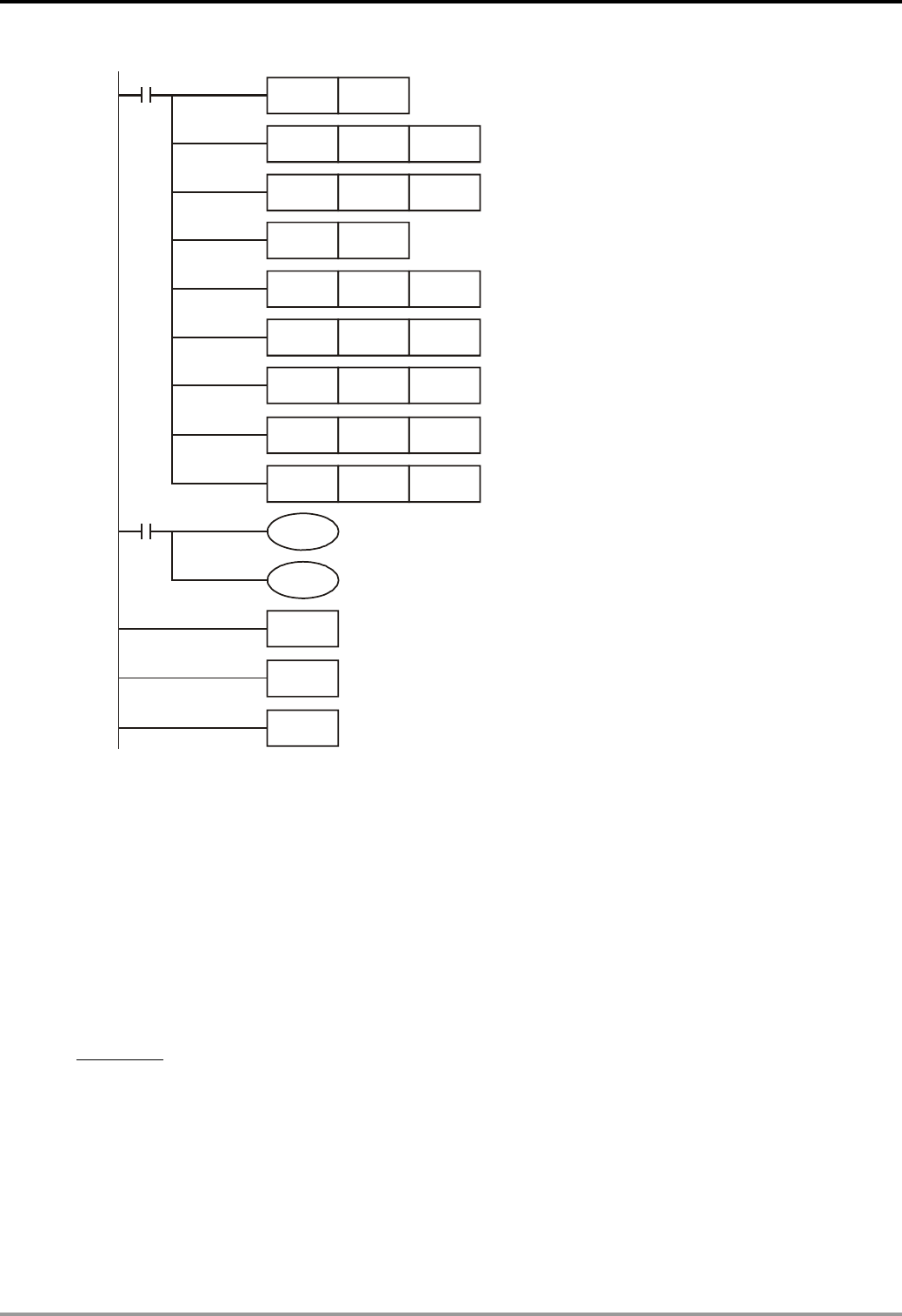
2 Functions of Devices in DVP-PLC
M1002
SET M1353
MOV K17 D1121
H86 D1120
K2000
K3000
K300
K48
K48
M1350
FEND
MOV
SET M1120
MOV
MOV
MOV
MOV
MOV
D1480
D1496
D1129
D1434
D1450
M1351
X1
IRET
END
I170
With I170, the processing of data in PLC LINK will not be done at END, but at the enabling of I170
immediately after the receiving of data is completed
If the reaction speed of the RS-485 IC direction control signal pin of the Slave is slow, it is suggested that
you do not enable I170.
You can set up D1399 (starting Slave ID designated by PLC LINK), and the ID# of the next 15 Slaves
have to be in sequence. For example, when D1399 is set as K20, the Master PLC will detect Slave ID# 20
~ 35.
c) Example 3: Connection of 1 Master and 2 Slaves by RS-485 and exchange of 16 data between Master and
Slaves through PLC LINK (M1353 = Off, linkage of 16 stations, 16 data read/write mode)
Write the ladder diagram program into Master PLC (ID#17)
DVP-PLC Application Manual
2-146
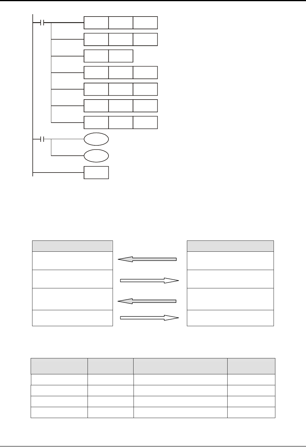
2 Functions of Devices in DVP-PLC
M1002
MOV K17 D1121
H86 D1120
K16
K16
M1351
END
MOV
SET M1120
MOV
MOV
D1434
D1450
M1350
X1
K16
K16
MOV
MOV
D1435
D1451
Master ID#
COM2 communication protocol
Retain communication protocol
Number of data read from Slave ID#1
Number of data written into Slave ID#1
Number of data read from Slave ID#2
Number of data written into Slave ID#2
Auto mode
Enable EASY PLC LINK
When X1 = On, the data exchange between Master and the two Slaves will be automatically done in PLC
LINK, i.e. the data in D100 ~ D115 in the two Slaves will be read into D1480 ~ D1495 and D1512 ~ D1527
of the Master, and the data in D1496 ~ D1511 and D1528 ~ D1543 will be written into D200 ~ D215 of the
two Slaves.
Master PLC *1 Slave PLC*2
D1480 ~ D1495 D100 ~ D115 of Slave ID#1
D1496 ~ D1511 D200 ~ D215 of Slave ID#1
D1512 ~ D1527 D100 ~ D115 of Slave ID#2
D1528 ~ D1543
Read
Write
Read
D200 ~ D215 of Slave ID#2
Write
Assume the data in D for data exchange between Master and Slave before PLC LINK is enabled (M1350
= Off) are as the follow:
Master PLC Preset value Slave PLC Preset value
D1480 ~ D1495 K0 D100 ~ D115 of Slave ID#1 K5,000
D1496 ~ D1511 K1,000 D200 ~ D215 of Slave ID#1 K0
D1512 ~ D1527 K0 D100 ~ D115 of Slave ID#2 K6,000
D1528 ~ D1543 K2,000 D200 ~ D215 of Slave ID#2 K0
DVP-PLC Application Manual 2-147
2 Functions of Devices in DVP-PLC
After PLC LINK is enabled (M1350 = On), the data in D for data exchange will become:
Master PLC Preset value Slave PLC Preset value
K5,000 D1480 ~ D1495 D100 ~ D115 of Slave ID#1 K5,000
D1496 ~ D1511 K1,000 D200 ~ D215 of Slave ID#1 K1,000
D1512 ~ D1527 K6,000 D100 ~ D115 of Slave ID#2 K6,000
D1528 ~ D1543 K2,000 D200 ~ D215 of Slave ID#2 K2,000
The Master PLC has to be SA/SX/SC/EH2/SV/EH3/SV2 series MPU, and the Slave PLC can be any MPU
of DVP series.
There can be maximum 16 Slave PLCs in PLC LINK. See the special Ds in the Master PLC
corresponding to D100 ~ D115 and D200 ~ D215 in every Slave PLC in the tables of special M and
special D.
d) Example 4: Connection between Delta PLC and Delta VFD-M AC motor drive through PLC LINK for STOP,
forward/reverser revolution and writing/reading of frequency.
Write the ladder diagram program into Master PLC (ID#17)
M1002
MOV K17 D1121
H86 D1120
K6
K2
M1351
END
MOV
SET M1120
MOV
MOV
D1434
D1450
M1350
X1
H2100
H2000
MOV
MOV
D1355
D1415
Master ID#
COM2 communication protocol
Retain communication protocol
Number of data read
Number of data written
Starting reference for Master to read from Slave
Starting reference for Master to write in Slave
Auto mode
Enable PLC LINK
D1480 ~ D1485 correspond to parameters H2100 ~ H2105 in VFD-M. When X1 = On, PLC LINK will be
enabled, and the data in H2100 ~ H2105 will be displayed in D1480 ~ D1485.
D1496 ~ D1497 correspond to parameters H2000 ~ H2001 in VFD-M. When X1 = On, PLC LINK will be
enabled, and the data in H2000 ~ H2001 will be displayed in D1496 ~ D1497.
Modify D1496 to give command to VFD, e.g. D1496 = H12: enabling forward revolution of VFD-M; D1496
= H11: enabling reverse revolution of VFD.
Modify D1497 to change the frequency of VFD, e.g. D1497 = K5,000: changing the frequency to 50kHz.
The Master PLC has to be SA/SX/SC/EH2/SV/EH3/SV2 series MPU, and the Slave AC motor drive can
be any VFD series models except VFD-A.
DVP-PLC Application Manual
2-148

2 Functions of Devices in DVP-PLC
The Slave can also be Delta temperature controller DTA, DTB, Delta servo ASDA and so on which are
compatible to Modbus protocol. Maximum 16 devices are connectable to the LINK.
See the tables of special M and special D for the starting ID of Slave to be read/written and the number of
data to be read/written.
2.12 Communication Addresses of Devices in DVP Series PLC
Applicable to
Device DVP Com. Modbus Com. EH2/
Range Type Address (hex) Address (dec) ES/EX/SS SA/SX/SC EH2-SL/SV
/EH3/SV2
S 000 ~ 255 bit 0000 ~ 00FF 000001 ~ 000256 0 ~ 127
S 246 ~ 511 bit 0100 ~ 01FF 000247 ~ 000512
S 512 ~ 767 bit 0200 ~ 02FF 000513 ~ 000768 0 ~ 1,023 0 ~ 1,023
-
S 768 ~ 1,023 bit 0300 ~ 03FF 000769 ~ 001024
X 000 ~ 377 (Octal) bit 0400 ~ 04FF 101025 ~ 101280 0 ~ 177 0 ~ 177 0 ~ 377
Y 000 ~ 377 (Octal) bit 0500 ~ 05FF 001281 ~ 001536 0 ~ 177 0 ~ 177 0 ~ 377
bit 0600 ~ 06FF 001537 ~ 001792
T 000 ~ 255 0 ~ 127 0 ~ 255 0 ~ 255
word 0600 ~ 06FF 401537 ~ 401792
M 000 ~ 255 bit 0800 ~ 08FF 002049 ~ 002304
M 256 ~ 511 bit 0900 ~ 09FF 002305 ~ 002560
M 512 ~ 767 bit 0A00 ~ 0AFF 002561 ~ 002816 0 ~ 1,279
M 768 ~ 1,023 bit 0B00 ~ 0BFF 002817 ~ 003072
M 1,024 ~ 1,279 bit 0C00 ~ 0CFF 003073 ~ 003328
M 1,280 ~ 1,535 bit 0D00 ~ 0DFF 003329 ~ 003584
M 1,536 ~ 1,791 bit B000 ~ B0FF 045057 ~ 045312
M 1,792 ~ 2,047 bit B100 ~ B1FF 045313 ~ 045568
M 2,048 ~ 2,303 bit B200 ~ B2FF 045569 ~ 045824 0 ~ 4,095 0 ~ 4,095
M 2,304 ~ 2,559 bit B300 ~ B3FF 045825 ~ 046080
M 2,560 ~ 2,815 bit B400 ~ B4FF 046081 ~ 046336 -
M 2,816 ~ 3,071 bit B500 ~ B5FF 046337 ~ 046592
M 3,072 ~ 3,327 bit B600 ~ B6FF 046593 ~ 046848
M 3,328 ~ 3,583 bit B700 ~ B7FF 046849 ~ 047104
M 3,584 ~ 3,839 bit B800 ~ B8FF 047105 ~ 047360
M 3,840 ~ 4,095 bit B900 ~ B9FF 047361 ~ 047616
bit 0E00 ~ 0EC7 003585 ~ 003784
0 ~ 199 16-bit 0 ~ 127 0 ~ 199 0 ~ 199
word 0E00 ~ 0EC7 403585 ~ 403784
bit 0EC8 ~ 0EFF 003785 ~ 003840
C
200 ~ 255 32-bit 232 ~ 255 200 ~ 255 200 ~ 255
word 0700 ~ 076F 403785 ~ 403840
D 000 ~ 256 word 1000 ~ 10FF 404097~404352 0 ~ 1,311 0 ~ 4,999 0 ~ 9,999
D 256 ~ 511 word 1100 ~ 11FF 404353 ~ 404608
DVP-PLC Application Manual 2-149

2 Functions of Devices in DVP-PLC
Applicable to
Device DVP Com. Modbus Com. EH2/
Range Type Address (hex) Address (dec) ES/EX/SS SA/SX/SC EH2-SL/SV
/EH3/SV2
D 512 ~ 767 word 1200 ~ 12FF 404609 ~ 404864
D 768 ~ 1,023 word 1300 ~ 13FF 404865 ~ 405120
D 1,024 ~ 1,279 word 1400 ~ 14FF 405121 ~ 405376 0 ~ 9,999
0 ~ 1,311
D 1,280 ~ 1,535 word 1500 ~ 15FF 405377 ~ 405632
D 1,536 ~ 1,791 word 1600 ~ 16FF 405633 ~ 405888 -
D 1,792 ~ 2,047 word 1700 ~ 17FF 405889 ~ 406144
D 2,048 ~ 2,303 word 1800 ~ 18FF 406145 ~ 406400
D 2,304 ~ 2,559 word 1900 ~ 19FF 406401 ~ 406656
D 2,560 ~ 2 815 word 1A00 ~ 1AFF 406657 ~ 406912
D 2,816 ~ 3,071 word 1B00 ~ 1BFF 406913 ~ 407168
D 3,072 ~ 3,327 word 1C00 ~ 1CFF 407169 ~ 407424 0 ~ 4,999
D 3,328 ~ 3,583 word 1D00 ~ 1DFF 407425 ~ 407680
D 3,584 ~ 3,839 word 1E00 ~ 1EFF 407681 ~ 407936
D 3,840 ~ 4,095 word 1F00 ~ 1FFF 407937 ~ 408192
D 4,096 ~ 4,351 word 9000 ~ 90FF 436865 ~ 437120
D 4,352 ~ 4,607 word 9100 ~ 91FF 437121 ~ 437376
D 4 608 ~ 4863 word 9200 ~ 92FF 437377 ~ 437632
D 4,864 ~ 5,119 word 9300 ~ 93FF 437633 ~ 437888
D 5,120 ~ 5,375 word 9400 ~ 94FF 437889 ~ 438144 -
D 5,376 ~ 5,631 word 9500 ~ 95FF 438145 ~ 438400
D 5,632 ~ 5,887 word 9600 ~ 96FF 438401 ~ 438656
D 5,888 ~ 6,143 word 9700 ~ 97FF 438657 ~ 438912
D 6,144 ~ 6,399 word 9800 ~ 98FF 438913 ~ 439168
D 6,400 ~ 6,655 word 9900 ~ 99FF 439169 ~ 439424
D 6,656 ~ 6,911 word 9A00 ~ 9AFF 439425 ~ 439680
D 6,912 ~ 7,167 word 9B00 ~ 9BFF 439681 ~ 439936
D 7,168 ~ 7,423 word 9C00 ~ 9CFF 439937 ~ 440192
D 7,424 ~ 7,679 word 9D00 ~ 9DFF 440193 ~ 440448
D 7,680 ~ 7,935 word 9E00 ~ 9EFF 440449 ~ 440704
D 7,936 ~ 8,191 word 9F00 ~ 9FFF 440705 ~ 440960
D 8,192 ~ 8,447 word A000 ~ A0FF 440961 ~ 441216
D 8,448 ~ 8,703 word A100 ~ A1FF 441217 ~ 441472
D 8,704 ~ 8,959 word A200 ~ A2FF 441473 ~ 441728
D 8,960 ~ 9,215 word A300 ~ A3FF 441729 ~ 441984
D 9,216 ~ 9,471 word A400 ~ A4FF 441985 ~ 442240
D 9,472 ~ 9,727 word A500 ~ A5FF 442241 ~ 442496
DVP-PLC Application Manual
2-150
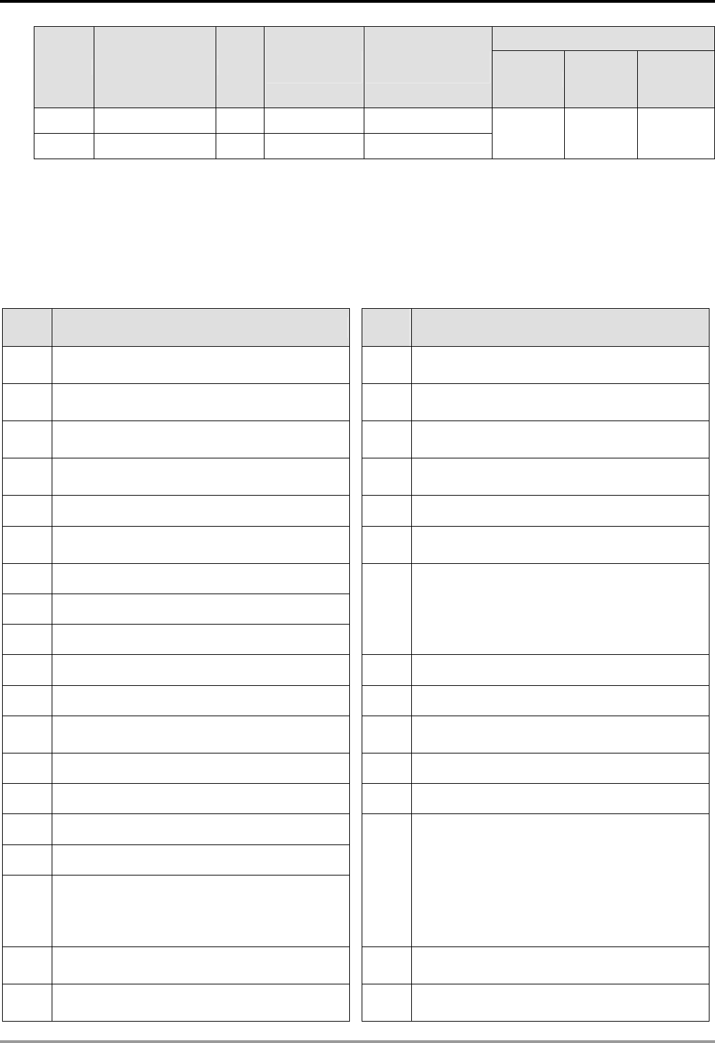
2 Functions of Devices in DVP-PLC
Applicable to
Device DVP Com. Modbus Com. EH2/
Range Type Address (hex) Address (dec) ES/EX/SS SA/SX/SC EH2-SL/SV
/EH3/SV2
D 9,728 ~ 9,983 word A600 ~ A6FF 442497 ~ 442752
D 9,984 ~ 9,999 word A700 ~ A70F 442753 ~ 443008
2.13 Error Codes
After you write the program into the PLC, the illegal use of operands (devices) or incorrect syntax in the program
will result in flashing of ERROR indicator and M1004 = On. In this case, you can find out the cause of the error by
checking the error code (hex) in special register D1004. The address where the error occurs is stored in the data
register D1137. If the error is a general loop error, the address stored in D1137 will be invalid.
Error Error
Cause of error Cause of error
code code
Times of using TTMR, STMR instruction
exceed the range
Use of device S exceeds the range
0001 0F0A
Using P* repeatedly or use of P* exceeds the
range
Times of using SORT instruction exceed the
range
0002 0F0B
Times of using TKY instruction exceed the
range
Use of KnSm exceeds the range
0003 0F0C
Using I* repeatedly or use of I* exceeds the
range
Times of using HKY instruction exceed the
range
0102 0F0D
Use of MC N* exceeds the range Improper use of operands of ZRST instruction
0202 1000
Incorrect use of E, F, or the modification
exceeds the range
Use of MCR N* exceeds the range
0302 10EF
Use of device X exceeds the range
0401
0403 Use of KnXm exceeds the range
Times of using TTMR, PR, HOUR instructions
exceed the range.
2000 Improper use of operands of MRT, ARWS
instructions
Use of device Y exceeds the range
0501
Use of KnYm exceeds the range Illegal instruction
0503 C400
Use of device T exceeds the range General loop error
0601 C401
Continuously using LD/LDI instructions for
more than 9 times
Use of register T exceeds the range
0604 C402
Use of device M exceeds the range Continuously using MPS for more than 9 times
0801 C403
Use of KnMm exceeds the range More than 6 steps in FOR – NEXT
0803 C404
Incorrect use of KH
0B01
0D01 Improper use of operands of DECO instruction Using STL/RET between FOR – NEXT
Using SRET/IRET between FOR – NEXT
C405
ES/EX/SS/EH2/SV/EH3/SV2: improper use of
operands of ENCO instruction Using MC/MCR between FOR – NEXT
Using END/FEND between FOR – NEXT
0D02 SA/SX/SC: illegal use of the first operand of
ANS instruction
Improper use of operands of DHSCS
instruction Continuously using STL for more than 9 times
0D03 C407
Improper use of operands of DHSCR
instruction Using MC/MCR in STL, using I/P in STL
0D04 C408
DVP-PLC Application Manual 2-151

2 Functions of Devices in DVP-PLC
Error Error
Cause of error Cause of error
code code
Using STL/RET in subroutine
Improper use of operands of pulse output
instruction
0D05 C409 Using STL/RET in interruption subroutine
Improper use of operands of PWM instruction
0D06 Using MC/MCR in subroutine
C40A Using MC/MCR in interruption subroutine
Improper use of operands of FROM/TO
instruction
0D07 MC/MCR does not start from N0, or is not
continuous
C40B
Improper use of operands of PID instruction Corresponding N of MC and MCR are different
0D08 C40C
Improper use of operands of SPD instruction Improper use of I/P
0D09 C40D
IRET does not appear after the last FEND
Incorrect operands in DHSZ instruction
0D0A C40E SRET does not appear after the last FEND
PLC program and data in parameters have not
been initialized
Improper use of operands in IST instruction
0D0B C40F
Invalid RUN/STOP instruction to extension
module
Use of device C exceeds the range
0E01 C41B
Use of register C exceeds the range Points of extension module exceed the range
0E04 C41C
Improper use of operand CXXX of DCNT
instsruction
Number of extension modules exceeds the
range
0E05 C41D
BCD conversion error Incorrect hardware setting for extension module
0E18 C41E
Division error (divisor = 0) Failing to write data into memory
0E19 C41F
Use of device exceeds the range (including E,
F index register modification) Read/write function card error
0E1A C420
The index of the radical is a negative value Initializing parallel interface error
0E1B C430
Communication error of FROM/TO instruction Hardware error in high-speed counter
0E1C C440
Use of register D exceeds the range Hardware error in high-speed comparator
0F04 C441
Improper use of operand DXXX of DCNT
instruction Hardware error in MCU pulse output
0F05 C442
Improper use of operands of SFTR instruction No response from extension unit
0F06 C443
Improper use of operands of SFTL instruction No END instruction in the program
0F07 C4EE
Improper use of operands of REF instruction Invalid instruction (no such instruction existing)
0F08 C4FF
Improper use of operands of WSFR, WSFL
instructions
0F09
DVP-PLC Application Manual
2-152
3 Basic Instructions
3.1 Basic Instructions and Step Ladder Instructions
ES includes ES/EX/SS; SA includes SA/SX/SC; EH includes EH2/SV/EH3/SV2.
For EH series MPU, the execution speed in the brackets ( ) refers to the execution speed of designated operand
M1536 ~ M4095.
Basic Instructions
Execution speed (us)
Instruction
Code Function Operands ES SA STEP Page
EH
LD Loading in A contact X, Y, M, S, T, C 3.8 0.24 (0.56) 1~3 3-4
3.8
LDI Loading in B contact X, Y, M, S, T, C 3.88 0.24 (0.56) 1~3 3-4
3.88
AND Series connection- A contact X, Y, M, S, T, C 2.32 0.24 (0.56) 1~3 3-4
2.32
ANI Series connection- B contact X, Y, M, S, T, C 2.4 0.24 (0.56) 1~3 3-5
2.4
OR Parallel connection- A contact X, Y, M, S, T, C 2.32 0.24 (0.56) 1~3 3-5
2.32
ORI Parallel connection- B contact X, Y, M, S, T, C 2.4 0.24 (0.56) 1~3 3-6
2.4
ANB Series connection- loop blocks N/A 1.76 0.24 1~3 3-6
1.76
ORB Parallel connection- loop blocks N/A 1.76 0.24 1~3 3-7
1.76
Store the current result of the internal
PLC operations
MPS N/A 1.68 0.24 1~3 3-7
1.68
Reads the current result of the
internal PLC operations
MRD N/A 1.6 0.24 1 3-7
1.6
Pops (recalls and removes) the
currently stored result N/A 1.6 0.24 1 3-7
MPP 1.6
Output instructions
Execution speed (us)
Instruction
Code Function Operands
ES SA
STEP Page
EH
OUT Output coil Y, M, S 5.04 0.24 (0.56) 1~3 3-8
5.04
Latched(On)
SET Y, M, S 3.8 0.24 (0.56) 1~3 3-8
3.8
RST Clear the contacts or the registers Y, M, S, T, C, D, E, F 7.8 0.24 (0.56) 3 3-9
7.8
Timers, Counters
Execution speed (us)
API Instruction
Code Function Operands
ES SA
STEP Page
EH
96 TMR 16-bit timer T-K or T-D 10.6 9.6 4 3-9
10.6
97 CNT 16-bit counter C-K or C-D (16 bits) 9.7 12.8 4 3-10
9.7
97 DCNT 32-bit counter C-K or C-D (32 bits) 10.3 14.3 6 3-10
10.3
DVP-PLC Application Manual 3-1
3 Basic Instructions
Main control instructions
Execution speed (us)
Instruction
Code Function Operands
ES SA
STEP Page
EH
Master control start
MC N0 ~ N7 5.6 5.6 5.6 3 3-11
Master control reset
MCR N0 ~ N7 5.7 5.7 5.7 3 3-11
Instructions for detecting the contacts of rising-/falling-edge
Execution speed (us)
API Instruction
Code Function Operands
ES SA
STEP Page
EH
Rising-edge detection operation
90 LDP X, Y, M, S, T, C 5.1 5.1 0.56 (0.88) 3 3-12
Falling-edge detection operation
91 LDF X, Y, M, S, T, C 5.1 5.1 0.56 (0.88) 3 3-13
Rising-edge series connection
92 ANDP X, Y, M, S, T, C 4.9 4.9 0.56 (0.88) 3 3-13
Falling-edge series connection
93 ANDF X, Y, M, S, T, C 4.9 4.9 0.56 (0.88) 3 3-13
Rising-edge parallel connection
94 ORP X, Y, M, S, T, C 4.9 4.9 0.56 (0.88) 3 3-14
Falling-edge parallel connection
95 ORF X, Y, M, S, T, C 4.9 4.9 0.56 (0.88) 3 3-14
Rising-/falling-edge output instructions
Execution speed (us)
API Instruction
Code Function Operands
ES SA
STEP Page
EH
Rising-edge output Y, M
89 PLS 7.8 7.8 9.92 3 3-14
Falling-edge output Y, M
99 PLF 7.8 7.8 10.16 3 3-15
End instruction
Execution speed (us)
Instruction
Code Function Operands
ES SA
STEP Page
EH
Program ends
END N/A 5 5 0.24 1 3-16
Other instructions
Execution speed (us)
API Instruction
Code Function Operands
ES SA
STEP Page
EH
NOP No operation 0.88 0.16 1
N/A 0.88 3-16
INV Inverting operation 1.6 0.24 1
98 N/A 1.6 3-16
P Pointer P0 ~ P255 0.88 - 1
0.88 3-17
I□□□
I Interruption program marker 0.88 - 1
0.88 3-17
DVP-PLC Application Manual
3-2

3 Basic Instructions
Step ladder instructions
Execution speed (us)
Instruction
Code Function Operands
ES SA
STEP Page
EH
STL Step transition ladder start instruction S 1 4-1
11.6 10.6 0.56
RET Step transition ladder return instruction N/A 7.04 6.04 0.24
1 4-1
Note 1: ES includes ES/EX/SS; SA includes SA/SX/SC; EH includes EH/EH2/SV.
Note 2: For EH series MPU, the execution speed in the brackets ( ) refers to the execution speed of designated
operand M1536 ~ M4095.
DVP-PLC Application Manual 3-3
3 Basic Instructions
3.2 Explanations on Basic Instructions
Mnemonic Function Program steps Controllers
ES
LD Loading in A contact 1 EX SS SA SX SC EH2 SV EH3 SV2
X0 ~ X377 Y0 ~ Y377 M0 ~ M4095 S0 ~ S1023 T0 ~ T255 C0 ~ C255 D0 ~ D9999
Operand 9 9 9 9 9 9 -
Explanations:
The LD instruction is used on the A contact that has its start from the left BUS or the A contact that is the start of a
contact circuit. The functions are to save the present contents and store the acquired contact status into the
accumulative register.
Program Example:
Ladder diagram: Instruction code: Operation:
X0 X1
Y1
LD X0 Loading in contact A of X0
AND X1 Connecting to contact A of X1 in series
OUT Y1 Driving Y1 coil
Mnemonic Function Program steps Controllers
ES
LDI Loading in B contact 1 EX SS SA SX SC EH2 SV EH3 SV2
X0 ~ X377 Y0 ~ Y377 M0 ~ M4095 S0 ~ S1023 T0 ~ T255 C0 ~ C255 D0 ~ D9999
Operand 9 9 9 9 9 9 -
Explanations:
The LDI instruction is used on the B contact that has its start from the left BUS or the B contact that is the start of a
contact circuit. The functions are to save the present contents and store the acquired contact status into the
accumulative register.
Program Example:
Ladder diagram: Instruction code: Operation:
X0 X1
Y1
LDI X0 Loading in contact B of X0
AND X1 Connecting to contact A of X1 in series
OUT Y1 Driving Y1 coil
Mnemonic Function Program steps Controllers
ES
AND Series connection- A contact 1 EX SS SA SX SC EH2 SV EH3 SV2
X0 ~ X377 Y0 ~ Y377 M0 ~ M4095 S0 ~ S1023 T0 ~ T255 C0 ~ C255 D0 ~ D9999
Operand 9 9 9 9 9 9 -
Explanations:
The AND instruction is used in the series connection of A contact. The functions are to read out the status of present d
DVP-PLC Application Manual
3-4
3 Basic Instructions
series connection contacts and perform the “AND” operation with the logical operation result obtained. The final result
will be store in the accumulative register.
Program Example:
Ladder diagram: Instruction code: Operation:
X0X1
Y1
LDI X1 Loading in contact B of X1
AND X0 Connecting to contact A of X0 in series
OUT Y1 Driving Y1 coil
Mnemonic Function Program steps Controllers
ES
ANI Series connection- B contact 1 EX SS SA SX SC EH2 SV EH3 SV2
X0 ~ X377 Y0 ~ Y377 M0 ~ M4095 S0 ~ S1023 T0 ~ T255 C0 ~ C255 D0 ~ D9999
Operand 9 9 9 9 9 9 -
Explanations:
The ANI instruction is used in the series connection of B contact. The functions are to read out the status of present
designated series connection contacts and perform the “AND” operation with the logical operation result obtained.
The final result will be store in the accumulative register.
Program Example:
Ladder diagram: Instruction code: Operation:
X0X1
Y1
LD X1 Loading in contact A of X1
ANI X0 Connecting to contact B of X0 in series
OUT Y1 Driving Y1 coil
Mnemonic Function Program steps Controllers
ES
OR Parallel connection- A contact 1 EX SS SA SX SC EH2 SV EH3 SV2
X0 ~ X377 Y0 ~ Y377 M0 ~ M4095 S0 ~ S1023 T0 ~ T255 C0 ~ C255 D0 ~ D9999
Operand 9 9 9 9 9 9 -
Explanations:
The OR instruction is used in the parallel connection of A contact. The functions are to read out the status of present
designated parallel connection contacts and perform the “OR” operation with the logical operation result obtained.
The final result will be store in the accumulative register.
Program Example:
Ladder diagram: Instruction code: Operation:
LD X0 Loading in contact A of X0
X0
X1
Y1
OR X1 Connecting to contact A of X1 in parallel
OUT Y1 Driving Y1 coil
DVP-PLC Application Manual 3-5
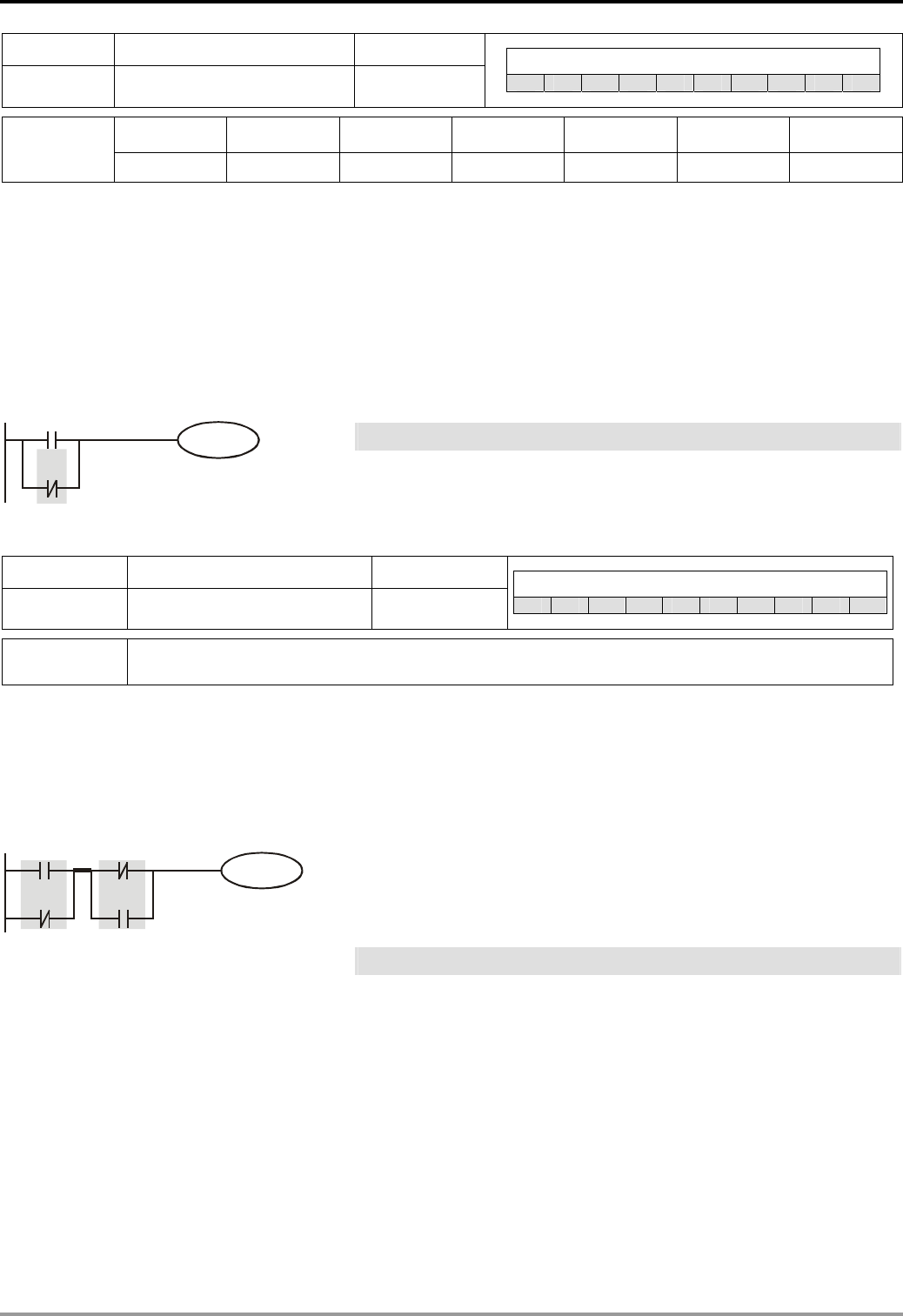
3 Basic Instructions
Mnemonic Function Program steps Controllers
ES
ORI Parallel connection- B contact 1 EX SS SA SX SC EH2 SV EH3 SV2
X0 ~ X377 Y0 ~ Y377 M0 ~ M4095 S0 ~ S1023 T0 ~ T255 C0 ~ C255 D0 ~ D9999
Operand 9 9 9 9 9 9 -
Explanations:
The OR instruction is used in the parallel connection of B contact. The functions are to read out the status of present
designated parallel connection contacts and perform the “OR” operation with the logical operation result obtained.
The final result will be store in the accumulative register.
Program Example:
Ladder diagram: Instruction code: Operation:
LD X0 Loading in contact A of X0
X0
X1
Y1
ORI X1 Connecting to contact B of X1 in parallel
OUT Y1 Driving Y1 coil
Mnemonic Function Program steps Controllers
ES
ANB Series connection- loop blocks 1 EX SS SA SX SC EH2 SV EH3 SV2
N/A
Operand
Explanations:
To perform the “AND” operation of the preserved logic results and content in the accumulative register.
Program Example:
Ladder diagram: Instruction code: Operation:
X0
X2
Y1
X1
X3
ANB
Block A Block B
LD X0 Loading in contact A of X0
ORI X2 Connecting to contact B of X2 in parallel
LDI X1 Loading in contact B of X1
OR X3 Connecting to contact A of X3 in parallel
ANB Connecting circuit block in series
OUT Y1 Driving Y1 coil
DVP-PLC Application Manual
3-6
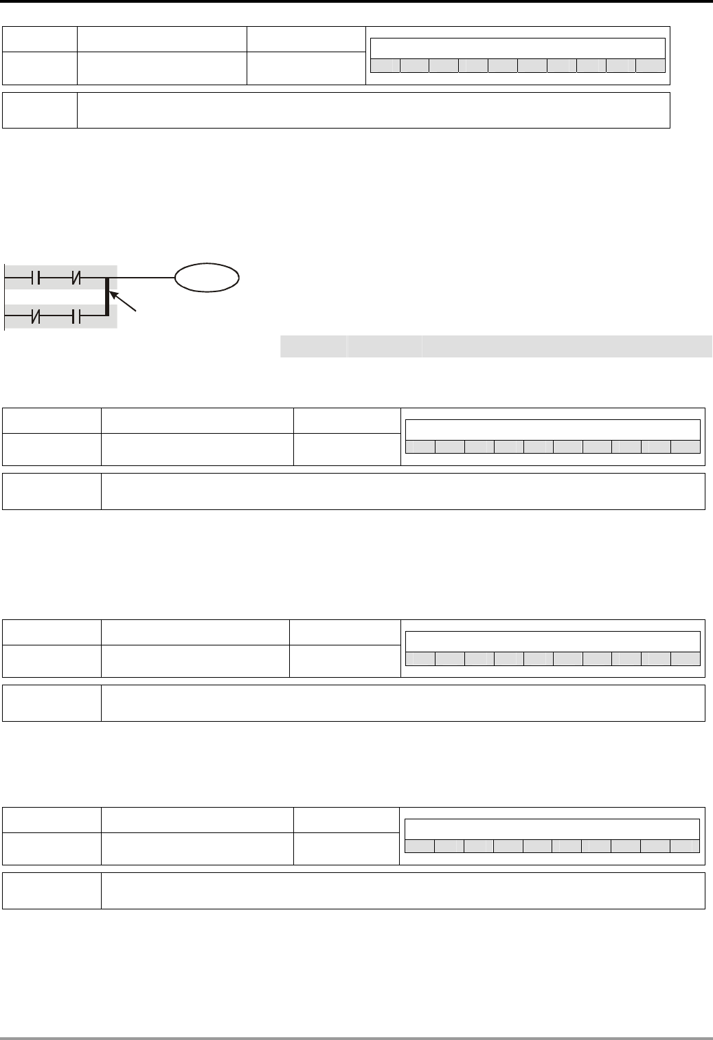
3 Basic Instructions
Mnemonic Function Program steps Controllers
Parallel connection- loop
blocks ES
ORB 1 EX SS SA SX SC EH2 SV EH3 SV2
N/A
Operand
Explanations:
To perform the “OR” operation of the preserved logic results and content in the accumulative register.
Program Example:
Ladder diagram: Instruction code: Operation:
X0
X2
Y1
X1
X3
ORB
Block A
Block B
LD X0 Loading in contact A of X0
ANI X1 Connecting to contact B of X1 in series
LDI X2 Loading in contact B of X2
AND X3 Connecting to contact A of X3 in series
ORB Connecting circuit block in parallel
OUT Y1 Driving Y1 coil
Mnemonic Function Program steps Controllers
Store the current result of
the internal PLC operations ES
MPS 1 EX SS SA SX SC EH2 SV EH3 SV2
N/A
Operand
Explanations:
To save the content in the accumulative register into the operational result (the pointer of operational result will plus
1).
Mnemonic Function Program steps Controllers
Reads the current result of
the internal PLC operations ES
MRD 1 EX SS SA SX SC EH2 SV EH3 SV2
N/A
Operand
Explanations:
To read the operational result and store it into the accumulative register (the pointer of operational result stays intact).
Mnemonic Function Program steps Controllers
Pops (recalls and removes)
the currently stored result ES
MPP 1 EX SS SA SX SC EH2 SV EH3 SV2
N/A
Operand
Explanations:
To retrieve the previous preserved logical operation result and store it into the accumulative register (the pointer of
operational result will minus 1).
DVP-PLC Application Manual 3-7
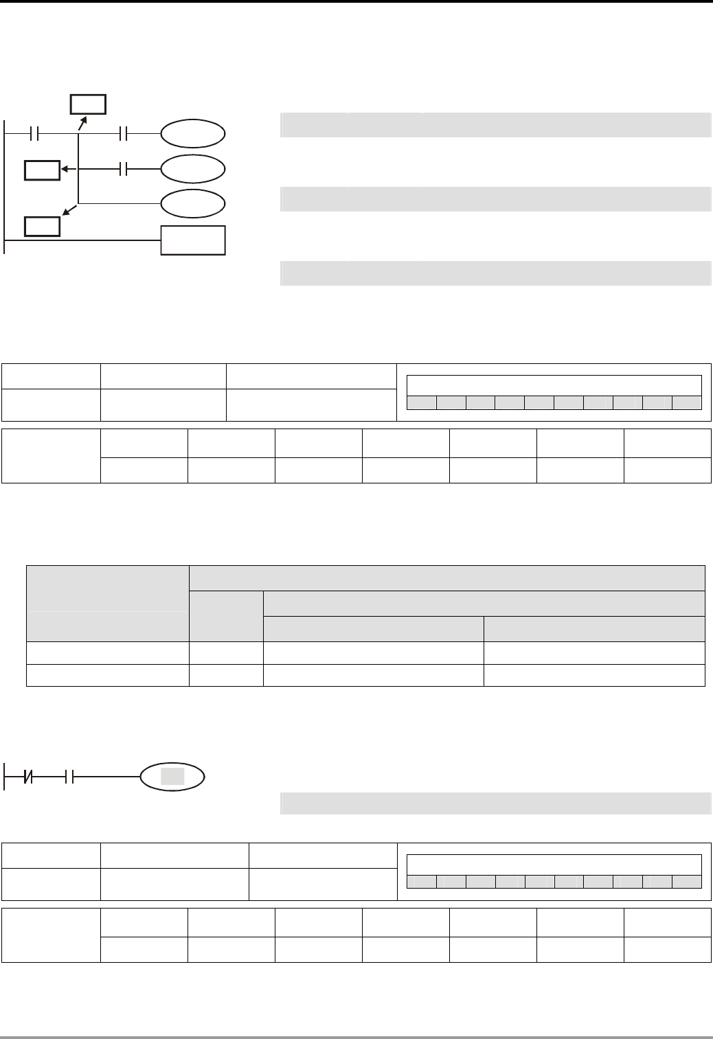
3 Basic Instructions
Program Example:
Ladder diagram: Instruction code: Operation:
LD X0 Loading in contact A of X0
X0
Y1
X1
M0
X2
Y2
END
MPP
MRD
MPS
Saving into stack
MPS
AND X1 Connecting to contact A of X1 in series
OUT Y1 Driving Y1 coil
Reading from stack
MRD
AND X2 Connecting to contact A of X2 in series
OUT M0 Driving M0 coil
Reading from stack and pop pointer
MPP
OUT Y2 Driving Y2 coil
END Program ends
Mnemonic Function Program steps Controllers
ES
OUT Output coil 1 EX SS SA SX SC EH2 SV EH3 SV2
X0 ~ X377 Y0 ~ Y377 M0 ~ M4095 S0 ~ S1023 T0 ~ T255 C0 ~ C255 D0 ~ D9999
Operand - -
9 9 9 -
-
Explanations:
1. To output the logical operation result before OUT instruction into a designated device.
2. Actions of coil contact:
OUT instruction
Contact
Operational result Coil A contact (normally open) B contact (normally closed)
FALSE Off Off On
TRUE On On Off
Program Example:
Ladder diagram: Instruction code: Operation:
X0 X1
Y1
LDI X0 Loading in contact B of X0
AND X1 Connecting to contact A of X1 in series
OUT Y1 Driving Y1 coil
Mnemonic Function Program Steps Controllers
ES
SET Latched (On) 1 EX SS SA SX SC EH2 SV EH3 SV2
X0 ~ X377 Y0 ~ Y377 M0 ~ M4095 S0 ~ S1023 T0 ~ T255 C0 ~ C255 D0 ~ D9999
Operand - -
9 9 9 -
-
Explanations:
DVP-PLC Application Manual
3-8
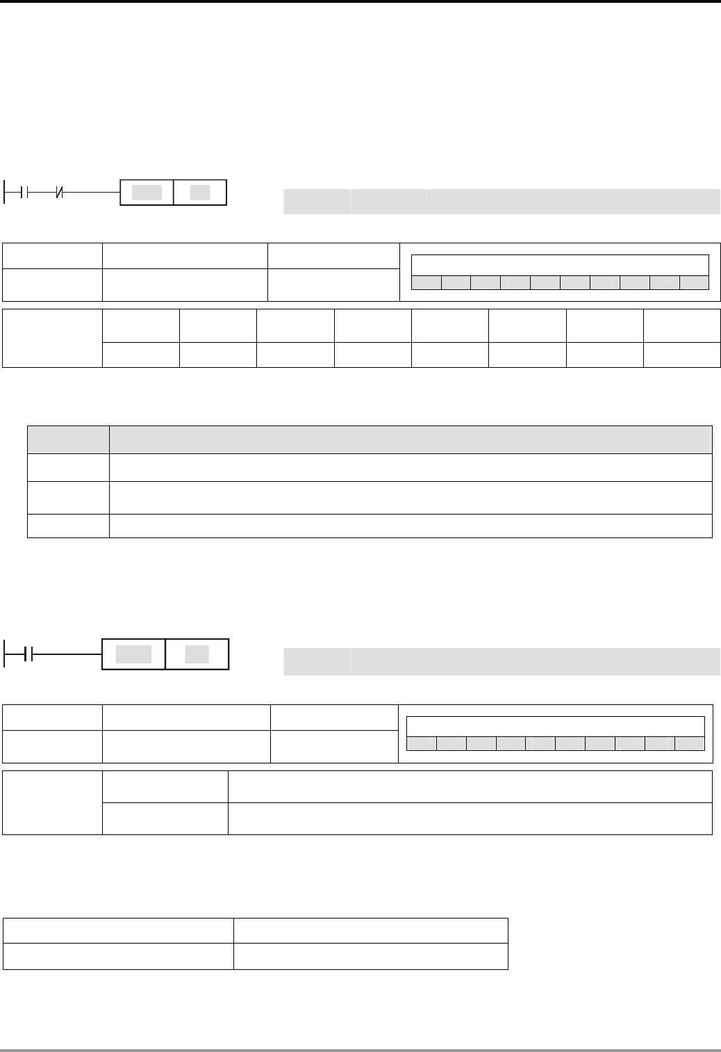
3 Basic Instructions
When the SET instruction is driven, its designated device will be “On” and keep being On both when SET instruction
is still being driven or not driven. Use RST instruction to set “Off” the device.
Program Example:
Ladder diagram: Instruction code: Operation:
LD X0 Loading in contact A of X0
ANI Y0 Connecting to contact B of Y0 in series
X0 Y0
Y1
SET
Y1 latched (On)
SET Y1
Mnemonic Function Program steps Controllers
Clear the contacts or
the registers ES
RST 1 EX SS SA SX SC EH2 SV EH3 SV2
D0 ~
D9999
E0 ~ E7
M0 ~
M4095 S0 ~ S1023 T0 ~ T255 C0 ~ C255
X0 ~ X377 Y0 ~ Y377 F0 ~ F7
Operand
9 9 9 9
9 9 9
-
Explanations:
1. When the RST instruction is driven, the actions of the designated devices are:
Device Status
Y, M, S, Coil and contact will be set to “Off”
Present values of the timer or counter will be set to “0”, and the coil and contact will be set to
“Off”
T, C
D, E, F The content will be set to “0”.
2. If RST instruction is not being executed, the status of the designated device will stay intact.
Program Example:
Ladder diagram: Instruction code: Operation:
X0
Y5
RST
LD X0 Loading in contact A of X0
RST Y5 Resetting contact Y5
Mnemonic Function Program steps Controllers
ES
TMR 16-bit timer 1 EX SS SA SX SC EH2 SV EH3 SV2
T-K T0 ~ T255, K0 ~ K32,767
Operand
T-D T0 ~ T255, D0 ~ D9999
Explanations:
When TMR instruction is executed, the designated coil of the timer will be On and the timer will start to time. When the
set value in the timer is reached (present ≥ set value), the contact will be:
NO (Normally Open) contact Open collector
NC (Normally Closed) contact Close collector
DVP-PLC Application Manual 3-9
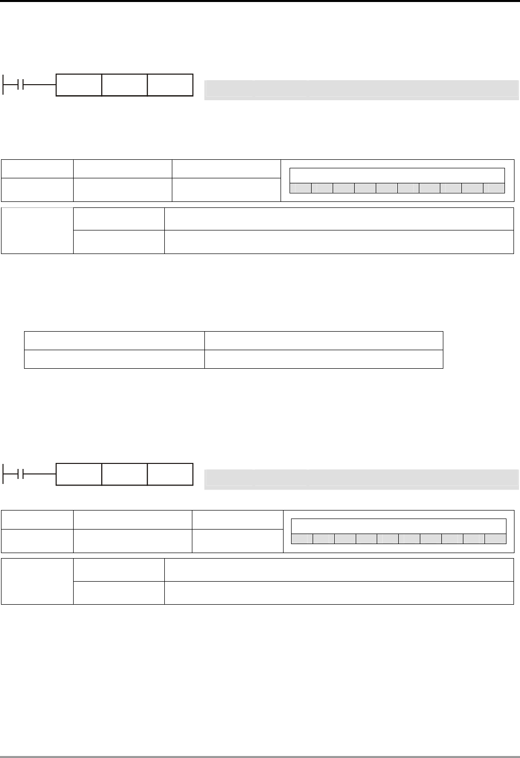
3 Basic Instructions
Program Example:
Ladder diagram: Instruction code: Operation:
X0
T5TMR K1000
LD X0 Loading in contact A of X0 T5 timer
TMR T5 K1000 Set value in timer T5 as K1,000
Remarks:
See the specification of each model for the range of operand T.
Mnemonic Function Program steps Controllers
ES
CNT 16-bit counter 1 EX SS SA SX SC EH2 SV EH3 SV2
C-K C0 ~ C199, K0~K32,767
Operand
C-D C0 ~ C199, D0 ~ D9999
Explanations:
1. When the CNT instruction goes from Off to On, the designated counter coil will be driven, and the present value
in the counter will plus 1. When the counting reaches the set value (present value = set value), the contact will
be:
NO (Normally Open) contact Open collector
NC (Normally Closed) contact Close collector
2. If there are other counting pulse input after the counting reaches its target, the contact and present value will
stay intact. Use RST instruction to restart or reset the counting.
Program Example:
Ladder diagram: Instruction code: Operation:
X0
C20CNT K100
LD X0 Loading in contact A of X0
CNT C20 K100 Set value in counter C20 as K100
Mnemonic Function Program steps Controllers
ES
DCNT 32-bit counter 1 EX SS SA SX SC EH2 SV EH3 SV2
C-K C200 ~ C255, K-2,147,483,648 ~ K2,147,483,647
Operand
C-D C200 ~ C255, D0 ~ D9999
Explanations:
1. DCNT is the instruction for enabling the 32-bit high-speed counters C200 ~ C255.
2. For general purpose addition/subtraction counters C200 ~ C234, when DCNT goes from Off to On, the present
value in the counter will pulse 1 (counting up) or minus 1 (counting down) according to the modes set in special
M1200 ~ M1235.
3. For high-speed addition/subtraction counters C235 ~ C255, when the high-speed counting pulse input goes
from Off to On, the counting will start its execution. For the input terminals (X0 ~ X17) and counting methods
DVP-PLC Application Manual
3-10
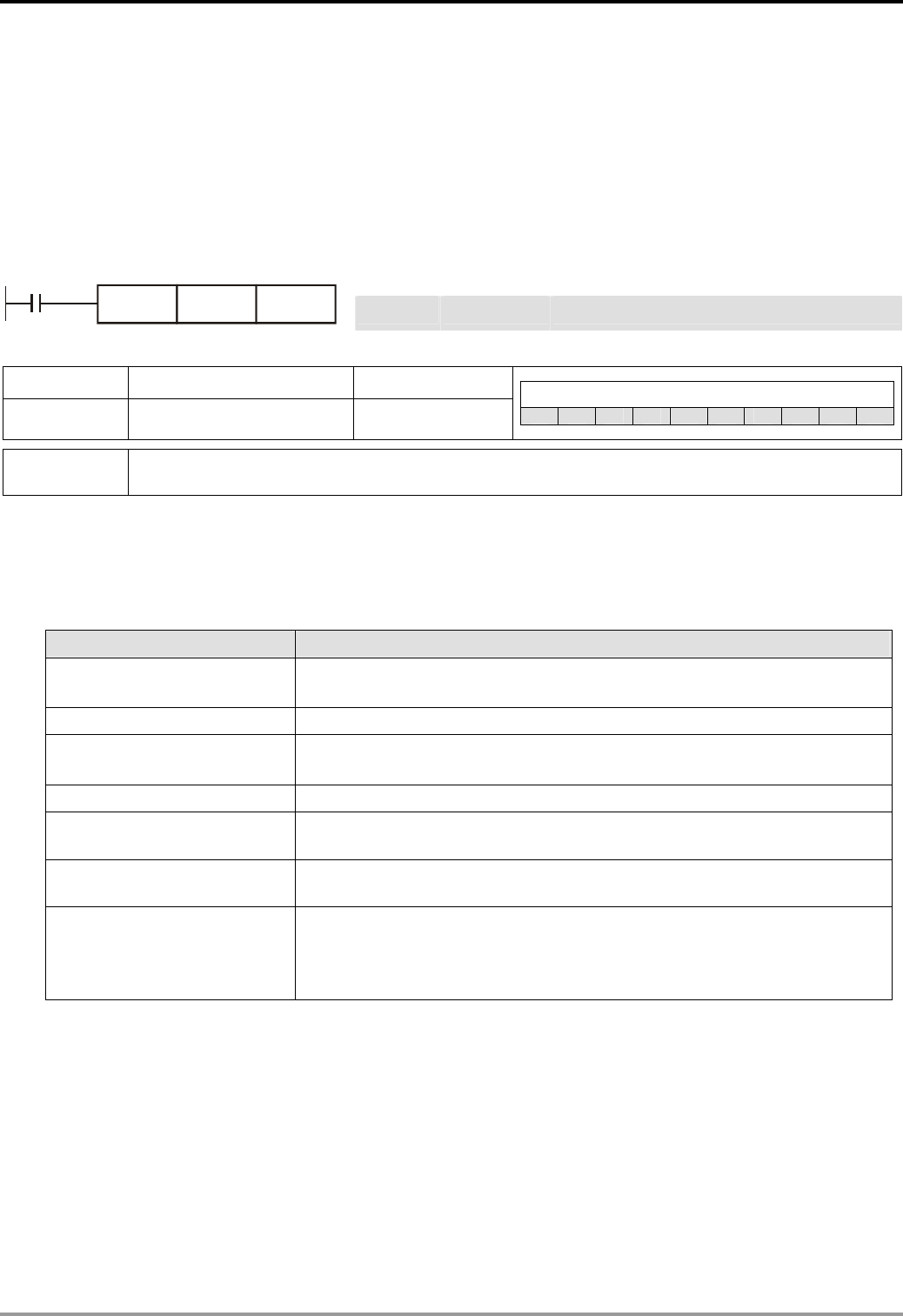
3 Basic Instructions
(counting up/down) of the high-speed counter, see Chapter 2.7 Numbering and Function of Counter [C] for more
details.
4. When DCNT is Off, the counting will stop, but the existing present value in the counter will not be cleared. To
clear the present value and the contact, you have to use the instruction RST C2XX. Use externally designated
input points to clear the present values and contacts of high-speed addition/subtraction counters C235 ~ C255.
Program Example:
Ladder diagram: Instruction code: Operation:
M0
C254DCNT K1000
LD M0 Loading in contact A of M0
DCNT C254 K1000 Set value of counter C254 as K1,000
Mnemonic Function Program steps Controllers
Master control
Start/Reset ES
MC / MCR 1 EX SS SA SX SC EH2 SV EH3 SV2
N0 ~ N7
Operand
Explanations:
1. MC is the main-control start instruction. When MC instruction is executed, the execution of instructions between
MC and MCR will not be interrupted. When MC instruction is Off, the actions of the instructions between MC and
MCR are:
Instruction type Explanation
Present value = 0
General purpose timer Coil is Off, No action for the contact
Accumulative timer Coil is Off, present value and contact stay intact
Present value = 0
Subroutine timer Coil is Off, No action for the contact
Counter Coil is Off, present value and contact stay intact
Coils driven by OUT
instruction All Off
Devices driven by SET and
RST instructions Stay intact
All disabled.
The FOR-NEXT nested loop will still execute back and forth for N times.
Application instructions Instructions between FOR-NEXT will act as the instructions between MC
and MCR.
2. MCR is the main-control end instruction that is placed in the end of the main-control program. There should not
be any contact instructions prior to MCR instruction.
3. MC-MCR main-control program instructions support the nested program structure (max. 8 layers) and please
use the instruction in the order N0 ~ N7.
DVP-PLC Application Manual 3-11
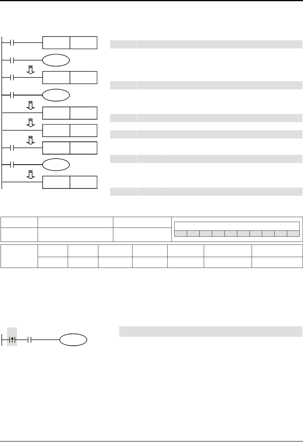
3 Basic Instructions
Program Example:
Ladder diagram: Instruction code: Operation:
X0
Y0
MC N0
X1
X2
Y1
MC N1
X3
MCR N1
MCR N0
X10
MC N0
Y10
X11
MCR N0
LD X0 Loading in A contact of X0
MC N0 Enabling N0 common series connection contact
LD X1 Loading in A contact of X1
OUT Y0 Driving Y0 coil
:
LD X2 Loading in A contact of X2
MC N1 Enabling N1 common series connection contact
LD X3 Loading in A contact of X3
OUT Y1 Driving Y1 coil
:
MCR N1 Disabling N1 common series connection contact
:
MCR N0 Disabling N0 common series connection contact
:
LD X10 Loading in A contact of X10
MC N0 Enabling N0 common series connection contact
LD X11 Loading in A contact of X11
OUT Y10 Driving Y10 coil
:
MCR N0 Disabling N0 common series connection contact
Mnemonic Function Program steps Controllers
Rising-edge detection
operation ES
LDP 1 EX SS SA SX SC EH2 SV EH3 SV2
X0 ~ X377 Y0 ~ Y377 M0 ~ M4095 S0 ~ S1023 T0 ~ T255 C0 ~ C255 D0 ~ D9999
Operand 9 9 -
9 9 9 9
Explanations:
The method of using LDP is the same as using LD, but the actions of the two instructions differ. LDP saves the current
content and store the detected status of rising-edge to the accumulative register.
Program Example:
Ladder diagram: Instruction code: Operation:
X0 X1
Y1
Starting X0 rising-edge detection
LDP X0
AND X1 Series connecting A contact of X1
OUT Y1 Driving Y1 coil
Remarks:
1. See the specification of each model for the range of operands.
2. If the status of a designated rising-edge is On before the PLC is powered, the contact of the rising-edge will be
TRUE after PLC is powered.
DVP-PLC Application Manual
3-12
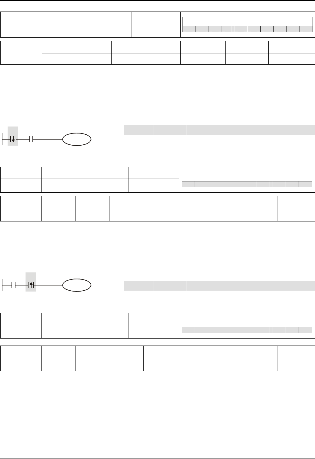
3 Basic Instructions
Mnemonic Function Program steps Controllers
Falling-edge detection
operation ES
LDF 1 EX SS SA SX SC EH2 SV EH3 SV2
X0 ~ X377 Y0 ~ Y377 M0 ~ M4095 S0 ~ S1023 T0 ~ T255 C0 ~ C255 D0 ~ D9999
Operand 9 9 -
9 9 9 9
Explanations:
The method of using LDF is the same as using LD, but the actions of the two instructions differ. LDF saves the current
content and store the detected status of falling-edge to the accumulative register.
Program Example:
Ladder diagram: Instruction code: Operation:
X0 X1
Y1
LDF X0 Starting X0 falling-edge detection
AND X1 Series connecting A contact of X1
OUT Y1 Driving Y1 coil
Mnemonic Function Program steps Controllers
Rising-edge series
connection ES
ANDP 1 EX SS SA SX SC EH2 SV EH3 SV2
M0 ~
M4095
X0 ~ X377 Y0 ~ Y377 S0 ~ S1023 T0 ~ T255 C0 ~ C255 D0 ~ D9999
Operand
9 9 -
9 9 9 9
Explanations:
ANDP instruction is used in the series connection of the contacts’ rising-edge detection.
Program Example:
Ladder diagram: Instruction code: Operation:
X1X0
Y1
LD X0 Loading in A contact of X0
ANDP X1 X1 rising-edge detection in series connection
OUT Y1 Driving Y1 coil
Mnemonic Function Program steps Controllers
Falling-edge series
connection ES
ANDF 1 EX SS SA SX SC EH2 SV EH3 SV2
M0 ~
M4095 S0 ~ S1023 T0 ~ T255 C0 ~ C255 D0 ~ D9999
X0 ~ X377 Y0 ~ Y377
Operand
9 9 -
9 9 9 9
Explanations:
ANDF instruction is used in the series connection of the contacts’ falling-edge detection.
DVP-PLC Application Manual 3-13
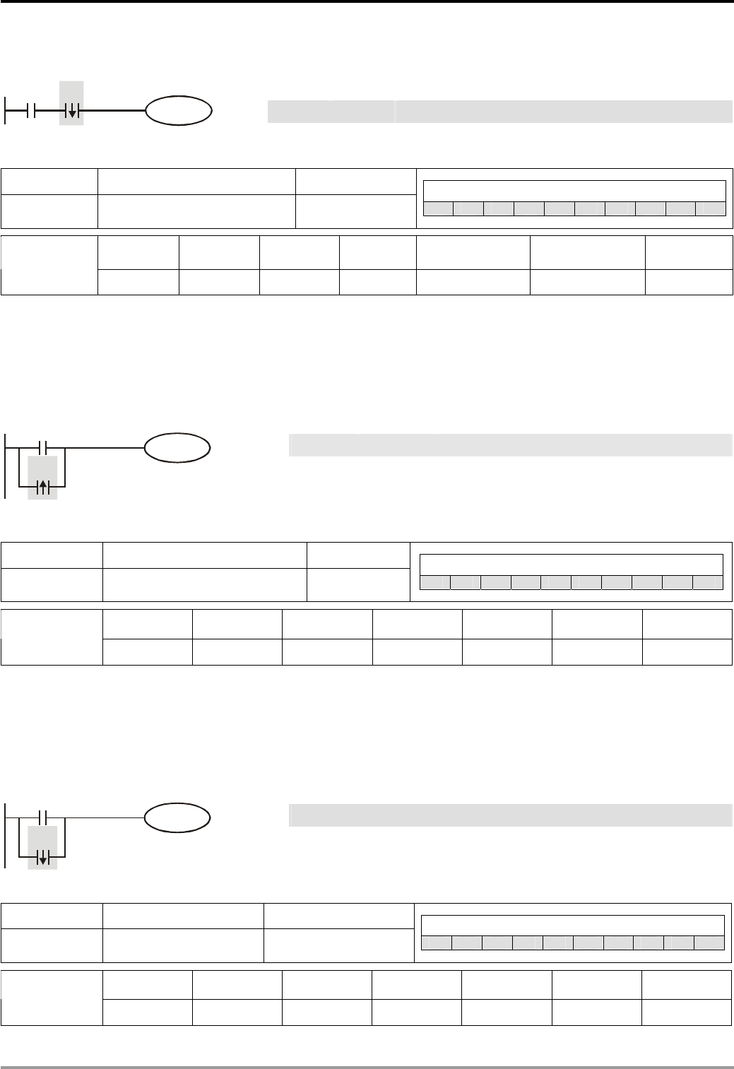
3 Basic Instructions
[Program Example:
Ladder diagram: Instruction code: Operation:
X1X0
Y1
LD X0 Loading in A contact of X0
ANDF X1 X1 falling-edge detection in series connection
OUT Y1 Drive Y1 coil
Mnemonic Function Program steps Controllers
Rising-edge parallel
connection ES
ORP 1 EX SS SA SX SC EH2 SV EH3 SV2
M0 ~
M4095
S0 ~
S1023
X0 ~ X377 Y0 ~ Y377 T0 ~ T255 C0 ~ C255 D0 ~ D9999
Operand
9 9 -
9 9 9 9
Explanations:
The ORP instructions are used in the parallel connection of the contact’s rising-edge detection.
Program Example:
Ladder diagram: Instruction code: Operation:
LD X0 Loading in A contact of X0
X0
X1
Y1
ORP X1 X1 rising-edge detection in parallel connection
OUT Y1 Driving Y1 coil
Mnemonic Function Program steps Controllers
ES
ORF Falling-edge parallel connection 1 EX SS SA SX SC EH2 SV EH3 SV2
X0 ~ X377 Y0 ~ Y377 M0 ~ M4095 S0 ~ S1023 T0 ~ T255 C0 ~ C255 D0 ~ D9999
Operand 9 9 -
9 9 9 9
Explanations:
The ORP instructions are used in the parallel connection of the contact’s falling-edge detection.
Program Example:
Ladder diagram: Instruction code: Operation:
LD X0 Loading in A contact of X0
X0
X1
Y1
ORF X1 X1 falling-edge detection in parallel connection
OUT Y1 Driving Y1 coil
Mnemonic Function Program steps Controllers
ES
PLS Rising-edge output 1 EX SS SA SX SC EH2 SV EH3 SV2
X0 ~ X377 Y0 ~ Y377 M0 ~ M4095 S0 ~ S1023 T0 ~ T255 C0 ~ C255 D0 ~ D9999
Operand - - - -
9 9
-
DVP-PLC Application Manual
3-14
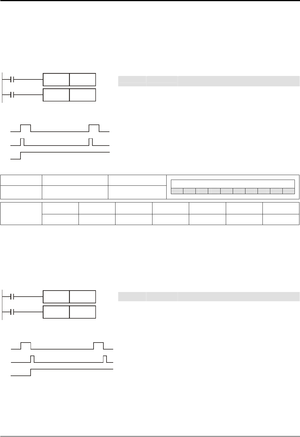
3 Basic Instructions
Explanations:
When X0 goes from Off to On (rising-edge trigger), PLS instruction will be executed and S will send out pulses for
once of 1 scan time.
Program Example:
Ladder diagram: Instruction code: Operation:
LD X0 Loading in A contact of X0
X0
M0
PLS
M0
Y0SET
PLS M0 M0 rising-edge output
LD M0 Loading in contact A of M0
SET Y0
Y0 latched (On)
Timing Diagram:
X0
M0
Y0
1 scan time
Mnemonic Function Program steps Controllers
ES
PLF Falling-edge output 1 EX SS SA SX SC EH2 SV EH3 SV2
X0 ~ X377 Y0 ~ Y377 M0 ~ M4095 S0 ~ S1023 T0 ~ T255 C0 ~ C255 D0 ~ D9999
Operand - - - -
9 9
-
Explanations:
When X0 goes from On to Off (falling-edge trigger), PLF instruction will be executed and S will send out pulses for
once of 1 scan time.
Program Example:
Ladder diagram: Instruction code: Operation:
LD X0 Loading in A contact of X0
X0
M0
PLF
M0
Y0SET
PLF M0 M0 falling-edge output
LD M0 Loading in contact A of M0
SET Y0 Y0 latched (On)
Timing Diagram:
1 scan time
X0
M0
Y0
DVP-PLC Application Manual 3-15
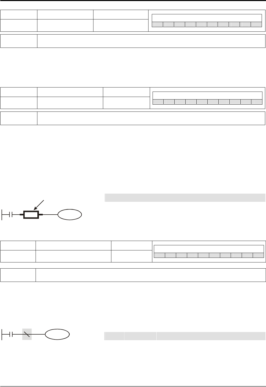
3 Basic Instructions
Mnemonic Function Program steps Controllers
ES
END Program End 1 EX SS SA SX SC EH2 SV EH3 SV2
N/A
Operand
Explanations:
END instruction has to be placed in the end of a ladder diagram or instruction program. PLC will start to scan from
address 0 to END instruction and return to address 0 to restart the scan.
Mnemonic Function Program steps Controllers
ES
NOP No operation 1 EX SS SA SX SC EH2 SV EH3 SV2
N/A
Operand
Explanations:
NOP instruction does not conduct any operations in the program; therefore, after the execution of NOP, the existing
logical operation result will be kept. If you want to delete a certain instruction without altering the length of the program,
you can use NOP instruction.
Program Example:
Ladder diagram: Instruction code: Operation:
X0
Y1
NOP
NOP instruction will be
omitted in the ladder diagram
LD X0 Loading in B contact of X0
NOP No operation
OUT Y1 Driving Y1 coil
Mnemonic Function Program steps Controllers
ES
INV Inverting Operation 1 EX SS SA SX SC EH2 SV EH3 SV2
N/A
Operand
Explanations:
The logical operation result before INV instruction will be inverted and stored in the accumulative register.
Program Example:
Ladder diagram: Instruction code: Operation:
X0
Y1
LD X0 Loading in A contact of X0
INV Inverting the operation result
OUT Y1 Driving Y1 coil
DVP-PLC Application Manual
3-16
3 Basic Instructions
Mnemonic Function Program steps Controllers
P Pointer 1
ES EX SS SA SX SC EH2 SV EH3 SV2
P0 ~ P255
Operand
Explanations:
Pointer P is used in API 00 CJ and API 01 CALL instructions. The use of P does not need to start from No. 0, and the
No. of P cannot be repeated; otherwise, unexpected errors may occur.
Program Example:
Ladder diagram: Instruction code: Operation:
X0
Y1
CJ P10
X1
P10
LD X0 Loading in A contact of X0
CJ P10 From instruction CJ to P10
:
P10 Pointer P10
LD X1 Loading in A contact of X1
Driving Y1 coil OUT Y1
Mnemonic Function Program steps Controllers
ES
I Interruption program marker (I) 1 EX SS SA SX SC EH2 SV EH3 SV2
I00□, I10□, I20□, I30□, I40□, I50□, I6□□, I7□□, I8□□
Operand I010, I020, I030, I040, I050, I060, I110, I120, I130, I140, I150, I160, I170, I180
Explanations:
A interruption program has to start with a interruption pointer (I□□□) and ends with API 03 IRET. I instruction has to
be used with API 03 IRET, API 04 EI, and API 05 DI. See Chapter 2.9 for pointers of all DVP series PLCs.
Program Example:
Ladder diagram: Instruction code: Operation:
EI Enabling interruption
Y1
EI
X1
I 001
DI
FEND
Y2
X2
IRET
A
llowable range
for interruption
Interruption
subroutine
Pointer of
interruption
program
Loading A contact of X1 LD X1
OUT Y1 Driving Y1 coil
:
DI Disabling interruption
:
FEND Main program ends
I001 Interruption pointer
LD X2 Loading in A contact of X2
OUT Y2 Driving Y2 coil
:
IRET Interruption return
DVP-PLC Application Manual 3-17

3 Basic Instructions
MEMO
DVP-PLC Application Manual
3-18
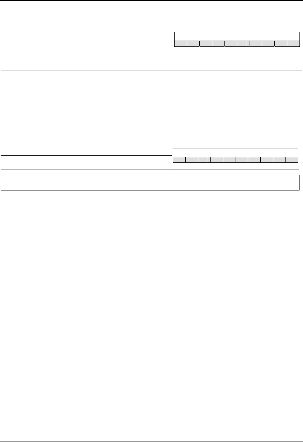
4 Step Ladder Instructions
4.1 Step Ladder Instructions [STL], [RET]
Mnemonic Function Program steps
STL Step Transition Ladder Start 1
Controllers
ES EX SS SA SX SC EH2 SV EH3 SV2
Operand S0 ~ S1023
Explanations:
STL Sn constructs a step. When STL instruction appears in the program, the program will enter a step ladder diagram
status controlled by steps. The initial status has to start from S0 ~ S9. RET instruction indicates the end of a step
ladder diagram starting from S0 ~ S9 and the bus returns to a normal ladder diagram instruction. SFC uses the step
ladder diagram composed of STL/RET to complete the action of a circuit. The No. of S cannot be repeated.
Mnemonic Function Program
steps
RET Step Transition Ladder Return 1
Controllers
ES EX SS SA SX SC EH2 SV EH3 SV2
Operand N/A
Explanations:
RET indicates the end of a step. There has to be a RET instruction in the end of a series of steps. One PLC program
can be written in maximum 10 steps (S0 ~ S9) and every step should end with a RET.
DVP-PLC Application Manual 4-1
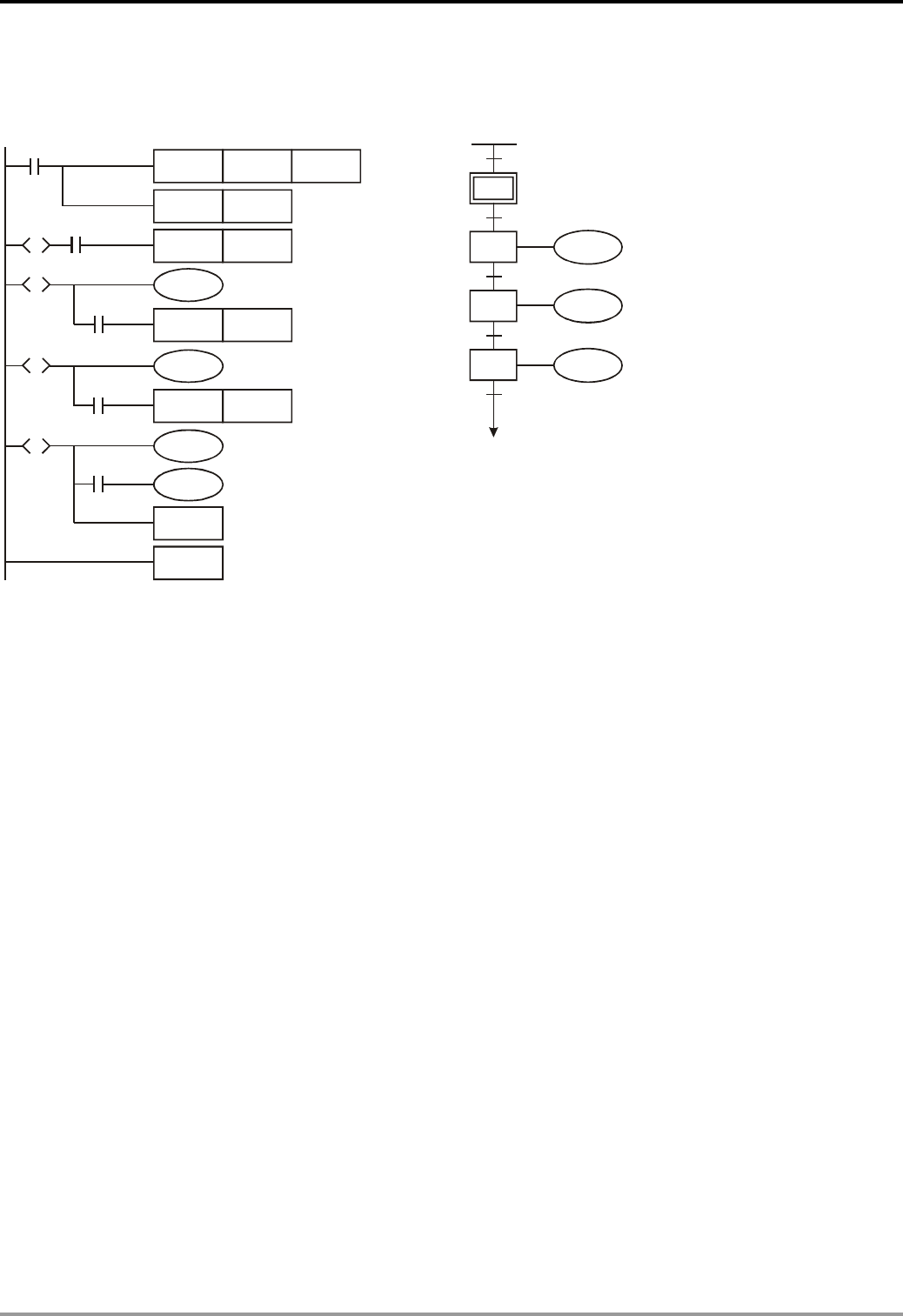
4 Step Ladder Instructions
Program Example:
Ladder diagram: SFC:
M1002
ZRST S0 S127
SET S0
SET S20
Y0
SET S30
Y1
SET S40
Y2
S0
RET
END
X0S0
S
S20
S
X1
S30
S
X2
S40
S
X3
S0
S20
S30
S40
M1002
X0
X1
X2
X3
Y0
Y1
Y2
S0
4.2 Sequential Function Chart (SFC)
In automation, we always need electric control to work with mechanical control for an automation control. The
sequential control can be divided into several orderly steps (or stages). Each step has its actions that should be
completed and the transition from one step to another normally requires some criteria. The action of the last step
finishes when all criteria is true and the beginning of the next step will clear the actions of the last step. This is the
concept of designing a sequential function chart (SFC).
DVP-PLC Application Manual
4-2
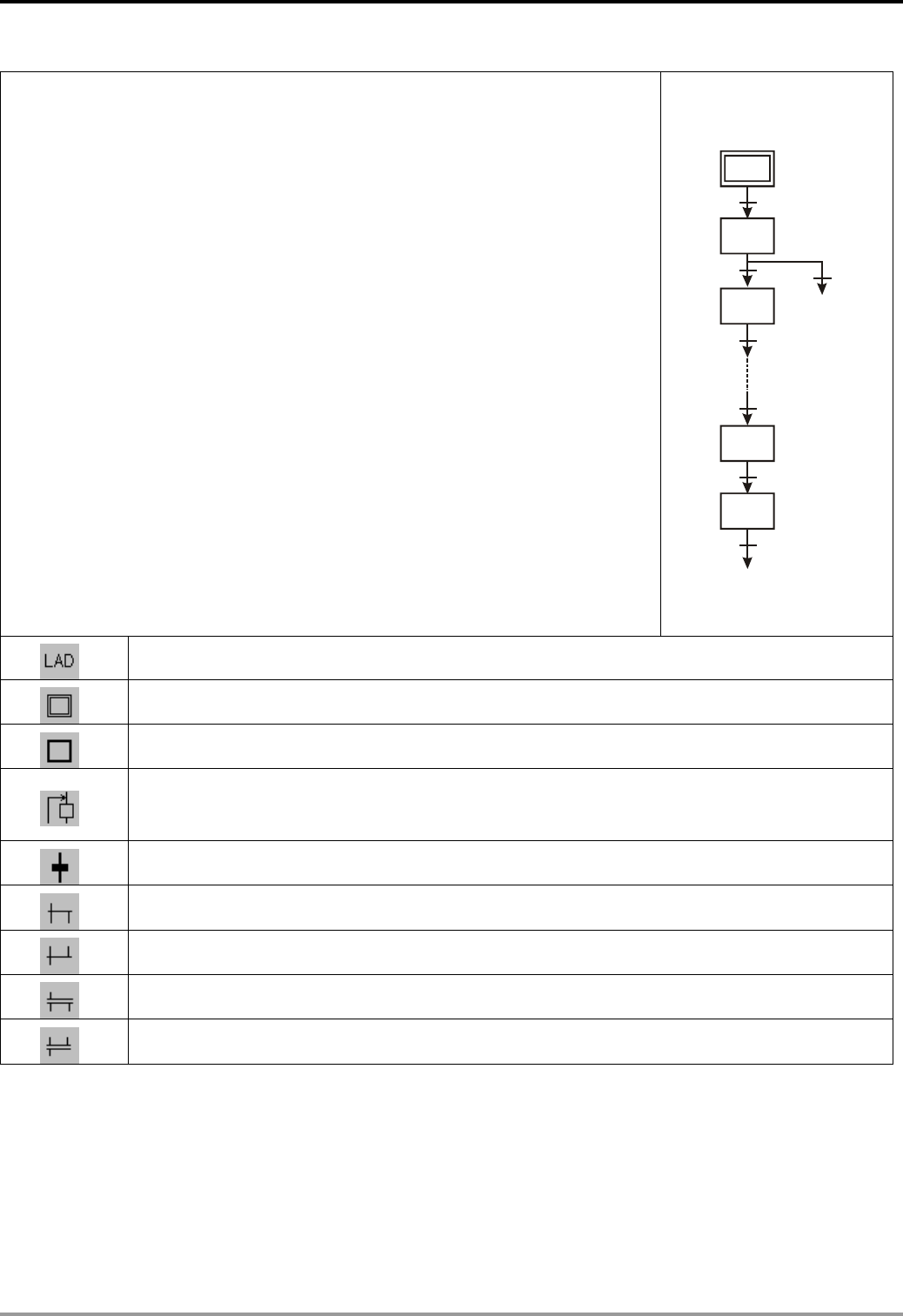
4 Step Ladder Instructions
Features:
1. No sequential design is required for constant step actions, and PLC will
automatically execute the interlocking and dual outputs among all status. An
easy sequential design is the only thing required to make the machine work
normally.
2. The actions in SFC are easy to understand, adjust for a trial operation, detect
the errors and maintain.
3. SFC is a type of diagram editing. The structure of a SFC looks like a flow chart.
Every No. of the step relay S inside the PLC represents a step, equal to every
processing procedure in a flow chart. When the current procedure is
completed, the program will move to the next step according to the set
transition criteria. Therefore, you can repeat the cycle and obtain the result you
desire.
4. See the SFC chart in the right hand side: The initial step S0 transfers to a
general purpose step S21 by making the status transition condition X0
condition true. S21 transfer to S22 or jumps to S24 by making X1 or X2 true. In
step S25, X6 will be true and the chart will return to S0 to complete a cycle. The
cycle and be repeated to reach a cyclic control.
5. Next are some basic icons for drawing SFC in WPLSoft SFC editor.
SFC:
S0
S21
S24
S25
S0
X0
X1
X5
X6
X2
S22
X4
X3
S24
Ladder diagram mode. The icon indicates that the internal editing program is a general ladder
diagram, not a step ladder program.
Initial step in SFC. Applicable for S0 ~ S9.
General step. Applicable for S10 ~ S1023.
Step jumps. Used for a step to jump to another non-adjacent step.
(Jumping up/down to non-adjacent steps in the same sequence, returning to initial step, or
jumping among different sequences.)
Transition condition between steps.
Alternative divergence. The same step transfers to a corresponding step by different transition
condition.
Alternative convergence. More than 2 steps transfer to the same step by transition condition.
Simultaneous divergence. The same step transfers to more than 2 steps by the same transition
condition.
Simultaneous convergence. More than 2 steps transfer to the same step by a single transition
condition.
4.3 How does a Step Ladder Instruction Work?
STL instruction is used for designing the syntax of a sequential function chart (SFC), making the program
designing similar to drawing a flow chart and allowing a more explicit and readable program. From the figure in the left
hand side below, we can see very clearly the sequence to be designed, and we can convert the sequence into the
step ladder diagram in the right hand side.
DVP-PLC Application Manual 4-3
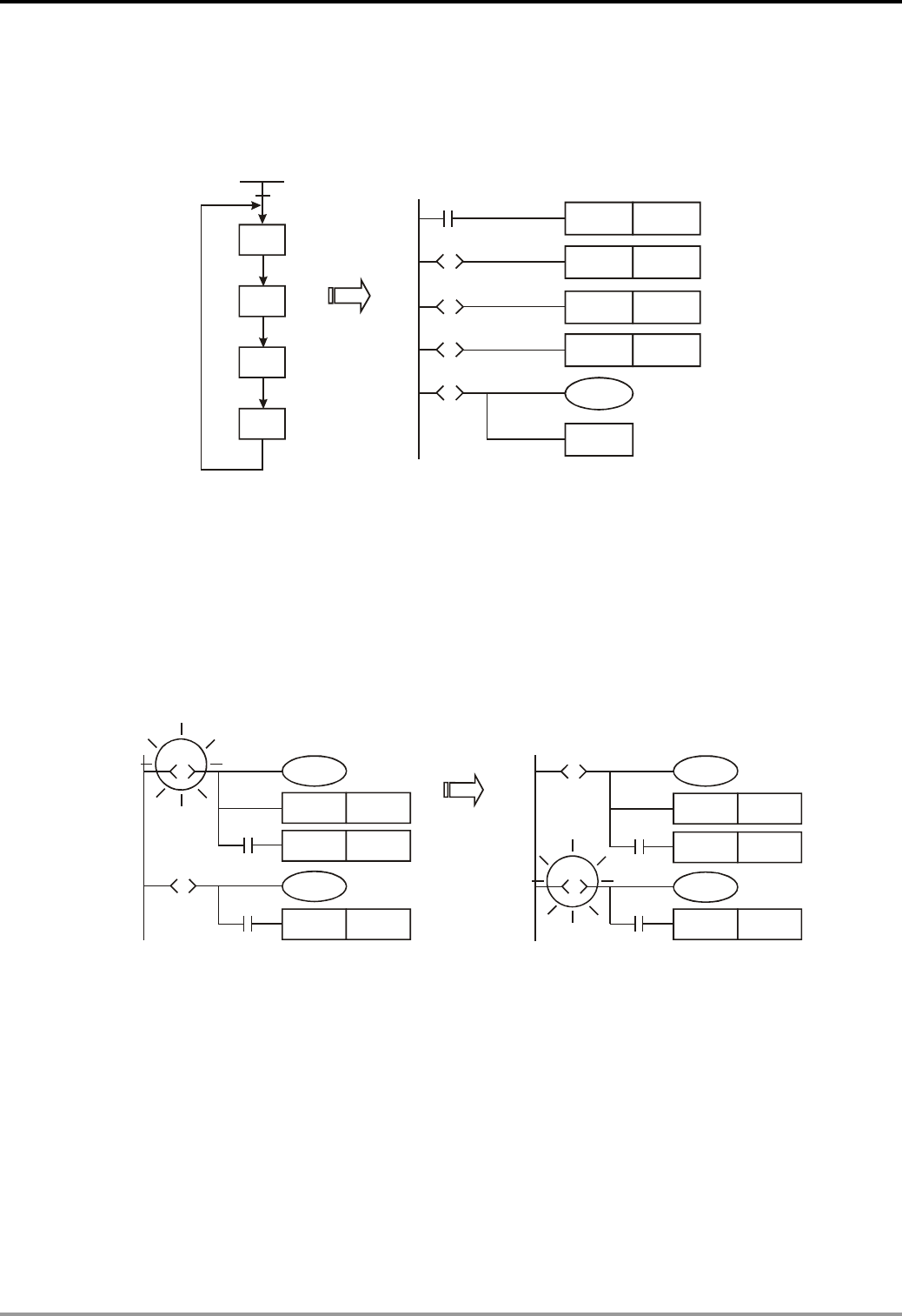
4 Step Ladder Instructions
RET instruction has to be written at the end of every step sequence, representing the end of a sequence. There
can be more than one step sequence in a program. Therefore, we have to write in RET at the end of every step
sequence. There is no limitation on the times of using RET which is used together with S0 ~ S9.
If there is no RET instruction at the end of a step sequence, errors will be detected by WPL editor.
S0
S21
S22
S23
M1002
S0
SET
SET S22
S0
RET
S21
S
S22
S
SET
S21
S0
S
S23
S
SET S23
M1002
initial pulse
1. Actions of Step Ladder:
A step ladder is composed of many steps and every step controls an action in the sequence. The step ladder
has to:
a) Drive the output coil
b) Designate the transition condition
c) Designate which step will take over the control from the current step
Example:
SET Y1
Y0
SET S20
Y10
SET S30
S10
S
X0
S20
S
X1
SET Y1
Y0
SET S20
Y10
SET S30
S10
S
X0
S20
S
X1
When X0=On,
S20 = On,
S10 = Off.
Explanation:
When S10 = On, Y0 and Y1 will be On. When X0 = On, S20 will be On and Y10 will be On. When S10 = Off, Y0
will be Off and Y1 will be On.
2. Timing Diagram of Step Ladder:
When the status contact Sn = On, the circuit will be activated. When Sn = Off, the circuit will be disactivated. The
actions will delay for 1 scan time.
DVP-PLC Application Manual
4-4
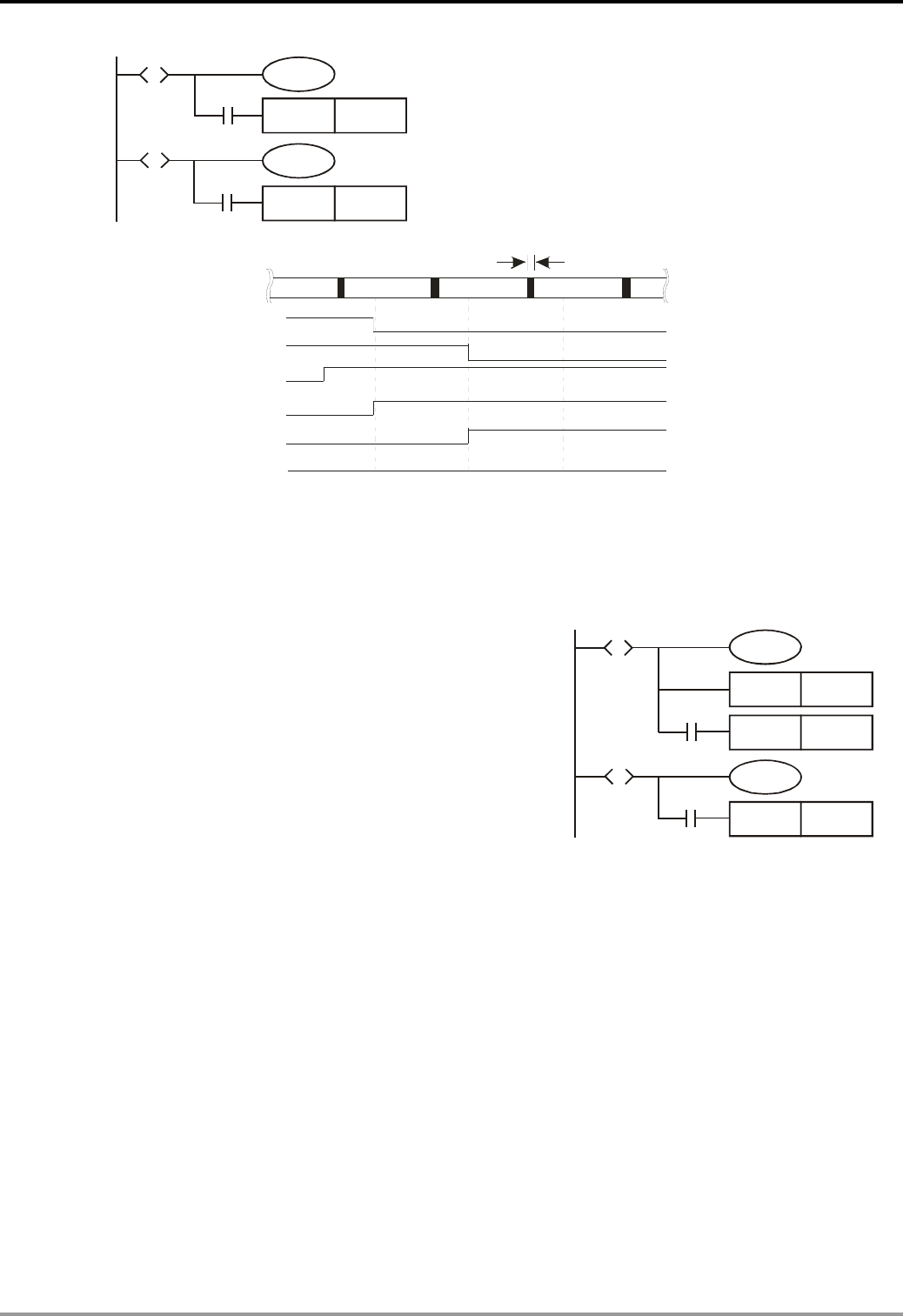
4 Step Ladder Instructions
SET S12
Y11
SET S14
S10
S
X0
S12
S
X1
Y10
Executing the timing diagram below. After the
status of S10 and S12 are transferred (taking place
simultaneously), and after a delay of 1 scan time,
Y10 will be Off and Y11 will be On. There will not be
overlapping outputs.
STL S10
S10
Y10
S12
Y11
X1
X0
Program
execution
Ren ew I nput/ Out put
Circuit no t activate d
Program
execution Program
execution
3. Repeated Use of Output Coil:
a) You can use output coils of the same No. in different steps.
b) See the diagram in the right. There can be the same
output device (Y0) among different statuses. Y0 will be On
when S10 or S20 is On. Such as right diagram, there is the
same output device Y0 in the different state. No matter
S10 or S20 is On, Y0 will be On.
c) Y0 will be Off when S10 is transferring to S20. After S20 is
On, Y0 will output again. Therefore in this case, Y0 will be
On when S10 or S20 is On.
d) Normally in a ladder diagram, avoid repeated use of an
output coil. The No. of output coil used by a step should
also avoid being used when the step ladder diagram
returns to a general ladder diagram.
SET Y1
Y0
SET S20
SET S30
S10
S
X0
S20
S
X1
Y0
DVP-PLC Application Manual 4-5
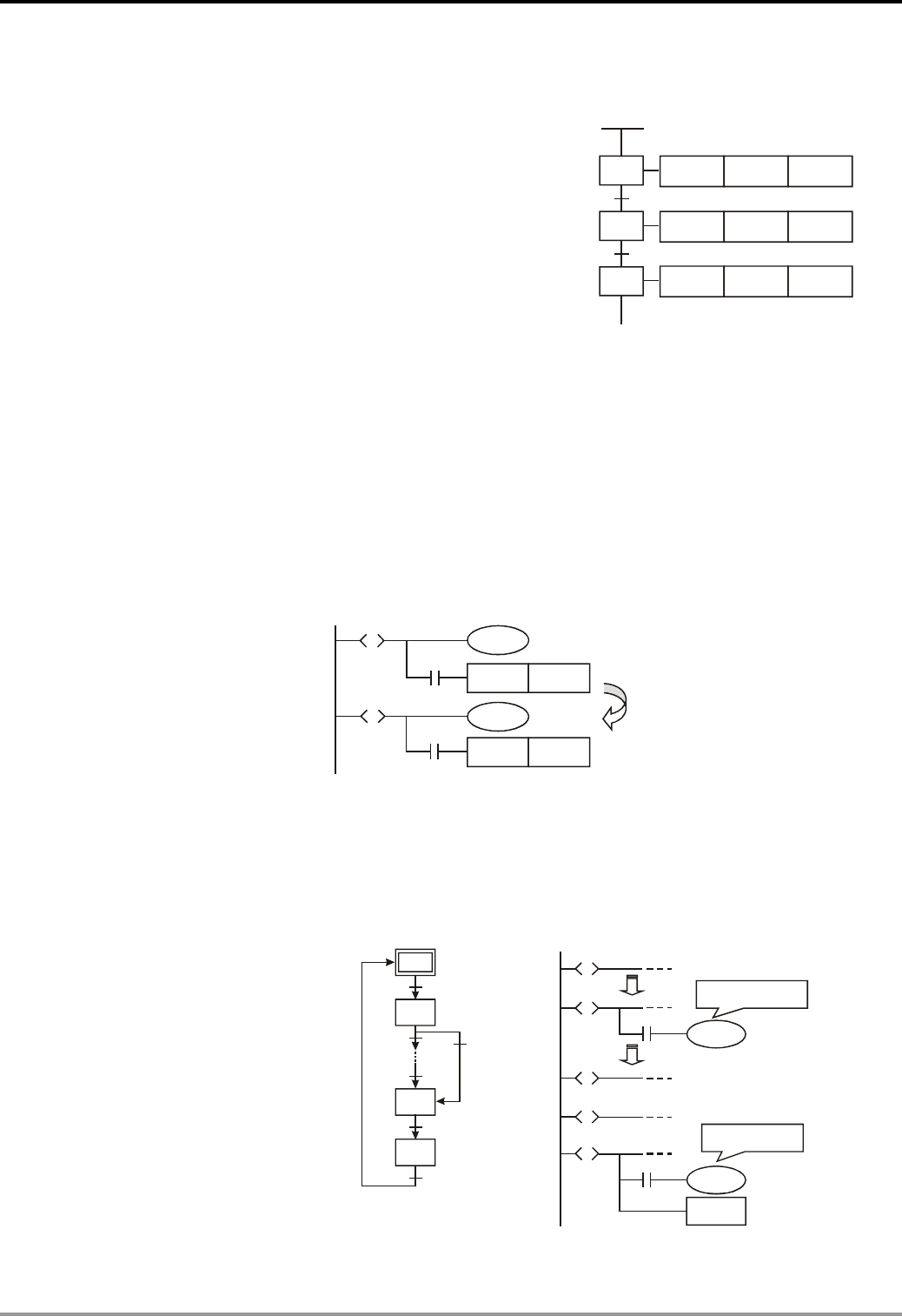
4 Step Ladder Instructions
4. Repeated Use of Timer:
The timers in EH2/SV series MPU are the same as general
output points and can be repeatedly used in different steps.
This is one of the features of the step ladder diagram.
However, in a general ladder diagram, it is better not be
repeatedly use the output coil. Also avoid using the No. of the
output coil used by a step after the step ladder diagram returns
to a general ladder diagram.
Note: See the figure in the right. The timers in ES/EX/SS/SA/
SX/SC series MPU can be used repeatedly in non-adjacent
steps.
S20
S30
S40
X1
X2
TMR T1 K10
TMR T2 K20
TMR T1 K30
5. Transfer of Step:
SET Sn and OUT Sn instructions are used to enable (or transfer to) another step. When the control power is
shifted to another step, the status of the previous step S and the action of the output point will be cleared. Due to
that there can be many step control sequences (i.e. the step ladder diagram starting with S0 ~ S9) co-existing in
the program. The transfer of a step can take place in the same step sequence, or be transferred to different step
sequence. Therefore, there are some slight differences regarding how to use SET Sn and OUT Sn. See the
explanations below.
SET Sn Used for driving the next
step in the same
sequence. After the
transition, all output from
the previous status will be
cleared.
Y10
SET S12
SET S14
S10
S
X0
S12
S
X1 Y11
When SET S12 instruction is executed,
S10 will transfer to S12, and S10 and all
its outputs (Y10) will be cleared.
OUT Sn Used for returning to the initial step in the same step sequence. Also for jumping up/down to
non-adjacent steps in the same sequence, or separating steps in different sequences. After the
transition, all output from the previous status will be cleared.
c Returning to the
initial step in the
same sequence.
d Jumping up/down
to non-adjacent
steps in the same
sequence.
SFC: Ladder diagram:
S0
S21
S24
S25
X7
X2
OUT
OUT
S24
S21
S
S0
S
S23
S
X2
S24
S
S25
S
S0
X7
RET
Using OUT S24
Using OUT S0
S25 returns to the initial
step S0 by using OUT.
Driving the jumping
of step
Return to initial step
DVP-PLC Application Manual
4-6
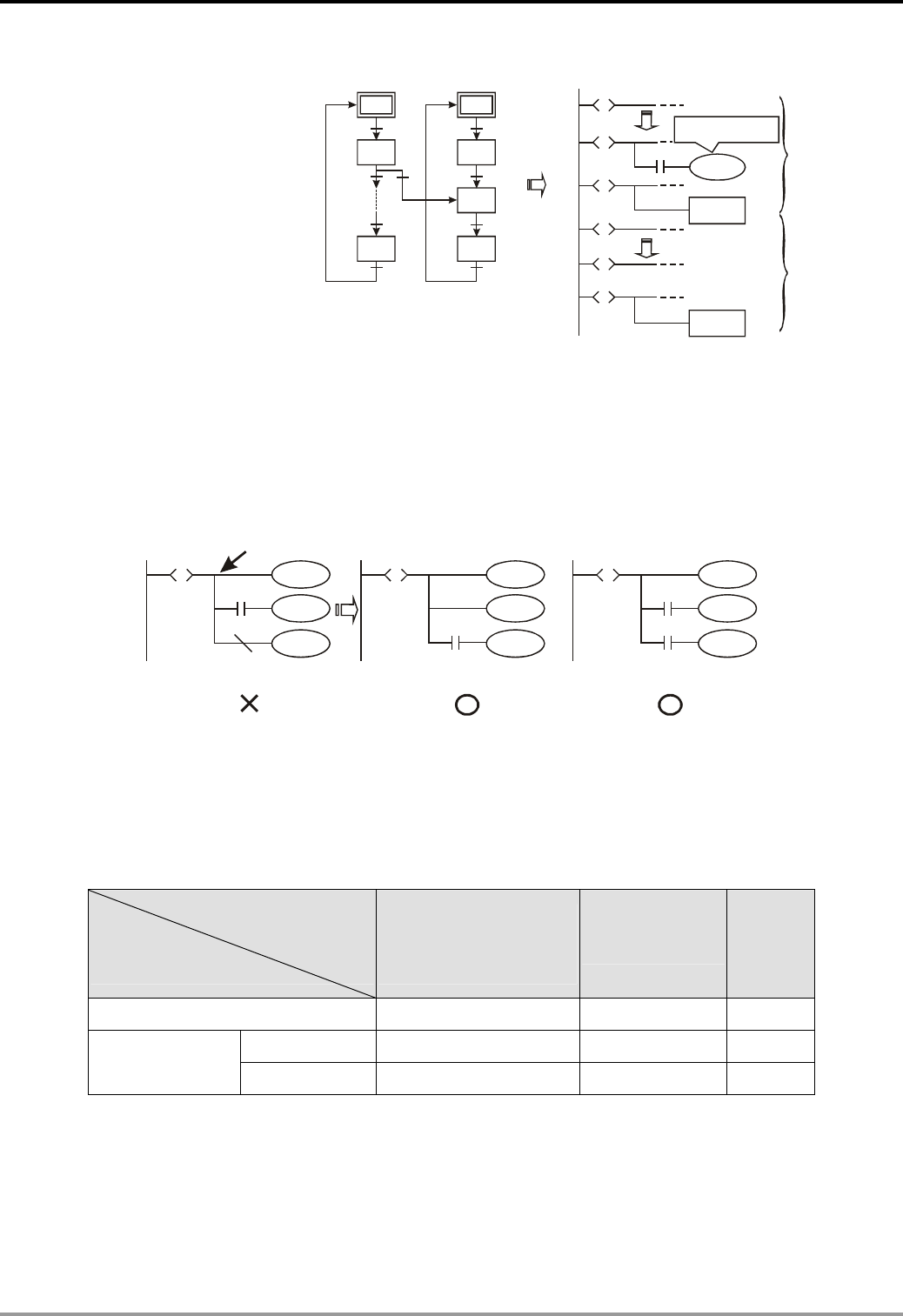
4 Step Ladder Instructions
e Separating steps
in different
sequences.
SFC: Ladder diagram:
S0
S21
S23
X2 OUT
OUT
S1
S41
S43
OUT
S42
S42
S21
S
S0
S
S1
S
X2
S42
S
S43
S
RET
S23
S
RET
Step sequence
initiated by S0
Step sequence
initiated by S1
Using OUT S42
Two different step sequence: S0 and S1
S23 returns to initial step S0 by using OUT.
S43 returns to initial step S1 by using OUT.
Driving the separating
of steps
6. Cautions for Driving Output Point:
See the figure below. After the step point and once LD or LDI instructions are written into the second line, the
bus will not be able to connect directly to the output coil, and errors will occur in the compilation of the ladder
diagram. You have to correct the diagram into the diagram in the right hand side for a correct compilation.
Y0
S
S
Y1
Y2
M0
nY0
S
S
Y2
Y1
n
M0
Y0
S
S
Y1
Y2
M0
n
M1000
BUS
or
Modifying the
position of M0. Normally open
contact in RUN
mode
7. Restrictions on Using Some Instructions:
The program of every step is the same as a general ladder diagram, in which you can use all kinds of
series/parallel circuits or instructions. However, there are restrictions on some of the instructions.
Basic instructions applicable in a step
Instruction
Step
LD/LDI/LDP/LDF
AND/ANI/ANDP/ANDF
OR/ORI/ORP/ORF
INV/OUT/SET/RST
ANB/ORB
MPS/MRD/MPP MC/MCR
Initial step/general step Yes Yes No
General output Yes Yes No Divergence/
convergence step Step transfer Yes No No
DO NOT use MC/MCR instruction in the step.
DO NOT use STL instruction in a general subroutine or interruption subroutine.
You can still use CJ instruction in STL instruction, but this will make the actions more complicated. We do not
recommend you do so.
DVP-PLC Application Manual 4-7
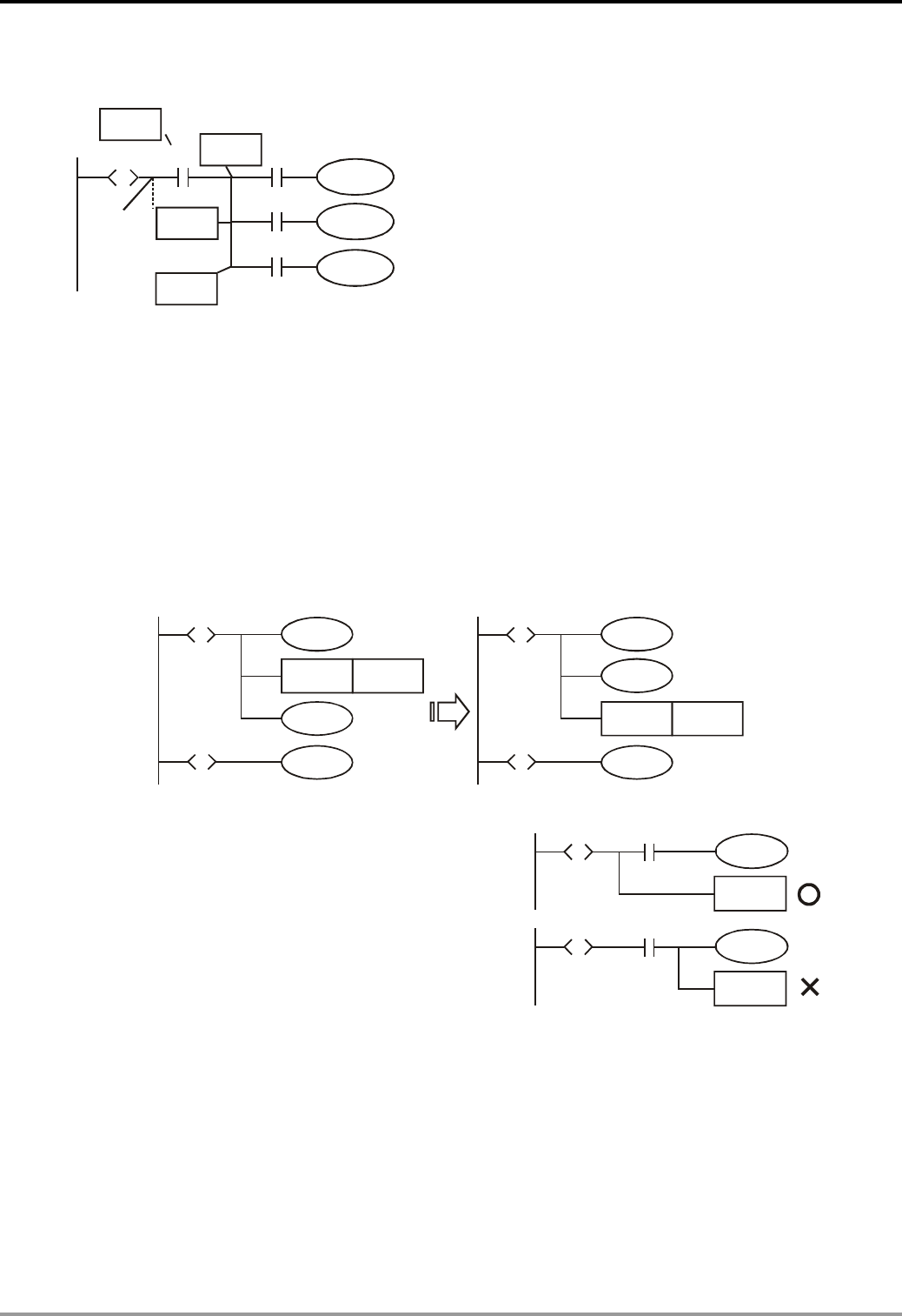
4 Step Ladder Instructions
The position of MPS/MRD/MPP instruction:
Ladder diagram:
Y1
S
S
M0
Y2
X2
n
X3
X1
X0
MPP
MRD
MPS
BUS
LD X0
Instruction code:
STL Sn
LD X0
MPS
AND X1
OUT Y1
MRD
AND X2
OUT M0
MPP
AND X3
OUT Y2
Explanation:
MPS/MRD/MPP instruction cannot
be used directly on the new bus.
You have to execute LD or LDI
instruction first before applying
MPS/MRD/MPP.
8. Other Points to Note:
The instruction used for transferring the step (SET S□ or OUT S□) can only be executed after all the relevant
outputs and actions in the current status are completed. See the figure below. The executed results by the PLC are
the same, but if there are many conditions or actions in S10, it is recommended that you modify the diagram in the
left hand side into the diagram in the right hand side. SET S20 is only executed after all relevant outputs and
actions are completed, which is a more explicit sequence.
SET
Y0
S10
S
S20
S
Y2
S20
Y1 SET
Y0
S10
S
S20
S
Y2
S20
Y1
Make sure to add RET instruction after STL at the end of
the step ladder diagram.
S0
S20
S
RET
X1
S0
S20
S
RET
X1
4.4 Things to Note for Designing a Step Ladder Program
1. The first step in the SFC is called the “initial step", S0 ~ S9. Use the initial step as the start of a sequence and end a
complete sequence with RET instruction.
2. If STL instruction is not in use, step S can be a general-purpose auxiliary relay.
3. When STL instruction is in use, the No. of step S cannot be repeated.
4. Types of sequences:
DVP-PLC Application Manual
4-8
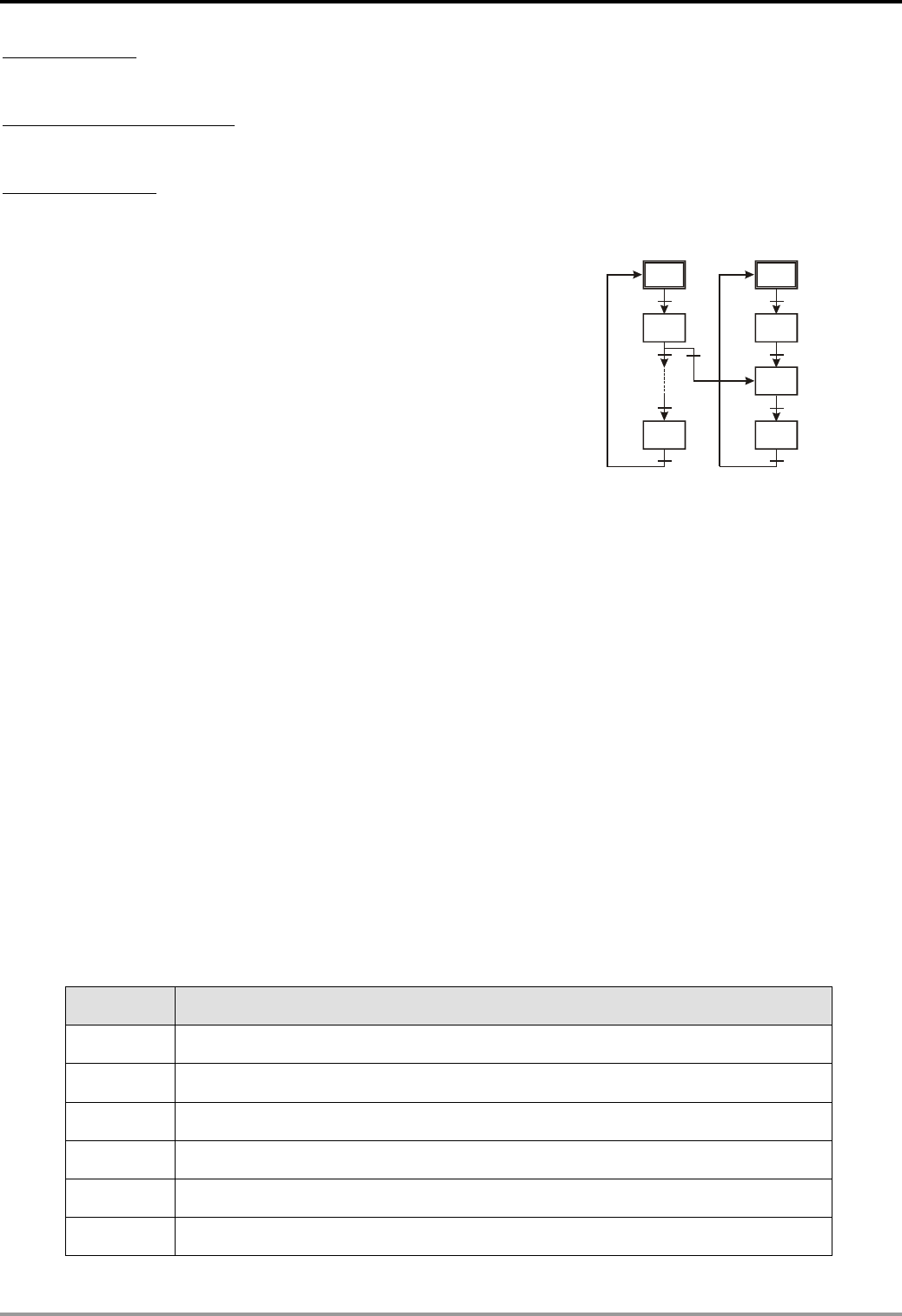
4 Step Ladder Instructions
Single sequence: There is only one sequence without alternative divergence, alternative convergence, simultaneous
divergence and simultaneous convergence in a program.
Complicated single sequence: There is only one sequence with alternative divergence, alternative convergence,
simultaneous divergence and simultaneous convergence in a program.
Multiple sequences: There are more than one sequence in a program, maximum 10 sequences, S0 ~ S9.
5. Separation of sequence: Multiple sequences are allowed to be written into the step ladder diagram.
a) See the diagram in the right hand side. There are two
sequences S0 and S1. The program writes in S0 ~ S30 first
and S1 ~ S43 next.
b) You can designate a step in the sequence to jump to any step
in another sequence.
c) When the condition below S21 is true, the sequence will jump
to step S42 in sequence S1, which is called “separating the
step”.
S0
S21
S30
OUT
OUT
S1
S41
S43
OUT
S42
6. Restrictions on diverging sequence: See 4.5 for example
a) You can use maximum 8 diverged steps in a divergence sequence.
b) You can use maximum 16 loops in multiple divergence sequences or in simultaneous sequences combined into
one sequence.
c) You can designate a step in the sequence to jump to any step in another sequence.
7. Reset of the step and the inhibiting output:
a) Use ZRST instruction to reset a step to be Off.
b) Make M1034 = On to inhibit output Y.
8. Latched step:
The On/Off status of the latched step will be memorized when the power of the PLC is switched off. When the
PLC is re-powered, the status before the power-off will be recovered and the execution will resume. Please be
aware of the area for the latched steps.
9. Special auxiliary relays and special registers: See 4.6refer to chapter 4.6 IST instruction for more details.
Device No. Function
M1040 Disabling step. Disabling all the shifting of steps when On.
M1041 Starting step. Flag for IST instruction.
M1042 Enabling pulses. Flag for IST instruction.
M1043 Zero return completed. Flag for IST instruction.
M1044 Zero point condition. Flag for IST instruction.
M1045 Disabling all output reset. Flag for IST instruction.
DVP-PLC Application Manual 4-9
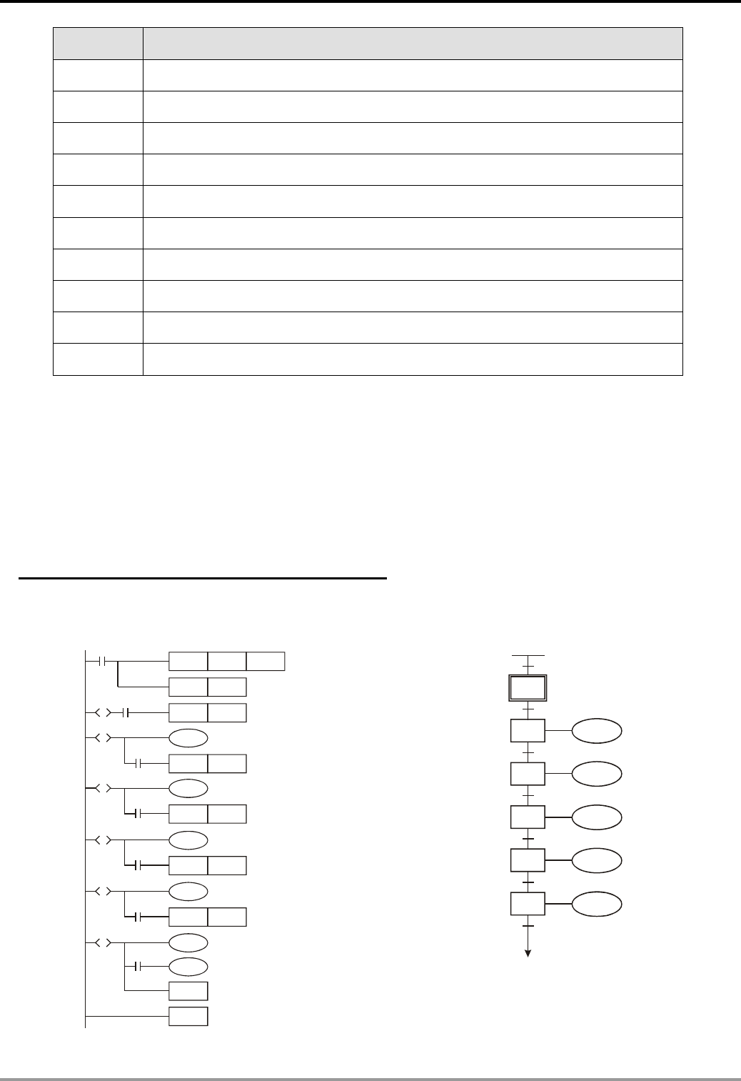
4 Step Ladder Instructions
Device No. Function
M1046 Setting STL status as On. On when any of the steps is On.
M1047 Enabling STL monitoring
D1040 On status of step No. 1
D1041 On status of step No. 2
D1042 On status of step No. 3
D1043 On status of step No. 4
D1044 On status of step No. 5
D1045 On status of step No. 6
D1046 On status of step No. 7
D1047 On status of step No. 8
4.5 Types of Sequences
Single Sequence: The basic type of sequences
The first step in a step ladder diagram is called the initial step, which can be S0 ~ S9. The steps following the
initial step are general steps, which can be S10 ~ S1023. If you are using IST instruction, S10 ~ S19 will become the
steps for zero return.
a) Single sequence without divergence and convergence
After a sequence is completed, the control power on the steps will be given to the initial step.
Step ladder diagram
M100
2
ZRST S0 S127
SET S0
SET S20
Y0
SET S30
Y1
SET S40
Y4
S0
RET
END
X0S0
S
S20
S
X1
S30
S
X2
S60
S
X5
Y2
SET S50
S40
S
X3
Y3
SET S60
S50
S
X4
SFC:
S0
S20
S30
S40
S0
M1002
X0
X1
X2
X5
Y0
Y1
Y2
S50
X3
Y3
S60
X4
Y4
DVP-PLC Application Manual
4-10
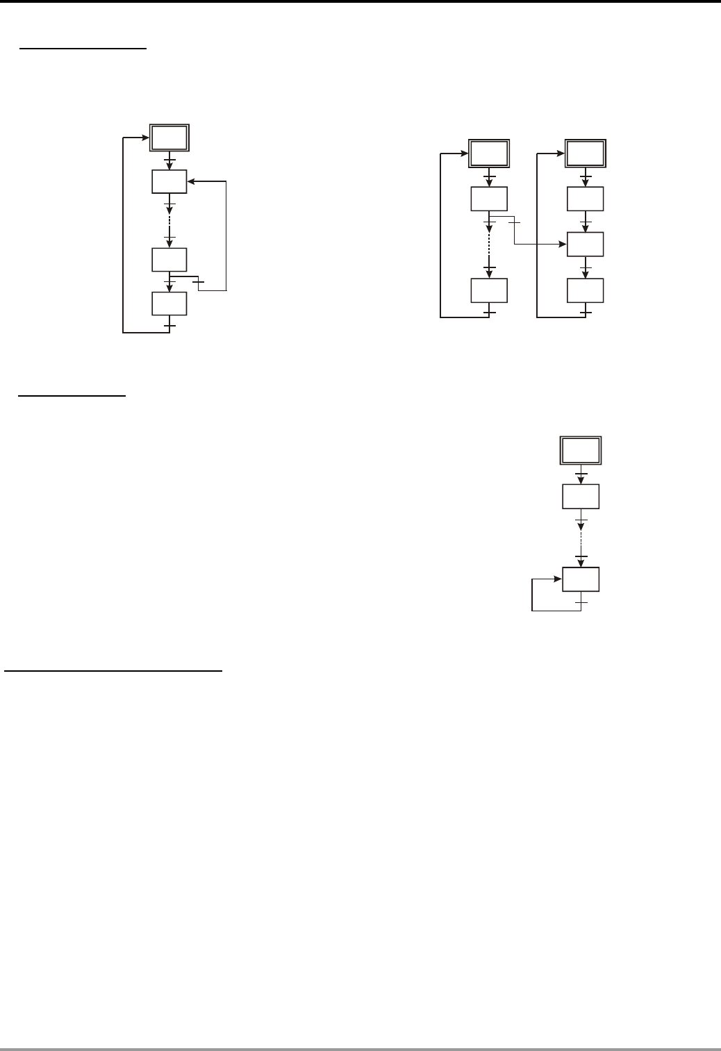
4 Step Ladder Instructions
b) Jumping Sequence
1. The control power over the step is transferred to
a certain step on top. 2. The control power over the step is transferred to
the step in another sequence.
S0
S21
S42
S43
OUT
OUT
S0
S21
S41
OUT
OUT
S1
S41
S43
OUT
S42
c) Reset Sequence
See the diagram in the right hand side. When the condition at S50
is true, S50 will be reset and the sequence will be completed at
this time.
S0
S21
S50
RST
Complicated Single Sequence:
Including simultaneous divergence, alternative divergence, simultaneous convergence and alternative
convergence.
DVP-PLC Application Manual 4-11
4 Step Ladder Instructions
a) Structure of simultaneous divergence
When the condition at the current step is true, the step can be transferred to many steps. See the diagrams
below. When X0 = On, S20 will be simultaneously transferred to S21, S22, S23 and S24.
Ladder diagram:
X0
SET
SET S22
S21
S
SET S23
S20
SET S24
SFC:
S20
S21 S22 S23 S24
b) Structure of alternative divergence
When the individual condition at the current status is true, the step will be transferred to another individual step.
See the diagrams below. When X0 = On, S20 will be transferred to S30; when X1 = On, S20 will be transferred to
S31; when X2 = On, S20 will be transferred to S32.
Ladder diagram:
X0
SET
SET S31
S30
S
SET S32
S20
X1
X2
SFC:
S20
S30 S31 S32
X0 X1 X2
c) Structure of the simultaneous convergence
See the ladder diagram below. A continuous STL instruction represents a simultaneous convergence. When the
condition is true after a continuous output, the step will be transferred to the next step. In the simultaneous
convergence, only when several conditions are true will the transfer be allowed.
Ladder diagram:
X
2
SET S50
S
S40
S
S41
S
S42
SFC:
S40
S50
S41 S42
X2
d) Structure of alternative convergence
See the diagrams below. Depending on the condition of the input signal of which of S30, S40 and S50 becomes
true first, the first one will be first transferred to S60.
DVP-PLC Application Manual
4-12
4 Step Ladder Instructions
Ladder diagram:
X0
SET
SET S60
S60
S
SET S60
S30
X1
X2
S
S40
S
S50
SFC:
S30
S60
S40 S50
X0 X1 X2
Examples of alternative divergence & alternative convergence:
Ladder diagram:
M100
2
ZRST S0 S127
SET S1
SET S20
Y0
SET S30
Y1
SET S40
Y2
END
X0S1
S
S20
S
X1
S30
S
X2
S40
S
X3
SET S31
X4
SET S32
X7
SET S50
Y3
S31
S
X5
SET S41
Y4
S41
S
X6
SET S50
Y5
S32
S
X10
SET S42
Y6
S42
S
X11
SET S50
S50
S
T1
SET S60
TMR T1 K10
Y7
S60
S
X12
RET
S1
SFC:
S1
S20
S30
S40
S1
M1002
X0
X1
X2
X12
Y0
Y1
Y2
S50
X3
S60
T1
Y7
S31
S41
X4
X5
Y3
Y4
X6
TMR T1 K10
S32
S42
X7
X10
Y5
Y6
X11
DVP-PLC Application Manual 4-13
4 Step Ladder Instructions
Examples of simultaneous divergence & simultaneous convergence:
Ladder diagram:
M1002
ZRST S0 S127
SET S3
SET S20
Y0
SET S30
Y1
SET S40
Y2
END
X0S3
S
S20
S
X1
S30
S
X2
S40
S
SET S31
SET S32
Y3
S31
S
X3
SET S41
Y4
S41
S
Y5
S32
S
X4
SET S42
Y6
S42
S
X5
SET S50
S50
S
T1
SET S60
TMR T1 K10
Y7
S60
S
X6
RET
S3
S40
S
S41
S
S42
S
SFC:
S3
S20
S30
S40
S3
M1002
X0
X1
X2
X6
Y0
Y1
Y2
S50
X5
S60
T1
Y7
S31
S41
X3
Y3
Y4
TMR T1 K10
S32
S42
X4
Y5
Y6
DVP-PLC Application Manual
4-14
4 Step Ladder Instructions
Example of the simultaneous divergence & alternative convergence:
Ladder diagram:
S127
K10
M1002
ZRST S0
SET S4
SET S20
Y0
SET S30
Y1
SET S40
Y2
END
X0S4
S
S20
S
X1
S30
S
X2
S40
S
X3
SET S31
SET S32
SET S50
Y3
S31
S
X4
SET S41
Y4
S41
S
X5
SET S50
Y5
S32
S
X6
SET S42
Y6
S42
S
X7
SET S50
S50
S
T1
SET S60
TMR T1
Y7
S60
S
X6
RET
S4
SFC:
S4
S20
S30
S40
S4
M1002
X0
X1
X2
Y0
Y1
Y2
S50
X3
S60
T1
Y7
S31
S41
X4
Y3
Y4
TMR T1 K10
S32
S42
X6
Y5
Y6
X5 X7
DVP-PLC Application Manual 4-15
4 Step Ladder Instructions
Combination Example 1:
(Including alternative divergence/convergence and simultaneous divergence/convergence)
Ladder diagram:
S127
M1002
ZRST S0
SET S0
Y1
SET S30
Y2
SET S40
Y3
S
X1
S30
S
X4
S31
S
X5
SET S31
SET S32
SET S40
Y5
S40
S
X7
SET S50
Y7
S50
S
X11
SET S60
Y13
S60
S
SET S51
X2
X3
S20
Y0
SET S20
S
X0
S0
END
Y10
S51
S
X12
SET S61
S61
S
X15
SET S70
Y14
Y17
S70
S
X17
RET
S0
S60
S
S61
S
Y4
S32
S
X6
SET S41
Y6
S41
S
X10
SET S52
SET S53
Y12
S63
S
X14
SET S63
Y15
S62
S
Y16
S63
S
X16
S0
S62
S
S63
S
Y11
S52
S
X13
SET S62
SFC:
S0
S20
S30
S40
S0
M1002
X0
X1
X4
X17
Y1
Y2
Y5
S50
X7
S70
Y17
S51
S61
X12
Y10
Y14
S52
S62
X13
Y11
Y15
X11
X15
S60
Y13
Y0
Y7
S31
Y3
X5
X2
S32
Y4
X6
X3
S41
Y6
X10
X16
S53
S63
Y12
Y16
X14
S0
DVP-PLC Application Manual
4-16
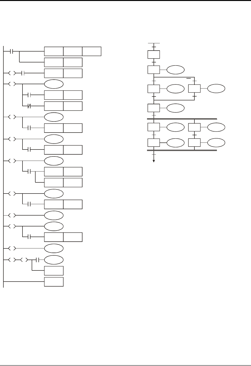
4 Step Ladder Instructions
Combination Example 2:
(Including alternative divergence/convergence and simultaneous divergence/convergence)
Ladder diagram: SFC:
S127
M1002
ZRST S0
SET S0
SET S30
Y0
SET S31
Y1
SET S33
Y2
END
X0S0
S
S30
S
X1
S31
S
X2
S32
S
X3
SET S32
SET S33
Y3
S33
S
X4
SET S34
Y4
S34
S
X5
SET S35
Y6
S36
S
X6
SET S37
Y7
S37
S
S0
S35
S
RET
X1
SET S36
Y5
S35
S
X7
S37
S
S0
S30
S31
S33
M1002
X0
X1
X2
Y0
Y1
Y3
S34
X4
S36
S37
X6
Y6
Y7
X5
S35
Y5
Y4
S32
Y2
X3
X1
S0
X7
DVP-PLC Application Manual 4-17
4 Step Ladder Instructions
Restrictions on Divergence Sequence:
1. You can use maximum 8 divergence steps in a divergence sequence. As the diagram below, there are maximum
8 diverged steps S30 ~ S37 after step S20.
2. You can use maximum 16 loops in multiple divergence sequences or in simultaneous sequences combined into
one sequence. As the diagram below, there are 4 steps diverged after S40, 7 steps diverged after S41, and 5
steps diverged after S42. There are maximum 16 loops in this sequence.
3. You can designate a step in the sequence to jump to any step in another sequence.
Y26
S60
X26
X41
S0
S20
S30
S40
S0
M1002
X0
X1
X11
X51
Y0
Y1
Y11
S50
X20
S80
Y41
S51
S71
X33
Y15
Y33
S53
S73
X35
Y17
Y35
X32
X44
S70
Y32
Y14
S31
Y2
X12
X2
S32
Y4
X15
X4
S41
Y12
X21
X52
S54
Y20
S0
SET
S32
Y3
X14
X3
S52
S72
X34
Y16
Y34
S0
SET
X13
S20
OUT
S20
OUT
S81
X45
Y42
SET
S34
Y5
X15
X5
S35
X15
X6
S55
S74
X36
X22
X46
Y27
S61
X27
X42
Y30
S62
X30
Y31
S63
X31
Y40
S76
X43
X50
Y6
S36
X16
X7
Y7
Y21
Y36
S56
Y22
S57
Y23
S20
X23 OUT
RST
S36
Y10
Y13
Y25
Y37
S58
X37
X24
Y24
RST
S58
S37
S42
S59
S75
X40
X47
X10
X17
X25
SET
S0
OUT
S42
4.6 IST Instruction
API Mnemonic Operands Function
60
IST Initial State
Bit Devices Word Devices Program Steps Type
OP X Y M S K H KnX KnY KnM KnS T C D E F
S * * *
D1 *
D2 *
IST: 7 steps
PULSE 16-bit 32-bit
ES EX SS SA SX SC EH2 SV EH3 SV2 ES EX SS SA SX SC EH2 SV EH3 SV2 ES EX SS SA SX SC EH2 SV EH3 SV2
Operands:
S: Start device in the designated operation mode D1: The smallest No. of designated step in auto mode
D2: The biggest No. of designated step in auto mode
Explanations:
1. S will occupy 8 consecutive points.
2. Range of D1 and D2: for SA/SX/SC/EH2/SV/EH3/SV2 S20 ~ S899; for ES/EX/SS S20 ~ S127; D2 > D1.
3. See the specifications of each model for their range of use.
4. IST instruction can only be used once in the program.
5. Flags: M1040 ~ M1047. See remarks for more details.
6. IST instruction is a handy instruction specifically for the initial status of step ladder control procedure to
DVP-PLC Application Manual
4-18
4 Step Ladder Instructions
accommodate special auxiliary relay.
Program Example 1:
1. Use of IST instruction
M1000
IST X10 S20 S60
S X10: Individual operation
X11: Zero return
X12: Step operation
X13: One cycle operation
X14: Continuous operation
X15: Zero return enabled switch
X16: Start switch
X17: Stop switch
2. When IST instruction is being executed, the following special auxiliary relays will switch automatically.
M1040: Operation forbidden
M1041: Operation starts
M1042: Pulse output enabled
M1047: STL monitor enabled
S0: Initiates manual operation
S1: Initiates zero return
S2: Initiates auto operation
3. S10 ~ S19 are for zero return and cannot be used as general steps. When S0 ~ S9 are in use, S0 ~ S2 represent
manual operation mode, zero return mode and auto operation mode. Therefore, in the program, you have to write
the circuit of the three steps in advance.
4. When switched to S1 (zero return) mode, any On in S10 ~ S19 will result in no zero return.
5. When switched to S2 (auto operation) mode, any On of the S in D1 ~ D2 or M1043 = On will result in no auto
operation.
Program Example 2:
1. Robot arm control (by IST instruction):
a) Motion request: Separate the big ball and small ball and move them to different boxes. Configure the control
panel for the control.
b) Motions of the robot arm: descending, clipping ball, ascending, right shifting, releasing ball, ascending, left
shifting.
c) I/O devices:
Y0
Y1
Y2Y3
Left-limit X1
Upper-limit X4
Lower-limit X5
Right-limit X2
(big) Right-limit X3
(small)
Big Small
Ball size
sensor X0
2. Operation modes:
Manual operation: Turn On/Off of the load by a single button.
Zero return: Press the zero return button to automatically zero-return the machine.
Auto operation:
a) Single step operation: Press “auto start” button for every one step forward.
b) One cycle operation: Press “auto start” button at the zero point. After a cycle of auto operation, the operation
will stops at the zero point. Press “auto stop” button in the middle of the operation to stop the operation and
press “auto start” to restart the operation. The operation will resume until it meets the zero point.
DVP-PLC Application Manual 4-19
4 Step Ladder Instructions
c) Continuous operation: Press “auto start” button at the zero point to resume the operation. Press “auto stop” to
operate until it meets the zero point.
3. The control panel:
X15 X16
X17
X20
X21
X22
X23
X24
X25
Step X12
One cycle
Operation X13
Continuous
Operation X14
Manual
Operation X10
Zero Return X11
Start Power
Stop Power
Start Zero Return Auto Start
Auto Stop
Right
Shift
Left
Shift
Release
Ball
Clip
Ball
Descend
Ascend
a) Ball size sensor X0.
b) Robot arm: left limit X1, big ball right limit X2, small ball right limit X3, upper limit X4, lower limit X5.
c) Robot arm: ascending Y0, descending Y1, right shifting Y2, left shifting Y3, clipping Y4.
Start Circuit
M1000
IST X10 S20 S80
X0
M1044
X1 Y4
Manual Operation Mode
X20
SET
RST Y4
Y4
S
S0
X21
X22 Y1
Y0
X23 Y0
Y1
X24 X4
Y2
Y3
X25 X4
Y3
Y2
Clipping tightly
Clipping released
Descending
Ascending
Interlocked
Right shifting
Left shifting
Interlocked
Robot arm ascends to upper limit (X4 On)
Zero Return Mode
SFC:
DVP-PLC Application Manual
4-20
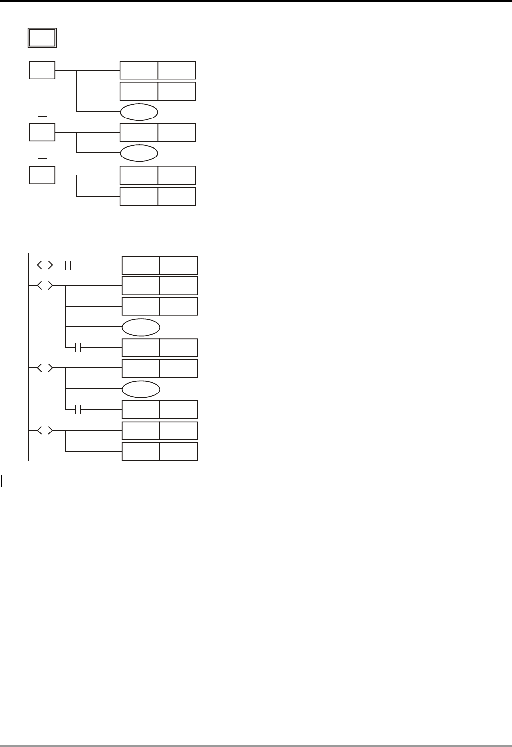
4 Step Ladder Instructions
S1
S10
X15
S11
X4
S12
X1
RST Y4
RST Y1
Y0
RST Y2
Y3
SET M1043
RST S12
Clipping released
Descending stops
Robot arm ascends to upper limit (X4 On)
Right shifting stops
Robot arm left shifting to left limit (X1 On)
Enable zero return completed flag
Zero return operation completed
Ladder Diagram:
X15
SET S10
S
S1
RST Y4
S
S10
RST Y1
Y0
X4
SET S11
RST Y2
S
S11
Y3
X1
SET S12
SET M1043
S
S12
RST S12
Enter zero return mode
Clipping released
Descending stops
Robot arm ascends to upper limit (X4 On)
Right shifting stops
Robot arm left shifting to left limit (X1 On)
Enable zero return completed flag
Zero return operation completed
Auto Operation Modes
SFC:
DVP-PLC Application Manual 4-21
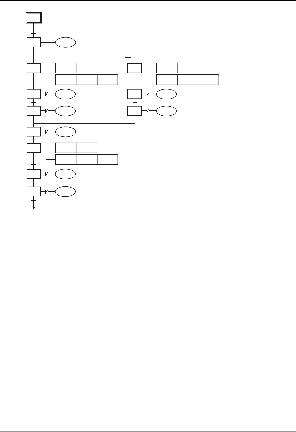
4 Step Ladder Instructions
S2
S20
S30
S31
M1044
X5
T0
Y1
SET
Y0
S32
X4
X2
S50
Y1
Y2
S2
X1
M1041
X0
Y4
TMR T0 K30
S60
RST
X5
Y4
TMR T2 K30
S70
T2
Y0
S80
X4
Y3
X1
S40
S41
X5
T1
SET
Y0
S42
X4
X3
Y2
X0
Y4
TMR T1 K30
X3X2
X4
X4
X5
X4
DVP-PLC Application Manual
4-22
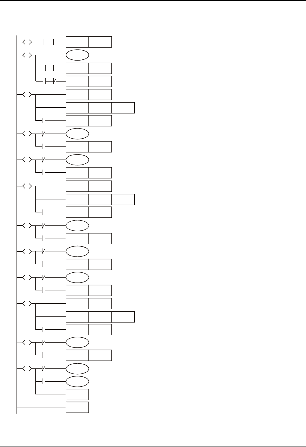
4 Step Ladder Instructions
Ladder Diagram:
SET S20
SET S30
SET Y4
Y0
END
X5
S31
S
X4
TMR T0
SET S32
S2
S
M1041 M1044
S20
S
S30
S
Y1
X0
SET S40
X5 X0
SET S31
T0
K30
Y2
S32
S
X2
SET S50
X2
SET Y4
TMR T1
S40
S
SET S41
T1
K30
Y0
S41
S
X4
SET S42
Y2
S42
S
X3
SET S50
X3
Y1
S50
S
X5
SET S60
RST Y4
TMR T2
S60
S
SET S70
T2
K30
Y0
S70
S
X4
SET S80
Y3
S80
S
X1
X1
RET
S2
Enter auto operation mode
Clipping tightly
Clipping released
Robot arm descending
Right shifting
Robot arm ascending to upper limit (X4 On)
Robot arm left shifting to left limit (X1 On)
Clipping tightly
Robot arm ascending to upper limit (X4 On)
Right shifting
Robot arm descending
Robot arm ascending to upper limit (X4 On)
X4
X4
X4X4
X5
X4
DVP-PLC Application Manual 4-23

4 Step Ladder Instructions
MEMO
DVP-PLC Application Manual
4-24

5 Categories & Use of Application Instructions
5.1 List of Instructions
For applicable models, ES includes ES/EX/SS; SA includes SA/SX/SC; EH includes EH2/SV/EH3/SV2.
ES/EX/SS series MPU does not support pulse execution type instructions (P instruction).
Mnemonic Applicable to STEPS
Category API 16-bit 32-bit
P
instruction Function
ES SA EH2 EH3 16-bit 32-bit
Page
00 CJ -
3 Conditional Jump 3 3 3 3 - 6-1
01 CALL -
3 Call Subroutine 3 3 3 3 - 6-5
02 SRET - - Subroutine Return 3 3 3 1 - 6-5
03 IRET -
- Interrupt Return 3 3 3 1 - 6-8
04 EI -
- Enable Interrupts 3 3 3 1 - 6-8
05 DI -
- Disable Interrupts 3 3 3 1 - 6-8
06 FEND - - The End of The Main Program
(First End) 3 3 3 1 - 6-13
07 WDT -
3 Watchdog Timer Refresh 3 3 3 1 - 6-15
08 FOR -
- Start of a FOR-NEXT loop 3 3 3 3 - 6-16
Loop Control
09 NEXT - - End of a FOR-NEXT loop 3 3 3 1 - 6-16
10 CMP DCMP 3 Compare 3 3 3 7136-19
11 ZCP DZCP 3 Zone Compare 3 3 3 9176-20
12 MOV DMOV 3 Move 3 3 3 5 9 6-21
13 SMOV - 3 Shift Move - 3 3 11 - 6-22
14 CML DCML 3 Compliment 3 3 3 5 9 6-24
15 BMOV - 3 Block Move 3 3 3 7–6-26
16 FMOV DFMOV 3 Fill Move 3 3 3 7136-28
17 XCH DXCH 3 Exchange 3 3 3 5 9 6-29
18 BCD DBCD 3 Binary Coded Decimal 3 3 3 5 9 6-31
Transmission Comparison
19 BIN DBIN 3 Binary 3 3 3 5 9 6-32
20 ADD DADD 3 Addition 3 3 3 7136-34
21 SUB DSUB 3 Subtraction 3 3 3 7136-36
22 MUL DMUL 3 Multiplication 3 3 3 7136-37
23 DIV DDIV 3 Division 3 3 3 7136-39
24 INC DINC 3 Increment 3 3 3 3 5 6-41
25 DEC DDEC 3 Decrement 3 3 3 3 5 6-42
26 WAND DAND 3 Logical Word AND 3 3 3 7136-43
27 WOR DOR 3 Logical Word OR 3 3 3 7136-44
28 WXOR DXOR 3 Logical Exclusive OR 3 3 3 7136-45
Four Arithmetic Operation
29 NEG DNEG 3 2’s Complement (Negative) 3 3 3 3 5 6-46
30 ROR DROR 3 Rotation Right 3 3 3 5 9 6-48
31 ROL DROL 3 Rotation Left 3 3 3 5 9 6-49
32 RCR DRCR 3 Rotation Right with Carry 3 3 3 5 9 6-50
33 RCL DRCL 3 Rotation Left with Carry 3 3 3 5 9 6-51
34 SFTR - 3 Bit Shift Right 3 3 3 9- 6-52
35 SFTL - 3 Bit Shift Left 3 3 3 9- 6-53
36 WSFR - 3 Word Shift Right - 3 3 9- 6-54
37 WSFL - 3 Word Shift Left - 3 3 9- 6-56
38 SFWR - 3 Shift Register Write - 3 3 7- 6-57
Rotation & Displacement
39 SFRD - 3 Shift Register Read - 3 3 7 - 6-58
DVP-PLC Application Manual 5-1

5 Categories & Use of Application Instructions
Mnemonic Applicable to STEPS
Category API 16-bit 32-bit
P
instruction Function
ES SA EH2 EH3 16-bit
Page
32-bit
40 ZRST - 3 Zero Reset 3 3 3 5 - 6-59
41 DECO - 3 Decode 3 3 3 7 - 6-61
42 ENCO - 3 Encode 3 3 3 7 - 6-63
43 SUM DSUM 3 Sum of Active Bits 3 3 3 5 9 6-65
44 BON DBON 3 Check Specified Bit Status 3 3 3 7 13 6-66
45 MEAN DMEAN 3 Mean 3 3 3 7 13 6-67
46 ANS -
- Timed Annunciator Set - 3 3 7 - 6-68
47 ANR -
3 Annunciator Reset - 3 3 1 - 6-68
48 SQR DSQR 3 Square Root 3 3 3 5 9 6-71
Data Processing
49 FLT DFLT 3 Floating Point 3 3 3 5 9 6-72
50 REF -
3 Refresh 3 3 3 5 - 7-1
51 REFF - 3 Refresh and Filter Adjust - 3 3 3 - 7-2
52 MTR -
- Input Matrix - 3 3 9 - 7-3
53 - DHSCS - High Speed Counter Set 3 3 3 - 13 7-5
54 - DHSCR - High Speed Counter Reset 3 3 3 - 13 7-15
55 - DHSZ - High Speed Zone Compare - 3 3 - 17 7-17
56 SPD -
- Speed Detection 3 3 3 7 - 7-24
57 PLSY DPLSY - Pulse Y Output 3 3 3 7 13 7-26
58 PWM - - Pulse Width Modulation 3 3 3 7 - 7-33
High Speed Processing
59 PLSR DPLSR - Pulse Ramp 3 3 3 9 17 7-36
60 IST - - Initial State 3 3 3 7 - 7-41
61 SER DSER 3 Search a Data Stack - 3 3 9 17 7-48
62 ABSD DABSD - Absolute Drum Sequencer - 3 3 9 17 7-50
63 INCD - - Incremental Drum Sequencer -
3 3 9 - 7-52
64 TTMR - - Teaching Timer -
3 3 5 -
7-54
65 STMR - - Special Timer - 3 3 7 -
7-56
66 ALT -
3 Alternate State 3 3 3 3 - 7-58
67 RAMP - - Ramp Variable Value - 3 3 9 - 7-59
68 DTM - - Data Transform and Move - 3 3 9 - 7-61
Handy Instructions
69 SORT - - Sort Tabulated Data -
3 3 11 - 7-69
70 TKY DTKY - Ten Key Input - 3 3 7 13 7-71
71 HKY DHKY - Hexadecimal Key Input - 3 3 9 17 7-73
72 DSW - - Digital Switch - 3 3 9 - 7-76
73 SEGD - 3 Seven Segment Decoder 3 3 3 5 - 7-78
74 SEGL - - Seven Segment with Latch 3 3 3 7 - 7-79
75 ARWS - - Arrow Switch - 3 3 9 - 7-82
76 ASC - - ASCII Code Conversion -
3 3 11 - 7-84
Display of External
Settings
77 PR - - Print (ASCII Code Output) - 3 3 5 - 7-86
78 FROM DFROM 3 Read CR Data in Special
Modules 3 3 3 9 17 7-88
79 TO DTO 3 Write CR Data into Special
Modules 3 3 3 9 17 7-89
80 RS -
- Serial Communication
Instruction 3 3 3 9 - 7-93
81 PRUN DPRUN 3 Parallel Run - 3 3 5 9 7-106
82 ASCI - 3 Converts Hex to ASCII 3 3 3 7 - 7-107
Serial I/O
83 HEX -
3 Converts ASCII to Hex 3 3 3 7 - 7-112
DVP-PLC Application Manual
5-2

5 Categories & Use of Application Instructions
Mnemonic Applicable to STEPS
Category API 16-bit 32-bit
P
instruction Function
ES SA EH2 EH3 16-bit
Page
32-bit
84 CCD -
3 Check Code - 3 3 7- 7-115
85 VRRD - 3 Volume Read - 3 3 5- 7-117
86 VRSC - 3 Volume Scale - 3 3 5- 7-119
87 ABS DABS 3 Absolute Value 3 3 3 3 5 7-120
88 PID DPID - PID Control Loop 3 3 3 917 7-121
89 PLS - - Rising-edge Output 3 3 3 3 - 3-14
90 LDP - -
Rising-edge Detection
Operation 3 3 3 3 - 3-12
91 LDF - -
Falling-edge Detection
Operation 3 3 3 3 - 3-13
92 ANDP - - Rising-edge Series Connection 3 3 3 3- 3-13
93 ANDF - - Falling-edge Series Connection 3 3 3 3 - 3-13
94 ORP - -
Rising-edge Parallel
Connection 3 3 3 3 - 3-14
95 ORF - -
Falling-edge Parallel
Connection 3 3 3 3 - 3-14
96 TMR -
- 16-bit Timer 3 3 3 4- 3-9
97 CNT DCNT - 16-bit / 32-bit Counter 3 3 3 4 6 3-10
98 INV - - Inverting Operation 3 3 3 1- 3-16
Basic Instructions
99 PLF - - Falling-edge Output 3 3 3 3 - 3-15
100 MODRD - - Read Modbus Data 3 3 3 7 - 8-1
101 MODWR - - Write Modbus Data 3 3 3 7 - 8-5
102 FWD - - Forward Running of VFD-A 3 3 3 7- 8-10
103 REV - - Reverse Running of VFD-A 3 3 3 7 - 8-10
104 STOP - - Stop VFD-A 3 3 3 7 - 8-10
105 RDST - - Read VFD-A Status 3 3 3 5 - 8-13
106 RSTEF - - Reset Abnormal VFD-A 3 3 3 5- 8-15
107 LRC -
3 Checksum LRC Mode 3 3 3 7 - 8-16
108 CRC -
3 Checksum CRC Mode 3 3 3 7 - 8-18
150 MODRW - - Read/Write Modbus Data 11 - 9-1
Communication
206 ASDRW - - ASDA servo drive R/W - - - 7-
10-9
110 - DECMP 3 Floating Point Compare 3 3 3 - 13 8-21
111 - DEZCP 3 Floating Point Zone Compare 3 3 3 - 17 8-22
112 - DMOVR 3 Move Floating Point Data 3 3 3 - 9 8-23
116 - DRAD 3 Angle Radian - 3 3 - 9 8-24
117 - DDEG 3 Radian Angle - 3 3 - 9 8-25
118 - DEBCD 3 Float to Scientific Conversion 3 3 3 - 9 8-26
119 - DEBIN 3 Scientific to Float Conversion 3 3 3 - 9 8-27
120 - DEADD 3 Floating Point Addition 3 3 3 - 13 8-29
121 - DESUB 3 Floating Point Subtraction 3 3 3 - 13 8-30
122 - DEMUL 3 Floating Point Multiplication 3 3 3 - 13 8-31
123 - DEDIV 3 Floating Point Division 3 3 3 - 13 8-32
124 - DEXP 3 Exponent of Binary Floating
Point 3 3 3 - 9 8-33
125 - DLN 3 Natural Logarithm of Binary
Floating Point 3 3 3 - 9 8-34
126 - DLOG 3 Logarithm of Binary Floating
Point 3 3 3 - 13 8-35
Floating Point Operation
127 - DESQR 3 Floating Point Square Root 3 3 3 - 9 8-36
DVP-PLC Application Manual 5-3

5 Categories & Use of Application Instructions
Mnemonic Applicable to STEPS
Category API 16-bit 32-bit
P
instruction Function
ES SA EH2 EH3 16-bit
Page
32-bit
128 - DPOW 3 Floating Point Power Operation 3 3 3 - 13 8-37
129 INT DINT 3 Float to Integer 3 3 3 5 9 8-38
130 - DSIN 3 Sine 3 3 3 - 9 8-39
131 - DCOS 3 Cosine 3 3 3 - 9 8-41
132 - DTAN 3 Tangent 3 3 3 - 9 8-43
133 - DASIN 3 Arc Sine - 3 3 - 9 8-45
134 - DACOS 3 Arc Cosine - 3 3 - 9 8-46
135 - DATAN 3 Arc Tangent - 3 3 - 9 8-47
136 - DSINH 3 Hyperbolic Sine - -3 - 9 8-48
137 - DCOSH 3 Hyperbolic Cosine - - 3 - 9 8-49
138 - DTANH 3 Hyperbolic Tangent - -3 - 9 8-50
172 - DADDR Addition of Floating-point
Numbers - 13 9-67
173 - DSUBR Subtraction of Floating-point
Numbers - 13 9-69
174 - DMULR Multiplication of Floating-point
Numbers - 13 9-71
Floating Point Operation
175 - DDIVR Division of Floating-point
Numbers - 13 9-73
109 SWRD - 3 Read Digital Switch - -3 3 - 8-20
143 DELAY - Delay Instruction - 3 3 3 - 8-51
144 GPWM - - General PWM Output - 3 3 7 - 8-53
145 FTC - - Fuzzy Temperature Control
- 3 3 9 - 8-54
146 CVM - - Valve Control - - 3 7 - 8-59
147 SWAP DSWAP 3 Byte Swap 3 3 3 3 5 8-63
148 MEMR DMEMR 3 Read File Register - 3 3 7 13 8-64
149 MEMW DMEMW 3 Write File Register - 3 3 7 13 8-66
151 PWD - - Detection of Input Pulse Width - - 3 5 - 9-19
152 RTMU - -
Start of the Measurement of
Execution Time of I Interruption - - 3 5 - 9-20
153 RTMD - -
End of the Measurement of the
Execution Time of I Interruption - - 3 3 - 9-21
154 RAND - 3 Random Number - 3 3 7 - 9-23
168 MVM DMVM Move the Designated Bit - –
7 13 9-62
176 MMOV - 3 Magnify Move -
5 - 9-75
177 GPS - -
GPS data receiving - - - 5 - 9-76
178 SPA DSPA - Solar Panel Positioning - - - - 9 9-79
179 WSUM DWSUM Get the Sum - - 7 13 9-81
196 HST -
3 High Speed Timer - - 3 3 - 9-117
202 SCAL -
3 Proportional Value Calculation
9 - 10-1
203 SCLP -
3 Parameter Proportional Value
Calculation
9 - 10-3
205 CMPT - Compare table - - 9 - 10-7
Others
207 CSFO - - Catch speed and proportional
output - - - 7 - 10-11
155 - DABSR -
Read the Absolute Position
from a Servo Motor - 3 3 7 13 9-24
156 ZRN DZRN - Zero Return -
-3 9 17 9-29
157 PLSV DPLSV - Adjustable Speed Pulse Output - - 3 7 13 9-34
158 DRVI DDRVI - Drive to Increment - -3 9 17 9-35
Position
Control
159 DRVA DDRVA - Drive to Absolute - - 3 9 17 9-42
DVP-PLC Application Manual
5-4

5 Categories & Use of Application Instructions
Mnemonic Applicable to STEPS
Category API 16-bit 32-bit
P
instruction Function
ES SA EH2 EH3 16-bit 32-bit
Page
191 - DPPMR -
2-Axis Relative Point to Point
Motion - - - 17 9-99
192 - DPPMA -
2-Axis Absolute Point to Point
Motion - - - 17 9-102
193 - DCIMR -
2-Axis Relative Position Arc
Interpolation - - - 17 9-105
194 - DCIMA -
2-Axis Absolute Position Arc
Interpolation - - - 17 9-110
195 - DPTPO -
Single-Axis Pulse Output by
Table - - - 13 9-115
197 - DCLLM -
Close Loop Position Control - - - 17 9-119
198 - DVSPO -
Variable Speed Pulse Output - - - 17 9-127
Position Control
199 - DICF Immediately Change Frequency - - - 13 9-131
160 TCMP - 3 Time Compare - 3 3 11 - 9-54
161 TZCP - 3 Time Zone Compare - 3 3 9 - 9-55
162 TADD - 3 Time Addition - 3 3 7 - 9-56
163 TSUB - 3 Time Subtraction - 3 3 7 - 9-57
166 TRD - 3 Time Read - 3 3 3- 9-58
167 TWR -
3 Time Write - 3 3 3 - 9-60
Real Time
Calendar
169 HOUR DHOUR - Hour Meter - 3 3 7139-63
170 GRY DGRY 3 BIN Gray Code - 3 3 59 9-65
Gray
code
171 GBIN DGBIN 3 Gray Code BIN - 3 3 5 9 9-66
180 MAND - 3 Matrix ‘AND’ Operation - 3 3 9- 9-82
181 MOR -
3 Matrix ‘OR’ Operation - 3 3 9 - 9-84
182 MXOR - 3 Matrix ‘XOR’ Operation - 3 3 9 - 9-85
183 MXNR - 3 Matrix ‘XNR’ Operation - 3 3 9 - 9-86
184 MINV -
3 Matrix Inverse Operation - 3 3 7 - 9-87
185 MCMP - 3 Matrix Compare - 3 3 9 - 9-88
186 MBRD - 3 Read Matrix Bit - 3 3 7 - 9-90
187 MBWR - 3 Write Matrix Bit - 3 3 7 - 9-92
188 MBS -
3 Matrix Bit Displacement - 3 3 7 - 9-94
189 MBR -
3 Matrix Bit Rotation - 3 3 7 - 9-96
Matrix
190 MBC -
3 Matrix Bit Status Counting - 3 3 7 - 9-98
215 LD& DLD& - S1 & S2-3 3 5 9 10-15
216 LD| DLD| - S1 | S2-3 3 59
10-15
217 LD^ DLD^ - S1 ^ S2-3 3 59
10-15
218 AND& DAND& - S1 & S2-3 3 59
10-16
219 AND| DAND| - S1 | S2-3 3 59
10-16
220 AND^ DAND^ - S1 ^ S2-3 3 59
10-16
221 OR& DOR& - S1 & S2-3 3 59
10-17
222 OR| DOR| - S1 | S2-3 3 59
10-17
Contact Type Logic
Operation
223 OR^ DOR^ - S1 ^ S2-3 3 59
10-17
224 LD= DLD= - S1 = S23 3 3 59
10-18
225 LD> DLD> - S1 > S23 3 3 59
10-18
226 LD< DLD< - S1 < S23 3 3 59
10-18
228 LD<> DLD<> - S1 ≠ S23 3 3 59
10-18
229 LD<= DLD<= - S1 ≤ S23 3 3 59
10-18
230 LD>= DLD>= - S1 ≥ S23 3 3 59
10-18
Contact Type
Comparison
Instruction
232 AND= DAND= - S1 = S23 3 3 59
10-19
DVP-PLC Application Manual 5-5

5 Categories & Use of Application Instructions
Mnemonic Applicable to STEPS
Category API 16-bit 32-bit
P
instruction Function
ES SA EH2 EH3 16-bit 32-bit
Page
233 AND> DAND> - S1 > S23 3 3 5 9
10-19
234 AND< DAND< - S1 < S23 3 3 5 9
10-19
236 AND<> DAND<> - S1 ≠ S23 3 3 5 9
10-19
237 AND<= DAND<= - S1 ≤ S23 3 3 5 9
10-19
238 AND>= DAND>= - S1 ≥ S23 3 3 5 9
10-19
240 OR= DOR= - S1 = S23 3 3 5 9
10-20
241 OR> DOR> - S1 > S23 3 3 5 9
10-20
242 OR< DOR< - S1 < S23 3 3 5 9 10-20
244 OR<> DOR<> - S1 ≠ S23 3 3 5 9 10-20
245 OR<= DOR<= - S1 ≤ S23 3 3 5 9 10-20
Contact Type Comparison
Instruction
246 OR>= DOR>= - S1 ≥ S23 3 3 5 9 10-20
266 BOUT DBOUT - Output Specified Bit of a Word - - 5 9 10-21
267 BSET DBSET - Set ON Specified Bit of a Word - - 5 9 10-22
268 BRST DBRST - Reset Specified Bit of a Word - - 5 9 10-23
269 BLD DBLD -
Load NO Contact by Specified
Bit - - 5 9 10-24
270 BLDI DBLDI -
Load NC Contact by Specified
Bit - - 5 9 10-25
271 BAND DBAND - Connect NO Contact in Series
by Specified Bit - - 5 9 10-26
272 BANI DBANI - Connect NC Contact in Series
by Specified Bit - - 5 9 10-27
273 BOR DBOR -
Connect NO Contact in Parallel
by Specified Bit - - 5 9 10-28
Word Device Bit Instruction
274 BORI DBORI - Connect NC Contact in Parallel
by Specified Bit - - 5 9 10-29
275 - FLD= - S1 = S
2- - - 9 10-30
276 - FLD> - S1 > S
2- - - 9 10-30
277 - FLD< - S1 < S
2- - - 9 10-30
278 - FLD<> - S1 ≠ S2- - - 9 10-30
279 - FLD<= - S1 ≦ S2- - - 9 10-30
280 - FLD>= - S1 ≧ S2- - - 9 10-30
281 - FAND= - S1 = S
2- - - 9 10-31
282 - FAND> - S1 > S
2- - - 9 10-31
283 - FAND< - S1 < S
2 - - - 9 10-31
284 - FAND<> - S1 ≠ S2- - - 9 10-31
285 - FAND<= - S1 ≦ S2- - - 9 10-31
286 - FAND>= - S1 ≧ S2- - - 9 10-31
287 - FOR= - S1 = S
2- - - 9 10-32
288 - FOR> - S1 > S
2- - - 9 10-32
289 - FOR< - S1 < S
2- - - 9 10-32
290 - FOR<> - S1 ≠ S2- - - 9 10-32
291 - FOR<= - S1 ≦ S2- - - 9 10-32
Floating-point Contact Type Comparison Instruction
292 - FOR>= - S1 ≧ S2- - - 9 10-32
DVP-PLC Application Manual
5-6
5 Categories & Use of Application Instructions
5.2 Composition of Application Instruction
An application instruction has two parts: the instruction and operands.
Instruction: The function of the instruction
Operands: Devices for processing the operations of the instruction
The instruction part of an application instruction usually occupies 1 step, and one operand occupies 2 or 4 steps
depending on the instruction is a 16-bit or 32-bit one.
Format of an application instruction:
1234567
8
9
11
12
13
10
API
41 P
DECO
Mnemonic
S
D
n
Operands Function
Decode
Control lers
ES /EX /SS SA /SX /SC EH /S V
Program Steps
DECO, DECOP: 7 steps
Bit Devic es Word De vices
XYMSKH
KnX KnY KnM KnS
TD
CEF
Type
OP
S
D
n
****** ***
*********
**
**
ES ES ESSSEX SA SX SC EH SV EX SS SA SX SC EH SV EX SS SXSA SC EH SV
PULSE 16-bit 32-bit
API No.
Indication of if there is a 16-bit or 32-bit instruction. If there is a 32-bit instruction, the column will be marked
with “D”.
Mnemonic of the application instruction
Indication of if there is a pulse execution type instruction. If there is a pulse instruction, the column will be
marked with “P”.
Operands
Function of the application instruction
DVP-PLC applicable to the application instruction. ES includes ES/EX/SS, SA includes SA/SX/SC, EH2
includes EH2/SV, and EH3 includes EH3/SV2.
Steps occupied by the 16-bit/32-bit/pulse execution instruction
DVP-PLC applicable to the pulse/16-bit/32-bit instruction
Column marked with * and in grey refers to E, F index register modification is applicable.
Column marked with * is the device applicable for the operand
Device name
Device type
Input of application instruction:
Some application instructions are only composed of the instruction part (mnemonic), e.g. EI, DI, WDT…. Most
application instructions are composed of the instruction part and many operands.
DVP-PLC Application Manual 5-7
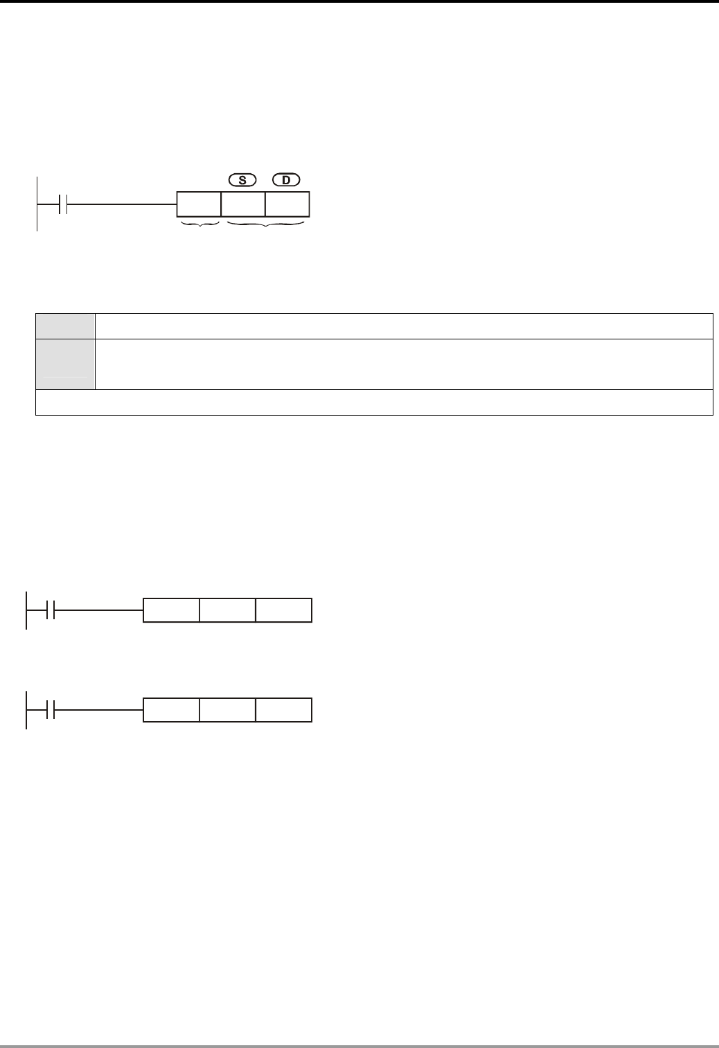
5 Categories & Use of Application Instructions
The application instructions for DVP-PLC are represented as API 00 ~ API 246. Every application instruction
has its own mnemonic. For example, the mnemonic of API 12 is MOV. If you are using the ladder diagram editing
software (WPLSoft) to input API 12 into the program, you only have to enter “MOV”. If you are using the handheld
programming panel (HPP) to input API 12 into the program, you will have to enter the API No. “12”.
Different application instructions designate different operands. Take MOV instruction for example:
X0
MOV K10 D10
Instruction
mnemonic
Operands
MOV instruction is to move the operand designated in S to the operand designated in D.
S Source operand: If there are more than 1 source operands, they will be represented as S1, S2, ….
D Destination operand: If there are more than 1 destination operands, they will be represented as
D1, D2, ….
If the operand can only be constant K/H or a register, it will be represented as m, m1, m2, n, n1, n2, ….
Length of operand (16-bit instruction or 32-bit instruction)
Depending on the contents in the operand, the length of an operand can be 16-bit or 32-bit. Therefore, a
16-bit instruction is for processing 16-bit operands, and 32-bit instruction is for processing 32-bit operands. The
32-bit instruction is indicated by adding a “D” before the 16-bit instruction.
16-bit MOV instruction
X0
K10 D10MOV
When X0 = On, K10 will be sent to D10.
32-bit DMOV instruction
X1
D10 D20DMOV
When X1 = On, the content in (D11, D10) will be sent
to (D21, D20).
Continuous execution instruction and pulse execution instruction
Continuous execution and pulse execution are the two types of execution for an application instruction. Due to
that the execution time required will be shorter when the instruction is not executer, the pulse execution
instructions are used more to shorten the scan period. Instructions marked with a “P" following the mnemonic are
pulse execution instruction. Some instructions are mostly used as pulse execution type, e.g. INC, DEC, the kind of
displacement instructions.
DVP-PLC Application Manual
5-8
5 Categories & Use of Application Instructions
Pulse execution instruction
X0
D10 D12MOVP
When X0 goes from Off to On, MOVP instruction will be
executed once and the instruction will not be executed
again in the scan period.
Continuous execution instruction
X1
D10 D12MOV
In every scan period when X1 = On, MOV instruction will
be executed once.
In the two figures, when X0, X1 = Off, the instruction will not be executed, and the content in operand D will
remain unchanged.
Designation of operands
1. Bit devices X, Y, M, and S can be combined into word device, storing values and data for operaions in the form
of KnX, KnY, KnM and KnS in an application instruction.
2. Data register D, timer T, counter C and index register E, F are designated by general operands.
3. A data register is usually in 16 bits, i.e. of the length of 1 register D. A designated 32-bit data register refers to
2 consecutive register Ds.
4. If an operand of a 32-bit instruction designates D0, the 32-bit data register composed of (D1, D0) will be
occupied. D1 is the higher 16 bits; D0 is the lower 16 bits. The same rule also apply to timer T, 16-bit timers
and C0 ~ C199.
5. When the 32-bit counters C200 ~ C255 are used as data registers, they can only be designataed by the
operands of 32-bit instructions.
Format of operand
1. X, Y, M, and S can only On/Off a single point and are defined as bit devices.
2. 16-bit (or 32-bit) devices T, C, D, and registers E, F are defined as word devices.
3. You can place Kn (n = 1 refers to 4 bits. For 16-bit instruction, n = K1 ~ K4; for 32-bit instruction, n = K1 ~ K8)
before bit devices X, Y, M and S to make it a word device for performing word-device operations. For example,
K1M0 refers to 8 bits, M0 ~ M7.
X0
K2M0 D10
MOV
When X0 = On, the contents in M0 ~ M7 will be moved to
bit0 ~ 7 in D10 and bit8 ~ 15 will be set to “0”.
DVP-PLC Application Manual 5-9
5 Categories & Use of Application Instructions
Data processing of word devices combined from bit devices
16-bit instruction 32-bit instruction
Designated value: K-32,768 ~ K32,767
Designated value: K-2,147,483,648 ~ K2,147,483,647
Values for designated K1 ~ K4 Values for designated K1 ~ K8
K1 (4 bits) 0 ~ 15 K1 (4 bits) 0 ~ 15
K2 (8 bits) 0 ~ 255 K2 (8 bits) 0 ~ 255
K3 (12 bits) 0 ~ 4,095 K3 (12 bits) 0 ~ 4,095
K4 (16 bits) -32,768 ~ +32,767 K4 (16 bits) 0 ~ 65,535
K5 (20 bits) 0 ~ 1,048,575
K6 (24 bits) 0 ~ 167,772,165
K7 (28 bits) 0 ~ 268,435,455
K8 (32 bits) -2,147,483,648 ~ +2,147,483,647
Flags
1. General flags
a) The flags listed below are for indicating the operational result of the application instruction.
M1020: zero flag M1022: carry flag
M1021: borrow flag M1029: execution of instruction is completed
All flags will turn On or Off according to the operational result of an instruction. For example, the
execution result of operation instructions ADD/SUB/MUL/DVI will affect the status of M1020 ~ M1022. When
the instruction is not executed, the On/Off status of the flag will be held. The status of the four flags relates to
many instructions. See relevant instructions for more details.
b) Example of M1029
When the contact of DSW (Digital Switch) instruction is On, 4 output points will automatically act in cycle
at the frequency of 0.1 second in order to read the set value of the digital switch. If the contact goes Off
during the execution, the action will be disable. When it is On again, the disabled action will be re-executed. If
you do not wish the action to be disabled, you can take the circuit below as a reference.
X0
SET M0
M0
DSW X10 Y10 D0 K0
RST M0
M1029
When X0 = On, DSW will be enabled.
When X0 = Off, M0 will be Off only when DSW
completes a cycle and M1029 = On.
2. Error Operation Flags
Errors occur during the execution of the instruction when the combination of application instructions is
incorrect or the devices designated by the operand exceed their range. Other than errors, the flags listed in
the table below will be On, and error codes will also appear.
DVP-PLC Application Manual
5-10

5 Categories & Use of Application Instructions
Device Explanation
M1067
D1067
D1069
When operational errors occur, M1067 will be On. D1067 displays the error code. D1069
displays the step where the error occurs. Other errors occurring will update the contents in
D1067 and D1069. M1067 will be Off when the error is eliminated.
M1068
D1068
When operational errors occur, M1068 will be On. D1068 displays the step where the error
occurs. Other errors occurring wil not update the content in D1068. You have to use RST
instruction to reset M1068 to Off; otherwise M1068 will keep being On.
3. Flags for expanding functions
Some application instructions can use some special flags to expand their functions or complete special
functions. For example, the communication instruction RS can use M1161 to switch between 8-bit and 16-bit
transmission mode.
Times of using instructions
There are limitation on the times of using some instructions in the program. However, you can use index register
modification in the operands to expand the functions of the instruction.
1. Can be used only once in the program:
API 58 PWM (ES series MPU) API 60 IST (ES/SA/EH2/EH3 series MPU)
API 74 SEGL (ES series MPU) API 155 DABSR (SC/EH2/EH3 series MPU)
2. Can be used only twice in the program:
API 57 PLSY (ES series MPU) API 59 PLSR (ES series MPU)
API 74 SEGL (EH2/EH3 series MPU) API 77 PR (SA/EH2/EH3 series MPU)
3. Can be used only 4 times in the program:
API 169 HOUR (SA series MPU)
4. Can be used only 8 times in the program:
API 64 TTMR (SA series MPU)
5. API 53 DHSCS and API 54 DHSCR together can be used only maximum 4 times in the program (ES series
MPU).
6. API 53 DHSCS, API 54 DHSCR, and API 55 DHSZ together can be used only maximum 6 times in the program
(SA series MPU).
There is no limitation on the times of using the instructions listed below, but there are limitations on the times of
executing the same instruction at the same time.
1. Instructions which can be executed only once: API 52 MTR (SA/EH2/EH), API 56 SPD (ES/SA/EH2/EH3), API
69 SORT (SA/EH2/EH3), API 70 TKY (SA/EH2/EH3), API 71 HKY (SA/EH2/EH3), API 72 DSW (SA), API 74
SEGL (SA), API 75 ARWS, API 80 RS (ES/SA/EH2/EH3), API 100 MODRD (ES/SA/EH2/EH3), API 101
DVP-PLC Application Manual 5-11
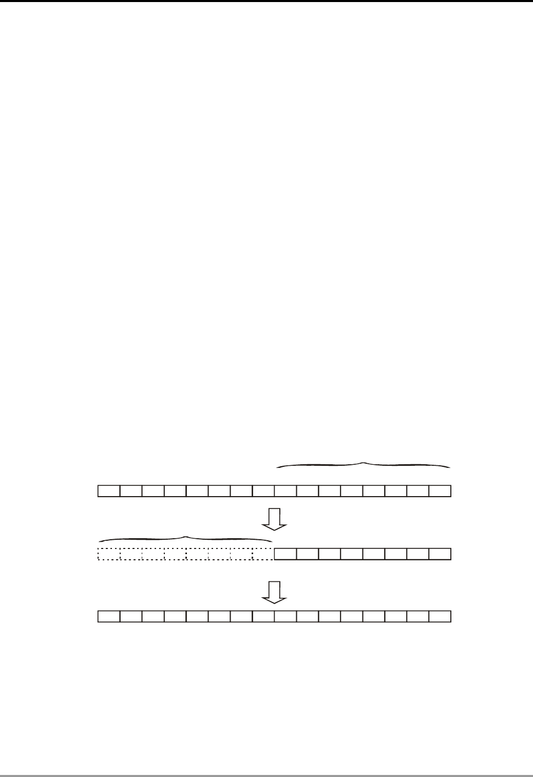
5 Categories & Use of Application Instructions
MODWR (ES/SA/EH2/EH3), API 102 FWD (ES/SA/EH2/EH3), API 103 REV (ES/SA/EH2/EH3), API 104 STOP
(ES/SA/EH2/EH3), API 105 RDST (ES/SA/EH2/EH3), API 106 RSTEF (ES/SA/EH2/EH3), API 150 MODRW
(ES/SA/EH2/EH3), API 151 PWD (EH2/EH3).
2. Instructions which can be executed only twice: API 57 PLSY (EH2/EH3), API 58 PWM (SA/EH2/EH3), API 59
PLSR (SA/EH2/EH3), API 72 DSW (EH2/EH3).
3. Instructions which can be executed only 4 times: API 57 PLSY (EH2/SV/EH3), API 58 PWM (EH2/SV/EH3), API
169 HOUR (EH2/EH3).
4. Instructions which can be executed only 8 times: API 64 TTMR (EH2/EH3).
5. In SA series MPU, there is on limitation on the times of using the high-speed output instructions PLSY, PWM and
PLSR, bit only one high-speed output instruction will be enabled in every scan.
6. In EH2/EH3 series MPU, there is no limitation on the times of using hardware high-speed counter instructions
DHSCS, DHSCR and DHSZ, but when the three instructions are enabled at the same time, DHSCS will occupy 1
memory unit, DHSCR 1 memory unit, and DHSZ 2 memory units. The total memeory units occupied by the three
instructions cannot be more than 8 units. If there are more than 8 memory units occupied, the PLC system will
execute the instruction that is first scanned and enabled and ignore the rest.
5.3 Handling of Numeric Values
Devices only with On/Off status are called bit devices, e.g. X, Y, M and S. Devices used exclusively for storing
numeric values are called word devices, e.g. T, C, D, E and F. Bit device plus a specific bit device (place a digit
before the bit device in Kn) can be used in the operand of an application instruction in the form of numeric value.
n = K1 ~ K4 for a 16-bit value; n = K1 ~ K8 for a 32-bit value. For example, K2M0 refers to a 8-bit value composed of
M0 ~ M7.
M15 M14 M13 M12 M11 M10 M9 M8 M7 M6 M5 M4 M3 M2 M0M1
00000000
00001 1 1 1
11111111
D1
D1 1111000000000000
b15 b14 b13 b12 b11 b10 b9 b8 b7 b6 b5 b4 b3 b2 b0b1
0000000
0
Valid data
Reset to 0
Transmit to
Equals
Low byte
Low byte
K1M0, K2M0, and K3M0 are transmitted to 16-bit registers and the vacant high bits will be filled in “0”. The same
rule applied to when K1M0, K2M0, K3M0, K4M0, K5M0, K6M0, and K7M0 are transmitted to 32-bit registers and
the vacant high bits will be filled in “0”.
In the 16-bit (or 32-bit) operation, if the contents of the operand are designated as bit devices K1 ~ K3 (or K4 ~ K7),
the vacant high bits will be regarded as “0”. Therefore, the operation is a positive-value one.
DVP-PLC Application Manual
5-12
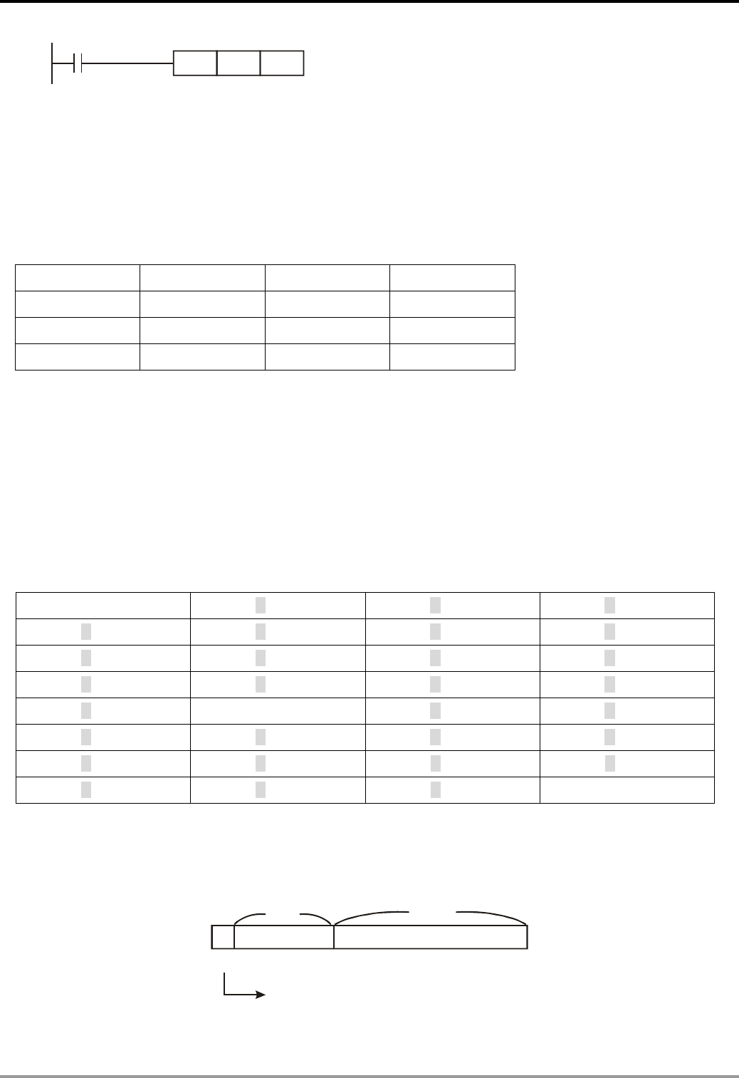
5 Categories & Use of Application Instructions
M0
BIN K2X4 D0
The BCD value composed of X4 ~ X13 will be converted to BIN
value and sent to D0.
You can choose any No. for bit devices, but please make the 1s digit of X and Y “0”, e.g. X0, X10, X20, …Y0, Y10…,
and the 1s digit of M and S “8’s multiple” (“0” is still the best choice), e.g. M0, M10, M20….
Designating continuous device No.
Take data register D for example, continuous D refers to D0, D1, D2, D3, D4….
For bit devices with specifically designated digit, continuous No. refers to:
K1X0 K1X4 K1X10 K1X14…
K2Y0 K2Y10 K2Y20
Y2X30…
K3M0 K3M12 K3M24
K3M36…
K4S0 K4S16 K4S32
K4S48…
Please follow the No. in the table and do not skip No. in case confusion may occur. In addition, if you use K4Y0 in
the 32-bit operation, the higher 16 bits will be regarded as “0”. For 32-bit data, please use K8Y0.
The operations in DVP-PLC are conducted in BIN integers. When the integer performs division, e.g. 40 ÷ 3 = 13
and the remainder is 1. When the integer performs square root operations, the decimal point will be left out. Use
decimal point operation instructions to obtain the decimal point.
Application instructions revelant to decimal point:
API 49 (FLT) API 110 (D ECMP) API 111 (D EZCP) API 112 (D MOVR)
API 116 (D RAD) API 117 (D DEG) API 118 (D EBCD) API 119 (D EBIN)
API 120 (D EADD) API 121 (D ESUB) API 122 (D EMUL) API 123 (D EDIV)
API 124 (D EXP) API 125 (D LN) API 126 (D LOG) API 127 (D ESQR)
API 128 (D POW) API 129 (INT) API 130 (D SIN) API 131 (D COS)
API 132 (D TAN) API 133 (D ASIN) API 134 (D ACOS) API 135 (D ATAN)
API 136 (D SINH) API 137 (D COSH) API 138 (D TANH) API 172 (D ADDR)
API 173 (D SUBR) API 174 (D MULR) API 175 (D DIVR)
Binary Floating Point
DVP-PLC represents floating points in 32 bits, following the IEEE754 standard:
S
exponent mantissa
8 bits 23 bits
b
31
b
0
Sign bit
0: positive
1: negative
DVP-PLC Application Manual 5-13
5 Categories & Use of Application Instructions
()
M
BE
S.121 ××− −, in which B = 127
Therefore, the range for the 32-bit floating point is ±2-126 ~ ±2+128, i.e. ±1.1755 × 10-38 ~ ±3.4028 × 10+38
Example 1: Representing "23" in 32-bit floating point
Step 1: Convert “23” into a binary value: 23.0 = 10111
Step 2: Normalize the binary value: 10111 = 1.0111 × 24, in which 0111 is mantissa and 4 is exponent
Step 3: Obtain the exponent: ∵ E – B = 4 E – 127 = 4 ∴ E = 131 = 100000112
Step 4: Combine the sign bit, exponent and mantissa into a floating point
0 10000011 011100000000000000000002 = 41B8000016
Example 2: Representing “-23.0” in 32-bit floating point
The steps required are the same as those in Example 1. The only difference is you have to alter the sign bit into “1”.
DVP-PLC uses registers of 2 continuous No. to combine into a 32-bit floating point. For example, we use registers
(D1, D0) for storing a binary floating point as below:
S E7 E6 E5 E1 E0 A22 A21 A20 A6 A5 A4 A3 A2 A1 A0
b0b1b2b3b4b5b6b20b21b22b23b24b28b29b30b31
222 222 22 2 222 222
7 6 5 1 0 -1 -2 -3 -17 -18 -19 -20 -21 -22 -23
D1(b15~b0) D0(b15~b0)
8 bits of exponent 23 bits of mantissa
Sign bit (0: positive 1: negative)
When b0~b31 is 0, the content is 0.
Hidden decimal point
Decimal Floating Point
Since the binary floating point are not very user-friendly, we can convert it into a decimal floating point for use.
Please be noted that the decimal point operation in DVP-PLC is still in binary floating point.
The decimal floating point is represented by 2 continuous registers. The register of smaller No. is for the constant
while the register of bigger No. is for the exponent.
Example: Storing a decimal floating point in registers (D1, D0)
Decimal floating point = [constant D0] × 10 [exponent D1 ]
Constant D0 = ±1,000 ~ ±9,999
Exponent D1 = -41 ~ +35
The constant 100 does not exist in D0 due to 100 is represented as 1,000 × 10-1. The range of decimal floating point
is ±1175 × 10-41 ~ ±3402×10+35.
DVP-PLC Application Manual
5-14

5 Categories & Use of Application Instructions
The decimal floating point can be used in the following instructions:
D EBCD: Converting binary floating point to decimal floating point
D EBIN: Converting decimal floating point to binary floating point
Zero flag (M1020), carry flag (M1021), carry flag (M1022) and the floating point operation instructions:
Zero flag: M1020 = On if the operational result is “0”.
Borrow flag: M1021 = On if the operational result exceeds the minimum unit.
Carry flag: M1022 = On if the absolute value of the operational result exceeds the range of use.
5.4 E, F Index Register Modification
The index registers are 16-it registers. There are 2 points of E, F in ES/EX/SS, 8 points E0 ~ E3 and F0 ~ F3 in
SA/SX/SC, and 16 points E0 ~ E7 and F0 ~ F7 in EH2/SV/EH3 series MPU.
F0 E0
E0
F0
16-bit 16-bit
32-bit
High byte Low byte
E and F index registers are 16-bit data registers, can be read and
written.
If you need a 32-bit register, you have to designate E. In this case, F
will be covered up by E and cannot be used; otherwise, the contents
in E may become incorrect. (We recommend you use MOVP
instruction to reset the contents in D to 0 when the PLC is switched
on.)
Combination of E and F when you designate a 32-bit index register:
(E0, F0), (E1, F1), (E2, F2), ... (E7, F7)
MOV K20E0 D10F0
E0 = 8 F0 = 14
20 + 8 = 28 10 + 14 = 24
Transmission K28 D24
See the diagram in the left hand side. E, F index register
modification refers to the content in the operand changes with
the contents in E and F.
For example, E0 = 8 and K20E0 represents constant K28 (20
+ 8). When the condition is true, constant K28 will be
transmitted to register D24.
Devices modifiable in ES/EX/SS series MPU: P, X, Y, M, S, KnX, KnY, KnM, KnS, T, C, D.
Devices modifiable in SA/SX/SC series MPU: P, X, Y, M, S, KnX, KnY, KnM, KnS, T, C, D
Devices modifiable in EH2/SV/EH3 series MPU: P, I, X, Y, M, S, K, H, KnX, KnY, KnM, KnS, T, C, D
E and F can modify the devices listed above but cannot modify themselves and Kn. K4M0E0 is valid and
K0E0M0 is invalid. Grey columns in the table of operand at the beginning page of each application instruction indicate
the operands modifiable by E and F.
DVP-PLC Application Manual 5-15

5 Categories & Use of Application Instructions
If you need to modify device P, I, X, Y, M, S, KnX, KnY, KnM, KnS, T, C and D by E, F, you have to select a
16-bit register, i.e. you can designate E or F. To modify constant K and H in a 32-bit instruction, you have to select a
32-bit register, i.e. you have to designate E.
When you use the instruction mode in WPLSoft to modify constant K and H, you have to use @, e.g.
"MOV K10@E0 D0F0”
DVP-PLC Application Manual
5-16

5 Categories & Use of Application Instructions
5.5 Instruction Index
For applicable models, ES includes ES/EX/SS; SA includes SA/SX/SC; EH2 includes EH2/SV; EH3 includes
EH3/SV2..
ES/EX/SS series MPU does not support pulse execution type instructions (P instruction).
Sorted by alphabetic order & API No.
Mnemonic Applicable to
Category API 16-bit 32-bit
P
Instructio
n
Function ES SA EH
2
EH
3
Page
87 ABS DABS Absolute Value 3 3 37-120
62 ABSD DABSD - Absolute Drum Sequencer - 3 37-50
20 ADD DADD Addition 3 3 36-34
66 ALT - Alternate State 3 3 37-58
218 AND& DAND& - S1 & S2- 3 310-16
220 AND^ DAND^ - S1 ^ S2- 3 310-16
219 AND| DAND| - S1 | S2- 3 310-16
234 AND< DAND< - S1 < S23 3 310-19
237 AND<= DAND<= - S1 ≤ S23 3 310-19
236 AND<> DAND<> - S1 ≠ S23 3 310-19
232 AND= DAND= - S1 = S23 3 310-19
233 AND> DAND> - S1 > S23 3 310-19
238 AND>= DAND>= - S1 ≥ S23 3 310-19
93 ANDF - - Falling-edge Series Connection 3 3 33-13
92 ANDP - - Rising-edge Series Connection 3 3 33-13
47 ANR -
Annunciator Reset - 3 36-68
46 ANS - - Timed Annunciator Set - 3 36-68
75 ARWS - - Arrow Switch - 3 37-82
76 ASC - - ASCII Code Conversion - 3 37-84
82 ASCI -
Converts Hex to ASCII 3 3 37-107
A
206 ASDRW - - ASDA servo drive R/W - - - 10-9
271 BAND DBAND - Connect NO Contact in Series by Specified
Bit - - 10-26
272 BANI DBANI - Connect NC Contact in Series by Specified
Bit - - 10-27
18 BCD DBCD Binary Coded Decimal 3 3 36-31
19 BIN DBIN Binary 3 3 36-32
269 BLD DBLD - Load NO Contact by Specified Bit - - 10-24
270 BLDI DBLDI - Load NC Contact by Specified Bit - - 10-25
15 BMOV - Block Move 3 3 36-26
44 BON DBON Check Specified Bit Status 3 3 36-66
B
273 BOR DBOR - Connect NO Contact in Parallel by Specified
Bit - - 10-28
155 - DABSR - Read the Absolute Position from a Servo
Motor - 3 39-24
134 - DACOS Arc Cosine - 3 38-46
172 - DADDR Addition of Floating-point Numbers 9-67
133 - DASIN Arc Sine - 3 38-45
135 - DATAN Arc Tangent - 3 38-47
D
111 - DEZCP Floating Point Zone Compare 3 3 38-22
DVP-PLC Application Manual 5-17

5 Categories & Use of Application Instructions
Mnemonic Applicable to
Category API 16-bit 32-bit
P
Instructio
n
Function ES SA EH
2
Page
EH
3
54 - DHSCR - High Speed Counter Reset 3 3 3 7-15
53 - DHSCS - High Speed Counter Set 3 3 3 7-5
55 - DHSZ - High Speed Zone Compare - 3 3 7-17
199 - DICF Immediately Change Frequency - - 9-131
125 - DLN Natural Logarithm of Binary Floating Point 3 3 3 8-34
126 - DLOG Logarithm of Binary Floating Point 3 3 3 8-35
112 - DMOVR Move Floating Point Data 3 3 3 8-23
174 - DMULR Multiplication of Floating-point Numbers 9-71
128 - DPOW Floating Point Power Operation 3 3 3 8-37
192 - DPPMA - 2-Axis Absolute Point to Point Motion - - 9-102
191 - DPPMR - 2-Axis Relative Point to Point Motion - - 9-99
195 - DPTPO - Single-Axis Pulse Output by Table - - 9-115
116 - DRAD Angle Radian - 3 3 8-24
130 - DSIN Sine 3 3 3 8-39
136 - DSINH Hyperbolic Sine - - 3 8-48
178 - DSPA - Solar Panel Positioning - - - 9-79
173 - DSUBR Subtraction of Floating-point Numbers 9-69
132 - DTAN Tangent 3 3 3 8-43
138 - DTANH Hyperbolic Tangent - - 3 8-50
198 - DVSPO - Variable Speed Pulse Output - - 9-127
06 FEND - - The End of The Main Program (First End) 3 3 3 6-13
49 FLT DFLT Floating Point 3 3 3 6-72
16 FMOV DFMOV Fill Move 3 3 3 6-28
08 FOR - - Start of a FOR-NEXT loop 3 3 3 6-16
78 FROM DFROM Read CR Data in Special Modules 3 3 3 7-88
145 FTC - - Fuzzy Temperature Control - 3 3 8-54
102 FWD - - Forward Running of VFD-A 3 3 3 8-10
283 - FAND< - S1 < S
2 - - 10-31
285 - FAND<= - S1 ≦ S2- - 10-31
284 - FAND<> - S1 ≠ S2- - 10-31
281 - FAND= - S1 = S
2- - 10-31
282 - FAND> - S1 > S
2- - 10-31
286 - FAND>= - S1 ≧ S2- - 10-31
277 - FLD< - S1 < S
2- - 10-30
279 - FLD<= - S1 ≦ S2- - 10-30
278 - FLD<> - S1 ≠ S2- - 10-30
275 - FLD= - S1 = S
2- - 10-30
276 - FLD> - S1 > S
2- - 10-30
280 - FLD>= - S1 ≧ S2- - 10-30
289 - FOR< - S1 < S
2- - 10-32
291 - FOR<= - S1 ≦ S2- - 10-32
290 - FOR<> - S1 ≠ S2- - 10-32
287 - FOR= - S1 = S
2- - 10-32
F
288 - FOR> - S1 > S
2- - 10-32
DVP-PLC Application Manual
5-18

5 Categories & Use of Application Instructions
Mnemonic Applicable to
Category API 16-bit 32-bit
P
Instructio
n
Function ES SA EH
2
Page
EH
3
292 - FOR>= - S1 ≧ S2- - 10-32
171 GBIN DGBIN Gray Code BIN - 3 39-66
177 GPS - - GPS data receiving - - - 9-76
144 GPWM - - General PWM Output - 3 38-53
G
170 GRY DGRY BIN Gray Code - 3 39-65
24 INC DINC Increment 3 3 36-41
63 INCD - - Incremental Drum Sequencer - 3 37-52
129 INT DINT Float to Integer 3 3 38-38
I
98 INV - - Inverting Operation 3 3 33-16
03 IRET - - Interrupt Return 3 3 36-8
I 60 IST - - Initial State 3 3 37-41
215 LD& DLD& - S1 & S2- 3 310-15
217 LD^ DLD^ - S1 ^ S2- 3 310-15
216 LD| DLD| - S1 | S2- 3 310-15
226 LD< DLD< - S1 < S23 3 310-18
229 LD<= DLD<= - S1 ≤ S23 3 310-18
228 LD<> DLD<> - S1 ≠ S23 3 310-18
224 LD= DLD= - S1 = S23 3 310-18
225 LD> DLD> - S1 > S23 3 310-18
230 LD>= DLD>= - S1 ≥ S23 3 310-18
91 LDF - - Falling-edge Detection Operation 3 3 33-13
90 LDP - - Rising-edge Detection Operation 3 3 33-12
L
107 LRC -
Checksum LRC Mode 3 3 38-16
180 MAND - Matrix ‘AND’ Operation - 3 39-82
190 MBC -
Matrix Bit Status Counting - 3 39-98
189 MBR -
Matrix Bit Rotation - 3 39-96
186 MBRD - Read Matrix Bit - 3 39-90
188 MBS -
Matrix Bit Displacement - 3 39-94
187 MBWR - Write Matrix Bit - 3 39-92
185 MCMP - Matrix Compare - 3 39-88
45 MEAN DMEAN Mean 3 3 36-67
148 MEMR DMEMR Read File Register - 3 38-64
149 MEMW DMEMW Write File Register - 3 38-66
184 MINV -
Matrix Inverse Operation - 3 39-87
176 MMOV - Magnify Move - 9-75
100 MODRD - - Read Modbus Data 3 3 38-1
150 MODRW - - Read/Write Modbus Data 9-1
101 MODWR - - Write Modbus Data 3 3 38-5
181 MOR -
Matrix ‘OR’ Operation - 3 39-84
12 MOV DMOV Move 3 3 36-21
52 MTR - - Input Matrix - 3 37-3
22 MUL DMUL Multiplication 3 3 36-37
168 MVM DMVM Move the Designated Bit - -
9-62
183 MXNR - Matrix ‘XNR’ Operation - 3 39-86
M
182 MXOR - Matrix ‘XOR’ Operation - 3 39-85
DVP-PLC Application Manual 5-19

5 Categories & Use of Application Instructions
Mnemonic Applicable to
Category API 16-bit 32-bit
P
Instructio
n
Function ES SA EH
2
Page
EH
3
29 NEG DNEG 2’s Complement (Negative) 3 3 3 6-46
N 09 NEXT - - End of a FOR-NEXT loop 3 3 3 6-16
221 OR& DOR& - S1 & S2- 3 3 10-17
223 OR^ DOR^ - S1 ^ S2- 3 3 10-17
222 OR| DOR| - S1 | S2- 3 3 10-17
242 OR< DOR< - S1 < S23 3 3 10-20
245 OR<= DOR<= - S1 ≤ S23 3 3 10-20
244 OR<> DOR<> - S1 ≠ S23 3 3 10-20
240 OR= DOR= - S1 = S23 3 3 10-20
241 OR> DOR> - S1 > S23 3 3 10-20
246 OR>= DOR>= - S1 ≥ S23 3 3 10-20
95 ORF - - Falling-edge Parallel Connection 3 3 3 3-14
O
94 ORP - - Rising-edge Parallel Connection 3 3 3 3-14
88 PID DPID - PID Control Loop 3 3 3 7-121
99 PLF - - Falling-edge Output 3 3 3 3-15
89 PLS - - Rising-edge Output 3 3 3 3-14
59 PLSR DPLSR - Pulse Ramp 3 3 3 7-36
157 PLSV DPLSV - Adjustable Speed Pulse Output - - 3 9-34
57 PLSY DPLSY - Pulse Y Output 3 3 3 7-26
77 PR - - Print (ASCII Code Output) - 3 3 7-86
81 PRUN DPRUN Parallel Run - 3 3 7-106
151 PWD - - Detection of Input Pulse Width - - 3 9-19
P
58 PWM - - Pulse Width Modulation 3 3 3 7-33
67 RAMP - - Ramp Variable Value - 3 3 7-59
154 RAND - Random Number - 3 3 9-23
33 RCL DRCL Rotation Left with Carry 3 3 3 6-51
32 RCR DRCR Rotation Right with Carry 3 3 3 6-50
105 RDST - - Read VFD-A Status 3 3 3 8-13
50 REF -
Refresh 3 3 3 7-1
51 REFF -
Refresh and Filter Adjust - 3 3 7-2
103 REV - - Reverse Running of VFD-A 3 3 3 8-10
31 ROL DROL Rotation Left 3 3 3 6-49
30 ROR DROR Rotation Right 3 3 3 6-48
80 RS - - Serial Communication Instruction 3 3 3 7-93
106 RSTEF - - Reset Abnormal VFD-A 3 3 3 8-15
153 RTMD - - End of the Measurement of the Execution
Time of I Interruption - - 3 9-21
R
152 RTMU - - Start of the Measurement of Execution Time
of I Interruption - - 3 9-20
202 SCAL -
Proportional Value Calculation
10-1
203 SCLP -
Parameter Proportional Value Calculation
10-3
73 SEGD - Seven Segment Decoder 3 3 3 7-78
74 SEGL - - Seven Segment with Latch 3 3 3 7-79
61 SER DSER Search a Data Stack - 3 3 7-48
39 SFRD -
Shift Register Read - 3 3 6-58
S
35 SFTL -
Bit Shift Left 3 3 3 6-53
DVP-PLC Application Manual
5-20
5 Categories & Use of Application Instructions
Mnemonic Applicable to
Category API 16-bit 32-bit
P
Instructio
n
Function ES SA EH
2
Page
EH
3
34 SFTR -
Bit Shift Right 3 3 36-52
38 SFWR - Shift Register Write - 3 36-57
13 SMOV - Shift Move - 3 36-22
69 SORT - - Sort Tabulated Data - 3 37-69
56 SPD - - Speed Detection 3 3 37-24
48 SQR DSQR Square Root 3 3 36-71
02 SRET - - Subroutine Return 3 3 36-5
65 STMR - - Special Timer - 3 37-56
104 STOP - - Stop VFD-A 3 3 38-10
21 SUB DSUB Subtraction 3 3 36-36
43 SUM DSUM Sum of Active Bits 3 3 36-65
147 SWAP DSWAP Byte Swap 3 3 38-63
109 SWRD - Read Digital Switch - - 38-20
162 TADD -
Time Addition - 3 39-56
160 TCMP - Time Compare - 3 39-54
70 TKY DTKY - Ten Key Input - 3 37-71
96 TMR - - 16-bit Timer 3 3 33-9
79 TO DTO Write CR Data into Special Modules 3 3 37-89
166 TRD -
Time Read - 3 39-58
163 TSUB -
Time Subtraction - 3 39-57
64 TTMR - - Teaching Timer - 3 37-54
167 TWR -
Time Write - 3 39-60
T
161 TZCP -
Time Zone Compare - 3 39-55
85 VRRD - Volume Read - 3 37-117
V 86 VRSC -
Volume Scale - 3 37-119
26 WAND DAND Logical Word AND 3 3 36-43
07 WDT -
Watchdog Timer Refresh 3 3 36-15
27 WOR DOR Logical Word OR 3 3 36-44
37 WSFL -
Word Shift Left - 3 36-56
36 WSFR - Word Shift Right - 3 36-54
179 WSUM DWSUM Get the Sum - - 9-81
W
28 WXOR DXOR Logical Exclusive OR 3 3 36-45
X 17 XCH DXCH Exchange 3 3 36-29
11 ZCP DZCP Zone Compare 3 3 36-20
156 ZRN DZRN - Zero Return - - 39-29
Z
40 ZRST -
Zero Reset 3 3 36-59
DVP-PLC Application Manual 5-21

5 Categories & Use of Application Instructions
MEMO
DVP-PLC Application Manual
5-22

6 Application Instructions API 00-49
DVP-PLC Application Manual 6-1
API Mnemonic Operands Function
00
CJ P Conditional Jump
OP Range Program Steps
P0~P255 CJ, CJP: 3 steps
PULSE 16-bit 32-bit
ES EX SS SA SX SC EH SV EH3
SV2 ES EX SS SA SX SC EH SV EH3
SV2 ES EX SS SA SX SC EH SV EH3
SV2
Operands:
S: The destination pointer of conditional jump
Explanations:
1. Operand S can designate P
2. P can be modified by index register E, F
3. In ES/EX/SS series models: Operand S can designate P0 ~ P63
4. In SA/SX/SC/EH/EH2/SV series models: Operand S can designate P0 ~ P255
5. When the user does not wish a particular part of PLC program in order to shorten the scan time and execute
dual outputs, CJ instruction or CJP instruction can be adopted.
6. When the program designated by pointer P is prior to CJ instruction, WDT timeout will occur and PLC will stop
running. Please use it carefully.
7. CJ instruction can designate the same pointer P repeatedly. However, CJ and CALL cannot designate the same
pointer P; otherwise an error will occur.
8. Actions of all devices while conditional jumping is being executed.
a) Y, M and S remain their previous status before the conditional jump takes place.
b) Timer 10ms and 100ms that is executing stops.
c) Timer T192 ~ T199 that execute the subroutine program will continue and the output contact executes normally.
d) The high-speed counter that is executing the counting continues counting and the output contact executes
normally.
e) The ordinary counters stop executing.
f) If the “reset instruction” of the timer is executed before the conditional jump, the device will still be in the reset
status while conditional jumping is being executed.
g) Ordinary application instructions are not executed.
h) The application instructions that are being executed, i.e. API 53 DHSCS, API 54 DHSCR, API 55 DHSZ, API 56
SPD, API 57 PLSY, API 58 PWM, API 59 PLSR, API 157 PLSV, API 158 DRVI, API 159 DRVA, continue being
executed.
Program Example 1:
1. When X0 = On, the program automatically jumps from address 0 to N (the designated label P1) and keeps its
execution. The addresses between 0 and N will not be executed.
2. When X0 = Off, as an ordinary program, the program keeps on executing from address 0. CJ instruction will not
be executed at this time.
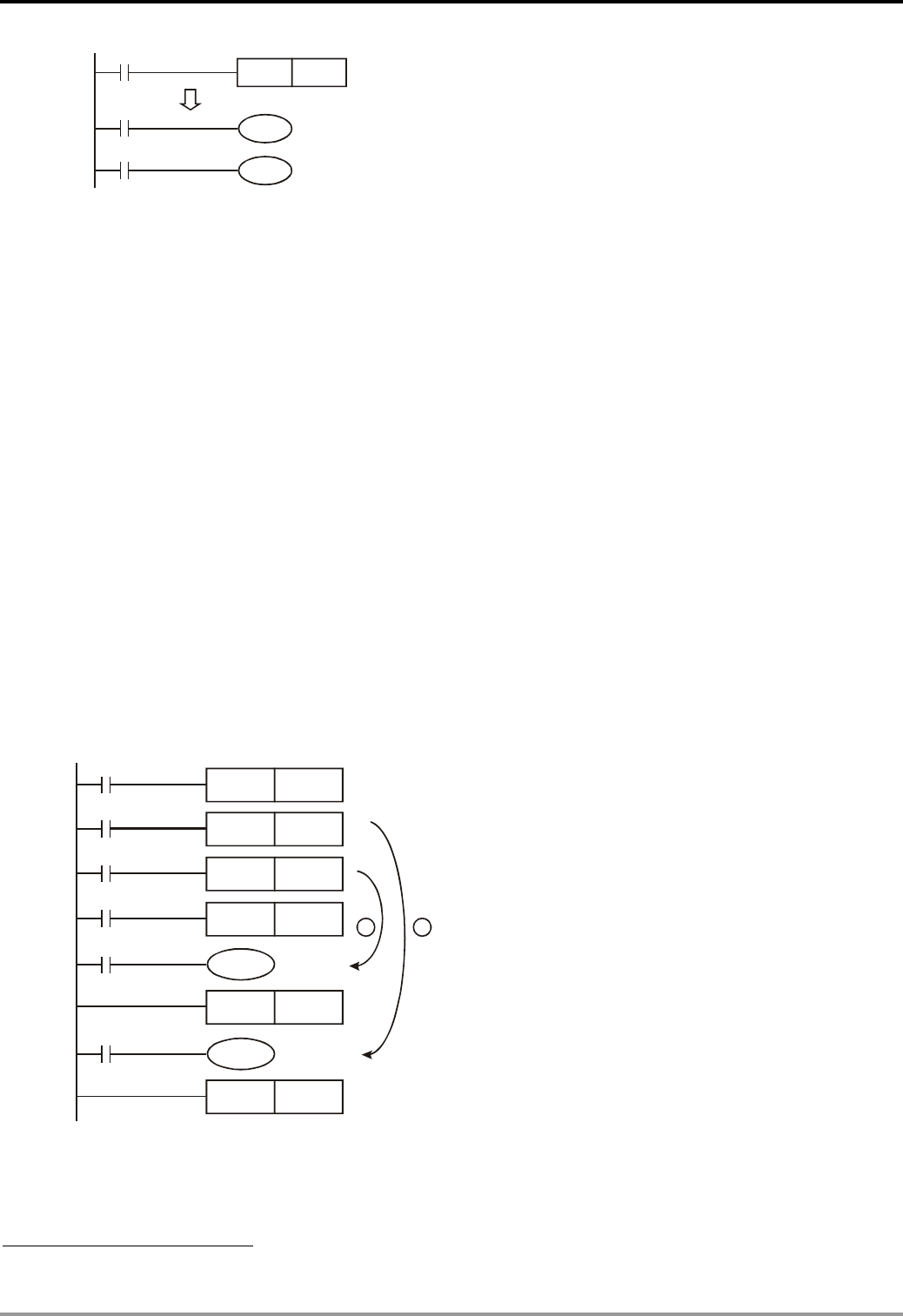
6 Application Instructions API 00-49
DVP-PLC Application Manual
6-2
X0
X1
X2
CJ P1
Y1
Y2
0
NP1
P***
()
CJ instruction
Program Example 2:
1. CJ instruction can be used in the following 5 conditions between MC and MCR instructions.
a) Without MC ~ MCR.
b) From without MC to within MC. Valid in the loop P1 as shown in the figure below.
c) In the same level N, inside of MC~MCR.
d) From within MC to without MCR.
e) Jumping from this MC ~ MCR to another MC ~ MCR1.
2. Actions in ES/EX/SS series models V4.7 (and below): When CJ instruction is used between MC and MCR, it
can only be applied without MC ~ MCR or in the same N layer of MC ~ MCR. Jumping from this MC ~ MCR to
another MC ~ MCR will result in errors, i.e. a) and c) as stated above can ensure correct actions; others will
cause errors.
3. When MC instruction is executed, PLC will push the status of the switch contact into the self-defined stack in
PLC. The stack will be controlled by the PLC, and the user cannot change it. When MCR instruction is executed,
PLC will obtain the previous status of the switch contact from the top layer of the stack. Under the conditions as
stated in b), d) and e), the times of pushing-in and obtaining stack may be different. In this case, the maximum
stack available to be pushed in is 8 and the obtaining of stacks cannot resume once the stack becomes empty.
Thus, when using CALL or CJ instructions, the user has to be aware of the pushing-in and obtaining of stacks.
X0
MC N0
X2
X3
X1
M1000
M1000
P1
P0
CJ
CJ
MC N1
N1
N0
P1
P0
Y1
Y0
MCR
MCR
1 This function is only available in ES/EX/SS series models V4.9 (and above) and SA/SX/SC/EH/EH2/SV series models.

6 Application Instructions API 00-49
DVP-PLC Application Manual 6-3
Program Example 3:
1. The states of each device
Device Contact state before CJ
is executed
Contact state when CJ is
being executed
Output coil state when CJ is
being executed
M1, M2, M3 Off M1, M2, M3 OfftOn Y1 *1, M20, S1 Off
Y, M , S
M1, M2, M3 On M1, M2, M3 OntOff Y1 *1, M20, S1 On
M4 Off M4 OfftOn Timer T0 is not enabled.
10ms, 100ms
Timer
ES/SA/EH M4 On M4 OntOff
Timer T0 immediately stops
and is latched. M0 OntOff,
T0 is reset as 0.
M6 Off M6 OfftOn Timer T240 is not enabled.
1ms, 10ms, 100ms
Timer *2
(accumulative)
SA/EH M6 On M6 OntOff
Once the timer function is
enabled and when met with
CJ instruction, all
accumulative timers will stop
timing and stay latched. M0
OntOff. T240 remains
unchanged.
M7, M10 Off M10 On/Off trigger Counter does not count.
C0 ~ C234 *3 M7 Off, M10 On/Off
trigger M10 On/Off trigger
Counter C0 stops counting
and stays latched. After M0
goes Off, C0 resumes its
counting.
M11 Off M11 OfftOn Application instructions are
not executed.
Application
instruction M11 On M11 OntOff
The skipped application
instructions are not executed,
but API 53 ~ 59, API 157 ~
159 keep being executed.
*1: Y1 is a dual output. When M0 is Off, M1 will control Y1. When M0 is On, M12 will control Y1.
*2: When the timers (T192 ~ T199, applicable in SA/EH series MPU) used by a subroutine re driven and encounter
the execution of CJ instruction, the timing will resume. After the timing target is reached, the output contact of the
timer will be On.
*3: When the high-speed counters (C235 ~ C255) are driven and encounter the execution of CJ instruction, the
counting will resume, as well as the action of the output points.
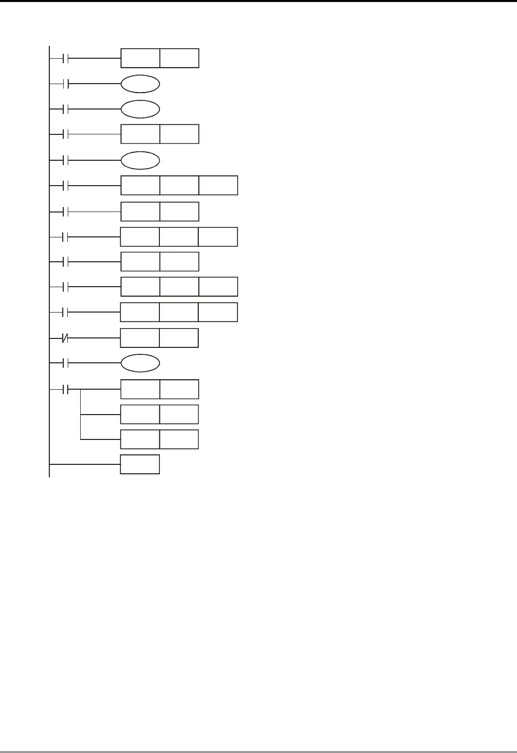
6 Application Instructions API 00-49
DVP-PLC Application Manual
6-4
2. Y1 is a dual output. When M0 = Off, Y1 is controlled by M1. When M0 = On, Y1 is controlled by M12.
CJ P0
M0
M1
M2
M17
M3
M4
M5
M6
M7
M10
M11
M0
M12
M13
END
RST
RST
RST T127
C0
D0
Y1
CJ P0
CJ P63
S1
TMR T0 K10
TMR
RST
RST
CNT
MOV
T127
T127
C0
C0
D0K3
K20
Y1
M20
K1000
P0
P63
6 Application Instructions API 00-49
DVP-PLC Application Manual 6-5
API Mnemonic Operands Function
01
CALL P Call Subroutine
OP Range Program Steps
P0 ~ P255 CALL, CALLP: 3 steps
PULSE 16-bit 32-bit
ES EX SS SA SX SC EH SV EH3
SV2 ES EX SS SA SX SC EH SV EH3
SV2 ES EX SS SA SX SC EH SV EH3
SV2
Operands:
S: The pointer of call subroutine.
Explanations:
1. Operand S can designate P.
2. P can be modified by index register E, F.
3. In ES/EX/SS series models: Operand S can designate P0 ~ P63.
4. In SA/SX/SC/EH/EH2/SV series models: Operand S can designate P0 ~ P255.
5. Edit the subroutine designated by the pointer after FEND instruction.
6. The number of pointer P, when used by CALL, cannot be the same as the number designated by CJ instruction.
7. If only CALL instruction is in use, it can call subroutines of the same pointer number with no limit on times.
8. Subroutine can be nested for 5 levels including the initial CALL instruction. (If entering the sixth level, the
subroutine won’t be executed.)
API Mnemonic Function
02
SRET Subroutine Return
OP Descriptions Program Steps
N/A Automatically returns to the step immediately following the
CALL instruction which activated the subroutine
SRET: 1 steps
PULSE 16-bit 32-bit
ES EX SS SA SX SC EH SV EH3
SV2 ES EX SS SA SX SC EH SV EH3
SV2 ES EX SS SA SX SC EH SV EH3
SV2
Explanations:
1. No operand. No contact to drive the instruction is required.
2. The subroutine will return to main program by SRET after the termination of subroutine and execute the
sequence program located at the next step to the CALL instruction.
Program Example 1:
When X0 = On, CALL instruction is executed and the program jumps to the subroutine designated by P2. When
SRET instruction is executed, the program returns to address 24 and continues its execution.

6 Application Instructions API 00-49
DVP-PLC Application Manual
6-6
X0
X1
CALL P2
Y1
20
P***
24
FEND
SRET
P2 Y0
Y0
Subroutine P2
subroutine return
call subroutine P***
Program Example 2:
1. When X10 goes from Off to On, its rising-edge trigger executes CALL P10 instruction and the program jumps to
the subroutine designated by P10.
2. When X11 is On, CALL P11 is executed and the program jumps to the subroutine designated by P11.
3. When X12 is On, CALL P12 is executed and the program jumps to the subroutine designated by P12.
4. When X13 is On, CALL P13 is executed and the program jumps to the subroutine designated by P13.
5. When X14 is On, CALL P14 is executed and the program jumps to the subroutine designated by P14. When
SRET is executed, the program returns to the previous P※ subroutine and continues its execution.
6. After SRET instruction is executed in P10 subroutine, returning to the main program.
6 Application Instructions API 00-49
DVP-PLC Application Manual 6-7
X0
X10
INC D0
Y0
CALL P10
X0
INC D1
Y1
FEND
INC D10
X2
P10
Y4
X2
X11
CALL P11
INC D11
Y5
SRET
INC D20
X2
P11
Y6
X12
CALL P12
X2
INC D21
Y7
SRET
X2
X13
X2
X2
X2
X14
X2
P13
P14
P12 INC D30
Y10
CALL P13
INC D31
Y11
SRET
INC D40
Y12
CALL P14
INC D41
Y13
SRET
INC D50
Y14
SRET
END
Main
Program
Main
Program
subroutine
subroutine
subroutine
subroutine
subroutine
6 Application Instructions API 00-49
DVP-PLC Application Manual
6-8
API Mnemonic Function
03
IRET Interrupt Return
OP Descriptions Program Steps
N/A IRET ends the processing of an interruption subroutine and
returns to the execution of the main program.
IRET: 1 steps
PULSE 16-bit 32-bit
ES EX SS SA SX SC EH SV EH3
SV2 ES EX SS SA SX SC EH SV EH3
SV2 ES EX SS SA SX SC EH SV EH3
SV2
Explanations:
1. No operand. No contact to drive the instruction is required.
2. Interruption return refers to interrupt the subroutine.
3. After the interruption is over, returning to the main program from IRET to execute the next instruction where the
program was interrupted.
API Mnemonic Function
04
EI Enable Interrupts
OP Descriptions Program Steps
N/A See more details of the explanation on this instruction in DI
(Disable Interruption) instruction.
EI: 1 steps
PULSE 16-bit 32-bit
ES EX SS SA SX SC EH SV EH3
SV2 ES EX SS SA SX SC EH SV EH3
SV2 ES EX SS SA SX SC EH SV EH3
SV2
Explanations:
1. No operand. No contact to drive the instruction is required.
2. The pulse width of the interruption signal should be >200us.
3. See DI instruction for the range of the No. of I for all models.
4. See DI instruction for more details about M1050 ~ M1059, M1280 ~ M1299.
API Mnemonic Function
05
DI Disable Interrupts
OP Descriptions Program Steps
N/A
When the special auxiliary relay M1050 ~ M1059, M1280 ~
M1299 for disabling interruption is driven, the corresponding
interruption request will not be executed even in the range
allowed for interruptions.
DI: 1 step
PULSE 16-bit 32-bit
ES EX SS SA SX SC EH SV EH3
SV2 ES EX SS SA SX SC EH SV EH3
SV2 ES EX SS SA SX SC EH SV EH3
SV2
Explanations:
1. No operand. No contact to drive the instruction is required.
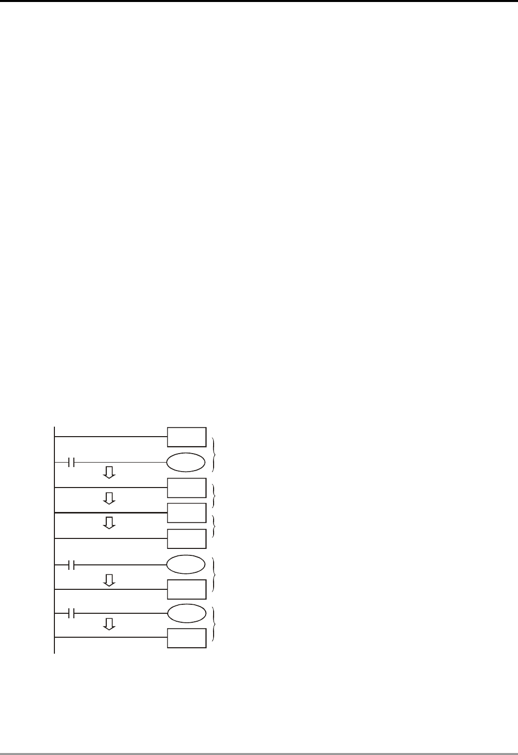
6 Application Instructions API 00-49
DVP-PLC Application Manual 6-9
2. EI instruction allows interrupting subroutine in the program, e.g. external interruption, timed interruption, and
high-speed counter interruption.
3. In the program, using interruption subroutine between EI and DI instruction is allowed. However, you can
choose not to use DI instruction if there is no interruption-disabling section in the program.
4. When M1050 ~ M1059 are the special auxiliary relays to drive disabling interruption in ES/SA, or M1280 ~
M1299 are the special auxiliary relays to drive disabling interruption in EH/EH2/SV, the corresponding
interruptions will not be executed even in the area allowed for interruptions.
5. Pointer for interruption (I) must be placed after FEND instruction.
6. Other interruptions are not allowed during the execution of interruption subroutine.
7. When many interruptions occur, the priority is given to the firstly executed interruption. If several interruptions
occur simultaneously, the priority is given to the interruption with the smaller pointer No.
8. The interruption request occurring between DI and EI instructions that cannot be executed immediately will be
memorized and will be executed in the area allowed for interruption.
9. The time interruptions in ES/SA will not be memorized.
10. When using the interruption pointer, DO NOT repeatedly use the high-speed counter driven by the same X input
contact.
11. When immediate I/O is required during the interruption, write REF instruction in the program to update the status
of I/O.
Program Example:
During the operation of PLC, when the program scans to the area between EI and DI instructions and X1 = Off→On
or X2 = Off→On, interruption subroutine A or B will be executed. When the subroutine executes to IRET, the program
will return to the main program and resumes its execution.
I 101
I 201
Y1
EI
FEND
X0
DI
IRET
IRET
Y0
Y0
EI
Disable interruption
Enable interruption
Enable interruption
Interruption subroutine A
Interruption subroutine B
Remarks:
1. No. of interruption pointer I in ES/EX/SS:

6 Application Instructions API 00-49
DVP-PLC Application Manual
6-10
a) External interruptions: (I001, X0), (I101, X1), (I201, X2), (I301, X3) 4 points2.
b) Time interruptions: I6□□, 1 point (□□ = 10 ~ 99, time base = 1ms) (support V5.7 and above)
c) Communication interruption for receiving specific words (I150) (support V5.7 and above)
2. No. of interruption pointer I in SA/SX/SC:
a) External interruptions: (I001, X0), (I101, X1), (I201, X2), (I301, X3), (I401, X4), (I501, X5) 6 points.
b) Time interruptions: I6□□, I7□□ 2 points. (□□ = 1 ~ 99ms, time base = 1ms)
c) High-speed counter interruptions: I010, I020, I030, I040 4 points. (used with API 53 DHSCS instruction to
generate interruption signals)
d) Communication interruption for receiving specific words .(I150)
e) The order for execution of interruption pointer I: high-speed counter interruption, external interruption, time
interruption and communication interruption for receiving specific words.
f) Among the following 6 interruption No., (I001, I010), (I101, I020), (I201, I030), (I301, I040), (I401, I050), (I501,
I060), the program allows the user to use only one of the two numbers in a pair. If the user uses the two
numbers in the pair, grammar check errors may occur when the program is written into PLC.
3. No. of interruption pointer I in EH/EH2/SV:
a) External interruptions: (I00□, X0), (I10□, X1), (I20□, X2), (I30□, X3), (I40□, X4), (I50□, X5) 6 points. (□ = 0
designates interruption in falling-edge, □ = 1 designates interruption in rising-edge)
b) Time interruptions: I6□□, I7□□, 2 points. (□□ = 1~99ms, time base = 1ms)
I8□□ 1 point. (□□ = 1 ~ 99ms, time base = 0.1ms)
c) High-speed counter interruptions: I010, I020, I030, I040, 1050, 1060 6 points. (used with API 53 DHSCS
instruction to generate interruption signals)
d) When pulse output interruptions I110, I120 (triggered when pulse output is finished), I130, I140 (triggered when
the first pulse output starts) are executed, the currently executed program is interrupted and jumps to the
designated interruption subroutine.
e) Communication interruption: I150, I160, I170
f) Frequency measurement card interruption: I180
g) The order for execution of interruption pointer I: external interruption, time interruption, high-speed counter
interruption, pulse interruption, communication interruption and frequency measurement card interruption.
4. No. of interruption pointer I in EH3/SV2:
a) External interruptions: (I00□, X0), (I10□, X1), (I20□, X2), (I30□, X3), (I40□, X4), (I50□, X5), (I60□, X6),
(I70□, X7), (I90□, X10), (I91□, X11), (I92□, X12), (I93□, X13), (I94□, X14), (I95□, X15), (I96□, X16), (I97□,
X17) 16 points. (□ = 0 designates interruption in falling-edge, □ = 1 designates interruption in rising-edge)
b) Time interruptions: I6□□, I7□□, 2 points. (□□ = 2~99ms, time base = 1ms)
I8□□ 1 point. (□□ = 1 ~ 99ms, time base = 0.1ms)
c) High-speed counter interruptions: I010, I020, I030, I040, 1050, 1060 6 points. (used with API 53 DHSCS
instruction to generate interruption signals)
d) When pulse output interruptions I110, I120 (triggered when pulse output is finished), I130, I140 (triggered when
the first pulse output starts) are executed, the currently executed program is interrupted and jumps to the
2 Input points occupied by external interruptions cannot be used for inputs of high-speed counters; otherwise grammar check errors may occur
when the program is written in PLC.

6 Application Instructions API 00-49
DVP-PLC Application Manual 6-11
designated interruption subroutine.
e) Communication interruption: I150, I160, I170
f) The order for execution of interruption pointer I: external interruption, time interruption, high-speed counter
interruption, pulse interruption, and communication interruption.
5. “Disable interruption” flags in ES/EX/SS:
Flag Function
M1050 Disable external interruption I001
M1051 Disable external interruption I101
M1052 Disable external interruption I201
M1053 Disable external interruption I301
M1056 Disable time interruption I6□□
6. “Disable interruption” flags in SA/SX/SC:
Flag Function
M1050 Disable external interruption I001
M1051 Disable external interruption I101
M1052 Disable external interruption I201
M1053 Disable external interruption I301
M1054 Disable external interruption I401
M1055 Disable external interruption I501
M1056 Disable time interruption I6□□
M1057 Disable time interruption I7□□
M1059 Disable high-speed counter interruption I010 ~ I060
7. “Disable interruption” flags in EH/EH2/SV/EH3/SV2:
Flag Function
M1280 Disable external interruption I00□
M1281 Disable external interruption I10□
M1282 Disable external interruption I20□
M1283 Disable external interruption I30□
M1284 Disable external interruption I40□
M1285 Disable external interruption I50□
M1286 Disable time interruption I6□□
M1287 Disable time interruption I7□□
M1288 Disable time interruption I8□□
M1289 Disable high-speed counter interruption I010
M1290 Disable high-speed counter interruption I020
M1291 Disable high-speed counter interruption I030
M1292 Disable high-speed counter interruption I040
M1293 Disable high-speed counter interruption I050
M1294 Disable high-speed counter interruption I060
M1295 Disable pulse output interruption I110
M1296 Disable pulse output interruption I120
M1297 Disable pulse output interruption I130
M1298 Disable pulse output interruption I140
M1299 Disable communication interruption I150
M1300 Disable communication interruption I160

6 Application Instructions API 00-49
DVP-PLC Application Manual
6-12
Flag Function
M1301 Disable communication interruption I170
M1302 Disable frequency measurement card interruption I180
M1340 Generate interruption I110 after CH0 pulse is sent
M1341 Generate interruption I120 after CH1 pulse is sent
M1342 Generate interruption I130 when CH0 pulse is being sent
M1343 Generate interruption I140 when CH1 pulse is being sent
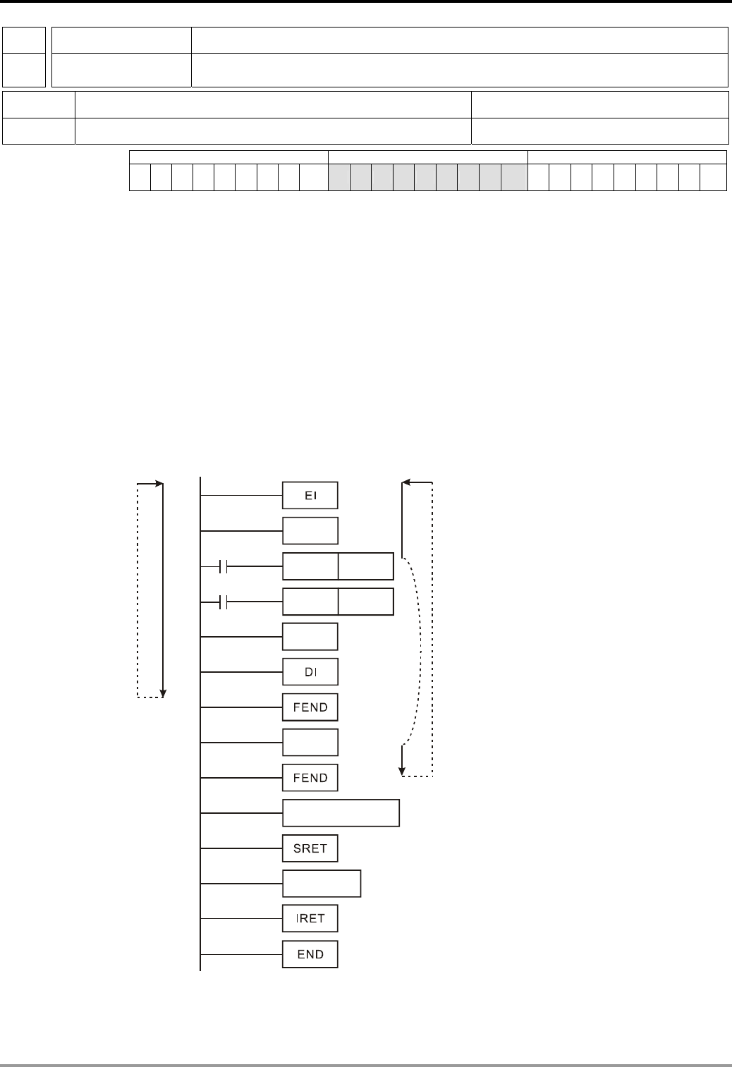
6 Application Instructions API 00-49
DVP-PLC Application Manual 6-13
API Mnemonic Function
06
FEND The End of The Main Program (First End)
OP Descriptions Program Steps
N/A No contact to drive the instruction is required. FEND: 1 steps
PULSE 16-bit 32-bit
ES EX SS SA SX SC EH SV EH3
SV2 ES EX SS SA SX SC EH SV EH3
SV2 ES EX SS SA SX SC EH SV EH3
SV2
Explanations:
1. This instruction denotes the end of the main program. It has the same function as that of END instruction when
being executed by PLC.
2. CALL must be written after FEND instruction and add SRET instruction in the end of its subroutine. Interruption
program has to be written after FEND instruction and IRET must be added in the end of the service program.
3. If several FEND instructions are in use, place the subroutine and interruption service programs between the
final FEND and END instruction.
4. After CALL instruction is executed, executing FEND before SRET will result in errors in the program.
5. After FOR instruction is executed, executing FEND before NEXT will result in errors in the program.
CJ Instruction Program Flow:
X1
CALL P63
P0
P63
CJ P0
I301
X0
0
The program flow
when X0=off,
X1=off main
program
main
program
main
program
The program flow when X=On
and the program jumps to P0.
Interruption
subroutine
CALL instruction
subroutine
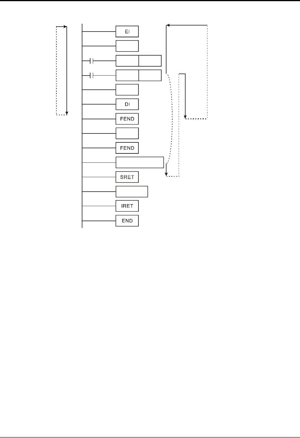
6 Application Instructions API 00-49
DVP-PLC Application Manual
6-14
CALL Instruction Program Flow:
X1
CALL P63
P0
P63
CJ P0
I301
X0
0
The program flow
when X0=off,
X1=off main
program
main
program
main
program
The program flow
when X0=Off,
X1=On.
Interruption
subroutine
CALL instruction
subroutine
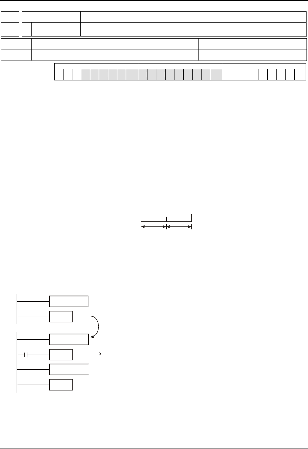
6 Application Instructions API 00-49
DVP-PLC Application Manual 6-15
API Mnemonic Function
07
WDT P Watchdog Timer Refresh
OP Descriptions Program Steps
N/A WDT, WDTP: 1 steps
PULSE 16-bit 32-bit
ES EX SS SA SX SC EH SV EH3
SV2 ES EX SS SA SX SC EH SV EH3
SV2 ES EX SS SA SX SC EH SV EH3
SV2
Explanations:
1. No operand.
2. The watchdog timer in DVP series PLCs is used for monitoring the operation of the PLC system.
3. WDT instruction can be used to reset Watch Dog Timer. If the PLC scan time (from step 0 to END or when
FEND instruction is executed) exceeds 200ms, PLC ERROR LED will flash. The user will have to turn off PLC
and back On again. PLC will determine RUN/STOP status by RUN/STOP switch. If there is no RUN/STOP
switch, PLC will return to STOP status automatically.
4. When to use WDT:
a) When errors occur in the PLC system.
b) When the executing time of the program is too long, resulting in the scan time being larger than the content in
D1000, the user can improve the problem by the following two methods.
Using WDT instruction
t1 t2
STEP0 END(FEND)
WDT
Using the set value in D1000 (default value: 200ms) to change the time for watchdog.
Program Example:
Assume the scan time of the program is 300ms, divide the program into two parts and place WDT instruction in the
middle of the two parts, making scan time of the first half and second half of the program being less than 200ms.
X0
END
END
WDT
300ms program
150ms program
150ms program
Dividing the program to two parts
so that both parts' scan time are
less than 200ms.
Watchdog timer reset
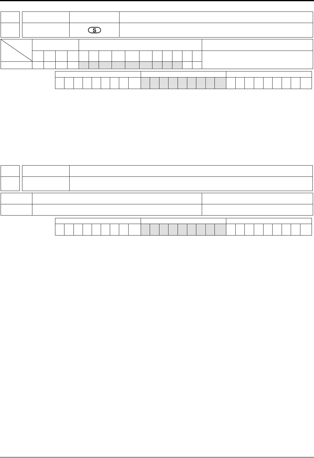
6 Application Instructions API 00-49
DVP-PLC Application Manual
6-16
API Mnemonic Operands Function
08
FOR Start of a FOR-NEXT Loop
Bit Devices Word Devices Program Steps Type
OP X Y M S K H KnX KnY KnM KnS T C D E F
S * ** * * * * * ***
FOR: 3 steps
PULSE 16-bit 32-bit
ES EX SS SA SX SC EH SV EH3
SV2 ES EX SS SA SX SC EH SV EH3
SV2 ES EX SS SA SX SC EH SV EH3
SV2
Operands:
S: The number of repeated nested loops
Explanations:
1. No contact to drive the instruction is required.
2. See the specifications of each model for their range of use.
API Mnemonic Function
09
NEXT End of a FOR-NEXT Loop
OP Descriptions Program Steps
N/A NEXT: 1 steps
PULSE 16-bit 32-bit
ES EX SS SA SX SC EH SV EH3
SV2 ES EX SS SA SX SC EH SV EH3
SV2 ES EX SS SA SX SC EH SV EH3
SV2
Explanations:
1. No operand. No contact to drive the instruction is required.
2. FOR instruction indicates FOR ~ NEXT loops executing back and forth N times before escaping for the next
execution.
3. N = K1 ~ K32,767. N is regarded as K1 when N ≤ 1.
4. When FOR~NEXT loops are not executed, the user can use the CJ instruction to escape the loops.
5. Error will occur when
a) NEXT instruction is before FOR instruction.
b) FOR instruction exists but NEXT instruction does not exist.
c) There is NEXT instruction after FEND or END instruction.
d) The number of instructions between FOR ~ NEXT differs.
6. FOR~NEXT loops can be nested for maximum five levels. Be careful that if there are too many loops, the
increased PLC scan time may cause timeout of watchdog timer and error. Users can use WDT instruction to
modify this problem.
Program Example 1:
After program A has been executed for 3 times, it will resume its execution after NEXT instruction. Program B will be
executed for 4 times whenever program A is executed once. Therefore, program B will be executed 3 × 4 = 12 times
in total.
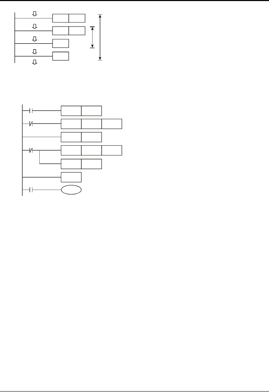
6 Application Instructions API 00-49
DVP-PLC Application Manual 6-17
FOR K3
FOR K4
NEXT
NEXT
AB
Program Example 2:
When X7 = Off, PLC will execute the program between FOR ~ NEXT. When X7 = On, CJ instruction jumps to P6 and
avoids executing the programs between FOR ~ NEXT.
X7
M0
M0
P6
MOV
FOR
MOV D0
D0
K3
K0
Y10
INC
MEXT
X10
D0
D1
CJ P6
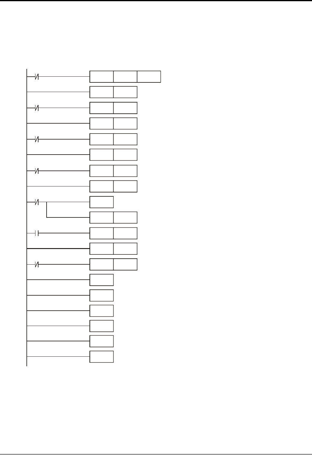
6 Application Instructions API 00-49
DVP-PLC Application Manual
6-18
Program Example 3:
When the programs between FOR ~ NEXT are not to be executed, the user can adopt CJ instruction for a jumping.
When the most inner FOR ~ NEXT loop is in the status of X1 = On, CJ instruction executes jumping to P0 and skips
the execution on P0.
X0
TMR T0 K10
P0
FOR K4X100
X0
INC D0
K2
X0
D1
K3
X0
D2
K4
X0
WDT
D3
X1
CJ P0
FOR K5
X0
INC D4
NEXT
NEXT
NEXT
NEXT
NEXT
END
FOR
INC
FOR
INC
FOR
INC
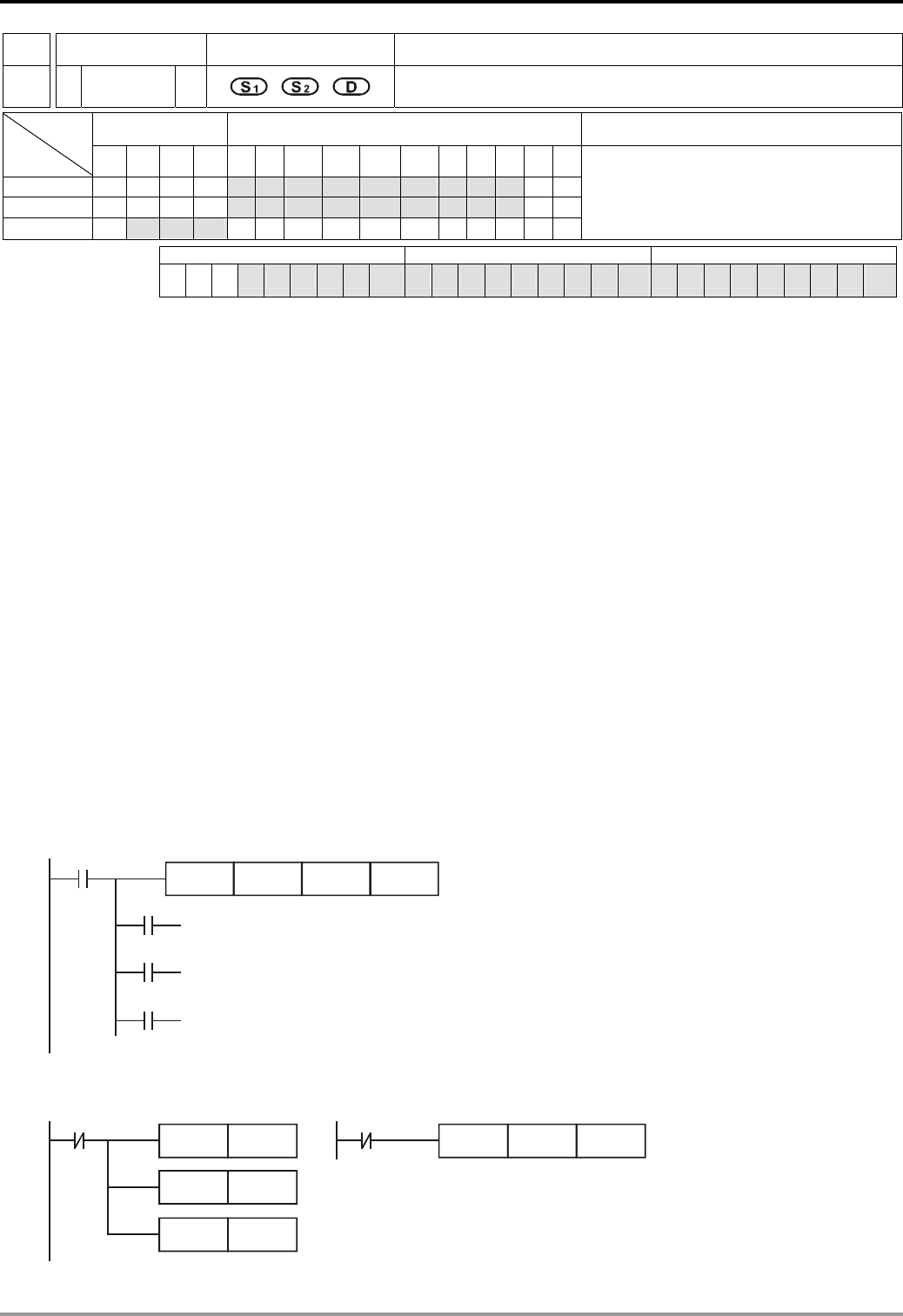
6 Application Instructions API 00-49
DVP-PLC Application Manual 6-19
API Mnemonic Operands Function
10
D CMP P Compare
Bit Devices Word Devices Program Steps Type
OP X Y M S K H KnX KnY KnM KnS T C D E F
S1 * * * ** * *****
S2 * * * ** * *****
D * * *
CMP, CMPP: 7 steps
DCMP, DCMPP: 13 steps
PULSE 16-bit 32-bit
ES EX SS SA SX SC EH SV EH3
SV2 ES EX SS SA SX SC EH SV EH3
SV2 ES EX SS SA SX SC EH SV EH3
SV2
Operands:
S1: Comparison Value 1 S2: Comparison Value 2 D: Comparison result
Explanations:
1. If S1 and S2 are used in device F, only 16-bit instruction is applicable.
2. Operand D occupies 3 consecutive devices.
3. See the specifications of each model for their range of use.
4. The contents in S1 and S2 are compared and the result will be stored in D.
5. The two comparison values are compared algebraically and the two values are signed binary values. When b15
= 1 in 16-bit instruction or b31 = 1 in 32-bit instruction, the comparison will regard the value as negative binary
values.
Program Example:
1. Designate device Y0, and operand D automatically occupies Y0, Y1, and Y2.
2. When X10 = On, CMP instruction will be executed and one of Y0, Y1, and Y2 will be On. When X10 = Off, CMP
instruction will not be executed and Y0, Y1, and Y2 remain their status before X10 = Off.
3. If the user need to obtain a comparison result with ≥ ≤, and ≠, make a series parallel connection between Y0 ~
Y2.
X10
Y0
Y1
Y2
CMP K10 D10 Y0
If K10>D10, Y0 = On
If K10=D10, Y1 = On
If K10<D10, Y2= On
4. To clear the comparison result, use RST or ZRST instruction.
X10
RST M0
RST
RST
M1
M2
X10
ZRST M0 M2
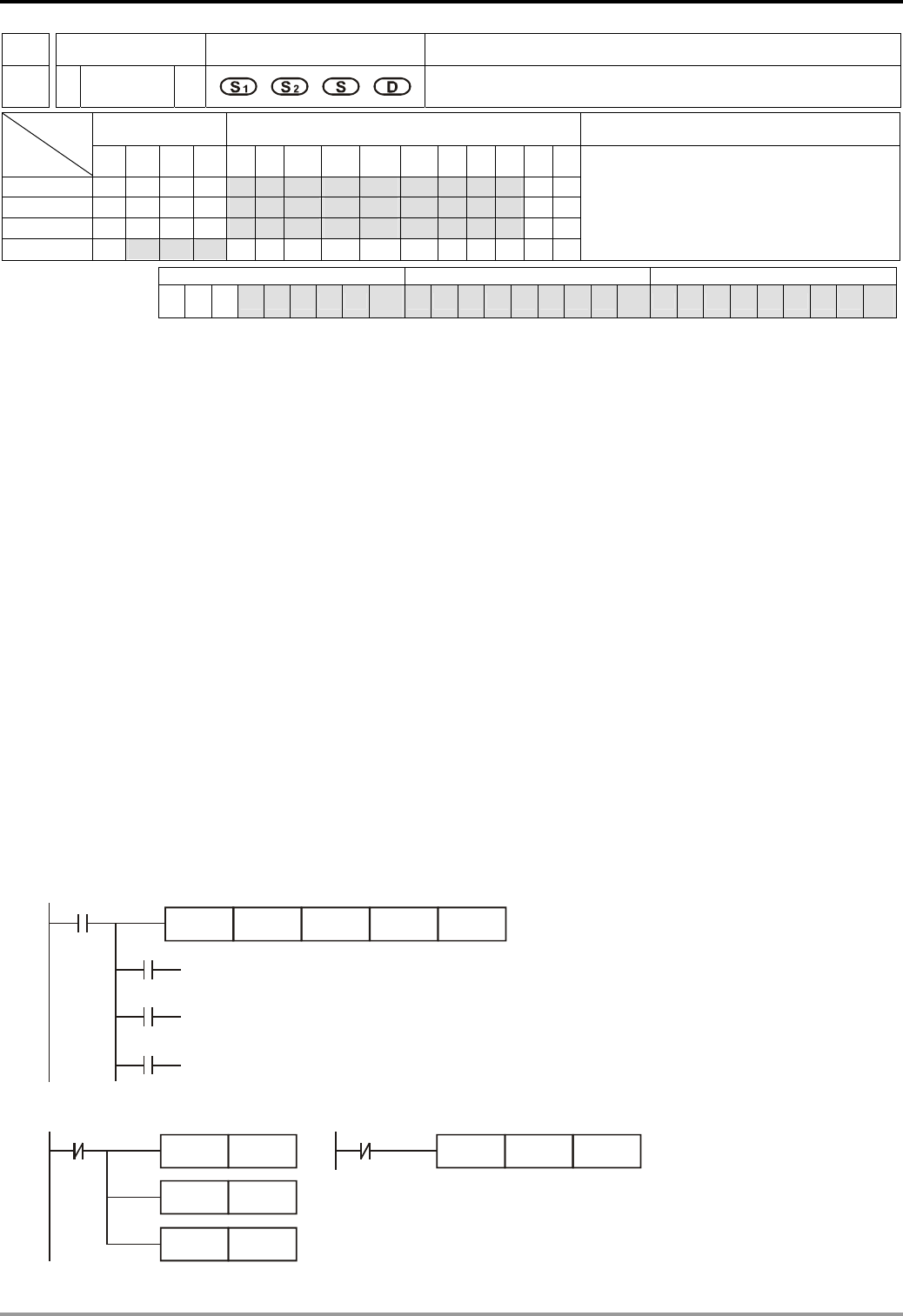
6 Application Instructions API 00-49
DVP-PLC Application Manual
6-20
API Mnemonic Operands Function
11
D ZCP P Zone Compare
Bit Devices Word Devices Program Steps Type
OP X Y M S K H KnX KnY KnM KnS T C D E F
S1 * ** * * * * * ***
S2 * ** * * * * * ***
S * ** * * * * * ***
D * * *
ZCP, ZCPP: 9 steps
DZCP, DZCPP: 17 steps
PULSE 16-bit 32-bit
ES EX SS SA SX SC EH SV EH3
SV2 ES EX SS SA SX SC EH SV EH3
SV2 ES EX SS SA SX SC EH SV EH3
SV2
Operands:
S1: Lower bound of zone comparison S2: Upper bound of zone comparison S: Comparison value
D: Comparison result
Explanations:
1. If S1, S2 and S are used in device F, only 16-bit instruction is applicable.
2. The content in S1 should be smaller than the content in S2.
3. Operand D occupies 3 consecutive devices.
4. See the specifications of each model for their range of use.
5. S is compared with its S1, S2 and the result is stored in D.
6. When S1 > S2, the instruction performs comparison by using S1 as the lower/upper bound.
7. The two comparison values are compared algebraically and the two values are signed binary values. When b15
= 1 in 16-bit instruction or b31 = 1 in 32-bit instruction, the comparison will regard the value as negative binary
values.
Program Example:
1. Designate device M0, and operand D automatically occupies M0, M1 and M2.
2. When X0 = On, ZCP instruction will be executed and one of M0, M1, and M2 will be On. When X0 = Off, ZCP
instruction will not be executed and M0, M1, and M2 remain their status before X0 = Off.
X0
M0
M1
M2
ZCP
If C10 < K10, M0 = On
If K10 < C10 < K100, M1 = On
If C10 > K100, M2 = On
X0
K10 C10 M0K100
==
3. To clear the comparison result, use RST or ZRST instruction.
X0
RST M0
RST
RST
M1
M2
X0
ZRST M0 M2
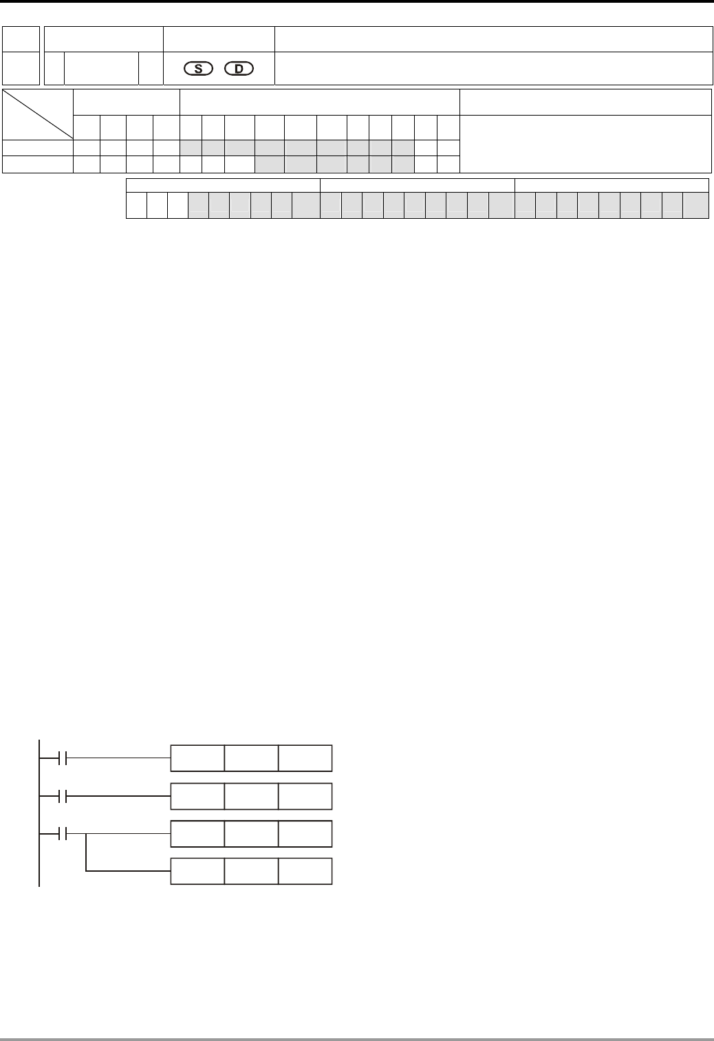
6 Application Instructions API 00-49
DVP-PLC Application Manual 6-21
API Mnemonic Operands Function
12
D MOV P Move
Bit Devices Word Devices Program Steps Type
OP X Y M S K H KnX KnY KnM KnS T C D E F
S * * * ** * *****
D ** * *****
MOV, MOVP: 5 steps
DMOV, DMOVP: 9 steps
PULSE 16-bit 32-bit
ES EX SS SA SX SC EH SV EH3
SV2 ES EX SS SA SX SC EH SV EH3
SV2 ES EX SS SA SX SC EH SV EH3
SV2
Operands:
S: Source of data D: Destination of data
Explanations:
1. If S and D are used in device F, only 16-bit instruction is applicable.
2. See the specifications of each model for their range of use.
3. When this instruction is executed, the content of S will be moved directly to D. When this instruction is not
executed, the content of D remains unchanged.
4. If the operation result refers to a 32-bit output, (i.e. application instruction MUL and so on), and the user needs
to move the present value in the 32-bit high-speed counter, DMOV instruction has to be adopted.
Program Example:
1. MOV instruction has to be adopted in the moving of 16-bit data.
a) When X0 = Off, the content in D10 will remain unchanged. If X0 = On, the value K10 will be moved to D10 data
register.
b) When X1 = Off, the content in D10 will remain unchanged. If X1 = On, the present value T0 will be moved to
D10 data register.
2. DMOV instruction has to be adopted in the moving of 32-bit data.
When X2 = Off, the content in (D31, D30) and (D41, D40) will remain unchanged. If X2 = On, the present value
of (D21, D20) will be sent to (D31, D30) data register. Meanwhile, the present value of C235 will be moved to
(D41, D40) data register.
X0
X1
X2
MOV K10 D0
MOV T0 D10
DMOV D20 D30
DMOV C235 D40
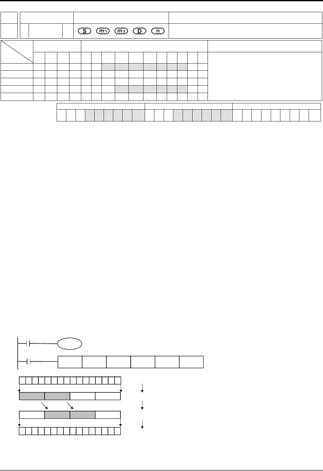
6 Application Instructions API 00-49
DVP-PLC Application Manual
6-22
API Mnemonic Operands Function
13
SMOV P Shift Move
Bit Devices Word Devices Program Steps Type
OP X Y M S K H KnX KnY KnM KnS T C D E F
S * * * * * * ***
m1 * *
m2 * *
D * * * * * ***
n * *
SMOV, SMOVP: 11 steps
PULSE 16-bit 32-bit
ES EX SS SA SX SC EH SV EH3
SV2 ES EX SS SA SX SC EH SV EH3
SV2 ES EX SS SA SX SC EH SV EH3
SV2
Operands:
S: Source of data m1: Start digit to be moved of the source data m2: Number of digits (nibbles) to be moved of the
source data D: Destination device n: Start digit of the destination position for the moved digits
Explanations:
1. This instruction is able to re-allocate or combine data. When the instruction is executed, m2 digits of contents
starting from digit m1 (from high digit to low digit) of S will be sent to m2 digits starting from digit n (from high digit
to low digit) of D.
2. Range: m1 = 1 ~ 4; m2 = 1 ~ m1; n = m2 ~ 4
3. See the specifications of each model for their range of use.
4. M1168 is designated by SMOV working mode. When M1168 = On, the program is in BIN mode. When M1168 =
Off, the program is in BCD mode.
Program Example 1:
1. When M1168 = Off (in BCD mode) and X0 = On, the 4th (thousand) and 3rd (hundred) digit of the decimal value
in D10 start to move to the 3rd (hundred) and 2nd (ten) digit of the decimal value in D20. 103 and 100 of D20
remain unchanged after this instruction is executed.
2. When the BCD value exceeds the range of 0 ~ 9,999, PLC will determine an operation error and will not execute
the instruction. M1067, M1068 = On and D1067 records the error code OE18 (hex).
M1168
10
3
10
2
10
1
10
0
10
3
10
2
10
1
10
0
Unchanged Unchanged
D10(BIN 16 bits)
D10(BCD 4 digits)
D20(BIN 16 bits)
D20(BCD 4 digits)
Shift move
Auto conversion
Auto conversion
M100
1
X0
SMOV D10 K2 D20 K3K4
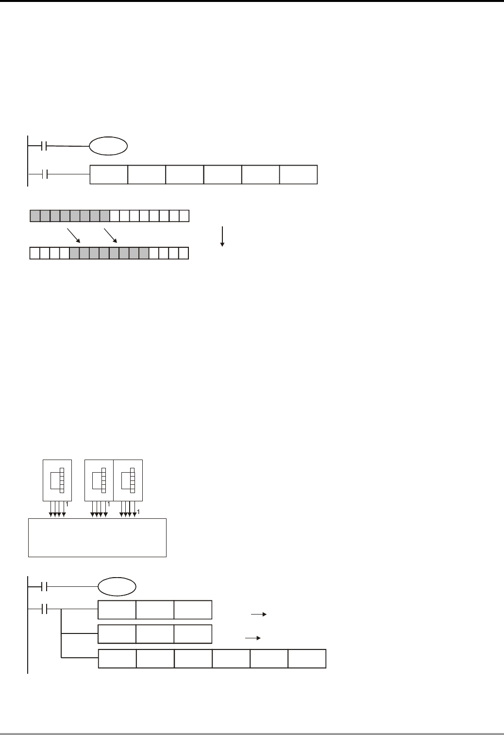
6 Application Instructions API 00-49
DVP-PLC Application Manual 6-23
Before the execution, assume D10 = K1234 and D20 = K5678. After the execution, D10 will remain unchanged and
D20 will become K5128.
Program Example 2:
When M1168 = On (in BIN mode) and SMOV instruction is in use, D10 and D20 will not be converted in BCD format
but be moved in BIN format (4 digits as a unit).
Unchanged
U
nchanged
D10(BIN 16 bits)
D20(BIN 16 bits)
Moving digits
M100
0
X0
Digit 4 Digit 3 Digit 2 Digit 1
Digit 4 Digit 3 Digit 2 Digit 1
M1168
SMOV D10 K2 D20 K3K4
Before the execution, assume D10 = H1234 and D20 = H5678. After the execution, D10 will remain unchanged and
D20 will become H5128.
Program Example 3:
1. This instruction can be used to combine the DIP switches connected to the input terminals with interrupted No.
2. Move the 2nd right digit of the DIP switch to the 2nd right digit of D2, and the 1st left digit of the DIP switch to the
1st right digit of D1.
3. Use SMOV instruction to move the 1st digit of D1 to the 3rd digit of D2 and combine the two DIP switches into
one.
10
1
10
0
10
2
6 4 2
PLC
X13~X10 X27~X20
88
8
M1000
BIN K2X20 D2
D1
SMOV D1 K1 D2 K3
K1
K1X10
(X20~X27)BCD
(X10~X13)BCD
2 digits D2(BIN)
1 digit D1(BIN)
M1001
M1168
BIN
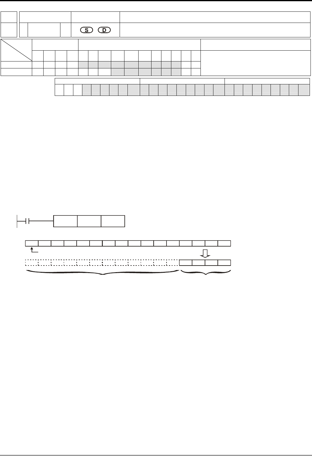
6 Application Instructions API 00-49
DVP-PLC Application Manual
6-24
API Mnemonic Operands Function
14
D CML P Compliment
Bit Devices Word Devices Program Steps Type
OP X Y M S K H KnX KnY KnM KnS T C D E F
S * ** * * * * * ***
D * * * * * ***
CML, CMLP: 5 steps
DCML, DCMLP: 9 steps
PULSE 16-bit 32-bit
ES EX SS SA SX SC EH SV EH3
SV2 ES EX SS SA SX SC EH SV EH3
SV2 ES EX SS SA SX SC EH SV EH3
SV2
Operands:
S: Source of data D: Destination device
Explanations:
1. If S and D are used in device F, only 16-bit instruction is applicable.
2. See the specifications of each model for their range of use.
3. This instruction can be used for phase-reversed output.
4. Reverse the phase (0→1, 1→0) of all the contents in S and send the contents to D. Given that the content is a
constant K, K will be automatically converted into a BIN value.
Program Example 1:
1. When X10 = On, b0 ~ b3 in D1 will be phase-reversed and send to Y0 ~ Y3.
X10
CML K1Y0
D1
b
0
b
1
b
2
b
3
b
15
D1 1010101010101010
Symbol bit (0=positive, 1=negative)
0101
No data Sending the phase-reversed data
Program Example 2:
The loop below can also adopt CML instruction (see right below).

6 Application Instructions API 00-49
DVP-PLC Application Manual 6-25
X000
M0
X001
M1
X002
M2
X003
M3
X000
M0
X001
M1
X002
M2
X003
M3
M1000
CML K1M0
K1X0
Normally on contact
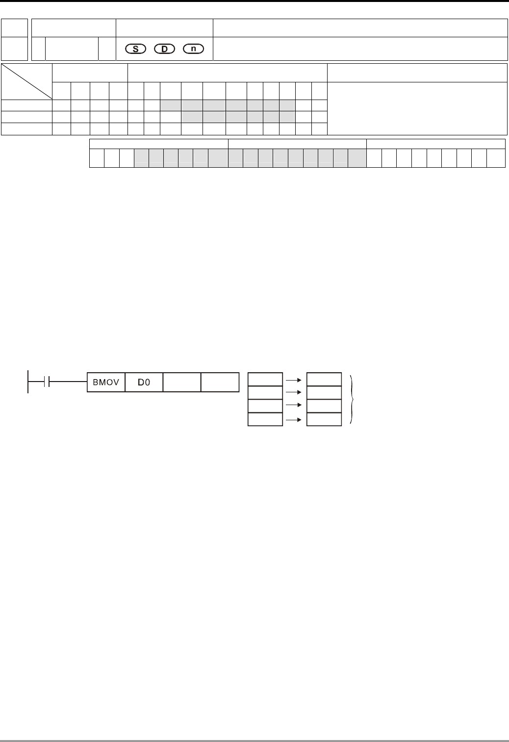
6 Application Instructions API 00-49
DVP-PLC Application Manual
6-26
API Mnemonic Operands Function
15
BMOV P Block Move
Bit Devices Word Devices Program Steps Type
OP X Y M S K H KnX KnY KnM KnS T C D E F
S * * * * * * *
D * * * * * *
n * * * * *
BMOV, BMOVP: 7 steps
PULSE 16-bit 32-bit
ES EX SS SA SX SC EH SV EH3
SV2 ES EX SS SA SX SC EH SV EH3
SV2 ES EX SS SA SX SC EH SV EH3
SV2
Operands:
S: Start of source devices D: Start of destination devices n: Number of data to be moved
Explanations:
1. Range of n: 1 ~ 512
2. See the specifications of each model for their range of use.
3. The contents in n registers starting from the device designated by S will be moved to n registers starting from
the device designated by D. If n exceeds the actual number of available source devices, only the devices that
fall within the valid range will be used.
Program Example 1:
When X10 = On, the contents in registers D0 ~ D3 will be moved to the 4 registers D20 ~ D23.
X10
D20 K4 D0
D1
D2
D3
D20
D21
D22
D23
n=4
Program Example 2:
1. Assume the bit devices KnX, KnY, KnM and KnS are designated for moving, the number of digits of S and D has
to be the same, i.e. their n has to be the same.
2. ES/EX/SS do not support the use of KnX, KnY, KnM, KnS and E, F index register modification.
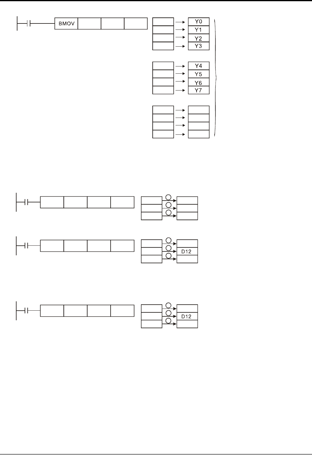
6 Application Instructions API 00-49
DVP-PLC Application Manual 6-27
M1000
K1M0 K1Y0 K3 M0
M1
M2
M3
M4
M5
M6
M7
M8
M9
M10
n=3
M11
Y10
Y11
Y12
Y13
Program Example 3:
To avoid coincidence of the device numbers to be moved designated by the two operands and cause confusion,
please be aware of the arrangement on the designated device numbers.
1. When S > D, the instruction is processed following the order 1→2→3
X10
BMOV D20 D19 K3 D19
D20
D21
D20
D21
D22
2
1
3
2. In EH/EH2/SV/EH3/SV2, when S < D, the instruction is processed following the order 1→2→3
D11
D13
X11
BMOV D10 D11 K3 D10
D11
D12
1
3
2
3. In ESEX/SS/SA/SX/SC, when S < D, avoid the number difference of “1” and the instruction is processed
following the order 3→2→1. If the devices have the number difference of “1”, the contents in D11 ~ D13 will all
be the content in D10.
D11
D13
X11
BMOV D10 D11 K3 D10
D11
D12
1
3
2
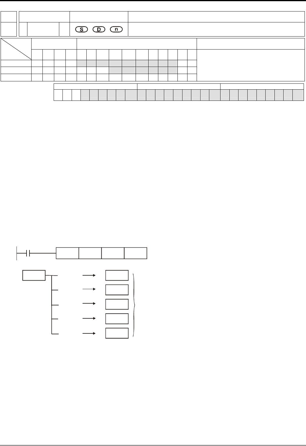
6 Application Instructions API 00-49
DVP-PLC Application Manual
6-28
API Mnemonic Operands Function
16
D FMOV P Fill Move
Bit Devices Word Devices Program Steps Type
OP X Y M S K H KnX KnY KnM KnS T C D E F
S * ** * * * * * ***
D * * * * * *
n * *
FMOV, FMOVP: 7 steps
DFMOV, DFMOVP: 13 steps
PULSE 16-bit 32-bit
ES EX SS SA SX SC EH SV EH3
SV2 ES EX SS SA SX SC EH SV EH3
SV2 ES EX SS SA SX SC EH SV EH3
SV2
Operands:
S: Source of data D: Destination of data n: Number of data to be moved
Explanations:
1. If S is used in device F, only 16-bit instruction is applicable.
2. Range of n: 1~ 512 (16-bit, 32-bit instructions)
3. See the specifications of each model for their range of use.
4. The contents in n registers starting from the device designated by S will be moved to n registers starting from
the device designated by D. If n exceeds the actual number of available source devices, only the devices that
fall within the valid range will be used.
5. ES/EX/SS do not support the use of KnX, KnY, KnM, KnS and E, F index register modification.
Program Example:
When X10 = On, K10 will be moved to the 5 consecutive registers starting from D10.
X10
D10 K5FMOV K10
K10
K10
K10
K10
K10
K10 D10
D11
D12
D13
D14
n=5
6 Application Instructions API 00-49
DVP-PLC Application Manual 6-29
API Mnemonic Operands Function
17
D XCH P Exchange
Bit Devices Word Devices Program Steps Type
OP X Y M S K H KnX KnY KnM KnS T C D E F
D1 ** * *****
D2 ** * *****
XCH, XCHP: 5 steps
DXCH, DXCHP: 9 steps
PULSE 16-bit 32-bit
ES EX SS SA SX SC EH SV EH3
SV2 ES EX SS SA SX SC EH SV EH3
SV2 ES EX SS SA SX SC EH SV EH3
SV2
Operands:
D1: Data to be exchanged 1 D2: Data to be exchanged 2
Explanations:
1. If D1 and D2 are used in device F, only 16-bit instruction is applicable.
2. See the specifications of each model for their range of use.
3. The contents in the devices designated by D1 and D2 will exchange.
4. Flag: M1303 (designated by XCH working mode).
Program Example 1:
When X0 = Off→On, the contents in D20 and D40 exchange with each other.
X0
D40
XCHP
D20
Before
execution
After
execution
120
120
40
40
D20
D40
D20
D40
Program Example 2:
When X0 = Off → On, the contents in D100 and D200 exchange with each other.
X0
D200D100
Before
execution
After
execution
40
20
D100
D101
D100
D101
20
40
D200
D201
D200
D201
DXCHP
Remarks:
1. ES/EX/SS do not support M1303.
2. As a 16-bit instruction, when the devices designated by D1 and D2 are the same and M1303 = On, the upper and
lower 8 bits of the designated devices exchange with each other.
3. As a 32-bit instruction, when the devices designated by D1 and D2 are the same and M1303 = On, the upper and
lower 16 bits in the individual designated device exchange with each other.
4. When X0 = On and M1303 = On, the 16-bit contents in D100 and those in D101 will exchange with each other.

6 Application Instructions API 00-49
DVP-PLC Application Manual
6-30
X0
M1303
DXCHP D100 D100
9
20
20
9
D100L
D100H
8
40
40
8
D101L
D101H
D100L
D100H
D101L
D101H
Before
execution
After
execution
6 Application Instructions API 00-49
DVP-PLC Application Manual 6-31
API Mnemonic Operands Function
18
D BCD P Binary Coded Decimal
Bit Devices Word Devices Program Steps Type
OP X Y M S K H KnX KnY KnM KnS T C D E F
S * ** * *****
D ** * *****
BCD, BCDP: 5 steps
DBCD, DBCDP: 9 steps
PULSE 16-bit 32-bit
ES EX SS SA SX SC EH SV EH3
SV2 ES EX SS SA SX SC EH SV EH3
SV2 ES EX SS SA SX SC EH SV EH3
SV2
Operands:
S: Source of data D: Conversion result
Explanations:
1. If S and D are used in device F, only 16-bit instruction is applicable.
2. See the specifications of each model for their range of use.
3. Flags: M1067 (operation error); M1068 (operation error); D1067 (error code)
4. The content in S (BIN value) is converted into BCD value and stored in D.
5. As a 16-bit (32-bit) instruction, when the conversion result exceeds the range of 0 ~ 9,999 (0 ~ 99,999,999), and
M1067, M1068 = On, D1067 will record the error code 0E18 (hex).
6. The four arithmetic operations and applications in PLC and the execution of INC and DEC instructions are
performed in BIN format. Therefore, if the user needs to see the decimal value display, simply use this
instruction to convert the BIN value into BCD value.
Program Example:
1. When X0 = On, the binary value of D10 will be converted into BCD value, and the 1s digit of the conversion
result will be stored in K1Y0 (Y0 ~ Y3, the 4 bit devices).
X0
BCD D10 K1Y0
2. When D10 = 001E (hex) = 0030 (decimal), the execution result will be: Y0 ~ Y3 = 0000(BIN).
6 Application Instructions API 00-49
DVP-PLC Application Manual
6-32
API Mnemonic Operands Function
19
D BIN P Binary
Bit Devices Word Devices Program Steps Type
OP X Y M S K H KnX KnY KnM KnS T C D E F
S * * * * * * ***
D * * * * * ***
BIN, BINP: 5 steps
DBIN, DBINP: 9 steps
PULSE 16-bit 32-bit
ES EX SS SA SX SC EH SV EH3
SV2 ES EX SS SA SX SC EH SV EH3
SV2 ES EX SS SA SX SC EH SV EH3
SV2
Operands:
S: Source of data D: Conversion result
Explanations:
1. If S and D are used in device F, only 16-bit instruction is applicable.
2. See the specifications of each model for their range of use.
3. Flags: M1067 (operation error); M1068 (operation error); D1067 (error code)
4. The content in S (BCD value) is converted into BIN value and stored in D.
5. Valid range of S : BCD (0 ~ 9,999), DBCD (0 ~ 99,999,999)
6. Provided the content in S is not a BCD value (in hex and any one of its digits does not fall in the range of 0 ~ 9),
an operation error will occur. M1067, M1068 = On and D1067 records the error code 0E18 (hex).
7. Constant K and H will automatically be converted into BIN format. Thus, they do not need to adopt this
instruction.
Program Example:
When X0 = On, the BCD value of K1M0 will be converted to BIN value and stored in D10.
X0
BIN D10K1M0
Remarks:
Explanations on BCD and BIN instructions:
1. When PLC needs to read an external DIP switch in BCD format, BIN instruction has to be first adopted to
convert the read data into BIN value and store the data in PLC.
2. When PLC needs to display its stored data by a 7-segment display in BCD format, BCD instruction has to be
first adopted to convert the data into BCD value and send the data to the 7-segment display.
3. When X0 = On, the BCD value of K4X0 is converted into BIN value and sent it to D100. The BIN value of D100
will then be converted into BCD value and sent to K4Y20.
X0
BIN D100K4X0
BCD D100 K4Y20
6 Application Instructions API 00-49
DVP-PLC Application Manual 6-33
10
1
10
0
10
2
6 4 2
X17 X0
888
10
3
6
8
Y37 Y20
4-digit DIP switch in BCD format
4-digit BCD value
Using BIN instruction to store
the BIN value into D100
Using BCD instruction to convert the
content in D100 into a 4-digit BCD value.
4-digit 7-segment display in BCD format
6 Application Instructions API 00-49
DVP-PLC Application Manual
6-34
API Mnemonic Operands Function
20
D ADD P Addition
Bit Devices Word Devices Program Steps Type
OP X Y M S K H KnX KnY KnM KnS T C D E F
S1 * ** * * * * * ***
S2 * ** * * * * * ***
D * * * * * ***
ADD, ADDP: 7 steps
DADD, DADDP: 13 steps
PULSE 16-bit 32-bit
ES EX SS SA SX SC EH SV EH3
SV2 ES EX SS SA SX SC EH SV EH3
SV2 ES EX SS SA SX SC EH SV EH3
SV2
Operands:
S1: Summand S2: Addend D: Sum
Explanations:
1. If S1, S2 and D are used in device F, only 16-bit instruction is applicable.
2. See the specifications of each model for their range of use.
3. Flags: M1020 (zero flag); M1021 (borrow flag); M1022 (carry flag)
4. This instruction adds S1 and S2 in BIN format and store the result in D.
5. The highest bit is symbolic bit 0 (+) and 1 (-), which is suitable for algebraic addition, e.g. 3 + (-9) = -6.
6. Flag changes in binary addition
In 16-bit BIN addition,
a) If the operation result = 0, zero flag M1020 = On.
b) If the operation result < -32,768, borrow flag M1021 = On.
c) If the operation result > 32,767, carry flag M1022 = On.
In 32-bit BIN addition,
a) If the operation result = 0, zero flag M1020 = On.
b) If the operation result < -2,147,483,648, borrow flag M1021 = On.
c) If the operation result > 2,147,483,647, carry flag M1022 = On.
Program Example 1:
In 16-bit BIN addition:
When X0 = On, the content in D0 will plus the content in D10 and the sum will be stored in D20.
X0
A
DD D0 D10 D20
Program Example 2:
In 32-bit BIN addition:
When X0 = On, the content in (D31, D30) will plus the content in (D41, D40) and the sum will be stored in (D51, D50).
D30, D40 and D50 are low 16-bit data; D31, D41 and D51 are high 16-bit data.
X10
DADD D30 D40 D50
(D31, D30) + (D41, D40) = (D51, D50)

6 Application Instructions API 00-49
DVP-PLC Application Manual 6-35
Remarks:
Flags and the positive/negative sign of the values:
-2 -1 0 -32,768、、、 、、-1 0 1 32,767 0 1 2、、、
-2 -1 0 -2,147,483,648、、、 、、-1 0 1 2,147,483,647 0 1 2、、、
16-bit : Zero flag Zero flag
Borrow flag The highest bit of
the data = 1 (negative)
32-bit : Zero flag Zero flag
The highest bit of
the data = 0 (positive) Carry flag
Borrow flag The highest bit of
the data = 1 (negative)
The highest bit of
the data = 0 (positive) Carry flag
Zero flag
Zero flag
+-
-+
6 Application Instructions API 00-49
DVP-PLC Application Manual
6-36
API Mnemonic Operands Function
21
D SUB P Subtraction
Bit Devices Word Devices Program Steps Type
OP X Y M S K H KnX KnY KnM KnS T C D E F
S1 * ** * * * * * ***
S2 * ** * * * * * ***
D * * * * * ***
SUB, SUBP: 7 steps
DSUB, DSUBP: 13 steps
PULSE 16-bit 32-bit
ES EX SS SA SX SC EH SV EH3
SV2 ES EX SS SA SX SC EH SV EH3
SV2 ES EX SS SA SX SC EH SV EH3
SV2
Operands:
S1: Minuend S2: Subtrahend D: Remainder
Explanations:
1. If S1, S2 and D are used in device F, only 16-bit instruction is applicable.
2. See the specifications of each model for their range of use.
3. Flags: M1020 (zero flag); M1021 (borrow flag); M1022 (carry flag)
4. This instruction subtracts S1 and S2 in BIN format and stores the result in D.
5. The highest bit is symbolic bit 0 (+) and 1 (-), which is suitable for algebraic subtraction.
6. Flag changes in binary subtraction
In 16-bit instruction:
a) If the operation result = 0, zero flag M1020 = On.
b) If the operation result < –32,768, borrow flag M1021 = On.
c) If the operation result > 32,767, carry flag M1022 = On.
In 32-bit instruction:
a) If the operation result = 0, zero flag M1020 = On.
b) If the operation result < –2,147,483,648, borrow flag M1021 = On.
c) If the operation result > 2,147,483,647, carry flag M1022 = On.
7. For flag operations of SUB instruction and the positive/negative sign of the value, see the explanations in ADD
instruction on the previous page.
Program Example 1:
In 16-bit BIN subtraction:
When X0 = On, the content in D0 will minus the content in D10 and the remainder will be stored in D20.
X0
SUB D0 D10 D20
Program Example 2:
In 32-bit BIN subtraction:
When X10 = On, the content in (D31, D30) will minus the content in (D41, D40) and the remainder will be stored in
(D51, D50). D30, D40 and D50 are low 16-bit data; D31, D41 and D51 are high 16-bit data.
X10
DSUB D30 D40 D50
(
D31
,
D30
)
−
(
D41
,
D40
)
=
(
D51
,
D50
)
6 Application Instructions API 00-49
DVP-PLC Application Manual 6-37
API Mnemonic Operands Function
22
D MUL P Multiplication
Bit Devices Word Devices Program Steps Type
OP X Y M S K H KnX KnY KnM KnS T C D E F
S1 * * * ** * *****
S2 * * * ** * *****
D ** * ****
MUL, DMULP: 7 steps
DMUL, DMULP: 13 steps
PULSE 16-bit 32-bit
ES EX SS SA SX SC EH SV EH3
SV2 ES EX SS SA SX SC EH SV EH3
SV2 ES EX SS SA SX SC EH SV EH3
SV2
Operands:
S1: Multiplicand S2: Multiplicator D: Product
Explanations:
1. If S1 and S2 are used in device F, only 16-bit instruction is applicable.
2. If D is used in device E, only 16-bit instruction is applicable.
3. In 16-bit instruction, D occupies 2 consecutive devices.
4. In 32-bit instruction, D occupies 4 consecutive devices.
5. See the specifications of each model for their range of use.
6. This instruction multiplies S1 by S2 in BIN format and stores the result in D. Be careful with the positive/negative
signs of S1, S2 and D when doing 16-bit and 32-bit operations.
7. In 16-bit BIN multiplication,
b15................ b00
X
=
b15................ b00 b31............ b16 b15.............b00
+1
b15 is a symbol bit b15 is a symbol bit b31 is a symbol bit D+1) (b15 of
Symbol bit = 0 refers to a positive value.
Symbol bit = 1 refers to a negative value.
When D serves as a bit device, it can designate K1 ~ K4 and construct a 16-bit result, occupying consecutive 2
groups of 16-bit data. ES/EX/SS only stores low 16-bit data.
8. 32-bit BIN multiplication,
b31.. b16
X
=
+1
b31 is a symbol bit b31 is a symbol bit b63 is a symbol bit ) (b15 of D+3
Symbol bit = 0 refers to a positive value.
Symbol bit = 1 refers to a negative value.
b15.. b00 b31.. b16 b15.. b00
+1
b63. b48 b47. b32 b31. b16 b15. b00
+3 +2 +1
When D serves as a bit device, it can designate K1 ~ K8 and construct a 32-bit result, occupying consecutive 2
groups of 32-bit data.
Program Example:
The 16-bit D0 is multiplied by the 16-bit D10 and brings forth a 32-bit product. The higher 16 bits are stored in D21

6 Application Instructions API 00-49
DVP-PLC Application Manual
6-38
and the lower 16-bit are stored in D20. On/Off of the most left bit indicates the positive/negative status of the result
value.
X
0
MUL D0 D10 D20
MUL D0 D10 K8M0
6 Application Instructions API 00-49
DVP-PLC Application Manual 6-39
API Mnemonic Operands Function
23
D DIV P Division
Bit Devices Word Devices Program Steps Type
OP X Y M S K H KnX KnY KnM KnS T C D E F
S1 * * * ** * ****
S2 * * * ** * ****
D ** * ****
DIV, DIVP: 7 steps
DDIV, DDIVP: 13 steps
PULSE 16-bit 32-bit
ES EX SS SA SX SC EH SV EH3
SV2 ES EX SS SA SX SC EH SV EH3
SV2 ES EX SS SA SX SC EH SV EH3
SV2
Operands:
S1: Dividend S2: Divisor D: Quotient and remainder
Explanations:
1. If S1 and S2 are used in device F, only 16-bit instruction is applicable.
2. If D is used in device E, only 16-bit instruction is applicable.
3. In 16-bit instruction, D occupies 2 consecutive devices.
4. In 32-bit instruction, D occupies 4 consecutive devices.
5. See the specifications of each model for their range of use.
6. This instruction divides S1 and S2 in BIN format and stores the result in D. Be careful with the positive/negative
signs of S1, S2 and D when doing 16-bit and 32-bit operations.
7. This instruction will not be executed when the divisor is 0. M1067 and M1068 will be On and D1067 records the
error code 0E19 (hex).
8. In 16-bit BIN division,
+1
=/
Quotient Remainder
When D serves as a bit device, it can designate K1 ~ K4 and construct a 16-bit result, occupying consecutive 2
groups of 16-bit data and bringing forth the quotient and remainder. ES/EX/SS is able to bring forth only quotient
without the remainder.
9. In 32-bit BIN division,
+1
/=
+1 +1 +3 +2
Quotient Remainder
When D serves as a bit device, it can designate K1 ~ K8 and construct a 32-bit result, occupying consecutive 2
groups of 32-bit data and bringing forth the quotient and remainder.
Program Example:
When X0 = On, D0 will be divided by D10 and the quotient will be stored in D20 and remainder in D21. On/Off of the
highest bit indicates the positive/negative status of the result value.

6 Application Instructions API 00-49
DVP-PLC Application Manual
6-40
X0
DIV D0 D10 D20
D0 D10 K4Y0
DIV

6 Application Instructions API 00-49
DVP-PLC Application Manual 6-41
API Mnemonic Operands Function
24
D INC P Increment
Bit Devices Word Devices Program Steps Type
OP X Y M S K H KnX KnY KnM KnS T C D E F
D ** * *****
INC, INCP: 3 steps
DINC, DINCP: 5 steps
PULSE 16-bit 32-bit
ES EX SS SA SX SC EH SV EH3
SV2 ES EX SS SA SX SC EH SV EH3
SV2 ES EX SS SA SX SC EH SV EH3
SV2
Operands:
D: Destination device
Explanations:
1. If D is used in device F, only 16-bit instruction is applicable.
2. See the specifications of each model for their range of use.
3. If the instruction is not a pulse execution one, the content in the designated device D will plus “1” in every scan
period whenever the instruction is executed.
4. This instruction adopts pulse execution instructions (INCP, DINCP).
5. In 16-bit operation, 32,767 pluses 1 and obtains -32,768. In 32-bit operation, 2,147,483,647 pluses 1 and
obtains -2,147,483,648.
6. The operation results will not affect M1020 ~ M1022.
Program Example:
When X0 = Off→On, the content in D0 pluses 1 automatically.
X0
INCP D0
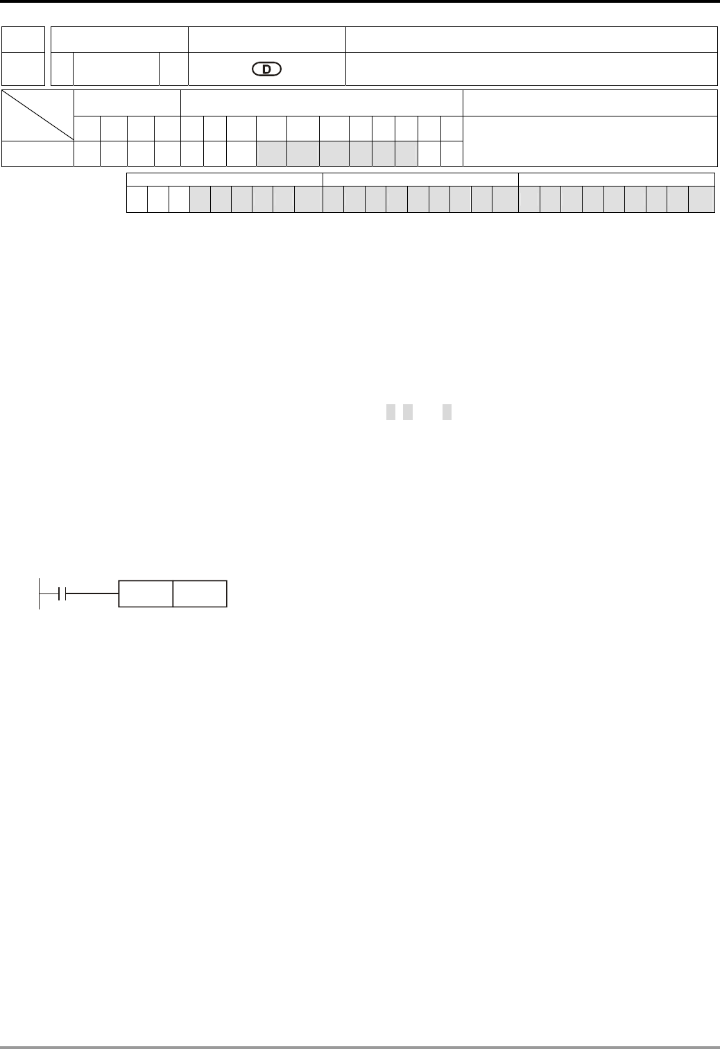
6 Application Instructions API 00-49
DVP-PLC Application Manual
6-42
API Mnemonic Operands Function
25
D DEC P Decrement
Bit Devices Word Devices Program Steps Type
OP X Y M S K H KnX KnY KnM KnS T C D E F
D * * * * * ***
DEC, DECP: 3 steps
DDEC, DDECP: 5 steps
PULSE 16-bit 32-bit
ES EX SS SA SX SC EH SV EH3
SV2 ES EX SS SA SX SC EH SV EH3
SV2 ES EX SS SA SX SC EH SV EH3
SV2
Operands:
D: Destination device
Explanations:
1. If D is used in device F, only 16-bit instruction is applicable.
2. See the specifications of each model for their range of use.
3. If the instruction is not a pulse execution one, the content in the designated device D will minus “1” in every scan
period whenever the instruction is executed.
4. This instruction adopts pulse execution instructions (DECP, DDECP).
5. In 16-bit operation, -32,768 minuses 1 and obtains 32,767. In 32-bit operation, -2,147,483,648 minuses 1 and
obtains 2,147,483,647.
6. The operation results will not affect M1020 ~ M1022.
Program Example:
When X0 = Off→On, the content in D0 minuses 1 automatically.
X0
DECP D0
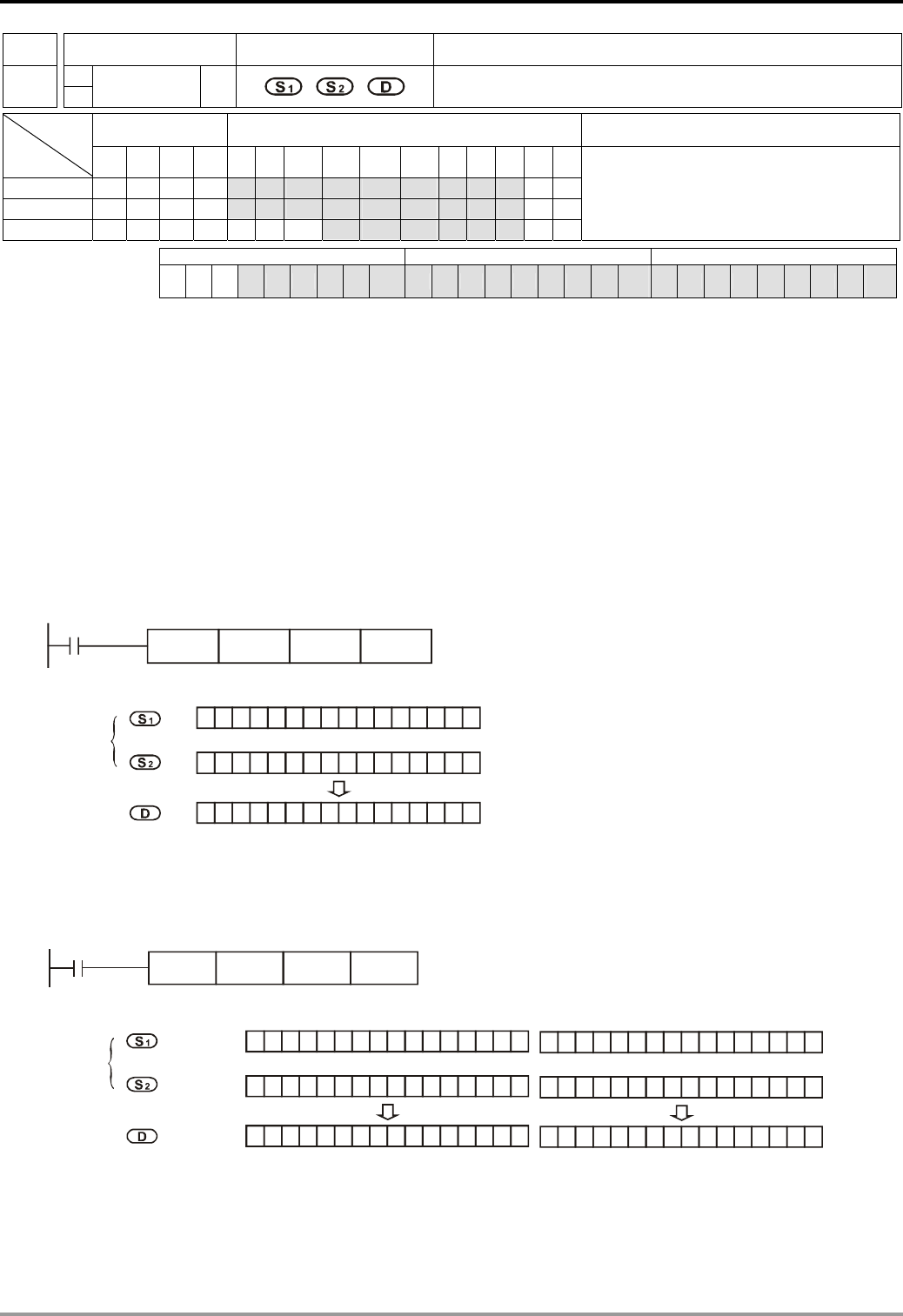
6 Application Instructions API 00-49
DVP-PLC Application Manual 6-43
API Mnemonic Operands Function
W
26
D AND P Logical Word AND
Bit Devices Word Devices Program Steps Type
OP X Y M S K H KnX KnY KnM KnS T C D E F
S1 * * * ** * *****
S2 * * * ** * *****
D ** * *****
WAND, WANDP: 7 steps
DAND, DANDP: 13 steps
PULSE 16-bit 32-bit
ES EX SS SA SX SC EH SV EH3
SV2 ES EX SS SA SX SC EH SV EH3
SV2 ES EX SS SA SX SC EH SV EH3
SV2
Operands:
S1: Source data device 1 S2: Source data device 2 D: Operation result
Explanations:
1. If S1, S2 and D are used in device F, only 16-bit instruction is applicable.
2. See the specifications of each model for their range of use.
3. This instruction conducts logical AND operation of S1 and S2 and stores the result in D.
4. Operation rule: The corresponding bit of the operation result in D will be “0” if any of the bits in S1 or S2 is “0”.
Program Example 1:
When X0 = On, the 16-bit D0 and D2 will perform WAND, logical AND operation, and the result will be stored in D4.
WAND
X0
D2
D0 D4
0000111111111111
000 00 000 0 0011 111
000 00 000000 00
11 1
WAND
b15 b0
Before
execution
After
execution
D0
D2
D4
Program Example 2:
When X1 = On, the 32-bit (D11, D10) and (D21, D20) will perform DAND, logical AND operation, and the result will be
stored in (D41, D40).
X1
DAND D10 D20 D40
0000111111111111
000 00 000 0 0011 111
000 00 000000 00
11 1
DAND
b31
Before
execution
After
execution
0000111111111111
00000000 00011 111
000 00 000000 0 0
11 1
b15 b0
D11 D10
D21 D20
D41 D40
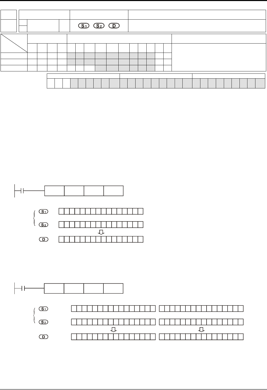
6 Application Instructions API 00-49
DVP-PLC Application Manual
6-44
API Mnemonic Operands Function
W
27
D OR P Logical Word OR
Bit Devices Word Devices Program Steps Type
OP X Y M S K H KnX KnY KnM KnS T C D E F
S1 * ** * * * * * ***
S2 * ** * * * * * ***
D * * * * * ***
WOR, WORP: 7 steps
DOR, DORP: 13 steps
PULSE 16-bit 32-bit
ES EX SS SA SX SC EH SV EH3
SV2 ES EX SS SA SX SC EH SV EH3
SV2 ES EX SS SA SX SC EH SV EH3
SV2
Operands:
S1: Source data device 1 S2: Source data device 2 D: Operation result
Explanations:
1. If S1, S2 and D are used in device F, only 16-bit instruction is applicable.
2. See the specifications of each model for their range of use.
3. This instruction conducts logical OR operation of S1 and S2 and stores the result in D.
4. Operation rule: The corresponding bit of the operation result in D will be “1” if any of the bits in S1 or S2 is “1”.
Program Example 1:
When X0 = On, the 16-bit D0 and D2 will perform WOR, logical OR operation, and the result will be stored in D4.
X0
WOR D0 D2 D4
00 111111
000 0 0 011 1 1
00 00
11 1
WOR
b15 b0
0000 0011
0111 0 1
11111111 1
Before
execution
After
execution
D2
D4
D0
Program Example 2:
When X1 = On, the 32-bit (D11, D10) and (D21, D20) will perform DOR, logical OR operation, and the result will be
stored in (D41, D40).
X1
DOR D10 D20 D40
00 111111
000 0 0 011 1 1
00 00
11 1
b31
0000 0011
0111 0 1
11111111 1
Before
execution
After
execution
D11 D10
DOR
00 111111
000 0 0 011 1 1
00 00
11 1
b15 b0
0000 0011
0111 0 1
11111111 1
D21 D20
D41 D40
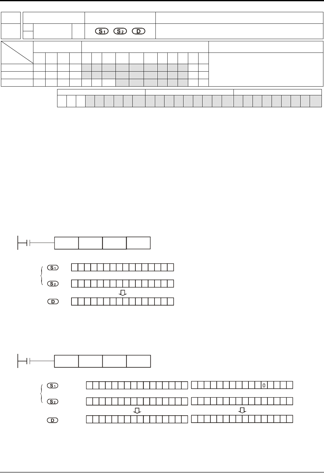
6 Application Instructions API 00-49
DVP-PLC Application Manual 6-45
API Mnemonic Operands Function
W
28
D XOR P Logical Exclusive OR
Bit Devices Word Devices Program Steps Type
OP X Y M S K H KnX KnY KnM KnS T C D E F
S1 * * * ** * *****
S2 * * * ** * *****
D ** * *****
WXOR, WXORP: 7 steps
DXOR, DXORP: 13 steps
PULSE 16-bit 32-bit
ES EX SS SA SX SC EH SV EH3
SV2 ES EX SS SA SX SC EH SV EH3
SV2 ES EX SS SA SX SC EH SV EH3
SV2
Operands:
S1: Source data device 1 S2: Source data device 2 D: Operation result
Explanations:
1. If S1, S2 and D are used in device F, only 16-bit instruction is applicable.
2. See the specifications of each model for their range of use.
3. This instruction conducts logical XOR operation of S1 and S2 and stores the result in D.
4. Operation rule: If the bits in S1 and S2 are the same, the corresponding bit of the operation result in D will be “0”;
if the bits in S1 and S2 are different, the corresponding bit of the operation result in D will be “1”.
Program Example 1:
When X0 = On, the 16-bit D0 and D2 will perform WXOR, logical XOR operation, and the result will be stored in D4.
X0
WXOR D0 D2 D4
00 111111
000 0 0 011 1 1
00 00
11 0
WOR
b15
0000 0011
0111 0 1
11001111 0
Before
execution
After
execution
D0
D2
D4
b0
Program Example 2:
When X1 = On, the 32-bit (D11, D10) and (D21, D20) will perform DXOR, logical XOR operation, and the result will be
stored in (D41, D40).
X1
DXOR D10 D20 D40
00 111111
000 0 0 001 1 1
11 11
00 0
b31
1111 1100
1000 0
1 11 10 011 1
Before
execution
After
execution
D11 D10
DXOR
1
D21 D20
D41 D40
00 111111
000 0 0 001 1 1
11 11
00 0
b15
1111 110
1000 0
11110011 1
1
b0
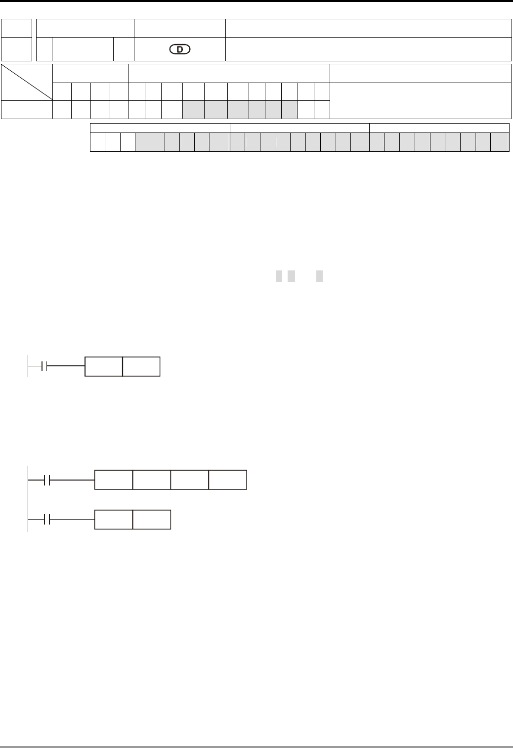
6 Application Instructions API 00-49
DVP-PLC Application Manual
6-46
API Mnemonic Operands Function
29
D NEG P 2’s Complement (Negative)
Bit Devices Word Devices Program Steps Type
OP X Y M S K H KnX KnY KnM KnS T C D E F
D * * * * * ***
NEG, NEGP: 3 steps
DNEG, DNEGP: 5 steps
PULSE 16-bit 32-bit
ES EX SS SA SX SC EH SV EH3
SV2 ES EX SS SA SX SC EH SV EH3
SV2 ES EX SS SA SX SC EH SV EH3
SV2
Operands:
D: Device to store 2’s complement
Explanations:
1. If D is used in device F, only 16-bit instruction is applicable.
2. See the specifications of each model for their range of use.
3. This instruction converts a negative BIN value into an absolute value.
4. This instruction adopts pulse execution instructions (NEGP, DNEGP).
Program Example 1:
When X0 = Off→On, the phase of every bit of the content in D10 will be reversed (0→1, 1→0) and pluses 1. The
result will then be stored in D10.
X0
NEGP D10
Program Example 2:
Obtaining the absolute value of a negative value:
a) When the 15th bit of D0 is “1”, M0 = On. (D0 is a negative value).
b) When M0 = Off→On, NEG instruction will obtain 2’s complement of D0 and further its absolute value.
M1000
BON D0 K15
M0
M0
NEGP D0
Normal ON contact
Program Example 3:
Obtaining the absolute value by the remainder of the subtraction. When X0 = On,
a) If D0 > D2, M0 = On.
b) If D0 = D2, M1 = On.
c) If D0 < D2, M2 = On.
d) D4 is then able to remain positive.
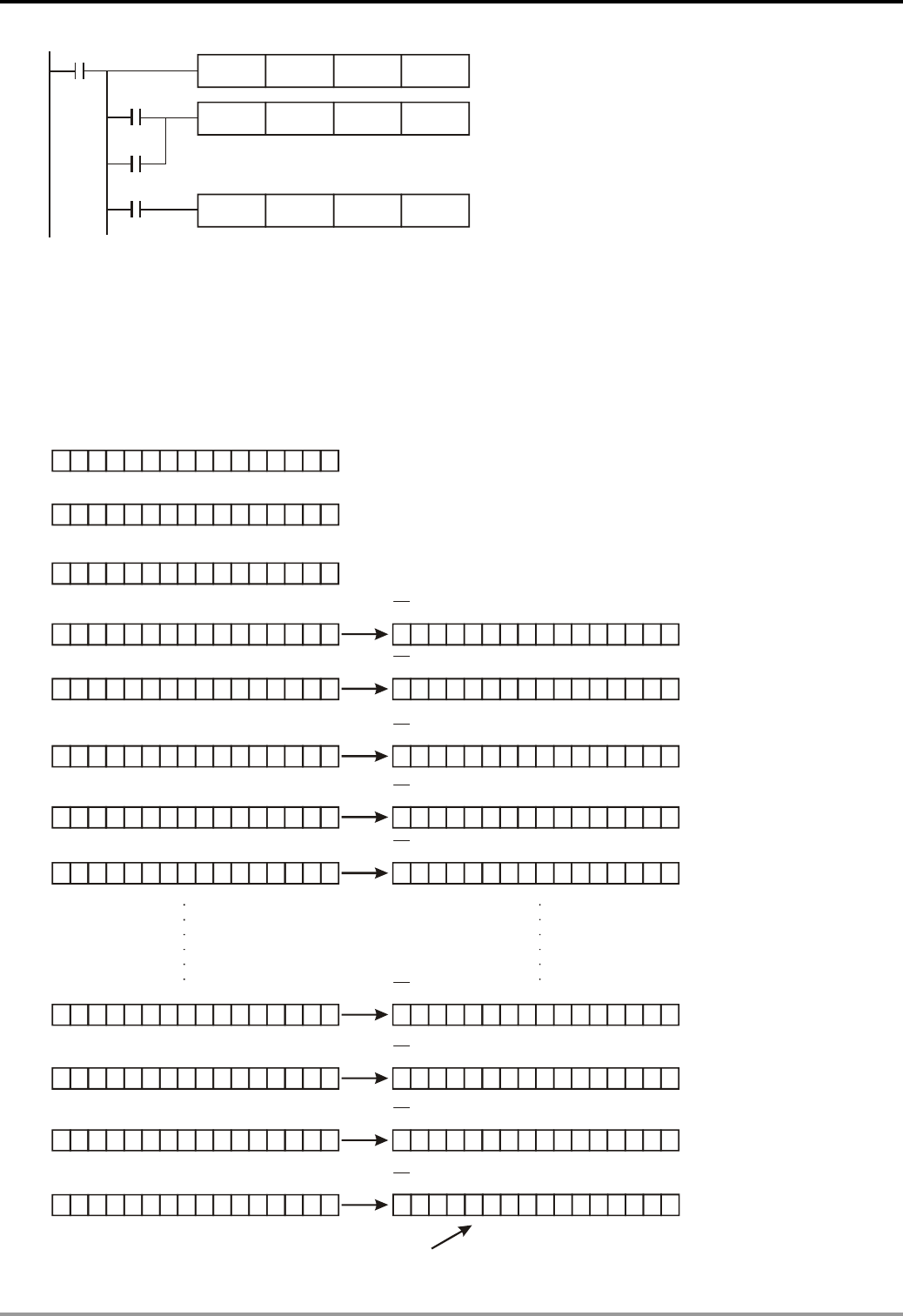
6 Application Instructions API 00-49
DVP-PLC Application Manual 6-47
X0
CMP D0 D2 M0
M0
SUB D0 D2 D4
M2
SUB D2 D0 D4
M1
Remarks:
Negative value and its absolute value
a) The sign of a value is indicated by the highest (most left) bit in the register. 0 indicates that the value is a positive
one and 1 indicates that the value is a negative one.
b) NEG instruction is able to convert a negative value into its absolute value.
00 0000000000 0100
00 0100000000 0000
00 0000000000 0000
(D0=2)
(D0=1)
(D0=0)
111 1 1 111 1 11111 1 1
(D0=-1)
00 0100000000 0000
(D0)+1=1
111 1 1 111 1 11111 1 0
(D0=-2)
00 0000000000 0100
(D0)+1=2
111 1 1 011 1 11111 1 1
(D0=-3)
00 0100000000 0100
(D0)+1=3
111 1 1 011 1 11111 1 0
(D0=-4)
00 1000000000 0000
(D0)+1=4
111 1 1 111 1 01111 1 1
(D0=-5)
00 1100000000 0000
(D0)+1=5
100 0 0 100 0 00000 0 1
(D0=-32,765)
11 1111110111 1011
(D0)+1=32,765
100 0 0 100 0 00000 0 0
(D0=-32,766)
11 1011110111 1111
(D0)+1=32,766
100 0 0 000 0 00000 0 1
(D0=-32,767)
11 1111110111 1111
(D0)+1=32,767
100 0 0 000 0 00000 0 0
(D0=-32,768) (D0)+1=-32,768
100 0 0 000 0 00000 0 0
Max. absolute value is 32,767
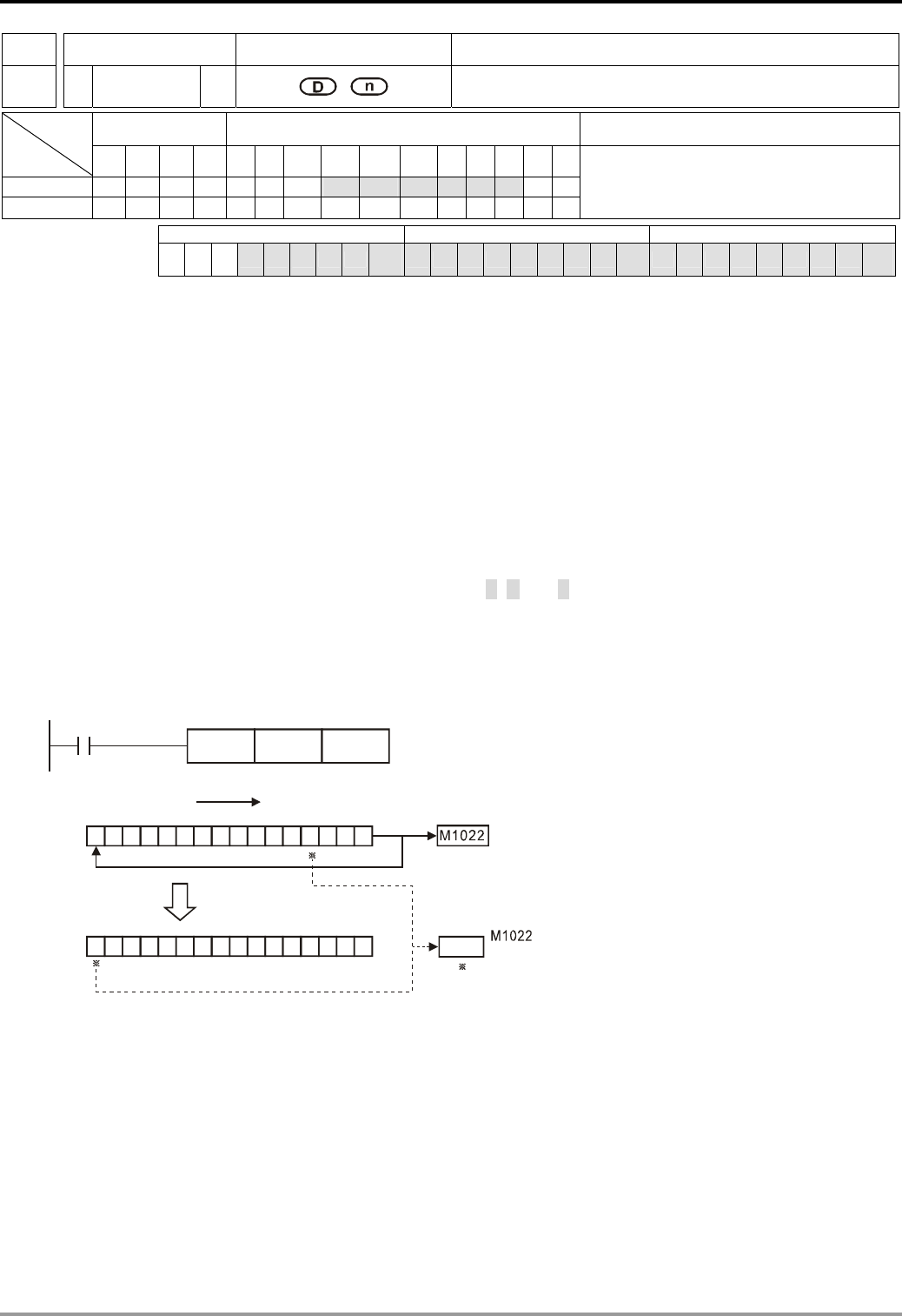
6 Application Instructions API 00-49
DVP-PLC Application Manual
6-48
API Mnemonic Operands Function
30
D ROR P Rotation Right
Bit Devices Word Devices Program Steps Type
OP X Y M S K H KnX KnY KnM KnS T C D E F
D * * * * * ***
n * *
ROR, RORP: 5 steps
DROR, DRORP: 9 steps
PULSE 16-bit 32-bit
ES EX SS SA SX SC EH SV EH3
SV2 ES EX SS SA SX SC EH SV EH3
SV2 ES EX SS SA SX SC EH SV EH3
SV2
Operands:
D: Device to be rotated n: Number of bits to be rotated in 1 rotation
Explanations:
1. If D is used in device F, only 16-bit instruction is applicable.
2. If D is designated as KnY, KnM, and KnS, only K4 (16-bit) and K8 (32-bit) are valid.
3. Range of n: K1 ~ K16 (16-bit); K1 ~ K32 (32-bit)
4. See the specifications of each model for their range of use.
5. Flag: M1022 (carry flag)
6. This instruction rotates the device content designated by D to the right for n bits.
7. This instruction adopts pulse execution instructions (RORP, DRORP).
Program Example:
When X0 = Off→On, the 16 bits (4 bits as a group) in D10 will rotate to the right, as shown in the figure below. The bit
marked with ※ will be sent to carry flag M1022.
01110101 00111 001
010111001111001 0 0
higher
bit lower bit
higher
bit lower bit
X0
RORP D10 K4
Rotate to the right
16 bits
Carry
flag
Carry
flag
After one rotation
to the right
D10
D10
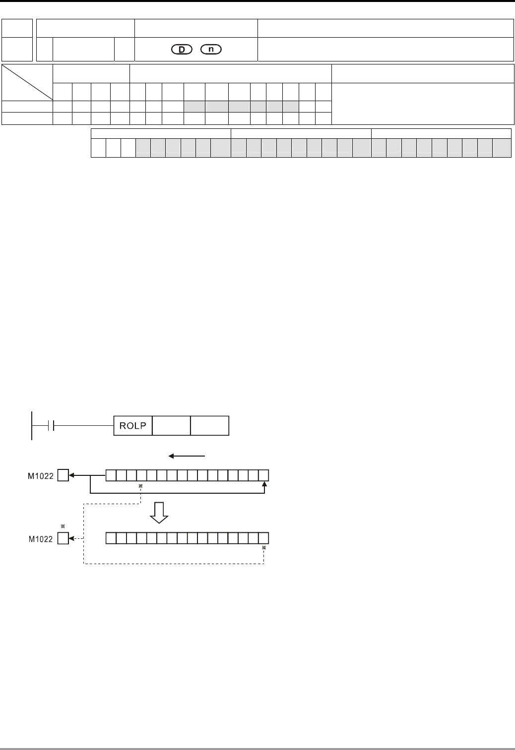
6 Application Instructions API 00-49
DVP-PLC Application Manual 6-49
API Mnemonic Operands Function
31
D ROL P Rotation Left
Bit Devices Word Devices Program Steps Type
OP X Y M S K H KnX KnY KnM KnS T C D E F
D ** * *****
n * *
ROL, ROLP: 5 steps
DROL, DROLP: 9 steps
PULSE 16-bit 32-bit
ES EX SS SA SX SC EH SV EH3
SV2 ES EX SS SA SX SC EH SV EH3
SV2 ES EX SS SA SX SC EH SV EH3
SV2
Operands:
D: Device to be rotated n: Number of bits to be rotated in 1 rotation
Explanations:
1. If D is used in device F, only 16-bit instruction is applicable.
2. If D is designated as KnY, KnM, and KnS, only K4 (16-bit) and K8 (32-bit) are valid.
3. Range of n: K1 ~ K16 (16-bit); K1 ~ K32 (32-bit)
4. See the specifications of each model for their range of use.
5. Flag: M1022 (carry flag)
6. This instruction rotates the device content designated by D to the left for n bits.
7. This instruction adopts pulse execution instructions (ROLP, DROLP).
Program Example:
When X0 = Off→On, the 16 bits (4 bits as a group) in D10 will rotate to the left, as shown in the figure below. The bit
marked with ※ will be sent to carry flag M1022.
X0
D10 K4
111 11 100 0 0011 000
11000001100110111
16 bits
Rotate to the left
After one rotation
to the left
Carry
flag
Carry
flag
D10
D10
lower bit
lower bit
higher bit
higher bit
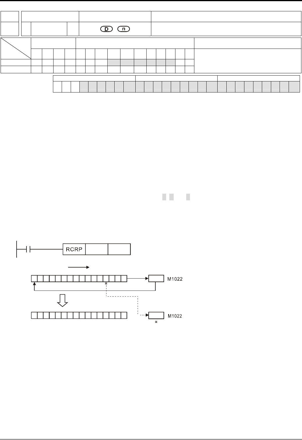
6 Application Instructions API 00-49
DVP-PLC Application Manual
6-50
API Mnemonic Operands Function
32
D RCR P Rotation Right with Carry
Bit Devices Word Devices Program Steps Type
OP X Y M S K H KnX KnY KnM KnS T C D E F
D * * * * * ***
n * *
RCR, RCRP: 5 steps
DRCR, DRCRP: 9 steps
PULSE 16-bit 32-bit
ES EX SS SA SX SC EH SV EH3
SV2 ES EX SS SA SX SC EH SV EH3
SV2 ES EX SS SA SX SC EH SV EH3
SV2
Operands:
D: Device to be rotated n: Number of bits to be rotated in 1 rotation
Explanations:
1. If D is used in device F, only 16-bit instruction is applicable.
2. If D is designated as KnY, KnM, and KnS, only K4 (16-bit) and K8 (32-bit) are valid.
3. Range of n: K1 ~ K16 (16-bit); K1 ~ K32 (32-bit)
4. See the specifications of each model for their range of use.
5. Flag: M1022 (carry flag)
6. This instruction rotates the device content designated by D together with carry flag M1022 to the right for n bits.
7. This instruction adopts pulse execution instructions (RCRP, DRCRP).
Program Example:
When X0 = Off→On, the 16 bits (4 bits as a group) in D10 together with carry flag M1022 (total 17 bits) will rotate to
the right, as shown in the figure below. The bit marked with ※ will be sent to carry flag M1022.
00011100 01001 001
10001100111000 0 0
1
X0
D10 K4
Rotate to the right
16 bits
Carry
flag
Carry
flag
After one rotation
to the right lower bit
lower bit
1
D10
D10
higher bit
higher bit
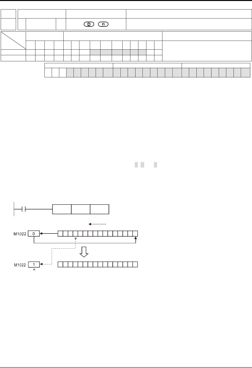
6 Application Instructions API 00-49
DVP-PLC Application Manual 6-51
API Mnemonic Operands Function
33
D RCL P Rotation Left with Carry
Bit Devices Word Devices Program Steps Type
OP X Y M S K H KnX KnY KnM KnS T C D E F
D ** * *****
n * *
RCL, RCLP: 5 steps
DRCL, DRCLP: 9 steps
PULSE 16-bit 32-bit
ES EX SS SA SX SC EH SV EH3
SV2 ES EX SS SA SX SC EH SV EH3
SV2 ES EX SS SA SX SC EH SV EH3
SV2
Operands:
D: Device to be rotated n: Number of bits to be rotated in 1 rotation
Explanations:
1. If D is used in device F, only 16-bit instruction is applicable.
2. If D is designated as KnY, KnM, and KnS, only K4 (16-bit) and K8 (32-bit) are valid.
3. Range of n: K1 ~ K16 (16-bit); K1 ~ K32 (32-bit)
4. See the specifications of each model for their range of use.
5. Flag: M1022 (carry flag)
6. This instruction rotates the device content designated by D together with carry flag M1022 to the left for n bits.
7. This instruction adopts pulse execution instructions (RCLP, DRCLP).
Program Example :
When X0 = Off→On, the 16 bits (4 bits as a group) in D10 together with carry flag M1022 (total 17 bits) will rotate to
the left, as shown in the figure below. The bit marked with ※ will be sent to carry flag M1022.
X0
RCLP D10 K4
11111100 00011 000
1100000 10000111 1
16 bits
Rotate to the left
After one rotation
to the left
Carry
flag
Carry
flag
lower bit
lower bit
D10
D10
higher bit
higher bit
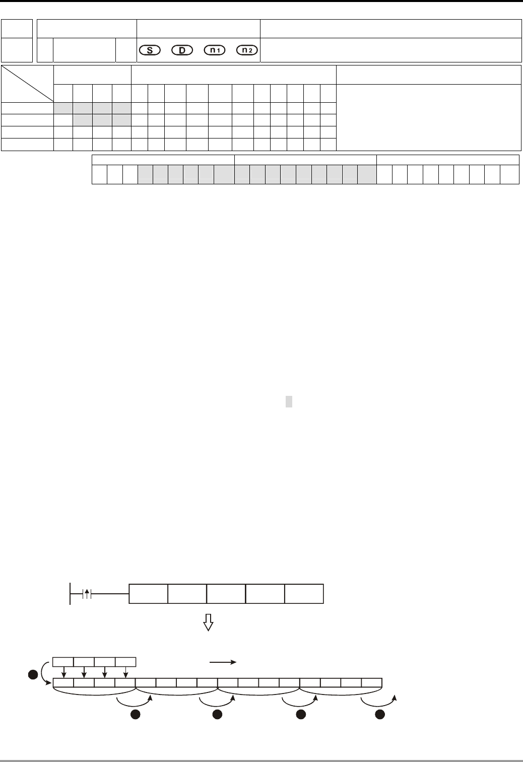
6 Application Instructions API 00-49
DVP-PLC Application Manual
6-52
API Mnemonic Operands Function
34
SFTR P Bit Shift Right
Bit Devices Word Devices Program Steps Type
OP X Y M S K H KnX KnY KnM KnS T C D E F
S * * * *
D * * *
n1 * *
n2 * *
SFTR, SFTRP: 9 steps
PULSE 16-bit 32-bit
ES EX SS SA SX SC EH SV EH3
SV2 ES EX SS SA SX SC EH SV EH3
SV2 ES EX SS SA SX SC EH SV EH3
SV2
Operands:
S: Start No. of the shifted device D: Start No. of the device to be shifted n
1: Length of data to be shifted
n2: Number of bits to be shifted in 1 shift
Explanations:
1. Range of n1: 1~ 1,024
2. Range of n2: 1 ~ n1
3. In ES/EX/SS, 1 ≤ n2 ≤ n1 ≤ 512
4. ES/EX/SS series MPU does not support E, F index register modification.
5. See the specifications of each model for their range of use.
6. This instruction shifts the bit device of n1 bits (desired length for shifted register) starting from D to the right for n2
bits. S is shifted into D for n2 bits to supplement empty bits.
7. This instruction adopts pulse execution instructions (SFTRP).
Program Example:
1. When X0 = Off→On, M0 ~M15 will form 16 bits and shifts to the right (4 bits as a group).
2. The figure below illustrates the right shift of the bits in one scan.
n M3 ~ M0 → carry
o M7 ~ M4 → M3 ~ M0
p M11 ~ M8 → M7 ~ M4
q M15 ~ M12 → M11 ~ M8
r X3 ~ X0 → M15 ~ M12 completed
X0
SFTR X0 M0 K16 K4
X3 X2 X1 X0
M15 M14 M13 M12 M11 M10 M9 M8 M7 M6 M5 M4 M3 M2 M1 M0
1234
5
carry
4 bits as a group shifting to the right
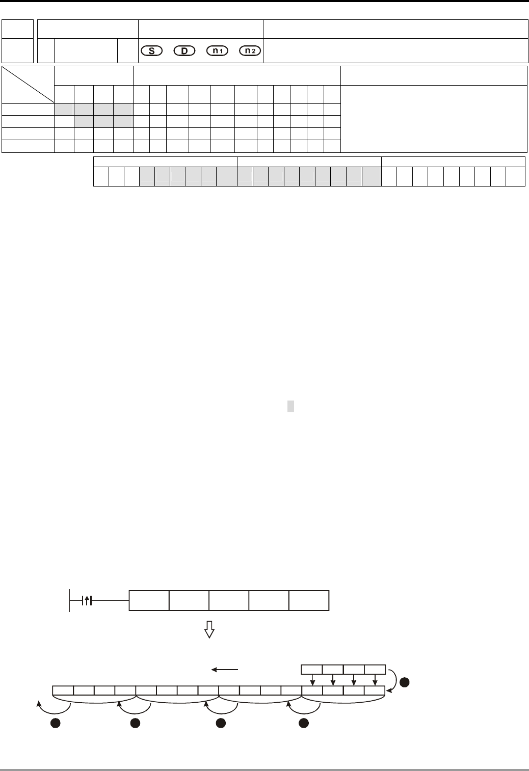
6 Application Instructions API 00-49
DVP-PLC Application Manual 6-53
API Mnemonic Operands Function
35
SFTL P Bit Shift Left
Bit Devices Word Devices Program Steps Type
OP X Y M S K H KnX KnY KnM KnS T C D E F
S * * * *
D * * *
n1 * *
n2 * *
SFTL, SFTLP: 9 steps
PULSE 16-bit 32-bit
ES EX SS SA SX SC EH SV EH3
SV2 ES EX SS SA SX SC EH SV EH3
SV2 ES EX SS SA SX SC EH SV EH3
SV2
Operands:
S: Start No. of the shifted device D: Start No. of the device to be shifted n
1: Length of data to be shifted
n2: Number of bits to be shifted in 1 shift
Explanations:
1. Range of n1: 1~ 1,024
2. Range of n2: 1 ~ n1
3. In ES/EX/SS, 1 ≤ n2 ≤ n1 ≤ 512
4. ES/EX/SS series MPU does not support E, F index register modification.
5. See the specifications of each model for their range of use.
6. This instruction shifts the bit device of n1 bits (desired length for shifted register) starting from D to the left for n2
bits. S is shifted into D for n2 bits to supplement empty bits.
7. This instruction adopts pulse execution instructions (SFTLP).
Program Example:
1. When X0 = Off→On, M0 ~M15 will form 16 bits and shifts to the left (4 bits as a group).
2. The figure below illustrates the left shift of the bits in one scan.
n M15 ~ M12 → carry
o M11 ~ M8 → M15 ~ M12
p M7 ~ M4 → M11 ~ M8
q M3 ~ M0 → M7 ~ M4
r X3 ~ X0 → M3 ~ M0 completed
X
0
SFTR X0 M0 K16 K4
X3 X2 X1 X0
M15 M14 M13 M12 M11 M10 M9 M8 M7 M6 M5 M4 M3 M2 M1 M0
1 2 3 4
5
carry
4 bits as a group shifting to the left
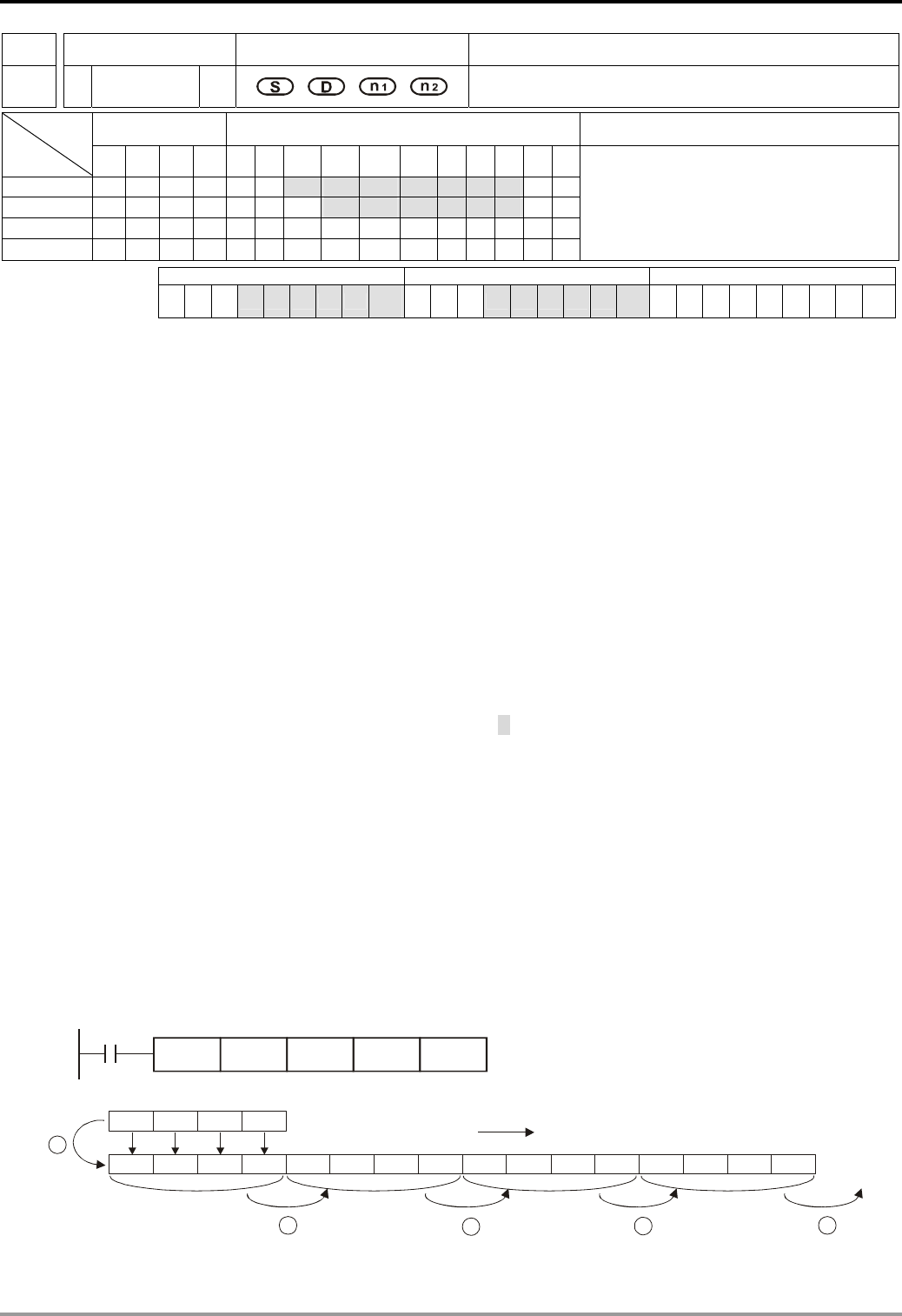
6 Application Instructions API 00-49
DVP-PLC Application Manual
6-54
API Mnemonic Operands Function
36
WSFR P Word Shift Left
Bit Devices Word Devices Program Steps Type
OP X Y M S K H KnX KnY KnM KnS T C D E F
S * * * * * * *
D * * * * * *
n1 * *
n2 * *
WSFR, WSFRP: 9 steps
PULSE 16-bit 32-bit
ES EX SS SA SX SC EH SV EH3
SV2 ES EX SS SA SX SC EH SV EH3
SV2 ES EX SS SA SX SC EH SV EH3
SV2
Operands:
S: Start No. of the shifted device D: Start No. of the device to be shifted n
1: Length of data to be shifted
n2: Number of words to be shifted in 1 shift
Explanations:
1. The type of devices designated by S and D has to be the same, e.g. KnX, KnY, KnM, and KnS as a category and
T, C, and D as another category.
2. Provided the devices designated by S and D belong to Kn type, the number of digits of Kn has to be the same.
3. Range of n1: 1~ 512
4. Range of n2: 1 ~ n1
5. See the specifications of each model for their range of use.
6. This instruction shifts the stack data of n1 words starting from D to the right for n2 words. S is shifted into D for n2
words to supplement empty words.
7. This instruction adopts pulse execution instructions (WSFRP)
Program Example 1:
1. When X0 = Off→On, the 16 register stack data composed of D20 ~ D35 will shift to the right for 4 registers.
2. The figure below illustrates the right shift of the words in one scan.
n D23 ~ D20 → carry
o D27 ~ D24 → D23 ~ D20
p D31 ~ D28 → D27 ~ D24
q D35 ~ D32 → D31 ~ D28
r D13 ~ D10 → D35 ~ D32 completed
X0
WSFRP D10 K16D20 K4
D13 D12 D11 D10
D35 D34 D33 D32 D31 D30 D29 D28 D27 D26 D25 D24 D23 D22 D21 D20
1
23
4
5
Carry
Right-shifting for 4 registers
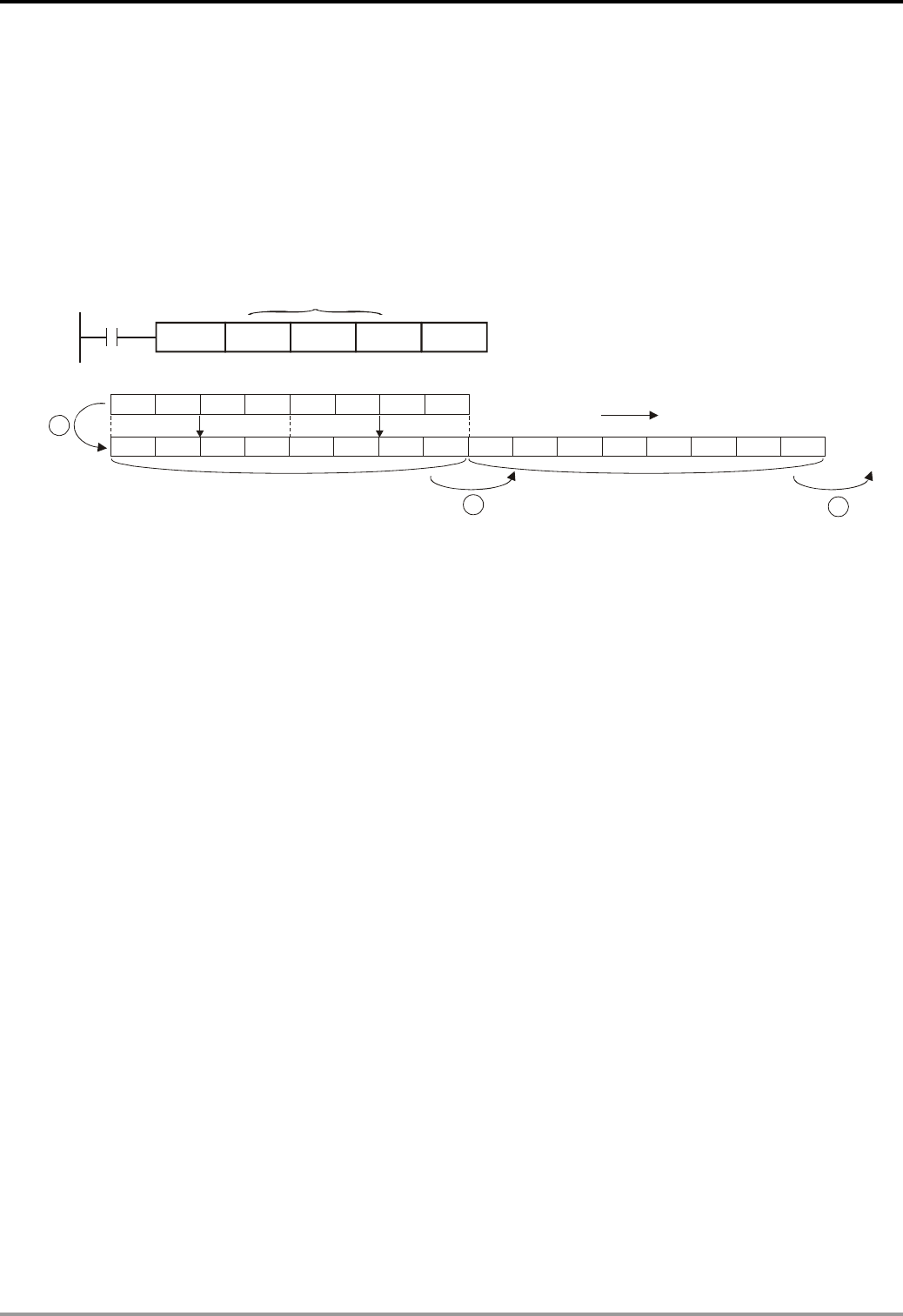
6 Application Instructions API 00-49
DVP-PLC Application Manual 6-55
Program Example 2:
1. When X0 = Off→On, the bit register stack data composed of Y10 ~ Y27 will shift to the right for 2 digits.
2. The figure below illustrates the right shift of the words in one scan.
n Y17 ~ Y10 → carry
o Y27 ~ Y20 → Y17 ~ Y10
p X27 ~ X20 → Y27 ~ Y20 completed
X0
WSFRP K1X20 K4 K2
X27 X26 X25 X24
Y27 Y26 Y25 Y24 Y23 Y22 Y21 Y20 Y17 Y16 Y15 Y14 Y13 Y12 Y11 Y10
1
2
3
Carry
K1Y10
X23 X22 X21 X20
When using Kn type device, please designate the same number of digits.
Right-shifting for 2 digits
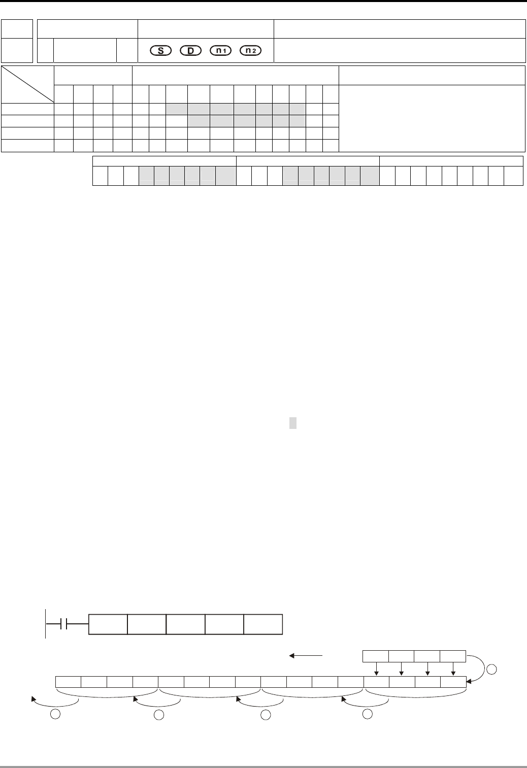
6 Application Instructions API 00-49
DVP-PLC Application Manual
6-56
API Mnemonic Operands Function
37
WSFL P Word Shift Left
Bit Devices Word Devices Program Steps Type
OP X Y M S K H KnX KnY KnM KnS T C D E F
S * * * * * * *
D * * * * * *
n1 * *
n2 * *
WSFL, WSFLP: 9 steps
PULSE 16-bit 32-bit
ES EX SS SA SX SC EH SV EH3
SV2 ES EX SS SA SX SC EH SV EH3
SV2 ES EX SS SA SX SC EH SV EH3
SV2
Operands:
S: Start No. of the shifted device D: Start No. of the device to be shifted n
1: Length of data to be shifted
n2: Number of words to be shifted in 1 shift
Explanations:
1. The type of devices designated by S and D has to be the same, e.g. KnX, KnY, KnM, and KnS as a category and
T, C, and D as another category.
2. Provided the devices designated by S and D belong to Kn type, the number of digits of Kn has to be the same.
3. Range of n1: 1~ 512
4. Range of n2: 1 ~ n1
5. See the specifications of each model for their range of use.
6. This instruction shifts the stack data of n1 words starting from D to the left for n2 words. S is shifted into D for n2
words to supplement empty words.
7. This instruction adopts pulse execution instructions (WSFLP)
Program Example:
1. When X0 = Off→On, the 16 register stack data composed of D20 ~ D35 will shift to the left for 4 registers.
2. The figure below illustrates the left shift of the words in one scan.
n D35 ~ D32 → carry
o D31 ~ D28 → D35 ~ D32
p D27 ~ D24 → D31 ~ D28
q D23 ~ D20 → D27 ~ D24
r D13 ~ D10 → D23 ~ D20 completed
134
5
2
Carry
X0
WSFLP D10 K16
D20 K4
D13 D12 D11 D10
D35 D34 D33 D32 D31 D30 D29 D28 D27 D26 D25 D24 D23 D22 D21 D20
Left-shifiting for 4 registers
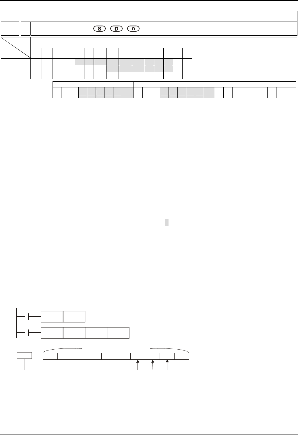
6 Application Instructions API 00-49
DVP-PLC Application Manual 6-57
API Mnemonic Operands Function
38
SFWR P Shift Register Write
Bit Devices Word Devices Program Steps Type
OP X Y M S K H KnX KnY KnM KnS T C D E F
S * * * ** * *****
D ** * * * *
n * *
SFWR, SFWRP: 7 steps
PULSE 16-bit 32-bit
ES EX SS SA SX SC EH SV EH3
SV2 ES EX SS SA SX SC EH SV EH3
SV2 ES EX SS SA SX SC EH SV EH3
SV2
Operands:
S: Device of stack data written in D: Start No. of stack data n: Length of stack data
Explanations:
1. Range of n: 2 ~ 512
2. See the specifications of each model for their range of use.
3. Flag: M1022 (carry flag)
4. The stack data of n words starting from D are defined as “first-in, first-out” stack data and designate the first
device as the pointer. When the instruction is executed, the content in the pointer pluses 1, and the content in
the device designated by S will be written into the designated location in the “first-in, first-out” stack data
designated by the pointer. When the content in the pointer exceeds n - 1, this instruction will not process any
new value written in and the carry flag M1022 = On.
5. This instruction adopts pulse execution instructions (SFWRP)
Program Example:
1. Pointer D0 is reset as 0. When X0 = Off→On, the content in D20 will be sent to D1 and the content in pointer D0
becomes 1. After the content in D20 is changed, make X0 = Off→On again, and the content in D2 will be sent to
D2 and the content in D0 becomes 2.
2. The figure below illustrates the shift and writing in 1~2 execution of the instruction.
n The content in D20 is sent to D1.
o The content in pointer D0 becomes 1.
X10
RST D0
D9 D8 D7 D6 D5 D4 D3 D2 D1 D0
D20
X0
SFWRP D20 K10
D0
pointer
n = 10 points
D0 = 3 2 1
Reset the content of D0 as 0 in advance
Remarks:
This instruction can be used together with API 39 SFRD for the reading/writing of “first-in, first-out” stack data.
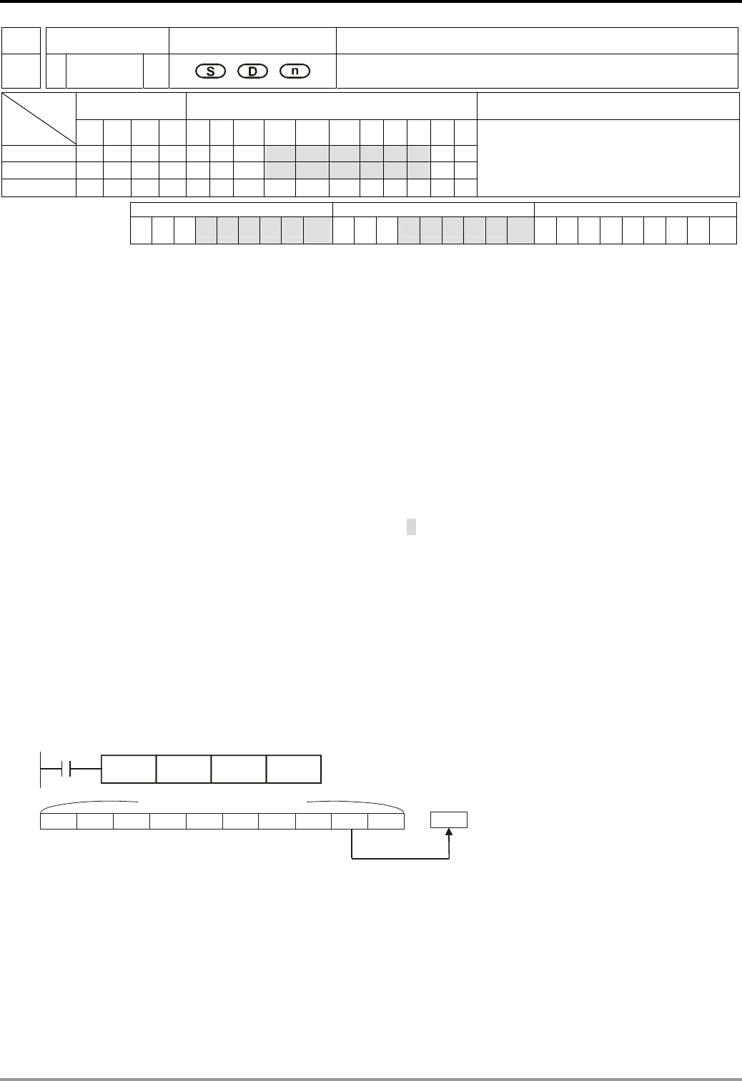
6 Application Instructions API 00-49
DVP-PLC Application Manual
6-58
API Mnemonic Operands Function
39
SFRD P Shift Register Read
Bit Devices Word Devices Program Steps Type
OP X Y M S K H KnX KnY KnM KnS T C D E F
S * * * * * *
D * * * * * ***
n * *
SFRD, SFRDP: 7 steps
PULSE 16-bit 32-bit
ES EX SS SA SX SC EH SV EH3
SV2 ES EX SS SA SX SC EH SV EH3
SV2 ES EX SS SA SX SC EH SV EH3
SV2
Operands:
S: Start No. of stack data D: Device of stack data read out n: Length of stack data
Explanations:
1. Range of n: 2 ~ 512
2. See the specifications of each model for their range of use.
3. Flag: M1020 (zero flag)
4. The stack data of n words starting from S are defined as “first-in, first-out” stack data. After the content in S
minuses 1, the content in the device designated by (S + 1) will be written into the location designated by D, and
(S + n-1) ~ (S + 2) will all right shift for one register while the content in (S + n-1) remains the same. When the
content in S equals 0, this instruction will not process any new value read out and the zero flag M1020 = On.
5. This instruction adopts pulse execution instructions (SFRDP)
Program Example:
1. When X0 = Off→On, the content in D1 will be sent to D21 and D9~D2 will shift to the right for 1 register (content
in D9 remains unchanged) and the content in D0 minus 1.
2. The figure below illustrates the shift and reading in 1~3 execution of the instruction.
n The content in D1 is sent to D21.
o D9 ~ D2 shift to the right for 1 register.
p The content in D0 minuses 1.
D9 D8 D7 D6 D5 D4 D3 D2 D1 D0 D21
X0
SFRDP D0 K10
D21
n = 10 points
data read
pointer
Remarks:
This instruction can be used together with API 38 SFWR for the reading/writing of “first-in, first-out” stack data.
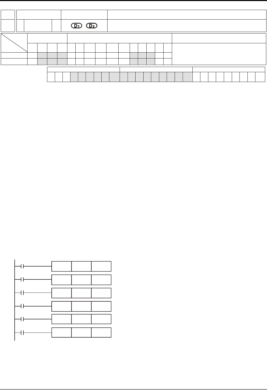
6 Application Instructions API 00-49
DVP-PLC Application Manual 6-59
API Mnemonic Operands Function
40
ZRST P Zero Reset
Bit Devices Word Devices Program Steps Type
OP X Y M S K H KnX KnY KnM KnS T C D E F
D1 * * * ***
D2 * * * ***
ZRST, ZRSTP: 5 steps
PULSE 16-bit 32-bit
ES EX SS SA SX SC EH SV EH3
SV2 ES EX SS SA SX SC EH SV EH3
SV2 ES EX SS SA SX SC EH SV EH3
SV2
Operands:
D1: Start device of the range to be reset D2: End device of the range to be reset
Explanations:
1. No. of operand D1 ≤ No. of operand D2.
2. D1 and D2 have to designate devices of the same type.
3. ES/EX/SS series MPU does not support E, F index register modification.
4. See the specifications of each model for their range of use.
5. When the instruction is executed, area from D1 to D2 will be cleared.
6. In ES/EX/SS, 16-bit counter and 32-bit counter cannot use ZRST instruction together.
7. In SA/EH, 16-bit counter and 32-bit counter can use ZRST instruction together.
8. When D1 > D2, only operands designated by D2 will be reset.
Program Example:
1. When X0 = On, auxiliary relays M300 ~ M399 will be reset to Off.
2. When X1 = On, 16 counters C0 ~ C127 will all be reset (writing in 0; contact and coil being reset to Off).
3. When X10 = On, timers T0 ~ T127 will all be reset (writing in 0; contact and coil being reset to Off).
4. When X2 = On, steps S0 ~ S127 will be reset to Off.
5. When X3 = On, data registers D0 ~ D100 will be reset to 0.
6. When X4 = On, 32-bit counters C235 ~ C254 will all be reset. (writing in 0; contact and coil being reset to Off)
ZRST M300 M399
ZRST C0 C127
ZRST T0 T127
ZRST S0 S127
ZRST D0 D100
ZRST C235 C254
X0
X1
X10
X2
X3
X4
Remarks:
1. Devices, e.g. bit devices Y, M, S and word devices T, C, D, can use RST instruction.
2. API 16 FMOV instruction is also to send K0 to word devices T, C, D or bit registers KnY, KnM, KnS for reset.

6 Application Instructions API 00-49
DVP-PLC Application Manual
6-60
RST M0
X0
RST T0
RST Y0
FMOV K0 D10 K5
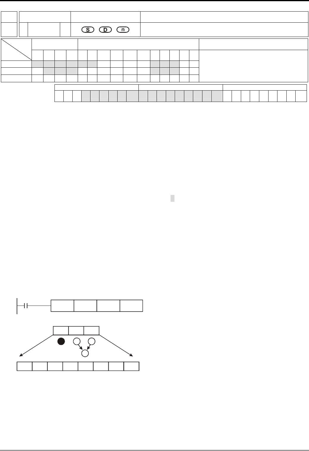
6 Application Instructions API 00-49
DVP-PLC Application Manual 6-61
API Mnemonic Operands Function
41
DECO P Decode
Bit Devices Word Devices Program Steps Type
OP X Y M S K H KnX KnY KnM KnS T C D E F
S * * * * * * *****
D * * * *****
n * *
DECO, DECOP: 7 steps
PULSE 16-bit 32-bit
ES EX SS SA SX SC EH SV EH3
SV2 ES EX SS SA SX SC EH SV EH3
SV2 ES EX SS SA SX SC EH SV EH3
SV2
Operands:
S: Source device to be decoded D: Device for storing the decoded result n: Length of decoded bits
Explanations:
1. Range of n when D is a bit device: 1 ~ 8
2. Range of n when D is a word device: 1 ~ 4
3. ES/EX/SS series MPU does not support E, F index register modification.
4. See the specifications of each model for their range of use.
5. The lower “n” bits of S are decoded and the results of “2n” bits are stored in D.
6. This instruction adopts pulse execution instructions (DECOP)
Program Example 1:
1. When D is used as a bit device, n = 1 ~ 8. Errors will occur if n = 0 or n > 8.
2. When n = 8, the maximum points to decode is 28 = 256 points. (Please be aware of the storage range of the
devices after the decoding and do not use the devices repeatedly.)
3. When X10 = Off→On, this instruction will decode the content in X0 ~ X2 to M100 ~ M107.
4. When the source of data is 1 + 2 = 3, set M103, the 3rd bit starting from M100, as 1.
5. After the execution of this instruction is completed and X10 turns to Off, the content that has been decoded and
output keeps acting.
X10
DECOP D10 D20 K3
X2 X1 X0
M107 M106 M105 M104 M103 M102 M101 M100
011
1
0000 000
3
76 54 210
412
3
Program Example 2:
1. When D is used as a word device, n = 1 ~ 4. Errors will occur if n = 0 or n > 4.
2. When n = 4, the maximum points to decode is 24 = 16 points.

6 Application Instructions API 00-49
DVP-PLC Application Manual
6-62
3. When X10 = Off→On, this instruction will decode b2 ~ b0 in D10 to b7 ~ b0 in D20. b15 ~ b8 that have not been
used in D20 will all become 0.
4. The lower 3 bits of D10 are decoded and stored in the lower 8 bits of D20. The higher 8 bits of D20 are all 0.
5. After the execution of this instruction is completed and X10 turns to Off, the content that has been decoded and
output keeps acting.
X10
DECOP D10 D20 K3
0000000011111111
0 000 0000 00 001 00 0
01234567
1
24
b15
b15 b0
b0
D10
D20
all be 0
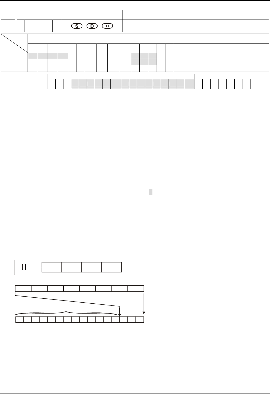
6 Application Instructions API 00-49
DVP-PLC Application Manual 6-63
API Mnemonic Operands Function
42
ENCO P Encode
Bit Devices Word Devices Program Steps Type
OP X Y M S K H KnX KnY KnM KnS T C D E F
S * * * * *****
D *****
n * *
ENCO, ENCOP: 7 steps
PULSE 16-bit 32-bit
ES EX SS SA SX SC EH SV EH3
SV2 ES EX SS SA SX SC EH SV EH3
SV2 ES EX SS SA SX SC EH SV EH3
SV2
Operands:
S: Source device to be encoded D: Device for storing the encoded result n: Length of encoded bits
Explanations:
1. Range of n when S is a bit device: 1 ~ 8
2. Range of n when S is a word device: 1 ~ 4
3. ES/EX/SS series MPU does not support E, F index register modification.
4. See the specifications of each model for their range of use.
5. The lower “2n” bits of S are encoded and the result is stored in D.
6. If several bits of S are 1, the first bit that is 1 will be processed orderly from high bit to low bit.
7. If no bits of S is 1, M1067, M1068 = On and D1067 records the error code 0E1A (hex).
8. This instruction adopts pulse execution instructions (ENCOP)
Program Example 1:
1. When S is used as a bit device, n = 1 ~ 8. Errors will occur if n = 0 or n > 8.
2. When n = 8, the maximum points to encode is 28 = 256 points.
3. When X10 = Off→On, this instruction will encode the 23 bits data (M0 ~ M7) and store the result in the lower 3
bits (b2 ~ b0) of D0. b15 ~ b3 that have not been used in D0 will all become 0.
4. After the execution of this instruction is completed and X10 turns to Off, the content in D remains unchanged.
ENCOP M0 K3
D0
X0
0 000 000 0 00 00 100
124
b15 b0
D0
1
00 0 01 00 0
76 5 4 3 21 0
M7 M6 M5 M4 M3 M2 M1 M0
all be 0
Program Example 2:
1. When S is used as a word device, n = 1 ~ 4. Errors will occur if n = 0 or n > 4.
2. When n = 4, the maximum points to decode is 24 = 16 points.

6 Application Instructions API 00-49
DVP-PLC Application Manual
6-64
3. When X10 = Off→On, this instruction will encode 23 bits (b0 ~ b7) in D10 and stores the result in the lower 3 bits
(b2 ~ b0) of D20. b15 ~ b3 that have not been used in D20 will all become 0. b8 ~ b15 of D10 are invalid data.
4. After the execution of this instruction is completed and X10 turns to Off, the content in D remains unchanged.
ENCOP D10 K3
D20
X0
0 000 0 000 00 00 100
b15 b0
D20
1
6543210
00 00 000010100111
b15
b0
7
D10
all be 0
Invalid data
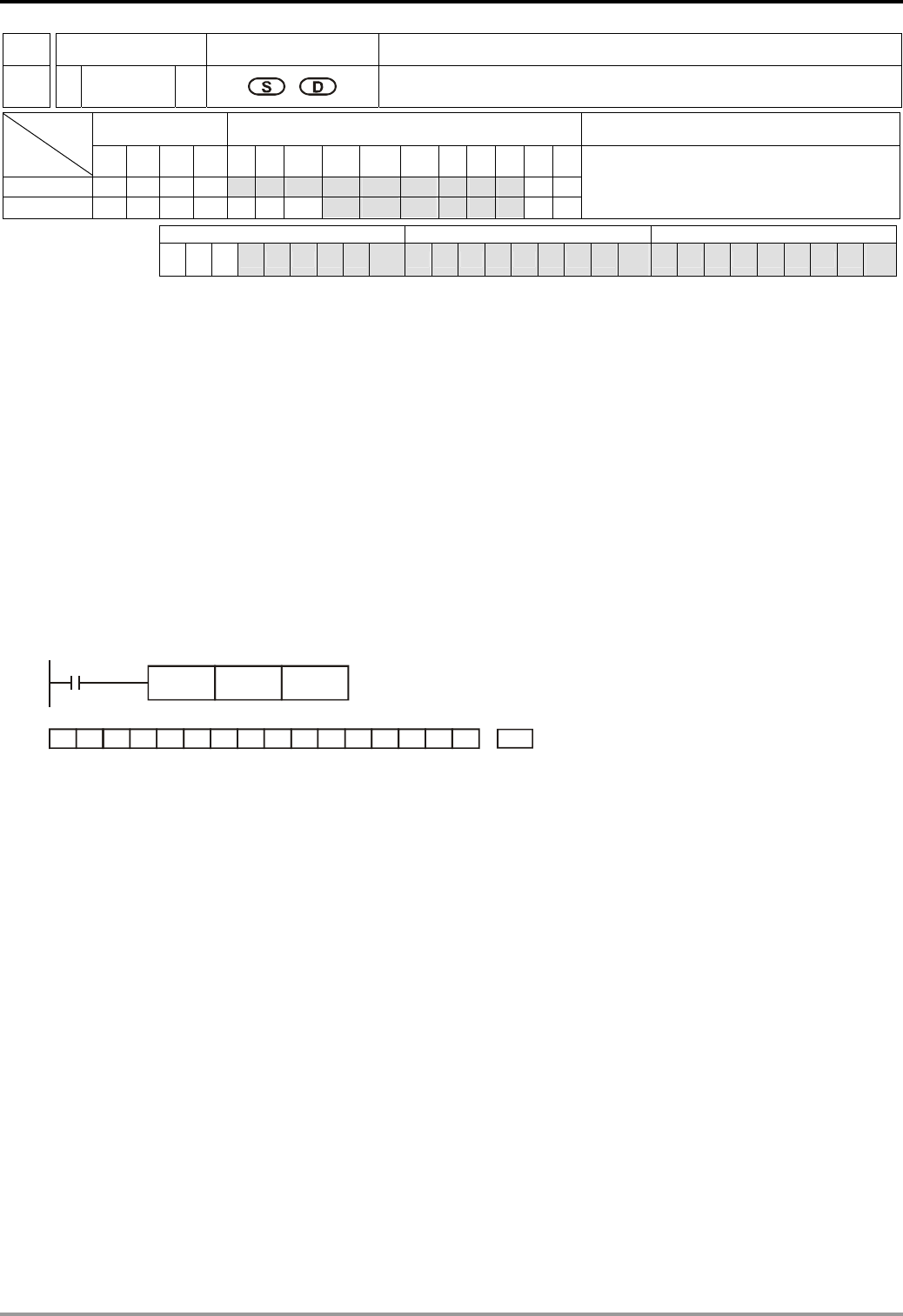
6 Application Instructions API 00-49
DVP-PLC Application Manual 6-65
API Mnemonic Operands Function
43
D SUM P Sum of Active Bits
Bit Devices Word Devices Program Steps Type
OP X Y M S K H KnX KnY KnM KnS T C D E F
S * * * ** * *****
D ** * *****
SUM, SUMP: 5 steps
DSUM, DSUMP: 9 steps
PULSE 16-bit 32-bit
ES EX SS SA SX SC EH SV EH3
SV2 ES EX SS SA SX SC EH SV EH3
SV2 ES EX SS SA SX SC EH SV EH3
SV2
Operands:
S: Source device D: Destination device for storing counted value
Explanations:
1. If S and D are used in device F, only 16-bit instruction is applicable.
2. See the specifications of each model for their range of use.
3. Flag: M1020 (zero flag)
4. Among the bits of S, the total of bits whose content is “1” will be stored in D.
5. When all the 16 bits of S are “0”, zero flag M1020 = On.
6. When 32- instruction is in use, D will occupy 2 registers.
Program Example:
When X10 = On, among the 16 bits of D0, the total of bits whose content is “1” will be stored in D2.
X10
SUM D0 D2
0000 00011 100 0000 K3
D2D0
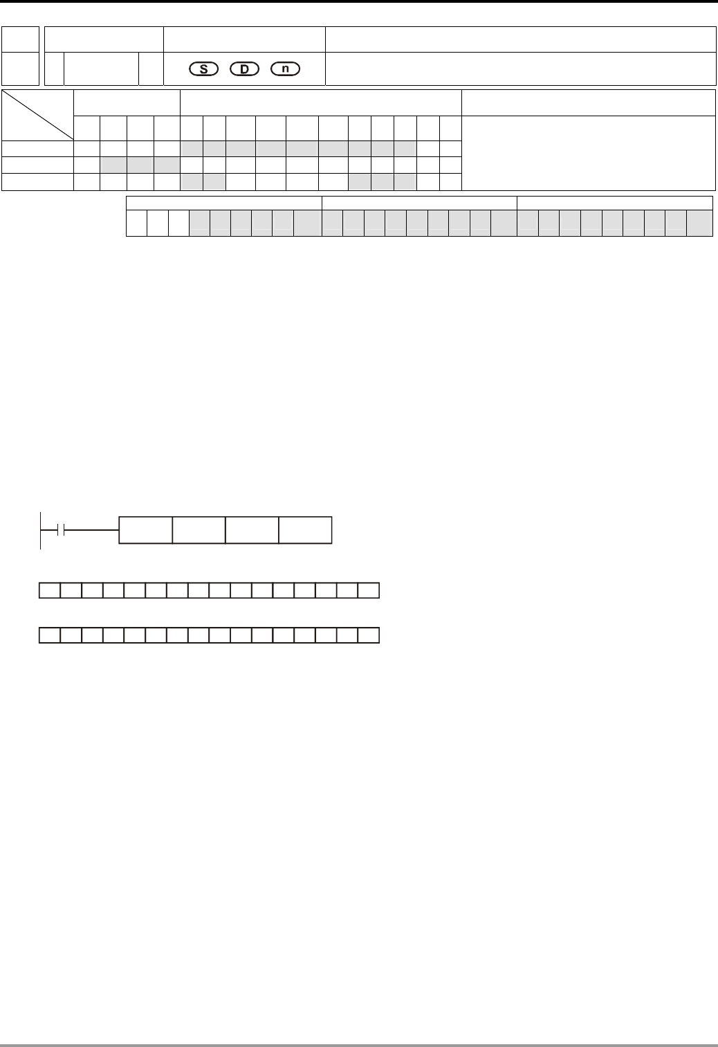
6 Application Instructions API 00-49
DVP-PLC Application Manual
6-66
API Mnemonic Operands Function
44
D BON P Check Specified Bit Status
Bit Devices Word Devices Program Steps Type
OP X Y M S K H KnX KnY KnM KnS T C D E F
S * ** * * * * * ***
D * * *
n * * * * ***
BON, BONP: 7 steps
DBON, DBONP: 13 steps
PULSE 16-bit 32-bit
ES EX SS SA SX SC EH SV EH3
SV2 ES EX SS SA SX SC EH SV EH3
SV2 ES EX SS SA SX SC EH SV EH3
SV2
Operands:
S: Source device D: Device for storing check result n: Bits specified for check
Explanations:
1. If S is used in device F, only 16-bit instruction is applicable.
2. Range of n: 0 ~ 15 (16-bit instruction); 0 ~ 31 (32-bit instruction)
3. See the specifications of each model for their range of use.
4. When the nth bit of S is “1”, D = On; when the nth bit of S is “0”, D = Off.
Program Example:
1. When X0 = On, assume the 15th bit of D0 is “1”, and M0 = On. Assume the 15th bit of D0 is “0”, and M0 = Off.
2. When X0 goes Off, M0 will remains in its previous status.
X0
BON D0 M0
0000 00011 100 0000
D0
K15
b0
M0=Off
b15
1000 00011 100 0000
D0
b0
M0=On
b15
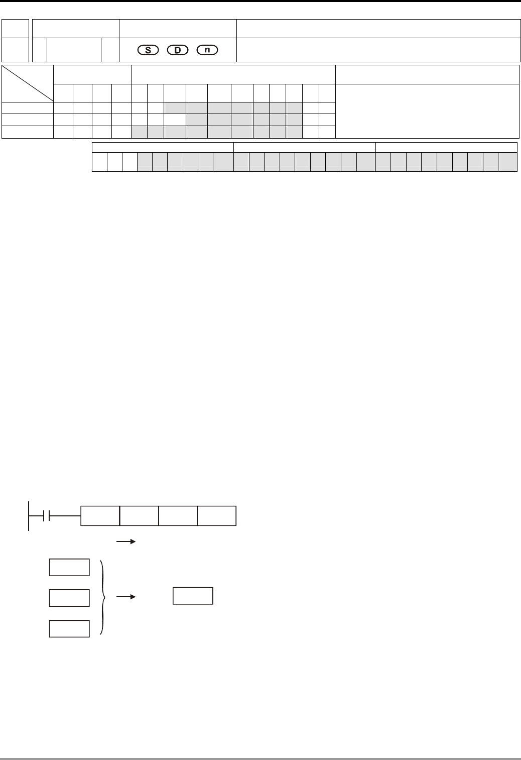
6 Application Instructions API 00-49
DVP-PLC Application Manual 6-67
API Mnemonic Operands Function
45
D MEAN P Mean
Bit Devices Word Devices Program Steps Type
OP X Y M S K H KnX KnY KnM KnS T C D E F
S * ** * * * *
D ** * *****
n * * * ** * *****
MEAN, MEANP: 7 steps
DMEAN, DMEANP: 13 steps
PULSE 16-bit 32-bit
ES EX SS SA SX SC EH SV EH3
SV2 ES EX SS SA SX SC EH SV EH3
SV2 ES EX SS SA SX SC EH SV EH3
SV2
Operands:
S: Start device to obtain mean value D: Destination device for storing mean value n: The number of consecutive
source devices used
Explanations:
1. If D is used in device F, only 16-bit instruction is applicable.
2. Range of n: 1 ~ 64
3. In ES/EX/SS series models: Operand S cannot designate KnX, KnY, KnM, KnS.
4. ES/EX/SS series MPU does not support E, F index register modification.
5. See the specifications of each model for their range of use.
6. After the content of n devices starting from S are added up, the mean value of the result will be stored in D.
7. Remainders in the operation will be left out.
8. Provided the No. of designated device exceeds its normal range, only the No. within the normal range can be
processed.
9. If n falls without the range of 1 ~ 64, PLC will determine it as an “instruction operation error”.
Program Example:
When X10 = On, the contents in 3 (n = 3) registers starting from D0 will be summed and then divided by 3. The
obtained mean value will be stored in D10 and the remainder will be left out.
MEAN D0 K3
D10
X10
(D0+D1+D2)/3 D10
D0
D1
D2
K100
K113
K125
K112
D10
Remainder = 3, left out
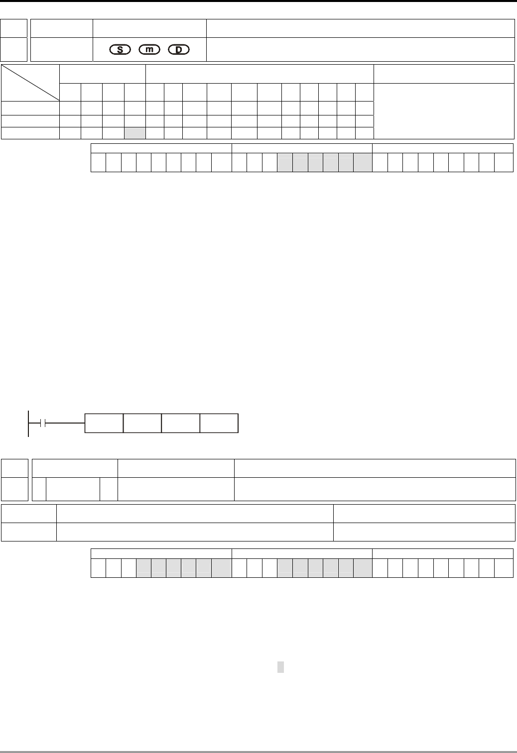
6 Application Instructions API 00-49
DVP-PLC Application Manual
6-68
API Mnemonic Operands Function
46
ANS Timed Annunciator Set
Bit Devices Word Devices Program Steps Type
OP X Y M S K H KnX KnY KnM KnS T C D E F
S *
m *
D *
ANS: 7 steps
PULSE 16-bit 32-bit
ES EX SS SA SX SC EH SV EH3
SV2 ES EX SS SA SX SC EH SV EH3
SV2 ES EX SS SA SX SC EH SV EH3
SV2
Operands:
S: Timer for monitoring annunciator m: Time setting D: Annunciator device
Explanations:
1. Range of S: for SA/SX/SC T0 ~ T191; for EH/EH2/SV/EH3/SV2 T0 ~ T199.
2. m can designate K1 ~ K32,767 (unit: 100ms)
3. Range of D: for SA/SX/SC S896 ~ S1023; for EH/EH2/SV/EH3/SV2 S900 ~ S1023.
4. See the specifications of each model for their range of use.
5. Flags: M1048 (annunciator in action); M1049 (valid monitoring)
6. This instruction is used for enabling the annunciator.
Program Example:
If X3 = On for more than 5 seconds, annuniciator point S999 = On. Even X3 goes Off afterwards, S999 will still keep
On. However, T10 will be reset to Off and the present value = 0.
X3
ANS T10 K50 S999
API Mnemonic Operands Function
47
ANR P Annunciator Reset
OP Descriptions Program Steps
N/A ANR, ANRP: 1 steps
PULSE 16-bit 32-bit
ES EX SS SA SX SC EH SV EH3
SV2 ES EX SS SA SX SC EH SV EH3
SV2 ES EX SS SA SX SC EH SV EH3
SV2
Explanations:
1. No operand.
2. This instruction is used for resetting the annunciator.
3. When more than one annuciators are On, the annunciator of smaller number will be reset.
4. This instruction adopts pulse execution instructions (ANRP)
Program Example:
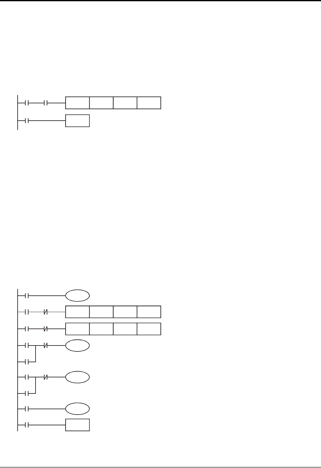
6 Application Instructions API 00-49
DVP-PLC Application Manual 6-69
1. If X10 and X11 = On at the same time for more than 2 seconds, annuniciator point S910 = On. Even X10 and
X11 go Off afterwards, S910 will still keep On. However, T10 will be reset to Off and the present value = 0.
2. When X10 and X11 are On at the same time for less than 2 seconds, the present value of T10 will be reset to 0.
3. When X3 goes from Off to On,
S896 ~ S1023 in SA/SX/SX are able to reset the annunciators in action.
S900 ~ S1023 in EH/EH2/ SV/EH3/SV2 are able to reset the annunciators in action.
4. When X3 goes from Off to On again, the annuniator with secondary smaller No. will be reset.
X10
ANS T10 K20 S910
X11
X3
ANRP
Remarks:
1. Flag:
a) M1048 (annunciator in action): When M1049 = On, any of the annunciators among S896 ~ S1023 in
SA/SX/SC or S900 ~ S1023 in EH/EH2/SV/EH3/SV2 starts output, M1048 will be On.
b) M1049 (valid monitoring): When M1049 = On, D1049 will automatically display the annuciator of the
smallest number in action.
2. Application of annunciators:
I/O point configuration:
X0: Forward switch Y0: Forward S910: Forward annunciator
X1: Backward switch Y1: Backward S920: Backward annunciator
X2: Front position switch Y2: Annunciator indicator
X3: Back position switch
X4: Annunciatro reset button
Y0
ANS T0 K100 S910
X2
X4
ANRP
M1000
M1049
Y1
ANS T1 K200 S920
X3
X0
Y0
X2
M1048
Y2
Y0
X1
Y1
X3
Y1
1. M1048 and D1049 are valid only when M1049 = On.

6 Application Instructions API 00-49
DVP-PLC Application Manual
6-70
2. When Y0 = On for more than 10 seconds and the device fails to reach the frong position X2, S910= On.
3. When Y1 = On for more than 10 seconds and the device fails to reach the back position X3, S920= On.
4. When backward switch X1 = On and backward device Y1 = On, Y1 will go Off only when the device reaches the
back position switch X3.
5. Y2 will be On when any annunciator is enabled. Whenever X4 is on, 1 annunciator in action will be reset. The
reset starts from the annunciator with the smallest No.
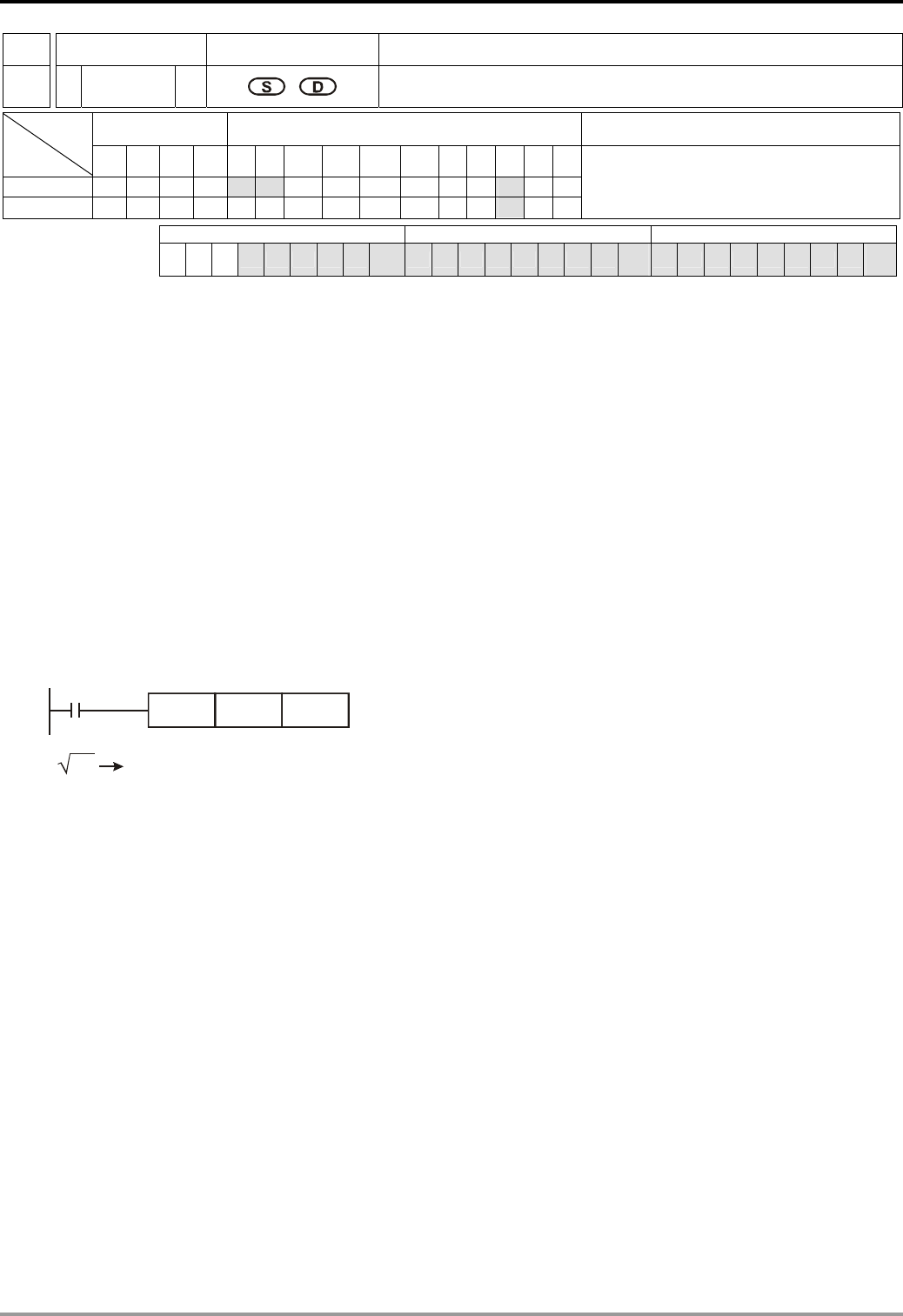
6 Application Instructions API 00-49
DVP-PLC Application Manual 6-71
API Mnemonic Operands Function
48
D SQR P Square Root
Bit Devices Word Devices Program Steps Type
OP X Y M S K H KnX KnY KnM KnS T C D E F
S * * *
D *
SQR, SQRP: 5 steps
DSQR, DSQRP: 9 steps
PULSE 16-bit 32-bit
ES EX SS SA SX SC EH SV EH3
SV2 ES EX SS SA SX SC EH SV EH3
SV2 ES EX SS SA SX SC EH SV EH3
SV2
Operands:
S: Source device D: Device for storing the result
Explanations:
1. See the specifications of each model for their range of use.
2. Flags: M1020 (zero flag); M1021 (borrow flag); M1067 (instruction operation error)
3. This instruction performs a square root operation on S and stores the result in D.
4. S can only be a positive value. If S is negative, PLC will regard it as an “instruction operation error” and will not
execute this instruction. M1067 and M1068 = On and D1067 records the error code 0E1B (hex).
5. The operation result D should be integer only, and the decimal will be left out. Borrow flag M1021 = On.
6. When the operation result D = 0, zero flag M1020 = On.
Program Example:
When X10 = On, the instruction performs a square root on D0 and stores the result in D12.
X10
SQR D0 D12
D0 D12

6 Application Instructions API 00-49
DVP-PLC Application Manual
6-72
API Mnemonic Operands Function
49
D FLT P Convert BIN integer to binary floating point
Bit Devices Word Devices Program Steps Type
OP X Y M S K H KnX KnY KnM KnS T C D E F
S *
D *
FLT, FLTP: 5 steps
DFLT, DFLTP: 9 steps
PULSE 16-bit 32-bit
ES EX SS SA SX SC EH SV EH3
SV2 ES EX SS SA SX SC EH SV EH3
SV2 ES EX SS SA SX SC EH SV EH3
SV2
Operands:
S: Source device for conversion D: Device for storing the conversion result
Explanations:
1. See the specifications of each model for their range of use.
2. Flags: M1081 (FLT instruction function switch); M1020 (zero flag); M1021 (borrow flag); M1022 (carry flag)
3. D will occupy 2 consecutive devices
4. When M1081 is Off, BIN integer is converted into binary floating point value. At this time, S of the 16-bit
instruction, FLT, occupies 1 register and D occupies 2 registers.
a) If the absolute value of the conversion result > max. floating value, carry flag M1022 = On.
b) If the absolute value of the conversion result < min. floating value, carry flag M1021 = On.
c) If the conversion result is 0, zero flag M1020 = On.
5. When M1081 is On, binary floating point value is converted into BIN integer (digits after decimal point are left
out). At this time, S of the 16-bit instruction, FLT, occupies 2 registers and D occupies 1 register (action same as
that of INT instruction).
a) If the conversion result exceeds the range of BIN integer available in D (for 16-bit: -32,768 ~ 32,767; for 32-bit:
-2,147,483,648 ~ 2,147,483,647), D will obtain the maximum or minimum value and carry flag M1022 = On.
b) If any digits is left out during the conversion, borrow flag M1021 = On.
c) If S = 0, zero flag M1020 = On.
d) After the conversion, D stores the result in 16 bits.
Program Example 1:
1. When M1081 = Off, the BIN integer is converted into binary floating point value.
2. When X10 = On, D0 (BIN integer) is converted into D13 and D12 (binary floating point value).
3. When X11 = On, D1 and D0 (BIN integer) are converted into D21 and D20 (binary floating point value).
4. If D0 = K10, X10 will be On. The 32-bit value of the converted floating point will be H41200000 and stored in
32-bit register D12 (D13).
5. If 32-bit register D0 (D1) = K100,000, X11 will be On. The 32-bit value of the converted floating point will be
H47C35000 and stored in 32-bit register D20 (D21).
6 Application Instructions API 00-49
DVP-PLC Application Manual 6-73
M1002
RST M1081
X10
FLT D0 D12
X11
DFLT D0 D20
Program Example 2:
1. When M1081 = On, the binary floating point value is converted into BIN integer (the decimal is left out).
2. When X10 = On, D0 and D1 (binary floating point value) are converted into D12 (BIN integer). If D0 (D1) =
H47C35000, the floating point value will be presented as 100,000. Due to that the value is larger than the value
presentable by the 16-bit register D12, the result will be D12 = K32, 767 and M1022 = On.
3. When X11 = On, D1 and D0 (binary floating point value) are converted into D21 and D20 (BIN integer). If D0 (D1)
= H47C35000, the floating point value will be presented as 100,000. The result will be stored in the 32-bit
register D20 (D21).
M1002
SET M1081
X10
FLT D0 D12
X11
DFLT D0 D20
Program Example 3:
Please use this instruction to complete the following operation.
(D10) (X7~X0) K61.5
16 BIN-bit 2-digit BCD
(D21,D20)
(D101,D100) (D200) BIN
(D203,D202)
(D301,D300)
(D401,D400)
(D31,D30)
(D41,D40)
12
3
4
5
6
7
8
binary floating point
binary floating pointbinary floating point
binary floating point
binary floating point
decimal floating point (for )monitoring
32 integer-bit

6 Application Instructions API 00-49
DVP-PLC Application Manual
6-74
M1000
FLT D10 D100
BIN K2X0 D200
FLT D200 D202
DEDIV K615 K10
DEDIV D100 D202
DEMUL D400 D300
DEBCD D20 D30
DINT D20 D40
D300
D400
D20
1
2
3
4
5
6
7
8
○
1 D10 (BIN integer) is converted to D101 and D102 (binary floating point value).
○
2 X7 ~ X0 (BCD value) are converted to D200 (BIN value).
○
3 D200 (BIN integer) is converted to D203 and D202 (binary floating point value).
4The result of K615 ÷ K10 is stored in D301 and D300 (binary floating point value).
○
5 The result of binary decimal division (D101, D100) ÷ (D203, D202) is stored in D401 and D400 (binary floating
point value).
○
6 The result of binary decimal multiplication (D401, D400) × (D301, D300) is stored in D21 and D20 (binary
floating point value).
○
7 D21 and D20 (binary floating point value) are converted to D31 and D30 (decimal floating point value).
○
8 D21 and D20 (binary floating point value) are converted to D41 and D40 (BIN integer).
7 Application Instructions API 50-99
DVP-PLC APPLICATION MANUAL
7-1
API Mnemonic Operands Function
50
REF P Refresh
Bit Devices Word Devices Program Steps Type
OP X Y M S K H KnX KnY KnM KnS T C D E F
D * *
n * *
REF, REFP: 5 steps
PULSE 16-bit 32-bit
ES EX SS SA SX SC EH SV EH3
SV2 ES EX SS SA SX SC EH SV EH3
SV2 ES EX SS SA SX SC EH SV EH3
SV2
Operands:
D: Start device to be I/O refreshed n: Number of items to be I/O refreshed
Explanations:
1. D must designate X0, X10, Y0, Y10…the points whose 1s digit is “0”. See remarks for more details.
2. Range of n: 8 ~ 256 (has to be the multiple of 8).
3. See the specifications of each model for their range of use.
4. The status of all PLC input/output terminals will be updated after the program scans to END. When the
program starts to scan, the status of the external input terminal is read and stored into the memory of the input
point. The output terminal will send the content in the output memory to the output device after END instruction
is executed. Therefore, this instruction is applicable when the latest input/output data are needed for the
operation.
5. D has to be designated to be X0, X10, Y0, Y10…such forms whose 1st digit is “0”. Range of n: 8 ~ 256 (must
be 8’s multiple); otherwise it will be regarded as an error. The range varies in different models. See Remarks
for more details.
Program Example 1:
When X0 = On, PLC will read the status of input points X0 ~ X17 immediately and refresh the input signals without
any input delay.
X0
REF X0 K16
Program Example 2:
When X0 = On, the 8 output signal from Y0 ~ Y7 will be sent to output terminals and refreshed without having to wait
for the END instruction for output.
X0
REF Y0 K8
Remarks:
The instruction only process the I/O points X0 ~ X17 and Y0 ~ Y17 of ES/EX/SS/SA/SX/SC series MPU, namely n =
K8 or n = K16.
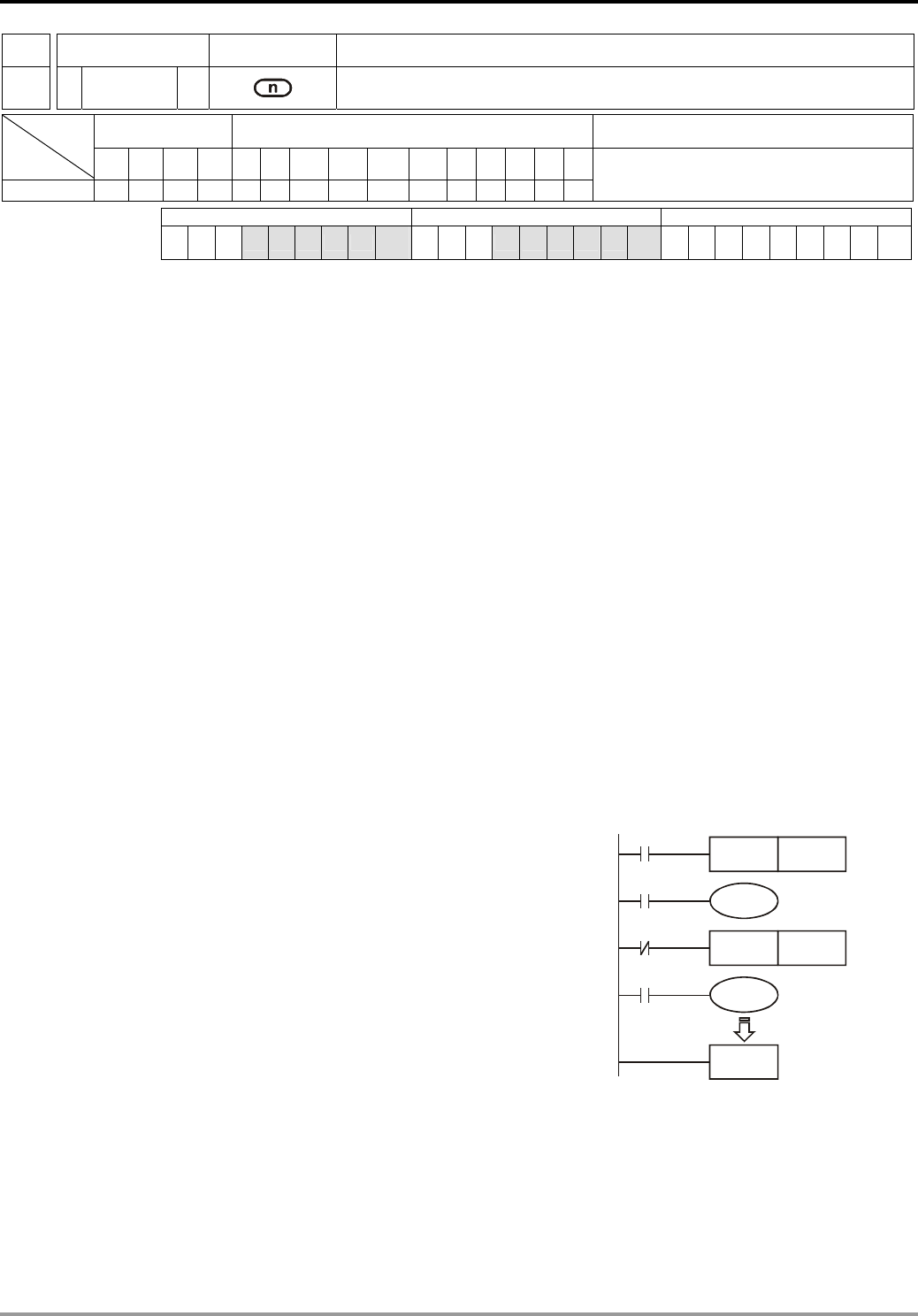
7 Application Instructions API 50-99
DVP-PLC APPLICATION MANUAL
7-2
API Mnemonic Operands Function
51
REFF P Refresh and Filter Adjust
Bit Devices Word Devices Program Steps Type
OP X Y M S K H KnX KnY KnM KnS T C D E F
n * *
REFF, REFFP: 3 steps
PULSE 16-bit 32-bit
ES EX SS SA SX SC EH SV EH3
SV2 ES EX SS SA SX SC EH SV EH3
SV2 ES EX SS SA SX SC EH SV EH3
SV2
Operands:
n: Response time (unit: ms)
Explanation:
1. Range of n: for SA/SX/SC, n = K0 ~ K20; for EH/EH2/SV/EH3/SV2, n = K0 ~ K60.
2. To avoid interferences, X0 ~ X17 of EH/EH2/SV/EH3/SV2 series MPU and X0 ~ X7 of SA/SX/SC series MPU
are equipped with digital filters on output terminals. Digital filters adjust the response time by REFF instruction.
This instruction sets up n directly in D1020 (adjusting the response time of X0 ~ X7) and D1021 (adjusting the
response time of X10 ~ X17).
3. Rules for adjusting the reponse time of the filter at X0 ~ X17:
a) When the power of PLC turns from Off to On or the END instruction is being executed, the response time
will be determined upon the contents in D1020 and D1021.
b) You can use MOV instruction in the program to move the time values to D1020 and D1021 and make
adjustments in the next scan.
c) You can use REFF instruction to change the response time during the execution of the program. The
changed response time will be move to D1020 and D1021 and you can make adjustments in the next scan.
Program Example:
1. When the power of PLC turns from Off to On, the response
time of X0 ~ X17 will be determined by the contents in D1020
and D1021.
2. When X20 = On, REFF K5 will be executed and the response
time will be changed to 5ms for the adjustment in the next
scan.
3. When X20 = Off, the REFF K20 will be executed and the
response time will be changed to 20ms for the adjustment in
the next scan.
X20
REFF K5
X0
Y1
X20
REFF K20
X1
Y2
END
Remarks:
When inserting an interruption subroutine in the program or using the high speed counter or API 56 SPD instruction,
the corresponding signals at the input terminals will not delay and has nothing to do with this instruction.

7 Application Instructions API 50-99
DVP-PLC APPLICATION MANUAL
7-3
API Mnemonic Operands Function
52
MTR Input Matrix
Bit Devices Word Devices Program Steps Type
OP X Y M S K H KnX KnY KnM KnS T C D E F
S *
D1 *
D2 * * *
n * *
MTR: 9 steps
PULSE 16-bit 32-bit
ES EX SS SA SX SC EH SV EH3
SV2 ES EX SS SA SX SC EH SV EH3
SV2 ES EX SS SA SX SC EH SV EH3
SV2
Operands:
S: Start device of matrix input D1: Start device of matrix output D2: Corresponding start device for matrix scan
n: Number of arrays in matrix scan
Explanations:
1. S must designate X0, X10…the X points whose 1st digit is “0” and occupies 8 consecutive points.
2. D1 must designate Y0, Y10…the Y points whose 1st digit is “0” and occupies n consecutive points.
3. D2 must designate Y0, M0. S0…the Y, M, S points whose 1st digit is “0”.
4. Range of n: 2 ~ 8.
5. See the specifications of each model for their range of use.
6. Flag: M1029 (execution of the instruction is completed).
7. S is the start device No. of all input terminals connected to the matrix. Once S is designated, the 8 points
following the No. will be the input terminals in the matrix.
8. D1 designate the start device No. of transistor output Y in the matrix scan.
9. This instruction occupies continuous 8 input devices starting from S. n external output terminals starting from
D1 read the 8 switches of n arrays by matrix scan, obtaining 8 × n multiple-matrix input points. The status of
scanned switches will be stored in the devices starting from D2.
10. Maximum 8 input switches can be parallelly connected in 8 arrays and obtaining 64 input points (8 × 8 = 64).
11. When the 8-point 8-array matrix inputs are in use, the reading time of each array is approximately 25ms,
totaling the reading of 8 arrays 200ms, i.e. the input signals with On/Off speed of over 200ms are not
applicable in a matrix input.
12. The drive contact of this instruction uses normally On contact M1000.
13. Whenever this instruction finishes a matrix scan, M1029 will be On for one scan period.
14. There is no limitation on the number of times using the instruction, but only one instruction can be executed in
a period of time.
Program Example:
1. When PLC RUN, MRT instruction will start to be executed. The statuses of the external 2 arrays of 16 switches
will be read in order and stored in the internal relays M10 ~ M17, M20 ~ M27.
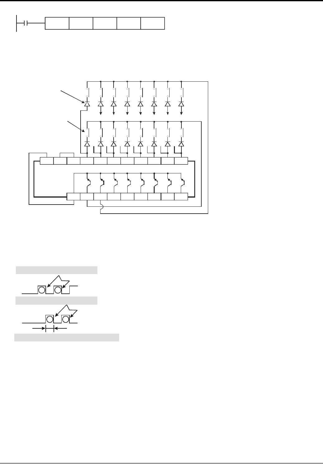
7 Application Instructions API 50-99
DVP-PLC APPLICATION MANUAL
7-4
M1000
MTR X40 Y40 M10 K2
2. The figure below illustrates the external wiring of the 2-array matrix input loop constructed by X40 ~ X47 and
Y40 ~ Y41. The 16 switches correponds to the internal relays M10 ~ M17, M20 ~ M27. Should be used with
MTR instruction.
S/S X40 X41 X42 X43 X44 X45 X47X46
CY40 Y41 Y42 Y43 Y44 Y45 Y47Y46
M10
X41
M20
M11 M12 M13 M14 M15 M16 M17
X42 X43 X44 X45 X46 X47
M21 M22 M23 M24 M25 M26 M27
+24V
24G
M10: the internal relay
corresponding to
the external switch
Must connect to the diode
of 0.1A/50V, 1N4148, in series
3. See the figure above. The 8 points starting from X40 start to perform a matrix scan from Y40 ~ Y41 (n = 2). D2
designates that the start device No. of the read results is M10, indicating that the first array is read to M10 ~
M17 and the second array is read to M20 ~ M27.
2 4
Y41
Y40
25ms
1 3
Read input signals in the 1st array
Read input signals in the 2nd array
Processing time of each array: approx. 25ms
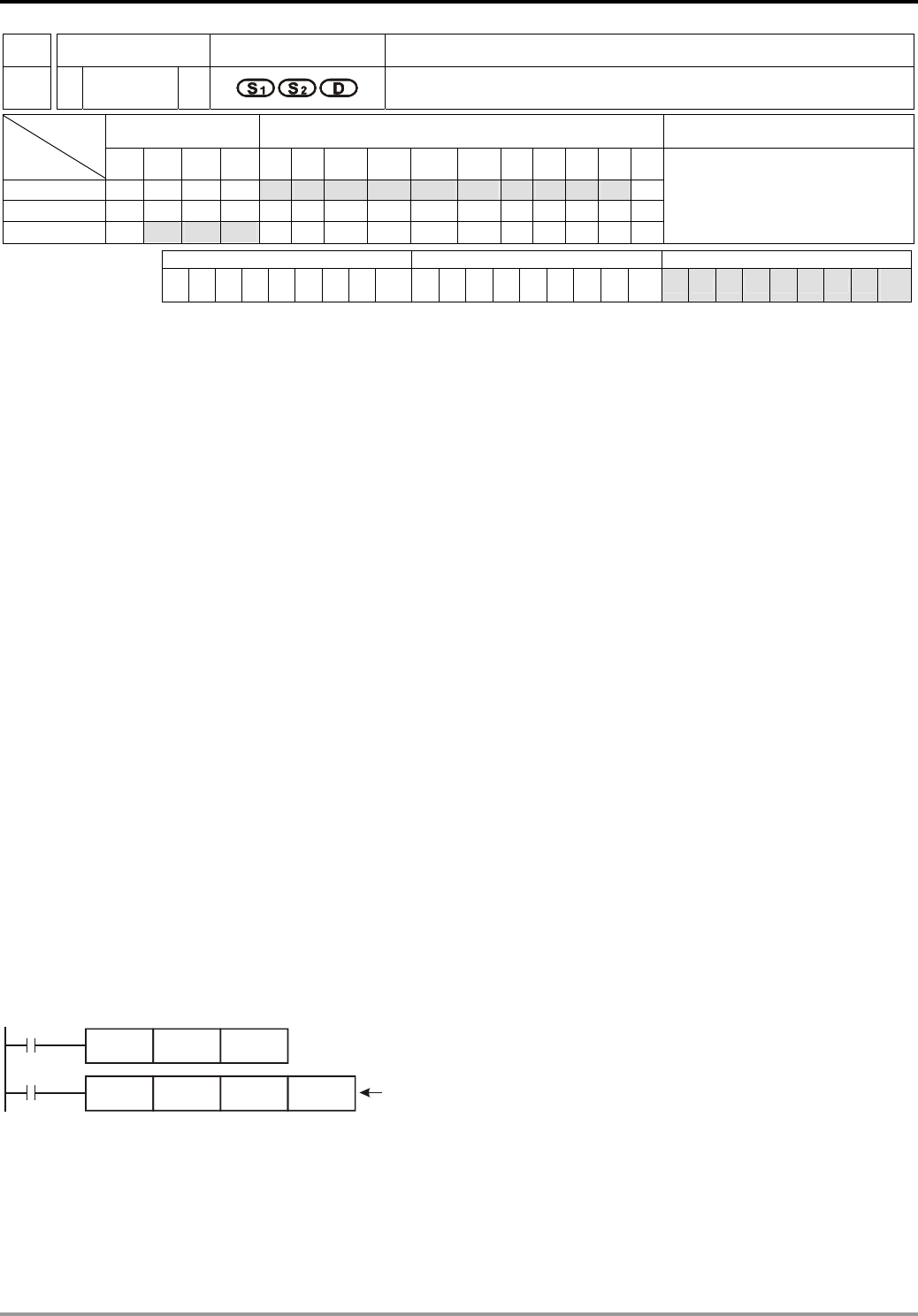
7 Application Instructions API 50-99
DVP-PLC APPLICATION MANUAL
7-5
API Mnemonic Operands Function
53
D HSCS High Speed Counter Set
Bit Devices Word Devices Program Steps Type
OP X Y M S K H KnX KnY KnM KnS T C D E F
S1 * * * * * * * * * *
S2 *
D * * *
DHSCS: 13 steps
PULSE 16-bit 32-bit
ES EX SS SA SX SC EH SV EH3
SV2 ES EX SS SA SX SC EH SV EH3
SV2 ES EX SS SA SX SC EH SV EH3
SV2
Operands:
S1: Comparative value S2: No. of high speed counter D: Comparison result
Explanations:
1. S2 has to designate the No. of high speed counters C235 ~ C255. See remarks for more details.
2. D can designate I0□0; □ = 1 ~ 6. ES series MPU does not support this.
3. D of ES and SA series MPU does not support E, F index register modification.
4. See the specifications of each model for their range of use.
5. Flags: M1289 ~ M1294 are interruption disability of the high speed counters in EH/EH2/SV/EH3/SV2 series
MPU. See Program Example 3 for more details.
6. The high speed counter inputs counting pulses from the corresponding external input terminals X0 ~ X17 by
inserting an interruption. When the high speed counter designated in S2 pluses 1 or minuses 1, DHSCS
instruction will perform a comparison immediately. When the present value in the high speed counter equals
the comparative value designated in S1, device designated in D will turn On. Even the afterward comparison
results are unequal, the device will still be On.
7. If the devices specified as the device D are Y0 ~ Y17, when the compare value and the present value of the
high-speed counter are equal, the comparison result will immediately output to the external inputs Y0 ~ Y17,
and other Y devices will be affected by the scan cycle. However, M, S devices are immediate output and will
not be affected by the scan cycle.
Program Example 1:
After PLC RUN and M0 = On, DHSCS instruction will be executed. When the present value in C235 changes from
99 to 100 or 101 to 100, Y10 will be On constantly.
M1000
DCNT C235 K1000
M0
DHSCS K100 C235 Y10 On immediately
Program Example 2:
Differences between Y output of DHSCS instruction and general Y output:
a) When the present value in C249 changes from 99 to 100 or 101 to 100, Y10 outputs immediately to the external
output point by interruption and has nothing to do with the PLC scan time. However, the time will still be delayed
by the relay (10ms) or transistor (10us) of the output module.
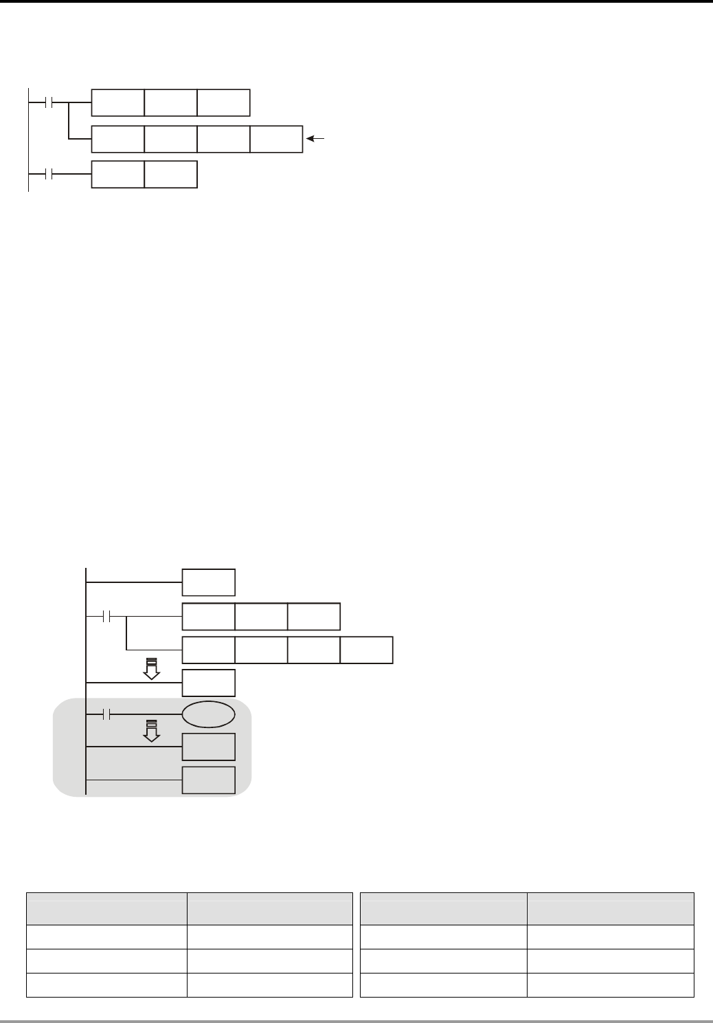
7 Application Instructions API 50-99
DVP-PLC APPLICATION MANUAL
7-6
b) When the present value in C249 changes from 99 to 100, the drive contact of C249 will be On immediately. When
the execution arrives at SET Y17, Y17 will still be affected by the scan time and will output after END instruction.
M1000
DCNT C249 K100
SET Y17
C249
DHSCS K100 C249 Y10 On immediately
Program Example 3:
1. High speed counter interruption:
a) Operand D of DHSCS instruction can designate I0□0, □ = 1 ~ 6, as the timing of interruption when the
counting reaches its target.
b) ES/EX/SS series MPU does not support high speed counter interruption.
c) SA/SX/SC series MPU supports high speed counter interruption. However, when DHSCS instruction
designates an I interruption, the designated high speed counter cannot be used in DHSCS, DHSCR, DHSZ
instructions. Misuse of high speed counter will result in error.
d) For SA/SX/SC series MPU, when the counting reaches the target, the interruption will occur. X0 is the
counter for counting input and the interruption No. is I010 (1 phase 2 inputs and A-B phase counter No. C246
~ C254 can only designate I010). X1 designates I020; X2 designates I030; X3 designates I040; X4
designates I050; X5 designates I060, totaling 6 points.
e) When the present value in C251 changes from 99 to 100 or 101 to 100, the program will jump to I010 and
execute the interruption service subroutine.
M1000
DCNT C251 K1000
FEND
DHSCS K100 C251 I010
M1000
Y1
IRET
END
I010
EI
2. In SA/SX/SC series MPU, M1059 is “I010 ~ I060 high speed counter interruption forbidden” flag.
3. In EH/EH2/SV/EH3/SV2 series MPU, M1289 ~ M1294 are the respectively for I010 ~ I060 “high speed counter
interruption forbidden flags”, i.e. when M1294 = On, I060 interruption will be forbidden.
Interruption pointer I No. Interruption forbidden flag Interruption pointer I No. Interruption forbidden flag
I010 M1289 I040 M1292
I020 M1290 I050 M1293
I030 M1291 I060 M1294
7 Application Instructions API 50-99
DVP-PLC APPLICATION MANUAL
7-7
Remarks:
1. The output contact of the high speed counter and the comparative outputs of API 53 DHSCS, API 34 DHSCR
and API 55 DHSZ instructions only perform comparison and contact outputs when there is a counting input.
When using data operation instructions, e.g. DADD, DMOV, for changing the present value in the high speed
counter or making the present value equals the set value, there will not be comparisons or comparative
outputs because there is no counting inputs.
2. High speed counters supported by ES/EX/SS series MPU (total bandwidth: 20kHz):
1-phase 1 input 1-phase 2 inputs 2-phase 2 inputs
Type
Input C235 C236 C237 C238 C241 C242 C244 C246 C247 C249 C251 C252 C254
X0 U/D U/D U/D U U U A A A
X1 U/D R R D D D B B B
X2 U/D U/D R R R R
X3 U/D R S S S
U: Progressively increasing input A: A phase input S: Input started
D: Progressively decreasing input B: B phase input R: Input cleared
a) Input points X0 and X1 can be planned as counters of higher speed (1 phase input can reach 20kHz).
However, the total counting frequency of the two input points has to be smaller or equal 20kHz. Provided
the input is a 2-phas input signal, the counting frequency will be approximately 4kHz. The frequency of
the input points X2 and X3 (1-phase) can reach 10kHz.
b) For ES/EX/SS series MPU, the uses of DHSCS instructio with DHSCR instruction cannot be more than 4
times.
3. High speed counters supported by SA/SX series MPU (total bandwidth: 40kHz):
1-phase 1 input 1-phase 2 inputs 2-phase 2 inputs
Type
Input C235 C236 C237 C238 C239 C240 C241 C242 C244 C246 C247 C249 C251 C252 C253 C254
X0 U/D U/D U/D U U U A A B A
X1 U/D R R D D D B B A B
X2 U/D U/D R R R R
X3 U/D R S S S
X4 U/D
X5 U/D
U: Progressively increasing input A: A phase input S: Input started
D: Progressively decreasing input B: B phase input R: Input cleared
a) Input points X0 and X1 for 1-phase input can reach a frequency of 20kHz and X2 ~ X5 can reach 10kHz.
2-phase input (X0, X1) C251, C252 and C254 can reach a frequency of 4kHz and C253 reach 25kHz
(only supports 4 times frequency counting).
b) Functions of the input point X5:
i) When M1260 = Off, C240 is the general U/D high speed counuter.
ii) When M1260 = On and C240 is enabled by DCNT instruction, X5 will be the shared reset signal for
C235 ~ C239. The counter C240 will still receive the counting input signals from X5.

7 Application Instructions API 50-99
DVP-PLC APPLICATION MANUAL
7-8
4. High speed counters supported by SC series MPU (total bandwidth: 130kHz):
1-phase 1 input 1-phase 2 inputs 2-phase inputs
Type
Input C235 C236 C237 C238 C239 C240 C241 C242 C243 C244 C245 C246 C247 C249 C250 C251 C252 C254 C255
X0 U/D U/D U/D U U U A A A
X1 U/D R R D D D B B B
X2 U/D U/D R R R R
X3 U/D R S S S
X4 U/D
X5 U/D
X10 U/D U A
X11 U/D D B
U: Progressively increasing input A: A phase input S: Input started
D: Progressively decreasing input B: B phase input R: Input cleared
a) The functions of the high speed counters of input points X0 ~ X5 are the same of those in SA/SX series
MPU.
b) The input points of 1-phase input X10 (C243), X11 (C245) and (X10, X11) C250 can reach a frequency of
100kHz. The total bandwidth of X10 ~ X11 is 130kHz. C255 of the 2-phase input (X10, X11) can reach a
frequency of 50kHz.
c) For SA/SX/SC series MPU, the uses of DHSCS instruction with DHSCR instruction cannot be more than 6
times and the uses of DHSZ instruction cannot be more than 6 times as well. When DHSCR instruction
designates I interruption, the designated high speed counter cannot be used in other DHSCS, DHSCR
and DHSZ instructions.
d) The functions of X10 ~ X11 high speed counters in SC series MPU:
i) When X10 and X11 are set as 1-phase 1 input or 1-phase 2 inputs. The maximum frequency of a
single phase can reach 100kHz. When they are set as 2-phase 2 inputs, the maximum frequency can
reach 50kHz.
ii) X10 and X11 can select rising-edge counting mode or falling-edge counting mode. X10 is set by
D1166 and X11 is set by D1167. K0: rising-edge counting. K1: falling-edge counting. K2: rising/falling
edge counting (only supports X10).
iii) The counting up and down of C243 are determined by the On/Off of M1243. The counting up and
down of C245 are determined by the On/Off of M1245. Rising-edge and falling-edge counting are not
able to take place at the same time. The rising-edge trigger and falling-edge trigger of C250 are
determined by the content (K0 or K1) of D1166. C255 can only be used in a 4 times frequency
counting and you can only select rising-edge trigger.
iv) When C243 or C245 is in use, you will not be able to use C250 or C255, and vice versa.
v) High speed counter and high speed comparator:
7 Application Instructions API 50-99
DVP-PLC APPLICATION MANUAL
7-9
X10
X11
C243
C245
C250
C255
Comparator
High-speed
comparison instruction
Output reaches
comparative value
Set value 10
Set value 11
vi) Explanations on high speed counter and high speed comparator:
(1) When DHSCS and DHSCR instructions use the high speed counter (C243/C245/C250/C255),
they can only use the set values of 2 groups of high speed comparative instructions. Assume that
a group of comparative instruction DHSCS D0 C243 Y10 is already in use, you can only set
another group DHSCR D2 C243 Y10 or DHSCS D4 C245 Y10.
(2) When DHSZ instruction use the high speed counter (C243/C245/C250/C255), it can only use the
set value of a group of comparators.
(3) The number of set values in a high-speed comparative instruction offered in SA/SX series MPU
will not decrease becasus of the addition of the new high speed counters.
(4) If the high-speed comparative instruction DHSCS requires a high-speed reponse output, it is
suggested that you use Y10 or Y11 for the output. If you use other general devices for the output,
there will be delay of 1 scan period. For example, when in I0x0 interruption, C234 will correspond
to I020, C245 to I040 and C250/C255 to I060.
(5) The high-speed comparative instruction DHSCR can clear output devices and counter devices,
but only the counters used by the same instruction, e.g. DHSCR K10 C243 C243. This function
can only applied in the four special high speed counters C243, C245, C250 and C255.
e) Counting modes:
i) The 2-phase 2 inputs counting mode of the high speed counters in ES/EX/SS (V5.5 and above) and
SA/SX/SC series MPU is set by special D1022 with normal frequency, double frequency and 4 times
frequency modes. The contents in D1022 will be loaded in in the first scan when PLC is switched from
STOP to RUN.
Device No. Function
D1022 Setting up the multiplied frequency of the counter
D1022 = K1 Normal frequency mode selected
D1022 = K2 or 0 Double frequency mode selected (default)
D1022 = K4 4 times frequency mode selected
7 Application Instructions API 50-99
DVP-PLC APPLICATION MANUAL
7-10
ii) Multiplied frequency mode (qr indicates the occurrence of counting)
Counting mode Counting wave pattern
1
(Normal
frequency)
A-phase
B-phase
Counting up Counting down
2
(Double
frequency)
A-phase
B-phase
Counting up Counting down
2-phase 2 inputs
4
(4 times
frequency)
A-phase
B-phase
Counting up Counting down
5. EH/EH2/SV/EH3/SV2 series MPU supports high speed counters. C235 ~ C240 are program-interruption
1-phase high speed counter with a total bandwidth of 20kHz, can be used alone with a counting frequency of
up to 10kHz. C241 ~ C254 are hardware high speed counter (HHSC). There are four HHSC in
EH/EH2/SV/EH3/SV2 series MPU, HHSC0 ~ 3. The pulse input frequency of HHSC0 and HHSC1 can reach
200kHz and that of HHSC2 and HHSC3 can reach 20kHz (1 phase or A-B phase). The pulse input frequency of
HHSC0 ~ 3 of 40EH2 series MPU can reach 200kHz, among which:
C241, C246 and C251 share HHSC0
C242, C247 and C252 share HHSC1
C243, C248 and C253 share HHSC2
C244, C249 and C254 share HHSC3
a) Every HHSC can only be designated to one counter by DCNT instruction.
b) There are three counting modes in every HHSC (see the table below):
i) 1-phase 1 input refers to “pulse/direction” mode.
ii) 1-phase 2 inputs refers to “clockwise/counterclockwise (CW/CCW)” mode.
iii) 2-phase 2 inputs refers to “A-B phase” mode.

7 Application Instructions API 50-99
DVP-PLC APPLICATION MANUAL
7-11
Counter
type
Program-interruption
high speed counter Hardware high speed counter
1-phase 1 input 1-phase 1 input 1-phase 2 inputs 2-phase 2 inputs
Type
Input C235 C236 C237 C238 C239 C240 C241 C242 C243 C244 C246 C247 C248 C249 C251 C252 C253 C254
X0 U/D U/D U A
X1 U/D D B
X2 U/D R R R
X3 U/D S S S
X4 U/D U/D U A
X5 U/D D B
X6 R R R
X7 S S S
X10 U/D U A
X11 D B
X12 R R R
X13 S S S
X14 U/D U A
X15 D B
X16 R R R
X17 S S S
U: Progressively increasing input A: A phase input S: Input started
B: Progressively decreasing input B: B phase input R: Input cleared
c) In EH/EH2/SV/EH3/SV2 series MPU, there is no limitation on the times of using the hardware high speed
counter related instructions, DHSCS, DHSCR and DHSZ. However, when these instructions are enabled
at the same time, there will be some limitations. DHSCS instruction will occupy 1 group of settings,
DHSCR 1 group of settings and DHSZ 2 groups of settings. There three instructions cannot occupy 8
groups of settings in total; otherwise the system will ignore the instructions which are not the first scanned
and enabled.
d) System structure of the hardware high speed counters:
i) HHSC0 ~ 3 have reset signals and start signals from external inputs. Settings in M1272, M1274,
M1276 and M1278 are reset signals of HHSC0, HHSC1, HHSC2 and HHSC3. Settings in M1273,
M1275, M1277 and M1279 are start signals of HHSC0, HHSC1, HHSC2 and HHSC3.
ii) If the external control signal inputs of R and S are not in use, you can set M1264/M1266/M1268/M1270
and M1265/M1267/M1269/M1271 as True and disable the input signals. The corresponding external
inputs can be used again as general input points (see the figure below).
iii) When special M is used as a high speed counter, the inputs controlled by START and RESET will be
affected by the scan time.
7 Application Instructions API 50-99
DVP-PLC APPLICATION MANUAL
7-12
HHSC0
HHSC1
HHSC2
HHSC3
M1265
M1273
M1267
M1275
M1269
M1277
M1271
M1279
X3 X7 X17X13
M1272 M1274 M1276 M1278
M1264 M1266 M1268 M1270
X2 X6 X12 X16
M1241 M1242 M1243 M1244
C241 C242 C243 C244
D1225 D1226 D1227 D1228
X1 X5 X11 X15
X14X10X4X0
HHSC0 HHSC1 HHSC2 HHSC3
HHSC0 HHSC1 HHSC2 HHSC3
HHSC0 HHSC1 HHSC2 HHSC3
HHSC0 HHSC1 HHSC2 HHSC3
HHSC0 HHSC1 HHSC2 HHSC3
HHSC0 HHSC1 HHSC2 HHSC3
M1246
M1247
M1248
M1249 M1254
M1253
M1252
M1251
DHSCS
DHSCR
DHSCZ
I
010
I
020
I
030
I
040
I
050
I
060
M1289
M1290
M1291
M1292
M1293
M1294M1294
HHSC0
HHSC1
HHSC2
HHSC3
AND OR
AND OR
U/D
U
A
B
D
Counting pulses
Counting pulses
Present value in counter
Select counting modes
U/D mode setup flag
Reset signal R
Set values 1 ~ 4 indicate
Mode 1 ~ 4 (1 ~ 4 times frequency)
Start signal S
Interruption forbidden flag
High-speed
comparative
instruction
Output reaches
comparative value
Output reaches
comparative value
for outputs
Counting up/down
monitoring flag
Comparator
Counting reaches set value
8 set values
DHSCS occupies 1 group of set values
DHSCR occupies 1 group of set values
DHSCZ occupies 2 groups of set values
SET/RESET
010 ~ 060 clear
the present value
II
e) Counting modes:
Special D1225 ~ D1228 are for setting up different counting modes of the hardware high speed counters
(HHSC0 ~ 3) in EH/EH2/SV/EH3/SV2 series MPU. There are normal ~ 4 times frequency for the counting
and the default setting is double frequency.
Counting modes Wave pattern
Type Set value in
special D Counting up(+1) Counting down(-1)
1
(Normal
frequency)
U/D
U/D FLAG
1-phase
1 input 2
(Double
frequency)
U/D
U/D FLAG
1
(Normal
frequency)
U
D
1-phase
2 inputs 2
(Double
frequency)
U
D
1
(Normal
frequency)
A
B
2
(Double
frequency)
A
B
3
(Triple
frequency)
A
B
2-phase
2 inputs
4
(4 times
frequency)
A
B

7 Application Instructions API 50-99
DVP-PLC APPLICATION MANUAL
7-13
f) Special registers for relevant flags and settings of high speed counters:
Flag Function
M1150 DHSZ instruction in multiple set values comparison mode
M1151 The execution of DHSZ multiple set values comparison mode is completed.
M1152 Set DHSZ instruction as frequency control mode
M1153 DHSZ frequency control mode has been executed.
M1235 ~ M1245
Designating the counting direction of high speed counters C235 ~ C245
When M12□□ = Off, C2□□ will perform a counting up.
When M12□□ = On, C2□□ will perform a counting down.
M1246 ~ M1255
Monitor the counting direction of high speed counters C246 ~ C255
When M12□□ = Off, C2□□ will perform a counting up.
When M12□□ = On, C2□□ will perform a counting down.
M1260 X5 as the reset input signal of all high speed counters
M1261 High-speed comparison flag for DHSCR instruction
M1264 Disable the external control signal input point of HHSC0 reset signal point (R)
M1265 Disable the external control signal input point of HHSC0 start signal point (S)
M1266 Disable the external control signal input point of HHSC1 reset signal point (R)
M1267 Disable the external control signal input point of HHSC1 start signal point (S)
M1268 Disable the external control signal input point of HHSC2 reset signal point (R)
M1269 Disable the external control signal input point of HHSC2 start signal point (S)
M1270 Disable the external control signal input point of HHSC3 reset signal point (R)
M1271 Disable the external control signal input point of HHSC3 start signal point (S)
M1272 Internal control signal input point of HHSC0 reset signal point (R)
M1273 Internal control signal input point of HHSC0 start signal point (S)
M1274 Internal control signal input point of HHSC1 reset signal point (R)
M1275 Internal control signal input point of HHSC1 start signal point (S)
M1276 Internal control signal input point of HHSC2 reset signal point (R)
M1277 Internal control signal input point of HHSC2 start signal point (S)
M1278 Internal control signal input point of HHSC3 reset signal point (R)
M1279 Internal control signal input point of HHSC3 start signal point (S)
M1289 High speed counter I010 interruption forbidden
M1290 High speed counter I020 interruption forbidden
M1291 High speed counter I030 interruption forbidden
M1292 High speed counter I040 interruption forbidden
M1293 High speed counter I050 interruption forbidden
M1294 High speed counter I060 interruption forbidden
M1312 C235 Start input point control
M1313 C236 Start input point control

7 Application Instructions API 50-99
DVP-PLC APPLICATION MANUAL
7-14
Flag Function
M1314 C237 Start input point control
M1315 C238 Start input point control
M1316 C239 Start input point control
M1317 C240 Start input point control
M1320 C235 Reset input point control
M1321 C236 Reset input point control
M1322 C237 Reset input point control
M1323 C238 Reset input point control
M1324 C239 Reset input point control
M1325 C240 Reset input point control
M1328 Enable Start/Reset of C235
M1329 Enable Start/Reset of C236
M1330 Enable Start/Reset of C237
M1331 Enable Start/Reset of C238
M1332 Enable Start/Reset of C239
M1333 Enable Start/Reset of C240
Special D Function
D1022 Multiplied frequency of A-B phase counters for ES/SA series MPU
D1150 Table counting register for DHSZ multiple set values comparison mode
D1151 Register for DHSZ instruction frequency control mode (counting by table)
D1152 (low word)
D1153 (high word)
In frequency control mode, DHSZ reads the upper and lower limits in the table
counting register D1153 and D1152.
D1166 Switching between rising/falling edge counting modes of X10 (for SC series
MPU only)
D1167 Switching between rising/falling edge counting modes of X11 (for SC series
MPU only)
D1225 The counting mode of the 1st group counters (C241, C246, C251)
D1226 The counting mode of the 2nd group counters (C242, C247, C252)
D1227 The counting mode of the 3rd group counters (C243, C248, C253)
D1228 The counting mode of the 4th group counters (C244, C249, C254)
D1225 ~ D1228
Counting modes of HHSC0 ~ HHSC3 in EH/EH2/SV/EH3/SV2 series MPU
(default = 2)
1: Normal frequency counting mode
2: Double frequency counting mode
3: Triple frequency counting mode
4: 4 times frequency counting mode

7 Application Instructions API 50-99
DVP-PLC APPLICATION MANUAL
7-15
API Mnemonic Operands Function
54
D HSCR High Speed Counter Reset
Bit Devices Word Devices Program Steps Type
OP X Y M S K H KnX KnY KnM KnS T C D E F
S1 * * * * * * * * * *
S2 *
D * * * *
DHSCR: 13 steps
PULSE 16-bit 32-bit
ES EX SS SA SX SC EH SV EH3
SV2 ES EX SS SA SX SC EH SV EH3
SV2 ES EX SS SA SX SC EH SV EH3
SV2
Operands:
S1: Comparative value S2: No. of high speed counter D: Comparison result
Explanations:
1. S2 has to designate the No. of high speed counters C235 ~ C255. See remarks of API 53 DHSCS for more
details.
2. D of EH/EH2/SV series MPU can designate the No. of high speed counters C241 ~ C254 that are the same as
the counters designated by S2.
3. D of SC series MPU can designate the No. of high speed counters C243, C245, C248, C250 and C255 that
are the same as the counters designated by S2.
4. D of ES/EX/SS/SA/SX series MPU does not support device C.
5. See the specifications of each model for their range of use.
6. Flags: M1150 ~ M1333; see remarks of API 53 DHSCS for more details. ES/EX/SS/SA/SX/SC series MPU
does not support M1261 (high speed counter external reset mode designation); see remarks for more details.
7. The high speed counter inputs counting pulses from the corresponding external input terminals X0 ~ X17 by
inserting an interruption. When the No. of high-speed counter designated in S2 “+1“ or “-1”, DHSCR will
perform a comparison immediately. When the present value in the high speed counter equals the comparative
value designated in S1, the device designated in D will turn Off and even the afterward comparison results are
unequal, the device will still be Off.
8. If the devices designated in D are Y0 ~ Y17, when the comparative value equals the present value in the high
speed counter, the comparison result will immediately output to the external output terminals Y0 ~ Y17 (and
clear the designated Y output) and the rest of Y devices will be affected by the scan cycle. Devices M and S
act immediately without being affected by the scan cycle.
Program Example 1:
1. When M0 = On and the present value in the high speed counter C251 changes from 99 to 100 or 101 to 100,
Y10 will be cleared and Off.
2. When the present value in the high speed counter C251 changes from 199 to 200, the contact of C251 will be
On and make Y0 = On. However, the program scan time will delay the output.
3. Y10 will immediately reset the status when the counting reaches its target. D is also able to designate high
speed counters of the same No. See Program Example 2.
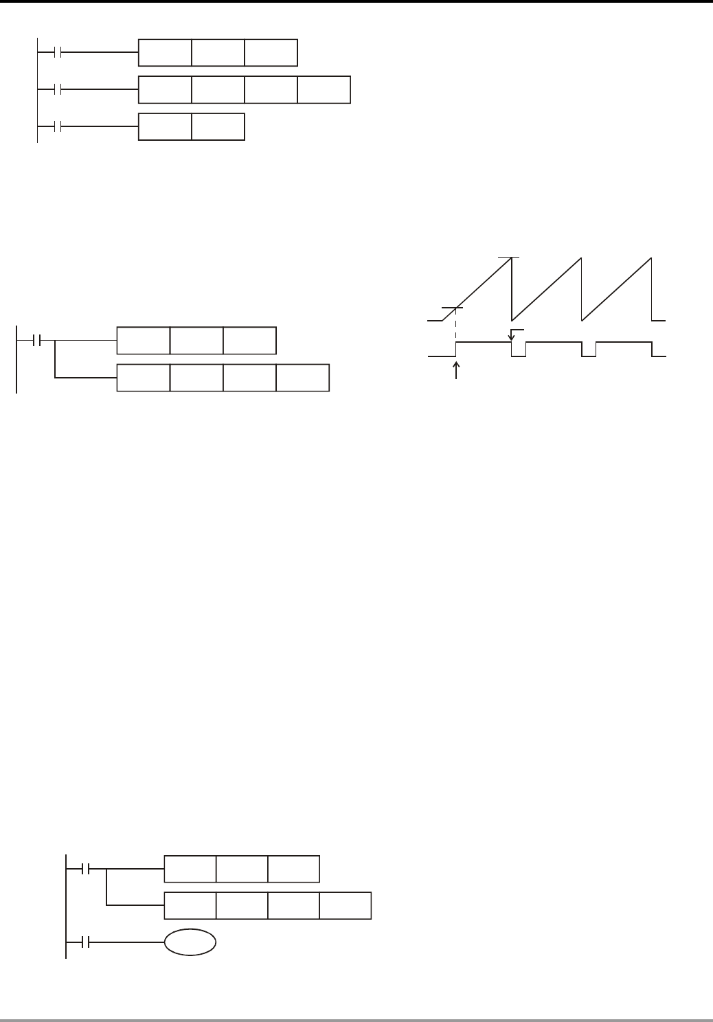
7 Application Instructions API 50-99
DVP-PLC APPLICATION MANUAL
7-16
M1000
DCNT C251 K200
M0
DHSCR K100 C251 Y10
C251
SET Y0
Program Example 2:
When DHSCR instruction designates the same high speed counter, and the present value in the high speed counter
C251 changes from 999 to 1,000 or 1,001 to 1,000, C251 will be reset to Off.
M1000
DCNT C251 K200
DHSCR K1000 C251 C251
1,000
200
Affected by scan time
C251 output contact
Not affected by scan time
Remarks:
1. DVP all series MPU support high speec counters. For the limitation on the use of instructions, see remarks of
API 53 DHSCS for more details.
2. M1261 of EH/EH2/SV/EH3/SV2 series MPU designates the external reset modes of the high speed counter.
Some high speec counters have input points for external reset; therefore, when the input point is On, the
present value in the corresponding high speed counter will be cleared to 0 and the output contact will be Off. If
you wish the reset to be executed immediately by the external output, you have to set M1261 to be On.
3. M1261 can only be used in the hardware high speed counter C241 ~ C255.
4. Example:
a) X2 is the input point for external reset of C251.
b) Assume Y10 = On.
c) When M1261 = Off and X2 = On, the present value in C251 will be cleared to 0 and the contact of C251 will
be Off. When DHSCR instruction is executed, there will be no counting input and the comparison result will
not output. The external output will not execute the reset; therefore Y10 = On will remain unchanged.
d) When M1261 = On and X2 = On, the present value in C251 will be cleared to 0 and the contact of C251 will
be Off. When DHSCR instruction is executed, there will be no counting input but the comparison result will
output. Therefore, Y10 will be reset.
M1000
DCNT C251 K1000
DHSCR K0 C251 Y10
X10
M1261
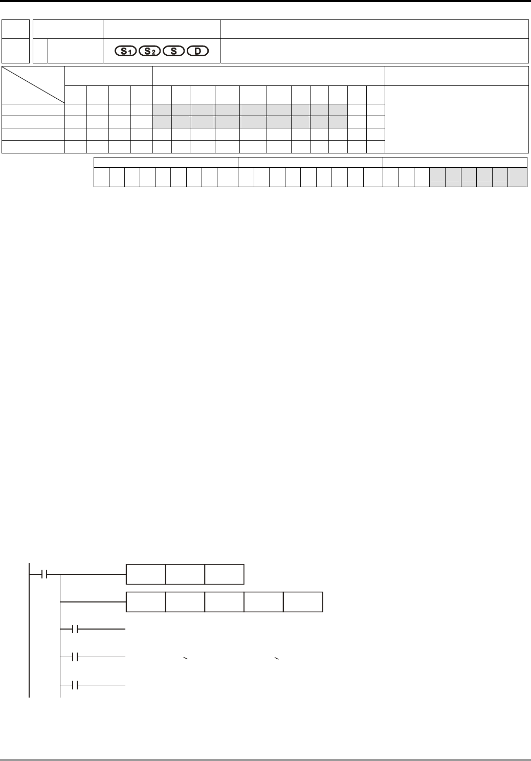
7 Application Instructions API 50-99
DVP-PLC APPLICATION MANUAL
7-17
API Mnemonic Operands Function
55
D HSZ High Speed Zone Compare
Bit Devices Word Devices Program Steps Type
OP X Y M S K H KnX KnY KnM KnS T C D E F
S1 * * * * * * * * * *
S2 * * * * * * * * * *
S *
D * * *
DHSZ: 17 steps
PULSE 16-bit 32-bit
ES EX SS SA SX SC EH SV EH3
SV2 ES EX SS SA SX SC EH SV EH3
SV2 ES EX SS SA SX SC EH SV EH3
SV2
Operands:
S1: Lower bound of the comparison zone S2: Upper bound of the comparison zone S: No. of high speed
counter D: Comparison result
Explanations:
1. S1 has to be euqal to or smaller than S2. (S1 ≤ S2)
2. When S1 > S2, the instruction will perform a comparison by using S1 as the upper bound and S2 as the lower
bound.
3. S has to designate high speed counters C235 ~ C255, See remarks of API 53 DHSCS for more details.
4. D will occupy 3 consecutive devices.
5. Flags: M1150 ~ M1333; see remarks of API 53 DHSCS for more details. M1150, M1151 DHSZ executing
multiple points comparison mode; see Program Example 3 for more details; SA/SX/SC series MPU does not
support. M1152, M1153 DHSZ as frequency control mode; see Program Example 4 for more details; SA/SX/SC
series MPU does not support.
6. The output will not be affected by the scan time.
7. The zone comparisons and outputs are all processed by inserting interruptions.
Program Example 1:
1. Designate device Y0 and Y0 ~ Y2 will be automatically occupied.
2. When DHSZ instruction is being executed and the counting of the high speed counter C246 reaches upper and
lower bounds, one of Y0 ~ Y2 will be On
M1000
DCNT C246 K20000
DHSZ K1500 K2000 C246
Y0
Y0
Y1
Y2
When the present value in C246 < K1,500, Y0 = On
When K1,500 < present value in C246 < K2,000, Y1 = On
When the present value in C246 > K2,000, Y2 = On
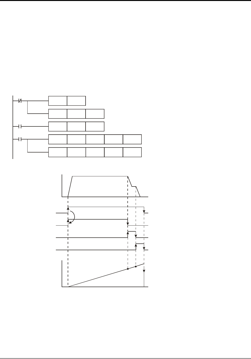
7 Application Instructions API 50-99
DVP-PLC APPLICATION MANUAL
7-18
Program Example 2:
1. Use DHSZ instruction for high/low speed stop control. C251 is an A-B phase high speed counter and DHSZ only
performs comparison output when there is a C251 counting pulse input. Therefore, even when the present value
in the counter is 0, Y10 will not be On.
2. When X10 = On, DHSZ will require that Y10 has to be On when the present value in the counter ≤ K2,000. To
solve this requirement, you can execute DZCPP instruction when the program was first RUN and compare
C251 with K2,000. When the present value in the counter ≤ K2,000, Y10 will be On. DZCPP instruction is a
pulse execution instruction and will only be executed once with Y10 being kept On.
3. When the drive contact X10 = Off, Y10 ~ Y12 will be reset to Off.
X10
RST C251
ZRST Y10 Y12
M1000
DCNT C251 K10000
X10
DZCPP K2000 K2400 C251 Y10
DHSZ K2000 K2400 C251 Y10
4. The timing diagram
2,0002,400
0
X10
Y10
Y11
Y12
0
high speed
forward
low speed
forward
Stop
Speed of variable speed
transmission equipment
Present value in
counter C251
Program Example 3:
1. Program Example 3 is only applicable to EH/EH2/SV/EH3/SV2 series MPU.
2. The multiple set values comparison mode: If D of DHSZ instruction designates a special auxiliary relay M1150,
the instruction will be able to compare (output) the present value in the high speed counter with many set
values.

7 Application Instructions API 50-99
DVP-PLC APPLICATION MANUAL
7-19
3. In this mode,
- S1: start device in the comparison table. S1 can only designate data register D and can be modified by E and
F. Once this mode is enabled, S1 will not be changed even the E and F has been changed.
- S2: number of group data to be compared. S2 can only designate K1 ~ K255 or H1 ~ HFF and can be
modified by E and F. Once this mode is enabled, S2 cannot be changed. If S2 is not within its range, error
code 01EA (hex) will display and the instruction will not be executed.
- S: No. of high speed counter (designated as C241 ~ C254).
- D: Designated mode (can only be M1150)
4. The No. of start register designated in S1 and the number of rows (groups) designated in S2 construct a
comparison table. Please enter the set values in every register in the table before executing the instruction.
5. When the present value in the counter C251 designated in S equals the set values in D1 and D0, the Y output
designated by D2 will be reset to Off (D3 = K0) or On (D3 = K1) and be kept. Output Y will be processed as an
interruption. No. of Y output pointss are in decimal (range: 0 ~ 255). If the No. falls without the range,
SET/RESET will not be enabled when the comparison reaches its target.
6. When this mode is enabled, PLC will first acquire the set values in D0 and D1 as the target value for the first
comparison section. At the same time, the index value displayed in D1150 will be 0, indicating that PLC
performs the comparison based on the group 0 data.
7. When the group 0 data in the table have been compared, PLC will first execute the Y output set in group 0 data
and determine if the comparison reaches the target number of groups. If the comparison reaches the target,
M1151 will be On; if the comparison has not reached the final group, the content in D1150 will plus 1 and
continue the comprison for the next group.
8. M1151 is the flag for the completion of one execution of the table, can be Off by the user. Or when the next
comparion cycle takes place and the group 0 data has been compared, PLC will automatically reset the flag.
9. When the drive contact of the instruction X10 goes Off, the execution of the instruction will be interrupted and
the content in D1150 (table counting register) will be reset to 0. However, the On/Off status of all outputs will be
remained.
10. When the instruction is being executed, all set values in the comparison table will be regarded as valid values
only when the scan arrives at END instruction for the first time.
11. This mode can only be used once in the program.
12. This mode can only be used on the hardware high speed counters C241 ~ C254.
13. When in this mode, the frequency of the input counting pulses cannot exceed 50kHz or the neighboring two
groups of comparative values cannot differ by 1; otherwise there will not be enough time for the PLC to react
and result in errors.
X10
DHSZ D0 K4 C251 M1150
7 Application Instructions API 50-99
DVP-PLC APPLICATION MANUAL
7-20
The comparison table:
32-bit data for comparison
High word Low word No. of Y output On/Off indication Table counting
register D1150
D1 (K0) D0 (K100) D2 (K10) D3 (K1) 0
D5 (K0) D4 (K200) D6 (K11) D7 (K1) 1
D9 (K0) D8 (K300) D10 (K10) D11 (K0) 2
D13 (K0) D12 (K400) D14 (K11) D15 (K0) 3
K10: Y10
K11: Y11
K0: Off
K1: On
0→1→2→3→0
Cyclic scan
M1151
D1150
Y11
Y10
100
200
300
400
0123
0
Present value
in C251
14. Special registers for flags and relevant settings:
Flag Function
M1150 DHSZ instruction in multiple set values comparison mode
M1151 The execution of DHSZ multiple set values comparison mode is completed.
Special D Function
D1150 Table counting register for DHSZ multiple set values comparison mode
Program Example 4:
1. Program Example 4 is only applicable to EH/EH2/SV/EH3/SV2 series MPU.
2. DHSZ and DPLSY instructions are combined for frequency control. If D of DHSZ instruction is a special auxiliary
relay M1152, the present value in the counter will be able to control the pulse output frequency of DPLSY
instruction.
3. In this mode,
- S1: start device in the comparison table. S1 can only designate data register D and can be modified by E and
F. Once this mode is enabled, S1 will not be changed even the E and F has been changed.
- S2: number of group data to be compared. S2 can only designate K1 ~ K255 or H1 ~ HFF and can be
modified by E and F. Once this mode is enabled, S2 cannot be changed. If S2 is not within its range, error
code 01EA (hex) will display and the instruction will not be executed.
- S: No. of high speed counter (designated as C241 ~ C254).
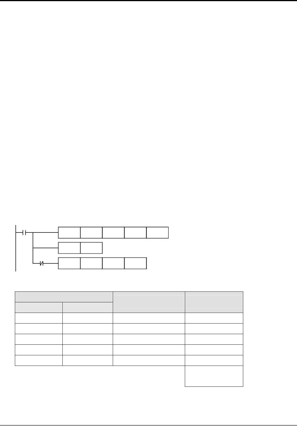
7 Application Instructions API 50-99
DVP-PLC APPLICATION MANUAL
7-21
- D: Designated mode (can only be M1152)
4. This mode can only be used once. For EH/EH2/SV/EH3/SV2 series MPU, this mode can only be used in the
hardware high speed counter C241 ~ C254. Please enter the set values in every register in the table before
executing the instruction.
5. When this mode is enabled, PLC will first acquire the set values in D0 and D1 as the target value for the first
comparison section. At the same time, the index value displayed in D1152 will be 0, indicating that PLC
performs the comparison based on the group 0 data.
6. When the group 0 data in the table have been compared, PLC will first execute at the frequency set in group 0
data (D2, D3) and copy the data to D1152 and D1153, determining if the comparison reaches the target number
of groups. If the comparison reaches the target, M1153 will be On; if the comparison has not reached the final
group, the content in D1151 will plus 1 and continue the comprison for the next group.
7. M1153 is the flag for the completion of one execution of the table, can be Off by the user. Or when the next
comparion cycle takes place and the group 0 data has been compared, PLC will automatically reset the flag.
8. If you wish to use this mode with PLSY instruction, please preset the value in D1152.
9. If you wish to stop the execution at the last row, please set the value in the last row K0.
10. When the drive contact of the instruction X10 goes Off, the execution of the instruction will be interrupted and
the content in D1151 (table counting register) will be reset to 0.
11. When in this mode, the frequency of the input counting pulses cannot exceed 50kHz or the neighboring two
groups of comparative values cannot differ by 1; otherwise there will not be enough time for the PLC to react
and result in errors.
X10
DHSZ D0 K5 C251 M1152
PLS M0
DPLSY D1152 K0 Y0
M0
The comparison table:
32-bit data for comparison
High word Low word
Pulse output frequency
0 ~ 200kHz
Table counting
register D1151
D1 (K0) D0 (K0) D3, D2 (K5,000) 0
D5 (K0) D4 (K100) D7, D6 (K10,000) 1
D9 (K0) D8 (K200) D11, D10 (K15,000) 2
D13 (K0) D12 (K300) D15, D14 (K6,000) 3
D17 (K0) D16 (K400) D19, D18 (K0) 4
0→1→2→3→4
Cyclic scan
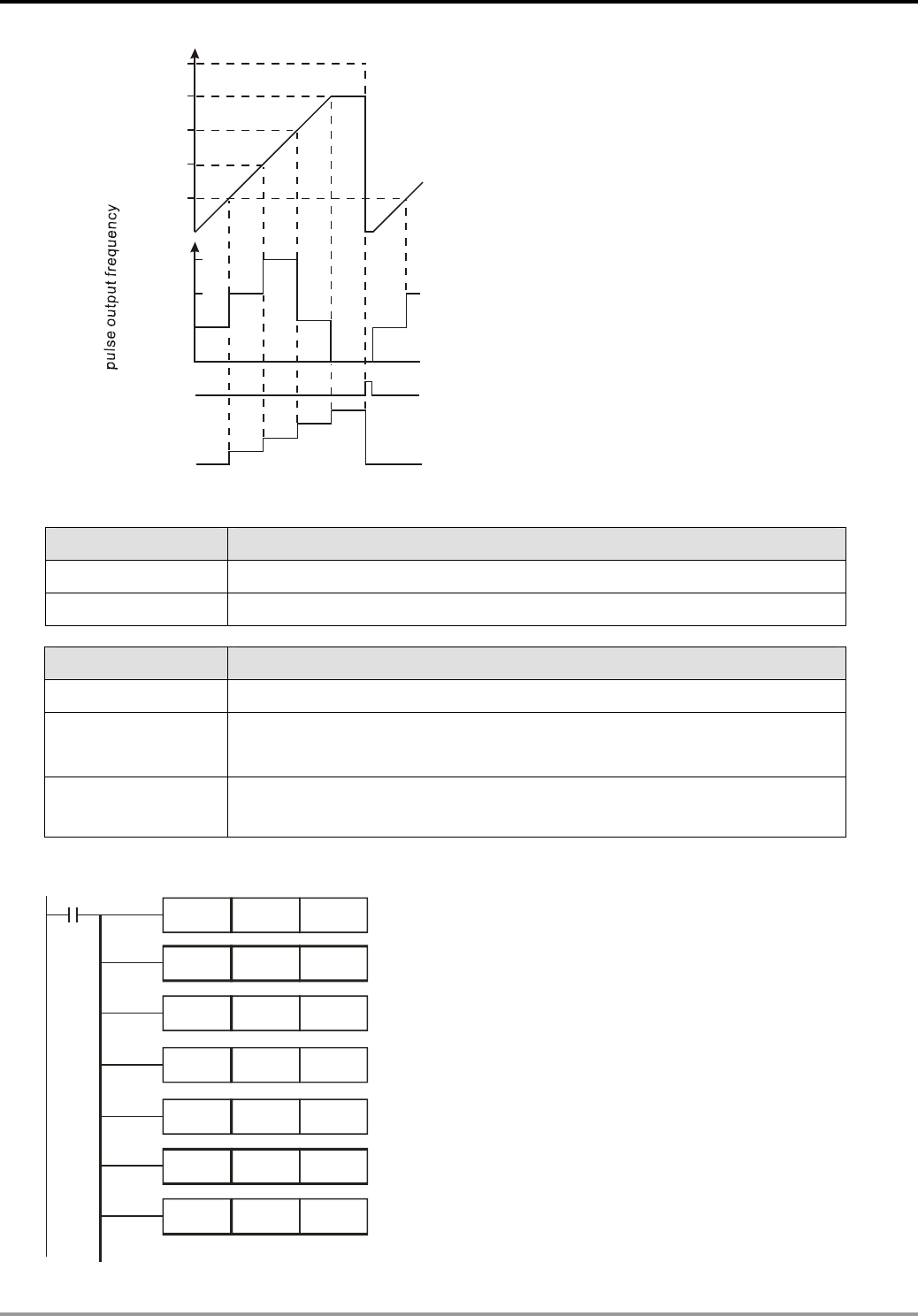
7 Application Instructions API 50-99
DVP-PLC APPLICATION MANUAL
7-22
D1151 012
0
34
0
5,000
10,000
15,000
M1153
0
100
200
300
400
500
(Hz)
Present value
in C251
12. Special registers for flags and relevant settings:
Flag Function
M1152 DHSZ instruction in frequency control mode
M1153 The execution of DHSZ frequency control mode is completed.
Special D Function
D1151 Table counting register for DHSZ multiple set values comparison mode
D1152 (low word)
D1153 (high word)
In frequency control mode, DHSZ reads the upper and lower limits in the
table counting register D1153 and D1152.
D1336 (low word)
D1337 (high word) Current number of pulses output by DPLSY instruction
13. The complete program:
X10
DMOVP K5000 D2
DMOVP K10000 D6
DMOVP K15000 D10
DMOVP K6000 D14
DMOVP K0 D18
DMOVP K0 D0
DMOVP K100 D4

7 Application Instructions API 50-99
DVP-PLC APPLICATION MANUAL
7-23
DHSZ D0 K5 C251 M1152
DMOVP K200 D8
DMOVP K300 D12
DMOVP K400 D16
PLS M0
M0
DPLSY D1152 K0 Y0
Frequency Number
of
pulses
Output
point
14. During the execution of DHSZ instruction, do not modify the set values in the comparison table.
15. The designated data will be arranged into the the above program diagram when the program executes to END
instruction. Therefore, PLSY instruction has to be executed after DHSZ instruction has been executed once.
7 Application Instructions API 50-99
DVP-PLC APPLICATION MANUAL
7-24
API Mnemonic Operands Function
56
SPD Speed Detection
Bit Devices Word Devices Program Steps Type
OP X Y M S K H KnX KnY KnM KnS T C D E F
S1 *
S2 * * * * * * * * * * *
D * * *
SPD: 7 steps
PULSE 16-bit 32-bit
ES EX SS SA SX SC EH SV EH3
SV2 ES EX SS SA SX SC EH SV EH3
SV2 ES EX SS SA SX SC EH SV EH3
SV2
Operands:
S1: External pulse input terminal S2: Pulse receiving time (ms) D: Detected result
Explanations:
1. See the specifications of each model for their range of use.
2. Flag: M1100 (SPD instruction performs sampling for one time)
3. External pulse input terminals designated in S1 for all series MPU:
MPU
Input
ES/EX/SS
(V5.7and above) SA/SX/SC EH EH2/SV/EH3/SV2
Available input points X1, X2 X0 / X1,
X1, X2 X0, X1, X2, X3 X0 / X1,
X1, X2, X3
4. For SA/SX (V1.4 and above) series MPU and SC (V1.2 and above) series MPU, the new X0 and X1 can be
used together with A-B phase input points. When “A ahead of B” detection result is a positive value and “B
ahead of A” detection result is a negative value, the multiplied frequency of the counter can be set by D1022.
5. Input points on EH series are single-phase input. EH2/SV/EH3/SV2 series support A-B phase input, and X0 has
to be designated in the instruction as the speed detection point and X1 occupied. When B is ahead of A, the
detection result will be positive value. If A is ahead of B, the detection result will be negative value.
6. The received number of pulses of the input terminal designated in S1 is calculated within the time (in ms)
designated in S2. The result is stored in the register designated in D.
7. D will occupy 5 consecutive devices. D + 1 and D are the detected value obtained from the previous pulses; D
+3 and D + 2 are the current accumulated number of values; D + 4 is the counting time remaining (max.
32,767ms).
8. Pulse frequency detection for all series:
MPU Max. frequency
ES/EX/SS (V5.7 and later versions) X1 (20kHz), X2 (10kHz)
SA/SX/SC X0/X1 (4kHz), X1 (30kHz), X2 (10kHz)
EH X0 (200kHz), X1 (200kHz), X2 (20kHz), X3 (20kHz)
EH2/SV/EH3/SV2 X0/X1 (200kHz), X1 (200kHz), X2 (20kHz), X3 (20kHz)
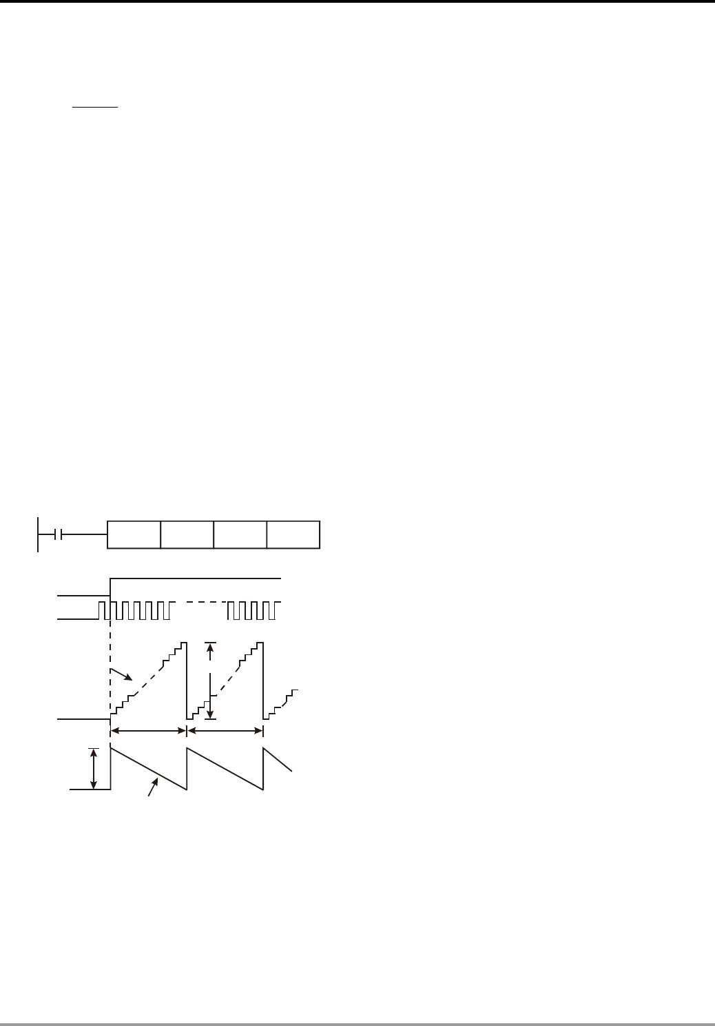
7 Application Instructions API 50-99
DVP-PLC APPLICATION MANUAL
7-25
9. This instruction is mainly used for obtaining a proportional value of rotation speed. The result D and rotation
speed will be in proportion. The following equation is for obtaining the rotation speed of motor.
N: Rotation speed
n: The number of pulses produced per rotation
N=
()
()
rpm10×
nt
0D60 3
t: Detecting time designated in S2 (ms)
10. The X input point designated by this instruction cannot be used again as the pulse input terminal of the high
speed counter or as an external interruption signal.
11. When M1036 in SC (V1.4 and above) series MPU is enabled, SPD instruction can detect the speeds at X0 ~ X5
at the same time with a total bandwidth of 40kHz. See 2.11 for more details for how to use M1036.
12. There is no limitation on the times of using this instruction in the program, but only one instruction will be
executed at a time.
13. When SPD instruction is enabled and M1100 = On, SPD instruction will perform a sampling at the moment when
M1100 goes from Off to On and stop the sampling. If you wish to resume the sampling, you have to turn Off
M1100 and re-enable SPD instruction.
Program Example:
1. When X7 = On, D2 will calculate the high-speed pulses input by X1 and stop the calculation automatically after
1,000ms. The result will be stored in D0.
2. When the 1,000ms counting is completed, D2 will be cleared to 0. When X7 is On again, D2 will start the
calculation again.
X7
SPD X1 K1000 D0
X7
X1
1,000
1,000ms 1,000ms
D2: Present value
Content in D2
Content in D4 D4: Remaining time (ms)
D0: Detected value
Remarks:
1. When ES/EX/SS (V5.7 and above) and SA/SX/SC series MPU use X1 or X2, the relevant high speed counters
or external interruptions I101 and I201 cannot be used.
2. For SC (V1.4 and above) series MPU, when M1036 is enabled, the speed of X0 ~ X5 can be detected at the
same time.
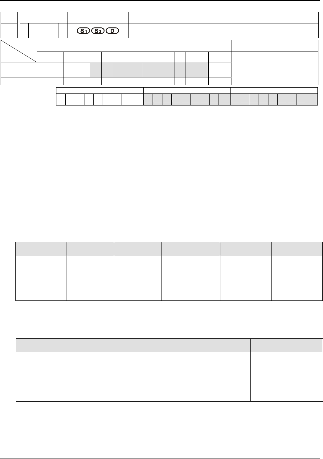
7 Application Instructions API 50-99
DVP-PLC APPLICATION MANUAL
7-26
API Mnemonic Operands Function
57
D PLSY Pulse Y Output
Bit Devices Word Devices Program Steps Type
OP X Y M S K H KnX KnY KnM KnS T C D E F
S1 * * * * * * * * * * *
S2 * * * * * * * * * * *
D *
PLSY: 7 steps
DPLSY: 13 steps
PULSE 16-bit 32-bit
ES EX SS SA SX SC EH SV EH3
SV2 ES EX SS SA SX SC EH SV EH3
SV2 ES EX SS SA SX SC EH SV EH3
SV2
Operands:
S1: Pulse output frequency S2: Number of output pulses D: Pulse output device (please use transistor output
module)
Explanations:
1. The program of ES/EX/SS series MPU can use PLSY instruction two times but cannot designate the same Y
device.
2. Flags: M1010 ~ M1345. See remarks for more details.
3. S1 designates the pulse output frequency. With M1133 ~ M1135 and D1133, Y0 of SA/SX series MPU is able to
output pulses at 50kHz. SV/EH2/EH3/SV2 series MPU of V1.4 and later versions use M1190 ~ M1191, and Y0
and Y2 are able to output 0.01 ~ 500Hz.
Range of output frequency for all series:
MPU ES/EX/SS SA/SX SC EH EH2/SV/EH3/SV2
Frequency range Y0: 0 ~10kHz
Y1: 0 ~10kHz
Y0: 0 ~ 32kHz
Y1: 0 ~10kHz
Y0: 0 ~ 30kHz
Y1: 0 ~ 30kHz
Y10: 77 ~ 100kHz
Y11: 77 ~ 100kHz
Y0: 1 ~ 200kHz
Y2: 1 ~ 200kHz
Y0: 0 ~ 200kHz
Y2: 0 ~ 200kHz
Y4: 0 ~ 200kHz
Y6: 0 ~ 200kHz
4. S2 designates the number of output pulses. The 16-bit instruction can designate 1 ~ 32,767 pulses and the
32-bit instruction can designate 1 ~ 2,147,483,647 pulses.
Number of continuous pulses for all series:
MPU ES/EX/SS/SA/SX/SC SC EH/EH2/SV/EH3/SV2
How to designate
continuous pulses
M1010 (Y0) On
M1023 (Y1) On
M1010 (Y0) On
M1023 (Y1) On
The number of output pulses designated
for Y10 and Y11 is set to K0.
The number of output
pulses designated for
Y0, Y2, Y4 and Y6 is set
to K0
5. For EH/EH2/SV/EH3/SV2 series MPU, when the number of output pulses is set to 0, there will be continuous
pulse output with no limitation on the number of pulses. For ES/EX/SS/SA/SX/SC series MPU, you have to
make M1010 (Y0) or M1023 (Y1) On to allow a continuous pulse output with no limitation on the number of
pulses.

7 Application Instructions API 50-99
DVP-PLC APPLICATION MANUAL
7-27
6. For the pulse output device designated in D, EH series MPU can designate Y0 and Y2, EH2/SV/EH3/SV2 series
MPU can designate Y0, Y2, Y4 and Y6, ES/EX/SS/SA/SX series MPU can designate Y0 and Y1, SC series
MPU can designate Y0, Y1, Y10 and Y11. (SC V1.2 and above series MPU supports Y10 and Y11).
7. EH series MPU has two groups of A-B phase pulse output from CH0 (Y0, Y1) and CH1 (Y2, Y3);
EH2/SV/EH3/SV2 series MPU has four groups of A-B phase pulse output from CH0 (Y0, Y1), CH1 (Y2, Y3),
CH2 (Y4, Y5) and CH3 (Y6, Y7). See 2.3 and remarks for how to set up.
8. When PLSY instruction is executed, it will designate the number of output pulses (S2) output from the output
device (D) at a pulse output frequency (S1).
9. When PLSY instruction is used in the program, its outputs cannot be the same as those in API 58 PWM and API
59 PLSR.
10. Pulse output completed flags for all series:
MPU ES/EX/SS
SA/SX/SC SC EH/EH2/SV EH2/SV/EH3/SV2
Output device Y0 Y1 Y10 Y11 Y0 Y2 Y4 Y6
Flag M1029 M1030 M1102 M1103 M1029 M1030 M1036 M1037
11. For ES/EX/SS/SA/SX/SC/EH series MPU, when PLSY and DPLSY instruction is disabled, the pulse output
completed flags will all be Off automatically.
12. For EH2/SV/EH3/SV2 series MPU, when PLSY and DPLSY instruction is disabled, the user will have to reset
the pulse output completed flags.
13. The user has to reset the pulse output completed flags after the pulse output is completed.
14. After PLSY instruction starts to be executed, Y will start a pulse output. Modifying S2 at this moment will not
affect the current output. If you wish to modify the number of output pulses, you have to first stop the execution
of PLSY instruction and modify the number.
15. S1 can be modified when the program executes to PLSY instruction.
16. Off time : On time of the pulse output = 1 : 1.
17. When the program executes to PLSY instruction, the current number of output pulses will be stored in the
special data registers D1336 ~ D1339. See remarks for more details.
18. For SA/EH series MPU, there is no limitation on the times using this instruction. For SA/SX/SC/EH series MPU,
the program allows two instructions being executed at the same time. For EH2/SV/EH3/SV2 series MPU, the
program allows four instructions being executed at the same time.
Program Example:
1. When X0 = On, there will be 200 pulses output from Y0 at 1kHz. When the pulse output is completed, M1029
will be On and Y10 will be On.
2. When X0 = Off, the pulse output from Y0 will stop immediately. When X0 is On again, the output will start again
ffrom the first pulse.

7 Application Instructions API 50-99
DVP-PLC APPLICATION MANUAL
7-28
X0
PLSY K1000 K200 Y0
M1029
Y10
123 200
0.5ms
1ms
Y0 output
Remarks:
1. Flags and special registers for ES/EX/SS series MPU:
M1010: When On, Y0 output will be continuous with no limitation on the number of pulses. When Off, the
number of output pulses from Y0 will be decided by S2.
M1023: When On, Y1 output will be continuous with no limitation on the number of pulses. When Off, the
number of output pulses from Y1 will be decided by S2.
M1029: On when Y0 pulse output is completed.
M1030: On when Y1 pulse output is completed.
M1078: Y0 output pauses.
M1079: Y1 output pauses.
D1030: Low word of the current number of output pulses from Y0
D1031: High word of the current number of output pulses from Y0
D1032: Low word of the current number of output pulses from Y1
D1033: High word of the current number of output pulses from Y1
2. Flags and special registers for SA/SX/SC series MPU:
M1010: (SA/SX/SC) When On, Y0 output will be continuous with no limitation on the number of pulses.
When Off, the number of output pulses from Y0 will be decided by S2.
M1023: (SA/SX/SC) When On, Y1 output will be continuous with no limitation on the number of pulses.
When Off, the number of output pulses from Y1 will be decided by S2.
M1029: (SA/SX/SC) On when Y0 pulse output is completed.
M1030: (SA/SX/SC) On when Y1 pulse output is completed.
M1078: (SA/SX/SC) Y0 output pauses.
M1079: (SA/SX/SC) Y1 output pauses.
M1102: (SC) On when Y10 pulse output is completed.
M1103: (SC) On when Y11 pulse output is completed.
M1347: (SA/SC) Auto zero return after Y0 output is completed.
(Available only in SA V1.8 and later versions, SC V1.6 and later versions)
M1348: (SA/SC) Auto zero return after Y1 output is completed.
(Available only in SA V1.8 and later versions, SC V1.6 and later versions)
M1524: (SC) Auto zero return after Y10 output is completed. (Available only in V1.6 and later versions)
M1525: (SC) Auto zero return after Y11 output is completed. (Available only in V1.6 and later versions)

7 Application Instructions API 50-99
DVP-PLC APPLICATION MANUAL
7-29
D1030: (SA/SX/SC) Low word of the current number of output pulses from Y0
D1031: (SA/SX/SC) High word of the current number of output pulses from Y0
D1032: (SA/SX/SC) Low word of the current number of output pulses from Y1
D1033: (SA/SX/SC) High word of the current number of output pulses from Y1
D1348: (SC) Low word of the current number of output pulses from Y10
D1349: (SC) High word of the current number of output pulses from Y10
D1350: (SC) Low word of the current number of output pulses from Y11
D1351: (SC) High word of the current number of output pulses from Y11
3. Flags and special registers for EH/EH2/SV/EH3/SV2 series MPU:
M1010: (EH/EH2/SV/EH3/SV2) When On, CH0, CH1, CH2 and CH3 will output pulses at END instruction.
Off when the output starts.
M1029: (EH/EH2/SV/EH3/SV2) On when CH0 pulse output is completed.
M1030: (EH/EH2/SV/EH3/SV2) On when CH1 pulse output is completed.
M1036: (EH2/SV/EH3/SV2) On when CH2 pulse output is completed.
M1037: (EH2/SV/EH3/SV2) On when CH3 pulse output is completed.
M1190: (EH2/SV/EH3/SV2) Able to output 0.01 ~ 500Hz when PLSY Y0 high-speed output is enabled.
M1191: (EH2/SV/EH3/SV2) Able to output 0.01 ~ 500Hz when PLSY Y2 high-speed output is enabled.
M1334: (EH/EH2/SV/EH3/SV2) CH0 pulse output pauses.
M1335: (EH/EH2/SV/EH3/SV2) CH1 pulse output pauses.
M1520: (EH2/SV/EH3/SV2) CH2 pulse output pauses.
M1521: (EH2/SV/EH3/SV2) CH3 pulse output pauses.
M1336: (EH/EH2/SV/EH3/SV2) CH0 pulse output has been sent.
M1337: (EH/EH2/SV/EH3/SV2) CH1 pulse output has been sent.
M1522: (EH2/SV/EH3/SV2) CH2 pulse output has been sent.
M1523: (EH2/SV/EH3/SV2) CH3 pulse output has been sent.
M1338: (EH/EH2/SV/EH3/SV2) CH0 offset pulses enabled.
M1339: (EH/EH2/SV/EH3/SV2) CH1 offset pulses enabled.
M1340: (EH/EH2/SV/EH3/SV2) I110 interruption occurs after CH0 pulse output is completed.
M1341: (EH/EH2/SV/EH3/SV2) I120 interruption after occurs CH1 pulse output is completed.
M1342: (EH/EH2/SV/EH3/SV2) I130 interruption occurs when CH0 pulse output is sending.
M1343: (EH/EH2/SV/EH3/SV2) I140 interruption occurs when CH0 pulse output is sending.
M1344: (EH/EH2/SV/EH3/SV2) CH0 pulse compensation enabled.
M1345: (EH/EH2/SV/EH3/SV2) CH1 pulse compensation enabled.
M1347: (EH/EH2/SV/EH3/SV2) CH0 pulse output reset flag
M1348: (EH/EH2/SV/EH3/SV2) CH1 pulse output reset flag
M1524: (EH2/SV/EH3/SV2) CH2 pulse output reset flag
M1525: (EH2/SV/EH3/SV2) CH3 pulse output reset flag

7 Application Instructions API 50-99
DVP-PLC APPLICATION MANUAL
7-30
D1220: (EH/EH2/SV/EH3/SV2) Phase setting of CH0 (Y0, Y1): D1220 determines the phase by the last
two bits; other bits are invalid.
1. K0: Y0 output
2. K1: Y0, Y1 AB-phase output; A ahead of B.
3. K2: Y0, Y1 AB-phase output; B ahead of A.
4. K3: Y1 output
D1221: (EH/EH2/SV/EH3/SV2) Phase setting of CH1 (Y2, Y3): D1221 determines the phase by the last
two bits; other bits are invalid.
1. K0: Y2 output
2. K1: Y2, Y3 AB-phase output; A ahead of B.
3. K2: Y2, Y3 AB-phase output; B ahead of A.
4. K3: Y3 output
D1229: (EH2/SV/EH3/SV2) Phase setting of CH2 (Y4, Y5): D1229 determines the phase by the last two
bits; other bits are invalid.
1. K0: Y4 output
2. K1: Y4, Y5 AB-phase output; A ahead of B.
3. K2: Y4, Y5 AB-phase output; B ahead of A.
4. K3: Y5 output
D1230: (EH2/SV/EH3/SV2) Phase setting of CH3 (Y6, Y7): D1230 determines the phase by the last two
bits; other bits are invalid.
1. K0: Y6 output
2. K1: Y6, Y7 AB-phase output; A ahead of B.
3. K2: Y6, Y7 AB-phase output; B ahead of A.
4. K3: Y7 output
D1328: (EH/EH2/SV/EH3/SV2) Low word of the number of CH0 offset pulses
D1329: (EH/EH2/SV/EH3/SV2) High word of the number of CH0 offset pulses
D1330: (EH/EH2/SV/EH3/SV2) Low word of the number of CH1 offset pulses
D1331: (EH/EH2/SV/EH3/SV2) High word of the number of CH1 offset pulses
D1332: (EH/EH2/SV/EH3/SV2) Low word of the number of remaining pulses at CH0
D1333: (EH/EH2/SV/EH3/SV2) High word of the number of remaining pulses at CH0
D1334: (EH/EH2/SV/EH3/SV2) Low word of the number of remaining pulses at CH1
D1335: (EH/EH2/SV/EH3/SV2) High word of the number of remaining pulses at CH1
D1336: (EH/EH2/SV/EH3/SV2) Low word of the current number of output pulses at CH0
D1337: (EH/EH2/SV/EH3/SV2) High word of the current number of output pulses at CH0
D1338: (EH/EH2/SV/EH3/SV2) Low word of the current number of output pulses at CH1
D1339: (EH/EH2/SV/EH3/SV2) High word of the current number of output pulses at CH1
D1375: (EH2/SV/EH3/SV2) Low word of the current number of output pulses at CH2
D1376: (EH2/SV/EH3/SV2) High word of the current number of output pulses at CH2
D1377: (EH2/SV/EH3/SV2) Low word of the current number of output pulses at CH3
D1378: (EH2/SV/EH3/SV2) High word of the current number of output pulses at CH3
D1344: (EH/EH2/SV/EH3/SV2) Low word of the number of compensation pulses at CH0
D1345: (EH/EH2/SV/EH3/SV2) High word of the number of compensation pulses at CH0
D1346: (EH/EH2/SV/EH3/SV2) Low word of the number of compensation pulses at CH1
D1347: (EH/EH2/SV/EH3/SV2) High word of the number of compensation pulses at CH1
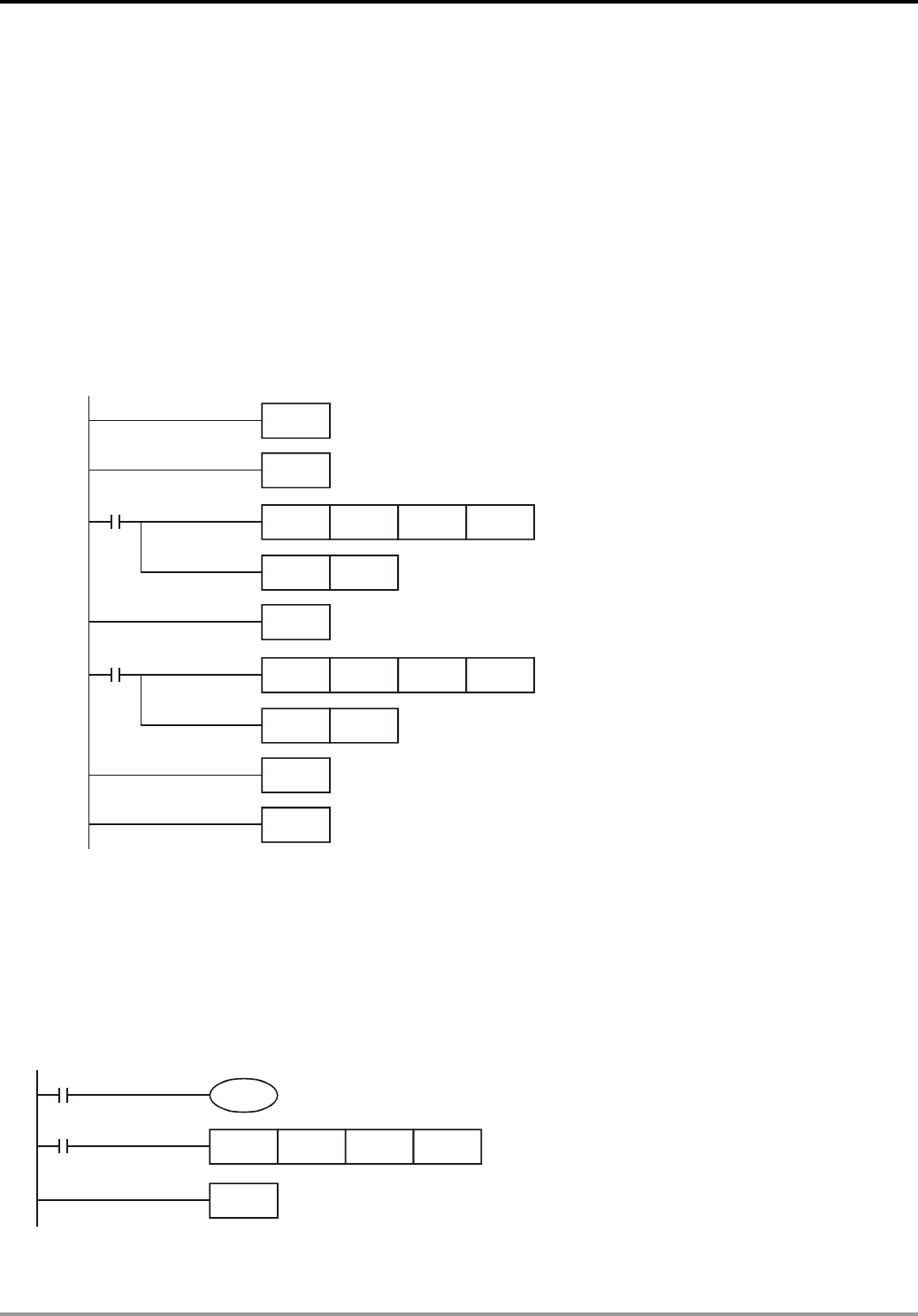
7 Application Instructions API 50-99
DVP-PLC APPLICATION MANUAL
7-31
4. When there are many high speed output instructions (PLSY, PWM, PLSR) for Y0 output in a program, PLC will
only execute the settings and outputs of the instruction that is first enabled.
5. More explanations on M1347 and M1348:
If M1347 and M1348 is enabled, and when the execution of PLSY instruction has been completed, M1347/M1348
will be reset automatically, i.e. you do not have to turn the status of the drive contact from Off to On before PLSY
instruction and when PLC scans to the instruction (assume the drive contact of the instruction is True), there will
still be pulse output. PLC detects the status of M1347 and M1348 when END instruction is being executed.
Therefore, when the pulse output is completed and if PLSY instruction is a continuous execution one, there will be
a scan time of delay in the next string of pulse output.
Program Example 1:
M1000
DPLSY K1000 K1000
EI
FEND
Y0
I 001
IRET
SET M1347
M1000
DPLSY K1000 K1000 Y2
I 101
IRET
SET M1348
END
Explanations:
a) Whenever X0 is triggered, Y0 will output 1,000 pulses; whenever X1 is triggered, Y2 will output 1,000 pulses.
b) When X triggers Y pulse output, there should be an interval of at least one scan time between the end of Y
pulse output and the next X-triggered output.
Program Example 2:
X1
M1347
PLSY K1000 K1000 Y0
X2
END
Explanations:

7 Application Instructions API 50-99
DVP-PLC APPLICATION MANUAL
7-32
When both X1 and X2 are On, Y0 pulse output will keep operating. However, there will be a short pause (approx.
1 scan time) every 1,000 pulses before the output of the next 1,000 pulses.
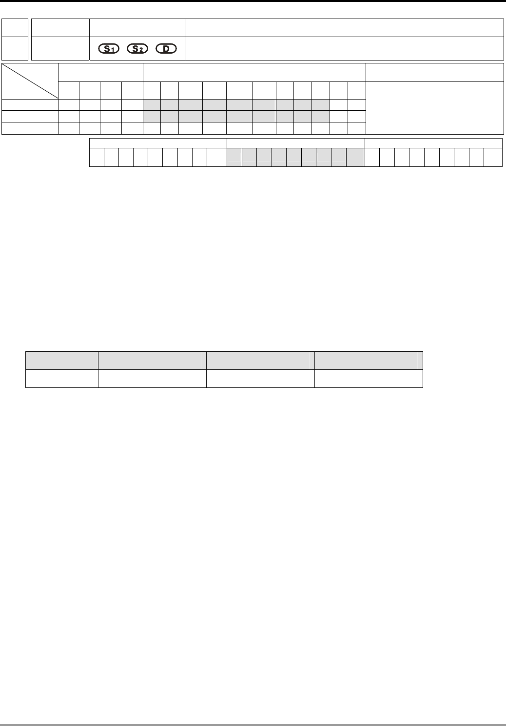
7 Application Instructions API 50-99
DVP-PLC APPLICATION MANUAL
7-33
API Mnemonic Operands Function
58
PWM Pulse Width Modulation
Bit Devices Word Devices Program Steps Type
OP X Y M S K H KnX KnY KnM KnS T C D E F
S1 * * * * * * * * * * *
S2 * * * * * * * * * * *
D *
PWM: 7 steps
PULSE 16-bit 32-bit
ES EX SS SA SX SC EH SV EH3
SV2 ES EX SS SA SX SC EH SV EH3
SV2 ES EX SS SA SX SC EH SV EH3
SV2
Operands:
S1: Pulse output width S2: Pulse output period D: Pulse output device (please use transistor output module)
Explanations:
1. S1 ≤ S2.
2. See the specifications of each model for their range of use.
3. In ES/EX/SS series MPU, PWM instruction can only be used once in the program.
4. Flags: See remarks for more details.
5. Range of S1: (t) 0 ~ 32,767ms.
6. Range of S2: (T) 1 ~ 32,767ms (but S1 ≤ S2).
7. D for all series MPU:
MPU ES/EX/SS/SA/SX/SC EH EH2/SV/EH3/SV2
Output point Y1 Y0, Y2 Y0, Y2, Y4, Y6
8. When PWM instruction is used in the program, its outputs cannot be the same as those of API 57 PLSY and API
59 PLSR.
9. PWM instruction designates the pulse output width in S1 and pulse output period in S2 and outputs from output
device D.
10. For SA/SX/SC series MPU, When, S1 ≤ 0 or S2 ≤ 0 or S1 > S2, there will be operational errors (M1067 and
M1068 will not be On), and there will be no output from the pulse output device. When S1 = S2, the pulse output
device will keep being On.
11. For EH/EH2/SV/EH3/SV2 series MPU, When, S1 < 0 or S2 ≤ 0 or S1 > S2, there will be operational errors (M1067
and M1068 will be On), and there will be no output from the pulse output device. When S1 = 0, M1067 and
M1068 will not be On and there will be no output from the pulse output device. When S1 = S2, the the pulse
output device will keep being On.
12. S1 and S2 can be changed when PWM instruction is being executed.
13. For SA/EH series MPU, there is no limitation on the times using this instruction in the program. However, for EH
series MPU, two instructions are allowed to be executed at the same time; for EH2/SV/EH3/SV2 series MPU,
four instructions are allowed to be executed at the same time.

7 Application Instructions API 50-99
DVP-PLC APPLICATION MANUAL
7-34
Program Example:
When X0 = On, Y1 will output the pulses as below. When X0 = Off, Y1 output will also be Off.
X0
PWM K1000 K2000 Y1
Y1 output
t=1,000ms
T=2,000ms
Remarks:
1. Flags for ES/EX/SS/SA/SX/SC series MPU:
M1070: Y1 pulse output time unit switch. When Off: 1ms; when On: 100us
2. Flags and special registers for EH/EH2/SV/EH3/SV2 series MPU:
M1010: (EH/EH2/SV/EH3/SV2) When On, CH0, CH1, CH2 and CH3 will output pulses when END
instruction is executed. Off when the output starts.
M1070: (EH/EH2/SV/EH3/SV2) The setting of time unit of CH0 has to work with D1371.
M1071: (EH/EH2/SV/EH3/SV2) The setting of time unit of CH1 has to work with D1372.
M1258: (EH/EH2/SV/EH3/SV2) CH0 pulse output signals reverse.
M1259: (EH/EH2/SV/EH3/SV2) CH1 pulse output signals reverse.
M1334: (EH/EH2/SV/EH3/SV2) CH0 pulse output pauses.
M1335: (EH/EH2/SV/EH3/SV2) CH1 pulse output pauses.
M1336: (EH/EH2/SV/EH3/SV2) CH0 pulse output has been sent.
M1337: (EH/EH2/SV/EH3/SV2) CH1 pulse output has been sent.
M1520: (EH2/SV/EH3/SV2) CH2 pulse output pauses.
M1521: (EH2/SV/EH3/SV2) CH3 pulse output pauses.
M1522: (EH2/SV/EH3/SV2) CH2 pulse output has been sent.
M1523: (EH2/SV/EH3/SV2) CH3 pulse output has been sent.
M1526: (EH2/SV/EH3/SV2) CH2 pulse output signals reverse.
M1527: (EH2/SV/EH3/SV2) CH3 pulse output signals reverse.
M1530: (EH2/SV/EH3/SV2) The setting of time unit of CH2 has to work with D1373.
M1531: (EH2/SV/EH3/SV2) The setting of time unit of CH3 has to work with D1374.
D1336: (EH/EH2/SV/EH3/SV2) Low word of the current number of output pulses from CH0.
D1337: (EH/EH2/SV/EH3/SV2) High word of the current number of output pulses from CH0.
D1338: (EH/EH2/SV/EH3/SV2) Low word of the current number of output pulses from CH1.
D1339: (EH/EH2/SV/EH3/SV2) High word of the current number of output pulses from CH1.
D1371: (EH/EH2/SV/EH3/SV2) Time unit of CH0 output pulses when M1070 = On.
D1372: (EH/EH2/SV/EH3/SV2) Time unit of CH1 output pulses when M1071 = On.

7 Application Instructions API 50-99
DVP-PLC APPLICATION MANUAL
7-35
D1373: (EH2/SV/EH3/SV2) Time unit of CH2 output pulses when M1530 = On.
D1374: (EH2/SV/EH3/SV2) Time unit of CH3 output pulses when M1531 = On.
D1375: (EH2/SV/EH3/SV2) Low word of the current number of output pulses from CH2.
D1376: (EH2/SV/EH3/SV2) High word of the current number of output pulses from CH2.
D1377: (EH2/SV/EH3/SV2) Low word of the current number of output pulses from CH3.
D1378: (EH2/SV/EH3/SV2) High word of the current number of output pulses from CH3.
3. Time unit settings for EH/EH2/SV/EH3/SV2 series MPU:
You cannot modify M1070 in the program.
D1371, D1372, D1373 and D1374 determine the time unit of the output pulses from CH0, CH1, CH2 and CH3
and the default setting is K1. If your set value is not within the range, the default value will be adopted.
D1371, D1372, D1373, D1374 K0 K1 K2 K3
Time unit 10us 100us 1ms 10ms
4. When there are many high speed pulse output instructions (PLSY, PWM, PLSR) in a program for Y0 output, and
provided these instructions are being executed in the same scan period, PLC will set up and output the
instructions with the fewest steps.

7 Application Instructions API 50-99
DVP-PLC APPLICATION MANUAL
7-36
API Mnemonic Operands Function
59
D PLSR Pulse Ramp
Bit Devices Word Devices Program Steps Type
OP X Y M S K H KnX KnY KnM KnS T C D E F
S1 * * * * * * * * * * *
S2 * * * * * * * * * * *
S3 * * * * * * * * * * *
D *
PLSR: 9 steps
DPLSR: 17 steps
PULSE 16-bit 32-bit
ES EX SS SA SX SC EH SV EH3
SV2 ES EX SS SA SX SC EH SV EH3
SV2 ES EX SS SA SX SC EH SV EH3
SV2
Operands:
S1: Maximum speed of pulse output S2: Total number of output pulses S3: Acceleration/deceleration time (ms)
D: Pulse output device (please use transistor output module)
Explanations:
1. See the specifications of each model for their range of use.
2. For ES/EX/SS series MPU, PLSR instruction can be used twice in the program but the outputs cannot be
overlapped.
3. Flags: See remarks of API 57 PLSY.
4. Range of S1: 10 ~ 32,767Hz (16-bit); 10 ~ 200,000Hz (32-bit). The maximum speed has to be 10’s multiple; if
not, the 1s digit will be left out. 1/10 of the maximum speed is the variation of one acceleration or deleration.
Please be aware if the variation reponds to the acceleration/deceleration demand from the step motor, in case
the step motor may crash.
5. Range of S2: 110 ~ 32,767 (16-bit); 110 ~ 2,147,483,647 (32-bit). If S2 is less than 110, the pulet output will be
abnormal.
6. Range of S3: below 5,000ms. The acceleration time and deceleration time have to be the same.
a) The acceleration/deceleration time has to be 10 times longer than the maximum scan time (D1012). If not,
the slope of accleration and deceleration will be incorrect.
b) The minimum set value of acceleration/deceleration time can be obtained from the following equation:
90,000
>
S
3
S
1
If the set value is less than the result obtained from the equation, the acceleration/deceleration time will be
longer. If the set value is less than 90,000/S1, use the result of 90,000/S1 as the set value.
c) The maximum set value of acceleration/deceleration time can be obtained from the following equation:
818
S
1
S
2
S
3
<
X
d) The speed variation is fixed to 10 steps. If the input acceleration/deceleration time is longer than the
maximum set value, the acceleration/deceleration time will follow the maximum set time. If shorter than the
minimum set value, the accleration/deceleration time will follow the minimum set time.

7 Application Instructions API 50-99
DVP-PLC APPLICATION MANUAL
7-37
7. D for all series MPU:
MPU ES/EX/SS/SA/SX/SC EH EH2/SV/EH3/SV2
Output point Y0, Y1 Y0, Y2 Y0, Y2, Y4, Y6
8. EH series MPU has two groups pf A-B phase pulse output CH0 (Y0, Y1) and CH1 (Y2, Y3). EH2/SV/EH3/SV2
series MPU has four groups pf A-B phase pulse output CH0 (Y0, Y1), CH1 (Y2, Y3), CH2 (Y4, Y5) and CH3 (Y6,
Y7). See remarks of API 57 PLSY for how to set up.
9. PLSR instruction is a pulse output instruction with acclerating and decelerating functions. The pulses accelerate
from the static status to target speed and decelerates when the target distance is nearly reached. The pulse
output will stop when the target distance is reached.
10. When PLSR instruction is executed, after S1, S2 and S3 are set, the pulses will output from D. The output starts
at the frequency of increasing S1/10 at a time. The time forf every frequency is fixed at S3/9.
11. S1, S2 and S3 can be changed when PLSR instruction is being executed.
12. For ES/EX/SS/SA/SX/SC series MPU, when all the Y0 pulses have been sent, M1029 will be On; when all the
Y1 pulses have been sent, M1030 will be On. Next time when PLSR instruction is enabled, M1029 or M1030 will
be 0 again and after the pulse output is completed, it will become 1 again.
13. For EH/EH2/SV/EH3/SV2 series MPU, when all the CH0 (Y0, Y1) pulses have been sent, M1029 will be On;
when all the CH1 (Y2, Y3) pulses have been sent, M1030 will be On; when CH2 (Y4, Y5) pulses have been sent,
M1036 will be On; when CH3 (Y6, Y7) pulses have been sent, M1037 will be On. Next time when PLSR
instruction is enabled, M1029, M1030, M1036 or M1037 will be 0 again and after the pulse output is completed,
they will become 1 again.
14. For EH2/SV/EH3/SV2 series MPU V1.4 and later versions, when the instruction designate incorrect parameters,
the default output will become the maximum value or mininum value.
15. During every acceleration section, the number of pulses ( frequency × time) may not all be integers. PLC will
round up the number to an integer before the output. Therefore, the acceleration time of every section may not
be exactly the same. The offset is determined upon the frequency and the decimal after rounding up. In order to
ensure the correct number of output pulses, PLC will supplement insufficient pulses in the last section.
16. For SA/EH series MPU, there is no limitation on the times of using this instruction in the program. However, for
SA/SX/SC/EH series MPU, two instructions can be exeucted at the same time; for EH2/SV/EH3/SV2 series
MPU, four instructions can be executed at the same time.
Program Example:
1. When X0 = On, the pulses will output at the maximum frequency 1,000Hz with the total number D10 at 3,000ms
from Y0. The frequency will increase by 1,000/10Hz at a time and every frequency will last for 3,000/9 (ms).
2. When X10 is Off, the output will be interrupted. When X0 is On again, the counting of pulses will start from 0.
X0
PLSR K1000 D10 K3000 Y0
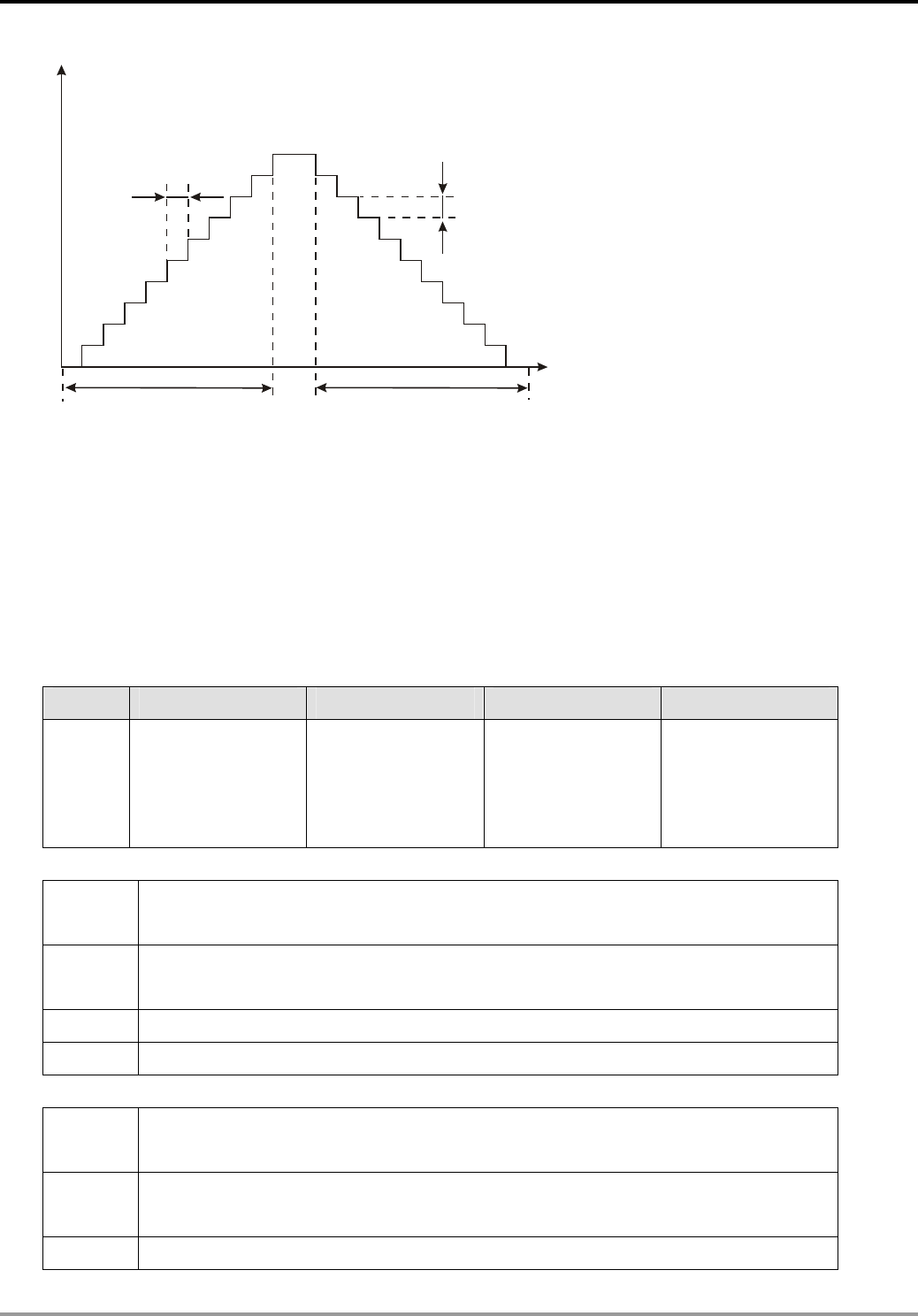
7 Application Instructions API 50-99
DVP-PLC APPLICATION MANUAL
7-38
Output: Y0 or Y2
Pulse speed (Hz)
Targeted speed: 10 ~ 200,000Hz
Time(Sec)
Decel time
below 5,000ms
Accel time
below 5,000ms
16-bit command:110~32,767PLS
32-bit command:110~2,147,483,647PLS
11
22
33
44
55
66
77
88
99
1010
10-step
variations
10-step
variations
Time interval among
pulse outputs
= x 1/10
S
3
Every speed variation
= x 1/10
S
1
S
2
()
S
3
()
S
3
Remarks:
1. The outputs cannot be the same as those of API 57 PLSY and API 58 PWM.
2. When there are many high speed pulse output instructions (PLSY, PWM, PLSR) in a program for Y0 output, and
provided these instructions are being executed in the same scan period, PLC will set up and output the
instructions with the fewest steps.
3. With M1133 ~ M1135 and D1133, Y0 of SA/SX/SC series MPU can output pulses at up to 50kHz. See 2.11 for
more details of special D and special M.
Range of output frequecies for all series:
MPU ES/EX/SS SA/SX/SC EH EH2/SV/EH3/SV2
Range Y0: 10 ~ 10,000Hz
Y1: 10 ~ 10,000Hz
Y0: 10 ~ 30,000Hz
Y1: 10 ~ 30,000Hz
Y0: 10 ~ 200,000Hz
Y2: 10 ~ 200,000Hz
Y0: 10 ~ 200,000Hz
Y2: 10 ~ 200,000Hz
Y4: 10 ~ 200,000Hz
Y6: 10 ~ 200,000Hz
4. Flags and special registers for SA/SC series MPU:
M1347 For SA/SC. Reset flag for Y0 pulse output
(Available in SA V1.8 and later version, SC V1.6 and later versions)
M1348 For SA/SC. Reset flag for Y1 pulse output
(Availabe in SA V1.8 and later versions, SC V1.6 and later versions)
M1524 For SC (V1.6 and later versions). Reset flag for Y10 pulse output
M1525 For SC (V1.6 and later versions). Reset flag for Y11 pulse output
5. Flags and special registers for EH2/SV/EH3/SV2 series MPU:
M1257 The acceleration/decelration of the high-speed pulse output Y0, and that of Y2 are S
curves.
M1308 Off->On: The high-speed output of the first pulse CH0 (Y0, Y1) paruse immediately.
On->Off: Continue to output the pulses which have not been output.
M1309 Off->On: The high-speed output of the first pulse CH1 (Y2, Y3) paruse immediately.
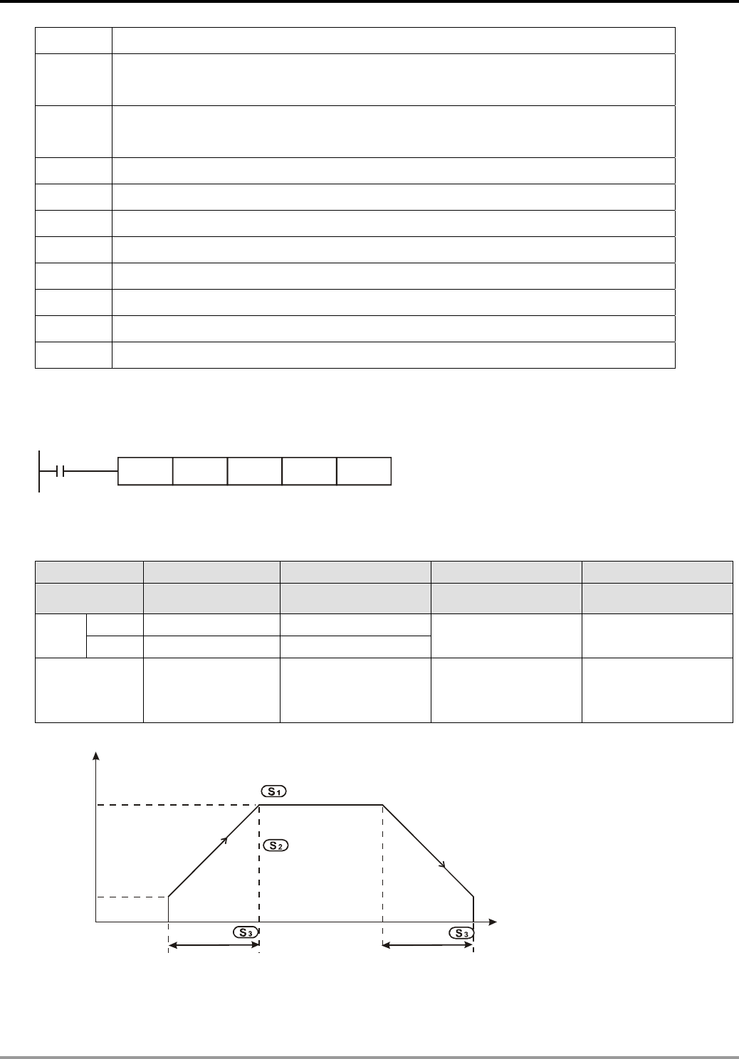
7 Application Instructions API 50-99
DVP-PLC APPLICATION MANUAL
7-39
On->Off: Continue to output the pulses which have not been output.
M1310 Off->On: The high-speed output of the first pulse CH2 (Y4, Y5) paruse immediately.
On->Off: Continue to output the pulses which have not been output.
M1311 Off->On: The high-speed output of the first pulse CH3 (Y6, Y7) paruse immediately.
On->Off: Continue to output the pulses which have not been output.
M1347 For EH2/SV/EH3/SV2 (V1.4 and later versions). Reset flag for CH0 pulse output
M1348 For EH2/SV/EH3/SV2 (V1.4 and later versions). Reset flag for CH1 pulse output
M1524 For EH2/SV/EH3/SV2 (V1.4 and later versions). Reset flag for CH2 pulse output
M1525 For EH2/SV/EH3/SV2 (V1.4 and later versions). Reset flag for CH3 pulse output
D1127 The number of pulses at the acceleration setion for the position instruction (low word)
D1128 The number of pulses at the acceleration setion for the position instruction (high word)
D1133 The number of pulses at the deceleration setion for the position instruction (low word)
D1134 The number of pulses at the deceleration setion for the position instruction (high word)
Functions in EH series MPU:
1. Relevant devices for EH/EH2/SV/EH3/SV2 series MPU:
X0
PLSR K1000 D10 K3000 Y0
2. The range of pulse speed for this instruction is 10 ~ 200,000Hz. If the set values of maximum speed and
acceleration/deceleration time exceed the range, PLC will operate by the default value that is within the range.
Operand S1 S2 S3 D
Explanation Max. frequency Total number of pulses Accel/Decel time Output point
16-bit 10 ~ 32,767Hz 110 ~ 32,767
Range 32-bit 10 ~ 200kHz 110 ~ 2,147,483,647 1 ~ 5,000ms Y0 ~ Y7
Definition
K0: No output
Kn: Designated
frequency
Kn: Designated
number Flag: M1067, M1068 See settings of D1220,
D1221
1 ~ 5,000ms 1 ~ 5,000ms
16-bit instruction: 110 ~ 32,767PLS
32-bit instruction: 110 ~ 2,147,483,647PLS
Frequency F
Maximum speed: 10 ~ 200,000Hz
Decel timeAccel time
F0
Start
frequency
Total number of output pulses
3. The acceleration/deceleration of EH/EH2/SV/EH3/SV2 series MPU is based on the number of pulses. If the
output cannot reach the maximum acceleration frequency within the acceleration/deceleration time offered, the
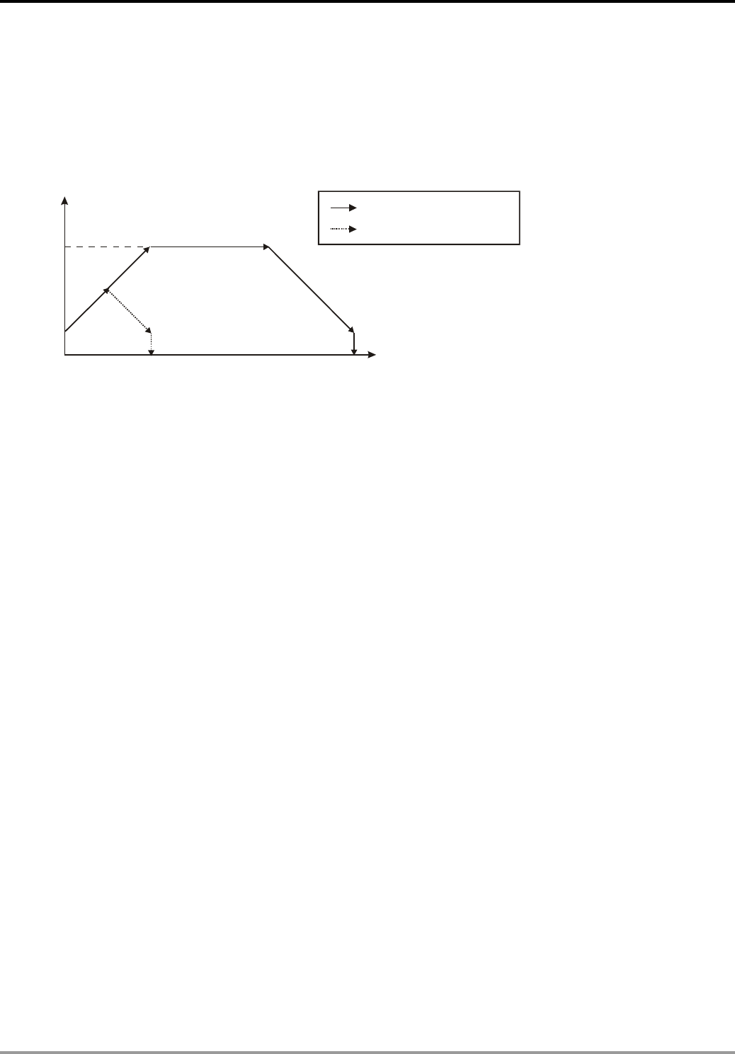
7 Application Instructions API 50-99
DVP-PLC APPLICATION MANUAL
7-40
instruction will automatically adjust the acceleration/deceleration time and the maximum frequency.
4. The operands have to be set before the execution of the instruction PLSR.
5. All acceleration/deceleration instructions are included with the brake function. The brake function will be
enabled when PLC is performing acceleration and the switch contact is suddenly Off. The deceleration will
operate at the slope of the acceleration.
S
1
F
0
Time T
Frequency F
Original acceleration path
Brake path
7 Application Instructions API 50-99
DVP-PLC APPLICATION MANUAL
7-41
API Mnemonic Operands Function
60
IST Initial State
Bit Devices Word Devices Program Steps Type
OP X Y M S K H KnX KnY KnM KnS T C D E F
S * * *
D1 *
D2 *
IST: 7 steps
PULSE 16-bit 32-bit
ES EX SS SA SX SC EH SV EH3
SV2 ES EX SS SA SX SC EH SV EH3
SV2 ES EX SS SA SX SC EH SV EH3
SV2
Operands:
S: Start device in the designated operation mode D1: The smallest No. of designated step in auto mode
D2: The biggest No. of designated step in auto mode
Explanations:
1. S will occupy 8 consecutive points.
2. Range of D1 and D2: for SA/SX/SC/EH/EH2/SV/EH3 /SV2 S20 ~ S899; for ES/EX/SS S20 ~ S127; D2 > D1.
3. See the specifications of each model for their range of use.
4. ES/SA series MPU does not support E, F index register modification.
5. IST instruction can only be used once in the program.
6. Flags: M1040 ~ M1047. See remarks for more details.
7. IST instruction is a handy instruction specifically for the initial status of step ladder control procedure to
accommodate special auxiliary relay.
Program Example 1:
1. Use of IST instruction
M1000
IST X10 S20 S60
S X10: Individual operation
X11: Zero return
X12: Step operation
X13: One cycle operation
X14: Continuous operation
X15: Zero return enabled switch
X16: Start switch
X17: Stop switch
2. When IST instruction is being executed, the following special auxiliary relays will switch automatically.
M1040: Operation forbidden
M1041: Operation starts
M1042: Pulse output enabled
M1047: STL monitor enabled
S0: Initiates manual operation
S1: Initiates zero return
S2: Initiates auto operation
3. S10 ~ S19 are for zero return and cannot be used as general steps. When S0 ~ S9 are in use, S0 ~ S2 represent
manual operation mode, zero return mode and auto operation mode. Therefore, in the program , you have to
write the circuit of the three steps in advance.
4. When switched to S1 (zero return) mode, any On in S10 ~ S19 will result in no zero return.
5. When switched to S2 (auto operation) mode, any On of the S in D1 ~ D2 or M1043 = On will result in no auto
7 Application Instructions API 50-99
DVP-PLC APPLICATION MANUAL
7-42
operation.
Program Example 2:
1. Robot arm control (by IST instruction):
a) Motion request: Separate the big ball and small ball and move them to different boxes. Configure the control
panel for the control.
b) Motions of the robot arm: descending, clipping ball, ascending, right shifting, releasing ball, ascending, left
shifting.
c) I/O devices:
Y0
Y1
Y2Y3
Left-limit X1
Upper-limit X4
Lower-limit X5
Right-limit X2
(big)
Right-limit X3
(small)
Big Small
Ball size
sensor X0
2. Operation modes:
Manual operation: Turn On/Off of the load by a single button.
Zero return: Press the zero return button to automatically zero-return the machine.
Auto operation:
a) Single step operation: Press “auto start” button for every one step forward.
b) One cycle operation: Press “auto start” button at the zero point. After a cycle of auto operation, the operation
will stops at the zero point. Press “auto stop” button in the middle of the operation to stop the operation and
press “auto start” to restart the operation. The operation will resume until it meets the zero point.
c) Continuous operation: Press “auto start” button at the zero point to resume the operation. Press “auto stop” to
operate until it meets the zero point.
3. The control panel:
X15 X16
X17
X20
X21
X22
X23
X24
X25
Step X12
One cycle
Operation X13
Continuous
Operation X14
Manual
Operation X10
Zero Return X11
Start Power
Stop Power
Start Zero Return Auto Start
Auto Stop
Right
Shift
Left
Shift
Release
Ball
Clip
Ball
Descend
Ascend
a) Ball size sensor X0.
b) Robot arm: left limit X1, big ball right limit X2, small ball right limit X3, upper limit X4, lower limit X5.
c) Robot arm: ascending Y0, descending Y1, right shifting Y2, left shifting Y3, clipping Y4.
Start Circuit

7 Application Instructions API 50-99
DVP-PLC APPLICATION MANUAL
7-43
M1000
IST X10 S20 S80
X0
M1044
X1 Y4
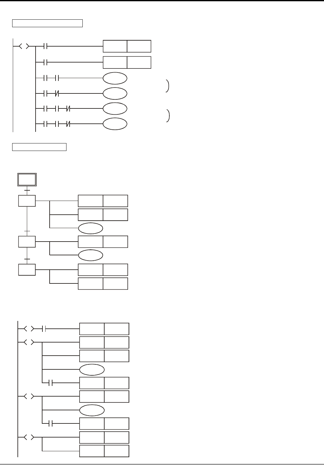
7 Application Instructions API 50-99
DVP-PLC APPLICATION MANUAL
7-44
Manual Operation Mode
X20
SET
RST Y4
Y4
S
S0
X21
X22 Y1
Y0
X23 Y0
Y1
X24 X4
Y2
Y3
X25 X4
Y3
Y2
Clipping tightly
Clipping released
Descending
Ascending
Interlocked
Right shifting
Left shifting
Interlocked
Robot arm ascends to upper limit (X4 On)
Zero Return Mode
SFC:
S1
S10
X15
S11
X4
S12
X1
RST Y4
RST Y1
Y0
RST Y2
Y3
SET M1043
RST S12
Clipping released
Descending stops
Robot arm ascends to upper limit (X4 On)
Right shifting stops
Robot arm left shifting to left limit (X1 On)
Enable zero return completed flag
Zero return operation completed
Ladder Diagram:
X15
SET S10
S
S1
RST Y4
S
S10
RST Y1
Y0
X4
SET S11
RST Y2
S
S11
Y3
X1
SET S12
SET M1043
S
S12
RST S12
Enter zero return mode
Clipping released
Descending stops
Robot arm ascends to upper limit (X4 On)
Right shifting stops
Robot arm left shifting to left limit (X1 On)
Enable zero return completed flag
Zero return operation completed
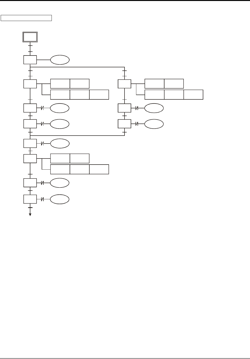
7 Application Instructions API 50-99
DVP-PLC APPLICATION MANUAL
7-45
Auto Operation Modes
SFC:
S2
S20
S30
S31
M1044
X5
T0
Y1
SET
Y0
S32
X4
X2
S50
Y1
Y2
S2
X1
M1041
X0
Y4
TMR T0 K30
S60
RST
X5
Y4
TMR T2 K30
S70
T2
Y0
S80
X4
Y3
X1
S40
S41
X5
T1
SET
Y0
S42
X4
X3
Y2
X0
Y4
TMR T1 K30
X3
X2
X4
X4
X5
X4
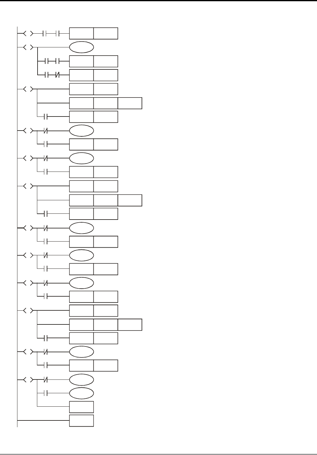
7 Application Instructions API 50-99
DVP-PLC APPLICATION MANUAL
7-46
Ladder Diagram:
SET S20
SET S30
SET Y4
Y0
END
X5
S31
S
X4
TMR T0
SET S32
S2
S
M1041 M1044
S20
S
S30
S
Y1
X0
SET S40
X5 X0
SET S31
T0
K30
Y2
S32
S
X2
SET S50
X2
SET Y4
TMR T1
S40
S
SET S41
T1
K30
Y0
S41
S
X4
SET S42
Y2
S42
S
X3
SET S50
X3
Y1
S50
S
X5
SET S60
RST Y4
TMR T2
S60
S
SET S70
T2
K30
Y0
S70
S
X4
SET S80
Y3
S80
S
X1
X1
RET
S2
Enter auto operation mode
Clipping tightly
Clipping released
Robot arm descending
Right shifting
Robot arm ascending to upper limit (X4 On)
Robot arm left shifting to left limit (X1 On)
Clipping tightly
Robot arm ascending to upper limit (X4 On)
Right shifting
Robot arm descending
Robot arm ascending to upper limit (X4 On)
X4
X4
X4X4
X5
X4

7 Application Instructions API 50-99
DVP-PLC APPLICATION MANUAL
7-47
Remarks:
Flag explanations:
M1040: When On, all step operations are forbidden.
1. Manual mode: M1040 keeps being On
2. Zero return/one cycle operation mode: Between the timing of pressing “auto stop” and “auto start”
buttons, M1040 will keep being On.
3. Step mode: M1040 keeps being On until “auto start” button is pressed.
4. Continuous operation mode: When PLC goes from STOP to RUN, M1040 will keep being On and
turn Off when “auto start” button is pressed.
M1041: Step operation starts. Special M for initial S2 to move to the next step.
1. Manual/zero return mode: M1041 keeps being Off.
2. Step/one cycle operation mode: M1041 will only be On when “auto start” button is pressed.
3. Continuous operation mode: M1041 keeps On when “auto start” button is pressed; Off when “auto
stop” button is pressed.
M1042: Enabling pulse output. Sending pulses once when “auto start” button is pressed.
M1043: On when zero return is completed.
M1044: In continuous operation mode, M1044 has to be On to more S2 to the next step.
M1045: All output resets are forbidden.
If the machine (not at the zero point) goes
- from manual (S0) to zero return (S1)
- from auto (S2) to manual (S0)
- from auto (S2) to zero return (S1)
1. When M1045 is Off, and any of the S among D1 ~ D2 is On, SET Y output and the step in action will
be reset to Off.
2. When M1045 is On, SET Y output will be remained but the step in action will be reset to Off
If the machine executes zero return (at the zero point) and goes from zero return (S1) to manual (S0),
no matter M1045 is On or Off, SET Y output will be remained but the step in action will be reset to Off.
M1046: STL state setting. On when any of the steps is On. When M1047 is forced On, On of any S will result in
On of M1046. D1040 ~ D1047 will record the No. of the previous 8 points before On of S.
M1047: On for enabling STL monitor. When IST instruction starts to be executed, M1047 will be forced On. In
every scan time, as long as IST instruction is still On, M1047 will be forced On. M1047 monitors all the
S.
D1040 ~
D1047: On status of step No. 1 ~ 8
7 Application Instructions API 50-99
DVP-PLC APPLICATION MANUAL
7-48
API Mnemonic Operands Function
61
D SER P Search a Data Stack
Bit Devices Word Devices Program Steps Type
OP X Y M S K H KnX KnY KnM KnS T C D E F
S1 * * * * * * *
S2 * * * * * * * * * * *
D * * * * * *
n * * *
SER, SERP: 9 steps
DSER, DSERP: 17 steps
PULSE 16-bit 32-bit
ES EX SS SA SX SC EH SV EH3
SV2 ES EX SS SA SX SC EH SV EH3
SV2 ES EX SS SA SX SC EH SV EH3
SV2
Operands:
S1: Start device for data stack comparison S2: Data to be compared D: Start device for storing comparison
result n: Length of data to be compared
Explanations:
1. When S2 are used in device F, only 16-bit instruction is applicable.
2. D will occupy 5 consecutive points.
3. Range of n: for 16-bit instruction 1 ~ 256; for 32-bit instruction 1 ~ 128.
4. See the specifications of each model for their range of use.
5. The n data in the registers starting from S1 are compared with S2 and the results are stored in the registers
starting from D.
6. In the 32-bit instruction, S1, S2, D and n will designate 32-bit registers.
7. For D, the 16-bit counters and 32-bit counters in SA/SX/SC series MPU cannot be mixed when being used.
Program Example:
1. When X0 = On, the data stack consist of D10 ~ D19 will be compared against D0 and the result will be stored in
D50 ~ D52. If there are equivalent values appearing during the comparison, D50 ~ D52 will all be 0.
2. The data are compared algebraically. (-10 < 2).
3. The No. of the register with the smallest value among the compared data will be recorded in D53; the biggest
will be recorded in D54. When there are more than one smallest value or biggest value, device D will record the
No. of the register with bigger value.
X0
SER D10 D0 D50 K10

7 Application Instructions API 50-99
DVP-PLC APPLICATION MANUAL
7-49
S1 Content Data to be
compared Data No. Result D Content Description
D10 88 0 D50 4 Total number of data with
equivalent values
D11 100 1 Equal D51 1 No. of the first equivalent value
D12 110 2 D52 8 No. of the last equivalent value
D13 150 3 D53 7 No. of the smallest value
D14 100 4 Equal D54 9 No. of the biggest value
D15 300 5
D16 100 6 Equal
D17 5 7 Smallest
D18 100 8 Equal
n
D19 500
S2
D0 = K100
9 Biggest
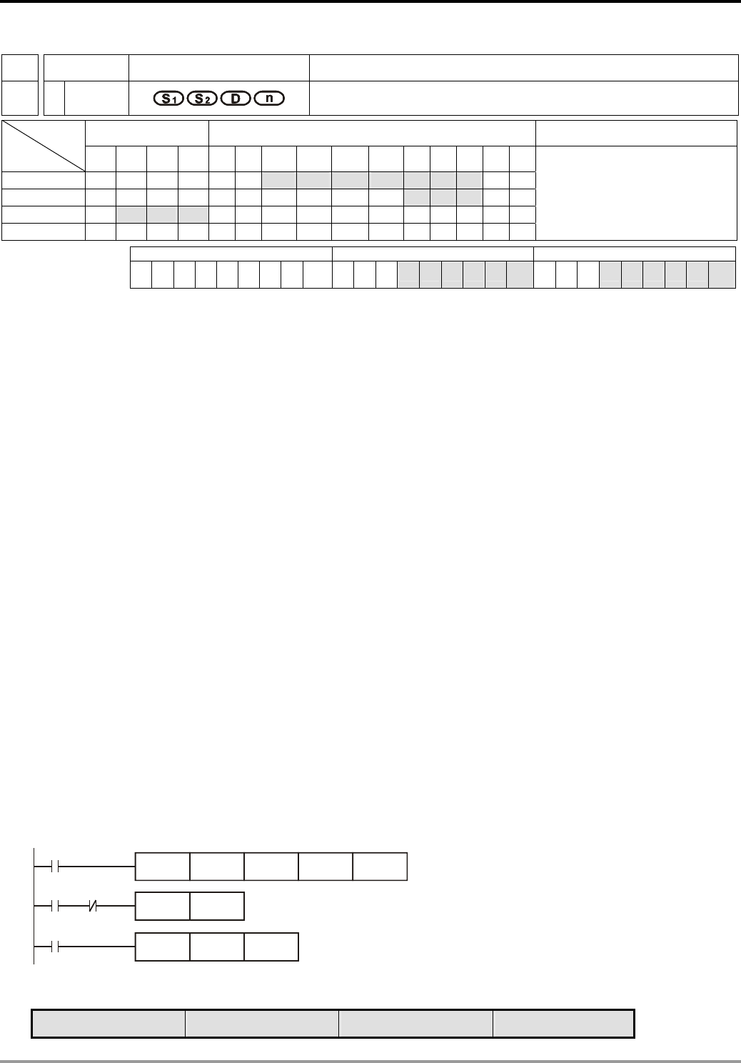
7 Application Instructions API 50-99
DVP-PLC APPLICATION MANUAL
7-50
API Mnemonic Operands Function
62
D ABSD Absolute Drum Sequencer
Bit Devices Word Devices Program Steps Type
OP X Y M S K H KnX KnY KnM KnS T C D E F
S1 * * * * * * *
S2 * * *
D * * *
n * *
ABSD: 9 steps
DABSD: 17 steps
PULSE 16-bit 32-bit
ES EX SS SA SX SC EH SV EH3
SV2 ES EX SS SA SX SC EH SV EH3
SV2 ES EX SS SA SX SC EH SV EH3
SV2
Operands:
S1: Start device in the data table S2: No. of counter D: Start No. of the devices for the comparison results
n: Number of data for comparison
Explanations:
1. When S1 designates KnX, KnY, KnM and KnS, the 16-bit instruction has to designate K4 and 32-bit instruction
has to designate K8.
2. For SA/SX/SC series MPU, S2 only supports C device.
3. Range of n: 1 ~ 64
4. See the specifications of each model for their range of use.
5. ABSD instruction is for the absolute control of the multiple output pulses generated by the present value in the
counter.
6. S2 of DABSD instruction can designate high speed counters. However, when the present value in the high
speed counter is compared with the target value, the result cannot output immediately owing to the scan time. If
an immediate output is required, please use DHSZ instruction that is exclusively for high speed counters.
Program Example:
1. Before the execution of ABSD instruction, use MOV instruction to write all the set values into D100 ~ D107 in
advance. The even-number D is for lower bound value and the odd-number D is for upper bound value.
2. When X10 = On, the present value in counter C10 will be compared with the four groups of lower and upper
bound values in D100 ~ D107. The comprison results will be stored in M10 ~ M13.
3. When X10 = Off, the original On/Off status of M10 ~ M13 will be remained.
X10
ABSD D100 C10 M10 K4
C10
RST C10
X11
CNT C10 K400
X11
4. M10~ M13 will be On when the present value in C10 ≦ upper bound value or ≧ lower bound value.
Lower bound value Upper bound value Present value in C10 Output
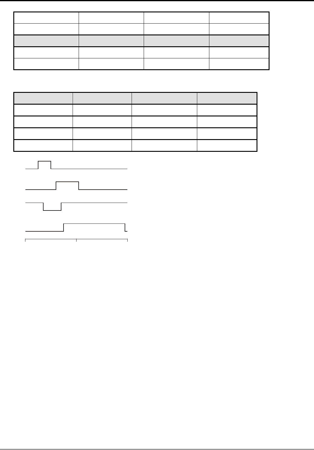
7 Application Instructions API 50-99
DVP-PLC APPLICATION MANUAL
7-51
D100 = 40 D101 = 100 40 ≦ C10 ≦ 100 M10 = On
D102 = 120 D103 = 210 120 ≦ C10 ≦ 210 M11 = On
Lower bound value Upper bound value Present value in C10 Output
D104 = 140 D105 = 170 140 ≦ C10 ≦ 170 M12 = On
D106 = 150 D107 = 390 150 ≦ C10 ≦ 390 M13 = On
5. If the lower bound value > upper bound value, when C10 < upper bound value (60) or > upper bound value (140),
M12 will be On.
Lower bound value Upper bound value Present value in C10 Output
D100 = 40 D101 = 100 40 ≦ C10 ≦ 100 M10 = On
D102 = 120 D103 = 210 120 ≦ C10 ≦ 210 M11 = On
D104 = 140 D105 = 60 60 ≦ C10 ≦ 140 M12 = On
D106 = 150 D107 = 390 150 ≦ C10 ≦ 390 M13 = On
4002000
40 100
120 210
60 140
150 390
M10
M11
M12
M13
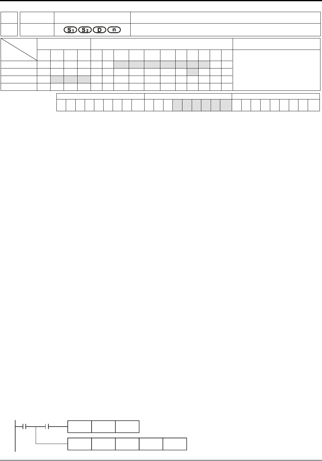
7 Application Instructions API 50-99
DVP-PLC APPLICATION MANUAL
7-52
API Mnemonic Operands Function
63
INCD Incremental Drum Sequencer
Bit Devices Word Devices Program Steps Type
OP X Y M S K H KnX KnY KnM KnS T C D E F
S1 * * * * * * *
S2 *
D * * *
n * *
INCD: 9 steps
PULSE 16-bit 32-bit
ES EX SS SA SX SC EH SV EH3
SV2 ES EX SS SA SX SC EH SV EH3
SV2 ES EX SS SA SX SC EH SV EH3
SV2
Operands:
S1: Start device in the data table S2: No. of counter D: Start No. of the devices for the comparison results
n: Number of data for comparison
Explanations:
1. When S1 designates KnX, KnY, KnM and KnS, it has to designate K4.
2. In the 16-bit instruction, S2 has to designate C0 ~ C198 and will occupy 2 consecutive No. of counters.
3. Range of n: 1 ~ 64
4. See the specifications of each model for their range of use.
5. Flag: M1029 (instruciton execution completed)
6. INCD instruction is for the relative control of the multiple output pulses generated by the present value in the
counter.
7. The present value in S2 is compared with S1. S2 will be reset to 0 whenever a comparison is completed. The
current number of data processed in temporarily stored in S2 + 1.
8. When n data have been processed, M1029 will be On for one scan period.
Program Example:
1. Before the execution of INCD instruction, use MOV instruction to write all the set values into D100 ~ D104 in
advance. D100 = 15, D101 = 30, D102 = 10, D103 = 40, D104 = 25.
2. The present value in C10 is compared against the set values in D100 ~ D104. The present value will be reset to
0 whenever a comparison is completed.
3. The current number of data having been processed is temporarily stored in C11.
4. The number of times of reset is temporarily stored in C11.
5. Whenever the content in C11 pluses 1, M10 ~ M14 will also correspondingly change. See the timing diagram
below.
6. After the 5 groups of data have been compared, M1029 will be On for one scan period.
7. When X0 goes from On to Off, C10 and C11 will both be reset to 0 and M10 ~ M14 will all be Off. When X0 is On
again, the instruction will start its execution again from the beginning.
INCD D100 C10 M10 K5
X0
CNT C10 K100
M1013
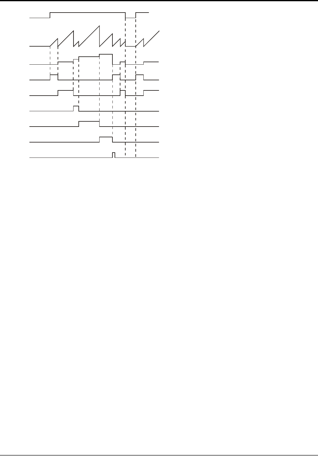
7 Application Instructions API 50-99
DVP-PLC APPLICATION MANUAL
7-53
X0
M10
M12
M11
M13
M14
M1029
15 10 15 15
30
30 40
25
111
000
234
C10
C11
Present value
Present value
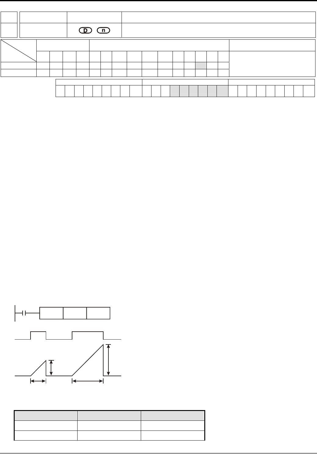
7 Application Instructions API 50-99
DVP-PLC APPLICATION MANUAL
7-54
API Mnemonic Operands Function
64
TTMR Teaching Timer
Bit Devices Word Devices Program Steps Type
OP X Y M S K H KnX KnY KnM KnS T C D E F
D *
n * *
TTMR: 5 steps
PULSE 16-bit 32-bit
ES EX SS SA SX SC EH SV EH3
SV2 ES EX SS SA SX SC EH SV EH3
SV2 ES EX SS SA SX SC EH SV EH3
SV2
Operands:
D: Device No. for storing the “On” time of button switch n: Multiple setting
Explanations:
1. D will occupy 2 consecutive devices.
2. Range of n: 0 ~ 2
3. See the specifications of each model for their range of use.
4. For SA series MPU, TTMR instruction can be used 8 times in the program.
5. The “On” time (unit: 100ms) of the external button switch is stored in device No. D + 1. The “On” time (unit:
second) of the switch is multiplied by n and stored in D.
6. Multiple setting:
When n = 0, unit of D = second
When n = 1, unit of D = 100ms (D × 10)
When n = 2, unit of D = 10ms (D × 100)
Program Example 1:
1. The “On” (being pressed) time of button switch X0 is stored in D1. The setting of n is stored in D0. Therefore, the
button switch will be able to adjust the set value in the timer.
2. When X0 goes Off, the content in D1 will be cleared to 0, but the content in D0 will remain.
X0
TTMR D0 K0
X0
D1
D0
D0
D1
TT
On time (sec) On time (sec)
3. Assume the “On” time of X0 is T (sec.), see the relation between D0, D1 and n in the table below.
n D0 D1 (unit: 100ms)
K0 (unit: s) 1 × T D1 = D0 × 10
K1 (unit: 100 ms) 10 × T D1 = D0
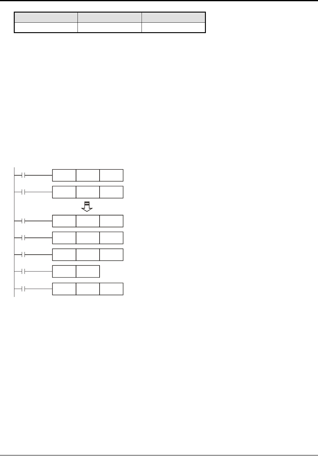
7 Application Instructions API 50-99
DVP-PLC APPLICATION MANUAL
7-55
n D0 D1 (unit: 100ms)
K2 (unit: 10 ms) 100 × T D1 = D0/10
Program Example 2:
1. Use TMR instruction to write in 10 groups of set time.
2. Write the set values into D100 ~ D109 in advance.
3. The timing unit for timer T0 ~ T9 is 0.1 sec. The timing unit for the teaching timer is 1 sec.
4. Connect the 1-bit DIP switch to X0 ~ X3 and use BIN instruction to convert the set value of the switch into a bin
value and store it in E.
5. Store the “On” time (sec.) of X10 in D200.
6. M0 refers to the pulses generated from one scan period after the button switch of the teaching timer X10 is
released.
7. Use the set number of the DIP switch as the indirectly designated pointer and send the content in D200 to
D100E (D100 ~ D109).
M10
TMR T0 D100
M11
TMR T1 D101
M19
TMR T9 D109
M1000
BIN K1X0 E
X10
TTMR D200 K0
X10
PLF M0
M0
MOV D200 D100E
Remarks:
1. For SA series MPU, TTMR instruction can be used 8 times in the program. But in a subroutine or interruption
subroutine, the instruction can only be used once.
2. For EH series MPU, there is no limitation on the times using this instruction in the program and 8 instructions can
be executed at the same time.
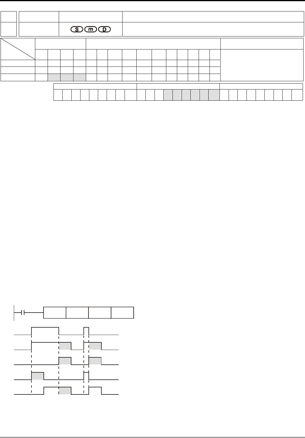
7 Application Instructions API 50-99
DVP-PLC APPLICATION MANUAL
7-56
API Mnemonic Operands Function
65
STMR Special Timer
Bit Devices Word Devices Program Steps Type
OP X Y M S K H KnX KnY KnM KnS T C D E F
S *
m * *
D * * *
STMR: 7 steps
PULSE 16-bit 32-bit
ES EX SS SA SX SC EH SV EH3
SV2 ES EX SS SA SX SC EH SV EH3
SV2 ES EX SS SA SX SC EH SV EH3
SV2
Operands:
S: No. of timer m: Set value in timer (unit: 100ms) D: No. of start output device
Explanations:
1. Range of S: for SA/SX/SC T0 ~ T191; for EH/EH2/SV T0 ~ T199; for EH3/SV2 T0 ~ T183
2. Range of m: 1 ~ 32,767
3. D will occupy 4 consecutive devices.
4. See the specifications of each model for their range of use.
5. STMR instruction is used for Off-delay, one shot timer and flashing sequence.
6. The No. of timers designated by STMR instructions can be used only once.
Program Example:
1. When X10 = On, STMR instruction will designate timer T0 and set the set value in T0 as 5 seconds.
2. Y0 is the contact of Off-delay. When X10 goes from Off to On, Y0 will be On. When X10 goes from On to Off, Y0
will be Off after a five seconds of delay.
3. When X10 goes from On to Off, there will be a five seconds of Y1 = On output.
4. When X10 goes from Off to On, there will be a five seconds of Y2 = On output.
5. When X10 goes from Off to On, Y3 will be On after a five seconds of delay. When X10 goes from On to Off, Y3
will be Off after a five seconds of delay.
X10
STMR T0 K50 Y0
X10
Y0
Y1
Y2
Y3
5 sec 5 sec
5 sec
5 sec
5 sec
5 sec
6. Add a b contact of Y3 after X10, and Y1 and Y2 can operate for flashing sequence output. When X10 goes Off,
Y0, Y1 and Y3 will be Off and the content in T10 will be reset to 0.

7 Application Instructions API 50-99
DVP-PLC APPLICATION MANUAL
7-57
X10
STMR T10 K50 Y0
Y3
X10
Y1
Y2
5 sec 5 sec
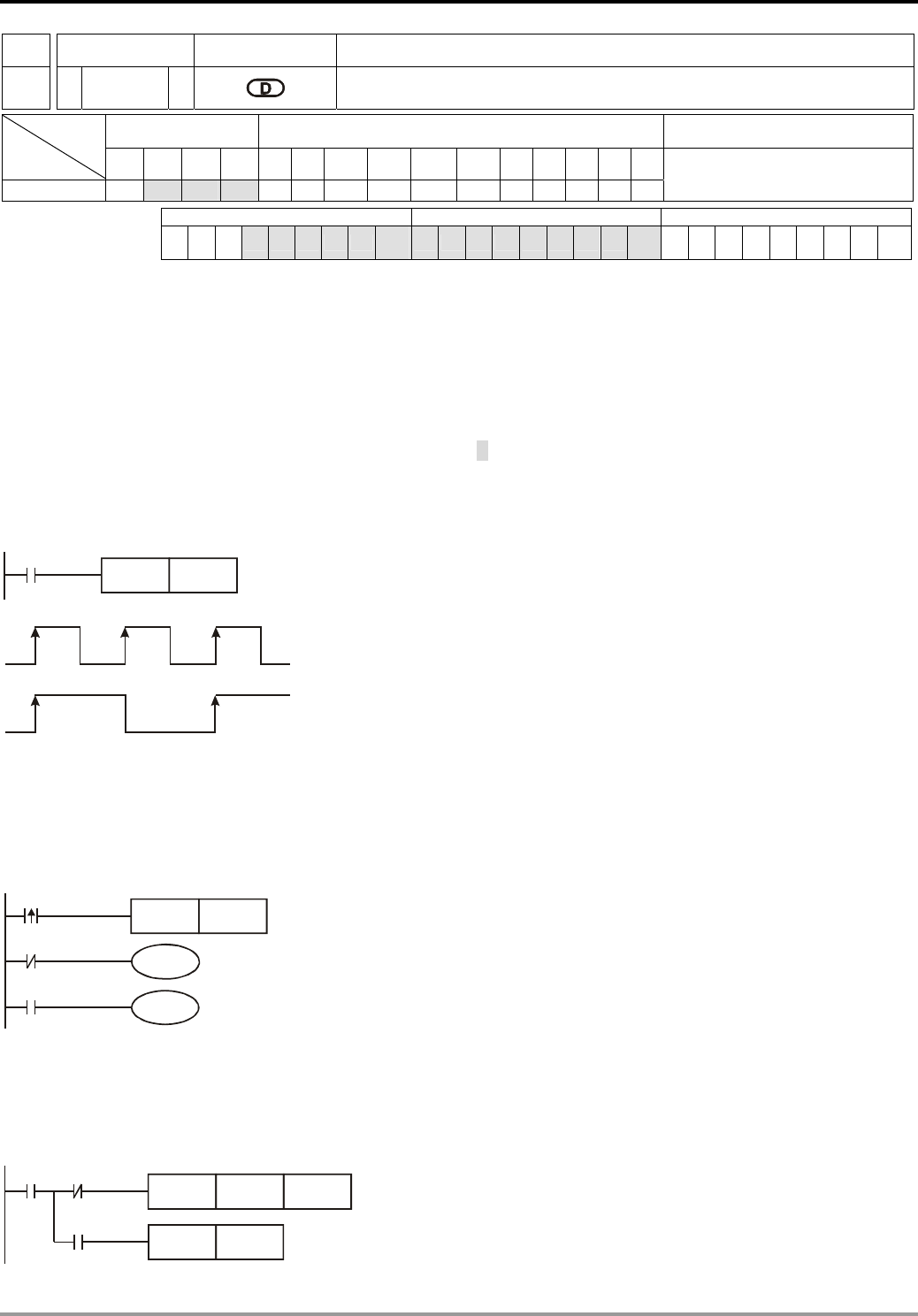
7 Application Instructions API 50-99
DVP-PLC APPLICATION MANUAL
7-58
API Mnemonic Operands Function
66
ALT P Alternate State
Bit Devices Word Devices Program Steps Type
OP X Y M S K H KnX KnY KnM KnS T C D E F
D * * *
ALT, ALTP: 3 steps
PULSE 16-bit 32-bit
ES EX SS SA SX SC EH SV EH3
SV2 ES EX SS SA SX SC EH SV EH3
SV2 ES EX SS SA SX SC EH SV EH3
SV2
Operands:
D: Destination device
Explanations:
1. See the specifications of each model for their range of use.
2. When ALT instruction is executed, “On” and “Off” of D will switch.
3. This instruction adopts pulse execution instructions (ATLP).
Program Example 1:
When X0 goes from Off to On, Y0 will be On. When X0 goes from Off to On for the second time, Y0 will be Off.
X0
ALTP Y0
X0
Y0
Program Example 2:
Using a single switch to enable and disable control. At the beginning, M0 = Off, so Y0 = On and Y1 = Off. When X10
switches between On/Off for the first time, M0 will be On, so Y1 = On and Y0 = Off. For the second time of On/Off
switching, M0 will be Off, so Y0 = On and Y1 = Off.
X10
ALT M0
M0
Y0
M0
Y1
Program Example 3:
Generating flashing. When X10 = On, T0 will generate a pulse every 2 seconds and Y0 output will switch between On
and Off following the T0 pulses.
X10
TMR T0
ALTP Y0
K20
T0
T0
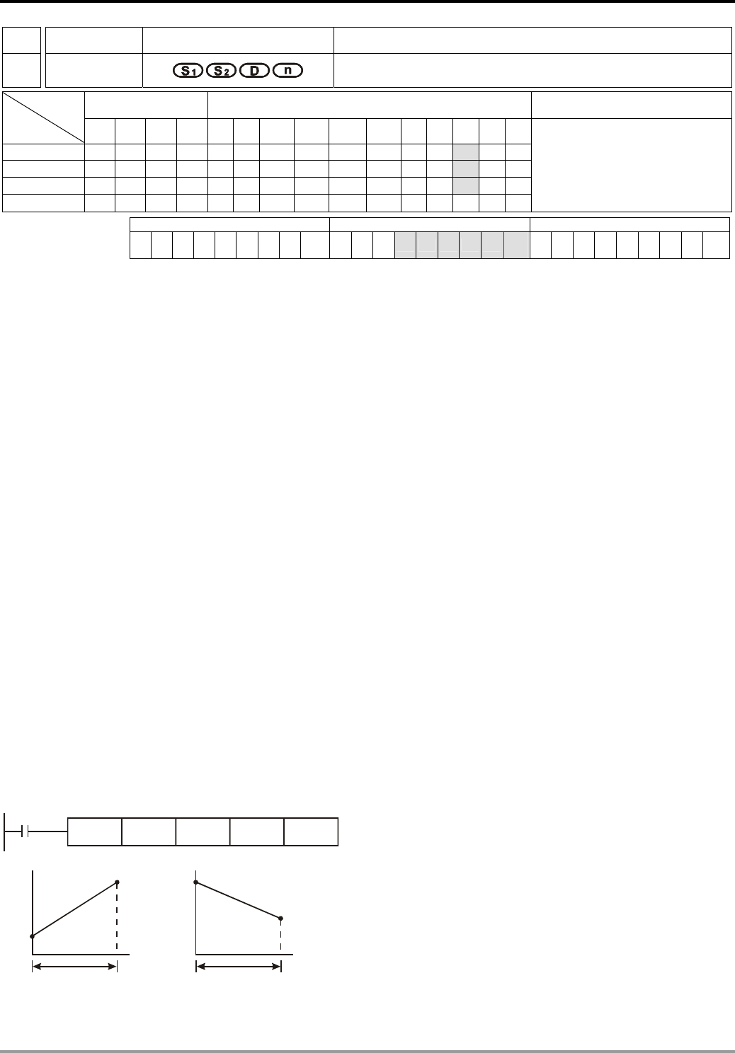
7 Application Instructions API 50-99
DVP-PLC APPLICATION MANUAL
7-59
API Mnemonic Operands Function
67
RAMP Ramp Variable Value
Bit Devices Word Devices Program Steps Type
OP X Y M S K H KnX KnY KnM KnS T C D E F
S1 *
S2 *
D *
n * *
RAMP: 9 steps
PULSE 16-bit 32-bit
ES EX SS SA SX SC EH SV EH3
SV2 ES EX SS SA SX SC EH SV EH3
SV2 ES EX SS SA SX SC EH SV EH3
SV2
Operands:
S1: Start of ramp signal S2: End of ramp signal D: Duration of ramp signal n: Scan times
Explanations:
1. Range of n: 1 ~ 32,767
2. D will occupy 2 consecutive points.
3. See the specifications of each model for their range of use.
4. Flags: M1026 (enabling RAMP; see remarks for more details); M1029 (RAMP execution completed).
5. This instruction is for obtaining slope (the relation between linearity and scan time). Before using this instruction,
you have to preset the scan time.
6. The set value of start ramp signal is pre-written in D10 and set value of end ramp signal in D11. When X10 = On,
D10 increases towards D11 through n (= 100) scans (the duration is stored in D12). The times of scans are
stored in D13.
7. In the program, first drive M1039 = On to fix the scan time. Use MOV instruction to write the fixed scan time to
the special data register D1039. Assume the scan time is 30ms and take the above program for example, n =
J100, the time for D10 to increase to D11 will be 3 seconds (30ms × 100).
8. When X10 goes Off, the instruction will stop its execution. When X10 goes On again, the content in D12 will be
reset to 0 for recalculation.
9. When M1026 = Off, M1029 will be On and the content in D12 will be reset to the set value in D10.
Program Example:
When this instruction is used with analog signal outputs, it will be able to buffer START and STOP.
X10
RAMP D10 D11 D12 K100
D10
D12
D11
D11
D12
D10
D10<D11 D10 >D11
n scans
The scan times is stored in D13
n scans

7 Application Instructions API 50-99
DVP-PLC APPLICATION MANUAL
7-60
Remarks:
D12 for enabling On/Off of M1026:
X10
D11
D10 D12
M1029
Start signal
M1026=ON
X10
D11
D10 D12
M1029
Start signal
M1026=OFF
Operand n in SA/SX V1.8, SC V1.6 and later versions support D device. Please be noted that the content in D can
only be modified when the instruction stops executing. Modification cannot be made in the execution of the
instruction.
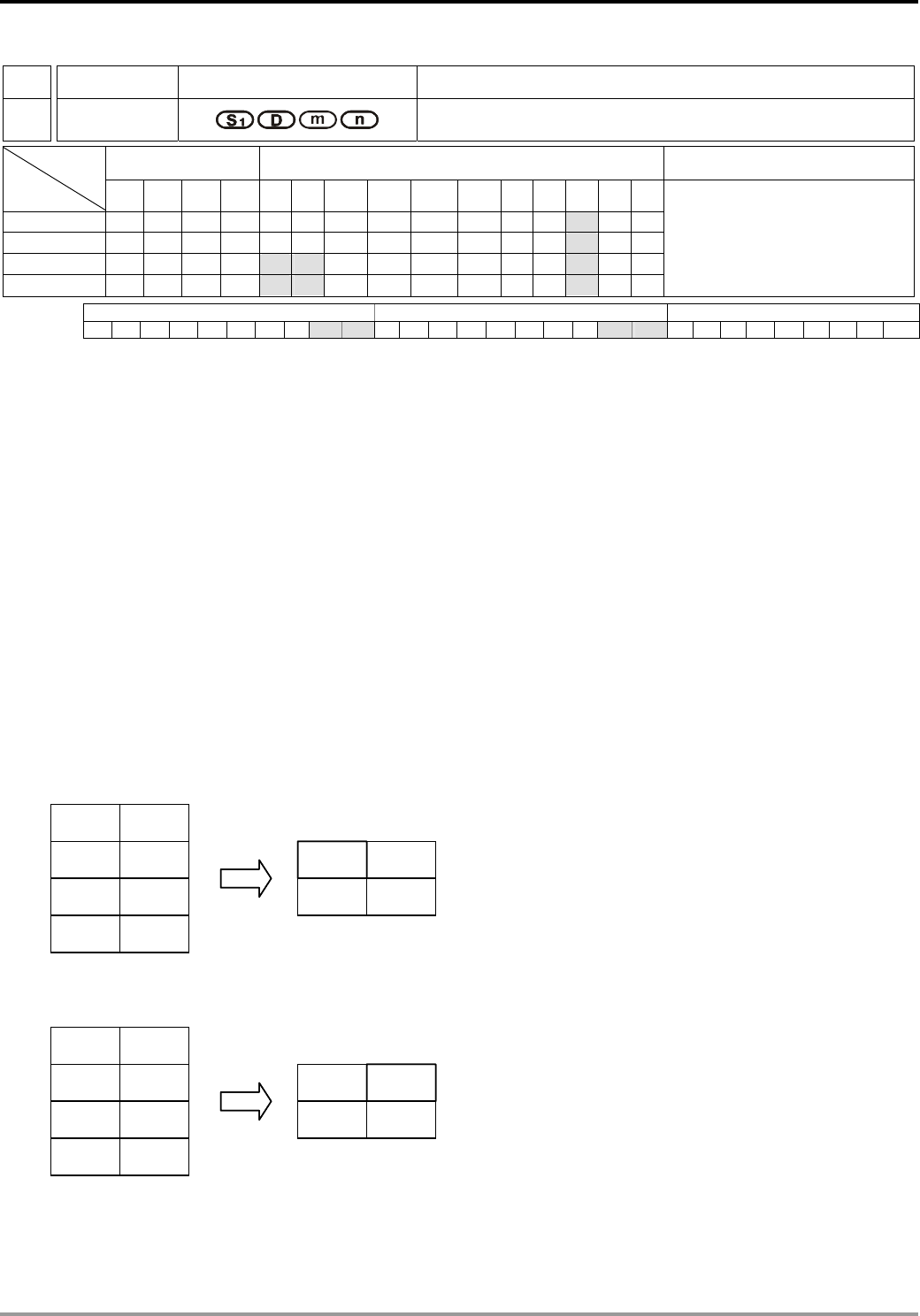
7 Application Instructions API 50-99
DVP-PLC APPLICATION MANUAL
7-61
API Mnemonic Operands Function
68
DTM Data Transform and Move
Bit Devices Word Devices Program Steps Type
OP X Y M S K H KnX KnY KnM KnS T C D E F
S1 *
S2 *
m * * *
n * * *
DTM: 9 steps
PULSE 16-bit 32-bit
ES EX SS SA SX SC EH SV EH3 SV2 ES EX SS SA SX SC EH SV EH3 SV2 ES EX SS SA SX SC EH SV EH3
Operands:
S1: Start device of the source data stack D: Start device of the destination data stack m: Transformation mode
n: Length of source data stack
Explanations:
1. For parameter settings of operand m, please refer to the following description. K, H, D devices can be specified
by operand m. If the set value is not in the available range, no transformation or move operation will be
executed and no error will be detected.
2. K, H, D devices can be specified by operand n, which indicates the length of the source data stack. The
available range for n is 1~256. If the set value falls out of available range, PLC will take the max value (256) or
the min value (1) as the set value automatically.
3. Explanations on parameter settings of m operand:
K0: With n = 4, transform 8-bit data into 16-bit data (Hi-byte, Lo-byte) in the following rule:
c
d
e
f
Hi-byte Lo-byte
c d
e f
Hi-byte Lo-byte
c
d
e
f
Hi-byte Lo-byte
c d
e f
Hi-byte Lo-byte
K1: With n = 4, transform 8-bit data into 16-bit data (Lo-byte, Hi-byte) in the following rule:
c
d
e
f
Hi-byte Lo-byte
cd
ef
Hi-byte Lo-byte
c
d
e
f
Hi-byte Lo-byte
cd
ef
Hi-byte Lo-byte
K2: With n = 2, transform 16-bit data (Hi-byte, Lo-byte) into 8-bit data in the following rule:
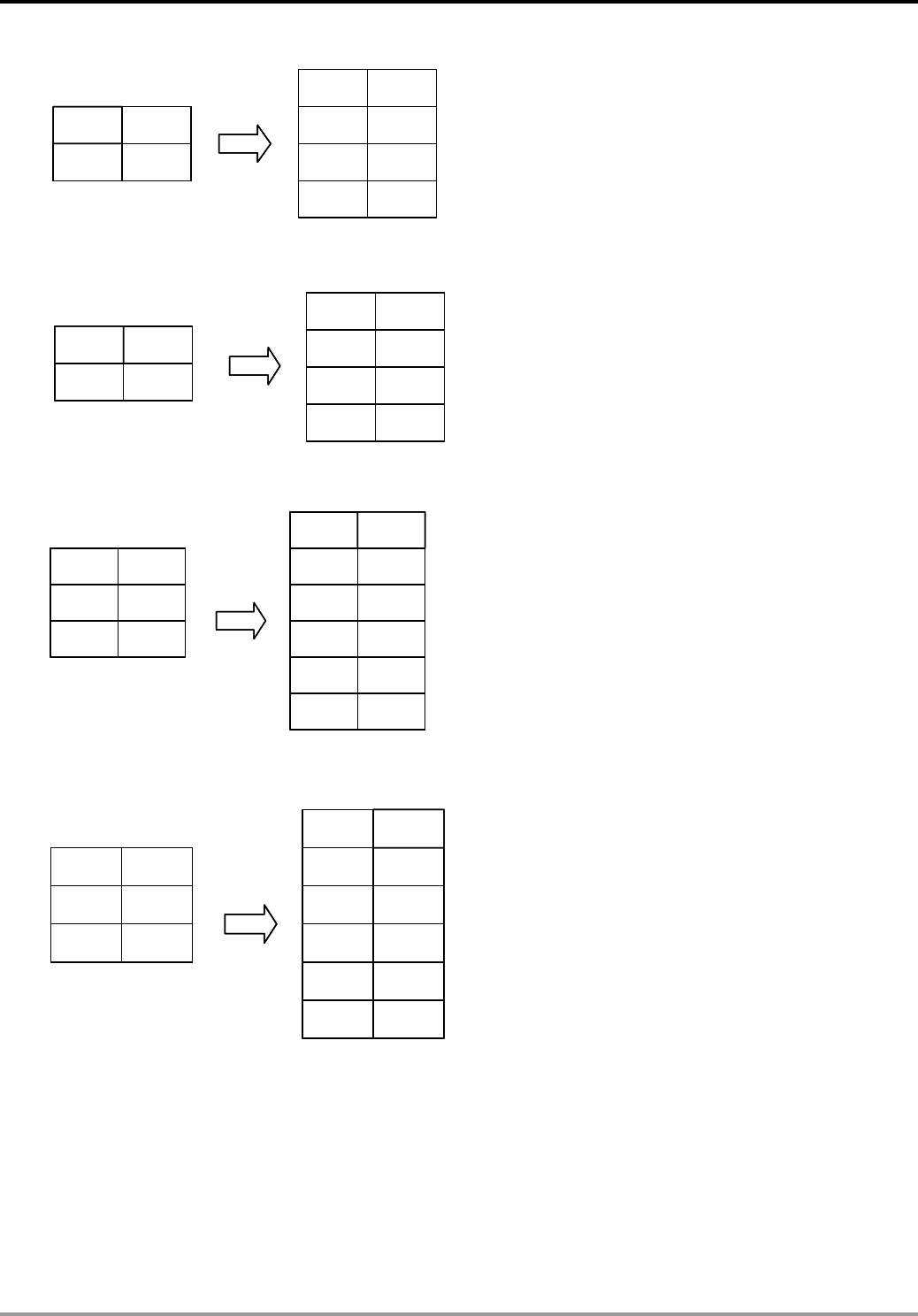
7 Application Instructions API 50-99
DVP-PLC APPLICATION MANUAL
7-62
c
d
e
f
Hi-byte Lo-byte
c d
e f
Hi-byte Lo-byte
c
d
e
f
Hi-byte Lo-byte
c d
e f
Hi-byte Lo-byte
K3: With n = 2, transform 16-bit data (Lo-byte, Hi-byte) into 8-bit data in the following rule:
c
d
e
f
Hi-byte Lo-byte
c d
e f
Hi-byte Lo-byte
c
d
e
f
Hi-byte Lo-byte
c d
e f
Hi-byte Lo-byte
K4: With n = 3, transform 8-bit HEX data into ASCII data (higher 4 bits, lower 4 bits) in the following rule:
c
d
e
Hi-byte Lo-byte
cH
dH
eH
eL
Hi-byte Lo-byte
dL
cLc
d
e
Hi-byte Lo-byte
cH
dH
eH
eL
Hi-byte Lo-byte
dL
cL
K5: With n = 3, transform 8-bit HEX data into ASCII data (lower 4 bits, higher 4 bits) in the following rule:
c
d
e
Hi-byte Lo-byte cL
dL
eL
eH
Hi-byte Lo-byte
dH
cHc
d
e
Hi-byte Lo-byte cL
dL
eL
eH
Hi-byte Lo-byte
dH
cH
K6: When n = 4, transform 8-bit ASCII data (higher 4 bits, lower 4 bits) into HEX data in the following rule:
(ASCII value to be transformed includes 0 ~ 9 (0x30~0x39), A ~ F (0x41~0x46), and a ~ f (0x61~0x66).)
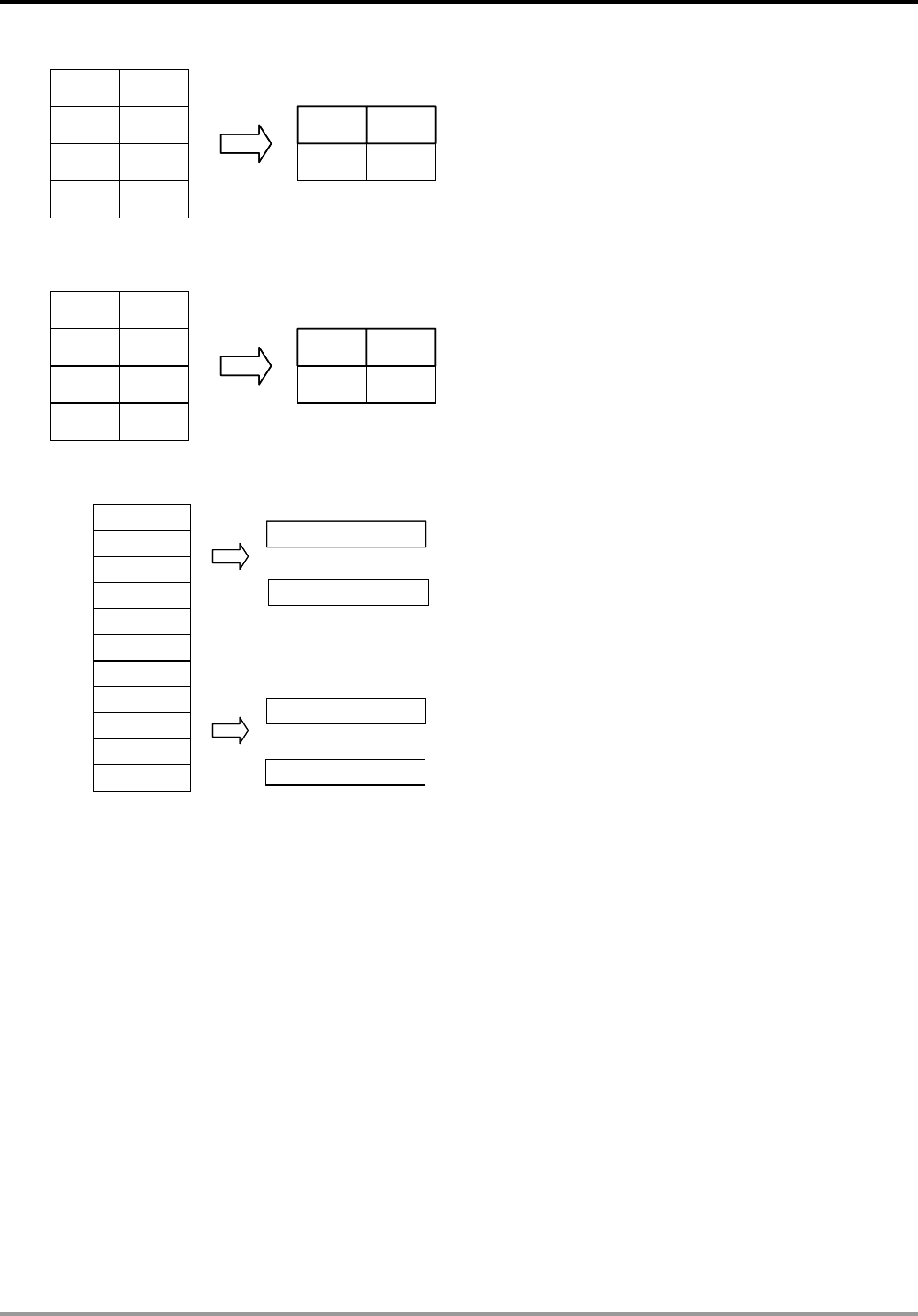
7 Application Instructions API 50-99
DVP-PLC APPLICATION MANUAL
7-63
c
d
e
f
Hi-byte Lo-byte
cd
ef
Hi-byte Lo-byte
c
d
e
f
Hi-byte Lo-byte
cd
ef
Hi-byte Lo-byte
K7: When n = 4, transform 8-bit ASCII data (lower 4 bits, higher 4 bits) into HEX data in the following rule:
c
d
e
f
Hi-byte Lo-byte
dc
fe
Hi-byte Lo-byte
c
d
e
f
Hi-byte Lo-byte
dc
fe
Hi-byte Lo-byte
K8: Transform 8-bit GPS data into 32-bit floating point data in the following rule:
dd
mm
1
mm
2
mm
3
Hi-byte Lo-byte
dd.mm
1
mm
2
mm
3
dd
1
dd
0
.mm
1
mm
2
mm
3
32bit Floating (S+4=H4E )
4E
dd
1
dd
0
mm
1
mm
2
mm
3
45
S+0
–dd.mm
1
mm
2
mm
3
32bit Floating (S+4 != H4E)
S+1
S+2
S+3
S+4
S+5
S+6
S+7
S+8
S+9
S+10
32bit Floating (S+10=H45)
D+0
D+0
–dd
1
dd
0
.mm
1
mm
2
mm
3
32bit Floating (S+10 != H45)
D+2
D+2
dd
mm
1
mm
2
mm
3
Hi-byte Lo-byte
dd.mm
1
mm
2
mm
3
dd
1
dd
0
.mm
1
mm
2
mm
3
32bit Floating (S+4=H4E )
4E
dd
1
dd
0
mm
1
mm
2
mm
3
45
S+0
–dd.mm
1
mm
2
mm
3
32bit Floating (S+4 != H4E)
S+1
S+2
S+3
S+4
S+5
S+6
S+7
S+8
S+9
S+10
32bit Floating (S+10=H45)
D+0
D+0
–dd
1
dd
0
.mm
1
mm
2
mm
3
32bit Floating (S+10 != H45)
D+2
D+2
K9: Calculate the optimal frequency for positioning instructions with ramp up/ down function.
Users only need to set up the total number of pulses for positioning and the total time for positioning first,
DTM instruction will automatically calculate the optimal max output frequency as well as the optimal start
frequency for positioning instructions with ramp-up/down function such as PLSR, DDRVI and DCLLM.
Points to note:
1. When the calculation results exceed the max frequency of PLC, the output frequency will be set as 0.
2. When the total of ramp-up and ramp-down time exceeds the total time for operation, PLC will change the
total time for operation (S+2) into “ramp-up time (S+3) + ramp-down time (S+4) + 1” automatically.
Explanation on operands:
S+0, S+1: Total number of pulses for operation (32-bit)
S+2: Total time for operation (unit: ms)
S+3: Ramp-up time (unit: ms)
S+4: Ramp-down time(unit: ms)
D+0, D+1: Optimal max output frequency (unit: Hz) (32-bit)
D+2: Optimal start frequency (Unit: Hz)

7 Application Instructions API 50-99
DVP-PLC APPLICATION MANUAL
7-64
n: Reserved
K11: Conversion from Local Time to Local Sidereal Time
Unlike the common local time defined by time zones, local sidereal time is calculated based on actual
longitude. The conversion helps the user obtain the more accurate time difference of each location within
the same time zone.
Explanation on operands:
S+0, S+1: Longitude (32-bit floating point value; East: positive, West: negative)
S+2: Time zone (16-bit integer; unit: hour)
S+3~ S+8: Year, Month, Day, Hour, Minute, Second of local time (16-bit integer)
D+0~D+5: Year, Month, Day, Hour, Minute, Second of the converted local sidereal time (16-bit integer)
n: Reserved
Example:
Input: Longitude F121.55, Time zone: +8, Local time: AM 8:00:00, Jan/6/2011
Conversion results: AM 8:06:12, Jan/6/2011
K12: Ramp value for multiple points (16-bit)
Explanation on operands (16 bits):
S: input value
S+1, S+2….. S+n: input values for multiple points. The value of these values must be set by the following rule,
S+1 must be the smallest value, S+2 must be larger than S+1 and so on. Therefore, S+n
must be the largest value.
D: ramp value
D+1, D +2 … D+n: Range of ramp values for multiple points
n: Setting value for multiple points. The setting value is within the range between K2 ~ K50. If the setting value
exceeds the range, the instruction is not executed.
The example of a curve is as follows. (n=K4)
S+1
D+1
S+2
D+2
S+3
D+4
S+4
D+3
D
S
S+1
D+1
S+2
D+2
S+3
D+4
S+4
D+3
D
S
Explanation of the example:
1. If S is larger than S+1 (S1) and is less than S+2 (S2), D+1 (D1) and D+2 (D2). D= ( ( S – S1) x ( D2 – D1 ) /
( S2 – S1 ) ) + D1.
2. If S is less than S+1, D = D+1. If S is larger than S+n, D = D+n.
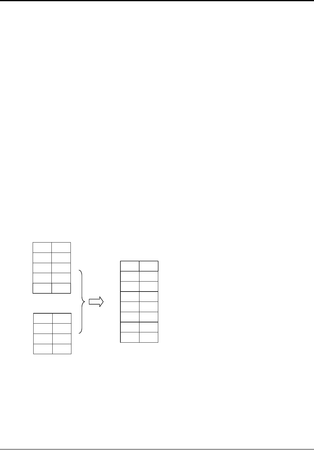
7 Application Instructions API 50-99
DVP-PLC APPLICATION MANUAL
7-65
3. The floating-point numbers are involved in the operation. The output value is rounded down to the nearest
whole digit, and then the 16-bit integer is output.
K13: Ramp value for multiple points (32-bit)
Please refer to parameter K12 for more information about the operands. The source device and the destination
device are represented by 32-bit values.
K14: Floating-point value for multiple points
Please refer to parameter K12 for more information about the operands. The source device and the destination
device are represented by 32-bit floating-point values.
K16: String combination
Explanations:
The system searches for the location of ETX (value 0x00) of the destination data string (lower 8 bits), then
copies the data string starting of the source register (lower 8 bits) to the end of the destination data string. The
source data string will be copied in byte order until the ETX (value 0x00) is reached.
Points to note:
The operand n sets the max data length after the string combination (max 256). If the ETX is not reached after
the combination, the location indicated by n will be the ETX and filled with 0x00.
The combination will be performed in the following rule:
‘A’
‘B’
‘C’
‘D’
Hi-byte Lo-byte
‘a’
‘b’
‘c’
Hi-byte Lo-byte
0x00
0x00
S+0
S+1
S+2
S+3
S+4
D+0
D+1
D+2
D+3
‘a’
‘b’
‘c’
Hi-byte Lo-byte
‘A’
D+0
D+1
D+2
D+3
‘B’
‘C’
‘D’
0x00
D+4
D+5
D+6
D+7
‘A’
‘B’
‘C’
‘D’
Hi-byte Lo-byte
‘a’
‘b’
‘c’
Hi-byte Lo-byte
0x00
0x00
S+0
S+1
S+2
S+3
S+4
D+0
D+1
D+2
D+3
‘a’
‘b’
‘c’
Hi-byte Lo-byte
‘A’
D+0
D+1
D+2
D+3
‘B’
‘C’
‘D’
0x00
D+4
D+5
D+6
D+7
K17: String capture
Explanations:
The system copies the source data string (lower 8 bits) with the data length specified by operand n to the
destination registers, where the n+1 register will be filled with 0x00. If value 0x00 is reached before the specified
capture length n is completed, the capture will also be ended.
The capture will be performed in the following rule:
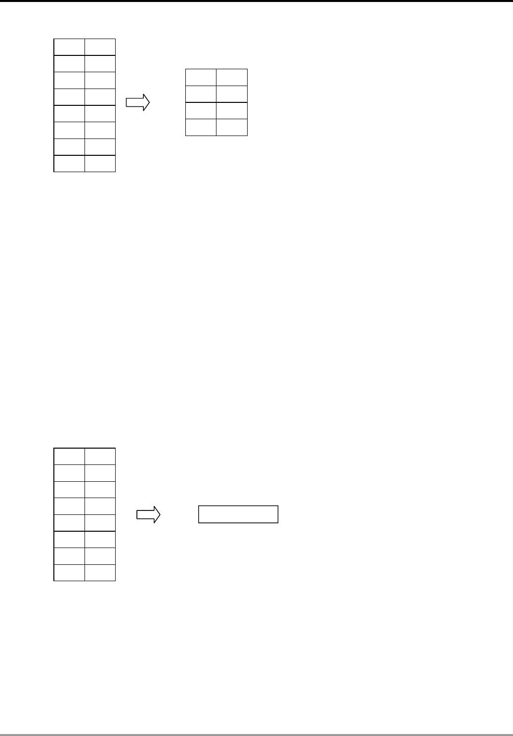
7 Application Instructions API 50-99
DVP-PLC APPLICATION MANUAL
7-66
‘a’
‘b’
‘c’
Hi-byte Lo-byte
‘A’
S+0
S+1
S+2
S+3
‘B’
‘C’
‘D’
0x00
S+4
S+5
S+6
S+7
‘a’
‘b’
‘c’
Hi-byte Lo-byte
0x00
D+0
D+1
D+2
D+3
n = k3
‘a’
‘b’
‘c’
Hi-byte Lo-byte
‘A’
S+0
S+1
S+2
S+3
‘B’
‘C’
‘D’
0x00
S+4
S+5
S+6
S+7
‘a’
‘b’
‘c’
Hi-byte Lo-byte
0x00
D+0
D+1
D+2
D+3
n = k3
K18: Convert data string to floating point value
Explanations:
The system converts n words (lower 8 bits) of the source data string (decimal point is not included) to floating
point value and stores the converted value in the destination device.
Points to note:
1. Operand n sets the number of total digits for the converted floating value. Max 8 digits are applicable and
the value over n digit will be omitted. For example, n = K6, data string “123.45678” will be converted to
“123.456”.
2. When there are characters other than numbers 1~9 or the decimal point in the source data string, the
character before the decimal point will be regarded as 0, and the value after the decimal point will be
regarded as the ETX.
3. If the source data string contains no decimal point, the converted value will be displayed by a n-digit
floating point value automatically.
The conversion will be performed in the following rule:
‘1’
‘2’
‘3’
Hi-byte Lo-byte
‘.’
S+0
S+1
S+2
S+3
‘4’
‘5’
‘6’
0x00
S+4
S+5
S+6
S+7
123.456
32-bit Floating value
D+0
D+1
‘1’
‘2’
‘3’
Hi-byte Lo-byte
‘.’
S+0
S+1
S+2
S+3
‘4’
‘5’
‘6’
0x00
S+4
S+5
S+6
S+7
123.456
32-bit Floating value
D+0
D+1
K19: Convert floating point value to data string
Explanations:
The system converts the floating point value in the source device S to data string with specified length n
(decimal point is not included).
Points to note:
7 Application Instructions API 50-99
DVP-PLC APPLICATION MANUAL
7-67
1. Operand n sets the number of total digits for the floating point value to be converted. Max 8 digits are
applicable and the value over n digit will be omitted. For example, n = K6, floating value F123.45678 will be
converted to data string “123.456”.
2. When the digits of source value are more than the specified n digits, only the n digits from the left will be
converted. For example, source value F123456.78 with n=K4 will be converted as data string "1234”.
3. If the source value is a decimal value without integers, e.g. 0.1234, the converted data string will be “.1234”
where the first digit is the decimal point.
The conversion will be performed in the following rule:
‘1’
‘2’
‘3’
Hi-byte Lo-byte
‘.’
D+0
D+1
D+2
D+3
‘4’
‘5’
‘6’
0x00
D+4
D+5
D+6
D+7
123.45678
32-bit Floating value
S+0
S+1
n = k6
‘1’
‘2’
‘3’
Hi-byte Lo-byte
‘.’
D+0
D+1
D+2
D+3
‘4’
‘5’
‘6’
0x00
D+4
D+5
D+6
D+7
123.45678
32-bit Floating value
S+0
S+1
n = k6
Program Example 1: K2, K4
1. When M0 = ON, transform 16-bit data in D0, D1 into ASCII data in the following order: H byte - L byte - H byte -
Low byte, and store the results in D10 ~ D17.
M0
DTM D0 D2 K2 K2
DTM D2 D10 K4 K4
2. Value of source devices D0, D1:
Register D0 D1
Value H1234 H5678
3. When the 1st DTM instruction executes (m=K2), ELC transforms the 16-bit data (Hi-byte, Lo-byte) into 8-bit data
and move to registers D2~D5.
Register D2 D3 D4 D5
Value H12 H34 H56 H78
4. When the 2nd DTM instruction executes (m=K4), ELC transforms the 8-bit HEX data into ASCII data and move
to registers D10~D17.
Register D10 D11 D12 D13 D14 D15 D16 D17
Value H0031 H0032 H0033 H0034 H0035 H0036 H0037 H0038
Program Example 2: K9
m = K9
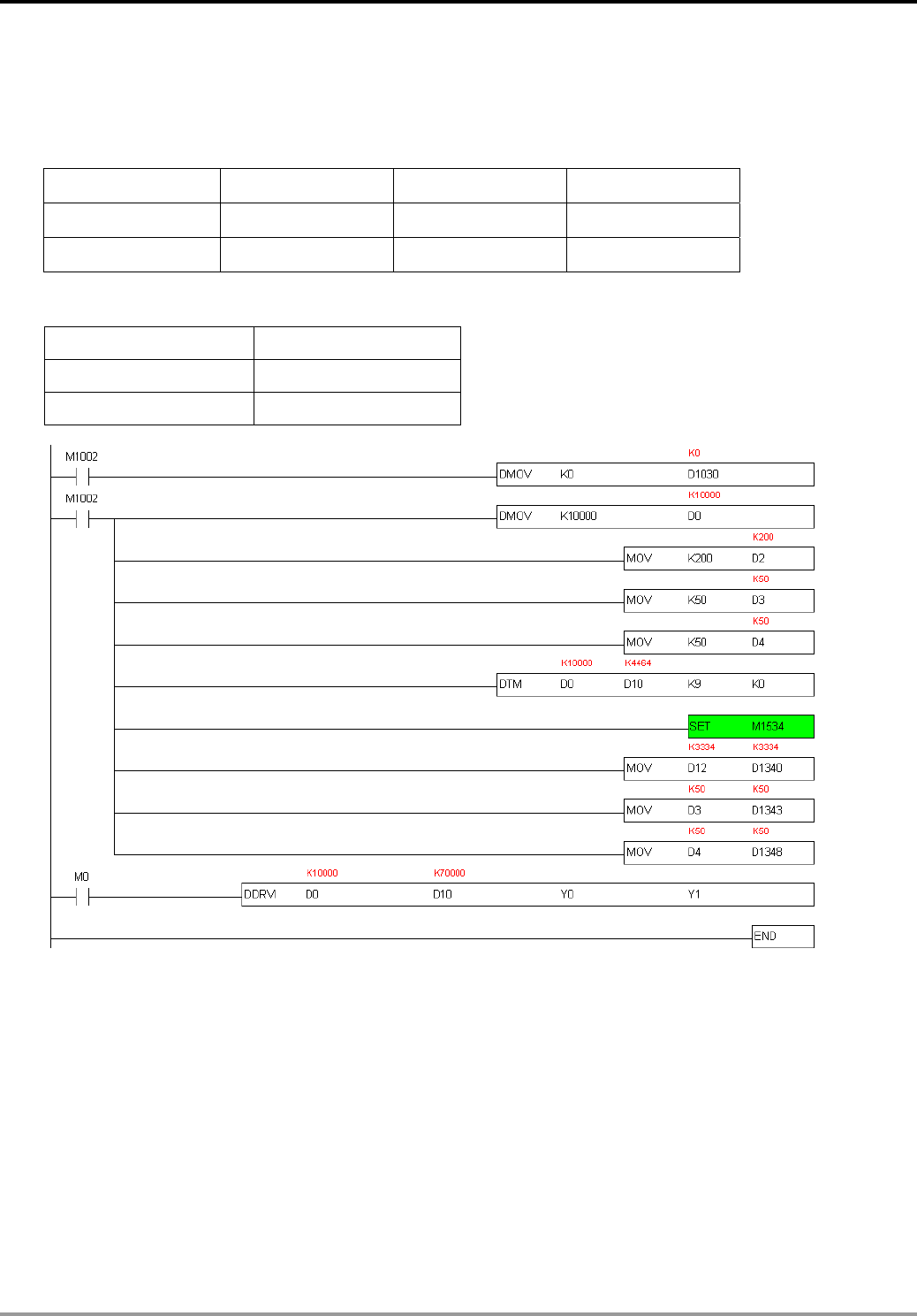
7 Application Instructions API 50-99
DVP-PLC APPLICATION MANUAL
7-68
1. Set up total number of pulses, total time, ramp-up time and ramp-down time in source device starting with D0.
Execute DTM instruction and the optimal max frequency as well as optimal start frequency can be obtained and
executed by positioning instructions.
2. Assume the data of source device is set up as below:
Total Pulses Total Time Ramp-up Time Ramp-down Time
D0, D1 D2 D3 D4
K10000 K200 K50 K50
3. The optimal positioning results can be obtained as below:
Optimal max frequency Optimal start frequency
D10, D11 D12
K70000 K3334
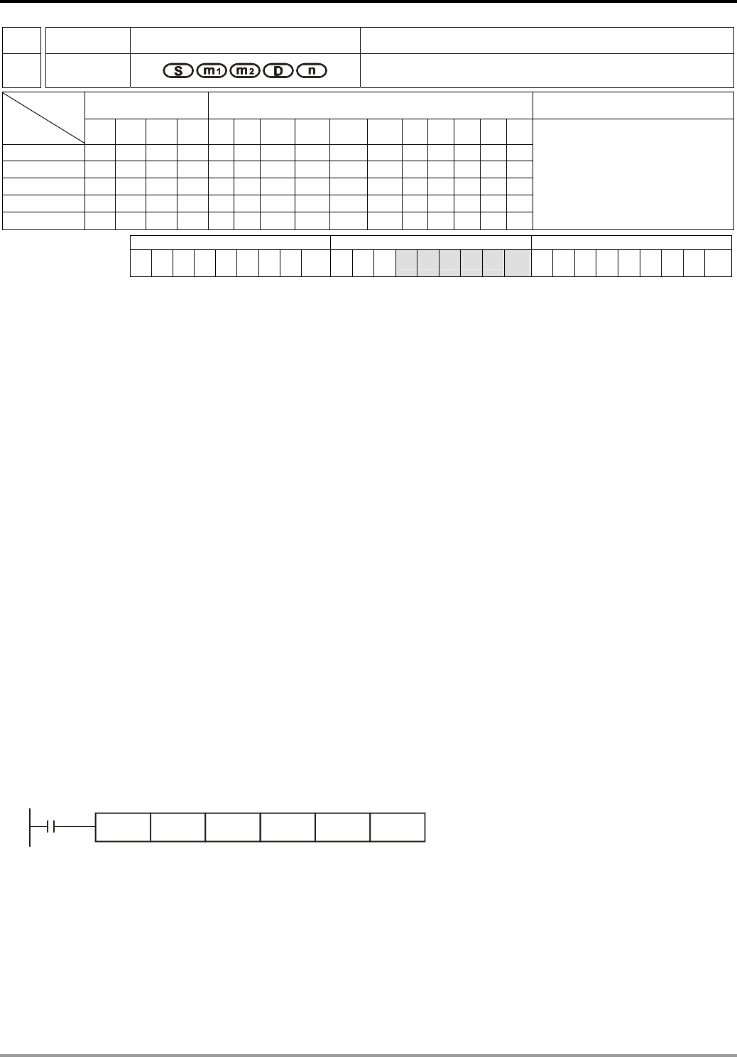
7 Application Instructions API 50-99
DVP-PLC APPLICATION MANUAL
7-69
API Mnemonic Operands Function
69
SORT Sort Tabulated Data
Bit Devices Word Devices Program Steps Type
OP X Y M S K H KnX KnY KnM KnS T C D E F
S *
m1 * *
m2 * *
D *
n * * *
SORT: 11 steps
PULSE 16-bit 32-bit
ES EX SS SA SX SC EH SV EH3
SV2 ES EX SS SA SX SC EH SV EH3
SV2 ES EX SS SA SX SC EH SV EH3
SV2
Operands:
S: Start device for the original data m1: Groups of data to be sorted m2: Number of columns of data
D: Start device for the sorted data n: Reference value for data sorting
Explanations:
1. Range of m1: 1 ~ 32.
2. Range of m2: 1 ~ 6
3. Range of n: 1 ~ m2
4. See the specifications of each model for their range of use.
5. Flag: M1029 (SORT execution completed).
6. The sorted result is stored in m1 × m2 registers starting from the device designated in D. Therefore, if S and D
designate the same register, the sorted result will be the same as the data designated in S.
7. It is better that the start No. designated in S is 0.
8. The sorting will be completed after m1 times of scans. After the sorting is completed, M1029 will be On.
9. There is no limitation on the times of using this instruction. However, only one instruction can be executed at a
time.
Program Example:
1. When X0 = On, the sorting will start. When the sorting is completed, M1029 will be On. DO NOT change the data
to be sorted during the execution of the instruction. If you wish to change the data, please make X0 go from Off to
On again.
X0
SORT D0 K5 K5 D50 D100
2. Example table of data sorting
7 Application Instructions API 50-99
DVP-PLC APPLICATION MANUAL
7-70
Columns of data: m2
Data Column
1 2 3 4 5
Column
Row Students No. Physics English Math Chemistry
1 (D0) 1 (D5) 90 (D10) 75 (D15) 66 (D20) 79
2 (D1) 2 (D6) 55 (D11) 65 (D16) 54 (D21) 63
3 (D2) 3 (D7) 80 (D12) 98 (D17) 89 (D22) 90
4 (D3) 4 (D8) 70 (D13) 60 (D18) 99 (D23) 50
Groups of data: m1
5 (D4) 5 (D9) 95 (D14) 79 (D19) 75 (D24) 69
Sorted data when D100 = K3.
Columns of data: m2
Data Column
1 2 3 4 5
Column
Row Students No. Physics English Math Chemistry
1 (D50) 4 (D55) 70 (D60) 60 (D65) 99 (D70) 50
2 (D51) 2 (D56) 55 (D61) 65 (D66) 54 (D71) 63
3 (D52) 1 (D57) 90 (D62) 75 (D67) 66 (D72) 79
4 (D53) 5 (D58) 95 (D63) 79 (D68) 75 (D73) 69
Groups of data: m1
5 (D54) 3 (D59) 80 (D64) 98 (D69) 89 (D74) 90
Sorted data when D100 = K5.
Columns of data: m2
Data Column
1 2 3 4 5
Column
Row Students No. Physics English Math Chemistry
1 (D50) 4 (D55) 70 (D60) 60 (D65) 99 (D70) 50
2 (D51) 2 (D56) 55 (D61) 65 (D66) 54 (D71) 63
3 (D52) 5 (D57) 95 (D62) 79 (D67) 75 (D72) 69
4 (D53) 1 (D58) 90 (D63) 75 (D68) 66 (D73) 79
Groups of data: m1
5 (D54) 3 (D59) 80 (D64) 98 (D69) 89 (D74) 90
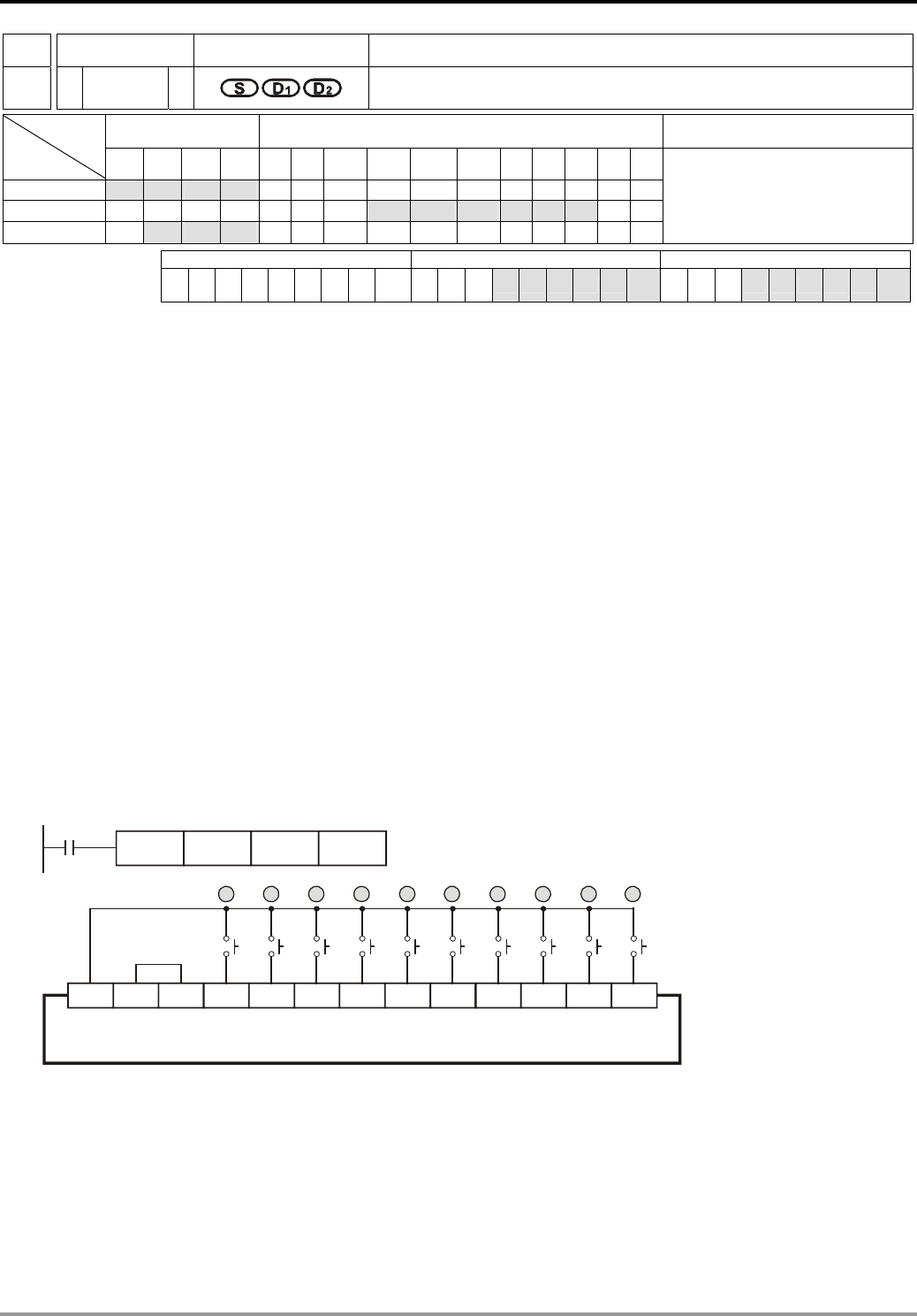
7 Application Instructions API 50-99
DVP-PLC APPLICATION MANUAL
7-71
API Mnemonic Operands Function
70
D TKY Ten Key Input
Bit Devices Word Devices Program Steps Type
OP X Y M S K H KnX KnY KnM KnS T C D E F
S * * * *
D1 * * * * * * * *
D2 * * *
TKY: 7 steps
DTKY: 13 steps
PULSE 16-bit 32-bit
ES EX SS SA SX SC EH SV EH3
SV2 ES EX SS SA SX SC EH SV EH3
SV2 ES EX SS SA SX SC EH SV EH3
SV2
Operands:
S: Start device for key input D1: Device for storing keyed-in value D2: Key output signal
Explanations:
1. S will occupy 10 consecutive points; D2 will occupy 11 consecutive points.
2. See the specifications of each model for their range of use.
3. For SA series MPU, S and D2 do not support E, F index register modification.
4. This instruction designates 10 external input points (representing decimal numbers 0 ~ 9) starting from S. The 10
points are respectively connected to 10 keys. By pressing the keys, you can enter a 4-digit decimal figure 0 ~
9,999 (16-bit instruction) or a 8-digit figure 0 ~ 99,999,999 (32-bit instruction) and store the figure in D1. D2 is
used for storing key status.
5. There is no limitation on the times of using this instruction. However, only one instruction can be executed at a
time.
Program Example:
1. Connect the 10 input points starting from X0 to the 10 keys (0 ~ 9). When X20 = On, the instruction will be
executed and the keyed-in values will be stored in D0 in bin form. The key status will be stored in M10 ~ M19.
X20
TKY X0 D0 M10
PLC
0 1 32 4 5 6 7 8 9
X3X2X1X0S/S X6X5X4 X10X7 X11+24V0V
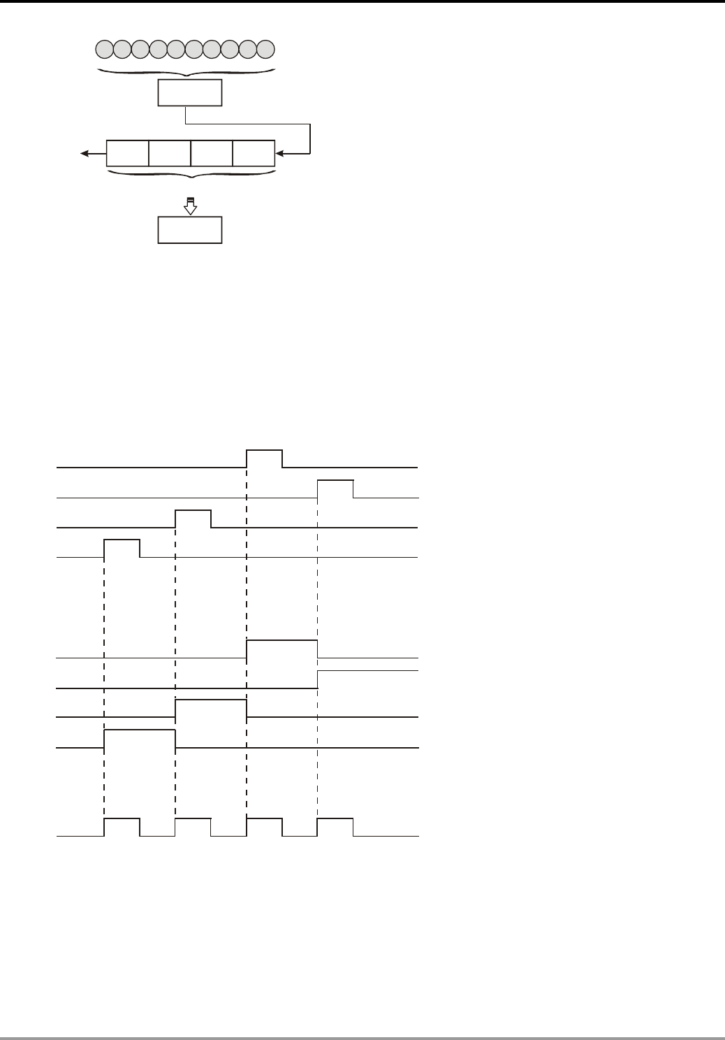
7 Application Instructions API 50-99
DVP-PLC APPLICATION MANUAL
7-72
0 1 23 4 5 6 7 8 9
D0
10
3
10
2
10
1
10
0
number key
BCD value 1-digit BCD code
BIN value
overflow
BCD value
2. As shown in the timing chart below, the 4 points X5, X3, X0, and X1 connected to the keys are entered in order
and you can obtain the result 5,301. Store the result in D0. 9,999 is the maximum value allowed to stored in D0.
Once the value exceeds 4 digits, the highest digit will overflow.
3. M12 = On when from X2 is pressed to the other key is pressed. Same to other keys.
4. When any of the keys in X0 ~ X11 is pressed, one of M10 ~ 19 will be On correspondingly.
5. M20 = On when any of the keys is pressed.
6. When X20 goes Off, the keyed-in value prior to D0 will remain unchanged, but M10 ~ M20 will all be Off.
X0
X1
X3
X5 1
2
3
4
1234
M10
M11
M13
M15
M20
Key output
signal
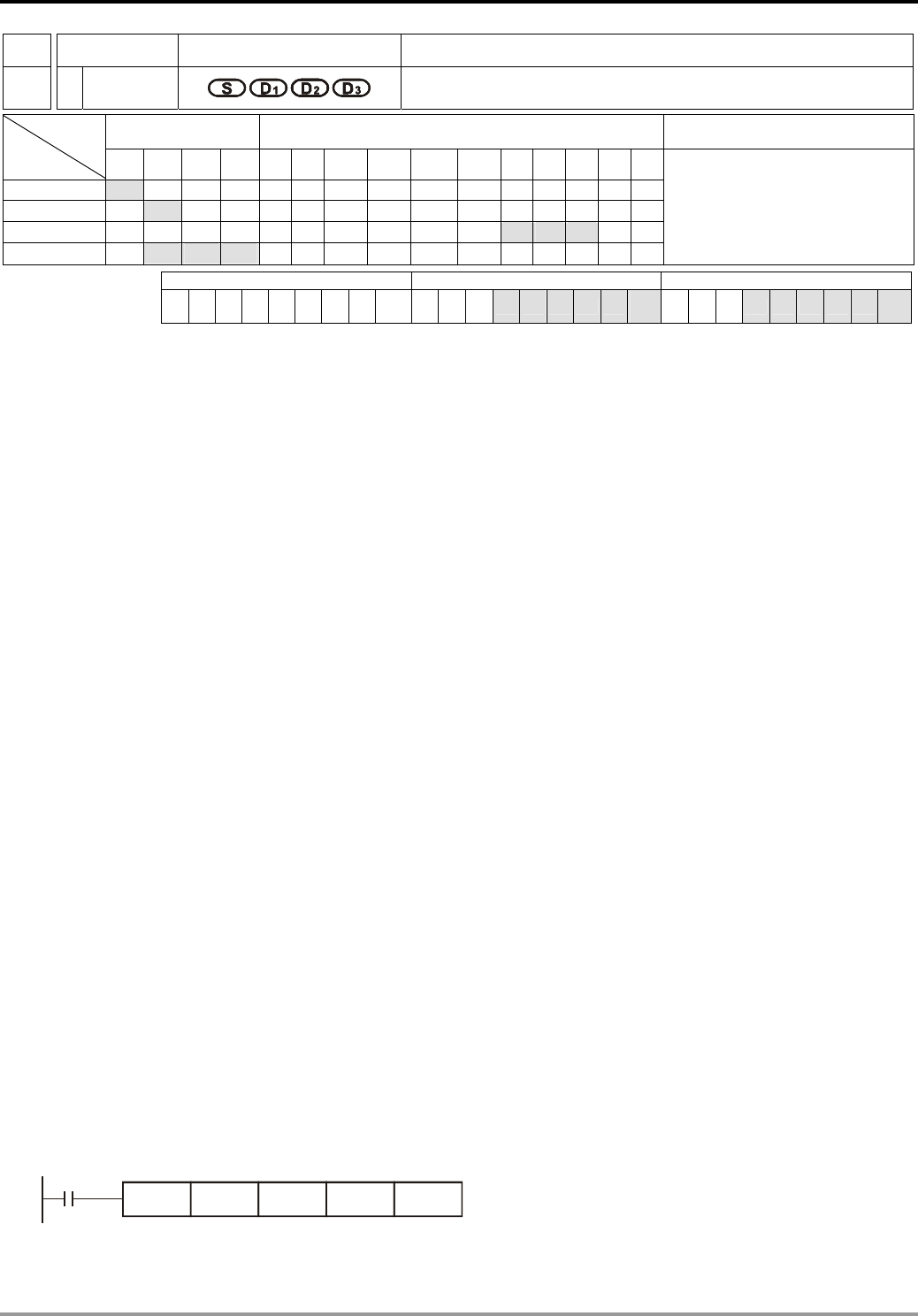
7 Application Instructions API 50-99
DVP-PLC APPLICATION MANUAL
7-73
API Mnemonic Operands Function
71
D HKY Hexadecimal Key Input
Bit Devices Word Devices Program Steps
Type
OP X Y M S K H KnX KnY KnM KnS T C D E F
S *
D1 *
D2 * * * * *
D3 * * *
HKY: 9 steps
DHKY: 17 steps
PULSE 16-bit 32-bit
ES EX SS SA SX SC EH SV EH3
SV2 ES EX SS SA SX SC EH SV EH3
SV2 ES EX SS SA SX SC EH SV EH3
SV2
Operands:
S: Start device for key scan input D1: Start device for key scan output D2: Device for storing keyed-in value
D3: Key output signal
Explanations:
1. S will occupy 4 consecutive points.
2. D1 will occupy 4 consecutive points.
3. D3 will occupy 8 consecutive points.
4. See the specifications of each model for their range of use.
5. For SA series MPU, S, D1 and D3 do not support E, F index register modification.
6. Flags: M1029 (On whenever a matrix scan period is completed); M1167 (HKY input modes switch). See remarks
for more details.
7. This instruction designates 4 continuous external input points starting from S and 4 continuous external input
points starting from D1 to construct a 16-key keyboard by a matrix scan. The keyed-in value will be stored in D2
and D3 is used for storing key status. If several keys are pressed at the same time, the first key pressed has the
priority.
8. The keyed-in value is termporarily stored in D0. When the 16-bit instruction HKY is in use, 9,999 is the maximum
value D0 is able to store. When the value exceeds 4 digits, the highest digit will overflow. When the 32-bit
instruction DHKY is in use, 99,999,999 is the maximum value D0 is able to store. When the value exceeds 8
digits, the highest digit will overflow.
9. There is no limitation on the times of using this instruction. However, only one instruction can be executed at a
time.
Program Example:
1. Designate 4 input points X10 ~ X13 and the other 4 input points Y10 ~ Y13 to construct a 16-key keyboard.
When X4 = On, the instruction will be executed and the keyed-in value will be stored in D0 in bin form. The key
status will be stored in M0 ~ M7.
X4
HKY X10 Y10 D0 M0
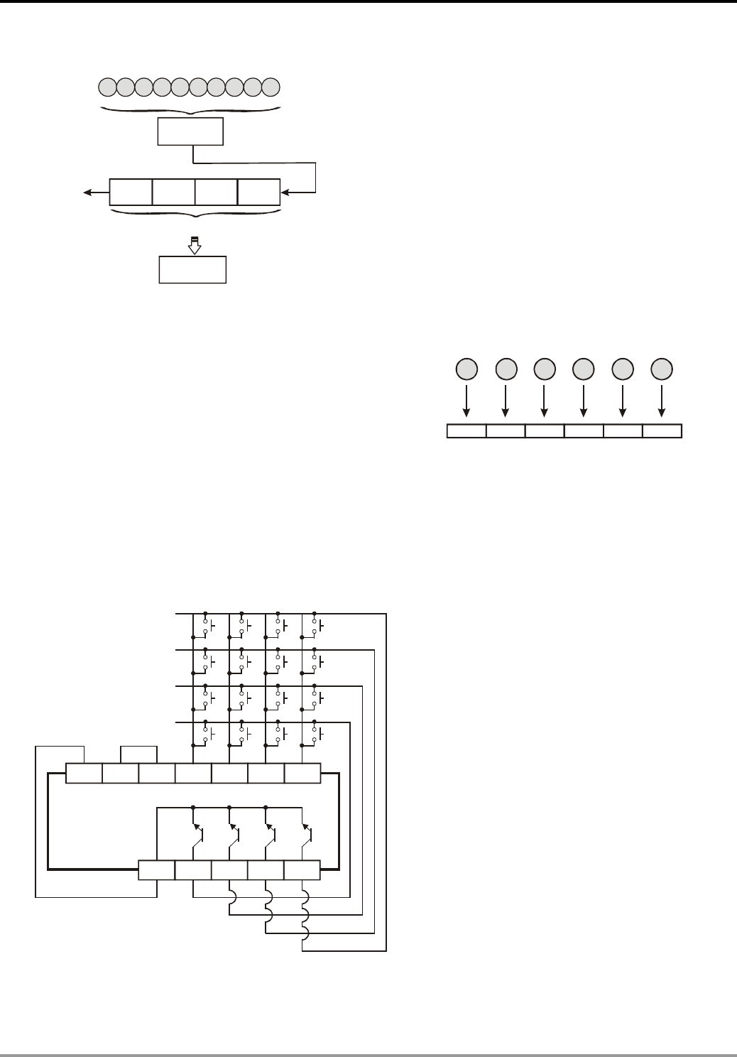
7 Application Instructions API 50-99
DVP-PLC APPLICATION MANUAL
7-74
2. Key in numbers:
0 1 23 4 5 6 7 8 9
D0
10
3
10
2
10
1
10
0
number key
1-digit BCD code
BCD value
BCD value
BIN value
overflow
3. Function keys input:
a) When A is pressed, M0 will be On and retained. When
D is pressed next, M0 will be Off, M3 will be On and
retained.
b) When many keys are pressed at the same time, the
first key pressed has the priority.
F E D C B A
M5 M4 M3 M2 M1 M0
4. Key output signal:
a) When any of A ~ F is pressed, M6 will be On for once.
b) When any of 0 ~ 9 is pressed, M7 will be On for once.
5. When X4 goes Off, the keyed-in value prior to D0 will remain unchanged, but M0 ~ M7 will all be Off.
6. External wiring:
Y13
Y12Y11
Y10
C
X13
X12X11
X10
S/S
CDEF
89AB
4567
0123
PLC (transistor output)
+24V
24G

7 Application Instructions API 50-99
DVP-PLC APPLICATION MANUAL
7-75
Remarks:
1. When this instruction is being executed, it will require 8 scans to obtain one valid keyed-in value. A scan period
that is too long or too short may result in poor keyed-in effect, which can be avoided by the following methods:
a) If the scan period is too short, I/O may not be able to respond in time, resulting in not being able to read the
keyed-in value correctly. In this case, please fix the scan time.
b) If the scan period is too long, the key may respond slowly. In this case, write this instruction into the time
interruption subroutine to fix the time for the execution of this instruction.
2. Functions of M1167:
a) When M1167 = On, HKY instruction will be able to input the hexadecimal value of 0 ~ F.
b) When M1167 = Off, HKY instruction will see A ~ F as function keys.
3. Functions of D1037 (only supports EH/EH2/SV/EH3/SV2 series MPU):
Write D1037 to set the overlapping time for keys (unit: ms). The overlapping time will vary upon different program
scan time and the settings in D1037.
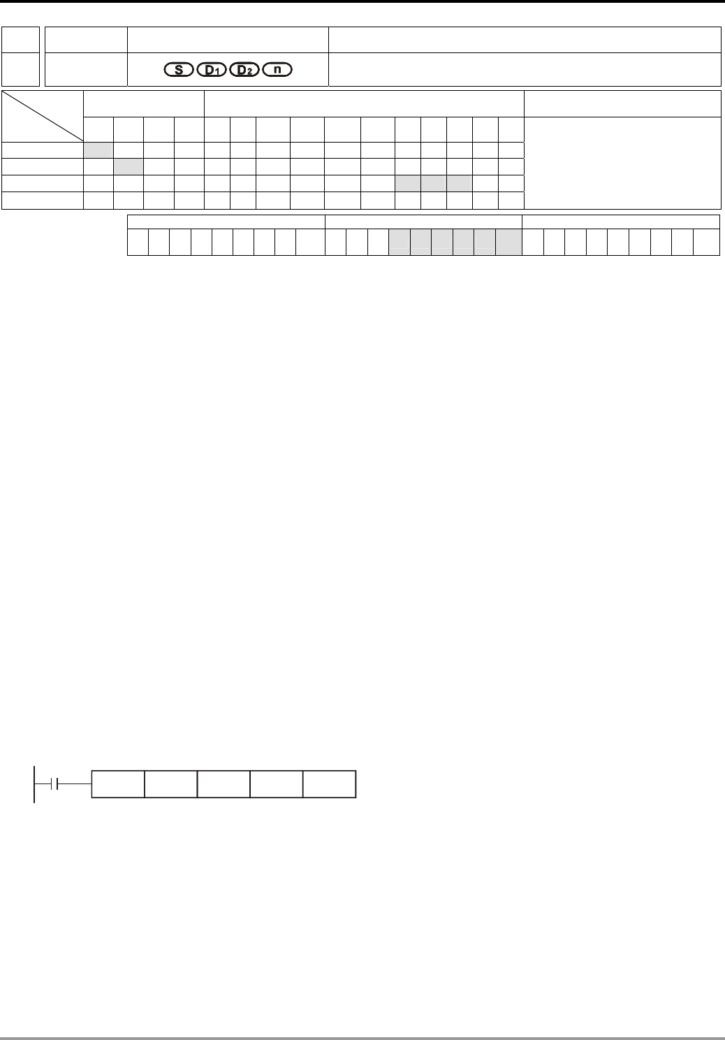
7 Application Instructions API 50-99
DVP-PLC APPLICATION MANUAL
7-76
API Mnemonic Operands Function
72
DSW Digital Switch
Bit Devices Word Devices Program Steps Type
OP X Y M S K H KnX KnY KnM KnS T C D E F
S *
D1 *
D2 * * *
n * *
DSW: 9 steps
PULSE 16-bit 32-bit
ES EX SS SA SX SC EH SV EH3
SV2 ES EX SS SA SX SC EH SV EH3
SV2 ES EX SS SA SX SC EH SV EH3
SV2
Operands:
S: Start device for switch scan input D1: Start device for switch scan output D2: Device for storing the set value
of switch n: Groups of switches
Explanations:
1. Range of n: 1 ~ 2
2. S and D1 in SA/SX/SC series MPU do not support E, F index register modification.
3. See the specifications of each model for their range of use.
4. Flag: M1029 (DSW execution completed)
5. This instruction designates 4 or 8 consecutive external input points starting from S and 4 consecutive external
input points starting from D1 to scan read 1 or 2 4-digit DIP switches.The set values of DIP switches are stored in
D2. n decides to read 1 or 2 4-digit DIP switches.
6. There is no limitation on the times of using this instruction in the program. However, for SA series MPU, only one
instruction can be executed at a time. For EH series MPU, two instructions are allowed to be executed at a time.
Program Example:
1. The first group of DIP switches consist of X20 ~ X23 and Y20 ~ Y23. The second group of switches consist of
X24 ~ X27 and Y20 ~ Y23. When X10 = On, the instruction will be executed and the set values of the first group
switches will be read and converted into bin values before being stored in D20. The set values of the second
group switches will be read, converted into bin values and stored in D21.
X10
DSW X20 Y20 D20 K2
2. When X10 = On, the Y20 ~ Y23 auto scan cycle will be On. Whenever a scan cycle is completed, M1029 will be
On for a scan period.
3. Please use transistor output for Y20 ~ Y23. Every pin 1, 2, 4, 8 shall be connected to a diode (0.1A/50V) before
connecting to the input terminals on PLC.
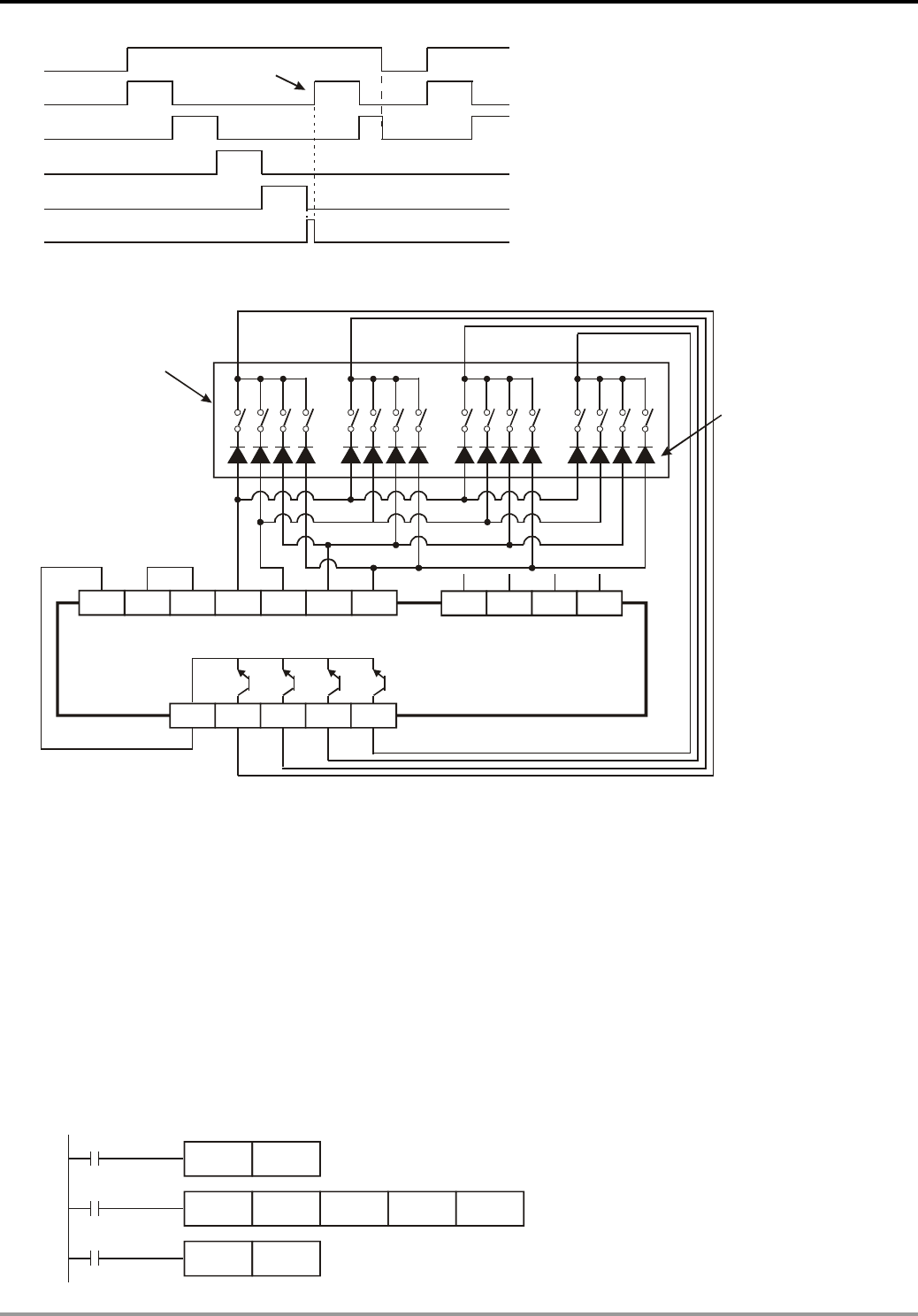
7 Application Instructions API 50-99
DVP-PLC APPLICATION MANUAL
7-77
X10
Y20
Y21
Y22
Y23
M1029
0.1s
0.1s
0.1s
0.1s
0.1s 0.1s
Interruption
Execution completed
Cyclic operation
4. Wiring for DIP swich input:
S/S X20 X21 X22 X23 X24 X25 X26 X27
Y23Y22Y21Y20C
1 2 48 1 2 48
PLC
10 10 10 10
0123
10
0
10
1
10
2
10
3
0V +24V
DIP switches for
BCD wiring
Must connect to a
diode (1N4148) in
series
The first group The second group
Remarks:
1. When n = K1, D2 will occupy one register. When n = K2, D2 will occupy 2 consecutive registers.
2. Follow the methods below for the transistor scan output:
a) When X10 = On, DSW instruction will be executed. When X10 goes Off, M10 will keep being On until the
scan output completes a scan cycle and go Off.
b) When X10 is used as a button switch, whenever X10 is pressed once, M10 will be reset to Off when the scan
output designated by DSW instruction completes a scan cycle. The DIP switch data will be read completely
and the scan output will only operate during the time when the button switch is pressed. Therefore, even the
scan output is a transistor type, the life span of the transistor can be extended because it does not operate
too frequently.
M10
DSW X20 Y20 D20 K2
X10
SET M10
M1029
RST M10
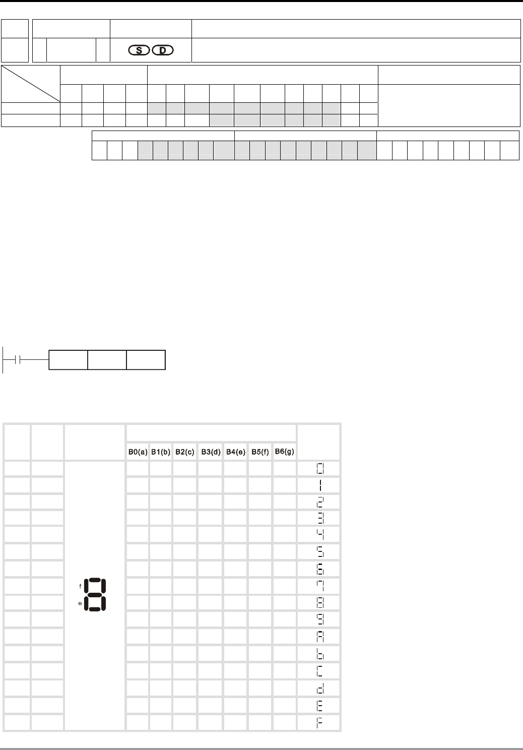
7 Application Instructions API 50-99
DVP-PLC APPLICATION MANUAL
7-78
API Mnemonic Operands Function
73
SEGD P Seven Segment Decoder
Bit Devices Word Devices Program Steps Type
OP X Y M S K H KnX KnY KnM KnS T C D E F
S * * * * * * * * * * *
D * * * * * * * *
SEGD, SEGDP: 5 steps
PULSE 16-bit 32-bit
ES EX SS SA SX SC EH SV EH3
SV2 ES EX SS SA SX SC EH SV EH3
SV2 ES EX SS SA SX SC EH SV EH3
SV2
Operands:
S: Source device to be decoded D: Output device after the decoding
Explanations:
See the specifications of each model for their range of use.
Program Example:
When X10 = On, the contents (0 ~ F in hex) of the lower 4 bits (b0 ~ b3) of D10 will be decoded into a 7-segment
display for output. The decoded results will be stored in Y10 ~ Y17. If the content exceeds 4 bits, the lower 4 bits are
still used for the decoding.
X10
SEGD D10 K2Y10
Decoding table of the 7-segment display:
0
1
2
3
4
5
6
7
8
9
A
B
C
D
E
F 1111
1110
1101
1100
1011
1010
1001
1000
0111
0110
0101
0100
0011
0010
0001
0000 ON OFFON ON ON ON ON
OFFOFFOFFOFF OFF
ON ON
ON ON ON ON
OFF OFF ON
ON ON ON ON ON
OFF
OFF
OFFOFF OFF
ON ON ON ON
ON OFF ON ON OFF ON ON
OFF ON ON ON ON ON
ON ON ON OFFOFF OFF
ON ON ON ON ON ON ON
ON ON ON ON ON ON
OFF
ON ON
OFF OFF ON ON ON
OFF ONON
ON OFF ON
OFF OFF ON ON ON ON
OFF OFF OFF
a
c
b
d
g
ON
ON
ONON ON
ON OFF
ON ON
ON OFF ON OFF
OFF ON ON ON
ON ON ON
ON
ON
Hex Bit
combi-
nation
Composition
of the 7-
segment display
Status of each segment Data
displayed
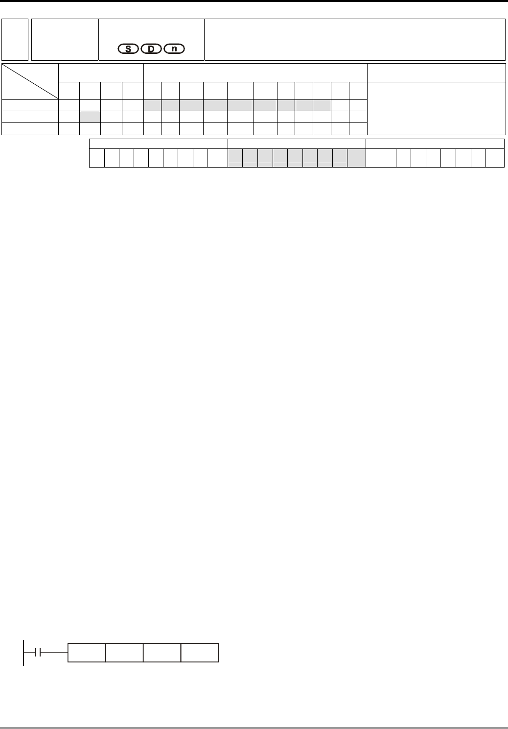
7 Application Instructions API 50-99
DVP-PLC APPLICATION MANUAL
7-79
API Mnemonic Operands Function
74
SEGL Seven Segment with Latch
Bit Devices Word Devices Program Steps Type
OP X Y M S K H KnX KnY KnM KnS T C D E F
S * * * * * * * * * * *
D *
n * *
SEGL: 7 steps
PULSE 16-bit 32-bit
ES EX SS SA SX SC EH SV EH3
SV2 ES EX SS SA SX SC EH SV EH3
SV2 ES EX SS SA SX SC EH SV EH3
SV2
Operands:
S: Source device to be displayed in 7-segment display D: Start device for 7-segment display scan output
n: Polarity setting of output signal and scan signal
Explanations:
1. Range of n: 0 ~ 7. See remarks for more details.
2. For ES series MPU, the instruction can only be used once in the program. For EH series MPU, the instruction
can be used twice in the program. For SA series MPU, there is no limitation on the times of using the instruction,
but only one instruction can be executed at a time.
3. For ES/EX/SS/SA/SX/SC series MPU, the last digit of D should be 0 and it does not support E, F index register
modification.
4. Flag: M1029 (SEGL execution completed)
5. This instruction occupies 8 or 12 continuous external input points starting from D for displaying 1 or 2 4-digit
7-segment display data and outputs of scanned signals. Every digit carries a 7-segment display drive (to convert
the BCD codes into 7-segment display signal). The drive also carries latch control signals to retain the
7-segment display.
6. n decides there be 1 group or 2 groups of 4-digit 7-segment display and designates the polarity for the output.
7. When there is 1 group of 4-digit output, 8 output points will be occupied. When there are 2 groups of 4-digit
output, 12 output points will be occupied.
8. When this instruction is being executed, the scan output terminals will circulate the scan in sequence. When the
drive contact of the instruction goes from Off to On again, the scan output terminal will restart the scan again.
Program Example:
1. When X10 = On, this instruction starts to be executed, Y10 ~ Y17 construct a 7-segment display scan circuit.
The value in D10 will be converted into BCD codes and sent to the first group 7-segment display. The value in
D11 will be converted into BCD codes as well and sent to the second group 7-segment display. If the values in
D10 and D11 exceed 9,999, operational error will occur.
X10
SEGL D10 Y10 K4
2. When X10 = On, Y14 ~ Y17 will circulate the scan automatically. Every cycle requires 12 scan period. Whenever
a cycle is completed, M1029 will be On for a scan period.
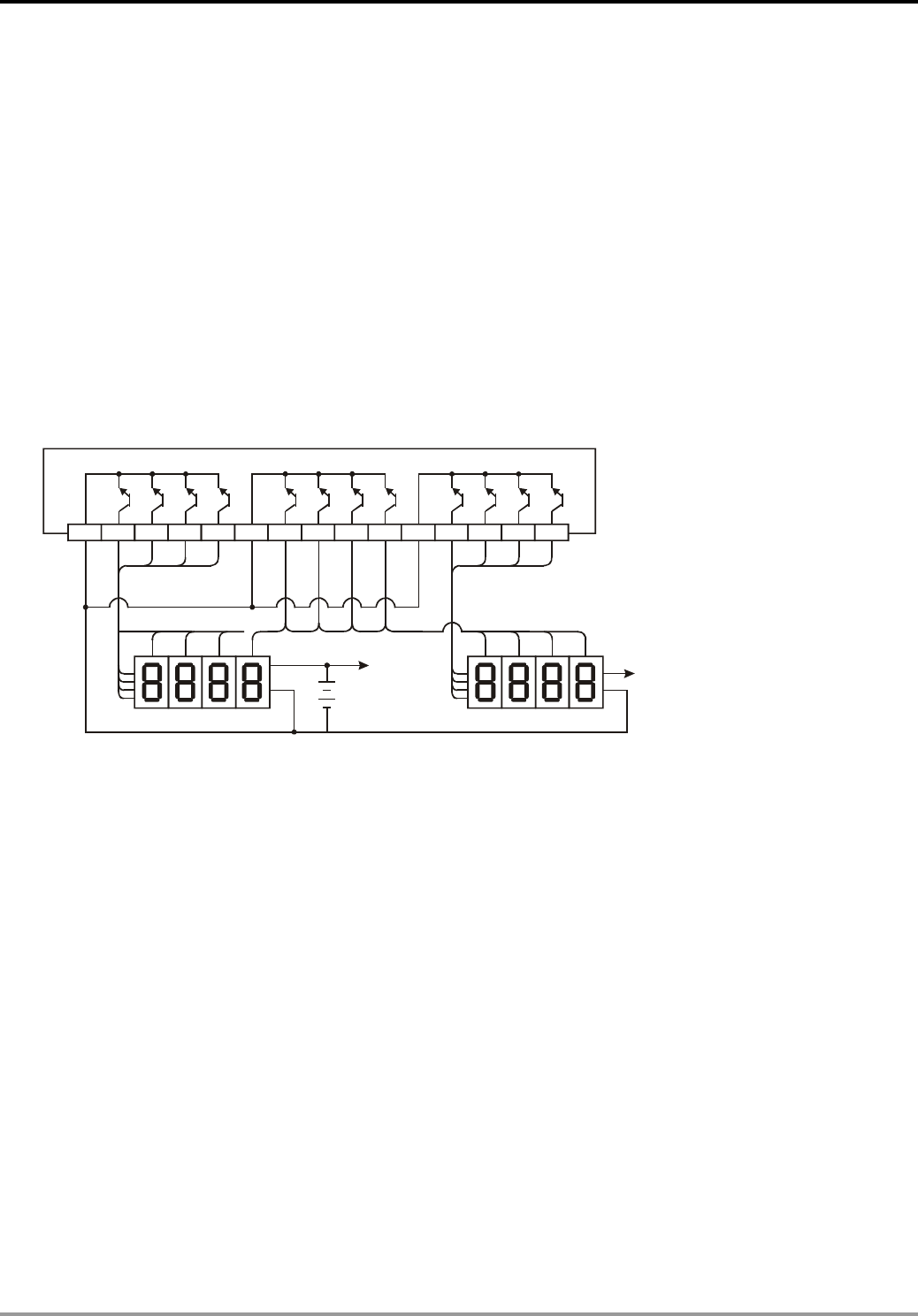
7 Application Instructions API 50-99
DVP-PLC APPLICATION MANUAL
7-80
3. When there is 1 group of 4-digit 7-segment display, n = 0 ~ 3.
a) Connect the already decoded 7-segment display terminals 1, 2, 4, 8 in parallel an connect them to Y10 ~
Y13 on the PLC. Connect the latch terminals of each digit to Y14 ~ Y17 on the PLC.
b) When X10 = On, the instruction will be executed and the content in D10 will be sent to the 7-segment
displays in sequence by the circulation of Y14 ~ Y17.
4. When there is 2 groups of 4-digit 7-segment display, n = 4 ~ 7.
a) Connect the already decoded 7-segment display terminals 1, 2, 4, 8 in parallel an connect them to Y20 ~
Y23 on the PLC. Connect the latch terminals of each digit to Y14 ~ Y17 on the PLC.
b) The contents in D10 are sent to the first group 7-segment display. The contents in D11 are sent the the
second group 7-segment display. If D10 = K1234 and D11 = K4321, the first group will display 1 2 3 4, and
the second group will display 4 3 2 1.
5. Wiring of the 7-segment display scan output:
COM Y10 Y11 Y12 Y13 Y14 Y15 Y16 Y17 Y20 Y21 Y22 Y23COM COM
1248
10
0
10
1
10
2
10
3
10
3
10
2
10
1
10
0
V+
10
3
10
2
10
1
10
0
V+
1
2
4
8
1
2
4
8
The first group The second group
Remarks:
1. ES/EX/SS series MPU (V4.9 and above) supports this instruction but only supports 1 group of 4-digit 7-segment
display and 8 points of output. This instruction can only be used once in the program. Range of n: 0 ~ 3.
2. D of ES/EX/SS series MPU can only designate Y0.
3. When this instruction is executed, the scan time has to be longer than 10ms. If the scan time is shorter than
10ms, please fix the scan time at 10ms.
4. n is for setting up the polarity of the transistor output and the number of groups of the 4-digit 7-segment display.
5. The output point must be a transistor module of NPN output type with open collector outputs. The output has to
connect to a pull-up resistor to VCC (less than 30VDC). Therefore, when output point Y is On, the signal output
will be in low voltage.
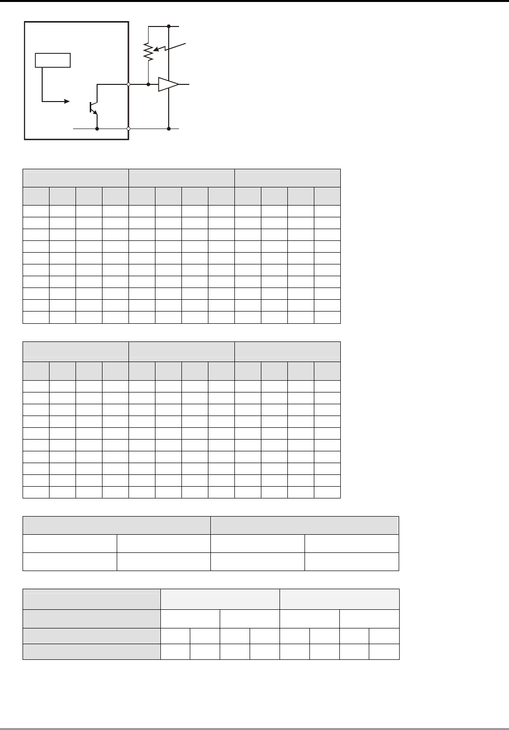
7 Application Instructions API 50-99
DVP-PLC APPLICATION MANUAL
7-81
On
PLC
VCC
Y
Pull-up resistor
Signal output
Drive Y
6. Positive logic (negative polarity) output of BCD code
BCD value Y output (BCDcode) Signal output
b3 b2 b1 b0 8 4 2 1 A B C D
0 0 0 0 0 0 0 0 1 1 1 1
0 0 0 1 0 0 0 1 1 1 1 0
0 0 1 0 0 0 1 0 1 1 0 1
0 0 1 1 0 0 1 1 1 1 0 0
0 1 0 0 0 1 0 0 1 0 1 1
0 1 0 1 0 1 0 1 1 0 1 0
0 1 1 0 0 1 1 0 1 0 0 1
0 1 1 1 0 1 1 1 1 0 0 0
1 0 0 0 1 0 0 0 0 1 1 1
1 0 0 1 1 0 0 1 0 1 1 0
7. Negative logic (positive polarity) output of BCD code
BCD value Y output (BCDcode) Signal output
b3 b2 b1 b0 8 4 2 1 A B C D
0 0 0 0 1 1 1 1 0 0 0 0
0 0 0 1 1 1 1 0 0 0 0 1
0 0 1 0 1 1 0 1 0 0 1 0
0 0 1 1 1 1 0 0 0 0 1 1
0 1 0 0 1 0 1 1 0 1 0 0
0 1 0 1 1 0 1 0 0 1 0 1
0 1 1 0 1 0 0 1 0 1 1 0
0 1 1 1 1 0 0 0 0 1 1 1
1 0 0 0 0 1 1 1 1 0 0 0
1 0 0 1 0 1 1 0 1 0 0 1
8. Scan latched signal display
Positive logic (negative polarity) Negative logic (positive polarity)
Y output (latch) Output signal Y output (latch) Output signal
1 0 0 1
9. Settings of n:
Groups of 7-segment display 1 group 2 groups
Y output of BCD code + - + -
Scan latched signal display + - + - + - + -
n 0 1 2 3 4 5 6 7
+: Positive logic (negative polarity) output -: Negative logic (positive polarity) output
10. The polarity of transistor output and the polarity of the 7-segment display input can be the same or different by
the setting of n.
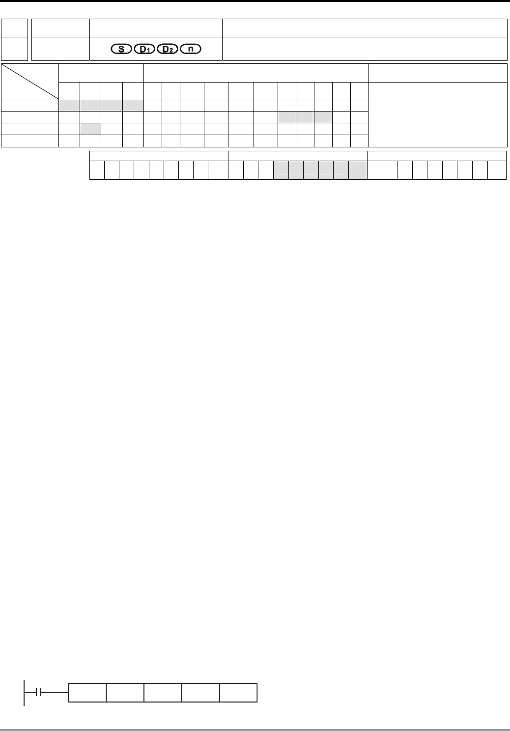
7 Application Instructions API 50-99
DVP-PLC APPLICATION MANUAL
7-82
API Mnemonic Operands Function
75
ARWS Arrow Switch
Bit Devices Word Devices Program Steps Type
OP X Y M S K H KnX KnY KnM KnS T C D E F
S * * * *
D1 * * * * *
D2 *
n * *
ARWS: 9 steps
PULSE 16-bit 32-bit
ES EX SS SA SX SC EH SV EH3
SV2 ES EX SS SA SX SC EH SV EH3
SV2 ES EX SS SA SX SC EH SV EH3
SV2
Operands:
S: Start device for key input D1: Device to be displayed in 7-segment display D2: Start device for 7-segment
display scan output n: Polarity setting of output signal and scan signal
Explanations:
1. S will occupy 4 consecutive points.
2. Range of n: 0 ~ 3. See remarks of API 74 SEGL for more details.
3. There no limitation on the times of using this instruction in the program. However, only one instruction is allowed
to be executed at a time.
4. S and D2 of SA series MPU do not support E, F index register modification, and D2 can only designate the devices
whose last digit is 0 (e.g. Y0, Y10….)
5. See the specifications of each model for their range of use.
6. The output points designated by this instruction shall be transistor output.
7. When using this instruction, please fix the scan time, or place this instruction in the time interruption subroutine
(I6□□ ~ I8□□).
Program Example:
1. When this instruction is executed, X20 is defined as down key, X21 is defined as up key, X22 is defined as right
key and X23 is defined as left key. The keys are used for setting up and displaying external set values. The set
values (range: 0 ~ 9,999) are stored in D20.
2. When X10 = On, digit 103 will be the valid digit for setup. If you press the left key at this time, the valid digit will
circulate as 103 → 100 → 101 → 102 → 103 → 100.
3. If you press the right key at this time, the valid digit will circulate as 103 → 102 → 101 → 100 → 103 → 102.
During the circulation, the digit indicators connected Y24 ~ Y27 will also be On interchangeably following the
circulation.
4. If you press the up key at this time, the valid digit will change as 0 → 1 → 2 … → 8 → 9 → 0 →1. If you
press the down key, the valid digit will change as 0 → 9 → 8 … → 1 → 0 → 9. The changed value will also
be displayed in the 7-segment display.
X10
ARWS X20 D20 Y20 K0

7 Application Instructions API 50-99
DVP-PLC APPLICATION MANUAL
7-83
1
2
4
8
10
3
10
2
10
1
10
0
Y20
Y21
Y22
Y23
Y27
Y26
Y25
Y24
Digit indication
LED X21
X20
X22X23
Minus down
Move to left Move to right
7-segment display for the 4-digit set value
Add up
The 4 switches are used for moving the digits
and increasing/decreasing set values.
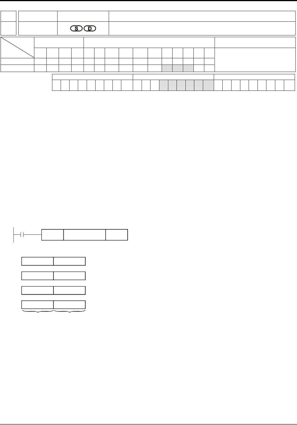
7 Application Instructions API 50-99
DVP-PLC APPLICATION MANUAL
7-84
API Mnemonic Operands Function
76
ASC ASCII Code Conversion
Bit Devices Word Devices Program Steps Type
OP X Y M S K H KnX KnY KnM KnS T C D E F
S
D * * *
ASC: 11 steps
PULSE 16-bit 32-bit
ES EX SS SA SX SC EH SV EH3
SV2 ES EX SS SA SX SC EH SV EH3
SV2 ES EX SS SA SX SC EH SV EH3
SV2
Operands:
S: English letter to be converted into ASCII code D: Device for storing ASCII code
Explanations:
1. S: enter 8 Engligh letters by using WPLSoft on computer or enter ASCII code by HPP.
2. S in SA series MPU only accepts A, B, C, D, E, F, G, H, the 8 English character.
3. See the specifications of each model for their range of use.
4. Flag: M1161 (8/16 bit mode switch)
5. If the execution of this instruction is connected to a 7-segment display, the error message can be displayed by
English letters.
Program Example:
1. When X0 = On, convert A ~ H into ASCII code and stored it in D0 ~ D3.
X0
ASC A B C D E F G H D0
D0
D1
D2
b15 b0
42H (B) 41H (A)
44H (D) 43H (C)
46H (F) 45H (E)
D3 48H (H) 47H (G)
Lower 8 bits
Upper 8 bits
2. When M1161 = On, every ASCII code converted from the letters will occupy the lower 8 bits (b7 ~ b0) of a
register. The upper 8 bits are invalid (filled by 0). One register stores a letter.

7 Application Instructions API 50-99
DVP-PLC APPLICATION MANUAL
7-85
b15 b0
D0
D2
D4
D6
D1
D3
D5
D7
00 H
00 H
00 H
00 H
00 H
00 H
00 H
00 H
41H (A)
42H (B)
43H (C)
44H (D)
45H (E)
46H (F)
47H (G)
48H (H)
Lower 8 bits
Upper 8 bits
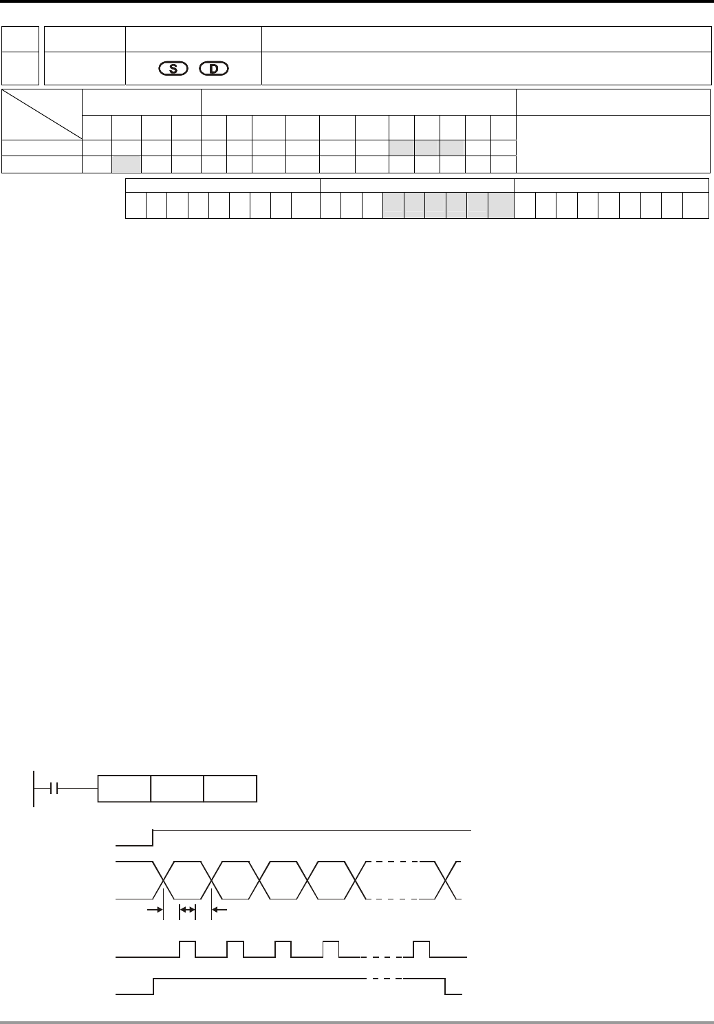
7 Application Instructions API 50-99
DVP-PLC APPLICATION MANUAL
7-86
API Mnemonic Operands Function
77
PR Print (ASCII Code Output)
Bit Devices Word Devices Program Steps Type
OP X Y M S K H KnX KnY KnM KnS T C D E F
S * * *
D *
PR: 5 steps
PULSE 16-bit 32-bit
ES EX SS SA SX SC EH SV EH3
SV2 ES EX SS SA SX SC EH SV EH3
SV2 ES EX SS SA SX SC EH SV EH3
SV2
Operands:
S: Device for storing ASCII code D: External ASCII code output points
Explanations:
1. S will occupy 4 consecutive points.
2. D will occupy 10 consecutive points.
3. This instruction can only be used twice in the program.
4. D in SA series MPU does not support E, F, index register modification.
5. See the specifications of each model for their range of use.
6. Flags: M1029 (PR execution completed); M1027 (number of PR outputs)
7. This instruction will output the ASCII codes in the 4 registers starting from S from the output devices in the order
designated in D.
Program Example 1:
1. Use API 76 ASC to convert A ~ H into ASCII codes and store them in D0 ~ D3 and use this instruction to output
the codes in sequence.
2. When M1027 = Off and X10 goes On, the instruction will be executed. Designate Y10 (low bits) ~ Y17 (high bits)
as the data output points and Y20 for scan signals. Designate Y21 for the monitor signals during the execution.
In this mode, you can execute an output for 8 letters in sequence. During the output, if the drive contact goes Off,
the data output will stop immediately and all the outputs will go Off.
3. During the execution of the instruction, when X10 goes Off, all the data output will be interrupted. When X10 is
On again, the output will be restarted.
X10
PR D0 Y10
TTT
ABCD H
X10 start signal
Y10 ~ Y17 data
Y20 scan signal
Y21 being executed
T: sc an tim e ( ms )
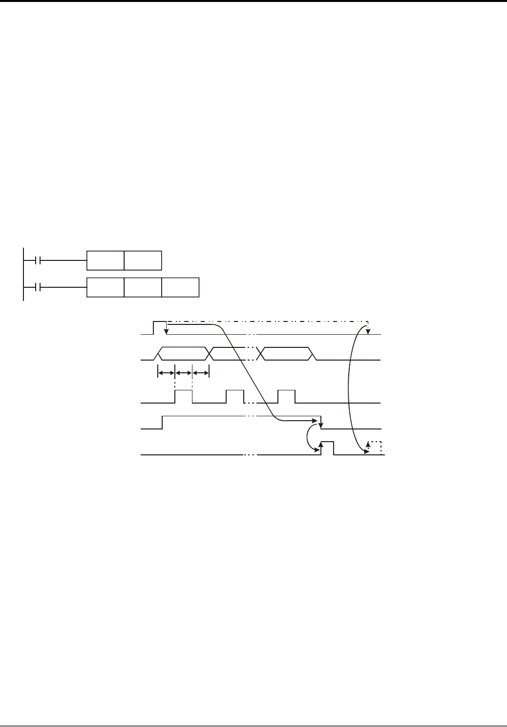
7 Application Instructions API 50-99
DVP-PLC APPLICATION MANUAL
7-87
Program Example 2:
1. PR instruction is for outputing a string of 8 bits. When the special auxiliary relay M1027 = Off, PR is able to
execute an output of maximum 8 letters in string. When M1027 = On, PR is able to execute an output of 1 ~ 16
letters in string.
2. When M1027 = On and X10 goes from Off to On, the instruction will be executed. Designate Y10 (low bits) ~ Y17
(high bits) as the data output points and Y20 for scan signals. Designate Y21 for the monitor signals during the
execution. In this mode, you can execute an output for 16 letters in sequence. During the output, if the drive
contact goes Off, the data output will stop after it is completed.
3. When the string encounters 00H (NUL), the string output will finish. The letters coming after it will not be
processed.
4. When X10 goes from On to Off, the data output will automatically stop after one cycle. If X10 keeps being On,
M1029 will not be enabled.
X10
PR D0 Y10
M1002
SET M1027
TTT
X10 start signal
Y10 ~ Y17 data
Y20 scan signal
Y21 being executed
M1029 (execution completed)
First letter Last letter
T: scan time or the time of
the inserted interruption
Remarks:
1. Please use transistor output for the output designated by this instruction.
2. When using this instruction, please fix the scan time or place this instruction in a timed interruption subroutine.
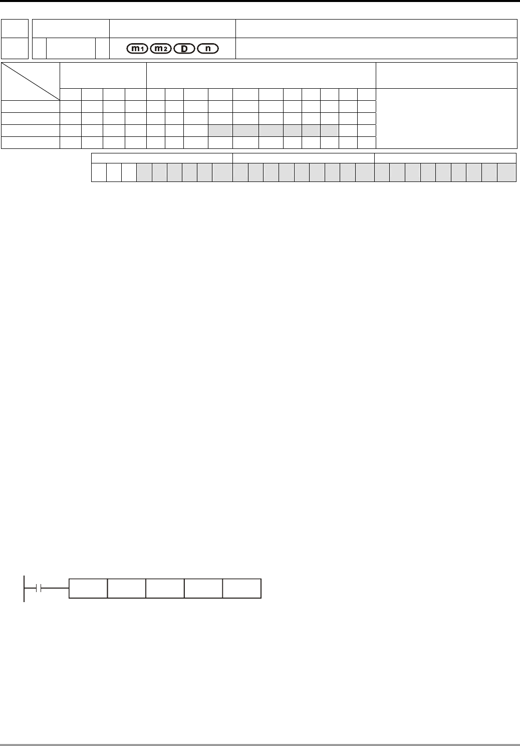
7 Application Instructions API 50-99
DVP-PLC APPLICATION MANUAL
7-88
API Mnemonic Operands Function
78
D FROM P Read CR Data in Special Modules
Bit Devices Word Devices Program Steps
Type
OP X Y M S K H KnX KnY KnM KnS T C D E F
m1 * * *
m2 * * *
D * * * * * * * *
n * * *
FROM, FROMP: 9 steps
DFROM, DFROMP: 17 steps
PULSE 16-bit 32-bit
ES EX SS SA SX SC EH SV EH3
SV2 ES EX SS SA SX SC EH SV EH3
SV2 ES EX SS SA SX SC EH SV EH3
SV2
Operands:
m1: No. of special module m2: CR# in special module to be read D: Device for storing read data n:
Number of data to be read at a time
Explanations:
1. Range of m1 (16-bit and 32-bit): for ES/SA: 0 ~ 7, for EH/EH2/EH3/SV2 :0 ~ 255, for SV: 0 ~ 107.
2. Range of m2 (16-bit and 32-bit): for ES/SA: 0 ~ 48, for EH: 0 ~ 254, for EH2/SV/EH3/SV2: 0 ~ 499.
3. Range of n:
a) 16-bit: for ES/SA: 1 ~ (49 – m2), for EH: 1 ~ (255 – m2), for EH2/SV/EH3/SV2: 1 ~ (500 – m2).
b) 32-bit: for ES/SA: 1 ~ (49 – m2)/2, for EH: 1 ~ (255 – m2)/2, for EH2/SV/EH3/SV2: 1 ~ (500 – m2)/2.
4. ES series MPU does not support E, F index register modification.
5. m1, m2 and n of EH series MPU do not support word device D.
6. Flag: M1083 (On when allowing interruptions during FROM/TO instruction).
7. This instruction is for reading the data in the CR in special modules.
8. The 16-bit instruction can designate D = K1 ~ K4; the 32-bit instruction can designate D = K1 ~ K8.
9. See application examples in API 79 TO insitruction for how to calculate the No. where the special module is
located.
Program Example:
1. Read CR#29 of special module No.0 into D0 and CR#30 into D1. Only 2 groups of data is read at a time (n = 2).
2. When X0 = On, the instruction will be executed. When X0 = Off, the instruction will not be executed and the data
read will not be changed.
X0
FROM K0 K29 D0 K2
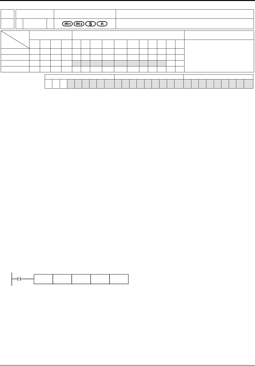
7 Application Instructions API 50-99
DVP-PLC APPLICATION MANUAL
7-89
API Mnemonic Operands Function
79
D TO P Write CR Data into Special Modules
Bit Devices Word Devices Program Steps Type
OP X Y M S K H KnX KnY KnM KnS T C D E F
m1 * * *
m2 * * *
S * * * * * * * * * * *
n * * *
TO, TOP: 9 steps
DTO, DTOP: 17 steps
PULSE 16-bit 32-bit
ES EX SS SA SX SC EH SV EH3
SV2 ES EX SS SA SX SC EH SV EH3
SV2 ES EX SS SA SX SC EH SV EH3
SV2
Operands:
m1: No. of special module m2: CR# in special module to be written S: Data to be written in CR n: Number
of data to be written at a time
Explanations:
1. Range of m1 (16-bit and 32-bit): for ES/SA: 0 ~ 7, for EH/EH2/EH3/SV2: 0 ~ 255, for SV: 0 ~ 107.
2. Range of m2 (16-bit and 32-bit): for ES/SA: 0 ~ 48, for EH: 0 ~ 254, for EH2/SV/EH3/SV2: 0 ~ 499.
3. Range of n:
a) 16-bit: for ES/SA: 1 ~ (49 – m2), for EH: 1 ~ (255 – m2), for EH2/SV/EH3/SV2: 1 ~ (500 – m2).
b) 32-bit: for ES/SA: 1 ~ (49 – m2)/2, for EH: 1 ~ (255 – m2)/2, for EH2/SV/EH3/SV2: 1 ~ (500 – m2)/2.
4. ES series MPU does not support E, F index register modification.
5. m1, m2 and n of EH series MPU do not support word device D.
6. Flag: M1083 (On when allowing interruptions during FROM/TO instruction). See remarks for more details.
7. This instruction is for writing the data into the CR in special modules.
8. The 16-bit instruction can designate S = K1 ~ K4; the 32-bit instruction can designate S = K1 ~ K8.
Program Example:
1. Use 32-bit instruction DTO to write the content in D11 and D10 into CR#13 and CR#12 of special module No.0.
Only 1 group of data is written in at a time (n = 1).
2. When X0 = On, the instruction will be executed. When X0 = Off, the instruction will not be executed and the data
written will not be changed.
X0
DTO K0 K12 D10 K1
3. Operand rules
a) m1: The No. of special modules connected to PLC MPU. No. 0 is the module closest to te MPU. Maximum 8
modules are allowed to connected to a PLC MPU and they will not occupy any I/O points.
b) m2: CR#. CR (control register) is the n 16-bit memories built in the special module, numbered in decimal as
#0 ~ #n. All operation status and settings of the special module are contained in the CR.
c) FROM/TO instruction is for reading/writing 1 CR at a time. DFROM/DTO instruction is for reading/writing 2
CRs at a time.
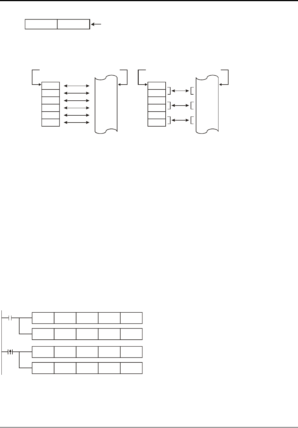
7 Application Instructions API 50-99
DVP-PLC APPLICATION MANUAL
7-90
CR #10 CR #9
Lower 16-bi
t
Designated CR number
Hi gher 16-bit
d) Number of groups “n” to be transmitted: n = 2 in 16-bit instructions and n = 1 in 32-bit instructions mean
the same.
D0
D1
D2
D3
D4
D5
CR #5
CR #6
CR #7
CR #8
CR #9
CR #10
D0
D1
D2
D3
D4
D5
CR #5
CR #6
CR #7
CR #8
CR #9
CR #10
Designated device Designated CR Designated device Designated CR
16-bit instruction when n=6 32-bit instruction when n=3
4. ES/EX/SS series MPU does not have M1083. During the execution of FROM/TO instruction, all external or
internal interruption subroutines will be forbidden. The interruptions are allowed only after FROM/TO instruction
finishes its execution. FROM/TO instruction can also be used in an interruption subroutine.
5. M1083 for switching instruction modes in SA/SX/SC/EH/EH2/SV/EH3/SV2 series MPU:
a) When M1083 = Off, during the execution of FROM/TO instruction, all external or internal interruption
subroutines will be forbidden. The interruptions are allowed only after FROM/TO instruction finishes its
execution. FROM/TO instruction can also be used in an interruption subroutine.
b) When M1083 = On and an interruption signal occurs during the execution of FROM/TO instruction, the
interruption will be processed first (with a 100us delay) and the execution of FROM/TO will be stopped. After
the interruption subroutine finishes its execution, the program will jump to the next instructio of FROM/TO.
FROM/TO cannot be used in an interruption subroutine.
FROM/TO Application Example 1:
Adjust the A/D conversion curve of DVP-04AD. Set the OFFSET value of CH1 as 0V (= K0LSB) and GAIN value as
2.5V (= K2,000LSB).
M1002
TO K0 K1 H0 K1
TO K0 K33 H0 K1
X0
TO K0 K18 K0 K1
TO K0 K24 K2000 K1
1. Write H0 to CR#1 of anlog input module No. 0 and set CH1 as mode 0 (voltage input: -10V ~ +10V).
2. Write H0 to CR#33 and allow OFFSET/GAIN tuning in CH1 ~ CH4.
3. When X0 goes from Off to On, write the OFFSET value K0 LSB into CR#18 and the GAIN value K2,000 LSB into
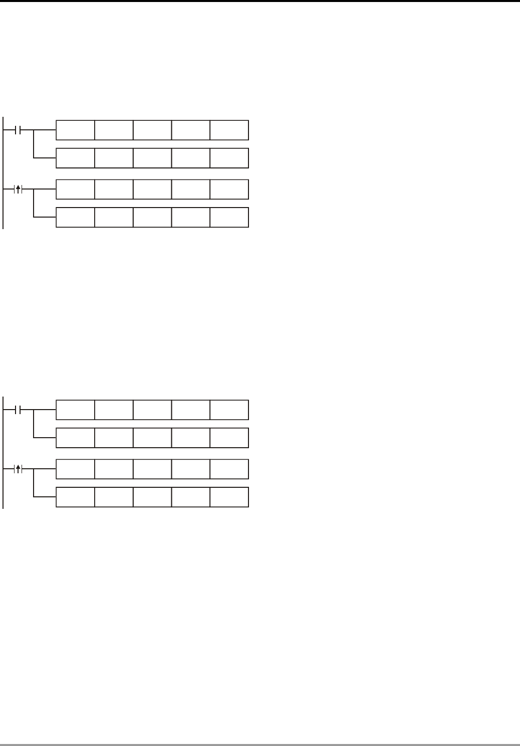
7 Application Instructions API 50-99
DVP-PLC APPLICATION MANUAL
7-91
CR#24.
FROM/TO Application Example 2:
Adjust the A/D conversion curve of DVP-04AD. Set the OFFSET value of CH2 as 2mA (= K400LSB) and GAIN value
as 18mA (= K3,600LSB).
M1002
TO K0 K1 H18 K1
TO K0 K33 H0 K1
X0
TO K0 K19 K400 K1
TO K0 K25 K3600 K1
1. Write H18 to CR#1 of anlog input module No. 0 and set CH2 as mode 3 (current input: -20mA ~ +20mA).
2. Write H0 to CR#33 and allow OFFSET/GAIN tuning in CH1 ~ CH4.
3. When X0 goes from Off to On, write the OFFSET value K400 LSB into CR#19 and the GAIN value K3,600 LSB into
CR#25.
FROM/TO Application Example 3:
Adjust the D/A conversion curve of DVP-02DA. Set the OFFSET value of CH2 as 0mA (= K0LSB) and GAIN value as
10mA (= K1,000LSB).
M1002
TO K1 K1 H18 K1
TO K1 K33 H0 K1
X0
TO K1 K22 K0 K1
TO K1 K28 K1000 K1
1. Write H18 to CR#1 of anlog output module No. 1 and set CH2 as mode 3 (current output: 0mA ~ +20mA).
2. Write H0 to CR#33 and allow OFFSET/GAIN tuning in CH1 and CH2.
3. When X0 goes from Off to On, write the OFFSET value K0 LSB into CR#22 and the GAIN value K1,000 LSB into
CR#28.
FROM/TO Application Example 4:
Adjust the D/A conversion curve of DVP-02DA. Set the OFFSET value of CH2 as 2mA (= K400LSB) and GAIN value
as 18mA (= K3,600LSB).
1. Write H10 to CR#1 of anlog output module No. 1 and set CH2 as mode 2 (current output: +4mA ~ +20mA).
2. Write H0 to CR#33 and allow OFFSET/GAIN tuning in CH1 and CH2.
3. When X0 goes from Off to On, write the OFFSET value K400 LSB into CR#23 and the GAIN value K3,600 LSB into
CR#29.
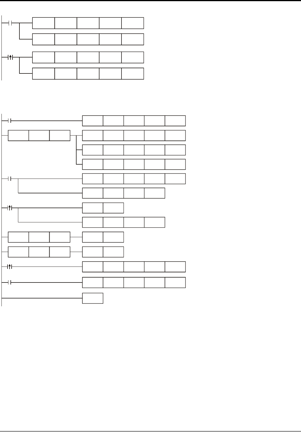
7 Application Instructions API 50-99
DVP-PLC APPLICATION MANUAL
7-92
M1002
TO K1 K1 H10 K1
TO K1 K33 H0 K1
X0
TO K1 K23 K400 K1
TO K1 K29 K3600 K1
FROM/TO Application Example 5:
When DVP-04AD-S is used with DVP-02DA-S
M1000
FROM K0 K0 D0 K1
TO K0 K1 H3030 K1LD= H88 D0
TO K0 K2 K32 K2
FROM K0 K6 D20 K4
M1000
FROM K1 K0 D0 K1
CMP H49 D0 M0
M1013
INC D100
ADD D101 K5 D101
RST D100LD= K4000 D100
RST D101LD= K4000 D101
M1
TO K1 K1 H10 K1
M1
TO K1 K10 D100 K2
END
1. Read CR#0 of the extension module No. 0 and see if it is DVP-04AD-S: H88.
2. If D0 = H88, set the input modes: (CH1, CH3) mode 0, (CH2, CH4) mode 3.
3. Set the average times in CH1 and CH2 from CR#2 and CR#3 as K32.
4. Read the average of input signals at CH1 ~ CH4 from CR#6 ~ CR#9 and store the 4 data in D20 ~ D23.
5. Read CR#0 of the extension module No. 1 and see if it is DVP-02DA-S: H49.
6. D100 increases K1 and D101 increases K5 every second.
7. When D100 and D101 reach K4,000, they will be cleared as 0.
8. See if the model is DVP-02DA-S when M1 = On. If so, set up output mode: CH1 in mode 0 and CH2 is mode 2.
9. Write the output settings of D100 and D101 into CR#10 and CR#11. The analog output will change by the
changes in D100 and D101.

7 Application Instructions API 50-99
DVP-PLC APPLICATION MANUAL
7-93
API Mnemonic Operands Function
80
RS Serial Communication Instruction
Bit Devices Word Devices Program Steps Type
OP X Y M S K H KnX KnY KnM KnS T C D E F
S *
m * * *
D *
n * * *
RS: 9 steps
PULSE 16-bit 32-bit
ES EX SS SA SX SC EH SV EH3
SV2 ES EX SS SA SX SC EH SV EH3
SV2 ES EX SS SA SX SC EH SV EH3
SV2
Operands:
S: Start device for the data to be transmitted m: Length of data to be transmitted D: Start device for receiving
data n: Length of data to be received
Explanations:
1. Range of m: 0 ~ 256
2. Range of n: 0 ~ 256
3. See the specifications of each model for their range of use.
4. ES series MPU does not support E, F index register modification.
5. This instruction is a handy instruction exclusively for MPU to use RS-485 serial communication interface. The
user has to pre-store word data in S data register, set up data length m and the data receiving register D and
received data length n. If E, F index registers are used to modify S and D, the user cannot change the set values
of E and F when the instruction is being executed; otherwise errors may cause in data writing or reading.
6. Designate m as K0 if you do not need to send data. Designate n as K0 if you do not need to receive data.
7. There is no limitation on the times of using this instruction in the program, but only one instruction is allowed to
be executed at a time.
8. During the execution of RS instruction, changing the data to be transmitted will be invalid.
9. If the peripheral devices, e.g. AC motor drive, are equipped with RS-485 serial communication and its
communication format is open, you can use RS instruction to design the program for the data transmission
between PLC and the peripheral device.
10. If the communication format of the peripheral device is Modbus, DVP series PLC offers handy communication
instructions API 100 MODRD, API 101 MODWR, and API 150 MODRW, to work with the device. See
explanations of the instructions in this application manual.
11. For the special auxiliary relays M1120 ~ M1161 and special data registers D1120 ~ D1131 relevant to RS-485
communication, see remarks for more details.
Program Example 1:
1. Write the data to be transmitted in advance into registers starting from D100 and set M1122 (sending request
flag) as On.
2. When X10 = On, RS instruction will be executed and PLC will start to wait for the sending and receiving of data.
D100 starts to continuousl send out 10 data and when the sending is over, M1122 will be automatically reset to
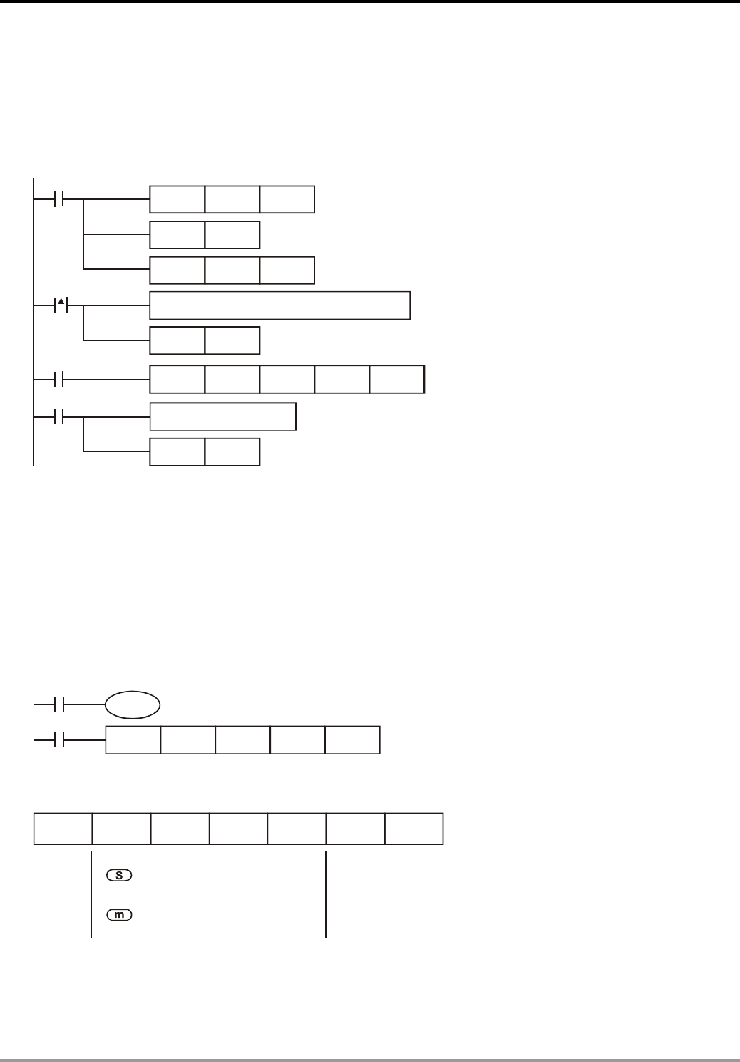
7 Application Instructions API 50-99
DVP-PLC APPLICATION MANUAL
7-94
Off (DO NOT use the program to execute RST M1122). After 1ms of waiting, PLC will start to receive the 10 data.
Store the data in consecutive registers starting from D120.
3. When the receiving of data is completed, M1123 will automatically be On. After the program finishes processing
the received data, M1123 has to be reset to Off and the PLC will start to wait for the sending and receiving of
data again. DO NOT use the program to continuously execute RST M1123.
MOV D1120H86
M1002
SET M1120
SET M1122
MOV D1129K100
X10
M1123
RST M1123
RS D100 K10 D120 K10
Process of received data
Set up communication protocol 9600,7,E,1
Retain communication protocol
Set up communication time-out 100ms
Set up sending request
Receiving of data is completed the flag is reset.
Write in the data to be transmitted in advance
Sending request
pulses
Receiving
completed
The flag is reset.
Program Example 2:
Switching between 8-bit mode (M1161 = On) and 16-bit mode (M1161 = Off)
1. 8-bit mode:
The head code and tail code of the data are set up by M1126 and M1130 together with D1124 ~ D1126. When
PLC is executing RS instruction, the head code and tail code set up by the user will be sent out automatically.
M1161 = On indicates PLC in 8-bit conversion mode. The 16-bit data will be divided into the higher 8 bits and
lower 8 bits. The higher 8 bits are ignored and only the lower 8 bits are valid for data transmission.
M1000
M1161
D100 D120
K4 K7RS
X0
Sending data: (PLC -> external equipment)
STX D100L D101L D102L D103L ETX1 ETX2
Head
code
source data register, starting from
the lower 8 bits of D100
length = 4
Tail cod e
1
Tail code
2
Receiving data: (External equipment -> PLC)
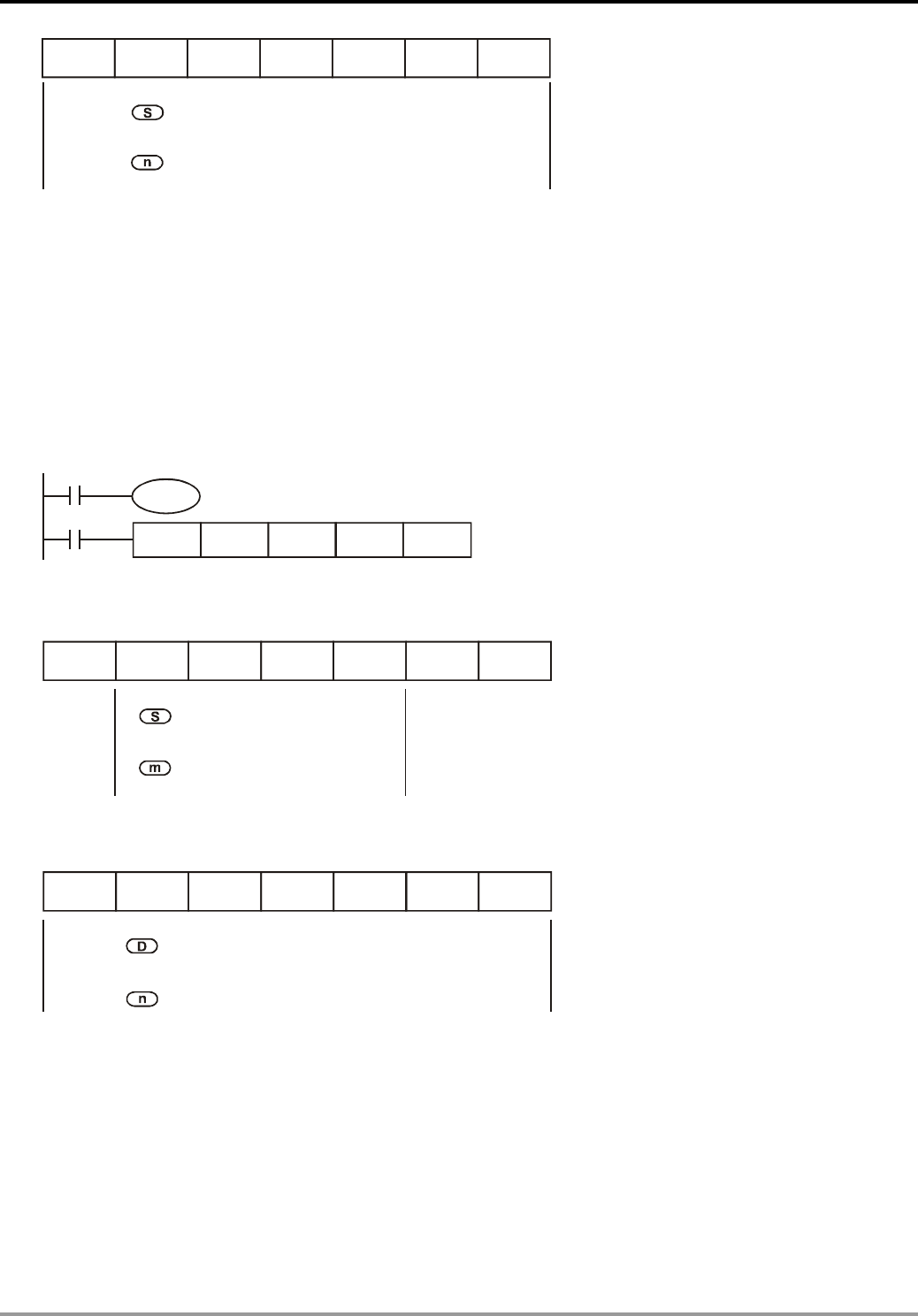
7 Application Instructions API 50-99
DVP-PLC APPLICATION MANUAL
7-95
D120L D122L D123L D124L D125L D126LD121L
Head
code
Tail cod e
1
Tail code
2
received data register, starting from
the lower 8 bits of D120
length = 7
When receiving data, PLC will receive the head code and tail code of the data from the external equipment;
therefore, the user has to be aware of the setting of data length n.
2. 16-bit mode:
The head code and tail code of the data are set up by M1126 and M1130 together with D1124 ~ D1126. When
PLC is executing RS instruction, the head code and tail code set up by the user will be sent out automatically.
M1161 = Off indicates PLC in 16-bit conversion mode. The 16-bit data will be divided into the higher 8 bits and
lower 8 bits for data transmission.
M1001
M1161
D100 D120
K4 K7
RS
X0
Sending data: (PLC -> external equipment)
STX D100L D100L D101L D101L ETX1 ETX2
Head
code source data register, starting from
the lower 8 bits of D100
length = 4
Tail code
1
Tail code
2
Receiving data: (External equipment -> PLC)
D120L D120H D121L D121H D122L D122H D123L
Tail code
1
Tail code
2
received data register, starting from
the lower 8 bits of D120
length = 7
Head
code
When receiving data, PLC will receive the head code and tail code of the data from the external equipment;
therefore, the user has to be aware of the setting of data length n.
Program Example 3:
Connect PLC to VFD-B series AC motor drives (AC motor drive in ASCII Mode; PLC in 16-bit mode and M1161 = Off).
Write in the 6 data starting from parameter address H2101 in VFD-B in advance as the data to be transmitted.
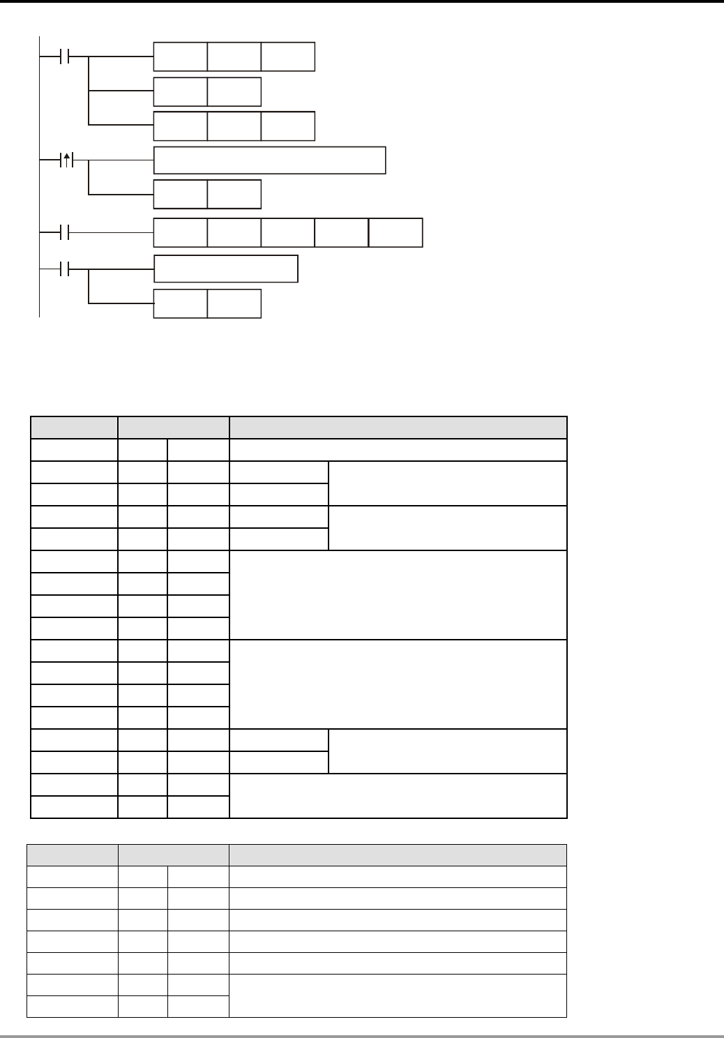
7 Application Instructions API 50-99
DVP-PLC APPLICATION MANUAL
7-96
MOV D1120H86
M1002
SET M1120
SET M1122
MOV D1129K100
X10
M1123
RST M1123
RS D100 K17 D120 K35
Process of received data
Set up communication protocol 9600,7,E,1
Retain communication protocol
Set up communication time-out 100ms
Write in data to be transmitted in advance
Set up sending request
Receiving of data is completed.
The flag is reset.
Sending request
pulses
Receiving
completed
PLC Ö VFD-B, PLC sends “: 01 03 2101 0006 D4 CR LF “
VFD-B Ö PLC, PLC receives “: 01 03 0C 0100 1766 0000 0000 0136 0000 3B CR LF “
Registers for sent data (PLC sends out message)
Register Data Explanation
D100 low ‘: ’ 3A H STX
D100 high ‘0’ 30 H ADR 1
D101 low ‘1’ 31 H ADR 0
Address of AC motor drive: ADR
(1,0)
D101 high ‘0’ 30 H CMD 1
D102 low ‘3’ 33 H CMD 0 Instruction code: CMD (1,0)
D102 high ‘2’ 32 H
D103 low ‘1’ 31 H
D103 high ‘0’ 30 H
D104 low ‘1’ 31 H
Start data address
D104 high ‘0’ 30 H
D105 low ‘0’ 30 H
D105 high ‘0’ 30 H
D106 low ‘6’ 36 H
Number of data (counted by words)
D106 high ‘D’ 44 H LRC CHK 1
D107 low ‘4’ 34 H LRC CHK 0 Error checksum: LRC CHK (0,1)
D107 high CR D H
D108 low LF A H END
Registers for received data (VFD-B responds with messages)
Register Data Explanation
D120 low ‘: ’ 3A H STX
D120 high ‘0’ 30 H ADR 1
D121 low ‘1’ 31 H ADR 0
D121 high ‘0’ 30 H CMD 1
D122 low ‘3’ 33 H CMD 0
D122 high ‘0’ 30 H
D123 low ‘C’ 43 H Number of data (counted by byte)

7 Application Instructions API 50-99
DVP-PLC APPLICATION MANUAL
7-97
Register Data Explanation
D123 high ‘0’ 30 H
D124 low ‘1’ 31 H
D124 high ‘0’ 30 H
D125 low ‘0’ 30 H
Content of address 2101 H
D125 high ‘1’ 31 H
D126 low ‘7’ 37 H
D126 high ‘6’ 36 H
D127 low ‘6’ 36 H
Content of address 2102 H
D127 high ‘0’ 30 H
D128 low ‘0’ 30 H
D128 high ‘0’ 30 H
D129 low ‘0’ 30 H
Content of address 2103 H
D129 high ‘0’ 30 H
D130 low ‘0’ 30 H
D130 high ‘0’ 30 H
D131 low ‘0’ 30 H
Content of address 2104 H
D131 high ‘0’ 30 H
D132 low ‘1’ 31 H
D132 high ‘3’ 33 H
D133 low ‘6’ 36 H
Content of address 2105 H
D133 high ‘0’ 30 H
D134 low ‘0’ 30 H
D134 high ‘0’ 30 H
D135 low ‘0’ 30 H
Content of address 2106 H
D135 high ‘3’ 33 H LRC CHK 1
D136 low ‘B’ 42 H LRC CHK 0
D136 high CR D H
D137 low LF A H END
Program Example 4:
Connect PLC to VFD-B series AC motor drives (AC motor drive in RTU Mode; PLC in 16-bit mode and M1161 = On).
Write in H12 to parameter address H2000 in VFD-B in advance as the data to be transmitted.
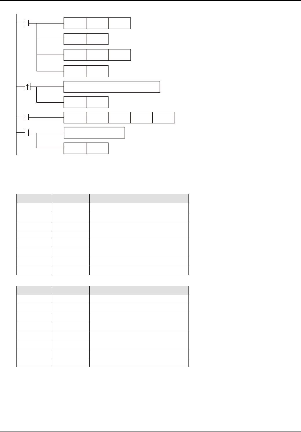
7 Application Instructions API 50-99
DVP-PLC APPLICATION MANUAL
7-98
MOV D1120H86
M1002
SET M1120
SET M1122
MOV D1129K100
X10
M1123
RST M1123
RS D100 K8 D120 K8
SET M1161
Process of received data
Set up communication protocol 9600,7,E,1
Retain communication protocol
Set up communication time-out 100ms
8-bit mode
Sending request
pulses
Write in data to be transmitted in advance
Set up sending request
Receiving of data is completed.
The flag is reset.
PLC Ö VFD-B, PLC sends: 01 06 2000 0012 02 07
VFD-B Ö PLC, PLC receives: 01 06 2000 0012 02 07
Registers for sent data (PLC sends out messages)
Register Data Explanation
D100 low 01 H Address
D101 low 06 H Function
D102 low 20 H
D103 low 00 H Data address
D104 low 00 H
D105 low 12 H Data content
D106 low 02 H CRC CHK Low
D107 low 07 H CRC CHK High
Registers for received data (VFD-B responds with messages)
Register Data Explanation
D120 low 01 H Address
D121 low 06 H Function
D122 low 20 H
D123 low 00 H Data address
D124 low 00 H
D125 low 12 H Data content
D126 low 02 H CRC CHK Low
D127 low 07 H CRC CHK High
Remarks:
1. Flags for the RS-485 communication of RS/MODRD/MODWR/FWD/REV/STOP/RDST/RSTEF/MODRW
instructions

7 Application Instructions API 50-99
DVP-PLC APPLICATION MANUAL
7-99
Flag Function Action
M1120
For retain the communication setting. After the first program scan
is completed, the communication setting will be reset according
to the setting in the special data register D1120. When the
second program scan starts and RS instruction is being
executed, the communication settings will all be reset according
to the settings in D1120. If your communication protocol is fixed,
you can set M1120 to On and the communication protocol will not
be reset whenever
RS/MODRD/MODWR/FWD/REV/STOP/RDST/RSTEF/MODRW
instruction is executed. In this case, even the settings in D1120
are modified, the communication protocol will not be changed.
Set up and reset by the
user.
M1121 Off when the RS-485 communication data is being transmitted. By the system.
M1122
Sending request. When you need to send out or receive data by
RS/MODRD/MODWR/FWD/REV/STOP/RDST/RSTEF/MODRW
instructions, you have to set M1122 to On by a pulse instruction.
When these instructions start to execute, PLC will start to send
out or receive data. When the data transmission is completed,
M1122 will be reset automatically.
Set up by the user; reset
automatically by the
system.
M1123
Receiving is completed. When the execution of
RS/MODRD/MODWR/FWD/REV/STOP/RDST/RSTEF/MODRW
instructions is completed, M1123 will be set to On. You can
process the data received when M1123 is On in the program.
You have to reset M1123 to Off when the process of received
data is completed.
Set up automatically by the
system; reset by the user.
M1124 Waiting for receiving. On when PLC is waiting for receiving data. By the system.
M1125
Receiving status cleared. When M1125 = On, the waiting for
receiving status of PLC will be cleared. You have to reset M1125
to Off after the staus is cleared.
M1126 User/system defined STX/ETX selection of RS instruction (see
the next table for details.)
M1130 User/system defined STX/ETX selection of RS instruction (see
the next table for details.)
Set up and reset by the
user.
M1127 Data transmission is completed for communication instructions
(RS instruction not included)
Set up automatically by the
system; reset by the user.
M1128 Data being sent/received indication By the systme.
M1129
Receiving time-out. If you already set up a communication
time-out in D1129 and the data have not been received
completey when the time-out set is reached, M1129 will be On.
You have to reset M1129 to Off after the problem is solved.
Set up automatically by the
system; reset by the user.
M1131
On when the data are converted into hex of
MODRD/RDST/MODRW instructions when in ASCII mode;
otherwise, M1131 is Off.
M1140 Data receiving error of MODRD/MODWR/MODRW instructions
M1141 Parameter error of MODRD/MODWR/MODRW instructions
M1142 Data receiving error of VFD-A handy commands
By the system
M1143 ASCII/RTU mode selection (used with
MODRD/MODWR/MODRW instructions). On = RTU; Off = ASCII
M1161 8/16-bit mode selection. On = 8-bit; Off = 16-bit
Set up and reset by the
user.

7 Application Instructions API 50-99
DVP-PLC APPLICATION MANUAL
7-100
2. Special data register for the RS-485 communication of RS/MODRD/MODWR/FWD/REV/STOP/RDST/RSTEF
/MODRW instructions
Special D Function
D1038 For setting up the data responding delay time when a PLC MPU using RS-485
communication is used as a slave. Range: 0 ~ 10,000 (unit: 0.1ms)
D1050 ~ D1055 When MODRD/RDST instruction is executed, PLC will automatically convert the ASCII
characters in D1070 ~ D1085 into hex and store the hex value in D1050 ~ D1055.
D1070 ~ D1085
When the RS-485 communication instructions built in PLC are executed, the receiving
end will respond with a message and the messages will be stored in D1070 ~ D1085.
You can check on the responded data stored in these registers (not applicable for RS
instruction).
D1089 ~ D1099
When the RS-485 communication instructions built in PLC are executed, the data sent
will be stored in D1089 ~ D1099. You can check on whether the data sent are correct by
checking these registers (not applicable for RS instruction).
D1120 RS-485 communication protocol. See the next table for more details.
D1121 The communication address of PLC when it operates as a slave.
D1122 Remaining number of words of the data being sent
D1123 Remaining number of words of the data being received
D1124 Definition of the start word (STX). See the table above for more details.
D1125 Definition of the first end word (ETX1) of RS instruction. See the table above for more
details.
D1126 Definition of the second end word (ETX2) of RS instruction. See the table above for more
details.
D1129
Abnormal communication time-out (in ms). When D1129 = 0, there will be no time-out
occurring. When D1129 > 0 and RS/MODRD/
MODWR/FWD/REV/STOP/RDST/RSTEF/MODRW instructions are being executed, if
the first word has not been received within designated time or the time interval between
any two words exceeds the value (>0) after PLC enters the receiving mode, PLC will
automatically set M1129 to On. You can also use M1129 for handling the communication
time-out. Please be noted that you have to reset M1129 after the time-out.
D1130 Error code sent back by Modbus
D1168 For RS instruction, when the received number of words = the low byte of D1168, the
interruption I150 will be triggered.
D1169 For RS instruction, when the received data length = the low byte of D1169, the
interruption I160 will be triggered. When D1169 = 0, I160 will not be triggered.
D1256 ~ D1295
When the RS-485 communication instruction MODRW built in PLC is executed, the data
sent will be stored in D1256 ~ D1295. You can check on whether the data sent are
correct by checking these registers.
D1296 ~ D1311 For MODRW instruction, PLC will automatically convert the ASCII characters into hex.
7 Application Instructions API 50-99
DVP-PLC APPLICATION MANUAL
7-101
3. How to set up RS-485 communication protocol in D1120
Content 0 1
b0 Data length 7 8
00: None
01: Odd
b1
b2 Parity bits
11: Even
b3 Stop bits 1 bit 2 bits
0001 (H1)
: 110
0010 (H2)
: 150
0011 (H3)
: 300
0100 (H4) : 600
0101 (H5) : 1200
0110 (H6) : 2400
0111 (H7)
: 4800
1000 (H8) : 9600
1001 (H9) : 19200
1010 (HA) : 38400
1011 (HB) : 57600 (does not support ES/SS V5.8 and below)
b4
b5
b6
b7
1100 (HC) : 115200 (does not support ES/SS V5.8 and below)
b8 Start word None D1124
b9 First end word None D1125
b10 Second end word None D1126
b15 ~ b11 Not defined
4. When RS instruction is in use, the frequently used communication format in the peripheral device will define the
start word and end word of the control string. Therefore, you can set up the start word and end word in D1124 ~
D1126 or use the start word and end word defined by the PLC. When you use M1126, M1130 and D1124 ~
D1126 to set up the start word and end word, b8 ~ b10 of D1120 have to be set as 1 to make valid the RS-485
communication protocol. See the table below for how to set up.
M1130
0 1
0
D1124: user defined
D1125: user defined
D1126: user defined
D1124: H 0002
D1125: H 0003
D1126: H 0000 (no setting)
M1126
1
D1124: user defined
D1125: user defined
D1126: user defined
D1124: H 003A (’:’)
D1125: H 000D (CR)
D1126: H 000A (LF)
5. Example of how to set up the communication format:
Assume there is a communication format: Baud rate 9600 7, N, 2
STX : “:”
ETX1 : “CR”
ETX2 : “LF”
Check the table and obtain the communication format H788 and write it into D1120.
b15 b0
0000011110001000
788
D1120
0
Don t care

7 Application Instructions API 50-99
DVP-PLC APPLICATION MANUAL
7-102
When STX, ETX1 and EXT2 are in use, please be aware of the On and Off of the special auxiliary relays M1126
and M1130.
6. M1143 is for the selection of ASCII mode or RTU mode. On = RTU mode; Off = ASCII mode.
Take the standard Modbus format for example:
In ASCII mode (M1143 = Off)
STX Start word = ‘:’ (3AH)
Address Hi
Address Lo
Communication address:
The 8-bit address consists of 2 ASCII codes
Function Hi
Function Lo
Function code:
The 8-bit function code consists of 2 ASCII codes
DATA (n-1)
…….
DATA 0
Data:
The n × 8-bit data consists of 2n ASCll codes
LRC CHK Hi
LRC CHK Lo
LRC checksum:
The 8-bit checksum consists of 2 ASCll code
END Hi
END Lo
End word:
END Hi = CR (0DH), END Lo = LF(0AH)
The communication protocol is in Modbus ASCII mode, i.e. every byte is composed of 2 ASCII characters. For
example, 64Hex is ‘64’ in ASCII, composed by ‘6’ (36Hex) and ‘4’ (34Hex). Every hex ‘0’…’9’, ‘A’…’F’
corresponds to an ASCII code.
Character ‘0’ ‘1’ ‘2’ ‘3’ ‘4’ ‘5’ ‘6’ ‘7’
ASCII code 30H 31H 32H 33H 34H 35H 36H 37H
Character ‘8’ ‘9’ ‘A’ ‘B’ ‘C’ ‘D’ ‘E’ ‘F’
ASCII code 38H 39H 41H 42H 43H 44H 45H 46H
Start word (STX):
Fixed as ‘:’ (3AH)
Address:
‘0’ ‘0’: Broadcasting to all drivers
‘0’ ‘1’: To the driver at address 01
‘0’ ‘F’: To the driver at address 15
‘1’ ‘0’: To the driver at address 16
….and so on, maximum to the driver at address 255 (‘F’ ‘F’)
Function code:
‘0’ ‘3’: Read contents of many registers
‘0’ ‘6’: Write 1 word to register
‘1’ ‘0’: Write in contents of many registers
Data characters: The data sent by the user.
LRC checksum:
LCR checksum is 2’s complement of the value added from Address to Data Content.
For example: 01H + 03H + 21H + 02H + 00H + 02H = 29H. 2’s complement of 29H = D7H
End word (END):
7 Application Instructions API 50-99
DVP-PLC APPLICATION MANUAL
7-103
Fixed as END Hi = CR (0DH), END Lo = LF (0AH)
For example: Read 2 continuous data stored in the registers of the driver at address 01H (see the table below).
The start register is at address 2102H.
Inquiry message: Responding message:
STX ‘: ’ STX ‘: ’
‘0’ ‘0’
Address ‘1’ Address ‘1’
‘0’ ‘0’
Function code ‘3’ Function code ‘3’
‘2’ ‘0’
‘1’
Number of data
(counted by byte) ‘4’
‘0’ ‘1’
Start address
‘2’ ‘7’
‘0’ ‘7’
‘0’
Content in start address
2102H
‘0’
‘0’ ‘0’
Number of data
(counted by words)
‘2’ ‘0’
‘D’ ‘0’
LRC checksum ‘7’
Content of address
2103H
‘0’
CR ‘7’
END LF LRC check ‘1’
CR
END LF
In RTU mode (M1143 = On)
START See the following explanation
Address Communication address: In 8-bit binary
Function Function code: In 8-bit binary
DATA (n-1)
…….
DATA 0
Data:
n × 8-bit data
CRC CHK Low
CRC CHK High
CRC checksum:
16-bit CRC consists of 2 8-bit binary
END See the following explanation
START:
For ES/EX/SS/SA/SX series MPU, no input signal can be ≥ 10ms.
See the table below for EH/EH2/SV/EH3/SV2 series MPU:
Baud rate(bps) RTU timeout timer (ms) Baud rate (bps) RTU timeout timer (ms)
300 40 9,600 2
600 21 19,200 1
1,200 10 38,400 1
2,400 5 57,600 1
4,800 3 115,200 1
Address:
00H: Broadcasting to all drivers
01H: To the driver at address 01
0FH: To the driver at address 15
10H: To the driver at address 16…. And so on, maximum to the driver at address 254 (FE H)
Function code:
03H: Read contents of many registers

7 Application Instructions API 50-99
DVP-PLC APPLICATION MANUAL
7-104
06H: Write 1 word to register
10H: Write in contents of many registers
Data characters: The data sent by the user.
CRC checksum: Starting from Address and ending at Data Content.
Step 1: Make the 16-bit register (CRC register) = FFFFH
Step 2: Exclusive OR the first 8-bit message and the low 16-bit CRC register. Store the result in the CRC
register.
Step 3: Right shift CRC register for a bit and fill “0” into the high bit.
Step 4: Check the value shifted to the right. If it is 0, fill in the new value obtained in step 3 and store the value
in CRC register; otherwise, Exclusive OR A001H and CRC register and store the result in the CRC
register.
Step 5: Repeat step 3 – 4 and finish operations of all the 8 bits.
Step 6: Repeat step 2 – 5 for obtaining the next 8-bit message until the operation of all the messages are
completed. The final value obtained in the CRC register is the CRC checksum. The CRC checksum
has to be placed interchangeably in the checksum of the message.
END:
For ES/EX/SS V5.8 (and below) and SA/SX V1.1 (and below) series MPU, keep no input signal be ≥ 10ms.
See the table below for EH/EH2/SV series MPU:
Baud rate(bps) RTU timeout timer (ms) Baud rate (bps) RTU timeout timer (ms)
300 40 9,600 2
600 21 19,200 1
1,200 10 38,400 1
2,400 5 57,600 1
4,800 3 115,200 1
For example: Read 2 continuous data stored in the registers of the driver at address 01H (see the table below).
The start register is at address 2102H.
Inquiry message: Responding message:
Address 01 H
Address 01 H
Function 03 H
Function 03 H
21 H
Start data address 02 H
Number of data
(counted by byte) 04 H
00 H 17 H Number of data
(counted by words) 02 H
Content in data address
8102H 70 H
CRC CHK Low 6F H 00 H
CRC CHK High F7 H
Content in data address
8103H 00 H
CRC CHK Low FE H
CRC CHK High 5C H
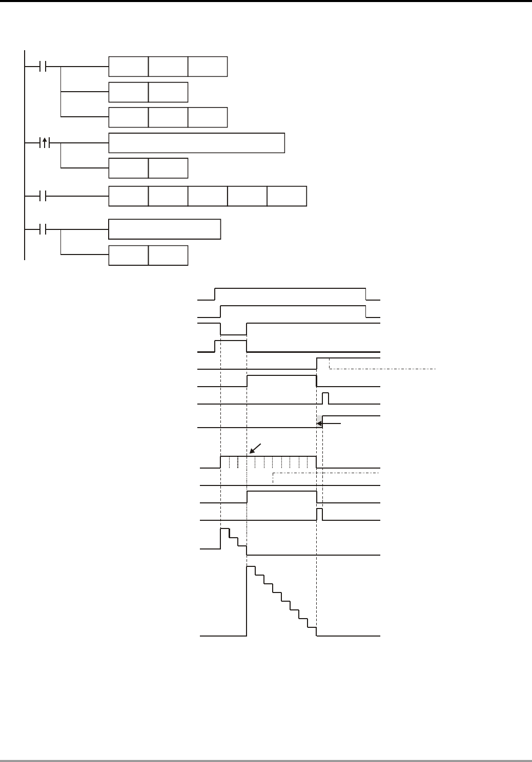
7 Application Instructions API 50-99
DVP-PLC APPLICATION MANUAL
7-105
7. Timing diagram of RS-485 communication flag:
MOV D1120H86
M1002
SET M1120
SET M1122
MOV D1129K100
X10
M1123
RST M1123
RS D100 K3 D120 K8
Setting communication time out 100ms
Process of received data
Set up communication protocol 9600,7,E,1
Retain communication protocol
Write the data to be transmitted in advance
Set up sending request
Receiving of data is completed.
The flag is reset.
Receiving
completed
Sending request
pulses
8
7
6
5
4
3
2
1
0
3
2
1
0
12345678
123
SET M1122 X0
MODRD/RDST/MODRW data
receiving and conversion
completed
M1127
MODRD/RDST/MODRW
data converted to hex M1131
Transmission ready M1121
Sending request M1122
Receiving completed M1123
Waiting for receiving M1124
Communication status cleared M1125
Transmitting and receiving M1128
Receiving time-out M1129
Receiving time-out timer, set by D1129
Remaining words of the sent data D1122
Remaining words of the received data D1123
Auto reset after the data transmission is completed
Converting data
Execution of RS instruction X10
Changing direction
immediately
The user has to do the reset in the program.
Using this in the program will return the
status to the initial transmission ready status.
ASCII data being converted to hex
takes less than 1 scan period.
On when receiving message from the time-out counter
Stop counting when receiving all the data
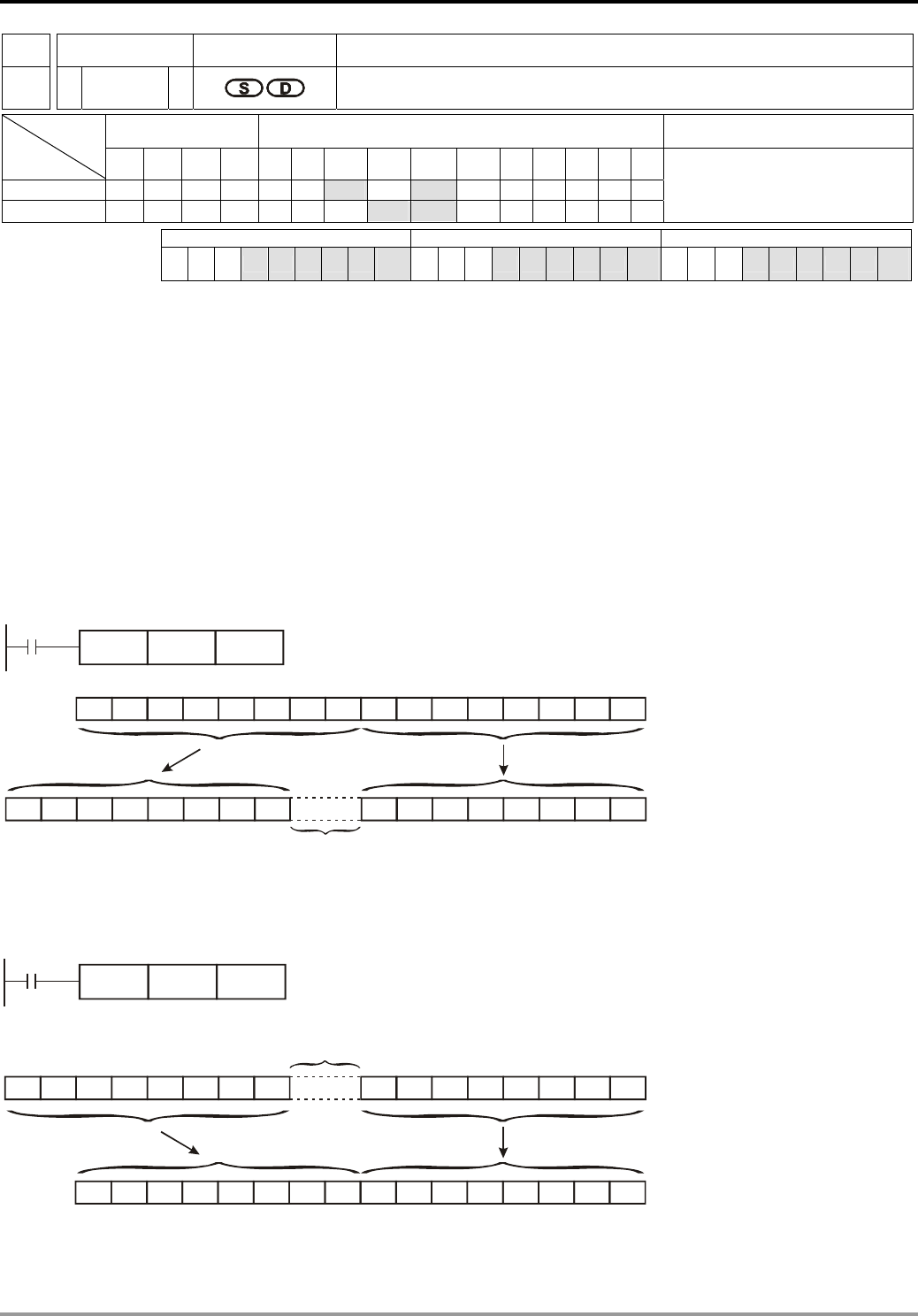
7 Application Instructions API 50-99
DVP-PLC APPLICATION MANUAL
7-106
API Mnemonic Operands Function
81
D PRUN P Parallel Run
Bit Devices Word Devices Program Steps Type
OP X Y M S K H KnX KnY KnM KnS T C D E F
S * *
D * *
PRUN, PRUNP: 5 steps
DPRUN, DPRUNP: 9 steps
PULSE 16-bit 32-bit
ES EX SS SA SX SC EH SV EH3
SV2 ES EX SS SA SX SC EH SV EH3
SV2 ES EX SS SA SX SC EH SV EH3
SV2
Operands:
S: Source device D: Destination device
Explanations:
1. The most right digit of X, Y and M of KnX, KnY and KnM has to be 0.
2. When S designates KnX, D has to designate KnM; when S designates KnM, D has to designate KnY.
3. See the specifications of each model for their range of use.
4. This instruction sends the content in S to D in the form of octal system.
Program Example 1:
When X3 = On, the content in K4X10 will be sent to K4M10 in octal form.
X3
PRUN K4X10 K4M10
X27
M27
X26 X25 X24 X23 X22 X21 X20 X17 X16 X15 X14 X13 X12 X11 X10
M17 M16 M15 M14 M13 M12 M11 M10
M26 M25 M24 M23 M22 M21 M20 M19 M18
No change
Program Example 2:
When X2 = On, the content in K4M10 will be sent to K4Y10 in octal form.
X2
PRUN K4M10 K4Y10
Y27
M27
Y26 Y25 Y24 Y23 Y22 Y21 Y20 Y17 Y16 Y15 Y14 Y13 Y12 Y11 Y10
M17 M16 M15 M14 M13 M12 M11 M10
M26 M25 M24 M23 M22 M21 M20 M19 M18
Will not be transmitted
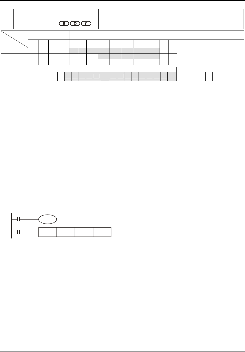
7 Application Instructions API 50-99
DVP-PLC APPLICATION MANUAL
7-107
API Mnemonic Operands Function
82
ASCI P Converts Hex to ASCII
Bit Devices Word Devices Program Steps Type
OP X Y M S K H KnX KnY KnM KnS T C D E F
S * * * * * * * * *
D * * * * * *
n * *
ASCI, ASCIP: 7 steps
PULSE 16-bit 32-bit
ES EX SS SA SX SC EH SV EH3
SV2 ES EX SS SA SX SC EH SV EH3
SV2 ES EX SS SA SX SC EH SV EH3
SV2
Operands:
S: Start device for source data D: Start device for storing the converted result n: Number of bits to be converted
Explanations:
1. Range of n: 1 ~ 256
2. See the specifications of each model for their range of use.
3. Flag: M1161 (8/16 bit mode switch)
4. 16-bit conversion mode: When M1161 = Off, the instruction converts every bit of the hex data in S into ASCII
codes and send them to the 8 high bits and 8 low bits of D. n = the converted number of bits.
5. 8-bit conversion mode: When M1161 = On, the instruction converts every bit of the hex data in S into ASCII
codes and send them to the 8 low bits of D. n = the number of converted bits. (All 8 high bits of D = 0)
Program Example 1:
1. M1161 = Off: The 16-bit conversion mode
2. When X0 = On, convert the 4 hex values in D10 into ASCII codes and send the result to registers starting from
D20.
X0
ASCI D10 D20 K4
M1001
M1161
3. Assume
(D10) = 0123 H ‘0’ = 30H ‘4’ = 34H ‘8’ = 38H
(D11) = 4567 H ‘1’ = 31H ‘5’ = 35H ‘9’ = 39H
(D12) = 89AB H ‘2’ = 32H ‘6’ = 36H ‘A’ = 41H
(D13) = CDEF H ‘3’ = 33H ‘7’ = 37H ‘B’ = 42H
4. When n = 4, the bit structure will be as:
7 Application Instructions API 50-99
DVP-PLC APPLICATION MANUAL
7-108
0000000100100011
0123
D10=0123 H
D20
D21
0011000100110000
0011001100110010
131H 030H
333H 232H
High byte Low byte
High byte Low byte
5. When n = 6, the bit structure will be as:
0000 0 1 0 111000000
0 0001 0 0 1 0 1111110
01101 01101001101
01 2 3
D10 = H 0123
b15
b15
7 H 37 6 H 36
Converted to
b15
0011 0 1 0 001100000
0 1100 1 0 0 0 0100111
b15
3 H 33 2 H 32
D22
b15
b0
b0
b0
b0
b0
D11 = H 4567
45 6 7
D20
D21
1 H 31 0 H 30
6. When n = 1 ~ 16:
n
D K1 K2 K3 K4 K5 K6 K7 K8
D20 Low byte “3” “2” “1” “0” “7” “6” “5” “4”
D20 High byte “3” “2” “1” “0” “7” “6” “5”
D21 Low byte “3” “2” “1” “0” “7” “6”
D21 High byte “3” “2” “1” “0” “7”
D22 Low byte “3” “2” “1” “0”
D22 High byte “3” “2” “1”
D23 Llow byte “3” “2”
D23 High byte “3”
D24 Low byte
D24 High byte
D25 Low byte
D25 High byte
D26 Low byte
D26 High byte
D27 Low byte
D27 High byte
no
change
n
D K9 K10 K11 K12 K13 K14 K15 K16
D20 Low byte “B” “A” “9” “8” “F” “E” “D” “C”
D20 High byte “4” “B” “A” “9” “8” “F” “E” “D”
D21 Low byte “5” “4” “B” “A” “9” “8” “F” “E”
D21 High byte “6” “5” “4” “B” “A” “9” “8” “F”
D22 Low byte “7” “6” “5” “4” “B” “A” “9” “8”
D22 High byte “0” “7” “6” “5” “4” “B” “A” “9”
D23 Llow byte “1” “0” “7” “6” “5” “4” “B” “A”
D23 High byte “2” “1” “0” “7” “6” “5” “4” “B”
7 Application Instructions API 50-99
DVP-PLC APPLICATION MANUAL
7-109
D24 Low byte “3” “2” “1” “0” “7” “6” “5” “4”
D24 High byte “3” “2” “1” “0” “7” “6” “5”
D25 Low byte “3” “2” “1” “0” “7” “6”
D25 High byte “3” “2” “1” “0” “7”
D26 Low byte “3” “2” “1” “0”
D26 High byte “3” “2” “1”
D27 Low byte “3” “2”
D27 High byte
no
change
“3”
Program Example 2:
1. M1161 = On: The 8-bit conversion mode
2. When X0 = On, convert the 4 hex values in D10 into ASCII codes and send the result to registers starting from
D20.
X0
ASCI D10 D20 K4
M1000
M1161
3. Assume
(D10) = 0123 H ‘0’ = 30H ‘4’ = 34H ‘8’ = 38H
(D11) = 4567 H ‘1’ = 31H ‘5’ = 35H ‘9’ = 39H
(D12) = 89AB H ‘2’ = 32H ‘6’ = 36H ‘A’ = 41H
(D13) = CDEFH ‘3’ = 33H ‘7’ = 37H ‘B’ = 42H
4. When n = 2, the bit structure will be as:
0000000100100011
0123
D10=0123 H
00 000 001100 0
00 00 0011001
3
33
2
100 0
100 00
ASCII code of D20=2 is 32H
ASCII code of D21=3 is 33H
5. When n = 4, the bit structure will be as:
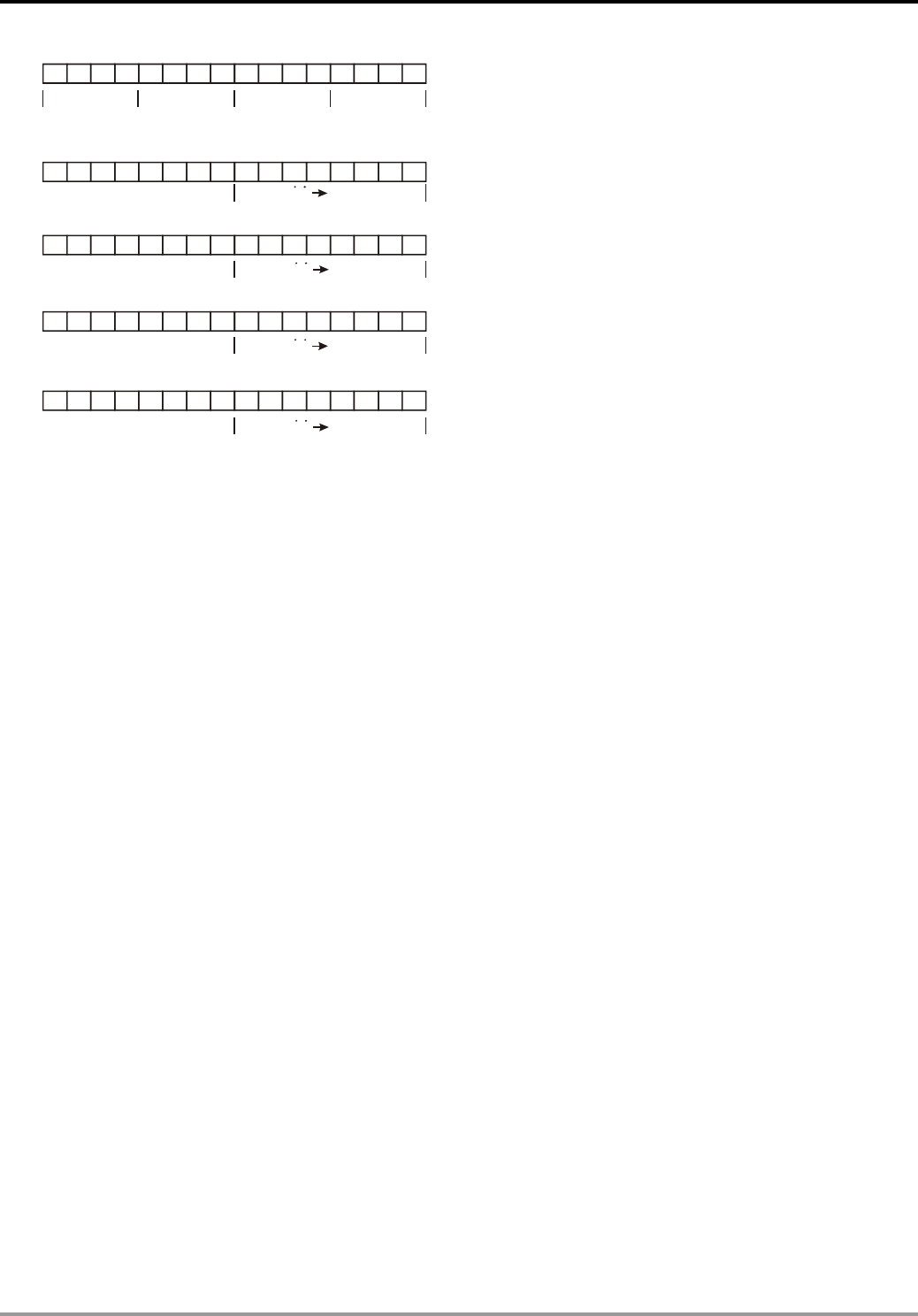
7 Application Instructions API 50-99
DVP-PLC APPLICATION MANUAL
7-110
0000 0 1 0 111000000
0 00000 00 00000011
00
01 2 3
D10 = H 0123
b15
b15
Converted to
b15
0 00000 00 00110011
b15
3 H 33
2 H 32
D22
b15
b0
b0
b0
b0
b0
D20
D21
1 H 31
D23
0 H 30
00000 00 0001011
00 00000 00 0010011
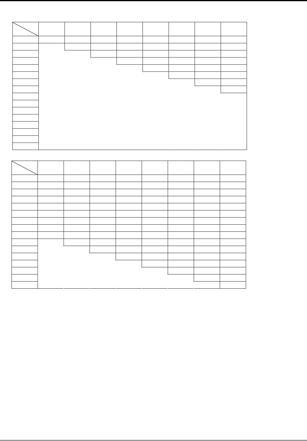
7 Application Instructions API 50-99
DVP-PLC APPLICATION MANUAL
7-111
6. When n = 1 ~ 16:
n
D K1 K2 K3 K4 K5 K6 K7 K8
D20 “3” “2” “1” “0” “7” “6” “5” “4”
D21 “3” “2” “1” “0” “7” “6” “5”
D22 “3” “2” “1” “0” “7” “6”
D23 “3” “2” “1” “0” “7”
D24 “3” “2” “1” “0”
D25 “3” “2” “1”
D26 “3” “2”
D27 “3”
D28
D29
D30
D31
D32
D33
D34
D35
no
change
n
D K9 K10 K11 K12 K13 K14 K15 K16
D20 “B” “A” “9” “8” “F” “E” “D” “C”
D21 “4” “B” “A” “9” “8” “F” “E” “D”
D22 “5” “4” “B” “A” “9” “8” “F” “E”
D23 “6” “5” “4” “B” “A” “9” “8” “F”
D24 “7” “6” “5” “4” “B” “A” “9” “8”
D25 “0” “7” “6” “5” “4” “B” “A” “9”
D26 “1” “0” “7” “6” “5” “4” “B” “A”
D27 “2” “1” “0” “7” “6” “5” “4” “B”
D28 “3” “2” “1” “0” “7” “6” “5” “4”
D29 “3” “2” “1” “0” “7” “6” “5”
D30 “3” “2” “1” “0” “7” “6”
D31 “3” “2” “1” “0” “7”
D32 “3” “2” “1” “0”
D33 “3” “2” “1”
D34 “3” “2”
D35
no
change
“3”
7 Application Instructions API 50-99
DVP-PLC APPLICATION MANUAL
7-112
API Mnemonic Operands Function
83
HEX P Converts ASCII to Hex
Bit Devices Word Devices Program Steps Type
OP X Y M S K H KnX KnY KnM KnS T C D E F
S * * * * * * * * *
D * * * * * *
n * *
HEX, HEXP: 7 steps
PULSE 16-bit 32-bit
ES EX SS SA SX SC EH SV EH3
SV2 ES EX SS SA SX SC EH SV EH3
SV2 ES EX SS SA SX SC EH SV EH3
SV2
Operands:
S: Start device for source data D: Start device for storing the converted result n: Number of bits to be converted
Explanations:
1. Range of n: 1 ~ 256
2. See the specifications of each model for their range of use.
3. Flag: M1161 (8/16 bit mode switch)
4. 16-bit conversion mode: When M1161 = Off, the instruction is in 16-bit conversion mode. ASCII codes of the 8
high bits and 8 low bits of the hex data in S are converted into hex value and sent to D (every 4 bits as a group). n
= the number of bits converted into ASCII codes.
5. 8-bit conversion mode: When M1161 = On, the instruction is in 8-bit conversion mode. Every bit of the hex data in
S are converted into ASCII codes and sent to the 8 low bits of D. n = the number of converted bits. (All 8 high bits
of D = 0)
Program Example 1:
1. M1161 = Off: The 16-bit conversion mode
2. When X0 = On, convert the ASCII codes stored in the registers starting from D20 into hex value and send the
result (every 4 bits as a group) to registers starting from D10. n = 4.
X0
HEX D20 D10 K4
M1001
M1161
3. Assume
S ASCII code Converted to hex S ASCII code Converted to hex
D20 low byte H 43 “C” D24 low byte H 34 “4”
D20 high byte H 44 “D” D24 high byte H 35 “5”
D21 low byte H 45 “E” D25 low byte H 36 “6”
D21 high byte H 46 “F” D25 high byte H 37 “7”
D22 low byte H 38 “8” D26 low byte H 30 “0”
D22 high byte H 39 “9” D26 high byte H 31 “1”
D23 low byte H 41 “A” D27 low byte H 32 “2”
D23 high byte H 42 “B” D27 high byte H 33 “3”
4. When n = 4, the bit structure will be as:
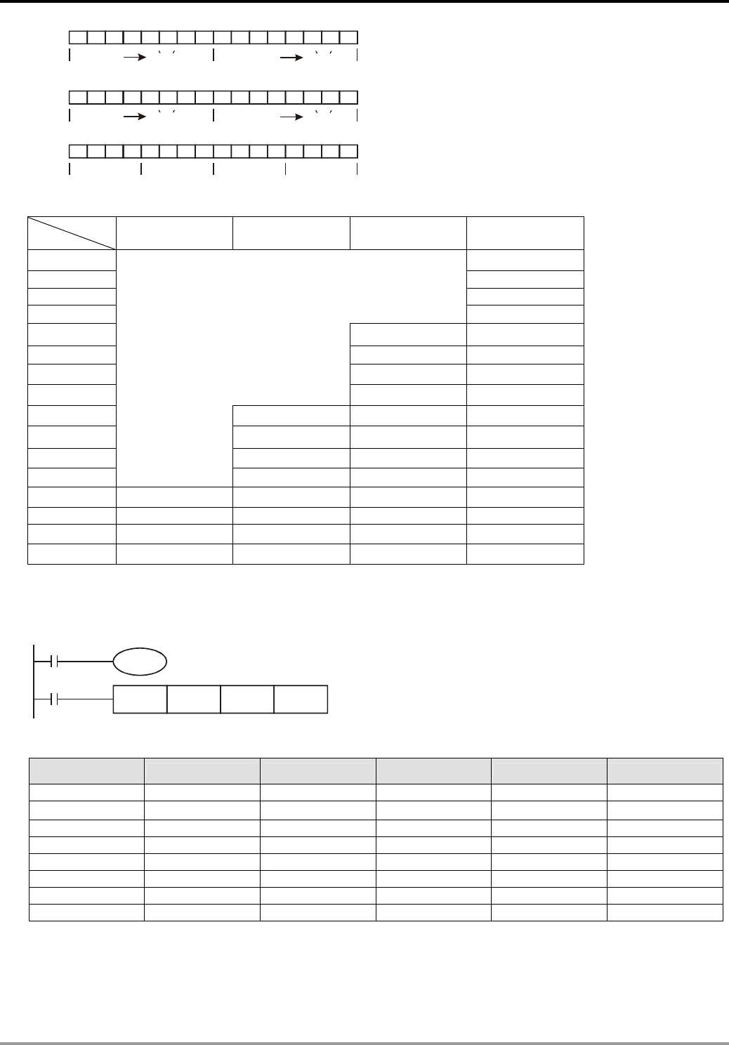
7 Application Instructions API 50-99
DVP-PLC APPLICATION MANUAL
7-113
0000 000 00
000010
1100110 11 1
D20
D21
D10
111 110
1000 10
1
44H D43H C
46H F45H E
CD E F
111001
1011
5. When n = 1 ~ 16:
D
n D13 D12 D11 D10
1 ***C H
2 **CD H
3 *CDE H
4
CDEF H
5 ***C H DEF8 H
6 **CD H EF89 H
7 *CDE H F89A H
8
CDEF H 89AB H
9 ***C H DEF8 H 9AB4 H
10 **CD H EF89 H AB45 H
11 *CDE H F89A H B456 H
12
The
undesignated
parts in the
registers in use
are all 0.
CDEF H 89AB H 4567 H
13 ***C H DEF8 H 9AB4 H 5670 H
14 **CD H EF89 H AB45 H 6701 H
15 *CDE H F89A H B456 H 7012 H
16 CDEF H 89AB H 4567 H 0123 H
Program Example 2:
1. M1161 = On: The 8-bit converstion mode
X0
HEX D20 D10 K4
M1000
M1161
2. Assume
S ASCII code Converted to hex S ASCII code Converted to hex
D20 H 43 “C” D28 H 34 “4”
D21 H 44 “D” D29 H 35 “5”
D22 H 45 “E” D30 H 36 “6”
D23 H 46 “F” D31 H 37 “7”
D24 H 38 “8” D32 H 30 “0”
D25 H 39 “9” D33 H 31 “1”
D26 H 41 “A” D34 H 32 “2”
D27 H 42 “B” D35 H 33 “3”
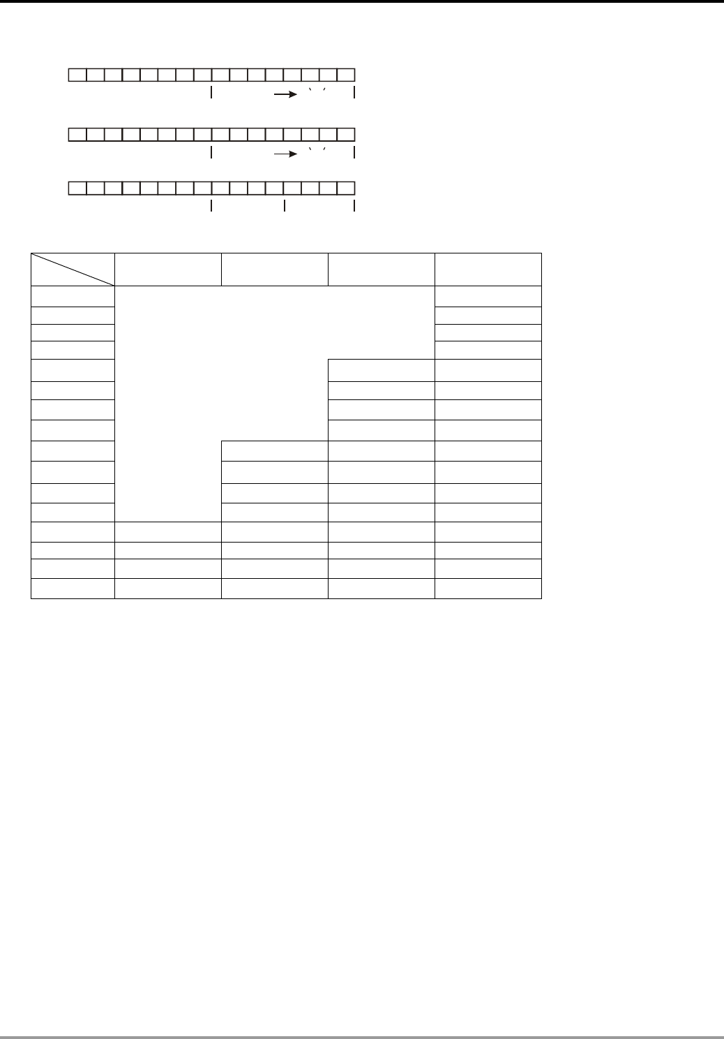
7 Application Instructions API 50-99
DVP-PLC APPLICATION MANUAL
7-114
3. When n = 2, the bit structure will be as:
0100
0010
00 0 11 1
D20
D21
D10
11 0
010
00
00 00 0 0 0
0
11
43H C
44H D
CD
4. When n = 1 ~ 16:
D
n D13 D12 D11 D10
1 ***C H
2 **CD H
3 *CDE H
4
CDEF H
5 ***C H DEF8 H
6 **CD H EF89 H
7 *CDE H F89A H
8
CDEF H 89AB H
9 ***C H DEF8 H 9AB4 H
10 **CD H EF89 H AB45 H
11 *CDE H F89A H B456 H
12
The used
registers
which are not
specified are
all 0
CDEF H 89AB H 4567 H
13 ***C H DEF8 H 9AB4 H 5670 H
14 **CD H EF89 H AB45 H 6701 H
15 *CDE H F89A H B456 H 7012 H
16 CDEF H 89AB H 4567 H 0123 H
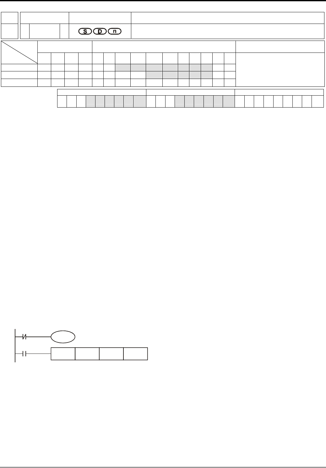
7 Application Instructions API 50-99
DVP-PLC APPLICATION MANUAL
7-115
API Mnemonic Operands Function
84
CCD P Check Code
Bit Devices Word Devices Program Steps Type
OP X Y M S K H KnX KnY KnM KnS T C D E F
S * * * * * * *
D * * * * *
n * * *
CCD, CCDP: 7 steps
PULSE 16-bit 32-bit
ES EX SS SA SX SC EH SV EH3
SV2 ES EX SS SA SX SC EH SV EH3
SV2 ES EX SS SA SX SC EH SV EH3
SV2
Operands:
S: Start device for source data D: Device for storing the sum check result n: Number of data
Explanations:
1. Range of n: 1 ~ 256
2. See the specifications of each model for their range of use.
3. Flag: M1161 (8/16 bit mode switch)
4. The sum check is used for ensuring the correctness of the data transmission.
5. 16-bit conversion mode: When M1161 = Off, the instruction is in 16-bit conversion mode. The instruction sums
up n data (8 bits as a unit) from the start register designated in S and stores the results in the registers
designated in D. The parity bits are stored in D + 1.
6. 8-bit conversion mode: When M1161 = On, the instruction is in 8-bit conversion mode. The instruction sums up n
data (8 bits as a unit; only 8 low bits are valid) from the start register designated in S and stores the results in the
registers designated in D. The parity bits are stored in D + 1.
Program Example 1:
1. M1161 = Off: The 16-bit conversion mode
2. When X0 = On, the instruction will sum up 6 data stored in the register designated in D0 (8 bits as a unit; n = 6
indicates D0 ~ D2 are designated) and store the result in the register designated in D100. The parity bits are
stored in D101.
X0
CCD D0 D100 K6
M1000
M1161
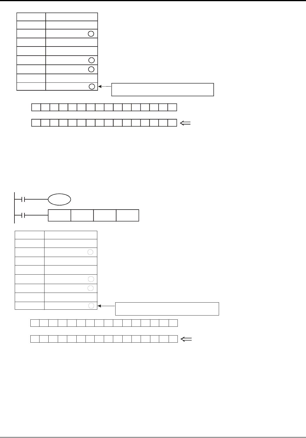
7 Application Instructions API 50-99
DVP-PLC APPLICATION MANUAL
7-116
0000 0 1 1 111000010
00000000 00010001
D100
D101
Parity
D0 low byte
D0 high byte
D1 low byte
D1 high byte
D2 low byte
D2 high byte
D100
D101
(S) Content of data
K100 = 0 1 1 0 0 1 0 0
K111 = 0 1 1 0 1 1 1 1
K120 = 0 1 1 1 1 0 0 0
K202 = 1 1 0 0 1 0 1 0
K123 = 0 1 1 1 1 0 1 1
K211 = 1 1 0 1 0 0 1 1
K867
0 0 0 1 0 0 0 1 The parity is 1 when there is a odd number of 1.
The parity is 0 when there is a even number of 1.
Total
Program Example 2:
1. M1161 = On: The 8-bit conversion mode
2. When X0 = On, the instruction will sum up 6 data stored in the register designated in D0 (8 bits as a unit; n = 6
indicates D0 ~ D5 are designated) and store the result in the register designated in D100. The parity bits are
stored in D101.
X0
CCD D0 D100 K6
M1000
M1161
0000 0 1 1 111000010
0 0000 0 0 0 0 0010001
D100
D101
Parity
D0 low byte
D1 low byte
D2 low byte
D3 low byte
D4 low byte
D5 low byte
D100
D101
(S) Content of data
K100 = 0 1 1 0 0 1 0 0
K111 = 0 1 1 0 1 1 1 1
K120 = 0 1 1 1 1 0 0 0
K202 = 1 1 0 0 1 0 1 0
K123 = 0 1 1 1 1 0 1 1
K211 = 1 1 0 1 0 0 1 1
K867
0 0 0 1 0 0 0 1 The parity is 1 when there is a odd number of 1.
The parity is 0 when there is a even number of 1.
Total
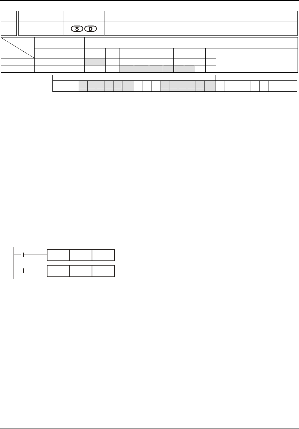
7 Application Instructions API 50-99
DVP-PLC APPLICATION MANUAL
7-117
API Mnemonic Operands Function
85
VRRD P Volume Read
Bit Devices Word Devices Program Steps Type
OP X Y M S K H KnX KnY KnM KnS T C D E F
S
* *
D * * * *****
VRRD, VRRDP: 5 steps
PULSE 16-bit 32-bit
ES EX SS SA SX SC EH SV EH3
SV2 ES EX SS SA SX SC EH SV EH3
SV2 ES EX SS SA SX SC EH SV EH3
SV2
Operands:
S: No. of VR D: Device for storing the volume of VR
Explanations:
1. Range of S: 0 ~ 7; without function card: 0 ~ 1.
2. See the specifications of each model for their range of use.
3. Flags: M1178, M1179. See remarks for more details.
4. VRRD instruction is used for reading 2 points (No.0, No.1) of PLC or the VR rotary switch volume change in the 6
points of the function cards (No.2 ~ No.7) and converting the data into values 0 ~ 255 (stored in D).
5. If you are to set up the timer by the VR volume, simply rotate the VR to modify the set time in the timer. If you are
to acquire a value larger than 255, multiply D by a constant.
Program Example 1:
1. When X0 = On, VR0 volume changed will be converted into an 8-bit BIN value (0 ~ 255) and stored in D0.
2. When X1 = On, the imer T0 will start to time with the content in D0 as the set value in the timer.
X1
TMR T0 D0
X0
VRRD K0 D0
Program Example 2:
1. Read the VR volume in order: The VR0 ~ VR7 rotary switches on the PLC correspond to S = K0 ~ K7 of VRRD
instruction. E index register modification is used in the example below, K0E = K0 ~ K7.
2. The timer converts the scale 0 ~ 10 on the rotary switch into 0 ~ 255. The timing unit of T0 ~ T7 is 0.1 second;
therefore, the set time in the timer will be 0 ~ 25.5 seconds.
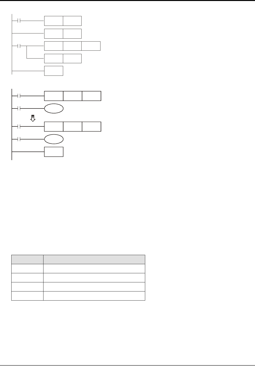
7 Application Instructions API 50-99
DVP-PLC APPLICATION MANUAL
7-118
M1000
RST E
FOR K8
M1000
VRRD
INC E
D100E
NEXT
K 0E
X10
TMR D100T0
T0
Y000
X17
TMR D107T7
T7
Y007
END
3. Operation of FOR ~ NEXT instruction:
a) In the area between FOR ~ NEXT instruction, FOR designating K8 indicates the loop between FOR ~ NEXT
will be executed repeatedly for 8 times before the next instruction is executed.
b) Between FOR ~ NEXT (INC E), E will be 0, 1, 2, …7 plusing 1. Therefore, the 8 VR rotary switch volumes
will be VR0→D100, VR1→D101, VR2→D102…VR7→D107 and be read to designated registers in order.
Remarks:
1. VR refers to Variable Resister.
2. The 2 points of VR rotary switch built in SA/SX/SC/EH/EH2/SV/EH3/SV2 series MPU can be used together with
special D and special M.
Device Function
M1178 Enabling VR0
M1179 Enabling VR1
D1178 VR0 value
D1179 VR1 value
3. If there is no VR extension card inserted in the PLC, setting up the No. of rotary switches as K2 ~ K7 in VRRD
and VRSC instruction in the program will result in errors in grammar check.
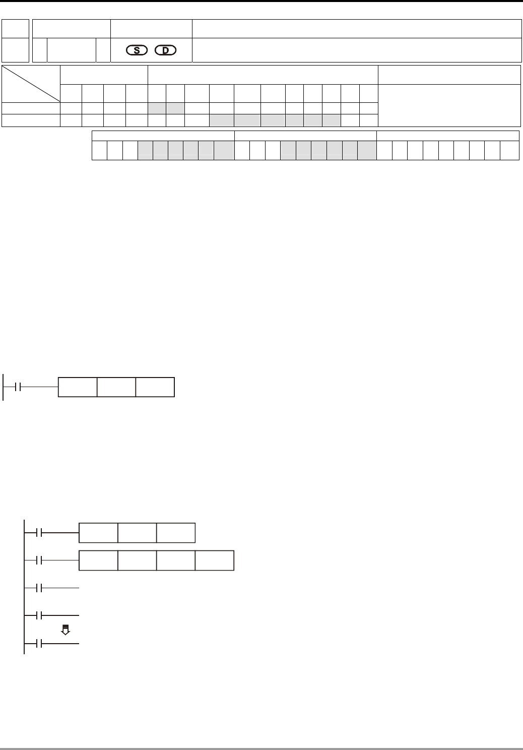
7 Application Instructions API 50-99
DVP-PLC APPLICATION MANUAL
7-119
API Mnemonic Operands Function
86
VRSC P Volume Scale
Bit Devices Word Devices Program Steps Type
OP X Y M S K H KnX KnY KnM KnS T C D E F
S * *
D * * * * * * * *
VRSC, VRSCP: 5 steps
PULSE 16-bit 32-bit
ES EX SS SA SX SC EH SV EH3
SV2 ES EX SS SA SX SC EH SV EH3
SV2 ES EX SS SA SX SC EH SV EH3
SV2
Operands:
S: No. of VR D: Device for storing the scale of VR
Explanations:
1. Range of S: 0 ~ 7; without function card: 0 ~ 1
2. See the specifications of each model for their range of use.
3. VRSC instruction is used for reading 2 points (No.0, No.1) of PLC or the VR rotary switch scale (0 ~ 10) in the 6
points of the function cards (No.2 ~ No.7) and storing the data in D. If the position of the VR falls in the middle of
two scales, VRSC will round up the value into an integer of 0 ~ 10.
Program Example 1:
When X0 = On, the scale of VR0 (0 ~ 10) will be stored in D10.
X0
VRSC K0 D10
Program Example 2:
1. When the VR is used as DIP switch, they will correspond to scale 0 ~ 10 and only one of M10 ~ M20 will be On.
Use API 41 DECO instruction to decode the scales into M10 ~ M25.
2. When X0 = On, store the scale (0 ~ 10) of VR1 into D1.
3. When X1 = On, use API 41 DECO to decode the scales into M10 ~ M25.
X0
VRSC K1 D1
X1
DECO D1 M10 K4
M10
M11
M20
On when the scale is 0
On when the scale is 1
On when the scale is 10
Remarks:
If the MPU is not inserted with a VR extension card, and the No. of the rotary switches inVRRD or VRSC instruction in
the program are set as K2 ~ K7, errors will occur in the execution of grammar check.
7 Application Instructions API 50-99
DVP-PLC APPLICATION MANUAL
7-120
API Mnemonic Operands Function
87
D ABS P Absolute Value
Bit Devices Word Devices Program Steps Type
OP X Y M S K H KnX KnY KnM KnS T C D E F
D * * * * * * * *
ABS, ABSP: 3 steps
DABS, DABSP: 5 steps
PULSE 16-bit 32-bit
ES EX SS SA SX SC EH SV EH3
SV2 ES EX SS SA SX SC EH SV EH3
SV2 ES EX SS SA SX SC EH SV EH3
SV2
Operands:
D: Device of the absolute value
Explanations:
1. See the specifications of each model for their range of use.
2. This instruction obtains the absolute value of the content in the designated in D.
3. This instruction adopts pulse execution instructions (ABSP, DABSP).
Program Example:
When X0 = Off→On, obtain the absolute value of the content in D0.
X0
ABS D0
7 Application Instructions API 50-99
DVP-PLC APPLICATION MANUAL
7-121
API Mnemonic Operands Function
88
D PID PID Control Loop
Bit Devices Word Devices Program Steps Type
OP X Y M S K H KnX KnY KnM KnS T C D E F
S1 *
S2 *
S3 *
D *
PID : 9 steps
DPID: 17 steps
PULSE 16-bit 32-bit
ES EX SS SA SX SC EH SV EH3
SV2 ES EX SS SA SX SC EH SV EH3
SV2 ES EX SS SA SX SC EH SV EH3
SV2
Operands:
S1: Set value (SV) S2: Present value (PV) S3: Parameter D: Output value (MV)
Explanations:
1. In 16-bit instruction, S3 will occupy 20 consecutive devices; in 32-bit instruction, S3 will occupy 21 consecutive
devices.
2. See the specifications of each model for their range of use.
3. See the Remarks below for the times of using PID instruction allowed in the program.
4. This instruction is specifically for PID control. PID operation will be executed by the scan only when the sampling
time is reached. PID refers to “proportion, integration and differential”. PID control is widely applied to many
machines, pneumatic and electronic equipments.
5. For the 16-bit instruction, the parameters are S3 ~ S3+19; for the 32-bit instruction, the parameters are S3 ~ S3+20.
After all the parameters are set up, PID instruction will start to be executed and the results will be stored in D. D
has to be the data register area without latched function. (If you wish to designate a latched data register area,
place the data register in the latched area at the beginning of the program and clear it as 0.)
Program Example:
1. Complete the parameter setting before executing PID instruction.
2. When X0 = On, the instruction will be executed and the result will be stored in D150. When X0 goes Off, the
instruction will not be executed and the data prior to the instruction will stay intact.
D150
X0
D100D1D0PID
Remarks:
1. ES/EX/SS series MPU V5.7 (and above) supports PID instruction. Other versions do not support the instruction.
2. There is no limitation on the times of using this instruction. However, the register No. designated in S3 cannot be
repeated.
3. For the 16-bit instruction, S3 will occupy 20 registers. In the program example above, the area designated in S3 is
D100 ~ D119. Before the execution of PID instruction, you have to transmit the setting value to the designated
register area by MOV instruction, If the designated registers are latched, use MOVP instruction to transmit all
setting value at a time.

7 Application Instructions API 50-99
DVP-PLC APPLICATION MANUAL
7-122
4. Settings of S3 in the 16-bit instruction
Device No. Function Setup Range Explanation
S3: Sampling time (TS)
(unit: 10ms)
1 ~ 2,000
(unit: 10ms)
If TS is less than 1 program scan time, PID
instruction will be executed for 1 program scan
time. If TS= 0, PID instruction will not be enabled.
The minimum TS has to be longer than the
program scan time.
S3 +1: Proportional gain (KP) 0 ~ 30,000 (%) The magnified error proportional value between
SV – PV.
S3 +2: Integral gain (KI) 0 ~ 30,000 (%)
The magnified proportional value of every
sampling time unit × the accumulated value of
the error.
S3 +3: Differential gain (KD) -30,000 ~ 30,000 (%) The magnified proportional value of the varied
error in every samping timme unit.
S3 +4: Control direction
(DIR)
0: automatic control
1: forward control (E = SV - PV)
2: inverse control (E = PV - SV)
3: Auto-tuning of parameter exclusively for the temperature control. The
device will automatically become K4 when the auto-tuning is
completed and be filled in with the appropriate parameter KP, KI and
KD (not avaliable in the 32-bit instruction).
4: Exclusively for the adjusted temperature control (not avaliable in the
32-bit instruction).
5: Auto direction control (limited integrall upper/lower limit)
P.S. K5 mode is only available in SV/EH2/EH3/SV2 V1.2, SA/SX V1.8
and SC V1.6.
S3 +5:
The range that error
value (E) doesn’t
work
0 ~ 32,767
E = the error of SV – PV. When S3 +5 = K0, the
function will not be enabled, e.g. when S3 +5 is
set as 5, MV of E between -5 and 5 will be 0.
S3 +6: Upper bound of output
value (MV) -32,768 ~ 32,767
Ex: if S3 +6 is set as 1,000, the output will be
1,000 when MV is bigger than 1,000. S3 +6 has
to be bigger or equal S3 +7; otherwise the upper
bound and lower bound will switch.
S3 +7: Lower bound of output
value (MV) -32,768 ~ 32,767 Ex: if S3 +7 is set as -1,000, the output will be
-1,000 when MV is smaller than -1,000.
S3 +8: Upper bound of
integral value -32,768~32,767
Ex: if S3 +8 is set as 1,000, the output will be
1,000 when the integral value is bigger than
1,000 and the integration will stop. S3 +8 has to
be bigger or equal S3 +9; otherwier the upper
bound and lower bound will switch.
S3 +9: Lower bound of
integral value -32,768 ~ 32,767
Ex: if S3 +9 is set as -1,000, the output will be
-1,000 when the integral value is smaller than
-1,000 and the integration will stop.
S3 +10,11: Accumulated integral
value 32-bit floating point
The accumulated integral value is only for
reference. You can still clear or modify it (in
32-bit floating point) according to your need.
S3 +12: The previous PV - The previous PV is only for reference. You can
still modify it according to your need.
S3 +13:
~
S3 +19: For system use only.
5. When parameter setting exceeds its range, the upper bound and lower bound will become the setting value.
However, if the motion direction (DIR) exceeds the range, it will be set to 0.
6. PID instruction can be used in interruption subroutines, step points and CJ instruction.

7 Application Instructions API 50-99
DVP-PLC APPLICATION MANUAL
7-123
7. The maximum error of sampling time TS = - (1 scan time + 1ms) ~ + (1 scan time). When the error affects the
output, please fix the scan time or execute PID instruction in the interruption subroutine of the timer.
8. PV of PID instruction has to be stable before the execution of PID instruction. If you are to extract the input value
of DVP04AD/04DA/06XA/04PT/04TC for PID operation, please be aware of the A/D conversion time of these
modules.
9. For the 32-bit instruction, If S3 designates the parameter setting area of PID instruction as D100 ~ D120, S3
occupies 21 registers. Before the execution of PID instruction, you have to use MOV instrction first to send the
setting value to the register area for setup. If the designated registers are latched one, use MOVP instruction to
send all the setting value at a time.
10. Settings of S3 in the 32-bit instruction
Device No. Function Setup range Explanation
S3: Sampling time (TS)
(unit: 10ms)
1 ~ 2,000
(unit: 10ms)
If TS is less than 1 program scan time, PID
instruction will be executed for 1 program
scan time. If TS= 0, PID instruction will not be
enabled. The minimum TS has to be longer
than the program scan time.
S3 +1: Proportional gain (KP) 0 ~ 30,000 (%) The magnified error proportional value
between SV – PV.
S3 +2: Integral gain (KI) 0 ~ 30,000 (%)
The magnified proportional value of every
sampling time unit × the accumulated value
of the error.
S3 +3: Differential gain (KD) -30,000 ~ 30,000 (%) The magnified proportional value of the
varied error in every samping timme unit.
S3 +4: Control direction (DIR)
0: automatic control
1: forward control (E = SV – PV)
2: inverse control (E = PV – SV)
S3 +5, 6:
The range that 32-bit
error value (E) doesn’t
work
0 ~ 2,147,483,647
E = the error of SV – PV. When S3 +5,6 = K0,
the function will not be enabled, e.g. when S3
+5,6 is set as 5, MV of E between -5 and 5
will be 0.
S3 +7, 8: Upper bound of 32-bit
output value (MV)
-2,147,483,648 ~
2,147,483,647
Ex: if S3 +7,8 is set as 1,000, the output will
be 1,000 when MV is bigger than 1,000. S3
+7,8 has to be bigger or equal S3 +9,10;
otherwise the upper bound and lower bound
will switch.
S3 +9, 10: Lower bound of 32-bit
output value (MV)
-2,147,483,648 ~
2,147,483,647
Ex: if S3 +9,10 is set as -1,000, the output will
be -1,000 when MV is smaller than -1,000.
S3 +11, 12: Upper bound of 32-bit
integral value
-2,147,483,648 ~
2,147,483,647
Ex: if S3 +11,12 is set as 1,000, the output
will be 1,000 when the integral value is
bigger than 1,000 and the integration will
stop. S3 +11,12 has to be bigger or equal S3
+13,14; otherwier the upper bound and lower
bound will switch.
S3 +13, 14: Lower bound of 32-bit
integral value
-2,147,483,648 ~
2,147,483,647
Ex: if S3 +13,14 is set as -1,000, the output
will be -1,000 when the integral value is
smaller than -1,000 and the integration will
stop.
S3 +15, 16: 32-bit accumulated
integral value 32-bit floating point
The accumulated integral value is only for
reference. You can still clear or modify it (in
32-bit floating point) according to your need.
S3 +17, 18: 32-bit previous PV - The previous PV is only for reference. You

7 Application Instructions API 50-99
DVP-PLC APPLICATION MANUAL
7-124
Device No. Function Setup range Explanation
can still modify it according to your need.
S3 +19:
~
S3 +20:
For system use only.
11. The explanation of 32-bit S3 and 16-bit S3 are almost the same. The difference is the capacity of S3+5 ~ S3+20.
PID Equations:
1. The PID operation is conducted according to the speed and the differential PV.
2. The PID operation has three control directions: automatic, foreward and inverse. Forward or inverse are
designated in S3 +4. Other relevant settings of PID operation are set by the registers designated in S3 ~ S3 +5.
3. Basic PID equation:
() () ()
StPVK
S
tEKtEKMV DIP *
1
** ++=
Control direction PID equation
Forward, automatic E(t) = SV – PV
Inverse E(t) = PV – SV
(
)
StPV is the differential value of
()
tPV ;
()
S
tE 1 is the integral value of
(
)
tE . When
()
tE is less than 0
as the control direction is selected as forward or inverse,
()
tE will be regarded as “0".
The equation above illustrates that this instruction is different from a general PID instruction by the variable use
of the differential value. To avoid the flaw that the transient differential value is too big when a general PID
instruction is executed for the first time, our PID instruction monitors the differentiation status of the PV. When
the variation of PV is too big, this instruction will reduce the output of MV.
4. Symbol explanation:
MV : Output value
P
K: Proprotional gain
(
)
tE : Error value
PV : Present measured value
SV : Target value
D
K: Differential gain
()
StPV : Differential value of PV(t)
I
K: Integral gain
()
S
tE 1: Integral value of E(t)
5. Temperature Control Equation:
When S3 +4 is K3 and K4, the equation used in diagram 2 (see below) will be changed as:
() () ()
⎥
⎦
⎤
⎢
⎣
⎡+
⎟
⎠
⎞
⎜
⎝
⎛
+= StPVK
S
tE
K
tE
K
MV D
IP
*
111
7 Application Instructions API 50-99
DVP-PLC APPLICATION MANUAL
7-125
In which the error value is fixed as E(t) = SV – PV
This equation is exclusively designed for temperature control. Therefore, when the sampling time (TS) is set as 4
seconds (K400), the range of output value (MV) will be K0 ~ K4,000 and the cycle time of GPWM instruction
used together has to be set as 4 seconds (K4000) as well.
If you have no idea how to adjust the parameters, you can select K3 (auto-tuning) and after all the parameters
are adjusted (the control direction will be automatically set as K4), you can modify your parameters to better
ones according to the result of the control.
6. Control diagrams:
G(s)
S
1/S K
I
K
P
K
D
+++
+
PID instruction is within the dotted-lined area
Diagram 1: + 4 = K0 ~ K2
S
3
In Diagram 1, S is differentiation, referring to “PV – previous PV / sampling time”. 1 / S is integration, referring to
“(previous integral value + error value) × sampling time”. G(S) refers to the device being controlled.
G(s)
S
1/S 1/K
I
K
D
+++
+
1/K
P
PID operation is within the dotted-lined area
Diagram 2: + 4 = K3 ~ K4
S
3
In Diagram 2, 1/KI and 1/KP refer to “divided by KI” and “divided by KP”. Due to that this is exclusively for
temperature control, you have to use PID instruction together with GPWM instruction. See Application 3 for
more details.
7. Notes:
7 Application Instructions API 50-99
DVP-PLC APPLICATION MANUAL
7-126
a) S3 + 6 ~ S3 + 13 are only available in SA/SX/SC/EH/EH2/SV series, and ES/EX/SS (v5.7 and above) series
MPU.
b) PID instruction can only be used once in ES/EX/SS (v5.6 and below) series MPU. There is no limitation on
the times of using PID instruction in ES/EX/SS (v5.7 and above) series and SA/SX/SC/EH/EH2/SV/EH3/SV2
series MPU.
c) S3 + 3 of ES/EX/SS (v5.7 and below), SA/SX/SC (v1.1 and below) and EH (v1.0 and below) series MPU can
only be the value within 0 ~ 30,000.
d) There are a lot of circumstances where PID instruction can be applied; therefore, please choose the control
functions appropriately. For example, when you select parameter auto-tuning for the temperature (S3 + 4 =
K3), you cannot use it in a motor control environment in case improper control may occur.
e) When you adjust the three main parameters, KP, KI and KD (S3 + 4 = K0 ~ K2), you have to adjust KP first
(according to your experiences) and set KI and KD as 0. When you can roughly handle the control, you then
adjust KI (increasingly) and KD (increasingly) (see example 4 below for how to adjust). KP = 100 refers to
100%, i.e. the gain of the error is 1. KP < 100% will decrease the error and KP > 100% will increase the error.
f) When you select the parameter exclusively for temperature control (S3 + 4 = K3, K4), it is suggested that you
store the parameter in D register in the latched area in case the automatically adjusted parameter will
disappear after the power is cut off. There is no guarantee that the adjusted parameter is suitable for every
control. Therefore, you can modify the adjusted parameter according to your actual need, but it is suggested
that you modify only KI or KD.
g) PID instruction can to work with many parameters; therefore please do not randomly modify the parameters
in case the control cannot be executed normally.
Example 1: Diagram of using PID instruction in position control (S3 + 4 = 0)
PID MV
Encoder
PV
Position instruction
(SV)
Controlled
device
Example 2: Diagram of using PID instruction with AC motor drive on the control (S3 + 4 = 0)
PID
S+MV
Speed instruction (S)
Acceleration/deceleration
instruction (SV)
Acceleration/deceleration
output (MV)
Actual acceleration/
deceleration speed
(PV = S - P)
AC motor
drive
Speed
detection
device (P)
7 Application Instructions API 50-99
DVP-PLC APPLICATION MANUAL
7-127
Example 3: Diagram of using PID instruction in temperature control (S3 + 4 = 1)
PID
Temperature instruction (SV) Heating (MV)
Actual temperature
(PV)
Heater
Temperature
detection
device
Example 4: How to adjust PID parameters
Assume that the transfer function of the controlled device G(S) in a control system is a first-order function
()
a
s
b
sG +
= (most models of motors are first-order function), SV = 1, and sampling time (TS) = 10ms, we
suggest you to follow the steps below for adjusting the parameters.
Step 1: Set KI and KD as 0 and KP as 5, 10, 20 and 40. Record the SV and PV respectively and the results
are as the figure below.
1.5
1
0.5
00 0.1 0.2 0.3 0.4 0.5 0.6 0.7 0.8 0.9 1
K =40
P
K =20
P
K =10
P
SV=1
K =5
P
Time (sec)
Step 2: From the figure, we can see that when KP = 40, there will be over-reaction, so we will not select it.
When KP = 20, the PV reaction curve will be close to SV and there will not be over-reaction, but due to its
fast start-up with big transient MV, we will consider to put it aside. When KP = 10, the PV reaction curve will
get close to SV value more smoothly, so we will use it. Finally when KP = 5, we will not consider it due to the
slow reaction.
Step 3: Select KP = 10 and adjust KI from small to big (e.g. 1, 2, 4 to 8). KI should not be bigger than KP.
Adjust KD from small to big (e.g. 0.01, 0.05, 0.1 and 0.2). KD should not exceed 10% of KP. Finally we
obtain the figure of PV and SV below.
7 Application Instructions API 50-99
DVP-PLC APPLICATION MANUAL
7-128
1.5
1
0.5
00 0.1 0.2 0.3 0.4 0.5 0.6 0.7 0.8 0.9 1
PV=SV
K =10,K =8,K =0.2
PID
Time (sec)
Note: This example is only for your reference. Please adjust your parameters to proper ones according to your
actual condition of the control system.
Application Examples:
Application 1 Using PID instruction in the pressure control system (use the diagram of Example 1).
Purpose: Enabling the control system to reach the target pressure.
Explanation: The system requires a gradual control. Therefore, the system will be overloaded or out of control if the
process progresses too fast.
Suggested solution:
Solution 1: Longer sampling time
Solution 2: Using delay instruction. See the figure below.
PID MV
D5
SV
PV
D1
D1110
0
511
0
511
0V
10V
0rpm
rpm
3000
D1116
0
255
0V
5V
A
wave B
wave pressure
meter
Pressure
instruction
value (D0)
Pressure
instruction
delay
MV
converted
to
speed
Voltage
converted
to
instruction
value
Speed
converted
to
voltage
AC
motor
drive
280
00
280
250
200
150
100
50
tt
A wave B wave
Instruction
value
Instruction
value
D2: Instruction interval value
D3: Instruction interval time
Adjusted by the user according to the actual condition
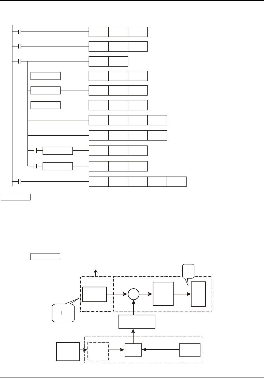
7 Application Instructions API 50-99
DVP-PLC APPLICATION MANUAL
7-129
The example program of the instruction delay:
M1002
MOV K10 D3
M0
TMR T0 D3
T0
RST T0
MOV K50 D2D1D0>
MOV K-50 D2D1D0<
MOV K0 D2D1D0=
ADD D2 D1 D1
M10
CMP D2 K0 M10
D0D1<
MOV D0 D1
M12
D0D1>
MOV D0 D1
M0
PID D1 D1116 D10 D5
Application 2 Speed control system and pressure control system work individually (use diagram of Example 2).
Purpose: After the speed control operates in open loop for a period of time, adding into it the pressure control system
(PID instruction) for close loop control.
Explanation: Since the speed and pressure control systems are not interrelated, we have to structure a open loop for
speed control first following by a close loop pressure control. If you fear that the control instruction of the
pressure control system changes too fast, you can consider to add the instruction delay illustrated in
Application 1 into the control. See the control diagram below.
D40
0
255
0rpm
3,000rpm
D30
D32 D1116
D31 +
+
M3
PID PV
MVD5
D1 SV
D0
D1110
Speed
instruction
M2 = On
Speed
converted
to
voltage
AC
motor
drive
MV converted to
accel/decel value
M0 = On
Pressure
instruction
Delay
(optional)
M1 = On
Pressure
meter
7 Application Instructions API 50-99
DVP-PLC APPLICATION MANUAL
7-130
Part of the example program:
M1
MOV K0 D5
M3
MOV D40 D30
M2
MOV K3000 D32K3000D32>
MOV K0 D32K0D32<
ADD D30 D31 D32
MOV D32 D1116
M1
PID D1 D1110 D10 D5
M1002
MOV K1000 D40
M0
MOV D0 D1
DIV D32 K11 D32
MOV K255 D32K255D32>
Application 3 Using auto-tuning on the parameter for the temperature control.
Purpose: Using auto-tuning to calculate the most suitable parameters for PID temperature control.
Explanation: You may not be familiar with the temperature environment for the first time, so you can use auto-tuning
(S3 + 4 = K3) for an initial adjustment. After this, PID instruction will become exclusively for temperature
control (S3 + 4 = K4). In this example, the control environment is an oven. See the example program
below.
M1002
M1013
M0
MOV K4000 D20
D200
K800 D10
TO K0 K2 K1
D11
K6FROM
K3 D204
RST M0
K400
MOV
MOV
K2
K0 K1
MOV
7 Application Instructions API 50-99
DVP-PLC APPLICATION MANUAL
7-131
M1
PID D10 D11 D0
GPWM D20 Y0
END
D200
D0
The experiment result of auto-tuning:
Auto tuning area
S3+4 = k3 PID control area
S3+4 = k4
Auto tuning area
S3+4 = k3 PID control area
S3+4 = k4
The experiment result of using the adjusted parameter exclusively for temperature control after auto-tuning:
From the figure above, we can see that the temperature control after auto-tuning is working fine and we use only
7 Application Instructions API 50-99
DVP-PLC APPLICATION MANUAL
7-132
approximately 20 minutes for the control. Next, we modify the target temperature from 80°C to 100°C and obtain the
result below.
From the result above, we can see that when the parameter is 100°C, we can still control the temperature without
spending too much time.
8 Application Instructions API 100-149
DVP-PLC Application Manual 8-1
API Mnemonic Operands Function
100
MODRD Read Modbus Data
Bit Devices Word Devices Program Steps Type
OP X Y M S K H KnX KnY KnM KnS T C D E F
S1 * * *
S2 * * *
n * * *
MODRD: 7 steps
PULSE 16-bit 32-bit
ES EX SS SA SX SC EH SV EH3
SV2 ES EX SS SA SX SC EH SV EH3
SV2 ES EX SS SA SX SC EH SV EH3
SV2
Operands:
S1: Address of communication device S2: Address of data to be read n: Length of read data
Explanations:
1. Range of S1: K0 ~ K254
2. Range of n: K1 ≤ n ≤ K6
3. See the specifications of each model for their range of use.
4. ES/EX/SS series MPU does not support E, F index register modification.
5. Flags: See API 80 RS for explanations on M1120 ~ M1131, M1140 ~ M1143
6. MODRD is a drive instruction exclusively for peripheral communication equipment in MODBUS ASCII mode
/RTU mode. The built-in RS-485 communication ports in Delta VFD drives (except for VFD-A series) are all
compatible with MODBUS communication format. MODRD can be used for controlling communication (read
data) of Delta drives.
7. If the address of S2 is illegal to the designed communication device, the device will respond with an error, PLC
will records the error code in D1130 and M1141 will be On.
8. The feedback (returned) data from the peripheral equipment will be stored in D1070 ~ D1085. After receiving
the feedback data is completed, PLC will auto-check if all data are correct. If there is an error, M1140 will be On.
9. In ASCII mode, due to that the feedback data are all in ASCII, PLC will convert the feedback data into numerals
and store them in D1050 ~ D1055. D1050 ~ D1055 will be invalid in RTU mode.
10. After M1140 or M1141 turn On, the program will send a correct datum to the peripheral equipment. If the
feedback datum is correct, M1140 and M1141 will be reset.
Program Example 1:
Communication between PLC and VFD-S series AC motor drives (ASCII Mode, M1143 = Off)
MOV D1120H87
M1002
SET M1120
MOV D1129K100
Set up communication protocol 9600, 8, E, 1
Retain communication protocol
Set up communication time-out: 100ms
SET M1122 Set up sending request
X1
8 Application Instructions API 100-149
DVP-PLC Application Manual
8-2
M1127
RST M1127
receiving
completed
Process of receiving data
Sending/receiving of data is completed. The flag is reset.
X0
MODRD K1 H2101 K6 Set up communication instruction device address 01
data address H2101 data length 6 words
The received data are stored in D1070 ~ D1085 in ASCII format.
PLC will automatically convert the data into numerals and store
them in D1050 ~ D1055.
PLC VFD-S, PLC sends: “01 03 2101 0006 D4”
VFD-S PLC , PLC receives: “01 03 0C 0100 1766 0000 0000 0136 0000 3B”
Registers for sent data (sending messages)
Register DATA Explanation
D1089 low ‘0’ 30 H ADR 1
D1089 high ‘1’ 31 H ADR 0
Address of AC motor
drive: ADR (1,0)
D1090 low ‘0’ 30 H CMD 1
D1090 high ‘3’ 33 H CMD 0
Instruction code: CMD
(1,0)
D1091 low ‘2’ 32 H
D1091 high ‘1’ 31 H
D1092 low ‘0’ 30 H
D1092 high ‘1’ 31 H
Starting data address
D1093 low ‘0’ 30 H
D1093 high ‘0’ 30 H
D1094 low ‘0’ 30 H
D1094 high ‘6’ 36 H
Number of data (counted by words)
D1095 low ‘D’ 44 H LRC CHK 1
D1095 high ‘4’ 34 H LRC CHK 0
Checksum: LRC CHK
(0,1)
Registers for received data (responding messages)
Register DATA Explanation
D1070 low ‘0’ 30 H ADR 1
D1070 high ‘1’ 31 H ADR 0
D1071 low ‘0’ 30 H CMD 1
D1071 high ‘3’ 33 H CMD 0
D1072 low ‘0’ 30 H
D1072 high ‘C’ 43 H Number of data (counted by byte)
D1073 low ‘0’ 30 H
D1073 high ‘1’ 31 H
D1074 low ‘0’ 30 H
D1074 high ‘0’ 30 H
Content of
address 2101 H
PLC automatically convert
ASCII codes to numerals
and store the numeral in
D1050 = 0100 H
D1075 low ‘1’ 31 H
D1075 high ‘7’ 37 H
D1076 low ‘6’ 36 H
D1076 high ‘6’ 36 H
Content of
address 2102 H
PLC automatically convert
ASCII codes to numerals
and store the numeral in
D1051 = 1766 H
D1077 low ‘0’ 30 H
D1077 high ‘0’ 30 H
D1078 low ‘0’ 30 H
D1078 high ‘0’ 30 H
Content of
address 2103 H
PLC automatically convert
ASCII codes to numerals
and store the numeral in
D1052 = 0000 H
D1079 low ‘0’ 30 H
D1079 high ‘0’ 30 H
D1080 low ‘0’ 30 H
D1080 high ‘0’ 30 H
Content of
address 2104 H
PLC automatically convert
ASCII codes to numerals
and store the numeral in
D1053 = 0000 H
D1081 low ‘0’ 30 H
D1081 high ‘1’ 31 H
D1082 low ‘3’ 33 H
D1082 high ‘6’ 36 H
Content of
address 2105 H
PLC automatically convert
ASCII codes to numerals
and store the numeral in
D1054 = 0136 H
8 Application Instructions API 100-149
DVP-PLC Application Manual 8-3
Register DATA Explanation
D1083 low ‘0’ 30 H
D1083 high ‘0’ 30 H
D1084 low ‘0’ 30 H
D1084 high ‘0’ 30 H
Content of
address 2106 H
PLC automatically convert
ASCII codes to numerals
and store the numeral in
D1055 = 0000 H
D1085 low ‘3’ 33 H LRC CHK 1
D1085 high ‘B’ 42 H LRC CHK 0
Program Example 2:
Communication between PLC and VFD-S series AC motor drives (RTU Mode, M1143 = On)
MOV D1120H87
M1002
SET M1120
MOV D1129K100
M1127
RST M1127
receiving
completed
Set up communication protocol 9600, 8, E, 1
Retain communication protocol
Set up communication time-out: 100ms
Process of receiving data
Sending/receiving of data is completed.
The flag is reset.
SET M1122 Set up as sending flag
X0
The received data in hex are stored in D1070 ~ D1085.
SET M1143 Set up as RTU mode
X0
MODRD K1 H2102
Set up communication instruction
device address 01 data address H2102
data length 2 words
K2
PLC VFD-S, PLC sends: 01 03 2102 0002 6F F7
VFD-S PLC, PLC receives: 01 03 04 1770 0000 FE 5C
Registers for sent data (sending messages)
Register DATA Explanation
D1089 low 01 H Address
D1090 low 03 H Function
D1091 low 21 H
D1092 low 02 H Starting data address
D1093 low 00 H
D1094 low 02 H Number of data (counted by words)
D1095 low 6F H CRC CHK Low
D1096 low F7 H CRC CHK High
Registers for received data (responding messages)
Register DATA Explanation
D1070 low 01 H Address
D1071 low 03 H Function
D1072 low 04 H Number of data (counted by bytes)
D1073 low 17 H
D1074 low 70 H Content of address 2102 H
D1075 low 00 H
D1076 low 00 H Content of address 2103 H
D1077 low FE H CRC CHK Low
D1078 low 5C H CRC CHK High
8 Application Instructions API 100-149
DVP-PLC Application Manual
8-4
Program Example 3:
1. In the communication between PLC and VFD-S series AC motor drive (ASCII Mode, M1143 = Off), retry when
communication time-out, data receiving error and sending address error occur.
2. When X0=On, PLC will read the data in VFFD-S data adress H2100 of device 01 and stores the data in ASCII
format in D1070 ~ D1085. PLC will automatically convert the data into numerals and stores them in D1050 ~
D1055.
3. M1129 will be On when communication time-out occurs. The program will trigger M1129 and send request to
M1122 for reading the data again.
4. M1140 will be On when data receiving error occurs. The program will trigger M1140 and send request to
M1122 for reading the data again.
5. M1141 will be On when sending address error occurs. The program will trigger M1141 and send request to
M1122 for reading the data again.
M1002
MOV H87 D1120
SET M1120
SET M1122
MOV K100 D1129
RST M1127
M1127
X0
MODRD K1 H2100 K 6
X0
M1129
M1140
M1141
RST M1129
Set up communication protocol to 9600, 8, E, 1
Set up communication instruction:
device address 01, data address
H2100
data length 6 words
Communication time-out Retry
sending address error Retry
receiving completed
handle received data
M1127
M1129
Retain communication protocol
Set up communication time-out: 100ms
Set up communication time-out: 100ms
Data receiving error Retry
Communication time-out. The flag is reset.
Sending/receiving of data is completed. The flag is reset.
The received data are stored in D1070~D1085 in ASCII
format. PLC will automatically convert the data into
numerals and store them in D1050~D1055.
Remarks:
1. The activation criteria placed before the three instructions, API 100 MODRD, API 105 RDST, and API 150
MODRW (Function Code H03), cannot use rising-edge contacts (LDP, ANDP ORP) and falling-edge contacts
(LDF, ANDF, ORF); otherwise, the data stores in the receiving registers will be incorrect.
2. M1127 for MODRD instruction stands for the response of data is completed. M1127 will only be On if the
responded data are correct. M1123 will be On no matter the responded data are correct or wrong.
3. There is no limitation on the times of using this instruction in the program, but only one instruction is allowed to
be executed at a time.

8 Application Instructions API 100-149
DVP-PLC Application Manual 8-5
API Mnemonic Operands Function
101
MODWR Write Modbus Data
Bit Devices Word Devices Program Steps Type
OP X Y M S K H KnX KnY KnM KnS T C D E F
S1 * * *
S2 * * *
n * * *
MODWR: 7 steps
PULSE 16-bit 32-bit
ES EX SS SA SX SC EH SV EH3
SV2 ES EX SS SA SX SC EH SV EH3
SV2 ES EX SS SA SX SC EH SV EH3
SV2
Operands:
S1: Address of communication device S2: Address of data to be read n: Data to be written
Explanations:
1. Range of S1: K0 ~ K254
2. See the specifications of each model for their range of use.
3. ES/EX/SS series MPU does not support E, F index register modification.
4. Flags: See API 80 RS for explanations on M1120 ~ M1131, M1140 ~ M1143
5. MODWR is a drive instruction exclusively for peripheral communication equipment in MODBUS ASCII
mode/RTU mode. The built-in RS-485 communication ports in Delta VFD drives (except for VFD-A series) are
all compatible with MODBUS communication format. MODRD can be used for controlling communication (write
data) of Delta drives.
6. If the address of S2 is illegal to the designed communication device, the device will respond with an error, PLC
will records the error code in D1130 and M1140 will be On. For example, if 8000H is illegal to VFD-S, M1141
will be On and D1130 = 2. For error codes, see the user manual of VFD-S.
7. The feedback (returned) data from the peripheral equipment will be stored in D1070 ~ D1076. After receiving
the feedback data is completed, PLC will auto-check if all data are correct. If there is an error, M1140 will be
On.
8. After M1140 or M1141 turn On, the program will send a correct datum to the peripheral equipment. If the
feedback datum is correct, M1140 and M1141 will be reset.
Program Example 1:
Communication between PLC and VFD-S series AC motor drives (ASCII Mode, M1143 = Off)
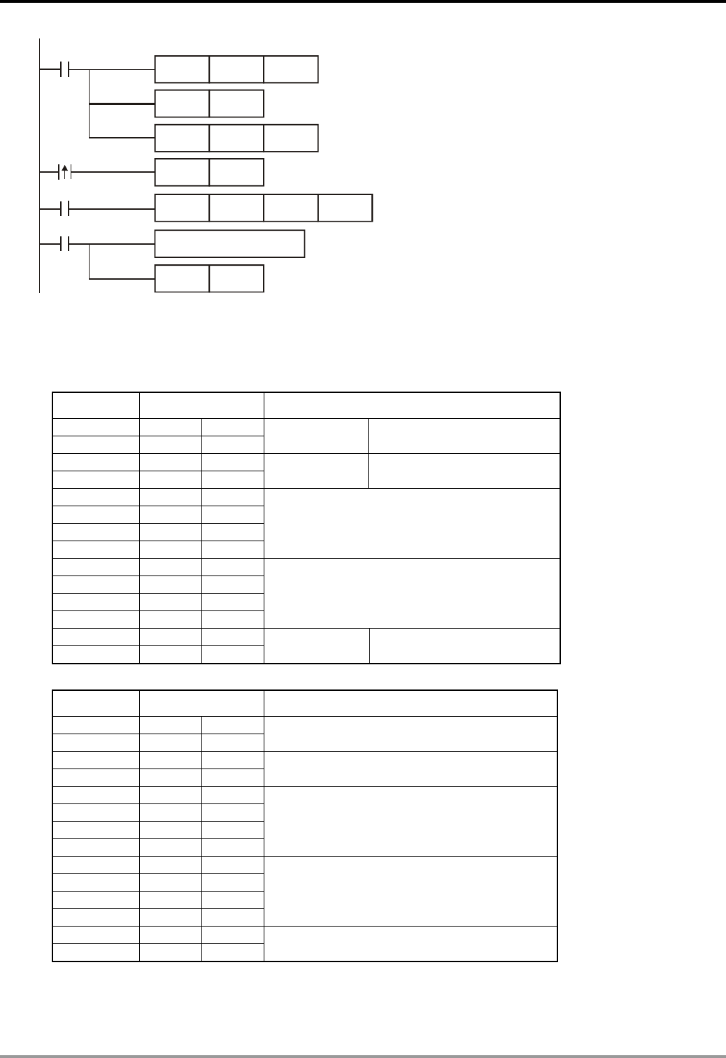
8 Application Instructions API 100-149
DVP-PLC Application Manual
8-6
MOV D1120H87
M1002
SET M1120
MOV D1129K100
M1127
RST M1127
receiving
completed
Set up communication protocol 9600, 8, E, 1
Retain communication protocol
Set up communication time-out: 100ms
Process of receiving data
SET M1122 Set up sending request
X1
X0
MODWR K1 H0100 H1770 Set up communication instruction device address 01
data address H0100 data H1770
The received data are stored in D1070 ~ D1085 in ASCII format.
PLC will automatically convert the data into numerals and store
them in D1050 ~ D1055.
Sending/receiving of data is completed. The flag is reset.
PLC VFD-B, PLC sends: “ 01 06 0100 1770 71 ”
VFD-B PLC, PLC receives: “ 01 06 0100 1770 71 ”
Registers for sent data (sending messages)
Register DATA Explanation
D1089 low ‘0’ 30 H ADR 1
D1089 high ‘1’ 31 H ADR 0
Address of AC motor drive:
ADR (1,0)
D1090 low ‘0’ 30 H CMD 1
D1090 high ‘6’ 36 H CMD 0 Instruction code: CMD (1,0)
D1091 low ‘0’ 30 H
D1091 high ‘1’ 31 H
D1092 low ‘0’ 30 H
D1092 high ‘0’ 30 H
Data address
D1093 low ‘1’ 31 H
D1093 high ‘7’ 37 H
D1094 low ‘7’ 37 H
D1094 high ‘0’ 30 H
Data contents
D1095 low ‘7’ 37 H LRC CHK 1
D1095 high ‘1’ 31 H LRC CHK 0
Error checksum: LRC CHK
(0,1)
PLC receiving data register (response messages)
Register DATA Explanation
D1070 low ‘0’ 30 H ADR 1
D1070 high ‘1’ 31 H ADR 0
D1071 low ‘0’ 30 H CMD 1
D1071 high ‘6’ 36 H CMD 0
D1072 low ‘0’ 30 H
D1072 high ‘1’ 31 H
D1073 low ‘0’ 30 H
D1073 high ‘0’ 30 H
Data address
D1074 low ‘1’ 31 H
D1074 high ‘7’ 37 H
D1075 low ‘7’ 37 H
D1075 high ‘0’ 30 H
Data content
D1076 low ‘7’ 37 H LRC CHK 1
D1076 high ‘1’ 31 H LRC CHK 0
Program Example 2:
Communication between PLC and VFD-S series AC motor drives (RTU Mode, M1143 = On)
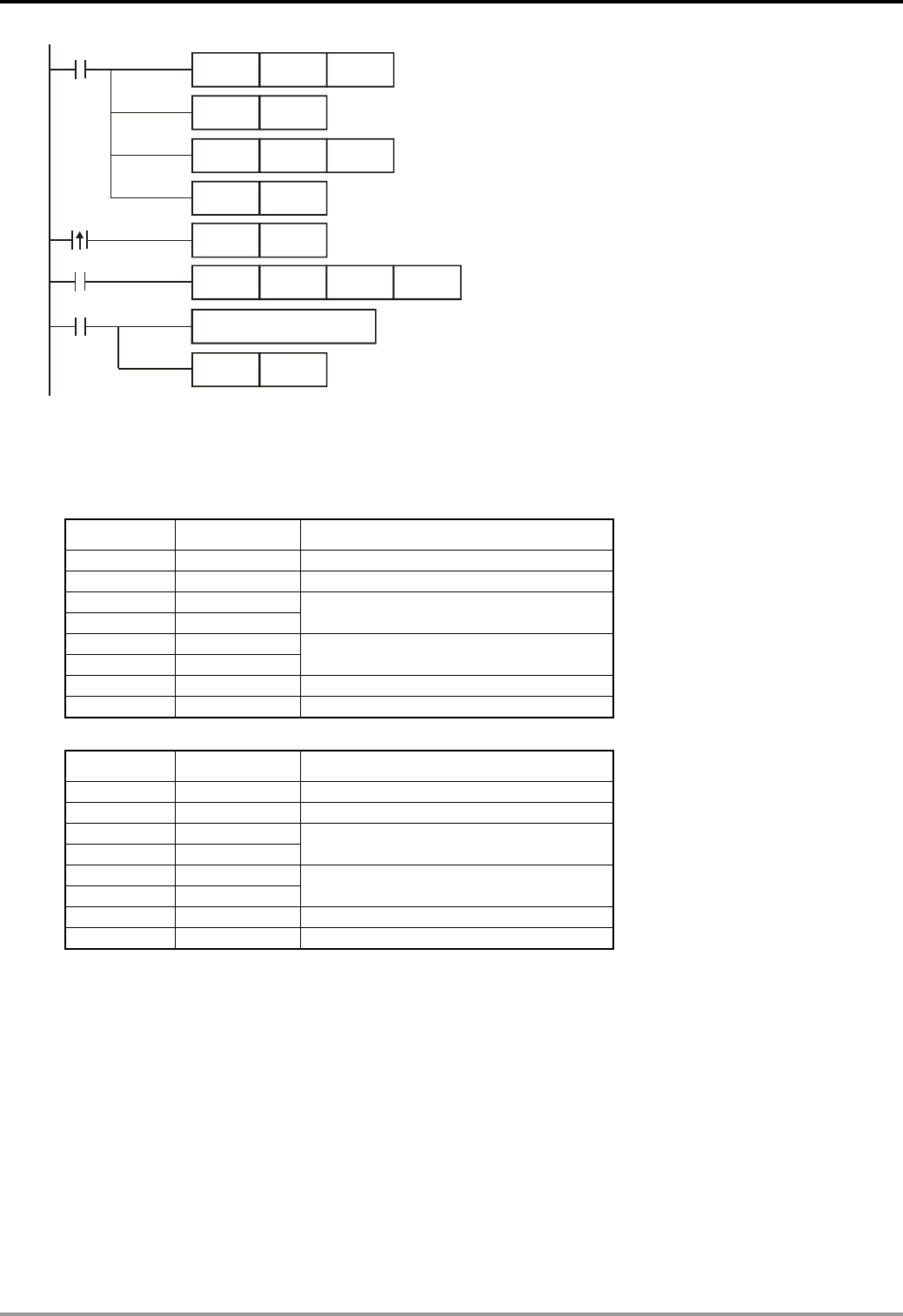
8 Application Instructions API 100-149
DVP-PLC Application Manual 8-7
MOV D1120H87
M1002
SET M1120
MOV D1129K100
M1127
RST M1127
receiving
completed
Set up communication protocol 9600, 8, E, 1
Retain communication protocol
Set up communication time-out: 100ms
Process of receiving data
Sending/receiving of data is completed.
The flag is reset.
SET M1122 Set up as sending flag
X0
The received data in hex are stored in D1070 ~ D1085.
SET M1143 Set up as RTU mode
X0
MODWR K1 H2000 Set up communication instruction device address 01
data address H2000 Write in data H12
H12
PLC VFD-S, PLC sends: 01 06 2000 0012 02 07
VFD-S PLC, PLC receives: 01 06 2000 0012 02 07
Registers for sent data (sending messages)
Register DATA Explanation
D1089 low 01 H Address
D1090 low 06 H Function
D1091 low 20 H
D1092 low 00 H Data address
D1093 low 00 H
D1094 low 12 H Data contents
D1095 low 02 H CRC CHK Low
D1096 low 07 H CRC CHK High
Registers for received data (responding messages)
Register DATA Explanation
D1070 low 01 H Address
D1071 low 06 H Function
D1072 low 20 H
D1073 low 00 H Data address
D1074 low 00 H
D1075 low 12 H Data contents
D1076 low 02 H CRC CHK Low
D1077 low 07 H CRC CHK High
Program Example 3:
1. In the communication between PLC and VFD-S series AC motor drive (ASCII Mode, M1143 = Off), retry when
communication time-out, data receiving error and sending address error occur.
2. When X0 = On, PLC will write H1770(K6000) into VFD-S data adress H0100 of device 01.
3. M1129 will be On when communication time-out occurs. The program will trigger M1129 and send request to
M1122 for writing the data again.
4. M1140 will be On when data receiving error occurs. The program will trigger M1140 and send request to M1122
for writing the data again.
5. M1141 will be On when sending address error occurs. The program will trigger M1141 and send request to
M1122 for writing the data again.
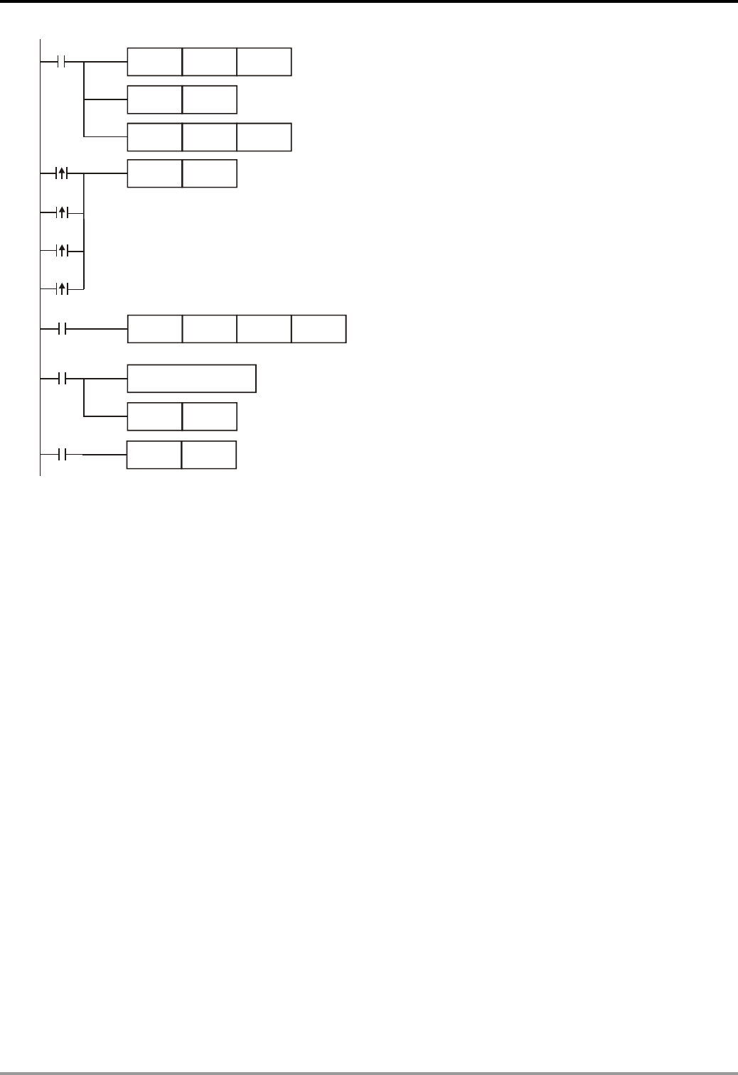
8 Application Instructions API 100-149
DVP-PLC Application Manual
8-8
M1002
MOV H87 D1120
SET M1120
SET M1122
MOV K100 D1129
RST M1127
M1127
X0
MODWR K1 H0100 H1770
X0
M1129
M1140
M1141
RST M1129
Set up communication protocol to 9600, 8, E, 1
Retain communication protocol
Set up communication time-out: 100ms
Set up communication instruction:
device address 01, data address H0100 data H1770
Communication time-out Retry
Data receiving error Retry
Sending address error Retry
receiving completed
handle received data The received data are stored in D1070 ~ D1085 in ASCII format.
Sending/receiving of data is completed. The flag is reset.
Communication time-out. The flag is reset.
M1127
M1129
Set up transmission request
Program Example 4:
1. In the communication between PLC and VFD-S series AC motor drive (ASCII Mode, M1143 = Off), retry when
communication time-out, data receiving error and sending address error occur. Times of retry = D0 (default = 3).
When communication Retry is successful, the user can return to controlling by triggering criteria.
2. When X0 = On, PLC will write H1770(K6000) into VFD-S data adress H0100 of device 01.
3. M1129 will be On when communication time-out occurs. The program will trigger M1129 and send request to
M1122 for writing the data again. Times of Retry = D0 (default = 3)
4. M1140 will be On when data receiving error occurs. The program will trigger M1140 and send request to M1122
for writing the data again. Times of Retry = D0 (default = 3)
5. M1141 will be On when sending address error occurs. The program will trigger M1141 and send request to
M1122 for writing the data again. Times of Retry = D0 (default = 3)
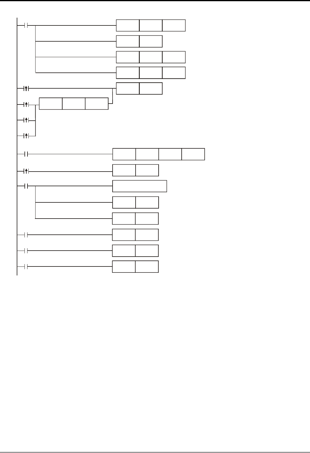
8 Application Instructions API 100-149
DVP-PLC Application Manual 8-9
M1002
MOV H87 D1120
SET M1120
SET M1122
MOV K100 D1129
RST M1127
M1127
X0
MODWR K1 H0100 H1770
X0
M1129
M1140
M1141
RST
M1129
MOV K3 D0
LD>= D0 D100
M1122
INC D100
RST
D100
M1129
M1140RST
M1140
M1141RST
M1141
Communication time-out Retry
Data receive error Retry
Sending address error Retry
Receiving completed
handle received data
Set up communication protocol
to 9600, 8, E, 1
Retain communication protocol
Set up communication
time-out: 100ms
Set up transmission request
Set up communication instruction:
device address 01, data address H0100
data H1770
The received data are stored in D1070 ~ D1085 in ASCII
format.
Sending/receiving of data is completed. The flag is reset.
Communication time-out. The flag is reset.
Remarks:
1. For the registers for flag settings, see explanations in API 80 RS.
2. The activation criteria placed before the two instructions, API 101 MODWR and API 150 MODRW (Function
Code H06, H10), cannot use rising-edge contacts (LDP, ANDP ORP) and falling-edge contacts (LDF, ANDF,
ORF) and have to enable sending request M1122 first.
3. M1127 for MODWR instruction stands for the response of data is completed. M1127 will only be On if the
responded data are correct. M1123 will be On no matter the responded data are correct or wrong.
4. There is no limitation on the times of using this instruction in the program, but only one instruction is allowed to
be executed at a time.
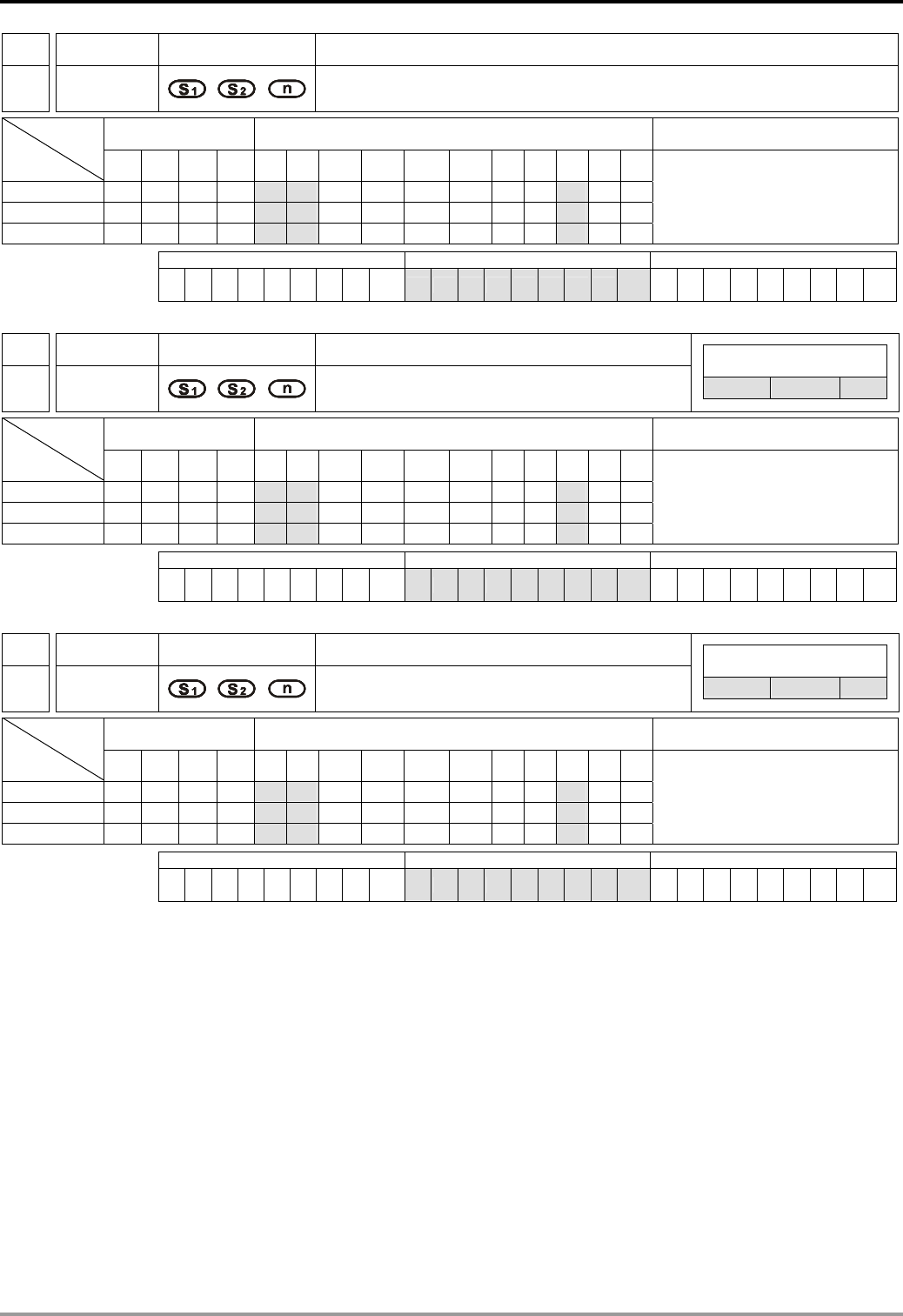
8 Application Instructions API 100-149
DVP-PLC Application Manual
8-10
API Mnemonic Operands Function
102
FWD Forward Running of VFD-A
Bit Devices Word Devices Program Steps Type
OP X Y M S K H KnX KnY KnM KnS T C D E F
S1 * * *
S2 * * *
n * * *
FWD: 7 steps
PULSE 16-bit 32-bit
ES EX SS SA SX SC EH SV EH3
SV2 ES EX SS SA SX SC EH SV EH3
SV2 ES EX SS SA SX SC EH SV EH3
SV2
API Mnemonic Operands Function
103
REV Reverse Running of VFD-A
Controllers
ES/EX/SS SA/SX/SC EH/SV
Bit Devices Word Devices Program Steps Type
OP X Y M S K H KnX KnY KnM KnS T C D E F
S1 * * *
S2 * * *
n * * *
REV: 7 steps
PULSE 16-bit 32-bit
ES EX SS SA SX SC EH SV EH3
SV2 ES EX SS SA SX SC EH SV EH3
SV2 ES EX SS SA SX SC EH SV EH3
SV2
API Mnemonic Operands Function
104
STOP Stop VFD-A
Controllers
ES/EX/SS SA/SX/SC EH/SV
Bit Devices Word Devices Program Steps Type
OP X Y M S K H KnX KnY KnM KnS T C D E F
S1 * * *
S2 * * *
n * * *
STOP: 7 steps
PULSE 16-bit 32-bit
ES EX SS SA SX SC EH SV EH3
SV2 ES EX SS SA SX SC EH SV EH3
SV2 ES EX SS SA SX SC EH SV EH3
SV2
Operands:
S1: Address of communication device S2: Rotation frequency of AC motor drive n: Target to be instructed
Explanations:
1. Range of S1: K0 ~ K31
2. Range of n: K1 or K2
3. See the specifications of each model for their range of use.
4. ES series MPU does not support E, F index register modification.
5. Flags: See API 80 RS for explanations on M1120 ~ M1131, M1140 ~ M1143
6. FWD/REV/STOP are handy instructions exclusively for Delta VFD-A/H series AC motor drive to perform
forward running/reverse running/stop. Be sure to set up communication time-out (D1129) when executing this
instruction.
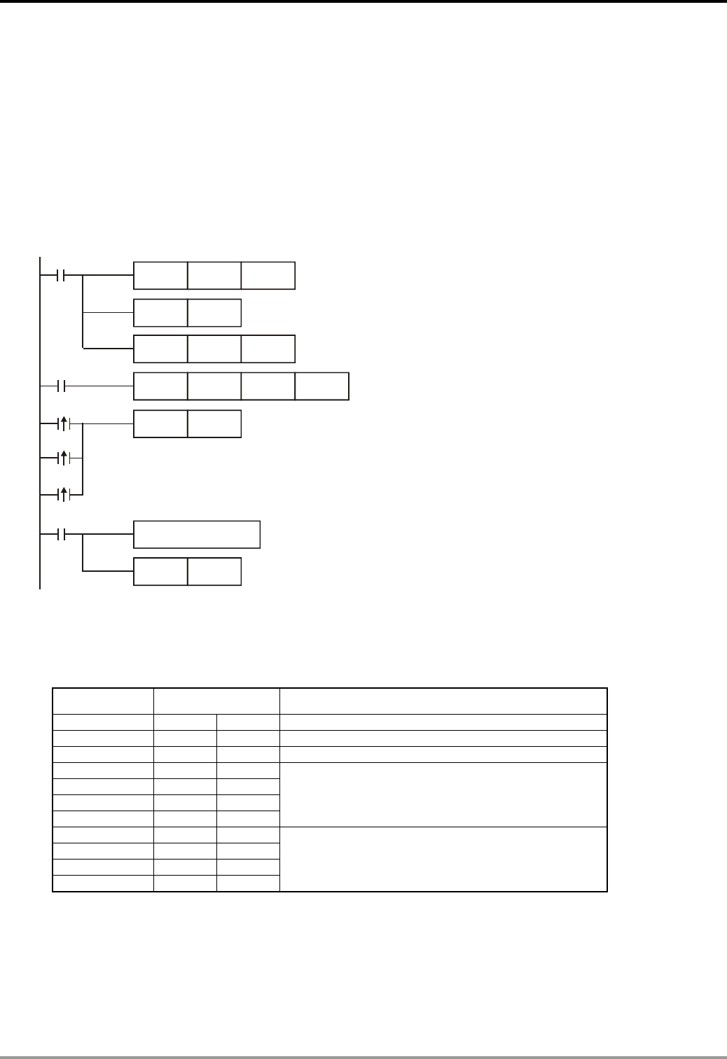
8 Application Instructions API 100-149
DVP-PLC Application Manual 8-11
7. S2 = operation frequency of AC motor drive. Set frequency in A-series AC motor drive: K0 ~ K4,000 (0.0Hz ~
400.0Hz). Set frequency in H-series: K0 ~ K1,500 (0Hz ~ 1,500Hz).
8. n = instructed target. n=1: AC motor drive at designated address. n=2: all connected AC motor drives.
9. The feedback (returned) data from the peripheral equipment will be stored in D1070 ~ D1080. After receiving
the feedback data is completed, PLC will auto-check if all data are correct. If there is an error, M1142 will be On.
When n = 2, PLC will not receive any data.
Program Example :
Communication between PLC and VFD-A series AC drives, retry for communication time-out and received data error.
M1002
MOV H0073 D1120
SET M1120
MOV K100 D1129
RST M1127
M1127
X0
FWD K0 K500 K1
SET M1122
M1129
M1142
X0
Communication time-out Retry
Data receive error Retry
handle received data
Receiving completed
Communication command setting:Device address: 0
Frequency: 500Hz K1: indicated AC motor drive
Set up communication protocol to 4800, 8, O, 1
Retain communication protocol
Set up communication time-out: 100ms
Set up transmission request
Sending/receiving of data is completed. The flag is reset.
The received data are stored in the low bit group of
D1070 ~ D1080 by ASCI format.
PLC VFD-A, PLC sends: “C ♥ ☺ 0001 0500 ”
VFD-A PLC, PLC sends: “C ♥ ♠ 0001 0500 ”
Registers for sent data (sending messages)
Register DATA Explanation
D1089 low ‘C’ 43 H Start word of instruction
D1090 low ‘♥’ 03 H Checksum
D1091 low ‘☺’ 01 H Instructed target
D1092 low ‘0’ 30 H
D1093 low ‘0’ 30 H
D1094 low ‘0’ 30 H
D1095 low ‘1’ 31 H
Communication address
D1096 low ‘0’ 30 H
D1097 low ‘5’ 35 H
D1098 low ‘0’ 30 H
D1099 low ‘0’ 30 H
Running instruction

8 Application Instructions API 100-149
DVP-PLC Application Manual
8-12
Registers for received data (responding messages)
Register DATA Explanation
D1070 low ‘C’ 43 H Start word of instruction
D1071 low ‘♥’ 03 H Checksum
D1072 low ‘♠’ 06 H Reply authorization (correct: 06H, incorrect: 07 H)
D1073 low ‘0’ 30 H
D1074 low ‘0’ 30 H
D1075 low ‘0’ 30 H
D1076 low ‘1’ 31 H
Communication address
D1077 low ‘0’ 30 H
D1078 low ‘5’ 35 H
D1079 low ‘0’ 30 H
D1080 low ‘0’ 30 H
Running instruction
Remarks:
There is no limitation on the times of using this instruction in the program, but only one instruction is allowed to be
executed at a time.
8 Application Instructions API 100-149
DVP-PLC Application Manual 8-13
API Mnemonic Operands Function
105
RDST Read VFD-A Status
Bit Devices Word Devices Program Steps Type
OP X Y M S K H KnX KnY KnM KnS T C D E F
S * * *
n * * *
RDST: 5 steps
PULSE 16-bit 32-bit
ES EX SS SA SX SC EH SV EH3
SV2 ES EX SS SA SX SC EH SV EH3
SV2 ES EX SS SA SX SC EH SV EH3
SV2
Operands:
S: Address of communicatino device n: Target to be instructed
Explanations:
1. Range of S: K0 ~ K31
2. Range of n: K0 ~ K3
3. See the specifications of each model for their range of use.
4. ES series MPU does not support E, F index register modification.
5. Flags: See API 80 RS for explanations on M1120 ~ M1131, M1140 ~ M1143
6. n: Instructed target (to be read) in AC motor drive
n=0, frequency
n=1, output frequency
n=2, output current
n=3, running instruction
7. Data sent back (feedback) from AC motor drive (11 bytes, see VFD-A user manual) are stored in the low bytes
of D1070 ~ D1080.
”Q, S, B, Uu, Nn, ABCD”
Feedbac
k
Explanation Data storage
Q Start word: ’Q’ (51H). D1070 low
S Checksum code: 03H. D0171 low
B Instruction authorization. correct: 06H, incorrect: 07H. D1072 low
U D1073 low
U
Communication address (address: 00~31). ”Uu” = (“00” ~ ”31”) indicated
in ASCII format. D1074 low
N D1075 low
N Instructed target (00 ~ 03).”Nn” = (“00 ~ 03”) indicated in ASCII format. D1076 low
A D1077 low
B D1078 low
C D1079 low
D
Instructed data. The content of ”ABCD” differs upon the instructed targets
(00 ~ 03). 00 ~ 03 indicate frequency, current and running mode
respectively. Please refer to the explanations below for details. D1080 low
Nn = “00” Frequency instruction = ABC.D (Hz)
Nn = “01” Output instruction = ABC.D (Hz)
Nn = “02” Output current = ABC.D (A)
PLC will automatically convert the ASCII characters of ”ABCD” into numerals and store the
numeral in D1050. For example, assume ”ABCD” = “0600”, PLC will convert ABCD into K0600
(0258 H) and store it in the special register D1050.
8 Application Instructions API 100-149
DVP-PLC Application Manual
8-14
Nn = “03” Running instruction
‘A’ = ‘0’ Stop, ‘5’ JOG (forward)
‘1’ Forward running ‘6’ JOG (reverse)
‘2’ Stop, ‘7’ JOG (reverse)
‘3’ Reverse running ‘8’ Abnormal
‘4’ JOG (forward),
ES series PLCs will convert the ASCII characters of ”A” into a numeral and store the
numeral in D1051. For example, assume ”A” = “3”, PLC will convert A into K3 and
store it in the special register D1051. SA/EH series PLCs will store the numeral in low
bytes of D1051.
‘B’ = b7 b6 b5 b4 Source of running instruction
0 0 0 0 Digital keypad
0 0 0 1 1st Step Speed
0 0 1 0 2nd Step Speed
0 0 1 1 3rd Step Speed
0 1 0 0 4th Step Speed
0 1 0 1 5th Step Speed
0 1 1 0 6th Step Speed
0 1 1 1 7th Step Speed
1 0 0 0 JOG frequency
1 0 0 1 Analog signal frequency instruction
1 0 1 0 RS-485 communication interface
1 0 1 1 Up/Down control
b3 = 0 No DC braking stop 1 DC braking stop
b2 = 0 No DC braking startup 1 DC braking startup
b1 = 0 Forward running 1 Reverse running
b0 = 0 Stop 1 Running
ES series PLCs will store ”B” in special auxiliary relay M1168 (b0) ~ M1175 (b7).
SA/EH series PLCs will store “B” (in hex) in the high bytes of special register D1051.
“CD” = “00” No abnormal record “10” OcA
“01” oc “11” Ocd
“02” ov “12” Ocn
“03” oH “13” GFF
“04” oL “14” Lv
“05” oL1 “15” Lv1
“06” EF “16” cF2
“07” cF1 “17” bb
“08” cF3 “18” oL2
“09” HPF “19”
ES/SA/EH series PLCs will convert the ASCII characters of ”CD” into a numerals and
store the numeral in D1052. For example, assume ”CD” = “16”, PLC will convert CD
into K16 and store it in the special register D1052.
Remarks:
1. The activation criteria placed before the three instructions, API 100 MODRD, API 105 RDST and API 150
MODRW (Function Code 03), cannot use rising-edge contacts (LDP, ANDP ORP) and falling-edge contacts
(LDF, ANDF, ORF); otherwise, the data stores in the receiving registers will be incorrect.
2. For the registers for flag settings, see explanations in API 80 RS.
3. There is no limitation on the times of using this instruction in the program, but only one instruction is allowed to
be executed at a time.

8 Application Instructions API 100-149
DVP-PLC Application Manual 8-15
API Mnemonic Operands Function
106
RSTEF Reset Abnormal VFD-A
Bit Devices Word Devices Program Steps Type
OP X Y M S K H KnX KnY KnM KnS T C D E F
S * * *
n * * *
RSTEF: 5 steps
PULSE 16-bit 32-bit
ES EX SS SA SX SC EH SV EH3
SV2 ES EX SS SA SX SC EH SV EH3
SV2 ES EX SS SA SX SC EH SV EH3
SV2
Operands:
S: Address of communication device n: Target to be instructed
Explanations:
1. Range of S: K0 ~ K31
2. Range of n: K1 or K2
3. See the specifications of each model for their range of use.
4. Flags: See API 80 RS for explanations on M1120 ~ M1131, M1140 ~ M1143
5. RSTEF is a handy communication instruction exclusively for Delta VFD-A series AC motor drives and is used
for reset when the AC motor drive operates abnormally.
6. n: instructed target. n=1: AC motor drive at assigned address. n=2: all connected AC motor drives.
7. The feedback (returned) data from the peripheral equipment will be stored in D1070 ~ D1089. If n = 2, there will
be no feedback data.
Remarks:
1. The activation criteria placed before the three instructions, API 100 MODRD, API 105 RDST and API 150
MODRW (Function Code 03), cannot use rising-edge contacts (LDP, ANDP ORP) and falling-edge contacts
(LDF, ANDF, ORF); otherwise, the data stores in the receiving registers will be incorrect.
2. For the registers for flag settings, see explanations in API 80 RS.
3. There is no limitation on the times of using this instruction in the program, but only one instruction is allowed to
be executed at a time.
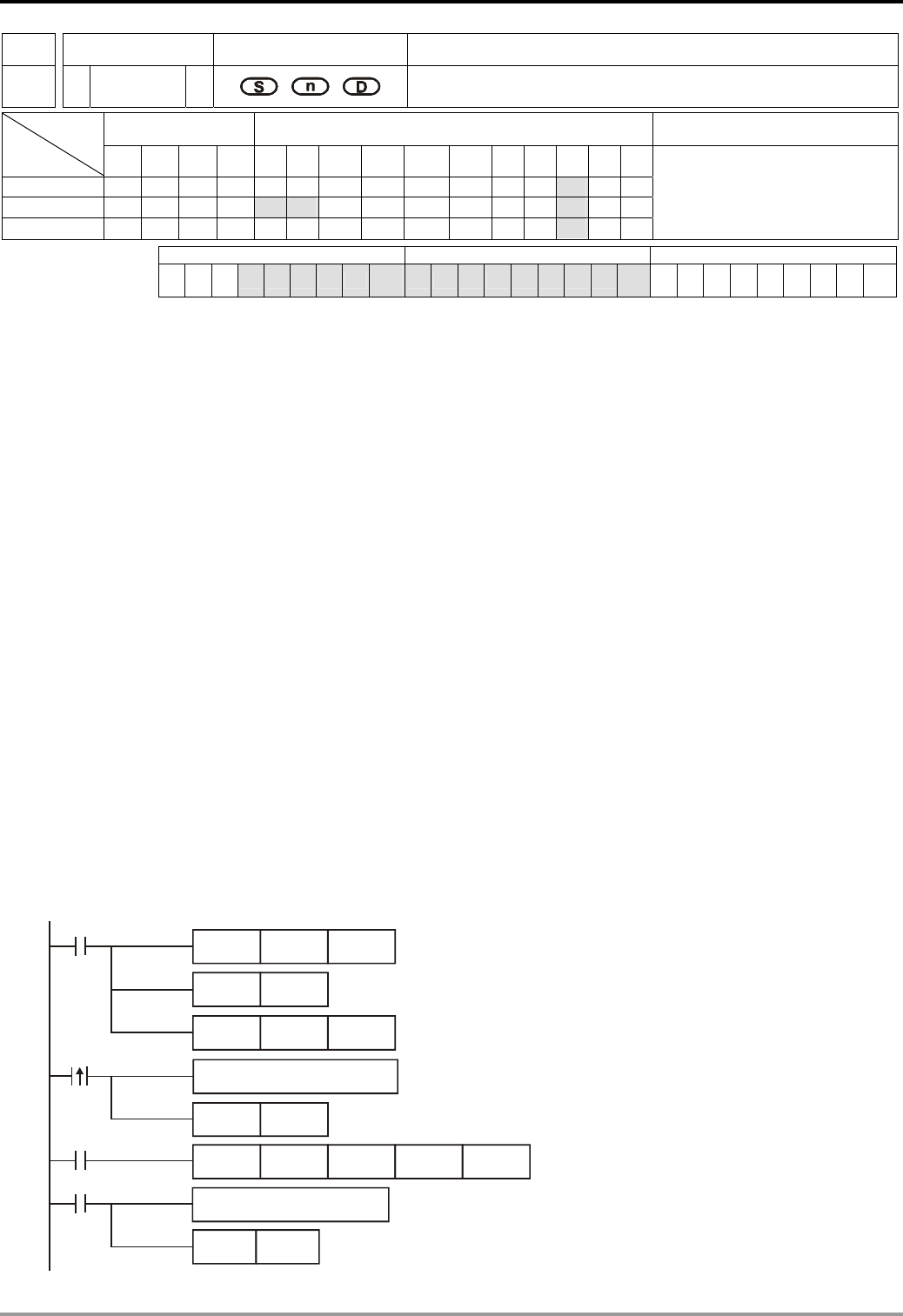
8 Application Instructions API 100-149
DVP-PLC Application Manual
8-16
API Mnemonic Operands Function
107
LRC P Checksum LRC Mode
Bit Devices Word Devices Program Steps Type
OP X Y M S K H KnX KnY KnM KnS T C D E F
S *
n * * *
D *
LRC, LRCP: 7 steps
PULSE 16-bit 32-bit
ES EX SS SA SX SC EH SV EH3
SV2 ES EX SS SA SX SC EH SV EH3
SV2 ES EX SS SA SX SC EH SV EH3
SV2
Operands:
S: Start operation device for ASCII mode checksum n: Number of calculated bits D: Start device for storing the
operation result LRC checksum: See remarks.
Explanations:
1. Range of n: K1 ~ K256
2. See the specifications of each model for their range of use.
3. Flag: M1161 (switching between 8/16 bit modes)
4. n has to be even. If n does not fall within its range, an operation error will occur, the instruction will not be
executed, M1067, M1068 = On and D1067 will record the error code H’0E1A.
5. In 16-bit conversion mode: When M1161 = Off, S divides its hex data area into higher 8 bits and lower 8 bits
and performs LRC checksum operation on each bit. The data will be sent to the higher 8 bits and lower 8 bits in
D. n = the number of calculated bits.
6. In 8-bit conversion mode: When M1161 = On, S divides its hex data area into higher 8 bits (invalid data) and
lower 8 bits and performs LRC checksum operation on each bit. The data will be sent to the lower 8 bits in D
and occupy 2 registers. n = the number of calculated bits. (All higher bits in D are “0”.)
Program Example:
When PLC communicates with VFD-S series AC motor drives (In ASCII mode, M1143 = Off), (In 8-bit mode, M1161 =
On), the sent data write in advance the 6 data read starting from H2101 of VFD-S.
MOV D1120H86
M1002
SET M1120
SET M1122
MOV D1129K100
X10
M1123
RST M1123
RS D100 K17 D120 K35
pulse
receiving completed
Process of receiving data
Set up communication protocol to 9600, 7, E, 1
Retain communication protocol
Set up communication time-out: 100ms
Set up transmission request
Sending/receiving of data is completed.
The flag is reset.
Write in sent data in advance
sending request pulse
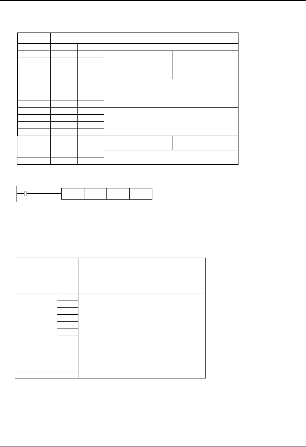
8 Application Instructions API 100-149
DVP-PLC Application Manual 8-17
PLC VFD-S, PLC sends: “: 01 03 2101 0006 D4 CR LF ”
Registers for sent data (sending messages)
Register DATA Explanation
D100 low ‘: ’ 3A H STX
D101 low ‘0’ 30 H ADR 1
D102 low ‘1’ 31 H ADR 0
Address of AC motor
drive: ADR (1,0)
D103 low ‘0’ 30 H CMD 1
D104 low ‘3’ 33 H CMD 0
Instruction code: CMD
(1,0)
D105 low ‘2’ 32 H
D106 low ‘1’ 31 H
D107 high ‘0’ 30 H
D108 low ‘1’ 31 H
Starting data address
D109 low ‘0’ 30 H
D110 low ‘0’ 30 H
D111 low ‘0’ 30 H
D112 low ‘6’ 36 H
Number of data (counted by words)
D113 low ‘D’ 44 H LRC CHK 1
D114 low ‘4’ 34 H LRC CHK 0
Error checksum: LRC
CHK (0,1)
D115 low CR A H
D116 low LF D H END
The error checksum LRC CHK (0,1) can be calculated by LRC instruction (in 8-bit mode, M1161 = On).
M1000
LRC D101 K12 D113
LRC checksum: 01 H + 03 H + 21 H + 01 H + 00 H + 06 H = 2C H. Obtain 2’s complement, D4H, and store ‘D’(44H) in
the lower 8 bits of D113 and ‘4’(34H) in the lower 8 bits of D114.
Remarks:
1. The format of ASCII mode with a communication datum
STX ‘: ’ Start word = ‘: ’ (3AH)
Address Hi ‘ 0 ’
Address Lo ‘ 1 ’
Communication:
8-bit address consists of 2 ASCll codes
Function Hi ‘ 0 ’
Function Lo ‘ 3 ’
Function code:
8-bit function consists of 2 ASCll codes
‘ 2 ’
‘ 1 ’
‘ 0 ’
‘ 2 ’
‘ 0 ’
‘ 0 ’
‘ 0 ’
DATA (n-1)
…….
DATA 0
‘ 2 ’
Data content:
n × 8-bit data consists of 2n ASCll
codes
LRC CHK Hi ‘ D ’
LRC CHK Lo ‘ 7 ’
LRC checksum:
8-bit checksum consists of 2 ASCll codes
END Hi CR
END Lo LF
End word:
END Hi = CR (0DH), END Lo = LF(0AH)
2. LRC checksum: 2’s complement of the summed up value of communication address and data. For example,
01 H + 03 H + 21 H + 02 H + 00 H + 02 H = 29 H. Obtain 2’s complement = D7H.
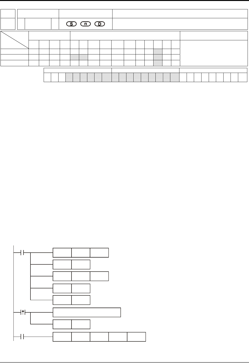
8 Application Instructions API 100-149
DVP-PLC Application Manual
8-18
API Mnemonic Operands Function
108
CRC P Checksum CRC Mode
Bit Devices Word Devices Program Steps Type
OP X Y M S K H KnX KnY KnM KnS T C D E F
S *
n * * *
D *
CRC, CRCP: 7 steps
PULSE 16-bit 32-bit
ES EX SS SA SX SC EH SV EH3
SV2 ES EX SS SA SX SC EH SV EH3
SV2 ES EX SS SA SX SC EH SV EH3
SV2
Operands:
S: Start operation device for RTU mode checksum n: Number of calculated bits D: Start device for storing the
operation result CRC checksum: See remarks.
Explanations:
1. Range of n: K1 ~ K256
2. Flags: M1161 (switching between 8/16-bit modes)
3. If n does not fall within its range, an operation error will occur, the instruction will not be executed, M1067,
M1068 = On and D1067 will record the error code H’0E1A.
4. In 16-bit conversion mode: When M1161 = Off, S divides its hex data area into higher 8 bits and lower 8 bits
and performs CRC checksum operation on each bit. The data will be sent to the higher 8 bits and lower 8 bits in
D. n = the number of calculated bits.
5. In 8-bit conversion mode: When M1161 = On, S divides its hex data area into higher 8 bits (invalid data) and
lower 8 bits and performs CRC checksum operation on each bit. The data will be sent to the lower 8 bits in D
and occupy 2 registers. n = the number of calculated bits. (All higher 8 bits in D are “0”.)
Program Example:
When PLC communicates with VFD-S series AC motor drives (In RTU mode, M1143 = On), (In 16-bit mode, M1161 =
On), the sent data write in advance H12 into H2000 of VFD-S.
M1002
X10
RS D100 K8 D120 K8
SET M1143
SET M1161
RTU Mode
8-bit Mode
Write transmitting data in advance
transmission
request
pulse
MOV D1120H87
SET M1120
MOV D1129K100
Set up communication protocol
to 9600, 8, E, 1
Retain communication protocol
Set up communication
time-out: 100ms
SET M1122 Set up transmission request
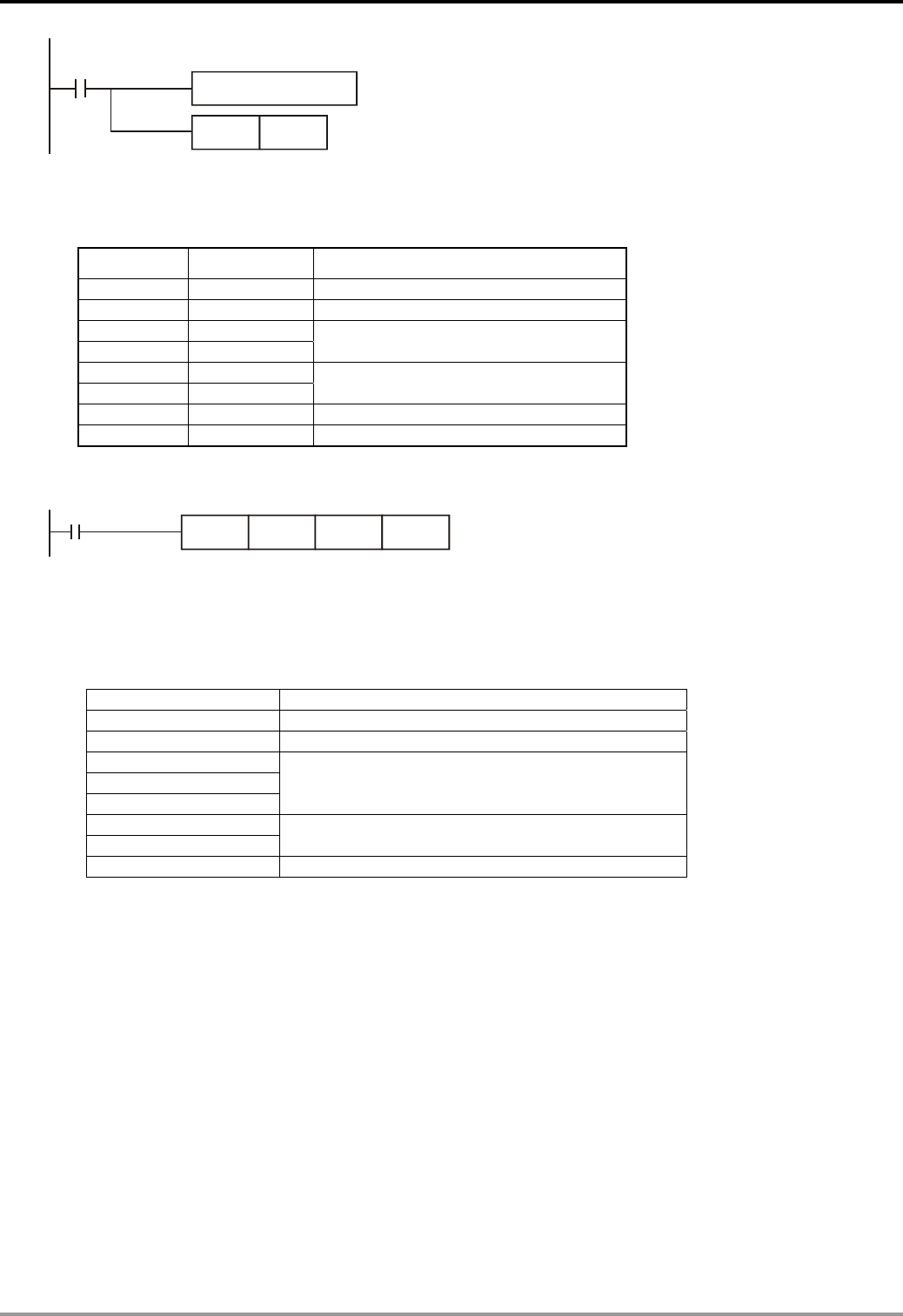
8 Application Instructions API 100-149
DVP-PLC Application Manual 8-19
M1123
RST M1123 Receiving completed and flag reset
receiving completed
Process received data
PLC VFD-S, PLC sends: 01 06 2000 0012 02 07
Registers for sent data (sending messages)
Register DATA Explanation
D100 low 01 H Address
D101 low 06 H Function
D102 low 20 H
D103 low 00 H Data address
D104 low 00 H
D105 low 12 H Data content
D106 low 02 H CRC CHK 0
D107 low 07 H CRC CHK 1
The error checksum CRC CHK (0,1) can be calculated by CRC instruction (in 8-bit mode, M1161 = On).
M1000
CRC D100 K6 D106
CRC checksum: 02 H is stored in the lower 8 bits of D106 and 07 H in the lower 8 bits of D107,
Remarks:
1. The format of RTU mode with a communication datum
START Time interval
Address Communication address: 8-bit binary
Function Function code: 8-bit binary
DATA (n-1)
…….
DATA 0
Data content:
n × 8-bit data
CRC CHK Low
CRC CHK High
CRC checksum:
16-bit CRC checksum consists of 2 8-bit binaries
END Time interval
2. CRC checksum starts from Address and ends at Data content.
The operation of CRC checksum:
Step 1: Make the 16-bit register (CRC register) = FFFFH
Step 2: Exclusive OR the first 8-bit byte message instruction and the low-bit 16-bit CRC register. Store the
result in CRC register.
Step 3: Shift the CRC register one bit to the right and fill 0 in the higher bit.
Step 4: Check the value that shifts to the right. If it is 0, store the new value from Step 3 into the CRC register,
otherwise, Exclusive OR A001H and the CRC register, and store the result in the CRC register.
Step 5: Repeat Step 3 ~ 4 and finish calculating the 8 bits.
Step 6: Repeat Steps 2 ~ 5 for obtaining the next 8-bit message instruction until all the message instructions
are calculated. In the end, the obtained CRC register value is the CRC checksum. Be aware that
CRC checksum should be placed in the checksum of the message instruction.
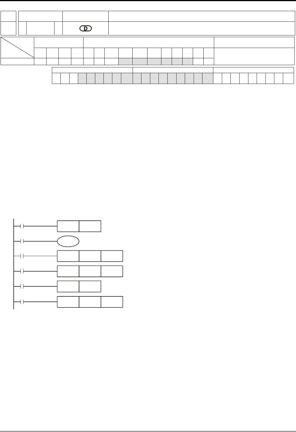
8 Application Instructions API 100-149
DVP-PLC Application Manual
8-20
API Mnemonic Operands Function
109
SWRD P Read Digital Switch
Bit Devices Word Devices Program Steps Type
OP X Y M S K H KnX KnY KnM KnS T C D E F
D * * * * * ***
SWRD, SWRDP: 3 steps
PULSE 16-bit 32-bit
ES EX SS SA SX SC EH SV EH3
SV2 ES EX SS SA SX SC EH SV EH3
SV2 ES EX SS SA SX SC EH SV EH3
SV2
Operands:
D: Device for storing the read value
Explanations:
1. See the specifications of each model for their range of use.
2. Flags: M1104 ~ M1111 (status of digital switch)
3. This instruction stores the value read from digital switch function card into D.
4. The read value is stored in the low byte in D. Every switch has a corresponding bit.
5. When there is no digital function card inserted, the error message C400 (hex) will appear in grammar check.
Program Example:
1. There are l 8 DIP switches on the digital switch function card. After the switches are read by SWRD instruction,
the status of each switch will correspond to M0 ~ M7.
M1000
SWRD K2M0
M0
Y0
M1
MOV K2M0 D0
M2
CNT C0 K10
M3
RST C0
M4
TMR T0 K100
2. The status of M0 ~ M7 can be executed by each contact instruction.
3. The execution of END instruction indicates that the process of input is completed. REF (I/O refresh) instruction
will be invalid.
4. When SWRD instruction uses the data in digital switch function card, it can read minimum 4 bits (K1Y*, K1M*
or K1S*).
Remarks:
When digital switch function card is inserted, the status of the 8 DIP switches will correspond to M1104 ~ M1111.
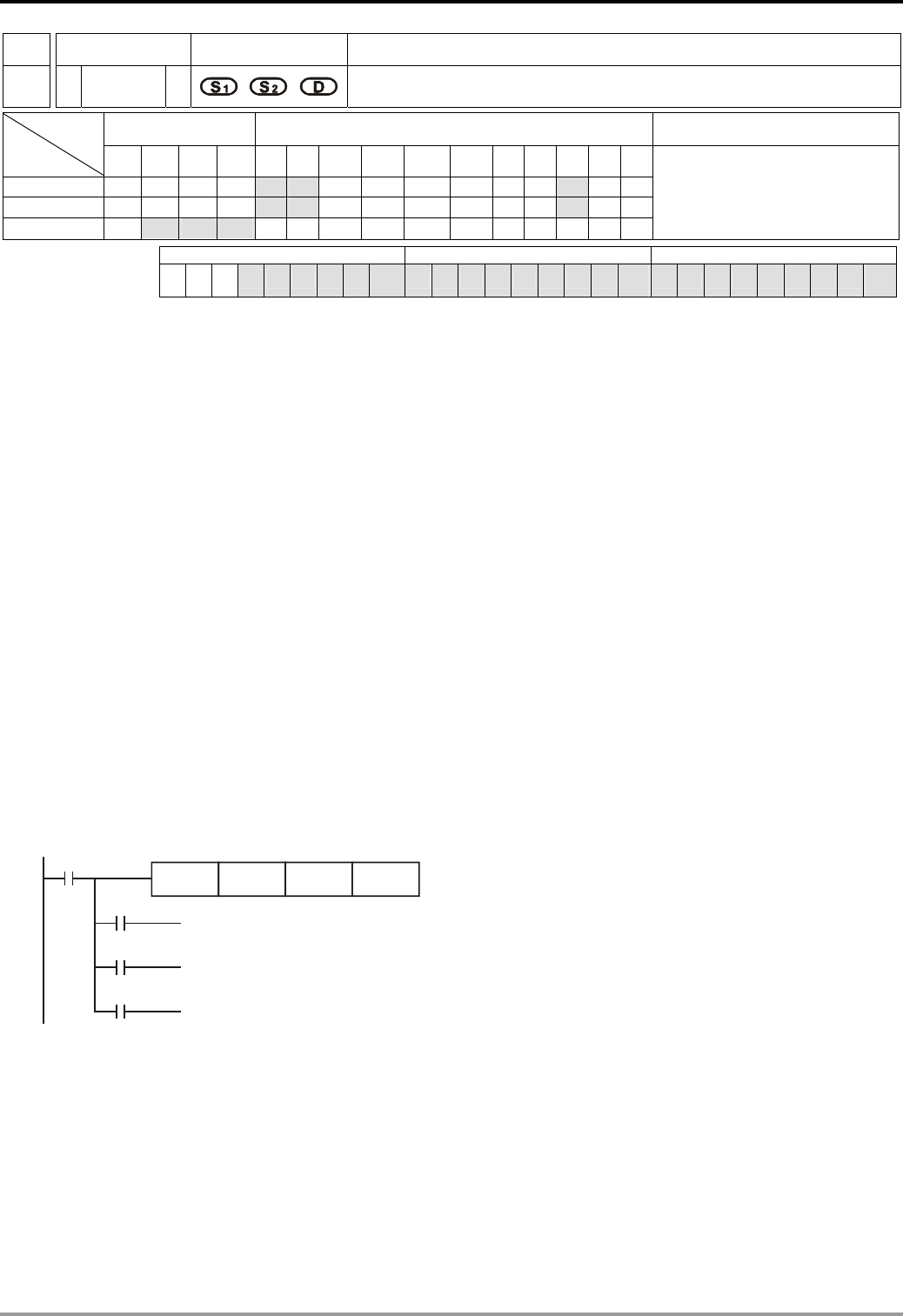
8 Application Instructions API 100-149
DVP-PLC Application Manual 8-21
API Mnemonic Operands Function
110
D ECMP P Floating Point Compare
Bit Devices Word Devices Program Steps Type
OP X Y M S K H KnX KnY KnM KnS T C D E F
S1 * * *
S2 * * *
D * * *
DECMP, DECMPP: 13 steps
PULSE 16-bit 32-bit
ES EX SS SA SX SC EH SV EH3
SV2 ES EX SS SA SX SC EH SV EH3
SV2 ES EX SS SA SX SC EH SV EH3
SV2
Operands:
S1: Binary floating point comparison value 1 S2: Binary floating point comparison value 2 D: Comparison
result
Explanations:
1. D occupies 3 consecutive devices.
2. See the specifications of each model for their range of use.
3. The binary floating point values S1 and S2 are compared with each other. The comparison result (>, =, <) is
stored in D.
4. If S1 or S2 is an designated constant K or H, the instruction will convert the constant into a binary floating point
value before the comparison.
Program Example:
1. Designated device M10 and M10 ~ M12 are automatically occupied.
2. When X0 = On. DECMP instruction will be executed and one of M10 ~ M12 will be On. When X0 = Off, DECMP
instruction will not be executed and M10 ~ M12 will remain their status before X0 = Off.
3. To obtain results , , ≠≧≦ , serial-parallel M10 ~ M12.
4. Use RST or ZRST instruction to clear the result.
X0
DECMP D0 D100 M10
M10
M11
M12
On when (D1,D0)>(D101,D100)
On when (D1,D0)=(D101,D100)
On when (D1,D0)<(D101,D100)
Remarks:
For floating point operations, see “5.3 Handling of Numeric Values”.
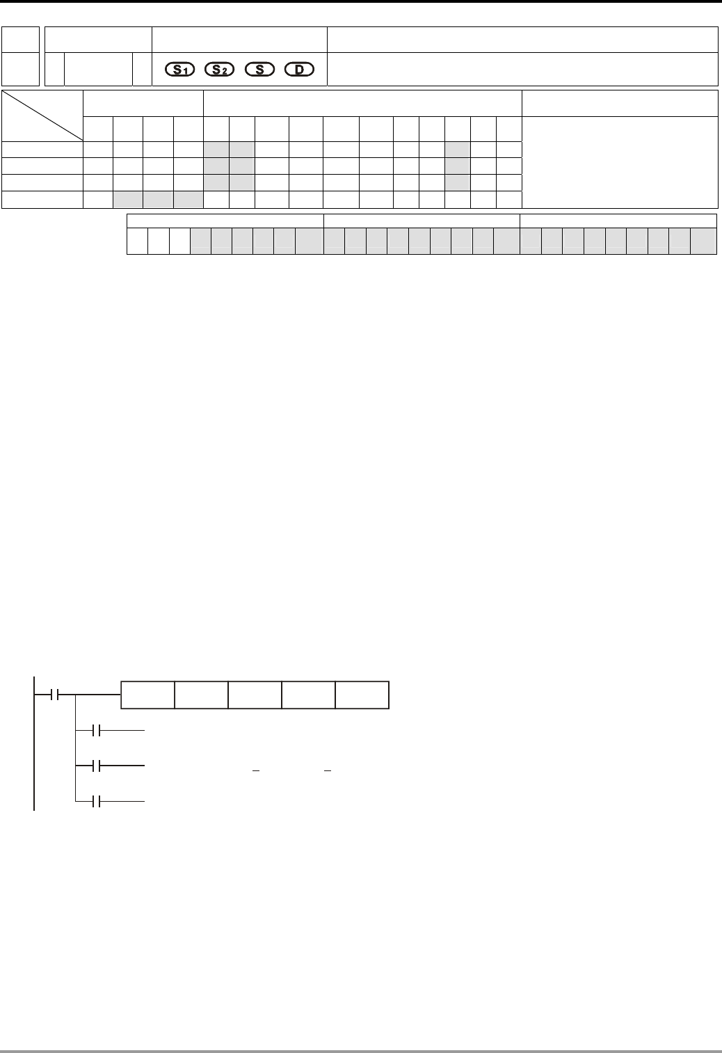
8 Application Instructions API 100-149
DVP-PLC Application Manual
8-22
API Mnemonic Operands Function
111
D EZCP P Floating Point Zone Compare
Bit Devices Word Devices Program Steps Type
OP X Y M S K H KnX KnY KnM KnS T C D E F
S1 * * *
S2 * * *
S * * *
D * * *
DEZCP, DEZCPP: 17 steps
PULSE 16-bit 32-bit
ES EX SS SA SX SC EH SV EH3
SV2 ES EX SS SA SX SC EH SV EH3
SV2 ES EX SS SA SX SC EH SV EH3
SV2
Operands:
S1: Lower bound of binary floating point S2: Upper bound of binary floating point S: Binary floating point
comparison result D: Comparison result
Explanations:
1. D occupied 3 consecutive devices.
2. S1 ≤ S2. See the specifications of each model for their range of use.
3. S is compared with S1 and S2 and the result (>, =, <) is stored in D.
4. If S1 or S2 is andesignated constant K or H, the instruction will convert the constant into a binary floating point
value before the comparison.
5. When S1 > S2, S1 will be used as upper/lower bound for the comparison.
Program Example:
1. Designated device M0 and M0 ~ M2 are automatically occupied.
2. When X0 = On. DEZCP instruction will be executed and one of M0 ~ M2 will be On. When X0 = Off, EZCP
instruction will not be executed and M0 ~ M2 will remain their status before X0 = Off.
3. Use RST or ZRST instruction to clear the result.
X0
DEZCP D0 D10 D20
M0
M1
M2
M0
On when (D1,D0) > (D21, D20)
On when (D1,D0) (D21, D20) (D11, D10)<<
On when (D21, D20) > (D11, D10)
Remarks:
For floating point operations, see “5.3 Handling of Numeric Values”.
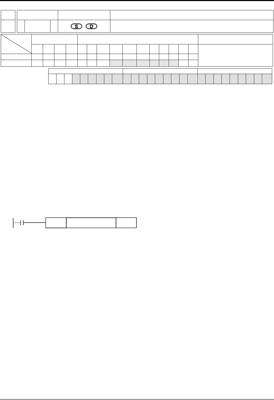
8 Application Instructions API 100-149
DVP-PLC Application Manual 8-23
API Mnemonic Operands Function
112
D MOVR P Move Floating Point Data
Bit Devices Word Devices Program Steps Type
OP X Y M S K H KnX KnY KnM KnS T C D E F
S
D * * * * * *
DMOVR, DMOVRP: 9 steps
PULSE 16-bit 32-bit
ES EX SS SA SX SC EH SV EH3
SV2 ES EX SS SA SX SC EH SV EH3
SV2 ES EX SS SA SX SC EH SV EH3
SV2
Operands:
S:Source floating point data D:Destination device
Explanations:
1. S can only be in floating point (FX.XX).
2. See the specifications of each model for their range of use.
3. This instruction is able to enter floating point values directly in S.
4. When the instruction is executed, the content in S is moved directly into D. When the instruction is not executed,
the content in D will not be modified.
Program Example:
1. User DMOVR instruction to move 32-bit floating point data.
2. When X0 = Off, the content in (D11、D10) remains unchanged. When X0 = On, the present value
F1.20000004768372 will be moved to data registers (D11, D10).
X0
DMOVR F1.20000004768372 D10
Remarks:
This instruction only supports ES V6.1, SA/SX_V1.1, SV_V1.2, EH_V1.2, EH2/SV/EH3/SV2_V1.0 and above
versions.
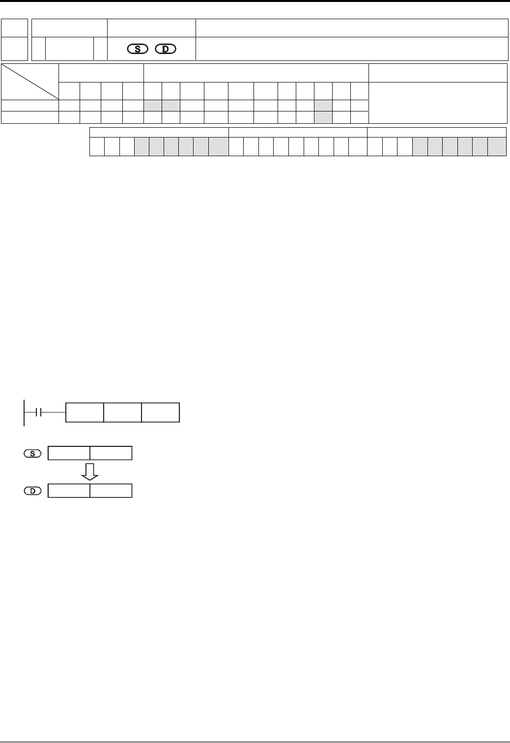
8 Application Instructions API 100-149
DVP-PLC Application Manual
8-24
API Mnemonic Operands Function
116
D RAD P Angle Radian
Bit Devices Word Devices Program Steps Type
OP X Y M S K H KnX KnY KnM KnS T C D E F
S * * *
D *
DRAD, DRADP: 9 steps
PULSE 16-bit 32-bit
ES EX SS SA SX SC EH SV EH3
SV2 ES EX SS SA SX SC EH SV EH3
SV2 ES EX SS SA SX SC EH SV EH3
SV2
Operands:
S: Source (angle) D: Result (radian)
Explanations:
1. See the specifications of each model for their range of use.
2. Flags: M1020 (zero flag); M1021 (borrow flag); M1022 (carry flag)
3. Radian = degree × (π/180)
4. If the absolute value of the result > maximum floating point available, the carry flag M1022 = On.
5. If the absolute value of the result < minimum floating point available, the borrow flag M1021 = On.
6. If the result = 0, the zero flag M1020 = On.
Program Example:
When X0 = On, designate the degree of binary floating point (D1, D0). Convert the angle into radian and store the
result in binary floating point in (D11, D10).
X0
DRAD D0 D10
D 1 D 0
D 11 D 10 binary floating point
Radian ( 180)
/
X
π
degree
Angle
binary floating point
Remarks:
For floating point operations, see “5.3 Handling of Numeric Values”.
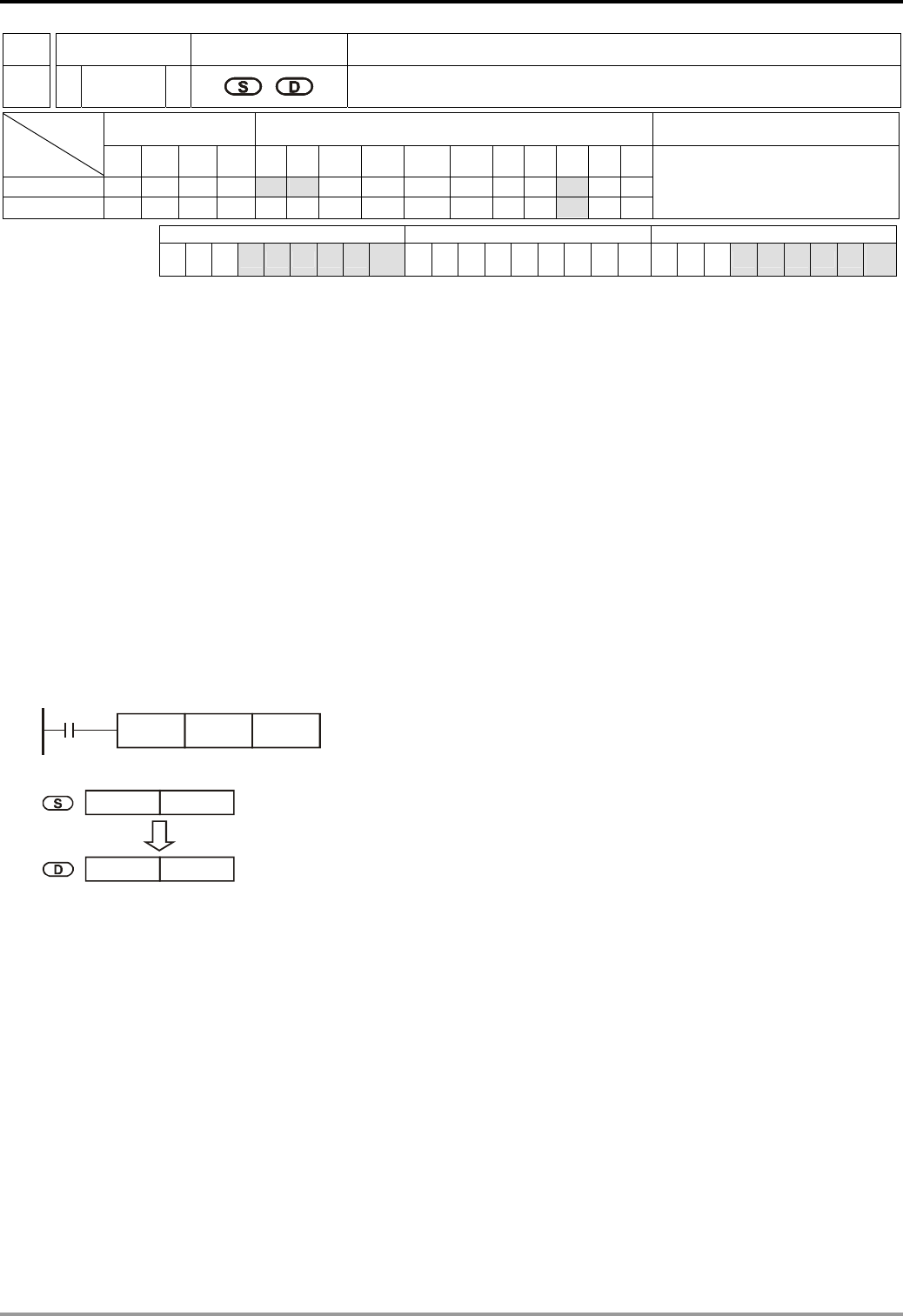
8 Application Instructions API 100-149
DVP-PLC Application Manual 8-25
API Mnemonic Operands Function
117
D DEG P Radian Angle
Bit Devices Word Devices Program Steps Type
OP X Y M S K H KnX KnY KnM KnS T C D E F
S * * *
D *
DDEG, DDEGP: 9 steps
PULSE 16-bit 32-bit
ES EX SS SA SX SC EH SV EH3
SV2 ES EX SS SA SX SC EH SV EH3
SV2 ES EX SS SA SX SC EH SV EH3
SV2
Operands:
S: Source (radian) D: Result (angle)
Explanations:
1. See the specifications of each model for their range of use.
2. Flags: M1020 (zero flag); M1021 (borrow flag); M1022 (carry flag)
3. Degree = radian × (180/π)
4. If the absolute value of the result > maximum floating point available, the carry flag M1022 = On.
5. If the absolute value of the result < minimum floating point available, the borrow flag M1021 = On.
6. If the result = 0, the zero flag M1020 = On.
Program Example:
When X0 = On, designate the angle of binary floating point (D1, D0). Convert the radian into angle and store the
result in binary floating point in (D11, D10).
X0
DDEG D0 D10
D 1 D 0
D 11 D 10 binary floating point
Angle (radian 180/ )
X
π
Radian
binary floating point
Remarks:
For floating point operations, see “5.3 Handling of Numeric Values”.
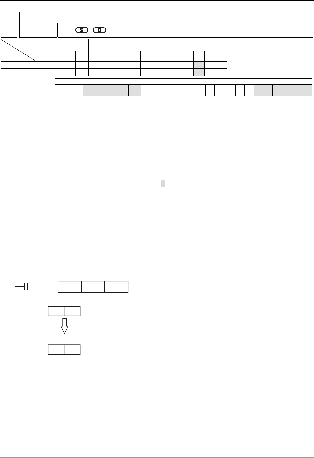
8 Application Instructions API 100-149
DVP-PLC Application Manual
8-26
API Mnemonic Operands Function
118
D EBCD P Float to Scientific Conversion
Bit Devices Word Devices Program Steps Type
OP X Y M S K H KnX KnY KnM KnS T C D E F
S *
D *
DEBCD, DEBCDP: 9 steps
PULSE 16-bit 32-bit
ES EX SS SA SX SC EH SV EH3
SV2 ES EX SS SA SX SC EH SV EH3
SV2 ES EX SS SA SX SC EH SV EH3
SV2
Operands:
S: Source D: Result
Explanations:
1. See the specifications of each model for their range of use.
2. Flags: M1020 (zero flag); M1021 (borrow flag); M1022 (carry flag)
3. This instruction converts binary floating point value in the register designated by S into decimal floating point
value and stores it in the register designated by D.
4. PLC conducts floating point operation in binary format. DEBCD instruction is exclusively for converting floating
points from binary to decimal.
5. If the absolute value of the result > maximum floating point available, the carry flag M1022 = On.
6. If the absolute value of the result < minimum floating point available, the borrow flag M1021 = On.
7. If the result = 0, the zero flag M1020 = On.
Program Example:
When X0 = On, the binary floating points in D1 and D0 will be converted into decimal floating points and stored in D3
and D2.
D0
DEBCD
X0
D2
D0D1
D2D3
Binary
Floating Point
32 bits for real number, 8 bits for exponent
1 bit for symbol bit
[D2] * 10
[D3]
Decimal
Floating Point
32 bits for real number, 8 bits for exponent
1 bit for symbol bit
Exponent Real number Exponent
Real number
Remarks:
For floating point operations, see “5.3 Handling of Numeric Values”.
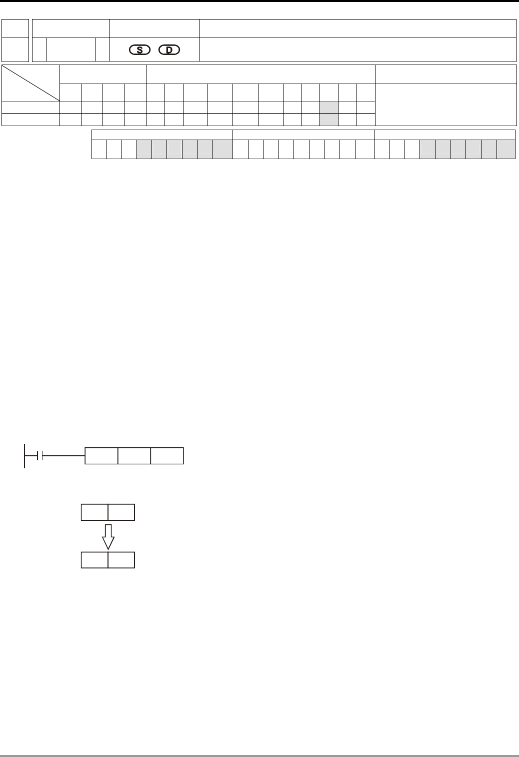
8 Application Instructions API 100-149
DVP-PLC Application Manual 8-27
API Mnemonic Operands Function
119
D EBIN P Scientific to Float Conversion
Bit Devices Word Devices Program Steps Type
OP X Y M S K H KnX KnY KnM KnS T C D E F
S *
D *
DEBIN, DEBINP: 9 steps
PULSE 16-bit 32-bit
ES EX SS SA SX SC EH SV EH3
SV2 ES EX SS SA SX SC EH SV EH3
SV2 ES EX SS SA SX SC EH SV EH3
SV2
Operands:
S: Source D: Result
Explanations:
1. See the specifications of each model for their range of use.
2. Flag: M1020 (zero flag)
3. This instruction converts decimal floating point value in the register designated by S into binary floating point
value and stores it in the register designated by D.
4. DEBIN instruction is exclusively for converting floating points from decimal to binary.
5. Range of decimal floating point real numbers: -9.999 ~ +9,999. Range of exponants: -41 ~ +35. Range of PLC
decimal floating points: ±1,175 × 10-41 ~ ±3,402 × 10+35.
6. If the result = 0, the zero flag M1020 = On.
Program Example 1:
When X1 = On, the decimal floating points in D1 and D0 will be converted into binary floating points and stored in D3
and D2.
D0DEBIN
X1
D2
D0D1
D2D3
[D1] * 10
[D0]
Decimal
Floating Point
Binary
Floating Point 23 bits for real number, 8 bits for exponent
1 bit for symbol bit
Real number
Exponent
Exponent
Real number
Program Example 2:
1. Use FLT instruction (API 149) to convert BIN integer into binary floating point before performing floating point
operation. The value to be converted must be BIN integer and use DEBIN instruction to convert the floating
point into a binary one.
2. When X0 = On, move K3,140 to D0 and K-3 to D1 to generate decimal floating point (3.14 = 3140 × 10-3).

8 Application Instructions API 100-149
DVP-PLC Application Manual
8-28
X0
MOVP K3140 D0
MOVP K-3 D1
DEBIN D0 D2
K3140 D0
K-3 D1
[D1]
[D0]
3140 10
X
-3
3140 10
X
-3
(D1, D0) (D3, D2)
Binary floating point
Remarks:
For floating point operations, see “5.3 Handling of Numeric Values”.
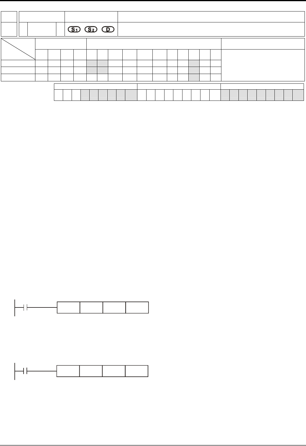
8 Application Instructions API 100-149
DVP-PLC Application Manual 8-29
API Mnemonic Operands Function
120
D EADD P Floating Point Addition
Bit Devices Word Devices Program Steps Type
OP X Y M S K H KnX KnY KnM KnS T C D E F
S1 * * *
S2 * * *
D *
DEADD, DEADDP: 13 steps
PULSE 16-bit 32-bit
ES EX SS SA SX SC EH SV EH3
SV2 ES EX SS SA SX SC EH SV EH3
SV2 ES EX SS SA SX SC EH SV EH3
SV2
Operands:
S1: Summand S2: Addend D: Sum
Explanations:
1. See the specifications of each model for their range of use.
2. Flags: M1020 (zero flag); M1021 (borrow flag); M1022 (carry flag)
3. S1 + S2 = D. The floating point value in the register designated by S1 and S2 are added up and the result is
stored in the register designated by D. The addition is conducted in binary floating point system.
4. If S1 or S2 is an designated constant K or H, the instruction will convert the constant into a binary floating point
value before the operation.
5. S1 and S2 can designate the same register. In this case, if the “continuous execution” instruction is in use,
during the period when the criteria contact in On, the register will be added once in every scan by pulse
execution instruction DEADDP.
6. If the absolute value of the result > maximum floating point available, the carry flag M1022 = On.
7. If the absolute value of the result < minimum floating point available, the borrow flag M1021 = On.
8. If the result = 0, the zero flag M1020 = On.
Program Example 1:
When X0 = On, binary floating point (D1, D0) + binary floating point (D3, D2) and the result is stored in (D11, D10).
D0DEADD
X0
D2 D10
Program Example 2:
When X2 = On, binary floating point (D11, D10) + K1234 (automatically converted into binary floating point) and the
result is stored in (D21, D20).
D10
DEADD
X2
K1234 D20
Remarks:
For floating point operations, see “5.3 Handling of Numeric Values”.
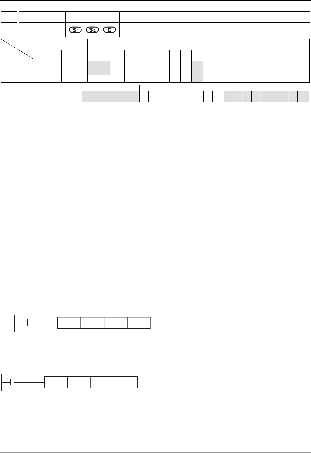
8 Application Instructions API 100-149
DVP-PLC Application Manual
8-30
API Mnemonic Operands Function
121
D ESUB P Floating Point Subtraction
Bit Devices Word Devices Program Steps Type
OP X Y M S K H KnX KnY KnM KnS T C D E F
S1 * * *
S2 * * *
D *
DESUB, DESUBP: 13 steps
PULSE 16-bit 32-bit
ES EX SS SA SX SC EH SV EH3
SV2 ES EX SS SA SX SC EH SV EH3
SV2 ES EX SS SA SX SC EH SV EH3
SV2
Operands:
S1: Minuend S2: Subtrahend D: Remainder
Explanations:
1. See the specifications of each model for their range of use.
2. Flags: M1020 (zero flag); M1021 (borrow flag); M1022 (carry flag)
3. S1 − S2 = D. The floating point value in the register designated by S2 is subtracted from the floating point value
in the register assigned by S1 and the result is stored in the register designated by D. The subtraction is
conducted in binary floating point system.
4. If S1 or S2 is an designated constant K or H, the instruction will convert the constant into a binary floating point
value before the operation.
5. S1 and S2 can designate the same register. In this case, if the “continuous execution” instruction is in use,
during the period when the criteria contact in On, the register will be subtracted once in every scan by pulse
execution instruction DESUBP.
6. If the absolute value of the result > maximum floating point available, the carry flag M1022 = On.
7. If the absolute value of the result < minimum floating point available, the borrow flag M1021 = On.
8. If the result = 0, the zero flag M1020 = On.
Program Example 1:
When X0 = On, binary floating point (D1, D0) - binary floating point (D3, D2) and the result is stored in (D11, D10).
D0
DESUB
X0
D2 D10
Program Example 2:
When X2 = On, K1234 (automatically converted into binary floating point) - binary floating point (D1, D0) and the
result is stored in (D11, D10).
K1234
DESUB
X2
D0 D10
Remarks:
For floating point operations, see “5.3 Handling of Numeric Values”.

8 Application Instructions API 100-149
DVP-PLC Application Manual 8-31
API Mnemonic Operands Function
122
D EMUL P Floating Point Multiplication
Bit Devices Word Devices Program Steps Type
OP X Y M S K H KnX KnY KnM KnS T C D E F
S1 * * *
S2 * * *
D *
DEMUL, DEMULP: 13 steps
PULSE 16-bit 32-bit
ES EX SS SA SX SC EH SV EH3
SV2 ES EX SS SA SX SC EH SV EH3
SV2 ES EX SS SA SX SC EH SV EH3
SV2
Operands:
S1: Multiplicand S2: Multiplicator D: Product
Explanations:
1. See the specifications of each model for their range of use.
2. Flags: M1020 (zero flag); M1021 (borrow flag); M1022 (carry flag)
3. S1 × S2 = D. The floating point value in the register assigned by S1 is multiplied with the floating point value in
the register designated by S2 and the result is stored in the register designated by D. The multiplication is
conducted in binary floating point system.
4. If S1 or S2 is an designated constant K or H, the instruction will convert the constant into a binary floating point
value before the operation.
5. S1 and S2 can designate the same register. In this case, if the “continuous execution” instruction is in use,
during the period when the criteria contact in On, the register will be multiplied once in every scan by pulse
execution instruction DEMULP.
6. If the absolute value of the result > maximum floating point available, the carry flag M1022 = On.
7. If the absolute value of the result < minimum floating point available, the borrow flag M1021 = On.
8. If the result = 0, the zero flag M1020 = On.
Program Example 1:
When X1 = On, binary floating point (D1, D0) × binary floating point (D11, D10) and the result is stored in (D21, D20).
D0DEMUL
X1
D10 D20
Program Example 2:
When X2 = On, K1234 (automatically converted into binary floating point) × binary floating point (D1, D0) and the
result is stored in (D11, D10).
K1234DEMUL
X2
D0 D10
Remarks:
For floating point operations, see “5.3 Handling of Numeric Values”.
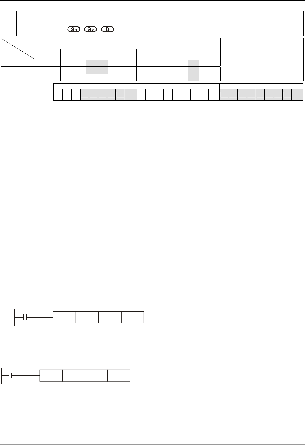
8 Application Instructions API 100-149
DVP-PLC Application Manual
8-32
API Mnemonic Operands Function
123
D EDIV P Floating Point Division
Bit Devices Word Devices Program Steps Type
OP X Y M S K H KnX KnY KnM KnS T C D E F
S1 * * *
S2 * * *
D *
DEDIV, DEDIVP: 13 steps
PULSE 16-bit 32-bit
ES EX SS SA SX SC EH SV EH3
SV2 ES EX SS SA SX SC EH SV EH3
SV2 ES EX SS SA SX SC EH SV EH3
SV2
Operands:
S1: Dividend S2: Divisor D: Quotient and remainder
Explanations:
1. See the specifications of each model for their range of use.
2. Flags: M1020 (zero flag); M1021 (borrow flag); M1022 (carry flag)
3. S1 ÷ S2 = D. The floating point value in the register designated by S1 is divided by the floating point value in the
register assigned by S2 and the result is stored in the register designated by D. The division is conducted in
binary floating point system.
4. If S1 or S2 is an designated constant K or H, the instruction will convert the constant into a binary floating point
value before the operation.
5. If S2 = 0, operation error will occur, the instruction will not be executed, M1067, M1068 = On and D1067 will
recorded the error code H’0E19.
6. If the absolute value of the result > maximum floating point available, the carry flag M1022 = On.
7. If the absolute value of the result < minimum floating point available, the borrow flag M1021 = On.
8. If the result = 0, the zero flag M1020 = On.
Program Example 1:
When X1 = On, binary floating point (D1, D0) ÷ binary floating point (D11, D10) and the quotient is stored in (D21,
D20).
D0
DEDIV
X1
D10 D20
Program Example 2:
When X2 = On, binary floating point (D1, D0) ÷ K1234 (automatically converted into binary floating point) and the
result is stored in (D11, D10).
X2
DEDIV D0 K1234 D10
Remarks:
For floating point operations, see “5.3 Handling of Numeric Values”.
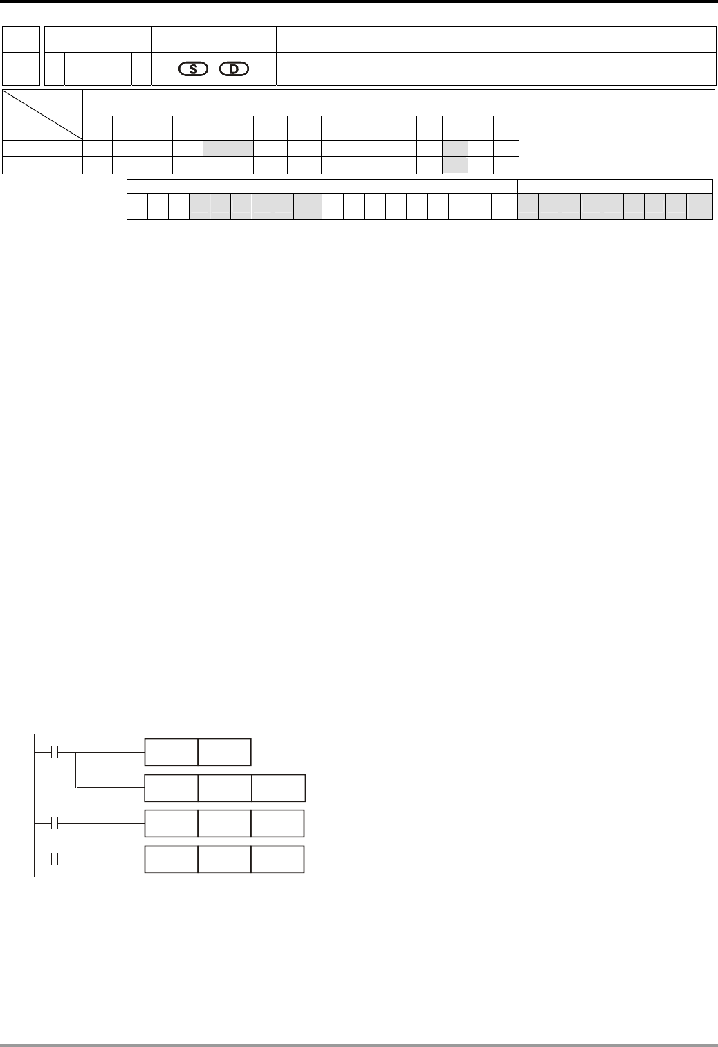
8 Application Instructions API 100-149
DVP-PLC Application Manual 8-33
API Mnemonic Operands Function
124
D EXP P Exponent of Binary Floating Point
Bit Devices Word Devices Program Steps Type
OP X Y M S K H KnX KnY KnM KnS T C D E F
S * * *
D *
DEXP, DEXPP: 13 steps
PULSE 16-bit 32-bit
ES EX SS SA SX SC EH SV EH3
SV2 ES EX SS SA SX SC EH SV EH3
SV2 ES EX SS SA SX SC EH SV EH3
SV2
Operands:
S: Device for operation source D: Device for operation result
Explanations:
1. See the specifications of each model for their range of use.
2. Flags: M1020 (zero flag); M1021 (borrow flag); M1022 (carry flag)
3. e = 2.71828 as the base and S as exponent for EXP operation: EXP[D +1, D]=[S +1, S]
4. Both positive and negative values are valid for S. When designating D registers, the data should be 32-bit and
the operation should be performed in floating point system. Therefore, S should be converted into a floating
point value.
5. The content in D = eS; e = 2.71828, S = designated source data
6. If the absolute value of the result > maximum floating point available, the carry flag M1022 = On.
7. If the absolute value of the result < minimum floating point available, the borrow flag M1021 = On.
8. If the result = 0, the zero flag M1020 = On.
Program Example:
1. When M0 = On, convert (D1, D0) into binary floating point and store it in register (D11, D10).
2. When M1= On, use (D11, D10) as the exponent for EXP operation and store the binary floating point result in
register (D21, D20).
3. When M2 = On, convert the binary floating point (D21, D20) into decimal floating point (D30 × 10[D31]) and store
it in register (D31, D30).
M0
RST M1081
M1
DEXP D10 D20
M2
DEBCD D20 D30
DFLT D0 D10
Remarks:
For floating point operations, see “5.3 Handling of Numeric Values”.

8 Application Instructions API 100-149
DVP-PLC Application Manual
8-34
API Mnemonic Operands Function
125
D LN P Natural Logarithm of Binary Floating Point
Bit Devices Word Devices Program Steps Type
OP X Y M S K H KnX KnY KnM KnS T C D E F
S * * *
D *
DLN, DLNP: 9 steps
PULSE 16-bit 32-bit
ES EX SS SA SX SC EH SV EH3
SV2 ES EX SS SA SX SC EH SV EH3
SV2 ES EX SS SA SX SC EH SV EH3
SV2
Operands:
S: Device for operation source D: Device for operation result
Explanations:
1. See the specifications of each model for their range of use.
2. Flags: M1020 (zero flag); M1021 (borrow flag); M1022 (carry flag)
3. This instruction performs natural logarithm “LN” operation by S: LN[S + 1, S]=[D + 1, D]
4. Only positive values are valid for S. When designating D registers, the data should be 32-bit and the operation
should be performed in floating point system. Therefore, S should be converted into a floating point value.
5. eD = S .The content in D = lnS; S = designated source data.
6. If the absolute value of the result > maximum floating point available, the carry flag M1022 = On.
7. If the absolute value of the result < minimum floating point available, the borrow flag M1021 = On.
8. If the result = 0, the zero flag M1020 = On.
Program Example:
1. When M0 = On, convert (D1, D0) into binary floating point and store it in register (D11, D10).
2. When M1= On, use register (D11, D10) as the real number for LN operation and store the binary floating point
result in register (D21, D20).
3. When M2 = On, convert the binary floating point (D21, D20) into decimal floating point (D30 × 10[D31]) and store
it in register (D31, D30).
M0
RST M1081
M1
DLN D10 D20
M2
DEBCD D20 D30
DFLT D0 D10
Remarks:
For floating point operations, see “5.3 Handling of Numeric Values”.
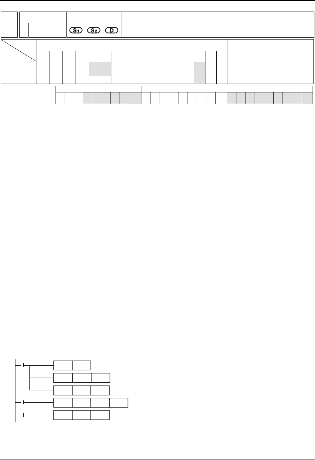
8 Application Instructions API 100-149
DVP-PLC Application Manual 8-35
API Mnemonic Operands Function
126
D LOG P Logarithm of Binary Floating Point
Bit Devices Word Devices Program Steps Type
OP X Y M S K H KnX KnY KnM KnS T C D E F
S1 * * *
S2 * * *
D *
DLOG, DLOGP: 13 steps
PULSE 16-bit 32-bit
ES EX SS SA SX SC EH SV EH3
SV2 ES EX SS SA SX SC EH SV EH3
SV2 ES EX SS SA SX SC EH SV EH3
SV2
Operands:
S1: Device for base S2: Device for operation source D: Device for operation result
Explanations:
1. See the specifications of each model for their range of use.
2. Flags: M1020 (zero flag); M1021 (borrow flag); M1022 (carry flag)
3. This instruction performs “log” operation of the content in S1 and S2 and stores the result in D.
4. Only positives are valid for the content in S1 and S2. When designating D registers, the data should be 32-bit
and the operation should be performed in floating point system. Therefore, S1 and S2 should be converted into
floating point values.
5. S1D = S2, D = ? LogS1S2 = D
Example: Assume S1 = 5, S2 = 125, D = log5
125 = ?
S1D = S2 5D = 125 D = log5
125 = 3
6. If the absolute value of the result > maximum floating point available, the carry flag M1022 = On.
7. If the absolute value of the result < minimum floating point available, the borrow flag M1021 = On.
8. If the result = 0, the zero flag M1020 = On.
Program Example:
1. When M0 = On, convert (D1, D0) and (D3, D2) into binary floating points and store them in the 32-bit registers
(D11, D10) and (D13, D12).
2. When M1= On, perform log operation on the binary floting points in 32-bit registers (D11, D10) and (D13, D12)
and store the result in the 32-bit register (D21, D20).
3. When M2 = On, convert the binary floating point (D21, D20) into decimal floating point (D30 × 10[D31]) and store
it in register (D31, D30).
M0
RST M1081
M1
D10 D12
M2
DEBCD D20 D30
D2 D12
D20
DFLT
DFLT
DLOG
D0 D10
Remarks:
For floating point operations, see “5.3 Handling of Numeric Values”.
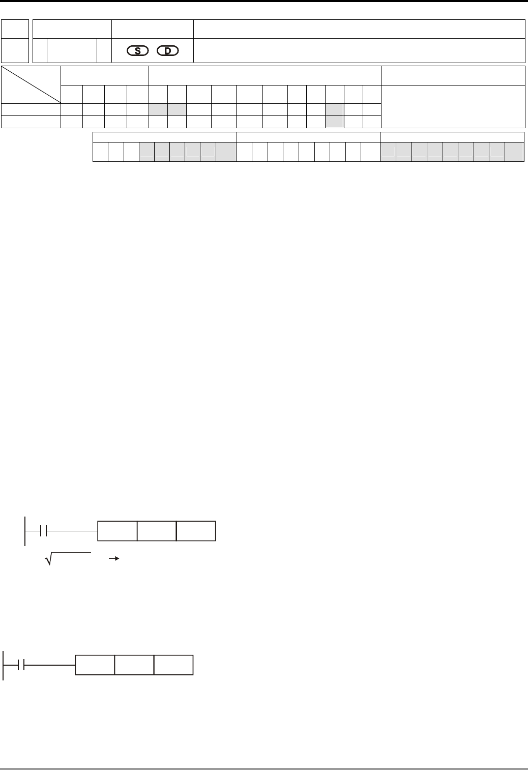
8 Application Instructions API 100-149
DVP-PLC Application Manual
8-36
API Mnemonic Operands Function
127
D ESQR P Floating Point Square Root
Bit Devices Word Devices Program Steps Type
OP X Y M S K H KnX KnY KnM KnS T C D E F
S * * *
D *
DESQR, DESQRP: 9 steps
PULSE 16-bit 32-bit
ES EX SS SA SX SC EH SV EH3
SV2 ES EX SS SA SX SC EH SV EH3
SV2 ES EX SS SA SX SC EH SV EH3
SV2
Operands:
S: Source device D: Operation result
Explanations:
1. Range of S: ≥ 0
2. See the specifications of each model for their range of use.
3. Flags: M1020 (zero flag); M1067 (operation error)
4. This instruction performs a square root operation on the content in the register designated by S and stores the
result in the register designated by D. The square root operation is performed in floating point system.
5. If S is an designated constant K or H, the instruction will convert the constant into a binary floating point value
before the operation.
6. If the result of the operation = 0, the zero flag M1020 = On.
7. S can only be a positive value. Performing any square root operation on a negative value will result in an
“operation error” and this instruction will not be executed. M1067 and M1068 will be On and D1067 will record
the error code H’0E1B.
Program Example 1:
When M0 = On, calculate the square root of the binary floating point (D1, D0) and store the result in register (D11,
D10).
D0
DESQR
X0
D10
(D1, D0) (D11 D10),
binary floating point binary floating point
Program Example 2:
When M2 = On, calculate the square root of K1,234 (automatically converted into binary floating point) and store the
result in register (D11, D10).
K1234DESQR
X2
D10
Remarks:
For floating point operations, see “5.3 Handling of Numeric Values”.
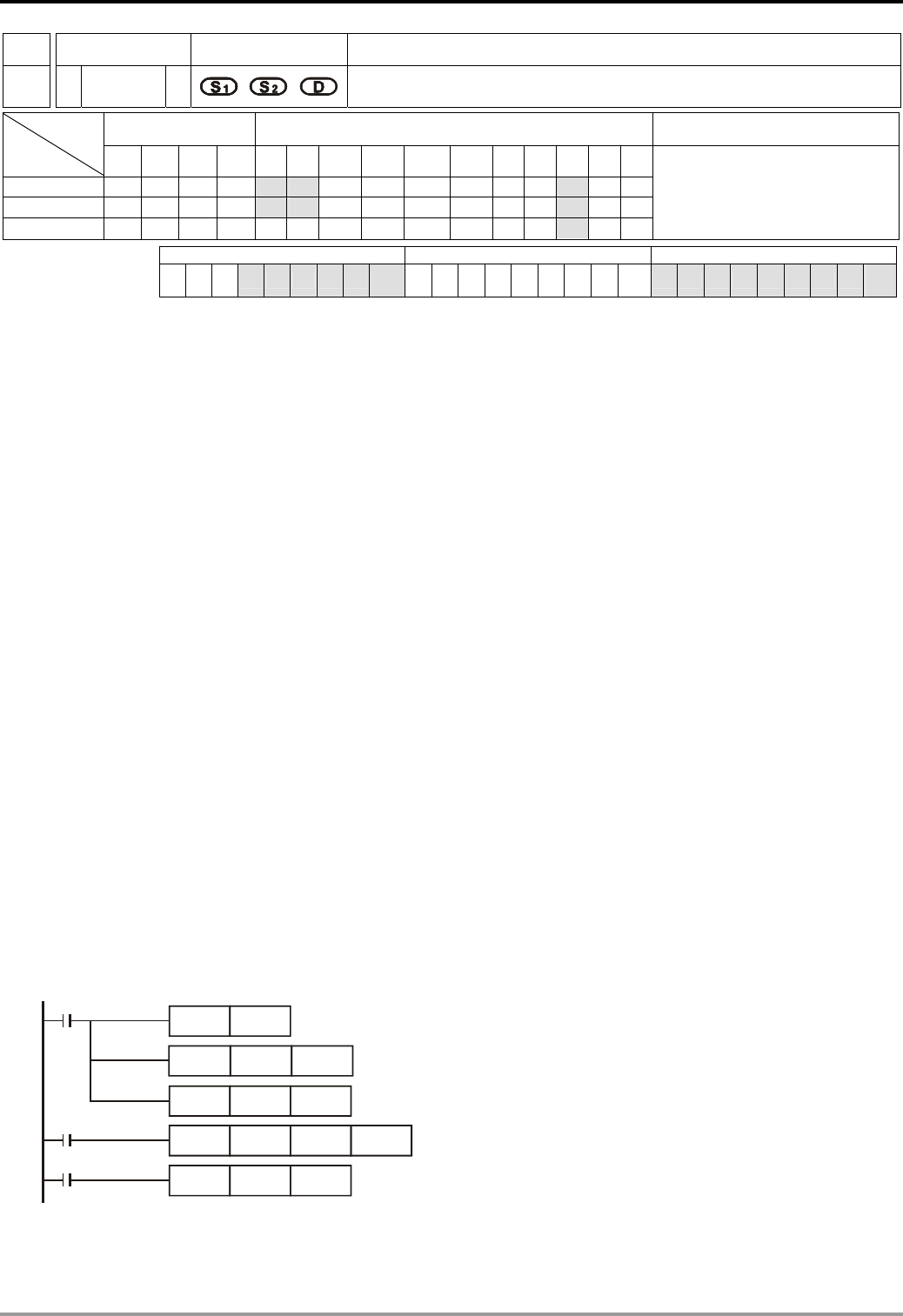
8 Application Instructions API 100-149
DVP-PLC Application Manual 8-37
API Mnemonic Operands Function
128
D POW P Floating Point Power Operation
Bit Devices Word Devices Program Steps Type
OP X Y M S K H KnX KnY KnM KnS T C D E F
S1 * * *
S2 * * *
D *
DPOW, DPOWP: 13 steps
PULSE 16-bit 32-bit
ES EX SS SA SX SC EH SV EH3
SV2 ES EX SS SA SX SC EH SV EH3
SV2 ES EX SS SA SX SC EH SV EH3
SV2
Operands:
S1: Device for base. S2: Device for exponent. D: Device for operation result
Explanations:
1. See the specifications of each model for their range of use.
2. This instruction performs power multiplication of binary floating point S1 and S2 and stores the result in D.
D = POW[S1 + 1, S1]^[S2 + 1, S2]
3. Only positives are valid for the content in S1. Both positives and negatives are valid for the content in S2. When
designating D registers, the data should be 32-bit and the operation should be performed in floating point
system. Therefore, S1 and S2 should be converted into floating point values.
Example: When S1S2 = D, D = ?
Assume S1 = 5, S2 = 3, D = 53 =125
4. If the absolute value of the result > maximum floating point available, the carry flag M1022 = On.
5. If the absolute value of the result < minimum floating point available, the borrow flag M1021 = On.
6. If the result = 0, the zero flag M1020 = On.
Program Example:
1. When M0 = On, convert (D1, D0) and (D3, D2) into binary floating points and store them in the 32-bit registers
(D11, D10) and (D13, D12).
2. When M1= On, perform POW operation on the binary floting points in 32-bit registers (D11, D10) and (D13,
D12) and store the result in the 32-bit register (D21, D20).
3. When M2 = On, convert the binary floating point (D21, D20) into decimal floating point (D30 × 10[D31]) and store
it in register (D31, D30).
M0
RST M1081
M1
D10 D12
M2
DEBCD D20 D30
D2 D12
D20
DFLT
DFLT
DPOW
D0 D10
Remarks:
For floating point operations, see “5.3 Handling of Numeric Values”.
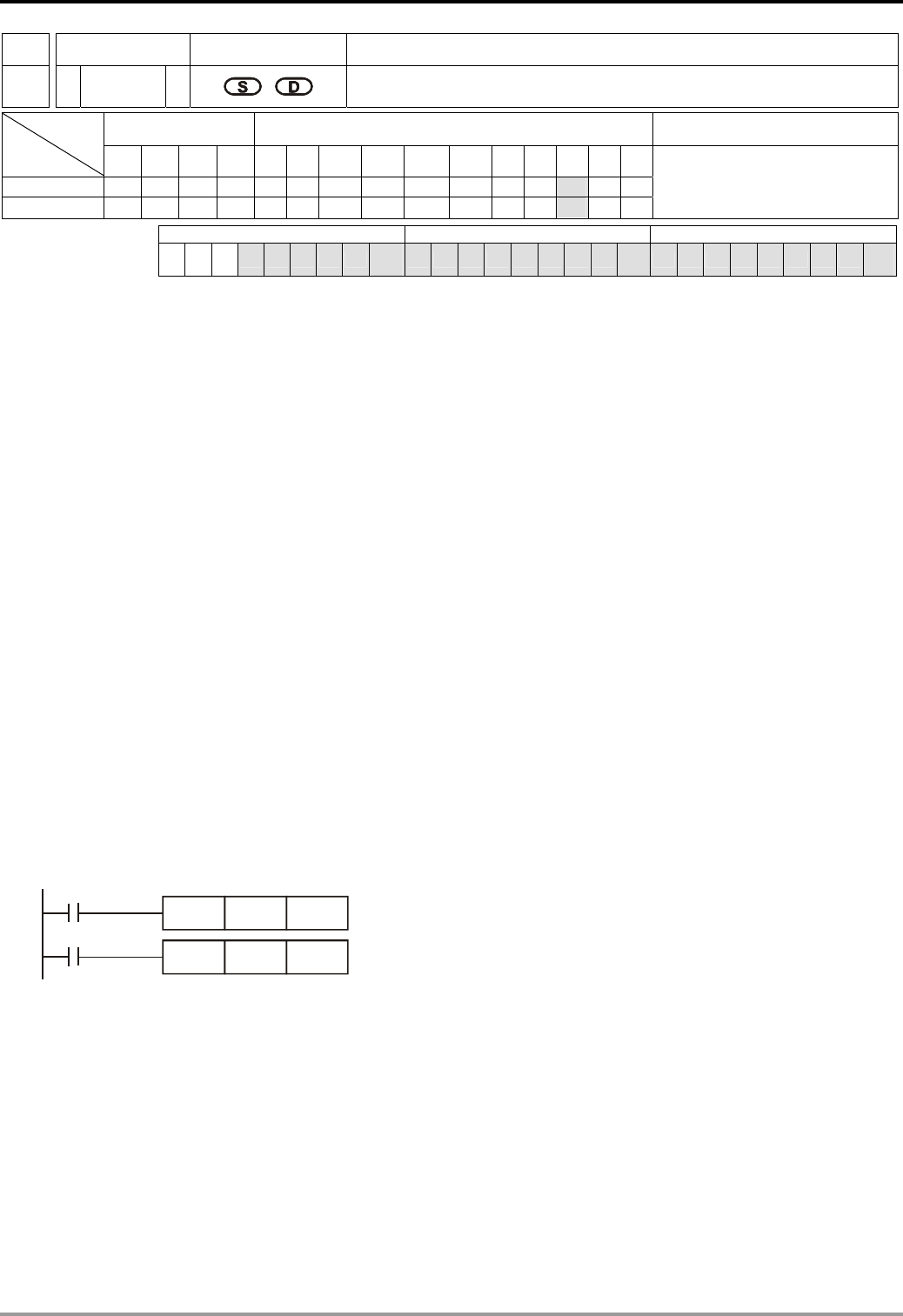
8 Application Instructions API 100-149
DVP-PLC Application Manual
8-38
API Mnemonic Operands Function
129
D INT P Float to Integer
Bit Devices Word Devices Program Steps Type
OP X Y M S K H KnX KnY KnM KnS T C D E F
S *
D *
INT, INTP: 5 steps
DINT, DINTP: 9 steps
PULSE 16-bit 32-bit
ES EX SS SA SX SC EH SV EH3
SV2 ES EX SS SA SX SC EH SV EH3
SV2 ES EX SS SA SX SC EH SV EH3
SV2
Operands:
S: Source device D: Converted result
Explanations:
1. S occupies 2 consecutive devices. See the specifications of each model for their range of use.
2. Flags: M1020 (zero flag); M1021 (borrow flag); M1022 (carry flag)
3. The binary floating point value of the register designated by S is converted to BIN integer and stored in the
register designated by D. The decimal of BIN integer is left out.
4. This instruction is the inverse operation of API 49 FLT instruction.
5. If the converstion result = 0, the zero flag M1020 = On
If there is any decimal left out, the borrow flag M1021 = On.
If the result exceeds the range listed below, the carry flag M1022 = On.
16-bit instruction: -32,768 ~ 32,767
32-bit instruction: -2,147,483,648 ~ 2,147,483,647
Program Example:
1. When X0 = On, the binary floating point (D1, D0) will be converted into BIN integer and the result will be stored
in (D10). The decimal of BIN integer will be left out.
2. When X1 = On, the binary floating point (D21, D20) will be converted into BIN integer and the result will be
stored in (D31, D30). The decimal of BIN integer will be left out.
INT
X0
D0 D10
DINT
X1
D20 D30
Remarks:
For floating point operations, see “5.3 Handling of Numeric Values”.
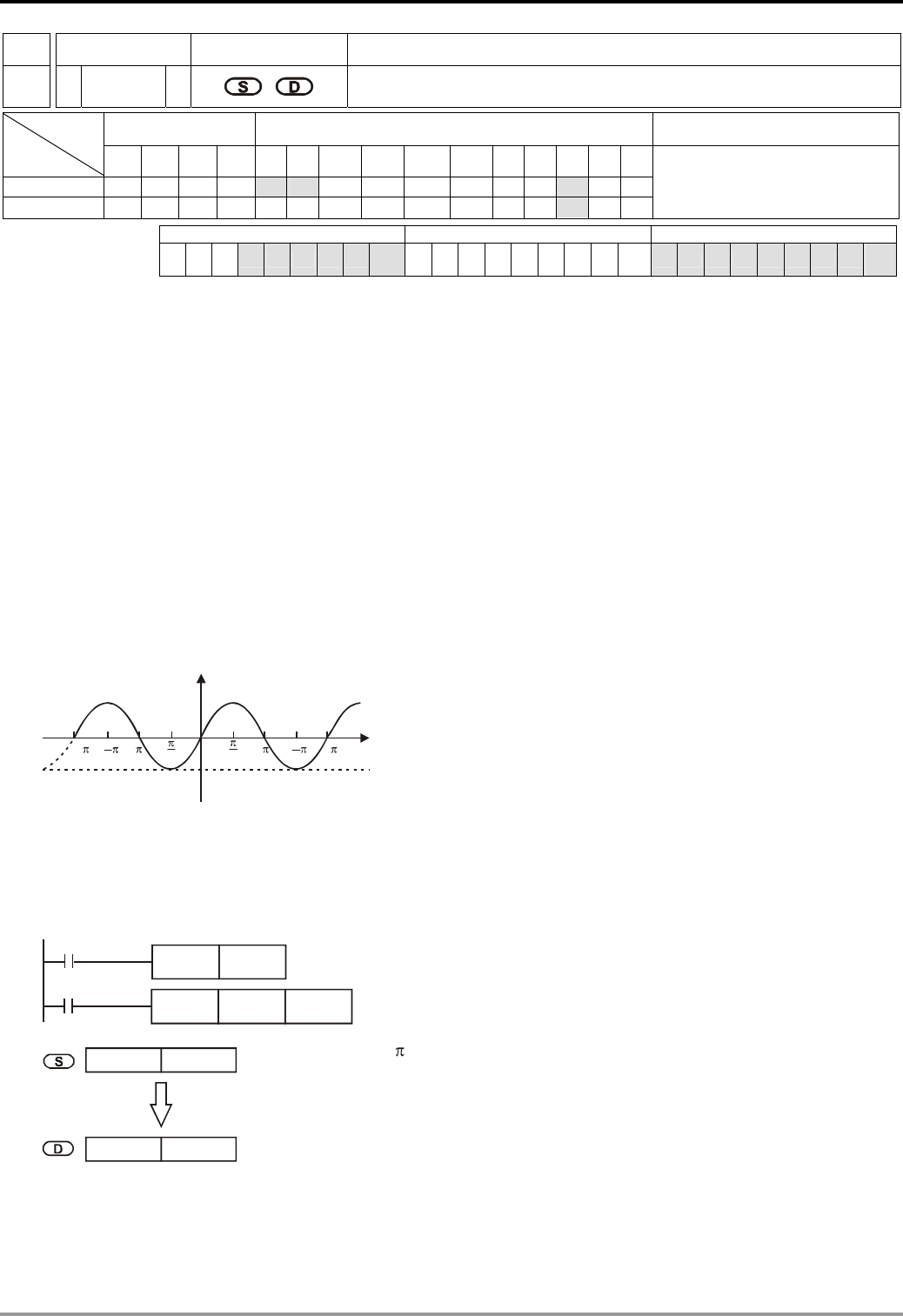
8 Application Instructions API 100-149
DVP-PLC Application Manual 8-39
API Mnemonic Operands Function
130
D SIN P Sine
Bit Devices Word Devices Program Steps Type
OP X Y M S K H KnX KnY KnM KnS T C D E F
S * * *
D *
DSIN, DSINP: 9 steps
PULSE 16-bit 32-bit
ES EX SS SA SX SC EH SV EH3
SV2 ES EX SS SA SX SC EH SV EH3
SV2 ES EX SS SA SX SC EH SV EH3
SV2
Operands:
S: Source value D: SIN result
Explanations:
1. 0° ≤ S < 360°. See the specifications of each model for their range of use.
2. Flags: M1018 (angle or radian); M1020 (zero flag)
3. S can be an angle or radian, decided by M1018.
4. When M1018 = Off, the program will be in radian mode and the RAD value = angle ×π/180
5. When M1018 = On, the program will be in angle mode and the range of angle should be “0° ≤ angle < 360°”
6. If the result = On, M1020 = On.
7. The SIN value obtained by S is calculated and stored in the register designated by D. The figure below offers
the relation between radian and the result.
S: Radian
R: Result (SIN ) value
R
S
-2 3
2-2 2
3
2
2
2
-
1
-1
0
-
Program Example 1:
When M1018 = Off, the program is in radian mode. When X0 = On, use the RAD value of binary floating point (D1, D0)
and obtain its SIN value. The binary floating point result will be stored in (D11, D10).
M1002
RST M1018
X0
DSIN D0 D10
D1 D0
D11 D10 SIN value
RAD 180) value (angle x /
binary floating point
binary floating point
Program Example 2:
When M1018 = Off, the program is in radian mode. Input terminals X0 and X1 select the angle. The angles are
converted into RAD value for calculating the SIN value.
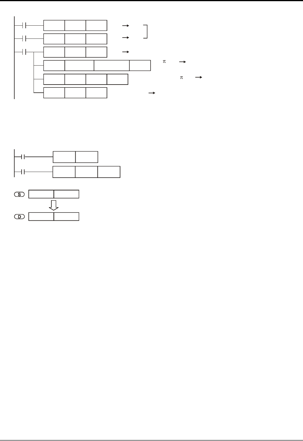
8 Application Instructions API 100-149
DVP-PLC Application Manual
8-40
D10FLT
M1000
D14
K31415926 K1800000000
D20D14 D40
K30
MOVP
X0
D10
K60
X1
D10
D50D40
DEDIV
DSIN
D20
MOVP
DEMUL
(K30 D10)
(K60 D10)
(D10 D15, D14)
( /180) (D21, D20)
(D15, D14) angle x /180
(D41, D40) RAD binary floating point
(D41 D40) RAD (D51, D50) SIN,
binary
floating point
binary floating point
binary
floating point
binary floating point
Program Example 3:
When M1018 = On, the program is in angle mode. When X0 = On, use the angle of (D1, D0) to obtain SIN value and
store the binary floating point result in (D11, D10). (0° ≤ angle < 360°)
M1002
SET M1018
X0
DSIN D0 D10
D 1 D 0
D 11 D 10
angle value
SIN value
(binary floating point)
Remarks:
For floating point operations, see “5.3 Handling of Numeric Values”.
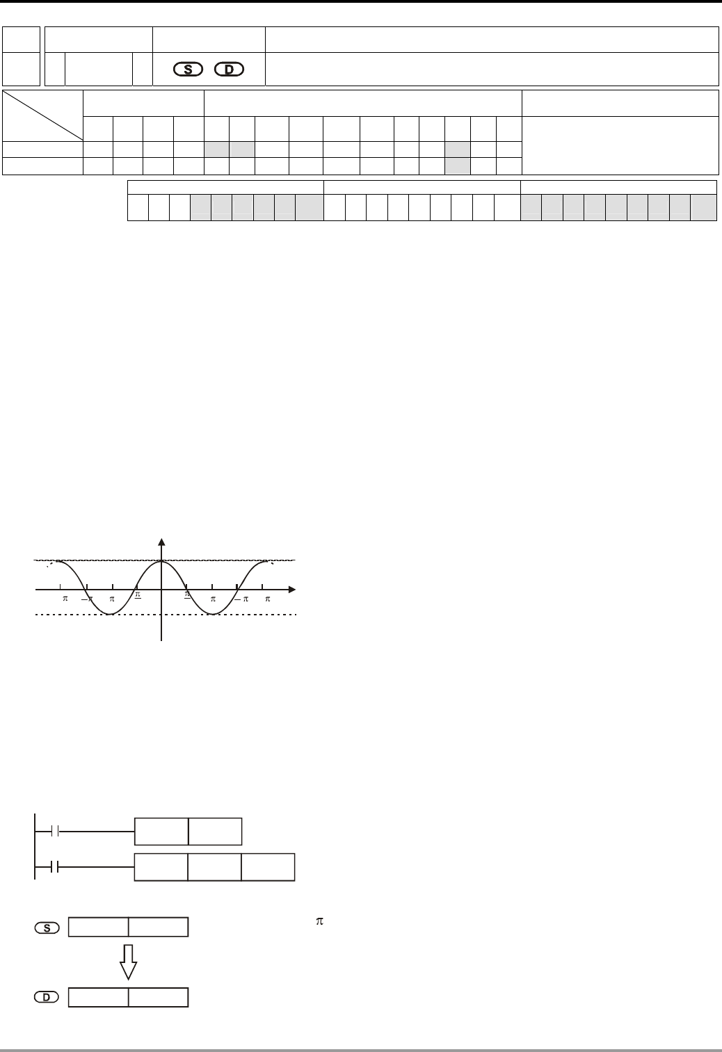
8 Application Instructions API 100-149
DVP-PLC Application Manual 8-41
API Mnemonic Operands Function
131
D COS P Cosine
Bit Devices Word Devices Program Steps Type
OP X Y M S K H KnX KnY KnM KnS T C D E F
S * * *
D *
DCOS, DCOSP: 9 steps
PULSE 16-bit 32-bit
ES EX SS SA SX SC EH SV EH3
SV2 ES EX SS SA SX SC EH SV EH3
SV2 ES EX SS SA SX SC EH SV EH3
SV2
Operands:
S: Source value D: COS result
Explanations:
1. 0° ≤ S < 360°. See the specifications of each model for their range of use.
2. Flags: M1018 (angle or radian); M1020 (zero flag)
3. S can be an angle or radian, decided by M1018.
4. When M1018 = Off, the program will be in radian mode and the RAD value = angle ×π/180
5. When M1018 = On, the program will be in angle mode and the range of angle should be “0° ≤ angle < 360°”
6. If the result = On, M1020 = On.
7. The COS value obtained by S is calculated and stored in the register designated by D. The figure below offers
the relation between radian and the result.
S: Radian
R: Result (COS value)
S
-2 3
2-2 2
3
2
2
2
-
1
-1
0
-
R
8. Switch between radian and angle by M1018: When M1018 = Off, S will be a RAD value; when M1018 = On, S
will be an angle (0° ~ 360°).
Program Example 1:
When M1018 = Off, the program is in radian mode. When X0 = On, use the RAD value of binary floating point (D1, D0)
and obtain its COS value. The binary floating point result will be stored in (D11, D10).
M1002
RST M1018
X0
DCOS D0 D10
D1 D0
D11 D10 COS value
RAD value (angle x /180)
binary floating point
binary floating point

8 Application Instructions API 100-149
DVP-PLC Application Manual
8-42
Program Example 2:
When M1018 = On, the program is in angle mode. When X0 = On, use the angle of (D1, D0) to obtain COS value and
store the binary floating point result in (D11, D10). (0° ≤ angle < 360°)
M1002
SET M1018
X0
DCOS D0 D10
D 1 D 0
D11 D 10
angle value
COS value
(binary floating point)
Remarks:
For floating point operations, see “5.3 Handling of Numeric Values”.
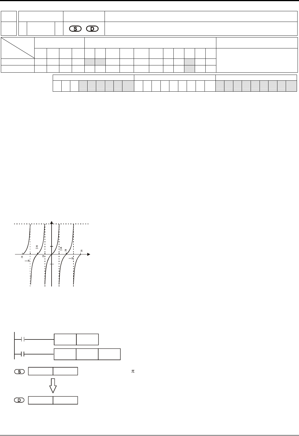
8 Application Instructions API 100-149
DVP-PLC Application Manual 8-43
API Mnemonic Operands Function
132
D TAN P Tangent
Bit Devices Word Devices Program Steps Type
OP X Y M S K H KnX KnY KnM KnS T C D E F
S * * *
D *
DTAN, DTANP: 9 steps
PULSE 16-bit 32-bit
ES EX SS SA SX SC EH SV EH3
SV2 ES EX SS SA SX SC EH SV EH3
SV2 ES EX SS SA SX SC EH SV EH3
SV2
Operands:
S: Source value D: TAN result
Explanations:
1. 0° ≤ S < 360°. See the specifications of each model for their range of use.
2. Flags: M1018 (angle or radian); M1020 (zero flag)
3. S can be an angle or radian, decided by M1018.
4. When M1018 = Off, the program will be in radian mode and the RAD value = angle ×π/180
5. When M1018 = On, the program will be in angle mode and the range of angle should be “0° ≤ angle < 360°”
6. If the result = On, M1020 = On.
7. The TAN value obtained by S is calculated and stored in the register designated by D. The figure below offers
the relation between radian and the result.
S: Radian
R: Result (TAN value)
R
S
-2
2
3
2
2
2
-
1
-1
0
3
2
-
-
Program Example 1:
When M1018 = Off, the program is in radian mode. When X0 = On, use the RAD value of binary floating point (D1, D0)
and obtain its TAN value. The binary floating point result will be stored in (D11, D10).
M1002
RST M1018
X0
DTAN D0 D10
D1 D0
D11 D10
RAD value (angle x /180)
TAN value
binary floating point
binary floating point
Program Example 2:

8 Application Instructions API 100-149
DVP-PLC Application Manual
8-44
When M1018 = On, the program is in angle mode. When X0 = On, use the angle of (D1, D0) to obtain TAN value and
store the binary floating point result in (D11, D10). (0° ≤ angle < 360°)
M1002
SET M1018
X0
DTAN D0 D10
D 1 D 0
D 11 D 10
angle value
TAN value
(binary floating point)
Remarks:
For floating point operations, see “5.3 Handling of Numeric Values”.

8 Application Instructions API 100-149
DVP-PLC Application Manual 8-45
API Mnemonic Operands Function
133
D ASIN P Arc Sine
Bit Devices Word Devices Program Steps Type
OP X Y M S K H KnX KnY KnM KnS T C D E F
S * * *
D *
DASIN, DASINP: 9 steps
PULSE 16-bit 32-bit
ES EX SS SA SX SC EH SV EH3
SV2 ES EX SS SA SX SC EH SV EH3
SV2 ES EX SS SA SX SC EH SV EH3
SV2
Operands:
S: Source value (binary floating point) D: ASIN result
Explanations:
1. See the specifications of each model for their range of use.
2. Flag: M1020 (zero flag)
3. ASIN value=sin–1. The figure below offers the relation between the entered sin value and the result.
S: Entered data (sine value)
R: ASIN value (radian)
R
S
2
2
-
0
-1,0 1,0
4. The decimal floating point of the SIN value designated by S should be within -1.0 ~ +1.0. If the value falls without
the range, M1067 and M1068 will be On without performing any action.
5. If the result = 0, M1020 = On.
Program Example:
When X0 = On, obtain the ASIN value of binary floating point (D1, D0) and store the binary floating point result in (D11,
D10).
DASIN
X0
D0 D10
D1 D0
D11 D10 ASIN value
binary floating point
binary floating point
Remarks:
For floating point operations, see “5.3 Handling of Numeric Values”.
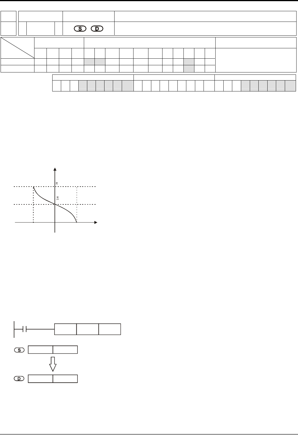
8 Application Instructions API 100-149
DVP-PLC Application Manual
8-46
API Mnemonic Operands Function
134
D ACOS P Arc Cosine
Bit Devices Word Devices Program Steps Type
OP X Y M S K H KnX KnY KnM KnS T C D E F
S * * *
D *
DACOS, DACOSP: 9 steps
PULSE 16-bit 32-bit
ES EX SS SA SX SC EH SV EH3
SV2 ES EX SS SA SX SC EH SV EH3
SV2 ES EX SS SA SX SC EH SV EH3
SV2
Operands:
S: Source value (binary floating point) D: ACOS result
Explanations:
1. See the specifications of each model for their range of use.
2. Flag: M1020 (zero flag)
3. ACOS value=cos–1. The figure below offers the relation between the entered cos value and the result.
S: Entered data (cosine value)
R: ACOS value (radian)
R
S
2
01,0
-1,0
4. The decimal floating point of the COS value designated by S should be within -1.0 ~ +1.0. If the value falls
without the range, M1067 and M1068 will be On without performing any action.
5. If the result = 0, M1020 = On.
Program Example:
When X0 = On, obtain the ACOS value of binary floating point (D1, D0) and store the binary floating point result in
(D11, D10).
DACOS
X0
D0 D10
D1 D0
D11 D10 ACOS value
binary floating point
binary floating point
Remarks:
For floating point operations, see “5.3 Handling of Numeric Values”.
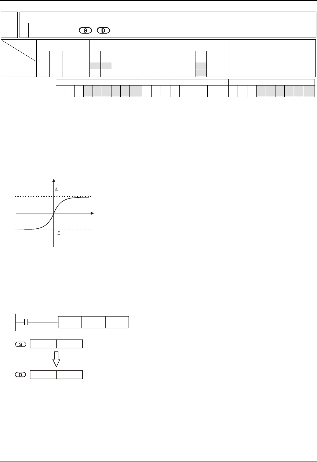
8 Application Instructions API 100-149
DVP-PLC Application Manual 8-47
API Mnemonic Operands Function
135
D ATAN P Arc Tangent
Bit Devices Word Devices Program Steps Type
OP X Y M S K H KnX KnY KnM KnS T C D E F
S * * *
D *
DATAN, DATANP: 9 steps
PULSE 16-bit 32-bit
ES EX SS SA SX SC EH SV EH3
SV2 ES EX SS SA SX SC EH SV EH3
SV2 ES EX SS SA SX SC EH SV EH3
SV2
Operands:
S: Source value (binary floating point) D: ATAN value
Explanations:
1. See the specifications of each model for their range of use.
2. Flag: M1020 (zero flag)
3. ATAN value=tan–1. The figure below offers the relation between the entered tan value and the result.
S: Entered data (tangent value)
R: ATAN value (radian)
R
S
2
2
-
0
4. If the result =0, M1020 = On.
Program Example:
When X0 = On, obtain the ATAN value of binary floating point (D1, D0) and store the binary floating point result in
(D11, D10).
DATAN
X0
D0 D10
D1 D0
D11 D10 ATAN value
binary floating point
binary floating point
Remarks:
For floating point operations, see “5.3 Handling of Numeric Values”.
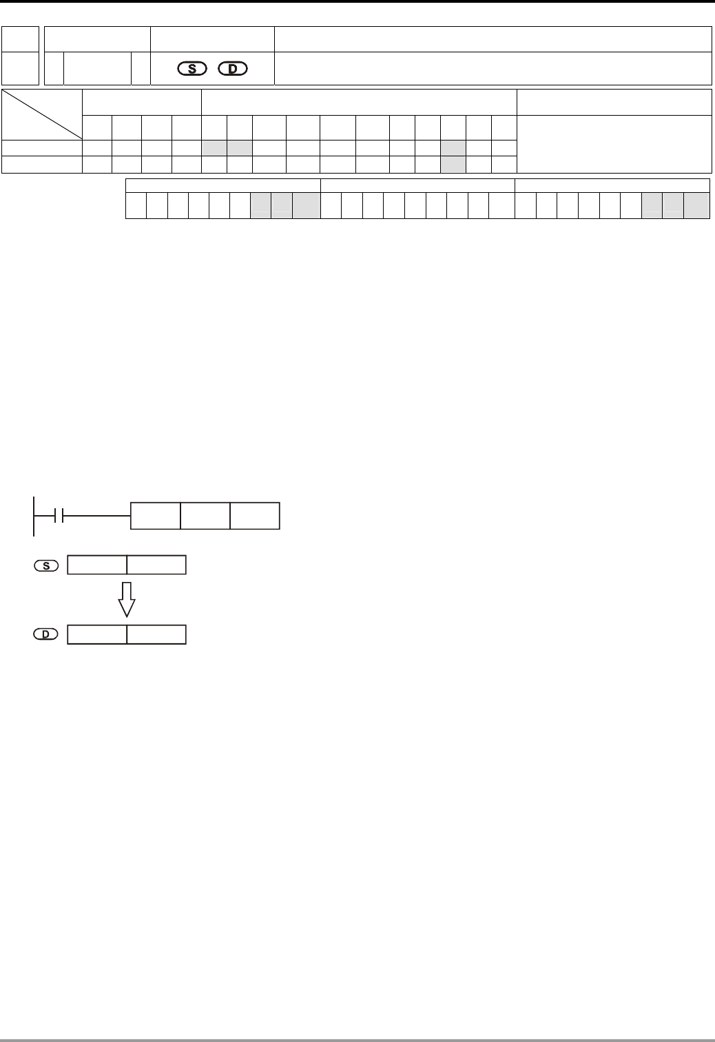
8 Application Instructions API 100-149
DVP-PLC Application Manual
8-48
API Mnemonic Operands Function
136
D SINH P Hyperbolic Sine
Bit Devices Word devices Program Steps Type
OP X Y M S K H KnX KnY KnM KnS T C D E F
S * * *
D *
DSINH, DSINHP: 9 steps
PULSE 16-bit 32-bit
ES EX SS SA SX SC EH SV EH3
SV2 ES EX SS SA SX SC EH SV EH3
SV2 ES EX SS SA SX SC EH SV EH3
SV2
Operands:
S: Source value (binary floating point) D: SINH value
Explanations:
1. See the specifications of each model for their range of use.
2. Flags: M1020 (zero flag); M1021 (borrow flag); M1022 (carry flag)
3. SINH value=(es-e-s)/2. The result is stored in D.
Program Example:
1. When X0 = On, obtain the SINH value of binary floating point (D1, D0) and store the binary floating point result in
(D11, D10).
DSINH
X0
D0 D10
D1 D0
D11 D10 SINH value
binary floating point
binary floating point
2. If the absolute value of the result > maximum floating point available, the carry flag M1022 = On.
3. If the absolute value of the result < minimum floating point available, the borrow flag M1021 = On.
4. If the result = 0, the zero flag M1020 = On.
Remarks:
For floating point operations, see “5.3 Handling of Numeric Values”.
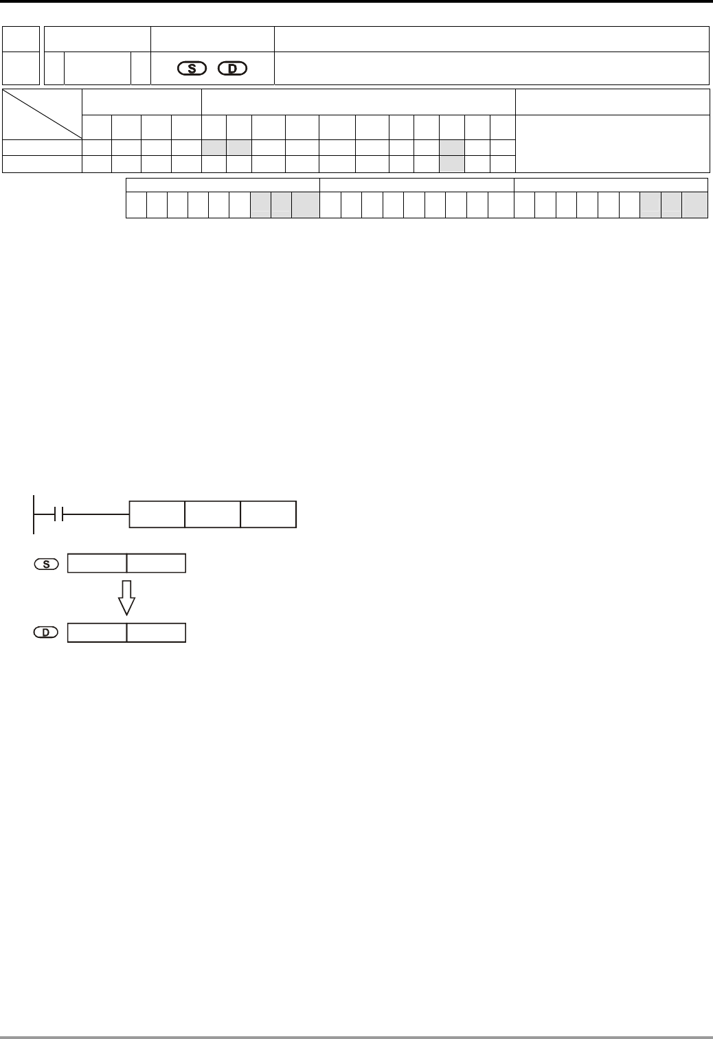
8 Application Instructions API 100-149
DVP-PLC Application Manual 8-49
API Mnemonic Operands Function
137
D COSH P Hyperbolic Cosine
Bit Devices Word devices Program Steps Type
OP X Y M S K H KnX KnY KnM KnS T C D E F
S * * *
D *
DCOSH, DCOSHP: 9 steps
PULSE 16-bit 32-bit
ES EX SS SA SX SC EH SV EH3
SV2 ES EX SS SA SX SC EH SV EH3
SV2 ES EX SS SA SX SC EH SV EH3
SV2
Operands:
S: Source value (binary floating point) D: COSH value
Explanations:
1. See the specifications of each model for their range of use.
2. Flags: M1020 (zero flag); M1021 (borrow flag); M1022 (carry flag)
3. COSH value=(es+e-s)/2. The result is stored in D.
Program Example:
1. When X0 = On, obtain the COSH value of binary floating point (D1, D0) and store the binary floating point result in
(D11, D10).
DCOSH
X0
D0 D10
D1 D0
D11 D10 COSH value
binary floating point
binary floating point
5. If the absolute value of the result > maximum floating point available, the carry flag M1022 = On.
6. If the absolute value of the result < minimum floating point available, the borrow flag M1021 = On.
7. If the result = 0, the zero flag M1020 = On.
Remarks:
For floating point operations, see “5.3 Handling of Numeric Values”.

8 Application Instructions API 100-149
DVP-PLC Application Manual
8-50
API Mnemonic Operands Function
138
D TANH P Hyperbolic Tangent
Bit Devices Word devices Program Steps Type
OP X Y M S K H KnX KnY KnM KnS T C D E F
S * * *
D *
DTANH, DTANHP: 9 steps
PULSE 16-bit 32-bit
ES EX SS SA SX SC EH SV EH3
SV2 ES EX SS SA SX SC EH SV EH3
SV2 ES EX SS SA SX SC EH SV EH3
SV2
Operands:
S: Source value (binary floating point) D: TANH result
Explanations:
1. See the specifications of each model for their range of use.
2. Flags: M1020 (zero flag); M1021 (borrow flag); M1022 (carry flag)
3. TANH value=(es-e-s)/(es+e-s) . The result is stored in D.
Program Example:
1. When X0 = On, obtain the TANH value of binary floating point (D1, D0) and store the binary floating point result in
(D11, D10).
DTANH
X0
D0 D10
D1 D0
D11 D10 TANH value
binary floating point
binary floating point
2. If the absolute value of the result > maximum floating point available, the carry flag M1022 = On.
3. If the absolute value of the result < minimum floating point available, the borrow flag M1021 = On.
4. If the result = 0, the zero flag M1020 = On.
Remarks:
For floating point operations, see “5.3 Handling of Numeric Values”.
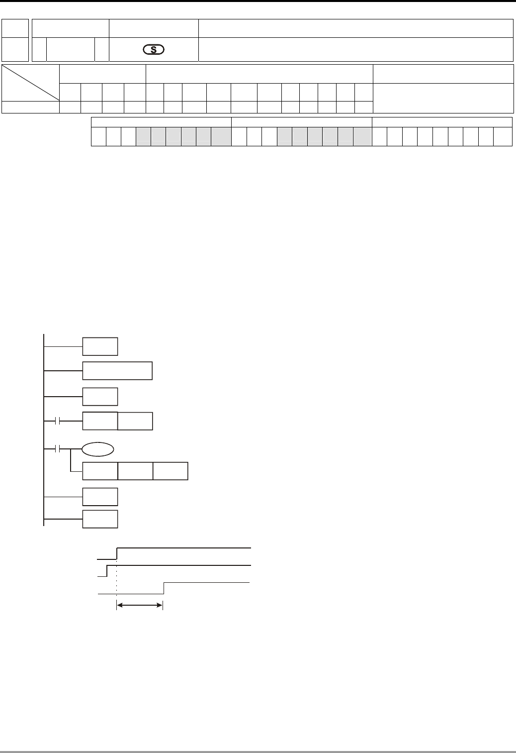
8 Application Instructions API 100-149
DVP-PLC Application Manual 8-51
API Mnemonic Operands Function
143
DELAY Delay Instruction
Bit Devices Word Devices Program Steps Type
OP X Y M S K H KnX KnY KnM KnS T C D E F
S * * *
DELAY, DELAYP: 3 steps
PULSE 16-bit 32-bit
ES EX SS SA SX SC EH SV EH3
SV2 ES EX SS SA SX SC EH SV EH3
SV2 ES EX SS SA SX SC EH SV EH3
SV2
Operands:
S: delay time (unit: 0.1ms)
Explanations:
1. Range of S: K1 ~ K1,000. See the specifications of each model for their range of use.
2. After DELAY instruction is executed, the program after DELAY in every scan period will execute delay outputs
according to the delay time designated by the user.
Program Example:
When X0 goes from Off to On and generates an external interruption, the interruption subroutine will execute DELAY
for 2ms before executing the next step, X1 = On and Y0 = On.
M1000
DELAY K20
FEND
I001
X1
Y0
IRET
END
EI
REF Y0 K8
Main Program
Output Y0
T=2ms
Input X1
Interrupt input X0
Remarks:
1. User can define the delay time based on their needs.
2. The delay time may increase due do the influences from communication, high-speed counters and high-speed
pulse output instructions.
3. The delay time of designated external output (transistor or relay) will increase due to the delay on the transistor

8 Application Instructions API 100-149
DVP-PLC Application Manual
8-52
or relay itself. See 2.3 for more information.
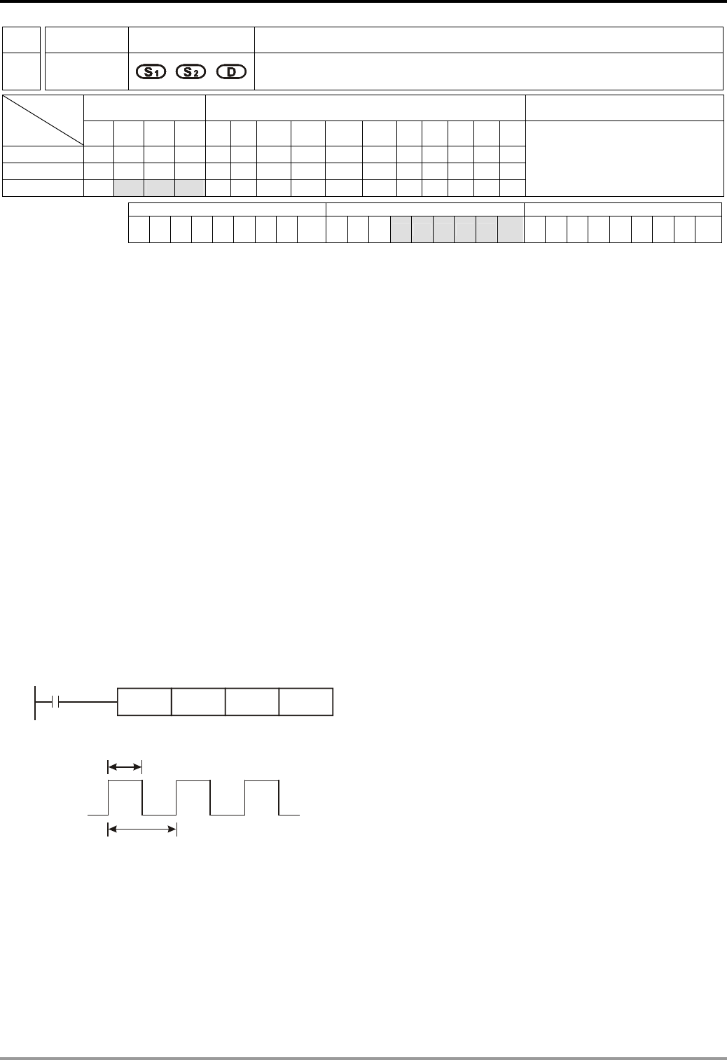
8 Application Instructions API 100-149
DVP-PLC Application Manual 8-53
API Mnemonic Operands Function
144
GPWM General PWM Output
Bit Devices Word Devices Program Steps Type
OP X Y M S K H KnX KnY KnM KnS T C D E F
S1 *
S2 *
D * * *
GPWM: 7 steps
PULSE 16-bit 32-bit
ES EX SS SA SX SC EH SV EH3
SV2 ES EX SS SA SX SC EH SV EH3
SV2 ES EX SS SA SX SC EH SV EH3
SV2
Operands:
S1: Width of output pulse S2: Pulse output cycle D: Pulse output device
Explanations:
1. S2 occupies 3 consecutive devices.
2. S1 ≤ S2. See the specifications of each model for their range of use.
3. Range of S1: t = 0 ~ 32,767ms.
4. Range of S2: t = 1 ~ 32,767ms.
5. S2 +1 and S2 +2 are parameters for the system. Do not occupy them.
6. Pulse output devices D: Y, M, S.
7. When being executed, GPWM instruction designates S1 and S2 and that pulses output will be from device D.
8. When S1 ≤ 0, there will be no pulse output. When S1 ≥ S2, the pulse output device will keep being On.
9. S1 and S2 can be modified when GPWM instruction is being executed.
Program Example:
When X0 = On, D0 = K1,000, D2 = K2,000, and Y10 will output the pulse illustrated below. When X0 = Off, Y10 output
will be Off.
X0
GPWM D0 D2 Y10
tT
t=1000ms
T=2000ms
Output Y10
Explanations:
1. This instruction counts by the scan cycle; therefore the maximum offset will be one PLC scan cycle. S1, S2 and
(S2 - S1) should > PLC scan cycle; otherwise, errors will occur during GPWM outputs.
2. Please note that placing this instruction in a subroutine or interruption will cause inaccurate GPWM outputs.
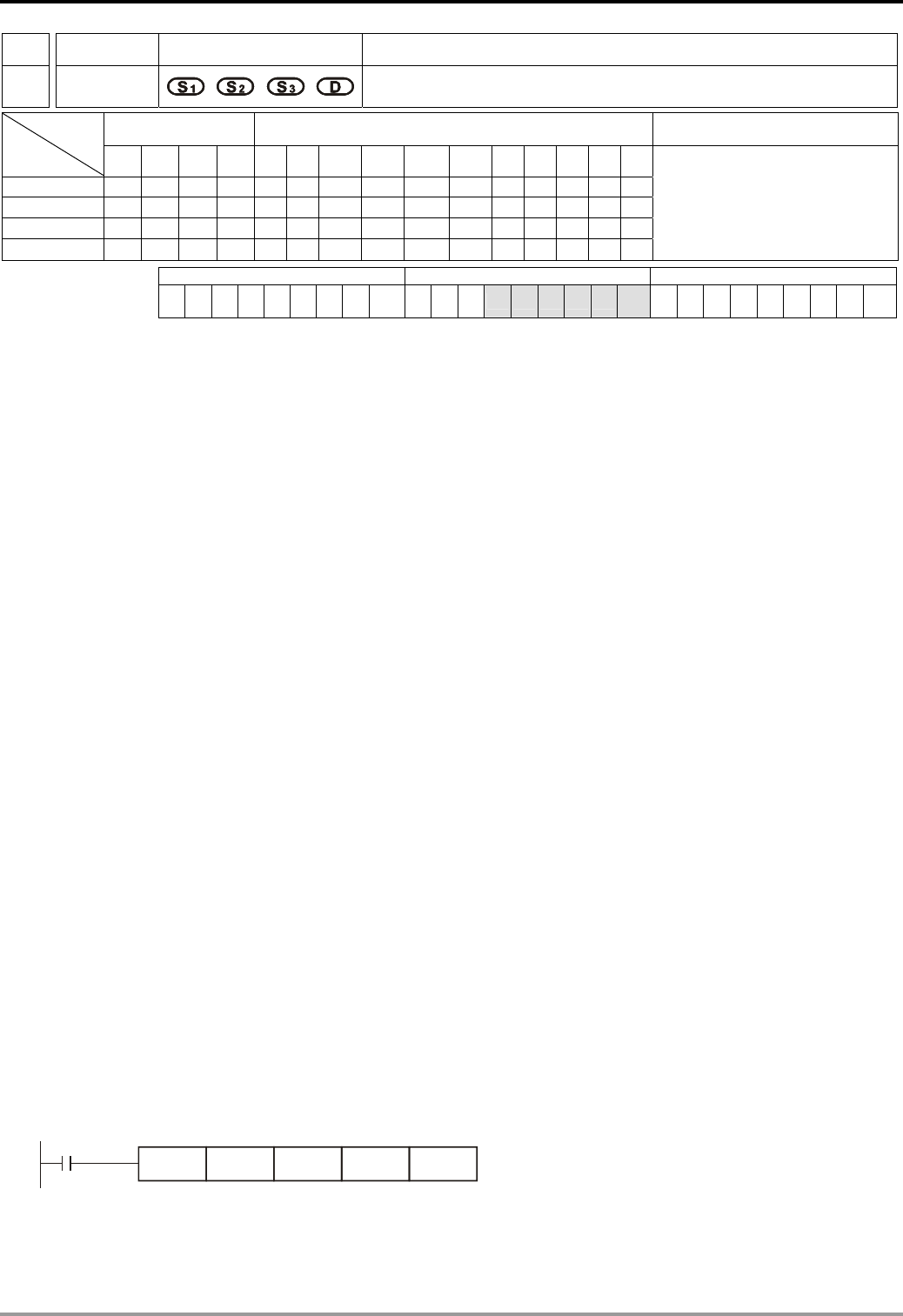
8 Application Instructions API 100-149
DVP-PLC Application Manual
8-54
API Mnemonic Operands Function
145
FTC Fuzzy Temperature Control
Bit Devices Word Devices Program Steps Type
OP X Y M S K H KnX KnY KnM KnS T C D E F
S1 * * *
S2 * * *
S3 *
D *
FTC: 9 steps
PULSE 16-bit 32-bit
ES EX SS SA SX SC EH SV EH3
SV2 ES EX SS SA SX SC EH SV EH3
SV2 ES EX SS SA SX SC EH SV EH3
SV2
Operands:
S1: Set value (SV) S2: Present value (PV) S3: Parameter (sampling time) D: Output value (MV)
Explanations:
1. Range of S1 : 1 ~ 5000 (shown as 0.1°C ~ 500°C). Unit: 0.1°. If (S3 +1) is set as K0, the range will be 0.1°C ~
500°C.
2. Range of S2 : 1 ~ 5000 (shown as 0.1°C ~ 500°C). Unit: 0.1°. If (S3 +1) is set as bit0 = 0, the range will be 0.1°C
~ 500°C. Therefore, when the user obtain an A/D value from the temperature sensor, the value has to be
converted into a value between 1 ~ 5,000 by four arithmetic operation instructions.
3. If S3 < K1, the instruction will not be executed. If S3 > K200, S3 will adopt K200. S3 will occupy 7 consecutive
devices.
4. See the specifications of each model for their range of use.
5. Settings of parameter S3 +1: bit0 = 0 ->°C; bit1 = 0 ->°F; bit1 = 0 -> no filter function; bit1 = 1 -> with filter
function; bit2 ~ bit5 -> 4 kinds of heating environments; bit6 ~ bit15 -> reserved. See remarks for more
information.
6. D is the value between 0 ~ sampling time × 100. When using this instruction, the user has to adopt other
instructions according to the types of the heater. For example, FTC can be used with GPWM for output pulse
control. “Sampling time × 100” is the cycle of GPWM pulse output; MV is the width of GPWM pulse. See
program example 1.
7. There is no limit on the times of using FTC instruction, but Do not repeatedly use a designated operand in case
an error may occur..
Program Example:
1. Set up the parameter before executing FTC instruction.
2. When X0 = On, the instruction will be executed and and result will be stored in D150. When X0 = Off, the
instruction will not be executed and the previous data remain unchanged.
X0
FTC D0 D1 D100 D150
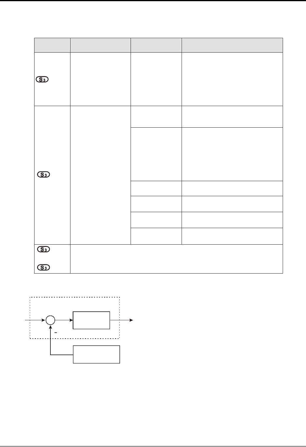
8 Application Instructions API 100-149
DVP-PLC Application Manual 8-55
Remarks:
1. Setting of S3:
Device No. Function Range Explanation
Sampling time (TS)
(unit: 100ms)
1 ~ 200
(unit: 100ms)
If TS is less than a scan time, PID
instruction will be executed for a
scan time. If TS= 0, PID instruction
will not be enabled. The minimum TS
must be greater than a scan time.
b0 =0 means oC
b0 =1 means oF
When the value exceeds the upper
bound, use upper bound.
b1=0 means
without fileter
function
b1=1 means with
filter function
When without filter function, PV =
currently measured value. When with
filter function, PV = (currently
measured value + previous PV)/2
b2=1 Slow heating environment
b3=1 General heating environment
b4=1 Fast heating environment
+1
b0: temperature unit
b1: filter function
b2 ~ b5: heating
environnment
b6 ~ b15: reserved
b5=1 High-speed heating environment
+2
~
+6
Parameters for system use only. Do not use them.
2. Control Diagram:
+
e
FTC
PV
MV
Fuzzy
Controller
Temperature
Sensor
SV
3. Notes and suggestion:
It is recommended that the sampling time be set to 2 times more than the sampling time of the temperature
sensor for better temperature control.
bit2 ~ bit5 of S3+1 are for the control speed. If the user does not set up the parameter, FTC will automatically
activate “general heating environment”. When the user finds that the control is too slow to reach SV, select “slow
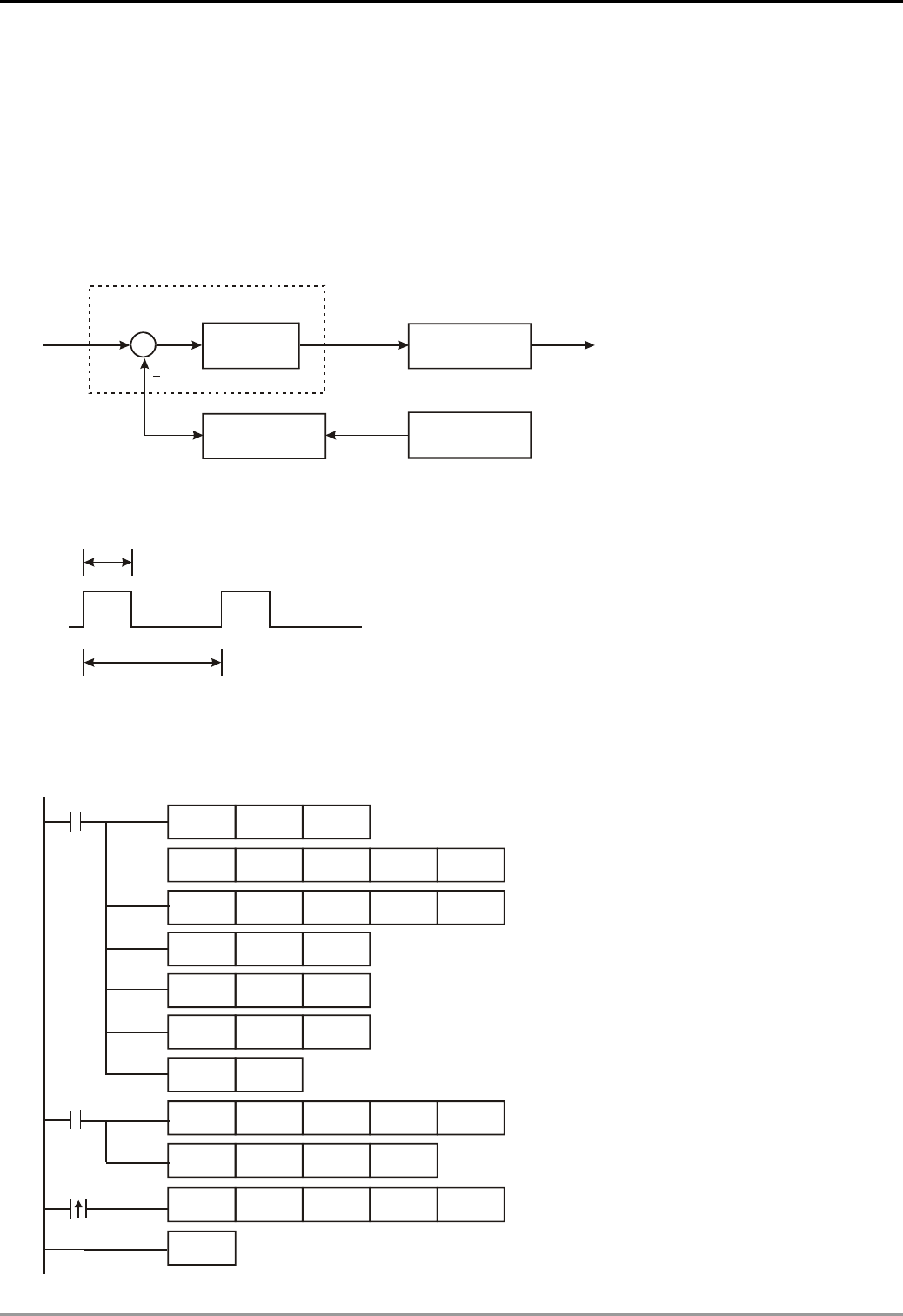
8 Application Instructions API 100-149
DVP-PLC Application Manual
8-56
heating environment” to enhance the speed to reach SV. On the contrary, when the user finds that the control is
too fast or with too many fluctuations, select “fast heating environment” to slow down the control speed.
When bit2 ~ bit5 of S3+1 are all set as 1 or more than 1 environments are designated, FTC instruction will check
from bit2 to bit 5 in order and enable the function that has been set as 1. The parameter can be modified during
the control.
4. Example 1: control diagram
Fuzzy
Controller
FT
C
SV
D10 D22
MV Y0
D11
PV
+
e
PT Module
GPWM Program
Temperature
Sensor
Output D22 (MV) of FTC instruction is the input D22 of GPWM instruction, as the duty cycle of ajustable pulses.
D30 is the fixed cycle time of pulses. See below for the timing diagram of Y0 output.
D22
D30
Y0
Assume parameter settings: D10 = K1,500 (target temperature), D12 = K60 (sampling time: 6 secs.), D13 = K8
(bit3=1), D30 = K6,000 (=D12*100)
The example control program is indicated as:
M1002
MOV K1500 D10
TO K0 K2 K2 K1
FROM K0 K6 D11 K1
MOV K60 D12
MOV K8 D13
MOV K6000 D30
SET M1
M1
FTC D10 D11 D12 D22
GPWM D22 D30 Y0
M1013 FROM K0 K6 D11 K1
END
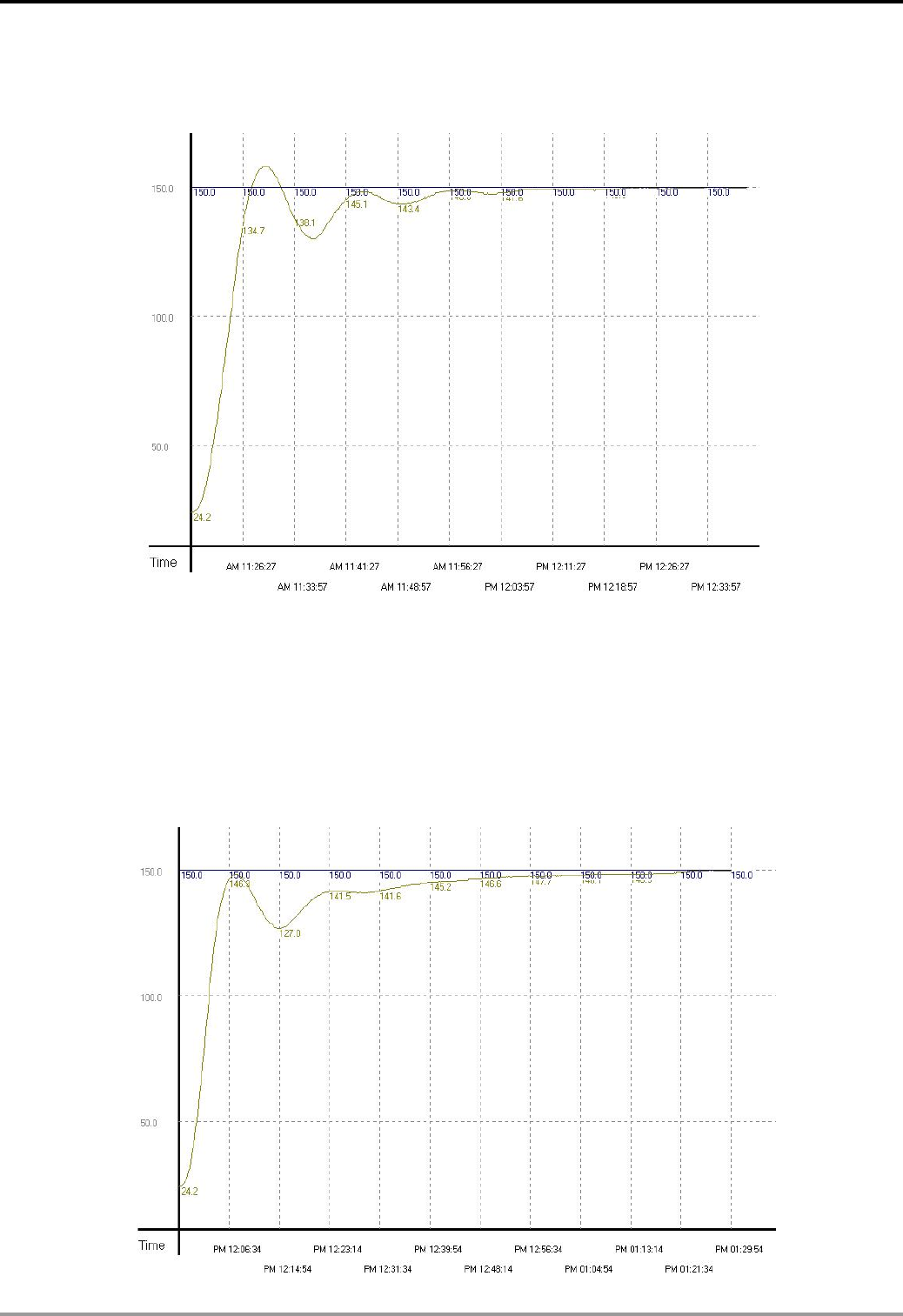
8 Application Instructions API 100-149
DVP-PLC Application Manual 8-57
Experiment in an oven which can be heated up to 250°C. See below for the records of target and present
temperatures. As shown in the diagram below, we can see that after 48 minutes, the temperature is able to
reach the target temperature with ±1oC inaccuracy and exceed approx. 10°C of the target temperature.
Example 2: Due to that the temperature once exceeds the target temperature, we modify the heating
environment into “fast heating environment” (D13 = K16). The results are shown in the diagram below.
From the diagram below, we see that though the temperature no longer exceeds the target temperature, it still
needs to take more than 1 hour and 15 minutes to reach the target temperature with ±1oC inaccuracy. It seems
that we have chosen the right environment, but the sampling time is too long, resulting in the extension of
heating time.
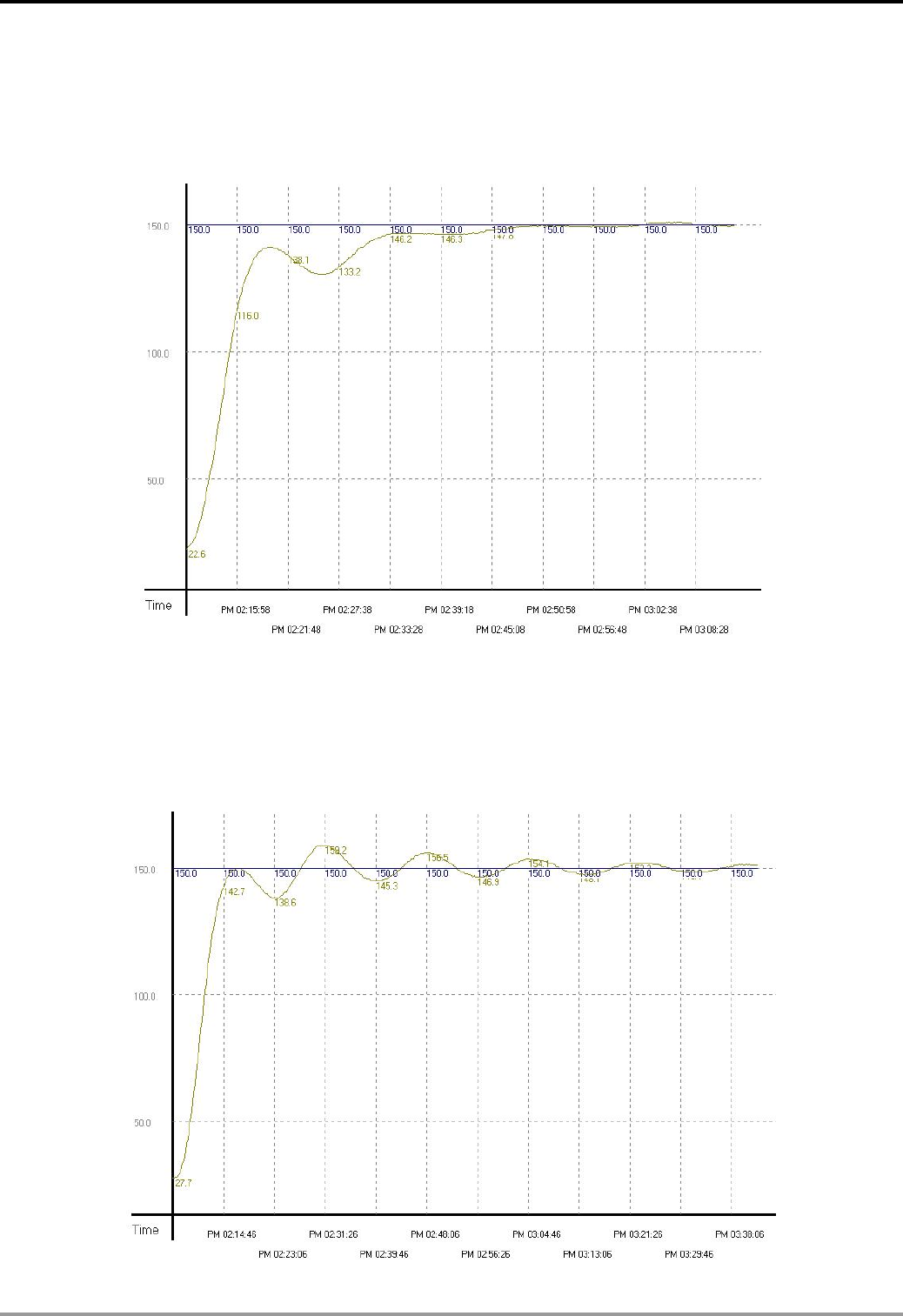
8 Application Instructions API 100-149
DVP-PLC Application Manual
8-58
Example 3: To speed up the speed to reach the target temperature, we correct the sampling time as 4 seconds
(D12 = K40, D30 = K4,000). The results are shown in the diagram below.
From the diagram below, we see that the overall control time has been shortened as 37 minutes. Therefore, we
find out that modifying the sampling time can speed up the time for reaching the target temperature.
Example 4: To see if we can reach the target temperature faster, we modify the sampling time frim example 3
into 2 seconds (D12 = K20, D30 = K2,000). The results are shown in the diagram below.
From the diagram below, we see that the sampling time that is too short will cause the control system to become
too sensitive and lead to up and down fluctuations.
8 Application Instructions API 100-149
DVP-PLC Application Manual 8-59
API Mnemonic Operands Function
146
CVM
Valve Control
Bit Devices Word Devices Program Steps Type
OP X Y M S K H KnX KnY KnM KnS T C D E F
S1 *
S2 * * *
D * * *
CVM: 7 steps
PULSE 16-bit 32-bit
ES EX SS SA SX SC EH SV EH3
SV2 ES EX SS SA SX SC EH SV EH3
SV2 ES EX SS SA SX SC EH SV EH3
SV2
Operands:
S1: Target time of valve (absolute position) S2: Time from fully-closed to fully-open of valve (destination)
D: Output device
Explanations:
1. S1 occupies 3 consecutive registers when in use. S1 + 0 are for the user to store the designated value; S1 + 1 (the
current position of the valve) and S1 + 2 are for storing the parameters recorded in the instruction and please DO
NOT use and alter these two registers.
2. D occupies 2 consecutive output devices when in use. D + 0 is the “open” contact and D + 1 is the “close” contact.
3. This instruction only supports EH2/SV/EH3/SV2 and does not support EH.
4. The unit of time: 0.1 second. When the scan time of the program exceeds 0.1 second, DO NOT use this
instruction to adjust the position of the valve.
5. Frequency of the output device: 10Hz.
6. When the time of S1 + 0 > the fully-opened time set in S2, D + 0 will keep being On and D + 1 being Off. When
the time of S1 + 0 < 0, D + 0 will keep being Off and D + 1 being On.
7. When the instruction is enabled, the instruction will start to control the valve from “0” time position. Therefore, if
the user cannot be sure whether the valve is at “0” before executing the instruction, please designate S1 + 0 as
less than 0 and execute the instruction for S2 (time) before sending in the correct target control time.
Program Example 1:
1. The control valve
Y0Y1
Fully-closed Fully-open
2. Definitions of the control valve:

8 Application Instructions API 100-149
DVP-PLC Application Manual
8-60
a) When Y0 and Y1 = Off: No valve action
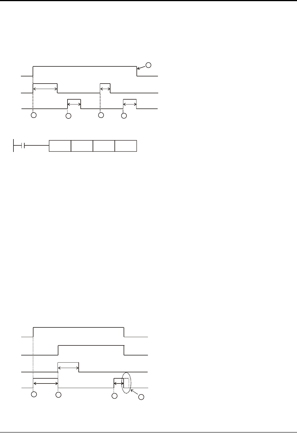
8 Application Instructions API 100-149
DVP-PLC Application Manual 8-61
b) When Y0 = On and Y1 = Off: Valve “open”
c) When Y0 = Off and Y1 = On: Valve “closed”
d) When Y0 and Y1 = On: The action is prohibited.
3. Timing diagram and program of the control:
M0
Y0
Y1
D0=k40 D0=k20 D0=k30 D0=k10
4sec
2sec
1sec
2sec
1234
5
M0
CVM D0 K50 Y0
4. Control phases:
1) Phase
1: When M0 = On, D0 = K40 refers to the valve shall be open (Y0 = On, Y1 = Off) till the position of
4 seconds.
2) Phase
2: Change the position of the valve and D0 = K20. Due to that the previous position was at 4
seconds, the valve shall be closed (Y0 = Off, Y1 = On) for 2 seconds, moving the valve to the position of 2
seconds.
3) Phase
3: Change the position of the valve and D0 = K30. Due to that the previous position was at 2
seconds, the valve shall be open (Y0 = On, Y1 = Off) for 1 second, moving the valve to the position of 3
seconds.
4) Phase
4: Change the position of the valve and D0 = K10. Due to that the previous position was at 2
seconds, the valve shall be closed (Y0 = Off, Y1 = On) for 2 seconds, moving the valve to the position of 1
second.
5) Phase
5: Switch off X0 and no actions at the valve (Y0 = Off, Y1 = Off).
Program Example 2:
1. Timing diagram and program of the control:
Y0
Y1
D0=k40 D0=k10
4sec
2sec
1234
M0
T0
5sec
D0=1

8 Application Instructions API 100-149
DVP-PLC Application Manual
8-62
M
0
K50
CVM D0 K50 Y0
D0
T0TMR
MOV k-1
T0
2. Control phases:
1) Phase
1: When M0 = On, due to that we are not sure about there the valve is, set D0 = K-1 to deliberately
close the valve (Y0 = Off, Y1 = On) for 5 seconds and make sure the valve is at the position of 0 second
before moving on to the next step.
2) Phase
2: When T0 = On, allow D0 = K40 to start is action. Open the valve (Y0 = On, Y1 = Off) for 4
seconds, moving the valve to the position of 4 seconds.
3) Phase
3: Change the position of the valve and D0 = K10. Due to that the previous position was at 4
seconds, the valve shall be closed (Y0 = Off, Y1 = On) for 3 seconds, moving the valve to the position of 1
second.
4) Phase
4: Switch off M0 and the valve will no longer move (Y0 = Off, Y1 = Off).
8 Application Instructions API 100-149
DVP-PLC Application Manual 8-63
API Mnemonic Operands Function
147
D SWAP P Byte Swap
Bit Devices Word Devices Program Steps Type
OP X Y M S K H KnX KnY KnM KnS T C D E F
S * * * * * ***
SWAP, SWAPP: 3 steps
DSWAP, DSWAPP: 5 steps
PULSE 16-bit 32-bit
ES EX SS SA SX SC EH SV EH3
SV2 ES EX SS SA SX SC EH SV EH3
SV2 ES EX SS SA SX SC EH SV EH3
SV2
Operands:
S: Device for swapping 8 high/low byte.
Explanations:
1. If D is used in device F, only 16-bit instruction is applicable.
2. See the specifications of each model for their range of use.
3. As 16-bit instruction: the contents in the 8 high bytes and 8 low bytes are swapped.
4. As 32-bit instruction: the 8 high bytes and 8 low bytes in the two registers swap with each other respectively.
5. This instruction adopts pulse execution instructions (SWAPP, DSWAPP).
Program Example 1:
When X0 = On, the high 8 bytes and low 8 bytes in D0 will swap with each other.
D0
SWAPP
X0
D0
High Byte Low Byte
Program Example 2:
When X0 = On, the high 8 bytes and low 8 bytes in D11 will swap with each other and the high 8 bytes and low 8
bytes in D10 will swap with each other.
X0
DSWAPP D10
D10
D11
High Byte
High Byte Low Byte Low Byte
8 Application Instructions API 100-149
DVP-PLC Application Manual
8-64
API Mnemonic Operands Function
148
D MEMR P Read File Register
Bit Devices Word Devices Program Steps Type
OP X Y M S K H KnX KnY KnM KnS T C D E F
m * * *
D *
n * * *
MEMR, MEMRP: 7 steps
DMEMR, DMEMRP: 13 steps
PULSE 16-bit 32-bit
ES EX SS SA SX SC EH SV EH3
SV2 ES EX SS SA SX SC EH SV EH3
SV2 ES EX SS SA SX SC EH SV EH3
SV2
Operands:
m: Address in the file register to be read D: Device for storing the read data (starting from the designated D)
n: Number of data read at a time
Explanations:
1. Range of m: K0 ~ K1,599 (SA/SX/SC); K0 ~ K9,999 (EH/EH2/SV)
2. Range of D: D2000 ~ D4999 (SA/SX/SC); D2000 ~ D9999 (EH/EH2/SV)
3. Range of n: For 16-bit instruction K1 ~ K1,600 (SA/SX/SC), K1 ~ K8,000 (EH/EH2/SV); For 32-bit instruction
K1 ~ K800 (SA/SX/SC), K1 ~ K4,000 (EH/EH2/SV)
4. See the specifications of each model for their range of use.
5. Flag: M1101. See explanations below.
6. SA/SX/SC/EH/EH2/SV/EH3/SV2 uses this instruction to read the data in file registers and store them into data
registers.
7. SA/SX/SC offers 1,600 16-bit file registers.
8. m and n of SA/SX/SC do not support E and F index register modification.
9. EH/EH2/SV/EH3/SV2 offers 10,000 16-bit file registers.
10. If m, D and n fall without their range, operation error will occur. M1067, M1068 = On and D1067 will record the
error code H’0E1A.
Program Example 1:
1. The 16-bit instruction MEMR reads 100 data at address 10 in the file register and store the read data in register
D starting from D2000.
2. When X0 = On, the instruction will be executed. When X0 = Off, the instruction will not be executed and the
previously read data will remain unchanged.
X0
MEMR K10 D2000 K100
Program Example 2:
1. The 32-bit instruction DMEMR reads 100 data at address 20 in the file register and store the read data in
register D starting from D3000.
2. When X0 = On, the instruction will be executed. When X0 = Off, the instruction will not be executed and the
previously read data will remain unchanged.

8 Application Instructions API 100-149
DVP-PLC Application Manual 8-65
X0
DMEMR K20 D3000 K100

8 Application Instructions API 100-149
DVP-PLC Application Manual
8-66
API Mnemonic Operands Function
149
D MEMW P Write File Register
Bit Devices Word Devices Program Steps Type
OP X Y M S K H KnX KnY KnM KnS T C D E F
S *
m * * *
n * * *
MEMW, MEMWP: 7 steps
DMEMW, DMEMWP: 13 steps
PULSE 16-bit 32-bit
ES EX SS SA SX SC EH SV EH3
SV2 ES EX SS SA SX SC EH SV EH3
SV2 ES EX SS SA SX SC EH SV EH3
SV2
Operands:
S: Device for storing the written data (starting from the designated D) m: Address in the file register to be written
n: Number of data to be written at a time
Explanations:
1. Range of S: D2000 ~ D4999 (SA/SX/SC); D2000 ~ D9999 (EH/EH2/SV)
2. Range of m: K0 ~ K1,599 (SA/SX/SC); K0 ~ K9,999 (EH/EH2/SV)
3. Range of n: For 16-bit instruction K1 ~ K1,600 (SA/SX/SC), K1 ~ K8,000 (EH/EH2/SV); For 32-bit instruction K1
~ K800 (SA/SX/SC), K1 ~ K4,000 (EH/EH2/SV)
4. See the specifications of each model for their range of use.
5. Flag: M1101. See explanations below.
6. SA/SX/SC/EH/EH2/SV/EH3/SV2 uses this instruction to read the data in data registers and write them into file
registers.
7. SA/SX/SC offers 1,600 16-bit file registers.
8. m and n of SA/SX/SC do not suppot E and F index register modification.
9. EH/EH2/SV/EH3/SV2 offers 10,000 16-bit file registers.
10. If S, m and n fall without their range, operation error will occur. M1067, M1068 = On and D1067 will record the
error code H’0E1A.
Program Example:
1. When X0 = On, the 32-bit instruction DMEMW writes 100 32-bit data starting from D2001 and D2000 into
address 0 ~ 199 in the file register.
2. When X0 = On, the instruction will be executed. When X0 = Off, the instruction will not be executed and the
previously data written in will remain unchanged.
X0
DMEMW D2000 K0 K100
File Register:
1. EH/EH2/SV/EH3/SV2: When the PLC is powered, it will decide whether to automatically send the data in the
file register to the designated data register by M1101 (whether to enable the function of file register), D1101
(start address in file register K0 ~ K9,999), D1102 (number of data to be read in file register K1 ~ k8,000), and
D1103 (device for storing read data, starting from designated D, K2,000 ~ K9,999).

8 Application Instructions API 100-149
DVP-PLC Application Manual 8-67
2. In EH/EH2/SV/EH3/SV2, the reading of data from file register to data register D will not be executed if D1101 <
0, D1101 > K9,999, D1103 < K2,000 or D1103 > K9,999.
3. SA/SX/SC: When the PLC is powered, it will decide whether to automatically send the data in the file register to
the designated data register by M1101 (whether to enable the function of file register), D1101 (start address in
file register K0 ~ K1,599), D1102 (number of data to be read in file register K1 ~ k1,600), and D1103 (device for
storing read data, starting from designated D, K2,000 ~ K4,999).
4. In SA/SX/SC, the reading of data from file register to data register D will not be executed if D1101 < 0, D1101 >
K1,599, D1103 < K2,000 or D1103 > K4,999.
5. When the reading of data from file register to data register D starts, PLC will stop the reading if the address of
file register or data register exceed their range.
6. In PLC program, only API 148 MEMR and API 149 MEMW can be used to read or write the file register. See
2.8.3 for more information on file registers.
7. File registers do not have actual addresses in it. Reading and writing of file registers can only be done through
API 148 MEMR, API 149 MEMW or peripheral devices HPP and WPLSoft.
8. If the address in the file register to be read exceeds its range, the read value will be 0.
9. Special relays of file register and other relevant special registers:
Flag Function
M1101 Whether to enable the function of file register; latched; default = off
Special D Function
D1101
Start address in file register. SA/SX/SC: K0 ~ K1,599;
EH/EH2/SV/EH3/SV2: K0 ~ K9,999; latched; default = 0
D1102
Number of data to be read in file register. SA/SX/SC: K1 ~ K1,600;
EH/EH2/SV/EH3/SV2: K1 ~ K8,000; latched; default = 0
D1103
Device for storing read data, starting from designated D. SA/SX/SC:
K2,000 ~ K4,999; EH/EH2/SV/EH3/SV2: K2,000 ~ K9,999; latched;
default = 2,000

8 Application Instructions API 100-149
DVP-PLC Application Manual
8-68
MEMO
9 Application Instructions API 150-199
DVP-PLC Application Manual
9-1
API Mnemonic Operands Function
150
MODRW Read/Write MODBUS Data
Bit Devices Word Devices Program Steps Type
OP X Y M S K H KnX KnY KnM KnS T C D E F
S1 * * *
S2 * * *
S3 * * *
S *
n * * *
MODRW: 11 steps
PULSE 16-bit 32-bit
ES EX SS SA SX SC EH SV EH3
SV2 ES EX SS SA SX SC EH SV EH3
SV2 ES EX SS SA SX SC EH SV EH3
SV2
Operands:
S1: Address of communication device S2: Function code S3: Device address of data to be read/written
S: Register for storing read/written data (source or destination) n: Length of read/written data
Explanations:
1. The content of S2 shall only be: K3(H03), K6(H06), K16(H10). SA/SX V1.8, SC V1.6 and EH2/SV/EH3/SV2
V1.2 and later versions support K2(H02) and K15(H0F); EH2/SV/EH3/SV2 V1.4 and later versions support
K5(H05).
2. ES/EX/SS V.4.9 (and above) support the continuous execution instruction (MODRW). Other versions do not
support this instruction.
3. ES/EX/SS series MPU does not support E, F index register modification.
4. Flags: M1120 ~ M1131, M1140 ~ M1143. See remarks for more details.
5. Range of S1: K0 ~ K254
6. S2: Funcation code. Only these function codes are available currently; other function codes are still not
executable. See program examples for more information.
Code Function Applicable models
H02 Read many bit devices SA/SX V1.8, SC V1.6 and EH2/SV/EH3/SV2 V V1.2 and
H03 Read many word devices ES/SA/EH series MPU
H05 Write single bit device EH2/SV/EH3/SV2 V1.4 and later versions
H06 Write single word device ES/SA/EH series MPU
H0F Write many bit devices SA/SX V1.8, SC V1.6 and EH2/SV/EH3/SV2 V1.2 and later
H10 Write many word devices ES/SA/EH series MPU
7. S3: Device address of data to be read/written. The device address inside the communication device. If the
address is illegal to a designated communication device, the communication device will respond with an error
message and PLC will store the error code in D1130 and M1141 = On. For example, if 8000H is illegal to
VFD-S, M1141 will be On and D1130 = 2. See user manual of VFD-S for error codes.
8. S: Register for storing read/written data. The user sets up a register and stores the data to be written in the
register in advance. The register can be register for storing the read data.
9. n: Length of read/written data.
In Modbus function code H05 (force On/Off), n=0: Off, n=1: On.

9 Application Instructions API 150-199
DVP-PLC Application Manual
9-2
In Modbus function code H02, H03, H0F, H10 (data length), the range = K1 ~ Km. See the table below for m
upon different models and communication modes, in which the unit of H02 and H0F is word, and bit for H03
and H10.
Communication
mode Model H02 H03 H0F H10
ES Not available K16 Not available K16
SA K64 K16 K64 K16
M1143 On
(RTU Mode) EH K256 K16 K256 K16
ES Not available K8 Not available K8
SA K64 K8 K64 K8
M1143 Off
(ASCII Mode) EH K256 K16 K256 K16
10. There is no limitation on the times of using this instruction. However, only one instruction can be executed at a
time.
Program Example 1:
1. Function code K3(H03): For reading many data in register
When PLC is connected to VFD-S AC motor drive: M1143 = Off, in ASCII mode
When PLC is connected to VFD-S AC motor drive: M1143 = On, in RTU mode
2. When in ASCII mode, the received data will be stored in the designated registers starting from D0 in ASCII
format and PLC will automatically convert the data into hex value and store them in special registers D1296 ~
D1311. When the conversion into hex value starts, M1131 will be On and turn Off when the conversion is
completed.
3. If necessary, the user can move the hex values stored in D1296 ~ D1131 to other general registers by using
MOV, DMOV or BMOV instruction. Other instructions of ES/EX/SS do not function on the data in D1296 ~
D1311.
4. When in RTU mode, the received data will be stored in the designated registers starting from D0 in hex format.
5. When In ASCII mode or RTU mode, PLC will store the data to be sent in D1256 ~ D1295. If necessary, the
user can move the data to other general registers by using MOV, DMOV or BMOV instruction. Other
instructions of ES/EX/SS do not function on the data in D1256 ~ D1295.
6. The data sent back from AC motor drive are stored in the registers designated by the user. After the
transmission is completed, PLC will auto-check if the received data are incorrect. M1140 will be On if there is
an error.
7. If the device address is illegal to a designated communication device, the communication device will respond
with an error message and PLC will store the error code in D1130 and M1141 = On. For example, if 8000H is
illegal to VFD-S, M1141 will be On and D1130 = 2. See user manual of VFD-S for error codes.
8. After M1140 = On or M1141 = On, PLC will send another correct datum to AC motor drive. If the data sent back
from AC motor drive is correct, M1140 and M1141 will be reset.
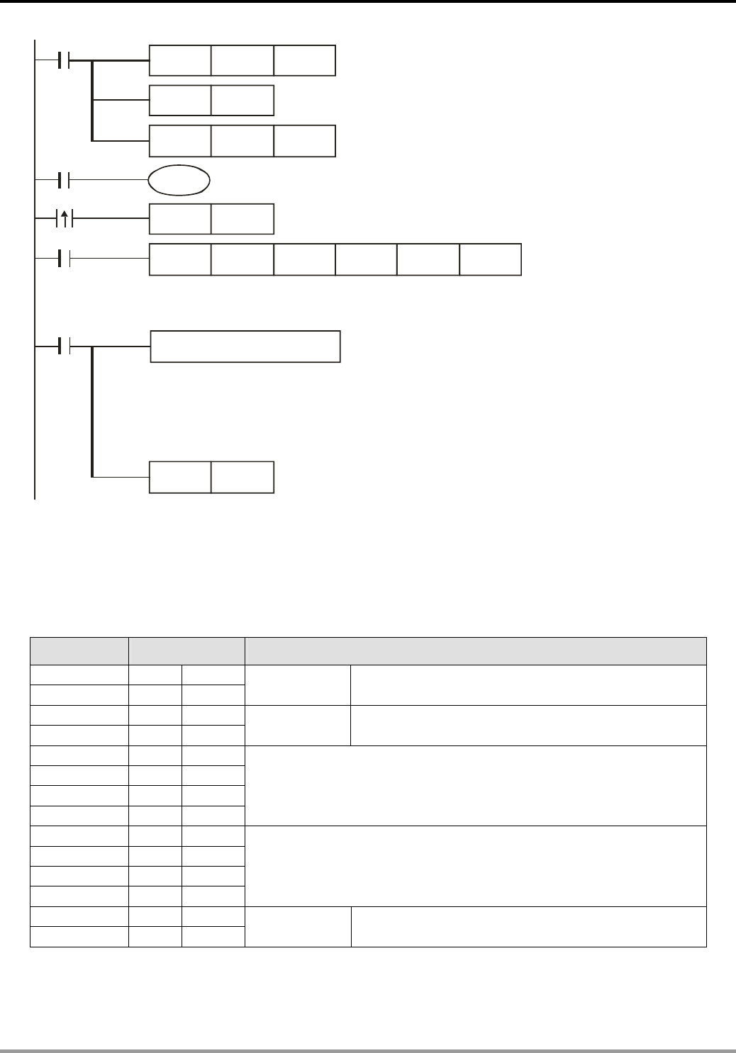
9 Application Instructions API 150-199
DVP-PLC Application Manual
9-3
H87
MOV
M100
2
D1120
SET M1120
K100
MOV D1129
M1127
RST M1127
M1143
X10
Set up communication protocol 9600, 8, E, 1
Retain communication protocol
Communication time-out 100ms
MODRW K3
K1
X0
H2100 D0 K6
Address of
communi-
cation
device K1
Function
code K3:
read
many data
Data address
H2100
Register
for storing
the data
Data length
(word)
Process of received data
ASCII mode: The received data will be stored in the designated registers starting
from D0 in ASCII format and PLC will automatically convert the data into hex value
and store them in special registers D1296 ~ D1311.
Sending/receiving of data is completed. The flag is reset.
RTU mode
SET
X0
M1122 Set up sending request
RTU mode: The received data will be stored in the designated registers starting
from D0 in hex format.
9. ASCII Mode: When PLC is connected to VFD-S AC motor drive.
PLC Ö VFD-S, PLC sends: “01 03 2100 0006 D5”
VFD-S Ö PLC, PLC receives: “01 03 0C 0100 1766 0000 0000 0136 0000 3B”
Registers for sent data (sending messages)
Register DATA Explanation
D1256 Low ‘0’ 30 H ADR 1
D1256 High ‘1’ 31 H ADR 0 Address of AC motor drive: ADR (1,0)
D1257 Low ‘0’ 30 H CMD 1
D1257 High ‘3’ 33 H CMD 0 Command code: CMD (1,0)
D1258 Low ‘2’ 32 H
D1258 High ‘1’ 31 H
D1259 Low ‘0’ 30 H
D1259 High ‘0’ 30 H
Starting Data Address
D1260 Low ‘0’ 30 H
D1260 High ‘0’ 30 H
D1261 Low ‘0’ 30 H
D1261 High ‘6’ 36 H
Number of Data (counted by words)
D1262 Low ‘D’ 44 H LRC CHK 1
D1262 High ‘5’ 35 H LRC CHK 0 Error checksum: LRC CHK (0,1)
9 Application Instructions API 150-199
DVP-PLC Application Manual
9-4
Registers for received data D0 (responding messages)
Register DATA Explanation
D0 Low ‘0’ 30 H ADR 1
D0 High ‘1’ 31 H ADR 0
D1 Low ‘0’ 30 H CMD 1
D1 High ‘3’ 33 H CMD 0
D2 Low ‘0’ 30 H
D2 High ‘C’ 43 H Number of Data (counted by byte)
D3 Low ‘0’ 30 H
D3 High ‘1’ 31 H
D4 Low ‘0’ 30 H
D4 High ‘0’ 30 H
Content of
address
2100H
PLC automatically convert ASCII codes to numerals and
store the numeral in D1296 = H0100
D5 Low ‘1’ 31 H
D5 High ‘7’ 37 H
D6 Low ‘6’ 36 H
D6 High ‘6’ 36 H
Content of
address
2101H
PLC automatically convert ASCII codes to numerals and
store the numeral in D1297 = H1766
D7 Low ‘0’ 30 H
D7 High ‘0’ 30 H
D8 Low ‘0’ 30 H
D8 High ‘0’ 30 H
Content of
address
2102H
PLC automatically convert ASCII codes to numerals and
store the numeral in D1298 = H0000
D9 Low ‘0’ 30 H
D9 High ‘0’ 30 H
D10 Low ‘0’ 30 H
D10 High ‘0’ 30 H
Content of
address
2103H
PLC automatically convert ASCII codes to numerals and
store the numeral in D1299 = H0000
D11 Low ‘0’ 30 H
D11 High ‘1’ 31 H
D12 Low ‘3’ 33 H
D12 High ‘6’ 36 H
Content of
address
2104H
PLC automatically convert ASCII codes to numerals and
store the numeral in D1300 = H0136
D13 Low ‘0’ 30 H
D13 High ‘0’ 30 H
D14 Low ‘0’ 30 H
D14 High ‘0’ 30 H
Content of
address
2105H
PLC automatically convert ASCII codes to numerals and
store the numeral in D1301 = H0000
D15 Low ‘3’ 33 H LRC CHK 1
D15 High ‘B’ 42 H LRC CHK 0
10. RTU Mode: When PLC is connected to VFD-S AC motor drive
PLC Ö VFD-S, PLC sends: “01 03 2100 0006 CF F4”
VFD-S Ö PLC, PLC receives: “01 03 0C 0000 0503 0BB8 0BB8 0000 012D 8E C5”
Registers for sent data (sending messages)
Register DATA Explanation
D1256 Low 01 H Address
D1257 Low 03 H Function
D1258 Low 21 H
D1259 Low 00 H Starting Data Address
D1260 Low 00 H
D1261 Low 06 H Number of Data (counted by words)
D1262 Low CF H CRC CHK Low
9 Application Instructions API 150-199
DVP-PLC Application Manual
9-5
Register DATA Explanation
D1263 Low F4 H CRC CHK High
Registers for received data D0 (responding messages)
Register DATA Explanation
D0 Low 01 H Address
D1 Low 03 H Function
D2 Low 0C H Number of Data (byte)
D3 Low 00 H
D4 Low 00 H
Content of
address 2100H
PLC automatically convert ASCII codes to numerals
and store the numeral in D1296 = H0000
D5 Low 05 H
D6 Low 03 H
Content of
address 2101H
PLC automatically convert ASCII codes to numerals
and store the numeral in D1297 = H0503
D7 Low 0B H
D8 Low B8 H
Content of
address 2102H
PLC automatically convert ASCII codes to numerals
and store the numeral in D1298 = H0BB8
D9 Low 0B H
D10 Low B8 H
Content of
address 2103H
PLC automatically convert ASCII codes to numerals
and store the numeral in D1299 = H0BB8
D11 Low 00 H
D12 Low 00 H
Content of
address 2104H
PLC automatically convert ASCII codes to numerals
and store the numeral in D1300 = H0000
D13 Low 01 H
D14 Low 2D H
Content of
address 2105H
PLC automatically convert ASCII codes to numerals
and store the numeral in D1301 = H012D
D15 Low 8E H CRC CHK Low
D16 Low C5 H CRC CHK High
Program Example 2:
1. Function code K6(H6): For writing a word data to register
When PLC is connected to VFD-S AC motor drive: M1143 = Off, in ASCII mode
When PLC is connected to VFD-S AC motor drive: M1143 = On, in RTU mode
2. When in ASCII mode, the user stores the data to be written in the designated register D50 in hex format. The
data sent back from AC motor drive are stored in D1070 ~ D1076.
3. When in RTU mode, the user stores the data to be written in the designated register D50 in hex format. The
data sent back from AC motor drive are stored in D1070 ~ D1077.
4. When In ASCII mode or RTU mode, PLC will store the data to be sent in D1256 ~ D1295. If necessary, the
user can move the data to other general registers by using MOV, DMOV or BMOV instruction. Other
instructions of ES/EX/SS do not function on the data in D1256 ~ D1295.
5. After receiving the data sent back from AC motor drive is completed, PLC will auto-check if the received data
are incorrect. M1140 will be On if there is an error.
6. If the device address is illegal to a designated communication device, the communication device will respond
with an error message and PLC will store the error code in D1130 and M1141 = On. For example, if 8000H is
illegal to VFD-S, M1141 will be On and D1130 = 2. See user manual of VFD-S for error codes.
7. After M1140 = On or M1141 = On, PLC will send another correct datum to AC motor drive. If the data sent back
from AC motor drive is correct, M1140 and M1141 will be reset.
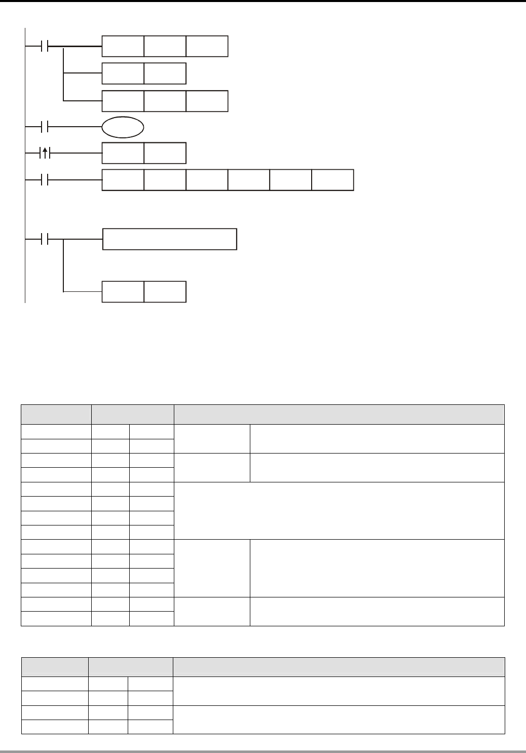
9 Application Instructions API 150-199
DVP-PLC Application Manual
9-6
H87MOV
M1002
D1120
SET M1120
K100
MOV D1129
M1127
RST M1127
M1143
X10
Set up communication protocol 9600, 8, E, 1
Retain communication protocol
Communication time-out 100ms
MODRW K6K1
X0
H2000 D50 K1
Address of
communi-
cation
device K1
Function
code K6:
write 1
word datum
Data address
H2000
Register
for storing
the data
Data length
(word)
SET
X0
M1122 Set up sending request
Process of received data
ASCII mode:
the received data will be stored in special registers D1070 ~ D1076 in ASCII format.
Sending/receiving of data is completed. The flag is reset.
RTU mode:
the received data will be stored in special registers D1070 ~ D1077 in hex format.
8. ASCII Mode: When PLC is connected to VFD-S AC motor drive.
PLC Ö VFD-S, PLC sends: “01 06 0100 1770 71”
VFD-S Ö PLC, PLC receives: “01 06 0100 1770 71”
Registers for sent data (sending messages)
Register DATA Explanation
D1256 Low ‘0’ 30 H ADR 1
D1256 High ‘1’ 31 H ADR 0 Address of AC motor drive: ADR (1,0)
D1257 Low ‘0’ 30 H CMD 1
D1257 High ‘6’ 36 H CMD 0 Command code: CMD (1,0)
D1258 Low ‘0’ 30 H
D1258 High ‘1’ 31 H
D1259 Low ‘0’ 30 H
D1259 High ‘0’ 30 H
Data Address
D1260 Low ‘1’ 31 H
D1260 High ‘7’ 37 H
D1261 Low ‘7’ 37 H
D1261 High ‘0’ 30 H
Data content The content of register D50 (H1770 = K6,000)
D1262 Low ‘7’ 37 H LRC CHK 1
D1262 High ‘1’ 31 H LRC CHK 0 LRC CHK (0,1) is error check
Registers for received data (responding messages)
Register DATA Explanation
D1070 Low ‘0’ 30 H ADR 1
D1070 High ‘1’ 31 H ADR 0
D1071 Low ‘0’ 30 H CMD 1
D1071 High ‘6’ 36 H CMD 0
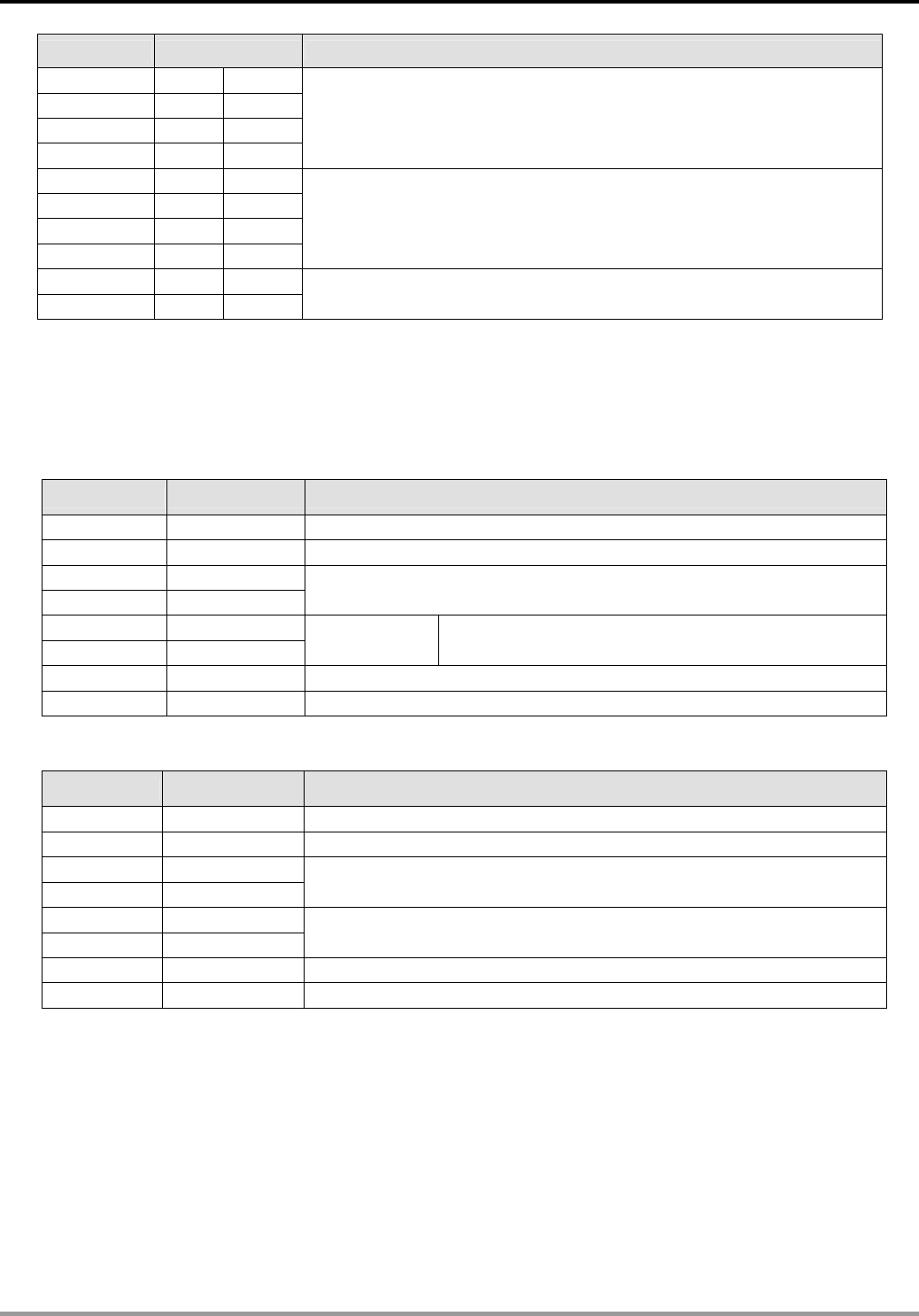
9 Application Instructions API 150-199
DVP-PLC Application Manual
9-7
Register DATA Explanation
D1072 Low ‘0’ 30 H
D1072 High ‘1’ 31 H
D1073 Low ‘0’ 30 H
D1073 High ‘0’ 30 H
Data Address
D1074 Low ‘1’ 31 H
D1074 High ‘7’ 37 H
D1075 Low ‘7’ 37 H
D1075 High ‘0’ 30 H
Data content
D1076 Low ‘7’ 37 H LRC CHK 1
D1076 High ‘1’ 31 H LRC CHK 0
9. RTU Mode: When PLC is connected to VFD-S AC motor drive
PLC Ö VFD-S, PLC sends: “01 06 2000 0012 02 07”
VFD-S Ö PLC, PLC receives: “01 06 2000 0012 02 07”
Registers for sent data (sending message)
Register DATA Explanation
D1256 Low 01 H Address
D1257 Low 06 H Function
D1258 Low 20 H
D1259 Low 00 H Data Address
D1260 Low 00 H
D1261 Low 12 H Data content The content of register D50 (H12)
D1262 Low 02 H CRC CHK Low
D1263 Low 07 H CRC CHK High
Registers for received data (responding message)
Register DATA Explanation
D1070 Low 01 H Address
D1071 Low 06 H Function
D1072 Low 20 H
D1073 Low 00 H Data Address
D1074 Low 00 H
D1075 Low 12 H Data content
D1076 Low 02 H CRC CHK Low
D1077 Low 07 H CRC CHK High
Program Example 3:
1. Function code K16(H10): For writing many word data into register.
When PLC is connected to VFD-S AC motor drive: M1143 = Off, in ASCII mode
When PLC is connected to VFD-S AC motor drive: M1143 = On, in RTU mode
2. When in ASCII mode, the user stores the data to be written in the designated register D50 in hex format. The
data sent back from AC motor drive are stored in D1070 ~ D1076.
3. When in RTU mode, the user stores the data to be written in the designated register D50 in hex format. The
9 Application Instructions API 150-199
DVP-PLC Application Manual
9-8
data sent back from AC motor drive are stored in D1070 ~ D1077.
4. When In ASCII mode or RTU mode, PLC will store the data to be sent in D1256 ~ D1295. If necessary, the
user can move the data to other general registers by using MOV, DMOV or BMOV instruction. Other
instructions of ES/EX/SS do not function on the data in D1256 ~ D1295.
5. After receiving the data sent back from AC motor drive is completed, PLC will auto-check if the received data
are incorrect. M1140 will be On if there is an error.
6. If the device address is illegal to a designated communication device, the communication device will respond
with an error message and PLC will store the error code in D1130 and M1141 = On. For example, if 8000H is
illegal to VFD-S, M1141 will be On and D1130 = 2. See user manual of VFD-S for error codes.
7. After M1140 = On or M1141 = On, PLC will send another correct datum to AC motor drive. If the data sent back
from AC motor drive is correct, M1140 and M1141 will be reset.
H87
MOV
M1002
D1120
SET M1120
K100MOV D1129
M1127
RST M1127
M1143
X10
Set up communication protocol 9600, 8, E, 1
Retain communication protocol
Communication time-out 100ms
MODRW K16K1
X0
H2000 D50 K8
Address of
communi-
cation
device K1
Function
code K16:
write many
word data
Data address
H2000
Register
for storing
the data
Data length
(word)
SET
X0
M1122 Set up sending request
Process of received data
ASCII mode
: The received data are stored in special registers D1070 ~ D1078 in ASCII format.
Sending/receiving of data is completed. The flag is reset.
RTU mode
: The
.
received data are stored in special registers D1070~1078 in hex format
8. ASCII Mode: When PLC is connected to VFD-S AC motor drive.
PLC Ö VFD-S, PLC sends: “01 10 2000 0002 04 0012 1770 30”
VFD-S Ö PLC, PLC receives: “01 10 2000 0002 CD”
Registers for sent data (sending messages)
Register DATA Explanation
D1256 Low ‘0’ 30 H ADR 1
D1256 High ‘1’ 31 H ADR 0 Address of AC motor drive: ADR (1,0)
D1257 Low ‘1’ 31 H CMD 1
D1257 High ‘0’ 30 H CMD 0 Command code: CMD (1,0)
D1258 Low ‘2’ 32 H
D1258 High ‘0’ 30 H
D1259 Low ‘0’ 30 H
D1259 High ‘0’ 30 H
Data Address
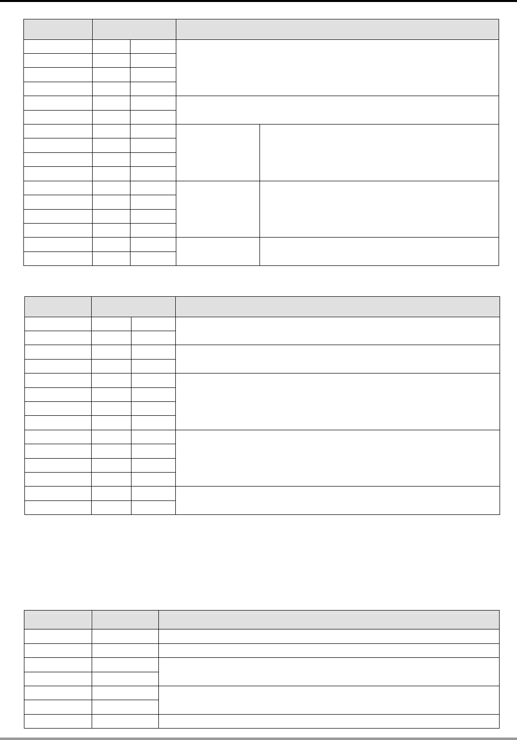
9 Application Instructions API 150-199
DVP-PLC Application Manual
9-9
Register DATA Explanation
D1260 Low ‘0’ 30 H
D1260 High ‘0’ 30 H
D1261 Low ‘0’ 30 H
D1261 High ‘2’ 32 H
Number of Registers
D1262 Low ‘0’ 30 H
D1262 High ‘4’ 34 H Byte Count
D1263 Low ‘0’ 30 H
D1263 High ‘0’ 30 H
D1264 Low ‘1’ 31 H
D1264 High ‘2’ 32 H
Data contents 1 The content of register D50 (H12)
D1265 Low ‘1’ 31 H
D1265 High ‘7’ 37 H
D1266 Low ‘7’ 37 H
D1266 High ‘0’ 30 H
Data contents 2 The content of register D51 (H1770 = K6,000)
D1267 Low ‘3’ 33 H LRC CHK 1
D1267 High ‘0’ 30 H LRC CHK 0 Error checksum: LRC CHK (0,1)
Registers for received data (responding messages)
Register DATA Explanation
D1070 Low ‘0’ 30 H ADR 1
D1070 High ‘1’ 31 H ADR 0
D1071 Low ‘1’ 31 H CMD 1
D1071 High ‘0’ 30 H CMD 0
D1072 Low ‘2’ 32 H
D1072 High ‘0’ 30 H
D1073 Low ‘0’ 30 H
D1073 High ‘0’ 30 H
Data Address
D1074 Low ‘0’ 30 H
D1074 High ‘0’ 30 H
D1075 Low ‘0’ 30 H
D1075 High ‘2’ 32 H
Number of Registers
D1076 Low ‘C’ 43 H LRC CHK 1
D1076 High ‘D’ 44 H LRC CHK 0
9. RTU Mode: When PLC is connected to VFD-S AC motor drives
PLC Ö VFD-S, PLC sends: “01 10 2000 0002 04 0012 1770 C4 7F”
VFD-S Ö PLC, PLC receives: “01 10 2000 0002 4A 08”
Registers for sent data (sending messages)
Register DATA Explanation
D1256 Low 01 H Address
D1257 Low 10 H Function
D1258 Low 20 H
D1259 Low 00 H Data Address
D1260 Low 00 H
D1261 Low 02 H Number of Registers
D1262 Low 04 H Byte Count
9 Application Instructions API 150-199
DVP-PLC Application Manual
9-10
Register DATA Explanation
D1263 Low 00 H
D1264 Low 12 H Data content 1 The content of register D50 (H12)
D1265 Low 17 H
D1266 Low 70 H Data content 2 The content of register D51 (H1770 = K6,000)
D1267 Low C4 H CRC CHK Low
D1268 Low 7F H CRC CHK High
Registers for received data (responding messages)
Register DATA Explanation
D1070 Low 01 H Address
D1071 Low 10 H Function
D1072 Low 20 H
D1073 Low 00 H Data Address
D1074 Low 00 H
D1075 Low 02 H Number of Registers
D1076 Low 4A H CRC CHK Low
D1077 Low 08 H CRC CHK High
Program Example 4:
1. Function code K2(H02): Read many bit devices. The read communication code will be placed in the register
designated by the 4th operand of the instruction. In the example below, K6 refers to the data length (bit).
Assume Y2=Y4=Y5=Y11=Y14=On for Y0 ~ Y16 status.
Set up communication protocol to 9600,8,E,1
M1002
MOV H87 D1120
SET M1120
MOV K100 D1129
X10
M1143
X0
MODRW K1 K2 H0500 D0 K6
X0
SET M1122
M1127
RST M1127
Retain communication protocol
Set up communication time-out: 100ms
Set up RTU mode
Set up sending request
Address of
communi-
cation
device K1
Function
code K2:
reads many
bit data
Data address:
H0500
PLC device:
Y0
Data
register
Read/write
data length
(word)
Process of received data
ASCII mode:
The received data are stored in special registers starting from D0 in
ASCII format. PLC will automatically convert the data into hex and store them in
D1296 ~ D1311.
RTU mode:
The received data are stored in special registers starting from D0
designated by the user in hex format.
Sending/receiving of data is completed.
The flag is reset.
9 Application Instructions API 150-199
DVP-PLC Application Manual
9-11
2. ASCII Mode: When PLC1 is connected to PLC2
When X0 = On, function code 02 of MODRW instrruction will start to be executed.
PLC1Ö PLC2, PLC1 sends: “01 02 0500 0010 E8”
PLC2 Ö PLC1, PLC1 receives: “01 02 02 34 12 B5”
Registers for PLC1 sent data (sending messages)
Register DATA Explanation
D1256 Low ‘0’ 30 H ADR 1
D1256 High ‘1’ 31 H ADR 0 Address of connected device: ADR (1,0)
D1257 Low ‘0’ 30 H CMD 1
D1257 High ‘2’ 32 H CMD 0 Command code: CMD (1,0)
D1258 Low ‘0’ 30 H
D1258 High ‘5’ 35 H
D1259 Low ‘0’ 30 H
D1259 High ‘0’ 30 H
Starting Data Address
D1260 Low ‘0’ 30 H
D1260 High ‘0’ 30 H
D1261 Low ‘1’ 31 H
D1261 High ‘0’ 30 H
Number of Data (counted by bits)
D1262 Low ‘E’ 45 H LRC CHK 1
D1262 High ‘8’ 38 H LRC CHK 0 Error checksum: LRC CHK (0,1)
Register (D0) for PLC1 received data (responding messages):
Register DATA Explanation
D0 Low ‘0’ 30 H ADR 1
D0 High ‘1’ 31 H ADR 0
D1 Low ‘0’ 30 H CMD 1
D1 High ‘2’ 33 H CMD 0
D2 Low ‘0’ 30 H
D2 High ‘2’ 32 H Number of data (counted by bytes)
D3 Low ‘3’ 33 H
D3 High ‘4’ 34 H
D4 Low ‘1’ 31H
D4 High ‘2’ 32H
Content in
address 0500 ~
0505
PLC automatically convert ASCII words and store
the result in D1296 = H1234
(b0 ~ b5 are valid)
D5 Low ‘B’ 52H LRC CHK 1
D5 High ‘5’ 35 H LRC CHK 0
3. RTU Mode: When PLC1 is connected to PLC2
When X10 = On, function code 02 of MODRW instruction will start to be executed.
PLC1Ö PLC2, PLC1 sends: “01 02 0500 0010 79 0A”
PLC2 Ö PLC1, PLC1 receives: “01 02 02 34 12 2F 75”
Registers for PLC sent data (sending messages):
Register DATA Explanation
D1256 low 1 H Address
D1257 low 2 H Function
9 Application Instructions API 150-199
DVP-PLC Application Manual
9-12
Register DATA Explanation
D1258 low 5 H
D1259 low 0 H Starting data address
D1260 low 0 H
D1261 low 10 H Number of data (counted by words)
D1262 low 79 H CRC CHK Low
D1263 low 0A H CRC CHK High
Register (D0) for PLC received data (responding messages):
Register DATA Explanation
D0 low 01 H Address
D1 low 02 H Function
D2 low 02 H Number of data (byte)
D3 low 34 H
D4 low 12 H
Content in address
0500H
PLC automatically stores the value in
D1296=H1234 (b0 ~ b5 are valid)
D5 low 2F H CRC CHK Low
D6 low 75 H CRC CHK High
Program Example 5:
1. Function code K15(H0F): Write many bit devices. The preset bit status has to be placed in the register
designated by the 4th operand of the instruction in b0 ~ b5 order. 1 word is able to contain 16 bit status data.
M1002
MOV H87 D1120
SET M1120
MOV K100 D1129
X10
M1143
X0
MODRW K1 K15 H0500 D0 K6
X0
SET M1122
M1127
RST M1127
MOV HFFFF D0
Set up communication protocol to 9600,8,E,1
Retain communication protocol
Set up communication time-out: 100ms
Set up RTU mode
Set up sending request
Set up status value to be written into device
Address of
communi-
cation
device K1
Function
code K15:
writes many
bit data
Data address:
H0500
PLC device:
Y0
Data
register
Read/write
data length
(word)
Process of received data
ASCII mode:
The received data are stored in special registers starting from D0 in ASCII format.
PLC will automatically convert the data into hex and store them in D1296 ~ D1311.
RTU mode:
The received data are stored in special registers starting from D0 desiganted
by the user in hex format.
Sending/receiving of data is completed.
The flag is reset.
9 Application Instructions API 150-199
DVP-PLC Application Manual
9-13
2. ASCII Mode: When PLC1 is connected to PLC2
When X0 = On, function code 0F of MODRW instruction will start to be executed.
PLC1 Ö PLC2, PLC sends: “ 1 0F 0500 0006 01 3F A5”
PLC2 Ö PLC1, PLC receives: “ 1 0F 0500 0006 E5”
Registers for PLC1 sent data (sending messages):
Register DATA Explanation
D1256 low ‘0’ 30 H ADR 1
D1256 high ‘1’ 31 H ADR 0 Address of connected device: ADR (1,0)
D1257 low ‘0’ 30 H CMD 1
D1257 high ‘F’ 46 H CMD 0 Command code: CMD (1,0)
D1258 low ‘0’ 30 H
D1258 high ‘5’ 35 H
D1259 low ‘0’ 30 H
D1259 high ‘0’ 30 H
Data address
D1260 low ‘0’ 30 H
D1260 high ‘0’ 30 H
D1261 low ‘0’ 30H
D1261 high ‘6’ 36 H
Number of data (counted by bits)
D1262 low ‘0’ 30 H
D1262 high ‘1’ 31 H Byte Count
D1263 low ‘3’ 33 H
D1263 high ‘F’ 46 H Data content 1 Content in D0 register (H3F)
D1264 low ‘A’ 41 H LRC CHK 1
D1264 high ‘5’ 35 H LRC CHK 0 Error checksum: LRC CHK (0,1)
Registers for PLC1 received data (responding messages):
Register DATA Explanation
D1070 low ‘0’ 30 H ADR 1
D1070 high ‘1’ 31 H ADR 0
D1071 low ‘0’ 31 H CMD 1
D1071 high ‘F’ 46 H CMD 0
D1072 low ‘0’ 30 H
D1072 high ‘5’ 35 H
D1073 low ‘0’ 30 H
D1073 high ‘0’ 30 H
Data address
D1074 low ‘0’ 30 H
D1074 high ‘0’ 30 H
D1075 low ‘0’ 30 H
D1075 high ‘6’ 36 H
Number of registers
D1076 low ‘E’ 45 H LRC CHK 1
D1076 high ‘5’ 35 H LRC CHK 0
3. RTU Mode: When PLC1 is connected to PLC2
When X10 = On, function code 15 of MODRW instruction will start to be executed.
PLC1Ö PLC2, PLC1 sends: “01 0F 0500 0006 01 3F”
9 Application Instructions API 150-199
DVP-PLC Application Manual
9-14
PLC2 Ö PLC1, PLC1 receives: “01 0F 0500 0006 D5 05”
Registers for PLC sent data (sending messages):
Register DATA Explanation
D1256 low 01 H Address
D1257 low 0F H Function
D1258 low 05 H
D1259 low 00 H Data address
D1260 low 00 H
D1261 low 06 H Data content Content in D0 register (H3F)
D1262 low 01 H CRC CHK Low
D1263 low 3F H CRC CHK High
Registers for PLC received data (responding messages):
Register DATA Explanation
D1070 low 01 H Address
D1071 low 0F H Function
D1072 low 05 H
D1073 low 00 H Data address
D1074 low 00 H
D1075 low 06H Data content
D1076 low D5H CRC CHK Low
D1077 low 05 H CRC CHK High
Program Example 6:
1. Function code K5(H5): Write status of single bit device. In the example below, Set K1 to bit On, K0 to bit Off.
M1002
MOV H87 D1120
SET M1120
MOV K100 D1129
M10
M1143
M0
MODRW K1 K5 H0500 D0 K1
M0
SET M1122
M0
M0
MODRW K1 K5 H0500 D0 K0
Set up communication protocol to 9600,8,E,1
Retain communication protocol
Set up communication time-out: 100ms
Set up RTU mode
Set up sending request
Address of
communi-
cation
device K1
Function
code K15:
sets single
point On/Off
Data address:
H0500
PLC device:
Y0
Set On
Set Off
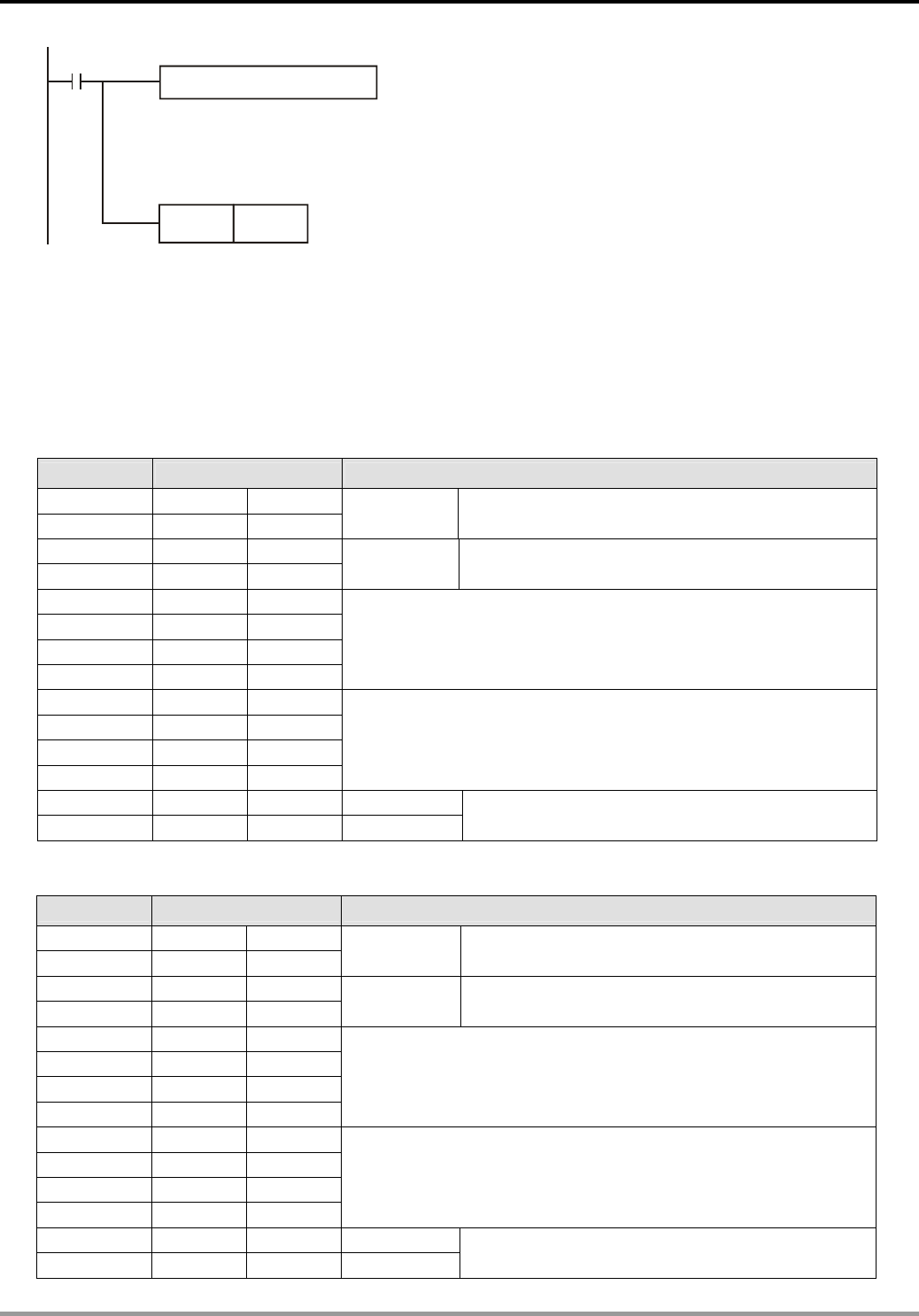
9 Application Instructions API 150-199
DVP-PLC Application Manual
9-15
M1127
RST M1127
Process of received data
ASCII mode:
RTU mode:
The received data are stored in special registers D1070 ~ D1076 in ASCII format.
The received data are stored in special registers D1070 ~ D1077 in hex format.
Sending/receiving of data is completed.
The flag is reset.
2. ASCII Mode: When PLC1 is connected to PLC2
When M0 = On, function code 05 (bit On) of MODRW instruction will start to be executed.
PLC1Ö PLC2, PLC1 sends: “01 05 0500 FF00 F6”
PLC2 Ö PLC1, PLC1 receives: “01 05 0500 FF00 F6”
Registers for PLC1 sent data (sending messages):
Register DATA Explanation
D1256 low ‘0’ 30 H ADR 1
D1256 high ‘1’ 31 H ADR 0 Address of connected device: ADR (1,0)
D1257 low ‘0’ 30 H CMD 1
D1257 high ‘5’ 35 H CMD 0 Command code: CMD (1,0)
D1258 low ‘0’ 30 H
D1258 high ‘5’ 35 H
D1259 low ‘0’ 30 H
D1259 high ‘0’ 30 H
Starting data address
D1260 low ‘F’ 46 H
D1260 high ‘F’ 46 H
D1261 low ‘0’ 30 H
D1261 high ‘0’ 30 H
Request bit On/Off
D1262 low ‘F’ 46 H LRC CHK 1
D1262 high ‘6’ 36 H LRC CHK 0 Error checksum: LRC CHK (0,1)
Registers (D0) for PLC1 received data (responding messages):
Register DATA Explanation
D1070 low ‘0’ 30 H ADR 1
D1070 high ‘1’ 31 H ADR 0 Address of connected device: ADR (1,0)
D1071 low ‘0’ 30 H CMD 1
D1071 high ‘5’ 35 H CMD 0 Command code: CMD (1,0)
D1072 low ‘0’ 30 H
D1072 high ‘5’ 35 H
D1073 low ‘0’ 30 H
D1073 high ‘0’ 30 H
Starting data address
D1074 low ‘F’ 46 H
D1074 high ‘F’ 46 H
D1075 low ‘0’ 30 H
D1075 high ‘0’ 30 H
Request bit On/Off
D1076 low ‘F’ 46 H LRC CHK 1
D1076 high ‘6’ 36 H LRC CHK 0 Error checksum: LRC CHK (0,1)
9 Application Instructions API 150-199
DVP-PLC Application Manual
9-16
When M0 = Off, function code 05 (bit Off) will start to be executed.
PLC1Ö PLC2, PLC1 sends: “01 05 0500 FF00 F6”
PLC2 Ö PLC1, PLC1 receives: “01 05 0500 FF00 F6”
Registers for PLC1 sent data (sending messages):
Register DATA Explanation
D1256 low ‘0’ 30 H ADR 1
D1256 high ‘1’ 31 H ADR 0 Address of connected device: ADR (1,0)
D1257 low ‘0’ 30 H CMD 1
D1257 high ‘5’ 35 H CMD 0 Command code: CMD (1,0)
D1258 low ‘0’ 30 H
D1258 high ‘5’ 35 H
D1259 low ‘0’ 30 H
D1259 high ‘0’ 30 H
Starting data address
D1260 low ‘0’ 30 H
D1260 high ‘0’ 30 H
D1261 low ‘0’ 30 H
D1261 high ‘0’ 30 H
Request bit On/Off
D1262 low ‘F’ 46 H LRC CHK 1
D1262 high ‘5’ 35 H LRC CHK 0 Error checksum: LRC CHK (0,1)
Registers (D0) for PLC1 received data (responding messages):
Register DATA Explanation
D1070 low ‘0’ 30 H ADR 1
D1070 high ‘1’ 31 H ADR 0 Address of connected device: ADR (1,0)
D1071 low ‘0’ 30 H CMD 1
D1071 high ‘5’ 35 H CMD 0 Command code: CMD (1,0)
D1072 low ‘0’ 30 H
D1072 high ‘5’ 35 H
D1073 low ‘0’ 30 H
D1073 high ‘0’ 30 H
Starting data address
D1074 low ‘0’ 30 H
D1074 high ‘0’ 30 H
D1075 low ‘0’ 30 H
D1075 high ‘0’ 30 H
Request bit On/Off
D1076 low ‘F’ 46 H LRC CHK 1
D1076 high ‘5’ 35 H LRC CHK 0 Error checksum: LRC CHK (0,1)
3. RTU Mode: When PLC1 is connected to PLC2
When M0 = On, function code 05 (bit On) of MODRW instruction will start to be executed.
PLC1Ö PLC2, PLC1 sends: “01 05 0500 FF00 8C F6”
PLC2 Ö PLC1, PLC1 receives: “01 05 0500 FF00 8C F6”
Registers for PLC sent data (sending messages):
Register DATA Explanation
D1256 low 01 H Address
D1257 low 05 H Function
9 Application Instructions API 150-199
DVP-PLC Application Manual
9-17
Register DATA Explanation
D1258 low 05 H
D1259 low 00 H Starting data address
D1260 low FF H
D1261 low 00 H
Set bit On/Off
Request bit ON/OFF
D1262 low 8C H CRC CHK Low
D1263 low F6 H CRC CHK High
Registers (D0) for PLC received data (responding messages):
Register DATA Explanation
D1070 low 01 H Address
D1071 low 05 H Function
D1072 low 05 H
D1073 low 00 H Starting data address
D1074 low FF H
D1075 low 00 H
Set bit On/Off
Request bit ON/OFF
D1076 low 8C H CRC CHK Low
D1077 low F6 H CRC CHK High
When M10 = Off, function code 05 (bit Off) of MODRW instruction will start to be executed.
PLC1Ö PLC2, PLC1 sends: “01 05 0500 0000 CD 06”
PLC2 Ö PLC1, PLC1 receives: “01 05 0500 0000 CD 06”
Registers for PLC sent data (sending messages):
Register DATA Explanation
D1256 low 01 H Address
D1257 low 05 H Function
D1258 low 05 H
D1259 low 00 H Starting data address
D1260 low 00 H
D1261 low 00 H
Set bit On/Off
Request bit ON/OFF
D1262 low CD H CRC CHK Low
D1263 low 06 H CRC CHK High
Registers (D0) for PLC received data (responding messages):
Register DATA Explanation
D1070 low 01 H Address
D1071 low 05 H Function
D1072 low 05 H
D1073 low 00 H Starting data address
D1074 low 00 H
D1075 low 00 H
Set bit On/Off
Request bit ON/OFF
D1076 low CD H CRC CHK Low
D1077 low 06 H CRC CHK High
Remarks:
1. The activation condition placed before MODRD, RDST and MODRW instructions cannot use rising-edge or

9 Application Instructions API 150-199
DVP-PLC Application Manual
9-18
falling-edge contacts; otherwise the data stored in the registers for received data will encounter errors.
2. Flags and special registers for MODRW instruction in RS-485 communication. (For details, see API 80 RS).
Flags Function
M1120 For retaining communication setups. After the setup is made, changes in D1120 will be
invalid.
M1121 When Off, RS-485 is sending data.
M1122 Sending request
M1123 Receiving is completed
M1124 Waiting for receiving data
M1125 Disable receiving status
M1126 Selecting STX/ETX system
M1127 Sending/receiving data through MODRD / RDST / MODRW instructions is completed.
M1128 Sending data…/receiving data…
M1129 Receiving data time-out
M1130 User/system defined STX/ETX
M1131 On when MODRD / MODWR / MODRW is converting data to hex
M1140 MODRD / MODWR / MODRW data receiving error
M1141 MODRD / MODWR / MODRW parameter error
M1142 VFD-A handy instruction data receiving error
M1143 ASCII/RTU mode selection (used with MODRD/MODWR/MODRW) (Off = ASCII mode;
On = RTU mode)
D1070 ~ D1085
When the built-in RS-485 communication instruction is executed and sends out data, the
receiving end will respond with a message and the message will be stored in D1070 ~
D1085. The user can check the registers for the messages.
D1120 RS-485 communication protocol
D1121 PLC communication address (saving PLC communication address; latched)
D1122 Remaining words of the sent data
D1123 Remaining words of the received data
D1124 Start text definition (STX)
D1125 Definition of end text 1 (ETX1)
D1126 Definition of end text 2 (ETX2)
D1129 Abnormal communication time-out. Unit: ms
D1130 Records of error codes sent back from MODBUS
D1256 ~ D1295
When the built-in RS-485 communication instruction MODRW is executed, the sent out
data will be stored in D1256 ~ D1295. The user can check whether the instruction is
correct by the contents in the registers.
D1296 ~ D1311 PLC will automatically convert the ASCII data stored in the register designated by the user
into hex format.
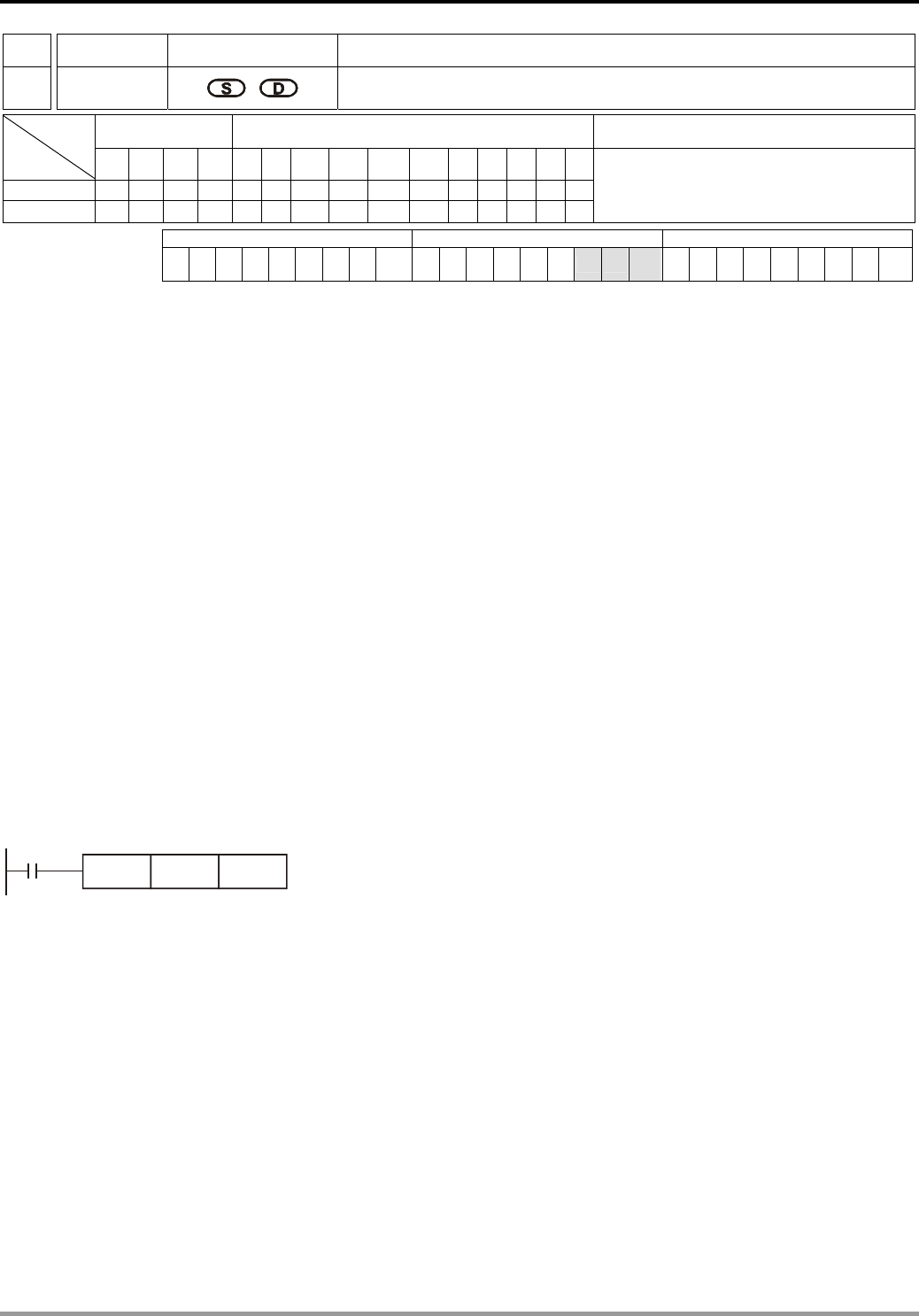
9 Application Instructions API 150-199
DVP-PLC Application Manual
9-19
API Mnemonic Operands Function
151
PWD Detection of Input Pulse Width
Bit Devices Word Devices Program Steps Type
OP X Y M S K H KnX KnY KnM KnS T C D E F
S *
D *
PWD: 5 steps
PULSE 16-bit 32-bit
ES EX SS SA SX SC EH SV EH3
SV2 ES EX SS SA SX SC EH SV EH3
SV2 ES EX SS SA SX SC EH SV EH3
SV2
Operands:
S: Source device D: Destination device for storing the detected result
Explanations:
1. Range of S: X10 ~ X17
2. Range of D: D0 ~ D999, occupying 2 consecutive devices. Can only be used once in the program.
3. PWD instruction is for detecting the time span of output signals from X10 ~ X17; the valid frequency range is 1
~1kHz. When M1169 = On, the instruction will detect the time span of the continuous rising edge and falling
edge of the input signals (time unit: 100us). When M1169 = On, the instruction will detect the time span of 2
continuous rising edges of the input signals (time unit: 1us). It cannot designate the same X10 ~ X17 as does
DCNT and ZRN instructions.
4. D occupies two continuous devices. The longest detectable time is 21,474.83647 seconds, about 357.9139
minutes or 5.9652 hours.
5. There is no limitation on the times of using this instruction. However, only one instruction can be executed at a
time.
Program Example:
When X0 = On, record the time span of X10 = On and store it in D1 and D0.
X0
PWD X10 D0

9 Application Instructions API 150-199
DVP-PLC Application Manual
9-20
API Mnemonic Operands Function
152
RTMU Start of the Measurement of Execution Time of I Interruption
Bit Devices Word Devices Program Steps Type
OP X Y M S K H KnX KnY KnM KnS T C D E F
D * * *
n * * *
RTMU: 5 steps
PULSE 16-bit 32-bit
ES EX SS SA SX SC EH SV EH3
SV2 ES EX SS SA SX SC EH SV EH3
SV2 ES EX SS SA SX SC EH SV EH3
SV2
Operands:
D: Device for storing the measuring time (unit: 1us) n: Measurement time base. Parameter range: K10 ~ K500
(time unit: 1us)
Explanations:
1. Range of D: K0 ~ K9
2. Range of n: K10 ~ K500
3. The designated special D registers (D1156 ~ D1165) can measure up to 10 interruption subroutines. For
example, when D = K5, the designated D register will be D1161.
4. When RTMU is executed, if the D and n entered by the user are legal, interruption of the timer will be enabled
and the counting starts and the special D designated by D is cleared as 0. When RTMD is executed,
interruption of the timer is disabled and the calculated time will be assigned to special D designated by RTMD.
5. With API 153 RTMD, RTMU can measure the execution time of “I” interruption service subroutine, which can
be reference for dealing with the high-speed response when the user is at the initial stage of developing the
program.
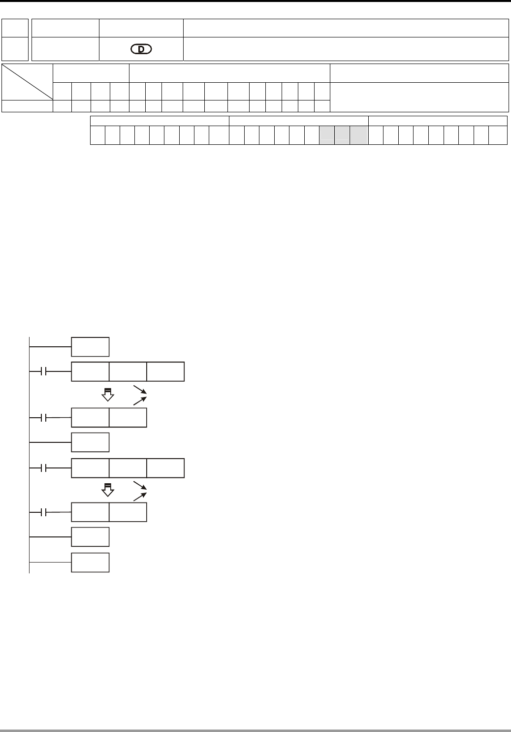
9 Application Instructions API 150-199
DVP-PLC Application Manual
9-21
API Mnemonic Operands Function
153
RTMD End of the Measurement of the Execution Time of I Interruption
Bit Devices Word Devices Program Steps Type
OP X Y M S K H KnX KnY KnM KnS T C D E F
D * * *
RTMD: 3 steps
PULSE 16-bit 32-bit
ES EX SS SA SX SC EH SV EH3
SV2 ES EX SS SA SX SC EH SV EH3
SV2 ES EX SS SA SX SC EH SV EH3
SV2
Operands:
D: Device to store the measuring time (unit: 1us).
Explanations:
1. Range of D: K0 ~ K9. The No. of D has to be the same as that designated by D in API 152 RTMU; otherwise the
result of the measurement may be unexpectable.
Program Example:
When X0 goes from Off to On, the program will enter I001 interruption subroutine. RTMU will activate an 8-bit timer
(unit: 10us) and RTMD (when D = K0) will shut down the timer and store the time in the timer in special D registers
(D1156 ~ D1165, designated by K0 ~ K9).
FEND
M1000
RTMU K0 K10
RTMD K0
IRET
I 001
M1000
M1000
RTMU K1 K10
RTMD K1
IRET
I 101
M1000
END
Both K0 should be the same
Both K1 should be the same
Remarks:
1. We suggest you remove this instruction after you finish developing your PLC program.
2. Due to the lower priority of the interruption enabled by RTMU, when RTMU is enabled, other high-speed pulse
input counting or high-speed pulse output may result in failure to trigger the timer.
3. If you activate RTMU but do not activate RTMD before the end of the interruption, the interruption will not be
shut down.
4. RTMU instruction activates 1 timer interruption in PLC. Therefore, if many RTMU or RTMD are executed at the

9 Application Instructions API 150-199
DVP-PLC Application Manual
9-22
same time, confusion in the timer may occur. Please be aware of the situation.
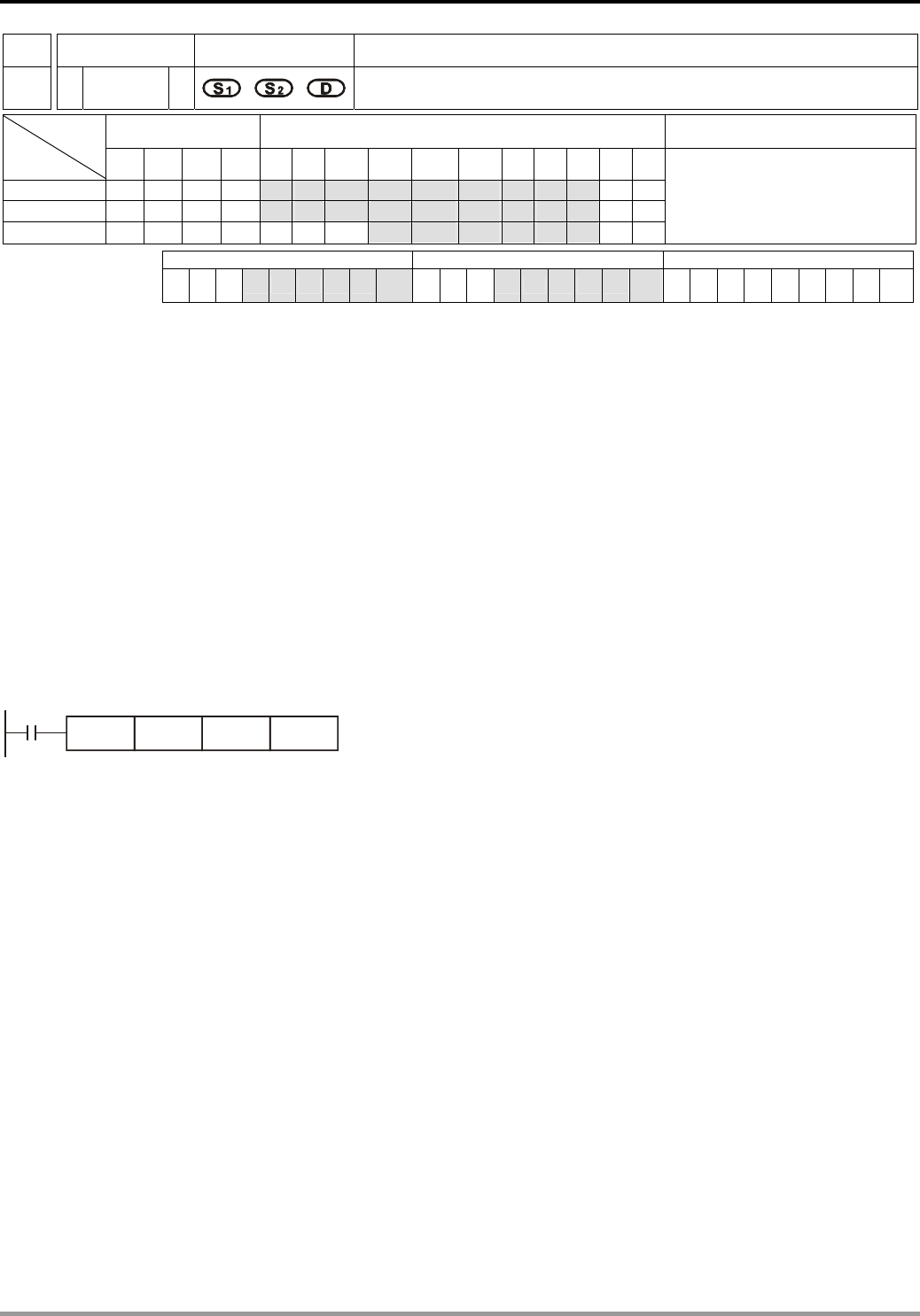
9 Application Instructions API 150-199
DVP-PLC Application Manual
9-23
API Mnemonic Operands Function
154
RAND P Random Number
Bit Devices Word Devices Program Steps Type
OP X Y M S K H KnX KnY KnM KnS T C D E F
S1 * * * * * * * * ***
S2 * * * * * * * * ***
D * * * * * ***
RAND, RANDP: 7 steps
PULSE 16-bit 32-bit
ES EX SS SA SX SC EH SV EH3
SV2 ES EX SS SA SX SC EH SV EH3
SV2 ES EX SS SA SX SC EH SV EH3
SV2
Operands:
S1: Lower bound of the random number S2: Upper bound of the random number D: The random number
produced
Explanations:
1. S1≦S2; K0 ≦ S
1 , S2 ≦K32,767
2. See the specifications of each model for their range of use.
3. Entering S1 > S2 will result in operation error. The instruction will not be executed at this time, M1067, M1068 =
On and D1067 records the error code 0E1A (hex).
Program Example:
When X10 = On, RAND will produce the random number between the lower bound D0 and upper bound D10 and
store the result in D20.
X10
RAND D0 D10 D20
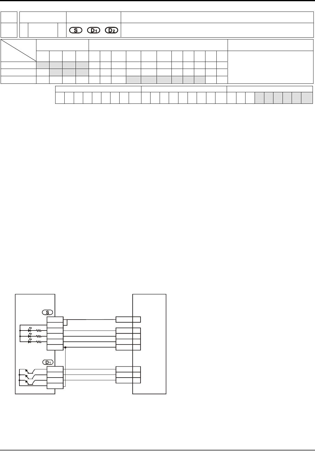
9 Application Instructions API 150-199
DVP-PLC Application Manual
9-24
API Mnemonic Operands Function
155
D ABSR Read the Absolute Position from a Servo Motor
Bit Devices Word Devices Program Steps Type
OP X Y M S K H KnX KnY KnM KnS T C D E F
S * * * *
D1 * * *
D2 * * * * * **
DABSR: 13 steps
PULSE 16-bit 32-bit
ES EX SS SA SX SC EH SV EH3
SV2 ES EX SS SA SX SC EH SV EH3
SV2 ES EX SS SA SX SC EH SV EH3
SV2
Operands:
S: Input signal from Servo (occupies 3 consecutive devices) D1: Control signal for controlling Servo (occupies 3
consecutive devices) D2: Absolute position data (32-bit) read from Servo
Explanations:
1. Operand S and D1 of SA series MPU do not support E, F index register modification.
2. See the specifications of each model for their range of use.
3. This instruction can only be used once in the program.
4. Flag: see remarks for more details.
5. This instruction reads the absolute position (ABS) of MITSUBISHI MR-J2 servo drive (with absolute position
check function).
6. S will occupy 3 consecutive devices, S, S +1, and S +2. S and S +1 are connected to the absolute position (bit
0, bit 1) on the servo for data transmitting. S +2 is connected to Servo for transmitting data ready flag. See the
wiring example below for more details.
7. D1 will occupy 3 consecutive devices, D1, D1 + 1, D1 + 2. D1 is connected to SERVO On (SON) of Servo. D1+1 is
connected to ABS transmisstion mode of Servo and D1+2 is connected to ABS request signal. See the wiring
example below for more details.
PLC
DVP32EH00T
ABS(bit 0)
ABS(bit 1)
SERVO ON
SERVO AMP
MR-J2-A
CN1B
D01 4
19
10
6
ZSP
TLC
SG
5
8
9
SON
ABSM
ABSR
X0
X1
X2
24G
S/S
+24V
Y4
Y5
Y6
C4
VDD 3
transmission data is ready
ABS request
ABS transmission mode
8. D2 will occupy 2 consecutive devices D2 and D2 + 1. D2 is the lower 16 bits and D2 + 1 is the higher 16 bits. The
absolute position data should be written into the present value registers (D1337, D1336) of CH0 pulse (Y0, Y1)
or the present value registers (D1339, D1338) of CH1 pulse (Y2, Y3) in EH series MPU; therefore, we suggest
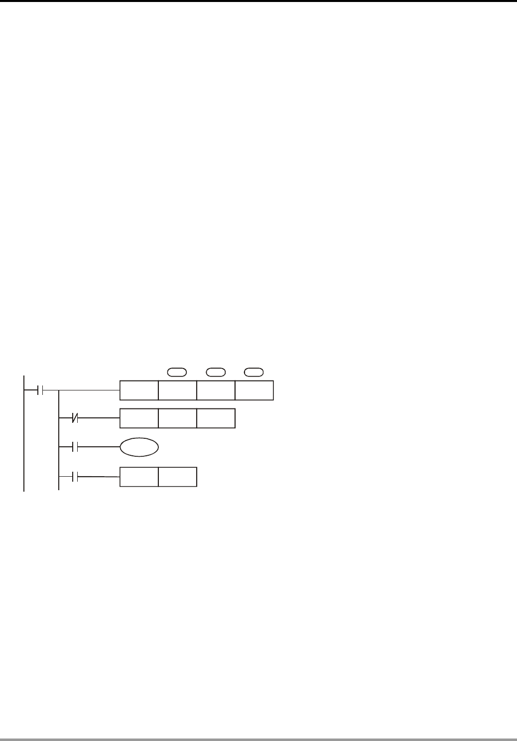
9 Application Instructions API 150-199
DVP-PLC Application Manual
9-25
you designate the two corresponding registers. If you designate other devices as the registers, you still have to
transmit the data to D1337 and D1336 of CH0 or D1339 and D1338 of CH1. In addition, the absolute position
data should be written into the present value registers (D1348, D1349) of CH0 pulse (Y10) or the present value
registers (D1350, D1351) of CH1 pulse (Y11) in SC series MPU; therefore, we suggest you designate the two
corresponding registers. If you designate other devices as the registers, you still have to transmit the data to
D1348 and D1349 of CH0 or D1350 and D1351 of CH1.
9. When DABSR instruction starts to read, after finishing reading the absolute position of SERVO, flag M1029 will
be On. The user has to reset the flag.
10. When driving the DABSR command, please specify normally open contact. If the drive contact of DABSR
command turns Off when DABSR command read starts, the execution of absolute current value read will be
interrupted and result in incorrect data. Please be careful and notice that.
Program Example:
1. When X7 = On, the 32-bit absolute position data read from Servo will be stored in the present value registers
(D1337, D1336) of CH0 pulse in EH MPU. At the same time, the timer T10 is enabled and starts to count for 5
seconds. If the reading of the absolute position is not completed after 5 seconds, M10 will be On, indicating that
the reading of absolute position encounters abnormality.
2. When enabling the connection to the system, please synchronize the power input of DVP-PLC
EH/EH2/SV/EH3/SV2 and SERVO AMP or activate the power of SERVO AMP earlier than DVP-PLC.
X7
M11
T0
M1029
SET M11
M10
TMR T0 K50
DABS X0 Y4 D1336
Time-out : 5 sec.
ABS absolute position data read is abnormal
ABS absolute position data read completed
execution completed
flag
Read overtime
ABS read completed
SDD
12
Remarks:
1. If the instruction is interrupted when PLC is still reading the absolute position of SERVO, an ALARM message
(ALE5) will occur in SERVO.
2. Timing chart of DABSR instruction reading absolute position:
a) When DABSR instruction starts to execute, it will drive SERBVO On (SON) and ABS transmittion mode for
output.
b) By “transmission is ready” and “ABS request” signals, you can confirm the transmission and reciept of both
sides as well as processing the transmission of the 32-bit present position data plus the 6-bit check data.
c) The data are transmitted by ABS (bit0, bit1).
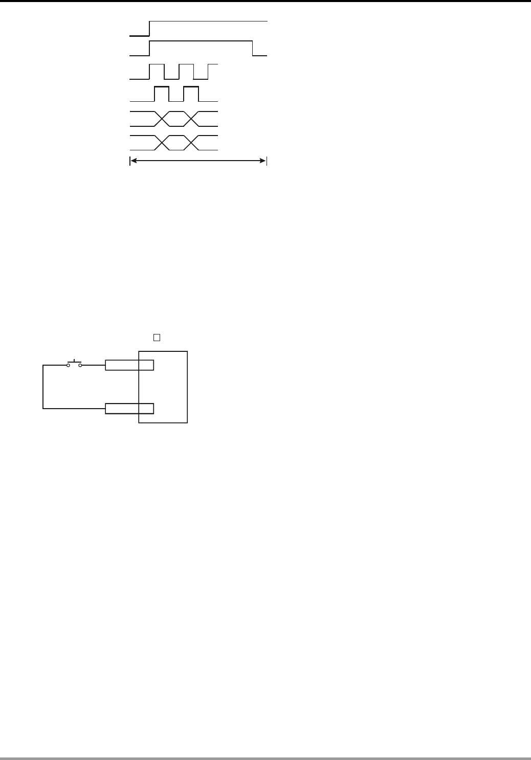
9 Application Instructions API 150-199
DVP-PLC Application Manual
9-26
SON
ABSM
TLC
ABSR
ZSP
D01
AMP output
SERVO ON
ABS(bit 1)
ABS(bit 0)
32-bit present value position data
+(plus) 6-bit check data
Controller output
AMP output
AMP output
ABS data
transmission mode
Transmission dat
a
is read
y
ABS request
3. This instruction is applicable to the Servo motor equipped with absolute positioning function, e.g. Mitsubishi
MR-J2-A Servo drive.
4. Select one of the following methods for the initial reading of present absolute position.
a) Complete zero point return by using reset signal function to execute API 156 ZRN instruction.
b) After using JOG or manual operation to adjust the zero point position, input a reset signal in SERVO AMP.
See the figure of external switch below for whether to use DVP-PLC for output. For the wiring of DVP-PLC
and Mitsubishi MR-H2-□A, see remarks of API 159 DRVA instruction.
CR 8
SG 10
reset
Ex: Mitsubishi MR-J2- A
5. Flags explanation:
M1010: (For EH/EH2/SV/EH3/SV2 series MPU) When M1010 is On, CH0 (Y0, Y1) and CH1 (Y2, Y3) will
output pulses while END instruction is being executed. When the output starts, M1010 will
automatically turn Off.
M1029: (For EH/EH2/SV/EH3/SV2 series MPU) When the first group CH0 (Y0, Y1) pulse output or the
execution of other relevant instructions are completed, M1029 will turn On.
M1030: (For EH/EH2/SV/EH3/SV2 series MPU) When the second group CH1 (Y2, Y3) pulse output is
completed, M1030 will turn on.
M1102: (For SC series MPU) When the first group CH0 (Y10) pulse output is completed, M1102 will turn On.
M1103: (For SC series MPU) When the second group CH1 (Y11) pulse output is completed, M1103 will turn
On.
M1258: (For EH/EH2/SV/EH3/SV2 series MPU) When M1258 is On, CH0 (Y0, Y1) will output reverse pulses.
M1259: (For EH/EH2/SV/EH3/SV2 series MPU) When M1259 is On, CH1 (Y2, Y3) will output reverse pulses.
M1305: (For EH/EH2/SV/EH3/SV2 series MPU) PLSV, DPLSV, DRVI, DDRVI, DRVA, DDRVA instructions
for CH0 (Y1, Y2) reverse running.

9 Application Instructions API 150-199
DVP-PLC Application Manual
9-27
M1306: (For EH/EH2/SV/EH3/SV2 series MPU) PLSV, DPLSV, DRVI, DDRVI, DRVA, DDRVA instructions
for CH1 (Y2, Y3) reverse running.
M1334: (For EH series MPU) When M1334 = On, CH0 (Y0, Y1) pulse output will pause.
(For EH/EH2/SV/EH3/SV2 series MPU) When M1334 = On, CH0 (Y0, Y1) pulse output will stop.
(For SC series MPU) When M1334 = On, the DDRVI and DDRVA execution criteria will stop and CH0
(Y10) pulse output will stop immediately without deceleration.
M1335: (For EH series MPU) When M1335 = On, CH1 (Y2, Y3) pulse output will pause.
(For EH/EH2/SV/EH3/SV2 series MPU) When M1335 = On, CH1 (Y2, Y3) pulse output will stop.
(For SC series MPU) When M1335 = On, DDRVI and DDRVA execution criteria will stop and CH1
(Y11) pulse output will stop immediately without deceleration.
M1520: (For EH/EH2/SV/EH3/SV2 series MPU) When M1520 = On, CH2 (Y4, Y5) pulse output will stop.
M1521: (For EH/EH2/SV/EH3/SV2 series MPU) When M1521 = On, CH3 (Y6, Y7) pulse output will stop.
M1336: (For EH/EH2/SV/EH3/SV2 series MPU) CH0 (Y0, Y1) pulse output indication flag
M1337: (For EH/EH2/SV/EH3/SV2 series MPU) CH1 (Y2, Y3) pulse output indication flag
M1346: (For EH/EH2/SV/EH3/SV2 series MPU) ZRN instruction for “enabling CLEAR output signal” flag
6. Special registers:
D1337, D1336: 1. (For EH/EH2/SV/EH3/SV2 series MPU) Registers for the first group (Y0, Y1) output pulse
present value of position control instructions (API 156 ZRN, API 157 PLSV, API 158
DRVI, API 159 DRVA). The present value increases or decreases according to the
corresponding rotation direction. D1337 is for high word; D1336 is for low word.
2. (For EH/EH2/SV/EH3/SV2 series MPU) Registers for storing the current number of output
pulses of the first group (Y0, Y1) output of pulse output instructions (API 57 PLSY, API 59
PLSR). D1337 is for high word; D1336 is for low word.
D1338, D1339: 1. (For EH/EH2/SV/EH3/SV2 series MPU) Registers for the second group (Y2, Y3) output
pulse present value of position control instructions (API 156 ZRN, API 157 PLSV, API 158
DRVI, API 159 DRVA). The present value increases or decreases according to the
corresponding rotation direction. D1339 is for high word; D1338 is for low word.
2. (For EH/EH2/SV/EH3/SV2 series MPU) Registers for storing the current number of output
pulses of the second group (Y2, Y3) output of pulse output instructions (API 57 PLSY, API
59 PLSR). D1339 is for high word; D1338 is for low word.
D1340 (D1352): For setting up the frequencies of the first acceleration segment and the last deceleration
segment when the position control instructions (API 156 ZRN, API 158 DRVI, API 159
DRVA) are executing CH0 (CH1) outputs.
Range of setting:
For EH/EH2/SV/EH3/SV2 series MPU, the speed has to be higher than 10Hz. Frequency
lower than 10Hz or higher than maximum output frequency will be output by 10Hz. The
default setting in EH/EH2/SV series MPU is 200Hz. For SC series MPU, the speed has to be
100 ~ 100kHz. Frequency lower than 100Hz will be output by 100Hz and frequency higher
than 100kHz will be output by 100kHz. The default setting in SC series MPU is 100Hz.

9 Application Instructions API 150-199
DVP-PLC Application Manual
9-28
Note: During the control of the stepping motor, please consider the resonance and the
limitation on the start frequency when you set up the speed.
D1341, D1342: (For EH/EH2/SV/EH3/SV2 series MPU) For setting up the maximum speed when the
position control instructions (API 156 ZRN, API 158 DRVI, API 159 DRVA) are being
executed. D1342 is for high word; D1341 is for low word.
Range of setting: 200kHz fixed.
D1343 (D1353): For setting up the time of the first acceleration segment and the last deceleration segment
when the position control instructions (API 156 ZRN, API 158 DRVI, API 159 DRVA) are
executing CH0 (CH1) outputs.
Range of setting:
For EH/EH2/SV/EH3/SV2 series MPU, the acceleration/deceleration time has to be 1 ~
10,000ms. The time longer than 10,000ms will be output by the default 100ms. For SC
series MPU, the time has to be 50 ~ 20,000ms. The time shorter than 50ms will be regarded
as 50ms.
Note: During the control of the stepping motor, please consider the resonance and the
limitation on the start frequency when you set up the speed.
D1348, D1349: (For SC series MPU) Registers for the first group (Y0, Y1) output pulse present value of
position control instructions (API 156 ZRN, API 158 DRVI, API 159 DRVA). The present
value increases or decreases according to the corresponding rotation direction. D1349 is for
high word; D1348 is for low word.
D1350, D1351: (For SC series MPU) Registers for the second group (Y11) output pulse present value of
position control instructions (API 156 ZRN, API 158 DRVI, API 159 DRVA). The present
value increases or decreases according to the corresponding rotation direction. D1351 is for
high word; D1350 is for low word.

9 Application Instructions API 150-199
DVP-PLC Application Manual
9-29
API Mnemonic Operands Function
156
D ZRN Zero Return
Bit Devices Word Devices Program Steps Type
OP X Y M S K H KnX KnY KnM KnS T C D E F
S1 * * * * * * * * ***
S2 * * * * * * * * ***
S3 * * * *
D *
ZRN: 9 steps
DZRN: 17 steps
PULSE 16-bit 32-bit
ES EX SS SA SX SC EH SV EH3
SV2 ES EX SS SA SX SC EH SV EH3
SV2 ES EX SS SA SX SC EH SV EH3
SV2
Operands:
S1: Zero return speed S2: Creep speed S3: Near p oint signal (DOG) D: Pulse output device (please use
transistor output module)
Explanations:
1. When S1 and S2 are used in device F, only 16-bit instruction is applicable.
2. S1 and S2 of SC series MPU only support device K, H and D. S3 of SC series MPU only supports device X10
and X11.
3. Flag: see remarks of API 155 ABSR and API 158 DDRVI for more details.
4. S1 is the starting speed of zero return operation. For EH2/SV/EH3/SV2 series MPU, the 16-bit instruction can
designate the range of the speed, which is 10 ~ 32,767Hz and the range designated by the 32-bit instruction is
10 ~ 200,000Hz. If the designated speed is slower than 10Hz, the zero return will operate at 10Hz and when
the designated speed is faster than 200kHz, the zero return will operate at 200kHz. For SC series MPU, the
32-bit instruction can designate the range of speed , which is 100 ~ 100,000Hz. If the designated speed is
slower than 100Hz, the zero return will operate at 100Hz, and when the designated speed is faster than
100kHz, the zero return will operate at 100kHz.
5. S2 is the designated low speed after the near point signal (DOG) is On. EH2/SV/EH3/SV2 series MPU can
designate the range of S2, which is 10 ~ 32,767Hz and SC series MPU can designate the range 100 ~
100,000Hz.
6. S3 is the designated near point signal (DOG) input (input from A contact). In EH2/SV/EH3/SV2 series MPU, if
devices other than the external output device (X10 ~ X17), e.g. X, Y, M, S are designated, they will be affected
by the scan period, resulting in dispersion of the zero point. In addition, please note that the MPU cannot
designate the same input points X10 ~ X17 as those designated by DCNT and PWD instructions. SC series
MPU can only designate X10 and X11 and cannot designate the same input points as those designated by
DCNT instruction.
7. EH series MPU has two groups of A/B phase pulse output, CH0 (Y0, Y1) and CH1 (Y2, Y3); EH2/SV/EH3/SV2
series MPU has four groups of A/B phase pulse output, CH0 (Y0, Y1), CH1 (Y2, Y3), CH2 (Y4, Y5) and CH3
(Y6, Y7). See remarks for the setup methods.
8. Zero return output device in different models:
Model SC MPU EH MPU EH2/SV/EH3/SV2 MPU
Zero return output Y10, Y11 Y0, Y2 Y0, Y2, Y4, Y6
9 Application Instructions API 150-199
DVP-PLC Application Manual
9-30
9. EH3/SV2: The instruction DZRN can be used to detect the limit switch, nake the pulsed output stop at the
positive position, search for the Z phase, and output a certain number of displacement. Therefore, when the
instrcution is writtem, the input number of the DOG point should be consisten with the description in the table
below.
Output point number (D) Y0 Y2 Y4 Y6
Corresponding output point number Y1 Y3 Y5 Y7
DOG point number (S3) X2 X6 X12 X16
Disabling the left limit M1570=On M1571=On M1572=On M1573=On
Left limit input point X3 X7 X13 X17
Stopping at the right side of DOG M1574=On M1575=On M1576=On M1577=On
Z phase number X1 X5 X11 X15
Searching for
the Z phase
(M1578=Off)
The number of times
the Z phase is
searched for is
stored in D1312.
Positive value: Searching for the Z phase in the positive direction
Negative value: Searching for the Z phase in the negative direction
Number of
displacement
(M1578=On)
The number of
displacement is
stored in D1312.
Positive value: The pulse output is in the positive direction
Negative value: The pulse output is in the negative direction
Clearing the output (M1346=On) Y10 Y11 Y12 Y13
10. When executing API 158 DRVI (releative positioning) or API 159 DRVA (absolute positioning), PLC will
automatically store the increasing or decreasing forward/reverse pulses in the present value registers. For
EH2/SV/EH3/SV2 series MPU, Y0: D1337, D1336; Y2: D1339, D1338, Y4: D1376, D1375; Y6: D1378, D1377.
For SC series MPU, Y10: D1348, D1349; Y11: D1350, D1351. In this way, you can keep track of the position of
the machine at any time. However, due to that the data will be lost when the power of the PLC is switched off,
you have to enter the zero point position of the machine when executing zero return for the first time.
Program Example:
When M10= On, Y0 output pulses start to operate zero return at the frequency of 20kHz. When the zero return meets
DOG X15 = On, Y0 output pulses will start to operate by creep speed 1kHz until X15 is Off.
M10
ZRN K20000 K1000 X15 Y0
Remarks:
1. Timing chart of the reset signal output for EH2/SV/EH3/SV2 series MPU. (SC series MPU does not support this
function.)
a) When the reset signal flag M1346 = On, after zero return is completed, the PLC can send the reset signal to
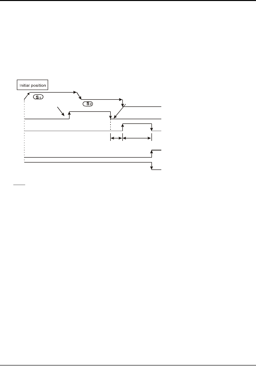
9 Application Instructions API 150-199
DVP-PLC Application Manual
9-31
the servo drive and the signal will last for approximately 20ms. After 20ms, the reset signal will return to Off
again.
b) Output devices for reset signals of EH2/SV/EH3/SV2 series MPU:
CH0 (Y0, Y1) reset output device (Y10)
CH1 (Y2, Y3) reset output device (Y11)
CH2 (Y4, Y5) reset output device (Y12)
CH3 (Y6, Y7) reset output device (Y13)
Off
On
On
Off
DOG ON
Zero return speed
Scan in circle Creep speed
Reset signal
Output near point signal (DOG)
Reset signal Y4 or Y5
M1336, M1337
Pulse output monitor
Inside 1 ms Greater than 20ms
Program interrupt
Note: The designated devices, X, Y, M, and S, other than the external input devices X10 ~ X17 will be affected
by the scan period, 2 times of the scan period at worst.
2. The zero return operation:
a) When ZRN instruction is executed, the frequency of the first acceleration segment of CH0 (CH1) in
EH2/SV/EH3/SV2 series MPU is set by D1340 (D1352). In SC series MPU, CH0 (CH1) will set creep speed
as the start frequency. The acceleration time of EH2/SV/EH3/SV2/SC series MPU is set by D1343 (D1353).
S1 will start to move when the acceleration reaches the zero return speed.
b) When the DOG signal goes from Off to On, the zero return speed will decelerate to S2 by the time set in
D1343 (D1353).
c) When the DOG signal goes from On to Off and the pulse output stops, 0 will be written in the present value
registers (D1337, D1336) of CH0 pulses, D1339 and D1338 of CH1 pulses, D1375 and D1376 of CH2 pulses,
and D1377 and D1378 of CH3 pulses in EH2/SV/EH3/SV2 series MPU; 0 will also be written in D1348 and
D1349 of Y10 (CH0) pulses or D1350 and D1351 of Y11 (CH1) pulses in SC series MPU.
d) When the DOG signal goes from On to Off and the reset signal flag M1346 = On, Y4 (CH0) or Y5 (CH1) in EH
series MPU will output a reset signal; Y10 (CH0), Y11 (CH1) , Y12 (CH2) and Y13 (CH3) in EH2/SV/EH3/SV2
series MPU will output a reset signal.
e) For EH2/SV/EH3/SV2 series MPU, when the pulse output is completed and M1029, M1030, M1036 and
M1037 are enabled, indication flag M1336 sent by CH0 pulses, M1337 by CH1, M1522 by CH2 and M1523
by CH3 will be Off. For SC series MPU, when the pulse output is completed, M1102 and M1103 will be
enabled.
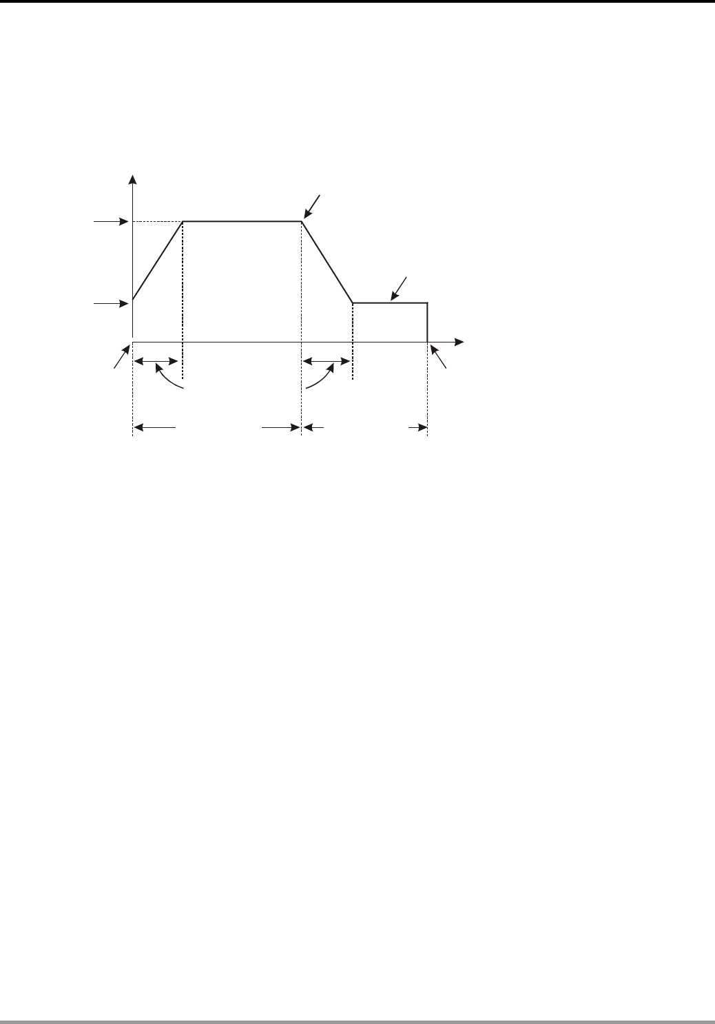
9 Application Instructions API 150-199
DVP-PLC Application Manual
9-32
f) Due to that ZRN (DZRN) instruction cannot locate the position of DOG, the zero return can only be done
towards a single direction. In the zero return operation of EH2/SV/EH3/SV2 series MPU, D1337 and D1336
(present value registers) of CH0 pulses or D1339 and D1338 of CH1 pulses are decreasing. In the zero return
operation of SC series MPU, D1348 and D1349 of CH0 pulses or D1350 and D1351 of CH1 pulses are also
decreasing.
S
3
Frequency
near point signal =On
time
near point signal =Off
Enabling
the
instruction accel/decel. time
D1343
acceleration deceleration
End frequency (S )
2
Target
frequency
(S )
1
Start
frequency
(S )
2
S
3
g) ZRN (DZRN) instruction is applicable to servo motor with absolute positioning function, e.g. Mitsubishi
MR-J2-A servo drive. Even when the power is switched off, the current position can still be recorded. In
addition, the current position of servo drive can be read by API 155 DABSR of EH2/SV/EH3/SV2/SC series
MPU; therefore only one zero return operation is required and no zero return has to be done after the power is
switched off.
h) When the drive contact of ZRN instruction is On, CH0 (CH1) will read the acceleration/deceleration time set in
D1343 (D1353) and accelerate to the zero return speed, waiting for the DOG and decelerate to creep speed.
When the DOG is Off, the pulse output will stop immediately.
i) For SC series MPU, many ZRN instructions can be compiled in the program but only one instruction can be
executed when the PLC program is being executed. For example, provided there is already an instruction
enabling Y10 output, other instructions enabling also Y10 output will not be executed. The principle of the
instruction execution is “first come, first executed”.
j) For SC series MPU, when you designate Y10 as the output device, you can choose either X10 or X11 for
DOG input in the “acceleration to deceleration” segment. In other words, when designating Y11 as the output
device, you can also choose either X10 or X11 for DOG input.
k) For SC series MPU, due to that this instruction does not compare between the number of output pulses, the
DOG input (from Off to On) will therefore become the trigger of acceleration converting to deceleration. The
“On” time of DOG has to be longer than 10us; otherwise the signal may be regarded as useless interference.
l) For SC series MPU, when the execution of the instrucion enters the deceleration segment and the output
frequency reaches creep speed (end frequency), the output will stop when DOG goes from On to Off.
m) For SC series MPU, the current accumulated number of pulses of Y10 is stored in D1348 and D1349 and that
of Y11 is stored in D1350 and D1351. Then the program operates from STOP to RUN or from RUN to STOP,

9 Application Instructions API 150-199
DVP-PLC Application Manual
9-33
the contents will not be cleared to 0.
n) For SC series MPU, M1102 = On indicates the end of Y10 pulse output; M1103 = On indicates the end of Y11
pulse output.
o) For SC series MPU, after the instruction is executed, all parameters cannot be modified unless the execution
of the instruction stops.
p) For SC series MPU, when the execution of the stops, all outputs will stop immediately no matter what type of
the output it is.
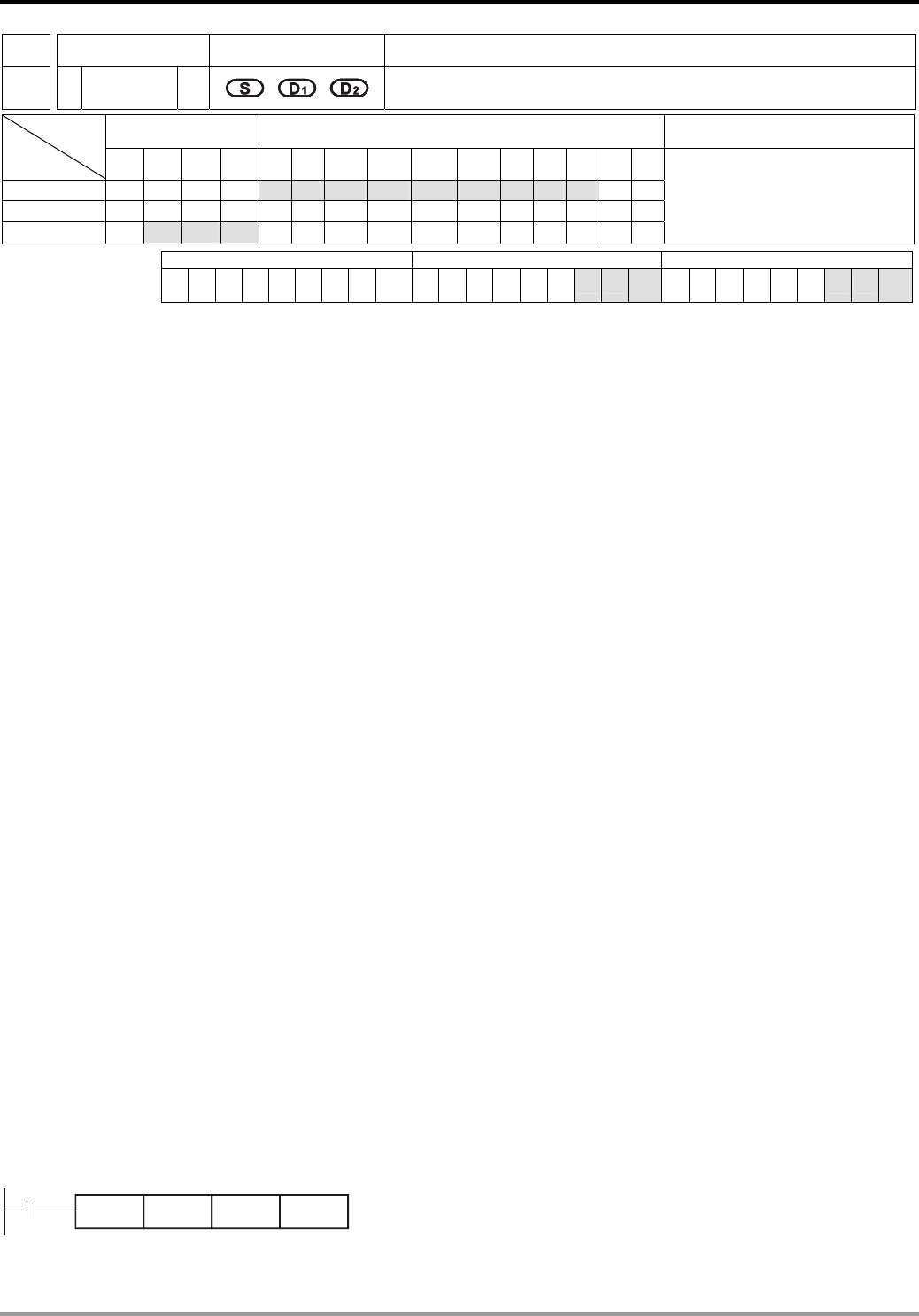
9 Application Instructions API 150-199
DVP-PLC Application Manual
9-34
API Mnemonic Operands Function
157
D PLSV Adjustable Speed Pulse Output
Bit Devices Word Devices Program Steps Type
OP X Y M S K H KnX KnY KnM KnS T C D E F
S * * * * * * * * * * *
D1 *
D2 * * *
PLSV: 7 steps
DPLSV: 13 steps
PULSE 16-bit 32-bit
ES EX SS SA SX SC EH SV EH3
SV2 ES EX SS SA SX SC EH SV EH3
SV2 ES EX SS SA SX SC EH SV EH3
SV2
Operands:
S: Pulse output frequency D1: Pulse output device (please use transistor output module) D2: Output device for
the signal of rotation direction
Explanations:
1. See remarks for the setting range of S, D1 and D2.
2. Flag: see remarks of API 155 ABSR and API 158 DDRVI for more details.
3. S is the designated pulse output frequency. The 16-bit instruction can designate its range 0 ~ +32,767Hz, 0 ~
-32,768Hz. The ranges designated by 32-bit instruction are 0 ~ +200,000Hz and 0 ~ -200,000Hz. “+/-” signs
indicate forward/backward directions. During the pulse output, the frequency can be changed, but not the
frequencies of different directions.
4. D1 is the pulse output device. EH series MPU can designate Y0 and Y2 and EH2/SV/EH3/SV2 series MPU can
designate Y0, Y2, Y4 and Y6.
5. The operation of D2 corresponds to the “+” or “-“ of S. When S is “+”, D2 will be On; when S is “-“, D2 will be Off.
6. PLSV instruction does not have settings for acceleration and deceleration. Please use API 67 RAMP for the
acceleration and deceleration of pulse output frequency.
7. During the pulse output executed by PLSV instruction, the drive contact turning Off will result in the immediate
stop of the output without going through a deceleration.
8. When the absolute value of the input frequency during the execution of DPLSV is bigger than 200kHz, the
output will operate at 200kHz.
9. For EH/EH2/SV/EH3/SV2 series MPU, D1222, D1223, D1383 and D1384 are the time differences sent
between the direction setup signal and pulse output points of CH0, CH1, CH2 and CH3.
10. For EH/EH2/SV/EH3/SV2 series MPU, M1305, M1306, M1532 and M1533 are the flags of the direction signals
of CH0, CH1, CH2 and CH3. When S is “+”, the output will operate towards a forward direction and the flag will
go Off. When S is “-“, the output will operate towards a backward direction and the flag will go On.
Program Example:
When M10 = On, Y0 will output pulses at 20kHz. Y5 = On indicates forward pulses.
M10
PLSV K20000 Y0 Y5
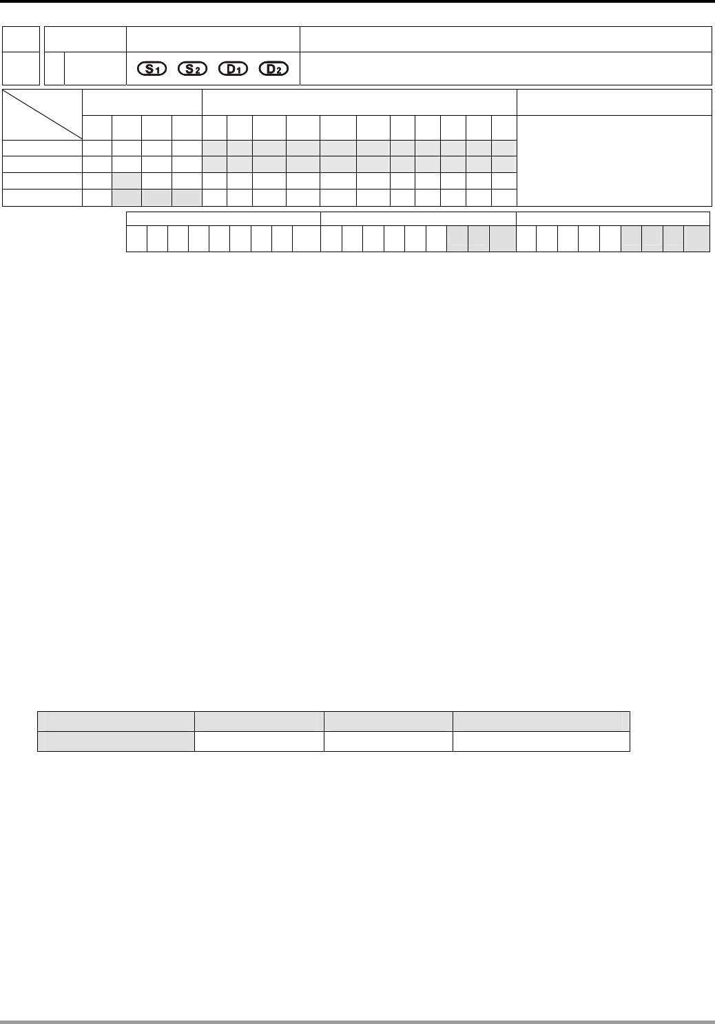
9 Application Instructions API 150-199
DVP-PLC Application Manual
9-35
API Mnemonic Operands Function
158
D DRVI Drive to Increment
Bit Devices Word Devices Program Steps Type
OP X Y M S K H KnX KnY KnM KnS T C D E F
S1 * * * * * * * * * * *
S2 * * * * * * * * * * *
D1 *
D2 * * *
DRVI: 9 steps
DDRVI: 17 steps
PULSE 16-bit 32-bit
ES EX SS SA SX SC EH SV EH3
SV2 ES EX SS SA SX SC EH SV EH3
SV2 ES EX SS SA SX SC EH SV EH3
SV2
Operands:
S1: Number of output pulses (relative designation) S2: Pulse output frequency D1: Pulse output device (please
use transistor output module) D2: Output device for the signal of rotation direction
Explanations:
1. See remarks for the setting range of S1, S2, D1 and D2.
2. S1 and S2 of SC series MPU only support device K, H and D.
3. Flag: see remarks for more details.
4. S1 is the number of output pulses (relative designation). For EH/EH2/SV/EH3/SV2 series MPU, the 16-bit
instruction can designate the range -32,768 ~ +32,767. The range designated by 32-bit instruction is
-2,147,483,648 ~ +2,147,483,647. For SC series MPU, the 32-bit instruction can designate the range
-2,147,483,648 ~ +2,147,483,647. “+/-” signs indicate forward/backward directions.
5. S2 is the designated pulse output frequency. For EH/EH2/SV/EH3/SV2 series MPU, the 16-bit instruction can
designate its range 10 ~ 32,767Hz. The range designated by 32-bit instruction is 10 ~ 200,000Hz. For SC
series MPU, the 32-bit instruction can designate the range 100 ~ 100,000Hz.
6. EH series MPU has two groups of A/B phase pulse output, CH0 (Y0, Y1) and CH1 (Y2, Y3). EH2/SV/EH3/SV2
series MPU has four groups of A/B phase pulse output, CH0 (Y0, Y1), CH1 (Y2, Y3), CH2 (Y4, Y5) and CH3
(Y6, Y7). See remarks for the setup methods.
7. Pulse output device D1 in different models
Model SC MPU EH MPU EH2/SV/EH3/SV2 MPU
Pulse output end Y10, Y11 Y0, Y2 Y0, Y2, Y4, Y6
8. The operation of D2 corresponds to the “+” or “-“ of S1. When S1 is “+”, D2 will be On; when S1 is “-“, D2 will be
Off. D2 will not be Off immediately after the pulse output is over; it will be Off only when the drive contact of the
instruction turns Off.
9. For EH/EH2/SV/EH3/SV2 series MPU, S1 is
- The 32-bit data stored in the present value registers D1337 (high word) and D1336 (low word) of CH0 (Y0,
Y1).
- The 32-bit data stored in the present value registers D1339 (high word) and D1338 (low word) of CH1 (Y2,
Y3).
- The 32-bit data stored in the present value registers D1376 (high word) and D1375 (low word) of CH2 (Y4,
Y5).

9 Application Instructions API 150-199
DVP-PLC Application Manual
9-36
- The 32-bit data stored in the present value registers D1378 (high word) and D1377 (low word) of CH3 (Y5,
Y6).
- When in backward direction, the content in the present value register will decrease.
10. For SC series MPU, S1 is the 32-bit data stored in the present value registers D1348 (low word) and D1349
(high word) of CH0 (Y10) or the 32-bit data stored in the present value registers D1350 (low word) and D1351
(high word) of CH1 (Y11). When in backward direction, the content in the present value register will decrease.
When the program goes from STOP to RUN or from RUN to STOP, the content in the present value register
will remain unchanged.
11. When DRVI instruction is executing pulse output, you cannot change the content of all operands. The changes
will be valid next time when DRVI instruction is enabled.
12. For EH/EH2/SV/EH3/SV2 series MPU, when the drive contact of DRVI instruction is Off, even the indication
flag M1336 sent by CH0 pulses, M1337 sent by CH1 pulses, M1522 sent by CH2 pulses and M1523 sent by
CH3 pulses are “On”, DRVI instruction will not be driven again.
13. When the absolute value of the input frequency of DDRVI insturction in EH/EH2/SV/EH3/SV2 series MPU is
larger than 200kHz, the output will be operated at 200kHz. When the absolute value of the input frequency is
smaller than 10Hz, the output will be operated at 10Hz.
14. D1343 (D1353) is for setting up the time of the first acceleartion segment and last deceleration segment of
CH0 (CH1). The acceleration and deceleration time of EH/EH2/SV/EH3/SV2 series MPU is 1 ~ 10,000ms. The
output will be operated for the default 100ms if the time is longer than 10,000ms. The time range for SC series
MPU is 50 ~ 20,000ms. The output will be operated for 20,000ms or 50ms if the time set is longer than
20,000ms or shorter than 50ms.
15. D1340 (D1352) is for setting up the start/end frequency of Y10 (Y11). If S2 is less than or equals start/end
frequency, the pulse output frequency will be executed by the start/end frequency.
16. For EH/EH2/SV/EH3/SV2 series MPU, M1305 (M1306) is the direction signal of CH0 (CH1). When S1 is a
positive number, the output will be operated in a forward direction and M1305 (M1306) will be Off. When S1 is
a negative number, the output will be operated in a backward direction and M1305 (M1306) will be On.
Program Example:
When M10= On, Y0 will output 20,000 pulses (relative designation) at 2kHz. Y5 = On indicates the pulses are
executed in forward direction.
M10
DRVI K20000 K2000 Y0 Y5
Remarks:
1. Explanations on EH/EH2/SV/EH3/SV2 series MPU:
a) Relative position control: Designating the traveling distance starting from the current position by “+/ -“ signs;
also known as a relative driving method.
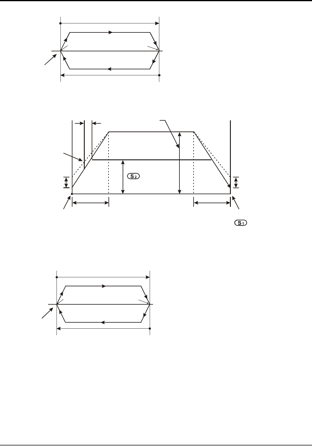
9 Application Instructions API 150-199
DVP-PLC Application Manual
9-37
+3,000
-3,000
0
Current
position
F0 the first acceleration
segment
The last deceleration
segment
(D1340) Min: 10Hz
b) Settings of relative positioning and the acceleration/deceleration speed:
Default: 100ms
(D1343)
(D1343)
Default: 200,000Hz
Output pulse
frequency
Max. speed
(D1342, D1341)
Current
position Output pulse
numbers
Accel/Decel time
Accel/Decel time
Default:100ms
Acceleration
sampling time
Acceleration
slope
First acceleration
segment (D1340)
Min: 10Hz
Last deceleration
segment (D1340
)
Min: 10Hz
2. Explanations on SC series MPU:
a) Relative position control: Designating the traveling distance starting from the current position by “+/ -“ signs;
also known as a relative driving method.
+3,000
-3,000
0
Current
position
F0 the first acceleration
segment
The last deceleration
segment
Y10 (D1340)
Y11 (D1352) Min: 10Hz
b) Settings of relative positioning and the acceleration/deceleration speed: D1343 (D1353) is for settings of the
time of the first acceleration segment and last deceleration segment of Y10 (Y11). D1340 (D1352) is for
settings of start/end frequency of Y10 (Y11).

9 Application Instructions API 150-199
DVP-PLC Application Manual
9-38
Acceleration
slope
Acceleration
sampling time output pulse frequency
accel/decel time
accel/decel time
Current
position
The first acceleration
segment
Y10 (D1340)
Y11 (D1352)
Min: 100Hz
Default: 200ms
Y10 (D1343)
Y11 (D1353)
The last deceleration
segment
Y10 (D1340)
Y11 (D1352)
Min: 100Hz
Default: 200ms
Y10 (D1343)
Y11 (D1353)
Output pulse
numbers
c) Many DRVI instructions can be compiled synchronously in the program, but only one instruction can be
activated whenever the PLC executes the program. For example, if Y10 output has already been activated by
an instruction, other instructions that are also used to activate Y10 output will not be excecuted. Therefore,
the principle of the instruction activation sequence is “first activated, first executed”.
d) When Y10 is activated by DDRVI instruction, the output function of Y10 will be disabled until DDRVI is OFF.
The same rule applies to Y11.
e) Once the instruction is activated, all other parameters cannot be modified until the instruction is disabled.
f) When the instruction is disabled but the output has not yet completed:
M1334 = On indicates that Y10 will stop output immediately.
M1334 = Off indicates that Y10 will decelerate according to the deceleration time till it reaches end frequency
and stop the pulse output.
M1335 corresponds to Y11 output and applies the same rule.
3. Flags for SC series MPU:
M1102: M1102 = On after Y10 pulse output is completed.
M1103: M1103 = On after Y11 pulse outout is completed.
M1334: Y10 pulse output stops immediately without deceleration when the pulse output instruction is
disabled.
M1335: Y11 pulse output stops immediately without deceleration when the pulse output instruction is
disabled.
M1347: For SC (V1.6 and later versions). Auto reset after Y0 output is completed.
M1348: For SC (V1.6 and later versions). Auto reset after Y1 output is completed.
M1524: For SC (V1.6 and later versions). Auto reset after Y10 output is completed.
M1525: For SC (V1.6 and later versions). Auto reset after Y11 output is completed.
4. Special registers for SC series MPU:
D1348: Low word of the current number of Y10 output pulses.
D1349: High word of the current number of Y10 output pulses.
D1350: Low word of the current number of Y11 output pulses.
D1351: High word of the current number of Y11 output pulses..
D1340: Settings of the first start frequency and the last end frequency of Y10 output pulses.

9 Application Instructions API 150-199
DVP-PLC Application Manual
9-39
D1352: Settings of the first start frequency and the last end frequency of Y11 output pulses.
D1343: Settings of the acceleration/deceleration time of Y10 output pulses.
D1353: Settings of the acceleration/deceleration time of Y11 output pulses.
5. Flags for EH/EH2/SV/EH3/SV2 series MPU:
M1010: For EH/EH2/SV/EH3/SV2, when M1010 = On, CH0, CH1, CH2 and CH3 will output pulses
when END instruction is being executed. M1010 will be Off automatically when the output
starts.
M1029: For EH/EH2/SV/EH3/SV2, M1029 = On after CH0 pulse output is completed.
M1030: For EH/EH2/SV/EH3/SV2, M1030 = On after CH1 pulse output is completed.
M1036: For EH2/SV/EH3/SV2, M1036 = On after CH2 pulse output is completed.
M1037: For EH2/SV/EH3/SV2, M1037 = On after CH3 pulse output is completed.
M1119 For EH2/SV/EH3/SV2, the instruction DDRVI/DDRVA is enabled when M1119 is On.
M1257 For EH/EH2/SV/EH3/SV2, the acceleration/deceleration of high-speed outputs Y0 and Y2 are
S curves when M1257 is On.
M1305: For EH/EH2/SV/EH3/SV2, direction signal of CH0.
M1306: For EH/EH2/SV/EH3/SV2, direction signal of CH1.
M1334: For EH, CH0 pulse output pauses.
For EH2/SV/EH3/SV2, CH0 pulse output stops.
M1308 For EH/EH2/SV/EH3/SV2,
Off->On: The first high-speed pulse output CH0 (Y0, Y1) pauses immediately.
On->Off: Continuing to output the pulses which have not been output
M1309 For EH/EH2/SV/EH3/SV2,
Off->On: The first high-speed pulse output CH1 (Y2, Y3) pauses immediately.
On->Off: Continuing to output the pulses which have not been output
M1310 For EH/EH2/SV/EH3/SV2,
Off->On: The first high-speed pulse output CH2 (Y4, Y5) pauses immediately.
On->Off: Continuing to output the pulses which have not been output
M1311 For EH/EH2/SV/EH3/SV2,
Off->On: The first high-speed pulse output CH3 (Y6, Y7) pauses immediately.
On->Off: Continuing to output the pulses which have not been output
M1335: For EH, CH1 pulse output pauses.
For EH2/SV/EH3/SV2, CH1 pulse output stops.
M1336: For EH/EH2/SV/EH3/SV2, “CH0 sends out pulses” indication.
M1337: For EH/EH2/SV/EH3/SV2, “CH1 sends out pulses” indication.
M1347: For EH2/SV/EH3/SV2 (V1.4 and later versions). Reset flag for CH0 pulse output.
M1348: For EH2/SV/EH3/SV2 (V1.4 and later versions). Reset flag for CH1 pulse output.
M1520: For EH2/SV/EH3/SV2, CH2 pulse output stops.
M1521: For EH2/SV/EH3/SV2, CH3 pulse output stops.
M1522: For EH2/SV/EH3/SV2, “CH2 sends out pulses” indication.

9 Application Instructions API 150-199
DVP-PLC Application Manual
9-40
M1523: For EH2/SV/EH3/SV2, “CH3 sends out pulses” indication.
M1524: For EH2/SV/EH3/SV2 (V1.4 and later versions). Reset flag for CH2 pulse output.
M1525: For EH2/SV/EH3/SV2 (V1.4 and later versions). Reset flag for CH3 pulse output.
M1534: For EH2/SV/EH3/SV2, designated deceleration time of CH0 (should be used with D1348).
M1535: For EH2/SV/EH3/SV2, designated deceleration time of CH1 (should be used with D1349).
M1536: For EH2/SV/EH3/SV2, designated deceleration time of CH2 (should be used with D1350).
M1537: For EH2/SV/EH3/SV2, designated deceleration time of CH3 (should be used with D1351).
M1532: For EH2/SV/EH3/SV2, direction signal of CH2.
M1533: For EH2/SV/EH3/SV2, direction signal of CH3.
6. Special registers for EH/EH2/SV/EH3/SV2 series MPU:
D1127: For EH2/SV/EH3/SV2, the number of pulses in the acceleration section in the position
instruction (low word)
D1128: For EH2/SV/EH3/SV2, the number of pulses in the acceleration section in the position
instruction (high word)
D1133: For EH2/SV/EH3/SV2, the number of pulses in the deceleration section in the position
instruction (low word)
D1134: For EH2/SV/EH3/SV2, the number of pulses in the deceleration section in the position
instruction (high word)
D1220: For EH/EH2/SV/EH3/SV2, phase setting of CH0 (Y0, Y1): D1220 determines the phase by
the last two bits; other bits are invalid.
1. K0: Y0 output
2. K1: Y0, Y1 AB-phase output; A ahead of B.
3. K2: Y0, Y1 AB-phase output; B ahead of A.
4. K3: Y1 output
D1221: For EH/EH2/SV/EH3/SV2, phase setting of CH1 (Y2, Y3): D1221 determines the phase by
the last two bits; other bits are invalid.
1. K0: Y2 output
2. K1: Y2, Y3 AB-phase output; A ahead of B.
3. K2: Y2, Y3 AB-phase output; B ahead of A.
4. K3: Y3 output
D1222: For EH/EH2/SV/EH3/SV2, the time difference between the direction signal and pulse output
sent by CH0.
D1223: For EH/EH2/SV/EH3/SV2, the time difference between the direction signal and pulse output
sent by CH1.
D1229: For EH2/SV/EH3/SV2, phase setting of CH2 (Y4, Y5): D1229 determines the phase by the
last two bits; other bits are invalid.
1. K0: Y4 output
2. K1: Y4, Y5 AB-phase output; A ahead of B.
3. K2: Y4, Y5 AB-phase output; B ahead of A.
4. K3: Y5 output
D1230: For EH2/SV/EH3/SV2, phase setting of CH3 (Y6, Y7): D1230 determines the phase by the
last two bits; other bits are invalid.
1. K0: Y6 output
2. K1: Y6, Y7 AB-phase output; A ahead of B.
3. K2: Y6, Y7 AB-phase output; B ahead of A.

9 Application Instructions API 150-199
DVP-PLC Application Manual
9-41
4. K3: Y7 output
D1336: For EH/EH2/SV/EH3/SV2, low word of the current number of output pulses from CH0.
D1337: For EH/EH2/SV/EH3/SV2, high word of the current number of output pulses from CH0.
D1338: For EH/EH2/SV/EH3/SV2, low word of the current number of output pulses from CH1.
D1339: For EH/EH2/SV/EH3/SV2, high word of the current number of output pulses from CH1.
D1340: For EH/EH2/SV/EH3/SV2, settings of the first start frequency and the last end frequency of
CH0.
D1343: For EH/EH2/SV/EH3/SV2, settings of acceleration/deceleration time for CH0 pulse output.
D1348: For EH2/SV/EH3/SV2, deceleration time for CH0 pulse output when M1534 = On.
D1349: For EH2/SV, deceleration time for CH1 pulse output when M1535 = On.
D1350: For EH2/SV, deceleration time for CH2 pulse output when M1536 = On.
D1351: For EH2/SV, deceleration time for CH3 pulse output when M1537 = On.
D1352: For EH/EH2/SV/EH3/SV2, settings of the first start frequency and the last end frequency of
CH1.
D1353: For EH/EH2/SV/EH3/SV2, settings of acceleration/deceleration time for CH1 pulse output.
D1375: For EH2/SV/EH3/SV2, low word of the current number of output pulses from CH2.
D1376: For EH2/SV/EH3/SV2, high word of the current number of output pulses from CH2.
D1377: For EH2/SV/EH3/SV2, low word of the current number of output pulses from CH3.
D1378: For EH2/SV/EH3/SV2, high word of the current number of output pulses from CH3.
D1379: For EH2/SV/EH3/SV2, settings of the first start frequency and the last end frequency of CH2.
D1380: For EH2/SV/EH3/SV2, settings of the first start frequency and the last end frequency of CH3.
D1381: For EH2/SV/EH3/SV2, settings of acceleration/deceleration time for CH2 pulse output.
D1382: For EH2/SV/EH3/SV2, settings of acceleration/deceleration time for CH3 pulse output.
D1383: For EH2/SV/EH3/SV2, the time difference between the direction signal and pulse output sent
by CH2.
D1384: For EH2/SV/EH3/SV2, the time difference between the direction signal and pulse output sent
by CH3.
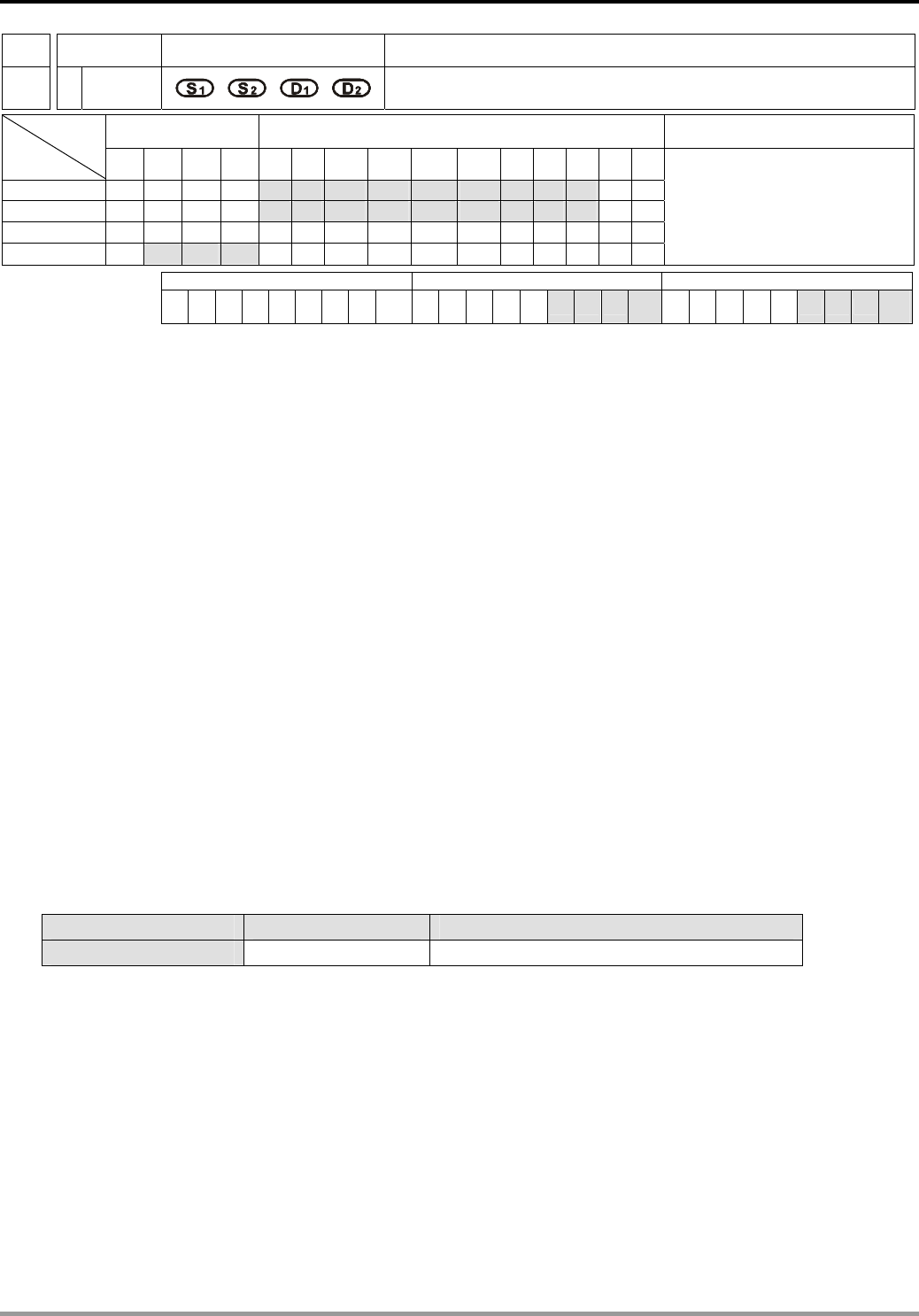
9 Application Instructions API 150-199
DVP-PLC Application Manual
9-42
API Mnemonic Operands Function
159
D DRVA Drive to Absolute
Bit Devices Word Devices Program Steps Type
OP X Y M S K H KnX KnY KnM KnS T C D E F
S1 * * * * * * * * * * *
S2 * * * * * * * * * * *
D1 *
D2 * * *
DRVA: 9 steps
DDRVA: 17 steps
PULSE 16-bit 32-bit
ES EX SS SA SX SC EH SV EH3
SV2 ES EX SS SA SX SC EH SV EH3
SV2 ES EX SS SA SX SC EH SV EH3
SV2
Operands:
S1: Number of output pulses (absolute designation) S2: Pulse output frequency D1: Pulse output device
(please use transistor output module) D2: Output device for the signal of rotation direction
Explanations:
1. See remarks for the setting range of S1, S2, D1 and D2.
2. S1 and S2 of SC series MPU only support device K, H and D.
3. Flag: see remarks of API 158 DRVI for more details.
4. S1 is the number of output pulses (absolute designation). For EH/EH2/SV/EH3/SV2 series MPU, the 16-bit
instruction can designate the range -32,768 ~ +32,767. The range designated by 32-bit instruction is
-2,147,483,648 ~ +2,147,483,647. For SC series MPU, the 32-bit instruction can designate the range
-2,147,483,648 ~ +2,147,483,647. “+/-” signs indicate forward/backward directions.
5. S2 is the designated pulse output frequency. For EH/EH2/SV/EH3/SV2 series MPU, the 16-bit instruction can
designate its range 10 ~ 32,767Hz. The range designated by 32-bit instruction is 10 ~ 200,000Hz. For SC
series MPU, the 32-bit instruction can designate the range 100 ~ 100,000Hz.
6. EH series MPU has two groups of A/B phase pulse output, CH0 (Y0, Y1) and CH1 (Y2, Y3). EH2/SV series
MPU has four groups of A/B phase pulse output, CH0 (Y0, Y1), CH1 (Y2, Y3), CH2 (Y4, Y5) and CH3 (Y6, Y7).
See remarks for the setup methods.
7. Pulse output device D1 in different models
Model SC MPU EH/EH2/SV/EH3/SV2 MPU
Pulse output end Y10, Y11 Y0, Y2
8. When S1 is larger than the current relative position, D2 will be Off; when S1 is smaller than the current relative
position, D2 will be On. D2 will not be Off immediately after the pulse output is over; it will be Off only when the
drive contact of the instruction turns Off.
9. For EH/EH2/SV/EH3/SV2 series MPU, S1 is
- The 32-bit data stored in the present value registers D1337 (high word) and D1336 (low word) of CH0 (Y0,
Y1).
- The 32-bit data stored in the present value registers D1339 (high word) and D1338 (low word) of CH1 (Y2,
Y3).
- The 32-bit data stored in the present value registers D1376 (high word) and D1375 (low word) of CH2 (Y4,
Y5).

9 Application Instructions API 150-199
DVP-PLC Application Manual
9-43
- The 32-bit data stored in the present value registers D1378 (high word) and D1377 (low word) of CH3 (Y5,
Y6).
When in backward direction, the content in the present value register will decrease.
10. For SC series MPU, S1 is the 32-bit data stored in the present value registers D1348 (low word) and D1349
(high word) of CH0 (Y10) or the 32-bit data stored in the present value registers D1350 (low word) and D1351
(high word) of CH1 (Y11). When in backward direction, the content in the present value register will decrease.
When the program goes from STOP to RUN or from RUN to STOP, the content in the present value register
will remain unchanged.
11. For EH/EH2/SV/EH3/SV2 series MPU, when DRVA instruction is executing pulse output, you cannot change
the content of all operands. The changes will be valid next time when DRVA instruction is enabled.
12. For EH/EH2/SV/EH3/SV2 series MPU, when the drive contact of DRVA instruction is Off, the pulse output will
decelerate to stop and M1029 and M1030 will be enabled. For SC series MPU, the pulse output will decelerate
to stop and M1102 and M1103 will be enabled.
13. For EH/EH2/SV/EH3/SV2 series MPU, when the drive contact of DRVA instruction is Off, even the indication
flag M1336 sent by CH0 pulses or M1337 sent by CH1 pulses are “On”, DRVA instruction will not be driven
again.
14. When the absolute value of the input frequency of DRVA and DDRVA insturctions in EH/EH2/SV/EH3/SV2
series MPU is larger than 200kHz, the output will be operated at 200kHz. When the absolute value of the input
frequency is smaller than 10Hz, the output will be operated at 10Hz.
15. D1343 (D1353) is for setting up the time of the first acceleartion segment and last deceleration segment of
CH0 (CH1). The acceleration and deceleration time of EH/EH2/SV/EH3/SV2 series MPU is 1 ~ 10,000ms. The
output will be operated for the default 100ms if the time is longer than 10,000ms. The time range for SC series
MPU is 50 ~ 20,000ms. The output will be operated for 20,000ms or 50ms if the time set is longer than
20,000ms or shorter than 50ms.
16. For EH/EH2/SV/EH3/SV2 series MPU, M1305 (M1306) is the direction signal of CH0 (CH1). When S1 is a
positive number, the output will be operated in a forward direction and M1305 (M1306) will be Off. When S1 is a
negative number, the output will be operated in a backward direction and M1305 (M1306) will be On.
17. D1340 (D1352) is for setting up the start/end frequency of Y10 (Y11). If S2 is less than or equals start/end
frequency, the pulse output frequency will be executed by the start/end frequency.
Program Example:
When M10= On, Y0 will output 20,000 pulses (absolute designation) at 2kHz. Y5 = On indicates the pulses are
executed in forward direction.
M10
DRVA K20000 K2000 Y0 Y5
Remarks:
1. Explanations on EH/EH2/SV/EH3/SV2 series MPU:
a) Absolute position control: Designating the traveling distance starting from the zero point (0); also known as a
absolute driving method.
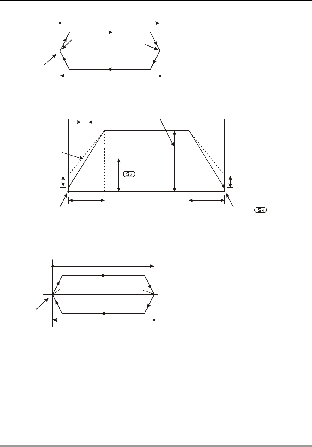
9 Application Instructions API 150-199
DVP-PLC Application Manual
9-44
+3,000
0
0
Zero point
Target position
F0 the first acceleration segment
The last deceleration segment
(D1340) Min: 10Hz
b) Settings of absolute positioning and the acceleration/deceleration speed:
T Accel/Decel time
Current
position
Accel/Decel time
Output pulse frequency
Output pulse
numbers
Acceleration
sampling time
Acceleration slope
Default: 200,000Hz
Max. speed
(D1342, D1341)
First acceleration
segment (D1340)
Min: 10Hz
Default: 100ms
(D1343)
Default: 100ms
(D1343)
Last deceleration
segment (D1340)
Min: 10Hz
2. Explanations on SC series MPU:
a) Absolute position control: Designating the traveling distance starting from the zero point (0); also known as a
absolute driving method.
+3,000
-3,000
0
Zero
point
F0 the first acceleration
segment
The last deceleration
segment
Y10 (D1340)
Y11 (D1352) Min: 10Hz
b) Settings of absolute positioning and the acceleration/deceleration speed: D1343 (D1353) is for settings of
the time of the first acceleration segment and last deceleration segment of Y10 (Y11). D1340 (D1352) is for
settings of start/end frequency of Y10 (Y11).

9 Application Instructions API 150-199
DVP-PLC Application Manual
9-45
Acceleration
slope
accel/decel time
accel/decel time
Current
position
Acceleration
sampling time Output pulse
frequency
First acceleration segment
Y10 (D1340)
Y11 (D1352) Min: 100Hz
Default: 200ms
Y10 (D1343)
Y11 (D1353)
Default: 200ms
Y10 (D1343)
Y11 (D1353)
Last deceleration segment
Y10 (D1340)
Y11 (D1352)
Min: 100Hz
Output pulse
numbers
c) Many DRVA instructions can be compiled synchronously in the program, but only one instruction can be
activated whenever the PLC executes the program. For example, if Y10 output has already been activated
by an instruction, other instructions that are also used to activate Y10 output will not be excecuted.
Therefore, the principle of the instruction activation sequence is “first activated, first executed”.
d) When Y10 is activated by DDRVA instruction, the output function of Y10 will be disabled until DDRVAis OFF.
The same rule applies to Y11.
e) Once the instruction is activated, all other parameters cannot be modified until the instruction is disabled.
f) When the instruction is disabled but the output has not yet completed:
M1334 = On indicates that Y10 will stop output immediately.
M1334 = Off indicates that Y10 will decelerate according to the deceleration time till it reaches end frequency
and stop the pulse output.
M1335 corresponds to Y11 output and applies the same rule.
3. See remarks of DDRVI instruction for more details on the flags.
4. Wiring of DVP-EH series and Delta ASDA servo drive:
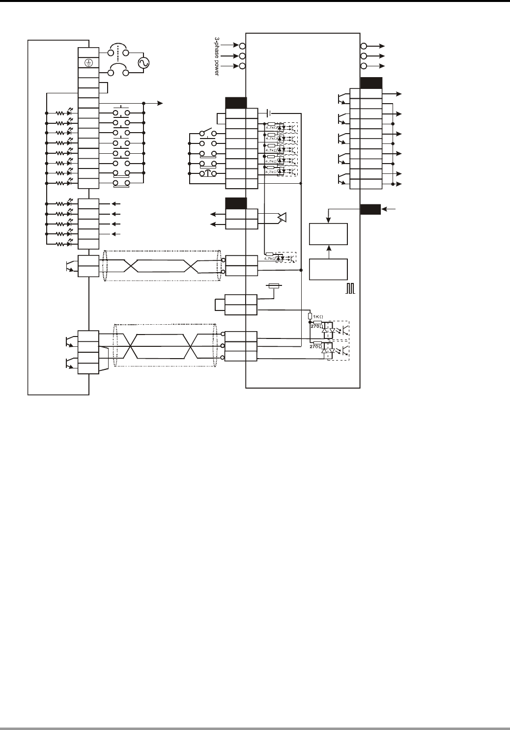
9 Application Instructions API 150-199
DVP-PLC Application Manual
9-46
/
OZ
50
EH MPU
L
N
X0
X1
X2
X3
X4
X5
X6
S/S
Y4
C2
JOG(+)
DI 1:
DI 5:
DI 6:
DI 7:
DI 8:
R
S
T
U
V
W
Delta Servo Drive
COM-
DI 2
+24V
X7
24G
JOG(-)
DO_COM
X10
X11
X12
X13
X14
SRDY
ZSPD
TPOS
ALARM
CN1 CN2
10
45
Y0
C0
Y1
C1
DVP32EH00T
CN1
26
1
2
3
4
5
6
7DO1+
DO2+
DO3+
DO4+
DO1-
DO2-
DO3-
DO4-
SRDY
ZSPD
HOME
TPOS
220VAC 220VAC
24
27
28 DO5+
DO5-
ALARM
DO_COM
OZ
COM-
PLS 41
47
SIGN 37
PU-HI
VDD 17
35
DC24V
Max. input pulse
frequency: 200kPPS
24V
CN1
VDD
COM+
DI 1
DI 5
DI 6
DI 7
DI 8
17
11
9
33
32
31
30
COM- 45
Single phase
Start
Zero return
Stop
Error reset
Forward limit
Reverse limit
ASDA series
Servo Motor
Servo start
Servo reset
Forward limit
Reverse limit
Emergency stop
Differential
signal
Clear pulse
Z-phase signal
(zero point signal)
Pulse output
VDD 17
Approx.
Encoder
Error
counter
Electric
gear
Forward/backward direction
Note:
(a) The parameter setting of Delta ASDA servo drive:
P1-01: position mode
P1-00: pulse input type as Pulse+DIR.
(b) The forward/reverse limit switch should be connected to SERVO AMP.
(c) The “clear pulse” signal will clear the current number of pulses left inside the servo.
5. Wiring of DVP-SC series and Delta ASDA servo drive:
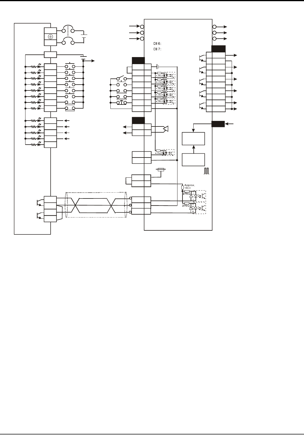
9 Application Instructions API 150-199
DVP-PLC Application Manual
9-47
/
OZ
50
24V
0V
X0
X1
X2
X3
X4
X5
X20
S/S
JOG(+)
DI 1:
DI 5:
DI 8:
R
S
T
U
V
W
Delta Servo Drive
COM-
DI 2
X21
JOG(-)
DO_COM
X22
X23
X24
X25
X26
SRDY
ZSPD
TPOS
ALARM
CN1 CN2
10
45
Y10
C2
Y0
C0
CN1
26
1
2
3
4
5
6
7DO1+
DO2+
DO3+
DO4+
DO1-
DO2-
DO3-
DO4-
SRDY
ZSPD
HOME
TPOS
220VAC
24
27
28 DO5+
DO5-
ALARM
OZ
COM-
PLS 41
47
SIGN 37
PU-HI
VDD 17
35
DC24V
24V
CN1
VDD
COM+
DI 1
DI 5
DI 6
DI 7
DI 8
17
11
9
33
32
31
30
COM- 45
DVP12SC11T+DVP16SP11T
24VDC
24VDC
DO_COM
Max. input pulse
frequency: 100kPPS
SC MPU + 16SP
3-phase power
ASDA series
Servo motor
Servo start
Servo reset
Forward limit
Reverse limit
Emergency stop
Start
Zero return
Start
Error reset
Forward limit
Reverse limit
Differential
signal
Z-phase signal
(zero point signal)
Pulse output
Forward/backward direction
Encoder
Error
counter
Electric
gear
Note:
(a) The parameter setting of Delta ASDA servo drive:
P1-01: position mode
P1-00: pulse input type as Pulse+DIR.
(b) The forward/reverse limit switch should be connected to SERVO AMP.
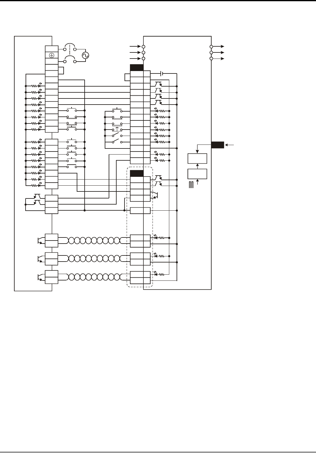
9 Application Instructions API 150-199
DVP-PLC Application Manual
9-48
6. Wiring of DVP-EH series PLC and a Mitsubishi MR-J2-□A Servo drive:
L
N
X0
X1
X2
X3
X4
X5
X6
S/S
+24V
200KPPS
R
S
T
U
V
W
24V
24G
X7
X10
X11
X12
X13
X14
X15
X16
X17
Y6
Y7
C4
Y4
Y0
Y1
C2
C0
C1
DOG
JOG(+)
JOG(-)
CN1B
VDD
COM
D01
ZSP
TLC
ALM
RES
LSP
LSN
EMG
TL
SON
SG
ABSR
ABSM
CN1A
OP
INP
RD
LG
SG
CR
SG
PP
SG
NP
SG 10
2
10
3
20
8
20
1
19
18
14
8
9
10
5
9
15
17
16
14
18
6
19
4
13
3
ABS bit 0
ABS bit 1
CN2
DVP
3
2EH
00
T
EH MPU
Mi
tsu
bi
s
hi
servo
d
r
i
ve
MR-J2 series
220VAC
Single phase
3-phase power
ABS transmission
Stop
Left limit
Right limit
Zero return
Forward
positioning
Reverse
positioning
Positioning completed
Preparation completed
Z-phase signal (zero point)
Read ABS ready
Enter ABS mode
Servo motor
Error
counter
Electric
gear
Encode
r
Clear pulse
Pulse output
Forward/backward direction
Note:
(a) When detecting an absolute position by using DABSR instruction, the parameter setting of a Mitsubishi
MR-J2-□A servo drive that connects to Delta EH series PLC:
P0: position mode.
P1: using absolute value.
P21: pulse input type as Pulse+DIR.
(b) The forward/reverse limit switch should be connected to SERVO AMP.
(c) When using OP (Z-phase signal) in servo and given that the Z-phase signal is a high-frequency one when
the motor is running at high speed, the valid detection can only be possible when the signal is within the
range detectable by PLC. When using OP (Z phase signal) of the servo, if Z phase signal is a high
frequency signal during high-speed motor operation, the high frequency signal shall be within the available
range that can be detected by PLC.

9 Application Instructions API 150-199
DVP-PLC Application Manual
9-49
7. Cautions when designing a position control program:
a) There is no limitation on the times of using the position control instructions, API 156 ZRN, API 157 PLSV,
API 158 DRVI, and API 159 DRVA. However, the user still have to note that:
i. Do not drive the position control instructions which use the same output CH0(Y0, Y1) or CH1(Y2, Y3)
simultaneously. Otherwise, they will be treated as repeated outputs and cannot function normally.
ii. It is recommended that you use the step ladder instruction (STL) to design the position control program
(see the example below).
b) How to use the position control instructions (API 156 ABSR, API 157 PLSV, API 158 DRVI, and API 159
DRVA) and pulse output instructions (API 57 PLSY, API 58 PWM and API 59 PLSR) at the same time.
The position control instruction and pulse output instruction share the 32 bits of the present value register
(D1337 high word; D1336 low word) of CH0 (Y0, Y1) or the present value register of CH1 (Y2, Y3), which will
make the operation complicated. Therefore, it is recommanded that you replace the pulse output instruction
with position control instruction.
c) Explanations on the (Y0, Y1) pulses from CH0 and (Y2, Y3) pulses from CH1.
Voltage range: DC5V ~ DC24V
Current range: 10mA ~ 100mA
Output pulse frequency: Y0, Y2 at 200kHz; Y1, Y3 at 10kHz.
8. Settings of pulse output signals in the operation of position control for EH/EH2/SV/EH3/SV2 series MPU:
a) Pulse + DIR (recommended)
Pulse
DI
R
b) CW/CCW (limited frequency at 10kHz)
CW
CCW
c) A/B-phase output (limited frequency at 10kHz)
A
B
9. Follow the above output settings of PLC for the pulse input parameters of SERVO AMP or stepping motor.
10. For EH/EH2/SV/EH3/SV2 series MPU, when Y0 output adopts many high-speed pulse output instructions
(PLSY, PWM, PLSR) and position control instructions (ZRN, PLSV, DRVI, DRVA) in a program and these
instructions are executed synchronously in the same scan period, PLC will execute the instruction with the
fewest step numbers.
Programming example for forward/reverse operation:
For the wiring, see the wiring drawing of DVP-EH series and Mitsubishi MR-J2-□A servo drive
One operation mode performs positioning by absolute position:
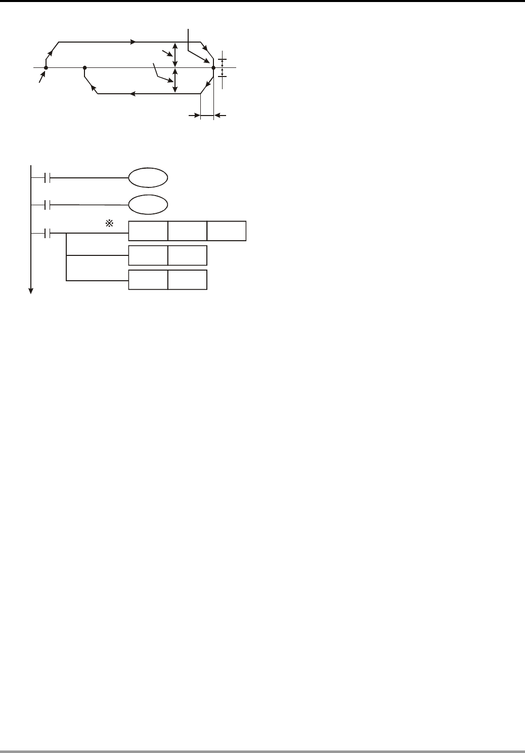
9 Application Instructions API 150-199
DVP-PLC Application Manual
9-50
500Hz
500Hz
500,000
100
200ms
200,000Hz
Zero point
Output pulse frequency
Acceleration/
Deceleration time
11. Programming example of using step ladder instruction (STL):
MOV
M1000
M1002 1
Stop
Y0 pulse output pauses
With clear signal output valid zero return
Settings of accel/decel time 200ms--D1343
SERVO On control
X4
M1334
M1346
D1343K200
SET S0
Y5SET
※1. If the accel./decel. time (D1343) of CH1 can be default setting, (100ms) this program step can be ignored.
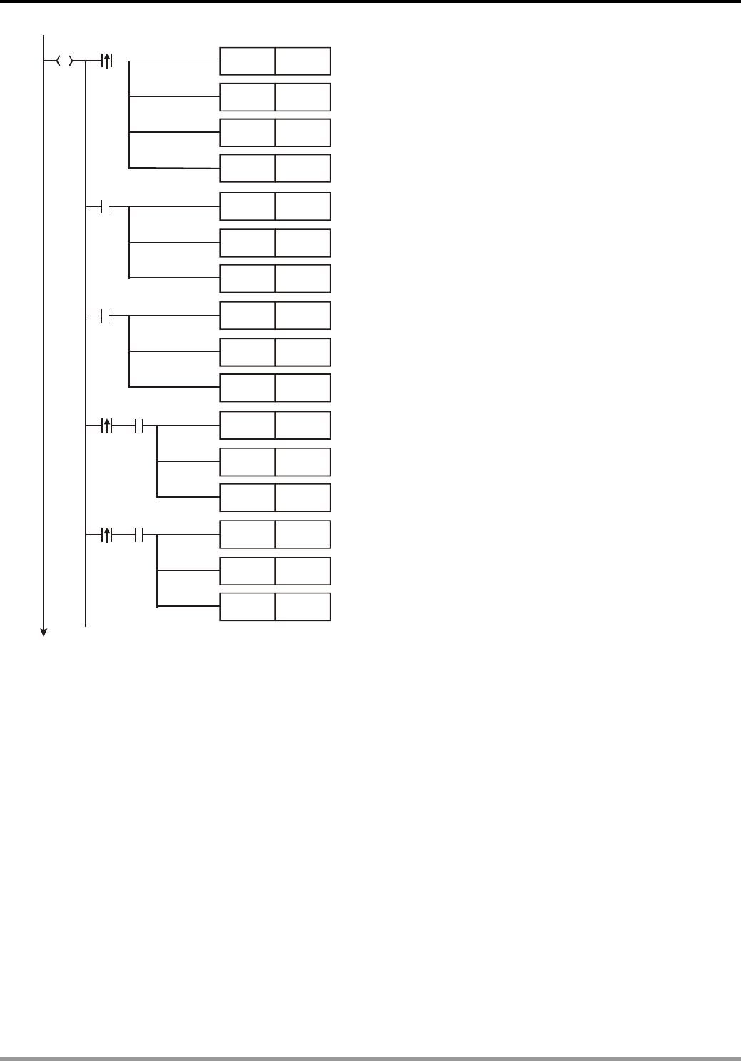
9 Application Instructions API 150-199
DVP-PLC Application Manual
9-51
S
S0 X7
X10
X13
X12
X11
M10
M10
RST M10
M12
M13
S20
M12
M13
S21
M12
M13
S22
M12
M13
S23
M12
M13
S24SET
RST
RST
RST
RST
RST
RST
RST
RST
RST
RST
SET
SET
SET
SET
Zero
return
JOG(+)
JOG(-)
Forward
Positioning
Zero
return
completed
flag
Backward
positioning
Zero
return
completed
flag
Reset zero point return completed flag
Reset forward positioning completed flag
Reset backward positioning completed flag
Drive zero return (S20)
Reset forward positioning completed flag
Reset backward positioning completed flag
Drive JOG(+) (S21)
Reset forward positioning completed flag
Reset backward positioning completed flag
Drive JOG(-) (S22)
Reset forward positioning completed flag
Reset backward positioning completed flag
Drive forward positioning(S23)
Reset forward positioning completed flag
Reset backward positioning completed flag
Drive forward positioning(S24)
※2. The max. traveling distance of a JOG operation equals to the max. number of output pulses
(-2,147,483,648 ~ +2,147,483,647) of API 158 DDRVI instruction. Please re-execute JOG of the traveling
distance exceeds the range.
9 Application Instructions API 150-199
DVP-PLC Application Manual
9-52
M1029
M1000
M10
DZRN K50000 K5000 X14
Zero
return
S
S20
SET
M0
M0
M1336 M0
Y0
S0
Y0 output being executed
Execution
completed
Zero return
speed
Creep
speed
DOG Pulse output
device
Zero return instruction
operates in the(-) direction.
Reset zero point return completed flag
Zero point return is completed
Time-out 1 scan period
M1000
DDRVI K999999 K30000 Y1S
S21
M1336 M1
Y0
S0
Y0 output being executed
JOG(+) operation is completed
Time-out 1 scan period
X2
JOG(+)
Use relative positioning instruction to
execute a JOG operation (when Y1=On)
in the (+) direction.
Number of
output pulses
(in + direction)
Output pulse
frequency
Pulse output
device
Output point for
reverse signals
JOG(+)
M1000
K 999999
-
K30000 Y1S
M1336
Y0
S0
Y0 output being executed
JOG( ) operation is completed
-
Time-out 1 scan period
Use relative positioning instruction to
execute a JOG operation (when Y1=On)
in the ( ) direction.
-
Number of
output pulses
(in + direction)
Output pulse
frequency
Pulse output
device
Output point for
reverse signals
JOG( )
-
S22 X3
JOG( )
-
M2
M2
M1
DDRVI
M1000
Y1S
M1336
Y0
S0
Y0 output being executed
Time-out 1 scan period
Output pulse
frequency
Pulse output
device
Output point for
reverse signals
S23
Forward
positioning
M1029 M3
SET M12
DDRVA K500000 K100000
Absolute
position
Forward positioning completed flag
Forward positioning is completed
Use absolute positioning instruction to
travel to absolute position 500,000
(Y1=On).
M3
M3
Execution
completed
M1000
Y1S
M1336
Y0
S0
Time-out 1 scan period
Output pulse
frequency
Pulse output
device
Output point for
reverse signals
M1029
SET
DDRVA K100000
Absolute
position
Use absolute positioning instruction to
travel to absolute position 00 (Y1=On).1
M3
M3
Execution
completed
END
RET
S24
Backward
positioning
K100
M4
M13 Backward positioning completed flag
Backward positioning is completed

9 Application Instructions API 150-199
DVP-PLC Application Manual
9-53
12. Flags and special registers for SC series MPU:
M1347: For SC (V1.6 and later versions). Auto reset after Y0 output is completed.
M1348: For SC (V1.6 and later versions). Auto reset after Y1 output is completed.
M1524: For SC (V1.6 and later versions). Auto reset after Y10 output is completed.
M1525: For SC (V1.6 and later versions). Auto reset after Y11 output is completed.
13. Flags and special registers for EH/EH2/SV/EH3/SV2 series MPU:
M1347: For EH2/SV/EH3/SV2 (V1.4 and later versions). Reset flag for CH0 pulse
output.
M1348: For EH2/SV/EH3/SV2 (V1.4 and later versions). Reset flag for CH1 pulse
output.
M1524: For EH2/SV/EH3/SV2 (V1.4 and later versions). Reset flag for CH2 pulse
output.
M1525: For EH2/SV/EH3/SV2 (V1.4 and later versions). Reset flag for CH3 pulse
output.
9 Application Instructions API 150-199
DVP-PLC Application Manual
9-54
API Mnemonic Operands Function
160
TCMP P Time Compare
Bit Devices Word Devices Program Steps Type
OP X Y M S K H KnX KnY KnM KnS T C D E F
S1 * * * * * * * * * * *
S2 * * * * * * * * * * *
S3 * * * * * * * * * * *
S * * *
D * * *
TCMP, TCMPP: 11 steps
PULSE 16-bit 32-bit
ES EX SS SA SX SC EH SV EH3
SV2 ES EX SS SA SX SC EH SV EH3
SV2 ES EX SS SA SX SC EH SV EH3
SV2
Operands:
S1: “Hour” for comparison S2: “Minute” for comparison S3: “Second” for comparison S: Current time of
RTC D: Comparison result
Explanations:
1. Range of S1: K0 ~ K23; range of S2 and S3: K0 ~ K59
2. S will occupy 3 consecutive devices; D will occupy 3 consecutive points.
3. See the specifications of each model for their range of use.
4. S1, S2 and S3 are compared with the present values of “hour”, “minute” and “second” starting from S. The
comparison result is stored in D.
5. S is the “hour” of the current time (K0 ~ K23) in RTC; S + 1 is the “minute” (K0 ~ K59) and S + 2 is the “second”
(K0 ~ K59).
6. S is read by TRD instruction and the comparison is started by TCMP instruction. If S exceeds the range, the
program will regard this as an operation error and the instruction will not be executed, M1067 and M1068 = On
and D1067 will record the error code 0E1A (hex).
Program Example:
1. When X10= On, the instruction will compare the current time in RTC (D20 ~ D22) with the set value 12:20:45
and display the result in M10 ~ M12. When X10 goes from On to Off, the instruction will not be executed, but
the On/Off stauts prior to M10 ~ M12 will remain.
2. Connect M10 ~ M12 in series or in parallel to obtain the result of ≧, ≦, and ≠.
X10
M10
TCMP K12 K20 K45 D20 M10
M11
M12
ON when 12:20:45
ON when 12:20:45
ON when 12:20:45
>
=
<
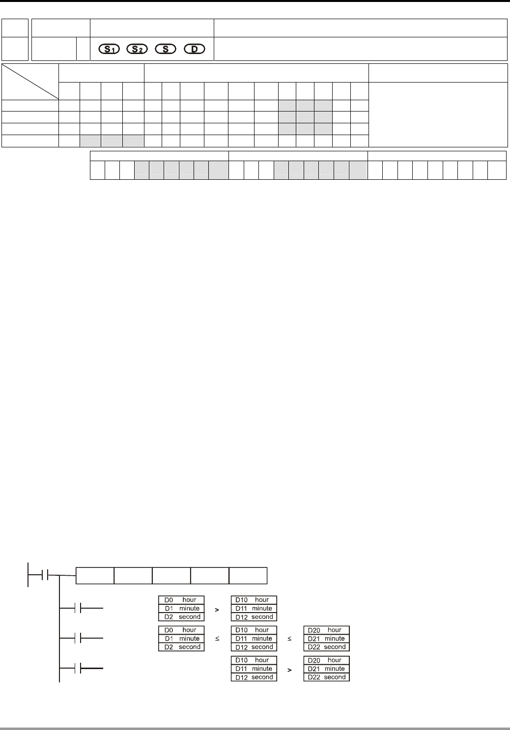
9 Application Instructions API 150-199
DVP-PLC Application Manual
9-55
API Mnemonic Operands Function
161
TZCP P Time Zone Compare
Bit Devices Word Devices Program Steps Type
OP X Y M S K H KnX KnY KnM KnS T C D E F
S1 ***
S2
***
S
***
D * * *
TZCP, TZCPP: 9 steps
PULSE 16-bit 32-bit
ES EX SS SA SX SC EH SV EH3
SV2 ES EX SS SA SX SC EH SV EH3
SV2 ES EX SS SA SX SC EH SV EH3
SV2
Operands:
S1: Lower bound of the time for comparison S2: Upper bound of the time for comparison S: Current time of
RTC D: Comparison result
Explanations:
1. S1, S2, and S will occupy 3 consecutive devices.
2. The content in S1 must be less than the content in S2.
3. D will occupy 3 consecutive points.
4. See the specifications of each model for their range of use.
5. S is compared with S1 and S2. The comparsion result is stored in D.
6. S1 , S1 +1, S1 +2: The “hour”, “minute” and “second” of the lower bound of the time for comparison.
7. S2, S2 +1, S2 +2: The “hour”, “minute” and “second”ond” of the upper bound of the time for comparison.
8. S , S +1, S +2: The “hour”, “minute” and “second” of the current time of RTC.
9. D0 designated by S is read by TRD instruction and the comparison is started by TZCP instruction. If S1, S2, and
S exceed their ranges, the program will regard this as an operation error and the instruction will not be
executed, M1067 and M1068 = On and D1067 will record the error code 0E1A (hex).
10. When S < S1 and S < S2, D will be On. When S > S1 and S > S2, D + 2 will be On. In other occasions, D + 1
will be On.
Program Example:
When X10= On, TZCP instruction will be executed and one of M10 ~ M12 will be On. When X10 = Off, TZCP
instruction will not be executed and the status of M10 ~ M12 prior to X10 = Off will remain unchanged.
X10
M10
TZCP D0 D20 D10 M10
M11
M12
ON when
ON when
ON when
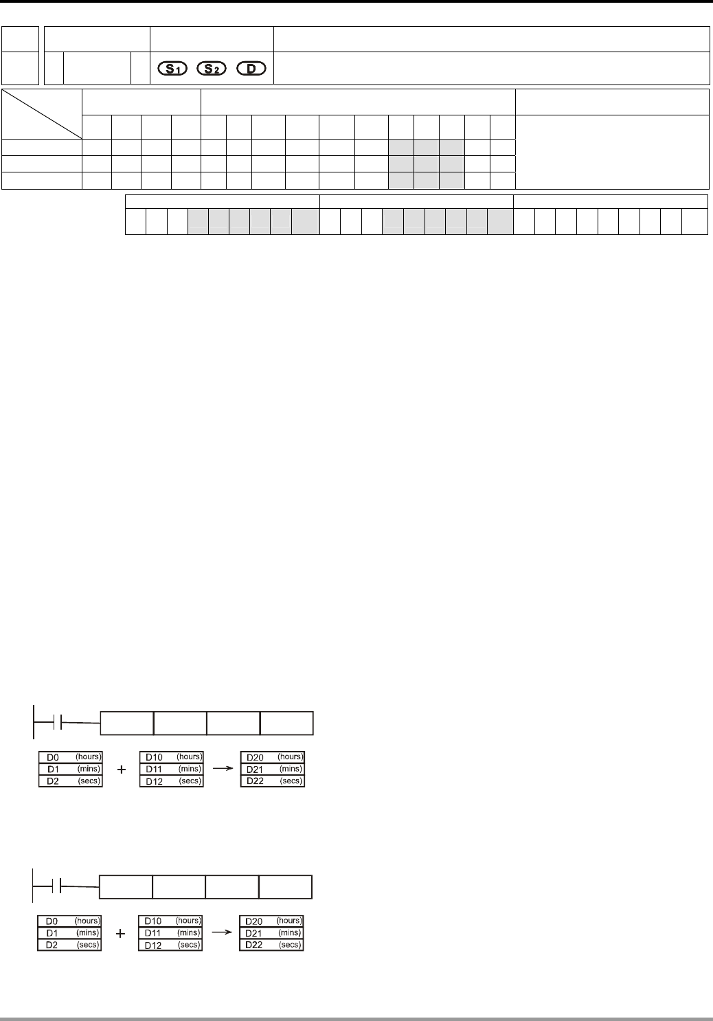
9 Application Instructions API 150-199
DVP-PLC Application Manual
9-56
API Mnemonic Operands Function
162
TADD P Time Addition
Bit Devices Word Devices Program Steps Type
OP X Y M S K H KnX KnY KnM KnS T C D E F
S1 * * *
S2 * * *
D * * *
TADD, TADDP: 7 steps
PULSE 16-bit 32-bit
ES EX SS SA SX SC EH SV EH3
SV2 ES EX SS SA SX SC EH SV EH3
SV2 ES EX SS SA SX SC EH SV EH3
SV2
Operands:
S1: Time summand S2: Time addend D: Time sum
Explanations:
1. S1, S2, and D will occupy 3 consecutive devices.
2. See the specifications of each model for their range of use.
3. Flags: M1020 (zero flag); M1022 (carry flag)
4. S1 + S2 = D. The hour, minute, and second of the RTC designated in S1 plus the hour, minute, and second
designated in S2. The result is stored in the hour, minute, and second of the register designated in D.
5. If S1 and S2 exceed their ranges, the program will regard this as an operation error and the instruction will not
be executed. M1067 and M1068 will be On and D1067 record the error code 0E1A (hex).
6. If the sum is larger than 24 hours, the carry flag M1022 will be On and the value in D will be the result of “sum
minuses 24 hours”.
7. If the sum equals 0 (00:00:00), the zero flag M1020 will be On.
Program Example:
1. When X10= On, TADD instruction will be executed and the hour, minute and second in RTC designated in D0
~ D2 will plus the hour, minute and second in RTC designated in D10 ~ D12. The sum is stored in the hour,
minute and second of the register designated in D20 ~ D22.
X10
TADD D0 D10 D20
8
20
6
40
6
14
26
50
10
08:10:20 06:40:06 14:50:26
2. If the sum is larger than 24 hours, M1022 will be On.
X10
TADD D0 D10 D20
30
11
30
8
6
38
10
40
18:40:30 11:30:08 06:10:38
18
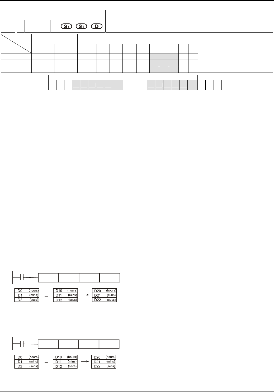
9 Application Instructions API 150-199
DVP-PLC Application Manual
9-57
API Mnemonic Operands Function
163
TSUB P Time Subtraction
Bit Devices Word Devices Program Steps Type
OP X Y M S K H KnX KnY KnM KnS T C D E F
S1 * * *
S2 * * *
D * * *
TSUB, TSUBP: 7 steps
PULSE 16-bit 32-bit
ES EX SS SA SX SC EH SV EH3
SV2 ES EX SS SA SX SC EH SV EH3
SV2 ES EX SS SA SX SC EH SV EH3
SV2
Operands:
S1: Time minuend S2: Time subtrahend D: Time remainder
Explanations:
1. S1, S2, and D will occupy 3 consecutive devices.
2. See the specifications of each model for their range of use.
3. Flags: M1020 (zero flag); M1021 (borrow flag)
4. S1 − S2 = D. The hour, minute, and second of the RTC designated in S1 minus the hour, minute, and second
designated in S2. The result is stored in the hour, minute, and second of the register designated in D.
5. If S1 and S2 exceed their ranges, the program will regard this as an operation error and the instruction will not
be executed. M1067 and M1068 will be On and D1067 record the error code 0E1A (hex).
6. If the remainder is a negative value, the borrow flag M1021 will be On. The value in D will be the result of “the
negative value pluses 24 hours”.
7. If the remainder equals 0 (00:00:00), the zero flag M1020 will be On.
Program Example:
1. When X10= On, TADD instruction will be executed and the hour, minute and second in RTC designated in D0
~ D2 will minus the hour, minute and second in RTC designated in D10 ~ D12. The remainder is stored in the
hour, minute and second of the register designated in D20 ~ D22.
X10
TSUB D0 D10 D20
14
30
8
5
57
49
20
20:20:05 14:30:08 05:49:57
20
5
2. If the subtraction result is a negative value, M1021 will be On.
X10
TSUB D0 D10 D20
19
11
15 15
9
20
05:20:30 19:11:15 10:09:15
5
30
10
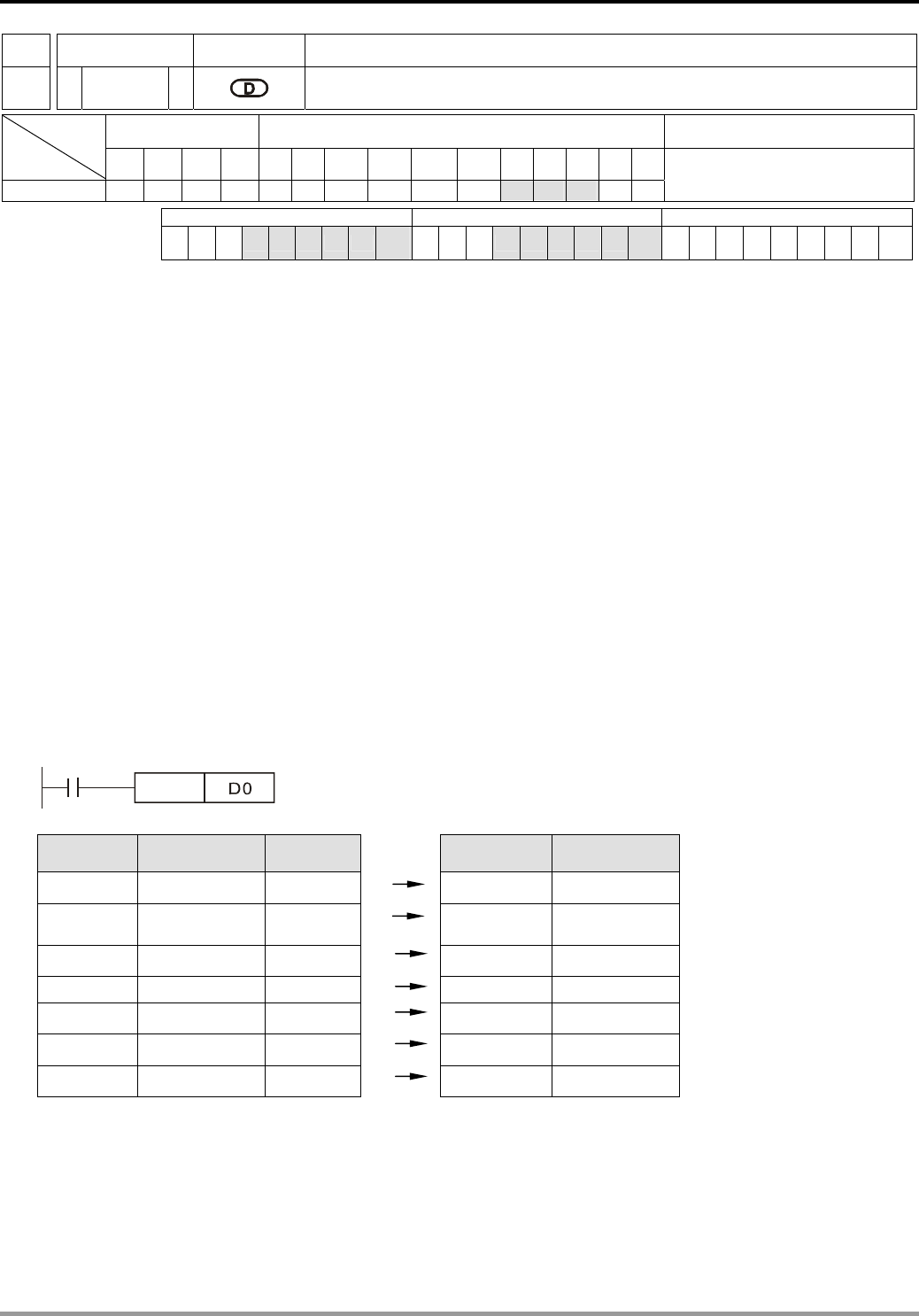
9 Application Instructions API 150-199
DVP-PLC Application Manual
9-58
API Mnemonic Operands Function
166
TRD P Time Read
Bit Devices Word Devices Program Steps Type
OP X Y M S K H KnX KnY KnM KnS T C D E F
D * * *
TRD, TRDP: 3 steps
PULSE 16-bit 32-bit
ES EX SS SA SX SC EH SV EH3
SV2 ES EX SS SA SX SC EH SV EH3
SV2 ES EX SS SA SX SC EH SV EH3
SV2
Operands:
D: The device for storing the current time read in RTC
Explanations:
1. D will occupy 7 consecutive devices.
2. See the specifications of each model for their range of use.
3. Flags: M1016, M1017, M1076. See remarks for more details.
4. The built-in RTC in EH/EH2/SV/EH3/SV2/SA/SX/SC series MPU offers 7 data (year, week, month, day, hour,
minute, second) stored in D1319 ~ D1313. TRD instruction is for program designers to read the current data in
RTC and store the data to the 7 registers designated.
5. D1319 only reads the 2-digit year in A.D. If you wish D1319 to read the 4-digit year, see remarks for more
information.
Program Example:
1. When X0 = On, the instruction will read the current time in RTC to the designated registers D0 ~ D6.
2. The content of D1318: 1 = Monday; 2 = Tuesday … 7 = Sunday.
TRD
X0
Special D Item Content General D Item
D1319 Year (A.D.) 00~99 D0 Year (A.D.)
D1318 Day
(Mon ~ Sun) 1~7 D1 Day
(Mon ~ Sun)
D1317 Month 1~12 D2 Month
D1316 Day 1~31
D3 Date
D1315 Hour 0~23 D4 Hour
D1314 Minute 0~59 D5 Minute
D1313 Second 0~59 D6 Second
9 Application Instructions API 150-199
DVP-PLC Application Manual
9-59
Remarks:
1. Flags and special registers for the built-in RTC in SA/SX/SC/EH/EH2/SV/EH3/SV2 series MPU.
Device Name Function
M1016 Displaying year in
A.D. in RTC
When Off, D1319 will display 2-digit year in A.D.
When On, D1319 will display “2-digit year in A.D + 2,000”.
M1017 ±30 seconds
correction
Correction takes place when M1017 goes from Off to On (reset to 0 when in
0 ~ 29 second; minute pluses 1 and second resets to 0 in 30 ~ 59 second)
M1076 Malfunction of RTC On when the set value exceeds the range. (only available when the power
is being switched on).
D1313 Second 0 ~ 59
D1314 Minue 0 ~ 59
D1315 Hour 0 ~ 23
D1316 Day 1 ~ 31
D1317 Month 1 ~ 12
D1318 Week 1 ~ 7
D1319 Year 0 ~ 99 (2-digit year in A.D.)
2. How to correct RTC:
There are 2 ways to correct the built-in RTC.
a) By a specific instruction. (See API 167 TWR instruction)
b) By peripheral devices, WPLSoft, the ladder diagram editing software.
3. How to display 4-digit year in A.D.:
a) Normally, the year is only displayed in 2 digits (e.g. 2003 displayed as 03). If you wish the year to be
displayed in 4 digits, please key in the following program at the start of the program.
M1002
SET M1016 display 4-digit year in A.D.
b) The original 2-digit year will be switched to a 4-digit year, i.e. the 2-digit year will pluses 2,000.
c) If you wish to write in new time in the 4-digit year display mode, you can only write in a 2-digit year (0 ~ 99,
indicating year 2000 ~ 2099). For example, 00=year 2000, 50=year 2050 and 99=year 2099.
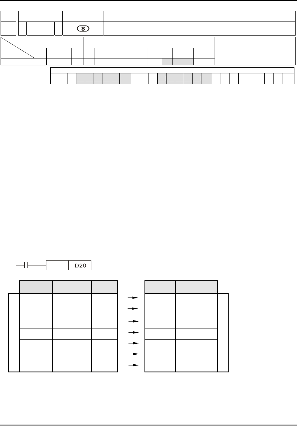
9 Application Instructions API 150-199
DVP-PLC Application Manual
9-60
API Mnemonic Operands Function
167
TWR P Time Write
Bit Devices Word Devices Program Steps Type
OP X Y M S K H KnX KnY KnM KnS T C D E F
S * * *
TWR, TWRP: 3 steps
PULSE 16-bit 32-bit
ES EX SS SA SX SC EH SV EH3
SV2 ES EX SS SA SX SC EH SV EH3
SV2 ES EX SS SA SX SC EH SV EH3
SV2
Operands:
S: Device for storing the new time to be written into RTC
Explanations:
1. S will occupy 7 consecutive devices.
2. See the specifications of each model for their range of use.
3. Flags: M1016, M1017, M1076. See remarks of API 166 TRD for more details.
4. To make adjustment on the RTC built in SA/SX/SC/EH/EH2/SV/EH3/SV2 series MPU, use this instruction to
write the correct time into the RTC.
5. When this instruction is executed, the new set time will be written in the RTC built in PLC immediately.
Therefore, please be noted that the new set time has to match the current time then when the instruction is
executed.
6. If S exceeds its range, the program will regard it as an operation error and the instruction will not be executed.
M1067 and M1068 will be On and D1067 will record the error code 0E1A (hex).
Program Example 1:
When X0= On, write the correct current time into the RTC.
TWRP
X0
General D Item Content Special D Item
D20 Year (A.D.) 00~99 D1319 Year (A.D.)
D21 Day
(Mon ~ Sun) 1~7 D1318 Day
(Mon ~ Sun)
D22 Month 1~12
D1317 Month
D23 Date 1~31
D1316 Date
D24 Hour 0~23
D1315 Hour
D25 Minute 0~59
D1314 Minute
New set time
D26 Second 0~59 D1313 Second
Real Time Clock
Program Example 2:
1. Set the current time in the RTC as 15:27:30, Tuesday, August 19, 2003.
2. D0 ~ D6 indicate the new set time in the RTC.
3. X10 = On for changing the current time in the RTC and make the changed value the new set value.
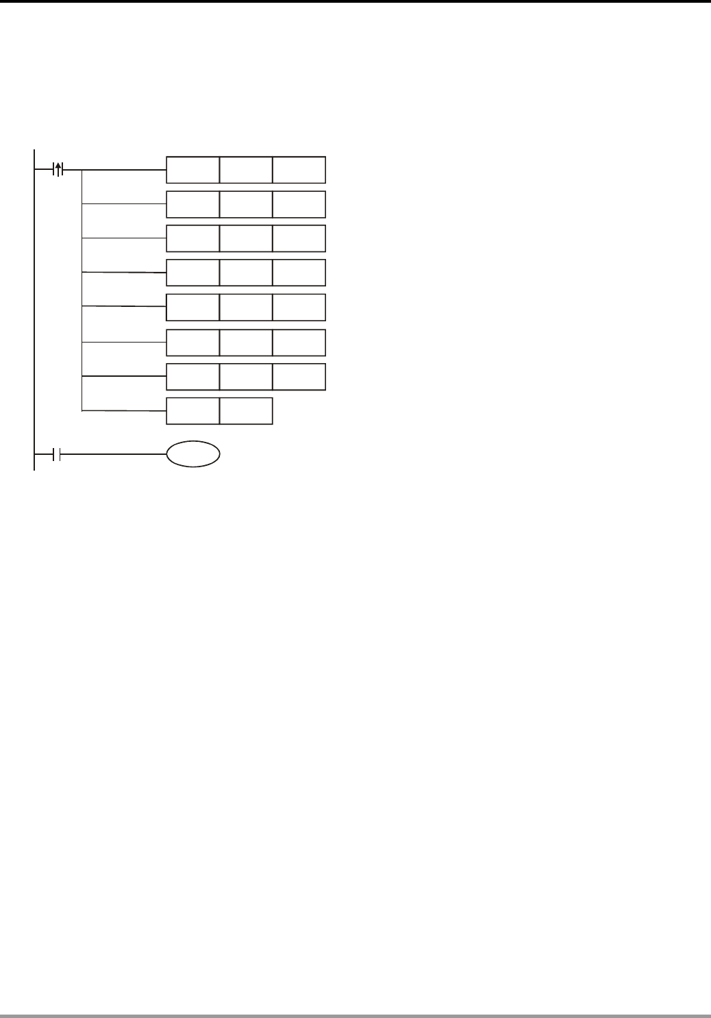
9 Application Instructions API 150-199
DVP-PLC Application Manual
9-61
4. Whenever X11 = On, RTC will perform a ±30 second correction. The correction is performed according to the
rules: When the second hand of RTC locates at 1 ~ 29, the second will be automatically reset to “0” and the
minute hand will remain at its location. When the second hand locates at 30 ~ 59, the second will be
automatically reset to “0” and the minute hand will increase by 1 minute.
X11
K15 D4
X01
MOV
MOV
MOV
MOV
K03
K2
K8
K19
D0
D1
D2
D3
MOV
MOV
MOV
D0
K27
K30
D5
D6
TWR
M1017
Year (2003)
Day (Tuesday)
Month (August)
Data
Hour
Minute
Second
Write the set time into RTC
30 seconds correction
+
-
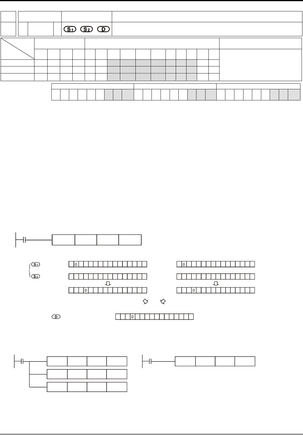
9 Application Instructions API 150-199
DVP-PLC Application Manual
9-62
API Mnemonic Operands Function
168
D MVM P Mask and Combine Designated Bits
Bit Devices Word devices Program Steps Type
OP X Y M S K H KnX KnY KnM KnS T C D E F
S1 * * * * * * ***
S2 ** * * * * * * ***
D * * * * * * ***
MVM, MVMP: 7 steps
DMVM,DMVMP:
13 steps
PULSE 16-bit 32-bit
ES EX SS SA SX SC EH SV EH3
SV2 ES EX SS SA SX SC EH SV EH3
SV2 ES EX SS SA SX SC EH SV EH3
SV2
Operands:
S1: Source device 1 S2: Bits to be masked (OFF) D: Source device 2 / Operation results
[D = (S1 & S2) | (D & ~S2)]
Explanations:
1. The instruction conducts logical AND operation between S1 and S2 first, logical AND operation between D and
~S2 secondly, and combines the 1st and 2nd results in D by logical OR operation.
2. Rule of Logical AND operation: 0 AND 1 = 0, 1 AND 0 = 0, 0 AND 0 = 0, 1 AND 1 = 1
3. Rule of Logical OR operation: 0 OR 1= 1, 1 OR 0 = 1, 0 OR 0 = 0, 1 OR 1 = 1.
Program Example 1 :
When X0 = ON, MVM instruction conducts logical AND operation between 16-bit register D0 and H’FF00 first, logical
AND operation between D4 and H’00FF secondly, and combines the 1st and 2nd results in D4 by logical OR operation.
MVM
X0
D0 HFF00 D4
010101011101010
111 11 10 0 0 0011 000
101 10 000000 00
10
AND
b15 b0
執行前
執行後
D0=HAA55
HFF00
D4=HAA34
HAA00
001101000010010
00000011 11100 111
000 00 000110 00
01
AND
b15 b0
D4=H1234
H00FF
H0034
OR
101 10 000110 00
11
Program Example 2 :
Simplify instructions:
WAND
X0
HFF00 D110 D110 MVM
X0
D110 HFF00 D120
WAND H00FF D120 D120
WOR D100 D120 D120
=
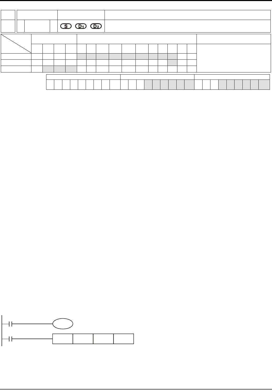
9 Application Instructions API 150-199
DVP-PLC Application Manual
9-63
API Mnemonic Operands Function
169
D HOUR Hour Meter
Bit Devices Word Devices Program Steps Type
OP X Y M S K H KnX KnY KnM KnS T C D E F
S * * * * * * * * * * *
D1 *
D2 * * *
HOUR: 7 steps
DHOUR: 13 steps
PULSE 16-bit 32-bit
ES EX SS SA SX SC EH SV EH3
SV2 ES EX SS SA SX SC EH SV EH3
SV2 ES EX SS SA SX SC EH SV EH3
SV2
Operands:
S: Period of time when D2 is On (in hour) D1: Current value being measured (in hour) D2: Output device
Explanations:
1. If S is used in device F, only 16-bit instruction is applicable.
2. D1 will occupy 2 consecutive points. D1 + 1 uses 16-bit register in 16-bit or 32-bit instruction.
3. See the specifications of each model for their range of use.
4. HOUR instruction can be used 4 times of SA/SX/SC.
5. Range of S: K1 ~ K32,767 (unit: hour); range of D1: K0 ~ K32,767 (unit: hour). D1 + 1 refers to the current time
that is less than an hour (range: K0 ~K3,599; unit: second).
6. This instruction times the time and when the time reaches the set time (in hour), D2 will be On. This function
allows the user to time the operation of the machine or conduct maintenance works.
7. After D2 is On, the timer will resume the timing.
8. In the 16-bit instruction, when the current time measured reaches the maximum 32,767 hours/3,599 seconds,
the timing will stop. To restart the timing, D1 and D1 + 1 have to be reset to “0”.
9. In the 32-bit instruction, when the current time measured reaches the maximum 2,147,483,647 hours/3,599
seconds, the timing will stop. To restart the timing, D1 ~ D1 + 2 have to be reset to “0”.
10. There is no limitations on the times of using this instruction in the program for EH series MPU; however, only 4
instructions can be executed at the same time.
Program Example 1:
In 16-bit instruction, when X0 = On, Y10 will be On and the timing will start. When the timing reaches 100 hours, Y0
will be On and D0 will record the current time measured (in hour) and D1 will record the current time that is less than
an hour (0 ~ 3,599; unit: second).
Y10
HOUR K100 D0 Y0
X0
Y10

9 Application Instructions API 150-199
DVP-PLC Application Manual
9-64
Program Example 2:
In 32-bit instruction, when X0 = On, Y10 will be On and the timing will start. When the timing reaches 40,000 hours,
Y0 will be On. D1 and D0 will record the current time measured (in hour) and D2 will record the current time that is
less than an hour (0 ~ 3,599; unit: second).
Y10
DHOUR K40000 D0 Y0
X0
Y10
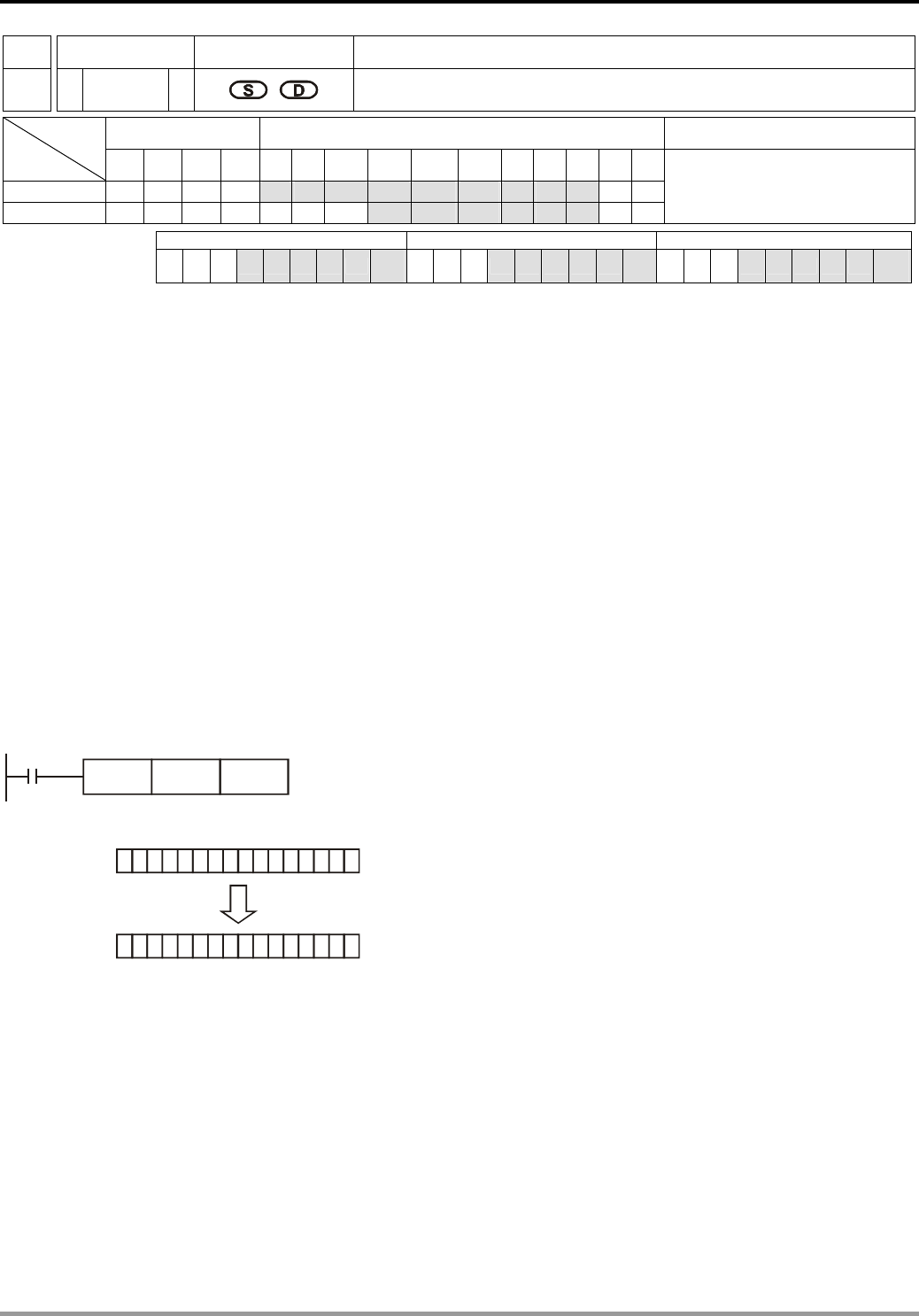
9 Application Instructions API 150-199
DVP-PLC Application Manual
9-65
API Mnemonic Operands Function
170
D GRY P BIN Æ Gray Code
Bit Devices Word Devices Program Steps Type
OP X Y M S K H KnX KnY KnM KnS T C D E F
S * * * * * * * * * * *
D * * * * * * * *
GRY, GRYP: 5 steps
DGRY, DGRYP: 9 steps
PULSE 16-bit 32-bit
ES EX SS SA SX SC EH SV EH3
SV2 ES EX SS SA SX SC EH SV EH3
SV2 ES EX SS SA SX SC EH SV EH3
SV2
Operands:
S: Source device for BIN value D: Device for storing Gray code
Explanations:
1. If S and D are used in device F, only 16-bit instruction is applicable.
2. See the specifications of each model for their range of use.
3. This instruction converts the BIN value in the device designated in S into Gray code and stores the value in D.
4. See the ranges of S as indicated below. If S exceeds the ranges, the program will regard it as an operation
error and the instruction will not be executed. M1067 and M1068 will be On and D1067 will record the error
code 0E1A (hex).
In 16-bit instruction: 0 ~ 32,767
In 32-bit instruction: 0 ~ 2,147,483,647
Program Example:
When X0 = On, the instruction will convert constant K6,513 into Gray code and store the result in K4Y20.
X0
GRY K6513 K4Y20
00011 100 011 1 1000
b15 b0
K6513=H1971
00000 00001111111
K4Y20
Y37 Y20
GRAY6513
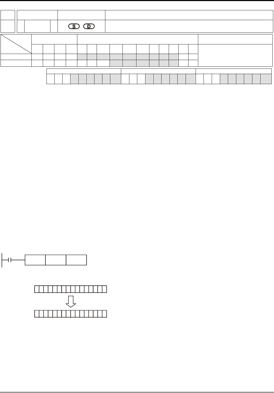
9 Application Instructions API 150-199
DVP-PLC Application Manual
9-66
API Mnemonic Operands Function
171
D GBIN P Gray Code Æ BIN
Bit Devices Word Devices Program Steps Type
OP X Y M S K H KnX KnY KnM KnS T C D E F
S * * * * * * * * * * *
D * * * * * * * *
GBIN, GBINP: 5 steps
DGBIN, DGBINP: 9 steps
PULSE 16-bit 32-bit
ES EX SS SA SX SC EH SV EH3
SV2 ES EX SS SA SX SC EH SV EH3
SV2 ES EX SS SA SX SC EH SV EH3
SV2
Operands:
S: Source device for Gray code D: Device for storing BIN value
Explanations:
1. If S and D are used in device F, only 16-bit instruction is applicable.
2. See the specifications of each model for their range of use.
3. This instruction converts the Gray code in the device designated in S into BIN value and stores the value in D.
4. This instruction converts the content (in Gray code) in the absolute position encoder connected at the PLC
input terminal into BIN value and store the result in the designated register.
5. See the ranges of S as indicated below. If S exceeds the ranges, the program will regard it as an operation
error and the instruction will not be executed. M1067 and M1068 will be On and D1067 will record the error
code 0E1A (hex).
In 16-bit instruction: 0 ~ 32,767
In 32-bit instruction: 0 ~ 2,147,483,647
Program Example:
When X20 = On, the Gray code in the absolute position encoder connected at X0 ~ X17 will be converted into BIN
value and stored in D10.
X20
GBIN K4X0 D10
0001 10111000
b15 b0
H1971=K6513
000 0 00111111
X17 X0
GRAY6513
K4X0
01 0 1
0010

9 Application Instructions API 150-199
DVP-PLC Application Manual
9-67
API Mnemonic Operands Function
172
D ADDR P Floating Point Addition
Bit Devices Word Devices Program Steps Type
OP X Y M S K H KnX KnY KnM KnS T C D E F
S1 *
S2 *
D *
DADDR, DADDRP: 13 steps
PULSE 16-bit 32-bit
ES EX SS SA SX SC EH SV EH3
SV2 ES EX SS SA SX SC EH SV EH3
SV2 ES EX SS SA SX SC EH SV EH3
SV2
Operands:
S1: Floating point summand S
2: Floating point addend D: Sum
Explanations:
1. S1 and S2 can be floating point values (FX.XX).
2. See the specifications of each model for their range of use.
3. Flags: M1020 (zero flag), M1021 (borrow flag), M1022 (carry flag)
4. In DADDR instruction, floating point values (e.g. F1.2) can be entered directly into S1 and S2 or stored in register
D for operation. When the instruction is being executed, operand D will store the operation result.
5. When S1 and S2 stores the floating point values in register D, their functions are the same as API 120 EADD.
6. S1 and S2 can designate the same register. In this case, if the “continuous execution” type instruction is in use and
during the On period of the drive contact, the register will be added once in every scan by a “pulse execution” type
instruction (DADDRP).
7. If the absolute value of the operation result is larger than the maximum floating point displayable, the carry flag
M1022 will be On.
8. If the absolute value of the operation result is smaller than the minimum floating point displayable, the borrow flag
M1021 will be On.
9. If the operation result is “0”, the zero flag M1020 will be On.
Program Example 1:
When X0 = On, the floating point F1.20000004768372 will plus F2.20000004768372 and the result
F3.40000009536743 will be stored in the data registers (D10, D11).
X0
DADDR F1.20000004768372 D10
F1.20000004768372 F2.20000004768372
Program Example 2:
When X0 = On, the floating point value (D1, D0) + floating point value (D3, D2) and the result will be stored in the
registers designated in (D11, D10).
X0
DADDR D0 D2 D10
Remarks:
The functions of this instruction are in V6.6 of ES/EX/SS series, V1.6 of SA/SX series and V1.4 of SC series.

9 Application Instructions API 150-199
DVP-PLC Application Manual
9-68
DADDR instruction supports V1.0 of EH2/SV/EH3/SV2 series, but not EH series.
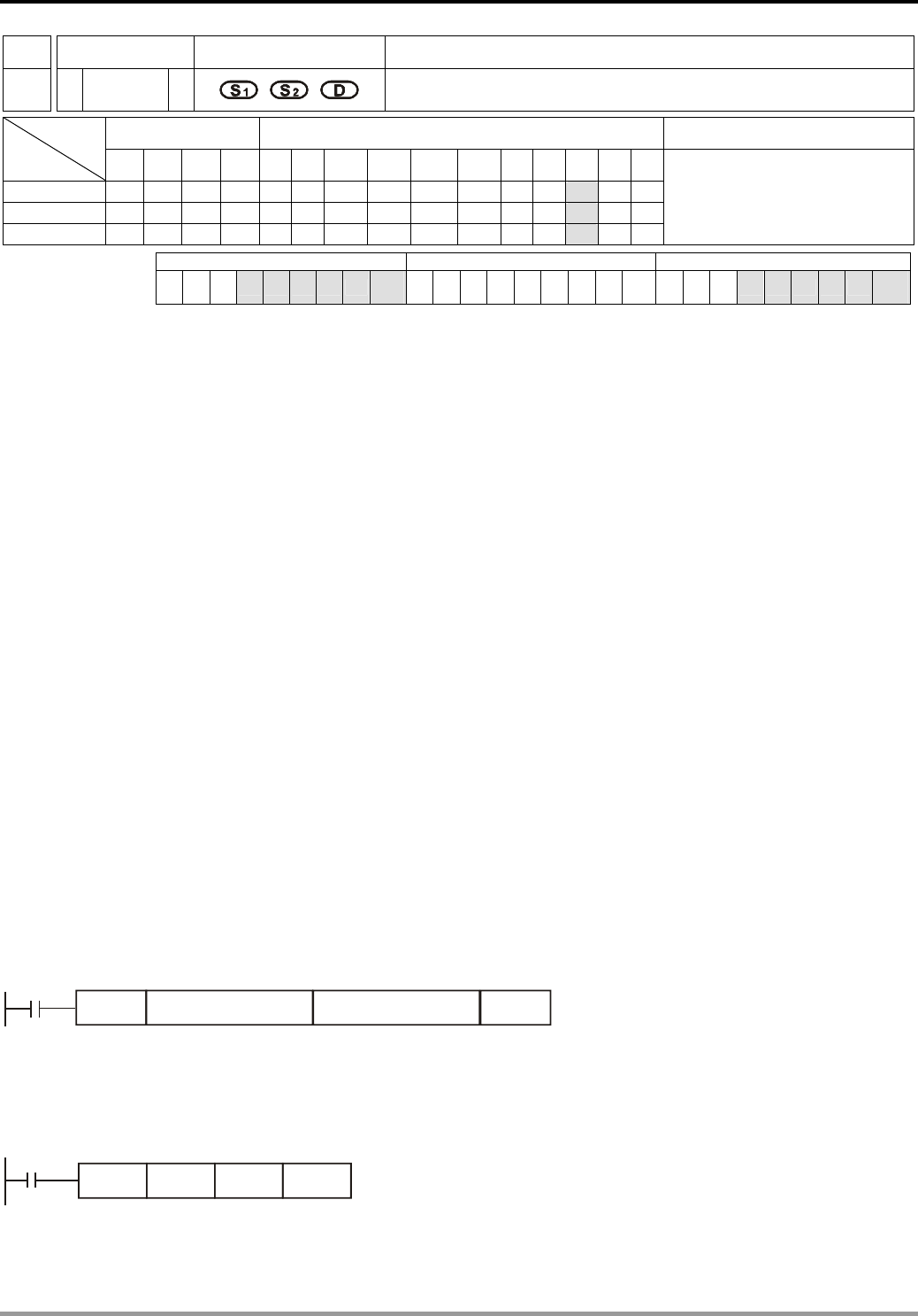
9 Application Instructions API 150-199
DVP-PLC Application Manual
9-69
API Mnemonic Operands Function
173
D SUBR P Floating Point Subtraction
Bit Devices Word Devices Program Steps Type
OP X Y M S K H KnX KnY KnM KnS T C D E F
S1 *
S2 *
D *
DSUBR, DSUBRP: 13 steps
PULSE 16-bit 32-bit
ES EX SS SA SX SC EH SV EH3
SV2 ES EX SS SA SX SC EH SV EH3
SV2 ES EX SS SA SX SC EH SV EH3
SV2
Operands:
S1: Floating point minuend S
2: Floating point subtrahend D: Remainder
Explanations:
1. S1 and S2 can be floating point values (FX.XX).
2. See the specifications of each model for their range of use.
3. Flags: M1020 (zero flag), M1021 (borrow flag), M1022 (carry flag)
4. In DSUBR instruction, floating point values (e.g. F1.2) can be entered directly into S1 and S2 or stored in register
D for operation. When the instruction is being executed, operand D will store the operation result.
5. When S1 and S2 stores the floating point values in register D, their functions are the same as API 121 ESUB.
6. S1 and S2 can designate the same register. In this case, if the “continuous execution” type instruction is in use and
during the On period of the drive contact, the register will be subtracted once in every scan by a “pulse execution”
type instruction (DSUBRP).
7. If the absolute value of the operation result is larger than the maximum floating point displayable, the carry flag
M1022 will be On.
8. If the absolute value of the operation result is smaller than the minimum floating point displayable, the borrow flag
M1021 will be On.
9. If the operation result is “0”, the zero flag M1020 will be On.
Program Example 1:
When X0 = On, the floating point F1.20000004768372 will minus F2.20000004768372 and the result F-1 will be
stored in the data registers (D10, D11).
X0
DSUBR F1.20000004768372 D10
F1.20000004768372 F2.20000004768372
Program Example 2:
When X0 = On, the floating point value (D1, D0) – floating point value (D3, D2) and the result will be stored in the
registers designated in (D11, D10).
X0
DSUBR D0 D2 D10
Remarks:
The functions of this instruction are in V6.6 of ES/EX/SS series, V1.6 of SA/SX series and V1.4 of SC series.

9 Application Instructions API 150-199
DVP-PLC Application Manual
9-70
DADDR instruction supports V1.0 of EH2/SV/EH3/SV2 series, but not EH series.
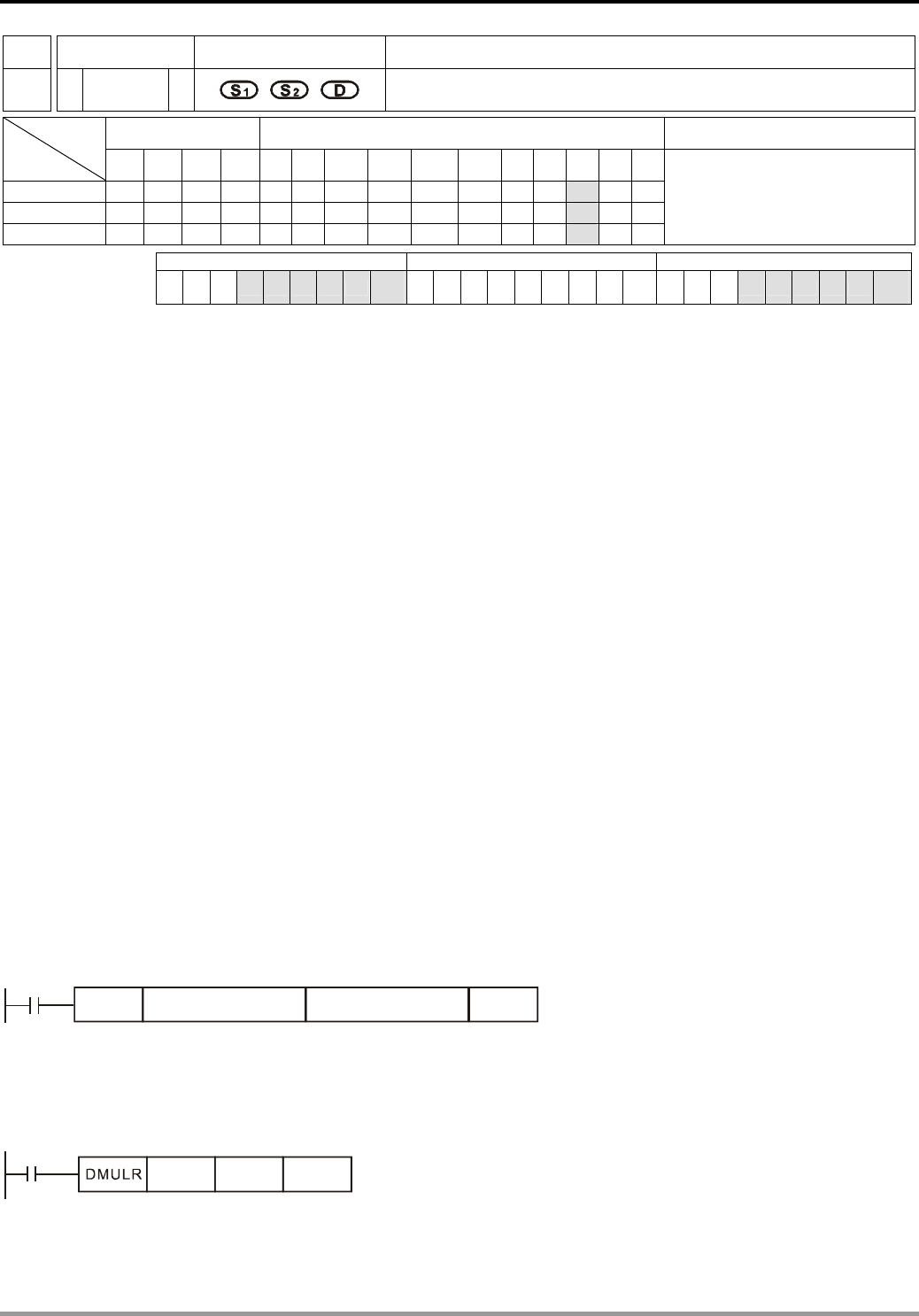
9 Application Instructions API 150-199
DVP-PLC Application Manual
9-71
API Mnemonic Operands Function
174
D MULR P Floating Point Multiplication
Bit Devices Word Devices Program Steps Type
OP X Y M S K H KnX KnY KnM KnS T C D E F
S1 *
S2 *
D *
DMULR, DMULRP: 13 steps
PULSE 16-bit 32-bit
ES EX SS SA SX SC EH SV EH3
SV2 ES EX SS SA SX SC EH SV EH3
SV2 ES EX SS SA SX SC EH SV EH3
SV2
Operands:
S1: Floating point multiplicand S
2: Floating point multiplicator D: Product
Explanations:
1. S1 and S2 can be floating point values (FX.XX).
2. See the specifications of each model for their range of use.
3. Flags: M1020 (zero flag), M1021 (borrow flag), M1022 (carry flag)
4. In DMULR instruction, floating point values (e.g. F1.2) can be entered directly into S1 and S2 or stored in register
D for operation. When the instruction is being executed, operand D will store the operation result.
5. When S1 and S2 stores the floating point values in register D, their functions are the same as API 122 EMUL.
6. S1 and S2 can designate the same register. In this case, if the “continuous execution” type instruction is in use and
during the On period of the drive contact, the register will be multiplied once in every scan by a “pulse execution”
type instruction (DMULRP).
10. If the absolute value of the operation result is larger than the maximum floating point displayable, the carry flag
M1022 will be On.
11. If the absolute value of the operation result is smaller than the minimum floating point displayable, the borrow flag
M1021 will be On.
12. If the operation result is “0”, the zero flag M1020 will be On.
Program Example 1:
When X0 = On, the floating point F1.20000004768372 will multiply F2.20000004768372 and the result
F2.64000010490417 will be stored in the data registers (D10, D11).
X0
DMULR F1.20000004768372 D10F1.20000004768372 F2.20000004768372
Program Example 2:
When X1 = On, the floating point value (D1, D0) × floating point value (D11, D10) and the result will be stored in the
registers designated in (D21, D20).
X1
D0 D10 D20
Remarks:
The functions of this instruction are in V6.6 of ES/EX/SS series, V1.6 of SA/SX series and V1.4 of SC series. DADDR

9 Application Instructions API 150-199
DVP-PLC Application Manual
9-72
instruction supports v1.0 of EH2/SV/EH3/SV2 series, but not EH series.

9 Application Instructions API 150-199
DVP-PLC Application Manual
9-73
API Mnemonic Operands Function
175
D DIVR P Floating Point Division
Bit Devices Word Devices Program Steps Type
OP X Y M S K H KnX KnY KnM KnS T C D E F
S1 *
S2 *
D *
DDIVR, DDIVRP: 13 steps
PULSE 16-bit 32-bit
ES EX SS SA SX SC EH SV EH3
SV2 ES EX SS SA SX SC EH SV EH3
SV2 ES EX SS SA SX SC EH SV EH3
SV2
Operands:
S1: Floating point dividend S
2: Floating point divisor D: Quotient
Explanations:
1. S1 and S2 can be floating point values.
2. See the specifications of each model for their range of use.
3. Flags: M1020 (zero flag), M1021 (borrow flag), M1022 (carry flag)
4. In DDIVR instruction, floating point values (e.g. F1.2) can be entered directly into S1 and S2 or stored in register D
for operation. When the instruction is being executed, operand D will store the operation result.
5. When S1 and S2 stores the floating point values in register D, their functions are the same as API 123 EDIV.
6. If S2 is “0”, the program will regard it as an operation error and the instruction will not be executed. M1067 and
M1068 will be On and D1067 will record the error code H’0E19.
7. If the absolute value of the operation result is larger than the maximum floating point displayable, the carry flag
M1022 will be On.
8. If the absolute value of the operation result is smaller than the minimum floating point displayable, the borrow flag
M1021 will be On.
9. If the operation result is “0”, the zero flag M1020 will be On.
Program Example 1:
When X0 = On, the floating point F1.20000004768372 will be divided by F2.20000004768372 and the result
F0.545454561710358 will be stored in the data registers (D10, D11).
X0
DDIVR F1.20000004768372 D10F1.20000004768372 F2.20000004768372
Program Example 2:
When X1 = On, the floating point value (D1, D0) ÷ floating point value (D11, D10) and the quotient will be stored in the
registers designated in (D21, D20).
X1
DDIVR D0 D10 D20
Remarks:
The functions of this instruction are in V6.6 of ES/EX/SS series, V1.6 of SA/SX series and V1.4 of SC series.

9 Application Instructions API 150-199
DVP-PLC Application Manual
9-74
DADDR instruction supports V1.0 of EH2/SV/EH3/SV2 series, but not EH series.
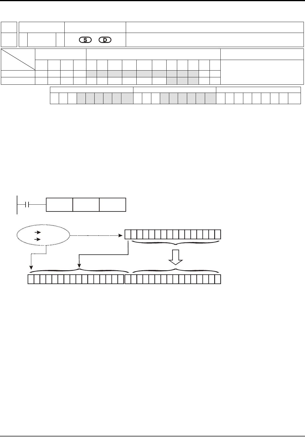
9 Application Instructions API 150-199
DVP-PLC Application Manual
9-75
API Mnemonic Operands Function
176
MMOV P Magnifying Transfer with Sign Extension
Bit Devices Word Devices Program Steps Type
OP X Y M S K H KnX KnY KnM KnS T C D E F
S * * * * * * * * *
D * * *
MMOV, MMOVP: 5 steps
PULSE 16-bit 32-bit
ES EX SS SA SX SC EH SV EH3
SV2 ES EX SS SA SX SC EH SV EH3
SV2 ES EX SS SA SX SC EH SV EH3
SV2
Operands:
S: Data source (16-bit) D: Data destination (32-bit)
Explanations:
1. MMOV instruction sends the data in the 16-bit S device to the 32-bit D device. The designated sign bit will be
copied and stored in the destination device.
Program Example 1:
When X23 = On, the data in D4 will be sent to D6 and D7.
X23
MMOV D4 D6
0011 1
0
0
0
11
1
1000
b15 b0
00 0 001111
D7, D6
1
11111111
b31 b16
1
b0
b15
D4
0
1
1
00
1
111
1
11
11
"+"號
0
1
"-"號
In the example, b15 of D4 is sent to b15 ~ b31 of (D7, D6) as a negative value (same as it is in D4).
9 Application Instructions API 150-199
DVP-PLC Application Manual
9-76
API Mnemonic Operands Function
177
GPS GPS data receiving
Bit Devices Word devices Program Steps Type
OP X Y M S K H KnX KnY KnM KnS T C D E F
S ** *
D *
GPS: 5 steps
PULSE 16-bit 32-bit
ES EX SS SA SX SC EH SV EH3
SV2 ES EX SS SA SX SC EH SV EH3
SV2 ES EX SS SA SX SC EH SV EH3
SV2
Operands:
S: Sentence identifier for GPS data receiving D: Destination device for feedback data
Explanations:
1. GPS data receiving instruction is only applicable on COM1 (RS-232), with communication format: 9600,8,N,1,
protocol: NMEA-0183, and communication frequency: 1Hz.
2. Operand S is sentence identifier for GPS data receiving. K0: $GPGGA, K1: $GPRMC.
3. Operand D stores the received data. Up to 17 consecutive words will be occupied and can not be used
repeatedly. Please refer to the table below for the explanations of each D device.
z When S is set as K0, sentence identifier $GPGGA is specified. D devices refer to:
No. Content Range Format Note
D + 0 Hour 0 ~ 23 Word
D + 1 Minute 0 ~ 59 Word
D + 2 Second 0 ~ 59 Word
D + 3~4 Latitude 0 ~ 90 Float Unit: dd.mmmmmm
D + 5 North / South 0 or 1 Word 0(+)ÆNorth, 1(-)ÆSouth
D + 6~7 Longitude 0 ~ 180 Float Unit: ddd.mmmmmm
D + 8 East / West 0 or 1 Word 0(+)ÆEast, 1(-)ÆWest
D + 9 GPS data valid / invalid 0, 1, 2 Word 0 = invalid
D + 10~11 Altitude 0 ~9999.9 Float Unit: meter
D + 12~13 Latitude -90 ~ 90 Float
Unit: ±dd.ddddd
D + 14~15 Longitude -180 ~ 180 Float Unit: ±ddd.ddddd
z When S is set as K1, sentence identifier $GPRMC is specified. D devices refer to:
No. Content Range Format Note
D + 0 Hour 0 ~ 23 Word
D + 1 Minute 0 ~ 59 Word
D + 2 Second 0 ~ 59 Word
D + 3~4 Latitude 0 ~ 90 Float Unit: dd.mmmmmm
D + 5 North / South 0 or 1 Word 0(+)ÆNorth, 1(-)ÆSouth
D + 6~7 Longitude 0 ~ 180 Float Unit: ddd.mmmmmm
D + 8 East / West 0 or 1 Word 0(+)ÆEast, 1(-)ÆWest
9 Application Instructions API 150-199
DVP-PLC Application Manual
9-77
No. Content Range Format Note
D + 9 GPS data valid / invalid 0, 1, 2 Word 0 = invalid
D + 10 Day 1 ~ 31 Word
D + 11 Month 1 ~ 12 Word
D + 12 Year 2000 ~ Word
D + 13~14 Latitude -90 ~ 90 Float Unit: ±dd.ddddd
D + 15~16 Longitude -180 ~ 180 Float Unit: ±ddd.ddddd
4. When applying GPS instruction, COM1 has to be applied in Master mode, i.e. M1312 has to be enabled to
sending request. In addition, M1314 = ON indicates receiving completed. M1315 = ON indicates receiving error.
(D1250 = K1, receiving time-out; D1250 = K2, checksum error)
5. Associated M flags and special D registers:
No. Function
M1312 COM1 (RS-232) sending request
M1313 COM1 (RS-232) ready for data receiving
M1314 COM1 (RS-232) data receiving completed
M1315 COM1 (RS-232) data receiving error
M1138 Retaining communication setting of COM1
D1036 COM1 (RS-232) Communication protocol
D1249 COM1 (RS-232) data receiving time-out setting. (Suggested value: >1s)
D1250 COM1 (RS-232) communication error code
6. Before applying the received GPS data, please check the value in D+9. If D+9 = 0, the GPS data is invalid.
7. If data receiving error occurs, the previous data in D registers will not be cleared, i.e. the previous received data
remains intact.
Program example: Sentence identifier: $GPGGA
1. Set COM1 communication protocol first
M1002
MOV H81 D1036
SET M1138
MOV K2000 D1249
Set communication protocol
as 9600,8,N,1
Retain communication setting
Set receiving time-out as 2s
2. Then enable M0 to execute GPS instruction with sentence identifier $GPGGA
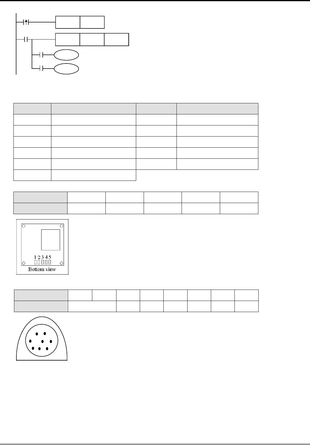
9 Application Instructions API 150-199
DVP-PLC Application Manual
9-78
M0
GPS K0 D0
SET M1312
M0
M1314
M1315
Y0
Y1
3. When receiving completed, M1314 = ON. When receiving failed, M1315 = ON. The received data will be stored
in devices starting with D0.
No. Content No. Content
D0 Hour D8 East / West
D1 Minute D9 GPS data valid / invalid
D2 Second D10~D11 Altitude
D3~D4 Latitude D12~D13
Latitude. Unit: ±dd.ddddd
D5 North / South D14~D15 Longitude. Unit: ±ddd.ddddd
D6~D7 Longitude
4. Pin number description on GPS module (LS20022)
Pin No. of GPS 1 2 3 4 5
Definition VCC(+5V) Rx Tx GND GND
5. Pin number description on PLC COM1:
Pin No. of COM1 1 2 3 4 5 6 7 8
Definition VCC(+5V) -- Rx Tx -- -- GND
1
2
3
4
5
6
7
8
1
2
3
4
5
6
7
8
9 Application Instructions API 150-199
DVP-PLC Application Manual
9-79
API Mnemonic Operands Function
178
D SPA Solar Panel Positioning
Bit Devices Word devices Program Steps Type
OP X Y M S K H KnX KnY KnM KnS T C D E F
S * * *
D *
DSPA: 9 steps
PULSE 16-bit 32-bit
ES EX SS SA SX SC EH SV EH3
SV2 ES EX SS SA SX SC EH SV EH3
SV2 ES EX SS SA SX SC EH SV EH3
SV2
Operands:
S: Start device for input parameters D: Start device for output parameters
Explanations:
1. Operand S occupies 208 consecutive word registers. The function of each device is as below:
No. Content Range Format Note
S + 0 Year 2000 ~ Word
S + 1 Month 1 ~ 12 Word
S + 2 Day 1 ~ 31 Word
S + 3 Hour 0 ~ 23 Word
S + 4 Minute 0 ~ 59 Word
S + 5 Second 0 ~ 59 Word
S + 6~7 Time difference (Δt) (sec) ± 8000 Float
S + 8~9 Local time zone ± 12 Float West: negative
S + 10~11 Longitude ± 180 Float West: negative
Unit: degree
S + 12~13 Latitude ± 90 Float South: negative
Unit: degree
S + 14~15 Elevation 0~
6500000
Float Unit: meter
S + 16~17 Pressure 0 ~ 5000 Float Unit: millibar
S + 18~19 Mean annual temperature (MAT) -273~6000 Float Unit: °C
S + 20~21 Slope ± 360 Float
S + 22~23 Azimuth ± 360 Float
S + 24~25 Atmospheric refraction between
sunrise and sunset
± 5 Float
S +26~207 Reserved for system operation
2. Operand D occupies 8 consecutive word registers. The function of each device is as below:
No. Content Range Format Note
D + 0~1 Zenith 0 ~ 90 Float Horizontal=0
D + 2~3 Azimuth 0 ~ 360 Float North point=0
9 Application Instructions API 150-199
DVP-PLC Application Manual
9-80
No. Content Range Format Note
D + 4~5 Incidence 0 ~ 90 Float
D + 6 Converted DA value of Zenith 0 ~ 2000 Word 1LSB = 0.045
degree
D + 7 Converted DA value of Azimuth 0 ~ 2000 Word 1LSB = 0.18
degree
3. The execution time of SPA instruction costs up to 50ms, therefore we suggest users to execute this instruction
with an interval not less than 1 sec, preventing the instruction from taking too much PLC operation time.
4. Definition of Zenith: 0° and 45°.
0° 45°
5. Definition of Azimuth:
N
0°
90°
180°
270°
N
0°
90°
180°
270°
Program example:
1. Input parameters starting from D4000: 2009/3/23/(y/m/d),10:10:30, Δt = 0, Local time zone = +8,
Longitude/Latitude = +119.192345 East, +24.593456 North, Elevation = 132.2M, Pressure = 820m, MAT =
15.0℃, Slope = 0 degree, Azimuth = -10 degree.
M0
DSPA D4000 D5000
M1013
2. Output results: D5000: Zenith = F37.2394 degree; D5002: Azimuth = F124.7042 degree.
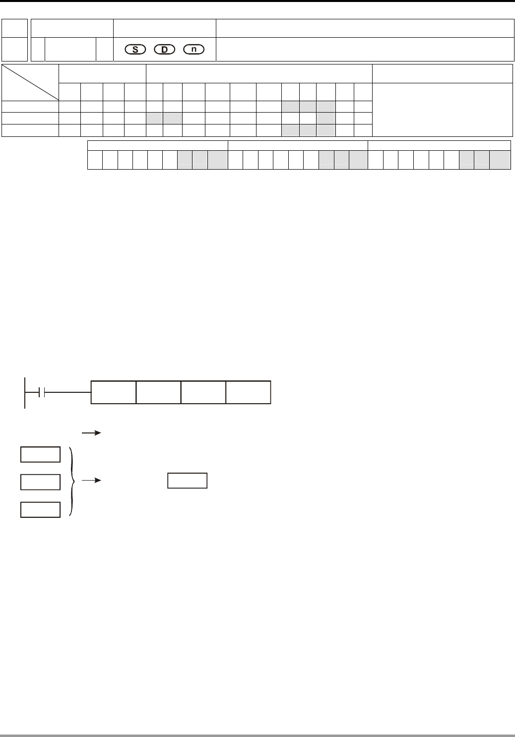
9 Application Instructions API 150-199
DVP-PLC Application Manual
9-81
API Mnemonic Operands Function
179
D WSUM P Sum of multiple devices
Bit Devices Word devices Program Steps Type
OP X Y M S K H KnX KnY KnM KnS T C D E F
S * * *
n * * *
D * * *
WSUM, WSUMP: 7 steps
DWSUM, DWSUMP: 13 steps
PULSE 16-bit 32-bit
ES EX SS SA SX SC EH SV EH3
SV2 ES EX SS SA SX SC EH SV EH3
SV2 ES EX SS SA SX SC EH SV EH3
SV2
Operands:
S: Source device n: Data length to be summed up D: Device for storing the result
Explanations:
1. WSUM instruction sums up n devices starting from S and store the result in D.
2. The instruction supports V1.7 of EH2/SV/EH3/SV2 series and above, but it does not support EH series.
3. If the specified source devices S are out of valid range, only the devices in valid range will be processed.
4. Valid range for n: 1~64. If the specified n value is out of the available range (1~64), PLC will take the upper (64)
or lower (1) bound value as the set value.
Program example:
When X10 = ON, 3 consecutive devices (n = 3) from D0 will be summed up and the result will be stored in D10
X10
WSUM D0 D10
K3
D0
D1
D2
D10
K338
K100
K113
K125
(D0+D1+D2)
D10
Result:

9 Application Instructions API 150-199
DVP-PLC Application Manual
9-82
API Mnemonic Operands Function
180
MAND P Matrix ‘AND’ Operation
Bit Devices Word Devices Program Steps Type
OP X Y M S K H KnX KnY KnM KnS T C D E F
S1 * * * * * * *
S2 * * * * * * *
D * * * * * *
n * * *
MAND, MANDP: 9 steps
PULSE 16-bit 32-bit
ES EX SS SA SX SC EH SV EH3
SV2 ES EX SS SA SX SC EH SV EH3
SV2 ES EX SS SA SX SC EH SV EH3
SV2
Operands:
S1: Matrix source device 1 S2: Matrix source device 2 D: Operation result n: Array length
Explanations:
1. Range of n: K1 ~ K256
2. S1, and S2 designate KnX, KnY, KnM and KnS; D designates KnYm KnM and KnS
3. SA/SX/SC can designate n = 4. EH/EH2/SV/EH3/SV2 can designate n 4≦.
4. See the specifications of each model for their range of use.
5. The two matrix sources S1 and S2 perform matrix ‘AND’ operation according to the array length n. The result is
stored in D.
6. Operation rule of matix ‘AND’ : The result will be 1 if both two bits are 1; otherwise the result will be 0.
Program Example:
When X0 = On, the 3 arrays of 16-bit registers D0 ~ D2 and the 3 arrays of 16-bit registers D10 ~ D12 will perform a
matrix ‘AND’ operation. The result will be stored in the 3 arrays of 16-bitd registers D20 ~ D22.
X0
MAND D0 D10 D20 K3
1111111111 11
0000
1111111111 11
0000
1111111111 11
0000
b15 b0
MAND
11000
111
00000000
11 000
111
00000000
11000
1
11
00000000
11000000000000
11 000
0
00000000
11 000
0
00000000
00
00
00
Before
execution
After
execution
Remarks:
1. Explanations on the matrix instruction:
a) A matix consists of more than 1 consecutive 16-bit registers. The number of registers in the matrix is the
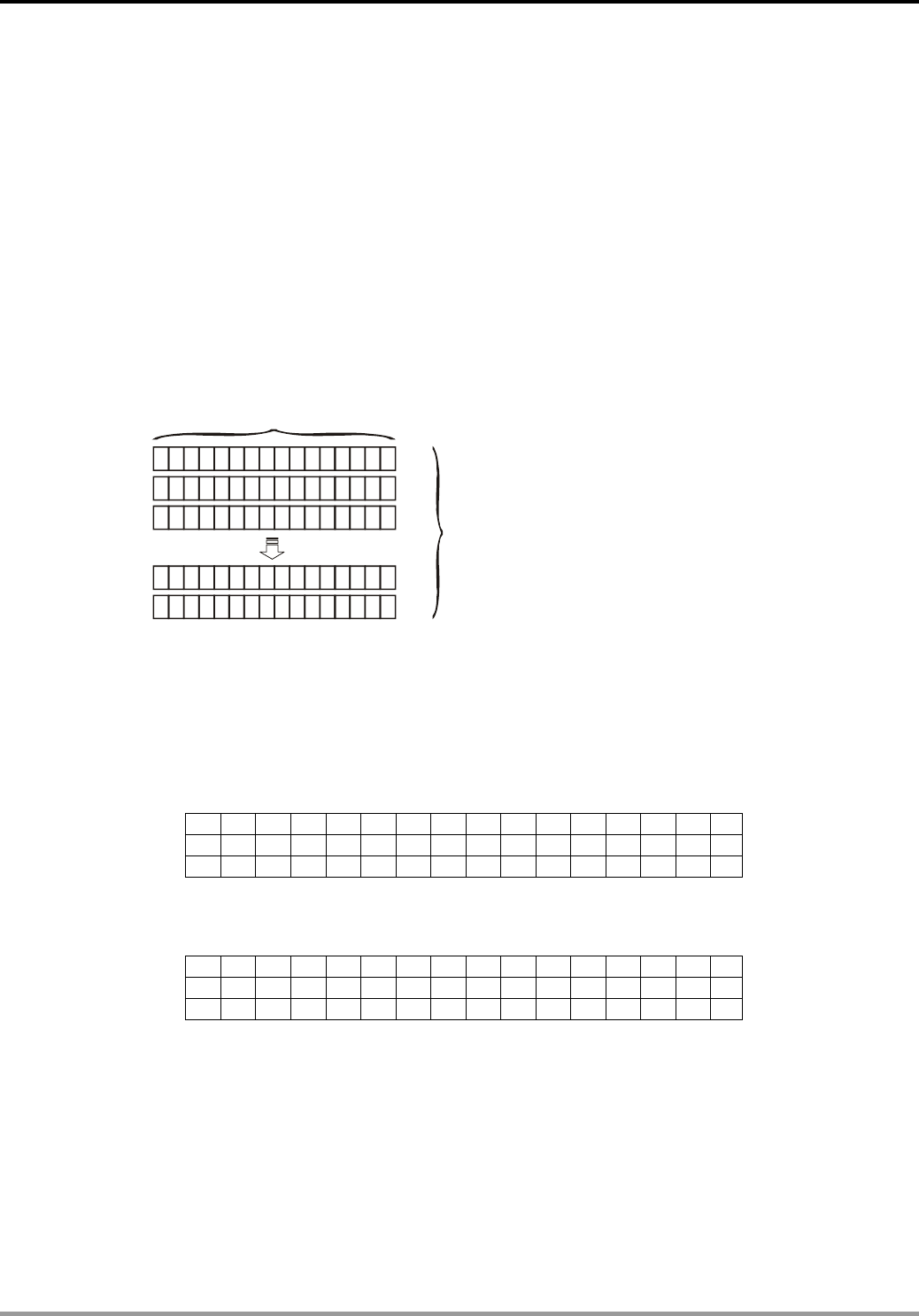
9 Application Instructions API 150-199
DVP-PLC Application Manual
9-83
length of the array (n). A matrix contains 16 × n bits (points) and there is only 1 bit (point) offered for an
operand at a time.
b) The matrix instruction gathers a series of 16 × n bits (b0 ~ b16n-1) and designates a single point for operation.
The point will not be seen as a value.
c) The matrix instruction processes the moving, copying, comparing and searching of one-to-many or
many-to-many matrix status, which is a very handy and important application instruction.
d) The matrix operation will need a 16-bit register to designate a point among the 16n points in the matrix for the
operation. The register is the Pointer (Pr) of the matrix, designated by the user in the instruction. The vaild
range of Pr is 0 ~ 16n -1, corresponding to b0 ~ b16n-1 in the matrix.
e) There are left displacement, right displacement and rotation in a matrix operation. The bit number decreases
from left to right (see the figure below).
1111111111 000011
1111111111 000011
11 01000 00000 11 00
11 01000 00000 11 00
b0
b16
b32
b31
b15
b47
D0
D1
D2
b16n-1
1111111111 000011
Left Right
Width: 16 bits
Dn-1
Length: n
f) The matrix width (C) is fixed at 16 bits.
g) Pr: matrix pointer. E.g. if Pr is 15, the designated point will be b15.
h) Array length (R) is n: n = 1 ~ 256.
Example: The matrix is composed of D0, n = 3; D0 = HAAAA, D1 = H5555, D2 = HAAFF
C15 C
14 C
13 C
12 C
11 C10 C9C8C7C6C5C4C3C2 C
1 C
0
R0 1 0 1 0 1 0 1 0 1 0 1 0 1 0 1 0
D0
R1 0 1 0 1 0 1 0 1 0 1 0 1 0 1 0 1
D1
R2 1 0 1 0 1 0 1 0 1 1 1 1 1 1 1 1
D2
Example: The matrix is composed of K2X0, n = 3; K2X0 = H37, K2X10 = H68, K2X20 = H45
C15 C
14 C
13 C
12 C
11 C10 C9C8C7C6C5C4C3C2 C
1 C
0
R0 0 0 0 0 0 0 0 0 0 0 1 1 0 1 1 1 X0~X7
R1 0 0 0 0 0 0 0 0 0 1 1 0 1 0 0 0 X10~X17
R2 0 0 0 0 0 0 0 0 0 1 0 0 0 1 0 1 X20~X27
Fill “0” into the blank in R0(C15-C8), R1(C15-C8), and R2(C15-C8).
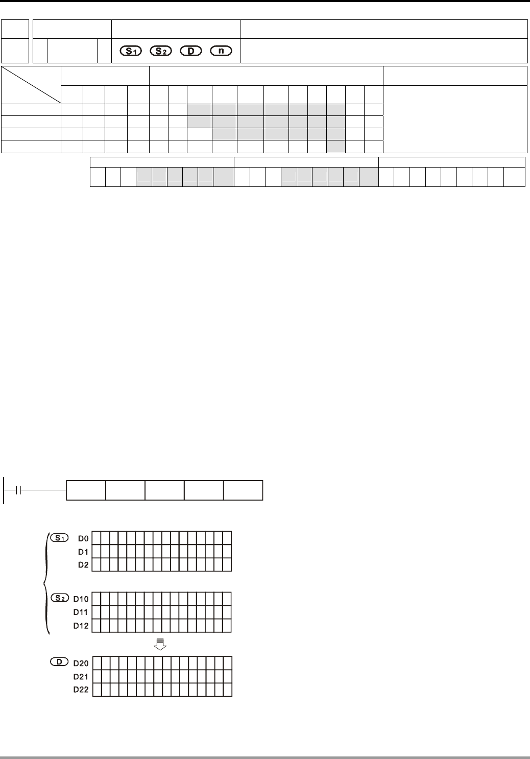
9 Application Instructions API 150-199
DVP-PLC Application Manual
9-84
API Mnemonic Operands Function
181
MOR P Matrix ‘OR’ Operation
Bit Devices Word Devices Program Steps Type
OP X Y M S K H KnX KnY KnM KnS T C D E F
S1 * * * * * * *
S2 * * * * * * *
D * * * * * *
n * * *
MOR, MORP: 9 steps
PULSE 16-bit 32-bit
ES EX SS SA SX SC EH SV EH3
SV2 ES EX SS SA SX SC EH SV EH3
SV2 ES EX SS SA SX SC EH SV EH3
SV2
Operands:
S1: Matrix source device 1 S2: Matrix source device 2. D: Operation result n: Array length
Explanations:
1. Range of n: K1 ~ K256
2. S1, and S2 designate KnX, KnY, KnM and KnS; D designates KnYm KnM and KnS
3. SA/SX/SC can designate n = 4. EH/EH2/SV/EH3/SV2 can designate n 4≦.
4. See the specifications of each model for their range of use.
5. The two matrix sources S1 and S2 perform matrix ‘OR’ operation according to the array length n. The result is
stored in D.
6. Operation rule of matrix ‘OR’: The result will be 1 if either of the two bits is 1. The result is 0 only when both two
bits are 0.
Program Example:
When X0 = On, the 3 arrays of 16-bit registers D0 ~ D2 and the 3 arrays of 16-bit registers D10 ~ D12 will perform a
matrix ‘OR’ operation. The result will be stored in the 3 arrays of 16-bit registers D20 ~ D22.
X0
MOR D0 D10 D20 K3
1
11 00011
0000
11 00011
0000
11 00011
0000
010101010101010
1010101010101010
1010101010101010
1
1
1
1
1
1
0
0
0
1
1
1
1
1
1
11 00
11
00
11 001
1
00
11 00
1
1
00
1
1
1
1
1
1
1
1
1
1
1
1
1111
1
1
1
1
1
1
1
1
b15 b0
MOR
Before
Execution
After
Execution
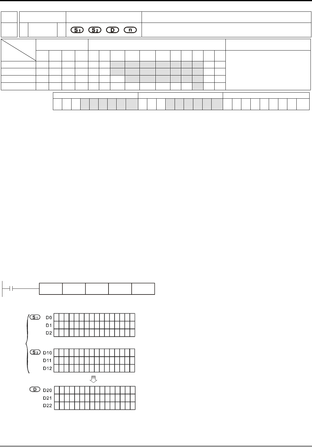
9 Application Instructions API 150-199
DVP-PLC Application Manual
9-85
API Mnemonic Operands Function
182
MXOR P Matrix ‘XOR’ Operation
Bit Devices Word Devices Program Steps Type
OP X Y M S K H KnX KnY KnM KnS T C D E F
S1 * * * * * * *
S2 * * * * * * *
D * * * * * *
n * * *
MXOR, MXORP: 9 steps
PULSE 16-bit 32-bit
ES EX SS SA SX SC EH SV EH3
SV2 ES EX SS SA SX SC EH SV EH3
SV2 ES EX SS SA SX SC EH SV EH3
SV2
Operands:
S1: Matrix source device 1 S2: Matrix source device 2 D: Operation result n: Array length
Explanations:
1. Range of n: K1 ~ K256
2. S1, and S2 designate KnX, KnY, KnM and KnS; D designates KnYm KnM and KnS
3. SA/SX/SC can designate n = 4. EH/EH2/SV/EH3/SV2 can designate n 4≦.
4. See the specifications of each model for their range of use.
5. The two matrix sources S1 and S2 perform matrix ‘XOR’ operation according to the array length n. The result is
stored in D.
6. Operation rule of matrix ‘XOR’: The result will be 1 if the two bits are different. The result will be 0 if the two bits
are the same.
Program Example:
When X0 = On, the 3 arrays of 16-bit registers D0 ~ D2 and the 3 arrays of 16-bit registers D10 ~ D12 will perform a
matrix ‘XOR’ operation. The result will be stored in the 3 arrays of 16-bit registers D20 ~ D22.
X0
MXOR D0 D10 D20 K3
1
11 00011
0000
11 00011
0000
11 00011
0000
010101010101010
1010101010101010
1010101010101010
1
1
1
1
1
1
0
0
0
1
1
1
1
1
1
11 00
11
00
11 001
1
00
11 00
1
1
00
1
1
1
1
1
1
1
1
1
1
1
1
1111
1
1
1
1
1
1
1
1
b15 b0
MOR
Before
Execution
After
Execution
MXOR

9 Application Instructions API 150-199
DVP-PLC Application Manual
9-86
API Mnemonic Operands Function
183
MXNR P Matrix ‘XNR’ Operation
Bit Devices Word Devices Program Steps Type
OP X Y M S K H KnX KnY KnM KnS T C D E F
S1 * * * * * * *
S2 * * * * * * *
D * * * * * *
n * * *
MXNR, MXNRP: 9 steps
PULSE 16-bit 32-bit
ES EX SS SA SX SC EH SV EH3
SV2 ES EX SS SA SX SC EH SV EH3
SV2 ES EX SS SA SX SC EH SV EH3
SV2
Operands:
S1: Matrix source device 1 S2: Matrix source device 2 D: Operation result n: Array length
Explanations:
1. Range of n: K1 ~ K256
2. S1, and S2 designate KnX, KnY, KnM and KnS; D designates KnYm KnM and KnS
3. SA/SX/SC can designate n = 4. EH/EH2/SV/EH3/SV2 can designate n 4≦.
4. See the specifications of each model for their range of use.
5. The two matrix sources S1 and S2 perform matrix ‘XNR’ operation according to the array length n. The result is
stored in D.
6. Operation rule of matrix ‘XNR’: The result will be 1 if the two bits are the same. The result will be 0 if the two bits
are different.
Program Example:
When X0 = On, the 3 arrays of 16-bit registers D0 ~ D2 and the 3 arrays of 16-bit registers D10 ~ D12 will perform a
matrix ‘XNR’ operation. The result will be stored in the 3 arrays of 16-bit registers D20 ~ D22.
X0
MXNR D0 D10 D20 K3
Before
Execution
After
Execution
1
11 00011
0000
1100011
0000
1100011
0000
010101010101010
1010101010101010
1010101010101010
1
1
1
1
1
1
0
0
0
1
1
1
1
1
1
1000
1000
1000
1
1
1
11
1
1
1
1
0
0
0
0
0
0
0
0
0
0
0
0
0
0
0
1
1
1
1
1
1
1
1
1
1
1
1
b15 b0
MXNR
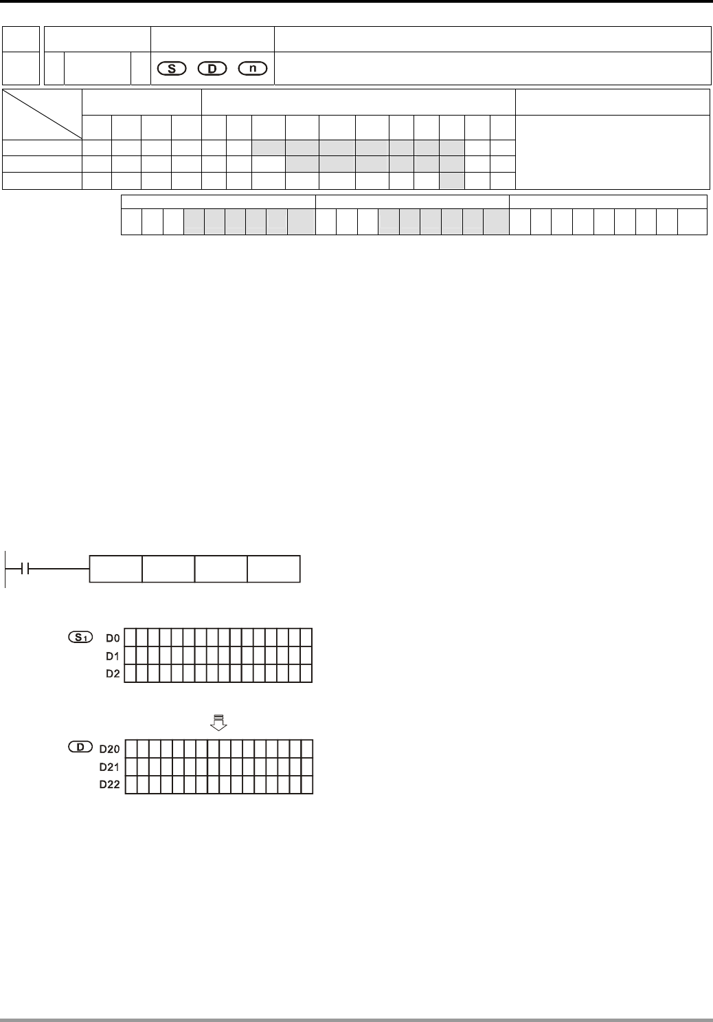
9 Application Instructions API 150-199
DVP-PLC Application Manual
9-87
API Mnemonic Operands Function
184
MINV P Matrix Inverse Operation
Bit Devices Word Devices Program Steps Type
OP X Y M S K H KnX KnY KnM KnS T C D E F
S * * * * * * *
D * * * * * *
n * * *
MINV, MINVP: 7 steps
PULSE 16-bit 32-bit
ES EX SS SA SX SC EH SV EH3
SV2 ES EX SS SA SX SC EH SV EH3
SV2 ES EX SS SA SX SC EH SV EH3
SV2
Operands:
S: Matrix source device D: Operation result n: Array length
Explanations:
1. Range of n: K1 ~ K256
2. S designates KnX, KnY, KnM and KnS; D designates KnY, KnM and KnS.
3. SA/SX/SC can designate n = 4. EH/EH2/SV/EH3/SV2 can designate n 4≦.
4. See the specifications of each model for their range of use.
5. S performs an inverse matrix operation according to the array length n. The result is stored in D.
Program Example:
When X0 = On, the 3 arrays of 16-bit registers D0 ~ D2 perform a matrix inverse operation. The result will be stored in
the 3 arrays of 16-bit registers D20 ~ D22.
X0
MINV D0 D20 K3
Before
Execution
After
Execution
0
0
0
11
1
1
1
1
0
0
0
0
0
0
11
1
1
1
1
0
0
0
1
1
1
0
0
0
1
1
1
0
0
0
1
1
1
0
0
0
1
1
1
0
0
0
1010101010101010
1010101010101010
1010101010101010
b15 b0
MINV

9 Application Instructions API 150-199
DVP-PLC Application Manual
9-88
API Mnemonic Operands Function
185
MCMP P Matrix Compare
Bit Devices Word Devices Program Steps Type
OP X Y M S K H KnX KnY KnM KnS T C D E F
S1 * * * * * * *
S2 * * * * * * *
n * * *
D * * * * * * * *
MCMP, MCMPP: 9 steps
PULSE 16-bit 32-bit
ES EX SS SA SX SC EH SV EH3
SV2 ES EX SS SA SX SC EH SV EH3
SV2 ES EX SS SA SX SC EH SV EH3
SV2
Operands:
S1: Matrix source device 1 S2: Matrix source device 2 n: Array length
D: Pointer (Pr), for storing the value of target location
Explanations:
1. Range of n: K1 ~ K256
2. S1, and S2 designate KnX, KnY, KnM and KnS; D designates KnY, KnM and KnS.
3. SA/SX/SC can designate n = 4. EH/EH2/SV/EH3/SV2 can designate n 4≦.
4. See the specifications of each model for their range of use.
5. Flags: M1088 ~ M1092. See remarks for more details.
6. This instruction compares every bit in S1 with every bit in S2 starting from location D + 1 and finds out the
location of different bits. The location will be stored in D.
7. The matrix comparison flag (M1088) decides to compare between equivalent values (M1088 = 1) or different
values (M1088 = 0). When the comparison is completed, it will stop immediately and the matrix bit search flag
will turn “On” (M1091 = 1). When the comparison progresses to the last bit, the matrix search end flag (M1089)
will turn “On” and the No. where the comparison is completed is stored in D. The comparison will start from the
0th bit in the next scan period when the matrix search start flag turns “On” (M1090 = 1). When D exceeds the
range, the pointer error flag will turn “On” (M1092 = 1).
8. The matrix operation will need a 16-bit register to designate a point among the 16n points in the matrix for the
operation. The register is the Pointer (Pr) of the matrix, designated by the user in the instruction. The vaild
range of Pr is 0 ~ 16n -1, corresponding to b0 ~ b16n-1 in the matrix. Please avoid changing the Pr value
during the operation in case the comparing and searching will not ne correct. If the Pr value exceeds its range,
M1092 will be On and the instruction will not be executed.
9. When M1089 and M1091 take place at the same time, both flags will be “1” at the same time.
Program Example:
1. When X0 goes from Off to On, the matrix search start falg M1090 = 0. The searching will start from the bit
marked with “*” (current Pr value +1) for bits of different status (M1088 = 0).
2. Set the Pr value D20 = 2. When X0 goes from Off to On for 4 times, we can obtain the 4 execution results n, o,
p, q.
n D20 = 5, M1091 = 1, M1089 = 0.
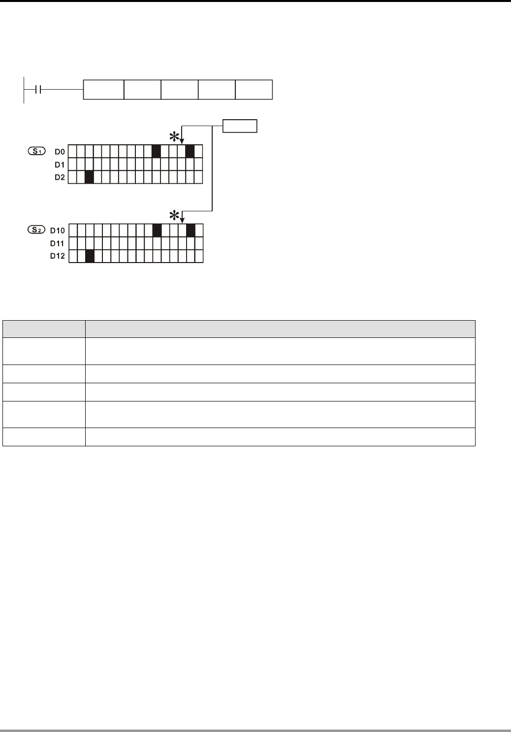
9 Application Instructions API 150-199
DVP-PLC Application Manual
9-89
o D20 = 45, M1091 = 1, M1089 = 0.
p D20 = 47, M1091 = 0, M1089 = 1.
q D20 = 1, M1091 = 1, M1089 = 0.
X0
MCMPP D0 D10 D20K3
1011
000
100011
000
100011
00
1
1
1
1
1
1
1
1
1
D20
2
1
1
1
0
0
0
0
0
0
1
1
1
10101010101101
1010101010101010
101101010101010
b47
b0
MCMP
b47
b0
0
01
1
10
pointer
Remarks:
Flags explanations:
Flags Function
M1088 Matrix comparison flag. Comparing between equivalent values (M1088 = 1) or different
values (M1088 = 0).
M1089 Matrix search end flag. When the comparison reaches the last bit, M1089 = 1.
M1090 Matrix search start flag. Comparing from bit 0 (M1090 = 1).
M1091 Matrix bit search flag. When the comparison is completed, the comparison will stop
immediately (M1091=1).
M1092 Matrix pointer error flag. When the pointer Pr exceeds its range, M1092 = 1.
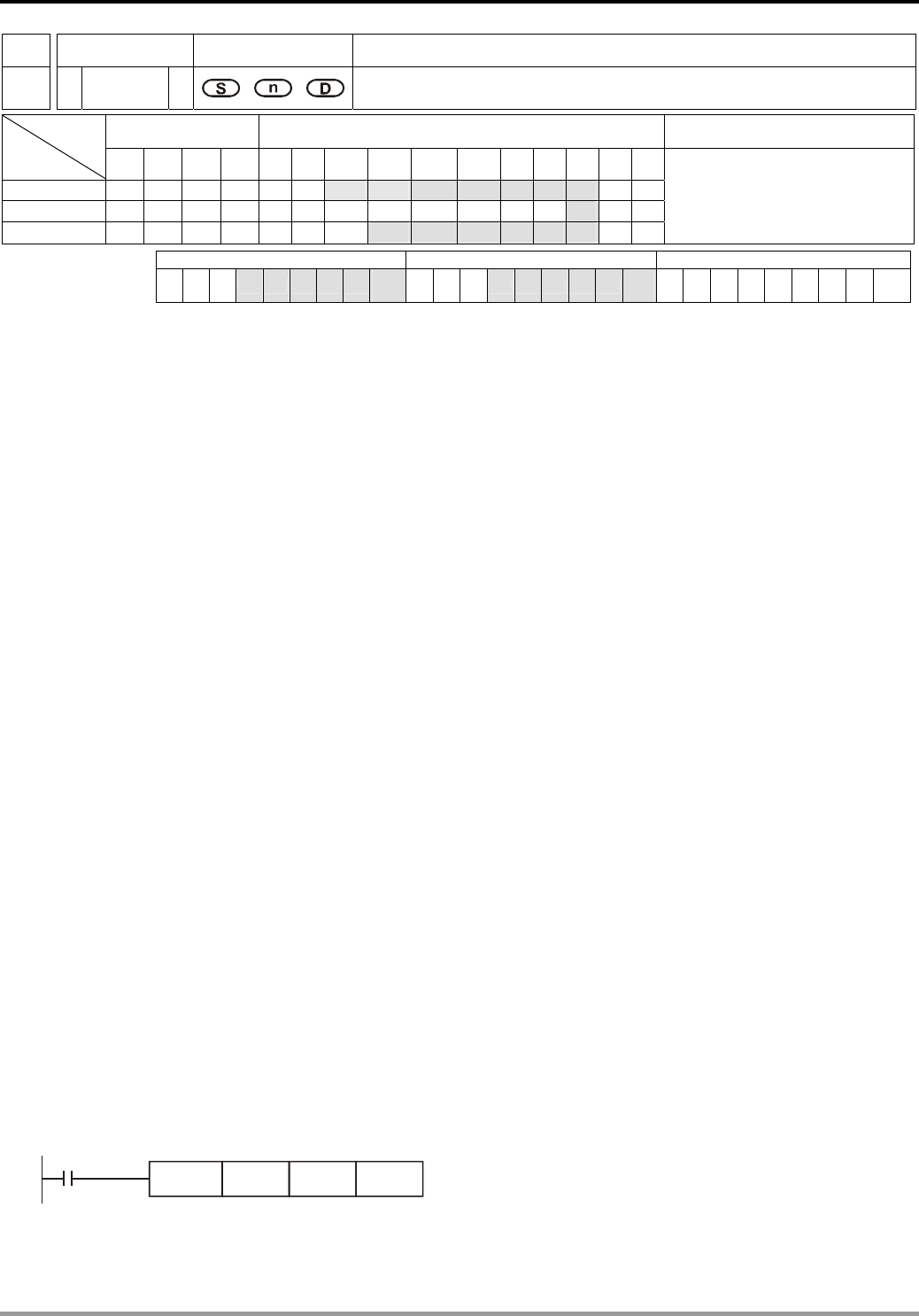
9 Application Instructions API 150-199
DVP-PLC Application Manual
9-90
API Mnemonic Operands Function
186
MBRD P Read Matrix Bit
Bit Devices Word Devices Program Steps Type
OP X Y M S K H KnX KnY KnM KnS T C D E F
S * * * * * * *
n * * *
D * * * * * * * *
MBRD, MBRDP: 7 steps
PULSE 16-bit 32-bit
ES EX SS SA SX SC EH SV EH3
SV2 ES EX SS SA SX SC EH SV EH3
SV2 ES EX SS SA SX SC EH SV EH3
SV2
Operands:
S: Matrix source device n: Array length D: Pointer (Pr), for storing the value of target location
Explanations:
1. Range of n: K1 ~ K256
2. S designates KnX, KnY, KnM and KnS; D designates KnY, KnM and KnS.
3. SA/SX/SC can designate n = 4. EH/EH2/SV/EH3/SV2 can designate n 4≦.
4. See the specifications of each model for their range of use.
5. Flags: M1089 ~ M1095. See remarks for more details.
6. When this instruction is executed, it first determines if the matrix pointer clear flag (M1094) is “On”. If it is “On”,
pointer D is cleared as 0. The instruction then reads the On/Off status from the 0th bit of S to the matrix
rotation/displacement/output carry flag (M1095). Whenever finishing reading 1 bit, the instruction determines
whether the matrix pointer increasing flag (M1093) is “On”. If it is “On”, the value of pointer D will plus 1. When
the reading is processed to the last bit, the matrix search end flag (M1089) will turn “On” and pointer D record
the No. of read bits.
7. The Pointer (Pr) of the matrix is designated by the user in the instruction. The vaild range of Pr is 0 ~ 16n -1,
corresponding to b0 ~ b16n-1 in the matrix. If the Pr value exceeds its range, M1092 will be On and the instruction
will not be executed.
Program Example:
1. When X0 goes from Off to On, M1094 will be set to “0” and M1093 to “1”. Therefore, the Pr will plus 1 after
every reading.
2. Set the Pr value D20 = 45. When X0 goes from Off to On for 3 times, we can obtain the 3 execution results n,
o, p.
n D20 = 46, M1095 = 0, M1089 = 0.
o D20 = 47, M1095 = 1, M1089 = 0.
p D20 = 47, M1095 = 1, M1089 = 1.
X0
MBRDP D0 D20K3
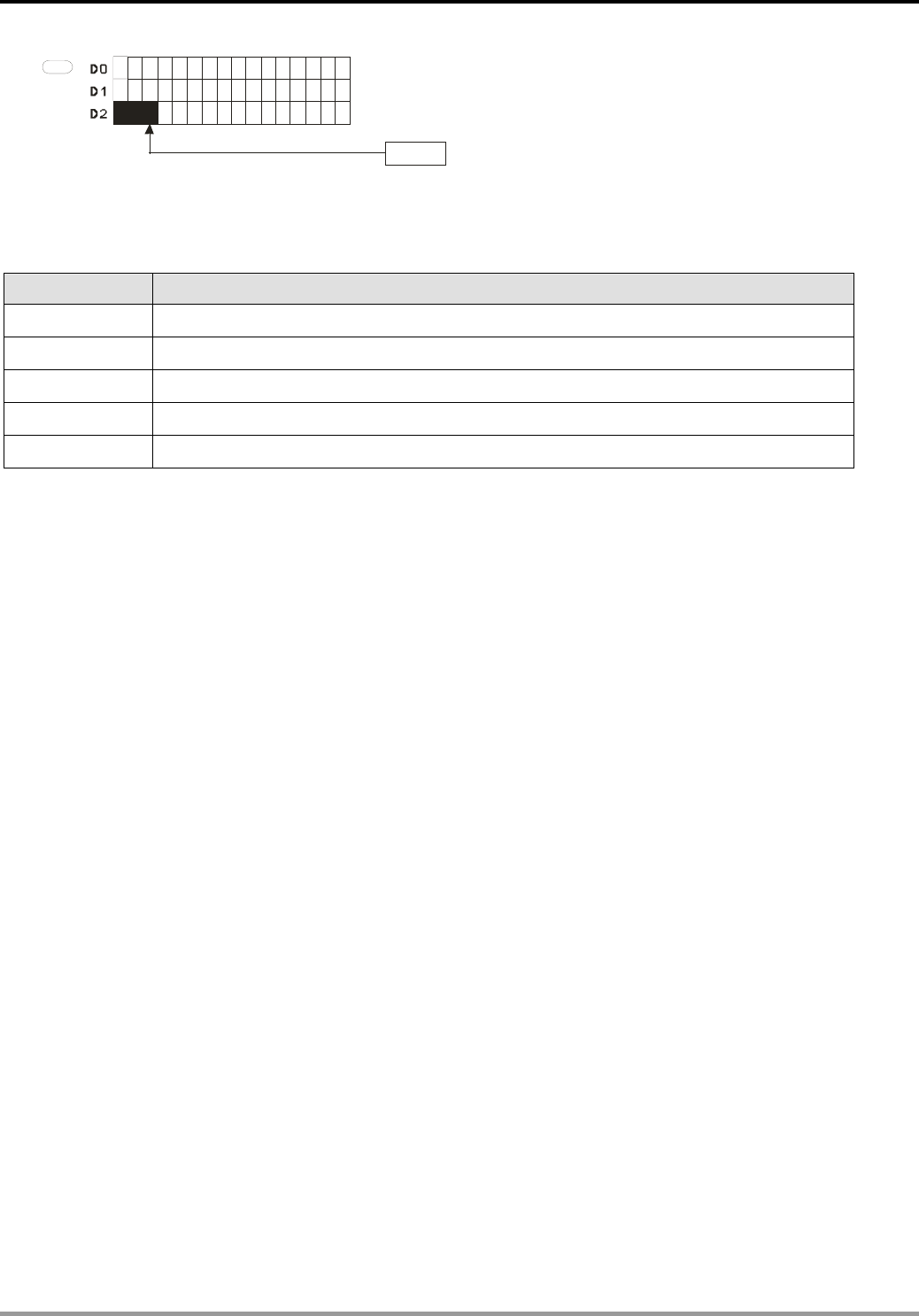
9 Application Instructions API 150-199
DVP-PLC Application Manual
9-91
b0
D20
45
1
01
01
01
01
011
01
1010101010101010
1101010101010
b47
S
0
01
01
Pointer
Remarks:
Flag explanations:
Flags Function
M1088 Matrix search end flag. When the comparison reaches the last bit, M1089 = 1.
M1092 Matrix pointer error flag. When the pointer Pr exceeds its range, M1092 = 1.
M1093 Matrix pointer increasing flag. Adding 1 to the current value of the Pr.
M1094 Matrix pointer clear flag. Clearing the current value of the Pr to 0.
M1095 Matrix rotation/displacement/output carry flag.
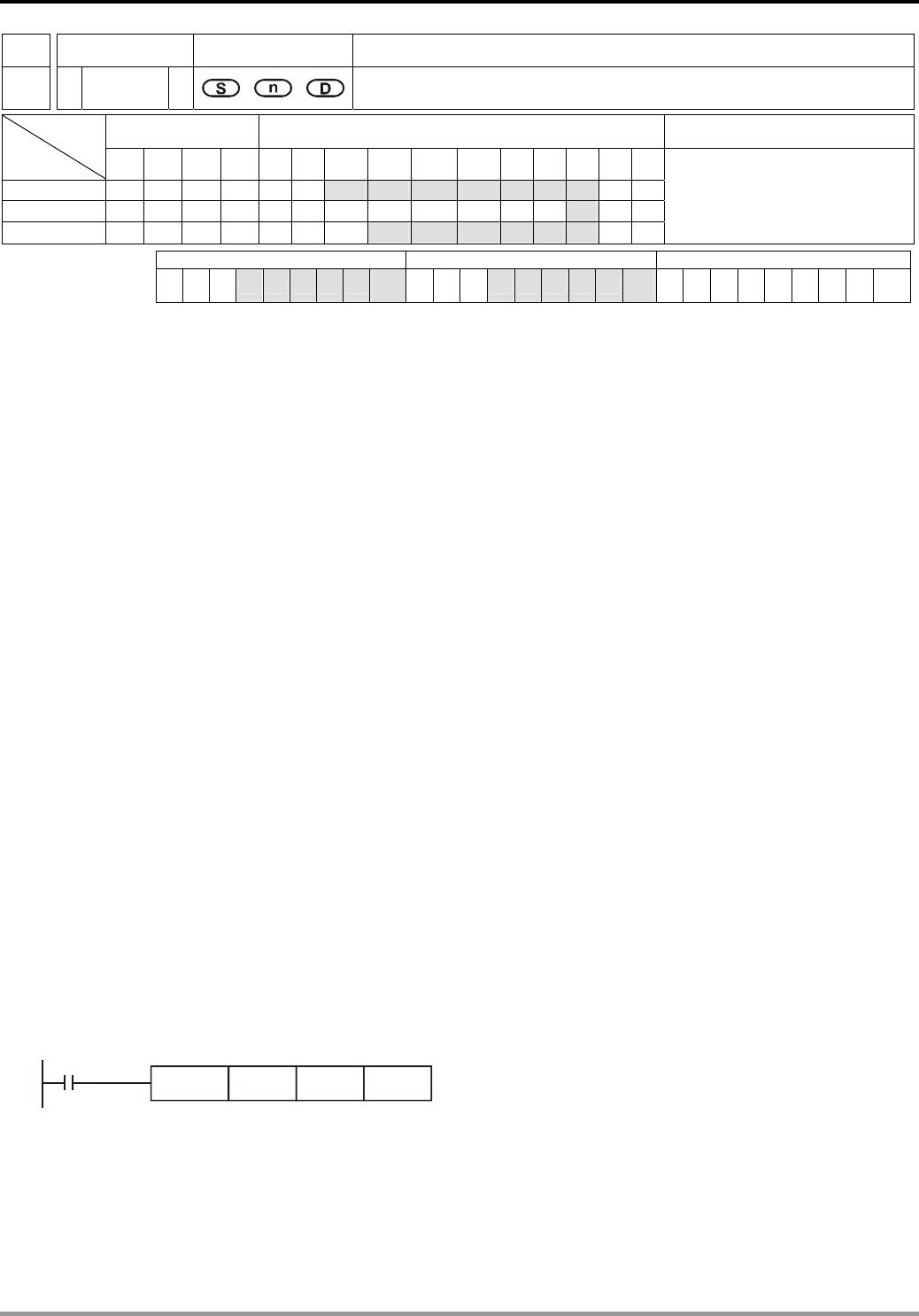
9 Application Instructions API 150-199
DVP-PLC Application Manual
9-92
API Mnemonic Operands Function
187
MBWR P Write Matrix Bit
Bit Devices Word Devices Program Steps Type
OP X Y M S K H KnX KnY KnM KnS T C D E F
S * * * * * * *
n * * *
D * * * * * * * *
MBWR, MBWRP: 7 steps
PULSE 16-bit 32-bit
ES EX SS SA SX SC EH SV EH3
SV2 ES EX SS SA SX SC EH SV EH3
SV2 ES EX SS SA SX SC EH SV EH3
SV2
Operands:
S: Matrix source device n: Array length D: Pointer (Pr), for storing the value of target location
Explanations:
1. Range of n: K1 ~ K256
2. S designates KnX, KnY, KnM and KnS; D designates KnY, KnM and KnS.
3. SA/SX/SC can designate n = 4. EH/EH2/SV/EH3/SV2 can designate n 4≦.
4. See the specifications of each model for their range of use.
5. Flags: M1089 ~ M1096. See remarks for more details.
6. When this instruction is executed, if first determines if the matrix pointer clear flag (M1094) is “On”, If it is “On”,
pointer D is cleared as 0. The instruction then writes the value in the matrix displacement/input complement
flag (M1096) into the location starting from the 0th bit of S. Whenever finishing writing 1 bit, the instruction
determines whether the matrix pointer increasing flag (M1093) is “On”. If it is “On”, the value of pointer D will
plus 1. When the writing is processed to the last bit, the matrix search end flag (M1089) will turn “On” and
pointer D records the No. of written bits. If D exceeds its range, M1092 will be On.
7. The Pointer (Pr) of the matrix is designated by the user in the instruction. The vaild range of Pr is 0 ~ 16n -1,
corresponding to b0 ~ b16n-1 in the matrix. If the Pr value exceeds its range, M1092 will be On and the instruction
will not be executed.
Program Example:
1. When X0 goes from Off to On, M1094 will be set to “0” and M1093 to “1”. Therefore, the Pr will plus 1 after
every writing.
2. Set the Pr value D20 = 45 and M1096 = 1. When X0 goes from Off to On for 1 time, we can obtain the execution
results: D20 = 46, M1096 = 1, M1089 = 0.
X0
MBWRP D0 D20K3
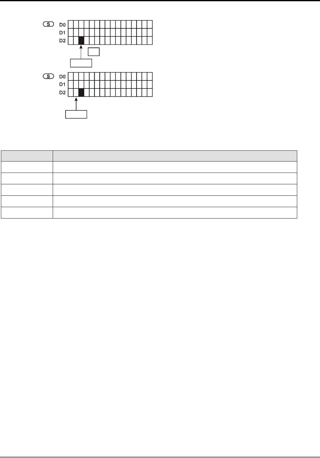
9 Application Instructions API 150-199
DVP-PLC Application Manual
9-93
1
b0
0101010101
0101
1010101010101010
1
011
01
01
01
01
01
0
b47
D20
45
1
1M1096
10101010101
0101
1010101010101010
101101010101010
1
0
1
b47
D20
46
Before
Execution
After
Execution
pointer
pointer
(Matrix displacement/input complement flag)
Remarks:
Flag explanations:
Flags Function
M1088 Matrix search end flag. When the comparison reaches the last bit, M1089 = 1.
M1092 Matrix pointer error flag. When the pointer Pr exceeds its range, M1092 = 1.
M1093 Matrix pointer increasing flag. Adding 1 to the current value of the Pr.
M1094 Matrix pointer clear flag. Clearing the current value of the Pr to 0.
M1096 Matrix displacement/input complement flag.
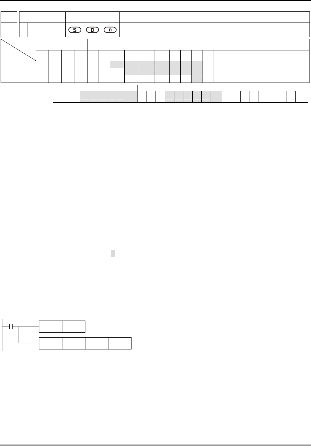
9 Application Instructions API 150-199
DVP-PLC Application Manual
9-94
API Mnemonic Operands Function
188
MBS P Matrix Bit Displacement
Bit Devices Word Devices Program Steps Type
OP X Y M S K H KnX KnY KnM KnS T C D E F
S * * * * * * *
D * * * * * *
n * * *
MBS, MBSP: 7 steps
PULSE 16-bit 32-bit
ES EX SS SA SX SC EH SV EH3
SV2 ES EX SS SA SX SC EH SV EH3
SV2 ES EX SS SA SX SC EH SV EH3
SV2
Operands:
S: Matrix source device D: Operation result n: Array length
Explanations:
1. Range of n: K1 ~ K256
2. S designates KnX, KnY, KnM and KnS; D designates KnY, KnM and KnS.
3. SA/SX/SC can designate n = 4. EH/EH2/SV/EH3/SV2 can designate n 4≦.
4. See the specifications of each model for their range of use.
5. Flags: M1095 ~ M1097. See remarks for more details.
6. This instruction performs left-right displacement on the matrix bits in S according to array length n. M1097
determines the left (M1097 = 0) or right (M1097 = 1) displacement of matrix bits. The empty bits derived from
every displacement of 1 bit (when left displacement: b0; when right displacement: b16n-1) is filled by the status of
the complement flag (M1096). The spare bits (when left displacement: b16n-1; when right displacement: b0) are
sent to the carry flag (M1095). The result is stored in D.
7. The pulse execution instruction MBSP is generally adopted.
Program Example 1:
When X0 = On, M1097 = Off, indicating a left matrix displacement is performed. Set M1096 = 0 and the 16-bit
registers D0 ~ D2 will perform a left matrix displacement and the result will be stored in the matrix of the 16-bit
registers D20 ~ D22. The carry flag M1095 will be “1”.
X0
RST
MBSP D0 D20 K3
M1097
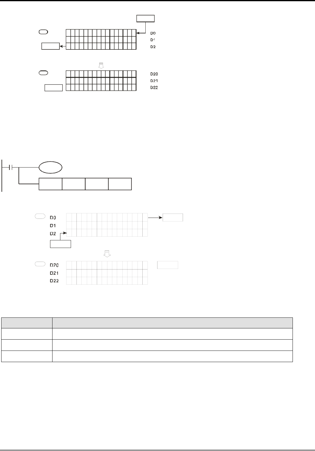
9 Application Instructions API 150-199
DVP-PLC Application Manual
9-95
1
b0
0101010101
0101
10
1
01
01
01
01
01
01
0
101101010 101010
b15
0
0
0
M1096
10101010101
0100
1010101010101010
1011010101010100
0
S
D
1
M1095
M1095
MBS
M1097=0
Complement
flag
Before
execution
Carry flag
Carry flag
After the execution of
left matrix displacement
Program Example 2:
When X1 = On, M1097 = On, indicating a right matrix displacement is performed. Set M1096 = 1 and the 16-bit
registers D0 ~ D2 will perform a right matrix displacement and the result will be stored in the matrix of the 16-bit
registers D20 ~ D22. The carry flag M1095 will be “0”.
X1
M1097
MBSP D0 D20 K3
1
b0
0101010101
0101
1010101010101010
101101010 101010
b15
0
0
10101010101
0101
1
01
01
01
01
01
01
01
0
111010101010100
0
S
D
0
M1095
M1095
MBS
M1097=1
1
1M1096
Carry flag
Carry flag
Before
execution
Complement
flage
After the execution of
right matrix displacement
Explanations:
Flag explanations:
Flags Function
M1095 Matrix rotation/displacement/output carry flag.
M1096 Matrix displacement/input complement flag.
M1097 Matrix rotation/displacement direction flag.
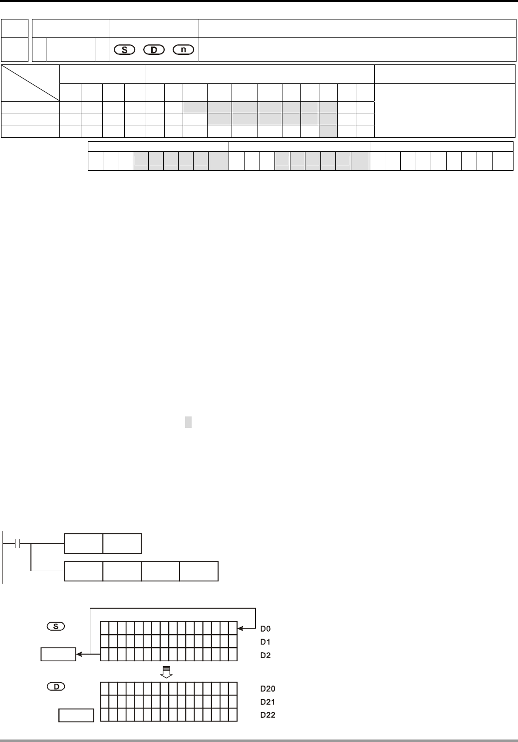
9 Application Instructions API 150-199
DVP-PLC Application Manual
9-96
API Mnemonic Operands Function
189
MBR P Matrix Bit Rotation
Bit Devices Word Devices Program Steps Type
OP X Y M S K H KnX KnY KnM KnS T C D E F
S * * * * * * *
D * * * * * *
n * * *
MBR, MBRP: 7 steps
PULSE 16-bit 32-bit
ES EX SS SA SX SC EH SV EH3
SV2 ES EX SS SA SX SC EH SV EH3
SV2 ES EX SS SA SX SC EH SV EH3
SV2
Operands:
S: Matrix source device D: Operation result n: Array length
Explanations:
1. Range of n: K1 ~ K256
2. S designates KnX, KnY, KnM and KnS; D designates KnY, KnM and KnS.
3. SA/SX/SC can designate n = 4. EH/EH2/SV/EH3/SV2 can designate n 4≦.
4. See the specifications of each model for their range of use.
5. Flags: M1095, M1097. See remarks for more details.
6. This instruction performs left-right rotation on the matrix bits in S according to array length n. M1097
determines the left (M1097 = 0) or right (M1097 = 1) rotation of matrix bits. The empty bits derived from every
rotation of 1 bit (when left rotation: b0; when right rotation: b16n-1) is filled by rotation bits (when left rotation:
b16n-1; when right rotation: b0). The result is stored in D. Rotation bits not only fill the empty bits but also send
the status of bits to the carry flag M1095.
7. The pulse execution instruction MBRP is generally adopted.
Program Example 1:
When X0 = On, M1097 = Off, indicating a left matrix rotation is performed. The 16-bit registers D0 ~ D2 will perform a
left matrix rotation and the result will be stored in the matrix of the 16-bit registers D20 ~ D22. The carry flag M1095
will be “1”.
X0
MBRP D0 D20 K3
RST M1097
Before
Execution
After left rotation
1
b0
0101010101
0101
1010101010101010
101101010 101010
b15
0
0
10101010101
0101
1
01
01
01
01
01
01
01
0
1
011
01
01
01
01
01
00
0
1
M1095
M1095
MBR
M1097=0
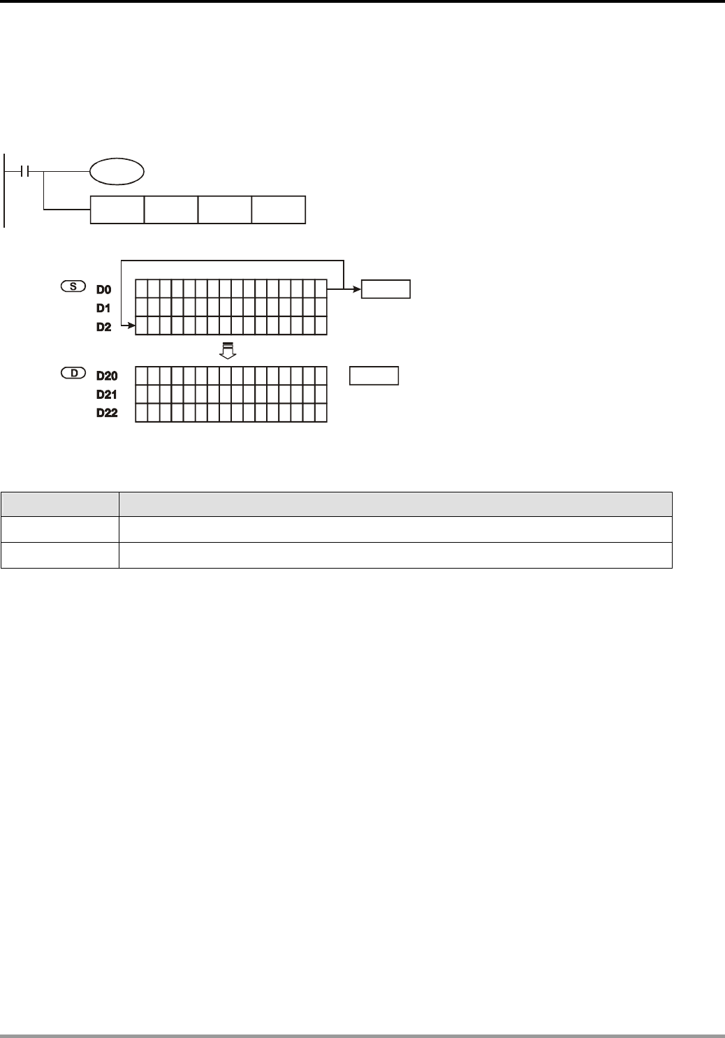
9 Application Instructions API 150-199
DVP-PLC Application Manual
9-97
Program Example 2:
When X1 = On, M1097 = On, indicating a right matrix rotation is performed. The 16-bit registers D0 ~ D2 will perform
a right matrix rotation and the result will be stored in the matrix of the 16-bit registers D20 ~ D22. The carry flag
M1095 will be “0”.
X1
MBRP D0 D20 K3
M1097
Before
Execution
After right
rotation
M1097=0
1
b0
0101010101
0101
1010101010101010
101101010101010
b15
0
0
10101010101
0101
1010101010101010
1011010101010100
0
0
M1095
M1095
MBR
Remarks:
Flag explanations:
Flags Function
M1095 Matrix rotation/displacement/output carry flag.
M1097 Matrix rotation/displacement direction flag.
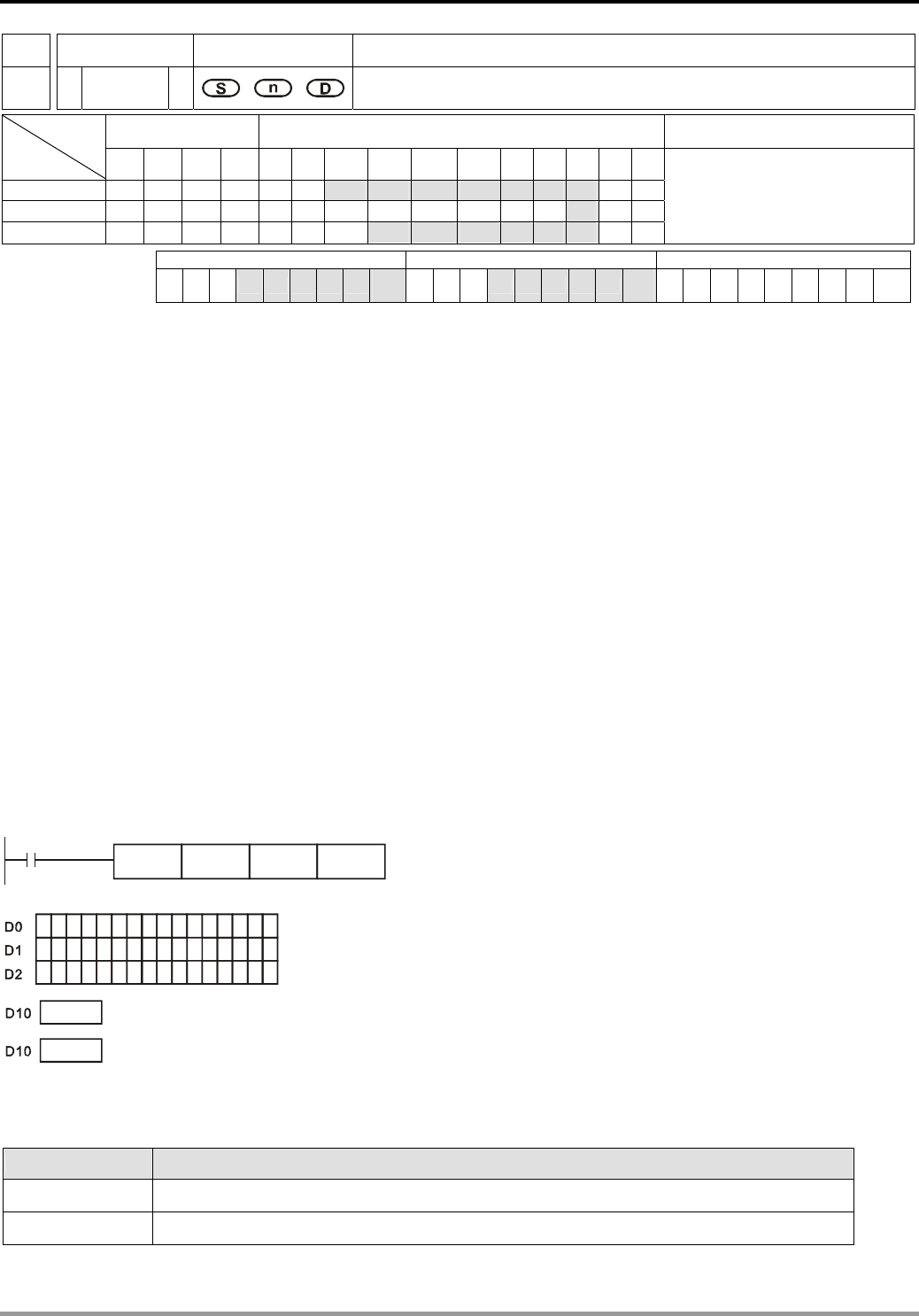
9 Application Instructions API 150-199
DVP-PLC Application Manual
9-98
API Mnemonic Operands Function
190
MBC P Matrix Bit Status Counting
Bit Devices Word Devices Program Steps Type
OP X Y M S K H KnX KnY KnM KnS T C D E F
S * * * * * * *
n * * *
D * * * * * * * *
MBC, MBCP: 7 steps
PULSE 16-bit 32-bit
ES EX SS SA SX SC EH SV EH3
SV2 ES EX SS SA SX SC EH SV EH3
SV2 ES EX SS SA SX SC EH SV EH3
SV2
Operands:
S: Matrix source device n: Array length D: Counting result
Explanations:
1. Range of n: K1 ~ K256
2. S designates KnX, KnY, KnM and KnS; D designates KnY, KnM and KnS.
3. SA/SX/SC can designate n = 4. EH/EH2/SV/EH3/SV2 can designate n 4≦.
4. See the specifications of each model for their range of use.
5. Flags: M1098, M1099. See remarks for more details.
6. This instruction counts the number of bits which are “1” or “0” in S by array length n. The result is stored in D.
7. The instruction counts the number of bits which are “1” when M1098 = 1 and counts the number of bits which
are “0” when M1098 = 0. When the operation result is “0”, M1099 = 1.
Program Example:
When X10 = On, in the matrix of D0 ~ D2, when M1098 = 1, the instruction counts the total number of bits which are
“1” and store the number in D10. When M1098 = 0, the instruction counts the total number of bits which are “0” and
store the number in D10.
X10
MBC D0 K3 D10
11111 101
11111 1010
11111 1010
0
12
1
1
1
1
1
1
1
1
1
1
1
1
1
1
1
0
0
0
0
0
0
M1098=0
36
M1098=1
Remarks:
Flag explanations:
Flags Function
M1098 Counting the number of bits which are “1” or “0”
M1099 On when the counting result is “0”.

9 Application Instructions API 150-199
DVP-PLC Application Manual
9-99
API Mnemonic Operands Function
191
D PPMR 2-Axis Relative Point to Point Motion
Bit Devices Word Devices Program Steps Type
OP X Y M S K H KnX KnY KnM KnS T C D E F
S1 * * *
S2 * * *
S * * *
D *
DPPMR: 17 steps
PULSE 16-bit 32-bit
ES EX SS SA SX SC EH SV EH3
SV2 ES EX SS SA SX SC EH SV EH3
SV2 ES EX SS SA SX SC EH SV EH3
SV2
Operands:
S1: Number of output pulses of X axis S2: Number of output pulses of Y axis
S: Max. point to point output frequency D: Pulse output device
Explanations:
1. Flags: M1029, M1030, M1334, M1335. See remarks for more details.
2. This instruction only supports EH2/SV/EH3/SV2 series MPU, not EH series. In terms of pulse output methods,
this instructin only supports “pulse + direction” mode.
3. S1 and S2 are the designated (relative designation) number of output pulses in X axis (Y0 or Y4) and Y axis (Y2
or Y6). The range of the number is -2,147,483,648 ~ +2,147,483,647 (+/- represents the forward/backward
direction). When in forward direction, the pulse present value registers CH0 (D1337 high word, D1336 low word),
CH1 (D1339 high word, D1338 low word), CH2 (D1376 high word, D1375 low word) and CH3 (D1378 high word,
D1377 low word) will increase. When in backward direction, the present value will decrease.
4. D can designate Y0 and Y4.
When Y0 is designated:
Y0 refers to 1st group X-axis pulse output device.
Y1 refers to 1st group X-axis direction signal.
Y2 refers to 1st group Y-axis pulse output device.
Y3 refers to 1st group Y-axis direction signal.
Y4 refers to 2nd group X-axis pulse output device.
Y5 refers to 2nd group X-axis direction signal.
Y6 refers to 2nd group Y-axis pulse output device.
Y7 refers to 2nd group Y-axis direction signal.
When direction signal outputs, Off will not occur immediately after the pulse output is over. Direction signal will
turn Off when the drive contact is Off.
5. D1340 (D1379) refers to the settings of the start/end frequencies of the 1st/2nd 2-axis motion. D1343 (D1381)
refers to the time of the first acceleration segment and last deceleration segment of the 1st/2nd 2-axis motion.
The time shall be longer than 10ms. If the time is shorter than 10ms or longer than 10,000ms, the output will be
operated at 10ms. Default setting = 100ms.
6. If the maximum output frequency setting is less than 10Hz, the output will be operated at 10Hz. If the setting is
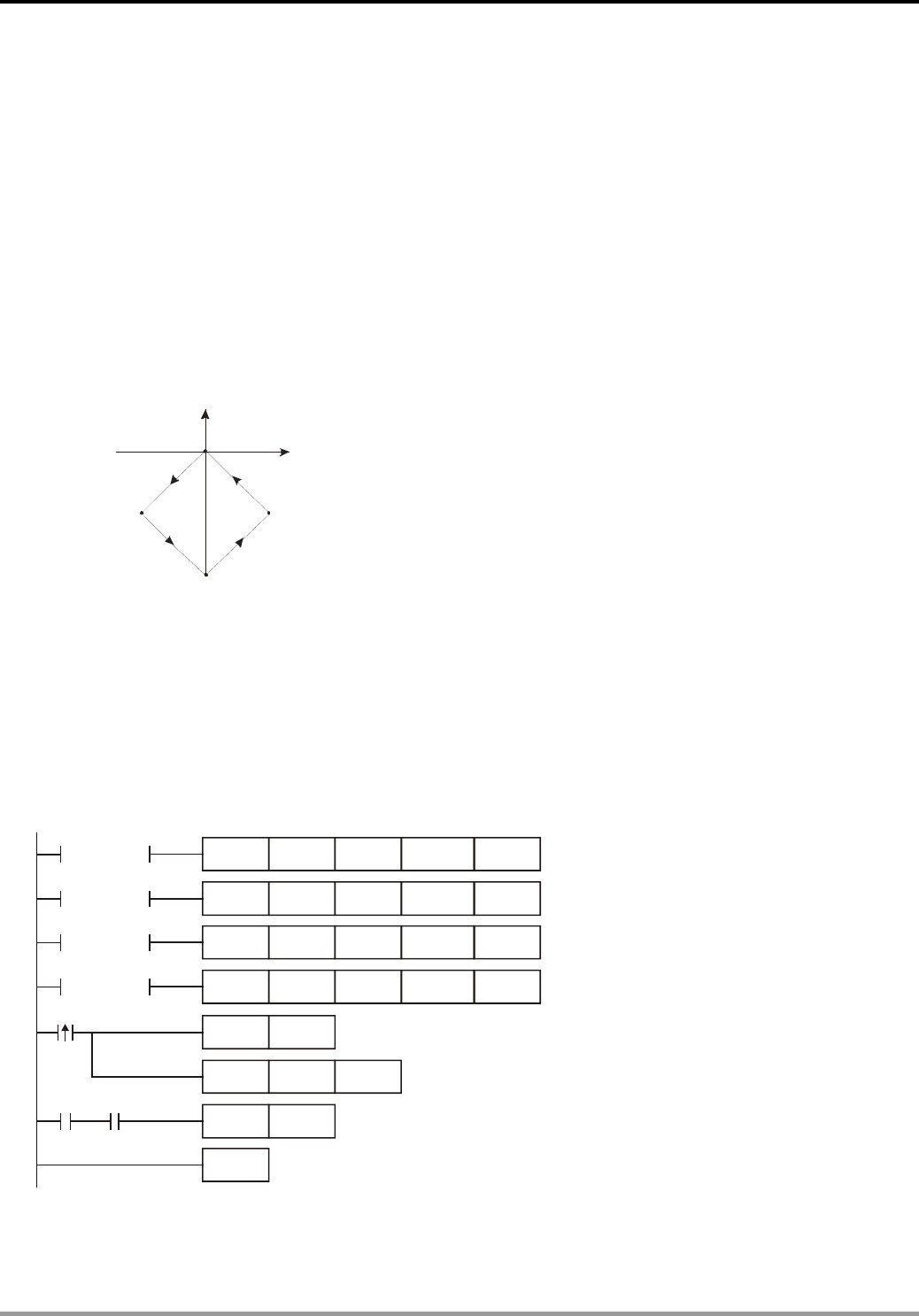
9 Application Instructions API 150-199
DVP-PLC Application Manual
9-100
more than 200kHz, the output will be operated at 200kHz.
7. When the 2-axis synchronous motion instruction is enabled, the start frequency and acceleration/deceleration
time in Y axis will be same as the settings in X axis.
8. The number of output pulses for the 2-axis motion shall not be less than 59; otherwise the line drawn will not be
straight enough.
9. There is no limitation on the number of times using the instruction. However, assume CH1 or CH2 output is in
use, the 1st group X/Y axis will not be able to output. If CH3 or CH4 output is in use, the 2nd group X/Y axis will
not be able to output.
Program Example:
1. Draw a rhombus as the figure below.
(0,0)
(-27000,-27000)
(0,-55000)
(27000,-27000)
X
Y
2. Steps:
a) Set the four coordinates (0,0), (-27000, -27000), (0, -55000), (27000, -27000) (as the figure above). Calculate the
relative coordinates of the four points and obtain (-27000, -27000), (27000, -28000), (27000, 27000), and (-27000,
27000). Place them in the 32-bit (D200, D202), (D204, D206), (D208, D210), (D212, D214).
b) Write program codes as follows.
c) PLC RUN. Set M0 as On and start the 2-axis line drawing.
M0
RST
= D0 K1 DPPMR D200 D202 K100000 Y0
= D0 K2 DPPMR D204 D206 K100000 Y0
= D0 K3 DPPMR D208 D210 K100000 Y0
= D0 K4 DPPMR D212 D214 K100000 Y0
MOV D0
M0
INCP
END
M1029
D0
M1029
K1
3. Motion explanation:
When PLC RUN and M0 = On, PLC will start the first point-to-point motion by 100kHz. D0 will plus 1 whenever a
point-to-point motion is completed and the second point-to-point motion will start to execute automatically. The

9 Application Instructions API 150-199
DVP-PLC Application Manual
9-101
same motion will keep executing until the fourth point-to-point motion is completed.
Remarks:
1. Flag explanations:
M1029: On when the 1st group 2-axis pulse output is completed.
M1036: On when the 2nd group 2-axis pulse output is completed.
M1334: On when the 1st group 2-axis pulse output is forbidden.
M1336: 1st group 2-axis pulse output indication flag
M1520: On when the 2nd group 2-axis pulse output is forbidden.
M1522: 2nd group 2-axis pulse output indication flag
2. Special register explanations:
D1336, D1337 : Pulse present value register for Y0 output of the 1st group X-axis motion. The present value
increases or decreases following the rotation direction. (D1337 high word; D1336 low word)
D1338, D1339 : Pulse present value register for Y2 output of the 1st group Y-axis motion. The present value
increases or decreases following the rotation direction. (D1339 high word; D1338 low word)
D1340 : Frequency settings of the first acceleration and last deceleration segment for the Y0 output
of the 1st group X-axis motion and Y2 of the Y-axis motion for API 191 DPPMR and API 192
DPPMA.
D1343 : Time settings of the first acceleration and last deceleration segment for the Y0 output of the
1st group X-axis motion and Y2 of the Y-axis motion for API 191 DPPMR and API 192
DPPMA.
D1375, D1376 : Pulse present value register for Y4 output of the 2nd group X-axis motion. The present value
increases or decreases following the rotation direction. (D1337 high word; D1336 low word)
D1377, D1378 : Pulse present value register for Y6 output of the 2nd group Y-axis motion. The present value
increases or decreases following the rotation direction. (D1339 high word; D1338 low word)
D1379 : Frequency settings of the first acceleration and last deceleration segment for the Y4 output
of the 2nd group X-axis motion and Y6 of the Y-axis motion for API 191 DPPMR and API 192
DPPMA.
D1381 : Time settings of the first acceleration and last deceleration segment for the Y4 output of the
2nd group X-axis motion and Y6 of the Y-axis motion for API 191 DPPMR and API 192
DPPMA.

9 Application Instructions API 150-199
DVP-PLC Application Manual
9-102
API Mnemonic Operands Function
192
D PPMA 2-Axis Absolute Point to Point Motion
Bit Devices Word Devices Program Steps Type
OP X Y M S K H KnX KnY KnM KnS T C D E F
S1 * * *
S2 * * *
S * * *
D *
DPPMA: 17 steps
PULSE 16-bit 32-bit
ES EX SS SA SX SC EH SV EH3
SV2 ES EX SS SA SX SC EH SV EH3
SV2 ES EX SS SA SX SC EH SV EH3
SV2
Operands:
S1: Number of output pulses of X axis S2: Number of output pulses of Y axis
S: Max. point to point output frequency D: Pulse output device
Explanations:
1. Flags: M1029, M1030, M1334, M1335. See remarks of API 191 DPPMR for more details.
2. This instruction only supports EH2/SV/EH3/SV2 series MPU, not EH series. In terms of pulse output methods,
this instructin only supports “pulse + direction” mode.
3. S1 and S2 are the designated (absolute designation) number of output pulses in X axis (Y0 or Y4) and Y axis (Y2
or Y6). The range of the number is -2,147,483,648 ~ +2,147,483,647 (+/- represents the forward/backward
direction). When in forward direction, the pulse present value registers CH0 (D1337 high word, D1336 low word),
CH1 (D1339 high word, D1338 low word), CH2 (D1376 high word, D1375 low word) and CH3 (D1378 high word,
D1377 low word) will increase. When in backward direction, the present value will decrease.
4. D can designate Y0 and Y4.
When Y0 is designated:
Y0 refers to 1st group X-axis pulse output device.
Y1 refers to 1st group X-axis direction signal.
Y2 refers to 1st group Y-axis pulse output device.
Y3 refers to 1st group Y-axis direction signal.
Y4 refers to 2nd group X-axis pulse output device.
Y5 refers to 2nd group X-axis direction signal.
Y6 refers to 2nd group Y-axis pulse output device.
Y7 refers to 2nd group Y-axis direction signal.
When direction signal outputs, Off will not occur immediately after the pulse output is over. Direction signal will
turn Off when the drive contact is Off.
5. D1340 (D1379) refers to the settings of the start/end frequencies of the 1st/2nd 2-axis motion. D1343 (D1381)
refers to the time of the first acceleration segment and last deceleration segment of the 1st/2nd 2-axis motion. The
time shall be longer than 10ms. If the time is shorter than 10ms or longer than 10,000ms, the output will be
operated at 10ms. Default setting = 100ms.
6. If the maximum output frequency setting is less than 10Hz, the output will be operated at 10Hz. If the setting is
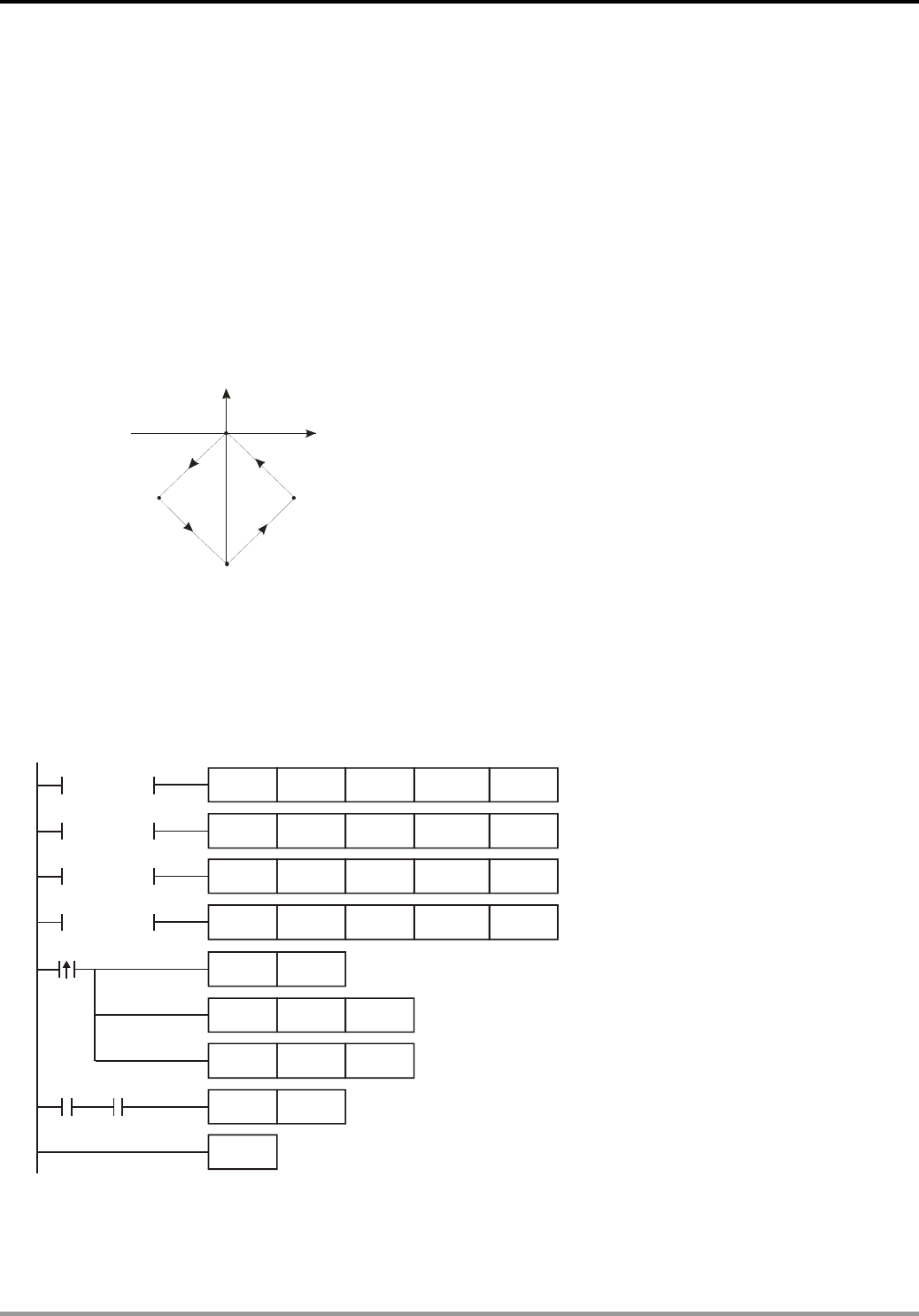
9 Application Instructions API 150-199
DVP-PLC Application Manual
9-103
more than 200kHz, the output will be operated at 200kHz.
7. When the 2-axis synchronous motion instruction is enabled, the start frequency and acceleration/deceleration
time in Y axis will be same as the settings in X axis.
8. The number of output pulses for the 2-axis motion shall not be the values within 1 ~ 59; otherwise the line drawn
will not be straight enough.
9. There is no limitation on the number of times using the instruction. However, assume CH1 or CH2 output is in use,
the 1st group X/Y axis will not be able to output. If CH3 or CH4 output is in use, the 2nd group X/Y axis will not be
able to output.
Program Example:
1. Draw a rhombus as the figure below.
(0,0)
(-27,000, -27,000)
(0, -55,000)
(27,000, -27,000)
X
Y
2. Steps:
a) Set the four coordinate (-27,000, -27,000), (0, -55,000), (27,000, -27,000), (0,0) (as the figure above). Place them
in the 32-bit (D200, D202), (D204, D206), (D208, D210), (D212, D214).
b) Write program codes as follows.
c) PLC RUN. Set M0 as On and start the 2-axis line drawing.
M0
RST
= D0 K1 DPPMA D200 D202 K100000 Y0
= D0 K2 DPPMA D204 D206 K100000 Y0
= D0 K3 DPPMA D208 D210 K100000 Y0
= D0 K4 DPPMA D212 D214 K100000 Y0
MOV D0
M0
INCP
END
M1029
D0
M1029
K1
ZRST D1336 D1339
3. Motion explanation:
When PLC RUN and M0 = On, PLC will start the first point-to-point motion by 100kHz. D0 will plus 1 whenever a
point-to-point motion is completed and the second point-to-point motion will start to execute automatically. The

9 Application Instructions API 150-199
DVP-PLC Application Manual
9-104
same motion will keep executing until the fourth point-to-point motion is completed.
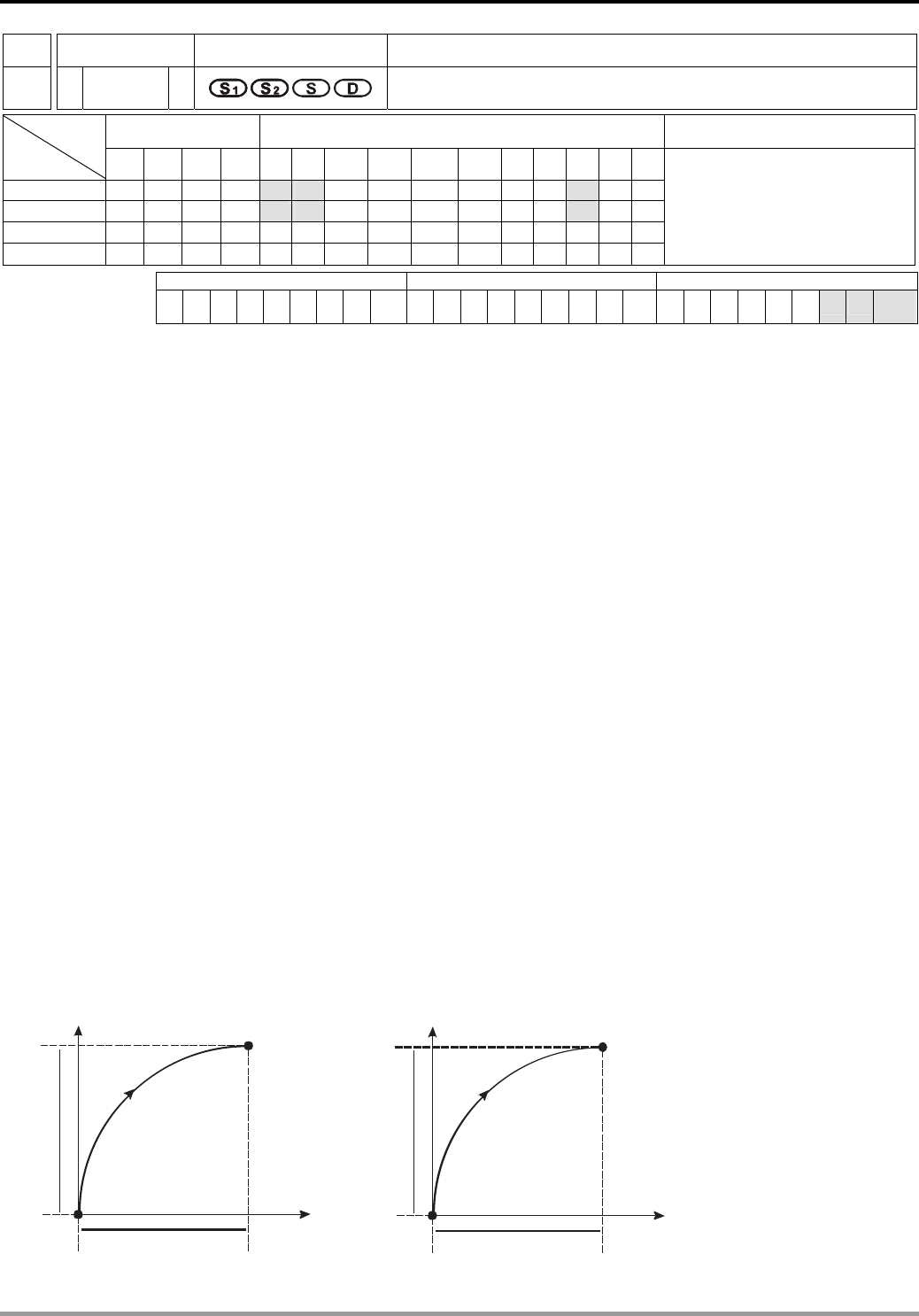
9 Application Instructions API 150-199
DVP-PLC Application Manual
9-105
API Mnemonic Operands Function
193
D CIMR 2-Axis Relative Position Arc Interpolation
Bit Devices Word Devices Program Steps Type
OP X Y M S K H KnX KnY KnM KnS T C D E F
S1 * * *
S2 * * *
S *
D *
DCIMR: 17 steps
PULSE 16-bit 32-bit
ES EX SS SA SX SC EH SV EH3
SV2 ES EX SS SA SX SC EH SV EH3
SV2 ES EX SS SA SX SC EH SV EH3
SV2
Operands:
S1: Number of output pulses of X axis S2: Number of output pulses of Y axis S: Parameter setting
D: Pulse output device
Explanations:
1. Flags: M1029, M1030, M1334, M1335. See remarks of API 191 DPPMR for more details.
2. This instruction only supports EH2/SV/EH3/SV2 series MPU, not EH series. In terms of pulse output methods,
this instructin only supports “pulse + direction” mode.
3. S1 and S2 are the designated (relative designation) number of output pulses in X axis (Y0 or Y4) and Y axis (Y2 or
Y6). The range of the number is -2,147,483,648 ~ +2,147,483,647 (+/- represents the forward/backward
direction). When in forward direction, the pulse present value registers CH0 (D1337 high word, D1336 low word),
CH1 (D1339 high word, D1338 low word), CH2 (D1376 high word, D1375 low word) and CH3 (D1378 high word,
D1377 low word) will increase. When in backward direction, the present value will decrease.
4. The lower 16 bits of S (settings of direction and resolution): K0 refers to clockwise 10-segment (average
resolution) output; K2 refers to clockwise 20-segment (higher resolution) output and a 90° arc can be drawn (see
figure 1 and 2). K1 refers to counterclockwise 10-segment (average resolution) output; K3 refers to
counterclockwise 20-segment (higher resolution) output and a 90° arc can be drawn (see figure 3 and 4).
5. The higher 16 bits of S (settings of motion time): K1 refers to 0.1 second. The setting range for average resolution
is K1 ~ K100 (0.1 sec. ~ 10 secs.), for higher resolution is K2 ~ K200 (0.2 sec. ~ 20 secs.) This instruction is
restricted by the maximum pulse output frequency; therefore when the set time goes faster than the actual output
time, the set time will be automatically modified.
(0,0) X
Y (S ,S )
12
10 segments
10 segments
Figure 1
(0,0) X
Y (S ,S )
12
20 segments
20 segments
Figure 2
9 Application Instructions API 150-199
DVP-PLC Application Manual
9-106
(0,0)
X
Y
(0,0) X
Y
(S ,S )
12
(S ,S )
12
10 segments
10 segments
20 segments
20 segments
Figure 3 Figure 4
6. D can designate Y0 and Y4.
When Y0 is designated:
Y0 refers to 1st group X-axis pulse output device.
Y1 refers to 1st group X-axis direction signal.
Y2 refers to 1st group Y-axis pulse output device.
Y3 refers to 1st group Y-axis direction signal.
When Y4 is designated:
Y4 refers to 2nd group X-axis pulse output device.
Y5 refers to 2nd group X-axis direction signal.
Y6 refers to 2nd group Y-axis pulse output device.
Y7 refers to 2nd group Y-axis direction signal.
When direction signal outputs, Off will not occur immediately after the pulse output is over. Direction signal will
turn Off when the drive contact is Off.
7. Draw four 90° arcs.
8. When the direction signal is On, the direction is positive. When the direction signal is Off, the direction is negative.
When S is set as K0, K2, the arcs will be clockwise (see figure 5). When S is set as K1, K3, the arcs will be
counterclockwise (see figure 6).
Y
X
Y
X
Quadrant I
Qu adrant II
Quadrant III
Qu adrant IV
Quadrant I
Quadrant II
Quadrant III
Qu adrant IV
Figure 5 Figure 6
9. When the 2-axis motion is being executed in 10 segments (of average resolution), the operation time of the
instruction when the instruction is first enabled is approximately 5ms. The number of output pulses cannot be less
than 100 and more than 1,000,000; otherwise, the instruction cannot be enabled.
10. When the 2-axis motion is being executed in 20 segments (of high resolution), the operation time of the
instruction when the instruction is first enabled is approximately 10ms. The number of output pulses cannot be
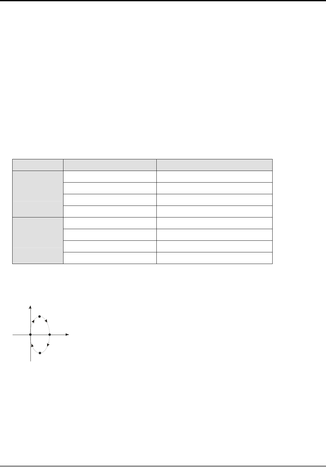
9 Application Instructions API 150-199
DVP-PLC Application Manual
9-107
less than 1,000 and more than 10,000,000; otherwise, the instruction cannot be enabled.
11. If you wish the number of pulses in 10-segment or 20-segment motion to be off the range, you may adjust the
gear ratio of the servo for obtaining your desired number.
12. Every time when the instruction is executed, only one 90° arc can be drawn. It is not necessary that the arc has to
be a precise arc, i.e. the numbers of output pulses in X and Y axes can be different.
13. There are no settings of start frequency and acceleration/deceleration time.
14. There is no limitation on the number of times using the instruction. However, assume CH1 or CH2 output is in use,
the 1st group X/Y axis will not be able to output. If CH3 or CH4 output is in use, the 2nd group X/Y axis will not be
able to output.
15. The settings of direction and resolution in the lower 16 bits of S can only be K0 ~ K3.
16. The settings of motion time in the high 16 bits of S can be slower than the the fastest suggested time but shall not
be faster than the fastest suggested time.
17. The fastest suggested time for the arc interpolation:
Segments Max. target position (pulse) Fastest suggested set time (unit:100ms)
100 ~ 10,000 1
10,001 ~ 19,999 2
: :
Average
resolution
Less than 1,000,000 Less than 100
1,000 ~ 20,000 2
20,000 ~ 29,999 3
: :
Higher
resolution
Less than 10,000,000 Less than 200
Program Example 1:
1. Draw an ellipse as the figure below.
Y
X
()1600,2200
()3200,0
()0,0
(1600,-2200)
2. Steps:
a) Set the four coordinates (0,0), (1600, 2200), (3200, 0), (1600, -2200) (as the figure above). Calculate the relative
coordinates of the four points and obtain (1600, 2200), (1600, -2200), (-1600, -2200), and (-1600, 2200). Place
them in the 32-bit (D200, D202), (D204, D206), (D208, D210), (D212, D214).
b) Select “draw clockwise arc” and “average resolution” (S = K0).
c) Write program codes as follows.
d) PLC RUN. Set M0 as On and start the drawing of the ellipse.
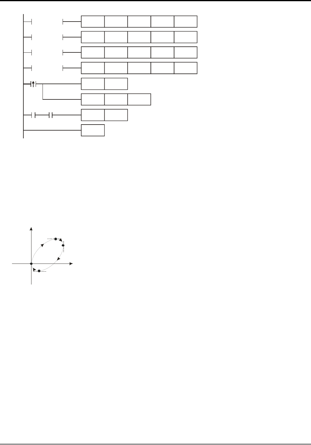
9 Application Instructions API 150-199
DVP-PLC Application Manual
9-108
M0
RST
= D0 K1 D200 D202 K0 Y0
= D0 K2 D204 D206 Y0
= D0 K3 D208 D210 Y0
= D0 K4 D212 D214 Y0
MOV D0
M0
INCP
END
M1029
D0
M1029
K1
K0
K0
K0
DCIMR
DCIMR
DCIMR
DCIMR
3. Motion explanation:
When PLC RUN and M0 = On, PLC will start the drawing of the first segment of the arc. D0 will plus 1 whenever a
segment of arc is completed and the second segment of the arc will start to execute automatically. The same
motion will keep executing until the fourth segment of arc is completed.
Program Example 2:
1. Draw a tilted ellipse as the figure below.
Y
X
(0,0)
(26000 ,2 60 00)
(34000,1 80 00)
(800 0,- 8000)
2. Steps:
a) Find the max. and min. coordinates on X and Y axes (0,0), (26000,26000), (34000,18000), (8000,-8000) (as the
figure above). Calculate the relative coordinates of the four points and obtain (26000,26000)、(8000,-8000)、
(-26000,-26000), (-8000,8000). Place them respectively in the 32-bit (D200,D202), (D204,D206), (D208,D210)
and (D212,D214).
b) Select “draw clockwise arc” and “average resolution” (S = K0).
c) Select DCIMR instruction for drawing arc and write program codes as follows.
d) PLC RUN. Set M0 as On and start the drawing of the ellipse.

9 Application Instructions API 150-199
DVP-PLC Application Manual
9-109
M0
RST
= D0 K1 D200 D202 K0 Y0
= D0 K2 D204 D206 Y0
= D0 K3 D208 D210 Y0
= D0 K4 D212 D214 Y0
MOV D0
M0
INCP
END
M1029
D0
M1029
K1
K0
K0
K0
DCIMR
DCIMR
DCIMR
DCIMR
3. Motion explanation:
When PLC RUN and M0 = On, PLC will start the drawing of the first segment of the arc. D0 will plus 1 whenever a
segment of arc is completed and the second segment of the arc will start to execute automatically. The same
motion will keep executing until the fourth segment of arc is completed.
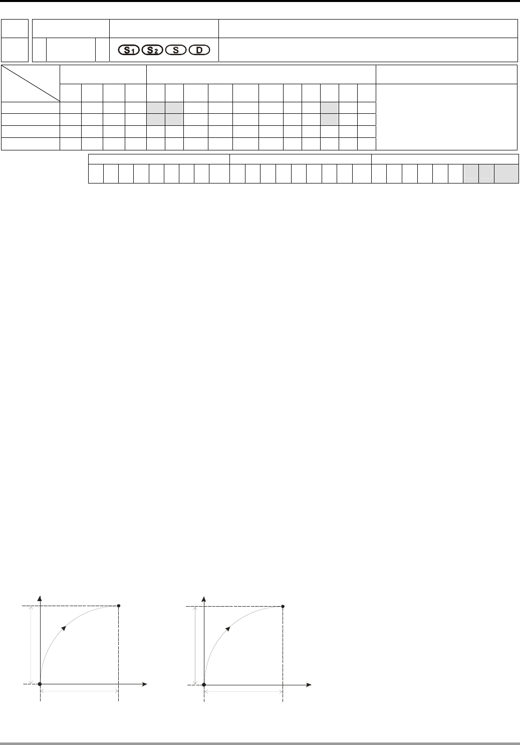
9 Application Instructions API 150-199
DVP-PLC Application Manual
9-110
API Mnemonic Operands Function
194
D CIMA 2-Axis Absolute Position Arc Interpolation
Bit Devices Word Devices Program Steps Type
OP X Y M S K H KnX KnY KnM KnS T C D E F
S1 * * *
S2 * * *
S *
D *
DCIMA: 17 steps
PULSE 16-bit 32-bit
ES EX SS SA SX SC EH SV EH3
SV2 ES EX SS SA SX SC EH SV EH3
SV2 ES EX SS SA SX SC EH SV EH3
SV2
Operands:
S1: Number of output pulses of X axis S2: Number of output pulses of Y axis S: Parameter setting D: Pulse
output device
Explanations:
1. Flags: M1029, M1030, M1334, M1335. See remarks of API 191 DPPMR for more details.
2. This instruction only supports EH2/SV/EH3/SV2 series MPU, not EH series. In terms of pulse output methods,
this instructin only supports “pulse + direction” mode.
3. S1 and S2 are the designated (absolute designation) number of output pulses in X axis (Y0 or Y4) and Y axis (Y2
or Y6). The range of the number is -2,147,483,648 ~ +2,147,483,647. When S1 and S2 are larger than pulse
present value registers CH0 (D1337 high word, D1336 low word), CH1 (D1339 high word, D1338 low word), CH2
(D1376 high word, D1375 low word), and CH3 (D1378 high word, D1377 low word), the output direction will be
positive and direction signals Y1, Y3, Y5, Y7 will be On. When S1 and S2 are less than pulse present value
registers, the output direction will be negative and direction signals Y1, Y3, Y5, Y7 will be Off.
4. The lower 16 bits of S (settings of direction and resolution): K0 refers to clockwise 10-segment (average
resolution) output; K2 refers to clockwise 20-segment (higher resolution) output and a 90° arc can be drawn (see
figure 1 and 2). K1 refers to counterclockwise 10-segment (average resolution) output; K3 refers to
counterclockwise 20-segment (higher resolution) output and a 90° arc can be drawn (see figure 3 and 4).
5. The higher 16 bits of S (settings of motion time): K0 refers to 0.1 second. The setting range for average resolution
is K1 ~ K100 (0.1 sec. ~ 10 secs.), for higher resolution is K2 ~ K200 (0.2 sec. ~ 20 secs.) This instruction is
restricted by the maximum pulse output frequency; therefore when the set time goes faster than the actual output
time, the set time will be automatically modified.
(0,0) X
Y (S ,S )
12
10 segments
10 segments
Figure 1
(0,0) X
Y (S ,S )
12
20 segments
20 segments
Figure 2
9 Application Instructions API 150-199
DVP-PLC Application Manual
9-111
(0,0)
X
Y
(0,0) X
Y
(S ,S )
12
(S ,S )
12
10 segments
10 segments
20 segments
20 segments
Figure 3 Figure 4
6. D can designate Y0 and Y4.
When Y0 is designated:
Y0 refers to 1st group X-axis pulse output device.
Y1 refers to 1st group X-axis direction signal.
Y2 refers to 1st group Y-axis pulse output device.
Y3 refers to 1st group Y-axis direction signal.
When Y4 is designated:
Y4 refers to 2nd group X-axis pulse output device.
Y5 refers to 2nd group X-axis direction signal.
Y6 refers to 2nd group Y-axis pulse output device.
Y7 refers to 2nd group Y-axis direction signal.
When direction signal outputs, Off will not occur immediately after the pulse output is over. Direction signal will
turn Off when the drive contact is Off.
7. Draw four 90° arcs.
8. When the direction signal is On, the direction is positive. When the direction signal is Off, the direction is negative.
When S is set as K0, K2, the arcs will be clockwise (see figure 5). When S is set as K1, K3, the arcs will be
counterclockwise (see figure 6).
Y
X
Y
X
Quadrant I
Quadrant II
Qu adrant III
Qu adrant IV
Qu adrant I
Quadrant II
Quadrant III
Quadrant IV
Figure 5 Figure 6
9. When the 2-axis motion is being executed in 10 segments (of average resolution), the operation time of the
instruction when the instruction is first enabled is approximately 5ms. The number of output pulses cannot be less
than 100 and more than 1,000,000; otherwise, the instruction cannot be enabled.
10. When the 2-axis motion is being executed in 20 segments (of high resolution), the operation time of the
instruction when the instruction is first enabled is approximately 10ms. The number of output pulses cannot be
less than 1,000 and more than 10,000,000; otherwise, the instruction cannot be enabled.
9 Application Instructions API 150-199
DVP-PLC Application Manual
9-112
11. If you wish the number of pulses in 10-segment or 20-segment motion to be off the range, you may adjust the
gear ratio of the servo for obtaining your desired number.
12. Every time when the instruction is executed, only one 90° arc can be drawn. It is not necessary that the arc has to
be a precise arc, i.e. the numbers of output pulses in X and Y axes can be different.
13. There are no settings of start frequency and acceleration/deceleration time.
14. There is no limitation on the number of times using the instruction. However, assume CH1 or CH2 output is in use,
the 1st group X/Y axis will not be able to output. If CH3 or CH4 output is in use, the 2nd group X/Y axis will not be
able to output.
15. The settings of direction and resolution in the lower 16 bits of S can only be K0 ~ K3.
16. The settings of motion time in the high 16 bits of S can be slower than the the fastest suggested time but shall not
be faster than the fastest suggested time.
17. The fastest suggested time for the arc interpolation:
Segments Max. target position (pulse) Fastest suggested set time (unit:100ms)
100 ~ 10,000 1
10,001 ~ 19,999 2
: :
Average
resolution
Less than 1,000,000 Less than 100
1,000 ~ 20,000 2
20,000 ~ 29,999 3
: :
Higher
resolution
Less than 10,000,000 Less than 200
Program Example 1:
1. Draw an ellipse as the figure below.
Y
X
()16000,22000
()32 00 0,0
()0,0
(16000,-22000)
2. Steps:
a) Set the four coordinates (0,0), (16000, 22000), (32000, 0), (16000, -22000) (as the figure above). Place them in
the 32-bit (D200, D202), (D204, D206), (D208, D210), (D212, D214).
b) Select “draw clockwise arc” and “average resolution” (S = K0).
c) Select DCIMA instruction for drawing arc and write program codes as follows.
d) PLC RUN. Set M0 as On and start the drawing of the ellipse.
9 Application Instructions API 150-199
DVP-PLC Application Manual
9-113
M0
RST
= D0 K1 D200 D202 K0 Y0
= D0 K2 D204 D206 Y0
= D0 K3 D208 D210 Y0
= D0 K4 D212 D214 Y0
MOV D0
M0
INCP
END
M1029
D0
M1029
K1
K0
K0
K0
DCIMA
DCIMA
DCIMA
DCIMA
ZRST D1336 D1339
3. Motion explanation: :
When PLC RUN and M0 = On, PLC will start the drawing of the first segment of the arc. D0 will plus 1 whenever a
segment of arc is completed and the second segment of the arc will start to execute automatically. The same
motion will keep executing until the fourth segment of arc is completed.
Program Example 2:
1. Draw a tilted ellipse as the figure below.
Y
X
(0,0)
(26000,260 00 )
(34000,1 80 00 )
(8000,-8000)
2. Steps:
a) Find the max. and min. coordinates on X and Y axes (0,0), (26000,26000), (34000,18000), (8000,-8000) (as the
figure above). Place them respectively in the 32-bit (D200,D202), (D204,D206), (D208,D210) and (D212,D214).
b) Select “draw clockwise arc” and “average resolution” (S = K0).
c) Select DCIMA instruction for drawing arc and write program codes as follows.
d) PLC RUN. Set M0 as On and start the drawing of the ellipse.
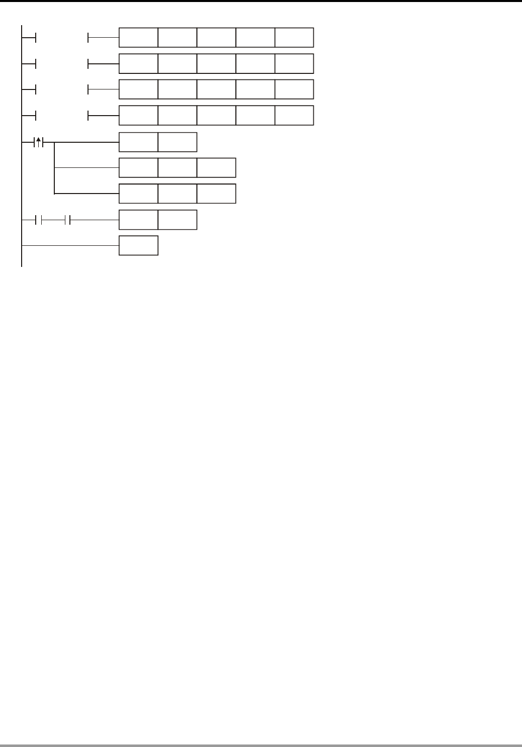
9 Application Instructions API 150-199
DVP-PLC Application Manual
9-114
M0
RST
= D0 K1 D200 D202 K0 Y0
= D0 K2 D204 D206 Y0
= D0 K3 D208 D210 Y0
= D0 K4 D212 D214 Y0
MOV D0
M0
INCP
END
M1029
D0
M1029
K1
K0
K0
K0
DCIMA
DCIMA
DCIMA
DCIMA
ZRST D1336 D1339
3. Motion explanation:
When PLC RUN and M0 = On, PLC will start the drawing of the first segment of the arc. D0 will plus 1 whenever a
segment of arc is completed and the second segment of the arc will start to execute automatically. The same
motion will keep executing until the fourth segment of arc is completed.

9 Application Instructions API 150-199
DVP-PLC Application Manual
9-115
API Mnemonic Operands Function
195
D PTPO Single-Axis Pulse Output by Table
Bit Devices Word Devices Program Steps Type
OP X Y M S K H KnX KnY KnM KnS T C D E F
S1 *
S2 *
D *
DPTPO: 13 steps
PULSE 16-bit 32-bit
ES EX SS SA SX SC EH SV EH3
SV2 ES EX SS SA SX SC EH SV EH3
SV2 ES EX SS SA SX SC EH SV EH3
SV2
Operands:
S1: Source start device S
2: Number of segments D: Pulse output device
Explanations:
1. Flags: M1029, M1030, M1334, M1335. See remarks for more details.
2. This instruction only supports EH2/SV/EH3/SV2 series MPU, not EH series.
3. According to the value of S2 + 0, every segment consecutively occupy four register D. (S1 + 0) refers to output
frequency. (S1 + 2) refers to the number of output pulses.
4. When the output frequency of S1 is less than 1, PLC will automatically modify it as 1. When the value is larger
than 200,000kHz, PLC will automatically modify it as 200,000kHz.
5. S2 + 0: number of segments (range: 1 ~ 60). S2 + 1: number of segments being executed. Whenever the program
scans to this instruction, the instruction will automatically update the segment No. that is currently being
executed.
6. D can only designate output devices Y0, Y2, Y4 and Y6 and can only perform pulse output control. For the pin for
direction control, the user has to compile other programs to control.
7. This instruction does not offer acceleration and deceleration functions. Therefore, when the instruction is disabled,
the output pulses will stop immediately.
8. In every program scan, each channel can only be executed by one instruction. However, there is no limitation on
the number of times using this instruction.
9. When the instruction is being executed, the user is not allowed to update the frequency or number of the
segments. Changes made will not be able to make changes in the actual output.
Program Example:
1. When X0 = On, the output will be operated according to the set frequency and number of pulses in every
segment.
2. Format of the table:
S2 = D300, number of segments
(D300 = K60)
S1 = D0, frequency (S1 + 0) S1 = D0, number of output pulses
(S1 + 2)
K1 (1st segment) D1, D0 D3, D2
K2 (2nd segment) D5, D4 D7, D6
:
:
:
:
:
:
K60 (60th segment) D237, D236 D239, D238
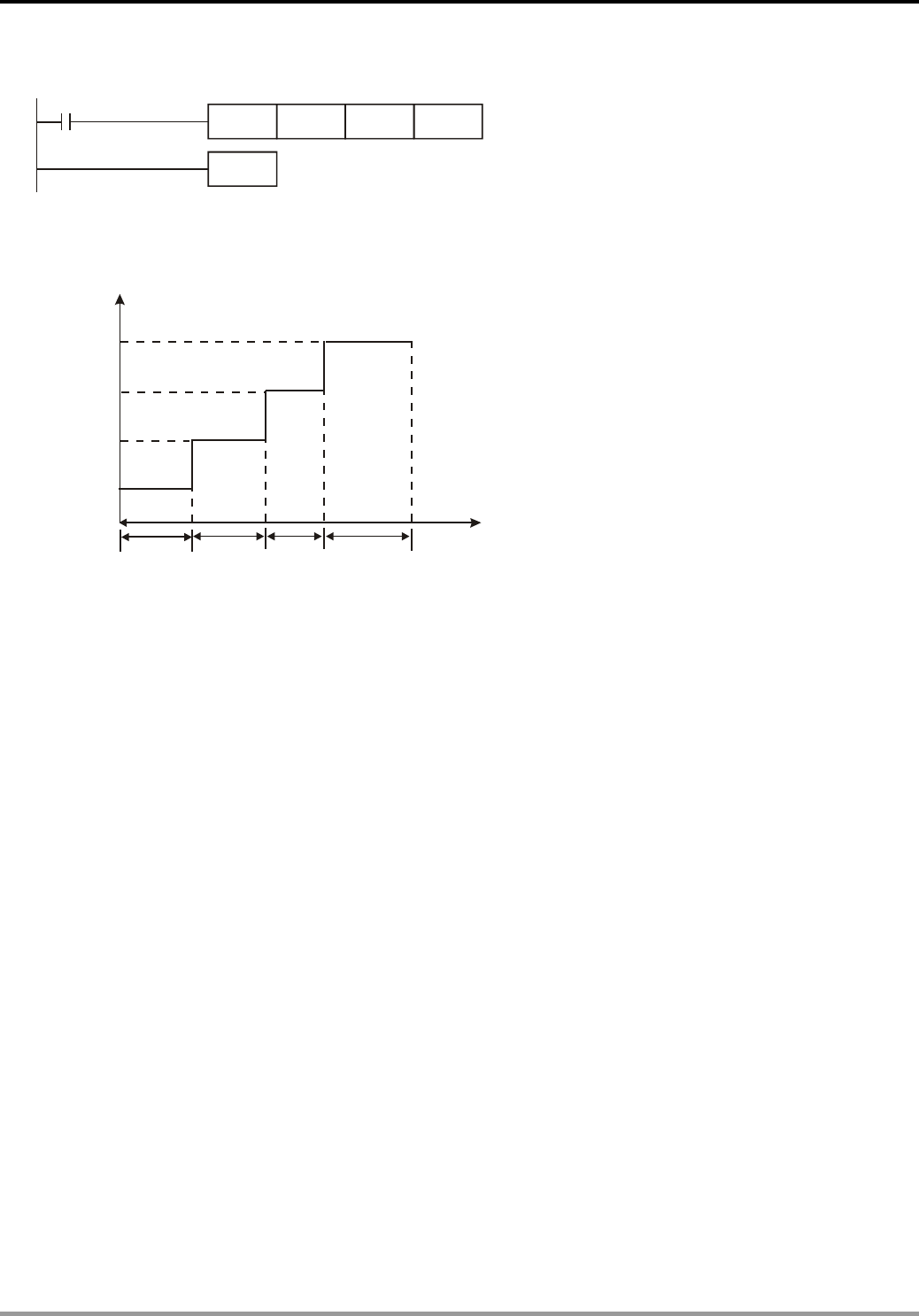
9 Application Instructions API 150-199
DVP-PLC Application Manual
9-116
3. Monitor the segment No. that is currently being executed in register D301.
X0
D0
DPTPO D300 Y0
END
4. The pulse output curve:
Frequency (Hz)
tttt
12.... 60
(D1,D0)
(D3,D2)
(D239,D238)
(D5,D4)
(D237,D236)
....
....
(D7,D6)
Time (S)
Remarks:
1. Flag explanations:
M1029: On when CH0 (Y0) pulse output is completed.
M1030: On when CH1 (Y2) pulse output is completed.
M1036: On when CH2 (Y4) pulse output is completed.
M1037: On when CH3 (Y6) pulse output is completed.
M1334: When On, CH0 (Y0) pulse output will be forbidden.
M1335: When On, CH1 (Y2) pulse output will be forbidden.
M1520: When On, CH2 (Y4) pulse output will be forbidden.
M1521: When On, CH3 (Y6) pulse output will be forbidden.
M1336: CH0 (Y0) pulse output indication flag
M1337: CH1 (Y2) pulse output indication flag
M1522: CH2 (Y4) pulse output indication flag
M1523: CH3 (Y6) pulse output indication flag
2. Special register explanations:
D1336, D1337: Pulse present value register of CH0 (Y0) (D1337 high word, D1336 low word)
D1338, D1339: Pulse present value register of CH1 (Y2) (D1339 high word, D1338 low word)
D1375, D1376: Pulse present value register of CH2 (Y4) (D1376 high word, D1375 low word)
D1377, D1378: Pulse present value register of CH3 (Y6) (D1378 high word, D1377 low word)
9 Application Instructions API 150-199
DVP-PLC Application Manual
9-117
API Mnemonic Operands Function
196
HST P High Speed Timer
Bit Devices Word Devices Program Steps Type
OP X Y M S K H KnX KnY KnM KnS T C D E F
S * *
HST, HSTP: 3 steps
PULSE 16-bit 32-bit
ES EX SS SA SX SC EH SV EH3
SV2 ES EX SS SA SX SC EH SV EH3
SV2 ES EX SS SA SX SC EH SV EH3
SV2
Operands:
S: Condition to stop the startup of high speed timer
Explanations:
1. Range of S: S = K0 (H0), K1 (H1).
2. Flag: M1015
3. When S = 1, the high speed timer will be enabled and M1015 = On. The high speed timer starts to time and
record the present value in D1015 (min. unit: 100us).
4. Timing range of D1015: K0 ~ K32,767. When the timing reaches K32,767, the next timing will restart from 0.
5. When S = 0, the high speed timer will be disabled and M1015 = Off. D1015 will stop the timing immediately.
6. When S is neither 1 nor 0, HST instruction will not be executed.
Program Example :
1. When X10 = On, M1015 will be On. The high speed timer will start to time and record the present value in
D1015.
2. When X10 = Off, M1015 will be Off. The high speed timer will be shut down.
X10
HST K1
X10
HST K0
Remarks:
1. Flag explanations:
M1015: high speed timer start-up flag
D1015: high speed timer
2. EH/EH2/SV/EH3/SV2 series MPU do not use this instruction and use special M and special D directly for the
timer.
a) Special M and special D are only applicable when PLC RUN.
b) When M1015 = On and PLC scans to END instruction, the high speed timer D1015 will be enabled. The
minimum timing unit of D1015: 100us.
c) Timing range of D1015: K0 ~ K32,767. When the timing reaches K32,767, the next timing will restart from
K0.
d) When M1015 = Off, D1015 will stop the timing when encountering END or HST instruction.
3. SA/SX/SC series MPU do not use this instruction and use special M and special D directly for the timer.

9 Application Instructions API 150-199
DVP-PLC Application Manual
9-118
a) Special M and special D are applicable when PLC RUN or STOP.
b) When M1015 = On, the high speed timer D1015 will be enabled. The minimum timing unit of D1015:
100us.
c) Timing range of D1015: K0 ~ K32,767. When the timing reaches K32,767, the next timing will restart from
K0.
d) When M1015 = Off, D1015 will stop the timing immediately.
9 Application Instructions API 150-199
DVP-PLC Application Manual
9-119
API Mnemonic Operands Function
197
D CLLM Close Loop Position Control
Bit Devices Word Devices Program Steps Type
OP X Y M S K H KnX KnY KnM KnS T C D E F
S1 * *
S2 * * *
S3 * * *
D *
DCLLM: 17 steps
PULSE 16-bit 32-bit
ES EX SS SA SX SC EH SV EH3
SV2 ES EX SS SA SX SC EH SV EH3
SV2 ES EX SS SA SX SC EH SV EH3
SV2
Operands:
S1: Feedback source device S2: Target number of feedbacks S3: Target frequency of output
D: Pulse output device
Explanations:
1. Flags: M1029, M1030, M1334, M1335. See remarks for more details.
2. This instruction only supports EH2/SV/EH3/SV2 series MPU, not EH series.
3. The corresponding interruption of S1:
Source device X0 X1 X2 X3 C241 ~ C254
Corresponding outout Y0 Y2 Y4 Y6 Y0 Y2 Y4 Y6
Interruption No. I00 I10 I20 I30 I010 I020 I030 I040
= 1: rising-edige trigger; = 0: falling-edge trigger
a) When S1 designates X as the input points and the pulse output reaches the set target number of feedbacks
in S2, the output will continue to operate by the frequency of the last segment until the interruption of X input
points occurs.
b) When S1 designates a high speed counter and the pulse output reaches the set target number of feedbacks
in S2, the output will continue to operate by the frequency of the last segment until the feedback pulses
reaches the target number.
c) S1 can be a high speed counter C or an external interruption X. If S1 is C, DCNT instruction should be first
executed to enable the high-speed counting function and EI and I0x0 interruption service program to enable
the high-speed interruption. If S1 is X, EI instruction and I0x0 interruption service program should be
executed to enable the external interruption function.
4. The range of S2: -2,147,483,648 ~ +2,147,483,647 (+/- represents the forward/backward direction). When in
forward direction, the pulse present value registers CH0 (D1337 high word, D1336 low word), CH1 (D1339 high
word, D1338 low word), CH2 (D1376 high word, D1375 low word) and CH3 (D1378 high word, D1377 low word)
will increase. When in backward direction, the present value will decrease.
5. If S3 is lower than 10Hz, the output will operate at 10Hz; if S3 is higher than 200kHz, the output will operate at
200kHz.
6. D can only designate Y0, Y2, Y4 and Y6 and the direction signals repectively are Y1, Y3, Y5 and Y7. When
there is a direction signal output, the direction signal will not be Off immediately after the pulse output is
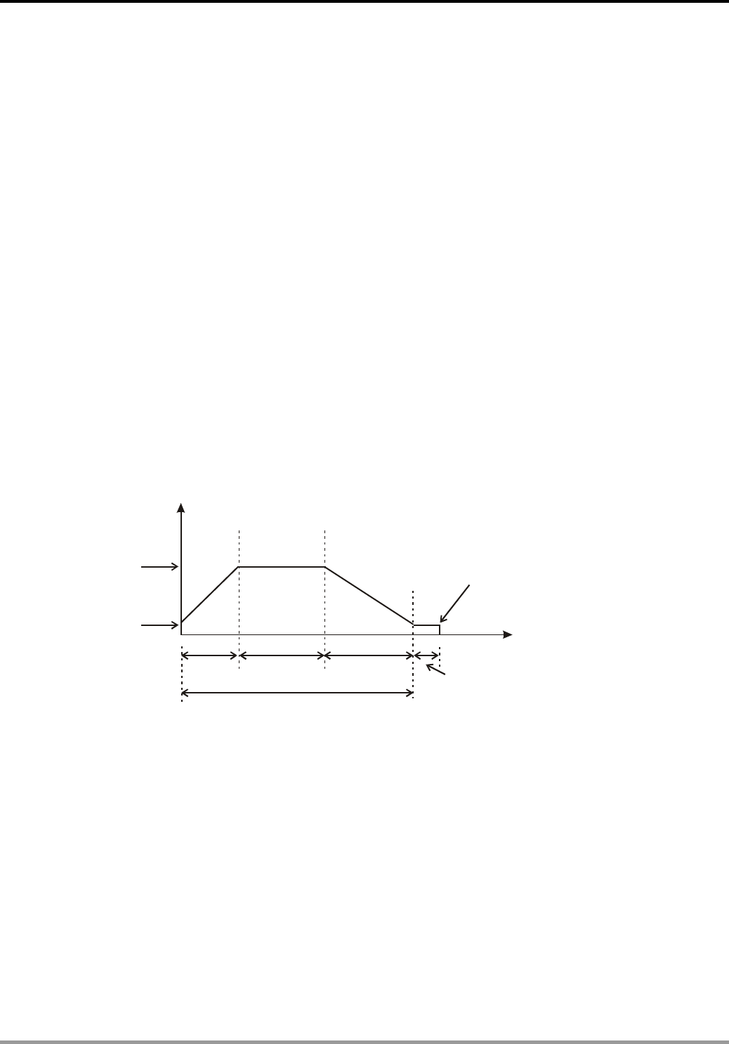
9 Application Instructions API 150-199
DVP-PLC Application Manual
9-120
completed. The direction signal will be Off only when the drive contact is Off.
7. D1340, D1352, D1379 and D1380 are the settings of start/end frequencies of CH0 ~ CH3. The minimun
frequency is 10Hz and default is 200Hz.
8. D1343, D1353, D1381 and D1382 are the settings of the time of the first segment and the last deceleration
segment of CH0 ~ CH3. The acceleration/deceleration time cannot be shorter than 10ms. The outptu will be
operated in 10ms if the time set is shorter than 10ms or longer than 10,000ms. The dafault setting is 100ms.
9. D1131, D1132, D1478 and D1479 are the output/input ratio of the close loop control in CH0 ~ CH3. K1 refers to
1 output pulse out of the 100 target feedback input pulses; K200 refers to 200 output pulses out of the 100
target feedback input pulses. D1131, D1132, D1478 and D1479 are the numerators of the ratio (range: K1 ~
K10,000) and the denominator is fixed as K100 (the user does not have to enter a denominator).
10. M1305, M1306, M1532 and M1533 are the direction signal flags for CH0 ~ CH3. When S2 is a positive value,
the output will be in forward direction and the flag will be Off. When S2 is a negative value, the output will be in
backward direction and the flag will be On.
Close Loop Explanations:
1. Function: Immediately stop the high-speed pulse output according to the number of feedback pulses or external
interruption signals.
2. The execution:
Frequency
Time
Number
C high speed counting = target number of feedbacks
or
occurrence of external interruption
Target frequency
Start/end frequency
Acceleration
time
High speed time Deceleration time
Idling time
Number of output pulses =
target number of feedbacks x percentage value/100
3. How to adjust the time for the completion of the positioning:
a) The time for the completion of the positioning refers to the time for “acceleration + high speed +
deceleration + idling” (see the figure above). For example, you can increase or decrease the entire number
of output pulses by making adjustment on the percentage value and further increase or decrease the time
required for the positioning.
b) Among the four segments of time, only the idling time cannot be adjusted directly by the user. However, you
can determine if the execution result is good or bad by the length of the idling time. In theory, a bit of idling
left is the best result for a positioning.
c) Owing to the close loop operation, the length of idling time will not be the same in every execution.
Therefore, when the content in the special D for displaying the actial number of output pulses is smaller or
larger than the calculated number of output pulses (taget number of feedbacks x percentage value/100),
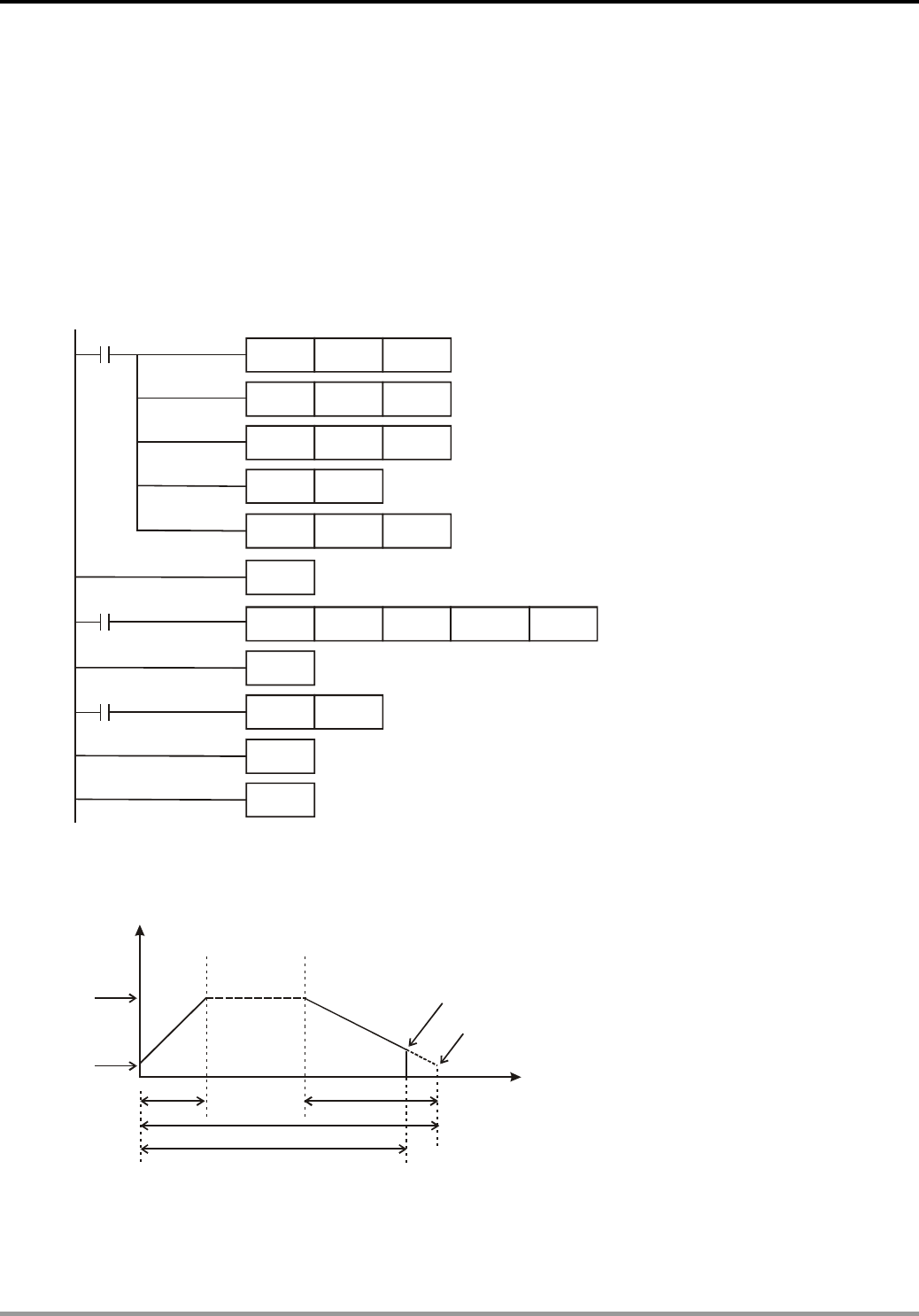
9 Application Instructions API 150-199
DVP-PLC Application Manual
9-121
you can improve the situation by adjusting the percentage value, acceleration/decelartion time or target
frequency.
Program Example:
1. Assume we adopt X0 as the external interruption, together with I001 (rising-edge trigger) interruption program;
target number of feedbacks = 50,000; target frequency = 10kHz; Y0, Y1 (CH0) as output pulses; start/end
frequency (D1340) = 200Hz; acceleration time (D1343) = 300ms; deceleration time (D1348) = 600ms;
percentage value (D1131) = 100; current number of output pulses (D1336, D1337) = 0.
2. Write the program codes as follows:
MOV
MOV
MOV
K100
K600
K300
D0
M1002
D1131
D1343
D1348
SET
DMOV K0 D1336
EI
FEND
IRET
END
DCLLM X0 K50000 K100000 Y0
INC
M1534
M0
M1000
I010
3. Assume the first execution result as:
100KHz
D1340
D1348D1343
X0 Off --> On
Frequenc
y
Y0 stops output
Time
Number
Estimated number of output pulses: 50,000
Actual number of output pulses (D1336, D1337) = K49,200
D1340
4. Observe the result of the first execution:
a) The actual output number 49,200 – estimated output number 50,000 = -800 (a negative value). A negative
value indicates that the entire execution finishes earlier and has not completed yet.

9 Application Instructions API 150-199
DVP-PLC Application Manual
9-122
b) Try to shorten the acceleration time (D1343) into 250ms and deceleration time (D1348) into 550ms.
5. Obtain the result of the second execution:
100KHz
D1340
D1348D1343
X0 Off --> On
Frequency
Y0 stops output
Time
Number
Estimated number of output pulses: 50,000
Actual number of output pulses (D1336, D1337) = K50,020
D1340
6. Observe the result of the second execution:
a) The actual output number 50,020 – estimated output number 50,000 = 20
b) 20 x (1/200Hz) = 100ms (idling time)
c) 100ms is an appropriate value. Therefore, set the acceleration time as 250ms and deceleration time as
550ms to complete the design.
Program Example 2:
1. Assume the feedback of the encoder is an A/B phase input and we adopt C251 timing (we suggust you clear it
to 0 before the execution); target number of feedbacks = 50,000; target output frequency = 100kHz; Y0, Y1
(CH0) as output pulses; start/end frequency (D1340) = 200Hz; acceleration time (D1343) = 300ms; deceleration
time (D1348) = 600ms; precentage value (D1131) = 100; current number of output pulses (D1336, D1337) = 0.
2. Write the program codes as follows:
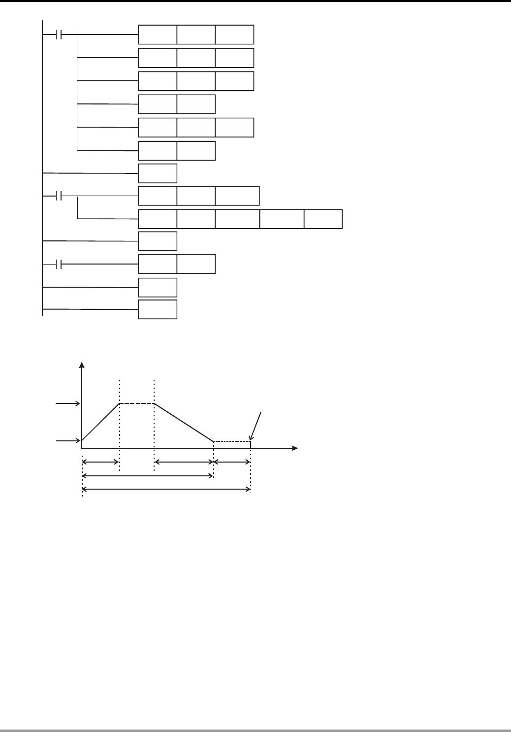
9 Application Instructions API 150-199
DVP-PLC Application Manual
9-123
MOV
MOV
MOV
K100
K600
K300
D0
M1002
D1131
D1343
D1348
SET
DMOV K0 D1336
RST C251
EI
DCNT C251 K100000
FEND
IRET
END
DCLLM K50000 K100000 Y0
INC
M1534
M0
M1000
I010
C251
3. Assume the first execution result as:
100KHz
D1340
D1348D1343
C251 =K50000
3s
Frequency
Y0 stops output
Time
Number
Estimated number of output pulses: 50,000
Actual number of output pulses (D1336, D1337) = K50,600
4. Observe the result of the first execution:
a) The actual output number 50,600 – estimated output number 50,000 = 600
b) 600 x (1/200Hz) = 3s (idling time)
c) 3 seconds are too long. Therefore, increase the percentage value (D1131) to K101.
5. Obatin the result of the second execution:

9 Application Instructions API 150-199
DVP-PLC Application Manual
9-124
100KHz
D1340
D1348D1343
C251 =K50000
300ms
Frequency
Y0 stops output
Time
Number
Estimated number of output pulses: 50,500
Actual number of output pulses (D1336, D1337) = K50,560
6. Observe the result of the second execution:
a) The actual output number 50,560 – estimated output number 50,500 = 60
b) 60 x (1/200Hz) = 300ms (idling time)
c) 300ms is an appropriate value. Therefore, set the percentage value (D1131) as K101 to complete the
design.
Remarks:
1. Flag explanations:
M1010: When On, CH0, CH1, CH2 and CH3 will output pulses when encountering END instruction. Off
when the output starts.
M1029: On when CH0 pulse output is completed.
M1030: On when CH1 pulse output is completed.
M1036: On when CH2 pulse output is completed.
M1037: On when CH3 pulse output is completed.
M1257 The acceleration/deceleration of the high-speed pulse output Y0 and Y2 are S curves.
M1334: When On, CH0 pulse output will be forbidden.
M1335: When On, CH1 pulse output will be forbidden.
M1520: When On, CH2 pulse output will be forbidden.
M1521: When On, CH3 pulse output will be forbidden.
M1336: CH0 pulse output indication flag
M1337: CH1 pulse output indication flag
M1522: CH2 pulse output indication flag
M1523: CH3 pulse output indication flag
M1305: CH0 direction signal flag
M1306: CH1 direction signal flag
M1532: CH2 direction signal flag
M1533: CH3 direction signal flag
M1534: Deceleration time of CH0 setup flag (must used with D1348)
M1535: Deceleration time of CH1 setup flag (must used with D1349)
M1536: Deceleration time of CH2 setup flag (must used with D1350)
M1537: Deceleration time of CH3 setup flag (must used with D1351)

9 Application Instructions API 150-199
DVP-PLC Application Manual
9-125
2. Special register explanations:
D1127 The number of pulses in the acceleration section in the position instruction (low word)
D1128 The number of pulses in the acceleration section in the position instruction (high word)
D1131: Close loop output/input ratio of CH0 (default: K100)
D1132: Close loop output/input ratio of CH1 (default: K100)
D1133 The number of pulses in the deceleration section in the position instruction (low word)
D1134 The number of pulses in the deceleration section in the position instruction (high word)
D1220: Phase setting of CH0 (Y0, Y1): determined by the last 2 digits of D1220; other digits are invalid.
1. K0: Y0 output
2. K1: Y0, Y1 AB-phase output; A ahead of B
3. K2: Y0, Y1 AB-phase output; B ahead of A
D1221: Phase setting of CH1 (Y2, Y3): determined by the last 2 digits of D1221; other digits are invalid.
1. K0: Y2 output
2. K1: Y2, Y3 AB-phase output; A ahead of B
3. K2: Y2, Y3 AB-phase output; B ahead of A
D1229: Phase setting of CH2 (Y4, Y5): determined by the last 2 digits of D1229; other digits are invalid.
1. K0: Y4 output
2. K1: Y4, Y5 AB-phase output; A ahead of B
3. K2: Y4, Y5 AB-phase output; B ahead of A
D1230: Phase setting of CH3 (Y6, Y7): determined by the last 2 digits of D1230; other digits are invalid.
1. K0: Y6 output
2. K1: Y6, Y7 AB-phase output; A ahead of B
3. K2: Y6, Y7 AB-phase output; B ahead of A
D1222: Time difference between the direction signal and pulse output of CH0
D1223: Time difference between the direction signal and pulse output of CH1
D1240 Low 16 bytes of the setting value for the end frequency of the high-speed output CH0 (available
when the acceleration and deceleration are separate) (If D1240 < D1340, D1340 is adopted.)
D1241 High 16 bytes of the setting value for the end frequency of the high-speed output CH0
(available when the acceleration and deceleration are separate) (If D1240 < D1340, D1340 is
adopted.)
D1244 Number of idle speed output from CH0 (> 0: Effective vale; <= 0: Continuous output)
D1245 Number of idle speed output from CH1 (> 0: Effective vale; <= 0: Continuous output)
D1246 Number of idle speed output from CH2 (> 0: Effective vale; <= 0: Continuous output)
D1247 Number of idle speed output from CH3 (> 0: Effective vale; <= 0: Continuous output)
D1383: Time difference between the direction signal and pulse output of CH2
D1384: Time difference between the direction signal and pulse output of CH3
D1336: Low word of the current number of output pulses of CH0
D1337: High word of the current number of output pulses of CH0
D1338: Low word of the current number of output pulses of CH1

9 Application Instructions API 150-199
DVP-PLC Application Manual
9-126
D1339: High word of the current number of output pulses of CH1
D1375: Low word of the current number of output pulses of CH2
D1376: High word of the current number of output pulses of CH2
D1377: Low word of the current number of output pulses of CH3
D1378: High word of the current number of output pulses of CH3
D1340: Start/end frequency settings of CH0 (default: K200)
D1352: Start/end frequency settings of CH1 (default: K200)
D1379: Start/end frequency settings of CH2 (default: K200)
D1380: Start/end frequency settings of CH3 (default: K200)
D1348: Deceleration time of CH0 pulse output when M1534 = On (default: K100)
D1349: Deceleration time of CH1 pulse output when M1535 = On (default: K100)
D1350: Deceleration time of CH2 pulse output when M1536 = On (default: K100)
D1351: Deceleration time of CH3 pulse output when M1537 = On (default: K100)
D1343: Acceleration/deceleration time of CH0 pulse output (default: K100)
D1353: Acceleration/deceleration time of CH1 pulse output (default: K100)
D1381: Acceleration/deceleration time of CH2 pulse output (default: K100)
D1382: Acceleration/deceleration time of CH3 pulse output (default: K100)
D1478: Close loop output/input ratio of CH2 (default: K100)
D1479: Close loop output/input ratio of CH3 (default: K100)

9 Application Instructions API 150-199
DVP-PLC Application Manual
9-127
API Mnemonic Operands Function
198
D VSPO Variable speed pulse output
Bit Devices Word devices Program Steps Type
OP X Y M S K H KnX KnY KnM KnS T C D E F
S1 *
S2 * * *
S3 * * *
D *
DVSPO: 17 steps
PULSE 16-bit 32-bit
ES EX SS SA SX SC EH SV EH3
SV2 ES EX SS SA SX SC EH SV EH3
SV2 ES EX SS SA SX SC EH SV EH3
SV2
Operands:
S1: Target frequency of output S2: Target number of pulses S3: Gap time and gap frequency
D: Pulse output device (Y0, Y2, Y4, Y6)
Explanations:
1. The instruciton only supports V2.0 of EH2 series. It does not support EH/SV series.
2. Max frequency for S1: 100kHz. Target frequency can be modified during the execution of instruction. When S1 is
modified, VSPO will ramp up/down to the target frequency according to the ramp-up gap time and gap
frequency set in S3.
3. S2 target number of pulses is valid only when the instruction is executed first time. S2 can NOT be modified
during the execution of instruction. S2 can be a negative value. When target number of pulses are specified with
0, PLC will perform continuous output.
4. S3 occupies 2 consecutive 16-bit devices. S3+0 stores the gap frequency S3+1 stores the gap time. Parameter
setting can be modified during the execution of instruction. Set range for S3+0: 6Hz ~ 32767Hz; set range for
S3+0: 1ms ~ 80ms. If set value exceeds the available range, PLC will take the upper or lower bound value.
5. D pulse output device supports Y0, Y2, Y4 and Y6. Y1, Y3, Y5 and Y7 are corresponding output direction. The
positive direction is On.
6. Parameters set in S3 can only be modified while modifying the value in S1. When target frequency is set as 0,
PLC will ramp down to stop according to parameters set in S3. When the output is stopped, PLC will enable the
flags indicating pause status (CH0: M1538; CH1: M1539; CH2: M1540; CH3: M1541). If target frequency other
than 0 is specified again, pulse output will ramp up to target frequency and operates untill target number of
pulses are completed.
Function Explanations:
Pulse output diagram:
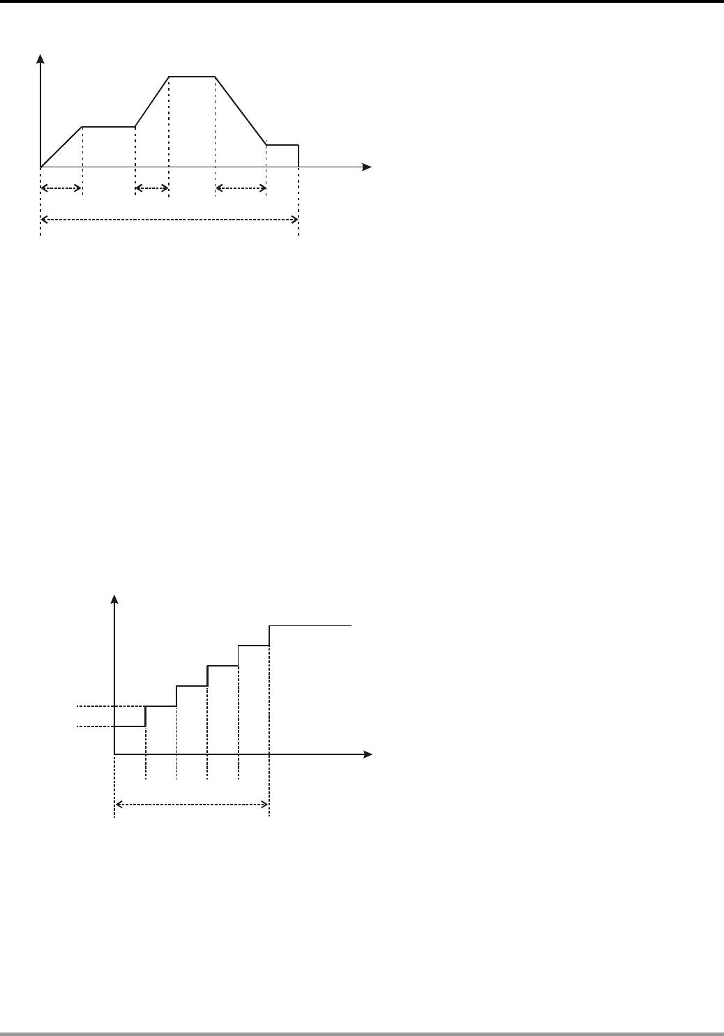
9 Application Instructions API 150-199
DVP-PLC Application Manual
9-128
Freq.
Time
t1
t2
t3
g1 g2 g3
S
2
Pulse number
1. Definitions:
t1 Æ target frequency of 1st shift
t2 Æ target frequency of 2nd shift
t3 Æ target frequency of 3rd shift
g1 Æ ramp-up time of 1st shift
g2 Æ ramp-up time of 2nd shift
g3 Æ ramp-down time of 3rd shift
S2 Æ total output pulses
2. Explanations on each shift:
1
st shift:
Assume t1 = 6kHz, gap freqency = 1kHz, gap time = 10ms
Ramp-up steps of 1st shift:
Freq.
Time
1kHz
t1=6kHz
10ms 10ms 10ms 10ms 10ms
g1=50ms
0Hz
2
nd shift:
Assume t2 = 11kHz, internal frequency = 2kHz, gap time = 20ms
Ramp-up steps of 2nd shift:
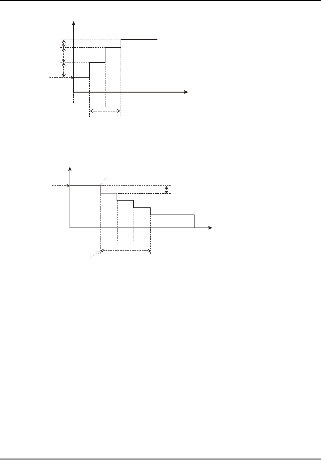
9 Application Instructions API 150-199
DVP-PLC Application Manual
9-129
Freq.
Time
2kHz
t2=11kHz
20ms
g2=40ms
20ms 20ms
1kHz
2kHz
t1=6kHz
3
rd shift:
Assume t3 = 3kHz, gap frequency = 2kHz, gap time = 20ms
Ramp-down steps of 3rd shift:
Freq.
Time
Change to t3
2kHz
t3=3kHz
t2=11kHz
Start to change g3=60ms
20ms 20ms 20ms 20ms
For program examples please refer to API 199
Points to note:
1. Associated flags:
M1029: CH0 pulse output execution is completed
M1030: CH1 pulse output execution is completed
M1036: CH2 pulse output execution is completed
M1037: CH3 pulse output execution is completed
M1538: Indicating pause status of CH0
M1539: Indicating pause status of CH1
M1540: Indicating pause status of CH2
M1541: Indicating pause status of CH0
M1542: CH0 executes the function that the constant speed output section reaches the
target frequency.
M1544: CH1 executes the function that the constant speed output section reaches the
target frequency.

9 Application Instructions API 150-199
DVP-PLC Application Manual
9-130
M1546: CH2 executes the function that the constant speed output section reaches the
target frequency.
M1548: CH3 executes the function that the constant speed output section reaches the
target frequency.
M1543: CH0 executed the function that the constant speed output section reaches the
target number.
M1545: CH1 executed the function that the constant speed output section reaches the
target number.
M1547: CH2 executed the function that the constant speed output section reaches the
target number.
M1549: CH3 executed the function that the constant speed output section reaches the
target number.
M1528: Enabling the instruction DICF to execute the constant speed output section
M1529: Enabling the instruction DICF to execute the final output section
2. Special register explanations:
D1336: Low word of the present value of Y2 pulse output
D1337: High word of the present value of Y2 pulse output
D1338: Low word of the current number of output pulses from CH1
D1339: High word of the current number of output pulses from CH1
D1375: Low word of the current number of output pulses from CH2
D1376: High word of the current number of output pulses from CH2
D1377: Low word of the current number of output pulses from CH3
D1378: High word of the current number of output pulses from CH3
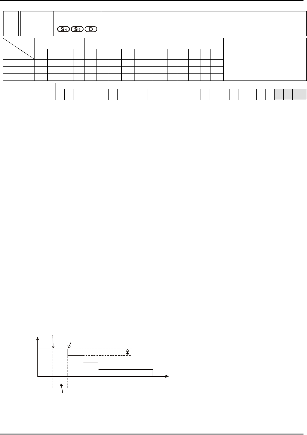
9 Application Instructions API 150-199
DVP-PLC Application Manual
9-131
API Mnemonic Operands Function
199
D ICF Immediately change frequency
Bit Devices Word devices Program Steps Type
OP X Y M S K H KnX KnY KnM KnS T C D E F
S1 *
S2 * * *
D *
DVSPO: 13 steps
PULSE 16-bit 32-bit
ES EX SS SA SX SC EH SV EH3
SV2 ES EX SS SA SX SC EH SV EH3
SV2 ES EX SS SA SX SC EH SV EH3
SV2
Operands:
S1: Target frequency to be changed S2: Gap time and gap frequency D: Pulse output device (Y0, Y2)
Explanations:
1. The instruciton only supports V2.0 of EH2 series. It does not support EH/SV series.
2. Max frequency for S1: 100kHz. When ICF instruction executes, frequecy changing will start immediately with
ramp-up/down process.
3. ICF instruction has to be executed after the execution of DVSPO or DPLSY instructions. When the instruction is
used together with DVSPO, operands S1, S2, D of DICF has to be assigned the same device with S1, S3, D of
DVSPO. When the instruction is used with DPLSY, operands S1 and D has to be assigned the same device with
S1 and D of DPLSY.
4. If ICF instruction is used with DPLSY instruction, operand S2 is invalid.
5. When ICF instruction is used with DVSPO instruction, parameter setting of S2 functions the same as S3 in
DVSPO instruction, specifying the gap time and gap frequency of ramp-up/down process.
6. D pulse output device supports only Y0 and Y2.
7. The instruction is suggested to be applied in interrupt subroutines for obtaining the better response time and
execution results
8. For associated flags and registers, please refer to Points to note of API 198 DVSPO instruction.
Function Explanations:
1. If users change the target frequency by using DVSPO instruction, the actual changing timing will be delayed due
to the program scan time and the gap time as below.
Freq.
Time
Gap freq.
Delayed by program scan cycle
Gap
time
Gap
time
Change target freq.
Actual timing of changing
2. If users change the target frequency by applying DICF instruction in insterupt subroutines, the actual changing
timing will be executed immediately with only an approx. 10us delay (execution time of DICF instruction).
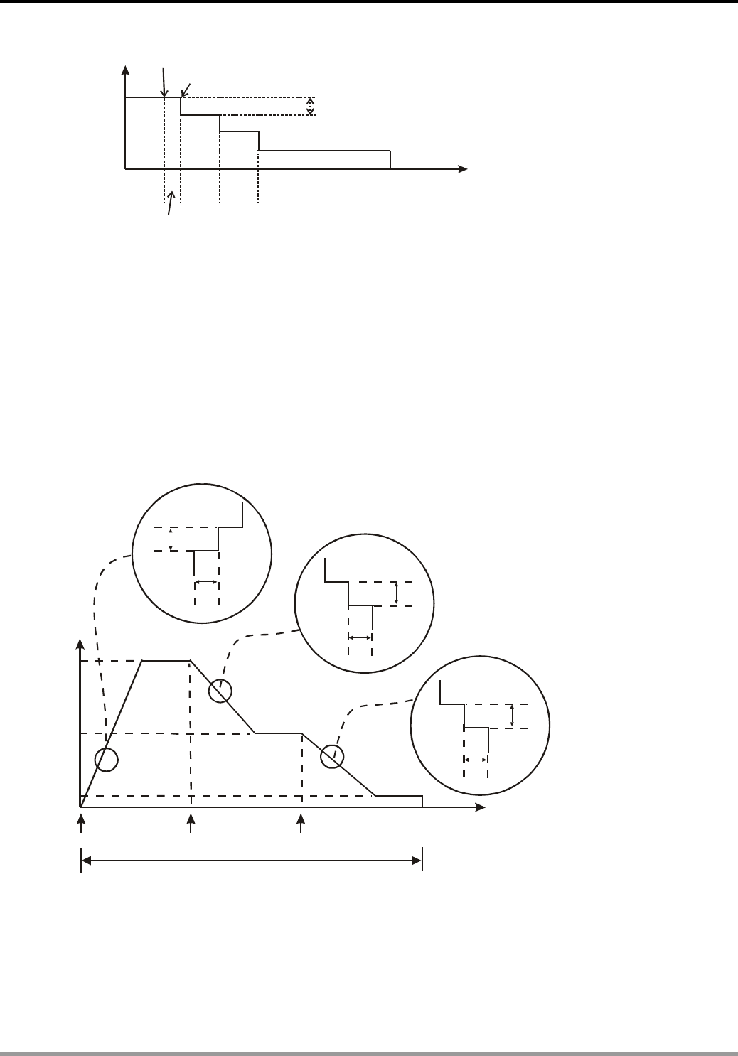
9 Application Instructions API 150-199
DVP-PLC Application Manual
9-132
The timing diagram is as below:
Freq.
Time
Gap freq.
approx.10us
Gap
time
Gap
time
Interrupt
A
ctual timing of changing
Program Example:
1. When M0 = ON, pulse output ramps up to 100kHz. Total shifts: 100, Gap frequency: 1000Hz, Gap time: 10ms.
Calculation of total shifts: (100,000 ﹣0) ÷ 1000 = 100.
2. When X6 external interrupt executes, target frequency is changed and ramp down to 50kHz immediately. Total
shifts: 150, Gap frequency: 800Hz, Gap time: 20ms. Calculation of total shifts: (100,000 ﹣50,000) ÷ 800 = 125
3. When X7 external interrupt executes, target frequency is changed and ramp down to 100Hz immediately. Total
shifts: 25, Gap frequency: 2000Hz, Gap time: 100ms. Calculation of total shifts: (50,000 ﹣100) ÷ 2000 = 25.
4. When pulse output reaches 100Hz, the frequency is kept constant and pulse output stops when 1,000,000 pulses
is completed.
Freq.(Hz)
Time(ms)
1000Hz
10ms
20ms
800Hz
100ms
2000Hz
M0=ON X6=ON X7=ON
100KHz
50KHz
100Hz
1,000,000pulse
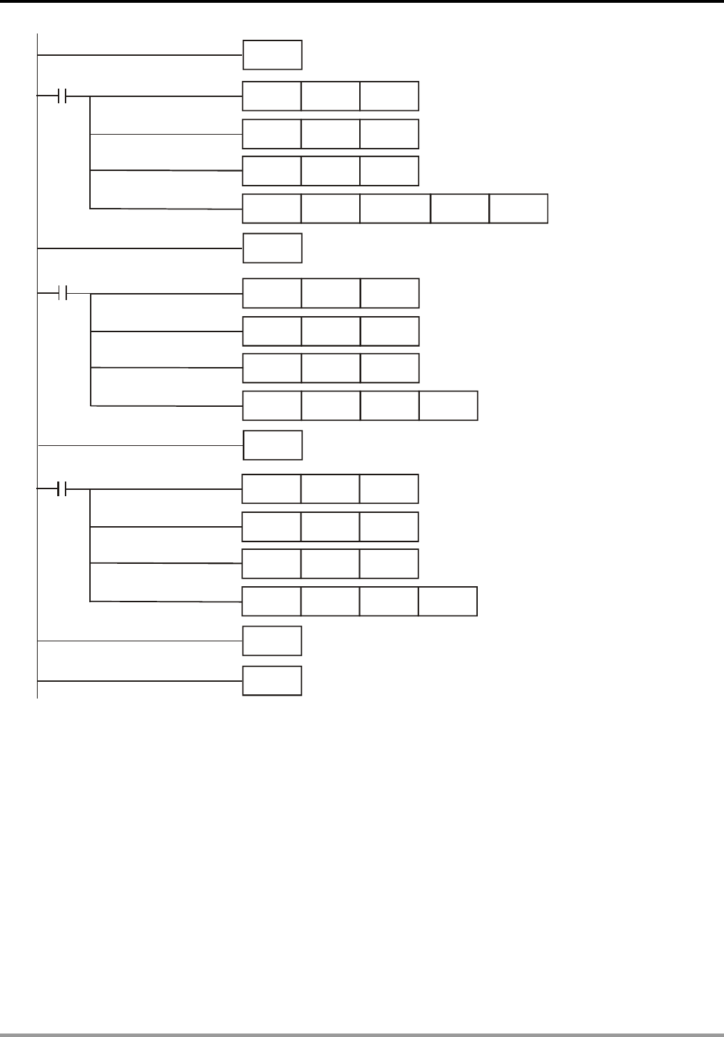
9 Application Instructions API 150-199
DVP-PLC Application Manual
9-133
MOV
M0
EI
MOVMOV
FEND
DMOVP K100000 D500
K1000 D502
K10 D503
DVSPO K1000000 Y0
D502
D500
MOV
M1000
MOVMOV
IRET
DMOV K50000 D500
K800 D502
K20 D503
DICF Y0
D502
D500
I601
MOV
M1000
MOVMOV
IRET
DMOV K0 D500
K2000 D502
K100 D503
DICF Y0
D502
D500
I701
END

9 Application Instructions API 150-199
DVP-PLC Application Manual
9-134
MEMO
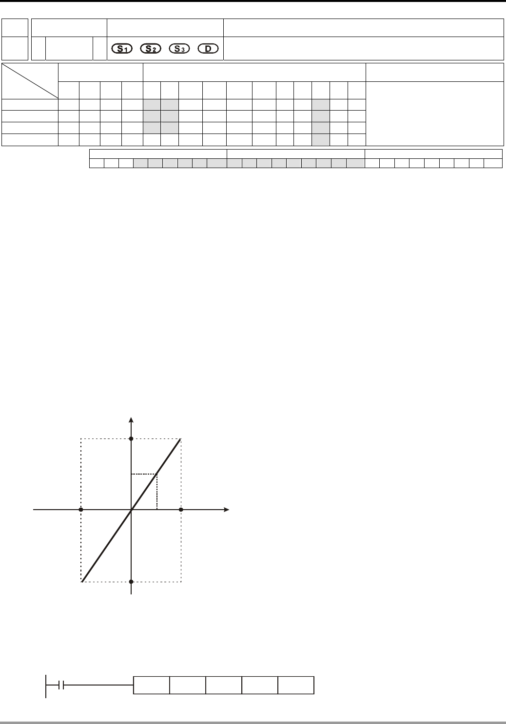
10 Application Instructions API 200-249
DVP-PLC Application Manual
10-1
API Mnemonic Operands Function
202
SCAL P Proportional Value Calculation
Bit Devices Word Devices Program Steps Type
OP X Y M S K H KnX KnY KnM KnS T C D E F
S1 * * *
S2 * * *
S3 * * *
D *
SCAL, SCALP: 9 steps
PULSE 16-bit 32-bit
ES EX SS SA SX SC EH SV EH3 ES EX SS SA SX SC EH SV EH3 ES EX SS SA SX SC EH SV EH3
Operands:
S1: Source value S2: Slope S3: Offset D: Destination device
Explanations:
1. Range of S1, S2, S3: -32,768 ~ 32,767
2. Unit of S2: 0.001
3. See the specifications of each model for their range of use.
4. Operation equation in the instruction: D = (S1 × S2) ÷ 1,000 + S3.
Users have to obtain S2 and S3 (decimals are rounded up into 16-bit integers) by using the slope and offset
equations below.
Slope equation: S2 = [(max. destination value – min. destination value) ÷ (max. source value – min. source value)]
× 1,000
Offset equation: S3 = min. destination value – min. source value × S2 ÷ 1,000
The output curve is shown as the figure:
D
1
Min. destination value
Max. Destination value
Destination value
Source value
Max.
source value
Min.
source value
S
Program Example 1:
1. Assume S1 = 500, S2 = 168, S3 = -4. When X0 = On, SCAL instruction will be executed and obtain the proportional
value at D0.
2. Equation: D0 = (500 × 168) ÷ 1,000 + (-4) = 80
X0
SCAL K500 K168 K-4 D0
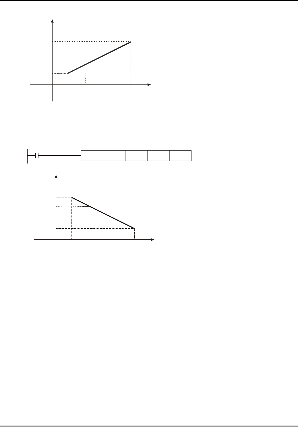
10 Application Instructions API 200-249
DVP-PLC Application Manual
10-2
D
1
0=500
Slope=168
Destination value
Source value
Offset=-4
S
Program Example 2:
1. Assume S1 = 500, S2 = -168, S3 = 534. When X10 = On, SCAL instruction will be executed and obtain the
proportional value at D10.
2. Equation: D0 = (500 × -168) ÷ 1,000 + 534 = 450
X10
SCAL K500 K-168 K534 D10
Offset=534
D
S=500
1
0
Slope=-168
Destination value
Source value
Remarks:
1. This instruction is applicable for known slope and offset. If slope and offset are unknown, use SCLP instruction for
the calculation.
2. S2 has to be within the range -32,768 ~ 32,767. If S2 falls without the range, use SCLP instruction for the
calculation.
3. When using the slope equation, please be aware that the max. source value must > min. source value, but it is
not necessary that max. destination value > min. destination value.
4. If the value of D > 32,767, D = 32,767; if the value of D < -32,768, D = -32,768.
5. Only ES_V6.2, SA/SX_V1.6, SC_V1.4, EH2/SV/EH3_V1.0 and versions above support this instruction. EH series
MPU does not support this instruction.
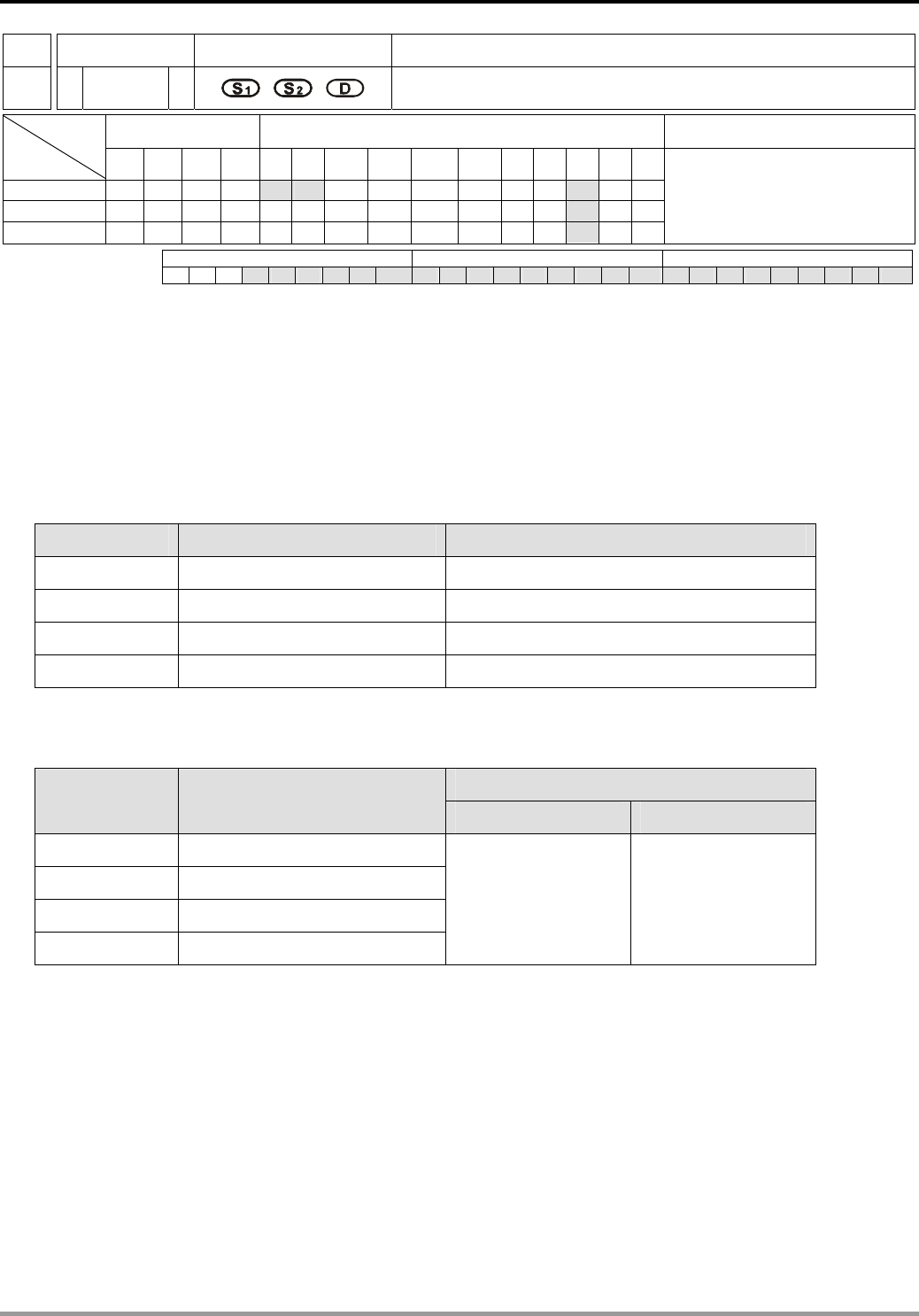
10 Application Instructions API 200-249
DVP-PLC Application Manual
10-3
Mnemonic Operands Function
203
D SCLP P Parameter Proportional Value Calculation
Bit Devices Word Devices Program Steps Type
OP X Y M S K H KnX KnY KnM KnS T C D E F
S1 * * *
S2 *
D *
SCLP, SCLPP: 7 steps
DSCLP, DSCLPP: 13 steps
PULSE 16-bit 32-bit
ES EX SS SA SX SC EH SV EH3 ES EX SS SA SX SC EH SV EH3 ES EX SS SA SX SC EH SV EH3
Operands:
S1: Source value S2: Parameter D: Destination device
Explanations:
1. See the specifications of each model for the range of operands.
2. Flags: M1162 (decimal integer or binary floating point); M1162 = On -> Binary floating point
3. Settings of S2 for 16-bit instruction:
S2 occupies 4 consecutive devices in 16-bit instruction.
Device No. Parameter Range
S2 Maximum source value -32,768 ~ 32,767
S2 + 1 Minimum source value -32,768 ~ 32,767
S2 + 2 Maximum destination value -32,768 ~ 32,767
S2 + 3 Minimum destination value -32,768 ~ 32,767
4. Settings of S2 for 32-bit instruction:
S2 occupies 8 consecutive devices in 32-bit instruction.
Range
Device No. Parameter Integer Floating point
S2, S2 + 1 Maximum source value
S2 + 2, 3 Minimum source value
S2 + 4, 5 Maximum destination value
S2 + 6, 7 Minimum destination value
-2,147,483,648 ~
2,147,483,647
Range of 32-bit
floating point
5. Operation equation in the instruction: D = [(S1 – min. source value) × (max. destination value – min. destination
value)] ÷ (max. source value – min. source value) + min. destination value
6. The operational relation between source value and destination value is as stated below:
y = kx + b
y= Destination value (D)
k= Slope = (max. destination value – min. destination value) ÷ (max. source value – min. source value)
x= Source value (S1)
b= Offset = Min. destination value – Min. source value × slope
Bring all the parameters into equation y = kx + b and obtain the equation in the instruction:
y = kx + b = D = k S1 + b = slope ×S1 + offset = slope ×S1 + min. destination value – min. source value × slope
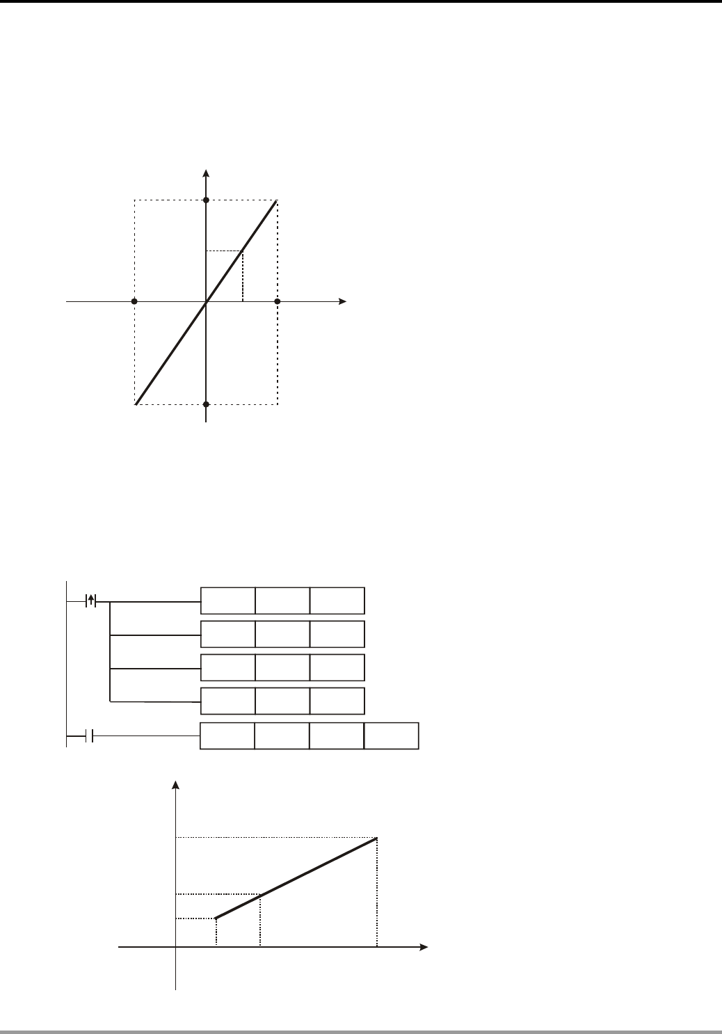
10 Application Instructions API 200-249
DVP-PLC Application Manual
10-4
= slope × (S1 – min. source value) + min. destination value = (S1 – min. source value) × (max. destination
value – min. destination value) ÷ (max. source value – min. source value) + min. destination value
7. If S1 > max. source value, S1 = max. source value
If S1 < min. source value, S1 = min. source value
When all the input values and parameters are set, the output curve is shown as the figure:
D
1
Min. destination value
Max. Destination value
Destination valu
e
Source value
Max.
source value
Min.
source value
S
Program Example 1:
1. Assume S1 = 500, max. source value D0 = 3,000, min. source value D1 = 200, max. destination value D2 = 500,
and min. destination value D3 = 30. When X0 = On, SCLP instruction will be executed and obtain the proportional
value at D10.
2. Equation: D10 = [(500 – 200) × (500 – 30)] ÷ (3,000 – 200) + 30 = 80.35. Round off the result into an integer D10
= 80.
X0
SCLP K500 D0 D10
X0
MOV
MOV
MOV
MOV
K3000
K200
K500
K30
D0
D1
D2
D3
D
S
1
0
=500
Source value
Destination value
Min.
Source
value
Max.
Source
value
=200 =3000
Min.
Destination
value
=30
Max.
Destination
value =500
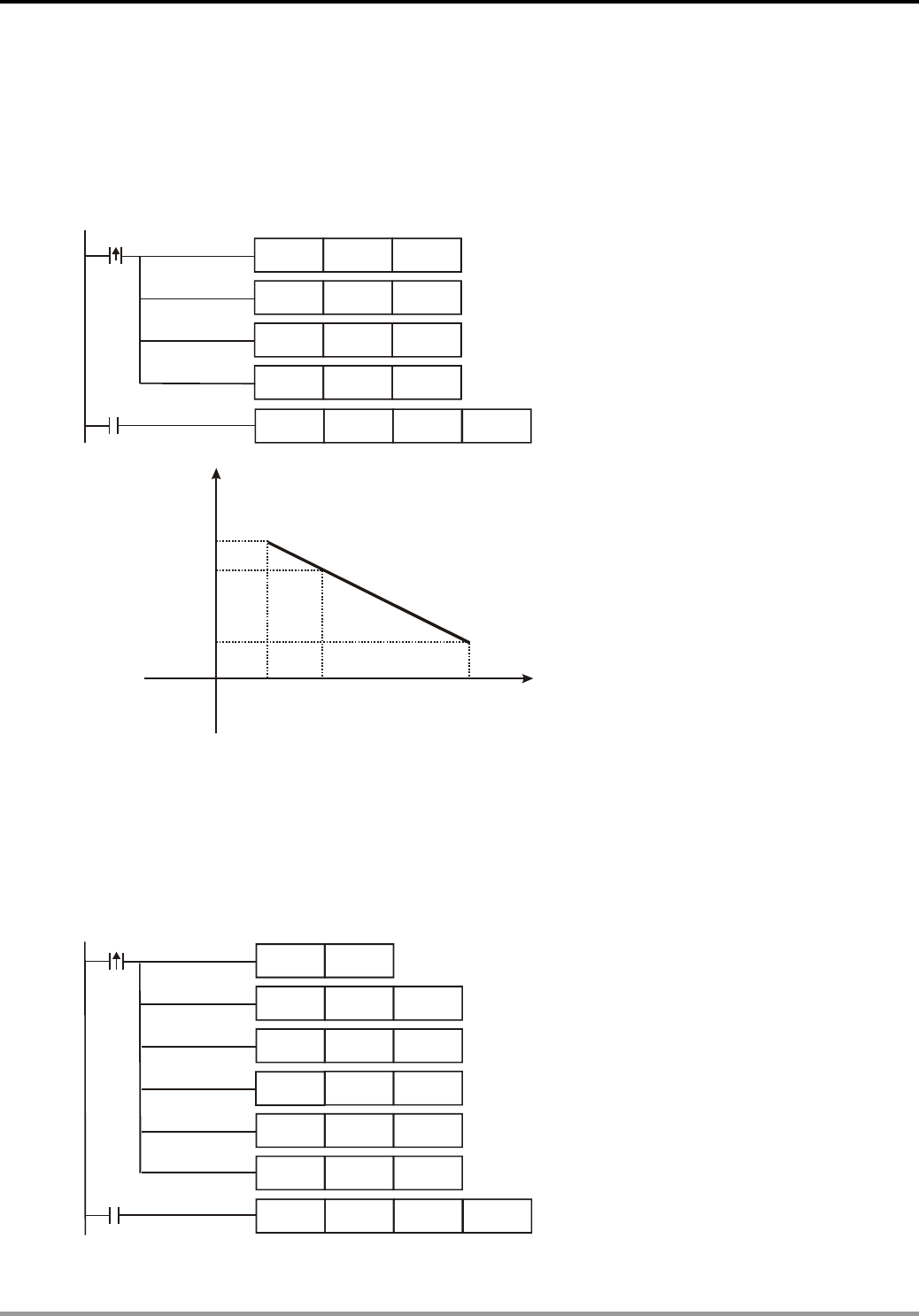
10 Application Instructions API 200-249
DVP-PLC Application Manual
10-5
Program Example 2:
1. Assume S1 = 500, max. source value D0 = 3,000, min. source value D1 = 200, max. destination value D2 = 30,
and min. destination value D3 = 500. When X0 = On, SCLP instruction will be executed and obtain the
proportional value at D10.
2. Equation: D10 = [(500 – 200) × (30 – 500)] ÷ (3,000 – 200) + 500 = 449.64. Round off the result into an integer
D10 = 450.
X0
SCLP K500 D0 D10
X0
MOV
MOV
MOV
MOV
K3000
K200
K30
K500
D0
D1
D2
D3
S
1=
500
D
0
Destination value
Source value
Max.
Destination
value =500
Min.
Destination
value
=30
Min.
Source
value
=200
Max.
Source
value
=3000
Program Example 3:
1. Assume the source of S1 D100 = F500, max. source value D0 = F3000, min. source value D2 = F200, max.
destination value D4 = F500, and min. destination value D6 = F30. When X0 = On, set up M1162, adopt floating
point operation and execute DSCLP instruction. The proportional value will be obtained at D10.
2. Equation: D10 = [(F500 – F200) × (F500 – F30)] ÷ (F3000 – F200) + F30 = F80.35. Round off the result into an
integer D10 = F80.
X0
DSCLP D100 D0 D10
X0
DMOVR
DMOVR
F3000
F200
F500
F500
F30
D0
D2
D4
D6
DMOVR
DMOVR
DMOVR
D100
SET M1162

10 Application Instructions API 200-249
DVP-PLC Application Manual
10-6
D
S
1
0
=F500
Destination value
Source value
Max.
Source
value
=F3000
Min.
Source
value
=F200
Min.
Destination
value
=F30
Max.
Destination
value =F500
Remarks:
1. Range of S1 for 16-bit instruction: max. source value ≥ S1 ≥ min. source value; -32,768 ~ 32,767. If the value falls
without the bounds, the bound value will be used for calculation.
2. Range of integer S1 for 32-bit instruction: max. source value ≥ S1 ≥ min. source value; -2,147,483,648 ~
2,147,483,647. If the value falls without the bounds, the bound value will be used for calculation.
3. Range of floating point S1 for 32-bit instruction: max. source value ≥ S1 ≥ min. source value; following the range of
32-bit floating point. If the value falls without the bounds, the bound value will be used for calculation.
4. Please be aware that the max. source value must > min. source value, but it is not necessary that max.
destination value > min. destination value.
5. Only ES_V6.2, SA/SX_V1.6, SC_V1.4, EH2/SV/EH3_V1.0 and versions above support this instruction. EH series
MPU does not support this instruction.
10 Application Instructions API 200-249
DVP-PLC Application Manual
10-7
API Mnemonic Operands Function
205
CMPT P Compare table
Bit Devices Word devices Program Steps Type
OP X Y M S K H KnX KnY KnM KnS T C D E F
S1 * * *
S2 * * *
n * * *
D * * * * * *
CMPT: 9 steps
DCMPT: 17 steps
DCMPTP: 17 steps
PULSE 16-bit 32-bit
ES EX SS SA SX SC EH SV EH3ESEXSSSASXSCEH SV EH3 ES EX SS SA SX SC EH SV EH3
Operands:
S1: Source device 1 S2: Source device 2 n: Data length/function D: Destination device
Explanations:
1. EH2/SV_V1.9 and versions above, and EH3/SV2 support the 16-bit instruction. EH3_V1.20 and version above,
and SV2 support the 32-bit instruction.
2. S1 and S2 can be T/C/D devices, for C devices only 16-bit devices are applicable (C0~C199).
3. The high 16-bit value in the operand n used in the 32-bit instruction is an invalid value.
4. The low 8-bit value in the operand n indicates the data length. The operand n used in the 16-bit instruction
should be within the range between 1 and 16. The operand n used in the 32-bit instruction should be within the
range between 1 and 32. PLC will take the upper/lower bound value if set value exceeds the available range.
5. The high 8-bit value in the operand n indicates the comparison condition.
Value K0 K1 K2 K3 K4
Comparison condition S1 = S2 S1 < S2 S1 <= S2 S1 > S2 S1 >= S2
6. If n used in the 16-bit instruction is set to H0108, it means that 8 pieces of data are compared to 8 pieces of data,
and the “larger than” comparison is performed. If n used in the 32-bit instruction is set to H00000320, it means
that 32 pieces data are compared to 32 pieces of data, and the “less than” comparison is performed.
7. If the setting value for the comparison condition exceeds the range, or the firmware version does not support the
comparison condition, the default “equal to” comparison is performed. EH3_V1.20 and version above, and SV2
and versions above support the setting value for the comparison condition.
8. The comparison values used in the 16-bit instruction are signed values. The comparison values used in the
32-bit instruction are 32-bit values (M1162=Off), or floating-point values (M1162=On).
9. Data written in operand D will all be stored in 16-bit format or in 32-bit format. When data length is less than 16
or 32, the null bits are fixed as 0, e.g. if n = K8, bit 0~7 will be set according to compare results, and bit 8~15 will
all be 0.
10. If the comparison result meets the condition, the corresponding bit is set to 1. Otherwise, it is set to 0.
Program example:
When M0 = ON, compare the 16-bit value in D0~D7 with D20~D27 and store the results in D100.
M0
CMPT D0 K8 D100
D20

10 Application Instructions API 200-249
DVP-PLC Application Manual
10-8
y Content in D0~D7:
No. D0 D1 D2 D3 D4 D5 D6 D7
Value K10 K20 K30 K40 K50 K60 K70 K80
y Content in D20~D27:
No. D20 D21 D22 D23 D24 D25 D26 D27
Value K12 K20 K33 K44 K50 K66 K70 K88
y After the comparison of CMPT instruction, the associated bit will be 1 if two devices have the same value, and
other bits will all be 0. Therefore the results in D100 will be as below:
Bit0 Bit1 Bit2 Bit3 Bit4 Bit5 Bit6 Bit7 Bit8~15
0 1 0 0 1 0 1 0 0…0
D100
H0052 (K82)
10 Application Instructions API 200-249
DVP-PLC Application Manual
10-9
API Mnemonic Operands Function
206
ASDRW ASDA servo drive R/W
Bit Devices Word devices Program Steps Type
OP X Y M S K H KnX KnY KnM KnS T C D E F
S1 * * *
S2 * * *
S *
ASDRW: 7 steps
PULSE 16-bit 32-bit
ES EX SS SA SX SC EH SV EH3 ES EX SS SA SX SC EH SV EH3 ES EX SS SA SX SC EH SV EH3
Operands:
S1: Address of servo drive (K0~K254) S2: Function code S: Register for read/written data
Explanations:
1. ASDRW communication instruction supports COM2 (RS-485) and COM3 (RS-485)
2. S1: station number of servo drive. Range: K0~K254. K0 indicates broadcasting, i.e. PLC will not receive
feedback data.
3. S2: function code. Please refer to the table below.
4. S: Register for read/written data. Please refer to the table below for explanations.
5. Explanations of function code:
Exclusively for ASDA of A-type, AB type, A+ type, B type
Code Function Parameter Com. Addr. Read/Write data (Settings)
K0(H0) Status monitor P0-04 ~ P0-08 0004H ~ 0008H S+0 ~ S+4: Please refer to
explanations in ASDA
manuals.
K1(H1) Block Data Read
Register
P0-09 ~ P0-16 0009H ~ 0010H S+0 ~ S+7: Please refer to
explanations in ASDA
manuals. B Type is not
supported.
K2(H2) Block Data Write
Register
P0-09 ~ P0-16 0009H ~ 0010H S+0 ~ S+7: Please refer to
explanations in ASDA
manuals. B Type is not
supported.
K3(H3) JOG Operation P4-05 0405H S: Range: 1~3000, 4999, 4998,
5000
K4(H4) Servo ON/OFF P2-30 021EH S: K1 = ON, Others = OFF
K5(H5) Speed Command
(3 sets)
P1-09 ~ P1-11 0109H ~ 010BH S+0 ~ S+2: Range:
-5000~+5000
K6(H6) Torque Command
(3 sets)
P1-12 ~ P1-14 010CH ~ 010EH S+0 ~ S+2: Range:
-300~+300

10 Application Instructions API 200-249
DVP-PLC Application Manual
10-10
For A2-type only
Code Function Parameter Com. Addr. Read/Write data (Settings)
K16(H10) Status monitor
(Read)
P0-09 ~ P0-13 0012H ~ 001BH S+0 ~ S+9: Please refer to
explanations in ASDA-A2
manual.
K17(H11) Status monitor
selection (Write)
P0-17 ~ P0-21 0022H ~ 002BH S+0 ~ S+9: Please refer to
explanations in ASDA-A2
manual.
K18(H12) Mapping
parameter (Write)
P0-25 ~ P0-32 0032H ~ 0041H S+0 ~ S+15: Please refer to
explanations in ASDA-A2
manual.
K19(H13) JOG Operation P4-05 040AH S: Range:
1~5000, 4999, 4998, 0
K20(H14) Auxiliary Function
(Servo ON/OFF)
P2-30 023CH S: K1 = ON, Others = OFF
K21(H15) Speed Command
(3 sets)
P1-09 ~ P1-11 0112H ~ 0117H S+0 ~ S+5: Range:
-60000~+60000
K22(H16) Torque Command
(3 sets)
P1-12 ~ P1-14 0118H ~ 011DH S+0 ~ S+5: Range: -300~+300
K23(H17) Block Data Read /
Write Register
(for mapping
parameter )
P0-35 ~ P0-42 0046H~ 0055H S+0 ~ S+15: Please refer to
explanations in ASDA-A2
manual.
6. For relative M flags and special D registers, please refer to explanations of API 80 RS instruction.
Program example 1: COM2 (RS-485)
1. When X0 = ON, PLC will send out communication commands by COM2 to read status of servo drive.
2. When PLC received the feedback data from ASDA, M1127 will be active and the read data will be stored in
D0~D4.
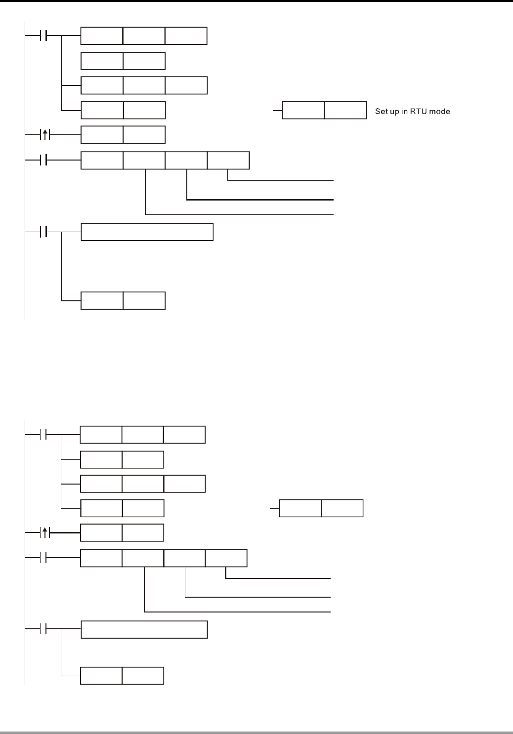
10 Application Instructions API 200-249
DVP-PLC Application Manual
10-11
H87MOV
M1002
D1120
SET M1120
K100
MOV D1129
RST M1127
ASDRW K0K1
X0
D0
A
SDA address: K1
Function Code: K0
Monitor ASDA status
Data Register
M1127
SET
X0
M1122
Set up in
ASCII mode
RST M1143 SET M1143
Reset communication completed flag M1127
Set communication protocol as 9600,8,E,1
Set time-out value as 100ms
ASCII mode: Store the received data into specified registers D0~D4 in Hex
RTU mode
:
Store the received data into specified registers D0~D4 in Hex
Sending request
Processing received data
Retain communication setting
Program example 2: COM3(RS-485)
1. When M0 = ON, PLC sends communication commands by COM3 to read servo drive status.
2. When PLC received the feedback data from ASDA, M1318 will be active and the read data will be stored in
D0~D4.
H87MOV
M1002
D1109
SET M1136
K100
MOV D1252
RST M1318
ASDRW K0
K1
M0
D0
A
SDA address: K1
Function Code: K0
Monitor ASDA status
Data Register
M1318
SET
M0
M1316
Set up in
ASCII mode
RST M1320 SET M1320
Reset communication completed flag M1318
Set communication protocol as 9600,8,E,1
Retain communication setting
Set reveiving time-out as 100ms
ASCII mode: Store the received data into specified registers D0~D4 in Hex
RTU mode
:
Store the received data into specified registers D0~D4 in Hex
Sending request
Processing received data
Set up in RTU mode
Points to note:

10 Application Instructions API 200-249
DVP-PLC Application Manual
10-12
Relative flags and special D registers of COM2/COM3 :
COM2 COM3 Function Description
M1120 M1136
Retain communication setting
M1143 M1320 ASCII/RTU mode selection
D1120 D1109 Communication protocol
Protocol
setting
D1121 D1255 PLC communication address
M1122 M1316 Sending request
Sending
request D1129 D1252 Communication timeout setting (ms)
Receiving
completed M1127 M1318 Data receiving completed
- M1319 Data receiving error
- D1253 Communication error code
M1129 - Communication timeout setting (ms)
M1140 -
COM2 (RS-485) MODRD/MODWR/MODRW data
receiving error
M1141 -
MODRD/MODWR/MODRW parameter error (Exception
Code exists in received data) Exception Code is stored
in D1130
Errors
D1130 -
COM2 (RS-485) Error code (exception code) returning
from Modbus communication

10 Application Instructions API 200-249
DVP-PLC Application Manual
10-13
API Mnemonic Operands Function
207
CSFO Catch speed and proportional output
Bit Devices Word devices Program Steps Type
OP X Y M S K H KnX KnY KnM KnS T C D E F
S *
S1 *
D *
CSFO: 7 steps
PULSE 16-bit 32-bit
ES EX SS SA SX SC EH SV EH3 ES EX SS SA SX SC EH SV EH3 ES EX SS SA SX SC EH SV EH3
Operands:
S: Source device of signal input (Only X0~X3 are available)
S1: Sample time setting and the input speed information
D: Output proportion setting and output speed information
Explanations:
1. When S specifies X0, PLC only uses X0 input point and its associated high speed pulse output: Y0, in this case
Y1 is normal output point. When S specifies X1, PLC uses X0 (A phase) and X1 (B phase) input points and their
associated output: Y0 (Pulse) / Y1 (Dir).
2. The execution of CSFO requires hardware high speed counter function as well as the high speed output
function. Therefore, when program scan proceeds to CSFO instruction with high speed counter input points (X0,
X1) enabled by DCNT instruction, or high speed pulse outputs (Y0, Y1) enabled by other high speed output
instructions, CSFO instruction will not be activated.
3. If S specifies X1 with 2-phase 2 inputs, the counting mode is fixed as quadruple frequency.
4. During pulse output process of Y0, special registers (D1337, D1336) storing the current number of output pulses
will be updated when program scan proceeds to this instruction.
5. S1 occupies consecutive 4 16-bit registers. S1 +0 specifies the sampling times, i.e. when S1 +0 specifies K1,
PLC catches the speed every time when 1 pulse is outputted. Valid range for S1 +0 in 1-phase 1-input mode:
K1~K100, and 2-phase 2-input mode: K2~K100. If the specified value exceeds the valid range, PLC will take the
lower/upper bound value as the set value. Sample time can be changed during PLC operation, however the
modified value will take effect until program scan proceeds to this instruction. S1+1 indicates the latest speed
sampled by PLC (Read-only). Unit: 1Hz. Valid range: ±10kHz. S1+2 and S1+3 indicate the accumulated number
of pulses in 32-bit data (Read-only).
6. For single phase input, the max frequency is 10kHz; for 2-phase 2 inputs, the max frequency is 2kHz.
7. D occupies 3 consecutive 16-bit registers. D +0 specifies the output proportion value. Valid range: K1 (1%) ~
K10000 (10000%). If the specified value exceeds the valid range, PLC will take the lower/upper bound value as
the set value. Output proportion can be changed during PLC operation, however the modified value will take
effect until program scan proceeds to this instruction. D+2 and D+1 indicates the output speed in 32-bit data.
Unit: 1Hz. Valid range: ±100kHz.
8. The speed sampled by PLC will be multiplied with the output proportion D+0, then PLC will generate the actual
output speed. PLC will take the integer of the calculated value, i.e. if the calculated result is smaller than 1Hz,
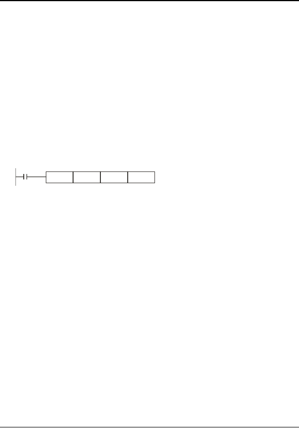
10 Application Instructions API 200-249
DVP-PLC Application Manual
10-14
PLC will output with 0Hz. For example, input speed: 10Hz, output proportion: K5 (5%), then the calculation
result will be 10 x 0.05 = 0.5Hz. Pulse output will be 0Hz; if output proportion is modified as K15 (15%), then the
calculation result will be 10 x 0.15 = 1.5Hz. Pulse output will be 1Hz.
Program Example:
1. If D0 is set as K2, D10 is set as K100:
When the sampled speed on (X0, X1) is +10Hz (D1 = K10), (Y0, Y1) will output pulses with +10Hz (D12, D11 =
K10); When the sampled speed is -10Hz (D1 = K-10), (Y0, Y1) will output pulses with -10Hz (D12, D11 = K-10)
2. If D0 is set as K2, D10 is set as K1000:
When the sampled speed on (X0, X1) is +10Hz (D1 = K10), (Y0, Y1) will output pulses with +100Hz (D12, D11 =
K100); When the sampled speed is -100Hz (D1 = K-100), (Y0, Y1) will output pulses with -100Hz (D12, D11 =
K-100)
3. If D0 is set as K10, D10 is set as K10:
When the sampled speed on (X0, X1) is +10Hz (D1 = K10), (Y0, Y1) will output pulses with +1Hz (D12, D11 =
K1); When the sampled speed is -10Hz (D1 = K-10), (Y0, Y1) will output pulses with -1Hz (D12, D11 = K-1)
M0
CSFO X1 D10D0
10 Application Instructions API 200-249
DVP-PLC Application Manual
10-15
API Mnemonic Operands Function
215~
217
D LD# Contact Logical Operation LD#
Bit Devices Word Devices Program Steps Type
OP X Y M S K H KnX KnY KnM KnS T C D E F
S1 * * * * * * * * ***
S2 * * * * * * * * ***
LD#: 5 steps
DLD#: 9 steps
PULSE 16-bit 32-bit
ES EX SS SA SX SC EH SV EH3 ES EX SS SA SX SC EH SV EH3 ES EX SS SA SX SC EH SV EH3
Operands:
S1: Data source device 1 S2: Data source device 2
Explanations:
1. See the specifications of each model for the range of operands.
2. This instruction compares the content in S1 and S2. If the result is not “0”, the continuity of the instruction is
enabled. If the result is “0”, the continuity of the instruction is disabled.
3. LD# instruction is used for direct connection with BUS.
API No. 16 -bit
instruction
32 -bit
instruction
Continuity
condition
No-continuity
condition
215 LD& DLD& S1 & S2 ≠ 0 S1 & S2 = 0
216 LD| DLD| S1 | S2 ≠ 0 S1 | S2 = 0
217 LD^ DLD^ S1 ^ S2 ≠ 0 S1 ^ S2 = 0
4. &: Logical “AND” operation
5. |: Logical “OR” operation
6. ^: Logical “XOR” operation
7. When 32-bit counters (C200 ~ C255) are used in this instruction for comparison, make sure to adopt 32-bit
instruction (DLD#). If 16-bit instructions (LD#) is adopted, a “program error” will occur and the ERROR
indicator on the MPU panel will flash.
Program Example:
1. When the result of logical AND operation of C0 and C10 ≠ 0, Y10 = On.
2. When the result of logical OR operation of D200 and D300 ≠ 0 and X1 = On, Y11 = On will be retained.
3. When the result of logical XOR operation of C201 and C200 ≠ 0 or M3 = On, M50 = On.
M3
DLD C201 C200 M50
LD C0 C10
LD D200 D300 SET
X1
&
^
IY011
Y10
10 Application Instructions API 200-249
DVP-PLC Application Manual
10-16
API Mnemonic Operands Function
218~
220
D AND# Contact Logical Operation AND#
Bit Devices Word Devices Program Steps Type
OP X Y M S K H KnX KnY KnM KnS T C D E F
S1 * * * * * * * * ***
S2 * * * * * * * * ***
AND#: 5 steps
DAND#: 9 steps
PULSE 16-bit 32-bit
ES EX SS SA SX SC EH SV EH3 ES EX SS SA SX SC EH SV EH3 ES EX SS SA SX SC EH SV EH3
Operands:
S1: Data source device 1 S2: Data source device 2
Explanations:
1. See the specifications of each model for the range of operands.
2. This instruction compares the content in S1 and S2. If the result is not “0”, the continuity of the instruction is
enabled. If the result is “0”, the continuity of the instruction is disabled.
3. AND# is an operation instruction used on series contacts.
API No. 16 -bit
instruction
32 -bit
instruction
Continuity
condition
No-continuity
condition
218 AND& DAND&
S1 & S2 ≠ 0 S1 & S2 = 0
219 AND| DAND| S1 | S2 ≠ 0 S1 | S2 = 0
220 AND^ DAND^
S1 ^ S2 ≠ 0 S1 ^ S2 = 0
4. &: Logical “AND” operation
5. |: Logical “OR” operation
6. ^: Logical “XOR” operation
7. When 32-bit counters (C200 ~ C255) are used in this instruction for comparison, make sure to adopt 32-bit
instruction (DAND#). If 16-bit instructions (AND#) is adopted, a “program error” will occur and the ERROR
indicator on the MPU panel will flash.
Program Example:
1. When X0 = On and the result of logical AND operation of C0 and C10 ≠ 0, Y10 = On.
2. When X1 = Off and the result of logical OR operation of D10 and D0 ≠ 0 and X1 = On, Y11 = On will be retained.
3. When X2 = On and the result of logical XOR operation of 32-bit register D200 (D201) and 32-bit register D100
(D101) ≠ 0 or M3 = On, M50 = On.
M3
DAND D200 D100 M50
AND C0 C10
AND D10 D0 SET
&
^
IY11
Y10
X0
X1
X2
10 Application Instructions API 200-249
DVP-PLC Application Manual
10-17
API Mnemonic Operands Function
221~
223
D OR# Contact Logical operation OR#
Bit Devices Word Devices Program Steps Type
OP X Y M S K H KnX KnY KnM KnS T C D E F
S1 * * * * * * * * ***
S2 * * * * * * * * ***
OR#: 5 steps
DOR#: 9 steps
PULSE 16-bit 32-bit
ES EX SS SA SX SC EH SV EH3 ES EX SS SA SX SC EH SV EH3 ES EX SS SA SX SC EH SV EH3
Operands:
S1: Data source device 1 S2: Data source device 2
Explanations:
1. See the specifications of each model for the range of operands.
2. This instruction compares the content in S1 and S2. If the result is not “0”, the continuity of the instruction is
enabled. If the result is “0”, the continuity of the instruction is disabled.
3. OR# is an operation instruction used on parallel contacts.
API No. 16 -bit
instruction
32 -bit
instruction
Continuity
condition
No-continuity
condition
221 OR& DOR& S1 & S2 ≠ 0 S1 & S2 = 0
222 OR| DOR| S1 | S2 ≠ 0 S1 | S2 = 0
223 OR^ DOR^ S1 ^ S2 ≠ 0 S1 ^ S2 = 0
4. &: Logical “AND” operation
5. |: Logical “OR” operation
6. ^: Logical “XOR” operation
7. When 32-bit counters (C200 ~ C255) are used in this instruction for comparison, make sure to adopt 32-bit
instruction (DOR#). If 16-bit instructions (OR#) is adopted, a “program error” will occur and the ERROR
indicator on the MPU panel will flash.
Program Example:
1. When X1 = On and the result of logical AND operation of C0 and C10 ≠ 0, Y10 = On.
2. M60 will be On when X2 = On and M30 = On, or the result of logical OR operation of 32-bit register D10 (D11)
and 32-bit register D20 (D21) ≠ 0, or the result of logical XOR operation of 32-bit register D200 (D201) and
32-bit counter C235 ≠ 0.
DOR D100 D200
OR C0 C10
DOR D10 D20
&
^
I
Y0
X2
X1
M30
M60
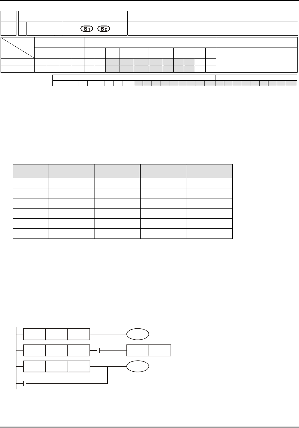
10 Application Instructions API 200-249
DVP-PLC Application Manual
10-18
API Mnemonic Operands Function
224~
230
D LD※ LoaD Compare
Bit Devices Word Devices Program Steps
Type
OP X Y M S K H KnX KnY KnM KnS T C D E F
S1 * * * * * * * * ***
S2 * * * * * * * * ***
LD※: 5 steps
DLD※: 9 steps
PULSE 16-bit 32-bit
ES EX SS SA SX SC EH SV EH3 ES EX SS SA SX SC EH SV EH3 ES EX SS SA SX SC EH SV EH3
Operands:
S1: Data source device 1 S2: Data source device 2
Explanations:
1. See the specifications of each model for the range of operands.
2. This instruction compares the content in S1 and S2. Take API224 (LD=) for example, if the result is “=”, the
continuity of the instruction is enabled. If the result is “≠”, the continuity of the instruction is disabled.
3. LD※ instruction is used for direct connection with BUS.
API No. 16 -bit
instruction
32 -bit
instruction
Continuity
condition
No-continuity
condition
224 LD = DLD = S1 = S2 S1 ≠ S2
225 LD > DLD > S1 > S2 S1 ≤ S2
226 LD < DLD < S1 < S2 S1 ≥ S2
228 LD < > DLD < > S1 ≠ S2 S1 = S2
229 LD < = DLD < = S1 ≤ S2 S1 > S2
230 LD > = DLD > = S1 ≥ S2 S1 < S2
4. When 32-bit counters (C200 ~ C255) are used in this instruction for comparison, make sure to adopt 32-bit
instruction (DLD※). If 16-bit instructions (LD※) is adopted, a “program error” will occur and the ERROR
indicator on the MPU panel will flash.
Program Example:
1. When the content in C10 = K200, Y10 = On.
2. When the content in D200 > K-30 and X1 = On, Y11= On will be retained.
3. When the content in C200 < K678,493 or M3 = On, M50 = On.
LD= K200 C10
DLD> K678493 C200
M3
Y10
LD> D200 K-30
X1
SET Y11
M50
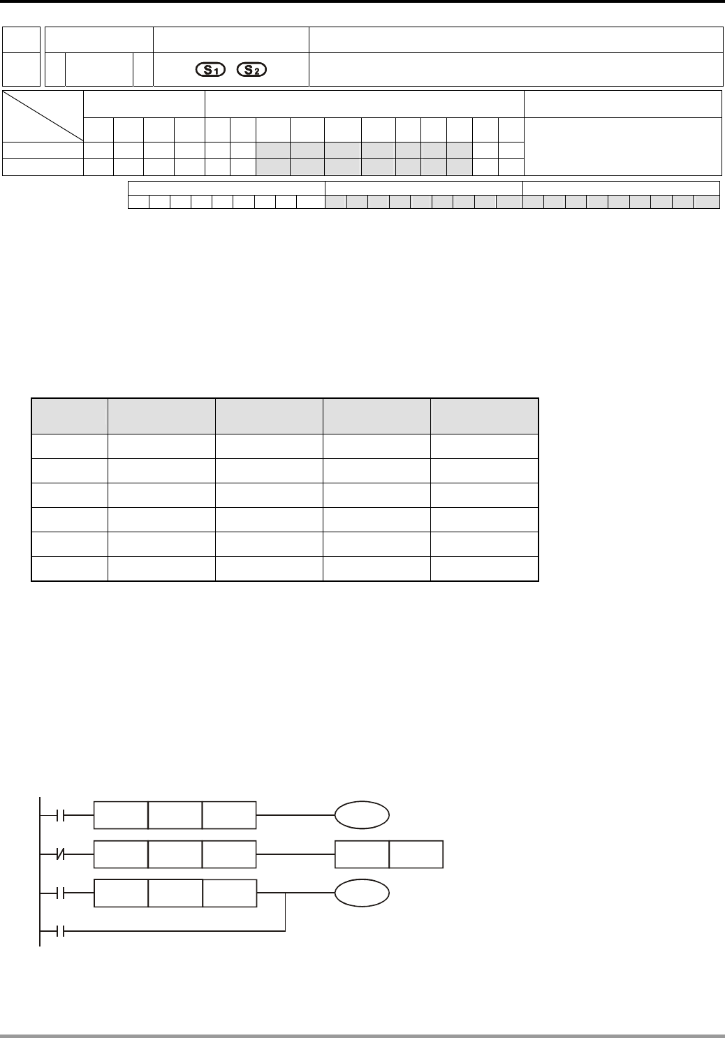
10 Application Instructions API 200-249
DVP-PLC Application Manual
10-19
API Mnemonic Operands Function
232~
238
D AND※ AND Compare
Bit Devices Word Devices Program Steps
Type
OP X Y M S K H KnX KnY KnM KnS T C D E F
S1 * * * * * * * * ***
S2 * * * * * * * * ***
AND※: 5 steps
DAND※: 9 steps
PULSE 16-bit 32-bit
ES EX SS SA SX SC EH SV EH3 ES EX SS SA SX SC EH SV EH3 ES EX SS SA SX SC EH SV EH3
Operands:
S1: Data source device 1 S2: Data source device 2
Explanations:
1. See the specifications of each model for the range of operands.
2. This instruction compares the content in S1 and S2. Take API232 (AND=) for example, if the result is “=”, the
continuity of the instruction is enabled. If the result is “≠”, the continuity of the instruction is disabled.
3. AND※ is a comparison instruction is used on series contacts.
API No. 16 –bit
instruction
32 –bit
instruction
Continuity
condition
No-continuity
condition
232 AND = DAND = S1 = S2 S1 ≠ S2
233 AND > DAND > S1 > S2 S1 ≤ S2
234 AND < DAND < S1 < S2 S1 ≥ S2
236 AND < > DAND < > S1 ≠ S2 S1 = S2
237 AND < = DAND < = S1 ≤ S2 S1 > S2
238 AND > = DAND > = S1 ≥ S2 S1 < S2
4. When 32-bit counters (C200 ~ C255) are used in this instruction for comparison, make sure to adopt 32-bit
instruction (DAND※). If 16-bit instructions (AND※) is adopted, a “program error” will occur and the ERROR
indicator on the MPU panel will flash.
Program Example:
1. When X0 = On and the content in C10 = K200, Y10 = On.
2. When X1 = Off and the content in D0 ≠ K-10, Y11= On will be retained.
3. When X2 = On and the content in 32-bit register D0 (D11) < 678,493 or M3 = On, M50 = On.
AND= K200 C10
DAND> K678493 D10
M3
Y10
AND<> K-10 D0 SET Y11
M50
X2
X1
X0
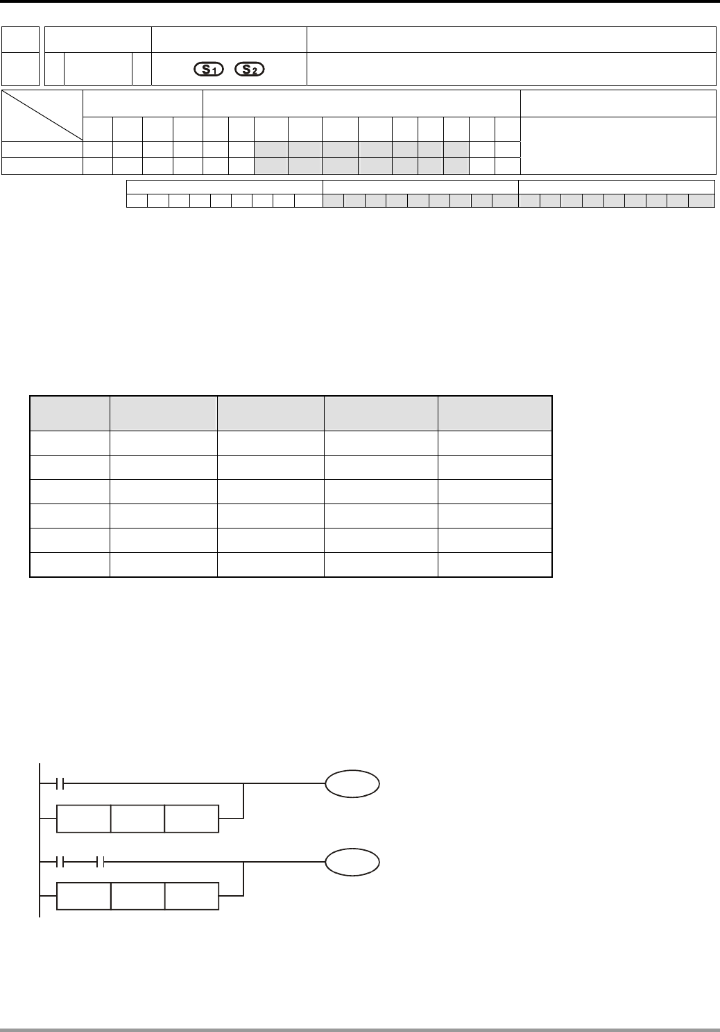
10 Application Instructions API 200-249
DVP-PLC Application Manual
10-20
API Mnemonic Operands Function
240~
246
D OR※ OR Compare
Bit Devices Word Devices Program Steps
Type
OP X Y M S K H KnX KnY KnM KnS T C D E F
S1 * * * * * * * * ***
S2 * * * * * * * * ***
OR*: 5 steps
DOR*: 9 steps
PULSE 16-bit 32-bit
ES EX SS SA SX SC EH SV EH3 ES EX SS SA SX SC EH SV EH3 ES EX SS SA SX SC EH SV EH3
Operands:
S1: Data source device 1 S2: Data source device 2
Explanations:
1. See the specifications of each model for the range of operands.
2. This instruction compares the content in S1 and S2. Take API240 (OR=) for example, if the result is “=”, the
continuity of the instruction is enabled. If the result is “≠”, the continuity of the instruction is disabled.
3. OR※ is an comparison instruction used on parallel contacts.
API No. 16 -bit
instruction
32 -bit
instruction
Continuity
condition
No-continuity
condition
240 OR = DOR = S1 = S2 S1 ≠ S2
241 OR > DOR > S1 > S2 S1 ≤ S2
242 OR < DOR < S1 < S2 S1 ≥ S2
244 OR < > DOR < > S1 ≠ S2 S1 = S2
245 OR < = DOR < = S1 ≤ S2 S1 > S2
246 OR > = DOR > = S1 ≥ S2 S1 < S2
4. When 32-bit counters (C200 ~ C255) are used in this instruction for comparison, make sure to adopt 32-bit
instruction (DOR※). If 16-bit instructions (OR※) is adopted, a “program error” will occur and the ERROR
indicator on the MPU panel will flash.
Program Example:
1. When X1 = On and the present value of C10 = K200, Y0 = On.
2. M60 will be On when X2 = On, M30 = On and the content in 32-bit register D100 (D101) ≥ K100,000.
OR= K200 C10
DOR> D100 K100000
Y0
X2
X1
M30
M60
=
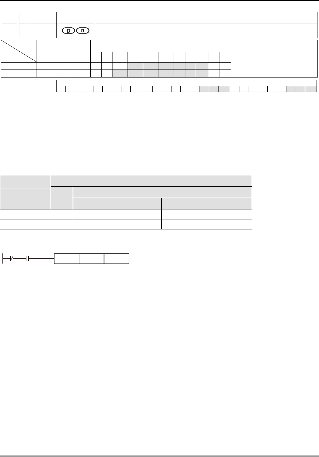
10 Application Instructions API 200-249
DVP-PLC Application Manual
10-21
API Mnemonic Operands Function
266
D BOUT Output Specified Bit of a Word
Bit Devices Word devices Program Steps
Type
OP X Y M S K H KnX KnY KnM KnS T C D E F
D * * * * * *
n * * * * * * * * ***
BOUT: 5 steps
DBOUT: 9 steps
PULSE 16-bit 32-bit
ES EX SS SA SX SC EH SV EH3 ES EX SS SA SX SC EH SV EH3 ES EX SS SA SX SC EH SV EH3
Operands:
D: Destination output device n: Device specifying the output bit
Explanations:
1. EH2/SV_V1.9 and versions above, and EH3/SV2 supports the function. EH series does not support the dunction.
2. Available range for the value in operand n: K0~K15 for 16-bit instruction; K0~K31 for 32-bit instruction.
3. BOUT instruction performs bit output on the output device according to the value specified by operand n.
Status of Coils and Associated Contacts:
BOUT instruction
Associated Contacts
Evaluation result Coil NO contact(normally open)NC contact(normally closed)
FALSE OFF Current blocked Current flows
TRUE ON Current flows Current blocked
Program Example:
X0 X1
BOUT K4Y0 D0
Instruction: Operation:
LDI X0 Load NC contact X0
AND X1 Connect NO contact
X1 in series.
BOUT K4Y0 D0 When D0 = k1,
executes output on Y1
When D0 = k2,
executes output on Y2
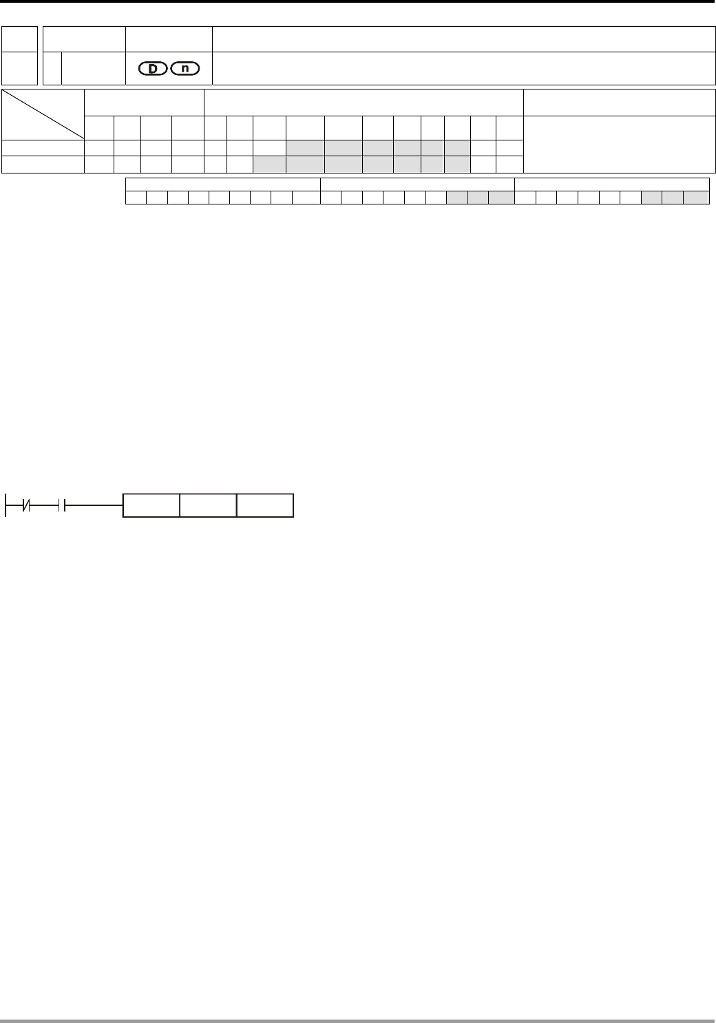
10 Application Instructions API 200-249
DVP-PLC Application Manual
10-22
API Mnemonic Operands Function
267
D BSET Set ON Specified Bit of a Word
Bit Devices Word devices Program Steps
Type
OP X Y M S K H KnX KnY KnM KnS T C D E F
D * * * * * *
n * * * * * * * * ***
BSET: 5 steps
DBSET: 9 steps
PULSE 16-bit 32-bit
ES EX SS SA SX SC EH SV EH3 ES EX SS SA SX SC EH SV EH3 ES EX SS SA SX SC EH SV EH3
Operands:
D: Destination device to be Set ON n: Device specifying the bit to be Set ON
Explanations:
1. EH2/SV_V1.9 and versions above, and EH3/SV2 supports the function. EH series does not support the
dunction.
2. Available range for the value in operand n: K0~K15 for 16-bit instruction; K0~K31 for 32-bit instruction.
3. When BSET instruction executes, the output device specified by operand n will be On and latched. To reset the
On state of the device, BRST instruction is required.
Program Example:
X0 X1
BSET K4Y0 D0
Instruction: Operation:
LDI X0 Load NC contact X0
AND X1 Connect NO contact
X1 in series.
BSET K4Y0 D0 When D0 = k1,
Y1 is ON and latched
When D0 = k2,
Y2 = ON and latched
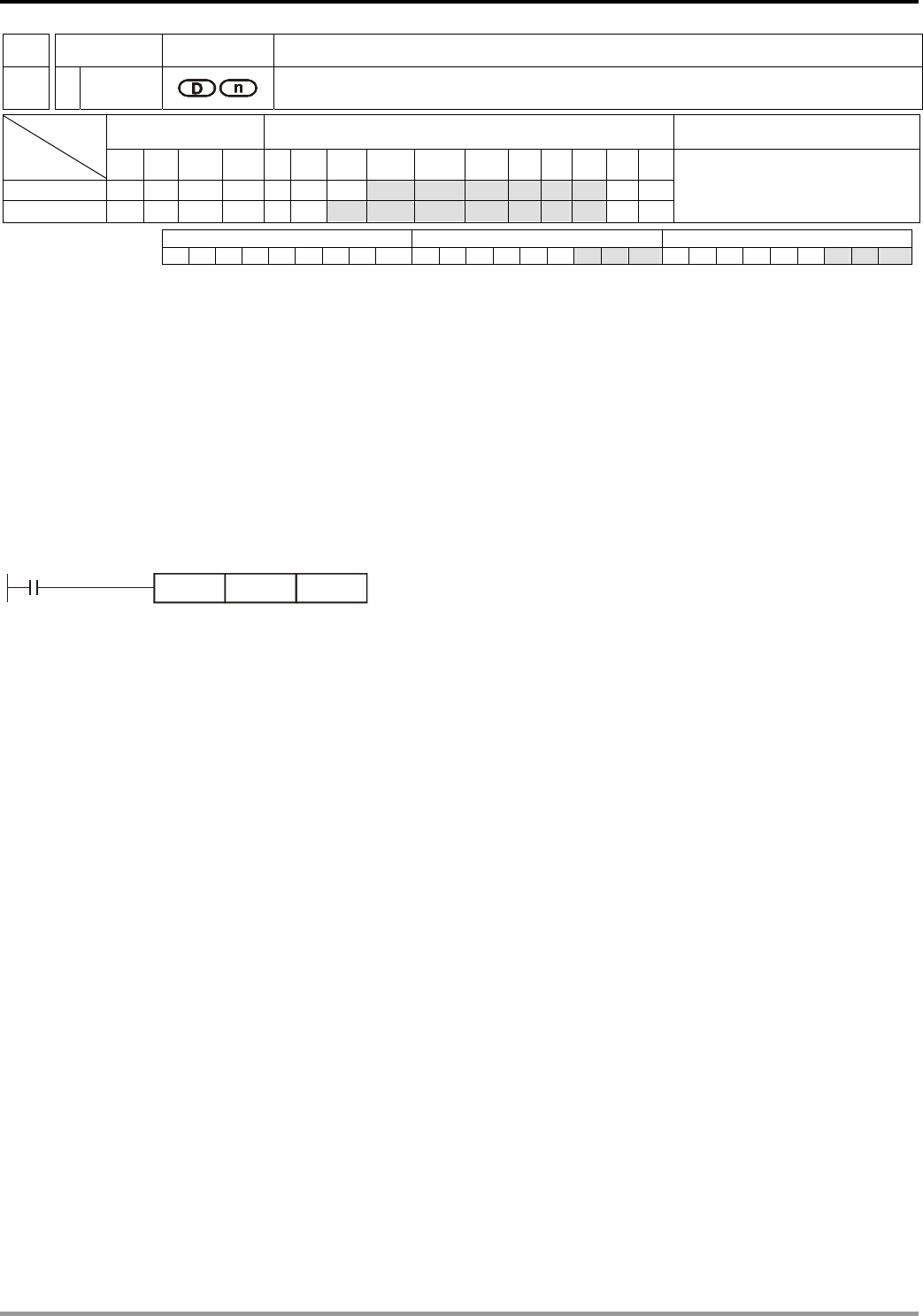
10 Application Instructions API 200-249
DVP-PLC Application Manual
10-23
API Mnemonic Operands Function
268
D BRST Reset Specified Bit of a Word
Bit Devices Word devices Program Steps
Type
OP X Y M S K H KnX KnY KnM KnS T C D E F
D * * * * * *
n * * * * * * * * ***
BRST: 5 steps
DBRST: 9 steps
PULSE 16-bit 32-bit
ES EX SS SA SX SC EH SV EH3 ES EX SS SA SX SC EH SV EH3 ES EX SS SA SX SC EH SV EH3
Operands:
D: Destination device to be reset n: Device specifying the bit to be reset
Explanations:
1. EH2/SV_V1.9 and versions above, and EH3/SV2 supports the function. EH series does not support the
dunction.
2. Available range for the value in operand n: K0~K15 for 16-bit instruction; K0~K31 for 32-bit instruction.
3. When BRST instruction executes, the output device specified by operand n will be reset (OFF).
Program Example:
X0
BRST K4Y0 D0
Instruction: Operation:
LD X0 Load NO contact X0
BRST K4Y0 D0 When D0 = k1,
Y1 is OFF
When D0 = k2,
Y2 = OFF
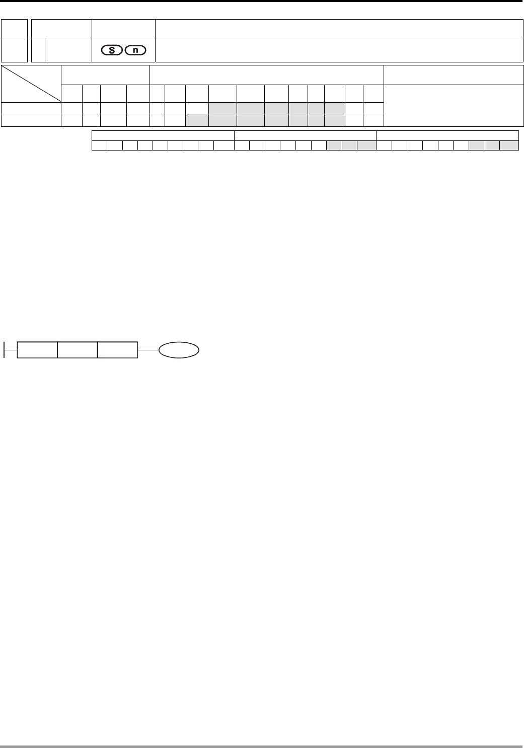
10 Application Instructions API 200-249
DVP-PLC Application Manual
10-24
API Mnemonic Operands Function
269
D BLD Load NO Contact by Specified Bit
Bit Devices Word devices Program Steps
Type
OP X Y M S K H KnX KnY KnM KnS T C D E F
S * * * * * *
n * * * * * * * * ***
BLD: 5 steps
DBLD: 9 steps
PULSE 16-bit 32-bit
ES EX SS SA SX SC EH SV EH3 ES EX SS SA SX SC EH SV EH3 ES EX SS SA SX SC EH SV EH3
Operands:
S: Reference source device n: Reference bit
Explanations:
1. EH2/SV_V1.9 and versions above, and EH3/SV2 supports the function. EH series does not support the
dunction.
2. Available range for the value in operand n: K0~K15 for 16-bit instruction; K0~K31 for 32-bit instruction.
3. BLD instruction is used to load NO contact whose contact state is defined by the reference bit n in reference
device D, i.e. if the bit specified by n is ON, the NO contact will be ON, and vice versa.
Program Example:
BLD D0 K3 Y0
Instruction: Operation:
BLD D0 K3 Load NO contact X0 with bit
Status of bit3 in D0
OUT Y0 Device coil Y0
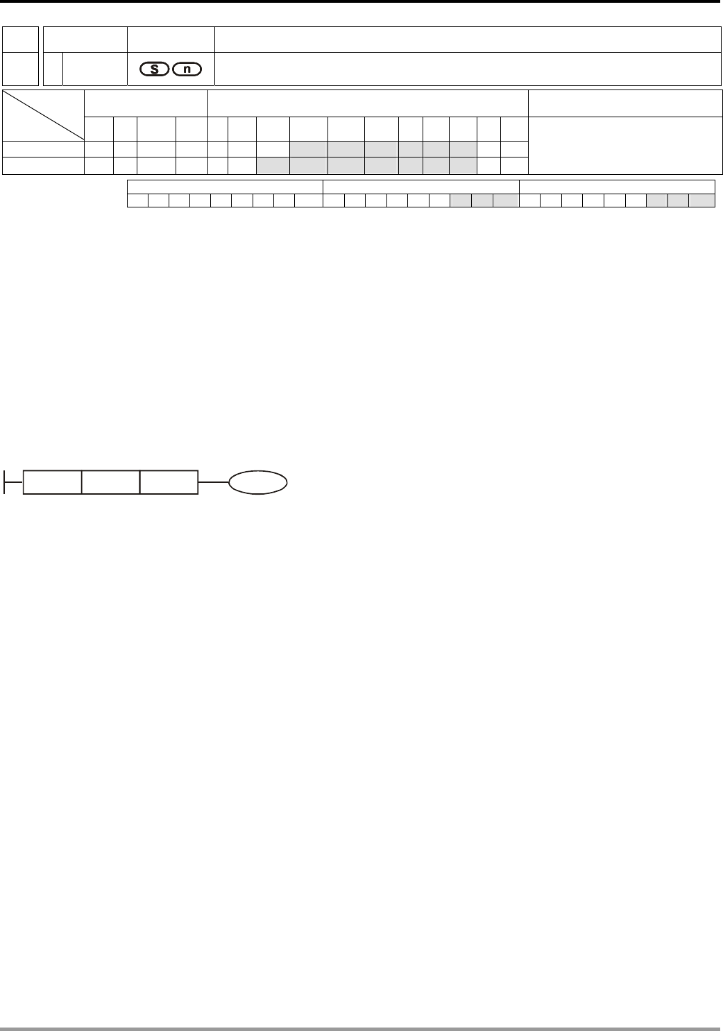
10 Application Instructions API 200-249
DVP-PLC Application Manual
10-25
API Mnemonic Operands Function
270
D BLDI Load NC Contact by Specified Bit
Bit Devices Word devices Program Steps
Type
OP X Y M S K H KnX KnY KnM KnS T C D E F
S * * * * * *
n * * * * * * * * ***
BLDI: 5 steps
DBLDI: 9 steps
PULSE 16-bit 32-bit
ES EX SS SA SX SC EH SV EH3 ES EX SS SA SX SC EH SV EH3 ES EX SS SA SX SC EH SV EH3
Operands:
S: Reference source device n: Reference bit
Explanations:
1. EH2/SV_V1.9 and versions above, and EH3/SV2 supports the function. EH series does not support the
dunction.
2. Available range for the value in operand n: K0~K15 for 16-bit instruction; K0~K31 for 32-bit instruction.
3. BLD instruction is used to load NC contact whose contact state is defined by the reference bit n in reference
device D, i.e. if the bit specified by n is ON, the NC contact will be ON, and vice versa.
Program Example:
BLDI D0 K1 Y0
Instruction: Operation:
BLDI D0 K1 Load NC contact with bit
status of bit1 in D0
OUT Y0 Drive coil Y0
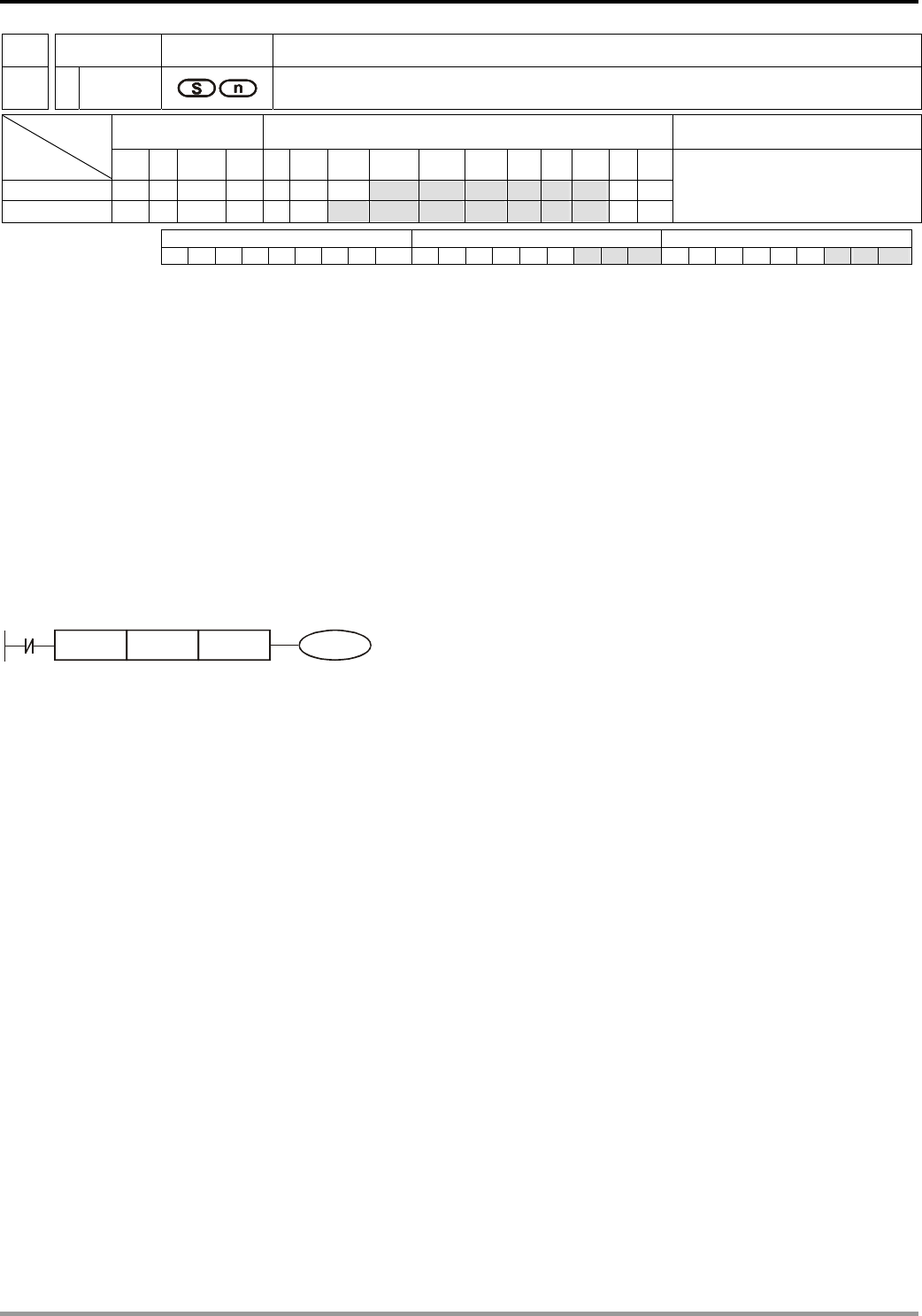
10 Application Instructions API 200-249
DVP-PLC Application Manual
10-26
API Mnemonic Operands Function
271
D BAND Connect NO Contact in Series by Specified Bit
Bit Devices Word devices Program Steps
Type
OP X Y M S K H KnX KnY KnM KnS T C D E F
S * * * * * *
n * * * * * * * * ***
BAND: 5 steps
DBAND: 9 steps
PULSE 16-bit 32-bit
ES EX SS SA SX SC EH SV EH3 ES EX SS SA SX SC EH SV EH3 ES EX SS SA SX SC EH SV EH3
Operands:
S: Reference source device n: Reference bit
Explanations:
1. EH2/SV_V1.9 and versions above, and EH3/SV2 supports the function. EH series does not support the
dunction.
2. Available range for the value in operand n: K0~K15 for 16-bit instruction; K0~K31 for 32-bit instruction.
3. BAND instruction is used to connect NO contact in series. The current state of the contact which is connected in
series is read, and then the logical AND operation is performed on the current state and the previous logical
operation result. The final result is stored in the accumulative register.
Program Example:
X1
BAND D0 K0 Y0
Instruction: Operation:
LDI X1 Load NC contact X1
BAND D0 K0 Connect NO contact in series,
whose state is defined by
bit0 of D0
OUT Y0 Drive coil Y0

10 Application Instructions API 200-249
DVP-PLC Application Manual
10-27
API Mnemonic Operands Function
272
D BANI Connect NC Contact in Series by Specified Bit
Bit Devices Word devices Program Steps
Type
OP X Y M S K H KnX KnY KnM KnS T C D E F
S * * * * * *
n * * * * * * * * ***
BANI: 5 steps
DBANI: 9 steps
PULSE 16-bit 32-bit
ES EX SS SA SX SC EH SV EH3 ES EX SS SA SX SC EH SV EH3 ES EX SS SA SX SC EH SV EH3
Operands:
S: Reference source device n: Reference bit
Explanations:
1. EH2/SV_V1.9 and versions above, and EH3/SV2 supports the function. EH series does not support the
dunction.
2. Available range for the value in operand n: K0~K15 for 16-bit instruction; K0~K31 for 32-bit instruction.
3. BANI instruction is used to connect NC contact in series. The current state of the contact which is connected in
series is read, and then the logical AND operation is performed on the current state and the previous logical
operation result. The final result is stored in the accumulative register.
Program Example:
X1
BANI D0 K0 Y0
Instruction: Operation:
LDI X1 Load NC contact X1
BANI D0 K0 Connect NC contact in series,
whose state is defined by
bit0 of D0
OUT Y0 Drive coil Y0
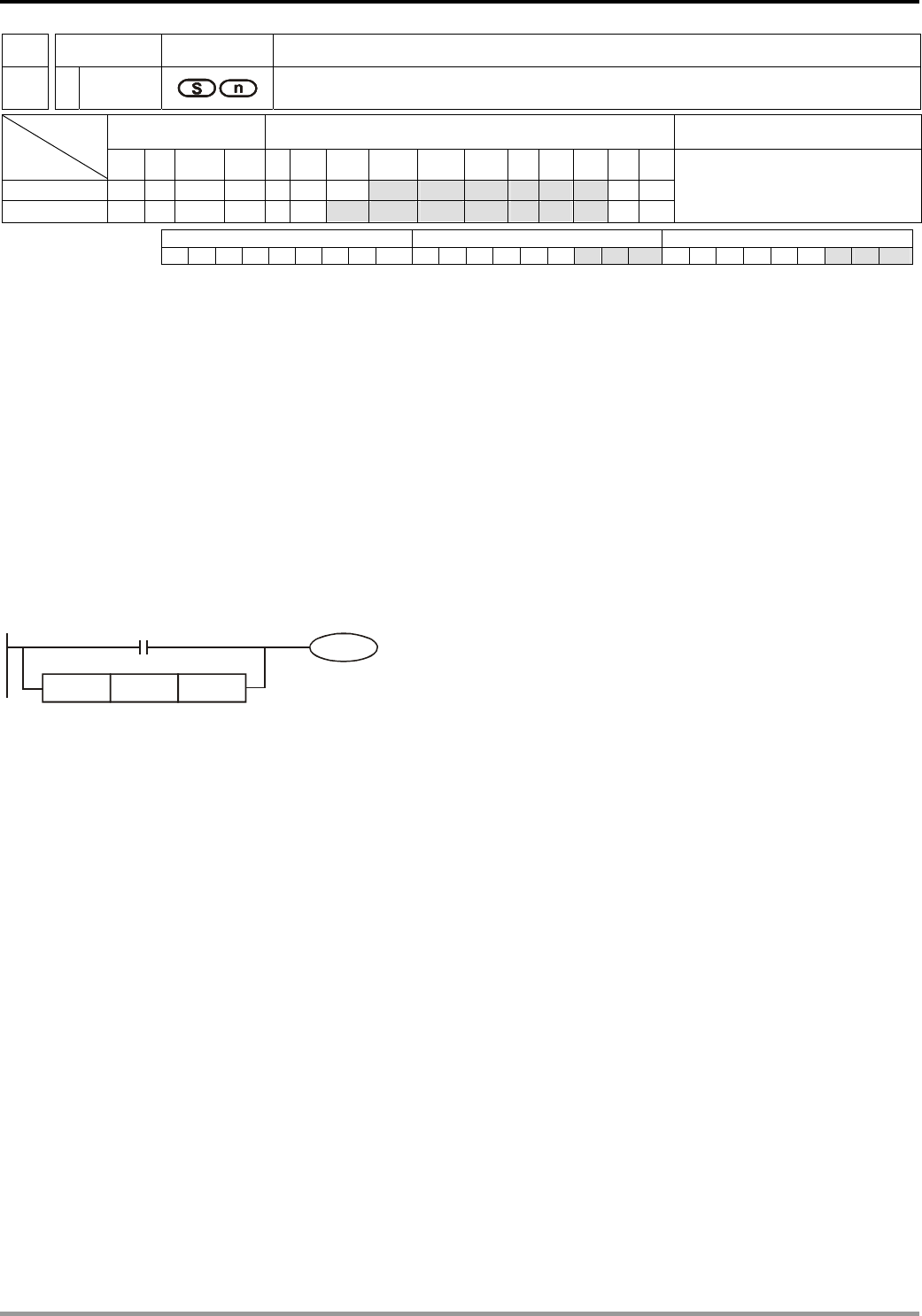
10 Application Instructions API 200-249
DVP-PLC Application Manual
10-28
API Mnemonic Operands Function
273
D BOR Connect NO Contact in Parallel by Specified Bit
Bit Devices Word devices Program Steps
Type
OP X Y M S K H KnX KnY KnM KnS T C D E F
S * * * * * *
n * * * * * * * * ***
BOR: 5 steps
DBOR: 9 steps
PULSE 16-bit 32-bit
ES EX SS SA SX SC EH SV EH3 ES EX SS SA SX SC EH SV EH3 ES EX SS SA SX SC EH SV EH3
Operands:
S: Reference source device n: Reference bit
Explanations:
1. EH2/SV_V1.9 and versions above, and EH3/SV2 supports the function. EH series does not support the
dunction.
2. Available range for the value in operand n: K0~K15 for 16-bit instruction; K0~K31 for 32-bit instruction.
3. BOR instruction is used to connect NO contact in parallel. The current state of the contact which is connected in
series is read, and then the logical OR operation is performed on the current state and the previous logical
operation result. The final result is stored in the accumulative register.
Program Example:
X0
Y1
BOR D0 K0
Instruction: Operation:
LD X0 Load NO contact X0
BOR D0 K0 Connect NO contact in
parallel, whose state is
defined by bit0 of D0
OUT Y1 Drive coil Y1
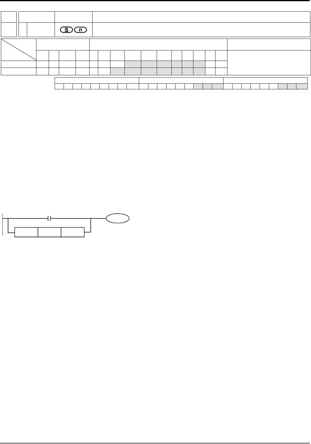
10 Application Instructions API 200-249
DVP-PLC Application Manual
10-29
API Mnemonic Operands Function
274
D BORI Connect NC Contact in Parallel by Specified Bit
Bit Devices Word devices Program Steps
Type
OP X Y M S K H KnX KnY KnM KnS T C D E F
S * * * * * *
n * * * * * * * * ***
BORI: 5 steps
DBORI: 9 steps
PULSE 16-bit 32-bit
ES EX SS SA SX SC EH SV EH3 ES EX SS SA SX SC EH SV EH3 ES EX SS SA SX SC EH SV EH3
Operands:
S: Reference source device n: Reference bit
Explanations:
1. EH2/SV_V1.9 and versions above, and EH3/SV2 supports the function. EH series does not support the
dunction.
2. Available range for the value in operand n: K0~K15 for 16-bit instruction; K0~K31 for 32-bit instruction.
3. BORI instruction is used to connect NC contact in parallel. The current state of the contact which is connected in
series is read, and then the logical OR operation is performed on the current state and the previous logical
operation result. The final result is stored in the accumulative register.
Program Example:
X0
Y1
BORI D0 K0
Instruction: Operation:
LD X0 Load NO contact X0
BORI D0 K0 Connect NC contact in
parallel, whose state is
defined by bit0 of D0
OUT Y1 Drive coil Y1
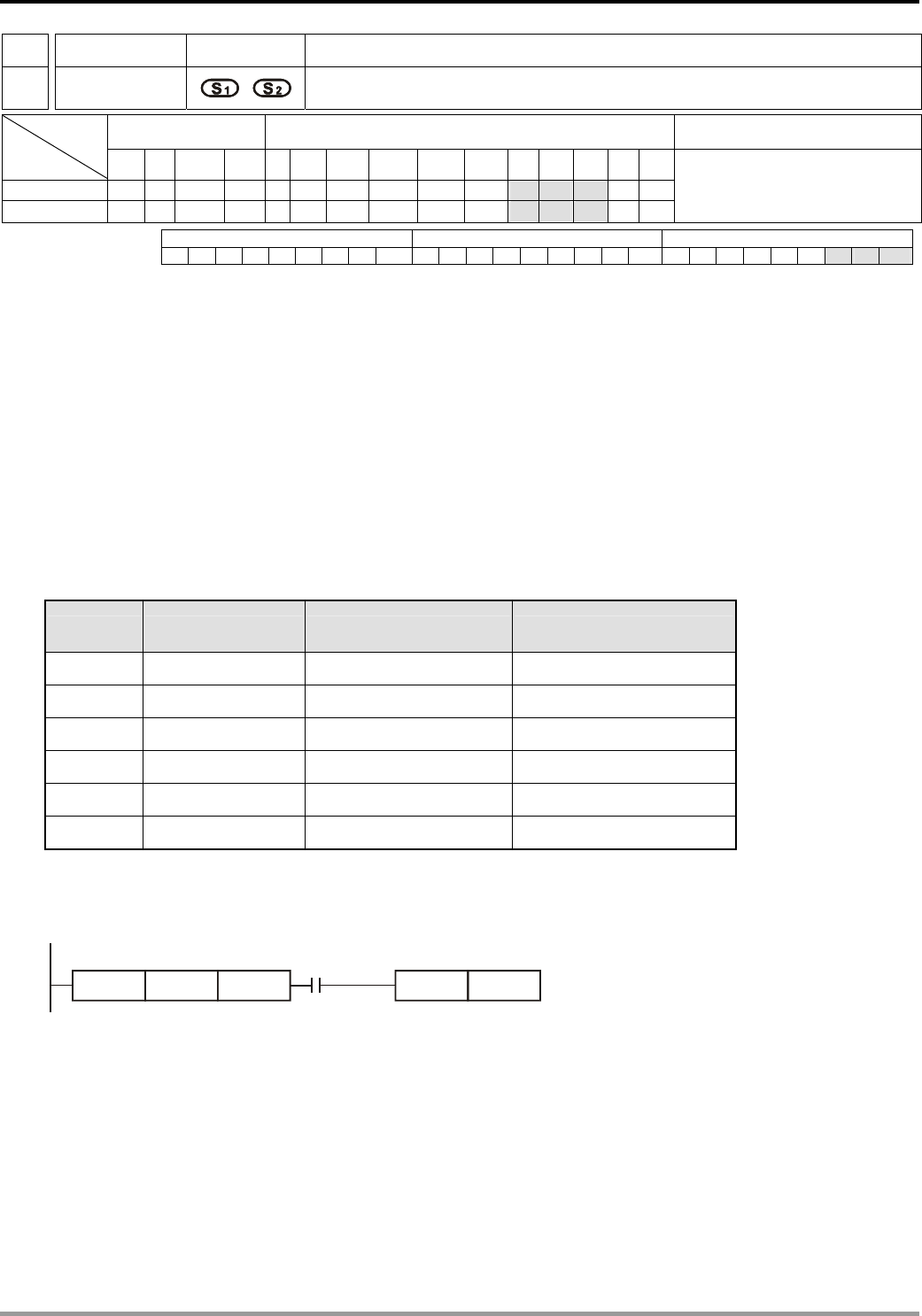
10 Application Instructions API 200-249
DVP-PLC Application Manual
10-30
API Mnemonic Operands Function
275~
280
FLD※ Floating Point Contact Type Comparison
Bit Devices Word devices Program Steps
Type
OP X Y M S K H KnX KnY KnM KnS T C D E F
S1 * * *
S2 * * *
FLD※: 9 steps
PULSE 16-bit 32-bit
ES EX SS SA SX SC EH SV EH3 ES EX SS SA SX SC EH SV EH3 ES EX SS SA SX SC EH SV EH3
Operands:
S1: Source device 1 S2: Source device 2
Explanations:
1. EH2/SV_V1.9 and versions above, and EH3/SV2 supports the function. EH series does not support the
dunction.
2. This instruction compares the content in S1 and S2. Take API275 (FLD=) for example, if the result is “=”, the
continuity of the instruction is enabled. If the result is “≠”, the continuity of the instruction is disabled.
3. The user can specify the floating point value directly into operands S1 and S2 (e.g. F1.2) or store the floating
point value in D registers for further operation.
4. FLD※ (※: =, >, <, <>, ≤, ≥) instruction is used for direct connection with left hand bus bar.
API No. 32 -bit instruction Continuity condition Discontinuity condition
275 FLD= S1=S2 S1≠S2
276 FLD> S1>S2 S1≦S2
277 FLD< S1<S2 S1≧S2
278 FLD<> S1≠S2 S1=S2
279 FLD<= S1≦S2 S1>S2
280 FLD>= S1≧S2 S1<S2
Program Example:
When the content in D200(D201) ≤ F1.2 and X1 is ON, Y21 = ON and latched.
FLD<= D200 F1.2
X1
SET Y21
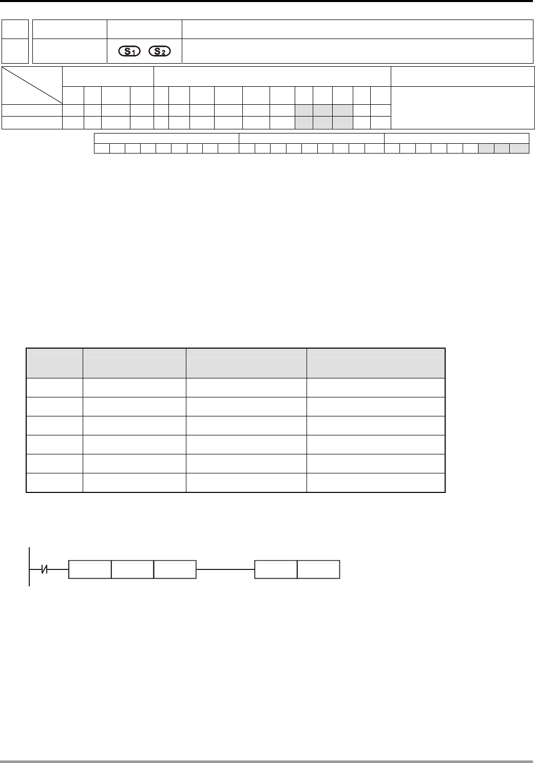
10 Application Instructions API 200-249
DVP-PLC Application Manual
10-31
API Mnemonic Operands Function
281~
286
FAND※ Floating Point Serial Type Comparison
Bit Devices Word devices Program Steps
Type
OP X Y M S K H KnX KnY KnM KnS T C D E F
S1 * * *
S2 * * *
FAND※: 9 steps
PULSE 16-bit 32-bit
ES EX SS SA SX SC EH SV EH3 ES EX SS SA SX SC EH SV EH3 ES EX SS SA SX SC EH SV EH3
Operands:
S1: Source device 1 S2: Source device 2
Explanations:
1. EH2/SV_V1.9 and versions above, and EH3/SV2 supports the function. EH series does not support the
dunction.
2. This instruction compares the content in S1 and S2. Take API281 (FAND =) for example, if the result is “=”, the
continuity of the instruction is enabled. If the result is “≠”, the continuity of the instruction is disabled.
3. The user can specify the floating point value directly into operands S1 and S2 (e.g. F1.2) or store the floating
point value in D registers for further operation.
4. FAND※ (※: =, >, <, <>, ≤, ≥) instruction is used for serial connection with contacts.
API No. 32-bit instruction Continuity condition Discontinuity condition
281 FAND= S1=S2 S1≠S2
282 FAND> S1>S2 S1≦S2
283 FAND< S1<S2 S1≧S2
284 FAND<> S1≠S2 S1=S2
285 FAND<= S1≦S2 S1>S2
286 FAND>= S1≧S2 S1<S2
Program Example:
When X1 is OFF and the content in D0(D1) does not equal to F1.2, Y21 = ON and latched.
FAND<> F1.2 D0 SET Y21
X1
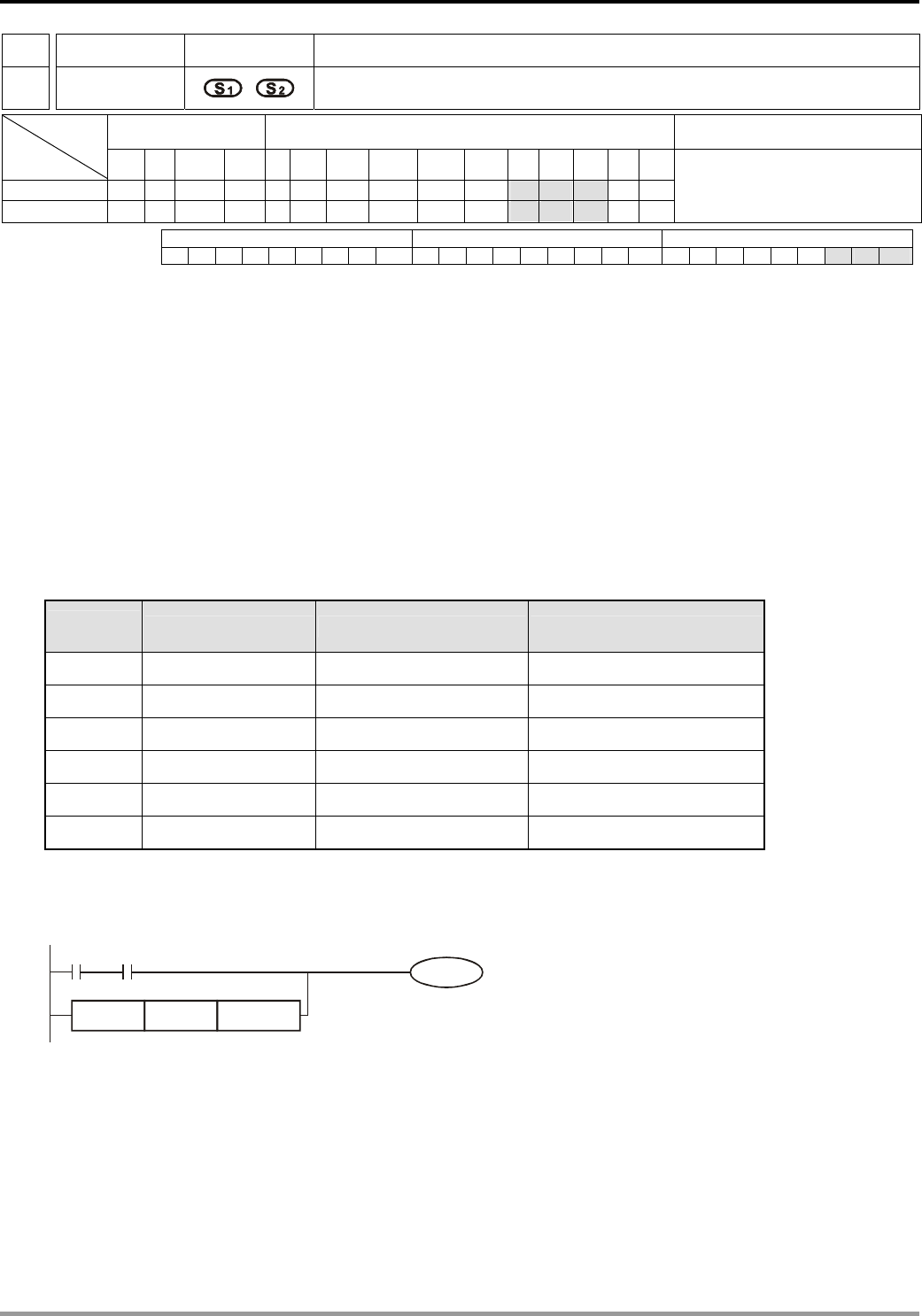
10 Application Instructions API 200-249
DVP-PLC Application Manual
10-32
API Mnemonic Operands Function
287~
292
FOR※ Floating Point Parallel Type Comparison
Bit Devices Word devices Program Steps
Type
OP X Y M S K H KnX KnY KnM KnS T C D E F
S1 * * *
S2 * * *
FOR※: 9 steps
PULSE 16-bit 32-bit
ES EX SS SA SX SC EH SV EH3 ES EX SS SA SX SC EH SV EH3 ES EX SS SA SX SC EH SV EH3
Operands:
S1: Source device 1 S2: Source device 2
Explanations:
1. EH2/SV_V1.9 and versions above, and EH3/SV2 supports the function. EH series does not support the
dunction.
2. This instruction compares the content in S1 and S2. Take API287 (FOR =) for example, if the result is “=”, the
continuity of the instruction is enabled. If the result is “≠”, the continuity of the instruction is disabled
3. The user can specify the floating point value directly into operands S1 and S2 (e.g. F1.2) or store the floating
point value in D registers for further operation.
4. OR※ (※: =, >, <, <>, ≤, ≥) instruction is used for parallel connection with contacts.
API No. 32-bit instruction Continuity condition Discontinuity condition
287 FOR= S1=S2 S1≠S2
288 FOR> S1>S2 S1≦S2
289 FOR< S1<S2 S1≧S2
290 FOR<> S1≠S2 S1=S2
291 FOR<= S1≦S2 S1>S2
292 FOR>= S1≧S2 S1<S2
Program Example:
When both X2 and M30 are OFF and the content in D100(D101) ≥ F1.234, M60 = ON..
FOR>= D100 F1.234
X2 M30
M60

11 Appendix
DVP-PLC Application Manual 11-1
11.1 Appendix A: Table for Self-Detecting Abnormality
When you encounter abnormality using the product, you can analyze the problem first by doing the self
detections below.
Abnormality Possible cause Suggested correction
Loosened terminal block Check if the removable terminal block is
loosened.
Output point abnormality The input counting specification may not
match the pulse output frequency of the
PLC model in use.
Check if the hardware is normal by
low-frequency pulse counting.
The length of communication cable
Make sure the RS-232 cable is at least 3
meters long to ensure normal
communication (specification unknown).
Communication
abnormality Incorrect communication protocol or
address setting
Broadcast from station 0 first by RS-232
to search for communication protocol and
address and later confirm by RS-485
communication.
Extension module unable
to work Poor connection or MPU problem
Make sure the MPU is tightly connected
to the extension module and compare to
make sure whether the problem lies in
the MPU or the extension module.
Counter (input point)
abnormality
The applicable frequency exceeds the
maximum bandwidth.
The frequency should be within the
allowed PLC specifications.
ERROR LED flashes Incorrect program syntax
Record the error code first, and write
whether the ERROR LED should not
flash anymore by syntactically correct
program. Model with battery should be
checked whether the time of RTC is
correct (not being correct means the
battery might once be unattached,
causing reset of time).
L.V. LED On Low input power supply Make sure the power supply voltage is
normal.
RUN LED Off after
execution
There is no program inside the new
PLC, resulting in misjudgment. Write in the program first.
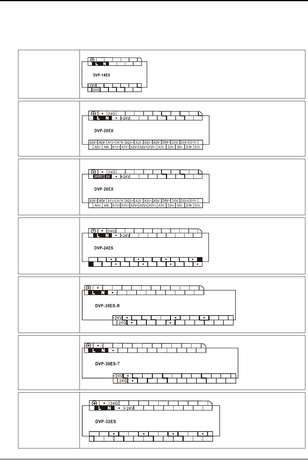
11 Appendix
DVP-PLC Application Manual
11-2
11.2 Appendix B: MPU Terminal Layout
For ES series MPU
DVP14ES00R2/T2
X7X6X5
X3X2X1
Y0 Y1 Y2 Y3
C2C1C0
( AC Power IN, DC Signal IN )
C3
X4S/S
X0
Y4
Y5
DVP20EX00R2/T2
X7X6X5X4
X3X2X1X0 Y0 Y1
Y2
Y3 Y4
Y5C1C0
( AC Power IN, DC Signal IN )
S/S
DVP20EX11R2/T2
X7X6X5X4
X3X2X1X0 Y0 Y1
Y2
Y3 Y4
Y5C1C0
( DC Power IN, DC Signal IN )
S/S
DVP24ES00R2/T2
X17X16X15X14X13X12X11X10
X7X6X5X4X3X2X1X0
Y0 Y1 Y2 Y3 Y4 Y5 Y6
C6C2C1C0
( AC Power IN, DC Signal IN )
S/S
Y7
C3 C4 C5 C7
DVP30ES00R2
X16X14X12X10X6X4X2X0
X17X15X13X11X7X5X3X1
C0
Y1 Y2
C2 C4C3C1 Y5 Y7 Y11 Y13
Y10Y6
( AC Power IN, DC Signal IN )
S/S
X21
X20
Y0 Y12Y4Y3
DVP30ES00T2
X16X14X12X10X6X4X2X0
X17X15X13X11X7X5X3X1
ZP0
Y0
UP1
Y1
ZP3
Y3
ZP1
Y5 Y7 Y11 Y13
Y10Y6
( AC Power IN, DC Signal IN )
S/S
X21
X20
UP0
Y12Y4
UP2
Y2
ZP2
UP3
DVP32ES00R2/T2
X17X16X15X14X13X12X11X10
X7X6X5X4X3X2X1X0
Y0 Y1
Y2 Y3
Y4 Y5
Y6 C3C2C1C0 Y7 Y12 Y13 Y16 Y17
Y15Y14Y11Y10
( AC Power IN, DC Signal IN )
S/S
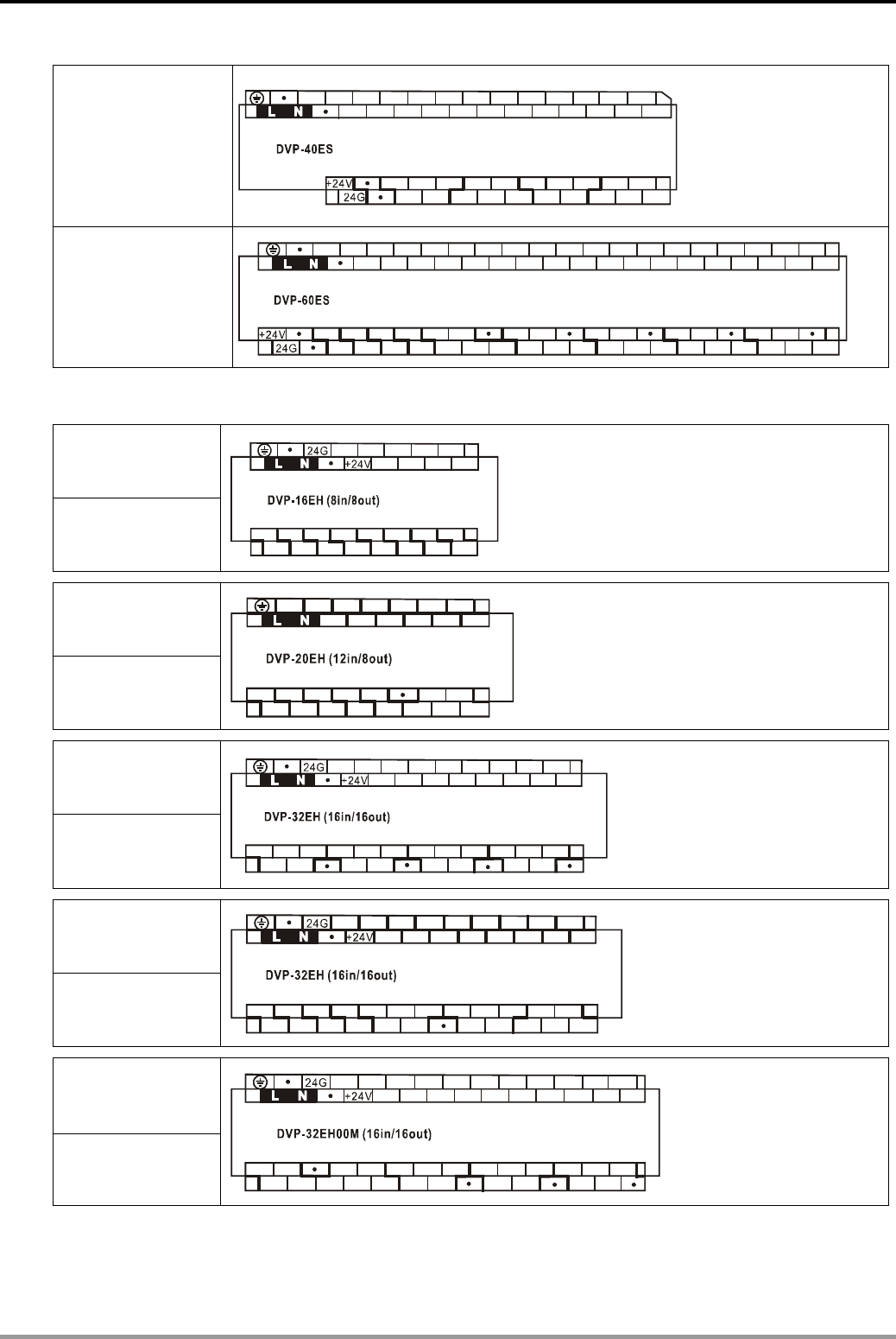
11 Appendix
DVP-PLC Application Manual 11-3
DVP40ES00R2/T2
X16X14X12X10X6X4X2X0
X17X15X13X11X7X5X3X1
Y0
Y1 Y3
C1 C3Y7Y2 Y5 Y10 Y12 Y15 Y17
Y14Y13Y11Y6
( AC Power IN, DC Signal IN )
S/S
X21 X23 X25
X20 X22 X24
X27
X26
C0 Y16C2Y4
DVP60ES00R2/T2
S/S X22 X23 X24 X25 X26 X27 X30 X31 X32 X33 X34 X35 X36 X37 X40 X41 X42 X43
X21X20X17X16X15X14X13X12X11X10X7X6X5X4X3X2X1X0
Y0 Y1 Y2 Y3 Y4 Y5
Y6
C4
C3C2C1C0 Y7 C5 Y12 Y13 Y16 Y17 Y22 Y23C6 C7 C8 Y26 Y27
Y25Y24Y21Y20Y15Y14Y11Y10
( AC Power IN, DC Signal IN )
For EH2/EH3 series MPU
DVP16EH00R2/T2
DVP16EH00R3/T3
X7
X6
X5
X4
X3
X2
X1
X0
Y0 Y1 Y2 Y3 Y4 Y5 Y6
C6C2
C1C0
S/S
Y7
C3 C4 C5 C7
DVP20EH00R2/T2
DVP20EH00R3/T3
X13
X12
X11
X10
X7
X6
X5
X4
X3
X2
X1
X0
Y0 Y1
C1
Y2 Y3 Y4
C3C0
S/S
C2 C4
+24V
24G
Y6
Y5 Y7
DVP32EH00R2
DVP32EH00R3
X17
X16
X15
X14
X13
X12
X11
X10
X7
X6
X5
X4
X3
X2
X1
X0
Y0 Y1
Y2
Y3 Y4 Y5
Y6 C3C2C1C0
Y7
Y12
Y13
Y16
Y17
Y15Y14Y11Y10
S/S
DVP32EH00T2
DVP32EH00T3
X17
X16
X15
X14
X13
X12
X11
X10
X7
X6
X5
X4
X3
X2
X1
X0
Y0 Y1
C1
Y2 Y3 Y4
Y6 C5C3C0
Y5
Y12
Y11
Y17
Y16
Y14Y13Y10Y7
S/S
C2 C6 Y15C4
DVP32EH00M2
DVP32EH00M3
X13
X12
X11
X10
X7
X6
X5-
X5+
X4-
X4+
X3
X2
X1-
X1+
X0-
X0+
Y0- Y1-
Y1+
Y2- Y3-
Y3+ C1C0Y2+Y0+
Y4 Y10 Y14
Y13Y11Y7Y5
S/S
Y15 Y17
Y16
SG0 Y6 Y12 C2
X14 X16
X15 X17
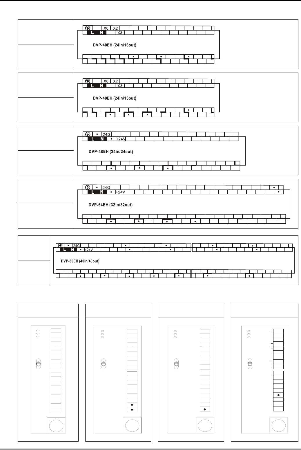
11 Appendix
DVP-PLC Application Manual
11-4
DVP40EH00R2
DVP40EH00R3
X23
X22
X21
X20
X17
X16
X15
X14
X13
X12
X11
X10
X7
X6
X5
X4
24G Y0
C0
Y2 Y3
C3 C5C4C224V
Y12Y10Y6Y4
S/S
Y14 Y16
Y15
C1 Y5 Y11 C6
X24 X26
X25 X27
Y1
Y7 Y13 Y17
X1
DVP40EH00T2
DVP40EH00T3
X23
X22
X21
X20
X17
X16
X15
X14
X13
X12
X11
X10
X7
X6
X5
X4
24G Y0
C0
Y2 Y3
C4C2C124V
Y12Y10Y6Y4
S/S
Y14 Y16
Y15
Y5
Y11 C5
X24 X26
X25 X27
Y1 Y7
Y13 Y17
X1
C3
DVP48EH00R2/T2
DVP48EH00R3/T3
X17
X16
X15
X14
X13
X12
X11
X10
X7
X6
X5
X4
X3
X2
X1
X0
Y0 Y1
Y2
Y3 Y4 Y5
Y6 C3C2C1C0
Y7
Y12
Y13
Y16
Y17
Y15Y14Y11Y10
S/S
X27
X26
X25
X24
X23
X22
X21
X20
C4 Y21
Y22
Y27
Y23
Y26Y24Y20
Y25
DVP64EH00R2/T2
DVP64EH00R3/T3
X17
X16
X15
X14
X13
X12
X11
X10
X7
X6
X5
X4
X3
X2
X1
X0
Y0 Y1
Y2
Y3 Y4 Y5
Y6 C3C2C1C0
Y7
Y12
Y13
Y16
Y17
Y15Y14Y11Y10
S/S
X27
X26
X25
X24
X23
X22
X21
X20
C4 Y22
Y21 Y27
Y24
Y25Y23Y20
Y26
X37
X36
X35
X34
X33
X32
X31
X30
C5 Y31
Y32
Y37
Y33
Y36Y34Y30
Y35
DVP80EH
00R2/T2
DVP80EH
00R3/T3
X15
X14
X13
X12
X11
X10
X7
X6
X5
X4
X3
X2
X1
X0
Y0 Y1
Y2
Y3 Y4 Y5
Y6 C3C2C1C0
Y7
Y12
Y13
Y16
Y17
Y15Y14Y11Y10
S/S
X23
X22
X21
X20
X17
X16
C4 Y22
Y21 Y27
Y25
Y23Y20
Y26
X31
X30
X33
X32
X27
X26
X25
X24
C6 Y32
Y31 Y37
Y34
Y35Y33Y30
Y36
X35
X34
X37
X36
X41
X40
X43
X42
X45
X44
X47
X46
C5
Y24
C7 Y42
Y41 Y47
Y44
Y45Y43Y40
Y46
For SS/SA/SC/SX series MPU
DVP14SS DVP12SA DVP12SC-T DVP10SX
S/S
X0
X1
X2
X3
X4
X5
X6
X7
C0
Y0
C1
C2
Y1
Y2
Y3
Y4
Y5
STOP
RUN
S/S
X0
X1
X2
X3
X4
X5
X6
X7
C0
Y0
C1
C2
Y1
Y2
Y3
STOP
RUN
S/S
X0
X1
X2
X3
X4
X5
X10
X11
C0
Y0
C1
C2
Y1
Y10
C3
Y11
STOP
RUN
V0+
I 0+
V1+
I 1+
V0+
I 0+
V1+
I 1+
COM
S/S
X0
X1
X3
X2
Y1
C0
Y0
STOP
RUN
A/D
D/A
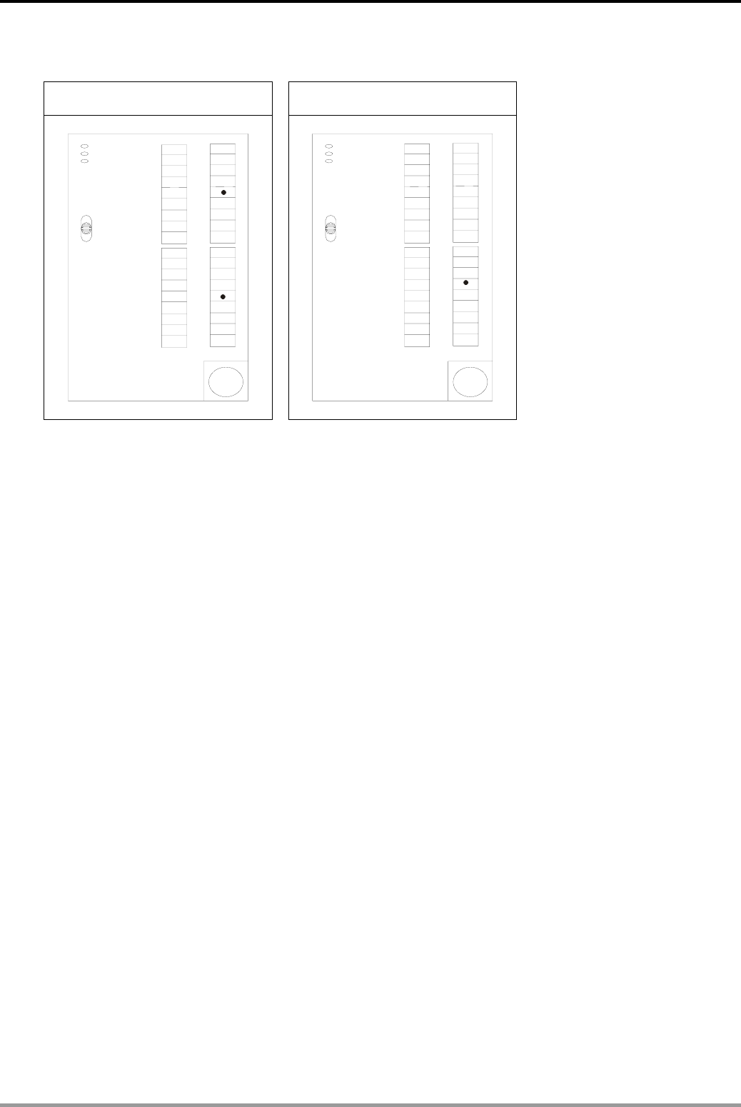
11 Appendix
DVP-PLC Application Manual 11-5
For SV/SV2 series MPU
DVP28SV11R DVP28SV11T
C2
Y6
Y7
Y10
C3
Y11
Y12
Y13
S/S
X0
X1
X2
X3
X4
X5
X6
X7
S/S
X10
X11
X12
X13
X14
X15
X16
X17
C0
Y0
Y1
Y2
C1
Y3
Y4
Y5
STOP
RUN
C3
Y6
Y7
C4
Y10
Y11
Y12
Y13
S/S
X0
X1
X2
X3
X4
X5
X6
X7
S/S
X10
X11
X12
X13
X14
X15
X16
X17
C0
Y0
Y1
C1
Y3
C2
Y4
Y5
Y2
STOP
RUN
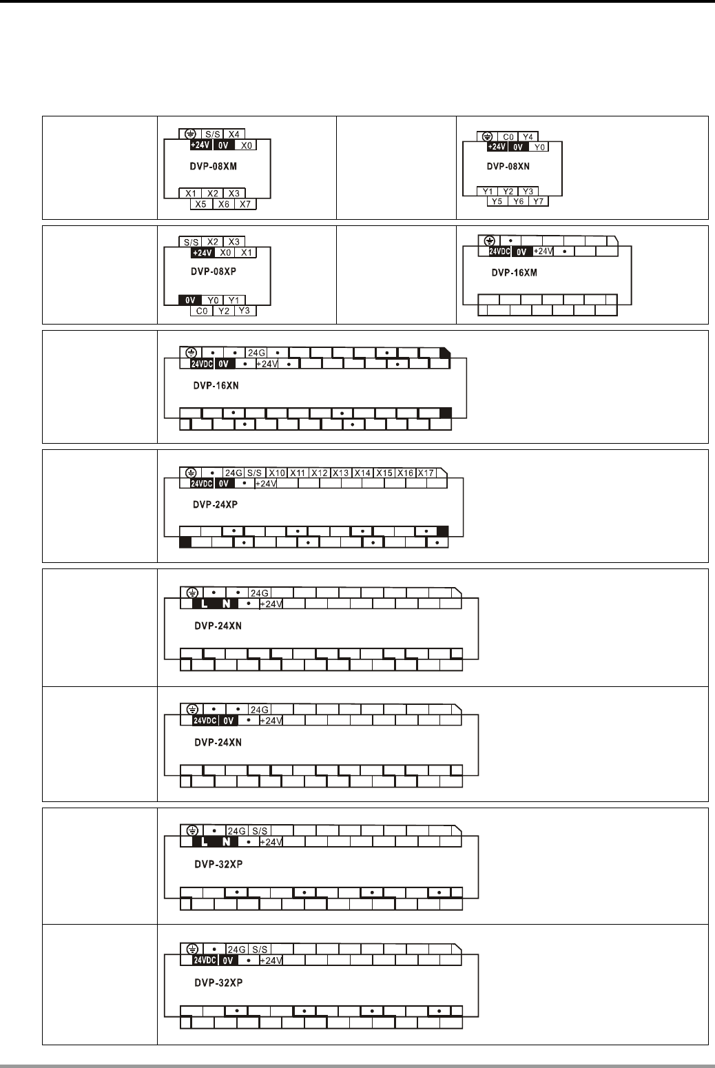
11 Appendix
DVP-PLC Application Manual
11-6
11.3 Appendix C: Terminal Layout for Digital I/O Modules
For ES/EX series digital I/O modules
DVP08XM11N
( DC Power IN )
DVP08XN11R/T
( DC Power IN )
DVP08XP11R/T
( DC Power IN )
DVP16XM11N
X1
X11
X0
X7
X16 X17
X10
( DC Power IN )
S/S
24G
X2 X3 X4 X5 X6
X12 X13 X14 X15
DVP16XN11R/T
Y0 Y1 Y2 Y3 Y4 Y5
C1
C0 C2 C3 C4 C5
C11 C12 C13
Y11 Y12 Y13 Y14 Y15 Y16 Y17
C14 C15 C16 C17
( DC Power IN )
Y6 Y7
C6 C7
Y10
C10
DVP24XP11R/T
X1
C3
Y3 Y4
X0 X2 X3 X4 X5 X6 X7
( DC Power IN, DC Signal IN )
Y5 Y6 Y7
C4 C5 C6 C7
Y0 Y1
C0 C1
Y2
C2
DVP24XN00R/T
Y4Y3Y2Y1Y0
C10
Y12
Y13
Y16
Y17
Y15Y14Y11
( AC Power IN )
C11 C12 C13
Y10
C15C14 Y23
Y20 Y21 Y22
C0 C1 C2 C3 C4
Y7Y6Y5
C16 C17
Y24 Y25 Y26
Y27
C5 C6 C7
DVP24XN00R/T
Y4Y3Y2Y1Y0
C10
Y12
Y13
Y16
Y17
Y15Y14Y11
( DC Power IN )
C11 C12 C13
Y10
C15C14 Y23
Y20 Y21 Y22
C0 C1 C2 C3 C4
Y7Y6Y5
C16 C17
Y24 Y25 Y26
Y27
C5 C6 C7
DVP32XP00R/T
Y7
Y6
Y5Y4
Y3Y2
Y1Y0
Y12 Y13 Y16
( AC Power IN, DC Signal IN )
C0 C1 C2 C3
Y10 Y11 Y14 Y15
X10 X11 X12 X13 X14 X15 X16
X0 X1 X2 X3 X4 X5
Y17
X17
X6 X7
DVP32XP11R/T
Y7
Y6
Y5Y4
Y3Y2
Y1Y0
Y12 Y13 Y16
( DC Power IN, DC Signal IN )
C0 C1 C2 C3
Y10 Y11 Y14 Y15
X10 X11 X12 X13 X14 X15 X16
X0 X1 X2 X3 X4 X5
Y17
X17
X6 X7
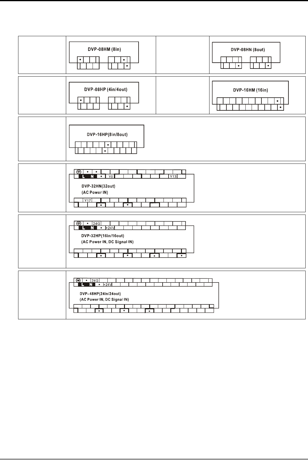
11 Appendix
DVP-PLC Application Manual 11-7
For EH2/EH3 series digital I/O modules
DVP08HM11N
X0 X2 X4 X6
X1 X3 X5 X7
S/S
DVP08HN11R/T
Y0 Y1 Y3 Y4 Y5 Y7
C0 Y2 C1 Y6
DVP08HP11R/T
X0 Y1 Y3
C0 Y2
Y0
X2
S/S
X1 X3
DVP16HM11N
X10 X11
S/S X1 X3
S/S X12X13X14 X15X16 X17
X0 X2 X4 X5 X7
X6
DVP16HP11R/T
X4 X5
X1 X3
S/S X6 X7
Y3
Y4 Y5 Y6
X0 X2 C0 Y0 Y2
Y1
Y7
DVP32HN00R/T
X15
X14
C3
Y12
Y11
Y10
Y7
Y6
C2
Y5
Y4
Y3
C1
Y2
Y1
Y16
Y20
Y21 Y22 Y23
Y24 C7C6C5C4
Y25
Y30
Y31
Y35
Y36
Y34Y32Y27Y26
C0
Y33 Y37
DVP32HP00R/T
X17
X16
X15
X14
X13
X12
X11
X10
X7
X6
X5
X4
X3
X2
X1
X0
Y0 Y1
Y2
Y3 Y4 Y5
Y6 C3C2C1C0
Y7
Y12
Y13
Y16
Y17
Y15Y14Y11Y10
S/S
DVP48HP00R/T
X17
X16
X15
X14
X13
X12
X11
X10
X7
X6
X5
X4
X3
X2
X1
X0
Y0 Y1
Y2
Y3 Y4 Y5
Y6 C3C2C1C0
Y7
Y12
Y13
Y16
Y17
Y15Y14Y11Y10
S/S
X27
X26
X25
X24
X23
X22
X21
X20
C4 Y21
Y22
Y27
Y23
Y26Y24Y20
Y25
11 Appendix
DVP-PLC Application Manual
11-8
For Slim (SS/SA/SC/SX/SV/SV2) series digital I/O modules
DVP08SM11N DVP08SM10N DVP16SM11N DVP08SN11R
DVP08SN11T
S/S
X0
X1
X2
X3
X4
X5
X6
X7
COM
X0
X1
X2
X3
X4
X5
X6
X7
S/S
X0
X1
X2
X3
S/S
X10
X11
X12
X14
X15
X16
X17
X13
X4
X5
X6
X7
C0
Y0
Y1
Y2
Y4
Y5
Y6
Y7
Y3
DVP08SP11R
DVP08SP11T DVP16SP11R DVP16SP11TS DVP06SN11R
S/S
X0
X1
X2
X3
C0
Y0
C1
Y1
Y2
C3
C2
Y3
S/S
X0
X1
X2
X3
C0
Y0
Y1
Y2
Y4
Y5
Y6
Y7
X4
X5
X6
X7
Y3
S/S
X0
X1
X2
X3
UP
Y0
Y1
Y2
Y4
Y5
Y6
Y7
X4
X5
X6
X7
Y3
ZP
C0
Y0
C1
C3
Y3
C4
C5
Y5
Y4
C2
Y2
Y1

11 Appendix
DVP-PLC Application Manual 11-9
11.4 Appendix D: Difference between EH2 and EH3
The capacity of the program is upgraded to 30k Steps, and the number of D devices is increased to 12000.
The capacity of the memory card has doubled. To prevent the wrong insertion, the new memory card and the old
one are not interchangeable
Some function cards of DVP-EH2 can not be used in DVP-EH3. The function cards which can be used are all
communication cards, 02AD card and 02DA card.
When the position of the basic instruction is below 16k Step, the execution speed does not make any change.
When its position is above 16k Step, the execution speed becomes 2.8μs.
The execution speed of MOV instruction is improved to 4.8μs, and that of other application instructions is also
improved by 4~5 times.
The high-speed input/output functions of DVP-EH3
A. The number of external input interruptions is 16. (Please refer to section 2.1.)
B. There are 3 sets of masking functions of the interruption. (Please refer to section 2.11.)
C. Newly added CSFO instruction has the speed-tracing function and can be used with the manual pulse
generator. (Please refer to API 207.)
D. Newly added DVSPO and DICF instructions have various speed-changing functions. (Please refer to API
198 and API 199.)
E. The zero return instruction (DZRN) has the function of detecting limit switches, stopping at the positive
position, seeking Z phase, and outputting the displacement. (Please refer to API 156.)
F. The direction outputs of DZRN instruction are used with Y1, Y3, Y5, and Y7. (Please refer to API 156.)
G. That special M can set the start and reset functions of C235~C240 is cancelled. The bandwidth of
C235~C240can be up to 10 KHz.
Other newly added functions of DVP-EH3
A. COM1 card and COM3 card can be masters. COM3 is an independent communication port which does not
occupy COM2. The flag of the transmitting function in the master is the same as that in DVP-ES2.
B. The solar energy instructions DSPA and GPS instruction are added. (Please refer to API 177 and API
178)。
C. We add the m servo convenience instruction ASDRW.(Please refer to API 206.)
D. The program can be automatically backuped, and will not disappear even if the battery has run down.
E. The second-backup function can store the second program and data.
F. We add the basic instructions which are used exclusively for words. For example, BLD, BOUT, and etc.
(Please refer to API 266~274)
G. The comparison instruction of the floating point number (FLD>=….).is added. (Please refer to API
275~292)
H. M1356 can be used in PLC-LINK to designate the station numbers. Only when M1353 is on can
D1900~D1931 be used.
I. ISPSoft and WPLSoft can set the read-only function of the communication and function of downloading the
program.
J. It can connect with at most 12 right-side analog extension modules.

11 Appendix
DVP-PLC Application Manual
11-10
11.5 Appendix E: Revision History
Item Revisions Chapter
#1 Information related to EH3 and SV2 is added. All
#2
1.3 How to Edit Ladder Diagram: The ladder diagram and explanations on ANI
instruction
1.7 Basic Program Designing Examples: Explanations on Start, Stop and Latched
Chapter 1
#3
Special auxiliary relays: M1025, M1036, M1058, M1075, M1085, M1087,
M1102~M1103, M1133~M1137, M1154~M1160, M1163~M1164, M1181~M1182,
M1189~M1191, M1194~M1195, M1304, M1308~M1311, M1347~M1348, M1355,
M1520~M1525, M1534~M1541
Special data registers: D1002, D1026~D1027, D1063~D1064, D1109,
D1131~D1133, D1147, D1172, D1180~D1181, D1198~D1199, D1320~D1327,
D1232~D1239, D1341~D1342, D1352~D1353, D1383~D1384, D1386~D1393,
D1478~D1479, D1995~D1999
Communication addresses for DVP series PLC
Chapter 2
#4
5.1 List of Instructions
5.5 Instruction Index Chapter 5
#5 Modified instructions: CJ, FMOV, INC, DEC, WSFL, SFRD, ANR, FLT Chapter 6
#6
Modified instructions: REF, HSCS, HSCR, SPD, PLSY, PLSR, ABSD, RAMP,
SORT, DSW, ARWS, ASC, PR, FROM, TO, PID Chapter 7
#7 Modified instructions: MODRD, MODWR, CRC, EXP, CVM, MEMW Chapter 8
#8
New instruction: MMOV
Modified instructions: MODRW, ABSR, ZRN, DRVI, DRVA, HOUR, MCMP, MBWR,
PPMR, PPMA, CIMR, CIMA, PTPO, CLLM
Chapter 9
#8
New appendices: Table for self-detecting abnormality, terminal layouts for MPU
and digital I/O modules, difference between EH2 and EH3, revision history Chapter 11
