DW1000 USER MANUAL DWM1000
User Manual:
Open the PDF directly: View PDF ![]() .
.
Page Count: 245 [warning: Documents this large are best viewed by clicking the View PDF Link!]
- List of Figures
- List of Tables
- 1 Introduction
- 2 Overview of the DW1000
- 2.1 Introduction
- 2.2 Interfacing to the DW1000
- 2.3 DW1000 Operational States
- 2.4 Power On Reset (POR)
- 2.5 Default Configuration on Power Up
- 3 Message Transmission
- 4 Message Reception
- 5 Media Access Control (MAC) hardware features
- 6 Other features of the DW1000
- 7 The DW1000 register set
- 7.1 Register map overview
- 7.2 Detailed register description
- 7.2.1 Terminology
- 7.2.2 Register file: 0x00 – Device Identifier
- 7.2.3 Register file: 0x01 – Extended Unique Identifier
- 7.2.4 Register file: 0x02 – Reserved
- 7.2.5 Register file: 0x03 – PAN Identifier and Short Address
- 7.2.6 Register file: 0x04 – System Configuration
- 7.2.7 Register file: 0x05 – Reserved
- 7.2.8 Register file: 0x06 – System Time Counter
- 7.2.9 Register file: 0x07 – Reserved
- 7.2.10 Register file: 0x08 – Transmit Frame Control
- 7.2.11 Register file: 0x09 – Transmit Data Buffer
- 7.2.12 Register file: 0x0A – Delayed Send or Receive Time
- 7.2.13 Register file: 0x0B – Reserved
- 7.2.14 Register file: 0x0C – Receive Frame Wait Timeout Period
- 7.2.15 Register file: 0x0D – System Control Register
- 7.2.16 Register file: 0x0E – System Event Mask Register
- 7.2.17 Register file: 0x0F – System Event Status Register
- 7.2.18 Register file: 0x10 – RX Frame Information Register
- 7.2.19 Register file: 0x11 – RX Frame Buffer
- 7.2.20 Register file: 0x12 – Rx Frame Quality Information
- 7.2.21 Register file: 0x13 – Receiver Time Tracking Interval
- 7.2.22 Register file: 0x14 – Receiver Time Tracking Offset
- 7.2.23 Register file: 0x15 – Receive Time Stamp
- 7.2.24 Register file: 0x16 – Reserved
- 7.2.25 Register file: 0x17 – Transmit Time Stamp
- 7.2.26 Register file: 0x18 – Transmitter Antenna Delay
- 7.2.27 Register file: 0x19 – Reserved
- 7.2.28 Register file: 0x1A – Acknowledgement time and response time
- 7.2.29 Register files: 0x1B and 0x1C – Reserved
- 7.2.30 Register file: 0x1D – SNIFF Mode
- 7.2.31 Register file: 0x1E – Transmit Power Control
- 7.2.32 Register file: 0x1F – Channel Control
- 7.2.33 Register file: 0x20 – Reserved
- 7.2.34 Register file: 0x21 – User defined SFD sequence
- 7.2.35 Register file: 0x22 – Reserved
- 7.2.36 Register file: 0x23 –AGC configuration and control
- 7.2.36.1 Sub-Register 0x23:00 – AGC_RES1
- 7.2.36.2 Sub-Register 0x23:02 – AGC_CTRL1
- 7.2.36.3 Sub-Register 0x23:04 – AGC_TUNE1
- 7.2.36.4 Sub-Register 0x23:06 – AGC_RES2
- 7.2.36.5 Sub-Register 0x23:0C – AGC_TUNE2
- 7.2.36.6 Sub-Register 0x23:10 – AGC_RES3
- 7.2.36.7 Sub-Register 0x23:12 – AGC_TUNE3
- 7.2.36.8 Sub-Register 0x23:14 – AGC_RES4
- 7.2.36.9 Sub-Register 0x23:1E – AGC_STAT1
- 7.2.37 Register file: 0x24 – External Synchronisation Control
- 7.2.38 Register file: 0x25 – Accumulator CIR memory
- 7.2.39 Register file: 0x26 – GPIO control and status
- 7.2.39.1 Sub-Register 0x26:00 – GPIO_MODE
- 7.2.39.2 Sub-Register 0x26:04 – Reserved
- 7.2.39.3 Sub-Register 0x26:08 – GPIO_DIR
- 7.2.39.4 Sub-Register 0x26:0C – GPIO_DOUT
- 7.2.39.5 Sub-Register 0x26:10 – GPIO_IRQE
- 7.2.39.6 Sub-Register 0x26:14 – GPIO_ISEN
- 7.2.39.7 Sub-Register 0x26:18 – GPIO_IMODE
- 7.2.39.8 Sub-Register 0x26:1C – GPIO_IBES
- 7.2.39.9 Sub-Register 0x26:20 – GPIO_ICLR
- 7.2.39.10 Sub-Register 0x26:24 – GPIO_IDBE
- 7.2.39.11 Sub-Register 0x26:28 – GPIO_RAW
- 7.2.40 Register file: 0x27 – Digital receiver configuration
- 7.2.40.1 Sub-Register 0x27:00 – DRX_RES1
- 7.2.40.2 Sub-Register 0x27:02 – DRX_TUNE0b
- 7.2.40.3 Sub-Register 0x27:04 – DRX_TUNE1a
- 7.2.40.4 Sub-Register 0x27:06 – DRX_TUNE1b
- 7.2.40.5 Sub-Register 0x27:08 – DRX_TUNE2
- 7.2.40.6 Sub-Register 0x27:0C – DRX_RES2
- 7.2.40.7 Sub-Register 0x27:20 – DRX_SFDTOC
- 7.2.40.8 Sub-Register 0x27:22 – DRX_RES3
- 7.2.40.9 Sub-Register 0x27:24 – DRX_PRETOC
- 7.2.40.10 Sub-Register 0x27:26 – DRX_TUNE4H
- 7.2.40.11 Sub-Register 0x27:28 – DRX_CAR_INT
- 7.2.40.12 Sub-Register 0x27:2C – RXPACC_NOSAT
- 7.2.41 Register file: 0x28 – Analog RF configuration block
- 7.2.41.1 Sub-Register 0x28:00 – RF_CONF
- 7.2.41.2 Sub-Register 0x28:00 – RF_CONF
- 7.2.41.3 Sub-Register Manual TX Power Control – RF_RES1
- 7.2.41.4 Sub-Register 0x28:0B– RF_RXCTRLH
- 7.2.41.5 Sub-Register 0x28:0C– RF_TXCTRL
- 7.2.41.6 Sub-Register 0x28:10 – RF_RES2
- 7.2.41.7 Sub-Register 0x28:2C – RF_STATUS
- 7.2.41.8 Sub-Register 0x28:30 – LDOTUNE
- 7.2.42 Register file: 0x29 – Reserved
- 7.2.43 Register file: 0x2A – Transmitter Calibration block
- 7.2.44 Register file: 0x2B – Frequency synthesiser control block
- 7.2.45 Register file: 0x2C – Always-on system control interface
- 7.2.45.1 Sub-Register 0x2C:00 – AON_WCFG
- 7.2.45.2 Sub-Register 0x2C:02 – AON_CTRL
- 7.2.45.3 Sub-Register 0x2C:03 – AON_RDAT
- 7.2.45.4 Reading from a specified address within AON memory
- 7.2.45.5 Sub-Register 0x2C:04 – AON_ADDR
- 7.2.45.6 Sub-Register 0x2C:05 – AON_RES1
- 7.2.45.7 Sub-Register 0x2C:06 – AON_CFG0
- 7.2.45.8 Sub-Register 0x2C:0A – AON_CFG1
- 7.2.46 Register file: 0x2D – OTP Memory Interface
- 7.2.46.1 Sub-Register 0x2D:00 – OTP_WDAT
- 7.2.46.2 Sub-Register 0x2D:04 – OTP_ADDR
- 7.2.46.3 Sub-Register 0x2D:06 – OTP_CTRL
- 7.2.46.4 Sub-Register 0x2D:08 – OTP_STAT
- 7.2.46.5 Sub-Register 0x2D:0A – OTP_RDAT
- 7.2.46.6 Sub-Register 0x2D:0E – OTP_SRDAT
- 7.2.46.7 Sub-Register 0x2D:12 – OTP_SF
- 7.2.46.8 Receiver operating parameter sets
- 7.2.47 Register file: 0x2E – Leading Edge Detection Interface
- 7.2.47.1 Sub-Register 0x2E:0000 – LDE_THRESH
- 7.2.47.2 Sub-Register 0x2E:0806 – LDE_CFG1
- 7.2.47.3 Sub-Register 0x2E:1000 – LDE_PPINDX
- 7.2.47.4 Sub-Register 0x2E:1002 – LDE_PPAMPL
- 7.2.47.5 Sub-Register 0x2E:1804 – LDE_RXANTD
- 7.2.47.6 Sub-Register 0x2E:1806– LDE_CFG2
- 7.2.47.7 Sub-Register 0x2E:2804 – LDE_REPC
- 7.2.48 Register file: 0x2F – Digital Diagnostics Interface
- 7.2.48.1 Sub-Register 0x2F:00 – Event Counter Control
- 7.2.48.2 Sub-Register 0x2F:04 – PHR Error Counter
- 7.2.48.3 Sub-Register 0x2F:06 – RSD Error Counter
- 7.2.48.4 Sub-Register 0x2F:08 – FCS Good Counter
- 7.2.48.5 Sub-Register 0x2F:0A – FCS Error Counter
- 7.2.48.6 Sub-Register 0x2F:0C – Frame Filter Rejection Counter
- 7.2.48.7 Sub-Register 0x2F:0E – RX Overrun Error Counter
- 7.2.48.8 Sub-Register 0x2F:10 – SFD Timeout Error Counter
- 7.2.48.9 Sub-Register 0x2F:12 – Preamble Detection Timeout Event Counter
- 7.2.48.10 Sub-Register 0x2F:14 – RX Frame Wait Timeout Event Counter
- 7.2.48.11 Sub-Register 0x2F:16 – TX Frame Sent Counter
- 7.2.48.12 Sub-Register 0x2F:18 – Half Period Warning Counter
- 7.2.48.13 Sub-Register 0x2F:1A – Transmitter Power-Up Warning Counter
- 7.2.48.14 Sub-Register 0x2F:1C – EVC_RES1
- 7.2.48.15 Sub-Register 0x2F:24 – Digital Diagnostics Test Mode Control
- 7.2.49 Register files: 0x30 to 0x35 – Reserved
- 7.2.50 Register file: 0x36 – Power Management and System Control
- 7.2.51 Register files: 0x37 to 0x3F – Reserved
- 8 DW1000 Calibration
- 9 Operational design choices when employing the DW1000
- 10 APPENDIX 1: The IEEE 802.15.4 UWB physical layer
- 11 APPENDIX 2: The IEEE 802.15.4 MAC layer
- 12 APPENDIX 3: Two-Way Ranging
- 13 APPENDIX 4: Abbreviations and acronyms
- 14 APPENDIX 5: References
- [1] IEEE 802.15.4-2011 or “IEEE Std 802.15.4™‐2011” (Revision of IEEE Std 802.15.4-2006). IEEE Standard for Local and metropolitan area networks – Part 15.4: Low-Rate Wireless Personal Area Networks (LR-WPANs). IEEE Computer Society Sponsored by the...
- 15 Document History
- 16 Change Log
- 17 FURTHER INFORMATION

© Decawave Ltd 2017
DW1000 User Manual
Version 2.15
Page 0
DW1000 USER MANUAL
HOW TO USE, CONFIGURE AND
PROGRAM THE DW1000 UWB
TRANSCEIVER
This document is subject to change without notice

DW1000 User Manual
© Decawave Ltd 2017
Version 2.15
Page 1 of 244
Table of Contents
LIST OF FIGURES ........................................................ 2
LIST OF TABLES .......................................................... 3
1 INTRODUCTION ................................................. 6
1.1 ABOUT THE DW1000 ...................................... 6
1.2 ABOUT THIS DOCUMENT .................................... 6
2 OVERVIEW OF THE DW1000 .............................. 9
2.1 INTRODUCTION ................................................ 9
2.2 INTERFACING TO THE DW1000 .......................... 9
2.3 DW1000 OPERATIONAL STATES ...................... 13
2.4 POWER ON RESET (POR) ................................ 17
2.5 DEFAULT CONFIGURATION ON POWER UP .......... 19
3 MESSAGE TRANSMISSION ................................ 24
3.1 BASIC TRANSMISSION ...................................... 24
3.2 TRANSMISSION TIMESTAMP .............................. 25
3.3 DELAYED TRANSMISSION ................................. 25
3.4 EXTENDED LENGTH DATA FRAMES ..................... 26
3.5 HIGH SPEED TRANSMISSION ............................. 28
4 MESSAGE RECEPTION ....................................... 31
4.1 BASIC RECEPTION ........................................... 31
4.2 DELAYED RECEIVE ........................................... 34
4.3 DOUBLE RECEIVE BUFFER................................. 34
4.4 LOW-POWER LISTENING .................................. 38
4.5 LOW-POWER SNIFF MODE .............................. 40
4.6 DIAGNOSTICS ................................................ 43
4.7 ASSESSING THE QUALITY OF RECEPTION AND THE RX
TIMESTAMP ................................................................ 43
5 MEDIA ACCESS CONTROL (MAC) HARDWARE
FEATURES ................................................................. 47
5.1 CYCLIC REDUNDANCY CHECK ............................. 47
5.2 FRAME FILTERING ........................................... 47
5.3 AUTOMATIC ACKNOWLEDGEMENT .................... 49
5.4 TRANSMIT AND AUTOMATICALLY WAIT FOR RESPONSE
53
6 OTHER FEATURES OF THE DW1000 ................... 54
6.1 EXTERNAL SYNCHRONISATION ........................... 54
6.2 EXTERNAL POWER AMPLIFICATION .................... 57
6.3 USING THE ON-CHIP OTP MEMORY ................... 57
6.4 MEASURING IC TEMPERATURE AND VOLTAGE ...... 61
7 THE DW1000 REGISTER SET .............................. 62
7.1 REGISTER MAP OVERVIEW ................................ 62
7.2 DETAILED REGISTER DESCRIPTION ...................... 64
8 DW1000 CALIBRATION ................................... 201
8.1 IC CALIBRATION – CRYSTAL OSCILLATOR TRIM ... 201
8.2 IC CALIBRATION – TRANSMIT POWER AND SPECTRUM
203
8.3 IC CALIBRATION – ANTENNA DELAY ................. 206
9 OPERATIONAL DESIGN CHOICES WHEN
EMPLOYING THE DW1000....................................... 209
9.1 OPERATING RANGE ....................................... 209
9.2 CHANNEL AND BANDWIDTH SELECTION ............. 209
9.3 CHOICE OF DATA RATE, PREAMBLE LENGTH AND PRF
209
9.4 POWER CONSUMPTION .................................. 210
9.5 NODE DENSITY AND AIR UTILISATION ................ 210
9.6 LOW–DUTY CYCLE – AIR TIME .......................... 211
9.7 LOCATION SCHEMES ...................................... 212
9.8 GENERAL CONSIDERATIONS............................. 213
10 APPENDIX 1: THE IEEE 802.15.4 UWB PHYSICAL
LAYER ..................................................................... 215
10.1 FRAME STRUCTURE OVERVIEW ........................ 215
10.2 DATA MODULATION SCHEME .......................... 215
10.3 SYNCHRONISATION HEADER MODULATION SCHEME
216
10.4 PHY HEADER ............................................... 217
10.5 UWB CHANNELS AND PREAMBLE CODES ........... 218
10.6 ADDITIONAL DETAILS ON THE STANDARD ........... 219
11 APPENDIX 2: THE IEEE 802.15.4 MAC LAYER ... 220
11.1 GENERAL MAC MESSAGE FORMAT .................. 220
11.2 THE FRAME CONTROL FIELD IN THE MAC HEADER 221
11.3 THE SEQUENCE NUMBER FIELD ....................... 223
11.4 MAC LEVEL PROCESSING IN THE DW1000........ 224
12 APPENDIX 3: TWO-WAY RANGING ................. 225
12.1 INTRODUCTION ............................................ 225
12.2 SINGLE-SIDED TWO-WAY RANGING .................. 225
12.3 DOUBLE-SIDED TWO-WAY RANGING ................ 227
13 APPENDIX 4: ABBREVIATIONS AND ACRONYMS
233
14 APPENDIX 5: REFERENCES .............................. 237
15 DOCUMENT HISTORY ..................................... 237
16 CHANGE LOG .................................................. 237
17 FURTHER INFORMATION ................................ 244

DW1000 User Manual
© Decawave Ltd 2017
Version 2.15
Page 2 of 244
List of Figures
FIGURE 1: SPI READ AND WRITE TRANSACTIONS ................... 10
FIGURE 2: SINGLE OCTET HEADER OF THE NON-INDEXED SPI
TRANSACTION ......................................................... 11
FIGURE 3: EXAMPLE NON-INDEXED READ OF THE DEVICE ID
REGISTER (0X00) .................................................... 11
FIGURE 4: TWO OCTET HEADER OF THE SHORT INDEXED SPI
TRANSACTION ......................................................... 11
FIGURE 5: EXAMPLE SHORT-INDEXED READ OF 3RD AND 4TH OCTETS
OF REGISTER 0X00 .................................................. 12
FIGURE 6: THREE OCTET HEADER OF THE LONG INDEXED SPI
TRANSACTION ......................................................... 12
FIGURE 7: EXAMPLE LONG-INDEXED WRITE OF ONE OCTET TO
INDEX 310 OF THE TX BUFFER ................................... 12
FIGURE 8: DW1000 STATE DIAGRAM ................................ 14
FIGURE 9: TIMING DIAGRAM AND POWER PROFILE FOR COLD
START POR ............................................................ 18
FIGURE 10: TRANSMIT FRAME FORMAT ............................... 24
FIGURE 11: BASIC TRANSMIT SEQUENCE ............................. 24
FIGURE 12 : PHR ENCODING EXTENDED LENGTH DATA FRAMES
........................................................................... 27
FIGURE 13: BASIC RECEIVE SEQUENCE .................................. 31
FIGURE 14: FLOW CHART FOR USING DOUBLE RX BUFFERING ... 37
FIGURE 15 : TRXOFF IN DOUBLE-BUFFERED MODE ............. 38
FIGURE 16 LOW POWER LISTENING WITH TWO SLEEP TIMES .... 39
FIGURE 17 POWER PROFILE FOR LOW POWER LISTENING MODE
WHERE NO FRAME IS RECEIVED ................................... 40
FIGURE 18: STATE TRANSITIONS DURING SNIFF MODE ........... 41
FIGURE 19 POWER PROFILE FOR SNIFF WHERE A FRAME IS NOT
RECEIVED ............................................................... 42
FIGURE 20 POWER PROFILE FOR SNIFF WHERE A FRAME IS
RECEIVED ............................................................... 42
FIGURE 21: POWER PROFILE FOR LOW DUTY-CYCLE SNIFF WHERE
A FRAME IS NOT RECEIVED ......................................... 43
FIGURE 22: ESTIMATED RX LEVEL VERSUS ACTUAL RX LEVEL .... 46
FIGURE 23: DW1000 EXTERNAL SYNCHRONISATION INTERFACE
............................................................................ 54
FIGURE 24: SYNCHRONISED TRANSMISSION .......................... 56
FIGURE 25: OSRS MODE RECEIVE TIMEBASE SYNCHRONISATION
............................................................................ 56
FIGURE 26: TRANSMIT POWER CONTROL OCTET .................. 107
FIGURE 27: COMBINING EDG1 AND EDV2 TO GIVE AN ED NOISE
FIGURE ................................................................ 125
FIGURE 28: FLOW CHART FOR DIRECT READ OF AON ADDRESS 168
FIGURE 29: PPM VS CRYSTAL TRIM SETTING, VBATT= 3.3 V . 203
FIGURE 30: TRANSMIT AND RECEIVE ANTENNA DELAY ......... 207
FIGURE 31: UWB PHY FRAME STRUCTURE ....................... 215
FIGURE 32:- BPM/BPSK DATA AND PHR MODULATION ...... 215
FIGURE 33: PHR BIT ASSIGNMENT .................................... 218
FIGURE 34: GENERAL MAC MESSAGE FORMAT ................... 220
FIGURE 35: MAC MESSAGE FRAME CONTROL FIELD .............. 221
FIGURE 36: SINGLE-SIDED TWO-WAY RANGING ................... 225
FIGURE 37: DOUBLE-SIDED TWO-WAY RANGING WITH FOUR
MESSAGES ............................................................ 227
FIGURE 38: DOUBLE-SIDED TWO-WAY RANGING WITH THREE
MESSAGES ............................................................ 227
FIGURE 39: RANGING TO 3 ANCHORS WITH JUST 5 MESSAGES
WHERE EACH ANCHOR CALCULATES ITS OWN RANGE RESULT
.......................................................................... 231

DW1000 User Manual
© Decawave Ltd 2017
Version 2.15
Page 3 of 244
List of Tables
TABLE 1: MAIN DW1000 OPERATIONAL STATES / MODES ...... 15
TABLE 2: MODE 2 EXCERPT FROM DW1000 DATA SHEET
OPERATIONAL MODES TABLE .................................... 20
TABLE 3: GPIO DEFAULT FUNCTIONS .................................. 20
TABLE 4: REGISTER ACCESSES REQUIRED TO LOAD LDE MICROCODE
........................................................................... 23
TABLE 5: PREAMBLE DURATION FIELD VALUES IN EXTENDED
LENGTH DATA FRAME PHR ...................................... 27
TABLE 6: RECOMMENDED PAC SIZE .................................... 31
TABLE 7: REGISTERS IN THE RX DOUBLE-BUFFERED SWINGING-SET
........................................................................... 35
TABLE 8: AUTO-ACK PREAMBLE LENGTH DEPENDING ON RXPSR
AND RXPACC ........................................................ 50
TABLE 9: AUTO-ACK PREAMBLE LENGTH SELECTION IN EXTENDED
LENGTH FRAMES MODE ............................................ 50
TABLE 10: OTP MEMORY MAP ........................................... 58
TABLE 11: OTP_SRDAT REGISTER .................................... 59
TABLE 12: REGISTER ACCESSES REQUIRED TO PROGRAM THE OTP
........................................................................... 59
TABLE 13: AN EXAMPLE OF REGISTER ACCESSES REQUIRED TO
READ FROM OTP .................................................... 60
TABLE 14: AN EXAMPLE OF REGISTER ACCESSES TO PERFORM A
READ OF THE TEMPERATURE AND VOLTAGE SENSORS ...... 61
TABLE 15: REGISTER MAP OVERVIEW ................................... 62
TABLE 16: PREAMBLE LENGTH SELECTION ............................. 76
TABLE 17: PREAMBLE LENGTH REPORTING ............................ 94
TABLE 18: RXPACC ADJUSTMENTS BY SFD CODE................. 97
TABLE 19: REFERENCE VALUES FOR REGISTER FILE: 0X1E –
TRANSMIT POWER CONTROL, FOR SMART TRANSMIT
POWER CONTROL ................................................. 111
TABLE 20: REFERENCE VALUES REGISTER FILE: 0X1E – TRANSMIT
POWER CONTROL FOR MANUAL TRANSMIT POWER
CONTROL (SMART TRANSMIT POWER CONTROL DISABLED)
......................................................................... 111
TABLE 21: RECOMMENDED SFD SEQUENCE CONFIGURATIONS
FOR BEST PERFORMANCE ........................................ 119
TABLE 22: OTHER POSSIBLE SFD SEQUENCE CONFIGURATIONS
......................................................................... 120
TABLE 23: REGISTER FILE: 0X23 –AGC CONFIGURATION AND
CONTROL OVERVIEW .............................................. 121
TABLE 24: SUB-REGISTER 0X23:04 – AGC_TUNE1 VALUES 123
TABLE 25: SUB-REGISTER 0X23:0C – AGC_TUNE2 VALUES 123
TABLE 26: SUB-REGISTER 0X23:12 – AGC_TUNE3 VALUES 124
TABLE 27: SCALING FACTOR FOR CHANNEL NOISE ENERGY
ESTIMATION ......................................................... 125
TABLE 28: REGISTER FILE: 0X26 – GPIO CONTROL AND STATUS
OVERVIEW ........................................................... 129
TABLE 29: REGISTER FILE: 0X27 – DIGITAL RECEIVER
CONFIGURATION OVERVIEW ..................................... 142
TABLE 30: SUB-REGISTER 0X27:02 – DRX_TUNE0B VALUES143
TABLE 31: SUB-REGISTER 0X27:04 – DRX_TUNE1AVALUES 145
TABLE 32: SUB-REGISTER 0X27:06 – DRX_TUNE1B VALUES145
TABLE 33: SUB-REGISTER 0X27:08 – DRX_TUNE2VALUES . 146
TABLE 34: REGISTER 0X27:26 DRX_TUNE4H VALUES ........ 148
TABLE 35: CONSTANTS FOR FREQUENCY OFFSET CALCULATION 149
TABLE 36: REGISTER FILE: 0X28 – ANALOG RF CONFIGURATION
BLOCK OVERVIEW .................................................. 150
TABLE 37: SUB-REGISTER 0X28:0B– RF_RXCTRLH VALUES 152
TABLE 38: SUB-REGISTER 0X28:0C– RF_TXCTRL VALUES ... 152
TABLE 39: REGISTER FILE: 0X2A – TRANSMITTER CALIBRATION
BLOCK OVERVIEW .................................................. 155
TABLE 40: SUB-REGISTER 0X2A:0B – TC_PGDELAY
RECOMMENDED VALUES ......................................... 159
TABLE 41: .................................................................... 160
TABLE 42: REGISTER FILE: 0X2B – FREQUENCY SYNTHESISER
CONTROL BLOCK OVERVIEW ..................................... 160
TABLE 43: SUB-REGISTER 0X2B:07 – FS_PLLCFG VALUES ... 161
TABLE 44: SUB-REGISTER 0X2B:0B – FS_PLLTUNE VALUES 162
TABLE 45: REGISTER FILE: 0X2C – ALWAYS-ON SYSTEM CONTROL
OVERVIEW............................................................ 163
TABLE 46: CONFIGURATIONS MAINTAINED IN THE AON MEMORY
ARRAY................................................................. 167
TABLE 47: REGISTER FILE: 0X2D – OTP MEMORY INTERFACE
OVERVIEW............................................................ 172
TABLE 48: RECEIVER OPERATING PARAMETER SETS ............... 177
TABLE 49: REGISTER FILE: 0X2E – LEADING EDGE DETECTION
INTERFACE OVERVIEW ............................................ 178
TABLE 50: SUB-REGISTER 0X2E:1806– LDE_CFG2 VALUES. 181
TABLE 51: SUB-REGISTER 0X2E:2804 – LDE_REPC VALUES 181
TABLE 52: REGISTER FILE: 0X2F – DIGITAL DIAGNOSTICS
INTERFACE OVERVIEW ............................................ 182
TABLE 53: REGISTER FILE: 0X36 – POWER MANAGEMENT AND
SYSTEM CONTROL OVERVIEW .................................. 192
TABLE 54: REGISTER ACCESSES REQUIRED FOR TRANSMITTER
CONFIGURATION PROCEDURE ................................... 204
TABLE 55: RECOMMENDED RX POWER LEVEL FOR ANTENNA
CALIBRATION ........................................................ 207
TABLE 56: RECOMMENDED TX-RX SEPARATION FOR ANTENNA
CALIBRATION ........................................................ 207
TABLE 57: RECOMMENDED PREAMBLE LENGTHS .................. 210
TABLE 58: TRANSMISSIONS PER SECOND USING ALOHA ....... 211
TABLE 59: TECHNIQUES TO SAVE POWER IN RECEIVING .......... 213
TABLE 60: PREAMBLE PARAMETERS ................................... 217

DW1000 User Manual
© Decawave Ltd 2017
Version 2.15
Page 4 of 244
TABLE 61: DW1000 SUPPORTED UWB CHANNELS AND
RECOMMENDED PREAMBLE CODES ............................ 218
TABLE 62: FRAME TYPE FIELD VALUES ................................ 221
TABLE 63: DESTINATION ADDRESSING MODE FIELD VALUES .... 223
TABLE 64: SOURCE ADDRESSING MODE FIELD VALUES ........... 223
TABLE 65: TYPICAL CLOCK INDUCED ERRORS IN SS-TWR TIME OF
FLIGHT ESTIMATION ............................................... 226
TABLE 66: TYPICAL CLOCK INDUCED ERROR IN SS-TWR TIME-OF-
FLIGHT ESTIMATION USING ACTUAL IEEE80.15.4-2011
UWB FRAME LENGTHS........................................... 226
TABLE 67: DOCUMENT HISTORY ....................................... 237

DW1000 User Manual
© Decawave Ltd 2017
Version 2.15
Page 5 of 244
DOCUMENT INFORMATION
Disclaimer
Decawave reserves the right to change product specifications without notice. As far as possible changes to functionality and
specifications will be issued in product specific errata sheets or in new versions of this document. Customers are advised to check
with Decawave for the most recent updates on this product.
Copyright © 2017 Decawave Ltd
LIFE SUPPORT POLICY
Decawave products are not authorized for use in safety-critical applications (such as life support) where a failure of the Decawave
product would reasonably be expected to cause severe personal injury or death. Decawave customers using or selling Decawave
products in such a manner do so entirely at their own risk and agree to fully indemnify Decawave and its representatives against
any damages arising out of the use of Decawave products in such safety-critical applications.
Caution! ESD sensitive device. Precaution should be used when handling the device in order to prevent
permanent damage.
REGULATORY APPROVALS
The DW1000, as supplied from Decawave, has not been certified for use in any particular geographic region by the appropriate
regulatory body governing radio emissions in that region although it is capable of such certification depending on the region
and the manner in which it is used.
All products developed by the user incorporating the DW1000 must be approved by the relevant authority governing radio
emissions in any given jurisdiction prior to the marketing or sale of such products in that jurisdiction and user bears all
responsibility for obtaining such approval as needed from the appropriate authorities.
DW1000 User Manual
© Decawave Ltd 2017
Version 2.15
Page 6 of 244
1 Introduction
1.1 About the DW1000
The DW1000 is a fully integrated low power, single chip CMOS radio transceiver IC compliant with the
IEEE 802.15.4-2011 ultra-wideband (UWB) standard.
• It facilitates proximity detection to an accuracy of +/- 10 cm using two-way ranging time-of-flight (TOF)
measurements.
• It facilitates real time location of assets in to an accuracy of +/- 10 cm using either two-way ranging (TOF)
measurements or one-way time difference of arrival (TDOA) Time Difference of Arrival schemes
• It spans 6 RF bands from 3.5 GHz to 6.5 GHz
• It supports data rates of 110 kbps, 850 kbps and 6.8 Mbps
• Its high data rates allow it to keep on-air time short and thereby save power and extend battery lifetimes
• Its ability to deal with severe multipath environments makes it ideal for highly reflective RF
environments
1.2 About this document
This user manual describes the operation and programming of the DW1000 and discusses some of the
design choices to be considered when implementing systems using it.
Information already contained in the DW1000 data sheet is not reproduced here and it is intended that the
reader should use this user manual in conjunction with the DW1000 data sheet.
The document is divided into a number of sections each of which deals with a particular aspect of the
DW1000 as follows: -
Section
No
Section Name
Information covered
2
Overview of the DW1000
Gives an overview of the DW1000, describes how to interface
to the device and details its various operating modes
3
Message Transmission
Describes the functionality and use of the DW1000
transmitter
4
Message Reception
Describes the functionality and use of the DW1000 receiver
5
Media Access Control (MAC)
hardware features
Describes the MAC level functionality provided in hardware
by the DW1000.
6
Other features of the DW1000
Describes other features supported by the DW1000
7
The DW1000 register set
Describes DW1000 user-accessible register set in detail, lists
all user accessible bit fields in each register and their
respective functions.

DW1000 User Manual
© Decawave Ltd 2017
Version 2.15
Page 7 of 244
Section
No
Section Name
Information covered
8
DW1000 Calibration
Describes the parameters of the DW1000 that require
calibration; the methodology that should be used in
calibrating them and how often they require calibration.
9
Operational design choices
when employing the DW1000
Discusses some of the issues to be considered and trade-offs
to be made when building systems based on the DW1000
10
APPENDIX 1: The IEEE 802.15.4
UWB physical layer
Provides background information on the UWB PHY layer of
the IEEE802.15.4 standard
11
APPENDIX 2: The IEEE 802.15.4
MAC layer
Provides background information on the MAC layer of the
IEEE802.15.4 standard
12
APPENDIX 3: Two-Way Ranging
Gives an introduction to the use of the DW1000 in two-way
ranging proximity systems
13
APPENDIX 4: Abbreviations and
acronyms
Provides a list and explanation of abbreviations and
acronyms used in the rest of the document
14
APPENDIX 5: References
Lists the documents referred to in this user manual
15
Document History
Gives the revision history of this document
16
Major changes
Gives the major changes at each revision of this document
Note: Decawave also provides DW1000 device driver software as source code. This source code includes a
set of API functions to initialise, configure and control the DW1000. It provides API functions for
transmission and reception, and for driving the functionalities of the IC. The DW1000 driver source code is
targeted for the ARM cortex M3 but is readily portable to other microprocessor systems. The code comes
with a number of demo/test applications, (including a two-way ranging application), to exercise the API and
the features of the DW1000.
Clock Periods and Frequencies
The chipping rate given by the IEEE 802.15.4-2011 standard [1] is 499.2 MHz. DW1000 system clocks are
referenced to this frequency. Where the system clock frequency is given as 125 MHz, this is an
approximation to the actual system clock frequency of 124.8 MHz. Similarly, where the system clock period
is given as 8 ns, this is an approximation to the actual period of 1/ (124.8×10⁶) seconds.
The 1 GHz PLL clock, where referenced, is an approximation to its actual frequency of 998.4 MHz.
A 63.8976 GHz sampling clock is associated with ranging for the IEEE 802.15.4-2011 standard, where a 15.65
picosecond time period is referred to, it is an approximation to the period of this clock.
PRF
PRF values of 16 MHz and 64 MHz are given in this document. These are approximations to the PRF values
dictated by [1]. PRF mean values are slightly higher for SHR as opposed to the other portions of a frame.

DW1000 User Manual
© Decawave Ltd 2017
Version 2.15
Page 9 of 244
2 Overview of the DW1000
2.1 Introduction
The DW1000 consists of an analog front-end (both RF and baseband) containing a receiver and transmitter
and a digital back-end that interfaces to a host processor, controls the analog front-end, accepts data from
the host processor for transmission and provides received data to the host processor over an industry
standard SPI interface. A variety of control schemes are implemented to maintain and optimize transceiver
performance.
2.2 Interfacing to the DW1000
2.2.1 The SPI Interface
The DW1000 host communications interface is a slave-only Serial Peripheral Interface (SPI) compliant with
the industry protocol. The host system must include a master SPI bus controller in order to communicate
with the DW1000.The SPI bus signals, their voltage levels and signal timings are described in the DW1000
data sheet.
The host system reads and writes DW1000 registers via the SPI. This section describes the format of the SPI
transactions. For details of the SPI physical circuits, operational mode configuration and timing parameters
please refer to the DW1000 data sheet. The SPI-accessible registers of the DW1000 are detailed in section
7–The DW1000 register set.
2.2.1.1 SPI operating modes
The operating mode of the SPI is determined when the DW1000’s digital control function is initialised as a
result of a device reset or as it is woken up from a sleep state. At this time GPIO lines 5 and 6 are sampled
and their values act to select the SPI mode.
It is possible to set the SPI mode within the DW1000’s one-time programmable configuration block to avoid
needing any external components and leave the GPIO free for alternative use. This is a one-time activity and
cannot be reversed so care must be taken to ensure that the desired SPI mode is set. Please refer to section
6.3–Using the on-chip OTP memory for more details of OTP configuration, and Register file: 0x2D – OTP
Memory Interface.
For full details of the SPI operating modes and their configuration, please refer to the DW1000 data sheet.
2.2.1.2 Transaction formats of the SPI interface
Each SPI transaction starts with a one to three octet transaction header followed by a variable number of
octets making up the transaction data. The number of data bytes allowed in an SPI transfer is not limited.
The transaction header selects whether the transaction is a read or a write and specifies the address to read
from or write to. Physically the SPI interface is full duplex in that every transaction shifts bits both into and
out of the DW1000. Logically however each transaction is either reading data from the DW1000 or writing
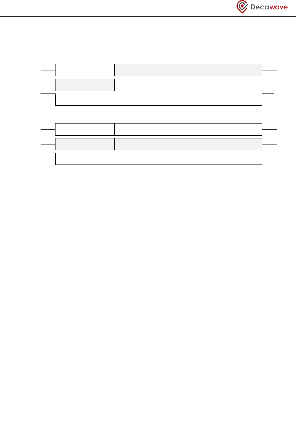
data to it. As shown in Figure 1, for a read transaction all octets beyond the transaction header are ignored
DW1000 User Manual
© Decawave Ltd 2017
Version 2.15
Page 10 of 244
by the DW1000, and for a write transaction all octets output by the DW1000 should be ignored by the host
system.
Figure 1: SPI Read and Write Transactions
Note: The octets are physically presented on the SPI interface data lines with the high order bit sent first in
time.
SPI transactions are enveloped by the assertion of the active low chip select line, SPICSn. The high-to-low
assertion (low) of SPICSn initialises the SPI transaction handler so that the DW1000 interprets the next
octet(s) as a new transaction header. The low-to-high de-assertion of SPICSn ends the SPI transaction.
Typically a software SPI interface driver will include a parameter to indicate the length of the transaction, i.e.
how many octets to write to the device on the SPI bus, or how many bytes to read.
The SPI accessible parameters of the DW1000 are organised into 64 separate register file locations (detailed
in section 7 – The DW1000 register set). Every SPI access transaction header includes a 6-bit register file ID
that identifies which register file is being accessed by the transaction. Sub-addressing within the selected
register file allows efficient access to all the parameters within the DW1000. Depending on the sub-
addressing being used, the transaction header is either one, two or three octets long. These three types of
transaction are described in the sub-sections below.
Note: when writing to any of the DW1000 registers care must be taken not to write extra data beyond the
published length of the selected register (see section 7 – The DW1000 register set).
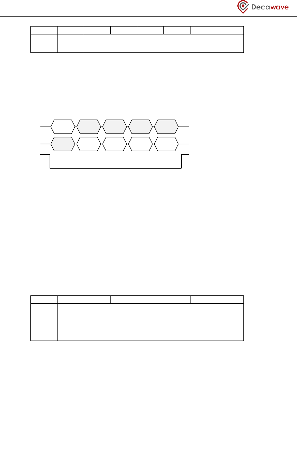
Figure 2 shows the fields within the one octet transaction header of a simple non-indexed SPI transaction.
Bit-6 is zero indicating that a sub-index is not present. The register (file) ID selects the top level addressing of
the DW1000 parameter or parameter block being accessed.
Transaction Header
Host should ignore
MOSI
MISO
Read
Transaction Header
Transaction Body
–
write data input by DW
1000
Host should ignore
Host should ignore
MOSI
MISO
Write
Transaction Body
–
read data output by DW
1000
ignored by DW
1000
SPICSn
SPICSn
DW1000 User Manual
© Decawave Ltd 2017
Version 2.15
Page 11 of 244
Figure 2: Single octet header of the non-indexed SPI transaction
The remaining octets of the transaction, the transaction body, immediately following this one-octet header
are read from (or written to) the selected register file beginning at index zero. Figure 3 shows an example of
a non-indexed read from the Device ID register using the single octet header.
Figure 3: Example non-indexed read of the Device ID register (0x00)
Note: The octets of a multi-octet value are transferred on the SPI interface in octet order beginning with
the low-order octet. This is shown in Figure 3.
2.2.1.2.1 SPI transaction with a 2-octet header
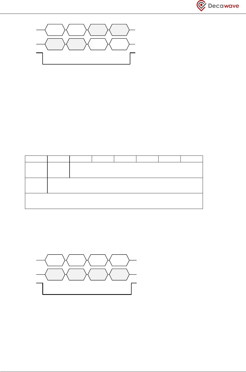
Figure 4 shows the fields within the two octet transaction header of a short-indexed SPI transaction. Bit-6 of
the first octet is 1 indicating that a sub-index is present. The register (file) ID in the first octet selects the top
level address of the DW1000 parameter block being accessed. In the second octet bit-7 is zero indicating
that a further transaction header octet is not present and that the remaining 7 bits of octet-2 are a short
sub-index into the register file.
Figure 4: Two octet header of the short indexed SPI transaction
The remaining octets of the transaction, the transaction body, immediately following this two-octet header
are read from (or written to) the selected register file beginning at the selected index address 0 to 127.
Figure 5 shows an example of an indexed read from the Device ID register using the two octet transaction
header.
76543210
Operation:
0 = Read
1 = Write
Bit = 0, says
sub-index is
not present
Register file ID – Range 0x00 to 0x3F (64 locations)
Bit number:
Meaning: Transaction Header
Octet
76543210
Operation:
0 = Read
1 = Write
Bit = 1, says
sub-index is
present
Register file ID – Range 0x00 to 0x3F (64 locations)
Extended
Address:
0 = no
7-bit Register File sub-address, range 0x00 to 0x7F (128 byte locations)
Bit number:
Meaning: Transaction Header
Octet 1
Octet 2
MOSI
MISO
SPICSn
0
x
00
0
x
30
0
x
01
0
xCA
0
xDE
Non sub indexed read from register
file ID
0
x
00
,
this
32
-
bit register
contains the Device ID
,
the
4
-
octet
result is
0
xDECA
0130
DW1000 User Manual
© Decawave Ltd 2017
Version 2.15
Page 12 of 244
Figure 5: Example short-indexed read of 3rd and 4th octets of register 0x00
2.2.1.2.2 SPI transaction with a 3-octet header
Figure 6 shows the fields within the three octet transaction header of a long-indexed SPI transaction. Bit-6 of
the first octet is 1 indicating that a sub-index is present. The register (file) ID in the first octet selects the top
level addressing of the DW1000 parameter or parameter block being accessed. In the second transaction
header octet bit-7 is set indicating the long form of indexed addressing is to be employed and thus the
remaining seven bits of the second octet along with all of the third transaction header octet form a 15-bit
sub-index into the selected register file.
Figure 6: Three octet header of the long indexed SPI transaction
The octets of transaction body which immediately follow the transaction header are read from (or written
to) the selected register file beginning at the selected sub-index address 0 to 32767.
Figure 7: Example long-indexed write of one octet to index 310 of the TX buffer
Figure 7 shows an example of an indexed write that uses the longer the three octet header. This example is a
write to the transmit data buffer at sub index 0x136. The TX buffer has register file ID of 0x09. Octet 1 of
transaction header is thus 0xC9 as bit-7 is 1 to signal a write and bit-6 is 1 indicating a sub-address follows.
The 15-bit sub-address has the binary value 000-0001-0011-0110. In octet 2 of the transaction header, bit 7
is set to indicate an extended sub-index and the remaining bits contain 0110110, the low 7 bits of the sub-
7 6 5 4 3 2 1 0
Operation:
0 = Read
1 = Write
Bit = 1, says
sub-index is
present
Register file ID – Range 0x00 to 0x3F (64 locations)
Extended
Address:
1 = yes
Low order 7 bits of 15-bit Register file sub-address
range 0x0000 to 0x7FFF (32768 byte locations)
High order 8 bits of 15-bit Register file sub-address
range 0x0000 to 0x7FFF (32768 byte locations)
Bit number:
Meaning: Transaction Header
Octet 1
Octet 2
Octet 3
MOSI
MISO
SPICSn
0
x
40
0
x
02
0
xCA
0
xDE
Short sub
-
indexed read
2
-
octets beginning at
index
2
in register file ID
0
x
00
.
This reads the
high two octets of this
32
-
bit register
,
the
result is
0
xDECA
.
MOSI
MISO
SPICSn
0
xC
9
0
xB
6
0
x
02
0
xA
5
Long sub indexed write of octet value
0
xA
5
to the transmit buffer
(
Reg ID
0
x
09
)
at index
310
(
0
x
136
in hex
)

DW1000 User Manual
© Decawave Ltd 2017
Version 2.15
Page 13 of 244
address. Octet 3 of the transaction header then contains 00000010, the remaining eight high order bits of
the sub-address index, which is 0x02 in hex.
The DW1000 parameters that may be read and written using these SPI transactions are detailed in section 7
– The DW1000 register set.
2.2.2 Interrupts
The DW1000 can be configured to assert its IRQ pin on the occurrence of one or more status events. The
assertion of the IRQ pin can be used to interrupt the host controller and redirect program flow to deal with
the cause of the event.
The polarity of the IRQ pin may be configured via the HIRQ_POL bit in the Register file: 0x0D – System
Control Register. By default on power up the IRQ polarity is active high. This is the recommended polarity to
ensure lowest power operation of the DW1000 in SLEEP and DEEPSLEEP device states. This pin will float in
SLEEP and DEEPSLEEP states and may cause spurious interrupts unless pulled low.
The occurrence of a status event in Register file: 0x0F – System Event Status Register may assert the IRQ pin
depending on the setting of the corresponding bit in the Register file: 0x0E – System Event Mask Register.
By default, on power-up, all interrupt generating events are masked and interrupts are disabled.
2.2.3 General Purpose I/O
The DW1000 provides 8 GPIO pins. These can be individually configured at the user’s discretion to be inputs
or outputs. The state of any GPIO configured as an input can be read and reported to the host controller
over the SPI interface. When configured as an output the host controller can set the state of the GPIO to
high or low.
Some of the GPIO lines have multiple functions as listed in the DW1000 data sheet.
The configuration and operation of the GPIO pins is controlled via Register file: 0x26 – GPIO control and
status.
By default, on power-up, all GPIOs are configured as inputs.
2.2.4 The SYNC pin
This pin is used for external clock synchronisation purposes. See section 6.1 – External Synchronisation for
further details.
2.3 DW1000 Operational States
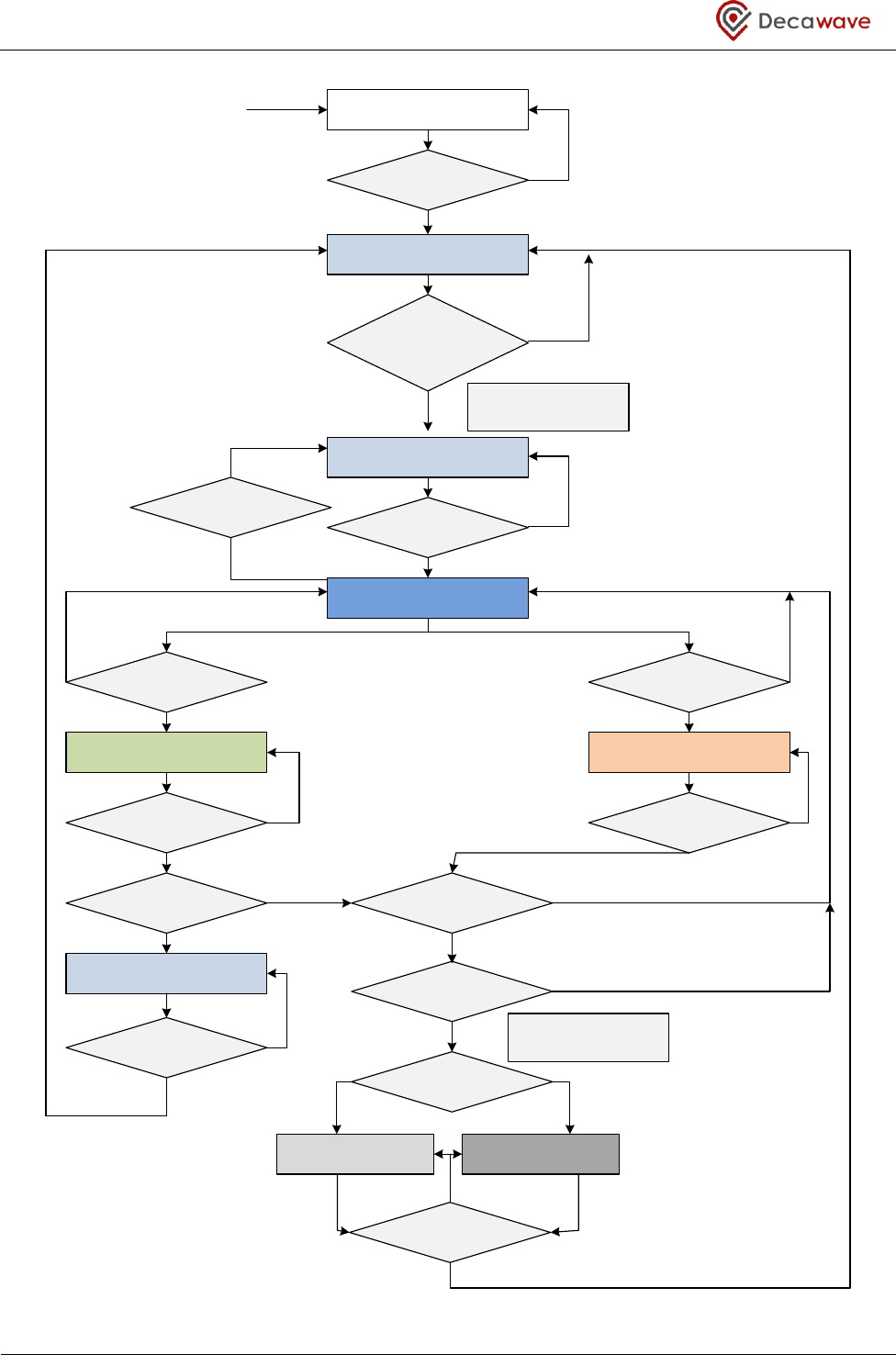
2.3.1 State diagram
The DW1000 has a number of different operational states (or modes). These are listed and described in
Table 1 below and the transitions between them are illustrated in Figure 8.
DW1000 User Manual
© Decawave Ltd 2017
Version 2.15
Page 14 of 244
Figure 8: DW1000 State Diagram
OFF
Crystal stable,
RSTn released &
Digital 1.2V LDO
enabled?
WAKEUP
INIT
RX enabled?
RX TX
RX complete?
Snooze set?
Snooze count complete?
Wakeup Event?
SNOOZE
SLEEP
CLKPLL locked?
TX enabled?
TX complete?
DEEPSLEEP
3.3 V rail > POR threshold?
Restore selected
AON configuration
IDLE
Store selected
AON configuration
SLEEP or DEEPSLEEP?
Power off
N
Y
N
Y
Y
N
Y
Y
Y
Y
AUTO SLEEP?
IRQ Pending?
N
N
N
N
Y
Y
Y
Y
N
N
N
N
N
Y
Force to INIT?
Y

DW1000 User Manual
© Decawave Ltd 2017
Version 2.15
Page 15 of 244
2.3.2 Overview of main operational states
Table 1: Main DW1000 operational states / modes
State Name
State Description
OFF
In the OFF state the DW1000 is completely powered off, with no voltages applied to
any of its input pins. Power consumption = 0 µA. No I/O pins should be driven or
power will leak through the I/O cells.
WAKEUP
During the WAKEUP state the crystal oscillator and the band-gap are enabled. After
approximately 4 ms the digital LDO will be enabled and the RSTn (output) will de-
assert allowing the DW1000 to enter the INIT state.
INIT
In the INIT state the main crystal oscillator is running. The raw 38.4 MHz XTAL
oscillator frequency is divided by 2 to give a 19.2 MHz internal clock called XTI. In the
INIT state digital circuitry of the DW1000 is fed from this 19.2 MHz XTI clock.
If the DW1000 has entered INIT state from a SLEEP or DEEPSLEEP state, (or as a result
of a reset), then the register configurations can be automatically restored from the
AON memory array.
Then the DW1000 turns on the CLKPLL and after 5 µs the CLKPLL will be locked and
the DW1000 will automatically transition into the IDLE state.
SPI accesses from an external microcontroller are possible in the INIT state, but these
are limited to a SPICLK input frequency of no greater than 3 MHz. Care should be
taken not to have an active SPI access in progress at the CLKPLL lock time (i.e. at t =
5 µs) when the automatic switch from the INIT state to the IDLE state is occurring,
because the switch-over of clock source can cause bit errors in the SPI transactions.
It is possible to return to the INIT state from the IDLE state under register control by
selecting the XTAL as the clock source and by disabling what is known as sequencing
so the device does not automatically transfer into the IDLE state.
IDLE
In the IDLE state the DW1000 internal clock generator CLKPLL is locked running and
ready for use but is gated off to most circuitry to minimize power consumption. In the
IDLE state SPI communications can operate at up to 20 MHz, the maximum SPICLK
frequency. In the IDLE state the analog receive and transmit circuits are powered
down. The external host can control the DW1000 to initiate a transmission or
reception and thus cause the DW1000 to progress into TX state or RX state
respectively. If a delayed TX or RX operation is initiated (see section 3.3 – Delayed
Transmission and 4.2 – Delayed Receive) then the DW1000 will stay in the IDLE state
until the delayed time has elapsed, after which it will enter the TX state or RX state.

DW1000 User Manual
© Decawave Ltd 2017
Version 2.15
Page 16 of 244
State Name
State Description
SLEEP
In the SLEEP state the IC consumes < 1 µA from the external power supply inputs. All
internal LDOs are turned off. In the SLEEP state the DW1000 internal low powered
ring oscillator is running and is used to clock the sleep counter whose expiry is
programmed to “wake up” the DW1000 and progress into the WAKEUP state. While in
SLEEP power should not be applied to GPIO, SPICLK or SPIMISO pins as this will cause
an increase in leakage current.
DEEPSLEEP
With the exception of the OFF state, the DEEPSLEEP state is the lowest power state of
the device.
In DEEPSLEEP all internal circuitry is powered down with the exception of the always-
on memory which can be used to hold the device configuration for restoration on
wakeup
Once in DEEPSLEEP the DW1000 remains there until the occurrence of a wakeup
event. This can be either:
1. the SPICSn line pulled low or
2. the WAKEUP line driven high
for the duration quoted in the DW1000 data sheet (nominally 500 μs).
It is also recommended to use the SLP2INIT or CPLOCK event status bits (in Register
file: 0x0F – System Event Status Register) to drive the IRQ interrupt output line high to
confirm the wake-up.
Once the DW1000 has detected a wakeup event it progresses into the WAKEUP state.
While in DEEPSLEEP power should not be applied to GPIO, SPICLK or SPIMISO pins as
this will cause an increase in leakage current.
TX state
In the TX state the DW1000 actively transmits a frame containing the contents of the
transmit buffer on the configured RF channel with the configured transmit parameters
(PRF, data rate, preamble code etc.)
Once the frame transmission is complete the DW1000 may enter one of three modes
depending on the programmed configuration.
After the frame transmission is complete the DW1000 will return to the IDLE state
unless the ATXSLP bit is set (in Sub-Register 0x36:04 – PMSC_CTRL1) in which case the
DW1000 will enter the SLEEP or DEEPSLEEP state automatically, (as long as no host
interrupts are pending).
Note that it is not possible to be in the TX and RX states simultaneously – the DW1000
is a half-duplex transceiver device.
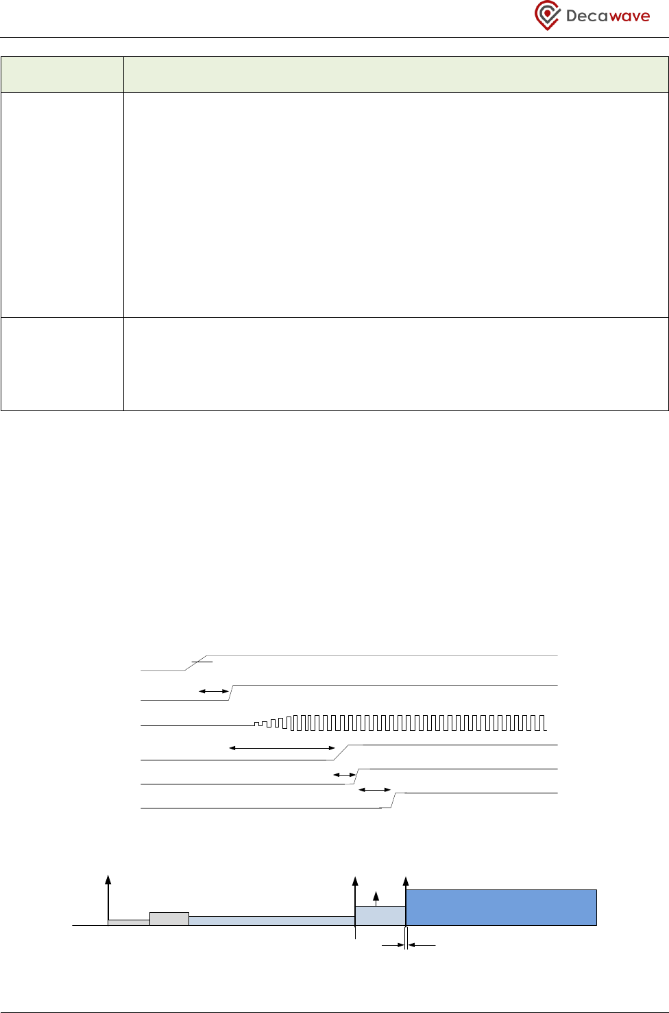
DW1000 User Manual
© Decawave Ltd 2017
Version 2.15
Page 17 of 244
State Name
State Description
RX state
In the RX state, the DW1000 receiver is active, either hunting for preamble or (once it
has detected preamble) actively receiving preamble searching for SFD, and
subsequently receiving the PHR, decoding it and receiving the data part of the frame.
In the RX state, the RF synthesiser and all RX blocks are active. After an event that ends
the reception, (either a good frame RX, or some error or timeout event that aborts
reception) the DW1000 will return to the IDLE state unless the ARXSLP bit is set (in Sub-
Register 0x36:04 – PMSC_CTRL1) in which case the DW1000 will enter the SLEEP or
DEEPSLEEP state automatically (as long as no host interrupts are pending).
Note that it is not possible to be in the RX and TX states simultaneously – the DW1000
is a half-duplex transceiver device.
SNOOZE
The SNOOZE state is similar to the INIT state except that a counter is running to cause
the DW1000 to automatically go to the RX state (via INIT and IDLE) when the counter
expires. The snooze count times are in units of the raw 19.2 MHz XTI clock rate, (since
the 125 MHz digital PLL clock is not running).
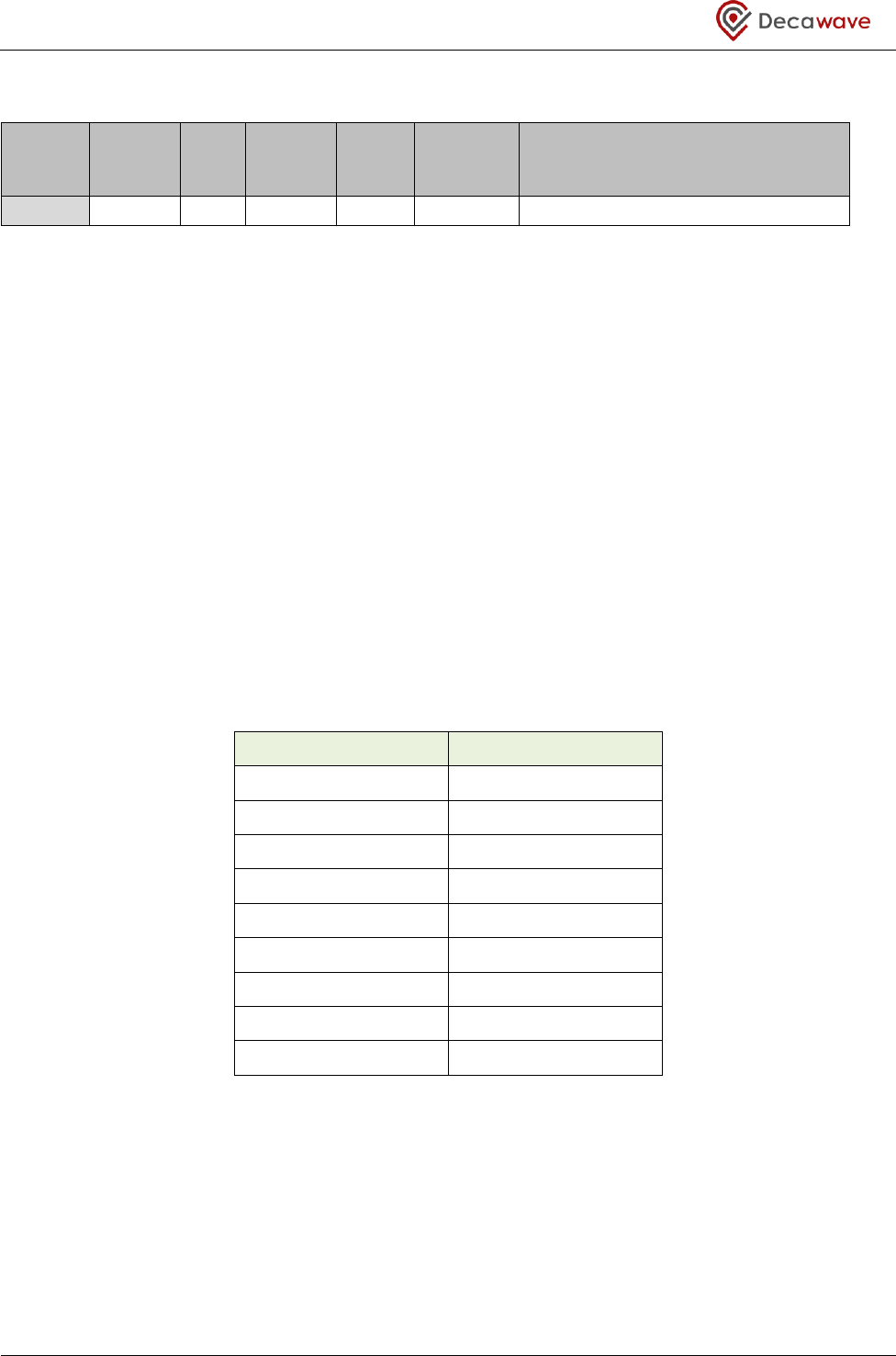
2.4 Power On Reset (POR)
When the external power source is applied to the DW1000 for the first time, the internal Power On Reset
(POR) circuit compares the externally applied supply voltage to an internal power-on threshold
(approximately 1.5 V), and once this threshold is passed the crystal oscillator is enabled and the external
device enable pin EXTON is asserted. An internal counter running off the low power oscillator is used to hold
the DW1000 in reset to ensure that the crystal oscillator is stable before it gets used. Once the digital reset is
de-asserted the digital core wakes up and enters the WAKEUP state. From this state it will automatically turn
on the CLKPLL and wait for it to lock before entering the IDLE state.
IDLE
INIT
OFF WAKEUP
CLKPLL locked
Crystal stable,
RSTn=1
POWERON
VDDBATT
EXTON
XTAL
VDDDIG
RSTn
Vpor
SPI comms
up to 3MHz SPI comms up
to max SPI frequency
Battery Inserted
VDDBATT switched on
300µs
4ms
5µs
7µs
CLKPLL
Lock
CLKPLL
enabled
SPI comms not advised
as PLL locks

DW1000 User Manual
© Decawave Ltd 2017
Version 2.15
Page 18 of 244
Figure 9: Timing diagram and power profile for cold start POR
2.4.1 SLEEP and DEEPSLEEP
In the DW1000 very low power DEEPSLEEP state, the IC is almost completely powered down except for a
small amount of memory necessary to maintain IC configurations. This is the lowest power mode of the IC
where the power drain is < 100 nA. To wake the IC from DEEPSLEEP requires an external agent to assert the
WAKEUP input line or the external host microprocessor to initiate an SPI transaction to assert the SPICSn
input.
The DW1000 also includes a low power SLEEP state where the IC can wake itself from sleeping as a result of
the elapsing of a sleep timer that is running from a low-powered ring oscillator internal to the DW1000 IC.
In this SLEEP state the power drain is < 1 µA. The DW1000 may wake from SLEEP state when the sleep timer
elapses. The WAKEUP or SPICSn inputs may also be used to wake the device.
The frequency of the low power oscillator is dependent on process variations within the IC, but is generally
somewhere in between 7,000 and 13,000 Hz. There are facilities within the IC to measure the length of an
LP oscillator cycle, in counts of the IC crystal oscillator divided by two, (i.e. this is 38.4 MHz ÷ 2, or 19.2 MHz).
2.4.1.1 Waking from sleep
The return from SLEEP and DEEPSLEEP modes, is via
Driving the WAKEUP pin high for approximately 500 μs, (assuming the WAKE_PIN configuration bit is
set in Sub-Register 0x2C:06 – AON_CFG0).
Driving the SPICSn pin low for approximately 500 μs, (assuming the WAKE_SPI configuration bit is set
in Sub-Register 0x2C:06 – AON_CFG0). This can be achieved by doing a dummy SPI read of sufficient
length.
NOTE: When using the SPICSn pin to wake up the device it is important that the SPIMOSI line is
held low for the duration of the SPICSn to ensure that a spurious write operation does not occur.
In addition return from SLEEP also occurs when
The internal sleep timer counter expires, (assuming the WAKE_CNT configuration is bit is set in Sub-
Register 0x2C:06 – AON_CFG0 along with an appropriate SLEEP_TIM).
In all of three wakeup cases the device is returned to the IDLE state by default but additional state
transitions can be automatically enacted thereafter depending on configurations.
2.4.1.2 Configuration register preservation
Prior to entering the SLEEP and DEEPSLEEP states and prior to exiting the WAKEUP state, the main DW1000
configurations are copied to and from an Always-On memory (AON). Power is maintained to AON memory
at all times, even in SLEEP and DEEPSLEEP states. The copying of configuration data (saving or restoring)
takes about 7 µs to complete. The detail of which configurations are saved and restored is given in Table

DW1000 User Manual
© Decawave Ltd 2017
Version 2.15
Page 19 of 244
46: Configurations maintained in the AON. Restoration of configurations during the WAKEUP state is only
done if the ONW_LDC configuration bit is set in 7.2.45.1 – Sub-Register 0x2C:00 – AON_WCFG.
Note: The host system should avoid SPI access to general system registers or OTP Memory during the
copying period to prevent any conflicts occurring. Access to the TX (or RX) buffer is not restricted during this
period.
2.4.1.3 Automatically loading LDO calibration data from the OTP
When waking from SLEEP or DEEPSLEEP it is necessary to load the LDOTUNE_CAL value from the OTP if it has
been programmed during IC production test calibration. To confirm if the LDOTUNE_CAL has been
programmed first read the OTP address 0x4. If this reads back as non-zero (only the first byte needs to be
checked) then the device has been calibrated and the ONW_LLDO bit in Sub-Register 0x2C:00 – AON_WCF
must be set. This will allow the OTP parameter LDOTUNE_CAL to be automatically copied over to the
required register (Sub-Register 0x28:30 – LDOTUNE) each time the DW1000 wakes up. If the OTP address
0x4 reads back as zero, then the ONW_LLDO bit must not be set.
2.4.2 Specific state sequences supported by the DW1000
The DW1000 supports a number of state sequences intended to minimize power consumption in certain
applications. These are: -
Mode Name
Mode Description
SNIFF MODE
In SNIFF mode the DW1000 alternates between the RX (on) and the IDLE (off) states.
Further details on this mode are given in section 4.5.1 – SNIFF.
LOW DUTY
CYCLE SNIFF
MODE
In Low duty-cycle SNIFF mode, where the off time is larger, the DW1000 can be
configured to spend this off time in the INIT state which is lower power than the IDLE
state (used for the off period of a SNIFF). Further details of this mode are given in
section 4.5.2 – Low duty-cycle SNIFF.
LOW POWER
LISTENING
Low-Power Listening mode is a special mode where the receiver spends most its time
in a low power (SLEEP or DEEPSLEEP) state only waking up occasionally to sample the
air for a message. This feature is described in detail in section 4.4 – Low-Power
Listening
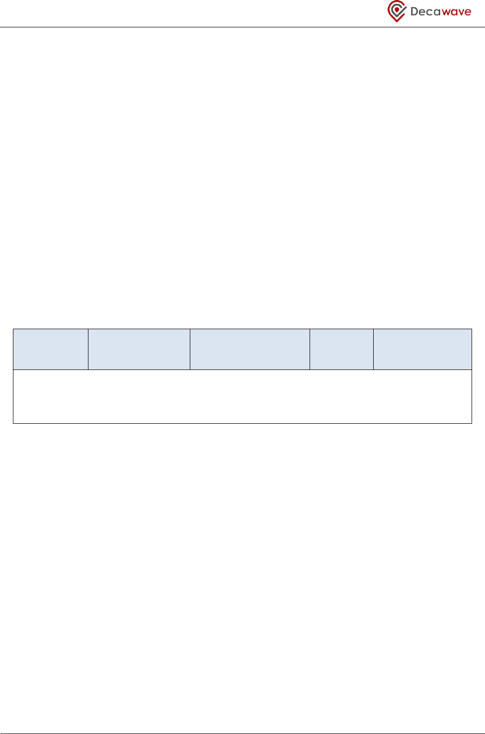
2.5 Default Configuration on Power Up
DW1000 is a highly configurable transceiver with many features. The register reset values have been
selected with the intention of minimising user configuration required. The default configuration may be
summarised as being channel 5, preamble code 4 and mode 2. Channel numbers and preamble codes are as
specified in the standard, IEEE 802.15.4-2011 [1] and mode 2 is as specified in the DW1000 data sheet
modes and comprises the following configurations:
DW1000 User Manual
© Decawave Ltd 2017
Version 2.15
Page 20 of 244
Table 2: Mode 2 Excerpt from DW1000 Data Sheet Operational Modes Table
Mode
Data Rate
PRF
(MHz)
Preamble
(Symbols)
Data
Length
(Bytes)
Packet
Duration (µs)
Typical Use Case
(Refer to DW1000 user manual for further information)
Mode 2
6.8 Mbps
16
128
12
152
RTLS, TDOA Scheme, Short Range, High Density
Some further details are given below on the specifics of the default device configuration. For full details the
reader may refer to the register map where the default value of each register is given, section 7 – The
DW1000 register set.
2.5.1 Default System Configuration
Much of the system configuration is configured in the SYS_CFG register, please see section Register file: 0x04
– System Configuration for a full description of the register contents and defaults.
By default, interrupt polarity is active high and all interrupts are disabled, see the SYS_CFG register for
interrupt polarity and the SYS_MASK and SYS_STATUS registers for interrupt configuration and information,
see sections Register file: 0x0E – System Event Mask Register and Register file: 0x0F – System Event Status
Register.
GPIOs are set to mode 0, their default function as shown in Table 3.
Table 3: GPIO Default Functions
GPIO Pin
Default Function
GPIO0/RXOKLED
GPIO0
GPIO1/SFDLED
GPIO1
GPIO2/RXLED
GPIO2
GPIO3/TXLED
GPIO3
GPIO4/EXTPA
GPIO4
GPIO5/EXTTXE/SPIPHA
GPIO5
GPIO6/EXTRXE/SPIPOL
GPIO6
SYNC/GPIO7
SYNC
IRQ/GPIO8
IRQ
Smart TX power is on by default, see section Register file: 0x1E – Transmit Power Control and Smart Transmit
Power Control for configuration and operation information.
Sniff mode is off, see Register file: 0x1D – SNIFF Mode for details, frame wait timeout (see SYS_CFG register
bit RXWTOE and Register file: 0x0C – Receive Frame Wait Timeout Period) and preamble detection timeout
(see Sub-Register 0x27:24 – DRX_PRETOC) are off, whilst SFD detection timeout (see Sub-Register 0x27:20 –
DRX_SFDTOC) is on.

DW1000 User Manual
© Decawave Ltd 2017
Version 2.15
Page 21 of 244
Other SYS_CFG register settings such as Automatic Receiver Re-Enable (RXAUTR) and MAC functions such as
frame filtering (FFEN), double buffering (DIS_DRXB) and automatic acknowledgement (AUTOACK) are all off
by default. Automatic CRC generation is on and the CRC LFSR is initialized to 0’s (FCS_INIT2F).
Note that CRC generation is selected as part of a transmit command, see Register file: 0x0D – System Control
Register.
External synchronisation and the use of external power amplifiers are deactivated by default, see sections
6.1 – External Synchronisation and 6.2 – External Power Amplification.
2.5.2 Default Channel Configuration
Channel 5, preamble code 4 and 16 MHz PRF are set by default in the CHAN_CTRL register, see Register file:
0x1F – Channel Control for more information.
The transmit data rate is set to 6.8 Mbps in the TX_FCTRL register, see TXBR field in Register file: 0x08 –
Transmit Frame Control . The receive data rate is never set unless 110 kbps reception is required. Note that
this must be configured in register SYS_CFG, field RXM110K, see Register file: 0x04 – System Configuration.
The RF PLL and Clock PLL are configured for channel 5 operation by default, please refer to Register file: 0x2B
– Frequency synthesiser control block for channel configuration settings for each channel.
2.5.3 Default Transmitter Configuration
Transmit RF channel configurations are set for channel 5 by default – see Sub-Register 0x28:0C– RF_TXCTRL.
Transmit Smart power is enabled by default via the DIS_STXP bit in SYS_CFG register, refer to Register file:
0x04 – System Configuration. Please see section 7.2.31.2 – Smart Transmit Power Control for further
information.
The transmit preamble symbol repetition length is 128 symbols, see Register file: 0x08 – Transmit Frame
Control, TXPSR and PE fields for configuration details.
2.5.4 Default Receiver Configuration
Receiver RF channel configurations are set for channel 5 by default, see Sub-Register 0x28:0B– RF_RXCTRLH.
Digital receiver tuning registers; DRX_TUNE0b, DRX_TUNE1a, DRX_TUNE1b and DRX_TUNE2 are configured
by default for 16 MHz PRF, 6.8 Mbps data rate and a preamble symbol repetition of length 128. See Sub-
Register 0x27:02 – DRX_TUNE0b, Sub-Register 0x27:04 – DRX_TUNE1a, Sub-Register 0x27:06 – DRX_TUNE1b
and Sub-Register 0x27:08 – DRX_TUNE2 for programming details.
The LDERUNE bit is enabled by default, which means that the microcode (the LDE algorithm) that has been
loaded in RAM will execute on every frame reception, which in turn will calculate accurate frame time-of-
arrival. However the DW1000 needs to load this microcode on power-on from a special ROM area in the
DW1000. This is done by enabling the LDELOAD bit as part of DW1000 initialisation (because after powering
up the DW1000 (or after exiting SLEEP or DEEPSLEEP states) the LDE RAM is empty). This should be done
before the receiver is enabled if it is important to timestamp this received frame. If the LDE code is not

DW1000 User Manual
© Decawave Ltd 2017
Version 2.15
Page 22 of 244
being loaded before the receiver is enabled then the LDERUNE (LDE run enable) control in Sub-Register
0x36:04 – PMSC_CTRL1 must be turned off (set to zero).
2.5.5 Default Configurations that should be modified
Although the DW1000 will power up in a usable mode for the default configuration outlined, some of the
register defaults are sub optimal and should be overwritten before proceeding to use the device in the
default mode.
2.5.5.1 AGC_TUNE1
AGC_TUNE1 is set to 0x889B by default which is not the optimal value for the default PRF of 16 MHz. For
best performance the user should set this value to 0x8870 before proceeding to use the default device
configuration. Refer to Sub-Register 0x23:04 – AGC_TUNE1.
2.5.5.2 AGC_TUNE2
AGC_TUNE2 must be set as described in Sub-Register 0x23:0C – AGC_TUNE2 for correct functioning of
DW1000.
2.5.5.3 DRX_TUNE2
DRX_TUNE2 is set to 0x311E0035 by default which is not the optimal value for the default PRF and PAC. For
best performance the user should set this value to 0x311A002D before proceeding to use the default device
configuration. Refer to Sub-Register 0x27:08 – DRX_TUNE2.
2.5.5.4 NTM
NTM is set to 0xC by default and may be set to 0xD for better performance, refer to Sub-Register 0x2E:0806
– LDE_CFG1.
2.5.5.5 LDE_CFG2
LDE_CFG2 is set to 0x0000 by default and should be set to 0x1607 for 16 MHz PRF before proceeding to use
the default configuration, refer to Sub-Register 0x2E:1806– LDE_CFG2.
2.5.5.6 TX_POWER
The TX_POWER setting is 0x1E080222 by default. This value should be set to 0x0E082848 before proceeding
to use the default configuration. Please see section 7.2.31.2 – Smart Transmit Power Control for further
information.
2.5.5.7 RF_TXCTRL
RF_TXCTRL is not set to the optimum values by default. This value should be set for channel 5 according to
Table 38 before proceeding to use the default configuration. Please see Sub-Register 0x28:0C– RF_TXCTRL
for further information.
DW1000 User Manual
© Decawave Ltd 2017
Version 2.15
Page 23 of 244
2.5.5.8 TC_PGDELAY
TC_PGDELAY is set to 0xC5 by default, which is the incorrect value for channel 5. This value should be set to
0xC0 before proceeding to use the default configuration. Please see Sub-Register 0x2A:0B – TC_PGDELAY
for further information.
2.5.5.9 FS_PLLTUNE
FS_PLLTUNE is set to 0x46 by default, which is not the optimal value for channel 5. This value should be set
to 0xBE before proceeding to use the default configuration. Please see Sub-Register 0x2B:0B – FS_PLLTUNE
for further information.
2.5.5.10 LDELOAD
LDELOAD is reset to 0 by default. This needs to be set as part of DW1000 initialisation and before receiver
enable, if it is important to get timestamp and diagnostic information from received frames. See description
of LDELOAD bit for further information. The table below outlines the programming steps to load the
microcode from ROM into RAM.
Table 4: Register accesses required to load LDE microcode
Step
Number
Instruction
Register
Address
Data
Length
(Bytes)
Data
(Write/Read)
L-1
Write Sub-Register
0x36:00 (PMSC_CTRL0)
2
0x0301
L-2
Write Sub-Register
0x2D:06 (OTP_CTRL)
2
0x8000
Wait 150 µs
L-3
Write Sub-Register
0x36:00 (PMSC_CTRL0)
2
0x0200
2.5.5.11 LDOTUNE
It is necessary to load the LDOTUNE_CAL value from the OTP if it has been programmed during IC production
test calibration. To confirm if the LDOTUNE_CAL has been programmed first read the OTP address 0x4. If this
reads back as non-zero (only the first byte needs to be checked) then the device has been calibrated. To load
this value automatically following a wake up from SLEEP or DEEPSLEEP see the section on Waking from
sleep. To use this value immediately, it should be read directly from OTP and written to Sub Register File
0x28:30 LDOTUNE.
DW1000 User Manual
© Decawave Ltd 2017
Version 2.15
Page 24 of 244
3 Message Transmission
3.1 Basic Transmission
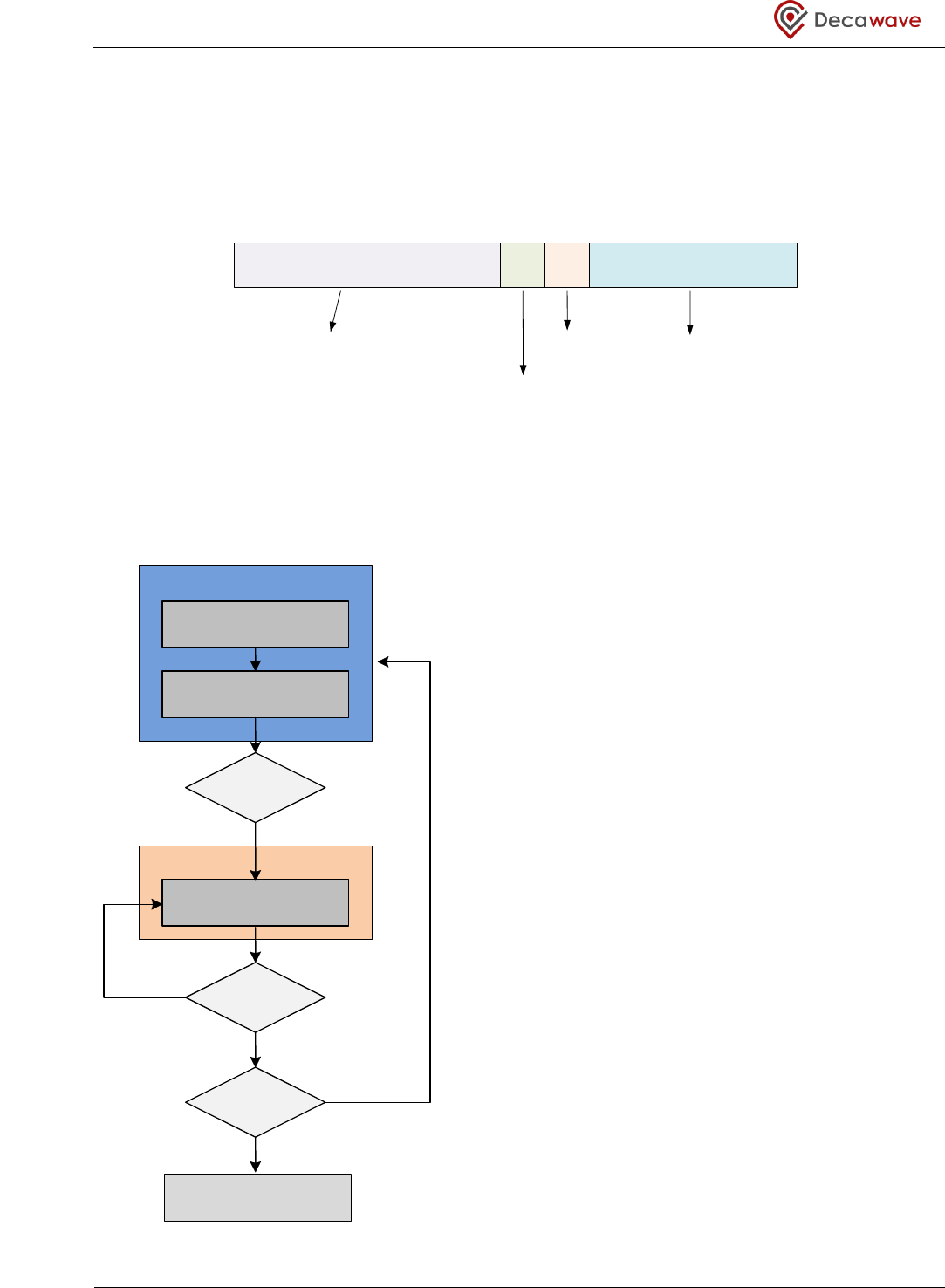
The transmission of data frames is one of the basic functions of the DW1000 transceiver. Figure 10 shows
the elements of the transmitted frame.
*Additional configurations marked “Extra” or “Extended” are proprietary to Decawave; see section 3.4 for details of
Extended Length Data Frames
Figure 10: Transmit Frame format
The modulation details of these frame elements can be found
in section 10 – APPENDIX 1: The IEEE 802.15.4 UWB physical
layer.
The transmit sequence is as shown in Figure 11. The DW1000
begins in the IDLE state awaiting instruction from the host
controller.
In order to transmit, the host controller must write data for
transmission to Register file: 0x09 – Transmit Data Buffer. The
desired selections for preamble length, data rate and PRF must
also be written to Register file: 0x08 – Transmit Frame Control.
Transmitter configuration is carried out in the IDLE state, but
frame configurations may be carried out during active transmit
as described in section 3.5 – High Speed Transmission.
Assuming all other relevant configurations have already been
made, the host controller initiates the transmission by setting
the TXSTRT control bit in Register file: 0x0D – System Control
Register. After transmission has been requested, the DW1000
automatically sends the complete frame; preamble, SFD, PHR
and data. The FCS (CRC) is automatically appended to the
message as an aid to the MAC layer framing.
The end of frame transmission is signalled to the host via the
TXFRS event status bit in Register file: 0x0F – System Event
Status Register, and the DW1000 returns to IDLE mode to
await new instructions.
Preamble
SFD
PHR
Data
IEEE STD
:
64
,
1024
or
4096
symbols
*Extra
:
128
,
256
,
512
,
1536
or
2048
symbols
IEEE STD
:
8
or
64
symbols
*Extra
:
16
symbols
21
bits
IEEE STD
:
Up to
127
coded octets
*Extended
:
Up to
1023
coded octets
NO
TX
complete
?
NO
YES
AUTOSLEEP
?
Write Tx data to data buffer
Configure Tx parameters
Transmit message
TX START
?
TRANSMIT
YES
IDLE
YES
SLEEP
Figure 11: Basic Transmit Sequence

DW1000 User Manual
© Decawave Ltd 2017
Version 2.15
Page 25 of 244
Further transmission features are described in the following sections:
Transmit message time-stamping – see section 3.2 –Transmission timestamp.
Delayed transmission – see section 3.3 – Delayed Transmission.
Long transmit frames – see section 3.4 – Extended Length Data Frames.
High Speed transmit – see section 3.5 – High Speed Transmission.
3.2 Transmission timestamp
During frame transmission the start of the PHR (PHY header) is the event nominated by the IEEE 802.15.4
UWB PHY standard for message time-stamping. The time the first symbol of the PHR launches from the
antenna (defined as the RMARKER) is the event nominated as the transmit time-stamp.
The DW1000 digital transmit circuitry takes note of the system clock counter as the RAW transmit
timestamp at the point when it begins sending the PHR. It then adds to this the transmit antenna delay
(configured in Register file: 0x18 – Transmitter Antenna Delay) to get the antenna adjusted transmit time-
stamp that it writes to the TX_STAMP field of Register file: 0x17 – Transmit Time Stamp.
See also section 8.3 – IC Calibration – Antenna Delay.
3.3 Delayed Transmission
For delayed transmission, the transmit time is programmed into Register file: 0x0A – Delayed Send or Receive
Time and then the delayed transmission is initiated by setting both TXDLYS and TXSTRT controls in Register
file: 0x0D – System Control Register.
One of the design goals of delayed transmission was that the specified transmission time would be
predictable and aligned with the Transmit timestamp. This was achieved in that the transmission time
specified is the time of transmission of the RMARKER (not including the TX antenna delay), that is the raw TX
time, TX_RAWST in Register file: 0x17 – Transmit Time Stamp before the antenna delay is added. This
allows for the time of transmission of a message to be pre-calculated and embedded in the message being
transmitted.
NOTE: The low-order 9 bits of the delayed Transmit value programmed into Register file: 0x0A – Delayed
Send or Receive Time are ignored giving a time resolution of 8 ns, or more precisely 4 ÷ (499.2×10⁶). To
calculate the time of transmission of the RMARKER at the antenna, the low 9 bits of the delayed TX time
should be zeroed before adding the TX antenna delay.
In performing a delayed transmission, the DW1000 calculates an internal start time for when to begin
sending the preamble to make the RMARKER raw timestamp agree with the programmed transmit time.
The DW1000 remains in idle state until the system time (Register file: 0x06 – System Time Counter) reaches
the correct point to turn on the transmitter and begin preamble.
One use of delayed transmission (and reception), is in symmetric double-sided two-way ranging, (described
in APPENDIX 3: Two-Way Ranging), where it is important to keep the response times the same at both ends
to reduce the error in range estimate. Minimising the response time also reduces this error, and in working

DW1000 User Manual
© Decawave Ltd 2017
Version 2.15
Page 26 of 244
to minimise this the host microprocessor may sometimes be late invoking the delayed TX, i.e. so that the
system clock has passed the specified start time (i.e. internal start time mentioned above) and then the IC
has to complete almost a whole clock count period before the start time is reached. The HPDWARN event
status flag in Register file: 0x0F – System Event Status Register warns of this “lateness” condition so that
during application development the delay may be chosen large enough to generally avoid this lateness. The
HPDWARN status flag also serves to facilitate detection of this late invocation condition so that recovery
measures may be taken should it ever occur in deployed product. For delayed transmission it is the internal
start time mentioned above that is used when deciding whether to set the HPDWARN event for the delayed
transmit. As long as the preamble start time is the near future, the HPDWARN event flag will not be set. If a
long delay was intended then the HPDWARN flag can be ignored and the transmission will begin at the
allotted time. If a long delay was not intended then the transmission can be stopped by issuing a TRXOFF via
Register file: 0x0D – System Control Register.
Under normal circumstances the IC transmitter needs a few microseconds to power up the transmitter – this
time is correctly handled for the RMARKER positioning, but is not included in the HPDWARN calculation. So,
if the initiation of a delayed transmission is commanded early enough so that it does not generate a
HPDWARN event but not sufficiently early for the IC transmitter to power up before the start of preamble;
then frame transmission will still occur and the RMARKER will be sent at the correct time, but, during the
initial few symbols of preamble (while the transmitter is powering-up) the preamble may not be sent
correctly. For most use cases this will not be an issue, as there is generally ample preamble remaining for
good reception. However for shorter preamble sequences, especially the 64-symbol preamble sequence,
losing a few symbols can have a performance impact.
When using delayed transmission with 64-symbol preambles then, designers should also be aware that the
power-up time for the transmitter is not included in the HPDWARN calculation which means that if the
preamble start time is too close then the initial few symbols of preamble (while the transmitter is powering-
up) may not be sent correctly. This is flagged in a transient TXPUTE bit status and counted in Sub-Register
0x2F:1A – Transmitter Power-Up Warning Counter, (assuming counting is enabled by the EVC_EN bit in Sub-
Register 0x2F:00 – Event Counter Control). It is recommended that checks are added, during design
validation, to ensure that the HPDWARN event does not happen and also (especially for short preambles)
that the TXPUTE event does not happen, and take appropriate measures to avoid them (like increasing the
response delay time).
3.4 Extended Length Data Frames
Standard IEEE 802.15.4-2011 UWB frames carry up to 127 bytes of payload. The DW1000 supports a non-
standard mode of operation with frame lengths up to 1023 bytes of data. This mode of operation is enabled
via the PHR_MODE selection bits of Register file: 0x04 – System Configuration.
In this proprietary mode the PHY header (PHR) is redefined to carry the 3 extra bits of frame length. In order
to communicate extended length data frames between two DW1000 devices both ends must be set to the
long frame PHY header mode via the PHR_MODE selection bits of Register file: 0x04 – System Configuration.
If the setting is only at one end of a link any attempt at communication will fail with PHR errors being
reported. When long frame mode is selected, the DW1000 will be unable to communicate with any device
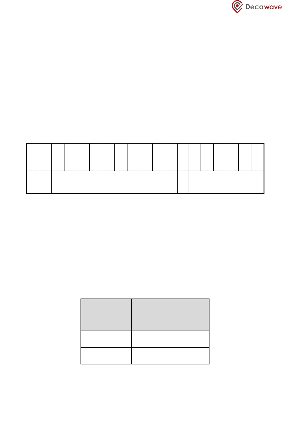
DW1000 User Manual
© Decawave Ltd 2017
Version 2.15
Page 27 of 244
operating with standard frame encoding because the SECDED error check sequence of the PHR in long frame
mode is incompatible with the standard encoding.
Note also that the probability of an error occurring within a frame increases as the frame length is increased,
and as a result of this increasing the frame length may or may not improve system throughput depending on
the frame error rate and the need to retransmit frames when there is an error.
In long frame mode only the high order bit of the TXPSR value from Register file: 0x08 – Transmit Frame
Control is sent in the PHR and reported in the RXPSR value in Register file: 0x10 – RX Frame Information
Register.
The PHR encoding for the proprietary extended length data frames is shown below in Figure 12:
Figure 12 : PHR Encoding Extended Length Data Frames
The Data Rate field has the same encoding as used for the IEEE 802.15.4-2011 PHR.
The frame length field L9-L0 is an unsigned 10-bit integer number that indicates the number of octets in the
PSDU from the MAC sub-layer. Note that the high order bit of the length is transmitted first in time.
A single bit, P0, provides the Preamble Duration field, indicating the length of the SYNC portion of the SHR
shown in Table 5.
Table 5: Preamble Duration field values in Extended Length Data Frame PHR
P0
Preamble length for
BPM-BPSK modulation
mode
0
64 to 1024 symbols
1
1536 to 4096 symbols
The Preamble Duration field may be used by a receiver to set the value of the preamble duration for an ACK
frame.
Valid preamble lengths are 64, 128, 256, 512, 1024, 1536, 2048 and 4096 symbols. Since the Preamble
Duration field in the transmitted frame covers a range of preamble lengths, a receiver may count the
Bit
01 2 3 4 5 6 7 8 9 10 11 12 13 14 14 16 17 18
R1 R0 L9 L8 L7 L6 L5 L4 L3 L2 L1 L0 P0 S5 S4 S3 S2 S1 S0
Data
Rate SECDED Check Bits
Preamble
Duration
Frame Length

DW1000 User Manual
© Decawave Ltd 2017
Version 2.15
Page 28 of 244
number of preamble symbols received to additionally inform the choice of preamble length for any response
frames.
The SECDED (single error correct, double error detect) field, S5–S0, is a set of six parity check bits that are used
to protect the PHR from errors caused by noise and channel impairments. The SECDED calculation is the same
as that defined in the IEEE 802.15.4-2011 standard except the bits C5–C0 are inverted to get S5–S0 as follows:
S0 = NOT (C0)
S1 = NOT (C1)
S2 = NOT (C2)
S3 = NOT (C3)
S4 = NOT (C4)
S5 = NOT (C5)
3.5 High Speed Transmission
Certain features of the DW1000 are designed to support maximum utilisation of the transmitter. These
features are described below:
3.5.1 TX buffer offset index
The TXBOFFS field (in Register file: 0x08 – Transmit Frame Control) allows the TX_BUFFER to be used to hold
more than one frame, (providing that data can fit within the 1024 octets of the buffer). In initiating a
transmission then the host controller will set the TXBOFFS offset index to the first octet of the frame to be
transmitted and set the length field to reflect the length of the frame to send. While sending is in progress,
the host controller can prepare and write another frame to a different part of the TX_BUFFER. After
transmission of the first frame then, the host has saved the time needed to write the next data frame, and
just needs to set the offset and initiate the transmission of the next frame.
During a data streaming or bulk data transfer then the host controller might divide the TX_BUFFER into two
areas of 512 octets each, sending from them alternately. For acknowledged data transfer then: the receipt
of the acknowledgement for frame, frame “A” (say), can be used to trigger the sending of the next frame,
frame “B” (say), that is already waiting in the other half of the buffer and at the same time signalling that the
buffer half that contained the acknowledged frame “A” can now, (while frame “B” is being transmitted), be
filled with the data for the subsequent frame, frame “C” (say). Where the acknowledgement for frame “A” is
not received, the data for it is still in the TX_BUFFER ready to be retransmitted.
3.5.2 TX buffer write while sending or receiving
For fast turnaround it is possible to initiate preamble sending before writing the frame data to the
TX_BUFFER or writing the frame length to the length as specified in the TFLEN and TFLE fields of the Register
file: 0x08 – Transmit Frame Control. So preamble transmission can begin before the TX data is written into
the DW1000. The host microprocessor then has the time of any fixed response delay, and the time for
sending preamble and SFD before it needs to have the frame length set in TFLEN and TFLE ready for the
DW1000 to insert into the PHR, and thereafter the host microprocessor needs to have the individual octets
of data written into the TX_BUFFER before they are consumed by the DW1000 transmitter.

DW1000 User Manual
© Decawave Ltd 2017
Version 2.15
Page 29 of 244
Clearly to do this care needs to be taken to have the frame length setup ready for inclusion in the PHR and to
have the data written into the TX_BUFFER before it is consumed, and, mechanisms are needed to ensure
that the wrong data cannot be sent as a good frame. The mechanisms to achieve this involves using SFCST
to suppress FCS transmission until all data is written to the TX_BUFFER and then CANSFCS to cancel this
suppression so that the FCS will be sent. (Both SFCST and CANSFCS are in Register file: 0x0D – System Control
Register).
While this technique is of use for fast responses, it could also be used for streaming in cases where the use
of the scheme described in section 3.5.1 – TX buffer offset index is not suitable, i.e. where the frame size is
between 513 and 1023 octets.
Similarly if DW1000 is actively receiving, data may be written to the TX_BUFFER while the receiver is active.
The following are the points of note for optimum throughput or fast response turnaround:
(a) The frame length should be set up as early as possible:
For streaming, TFLEN, TFLE, TXBOFFS, may be reprogrammed for the next frame as soon as the PHR
is sent, i.e. after the TXPHS (Transmit PHY Header Sent) event has been signalled.
For transmission of a response, depending on the application, the length of the response may be
known before the soliciting message has arrived. This is often true for example in two-way ranging.
(b) Initiate transmission as early as possible:
For streaming this is as soon as the previous transmission has finished or previous reception has
finished (RXDFR has been set). This is signalled by the activation of the TXFRS (Transmit Frame Sent)
event status bit is set in Register file: 0x0F – System Event Status Register, an event that would
generally be picked up by an interrupt handler in the host system.
For transmission of a response, the application may have to parse some of the message before
deciding whether a response is required. This parsing could perhaps be begun early but in any case
the initiation of transmission will in general be as soon as possible after the arrival of the message
soliciting the response. Message arrival is signalled by the RXDFR (Receiver Data Frame Ready) event
status bit in Register file: 0x0F – System Event Status Register, an event also generally picked up by
an interrupt handler in the host system.
Issue the TXSTRT with SFCST (Transmit Start with Suppress auto-FCS Transmission) instruction in
Register file: 0x0D – System Control Register to initiate the transmission. This will kick off preamble
transmission.
(c) Write the frame data to the TX_BUFFER as fast as possible.
This might be done in the interrupt handler or in a high priority task scheduled by it.
(d) Cancel the suppression of FCS as soon as possible thereafter.
This is done by issuing the CANSFCS (Cancel Suppression of auto-FCS transmission) instruction in
Register file: 0x0D – System Control Register. Assuming that the host has written every octet of data
to the TX_BUFFER before the DW1000 needed to consume it, then this will be successful and the

DW1000 User Manual
© Decawave Ltd 2017
Version 2.15
Page 30 of 244
frame will be sent with a good CRC, and that is essentially the end of the discussion on this
technique.
If the host system has not been quick enough in writing the data this will result in the frame being
sent with the wrong data but with a bad CRC also. The DW1000 transmitter includes a circuit to
detect the host microprocessor writing to the buffer between the selected TXBOFFS and any address
the IC has already consumed the data from, which is taken to mean that the data is being written
too late for transmission. This “Transmit Buffer Error” condition will cause the DW1000 to ignore the
CANSFCS command so the frame is sent with a bad CRC. It is signalled by the TXBERR bit in Register
file: 0x0F – System Event Status Register. Clearly this is a bad condition that will not help system
performance. It is up to system designers to avoid this condition, debugging and removing it during
the design phase, by ensuring the system responsiveness is sufficient such that this never happens,
(e.g. by employing a faster processor or a faster SPI, or by increasing the response/inter-frame delay
or increasing the preamble length).
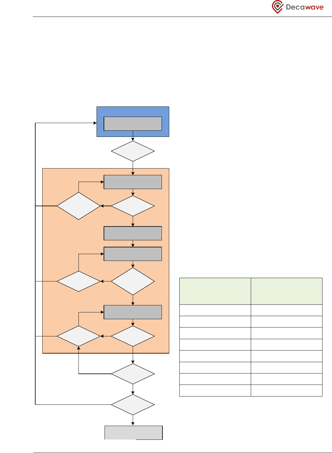
DW1000 User Manual
© Decawave Ltd 2017
Version 2.15
Page 31 of 244
4 Message Reception
4.1 Basic Reception
The reception of a frame is enabled by a host request or by an automatic re-enabling of the receiver. The
receiver will search for preamble continually until preamble has been detected or acquired, when a
demodulation will be attempted. A preamble detection timeout may be set to allow the receiver to stop
searching for preamble after a desired period. A basic receive sequence is shown in Figure 12.
4.1.1 Preamble Detection
The preamble sequence is detected by cross-correlating
in chunks which are a number of preamble symbols
long. The size of chunk used is selected by the PAC
configuration in Sub-Register 0x27:08 – DRX_TUNE2.
The PAC size should be selected depending on the
expected preamble size. A larger PAC size gives better
performance when the preamble is long enough to allow
it. But if the PAC is too large for the preamble length
then receiver performance will be impaired, or fail to
work at the extremes – (e.g. a PAC of 64 will never
receive frames with just 64 preamble symbols). Table 6
gives the recommended PAC size configuration to use in
the receiver depending on the preamble length being
used in the transmitter.
Table 6: Recommended PAC size
Expected preamble
length of frames being
received
Recommended PAC size
64
8
128
8
256
16
512
16
1024
32
1536
64
2048
64
4096
64
The choice of preamble length is discussed in section 9.3
– Choice of data rate, preamble length and PRF.
It is possible to abort reception if a valid preamble is not
detected within a configured time. This is done by using
NO
RX
complete?
NO
YES
AUTOSLEEP?
Configure Rx parameters
Search for Preamble
RX START?
RECEIVE
YES
IDLE
Preamble
Detected?
Preamble
Detection
Timeout?
YES
NO
NO
YES
Acquire SFD
Preamble
Acquisition
complete?
SFD Timeout?
YES
NO
NO
YES
Acquire data
Frame
Received?
YES
NO
Frame Wait
Timeout?
YES
Acquire Preamble
NO
YES
SLEEP
Figure 13: Basic receive sequence

DW1000 User Manual
© Decawave Ltd 2017
Version 2.15
Page 32 of 244
the preamble detection timeout, programmable in Sub-Register 0x27:24 – DRX_PRETOC. This may be useful
after sending a message where a response is being awaited. Here if the preamble is not detected then the
awaited response is not coming. The preamble detection time-out can be used to abandon the reception at
the earliest possible time, saving power.
The preamble detection state also has the possibility of operating in a mode called pulsed preamble
detection mode (PPDM), or SNIFF mode, programmable through Register file: 0x1D – SNIFF Mode. This is a
technique that where the receiver samples (“sniffs”) the air periodically on a timed basis, e.g. 50% or 25% of
the time, to reduce the power needed during preamble detection.
4.1.2 Preamble Accumulation
Once the preamble sequence is detected, the receiver begins accumulating correlated preamble symbols,
while looking for the SFD sequence (a particular sequence of preamble symbols, see section 10.3 –
Synchronisation header modulation scheme for details). Accumulation stops when the SFD is detected, but
may stop earlier if the accumulator grows quickly, (as is the case in close line-of-sight conditions for
instance), in this case the receiver continues receiving preamble, without accumulating, searching for the
SFD sequence.
4.1.3 SFD Detection
The detection of SFD is a key event in the reception of a frame, because it marks the start of the PHY header,
which defines the RMARKER that is time-stamped (see section 4.1.6 – RX Message timestamp), and it marks
the change from preamble demodulation to the BPM/BPSK demodulation of the PHR (and data
subsequently).
It is possible to abort reception if the SFD is not detected within a certain time after preamble is detected.
This functionality is configured via Sub-Register 0x27:20 – DRX_SFDTOC. This SFD detection timeout guards
against false detection of preamble (which has a finite chance of happening) that could otherwise lead to a
prolonged period receiving nothing. By default the SFD detection timeout is 4161 symbol times, (i.e. greater
than the largest possible preamble), but it can be set lower if it is known that all nodes in the network are
using shorter preambles. It is possible to disable the SFD detection timeout but this is not advised.
The SFD sequence is 64 symbols long for 110 kbps data rate and 8 symbols long for the other two supported
data rates of 850 kbps and 6.8 Mbps. The receiver needs to be configured to look for either the short 8-
symbol SFD or the long 64-symbol SFD. This is done via the RXM110K configuration bit in Register file: 0x04
– System Configuration.
The DW1000 also has the capability of programming non-standard SFD sequences that give improved
performance, see Register file: 0x21 – User defined SFD sequence.
4.1.4 PHR Demodulation
The main role of the PHY Header (PHR) is to convey the length of the data portion of the frame, and to
indicate the data rate being employed for data demodulation. See section 10.4 – PHY header for details of
the PHY header. For data rates of 850 kbps and 6.8 Mbps the PHR is modulated / demodulated as per the

DW1000 User Manual
© Decawave Ltd 2017
Version 2.15
Page 33 of 244
850 kbps data rate (note that because Reed Solomon encoding is not applied to the PHR, its bit rate is
approximately 1 Mbps). If the PHR is indicating 850 kbps then the data demodulation continues at this rate,
but if the PHR is indicating 6.8 Mbps then the demodulation changes to this rate at the end of the PHR as
data demodulation begins.
4.1.5 Data Demodulation
Section 10.2 – Data modulation scheme describes the modulation scheme. In the receiver a Viterbi decoder
is used recover the data bits (this is also used for PHR reception) which are then passed through the Reed
Solomon decoder to apply any further correction it can. Every octet thus received is passed through a CRC
checker which checks the frame against the transmitted FCS.
As the data octets are received they may also be parsed by the frame filtering function if enabled, see
section 5.2– Frame filtering for more details.
Successful reception of a frame is signalled to the host via the RXDFR and RXFCG event status bits in Register
file: 0x0F – System Event Status Register. Other status bits in this register may be used to flag reception of
other parts of the frame or, events indicating failure, i.e. RXPTO (Preamble detection Timeout), RXSFDTO
(SFD timeout), RXPHE (PHY Header Error), RXRFSL (Reed Solomon error), RXRFTO (Frame wait timeout), etc.
Other related features are: -
Delayed reception – see section 4.2 – Delayed Receive.
Long receive frames – see section 3.4–Extended Length Data Frames.
Double buffering – see section 4.3 – Double Receive Buffer.
Receive message time-stamping – see section 4.1.6 – RX Message timestamp.
4.1.6 RX Message timestamp
During frame reception the SFD detection event marking the end of the preamble and the start of the PHR is
the nominal point which is time-stamped by the IC. The IEEE 802.15.4 UWB standard nominates the time
when this RMARKER arrives at the antenna as the significant event that is time-stamped.
The DW1000 digital receiver circuitry takes a coarse timestamp of the symbol in which the RMARKER event
occurs and adds a various correction factors to give a resultant adjusted time stamp value, which is the time
at which the RMARKER arrived at the antenna. This includes subtracting the receive antenna delay as
configured in Sub-Register 0x2E:1804 – LDE_RXANTD and adding the correction factor determined by the
first path (leading edge) detection algorithm embedded in the DW1000. The resulting fully adjusted RX
timestamp is written into Register file: 0x15 – Receive Time Stamp.
See also section 8.3 – IC Calibration – Antenna Delay.
Note: Due to an issue in the re-initialisation of the receiver, it is necessary to apply a receiver reset after
certain receiver error or timeout events (i.e. RXPHE (PHY Header Error), RXRFSL (Reed Solomon error),
RXRFTO (Frame wait timeout), etc.). This ensures that the next good frame will have correctly calculated
timestamp. It is not necessary to do this in the cases of RXPTO (Preamble detection Timeout) and

DW1000 User Manual
© Decawave Ltd 2017
Version 2.15
Page 34 of 244
RXSFDTO (SFD timeout). For details on how to apply a receiver-only reset see SOFTRESET field of Sub-
Register 0x36:00 – PMSC_CTRL0.
4.2 Delayed Receive
In Delayed receive operation the receiver turn-on time is programmed into Register file: 0x0A – Delayed
Send or Receive Time and then the delayed receiving is initiated by setting both RXDLYE and RXENAB controls
in Register file: 0x0D – System Control Register.
The DW1000 remains in idle state until the system time (Register file: 0x06 – System Time Counter) reaches
the value programmed in Register file: 0x0A – Delayed Send or Receive Time and then the IC receiver is
turned on. This point marks the start time for any programmed timeouts that apply to the reception
process, i.e. the preamble detection timeout (which is set and enabled by Sub-Register 0x27:24 –
DRX_PRETOC) and the frame wait timeout (which is enabled by the RXWTOE configuration bit in Register file:
0x04 – System Configuration, and whose period is programmed in Register file: 0x0C – Receive Frame Wait
Timeout Period).
The benefit of delayed receive is that the receiver can be turned on at just the right moment to receive an
expected response, especially when that response is coming from a DW1000 employing delayed transmit to
send the response message at a precise time. This saves power because the idle mode power counting
down to the RX enable time is significantly less than the power required during frame reception.
One use of delayed receive, and especially delayed transmission, is in symmetric double-sided two-way
ranging, (described in APPENDIX 3: Two-Way Ranging), where it is important to keep the response times the
same at both ends to reduce the error in range estimate. Minimising the response time also reduces this
error, and here it is possible for the host microprocessor to be late invoking the delayed TX or RX, so that the
system clock is beyond the specified start time and then the IC has to complete almost a whole clock count
period before the specified start time is reached. The HPDWARN event status flag in Register file: 0x0F –
System Event Status Register warns of this “lateness” condition so that during development a delay may be
chosen large enough to generally avoid this lateness. The HPDWARN status flag also serves to facilitate
detection of this late invocation condition so that recovery measures may be taken should it ever occur in
deployed product.
4.3 Double Receive Buffer
This DW1000 has a pair of receive buffers offering the capability to receive into one of the pair while the
host system is reading previously received data from the other buffer of the pair. This is useful in a TDOA
RTLS anchor node where it is desired to have the receiver on as much as possible to avoid missing any tag
blink messages. A number of ancillary registers (timestamps, quality indicators and status bits) are also
doubly-buffered. The registers that are part of this “RX double-buffered swinging-set” are listed in Table 7.
Note: If overruns occur (see section 4.3.5), received frame data will be corrupted. Double buffering must
not be used in systems where overruns may be likely or frequent and is best used in systems where host
processing of the received frames is such that overruns will never occur.

DW1000 User Manual
© Decawave Ltd 2017
Version 2.15
Page 35 of 244
Table 7: Registers in the RX double-buffered swinging-set
RX double-buffered registers
LDEDONE, RXDFR, RXFCE and RXFCG bits in Register file: 0x0F – System Event Status Register
All of Register file: 0x10 – RX Frame Information Register
All of Register file: 0x11 – RX Frame Buffer
All of Register file: 0x12 – Rx Frame Quality Information
All of Register file: 0x13 – Receiver Time Tracking Interval
All of Register file: 0x14 – Receiver Time Tracking Offset
All of Register file: 0x15 – Receive Time Stamp
4.3.1 Enabling double-buffered operation
By default the DW1000 operates in a single buffered mode that is appropriate for many applications. When
using double-buffered mode it is appropriate to also configure the DW1000 to automatically re-enable the
receiver (moving on to the other buffer of the swinging set) as soon as it has completed receiving any
previous frame. Double-buffered receiving is enabled by setting the DIS_DRXB bit to zero, (in Register file:
0x04 – System Configuration). The RX auto-re-enable function is enabled by setting the RXAUTR bit to 1 (in
Register file: 0x04 – System Configuration).
DW1000 may be operated in double buffered mode without automatically re-enabling the receiver also,
which requires the host to manually enable the receiver to receive the next frame. The receiver can be
enabled in advance of processing the previously received frame. This operation will reduce the amount of
time for which the receiver may be actively listening for frames on the air, but will prevent both buffers
being full (at the same time) and will prevent overflows. This simplifies the buffer operation, see sections
4.3.3 and 4.3.5.
Note: When enabling or re-enabling the receiver in double-buffered mode, it is important to align both host
and IC receivers. That is, it is important to ensure that the buffer set that the IC receiver will first receive
into is the same set that the host system is pointing to and will first process when the first frame arrives.
Please refer to section 4.3.2 below for a discussion of this and how to achieve it.
4.3.2 Controlling which buffer is being accessed
There are two register sets, register-set-0 and register-set-1, but the host may only access one set at a time
through the register addresses listed in Table 7. To swap between sets the host issues the HRBPT (Host Side
Receive Buffer Pointer Toggle) command in Register file: 0x0D – System Control Register. The register-set
currently being accessed is reported by the HSRBP (Host Side Receive Buffer Pointer) status bit in Register
file: 0x0F – System Event Status Register. Every time the HRBPT command is issued the HSRBP status bit will
toggle.
There is also a read-only IC side buffer pointer index indicating which register-set the IC receiver is using or
will use for the next frame received, this is the ICRBP status bit (also in Register file: 0x0F – System Event

DW1000 User Manual
© Decawave Ltd 2017
Version 2.15
Page 36 of 244
Status Register). Reception of a new frame with good CRC will cause the ICRBP bit to increment (or toggle).
In the case that a received frame is rejected by frame filtering or bad CRC the ICRBP will not move on and the
buffer will be reused for the next incoming frame.
Thus, as noted in section 4.3.1 above, before enabling the receiver it is important to align both host and IC
receivers. This is done by reading the SYS_STATUS register 0x0F to checking that the HSRBP and ICRBP status
bits are the same, (i.e. both 1 or both 0), and if not issuing the HRBPT command to toggle HSRBP to be the
same as ICRBP.
4.3.3 Operation of double buffering
In normal operation the IC will receive a frame into the RX buffer (pointed to by ICRBP) and when the frame
is complete the IC will set the RXFCG interrupting the host and move on to receive into the other buffer of
the double-buffered swinging-set. Following this the host system should see this interrupt and service it by
reading the received data from the buffer along with any of the other ancillary registers it wants, and then
issue the HRBPT command to move to point to the other buffer. This HRBPT command also serves as the
mechanism to tell the IC that the host has finished with processing this received buffer (and is moving on to
the next one) essentially allowing the IC to reuse it for follow on frames. Figure 14 below is a flow chart
showing the use of double buffering in the receiver.
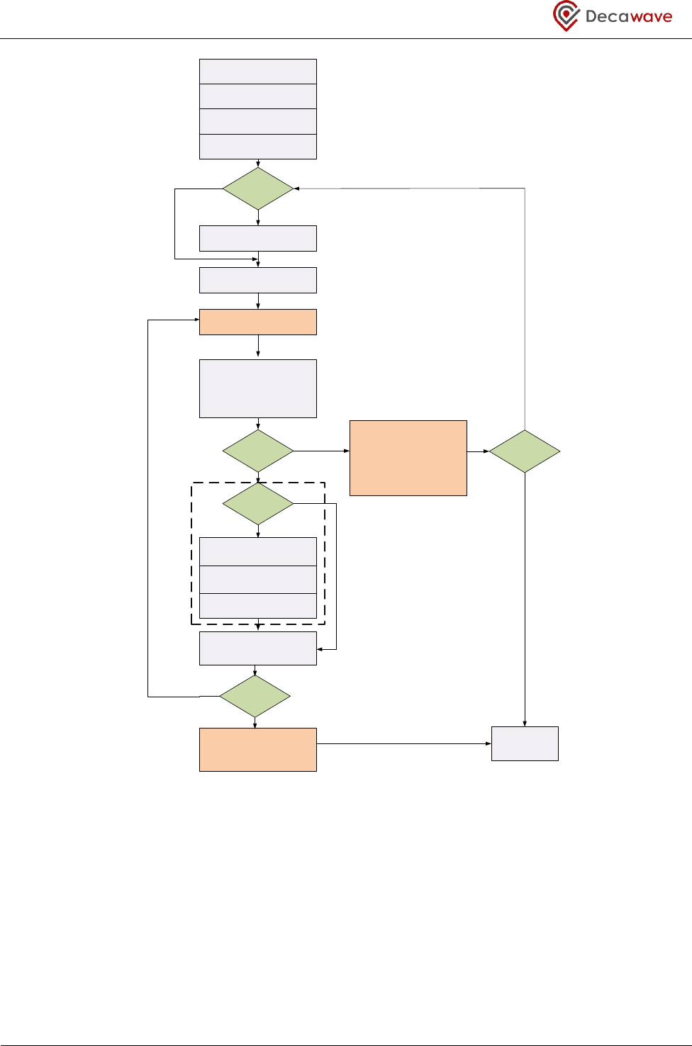
DW1000 User Manual
© Decawave Ltd 2017
Version 2.15
Page 37 of 244
Set up RX channel and other
parameters as required
Read SYS_STATUS reg:0F to
checking that HSRBP == ICRBP
HSRBP == ICRBP ?
Issue the HRBPT command in
reg:0x0D
Set RXENAB bit = 1, in reg:0D,
to enable the receiver
Set DIS_DRXB bit = 0 in reg:04
to Enable double buffering
YES
NO
Await frame arrival, as signalled
by the RXFCG event flag (IRQ)
Read the data in RX_BUFFER
reg:11.
Read other registers of interest
e.g. RX_FINFO reg:10, RX
timestamp in reg:15 and perhaps
frame quality reg:12.
RXOVRR==1
Issue the HRBPT to reg:0D to
signal finished with this buffer
and moving on to other of pair.
NO
YES
Set RXAUTR bit = 1 in reg:04
to enable RX auto-re-enable
Clear RX event flags in
SYS_STATUS reg:0F; bits FCE,
FCG, DFR, LDE_DONE
Frames must be discarded (do
not read frames) due to
corrupted registers and TRXOFF
command issued.
Receiver must be reset to exit
errored state.
Unmask Double buffered status
bits; FCE, FCG, DFR, LDE_DONE
Mask Double buffered status
bits; FCE, FCG, DFR, LDE_DONE
to prevent glitch when cleared
Rx more frames?
YES
HSRBP == ICRBP ?
YES
NO
Issue TRXOFF command and
clear double buffered status bits
to prevent spurious RX interrupts
NO
YES
NO
Rx more frames?
EXIT
Figure 14: Flow chart for using double RX buffering
In Figure 14 the section marked by the dashed black line can be omitted if the host system is able to service
the buffers with sufficient speed so that both buffers are never full at the same time. If this can be
guaranteed then an overrun (RXOVRR) can never occur and so cannot corrupt good frames, see section
4.3.5. In this case, buffer handling is simplified.
4.3.4 TRXOFF when using Double Buffering
To prevent spurious interrupts and for predictable behavior, TXRXOFF should be applied as shown below.
The double-buffered status bits should be cleared after the TRXOFF is applied and the interrupts on double-
buffered status bits should be masked while the bits are cleared.

DW1000 User Manual
© Decawave Ltd 2017
Version 2.15
Page 38 of 244
Clear RX event flags in
SYS_STATUS reg:0F; bits FCE,
FCG, DFR, LDE_DONE
Set TXRXOFF bit = 1, in reg:0D,
to disable the receiver
Mask Double buffered status
bits; FCE, FCG, DFR, LDE_DONE
to prevent glitch when cleared
Unmask Double buffered status
bits; FCE, FCG, DFR, LDE_DONE
Figure 15 : TRXOFF in Double-Buffered Mode
4.3.5 Overrun
An overrun condition may occur in the IC receiver if the host side is not keeping up with the arrival rate of
frames. So for example, say the IC receives a frame into the first buffer, moves on to the other buffer and
places a receive frame in it also. The IC will then move back to point to the first buffer again. If the host has
not completed reading the data from this first buffer (i.e. not yet issued the HRBPT) then the IC will not
overwrite that buffer with any new frame if one arrives. If a new frame arrives and the IC is unable to write
data to the buffer (because the host has not issued the HRBPT), then this is gives rise to an overrun
condition. The overrun condition occurs at the point the receiver finishes processing a good PHY header and
needs to write the first octet of data to the RX buffer. This event is detected by the IC and reported in the
RXOVRR status bit in Register file: 0x0F – System Event Status Register.
When a receiver overrun occurs, the frame reception in progress will be aborted and, assuming RX auto-re-
enable is enabled (by RXAUTR) the receiver will begin looking for preamble again. The overrun condition and
the RXOVRR status bit will be cleared as soon as the host issues the HRBPT command. Receiver overrun
events are also counted in Sub-Register 0x2F:0E – RX Overrun Error Counter, assuming that counting is
enabled by the EVC_EN bit in Sub-Register 0x2F:00 – Event Counter Control.
The overrun condition results in the corruption of the good frames previously received. The RX_FINFO,
RX_TIME and RX_FQUAL registers are affected. Received frames must be discarded due to corruption if an
overrun (RXOVRR) occurs. A receiver-only reset must be applied to the receiving device to clear the
errored state which may persist, see Figure 14. See the SOFTRESET field of Sub-Register 0x36:00 –
PMSC_CTRL0 for details of how to apply the receiver-only reset.
The impact of overrun corruption of previously received frames needs to be evaluated carefully in the
intended application. For instance, if overruns can occur the system should not use automatic
acknowledgements (see AUTOACK in SYS_CFG), as a corrupt frame will be acknowledged but then
discarded.
4.4 Low-Power Listening
Low-power listening is a feature whereby the DW1000 is predominantly in the SLEEP state but wakes
periodically for a very short time to sample the air for a preamble sequence. If no preamble is seen the
DW1000 automatically returns to SLEEP for another period, however if preamble is seen the DW1000 does
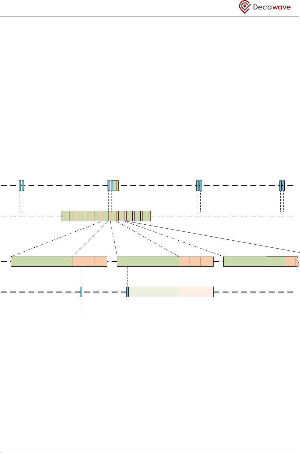
DW1000 User Manual
© Decawave Ltd 2017
Version 2.15
Page 39 of 244
not return to sleep but continues to receive preamble and the data frame, and after successful reception can
generate a receive frame interrupt to wake the host microprocessor to process the frame.
A typical example of this would be to use a sleep time of 1 second and a wake-up period of 2 PAC intervals,
where the average current for briefly listening and going back to sleep is very low. To wake up a device
operating in this low-power listening receiver mode, a transmitting device has to send sufficient data to
ensure that it is heard by the listener. Essentially then the transmitter has to send > 1 second of message to
ensure that it intersects with the short listening period of the receiving device. In practice this is done by
sending the same message repeatedly. In doing this, there is a finite chance that the listener listens at a time
when the transmitted preamble is not present. To avoid this, and give a better performing wakeup, the
DW1000 includes the ability to do a two-phase listen. This has a long sleep period followed by a sampling of
the air, followed by a short sleep period and then another sampling of the air. The short sleep time period is
set to ensure that if the first listen hits a message (missing the preamble) then the next listen will see
preamble. Figure 16 below shows the periodic listening for preamble and a wakeup sequence where the first
listening period intersects with the PHR or DATA, but where the second listening period allows successful
reception.
Figure 16 Low power listening with two sleep times
NOTE: Low-power listening works best for infrequent wake-ups across a population of listening nodes. The
reason is that every listening node will see preamble and wake-up and consume power receiving the packet
(even if the packet is not addressed to it).
In figure 16 there is a long period in SLEEP (or DEEPSLEEP) followed by a wakeup to the RX state (on) to sniff
for preamble, followed by (assuming no preamble is detected) a short period in SNOOZE state, followed by
the second RX state (on) to look for preamble, and (again assuming no preamble is detected) a return to
SLEEP (or DEEPSLEEP). Figure 17 shows the power profile associated with Low-Power Listening. If a
preamble is detected in either of the two receive windows, then the frame will be demodulated and an
interrupt set (if configured to do so).
Preamble SFD PHR DATA IFS Preamble SFD PHR DATA IFS Preamble SFD
Long Sleep (e.g. 1s) Long Sleep (e.g. 1s) Long Sleep (e.g. 1s)
Long Sleep (e.g. 1s) Short Sleep (e.g. 1.3ms)
Wake-up sequence 1s long
Preamble sample RX Frame
Detect preamble & Receive the frame
1st Listen 2nd Listen
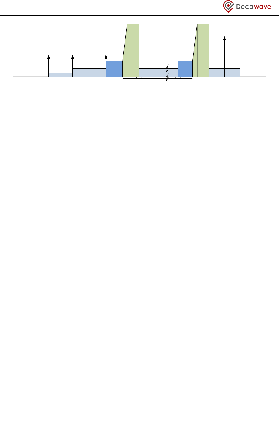
DW1000 User Manual
© Decawave Ltd 2017
Version 2.15
Page 40 of 244
Figure 17 Power profile for low power listening mode where no frame is received
4.4.1 Configuring low-power listening
Configure the receiver parameters for channel, data rate, PRF, preamble code, etc. as required for normal
receive operation. Then enable and configure the Low-Power Listening functionality as follows:
Set ARXSLP (after RX automatically sleep) bit in Sub-Register 0x36:04 – PMSC_CTRL1.
Set preamble detect timeout (RX ON time) in Sub-Register 0x27:24 – DRX_PRETOC.
Set SNOZ_TIM (snooze time) field of Sub-Register 0x36:0C – PMSC_SNOZT.
Set SNOZE (snooze enable) bit in Sub-Register 0x36:04 – PMSC_CTRL1.
Set SLEEP_TIM (sleep time period) field in Sub-Register 0x2C:06 – AON_CFG0.
Set SLEEP_EN (sleep enable) field in Sub-Register 0x2C:06 – AON_CFG0.
Set WAKE_CNT (wake when sleep counter elapses) field in Sub-Register 0x2C:06 – AON_CFG0.
Set ONW_RX (on wake turn on the receiver) bit in Sub-Register 0x2C:00 – AON_WCFG.
Set ONW_LDC (on wake load configurations) bit in Sub-Register 0x2C:00 – AON_WCFG.
Set PRES_SLEEP (preserve sleep) bit in Sub-Register 0x2C:00 – AON_WCFG.
Set only MRXFCG bit in Register file: 0x0E – System Event Mask Register.
Set the RXENAB bit in Register file: 0x0D – System Control Register.
The DW1000 will then begin the low power listening, and will only generate an interrupt when a frame is
received. Frame filtering can be enabled to further restrict the interrupt to only be generated when a
correctly addressed frame is received. To save power in such a system the host microprocessor (if
sufficiently capable) can enter a low power state awaiting the DW1000 interrupt to wake it when a frame
arrives.
When a frame is received, low-power listening must be deactivated by clearing the ARXSLP bit before the
RXFCG interrupt is cleared. This is required to ensure that the DW1000 does not go back to sleep as soon as
the interrupt is cleared, which would prevent the user from reading the frame data correctly. Once the
received frame has been handled, low-power listening mode can be reactivated by setting the ARXSLP bit
once more and putting the DW1000 back into reception or sleep mode.
4.5 Low-Power SNIFF mode
Low-Power SNIFF mode is a lower power preamble hunt mode, also known as pulsed preamble detection
mode (PPDM), where the receiver (RF and digital) is sequenced on and off rather than being on all the time.
These on and off times are configurable in Register file: 0x1D – SNIFF Mode, and have default values of zero,
RX
IDLE
INIT GO2SLP
Sample Wakeup Event:
Sleep counter expires
SLEEP SLEEP
2 RX attempts with no RX detected,
Host RX End.
WAKEUP
CLKPLL locked
Crystal stable,
RSTn=1 RX
Preamble
Timeout in PACs Snooze Count (Reg:36.0c)
(in 19.2MHz cycles)
SNOOZE IDLE
PLL Lock
Time (~5uS)
INIT
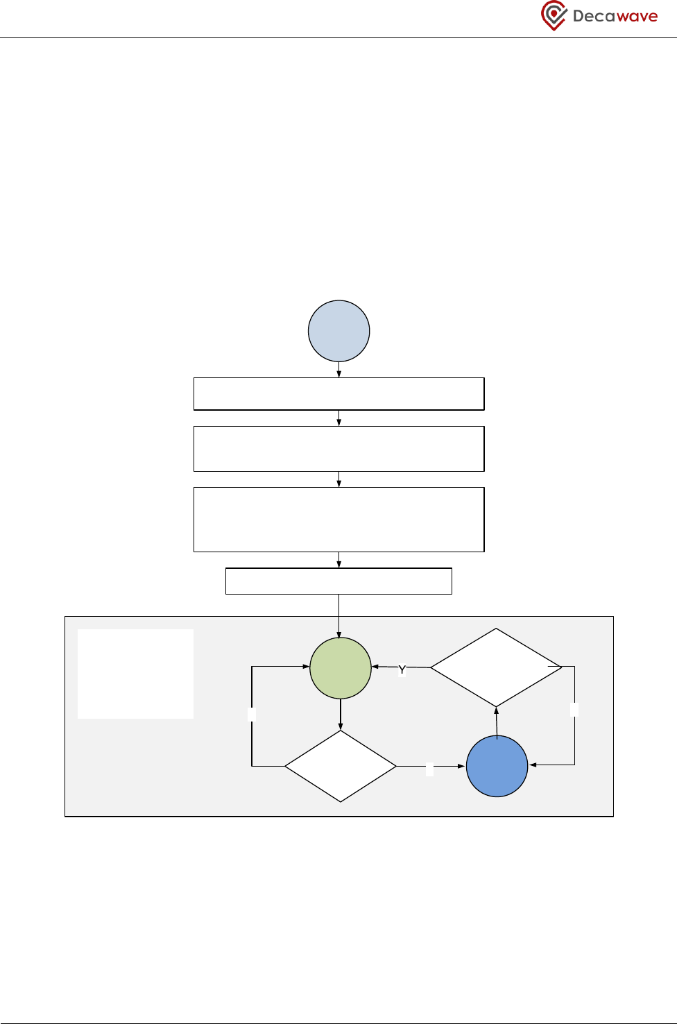
DW1000 User Manual
© Decawave Ltd 2017
Version 2.15
Page 41 of 244
disabling the feature. Using SNIFF mode causes a reduction in sensitivity depending on the ratio and
durations of the on and off periods.
There are two variations of low power SNIFF mode; these are termed SNIFF and Low duty-cycle SNIFF
described in the sub-sections below. The difference between the two modes is that in SNIFF mode the
DW1000 alternates between the RX state (on) and the IDLE (off) state, while in Low duty-cycle SNIFF mode
the IC spends the off time in the INIT state, transitioning only briefly through the IDLE state when entering
the RX state. The choice of mode has implications for calculating the Sniff Off time, which is described
below. The Low duty-cycle SNIFF mode will consume less power than SNIFF mode during the off period, but
both consume the same power during the on period. Figure 18 shows a simplified view of the state
transitions during SNIFF mode.
Figure 18: State transitions during SNIFF mode
4.5.1 SNIFF mode
In SNIFF mode the DW1000 alternates between the RX (on) and the IDLE (off) states. To enable SNIFF mode
two parameters SNIFF_ONT (sniff on time) and SNIFF_OFFT (the off time) need to be configured in Register
file: 0x1D – SNIFF Mode. The on duration is programmed in units of PAC, (these are described in section
4.1.1 – Preamble Detection), and must be set to at a minimum value of 2 for functional preamble detection.
The SNIFF_ONT counter automatically adds 1 PAC unit to the total PAC count so the programmed value
Setup RX mode of operation as per normal RX
Configure Sniff Mode On duration in multiples of PACs
(as set in RX mode of operation)
REG:1D[3:0] = SNIFF_ON
Configure Sniff Mode Off duration in uS. After this time
we start to turn on the RX blocks. Allow 5uS for the RX
RF block to be stable.
REG:1D[15:8] = SNIFF_OFF
PAC count =
Sniff on time?
Time count (µs)
= Sniff Off Time?
IDLE
(Sniff Off)
Y
N
N
This loop will continue
until preamble
detection or an RX
end event occurs
RX
(Sniff On)
Set RX_EN
IDLE
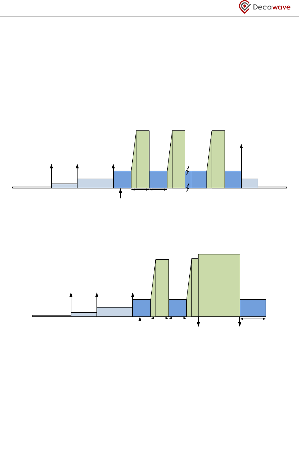
DW1000 User Manual
© Decawave Ltd 2017
Version 2.15
Page 42 of 244
should always be 1 less than the desired total. The off duration is programmed in units of 1 µs. When both
on and off durations are programmed with non-zero values SNIFF will be operational from the next RX
enable.
As an example if the PAC size is 8 symbols, (this is approximately 8 µs), and we want to have a 50:50 on-off
duty cycle, then we could set SNIFF_ONT to its minimum of 2 PAC intervals (by programming the counter
with a value of 1) and the SNIFF_OFFT to a value of 16 µs.
Figure 19 below shows the power profile associated with SNIFF mode where the IC wakes up from SLEEP and
progress into the repeated IDLE-RX-IDLE-RX… duty-cycle of the pulsed preamble detection mode. A timeout
ends this and the DW1000 is returned to SLEEP.
Figure 19 Power profile for SNIFF where a frame is not received
Figure 20 below, shows a power profile for SNIFF mode, similar to figure 19 except in this case preamble is
detected on the second period of RX sampling, and the DW1000 completes the reception of a frame.
Figure 20 Power profile for SNIFF where a frame is received
4.5.2 Low duty-cycle SNIFF mode
In Low duty-cycle SNIFF mode, where the off time is larger, the DW1000 can be configured to spend this off
time in the INIT state which is lower power than the IDLE state (used for the off period of a SNIFF). This is
enabled by setting the ARX2INIT bit in Sub-Register 0x36:04 – PMSC_CTRL1, in addition to configuring the on
and off times, SNIFF_ONT and SNIFF_OFFT, in Register file: 0x1D – SNIFF Mode. This instructs the receiver to
go to the INIT state for the off period of the Low-Power SNIFF mode.
RX
IDLE
INIT GO2SLP
Sample Wakeup Event:
Sleep counter expires
SLEEP SLEEP
Frame Wait Timeout,
Host RX End.
WAKEUP
CLKPLL locked
Crystal stable,
RSTn=1 RX RX
IDLE IDLE IDLE
Configure RX Sniff Mode
Sniff On Time
(in PACs) Sniff Off Time
(in uS)
RX
IDLE
INIT
Sample Wakeup Event:
Sleep counter expires
SLEEP
Interrupt Set
RX OK
WAKEUP
CLKPLL locked
Crystal stable,
RSTn=1 RX
(demod)
IDLE IDLE
Configure RX Sniff Mode
Sniff On Time
(in PACs) Sniff Off Time
(in uS) Preamble
Detected
Host Activity
Read RX buffer
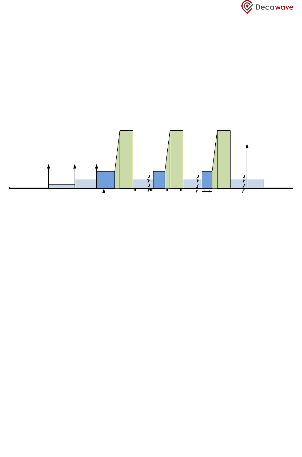
DW1000 User Manual
© Decawave Ltd 2017
Version 2.15
Page 43 of 244
NOTE: In the INIT state the 125 MHz digital PLL clock is not running, instead the system is clocked at the raw
19.2 MHz XTI clock rate. Thus, in Low duty-cycle SNIFF mode the off period configured in the SNIFF_OFFT is
in multiples of 6.6 µs (instead of the 1 µs units that apply in the SNIFF mode).
The power saving of Low duty-cycle SNIFF mode is only realised when the off period is greater than 1 (i.e. >
6.6 µs). This is because after the timer expiry the DW1000 will enter the IDLE state as the PLL is turned on
and locks (this takes approximately 5 µs) before progressing into the RX state.
Figure 21 shows the power profile associated with Low duty-cycle SNIFF mode where the IC wakes up from
SLEEP and progress into the repeated INIT-(IDLE)-RX-INIT-(IDLE)-RX cycles of the pulsed preamble detection
mode. A timeout ends this and the DW1000 is returned to SLEEP.
Figure 21: Power profile for Low duty-cycle SNIFF where a frame is not received
4.6 Diagnostics
The DW1000 includes the following diagnostic aids: -
The ability to drive LEDs to show TX and RX activity, which may be useful during product
development and in non-battery powered devices. The LED driving feature is an option on GPIO
lines, and is configurable via Sub-Register 0x26:00 – GPIO_MODE. Please refer to the register
description for details of the supported functionality.
Access to accumulator – of use during product development diagnostics. This is provided via Register
file: 0x25 – Accumulator CIR memory. Please refer to its description for details.
RX frame quality indications – of use for both product development diagnostics and for working
diagnostics, e.g. for network management or for deciding on confidence level for an RTLS or ranging
measurement. These are available through Register file: 0x12 – Rx Frame Quality Information.
Please refer to its description for details, and to section 4.7 – Assessing the quality of reception and
the RX timestamp
4.7 Assessing the quality of reception and the RX timestamp
The DW1000 receiver is capable of receiving messages under many different conditions. In some
circumstances it can be useful to assess the quality of the received signals and any timestamp data based on
them.
RX
IDLE
INIT GO2SLP
Sample Wakeup Event:
Sleep counter expires
SLEEP SLEEP
Frame Wait Timeout,
Host RX End.
WAKEUP
CLKPLL locked
Crystal stable,
RSTn=1 RX
Configure RX Sniff Mode
Sniff On Time
(in PACs)
Sniff Off Time
(in 19.2MHz cycles)
INIT
IDLE
INIT
RX
IDLE
PLL Lock
Time (~5uS)
INIT IDLE

DW1000 User Manual
© Decawave Ltd 2017
Version 2.15
Page 44 of 244
In a network it may be useful to assess the quality of message reception from a particular node in order to
change network routing or configurations related to that node to improve the reliability of the
communications. For example to improve communications reliability the frame length might be shortened,
or the data rate might be reduced, or the preamble length might be increased. In other situations with
consistently good communications the preamble length might be shortened to reduce the transmission
time, saving power and leaving more air-time free for other nodes to communicate.
In a TDOA RTLS system where a particular tag’s transmission is received at multiple anchors the quality of
reception and more particularly the quality of the RX timestamp information might be used to select which
anchors’ RX message timestamps to feed into the location engine.
The following details the elements of receive status reported by the DW1000 that may be used to assess the
quality of a received message and any related timestamp.
The Standard Deviation of Channel Impulse Response Estimate (CIRE) Noise value, reported in the
STD_NOISE field of Register file: 0x12 – Rx Frame Quality Information may be used to give a measure
of the noise associated with this and the received frame’s timestamp measurement. The STD_NOISE
can be used as an absolute value or it may be compared with the First Path Amplitude value – in this
latter case it is recommended that the amplitude value used for comparison is the value reported in
FP_AMPL2 field of Register file: 0x12 – Rx Frame Quality Information.
With a higher absolute CIRE noise figure it is more likely that the quality of receive timestamp will be
poorer. High noise may mean that the real first path is irretrievably buried in the noise. Comparing
the noise with the First Path Amplitude can give additional indication as to the quality of the first
path measurement. Where the First Path Amplitude has a large headroom over the noise, then the
received frame’s timestamp is likely to have been determined more precisely than when the First
Path Amplitude is closer to the noise level.
It is possible to compute an estimated receive power figure (using the equation and details given in
section 4.7.2 – Estimating the receive signal power) – for the purposes of this discussion this will be
called RX_POWER. It is also possible to compute an estimated power for just the first path signal
(using the equation and details given in section 4.7.1 – Estimating the signal power in the first path)
– for the purposes of this discussion this will be called FP_POWER. Using these two calculations it
may be possible to say whether the channel is line-of-sight (LOS) or non-line-of-sight signal (NLOS).
As a rule of thumb, if the difference between RX_POWER and FP_POWER, i.e. RX_POWER –
FP_POWER, is less than 6dB the channel is likely to be LOS, whilst if the difference is greater than
10dB the channel is likely to be NLOS.
Where the RX timestamp relates to a frame that is received in the presence of a higher CIRE noise power, or
relates to a non-line-of-sight path with attenuated first path, then that receive timestamp is naturally likely
to be of lower quality than that determined from a crisp line of sight first path signal that is well above the
noise floor.
Where a location system has an excess number receive timestamps to choose from then a quality estimate
relating to each timestamp may be used to weight the timestamps or to choose the highest quality set to
feed into the multilateration function of the location engine.

DW1000 User Manual
© Decawave Ltd 2017
Version 2.15
Page 45 of 244
4.7.1 Estimating the signal power in the first path
An estimate of the power in the first path signal may be calculated (in dBm) using the formula:
Where:
F1 = the First Path Amplitude (point 1) magnitude value reported in the FP_AMPL1 field of Register
file: 0x15 – Receive Time Stamp,
F2 = the First Path Amplitude (point 2) magnitude value reported in the FP_AMPL2 field of Register
file: 0x12 – Rx Frame Quality Information,
F3 = the First Path Amplitude (point 3) magnitude value reported in the FP_AMPL3 field of Register
file: 0x12 – Rx Frame Quality Information,
A= is the constant 113.77 for a PRF of 16 MHz, or, the constant 121.74 for a PRF of 64 MHz, and
N = the Preamble Accumulation Count value reported in the RXPACC field of Register file: 0x10 –
RX Frame Information Register. Note that RXPACC may need to be adjusted to remove SFD
symbol count before use, see the register field description in Register file: 0x10 – RX Frame
Information Register.
The resultant First Path Power Level (in dBm) may be compared with the estimated receive power figure
calculated as per section 4.7.2 – Estimating the receive signal power.
4.7.2 Estimating the receive signal power
It is possible to calculate an estimate of the receive power level (in dBm) using the formula:
Where:
C = the Channel Impulse Response Power value reported in the CIR_PWR field of Register file:
0x12 – Rx Frame Quality Information,
A= is the constant 113.77 for a PRF of 16 MHz, or, the constant 121.74 for a PRF of 64 MHz, and
N = the Preamble Accumulation Count value reported in the RXPACC field of Register file: 0x10 –
RX Frame Information Register. Note that RXPACC may need to be adjusted to remove SFD
symbol count before use, see the register field description in Register file: 0x10 – RX Frame
Information Register.
This resultant receive power estimate is very close to the actual receive power at lower receive levels, but is
lower than the actual receive power level at higher levels. Figure 22 below shows the relationship between
the actual receive power and the power estimated by this technique.
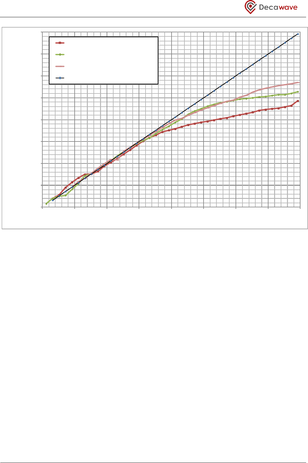
DW1000 User Manual
© Decawave Ltd 2017
Version 2.15
Page 46 of 244
Figure 22: Estimated RX level versus actual RX level
-105
-100
-95
-90
-85
-80
-75
-70
-65
-105 -100 -95 -90 -85 -80 -75 -70 -65
Estimated
RX LEVEL
(dBm)
Actual RX LEVEL (dBm)
Estimated RX LEVEL (16MHz PRF Free Space)
Estimated RX LEVEL (64MHz PRF Free Space)
Estimated RX LEVEL (64MHz PRF Multipath)
Actual RX LEVEL

DW1000 User Manual
© Decawave Ltd 2017
Version 2.15
Page 47 of 244
5 Media Access Control (MAC) hardware features
This section describes the features for media access control (MAC) that have been implemented in the
DW1000.
5.1 Cyclic redundancy check
The DW1000 includes a CRC generation function capable of automatically calculating and appending the 16-
bit CRC frame check sequence (FCS) at the end of each transmitted frame.
The DW1000 also includes a CRC checking function capable of automatically calculating the 16-bit CRC frame
check sequence (FCS) during frame reception and comparing this calculated CRC with the final two octets of
the received frame to check that the calculated CRC matches with CRC transmitted by the frame’s originator.
A mismatch between received and calculated CRC typically indicates that the received frame contains errors
(generally handled by discarding the received frame). At the end of the frame reception as reported via the
RXDFR event status bit, the result of the CRC comparison is reported by either the RXFCG or the RXFCE status
bit being set, i.e. depending on whether or not the CRCs matched. These three status bits are in Register file:
0x0F – System Event Status Register.
Where a CRC is not required it is possible to suppress the CRC transmission by employing the SFCST
(suppress FCS transmission) bit in Register file: 0x0D – System Control Register. This might be done when
using a different MAC layer protocol. This SFCST control is also employed during a throughput maximising
(response-time minimising) technique, as described in section 3.5.2 – TX buffer write while sending.
5.2 Frame filtering
Frame filtering is a feature of the DW1000 IC that can parse the received data of a frame that complies with
the MAC encoding defined in the IEEE 802.15.4–2011 standard, identifying the frame type and its
destination address fields, match these against the IC’s own address information, and only accept frames
that pass the filtering rules. See section 11 – APPENDIX 2: The IEEE 802.15.4 MAC layer for an introduction
to the message format defined in the standard.
The frame filtering functionality allows the IC to be placed into receive mode and only interrupt the host
processor when a frame arrives that passes the frame filtering criteria. When frame filtering is disabled all
frames with good CRC are accepted, typically to interrupt the host with event status indicating a frame has
been received with good CRC (i.e. the RXDFR and RXFCG event status bits are set in Register file: 0x0F –
System Event Status Register). When frame filtering is enabled the frame filtering rules have to be passed
before these event status (interrupt) bits are set. See section 4.1 - Basic Reception for general details of
reception.
Frame filtering is enabled by the FFEN configuration bit in Register file: 0x04 – System Configuration. This
register contains seven additional configuration bits (FFAB, FFAD, FFAA, FFAM, FFAR, FFA4 and FFA5) for fine
filtering control of the frame types.
5.2.1 Frame Filtering Rules
If frame filtering is enabled frames will be accepted or rejected based on the following rules:

DW1000 User Manual
© Decawave Ltd 2017
Version 2.15
Page 48 of 244
The frame type must be allowed for reception:
o The FFAB configuration bit must be set to allow a Beacon frame to be received.
o The FFAD configuration bit must be set to allow a Data frame to be received.
o The FFAA configuration bit must be set to allow an Acknowledgment frame to be received.
o The FFAM configuration bit must be set to allow a MAC command frame to be received.
o The FFAR configuration bit allows IEEE 802.15.4 reserved types, 4 to 7 to be received,
excluding those rejected due to the frame length check described below.
o The FFA4 configuration bit allows IEEE 802.15.4 reserved type 4 frames to be received,
excluding those rejected due to the frame length check described below.
o The FFA5 configuration bit allows IEEE 802.15.4 reserved type 5 frames to be received,
excluding those rejected due to the frame length check described below.
NB: For reserved frame types 4 to 7, if they are allowed here that is the end of the frame filtering.
The remaining rules below only apply for standard frame types 0 to 3. However, the frame
header will be interpreted as for frame types 0-3 to determine the size of the received frame
and reject it if it is shorter than expected. This can make the use of frame types 4, 5, 6 and 7
problematic and frame filtering may need to be carried out in software if use of frames of type
4, 5, 6, or 7 with different encodings for frame control bits affecting the header length is
planned. The frame control bits concerned are the address mode fields and the PID
compression field.
The frame version field must be 0x00 or 0x01
The Destination PAN ID if present must:
o Be the broadcast PAN ID (0xFFFF)
o Or match the PAN_ID programmed in Register file: 0x03 – PAN Identifier and Short Address
The Destination Address if present must:
o Be the (short 16-bit) broadcast address (0xFFFF)
o Or be a short (16-bit) address matching the SHORT_ADDR programmed in Register file: 0x03
– PAN Identifier and Short Address
o Or be a long (64-bit) address matching the Register file: 0x01 – Extended Unique Identifier.
If the frame is a beacon frame then the Source PAN ID must match the PAN_ID programmed in
Register file: 0x03 – PAN Identifier and Short Address, (or be 0xFFFF)
If only the source address is present, in a data or MAC command frame, then the frame will only be
accepted if the IC is configured to be a coordinator, (via the FFBC configuration bit in Register file:
0x04 – System Configuration) and the Source PAN ID matches the PAN_ID programmed in Register
file: 0x03 – PAN Identifier and Short Address.
The FCS (CRC) must be correct for the frame to be accepted.

DW1000 User Manual
© Decawave Ltd 2017
Version 2.15
Page 49 of 244
5.2.2 Frame Filtering Notes
The frame filtering does not take any notice of the Security Enabled field, in the frame control, so it is up to
the host software to decode any security information and accept/reject the frame is it sees fit. See section
11.2.2 – Security enabled Field for details.
The decisions on frame rejection/acceptance with respect to illegal frame control octets is made after the
first two octets of data are decoded, and at the end of reception of the address fields (as specified by the
frame control octets) for the relevant addressing rules. When a frame is rejected, the reception is aborted
immediately and the rejection is reported by the AFFREJ event bit in Register file: 0x0F – System Event Status
Register.
While frame filtering can save some work on the part of the host system, prolonged listening with the
DW1000 receiver on is a relatively power hungry activity best employed only on equipment with a mains
powered source.
All the configuration bits related to frame filtering are in Register file: 0x04 – System Configuration.
5.3 Automatic Acknowledgement
The automatic acknowledgement functionality of the DW1000 allows the IC to automatically send
acknowledgement frames when a frame is received and validated that includes an acknowledgement
request. The automatic acknowledgement functionality only operates when frame filtering is enabled and
automatic acknowledgement is enabled.
In order for automatic acknowledgement to operate:
• Frame filtering must be enabled and the received data or MAC command frame must be
correctly addressed and pass through the receive frame filtering, (see section 5.2 - Frame
filteringfor details of frame filtering configuration).
• The ACK request bit in the frame control field of the received frame must be set.
• Auto-acknowledgement must be enabled by the AUTOACK configuration in Register file: 0x04 –
System Configuration.
When these conditions are met the DW1000 will at the end of the reception automatically transition into
transmit mode to send the 5-octet MAC acknowledgement frame as defined by IEEE 802.15.4-2011.
If automatic acknowledgement and double buffering are intended to be used together, the system must be
designed such that overruns cannot occur, or if they can occur, that the system can deal with
acknowledgement of frames which subsequently become corrupted, see section 4.3.5.
5.3.1 Preamble length & SFD in Automatic Acknowledge Frame
5.3.1.1 Preamble length
The preamble length of the frame requesting acknowledgement (ACK) is encoded in the PHR of that frame,
(see section 10.4 – PHY header), and decoded in the DW1000 receiver (and reported in the RXPSR field of
Register file: 0x10 – RX Frame Information Register). This only covers preamble lengths defined in the IEEE
802.14.4 standard, but the DW1000 supports other preamble lengths. To cope with this the DW1000 selects

DW1000 User Manual
© Decawave Ltd 2017
Version 2.15
Page 50 of 244
preamble length as reported in the RXPSR field but also uses the Preamble Accumulation Count value
reported in the RXPACC field of Register file: 0x10 – RX Frame Information Register. Table 8 presents the
resulting preamble length used for the ACK frame as a function of RXPSR and RXPACC fields.
Table 8: Auto-ACK preamble length depending on RXPSR and RXPACC
PSR carried in PHR &
reported in RXPSR
PSR accumulated and
reported in the RXPACC value
Resultant Preamble
Length of auto ACK
64
Less than 65
64
Between 65 and 128
128
Between 129 and 256
256
Greater than 256
512
1024
Less than 1025
1024
Between 1025 and 1536
1536
Greater than 1536
2048
4096
Any value
4096
Table 8 relates to standard frames. In extended length frame mode, (as described in section 3.4 - Extended
Length Data Frames), just the Preamble Accumulation Count value (reported in the RXPACC field of Register
file: 0x10 – RX Frame Information Register) is used to determine the preamble length of the ACK. Table 9
presents the preamble lengths used for the ACK frame in extended length frame mode as a function of the
RXPACC field.
Table 9: Auto-ACK preamble length selection in extended length frames mode
PSR accumulated and
reported in the RXPACC value
Resultant Preamble
Length of auto ACK
Less than 17
16 *
Between 17 and 32
32 *
Between 33 and 64
64
Between 65 and 128
128
Between 129 and 256
256
Between 257 and 512
512
Between 513 and 1024
1024
Between 1025 and 1536
1536
Between 1537 and 2048
2048
Greater than 2048
4096
NOTE *: These (asterisked) short preamble lengths will not be received by the DW1000. Use cases where
this is likely to occur frequently should be avoided by one of the following strategies: (a) using a longer
preamble for retransmission when no ACK is received, (b) not using the extended length frames mode, or, (c)
by using the host microprocessor to generate the ACK in place of the DW1000’s auto-ACK feature.
NOTE 1: It is possible for the Preamble Accumulation Count value (reported in the RXPACC field of Register
file: 0x10 – RX Frame Information Register) to be significantly shorter than the transmitted preamble length,

DW1000 User Manual
© Decawave Ltd 2017
Version 2.15
Page 51 of 244
because the accumulation stops when any tap value grows to be a 16-bit number. This is typically when the
sending device is close to the receiver, but in any case the number reported has been sufficient for correct
reception of the frame being acknowledged, so even if this results in a shorter preamble for the auto-ACK
frame this preamble should still have ample length for correct reception.
NOTE 2: It is also possible for the Preamble Accumulation Count (reported in RXPACC) to be a little larger
than the transmitted preamble length. This can occur with early detection of preamble and because the
accumulation count may include accumulation that continues through the SFD (until the SFD is detected). If
this occurs it can result in the automatic acknowledgement frame being sent with a longer preamble than
the frame soliciting the ACK. In the worst case this will be one size bigger. Allowance for this fact should be
made when programming a shorter than default SFD detection timeout in Sub-Register 0x27:20 –
DRX_SFDTOC, e.g. set a time-out consistent with the next greater preamble size. And similarly if setting a
very tight time for the RX frame timeout (in Register file: 0x0C – Receive Frame Wait Timeout Period)
allowance should be made for the possible additional duration of the preamble sequence.
5.3.1.2 SFD Initialisation
The SFD sequence to be included in the Auto ACK frame must be initialised prior to the first Auto ACK frame
being sent. The SFD sequence is only initialised upon an user TX request which will not have taken place if
the Auto ACK frame is the first transmitted frame after start-up or reconfiguration of channel parameters.
The most efficient way to ensure the SFD sequence is correctly initialised is to simultaneously initiate and
abort a transmission thereby forcing the SFD initialisation. This can be done by writing to the the system
control register Register file: 0x0D – System Control Register with both the transmission startbit TXSTRT and
the transceiver off bit TRXOFF set at the same time. No signal will actually be transmitted as a result of this
operation. This operation should be performed each time the communication parameters are configured or
reconfigured as this can change the SFD sequence the DW1000 will use for the next transmission.
5.3.2 Automatic Receiver Re-Enable
Automatic acknowledgement can also operate correctly when the RX auto-re-enable function is enabled (by
the RXAUTR bit in Register file: 0x04 – System Configuration), as may be the case in double-buffered mode
(see section 4.3 - Double Receive Buffer). Here when frame filtering and automatic acknowledgements are
enabled, the DW1000 will automatically transition from receiving into transmit mode to send the
acknowledgement frame and when the transmission is complete, the DW1000 will automatically return into
receive mode to await the next frame.
5.3.3 Automatic ACK Turnaround Time
The IEEE 802.15.4 standard specifies a 12 symbol +/- 0.5 symbols turnaround time for ACK transmission. In
the DW1000 this period is configurable via the ACK_TIM parameter in Register file: 0x1A – Acknowledgement
time and response time.
5.3.4 Frame Pending bit
The standard IEEE 802.15.4-2011 MAC includes a frame pending bit in the frame control at the start of each
frame (see section 11.2.3 – Frame pending field). This bit can be set to indicate more data is coming or in the
case of the ACK frame to indicate that the responding node has data to send to the node soliciting the ACK.

DW1000 User Manual
© Decawave Ltd 2017
Version 2.15
Page 52 of 244
Please refer to the standard [1] for details of this. The DW1000 does not automatically determine the frame
pending bit inserted into the automatically-generated ACK frames. Instead it copies the value of the
AACKPEND configuration bit (from Register file: 0x04 – System Configuration), which is zero by default.
5.3.5 Host Notification
The AAT status bit (Register file: 0x0F – System Event Status Register) indicates that an acknowledgement
has been requested.
The AAT bit is set at the same time as the RXFCG event status (indicating a good CRC at the end of frame
reception). Please note however that in a polled system reading the status register looking for RXFCG and
AAT events, it is possible for the SPI read to overlap with this event such that AAT in first octet of the
SYS_STATUS register is clear as it is accessed, while RXFCG (and AAT) are both set as the second octet of the
SYS_STATUS register containing RXFCG is accessed. Thus it may appear that RXFCG is set with no AAT event
being indicated. A polled system then seeing RXFCG set may check for AAT being set in the same read of
SYS_STATUS, but finding AAT clear, should re-read and check the AAT state again just in case this race
condition has occurred."
If automatic acknowledgement is enabled then the AAT bit can be used during receive interrupt processing
to detect that acknowledgement is in progress and so avoid taking any action until the transmission of the
acknowledgement is completed, and signalled by the TXFRS (Transmit Frame Sent) event.
Note: If automatic acknowledgement is not enabled, then the AAT status bit must be ignored.
Note: there is a situation that can result in the AAT bit being set for the current frame as a result of a
previous frame that was received and rejected due to frame filtering. This is despite the fact that the current
frame is not requesting an automatic acknowledgement. In this circumstance an automatic
acknowledgment is not actually transmitted, however the fact that the AAT is set could cause the user to
wait for a non-existent automatic acknowledgement process to complete.
In this situation, when automatic acknowledgement is enabled and the AAT bit is observed as set, to avoid
waiting for the acknowledgement process to complete and TXFRS to be set, the Acknowledgment request
field in the frame control section of the MAC header of the received frame as described in Section 11.2.4
should be checked to confirm that the current frame has actually requested an automatic
acknowledgement. If the Acknowledgment request field is cleared, then the user should clear the AAT bit in
the status register Register file: 0x0F – System Event Status Register (as well as in any copy of the status
register that is returned to the user callback when using interrupts).
5.3.6 ACK Frame Corruption
The data in the Auto ACK frame can be corrupted if a read access is made to either TX_FCTRL or TX_BUFFER
during Auto ACK frame transmission.

DW1000 User Manual
© Decawave Ltd 2017
Version 2.15
Page 53 of 244
5.4 Transmit and automatically wait for response
The DW1000 has the ability to automatically turn on its receiver after a transmission has completed in order
to receive a response. This may also include an optional delay configuration between the end of the
transmission and the enabling of the receiver. This is controlled by the WAIT4RESP bit in Register file: 0x0D –
System Control Register and the W4R_TIM parameter in the Register file: 0x1A – Acknowledgement time and
response time.
Note: If the response that is received is a frame requesting an acknowledgement frame, the DW1000 will
transmit the ACK if automatic acknowledge is enabled, but the receiver will re-enable following the
transmission of the ACK. Depending on host response times this may allow the acknowledge-requesting
frame to be overwritten, or other behaviour such as receiver timeouts resulting from the device being in the
RX state rather than in IDLE.
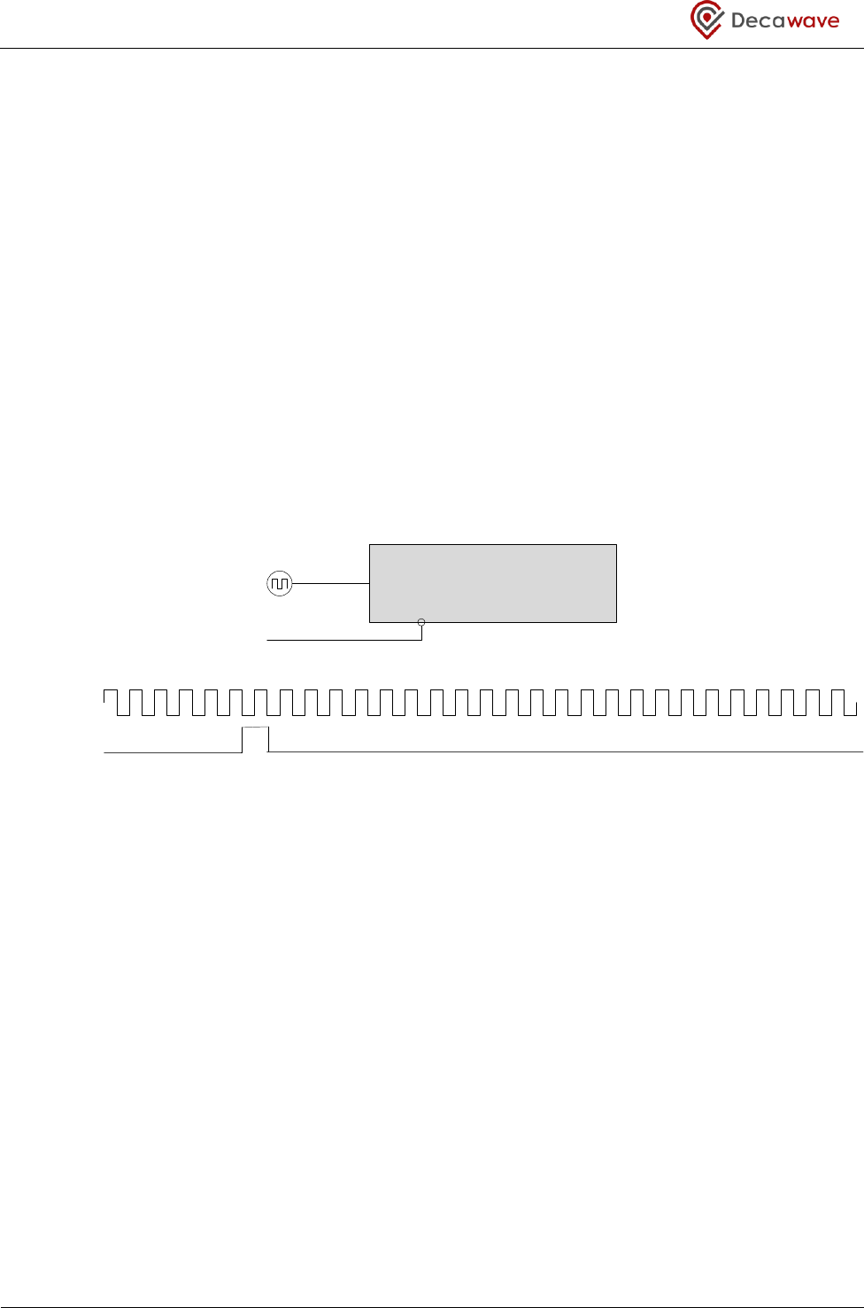
DW1000 User Manual
© Decawave Ltd 2017
Version 2.15
Page 54 of 244
6 Other features of the DW1000
6.1 External Synchronisation
This feature is used to synchronise DW1000 with external clocks or events or with other DW1000’s. For
example, this would be required in a TDOA RTLS system employing wired clock synchronisation of the anchor
nodes.
The DW1000 external synchronisation features allow the following functions:
a) The ability to reset the internal system counter in a deterministic way with respect to the assertion
of the SYNC input pin, and an external 38.4 MHz clock supplied on the EXTCLK pin.
b) The ability to initiate the transmission of a frame in a deterministic way with respect to the assertion
of the SYNC input pin, and an external 38.4 MHz clock supplied on the EXTCLK pin.
c) The ability to synchronise receive time stamping to an external counter
Figure 23: DW1000 External Synchronisation Interface
The SYNC input pin must be source synchronous with an external 38.4 MHz frequency reference clock
supplied on the EXTCLK pin. The SYNC input pin is sampled on the rising edge of EXTCLK. Refer to the
DW1000 datasheet for setup and hold times of the SYNC pin. The SYNC input provides a common reference
point in time to synchronise the DW1000 with the accuracy necessary to achieve high resolution location
estimation.
6.1.1 One Shot Timebase Reset (OSTR) Mode
One Shot Timebase Reset (OSTR) mode allows a reset to be applied to the timebase counter used for
timestamping in DW1000 at a deterministic and predictable time relative to a synchronisation event.Any
given device will reset the counter at a repeatable time to within 300ps (typically less than 100ps) variation.
Process variation between parts introduces a deterministic error that can be calibrated out as part of the
necessary calibration process to compensate for cable transmission delays in a wired synchronization
system. When several DW1000s are driven by the same reference clock and external SYNC signal their
internal timebases can be synchronised very accurately (allowing for the deterministic delays associated with
the distribution network for the reference clock and SYNC signal).
DW1000
External
Clock
SYNC
SYNC
External Clock supplied
on EXTCLK / XTAL1 pin

DW1000 User Manual
© Decawave Ltd 2017
Version 2.15
Page 55 of 244
To configure DW1000 for OSTR mode, the OSTRM bit in the EC_CTRL register is set and the WAIT value is set
to the desired delay value. When a counter running on the 38.4 MHz external clock and initiated on the
rising edge of the SYNC signal equals the WAIT programmed value, the DW1000 timebase counter will be
reset. See Register file: 0x24 – External Synchronisation Control for register details.
At the time the SYNC signal is asserted, the clock PLL dividers generating the DW1000 125 MHz system clock
are reset, to ensure that a deterministic phase relationship exists between the system clock and the
asynchronous 38.4 MHz external clock. For this reason, the WAIT value programmed will dictate the phase
relationship and should be chosen to give the desired phase relationship, as given by WAIT modulo 4. A
WAIT value of 33 decimal is recommended, but if a different value is chosen it should be chosen so that
WAIT modulo 4 is equal to 1, i.e. 29, 37, and so on.
6.1.2 One Shot Transmit Synchronisation (OSTS) Mode
DW1000 allows the transmission of a frame at a deterministic time after the SYNC signal is asserted, using
the One Shot Transmit Synchronisation (OSTS) mode. OSTS mode provides for the transmission of a frame at
a well-defined time relative to the assertion of the SYNC DW1000 input. This time will vary slightly per part,
typically 12 ps, but may vary up to 3 ns across process for all parts.
This feature will be used where a local master locationing device is using the DW1000 as a slave to provide
additional location data. Calibration can be employed by the master device to tune for the constant offset
due to the SYNC trace and process variation and in that case, the delay variation across all parts will be less
than 100 ps.
Note that OSTS mode works identically to OSTR in every respect except for the final action performed, e.g. to
reset the timebase or to initiate a transmission.
To configure OSTSmode the OSTSM bit must be set in the EC_CTRL register and the WAIT value set to the
desired delay value, see Register file: 0x24 – External Synchronisation Control. A value of 33 is
recommended; see 6.1.1 – One Shot Timebase Reset (OSTR) Mode. When a counter running on the 38.4
MHz external clock and initiated on the rising edge of the SYNC signal equals the WAIT programmed value,
the DW1000 will initiate a transmission, by issuing a TX START signal from the external synchronisation
circuit in the clock PLL to the transmitter. The rising edge of the TX START signal is synchronised to the 125
MHz system clock domain before it is used to enable the transmission.
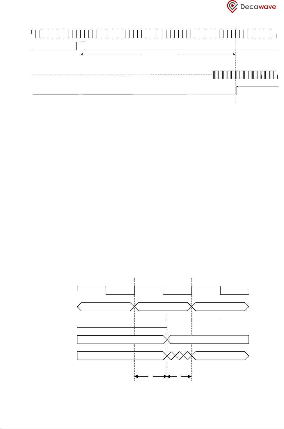
DW1000 User Manual
© Decawave Ltd 2017
Version 2.15
Page 56 of 244
External Clock
38.4 MHz
SYNC
124.8MHz
WAIT Cycles wrt
EXT_CLK
TX START
Figure 24: Synchronised Transmission
6.1.3 One Shot Receive Synchronisation (OSRS) Mode
One Shot Receive Synchronisation (OSRS) mode provides a second timebase in DW1000 that can be
synchronised to an external timebase and used to timestamp receive events. This allows a user to have a
timebase outside the DW1000, and to receive timing information about the receive events in this timebase.
OSRS mode is configured by setting the OSRSM bit in the EC_CTRL register, see Register file: 0x24 – External
Synchronisation Control. A 1 GHz clock for an offset counter, EC_GOLP, must also be activated in this mode,
by setting the PLLSYN field (bit 15) in the PMSC_CTRL1 register, see Sub-Register 0x36:04 – PMSC_CTRL1.
In normal operation, a ranging timestamp is calculated based on the DW1000 internal timebase; see section
4.1.6 – RX Message timestamp. The timebase counter is captured at the receive event, RMARKER, and a
number of offset values are combined with this capture value to give the ranging timestamp.
When timestamping the receive event relative to an external timebase, the procedure is similar to the
normal method except that an offset is introduced to compensate for the error introduced by the use of the
internal 125 MHz clock to capture a value on the external 38.4 MHz clock domain. As in normal operation,
these offsets and captured values are combined to give the ranging timestamp.
N-1 N N+1
T2T1
External Clock
38.4 MHz
Cycle Counter
(RX_TS_EST)
RMARKER
1GHz Offset Counter
(OFFSET_EXT)
N
Time Stamp
Figure 25: OSRS Mode Receive Timebase Synchronisation
Now the timestamp in the external timebase may be computed as:

DW1000 User Manual
© Decawave Ltd 2017
Version 2.15
Page 57 of 244
Trx = N×TExternal+T2+T3.
= (N+1) x TExternal -T1+T3.
Where:
N is the number of external clock cycles since the SYNC signal captured in timestamp and
may be read from EC_RXTC in the RS_TS_EST field, see Sub-Register 0x24:04 EC_RXTC.
TExternal is the period of the external clock.
T2 is time from the rising edge of the external clock to the RMARKER.
T1 is the time in ns reported by EC_GOLP in the OFFSET_EXT field, see Sub-Register 0x24:08
EC_GOLP.
T3 the leading path delay, calculated by subtracting the raw receive timestamp from the
receive timestamp, the difference between these will give the leading path delay, see
Register file: 0x15 – Receive Time Stamp.
T3 = RX_STAMP – RX_RAWST
6.2 External Power Amplification
In some geographic regions for certain situations (e.g. for emergency first responder use in ETSI UWB
regulations for EU) it is permitted to send at +20dB above the normal UWB regulation levels. To achieve
this with the DW1000 it is necessary to employ external amplification of the transmitted signal. The
DW1000 provides signals (using the GPIO lines in a special mode) to control the turn-on of the power
amplifier and to control the analog switching of the transmitter and receiver signal paths appropriately. This
mode of operation utilises the DW1000 pins EXTPA, EXTTXE and EXTRXE as configured via the fields MSGP4,
MSGP5 and MSGP6 in Sub-Register 0x26:00 – GPIO_MODE.
Care should be taken when using this feature to ensure that necessary regulatory requirements have been
fulfilled.
There is a separate application note giving details of the external power amplification. This includes the
circuit diagram, details of configuration and various design considerations that apply. Please consult with
Decawave’s applications support team for details.
6.3 Using the on-chip OTP memory
The DW1000 has a small amount of one-time-programmable (OTP) memory intended for device specific
configuration or calibration data. Some areas of the OTP memory are used to save device calibration values
determined during DW1000 testing, while other OTP memory locations are intended to be set by the
customer during module manufacture and test.
For example, an OTP memory area is reserved for customers to programme the EUI that is loaded into
Register file: 0x01 – Extended Unique Identifier as the IC comes out of reset (see Register file: 0x01 –
Extended Unique Identifier for details of the EUI functionality).
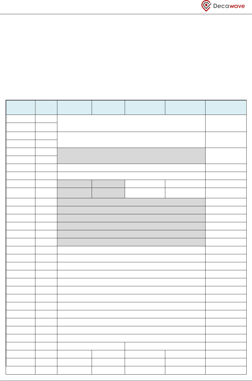
DW1000 User Manual
© Decawave Ltd 2017
Version 2.15
Page 58 of 244
This section lists the OTP memory areas defining their functionality and describes the algorithm for
programming values into the OTP memory, and how to read values from the OTP memory. Access to OTP
memory is achieved using Register file: 0x2D – OTP Memory Interface.
6.3.1 OTP memory map
The OTP memory locations are as defined in Table 10. The OTP memory locations are each 32-bits wide, OTP
addresses are word addresses so each increment of address specifies a different 32-bit word.
Table 10: OTP memory map
OTP
Address
Size
(Used
Bytes)
Byte [3]
Byte [2]
Byte [1]
Byte [0]
Programmed
By
0x000
4
64 bit EUID
(These 64 bits get automatically copied over to see Register file: 0x01 – Extended
Unique Identifier on each reset.)
Customer
0x001
4
0x002
4
Alternative 64bit EUID
Customer
0x003
4
0x004
4
40 bit LDOTUNE_CAL
(These 40 bits can be automatically copied over to Sub Register File 0x28:30 LDOTUNE
on wakeup)
Decawave Test
0x005
1
0x006
4
PART ID / CHIP ID (32bits)
Decawave Test
0x007
4
LOT ID (32 bits)
DecawaveTest
0x008
2
-
-
Vmeas @ 3.7 V
Vmeas @ 3.3 V
DecawaveTest
0x009
1 / 1
-
-
Tmeas @ Ant Cal
Tmeas @ 23 °C
Customer / Deca-
wave Test
0x00A
0
-
Reserved
0x00B
4
-
Reserved
0x00C
2
-
Reserved
0x00D
4
-
Reserved
0x00E
4
-
Reserved
0x00F
4
-
Reserved
0x010
4
CH1 TX Power Level PRF 16
Customer
0x011
4
CH1 TX Power Level PRF 64
Customer
0x012
4
CH2 TX Power Level PRF 16
Customer
0x013
4
CH2 TX Power Level PRF 64
Customer
0x014
4
CH3 TX Power Level PRF 16
Customer
0x015
4
CH3 TX Power Level PRF 64
Customer
0x016
4
CH4 TX Power Level PRF 16
Customer
0x017
4
CH4 TX Power Level PRF 64
Customer
0x018
4
CH5 TX Power Level PRF 16
Customer
0x019
4
CH5 TX Power Level PRF 64
Customer
0x01A
4
CH7 TX Power Level PRF 16
Customer
0x01B
4
CH7 TX Power Level PRF 64
Customer
0x01C
4
TX/RX Antenna Delay – PRF 64
TX/RX Antenna Delay – PRF 16
Customer
0x01D
0
-
-
-
-
Customer
0x01E
2
-
-
OTP Revision
XTAL_Trim[4:0]
Customer
0x01F
0
-
-
-
-
Customer
DW1000 User Manual
© Decawave Ltd 2017
Version 2.15
Page 59 of 244
OTP
Address
Size
(Used
Bytes)
Byte [3]
Byte [2]
Byte [1]
Byte [0]
Programmed
By
:
:
:
:
:
:
Reserved
0x400
4
SR Register (see below)
Customer
The SR (“Special Register”) is a 32-bit segment of OTP that is directly readable via the register interface upon
power up. To programme the SR register follow the normal OTP programming method but set the OTP
address to 0x400. The value of the SR register can be directly read back at address Register file: 0x2D – OTP
Memory Interface.
Table 11: OTP_SRDAT Register
Bit
Function
31:5
Reserved. Defaults to all “0”. If programming the OTP_SRDATA register these bits must be set to “0”
4:3
SPI_SR_EN[1:0]. Set to “01” to enable bits [1:0] to be used instead of GPIO[6:5] boot
strapping. If set, this will disable the external selection of SPI mode via GPIO6 and 5.
2
Reserved. Defaults to “0”. If programming the OTP_SRDATA register these bits must be set to “0”
1
SPI_SR_PH. Set SPI Phase mode to this value if bits [4:3] are set to “01”
0
SPI_SR_POL. Set SPI Polarity mode to this value if bits [4:3] are set to “01”
6.3.2 Programming a value into OTP memory
The programming of the OTP requires a number of setup steps to be carried out in sequence. Optimal
programming requires that the VDDIO pin be driven to 3.8 V (or the VDDIOA pin if access to VDDIO is not
available). The table below outlines the programming steps to place the OTP into its programming state and
to programme a single location.
Table 12: Register accesses required to program the OTP
Step
Number
Instruction
Register
Address
Data
Length
(Bytes)
Data
(Write/Read)
Configure OTP for Programming – Stage 1:
C-1
Write Sub-Register
0x36:00 (PMSC_CTRL0)
1
0x01
C-2
Write Sub-Register
0x2D:07 (OTP_CTRL+1)
1
0x03
C-3
Write Sub-Register
0x2D:00 (OTP_WDAT)
2
0x9220
C-4
Write Sub-Register
0x2D:06 (OTP_CTRL)
1
0x08
Wait 1ms
C-5
Write Sub-Register
0x2D.07 (OTP_CTRL+1)
1
0x02
C-6
Write Sub-Register
0x2D:06 (OTP_CTRL)
1
0x88
C-7
Write Sub-Register
0x2D:06 (OTP_CTRL)
1
0x80
C-8
Write Sub-Register
0x2D:06 (OTP_CTRL)
1
0x00
Configure OTP for Programming – Stage 2:
C-9
Write Sub-Register
0x2D:07 (OTP_CTRL+1)
1
0x05

DW1000 User Manual
© Decawave Ltd 2017
Version 2.15
Page 60 of 244
Step
Number
Instruction
Register
Address
Data
Length
(Bytes)
Data
(Write/Read)
C-10
Write Sub-Register
0x2D:00 (OTP_WDAT)
2
0x000E
C-11
Write Sub-Register
0x2D:06 (OTP_CTRL)
1
0x08
Wait 1ms
C-12
Write Sub-Register
0x2D.07 (OTP_CTRL+1)
1
0x04
C-13
Write Sub-Register
0x2D:06 (OTP_CTRL)
1
0x88
C-14
Write Sub-Register
0x2D:06 (OTP_CTRL)
1
0x80
C-15
Write Sub-Register
0x2D:06 (OTP_CTRL)
1
0x00
Configure OTP for Programming – Stage 3:
C-16
Write Sub-Register
0x2D:07 (OTP_CTRL+1)
1
0x01
C-17
Write Sub-Register
0x2D:00 (OTP_WDAT)
2
0x1024
C-18
Write Sub-Register
0x2D:06 (OTP_CTRL)
1
0x08
Wait 1ms
C-19
Write Sub-Register
0x2D.07 (OTP_CTRL+1)
1
0x00
Programming a single 32 bit word <DATA> to address <ADDR>:
P-1
Write Sub-Register
0x2D:06 (OTP_CTRL)
1
0x00
P-2
Write Sub-Register
0x2D:00 (OTP_WDAT)
4
<DATA[31:0]>
P-3
Write Sub-Register
0x2D:04 (OTP_ADR)
2
<ADDR[10:0]>
P-4
Write Sub-Register
0x2D:06 (OTP_CTRL)
1
0x40
P-5
Write Sub-Register
0x2D:06 (OTP_CTRL)
1
0x00
Wait 1 ms before reading back to verify
After programming an OTP word, it should be read back using the procedure in 6.3.3 – Reading a value from
OTP memory and verified for correctness. If it does not match the expected value, then the steps P-4
through P-5 should be repeated up to a maximum of 10 times (the address and data values in the registers
will still be valid and as such do not require re-programming). During the programming stages the OTP is
configured to stress the read-back circuits to their limits. This may result in continuous read-verify failures. In
the event that 10 attempts have been made to programme a location then a final read-verify is
recommended after a full IC reset, this will reset the OTP configuration to normal read operation.
When all OTP programming is finished it is recommended to reset the IC to revert back to the default
settings.
6.3.3 Reading a value from OTP memory
The OTP memory may be read by following the steps given in Table 13.
Table 13: An example of register accesses required to read from OTP
Step
Number
Instruction
Register
Address
Data
Length
(Bytes)
Data
(Write/Read)
1
Write Register
0x2D:04 (OTP_ADDR)
2
OTP Address
2
Write Sub-Register
0x2D:06 (OTP_CTRL)
1
0x03
3
Write Sub-Register
0x2D:06 (OTP_CTRL)
1
0x00
4
Read Register
0x2D:0A (OTP_RDAT)
4
OTP Read Value

DW1000 User Manual
© Decawave Ltd 2017
Version 2.15
Page 61 of 244
6.4 Measuring IC temperature and voltage
The DW1000 is equipped with a low speed 8-bit SAR A/D convertor which can be configured to sample
values from an internal IC temperature sensor and also from a battery voltage monitor on the VDDAON
power supply input. These readings can be manually run under host control, or they can be configured to be
run automatically each time the DW1000 enters the WAKEUP state. This automatic mode allows the
temperature and voltage to be read while the device is in a low power state, which will give the ambient
temperature and unloaded battery voltage.
The automatic mode is controlled by the ONW_RADC bit in Sub-Register 0x2C:00 – AON_WCFG. When this is
used the temperature and voltage readings are available in Sub-Register 0x2A:06 – TC_SARW as soon as the
IC reaches the IDLE state.
The procedure for host-initiated reading of temperature sensor (or battery voltage) is as follows:
Table 14: An example of register accesses to perform a read of the temperature and voltage sensors
Step
Number
Instruction
Register
Address
Data Length
(Bytes)
Data
(Write/Read)
1
Write Sub-Register
28:11
1
0x80
2
Write Sub-Register
28:12
1
0x0A
3
Write Sub-Register
28:12
1
0x0F
4
Write Register
2A:00
1
0x01
5
Write Register
2A:00
1
0x00
6
Read Register
2A:03
1
8-bit Voltage reading
7
Read Register
2A:04
1
8-bit Temperature reading
When in the ADC is configured for automatic operation on wakeup Register: 2C – ONWAKE_RUN_SAR, then
the ADC values for both the voltage and temperature sensors will be ready to read as soon as the IDLE state
is entered. These values can be read by performing steps 6 and 7 from the table above.
In the automatic mode it is possible to configure an interrupt to assert if the latest readings of temperature
or voltage differ from the previously recorded values by a value of 0x0A. This is approximately equal to
60 mV for the voltage reading and 10 ⁰C for the temperature reading.
The previous values are also available to the host to read at:
Register: 2A – SAR_LAST_VBAT,
Register: 2A – SAR_LAST_TEMP
DW1000 User Manual
© Decawave Ltd 2017
Version 2.15
Page 62 of 244
7 The DW1000 register set
The DW1000 is controlled by an associated host microcontroller system using the SPI interface to access a
series of registers within the device. The DW1000 register set includes configuration registers, status
registers, control registers, data buffer registers, and diagnostic registers. Section 2.2 – The SPI Interface
described the SPI interface and the low level transactions for reading and writing the parameters of the
DW1000. This section begins with 7.1– Register map overview and then 7.2– Detailed register description,
where each individual parameter is described in detail.
7.1 Register map overview
The register map overview is given in Table 15. This lists the registers in address order, by register file ID,
giving the register file length in octets, its type (RO = Read-Only, RW = Read & Write, SRW = Special Read
Write – see individual register descriptions for details about how the Read/Write access is special), and a
brief high level description of the register. Section 7.2 gives a detailed description of each register.
Note: When writing to any of the DW1000 registers care must be taken not to write beyond the published
length of the selected register and not to write to any of the reserved register locations. Doing so may cause
the device to malfunction.
Table 15: Register map overview
ID
Length
(octets)
Type
Mnemonic
Description
0x00
4
RO
DEV_ID
Device Identifier – includes device type and revision info
0x01
8
RW
EUI
Extended Unique Identifier
0x02
-
-
-
Reserved
0x03
4
RW
PANADR
PAN Identifier and Short Address
0x04
4
RW
SYS_CFG
System Configuration bitmap
0x05
-
-
-
Reserved
0x06
5
RO
SYS_TIME
System Time Counter (40-bit)
0x07
-
-
-
Reserved
0x08
5
RW
TX_FCTRL
Transmit Frame Control
0x09
1024
WO
TX_BUFFER
Transmit Data Buffer
0x0A
5
RW
DX_TIME
Delayed Send or Receive Time (40-bit)
0x0B
-
-
-
Reserved
0x0C
2
RW
RX_FWTO
Receive Frame Wait Timeout Period
0x0D
4
SRW
SYS_CTRL
System Control Register
0x0E
4
RW
SYS_MASK
System Event Mask Register
0x0F
5
SRW
SYS_STATUS
System Event Status Register
0x10
4
ROD
RX_FINFO
RX Frame Information
(in double buffer set)
0x11
1024
ROD
RX_BUFFER
Receive Data
(in double buffer set)
0x12
8
ROD
RX_FQUAL
Rx Frame Quality information
(in double buffer set)
0x13
4
ROD
RX_TTCKI
Receiver Time Tracking Interval
(in double buffer set)
0x14
5
ROD
RX_TTCKO
Receiver Time Tracking Offset
(in double buffer set)

DW1000 User Manual
© Decawave Ltd 2017
Version 2.15
Page 63 of 244
ID
Length
(octets)
Type
Mnemonic
Description
0x15
14
ROD
RX_TIME
Receive Message Time of Arrival
(in double buffer set)
0x16
-
-
-
Reserved
0x17
10
RO
TX_TIME
Transmit Message Time of Sending
0x18
2
RW
TX_ANTD
16-bit Delay from Transmit to Antenna
0x19
5
RO
SYS_STATE
System State information
0x1A
4
RW
ACK_RESP_T
Acknowledgement Time and Response Time
0x1B
-
-
-
Reserved
0x1C
-
-
-
Reserved
0x1D
4
RW
RX_SNIFF
Pulsed Preamble Reception Configuration
0x1E
4
RW
TX_POWER
TX Power Control
0x1F
4
RW
CHAN_CTRL
Channel Control
0x20
-
-
-
Reserved
0x21
41
RW
USR_SFD
User-specified short/long TX/RX SFD sequences
0x22
-
-
-
Reserved
0x23
33
RW
AGC_CTRL
Automatic Gain Control configuration
0x24
12
RW
EXT_SYNC
External synchronisation control.
0x25
4064
RO
ACC_MEM
Read access to accumulator data
0x26
44
RW
GPIO_CTRL
Peripheral register bus 1 access – GPIO control
0x27
44
RW
DRX_CONF
Digital Receiver configuration
0x28
58
RW
RF_CONF
Analog RF Configuration
0x29
-
-
-
Reserved
0x2A
52
RW
TX_CAL
Transmitter calibration block
0x2B
21
RW
FS_CTRL
Frequency synthesiser control block
0x2C
12
RW
AON
Always-On register set
0x2D
18
RW
OTP_IF
One Time Programmable Memory Interface
0x2E
-
RW
LDE_CTRL
Leading edge detection control block
0x2F
41
RW
DIG_DIAG
Digital Diagnostics Interface
0x30
to
0x35
-
-
-
Reserved
0x36
48
RW
PMSC
Power Management System Control Block
0x37
to
0x3F
-
-
-
Reserved
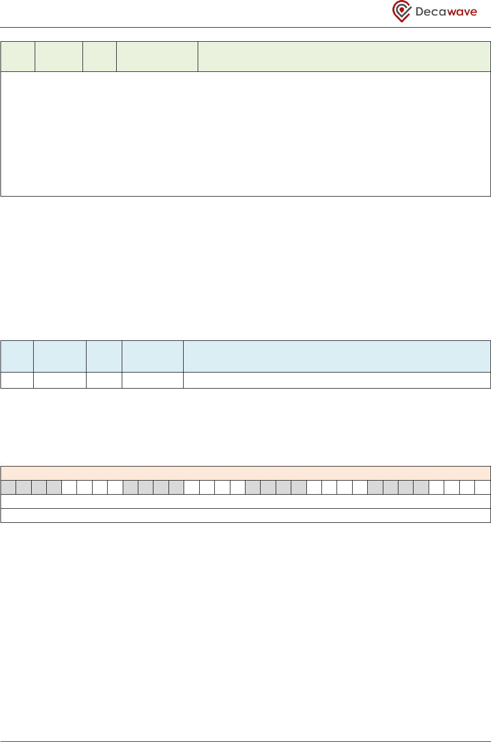
DW1000 User Manual
© Decawave Ltd 2017
Version 2.15
Page 64 of 244
ID
Length
(octets)
Type
Mnemonic
Description
Note the “Type” mnemonic in the table above has the following meaning:
• RO – Read Only,
• WO – Write Only,
• RW – Read and Write,
• SRW – Special type of Read and Write, refer to individual register description for details,
• ROD – Read Only part of RX Double buffered swinging set of RX frame related information,
• RWD – Read and Write part of RX Double buffered swinging set of RX frame related information.
7.2 Detailed register description
7.2.1 Terminology
Section 7.1 gives an overview of the DW1000 register set presenting all top level register file ID addresses in
Table 15. This section describes in detail the contents and functionality of these register files in separate sub
sections. In each case the row from Table 15 is reproduced with hex register file ID, its length, type,
mnemonic and one line description as follows:
ID
Length
(octets)
Type
Mnemonic
Description
This is followed by a description of the parameters within that register file. All parameters are presented
with format REG:RR:SS, where RR is register file ID and SS is the sub address. Where a register is made up of
individual bits or bit-fields these are identified with mnemonic and default values as follows:
REG:RR:SS – Mnemonic – one line description
31
30
29
28
27
26
25
24
23
22
21
20
19
18
17
16
15
14
13
12
11
10
9
8
7
6
5
4
3
2
1
0
<bits or bit-fields identified by a quoted mnemonic>
<default power-on-reset values are quoted as bits or values>
Then the fields or bits identified are described individually in detail.
Because many parameters are 4-octets long, the default presentation of the register values is as a 32-bit
value. This may be sub-divided into fields of various bit widths down to single bit values. It should be noted
that when reading these values via the SPI interface the octets are output least significant octet first. Also of
note is the fact that the indexed addressing modes allow individual octets to be accessed – a technique that
may be employed to reduce SPI traffic when only part of a register needs to be read or written.
Note: unused or reserved registers return 0xDEADDEAD when read. Unused or reserved bits/ bit fields
within registers return the appropriate bits / bit fields from 0xDEADDEAD.
Each register file is described below:
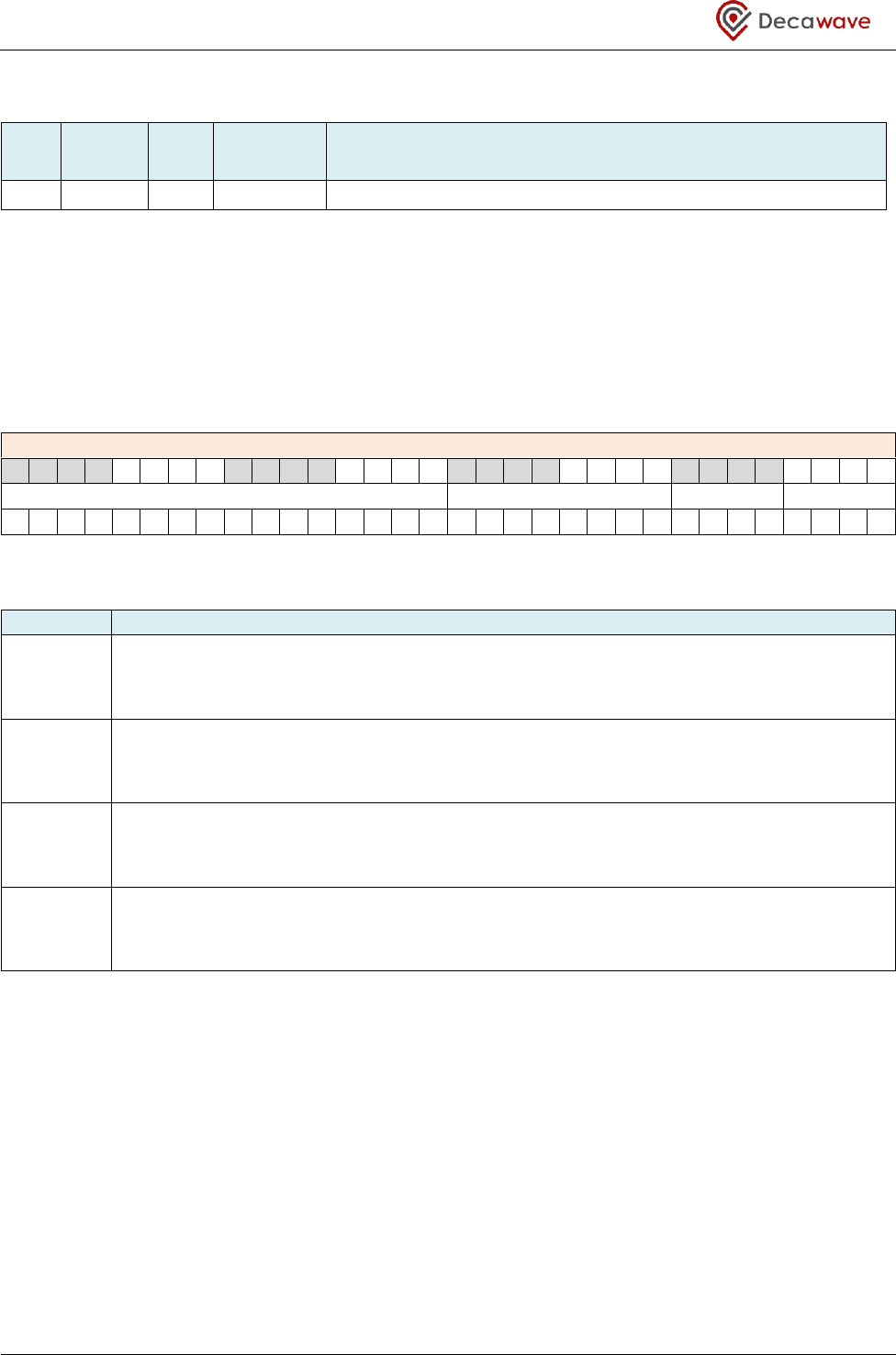
DW1000 User Manual
© Decawave Ltd 2017
Version 2.15
Page 65 of 244
7.2.2 Register file: 0x00 – Device Identifier
ID
Length
(octets)
Type
Mnemonic
Description
0x00
4
RO
DEV_ID
Device Identifier – includes device type and revision information
Register map register file 0x00 is the device identifier. This is hard-coded into the silicon. The value in this
register is read-only and cannot be overwritten by the host system. The device ID will be changed for any
silicon updates. The device ID register is ideal to use in the host µP to validate that the SPI interface is
operational. It is expected that the host system will validate that the device ID is the expected value,
supported by its software, before proceeding to use the IC.
The Device Identifier register contains the following sub-fields:
REG:00:00 – DEV_ID – Device Identifier
31
30
29
28
27
26
25
24
23
22
21
20
19
18
17
16
15
14
13
12
11
10
9
8
7
6
5
4
3
2
1
0
RIDTAG
MODEL
VER
REV
1
1
0
1
1
1
1
0
1
1
0
0
1
0
1
0
0
0
0
0
0
0
0
1
0
0
1
1
0
0
0
0
Definition of the sub fields of REG:00:00 – DEV_ID: Device Identifier:
Field
Description of fields within Register file: 0x00 – Device Identifier
REV
reg:00:00
bits:3–0
Revision: This number will be updated for minor corrections and changes in operation
VER
reg:00:00
bits:7–4
Version: This number will be updated if a new version is produced that has significant
differences from the previous version.
MODEL
reg:00:00
bits:15–8
The MODEL identifies the device. The DW1000 is device type 0x01.
RIDTAG
reg:00:00
bits:31–16
Register Identification Tag. It is planned that this will remain constant for all Decawave
parts. The value is 0xDECA in hex.
For the production DW1000 the Device ID is set to 0xDECA0130. The register descriptions in this user
manual relate to that DW1000 device and are not valid for any earlier sample parts.
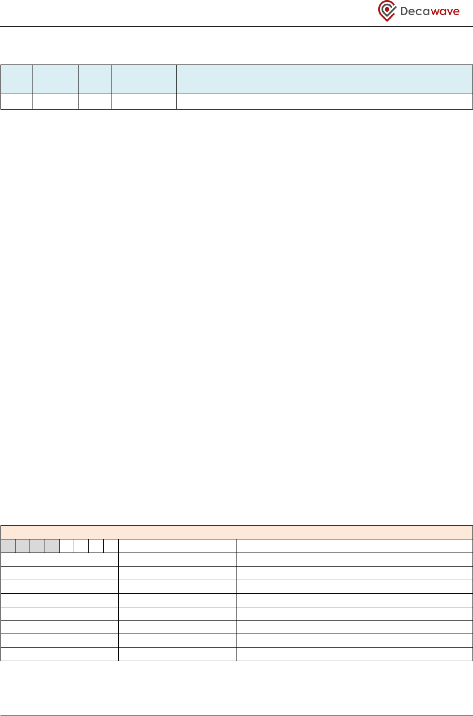
DW1000 User Manual
© Decawave Ltd 2017
Version 2.15
Page 66 of 244
7.2.3 Register file: 0x01 – Extended Unique Identifier
ID
Length
(octets)
Type
Mnemonic
Description
0x01
8
RW
EUI
Extended Unique Identifier – the 64-bit IEEE device address
Register map register file 0x01 is the Extended Unique Identifier register. For IEEE 802.15.4 compliance
every device should have a unique 64-bit device identifier. The high-order 24-bits of the EUI are a company
identifier assigned by the IEEE Registration Authority, (see http://standards.ieee.org/develop/regauth/oui/),
to the manufacturer. The low 40-bits of the EUI are the extension identifier uniquely chosen by the
manufacturer for each device manufactured and never repeated. The resultant EUI is a globally unique
identifier. It is expected that manufacturers who need to comply with this requirement will register with the
IEEE Registration Authority and generate and maintain their own EUI extension identifier numbering space to
ensure its uniqueness for every device made.
Manufacturers may store the EUI externally to the DW1000 or as an alternative the DW1000 has a one-time-
programmable memory area that may be programmed with the EUI during product manufacturing. Please
refer to section 6.3 – Using the on-chip OTP memory for details of programming values into OTP. Table 47:
Register file: 0x2D – OTP Memory Interface overview gives an overview of OTP contents and addresses.
During DW1000 initialisation, or upon waking up from sleep mode, the Register file: 0x01 – Extended Unique
Identifier register value is loaded from its OTP memory area. After this the EUI register value may be
overwritten by the host system if necessary.
Certain IEEE 802.15.4 defined frames use a 64-bit source address. The software (MAC) generating such
frames is expected to insert the EUI within the frame before the frame is written to the DW1000’s transmit
buffer.
The EUI register is used by the Receive Frame Filtering function, see section 5.2details. When frame filtering
is operational the DW1000 decodes each received frame according to the IEEE 802.15.4 MAC rules and any
64-bit destination address present must match the EUI register before the frame will be accepted.
The 8-octets of the Extended Unique Identifier may be accessed as a single 8-octet access to the EUI register
file starting at index 0. The bytes of the EUI are output/input in the following order:
REG:01:00 – EUI – Extended Unique Identifier
7
6
5
4
3
2
1
0
Octet Index
Description
0xHH
0
Bits 7 to 0 of the extension identifier
0xHH
1
Bits 15 to 8 of the extension identifier
0xHH
2
Bits 23 to 16 of the extension identifier
0xHH
3
Bits 31 to 24 of the extension identifier
0xHH
4
Bits 39 to 32 of the extension identifier
0xNN
5
Bits 7 to 0 of the OUI (manufacturer company ID)
0xNN
6
Bits 15 to 8 of the OUI (manufacturer company ID)
0xNN
7
Bits 23 to 16 of the OUI (manufacturer company ID)
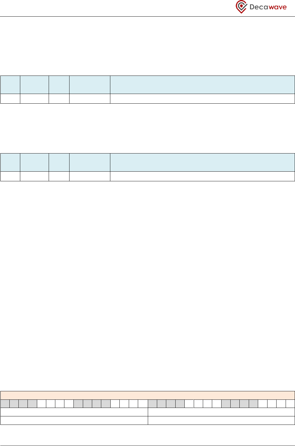
DW1000 User Manual
© Decawave Ltd 2017
Version 2.15
Page 67 of 244
The ordering of octets read from the Extended Unique Identifier register is designed to be directly
compatible with the octet ordering of the 64-bit source address fields of IEEE 802.15.4 standard MAC frames
easing the task of inserting it into a frame for transmission.
7.2.4 Register file: 0x02 – Reserved
ID
Length
(octets)
Type
Mnemonic
Description
0x02
-
-
-
Reserved – this register file is reserved
Register map register file 0x02 is reserved for future use. Please take care not to write to this register as
doing so may cause the DW1000 to malfunction.
7.2.5 Register file: 0x03 – PAN Identifier and Short Address
ID
Length
(octets)
Type
Mnemonic
Description
0x03
4
RW
PANADR
PAN Identifier and Short Address
Register map register file 0x03 contains two 16-bit parameters, the PAN Identifier and the Short Address.
When the DW1000 is powered-up or reset both the PAN Identifier and the Short Address in this register are
reset to the value 0xFFFF. The host software (MAC) should program the appropriate values into this register
if it wishes to use the DW1000’s receive frame filtering or automatic acknowledgement generation
functions.
In an IEEE 802.15.4 personal area network (PAN), the PAN coordinator node determines the PAN Identifier
for the network, and assigns it and short 16-bit addresses to devices (nodes) associating with the PAN. The
nodes in the PAN then should (at the MAC layer) use their assigned short address as the source address and
include it along with the PAN Identifier in the frames they transmit. When a node receives a frame it should
only process those with a destination address and PAN Identifier which matches their assigned node address
and network ID.
When the receive frame filtering and automatic acknowledgement functionality is operational the DW1000
decodes each received frame according to the IEEE 802.15.4 MAC specification and when it determines that
a 16-bit destination address is present in the frame, the DW1000 will compare the destination address with
the short address value programmed in this register before accepting/acknowledging the frame, and will
similarly only accept received frames when the PAN Identifier in the frame matches the PAN Identifier
programmed in this register. See sections 5.2 and 5.3 for details of the frame filtering and automatic
acknowledgement functionality.
The PAN Identifier and Short Address register contains the following sub-fields:
REG:03:00 –PANADR – PAN Identifier and Short Address
31
30
29
28
27
26
25
24
23
22
21
20
19
18
17
16
15
14
13
12
11
10
9
8
7
6
5
4
3
2
1
0
PAN_ID
SHORT_ADDR
0xFFFF
0xFFFF
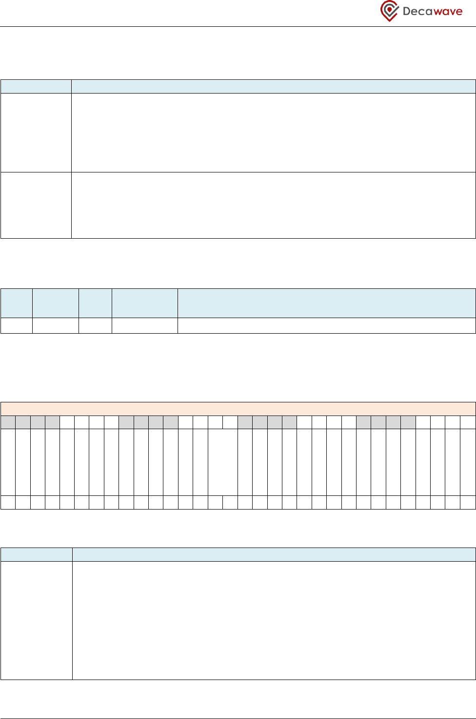
DW1000 User Manual
© Decawave Ltd 2017
Version 2.15
Page 68 of 244
The host software (MAC) only needs to program this register if it is using the DW1000’s receive frame
filtering and automatic acknowledgement generation functions. The sub-fields are:
Field
Description of fields within Register file: 0x03 – PAN Identifier and Short Address
SHORT_ADDR
reg:03:00
bits:15–0
Short Address. The host software needs to program this register if it is using the
DW1000’s receive frame filtering functionality, with or without the automatic
acknowledgement generation function. The short address is typically assigned to a node
by the coordinator function at MAC (or higher) layer as part of network association. The
value may alternatively be pre-defined in a closed network where the network association
phase is being skipped.
PAN_ID
reg:03:00
bits:31–16
PAN Identifier. The host software needs to program this register if it is using the
DW1000’s receive frame filtering functionality, with or without the automatic
acknowledgement generation function. The PAN ID is typically assigned as part of
network association. A predefined PAN ID might be used in a closed network where the
network association phase is being skipped.
7.2.6 Register file: 0x04 – System Configuration
ID
Length
(octets)
Type
Mnemonic
Description
0x04
4
RW
SYS_CFG
System Configuration bitmap
Register map register file 0x04 is the system configuration register. This is a bitmapped register. Each bit
field is separately identified and described below. The System Configuration register contains the following
bitmapped sub-fields:
REG:04:00 – SYS_CFG – System Configuration bit map
31
30
29
28
27
26
25
24
23
22
21
20
19
18
17
16
15
14
13
12
11
10
9
8
7
6
5
4
3
2
1
0
AACKPEND
AUTOACK
RXAUTR
RXWTOE
-
-
-
-
-
RXM110K
-
-
-
DIS_STXP
PHR_MODE
FCS_INIT2F
DIS_RSDE
DIS_PHE
DIS_DRXB
DIS_FCE
SPI_EDGE
HIRQ_POL
FFA5
FFA4
FFAR
FFAM
FFAA
FFAD
FFAB
FFBC
FFEN
0
0
0
0
0
0
0
0
0
0
0
0
0
0
0
0
0
0
0
1
0
0
1
0
0
0
0
0
0
0
0
0
Definition of the bit fields within REG:04:00 – SYS_CFG: System Configuration bitmap: -
Field
Description of fields within Register file: 0x04 – System Configuration
FFEN
reg:04:00
bit:0
Frame Filtering Enable. This bit enables the frame filtering functionality in the DW1000
receiver. The frame filtering is designed to follow the rules defined in the IEEE 802.15.4-
2011 standard. When frame filtering is enabled receive frames must pass the frame
filtering rules before being considered as a good frame. This includes the destination
address matching the PAN_ID and SHORT_ADDR as defined in Register file: 0x03 – PAN
Identifier and Short Address, or the long 64-bit defined by Register file: 0x01 – Extended
Unique Identifier. These addresses and the other frame filtering control bits of Register
file: 0x04 – System Configuration should be configured correctly before enabling frame
filtering with this FFEN bit. Section 5.2 describes frame filtering in more detail.

DW1000 User Manual
© Decawave Ltd 2017
Version 2.15
Page 69 of 244
Field
Description of fields within Register file: 0x04 – System Configuration
FFBC
reg:04:00
bit:1
Frame Filtering Behave as a Coordinator. FFEN must be set to enable this frame filtering
operation. A coordinator will accept a frame without a destination address if the source
address has the PAN_ID matching the coordinator’s PAN_ID. For an ordinary (non-
coordinator) node the destination address (if present) must match the node’s own
address or the frame will not be accepted. When FFBC is set to 1 the DW1000 will behave
as a coordinator. When FFBC is clear the DW1000 will behave as an ordinary normal
node. Section 5.2 describes frame filtering in more detail.
FFAB
reg:04:00
bit:2
Frame Filtering Allow Beacon frame reception. IEEE 802.15.4-2011 frames begin with
three bits, indicating the frame type for beacon frames these are binary 000. When FFAB
is set to 1 beacon frames will be accepted (assuming all other frame filtering rules are
passed) and when FFAB is clear beacon frames will be ignored. Section 5.2 describes
frame filtering in detail.
FFAD
reg:04:00
bit:3
Frame Filtering Allow Data frame reception. IEEE 802.15.4-2011 frames begin with three
bits, indicating the frame type, b3 to b0, for data frames these are binary 001. When
FFAD is set to 1 data frames will be accepted (assuming all other frame filtering rules are
passed) and when FFAD is clear data frames will be ignored. Section 5.2 describes frame
filtering in more detail.
FFAA
reg:04:00
bit:4
Frame Filtering Allow Acknowledgment frame reception. IEEE 802.15.4-2011 frames begin
with three frame type bits, b3 to b0, for acknowledgment frames these are binary 010.
When FFAA is set to 1 acknowledgment frames will be accepted (assuming all other frame
filtering rules are passed) and when FFAA is clear acknowledgment frames will be
ignored. Section 5.2 describes frame filtering in more detail.
FFAM
reg:04:00
bit:5
Frame Filtering Allow MAC command frame reception. IEEE 802.15.4-2011 frames begin
with three frame type bits, b3 to b0, for MAC command frames these are binary 011.
When FFAM is set to 1 MAC command frames will be accepted (assuming all other frame
filtering rules are passed) and when FFAM is clear MAC command frames will be ignored.
Section 5.2 describes frame filtering in more detail.
FFAR
reg:04:00
bit:6
Frame Filtering Allow Reserved frame types. IEEE 802.15.4-2011 frames begin with three
frame type bits, b3 to b0. The values of binary 100 through 111 (4 to 7) are not defined in
IEEE 802.15.4-2011 and would normally be rejected. When FFAR is 0 these frames may
be ignored (depending also on FFA4 and FFA5 which modify this behaviour). When FFAR
is set to 1 these frames are accepted. Since these frame types are unknown no further
frame decoding is done (e.g. no address matching etc.) and the software will thus be
responsible for validating and interpreting these frames. Section 5.2 describes frame
filtering in more detail.
Note that the frame filter does decode the frame control fields to determine the
minimum length of the expected frame and will reject the frame if it is too short, see
section 5.2.
FFA4
reg:04:00
bit:7
Frame Filtering Allow frames with frame type field of 4, (binary 100). IEEE 802.15.4-2011
frames begin with three frame type bits, b3 to b0. The value of binary 100 is not defined
in IEEE 802.15.4-2011. When FFA4 is set to 1, frames of type 4 will be accepted, but no
further frame decoding is done (e.g. no address matching etc.) so software will be
responsible for validating and interpreting these frames. When FFA4 is set to 0, frames of
type 4 will be ignored unless FFAR is set. Section 5.2 describes frame filtering in more
detail.
Note that the frame filter does decode the frame control fields to determine the
minimum length of the expected frame and will reject the frame if it is too short, see
section 5.2.

DW1000 User Manual
© Decawave Ltd 2017
Version 2.15
Page 70 of 244
Field
Description of fields within Register file: 0x04 – System Configuration
FFA5
reg:04:00
bit:8
Frame Filtering Allow frames with frame type field of 5, (binary 101). IEEE 802.15.4-2011
frames begin with three frame type bits, b3 to b0. The value of binary 100 is not defined
in IEEE 802.15.4-2011. When FFA5 is set to 1, frames of type 5 will be accepted, but no
further frame decoding is done (e.g. no address matching etc.) so software will be
responsible for validating and interpreting these frames. When FFA5 is set to 0, frames of
type 5 will be ignored unless FFAR is set. Section 5.2 describes frame filtering in more
detail.
Note that the frame filter does decode the frame control fields to determine the
minimum length of the expected frame and will reject the frame if it is too short, see
section 5.2.
HIRQ_POL
reg:04:00
bit:9
Host interrupt polarity. This bit allows the system integrator the ability to control the
polarity of the IRQ line from the DW1000. When HIRQ_POL is 1 the IRQ output line from
the DW1000 is active high, and, when HIRQ_POL is 0 the IRQ output line from the
DW1000 is active low.
Active high operation is recommended for low power applications so that the interrupt is
in its 0 V logical inactive state when the DW1000 is in SLEEP or DEEPSLEEP states.
SPI_EDGE
reg:04:00
bit:10
SPI data launch edge. This bit allows the system integrator the ability to control the
launch edge used for SPI data from the DW1000 on the MISO SPI data output line. This
may be used to select the MISO output operation most suitable to the target system.
When SPI_EDGE is 0 the DW1000 uses the sampling edge to launch MISO data. This
setting should give the highest rate operation. When SPI_EDGE is 1 the DW1000 uses the
opposite edges to launch the data. This setting may give a more robust operation.
DIS_FCE
reg:04:00
bit:11
Disable frame check error handling. This might be of use for protocols using a different
encoding scheme for error handling not based on standard IEEE 802.15.4-2011, but for
normal IEEE 802.15.4-2011 operation this bit should be set to 0. Setting this bit to one
makes the DW1000 treat the frame as valid, ignoring errors, so that in double buffering
mode (for example) it will move on to the next buffer. In normal operation (when
DIS_FCE is 0) with double buffering, a CRC error causes the current RX frame to be
discarded and the buffer to be reused for next frame’s reception.
DIS_DRXB
reg:04:00
bit:12
Disable Double RX Buffer. The DW1000 has a double buffered receiver allowing reception
of a new frame to proceed in one buffer while the host processor is in the process of
unloading the last frame received into the other buffer of the buffer pair. The double
buffering is enabled when DIS_DRXB is set to 0, and disabled when DIS_DRXB is set to 1.
More details on the operation of double buffering are given in section4.3.
DIS_PHE
reg:04:00
bit:13
Disable receiver abort on PHR error. When DIS_PHE is 0 (recommended) the receiver will
discontinue reception when it detects a non-correctable error in the PHY header, see
section 10.4 –PHY header for details of PHR encoding and error correction. The PHR error
is reported by the RXPHE event status bit in Register file: 0x0F – System Event Status
Register.
This bit is for debug only and should never be set in an application as it can seriously
impair receiver performance when set.

DW1000 User Manual
© Decawave Ltd 2017
Version 2.15
Page 71 of 244
Field
Description of fields within Register file: 0x04 – System Configuration
DIS_RSDE
reg:04:00
bit:14
Disable Receiver Abort on RSD error. During normal reception (i.e. with the DIS_RSDE bit
cleared to its recommended default zero value) when the Reed Solomon decoder detects
an non-correctable error then frame reception is aborted and the receiver will be disabled,
(unless the RXAUTR control bit is set in which case the receiver will automatically re-enable
and begin preamble hunt again). The Reed Solomon decoder error is generated when an
error is found that cannot be corrected using the Reed Solomon FEC (forward error
correction) data. The Reed Solomon decoder error is flagged in the RXRFSL event status bit
in Register file: 0x0F – System Event Status Register. When the DIS_RSDE bit is set the
receiver will not abort reception when the Reed Solomon error occurs, but will instead
continue to demodulate the data to the end of the frame (i.e. for the length specified in
the PHY Header). Typically the non-correctable Reed Solomon error will mean that the
frame is corrupted and that the CRC will not be correct.
FCS_INIT2F
reg:04:00
bit:15
This bit allows selection of the initial seed value for the FCS generation and checking
function that is set at the start of each frame transmission and reception. By default the
FCS_INIT2F bit is 0 selecting the FCS generation/checking seed initialisation to be all zero
(0x0000) – this is the standard setting required for IEEE 802.15.4 compliance. When the
FCS_INIT2F bit is 1 the FCS generation/checking initialisation value will be all ones (0xFFFF).
PHR_MODE
reg:04:00
bits:17,16
This configuration allows selection of PHR type to be one of two options. The default
setting gives IEEE standard PHR encoding and a maximum data payload of 127 octets.
The other option enables the proprietary long frames mode which allows a data payload
of up to 1023 octets. In this mode the PHR encoding does not follow the IEEE standard.
For successful communications between two nodes both must be configured for the
same PHR mode. Supported PHR_MODE configurations are:
00 – Standard Frame mode. Use this setting is for IEEE 802.15.4 compliance.
11 – Long Frames mode. Proprietary PHR encoding. Frame Length 0-1023.
DIS_STXP
reg:04:00
bit:18
Disable Smart TX Power control.
Smart TX power control applies at the 6.8 Mbps data rate. When sending short data frames
at this rate (and providing that the frame transmission rate is < 1 frame per millisecond) it
is possible to increase the transmit power and still remain within regulatory power limits
which are typically specified as average power per millisecond.
When DIS_STXP is 0, the transmitter automatically sets the transmitter power levels when
sending a frame at the 6.8 Mbps data rate, depending on the frame length specified in the
TFLEN field of Register file: 0x08 – Transmit Frame Control.
The actual power levels used are selected by the values configured in Register file: 0x1E –
Transmit Power Control, described in section 7.2.31.
NB: It is up to the external system to keep the frame rate below 1 frame per millisecond to
ensure that the power boost is not breaking the regulations.
When DIS_STXP is 1, the smart TX power control function is disabled and TX power does
not depend on data rate and frame length. In this case the values configured in Register
file: 0x1E – Transmit Power Control are used to specify the power in different phases of the
TX frame separately, see section 7.2.31.

DW1000 User Manual
© Decawave Ltd 2017
Version 2.15
Page 72 of 244
Field
Description of fields within Register file: 0x04 – System Configuration
-
reg:04:00
bits:21–19
These bits are reserved and should always be set to zero to avoid any malfunction of the
device.
RXM110K
reg:04:00
bit:22
Receiver Mode 110 kbps data rate. This configuration when set to 1 will cause the
receiver to look for long SFD and process the PHY Header and RX data as per the 110 kbps
frame mode. When this configuration is 0, (the default), the receiver will look for short
SFD and will determine the RX data rate from the PHY header as either 850 kbps or
6.8 Mbps.
-
reg:04:00
bits:27–23
These bits are reserved and should always be set to zero to avoid any malfunction of the
device.
RXWTOE
reg:04:00
bit:28
Receive Wait Timeout Enable. When set RX Enable will initialise an RX_FWTO down count
which will disable the receiver if no valid frame is received before the timeout occurs. The
timeout period is set in Register file: 0x0C – Receive Frame Wait Timeout Period. The
occurrence of the timeout is signalled by the RXRFTO event status bit in Register file: 0x0F
– System Event Status Register.
RXAUTR
reg:04:00
bit:29
Receiver Auto-Re-enable. This bit is used to cause the receiver to re-enable automatically.
Its operation changes depending on whether the IC is operating in single or double buffered
modes. The default value is 0. With this setting, the IC will not automatically re-enable the
receiver but will stop receiving and return to idle mode whenever any receive events
happen. This includes receiving a frame but also failing to receive a frame because of some
error condition, for example an error in the PHY header (as reported by the RXPHE event
status bit in Register file: 0x0F – System Event Status Register). In such cases if the host
wants to re-enable the receiver it must do it explicitly, using the RXENAB bit in Register file:
0x0D – System Control Register. The operation when RXAUTR = 1 is as follows:
(a) Double-buffered mode: After a frame reception event or failure (except a frame
wait timeout), the receiver will re-enable to receive another frame.
(b) Single-buffered mode: After a frame reception failure (except a frame wait
timeout), the receiver will re-enable to re-attempt reception.
For more information on frame reception see section 4 – Message Reception.
Note: In double-buffered mode when automatic frame acknowledgement is enabled (by
the AUTOACK bit below) the receiver will be re-enabled after the ACK frame has been
transmitted.
AUTOACK
reg:04:00
bit:30
Automatic Acknowledgement Enable. Default value 0. This is the enable for the
Automatic Acknowledgement function. See section 5.3– Automatic Acknowledgement for
details of operation of Automatic Acknowledgement.
AACKPEND
reg:04:00
bit:31
Automatic Acknowledgement Pending bit control. Default value 0. The value of the
AACKPEND bit is copied into the Frame Pending bit in the Frame Control field of the
DW1000 automatically generated ACK frame. See section 5.2 – Frame filtering for details
of operation of frame filtering.
7.2.7 Register file: 0x05 – Reserved
ID
Length
(octets)
Type
Mnemonic
Description
0x05
-
-
-
Reserved – this register file is reserved
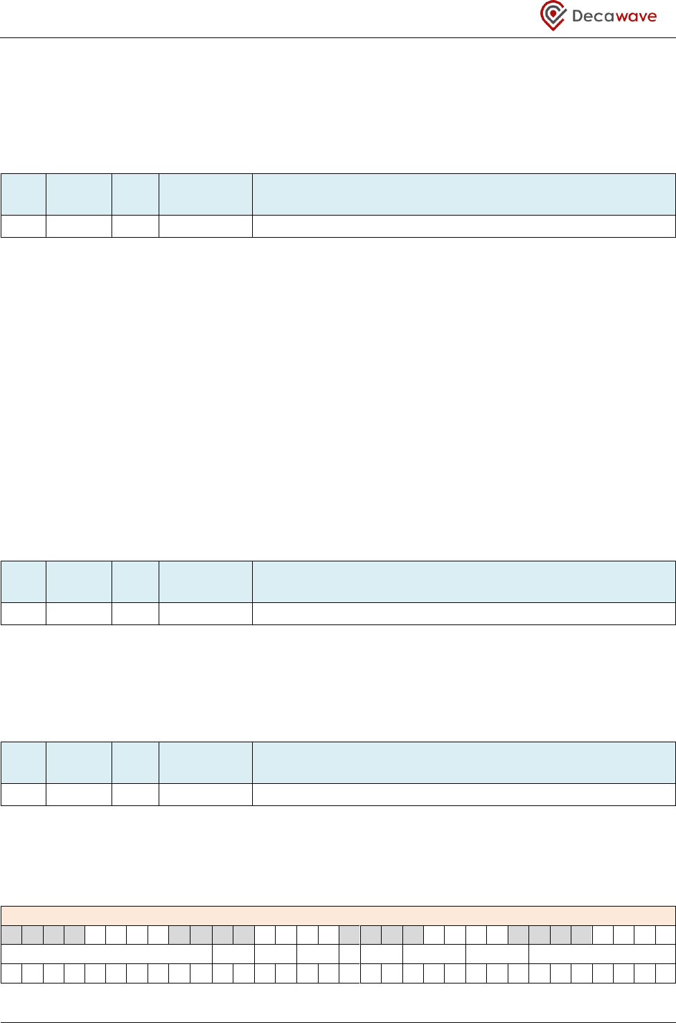
DW1000 User Manual
© Decawave Ltd 2017
Version 2.15
Page 73 of 244
Register map register file 0x05 is reserved for future use. Please take care not to write to this register as
doing so may cause the DW1000 to malfunction.
7.2.8 Register file: 0x06 – System Time Counter
ID
Length
(octets)
Type
Mnemonic
Description
0x06
5
RO
SYS_TIME
System Time Counter (40-bit)
Register map register file 0x06 is the System Time Counter register. System time and time stamps are
designed to be based on the time units which are nominally at 64 GHz, or more precisely 499.2 MHz × 128
which is 63.8976 GHz. In line with this when the DW1000 is in idle mode with the digital PLL enabled, the
System Time Counter is incremented at a rate of 125 MHz in units of 512. The nine low-order bits of this
register are thus always zero. The counter wrap period of the clock is then: 240 ÷ (128×499.2e6) = 17.2074
seconds.
Notes (a)
On power up, before the digital PLL is enabled, the System Time Counter increments are still
in units of 512 however the increment rate is half the external crystal frequency, (e.g. at
19.2 MHz for the 38.4 MHz crystal). The counter wrap period is then: 231 ÷ 19.2e6 = 111.8481
seconds.
(b)
In sleep modes the system time counter is disabled and this register is not updated.
7.2.9 Register file: 0x07 – Reserved
ID
Length
(octets)
Type
Mnemonic
Description
0x07
-
-
-
Reserved – this register file is reserved
Register map register file 0x07 is reserved for future use. Please take care not to write to this register as
doing so may cause the DW1000 to malfunction.
7.2.10 Register file: 0x08 – Transmit Frame Control
ID
Length
(octets)
Type
Mnemonic
Description
0x08
5
RW
TX_FCTRL
Transmit Frame Control
Register map register file 0x08, the transmit frame control register, contains a number of TX control fields.
Each field is separately identified and described below. (For a general discussion of transmission please refer
to section 3 – Message Transmission.
REG:08:00 – TX_FCTRL – Transmit Frame Control (Octets 0 to 3, 32-bits)
31
30
29
28
27
26
25
24
23
22
21
20
19
18
17
16
15
14
13
12
11
10
9
8
7
6
5
4
3
2
1
0
TXBOFFS
PE
TXPSR
TXPRF
TR
TXBR
R
TFLE
TFLEN
0
0
0
0
0
0
0
0
0
0
0
1
0
1
0
1
0
1
0
0
0
0
0
0
0
0
0
0
1
1
0
0
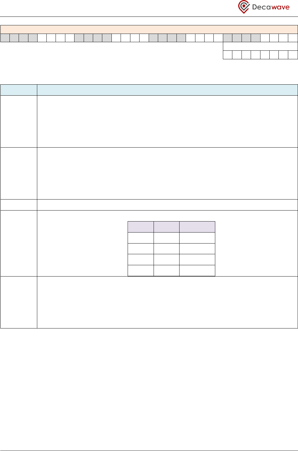
DW1000 User Manual
© Decawave Ltd 2017
Version 2.15
Page 74 of 244
REG:08:04 – TX_FCTRL – Transmit Frame Control (Octet 4, 8-bits)
31
30
29
28
27
26
25
24
23
22
21
20
19
18
17
16
15
14
13
12
11
10
9
8
7
6
5
4
3
2
1
0
IFSDELAY
0
0
0
0
0
0
0
0
The fields of the TX_FCTRL register identified above are individually described below:
Field
Description of fields within Register file: 0x08 – Transmit Frame Control
TFLEN
reg:08:00
bits:6–0
Transmit Frame Length. Standard IEEE 802.15.4 UWB frames can be up to 127 bytes long.
The value specified here determines the length of the data portion of the transmitted frame.
This length includes the two-octet CRC appended automatically at the end of the frame,
unless SFCST (in Register file: 0x0D – System Control Register) is use to suppress the FCS. The
frame length is also copied into the PHY Header of the TX frame so that the receiving device
knows how much data to decode.
TFLE
reg:08:00
bits:9–7
Transmit Frame Length Extension. The DW1000 supports a non-standard mode of operation
with data frame lengths up to 1023 bytes. This mode of operation is enabled via the
PHR_MODE selection bits of Register file: 0x04 – System Configuration. In this long frame
mode TFLE adds three high-order bits to TFLEN to extend the frame length to 10-bits,
allowing frame length from 0 up to 1023 bytes to be sent. Please refer to section 3.4 –
Extended Length Data Frames for more details of this non-standard mode.
R
Reserved. Bits 12, 11 & 10 are reserved for future expansion. They should be set to zero.
TXBR
reg:08:00
bits:14,13
Transmit Bit Rate. This sets the user bit rate for the data portion of the frame as follows:
Bit 14
Bit 13
Bit Rate
0
0
110 kbps
0
1
850 kbps
1
0
6.8 Mbps
1
1
reserved
TR
reg:08:00
bit: 15
Transmit Ranging enable. This bit has no operational effect on the DW1000; however it is
copied into the ranging bit in the PHY header (PHR) of the transmitted frame, identifying the
frame as a ranging frame. In some receiver implementations this may be used to enable
hardware or software associated with time-stamping the frame. In the DW1000 receiver the
time-stamping of the receive frame does not depend or use the ranging bit in the received
PHR.
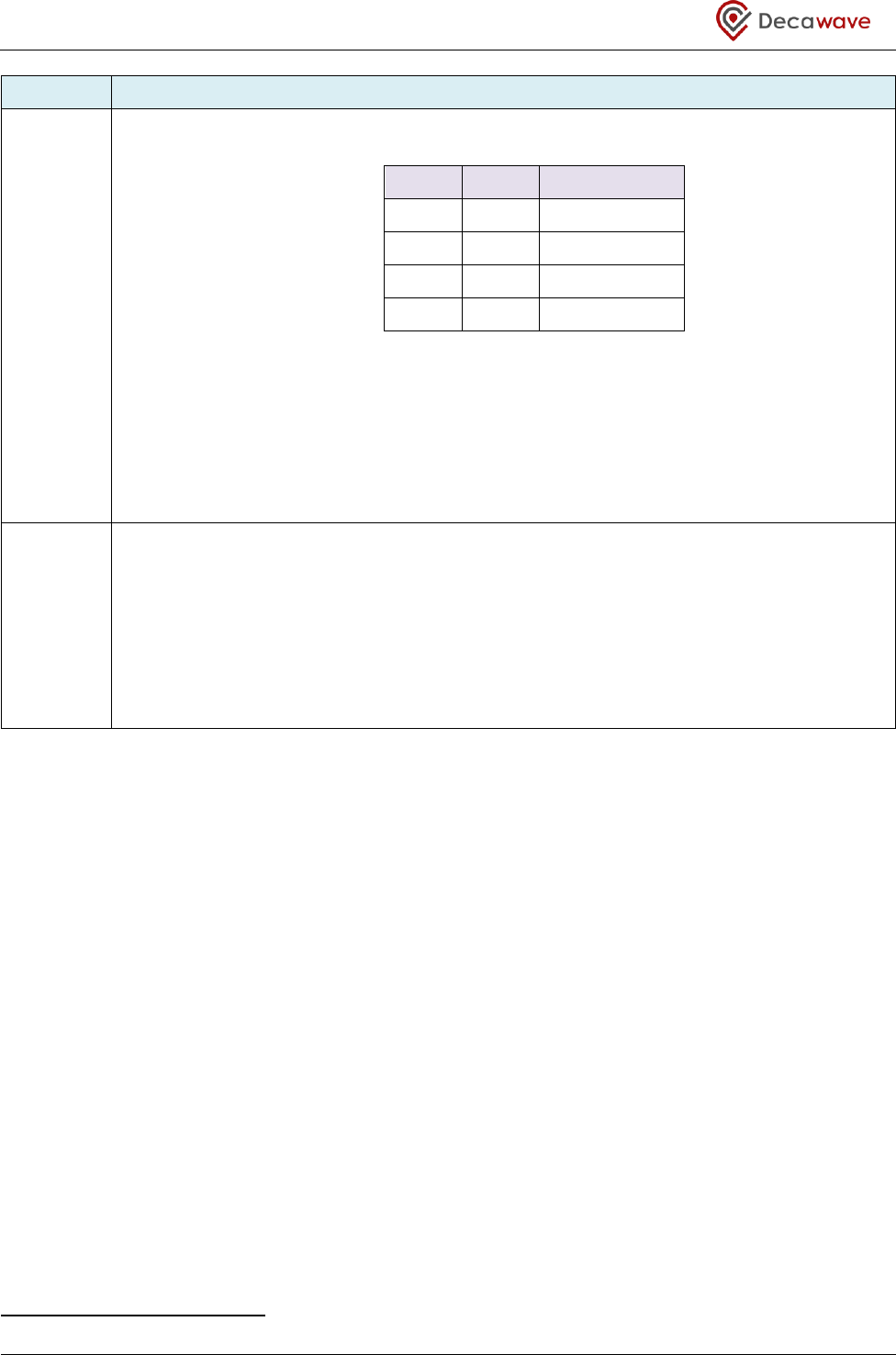
DW1000 User Manual
© Decawave Ltd 2017
Version 2.15
Page 75 of 244
Field
Description of fields within Register file: 0x08 – Transmit Frame Control
TXPRF
reg:08:00
bits:17,16
Transmit Pulse Repetition Frequency. This sets the mean Pulse Repetition Frequency (PRF)
used in the transmitter:
Bit 17
Bit 16
Nominal PRF
0
0
4 MHz
0
1
16 MHz
1
0
64 MHz
1
1
reserved
Note: (a) For successful reception of a frame the PRF in the receiver needs to be
configured to be the same as the PRF used for transmitting the frame.
(b) The choice of preamble code also needs to be appropriate to the configured PRF
and needs to be the same in both transmitting and receiving ends for successful
communication – please use Table 61 to select the appropriate preamble code.
I The DW1000 receiver does not support the 4 MHz PRF.
TXPSR
reg:08:00
bits:19,18
Transmit Preamble Symbol Repetitions (PSR). This sets the length of the transmitted
preamble sequence in symbols. Each preamble symbol is approximately 1 µs in duration1.The
two TXPSR bits are copied into the PHY Header. The receiving end is thus made aware of
how much preamble was sent. This might inform its choice of preamble length in any reply
message. There are four standard preamble lengths defined for the 802.15.4 UWB PHY –
these are 16, 64, 1024 and 4096 symbols. The DW1000 has facility via the PE (Preamble
Extension) configuration to send preambles of additional (non-standard) intermediary
lengths. Table 16 below lists the selectable preamble lengths.
1
The duration of preamble symbols is 993.59 ns with the 16 MHz PRF setting and 1017.63 ns with for 64 MHz PRF.

DW1000 User Manual
© Decawave Ltd 2017
Version 2.15
Page 76 of 244
Field
Description of fields within Register file: 0x08 – Transmit Frame Control
PE
reg:08:00
bits:21,20
Preamble Extension. This field allows specification of a non-standard number of preamble
symbol repetitions, thus extending the set of preamble lengths that are available to optimise
system performance. The resultant preamble lengths depend the setting of both PE and
TXPSR above. Table 16 below lists the useful preamble lengths that can be selected.
Table 16: Preamble length selection
Bit 19
Bit 18
Bit 21
Bit 20
TXPSR
PE
Preamble Length
0
1
0
0
64
0
1
0
1
128
0
1
1
0
256
0
1
1
1
512
1
0
0
0
1024
1
0
0
1
1536
1
0
1
0
2048
1
1
0
0
4096
The bit numbers quoted above are the bit numbers in the TX_FCTRL register.
The choice of preamble length has a bearing on operating range and system performance, a
discussion of the factors affecting the choice of preamble length (and other parameters) may
be found in section 9.3 below.
TXBOFFS
reg:08:00
bits:31–22
Transmit buffer index offset. This 10-bit field is used to specify an index in the transmit
buffer of the first octet to be transmitted. The TX frame begins with the octet at the
TXBOFFS index and continues for the number octets specified by the frame length (TFLEN
and TFLE) less 2 for the CRC. Care should be taken that the TXBOFFS plus the frame length
does not extend past the end of the TX_BUFFER. Some uses for TXBOFFS are outlined in
section 3.5.1.
IFSDELAY
reg:08:04
bits:7–0
Inter-Frame Spacing. This delay in preamble symbol times will be applied between
successive transmitted frames. One use of the IFSDELAY is to allow the receiver time to
unload and process the frame before another frame is sent to it. For this reason IFSDELAY is
logically considered to be a post-amble to the transmitted frame, and it begins counting
down after the last symbol of data is sent. Where the transmitter is enabled to begin a new
frame the DW1000 makes sure that IFSDELAY symbol times have passed. A new value of
IFSDELAY for the next frame should not be set until after the end-of-frame TXFRS (Transmit
Frame Sent) event has occurred. The IFSDELAY sets a minimum time between frames
enforced by the DW1000, assuming that the host has initiated a new transmission. Note:
Because of internal IC delays the on-air gap between the end of the previous frame and the
start of the new one is actually 6 symbol times larger than specified here, e.g. an IFSDELAY
setting of 34 will result in an on-air gap of 40 preamble symbols.
DW1000 User Manual
© Decawave Ltd 2017
Version 2.15
Page 77 of 244
7.2.11 Register file: 0x09 – Transmit Data Buffer
ID
Length
(octets)
Type
Mnemonic
Description
0x09
1024
WO
TX_BUFFER
Transmit Data Buffer
Register map register file 0x09 is the transmit data buffer. Data from the transmit buffer is transmitted
during the data payload portion of the transmitted frame. Section 3 – Message Transmission discusses the
basics of frame transmission and details the various parts of the TX frame.
The general procedure is to write the data frame for transmission into the TX_BUFFER, set the frame length
and other details in the TX_FCTRL register and initiate transmission using in the TXSTRT control bit in
Register file: 0x0D – System Control Register.
Note that read operations from the transmit data buffer are NOT supported. Reading the transmit data
buffer during an active transmit can corrupt the transmitted data. A read of the TX_FCTRL register will also
read the transmit data buffer so the TX_FCTRL register should not be read during an active transmit
operation.
7.2.12 Register file: 0x0A – Delayed Send or Receive Time
ID
Length
(octets)
Type
Mnemonic
Description
0x0A
5
RW
DX_TIME
Delayed Send or Receive Time (40-bit)
Register map register file 0x0A, the Delayed Send or Receive Time, is used to specify a time in the future to
either turn on the receiver to be ready to receive a frame, or to turn on the transmitter and send a frame.
The low-order 9-bits of this register are ignored. Delayed send is initiated by the TXDLYS control bit in
Register file: 0x0D – System Control Register. Delayed receive is initiated by the RXDLYE bit. Register file:
0x0D – System Control Register. For more information see section 3.3 – Delayed Transmission and section
4.2 – Delayed Receive.
Refer to the TX_PSTM field of Sub-Register 0x2F:24 – Digital Diagnostics Test Mode Control for details of
how to program this register for use in Transmit Power Spectrum Test Mode and note that bits 31:0 only are
used in this mode, whilst the 9 least significant bits are ignored in functional modes.
7.2.13 Register file: 0x0B – Reserved
ID
Length
(octets)
Type
Mnemonic
Description
0x0B
-
-
-
Reserved – this register file is reserved
Register map register file 0x0B is reserved for future use. Please take care not to write to this register as
doing so may cause the DW1000 to malfunction.
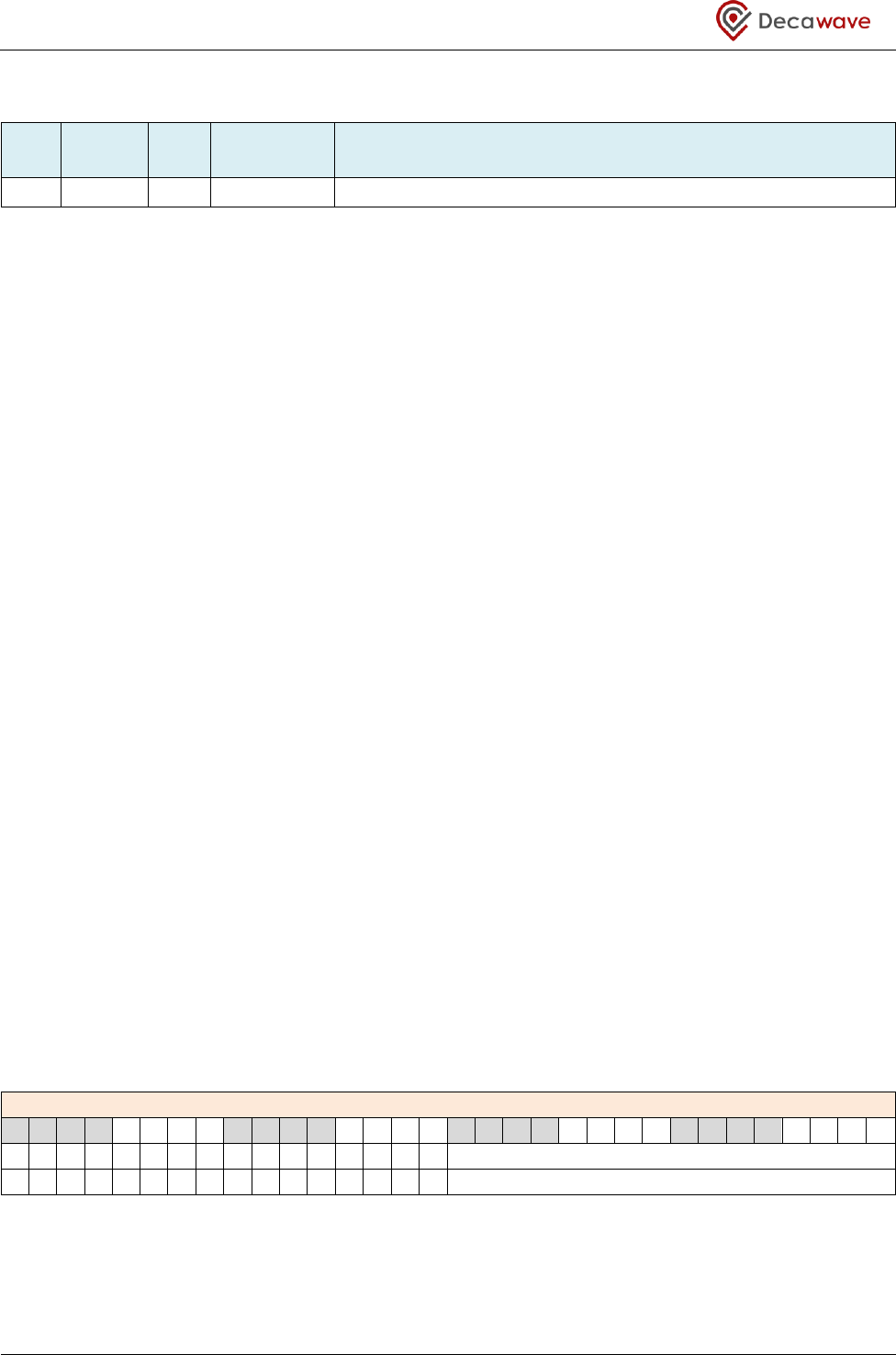
DW1000 User Manual
© Decawave Ltd 2017
Version 2.15
Page 78 of 244
7.2.14 Register file: 0x0C – Receive Frame Wait Timeout Period
ID
Length
(octets)
Type
Mnemonic
Description
0x0C
2
RW
RX_FWTO
Receive Frame Wait Timeout period
Register map register file 0x0C is the receive frame wait timeout period. The receive frame wait timeout
function is provided to allow the external microprocessor to enter a low power state awaiting a valid receive
frame and be woken up by the DW1000 when either a frame is received or the programmed timeout has
elapsed. While many microcontrollers have timers that might be used for this purpose, including this RX
timeout functionality in the DW1000 allows additional flexibility to the system designer in selecting the
microprocessor to optimise the solution. The frame wait timeout is enabled by the RXWTOE bit in Register
file: 0x04 – System Configuration.
When the receiver is enabled (and begins hunting for the preamble sequence) and RXWTOE is set, then the
frame wait timeout counter starts counting the timeout period programmed. Thereafter, assuming no
action is taken to change the operation, one of two things should happen:
a) The Receive Frame Wait Timeout period elapses. This disables the receiver and sets the RXRFTO
(Receiver Frame Wait Timeout) bit in the status register, (and resets the counter).
b) A valid receive frame arrives and sets the RXDFR and RXFCG bits in the status register. This stops the
receive frame wait timer counter so RXRFTO will not be set.
The receiver will not re-enable immediately following a RXRFTO (Receiver Frame Wait Timeout) irrespective
of whether the device is using the Double Receive Buffer, see section 4.3, or the Automatic Receiver Re-
enable, see section 5.3.2.
The timeout period should only be programmed when the device IDLE. Programming the timeout value at
other times is not prevented but may result in unpredictable behaviour.
The MRXFCG and MRXRFTO mask bits in the SYS_MASK register may be configured (before enabling the
receiver) to generate interrupts to the controlling microprocessor. If RXWTOE is cleared while the
countdown is running the countdown will be disabled, and RXRFTO will not be set.
When frame filtering is employed, any frames rejected are not treated as valid RX frames (neither RXDFR or
RXFCG are set) so the receiver and the receive frame wait timeout just continues its countdown
Register file: 0x0C – Receive Frame Wait Timeout Period contains the following fields:
REG:0C:00 – RX_FWTO – Receive Frame Wait Timeout Period
31
30
29
28
27
26
25
24
23
22
21
20
19
18
17
16
15
14
13
12
11
10
9
8
7
6
5
4
3
2
1
0
-
-
-
-
-
-
-
-
-
-
-
-
-
-
-
-
RXFWTO
0
0
0
0
0
0
0
0
0
0
0
0
0
0
0
0
0
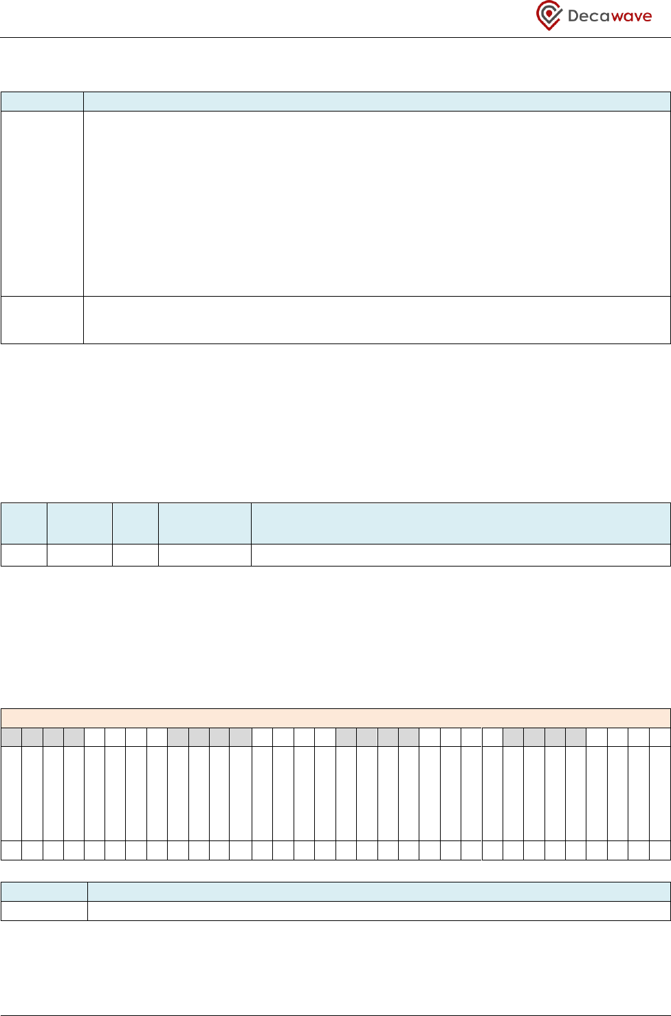
DW1000 User Manual
© Decawave Ltd 2017
Version 2.15
Page 79 of 244
The individual sub-fields are described below:
Field
Description of fields within Register file: 0x0C – Receive Frame Wait Timeout Period
RXFWTO
reg:0C:00
bits:15–0
The Receive Frame Wait Timeout period is a 16-bit field. The units for this parameter are
roughly 1µs, (the exact unit is 512 counts of the fundamental 499.2 MHz UWB clock, or
1.026 µs). When employing the frame wait timeout, RXFWTO should be set to a value
greater than the expected RX frame duration and include an allowance for any uncertainly
attaching to the expected transmission start time of the awaited frame. The Receive Frame
Wait Timeout feature is enabled by the RXWTOE in Register file: 0x04 – System
Configuration. When RXWTOE is set then each time the receiver is enabled a timer is started
with the RXFWTO specified period, and if no data is received before this RX Frame Wait
Timeout timer expires, then the receiver is returned to its idle state and the timeout is
signalled by the RXRFTO event status bit in Register file: 0x0F – System Event Status Register.
-
reg:0C:00
bits:31–16
These bits are reserved and should always be written as zero.
Note: The frame wait timeout may also be employed with double buffering, where after a frame is received
the DW1000 automatically re-enables the receiver (moving on to potentially receive a new frame in the next
buffer). Here when RXWTOE is set the countdown will be restarted as the receiver re-enables to receive into
the next buffer. See section 4.3 Double Receive Buffer for more information on double buffering.
7.2.15 Register file: 0x0D – System Control Register
ID
Length
(octets)
Type
Mnemonic
Description
0x0D
4
SRW
SYS_CTRL
System Control Register
Register map register file 0x0D is the system control register and contains a number of TX control fields. Each
field is separately identified and described below. For a general discussion of transmission please refer to
section 3 – Message Transmission. The control bits within the system control register are typically
automatically cleared. The host controller sets the appropriate bit to invoke an activity and the bit is
automatically cleared by the DW1000 as that commanded activity begins.
REG:0D:00 – SYS_CTRL – System Control
31
30
29
28
27
26
25
24
23
22
21
20
19
18
17
16
15
14
13
12
11
10
9
8
7
6
5
4
3
2
1
0
-
-
-
-
-
-
-
HRBPT
-
-
-
-
-
-
-
-
-
-
-
-
-
-
RXDLYE
RXENAB
WAIT4RESP
TRXOFF
-
-
CANSFCS
TXDLYS
TXSTRT
SFCST
0
0
0
0
0
0
0
0
0
0
0
0
0
0
0
0
0
0
0
0
0
0
0
0
0
0
0
0
0
0
0
0
Field
Description of fields within Register file: 0x0D – System Control Register
-
Bits marked ‘-’ in register 0x0D are reserved and should always be written as zero.

DW1000 User Manual
© Decawave Ltd 2017
Version 2.15
Page 80 of 244
Field
Description of fields within Register file: 0x0D – System Control Register
SFCST
reg:0D:00
bit:0
Suppress auto-FCS Transmission (on this next frame). This control works in conjunction with
the TXSTRT (Transmit Start) bit below to control whether or not the DW1000 automatically
calculates and appends the two Frame-Check-Sequence bytes. It is expected that the host
will decide this as transmission is invoked and set SFCST at the same time as TXSTRT is set if
FCS suppression is required. Normally SFCST is not set when transmission is started and the
DW1000 calculates the FCS on the octets fetched from the TX buffer, and automatically
appends the two-byte FCS sequence at the end of the frame. The FCS sequence follows the
IEEE 802.15.4 standard polynomial, x16 + x12 + x5 + 1, also known as CRC-16-CCITT or CRC-16
ITU-T. When SFCST is set (as transmission is started) the DW1000 will not append the FCS to
the data frame but instead fetches the two bytes from the TX buffer. The frame length is
determined by the TFLEN field of Register file: 0x08 – Transmit Frame Control. So, when
SFCST is clear, TFLEN-2 (frame length minus two) octets are fetched and sent from the TX
buffer, and the final two octets sent are the automatically generated FCS bytes. And, when
SFCST is set, TFLEN (frame length) octets are sent from the TX buffer. SFCST may be of use if
a non-standard IEEE 802.15.4 frame protocol is being employed, and can also be of use to
induce a FCS error in the remote receiver during testing. The SFCST bit will clear as soon as
the DW1000 sees TXSTRT and initiates transmission.
TXSTRT
reg:0D:00
bit:1
Transmit Start. This bit commands the DW1000 to begin transmission. When the DW1000
is in idle mode and the TXSTRT bit is set it the IC will begin transmission of a frame
immediately, unless TXDLYS is set (see below). In general it would be expected that the user
has a prepared frame in the transmit buffer and has configured the desired transmit mode
and set the frame length, in Register file: 0x08 – Transmit Frame Control, before setting
TXSTRT to invoke transmission. For a general discussion of transmission see section 3 –
Message Transmission. The TXSTRT bit will clear when the frame transmission begins.

DW1000 User Manual
© Decawave Ltd 2017
Version 2.15
Page 81 of 244
Field
Description of fields within Register file: 0x0D – System Control Register
TXDLYS
reg:0D:00
bit:2
Transmitter Delayed Sending. This control works in conjunction with TXSTRT and the
DX_TIME value specified by Register file: 0x0A – Delayed Send or Receive Time. When the
user wants to control the time of sending of a frame, the send time is programmed into
DX_TIME, and then both TXDLYS and TXSTRT should be set at the same time to correctly
invoke the delayed sending feature. The TXDLYS bit will clear along with the TXSTRT bit when
the delay has completed and the frame transmission begins and initiates the delayed
transmission.
When delayed sending is used the DW1000 precisely controls the transmission start time so
that the internal TX timestamp occurs at the point when SYS_TIME is equal to the DX_TIME
value. The actual time of TX then is calculable as DX_TIME plus the TX antenna delay.
TXDLYS has a number of uses: -
It can be used to give precise control of the transmission time of a response message,
which would allow a receiver that knows this response time to only turn on at the
correct time to receive the response, thus saving power.
In symmetric double-sided two-way ranging, the RX to TX response times at either
end should be the same so that their differences in local clocks correctly cancel out.
This may be ensured by setting TXDLYS to a value that is a fixed delta added to the RX
time-stamp.
In two-way ranging the TX timestamp of the final message exchange needs to be
communicated to the receiving end to allow the round-trip delay to be calculated.
Using TXDLYS allows this time to be predicted, pre-calculated and embedded into the
final message itself. This may save the need for an additional message interchange
which will give a power saving, and save time too.
Embedding the TX time in this way may also reduce the number of messages in a
wireless clock synchronisation scheme.
CANSFCS
reg:0D:00
bit:3
Cancel Suppression of auto-FCS transmission (on the current frame). This bit is intended to
be used when transmission is kicked off before the data is actually written to the transmit
buffer, which can be used to speed response times and/or system data throughput. A
general discussion of these techniques may be found in section 3.5 – High Speed
Transmission.
The general principle is not to send the FCS (marking a good frame) until all the data is
written to the TX_BUFFER. So transmission is initiated with SFCST set to suppress the FCS
and when all data is written to the TX_BUFFER the FCS transmission is enabled by setting
the CANSFCS bit to cancel the suppression, i.e. allow the transmission of the FCS. The
DW1000 transmitter includes a circuit to detect the host microprocessor writing to the
buffer between the configured TXBOFFS and any address it has already consumed data
from, which is taken to mean the HOST has written the data too late for transmission, in
which case the setting of CANSFCS will be ignored and the frame will be transmitted with a
bad CRC. This condition is signalled by the TXBERR bit in Register file: 0x0F – System Event
Status Register. The CANSFCS bit will clear as soon as the DW1000 sees and acts on it.
TRXOFF
reg:0D:00
bit:6
Transceiver Off. When this is set the DW1000 returns to idle mode immediately. Any TX or
RX activity that is in progress at that time will be aborted. The TRXOFF bit will clear as soon
as the DW1000 sees it and returns the IC to idle mode.

DW1000 User Manual
© Decawave Ltd 2017
Version 2.15
Page 82 of 244
Field
Description of fields within Register file: 0x0D – System Control Register
WAIT4RESP
reg:0D:00
bit:7
Wait for Response. The WAIT4RESP control works in conjunction with TXSTRT bit above
and the W4R_TIM value in Register file: 0x1A – Acknowledgement time and response time.
When WAIT4RESP is set at the same time as the TXSTRT then when the DW1000 has
finished transmitting the frame it will automatically turn-around, disabling the transmitter
and enabling the receiver, to await a response frame. The W4R_TIM value may be
programmed with a delay between TX end and RX enable. Delaying turning on the receiver
will save power in cases where the response is known to be a delayed by a certain amount.
The WAIT4RESP bit will clear at the time when DW1000 enables the receiver, (or when a
TRXOFF is employed). NB: When in use the WAIT4RESP bit must be set at the same time as
the TXSTRT bit is set, (i.e. by the same write).
RXENAB
reg:0D:00
bit:8
Enable Receiver. This bit commands the DW1000 to turn on its receiver and begin looking
for the configured preamble sequence. It is assumed that the all necessary configurations
have been made before turning on the receiver. For a general discussion of reception see
section 4 – Message Reception. The RXENAB bit will clear as soon as the DW1000 sees it
and initiates reception. NB: The receiver has a delay of 16 µs after issuing the enable
receiver command, after which it will start receiving preamble symbols.
RXDLYE
reg:0D:00
bit:9
Receiver Delayed Enable. This control works in conjunction with RXENAB and the DX_TIME
value specified by Register file: 0x0A – Delayed Send or Receive Time. When the user wants
to control the time of turning on the receiver, the turn on time is programmed into
DX_TIME, and then both RXDLYE and RXENAB should be set to correctly invoke the delayed
receiving feature. The DW1000 then precisely controls the RX turn on time so that it is
ready to receive the first symbol of preamble at the specified DX_TIME start time. In cases
when the received time can be known precisely, for example when a response is expected
at a well-defined time, employing RXDLYE will give a power saving as it allows the IC to
remain idle until the moment it is required to act for the reception.
HRBPT
reg:0D:00
bit:24
Host Side Receive Buffer Pointer Toggle. In the doubly buffered receiver mode the host
uses this bit to change which of the buffer pairs it is reading from. The half being accessed
is reported by the HSRBP (Host Side Receive Buffer Pointer) status bit in Register file: 0x0F –
System Event Status Register. See section 4.3 – Double Receive Bufferfor more details.
7.2.16 Register file: 0x0E – System Event Mask Register
ID
Length
(octets)
Type
Mnemonic
Description
0x0E
4
RW
SYS_MASK
System Event Mask Register
Register map register file 0x0E is the system event mask register. These are aligned with the event status
bits in the SYS_STATUS register. Whenever a bit in the SYS_MASK is set (to 1) and the corresponding bit in
the SYS_STATUS register is also set, then an interrupt will be generated asserting the hardware IRQ output
line. The interrupt condition may be removed by clearing the corresponding bit in this SYS_MASK register
(by setting it to 0) or by clearing the corresponding latched bit in the SYS_STATUS register (generally by
writing a 1 to the bit – please refer to individual SYS_STATUS register bit definitions for details).
The SYS_STATUS register contains the system event status bits identified and described below:

DW1000 User Manual
© Decawave Ltd 2017
Version 2.15
Page 83 of 244
REG:0E:00 – SYS_MASK – System Event Mask
31
30
29
28
27
26
25
24
23
22
21
20
19
18
17
16
15
14
13
12
11
10
9
8
7
6
5
4
3
2
1
0
-
-
MAFFREJ
MTXBERR
MHPDWAR
N
MPLLHILO
MRFPLLLL
MRFPLLLL
MSLP2INIT
MGPIOIRQ
MRXPTO
MRXOVRR
-
MLDEERR
MRXRFTO
MRXRFSL
MRXFCE
MRXFCG
MRXDFR
MRXPHE
MRXPHD
MLDEDON
MRXSFDD
MRXPRD
MTXFRS
MTXPHS
MTXPRS
MTXFRB
MAAT
MESYNCR
MCPLOCK
-
0
0
0
0
0
0
0
0
0
0
0
0
0
0
0
0
0
0
0
0
0
0
0
0
0
0
0
0
0
0
0
0
The system event mask bits of the SYS_MASK register identified above are individually described below:
Field
Description of fields within Register file: 0x0E – System Event Mask Register
–
reg:0E:00
bit:0
This bit is reserved.
MCPLOCK
reg:0E:00
bit:1
Mask clock PLL lock event. When MCPLOCK is 0 the CPLOCK event status bit will not
generate an interrupt. When MCPLOCK is 1 and the CPLOCK event status bit is 1, the
hardware IRQ interrupt line will be asserted to generate an interrupt.
MESYNCR
reg0E:00
bit:2
Mask external sync clock reset event. When MESYNCR is 0 the ESYNCR event status bit will
not generate an interrupt. When MESYNCR is 1 and the ESYNCR event status bit is 1, the
hardware IRQ interrupt line will be asserted to generate an interrupt.
MAAT
reg:0E:00
bit:3
Mask automatic acknowledge trigger event. When MAAT is 0 the AAT event status bit will
not generate an interrupt. When MAAT is 1 and the AAT event status bit is 1, the
hardware IRQ interrupt line will be asserted to generate an interrupt.
AAT should be masked when the automatic acknowledge is not enabled so that spurious
interrupts cannot affect system behaviour.
MTXFRB
reg:0E:00
bit:4
Mask transmit frame begins event. When MTXFRB is 0 the TXFRB event status bit will not
generate an interrupt. When MTXFRB is 1 and the TXFRB event status bit is 1, the
hardware IRQ interrupt line will be asserted to generate an interrupt.
MTXPRS
reg:0E:00
bit:5
Mask transmit preamble sent event. When MTXPRS is 0 the TXPRS event status bit will not
generate an interrupt. When MTXPRS is 1 and the TXPRS event status bit is 1, the
hardware IRQ interrupt line will be asserted to generate an interrupt.
MTXPHS
reg:0E:00
bit:6
Mask transmit PHY Header Sent event. When MTXPHS is 0 the TXPHS event status bit will
not generate an interrupt. When MTXPHS is 1 and the TXPHS event status bit is 1, the
hardware IRQ interrupt line will be asserted to generate an interrupt.
MTXFRS
reg:0E:00
bit:7
Mask transmit frame sent event. When MTXFRS is 0 the TXFRS event status bit will not
generate an interrupt. When MTXFRS is 1 and the TXFRS event status bit is 1, the
hardware IRQ interrupt line will be asserted to generate an interrupt.
MRXPRD
reg:0E:00
bit:8
Mask receiver preamble detected event. When MRXPRD is 0 the RXPRD event status bit
will not generate an interrupt. When MRXPRD is 1 and the RXPRD event status bit is 1, the
hardware IRQ interrupt line will be asserted to generate an interrupt.
MRXSFDD
reg:0E:00
bit:9
Mask receiver SFD detected event. When MRXSFDD is 0 the RXSFDD event status bit will
not generate an interrupt. When MRXSFDD is 1 and the RXSFDD event status bit is 1, the
hardware IRQ interrupt line will be asserted to generate an interrupt.
MLDEDONE
reg:0E:00
bit:10
Mask LDE processing done event. When MLDEDONE is 0 the LDEDONE event status bit will
not generate an interrupt. When MLDEDONE is 1 and the LDEDONE event status bit is 1,
the hardware IRQ interrupt line will be asserted to generate an interrupt.

DW1000 User Manual
© Decawave Ltd 2017
Version 2.15
Page 84 of 244
Field
Description of fields within Register file: 0x0E – System Event Mask Register
MRXPHD
reg:0E:00
bit:11
Mask receiver PHY header detect event. When MRXPHD is 0 the RXPHD event status bit
will not generate an interrupt. When MRXPHD is 1 and the RXPHD event status bit is 1, the
hardware IRQ interrupt line will be asserted to generate an interrupt.
MRXPHE
reg:0E:00
bit:12
Mask receiver PHY header error event. When MRXPHE is 0 the RXPHE event status bit will
not generate an interrupt. When MRXPHE is 1 and the RXPHE event status bit is 1, the
hardware IRQ interrupt line will be asserted to generate an interrupt.
MRXDFR
reg:0E:00
bit:13
Mask receiver data frame ready event. When MRXDFR is 0 the RXDFR event status bit will
not generate an interrupt. When MRXDFR is 1 and the RXDFR event status bit is 1, the
hardware IRQ interrupt line will be asserted to generate an interrupt.
MRXFCG
reg:0E:00
bit:14
Mask receiver FCS good event. When MRXFCG is 0 the RXFCG event status bit will not
generate an interrupt. When MRXFCG is 1 and the RXFCG event status bit is 1, the
hardware IRQ interrupt line will be asserted to generate an interrupt.
MRXFCE
reg:0E:00
bit:15
Mask receiver FCS error event. When MRXFCE is 0 the RXFCE event status bit will not
generate an interrupt. When MRXFCE is 1 and the RXFCE event status bit is 1, the
hardware IRQ interrupt line will be asserted to generate an interrupt.
MRXRFSL
reg:0E:00
bit:16
Mask receiver Reed Solomon Frame Sync Loss event. When MRXRFSL is 0 the RXRFSL
event status bit will not generate an interrupt. When MRXRFSL is 1 and the RXRFSL event
status bit is 1, the hardware IRQ interrupt line will be asserted to generate an interrupt.
MRXRFTO
reg:0E:00
bit:17
Mask Receive Frame Wait Timeout event. When MRXRFTO is 0 the RXRFTO event status
bit will not generate an interrupt. When MRXRFTO is 1 and the RXRFTO event status bit is
1, the hardware IRQ interrupt line will be asserted to generate an interrupt.
MLDEERR
reg:0E:00
bit:18
Mask leading edge detection processing error event. When MLDEERR is 0 the LDEERR
event status bit will not generate an interrupt. When MLDEERR is 1 and the LDEERR event
status bit is 1, the hardware IRQ interrupt line will be asserted to generate an interrupt.
–
reg:0F:00
bit:19
This bit is reserved.
MRXOVRR
reg:0E:00
bit:20
Mask Receiver Overrun event. When MRXOVRR is 0 the RXOVRR event status bit will not
generate an interrupt. When MRXOVRR is 1 and the RXOVRR event status bit is 1, the
hardware IRQ interrupt line will be asserted to generate an interrupt.
MRXPTO
reg:0E:00
bit:21
Mask Preamble detection timeout event. When MRXPTO is 0 the RXPTO event status bit
will not generate an interrupt. When MRXPTO is 1 and the RXPTO event status bit is 1, the
hardware IRQ interrupt line will be asserted to generate an interrupt.
MGPIOIRQ
reg:0E:00
bit:22
Mask GPIO interrupt event. When MGPIOIRQ is 0 the GPIOIRQ event status bit will not
generate an interrupt. When MGPIOIRQ is 1 and the GPIOIRQ event status bit is 1, the
hardware IRQ interrupt line will be asserted to generate an interrupt.
MSLP2INIT
reg:0E:00
bit:23
Mask SLEEP to INIT event. When MSLP2INIT is 0 the SLP2INIT event status bit will not
generate an interrupt. When MSLP2INIT is 1 and the SLP2INITevent status bit is 1, the
hardware IRQ interrupt line will be asserted to generate an interrupt.
MRFPLLLL
reg:0E:00
bit:24
Mask RF PLL Losing Lock warning event. When MRFPLLLL is 0 the RFPLL_LL event status bit
will not generate an interrupt. When MRFPLLLL is 1 and the RFPLL_LL event status bit is 1,
the hardware IRQ interrupt line will be asserted to generate an interrupt.
MCPLLLL
reg:0E:00
bit:25
Mask Clock PLL Losing Lock warning event. When MCPLLLL is 0 the CLKPLL_LL event status
bit will not generate an interrupt. When MCPLLLL is 1 and the CLKPLL_LL event status bit is
1, the hardware IRQ interrupt line will be asserted to generate an interrupt.
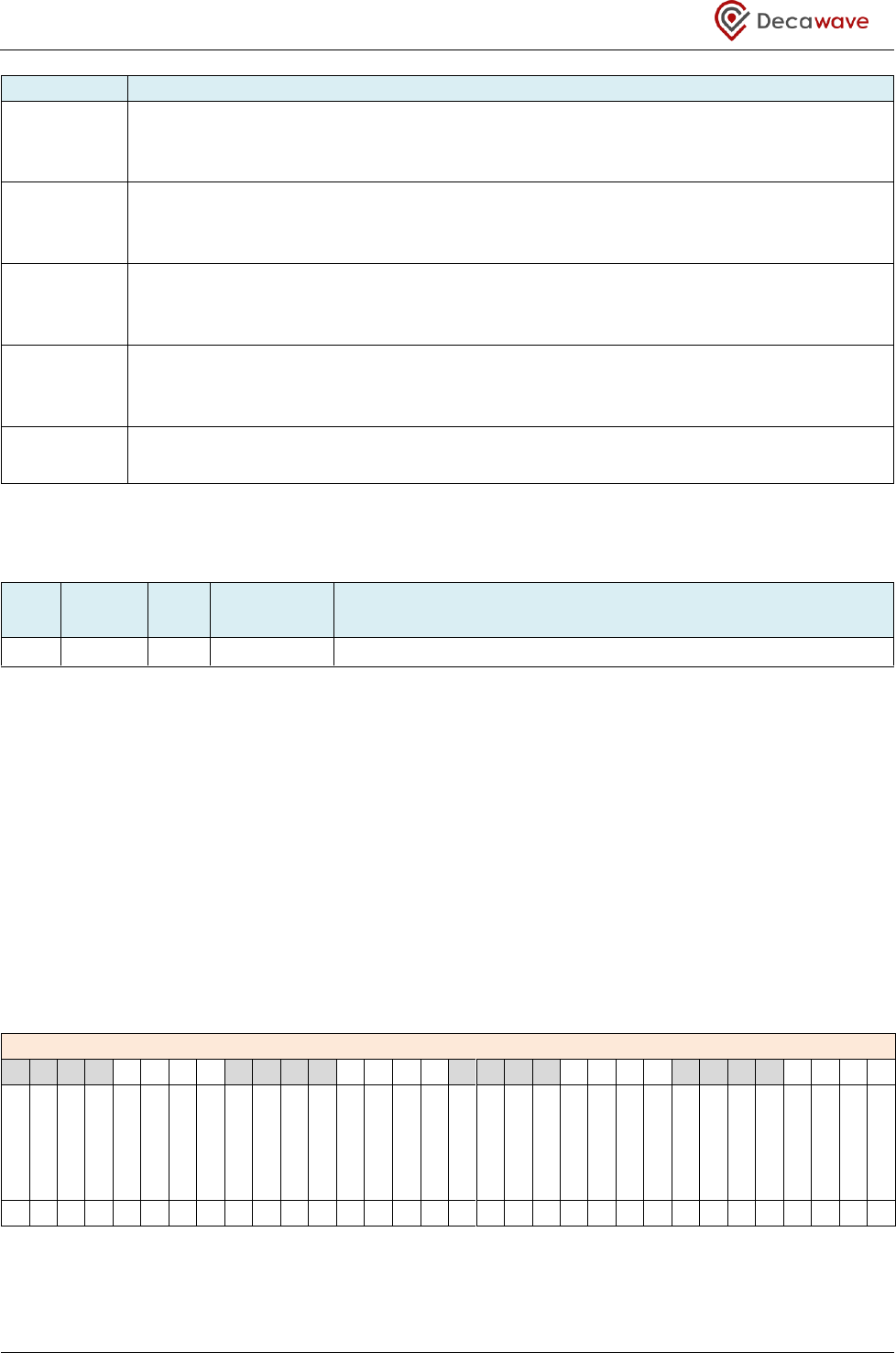
DW1000 User Manual
© Decawave Ltd 2017
Version 2.15
Page 85 of 244
Field
Description of fields within Register file: 0x0E – System Event Mask Register
MRXSFDTO
reg:0E:00
bit:26
Mask Receive SFD timeout event. When MRXSFDTO is 0 the RXSFDTO event status bit will
not generate an interrupt. When MRXSFDTO is 1 and the RXSFDTO event status bit is 1,
the hardware IRQ interrupt line will be asserted to generate an interrupt.
MHPDWARN
reg:0E:00
bit:27
Mask Half Period Delay Warning event. When MHPDWARN is 0 the HPDWARN event
status bit will not generate an interrupt. When MHPDWARN is 1 and the HPDWARN event
status bit is 1, the hardware IRQ interrupt line will be asserted to generate an interrupt.
MTXBERR
reg:0E:00
bit:28
Mask Transmit Buffer Error event. When MTXBERR is 0 the TXBERR event status bit will
not generate an interrupt. When MTXBERR is 1 and the TXBERR event status bit is 1, the
hardware IRQ interrupt line will be asserted to generate an interrupt.
MAFFREJ
reg:0E:00
bit:29
Mask Automatic Frame Filtering rejection event. When MAFFREJ is 0 the AFFREJ event
status bit will not generate an interrupt. When MAFFREJ is 1 and the AFFREJ event status
bit is 1, the hardware IRQ interrupt line will be asserted to generate an interrupt.
–
reg:0E:00
bits:30,31
These bits are reserved.
7.2.17 Register file: 0x0F – System Event Status Register
ID
Length
(octets)
Type
Mnemonic
Description
0x0F
5
SRW
SYS_STATUS
System Event Status Register
Register map register file 0x0F is the system event status register, SYS_STATUS. It contains status bits that
indicate the occurrence of different system events or status changes. It is possible to enable particular
events as interrupt sources, by employing the SYS_MASK, Register file: 0x0E – System Event Mask Register,
so that the setting of the event status bit will generate an interrupt, asserting the hardware IRQ output line.
This can be used, for example, to allow the host processor to enter a low-power state during frame
transmission or reception awaiting an interrupt to wake upon the completion of the TX or RX activity.
Reading the SYS_STATUS register returns the state of the status bits. Generally these event status bits are
latched so that the event is captured. Such latched bits need to be explicitly cleared by writing‘a’’1’ to the
bit position (writi‘g’’0’ has no effect).
The SYS_STATUS register contains the system event status bits identified and described below:
REG:0F:00 – SYS_STATUS – System Status Register (octets 0 to 3)
31
30
29
28
27
26
25
24
23
22
21
20
19
18
17
16
15
14
13
12
11
10
9
8
7
6
5
4
3
2
1
0
ICRBP
HSRBP
AFFREJ
TXBERR
HPDWARN
RXSFDTO
CLKPLL_LL
RFPLL_LL
SLP2INIT
GPIOIRQ
RXPTO
RXOVRR
-
LDEERR
RXRFTO
RXRFSL
RXFCE
RXFCG
RXDFR
RXPHE
RXPHD
LDEDONE
RXSFDD
RXPRD
TXFRS
TXPHS
TXPRS
TXFRB
AAT
ESYNCR
CPLOCK
IRQS
0
0
0
0
0
0
0
0
0
0
0
0
0
0
0
0
0
0
0
0
0
0
0
0
0
0
0
0
0
0
0
0

DW1000 User Manual
© Decawave Ltd 2017
Version 2.15
Page 86 of 244
REG:0F:04 – SYS_STATUS – System Status Register (octet 4)
31
30
29
28
27
26
25
24
23
22
21
20
19
18
17
16
15
14
13
12
11
10
9
8
7
6
5
4
3
2
1
0
-
-
-
-
-
TXPUTE
RXPREJ
RXRSCS
0
0
0
0
0
0
0
0
The system event status bits of the SYS_STATUS register identified above are individually described below:
Field
Description of fields within Register file: 0x0F – System Event Status Register
IRQS
reg:0F:00
bit:0
Interrupt Request Status. This is a READ ONLY status flag – it cannot be cleared or
overwritten. Whenever a status bit in Register file: 0x0F – System Event Status Register is
activated (i.e. has a value of 1) and the corresponding bit in Register file: 0x0E – System
Event Mask Register is enabled (i.e. has a value of 1 also) then the IRQ interrupt request line
will be driven to its active ON level. If there are no active mask enabled status bits then the
IRQ interrupt request line will be set to its inactive OFF level. This IRQS flag reflects the
overall status of interrupts. If there are any unmasked interrupt sources active then the IRQS
bit will be 1 (and IRQ interrupt request line will be at its active ON level) the otherwise IRQS
will be zero (and IRQ interrupt request line at its OFF level). The polarity of the IRQ interrupt
request line is controllable via the HIRQ_POL configuration bit in Register file: 0x04 – System
Configuration.
CPLOCK
reg:0F:00
bit:1
Clock PLL Lock. The CPLOCK event status bit indicates that the digital clock PLL has locked.
This may be used as an interrupt to indicate that the DW1000 clock is operating at full speed,
after which the SPI can be run at its maximum rate also. The CPLOCK bit is cleared by writing
a 1 to it. The clock PLL lock status is also available via the CPLLLOCK status bit in Sub-Register
0x28:2C – RF_STATUS.
Note: The PLLLDT bit in Register file 0x24:00 –EC_CTRL should be set to ensure reliable
operation of this CPLOCK bit.
ESYNCR
reg0F:00
bit:2
External Sync Clock Reset. This event status bit is set when the system counter is reset as a
result of the reception of an external synchronisation clock reset signal on the SYNC pin. The
ESYNCR flag bit is cleared by writing a 1 to it. Section 6.1 – External Synchronisation
describes this feature.
AAT
reg:0F:00
bit:3
Automatic Acknowledge Trigger. This status event status bit is set when frame filtering is
enabled and a data frame (or MAC command frame) is received (correctly addressed and
with a good CRC) with the acknowledgement request bit set in its frame control field.
If the automatic acknowledgement is enabled (by the AUTOACK bit in Register file: 0x04 –
System Configuration) then the AAT bit can be used during receive interrupt processing to
detect that acknowledgement is in progress and so avoid taking any action until the
transmission of the acknowledgement is completed – an event that might be detected by
awaiting the TXFRS (Transmit Frame Sent) status interrupt.
If automatic acknowledgement is not enabled, then the AAT status bit must be ignored.
The AAT bit can be cleared explicitly by writing a 1 to it. It is also automatically cleared by
the next receiver enable, (including those caused by the RXAUTR auto-re-enable).
TXFRB
reg:0F:00
bit:4
Transmit Frame Begins. This event status bit is set at the start of a frame transmission as the
transmitter begins to send preamble. The TXFRB bit is automatically cleared at the next
transmitter enable. It can also be cleared explicitly by writing a 1 to it.

DW1000 User Manual
© Decawave Ltd 2017
Version 2.15
Page 87 of 244
Field
Description of fields within Register file: 0x0F – System Event Status Register
TXPRS
reg:0F:00
bit:5
Transmit Preamble Sent. This event status bit is set at the end of preamble when SFD
sending begins. The TXPRS bit is automatically cleared at the next transmitter enable. It can
also be cleared explicitly by writing a 1 to it.
TXPHS
reg:0F:00
bit:6
Transmit PHY Header Sent. This event status bit is set when the PHR has been transmitted.
This marks the start of sending the data part of the frame (assuming the frame length is non-
zero) at the configured transmit data rate. The TXPHS bit is automatically cleared at the next
transmitter enable. It can also be cleared explicitly by writing a 1 to it.
TXFRS
reg:0F:00
bit:7
Transmit Frame Sent. This event status bit is set at the end of sending the data part of the
frame. It is expected that this will be used as the main “Transmit Done” (interrupt) event
signalling the completion of frame transmission. (In the case where frame length is zero the
TXFRS bit is set soon after the TXPHS event flag). The TXFRS bit is automatically cleared at
the next transmitter enable. It can also be cleared explicitly by writing a 1 to it.
RXPRD
reg:0F:00
bit:8
Receiver Preamble Detected status. This event status bit is set to indicate that the receiver
has detected (and confirmed) the presence of the preamble sequence. Preamble reception
continues after RXPRD has been set until the SFD is detected as signalled by the RXSFDD
event status bit or an SFD timeout occurs as signalled by the RXSFDTO event status bit.
Section 4 – Message Reception gives details of the frame reception process. The RXPRD bit
can be cleared explicitly by writing a 1 to it. It is also automatically cleared by the next
receiver enable, including those caused by the RXAUTR auto-re-enable.
RXSFDD
reg:0F:00
bit:9
Receiver SFD Detected. This event status bit is set to indicate that the receiver has detected
the SFD sequence and is moving on to decode the PHR. Section 4 – Message Reception gives
details of the frame reception process. The RXSFDD bit can be cleared explicitly by writing a
1 to it. It is also automatically cleared by the next receiver enable, including those caused
by the RXAUTR auto-re-enable.
LDEDONE
reg:0F:00
bit:10
LDE processing done. This event status bit is set to indicate the completion of the leading
edge detection and other adjustments of the receive timestamp information. The resultant
adjusted message RX timestamp is then available in Register file: 0x15 – Receive Time Stamp.
The detection of SFD as reported by the RXSFDD event status bit marks the end of the SFD
and the start of the PHR, which also marks the RMARKER whose arrival at the antenna is the
event that defines the frame arrival timestamp. To accurately determine this timestamp the
DW1000 employs an internal algorithm to adjust the RMARKER receive time. Among other
functions this performs a leading edge detection search on the channel impulse response
and subtracts the receive antenna delay as programmed in Sub-Register 0x2E:1804 –
LDE_RXANTD. For more information on the LDE and the process on message time-stamping
see section 4.1.6 – RX Message timestamp. The LDEDONE event status flag bit is included in
the RX double-buffered swinging-set. It is automatically cleared by the RX enable. It can also
be cleared explicitly by writing a 1 to it.
RXPHD
reg:0F:00
bit:11
Receiver PHY Header Detect. This event status bit is set to indicate that the receiver has
completed the decoding of the PHR. Section 4 – Message Reception gives details of the
frame reception process. The RXPHD bit can be cleared explicitly by writing a 1 to it. It is
also automatically cleared by the next receiver enable, including those caused by the
RXAUTR auto-re-enable.

DW1000 User Manual
© Decawave Ltd 2017
Version 2.15
Page 88 of 244
Field
Description of fields within Register file: 0x0F – System Event Status Register
RXPHE
reg:0F:00
bit:12
Receiver PHY Header Error. This event status bit is set to indicate that the receiver has
found a non-correctable error in the PHR. The PHR includes a SECDED error check sequence
(see section 10.4) that can correct a single bit error and detect a double bit error. The
double error is not correctable and its detection is the event that the RXPHE event status flag
is notifying. Generally this error means that correct frame reception is not possible, and so
typically this event will abort frame reception (depending on the DIS_PHE configuration in
Register file: 0x04 – System Configuration) after which the receiver may return to preamble
search (depending on the RXAUTR configuration also in Register file: 0x04 – System
Configuration). Section4 – Message Reception gives details of the frame reception process.
The RXPHE bit can be cleared explicitly by writing a 1 to it. It is also automatically cleared by
the next receiver enable, including those caused by the RXAUTR auto-re-enable. PHY Header
Error events are counted in Sub-Register 0x2F:04 – PHR Error Counter, as long as counting is
enabled by the EVC_EN bit in Sub-Register 0x2F:00 – Event Counter Control.
RXDFR
reg:0F:00
bit:13
Receiver Data Frame Ready. This event status bit is set to indicate that the completion of
the frame reception process. Section 4 – Message Reception gives details of the frame
reception process. It is expected that this will be used as the main “Receive” (interrupt)
event signalling the completion of a frame reception, and, that the receive event processing
routine will examine the RXFCG and RXFCE to determine whether the frame has been
received without error (or not), and also to check the LDEDONE event status flag to validate
the receive timestamp information.
In order to ensure that the receive timestamp information is valid before any receive
interrupt processing takes place, the setting of RXDFR is delayed until the LDE adjustments
of the timestamp have completed, at which time the LDEDONE event status bit will be set
(or possibly LDEERR). The RXDFR event status flag bit is included in the RX double-buffered
swinging-set. It is automatically cleared by the RX enable. It can also be cleared explicitly by
writing a 1 to it.
NOTE: If the RXDFR is set, but neither RXFCG nor RXFCE events have been flagged and also
neither LDEDONE nor LDEERR have been flagged then the LDE code has not been loaded
correctly and is not running correctly. Please review 2.5.5.10.
RXFCG
reg:0F:00
bit:14
Receiver FCS Good. This event status bit reflects the result of the frame CRC checking. It is
set (or not) at the end of frame reception coincidentally with the setting of the RXDFR event
status flag.
When RXFCG is set to 1 it indicates that the CRC check result generated on the received data
matches with the 2-octet FCS sequence at the end of the frame. RXDFR with RXFCG then
indicates the correct reception a valid frame. The RXFCG bit is in the RX double-buffered
swinging-set. It is automatically cleared by RX enable. It can also be cleared explicitly by
writing a 1 to it.
RXFCE
reg:0F:00
bit:15
Receiver FCS Error. This event status bit also reflects the result of the frame CRC checking. It
is valid at the end of frame reception coincidentally with the setting of the RXDFR event
status flag.
When RXFCE is set to 1 it indicates that the CRC check result generated on the received data
FAILED to match with the 2-octet FCS sequence at the end of the frame. The RXFCE bit is
included in the RX double-buffered swinging-set. It is automatically cleared by RX enable. It
can also be cleared explicitly by writing a 1 to it. RXFCE events are also counted in Sub-
Register 0x2F:0A – FCS Error Counter, as long as counting is enabled by the EVC_EN bit in
Sub-Register 0x2F:00 – Event Counter Control.

DW1000 User Manual
© Decawave Ltd 2017
Version 2.15
Page 89 of 244
Field
Description of fields within Register file: 0x0F – System Event Status Register
RXRFSL
reg:0F:00
bit:16
Receiver Reed Solomon Frame Sync Loss. The RXRFSL event status bit is set to indicate that
the receiver has found a non-correctable error during the Reed Solomon decoding of the
data portion of the frame. Generally this means that correct frame reception is not possible,
and so typically this event will abort frame reception (depending on the DIS_RSDE
configuration in Register file: 0x04 – System Configuration) after which the receiver may
return to preamble search (depending on the RXAUTR configuration also in Register file:
0x04 – System Configuration). Section 4 – Message Reception gives details of the frame
reception process. The RXRFSL bit can be cleared explicitly by writing a 1 to it. It is also
automatically cleared by the next receiver enable, including those caused by the RXAUTR
auto-re-enable. Reed Solomon Frame Sync Loss Error events are also counted in Sub-
Register 0x2F:06 – RSD Error Counter, as long as counting is enabled by the EVC_EN bit in
Sub-Register 0x2F:00 – Event Counter Control.
RXRFTO
reg:0F:00
bit:17
Receive Frame Wait Timeout. This event status bit is set to indicate that a receive frame
wait timeout has occurred. The receive frame wait timeout is enabled by the RXWTOE bit in
Register file: 0x04 – System Configuration, with the timeout being set by Register file: 0x0C –
Receive Frame Wait Timeout Period. The receive frame wait timeout starts running when
the receiver is enabled and stops running either when a valid frame is received or when the
timeout occurs and is signalled by this RXRFTO event status flag bit. It can be cleared
explicitly by writing a 1 to it. Receive frame wait timeout events are also counted in Sub-
Register 0x2F:14 – RX Frame Wait Timeout Event Counter, as long as counting is enabled by
the EVC_EN bit in Sub-Register 0x2F:00 – Event Counter Control.
LDEERR
reg:0F:00
bit:18
Leading edge detection processing error. A large part of the leading edge detection
algorithm is a search in the channel impulse response to find the first arriving ray of the
RMARKER. This should be bounded and finish in a reasonably short time, but in case not, the
LDE includes a failsafe mechanism of a watchdog timer (60 µs) that is initialized at the start
of each LDE search (when a good PHR has been detected). We do not expect DW1000 users
to ever see this event, however if the watchdog timer expires before the LDE has completed
its RX timestamp adjustments then the LDE search will be aborted and the error will be
reported by the LDEERR event status flag. t can becleared explicitly by writing a 1 to it.
–
reg:0F:00
bit:19
This bit is reserved.
RXOVRR
reg:0F:00
bit:20
Receiver Overrun. This event status bit only applies when double RX buffering is enabled
(by clearing the DIS_DRXB bit in Register file: 0x04 – System Configuration). The RXOVRR
event flag is set to indicate that an overrun error has occurred in the receiver. See section
4.3.5 – Overrun for more details of double buffering and the use of this RXOVRR error flag.
The RXOVRR event status bit is a READ ONLY bit. It will clear when HRBPT is used to signal
the completion of processing for a receiver buffer, freeing that buffer for data reception.
Receiver Overrun events are also counted in Sub-Register 0x2F:0E – RX Overrun Error
Counter, assuming that counting is enabled by the EVC_EN bit in Sub-Register 0x2F:00 –
Event Counter Control.

DW1000 User Manual
© Decawave Ltd 2017
Version 2.15
Page 90 of 244
Field
Description of fields within Register file: 0x0F – System Event Status Register
RXPTO
reg:0F:00
bit:21
Preamble detection timeout. This event status bit is set when the preamble detection timeout
occurs. The preamble detection timer is started when the receiver is enabled and begins
preamble hunt. This may begin immediately in the case of issuing an RXENAB command or
after a delay in the case of issuing a RXDLYE command. The preamble detection timeout value
is programmed in Sub-Register 0x27:24 – DRX_PRETOC.
The preamble detection timeout may be useful to save power by turning off the receiver if an
expected response frame does not begin. If a response message is expected with a certain
fixed timing and preamble is not detected at the appropriate time then this is likely to mean
that the response will not come. Reception can thus be aborted early, saving power.
The RXPTO bit is automatically cleared at the next receiver enable. It can also be cleared
explicitly by writing a 1 to it.
GPIOIRQ
reg:0F:00
bit:22
GPIO interrupt. The GPIOIRQ event status bit is set when an interrupt condition occurs in
the GPIO block. Various configurations are possible to enable interrupts coming from GPIO
input lines. The GPIO block may need to be interrogated to determine the source of the
interrupt if more than one input line is configured to interrupt. The GPIOIRQ bit is cleared by
writing a 1 to it. For details of GPIO programming see Register file: 0x26 – GPIO control and
status.
SLP2INIT
reg:0F:00
bit:23
SLEEP to INIT. This event status bit is set is set to indicate that the DW1000 has completed
the activities associated with awaking from SLEEP (or DEEPSLEEP) and is now in the INIT state.
This status bit will NOT activate if the LDE is configured to automatically download on wake
up (by setting the ONW_LLDE bit in Register file 0x2C:00-AON_WCFG ), in this case the CPLOCK
status bit should be used to indicate that wake up has occurred and the DW1000 is in the IDLE
state.
RFPLL_LL
reg:0F:00
bit:24
RF PLL Losing Lock. This event status bit is set is set to indicate that the RFPLL is having
locking issues. This should not happen in healthy devices operating in their normal range.
Its occurrence may indicate a bad configuration, a faulty part or a problem in the power or
clock inputs to the device. If this bit is set it may be advisable to turn off the transmitter to
avoid sending signals that are out of regulation. The RFPLL_LL bit is cleared by writing a 1 to
it.
CLKPLL_LL
reg:0F:00
bit:25
Clock PLL Losing Lock. This event status bit is set is set to indicate that the system’s digital
clock PLL is having locking issues. This should not happen in healthy devices operating in
their normal range. Its occurrence may indicate a bad configuration, a faulty part or a
problem in the power or clock inputs to the device. If this bit is set it may be advisable to
turn off the transmitter to avoid sending spurious signals. The CLKPLL_LL bit is cleared by
writing a 1 to it.
Note: The PLLLDT bit in Register file 0x24:00 –EC_CTRL should be set to ensure reliable
operation of this CLKPLL_LL bit.

DW1000 User Manual
© Decawave Ltd 2017
Version 2.15
Page 91 of 244
Field
Description of fields within Register file: 0x0F – System Event Status Register
RXSFDTO
reg:0F:00
bit:26
Receive SFD timeout. This event status bit is set when the SFD detection timeout occurs.
The SFD detection timeout starts running as soon as preamble is detected. If the SFD
sequence is not detected before the timeout period expires then the timeout will act to
abort the reception currently in progress. The period of the SFD detection timeout is in Sub-
Register 0x27:20 – DRX_SFDTOC. By default this has a value of 4096+64 representing the
longest possible preamble and SFD. Where it is known that a shorter preamble and SFD are
being employed this value can be reduced. The RXSFDTO event status bit can be cleared
explicitly by writing a 1 to it. It is also automatically cleared by the next receiver enable,
including those caused by the RXAUTR auto-re-enable. SFD timeout events are also counted
in Sub-Register 0x2F:10 – SFD Timeout Error Counter, assuming that counting is enabled by
the EVC_EN bit in Sub-Register 0x2F:00 – Event Counter Control.
HPDWARN
reg:0F:00
bit:27
Half Period Delay Warning. This event status bit relates to the use of delayed transmit and
delayed receive functionality. It indicates the delay is more than half a period of the system
clock.
For delayed send/receive the send/receive time is programmed into Register file: 0x0A –
Delayed Send or Receive Time and then the delayed sending/receiving is initiated by the
TXDLYS/RXDLYE controls in Register file: 0x0D – System Control Register. The delayed
transmit and receive functionality is described in detail in sections 3.3 – Delayed
Transmission and 4.2 – Delayed Receive.
The HPDWARN event status flag gets set if the time left to actually beginning transmission /
reception is more than half a period of the system clock (Register file: 0x06 – System Time
Counter) away. Assuming that the intent was not to schedule transmission/reception at a
time that is over 8 seconds in the future, the HPDWARN status flag can be polled after the
TXDLYS/RXDLYE is commanded, to check whether the delayed send/ receive invocation was
given in time (HPDWARN ==0) or not (HPDWARN == 1).
Typically when the HPDWARN event is detected the host controller will abort the delayed
TX/RX by issuing a TRXOFF transceiver off command and then take whatever remedial action
is deemed appropriate for the application.
The HPDWARN event status flag is READ ONLY. It will clear when the delayed TX/RX is
cancelled or when the delay remaining is no longer greater than half a period of the system
clock.
HPDWARN events are counted in Sub-Register 0x2F:18 – Half Period Warning Counter,
assuming counting is enabled by the EVC_EN bit in Sub-Register 0x2F:00 – Event Counter
Control.

DW1000 User Manual
© Decawave Ltd 2017
Version 2.15
Page 92 of 244
Field
Description of fields within Register file: 0x0F – System Event Status Register
TXBERR
reg:0F:00
bit:28
Transmit Buffer Error. The TXBERR event status flag bit indicates that a write to a
transmitted data buffer location has occurred whilst CRC was suppressed. Section 3.5 – High
Speed Transmission describes the DW1000 features for maximising data throughput. One
technique involves writing the frame data to the TX buffer after initiating the transmission of
that frame. During this data writing then, CRC sending is temporarily suppressed to protect
against sending the wrong data as a good frame (with good CRC). This CRC suppression is
cancelled when all the frame data has been written. If the frame data has been written to
the buffer in good time then the frame will be sent and a good CRC will be appended. If the
data is written late, (i.e. the host writes to the buffer area that is part of the TX frame after
the DW1000 has already consumed data from that area), then this is detected and flagged
here in this TXBERR event status flag bit. In this case CRC suppression cannot be cancelled
(so no CRC is appended). This will prevent transmission of a “bad” data frame with a good
CRC. The TXBERR bit is cleared by writing a 1 to it.
AFFREJ
reg:0F:00
bit:29
Automatic Frame Filtering rejection. The AFFREJ event status flag bit is set to indicate when
a frame has been rejected in receiver due to it not passing through the frame filtering. See
section 5.2 – Frame filtering for details of the operation of frame filtering. The AFFREJ event
status bit can be cleared explicitly by writing a 1 to it. It is also automatically cleared by the
next receiver enable, including those caused by the RXAUTR auto-re-enable. Frame Filtering
rejection events are also counted in Sub-Register 0x2F:0C – Frame Filter Rejection Counter,
assuming counting is enabled by the EVC_EN bit in Sub-Register 0x2F:00 – Event Counter
Control.
HSRBP
reg:0F:00
bit:30
Host Side Receive Buffer Pointer. This is status flag relating to the operation of the receiver
in double-buffered mode. Section 4.3 – Double Receive Buffer describes this operation in
detail. Essentially HSRBP is an index indicating which of the buffer pairs the host side is
accessing (reading from currently or awaiting to read from when filled by the IC), while
ICRBP is an index indicating which of the buffer pairs the IC is accessing (writing to currently
or will write to as soon as a frame data arrives). The HSRBP bit is a READ ONLY status bit, its
state is changed by issuing the HRBPT command in Register file: 0x0D – System Control
Register.
ICRBP
reg:0F:00
bit:31
IC side Receive Buffer Pointer. This is status flag relating to the operation of the receiver in
double-buffered mode. Section 4.3 – Double Receive Buffer describes this operation in
detail. Essentially ICRBP is an index indicating which of the buffer pairs the IC is accessing
(writing to currently or will write to as soon as a frame data arrives). The ICRBP bit is a READ
ONLY status bit.
RXRSCS
reg:0F:04
bit:0
Receiver Reed-Solomon Correction Status. This status bit indicates that the Reed-Solomon
has corrected at least one error in the frame being received. This is a low-level event status
flag. The RXRSCS bit probably not of interest to the host system. It was used during the
verification of the Reed-Solomon implementation. The RXRSCS bit cannot be used as an
interrupt source. The RXRSCS status bit can be cleared explicitly by writing a 1 to it. It is
also automatically cleared by the next receiver enable, including those caused by the
RXAUTR auto-re-enable.
RXPREJ
reg:0F:04
bit:1
Receiver Preamble Rejection. This is a low-level event status flag, which is probably not of
interest to the host system. It was used during the IC implementation as part of tuning the
preamble detection algorithm. In the DW1000, preamble detection a two stage process
where preamble is initially seen and then has to be confirmed as continuing for a number of
symbols before the RXSFDD event status bit actually gets set. If the preamble is not
confirmed then the RXSFDD event status bit will not be set, but instead this RXPREJ status
will be set. The RXPREJ bit cannot be used as an interrupt source. The RXPREJ event status
bit can be cleared explicitly by writing a 1 to it. It is also automatically cleared by the next
receiver enable, including those caused by the RXAUTR auto-re-enable.
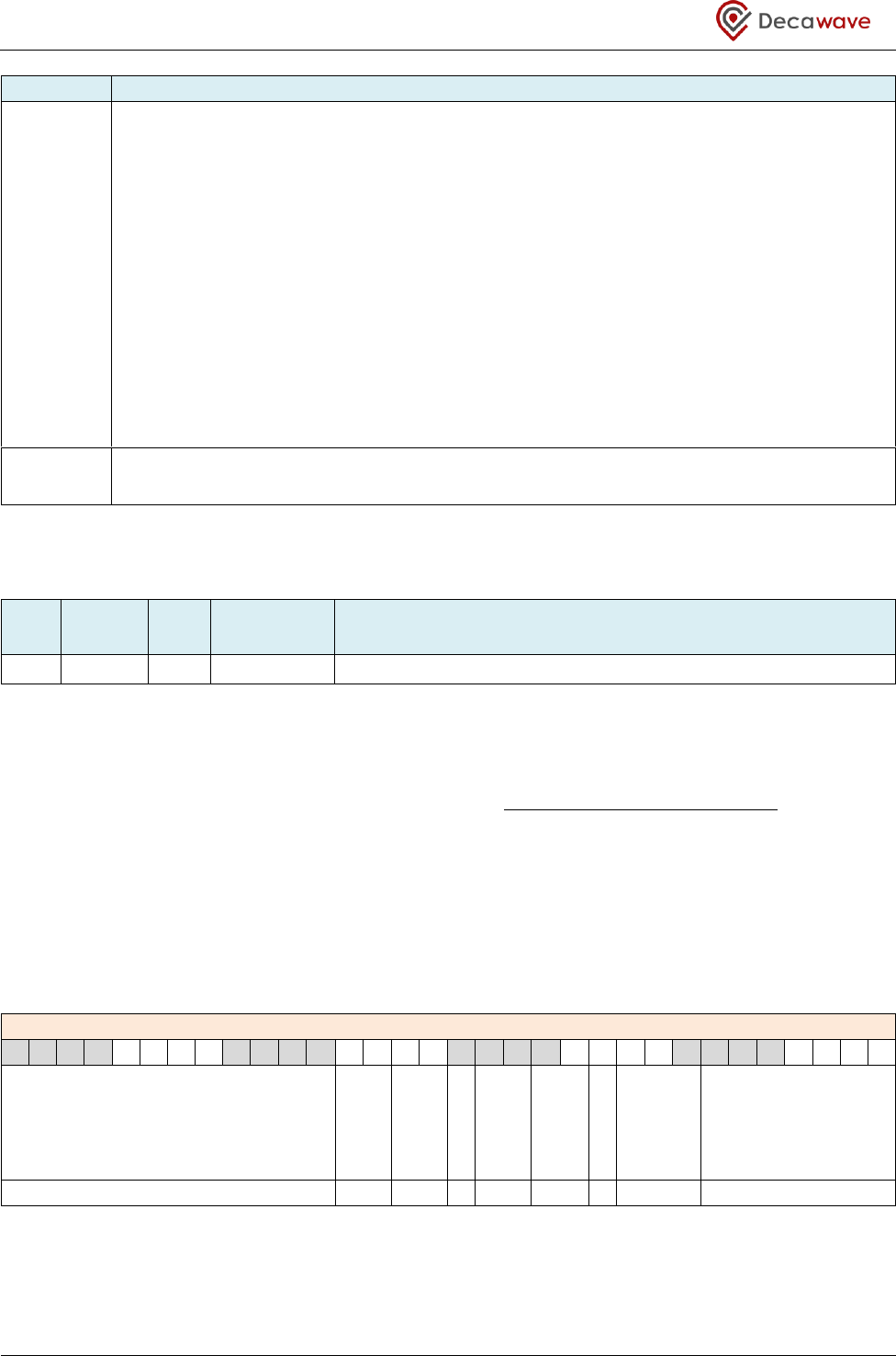
DW1000 User Manual
© Decawave Ltd 2017
Version 2.15
Page 93 of 244
Field
Description of fields within Register file: 0x0F – System Event Status Register
TXPUTE
reg:0F:04
bit:2
Transmit power up time error. This is a low-level event status flag. It applies when delayed
transmission is being used. Frame transmission will continue if this condition is detected,
and the RMARKER will be sent at the correct time, but that the initial few preamble symbols
may not transmit correctly. This may have a performance effect when a short preamble
sequence is being employed. The TXPUTE event status flag is READ ONLY. It will clear as
soon as the DW1000 begins to send preamble, (or if the DW1000 is returned to idle). Since
the TX power-up time is only a few symbol times in duration and because the TXPUTE bit
clears at the start of preamble, it is unlikely that the host system will see the TXPUTE bit set.
The condition therefore should be detected using the event counted in Sub-Register 0x2F:1A
– Transmitter Power-Up Warning Counter, (when counting is enabled by the EVC_EN bit in
Sub-Register 0x2F:00 – Event Counter Control).
The delayed transmit and receive functionality is described in detail in sections 3.3 – Delayed
Transmission and 4.2 – Delayed Receive.
–
reg:0F:04
bits:7–3
These bits are reserved
7.2.18 Register file: 0x10 – RX Frame Information Register
ID
Length
(octets)
Type
Mnemonic
Description
0x10
4
ROD
RX_FINFO
RX Frame Informati–n – included in swinging set
Register map register file 0x10 gives information on the received frame. It is updated after the reception of
a good PHR, i.e. PHR where the SECDED has not flagged a non-correctable error (see section 10.4).
Register file: 0x10 – RX Frame Information Register is in the RX double-buffered swinging-set. See section
4.3 – Double Receive Buffer for more details.
Note: During double buffered operation, a receiver overrun condition results in the corruption of this
RX_FINFO register 0x10, please refer to section 4.3.3 Operation of double bufferingfor details of the
correct be handling of this condition.
This RX_FINFO register contains a number of fields, separately identified and described below:
REG:10:00 – RX_FINFO – RX Frame Information
31
30
29
28
27
26
25
24
23
22
21
20
19
18
17
16
15
14
13
12
11
10
9
8
7
6
5
4
3
2
1
0
RXPACC
RXPSR
RXPRFR
RNG
RXBR
RXNSPL
-
RXFLE
RXFLEN
0
0
0
0
0
0
0
0
0
The individual sub-fields are described below:
DW1000 User Manual
© Decawave Ltd 2017
Version 2.15
Page 94 of 244
Field
Description of fields within Register file: 0x10 – RX Frame Information Register
RXFLEN
reg:10:00
bits:6–0
Receive Frame Length. This value is copied from the PHR of the received frame when a
good PHR is detected (when the RXPHD status bit is set). The frame length from the PHR is
used in the receiver to know how much data to receive and decode, and where to find the
FCS (CRC) to validate the received data. The frame length also tells the host system how
much data to read from the RX_BUFFER. This field is 7-bits wide to accommodate the
standard IEEE 802.15.4 UWB frames which can be up to 127 bytes long. The DW1000 also
supports a non-standard mode of operation with data frame lengths up to 1023 octets,
where the frame length reported is extended by the RXFLE field.
RXFLE
reg:10:00
bits:9–7
Receive Frame Length Extension. The DW1000 supports a non-standard mode of operation
with data frame lengths up to 1023 bytes. This mode of operation is enabled via the
PHR_MODE selection bits of Register file: 0x04 – System Configuration. In this long frame
mode RXFLE adds three high-order bits to RXFLEN extending it to 10-bits, and allowing frame
lengths from 0 up to 1023 bytes be reported. See also section 3.4 – Extended Length Data
Frames.
This value is updated when a good PHR is detected (when the RXPHD status bit is set).
-
reg:10:00
bit:10
This bit is reserved.
RXNSPL
reg:10:00
bits:12,11
Receive non-standard preamble length. The DW1000 is able to send non-standard preamble
lengths to allow system designers more choice in optimising performance. The RXNSPL field
operate in conjunction with the RXPSR field to report the received preamble length. The
RXPSR field reports the preamble length as signalled in the PHR (see 10.4 for details). The
receiver determines additional information about the transmitted preamble length from the
count of preamble accumulation, as reported by the RXPACC field, and uses this to set the
RXNSPL value.
Table 17 below lists the preamble lengths that can be reported by considering RXNSPL and
the RXPSR fields together:
Table 17: preamble length reporting
Bit 19
Bit 18
Bit 12
Bit 11
RXPSR
RXNSPL
RX Preamble Length
0
1
0
0
64
0
1
0
1
128
0
1
1
0
256
0
1
1
1
512
1
0
0
0
1024
1
0
0
1
1536
1
0
1
0
2048
1
1
0
0
4096
The bit numbers quoted above are the bit numbers in the RX_FINFO register.
Where preamble length is not predetermined and hard coded in the application, the
received preamble length information may be used to select the preamble length for any
response message, by copying RXNSPL and RXPSR fields into the PE and TXPSR configurations
respectively.
This value is updated when a good PHR is detected (when the RXPHD status bit is set).

DW1000 User Manual
© Decawave Ltd 2017
Version 2.15
Page 95 of 244
Field
Description of fields within Register file: 0x10 – RX Frame Information Register
RXBR
reg:10:00
bits:14,13
Receive Bit Rate report. This field reports the received bit rate. This information is signalled
in the received frame’s PHR (see 10.4 for details). Expected values supported by the
DW1000 are:
00 = 110 kbps, 01 =850 kbps, and 10 = 6.8Mbps
This value is updated when a good PHR is detected (when the RXPHD status bit is set).
RNG
reg:10:00
bit:15
Receiver Ranging. This reflects the ranging bit in the received PHY header identifying the
frame as a ranging packet.
This value is updated when a good PHR is detected (when the RXPHD status bit is set).
RXPRFR
reg:10:00
bits:17,16
RX Pulse Repetition Rate report. This field reports the PRF being employed in the receiver.
This is simply a copy of the RXPRF configuration from Register file: 0x1F – Channel Control.
The values are: 01 = 16 MHz, 10 = 64 MHz
RXPSR
reg:10:00
bits:19,18
RX Preamble Repetition. This field reports the received frame preamble length as signalled in
the frame’s PHR (see 10.4 for details). The values of these two bits are defined by the standard
as:
00 = 16 symbols, 01 = 64 symbols, 10= 1024 symbols, and, 11= 4096 symbols
In addition to these standard preamble lengths, the DW1000 also supports the transmission
of non-standard preamble lengths. These non-standard lengths cannot be signalled in the
PHR; instead the DW1000 gives an estimate of the preamble length based on the RXPSR from
the PHR and the RXPACC value. The estimate is reported using RXPSR and RXNSPL fields
together as per Table 17above.
This value is updated when a good PHR is detected (when the RXPHD status bit is set).

DW1000 User Manual
© Decawave Ltd 2017
Version 2.15
Page 96 of 244
Field
Description of fields within Register file: 0x10 – RX Frame Information Register
RXPACC
reg:10:00
bits:31–20
Preamble Accumulation Count. This reports the number of symbols of preamble
accumulated.
This may be used to estimate the length of TX preamble received and also during diagnostics
as an aid to interpreting the accumulator data.
It is possible for this count to be a little larger than the transmitted preamble length, because
of very early detection of preamble and because the accumulation count may include
accumulation that continues through the SFD (until the SFD is detected).
This value is updated when a good PHR is detected (when the RXPHD status bit is set).
The channel accumulation sometimes includes the SFD symbols, all except the last two.
Signal power calculations using RXPACC for the number of symbols sometimes need to be
adjusted for the SFD symbols accumulated. See section 4.7 for calculations using RXPACC.
The RXPACC counter will saturate when preamble is found by the receiver and the CIRE will
stop accumulating symbols. A debug symbol counter which does not saturate is given in
RXPACC_NOSAT. A comparison of RXPACC and RXPACC_NOSAT will indicate that RXPACC
count needs to be adjusted if the two counts are equal. If they are not equal, then RXPACC
has saturated before SFD accumulation and therefore the RXPACC value need not be
adjusted before use in signal power calculations.
To adjust the RXPACC count for SFD when RXPACC is equal to RXPACC_NOSAT, subtract the
number of SFD symbols from the count. Because the SFD sequences contain positive
symbols (normal preamble symbols) and negative symbols (symbols which are inverted
versions of preamble symbols) which have been added into the channel estimate, add the
number of positive symbols and subtract the number of negative symbols in the SFD
sequence from the RXPACC count. The last two symbols in the SFD sequence are always
ignored in the channel estimate, so these two symbols should not be counted when making
adjustments to RXPACC. See Table 18 below for some examples of how to adjust RXPACC
when RXPACC and RXPACC_NOSAT are equal.
Note that the shorter the preamble length, the more impact the SFD correction to RXPACC
will have on signal power calculations.
DW1000 User Manual
© Decawave Ltd 2017
Version 2.15
Page 97 of 244
Table 18: RXPACC Adjustments by SFD code
SFD
Sequence
Adjustment
to RXPACC
Standard
Short (8-
symbol)
0+0-+00-
-6+2-1=-5
Standard
Long (64-
symbol)
0+0−+00−0+0−+00–00+0−0+0+000−0−0−00+0–0−+0000++00−−−+−++0000++
-62+14-16=-
64
Decawave-
defined 8-
symbols
SFD
----+-00
-6+1-5=-10
Decawave-
defined
16-
symbols
SFD
----+-+--++--+00
-14+5-9=-18
Decawave-
defined
64-
symbols
SFD
−−−−−−−+−+−−−−−−+−−+−+−−+−−+−−+−−−++−−−+++−+−+−+−−−+−−+−−−−+++0
0
-62+21-41=-
82
7.2.19 Register file: 0x11 – RX Frame Buffer
ID
Length
(octets)
Type
Mnemonic
Description
0x11
1024
ROD
RX_BUFFER
RX Frame Data Buffer – included in swinging set
Register map register file 0x11 is the receive data buffer. The data from the received frame is available in
the received buffer. Assuming successful reception of a good frame, the full length of received data (as
reported by the RXFLEN and RXFLE fields of Register file: 0x10 – RX Frame Information Register), will be
available in the RX_BUFFER beginning at offset 0. Note since the reported length includes the FCS the host
system will probably choose not to read these final two octets.
Write operations to the RX_BUFFER are NOT supported; a write operation to the RX_BUFFER will corrupt
the buffer contents.
Register file: 0x11 – RX Frame Buffer is part of the RX double-buffered swinging-set. See section 4.3 –
Double Receive Buffer for more details.
7.2.20 Register file: 0x12 – Rx Frame Quality Information
ID
Length
(octets)
Type
Mnemonic
Description
0x12
8
ROD
RX_FQUAL
Rx Frame Quality information – included in swinging set
DW1000 User Manual
© Decawave Ltd 2017
Version 2.15
Page 98 of 244
Register map register file 0x12 gives information about quality of reception for the current frame. This
register consists of a number of sub-fields separately identified and described below:
Register file: 0x12 – Rx Frame Quality Information is in the RX double-buffered swinging-set. See section
4.3 – Double Receive Buffer for more details.
The RX_FQUAL register contains the following sub-fields:
REG:12:00 – RX_FQUAL – Rx Frame Quality Information (Octets 0 to 3, 2x16-bit values)
31
30
29
28
27
26
25
24
23
22
21
20
19
18
17
16
15
14
13
12
11
10
9
8
7
6
5
4
3
2
1
0
FP_AMPL2
STD_NOISE
0
0
0
0
0
0
0
0
0
0
0
0
0
0
0
0
0
0
0
0
0
0
0
0
0
0
0
0
0
0
0
0
REG:12:04 – RX_FQUAL – Rx Frame Quality Information (Octets 4 to 7, 2x16-bit values)
31
30
29
28
27
26
25
24
23
22
21
20
19
18
17
16
15
14
13
12
11
10
9
8
7
6
5
4
3
2
1
0
CIR_PWR
PP_AMPL3
0
0
0
0
0
0
0
0
0
0
0
0
0
0
0
0
0
0
0
0
0
0
0
0
0
0
0
0
0
0
0
0
The sub-fields of Register file: 0x12 – Rx Frame Quality Information are described below and are updated
when the LDE execution has completed successfully (when the LDEDONE status bit is set):
Field
Description of fields within Register file: 0x12 – Rx Frame Quality Information
STD_NOISE
reg:12:00
bits:15–0
Standard Deviation of Noise. This is a 16-bit value reporting the standard deviation of the
noise level seen during the LDE algorithm’s analysis of the accumulator data. This value can
be used in assessing the quality of the received signal and/or the receive timestamp
produced by the LDE. For more details please refer to section 4.7 – Assessing the quality of
reception and the RX timestamp.
FP_AMPL2
reg:12:00
bits:31–16
First Path Amplitude point 2. This is a 16-bit value that is part of reporting the magnitude of
the leading edge signal seen in the accumulator data memory during the LDE algorithm’s
analysis. The amplitude of the sample reported in the FP_AMPL2 parameter is the
magnitude of the accumulator tap at the index 2 beyond the integer portion of the rising
edge FP_INDEX reported in Register file: 0x15 – Receive Time Stamp. The FP_AMPL2
amplitude value can be used, in conjunction with the FP_AMPL3 value below and the
FP_AMPL1 value reported in Register file: 0x15 – Receive Time Stamp, as part of assessing
the quality of the receive timestamp produced by the LDE algorithm. For more details
please refer to section 4.7 – Assessing the quality of reception and the RX timestamp.
DW1000 User Manual
© Decawave Ltd 2017
Version 2.15
Page 99 of 244
Field
Description of fields within Register file: 0x12 – Rx Frame Quality Information
FP_AMPL3
reg:12:04
bits:15–0
First Path Amplitude point 3. This is a 16-bit value that is part of reporting the magnitude of
the leading edge signal seen in the accumulator data memory during the LDE algorithm’s
analysis. The amplitude of the sample reported in the FP_AMPL3 parameter is the magnitude
of the accumulator tap at the index 1 beyond the integer portion of the rising edge FP_INDEX
reported in Register file: 0x15 – Receive Time Stamp. This amplitude value can be used in
assessing the quality of the received signal and/or the receive timestamp produced by the
LDE. For more details please refer to section 4.7 – Assessing the quality of reception and the
RX timestamp.
The FP_AMPL3 amplitude value can be used, in conjunction with the FP_AMPL2 value above
and the FP_AMPL1 value reported in Register file: 0x15 – Receive Time Stamp, as part of
assessing the quality of the receive timestamp produced by the LDE algorithm. For more
details please refer to section 4.7 – Assessing the quality of reception and the RX timestamp.
CIR_PWR
reg:12:04
bits:31–16
Channel Impulse Response Power. This is a 16-bit value reporting the sum of the squares of
the magnitudes of the accumulator from the estimated highest power portion of the channel,
which is related to the receive signal power. This value can be used in assessing the quality of
the received signal and/or the receive timestamp produced by the LDE algorithm. For more
details please refer to section 4.7 – Assessing the quality of reception and the RX timestamp.
7.2.21 Register file: 0x13 – Receiver Time Tracking Interval
ID
Length
(octets)
Type
Mnemonic
Description
0x13
4
ROD
RX_TTCKI
Receiver Time Tracking Interval- included in swinging set
Register map register file 0x13 operates with Register file: 0x14 – Receiver Time Tracking Offset to give a
measure of the clock offset (or crystal offset) between the local receiver and the remote end transmitter
device.
Register file: 0x13 – Receiver Time Tracking Interval is in the RX double-buffered swinging-set. See section
4.3 – Double Receive Buffer for more details.
The RX_TTCKI register contains the following sub-fields which are updated when a frame demodulation is
completed successfully:
REG:13:00 – RX_TTCKI – Receiver Time Tracking Interval
31
30
29
28
27
26
25
24
23
22
21
20
19
18
17
16
15
14
13
12
11
10
9
8
7
6
5
4
3
2
1
0
RXTTCKI
0
Field
Description of fields within Register file: 0x13 – Receiver Time Tracking Interval
RXTTCKI
reg:13:00
bits:31–0
RX time tracking interval. The value here is the interval over which the timing offset
reported in the RXTOFS field of Register file: 0x14 – Receiver Time Tracking Offset is
measured. The clock offset is calculated by dividing RXTOFS by RXTTCKI. The value in
RXTTCKI will take just one of two values depending on the PRF: 0x01F00000 @ 16 MHz PRF,
and 0x01FC0000 @ 64 MHz PRF.
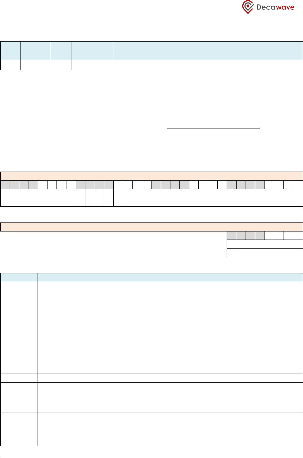
DW1000 User Manual
© Decawave Ltd 2017
Version 2.15
Page 100 of 244
7.2.22 Register file: 0x14 – Receiver Time Tracking Offset
ID
Length
(octets)
Type
Mnemonic
Description
0x14
5
ROD
RX_TTCKO
Receiver Time Tracking Offset- included in swinging set
Register map register file: 0x14 operates with Register file: 0x13 – Receiver Time Tracking Interval to give a
measure of the clock offset (or crystal offset) between the local receiver and the remote end transmitter
device.
Register file: 0x14 – Receiver Time Tracking Offset is in the RX double-buffered swinging-set. See section
4.3 – Double Receive Buffer for more details.
The RX_TTCKO register contains the following sub-fields which are updated when a frame demodulation is
completed successfully:
REG:14:00 – RX_TTCKO – Receiver Time Tracking Offset (Octets 0 to 3, 32-bits)
31
30
29
28
27
26
25
24
23
22
21
20
19
18
17
16
15
14
13
12
11
10
9
8
7
6
5
4
3
2
1
0
RSMPDEL
-
-
-
-
-
RXTOFS
0
-
-
-
-
-
0
REG:14:04 – RX_TTCKO – Receiver Time Tracking Offset (Octet 4, 8-bits)
7
6
5
4
3
2
1
0
-
RCPHASE
-
0
The individual sub-fields are described below:
Field
Description of fields within Register file: 0x14 – Receiver Time Tracking Offset
RXTOFS
reg:14:00
bits:18–0
RX time tracking offset. The value here is the offset measured over the interval reported in
the RXTTCKI field of Register file: 0x13 – Receiver Time Tracking Interval. This RXTOFS value
is a 19-bit signed quantity. The clock offset is calculated by dividing RXTOFS by RXTTCKI
Example (a): Say RXTOFS is reported as 0x000e4, and RXTTCKI is 0x01f00000 then this gives a
clock offset of 228 ÷ 32505856, which is 7.014E-06 or 7 ppm offset. So, the remote
transmitter’s clock is running faster than the local receiver’s clock by this 7 ppm amount.
Example (b): Say RXTOFS is reported as 0x7FF5C, and RXTTCKI is 0x01f00000 then this gives a
clock offset of -164 ÷ 32505856, which is -5.045E-06 or -5 ppm offset. So, the remote
transmitter’s clock is running slower than the local receiver’s clock by this 5 ppm amount.
-
Bits marked ‘-’ are reserved and should always be written as zero.
RSMPDEL
reg:14:00
bits:31–24
This 8-bit field reports an internal re-sampler delay value. This is not expected to be of any
direct use to the host system. It was of interest in the past during the development of the IC
receiver and the leading edge determination algorithm.
RCPHASE
reg:14:04
bits:6–0
This 7-bit field reports the receive carrier phase adjustment at time the ranging timestamp is
made. This gives the phase (7 bits = 360 degrees) of the internal carrier tracking loop at the
time that the RX timestamp is received. This can be used to partially compensate for the
phase offset in the CIR’s between two DW1000 devices.
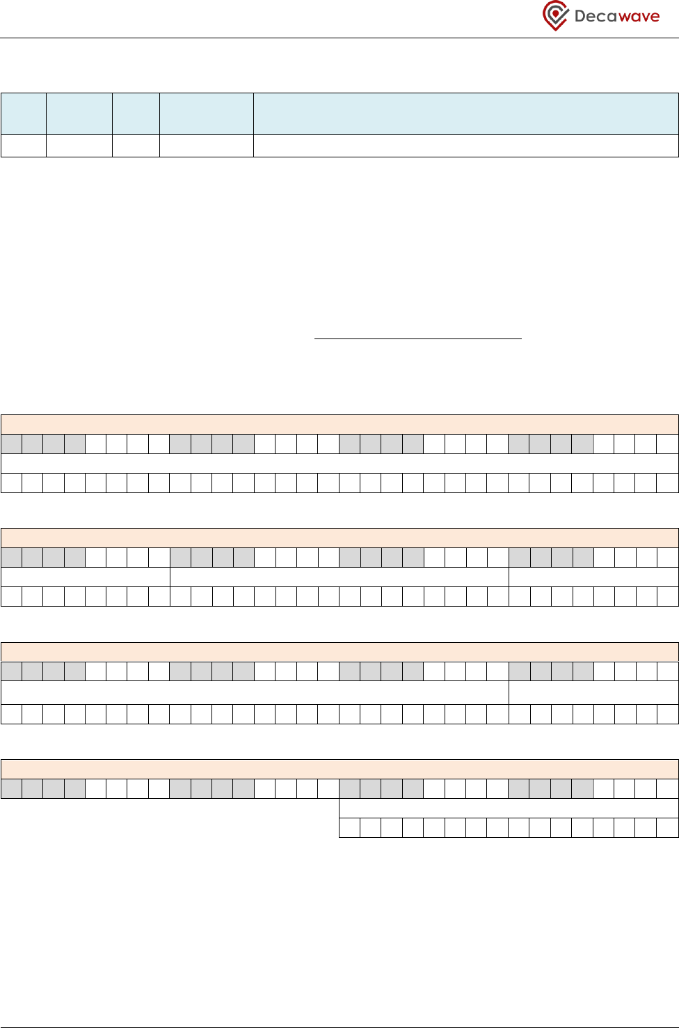
DW1000 User Manual
© Decawave Ltd 2017
Version 2.15
Page 101 of 244
7.2.23 Register file: 0x15 – Receive Time Stamp
ID
Length
(octets)
Type
Mnemonic
Description
0x15
14
ROD
RX_TIME
Receive Time Stamp- included in swinging set
Register map register file 0x15 reports the receive time stamp and related information. During frame
reception the SFD detection event marking the end of the preamble and the start of the PHR is the nominal
point which is time-stamped by the IC. The IEEE 802.15.4 UWB standard calls this point the RMARKER.
DW1000 takes a coarse timestamp of the symbol in which the RMARKER event occurs and to this adds
various correction factors to give a resultant time stamp value. Please refer to section 4.1.6 – RX Message
timestamp for more details of the corrections applied.
Register file: 0x15 – Receive Time Stamp is in the RX double-buffered swinging-set. See section 4.3 –
Double Receive Buffer for more details.
The RX_TIME register contains the following sub-fields:
REG:15:00 – RX_TIME – Receive Time Stamp (Octets 0 to 3, 32-bits)
31
30
29
28
27
26
25
24
23
22
21
20
19
18
17
16
15
14
13
12
11
10
9
8
7
6
5
4
3
2
1
0
RX_STAMP (low 32 bits of 40-bit value)
0
0
0
0
0
0
0
0
0
0
0
0
0
0
0
0
0
0
0
0
0
0
0
0
0
0
0
0
0
0
0
0
REG:15:04 – RX_TIME – Receive Time Stamp (Octets 4 to 7, 32-bits)
31
30
29
28
27
26
25
24
23
22
21
20
19
18
17
16
15
14
13
12
11
10
9
8
7
6
5
4
3
2
1
0
FP_AMPL1 (low 8 bits of 16)
FP_INDEX
RX_STAMP (high 8 bits of 40)
0
0
0
0
0
0
0
0
0
0
0
0
0
0
0
0
0
0
0
0
0
0
0
0
0
0
0
0
0
0
0
0
REG:15:08 – RX_TIME – Receive Time Stamp (Octets 8 to 11, 32-bits)
31
30
29
28
27
26
25
24
23
22
21
20
19
18
17
16
15
14
13
12
11
10
9
8
7
6
5
4
3
2
1
0
RX_RAWST (low 24 bits of 40-bit value)
FP_AMPL1 (high 8-bits of 16)
0
0
0
0
0
0
0
0
0
0
0
0
0
0
0
0
0
0
0
0
0
0
0
0
0
0
0
0
0
0
0
0
REG:15:0C – RX_TIME – Receive Time Stamp (Octets 12 to 13, 16-bits)
31
30
29
28
27
26
25
24
23
22
21
20
19
18
17
16
15
14
13
12
11
10
9
8
7
6
5
4
3
2
1
0
RX_RAWST (high 16 bits of 40-bit value)
0
0
0
0
0
0
0
0
0
0
0
0
0
0
0
0
The sub fields of Register file: 0x15 – Receive Time Stamp are laid out above in a map that is 32 bits wide,
however some parameters are larger than 32 bits. It is possible to read a variable number of bytes any byte
index and it is also possible to read the whole register file in a single block SPI read. The individual sub-fields
are described below:

DW1000 User Manual
© Decawave Ltd 2017
Version 2.15
Page 102 of 244
Field
Description of fields within Register file: 0x15 – Receive Time Stamp
RX_STAMP
reg:15:00
bits:39–0
This 40-bit (5-octet) field reports the. The fully adjusted time of reception. Please refer to
section 4.1.6 – RX Message timestamp for more details of the adjustments applied. The
units of the low order bit are approximately 15.65 picoseconds. The actual unit may be
calculated as 1/ (128*499.2×106) seconds. The value is available here when the leading edge
determination and timestamp adjustments are completed (when the LDEDONE status bit is
set).
FP_INDEX
reg:15:05
bits:15–0
First path index. This is a 16-bit value reporting the position within the accumulator that the
LDE algorithm has determined to be the first path. This value is set during the LDE
algorithm’s analysis of the accumulator data and is updated when the LDE execution has
completed (when the LDEDONE status bit is set). This value may be of use during diagnostic
graphing of the accumulator data, and may also be of use in assessing the quality of the
received message and/or the receive timestamp produced by the LDE. For more details of
that please refer to section 4.7 – Assessing the quality of reception and the RX timestamp.
The first path (or leading edge) is a sub-nanosecond quantity. Each tap in the accumulator
corresponds to a sample time, which is approximately 1 nanosecond (or 30 cm in terms of
the radio signal’s flight time through air). To report the position of the leading edge more
accurately than this 1 nanosecond step size, the index value consist of a whole part and a
fraction part. The 10 most significant bits of FP_INDEX represent the integer portion of the
number and the 6 least significant bits represent the fractional part.
FP_AMPL1
reg:15:05
bits:31–16
First Path Amplitude point 1. This is a 16-bit unsigned value that is part of reporting the
magnitude of the leading edge signal seen in the accumulator data memory during the LDE
algorithm’s analysis. The amplitude of the sample reported in the FP_AMPL1 parameter is
the magnitude of the accumulator tap at the index 3 beyond the integer portion of the rising
edge FP_INDEX reported in this register. The FP_AMPL1 amplitude value can be used, in
conjunction with the FP_AMPL2 and FP_AMPL3 values reported in Register file: 0x12 – Rx
Frame Quality Information, as part of assessing the quality of the receive timestamp
produced by the LDE algorithm. For more details please refer to section 4.7 – Assessing the
quality of reception and the RX timestamp.
This value is updated when the LDE execution has completed (when the LDEDONE status bit
is set).
RX_RAWST
reg:15:09
bits:39–0
This 40-bit (5-octet) field reports the Raw Timestamp for the frame. This is the value of the
system clock (125 MHz) captured at the time of the first chip of the first PHR symbol. The
precision here is approximately 125 MHz, i.e. the 9 least significant bits are zero.
When the PHR has been decoded successfully (when the RXPHD status bit is set), the
timestamp will be available for reading. If a PHR error is detected, the timestamp will not be
updated.
7.2.24 Register file: 0x16 – Reserved
ID
Length
(octets)
Type
Mnemonic
Description
0x16
-
-
-
Reserved – this register file is reserved
Register map register file 0x16 is reserved for future use. Please take care not to write to this register as
doing so may cause the DW1000 to malfunction.
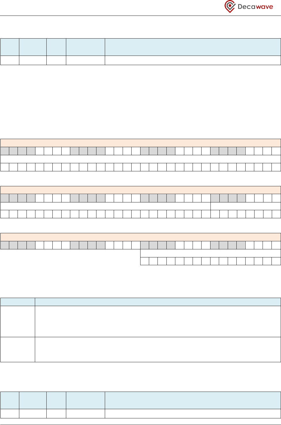
DW1000 User Manual
© Decawave Ltd 2017
Version 2.15
Page 103 of 244
7.2.25 Register file: 0x17 – Transmit Time Stamp
ID
Length
(octets)
Type
Mnemonic
Description
0x17
10
RO
TX_TIME
Transmit Time Stamp
Register map register file 0x17 reports the transmit time stamp information. During frame transmission the
start of the PHR is the nominal point which is time-stamped by the IC. The IEEE 802.15.4 UWB standard calls
this point the RMARKER. The DW1000 takes a timestamp of the symbol in which the RMARKER event occurs
and to this adds the antenna delay to give a resultant time stamp value, of when the RMARKER is launched
from the antenna.
This TX_TIME register contains the following sub-fields:
REG:17:00 – TX_TIME – Transmit Time Stamp (Octets 0 to 3, 32-bits)
31
30
29
28
27
26
25
24
23
22
21
20
19
18
17
16
15
14
13
12
11
10
9
8
7
6
5
4
3
2
1
0
TX_STAMP (low 32 bits of 40-bit value)
0
0
0
0
0
0
0
0
0
0
0
0
0
0
0
0
0
0
0
0
0
0
0
0
0
0
0
0
0
0
0
0
REG:17:04 – TX_TIME – Transmit Time Stamp (Octets 4 to 7, 32-bits)
31
30
29
28
27
26
25
24
23
22
21
20
19
18
17
16
15
14
13
12
11
10
9
8
7
6
5
4
3
2
1
0
TX_RAWST (low 24 bits of 40-bit value)
TX_STAMP (high 8 bits of 40)
0
0
0
0
0
0
0
0
0
0
0
0
0
0
0
0
0
0
0
0
0
0
0
0
0
0
0
0
0
0
0
0
REG:17:08 – TX_TIME – Transmit Time Stamp (Octets 8 to 9, 16-bits)
31
30
29
28
27
26
25
24
23
22
21
20
19
18
17
16
15
14
13
12
11
10
9
8
7
6
5
4
3
2
1
0
TX_RAWST (high 16 bits of 40-bit value)
0
0
0
0
0
0
0
0
0
0
0
0
0
0
0
0
The sub fields of Register file: 0x17 – Transmit Time Stamp are laid out above in a map that is 32 bits wide. It
is possible to read a variable number of bytes any byte index. The individual sub-fields are described below:
Field
Description of fields within Register file: 0x17 – Transmit Time Stamp
TX_STAMP
reg:17:00
bits:39–0
This 40-bit (5-octet) field reports the fully adjusted time of transmission. The unit of the
least significant bit is approximately 15.65 picoseconds. The actual unit may be calculated as
1/ (128*499.2×106) seconds. The value is available here when the PHR transmission has
completed.
TX_RAWST
reg:17:05
bits:39–0
This 40-bit (5-octet) field reports the Raw Timestamp for the frame. This is the value of the
system clock (125 MHz) captured at the time of the first chip of the first PHR symbol. The
precision here is approximately 125 MHz, i.e. the 9 least significant bits are zero.
7.2.26 Register file: 0x18 – Transmitter Antenna Delay
ID
Length
(octets)
Type
Mnemonic
Description
0x18
2
RW
TX_ANTD
16-bit Delay from Transmit to Antenna
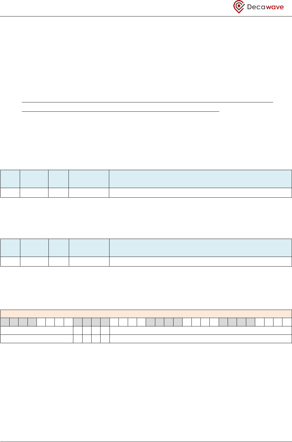
DW1000 User Manual
© Decawave Ltd 2017
Version 2.15
Page 104 of 244
Register map register file 0x18, the Transmitter Antenna Delay, is used to account for the delay between the
internal digital timestamp of the RMARKER (at the start of the PHR) and the time the RMARKER is at the
antenna. The value programmed here is automatically added to the raw timestamp TX_RAWST to get the
TX_STAMP reported in Register file: 0x17 – Transmit Time Stamp. Refer to section 8.3 – IC Calibration –
Antenna Delay for details of calibration of antenna delay. The units here are the same as those used for
system time and time stamps, i.e. 499.2 MHz × 128, so the least significant bit is about 15.65 picoseconds.
NB: This register is not preserved during SLEEP or DEEPSLEEP and so needs reprogramming after a
wakeup event in order to obtain the correct adjustment of the TX_STAMP.
The TX_ANTD is corrupted during wake-up (assuming the ONW_LDC bit in Sub-Register 0x2C:00 –
AON_WCFG is set to restore configurations) the high-octet of the receive antenna delay as
configured in Sub-Register 0x2E:1804 – LDE_RXANTD overwrites the low-octet of TX_ANTD.
7.2.27 Register file: 0x19 – Reserved
ID
Length
(octets)
Type
Mnemonic
Description
0x19
5
RO
SYS_STATE
System State information
Register map register file 0x19 is reserved.
7.2.28 Register file: 0x1A – Acknowledgement time and response time
ID
Length
(octets)
Type
Mnemonic
Description
0x1A
4
RW
ACK_RESP_T
Acknowledgement Time and Response Time
Register map register file 0x1A is a configuration register used for specifying turn-around times for DW1000
to use when automatically switching between TX mode and RX modes. The ACK_RESP_T register contains
the following bitmapped sub-fields:
REG:1A:00 – ACK_RESP – RX Frame Information
31
30
29
28
27
26
25
24
23
22
21
20
19
18
17
16
15
14
13
12
11
10
9
8
7
6
5
4
3
2
1
0
ACK_TIM
-
-
-
-
W4R_TIM
0
0
0
0
0
0
The individual sub-fields are described below:
DW1000 User Manual
© Decawave Ltd 2017
Version 2.15
Page 105 of 244
Field
Description of fields within Register file: 0x1A – Acknowledgement time and response time
W4R_TIM
reg:1A:00
bits:19–0
Wait-for-Response turn-around Time. This 20-bit field is used to configure the turn-around
time between TX complete and RX enable when the wait for response function is being used.
This function is enabled by the WAIT4RESP control in Register file: 0x0D – System Control
Register. The time specified by this W4R_TIM parameter is in units of approximately 1 µs, or
128 system clock cycles. This configuration may be used to save power by delaying the turn-
on of the receiver, to align with the response time of the remote system, rather than turning
on the receiver immediately after transmission completes. For more details see section 5.4 –
Transmit and automatically wait for response.
ACK_TIM
reg:1A:00
bits:31–24
Auto-Acknowledgement turn-around Time. This 8-bit field is used to configure the turn-
around time between the correct receipt of a data frame (or a MAC command frame) and
the transmission by the DW1000 of the acknowledgement frame. The time here is specified
in units of preamble symbols. (This resultant time is slightly different depending on whether
the PRF is 16 or 64 MHz, see Table 60 for details the preamble symbol lengths).This timer
only applies if auto-acknowledgement is in use and then only acts when the frame is
correctly received, passing through the RX frame filtering rules, and when the ACK bit in the
frame’s MAC header is set to request acknowledgement. Please refer to section 5.3 –
Automatic Acknowledgement for details of the Automatic Acknowledgementfunction. To
ensure that the receiver is ready for the first preamble symbol, and assuming that the
remote DW1000 has a its W4R_TIM parameter set to 0, the recommended minimum
ACK_TIM settings are as follows:
Data Rate
Recommend min.
ACK_TIM
110 kbps
0
850 kbps
2
6.8 Mbps
3
This is most important at the 6.8 Mbps data rate, where preamble sequences are generally
short, and losing even a few preamble symbols could potentially compromise ACK reception.
Where the W4R_TIM parameter is larger than zero, the ACK_TIM setting should be increased
also to ensure that none of the frame is sent before the remote receiver is listening.
-
Bits marked ‘-’ are reserved and should always be written as zero.
7.2.29 Register files: 0x1B and 0x1C – Reserved
ID
Length
(octets)
Type
Mnemonic
Description
0x1B
-
-
-
Reserved – this register file is reserved
0x1C
-
-
-
Reserved – this register file is reserved
Register map register file 0x1B and 0x1Care reserved for future use. Please take care not to write to these
registers as doing so may cause the DW1000 to malfunction.
DW1000 User Manual
© Decawave Ltd 2017
Version 2.15
Page 106 of 244
7.2.30 Register file: 0x1D – SNIFF Mode
ID
Length
(octets)
Type
Mnemonic
Description
0x1D
4
RW
RX_SNIFF
Sniff Mode Configuration
Register map register file 0x1D is used for configuration of SNIFF mode, which is a power saving technique
that can be employed to reduce the power consumption of preamble detection. For normal preamble
reception the receiver searches for preamble continually, while in SNIFF mode the receiver samples (“sniffs”)
the air periodically on a timed basis returning to receiver idle mode in between.
The transmitting device needs to be sending a sufficiently long preamble to allow for the SNIFF mode to
operate and leave sufficient preamble remaining thereafter to get a good reception and RX timestamp. The
power saving is dependent on the configured on/off times for this sampling. See additionally section 2.4.2 –
Specific state sequences supported by the DW1000 and 4.5 – Low-Power SNIFF mode for additional
discussion. The configuration consists of the fields identified and described below:
REG:1D:00 – RX_SNIFF –SNIFFMode Configuration
31
30
29
28
27
26
25
24
23
22
21
20
19
18
17
16
15
14
13
12
11
10
9
8
7
6
5
4
3
2
1
0
-
-
-
-
-
-
-
-
-
-
-
-
-
-
-
-
SNIFF_OFFT
-
-
-
-
SNIFF_ONT
-
-
-
-
-
-
-
-
-
-
-
-
-
-
-
-
0
0
0
0
0
0
The individual sub-fields are described below:
Field
Description of fields within Register file: 0x1D – SNIFF Mode
-
Bits marked ‘-’ are reserved.
SNIFF_ONT
reg:1D:00
bits:3–0
SNIFF Mode ON time. This parameter is specified in units of PAC. For details of PAC and its
role inPreamble Detection, please refer to section 4.1.1 – Preamble Detection. A value of
zero will disable SNIFF Mode. A non-zero value will enable Preamble Detection Mode and
select how long the receiver is turned on during the preamble hunt. NB: This must be a
minimum of 2 for the IC to correctly make a preamble detection decision. If preamble is
detected during this time window the receiver will remain on and will continue to attempt
reception of the frame. If no preamble is detected the receiver will be returned to idle
mode for the time configured by the SNIFF_OFFT parameter before sampling the air again.
SNIFF_OFFT
reg:1D:00
bits:15–8
SNIFF Mode OFF time specified in µs. This parameter is specified in units of approximately 1
µs, or 128 system clock cycles. A value of zero will disable SNIFF Mode. A non-zero value will
enable SNIFF Mode and select how long the receiver is turned off for during the preamble
hunt. Please refer to the SNIFF_ONT description above for more details of this feature.
As an example, with a 1024 preamble length, a roughly 50% duty cycle (on 50% and off 50%) can be
configured with a PAC of 8 symbols, SNIFF_ONT set to 3 PAC intervals, and SNIFF_OFFT set to 24
microseconds. The performance cost of this in terms of range is < 1 dB.
7.2.31 Register file: 0x1E – Transmit Power Control
ID
Length
(octets)
Type
Mnemonic
Description
0x1E
4
RW
TX_POWER
TX Power Control
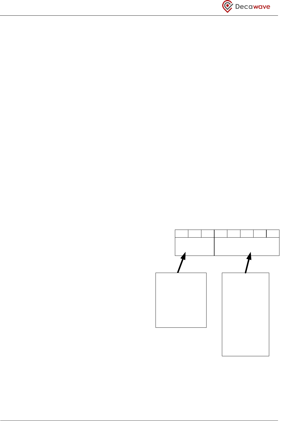
DW1000 User Manual
© Decawave Ltd 2017
Version 2.15
Page 107 of 244
Register map register file 0x1E is used for configuration and control of the transmitter output power.
Normally it is desired to transmit at (just under) the maximum power allowed by the regulations for the
geographic area of deployment simply because the higher the power the further the signal will go, although
in some circumstances it may be desired to reduce the power to limit the operating range or for other
reasons.
To optimise performance it is necessary (because of variations in the RF circuitry both internal to the IC and
in the external components) to verify the output power during module manufacture testing and store a
calibration value to set the module’s output power as high as possible within the limits of the regulations.
(The DW1000 has an area of OTP memory reserved for this. Please refer to section 8 –DW1000 Calibration
and section 6.3 – Using the on-chip OTP memory for more details).
The transmitter output power can be adjusted using this Register file: 0x1E – Transmit Power Control. This
contains four octets each of which specifies a separate transmit power setting. These separate settings are
applied by the IC in one of two ways. These two alternatives are described in section 7.2.31.2 – Smart
Transmit Power Control and section 7.2.31.3 – Manual Transmit Power Control below. The choice between
these two alternatives is selected by the setting of the DIS_STXP bit in Register file: 0x04 – System
Configuration.
7.2.31.1 Units of TX Power Control
Each power control octet, in Register file: 0x1E – Transmit Power Control, specifies the power as a
combination of a coarse gain parameter and a fine
gain parameter.
The gain control range is 33.5 dB consisting of 32 fine
(mixer gain) control steps of 0.5 dB and 7 coarse (DA
gain) steps of 3 dB, see Figure 26. For the best
spectral shape the coarse gain should be adjusted
first.
For optimum performance, (as noted in section
7.2.31), manufacturers have to calibrate the TX power
of each unit to account for IC to IC variations and
different IC to antenna losses. Usually the TX power is
set to the maximum allowed by spectral emission
regulations (-41.3 dBm/MHz) and such that no other
out-of-band limits are exceeded.
It should be noted that if you plan to use DA setting 000
you must ensure good isolation between pins VDDPA1
and VDDPA2 otherwise this setting may result in
compression of the TX signal. ( Good isolation requirIate PCB tracks to each of these pins. )
Figure 26: Transmit power control octet
7 6 5 4 3 2 1 0
Coarse (DA)
setting Fine (Mixer) setting
Bit number:
Meaning:
00000 = 0.0 dB gain
00001 = 0.5 dB gain
00010 = 1.0 dB gain
00011 = 1.5 dB gain
00100 = 2.0 dB gain
00101 = 2.5 dB gain
......
11010 = 13.0 dB gain
11011 = 13.5 dB gain
11100 = 14.0 dB gain
11101 = 14.5 dB gain
11110 = 15.0 dB gain
11111 = 15.5 dB gain
000 = 18 dB gain
001 = 15 dB gain
010 = 12 dB gain
011 = 9 dB gain
100 = 6 dB gain
101 = 3 dB gain
110 = 0 dB gain
111 = OFF – No output
DW1000 User Manual
© Decawave Ltd 2017
Version 2.15
Page 108 of 244
7.2.31.2 Smart Transmit Power Control
This functionality applies when the Disable Smart TX Power Control bit DIS_STXP in Register file: 0x04 –
System Configuration is zero (not set).
The power output regulations typically specify a transmit power limit of -41.3 dBm in each 1 MHz
bandwidth, and generally measure this using a 1 ms dwell time in each 1 MHz segment. When sending short
frames at 6.8 Mbps it is possible for a single frame to be sent in a fraction of a millisecond. Provided the
transmitter does not transmit again within that same millisecond, the power of that transmission can be
increased above the -41.3 dBm limit while remaining in compliance with the regulations. This transmit
power increase will increase the link budget and communication range. To make use of this the DW1000
includes functionality called Smart Transmit Power Control which automatically boosts the TX power for a
transmission when the frame is short.
Smart TX power control acts at the 6.8 Mbps data rate. When sending short data frames at this rate (and
providing that the frame transmission rate is < 1 frame per millisecond) it is possible to increase the transmit
power and still remain within regulatory power limits which are typically specified as average power per
millisecond.
When DIS_STXP is 0 and the data rate is configured to 6.8 Mbps, Smart Tx power is enabled. The DW1000
selects one of the fields of the TX Power Control register (BOOSTxxxx) depending on the overall frame
duration.
REG:1E:00 – TX_POWER – Transmit Power Control (When DIS_STXP = 0)
31
30
29
28
27
26
25
24
23
22
21
20
19
18
17
16
15
14
13
12
11
10
9
8
7
6
5
4
3
2
1
0
BOOSTP125
BOOSTP250
BOOSTP500
BOOSTNORM
0x0E
0x08
0x02
0x22
The individual sub-fields are described below:
Field
Description of fields within Register file: 0x1E – Transmit Power Control (when DIS_STXP is
0)
BOOSTNORM
reg:1E:00
bits:7–0
This is the normal power setting used for frames that do not fall within the data rate and
frame length criteria required for a boost, i.e. the frame duration is more than 0.5 ms.
It is also the power setting used for the PHR portion of the frame for all of the other three
cases.
Section 7.2.31.1 – Units of TX Power Control details the programming of this value.

DW1000 User Manual
© Decawave Ltd 2017
Version 2.15
Page 109 of 244
Field
Description of fields within Register file: 0x1E – Transmit Power Control (when DIS_STXP is
0)
BOOSTP500
reg:1E:00
bits:15–8
This value sets the power applied to the preamble and data portions of the frame during
transmission at the 6.8 Mbps data rate for frames that are less than 0.5 ms duration which
is determined by the following criteria:
-- Preamble Length of 64 symbols and Frame Length of <= 333 bytes.
-- Preamble Length of 128 symbols and Frame Length of <= 281 bytes.
-- Preamble Length of 256 symbols and Frame Length of <= 166 bytes.
At least a 3 dB power boost can be configured here so long as the external system keeps
the frame rate below 1 frame per millisecond to ensure the power boost is not breaking
regulations. The actual amount of power boost that can be applied may be calculated as
follows: -
Section 7.2.31.1 – Units of TX Power Control details the programming of this value.
BOOSTP250
reg:1E:00
bits:23–16
This value sets the power applied to the preamble and data portions of the frame during
transmission at the 6.8 Mbps data rate for frames that are less than 0.25 ms duration
which is determined by the following criteria:
-- Preamble Length of 64 symbols and Frame Length of <= 123 bytes.
-- Preamble Length of 128 symbols and Frame Length of <= 67 bytes.
At least a 6 dB power boost can be configured here so long as the external system keeps
the frame rate below 1 frame per millisecond to ensure the power boost is not breaking
regulations. The actual amount of power boost that can be applied may be calculated as
follows: -
Section 7.2.31.1– Units of TX Power Control details the programming of this value.
BOOSTP125
reg:1E:00
bits:31–24
This value sets the power applied to the preamble and data portions of the frame during
transmission at the 6.8 Mbps data rate for frames that are less than 0.125 ms duration
which is determined by the following criteria:
-- Preamble Length of 64 symbols, SFD Length <=16 symbols and Frame Length of <= 15
bytes.
-- Preamble Length of 64 symbols, SFD Length <=12 symbols and Frame Length of <= 19
bytes.
-- Preamble Length of 64 symbols, SFD Length of 8 symbols and Frame Length of <= 23
bytes.
At 64 MHz PRF a 9 dB power boost can be configured here so long as the external system
keeps the frame rate below 1 frame per millisecond to ensure the power boost is not
breaking regulations. At 16 MHz PRF the power boost should be set to the same 6 dB
value used for the BOOSTP250 configuration to avoid exceeding peak power regulations.
Section 7.2.31.1 – Units of TX Power Control details the programming of this value.
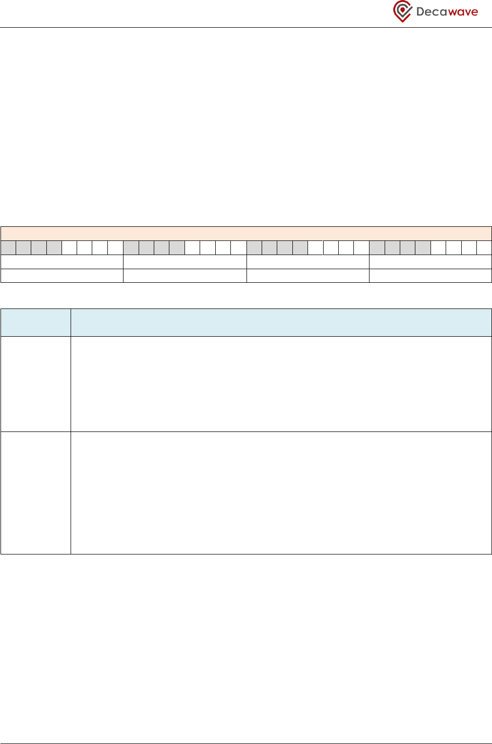
DW1000 User Manual
© Decawave Ltd 2017
Version 2.15
Page 110 of 244
7.2.31.3 Manual Transmit Power Control
This functionality applies when the Disable Smart TX Power Control bit DIS_STXP in Register file: 0x04 –
System Configuration is set to 1. In this case it is possible to exercise power control over the PHR part of the
transmit frame and the rest of the transmit frame separately. Please refer to section 10.1 – Frame structure
overview for details of frame structure. It is possible to boost the power for the frame excluding the PHR
part and stay within the regulatory limits if the frames are short, see section 7.2.31.2. The PHR part of the
frame is controlled separately so that the power can be boosted without violating the regulatory limits for
peak power. However, in general, the power settings for both parts of the frame should be programmed to
the same value.
When DIS_STXP is 1, the fields of the TX Power Control register are defined as follows:
REG:1E:00 – TX_POWER – Transmit Power Control (When DIS_STXP = 1)
31
30
29
28
27
26
25
24
23
22
21
20
19
18
17
16
15
14
13
12
11
10
9
8
7
6
5
4
3
2
1
0
Not applicable
TXPOWSD
TXPOWPHR
Not applicable
0x0E
0x08
0x02
0x22
The individual sub-fields are described below.
Field
Description of fields within Register file: 0x1E – Transmit Power Control (when DIS_STXP is
0)
TXPOWPHR
reg:1E:00
bits:15–8
This power setting is applied during the transmission of the PHY header (PHR) portion of
the frame. Section 7.2.31.1 – Units of TX Power Control details the programming of this.
WARNING: The register default value here is for the smart power control mode of
operation (as described in section 7.2.31.2 above) but may be too high for the manual use
case. In order to comply with regional spectrum regulations it should be reduced to the
level appropriate for the external RF circuitry and compliance to the regulations.
TXPOWSD
reg:1E:00
bits:23–16
This power setting is applied during the transmission of the synchronisation header (SHR)
and data portions of the frame. The SHR consists of the preamble and SFD portions of the
frame that precede the PHR, and the Data portion of the frame is the piece following the
PHR. Section 7.2.31.1 – Units of TX Power Control details the programming of this value.
WARNING: The register default value here is for the smart power control mode of
operation (as described in section 7.2.31.2 above) but may be too high for the manual use
case. In order to comply with regional spectrum regulations it should be reduced to a level
appropriate for the external RF circuitry and compliance to the regulations.
The Table 19 values apply when smart TX power is being employed (i.e. the Disable Smart TX Power Control
bit DIS_STXP in Register file: 0x04 – System Configuration is zero, not set), and, the Table 20 values apply
when smart TX power is disabled (i.e. DIS_STXP=1).
7.2.31.4 Transmit Power Control Reference Values
Reference values for setting Register file: 0x1E – Transmit Power Control are given below in Table 19 and
Table 20. These may be used as starting point for transmit power calibration. They are based on a typical IC
and an assumed IC to antenna loss of 1.5 dB with a 0 dBi antenna. Generally to avoid out of band spectral
emissions the mixer gain should be kept low however increasing the DA gain will increase current
consumption. The Table 19 and Table 20 values are dependent on the selected channel (frequency) and on
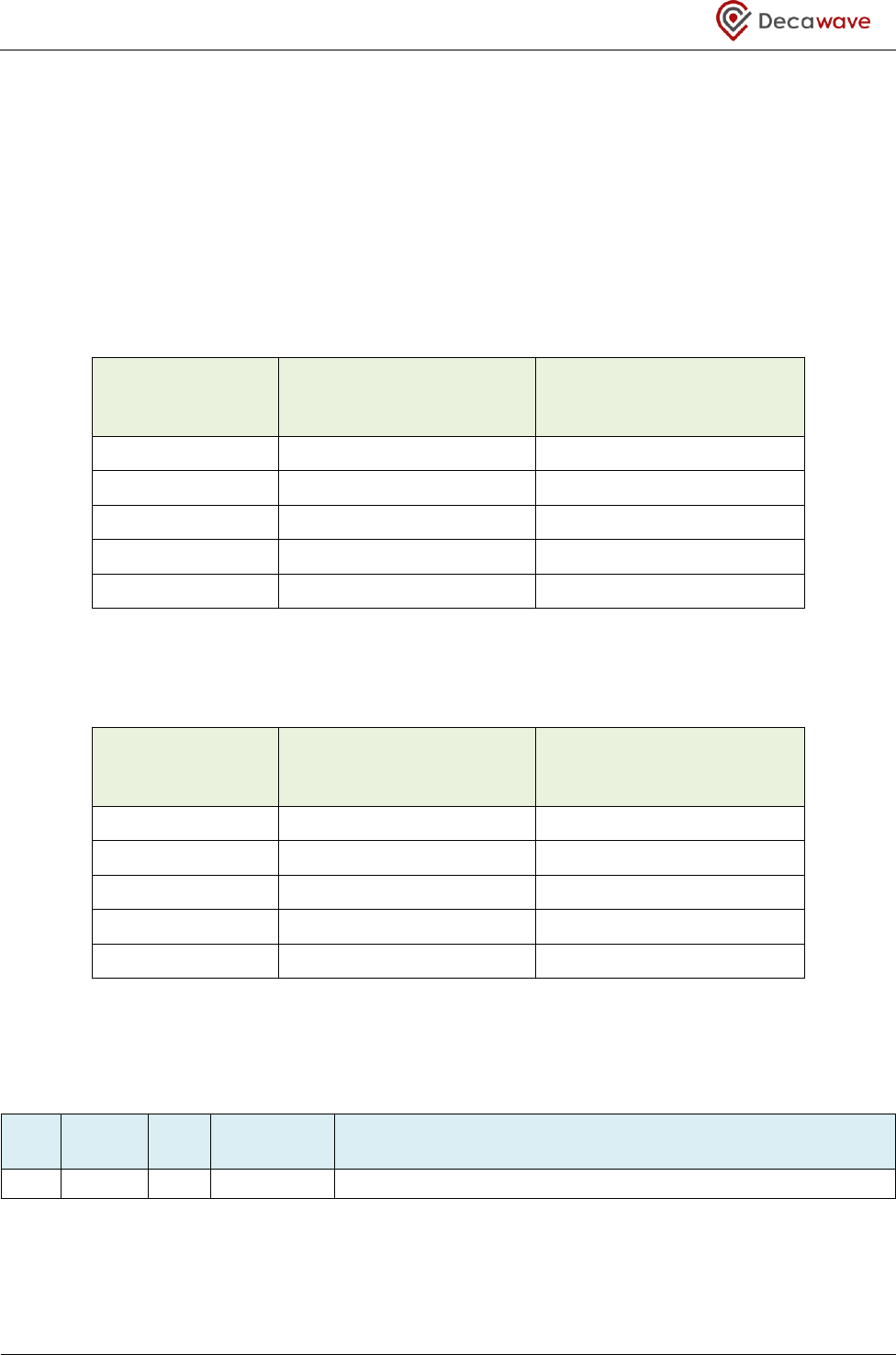
DW1000 User Manual
© Decawave Ltd 2017
Version 2.15
Page 111 of 244
the configured PRF. These settings are designed to deliver a nominal power spectrum density
of -41.3 dBm/MHz to the antenna, assuming a 1.5 dB loss (due to balun and RF traces) between the IC
output and the antenna.
The Table 19 values apply when smart TX power is being employed (i.e. the Disable Smart TX Power Control
bit DIS_STXP in Register file: 0x04 – System Configuration is zero, not set), and, the Table 20 values apply
when smart TX power is disabled (i.e. DIS_STXP = 1).
Table 19: Reference values for Register file: 0x1E – Transmit Power Control, for Smart Transmit Power
Control
TX Channel
Example Register file: 0x1E –
Transmit Power Control values
for 16 MHz, with DIS_STXP = 0
Example Register file: 0x1E –
Transmit Power Control values
for 64 MHz, with DIS_STXP = 0
1, 2
0x15355575
0x07274767
3
0x0F2F4F6F
0x2B4B6B8B
4
0x1F1F3F5F
0x3A5A7A9A
5
0x0E082848
0x25456585
7
0x32527292
0x5171B1D1
Table 20: Reference values Register file: 0x1E – Transmit Power Control for Manual Transmit Power
Control (Smart Transmit Power Control disabled)
Note: High and low octets of the 32-bit values in Table 20 are not relevant when smart TX
power is disabled.
7.2.32 Register file: 0x1F – Channel Control
ID
Length
(octets)
Type
Mnemonic
Description
0x1F
4
RW
CHAN_CTRL
Channel Control Register
Register map register file 0x1F is the channel control register. This is used to select transmit and receive
channels, and configure preamble codes and some related parameters.
TX Channel
Example Register file: 0x1E –
Transmit Power Control values
for 16 MHz, with DIS_STXP = 1
Example Register file: 0x1E –
Transmit Power Control values
for 64 MHz, with DIS_STXP = 1
1, 2
0x75757575
0x67676767
3
0x6F6F6F6F
0x8B8B8B8B
4
0x5F5F5F5F
0x9A9A9A9A
5
0x48484848
0x85858585
7
0x92929292
0xD1D1D1D1

DW1000 User Manual
© Decawave Ltd 2017
Version 2.15
Page 112 of 244
The fields of the Channel Control Register are defined as follows:
REG:1F:00 – CHAN_CTRL – Channel Control Register
31
30
29
28
27
26
25
24
23
22
21
20
19
18
17
16
15
14
13
12
11
10
9
8
7
6
5
4
3
2
1
0
RX_PCODE
TX_PCODE
RNSSFD
TNSSFD
RXPRF
DWSFD
-
-
-
-
-
-
-
-
-
RX_CHAN
TX CHAN
0
0
0
0
0
0
0
0
0
0
0
0
0
0
0
0
0
0
0
0
0
0
0
0
5
5
The individual sub-fields are described below:
Field
Description of fields within Register file: 0x1F – Channel Control
TX_CHAN
reg:1F:00
bits:3–0
This selects the transmit channel. Supported channels are 1, 2, 3, 4, 5, and 7. Other values
should not be used. Both TX_CHAN and RX_CHAN (below) should be set to the same value.
Full selection of TX channel requires that the following parameters are also set appropriately:
Sub-Register 0x28:0C– RF_TXCTRL
Sub-Register 0x2A:0B – TC_PGDELAY
Sub-Register 0x2B:07 – FS_PLLCFG
For correct operation of the DW1000 and compliance to the IEEE 802.15.4 UWB standard, the
preamble code should be set according to the operating channel. For details of centre
frequencies and preamble codes for the supported channels, please refer to section 10.5 –
UWB channels and preamble codes.
RX_CHAN
reg:1F:00
bits:7–4
This selects the receive channel. Supported channels are 1, 2, 3, 4, 5, and 7. Other values
should not be used. Both RX_CHAN and TX_CHAN (above) should be set to the same value.
Full selection of RX channel requires that the following parameters are also set appropriately:
Sub-Register 0x28:0B– RF_RXCTRLH
Sub-Register 0x2B:07 – FS_PLLCFG
For correct operation of the DW1000 and compliance to the IEEE 802.15.4 UWB standard, the
preamble code should be set according to the operating channel. For details of centre
frequencies and preamble codes for the supported channels, please refer to section 10.5 –
UWB channels and preamble codes.
-
reg:1F:00
bits:16–8
Bits marked ‘-’ in register 0x1F are reserved.

DW1000 User Manual
© Decawave Ltd 2017
Version 2.15
Page 113 of 244
Field
Description of fields within Register file: 0x1F – Channel Control
DWSFD
reg:1F:00
bit:17
This bit enables a non-standard Decawave proprietary SFD sequence. When DWSFD is 0, and
TNSSFD and RNSSFD are deasserted low, then the SFD sequence used by the DW1000 will be
the one prescribed by the IEEE 802.15.4-2011 standard.
When DWSFD is set a special Decawave-defined SFD sequence will be employed in the
transmitter and looked for in the receiver. For the 110 kbps this SFD is 64 symbols long (as
normal), but for 850 kbps the SFD may be either 8 or 16 symbols long, this is selected by the
SFD length field within Register file: 0x21 – User defined SFD sequence. Other length values
are invalid and should not be used. (For 6.8 Mbps the standard 8-symbol SFD).
The Decawave-defined SFD sequences are as follows:
SFD
Sequence
8-symbol
----+-00
16-
symbol
----+-+--++--+00
64-
symbol
−−−−−−−+−+−−−−−−+−−+−+−−+−−+−−+−−−++−−−+++−+−+−+−−−+−−+−−−−+++00
For more details please refer to Register file: Register file: 0x21 – User defined SFD sequence.
, and see Table 21: Recommended SFD sequence configurations for best performance
Note that DWSFD takes precedence over TNSSFD & RNSSFD. If DWSFD is set, the settings of
TNSSFD & RNSSFD are ignored.
RXPRF
reg:1F:00
bits:19–18
This two bit field selects the PRF used in the receiver. Values allowed here are binary 01 to
select the 16 MHz PRF or binary 10 to select the 64 MHz PRF. Other values are reserved and
should not be set.
TNSSFD
reg:1F:00
bit:20
This bit enables the use of a user specified (non-standard) SFD in the transmitter. When
TNSSFD is 0, and as long as DWSFD is not set, then the transmitted SFD sequence will be that
prescribed by the IEEE 802.15.4 standard. When TNSSFD is set the transmitted SFD
sequence is defined by the programming of Register file: 0x21 – User defined SFD sequence.
For correct operation the SFD sequence used in the receiver has to be programmed to match
the transmitted SFD sequence. The RNSSFD bit enables the use of user programmed non-
standard SFD sequence in the receiver. For more details please see Register file: 0x21 – User
defined SFD sequence.
RNSSFD
reg:1F:00
bit:21
This bit enables the use of a user specified (non-standard) SFD in the receiver. When
RNSSFD is 0, and as long as DWSFD is not set, then the SFD sequence searched for in the
receiver will be that prescribed by the IEEE 802.15.4 standard. When RNSSFD is set the
receiver SFD sequence is defined by the programming of Register file: 0x21 – User defined
SFD sequence. For correct operation the SFD sequence used in the transmitter has to be
programmed to match the SFD sequence being hunted for in the receiver. The TNSSFD bit
enables the use of user programmed non-standard SFD sequence in the transmitter. For
more details please refer to Register file: 0x21 – User defined SFD sequence.
TX_PCODE
reg:1F:00
bits:26–22
This field selects the preamble code used in the transmitter. The user should select the
preamble code from those recommended for the selected channel and PRF setting. Section
10.5 – UWB channels and preamble codes details the preamble codes allowed in the
supported channels.
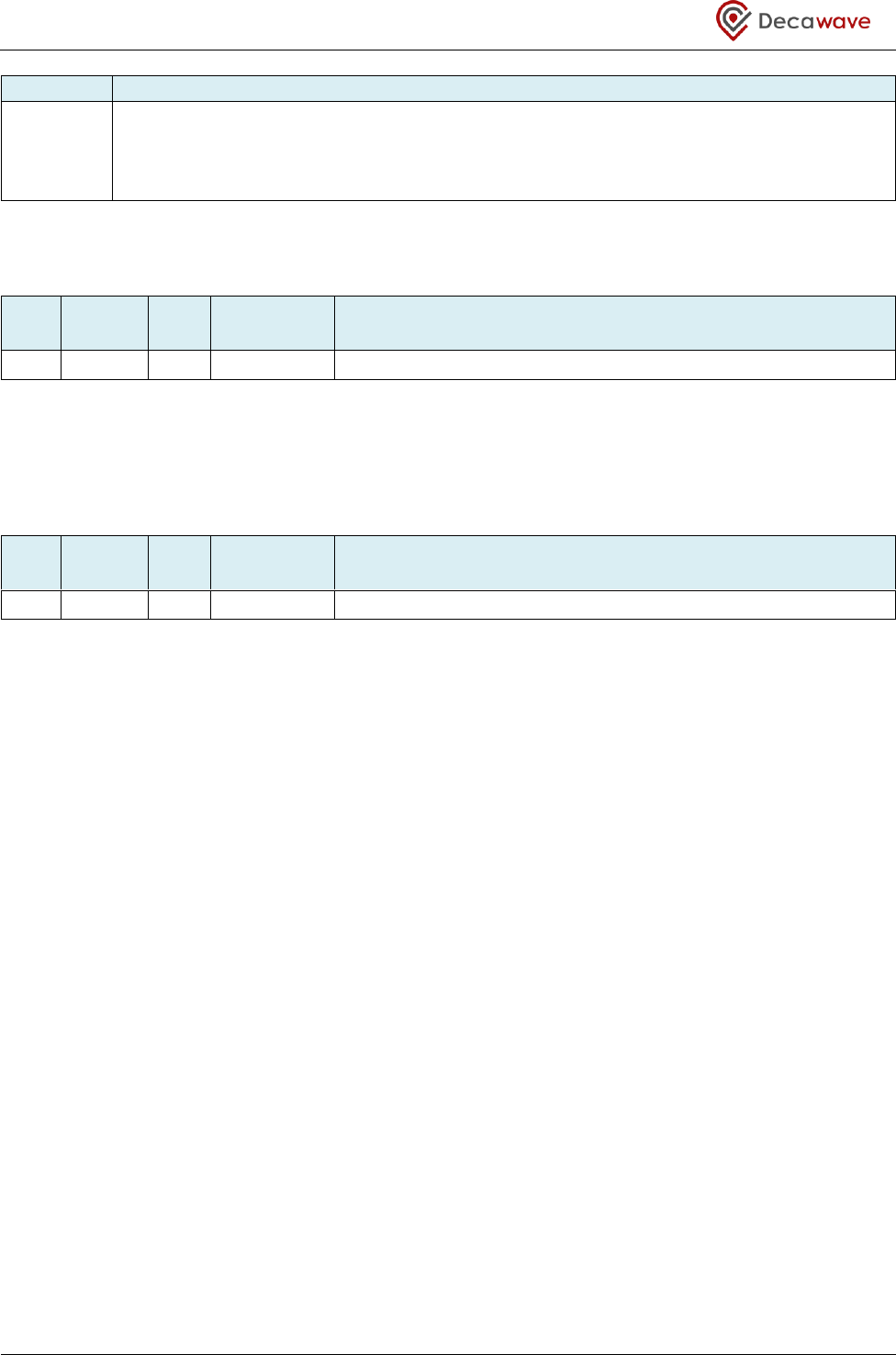
DW1000 User Manual
© Decawave Ltd 2017
Version 2.15
Page 114 of 244
Field
Description of fields within Register file: 0x1F – Channel Control
RX_PCODE
reg:1F:00
bits:31–27
This field selects the preamble code used in the receiver. The user should select the
preamble code from those recommended for the selected channel and PRF setting. Section
10.5 – UWB channels and preamble codes details the preamble codes allowed in the
supported channels.
7.2.33 Register file: 0x20 – Reserved
ID
Length
(octets)
Type
Mnemonic
Description
0x20
-
-
-
Reserved – this register file is reserved
Register map register file 0x20 is reserved for future use. Please take care not to write to this register as
doing so may cause the DW1000 to malfunction.
7.2.34 Register file: 0x21 – User defined SFD sequence
ID
Length
(octets)
Type
Mnemonic
Description
0x21
41
RW
USR_SFD
User-specified short/long TX/RX SFD sequences
Register map register file 0x21 is the user defined SFD sequence. This allows the possibility for a non-
standard SFD sequence to be programmed. The use of a non-standard SFD sequence is separately
configurable for the transmitter and receiver by the TNSSFD and RNSSFD bits in the Register file: 0x1F –
Channel Control.
In addition, the SFD_LENGTH part of this register file is used to select between 8 and 16 length SFD when the
special Decawave defined (non-standard) SFD is being used. This is enabled by the DWSFD bit in the Register
file: 0x1F – Channel Control. NB: when this is being used, length values of 8 or 16 are valid, other values
should not be used.
The length of an SFD sequence for 110 kbps is always 64 symbols, but the length of the SFD sequence for
other data rates may be configured to a value between 8 and 16 using the SFD_LENGTH register at sub
address 0x00.
The SFD pattern consists of the preamble symbols either not sent, or sent as normal or sent inverted (i.e.
positive and negative pulses reversed) see section 10.3 for more details of the standard SFD.
To program an SFD we set two elements per SFD symbol: -
A magnitude: defining the presence or not of a physical transmission for that symbol time.
A sign: defining, for symbols that are sent, whether the symbol is sent in its normal positive sense or
inverted into a negative symbol.
The individual sub-fields of Register file: 0x21 – User defined SFD sequence are described below, giving the
index within the register file, and defining the parameter at that index:

DW1000 User Manual
© Decawave Ltd 2017
Version 2.15
Page 115 of 244
NOTE: Designing SFD sequences is a complicated task, beyond the scope of this manual. Where improved
performance is desired and standard compliance is not required it is recommend to use the Decawave
defined (non-standard) SFD enabled by setting the DWSFD bit. Only experts should consider designing and
programming their own SFD sequences.
See Table 21: Recommended SFD sequence configurations for best performance
Data
Rate
DWSFD
reg:1F:00
bit:17
TNSSFD
reg:1F:00
bit:20
RNSSFD
reg:1F:00
bit:21
SFD_LENGTH
reg:21:00
bits:0–7
Description
6.8 Mbps
0
0
0
x
When the DW1000 is operating at 6.8 Mbps,
this programming selects the standard IEEE 8-
symbol SFD which gives sufficient robustness
since the data is already the weakest part of the
frame.
850 kbps
1
1
1
16
The standard IEEE 8-symbol SFD is weaker than
data at 850 kbps. When the DW1000 is
operating at 850 kbps, this programming selects
a Decawave defined non-standard 16-symbol
SFD, which removes the weakness making the
SFD stronger than the 850 kbps data.
110 kbps
1
0
0
x
This programming selects a Decawave defined
non-standard 64-symbol SFD which is more
robust than standard IEEE 64-symbol SFD
improving the performance in 110 kbps mode.
Table 22 below presents additional SFD sequence programming options. Note: The selection of SFD
sequences other than the IEEE 802.15.4-2011 UWB standard compliant SFD sequence may improve
performance, but will of course make it impossible to interwork with a device configured to use the standard
defined SFD (or with a third party devices using the standard SFD).

DW1000 User Manual
© Decawave Ltd 2017
Version 2.15
Page 116 of 244
Table 22: Other possible SFD sequence configurations
Data
Rate
DWSFD
reg:1F:00
bit:17
TNSSFD
reg:1F:00
bit:20
RNSSFD
reg:1F:00
bit:21
SFD_LENGTH
reg:21:00
bits:0–7
Description
850 kbps
0
0
0
x
This programming selects the 8-symbol SFD as
defined in the IEEE 802.15.4 standard, when
operating at 850 kbps.
110 kbps
0
0
0
x
This programming selects the 64-symbol SFD as
defined in the IEEE 802.15.4 standard, when
operating at 110 kbps.
850 kbps
1
0
0
x
When the DW1000 is operating at 850 kbps,
this programming selects a Decawave defined
non-standard 8-symbol SFD, which is stronger
than the standard defined SFD but still a little
weaker that the data. Hence our
recommendation of the 16-symbol SFD defined
Table 21 for best performance at 850 kbps.
6.8 Mbps
or
850 kbps
0
1
1
8 to 16
When the DW1000 is operating at 6.8 Mbps or
850 kbps, this programming selects the use of a
user configured SFD with length configurable in
the range 8 to 16 symbols. In this mode the
user is responsible for correctly programming
the SFD sequence in Register file: 0x21 – User
defined SFD sequence.
110 kbps
0
1
1
x
When the DW1000 is operating at 110 kbps,
this selects the use of a user configured SFD
with fixed length of 64 symbols. In this mode
the user is responsible for correctly
programming the SFD sequence in Register file:
0x21 – User defined SFD sequence.
Note: Configurations other than those defined in Table 21 or Table 22 are not recommended. To correctly
receive a frame the receiver must use the same SFD sequence configuration as is being used by the remote
transmitting device.

DW1000 User Manual
© Decawave Ltd 2017
Version 2.15
Page 117 of 244
Sub-Index
Field
Description of fields within Register file: 0x21 – User defined SFD
sequence
0
reg:21:00
SFD_LENGTH
This is the length of the SFD sequence used when the data rate is 850 kbps
and higher. Valid length configuration values must be between 8 and 16
symbol
2 8 ≤ SFD_LENGTH ≤ 16
When the DWSFD bit in (Register file: 0x1F – Channel Control) is one,
SFD_LENGTH must be set to either 8 or 16. Other values should not be used.
1
reg:21:01
TX_SSFD_MAGL
(Symbols 7..0)
This field sets the short SFD magnitude data for the transmitted SFD
sequence, for the first 8 symbol intervals. The low order bits define the part
of the SFD sequence sent first in time.
2
reg:21:02
TX_SSFD_MAGH
(Symbols 15..8)
This field sets the short SFD magnitude data for the transmitted SFD
sequence, for the second 8 symbol intervals. The values here are used when
SFD_LENGTH is greater than 8. Where SFD_LENGTH is less than 16 the low
order bits are applicable up to the specified length.
3
reg:21:03
TX_SSFD_SGNL
(Symbols 7..0)
This field sets the short SFD polarity data for the transmitted SFD sequence,
for the first 8 symbol intervals. The low order bits define the part of the SFD
sequence sent first in time.
4
reg:21:04
TX_SSFD_SGNH
(Symbols 15..8)
This field sets the short SFD polarity data for the transmitted SFD sequence,
for the second 8 symbol intervals. The values here are used when
SFD_LENGTH is greater than 8. Where SFD_LENGTH is less than 16 the low
order bits are applicable up to the specified length.
5
reg:21:05
RX_SSFD_MAGL
(Symbols 7..0)
This field sets the short SFD magnitude data for the receive SFD sequence, for
the first 8 symbol intervals. The low order bits define the part of the SFD
sequence sent first in time.
6
reg:21:06
TX_SSFD_SGNH
(Symbols 15..8)
This field sets the short SFD magnitude data for the receive SFD sequence, for
the second 8 symbol intervals. The values here are used when SFD_LENGTH
is greater than 8. Where SFD_LENGTH is less than 16 the low order bits are
applicable up to the specified length.
7
reg:21:07
RX_SSFD_SGNL
(Symbols 7..0)
This field sets the short SFD polarity data for the receive SFD sequence, for
the first 8 symbol intervals. The low order bits define the part of the SFD
sequence sent first in time.
8
reg:21:08
TX_SSFD_SGNH
(Symbols 15..8)
This field sets the short SFD polarity data for the receive SFD sequence, for
the second 8 symbol intervals. The values here are used when SFD_LENGTH
is greater than 8. Where SFD_LENGTH is less than 16 the low order bits are
applicable up to the specified length.
9
reg:21:09
TX_LSFD_MAG0
(Symbols 7..0)
This field sets the long (64-symbol) SFD magnitude data for the transmitted
SFD sequence. This byte covers the first 8 symbol intervals, symbols 7 to 0.
The low order bits define the part of the SFD sequence sent first in time.
10
reg:21:0A
TX_LSFD_MAG1
(Symbols 15..8)
This field sets the long (64-symbol) SFD magnitude data for the transmitted
SFD sequence, for symbol intervals 15 to 8.
11
reg:21:0B
TX_LSFD_MAG2
(Symbols 23..16)
This field sets the long (64-symbol) SFD magnitude data for the transmitted
SFD sequence, for symbol intervals 23 to 16.
12
reg:21:0C
TX_LSFD_MAG3
(Symbols 31..24)
This field sets the long (64-symbol) SFD magnitude data for the transmitted
SFD sequence, for symbol intervals 31 to 24.
13
reg:21:0D
TX_LSFD_MAG4
(Symbols 39..32)
This field sets the long (64-symbol) SFD magnitude data for the transmitted
SFD sequence, for symbol intervals 39 to 32.
14
reg:21:0E
TX_LSFD_MAG5
(Symbols 47..40)
This field sets the long (64-symbol) SFD magnitude data for the transmitted
SFD sequence, for symbol intervals 47 to 40.
15
reg:21:0F
TX_LSFD_MAG6
(Symbols 55..48)
This field sets the long (64-symbol) SFD magnitude data for the transmitted
SFD sequence, for symbol intervals 55 to 48.
16
reg:21:10
TX_LSFD_MAG7
(Symbols 63..56)
This field sets the long (64-symbol) SFD magnitude data for the transmitted
SFD sequence, for symbol intervals 63 to 56.

DW1000 User Manual
© Decawave Ltd 2017
Version 2.15
Page 118 of 244
Sub-Index
Field
Description of fields within Register file: 0x21 – User defined SFD
sequence
17
reg:21:11
TX_LSFD_SGN0
(Symbols 7..0)
This field sets the long (64-symbol) SFD polarity data for the transmitted SFD
sequence. This byte covers the first 8 symbol intervals, symbols 7 to 0. The
low order bits define the part of the SFD sequence sent first in time.
18
reg:21:12
TX_LSFD_SGN1
(Symbols 15..8)
This field sets the long (64-symbol) SFD polarity data for the transmitted SFD
sequence, for symbol intervals 15 to 8.
19
reg:21:13
TX_LSFD_SGN2
(Symbols 23..16)
This field sets the long (64-symbol) SFD polarity data for the transmitted SFD
sequence, for symbol intervals 23 to 16.
20
reg:21:14
TX_LSFD_SGN3
(Symbols 31..24)
This field sets the long (64-symbol) SFD polarity data for the transmitted SFD
sequence, for symbol intervals 31 to 24.
21
reg:21:15
TX_LSFD_SGN4
(Symbols 39..32)
This field sets the long (64-symbol) SFD polarity data for the transmitted SFD
sequence, for symbol intervals 39 to 32.
22
reg:21:16
TX_LSFD_SGN5
(Symbols 47..40)
This field sets the long (64-symbol) SFD polarity data for the transmitted SFD
sequence, for symbol intervals 47 to 40.
23
reg:21:17
TX_LSFD_SGN6
(Symbols 55..48)
This field sets the long (64-symbol) SFD polarity data for the transmitted SFD
sequence, for symbol intervals 55 to 48.
24
reg:21:18
TX_LSFD_SGN7
(Symbols 63..56)
This field sets the long (64-symbol) SFD polarity data for the transmitted SFD
sequence, for symbol intervals 63 to 56.
25
reg:21:19
RX_LSFD_MAG0
(Symbols 7..0)
This field sets the long (64-symbol) SFD magnitude data for the receive SFD
sequence. This byte covers the first 8 symbol intervals, symbols 7 to 0. The
low order bits define the part of the SFD sequence arriving first in time.
26
reg:21:1A
RX_LSFD_MAG1
(Symbols 15..8)
This field sets the long (64-symbol) SFD magnitude data for the receive SFD
sequence, for symbol intervals 15 to 8.
27
reg:21:1B
RX_LSFD_MAG2
(Symbols 23..16)
This field sets the long (64-symbol) SFD magnitude data for the receive SFD
sequence, for symbol intervals 23 to 16.
28
reg:21:1C
RX_LSFD_MAG3
(Symbols 31..24)
This field sets the long (64-symbol) SFD magnitude data for the receive SFD
sequence, for symbol intervals 31 to 24.
29
reg:21:1D
RX_LSFD_MAG4
(Symbols 39..32)
This field sets the long (64-symbol) SFD magnitude data for the receive SFD
sequence, for symbol intervals 39 to 32.
30
reg:21:1E
RX_LSFD_MAG5
(Symbols 47..40)
This field sets the long (64-symbol) SFD magnitude data for the receive SFD
sequence, for symbol intervals 47 to 40.
31
reg:21:1F
RX_LSFD_MAG6
(Symbols 55..48)
This field sets the long (64-symbol) SFD magnitude data for the receive SFD
sequence, for symbol intervals 55 to 48.
32
reg:21:20
RX_LSFD_MAG7
(Symbols 63..56)
This field sets the long (64-symbol) SFD magnitude data for the receive SFD
sequence, for symbol intervals 63 to 56.
33
reg:21:21
RX_LSFD_SGN0
(Symbols 7..0)
This field sets the long (64-symbol) SFD polarity data for the receive SFD
sequence. This byte covers the first 8 symbol intervals, symbols 7 to 0. The
low order bits define the part of the SFD sequence arriving first in time.
34
reg:21:22
RX_LSFD_SGN1
(Symbols 15..8)
This field sets the long (64-symbol) SFD polarity data for the receive SFD
sequence, for symbol intervals 15 to 8.
35
reg:21:23
RX_LSFD_SGN2
(Symbols 23..16)
This field sets the long (64-symbol) SFD polarity data for the receive SFD
sequence, for symbol intervals 23 to 16.
36
reg:21:24
RX_LSFD_SGN3
(Symbols 31..24)
This field sets the long (64-symbol) SFD polarity data for the receive SFD
sequence, for symbol intervals 31 to 24.
37
reg:21:25
RX_LSFD_SGN4
(Symbols 39..32)
This field sets the long (64-symbol) SFD polarity data for the receive SFD
sequence, for symbol intervals 39 to 32.
38
reg:21:26
RX_LSFD_SGN5
(Symbols 47..40)
This field sets the long (64-symbol) SFD polarity data for the receive SFD
sequence, for symbol intervals 47 to 40.
39
reg:21:27
RX_LSFD_SGN6
(Symbols 55..48)
This field sets the long (64-symbol) SFD polarity data for the transmitted SFD
sequence, for symbol intervals 55 to 48. Receive
40
reg:21:28
RX_LSFD_SGN7
(Symbols 63..56)
This field sets the long (64-symbol) SFD polarity data for the receive SFD
sequence, for symbol intervals 63 to 56.

DW1000 User Manual
© Decawave Ltd 2017
Version 2.15
Page 119 of 244
Table 21: Recommended SFD sequence configurations for best performance
Data
Rate
DWSFD
reg:1F:00
bit:17
TNSSFD
reg:1F:00
bit:20
RNSSFD
reg:1F:00
bit:21
SFD_LENGTH
reg:21:00
bits:0–7
Description
6.8 Mbps
0
0
0
x
When the DW1000 is operating at 6.8 Mbps,
this programming selects the standard IEEE 8-
symbol SFD which gives sufficient robustness
since the data is already the weakest part of the
frame.
850 kbps
1
1
1
16
The standard IEEE 8-symbol SFD is weaker than
data at 850 kbps. When the DW1000 is
operating at 850 kbps, this programming selects
a Decawave defined non-standard 16-symbol
SFD, which removes the weakness making the
SFD stronger than the 850 kbps data.
110 kbps
1
0
0
x
This programming selects a Decawave defined
non-standard 64-symbol SFD which is more
robust than standard IEEE 64-symbol SFD
improving the performance in 110 kbps mode.
Table 22 below presents additional SFD sequence programming options. Note: The selection of SFD
sequences other than the IEEE 802.15.4-2011 UWB standard compliant SFD sequence may improve
performance, but will of course make it impossible to interwork with a device configured to use the standard
defined SFD (or with a third party devices using the standard SFD).

DW1000 User Manual
© Decawave Ltd 2017
Version 2.15
Page 120 of 244
Table 22: Other possible SFD sequence configurations
Data
Rate
DWSFD
reg:1F:00
bit:17
TNSSFD
reg:1F:00
bit:20
RNSSFD
reg:1F:00
bit:21
SFD_LENGTH
reg:21:00
bits:0–7
Description
850 kbps
0
0
0
x
This programming selects the 8-symbol SFD as
defined in the IEEE 802.15.4 standard, when
operating at 850 kbps.
110 kbps
0
0
0
x
This programming selects the 64-symbol SFD as
defined in the IEEE 802.15.4 standard, when
operating at 110 kbps.
850 kbps
1
0
0
x
When the DW1000 is operating at 850 kbps,
this programming selects a Decawave defined
non-standard 8-symbol SFD, which is stronger
than the standard defined SFD but still a little
weaker that the data. Hence our
recommendation of the 16-symbol SFD defined
Table 21 for best performance at 850 kbps.
6.8 Mbps
or
850 kbps
0
1
1
8 to 16
When the DW1000 is operating at 6.8 Mbps or
850 kbps, this programming selects the use of a
user configured SFD with length configurable in
the range 8 to 16 symbols. In this mode the
user is responsible for correctly programming
the SFD sequence in Register file: 0x21 – User
defined SFD sequence.
110 kbps
0
1
1
x
When the DW1000 is operating at 110 kbps,
this selects the use of a user configured SFD
with fixed length of 64 symbols. In this mode
the user is responsible for correctly
programming the SFD sequence in Register file:
0x21 – User defined SFD sequence.
Note: Configurations other than those defined in Table 21 or Table 22 are not recommended. To correctly
receive a frame the receiver must use the same SFD sequence configuration as is being used by the remote
transmitting device.
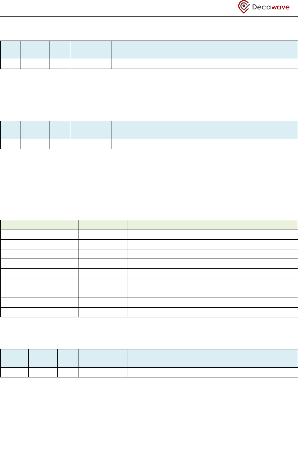
DW1000 User Manual
© Decawave Ltd 2017
Version 2.15
Page 121 of 244
7.2.35 Register file: 0x22 – Reserved
ID
Length
(octets)
Type
Mnemonic
Description
0x22
-
-
-
Reserved – this register file is reserved
Register map register file 0x22 is reserved for future use. Please take care not to write to this register as
doing so may cause the DW1000 to malfunction.
7.2.36 Register file: 0x23 –AGC configuration and control
ID
Length
(octets)
Type
Mnemonic
Description
0x23
33
RW
AGC_CTRL
Automatic Gain Control configuration and control
Register map register file 0x23 is for configuration and control of the receiver gain control block. It contains
a number of sub-registers, some of which need user control. Table 23 gives an overview of the sub-registers
within Register file: 0x23 –AGC configuration and control, and these sub-registers are individually described
in sub-sections below.
Table 23: Register file: 0x23 –AGC configuration and control overview
OFFSET in Register 0x23
Mnemonic
Description
0x00
-
reserved
0x02
AGC_CTRL1
AGC Control #1
0x04
AGC_TUNE1
AGC Tuning register 1
0x06
-
reserved
0x0C
AGC_TUNE2
AGC Tuning register 2
0x10
-
reserved
0x12
AGC_TUNE3
AGC Tuning register 3
0x14
-
reserved
0x1E
AGC_STAT1
AGC Status
7.2.36.1 Sub-Register 0x23:00 – AGC_RES1
ID
Length
(octets)
Type
Mnemonic
Description
23:00
2
-
AGC_RES1
Reserved area 1
Register file: 0x23 –AGC configuration and control, sub-register 0x00 is a reserved register. Please take care
not to write to this register as doing so may cause the DW1000 to malfunction.
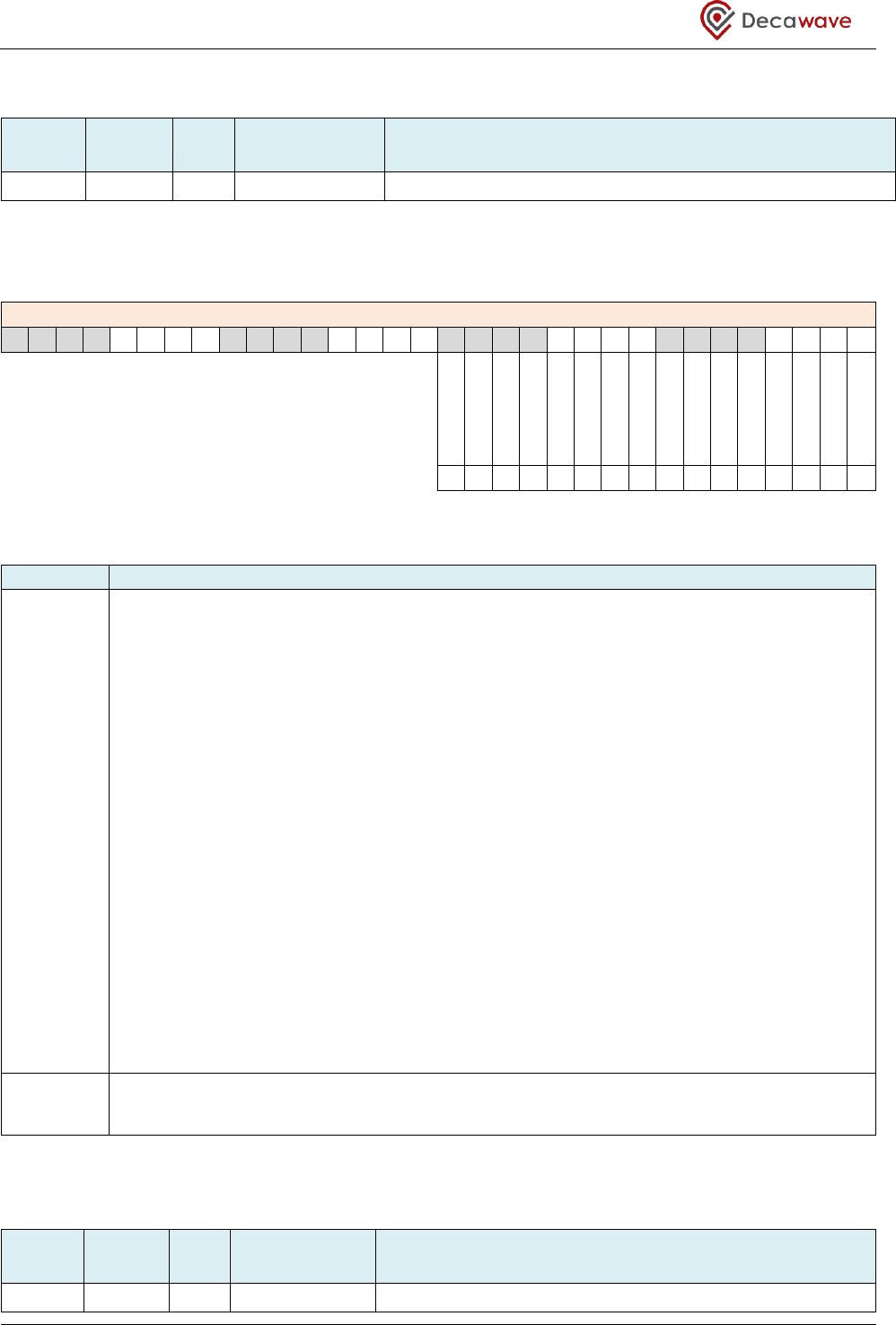
DW1000 User Manual
© Decawave Ltd 2017
Version 2.15
Page 122 of 244
7.2.36.2 Sub-Register 0x23:02 – AGC_CTRL1
ID
Length
(octets)
Type
Mnemonic
Description
23:02
2
RW
AGC_CTRL1
AGC Control #1
Register file: 0x23 –AGC configuration and control, sub-register 0x02 is a 16-bit control register for the
measurement function of the AGC. This register contains the fields identified and described below:
REG:23:02 – AGC_CTRL1 – AGC measurement control Register
31
30
29
28
27
26
25
24
23
22
21
20
19
18
17
16
15
14
13
12
11
10
9
8
7
6
5
4
3
2
1
0
-
-
-
-
-
-
-
-
-
-
-
-
-
-
-
DIS_AM
0
0
0
0
0
0
0
0
0
0
0
0
0
0
0
1
The bits of the AGC_CTRL1 register are described below:
Field
Description of fields within Sub-Register 0x23:02 – AGC_CTRL1
DIS_AM
reg:23:02
bit:0
Disable AGC Measurement. The DIS_AM bit is set by default to disable the AGC
measurement function. The AGC measurement function might be used as an energy
measurement for an “Energy Scan” as part of determining what channel to use. When
DIS_AM bit is clear and the receiver is enabled the AGC will settle on an estimate of the
background energy level and the result will be available via the EDG1 and EDV2 values in
Sub-Register 0x23:1E – AGC_STAT1. To save power in the receiver, when this facility is not
required or is not in use, it is recommended to set DIS_AM bit to 1 to disable this AGC
measurement function.
The recommended procedure to measure background energy level is as follows:
(a) Set up the operating channel and related parameters as required*.
(b) Set DIS_AM to 0.
I Turn on the receiver with the RXENAB bit in Register file: 0x0D – System Control
Register.
(d) Wait 32 µs for the AGC to settle
I Set DIS_AM bit to 1 to freeze the result.
(f) Read EDG1 and EDV2 values and calculate noise energy, (as per Figure 27 below).
(g) Turn off the DW1000 with the TRXOFF bit in Register file: 0x0D – System Control
Register.
* The important settings are the channel frequency related settings.
–
reg:22:02
bits:15–1
These bits are reserved.
7.2.36.3 Sub-Register 0x23:04 – AGC_TUNE1
ID
Length
(octets)
Type
Mnemonic
Description
23:04
2
RW
AGC_TUNE1
AGC Tuning register 1
DW1000 User Manual
© Decawave Ltd 2017
Version 2.15
Page 123 of 244
Register file: 0x23 –AGC configuration and control, sub-register 0x04 is a 16-bit tuning register for the AGC.
The value here needs to change depending on the PRF. The values needed depending on the RXPRF
configuration are given in Table 24 below. Please take care not to write other values to this register as doing
so may cause the DW1000 to 0x28:00.
Table 24: Sub-Register 0x23:04 – AGC_TUNE1 values
RXPRF configuration
Value to program to
Sub-Register 0x23:04 – AGC_TUNE1
(1) = 16 MHz PRF
0x8870
(2) = 64 MHz PRF
0x889B
7.2.36.4 Sub-Register 0x23:06 – AGC_RES2
ID
Length
(octets)
Type
Mnemonic
Description
23:06
6
-
AGC_RES2
Reserved area 2
Register file: 0x23 –AGC configuration and control, sub-register 0x06 is a reserved area. Please take care not
to write to this area as doing so may cause the DW1000 to malfunction.
7.2.36.5 Sub-Register 0x23:0C – AGC_TUNE2
ID
Length
(octets)
Type
Mnemonic
Description
23:0C
4
RW
AGC_TUNE2
AGC Tuning register 2
Register file: 0x23 –AGC configuration and control, sub-register 0x0C is a 32-bit tuning register for the AGC.
The default value of this register needs to be reconfigured for optimum operation of the AGC. Please ensure
to program it to the value given in Table 25 below. Please take care not to write other values to this register
as doing so may cause the DW1000 to malfunction.
Table 25: Sub-Register 0x23:0C – AGC_TUNE2 values
Value to program to
Sub-Register 0x23:0C – AGC_TUNE2
0X2502A907
7.2.36.6 Sub-Register 0x23:10 – AGC_RES3
ID
Length
(octets)
Type
Mnemonic
Description
23:10
2
-
AGC_RES3
Reserved area 3
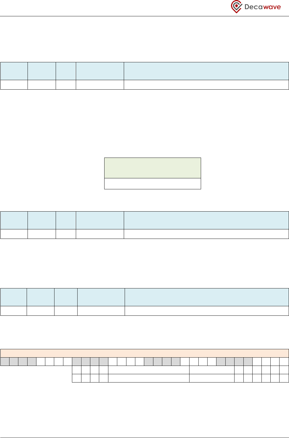
DW1000 User Manual
© Decawave Ltd 2017
Version 2.15
Page 124 of 244
Register file: 0x23 –AGC configuration and control, sub-register 0x10 is a reserved register. Please take care
not to write to this register as doing so may cause the DW1000 to malfunction.
7.2.36.7 Sub-Register 0x23:12 – AGC_TUNE3
ID
Length
(octets)
Type
Mnemonic
Description
23:12
2
RW
AGC_TUNE3
AGC Tuning register 3
Register file: 0x23 –AGC configuration and control, sub-register 0x12 is a 16-bit tuning register for the AGC.
The default value of this register needs to be reconfigured for optimum operation of the AGC. Please ensure
to program it to the value given in Table 26 below. Please take care not to write other values to this register
as doing so may cause the DW1000 to malfunction.
Table 26: Sub-Register 0x23:12 – AGC_TUNE3 values
Value to program to
Sub-Register 0x23:12 – AGC_TUNE3
0x0035
7.2.36.8 Sub-Register 0x23:14 – AGC_RES4
ID
Length
(octets)
Type
Mnemonic
Description
23:14
10
-
AGC_RES4
Reserved area 4
Register file: 0x23 –AGC configuration and control, sub-register 0x14 is a reserved area. Please take care not
to write to this area as doing so may cause the DW1000 to malfunction.
7.2.36.9 Sub-Register 0x23:1E – AGC_STAT1
ID
Length
(octets)
Type
Mnemonic
Description
23:1E
3
RO
AGC_STAT1
AGC Status
Register file: 0x23 –AGC configuration and control, sub-register 0x1E is a 24-bit status register for the
measurement function of the AGC. This register contains the fields identified and described below:
REG:23:1E – AGC_STAT1 – AGC Status Register
31
30
29
28
27
26
25
24
23
22
21
20
19
18
17
16
15
14
13
12
11
10
9
8
7
6
5
4
3
2
1
0
-
-
-
-
EDV2
EDG1
-
-
-
-
-
-
-
-
-
-
0
0
-
-
-
-
-
-
The bits of the AGC_STAT1 register are described below:
DW1000 User Manual
© Decawave Ltd 2017
Version 2.15
Page 125 of 244
Field
Description of fields within Sub-Register 0x23:1E – AGC_STAT1
EDG1
reg:23:1E
bits:10–6
This 5-bit gain value relates to input noise power measurement. EDG1 can be used in
conjunction with the EDV2 value to give a measure of the background in-band noise energy
level. This might be used for an Energy Detect (ED channel scan) as part of implementing the
IEEE 802.15.4 standard’s MLME-SCAN request primitive. The noise energy level is given by
combining EDG1 and EDV2 value as described in Figure 27 below.
EDV2
reg:23:1E
bits:19–11
This 9-bit value relates to the input noise power measurement. EDV2 can be used in
conjunction with the EDG1 value to give a measure of the background in-band noise energy
level. This might be used for an Energy Detect (ED channel scan) as part of implementing the
IEEE 802.15.4 standard’s MLME-SCAN request primitive. The noise energy level is given by
combining EDG1 and EDV2 value as described in Figure 27 below.
–
reg:23:1E
These bits are reserved.
Combining EDG1 and EDV2 value to get a noise energy level is achieved by the equation:
Where is a scaling factor dependant on channel as per Table 27 below: -
Table 27: Scaling factor for channel noise energy estimation
Channel
scaling factor
1 to 4
1.3335
5 and 7
1.0000
The above formula does not give an absolute level but instead gives a relative level that allows
comparison between channels in order to select the channel with least noise.
Figure 27: Combining EDG1 and EDV2 to give an ED noise figure
7.2.37 Register file: 0x24 – External Synchronisation Control
ID
Length
(octets)
Type
Mnemonic
Description
0x24
12
RW
EXT_SYNC
External synchronisation control
Register map register file 0x24 is for control of the DW1000 synchronisation hardware.
There is a separate application note giving details of the external synchronisation. Please consult with
Decawave applications support team for details. The capabilities of the DW1000 with respect to external
synchronisation are described briefly in section 6.1- External Synchronisation.
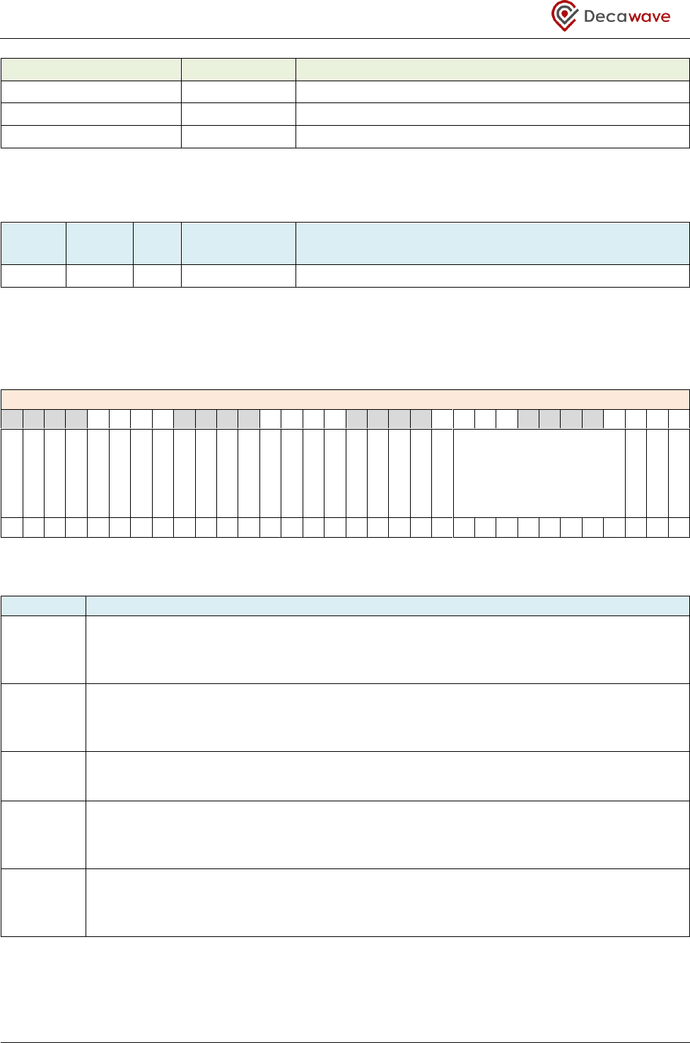
DW1000 User Manual
© Decawave Ltd 2017
Version 2.15
Page 126 of 244
OFFSET in Register 0x24
Mnemonic
Description
0x00
EC_CTRL
External clock synchronisation counter configuration
0x04
EC_RXTC
External clock counter captured on RMARKER
0x08
EC_GOLP
External clock offset to first path 1 GHz counter
7.2.37.1 Sub-Register 0x24:00 EC_CTRL
ID
Length
(octets)
Type
Mnemonic
Description
24:00
4
RW
EC_CTRL
External clock synchronisation counter configuration
Register file: 0x24 – External Synchronisation Control, sub-register 0x00 is the External clock synchronisation
counter configuration register, EC_CTRL. The EC_CTRL register is used to configure the external
synchronisation mode. The EC_CTRL register contains the following sub-fields:
REG:24:00 –EC_CTRL– External clock synchronisation counter configuration
31
30
29
28
27
26
25
24
23
22
21
20
19
18
17
16
15
14
13
12
11
10
9
8
7
6
5
4
3
2
1
0
-
-
-
-
-
-
-
-
-
-
-
-
-
-
-
-
-
-
-
-
OSTRM
WAIT
PLLLDT
OSRSM
OSTSM
0
0
0
0
0
0
0
0
0
0
0
0
0
0
0
0
0
0
0
0
0
0
0
0
0
0
0
0
0
0
0
0
The fields of the EC_CTRL register identified above are individually described below:
Field
Description of fields within Sub-Register 0x24:00 EC_CTRL
OSTSM
reg:24:00
bit:0
External transmit synchronisation mode enable. See section 6.1.2 – One Shot Transmit
Synchronisation (OSTS) Mode.
OSRSM
reg:24:00
bit:1
External receive synchronisation mode enable. See section 6.1.3 – One Shot Receive
Synchronisation (OSRS) Mode.
PLLLDT
reg:24:00
bit:2
Clock PLL lock detect tune. This bit should be set to 1 to ensure reliable operation of the clock
PLL lock detect flags.
WAIT
reg:24:00
bits:10:3
Wait counter used for external transmit synchronisation and external timebase reset. See
sections 6.1.2 – One Shot Transmit Synchronisation (OSTS) Mode and 6.1.1 – One Shot
Timebase Reset (OSTR) Mode.
OSTRM
reg:24:00
bit:11
External timebase reset mode enable. See section 6.1.1 – One Shot Timebase Reset (OSTR)
Mode.
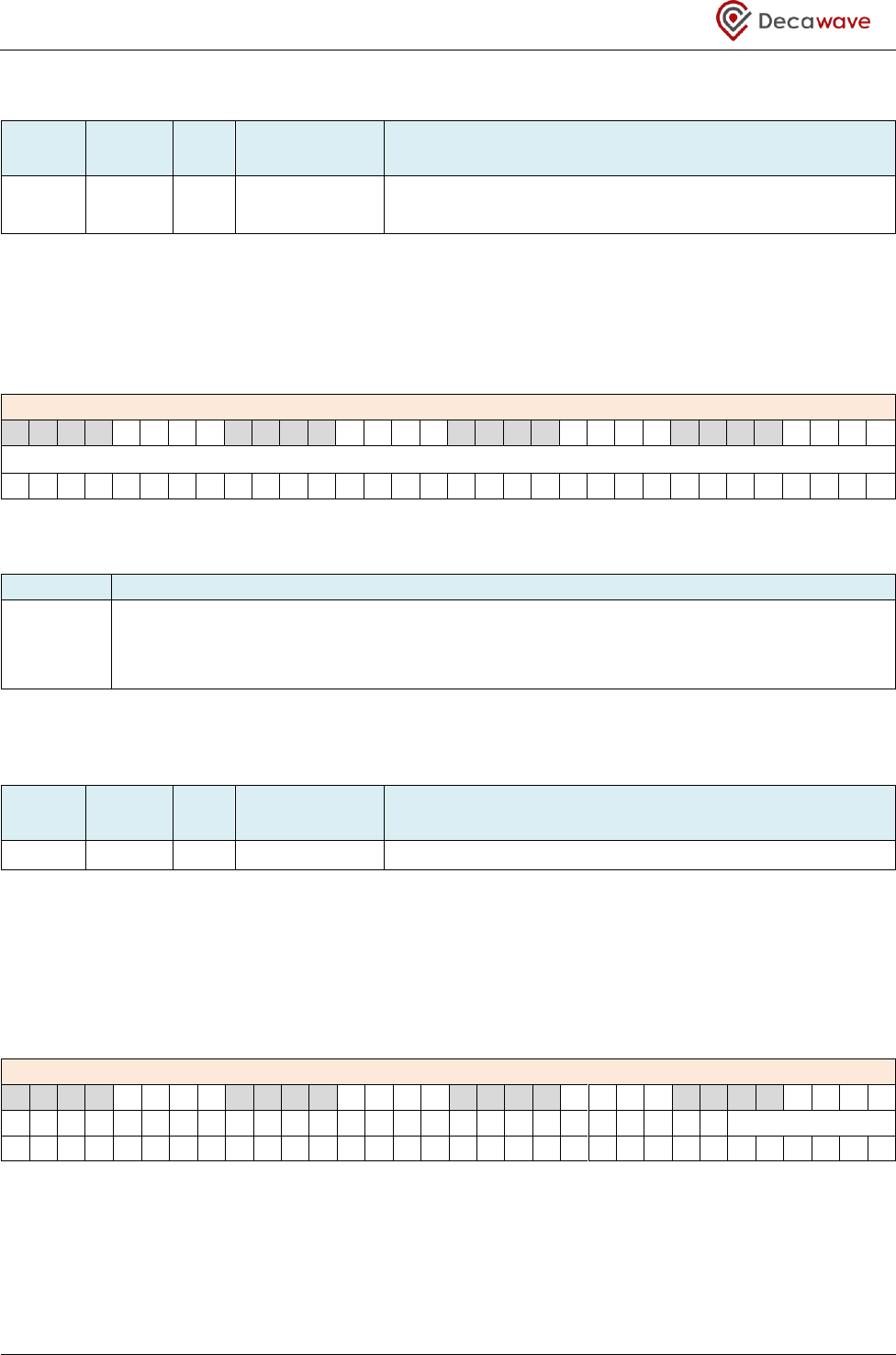
DW1000 User Manual
© Decawave Ltd 2017
Version 2.15
Page 127 of 244
7.2.37.2 Sub-Register 0x24:04 EC_RXTC
ID
Length
(octets)
Type
Mnemonic
Description
24:04
4
RO
EC_RXTC
External clock synchronisation counter captured on
RMARKER.
Register file: 0x24 – External Synchronisation Control, sub-register 0x04 is the External clock synchronisation
counter value captured on RMARKER, EC_RXTC. The EC_RXTC register is used to timestamp the received
packet with respect to the external clock, see section 6.1.3 – One Shot Receive Synchronisation (OSRS) Mode
for details of the procedure. The EC_RXTC register contains the following sub-fields:
REG:24:04 – EC_RXTC– External clock synchronisation timestamp capture
31
30
29
28
27
26
25
24
23
22
21
20
19
18
17
16
15
14
13
12
11
10
9
8
7
6
5
4
3
2
1
0
RX_TS_EST
-
-
-
-
-
-
-
-
-
-
-
-
-
-
-
-
-
-
-
-
-
-
-
-
-
-
-
-
-
-
-
-
The fields of the EC_RXTC register identified above are individually described below:
Field
Description of fields within Sub-Register 0x24:04 EC_RXTC
RX_TS_EST
reg:24:04
bits:31:0
External clock synchronisation counter captured on RMARKER. See section 6.1.3 – One Shot
Receive Synchronisation (OSRS) Mode.
7.2.37.3 Sub-Register 0x24:08 EC_GOLP
ID
Length
(octets)
Type
Mnemonic
Description
24:08
4
RO
EC_GOLP
External clock offset to first path 1 GHz counter
Register file: 0x24 – External Synchronisation Control, sub-register 0x08 is the External clock offset to first
path 1 GHz counter, EC_GOLP. The EC_GOLP register is used to time the offset in 1 GHz intervals between
the RMARKER, and the next edge of the external clock. This value can be used to calculate range with
respect to the external clock, see section 6.1.3 – One Shot Receive Synchronisation (OSRS) Mode for details
of the procedure. The EC_GOLP register contains the following sub-fields:
REG:24:08– EC_GOLP– External clock offset to first path 1 GHz counter
31
30
29
28
27
26
25
24
23
22
21
20
19
18
17
16
15
14
13
12
11
10
9
8
7
6
5
4
3
2
1
0
-
-
-
-
-
-
-
-
-
-
-
-
-
-
-
-
-
-
-
-
-
-
-
-
-
-
OFFSET_EXT
0
0
0
0
0
0
0
0
0
0
0
0
0
0
0
0
0
0
0
0
0
0
0
0
0
0
0
0
0
0
0
0
The fields of the EC_CTRL register identified above are individually described below:
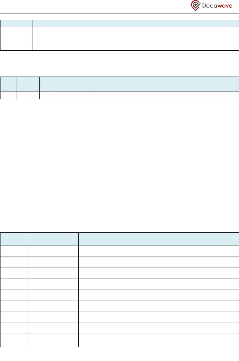
DW1000 User Manual
© Decawave Ltd 2017
Version 2.15
Page 128 of 244
Field
Description of fields within Sub-Register 0x24:08 EC_GOLP
OFFSET_EXT
reg:24:08
bits: 5:0
This register contains the 1 GHz count from the arrival of the RMARKER and the next edge of
the external clock. See section 6.1.3 – One Shot Receive Synchronisation (OSRS) Modefor
details of its use.
7.2.38 Register file: 0x25 – Accumulator CIR memory
ID
Length
(octets)
Type
Mnemonic
Description
0x25
4064
RO
ACC_MEM
Read access to accumulator data memory
Register map register file 0x25 is a large bank of memory that holds the accumulated channel impulse
response (CIR) data. To accurately determine this timestamp the DW1000 incorporates an internal (LDE)
algorithm to adjust the RMARKER receive timestamp as reported in Register file: 0x15 – Receive Time Stamp.
A main component of the LDE algorithm is a search of the channel impulse response in the ACC_MEM to find
the “leading edge” defining the first arriving ray.
The host system does not need to access the ACC_MEM in normal operation, however it may be of interest
to the system design engineers to visualise the radio channel for diagnostic purposes.
The accumulator contains complex values, a 16-bit real integer and a 16-bit imaginary integer, for each tap
of the accumulator, each of which represents a 1 ns sample interval (or more precisely half a period of the
499.2 MHz fundamental frequency). The span of the accumulator is one symbol time. This is 992 samples
for the nominal 16 MHz mean PRF, or, 1016 samples for the nominal 64 MHz mean PRF. These numbers are
calculated from Table 60 given that there are two samples per chip time.
NB: Because of an internal memory access delay when reading the accumulator the first octet output is a
dummy octet that should be discarded. This is true no matter what sub-index the read begins at.
Sub-Index
Field
Description of fields within Register file: 0x25 – Accumulator CIR
memory
0
reg:25:000
CIR[0].real.lo8
Low 8 bits of real part of accumulator sample 0
1
reg:25:001
CIR[0].real.hi8
High 8 bits of real part of accumulator sample 0
2
reg:25:002
CIR[0].imag.lo8
Low 8 bits of imaginary part of accumulator sample 0
3
reg:25:003
CIR[0].imag.lo8
High 8 bits of imaginary part of accumulator sample 0
4
reg:25:004
CIR[1].real.lo8
Low 8 bits of real part of accumulator sample 1
5
reg:25:005
CIR[1].real.hi8
High 8 bits of real part of accumulator sample 1
6
reg:25:006
CIR[1].imag.lo8
Low 8 bits of imaginary part of accumulator sample 1
7
reg:25:007
CIR[1].imag.lo8
High 8 bits of imaginary part of accumulator sample 1
:
:
:
:
:
:
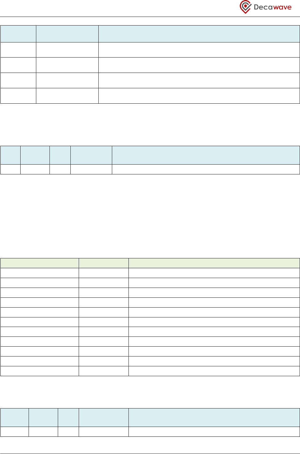
DW1000 User Manual
© Decawave Ltd 2017
Version 2.15
Page 129 of 244
Sub-Index
Field
Description of fields within Register file: 0x25 – Accumulator CIR
memory
4060
reg:25:FDC
CIR[1015].real.lo8
Low 8 bits of real part of accumulator sample 1015
(1016th and last sample of CIR for the nominal 64 MHz mean PRF)
4061
reg:25:FDD
CIR[1015].real.hi8
High 8 bits of real part of accumulator sample 1015
(1016th and last sample of CIR for the nominal 64 MHz mean PRF)
4062
reg:25:FDE
CIR[1015].imag.lo8
Low 8 bits of imaginary part of accumulator sample 1015
(1016th and last sample of CIR for the nominal 64 MHz mean PRF)
4063
reg:25:FDF
CIR[1015].imag.lo8
High 8 bits of imaginary part of accumulator sample 1015
(1016th and last sample of CIR for the nominal 64 MHz mean PRF)
NB: Because of an internal memory access delay when reading the accumulator the first octet output is a
dummy octet that should be discarded. This is true no matter what sub-index the read begins at.
7.2.39 Register file: 0x26 – GPIO control and status
ID
Length
(octets)
Type
Mnemonic
Description
0x26
44
RW
GPIO_CTRL
Peripheral register–bus 1 access – GPIO control
Register map register file 0x26 is concerned with the use of the GPIO. It contains a number of sub-registers.
An overview of these is given by Table 28. Each of these sub-registers is separately described in the sub-
sections below.
Note: the GPIO clocks need to be turned on, before enabling or disabling the GPIO mode or value. The
GPIO clocks are enabled by setting GPCE and GPRN in PMSC_CTRL0
Table 28: Register file: 0x26 – GPIO control and status overview
OFFSET in Register 0x26
Mnemonic
Description
0x00
GPIO_MODE
GPIO Mode Control Register
0x04
-
reserved
0x08
GPIO_DIR
GPIO Direction Control Register
0x0C
GPIO_DOUT
GPIO Data Output register
0x10
GPIO_IRQE
GPIO Interrupt Enable
0x14
GPIO_ISEN
GPIO Interrupt Sense Selection
0x18
GPIO_IMODE
GPIO Interrupt Mode (Level / Edge)
0x1C
GPIO_IBES
GPIO Interrupt “Both Edge” Select
0x20
GPIO_ICLR
GPIO Interrupt Latch Clear
0x24
GPIO_IDBE
GPIO Interrupt De-bounce Enable
0x28
GPIO_RAW
GPIO raw state
7.2.39.1 Sub-Register 0x26:00 – GPIO_MODE
ID
Length
(octets)
Type
Mnemonic
Description
26:00
4
RW
GPIO_MODE
GPIO Mode Control Register

DW1000 User Manual
© Decawave Ltd 2017
Version 2.15
Page 130 of 244
Register file: 0x26 – GPIO control and status, sub-register 0x00 is the GPIO Mode Control Register,
GPIO_MODE. The GPIO_MODE register is used to select whether the GPIO is operating as a GPIO or has
another special function. The GPIO_MODE register contains the following sub-fields:
REG:26:00 – GPIO_MODE – GPIO Mode Control Register
31
30
29
28
27
26
25
24
23
22
21
20
19
18
17
16
15
14
13
12
11
10
9
8
7
6
5
4
3
2
1
0
-
-
-
-
-
-
-
-
MSGP8
MSGP7
MSGP6
MSGP5
MSGP4
MSGP3
MSGP2
MSGP1
MSGP0
-
-
-
-
-
-
0
0
0
0
0
0
0
0
0
0
0
0
0
0
0
0
0
0
0
0
0
0
0
0
0
0
0
0
0
0
0
0
The fields of the GPIO_MODE register identified above are individually described below:
Field
Description of fields within Sub-Register 0x26:00 – GPIO_MODE
-
Bits marked ‘-’ are reserved and should be written as zero.
MSGP0
reg:26:00
bits:7,6
Mode Selection for GPIO0/RXOKLED.
00: The pin operates as GPIO0 – This is the default (reset) state.
01: The pin operates as the RXOKLED output.
10: bit [7] needs to be set high to get the system clock signal out on GPIO0.
11: Reserved. Do not select this value.
When operating as the RXOKLED driver, the output is asserted briefly when the receiver
completes the reception of a frame with a good FCS/CRC. The on time for the RXOKLED
depends on the blink time set in Sub-Register 0x36:28 – PMSC_LEDC.
Note: Lighting LEDs will drain power in battery-powered applications.
MSGP1
reg:26:00
bits:9,8
Mode Selection for GPIO1/SFDLED.
00: The pin operates as GPIO1– This is the default (reset) state.
01: The pin operates as the SFDLED output.
10: Reserved. Do not select this value.
11: Reserved. Do not select this value.
When operating as the driver, the output is asserted briefly when the receiver detects the SFD
sequence in the RX frame. The on time is determined by the blink time configuration set in
Sub-Register 0x36:28 – PMSC_LEDC
Note: Lighting LEDs will drain power in battery-powered applications.
MSGP2
reg:26:00
bits:11,10
Mode Selection for GPIO2/RXLED. Allowed values are:
00: The pin operates as the GPIO2 output – This is the default (reset) state.
01: The pin operates as the RXLED output.
10: Reserved. Do not select this value.
11: Reserved. Do not select this value.
When operating as the RXLED driver, the output is asserted when the receiver is on, and stays
on for a brief period after the receiver is turned off. The minimum on time is determined by
the blink time configurable in Sub-Register 0x36:28 – PMSC_LEDC.
Note: Lighting LEDs will drain power in battery-powered applications.

DW1000 User Manual
© Decawave Ltd 2017
Version 2.15
Page 131 of 244
Field
Description of fields within Sub-Register 0x26:00 – GPIO_MODE
MSGP3
reg:26:00
bits:13,12
Mode Selection for GPIO3/TXLED. Allowed values are:
00: The pin operates as GPIO3– This is the default (reset) state.
01: The pin operates as the TXLED output.
10: Reserved. Do not select this value.
11: Reserved. Do not select this value.
When operating as the TXLED driver, the output is asserted briefly when the transmitter
completes sending a frame. The blink time is configurable via Sub-Register 0x36:28 –
PMSC_LEDC.
Note: Lighting LEDs will drain power in battery-powered applications.
MSGP4
reg:26:00
bits:15,14
Mode Selection for GPIO4/EXTPA. Allowed values are:
00: The pin operates as GPIO4– This is the default (reset) state.
01: The pin operates as the EXTPA output.
10: Reserved. Do not select this value.
11: Reserved. Do not select this value.
Refer to section 6.2 – External Power Amplification for further information on the use of
EXTPA.
MSGP5
reg:26:00
bits:17,16
Mode Selection for GPIO5/EXTTXE. Allowed values are:
00: The pin operates as GPIO5 – This is the default (reset) state.
01: The pin operates as the EXTTXE output.
10: Reserved. Do not select this value.
11: Reserved. Do not select this value.
Refer to section 6.2 – External Power Amplification for further information on the use of
EXTTXE.
MSGP6
reg:26:00
bits:19,18
Mode Selection forGPIO6/EXTRXE. Allowed values of MSGP6 are:
00: The pin operates as GPIO6– This is the default (reset) state.
01: The pin operates as the EXTRXE output.
10: Reserved. Do not select this value.
11: Reserved. Do not select this value.
Refer to section 6.2 – External Power Amplification for further information on the use of
EXTRXE.
MSGP7
reg:26:00
bits:21,20
Mode Selection for SYNC/GPIO7.Allowed values are:
00: The pin operates as the SYNC input– This is the default (reset) state.
01: The pin operates as GPIO7.
10: Reserved. Do not select this value.
11: Reserved. Do not select this value.
Please refer to section 6.1- External Synchronisation for information on the use of the SYNC
pin.
MSGP8
reg:26:00
bits:23,22
Mode Selection for IRQ/GPIO8. Allowed values are:
00: The pin operates as the IRQ output – This is the default (reset) state.
01: The pin operates as GPIO8.
10: Reserved. Do not select this value.
11: Reserved. Do not select this value.
7.2.39.2 Sub-Register 0x26:04 – Reserved
ID
Length
(octets)
Type
Mnemonic
Description
26:04
4
-
-
Reserved
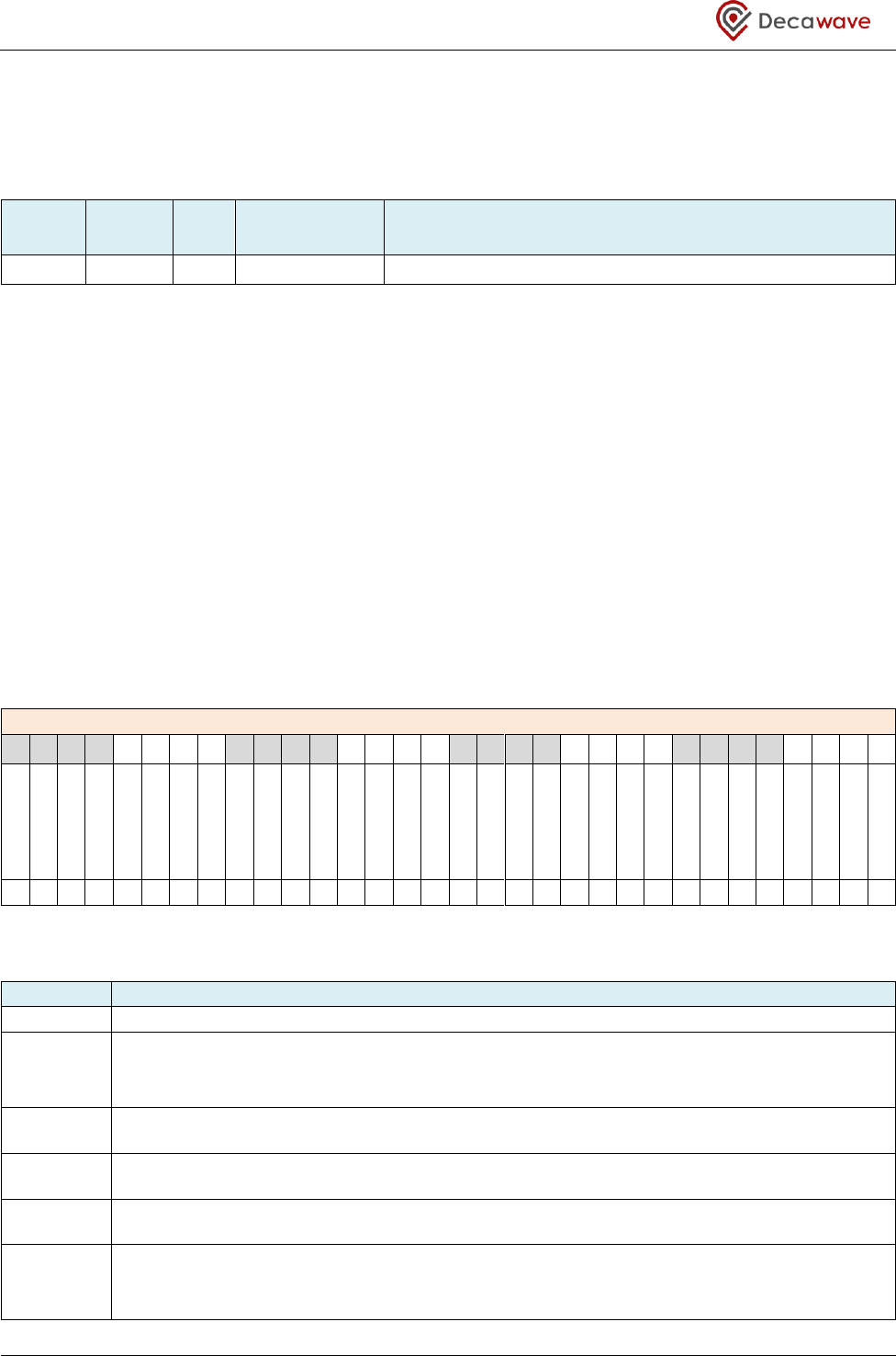
DW1000 User Manual
© Decawave Ltd 2017
Version 2.15
Page 132 of 244
Register file: 0x26 – GPIO control and status, sub-register 0x04 is reserved.
7.2.39.3 Sub-Register 0x26:08 – GPIO_DIR
ID
Length
(octets)
Type
Mnemonic
Description
26:08
4
RW
GPIO_DIR
GPIO Direction control register
Register file: 0x26 – GPIO control and status, sub-register 0x08 is the GPIO Direction Control Register,
GPIO_DIR. The GPIO_DIR register applies to the GPIO pins when they are selected to operate as GPIOs via
the GPIO_MODE register. It contains a bit for each GPIO to individually configure that GPIO as an input or
an output. The register is designed to allow software to change the direction of a single pin without
knowing the settings needed for other pins. This is achieved by having for each direction selection bit (GDP)
an associated mask bit (GDM) used to qualify the write to the GDP direction bit. This allows an individual
direction to be changed in the register without affecting other direction bits. Note that when reading from
this register only the direction GDP bits are returned and these are packed into the lower 9 bits. A GDP
direction bit value of 1 means the pin is an input. A GDP bit value of 0 means the pin is an output. The GDP
bits and their corresponding GDM mask bits are arranged with four GPIO per octet to allow a single octet
write to change direction of an individual GPIO.
The GPIO_DIR register contains the following sub-fields:
REG:26:08 – GPIO_DIR – GPIO Direction control register
31
30
29
28
27
26
25
24
23
22
21
20
19
18
17
16
15
14
13
12
11
10
9
8
7
6
5
4
3
2
1
0
-
-
-
-
-
-
-
-
-
-
-
GDM8
-
-
-
GDP8
GDM7
GDM6
GDM5
GDM4
GDP7
GDP6
GDP5
GDP4
GDM3
GDM2
GDM1
GDM0
GDP3
GDP2
GDP1
GDP0
0
0
0
0
0
0
0
0
0
0
0
0
0
0
0
1
0
0
0
0
1
1
1
1
0
0
0
0
1
1
1
1
The fields of the GPIO_DIR register identified above are individually described below:
Field
Description of fields within Sub-Register 0x26:08 – GPIO_DIR
-
Bits marked ‘-’ in are reserved and should be written as zero.
GDP0
reg:26:08
bit:0
Direction Selection for GPIO0. Reading this bit shows the direction setting for GPIO0.Values
1 = input, 0 = output. When writing (either 1 or 0) this GDP0 value is only changed if the
GDM0 mask bit has a value of 1 for the write operation.
GDP1
bit:1
Direction Selection for GPIO1. (See GDP0).
GDP2
bit:2
Direction Selection for GPIO2. (See GDP0).
GDP3
bit:3
Direction Selection for GPIO3. (See GDP0).
GDM0
reg:26:08
bit:4
Mask for setting the direction of GPIO0. When writing to GDP0 so select the I/O direction of
GPIO0, the value of GDP0 is only changed if this GDM0 mask bit has a value of 1 for the write
operation. GDM0 will always read as 0.
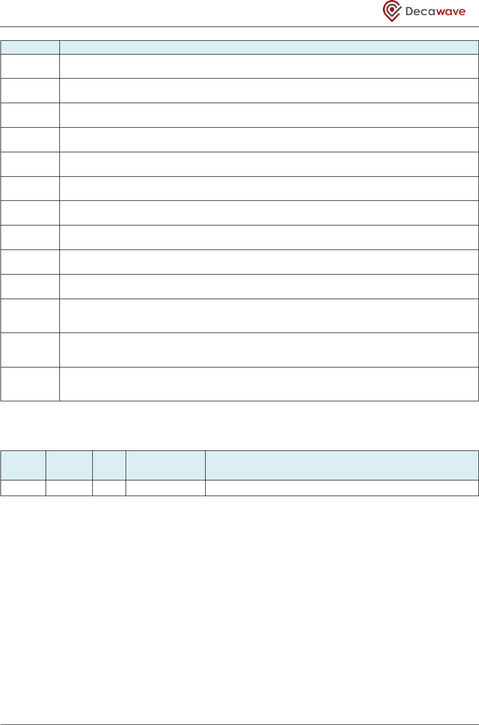
DW1000 User Manual
© Decawave Ltd 2017
Version 2.15
Page 133 of 244
Field
Description of fields within Sub-Register 0x26:08 – GPIO_DIR
GDM1
bit:5
Mask for setting the direction of GPIO1. (See GDM0).
GDM2
bit:6
Mask for setting the direction of GPIO2. (See GDM0).
GDM3
bit:7
Mask for setting the direction of GPIO3. (See GDM0).
GDP4
bit:8
Direction Selection for GPIO4. (See GDP0).
GDP5
bit:9
Direction Selection for GPIO5. (See GDP0).
GDP6
bit:10
Direction Selection for the GPIO6. (See GDP0).
GDP7
bit:11
Direction Selection for the GPIO7. (See GDP0).
GDM4
bit:12
Mask for setting the direction of GPIO4. (See GDM0).
GDM5
bit:13
Mask for setting the direction of GPIO5. (See GDM0).
GDM6
bit:14
Mask for setting the direction of GPIO6. (See GDM0).
GDM7
reg:26:08
bit:15
Mask for setting the direction of GPIO7. (See GDM0).
GDP8
reg:26:08
bit:16
Direction Selection for GPIO8. (See GDP0).
GDM8
reg:26:08
bit:20
Mask for setting the direction of GPIO8. (See GDM0).
7.2.39.4 Sub-Register 0x26:0C – GPIO_DOUT
ID
Length
(octets)
Type
Mnemonic
Description
26:0C
4
RW
GPIO_DOUT
GPIO Data Output register
Register file: 0x26 – GPIO control and status, sub-register 0x0C is the GPIO data output register. The
GPIO_DOUT register applies to the GPIO pins when they are selected to operate as GPIO outputs via the
GPIO_MODE and GPIO_DIR registers. It contains a bit for each GPIO pin to individually select the data to
output on the GPIO output pin. The GPIO_DOUT register is designed to allow software to change the output
state of a single pin without knowing the settings of other output pins. This is achieved by having for each
output value selection bit (GOP) an associated mask bit (GOM) used to qualify the write to the GOP bit.
When reading from the GPIO_DOUT register the mask bits are always read as 0, output value bits will read to
show the current output setting for the GPIO pins. Note, this does not mean this is being output since that
depends also on the appropriate selection of the GPIO_MODE and GPIO_DIR registers. The output value
bits and their corresponding mask bits arranged with four GPIO per octet to allow a single octet write to
change the state of an individual GPIO output.

DW1000 User Manual
© Decawave Ltd 2017
Version 2.15
Page 134 of 244
The GPIO_DOUT register contains the following sub-fields:
REG:26:0C – GPIO_DOUT – GPIO Data Output register
31
30
29
28
27
26
25
24
23
22
21
20
19
18
17
16
15
14
13
12
11
10
9
8
7
6
5
4
3
2
1
0
-
-
-
-
-
-
-
-
-
-
-
GOM8
-
-
-
GOP8
GOM7
GOM6
GOM5
GOM4
GOP7
GOP6
GOP5
GOP4
GOM3
GOM2
GOM1
GOM0
GOP3
GOP2
GOP1
GOP0
0
0
0
0
0
0
0
0
0
0
0
0
0
0
0
0
0
0
0
0
0
0
0
0
0
0
0
0
0
0
0
0
The fields of the GPIO_DOUT register identified above are individually described below:
Field
Description of fields within Sub-Register 0x26:0C – GPIO_DOUT
-
Bits marked ‘-’ are reserved and should be written as zero.
GOP0
reg:26:0C
bit:0
Output state setting for the GPIO0 output. Reading this bit shows the current setting for
GPIO0. Value 1 = logic 1 voltage high output and, value 0 = logic 1 voltage low output. When
writing (either 1 or 0) to this GOP0 bit, its value is only changed if the GOM0 mask bit has a
value of 1 in that write operation.
GOP1
bit:1
Output state setting for GPIO1. (See GOP0).
GOP2
bit:2
Output state setting for GPIO2. (See GOP0).
GOP3
bit:3
Output state setting for GPIO3. (See GOP0).
GOM0
reg:26:0C
bit:4
Mask for setting GPIO0 output state. When writing to GOP0 to select state of the GPIO0
output, the value of GOP0 is only changed if this GOM0 mask bit has a value of 1 for the write
operation. GOM0 will always read as 0.
GOM1
bit:5
Mask for setting GPIO1 output state. (See GOM0).
GOM2
bit:6
Mask for setting GPIO2 output state. (See GOM0).
GOM3
bit:7
Mask for setting GPIO3 output state. (See GOM0).
GOP4
bit:8
Output state setting for GPIO4. (See GOP0).
GOP5
bit:9
Output state setting for GPIO5. (See GOP0).
GOP6
bit:10
Output state setting for GPIO6. (See GOP0).
GOP7
bit:11
Output state setting for GPIO7. (See GOP0).
GOM4
bit:12
Mask for setting the GPIO4 output state. (See GOM0).
GOM5
bit:13
Mask for setting the GPIO5 output state. (See GOM0).
GOM6
bit:15
Mask for setting the GPIO6 output state. (See GOM0).
GOM7
reg:26:0C
bit:15
Mask for setting the GPIO7 output state. (See GOM0).
GOP8
reg:26:0C
bit:16
Output state setting for GPIO8. (See GOP0).
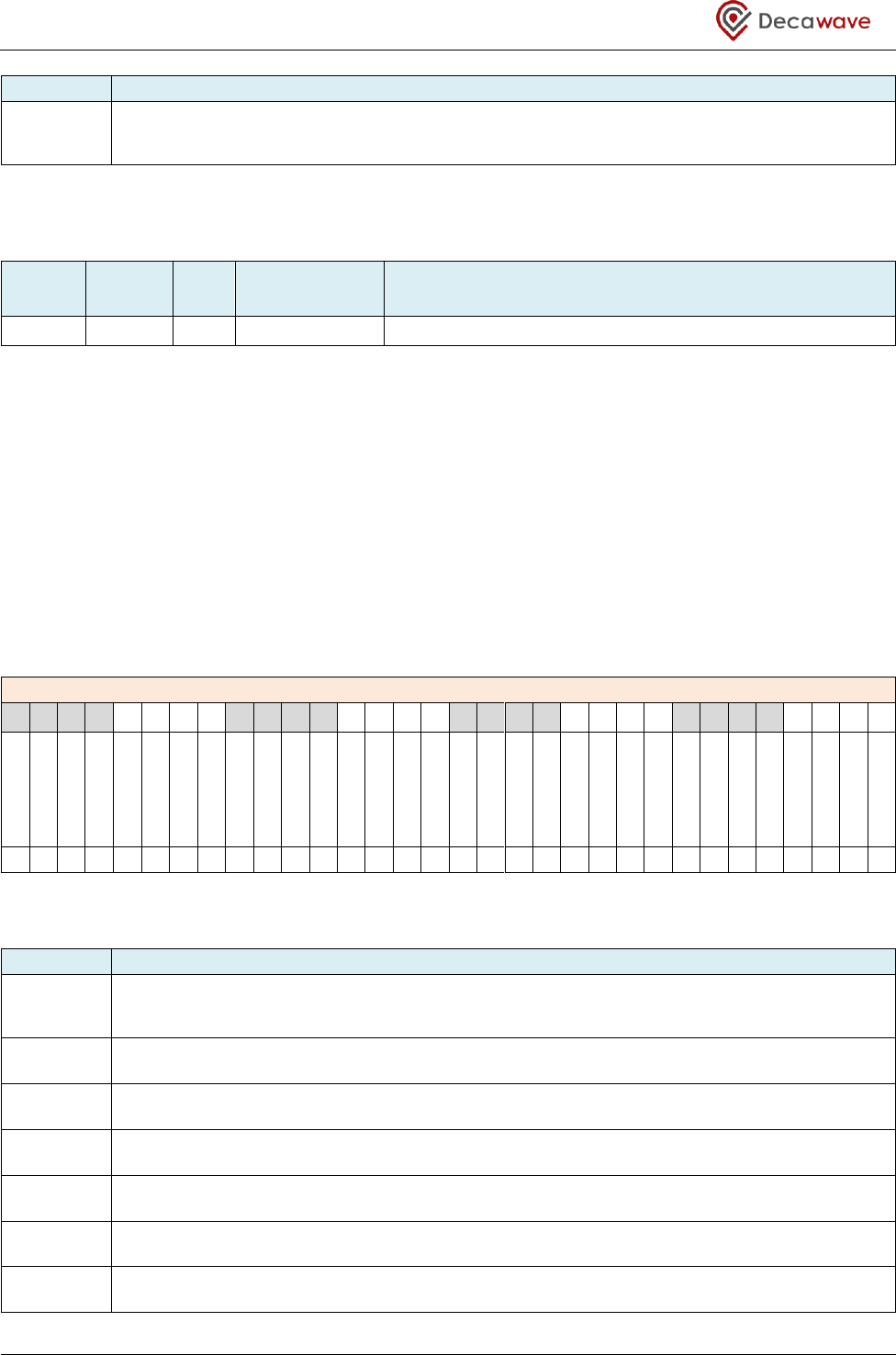
DW1000 User Manual
© Decawave Ltd 2017
Version 2.15
Page 135 of 244
Field
Description of fields within Sub-Register 0x26:0C – GPIO_DOUT
GOM8
reg:26:0C
bit:20
Mask for setting the GPIO8 output state. (See GOM0).
7.2.39.5 Sub-Register 0x26:10 – GPIO_IRQE
ID
Length
(octets)
Type
Mnemonic
Description
26:10
4
RW
GPIO_IRQE
GPIO Interrupt Enable
Register file: 0x26 – GPIO control and status, sub-register 0x10 is the GPIO interrupt enable register. The
GPIO_IRQE register allows a GPIO input pin to be selected as an interrupt source into the DW1000.
Additional configuration registers GPIO_IMODE, GPIO_ISEN, GPIO_IBES and GPIO_IDBE allow the interrupt
to be set as level sensitive with control of whether it is the low or high state that generates the interrupt, or
as edge sensitive with control of the edge(s) that generates the interrupt, and includes a configurable de-
bounce circuit that can be used to ignore transients on the input. The GPIO_IRQE register contains a bit for
each GPIO pin to allow each to be individually selected as interrupt source. Setting the appropriate bit to 1
enables the corresponding GPIO input as an interrupt source, a value of 0 disables that interrupt. When a
GPIO interrupt is triggered it is signalled to the host via the GPIOIRQ event status bit in Register file: 0x0F –
System Event Status Register. The bits of the GPIO_IRQE register are as following:
REG:26:10 – GPIO_IRQE – GPIO Interrupt Enable register
31
30
29
28
27
26
25
24
23
22
21
20
19
18
17
16
15
14
13
12
11
10
9
8
7
6
5
4
3
2
1
0
-
-
-
-
-
-
-
-
-
-
-
-
-
-
-
-
-
-
-
-
-
-
-
GIRQE8
GIRQE7
GIRQE6
GIRQE5
GIRQ E4
GIRQ E3
GIRQE2
GIRQE1
GIRQE0
0
0
0
0
0
0
0
0
0
0
0
0
0
0
0
0
0
0
0
0
0
0
0
0
0
0
0
0
0
0
0
0
The bits identified above are individually described below:
Field
Description of fields within Sub-Register 0x26:10 – GPIO_IRQE
GIRQE0
reg:26:10
bit:0
GPIO IRQ Enable for GPIO0 input. Value 1 = enable GPIO input GPIO0 as an interrupt source.
Value 0 = GPIO0 is not an interrupt source.
GIRQE1
bit:1
GPIO IRQ Enable for GPIO1 input. Value 1 = enable, 0 = disable.
GIRQE2
bit:2
GPIO IRQ Enable for GPIO2 input. Value 1 = enable, 0 = disable.
GIRQE3
bit:3
GPIO IRQ Enable for GPIO3 input. Value 1 = enable, 0 = disable.
GIRQE4
bit:4
GPIO IRQ Enable for GPIO4 input. Value 1 = enable, 0 = disable.
GIRQE5
bit:5
GPIO IRQ Enable for GPIO5 input. Value 1 = enable, 0 = disable.
GIRQE6
bit:6
GPIO IRQ Enable for GPIO6 input. Value 1 = enable, 0 = disable.
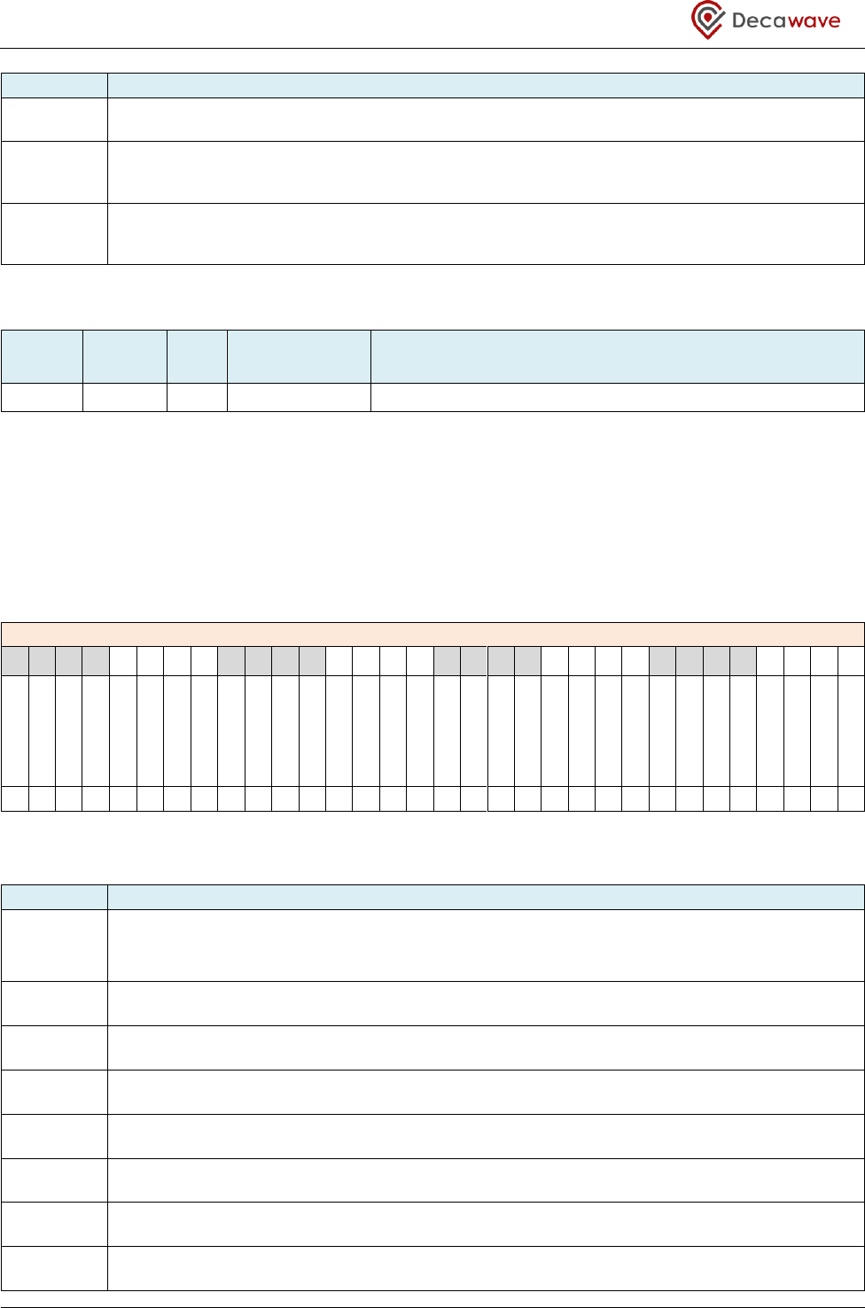
DW1000 User Manual
© Decawave Ltd 2017
Version 2.15
Page 136 of 244
Field
Description of fields within Sub-Register 0x26:10 – GPIO_IRQE
GIRQE7
bit:7
GPIO IRQ Enable for GPIO7 input. Value 1 = enable, 0 = disable.
GIRQE8
reg:26:10
bit:8
GPIO IRQ Enable for GPIO8 input. Value 1 = enable, 0 = disable.
-
reg:26:10
bits:31–9
Bits marked ‘-’ are reserved and should be written as zero.
7.2.39.6 Sub-Register 0x26:14 – GPIO_ISEN
ID
Length
(octets)
Type
Mnemonic
Description
26:14
4
RW
GPIO_ISEN
GPIO Interrupt Sense Selection
Register file: 0x26 – GPIO control and status, sub-register 0x14 is the GPIO interrupt sense selection register.
The GPIO_ISEN register acts to set the state/event that gives rise to a GPI interrupt. Assuming that the GPIO
is an input and that it is enabled as an interrupt via the GPIO_IRQE register, then the GPIO_IMODE register
selects whether the interrupt is level or edge sensitive, and this register GPIO_ISEN selects which level or
edge is the state/event that causes the interrupt. The GPIO_ISEN register contains a bit for each GPIO pin to
allow each to be individually configured. The bits are as follows:
REG:26:14 – GPIO_ISEN – GPIO Interrupt Sense Selection register
31
30
29
28
27
26
25
24
23
22
21
20
19
18
17
16
15
14
13
12
11
10
9
8
7
6
5
4
3
2
1
0
-
-
-
-
-
-
-
-
-
-
-
-
-
-
-
-
-
-
-
-
-
-
-
GISEN8
GISEN7
GISEN6
GISEN5
GISEN4
GISEN3
GISEN2
GISEN1
GISEN0
0
0
0
0
0
0
0
0
0
0
0
0
0
0
0
0
0
0
0
0
0
0
0
0
0
0
0
0
0
0
0
0
The bits of the GPIO_ISEN register identified above are individually described below:
Field
Description of fields within Sub-Register 0x26:14 – GPIO_ISEN
GISEN0
reg:26:14
bit:0
GPIO IRQ Sense selection GPIO0 input. Value 0 = Active high level sensitive interrupt or rising-
edge triggered interrupt. Value 1 = Active low level sensitive interrupt or falling-edge
triggered interrupt.
GISEN1
bit:1
GPIO IRQ sense for GPIO1 input. Value 0 = High or Rising-Edge, 1 = Low or falling-edge.
GISEN2
bit:2
GPIO IRQ sense for GPIO2 input. Value 0 = High or Rising-Edge, 1 = Low or falling-edge.
GISEN3
bit:3
GPIO IRQ sense for GPIO3 input. Value 0 = High or Rising-Edge, 1 = Low or falling-edge.
GISEN4
bit:4
GPIO IRQ sense for GPIO4 input. Value 0 = High or Rising-Edge, 1 = Low or falling-edge.
GISEN5
bit:5
GPIO IRQ sense for GPIO5 input. Value 0 = High or Rising-Edge, 1 = Low or falling-edge.
GISEN6
bit:6
GPIO IRQ sense for GPIO6 input. Value 0 = High or Rising-Edge, 1 = Low or falling-edge.
GISEN7
bit:7
GPIO IRQ sense for GPIO7 input. Value 0 = High or Rising-Edge, 1 = Low or falling-edge.
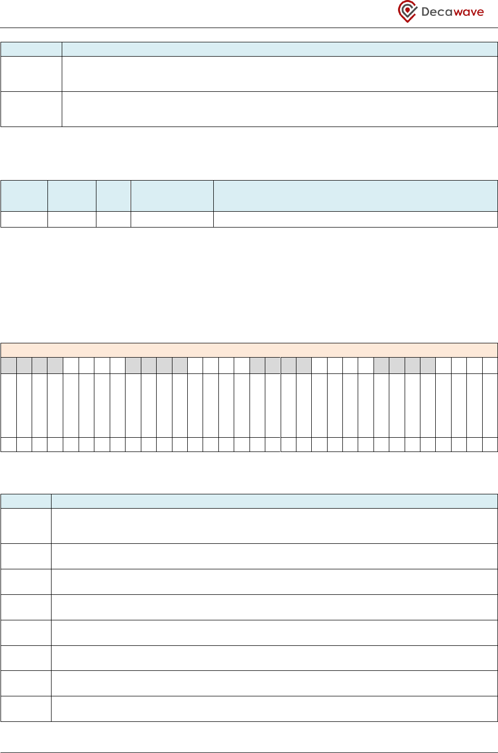
DW1000 User Manual
© Decawave Ltd 2017
Version 2.15
Page 137 of 244
Field
Description of fields within Sub-Register 0x26:14 – GPIO_ISEN
GISEN8
reg:26:14
bit:8
GPIO IRQ sense for GPIO8 input. Value 0 = High or Rising-Edge, 1 = Low or falling-edge.
-
reg:26:14
bits:31–9
Bits marked ‘-’ are reserved and should be written as zero.
7.2.39.7 Sub-Register 0x26:18 – GPIO_IMODE
ID
Length
(octets)
Type
Mnemonic
Description
26:18
4
RW
GPIO_IMODE
GPIO Interrupt Mode (Level/Edge)
Register file: 0x26 – GPIO control and status, sub-register 0x18 is the GPIO interrupt mode selection register.
Assuming that the GPIO is an input and enabled as an interrupt via the GPIO_IRQE register, then this
GPIO_IMODE register acts to select whether the interrupt is level sensitive or edge triggered. The
GPIO_IMODE register contains a bit for each GPIO pin to allow each to be individually configured. The bits
are as follows:
REG:26:18 – GPIO_IMODE – GPIO Interrupt Mode selection register
31
30
29
28
27
26
25
24
23
22
21
20
19
18
17
16
15
14
13
12
11
10
9
8
7
6
5
4
3
2
1
0
-
-
-
-
-
-
-
-
-
-
-
-
-
-
-
-
-
-
-
-
-
-
-
GIMOD8
GIMOD7
GIMOD6
GIMOD5
GIMOD4
GIMOD3
GIMOD2
GIMOD1
GIMOD0
0
0
0
0
0
0
0
0
0
0
0
0
0
0
0
0
0
0
0
0
0
0
0
0
0
0
0
0
0
0
0
0
The bits of the GPIO_IMODE register identified above are individually described below:
Field
Description of fields within Sub-Register 0x26:18 – GPIO_IMODE
GIMOD0
reg:26:18
bit:0
GPIO IRQ Mode selection for GPIO0 input. Value 0 = Level sensitive interrupt. Value 1 = Edge
triggered interrupt.
GIMOD1
bit:1
GPIO IRQ Mode selection for GPIO1 input. Value 0 = Level, 1 = Edge.
GIMOD2
bit:2
GPIO IRQ Mode selection for GPIO2 input. Value 0 = Level, 1 = Edge.
GIMOD3
bit:3
GPIO IRQ Mode selection for GPIO3 input. Value 0 = Level, 1 = Edge.
GIMOD4
bit:4
GPIO IRQ Mode selection for GPIO4 input. Value 0 = Level, 1 = Edge.
GIMOD5
bit:5
GPIO IRQ Mode selection for GPIO5 input. Value 0 = Level, 1 = Edge.
GIMOD6
bit:6
GPIO IRQ Mode selection for GPIO6 input. Value 0 = Level, 1 = Edge.
GIMOD7
bit:7
GPIO IRQ Mode selection for GPIO7 input. Value 0 = Level, 1 = Edge.
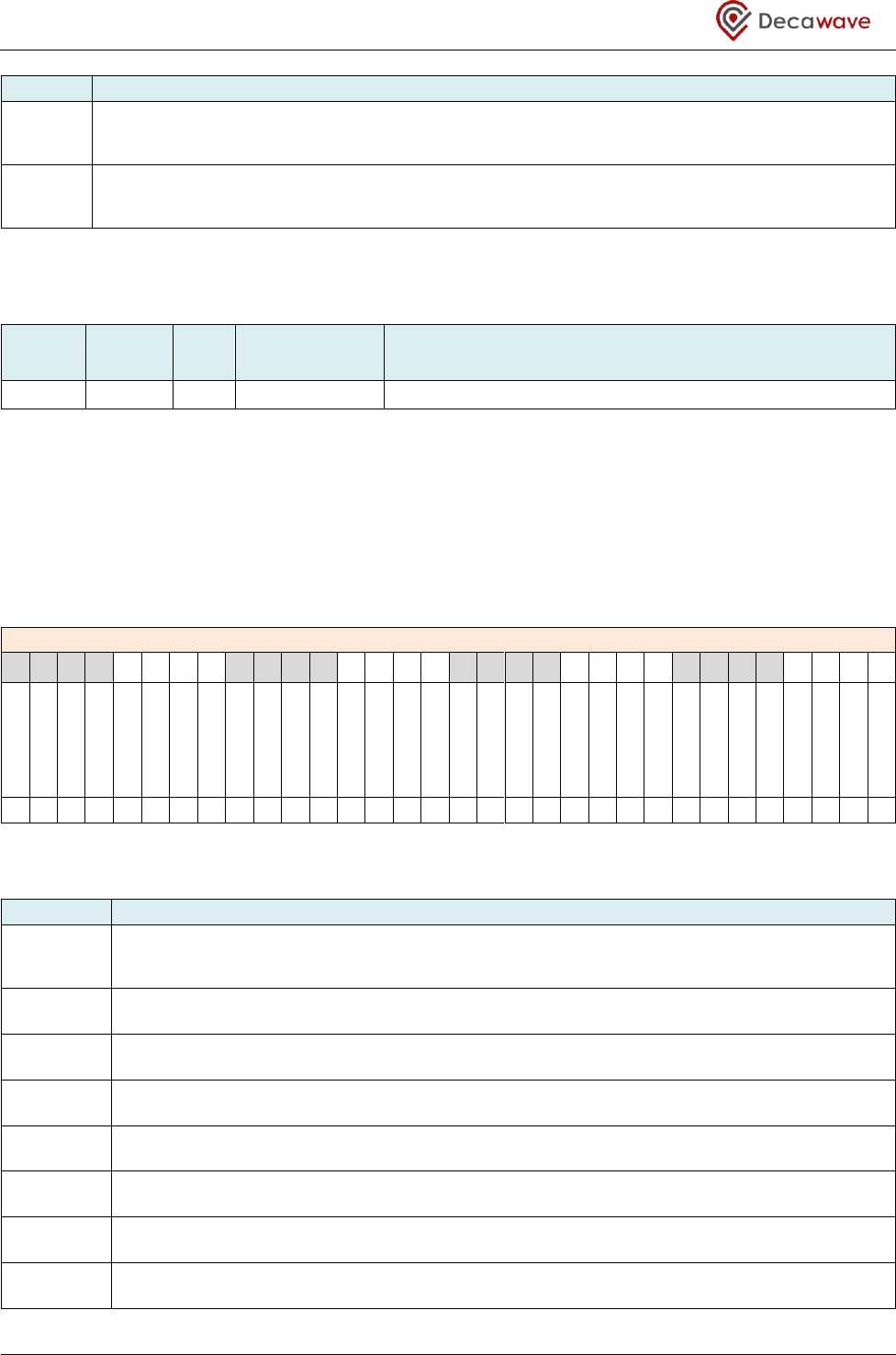
DW1000 User Manual
© Decawave Ltd 2017
Version 2.15
Page 138 of 244
Field
Description of fields within Sub-Register 0x26:18 – GPIO_IMODE
GIMOD8
reg:26:18
bit:8
GPIO IRQ Mode selection for GPIO8 input. Value 0 = Level, 1 = Edge.
-
reg:26:18
bits:31–9
Bits marked ‘-’ are reserved and should be written as zero.
7.2.39.8 Sub-Register 0x26:1C – GPIO_IBES
ID
Length
(octets)
Type
Mnemonic
Description
26:1C
4
RW
GPIO_IBES
GPIO Interrupt “Both Edge” Select
Register file: 0x26 – GPIO control and status, sub-register 0x1C is the GPIO interrupt “Both Edge” selection
register. This only applies when edge sensitive interrupts are enabled in the GPIO_IMODE register. In this
case the GPIO_ISEN register normally acts to select which edge triggers the interrupt. This GPIO_IBES
register overrides the GPIO_ISEN register to select both edges as which edge triggers the interrupt. The
GPIO_IBES register contains a bit for each GPIO pin to allow each to be individually configured. The bits are
as follows:
REG:26:1C – GPIO_IBES – GPIO Interrupt “Both Edge” selection register
31
30
29
28
27
26
25
24
23
22
21
20
19
18
17
16
15
14
13
12
11
10
9
8
7
6
5
4
3
2
1
0
-
-
-
-
-
-
-
-
-
-
-
-
-
-
-
-
-
-
-
-
-
-
-
GIBES8
GIBES7
GIBES6
GIBES5
GIBES4
GIBES3
GIBES2
GIBES1
GIBES0
0
0
0
0
0
0
0
0
0
0
0
0
0
0
0
0
0
0
0
0
0
0
0
0
0
0
0
0
0
0
0
0
The bits of the GPIO_IBES register identified above are individually described below:
Field
Description of fields within Sub-Register 0x26:1C – GPIO_IBES
GIBES0
reg:26:1C
bit:0
GPIO IRQ “Both Edge” selection for GPIO0 input. Value 0 = GPIO_IMODE register selects the
edge. Value 1 = Both edges trigger the interrupt.
GIBES1
bit:1
GPIO IRQ “Both Edge” selection for GPIO1 input. Value 0 = use GPIO_IMODE, 1 = Both Edges.
GIBES2
bit:2
GPIO IRQ “Both Edge” selection for GPIO2 input. Value 0 = use GPIO_IMODE, 1 = Both Edges.
GIBES3
bit:3
GPIO IRQ “Both Edge” selection for GPIO3 input. Value 0 = use GPIO_IMODE, 1 = Both Edges.
GIBES4
bit:4
GPIO IRQ “Both Edge” selection for GPIO4 input. Value 0 = use GPIO_IMODE, 1 = Both Edges.
GIBES5
bit:5
GPIO IRQ “Both Edge” selection for GPIO5 input. Value 0 = use GPIO_IMODE, 1 = Both Edges.
GIBES6
bit:6
GPIO IRQ “Both Edge” selection for GPIO6 input. Value 0 = use GPIO_IMODE, 1 = Both Edges.
GIBES7
bit:7
GPIO IRQ “Both Edge” selection for GPIO7 input. Value 0 = use GPIO_IMODE, 1 = Both Edges.
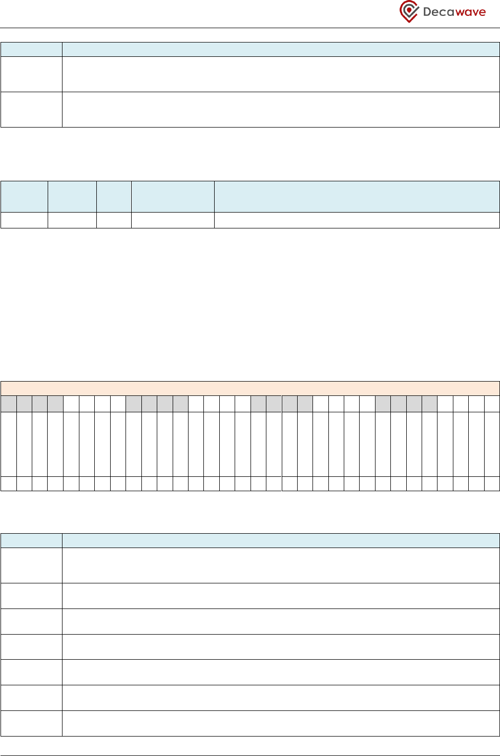
DW1000 User Manual
© Decawave Ltd 2017
Version 2.15
Page 139 of 244
Field
Description of fields within Sub-Register 0x26:1C – GPIO_IBES
GIBES8
reg:26:1C
bit:8
GPIO IRQ “Both Edge” selection for GPIO8 input. Value 0 = use GPIO_IMODE, 1 = Both Edges.
-
reg:26:1C
bits:31–9
Bits marked ‘-’ are reserved and should be written as zero.
7.2.39.9 Sub-Register 0x26:20 – GPIO_ICLR
ID
Length
(octets)
Type
Mnemonic
Description
26:20
4
RW
GPIO_ICLR
GPIO Interrupt Latch Clear
Register file: 0x26 – GPIO control and status, sub-register 0x20 is the GPIO interrupt clear register. When a
GPIO interrupt occurs that meets the configured criteria (edge/level etc.) that event is latched in an internal
interrupt latch. To clear the interrupt the host needs to write a 1 to the appropriate bit of this GPIO_ICLR
register. There is no way to read the interrupt latch, which means that only one GPIO can be enabled to
interrupt at a time, unless the host has some other external way to distinguish events. Although level
sensitive interrupts are latched, if the active level persists, then clearing the latch will be ineffective, since
the interrupt will occur again immediately. The GPIO_ICLR register contains a bit for each GPIO pin as
follows:
REG:26:20 – GPIO_ICLR – GPIO Interrupt latch clear
31
30
29
28
27
26
25
24
23
22
21
20
19
18
17
16
15
14
13
12
11
10
9
8
7
6
5
4
3
2
1
0
-
-
-
-
-
-
-
-
-
-
-
-
-
-
-
-
-
-
-
-
-
-
-
GICLR8
GICLR7
GICLR6
GICLR5
GICLR4
GICLR3
GICLR2
GICLR1
GICLR0
-
-
-
-
-
-
-
-
-
-
-
-
-
-
-
-
0
0
0
0
0
0
0
0
0
0
0
0
0
0
0
0
The bits of the GPIO_ICLR register identified above are individually described below:
Field
Description of fields within Sub-Register 0x26:20 – GPIO_ICLR
GICLR0
reg:26:20
bit:0
GPIO IRQ latch clear for GPIO0 input. Write 1 to clear the GPIO0 interrupt latch. Writing 0
has no effect. Reading returns zero.
GICLR1
bit:1
GPIO IRQ latch clear for GPIO1 input. Write 1 to clear the interrupt latch.
GICLR2
bit:2
GPIO IRQ latch clear for GPIO2 input. Write 1 to clear the interrupt latch.
GICLR3
bit:3
GPIO IRQ latch clear for GPIO3 input. Write 1 to clear the interrupt latch.
GICLR4
bit:4
GPIO IRQ latch clear for GPIO4 input. Write 1 to clear the interrupt latch.
GICLR5
bit:5
GPIO IRQ latch clear for GPIO5 input. Write 1 to clear the interrupt latch.
GICLR6
bit:6
GPIO IRQ latch clear for GPIO6 input. Write 1 to clear the interrupt latch.
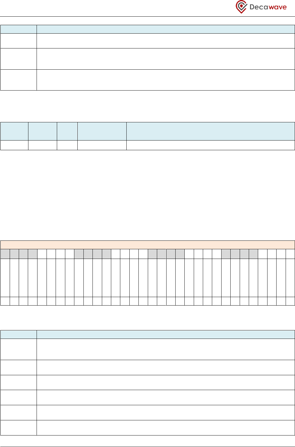
DW1000 User Manual
© Decawave Ltd 2017
Version 2.15
Page 140 of 244
Field
Description of fields within Sub-Register 0x26:20 – GPIO_ICLR
GICLR7
bit:7
GPIO IRQ latch clear for GPIO7 input. Write 1 to clear the interrupt latch.
GICLR8
reg:26:20
bit:8
GPIO IRQ latch clear for GPIO8 input. Write 1 to clear the interrupt latch.
-
reg:26:20
bits:31–9
Bits marked ‘-’ are reserved and should be written as zero.
7.2.39.10 Sub-Register 0x26:24 – GPIO_IDBE
ID
Length
(octets)
Type
Mnemonic
Description
26:24
4
RW
GPIO_IDBE
GPIO Interrupt De-bounce Enable
Register file: 0x26 – GPIO control and status, sub-register 0x24 is the GPIO interrupt de-bounce enable
register. The GPIO_IDBE controls a filtering function that operates on the GPIO inputs prior to their
presentation into the GPIO interrupt logic. This de-bounce filter circuit removes short transients by using the
kilohertz clock (as enabled by the KHZCLKEN bit in Sub-Register 0x36:00 – PMSC_CTRL0) to sample the input
signal. See KHZCLKDIV in Sub-Register 0x36:04 – PMSC_CTRL1 for a description of the kilohertz clock. The
de-bounce filter is active when a state change of the GPIO input needs to persist for two cycles of this clock
before it will be seen by the interrupt handling logic. The GPIO_IDBE register contains a bit for each GPIO
pin as follows:
REG:26:24 – GPIO_IDBE – GPIO Interrupt De-Bounce Enable
31
30
29
28
27
26
25
24
23
22
21
20
19
18
17
16
15
14
13
12
11
10
9
8
7
6
5
4
3
2
1
0
-
-
-
-
-
-
-
-
-
-
-
-
-
-
-
-
-
-
-
-
-
-
-
GIDBE8
GIDBE7
GIDBE6
GIDBE5
GIDBE4
GIDBE3
GIDBE2
GIDBE1
GIDBE0
-
-
-
-
-
-
-
-
-
-
-
-
-
-
-
-
0
0
0
0
0
0
0
0
0
0
0
0
0
0
0
0
The bits of the GPIO_IDBE register identified above are individually described below:
Field
Description of fields within Sub-Register 0x26:24 – GPIO_IDBE
GIDBE0
reg:26:24
bit:0
GPIO IRQ de-bounce enable for GPIO0. Value 1 = de-bounce enabled. Value 0 = de-bounce
disabled.
GIDBE1
bit:1
GPIO1 IRQ de-bounce configuration. Value 1 = de-bounce enabled, 0 = de-bounce disabled.
GIDBE2
bit:2
GPIO2 IRQ de-bounce configuration. Value 1 = de-bounce enabled, 0 = de-bounce disabled.
GIDBE3
bit:3
GPIO3 IRQ de-bounce configuration. Value 1 = de-bounce enabled, 0 = de-bounce disabled.
GIDBE4
bit:4
GPIO4 IRQ de-bounce configuration. Value 1 = de-bounce enabled, 0 = de-bounce disabled.
GIDBE5
bit:5
GPIO5 IRQ de-bounce configuration. Value 1 = de-bounce enabled, 0 = de-bounce disabled.
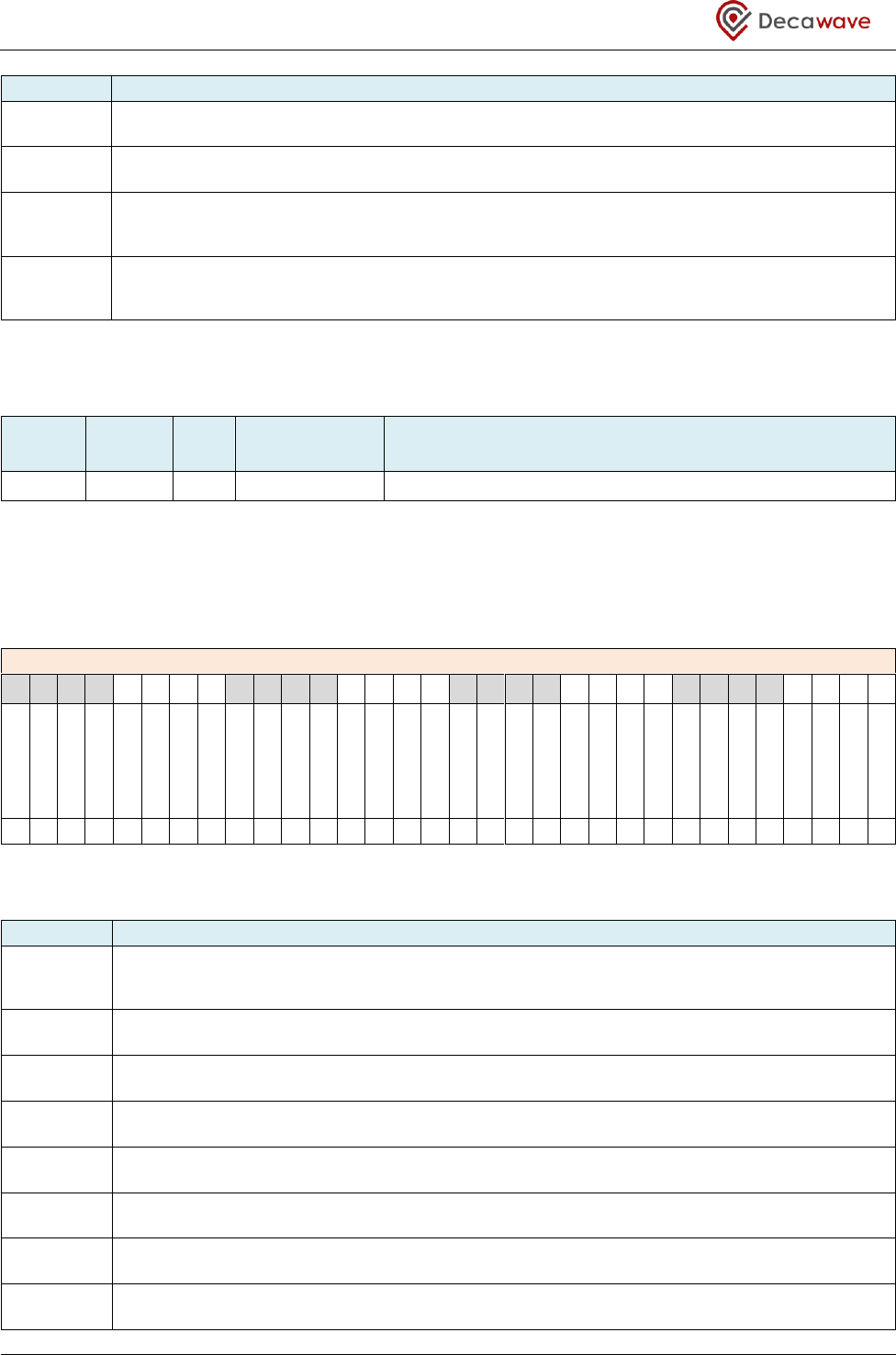
DW1000 User Manual
© Decawave Ltd 2017
Version 2.15
Page 141 of 244
Field
Description of fields within Sub-Register 0x26:24 – GPIO_IDBE
GIDBE6
bit:6
GPIO6 IRQ de-bounce configuration. Value 1 = de-bounce enabled, 0 = de-bounce disabled.
GIDBE7
bit:7
GPIO7 IRQ de-bounce configuration. Value 1 = de-bounce enabled, 0 = de-bounce disabled.
GIDBE8
reg:26:24
bit:8
GPIO8 IRQ de-bounce configuration. Value 1 = de-bounce enabled, 0 = de-bounce disabled.
-
reg:26:24
bits:31–9
Bits marked ‘-’ are reserved and should be written as zero.
7.2.39.11 Sub-Register 0x26:28 – GPIO_RAW
ID
Length
(octets)
Type
Mnemonic
Description
26:28
4
RO
GPIO_RAW
GPIO raw state
Register file: 0x26 – GPIO control and status, sub-register 0x28 allows the raw state of the GPIO pin to be
read. The GPIO_RAW register contains a bit for each GPIO pin as follows:
REG:26:28 – GPIO_RAW – GPIO raw state
31
30
29
28
27
26
25
24
23
22
21
20
19
18
17
16
15
14
13
12
11
10
9
8
7
6
5
4
3
2
1
0
-
-
-
-
-
-
-
-
-
-
-
-
-
-
-
-
-
-
-
-
-
-
-
GRAWP8
GRAWP7
GRAWP6
GRAWP5
GRAWP4
GRAWP3
GRAWP2
GRAWP1
GRAWP0
-
-
-
-
-
-
-
-
-
-
-
-
-
-
-
-
-
-
-
-
-
-
-
0
0
0
0
0
0
0
0
0
The bits of the GPIO_RAW register identified above are individually described below:
Field
Description of fields within Sub-Register 0x26:28 – GPIO_RAW
GRAWP0
reg:26:28
bit:0
This bit reflects the raw state of GPIO0.
GRAWP1
bit:1
GPIO1 port raw state.
GRAWP2
bit:2
GPIO2 port raw state.
GRAWP3
bit:3
GPIO3 port raw state.
GRAWP4
bit:4
GPIO4 port raw state.
GRAWP5
bit:5
GPIO5 port raw state.
GRAWP6
bit:6
GPIO6 port raw state.
GRAWP7
bit:7
GPIO7 port raw state.
DW1000 User Manual
© Decawave Ltd 2017
Version 2.15
Page 142 of 244
Field
Description of fields within Sub-Register 0x26:28 – GPIO_RAW
GRAWP8
reg:26:28
bit:8
GPIO8 port raw state.
-
reg:26:28
bits:31–9
Bits marked ‘-’ are reserved and should be written as zero.
7.2.40 Register file: 0x27 – Digital receiver configuration
ID
Length
(octets)
Type
Mnemonic
Description
0x27
-
-
DRX_CONF
Digital Receiver Configuration
Register map register file 0x27 is concerned with the low-level digital receiver configuration. It contains a
number of sub-registers. An overview of these is given by Table 29. Each of these sub-registers is separately
described in the sub-sections below.
Table 29: Register file: 0x27 – Digital receiver configuration overview
OFFSET in Register 0x27
Mnemonic
Description
0x02
DRX_TUNE0b
Digital Tuning Register 0b
0x04
DRX_TUNE1a
Digital Tuning Register 1a
0x06
DRX_TUNE1b
Digital Tuning Register 1b
0x08
DRX_TUNE2
Digital Tuning Register 2
0x20
DRX_SFDTOC
SFD timeout
0x24
DRX_PRETOC
Preamble detection timeout
0x26
DRX_TUNE4H
Digital Tuning Register 4H
0x28
DRX_CAR_INT
Carrier Recovery Integrator Register
0X2C
RXPACC_NOSAT
Unsaturated accumulated preamble symbols
7.2.40.1 Sub-Register 0x27:00 – DRX_RES1
ID
Length
(octets)
Type
Mnemonic
Description
27:00
2
-
-
Reserved
Register file: 0x27 – Digital receiver configuration, sub-register 0x00 is a reserved area. Please take care not
to write to this register as doing so may cause the DW1000 to malfunction.
7.2.40.2 Sub-Register 0x27:02 – DRX_TUNE0b
ID
Length
(octets)
Type
Mnemonic
Description
27:02
2
RW
DRX_TUNE0b
Digital Tuning Register 0b

DW1000 User Manual
© Decawave Ltd 2017
Version 2.15
Page 143 of 244
Register file: 0x27 – Digital receiver configuration, sub-register 0x02 is a 16-bit tuning register. For optimal
performance the value here needs to change depending on the data rate and depending on whether the SFD
sequence is configured to be the IEEE 802.15.4 UWB standard compliant SFD sequence, or the higher
performing non-standard SFD configuration. The values needed are given in Table 30 below. Please take
care not to write other values to this register as doing so may cause the DW1000 to malfunction.
Table 30: Sub-Register 0x27:02 – DRX_TUNE0b values
Data Rate
SFD configuration
Value to program to
Sub-Register 0x27:02 –
DRX_TUNE0b
110 kbps
Standard SFD
0x000A
Non-Standard SFD
0x0016
850 kbps
Standard SFD
0x0001
Non-Standard SFD
0x0006
6.8 Mbps
Standard SFD
0x0001
Non-Standard SFD
0x0002
Note: Please refer to Table 21: Recommended SFD sequence configurations for best performance
Data
Rate
DWSFD
reg:1F:00
bit:17
TNSSFD
reg:1F:00
bit:20
RNSSFD
reg:1F:00
bit:21
SFD_LENGTH
reg:21:00
bits:0–7
Description
6.8 Mbps
0
0
0
x
When the DW1000 is operating at 6.8 Mbps,
this programming selects the standard IEEE 8-
symbol SFD which gives sufficient robustness
since the data is already the weakest part of the
frame.
850 kbps
1
1
1
16
The standard IEEE 8-symbol SFD is weaker than
data at 850 kbps. When the DW1000 is
operating at 850 kbps, this programming selects
a Decawave defined non-standard 16-symbol
SFD, which removes the weakness making the
SFD stronger than the 850 kbps data.
110 kbps
1
0
0
x
This programming selects a Decawave defined
non-standard 64-symbol SFD which is more
robust than standard IEEE 64-symbol SFD
improving the performance in 110 kbps mode.
Table 22 below presents additional SFD sequence programming options. Note: The selection of SFD
sequences other than the IEEE 802.15.4-2011 UWB standard compliant SFD sequence may improve
performance, but will of course make it impossible to interwork with a device configured to use the standard
defined SFD (or with a third party devices using the standard SFD).

DW1000 User Manual
© Decawave Ltd 2017
Version 2.15
Page 144 of 244
Table 22: Other possible SFD sequence configurations
Data
Rate
DWSFD
reg:1F:00
bit:17
TNSSFD
reg:1F:00
bit:20
RNSSFD
reg:1F:00
bit:21
SFD_LENGTH
reg:21:00
bits:0–7
Description
850 kbps
0
0
0
x
This programming selects the 8-symbol SFD as
defined in the IEEE 802.15.4 standard, when
operating at 850 kbps.
110 kbps
0
0
0
x
This programming selects the 64-symbol SFD as
defined in the IEEE 802.15.4 standard, when
operating at 110 kbps.
850 kbps
1
0
0
x
When the DW1000 is operating at 850 kbps,
this programming selects a Decawave defined
non-standard 8-symbol SFD, which is stronger
than the standard defined SFD but still a little
weaker that the data. Hence our
recommendation of the 16-symbol SFD defined
Table 21 for best performance at 850 kbps.
6.8 Mbps
or
850 kbps
0
1
1
8 to 16
When the DW1000 is operating at 6.8 Mbps or
850 kbps, this programming selects the use of a
user configured SFD with length configurable in
the range 8 to 16 symbols. In this mode the
user is responsible for correctly programming
the SFD sequence in Register file: 0x21 – User
defined SFD sequence.
110 kbps
0
1
1
x
When the DW1000 is operating at 110 kbps,
this selects the use of a user configured SFD
with fixed length of 64 symbols. In this mode
the user is responsible for correctly
programming the SFD sequence in Register file:
0x21 – User defined SFD sequence.
Note: Configurations other than those defined in Table 21 or Table 22 are not recommended. To correctly
receive a frame the receiver must use the same SFD sequence configuration as is being used by the remote
transmitting device.
For details of the optimum selection of SFD sequence.
DW1000 User Manual
© Decawave Ltd 2017
Version 2.15
Page 145 of 244
7.2.40.3 Sub-Register 0x27:04 – DRX_TUNE1a
ID
Length
(octets)
Type
Mnemonic
Description
27:04
2
RW
DRX_TUNE1a
Digital Tuning Register 1a
Register file: 0x27 – Digital receiver configuration, sub-register 0x04 is a 16-bit tuning register. The value
here needs to change depending on the RXPRF configuration. The values needed are given in Table 31
below. Please take care not to write other values to this register as doing so may cause the DW1000 to
malfunction.
Table 31: Sub-Register 0x27:04 – DRX_TUNE1avalues
RXPRF configuration
Value to program to
Sub-Register 0x27:04 –
DRX_TUNE1a
(1) = 16 MHz PRF
0x0087
(2) = 64 MHz PRF
0x008D
7.2.40.4 Sub-Register 0x27:06 – DRX_TUNE1b
ID
Length
(octets)
Type
Mnemonic
Description
27:06
2
RW
DRX_TUNE1b
Digital Tuning Register 1b
Register file: 0x27 – Digital receiver configuration, sub-register 0x06 is a 16-bit tuning register. The value
here needs to change depending on use case. The values needed are given in Table 32 below. Please take
care not to write other values to this register as doing so may cause the DW1000 to malfunction.
Table 32: Sub-Register 0x27:06 – DRX_TUNE1b values
Use case
Value to program to
Sub-Register 0x27:06 –
DRX_TUNE1b
Preamble lengths > 1024 symbols, for
110 kbps operation
0x0064
Preamble lengths 128 to 1024 symbols,
for 850 kbps and 6.8 Mbps operation
0x0020
Preamble length = 64 symbols, for
6.8 Mbps operation
0x0010
DW1000 User Manual
© Decawave Ltd 2017
Version 2.15
Page 146 of 244
7.2.40.5 Sub-Register 0x27:08 – DRX_TUNE2
ID
Length
(octets)
Type
Mnemonic
Description
27:08
4
RW
DRX_TUNE2
Digital Tuning Register 2
Register file: 0x27 – Digital receiver configuration, sub-register 0x08 is a tuning register. The value here
needs to change depending on a number of parameters. The values needed are given in Table 33 below.
Please take care not to write other values to this register as doing so may cause the DW1000 to malfunction.
Table 33: Sub-Register 0x27:08 – DRX_TUNE2values
PAC size
(selected here)
RXPRF configuration
Value to program to
Sub-Register 0x27:08 –
DRX_TUNE2
8
16 MHz PRF
0x311A002D
64 MHz PRF
0x313B006B
16
16 MHz PRF
0x331A0052
64 MHz PRF
0x333B00BE
32
16 MHz PRF
0x351A009A
64 MHz PRF
0x353B015E
64
16 MHz PRF
0x371A011D
64 MHz PRF
0x373B0296
Note: This is selecting the PAC size, (via bits 26 & 25 of the values in Table 33).
The PAC size should be selected depending on the expected preamble length in the receiver. For details of
PAC size and its role please refer to section 4.1.1 – Preamble Detection where Table 6 gives the recommend
PAC size configuration for each preamble length.
7.2.40.6 Sub-Register 0x27:0C – DRX_RES2
ID
Length
(octets)
Type
Mnemonic
Description
27:0C
20
-
-
Reserved
Register file: 0x27 – Digital receiver configuration, from offset 0x0C to offset 0x1F inclusive is a reserved
area. Please take care not to write to this area as doing so may cause the DW1000 to malfunction.
DW1000 User Manual
© Decawave Ltd 2017
Version 2.15
Page 147 of 244
7.2.40.7 Sub-Register 0x27:20 – DRX_SFDTOC
ID
Length
(octets)
Type
Mnemonic
Description
27:20
2
RW
DRX_SFDTOC
SFD detection timeout count
Register file: 0x27 – Digital receiver configuration, sub-register 0x20 is used to set the 16-bit SFD detection
timeout counter period, in units of preamble symbols. The SFD detection timeout starts running as soon as
preamble is detected. If the SFD sequence is not detected before the timeout period expires then the
timeout will act to abort the reception currently in progress, and set RXSFDTO event status bit in Register
file: 0x0F – System Event Status Register. SFD timeout events are also counted in Sub-Register 0x2F:10 – SFD
Timeout Error Counter, assuming that counting is enabled by the EVC_EN bit in Sub-Register 0x2F:00 – Event
Counter Control.
The purpose of the SFD detection timeout is to recover from the occasional false preamble detection events
that occur. By default this value is 4096+64+1 symbols, which is just longer the longest possible preamble
and SFD sequence. This is the maximum value that is sensible. When it is known that a shorter preamble is
being used then the DRX_SFDTOC value can be reduced appropriately. It is also recommended to further
reduce the DRX_SFDTOC value by the PAC size as one PAC size of the preamble length will be lost as part of
the preamble detection.
WARNING: Please do NOT set DRX_SFDTOC to zero (disabling SFD detection timeout). With the SFD
timeout disabled and in the event of false preamble detection, the IC will remain in receive mode until
commanded to do otherwise by the external microcontroller. This can lead to significant reduction in
battery life.
7.2.40.8 Sub-Register 0x27:22 – DRX_RES3
ID
Length
(octets)
Type
Mnemonic
Description
27:22
2
-
-
Reserved
Register file: 0x27 – Digital receiver configuration, sub-register 0x22 is a reserved area. Please take care not
to write to this register as doing so may cause the DW1000 to malfunction.
7.2.40.9 Sub-Register 0x27:24 – DRX_PRETOC
ID
Length
(octets)
Type
Mnemonic
Description
27:24
2
RW
DRX_PRETOC
Preamble detection timeout count
Register file: 0x27 – Digital receiver configuration, sub-register 0x24 is used to set the 16-bit preamble
detection timeout period, in units of PAC size symbols. The default/reset value is zero which disables the
preamble detection timeout. The preamble detection timeout starts running as soon as the receiver is
enabled to hunt for preamble. In the case of delayed receive (as commanded using the RXDLYE control in
Register file: 0x0D – System Control Register) the preamble detection timeout starts after the delay when the
receiver actually turns on to hunt for preamble. If a preamble sequence in not detected before the timeout
DW1000 User Manual
© Decawave Ltd 2017
Version 2.15
Page 148 of 244
period expires then the timeout will act to abort the reception currently in progress, and set the RXPTO
event status bit in Register file: 0x0F – System Event Status Register.
In cases where a response is expected at a particular time, this timeout can be used to flag that the expected
response is not starting on time and hence to turn off the receiver earlier than would otherwise be the case,
(i.e. if just employing the frame wait timeout). This can give a good power saving, in situations of sending a
message and awaiting a response that often does not come.
The DRX_PRETOC is programmed in units of PAC size, which can be 8, 16, 32 or 64 symbols. Table 60 gives
the preamble symbol lengths. The PAC size is set in Sub-Register 0x27:08 – DRX_TUNE2. As this is a 16-bit
counter the maximum preamble detection timeout possible is 65535 × (PAC size), a period of over 500 ms
for the smallest PAC size. A value of zero disables the preamble detection timeout.
Example: Supposing our preamble length is 1024 symbols and the PAC size is set to 32 (in line with Table 6)
and, we send a message and know that the response (if present) will come after exactly 30 ms (because the
responder is using delayed send to begin the response exactly 30 ms after receiving our message). We can
command a 30 ms delayed receive (timed from our message transmission time) and have DRX_PRETOC
programmed to a value of 32, which is the preamble length (1024) divided by the PAC size (32).
Note that the counter automatically adds 1 to the programmed value so DRX_PRETOC should be
programmed to be 1 less than the desired value.
7.2.40.10 Sub-Register 0x27:26 – DRX_TUNE4H
ID
Length
(octets)
Type
Mnemonic
Description
27:26
2
RW
DRX_TUNE4H
Digital Tuning Register
Register file: 0x27 – Digital receiver configuration, sub-register 0x26 is a 16-bit tuning register. The value
here needs to change depending on the preamble length expected by the receiver. The values required are
given in Table 34. Please take care not to write other values to this register as doing so may cause the
DW1000 to malfunction.
Table 34: Register 0x27:26 DRX_TUNE4H values
Expected Receive Preamble
Length in Symbols
Value to program to
Sub-Register 0x27:26 –
DRX_TUNE4H
64
0x0010
128 or greater
0x0028
7.2.40.11 Sub-Register 0x27:28 – DRX_CAR_INT
ID
Length
(octets)
Type
Mnemonic
Description
27:28
3
RO
DRX_CAR_INT
Carrier Recovery Integrator Register
DW1000 User Manual
© Decawave Ltd 2017
Version 2.15
Page 149 of 244
Register file: 0x27 – Digital receiver configuration, sub-register 0x28 is a read-only 21 bit register.
The DW1000 receiver needs to compensate for frequency offsets between the timing references at the
transmitting device and itself to successfully receive a packet. Therefore, when a packet is successfully
received, the DW1000 has a sufficiently accurate estimate of the frequency offset.
This information is available in the carrier recovery integrator register, at address 0x27, offset 0x28. This is a
21 bit number with the lower 17 bits, the fractional part, and the upper 4 bits as the integer portion of the
number.
When a packet is successfully received, this register can be read and converted to the frequency error (in Hz)
using
Foffset is the absolute frequency error in Hz. It can be converted to a clock offset (in ppm) by scaling by the
carrier frequency as follows
The minus sign is produced by the process of measuring the clock offset.
For a particular channel, the formulas reduce to multiplying the content of the carrier integrator register
with the appropriate constant from the table below:
Table 35: Constants for frequency offset calculation
Data Rate
Channel 2
Channel 3
Channel 5
850 kb/s, 6.81 Mb/s
-0.9313e-3
-0.8278e-3
-0.5731e-3
110 kb/s
-0.1164e-3
-0.1035e-3
-0.0716e-3
7.2.40.12 Sub-Register 0x27:2C – RXPACC_NOSAT
ID
Length
(octets)
Type
Mnemonic
Description
27:2C
2
RO
RXPACC_NOSAT
Digital debug register. Unsaturated accumulated preamble
symbols.
DW1000 User Manual
© Decawave Ltd 2017
Version 2.15
Page 150 of 244
Register file: 0x27 – Digital receiver configuration, sub-register 0x2C is a read-only debug value containing a
count of accumulated preamble symbols without saturation. Note that the accumulated SFD symbols minus
two (two SFD symbols are always ignored in the receiver) are also included.
7.2.41 Register file: 0x28 – Analog RF configuration block
ID
Length
(octets)
Type
Mnemonic
Description
0x28
-
-
RF_CONF
Analog RF Configuration
Register map register file 0x28 is concerned with the low-level configuration of the IC analog blocks. It
contains a number of sub-registers. An overview of these is given by Table 36. Each of these sub-registers is
separately described in the sub-sections below.
Table 36: Register file: 0x28 – Analog RF configuration block overview
OFFSET in Register 0x28
Mnemonic
Description
0x00
RF_CONF
RF Configuration Register
0x04
RF_RES1
Reserved area 1
0x0B
RF_RXCTRLH
Analog RX Control Register
0x0C
RF_TXCTRL
Analog TX Control Register
0x10
RF_RES2
Reserved area 2
0x2C
RF_STATUS
RF Status Register
0x30
LDOTUNE
LDO voltage tuning
7.2.41.1 Sub-Register 0x28:00 – RF_CONF
ID
Length
(octets)
Type
Mnemonic
Description
28:00
4
RW
RF_CONF
RF Configuration Register
Register file: 0x28 – Analog RF configuration block, sub-register 0x00 is a 32-bit configuration register for the
transceiver. Please take care not to write other values to the reserved area of this register as doing so may
cause the DW1000 to malfunction.
Note that calibration programming steps may require writes to this register.
REG:28:00 – RF_CONF – RF Configuration Register
31
30
29
28
27
26
25
24
23
22
21
20
19
18
17
16
15
14
13
12
11
10
9
8
7
6
5
4
3
2
1
0
-
TXRXSW
LDOFEN
PLLFEN
TXFEN
-
0
0
0
0
0
0
0
0
0
0
0
0
0
0
0
0
0
0
0
0
0
0
0
0
0
0
0
0
0
0
0
0
DW1000 User Manual
© Decawave Ltd 2017
Version 2.15
Page 151 of 244
7.2.41.2 Sub-Register 0x28:00 – RF_CONF
Field
Description of fields within
Sub-Register 0x28:00 – RF_CONF
Reserved
reg:28:00
bits:31:23,7:0
These fields are reserved, and should not be set to 1 (may be overwritten with 0).
TXFEN
reg:28:00
bits:12:8
Transmit block force enable. Write 0x1F to force all TX blocks on. Enabling this field will
be used for certain test and calibration modes where we want to force the transmitter on
when there are not packets being TX’d (i.e. Continuous Wave mode).
PLLFEN
reg:28:00
bits:15:13
PLL block force enables. Write 0x5 to enable the CLK_PLL or 0x7 to enable both the
CLK_PLL and RF PLL. Enabling this field will be used for certain test and calibration modes
where we want to force the PLLs on when there are not packets being TX’d (i.e.
Continuous Wave mode).
LDOFEN
reg:28:00
bits:20:16
Write 0x1F to force the enable to all LDO’s. Enabling this field will be used for certain test
and calibration modes where we want to force the LDOs on when there are not packets
being TX’d (i.e. Continuous Wave mode).
TXRXSW
reg:28:00
bits:22:21
Force the TX/RX switch. To configure for TX the value written should be set to 0x2, and to
configure for RX the value should be set to 0x1.
7.2.41.3 Sub-Register Manual TX Power Control – RF_RES1
ID
Length
(octets)
Type
Mnemonic
Description
28:04
7
RW
RF_RES1
Reserved area 1
Register file: 0x28 – Analog RF configuration block, sub-register 0x04 is a reserved register. Please take care
not to write to this register as doing so may cause the DW1000 to malfunction.
7.2.41.4 Sub-Register 0x28:0B– RF_RXCTRLH
ID
Length
(octets)
Type
Mnemonic
Description
28:0B
1
RW
RF_RXCTRLH
Analog RX Control Register
Register file: 0x28 – Analog RF configuration block, sub-register 0x0B is an 8-bitcontrol register for the
receiver. The value here needs to be set depending on the RX channel selected by the RX_CHAN
configuration in Register file: 0x1F – Channel Control. The values required are given in Table 37. Please take
care not to write other values to this register as doing so may cause the DW1000 to malfunction.
DW1000 User Manual
© Decawave Ltd 2017
Version 2.15
Page 152 of 244
Table 37: Sub-Register 0x28:0B– RF_RXCTRLH values
RX Channel
8-bit value to program to
Sub-Register 0x28:0B–
RF_RXCTRLH
1, 2, 3, or 5
0xD8
4 or 7
0xBC
7.2.41.5 Sub-Register 0x28:0C– RF_TXCTRL
ID
Length
(octets)
Type
Mnemonic
Description
28:0C
3
RW
RF_TXCTRL
Analog TX Control Register
Register file: 0x28 – Analog RF configuration block, sub-register 0x0C is a 24-bit control register for the
transmitter. The value here needs to be set depending on the TX channel selected by the TX_CHAN
configuration in Register file: 0x1F – Channel Control. The values required are given in Table 38. Please take
care not to write other values to this register as doing so may cause the DW1000 to malfunction.
Table 38: Sub-Register 0x28:0C– RF_TXCTRL values
TX Channel
24-bit value to program to
Sub-Register 0x28:0C– RF_TXCTRL
1
0x00005C40
2
0x00045CA0
3
0x00086CC0
4
0x00045C80
5
0x001E3FE0
7
0x001E7DE0
REG:28:0C – RF_TXCTRL – Transmitter Analog Settings
31
30
29
28
27
26
25
24
23
22
21
20
19
18
17
16
15
14
13
12
11
10
9
8
7
6
5
4
3
2
1
0
RESERVED
TXMQ
TXMTUNE
-
0
0
0
0
0
0
0
0
0
0
0
1
1
1
1
0
0
0
1
1
1
1
0
1
1
1
1
0
0
0
0
0
DW1000 User Manual
© Decawave Ltd 2017
Version 2.15
Page 153 of 244
Definition of the bit fields within Sub-Register 0x28:0C– RF_TXCTRL:
Field
Description of fields within Sub-Register 0x28:0C– RF_TXCTRL
Reserved
reg:28:0C
bits:31:12,4:0
These fields are reserved. Program only as directed in Table 38.
TXMTUNE
reg:28:0C
bits:8:5
Transmit mixer tuning register. This register should be set as directed in Table 38. It is
possible to tune to optimise performance for individual part as described in section 8.2.2
– Other TX adjustments to consider.
TXMQ
reg:28:0C
bits:11:9
Transmit mixer Q-factor tuning register. This register should be set as directed in Table
38. It is possible to tune to optimise performance for individual part as described in
section 8.2.2 – Other TX adjustments to consider.
7.2.41.6 Sub-Register 0x28:10 – RF_RES2
ID
Length
(octets)
Type
Mnemonic
Description
28:10
16
RW
RF_RES2
Reserved area 2
Register file: 0x28 – Analog RF configuration block, sub-register 0x10 is a reserved register. Please take care
not to write to this register as doing so may cause the DW1000 to malfunction.
7.2.41.7 Sub-Register 0x28:2C – RF_STATUS
ID
Length
(octets)
Type
Mnemonic
Description
28:2C
4
RO
RF_STATUS
RF Status Register
Register file: 0x28 – Analog RF configuration block, sub-register 0x2C is the PLL lock status register.
Generally it is not necessary to monitor this register. However it may be useful as a diagnostic in the event
of problems. The RF_STATUS register contains the following status bits identified and described below:
REG:28:2C – RF_STATUS – RF Status Register
31
30
29
28
27
26
25
24
23
22
21
20
19
18
17
16
15
14
13
12
11
10
9
8
7
6
5
4
3
2
1
0
-
-
-
-
RFPLLLOCK
CPLLHIGH
CPLLLOW
CPLLLOCK
0
0
0
0
0
0
0
0
The bits of the RF_STATUS register identified above are individually described below:
DW1000 User Manual
© Decawave Ltd 2017
Version 2.15
Page 154 of 244
Field
Description of fields within Sub-Register 0x28:2C – RF_STATUS
CPLLLOCK
reg:28:2C
bit:0
Clock PLL Lock status. This is a READ ONLY status flag. CPLLLOCK indicates that the digital
clock PLL is locked. Note: The PLLLDT bit in Register file 0x24:00 –EC_CTRL should be set to
ensure reliable operation of this CPLLLOCK bit.
CPLLLOW
reg:28:2C
bit:1
Clock PLL Low flag status bit. This indicates PLL is running a little lower than its target
frequency, which may be an early indication of lock issues.
CPLLHIGH
reg:28:2C
bit:2
Clock PLL High flag status bit. This indicates PLL is running a little higher than its target
frequency, which may be an early indication of lock issues.
RFPLLLOCK
reg:28:2C
bit:3
RF PLL Lock status. This is a READ ONLY status flag. CPLLLOCK indicates that the RF PLL is
locked. Note that this lock detect flag may not be reliable and is only used for debug
purposes.
-
reg:28:2C
bits:31–4
Reserved. The remainder of this register is reserved.
7.2.41.8 Sub-Register 0x28:30 – LDOTUNE
ID
Length
(octets)
Type
Mnemonic
Description
28:30
5
RW
LDOTUNE
Internal LDO voltage tuning parameter
REG:28:30 – LDOTUNE – LDO voltage tuning
31
30
29
28
27
26
25
24
23
22
21
20
19
18
17
16
15
14
13
12
11
10
9
8
7
6
5
4
3
2
1
0
LDOTUNE
1
0
0
0
1
0
0
0
1
0
0
0
1
0
0
0
1
0
0
0
1
0
0
0
1
0
0
0
1
0
0
0
REG:28:30 – LDOTUNE – LDO voltage tuning
39
38
37
36
35
34
33
32
LDOTUNE
1
0
0
0
1
0
0
0
Register file: 0x28 – Analog RF configuration block, sub-register 0x30 is the LDO voltage tuning register.
Please take care not to write to this register unless you are loading the calibrated value from OTP.
Field
Description of fields within Sub-Register 0x28:30 – LDOTUNE
LDOTUNE
reg:28:30
bits:39:0
This register is used to control the output voltage levels of the on chip LDOs. If configured
to do so, this register can be automatically loaded from the OTP if a non-default value is
required, otherwise the default should be used. Ensure that the LDOTUNE_CAL OTP value
is programmed before attempting to copy it over to this address. To automatically load
the OTP value in to this register see Sub Register 0x2C:0 – AON_WCFG bit 12.
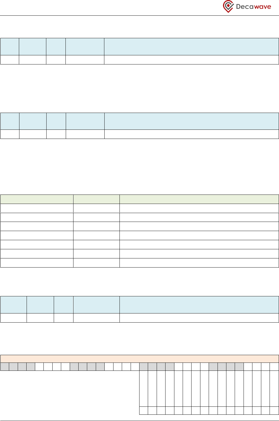
DW1000 User Manual
© Decawave Ltd 2017
Version 2.15
Page 155 of 244
7.2.42 Register file: 0x29 – Reserved
ID
Length
(octets)
Type
Mnemonic
Description
0x29
-
-
-
Reserved – this register file is reserved
Register file: 0x29 – Reserved is reserved. Please take care not to write to this register as doing so may cause
the DW1000 to malfunction.
7.2.43 Register file: 0x2A – Transmitter Calibration block
ID
Length
(octets)
Type
Mnemonic
Description
0x2A
-
-
TX_CAL
Transmitter calibration block
Register map register file 0x2A is the transmit calibration block concerned with ensuring the optimum
configuration of the transmit signal. It contains a number of sub-registers. An overview of these is given by
Table 39. Each of these sub-registers is separately described in the sub-sections below.
Table 39: Register file: 0x2A – Transmitter Calibration block overview
OFFSET in Register 0x2A
Mnemonic
Description
0x00
TC_SARC
Transmitter Calibration – SAR control
0x03
TC_SARL
Transmitter Calibration – Latest SAR readings
0x06
TC_SARW
Transmitter Calibration – SAR readings at last Wake-Up
0x08
TC_PG_CTRL
Transmitter Calibration – Pulse Generator Control
0x09
TC_PG_STATUS
Transmitter Calibration – Pulse Generator Status
0x0B
TC_PGDELAY
Transmitter Calibration – Pulse Generator Delay
0x0C
TC_PGTEST
Transmitter Calibration – Pulse Generator Test
7.2.43.1 Sub-Register 0x2A:00 – TC_SARC
ID
Length
(octets)
Type
Mnemonic
Description
2A:00
2
RW
TC_SARC
Transmitter Calibration – SAR control
Register file: 0x2A – Transmitter Calibration block, sub-register 0x00, contains the following bitmapped sub-
fields:
REG:2A:00 – TC_SARC – Transmitter Calibration SAR control
31
30
29
28
27
26
25
24
23
22
21
20
19
18
17
16
15
14
13
12
11
10
9
8
7
6
5
4
3
2
1
0
-
-
-
-
-
-
-
-
-
-
-
-
-
-
-
SAR_CTRL
0
0
0
0
0
0
0
0
0
0
0
0
0
0
0
0
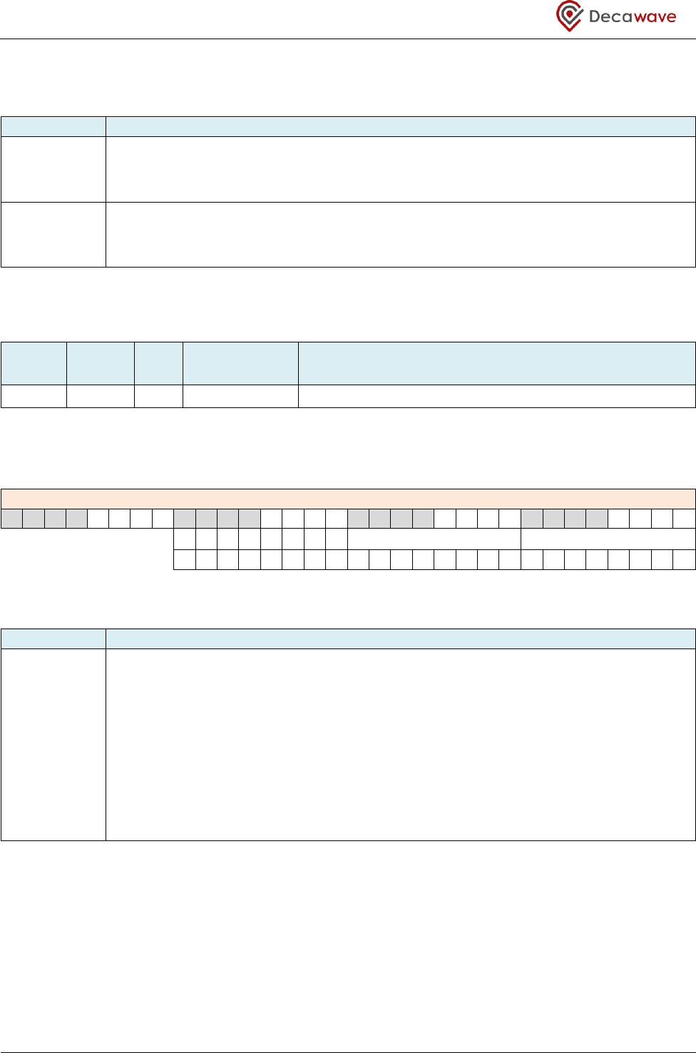
DW1000 User Manual
© Decawave Ltd 2017
Version 2.15
Page 156 of 244
Definition of the bit fields within Sub-Register 0x2A:00 – TC_SARC:
Field
Description of fields within Sub-Register 0x2A:00 – TC_SARC
SAR_CTRL
reg:2A:00
bit:0
Writing 1 sets SAR enable and writing 0 clears the enable. The enable should set for a
minimum of 2.5 µs to allow the SAR time to complete its reading.
-
reg:2A:00
bits:15–1
Bits marked ‘-’ in register 0x2A:00 are reserved and should always be written as zero to
avoid any malfunction of the DW1000.
7.2.43.2 Sub-Register 0x2A:03 – TC_SARL
ID
Length
(octets)
Type
Mnemonic
Description
2A:03
3
RO
TC_SARL
Transmitter Calibration –Latest SAR readings
Register file: 0x2A – Transmitter Calibration block, sub-register 0x03, contains the following bitmapped sub-
fields:
REG:2A:03 – TC_SARL – Transmitter Calibration Latest SAR readings
31
30
29
28
27
26
25
24
23
22
21
20
19
18
17
16
15
14
13
12
11
10
9
8
7
6
5
4
3
2
1
0
-
-
-
-
-
-
-
-
SAR_LTEMP
SAR_LVBAT
0
0
0
0
0
0
0
0
0
0
0
0
0
0
0
0
0
0
0
0
0
0
0
0
Definition of the bit fields within Sub-Register 0x2A:03 – TC_SARL:
Field
Description of fields within Sub-Register 0x2A:03 – TC_SARL
SAR_LVBAT
reg:2A:03
bits:7–0
Latest SAR reading for Voltage level. The 8-bit value reported here is the voltage reading,
from the last time the SAR A/D was used to sample the battery voltage monitor output.
The LSB is approximately 6 mV. The value can be converted to an actual voltage by
employing the formula:
Voltage (volts) = ( (SAR_LVBAT – OTP_READ(Vmeas @ 3.3 V) ) / 173) + 3.3
This uses the stored 3.3 V reading in the OTP that was recorded during production test.
The effective range of measurement is 2.25 V to 3.76 V. For more details please refer to
For more details please refer to section 6.4 – Measuring IC temperature and voltage.
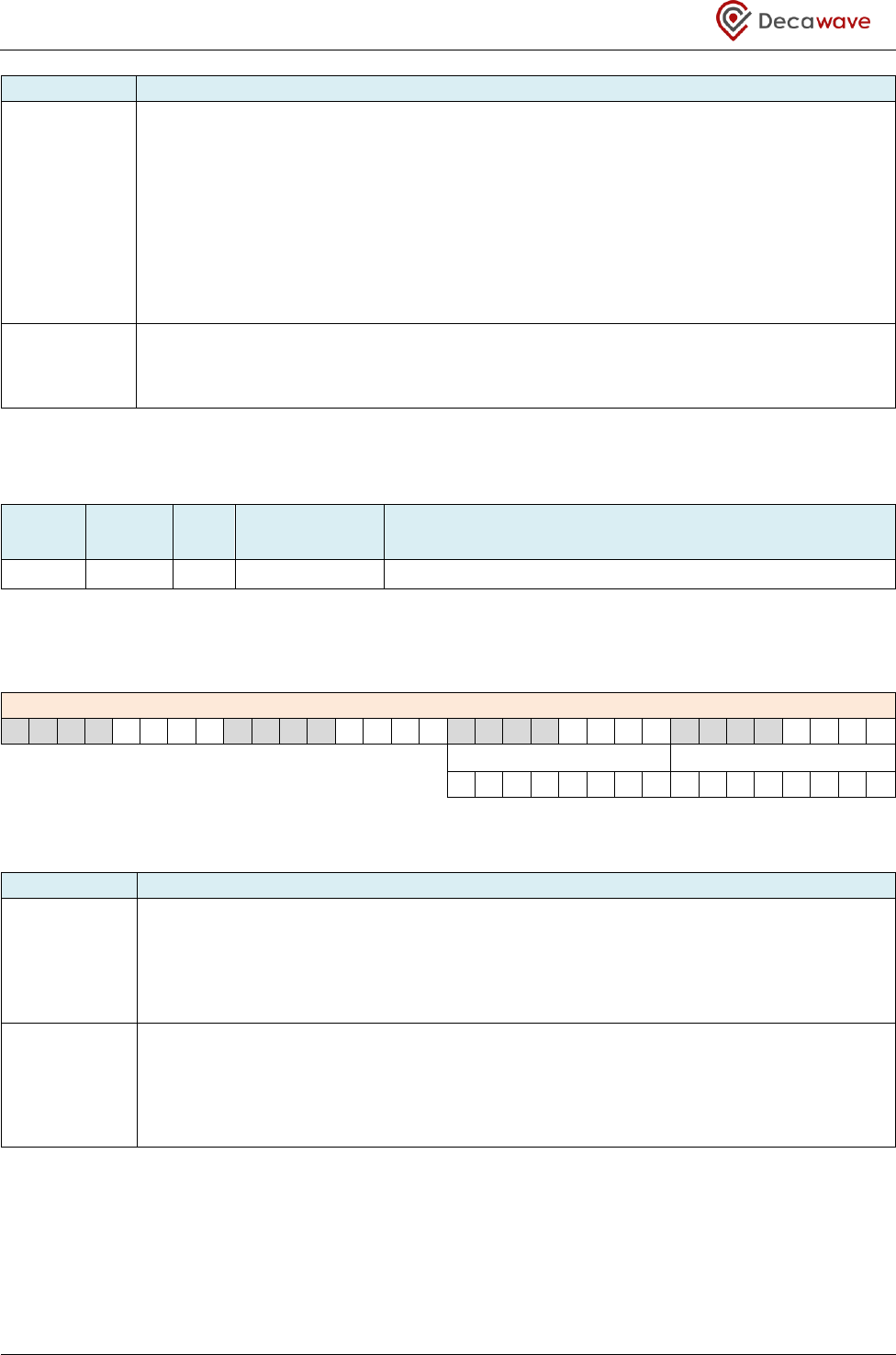
DW1000 User Manual
© Decawave Ltd 2017
Version 2.15
Page 157 of 244
Field
Description of fields within Sub-Register 0x2A:03 – TC_SARL
SAR_LTEMP
reg:2A:03
bits:15–8
Latest SAR reading for Temperature level. The 8-bit value reported here is the
temperature reading from the SAR A/D sampling of the DW1000 internal temperature
sensor. The LSB is approximately 0.8 °C. The value can be converted to an actual
temperature by employing the formula:
Temperature (°C )= ( (SAR_LTEMP – OTP_READ(Vtemp @ 23°C) ) x 1.14) + 23
This uses the stored 23°C reading in the OTP that was recorded during production test.
For additional details please refer to section 6.4 – Measuring IC temperature and voltage.
-
reg:2A:03
bits:23–16
Bits marked ‘-’ in register 0x2A:03 are reserved and should always be written as zero to
avoid any malfunction of the DW1000.
7.2.43.3 Sub-Register 0x2A:06 – TC_SARW
ID
Length
(octets)
Type
Mnemonic
Description
2A:06
2
RO
TC_SARW
Transmitter Calibration – SAR readings at last Wake-Up
Register file: 0x2A – Transmitter Calibration block, sub-register 0x06, is a 16-bit status register that contains
the following bitmapped sub-fields:
REG:2A:06 – TC_SARW– Transmitter Calibration SAR readings at last Wake-Up
31
30
29
28
27
26
25
24
23
22
21
20
19
18
17
16
15
14
13
12
11
10
9
8
7
6
5
4
3
2
1
0
SAR_WTEMP
SAR_WVBAT
0
0
0
0
0
0
0
0
0
0
0
0
0
0
0
0
Definition of the bit fields within Sub-Register 0x2A:06 – TC_SARW:
Field
Description of fields within Sub-Register 0x2A:06 – TC_SARW
SAR_WBAT
reg:2A:06
bits:7–0
SAR reading of Voltage level taken at last wakeup event. The 8-bit value reported here is
the voltage reading from the SAR A/D sampling of the battery voltage monitor output
during wakeup. For this to be valid the DW1000 has to have been reset or woken from
sleeping with the ONW_RADC bit enabled in the (saved) Sub-Register 0x2C:00 –
AON_WCFG.
SAR_WTEMP
reg:2A:06
bits:15– 8
SAR reading of temperature level taken at last wakeup event. The 8-bit value reported
here is the temperature reading from the SAR A/D sampling of the DW1000 internal
temperature sensor during wakeup. For this to be valid the DW1000 has to have been
reset or woken from sleep with the ONW_RADC bit enabled in the (saved) Sub-Register
0x2C:00 – AON_WCFG.
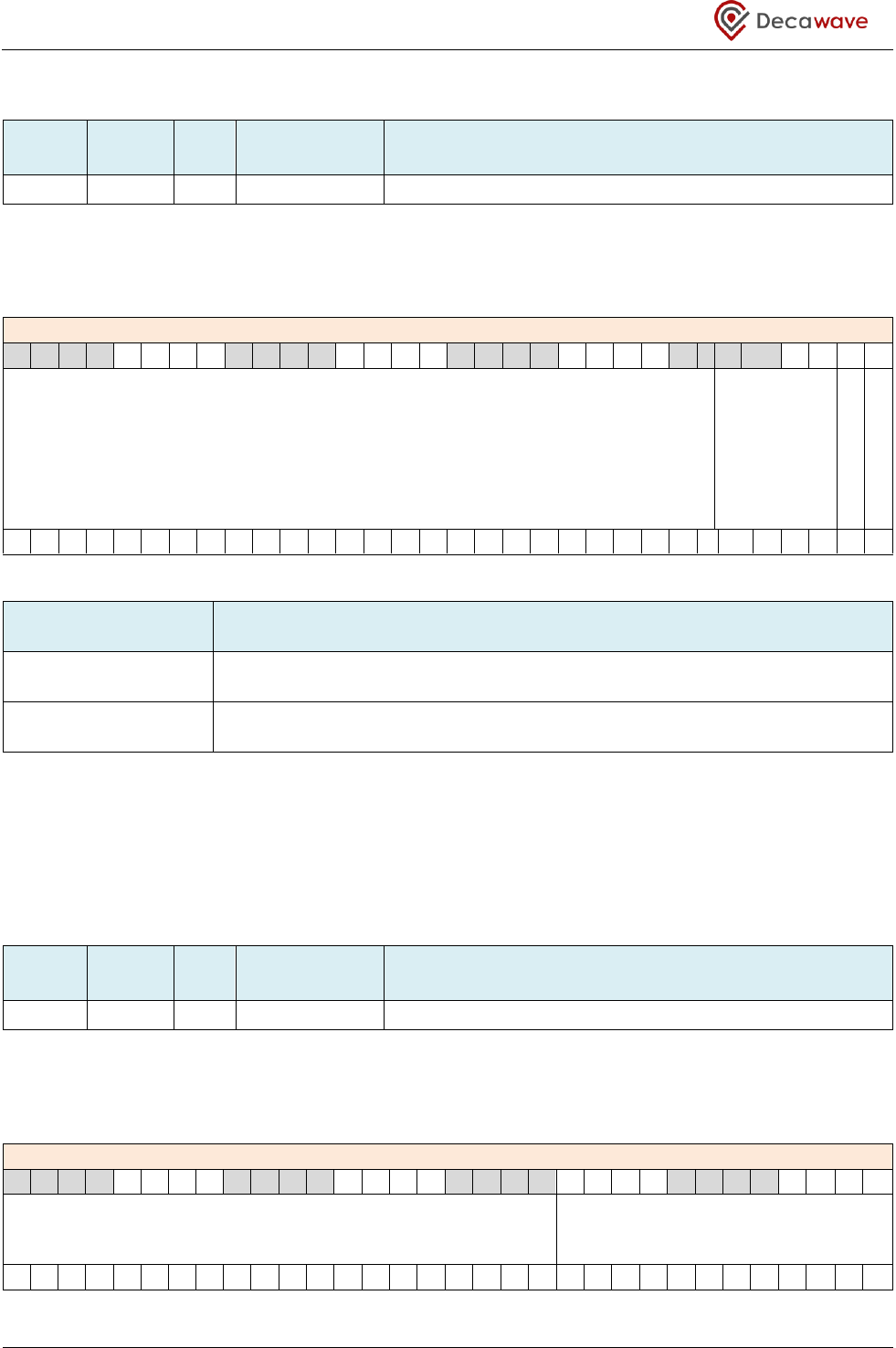
DW1000 User Manual
© Decawave Ltd 2017
Version 2.15
Page 158 of 244
7.2.43.4 Sub-Register 0x2A:08 – TC_PG_CTRL
ID
Length
(octets)
Type
Mnemonic
Description
2A:08
1
RW
TC_PG_CTRL
Transmitter Calibration – Pulse Generator Control
Register file: 0x2A – Transmitter Calibration block, sub-register 0x08, is a 16-bit control register that contains
the following bitmapped sub-fields:
REG:2A:08 – TC_PG_CTRL – Transmitter Calibration – Pulse Generator Control Settings
31
30
29
28
27
26
25
24
23
22
21
20
19
18
17
16
15
14
13
12
11
10
9
8
7
6
5
4
3
2
1
0
RESERVED
PG_TMEAS
RESERVED
PG_START
0
0
0
0
0
0
0
0
0
0
0
0
0
0
0
0
0
0
0
0
0
0
0
0
0
0
0
0
0
0
0
0
Definition of the bit fields within Sub-Reg–ster 0x2A:08 –TC_PG_CTRL:
Field
Description of fields within–Sub-Register –TC_PG_CTRL Sub-Register 0x28:0C–
RF_TXCTRL
PG_START
reg:2A:08 bit:0
Start the pulse generator calibration. Note: This bit is self clearing.
PG_TMEAS
reg:2A:08 bit5:2
Number of clock cycles over which to run the pulse generator cal counter.
These are t’e upper 4 MSb’s of a 10 bit counter clocked by the system clock.
This register controls the pulse generator calibration. When a calibration is complete, it generates a pulse
generator delay count based on the current TC_PGDELAY value. The count value is then stored automatically
into the TC_PG_STATUS register. This delay count gives a consistent reflection of the bandwidth regardless
of temperature.
7.2.43.5 Sub-Register 0x2A:09 – TC_PG_STATUS
ID
Length
(octets)
Type
Mnemonic
Description
2A:09
2
RO
TC_PG_STATUS
Transmitter Calibration – PG Status
Register file: 0x2A – Transmitter Calibration block, sub-register 0x09, is a 32 bit status register that contains
the following bitmapped sub-fields:
REG:2A:09 – TC_PG_STATUS – Transmitter Calibration – Pulse Generator Status
31
30
29
28
27
26
25
24
23
22
21
20
19
18
17
16
15
14
13
12
11
10
9
8
7
6
5
4
3
2
1
0
RESERVED
DELAY_CNT
0
0
0
0
0
0
0
0
0
0
0
0
0
0
0
0
0
0
0
0
0
0
0
0
0
0
0
0
0
0
0
0
DW1000 User Manual
© Decawave Ltd 2017
Version 2.15
Page 159 of 244
The reference value that is required for temperature bandwidth compensation is the contents of the
TC_PG_STATUS register. This represents a counter that increments with every pulse generated by the
DW1000 IC’s internal pulse generator. Intuitively, this count value (referred to as PG_COUNT) will vary
inversely with the TC_PGDELAY value – if the delay between pulses increases, the number of pulses within a
given timeframe will decrease, and vice versa. DELAY_CNT represents a counter that increments with every
pulse generated by the DW1000 IC’s internal pulse generator.
The TC_PGDELAY value will not give the same bandwidth for varying temperatures. The PG_COUNT value,
however, will give a stable bandwidth across all temperatures. It is taken as a reference as the DW1000 has a
pulse generator auto-calibration procedure; the procedure takes a PG_COUNT value and calculates the
TC_PGDELAY value from this. This TC_PGDELAY value can then be programmed in to give the desired
bandwidth.
More details on using these registers for bandwidth temperature compensation can be found in the
following application note : APS023 Part 2.
7.2.43.6 Sub-Register 0x2A:0B – TC_PGDELAY
ID
Length
(octets)
Type
Mnemonic
Description
2A:0B
1
RW
TC_PGDELAY
Transmitter Calibration –Pulse Generator Delay
Register file: 0x2A – Transmitter Calibration block, sub-register 0x0B is an 8-bit configuration register for
setting the Pulse Generator Delay value. This effectively sets the width of transmitted pulses effectively
setting the output bandwidth. The value used here depends on the TX channel selected by the TX_CHAN
configuration in Register file: 0x1F – Channel Control. Recommended values are given in Table 40 below;
note however that these values may need to be tuned for spectral regulation compliance depending on
external circuitry.
Table 40: Sub-Register 0x2A:0B – TC_PGDELAY recommended values
TX Channel
8-bit value to program to
Sub-Register 0x2A:0B – TC_PGDELAY
1
0xC9
2
0xC2
3
0xC5
4
0x95
5
0xC0
7
0x93
DW1000 User Manual
© Decawave Ltd 2017
Version 2.15
Page 160 of 244
7.2.43.7 Sub-Register 0x2A:0C – TC_PGTEST
ID
Length
(octets)
Type
Mnemonic
Description
2A:0C
1
RW
TC_PGTEST
Transmitter Calibration –Pulse Generator Test
Register file: 0x2A – Transmitter Calibration block, sub-register 0x0C is an 8-bit configuration register for use
in setting the transmitter into continuous wave (CW) mode. This CW mode is employed during the crystal
trimming operation which may be done at module manufacturing stage as part of calibrating the crystal
oscillator’s operating frequency. At all other times, for normal operation, the value in this register should be
left in its default power on value of 0x00.
Table 41:
Sub-Register 0x2A:0C – TC_PGTEST values
MODE
8-bit value to program to
Sub-Register 0x2A:0C – TC_PGTEST
Normal operation
0x00
Continuous Wave (CW) Test Mode
0x13
For more details of crystal trimming please refer to section 8.1 – IC Calibration – Crystal Oscillator Trim.
7.2.44 Register file: 0x2B – Frequency synthesiser control block
ID
Length
(octets)
Type
Mnemonic
Description
0x2B
-
-
FS_CTRL
Frequency synthesiser control block
Register map register file 0x2B is the frequency synthesiser control block. Its main functionality is the
generation of the carrier frequency necessary for the operating channel. It contains a number of sub-
registers. An overview of these is given by Table 42. Each of these sub-registers is separately described in
the sub-sections below.
Table 42: Register file: 0x2B – Frequency synthesiser control block overview
OFFSET in Register 0x2B
Mnemonic
Description
0x00
FS_RES1
Frequency synthesiser – Reserved area 1
0x07
FS_PLLCFG
Frequency synthesiser – PLL configuration
0x0B
FS_PLLTUNE
Frequency synthesiser – PLL Tuning
0x0C
FS_RES2
Frequency synthesiser – Reserved area 2
0x0E
FS_XTALT
Frequency synthesiser – Crystal trim
0x0F
FS_RES3
Frequency synthesiser – Reserved area 3
DW1000 User Manual
© Decawave Ltd 2017
Version 2.15
Page 161 of 244
7.2.44.1 Sub-Register 0x2B:00 – FS_RES1
ID
Length
(octets)
Type
Mnemonic
Description
2B:00
7
RW
FS_RES1
Frequency synthesiser – Reserved area 1
Register file: 0x2B – Frequency synthesiser control block, sub-register 0x00 is a reserved register. Please take
care not to write to this area as doing so may cause the DW1000 to malfunction.
7.2.44.2 Sub-Register 0x2B:07 – FS_PLLCFG
ID
Length
(octets)
Type
Mnemonic
Description
2B:07
4
RW
FS_PLLCFG
Frequency synthesiser – PLL configuration
Register file: 0x2B – Frequency synthesiser control block, sub-register 0x07 is the PLL configuration register.
The value here needs to be set depending on the channel being used, (i.e. depending on the RX_CHAN and
TX_CHAN configuration in Register file: 0x1F – Channel Control). The values required are given in Table 43.
Please take care not to write other values to this register as doing so may cause the DW1000 to malfunction.
Table 43: Sub-Register 0x2B:07 – FS_PLLCFG values
Operating Channel
32-bit value to program to
Sub-Register 0x2B:07 – FS_PLLCFG
1
0x09000407
2,4
0x08400508
3
0x08401009
5, 7
0x0800041D
7.2.44.3 Sub-Register 0x2B:0B – FS_PLLTUNE
ID
Length
(octets)
Type
Mnemonic
Description
2B:0B
1
RW
FS_PLLTUNE
Frequency synthesiser – PLL Tuning
Register file: 0x2B – Frequency synthesiser control block, sub-register 0x0B is a PLL tuning register. The value
here needs to be set depending on the channel being used, (i.e. depending on the RX_CHAN and TX_CHAN
configuration in Register file: 0x1F – Channel Control). The values required are given in Table 44. Please
take care not to write other values to this register as doing so may cause the DW1000 to malfunction.
DW1000 User Manual
© Decawave Ltd 2017
Version 2.15
Page 162 of 244
Table 44: Sub-Register 0x2B:0B – FS_PLLTUNE values
Operating Channel
8-bit value to program to
Sub-Register 0x2B:0B –
FS_PLLTUNE
1
0x1E
2,4
0x26
3
0x56
5,7
0xBE
7.2.44.4 Sub-Register 0x2B:0C – FS_RES2
ID
Length
(octets)
Type
Mnemonic
Description
2B:0C
2
RW
FS_RES2
Frequency synthesiser – Reserved area 2
Register file: 0x2B – Frequency synthesiser control block, sub-register 0x0C is a reserved area. Please take
care not to write to this area as doing so may cause the DW1000 to malfunction.
7.2.44.5 Sub-Register 0x2B:0E – FS_XTALT
ID
Length
(octets)
Type
Mnemonic
Description
2B:0E
1
RW
FS_XTALT
Frequency synthesiser – Crystal trim
Register file: 0x2B – Frequency synthesiser control block, sub-register 0x0E is the crystal trim register. This
allows a fine control over the crystal oscillator to tune the DW1000 operating frequencies quite precisely.
For details of the use of this register please refer to section 8.1 – IC Calibration – Crystal Oscillator Trim.
N.B.: Bits 7:5 must always be set to binary “011”. Failure to maintain this value will result in DW1000
malfunction.
REG:2B:0E – FS_XTALT – Crystal Trim Setting
7
6
5
4
3
2
1
0
R
R
R
XTALT
0
1
1
0
0
0
0
0
The bits of the FS_XTALT register identified above are individually described below:
DW1000 User Manual
© Decawave Ltd 2017
Version 2.15
Page 163 of 244
Field
Description of fields within Sub-Register 0x2B:0E – FS_XTALT
RESERVED
reg:2B:0E
bit:7:5
This field is reserved.
N.B.: Any change in the value of this field will cause the DW1000 to malfunction.
XTALT
reg:28:2C
bit:1
Crystal Trim. Crystals may be trimmed using this register setting to tune out errors, see 8.1 –
IC Calibration – Crystal Oscillator Trim.
7.2.44.6 Sub-Register 0x2B:0F – FS_RES3
ID
Length
(octets)
Type
Mnemonic
Description
2B:0F
6
RW
FS_RES3
Frequency synthesiser – Reserved area 3
Register file: 0x2B – Frequency synthesiser control block, sub-register 0x0F is a reserved area. Please take
care not to write to this area as doing so may cause the DW1000 to malfunction.
7.2.45 Register file: 0x2C – Always-on system control interface
ID
Length
(octets)
Type
Mnemonic
Description
0x2C
-
-
AON
Always on system control interface block
Register map register file 0x2C is the Always-On system control block, (AON).
The AON block contains a low-power configuration array that remains powered-up as long as power (from
the battery, for example) is supplied to the DW1000 via the VDDAON pin. User configurations, from SPI
accessible host interface registers, can be automatically saved in the AON memorywhen the DW1000 enters
SLEEP or DEEPSLEEP states and automatically restored from the AON memorywhen the DW1000 wakes from
sleeping. Additional discussion of these modes may be found in section 2.4.1 – SLEEP and DEEPSLEEP.
This Register file: 0x2C – Always-on system control interface controls the functions that remain on when the
IC enters its low-power SLEEP or DEEPSLEEP states, and configures the activities the DW1000 should take as
the IC wakes from these sleep states. It contains a number of sub-registers. An overview of these is given by
Table 45. Each of these sub-registers is separately described in the sub-sections below.
Table 45: Register file: 0x2C – Always-on system control overview
OFFSET in Register 0x2C
Mnemonic
Description
0x00
AON_WCFG
AON Wakeup Configuration Register
0x02
AON_CTRL
AON Control Register
0x03
AON_RDAT
AON Direct Access Read Data Result
0x04
AON_ADDR
AON Direct Access Address
0x05
-
reserved
0x06
AON_CFG0
AON Configuration Register 0
0x0A
AON_CFG1
AON Configuration Register 1
DW1000 User Manual
© Decawave Ltd 2017
Version 2.15
Page 164 of 244
7.2.45.1 Sub-Register 0x2C:00 – AON_WCFG
ID
Length
(octets)
Type
Mnemonic
Description
2C:00
2
RW
AON_WCFG
AON Wakeup Configuration Register
Register file: 0x2C – Always-on system control, sub-register 0x00 is a 16-bit configuration register that is used
to control what the DW1000 IC does as it wakes up from low-power SLEEP or DEEPSLEEP states. The
AON_WCFG register contains the following bitmapped sub-fields:
REG:2C:00 – AON_WCFG – AON Wake-up Configuration register
31
30
29
28
27
26
25
24
23
22
21
20
19
18
17
16
15
14
13
12
11
10
9
8
7
6
5
4
3
2
1
0
-
-
-
ONW_LLD
O
ONW_LLDE
-
-
PRES_SLEE
P
ONW_L64
P
ONW_LDC
-
-
ONW_LEUI
-
ONW_RX
ONW_RAD
C
0
0
0
0
0
0
0
0
0
0
0
0
0
0
0
0
Definition of the bit fields within Sub-Register 0x2C:00 – AON_WCFG:
Field
Description of fields within Sub-Register 0x2C:00 – AON_WCFG
ONW_RADC
reg:2C:00
bit:0
On Wake-up Run the (temperature and voltage) Analog-to-Digital Convertors. The
DW1000 is equipped with 8-bit A/D convertors to sample the IC temperature and its input
battery voltage. Setting this bit will cause the automatic initiation of temperature and
input battery voltage measurements when the DW1000 wakes from SLEEP or DEEPSLEEP
states. As a result the temperature is measured before the IC heats up (and so may be a
good measure of the ambient temperature around the IC), and, the battery voltage is
measured before any significant current drain occurs (which may be useful in checking
battery health). The resultant temperature and voltage values are available in Sub-
Register 0x2A:06 – TC_SARW. For more details of this functionality, please refer to
section 6.4 – Measuring IC temperature and voltage.
ONW_RX
reg:2C:00
bit:1
On Wake-up turn on the Receiver. With this bit it is possible to make the IC transition
into RX automatically as part of IC wake up. One of the uses for this is to implement a
scheme we call Low-Power Listening. See section 4.4 – Low-Power Listening for more
details.
-
reg:2C:00
bits:[various]
Bits marked ‘-’ in register 0x2C:00 are reserved and should always be written as zero to
avoid any malfunction of the DW1000.
ONW_LEUI
reg:2C:00
bit:3
On Wake-up load the EUI from OTP memory into Register file: 0x01 – Extended Unique
Identifier. When this bit is set to 1 the EUI value programmed into OTP memory will be
loaded into the Register file: 0x01 – Extended Unique Identifier when the DW1000 wakes-
up from SLEEP or DEEPSLEEP.
ONW_LDC
reg:2C:00
bit:6
On Wake-upload configurations from the AON memory into the host interface register set.
When the ONW_LDC bit is set to 1 the values of user configuration registers are restored
to their pre-sleep configuration values. When the ONW_LDC bit is 0 the values of user
configuration registers revert to their power-on-reset value when the DW1000 wakes-up
from SLEEP or DEEPSLEEP.
DW1000 User Manual
© Decawave Ltd 2017
Version 2.15
Page 165 of 244
Field
Description of fields within Sub-Register 0x2C:00 – AON_WCFG
ONW_L64P
reg:2C:00
bit:7
On Wake-up load the Length64 receiver operating parameter set. When the ONW_L64P
bit is set to 1 the Length64receiver operating parameter set is selected when the DW1000
wakes from SLEEP or DEEPSLEEP or is reset. When the ONW_L64P bit is 0 the receiver
operating parameter set reverts to its power-on-reset value (the default operating
parameter set) when the DW1000 wakes from SLEEP or DEEPSLEEP or is reset. For details
of receiver operating parameter set see section 7.2.46.8 – Receiver operating parameter
sets.
NB: This bit needs to be clear for reset to select the default operating parameter set.
PRES_SLEEP
reg:2C:00
bit:8
Preserve Sleep. This bit determines what the DW1000 does with respect to the ARXSLP
and ATXSLP sleep controls in Sub-Register 0x36:04 – PMSC_CTRL1 after a wake-up event.
When the PRES_SLEEP bit is set to 1 these sleep controls are not cleared upon wakeup, so
that the DW1000 can return to sleep after a failed reception (say). This needs to be set for
correct operation of call Low-Power Listening. See section 4.4 – Low-Power Listening for
more details of the required configurations.
ONW_LLDE
reg:2C:00
bit:11
On Wake-up load the LDE microcode. The LDE algorithm is implemented in a microcode
that is stored in a special ROM area on the DW1000 but run from a RAM area. Before the
LDE is run the DW1000 has to copy it from ROM to RAM. The LDE algorithm is responsible
for generating an accurate RX timestamp and calculating some signal quality statistics
related to the received packet. See Register file: 0x2E – Leading Edge Detection Interface
for more details about the LDE functionality. If the DW1000 is waking up to receive a frame
and it is important to timestamp this received frame then the ONW_LLDE bit should be set
to 1 to cause the LDE to be loaded into RAM. If time-stamping is not required then
ONW_LLDE bit may be left set to 0 to save this loading and save some energy in the process.
ONW_LLD0
reg:2C:00
bit:12
On Wake-up load the LDOTUNE value from OTP. When the DW1000 wakes up from SLEEP
or DEEPSLEEP states the value stored in OTP address 0x4 will be automatically written in to
Sub-Register 0x28:0x30 -
7.2.45.2 Sub-Register 0x2C:02 – AON_CTRL
ID
Length
(octets)
Type
Mnemonic
Description
2C:02
1
RW
AON_CTRL
AON Control Register
Register file: 0x2C – Always-on system control, sub-register 0x02 is an 8-bit control register. The bits in this
register in general cause direct activity within the AON block with respect to the stored AON memory. The
bits then act like commands that are processed by the DW1000 and the bits are automatically cleared as the
activity is taken.
The AON_CTRL register contains the following control bits:
REG:2C:02 – AON_CTRL – AON Control Register
31
30
29
28
27
26
25
24
23
22
21
20
19
18
17
16
15
14
13
12
11
10
9
8
7
6
5
4
3
2
1
0
DCA_ENAB
-
-
-
DCA_READ
UPL_CFG
SAVE
RESTORE
0
0
0
0
0
0
0
0

DW1000 User Manual
© Decawave Ltd 2017
Version 2.15
Page 166 of 244
Definition of the bit fields within Sub-Register 0x2C:02 – AON_CTRL:
Field
Description of fields within Sub-Register 0x2C:02 – AON_CTRL
RESTORE
reg:2C:02
bit:0
When this bit is set the DW1000 will copy the user configurations from the AON memory
to the host interface register set. The RESTORE bit will auto clear when this command is
executed.
SAVE
reg:2C:02
bit:1
When this bit is set the DW1000 will copy the user configurations from the host interface
register set into the AON memory. It will then proceed to upload the AON block
configurations. The SAVE bit will auto clear when this command is executed.
UPL_CFG
reg:2C:02
bit:2
Upload the AON block configurations to the AON. This control will copy the AON
configurations of the two registers: Sub-Register 0x2C:06 – AON_CFG0 and Sub-Register
0x2C:0A – AON_CFG1 into the AON configuration registers. This may be done for instance
to enter SLEEP mode after correctly configuring it in those two registers, although SLEEP
may be automatically entered under certain conditions by appropriate configurations
within Register file: 0x36 – Power Management and System Control. If the UPL_CFG is being
set for a purpose other than going to sleep then needs to be explicitly cleared immediately
after use as it is not self-clearing.
DCA_READ
reg:2C:02
bit:3
Direct AON memory access read. When this bit is set, (and direct access is enabled via the
DCA_ENAB bit below), it commands a direct read of the low-power configuration array
store memory. The address to read from is specified in Sub-Register 0x2C:04 – AON_ADDR
and the resultant read data is presented in Sub-Register 0x2C:03 – AON_RDAT. This access
is needed to retrieve the result of a calibration measurement on the low-power oscillator,
see LPOSC_CAL bit in Sub-Register 0x2C:0A – AON_CFG1.
–
reg:2C:02
bits:6–4
Bits marked ‘-’ in register 0x2C:02 are reserved and should always be written as zero to
avoid any malfunction of the DW1000.
DCA_ENAB
reg:2C:02
bit:7
Direct AON memory access enable bit. This bit needs to be set to 1 to enable the DCA_READ
above to operate. Note: DCA_ENAB must to be reset to 0 to allow the automatic
saving/restoring of user configurations to/from the AON memory, as needed for correct
operation during entry and exit from SLEEP and DEEPSLEEP modes.

DW1000 User Manual
© Decawave Ltd 2017
Version 2.15
Page 167 of 244
Table 46: Configurations maintained in the AON Memory Array
Configuration Register
Configuration Register
Register file: 0x03 – PAN Identifier and Short Address
Sub-Register 0x28:0B– RF_RXCTRLH
Register file: 0x04 – System Configuration
Sub-Register 0x28:0C– RF_TXCTRL
Register file: 0x08 – Transmit Frame Control2
Sub-Register 2A:0B – TC_PGDELAY
Register file: 0x0E – System Event Mask Register
Sub-Register 0x2B:07 – FS_PLLCFG
Register file: 0x1D – SNIFF Mode3
Sub-Register 0x2B:0E – FS_XTALT
Register file: 0x1E – Transmit Power Control
Sub-Register 0x2C:00 – AON_WCFG
Register file: 0x1F – Channel Control
Sub-Register 0x2C:06 – AON_CFG0
Register file: 0x21 – User defined SFD sequence4
Sub-Register 0x2C:0A – AON_CFG1
Sub-Register 0x23:04 – AGC_TUNE1
Sub-Register 0x2E:1804 – LDE_RXANTD5
Sub-Register 0x23:04 – AGC_TUNE1
Sub-Register 0x2E:1806– LDE_CFG2
Sub-Register 0x23:12 – AGC_TUNE3
* For NLOS operation this value has been optimized
as 0x0003. Refer to the application notes on
NLOS available on www.Decawave.com for more
information.
Sub-Register 0x2E:2804 – LDE_REPC
Sub-Register 0x26:00 – GPIO_MODE
Sub-Register 0x36:00 – PMSC_CTRL06
Register file: 0x27 – Digital receiver configuration
Sub-Register 0x36:04 – PMSC_CTRL17
Sub-Register 0x36:0C – PMSC_SNOZT
Sub-Register 0x36:28 – PMSC_LEDC8
2
Only the Low 32-bits are maintained.
3
All bits are maintained except for bit 0. Bit zero it is lost and restored as 0.
4
Only the SFD_LENGTH field in the first octet is maintained.
5
The TX antenna delay in Register file: 0x18 – Transmitter Antenna Delay is not preserved, but instead ends up corrupted by part
of the preserved RX antenna delay. After a wake-up then for correct TX time stamping The TX antenna delay will need
reprogramming.
6
Bits preserved are: 23, 15, 12, 11 and 6. The remainder revert to their reset value during wake-up init.
7
All preserved except for the KHZCLKDIV field which revert to its reset value during wake-up init.
8
Just the BLNKEN bit is preserved, the BLINK_TIM field reverts to its reset value during wake-up init.
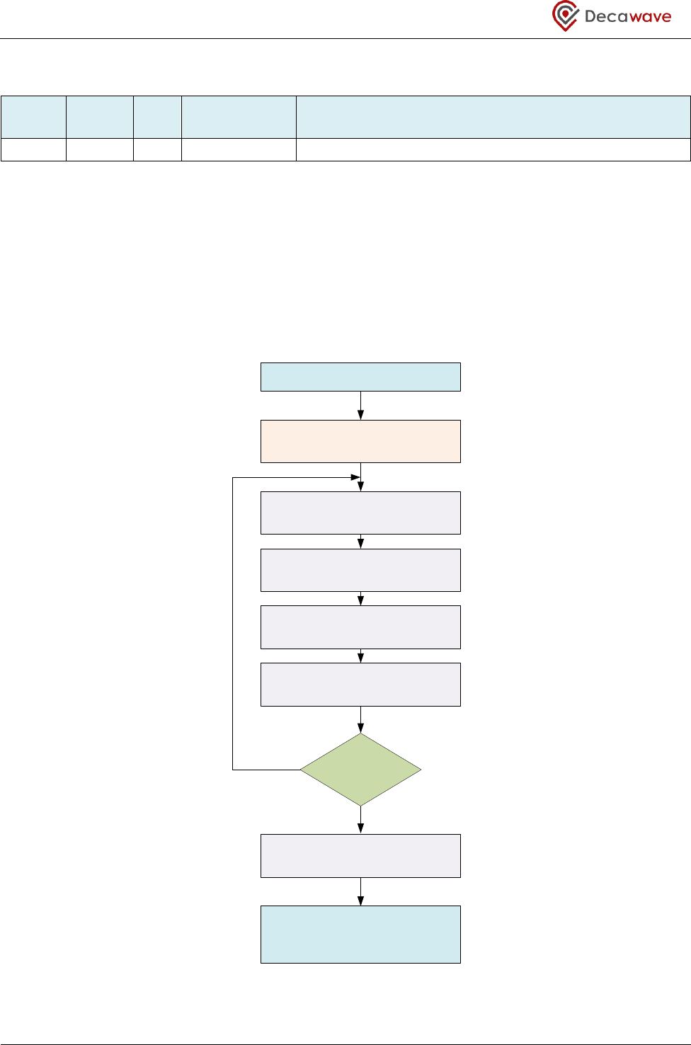
DW1000 User Manual
© Decawave Ltd 2017
Version 2.15
Page 168 of 244
7.2.45.3 Sub-Register 0x2C:03 – AON_RDAT
ID
Length
(octets)
Type
Mnemonic
Description
2C:03
1
RW
AON_RDAT
AON Direct Access Read Data Result
Register file: 0x2C – Always-on system control, sub-register 0x03 is an 8-bit register used to return the result
of a direct access read of a location in the AON memory array. The location to read from is specified by Sub-
Register 0x2C:04 – AON_ADDR and the read is initiated using the DCA_READ control bit in Sub-Register
0x2C:02 – AON_CTRL.
7.2.45.4 Reading from a specified address within AON memory
Figure 28 shows the procedural flow for reading from specified address in AON memory:
Figure 28: Flow chart for direct read of AON address
Ensure that the SPI clock
frequency is set < 3MHz.
YES
NO
Want to do
another read
?
Write Address to access into
Register 2C:04 – AON_ADDR
Set DCA_ENAB by writing octet
0x80 into Reg 2C:02 – AON_CTRL
Now also set DCA_READ by
writing octet 0x88 into Reg 2C:02
Read Result data from
Register 2C:03 – AON_RDAT
Clear DCA_ENAB and DCA_READ
by writing 0x00 into Reg 2C:02
DONE:
Return Result read from Address
PROC: read AON CAS @Address
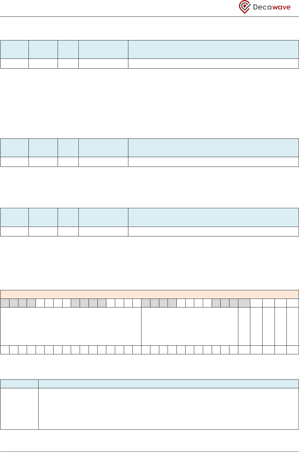
DW1000 User Manual
© Decawave Ltd 2017
Version 2.15
Page 169 of 244
7.2.45.5 Sub-Register 0x2C:04 – AON_ADDR
ID
Length
(octets)
Type
Mnemonic
Description
2C:04
1
RW
AON_ADDR
AON Direct Access Address
Register file: 0x2C – Always-on system control, sub-register 0x04 is an 8-bit register used to specify the
address for a direct access read of the AON memory array. The read is initiated using the DCA_READ control
bit in Sub-Register 0x2C:02 – AON_CTRL and the read result is returned in Sub-Register 0x2C:03 –
AON_RDAT.
7.2.45.6 Sub-Register 0x2C:05 – AON_RES1
ID
Length
(octets)
Type
Mnemonic
Description
2C:05
1
RW
AON_RES1
AON Reserved area 1
Register file: 0x2C – Always-on system control, sub-register 0x05 is reserved.
7.2.45.7 Sub-Register 0x2C:06 – AON_CFG0
ID
Length
(octets)
Type
Mnemonic
Description
2C:06
4
RW
AON_CFG0
AON Configuration Register 0
Register file: 0x2C – Always-on system control, sub-register 0x06 is a 32-bit configuration register for the
always on block. The fields of this register are interpreted inside the AON block, which can only happen after
these are loaded into the AON block via the UPL_CFG command in Sub-Register 0x2C:02 – AON_CTRL. The
AON_CFG0 register contains the following fields:
REG:2C:06 – AON_CFG0 – AON Configuration Register 0
31
30
29
28
27
26
25
24
23
22
21
20
19
18
17
16
15
14
13
12
11
10
9
8
7
6
5
4
3
2
1
0
SLEEP_TIM
LPCLKDIVA
LPDIV_EN
WAKE_CNT
WAKE_SPI
WAKE_PIN
SLEEP_EN
0
1
0
1
0
0
0
0
1
1
1
1
1
1
1
1
0
0
0
1
1
1
1
1
1
1
1
0
1
1
1
0
The fields of the AON_CFG0 register identified above are individually described below:
Field
Description of fields within Sub-Register 0x2C:06 – AON_CFG0
SLEEP_EN
reg:2C:06
bit:0
This is the sleep enable configuration bit. In order to put the DW1000 into the SLEEP state
this bit needs to be set and then the configuration needs to be uploaded to the AON using
the UPL_CFG bit in Sub-Register 0x2C:02 – AON_CTRL. The SLEEP state can also be entered
via the ATXSLP or ARXSLP controls in Sub-Register 0x36:04 – PMSC_CTRL1, which will
automatically do the configuration upload to the AON and set this SLEEP_EN control.

DW1000 User Manual
© Decawave Ltd 2017
Version 2.15
Page 170 of 244
Field
Description of fields within Sub-Register 0x2C:06 – AON_CFG0
WAKE_PIN
reg:2C:06
bit:1
Wake using WAKEUP pin. This configuration bit enables the WAKEUP line to bring the
DW1000 out of SLEEP or DEEPSLEEP states into operational mode. By default the
WAKE_PIN configuration is 1 enabling the WAKEUP line as a wake-up signal. Setting the
WAKE_PIN configuration bit to 0 will mean that the WAKEUP line cannot wake the DW1000
from SLEEP or DEEPSLEEP. See NOTE below on wakeup events.
WAKE_SPI
reg:2C:06
bit:2
Wake using SPI access. This configuration bit enables SPICSn to bring the DW1000 out of
SLEEP or DEEPSLEEP into operational mode. By default the WAKE_SPI configuration is 1
enabling the SPICSn input as a wake-up signal. Setting the WAKE_SPI configuration bit to 0
will mean that SPICSn cannot wake the DW1000 form SLEEP or DEEPSLEEP. See NOTE below
on wakeup events.
WAKE_CNT
reg:2C:06
bit:3
Wake when sleep counter elapses. This configuration bit enables the sleep counter to bring
the DW1000 out of SLEEP into operational mode. By default the WAKE_CNT configuration is
1 enabling the sleep counter as a wake-up signal. Setting the WAKE_CNT configuration bit
to 0 will mean that the sleep counter cannot wake the DW1000 form SLEEP. See NOTE
below on wakeup events.
LPDIV_EN
reg:2C:06
bit:4
Low power divider enable configuration. This bit enables a low power clock divider, that
allows and alternative source of clock for the sleep time counter. When LPDIV_EN is 0 the
sleep time counter counts cycles of the low powered ring oscillator. When LPDIV_EN is 1
the sleep time counter counts cycles of the LP Clock. See LPCLKDIVA below for details of
this.
NOTE: While the LP Clock is more accurate than the low powered ring oscillator, it is
thousands of times more power hungry and, for this reason there are few applications that
will use this.
LPCLKDIVA
reg:2C:06
bits:15–5
This field specifies a divider count for dividing the raw DW1000 XTAL oscillator frequency to
set an LP clock frequency. This LP clock and LPCLKDIVA functionality is only enabled when
the LPDIV_EN configuration bit is set to 1. The raw 38.4 MHz XTAL oscillator frequency input
to the LP clock divider is pre-divided by 2 to give a 19.2 MHz internal clock called XTI. The
LPCLKDIVA field is 11-bits allowing divisors up to 2047 or LP clock frequencies down to 9.4
kHz. An LPCLKDIVA value of 0 or 1 gives an LP clock frequency being the raw XTI frequency
of 19.2 MHz.
SLEEP_TIM
reg:2C:06
bits:31–16
Sleep time. This field configures the sleep time count elapse value. The units of SLEEP_TIM
depend on which timer is running. When the low powered oscillator is running the units are
dependent on the oscillating frequency of the IC’s internal RING oscillator, which is between
approximately 7,000 and 13,000 Hz depending on process variations within the IC. This
frequency can be measured using the LPOSC_CAL (low-power oscillator calibration) control
bit in Sub-Register 0x2C:0A – AON_CFG1 so that sleep times can be more accurately set. If
the LPDIV_EN is set to 1 then the sleep time counter counts cycles of the LP Clock as set by
the LPCLKDIVA above. Note while this is a more accurate clock it is not recommended for
general sleeping as this has a much higher power consumption than the ring oscillator based
sleep.
The SLEEP_TIM field is 16 bits wide, but represents the upper 16 bits of a 28-bit counter, i.e.
the low order bit is equal to 4096 counts. So, for example, if the ring oscillator frequency is
9500 Hz then programming the SLEEP_TIM with a value of 24 would yield a sleep time of 24
× 4096 ÷ 9500, which is approximately 10.35 seconds.
NOTE: There are three mechanisms to wake the DW1000: using the WAKEUP line when the WAKE_PIN
configuration is 1, using SPICSn when the WAKE_SPI configuration is 1, and using the sleep timer
when the WAKE_CNT configuration is 1 and the sleep counter is enabled via the SLEEP_CEN bit in
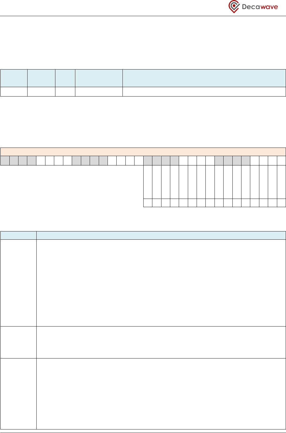
DW1000 User Manual
© Decawave Ltd 2017
Version 2.15
Page 171 of 244
Sub-Register 0x2C:0A – AON_CFG1. If none of these wakeup mechanisms are enabled and the
DW1000 is put into DEEPSLEEP mode then there will be no way to take the IC out of sleep except by
removing power at the VDDAON pin, (and short it to 0 volts to hasten the power down of the IC).
7.2.45.8 Sub-Register 0x2C:0A – AON_CFG1
ID
Length
(octets)
Type
Mnemonic
Description
2C:0A
2
RW
AON_CFG1
AON Configuration Register 1
Register file: 0x2C – Always-on system control, sub-register 0x0A is a 16-bit configuration register for
parameters within the always-on (AON) block. The fields of this register are interpreted inside the AON
block, and this can only happen after the register is loaded into the AON block via the UPL_CFG command in
Sub-Register 0x2C:02 – AON_CTRL. The AON_CFG1 register contains the following fields:
REG:2C:0A – AON_CFG1 – AON Configuration Register 1
31
30
29
28
27
26
25
24
23
22
21
20
19
18
17
16
15
14
13
12
11
10
9
8
7
6
5
4
3
2
1
0
-
-
-
-
-
-
-
-
-
-
-
-
-
LPOSC_C
AL
SMXX
SLEEP_CE
N
0
0
0
0
0
0
0
0
0
0
0
0
0
1
1
1
The fields of the AON_CFG1 register identified above are individually described below:
Field
Description of fields within Sub-Register 0x2C:0A – AON_CFG1
SLEEP_CEN
reg:2C:0A
bit:0
This bit enables the sleep counter. For correct operation of the sleep counter (down
counter) when loading a new value into the SLEEP_TIM field of Sub-Register 0x2C:06 –
AON_CFG0 it is recommended to set SLEEP_CEN to 0 before updating SLEEP_TIM. The
recommended operating procedure is then as follows:
(a) Set SLEEP_CEN (in AON_CFG1) to 0.
(b) Set UPL_CFG (in AON_CTRL) to 1, to apply this to the AON block.
I Program the new value of SLEEP_TIM (in AON_CFG0).
(d) Set SLEEP_CEN to 1.
I Set UPL_CFG to 1, to apply the new sleep time and enable the counter in the AON.
SMXX
reg:2C:0A
bit:1
This bit needs to be set to 0 for correct operation in the SLEEP state within the DW1000. By
default this bit is set to 1. The host system should set this bit to zero as part of initialisation
or controlling the entry of the DW1000 into the SLEEP state to ensure correct operation of
the SLEEP mode.
LPOSC_CAL
reg:2C:0A
bit:2
This bit enables the calibration function that measures the period of the IC’s internal low
powered oscillator. The operating frequency of this oscillator depends on process variations
within the IC and also on the operating voltage and temperature. It should lie somewhere
between approximately 7,000 and 13,000 Hz. Using this LPOSC_CAL bit then it is possible
measure the period of the oscillation in counts of the IC’s internal XTAL_DIV2 clock, which
runs at a frequency of 19.2 MHz. Using this information it is then possible to more
accurately determine the value to set into the SLEEP_TIM field (of Sub-Register 0x2C:06 –
AON_CFG0) for a particular desired sleep period.
DW1000 User Manual
© Decawave Ltd 2017
Version 2.15
Page 172 of 244
Field
Description of fields within Sub-Register 0x2C:0A – AON_CFG1
The recommended operating procedure for this is then using this is then is to:
(a) Ensure that the SPI operating frequency is set < 3MHz. (During procedure the system
uses the 19.2 MHz XTI clock which will not support higher SPI data rates).
(b) Set this LPOSC_CAL bit to 1, and upload it into the AON block by toggling the
UPL_CFG bit (in AON_CTRL) I1 and back to 0.
I Clear the LPOSC_CAL bit to 0, and upload it into the AON block by toggling UPL_CFG
(in AON_CTRL) to 1 and back to 0.
(d) Force the system clock to be the 19.2 MHz XTI clock, by setting SYSCLKS (in Sub-
Register 0x36:00 – PMSC_CTRL0) to 01 (binary).
I Wait for 400 µs to ensure a calibration count value is available. This is a 16-bit value
counting how many clock periods of the 19.2 MHz XTI clock it took to complete one
complete period of the low power ring oscillator.
(f) The ring oscillator period counter’s 8 MSBs are accessed at AON memory address 118
decimal (0x76) and its 8 LSBs are accessed at AON memory address 117 decimal
(0x75). Please refer to in section 7.2.45.4 – Reading from a specified address within
AON memory for details of the procedure defined for reading AON memory.
(g) After reading the period counter, restore the system clock automatic mode by setting
the SYSCLKS configuration back to 0.
The operating frequency of the ring oscillator is given by 19.2 MHz divided by the period
counter value.
–
reg:2C:0A
bits:15–3
Reserved bits
7.2.46 Register file: 0x2D – OTP Memory Interface
ID
Length
(octets)
Type
Mnemonic
Description
0x2D
-
-
OTP_IF
One Time Programmable Memory Interface
Register map register file 0x2D is the OTP memory interface. This allows read access to parameters stored in
the OTP memory, and it is also the interface via which parameters are programmed into the OTP memory.
The OTP memory interface contains a number of sub-registers. An overview of these sub-registers is given
by Table 47, and each is then separately described in the sub-sections below.
NOTE: Programming OTP memory is a one-time only activity, any values programmed in error cannot be
corrected. Also, please take care when programming OTP memory to only write to the designated areas –
programming elsewhere may permanently damage the DW1000’s ability to function normally.
For more details of the OTP memory please refer to section 6.3 – Using the on-chip OTP memory.
Table 47: Register file: 0x2D – OTP Memory Interface overview
OFFSET in Register 0x2D
Mnemonic
Description
0x00
OTP_WDAT
OTP Write Data
0x04
OTP_ADDR
OTP Address
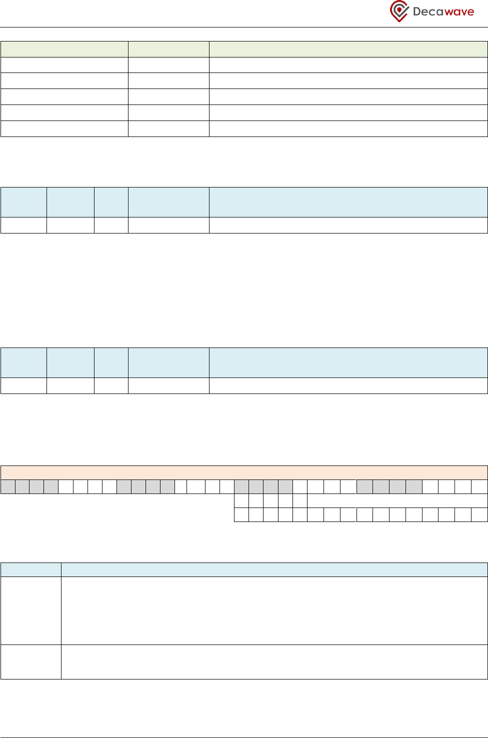
DW1000 User Manual
© Decawave Ltd 2017
Version 2.15
Page 173 of 244
OFFSET in Register 0x2D
Mnemonic
Description
0x06
OTP_CTRL
OTP Control
0x08
OTP_STAT
OTP Status
0x0A
OTP_RDAT
OTP Read Data
0x0E
OTP_SRDAT
OTP SR Read Data
0x12
OTP_SF
OTP Special Function
7.2.46.1 Sub-Register 0x2D:00 – OTP_WDAT
ID
Length
(octets)
Type
Mnemonic
Description
2D:00
4
RW
OTP_WDAT
OTP Write Data
Register file: 0x2D – OTP Memory Interface, sub-register 0x00 is a 32-bit register. The data value to be
programmed into an OTP location should be written here before invoking the programming function.
Writing to OTP memory is an involved procedure. For details of this please refer to section 6.3.2 –
Programming a value into OTP memory.
7.2.46.2 Sub-Register 0x2D:04 – OTP_ADDR
ID
Length
(octets)
Type
Mnemonic
Description
2D:04
2
RW
OTP_ADDR
OTP Address
Register file: 0x2D – OTP Memory Interface, sub-register 0x04 is a 16-bit register used to select the address
within the OTP memory block that is being accessed (for read or write) this OTP memory interface. The
OTP_ADDR register contains the following fields:
REG:2D:04 – OTP_ADDR – OTP Address
31
30
29
28
27
26
25
24
23
22
21
20
19
18
17
16
15
14
13
12
11
10
9
8
7
6
5
4
3
2
1
0
-
-
-
-
-
OTPADDR
-
-
-
-
-
0
0
0
0
0
0
0
0
0
0
0
The fields of the OTP_ADDR register are described below:
Field
Description of fields within Sub-Register 0x2D:04 – OTP_ADDR
OTPADDR
reg:2D:04
bits:10 –0
This 11-bit field specifies the address within OTP memory that will be accessed read or written.
For details of the OTP memory map and the procedures to read and write OTP memory, please
refer to section 6.3 – Using the on-chip OTP memory.
-
reg:2D:04
bits:15 –11
Reserved. The remainder of this register is reserved.
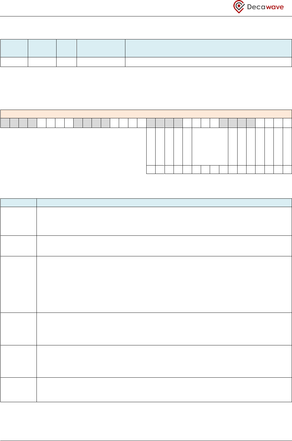
DW1000 User Manual
© Decawave Ltd 2017
Version 2.15
Page 174 of 244
7.2.46.3 Sub-Register 0x2D:06 – OTP_CTRL
ID
Length
(octets)
Type
Mnemonic
Description
2D:06
2
RW
OTP_CTRL
OTP Control
Register file: 0x2D – OTP Memory Interface, sub-register 0x06 is a 16-bit register used to control the
operation of the OTP memory through the process of reading and writing. The OTP_CTRL register contains
the following fields:
REG:2D:06 – OTP_CTRL – OTP Control
31
30
29
28
27
26
25
24
23
22
21
20
19
18
17
16
15
14
13
12
11
10
9
8
7
6
5
4
3
2
1
0
LDELOAD
R
R
R
R
OTPMR
OTPPROG
R
R
OTPMRWR
R
R
OTPREAD
OTPRDEN
0
0
0
0
0
0
0
0
0
0
0
0
0
0
0
0
The fields of the OTP_CTRL register are described below:
Field
Description of fields within Sub-Register 0x2D:06 – OTP_CTRL
R
reg:2D:06
bit:various
Reserved bits. May be overwritten with their default value.
OTPRDEN
reg:2D:06
bit:0
This bit forces the OTP into manual read mode. This bit must be set if using the OTPREAD bit
to issue a read command.
OTPREAD
reg:2D:06
bit:1
This bit commands a read operation from the address specified in the OTP_ADDR register,
the value read will then be available in the OTP_RDAT register. This bit will automatically
clear when the read operation is done.
For details of the OTP memory map and the procedures to read and write OTP memory,
please refer to section 6.3 – Using the on-chip OTP memory.
OTPMRWR
reg:2D:06
bit:3
OTP mode register write. This bit should be set to 1 then cleared when applying a new mode
to the OTP. This bit is used to configure the initial circuits of the OTP block. They used during
the programming of the OTP. For a description on how to drive these bits see the sample
code in 6.3.2 Programming a value into OTP memory.
OTPPROG
reg:2D:06
bit:6
Setting this bit will cause the contents of OTP_WDAT to be written to OTP_ADDR. This bit
should be cleared once the programming has completed as indicated by Sub-Register
0x2D:08 – OTP_STAT. For a description on how to drive these bits see the sample code in
6.3.2 Programming a value into OTP memory.
OTPMR
reg:2D:06
bit:10:7
OTP Mode register. These bits are used to configure the internal circuits of the OTP block.
They are used during the programming of the OTP. For a description on how to drive these
bits see the sample code in 6.3.2 Programming a value into OTP memory.
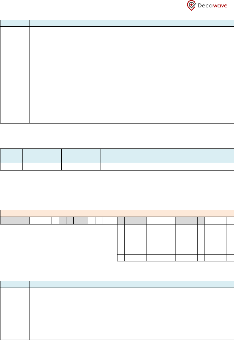
DW1000 User Manual
© Decawave Ltd 2017
Version 2.15
Page 175 of 244
Field
Description of fields within Sub-Register 0x2D:06 – OTP_CTRL
LDELOAD
reg:2D:06
bit:15
This bit forces a load of LDE microcode. The LDE algorithm is responsible for generating an
accurate RX timestamp and calculating some signal quality statistics related to the received
packet. See Register file: 0x2E – Leading Edge Detection Interface for more details about the
LDE functionality. The LDE algorithm is implemented in a microcode that is stored in a
special ROM area on the DW1000 but run from a RAM area. After powering up the
DW1000 (or after exiting SLEEP or DEEPSLEEP states) the LDE RAM is empty. Before the LDE
is run the code has to be copied from ROM to RAM. This should be done before receiver is
enabled if it is important to timestamp this received frame. Set LDELOAD to 1 to initiate the
loading, it will automatically clear when the load is done. If the LDE code is not being
loaded before the receiver is enabled then the LDERUNE (LDE run enable) control in Sub-
Register 0x36:04 – PMSC_CTRL1 must be turned off (set to zero).
When waking up from SLEEP or DEEPSLEEP to receive a frame, if the ONW_LLDE bit (in Sub-
Register 0x2C:00 – AON_WCFG), has been configured to 1, then the LDE load will be done
automatically as part of exiting the sleep state.
7.2.46.4 Sub-Register 0x2D:08 – OTP_STAT
ID
Length
(octets)
Type
Mnemonic
Description
2D:08
2
RW
OTP_STAT
OTP Status
Register file: 0x2D – OTP Memory Interface, sub-register 0x08 is a 16-bit register used to give status
information about the progress of the OTP programming activity. The OTP_STAT register contains the
following fields:
REG:2D:08 – OTP_STAT – OTP Status
31
30
29
28
27
26
25
24
23
22
21
20
19
18
17
16
15
14
13
12
11
10
9
8
7
6
5
4
3
2
1
0
-
-
-
-
-
-
-
-
-
-
-
-
-
-
OTPVPOK
OTPPRGD
0
0
0
0
0
0
0
0
0
0
0
0
0
0
0
0
The fields of the OTP_STAT register are described below:
Field
Description of fields within Sub-Register 0x2D:08 – OTP_STAT
OTPPRGD
reg:2D:04
bit:0
OTP Programming Done. This status bit indicates that the programming of the 32-bit word
from OTP_WDAT to the address specified by OTP_ADDR has completed. Writing to OTP
memory is an involved procedure. For details of this please refer to section 6.3.2 –
Programming a value into OTP memory.
OTPVPOK
reg:2D:04
bit:1
OTP Programming Voltage OK. This status bit indicates that the VPP level is sufficient for
programming the OTP memory. For details of OTP programming please refer to section 6.3
– Using the on-chip OTP memory.
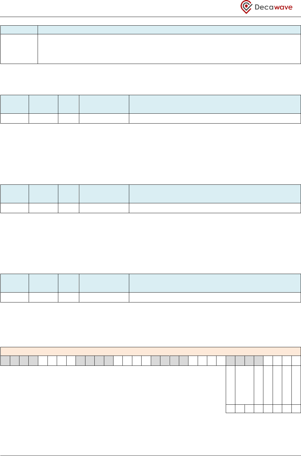
DW1000 User Manual
© Decawave Ltd 2017
Version 2.15
Page 176 of 244
Field
Description of fields within Sub-Register 0x2D:08 – OTP_STAT
-
reg:2D:00
bits:various
Reserved. Bits marked ‘-’ are reserved.
7.2.46.5 Sub-Register 0x2D:0A – OTP_RDAT
ID
Length
(octets)
Type
Mnemonic
Description
2D:0A
4
R
OTP_RDAT
OTP Read Data
Register file: 0x2D – OTP Memory Interface, sub-register 0x0A is a 32-bit register. The data value read from
an OTP location will appear here after invoking the OTP read function. For details of the OTP memory map
and the procedures to read OTP memory, please refer to section 6.3 – Using the on-chip OTP memory.
7.2.46.6 Sub-Register 0x2D:0E – OTP_SRDAT
ID
Length
(octets)
Type
Mnemonic
Description
2D:0E
4
RW
OTP_SRDAT
OTP Special Register Read Data
Register file: 0x2D – OTP Memory Interface, sub-register 0x0E is a 32-bit register. The data value stored in
the OTP SR (0x400) location will appear here after power up. For details of the OTP memory map and the
procedures to read OTP memory, please refer to section 6.3 – Using the on-chip OTP memory.
7.2.46.7 Sub-Register 0x2D:12 – OTP_SF
ID
Length
(octets)
Type
Mnemonic
Description
2D:12
1
RW
OTP_SF
OTP Special Function
Register file: 0x2D – OTP Memory Interface, sub-register 0x12 is an 8-bit special function register used to
select and load special receiver operational parameter sets. See 7.2.46.8 – Receiver operating parameter sets
for details. The OTP_SF register contains the following fields:
REG:2D:12 – OTP_SF – OTP Special Function
31
30
29
28
27
26
25
24
23
22
21
20
19
18
17
16
15
14
13
12
11
10
9
8
7
6
5
4
3
2
1
0
-
OPS_SEL
-
-
-
LDO_KICK
OPS_KICK
0
0
0
0
0
0
0
0
The fields of the OTP_SF register are described below:

DW1000 User Manual
© Decawave Ltd 2017
Version 2.15
Page 177 of 244
Field
Description of fields within Sub-Register 0x2D:08 – OTP_STAT
OPS_KICK
reg:2D:12
bit:0
This bit when set initiates a load of the operating parameter set selected by the OPS_SEL
configuration below. (This control is in the OTP block because the parameter sets are in OTP
memory during their development, only moving to ROM for the production IC).
LDO_KICK
reg:2D:12
bit:1
This bit when set initiates the loading of the LDOTUNE_CAL parameter from OTP address 0x4
into the register Sub-Register 0x28:30 – LDOTUNE. See the section Waking from sleep for
more details.
OPS_SEL
reg:2D:12
bits:6,5
Operating parameter set selection. This selects the operating parameter set to load when
the OPS_KICK is invoked. Allowed values are:
00: Select parameter set 0 – Length64.
01: Select parameter set 1 – Tight.
10: Select Default parameter set.
11: Reserved. Do not select this value.
See section 7.2.46.8 – Receiver operating parameter sets below for details of use of these
operating parameter sets.
-
reg:2D:12
Other bits
Reserved. Bits marked ‘-’ are reserved.
7.2.46.8 Receiver operating parameter sets
The DW1000 receiver has the capability of operating with specific parameter sets that relate to how it
acquires the preamble signal and decodes the data. Three distinct operating parameter sets are defined
within the IC for selection by the host system designer depending on system characteristics. Table 48 below
lists and defines these operating parameter sets indicating their recommended usages.
Table 48: Receiver operating parameter sets
Set
Description
10 – Default
This is the default operating parameter set. This parameter set is designed to work at all
data rates and can tolerate a total clock offset between the transmit and receiver of the
order of 40 ppm (e.g. 20 ppm XTAL in transmitter and receiver). It is however not
optimum for the very short preamble.
The default operating parameter set is selected upon device reset or exit of sleep modes,
in both cases only when the ONW_L64P bit (saved in 7.2.45.1 – Sub-Register 0x2C:00 –
AON_WCFG) is 0, meaning do not loading an alternative parameter set.
00 – Length64
This operating parameter set is designed to give good performance for very short
preambles, i.e. the length 64 preamble. However this performance optimization comes at
a cost, which is that it cannot tolerate large crystal offsets. In order to use this operating
parameter set the total clock offset between transmitter and receiver needs to be kept
below 15 ppm (e.g. 7.5 ppm XTAL in transmitter and receiver).
This length64 parameter set may be automatically loaded upon device reset or exit of
sleep modes, when the ONW_L64P bit (saved in 7.2.45.1 – Sub-Register 0x2C:00 –
AON_WCFG) is 1, and it may also be loaded under direct host control using the OPS_KICK
and OPS_SEL controls in Sub-Register 0x2D:08 – OTP_STAT.
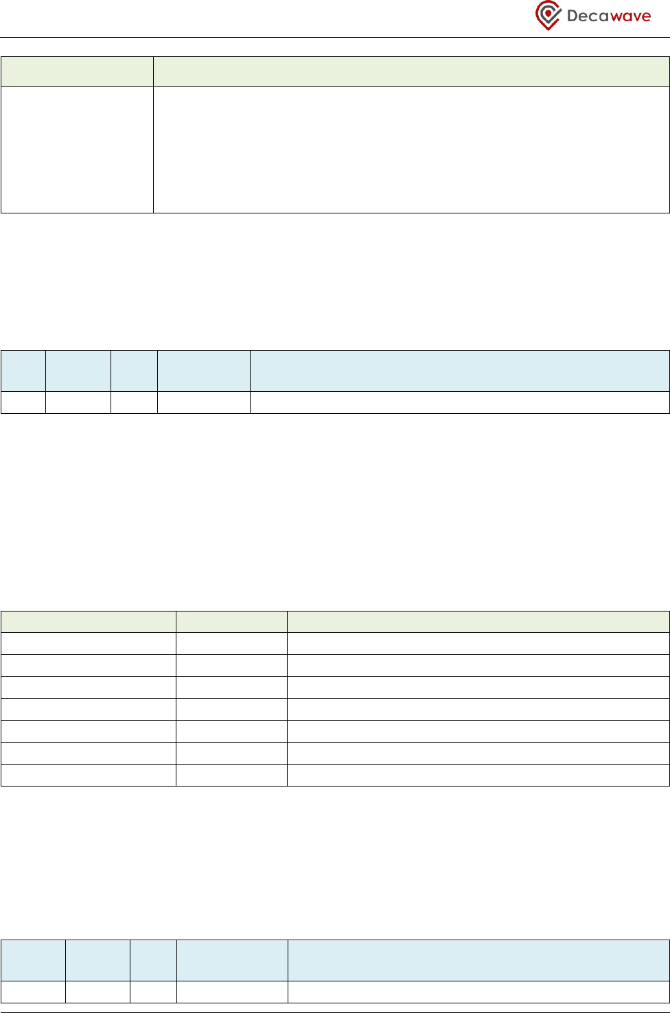
DW1000 User Manual
© Decawave Ltd 2017
Version 2.15
Page 178 of 244
Set
Description
01 – Tight
This operating parameter set maximises the operating range of the system. However this
performance optimization again comes at a cost, which is that the total crystal offset
between transmitter and receiver must be kept very tight, at or below about 1 ppm. This
might be done, for example, by using very high quality 0.5 ppm TCXOs in both the
transmitter and the receiver. The Tight operating parameter can only be selected via
direct host load control using the OPS_KICK and OPS_SEL controls in Sub-Register
0x2D:08 – OTP_STAT.
For most applications the default operating parameter set is the best choice. The use of the other operating
parameter sets may improve performance in particular use cases, but requires tighter control of clock
frequencies across the network of devices that have to interwork.
7.2.47 Register file: 0x2E – Leading Edge Detection Interface
ID
Length
(octets)
Type
Mnemonic
Description
0x2E
-
-
LDE_IF
Leading Edge Detection Interface
Register map register file 0x2E is the LDE control/status interface. The Leading Edge detection function is
responsible for analysing the accumulator data, (available in Register file: 0x25 – Accumulator CIR memory),
to find the first path and calculate the RX timestamp written to Register file: 0x15 – Receive Time Stamp and
the diagnostic information written into Register file: 0x12 – Rx Frame Quality Information. The LDE interface
contains a number of sub-registers. An overview of these sub-registers is given by Table 49 and each is then
separately described in the sub-sections below.
Table 49: Register file: 0x2E – Leading Edge Detection Interface overview
OFFSET in Register 0x2E
Mnemonic
Description
0x0000
LDE_THRESH
LDE Threshold report
0x0806
LDE_CFG1
LDE Configuration Register 1
0x1000
LDE_PPINDX
LDE Peak Path Index
0x1002
LDE_PPAMPL
LDE Peak Path Amplitude
0x1804
LDE_RXANTD
LDE Receive Antenna Delay configuration
0x1806
LDE_CFG2
LDE Configuration Register 2
0x2804
LDE_REPC
LDE Replica Coefficient configuration
PLEASE NOTE: Other areas within the address space of Register file: 0x2E – Leading Edge Detection Interface
are reserved. To ensure proper operation of the LDE algorithm (i.e. to avoid loss of performance or a
malfunction), care must be taken not to write to any byte locations other than those defined in the sub-
sections below.
7.2.47.1 Sub-Register 0x2E:0000 – LDE_THRESH
ID
Length
(octets)
Type
Mnemonic
Description
2E:0000
2
RO
LDE_THRESH
LDE Threshold report
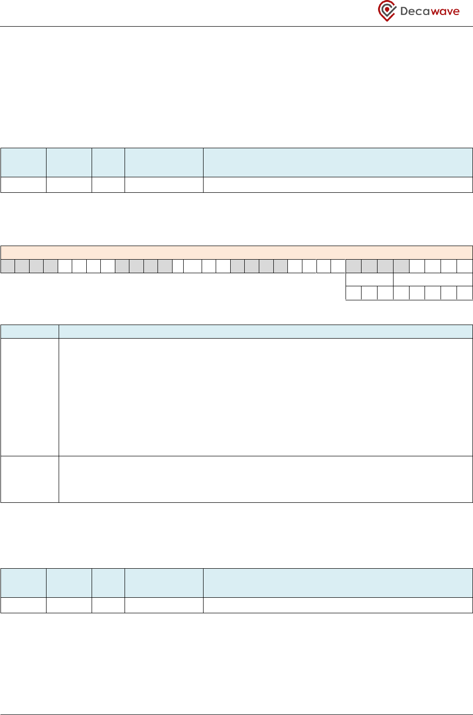
DW1000 User Manual
© Decawave Ltd 2017
Version 2.15
Page 179 of 244
Register file: 0x2E – Leading Edge Detection Interface, sub-register 0x0000 is a 16-bit status register
reporting the threshold that was used to find the first path. This threshold is calculated based on an
estimate of the noise made during the LDE algorithm’s analysis of the accumulator data. This threshold
report may be of diagnostic interest in certain circumstances.
7.2.47.2 Sub-Register 0x2E:0806 – LDE_CFG1
ID
Length
(octets)
Type
Mnemonic
Description
2E:0806
1
RW
LDE_CFG1
LDE Configuration Register 1
Register file: 0x2E – Leading Edge Detection Interface, sub-register 0x0806 is an8-bit configuration register
containing the following fields:
REG:2E:0806 – LDE_CFG1 – LDE Configuration Register 1
31
30
29
28
27
26
25
24
23
22
21
20
19
18
17
16
15
14
13
12
11
10
9
8
7
6
5
4
3
2
1
0
PMULT
NTM
0
1
1
0
1
1
0
0
The fields of the LDE_CFG1register are described below:
Field
Description of fields within Sub-Register 0x2E:0806 – LDE_CFG1
NTM
reg:2E:0806
bits:4–0
Noise Threshold Multiplier. This is a factor by which the observed noise level is multiplied to
set the threshold for the LDE algorithm’s first path search. By default NTM is 12. This value
was found to work well and give a reasonable compromise performance level between
falsely triggering on noise peaks and missing real attenuated (non-line-of-sight) first paths.
More recently an NTM value of 13 has been used in our device driver software to give more
accuracy in close-up LOS conditions. Where NLOS performance is more important to the
application the default NTM value of 0x07 (Note: This sets the upper 5 bits to 0) would be a
better choice. Refer to the application notes on NLOS available on www.Decawave.com for
more information.
PMULT
reg:2E:0806
bits:7–5
Peak Multiplier. This sets a factor by which the peak value of estimated noise is increased in
order to set the threshold for first path searching. By default this value is 3, giving a factor of
1.5, which has been found to work well. For NLOS operations these bits should be set to 0.
NB: To avoid any malfunction please ensure to only write one octet into the LDE_CFG1 register.
7.2.47.3 Sub-Register 0x2E:1000 – LDE_PPINDX
ID
Length
(octets)
Type
Mnemonic
Description
2E:1000
2
RO
LDE_PPINDX
LDE Peak Path Index
Register file: 0x2E – Leading Edge Detection Interface, sub-register 0x1000, is the LDE Peak Path Index
(LDE_PPINDX) register. This is a 16-bit status register reporting the position within the accumulator that the
LDE algorithm has determined to contain the maximum magnitude path. This value is set during the LDE
algorithm’s analysis of the accumulator data. This value may be of diagnostic interest in certain
DW1000 User Manual
© Decawave Ltd 2017
Version 2.15
Page 180 of 244
circumstances. The magnitude of the value at this index is reported in Sub-Register 0x2E:1002 –
LDE_PPAMPL.
7.2.47.4 Sub-Register 0x2E:1002 – LDE_PPAMPL
ID
Length
(octets)
Type
Mnemonic
Description
2E:1002
2
RO
LDE_PPAMPL
LDE Peak Path Amplitude
Register file: 0x2E – Leading Edge Detection Interface, sub-register 0x1002, is the LDE Peak Path Amplitude
(LDE_PPAMPL) register. This is a 16-bit status register reporting the magnitude of the peak signal seen in the
accumulator data memory during the LDE algorithm’s analysis, (the index at which this occurs is reported in
Sub-Register 0x2E:1000 – LDE_PPINDX). This value may be of diagnostic interest in certain circumstances.
7.2.47.5 Sub-Register 0x2E:1804 – LDE_RXANTD
ID
Length
(octets)
Type
Mnemonic
Description
2E:1804
2
RW
LDE_RXANTD
LDE Receive Antenna Delay configuration
Register file: 0x2E – Leading Edge Detection Interface, sub-register 0x1804 is a 16-bit configuration register
for setting the receive antenna delay. The receiver antenna delay is used to account for the delay between
the arrival of the RMARKER (the start of the PHR) at the antenna and the time the RMARKER is detected and
time-stamped by the internal digital RX circuitry. The units here are the same as those used for system time
and time stamps, i.e. 499.2 MHz × 128, so the least significant bit about 15.65 picoseconds.
The value programmed in this LDE_RXANTD register value is subtracted (by the LDE algorithm) from the raw
timestamp RX_RAWST to by the LDE algorithm which performs a number of other updates and
adjustments(including detecting and accounting for the first path position in the accumulator) in order to
generate the fully adjusted RX_STAMP value also in Register file: 0x15 – Receive Time Stamp.
Please refer to section 8.3 – IC Calibration – Antenna Delay for details of calibration of antenna delay.
7.2.47.6 Sub-Register 0x2E:1806– LDE_CFG2
ID
Length
(octets)
Type
Mnemonic
Description
2E:1806
2
RW
LDE_CFG2
LDE Configuration Register 2
Register file: 0x2E – Leading Edge Detection Interface, sub-register 0x1806 is a 16-bit LDE configuration
tuning register. The value here needs to change depending on the RXPRF configuration. The default values
required are given in Table 50 below. Other values may be appropriate in certain cirumstances as detailed in
applications information from Decawave.
DW1000 User Manual
© Decawave Ltd 2017
Version 2.15
Page 181 of 244
Table 50: Sub-Register 0x2E:1806– LDE_CFG2 values
RXPRF configuration
Value to program to
Sub-Register 0x2E:1806– LDE_CFG2
(1) = 16 MHz PRF
0x1607*
(2) = 64 MHz PRF
0x0607
* For NLOS operation this value has been optimized as 0x0003. Refer to the application notes on NLOS
available on www.Decawave.com for more information.
7.2.47.7 Sub-Register 0x2E:2804 – LDE_REPC
ID
Length
(octets)
Type
Mnemonic
Description
2E:2804
2
RW
LDE_REPC
LDE Replica Coefficient configuration
Register file: 0x2E – Leading Edge Detection Interface, sub-register 0x2804 is a 16-bit configuration register
for setting the replica avoidance coefficient. The accumulator operates on the preamble sequence to give
the channel impulse response. This works because of the perfect periodic auto-correlation property of the
IEEE 802.15.4 UWB preamble sequences. The auto-correlation is not perfect where there is a significant
clock offset between the remote transmitter and the local receiver. In these circumstances small amplitude
replicas of the channel impulse response appear repeatedly throughout the accumulator span. The
magnitude of this effect is dependent on the clock offset and on the preamble code being employed. To
avoid the LDE erroneously seeing one of these replica signals as the leading edge the threshold used for
detecting the first path is artificially raised by a factor depending on the measured clock offset. For optimum
performance this factor also needs to be dependent on the preamble code selected in the receiver. To
achieve this, the LDE_REPC configuration needs to be set depending on the receiver preamble code
configuration. The values required are given in Table 51. These values apply to 850 kbps and 6.8 Mbps data
rates only.
Table 51: Sub-Register 0x2E:2804 – LDE_REPC Values
* For NLOS operation this value has been optimized as 0x0003. Refer to the application notes on NLOS
available on www.Decawave.com for more information.
Sub-Register 0x2E:2804 – LDE_REPC configurations for (850 kbps & 6.8 Mbps)
RX_PCODE9
configuration
LDE_REPC
value to set
RX_PCODE
configuration
LDE_REPC
value to set
1
0x5998
13
0x3AE0
2
0x5998
14
0x35C2
3
0x51EA
15
0x2B84
9
RX_PCODE configuration is set Register file: 0x1F – Channel Control
DW1000 User Manual
© Decawave Ltd 2017
Version 2.15
Page 182 of 244
RX_PCODE9
configuration
LDE_REPC
value to set
RX_PCODE
configuration
LDE_REPC
value to set
4
0x428E
16
0x35C2
5
0x451E
17
0x3332
6
0x2E14
18
0x35C2
7
0x8000
19
0x35C2
8
0x51EA
20
0x47AE
9
0x28F4
21
0x3AE0
10
0x3332
22
0x3850
11
0x3AE0
23
0x30A2
12
0x3D70
24
0x3850
NB: When operating at 110 kbps the unsigned values in Table 51 have to be divided by 8, (right shifted 3,
shifting zeroes into the high order bits), before programming into Sub-Register 0x2E:2804 – LDE_REPC.
* For NLOS operation this value has been optimised as 0x0003. Please see Application noteson NLOS
available on www.Decawave.com for more information.
7.2.48 Register file: 0x2F – Digital Diagnostics Interface
ID
Length
(octets)
Type
Mnemonic
Description
0x2F
41
-
DIG_DIAG
Digital Diagnostics Interface
Register map register file 0x2F is the Digital Diagnostics interface. It contains a number of sub-registers that
give diagnostics information. An overview of these is given by Table 52. Each of these sub-registers is
separately described in the sub-sections below.
Table 52: Register file: 0x2F – Digital Diagnostics Interface overview
OFFSET in Register 0x2F
Mnemonic
Description
0x00
EVC_CTRL
Event Counter Control
0x04
EVC_PHE
PHR Error Counter
0x06
EVC_RSE
RSD Error Counter
0x08
EVC_FCG
Frame Check Sequence Good Counter
0x0A
EVC_FCE
Frame Check Sequence Error Counter
0x0C
EVC_FFR
Frame Filter Rejection Counter
0x0E
EVC_OVR
RX Overrun Error Counter
0x10
EVC_STO
SFD Timeout Counter
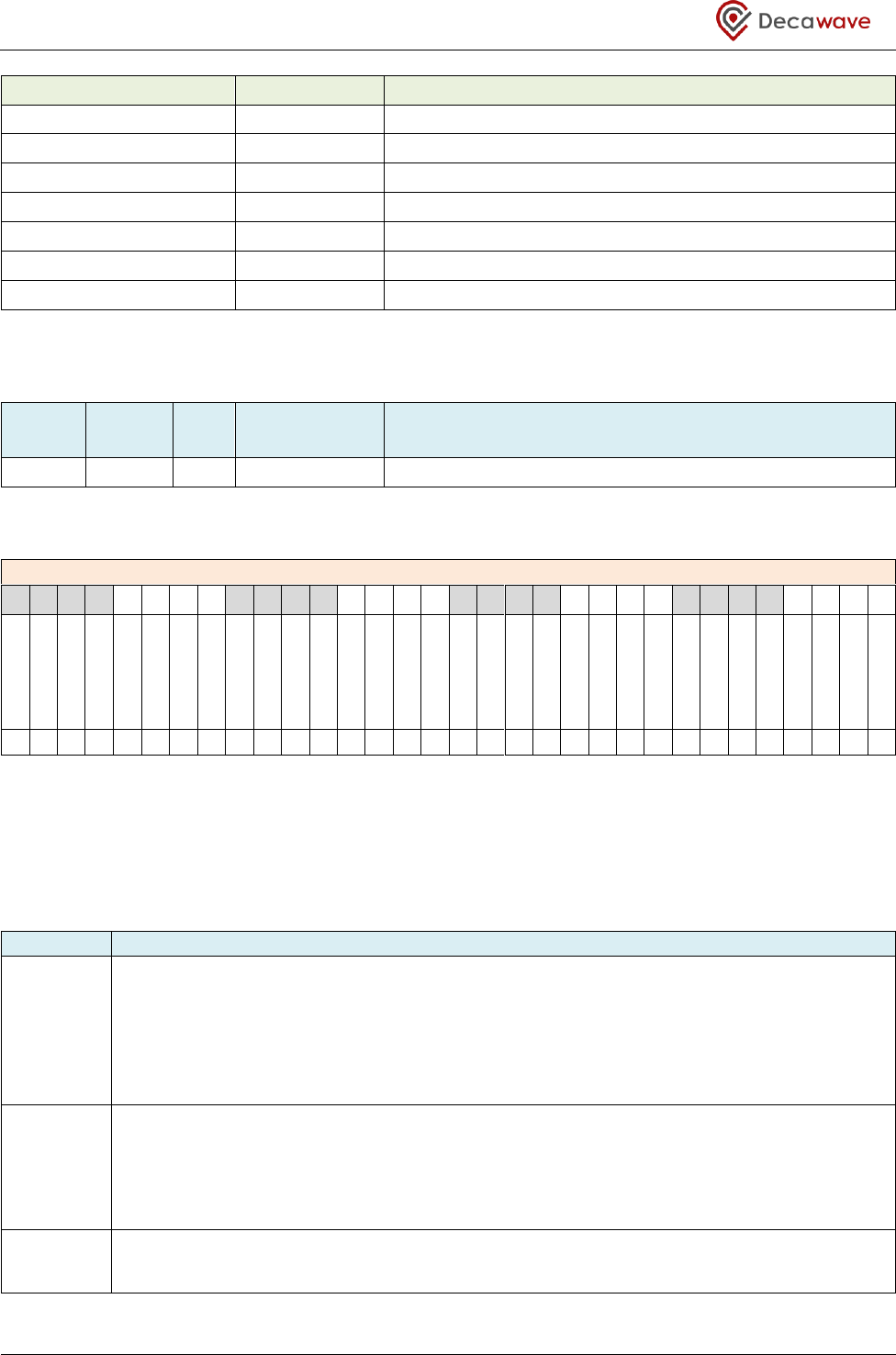
DW1000 User Manual
© Decawave Ltd 2017
Version 2.15
Page 183 of 244
OFFSET in Register 0x2F
Mnemonic
Description
0x12
EVC_PTO
Preamble Timeout Counter
0x14
EVC_FWTO
RX Frame Wait Timeout Counter
0x16
EVC_TXFS
TX Frame Sent Counter
0x18
EVC_HPW
Half Period Warning Counter
0x1A
EVC_TPW
Transmitter Power-Up Warning Counter
0x1C
EVC_RES1
Digital Diagnostics Reserved Area 1
0x24
DIAG_TMC
Test Mode Control Register
7.2.48.1 Sub-Register 0x2F:00 – Event Counter Control
ID
Length
(octets)
Type
Mnemonic
Description
2F:00
4
SRW
EVC_CTRL
Event Counter Control
Register file: 0x2F – Digital Diagnostics Interface, sub-register 0x00 is the event counter control register.
REG:2F:00 – EVC_CTRL – Event Counter Control
31
30
29
28
27
26
25
24
23
22
21
20
19
18
17
16
15
14
13
12
11
10
9
8
7
6
5
4
3
2
1
0
-
-
-
-
-
-
-
-
-
-
-
-
-
-
-
-
-
-
-
-
-
-
-
-
-
-
-
-
-
-
EVC_CLR
EVC_EN
-
-
-
-
-
-
-
-
-
-
-
-
-
-
-
-
-
-
-
-
-
-
-
-
-
-
-
-
-
-
0
0
Fields in the EVC_CTRL register are intended to be self-clearing. So, the event counters can be enabled or
cleared, but cannot be disabled. The register expects a two-byte minimum length write to the lowest two
bytes of the register. If a one-byte write is made to this register, the bits will not clear as expected.
The bits of the EVC_CTRL register identified above are individually described below:
Field
Description of fields within Sub-Register 0x2F:00 – Event Counter Control
EVC_EN
reg:2F:00
bit:0
Event Counters Enable. The EVC_EN bit acts to enable the event counters. When EVC_EN bit
is zero none of the event counters will update. When EVC_EN bit is set to 1 it enables event
counting. A number of sub-registers of Register file: 0x2F – Digital Diagnostics Interface,
contain counters of various system events – see below for the detailed description of the
parameters counted. If the host system has no interest in these event counters then a small
amount of power is saved by not enabling event counting.
EVC_CLR
reg:2F:00
bit:1
Event Counters Clear. The EVC_CLR bit acts to clear event counters to zero. This cannot be
done while EVC_EN bit is set. The correct procedure to clear the event counters is to write
0x02 to Sub-Register 0x2F:00 – Event Counter Control to disable counting and clear the counter
values to zero, and then to write 0x01 to Sub-Register 0x2F:00 – Event Counter Control to re-
enable counting if required.
-
reg:2F:00
bits:31–2
The remaining bits of Sub-Register 0x2F:00 – Event Counter Control are reserved and should
always be set to zero to avoid any malfunction of the device.

DW1000 User Manual
© Decawave Ltd 2017
Version 2.15
Page 184 of 244
7.2.48.2 Sub-Register 0x2F:04 – PHR Error Counter
ID
Length
(octets)
Type
Mnemonic
Description
2F:04
2
RO
EVC_PHE
PHR Error Event Counter
Register file: 0x2F – Digital Diagnostics Interface, sub-register 0x04is the PHY Header Error event counter.
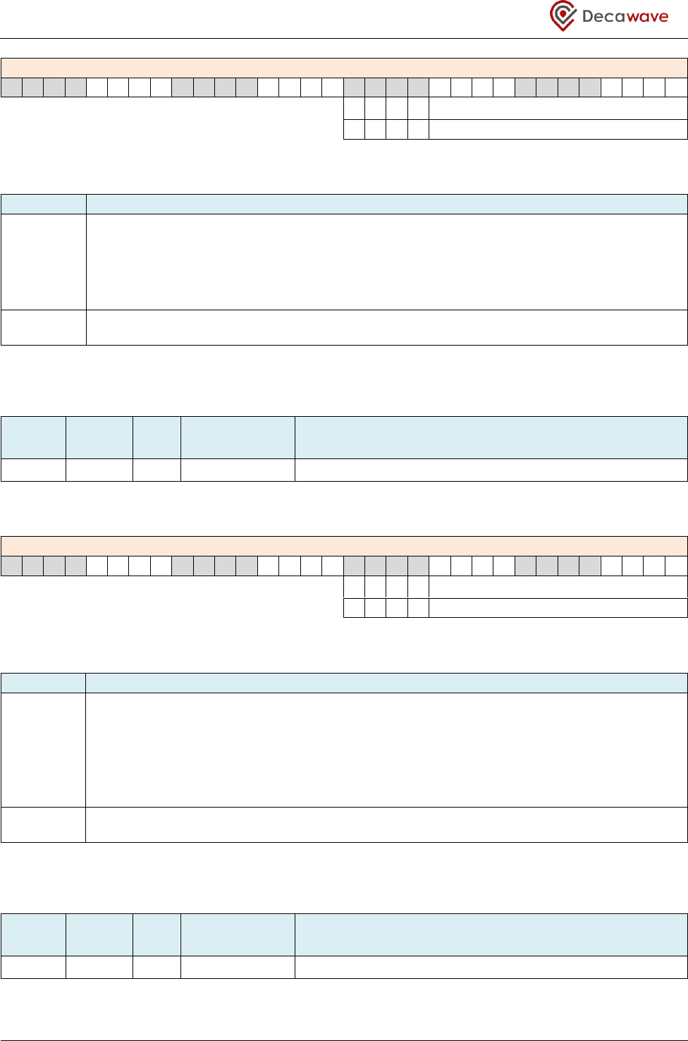
DW1000 User Manual
© Decawave Ltd 2017
Version 2.15
Page 185 of 244
REG:2F:04 – EVC_PHE – PHR Error Counter
31
30
29
28
27
26
25
24
23
22
21
20
19
18
17
16
15
14
13
12
11
10
9
8
7
6
5
4
3
2
1
0
-
-
-
-
EVC_PHE
-
-
-
-
0
The fields of the EVC_PHE register are described below:
Field
Description of fields within Sub-Register 0x2F:04 – PHR Error Counter
EVC_PHE
reg:2F:04
bits:11–0
PHR Error Event Counter. The EVC_PHE field is a 12-bit counter of PHY Header Errors. This
counts the reporting of RXPHE error events in Register file: 0x0F – System Event Status
Register.
NB: For this counter to be active, counting needs to be enabled by the setting the EVC_EN
bit in Sub-Register 0x2F:00 – Event Counter Control.
-
bits:15–12
The remaining bits of this register are reserved.
7.2.48.3 Sub-Register 0x2F:06 – RSD Error Counter
ID
Length
(octets)
Type
Mnemonic
Description
2F:06
2
RO
EVC_RSE
RSD Error Event Counter
Register file: 0x2F – Digital Diagnostics Interface, sub-register 0x06 is the RSD Error event counter.
REG:2F:06 – EVC_RSE – RSD Error Counter
31
30
29
28
27
26
25
24
23
22
21
20
19
18
17
16
15
14
13
12
11
10
9
8
7
6
5
4
3
2
1
0
-
-
-
-
EVC_RSE
-
-
-
-
0
The fields of the EVC_RSE register are described below:
Field
Description of fields within Sub-Register 0x2F:06 – RSD Error Counter
EVC_RSE
reg:2F:06
bits:11–0
Reed Solomon decoder (Frame Sync Loss) Error Event Counter. The EVC_RSE field is a 12-bit
counter of the non-correctable error events that can occur during Reed Solomon decoding.
This counts the reporting of RXRFSL error events in Register file: 0x0F – System Event Status
Register.
NB: For this counter to be active, counting needs to be enabled by the setting the EVC_EN bit
in Sub-Register 0x2F:00 – Event Counter Control.
-
bits:15–12
The remaining bits of this register are reserved.
7.2.48.4 Sub-Register 0x2F:08 – FCS Good Counter
ID
Length
(octets)
Type
Mnemonic
Description
2F:08
2
RO
EVC_FCG
Frame Check Sequence Good Event Counter
Register file: 0x2F – Digital Diagnostics Interface, sub-register 0x08 is the FCS good event counter.
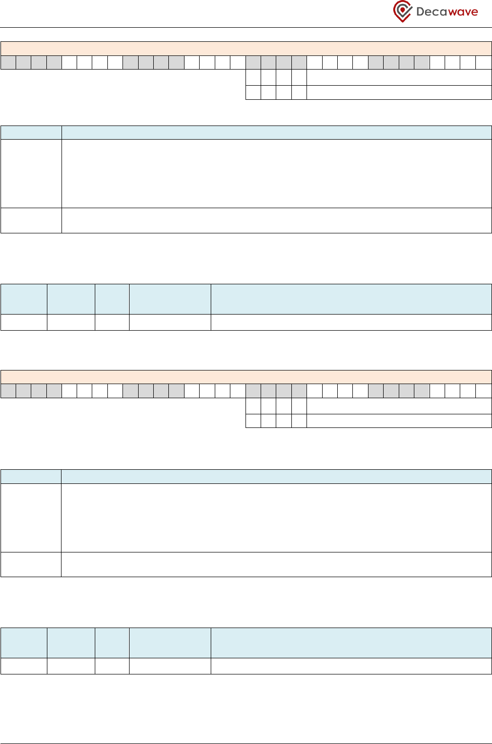
DW1000 User Manual
© Decawave Ltd 2017
Version 2.15
Page 186 of 244
REG:2F:08 – EVC_FCG – Frame Check Sequence Good Event Counter
31
30
29
28
27
26
25
24
23
22
21
20
19
18
17
16
15
14
13
12
11
10
9
8
7
6
5
4
3
2
1
0
-
-
-
-
EVC_FCG
-
-
-
-
0
The bits of the EVC_FCG register are described below:
Field
Description of fields within Sub-Register 0x2F:08 – FCS Good Counter
EVC_FCG
reg:2F:08
bits:11–0
Frame Check Sequence Good Event Counter. The EVC_FCG field is a 12-bit counter of the
frames received with good CRC/FCS sequence. This counts the reporting of RXFCG events in
Register file: 0x0F – System Event Status Register.
NB: For this counter to be active, counting needs to be enabled by the setting the EVC_EN
bit in Sub-Register 0x2F:00 – Event Counter Control.
-
bits:15–12
The remaining bits of this register are reserved.
7.2.48.5 Sub-Register 0x2F:0A – FCS Error Counter
ID
Length
(octets)
Type
Mnemonic
Description
2F:0A
2
RO
EVC_FCE
Frame Check Sequence Error Counter
Register file: 0x2F – Digital Diagnostics Interface, sub-register 0x0A is the FCS Error event counter.
REG:2F:0A – EVC_FCE – FCS Error Counter
31
30
29
28
27
26
25
24
23
22
21
20
19
18
17
16
15
14
13
12
11
10
9
8
7
6
5
4
3
2
1
0
-
-
-
-
EVC_FCE
-
-
-
-
0
The bits of the EVC_FCE register are described below:
Field
Description of fields within Sub-Register 0x2F:0A – FCS Error Counter
EVC_FCE
reg:2F:0A
bits:11–0
Frame Check Sequence Error Event Counter. The EVC_FCE field is a 12-bit counter of the
frames received with bad CRC/FCS sequence. This counts the reporting of RXFCE events in
Register file: 0x0F – System Event Status Register.
NB: For this counter to be active, counting needs to be enabled by the setting the EVC_EN bit
in Sub-Register 0x2F:00 – Event Counter Control.
-
bits:15–12
The remaining bits of this register are reserved.
7.2.48.6 Sub-Register 0x2F:0C – Frame Filter Rejection Counter
ID
Length
(octets)
Type
Mnemonic
Description
2F:0C
2
RO
EVC_FFR
Frame Filter Rejection Counter
Register file: 0x2F – Digital Diagnostics Interface, sub-register 0x0C is the Frame Filter Rejection counter.
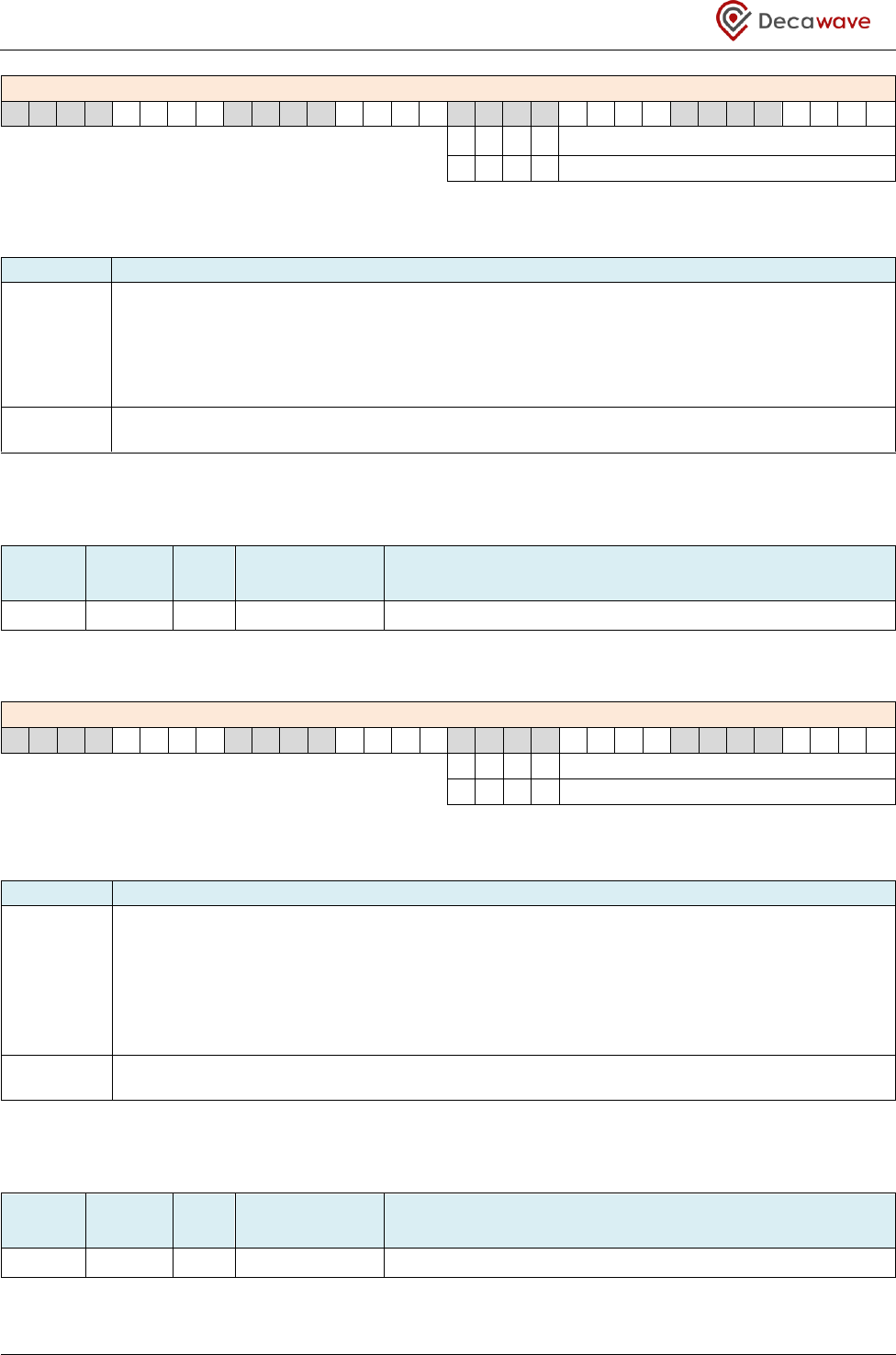
DW1000 User Manual
© Decawave Ltd 2017
Version 2.15
Page 187 of 244
REG:2F:0C – EVC_FFR – Frame Filter Rejection Counter
31
30
29
28
27
26
25
24
23
22
21
20
19
18
17
16
15
14
13
12
11
10
9
8
7
6
5
4
3
2
1
0
-
-
-
-
EVC_FFR
-
-
-
-
0
The bits of the EVC_FFR register are described below:
Field
Description of fields within Sub-Register 0x2F:0C – Frame Filter Rejection Counter
EVC_FFR
reg:2F:0C
bits:11–0
Frame Filter Rejection Event Counter. The EVC_FFR field is a 12-bit counter of the frames
rejected by the receive frame filtering function. This is essentially a count of the reporting of
AFFREJ events (in Register file: 0x0F – System Event Status Register).
NB: For this counter to be active, counting needs to be enabled by the setting the EVC_EN bit
in Sub-Register 0x2F:00 – Event Counter Control.
-
bits:15–12
The remaining bits of this register are reserved.
7.2.48.7 Sub-Register 0x2F:0E – RX Overrun Error Counter
ID
Length
(octets)
Type
Mnemonic
Description
2F:0E
2
RO
EVC_OVR
RX Overrun Error Counter
Register file: 0x2F – Digital Diagnostics Interface, sub-register 0x0E is the RX Overrun Error counter.
REG:2F:0E – EVC_OVR – RX Overrun Error Counter
31
30
29
28
27
26
25
24
23
22
21
20
19
18
17
16
15
14
13
12
11
10
9
8
7
6
5
4
3
2
1
0
-
-
-
-
EVC_OVR
-
-
-
-
0
The bits of the EVC_OVR register are described below:
Field
Description of fields within Sub-Register 0x2F:0C – Frame Filter Rejection Counter
EVC_OVR
reg:2F:0E
bits:11–0
RX Overrun Error Event Counter. The EVC_OVR field is a 12-bit counter of receive overrun
events. This is essentially a count of the reporting of RXOVRR events in Register file: 0x0F –
System Event Status Register. The EVC_OVR will be incremented once for each RX frame
discard that happens while an overrun condition persists.
NB: For this counter to be active, counting needs to be enabled by the setting the EVC_EN
bit in Sub-Register 0x2F:00 – Event Counter Control.
-
bits:15–12
The remaining bits of this register are reserved.
7.2.48.8 Sub-Register 0x2F:10 – SFD Timeout Error Counter
ID
Length
(octets)
Type
Mnemonic
Description
2F:10
2
RO
EVC_STO
SFD Timeout Error Counter
Register file: 0x2F – Digital Diagnostics Interface, sub-register 0x10 is the SFD Timeout Error counter.
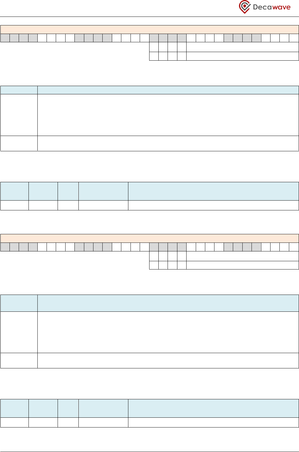
DW1000 User Manual
© Decawave Ltd 2017
Version 2.15
Page 188 of 244
REG:2F:10 – EVC_STO – SFD Timeout Error Counter
31
30
29
28
27
26
25
24
23
22
21
20
19
18
17
16
15
14
13
12
11
10
9
8
7
6
5
4
3
2
1
0
-
-
-
-
EVC_STO
-
-
-
-
0
The bits of the EVC_STO register are described below:
Field
Description of fields within Sub-Register 0x2F:10 – SFD Timeout Error Counter
EVC_STO
reg:2F:10
bits:11–0
SFD timeout errors Event Counter. The EVC_STO field is a 12-bit counter of SFD Timeout Error
events. This is essentially a count of the reporting of RXSFDTO events in Register file: 0x0F –
System Event Status Register.
NB: For this counter to be active, counting needs to be enabled by the setting the EVC_EN bit
in Sub-Register 0x2F:00 – Event Counter Control.
-
bits:15–12
The remaining bits of this register are reserved.
7.2.48.9 Sub-Register 0x2F:12 – Preamble Detection Timeout Event Counter
ID
Length
(octets)
Type
Mnemonic
Description
2F:12
2
RO
EVC_PTO
Preamble Detection Timeout Event Counter
Register file: 0x2F – Digital Diagnostics Interface, sub-register 0x12 is the Preamble Timeout Event Counter.
REG:2F:12 – EVC_PTO – Preamble Detection Timeout Event Counter
31
30
29
28
27
26
25
24
23
22
21
20
19
18
17
16
15
14
13
12
11
10
9
8
7
6
5
4
3
2
1
0
-
-
-
-
EVC_PTO
-
-
-
-
0
The bits of the EVC_PTO register are described below:
Field
Description of fields within Sub-Register 0x2F:12 – Preamble Detection Timeout Event
Counter
EVC_PTO
reg:2F:12
bits:11–0
Preamble Detection Timeout Event Counter. The EVC_PTO field is a 12-bit counter of
Preamble detection Timeout events. This is essentially a count of the reporting of RXPTO
events, in Register file: 0x0F – System Event Status Register.
NB: For this counter to be active, counting needs to be enabled by the setting the EVC_EN bit
in Sub-Register 0x2F:00 – Event Counter Control.
-
bits:15–12
The remaining bits of this register are reserved.
7.2.48.10 Sub-Register 0x2F:14 – RX Frame Wait Timeout Event Counter
ID
Length
(octets)
Type
Mnemonic
Description
2F:14
2
RO
EVC_FWTO
RX Frame Wait Timeout Counter
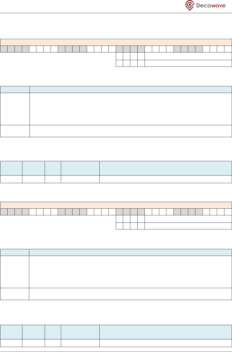
DW1000 User Manual
© Decawave Ltd 2017
Version 2.15
Page 189 of 244
Register file: 0x2F – Digital Diagnostics Interface, sub-register 0x14 is the RX Frame Wait Timeout Event
Counter.
REG:2F:14 – EVC_FWTO – RX Frame Wait Timeout Event Counter
31
30
29
28
27
26
25
24
23
22
21
20
19
18
17
16
15
14
13
12
11
10
9
8
7
6
5
4
3
2
1
0
-
-
-
-
EVC_FWTO
-
-
-
-
0
The bits of the EVC_FWTO register are described below:
Field
Description of fields within Sub-Register 0x2F:14 – RX Frame Wait Timeout Event Counter
EVC_FWTO
reg:2F:14
bits:11–0
RX Frame Wait Timeout Event Counter. The EVC_FWTO field is a 12-bit counter of receive
frame wait timeout events. This is essentially a count of the reporting of the RXRFTO events
in Register file: 0x0F – System Event Status Register.
NB: For this counter to be active, counting needs to be enabled by the setting the EVC_EN bit
in Sub-Register 0x2F:00 – Event Counter Control.
-
bits:15–12
The remaining bits of this register are reserved.
7.2.48.11 Sub-Register 0x2F:16 – TX Frame Sent Counter
ID
Length
(octets)
Type
Mnemonic
Description
2F:16
2
RO
EVC_TXFS
TX Frame Sent Counter
Register file: 0x2F – Digital Diagnostics Interface, sub-register 0x16 is the TX Frame Sent Counter.
REG:2F:16 – EVC_TXFS – TX Frame Sent Counter
31
30
29
28
27
26
25
24
23
22
21
20
19
18
17
16
15
14
13
12
11
10
9
8
7
6
5
4
3
2
1
0
-
-
-
-
EVC_TXFS
-
-
-
-
0
The bits of the EVC_TXFS register are described below:
Field
Description of fields within Sub-Register 0x2F:16 – TX Frame Sent Counter
EVC_TXFS
reg:2F:16
bits:11–0
TX Frame Sent Event Counter. The EVC_TXFS field is a 12-bit counter of transmit frames sent.
This is incremented every time a frame is sent. It is essentially a count of the reporting of the
TXFRS events in Register file: 0x0F – System Event Status Register.
NB: For this counter to be active, counting needs to be enabled by the setting the EVC_EN bit
in Sub-Register 0x2F:00 – Event Counter Control.
-
bits:15–12
The remaining bits of this register are reserved.
7.2.48.12 Sub-Register 0x2F:18 – Half Period Warning Counter
ID
Length
(octets)
Type
Mnemonic
Description
2F:18
2
RO
EVC_HPW
Half Period Warning Counter
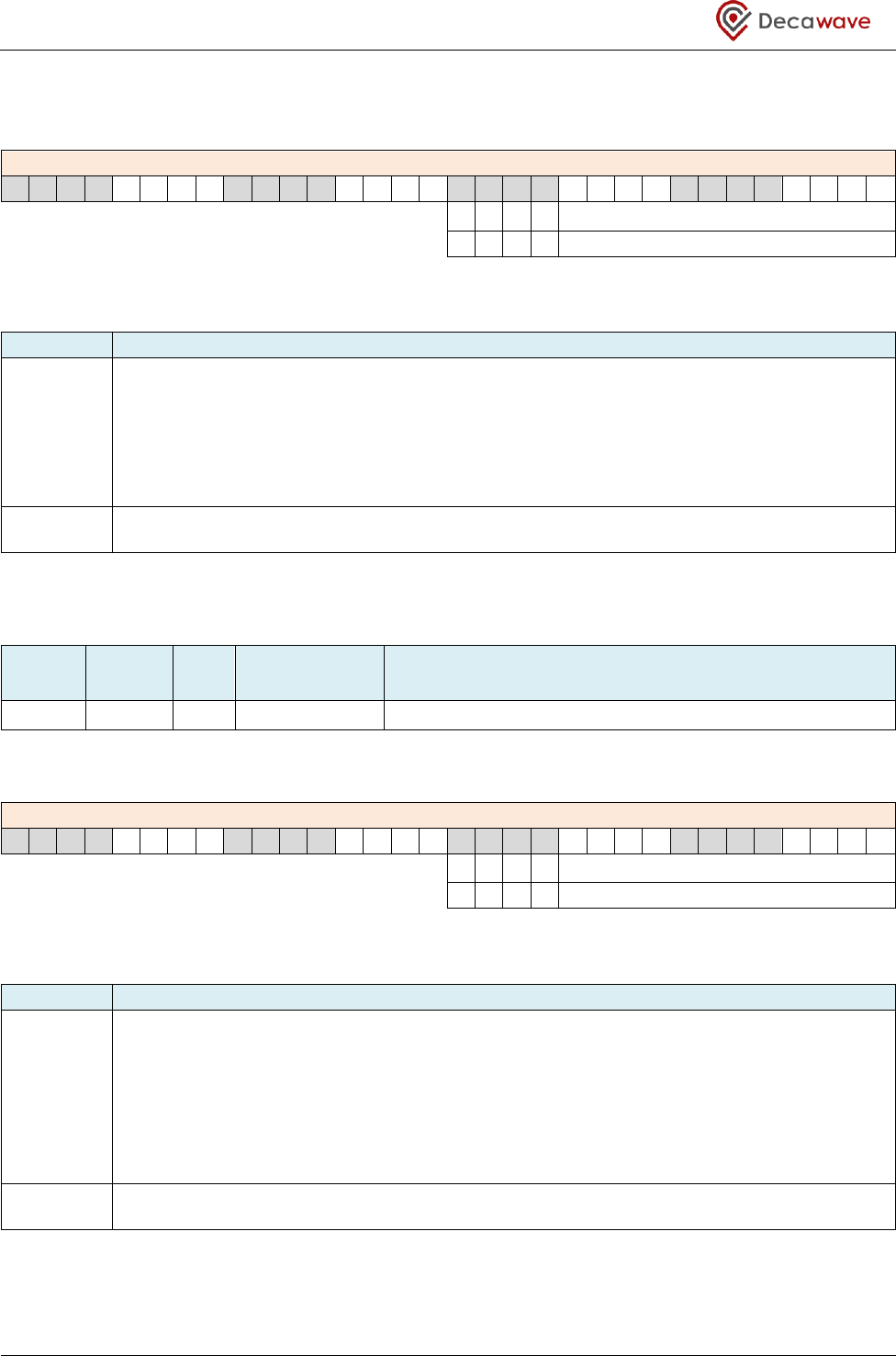
DW1000 User Manual
© Decawave Ltd 2017
Version 2.15
Page 190 of 244
Register file: 0x2F – Digital Diagnostics Interface, sub-register 0x18 is the Half Period Warning Counter.
REG:2F:18 – EVC_HPW – Half Period Warning Counter
31
30
29
28
27
26
25
24
23
22
21
20
19
18
17
16
15
14
13
12
11
10
9
8
7
6
5
4
3
2
1
0
-
-
-
-
EVC_HPW
-
-
-
-
0
The bits of the EVC_HPW register are described below:
Field
Description of fields within Sub-Register 0x2F:18 – Half Period Warning Counter
EVC_HPW
reg:2F:18
bits:11–0
Half Period Warning Event Counter. The EVC_HPW field is a 12-bit counter of “Half Period
Warnings”. This is a count of the reporting of the HPDWARN events in Register file: 0x0F –
System Event Status Register. These relate to late invocation of delayed transmission or
reception functionality. Please refer to the description of the HPDWARN bit for more details
of this event and its meaning. NB: For this counter to be active, counting needs to be
enabled by the setting the EVC_EN bit in Sub-Register 0x2F:00 – Event Counter Control.
-
bits:15–12
The remaining bits of this register are reserved.
7.2.48.13 Sub-Register 0x2F:1A – Transmitter Power-Up Warning Counter
ID
Length
(octets)
Type
Mnemonic
Description
2F:1A
2
RO
EVC_TPW
Transmitter Power-Up Warning Counter
Register file: 0x2F – Digital Diagnostics Interface, sub-register 0x1A is the TX Power-Up Warning Counter.
REG:2F:1A – EVC_TPW – Transmitter Power-Up Warning Counter
31
30
29
28
27
26
25
24
23
22
21
20
19
18
17
16
15
14
13
12
11
10
9
8
7
6
5
4
3
2
1
0
-
-
-
-
EVC_TPW
-
-
-
-
0
The bits of the EVC_TPW register are described below:
Field
Description of fields within Sub-Register 0x2F:1A – Transmitter Power-Up Warning Counter
EVC_TPW
reg:2F:1A
bits:11–0
TX Power-Up Warning Event Counter. The EVC_TPW field is a 12-bit counter of “Transmitter
Power-Up Warnings”. This is a count of the reporting of the TXPUTE events in Register file:
0x0F – System Event Status Register. These relate to a delayed sent time that is too short to
allow proper power up of the TX blocks before the delayed transmission is due to start.
Please refer to the description of the TXPUTE bit for more details of this event.
NB: For this counter to be active, counting needs to be enabled by the setting the EVC_EN
bit in Sub-Register 0x2F:00 – Event Counter Control.
-
bits:15–12
The remaining bits of this register are reserved.
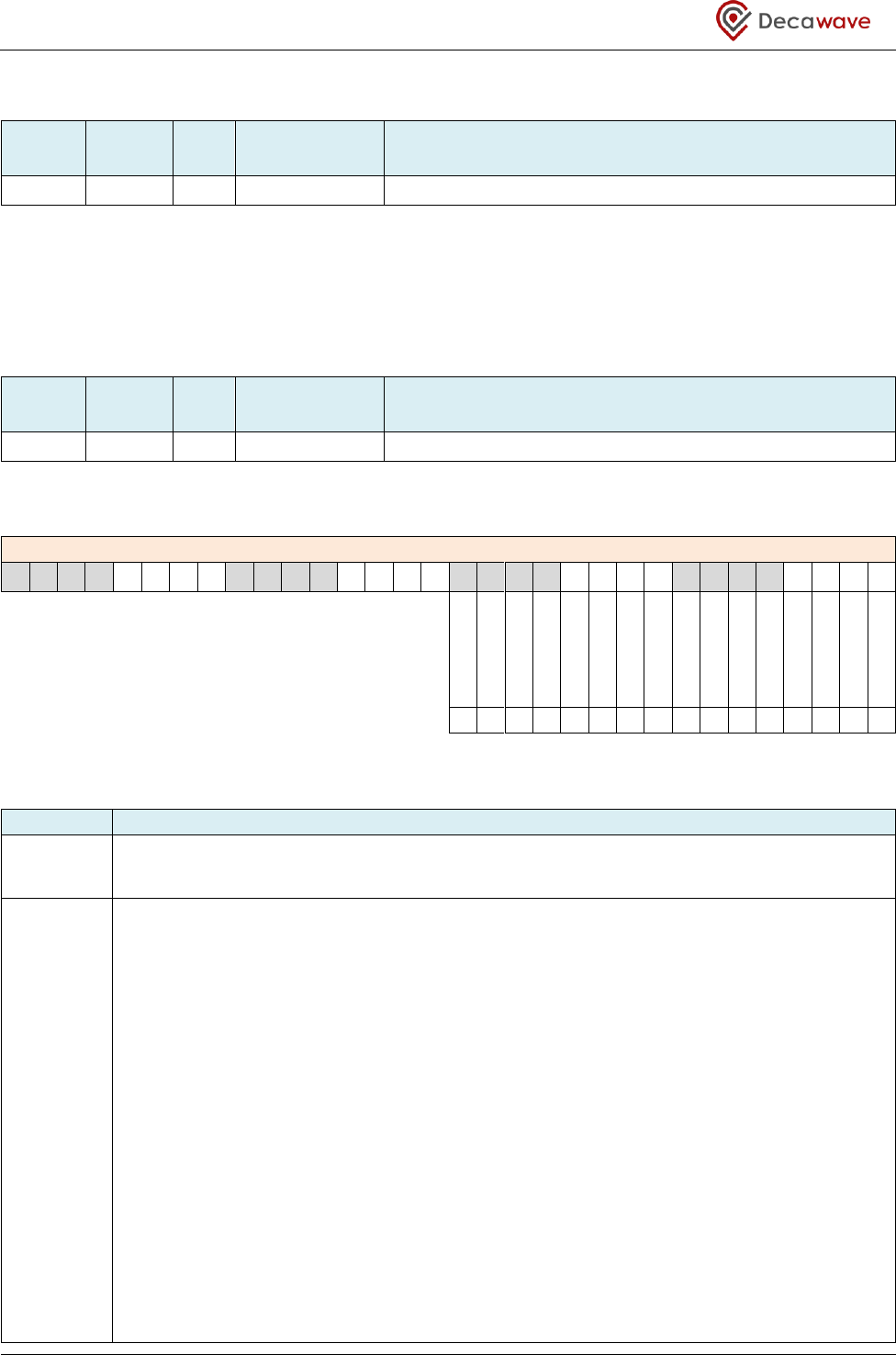
DW1000 User Manual
© Decawave Ltd 2017
Version 2.15
Page 191 of 244
7.2.48.14 Sub-Register 0x2F:1C – EVC_RES1
ID
Length
(octets)
Type
Mnemonic
Description
2F:1C
8
RW
EVC_RES1
Digital Diagnostics Reserved Area 1
Register file: 0x2F – Digital Diagnostics Interface, sub-register 0x1C is a reserved register. Please take care
not to write to this register as doing so may cause the DW1000 to malfunction.
7.2.48.15 Sub-Register 0x2F:24 – Digital Diagnostics Test Mode Control
ID
Length
(octets)
Type
Mnemonic
Description
2F:24
2
RW
DIAG_TMC
Test Mode Control Register
Register file: 0x2F – Digital Diagnostics Interface, sub-register 0x24 is the Test Mode control register.
REG:2F:24 – DIAG_TMC – Digital Diagnostics Test Mode Control
31
30
29
28
27
26
25
24
23
22
21
20
19
18
17
16
15
14
13
12
11
10
9
8
7
6
5
4
3
2
1
0
-
-
-
-
-
-
-
-
-
-
-
TX_PSTM
-
-
-
-
0
0
0
0
0
0
0
0
0
0
0
0
0
0
0
0
The bits of the DIAG_TMC register identified above are individually described below:
Field
Description of fields within Sub-Register 0x2F:24 – Digital Diagnostics Test Mode Control
-
reg:2F:24
bit:VARIOUS
These bits of the DIAG_TMC register are reserved and should always be set to zero to avoid
any malfunction of the device.
TX_PSTM
reg:2F:24
bit:4
Transmit Power Spectrum Test Mode. This test mode is provided to help support regulatory
approvals spectral testing. When the TX_PSTM bit is set it enables a repeating transmission
of the data from the TX_BUFFER. To use this test mode, the operating channel, preamble
code, data length, offset, etc. should all be set-up as if for a normal transmission.
The start-to-start delay between frames is programmed in the DX_TIME register. This is a
special use of that register, where bits 31 to 0 are used, and the value is programmed in
units of one quarter of the 499.2 MHz fundamental frequency, (~ 8 ns). To send one frame
per millisecond, a value of 124800 or 0x0001E780 should be programmed into the DX_TIME
register. A value <4 should not be used. A time value less than the frame duration will cause
an unpredictable inter-frame spacing and should not be used. To send back-to-back frames
the time value should be set to the frame duration.
When the mode and delay and TX buffer have been configured and the TX_PSTM bit is set,
the repeated TX mode is initiated by setting TXSTRT bit in Register file: 0x0D – System
Control Register.
To exit the Transmit Power Spectrum test mode reset the TX_PSTM bit to zero.
DW1000 User Manual
© Decawave Ltd 2017
Version 2.15
Page 192 of 244
7.2.49 Register files: 0x30 to 0x35 – Reserved
ID
Length
(octets)
Type
Mnemonic
Description
0x30
to
0x35
-
-
-
Reserved – these register files are reserved
Register map register files 0x30 through 0x35 are reserved for future use. Please take care not to write to
these registers as doing so may cause the DW1000 to malfunction.
7.2.50 Register file: 0x36 – Power Management and System Control
ID
Length
(octets)
Type
Mnemonic
Description
0x36
-
-
PMSC
Power Management System Control Block
Register map register file 0x36 is a control block for DW1000 power management and system control.
An overview of these is given by Table 53. Each of these sub-registers is separately described in the sub-
sections below.
Table 53: Register file: 0x36 – Power Management and System Control overview
OFFSET in Register
0x36
Mnemonic
Description
0x00
PMSC_CTRL0
PMSC Control Register 0
0x04
PMSC_CTRL1
PMSC Control Register 1
0x08
PMSC_RES1
PMSC reserved area 1
0x0C
PMSC_SNOZT
PMSC Snooze Time Register
0x10
PMSC_RES2
PMSC reserved area 2
0x26
PMSC_TXFSEQ
PMSC fine grain TX sequencing control
0x28
PMSC_LEDC
PMSC LED Control Register
7.2.50.1 Sub-Register 0x36:00 – PMSC_CTRL0
ID
Length
(octets)
Type
Mnemonic
Description
36:00
4
RW
PMSC_CTRL0
PMSC Control Register 0
Register file: 0x36 – Power Management and System Control, sub-register 0x00 is a 32-bit control register
relating to enabling clocking to various digital blocks within the DW1000. This register also has a field
allowing a software applied reset to be applied to the IC. The PMSC_CTRL0 register contains the following
sub-fields:

DW1000 User Manual
© Decawave Ltd 2017
Version 2.15
Page 193 of 244
REG:36:00 – PMSC_CTRL0 – PMSC Control Register 0
31
30
29
28
27
26
25
24
23
22
21
20
19
18
17
16
15
14
13
12
11
10
9
8
7
6
5
4
3
2
1
0
SOFTRESET
-
-
-
PLL2_SEQ_EN
KHZCLKEN
-
-
-
GPDRN
GPDCE
GPRN
GPCE
AMCE
-
-
-
-
ADCCE
-
-
-
FACE
TXCLKS
RXCLKS
SYSCLKS
1
1
1
1
0
0
0
0
0
0
1
1
0
0
0
0
0
0
0
0
0
0
1
0
0
0
0
0
0
0
0
0
The fields of the PMSC_CTRL0 register identified above are individually described below:
Field
Description of fields within Sub-Register 0x36:00 – PMSC_CTRL0
-
Bits marked ‘-’ are reserved and should be preserved at their reset value.
SYSCLKS
reg:36:00
bits:1,0
System Clock Selection. This selects the source of clock for DW1000 system clock.
Allowed values are:
00: Auto – The system clock will run off the 19.2 MHz XTI clock until the PLL is calibrated
and locked, then it will switch over the 125 MHz PLL clock.
01: Force system clock to be the 19.2 MHz XTI clock.
10: Force system clock to the 125 MHz PLL clock. (If this clock is not present the DW1000
will essentially lock up with further SPI communications impossible. In this case an
external reset will be needed to recover).
11: Reserved.
This control is used for certain procedures, e.g. to set system clock to be the 19.2 MHz XTI
clock for manual access to OTP Memory.
RXCLKS
reg:36:00
bits:3,2
Receiver Clock Selection. This selects the source of clock for the DW1000 receiver.
Allowed values are:
00: Auto – The RX clock will be disabled until it is required for an RX operation, at which
time it will be enabled to use the 125 MHz PLL clock.
01: Force RX clock enable and sourced clock from the 19.2 MHz XTI clock
10: Force RX clock enable and sourced from the 125 MHz PLL clock. (NB: ensure PLL
clock is present).
11: Force RX clock off.
This control is used for certain procedures, e.g. after a receive operation, if the host
system wants to read the Channel Impulse Response Estimate (CIRE) for diagnostic
purposes then, the receive clock needs to be present to access the accumulator memory.

DW1000 User Manual
© Decawave Ltd 2017
Version 2.15
Page 194 of 244
Field
Description of fields within Sub-Register 0x36:00 – PMSC_CTRL0
TXCLKS
reg:36:00
bits:5,4
Transmitter Clock Selection. This selects the source of clock for the DW1000 transmitter.
Allowed values are:
00: Auto – The TX clock will be disabled until it is required for a TX operation, at which
time it will be enabled to use the 125 MHz PLL clock.
01: Force TX clock enable and sourced clock from the 19.2 MHz XTI clock
10: Force TX clock enable and sourced from the 125 MHz PLL clock. (NB: ensure PLL
clock is present).
11: Force TX clock off.
This control is used for certain procedures, e.g. when setting up the continuous
transmission mode that is used during power output calibration and regulatory testing.
FACE
reg:36:00
bit:6
Force Accumulator Clock Enable. In normal operation this bit should be set to 0 to allow
the PMSC to control the accumulator clock as necessary for normal receiver operation. If
the host system wants to read the accumulator data, both this FACE bit and the AMCE bit
(below) need to be set to 1 to allow the accumulator reading to operate correctly.
ADCCE
reg:36:00
bit:10
(temperature and voltage) Analog-to-Digital Convertor Clock Enable. The DW1000 is
equipped with 8-bit A/D convertors to sample the IC temperature and its input battery
voltage. The IC can automatically sample the temperature and voltage as it wakes up
from SLEEP or DEEPSLEEP. This is controlled by the ONW_RADC bit in Sub-Register
0x2C:00 – AON_WCFG. If the host system wants to initiate temperature and/or voltage
measurements at other times then the clock to the Analog-to-Digital Convertor needs to
be enabled via this ADCCE bit. For more details of this functionality, please refer to
section 6.4 – Measuring IC temperature and voltage.
AMCE
reg:36:00
bit:15
Accumulator Memory Clock Enable. In normal operation this bit should be set to 0 to
allow the PMSC to control the accumulator memory clock as necessary for normal
receiver operation. If the host system wants to read the accumulator data, both this
AMCE bit and FACE bit (above) need to be set to 1 to allow the accumulator reading to
operate correctly.
GPCE
reg:36:00
bit:16
GPIO clock Enable. In order to use the GPIO port lines the GPCE enable must be set to 1
to enable the clock into the GPIO block. The GPRN bit (below) must also be set to 1 to
take the GPIO port out of its reset state.
GPRN
reg:36:00
bit:17
GPIO reset (NOT), active low. In order to use the GPIO port lines GPRN bit must be set to
1 to take the GPIO port out of its reset state. The GPCE enable bit (above) must also be
set to 1 to enable the clock into the GPIO block.

DW1000 User Manual
© Decawave Ltd 2017
Version 2.15
Page 195 of 244
Field
Description of fields within Sub-Register 0x36:00 – PMSC_CTRL0
GPDCE
reg:36:00
bit:18
GPIO De-bounce Clock Enable. The DW1000 GPIO port includes a de-bounce functionality
that may be applied to input lines being used as an interrupt source. The de-bounce filter
circuit clocks the GPIO inputs into the DW1000 and removes short transients by requiring
that the input persists for two cycles of this clock before it will be seen by the interrupt
handling logic. (See Sub-Register 0x26:24 – GPIO_IDBE for more details). In order to use
the GPIO port de-bounce functionality this GPDCE bit must be set to 1 to enable the clock
into the GPIO block. The GPDRN bit (below) must also be set to 1 to take the GPIO port
de-bounce filter circuit out of its reset state.
This GPDCE bit also serves to enable the clock that controls the LED blink functionality and
so must be enabled in order for the LEDs to function correctly. See Sub-Register 0x26:00
– GPIO_MODE for details of enabling LED functionality on GPIO lines.
Note: As this clock employs the kilohertz clock, the appropriate dividers and enables need
to be configured according to the desired functionality. See KHZCLKEN below and
KHZCLKDIV in Sub-Register 0x36:04 – PMSC_CTRL1.
GPDRN
reg:36:00
bit:19
GPIO de-bounce reset (NOT), active low. In order to use the GPIO port de-bounce filter
circuit the GPDRN bit must be set to 1 to take the de-bounce filter circuit out of its reset
state. The GPDCE enable bit (above) must also be set to 1 to enable the clock into the GPIO
de-bounce circuit.
KHZCLKEN
reg:36:00
bit:23
Kilohertz clock Enable. When this bit is set to 1 it enables the divider. The divider value is
set by KHZCLKDIV in Sub-Register 0x36:04 – PMSC_CTRL1.
PLL2_SEQ_EN
reg:36:00
bit:24
Value 0 means normal (TX sequencing control), value 1 means RX SNIFF mode control.
SOFTRESET
reg:36:00
bits:31–28
These four bits reset the IC TX, RX, Host Interface and the PMSC itself, essentially allowing
a reset of the IC under software control. These bits should be cleared to zero to force a
reset and then returned to one for normal operation. The correct procedure to achieve this
reset is to:
(a) Set SYSCLKS to 01
(b) Clear SOFTRESET to all zero’s
(c) Set SOFTRESET to all ones
The AON block is not reset by this activity and so may take action following the reset
depending on the configuration within Sub-Register 0x2C:00 – AON_WCFG.
To apply a receiver-only soft reset, clear and set bit 28 only.
7.2.50.2 Sub-Register 0x36:04 – PMSC_CTRL1
ID
Length
(octets)
Type
Mnemonic
Description
36:04
4
RW
PMSC_CTRL1
PMSC Control Register 1
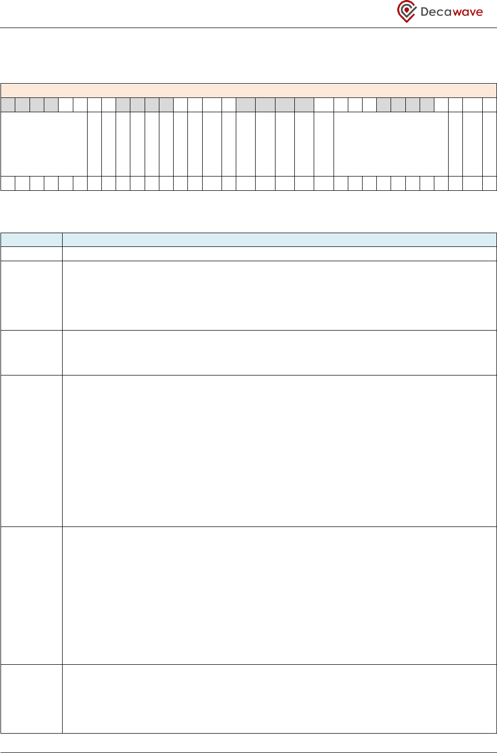
DW1000 User Manual
© Decawave Ltd 2017
Version 2.15
Page 196 of 244
Register file: 0x36 – Power Management and System Control, sub-register 0x04 is a 32-bit control register.
The PMSC_CTRL1 register contains the following sub-fields:
REG:36:04 – PMSC_CTRL1 – PMSC Control Register 1
31
30
29
28
27
26
25
24
23
22
21
20
19
18
17
16
15
14
13
12
11
10
9
8
7
6
5
4
3
2
1
0
KHZCLKDIV
-
-
-
-
-
-
-
-
LDERUNE
-
PLLSYN
SNOZR
SNOZE
ARXSLP
ATXSLP
PKTSEQ
-
ARX2INIT
-
1
0
0
0
0
0
0
1
0
0
0
0
0
0
1
0
0
0
0
0
0
1
1
1
0
0
1
1
1
0
0
0
The fields of the PMSC_CTRL1 register identified above are individually described below:
Field
Description of fields within Sub-Register 0x36:04 – PMSC_CTRL1
-
Bits marked ‘-’ are reserved and should be preserved at their reset value.
ARX2INIT
reg:36:04
bit:1
Automatic transition from receive mode into the INIT state. If the ARX2INIT bit is set then
the DW1000 will automatically transition into the INIT state after a receive attempt so long
as there are no unmasked interrupts pending. This control is used to enableLow duty-cycle
SNIFF mode. Please refer to section 4.5.2 – Low duty-cycle SNIFF mode for more details of
this functionality.
PKTSEQ
reg:36:04
bits:10-3
Writing 0 to PKTSEQ disables PMSC control of analog RF subsystems. To enable PMSC control
of these blocks a value of 0xE7 should be written.
ATXSLP
reg:36:04
bit:11
After TX automatically Sleep. If this bit is set then the DW1000 will automatically transition
into SLEEP or DEEPSLEEP mode after transmission of a frame has completed so long as there
are no unmasked interrupts pending. This bit is cleared when the DW1000 wakes from
sleep, unless the as the PRES_SLEEP bit is set in Sub-Register 0x2C:00 – AON_WCFG. Before
using this ATXSLP feature the AON configurations in Register file: 0x2C – Always-on system
control interface should be set to allow for the appropriate DW1000 wakeup functionality.
One of the uses for this would be in a device that periodically transmits a message (e.g.
TDOA RTLS Tag) to return the DW1000 to its lowest power state immediately after the
transmission, saving power.
NOTE: SLEEP_EN bit in Sub-Register 0x2C:06 – AON_CFG0 has to be set to enable this
functionality.
ARXSLP
reg:36:04
bit:12
After RX automatically Sleep. If this bit is set then the DW1000 will automatically transition
into SLEEP mode after a receive attempt so long as there are no unmasked interrupts
pending. Before using ARXSLP the AON configurations in Register file: 0x2C – Always-on
system control interface should be set to allow for the appropriate DW1000 wakeup
functionality. This bit is cleared when the DW1000 wakes from sleep, unless the as the
PRES_SLEEP bit is set in Sub-Register 0x2C:00 – AON_WCFG.One of the uses for this is to
implement a scheme called Low-Power Listening. See section 4.4 – Low-Power Listening for
more details.
NOTE: SLEEP_EN bit in Sub-Register 0x2C:06 – AON_CFG0 has to be set to enable this
functionality.
SNOZE
reg:36:04
bit:13
Snooze Enable. A SNOOZE is like a SLEEP except the snooze uses the 19.2 MHz XTI clock and
the snooze time period is specified by the SNOZ_TIM field of Sub-Register 0x36:0C –
PMSC_SNOZT. Snoozing is more precisely timed than sleeping but has a higher power drain
than sleeping. This is used to implement the Low-Power Listening scheme, see section 4.4 –
Low-Power Listening for more details.

DW1000 User Manual
© Decawave Ltd 2017
Version 2.15
Page 197 of 244
Field
Description of fields within Sub-Register 0x36:04 – PMSC_CTRL1
SNOZR
reg:36:04
bit:14
Snooze Repeat. The SNOZR bit is set to allow the snooze timer to repeat indefinitely.
SNOOZE-> RX-> SNOOZE-> RX->etc.
PLLSYN
reg:36:04
bit:15
This enables a special 1 GHz clock used for some external SYNC modes. If this is not required
then to save power the PLLSYN configuration should be left set to 0. See Register file: 0x24 –
External Synchronisation Control for more details.
LDERUNE
reg:36:04
bit:17
LDE run enable. This bit enables the running of the LDE algorithm. LDERUNE is 1 by default
which means that the LDE algorithm will be run as soon as the SFD is detected in the
receiver. When LDERUNE is set to zero the LDE algorithm will not be run and the RX_STAMP
in Register file: 0x15 – Receive Time Stamp will not be updated. For this the LDE code needs
to be loaded from ROM into its runtime RAM, which is achieved using the LDELOAD control
in Sub-Register 0x2D:06 – OTP_CTRL, an can also be done automatically when waking from
SLEEP or DEEPSLEEP via the ONW_LLDE control in Sub-Register 0x2C:00 – AON_WCFG. If the
LDE code is not loaded then the LDERUNE control must be disabled before turning on the
receiver.
KHZCLKDIV
reg:36:04
bits:31–26
Kilohertz clock divisor. This field specifies a clock divider designed to give a kilohertz range
clock that is used in the DW1000 for the LED blink functionality and also for the GPIO de-
bounce functionality. The input to the kHz divider is the 19.2 MHz XTI clock (which is the
raw 38.4 MHz XTAL ÷ 2). The KHZCLKDIV field specifies the top 6 bits of a 10-bit counter
allowing divisors up to 2016 or clock frequencies from 9.5 kHz up to 600 kHz. The resultant
clock is used directly in the GPIO de-bounce circuit (see Sub-Register 0x26:24 – GPIO_IDBE).
A further divider is applied for the LED blink functionality, see Sub-Register 0x36:28 –
PMSC_LEDC.
7.2.50.3 Sub-Register 0x36:08 – PMSC_RES1
ID
Length
(octets)
Type
Mnemonic
Description
36:08
4
RW
PMSC_RES1
PMSC reserved area 1
Register file: 0x36 – Power Management and System Control, sub-register 0x08 is a reserved register. Please
take care not to write to this register as doing so may cause the DW1000 to malfunction.
7.2.50.4 Sub-Register 0x36:0C – PMSC_SNOZT
ID
Length
(octets)
Type
Mnemonic
Description
36:0C
1
RW
PMSC_SNOZT
PMSC Snooze Time Register
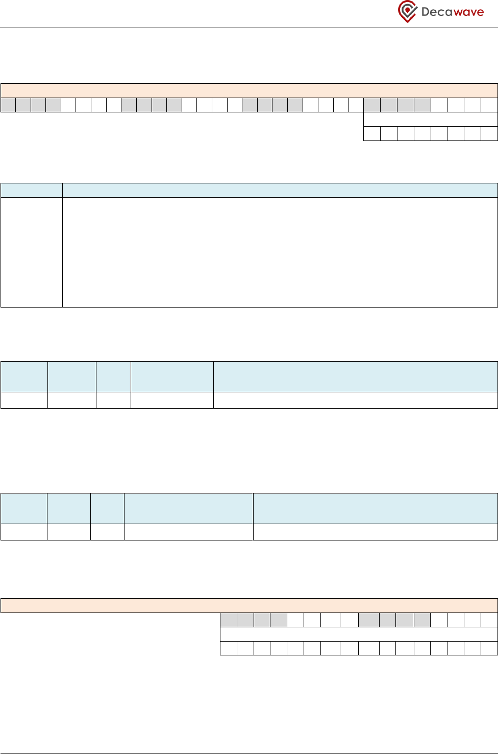
DW1000 User Manual
© Decawave Ltd 2017
Version 2.15
Page 198 of 244
Register file: 0x36 – Power Management and System Control, sub-register 0x0C is an 8-bit register for
specifying the snooze time period. The PMSC_SNOZT register contains the following sub-fields:
REG:36:0C – PMSC_SNOZT – PMSC Snooze Time Register
31
30
29
28
27
26
25
24
23
22
21
20
19
18
17
16
15
14
13
12
11
10
9
8
7
6
5
4
3
2
1
0
SNOZ_TIM
0
1
0
0
0
0
0
0
The fields of the PMSC_CTRL1 register identified above are individually described below:
Field
Description of fields within Sub-Register 0x36:0C – PMSC_SNOZT
SNOZ_TIM
reg:36:0C
bits:7–0
Snooze Time Period. These bits are the upper 8-bits of a 17-bit timer that defines the snooze
period in units of the 19.2 MHz XTI internal clock. The default value 0x40 (or decimal 64),
gives a period of 64×512/19.2e6 seconds, or 1.7 ms. Snoozing is enabled via the SNOZE bit
in Sub-Register 0x36:04 – PMSC_CTRL1, and is used during low power listening. See section
4.4 – Low-Power Listening for more details.
Note that the counter automatically adds 1 to the programmed value so SNOZ_TIM should
be programmed to be 1 less than the desired value.
7.2.50.5 Sub-Register 0x36:10 – PMSC_RES2
ID
Length
(octets)
Type
Mnemonic
Description
36:10
22
RW
PMSC_RES2
PMSC reserved area 2
Register file: 0x36 – Power Management and System Control, sub-register 0x10 is a reserved register. Please
take care not to write to this register as doing so may cause the DW1000 to malfunction.
7.2.50.6 Sub-Register 0x36:26 – PMSC_TXFSEQ
ID
Length
(octets)
Type
Mnemonic
Description
36:26
2
RW
PMSC_TXFSEQ
PMSC fine grain TX sequencing control
Register file: 0x36 – Power Management and System Control, sub-register 0x26 is used to control TX fine
grain power sequencing function. The PMSC_TXFSEQ register contains the following sub-fields:
REG:36:26 – PMSC_TXFSEQ – PMSC fine grain TX sequencing Control Register
15
14
13
12
11
10
9
8
7
6
5
4
3
2
1
0
TXFINESEQ
0
0
0
0
1
0
1
1
0
0
1
1
1
1
0
0
The fields of the PMSC_TXFSEQ register identified above are described below:
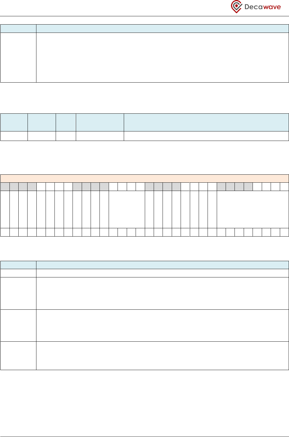
DW1000 User Manual
© Decawave Ltd 2017
Version 2.15
Page 199 of 244
Field
Description of fields within Sub-Register 0x36:26 – PMSC_TXFSEQ
TXFINESEQ
reg:36:26
bits:15–0
Writing 0 to this field will disable TX fine grain power sequencing, this is required for certain
test and calibration modes (Continuous Wave transmission). To enable fine grain power
sequencing the default value of 0x0B74 should be written back to this register.
Note that TX fine grain power sequencing must be disabled if an external power amplifier is
being used with the DW1000.
7.2.50.7 Sub-Register 0x36:28 – PMSC_LEDC
ID
Length
(octets)
Type
Mnemonic
Description
36:28
4
RW
PMSC_LEDC
PMSC LED Control Register
Register file: 0x36 – Power Management and System Control, sub-register 0x28 is a 32-bit LED control
register. The PMSC_LEDC register contains the following sub-fields:
REG:36:28 – PMSC_LEDC – PMSC LED Control Register
31
30
29
28
27
26
25
24
23
22
21
20
19
18
17
16
15
14
13
12
11
10
9
8
7
6
5
4
3
2
1
0
-
-
-
-
-
-
-
-
-
-
-
-
BLNKNOW
-
-
-
-
-
-
-
BLNKEN
BLINK_TIM
0
0
0
0
0
0
0
0
0
0
0
0
0
0
0
0
0
0
0
0
0
0
0
0
0
0
1
0
0
0
0
0
The fields of the PMSC_LEDC register identified above are individually described below:
Field
Description of fields within Sub-Register 0x36:28 – PMSC_LEDC
-
Bits marked ‘-’ are reserved and should be preserved at their reset value.
BLINK_TIM
reg:36:28
bits:7–0
Blink time count value. This field determines how long the LEDs remain lit after an event
that causes them to be set on. This time is specified in units of 14 ms so the default value of
0x20 will give an on blink of 400 ms followed by an off blink of 400 ms. The BLNKEN bit
(below) must be set to enable this blink functionality.
BLNKEN
reg:36:28
bit:8
Blink Enable. When this bit is set to 1 the LED blink feature is enabled.
Because the LED blink counter uses the low frequency KHZCLK timer, this timer must be
enabled as per Sub-Register 0x36:00 – PMSC_CTRL0 and configured as per Sub-Register
0x36:04 – PMSC_CTRL1
BLNKNOW
reg:36:28
bits:19:16
Manually triggers an LED blink. There is one trigger bit per LED IO.

DW1000 User Manual
© Decawave Ltd 2017
Version 2.15
Page 200 of 244
7.2.51 Register files: 0x37 to 0x3F – Reserved
ID
Length
(octets)
Type
Mnemonic
Description
0x37
to
0x3F
-
-
-
Reserved – these register files are reserved
Register map register files 0x36 through 0x3F are reserved for future use. Please take care not to write to
these registers as doing so may cause the DW1000 to malfunction.

DW1000 User Manual
© Decawave Ltd 2017
Version 2.15
Page 201 of 244
8 DW1000 Calibration
The operating characteristics and performance of the DW1000 is dependent on the IC itself and on its
external circuitry and on its operating environment. To give optimum performance it is necessary to
calibrate the IC to account for factors which affect its operation.
Some calibration parameters are dependent solely on natural variations that occur within the silicon of the
IC during its manufacture. These are typically measured during IC production test and the required
calibration parameters are written to the OTP memory of the DW1000. The host system software can then
use these values during DW1000 configuration to optimise the DW1000 performance.
Some calibration parameters are dependent on circuit elements external to the IC. These can only be
determined during the manufacture of the product module into which the DW1000 is soldered. These
parameters are typically measured during module production test and the required calibration parameters
are stored somewhere in the module. An area of the DW1000’s OTP memory has been set for module test
calibration parameters. The host system software will use this calibration data during DW1000
configuration to optimise the DW1000 performance.
Some calibration parameters may vary according to the operational environment of the DW1000. For
example some parameters may need to be changed if there are large variations in the ambient temperature
(e.g. moving from a warm area into a cold store) or if there are significant changes in battery voltage supply.
In such circumstances in order to optimise the DW1000 performance the host system software can monitor
the voltage and temperature using DW1000 and adjust configuration accordingly.
Elements of the DW1000 that may be subject to calibration are:
Crystal trimming – the DW1000 contains trimming capacitors that can fine tune the operating
frequency of its crystal oscillator
Transmitter output power and spectrum – the DW1000 output spectrum is tuneable to meet
regional spectral regulations and maximise the output power to achieve the greatest operating
range.
Antenna delay – the DW1000 antenna delay may be fine-tuned to give best possible ranging or
location
accuracy.
The sub-sections below detail the calibration of these DW1000 parameters.
8.1 IC Calibration – Crystal Oscillator Trim
DW1000 is specified to operate with clock offsets between the transmitting and receiving nodes of up to ±20
ppm. The receiver sensitivity of DW1000 can be improved by reducing the relative offset in clocks between
the transmitting and receiving nodes. One way to reduce the offset is to use temperature compensated
crystal oscillators (TCXO) in both transmitting and receiving nodes or just in one side of the link. Using TCXOs
increases system cost and current consumption so generally they are only used in fixed anchor scenarios.
Where crystals are used as the clock reference, DW1000 provides a facility to trim the oscillator frequency

DW1000 User Manual
© Decawave Ltd 2017
Version 2.15
Page 202 of 244
by switching in internal capacitor banks in parallel with the external loading capacitors associated with the
chosen crystal. This trimming can be used to reduce the crystal initial frequency error and to compensate for
temperature and aging drift, if required.
The amount of trimming is programmable through Sub-Register 0x2B:0E – FS_XTALT.
8.1.1 Calibration Method
The 38.4 MHz crystal’s frequency of oscillation cannot be directly observed because it is not possible to
probe the XTAL1 and XTAL2 input pins without disturbing the oscillation. The method used is to infer the
crystal oscillation frequency by observing the output of the transmitter using a spectrum analyzer or
frequency counter.
The DW1000 is configured to transmit a continuous wave (CW) signal at a particular channel frequency. It is
suggested that channel 5 is used because the higher the frequency the easier it is to observe step changes in
the output. While accurately measuring the centre frequency of the transmission, the trim value is adjusted
until the output frequency is as close as possible to the desired frequency (e.g. 6489.6 MHz for channel 5).
In order to allow the internal trimming circuits as large a range of programming as possible, the external
loading capacitors should be chosen during the board design phase such that on average (tested on a
number of boards) the crystal trim register setting is set close to mid-range which is a 5-bit decimal value of
15or 0x0F.
Test Setup:
Reset the device so that it is in a known state before initiating the test procedure.
Configure the transmitter as described in the following steps and then monitor the RF output on a spectrum
analyser or frequency counter.
Transmitter Configuration Procedure:
1. Sub-Register 0x28:00 – RF_CONF
2. Write 0x00000000 to Sub-Register 0x36:04 – PMSC_CTRL1
3. Write the correct value for the selected channel to Sub-Register 0x28:0C– RF_TXCTRL, see table 37,
e.g. 0x1E3FE0 for channel 5.
4. Write an appropriate value to Register file: 0x1E – Transmit Power Control, such as that for the
selected channel, see Table 20: Reference values Register file: 0x1E – Transmit Power Control.
5. Write the value for the selected channel to Sub-Register 0x2B:07 – FS_PLLCFG, e.g. 0x0800041D for
channel 5, see Table 43: Sub-Register 0x2B:07 – FS_PLLCFG values.
6. Write the correct value for the selected channel to Sub-Register 0x2B:0B – FS_PLLTUNE, e.g. 0xBE for
channel 5. See table 44
7. Write 0x22 to PMSC_CTRL0 to enable the appropriate clocks, see Sub-Register 0x36:00 –
PMSC_CTRL0.
8. Write 0x00000000 to reserved register Sub-Register 0x36:26 – PMSC_TXFSEQ.
9. Sub-Register 0x28:00 – RF_CONF
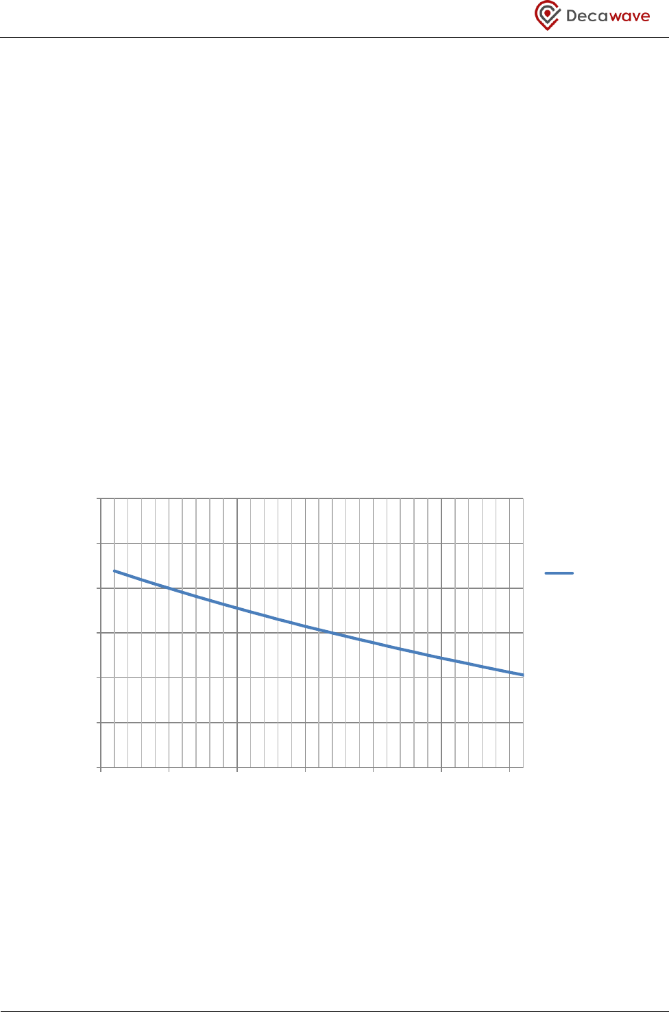
DW1000 User Manual
© Decawave Ltd 2017
Version 2.15
Page 203 of 244
Enable CW mode:
Set
Sub-Register 0x2A:0C – TC_PGTEST to 0x13 to enable Continuous Wave (CW) Test Mode.
Set trim register to mid-range setting, e.g. 0x0F, whilst maintaining the required reserved values in the most
significant bits of the register, see reserved field notes for Sub-Register 0x2B:0E – FS_XTALT:
Set Sub-Register 0x2B:0E – FS_XTALT to 0x6F.
While monitoring the CW frequency, adjust the trim register (5 bits) until the desired frequency is obtained.
Figure 30 shows that the trimming is typically linear and usually the final value is reached with just one or
two adjustments.
The crystal trim value should then be stored on the OTP memory, see section 6.3.2 – Programming a value
into OTP memory for details of how to program OTP memory and recommended memory locations.
In DW1000 applications using crystal trimming, the calibrated crystal trim value should be read by the
application from OTP memory as part of setup and programmed into the Sub-Register 0x2B:0E – FS_XTALT.
This register is preserved in the AON memory as long as the IC is powered. This facilitates the use of the trim
value when the IC wakes up from SLEEP or DEEPSLEEP modes.
Figure 29: PPM vs Crystal Trim Setting, VBATT= 3.3 V
8.2 IC Calibration – Transmit power and spectrum
In order to maximise range, DW1000 transmit power spectral density (PSD) should be set to the maximum
allowable for the geographic region of deployment. For most regions this is -41.3 dBm / MHz. DW1000 is
-60.00
-40.00
-20.00
0.00
20.00
40.00
60.00
0 5 10 15 20 25 30
PPM
Trim Code
3.3V

DW1000 User Manual
© Decawave Ltd 2017
Version 2.15
Page 204 of 244
designed such that if the transmit power is within mean power spectral density limits then it will
automatically be within peak power limits although this should be checked during product design
verification.
As this is an analog circuit, there will be some variation in output power levels from IC to IC and hence
DW1000 should be calibrated and the calibrated power setting stored in the OTP memory. DW1000 provides
the facility to adjust the transmit power in coarse and fine steps; 3 dB and 0.5 dB nominally. It also provides
the ability to adjust the spectral bandwidth. These adjustments can be used to maximise transmit power
whilst meeting regulatory spectral mask limits.
8.2.1 Calibration Method
This calibration can be performed using either a radiated or conducted measurement procedure. The
calibration method is slightly different depending on whether Manual Transmit Power Control (see 7.2.31.3
– Manual Transmit Power Control) or Smart Transmit Power Control (see 7.2.31.2 – Smart Transmit Power
Control) is configured.
8.2.1.1 Calibration – Manual TX Power Control
Test Setup:
Reset the device so that it is in a known state before initiating the test procedure.
Configure the transmitter as described in the following steps (Table 54) and monitor the RF output on a
spectrum analyser.
Table 54: Register accesses required for transmitter configuration procedure
Step
Number
Instruction
Register
Address
Data
Length
(Bytes)
Data
(Write/Read)
C-1
Write Sub-Register
0x36:00 (PMSC_CTRL0)
1
0x1 (set SYSCLKS
bit)
C-2
Write Sub-Register
0x36:04 (PMSC_CTRL1)
2
0x0 (clear PKTSEQ
bits)
C-3
Write Sub-Register
0x28:0C (RF_TXCTRL)
3
e.g. 0x45CA0 *
C-4
Write Sub-Register
0x1E:00 (TX_POWER)
4
e.g. 0x75757575 *
C-5
Write Sub-Register
0x2B:07 (FS_PLLCFG)
4
e.g. 0x08400508 *
C-6
Write Sub-Register
0x2B:0B (FS_PLLTUNE)
1
e.g. 0x26 *
C-7
Write Sub-Register
0x2A:0B (TC_PGDELAY)
1
e.g. 0xC2 *
C-8
Write Sub-Register
0x28:00 (RF_CONF)
4
0x1FE000
C-9
Write Sub-Register
0x28:00 (RF_CONF)
4
0x5FFF00
C-10
Write Sub-Register
0x36:00 (PMSC_CTRL0)
1
0x22
C-11
Write Sub-Register
0x04:00 (SYS_CFG)
4
set DIS_STXP bit
C-12
Write Sub-Register
0x1F:00 (CHAN_CTRL)
4
0x18C40022 *
C-13
Write Sub-Register
0x09:00 (TX_BUFFER)
16
test data *
C-14
Write Sub-Register
0x08:00 (TX_FCTRL)
4
0x25A010 *
C-15
Write Sub-Register
0x0A:00 (DX_TIME)
5
0x04
C-16
Write Sub-Register
0x2F:24 (DIAG_TMC)
2
set TX_PSTM bit

DW1000 User Manual
© Decawave Ltd 2017
Version 2.15
Page 205 of 244
1. Write the correct value for the selected channel to Sub-Register 0x28:0C– RF_TXCTRL, e.g. 0x045CA0
for channel 2.
2. Write an appropriate value for TX_POWER to Register file: 0x1E – Transmit Power Control, e.g. for
channel 2 at 16 MHz PRF, write 0x75757575. See Table 20.
3. Write the value for the selected channel to Sub-Register 0x2B:07 – FS_PLLCFG, e.g. 0x08400508 for
channel 2, see Table 43: Sub-Register 0x2B:07 – FS_PLLCFG values.
4. Write the correct value for the selected channel to Sub-Register 0x2B:0B – FS_PLLTUNE, e.g. 0x26 for
channel 2.
5. Write the correct value for the selected channel to TC_PGDELAY, see Sub-Register 0x2A:0B –
TC_PGDELAY, e.g. 0xC2 for channel 2.
6. Write 0x05FFF00 to Sub-Register 0x28:00 – RF_CONF
7. Write appropriate values to Register file: 0x1F – Channel Control, e.g. for channel 2, PRF 16 MHz and
preamble code 3, write 0x18C40022.
8. Write transmit data to the transmit buffer, see Register file: 0x09 – Transmit Data Buffer, e.g.
0x000000000000000000000000C2DEC1DE.
9. Write appropriate values to Register file: 0x08 – Transmit Frame Control, e.g. for frame length 16
bytes, 850 kbps data rate, 16 MHz PRF and 256 symbol preamble, write 0x25A010.
The spectrum analyser should be set up as follows:
Resolution Bandwidth = 1 MHz
Video Bandwidth = 1 MHz
Span = 2 GHz
Sweep time = 2 seconds
Detector = rms
Average time per point (on spectrum analyser scan) ≤ 1 ms
In order to easily view the transmit spectrum the device is set into Transmit Power Spectrum Test Mode by
setting the TX_PSTM field of Sub-Register 0x2F:24 – Digital Diagnostics Test Mode Control. A suitable value
for the repeat frame interval must be set in DX_TIME register, the minimum value is 4. For a repeat interval
of 1 ms, a value of 0x0001E780 may be written to DX_TIME, see Sub-Register 0x2F:24 – Digital Diagnostics
Test Mode Control TX_PSTM field description for details. For Manual Transmit Power Control testing this
setting should be configured to send frames continuously and so a value equal to the frame duration must
be set in DX_TIME.
When the test configuration has been completed, the transmitter may be initiated by setting the TXSTRT
field in the SYS_CTRL register, see Register file: 0x0D – System Control Register.
TX_POWER should be set for the selected channel as a starting point, see Register file: 0x1E – Transmit
Power Control. The TX_POWER setting should then be adjusted until the transmit level is just below the
required spectral density limit (usually -41.3dBm/MHz). This register value should then be stored in the OTP
memory, see section 6.3.2 – Programming a value into OTP memory for details of how to program OTP
memory and recommended memory locations.
In DW1000 applications using transmit power calibration, the calibrated TX_POWER value should be read by
the application from OTP memory as part of setup and programmed into Register file: 0x1E – Transmit

DW1000 User Manual
© Decawave Ltd 2017
Version 2.15
Page 206 of 244
Power Control. This register is preserved in the AON memory as long as the IC is powered. This facilitates the
use of this value when the IC wakes up from SLEEP or DEEPSLEEP modes.
8.2.1.2 Calibration – Smart TX Power Control
With Smart TX Power Control enabled the calibration is similar to the method used for Manual TX Power
Control except that we do not transmit repeated back to back frames. For this calibration, we configure the
transmitter to transmit 1 frame per millisecond. To do this, configure the Transmit Power Spectrum Test
Mode, see the TX_PSTM field description of Sub-Register 0x2F:24 – Digital Diagnostics Test Mode
Control.The repeat frame interval must be set in DX_TIME register, for a repeat interval of 1 ms, a value of
0x0001E780 should be written to DX_TIME, as described in the TX_PSTM field description.
Depending on the length of the frames to be used, see 7.2.31.2 – Smart Transmit Power Control,the
TX_POWER setting should be adjusted until the transmit level is just below the required spectral density limit
(usually -41.3dBm/MHz). This register value should then be stored in the OTP memory, see section 6.3.2 –
Programming a value into OTP memory for details of how to program OTP memory and recommended
memory locations.
In DW1000 applications using transmit power calibration, the calibrated TX_POWER value should be read by
the application from OTP memory as part of setup and programmed into Register file: 0x1E – Transmit
Power Control. This register is preserved in the AON memory as long as the IC is powered. This facilitates
the use of this value when the IC wakes up from SLEEP or DEEPSLEEP modes.
8.2.2 Other TX adjustments to consider
DW1000 recommended transmitter analog/RF settings will not need adjustment for most
designs/applications, however the following registers can be adjusted to tune the transmit spectrum
bandwidth or passband flatness:
TXMTUNE field of Sub-Register 0x28:0C– RF_TXCTRL, used to tune the transmit mixer.
TXMQ field of Sub-Register 0x28:0C– RF_TXCTRL, used to tune the transmit mixer Q-factor.
Sub-Register 0x2A:0B – TC_PGDELAY, used to tune the width of pulses and hence the spectrum
bandwidth.
To tune any of these values, start with the default value (as given in the register descriptions Sub-Register
0x28:0C– RF_TXCTRL and Sub-Register 0x2A:0B – TC_PGDELAY), and adjust the value iteratively observing
the effect on a spectrum analyser until the PSD occupies as much of the applicable spectral mask as possible.
8.3 IC Calibration – Antenna Delay
In order to measure range accurately, precise calculation of timestamps is required. To do this, a delay called
the antenna delay must be known. The DW1000 allows this delay to be calibrated and provides the facility to
compensate for delays introduced by PCB, external components, antenna and internal DW1000 delays.
To calibrate the antenna delay, range is measured at a known distance using 2 DW1000 systems. Antenna
delay is adjusted until the known distance and reported range agree. The antenna delay can be stored in
OTP memory.
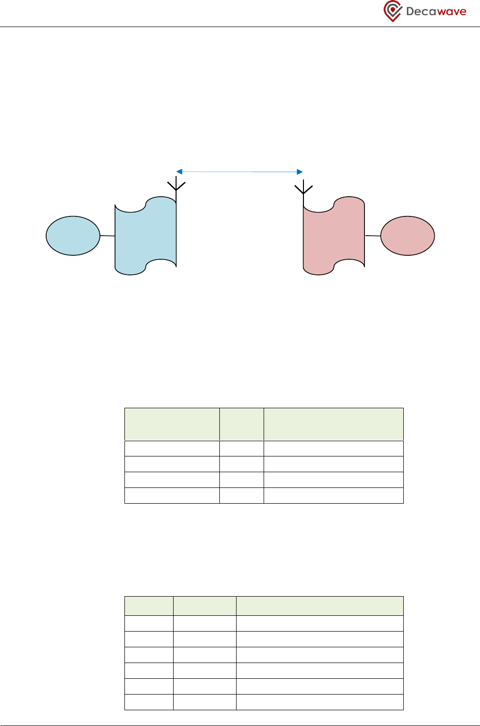
DW1000 User Manual
© Decawave Ltd 2017
Version 2.15
Page 207 of 244
There is a Transmitter Antenna Delay and a Receiver Antenna Delay. The Transmitter Antenna Delay is used
to account for the delay between the internal digital timestamp of the RMARKER (at the start of the PHR, see
3.2) inside the DW1000 and the time the RMARKER is transmitted from the antenna. The Receiver Antenna
Delay is used to account for the delay between the time of arrival of the RMARKER at the antenna and the
internal digital timestamp of the RMARKER (at the start of the PHR, see 4.1.6 – RX Message timestamp)
inside the DW1000.
Figure 30: Transmit and Receive Antenna Delay
8.3.1 Calibration Method
To achieve the highest accuracy during calibration, it is recommended that antenna delay is calibrated with
the receiver power input at the following levels:
Table 55: Recommended RX power level for antenna calibration
Power at receiver
input (dBm/MHz)
PRF
(MHz)
Channel
-108
16
1, 2, 3, 5
-104
64
1, 2, 3, 5
-104
16
4, 7
-104
64
4, 7
If the transmitter is set to -41.3dBm/MHz and 0 dBi antennas are used, then the receiver input powers above
equate to the following separations between transmit and receive antenna:
Table 56: Recommended TX-RX separation for antenna calibration
Channel
PRF (MHz)
Calibration Separation (m)
1
16
14.75
1
64
9.3
2
16
12.9
2
64
8.14
3
16
11.47
3
64
7.24
TX
TX
antenna
delay
RX
RX
antenna
delay
Distance

DW1000 User Manual
© Decawave Ltd 2017
Version 2.15
Page 208 of 244
Channel
PRF (MHz)
Calibration Separation (m)
4
16/64
8.68
5
16
7.94
5
64
5.01
7
16/64
5.34
The combined transmitter and receiver antenna delay is calibrated by choosing a distance (or receive power)
for calibration and modifying the receiver antenna delay until the range reading given by the device is
correct.
A method to calibrate combined receiver and transmitter antenna delay is as follows:
1. Place the transmitter and receiver at the recommended distance apart as per Table 56 or at a
shorter distance but ensuring that the receiver power level is as per Table 55
2. Using a two way ranging scheme (e.g. “DecaRanging” available from Decawave), perform 1000
ranges.
3. Adjust antenna delay until the average measured range matches the distance chosen in step 1 as
closely as possible.
Record the antenna delay value. This value is then divided by 2 and the new value is stored in the OTP
memory in the locations for both TX Antenna Delay and RX Antenna Delay (see section 6.3.2 – Programming
a value into OTP memory for details of how to program OTP memory and recommended memory locations).
Note: In many systems, where all devices have the same transmitter and receiver antenna delays, it is
unnecessary to calibrate the transmitter antenna delay. The transmitter antenna delay may be set to zero
and a combined receiver and transmitter delay value may be used for the receiver antenna delay without
impairing the ranging performance of the system.
The DW1000 ranging algorithm will calculate the time of reception of a packet in order to estimate the range
to the transmitter. The receiver antenna delay is a constant value representing the propagation time of the
received signal from the antenna to the receiver point of timestamp calculation.
This antenna delay value can then be subtracted from the receive timestamp in order to calculate the time
of flight.
For enhanced ranging accuracy the ranging software can adjust the antenna delay to compensate for
changes in temperature. Typically the reported range will vary by 2.15 mm / °C and by 5.35 cm / VBATT.

DW1000 User Manual
© Decawave Ltd 2017
Version 2.15
Page 209 of 244
9 Operational design choices when employing the DW1000
This chapter discusses some of the operational considerations to using the DW1000 in general RF transceiver
applications, with some additional focus on its use in real-time location systems, (RTLS).
9.1 Operating range
The operational range of the DW1000 depends on the frame data rate and the preamble length. In free-
space, line-of-sight (LOS), this may vary from 60 m at the 6.8 Mbps data rate to up to 250 m at the 110 kbps
data rate. In a typical indoor environment the LOS range is generally larger than the quoted free-space LOS
figure because multipath reflections give extra usable receive signal, e.g. the range at 850 kbps could be 40%
longer (and more) than that quoted for free-space LOS. In non-LOS conditions (NLOS), where there are
obstructions in the LOS path, the range will be reduced due to receive signal attenuation. The operating
range also varies depending on the channel centre frequency and channel bandwidth selected – a lower
centre frequency gets more range than a higher one, while the wider bandwidth channels channel 4 and
channel 7 have more range than the standard 500 MHz bandwidth channels as the wider channel allows
more energy to be sent at a given dBm / MHz regulatory limit.
9.2 Channel and Bandwidth selection
The choice of channel’s centre frequency is often dictated by regional regulations, e.g. USA and EUROPE
have different rules, albeit with some overlap, so channel choice in a product may depend on the target
market for that product. The choice of bandwidth may also depend on whether the resultant spectrum is
within the regional regulations. The IEEE 802.15.4 standard UWB PHY defines a number of channels, from 0
to 10 GHz, some with same centre frequency and different bandwidths, (e.g. channel 2 and channel 4 both
have 3993.6 MHz centre frequency, but have bandwidths of 499.2 and 1331.2 MHz respectively). Table 61 in
section 10.5 – UWB channels and preamble codes lists the channels supported by the DW1000.
Operating at a wider bandwidth increases range but also increases power consumption. The DW1000 has
fine control of the TX pulse width allowing optimum control of transmitted spectrum bandwidth.
9.3 Choice of data rate, preamble length and PRF
For a given operating centre frequency and bandwidth the choice of data rate generally determines the
operating range. However, the length of the preamble sequence also has a bearing on range.
The preamble is a repeated sequence of pulses following a pattern defined in the IEEE 802.15.4 standard.
See section 10.3 – Synchronisation header modulation scheme for details. On each numbered channel the
802.15.4 standard defines two preamble codes for the nominal 16 MHz PRF (pulse repetition frequency) and
four preamble codes for the nominal 64 MHz PRF. Table 61 in section 10.5 – UWB channels and preamble
codes lists the preamble codes allowed on each channel as defined in the IEEE 802.15.4 standard. These
codes are semi-orthogonal. This can allow devices on the same physical channel but using correctly chosen,
different, preamble codes to operate simultaneously under certain circumstances as if on separate
channels. Care should be exercised in the choice of preamble codes and the reader is referred to Decawave
Application Note APH010 on this topic. The preamble sequences’ property of perfect periodic auto-
correlation allows the receiver to accumulate the repeated preamble and ascertain an accurate model of the

DW1000 User Manual
© Decawave Ltd 2017
Version 2.15
Page 210 of 244
channel impulse response between the remote transmitter and itself. This is what gives the DW1000 its
good long-range performance and allows its accurate determination of the first path arrival time for the RX
timestamp.
The preamble sequence used at all data rates is the same, i.e. it does not depend on the chosen data rate.
The preamble sequence length, (i.e. the number of symbol intervals for which it is repeated), has a
significant effect on the operational range and the accuracy of timestamps. Table 57 gives some
recommended preamble sequence lengths to use depending on the data rate. In general, a longer preamble
gives improved range performance and better first path time of arrival information while a shorter preamble
gives a shorter air time and saves power. When operating a low data rate for long range, then a long
preamble is needed to achieve that range. At a high data rate the operating range is naturally short so there
is no point in sending a very long preamble as it wastes time and power for no added range advantage.
Table 57: Recommended preamble lengths
Data Rate
Recommended preamble
sequence length
6.8 Mbps
64 or 128 or 256
850 kbps
256 or 512 or 1024
110kbps
2048 or 4096
There are two choices of mean pulse repetition frequency (PRF) within the DW1000. These are 16 MHz PRF
or 64 MHz PRF. The 16 and 64 are “nominal” since the actual frequencies are related to the 499.2 MHz basic
time unit used and differ slightly between preamble and payload parts of the frame. The higher PRF gives
more accuracy on the first path timestamp and perhaps slightly improved operating range, however this
comes at the price of additional power consumption.
9.4 Power consumption
As described above, frames with lower data rate have the largest operating range. Such messages by their
nature also take longer to send and, as this means that the DW1000’s transmitter needs to be on for a
longer period, the result is that more power is consumed than for faster messages. The quantity of data
being transferred also has a bearing on this, i.e. higher data rates give more benefit when frame data sizes
are larger.
9.5 Node density and air utilisation
The ALOHA mechanism is the favoured channel access method in the IEEE 802.15.4 UWB PHY standard and
this is the channel access method employed by the DW1000. Essentially this involves assuming the air is idle
and transmitting whenever you want to. For ALOHA to work successfully total air utilisation has to be <18%
across all nodes in range of each other. With air utilisation above 18% collision probability is high and system
performance degrades quickly. Below the 18% value 97% of transmissions are likely to succeed without
collisions.

DW1000 User Manual
© Decawave Ltd 2017
Version 2.15
Page 211 of 244
This 18% air utilisation comes into play when deploying a population of RTLS tags periodically blinking. Table
58 gives some indications of the blink transmission rates corresponding to some typical data rate / preamble
length combinations and with a minimum 12-byte blink frame sending the Tag ID. The number of
transmissions that can be made within the 18% air-utilisation is highest for the shortest duration frame (64-
symbol preamble and 6.8 Mbps data rate) and lowest at the long range 110 kbps data rate with its long
preamble.
Table 58: Transmissions per second using ALOHA
Data rate
preamble
length
payload
Transmission
Time
TX per second at
18% air-utilisation
110 kbps
2048 symbols
12 bytes
3.042 ms
59.2
850 kbps
256 symbols
12 bytes
380.3 µs
473.4
6.8 Mbps
64 symbols
12 bytes
103.3 µs
1742
Note: These figures relate to an RTLS tag blink across a population of tags, so for instance at 6.8Mbps
1742 tags could blink once a second, or 17k tags could blink once every 10 s.
When deploying an RTLS system with blinking tags there is a trade-off between the blink rate(location
update rate) across the population of tags and the operating range (and of course power consumption). A
long range system with sparsely spaced anchor nodes cannot have a large population of tags with frequently
updated locations, (i.e. it needs to stay below 60 tags transmitting once per second, or 600 tags transmitting
once every 10 seconds), also as the packet is physically long the blinks in such a long range system consume
more power.
For a high update rate or a high density of tags the highest data rate and shortest preamble length is best.
This means range is lower so more infrastructure anchor nodes are needed, but the shorter blink packet
duration means lower power consumption for transmissions, so for the same update frequency the battery
life will be longer.
A larger percentage of air time can be used in cases where a system includes mechanisms to control when
nodes transmit. For example TDMA where a coordinating node transmits a periodic beacon defining a
“super-frame” that is subdivided into slots, and individual slave nodes synchronise with the beacon and
transmit only in their assigned slots. Employing an accelerometer and reducing the tag blink rate when it is
not moving is another technique that would allow a larger population of tag.
9.6 Low–duty cycle – air time
In some geographic areas certain UWB channels are only allowed by regulations when the transmissions are
following what are termed low duty cycle (LDC) rules. These LDC rules set limits on the maximum time of an
individual period of transmission, a minimum time between transmissions, a percentage of TX activity
allowed in any one second, and a percentage of activity allowed in any hour.
Depending on the application the LDC rules may or may not be a problem. Where LDC rules are impinging
on system operation there may be an option to use a different frequency band where the LDC rules do not
apply. Also, as the LDC rules relate to transmission time, using higher data rates and short preambles allows
more messages be sent within the time limits.

DW1000 User Manual
© Decawave Ltd 2017
Version 2.15
Page 212 of 244
9.7 Location schemes
This part of the discussion on operational design choices relates to RTLS location schemes. Some of the ideas
and points discussed may be more generally applicable.
In general to locate a mobile node measurements are needed to be referenced to a number of fixed known
location “anchor” nodes. Typically a minimum of three anchor nodes are needed to locate a mobile node in
two dimensions, while a minimum four non-coplanar anchors are needed to locate a mobile node in three
dimensions. The spacing of anchors nodes in an installation has to be such that four anchors are always in
communication range of the mobile tag no matter where it is within the operating space. The
communication range is dependent on data rate and preamble length, the choice of which is influenced by
the node density requirements and perhaps also power consumption.
There are two general methods of doing location. These are time difference of arrival (TDOA) based location
and time of flight (TOF) based location, the main operational points of each are outlined below. In either
case the calculation of location, combining measurements from multiple anchors, is typically done by a
software functionality called the central location engine.
Time of flight location requires two-way communication from the mobile node (tag) to each of the anchor
nodes in its vicinity. Periodic message exchanges are used to measure the round trip delay and hence
calculate the one way flight time between tag and anchor. The TOF times multiplied by the speed of light
(and radio waves) gives the distance between the tag and the anchor. Each distance estimate defines a
spherical surface, centred on the anchor, on which the tag must lie. The tag’s 3D location is yielded by the
intersection of the spheres resulting from TOF measurements to the four anchors.
In time difference of arrival (TDOA) location the mobile tag blinks periodically and the blink message is
received by the anchor nodes in its vicinity. When the anchor nodes have synchronised clocks so that the
arrival time of the blink message at all nodes can be compared, then for each pair of anchors the time
difference in the arrival of the blink message defines a hyperbolic surface on which the sending tag must lie.
The tag’s 3D location is yielded by the intersection of the hyperbolic surfaces defined by the TDOA of the
blink at four pairs of anchors.
For low power RTLS deployments the TDOA scheme has benefits in that the tag needs to only send a single
message in order for it to be located. In contrast in the TOF scheme the tag has to send and receive multiple
messages with multiple anchors, and it needs to know what anchors are in the vicinity so it can address each
of them in turn correctly. TOF does not need synchronised anchors, and may suit the case where a hand
held device calculates its own location as part of a navigation system. The TDOA is a lower power solution as
there are fewer messages involved, and this also suits higher density deployments. The TDOA anchor clock
synchronisation may be achieved via a wired clock distribution. Alternatively there are wireless techniques
for clock synchronisation. Wired synchronisation may suit higher tag densities as it allows anchors to listen
all the time so no tag blinks are missed or collide with the wireless clock sync messages (potentially
disrupting synchronisation). Anchors should be wired for power and also with Ethernet to communicate the
arrival times to the central location engine.
Two-way ranging (TOF) is good for proximity detection and separation alarms, especially when both parties
in the exchange are mobile nodes.

DW1000 User Manual
© Decawave Ltd 2017
Version 2.15
Page 213 of 244
In an RTLS the accuracy of the DW1000’s RX timestamps can give sub 10 cm resolution. Note, however that
the geometry of anchors with respect to the tag can smear the accuracy of the calculated location when
individual measurements are combined. Having additional anchors in range of the tag can offset this if it
allows the system to select anchors with best geometry and best receive signal quality with respect to the
tag being located.
9.8 General considerations
This chapter discussed the operational design choices with respect to selecting data rate, preamble length,
and PRF, and the trade-offs involved in selecting for high node density versus long operating range. The
discussion also indicated how these choices affect the power consumption.
In general infrequent transmission of short packets is best for a long battery life. When a large quantity of
data needs sending it is best to employ the longest frame length so that the overhead of the preamble and
other parts of the frame header represent a smaller proportion of the overall frame. Listening for and
receiving messages is relatively the most power expensive operation within the DW1000. It is
recommended that devices needing to listen all the time are connected to a mains derived power source.
This would include anchor nodes in an RTLS system, and those nodes of a wireless sensor network (WSN)
that are hubs nodes responsible for routing messages.
For mains powered nodes, the power consumption in the receiver is not an issue, but for battery powered
nodes where it is important to ensure a reasonable battery life, it will be necessary to include schemes to
reduce the time spent listening. Table 59 lists and briefly describes some techniques that can save power in
receiving.
Table 59: Techniques to save power in receiving
Name
Description
Low-Power
Listening
This is a technique based on the DW1000 preamble sampling function. The IC can
“sniff” the air for a short period looking for preamble, and if it does not see it return
to low power sleep mode. The transmit device has to send its message with long
preamble and repeat it for a period to guarantee that the preamble overlaps with
the period of RX sniffing. If the IC sees preamble it stays activated until it receives
the message after which it can interrupt the host microprocessor to process it.
With address filtering enabled the IC can return to sleep as soon as an address
mismatch is seen.
This technique really only suits cases where traffic volume is low so the
predominant activity of all nodes is occasionally sniffing the air for preamble. As
every message will wake up every node in range, at least until the address
mismatch, the power drain to all nodes can be quite high if there are frequent
transmissions.
Poll for message
This is a technique where a battery powered node periodically sends a poll message
and listens thereafter for a response from the mains powered infrastructure. The
response is only sent if the infrastructure has a message for the polling node. The
node sending the poll can delay turning on the receiver to allow for the response
time of the infrastructure, and thereafter can use preamble detect timeout to turn
of the receiver if a response is not starting. The predominant activity is then

DW1000 User Manual
© Decawave Ltd 2017
Version 2.15
Page 214 of 244
Name
Description
periodically sending the poll and listening for a short time for a response that does
not come.
Slotted listening
In this technique all devices listen for a periodic beacon from which slots are timed
and then listen in their assigned slot for a message. The amount of slots and the
amount of listening is dependent on the network size and required response times.
The frequency of listening for beacons depends on the super-frame size and the
clock drift. The listening for beacons and slot messages needs to begin early
enough to allow for any clock drift. Listening in a slot needs only continue for as
long as necessary to confirm that no message is being sent this time. The beacon
period and resulting frequency of listening is a trade-off between power
consumption and system responsiveness.
Sniff mode
This technique involves searching for preamble with a duty cycle of listening less
than 100% of the time, e.g. 50% of the time or 25% of the time, this reduces power
somewhat but it is still a relatively power hungry technique. When preamble is
detected the receiver switches to full powered RX mode to receive the frame. To
talk to a device employing sniff mode the transmitter needs to send a longer
preamble than would otherwise be the case to give the receiver a chance to detect
it and receive the frame.
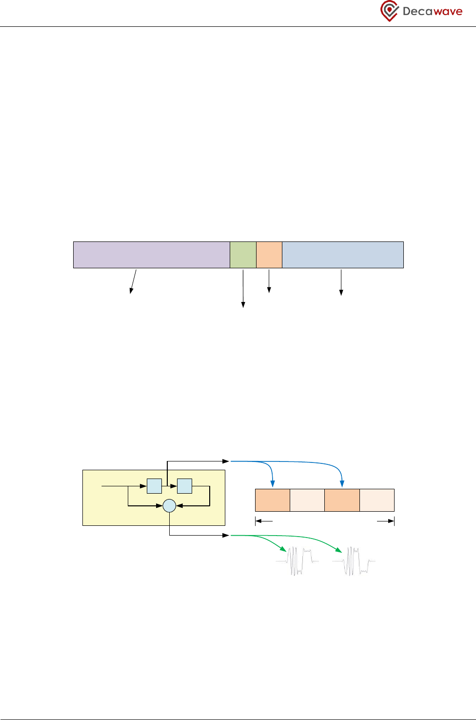
DW1000 User Manual
© Decawave Ltd 2017
Version 2.15
Page 215 of 244
10 APPENDIX 1: The IEEE 802.15.4 UWB physical layer
This appendix gives an introduction to the modulation scheme and frame structure of the UWB physical
layer as specified in the IEEE 802.15.4 – 2011 standard and as implemented by the DW1000 transceiver IC.
This is useful in understanding the operation of the DW1000 transceiver and its configuration options.
10.1 Frame structure overview
The UWB communications are based around the transmission and reception of frames. Figure 31 shows the
general structure of the UWB frame. It begins with a synchronisation header consisting of the preamble and
the SFD (start of frame delimiter), after which the PHY header (PHR) defines the length (and data rate) of the
data payload part of the frame.
Figure 31: UWB PHY Frame structure
10.2 Data modulation scheme
The UWB used in 802.15.4 is sometimes called impulse radio UWB because it is based on high speed pulses
of RF energy. During the PHR and Data parts of the frame, information bits are signalled by the position of
the burst, in a modulation scheme termed burst position modulation (BPM).
Figure 32:- BPM/BPSK data and PHR modulation
Each data bit passes through a convolution encoder to generate a “parity” bit used to set the phase of the
burst as either positive or negative, this component of the modulation is termed binary phase-shift keying
(BPSK). Figure 32 shows how the convolutional encoder contributes to this BPM/BPSK modulation. A
coherent receiver (i.e. one tracking carrier timing and phase) such as the one in the DW1000 can determine
this burst phase and use it in a Viterbi decoder to get an additional 3 dB of coding gain, thereby extending
the operational range of the modulation
Preamble SFD PHR Data
IEEE STD: 64, 1024 or 4096 symbols
IEEE STD: 8 or 64 symbols
19 bits IEEE STD: Up to 127 coded octets
Systematic
Convolution Encoder
Systematic (position) bit determines which
half of the symbol contains the burst
D D
Parity (sign) bit determines whether
the burst is inverted or not
Burst here
= 0
unused
guard
interval
Burst here
= 1
unused
guard
interval
One symbol interval (or bit time)
+
Data in

DW1000 User Manual
© Decawave Ltd 2017
Version 2.15
Page 216 of 244
In addition the quarter symbol interval is sub-divided into 2, 4, or 8 sub-intervals and a pseudo random
sequence used to determine both the burst shape and which of the sub-intervals are actually used for the
burst transmission. This gives more immunity to interference and whitens the output spectrum allowing a
higher signal power to be used in the transmitter.
Forward error correction (FEC) is also included in the PHR and Data parts of the frame. The 19-bit PHR
includes a 6-bit single-error-correct double-error-detect (SECDED) code and the data part of the frame has a
Reed Solomon (RS) code applied. The RS code does not reduce the data rate, as rate quoted includes
allowance for the RS code already. Both SECDED and RS codes are systematic meaning that the data can be
recovered without using the codes (and of course not benefitting from them in that case).
The data part of the frame may be at data rate of 110 kbps, 850 kbps, 6.8 Mbps, or 27 Mbps nominally,
(these figures include a 0.87 factor of reduction on the actual symbol rate to account for the overhead of the
Reed Solomon code).
For the 850 kbps, 6.8 Mbps, and 27 Mbps data rates, the 19-bit PHR part of the frame is transmitted as per
the 850 kbps encoding, but without the Reed Solomon code, so their bit rate is just less than 980 kbps. For
the 110 kbps data rate the PHR is transmitted as per the 110 kbps data coding, again without the Reed
Solomon code, giving them a bit rate is just over 120 kbps.
The DW1000 supports 110 kbps, 850 kbps, and 6.8 Mbps data rates but does not support the 27 Mbps data
rate.
10.3 Synchronisation header modulation scheme
The Synchronisation Header (SHR) consists of the preamble sequence and the SFD (start of frame delimiter).
In contrast to the BPM/BPSK modulation used for the PHR and data, the synchronisation header is made up
of single pulses. The symbol is divided into approximately 500 “chip” time intervals, (496/508 depending on
16/64 MHz PRF
10
), in which either a negative or a positive pulse may be sent, or no pulse. The “chip” interval
is 499.2 MHz, a fundamental frequency within the UWB PHY, and so the resultant symbol times are thus
496/499.2 µs for 16 MHz PRF, and 508/499.2 µs for 64 MHz PRF, (see Table 60 below).
The sequence of pulses actually sent during the symbol interval is determined by preamble code. The
standard defines 8 different length-31 preamble codes for use at 16 MHz PRF and 16 different length-127
preamble codes for use at 64 MHz PRF. The standard nominates particular codes for particular channels so
that at 16 MHz PRF there are just two to choose from per channel, while at 64 MHz PRF there is a choice of
four codes per channel. The length-31 codes are spread by inserting 15 zeros for each code point to give the
496 chip times per symbol while the length-127 codes are spread by inserting 3 zeros for each code point to
give the 508 chip times per symbol. The preamble length is defined by how many times (i.e. for how many
symbols) the sequence is repeated. This is determined by the configuration of preamble symbol repetitions
(PSR).
10
The DW1000 supports average pulse repetition frequencies of 16 MHz and 64 MHz

DW1000 User Manual
© Decawave Ltd 2017
Version 2.15
Page 217 of 244
Table 60: Preamble parameters
Mean PRF (MHz)
#Chips Per Symbol
Preamble Symbol Duration (ns)
16 nominal
496
993.59
64 nominal
508
1017.63
The standard defines PSR settings of 16, 64, 1024 and 4096. The DW1000 supports these (although it will
not receive frames with preamble length below 64 symbols) and in addition supports PSR settings of 128,
256, 512, 1536 and 2048.
The preamble sequence has a property of perfect periodic autocorrelation
11
which in essence allows a
coherent receiver to determine the exact impulse response of the RF channel between transmitter and
receiver. This brings two important benefits. Firstly, it allows the receiver make use of the received energy
from multiple paths, turning multipath from an interference source into a positive affect extending operating
range. Secondly, it lets the receiver resolve the channel in detail and determine the arrival time of the first
(most direct) path, even when attenuated, which brings precision advantages for RTLS applications.
The SFD marks the end of the preamble and the precise start of the switch into the BPM/BPSK modulation of
the PHR. The time-stamping of this event is very deterministic in terms of symbol times and it is this in
conjunction with determining the first arriving ray within that symbol time that allows the accurate time-
stamping needed for precision RTLS applications.
The standard specifies the SFD, which consists of the preamble symbols either not sent, or sent as normal or
sent inverted (i.e. positive and negative pulses reversed) in a defined pattern 8 symbol times long for data
rates other than 110 kbps, and 64 symbols long for the 110 kbps mode.
The length-8 SFD sequence is: 0, +1, 0, -1, +1, 0, 0, -1
The length-64 SFD sequence is: 0, +1, 0, -1, +1, 0, 0, -1, 0, +1, 0, -1, +1, 0, 0, -1, -1, 0, 0, +1, 0, -1, 0, +1, 0, +1,
0, 0, 0, -1, 0, -1, 0, -1, 0, 0, +1, 0, -1, -1, 0, -1, +1, 0, 0, 0, 0, +1, +1, 0, 0, -1, -1, -1, +1, -1, +1, +1, 0, 0, 0, 0, +1,
+1
The DW1000 has the capability for user programmability of SFD sequence, and thus has the possibility to
improve upon the SFD sequence in the standard, if a non-standard SFD sequence is programmed it will be
impossible to interwork with a device expecting the standard SFD sequence.
10.4 PHY header
The PHY header (PHR) is modulated using the BPM/BPSK modulation scheme defined in section 10.2 above,
but it does not employ the Reed Solomon code used for data, instead is employs a 6-bit SECDED (Single error
correct, Double error Detect) parity check sequence as part of its 19-bit length.
11
V. P. Ipatov, “Ternary sequences with ideal autocorrelation properties,” Radio Eng. Electron. Phys., vol. 24, pp. 75–79, 1979

DW1000 User Manual
© Decawave Ltd 2017
Version 2.15
Page 218 of 244
Bit 0
1
2
3
4
5
6
7
8
9
10
11
12
13
14
15
16
17
18
R1
R0
L6
L5
L4
L3
L2
L1
L0
RNG
EXT
P1
P0
C5
C4
C3
C2
C1
C0
Data Rate
Frame Length
Ranging
Packet
Header
Extension
Preamble
Duration
SECDED Check Bits
Figure 33: PHR bit assignment
Figure 33 above shows the bits of the PHR. These are transmitted bit-0 first in time. The DW1000 fills in the
Data Rate, Frame Length, Ranging Packet, and Preamble Duration fields of the PHR based on the user
configuration of the appropriate parameters in Register file: 0x08 – Transmit Frame Control and generates
the SECDED sequence accordingly. The Header Extension bit of the PHR is always zero and is reserved by
IEEE for future extensions.
10.5 UWB channels and preamble codes
The IEEE 802.15.4 UWB PHY has 16 defined channel/bands. The DW1000 supports the subset of these listed
in Table 61 below. Depending on the channel and the pulse repetition frequency (PRF) the IEEE 802.15.4
UWB PHY standard defines a choice of two or four preamble codes. The standard defined preamble code
options are also listed in Table 61. The combination of channel number and preamble code gives what the
standard terms a complex channel.
The DW1000 does not physically impose the channel code selection, so it is up to the software to select the
appropriate preamble code for the selected operating channel. The standard notes that wideband channels
may also employ the codes allocated to the narrower 499.2 MHz bandwidth channels if inter-channel
communication is desired.
Table 61: DW1000 supported UWB channels and recommended preamble codes
Channel
number
Centre
frequency
(MHz)
Bandwidth
(MHz)
Preamble Codes
(16 MHz PRF)
Preamble Codes
(64 MHz PRF)
1
3494.4
499.2
1, 2
9, 10, 11, 12
2
3993.6
499.2
3, 4
9, 10, 11, 12
3
4492.8
499.2
5, 6
9, 10, 11, 12
4
3993.6
1331.2 *
7, 8
17, 18, 19, 20
5
6489.6
499.2
3, 4
9, 10, 11, 12
7
6489.6
1081.6 *
7, 8
17, 18, 19, 20
N.B. For correct operation of the DW1000 the software must take care to only allow
selection of those preamble codes appropriate for the configured PRF.
* The DW1000 has a maximum receive bandwidth of 900 MHz
The preamble codes specified by the standard for use on a particular channel were chosen to have a low
cross correlation factor with each other with the intention that the complex channels could to operate
independently from each other as separate networks. In practice, as there is still a small amount of cross
correlation, there will be some break-through between different codes especially in conditions of close

DW1000 User Manual
© Decawave Ltd 2017
Version 2.15
Page 219 of 244
proximity with long preambles. This may mean that it is not possible to achieve the separation envisioned
by the standard’s authors.
The IEEE 802.15.4 UWB PHY standard includes a feature called dynamic preamble select (DPS) intended for
use a security mechanism for two-way ranging, where devices switch to using one of the DPS specific
preamble codes for the ranging exchange, and perhaps a different one for each direction of communication.
The idea is to make it more difficult to eavesdrop or spoof, by randomly changing the DPS preamble codes in
a mutually agreed sequence only known to the valid participants. This is supported by the DW1000 where at
64 MHz PRF the preamble codes additionally available for DPS are: 13, 14, 15, 16, 21, 22, 23 and 24.
10.6 Additional details on the standard
For additional details on the standard including precise details of the IEEE 802.15.4 UWB modulation, the
reader is referred to the standard itself [1].
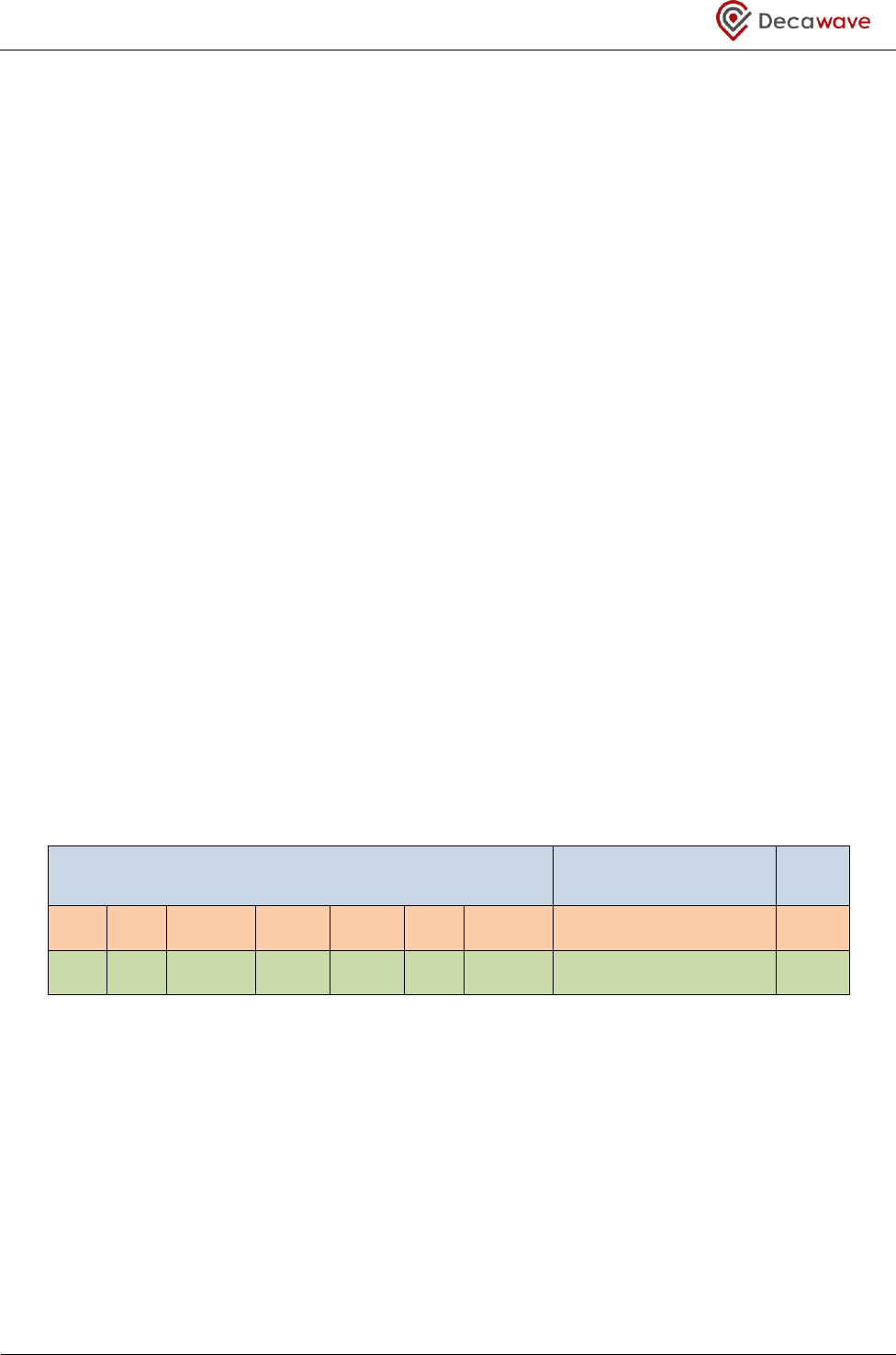
DW1000 User Manual
© Decawave Ltd 2017
Version 2.15
Page 220 of 244
11 APPENDIX 2: The IEEE 802.15.4 MAC layer
This appendix gives an introduction to some aspects of the MAC layer defined in the IEEE 802.15.4 – 2011
standard. The DW1000 transceiver does not implement the MAC layer. The MAC layer implementation is
the responsibility of the host microprocessor system controlling the DW1000. However the DW1000
includes some features to help with the MAC layer implementation. These are:
CRC generation and checking, (see section 5.1 – Cyclic redundancy check).
Frame filtering, (see section 5.2 – Frame filtering).
Automatic acknowledgement, (see section 5.3 – Automatic Acknowledgement).
Automatic turn-around to receive acknowledgement and other responses, (see section 5.4 –
Transmit and automatically wait for response)
An introduction to the MAC frame format is given by the sub-sections below. For more details the reader is
referred to the standard itself [1].
11.1 General MAC message format
The MAC message occupies the Data portion of the UWB Frame as described in section 10.1 – Frame
structure overview and shown in Figure 31. This may be up to 127 octets in length according to the standard,
and up to 1023 octets when employing the DW1000’s non-standard long frame mode, see section 3.4 –
Extended Length Data Frames. The general structure of a MAC message consists of a header that identifies
the frame, followed by a variable length (possibly zero) payload typically from the upper layers but
sometimes (as in the case of MAC command frames) generated within the MAC itself, and finally ended by
the MAC footer which is the FCS (Frame Checking Sequence) CRC used to detect transmission errors. Figure
34 shows the components of the MAC message frame in more detail, indicating the number of octets in each
component.
Figure 34: General MAC message format
The MAC header is parsed by the DW1000 as part of the frame filtering function to determine if its
destination address matches the IC’s address information programmed in Register file: 0x01 – Extended
Unique Identifier and Register file: 0x03 – PAN Identifier and Short Address (or if the frame is a broadcast
message). This parsing of receive frame is based on the contents of the Frame Control field (at the start of
the MAC header) described in section 11.2 below.
Frame
Control
2
octets
MAC Header (MHR) MAC Payload MAC Footer
(MFR)
Sequence
Number
1
octet
Destination
PAN Identifier
Destination
Address
Source PAN
Identifier
Source
Address
Aux Security
Header Frame Payload FCS
0 or 2
octets
0, 2 or 8
octets
0 or 2
octets
0, 2 or 8
octets
0, 5, 6 10 or 14
octets
Variable number of
octets
2
octets
DW1000 User Manual
© Decawave Ltd 2017
Version 2.15
Page 221 of 244
11.2 The frame control field in the MAC header
The frame control field is a two-octet (16-bit) field that begins every IEEE 802.15.4 MAC frame. Its role is to
identify the frame type and indicate what components are incorporated in the remainder of the MAC
header. Figure 35 shows the frame control this and identifies the sub-fields within it. These are described
below.
Figure 35: MAC message frame control field
11.2.1 Frame type field
This frame type field is a 3-bit field that indicates the type of frame. Table 62 below lists the eight possible
frame types and their assignment in IEEE 802.15.4-2011.
Table 62: Frame type field values
Frame Type Field
(FC bits 2 to 0)
Frame
0, 0, 0
Beacon
0, 0, 1
Data
0, 1, 0
Acknowledgement
0, 1, 1
MAC command
1, 0, 0
Reserved
1, 0, 1
Reserved
1, 1, 0
Reserved
1, 1, 1
Reserved
While only four of the eight frame types are assigned by IEEE 802.15.4-2011, some of the reserved types
have since been allocated within the IEEE 802.15 Working Group for special applications. The DW1000
provides only minimal support for the new frame types by allowing their acceptance to be enabled within
the frame filtering function. Please refer to section 5.2 – Frame filtering for details. If these new frames are
enabled then the host system will need to parse the received frames to validate each of them including
checking that the destination address is correct and the host system will need to initiate the transmission of
any acknowledgement response required.
11.2.2 Security enabled Field
This bit when set indicates the presence of the Auxiliary Security Header field within the MAC header and
indicates that the MAC may be employing security processing of the frame payload for authentication
and/or encryption. The DW1000 does not incorporate any facilities for security, so if the frame is
Frame
Type
Bits
0 to 2
Security
Enabled
Bit
3
Frame
Pending
Bit
4
ACK
Request
Bit
5
PAN ID
Compress
Bit
6
Reserved
Bits
7 to 9
Dest.
Address
Mode
Bits
10 & 11
Frame
Version
Bits
12 & 13
Source
Address
Mode
Bits
14 & 15

DW1000 User Manual
© Decawave Ltd 2017
Version 2.15
Page 222 of 244
beingsecured this processing must be done by the host system. For more detail on the IEEE 802.15.4 MAC
security process please refer to the standard [1].
11.2.3 Frame pending field
This bit indicates that the sending device has more data for the recipient. The reader is referred to the
standard [1] for the details of this MAC protocol. The DW1000 receiver does not use the frame pending field
in the receiver so it is up to the host software to handle it appropriately. The host software is also
responsible for forming the TX frame and setting the frame pending bit appropriately. In the case of the
DW1000’s automatically acknowledgement the setting of the frame pending bit may be controlled using the
AACKPEND configuration in Register file: 0x04 – System Configuration. Please also see section 5.3 –
Automatic Acknowledgement for additional details for the auto-ACK functionality.
11.2.4 Acknowledgement request field
The acknowledgement request bit specifies whether an acknowledgment is required from the receiving
device. This field should only be used in data frames or MAC command frames. If this bit is set to one, the
recipient device should send an acknowledgment frame, assuming it passes the appropriate frame filtering
rules. If this bit is set to zero, an acknowledgment frame should not be sent. Please refer to section 5.2 –
Frame filtering and section 5.3 – Automatic Acknowledgement for additional details of the DW1000 support
for this field. The host software is responsible for forming the TX frame and setting the acknowledgement
request field appropriately. If the DW1000’s Automatic Acknowledgementfeature is not being employed
then the host software should respond appropriately to the receipt of frames with the acknowledgement
request bit set.
11.2.5 PAN ID compression field
The PAN ID compression bit specifies whether the MAC frame contains only one of the PAN identifier fields
when both source and destination addresses are present. If the PAN ID compression bit is set to one and
both the source and destination addresses are present, the frame shall contain only the Destination PAN
Identifier field, and the Source PAN Identifier field shall be assumed equal to that of the destination. If the
PAN ID compression bit is set to zero, then the PAN Identifier field shall be present if and only if the
corresponding address is present. The host software is responsible for forming the TX frame and setting the
PAN ID compression bit appropriately for the frame being transmitted. The host software is also responsible
for correctly parsing the RX frame in the receiver including this bit. The DW1000 understands the PAN ID
compression bit and parses the RX frame correctly to identify destination address and destination PAN ID
during RX frame filtering (if enabled). Please refer to section 5.2 – Frame filtering for additional details.
11.2.6 Destination addressing mode field
The destination addressing mode field (2-bits) specifies whether the frame contains a destination address
and if so the size of the address field. Table 63 below summarises the options for destination addressing
mode. For additional information on the addressing modes please refer to the standard [1].

DW1000 User Manual
© Decawave Ltd 2017
Version 2.15
Page 223 of 244
Table 63: Destination addressing mode field values
Destination addressing mode
(FC bits 11 & 10)
Meaning
0, 0
No destination address or destination
PAN ID is present in the frame
0, 1
Reserved
1, 0
The destination address field is a short
(16-bit) address.
1, 1
The destination address field is an
extended (64-bit) address.
11.2.7 Frame version field
The frame version field (2-bits) specifies the version number of the frame. The rules for handling this are
defined in [1], which says the frame version field shall be set to 0x00 to indicate a frame compatible with
IEEE 802.15.4-2003 and 0x01 to indicate an IEEE 802.15.4 frame. The DW1000 understands this frame
version field rules and will reject receive frames that do not have the correct frame version. Please refer to
section 5.2 – Frame filtering for additional details.
11.2.8 Source addressing mode field
The source addressing mode field (2-bits) specifies whether the frame contains a source address and if so
the size of the address field. Table 64 below summarises the options for source addressing mode. For
additional information on the addressing modes please refer to the standard [1].
Table 64: Source addressing mode field values
Source addressing mode
(FC bits 15 & 14)
Meaning
0, 0
No source address or source PAN
ID is present in the frame
0, 1
Reserved
1, 0
The source address field is a short
(16-bit) address.
1, 1
The source address field is an
extended (64-bit) address.
11.3 The Sequence Number field
The Sequence Number field, in the 802.15.4 MAC layer transmitter there should be two sequence numbers
maintained, one for beacon frames transmitted and one for Data frames and MAC command frames. When
auto-acknowledgement is enabled the DW1000 will copy the Sequence Number field into the
acknowledgement frame for any MAC command frame or data frames it is acknowledging. The MAC layer
(software) awaiting the ACK should validate the ACK’s sequence number against that of the

DW1000 User Manual
© Decawave Ltd 2017
Version 2.15
Page 224 of 244
transmittedframe. As each new frame is transmitted (not a re-transmission of an unacknowledged frame)
the sequence number should be incremented by 1 (modulo-256) after it is used in the transmitted frame.
11.4 MAC level processing in the DW1000
The DW1000 transmits data from the TX_BUFFER in a frame with data length as specified in the TFLEN and
TFLE fields of the Register file: 0x08 – Transmit Frame Control, inserting the 2-octet FCS as the last two octets
of the data payload. The DW1000 will not do any other MAC level transmit processing. So, it is up to the
host system software to prepare the correctly formatted frame conforming to the IEEE 802.15.4 standard
MAC if this is required.
On the receive side, the DW1000 will validate the FCS of the received frame, and can parse frames
complying with IEEE 802.15.4-2011 to validate and accept only those with destination address that is the
broadcast address or matches the IC address information configured in Register file: 0x01 – Extended Unique
Identifier and Register file: 0x03 – PAN Identifier and Short Address. The DW1000 can also optionally
respond to the acknowledgement request bit set in the frame control field, of correctly addressed Data
Frames or MAC Command frames, by sending an IEEE 802.15.4-2011 to compliant acknowledgement frame.
The DW1000 will deliver the received data frame in the RX_BUFFER with its data length reported by the
RXFLEN and RXFLE fields of the Register file: 0x10 – RX Frame Information Register, and other than the RX
activities mentioned in the paragraph above the DW1000 will not do any additional MAC level receive
processing. So, it is up to the host system software to correctly parse the received frame according to the
IEEE 802.15.4 standard MAC definition and take whatever additional action is proscribed by the standard, if
this is required.
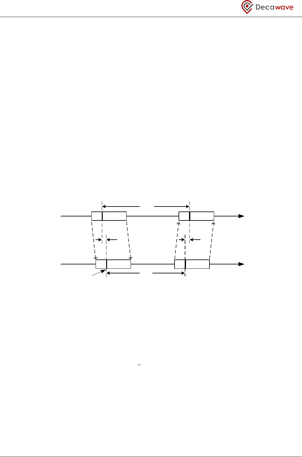
DW1000 User Manual
© Decawave Ltd 2017
Version 2.15
Page 225 of 244
12 APPENDIX 3: Two-Way Ranging
12.1 Introduction
This appendix is for information only and describes various methods of implementing a two-way ranging
scheme between two nodes.
The chosen two-way ranging algorithm is implemented by host system software and is not a feature of the
DW1000. The DW1000 just provides the facilities for message time-stamping and precise control of message
transmission times that enable these algorithms. See section 4.1.6 – RX Message timestamp, 3.2 –
Transmission timestamp and 3.3 – Delayed Transmission for details of this.
In all of the schemes that follow one node acts as Initiator, initiating a range measurement, while the other
node acts as a Responder listening and responding to the initiator, and calculating the range.
12.2 Single-sided Two-way Ranging
Single-sided two-way ranging (SS-TWR) involves a simple measurement of the round trip delay of a single
message from one node to another and a response sent back to the original node.
Figure 36: Single-sided Two-way ranging
The operation of SS-TWR is as shown in Figure 36, where device A initiates the exchange and device B
responds to complete the exchange and each device precisely timestamps the transmission and reception
times of the message frames, and so can calculate times Tround and Treply by simple subtraction. And the
resultant time-of-flight, Tprop may be estimated by the equation:
The times Tround and Treply are measured independently by device A and B using their respective local clocks,
which both have some clock offset error eA and eB from their nominal frequency, and so the resulting time-
of-flight estimate has a considerable error that increases as Treply increases. Some typical values for this are
presented in Table 65. Depending on the size of ranging error that is acceptable to the application, SS-TWR
may be an appropriate choice for range measurement especially if the reply time Treply is minimized and the
clock error is low. It should be noted that the reply time Treply is not just the RX-to-TX turnaround time but
also includes the message length.
Device A
Device B
TX
Tprop Tprop
RX
RX TX
Treply
Tround
time
RMARKER

DW1000 User Manual
© Decawave Ltd 2017
Version 2.15
Page 226 of 244
In this scheme the error in the measured Tprop is given by the following: -
Table 65: Typical clock induced errors in SS-TWR time of flight estimation
clock error
Treply
2 ppm
5 ppm
10 ppm
20 ppm
40 ppm
100 µs
0.1 ns
0.25 ns
0.5 ns
1 ns
2 ns
200 µs
0.2 ns
0.5 ns
1 ns
2 ns
4 ns
500 µs
0.5 ns
1.25 ns
2.5 ns
5 ns
10 ns
1 ms
1 ns
2.5 ns
5 ns
10 ns
20 ns
2 ms
2 ns
5 ns
10 ns
20 ns
40 ns
5 ms
5 ns
12.5 ns
25 ns
50 ns
100 ns
It can be seen that as Treply increases and as the clock offset increases the error in the time-of-flight
estimation increases to the point where the error is such as to render the estimation very inaccurate. For
this reason, SS-TWR is not commonly used but it is worthy of examination for particular use cases where
tight tolerance clocks are used and the communication range is relatively short.
Table 66: Typical clock induced error in SS-TWR time-of-flight estimation using actual IEEE80.15.4-2011
UWB frame lengths
clock error
Treply
2 ppm
5 ppm
10 ppm
20 ppm
40 ppm
211 µs total
6.81 Mbps
64 Symbol Preamble
96 µs response delay
0.2 ns
0.5 ns
1.1 ns
2.1 ns
4.2 ns
275 µs total
6.81 Mbps
128 Symbol Preamble
96 µs response delay
0.3 ns
0.7 ns
1.4 ns
2.8 ns
5.5 ns
403 µs total
6.81 Mbps
256 Symbol Preamble
96 µs response delay
0.4 ns
1 ns
2 ns
4 ns
8 ns
Note: An error of 1 ns is equivalent to a 30 cm error in measured distance.
Advantages
Drawbacks
Only one message exchange required which saves
time & power.
As Treply increases and clock offsets increase the
estimated time-of-flight becomes very inaccurate.
If Treply is kept short and accurate crystals are used
then time-of-flight estimation may be accurate
enough for certain use cases.
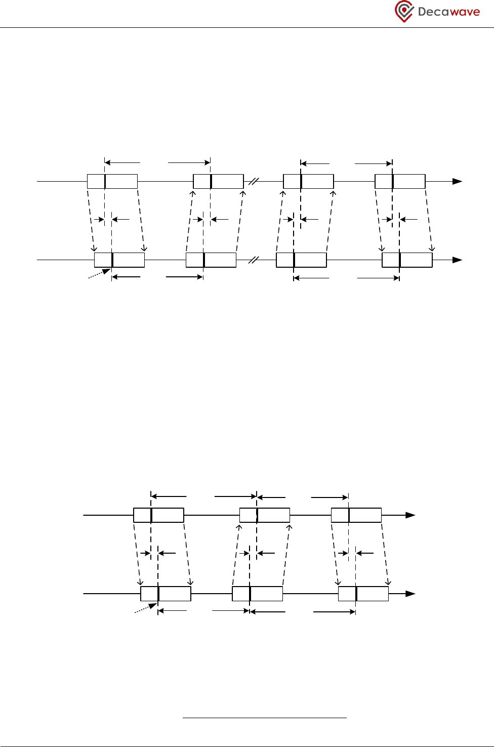
DW1000 User Manual
© Decawave Ltd 2017
Version 2.15
Page 227 of 244
12.3 Double-sided Two-way Ranging
12.3.1 Using 4 messages
Double-sided two-way ranging (DS-TWR), is an extension of the basic single-sided two-way ranging in which
two round trip time measurements are used and combined to give a time-of-flight result which has a
reduced error even for quite long response delays.
Figure 37: Double-sided two-way ranging with four messages
The operation of DS-TWR is as shown in Figure 37, where device A initiates the first round trip measurement
to which device B responds, after which device B initiates the second round trip measurement to which
device A responds completing the full DS-TWR exchange. Each device precisely timestamps the transmission
and reception times of the messages.
12.3.2 Using three messages
The four messages of DS-TWR, shown in Figure 37, can be reduced to three messages by using the reply of
the first round-trip measurement as the initiator of the second round-trip measurement. This is shown in
Figure 38.
Figure 38: Double-sided Two-way ranging with three messages
The resultant time-of-flight estimate, Tprop, in both the three and four message cases may be calculated using
the expression:
Device A
Device B
TX
Tprop Tprop
RX
RX TX
Treply1
Tround1
RMARKER
time
TX RX
RX TX
Treply2
Tround2
Tprop Tprop
Device A
Device B
TX
Tprop Tprop
RX
RX TX
Treply1
Tround1
time
RX
TX
Treply2
Tround2
Tprop
RMARKER

DW1000 User Manual
© Decawave Ltd 2017
Version 2.15
Page 228 of 244
Both of the above schemes are denoted ASYMMETRIC because they do not require the reply times from
each device to be the same.
Using this scheme, the typical clock induced error is in the low picosecond range even with 20 ppm crystals.
At these error levels the precision of determining the arrival time of the messages at each of the receivers is
a more significant contributor to overall Tprop error than The clock-induced error.
Where the clock in device A runs at ka times the desired frequency and the clock in device B runs at kb times
the desired frequency and both ka & kb are close to 1.
To give some idea of the size of this error, if devices A and B have clocks where each are 20 ppm away (the
worst case specification) from the nominal clock in directions which make their combined error additive and
equal to 40 ppm, then ka and kb might both be 0.99998 or 1.00002.
Even with a relatively large UWB operating range of say 100 m, the TOF is just 333 ns, so the error is 20 × 10-6
× 333 × 10-9 seconds, which is 6.7 × 10⁻¹² seconds or 6.7 picoseconds which is approximately 2.2 mm.
Again note that achieving these error levels does NOT require the use of the same response time at each
device.
At these error levels the precision of determining the arrival time of the message is actually the more
significant source of error.
Advantages
Drawbacks
Reply times need not be the same – gives great
flexibility in the design of use cases and application
scenarios
Requires multiplication and division operations
Error in the calculated time-of-flight is minimized
12.3.3 Using symmetric reply times
This is a special case of the double sided scheme known as SYMMETRIC Double-sided Two-way ranging (SDS-
TWR )
12
in which Treply1 and Treply2 are restrained to be equal (or as close to equal as possible). In this case:
This scheme requires only addition, subtraction and division by 4 which is easily achieved in low power
micro-controllers however it results in the entire exchange taking longer than necessary.
12
Nanotron is the owner of the intellectual property rights of the SDS-TWR scheme. The relevant Nanotron
patents are EU EP1815267B1 and USA US7843379B2

DW1000 User Manual
© Decawave Ltd 2017
Version 2.15
Page 229 of 244
It can be difficult to achieve a situation where the reply times at each device are the same although the use
of the DW1000 delayed send feature simplifies this; the calculations required at each device may not be the
same. For example, the final message from device A to device B will often need to embed the send and
receive times into the packet so that device B can calculate the time of flight. If symmetric delay times are
required, the whole round trip exchange will need to be expanded to accommodate this. When the response
delays are flexible, the exchange can be faster.
As the difference in reply time of the two devices increases there is a linear increase in the error in the
calculated time of flight which can approach 30 cm for a reply-time difference of 100 µs.
Advantages
Drawbacks
Requires only simple mathematical operations to
derive a result
Reply times must be the same – this is difficult to
achieve. If they are not the same then an error is
introduced into the result the magnitude of which
depends on the difference between the reply times
The ranging exchange is longer than necessary
because all reply times must be as long as the
longest reply time
12.3.4 Comparison between DS and SDS two-way ranging
12.3.4.1 Introduction
It is useful to compare the asymmetric and symmetric double-sided two-way ranging
13
schemes in some real
world applications so the implications of each can be seen.
12.3.4.2 Infrastructure based asset tracking
One anchor device sends a packet, P1, to many, say 5 tags. Each tag responds with a packet to this anchor in
successive responses. Tag 1 responds with packet P2a after time t, Tag 2 responds with P2b after time 2t,
Tag 3 responds with P2c after time 3t and so on until all tags have responded. Finally the anchor closes off
the round with a final packet P3.
Each tag can now calculate its distance from the anchor after a sequence of just 7 messages. If the anchor
had used symmetric S-TWR it would be forced to have the same delay for each tag interaction and a
minimum of 3 messages per tag, or 15 messages would be required.
In the asymmetric case the number of packets required is N+2 whereas in the symmetric case it is 3N.
12.3.4.3 Infrastructure based asset tracking
In this scheme a mobile tag (on an asset say) ranges to three fixed anchors. Each anchor then calculates the
distance to the tag. These three distances are then combined in an infrastructure-based solver to locate the
tag.
13
Nanotron is the owner of the intellectual property rights of the SDS-TWR scheme. The relevant Nanotron
patents are EU EP1815267B1 and USA US7843379B2

DW1000 User Manual
© Decawave Ltd 2017
Version 2.15
Page 230 of 244
With symmetric double-sided two-way ranging this needs 3 messages per distance measurement which is a
total of 6 transmissions and three receptions to derive the location.
In the asymmetric ranging scheme the tag sends a Poll message which is received by the three anchors in the
infrastructure who reply in successive responses with packets RespA, RespB & RespC after which the tag
sends the Final message received by all three anchors. This allows the tag to be located after sending only 2
messages and receiving 3. This scheme is illustrated in Figure 39. This represents a substantial saving in
message traffic thereby saving battery power and air-time.
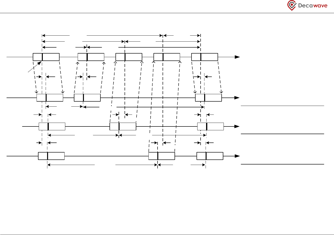
DW1000 User Manual
© Decawave Ltd 2017
Version 2.15
Page 231 of 244
Tag
Anchor A
TX
TpropA TpropA
RX
RX TX
Treply1A
Tround1A
time
RX
TX
Treply2A
TpropA
RMARKER
Anchor B
RX TX
Treply1B
Anchor C
RX TX
Treply1C Tround2C
RX RX
RX
RX
Tround1B
TpropB
TpropC
Tround1C Treply2B
Treply2C
TpropB
Tround2A
Tround2B
TpropB
TpropC
TpropC
Tround1A × Tround2A ̶ Treply1A × Treply2A
Tround1A + Tround2A + Treply1A + Treply2A
TpropA =
Tround1B × Tround2B ̶ Treply1B × Treply2B
Tround1B + Tround2B + Treply1B + Treply2B
TpropB =
Tround1C × Tround2C ̶ Treply1C × Treply2C
Tround1C + Tround2C + Treply1C + Treply2C
TpropC =
Poll
Poll
Poll
Poll
RespA
RespA RespB RespC
RespB
RespC
Final
Final
Final
Final
The Final message communicates the tag’s
Tround and Treply times to the anchors, which
each calculate the range to the tag as follows.
Figure 39: Ranging to 3 anchors with just 5 messages where each anchor calculates its own range result

DW1000 User Manual
© Decawave Ltd 2017
Version 2.15
Page 232 of 244
12.3.4.4 Infrastructure-less Peer-to-peer networks
In the case of a peer-to-peer network of N mobile nodes where each node wants to find its distance to every
other peer node as part of solving their relative location then this is ½N(N-1) distance measurements. For
example, for a 5 node system, this is 10 distance measurements.
With symmetric double-sided ranging this needs 3 messages per distance measurement. There may also be
a need to send an additional message to communicate the results, which could be 1 per distance
measurement or just 1 per node containing all the results which that node calculated. This is then a total of
35 to 40 messages in the 5 node example case.
With the asymmetric ranging scheme the ranging exchanges can be combined and completed with just two
transmissions per node, i.e. 10 messages in the case of the 5 node example. Again this represents a
substantial saving in message traffic thereby saving battery power and air-time. However the ranging
exchanges are highly asymmetric.
Further details on these various schemes and the derivation of the associated formulae are available from
Decawave.

DW1000 User Manual
© Decawave Ltd 2017
Version 2.15
Page 233 of 244
13 APPENDIX 4: Abbreviations and acronyms
Abbreviation
Full Title
Explanation
AGC
automatic gain
control
A scheme that automatically adjusts the gain of the DW1000 receiver
depending on the power in the received signal
ACK
acknowledgement
(frame)
A frame sent by the DW1000 in response to a received frame indicating
successful reception. DW1000 allows the automatic generation of such
frames when appropriately configured.
AON
always-on block
(forsaving
configuration)
A section of memory in DW1000 whose contents are retained provided
VDDAON is maintained above the minimum limit specified in the
DW1000 data sheet. Intended for saving device configuration during the
SLEEP and DEEPSLEEP states and restoring it thereafter.
BPM
burst position
modulation
A modulation scheme in which information is conveyed by the position
of a burst of pulses in one of a number of possible positions in a symbol
BPSK
binary phase-shift
keying
A modulation scheme in which information is conveyed by whether
pulses are positive or negative
CRC
cyclic redundancy
check (an FCS)
Error detecting code appended to the frame in the transmitter to allow
detection of errors at the receiver.
CIR
channel impulse
response
The impulse response of the communications channel between
transmitter and receiver as detected by DW1000 for the most recently
received frame
DPS
dynamic
preamble select
Anti-spoofing mechanism to allow IEEE 802.15.4 devices to move their
long preamble codes to codes that are different from those in normal
use, see 237[1].
ESD
electrostatic
discharge
A sudden flow of electrical current between two electrically charged
objects caused by contact, an electrical short circuit or dielectric
breakdown. Can cause failure of semiconductor devices. DW1000 is
resistant to ESD up to the limits specified in the data sheet.
EUI
extended unique
identifier
64-bit IEEE device address. Refer to Register file: 0x01 – Extended
Unique Identifier.
FCS
frame check
sequence (the
CRC)
A CRC appended to the frame in the transmitter to allow detection of
errors at the receiver.
IF
intermediate
frequency
A frequency to which a carrier frequency is shifted as an intermediate
step in transmission or reception.
LDC
low duty-cycle
Certain regulatory jurisdictions define rules that limit the duration of
UWB transmissions per unit time in certain channels. These rules are
generally referred to as low duty cycle rules
LDO
low drop-out
voltage regulator
Linear voltage regulator that requires only a small differential between
its input source voltage and its output regulated voltage below which it

DW1000 User Manual
© Decawave Ltd 2017
Version 2.15
Page 234 of 244
Abbreviation
Full Title
Explanation
can no longer regulate correctly. DW1000 uses a number of such
regulators.
LDE
leading edge (or
the process to
find and adjust
the RX message
timestamp)
Process to find and adjust the RX message timestamp
LNA
low noise
amplifier
Circuit normally found at the front-end of a radio receiver designed to
amplify very low level signals while keeping any added noise to as low a
level as possible
LOS
line of sight
Physical radio channel configuration in which there is a direct line of
sight between the transmitter and the receiver
NLOS
non line of sight
Physical radio channel configuration in which there is no direct line of
sight between the transmitter and the receiver
OTP
one-time
programmable
(memory)
Internal memory in DW1000 that can be programmed once to store
various identification and calibration values
PAC
preamble
acquisition chunk
A group of preamble symbols which are correlated together in the
preamble detection process in the receiver. The size of the PAC is
configurable –see Sub-Register 0x27:08 – DRX_TUNE2. The selection of
the most appropriate PAC size is discussed in section 4.1.1
PHR
PHY header
A 19-bit section of the IEEE802.15.4-2011 UWB frame that comes
directly after the SFD and before the message payload and defines
various characteristics of that payload required by the receiver for
successful reception.
PHY
physical layer
Defined in the context of the OSI 7-layer model for communications
systems in general and the IEEE802.15.4-2011 UWB standard in
particular, the PHY layer is the lowest layer in the 7-layermodel and
defines the physical interface to the communications medium
PLL
phase locked loop
Phase locked loop used to generate stable frequency clocks. These are
used in DW1000 to generate carrier frequencies and system clocks.
PRF
pulse repetition
frequency
Defined in the context of the IEEE802.15.4-2011 [1] standard. This is the
frequency at which pulses are repeated in the preamble and data
portions of a frame depending on the chosen configuration.
PSR
preamble symbol
repetitions
Used to define the overall preamble length. A larger number of
preamble symbol repetitions give a longer preamble.
RF
radio frequency
Generally used to refer to signals in the range of 3 kHz to 300 GHz. In
the context of a radio receiver, the term is generally used to refer to
circuits in a receiver before down-conversion takes place and in a
transmitter after up-conversion takes place

DW1000 User Manual
© Decawave Ltd 2017
Version 2.15
Page 235 of 244
Abbreviation
Full Title
Explanation
RMARKER
ranging marker
(start of PHR at
antenna)
Defined in the context of the IEEE802.15.4-2011 [1] standard. Defines
the start of the PHR at the antenna in either transmit or receive
RTLS
real time location
systems
System intended to provide information on the location of various items
in real-time.
RX
receive or
receiver
Term used to refer to the receiver section of a transceiver or the
operation of receiving signals
SAR
Successive
Approximation
Register ADC
A type of Analog to Digital converter that used a digital binary search to
converge on the correct digital representation of the analog input level.
SECDED
single error
correct, double
error detect (a
parity check
sequence in the
PHR)
A coding scheme that allows the: -
detection and correction of a single bit error in a group of bits or
the detection but not the correction of a double bit error in a group
of bits
The IEEE802.15.4-2011 UWB standard defines the use of such a scheme
as a parity check in the PHR portion of the frame.
SFD
start of frame
delimiter
Defined in the context of the IEEE802.15.4-2011 [1] standard. Indicates
the completion of the preamble section of the frame and the
commencement of the payload section.
SHR
synchronisation
header (consists
of preamble and
SFD)
Defined in the context of the IEEE802.15.4-2011 [1] standard. The first
portion of an IEEE802.15.4-2011 UWB frame containing the preamble
and SFD
SPI
serial peripheral
interface
An industry accepted method for interfacing between IC’s using a
synchronous serial scheme first introduced by Motorola
TDOA
time difference of
arrival
Method of deriving information on the location of a transmitter. The
time of arrival of a transmission at two physically different locations
whose clocks are synchronized is noted and the difference in the arrival
times provides information on the location of the transmitter. A
number of such TDOA measurements at different locations can be used
to uniquely determine the position of the transmitter. Refer to
Decawave’s website for further information.
TOF
time of flight
The time taken for a radio signal to travel between the transmitting
antenna and the receiving antenna
TX
transmit or
transmitter
Term used to refer to the transmitter section of a transceiver or the
operation of transmitting signals
UWB
ultra wide band
A radio scheme employing channel bandwidths of, or in excess of,
500MHz
WSN
wireless sensor
networks
A network of wireless nodes intended to enable the monitoring and
control of the physical environment
XTI
internal 19.2 MHz
clock (is the raw
The 38.4 MHz XTAL oscillator clock divided by 2.

DW1000 User Manual
© Decawave Ltd 2017
Version 2.15
Page 236 of 244
Abbreviation
Full Title
Explanation
38.4 MHz XTAL
oscillator input
÷ 2)

DW1000 User Manual
© Decawave Ltd 2017
Version 2.15
Page 237 of 244
14 APPENDIX 5: References
[1] IEEE 802.15.4-2011 or “IEEE Std 802.15.4™‐2011” (Revision of IEEE Std 802.15.4-2006). IEEE Standard for Local and
metropolitan area networks – Part 15.4: Low-Rate Wireless Personal Area Networks (LR-WPANs). IEEE Computer
Society Sponsored by the LAN/MAN Standards Committee. Available from http://standards.ieee.org/.
[2] APH010 DW1000 Inter-Channel Interference: How transmissions on one DW1000 channel can affect other
channels and how to minimize that effect. Available on www.decawave.com
15 Document History
Table 67: Document History
Revision
Date
Description
1.00
15th November 2013
First release
2.01
31st March 2014
Scheduled update
2.02
31st July 2014
Scheduled update
2.03
31st December 2014
Scheduled update
2.04
31st March 2015
Scheduled update
2.05
30th June, 2015
Scheduled update
2.06
17th November, 2015
Scheduled update
2.07
31st December 2015
Scheduled update
2.08
31st March 2016
Scheduled update
2.09
30th June 2016
Scheduled update
2.10
30th September 2016
Scheduled update
2.11
3rd March 2017
Scheduled update
2.12
28th July 2018
Scheduled update
2.13
7th Jan 2018
Scheduled update
2.14
31st July 2018
Scheduled update
2.15
4th September 2018
Schedules update
16 Change Log
Revision v2.03
Page
Change Description
All
Update of version number to v2.03
All
Various typographical changes
2
Update of table of contents
All
Repair of non-functioning cross-reference links in v2.02
18
Addition of section 2.4.1.3 re LDO TUNE
23
Addition of section 2.5.5.11 re LDO TUNE

DW1000 User Manual
© Decawave Ltd 2017
Version 2.15
Page 238 of 244
Page
Change Description
27
Inclusion of detail on extended frame mode
28
Addition of further information on the use of extended frames
57
Addition of LDOTUNE_CAL to OTP memory map in Table 10
164
Addition of information on LDO_KICK bit to 7.2.46.7 Sub-Register 0x2D:12 – OTP_SF
211
Correction to figure 36
216
Addition of v2.03 to table 64
Addition of this section & modification of heading numbers as a result
Revision v2.04
Page
Change Description
All
Update of version number to v2.04
All
Various typographical changes
8
Addition to table describing document sections
16
Inclusion of note re half duplex operation only
23
Modification of section heading 2.5.5.4 to refer to NTM rather than NSTD
58
Update to VDDIO for OTP programming to be consistent with DW1000 data sheet
85
Modification to CPLOCK bit description
89
Modification to description of CLKPLL_LL bit
106
Modification to Table 26 – transmit power octet
119
Inclusion of PLLLDT bit description
143
Modification to description of CPLLLOCK
149
Modification to Table 41- default values for FS_PLLTUNE for channels 5 & 7
167
Modification of NSTD to NTM
217
Addition of v2.04 to table 64
217
Inclusion of this table
Revision v2.05
Page
Change Description
All
Update of version number to v2.05
All
Various typographical changes
29, 30
Addition of text relating writing to the TX buffer while receiving a frame
87
Modification to description of RXFDR bit
190
Modification to table 51 to refer to RFCONF instead of RFRES1
211
Appendix 13: Inclusion of a more comprehensive discussion of TWR schemes including SS TWR,
Asymmetric DS TWR and Symmetric DS TWR

DW1000 User Manual
© Decawave Ltd 2017
Version 2.15
Page 239 of 244
Page
Change Description
221
Addition of v2.05 to table 64
222
Inclusion of this table
Revision v2.06
Page
Change Description
All
Update of version number to v2.06
All
Various typographical changes
17
Inclusion of CPLOCK bit
23
Section2.5.5.9 - modification to FS_PLLTUNE value
46
Section 4.7.1 & 4.7.2 – modification to 16 MHz PRF calculation fixed value
73
Section 7.2.10 Correction to register default value
104 – 107
Modification of text re smart Tx Power in 7.2.31
108
Section 7.2.32 Correction to register type
148
7.2.43.5 Correction to reference in register description
189
Correction to register write value in step 8 of the crystal trim procedure
221
Addition of v2.06 to table 64
223
Inclusion of this table
Revision v2.07
Page
Change Description
All
Update of version number to v2.07
All
Various typographical changes and formatting corrections
62
TX_BUFFER register type corrected to write-only.
62
RX_BUFFER register type corrected to write-only.
76
TX_BUFFER register type –hanged to write-only
92 – 93
RXPACC field of RX_FINFO updated to describe adjustments that can be made to the count to
calculate more accurate receive signal power as used in calculations in section 4.7.
96
RX_BUFFER register type changed to read-only.
111
DWSFD field of CHAN_CTRL register description updated to specify Decawave-defined SFD
sequences
137
RXPACC_NOSAT added to address 0x27, subaddress 0x2C
141
Subregister 0x27:2C, RXPACC_NOSAT added
173
EVC_CTRL register description corrected to239ehavior write-to-enable 239ehavior.
197
Addition of clarification text to Section 9.3 re use of different preamble codes to allow multiple
communications on the same physical channel

DW1000 User Manual
© Decawave Ltd 2017
Version 2.15
Page 240 of 244
Page
Change Description
224
Addition of v2.07 to table 65 / Addition of Reference [2]
226
Inclusion of this table
Revision v2.08
Page
Change Description
All
Update of version number to v2.08
All
Various typographical changes and formatting corrections
58
Corrections to OTP memory map to be consistent with APS012
94
Description of FINFO reg updated to indicate that RNG bit is bit 15 and not bit 10
106
Correction to references
143
TXFEN and PLLFEN descriptions updated
152
Modification to FS_PLLTUNE value for channel 3
168
Update to OP_SEL description. Update to clock offset descriptions in Table 46
186
Description of ATXSLP updated to include reference to SLEEP_EN (0x2c:06)
188
Added note to PMSC_TXFSEQ re use with external PA
207
Figure 33 replaced for readability
224
Update of table 65
226 / 7
Inclusion of this table
Revision v2.09
Page
Change Description
All
Update of version number to v2.09
All
Various typographical changes and formatting corrections
16
Update to description of INIT state
34
Correction to receiver errors for which a receiver reset is required
41
Addition of actions required to correctly read a frame received during low power listening
42
Correction to operation of SNOZ_TIM
52
Inclusion of section on SFD initialization in automatic acknowledgement
53
Further details on the operation of the AAT bit
58
Update to OTP memory map to ensure consistency with application note APS012
99
Inclusion of additional information on RCPHASE
106
Correction of reference to Figure 26
140
Change to text of warning on not using SFD timeout
141
Modification to the operation of DRX_PRETOC
186
Correction to operation of SNOZ_TIM

DW1000 User Manual
© Decawave Ltd 2017
Version 2.15
Page 241 of 244
Page
Change Description
188
Modification of definition of BLNKEN
211
Addition of clarification on operation of DWSFD / TNSSSFD / RNSSFD
224
Update of table 65
227
Inclusion of this table
Revision v2.10
Page
Change Description
All
Update of version number to v2.10
All
Various typographical changes and formatting corrections
58
Correct the fixed value in the first three hex digits to be 0x100 and not 0x101 as previously
suggested.
96 / 100
Updated definitions of FP_AMPL1 and FP_AMPL3
124
Update for setting MSGP0 bit 7, was reserved, now indicates how it is used to allow the system
clock appear on GPIO0
139
Added text about optimizing SFD timeout value.
179
Updated description of TX_PSTM for inter frame spacing
222
Update of table 65
226
Inclusion of this table
Revision v2.11
Page
Change Description
All
Update of version number to v2.11
All
Various typographical changes and formatting corrections
53
Added Sect 5.3.6 ACK corruption text added
77, 96
Amend TX and RX_Buffer descriptions
80
Updated description on TXSTRT bit
92
R(report) added to RXPF in Register REG:10:00 – RX_FINFO – RX Frame Information to match
the resume table.
95
Addition of prohibition of writing to receive buffer
114
Modification to Table 21 and addition of new Table 22. Renumbering of all subsequent tables.
146
Change sub register 0x28:0C– RF_TXCTRL to 24 (3bytes)
146
Table 37 . Change 32 to 24 bit
151
Added new section for details on “Carrier Recovery Integrator Register”
162
Addition of previously undocumented transmitter calibration pulse generator registers
173
Correction to desctiption of register 0x2F:06 section 7.2.48.3

DW1000 User Manual
© Decawave Ltd 2017
Version 2.15
Page 242 of 244
Page
Change Description
192
Write correct value Sub-Register 0x2B:0B – FS_PLLTUNE
199
Removal of restriction on writing only the default values to 0x2E:1806, section 7.2.47.6
207
Table 55, Change power at receiver input for ch 4 and ch7 to -104 (dBm/Mhz)
227
Addition of correct post code
Revision v2.12
Page
Change Description
All
Update of version number to v2.12
61
To read OTP OTP_RDAT change 2A.04 to 2D:0A (see also 7.2.46.5) Row 5 removed.
106
New note on requirement for isolation of VDDPA1 and VDDPA2 if using Tx gain setting 000
128
Note added to point out that GPIO clocks have to be on to use GPIO lines.
132
Sec 7.2.39.3 GDM6 is declared as bit 15, but it is bit 14
133
Sec 7.2.39.4 GOP2 should refer to GPIO2 and GOP3 should refer to GPIO3
140
Changed the sentence to “The bits of the GPIO_RAW register identified above are ind”vidually
described below:”
157
PG_TMEAS changed to reg:2A:08 bit5:2, it was given 4:2
238
Addition of this table
Revision v2.13
Page
Change Description
All
Update of version number to v2.13
59
Update of TABLE 10 address 6 & 7
61
Change OTP_RDAT from 0x2A:04 to 0x2D:0A
141
Remove embedded Table 21 & 22
181
LDE_CFG1 update
183
LDE_CGF2 update
207
Furthest range is possible with wider bandwidth channels 4 and 7
Revision v2.14
Page
Change Description
All
Update document with new logo and change of version number to v2.14
60`
Table 10, include PART ID
68
RXRFTO/LDEERR remove sentence stating bits are cleared at next EX enable
142
CRI (0x27 offset 8) added in table 29
DW1000 User Manual
© Decawave Ltd 2017
Version 2.15
Page 243 of 244
Page
Change Description
149
Length from 27:28 changed from 2 to 3
152
Add note to RF_CONF
153
Remove note for RF_RES1
158
Change voltage to temperature in SAR_LTEMP
195
PLL2_SEQ_EN added to 36:00 bit 24
203
Update Transmitter Configuration Procedure (Update line 1 and merge lines 9&10)
228/229
Include Nanotron IP information
Revision v2.15
Page
Change Description
All
Update of version number to v2.15
Removal of incorrect reference (error!)

DW1000 User Manual
© Decawave Ltd 2017
Version 2.15
Page 244 of 244
17 FURTHER INFORMATION
Decawave develops semiconductors solutions, software, modules, reference designs - that enable real-time,
ultra-accurate, ultra-reliable local area micro-location services. Decawave’s technology enables an entirely
new class of easy to implement, highly secure, intelligent location functionality and services for IoT and
smart consumer products and applications.
For further information on this or any other Decawave product, please refer to our website
www.decawave.com.
