Intel® Atom™ C3XXX Product Family Firmware Support Package (Intel® FSP) Integration Guide Denverton NSFsp
User Manual:
Open the PDF directly: View PDF ![]() .
.
Page Count: 32
- Intel® Atom® C3XXX Product Family Intel® Firmware Support Package (Intel® FSP)
- 1 Introduction
- 2 Intel® FSP Overview
- 3 Intel® FSP Integration
- 4 Intel® FSP Output
- 5 Intel® FSP Configuration Firmware File
- A Memory Down
- B FIA MUX Configuration Structure
- C EMMC* DLL Configuration Structure

Document ID: 335702-003US
Intel® Atom® C3XXX Product Family
Intel® Firmware Support Package
(Intel® FSP)
Integration Guide
November 2018
Production Validated 003

Intel® Atom® C3XXX Product Family Intel® Firmware Support Package (Intel® FSP)
Integration Guide November 2018
2Document ID: 335702-003US
Legal Lines and Discla imers
By using this document, in addition to any agreements you have with Intel, you accept the terms set forth below.
You may not use or facilitate the use of this document in connection with any infringement or other legal analysis concerning Intel products described
herein. You agree to grant Intel a non-exclusive, royalty-free license to any patent claim thereafter drafted which includes subject matter disclosed
herein.
INFORMATION IN THIS DOCUMENT IS PROVIDED IN CONNECTION WITH INTEL PRODUCTS. NO LICENSE, EXPRESS OR IMPLIED, BY ESTOPPEL OR
OTHERWISE, TO ANY INTELLECTUAL PROPERTY RIGHTS IS GRANTED BY THIS DOCUMENT.
Intel may make changes to specifications and product descriptions at any time, without notice. Designers must not rely on the absence or characteristics
of any features or instructions marked “reserved” or “undefined.” Do not finalize a design with this information.
The products described in this document may contain design defects or errors known as errata which may cause the product to deviate from published
specifications. Current characterized errata are available on request.
Contact your local Intel sales office or your distributor to obtain the latest specifications and before placing your product order.
Copies of documents which have an order number and are referenced in this document, or other Intel literature, may be obtained by calling 1-800-548-
4725, or go to: http://www.intel.com/design/literature.htm
Intel and the Intel logo are trademarks of Intel Corporation in the U.S. and/or other countries.
*Other names and brands may be claimed as the property of others.
Copyright © 2018, Intel Corporation. All rights reserved.

Intel® Atom® C3XXX Product Family Intel® Firmware Support Package (Intel® FSP)
November 2018 Integration Guide
Document ID: 335702-003US 3
Intel® Atom® C3XXX Product Family Intel® Firmware Support Package (Intel® FSP)
Revision History
Revision History
Date Revision Description
November 2018 003 Production Validated 003
Added PCIe Lane Reversal UPD
October 2017 002 Production Validated 001
March 2017 001 Initial Release - Production Candidate 001

Intel® Atom® C3XXX Product Family Intel® Firmware Support Package (Intel® FSP)
Contents
Intel® Atom® C3XXX Product Family Intel® Firmware Support Package (Intel® FSP)
Integration Guide November 2018
4Document ID: 335702-003US
Contents
1Introduction............................................................................................................. 5
1.1 Purpose............................................................................................................. 5
1.2 Intended Audience.............................................................................................. 5
1.3 Related Documents ............................................................................................. 5
1.4 Acronyms and Terminology .................................................................................. 6
2Intel
® FSP Overview ................................................................................................. 7
2.1 Technical Overview ............................................................................................. 7
2.2 Intel® FSP Distribution Package ........................................................................... 8
2.2.1 Package Layout ....................................................................................... 8
3Intel
® FSP Integration .............................................................................................. 9
3.1 Assumptions Used in this Document ...................................................................... 9
3.2 Boot Flow .......................................................................................................... 9
3.3 FSP Component Extraction ................................................................................... 9
3.4 Intel® FSP Information Header ............................................................................11
3.5 FSP Image ID and Revision .................................................................................11
3.6 Intel® FSP APIs .................................................................................................11
3.6.1 TempRamInit API ...................................................................................11
3.6.2 FspMemoryInit API..................................................................................12
3.6.3 TempRamExit API ...................................................................................12
3.6.4 FspSiliconInit API....................................................................................13
3.6.5 NotifyPhase API......................................................................................13
3.6.5.1 PostPciBusEnumeration Notification .............................................13
3.6.5.2 ReadyToBoot Notification............................................................13
3.6.5.3 EndOfFirmware Notification.........................................................13
4Intel
® FSP Output ....................................................................................................14
4.1 SMRAM Resource Descriptor HOB.........................................................................14
4.2 FIA MUX HOB....................................................................................................14
4.3 SMBIOS INFO HOB ............................................................................................15
4.4 MarginCheckerTestReport HOB ............................................................................15
5Intel
® FSP Configuration Firmware File....................................................................16
5.1 UPD Data Structure............................................................................................16
5.1.1 FSP Configuration Data............................................................................16
5.1.1.1 FSP-T UPD Structure..................................................................16
5.1.1.2 Detailed Description...................................................................16
5.1.2 FSP-T UPD Data Region ...........................................................................17
5.1.2.1 FSP-M UPD Data Region .............................................................17
5.1.2.2 FSP-S UPD Data Region .............................................................22
Figures
3-1 FSP Component Layout View ........................................................................................10
Tables
1-1 Platform and Intel® FSP Documentation ......................................................................... 5
1-2 Acronyms and Terminology ........................................................................................... 6
3-1 Memory Range and Cache Attributes .............................................................................12
§ §

Intel® Atom® C3XXX Product Family Intel® Firmware Support Package (Intel® FSP)
November 2018 Integration Guide
Document ID: 335702-003US 5
Intel® Atom® C3XXX Product Family Intel® Firmware Support Package (Intel® FSP)
Introduction
1 Introduction
1.1 Purpose
The purpose of this document is to describe the steps required to integrate the Intel®
Firmware Support Package (Intel® FSP) for Intel Atom® C3XXX Product Family
(formerly Denverton-NS) System-on-a-Chip (SoC) into a bootloader solution. This
document is a supplement to the Intel® FSP External Architecture Specification v2.0
(FSP EAS v2.0).
1.2 Intended Audience
This document is targeted at all platform and system developers who need to consume
Intel® FSP binaries in their bootloader solutions. This includes, but is not limited to,
system Basic Input/Output System (BIOS) developers, bootloader developers, system
integrators, and end users.
1.3 Related Documents
Table 1-1. Platform and Intel® FSP Documentation
Documentation Name Document Number /
Location
Intel® FSP External Architecture Specification v2.0 (FSP EAS v2.0)
https://www.intel.com/
content/dam/www/public/
us/en/documents/
technical-specifications/
fsp-architecture-spec-
v2.pdf
Binary Configuration Tool (BCT) for Intel® FSP https://github.com/
IntelFsp/BCT
Linux* FSP for Intel® Atom™ C3XXX Product Family https://github.com/
IntelFsp/FSP
Intel® Atom™ C3XXX Product Family Intel® Firmware Support
Package (Intel® FSP) Release Notes 335701

Intel® Atom® C3XXX Product Family Intel® Firmware Support Package (Intel® FSP)
Introduction
Intel® Atom® C3XXX Product Family Intel® Firmware Support Package (Intel® FSP)
Integration Guide November 2018
6Document ID: 335702-003US
1.4 Acronyms and Terminology
§
Table 1-2. Acronyms and Terminology
Acronym Definition
ACPI Advanced Configuration and Power Interface
BCT Binary Configuration Tool
BIOS Basic Input/Output System
BSP Boot Strap Processor
BSF Boot Setting File
BWG BIOS Writer’s Guide
CAR Cache-as-RAM
CPGC Converged Pattern Generator and Checking
eMMC* Embedded Multi-media Controller*
FIA Flexible I/O Adapter
HSUART High Speed Universal Asynchronous Receiver/Transmitter
Intel® FSP Intel® Firmware Support Package
FSP API Firmware Support Package Interface
GUID Globally Unique Identifier
HOB Hand-off Blocks
HSIO High Speed IO
LPC Low Pin Count
MTRR Memory Type and Range Register
MRC Memory Reference Code
ODM Original Design Manufacture
PCD Platform Configuration Database
PCIe* Peripheral Component Interconnect Express
PIC Position Independent Code
RMT Rank Margin Tool
SMM System Management Mode
SoC System-on-a-Chip
SPD Serial Presence Detect
SMBIOS System Management BIOS
SMBUS System Management Bus
TSEG Memory Reserved at the Top of Memory to be used as SMRAM
UPD Updatable Product Data
VPD Vital Product Data
xHCI Extensible Host Controller Interface

Intel® Atom® C3XXX Product Family Intel® Firmware Support Package (Intel® FSP)
November 2018 Integration Guide
Document ID: 335702-003US 7
Intel® Atom® C3XXX Product Family Intel® Firmware Support Package (Intel® FSP)
Intel® FSP Overview
2Intel
® FSP Overview
2.1 Technical Overview
The Intel® Firmware Support Package (Intel® FSP) provides chipset and processor
initialization in a format that can easily be incorporated into many existing bootloaders.
The Intel® FSP performs the necessary initialization steps as documented in the BIOS
Writer’s Guide (BWG) including initialization of the CPU, memory controller, chipset, and
certain bus interfaces, if necessary.
The Intel® FSP is NOT a stand-alone bootloader; therefore, it needs to be integrated
into a host bootloader to carry out other bootloader functions, such as initializing non-
Intel components, conducting bus enumeration, and discovering devices in the system
and all industry standard initialization.
The Intel® FSP binary can be integrated easily into many different bootloaders, such as
coreboot*, etc., and also into the embedded OS directly.
This Intel® FSP is compliant to the Intel® FSP External Architecture Specification v2.0
(FSP EAS v2.0).
Below are some required steps for the integration:
•Customizing
The static FSP configuration parameters are part of the FSP binary and can be
customized by the Binary Configuration Tool (BCT) for Intel® FSP (Refer to
Table 1-1).
•Rebasing
The FSP is not Position Independent Code (PIC) and the whole FSP has to be
rebased if it is placed at a location that is different from the preferred address
during build process.
•Placing
Once the FSP binary is ready for integration, the bootloader build process needs to
be modified to place this FSP binary at the specific rebasing location identified
above.
•Interfacing
The bootloader needs to add code to set up the operating environment for the FSP,
call the FSP with the correct parameters, and parse the FSP output to retrieve the
necessary information returned by the FSP.

Intel® Atom® C3XXX Product Family Intel® Firmware Support Package (Intel® FSP)
Intel® FSP Overview
Intel® Atom® C3XXX Product Family Intel® Firmware Support Package (Intel® FSP)
Integration Guide November 2018
8Document ID: 335702-003US
2.2 Intel® FSP Distribution Package
The Intel® FSP distribution package contains the following:
• FSP Binary - DenvertonNSFsp.fd
• Updatable Product Data (UPD) structure definitions - FspUpd.h, FspmUpd.h,
FspsUpd.h, FsptUpd.h
• Boot Setting File (BSF) File - DenvertonNSFsp.bsf
Refer to Table 1-1, Binary Configuration Tool (BCT) for Intel® FSP for the download
link.
2.2.1 Package Layout
•DENVERTON-NS_FSP_KIT:
• DenvertonNSFspBinPkg
—Docs
•license.txt
•FSP Release Notes
• FSP Integration Guide
—FspBin
• DenvertonNSFsp.bsf (BSF file for configuring the data using BCT tool)
• DenvertonNSFsp.fd (FSP Binary)
—Include
• FspUpd.h, FsptUpd.h, FspmUpd.h and FspsUpd.h (FSP UPD structure and
related definitions)
—Microcode
• DenvertonNSFspKitProductionRULACLicense.pdf
§

Intel® Atom® C3XXX Product Family Intel® Firmware Support Package (Intel® FSP)
November 2018 Integration Guide
Document ID: 335702-003US 9
Intel® Atom® C3XXX Product Family Intel® Firmware Support Package (Intel® FSP)
Intel® FSP Integration
3Intel
® FSP Integration
3.1 Assumptions Used in this Document
The Intel® FSP for the Intel Atom® C3XXX Product Family SoC is built with a preferred
base address of 0xFFF30000; the Intel® FSP binary is assumed to be placed at the
same address as part of the bootloader build. Users may rebase the FSP binary at a
different location with the Binary Configuration Tool (BCT) before integrating to the
bootloader.
For other assumptions and conventions, refer to the Intel® FSP Interface (Intel® FSP
API) section of the Intel® FSP External Architecture Specification v2.0 (FSP EAS v2.0)
3.2 Boot Flow
Refer to Table 1-1, Intel® FSP External Architecture Specification v2.0 (FSP EAS v2.0)
for the Boot flow chart.
Note: Intel Atom® C3XXX Product Family Intel® FSP does not return the reset-required
status.
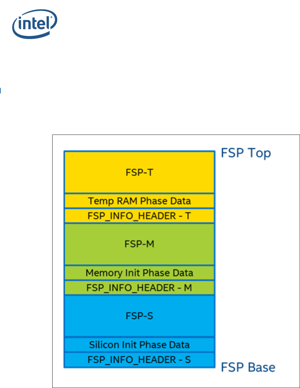
3.3 FSP Component Extraction
Intel Atom® C3XXX Product Family Intel® FSP image can be split into three different
components (FSP-T, FSP-M and FSP-S) and each component can be located at different
base addresses according to its execution location.
In Intel Atom® C3XXX Product Family boot flow there are three different execution
stages:
•Execution in ROM
• Execution in temporary RAM (Cache-as-RAM)
• Execution in system memory
The three extracted FSP components can be exactly mapped into different execution
stages on Intel Atom® C3XXX Product Family Intel® FSP boot flow.
• FSP-T executes in ROM.
• FSP-M executes in temporary memory. After the memory is initialized, the generic
code like PEI dispatcher and other FSP data is migrated into permanent memory.
• FSP-S executes in memory.
The FSP layout is shown in Figure 3-1. The following base addresses are used by
default:
• FSP-T component is set to 0xFFF30000
• FSP-M component is set to 0xFFF32000
• FSP-S component is set to 0xFFFC3000
Intel® Atom® C3XXX Product Family Intel® Firmware Support Package (Intel® FSP)
Intel® FSP Integration
Intel® Atom® C3XXX Product Family Intel® Firmware Support Package (Intel® FSP)
Integration Guide November 2018
10 Document ID: 335702-003US
If the FSP component needs to be loaded at different address, use the BCT tool to
rebase it before the integration.
FSP Binary is released as a single image (.FD extension). Use the python* script,
SplitFspBin.py, to split the FD in to the different FSP components. SplitFspBin.py
is available at:
https://github.com/IntelFsp/FSP/tree/master/Tools
The sample command shown below creates three binaries named after the input FSP
binary and appended with “_M”, “_S”, and “_T” respectively.
• python SplitFspBin.py split -f <FSP Binary>
Figure 3-1. FSP Component Layout View

Intel® Atom® C3XXX Product Family Intel® Firmware Support Package (Intel® FSP)
November 2018 Integration Guide
Document ID: 335702-003US 11
Intel® Atom® C3XXX Product Family Intel® Firmware Support Package (Intel® FSP)
Intel® FSP Integration
3.4 Intel® FSP Information Header
The Intel® FSP has an FSP_INFO_HEADER structure embedded in each FSP component.
It provides critical information required by the bootloader to successfully interface with
the Intel® FSP. Refer to Tab l e 1 - 1. Intel® FSP External Architecture Specification v2.0
(FSP EAS v2.0) for information on the structure of the Intel® FSP Information Header
listed in Figure 3-1.
3.5 FSP Image ID and Revision
The FSP_INFO_HEADER structure inside each FSP component also contains an Image
Identifier field and an Image Revision field that provide the identification and revision
information for the FSP binary. It is important to verify these fields while integrating the
FSP as the FSP configuration data could change over different FSP Image identifiers and
revisions.
The Intel® FSP API parameters documented in this integration guide are applicable for
the Image ID and Revision specified as below.
The current FSP ImageId string in the FSP information header is DNV-FSP0 and the
ImageRevision field is 0x00000111(1.11).
3.6 Intel® FSP APIs
This release of the Intel® Atom™ C3XXX Product Family Intel® FSP supports all APIs
required by the FSP EAS v2.0. The FSP information header contains the address offset
for these APIs. Refer to Table 1-1, Intel® FSP External Architecture Specification v2.0
(FSP EAS v2.0) for Register usage and calling conventions. Any usage not described by
the specification is described in the individual sections below.
The sections below highlights any changes that are specific to this FSP EAS v2.0
release.
3.6.1 TempRamInit API
Refer to the TempRamInit Section in the FSP EAS v2.0 for complete details including
the prototype, parameters and return value details for this API.
If the bootloader initializes the Temporary RAM (CAR) and chipset BARs, calling this API
should be skipped.
TempRamInit does basic early initialization; primarily, setting up temporary RAM
using cache. The API returns a temporary memory data region that can be used by the
bootloader with ECX pointing to beginning of temporary memory and EDX pointing to
end of temporary memory. The temporary memory data region returned by this FSP
release is from 0xFEF0_0000 (ECX) to 0xFEFF_FF00 (EDX).
Both FSPT_UPD.MicrocodeRegionBase and FSPT_UPD.MicrocodeRegionLength
can be set to 0. However, if a valid region is passed and a newer microcode update
revision is in this region, it will be loaded by the Intel® FSP.

Intel® Atom® C3XXX Product Family Intel® Firmware Support Package (Intel® FSP)
Intel® FSP Integration
Intel® Atom® C3XXX Product Family Intel® Firmware Support Package (Intel® FSP)
Integration Guide November 2018
12 Document ID: 335702-003US
3.6.2 FspMemoryInit API
Refer to the FspMemoryInit Section in the FSP EAS v2.0 for the prototype,
parameters and return value details for this API.
The FSP stack size reserved for this revision of the FSP is 320KB, stack base is
0xFEFFB000 by default.
The FspmUpdPtr is pointer to FSPM_UPD structure which is described in header file
FspmUpd.h.
Boot Loader must pass valid Cache-as-RAM (CAR) region for FSP stack use through
these UPDs:
• FSPM_UPD.FspmArchUpd.StackBase
• FSPM_UPD.FspmArchUpd.StackSize.
Note: Certain platforms might need some GPIOs to be initialized prior to the memory
initialization. In this case, the bootloader needs to configure the required GPIO pins
properly before calling into FspMemoryInit. For example, to read SPD data, the
System Management Bus (SMBUS) pins have to be configured properly.
3.6.3 TempRamExit API
Refer to the TempRamExit Section in the FSP EAS v2.0 for the prototype, parameters
and return value details for this API.
If the bootloader initialized the Temporary RAM (CAR) as well as the chipset BARs and
skipped calling TempRamInit API, then the bootloader is required to skip calling this
API, to tear down the temporary memory area setup in the cache, and to bring the
cache back to normal mode of operation.
This revision of Intel® FSP does not have any fields/structure to pass as parameter for
this API. Pass Null for TempRamExitParamPtr.
At the end of TempRamExit execution, the original code and data caching are
disabled. The Intel® FSP reconfigures the following Memory Type and Range Registers
(MTRRs) for performance optimization.
The bootloader can reconfigure the MTRRs immediately after this API call.
Table 3-1. Memory Range and Cache Attributes
Memory Range Cache Attribute
0x00000000 – 0x0009FFFF Write back
0x000A0000 – 0x000BFFFF Uncacheable
0x000C0000 – Top of Low Memory Write back
0xFF800000 – 0xFFFFFFFF (Flash region) Write protect
0x1000000000 – Top of High Memory Write back

Intel® Atom® C3XXX Product Family Intel® Firmware Support Package (Intel® FSP)
November 2018 Integration Guide
Document ID: 335702-003US 13
Intel® Atom® C3XXX Product Family Intel® Firmware Support Package (Intel® FSP)
Intel® FSP Integration
3.6.4 FspSiliconInit API
Refer to the FspSiliconInit Section in the FSP EAS v2.0 for the prototype, parameters
and return value details for this API.
The FspsUpdPtr is pointer to FSPS_UPD structure which is described in header file
FspsUpd.h.
The bootloader is responsible for programming the MTRRs for Boot Strap Processor
(BSP) as needed after TempRamExit but before entering FspSiliconInit. If MTRRs
are not programmed properly, boot performance might be impacted.
3.6.5 NotifyPhase API
Refer to the NotifyPhase Section in the FSP EAS v2.0 for the prototype, parameters
and return value details for this API.
Note: It is REQUIRED that all the supported NotifyPhase APIs are called and in the
recommended order.
3.6.5.1 PostPciBusEnumeration Notification
The bootloader calls this phase, EnumInitPhaseAfterPciEnumeration, after PCI bus
enumeration but before execution of third party code such as option ROMs. Currently,
no special operation is done in this phase, but in the future updates, programming may
be added in this phase.
3.6.5.2 ReadyToBoot Notification
The bootloader calls this phase, EnumInitPhaseReadyToBoot, before giving control
to OS Loader. It includes some final initialization steps recommended by the BWG,
including power management settings, locking down security-related registers, and
switching devices into ACPI mode if required, etc.
3.6.5.3 EndOfFirmware Notification
Intel® Atom™ C3XXX Product Family does not support this API.
§

Intel® Atom® C3XXX Product Family Intel® Firmware Support Package (Intel® FSP)
Intel® FSP Output
Intel® Atom® C3XXX Product Family Intel® Firmware Support Package (Intel® FSP)
Integration Guide November 2018
14 Document ID: 335702-003US
4Intel
® FSP Output
The Intel® FSP builds a series of data structures called the Hand-Off-Blocks (HOBs) as
it progresses through initializing the silicon.
Refer to Table 1-1, Platform Initialization (PI) Specification - Volume 3: Shared
Architectural Elements specification for PI Architectural HOBs.
Refer to the Intel® FSP Output chapter of the Intel® FSP External Architecture
Specification v2.0 (FSP EAS v2.0) for details about Intel® FSP Architectural HOBs.
The section below describes the HOBs implemented in Intel® Atom™ C3XXX Product
Family Intel® FSP that are not covered in the previous two specifications.
4.1 SMRAM Resource Descriptor HOB
The Intel® FSP reports the system SMRAM T-SEG range through a generic resource
HOB if T-SEG is enabled. The owner field of the HOB identifies the owner as T-SEG.
#define FSP_HOB_RESOURCE_OWNER_TSEG_GUID \
{ 0xd038747c, 0xd00c, 0x4980, { 0xb3, 0x19, 0x49, 0x01, 0x99, 0xa4, 0x7d,
0x55 } }
4.2 FIA MUX HOB
The Intel® FSP reports the Flexible I/O Adapter (FIA) Mux Settings thru the FIA Mux
HOB.
#define FSP_FIAMUX_HOB_GUID \
{ 0x26ad492e, 0xf951, 0x4e43, { 0xbc, 0x72, 0x22, 0x76, 0x58, 0xb1, 0xf6, 0x23
} }
Refer to the FspmUpd.h for the details of HOB structure.

Intel® Atom® C3XXX Product Family Intel® Firmware Support Package (Intel® FSP)
November 2018 Integration Guide
Document ID: 335702-003US 15
Intel® Atom® C3XXX Product Family Intel® Firmware Support Package (Intel® FSP)
Intel® FSP Output
4.3 SMBIOS INFO HOB
The Intel® FSP will report the System Management BIOS (SMBIOS) through a HOB with
below Globally Unique Identifier (GUID). This information can be consumed by the
bootloader to produce the SMBIOS tables.
#define FSP_SMBIOS_MEMORY_INFO_HOB_GUID \
{ 0x1a1108c, 0x9dee, 0x4984, { 0x88, 0xc3, 0xee, 0xe8, 0xc4,
0x9e, 0xfb, 0x89 } };
#define MAX_CHANNELS_NUM 2
#define MAX_DIMMS_NUM 2
typedef struct {
UINT8 DimmId;
UINT32 SizeInMb;
UINT16 MfgId;
/* Module part number for DRR3 is 18 bytes but DRR4 is 20
bytes as per JEDEC Spec, so reserving 20 bytes */
UINT8 ModulePartNum[20]; } DIMM_INFO;
typedef struct {
UINT8 ChannelId;
UINT8 DimmCount;
DIMM_INFO DimmInfo
[MAX_DIMMS_NUM];
} CHANNEL_INFO;
typedef struct {
UINT8 Revision;
UINT8 DataWidth;
/** As defined in SMBIOS 3.0 spec
Section 7.18.2 and Table 75
**/
UINT8 MemoryType;
UINT16 MemoryFrequencyInMHz;
/** As defined in SMBIOS 3.0 spec
Section 7.17.3 and Table 72
**/
UINT8 ErrorCorrectionType;
UINT8 ChannelCount;
CHANNEL_INFO ChannelInfo[MAX_CHANNELS_NUM];
} FSP_SMBIOS_MEMORY_INFO;
4.4 MarginCheckerTestReport HOB
The Intel® FSP uses this HOB to pass information (for Margin Check) from MRC to the
boot loader.
#define gFspFastBootCheckerHobGuid = { 0x7897f07b, 0xcda, 0x40e3, { 0xb4,
0xe4, 0x51, 0x5f, 0x47, 0x3b, 0x4, 0xb6 }} ;
§

Intel® Atom® C3XXX Product Family Intel® Firmware Support Package (Intel® FSP)
Intel® FSP Configuration Firmware File
Intel® Atom® C3XXX Product Family Intel® Firmware Support Package (Intel® FSP)
Integration Guide November 2018
16 Document ID: 335702-003US
5Intel
® FSP Configuration Firmware File
The Intel® FSP binary contains a configurable data region that is used by the FSP
during the initialization. Refer to the Intel® FSP Configuration Firmware File chapter of
the Intel® FSP External Architecture Specification v2.0 (FSP EAS v2.0) for details.
Note: A stack in temporary memory is used to store the Updatable Product Data (UPD) data
structure. This UPD data structure is copied, updated, and then passed to the FSP API.
When permanent memory is initialized, the Intel® FSP sets up a new stack in the
permanent memory and tears down the temporary memory. However, the Intel® FSP
saves the whole bootloader temporary memory region in a GUID HOB. The bootloader
can access the data in the temporary memory by parsing this HOB. The migrated
temporary memory contains an identical copy of the original data. Pointers to data
stored in the temporary memory needs to be updated to the location of the same data
in the permanent memory.
5.1 UPD Data Structure
The UPD data structure and related structure definitions are provided in the FspUpd.h,
FsptUpd.h, FspmUpd.h and FspsUpd.h file in the release package. The basic
information for each option is provided in the BCT configuration file. Use the BCT tool to
load this BSF file and get the detailed configuration option information.
5.1.1 FSP Configuration Data
5.1.1.1 FSP-T UPD Structure
FSP-T Core UPD Configuration is described in the FSP-T UPD Structure section of the
FSP EAS v2.0.
#include < FsptUpd.h>
typedef struct {
UINT32 MicrocodeRegionBase;
UINT32 MicrocodeRegionLength;
UINT32 CodeRegionBase;
UINT32 CodeRegionLength;
UINT8 Reserved1[16];
} FSPT_CORE_UPD;
5.1.1.2 Detailed Description
FSP-T Core UPD Configuration.
The documentation for this structure was generated from the following file:
FsptUpd.h
MicrocodeRegionBase: Base address of the microcode region. This address must be
16 byte aligned.
MicrocodeRegionLength: Length of the microcode region. The length must be total
size of all patches or 0xFFFFFFFF if auto size detection is desired.
CodeRegionBase: Base address of the cacheable flash region.
CodeRegionLength: Length of the cacheable flash region. A size of 0 indicates that no
code caching is desired.

Intel® Atom® C3XXX Product Family Intel® Firmware Support Package (Intel® FSP)
November 2018 Integration Guide
Document ID: 335702-003US 17
Intel® Atom® C3XXX Product Family Intel® Firmware Support Package (Intel® FSP)
Intel® FSP Configuration Firmware File
5.1.2 FSP-T UPD Data Region
This UPD data region can be configured statically by the BCT tool in the same way as
Vital Product Data (VPD) data region, but can also be overridden by the bootloader at
runtime. This provides more flexibility for the bootloader to customize these options
dynamically as needed.
PcdPort80RouteDisable
Used to enable/disable diversion of Low Pin Count (LPC) Port80 writes. When selecting
item “0x0/VPD-Style”, this Platform Configuration Database (PCD) cannot be
overridden and act as a VPD PCD. Valid inputs are:
0x0 - VPD-Style
0x1 - “Enabled Port80 Output” (Default)
0x2 - “Disabled Port80 Output”
PcdRegionTerminator
This field has a value of 0x55AA indicating the end of UPD data. DO NOT MODIFY.
5.1.2.1 FSP-M UPD Data Region
The UPD parameters that are part of the MemoryInitUpd and consumed by the
FspMemoryInit API are described below.
PcdCustomerRevision
The customer can add a label/version ID, maximum 32 characters.
PcdSmmTsegSize
Used to specify the Size of SMRAM (TSEG) memory reserved. Valid inputs are:
0x02 - “2 MB” (Default)
0x04 - “4 MB”
0x08 - “8 MB”
0x16 - “16 MB”
PcdFspDebugPrintErrorLevel
Controls the Intel® FSP debug message level. To allow the Intel® FSP debug message
print out, this option should be configured to any level other than 0. Valid inputs are:
0x00 – 0x00
0x01 – 0x01
0x02 - 0x02 (Default)
0x03 – 0x03
PcdSpdSmbusAddress_0_0
Used to configure SMBus address of Channel 0 DIMM 0 on the platform. Valid inputs
are:
From 0x00 to 0xFF
Default: 0xA0

Intel® Atom® C3XXX Product Family Intel® Firmware Support Package (Intel® FSP)
Intel® FSP Configuration Firmware File
Intel® Atom® C3XXX Product Family Intel® Firmware Support Package (Intel® FSP)
Integration Guide November 2018
18 Document ID: 335702-003US
PcdSpdSmbusAddress_0_1
Used to configure SMBus address of Channel 0 DIMM 1 on the platform. Valid inputs
are:
From 0x00 to 0xFF
Default: 0xA2
PcdSpdSmbusAddress_1_0
Used to configure SMBus address of Channel 1 DIMM 0 on the platform. Valid inputs
are:
From 0x00 to 0xFF
Default: 0xA4
PcdSpdSmbusAddress_1_1
Used to configure SMBus address of Channel 1 DIMM 1 on the platform. Valid inputs
are:
From 0x00 to 0xFF
Default: 0xA6
PcdMrcRmtSupport
Used to enable/disable Memory Reference Code (MRC) Rank Margin Tool (RMT). If
enabled, the MRC prints out the rank margining information so that it can be used as
the input for the RMT to analyze the platform memory sub-system margining.
PcdFastBoot option should be disabled because MRC fast boot path skips normal
memory training steps. The RMT log is printed to the serial console. Valid inputs are:
0 - “Disabled” (Default)
1 - “Enabled”
PcdMrcRmtCpgcExpLoopCntValue
Used to configure Rank Margin Tool (RMT). Set the Converged Pattern Generator and
Checking (CPGC) exp_loop_cnt field for RMT execution 2^ (exp_loop_cnt -1). Valid
inputs are:
From 1 to 15
Default: 12
PcdMrcRmtCpgcNumBursts
Used to configure Rank Margin Tool (RMT). Set the CPGC num_bursts field for RMT
execution 2^ (num_bursts -1). Valid inputs are:
From 1 to 15
Default: 6

Intel® Atom® C3XXX Product Family Intel® Firmware Support Package (Intel® FSP)
November 2018 Integration Guide
Document ID: 335702-003US 19
Intel® Atom® C3XXX Product Family Intel® Firmware Support Package (Intel® FSP)
Intel® FSP Configuration Firmware File
PcdMemoryPreservation
Used to enable/disable the memory preservation through warm resets. Valid inputs are:
0 - “Disabled” (Default)
1 - “Enabled”
PcdFastBoot
Used to enable/disable the Fast Boot function. Once enabled, all following boots use the
presaved MRC data to improve the boot performance. Valid inputs are:
0 - “Disabled”
1 - “Enabled” (Default)
PcdEccSupport
Used to enable/disable the error correcting code memory support. Valid inputs are:
0 - “Disabled”
1 - “Enabled” (Default)
PcdHsuartDevice
Select the Peripheral Connect Interface (PCI) High Speed Device for Serial Port. It is
expected that the bootloader will configure the PCI High Speed UART (HSUART) Device
for Serial Port prior to calling the FspInitEntry API. The bootloader should update this
Updatable Product Data (UPD) with the function number of the HSUART device so that
the Intel® FSP can output to the serial port. The supported device functions are 0, 1,
and 2. The Intel® FSP defaults to function 0 if this UPD is not configured with one of the
supported function numbers.
0 - HSUART0 (Default)
1 - HSUART1
2 - HSUART2
PcdMemoryDown
Used to enable/disable the Memory Down function. For designs that implement memory
soldered down to the board and that do not include SPD EEPROMs on the board, enable
this PCD. It is also required that the bootloader configures the SPD data; refer to
Appendix A.
However, if the design implements memory soldered down to the board and includes
SPD EEPROMs on the board, then it is not required to enable this PCD. In this situation,
the Intel® FSP needs to be configured with the SPD SMBus addresses for the SPD
EEPROMs for each memory bank.
0 - “Disabled” (Default)
1 - “Enabled”

Intel® Atom® C3XXX Product Family Intel® Firmware Support Package (Intel® FSP)
Intel® FSP Configuration Firmware File
Intel® Atom® C3XXX Product Family Intel® Firmware Support Package (Intel® FSP)
Integration Guide November 2018
20 Document ID: 335702-003US
PcdMemoryDownConfigPtr
It is required that the bootloader configures this UPD prior to calling the FspMemoryInit
API if the board design includes soldered down memory. Refer to Appendix A for details
on Memory Down support. This PCD cannot be configured by the BCT Tool.
0 - (Default)
PcdEnableSATA0
Used to enable/disable SATA Controller 0, including Static Power Gating. Valid inputs
are:
0x0 - “Disabled”
0x1 - “Enabled” (Default)
PcdEnableSATA1
Used to enable/disable SATA Controller 1, including Static Power Gating. Valid inputs
are:
0x0 - “Disabled”
0x1 - “Enabled” (Default)
PcdEnableIQAT
Used to enable/disable Intel Quick Assist Technology devices, including Static Power
Gating. Valid inputs are:
0x0 - “Disabled”
0x1 - “Enabled” (Default)
PcdSmbusSpdWriteDisable
Used to enable/disable SPD Write Protect. Set this PCD to Force Disable to allow
writes to slaves 0xA0 – 0xAE. After completing SPD flow, it is highly recommended
that the bootloader set SPD_WD. This will prevent any future writes (accidental or
malicious) to the DIMM EEPROMs; a malicious write could corrupt an EEPROM and
cause a Permanent Denial of Service (platform will not boot) until the DIMM is replaced.
A platform may be designed such that SMBus0 segment includes EEPROMs, other than
DIMM EEPROM (not Intel recommended). In this case, if the Original Design
Manufacture (ODM) expects write access by a regular SW driver or by BIOS/System
Management Mode (SMM) at a later time, it is possible to leave SPD_WD cleared.
However, the ODM should know that this exposes the DIMM EEPROMs to the security
vulnerability noted above.
1 – “Force Enable” (Default)
2 – “Force Disable”
PcdEnableMeShutdown
Enable/disable sending the ME_SHUTDOWN message to ME. Valid inputs are:
0x0 - “Disabled” (Default)
0x1 - “Enabled”

Intel® Atom® C3XXX Product Family Intel® Firmware Support Package (Intel® FSP)
November 2018 Integration Guide
Document ID: 335702-003US 21
Intel® Atom® C3XXX Product Family Intel® Firmware Support Package (Intel® FSP)
Intel® FSP Configuration Firmware File
PcdEnableXhci
Enable/disable Extensible Host Controller Interface (xHCI) controller, including Static
Power Gating. Valid inputs are:
0x0 - “Disabled”
0x1 - “Enabled” (Default)
PcdDdrFreq
Set DDR Memory Frequency to a specific value. Valid inputs are:
15 - “Auto”
3 - “1600 MHz”
4 - “1866 MHz”
5 - “2133 MHz” (Default)
6 - “2400 MHz”
For DDR3 memory, items “Auto”, “1600” and “1866” MHz can be selected.
For DDR4 memory, items “Auto”, “1866”, “2133”, and “2400” MHz can be selected.
PcdMmioSize
Used to set memory mapped IO space size. Valid inputs are:
0 - 2048M (Default)
1 - 1024M
2 - 3072M
PcdHalfWidthEnable
Used to enable/disable 32-bit Memory Bus Mode. Valid inputs are:
0x0 - “Disabled” (Default)
0x1 - “Enabled”
PcdTclIdle
Used to modify Tcl timing for performance improvement. Valid inputs are:
0x0 - “Disabled”
0x1 - “Enabled” (Default)
PcdInterleaveMode
Used to select memory interleave mode. Valid inputs are:
0 - disabled
1 – mode0
2 – mode1
3 – mode2 (Default)
PcdMemoryThermalThrottling
Used to enable/disable memory thermal throttling management mode.
0x0 - “Disabled” (Default)
0x1 - “Enabled”

Intel® Atom® C3XXX Product Family Intel® Firmware Support Package (Intel® FSP)
Intel® FSP Configuration Firmware File
Intel® Atom® C3XXX Product Family Intel® Firmware Support Package (Intel® FSP)
Integration Guide November 2018
22 Document ID: 335702-003US
5.1.2.2 FSP-S UPD Data Region
The UPD parameters that are part of the SiliconInitUpd and are consumed by the
FspSiliconInit API are described below.
PcdBifurcationPcie0
Configure Peripheral Component Interconnect Express * (PCIe*) controller 0
bifurcation.
0 - X2X2X2X2
1 - X2X2X4
2 - X4X2X2
3 - X4X4
4 - X8 (Default)
PcdBifurcationPcie1
Configure PCIe* controller 1 bifurcation.
0 - X2X2X2X2
1 - X2X2X4
2 - X4X2X2
3 - X4X4 (Default)
4 - X8
PcdActiveCoreCount
Used to select the number of Active Cores.
0 - ALL (Default)
1..15 - 1..15 Cores
PcdCpuMicrocodePatchBase
It is required that the bootloader configures this UPD prior to calling the FspSiliconInit
API. This UPD cannot be modified using the BCT.
0 - (Default)
PcdCpuMicrocodePatchSize
It is required that the bootloader configures this UPD prior to calling the FspSiliconInit
API. This UPD cannot be modified using the BCT.
0 - (Default)

Intel® Atom® C3XXX Product Family Intel® Firmware Support Package (Intel® FSP)
November 2018 Integration Guide
Document ID: 335702-003US 23
Intel® Atom® C3XXX Product Family Intel® Firmware Support Package (Intel® FSP)
Intel® FSP Configuration Firmware File
PcdEnablePcie0
Used to enable/disable PCIe* Controller 0 by controlling Static Power Gating. Valid
inputs are:
0x0 - “Disabled”
0x1 - “Enabled” (Default)
PcdEnablePcie1
Used to enable/disable PCIe Controller 1 by controlling Static Power Gating. Valid inputs
are:
0x0 - “Disabled”
0x1 - “Enabled” (Default)
PcdPcieRootPort[0:7] DeEmphasis
Used to configure PCIe root ports (1-8) De-Emphasis settings. Valid inputs are:
0x0 - “6 dB” (Default)
0x1 - “3.5 dB”
PcdRootPort[0:7]LaneReversal
Enable/Disable Lane Reversal on PCIe* Root Port 1-8.
0x0 - Disabled (Default)
0x1 _ Enabled
PcdEnableGbE
Used to enable/disable LAN Controller by controlling the Static Power Gating. Valid
inputs are:
0x0 - “Disable LAN 0 & LAN 1"
0x1 - “Enable LAN 0 & LAN 1” (Default)
0x2 - “Disable LAN 1 only”
PcdFiaMuxConfigRequestPtr
It is required that the bootloader configures this UPD prior to calling the FspSiliconInit
API to set the request FIA MUX configuration to allow Intel® FSP overriding High Speed
IO (HSIO) lanes for PCIe*/SATA/USB3 controllers. Refer to Appendix B for details how
to configure this pointer. This PCD cannot be configured by the BCT Tool.
0 - (Default)
PcdEnableEmmc
Used to enable/disable Embedded Multi-Media Controller* (eMMC*) by controlling the
Static Power Gating. Valid inputs are:
0x0 - “Disabled”
0x1 - “Enabled” (Default)
PcdEMMCDLLConfigPtr
It is required that the bootloader configures this UPD prior to calling the FspSiliconInit
API to set eMMC DLL configuration for eMMC controller. Refer to Appendix C for more
details. This PCD cannot be configured by the BCT Tool.
0 - (Default)

Intel® Atom® C3XXX Product Family Intel® Firmware Support Package (Intel® FSP)
Memory Down
Intel® Atom® C3XXX Product Family Intel® Firmware Support Package (Intel® FSP)
Integration Guide November 2018
24 Document ID: 335702-003US
AMemory Down
The details of Memory Down structure are shown below. These can be found in the
FspmUpd.h header file included in the Intel® FSP package.
#define MAX_CH 2 /* Maximum Number of Memory Channels */
#define MAX_DIMM 2 /* Maximum Number of DIMMs PER Memory
Channel */
#define MAX_SPD_BYTES 512 /* Maximum Number of SPD bytes */
typedef enum {
STATE_MEMORY_SLOT = 0, /* No memory down and a
physical memory slot. */
STATE_MEMORY_DOWN = 1, /* Memory down and not a
physical memory slot. */
} MemorySlotState;
typedef struct {
MemorySlotState SlotState[MAX_CH][MAX_DIMM]; /* Memory
Down state of each DIMM in each Channel */
UINT16 SpdDataLen; /* Length in Bytes of a
single DIMM's SPD Data */
UINT8 *SpdDataPtr[MAX_CH][MAX_DIMM]; /* Pointer
to SPD Data for each DIMM in each Channel */
} MEMORY_DOWN_CONFIG;
It is the responsibility of the bootloader to provide the SPD Data for the DIMMs used in
the platform.
§

Intel® Atom® C3XXX Product Family Intel® Firmware Support Package (Intel® FSP)
November 2018 Integration Guide
Document ID: 335702-003US 25
Intel® Atom® C3XXX Product Family Intel® Firmware Support Package (Intel® FSP)
FIA MUX Configuration Structure
B FIA MUX Configuration Structure
The details of the FIA MUX Configure structure are shown below. These can be found in
the FspmUpd.h header file included in the Intel® FSP package.
/*
* FIA MUX configuration structures.
*/
#define BL_ME_FIA_MUX_LANE_NUM_MAX 20
#define BL_ME_FIA_MUX_LANE_NUM_MIN 1
#define BL_ME_FIA_MUX_LANE_MUX_SEL_WIDTH 2
#define BL_ME_FIA_MUX_LANE_MUX_SEL_MASK 0x3
#define BL_ME_FIA_MUX_LANE_XHCI_ONLY 0xFF00000000
typedef enum {
BL_FIA_LANE00 = 0,
BL_FIA_LANE01,
BL_FIA_LANE02,
BL_FIA_LANE03,
BL_FIA_LANE04,
BL_FIA_LANE05,
BL_FIA_LANE06,
BL_FIA_LANE07,
BL_FIA_LANE08,
BL_FIA_LANE09,
BL_FIA_LANE10,
BL_FIA_LANE11,
BL_FIA_LANE12,
BL_FIA_LANE13,
BL_FIA_LANE14,
BL_FIA_LANE15,
BL_FIA_LANE16,
BL_FIA_LANE17,
BL_FIA_LANE18,
BL_FIA_LANE19,
} BL_ME_FIA_MUX_LANE_ORDER;
#define BL_ME_FIA_MUX_LANE_SATA0_BEGING BL_FIA_LANE04
#define BL_ME_FIA_MUX_LANE_SATA1_BEGING BL_FIA_LANE12
#define BL_FIA_LANE_CONFIG(Config, Lane) ( (UINT64) ( (UINT64)(Config) << (
(UINT64)(Lane) * (BL_ME_FIA_MUX_LANE_MUX_SEL_WIDTH))))

Intel® Atom® C3XXX Product Family Intel® Firmware Support Package (Intel® FSP)
FIA MUX Configuration Structure
Intel® Atom® C3XXX Product Family Intel® Firmware Support Package (Intel® FSP)
Integration Guide November 2018
26 Document ID: 335702-003US
typedef union _BL_ME_FIA_MUX_CONFIG {
UINT64 MeFiaMuxLaneConfig;
struct {
UINT64 Lane00MuxSel : 2; // ME_FIA_MUX_LANE_DISABLED or PCIE
UINT64 Lane01MuxSel : 2; // ME_FIA_MUX_LANE_DISABLED or PCIE
UINT64 Lane02MuxSel : 2; // ME_FIA_MUX_LANE_DISABLED or PCIE
UINT64 Lane03MuxSel : 2; // ME_FIA_MUX_LANE_DISABLED or PCIE
UINT64 Lane04MuxSel : 2; // ME_FIA_MUX_LANE_DISABLED or PCIE or SATA
UINT64 Lane05MuxSel : 2; // ME_FIA_MUX_LANE_DISABLED or PCIE or SATA
UINT64 Lane06MuxSel : 2; // ME_FIA_MUX_LANE_DISABLED or PCIE or SATA
UINT64 Lane07MuxSel : 2; // ME_FIA_MUX_LANE_DISABLED or PCIE or SATA
UINT64 Lane08MuxSel : 2; // ME_FIA_MUX_LANE_DISABLED or PCIE or SATA
UINT64 Lane09MuxSel : 2; // ME_FIA_MUX_LANE_DISABLED or PCIE or SATA
UINT64 Lane10MuxSel : 2; // ME_FIA_MUX_LANE_DISABLED or PCIE or SATA
UINT64 Lane11MuxSel : 2; // ME_FIA_MUX_LANE_DISABLED or PCIE or SATA
UINT64 Lane12MuxSel : 2; // ME_FIA_MUX_LANE_DISABLED or PCIE or SATA
UINT64 Lane13MuxSel : 2; // ME_FIA_MUX_LANE_DISABLED or PCIE or SATA
UINT64 Lane14MuxSel : 2; // ME_FIA_MUX_LANE_DISABLED or PCIE or SATA
UINT64 Lane15MuxSel : 2; // ME_FIA_MUX_LANE_DISABLED or PCIE or SATA
UINT64 Lane16MuxSel : 2; // ME_FIA_MUX_LANE_DISABLED or XHCI or SATA
UINT64 Lane17MuxSel : 2; // ME_FIA_MUX_LANE_DISABLED or XHCI or SATA
UINT64 Lane18MuxSel : 2; // ME_FIA_MUX_LANE_DISABLED or XHCI or SATA
UINT64 Lane19MuxSel : 2; // ME_FIA_MUX_LANE_DISABLED or XHCI or SATA
UINT64 Reserved : 24;
} BL_MeFiaMuxLaneMuxSel;
} BL_ME_FIA_MUX_CONFIG;
typedef enum {
BL_ME_FIA_MUX_LANE_DISCONNECTED,
BL_ME_FIA_MUX_LANE_PCIE,
BL_ME_FIA_MUX_LANE_SATA,
BL_ME_FIA_MUX_LANE_XHCI,
} BL_ME_FIA_MUX_LANE_CONFIG;
#define BL_ME_FIA_SATA_LANE_SEL_WIDTH 2
#define BL_ME_FIA_SATA_LANE_XHCI_ONLY 0x55000000
typedef enum {
BL_FIA_SATA_LANE04 = 0,
BL_FIA_SATA_LANE05,
BL_FIA_SATA_LANE06,
BL_FIA_SATA_LANE07,
BL_FIA_SATA_LANE08,
BL_FIA_SATA_LANE09,
BL_FIA_SATA_LANE10,
BL_FIA_SATA_LANE11,
BL_FIA_SATA_LANE12,
BL_FIA_SATA_LANE13,
BL_FIA_SATA_LANE14,
BL_FIA_SATA_LANE15,
BL_FIA_SATA_LANE16,
BL_FIA_SATA_LANE17,
BL_FIA_SATA_LANE18,
BL_FIA_SATA_LANE19
} BL_ME_FIA_SATA_LANE_ORDER;

Intel® Atom® C3XXX Product Family Intel® Firmware Support Package (Intel® FSP)
November 2018 Integration Guide
Document ID: 335702-003US 27
Intel® Atom® C3XXX Product Family Intel® Firmware Support Package (Intel® FSP)
FIA MUX Configuration Structure
#define BL_FIA_SATA_LANE_CONFIG(Config, Lane) ( (UINT32) ( (UINT32)(Config) << (
(UINT32)(Lane) * (BL_ME_FIA_SATA_LANE_SEL_WIDTH))))
typedef union _BL_ME_FIA_SATA_CONFIG {
UINT64 MeFiaSataLaneConfig;
struct {
UINT64 Lane04SataSel : 2;
UINT64 Lane05SataSel : 2;
UINT64 Lane06SataSel : 2;
UINT64 Lane07SataSel : 2;
UINT64 Lane08SataSel : 2;
UINT64 Lane09SataSel : 2;
UINT64 Lane10SataSel : 2;
UINT64 Lane11SataSel : 2;
UINT64 Lane12SataSel : 2;
UINT64 Lane13SataSel : 2;
UINT64 Lane14SataSel : 2;
UINT64 Lane15SataSel : 2;
UINT64 Lane16SataSel : 2;
UINT64 Lane17SataSel : 2;
UINT64 Lane18SataSel : 2;
UINT64 Lane19SataSel : 2;
UINT64 Reserved : 32;
} BL_MeFiaSataLaneSataSel;
} BL_ME_FIA_SATA_CONFIG;
typedef enum
{
BL_ME_FIA_SATA_CONTROLLER_LANE_ASSIGNED = 0,
BL_ME_FIA_SATA_CONTROLLER_LANE_NOT_ASSIGNED = 1,
BL_ME_FIA_SATA_CONTROLLER_LANE_SS_AND_GPIO_ASSIGNED = 3
} BL_ME_FIA_SATA_LANE_CONFIG;
#define BL_ME_FIA_PCIE_ROOT_PORT_LINK_WIDTH_SEL_WIDTH 4
#define BL_ME_FIA_PCIE_ROOT_PORTS_STATE_WIDTH 8
#define BL_ME_FIA_PCIE_ROOT_CONFIG_XHCI_ONLY 0x0
typedef enum {
BL_FIA_PCIE_ROOT_PORT_0 = 0,
BL_FIA_PCIE_ROOT_PORT_1,
BL_FIA_PCIE_ROOT_PORT_2,
BL_FIA_PCIE_ROOT_PORT_3,
BL_FIA_PCIE_ROOT_PORT_4,
BL_FIA_PCIE_ROOT_PORT_5,
BL_FIA_PCIE_ROOT_PORT_6,
BL_FIA_PCIE_ROOT_PORT_7
} BL_ME_FIA_PCIE_ROOT_PORT_ORDER;
#define BL_FIA_PCIE_ROOT_PORT_CONFIG(Type, Config, PcieRootPort) \
(((Type) == BL_ME_FIA_PCIE_ROOT_PORT_STATE) ? \
((UINT64)((UINT64)(Config) << (UINT64)(PcieRootPort))) : \
((UINT64)((UINT64)(Config) << (UINT64)(((UINT64)(PcieRootPort) *
(BL_ME_FIA_PCIE_ROOT_PORT_LINK_WIDTH_SEL_WIDTH)) + \
BL_ME_FIA_PCIE_ROOT_PORTS_STATE_WIDTH))))

Intel® Atom® C3XXX Product Family Intel® Firmware Support Package (Intel® FSP)
FIA MUX Configuration Structure
Intel® Atom® C3XXX Product Family Intel® Firmware Support Package (Intel® FSP)
Integration Guide November 2018
28 Document ID: 335702-003US
typedef union _BL_ME_FIA_PCIE_ROOT_PORTS_CONFIG {
UINT64 MeFiaPcieRootPortsConfig;
struct {
UINT64 PcieRp0En : 1;
UINT64 PcieRp1En : 1;
UINT64 PcieRp2En : 1;
UINT64 PcieRp3En : 1;
UINT64 PcieRp4En : 1;
UINT64 PcieRp5En : 1;
UINT64 PcieRp6En : 1;
UINT64 PcieRp7En : 1;
UINT64 PcieRp0LinkWidth : 4;
UINT64 PcieRp1LinkWidth : 4;
UINT64 PcieRp2LinkWidth : 4;
UINT64 PcieRp3LinkWidth : 4;
UINT64 PcieRp4LinkWidth : 4;
UINT64 PcieRp5LinkWidth : 4;
UINT64 PcieRp6LinkWidth : 4;
UINT64 PcieRp7LinkWidth : 4;
UINT64 Reserved : 24;
} BL_MeFiaPcieRpConfig;
} BL_ME_FIA_PCIE_ROOT_PORTS_CONFIG;
typedef enum
{
BL_ME_FIA_PCIE_ROOT_PORT_STATE,
BL_ME_FIA_PCIE_ROOT_PORT_LINK_WIDTH
} BL_ME_FIA_PCIE_ROOT_PORT_CONFIG_TYPE;
typedef enum
{
BL_ME_FIA_PCIE_ROOT_PORT_DISABLED,
BL_ME_FIA_PCIE_ROOT_PORT_ENABLED
} BL_ME_FIA_PCIE_ROOT_PORT_STATE_CONFIG;
typedef enum
{
BL_ME_FIA_PCIE_ROOT_PORT_LINK_WIDTH_BICTRL = 0,
BL_ME_FIA_PCIE_ROOT_PORT_LINK_X1 = 0xF
} BL_ME_FIA_PCIE_ROOT_PORT_LINK_CONFIG;
typedef struct _BL_ME_FIA_CONFIG
{
BL_ME_FIA_MUX_CONFIG MuxConfiguration;
BL_ME_FIA_SATA_CONFIG SataLaneConfiguration;
BL_ME_FIA_PCIE_ROOT_PORTS_CONFIG PcieRootPortsConfiguration;
} BL_ME_FIA_CONFIG;
/*
* The FIA_MUX_CONFIG block describes the expected configuration of
* FIA MUX configuration.
*/
typedef struct {
UINT32 SkuNumLanesAllowed; // Platform view of Num Lanes allowed
BL_ME_FIA_CONFIG FiaMuxConfig; // Current Platform FIA MUX Configuration
BL_ME_FIA_CONFIG FiaMuxConfigRequest; // FIA MUX Configuration Requested
} BL_FIA_MUX_CONFIG;
/*
* The FIA_MUX_CONFIG_STATUS describes the status of configuring
* FIA MUX configuration.
*/

Intel® Atom® C3XXX Product Family Intel® Firmware Support Package (Intel® FSP)
November 2018 Integration Guide
Document ID: 335702-003US 29
Intel® Atom® C3XXX Product Family Intel® Firmware Support Package (Intel® FSP)
FIA MUX Configuration Structure
typedef struct {
UINT64 FiaMuxConfigGetStatus; // Status returned from FiaMuxConfigGet, if not
EFI_SUCCESS, then error occurred and user can decide on next steps
UINT64 FiaMuxConfigSetStatus; // Status returned from FiaMuxConfigSet, if not
EFI_SUCCESS, then error occurred and user can decide on next steps
BOOLEAN FiaMuxConfigSetRequired; // Boolean: true - a FiaMuxConfigSet was
required, false otherwise
} BL_FIA_MUX_CONFIG_STATUS;
/*
* FIA MUX Config HOB structure
*/
typedef struct {
BL_FIA_MUX_CONFIG FiaMuxConfig;
BL_FIA_MUX_CONFIG_STATUS FiaMuxConfigStatus;
} BL_FIA_MUX_CONFIG_HOB;
/* PCIe port bifurcation codes - matches setup option values */
#define PCIE_BIF_CTRL_x2x2x2x2 0
#define PCIE_BIF_CTRL_x2x2x4 1
#define PCIE_BIF_CTRL_x4x2x2 2
#define PCIE_BIF_CTRL_x4x4 3
#define PCIE_BIF_CTRL_x8 4
#define BL_MAX_PCIE_CTRL 2
/*
* HSIO INFORMATION structure
*/
typedef enum {
BL_SKU_HSIO_06 = 6,
BL_SKU_HSIO_08 = 8,
BL_SKU_HSIO_10 = 10,
BL_SKU_HSIO_12 = 12,
BL_SKU_HSIO_20 = 20,
} BL_SKU_HSIO_LANE_NUMBER;
typedef struct {
UINT16 NumLanesSupported;
UINT8 PcieBifCtr[BL_MAX_PCIE_CTRL];
BL_ME_FIA_CONFIG FiaConfig;
} BL_HSIO_INFORMATION;
PcdFiaMuxConfigRequestPtr is a pointer for request FIA MUX configuration to be
configured by the Intel® FSP. It pointed to a structure BL_ME_FIA_CONFIG.

Intel® Atom® C3XXX Product Family Intel® Firmware Support Package (Intel® FSP)
FIA MUX Configuration Structure
Intel® Atom® C3XXX Product Family Intel® Firmware Support Package (Intel® FSP)
Integration Guide November 2018
30 Document ID: 335702-003US
Table B-1. Structure BL_ME_FIA_MUX_CONFIG Definition
Bit Range Options Descriptions
63:40 0 Reserved (RSVD): Reserved
39:38
00b – Lane disabled
01b – Reserved
10b – Lane owned by SATA
11b – Lane owned by xHCI
FIA MUX configuration of Lane 19
37:36
00b – Lane disabled
01b – Reserved
10b – Lane owned by SATA
11b – Lane owned by xHCI
FIA MUX configuration of Lane 18
35:34
00b – Lane disabled
01b – Reserved
10b – Lane owned by SATA
11b – Lane owned by xHCI
FIA MUX configuration of Lane 17
33:32
00b – Lane disabled
01b – Reserved
10b – Lane owned by SATA
11b – Lane owned by xHCI
FIA MUX configuration of Lane 16
31:30
00b – Lane disabled
01b – Lane owned by PCIe*
10b – Lane owned by SATA
11b – Reserved
FIA MUX configuration of Lane 15
29:28
00b – Lane disabled
01b – Lane owned by PCIe*
10b – Lane owned by SATA
11b – Reserved
FIA MUX configuration of Lane 14
27:26
00b – Lane disabled
01b – Lane owned by PCIe*
10b – Lane owned by SATA
11b – Reserved
FIA MUX configuration of Lane 13
25:24
00b – Lane disabled
01b – Lane owned by PCIe*
10b – Lane owned by SATA
11b – Reserved
FIA MUX configuration of Lane 12
23:22
00b – Lane disabled
01b – Lane owned by PCIe*
10b – Lane owned by SATA
11b – Reserved
FIA MUX configuration of Lane 11
21:20
00b – Lane disabled
01b – Lane owned by PCIe*
10b – Lane owned by SATA
11b – Reserved
FIA MUX configuration of Lane 10
19:18
00b – Lane disabled
01b – Lane owned by PCIe*
10b – Lane owned by SATA
11b – Reserved
FIA MUX configuration of Lane 9
17:16
00b – Lane disabled
01b – Lane owned by PCIe*
10b – Lane owned by SATA
11b – Reserved
FIA MUX configuration of Lane 8
15:14
00b – Lane disabled
01b – Lane owned by PCIe*
10b – Lane owned by SATA
11b – Reserved
FIA MUX configuration of Lane 7

Intel® Atom® C3XXX Product Family Intel® Firmware Support Package (Intel® FSP)
November 2018 Integration Guide
Document ID: 335702-003US 31
Intel® Atom® C3XXX Product Family Intel® Firmware Support Package (Intel® FSP)
FIA MUX Configuration Structure
13:12
00b – Lane disabled
01b – Lane owned by PCIe*
10b – Lane owned by SATA
11b – Reserved
FIA MUX configuration of Lane 6
11:10
00b – Lane disabled
01b – Lane owned by PCIe*
10b – Lane owned by SATA
11b – Reserved
FIA MUX configuration of Lane 5
09:08
00b – Lane disabled
01b – Lane owned by PCIe*
10b – Lane owned by SATA
11b – Reserved
FIA MUX configuration of Lane 4
07:06
00b – Lane disabled
01b – Lane owned by PCIe*
10b – Reserved
11b – Reserved
FIA MUX configuration of Lane 3
05:04
00b – Lane disabled
01b – Lane owned by PCIe*
10b – Reserved
11b – Reserved
FIA MUX configuration of Lane 2
03:02
00b – Lane disabled
01b – Lane owned by PCIe*
10b – Reserved
11b – Reserved
FIA MUX configuration of Lane 1
01:00
00b – Lane disabled
01b – Lane owned by PCIe*
10b – Reserved
11b – Reserved
FIA MUX configuration of Lane 0
Table B-1. Structure BL_ME_FIA_MUX_CONFIG Definition
Bit Range Options Descriptions

Intel® Atom® C3XXX Product Family Intel® Firmware Support Package (Intel® FSP)
EMMC* DLL Configuration Structure
Intel® Atom® C3XXX Product Family Intel® Firmware Support Package (Intel® FSP)
Integration Guide November 2018
32 Document ID: 335702-003US
C EMMC* DLL Configuration Structure
The details of the eMMC DLL Configure structure are shown below. These can be found
in the FspmUpd.h header file included in the Intel® FSP package.
/*
* eMMC DLL structure for EMMC DLL registers settings
*/
typedef struct {
UINT32 TxCmdCntl;
UINT32 TxDataCntl1;
UINT32 TxDataCntl2;
UINT32 RxCmdDataCntl1;
UINT32 RxStrobeCntl;
UINT32 RxCmdDataCntl2;
UINT32 MasterSwCntl;
} BL_EMMC_DLL_CONFIG;
typedef struct {
UINT16 Signature;
BL_EMMC_DLL_CONFIG eMMCDLLConfig;
} BL_EMMC_INFORMATION;
§ §
