ES7243 User Guide ä¿®æfl¹ NewLisax
User Manual:
Open the PDF directly: View PDF ![]() .
.
Page Count: 19

ES7243
ES7243 User Guide
Rev.1.00 1 September 2018
Latest datasheet: www.everest-semi.com or info@everest-semi.com
ES7243 User Guide
(Rev.1.00)

ES7243
ES7243 User Guide
Rev.1.00 2 September 2018
Latest datasheet: www.everest-semi.com or info@everest-semi.com
OVERVIEW
ES7243 is a high performance stereo audio ADC, and it supports LRCK frequency range from 8 kHz to 192 kHz. It has two
differential inputs, AINLP-AINLN and AINRP-AINRN, followed by a stereo microphone amplifier with programmable gain. Also, it
has TDM mode to cascade multiple ES7243 devices. Its TDM cascading mode makes it easy to connect with DSP.
ES7243 is easy to use, utilizing the differential inputs and the internal PGA to interface with microphone and boost the
microphone signal level. One ES7243 can interface with two microphones. It also can be interfaced with line input if the
internal PGA gain is +1dB.
ES7243 supports standard audio clocks (256Fs, 384Fs, 512Fs, etc), USB clocks (12/24 MHz), and some common non standard
audio clocks (25 MHz, 26 MHz, etc). According to the serial audio data sampling frequency (Fs), the device can work in three
speed modes: single speed mode, double speed mode and Quad Speed mode. In single speed mode, Fs normally range from 8
kHz to 48 kHz, and in double speed mode, Fs normally ranges from 64 kHz to 96 kHz. In quad speed mode, Fs normally range
from 96 kHz to 192 kHz.
ES7243 can work either in master clock mode or slave clock mode. In slave mode, LRCK and SCLK are supplied externally, and
LRCK and SCLK must be synchronously derived from the system clock with specific rates. In master mode, LRCK and SCLK are
derived internally from device master clock.
ES7243 is very suitable for music and voice application, such as Microphone Array, Conference system, Sound bar, Audio
Interface, DVR, NVR, etc. Its input circuit and TDM mode makes it ideal for microphone array application.
FEATURES
1. Supports I2S, Left Justified and DSP-A/B digital format, supports Master or Slave mode.
2. Supports 256 or 384 LRCK ratio. Also, it supports non standard LRCK ratio without obvious performance degraded.
3. Has one stereo differential line input or microphone input, followed by a stereo PGA with gain range from +1dB to +27dB.
4. Has I2C controls port to read/write internal register.
5. Has TDM mode to cascade multiple ES7243 for microphone array application or conference system.
6. Has standby capability to save power consumption.
ADC PERFORMANCE
1. -88dB THD+N
2. 103dB SNR @ +1dB PGA gain, 92dB SNR @ +27dB PGA gain
3. 24-bit, 8 to 200 kHz sampling frequency
4. Stereo differential line inputs or microphone inputs
PACKAGE OUTLINE
1. ES7241 QFN-20, 3mm × 3mm

ES7243
ES7243 User Guide
Rev.1.00 3 September 2018
Latest datasheet: www.everest-semi.com or info@everest-semi.com
1 BLOCK DIAGRAM ................................................................................................................................................................................................................................................ 4
2 RECOMMENDED OPERATING CONDITION ......................................................................................................................................................................................................... 4
3 APPLICATION CIRCUIT AND PCB LAYOUT GUIDE ............................................................................................................................................................................................... 4
3.1 ES7243 APPLICATION CIRCUIT ........................................................................................................................................................................................................... 4
3.2 PCB LAYOUT GUIDE ............................................................................................................................................................................................................................ 5
3.2.1 THE POWER SUPPLY, GROUNDING DECOUPLING AND FILTERS ................................................................................................................................................. 5
3.2.2 THE THERMAL PAD OF ES7243 ................................................................................................................................................................................................... 5
3.3 MICROPHONE CIRCUIT ...................................................................................................................................................................................................................... 6
3.4 LINE INPUT ......................................................................................................................................................................................................................................... 6
3.5 THE CIRCUIT SCHEMATIC FOR I2S ...................................................................................................................................................................................................... 6
3.6 THE CIRCUIT SCHEMATIC OF I2C ........................................................................................................................................................................................................ 7
3.7 TDMIN PIN ......................................................................................................................................................................................................................................... 7
4 ES7243 APPLICATION ......................................................................................................................................................................................................................................... 7
4.1 REGISTER MAP ................................................................................................................................................................................................................................... 8
4.2 I2C CONTROL PORT ............................................................................................................................................................................................................................ 8
4.3 SOFTWARE MODE .............................................................................................................................................................................................................................. 9
4.4 MASTER OR SLAVE MODE .................................................................................................................................................................................................................. 9
4.5 SPEED MODE ...................................................................................................................................................................................................................................... 9
4.6 INTERNAL CLOCK DIAGRAM ............................................................................................................................................................................................................... 9
4.7 SERIAL DIGITAL AUDIO FORMAT ...................................................................................................................................................................................................... 11
4.8 TDM MODE ...................................................................................................................................................................................................................................... 12
4.8.1 APPLICATION CIRCUIT OF TDM MODE ..................................................................................................................................................................................... 12
4.8.2 DIAGRAM AND TIMING OF TDM CASCADING MODE .............................................................................................................................................................. 13
4.8.3 PHASE DIFFERENCE BETWEEN MULTIPLE ADCs ....................................................................................................................................................................... 14
4.9 ANALOG INPUT ................................................................................................................................................................................................................................ 15
4.10 POWER CONTROL ............................................................................................................................................................................................................................ 16
4.11 SOFT RESET ...................................................................................................................................................................................................................................... 16
4.12 MUTE AND AUTO MUTE .................................................................................................................................................................................................................. 17
5 EFFECT OF ANTI-ALIASING FILTER .................................................................................................................................................................................................................... 17
6 REGISTER CONFIGURATION FOR ES7243 ......................................................................................................................................................................................................... 18
6.1 THE SEQUENCE FOR STARTUP-SLAVE MODE ................................................................................................................................................................................... 18
6.2 THE SEQUENCE FOR STARTUP- MASTER MODE .............................................................................................................................................................................. 18
6.3 THE SEQUENCE FOR CASCADING MODE (SLAVE MODE) ................................................................................................................................................................. 18
6.4 THE SEQUENCE FOR STANDBY MODE ............................................................................................................................................................................................. 18
ES7243
ES7243 User Guide
Rev.1.00 4 September 2018
Latest datasheet: www.everest-semi.com or info@everest-semi.com
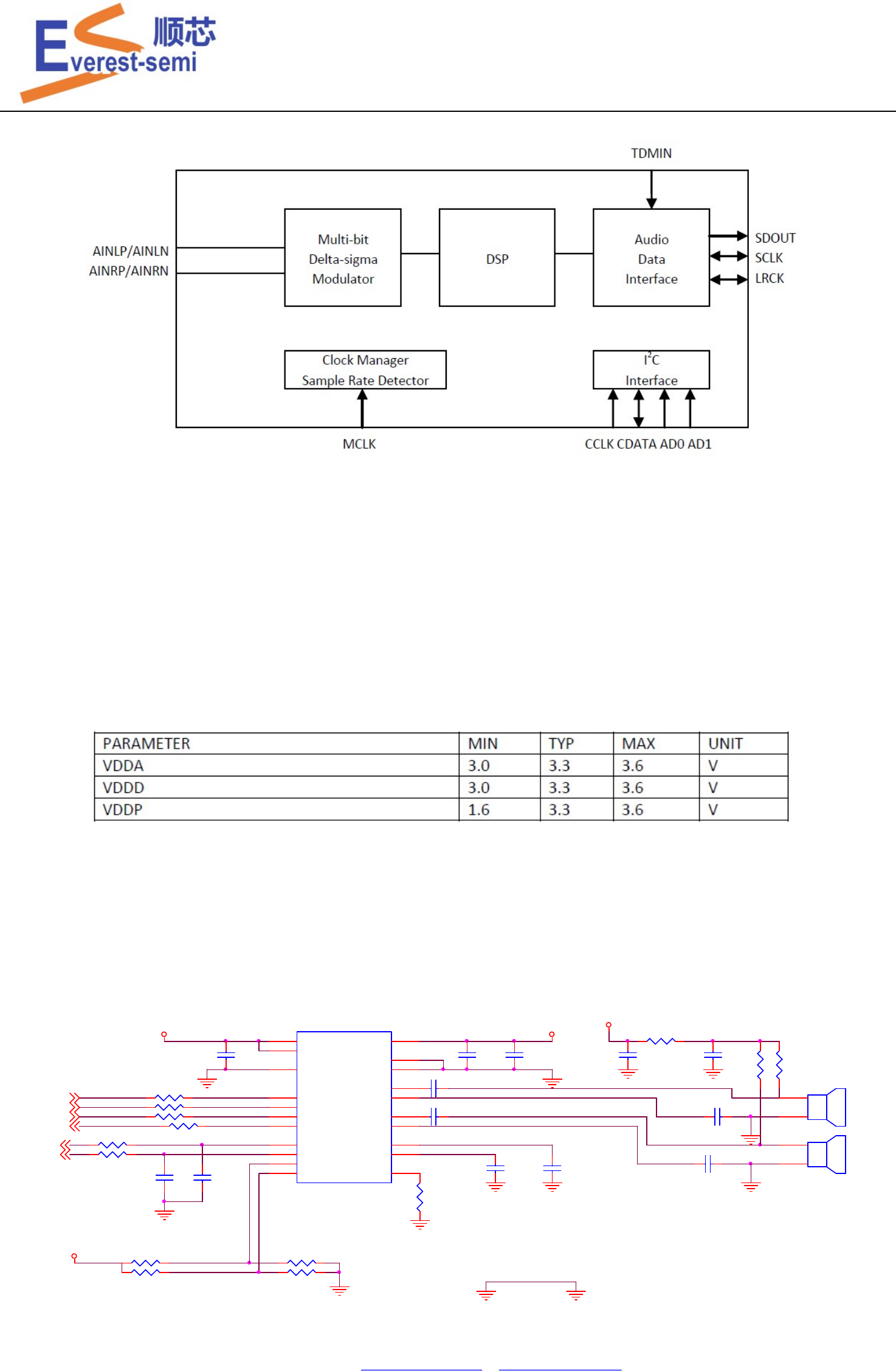
1 BLOCK DIAGRAM
ES7243 Block Diagram
SIGNAL PATH
ES7243 has stereo differential inputs, AINLP-AINLN and AINRP-AINRN, followed by a stereo PGA with gain range from +1dB to
+27dB. Then, the internal high performance multi-bit delta-sigma audio ADC does analog to digital converting. At last digital
signal should be outputted on ASDOUT pin.
The maximum input level of these line inputs is 1Vrms.
2 RECOMMENDED OPERATING CONDITION
The following Table shows the recommended operating condition of ES7243.
3 APPLICATION CIRCUIT AND PCB LAYOUT GUIDE
This section provides some guideline about circuit schematic and PCB layout.
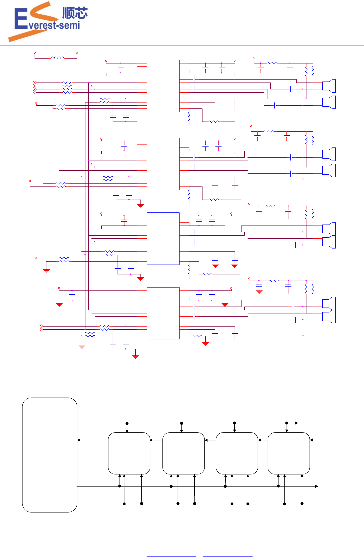
3.1 ES7243 APPLICATION CIRCUIT
Below circuit schematic shows the details about microphone interface, I2C, ground and power supply.
U504 ES7243
QFN20_3R00X3R00X0R85_T
VDDP
1
TDMIN 2
SDOUT
3
GNDD
4
VDDD
5
SCLK
6LRCK
7
AD1
8
AINLP 9
AINLN 10
REFQ 11
VDDA 12
GNDA 13
REFP 14
AINRN 15
AINRP 16
AD0
17 CDATA
18 CCLK
19
MCLK
20
PAD 21
R538 22R 1 2
C557
20pF
12
AU_GND
R548
10K
1 2
VCC_MICA
I2S0_LRCK_TX
C547
1uF
12
AU_GNDSYS_GND
R535
220R
1 2
R537
2k
1 2
C552
1uF
10V
1 2
AU_GND
VCC_MICA
C546
100nF
12
I2S0_MCLK
R544
10K
1 2
C550
1uF
1 2
MICBIAS
I2S0_SCLK
R546 22R
1 2
R547
10K
1 2
C551
1uF
1 2
C555
1uF
12
R539 22R 1 2
I2C Chip ID = 0x20
AU_GND
AU_GND
AU_GND
AU_GND
C554
1uF
12
AU_GND
I2C_AD0
AU_GND
R540 22R 1 2
I2S0_SDI2
I2C_SCL
I2C_SDA
C553
1uF
1 2
R545 22R
1 2
AU_GND
C549
1uF
12
AU_GND
J409
MICROPHONE
P
1
N
2
C545
100nF
12
VCC_MICA R536
2k
1 2
R543
10K
1 2
AU_GND
R541 22R 1 2
C548
1uF
12
VCC_MICA
J408
MICROPHONE
P
1
N
2
R542
10K
1 2
I2C_AD1
C556
20pF
12
ES7243
ES7243 User Guide
Rev.1.00 5 September 2018
Latest datasheet: www.everest-semi.com or info@everest-semi.com
3.2 PCB LAYOUT GUIDE
As with any high-resolution audio converter, designing with ES7243 requires careful attention to PCB layout if its potential
performance is to be realized.
3.2.1 THE POWER SUPPLY, GROUNDING DECOUPLING AND FILTERS
The power supply of ES7243 must be isolate from system power supply. A LDO specified for ES7243 is recommended in order
to get the best audio performance. Usually, GNDD and GNDA must be connect to the same analog ground plane, and then
join into system ground at a single point nearby the power supply. It is important to prevent high frequency noise or high
current noise from going into audio ground plane. Below diagram illustrates ES7243 power supply and grounding.
There need some decoupling and filter capacitors on VDDD, VDDA, REFP and REFQ pins. These decoupling and filter
capacitors must be as near to ES7243 package as possible, with the low value ceramic capacitor being the nearest. All signals,
especially clocks, should be kept away from REFP and REFQ in order to avoid unwanted coupling to ADC modulators. The
filter capacitors on REFP and REFQ pins, especially 0.1uF capacitor, must be positioned to minimize the electronic path from
these reference pins to GND.
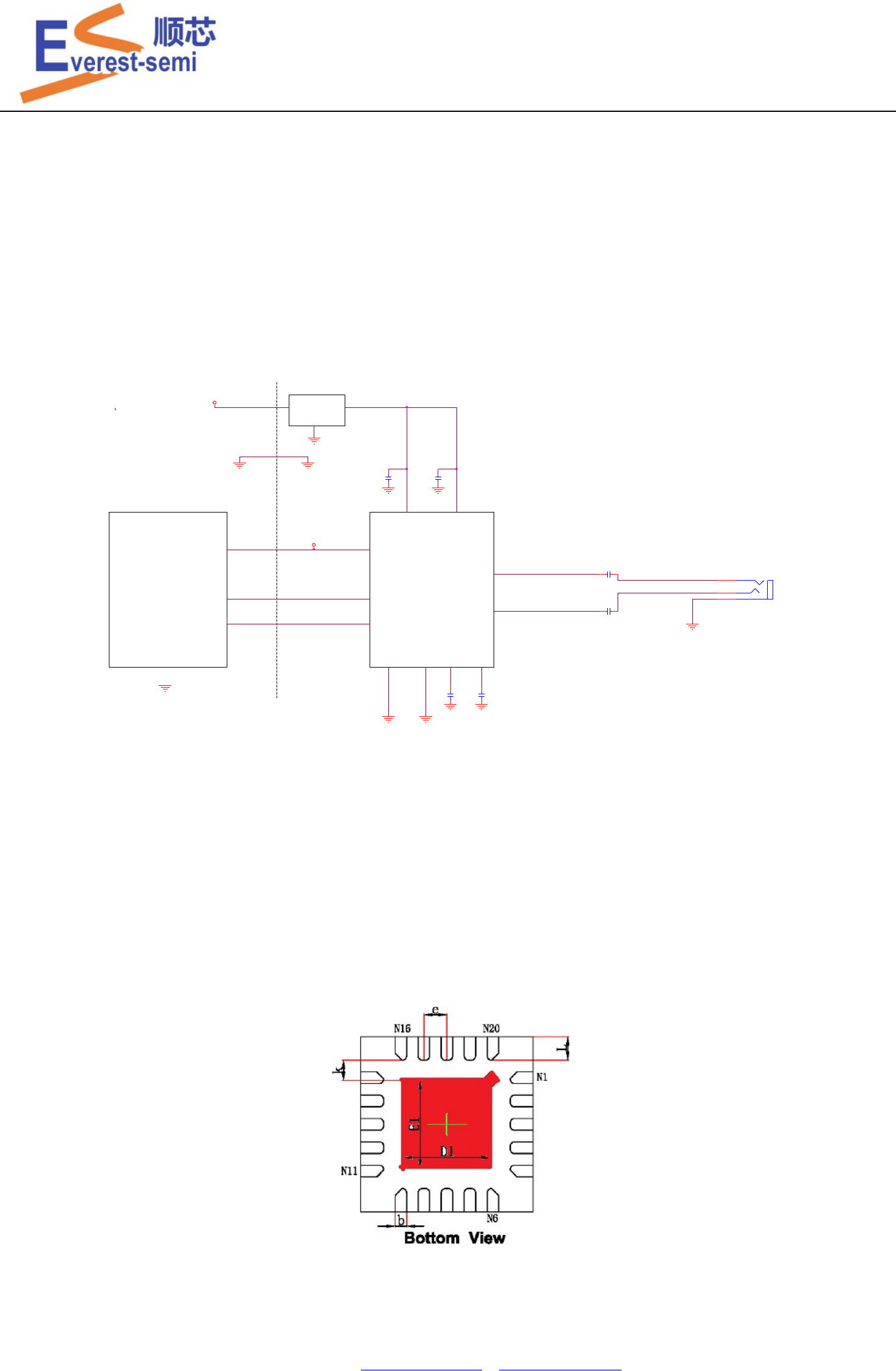
3.2.2 THE THERMAL PAD OF ES7243
There is a thermal pad on the bottom of ES7243 package. The following drawing shows this thermal pad.
In practical system, the thermal pad must be connected to ground plane by via.The following picture illustrates how the
thermal pad is connected to ground plane.
VSYS
C1
0.
1uF
C2
0.1uF
C3
1uF
C4
1uF
C5
1uF
C6
1uF
PVDD
AUD_GNDAUD_GND
AUD_GNDAUD_GND
AUD_GND AUD_GND
AUD_GND
1
2
3
J1
LINE IN JACK
AUD_GND
AINLx
I2S I2S
I2C I2C
PVDDVIO
AVDD
REFQREFP
AGND
DGND
AINRx
DVDD
AUD_GNDSYS_GND
ES724X
LDO
CPU
SYS_GND
ES7243
ES7243 User Guide
Rev.1.00 6 September 2018
Latest datasheet: www.everest-semi.com or info@everest-semi.com
3.3 MICROPHONE CIRCUIT
ES7243 has two differential inputs, AINLP-AINLN and AINRP-AINRN, which can be used as microphone interface. Usually,
AINLP and AINLN is a differential route. AINRP and AINRN is another differential route. It is important note here that the
analog input capacitors, such as C550, C551, C552 and C553, must be near to the microphone.
U504 ES7243
QFN20_3R00X3R00X0R85_T
VDDP
1
TDMIN 2
SDOUT
3
GNDD
4
VDDD
5
SCLK
6LRCK
7
AD1
8
AINLP 9
AINLN 10
REFQ 11
VDDA 12
GNDA 13
REFP 14
AINRN 15
AINRP 16
AD0
17 CDATA
18 CCLK
19
MCLK
20
PAD 21
AU_GND
C547
1uF
12
R535
220R
1 2
R537
2k
1 2
C552
1uF
10V
1 2
AU_GND
C546
100nF
12
R544
10K
1 2
C550
1uF
1 2
MICBIAS
C551
1uF
1 2
C555
1uF
12
I2C Chip ID = 0x20
AU_GND
AU_GND
AU_GND
C554
1uF
12
C553
1uF
1 2
AU_GND
C549
1uF
12
AU_GND
J409
MICROPHONE
P
1
N
2
VCC_MICA R536
2k
1 2
AU_GND
C548
1uF
12
VCC_MICA
J408
MICROPHONE
P
1
N
2
ES7243 doesn’t have microphone bias voltage, so an external microphone bias circuit is used to supply for microphones.
Usually, an R-C filter, for example 220Ω and 1uF, is used to generate microphone bias voltage from ES7243 power supply.
Below picture shows how to generate MICBIAS voltage from ES7243 power supply.
R535
220R
1 2 MICBIAS
AU_GND AU_GND
C549
1uF
12
C548
1uF
12
VCC_MICA
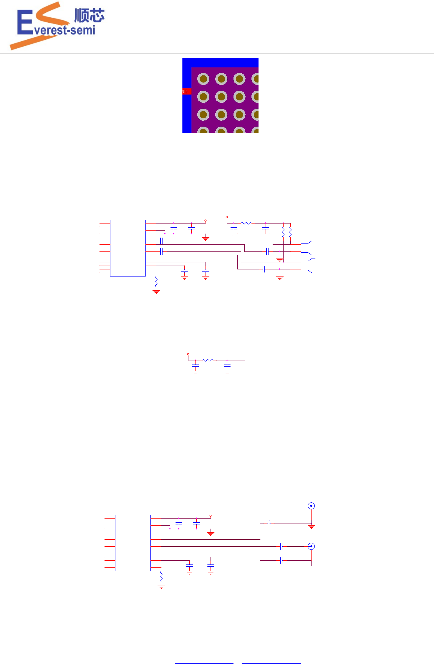
3.4 LINE INPUT
If the internal PGA gain is 1dB, the differential inputs of ES7243 can also be used as line inputs. Following circuit schematic
illustrates the line input of ES7243. It is important note here that the analog input capacitors, such as C563, C565, C564 and
C566, must be near to the line input jack.
AU_GND
AU_GND
VCC _MICA
C560
1uF
12
C563
1uF
1 2
AU_GND
C565
1uF
10V
1 2
U505 ES7243
QFN20_3R00X3R00X0R85_T
VDDP
1
TDMIN 2
SDOUT
3
GNDD
4
VDDD
5
SCLK
6LRCK
7
AD1
8
AINLP 9
AINLN 10
REFQ 11
VDDA 12
GNDA 13
REFP 14
AINRN 15
AINRP 16
AD0
17 CDATA
18 CCLK
19
MCLK
20
PAD 21 C559
100nF
12
C568
1uF
12
AU_GND
R558
10K
1 2
C567
1uF
12
J410
BNC
1
2
C566
1uF
1 2
AU_GND
C564
1uF
1 2
I2C Chip ID = 0x20
J411
BNC
1
2
AU_GND
3.5 THE CIRCUIT SCHEMATIC FOR I2S
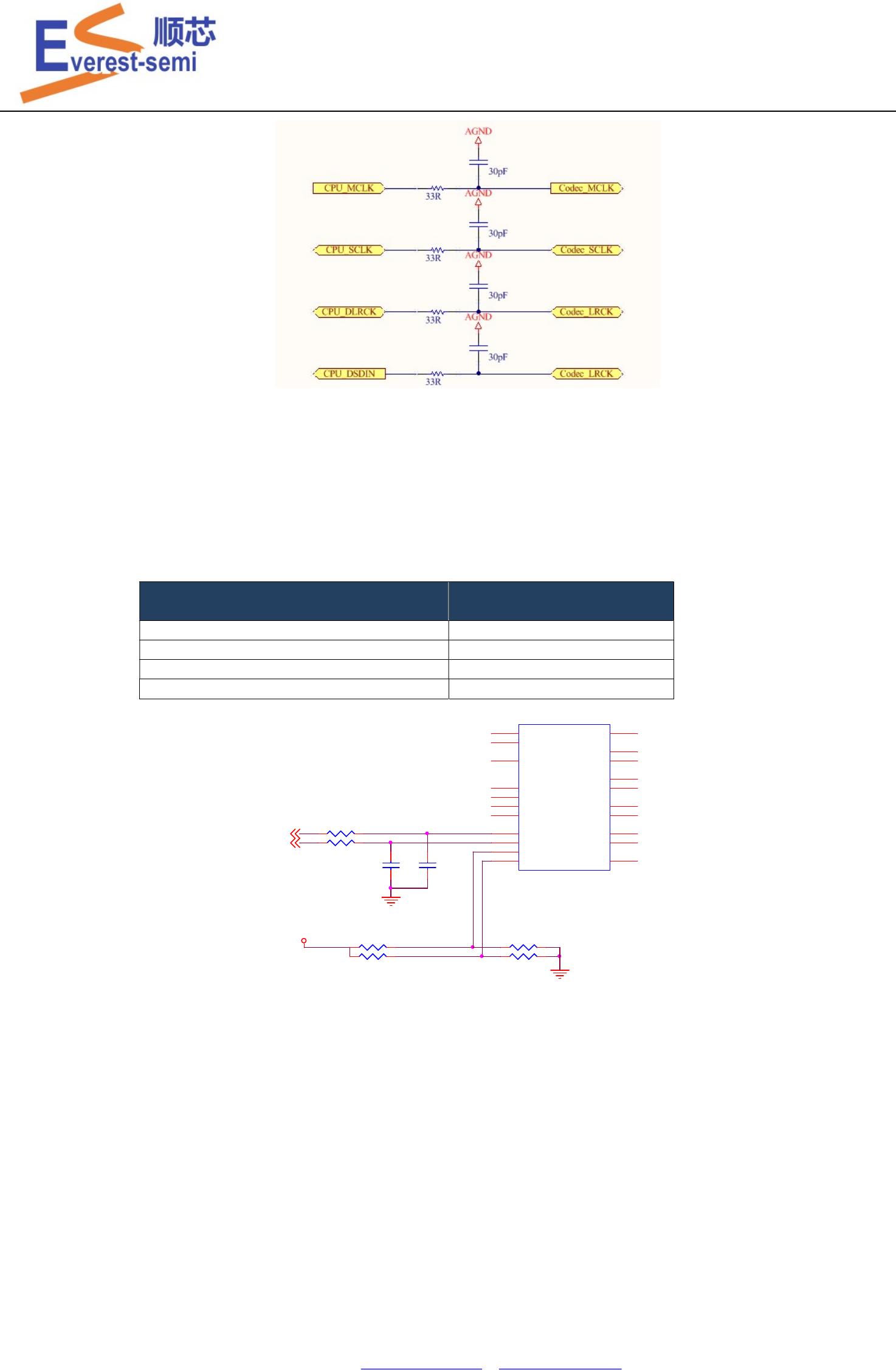
If the length of I2S clock is larger than 10cm, please use 30pF capacitors between I2S clock route and ground. For example,
ES7243
ES7243 User Guide
Rev.1.00 7 September 2018
Latest datasheet: www.everest-semi.com or info@everest-semi.com
3.6 THE CIRCUIT SCHEMATIC OF I2C
ES7243 has I2C control port to read / write internal register. Below schematic shows the circuit of I2C port. The R-C low pass
filter is generally recommended for I2C bus to avoid high frequency noise. The I2C route must be shielded by ground.
Pin17 (AD0) and Pin8 (AD1) are used to select the I2C chip address of ES7243. Following Table shows the definition of I2C
chip address.
ES7243 I2C Chip Address The Level of AD[1:0] pin
0x20 (8bit) / 0x10 (7bit) AD1 =1, AD0 = 1
0x22 (8bit) / 0x11(7bit) AD1 = 1, AD0 = 0
0x24 (8bit) / 0x12 (7bit) AD1 =0, AD0 = 1
0x26(8bit) / 0x13(7bit) AD1 = 0, AD0 = 0
R557 22R
1 2
VCC_MICA R560
10K
1 2
I2C_AD0
U505 ES7243
QFN20_3R00X3R00X0R85_T
VDDP
1
TDMIN 2
SDOUT
3
GNDD
4
VDDD
5
SCLK
6LRCK
7
AD1
8
AINLP 9
AINLN 10
REFQ 11
VDDA 12
GNDA 13
REFP 14
AINRN 15
AINRP 16
AD0
17 CDATA
18 CCLK
19
MCLK
20
PAD 21
C570
20pF
12
AU_GND
AU_GND
I2C_AD1
R561
10K
1 2
R556 22R
1 2
C569
20pF
12
R562
10K
1 2
I2C_SDA
I2C_SCL
R559
10K
1 2
I2C Chip ID = 0x20
3.7 TDMIN PIN
ES7243 has TDM mode to cascade multiple ES7243 devices. The TDMIN pin of ES7243 device must be pulled down to GND by
10kΩ resister whether TDM mode enabled or not.
4 ES7243 APPLICATION
ES7243 operates in software mode, and it communicates with host device by I2C port. In ES7243, some internal registers are
used for power control, PGA gain control, serial digital audio format selection, master or slave mode selection, TDM mode
enable/disable and LRCK ratio selection, etc.
Multiple ES7243 can be cascaded for microphone array application. This TDM cascading mode is very useful in speech
recognition, speech localization and conference system. It is important note here that the TDMIN pin must be pulled down to
GND by 10KΩ resister even if TDM mode is disabled.
ES7243
ES7243 User Guide
Rev.1.00 8 September 2018
Latest datasheet: www.everest-semi.com or info@everest-semi.com
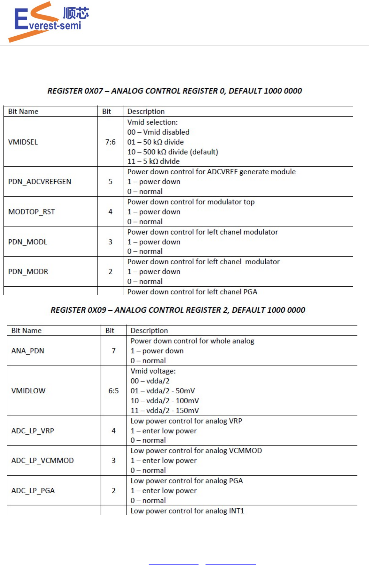
4.1 REGISTER MAP
Register Addr
B7 B6 B5 B4 B3 B2 B1 B0 default
Reg.00
0x00 /////////////////
/ MCLK_DIV ADC_HPF_DIS SPEED_MODE MS_MODE WORK_MODE 0x00
Reg.01
0x01 TDM_ENA SP_BCLKINV SP_LRP SP_WL SP_PROTOCAL 0x00
Reg.02
0x02 LRCKDIV 0x10
Reg.03
0x03 /////////////////
/
/////////////////
/ BCLKDIV 0x04
Reg.04
0x04 /////////////////
/
/////////////////
/ ////////////////// ////////////////// CLK_ADC_DIV 0x02
Reg.05
0x05 /////////////////
/
/////////////////
/ AUTOMUTE_DETED ADC_MUTE_SIZE ADC_SDP_MUTE ADC_NOISETHD ADC_AUTOMUTE 0x13
Reg.06
0x06 SP_TRI MCLK_DIS SEQ_DIS RST_DIG RST_ADCDIG FORCE_CSM 0x00
Reg.07
0x07 VMIDSEL PDN_ADCVREFGEN MODTOP_RST PDN_MODL PDN_MODR PDN_PGAL PDN_PGAR 0x3F
Reg.08
0x08 /////////////////
GAIN_SW[4:2] INPUT_SEL2 GAIN_SW[1:0] INPUT_SEL 0x11
Reg.09
0x09 ANA_PDN VMIDLOW ADC_LP_VRP ADC_LP_VCMMOD ADC_LP_PGA ADC_LP_INT1 ADC_LP_FLASH 0x80
Reg.10
0x0A CHIPINI_CON 0xC0
Reg.11
0x0B POWERUP_CON 0xC0
Reg.12
0x0C /////////////////
/
/////////////////
/ ADCBIAS_SWH SRATIO_DIV 0x12
Reg.13
0x0D ADC_CSM ADC_OSR 0xA0
Reg.14
0x0E CHIP_ID 0x40
4.2 I2C CONTROL PORT
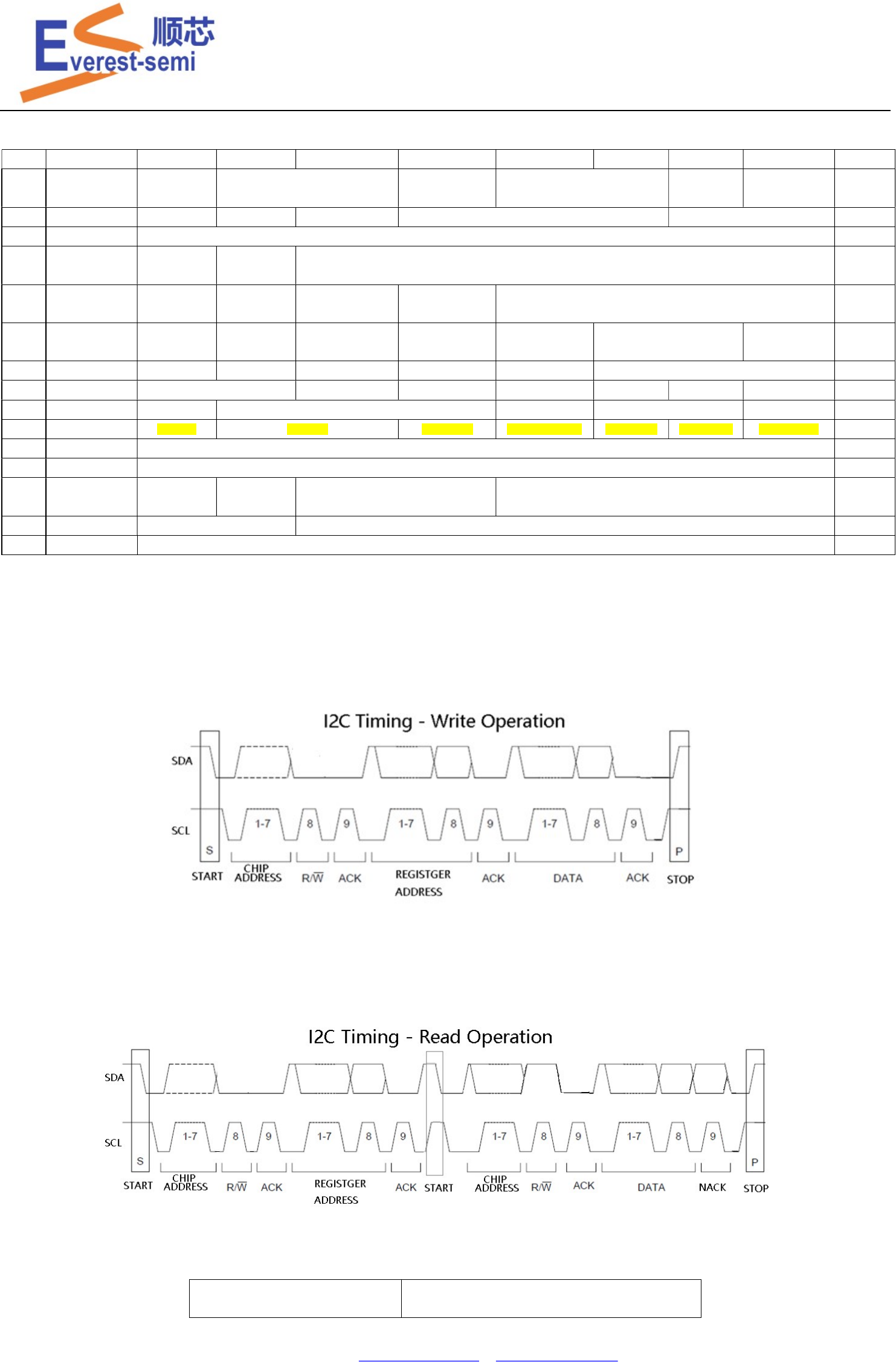
ES7243 supports standard I2C interface with maximum 400kbps rate. External host device can completely configure this
device through writing to internal registers. The transfer rate of I2C can be up to 400kbps.
The following drawing illustrates the timing of I2C.
ES7243 has two chip address pins, AD1 and AD0, to set I2C chip address. The following table shows the chip address
definition,
State of AD[1:0] pins Chip Address

ES7243
ES7243 User Guide
Rev.1.00 9 September 2018
Latest datasheet: www.everest-semi.com or info@everest-semi.com
00 0x13(7bit) / 0x26 (8bit)
01 0x12(7bit) / 0x24 (8bit)
10 0x11(7bit) / 0x22 (8bit)
11 0x10(7bit) / 0x20 (8bit)
4.3 SOFTWARE MODE
ES7243 operates in software mode. WORK_MODE (bit0 of register 0x00) must be set to 1 to enable software mode.
WORK_MODE = 0 ES7243 In Hardware Mode
WORK_MODE = 1 ES7243 In Software Mode
4.4 MASTER OR SLAVE MODE
ES7243 can operate in master mode or slave mode. In slave mode, LRCK and SCLK are supplied externally, and LRCK and SCLK
must be synchronously derived from the system clock with specific rates. In master mode, LRCK and SCLK are derived
internally from device master clock. In slave mode, ES7243 detects MCLK/LRCK ratio automatically. In master mode, ES7243
generates LRCK and SCLK from MCLK according to the setting of LRCKDIV and BCLKDIV.
MS_MODE (Bit1 of register 0x00) is used to select master or slave mode.
MS_MODE = 0 ES7243 In Slave Mode
MS _MODE = 1 ES7243 In Master Mode
4.5 SPEED MODE
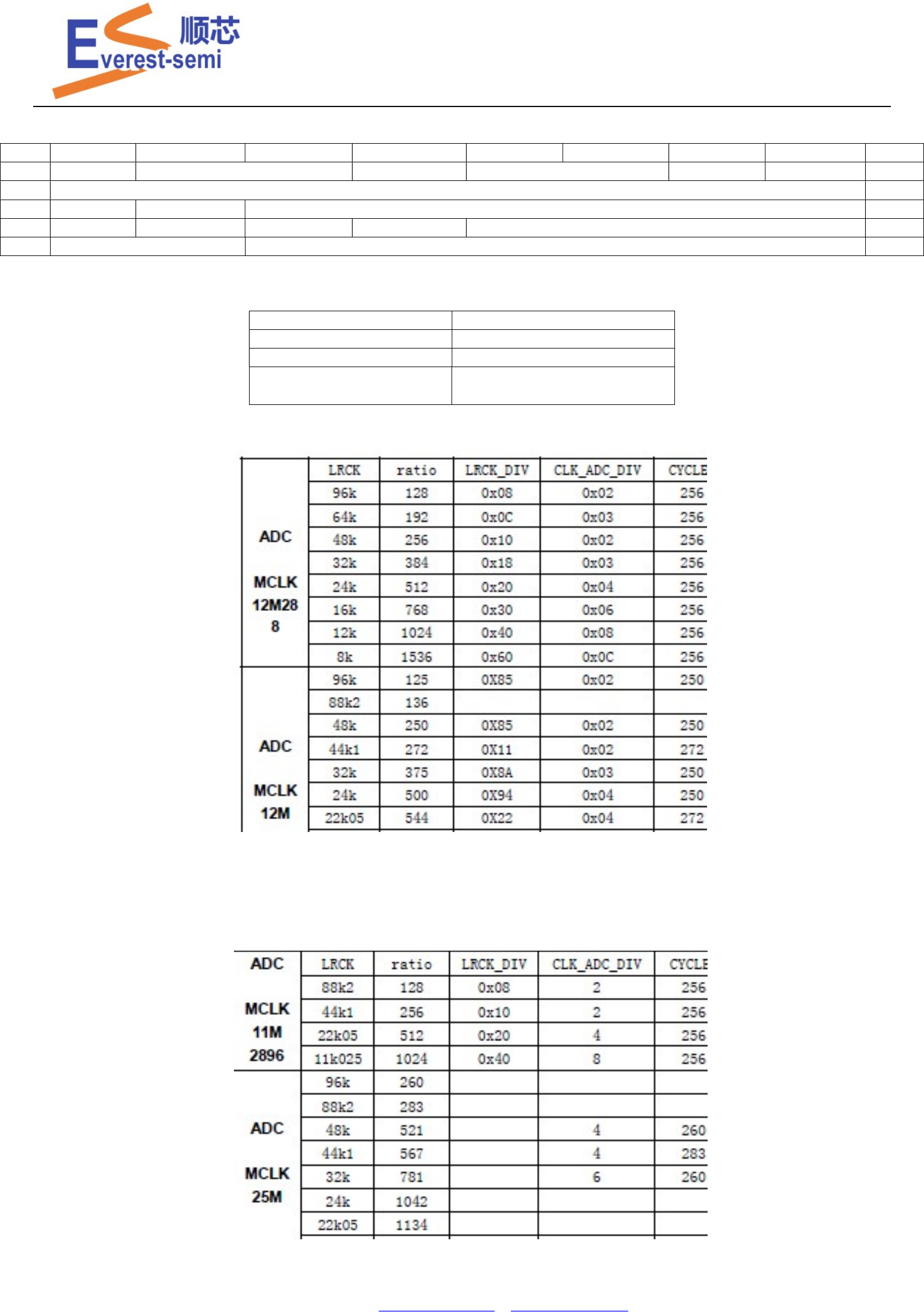
ES7243 supports three speed modes: single speed mode, double speed mode and quad speed mode. In single speed mode,
LRCK frequency normally ranges from 8kHz to 48kHz; In double speed mode, LRCK frequency normally ranges from 64kHz to
96kHz; In quad speed mode, LRCK frequency normally ranges from 96kHz to 192kHz.
In slave mode, ES7243 detects speed mode automatically. In master mode, Bit[3:2] of register 0x00 is used to select proper
speed mode.
4.6 INTERNAL CLOCK DIAGRAM
The following diagram illustrates internal clock diagram in master mode. It is important note here that ES7243 can detect
LRCK ratio automatically in slave mode
MCLK MCLK_DIV
Reg0x00.bit[6:5]
LRCKDIV
Reg0x02
BCLK DIV
Reg0x03.bit[5:0]
MS_MODE =1
Reg0x00.bit1
MS_MODE =1
Reg0x00.bit1
LRCK
SCLK
CLK_ADC_DIV
Reg0x04.bit[3:0]
Internal ADC clock
Internal MCLK
ES7243
ES7243 User Guide
Rev.1.00 10 September 2018
Latest datasheet: www.everest-semi.com or info@everest-semi.com
Following is the register definition for internal clock management.
B7 B6 B5 B4 B3 B2 B1 B0 default
Reg0x00
//////////////////
MCLK_DIV ADC_HPF_DIS SPEED_MODE MS_MODE WORK_MODE 0x00
Reg0x02
LRCKDIV 0x10
Reg0x03
//////////////////
////////////////// BCLKDIV 0x04
Reg0x04
//////////////////
////////////////// ////////////////// ////////////////// CLK_ADC_DIV 0x02
Reg0x0D
ADC_CSM ADC_OSR 0xA0
1. MCLK_DIV DEFINITION
MCLK_DIV = 00 Internal MCLK = MCLK /1
MCLK_DIV = 01 Internal MCLK = MCLK /2
MCLK_DIV = 10 Internal MCLK = MCLK /3
MCLK_DIV = 11 Internal MCLK = MCLK /4
2. LRCKDIV DEFINITION
3. BCLKDIV DEFINITION
ES7243
ES7243 User Guide
Rev.1.00 11 September 2018
Latest datasheet: www.everest-semi.com or info@everest-semi.com
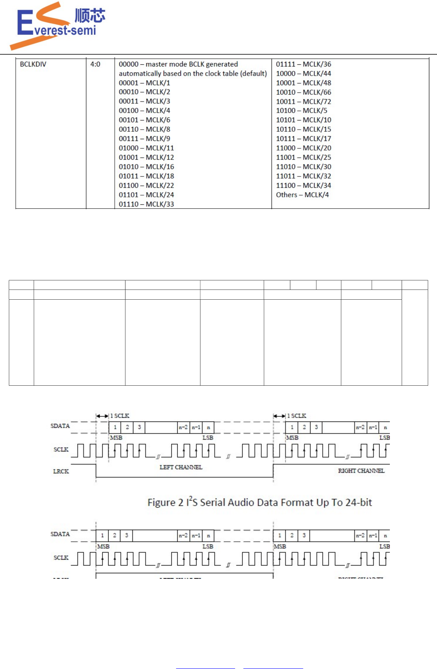
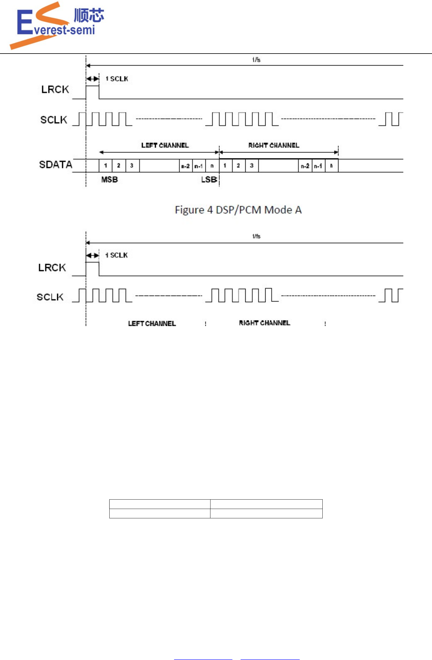
4.7 SERIAL DIGITAL AUDIO FORMAT
ES7243 supports I2S, Left Justified, DSP-A and DSP-B serial digital audio format with resolution from 16bits to 32bits. Only
DSP-A or DSP-B format is supported in TDM cascading mode.
The following is the register definition of serial digital audio format,
B7 B6 B5 B4 B3 B2 B1 B0 default
Reg0x01
TDM_ENA SP_BCLKINV SP_LRP SP_WL SP_PROTOCAL
0x00
1. Enable TDMIN for
Cascading mode
0. Disable TDMIN
SP_BCLKINV = 0, normal mode,
SP_BCLKINV=1, BCLK Inverted
LRC polarity
For I2S/Left Justify:
0 – L/R normal
polarity
1 – L/R invert
polarity
For DSP mode case:
0 – Mode A,
1 – Mode B,
The data format of serial data
port
000 – 24-bit
001 – 20-bit
010 – 18-bit
011 – 16-bit
100 – 32-bit
The protocol of serial
data port
00 – I2S
01 – LJ
10 – not allowed
11 – DSP
The following diagram illustrates the timing of serial digital audio format.
ES7243
ES7243 User Guide
Rev.1.00 12 September 2018
Latest datasheet: www.everest-semi.com or info@everest-semi.com
4.8 TDM MODE
ES7243 supports TDM mode to cascade multiple ES7243 devices. In TDM mode, up to 4 ES7243 devices can be cascaded, and
up to 8 channels ADC data will be presented in one LRCK cycle. No Phase difference exists between these ADC data.
Its TDM mode makes it ideal for microphone array application. Two critical issues must be considered in microphone array
application. One is the number of microphone. Another is the phase difference between ADC data .Usually more than one
microphone will be used to form a microphone array. Ideally, all ADCs in microphone array do analog-to-digital conversion at
the same time, so that there isn’t phase difference between ADC data.
If this microphone array consists of two microphones, there only needs one ES7243 device. If the array is made by more than
two microphones, there should need two or more ES7243 devices, and these ES7243 devices should be cascaded.
In TDM mode, the serial digital audio format must be DSP-A or DSP-B. CPU will get incorrect data if I2S or Left justified format
is used in TDM mode.
TDM_ENA (Bit7 of Register 0x01) is used to enable or disable TDM mode.
TDM_ENA = 0 TDM Mode Disable
TDM_ENA = 1 TDM Mode Enable
It is important note here that the TDMIN pin of ES7243 must be pulled down to ground by 10kΩ even if TDM mode is
disabled.
4.8.1 APPLICATION CIRCUIT OF TDM MODE
Below schematic shows four ES7243 devices cascaded in TDM mode.
ES7243
ES7243 User Guide
Rev.1.00 13 September 2018
Latest datasheet: www.everest-semi.com or info@everest-semi.com
SDO4
C602
1uF
C0603
X5R
10V
12
VCC_MICA
C592
1uF
C0603
X5R
10V
12
R598
22R
R0402
5%
1 2
J412
MICROPHONE
P
1
N
2
R570
10K R04025%
1 2
R588
10K
R0402
5%
1 2
U506 ES7243
QFN20_3R00X3R00X0R85_T
VDDP
1
TDMIN 2
SDOUT
3
GNDD
4
VDDD
5
SCLK
6LRCK
7
AD1
8
AINLP 9
AINLN 10
REFQ 11
VDDA 12
GNDA 13
REFP 14
AINRN 15
AINRP 16
AD0
17 CDATA
18 CCLK
19
MCLK
20
PAD 21
R578
10K R04025% 1 2
SDO4
C595
1uF
C0402
X5R 10V
1 2
C618
20pF
C0402
X5R
50V
12
SDO2
R566 22R R04025% 1 2
C584
100nF
C0402
X5R
10V
12
VCC_MICA
C614
1uF
C0603
X5R
10V
12
C620
20pF
C0402
X5R
50V
12
VCC_MICA
I2S0_LRCK_TX
C606
100nF
C0402
X5R
10V
12
R601 22R R04025%
12
I2C Chip ID = 0x20
C573
1uF
C0603
X5R
10V
12
I2C Chip ID = 0x26
VCC_MICA
C591
1uF
C0603
X5R
10V
12
R597
10K
R0402
5%
1 2
R603 22R R04025%
12
R580
220R
R0402
5%
1 2
VCC_MICA
C599 1uF
C0402
X5R
10V
1 2
C617
20pF
C0402
X5R
50V
12
R563
220R
R0402
5%
1 2
R565
2k
R0402
5%
1 2
R584
22R
R0402
5%
1 2
C578
1uF
C0402
X5R
10V
1 2
R599
220R
R0402
5%
1 2
C613
1uF
C0603
X5R
10V
12
C619
20pF
C0402
X5R
50V
12
VCC_MICA
VCC_MICA
R595
10K
R0402
5%
1 2
R573
22R
R0402
5%
1 2
U507 ES7243
QFN20_3R00X3R00X0R85_T
VDDP
1
TDMIN 2
SDOUT
3
GNDD
4
VDDD
5
SCLK
6LRCK
7
AD1
8
AINLP 9
AINLN 10
REFQ 11
VDDA 12
GNDA 13
REFP 14
AINRN 15
AINRP 16
AD0
17 CDATA
18 CCLK
19
MCLK
20
PAD 21
I2C1_SCL
C589 1uF
C0402
X5R
10V
1 2
VCC_MICA
C572
100nF
C0402
X5R
10V
12
R586 22R R04025%
12
I2S0_MCLK
U509 ES7243
QFN20_3R00X3R00X0R85_T
VDDP
1
TDMIN 2
SDOUT
3
GNDD
4
VDDD
5
SCLK
6LRCK
7
AD1
8
AINLP 9
AINLN 10
REFQ 11
VDDA 12
GNDA 13
REFP 14
AINRN 15
AINRP 16
AD0
17 CDATA
18 CCLK
19
MCLK
20
PAD 21
J416
MICROPHONE
P
1
N
2
R572
10K
R0402
5%
1 2
C583
1uF
C0603
X5R
10V
12
C576 1uF
C0402
X5R
10V
1 2
C615
20pF
C0402
X5R
50V
12
VCC_MICA
VCC_MICA
C605
1uF
C0603
X5R
10V
12
R587 22R R04025%
12
I2S0_SCLK
I2C1_SDA
C588
1uF
C0402
X5R
10V
1 2
VCC_MICA
C577 1uF
C0402
X5R
10V
1 2
U508 ES7243
QFN20_3R00X3R00X0R85_T
VDDP
1
TDMIN 2
SDOUT
3
GNDD
4
VDDD
5
SCLK
6LRCK
7
AD1
8
AINLP 9
AINLN 10
REFQ 11
VDDA 12
GNDA 13
REFP 14
AINRN 15
AINRP 16
AD0
17 CDATA
18 CCLK
19
MCLK
20
PAD 21
C616
20pF
C0402
X5R
50V
12
C581
1uF
C0603
X5R
10V
12
C601 1uF
C0402
X5R
10V
1 2
SDO3
R575
2k
R0402
5%
1 2
R567 22R R04025% 1 2
R604 22R R04025%
12
VCC_MICA
VCC_MICA
VCC_MICA
R591
2k
R0402
5%
1 2
I2C Chip ID = 0x22
VCC_MICA
SDO2
C582
1uF
C0603
X5R
10V
12
C604
1uF
C0603
X5R
10V
12
R589
10K
R0402
5%
1 2
R579
10K
R0402
5%
1 2
R581
10K
R0402
5%
1 2
J418
MICROPHONE
P
1
N
2
C598
1uF
C0603
X5R
10V
12
C580
1uF
C0603
X5R
10V
12
C594
1uF
C0603
X5R
10V
12
C609 1uF
C0402
X5R
10V
1 2
C612
1uF
C0402
X5R
10V
1 2
FB402
180R-100M
L0603
1.5A
25%
1 2
C600
1uF
C0402
X5R
10V
1 2
J417
MICROPHONE
P
1
N
2
R582
2k
R0402
5%
1 2
R574
220R
R0402
5%
1 2
C622
20pF
C0402
X5R
50V
12
R568 22R R04025% 1 2
I2S0_SDO
C597
100nF
C0402
X5R 10V
12
R576
2k
R0402
5%
1 2
C593
1uF
C0603
X5R
10V
12
R605 22R R04025%
12
R592
2k
R0402
5%
1 2
SDO3
C579
1uF
C0402
X5R
10V
1 2
R596
10K
R0402
5%
1 2
C586
1uF
C0603
X5R
10V
12
J415
MICROPHONE
P
1
N
2
I2C Chip ID = 0x24
C621
20pF
C0402
X5R
50V
12
C608
1uF
C0603
X5R
10V
12
R600 22R R04025%
12
C575
1uF
C0603
X5R
10V
12
C596
100nF
C0402
X5R
10V
12
C603
1uF
C0603
X5R
10V
12
J413
MICROPHONE
P
1
N
2
R602 22R R04025%
12
C571
100nF
C0402
X5R
10V
12
J419
MICROPHONE
P
1
N
2
C590
1uF
C0402
X5R
10V
1 2
VCC_MICA
R564
2k
R0402
5%
1 2
R571
10K
R0402
5%
1 2
R590
10K
R0402
5%
1 2
C585
100nF
C0402
X5R
10V
12
R583
2k
R0402
5%
1 2
J414
MICROPHONE
P
1
N
2
C607
100nF
C0402
X5R 10V
12
R569 22R R04025% 1 2
C610
1uF
C0402
X5R 10V
1 2
C611 1uF
C0402
X5R
10V
1 2
C587 1uF
C0402
X5R
10V
1 2
C574
1uF
C0603
X5R
10V
12
VDD_ADC
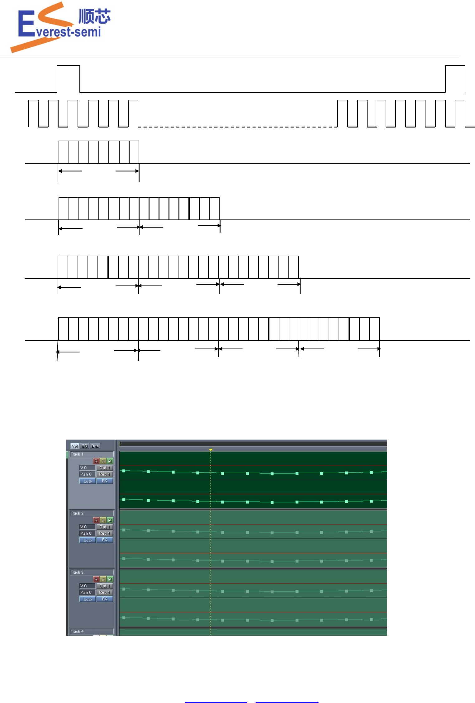
4.8.2 DIAGRAM AND TIMING OF TDM CASCADING MODE
Below diagram illustrates the TDM cascading mode of ES7243.
The following drawing shows the timing of TDM cascading mode.
I2C Bus
ASDOUT
ASDOUT
ASDOUT
ASDOUT
GND
TDMIN
TDMIN
TDMIN
TDMIN
I2S/PCM DATA IN
I2C/PCM CLK
CPU / SOC
ES7243
1# ES7243
2#
ES7243
3#
ES7243
4#
MIC1
MIC2
MIC3
MIC4
MIC5
MIC6
MIC7
MIC8
ES7243
ES7243 User Guide
Rev.1.00 14 September 2018
Latest datasheet: www.everest-semi.com or info@everest-semi.com
4.8.3 PHASE DIFFERENCE BETWEEN MULTIPLE ADCs
In TDM mode, there isn’t phase difference existing between the data of multiple ES7243 devices. Please use audio software,
for example Cooledit, to analysis the phase difference of multiple ADC data. Following picture shows the analysis result of
Cooledit. It shows that no phase difference exists between 8 channels TDM cascading data.
LRCK
3# SDOUT
2# SDOUT
1# SDOUT
L1R1 L2R2 L3R3 L4R4
L2R2 L3R3 L4R4
L3R3 L4R4
L4R4
SCLK
4# SDOUT
ES7243
ES7243 User Guide
Rev.1.00 15 September 2018
Latest datasheet: www.everest-semi.com or info@everest-semi.com
4.9 ANALOG INPUT
Below diagram shows the analog input path of ES7243.
In ES7243, there is a stereo differential analog input, AINLP-AINLN and AINRP-AINRN, followed by a stereo PGA with gain
range from +1dB to +27dB. INPUT_SEL (bit0 of register 0x08) is used to enable or disable these differential inputs. If
INPUT_SEL = 1’b, the differential inputs is enabled. In register 0x08, Bit[6:4] and Bit[2:1] are used to set the PGA gain. Below
table shows the definition of PGA gain.
Bit6 Bit5 Bit4 Bit2 Bit1 Gain (dB)
0 0 1 0 0 +1
0 0 1 0 1 +3.5
0 1 0 0 0 +18
0 1 0 0 1 +20.5
0 0 0 1 0 +22.5
1 0 0 0 0 +24.5
0 0 0 1 1 +25
1 0 0 0 1 +27
AINLP
AINLN PGAL
PGAR
Left ADC
Right ADC
4:1
Reg0x08
Bit[0]
Reg0x08
Bit[6:4]
AIN
RP
AIN
RN
4:1
Bit[2:1]
D2SEL
D2SER
ES7243
ES7243 User Guide
Rev.1.00 16 September 2018
Latest datasheet: www.everest-semi.com or info@everest-semi.com
4.10 POWER CONTROL
In ES7243, some registers are used for power control. The following shows the power control register definition.
4.11 SOFT RESET
In ES7243, some internal registers can be used for soft reset. If the reset bit is set to 1, the device will be in standby mode
ES7243
ES7243 User Guide
Rev.1.00 17 September 2018
Latest datasheet: www.everest-semi.com or info@everest-semi.com
and has minimum power consumption.
The following table shows the soft reset register definition.
4.12 MUTE AND AUTO MUTE
ES7243 has mute control which can mute ADC output. When mute control is set to 1, ADC always outputs all 0 or 1.
Also, ES7243 has auto mute feature. If auto mute is enabled, ES7243 detect the input level automatically. ADC will be mute if
the input level is lower than the threshold within a long duration. User can decide the threshold level and duration time.
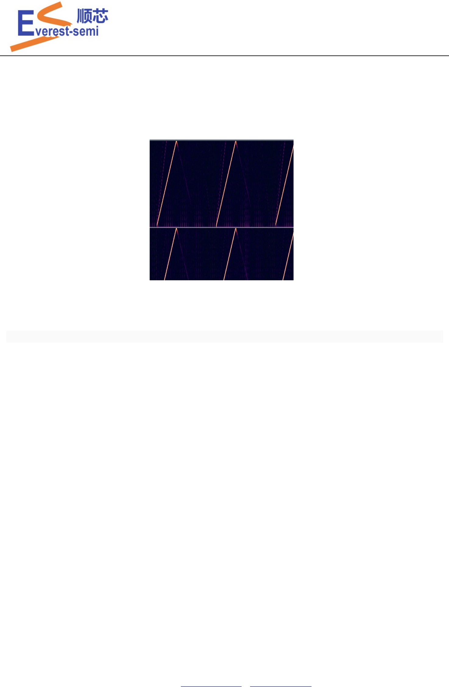
5 EFFECT OF ANTI-ALIASING FILTER
Usually, the bandwidth of audio ADC is lower than FS/2, where FS is sample rate. The signal whose spectrum is higher than
ES7243
ES7243 User Guide
Rev.1.00 18 September 2018
Latest datasheet: www.everest-semi.com or info@everest-semi.com
FS/2 is not interested by ADC. So there need a low-pass filter to restrict the bandwidth of a signal to approximately or
completely satisfy the sampling theorem over the band of interest. This low-pass filter is also named by anti-aliasing filter.
ES7243 has a proper anti-aliasing filter, so that the signal bandwidth is restricted to completely satisfy the sampling theorem.
The out band voice doesn’t have influence on the output spectrum of ADC. So ES7243 is ideal for microphone array
application. Below picture shows the output spectrum of ES7243, where LRCK is 16kHz and the signal range from 20Hz to
20kHz.
Please verify the effect of anti-aliasing filter before using it in microphone array.
6 REGISTER CONFIGURATION FOR ES7243
The Register configuration includes ADC start up, ADC Standby and ADC Cascading mode, etc.
6.1 THE SEQUENCE FOR STARTUP-SLAVE MODE
WriteReg(0x00, 0x01); //slave mode, software mode
WriteReg(0x06, 0x00);
WriteReg(0x05, 0x1B); //Mute ADC
WriteReg(0x01, 0x0C); //i2s -16bit
WriteReg(0x08, 0x43); //enable AIN, PGA GAIN = 27DB
WriteReg(0x05, 0x13); //un Mute ADC
6.2 THE SEQUENCE FOR STARTUP- MASTER MODE
WriteReg(0x00, 0x03); //master mode, software mode, single speed mode, mclk div = 1
WriteReg(0x05, 0x1B); //Mute ADC
WriteReg(0x06 0x10); //RESET ADC
WriteReg(0x01, 0x0C); //i2s -16bit
WriteReg(0x02, 0x10); //MCLK / LRCK = 256
WriteReg(0x03, 0x04); //MCLK / BCLK = 4
WriteReg(0x04, 0x02); //CLK_ADC_DIV=2
WriteReg(0x0D, 0Xa0); //CSM in normal mode, OSR = 32
WriteReg(0x08, 0x43); //enable AIN, PGA GAIN = 27DB
WriteReg(0x06 0x00); //UN RESET ADC
WriteReg(0x05, 0x13); //un Mute ADC
6.3 THE SEQUENCE FOR CASCADING MODE (SLAVE MODE)
WriteReg(0x00, 0x01); //slave mode, software mode
WriteReg(0x06, 0x00);
WriteReg(0x05, 0x1B); //Mute ADC
WriteReg(0x01, 0x8F); //DSP-A, TDM ENABLE
WriteReg(0x08, 0x43); //enable AIN, PGA GAIN = 27DB
WriteReg(0x05, 0x13); //un Mute ADC
6.4 THE SEQUENCE FOR STANDBY MODE
WriteReg(0x06, 0x05);
WriteReg(0x05, 0x1B);

ES7243
ES7243 User Guide
Rev.1.00 19 September 2018
Latest datasheet: www.everest-semi.com or info@everest-semi.com
WriteReg(0x06, 0x5C);
WriteReg(0x07, 0x3F);
WriteReg(0x08 0x4B);
WriteReg(0x09 0x9F);
