F9440_Microflame_Data_Sheet_Dec78 F9440 Microflame Data Sheet Dec78
User Manual: F9440_Microflame_Data_Sheet_Dec78
Open the PDF directly: View PDF ![]() .
.
Page Count: 20
PRELIMINARY
DATA
SHEET • DECEMBER 1978 •
GENERAL DESCRIPTION -
The
9440
MICROFLAME
single-chip
16-bit
bipolar
pro-
cessor, packaged in a 40-pin DIP, is implemented using Fairchild's Isoplanar Integrated
Injection
Logic
technology
(13L™).
Though
structurally
different
from
the CPUs
of
the
Data General NOVA line
of
minicomputers,
the 9440 offers comparable performance
and executes the same
instruction
set.
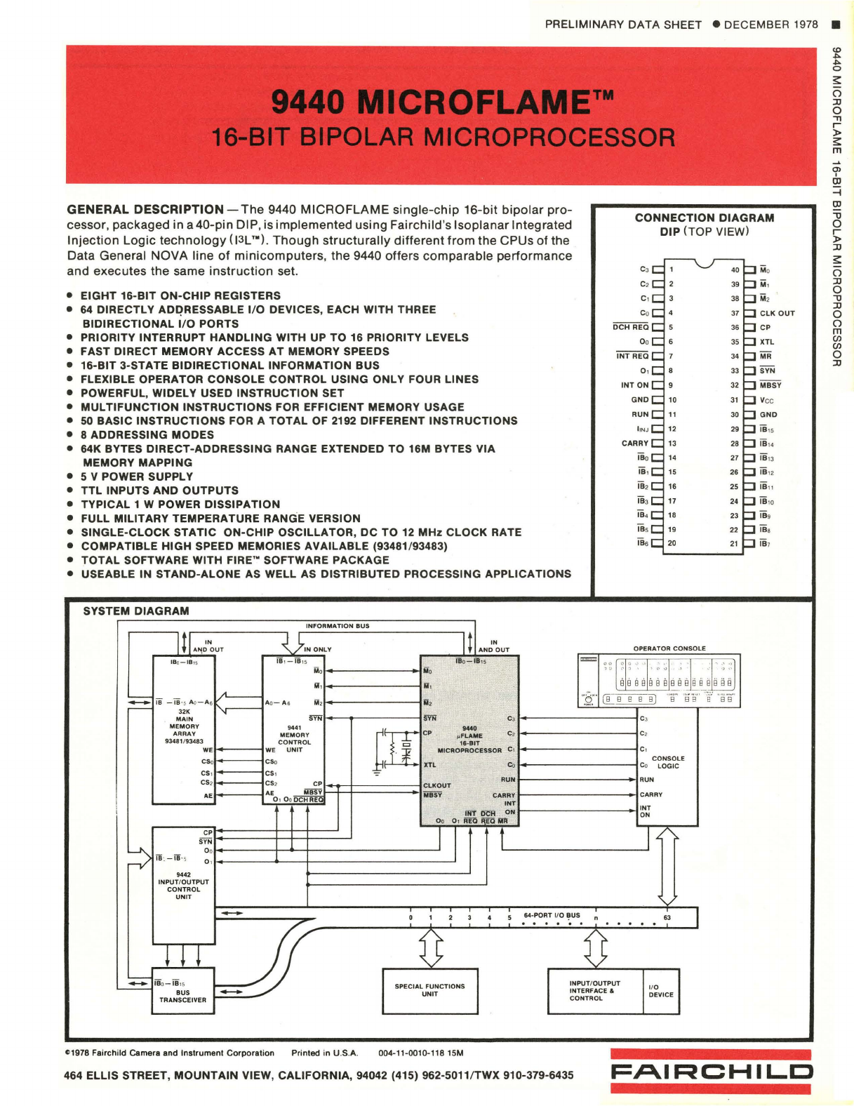
CONNECTION
DIAGRAM
DIP
(TOP
VIEW)
C3 Mo
C, M,
•
EIGHT
16-BIT
ON-CHIP
REGISTERS c, M,
•
64
DIRECTLY ADQRESSABLE
I/O
DEVICES, EACH WITH THREE Co CLK
OUT
BIDIRECTIONAL
I/O
PORTS DCH REO
CP
• PRIORITY INTERRUPT
HANDLING
WITH UP
TO
16 PRIORITY LEVELS 0 0
XTl
• FAST DIRECT MEMORY ACCESS
AT
MEMORY SPEEDS INT REO 34
MR
•
16-BIT
3-STATE
BIDIRECTIONAL
INFORMATION
BUS
0 , SYN
• FLEXIBLE OPERATOR
CONSOLE
CONTROL
USING ONLY FOUR LINES
INTON
32
MBsY
• POWERFUL, WIDELY USED
INSTRUCTION
SET
•
MULTIFUNCTION
INSTRUCTIONS
FOR EFFICIENT MEMORY USAGE
GND
10
31
V
ee
•
50
BASIC
INSTRUCTIONS
FOR A
TOTAL
OF 2192 DIFFERENT
INSTRUCTIONS
• 8 ADDRESSING MODES
• 64K BYTES DIRECT-ADDRESSING RANGE EXTENDED TO 16M BYTES VIA
MEMORY MAPPING
• 5 V POWER SUPPLY
RUN
11
30
GND
I
INJ
12
iB
Is
CARRY
13
28 iii
14
IBo 14 27
iii
l3
ii
, 15 26
iB
'2
•
TTL
INPUTS
AND
OUTPUTS
i82 16 25
iB
n
• TYPICAL 1 W POWER
DISSIPATION
iii
3
17
24
18
10
• FULL MILITARY TEMPERATURE RANGE VERSION
iB
4 18 23
iii
,
•
SINGLE-CLOCK
STATIC
ON-CHIP
OSCILLATOR,
DC
TO
12
MHz
CLOCK
RATE
•
COMPATIBLE
HIGH
SPEED MEMORI.
ES
AVAILABLE
(93481/93483)
IB
5 19 22
rn
8
iii
, 20
21
iii
,
•
TOTAL
SOFTWARE WITH FIRE'· SOFTWARE
PACKAGE
• USEABLE IN
STAND-ALONE
AS WELL AS
DISTRIBUTED
PROCESSING APPLICATIONS
SYSTEM
DIAGRAM
INFORMATION
BUS
I t I
A~~NOUT
VINONlY
It
IN
AND
OUT
OPERATOR
CONSOLE
IB
o
-IB
I~
IH ! -
IB
IS
111
0
ill
"
._-,
8 a
~
j
00
[:
1£
0 0
;IE
'
;[1
'
3[i
Mo Mo
,):J
".,.
" ,
"'
.>
•
M,
il
, "
8888888888888
';-;
is
-
TB
·
~
A
o-
A6 A
o-
A6 M,
il
,
·
~t
trB
ssBJ
irEi'
a"
.
~
'irs'
-
32K
.r---
MAIN
SYN
SYN
C3 e 3
MEMORY 9441
11I
944.
ARRAY
MEMORY
CP ,.
FLAME
C2 C,
93481/
93483
CONTROL
16-8IT
WE
WE
UNIT MICROPROCESSOR Ct C ,
CS
o
CS
o
CONSOLE
XTL
Co
Co LOGIC
CS
,
CS
,
CS
,
CS
,
CP
RUN RUN
ClKOUT
AE
AEO
'
o
o
~
M8SY
CARRY
CARRY
I INT INT
I
iNf
DCH
ON
ON
0 0 0 ,
Imllmlllll
CP
J I t
I/'
SYN
:)
0 0
i'B
:
-iih
0 ,
9442
INPUT
/
OUTPUT
CONTROL
UNIT
---
• 1 2 3 • 5
54·PORT
I/O
~us
n
63
jJ . . . . .
~
~
t ! t
:;:::;:-
iB
o
-iB
15
SPECIAL
FUNCTIONS
INPUT
/
OUTPUT
'----
INTERFACE
&
I/O
BUS -
UNIT
DEVICE
TRANSCEIVER
CONTROL
C1978 Fairchild Camera and
Instrument
Corporation
Printed in U.S.A. 004-11-0010-118 15M
464 ELLIS STREET,
MOUNTAIN
VIEW, CALIFORNIA, 94042 (415) 962-5011/TWX 910-379-6435
FAIRCHIL..C
cJ)
I
(II
=i
~
\l
o
r
»
:D
~
()
:D
o
\l
:D
o
()
m
Ul
Ul
o
:D
FAIRCHILD • 9440
~
"-
-
> PROGRAM SCRATCH
COUNTER r REGISTER -
1'-
~
~
...
BUS
REGISTER /
DST
~
DATA PATH
.I" /'r..
=)
MUX
f-
~
~tv7'
~
FOUR
IBo
-1815
16-BIT ALL! -
..
ACCUMULATORS
~
-
<
2:
~
INFOR~TION
t
=>
BUS
SRC
f-
"-
MUX
t--
INST
'\
REGISTER
./
I'
~
~~~~~-~---)---------~n.~---
CONTROL
'~
I >
CONSOLE MEMORY
CONTROL
LATCH
MICROPROGRAM
PLA
j..
CONTROL
110
CONTROL
If>
~
-
STATE
SEQUENCE
,/
l NEXT SEQUENCE
STATE
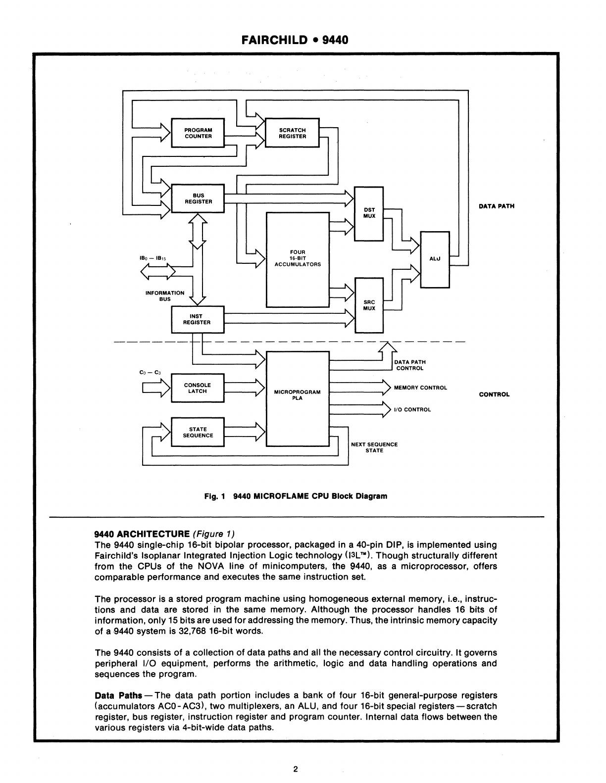
Fig. 1 9440 MICROFLAME CPU Block Diagram
9440 ARCHITECTURE (Figure 1)
The 9440 single-chip 16-bit bipolar processor, packaged in a 40-pin DIP, is implemented using
Fairchild's Isoplanar Integrated Injection Logic technology
(13L™l.
Though structurally different
from the CPUs of the NOVA line
of
minicomputers, the 9440,
as
a microprocessor, offers
comparable performance and executes the same instruction set.
The processor is a stored program machine using homogeneous external memory, i.e., instruc-
tions and data are stored in the same memory. Although the processor handles
16
bits
of
information,
only
15
bits are used
for
addressing the memory. Thus, the intrinsic memory capacity
of
a 9440 system is 32,768 16-bit words.
The 9440 consists
of
a collection of data paths and all the necessary control circuitry.
It
governs
peripheral
liD
equipment, performs the arithmetic, logic and data handling operations and
sequences the program.
Data Paths -The qata path portion includes a bank
of
four 16-bit general-purpose registers
(accumulators ACO-AC3),
two
multiplexers,
an
ALU, and
four
16-bit special
registers-scratch
register, bus register, instruction register and program counter. Internal data flows between the
various registers via 4-bit-wide data paths.
2
FAIRCHILD.
9440
The accumulators store the operands required
for
all arithmetic/logic operations. Accumulators
AC2 and AC3 are also used
as
index registers and AC3 serves
as
the subroutine linkage register
as
well. All
input-output
data transfers take place through the accumulators; however, a word in a
memory location may be incremented
or
decremented
without
accumulator participation. Data can
be
moved in either direction between the memory and any accumulator.
The destination and source multiplexers are connected
to
all
four
accumulators and select source
and destination registers
for
each operation. The multiplexers also receive other inputs from the
bus and instruction registers, which permit the ALU
to
be used
for
effective-address calculations
and other purposes.
The ALU is
four
bits wide and operates on
two
16-bit words in
four
consecutive steps, taking one 4-
bit nibble per step. By adding the associated Carry bit
to
the 16-bit result from the ALU, a 17-bit
word is formed which may
be
rotated either left
or
right.
Data from the ALU to the destination accumulator
is
held in the scratch register
for
one cycle. The
bus register is connected
to
the bidirectional information bus and can either supply
or
receive
16
bits of data in parallel. The instruction register is loaded with
16
bits in parallel, directly from the
information bus during an instruction-fetch operation. The 15-bit program counter determines the
sequence in which instructions are executed.
It
is incremented
to
take instructions from consecu-
tive locations and the instruction sequence can
be
altered at any time by changing the PC contents
(jump-class instruction)
or
by
incrementing
PC
twice (skip-class instruction).
Control-
Control signals are supplied to the data path by the internal mask-programmed logic
arrray (PLA). For each
of
72
different data-path operations, there
is
a 24-bit output word in the PLA
selected according
to
the combination
of
19
input lines. These are defined in Figure
2.
The 9440 operates with
an
on-chip
oscillator when a crystal is tied between CP and XTL
or
it
can be
driven by an external oscillator via the CP input. The on-chip clock logic
circuit
generates the
internal
clock
signal, a synchronization signal (SYN), and several other timing pulses.
A macro-instruction in the 9440 consists
of
several microcycles, each with a corresponding one-of-
16
sequence-control state. Each microcycle consists
of
several phases,
or
nanocycles,
four
of
which are devoted to controlling the data-path circuitry. During each
of
these phases, the data path
circuitry
operates on a 4-bit nibble out of the
16
bits of the operands and clocks its various registers
at half the oscillator rate. Another phase provides the time delay required
for
a new output word
of
the PLA
to
become valid after the PLA inputs are changed.
The bus register and the instruction register are loaded from the information bus at different times
during the execution cycle.
STATE
SEQUENCE
LOGIC
NEXT STATE
SEQUENCE
ALU, AC & MUX
CONTROL
INSTRUCTION
REGISTER
MICROPROGRAM
PLA
CONSOLE
LATCHES
BUS REG INST REG PC MEMORY
1/0
CONTROL
CONTROL
CONTROL
CONTROL
CONTROL
~~--------------~v~--------------~J
DATA
PATH
CONTROL
Fig. 2 Programmed Logic Array
3
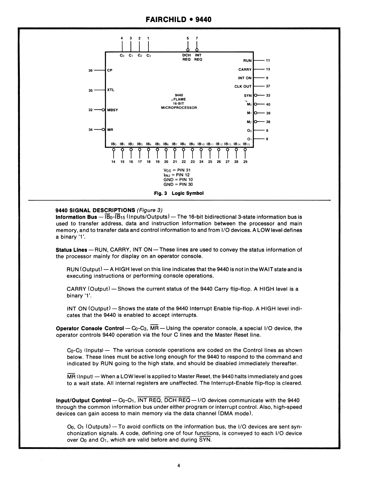
432
36' CP
35
XTl
32
34
FAIRCHILD
-9440
5 7
DCH
INT
REO REO
9440
~FlAME
16-BIT
MICROPROCESSOR
RUN
11
CARRY 13
INT
ON 9
ClK
OUT
37
00
6
I I I I I I
14 15 16 17 18 19
20
21
22 23 24 25 26 27 28 29
Vee = PIN
31
hNJ =
PIN
12
GND = PIN
10
GND = PIN
30
Fig. 3 Logic Symbol
9440 SIGNAL DESCRIPTIONS (Figure 3)
Information Bus
-180-1815
(Inputs/Outputs) -The 16-bit bidirectional 3-state information bus is
used to transfer address, data and instruction information between the processor and main
memory, and
to
transfer data and control information to and from 1/0 devices. A LOW level defines
a binary
'1
'.
Status Lines -RUN, CARRY, INT ON -These lines are used to convey the status information
of
the processor mainly
for
display on
an
operator console.
RUN (Output)
-A
HIGH level on this line indicates that the 9440 is not in the WAIT state and is
executing instructions
or
performing console operations.
CARRY (Output) -Shows the current status
of
the 9440 Carry flip-flop. A
HIGH
level is a
binary '1'.
INT ON (Output) -Shows the state
of
the 9440 Interrupt Enable flip-flop. A HIGH level indi-
cates that the 9440 is enabled to accept interrupts.
Operator Console
Control-
Co-C3,
MR
-Using the operator console, a special 1/0 device, the
operator controls 9440 operation via the four C lines and the Master Reset line.
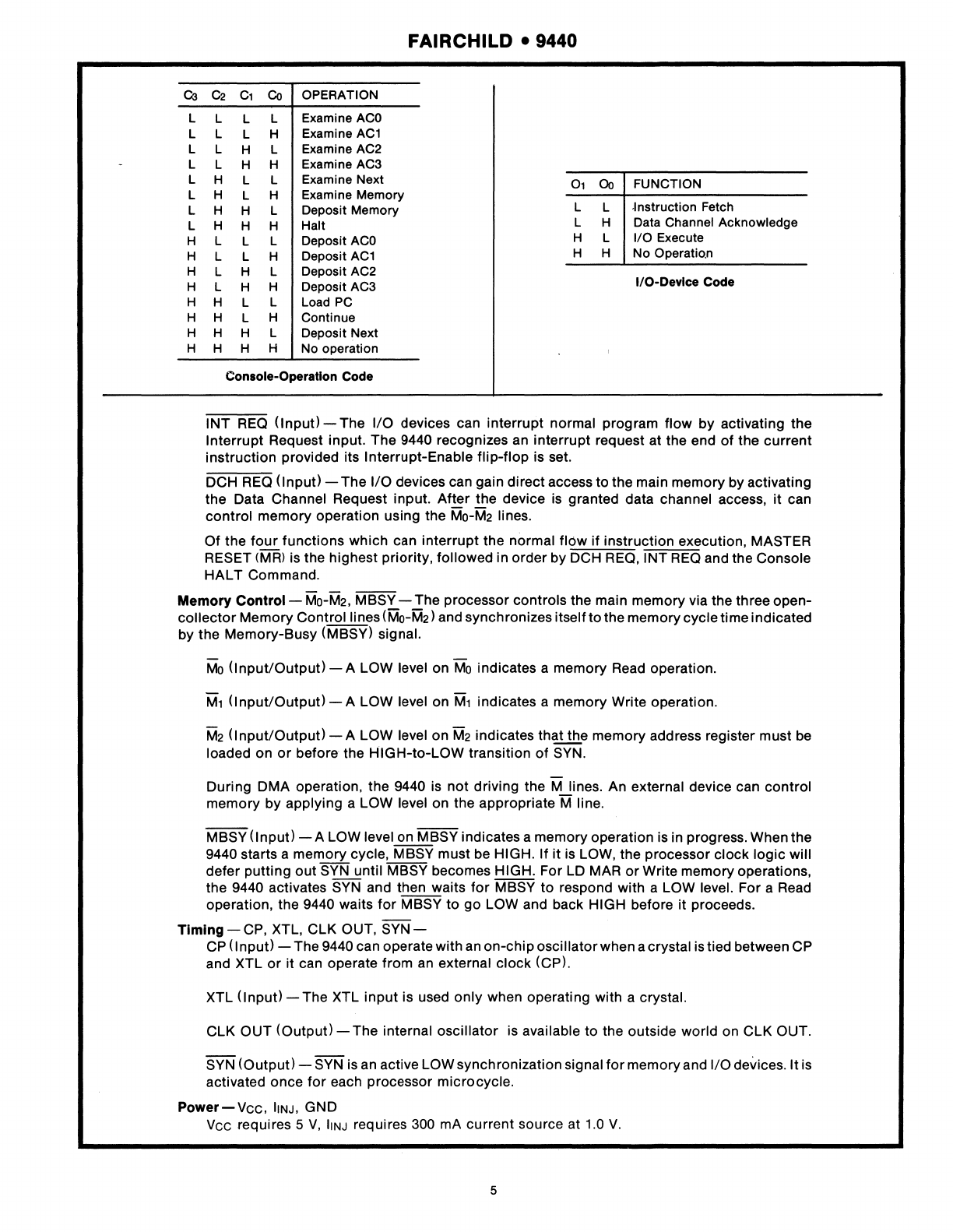
Co-C3
(Inputs) -The various console operations are coded on the Control lines
as
shown
below. These lines must be active long enough
for
the 9440
to
respond to the command and
indicated by RUN going to the high state, and should be disabled immediately thereafter.
MR
(Input) -When a LOW level
is
applied
to
Master Reset, the 9440 halts immediately and goes
to a wait state. All internal registers are unaffected. The Interrupt-Enable flip-flop is cleared.
InputlOutput
Control-
00-01, INT
REO,
DCH
REO
-1/0
devices communicate with the 9440
through the common information bus under either program
or
interrupt control. Also, high-speed
devices can gain access to main memory via the data channel (DMA mode).
00,
01
(Outputs) -
To
avoid conflicts on the information bus, the 1/0 devices are sent syn-
chonization signals. A code, defining one of four functions, is conveyed to each 1/0 device
over 00 and 01, which are valid before and during SYN.
4
-
C3
L
L
L
L
L
L
L
L
H
H
H
H
H
H
H
H
FAIRCHILD·9440
C2
C1
Co
OPERATION
L L L Examine
ACO
L L H Examine
AC1
L H L Examine AC2
L H H Examine AC3
H L L Examine Next
01
00 FUNCTION
H L H Examine Memcry
H H L Depcsit Memcry L L ·Instructicn Fetch
H H H Halt L H Data Channel Ackncwledge
L L L Depcsit
ACO
H L
I/O
Execute
L L H Depcsit
AC1
H H
No.
Operation
L H L Depcsit AC2
L H H Depcsit AC3 I/O-Device Code
H L L Lcad PC
H L H Ccntinue
H H L Depcsit Next
H H H
No.
cperaticn
Console-Operation Code
INT
REO
(Input)
-The
I/O
devices can
interrupt
normal program
flow
by
activating the
Interrupt
Request input. The 9440 recognizes an
interrupt
request at the end
of
the
current
instruction
provided its Interrupt-Enable
flip-flop
is set.
DCH REO
(Input)
-
The
I/O
devices can gain
direct
access to the main memory by activating
the Data Channel Request input.
After
the device is granted data channel access,
it
can
control
memory operation using the Mo-M2 lines.
Of the
four
functions
which
can
interrupt
the normal
flow
if
instruction execution, MASTER
RESET (MR) is the highest priority, followed in order by DCH REO,
INT
REO and the Console
HALT
Command.
Memory
Control-
Mo-M2, MBSY -The processor controls the main memory via the three open-
collector
Memory
Control
lines (Mo-M2) and synchronizes
itselfto
the memory cycle time indicated
by the
Memory-Busy
(MBSY) signal.
Mo
(Input/Output)
- A
lOW
level on
Mo
indicates a memory Read operation.
M1
(I
nput/Output)
- A
lOW
level on
M1
indicates a memory Write operation.
M2
(I
nput/Output)
- A
lOW
level
on
M2
indicates that the memory address register
must
be
loaded on
or
before the
HIGH-to-lOW
transition
of
SYN.
During
DMA
operation, the 9440 is
not
driving the M lines. An external device can
control
memory
by applying a
lOW
level on the appropriate M line.
MBSY
(Input)
-A
lOW
level on MBSY indicates a memory operation is in progress. When the
9440 starts a memory cycle, MBSY must be HIGH.
If
it
is
lOW,
the processor
clock
logic
will
defer
putting
out
SYN until MBSY becomes HIGH. For
lD
MAR
or
Write memory operations,
the 9440 activates SYN and then waits
for
MBSY
to
respond with a
lOW
level. For a Read
operation, the 9440 waits
for
MBSY
to
go
lOW
and back HIGH before it proceeds.
Timing
-CP,
XTl,
ClK
OUT,
SYN-
CP
(Input)
-The 9440 can operate
with
an
on-chip
oscillator
when a crystal is tied between CP
and XTL
or
it can operate from
an
external
clock
(CP).
XTl
(I nput) -The
XTl
input
is used
only
when operati ng with a crystal.
ClK
OUT
(Output)
-The internal
oscillator
is available
to
the outside world on
ClK
OUT.
SYN
(Output)
-SYN is an active
lOW
synchronization Signal
for
memory and
I/O
devices.
It
is
activated
once
for
each processor microcycle.
Power-Vee,
IINJ,
GND
Vee requires 5
V,
IINJ
requires 300 mA
current
source at 1.0
V.
5
FAIRCHILD • 9440
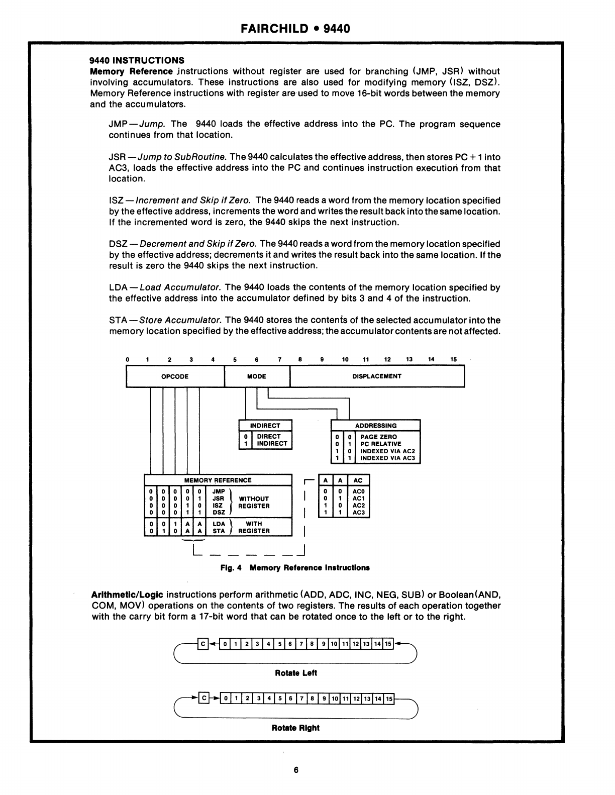
9440 INSTRUCTIONS
Memory Reference jnstructions without register are used for branching (JMP, JSR) without
involving accumulators. These instructions are also used for modifying memory (ISZ, DSZl.
Memory Reference instructions with register are used to move 16-bit words between the memory
and the accumulators.
JMP-Jump.
The 9440 loads the effective address into the
PC.
The program sequence
continues from that location.
JSR
-Jump
to SubRoutine. The 9440 calculates the effective address, then stores
PC
+ 1 into
AC3, loads the effective address into the
PC
and continues instruction execution from that
location.
ISZ
-Increment
and
Skip
if
Zero. The 9440 reads a word from the memory location specified
by the effective address, increments the word and writes the result back into the same location.
If the incremented word is zero, the 9440 skips the next instruction.
DSZ -Decrement and Skip
if
Zero. The 9440 reads a word from the memory location specified
by the effective address; decrements it and writes the result back into the same location. If the
result is zero the 9440 skips the next instruction.
LDA -Load Accumulator. The 9440 loads the contents of the memory location specified by
the effective addre,ss into the accumulator defined by bits 3 and 4
of
the instruction.
STA -Store Accumulator. The
9440
stores the contenfs of the selected accumulator into the
memory location specified by the effective address; the accumulator contents are not affected.
o 2 3 4 5 6 7 8 9 10
11
12 13
14
15
I OPCODE I MODE DISPLACEMENT I
l l
I
INDIRECT ADDRESSING
o I DIRECT 0 0 PAGE ZERO
1 INDIRECT 0 1
PC
RELATIVE
1 0 INDEXED VIA AC2
1 1 INDEXED VIA AC3
MEMORY !lEFERENCE r A A AC
0 0 0 0 0
JMP}
I 0 0
ACO
0 0 0 0 1
JSR
WITHOUT 0 1
AC1
0 0 0 1 0 ISZ REGISTER 1 0 AC2
0 0 0 1 1 DSZ 1 1 1 AC3
0 0 1 A A
LOA}
WITH
1
0 1 0 A A STA REGISTER
--
L
____
J
Fig. 4 Memory Ref.rence Instructions
Arithmetic/Logic instructions perform arithmetic (ADD, ADC, INC, NEG, SUB)
or
Boolean(AND,
COM, MOV) operations on the contents
of
two r-egisters. The results
of
each operation together
with the carry bit form a 17-bit word that can
be
rotated once to the left
or
to
the right.
r...J
0
11
1
2131
41
51&171
81
911011111211311+51~
Rotate Left
~
011
121
314151&171819110111112113114115~
Rotate Right
6
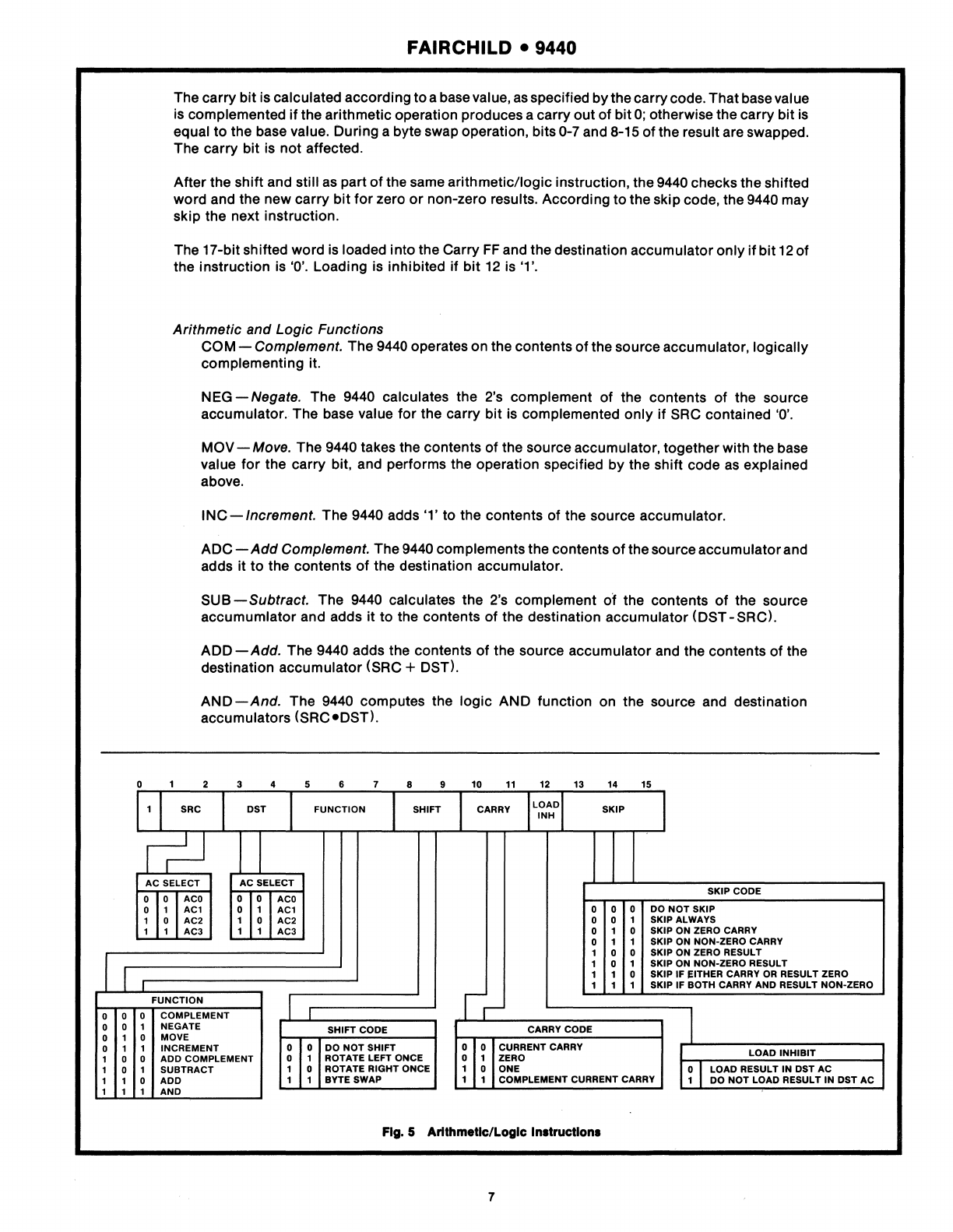
I I
0 0
0 0
0 1
0 1
1 0
1 0
1 1
1 1
o
1
FAIRCHILD.
9440
The carry bit is calculated according
to
a base value,
as
specified by the carry code. That base value
is complemented
if
the arithmetic operation produces a carry out of bit
0;
otherwise the carry bit is
equal
to
the base value. During a byte swap operation, bits 0-7 and 8-15 of the result are swapped.
The carry bit is not affected.
After the shift and still
as
part of the same arithmetic/logic instruction, the 9440 checks the shifted
word and the new carry bit
for
zero
or
non-zero results. According
to
the skip code, the 9440 may
skip the next instruction.
The 17-bit shifted word is loaded into the Carry
FF
and the destination accumulator only
ifbit
12
of
the instruction is '0'. Loading is inhibited
if
bit
12
is '1'.
Arithmetic and Logic Functions
COM -Complement. The
9440
operates on the contents of the source accumulator, logically
complementing it.
NEG
-Negate.
The 9440 calculates the 2's complement of the contents of the source
accumulator. The base value
for
the carry bit is complemented only
if
SRC contained '0'.
MOV -Move. The 9440 takes the contents of the source accumulator, together with the base
value
for
the carry bit, and performs the operation specified by the shift code
as
explained
above.
INC-Increment.
The 9440 adds '1' to the contents of the source accumulator.
ADC -
Add
Complement. The 9440 complements the contents
of
the source accumulator and
adds it
to
the contents of the destination accumulator.
SUB
-Subtract.
The
9440
calculates the 2's complement
of
the contents of the source
accumumlator and adds
it
to
the contents of the destination accumulator (DST -
SRcL
ADD
-Add.
The 9440 adds the contents of the source accumulator and the contents of the
destination accumulator (SRC + DST).
AND
-And.
The 9440 computes the logic AND function on the source and destination
accumulators
(SRC-DSTL
2 3 4 5 6 7 8 9 10
11
12
13 14 15
SRC
I
DST
I
FUNCTION I SHIFT
I
CARRY
ILOADI
INH SKIP
~
I
AC SELECT AC SELECT SKIP CODE
0 0
ACO
0 0
ACO
0 1
AC1
0 1
AC1
0 0 0 DO
NOT
SKIP
1 0 AC2 1 0 AC2 0 0 1 SKIP ALWAYS
1 1 AC3 1 1 AC3 0 1 0 SKIP ON ZI'RO CARRY
0 1 1 SKIP ON NON-ZERO CARRY
1 0 0 SKIP ON ZERO RESULT
1 0 1 SKIP
ON
NON-ZERO RESULT
1 1 0 SKIP IF I'ITHER CARRY
OR
RESULT ZERO
1 1 1 SKIP IF BOTH CARRY AND RESULT NON-ZERO
FUNCTION I
II
0 COMPLEMENT I 1
1 NEGATE SHIFT CODE CARRY CODE
0 MOVE
1 INCREMENT 0 0 DO NOT SHIFT 0 0 CURRENT CARRY L LOAD INHIBIT
0 ADD COMPLEMENT 0 1 ROTATE LEFT ONCE 0 1 ZERO
1 SUBTRACT 1 0 ROTATE RIGHT ONCE 1 0 ONE I 0 I LOAD RESULT IN DST AC
0 ADD 1 1 BYTE SWAP 1 1 COMPLEMENT CURRENT CARRY 1 DO NOT LOAD RESULT IN DST AC
1 AND
Fig. 5 Arithmetic/Logic Instructions
7
FAIRCHILD.
9440
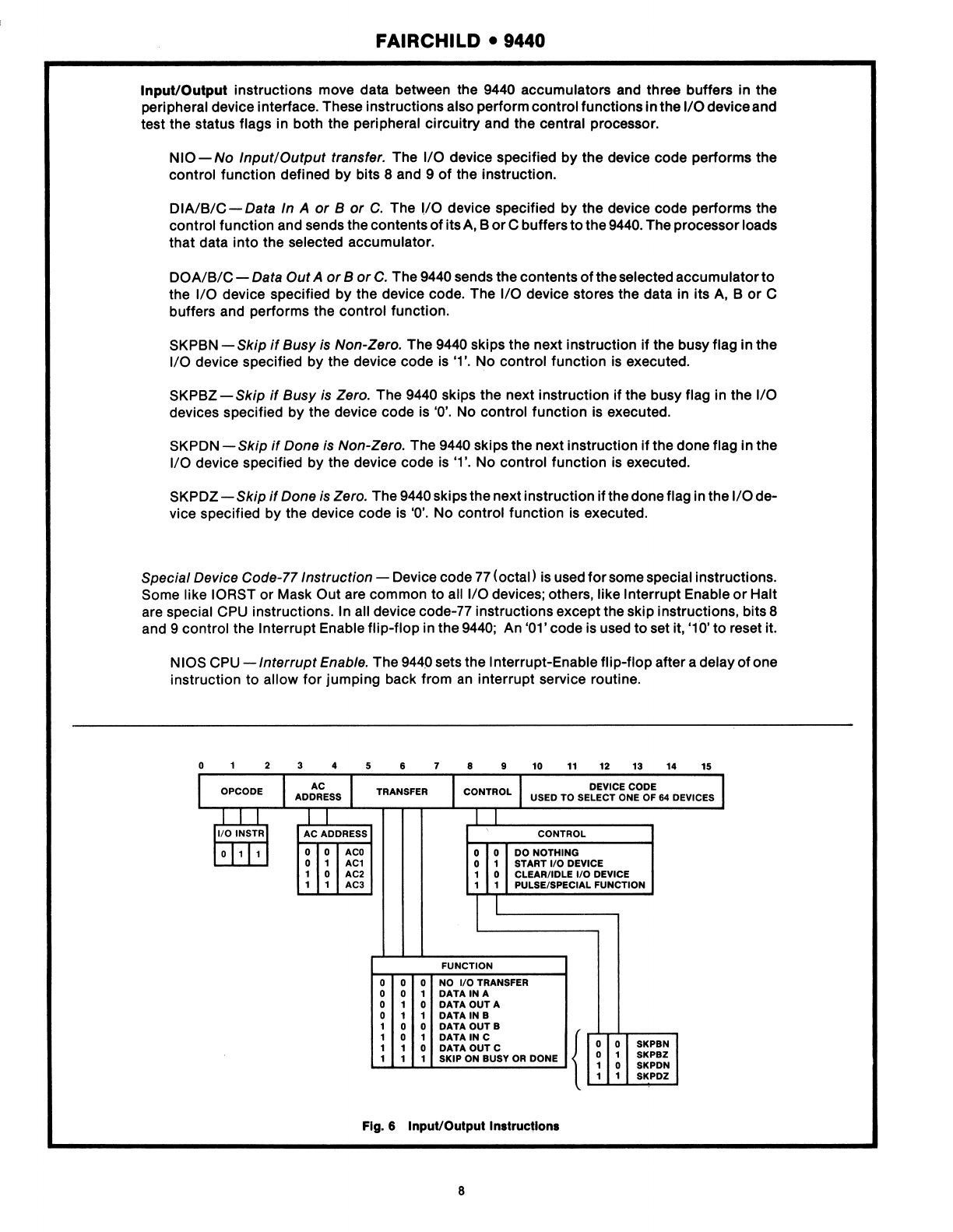
Input/Output instructions move data between the 9440 accumulators and three buffers
in
the
peripheral device interface. These instructions also perform control functions in the 1/0 device and
test the status flags in both the peripheral circuitry and the central processor.
NIO-No
InputlOutput
transfer. The 1/0 device specified
by
the device code performs the
control function defined
by
bits 8 and 9
of
the instruction.
DIAIB/C-Data
In A
or
B
or
C.
The VO device specified
by
the device code performs the
control function and sends the contents
of
its A, B
or
C buffers
to
the 9440. The processor loads
that data
into
the selected accumulator.
DOA/B/C -Data Out A
or
B
or
C.
The 9440 sends the contents
of
the selected accumulator
to
the 1/0 device specified
by
the device code. The 1/0 device stores the data in its A, B
or
C
buffers and performs the control function.
SKPBN -Skip
if
Busy
is
Non-Zero. The 9440 skips the next instruction if the busy flag in the
1/0 device specified
by
the device code is '1'.
No
control function is executed.
SKPBZ -Skip
if
Busy is Zero. The 9440 skips the next instruction if the busy flag in the 1/0
devices specified by the device code is '0'. No control function is executed.
SKPDN
-Skip
if
Done is Non-Zero. The 9440 skips the next instruction
ifthe
done flag
in
the
1/0 device specified by the device code is '1'.
No
control function is executed.
SKPDZ -Skip
if
Done is Zero. The 9440 skips the next instruction if the done flag in the
I/O
de-
vice specified
by
the device code is '0'.
No
control function is executed.
Special Device Code-77 Instruction -Device code 77 (octal) is used
for
some special instructions.
Some like 10RST
or
Mask Out are common to all 1/0 devices; others, like Interrupt Enable
or
Halt
are special CPU instructions. In all device code-77 instructions except the skip instructions, bits 8
and 9 control the Interrupt Enable flip-flop in the 9440; An '01' code is used to set it, '10' to reset it.
N lOS CPU
-Interrupt
Enable. The 9440 sets the Interrupt-Enable flip-flop after a delay
of
one
instruction to allow
for
jumping back from
an
interrupt service routine.
o 2 3 4 5 8 7 8 9 10
11
12 13 14 15
I OPCODE I
AD~;ESS
I TRANSFER I I DEVICE CODE I
CONTROL USED TO SELECT ONE
OF
64
DEVICES
I I I I I I I
\I/OINSTRI
AC ADDRESS , CONTROL
1 0
11
11
1 0 0
ACO
0 0 DO NOTHING
0 1
AC1
0 1 START 1/0 DEVICE
1 0 AC2 1 0 CLEAR/IDLE
110
DEVICE
1 1 AC3 1 1 PULSE/SPECIAL FUNCTION
I I
FUNCTION
0 0 0 NO
110
TRANSFER
0 0 1 DATA
INA
0 1 0 DATA OUT A
0 1 1
DATAINB
1 0 0 DATA OUT B {
1 0 1
DATAINC
0 SKPBN
1 1 0 DATA OUT C 0
1 1 1 SKIP ON BUSY
OR
DONE 0 1 SKPBZ
1 0 SKPDN
1 1 SKPDZ
Fig. 6 Input/Output Instrue_lons
8
FAIRCHILD • 9440
NIOC
CPU
-Interrupt
Disable. The 9440 clears the Interrupt-Enable flip-flop and does not re-
spond
to
subsequent Interrupt requests.
DIA CPU -Read Switches. The 9440 loads the contents
of
the front-panel switches into the
specified accumulator.
DIB
CPU
-Interrupt
Acknowledge. The 9440 loads the device code of the highest priority
1/0 device requesting
an
interrupt into bits 10-15
of
the specified accumulator.
DOB CPU -Mask Out. The
9440
puts the contents
of
the specified accumulator on the infor-
mation bus. Each
1/0
device
is
assigned a particular bit in that word. When the mask bit is
'1', the device disables its interrupt.
DIC
CPU
-Clear
110
Devices
or
10RST. All 1/0 devices connected
to
the bus must clear
their control flip-flops, including Busy and Done, and disable their interrupts.
DOC CPU -Halt. The
9440
halts after executing this instruction and the console displays
the Halt instruction on the data light. The location
of
the Halt instruction is displayed on the
address lights.
SKPBN CPU
-Skip
if
Interrupt Enable is Non-Zero. The
9440
will skip the next instruction
if
the Interrupt-Enable flip-flop
is
enabled.
SKPSZ CPU
-Skip
if
Interrupt Enable is Zero. The 9440 skips the next instruction
if
the
Interrupt-Enable flip-flop is disabled.
9440 MODES OF ADDRESSING
The flexible addressing structure
ofthe
9440 consists
offourtypes
of
addressing -one is absolute
addressing
of
page zero, i.e. the first 256 locations in the memory; the other three are relative
addressing where an a-bit displacment in the memory reference instruction is treated
as
a signed
number and added
to
a 15-bit base address in an index register, either AC2, AC3,
or
PC.
Each type
may
be
either direct
or
indirect for a total
of
eight modes. Relative addressing using accumulator
AC2
or
AC3
is
useful for accessing consecutive entries from a table in the memory, e.g., where a
displacement is added
to
the incrmented index in the accumulator. Relative addressing utilizing the
program counter is used
for
jumping to nearby locations when a relocatable program
is
executed.
In direct addressing, the 15-bit computed value
is
the actual address used to read
or
store the
operand. In case
of
indirect addressing (bit 5
of
the instruction is '1'), the computed value is the
address
of
an
address. The data read from an indirectly addressed location can be the final effective
address
or
another nested indirect address depending on the most significant bit in that word.
Bit
0 of the word read from the indirectly addressed location
is
treated
as
another indirect bit. Bits 1-
15
are the effective address ifbitO is'O'.lf bitO is '1', bits 1-15 pOinttoa location in memory where the
next level
of
indirect address resides. This process can continue indefinitely,
as
long
as
bit 0 of each
word read from memory is '1'.
When locations (20)8 through (27)8 are indirectly addressed, the auto-incrementfeature takes over
and the contents of the selected location are first incremented and the new value is treated
as
the
new address, which can
be
either direct
or
indirect. Locations (30)8 through (37)8 are used
as
auto-
decrement locations in a sim.ilar fashion.
9
...
,
MEMORY
CONTROL
WEI----!lrIE
UNIT
ONLY
FAIRCHILD.
9440
SYN
~~---~~r--------~
O,
....
----<
__
I--
________
~
...
2
INPUT/OUTPUT
CONTROL
UNIT
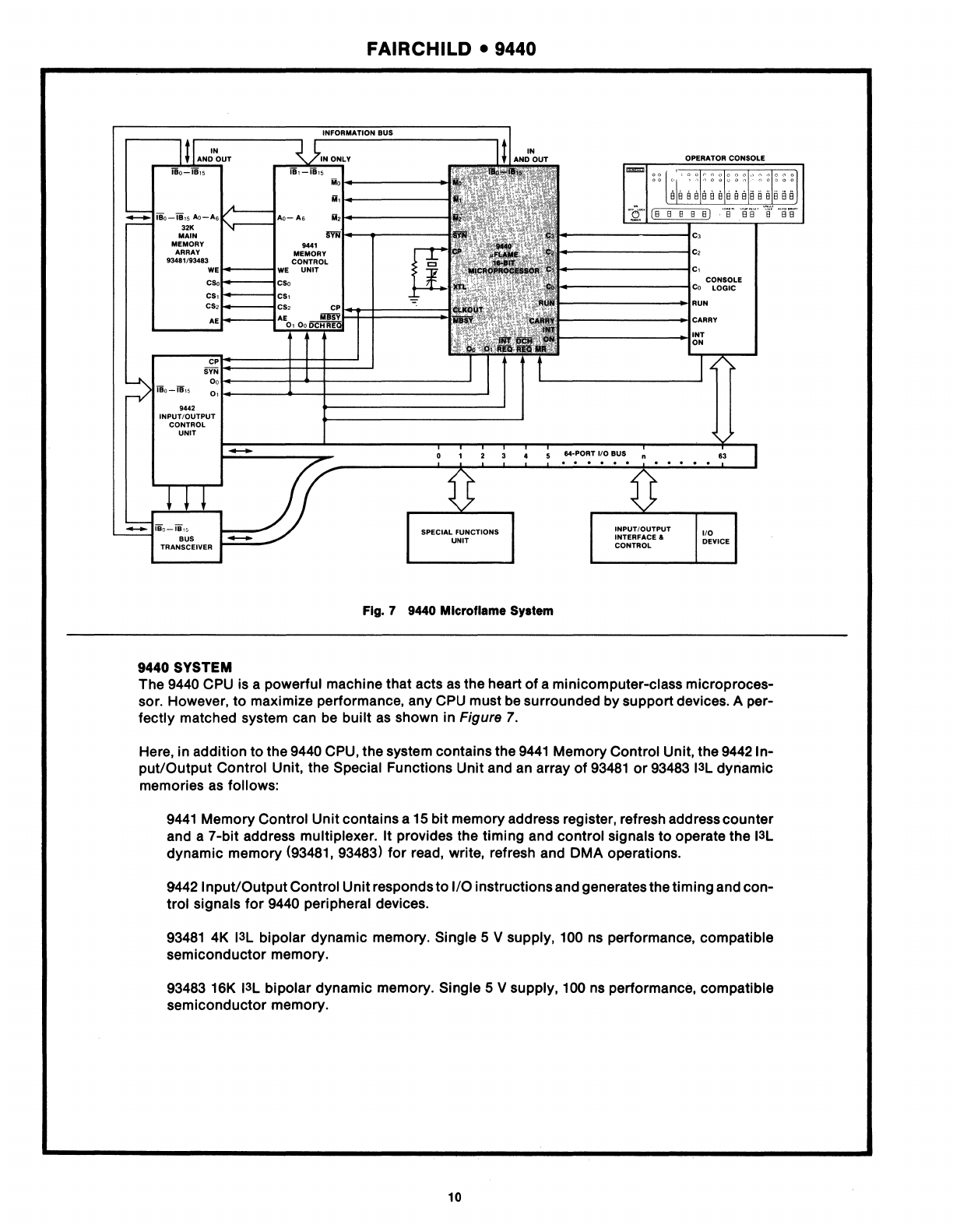
9440 SYSTEM
SPECIAL FUNCTIONS
UNIT
Fig. 7 9440 Mlcroflame System
CONSOLE
--------tCO
LOGIC
INPUT/OUTPUT
INTERFACE a
CONTAOL
110
DEVICE
The 9440 CPU is a powerful machine that acts
as
the heart of a minicomputer-class microproces-
sor. However,
to
maximize performance, any CPU must
be
surrounded by support devices. A per-
fectly matched system can
be
built
as
shown in Figure
7.
Here, in addition
to
the 9440 CPU, the system contains the
9441
Memory Control Unit, the
9442
In-
put/Output Control Unit, the Special Functions Unit and an array of
93481
or
93483
13L
dynamic
memories
as
follows:
9441
Memory Control Unit contains a
15
bit memory address register, refresh address counter
and a 7-bit address multiplexer. It provides the timing and control signals to operate the
13L
dynamic memory (93481, 93483)
for
read, write, refresh and DMA operations.
9442 Input/Output Control Unit responds to 1/0 instructions and generates the timing and con-
trol signals
for
9440 peripheral devices.
93481
4K
13L
bipolar dynamic memory. Single 5 V supply, 100 ns performance, compatible
semiconductor memory.
93483 16K
13L
bipolar dynamic memory. Single 5 V supply, 100 ns performance, compatible
semiconductor memory.
10
FAIRCHILD.
9440
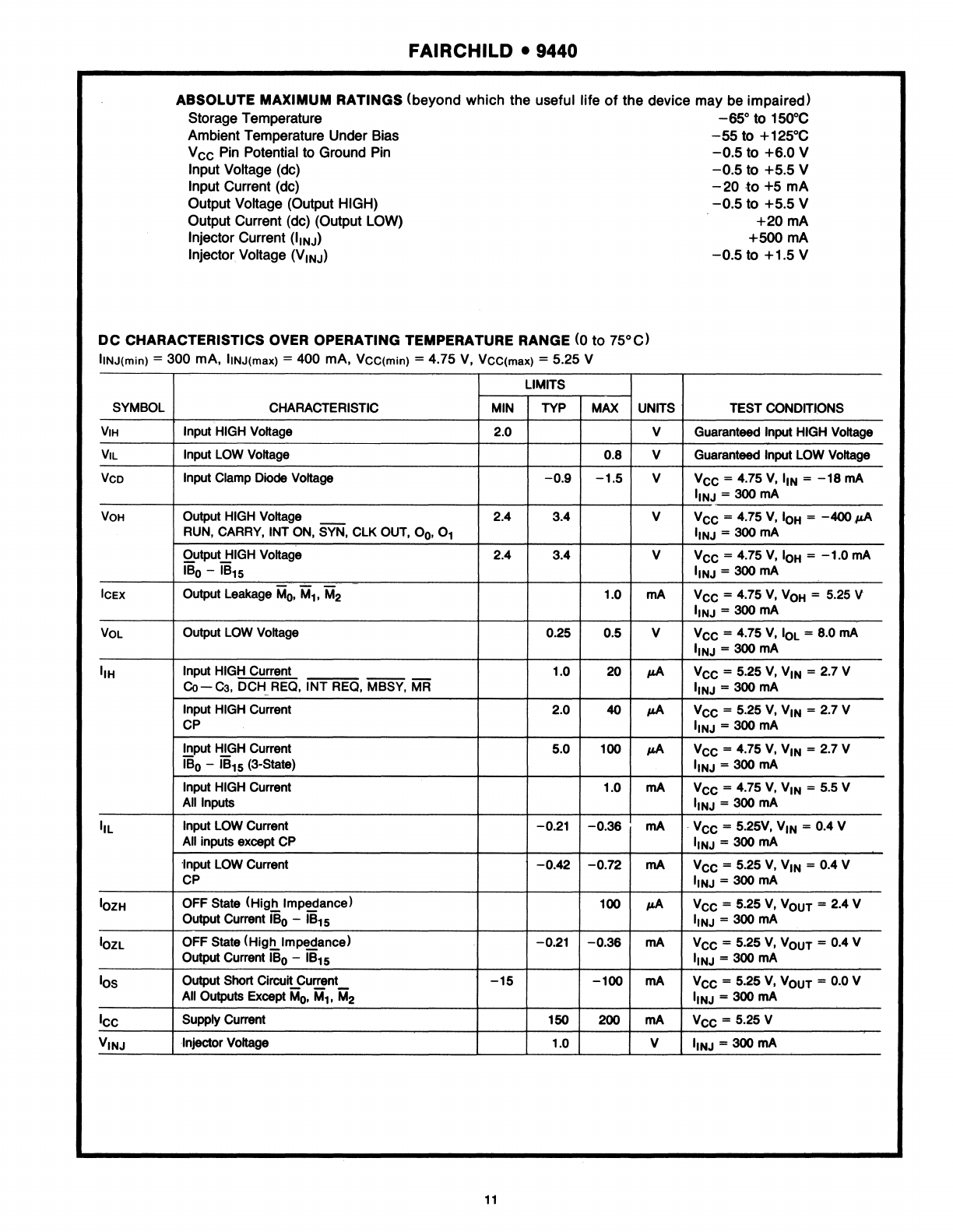
ABSOLUTE MAXIMUM RATINGS
(beyond
which
the
useful
life
of
the
device
may
be
impaired)
Storage
Temperature
-65°
to
150°C
Ambient
Temperature
Under
Bias
-55
to
+125°C
Vee
Pin Potential
to
Ground
Pin
-0.5
to
+6.0
V
Input
Voltage
(dc)
-0.5
to
+5.5
V
Input
Current
(dc) -
20
·to
+5
mA
Output
Voltage
(Output
HIGH)
-0.5
to
+5.5
V
Output
Current
(dc)
(Output
LOW)
+20
mA
Injector
Current
(IINJ)
+500
mA
Injector
Voltage
(V
INJ
)
-0.5
to
+
1.5
V
DC
CHARACTERISTICS OVER OPERATING TEMPERATURE RANGE
(0
to
75°C)
hNJ(min) =
300
mA,
hNJ(max)
= 400
mA,
Vee(min) = 4.75 V, Vee(max) = 5.25 V
LIMITS
SYMBOL CHARACTERISTIC MIN TYP MAX UNITS TEST CONDITIONS
VIH
Input HIGH Voltage 2.0 V Guaranteed Input HIGH Voltage
Vll
Input
lOW
Voltage 0.8 V Guaranteed Input
lOW
Voltage
VCD
Input Clamp Diode Voltage
-0.9
-1.5
V
Vee
= 4.75
V,
liN =
-18
rnA
IINJ = 300 rnA
VOH
Output HIGH Voltage 2.4 3.4 V
Vee
= 4.75
V,
10H
=
-400
pA
RUN, CARRY, INT ON, SYN,
ClK
OUT,
00'
01 IINJ = 300 rnA
Q.utputJ:lIGH Voltage 2.4 3.4 V
Vee
= 4.75
V,
10H
=
-1.0
rnA
IBo -
IB
15
IINJ = 300 rnA
tCEx
Output leakage
Mo,
M1,
M2
1.0 rnA
Vee
= 4.75
V,
VOH
= 5.25 V
tlNJ = 300 rnA
VOL
Output
lOW
Voltage 0.25 0.5 V
Vee
= 4.75
V,
10l
= 8.0 rnA
IINJ = 300 rnA
IIH Input HIGH Current 1.0 20
pA
Vee
= 5.25
V,
VIN
= 2.7 V
Co
-
C3,
DCH REO, tNT REO, MBSY,
MR
IINJ = 300
rnA
Input HIGH Current 2.0 40
pA
Vee
= 5.25
V,
VIN
= 2.7 V
CP IINJ = 300 rnA
!!!.put
~GH
Current 5.0 100
pA
Vee
= 4.75
V,
VIN
= 2.7 V
IBo -IB
15
(3-State) IINJ = 300
rnA
Input HIGH Current 1.0
rnA
Vee
= 4.75
V,
V
IN
= 5.5 V
All Inputs IINJ = 300 rnA
III
Input
lOW
Current
-0.21
-0.36
rnA -
Vee
= 5.25V,
VIN
= 0.4 V
All inputs except CP IINJ = 300 rnA
-Input
lOW
Current
-0.42 -0.72
rnA
Vee
= 5.25
V,
V
IN
= 0.4 V
CP IINJ = 300 rnA
10ZH
OFF State
(Hig!!
Irnp~ance)
100
pA
Vee
= 5.25
V,
VOUT
= 2.4 V
Output Current
IBo
-IB
15
IINJ = 300 rnA
10Zl OFF State
(Hig!!..trnp~ance)
-0.21
-0.36
rnA
Vee
= 5.25
V,
VOUT
= 0.4 V
Output Current IBo -
IB
15
IINJ = 300 rnA
105
Output Short
Circui!....Cu~nt_
-15
-100
rnA
Vee
= 5.25
V,
VO
UT
= 0.0 V
All Outputs Except
Mo,
M1,
M2
IINJ = 300
rnA
Icc
Supply Current 150 200 rnA
Vee
= 5.25 V
VINJ Injector Voltage 1.0 V IINJ = 300
rnA
11
FAIRCHILD.
9440
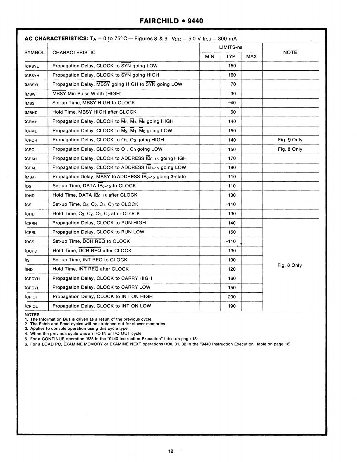
AC CHARACTERISTICS: T A = 0 to 75° C - Figures 8 & 9
Vcc
= 5.0 V
hNJ
= 300 rnA
.
LlMITS-ns
SYMBOL CHARACTERISTIC
NOTE
MIN TYP MAX
tCPSYL
Propagation Delay,
CLOCK
to
SYN going LOW 150
tCPSYH
Propagation Delay,
CLOCK
to
SYN going HIGH 160
tMBSYL
Propagation Delay, MBSY going HIGH
to
SYN going LOW 70
tMBw
MBSY Min Pulse Width (HIGH) 30
tMBs
Set-up Time, MBSY
HIGH
to
CLOCK
-40
tMBHO
Hold Time, MBSY HIGH after
CLOCK
60
tCPMH
Propagation Delay,
CLOCK
to
M2, M1,
Mo
going HIGH 140
tCPML
Propagation Delay,
CLOCK
to
M2, M1,
Mo
going
LOW 150
tCPOH
Propagation Delay,
CLOCK
to
01,
00
going HIGH 140 Fig. 9
Only
tCPOL
Propagation Delay,
CLOCK
to
01,00
going LOW 150 Fig. 8
Only
tCPAH
Propagation Delay,
CLOCK
to
ADDRESS
IBo-15
going HIGH 170
tCPAL
Propagation Delay,
CLOCK
to
ADDRESS
180-15
going LOW 180
tMBAF
Propagation Delay, MBSY
toADDRESS
IBo-15 going 3-state 110
tos
Set-up Time, DATA
180-15
to
CLOCK
-110
tOHO
Hold Time,
DATA
180-15
after
CLOCK
130
tcs
Set-up Time,
C3,
C2, C1,
Co
to
CLOCK
-110
tCHO
Hold Time,
C3, C2, C1,
Co
after
CLOCK
130
tCPRH
Propagation Delay,
CLOCK
to
RUN HIGH 140
tCPRL
Propagation Delay,
CLOCK
to
RUN LOW 150
tocs
Set-up Time, DCH REO to
CLOCK
-110
..
tOCHO
Hold Time, DCH REO after
CLOCK
130
tiS
Set-up Time, INT REO
to
CLOCK
-100
tlHO
Hold
Time.
INT
REO after
CLOCK
120 Fig. 8
Only
tCPCYH
Propagation Delay,
CLOCK
to
CARRY HIGH 160
tCPCYL
Propagation Delay,
CLOCK
to
CARRY LOW 150
tCPIOH
Propagation Delay,
CLOCK
to
INT
ON HIGH 200
tcPIOL
Propagation Delay,
CLOCK
to
INT ON LOW 190
NOTES:
1.
The
Information
Bus
is
driven
as
a result
of
the
previous
cycle.
2.
The
Fetch
and
Read
cycles will
be
stretched out for slower
memories.
3.
Applies
to console operation
using
this cycle
type.
4.
When
the
previous cycle
was
an
110
IN
or
110
OUT
cycle.
5.
For
a
CONTINUE
operation
(#35
in
the
"9440
Instruction Execution"
table
on
page
18),
6.
For
a
LOAD
PC,
EXAMINE
MEMORY
or
EXAMINE
NEXT
operations (#30,31,32
in
the
"9440
Instruction Execution"
table
on
page
18),
12
FAIRCHILD • 9440
CLKOUT
Mo
--------~------~------------_r--~------~_i,~------~----------------
00
==~~~------------~-r------~:~~-------------------
Fig. 8 Fetch Cycle
CLK
OUT
SVN
---~
MO
--------~--------~----------------+-----------~~~~~-------+--------~---------
oo
__________
-+
________
~
RUN, DCH REO, INT REO, CARRY, INT ON
unaffected during this cycle.
Fig. 9 Read Cycle
13
MEMORY @
BUSY
TIME
FAIRCHILD • 9440
-AC CHARACTERISTICS:
TA
= 0 to
75°C-
Figures
10
&
11
Vcc = 5.0
V,
hNJ
= 300 mA
LlMITS-ns
SYMBOL
CHARACTERISTIC
NOTE
MIN TYP
MAX
tCPSYL
Propagation Delay,
CLOCK
to
SYN
going
LOW 150
tCPSYH
Propagation Delay,
CLOCK
to
SYN gOing
HIGH
160
tMBSYL
Propagation Delay, MBSY
going
HIGH
to
SYN
going
LOW 70
tMBW
MBSY
Min
Pulse Width
(HIGH).
30
tMBS
Set-up
Time, MBSY LOW
to
CL,OCK
-40
tMBHD
!;Iold Time, MBSY LOW after
CLOCK
60
tCPMH
Propagation Delay,
CLOCK
to-M2,
M1,
Mo
going
HIGH
140
tCPML
Propagation Delay,
CLOCK
to
1'ii12,
M1,
Mo
going
LOW 150
tCPOH
Propagation Delay,
CLOCK
to
01,
00
going
HIGH
140
tCPOL
Propagation Delay,
CLOCK
to
01,00
going
LOW 150
tCPDH
Propagation Delay,
CLOCK
to
DATA
180-15
going
HIGH
170
tCPDL
Propagation Delay,
CLOCK
to
DATA
180-15
going
LOW
180 Fig. 10
Only
tCPDF
Propagation Delay,
CLOCK
to
DATA
iBo-15
going
3-state 110
tCPAH
Propagation Delay,
CLOCK
to
AODRES$
180-15
going
HIGH
170
tCPAL
Propagation Delay,
CLOCK
to
ADDRESS
180-15
going
LOW 180 Fig.
11
Only
tCPAF
Propagation Delay,
CLOCK
toADDRESS
180-15
going
3-state 160
tcs
Set-up Time,
C3, C2,
C1,
Co
to
CLOCK
-110
tCHD
Hold Time,
C3, C2, C1,
Co
after
CLOCK
130
NOTES:
7.
The
Information
Bus
is
driven
as
a result of the previous cycle.
8.
The
9440
waits for
MBSY
to
go
LOW.
By
holding
MsSv
HIGH,
the
user
may
idle the processor.
9.
For
DEPOSIT
MEMORY
or
DEPOSIT
NEXT
operations
(#33,
34
in-~e
"9440
Instruction Execution" table
on
page
18),
10.
For
EXAMINE
ACCUMULATOR
or-DEPOSIT
ACCUMULATOR
operations (#28:29
in
the
"9440
Instruction Execution" table
on
page
18),
ClK
OUT
SYN
-----f
Ml==::Ea:====t:=====±====±
M2
Mo
==~~~----~------~------~
----+----
oO===:$:~~
__
~
___
~
__
~
01
__________
~~-----'
iiO-15
====::C~===>------------------1----=:"-4::==!!~~=t:========~==:j
CO-3mm~~~~~~~~~~
RUN, DCH
REQ,
iNT'iiEci,
CARRY, INT ON
unaffected during this cycle.
Flg.10
Write Cycle
14
CLKOUT
SYN
MBSY
ii,
ii2
iio
00
0,
iiO~15
CO-3·
RUN
FAIRCHILD.
9440
I~---------------------------------------LDMAR--------------------------------------~
0
CLKOUT
SYN
MBSY
M,
M2
Mo
00
0,
iiO-15
CO-3
RUN
CARRY
2 3
SVN
DCH
REO,
iNTiiEQ.
CARRY,
INT
ON
unaffected
during
this cycle.
Flg.11 Load Memory Address Register Cycle
I~
0
~------------------------I/OOUT------------------------~·~I
PLA
PLA
...-t
CPOF
::1
DATA
OUT
----------------------------------------------------------
INTON
________________________________________________________________________
_
Fig. 12 1/0
Out
Cycle
15
FAIRCHILD-
9440
AC CHARACTERISTICS:
TA
= 0
to
75°C-
Figures
12,13,14,15
Vcc
= 5.0
V,
IINJ
=
300
mA
LlMITS-ns
SYMBOL CHARACTERISTIC
NOTE
MIN TYP MAX
tCPSYL
Propagation Delay,
CLOCK
to
SYN
going
LOW 150
tCPSYH
Propagation Delay,
CLOCK
to
SYN
going
HIGH
160
tCPMH
Propagation Delay,
CLOCK
to
M2, M1,
Mo
going
HIGH
140
tCPML
Propagation Delay,
CLOCK
to
M2, M1,
Mo
going
LOW 150
tCPOH
Propagation Delay,
CLOCK
to
01,
00
going
HIGH
140
tCPOL
Propagation Delay,
CLOCK
to
01,
00
going LOW 150
tCPDH
Propagation Delay,
CLOCK
to
DATA
180-15
going
HIGH 170
tCPDL
Propagation Delay,
CLOCK
to
DATA
180-15
going
LOW 180 Fig. 12
Only
tCPDF
Propagation Delay,
CLOCK
to
DATA
180-15
going
3-state 110
tDS
Set-up Time, DATA
180-15
to
CLOCK
-110
tDHD
Hold
Time, DATA
180-15
after
CLOCK
130 Fig. 13
Only
tcs
Set-up Time,
C3,
C2,
C1,
Co
to
CLOCK
-110
tCHD
Hold Time,
C3, C2, C1,
Co
after
CLOCK
130 Fig. 14
Only
NOTES:
11.
During
DCH,
the
9440 is
not
driving the M lines. An external device can control the memory when a
LOW
is
applied
to
the appropriate M line.
12.
The 9440 floats the
iSo-,s.
The Information Bus is available
to
the
I/O
devices, the Console, and the memory
as
needed.
13.
For
all the CONSOLE operations (#28-35 in the "9440 Instruction Execution" table on page
18),
14.
For CONSOLE operations (#28-34 in the "9440 Instruction Execution" table
on
page
18),
__
-----------I/ON
------------t-I
PLA
CLKOUT
SYN
-----r
M1
----+-~--.
M2
----+----
MO
:::::::::t::::::~""\o~--
---
----
-
---
-
-----
---
Oo
__________
~--------~~--------------------------~-----------
01
__________
~------~
_lcPMH_1
-j
IDS
....
IDHD:!j
iiiO-15
----------...:.:::..-.:::.-=:.--------------------------4(jD~A~TA~INCJ>I------
CO-3
RUN
__________________________
----
________________________________
_
CARRY
______________________________________________________________
___
INTON
______________________________________________________________
___
Fig. 13 1/0
In
Cycle
16
FAIR.CHILD • 9440
I
~'-------------------------WAIT------------------------~·I
o 3
~A
ClK
OUT
SYN
----~
M,
----~~-~
M.
----+----
MO
----+----
OO
__________
~~------~
O,
____________
~--------'
CO-3
___
~-~~~~~
ICPRL~@
RUN
_____________________
~a_
______________________________________________
_
DCH
REQ
CARRY
__________________________________________
~----------------------------
INTON
______________________________________________________________________
__
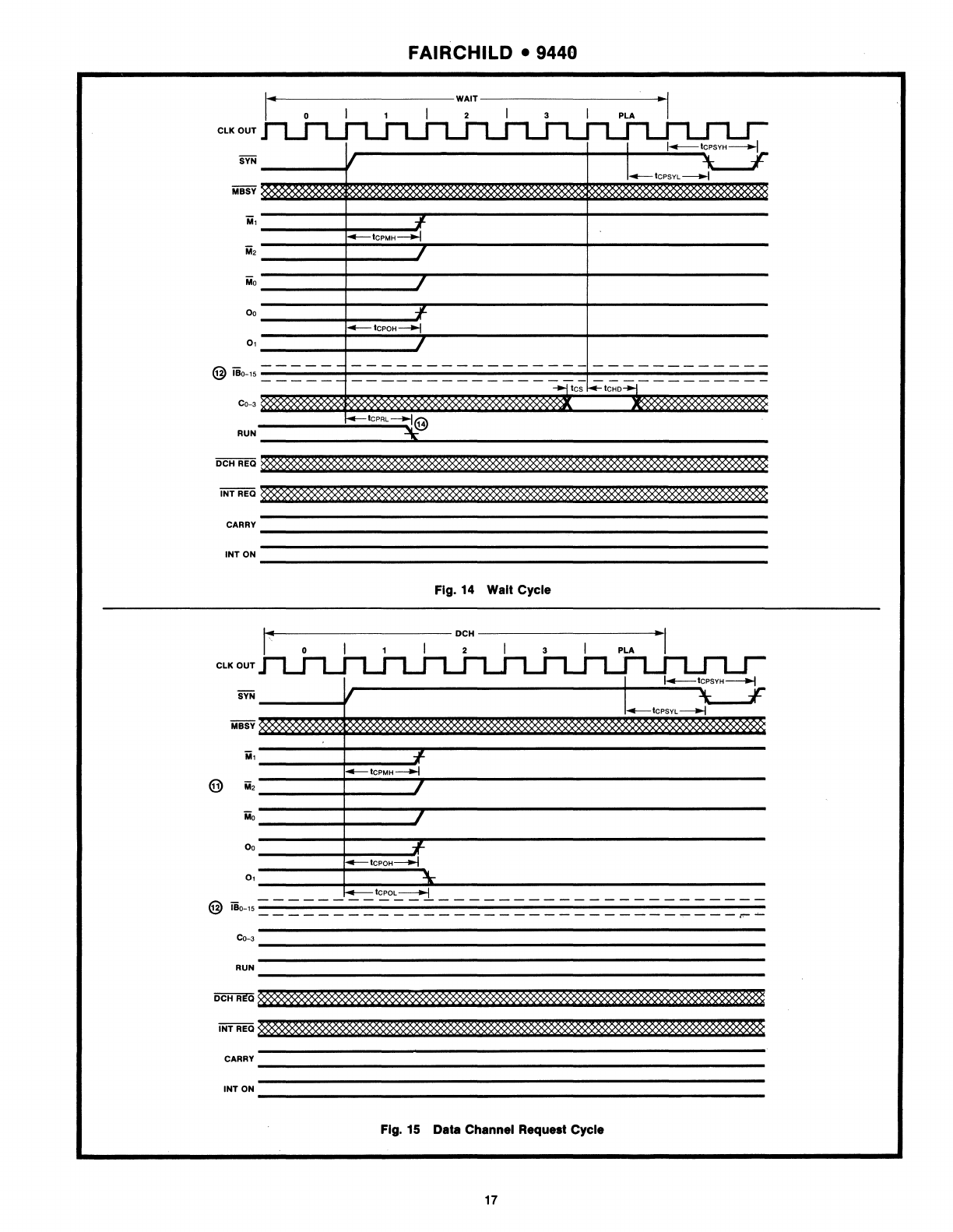
Fig. 14 Walt Cycle
I~
0
~-------------------------DCH-------------------------·~I
PLA
ClK
OUT
SYN
MBSY
M,
@
M.
Mo
00
0,
mO-'5------------------------------------------------------------------------
----------------------------~---~~
~~--------------------------------------------------------------------
RUN
______________________________________________________________________
__
DCHREQ
INT
REQ
CARRY
______________________________________________________________________
__
INTON
______________________________________________________________________
__
Flg.15
Data Channel Request Cycle
17
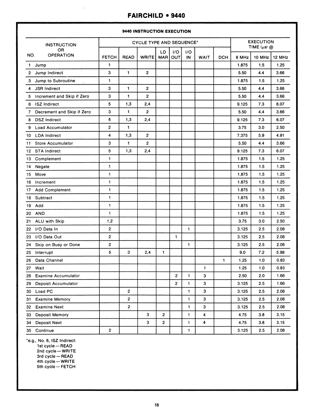
INSTRUCTION
OR
NO. OPERATION
1
Jump
2
Jump
Indirect
3
Jump
to Subroutine
4 JSR Indirect
5 Increment and Skip
if
Zero
6 ISZ Indirect
7 Decrement and Skip
if
Zero
8 DSZ Indirect
9 Load
Accumulator
10 LOA Indirect
11
Store
Accumulator
12
STA Indirect
13 Complement
14 Negate
15 Move
16
Increment
17 Add Complement
18
Subtract
19 Add
20
AND
21
ALU with Skip
22
1/0
Data In
23
1/0
Data
Out
24
Skip on Busy
or
Done
25
Interrupt
26
Data Channel
27
Wait
28
Examine Accumulator
29
Deposit
Accumulator
30
Load PC
31
Examine Memory
32
Examine Next
33
Deposit Memory
34 Deposit Next
35
Continue
"e.g.,
No.6,
ISZ Indirect:
1st
cycle-
READ
2nd
cycle-WRITE
3rd cycle -READ
4th
cycle-WRITE
5th cycle -FETCH
FETCH
1
3
1
3
3
5
3
5
2
4
3
5
1
1
1
1
1
1
1
1
1,2
2
2
2
5
2
FAIRCHILD • 9440
9440 INSTRUCTION EXECUTION
CYCLE TYPE
AND
SEQUENCE" EXECUTION
TIME
(~s)
@
LD
1/0
1/0
READ WRITE MAR
OUT
IN
WAIT
DCH 8 MHz 10 MHz 12 MHz
1.875 1.5 1.25
1 2 5.50 4.4 3.66
1.875 1.5 1.25
1 2 5.50 4.4 3.66
1 2 5.50 4.4 3.66
1,3 2,4 9.125 7.3 6.07
1 2 5.50 4.4 3.66
1,3 2,4 9.125 7.3 6.07
1 3.75 3.0 2.50
1,3 2 7.375 5.9
4.91
1 2 5.50 4.4 3.66
1,3 2,4 9.125
7.3
6.07
1.875 1.5 1.25
1.875 1.5 1.25
1.875 1.5 1.25
1.875 1.5 1.25
1.875 1.5 1.25
1.875 1.5 1.25
1.875 1.5 1.25
1.875 1.5 1.25
3.75 3.0 2.50
1 3.125 2.5 2.08
1 3.125 2.5 2.08
1 3.125
2.5
2.08
3 2,4 1 9.0 7.2 5.98
1 1.25 1.0 0.83
1 1.25 1.0 0.83
2 1 3 2.50 2.0 1.66
2 1 3 3.125
2.5
1.66
2 1 3 3.125
2.5
2.08
2 1 3 3.125 2.5 2.08
2 1 3 3.125
2.5
2.08
3 2 1 4 4.75 3.8 3.15
3 2 1 4 4.75 3.8 3.15
1 3.125 2.5 2.08
18
FAIRCHILD.
9440
9440 SOFTWARE
A performance-matched package
of
software
for
the 9440 is provided to optimize the use of the
9440 in a wide range of applications. The entire software package is called the Fairchild Integrated
Real-time Executive (FIR!:"'>' The initial set
of
available programs consists of:
FIRE-DIAGNOSTICS for testing 9440-based systems
FIRE-LOAD bootstrap and binary loaders
FIRE-1
PACKAGE
FIREBUG interactive assembler, debugger and editor
FIRE-SYMBUG symbolic debugger
FIRE-EDIT text editor
FIRE-BASIC high-level language interactive interperter
Software
to
be
available shortly includes: a macroassembler, a floppy-disk operating system, a
storage module operating system and a FORTRAN compiler.
Cross Macro Assembler, a Cross Linking Loader and a Cross Simulator Debugger are available
for
the FIRE Family
of
processors on a worldwide time sharing basis through the following company.
.-----
.175
(4.445)
.126
(3.175)
Mr. Michael Rooney, President
The Boston Systems Office, Inc.
469 Moody Street
Waltham, Massachusetts
02154
Tel. (617) 894-7800
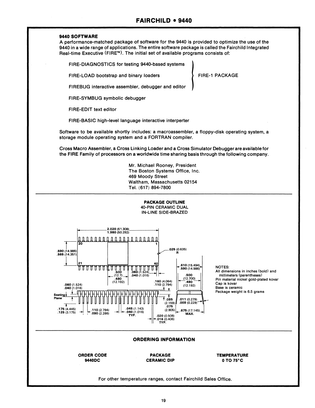
PACKAGE OUTLINE
40-PIN CERAMIC DUAL
IN-LINE SIDE-BRAZED
1--
____
2.020
(5'1.3P8}
____
--.l
1.980
(50.292)
ORDER CODE
9440DC
.025
(0.635)
R
.610
(15,494)
.590
(14,986)
k
·
6OO
rl
(12.700)
.480
(12.192)
::::;:,
t
.085
.011
(0.279)
(2,159)
.009
(0.229)
~~
(20:~5}L.675
(17.145}j
.020
(0.5OB)
MAX
.
.
016
(0.406)
TYP.
ORDERING INFORMATION
PACKAGE
CERAMIC
DIP
NOTES:
All dimensions in inches (bold) and
millimeters (parentheses)
Pin material nickel gold-plated kovar
Cap is kovar
Base is ceramic
Package weight is 6.5 grams
TEMPERATURE
o
TO
75°C
For other temperature ranges, contact Fairchild Sales Office.
19
FAIRCHILD.
9440
I=AIRCHIL.C
Fairchild cannot assume responsibility for use
of
any circuitry described other than circuitry entirely embodied in a Fairchild product.
No
other circuit patent licenses are implied.
Manufactured under one
of
the following U.S. Patents: 2981877. 3015048. 3064167. 3108359. 3117260; other patents pending.
Fairchild reserves the fight to make changes
In
the circuitry or speCifications at any time without notice.
