Description GM8136 Hardware Design User Guide V0.1
User Manual:
Open the PDF directly: View PDF ![]() .
.
Page Count: 41
- GM8136/GM8136S/GM8135S
- Hardware Design
- Revision History
- Table of Contents
- List of Tables
- List of Figures
- Chapter 1 Schematic Design Recommendations
- 1.1 SoC External Circuit Requirements
- 1.2 Design for Typical Interface Circuits of GM8136
- Chapter 2 Recommendation
- Chapter 3 PCB Unused Pin Setting

GM8136/GM8136S/GM8135S
HARDWARE DESIGN
User Guide
Rev.: 0.1
Issue Date: September 2014

REVISION HISTORY
GM8136/GM8136S/GM8135S Hardware Design User Guide
Date
Rev.
From
To
Sep. 2014
0.1
-
Original
Copyright © 2013 Grain Media, Inc.
All Rights Reserved.
Printed in Taiwan 2013
Grain Media and the Grain Media Logo are trademarks of Grain Media, Inc. in Taiwan and/or other countries.
Other company, product and service names may be trademarks or service marks of others.
All information contained in this document is subject to change without notice. The products described in this document are NOT intended for use in
implantation or other life support application where malfunction may result in injury or death to persons. The information contained in this document
does not affect or change Grain Media’s product specification or warranties. Nothing in this document shall operate as an express or implied license
or indemnity under the intellectual property rights of Grain Media or third parties. All information contained in this document was obtained in specific
environments, and is presented as an illustration. The results obtained in other operating environments may vary.
THE INFORMATION CONTAINED IN THIS DOCUMENT IS PROVIDED ON AN “AS IS” BASIS. In no event will Grain Media be liable for damages
arising directly or indirectly from any use of the information contained in this document.
Grain Media, Inc.
5F, No. 5, Li-Hsin Road III, Hsinchu Science Park, Hsinchu City, Taiwan 300, R.O.C.
Grain Media's home page can be found at:
http://www.grain-media.com

GM8136/GM8136S/GM8135S Hardware Design User Guide
www.grain-media.com
i
TABLE OF CONTENTS
Chapter 1 Schematic Design Recommendations .................................................................................. 1
1.1 SoC External Circuit Requirements ........................................................................... 2
1.1.1 Clock Circuit .................................................................................................. 2
1.1.2 Reset Circuit .................................................................................................. 4
1.1.3 JTAG Debug Circuit ....................................................................................... 4
1.1.4 Test Mode Circuit ........................................................................................... 6
1.1.5 Jumper Setting Circuit ................................................................................... 6
1.1.6 Power Supply Circuit for GM8136/GM8136S/GM8135S .............................. 8
1.1.7 Power-On Sequence for GM8136/GM8136S/GM8135S .............................. 9
1.1.8 Ground Plane .............................................................................................. 10
1.2 Design for Typical Interface Circuits of GM8136...................................................... 10
1.2.1 DDR3 Interface ............................................................................................ 10
1.2.2 MAC Port ..................................................................................................... 13
1.2.3 Flash Interface ............................................................................................. 15
1.2.4 I2S Interface ................................................................................................. 16
1.2.5 I2C Interface................................................................................................. 16
1.2.6 USB Interface .............................................................................................. 16
1.2.7 CVBS DAC Interface Design ....................................................................... 17
1.2.8 Audio ADDA Interface Design ..................................................................... 18
1.2.9 Video Input Interface ................................................................................... 20
Chapter 2 Recommendation ................................................................................................................ 21
2.1 Package of GM8136/GM8136S/GM8135S .............................................................. 22
2.2 DDR3-SDRAM Interface Layout .............................................................................. 22
2.3 Ethernet Interface Layout ......................................................................................... 23
2.4 USB Interface Layout ............................................................................................... 23
2.5 1-CH DAC Interface Layout...................................................................................... 25
2.6 MIC in Interface Layout ............................................................................................ 25
2.7 Speaker Interface Layout ......................................................................................... 25
2.8 MIPI/sub-LVDS Interface Layout .............................................................................. 26

GM8136/GM8136S/GM8135S Hardware Design User Guide
www.grain-media.com
ii
2.9 Video Input Port (Capture) ....................................................................................... 26
Chapter 3 PCB Unused Pin Setting ..................................................................................................... 29
3.1 GM8136/GM8136S/GM8135S Unused Pin Setting ................................................. 30

GM8136/GM8136S/GM8135S Hardware Design User Guide
www.grain-media.com
iii
LIST OF TABLES
Table 1-1. Signal Descriptions of JTAG/ICE Connectors ....................................................................... 4
Table 1-2. X_OM Test-mode Pins .......................................................................................................... 6
Table 1-3. Signals for Jumper Setting .................................................................................................... 6
Table 1-4. Lists the capture support format list .................................................................................... 20
Table 3-1. Unused Pin Settings of GM8136/GM8136S/GM8135S ...................................................... 30

GM8136/GM8136S/GM8135S Hardware Design User Guide
www.grain-media.com
iv
LIST OF FIGURES
Figure 1-1. 30MHz Crystal Circuit and Related Component Specifications for
GM8136/GM8136S/GM8135S .............................................................................................. 2
Figure 1-2. 32.768KHz Crystal Circuit and Related Component Specifications for
GM8136/GM8136S/GM8135S .............................................................................................. 3
Figure 1-3. Recommend Connection for GM8136S/GM8135S Reset Circuit ......................................... 4
Figure 1-4. Recommended JTAG/ICE Circuit ......................................................................................... 5
Figure 1-5. PLL Power Circuit for GM8136/GM8136S/GM8135S ........................................................... 9
Figure 1-6. Power-On Sequence for GM8136/GM8136S/GM8135S ...................................................... 9
Figure 1-7. Voltage Divider Circuit for DDR3-SDRAM Chips ................................................................ 11
Figure 1-8. DDR Connection Topology from GM8136 DDRC to DDR3-SDRAMs ................................ 11
Figure 1-9. DDR Differential Clock Connection from GM8136 DDRC to DDR3-SDRAMs ................... 12
Figure 1-10. DDR Address/Control Signal Connection from DDRC to DDR3-SDRAMs ........................ 13
Figure 1-11. Connection from GM8136/GM8136S/GM8135S MAC to 10/100Mbit Ethernet PHY in RMII
Mode ................................................................................................................................... 14
Figure 1-12. SPI Flash Connections ........................................................................................................ 15
Figure 1-13. USB 2.0 OTG for Firmware Upgrade Circuit of GM8136/GM8136S/GM8135S ................. 17
Figure 1-14. CVBS Circuit of GM8136/GM8136S/GM8135S .................................................................. 17
Figure 1-15. CVBS COMP Circuit of GM8136/GM8136S/GM8135S ...................................................... 18
Figure 1-16. MIC Circuit of GM8136/GM8136S/GM8135S .................................................................... 18
Figure 1-17. Speaker Circuit of GM8136/GM8136S/GM8135S ............................................................. 18
Figure 1-18. Audio ADDA Power Circuit of GM8136/GM8136S/GM8135S ........................................... 19
Figure 1-19. Audio ADDA VCM Circuit of GM8136/GM8136S/GM8135S ............................................. 19

GM8136/GM8136S/GM8135S Hardware Design User Guide
www.grain-media.com
2
1.1 SoC External Circuit Requirements
1.1.1 Clock Circuit
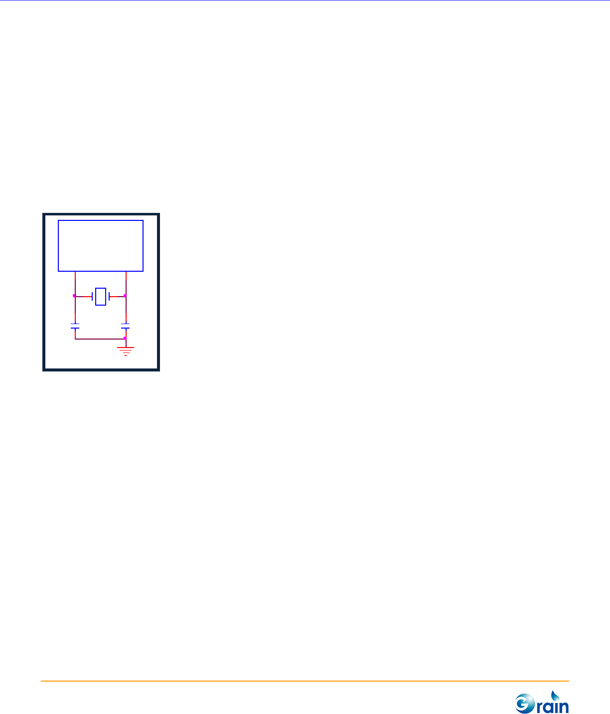
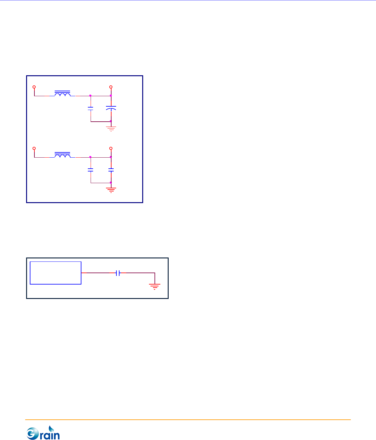
The GM8136/GM8136S/GM8135S system clock is generated by a 30MHz crystal circuit.
1.1.1.1 Main Clock Circuit for GM8136/GM8136S/GM8135S
Figure 1-1 shows the 30MHz crystal circuit and related component specifications for
GM8136/GM8136S/GM8135S.
Y
30MHz
1 2
C
22pF
X_OSCHIN
X_OSCHIO
DGND
C
22pF
Figure 1-1. 30MHz Crystal Circuit and Related Component Specifications for GM8136/GM8136S/GM8135S
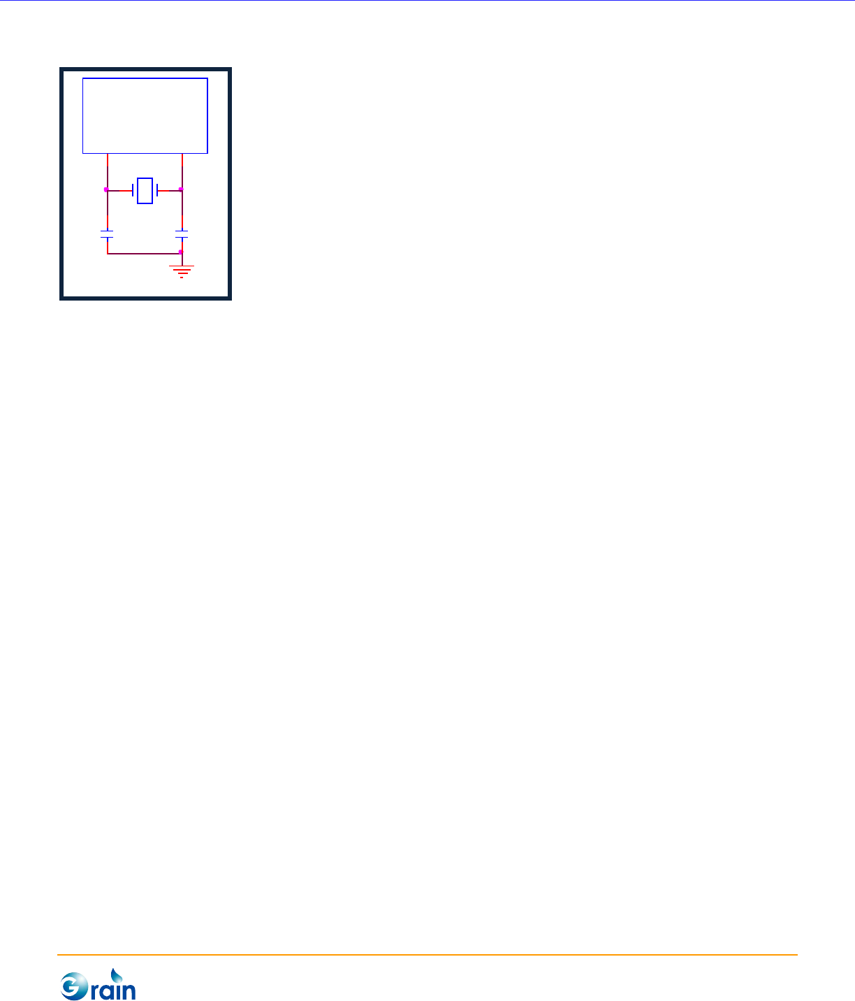
1.1.1.2 RTC Clock Circuit for GM8136/GM8136S/GM8135S
Figure 1-2 shows the 32.768 KHz crystal circuit and related component specifications for
GM8136/GM8136S/GM8135S.
GM8136/GM8136S/GM8135S Hardware Design User Guide
www.grain-media.com
3
Y
32.768KHz
1 2
C
15pF
C
15pF
X_OSCLIN
X_OSCLIO
DGND
Figure 1-2. 32.768KHz Crystal Circuit and Related Component Specifications for GM8136/GM8136S/GM8135S
GM8136/GM8136S/GM8135S Hardware Design User Guide
www.grain-media.com
4
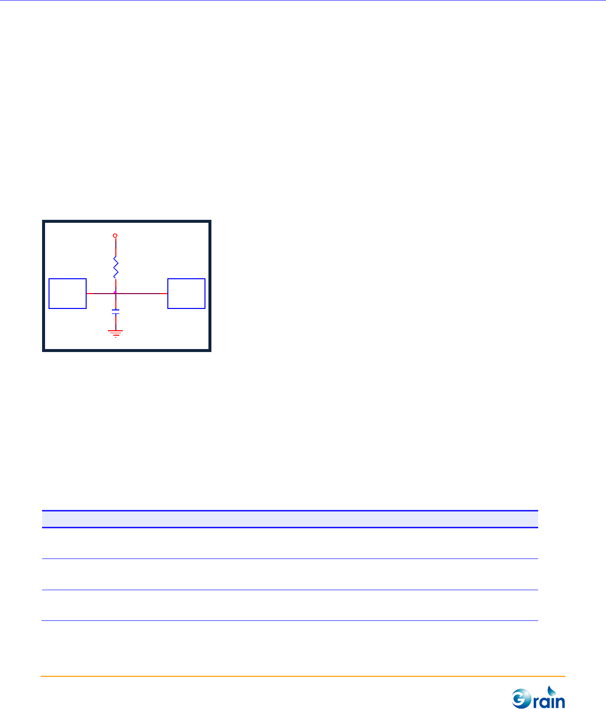
1.1.2 Reset Circuit
X_RSTN is the input reset pin for GM8136S/GM8135S. The pulse width of the reset signal should be longer
than 100ms in general.
An external reset IC for GM8136S/GM8135S is suggested for the reset input circuit. It is recommended
using a 0.1µF capacitor and a 10KΩ pull-up resistor near the GM8136S/GM8135S X_RSTN pin to avoid the
noise coupling and ESD issue.
Figure 1-3 shows the recommended connection for GM8136S/GM8135S reset circuit.
R
10K
X_RSTN
3V3
DGND
Reset IC
RESETN
C
0.1uF
Figure 1-3. Recommend Connection for GM8136S/GM8135S Reset Circuit
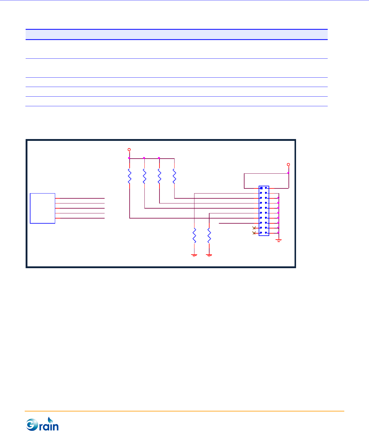
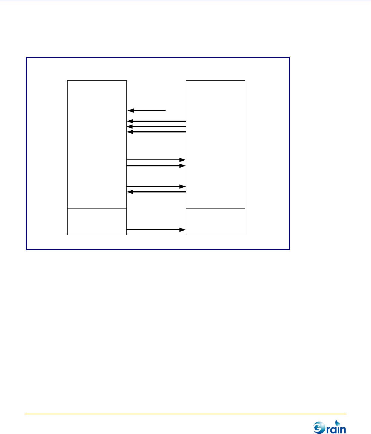
1.1.3 JTAG Debug Circuit
The JTAG interface of GM8136/GM8136S/GM8135S is a standard ARM JTAG interface. Developers can use
the ARM ICE simulator over this interface for debugging. GM8136/GM8136S/GM8135S has one JTAG ICE
interface for the FA7 processor.
Table 1-1. Signal Descriptions of JTAG/ICE Connectors
Signal Name
Description
ICE_TCK
JTAG clock input
Please pull up a 10KΩ resistor on board.
ICE_TMS
JTAG mode select
Please pull up a 10KΩ resistor on board.
ICE_TDO
JTAG data output
Please pull up a 10KΩ resistor on board.
GM8136/GM8136S/GM8135S Hardware Design User Guide
www.grain-media.com
5
Signal Name
Description
ICE_TDI
JTAG data input
Please pull up a 10KΩ resistor on board.
ICE_TRSTn
JTAG reset input and internal pull-down
Please pull down a 1KΩ resistor on board.
SRSTn
System reset for the ICE connector
3V3
3.3V power
GND
Ground
Figure 1-4 shows the recommended JTAG/ICE circuit.
X_TMS
R
10K
X_TCK
X_TDI
X_TDO
X_NTRST X_NTRST
X_TCK
X_TDO
X_TMS
X_TDI
X_NTRST X_TDI
X_TCK
R197
1K
X_TMS
R
10K
X_TDO
DGND
3V3
SRSTn
DGND
R
10K
DGND
3V3
J
2X10P
1
3
5
7
9
11
13
15
17
19
2
4
6
8
10
12
14
16
18
20
R
10K
R
10K
Figure 1-4. Recommended JTAG/ICE Circuit

GM8136/GM8136S/GM8135S Hardware Design User Guide
www.grain-media.com
6
1.1.4 Test Mode Circuit
The X_OM signal can only be used in the test mode. This pin already has an internal pull-down resistor.
For the normal application, this pin must be floating.
Table 1-2. X_OM Test-mode Pins
X_OM
Description
0
Normal Mode
GM8136/GM8136S/GM8135S system must operate in the normal mode.
1
Test Mode
It is used only for the IC test.
1.1.5 Jumper Setting Circuit
The system configuration circuit is used for the hardware initialization. GM8136/GM8136S/GM8135S
jumper setting circuit must be configured before the system is booting up.
Please note that GM8136/GM8136S/GM8135S can be booted from pure 3-byte or pure 4-byte SPI Flash,
SPI NAND, or NAND Flash, but it cannot be booted from the mixed 3-byte/4-byte command SPI Flash.
Table 1-3. Signals for Jumper Setting
Signal Name
Description
X_I2S1_TXD / X_CAP_RST
Jumper setting1/0
0/0: CPU400MHz DDR800MHz(Default)
0/1: CPU810MHz DDR1080MHz
1/0: CPU500MHz DDR1000MHz
0/1: CPU540MHz DDR1080MHz
X_SPI_SCLK
Jumper setting 6
0: Normal (Default)
1: Firmware update
X_SD_CLK
Jumper setting 19
0: Booting from SPI NOR 3byte Flash (Default)
1: Booting from SPI NOR 4byte Flash
X_UART0_TX
Jumper setting 7
0: Booting from SPI Flash (Default)

GM8136/GM8136S/GM8135S Hardware Design User Guide
www.grain-media.com
7
Signal Name
Description
1: Booting from Parallel NAND Flash

GM8136/GM8136S/GM8135S Hardware Design User Guide
www.grain-media.com
8
Signal Name
Description
X_UART2_TX
Jumper setting 8
0: auto PH_En
1: non auto PH_En (Default)
1.1.6 Power Supply Circuit for GM8136/GM8136S/GM8135S
For the detailed requirements of the power supply circuit of GM8136/GM8136S/GM8135S, please refer to
the "DC/AC Characteristics" section of the GM8136/GM8136S/GM8135S data sheet.
1.1.6.1 Core Power for GM8136/GM8136S/GM8135S
For GM8136/GM8136S/GM8135S core power pin (VCC11K), it is suggested using 1.1V digital power. The
supply current of the power chip must be greater than or equal to 1.5A.
1.1.6.2 DDR I/O Power for GM8136/GM8136S/GM8135S
The GM8136/GM8136S/GM8135S DDR power pin, (VCC_DDR), is connected to 1.5V( for GM8136,
GM8136S) or 1.8V(for GM8135S ) digital power.
1.1.6.3 VCC3IO I/O Power for GM8136/GM8136S/GM8135S
The input/output (I/O) power pin, VCC3IO, of GM8136/GM8136S/GM8135S must be connected to 3.3V
digital power.
GM8136/GM8136S/GM8135S Hardware Design User Guide
www.grain-media.com
9
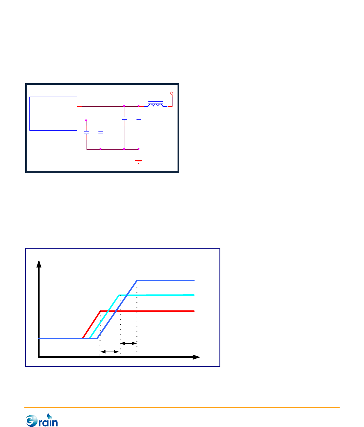
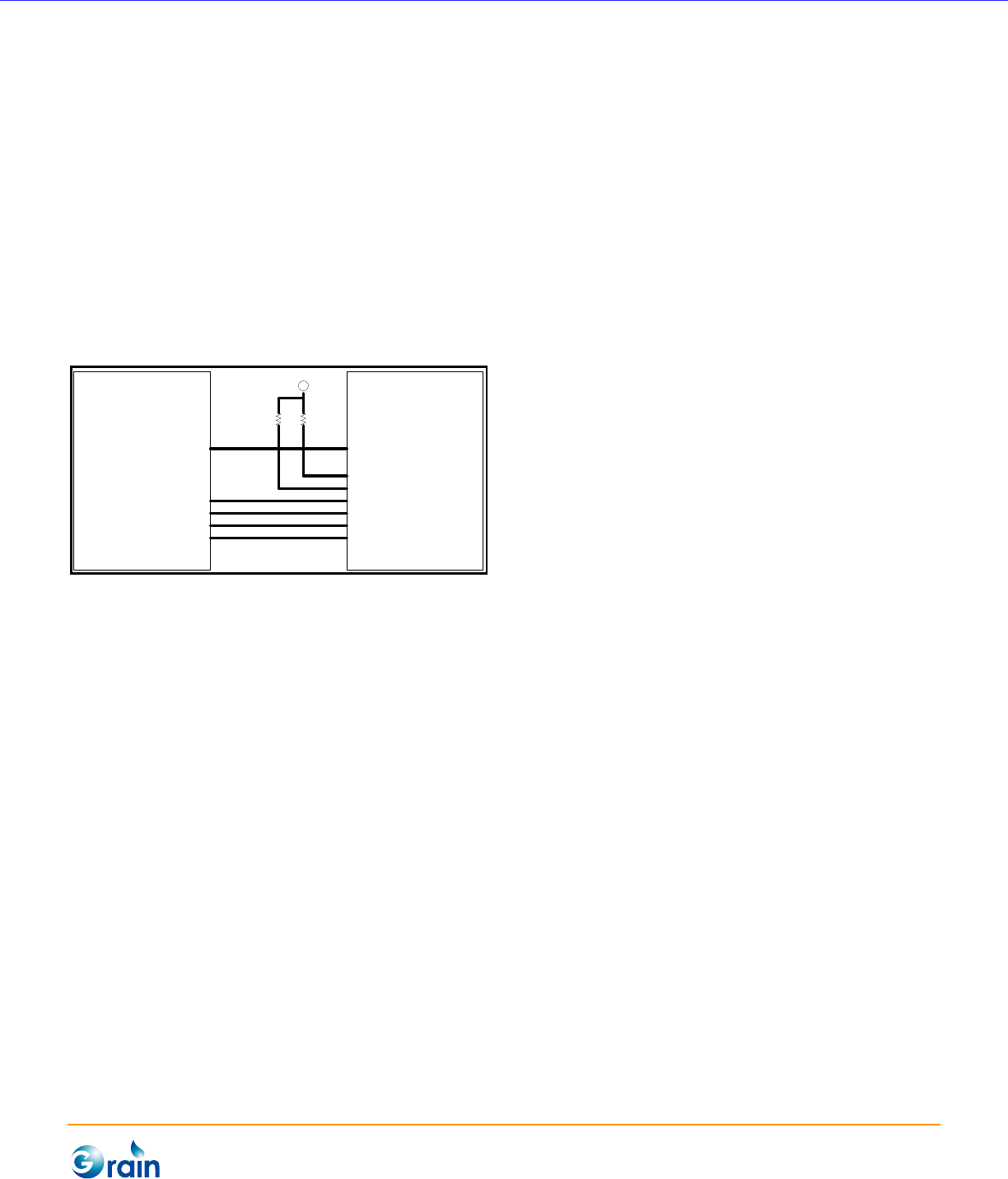
1.1.6.4 PLL Power for GM8136/GM8136/GM8135S
The Phase-Locked Loop (PLL) power is supplied from internal LDO. 3V3 should be inputted to the
VCC33A_REG pin to generate VCC11A_O_REG. The VCC11A_O_REG pin of GM8136/GM8136S/GM8135S
must be connected to one 0.1µF capacitor and one 3.3µF capacitor.
VCC33A_REG
VCC11A_O_REG
C
3.3uF
C
3.3uF
CB
0.1uF
DGND
3V3
CB
0.1uF
FB
.
Figure 1-5. PLL Power Circuit for GM8136/GM8136S/GM8135S
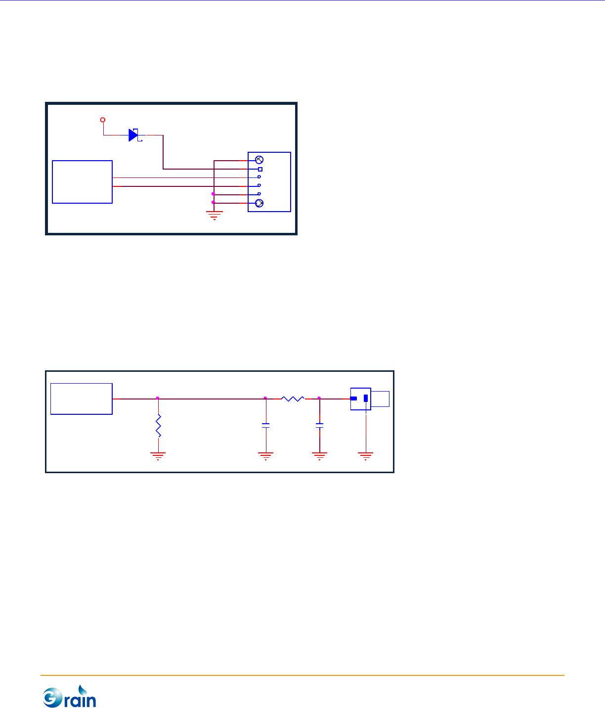
1.1.7 Power-On Sequence for GM8136/GM8136S/GM8135S
1.1V, 1.5V, and 3.3V of GM8136/GM8136S/GM8135S should be powered on in sequence. Please make
sure that 1.1V is powered on ahead of 3.3V.
1.1 V
1.5 V
3.3 V
T ≥ 0
Time
Voltage
T ≥ 0
Figure 1-6. Power-On Sequence for GM8136/GM8136S/GM8135S

GM8136/GM8136S/GM8135S Hardware Design User Guide
www.grain-media.com
10
1.1.8 Ground Plane
A whole ground plane for the system ground plane is suggested.
1.2 Design for Typical Interface Circuits of GM8136
1.2.1 DDR3 Interface
1.2.1.1 Introduction
GM8136 has 16-bit data bus width.
DDR3 interface contains two data groups and a command/address group. Each data group contains eight
data pins, one DQS/DQSB differential pair, and one DQM signal pin.
- Data group1 contains DQ[7:0], DQS0/DQSB0, and DQM0.
- Data group2 contains DQ[15:8], DQS1/DQSB1, and DQM1.
GM8136/GM8136S/GM8135S Hardware Design User Guide
www.grain-media.com
11
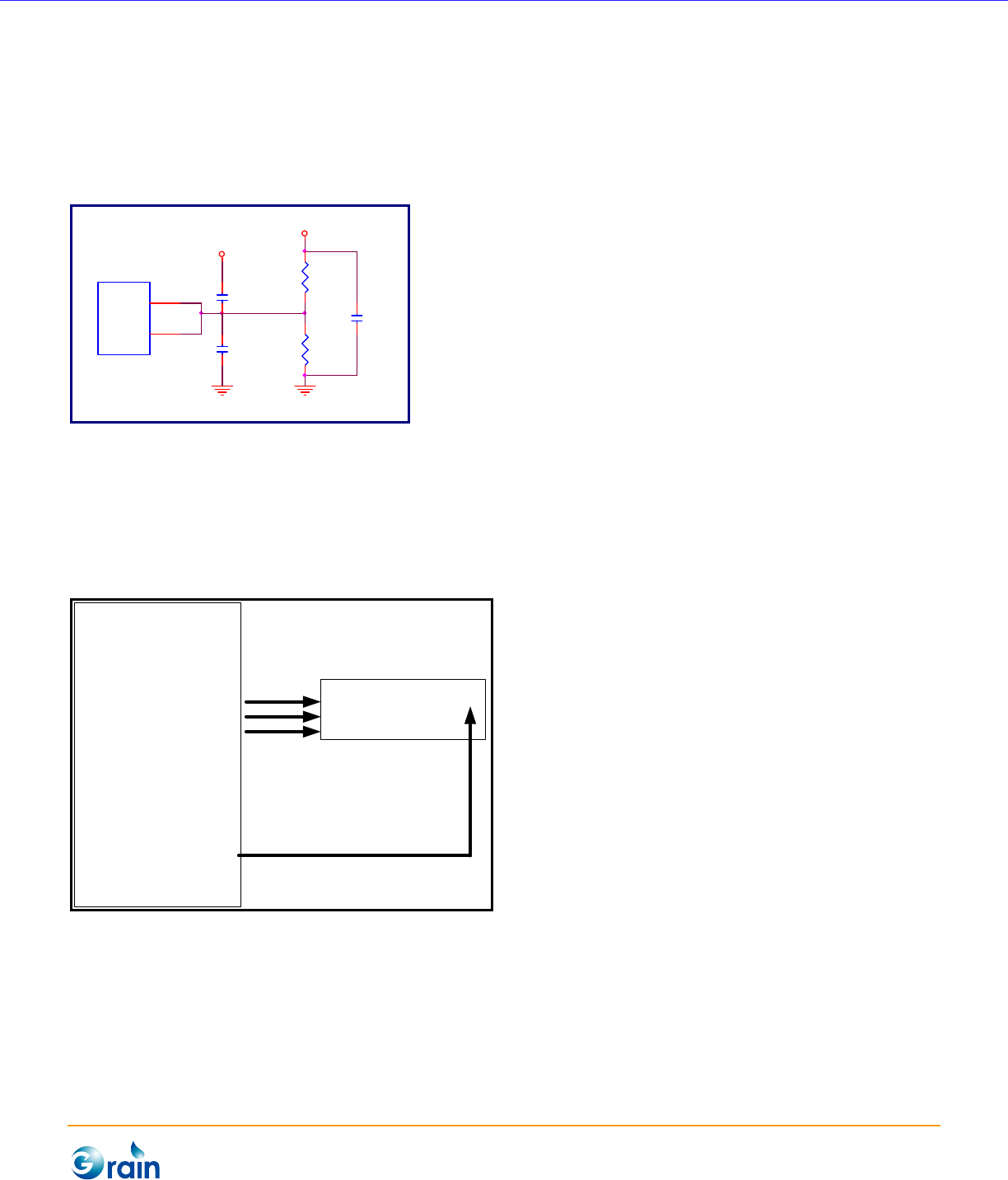
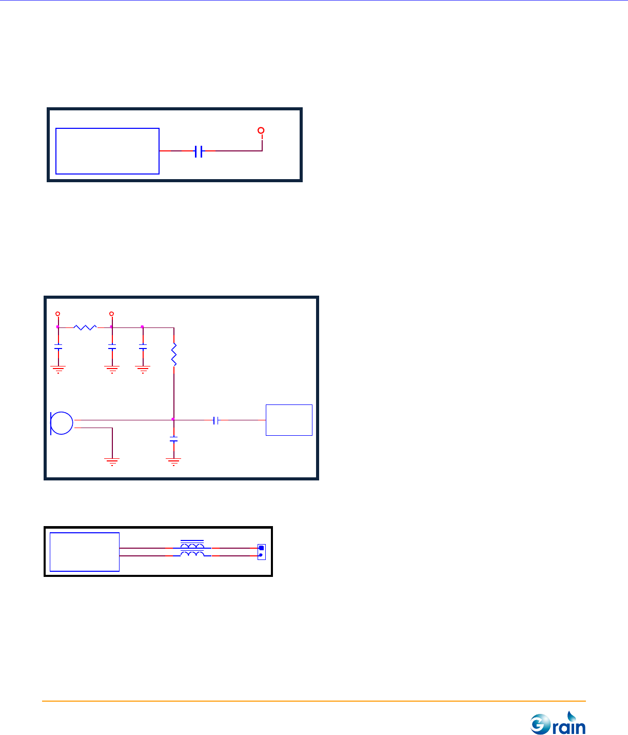
1.2.1.2 External DDR3-SDRAM Vref
The DDR3 SDRAM circuit must use the voltage divider circuit to generate 0.75V Vref reference voltage with
voltage divider resistor of 1% precision for the DDR3-SDRAM chips.
1.5 V
DDR3 SDRAM
Vref
DGND
R
1 kΩ
1.5 V
DGND
C
3.3 µF
R
1 kΩ
C
0.1 µF
DDRx_VREF
C
Vref 1 µF
Figure 1-7. Voltage Divider Circuit for DDR3-SDRAM Chips
1.2.1.3 DDR Topology for GM8136
Figure 1-8 shows the DDR connection topology from GM8136 DDRC to DDR3-SDRAMs.
DDR3 SDRAM
DDRx_DQ[15:0]
DDRx_DQS/DQSn[1:0]
DDRx_DM[1:0]
16bit DDR Controller
DDRx_DQ[15:0]
DDRx_DQS/DQSn[1:0]
DDRx_DM[1:0]
DDRx_CK/CKB
DDRx_CKE
DDRx_RESETn
DDRx_CSn
DDRx_RASn
DDRx_CASn
DDRx_Wen
DDRx_ODT
DDRx_BA[2:0]
CK/CKB,/CKE,/RESETn,/CSn,
/RASn,/CASn/,Wen/,ODT/,BA[2:0]
Figure 1-8. DDR Connection Topology from GM8136 DDRC to DDR3-SDRAMs
GM8136/GM8136S/GM8135S Hardware Design User Guide
www.grain-media.com
12
1.2.1.4 Bidirectional Signals DQ, DQS, and DQM
The point-to-point topology is used for the GM8136 DDRC data input/output (DQ), data strobe
(DQS/DQSB), and data mask (DQM). GM8136 DDRC provides the programmable On-Die Termination
(ODT) resistor. The DDRC registers are used to determine the value of the ODT resistor to be
20/24/30/40/50/60/120Ω or to disable the ODT resistor.
A DDR data group contains eight data pins (DQx), one differential reference clock (DQS/DQSB), and one
data mask pin (DQM). DQ and DQM refer to DQS/DQSB in the same group. The data pins cannot be
switched between different data groups.
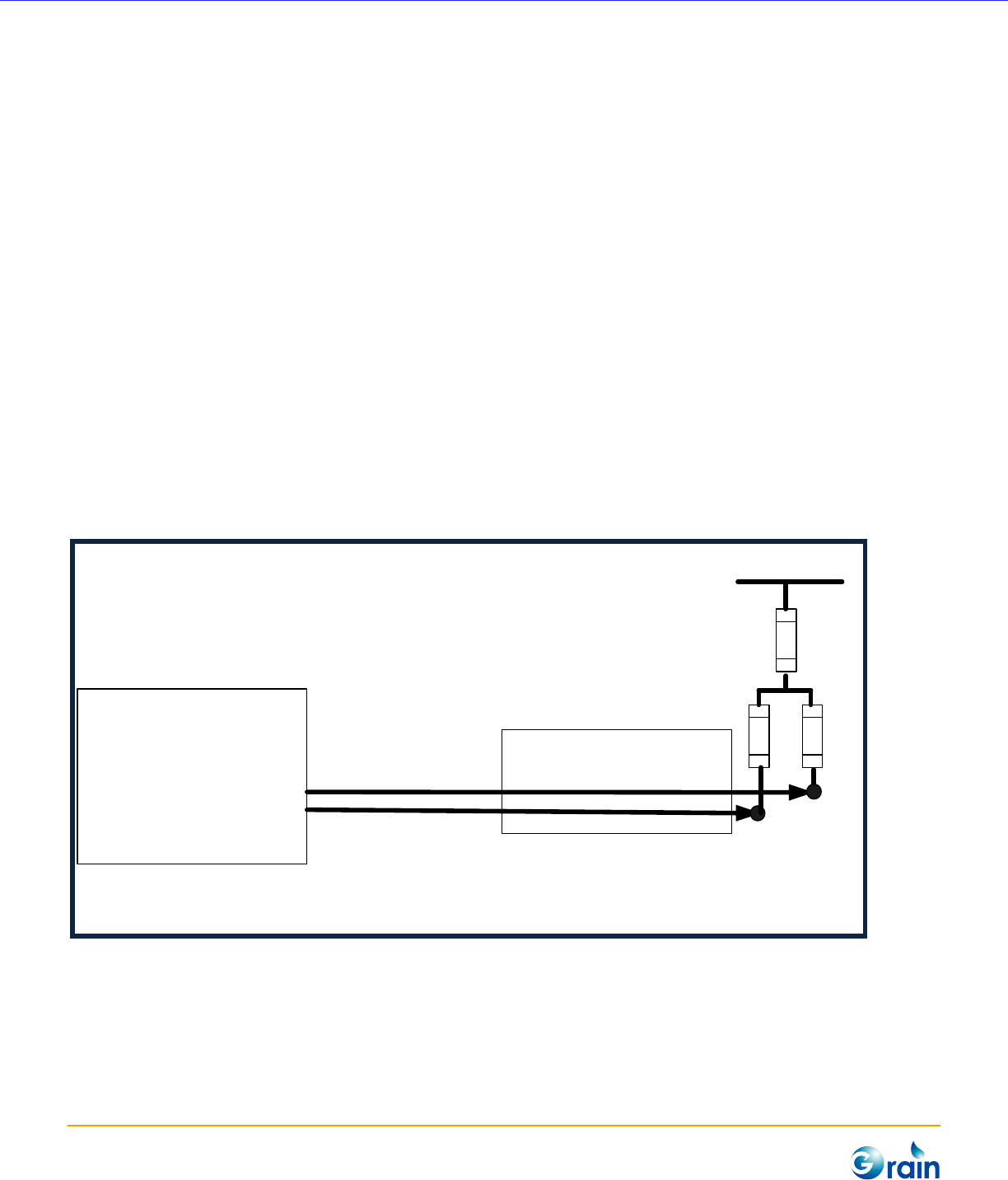
1.2.1.5 Differential Clock
The topology is used for the GM8136 DDRC differential clock (CK/CKB) and is end-terminated. The
differential clock termination resistor is suggested to be 36Ω and the capacitor is suggested to be 0.1µF.
They must be close to the nearest DDR3-SDRAM.
DDR Controller
CK
CKB
DDR3 SDRAM
CK
CKB
Note: VCC15O_DDR = 1.5 V
VCC15O_DDR
RR
C
Figure 1-9. DDR Differential Clock Connection from GM8136 DDRC to DDR3-SDRAMs
GM8136/GM8136S/GM8135S Hardware Design User Guide
www.grain-media.com
13
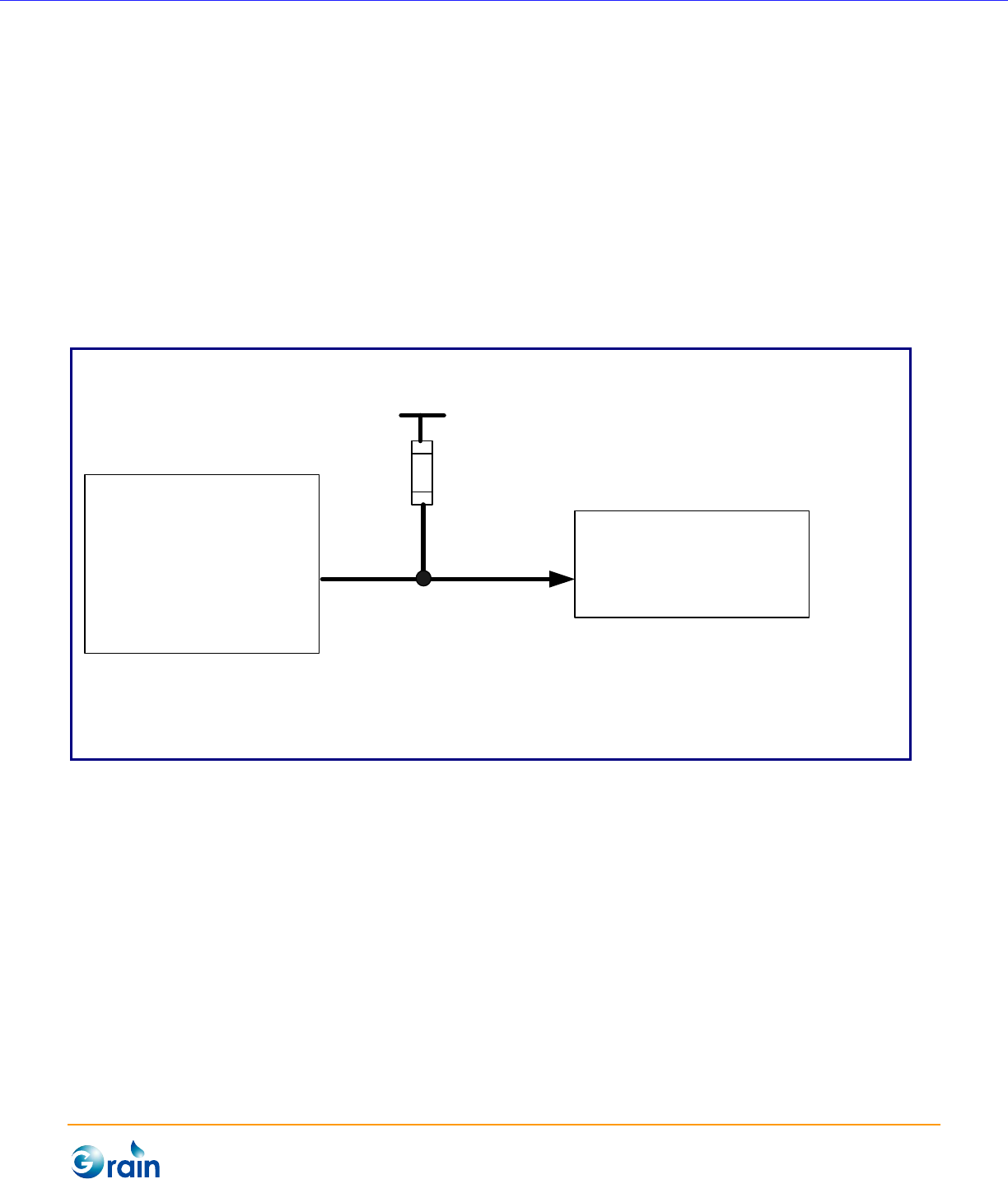
1.2.1.6 Address Signal and Control Signal
The point-to-multipoint topology is used for DDRC address. The control signals are end-terminated to the
termination resistors (VTT). For the address and control signals, the value of the VTT resistors are
suggested to be 39Ω and placed close to the nearest DDR3-SDRAM. The VTT power source has to be from
a DDR VTT termination power regulator.
The address and control signals include ADDR[13:0], CKE, RESETn, CSn, RASn, CASn, WEn, ODT, and
BA[2:0]. The DDRC reset pin, DDRx_RESETn, should be pulled up to VCC15O_DDR.
Address/Control
DDR3 SDRAM
Address/Control
VTT
R
Note: VTT = 0.5 * VCC15O_DDR
Figure 1-10. DDR Address/Control Signal Connection from DDRC to DDR3-SDRAMs
1.2.2 MAC Port
GM8136/GM8136S/GM8135S provides one Media Access Controller (MAC) to support the Reduce Media
Independent Interface (RMII) mode.
GM8136/GM8136S/GM8135S provides a 50MHz clock for 10/100 PHY. Users can connect this clock signal
to the crystal by using the pins of PHY. It is suggested connecting the damping resistors of 22Ω and 33Ω
in series to TXD[2:0], RXD[2:0], TX_EN, RX_ER, and RX_DV, and place the damping resistors near the
GM8136/GM8136S/GM8135S Hardware Design User Guide
www.grain-media.com
14
output pins.
MAC
RMII_PHYLINK
RMII_RX_DV
RMII_RX_ER
RMII_RXD[1:0]
RMII_TX_EN
RMII_TXD[1:0]
RMII_MDC
RMII_MDIO
PHY
RMII_RX_DV
RMII_RX_ER
RMII_RXD[1:0]
RMII_TX_EN
RMII_TXD[1:0]
RMII_MDC
RMII_MDIO
Clock
RMII_CKO
PHY
CLK_REF
50 MHz
RMII Mode
Figure 1-11. Connection from GM8136/GM8136S/GM8135S MAC to 10/100Mbit Ethernet PHY in RMII Mode
GM8136/GM8136S/GM8135S Hardware Design User Guide
www.grain-media.com
15
1.2.3 Flash Interface
GM8136/GM8136S/GM8135S supports the SPI NOR, SPI NAND Flash. GM8136/GM8136S/GM8135S can
be booted from the SPI Flash or NAND Flash. The booting Flash selection is by using the jumper setting.
1.2.3.1 SPI Flash Interface
The GM8136/GM8136S/GM8135S SPI Flash controller supports SPI Flash in pure 3-byte command mode,
pure 4-byte command mode, and SPI NAND mode. GM8136/GM8136S/GM8135S does not support SPI
Flash in mixed 3-byte/4-byte mode.
SPI IF
X_SPI_FS
X_SPI_SCLK
X_SPI_TXD
X_SPI_RXD
SPI flash
CSn
WPn
HOLDn
SCLK
DI
DO
3V3
10K 10K
Figure 1-12. SPI Flash Connections

GM8136/GM8136S/GM8135S Hardware Design User Guide
www.grain-media.com
16
1.2.4 I2S Interface
GM8136/GM8136S/GM8135S provides three I2S interfaces. Some interfaces are used as the
multi-function pins. For details, please refer to the GM8136/GM8136S/GM8135S data sheet.
1.2.5 I2C Interface
GM8136/GM8136S/GM8135S provides an I2C interfaces. The pull-up resistors are required for the
GM8136/GM8136S/GM8135S I2C signals and the pull-up resistor cannot be less than 1.8KΩ. Users are
suggested reserving the end-termination resistors near the I2C devices.
1.2.6 USB Interface
The GM8136/GM8136S/GM8135S provides two USB port, which are the USB 2.0 OTG port and the USB 1.1
device port.
The USB 2.0 OTG port can be used as a firmware upgrade port.
The USB 1.1 device port can be connected to PC for driver setup.
It is recommended adding the Electrostatic Discharge (ESD) protection element in the USB circuit. Please
place the protective components near the USB connector. For the high-speed USB OTG and USB host, the
parasitic capacitors of the protective components must be less than 1pF.
1.2.6.1 USB Power
The VCC33A_OTG pins of GM8136/GM8136S/GM8135S provide the USB port power. Please provide 3.3V
for the VCC33A_OTG power pin.
It is recommended using one 10µ F and three 0.1µ F for the VCC33A_OTG power pins. Please place 0.1µ F
near each VCC33A_OTG power pin.
GM8136/GM8136S/GM8135S Hardware Design User Guide
www.grain-media.com
17
1.2.6.2 USB Firmware Upgrade
The USB 2.0 OTG port can be used to upgrade firmware. Firmware upgrade uses the Grain Media PC tool.
D
2 1
VBUS
D+
D-
GND
CN
USB
1
2
3
4
5
6
DGND
5V
X_OTG_DP
X_OTG_DM
Figure 1-13. USB 2.0 OTG for Firmware Upgrade Circuit of GM8136/GM8136S/GM8135S
1.2.7 CVBS DAC Interface Design
The GM8136/GM8136S/GM8135S provides one video DAC for the Composite Video Broadcast Signal
(CVBS).
Figure 1- shows the CVBS circuit of GM8136/GM8136S/GM8135S.
DGND
G
S
J
RCA
1
2
R
75
C
10pF
DGNDDGND
X_TVE_IOUTA
C
NC(10pF)
DGND
R 0
Figure 1-14. CVBS Circuit of GM8136/GM8136S/GM8135S
Users are suggested using a 75Ω resistor with 1% precision. The usage of EMI/ESD protection components
depends on the customer requirement.
GM8136/GM8136S/GM8135S Hardware Design User Guide
www.grain-media.com
18
1.2.7.1 CVBS DAC COMP
CVBS DAC requires a 0.1µF pull-up capacitor to be connected to the same DAC power source.
CB 0.1uF
X_TVE_COMP
VCC33A_TVE
Figure 1-15. CVBS COMP Circuit of GM8136/GM8136S/GM8135S
1.2.8 Audio ADDA Interface Design
The GM8136/GM8136S/GM8135S chip provides 1CH MIC-in, and speaker out.
R 4.7K
DGND
3V3
C
0.01uF
R
2.2K
C
1uF
MIC
MIC-EM5BPS
C
10uF
DGND
C1uF
DGND
C
NC(220pF)
3V3_MIC
DGND
X_MICIN
DGND
Figure 1-16. MIC Circuit of GM8136/GM8136S/GM8135S
X_SPKOUTN
X_SPKOUTP FB 100M,17Ω
J
1X2P
1
2FB 100M,17Ω
Figure 1-17. Speaker Circuit of GM8136/GM8136S/GM8135S
GM8136/GM8136S/GM8135S Hardware Design User Guide
www.grain-media.com
19
1.2.8.1 Audio ADDA Power
The VCC33A_SPK and VCC33A_AUDIO pins of GM8136/GM8136S/GM8135S provide the Audio ADDA
powers. Please use 3.3V for the VCC33A_SPK and VCC33A_AUDIO power pins.
FB
3V3
DGND
CB
0.1uF
FB9
DGND
CB
0.1uF
3V3
CT
47uF,6.3V
VCC33A_AUDIO
C
10uF
VCC33A_SPK
0.1µF
0.1µF 10µF
47µF, 6.3V
Figure 1-18. Audio ADDA Power Circuit of GM8136/GM8136S/GM8135S
1.2.8.2 Audio ADDA VCM
Audio ADDA requires a 10µF capacitor to be connected to GND.
C10uF
DGND
X_AUDIO_VCM
Figure 1-19. Audio ADDA VCM Circuit of GM8136/GM8136S/GM8135S

GM8136/GM8136S/GM8135S Hardware Design User Guide
www.grain-media.com
20
1.2.9 Video Input Interface
GM8136/GM8136S/GM8135S supports 2-channel capture input interface. Table 1-4 lists the capture
support format list.
Table 1-4. Lists the capture support format list
Bayer
12b
Bayer
10b
Bayer 8b
BT656+
BT656
BT.1120
16b
BT.60
1 16b
Serial IF
Serial IF
+BT656
Bayer_CLK
CLK
CLK
CLK
D656_1_CLK
CLK
CLK
-
D656_0_CLK
Bayer_HS
HS
HS
HS
D656_0_CLK
-
HS
DN0
DN0
Bayer_VS
VS
VS
VS
-
VS
DP0
DP0
Bayer_D11
D11
D9
D7
BT656_1_D7
Y7
Y7
CKN
CKN
Bayer_D10
D10
D8
D6
BT656_1_D6
Y6
Y6
CKP
CKP
Bayer_D9
D9
D7
D5
BT656_1_D5
Y5
Y5
DN1
DN1
Bayer_D8
D8
D6
D4
BT656_1_D4
Y4
Y4
DP1
DP1
Bayer_D7
D7
D5
D3
BT656_1_D3
Y3
Y3
Bayer_D6
D6
D4
D2
BT656_1_D2
Y2
Y2
Bayer_D5
D5
D3
D1
BT656_1_D1
Y1
Y1
Bayer_D4
D4
D2
D0
BT656_1_D0
Y0
Y0
CAP0_D7
D3
D1
-
BT656_0_D7
C7
C7
-
BT656_0_D7
CAP0_D6
D2
D0
-
BT656_0_D6
C6
C6
-
BT656_0_D6
CAP0_D5
D1
-
-
BT656_0_D5
C5
C5
-
BT656_0_D5
CAP0_D4
D0
-
-
BT656_0_D4
C4
C4
-
BT656_0_D4
CAP0_D3
-
-
-
BT656_0_D3
C3
C3
-
BT656_0_D3
CAP0_D2
-
-
-
BT656_0_D2
C2
C2
-
BT656_0_D2
CAP0_D1
-
-
-
BT656_0_D1
C1
C1
-
BT656_0_D1
CAP0_D0
-
-
-
BT656_0_D0
C0
C0
-
BT656_0_D0

GM8136/GM8136S/GM8135S Hardware Design User Guide
www.grain-media.com
21
Chapter 2
Recommendation
This chapter contains the following sections:
2.1 Package of GM8136/GM8136S/GM8135S
2.2 DDR3-SDRAM Interface Layout
2.3 Ethernet Interface Layout
2.4 USB Interface Layout
2.5 1-CH DAC Interface Layout
2.6 MIC in Interface Layout
2.7 Speaker Interface Layout
2.8 MIPI/sub-LVDS Interface Layout
2.9 Video Input Port (Capture)

GM8136/GM8136S/GM8135S Hardware Design User Guide
www.grain-media.com
22
2.1 Package of GM8136/GM8136S/GM8135S
GM8136/GM8136SBGA/GM8135SBGA uses the 12mmx12mm BGA package. The package has 196 pins
and the ball pitch is 0.8mm. Pins of the outer two circles must breakout the top layer. Pins of the three and
four circles must breakout the bottom layer. GM8136SQFP/GM8135SQFP uses 14mmx14mm EPADLQFP
package.
Users are recommended using 4-layer PCB with the following stacks when routing all
GM8136/GM8136S/GM8135S signals:
- Top layer: Signal layer (Component layer)
- GND layer: Ground layer
- Power layer: Power layer
- Top bottom: Signal layer (Component layer)
Each pin has a breakout layout path. Please refer to the Grain Media EVB layout reference breakout
method.
2.2 DDR3-SDRAM Interface Layout
GM8136/GM8136S/GM8135S Double-Data-Rate Controller (DDRC) is a high-speed interface. The trace
length and layout method may affect the DDR controller and DDR chip parameters. Grain Media suggests
customers to follow the Grain Media DDR circuit and layout reference design.
2.2.1.1 Routing
- The DDR signal pins must be routed at a good reference plane, such as the ground plane or power
plane. Users should not route the DDR signal traces across the split reference plane or route the DDR
signal traces near the edge of the reference plane.
- The space between two adjacent DDR signal traces should be at least 2 times ~ 3 times of the width
of the signal trace.
- The spaces between different DDR data groups should be more than 3 times ~ 4 times of the width of
the signal trace.
- All DDR signals should be kept away from the DDR clock signal. The DDR signals should be routed by

GM8136/GM8136S/GM8135S Hardware Design User Guide
www.grain-media.com
23
groups.
- The number of Vias for the DDR signal traces should be as small as possible.
- DDR Vref is sensitive; please keep it away from other signal traces. Users should place a bypass
(Filtering) capacitor near the Vref pin, and keep the Vref trace as wide as possible.
2.2.1.2 Trace Impedance
DDR differential pairs: DQSx/DQSxn and CK/CKn
- The impedance for the single-ended DDR signal is 50Ω.
- The impedance for the differential pair for the DDR signals is 85Ω.
2.3 Ethernet Interface Layout
2.3.1.1 Routing
- The RMII signal pins must be routed at good reference plane, such as the ground plane or power plane.
Users should not route the RMII signal traces across the split reference plane or route the MAC signal
traces near the edge of the reference plane.
- The length mismatch of Ethernet PHY differential pair must be less than 5mils.
2.3.1.2 Trace Impedance
- The impedance of single-ended RMII signals is 50Ω.
- The impedance of differential pair for Ethernet PHY is 100Ω.
2.4 USB Interface Layout
2.4.1.1 Routing
- The USB signal pins must be routed on good ground plane. Users should not route the USB signal
traces across the split reference plane and should not route the USB trace on different routing planes.

GM8136/GM8136S/GM8135S Hardware Design User Guide
www.grain-media.com
24
- Differential pair should be routed with minimum corners. If the corners are required, please use 135°
turns.

GM8136/GM8136S/GM8135S Hardware Design User Guide
www.grain-media.com
25
- The USB signal trace should be routed as short as possible. The length mismatch of differential pair
must be less than 5mils.
- The USB signal should be routed away from clock signals, high-speed signals, and switching noise
sources at least 50mils. The USB signal should be away from other signal trace at least 20mils ~
25mils. Ground shielding for the USB differential pair is better.
2.4.1.2 Trace Impedance
The impedance of the USB differential pair is 90Ω.
2.5 1-CH DAC Interface Layout
1-CH DAC (CVBS) is an analog signal. Please route this signal away from the high-speed signals, clock
signals, and noise source. Ground shielding for the 1-CH DAC trace is preferred. It is preferred to use a
trace width of 2 times ~ 3 times of the 50Ω digital signal trace.
2.6 MIC in Interface Layout
MIC in is an analog signal. Please route this signal away from the high-speed signals, clock signals, and
noise source. Ground shielding for the MIC-in trace is preferred. It is preferred to use a trace width of 2
times ~ 3 times of the 50Ω digital signal trace.
2.7 Speaker Interface Layout
Speaker is an analog signal. Please route this signal away from the high-speed signals, clock signals, and
noise source. Ground shielding for the speaker trace is preferred. It is preferred to use a trace width of 2
times ~ 3 times of the 50Ω digital signal trace.

GM8136/GM8136S/GM8135S Hardware Design User Guide
www.grain-media.com
26
2.8 MIPI/sub-LVDS Interface Layout
2.8.1.1 Routing
- The MIPI/sub-LVDS signal pins must be routed at good ground plane. Users should not route the
MIPI/sub-LVDS signal traces across the split reference plane and should not route the MIPI/sub-LVDS
trace on different routing planes.
- Differential pair should be routed with minimum corners. If the corners are required, please use 135°
turns.
- The MIPI/sub-LVDS signal trace should be routed as short as possible. The length mismatch of
differential pair must be less than 5mils.
- The MIPI/sub-LVDS signal should be routed away from clock signals, high-speed signals, and
switching noise sources at least 50mils. The USB signal should be away from other signal trace at
least 20mils ~ 25mils. Ground shielding for the USB differential pair is better.
2.8.1.2 Trace Impedance
The impedance of the MIPI/sub-LVDS differential pair is 100Ω.
2.9 Video Input Port (Capture)
2.9.1.1 Routing
- The video input port (Capture) signals should be routed at good reference plane. Users should not
route these signals across the split reference plane.
- The space between two adjacent Capture signal traces is at least 2 times ~ 3 times of the width of the
signal trace. The space between the Capture clock trace and the Capture data trace should be at least
3 times ~ 4 times of the width of the signal trace. The space between different Capture group traces
should be at least 3 times ~ 4 times of the width of the signal trace.
- Ground shielding for differential Capture groups is better.

GM8136/GM8136S/GM8135S Hardware Design User Guide
www.grain-media.com
27
2.9.1.2 Trace Impedance
The impedance of the video input port trace is 50Ω.


GM8136/GM8136S/GM8135S Hardware Design User Guide
www.grain-media.com
30
3.1 GM8136/GM8136S/GM8135S Unused Pin Setting
Table 3-1 defines the pull-high/pull-low resistors for the electrical DC level of the unused pin settings of
GM8136/GM8136S/GM8135S.
Table 3-1. Unused Pin Settings of GM8136/GM8136S/GM8135S
Pin Name
Default Type
Unused Setting
Comment
ICE unused pin settings
X_ICE_TRSTn
I, PL
Floating
-
X_ICE_TCK
I, PU
Floating
-
X_ICE_TMS
I, PU
Floating
-
X_ICE_TDO
I, PU
Floating
-
X_ICE_TDI
I, PU
Floating
-
UART0 unused pin settings
X_UART0_SIN
I, PU
Floating
-
X_UART0_SOUT
I, PL
Floating
-
Capture unused pin settings
X_CAP_RST
I, PL
Floating
-
X_CAP_CLKOUT
I, PU
Floating
-
X_BAYER_CLK
I, PU
Floating
-
VCCIO_VCAP
-
Supply with 3.3V voltage
-
VCC11A_MPRX
-
Supply with 1.1V voltage
-
X_MPRX_RBIAS
-
Floating
-
X_Bayer_HS
-
Floating
-
X_Bayer_VS
-
Floating
-
X_Bayer_D11
-
Floating
-
X_Bayer_D10
-
Floating
-
X_Bayer_D9
-
Floating
-
X_Bayer_D8
-
Floating
-
X_Bayer_D7
I, PU
Floating
-
X_Bayer_D6
I, PU
Floating
-
X_Bayer_D5
I, PU
Floating
-
X_Bayer_D4
I, PU
Floating
-
X_CAP0_D7
I, PU
Floating
-

GM8136/GM8136S/GM8135S Hardware Design User Guide
www.grain-media.com
31
Pin Name
Default Type
Unused Setting
Comment
X_CAP0_D6
I, PU
Floating
-
X_CAP0_D5
I, PU
Floating
-
X_CAP0_D4
I, PU
Floating
X_CAP0_D3
I, PU
Floating
-
X_CAP0_D2
I, PU
Floating
-
X_CAP0_D1
I, PU
Floating
-
X_CAP0_D0
I, PU
Floating
-
I2C unused pin settings
X_I2C_SCL
I, PU
Floating
-
X_I2C_SDA
I, PU
Floating
-
Flash Controller unused pin settings
X_SPI_TXD
-
Floating
-
X_SPI_SCLK
-
Floating
-
X_SPI_FS
-
Floating
-
X_SPI_RXD
I, PU
Floating
-
X_SD_D2
I, PU
Floating
-
X_SD_D3
I, PU
Floating
-
X_SD_CMD_RSP
I, PU
Floating
-
X_SD_CLK
I, PL
Floating
-
X_SD_D0
I, PU
Floating
-
X_SD_D1
I, PU
Floating
-
X_SD_CD
I, PU
Floating
-
GPIO unused pin settings
X_GPIO0_28
I, PU
Floating
-
X_GPIO0_29
I, PU
Floating
-
X_GPIO0_30
I, PU
Floating
-
X_GPIO0_31
I, PU
Floating
-
X_GPIO1_19
I, PU
Floating
X_GPIO1_20
I, PU
Floating
X_GPIO1_21
I, PU
Floating
X_GPIO1_22
I, PU
Floating
X_GPIO1_23
I, PU
Floating

GM8136/GM8136S/GM8135S Hardware Design User Guide
www.grain-media.com
32
Pin Name
Default Type
Unused Setting
Comment
UART2 unused pin settings
X_UART2_SIN
I, PU
Floating
-
X_UART2_SOUT
I, PU
Floating
-
PWM unused pin settings
X_PWM0
I, PU
Floating
-
X_PMW1
I, PU
Floating
-
DAC(CVBS) unused pin setting
X_TVE_IOUTA
-
Floating
-
VCC33A_TVE
-
Supply with 3.3V voltage
-
X_TVE_COMP
-
Floating
-
ADC unused pin settings
X_XAIN0
-
Floating
-
X_XAIN1
-
Floating
-
Audio ADDA unused pin setting
VCC33A_SPK
-
Supply with 3.3V voltage
-
X_SPKOUTN
-
Floating
-
X_SPKOUTP
-
Floating
-
X_ADDA_VCM
-
Floating
-
VCC33A_AUDIO
-
Supply with 3.3V voltage
-
X_LMICIN
-
Floating
-
X_LMICIP
-
Floating
-
X_RMICIN
-
Floating
-
X_RMICIP
-
Floating
-
USB unused pin setting
VCC33A_OTG
-
Supply with 3.3V voltage
-
X_OTG_DM
-
Floating
-
X_OTG_DP
-
Floating
-
X_OTG11_DN
-
Floating
X_OTG11_DM
-
Floating
I2S1 unused pin setting
X_I2S1_FS
I, PU
Floating
-
X_I2S1_TXD
I, PL
Floating
-
X_I2S1_RXD
I, PU
Floating
-

GM8136/GM8136S/GM8135S Hardware Design User Guide
www.grain-media.com
33
Pin Name
Default Type
Unused Setting
Comment
X_I2S1_SCLK
I, PU
Floating
-
MAC unused pin settings
X_RMII_RXD[0]
I, PU
Floating
-
X_RMII_RXD[1]
I, PU
Floating
-
X_RMII_RX_ER
I, PU
Floating
-
X_RMII_TXD[0]
I, PU
Floating
-
X_RMII_TXD[1]
I, PU
Floating
-
X_RMII_TX_EN
I, PL
Floating
--
X_RMII_RX_CRS_DV
I, PU
Floating
X_RMII_CKO
I, PU
Floating
-
X_RMII_MDC
I, PU
Floating
-
X_RMII_MDIO
I, PU
Floating
-
X_RMII_PHYLINK
I, PU
Floating
-
X_RMII_RST
I, PL
Floating
-
OSCL (RTC Crystal) unused pin settings
X_OSCLIO
-
Floating
-
X_OSCLIN
-
Floating
-
System unused pin settings
X_OM
I, PL
Floating
-
X_RSTN
I, PU
Floating
-
