HC08LN56GRS, MC68HC08LN56, MC68HC708LN56, General Release Specification Data Sheet HC08LN56GRS
User Manual: HC08LN56GRS
Open the PDF directly: View PDF ![]() .
.
Page Count: 246 [warning: Documents this large are best viewed by clicking the View PDF Link!]
- Revision History
- List of Chapters
- Table of Contents
- Chapter 1 General Description
- 1.1 Introduction
- 1.2 Features
- 1.3 Block Diagram
- 1.4 Pin Assignment
- 1.4.1 Power Supply Pins (VDD3:VDD1-VSS3:VSS1)
- 1.4.2 Oscillator Pins (OSC1 and OSC2)
- 1.4.3 External Reset Pin (RST)
- 1.4.4 External Interrupt Pins (IRQ1/VPP and IRQ2)
- 1.4.5 Clock Ground Pin (CGND)
- 1.4.6 CGM Power Supply Pin (VDDA)
- 1.4.7 External Filter Capacitor Pin (CGMXFC)
- 1.4.8 Port A Input/Output (I/O) Pins (PTA7/KBD7:PTA0/KBD0)
- 1.4.9 Port B I/O Pins (PTB7:PTB4, PTB3/AD3:PTB0/AD0)
- 1.4.10 Port C I/O Pins (PTC6:PTC0)
- 1.4.11 Port D I/O Pins (PTD7/MISO2:PTD0/MISO1)
- 1.4.12 A/D Converter Power Supply Pins and Reference (AVDD, AVSS, VRH)
- 1.4.13 Port E I/O Pins (PTE6/RxD:PTE0/TCH0)
- 1.4.14 Port F I/O Pins (PTF3:PTF0)
- 1.4.15 LCD Back Planes (BP31:BP0)
- 1.4.16 LCD Driver Pins (FP39:FP0)
- 1.5 LCD Driver Power Supply Pins (CPFLT, VLL7:VLL1, VLL, VLLH, and VCP4:VCP1)
- 1.6 Clock Distribution
- Chapter 2 Memory
- Chapter 3 Central Processing Unit (CPU)
- Chapter 4 Clock Generator Module (CGMB)
- 4.1 Introduction
- 4.2 Features
- 4.3 Functional Description
- 4.4 I/O Signals
- 4.4.1 Crystal Amplifier Input Pin (OSC1)
- 4.4.2 Crystal Amplifier Output Pin (OSC2)
- 4.4.3 External Filter Capacitor Pin (CGMXFC)
- 4.4.4 PLL Analog Power Pin (Vdda)
- 4.4.5 PLL Analog Ground Pin (Vssa)
- 4.4.6 Buffered Crystal Clock Output (CGMVOUT)
- 4.4.7 CGMVSEL
- 4.4.8 Oscillator Enable Signal (SIMOSCEN)
- 4.4.9 Crystal Output Frequency Signal (CGMXCLK)
- 4.4.10 CGMB Base Clock Output (CGMOUT)
- 4.4.11 CGMB CPU Interrupt (CGMINT)
- 4.5 CGMB Registers
- 4.6 Interrupts
- 4.7 Special Modes
- 4.8 Acquisition/Lock Time Specifications
- 4.9 Numerical Electrical Specifications
- 4.10 Acquisition/Lock Time Specifications
- Chapter 5 System Integration Module (SIM)
- Chapter 6 Random-Access Memory (RAM)
- Chapter 7 Low-Voltage Inhibit (LVI)
- Chapter 8 External Interrupt Module (IRQ)
- Chapter 9 Keyboard Module (KB)
- Chapter 10 Timer Interface Module (TIM)
- Chapter 11 Serial Peripheral Interface Module (SPI)
- 11.1 Introduction
- 11.2 Features
- 11.3 Pin Name Conventions and I/O Register Addresses
- 11.4 Functional Description
- 11.5 Transmission Formats
- 11.6 Queuing Transmission Data
- 11.7 Error Conditions
- 11.8 Interrupts
- 11.9 Resetting the SPI
- 11.10 Low-Power Modes
- 11.11 SPI During Break Interrupts
- 11.12 I/O Signals
- 11.13 I/O Registers
- Chapter 12 Serial Communications Interface Module (SCI)
- Chapter 13 I/O Ports
- Chapter 14 Analog-to-Digital Converter (ADC)
- Chapter 15 Liquid Crystal Display Driver (LCD)
- Chapter 16 Computer Operating Properly Module (COP)
- Chapter 17 Break Module (BREAK)
- Chapter 18 EPROM/OTPROM
- Chapter 19 Configuration Register (CONFIG)
- Chapter 20 Time Base Module (TBM)
- Chapter 21 Monitor ROM (MON)
- Chapter 22 Preliminary Electrical Specifications
- 22.1 Introduction
- 22.2 Absolute Maximum Ratings
- 22.3 Functional Operating Range
- 22.4 Thermal Characteristics
- 22.5 DC Electrical Characteristics
- 22.6 Control Timing
- 22.7 Serial Peripheral Interface Characteristics
- 22.8 TImer Interface Module Characteristics
- 22.9 Clock Generation Module Electrical Characteristics
- 22.10 Analog-to-Digital Converter (ADC) Characteristics
- 22.11 Memory Characteristics
- 22.12 Liquid Crystal Display Driver Characteristics

M68HC08
Microcontrollers
freescale.com
MC68HC08LN56
MC68HC708LN56
General Release Specification
HC08LN56GRS
Rev. 2.1
09/2005

MC68HC08LN56 • MC68HC708LN56 General Release Specification, Rev. 2.1
Freescale Semiconductor 3
Freescale™ and the Freescale logo are trademarks of Freescale Semiconductor, Inc.
© Freescale Semiconductor, Inc., 2005. All rights reserved.
MC68HC08LN56
MC68HC708LN56
General Release Specification
To provide the most up-to-date information, the revision of our documents on the World Wide Web will be
the most current. Your printed copy may be an earlier revision. To verify you have the latest information
available, refer to:
http://freescale.com
The following revision history table summarizes changes contained in this document. For your
convenience, the page number designators have been linked to the appropriate location.
Revision History
Date Revision
Level Description Page
Number(s)
September,
2005 2.1 Updated to meet Freescale identity guidelines. Throughout

Revision History
MC68HC08LN56 • MC68HC708LN56 General Release Specification, Rev. 2.1
4Freescale Semiconductor

MC68HC08LN56 • MC68HC708LN56 General Release Specification, Rev. 2.1
Freescale Semiconductor 5
List of Chapters
Chapter 1 General Description. . . . . . . . . . . . . . . . . . . . . . . . . . . . . . . . . . . . . . . . . . . . . . . .17
Chapter 2 Memory. . . . . . . . . . . . . . . . . . . . . . . . . . . . . . . . . . . . . . . . . . . . . . . . . . . . . . . . . .25
Chapter 3 Central Processing Unit (CPU) . . . . . . . . . . . . . . . . . . . . . . . . . . . . . . . . . . . . . . .33
Chapter 4 Clock Generator Module (CGMB). . . . . . . . . . . . . . . . . . . . . . . . . . . . . . . . . . . . .39
Chapter 5 System Integration Module (SIM). . . . . . . . . . . . . . . . . . . . . . . . . . . . . . . . . . . . .61
Chapter 6 Random-Access Memory (RAM) . . . . . . . . . . . . . . . . . . . . . . . . . . . . . . . . . . . . .79
Chapter 7 Low-Voltage Inhibit (LVI). . . . . . . . . . . . . . . . . . . . . . . . . . . . . . . . . . . . . . . . . . . .81
Chapter 8 External Interrupt Module (IRQ) . . . . . . . . . . . . . . . . . . . . . . . . . . . . . . . . . . . . . .85
Chapter 9 Keyboard Module (KB) . . . . . . . . . . . . . . . . . . . . . . . . . . . . . . . . . . . . . . . . . . . . .91
Chapter 10 Timer Interface Module (TIM) . . . . . . . . . . . . . . . . . . . . . . . . . . . . . . . . . . . . . . .95
Chapter 11 Serial Peripheral Interface Module (SPI) . . . . . . . . . . . . . . . . . . . . . . . . . . . . .113
Chapter 12 Serial Communications Interface Module (SCI) . . . . . . . . . . . . . . . . . . . . . . .135
Chapter 13 I/O Ports . . . . . . . . . . . . . . . . . . . . . . . . . . . . . . . . . . . . . . . . . . . . . . . . . . . . . . .165
Chapter 14 Analog-to-Digital Converter (ADC). . . . . . . . . . . . . . . . . . . . . . . . . . . . . . . . . .179
Chapter 15 Liquid Crystal Display Driver (LCD). . . . . . . . . . . . . . . . . . . . . . . . . . . . . . . . .185
Chapter 16 Computer Operating Properly Module (COP) . . . . . . . . . . . . . . . . . . . . . . . . .207
Chapter 17 Break Module (BREAK). . . . . . . . . . . . . . . . . . . . . . . . . . . . . . . . . . . . . . . . . . .211
Chapter 18 EPROM/OTPROM. . . . . . . . . . . . . . . . . . . . . . . . . . . . . . . . . . . . . . . . . . . . . . . .215
Chapter 19 Configuration Register (CONFIG) . . . . . . . . . . . . . . . . . . . . . . . . . . . . . . . . . .217
Chapter 20 Time Base Module (TBM) . . . . . . . . . . . . . . . . . . . . . . . . . . . . . . . . . . . . . . . . .219
Chapter 21 Monitor ROM (MON) . . . . . . . . . . . . . . . . . . . . . . . . . . . . . . . . . . . . . . . . . . . . .223
Chapter 22 Preliminary Electrical Specifications. . . . . . . . . . . . . . . . . . . . . . . . . . . . . . . .231

List of Chapters
MC68HC08LN56 • MC68HC708LN56 General Release Specification, Rev. 2.1
6Freescale Semiconductor

MC68HC08LN56 • MC68HC708LN56 General Release Specification, Rev. 2.1
Freescale Semiconductor 7
Table of Contents
Chapter 1
General Description
1.1 Introduction . . . . . . . . . . . . . . . . . . . . . . . . . . . . . . . . . . . . . . . . . . . . . . . . . . . . . . . . . . . . . . . . 17
1.2 Features. . . . . . . . . . . . . . . . . . . . . . . . . . . . . . . . . . . . . . . . . . . . . . . . . . . . . . . . . . . . . . . . . . . 17
1.3 Block Diagram . . . . . . . . . . . . . . . . . . . . . . . . . . . . . . . . . . . . . . . . . . . . . . . . . . . . . . . . . . . . . . 18
1.4 Pin Assignment . . . . . . . . . . . . . . . . . . . . . . . . . . . . . . . . . . . . . . . . . . . . . . . . . . . . . . . . . . . . . 20
1.4.1 Power Supply Pins (VDD3:VDD1–VSS3:VSS1) . . . . . . . . . . . . . . . . . . . . . . . . . . . . . . . . . . . . 21
1.4.2 Oscillator Pins (OSC1 and OSC2) . . . . . . . . . . . . . . . . . . . . . . . . . . . . . . . . . . . . . . . . . . . . 21
1.4.3 External Reset Pin (RST). . . . . . . . . . . . . . . . . . . . . . . . . . . . . . . . . . . . . . . . . . . . . . . . . . . 21
1.4.4 External Interrupt Pins (IRQ1/VPP and IRQ2) . . . . . . . . . . . . . . . . . . . . . . . . . . . . . . . . . . . 21
1.4.5 Clock Ground Pin (CGND) . . . . . . . . . . . . . . . . . . . . . . . . . . . . . . . . . . . . . . . . . . . . . . . . . . 21
1.4.6 CGM Power Supply Pin (VDDA) . . . . . . . . . . . . . . . . . . . . . . . . . . . . . . . . . . . . . . . . . . . . . . 22
1.4.7 External Filter Capacitor Pin (CGMXFC) . . . . . . . . . . . . . . . . . . . . . . . . . . . . . . . . . . . . . . . 22
1.4.8 Port A Input/Output (I/O) Pins (PTA7/KBD7:PTA0/KBD0). . . . . . . . . . . . . . . . . . . . . . . . . . 22
1.4.9 Port B I/O Pins (PTB7:PTB4, PTB3/AD3:PTB0/AD0) . . . . . . . . . . . . . . . . . . . . . . . . . . . . . 22
1.4.10 Port C I/O Pins (PTC6:PTC0) . . . . . . . . . . . . . . . . . . . . . . . . . . . . . . . . . . . . . . . . . . . . . . . 22
1.4.11 Port D I/O Pins (PTD7/MISO2:PTD0/MISO1) . . . . . . . . . . . . . . . . . . . . . . . . . . . . . . . . . . . 22
1.4.12 A/D Converter Power Supply Pins and Reference (AVDD, AVSS, VRH) . . . . . . . . . . . . . . . . 22
1.4.13 Port E I/O Pins (PTE6/RxD:PTE0/TCH0). . . . . . . . . . . . . . . . . . . . . . . . . . . . . . . . . . . . . . . 22
1.4.14 Port F I/O Pins (PTF3:PTF0) . . . . . . . . . . . . . . . . . . . . . . . . . . . . . . . . . . . . . . . . . . . . . . . . 22
1.4.15 LCD Back Planes (BP31:BP0) . . . . . . . . . . . . . . . . . . . . . . . . . . . . . . . . . . . . . . . . . . . . . . . 22
1.4.16 LCD Driver Pins (FP39:FP0) . . . . . . . . . . . . . . . . . . . . . . . . . . . . . . . . . . . . . . . . . . . . . . . . 23
1.5 LCD Driver Power Supply Pins (CPFLT, VLL7:VLL1, VLL, VLLH, and VCP4:VCP1). . . . . . . . . . . . 23
1.6 Clock Distribution . . . . . . . . . . . . . . . . . . . . . . . . . . . . . . . . . . . . . . . . . . . . . . . . . . . . . . . . . . . . 23
Chapter 2
Memory
2.1 Introduction . . . . . . . . . . . . . . . . . . . . . . . . . . . . . . . . . . . . . . . . . . . . . . . . . . . . . . . . . . . . . . . . 25
2.2 I/O Section . . . . . . . . . . . . . . . . . . . . . . . . . . . . . . . . . . . . . . . . . . . . . . . . . . . . . . . . . . . . . . . . . 25
Chapter 3
Central Processing Unit (CPU)
3.1 Introduction . . . . . . . . . . . . . . . . . . . . . . . . . . . . . . . . . . . . . . . . . . . . . . . . . . . . . . . . . . . . . . . . 33
3.2 Features. . . . . . . . . . . . . . . . . . . . . . . . . . . . . . . . . . . . . . . . . . . . . . . . . . . . . . . . . . . . . . . . . . . 33
3.3 CPU Registers . . . . . . . . . . . . . . . . . . . . . . . . . . . . . . . . . . . . . . . . . . . . . . . . . . . . . . . . . . . . . . 33
3.3.1 Accumulator . . . . . . . . . . . . . . . . . . . . . . . . . . . . . . . . . . . . . . . . . . . . . . . . . . . . . . . . . . . . . 34
3.3.2 Index Register . . . . . . . . . . . . . . . . . . . . . . . . . . . . . . . . . . . . . . . . . . . . . . . . . . . . . . . . . . . 34
3.3.3 Stack Pointer . . . . . . . . . . . . . . . . . . . . . . . . . . . . . . . . . . . . . . . . . . . . . . . . . . . . . . . . . . . . 35
3.3.4 Program Counter . . . . . . . . . . . . . . . . . . . . . . . . . . . . . . . . . . . . . . . . . . . . . . . . . . . . . . . . . 35
3.3.5 Condition Code Register . . . . . . . . . . . . . . . . . . . . . . . . . . . . . . . . . . . . . . . . . . . . . . . . . . . 36

Table of Contents
MC68HC08LN56 • MC68HC708LN56 General Release Specification, Rev. 2.1
8Freescale Semiconductor
3.4 Arithmetic/Logic Unit . . . . . . . . . . . . . . . . . . . . . . . . . . . . . . . . . . . . . . . . . . . . . . . . . . . . . . . . . 37
3.5 CPU During Break Interrupts . . . . . . . . . . . . . . . . . . . . . . . . . . . . . . . . . . . . . . . . . . . . . . . . . . . 37
Chapter 4
Clock Generator Module (CGMB)
4.1 Introduction . . . . . . . . . . . . . . . . . . . . . . . . . . . . . . . . . . . . . . . . . . . . . . . . . . . . . . . . . . . . . . . . 39
4.2 Features. . . . . . . . . . . . . . . . . . . . . . . . . . . . . . . . . . . . . . . . . . . . . . . . . . . . . . . . . . . . . . . . . . . 39
4.3 Functional Description . . . . . . . . . . . . . . . . . . . . . . . . . . . . . . . . . . . . . . . . . . . . . . . . . . . . . . . . 39
4.3.1 Crystal Oscillator Circuit. . . . . . . . . . . . . . . . . . . . . . . . . . . . . . . . . . . . . . . . . . . . . . . . . . . . 41
4.3.2 Phase-Locked Loop Circuit (PLL) . . . . . . . . . . . . . . . . . . . . . . . . . . . . . . . . . . . . . . . . . . . . 41
4.3.3 PLL Circuits . . . . . . . . . . . . . . . . . . . . . . . . . . . . . . . . . . . . . . . . . . . . . . . . . . . . . . . . . . . . . 41
4.3.4 Acquisition and Tracking Modes . . . . . . . . . . . . . . . . . . . . . . . . . . . . . . . . . . . . . . . . . . . . . 42
4.3.5 Manual and Automatic PLL Bandwidth Modes . . . . . . . . . . . . . . . . . . . . . . . . . . . . . . . . . . 42
4.3.6 Programming the PLL . . . . . . . . . . . . . . . . . . . . . . . . . . . . . . . . . . . . . . . . . . . . . . . . . . . . . 43
4.3.7 Special Programming Exceptions . . . . . . . . . . . . . . . . . . . . . . . . . . . . . . . . . . . . . . . . . . . . 46
4.3.8 Base Clock Selector Circuit . . . . . . . . . . . . . . . . . . . . . . . . . . . . . . . . . . . . . . . . . . . . . . . . . 46
4.3.9 CGMB External Connections . . . . . . . . . . . . . . . . . . . . . . . . . . . . . . . . . . . . . . . . . . . . . . . . 46
4.4 I/O Signals . . . . . . . . . . . . . . . . . . . . . . . . . . . . . . . . . . . . . . . . . . . . . . . . . . . . . . . . . . . . . . . . . 47
4.4.1 Crystal Amplifier Input Pin (OSC1). . . . . . . . . . . . . . . . . . . . . . . . . . . . . . . . . . . . . . . . . . . . 47
4.4.2 Crystal Amplifier Output Pin (OSC2) . . . . . . . . . . . . . . . . . . . . . . . . . . . . . . . . . . . . . . . . . . 47
4.4.3 External Filter Capacitor Pin (CGMXFC) . . . . . . . . . . . . . . . . . . . . . . . . . . . . . . . . . . . . . . . 47
4.4.4 PLL Analog Power Pin (VDDA) . . . . . . . . . . . . . . . . . . . . . . . . . . . . . . . . . . . . . . . . . . . . . . . 47
4.4.5 PLL Analog Ground Pin (VSSA) . . . . . . . . . . . . . . . . . . . . . . . . . . . . . . . . . . . . . . . . . . . . . . 48
4.4.6 Buffered Crystal Clock Output (CGMVOUT) . . . . . . . . . . . . . . . . . . . . . . . . . . . . . . . . . . . . 48
4.4.7 CGMVSEL . . . . . . . . . . . . . . . . . . . . . . . . . . . . . . . . . . . . . . . . . . . . . . . . . . . . . . . . . . . . . . 48
4.4.8 Oscillator Enable Signal (SIMOSCEN) . . . . . . . . . . . . . . . . . . . . . . . . . . . . . . . . . . . . . . . . 48
4.4.9 Crystal Output Frequency Signal (CGMXCLK) . . . . . . . . . . . . . . . . . . . . . . . . . . . . . . . . . . 48
4.4.10 CGMB Base Clock Output (CGMOUT) . . . . . . . . . . . . . . . . . . . . . . . . . . . . . . . . . . . . . . . . 48
4.4.11 CGMB CPU Interrupt (CGMINT) . . . . . . . . . . . . . . . . . . . . . . . . . . . . . . . . . . . . . . . . . . . . . 48
4.5 CGMB Registers . . . . . . . . . . . . . . . . . . . . . . . . . . . . . . . . . . . . . . . . . . . . . . . . . . . . . . . . . . . . 48
4.5.1 PLL Control Register . . . . . . . . . . . . . . . . . . . . . . . . . . . . . . . . . . . . . . . . . . . . . . . . . . . . . . 49
4.5.2 PLL Bandwidth Control Register . . . . . . . . . . . . . . . . . . . . . . . . . . . . . . . . . . . . . . . . . . . . . 51
4.5.3 PLL Multiplier Select Register High . . . . . . . . . . . . . . . . . . . . . . . . . . . . . . . . . . . . . . . . . . . 52
4.5.4 PLL Multiplier Select Register Low . . . . . . . . . . . . . . . . . . . . . . . . . . . . . . . . . . . . . . . . . . . 52
4.5.5 PLL VCO Range Select Register. . . . . . . . . . . . . . . . . . . . . . . . . . . . . . . . . . . . . . . . . . . . . 53
4.5.6 PLL Reference Divider Select Register . . . . . . . . . . . . . . . . . . . . . . . . . . . . . . . . . . . . . . . . 54
4.6 Interrupts . . . . . . . . . . . . . . . . . . . . . . . . . . . . . . . . . . . . . . . . . . . . . . . . . . . . . . . . . . . . . . . . . . 54
4.7 Special Modes . . . . . . . . . . . . . . . . . . . . . . . . . . . . . . . . . . . . . . . . . . . . . . . . . . . . . . . . . . . . . . 54
4.7.1 Wait Mode . . . . . . . . . . . . . . . . . . . . . . . . . . . . . . . . . . . . . . . . . . . . . . . . . . . . . . . . . . . . . . 55
4.7.2 CGMB During Break Interrupts . . . . . . . . . . . . . . . . . . . . . . . . . . . . . . . . . . . . . . . . . . . . . . 55
4.8 Acquisition/Lock Time Specifications. . . . . . . . . . . . . . . . . . . . . . . . . . . . . . . . . . . . . . . . . . . . . 55
4.8.1 Acquisition/Lock Time Definitions . . . . . . . . . . . . . . . . . . . . . . . . . . . . . . . . . . . . . . . . . . . . 55
4.8.2 Parametric Influences on Reaction Time . . . . . . . . . . . . . . . . . . . . . . . . . . . . . . . . . . . . . . . 56
4.8.3 Choosing a Filter Capacitor . . . . . . . . . . . . . . . . . . . . . . . . . . . . . . . . . . . . . . . . . . . . . . . . . 56
4.8.4 Reaction Time Calculation . . . . . . . . . . . . . . . . . . . . . . . . . . . . . . . . . . . . . . . . . . . . . . . . . . 57
4.9 Numerical Electrical Specifications . . . . . . . . . . . . . . . . . . . . . . . . . . . . . . . . . . . . . . . . . . . . . . 58
4.10 Acquisition/Lock Time Specifications. . . . . . . . . . . . . . . . . . . . . . . . . . . . . . . . . . . . . . . . . . . . . 59

MC68HC08LN56 • MC68HC708LN56 General Release Specification, Rev. 2.1
Freescale Semiconductor 9
Chapter 5
System Integration Module (SIM)
5.1 Introduction . . . . . . . . . . . . . . . . . . . . . . . . . . . . . . . . . . . . . . . . . . . . . . . . . . . . . . . . . . . . . . . . 61
5.2 SIM Bus Clock Control and Generation . . . . . . . . . . . . . . . . . . . . . . . . . . . . . . . . . . . . . . . . . . . 63
5.2.1 Bus Timing . . . . . . . . . . . . . . . . . . . . . . . . . . . . . . . . . . . . . . . . . . . . . . . . . . . . . . . . . . . . . . 63
5.2.2 Clock Start-Up from POR or LVI Reset . . . . . . . . . . . . . . . . . . . . . . . . . . . . . . . . . . . . . . . . 63
5.2.3 Clocks in Stop Mode and Wait Mode. . . . . . . . . . . . . . . . . . . . . . . . . . . . . . . . . . . . . . . . . . 63
5.3 Reset and System Initialization . . . . . . . . . . . . . . . . . . . . . . . . . . . . . . . . . . . . . . . . . . . . . . . . . 64
5.3.1 External Pin Reset . . . . . . . . . . . . . . . . . . . . . . . . . . . . . . . . . . . . . . . . . . . . . . . . . . . . . . . . 64
5.3.2 Active Resets from Internal Sources . . . . . . . . . . . . . . . . . . . . . . . . . . . . . . . . . . . . . . . . . . 64
5.3.2.1 Power-On Reset . . . . . . . . . . . . . . . . . . . . . . . . . . . . . . . . . . . . . . . . . . . . . . . . . . . . . . . . 65
5.3.2.2 Computer Operating Properly (COP) Reset . . . . . . . . . . . . . . . . . . . . . . . . . . . . . . . . . . . 66
5.3.2.3 Illegal Opcode Reset . . . . . . . . . . . . . . . . . . . . . . . . . . . . . . . . . . . . . . . . . . . . . . . . . . . . 66
5.3.2.4 Illegal Address Reset . . . . . . . . . . . . . . . . . . . . . . . . . . . . . . . . . . . . . . . . . . . . . . . . . . . . 66
5.3.2.5 Low-Voltage Inhibit (LVI) Reset . . . . . . . . . . . . . . . . . . . . . . . . . . . . . . . . . . . . . . . . . . . . 67
5.4 SIM Counter. . . . . . . . . . . . . . . . . . . . . . . . . . . . . . . . . . . . . . . . . . . . . . . . . . . . . . . . . . . . . . . . 67
5.4.1 SIM Counter During Power-On Reset . . . . . . . . . . . . . . . . . . . . . . . . . . . . . . . . . . . . . . . . . 67
5.4.2 SIM Counter During Stop Mode Recovery. . . . . . . . . . . . . . . . . . . . . . . . . . . . . . . . . . . . . . 67
5.4.3 SIM Counter and Reset States . . . . . . . . . . . . . . . . . . . . . . . . . . . . . . . . . . . . . . . . . . . . . . 67
5.5 Exception Control. . . . . . . . . . . . . . . . . . . . . . . . . . . . . . . . . . . . . . . . . . . . . . . . . . . . . . . . . . . . 67
5.5.1 Interrupts . . . . . . . . . . . . . . . . . . . . . . . . . . . . . . . . . . . . . . . . . . . . . . . . . . . . . . . . . . . . . . . 68
5.5.1.1 Hardware Interrupts . . . . . . . . . . . . . . . . . . . . . . . . . . . . . . . . . . . . . . . . . . . . . . . . . . . . . 70
5.5.1.2 SWI Instruction . . . . . . . . . . . . . . . . . . . . . . . . . . . . . . . . . . . . . . . . . . . . . . . . . . . . . . . . . 70
5.5.1.3 Interrupt Status Registers. . . . . . . . . . . . . . . . . . . . . . . . . . . . . . . . . . . . . . . . . . . . . . . . . 71
5.5.2 Reset . . . . . . . . . . . . . . . . . . . . . . . . . . . . . . . . . . . . . . . . . . . . . . . . . . . . . . . . . . . . . . . . . . 73
5.5.3 Break Interrupts . . . . . . . . . . . . . . . . . . . . . . . . . . . . . . . . . . . . . . . . . . . . . . . . . . . . . . . . . . 73
5.5.4 Status Flag Protection in Break Mode . . . . . . . . . . . . . . . . . . . . . . . . . . . . . . . . . . . . . . . . . 73
5.6 Low-Power Modes . . . . . . . . . . . . . . . . . . . . . . . . . . . . . . . . . . . . . . . . . . . . . . . . . . . . . . . . . . . 73
5.6.1 Wait Mode . . . . . . . . . . . . . . . . . . . . . . . . . . . . . . . . . . . . . . . . . . . . . . . . . . . . . . . . . . . . . . 73
5.6.2 Stop Mode . . . . . . . . . . . . . . . . . . . . . . . . . . . . . . . . . . . . . . . . . . . . . . . . . . . . . . . . . . . . . . 74
5.7 SIM Registers . . . . . . . . . . . . . . . . . . . . . . . . . . . . . . . . . . . . . . . . . . . . . . . . . . . . . . . . . . . . . . 75
5.7.1 SIM Break Status Register (SBSR) . . . . . . . . . . . . . . . . . . . . . . . . . . . . . . . . . . . . . . . . . . . 76
5.7.2 SIM Reset Status Register (SRSR) . . . . . . . . . . . . . . . . . . . . . . . . . . . . . . . . . . . . . . . . . . . 77
5.7.3 SIM Break Flag Control Register (SBFCR) . . . . . . . . . . . . . . . . . . . . . . . . . . . . . . . . . . . . . 78
Chapter 6
Random-Access Memory (RAM)
6.1 Introduction . . . . . . . . . . . . . . . . . . . . . . . . . . . . . . . . . . . . . . . . . . . . . . . . . . . . . . . . . . . . . . . . 79
6.2 Functional Description . . . . . . . . . . . . . . . . . . . . . . . . . . . . . . . . . . . . . . . . . . . . . . . . . . . . . . . . 79
Chapter 7
Low-Voltage Inhibit (LVI)
7.1 Introduction . . . . . . . . . . . . . . . . . . . . . . . . . . . . . . . . . . . . . . . . . . . . . . . . . . . . . . . . . . . . . . . . 81
7.2 Features. . . . . . . . . . . . . . . . . . . . . . . . . . . . . . . . . . . . . . . . . . . . . . . . . . . . . . . . . . . . . . . . . . . 81
7.3 Functional Description . . . . . . . . . . . . . . . . . . . . . . . . . . . . . . . . . . . . . . . . . . . . . . . . . . . . . . . . 81
7.3.1 Polled LVI Operation . . . . . . . . . . . . . . . . . . . . . . . . . . . . . . . . . . . . . . . . . . . . . . . . . . . . . . 82
7.3.2 Forced Reset Operation. . . . . . . . . . . . . . . . . . . . . . . . . . . . . . . . . . . . . . . . . . . . . . . . . . . . 82

Table of Contents
MC68HC08LN56 • MC68HC708LN56 General Release Specification, Rev. 2.1
10 Freescale Semiconductor
7.4 LVI Status Register (LVISR) . . . . . . . . . . . . . . . . . . . . . . . . . . . . . . . . . . . . . . . . . . . . . . . . . . . 82
7.5 LVI Interrupts . . . . . . . . . . . . . . . . . . . . . . . . . . . . . . . . . . . . . . . . . . . . . . . . . . . . . . . . . . . . . . . 82
7.6 Low-Power Modes . . . . . . . . . . . . . . . . . . . . . . . . . . . . . . . . . . . . . . . . . . . . . . . . . . . . . . . . . . . 82
7.6.1 Wait Mode . . . . . . . . . . . . . . . . . . . . . . . . . . . . . . . . . . . . . . . . . . . . . . . . . . . . . . . . . . . . . . 82
7.6.2 Stop Mode . . . . . . . . . . . . . . . . . . . . . . . . . . . . . . . . . . . . . . . . . . . . . . . . . . . . . . . . . . . . . . 83
Chapter 8
External Interrupt Module (IRQ)
8.1 Introduction . . . . . . . . . . . . . . . . . . . . . . . . . . . . . . . . . . . . . . . . . . . . . . . . . . . . . . . . . . . . . . . . 85
8.2 Features. . . . . . . . . . . . . . . . . . . . . . . . . . . . . . . . . . . . . . . . . . . . . . . . . . . . . . . . . . . . . . . . . . . 85
8.3 Functional Description . . . . . . . . . . . . . . . . . . . . . . . . . . . . . . . . . . . . . . . . . . . . . . . . . . . . . . . . 85
8.3.1 IRQ1/VPP Pin . . . . . . . . . . . . . . . . . . . . . . . . . . . . . . . . . . . . . . . . . . . . . . . . . . . . . . . . . . . . 87
8.3.2 IRQ2 Pin. . . . . . . . . . . . . . . . . . . . . . . . . . . . . . . . . . . . . . . . . . . . . . . . . . . . . . . . . . . . . . . . 87
8.4 IRQ Module During Break Interrupts . . . . . . . . . . . . . . . . . . . . . . . . . . . . . . . . . . . . . . . . . . . . . 88
8.5 IRQ Status and Control Register . . . . . . . . . . . . . . . . . . . . . . . . . . . . . . . . . . . . . . . . . . . . . . . . 88
Chapter 9
Keyboard Module (KB)
9.1 Introduction . . . . . . . . . . . . . . . . . . . . . . . . . . . . . . . . . . . . . . . . . . . . . . . . . . . . . . . . . . . . . . . . 91
9.2 Features. . . . . . . . . . . . . . . . . . . . . . . . . . . . . . . . . . . . . . . . . . . . . . . . . . . . . . . . . . . . . . . . . . . 91
9.3 Functional Description . . . . . . . . . . . . . . . . . . . . . . . . . . . . . . . . . . . . . . . . . . . . . . . . . . . . . . . . 91
9.4 Keyboard Initialization . . . . . . . . . . . . . . . . . . . . . . . . . . . . . . . . . . . . . . . . . . . . . . . . . . . . . . . . 93
9.5 I/O Registers . . . . . . . . . . . . . . . . . . . . . . . . . . . . . . . . . . . . . . . . . . . . . . . . . . . . . . . . . . . . . . . 93
9.5.1 Keyboard Status and Control Register (KBSCR). . . . . . . . . . . . . . . . . . . . . . . . . . . . . . . . . 93
9.5.2 Keyboard Interrupt Enable Register (KBIER). . . . . . . . . . . . . . . . . . . . . . . . . . . . . . . . . . . . 94
9.6 Keyboard Module During Break Interrupts. . . . . . . . . . . . . . . . . . . . . . . . . . . . . . . . . . . . . . . . . 94
Chapter 10
Timer Interface Module (TIM)
10.1 Introduction . . . . . . . . . . . . . . . . . . . . . . . . . . . . . . . . . . . . . . . . . . . . . . . . . . . . . . . . . . . . . . . . 95
10.2 Features. . . . . . . . . . . . . . . . . . . . . . . . . . . . . . . . . . . . . . . . . . . . . . . . . . . . . . . . . . . . . . . . . . . 95
10.3 Functional Description . . . . . . . . . . . . . . . . . . . . . . . . . . . . . . . . . . . . . . . . . . . . . . . . . . . . . . . . 95
10.3.1 TIM Counter Prescaler. . . . . . . . . . . . . . . . . . . . . . . . . . . . . . . . . . . . . . . . . . . . . . . . . . . . . 98
10.3.2 Input Capture . . . . . . . . . . . . . . . . . . . . . . . . . . . . . . . . . . . . . . . . . . . . . . . . . . . . . . . . . . . . 98
10.3.3 Output Compare. . . . . . . . . . . . . . . . . . . . . . . . . . . . . . . . . . . . . . . . . . . . . . . . . . . . . . . . . . 98
10.3.4 Unbuffered Output Compare . . . . . . . . . . . . . . . . . . . . . . . . . . . . . . . . . . . . . . . . . . . . . . . . 98
10.3.5 Buffered Output Compare . . . . . . . . . . . . . . . . . . . . . . . . . . . . . . . . . . . . . . . . . . . . . . . . . . 99
10.3.6 Pulse Width Modulation (PWM) . . . . . . . . . . . . . . . . . . . . . . . . . . . . . . . . . . . . . . . . . . . . . . 99
10.3.7 Unbuffered PWM Signal Generation . . . . . . . . . . . . . . . . . . . . . . . . . . . . . . . . . . . . . . . . . 100
10.3.8 Buffered PWM Signal Generation . . . . . . . . . . . . . . . . . . . . . . . . . . . . . . . . . . . . . . . . . . . 100
10.3.9 PWM Initialization. . . . . . . . . . . . . . . . . . . . . . . . . . . . . . . . . . . . . . . . . . . . . . . . . . . . . . . . 101
10.4 Interrupts . . . . . . . . . . . . . . . . . . . . . . . . . . . . . . . . . . . . . . . . . . . . . . . . . . . . . . . . . . . . . . . . . 102
10.5 Low-Power Modes . . . . . . . . . . . . . . . . . . . . . . . . . . . . . . . . . . . . . . . . . . . . . . . . . . . . . . . . . . 102
10.5.1 Wait Mode . . . . . . . . . . . . . . . . . . . . . . . . . . . . . . . . . . . . . . . . . . . . . . . . . . . . . . . . . . . . . 102
10.5.2 Stop Mode . . . . . . . . . . . . . . . . . . . . . . . . . . . . . . . . . . . . . . . . . . . . . . . . . . . . . . . . . . . . . 103
10.6 TIM During Break Interrupts. . . . . . . . . . . . . . . . . . . . . . . . . . . . . . . . . . . . . . . . . . . . . . . . . . . 103

MC68HC08LN56 • MC68HC708LN56 General Release Specification, Rev. 2.1
Freescale Semiconductor 11
10.7 I/O Signals . . . . . . . . . . . . . . . . . . . . . . . . . . . . . . . . . . . . . . . . . . . . . . . . . . . . . . . . . . . . . . . . 103
10.7.1 TIM Clock Pin (PTE4/TCLK) . . . . . . . . . . . . . . . . . . . . . . . . . . . . . . . . . . . . . . . . . . . . . . . 103
10.7.2 TIM Channel I/O Pins (PTE0/TCH0:PTE3/TCH3) . . . . . . . . . . . . . . . . . . . . . . . . . . . . . . . 103
10.8 I/O Registers . . . . . . . . . . . . . . . . . . . . . . . . . . . . . . . . . . . . . . . . . . . . . . . . . . . . . . . . . . . . . . 104
10.8.1 TIM Status and Control Register (TSC) . . . . . . . . . . . . . . . . . . . . . . . . . . . . . . . . . . . . . . . 104
10.8.2 TIM DMA Select Register (TDMA) . . . . . . . . . . . . . . . . . . . . . . . . . . . . . . . . . . . . . . . . . . . 106
10.8.3 TIM Counter Registers (TCNTH:TCNTL). . . . . . . . . . . . . . . . . . . . . . . . . . . . . . . . . . . . . . 107
10.8.4 TIM Counter Modulo Registers (TMODH:TMODL) . . . . . . . . . . . . . . . . . . . . . . . . . . . . . . 107
10.8.5 TIM Channel Status and Control Registers (TSC0:TSC3). . . . . . . . . . . . . . . . . . . . . . . . . 108
10.8.6 TIM Channel Registers (TCH0H/L:TCH3H/L) . . . . . . . . . . . . . . . . . . . . . . . . . . . . . . . . . . 111
Chapter 11
Serial Peripheral Interface Module (SPI)
11.1 Introduction . . . . . . . . . . . . . . . . . . . . . . . . . . . . . . . . . . . . . . . . . . . . . . . . . . . . . . . . . . . . . . . 113
11.2 Features. . . . . . . . . . . . . . . . . . . . . . . . . . . . . . . . . . . . . . . . . . . . . . . . . . . . . . . . . . . . . . . . . . 113
11.3 Pin Name Conventions and I/O Register Addresses . . . . . . . . . . . . . . . . . . . . . . . . . . . . . . . . 114
11.4 Functional Description . . . . . . . . . . . . . . . . . . . . . . . . . . . . . . . . . . . . . . . . . . . . . . . . . . . . . . . 114
11.4.1 Master Mode . . . . . . . . . . . . . . . . . . . . . . . . . . . . . . . . . . . . . . . . . . . . . . . . . . . . . . . . . . . 116
11.4.2 Slave Mode . . . . . . . . . . . . . . . . . . . . . . . . . . . . . . . . . . . . . . . . . . . . . . . . . . . . . . . . . . . . 116
11.5 Transmission Formats . . . . . . . . . . . . . . . . . . . . . . . . . . . . . . . . . . . . . . . . . . . . . . . . . . . . . . . 117
11.5.1 Clock Phase and Polarity Controls. . . . . . . . . . . . . . . . . . . . . . . . . . . . . . . . . . . . . . . . . . . 117
11.5.2 Transmission Format When CPHA = 0 . . . . . . . . . . . . . . . . . . . . . . . . . . . . . . . . . . . . . . . 117
11.5.3 Transmission Format When CPHA = 1 . . . . . . . . . . . . . . . . . . . . . . . . . . . . . . . . . . . . . . . 118
11.5.4 Transmission Initiation Latency . . . . . . . . . . . . . . . . . . . . . . . . . . . . . . . . . . . . . . . . . . . . . 119
11.6 Queuing Transmission Data . . . . . . . . . . . . . . . . . . . . . . . . . . . . . . . . . . . . . . . . . . . . . . . . . . 119
11.7 Error Conditions . . . . . . . . . . . . . . . . . . . . . . . . . . . . . . . . . . . . . . . . . . . . . . . . . . . . . . . . . . . . 121
11.7.1 Overflow Error . . . . . . . . . . . . . . . . . . . . . . . . . . . . . . . . . . . . . . . . . . . . . . . . . . . . . . . . . . 121
11.7.2 Mode Fault Error . . . . . . . . . . . . . . . . . . . . . . . . . . . . . . . . . . . . . . . . . . . . . . . . . . . . . . . . 124
11.8 Interrupts . . . . . . . . . . . . . . . . . . . . . . . . . . . . . . . . . . . . . . . . . . . . . . . . . . . . . . . . . . . . . . . . . 125
11.9 Resetting the SPI . . . . . . . . . . . . . . . . . . . . . . . . . . . . . . . . . . . . . . . . . . . . . . . . . . . . . . . . . . . 126
11.10 Low-Power Modes . . . . . . . . . . . . . . . . . . . . . . . . . . . . . . . . . . . . . . . . . . . . . . . . . . . . . . . . . . 127
11.10.1 Wait Mode . . . . . . . . . . . . . . . . . . . . . . . . . . . . . . . . . . . . . . . . . . . . . . . . . . . . . . . . . . . . . 127
11.10.2 Stop Mode . . . . . . . . . . . . . . . . . . . . . . . . . . . . . . . . . . . . . . . . . . . . . . . . . . . . . . . . . . . . . 127
11.11 SPI During Break Interrupts . . . . . . . . . . . . . . . . . . . . . . . . . . . . . . . . . . . . . . . . . . . . . . . . . . . 127
11.12 I/O Signals . . . . . . . . . . . . . . . . . . . . . . . . . . . . . . . . . . . . . . . . . . . . . . . . . . . . . . . . . . . . . . . . 128
11.12.1 MISO (Master In/Slave Out). . . . . . . . . . . . . . . . . . . . . . . . . . . . . . . . . . . . . . . . . . . . . . . . 128
11.12.2 MOSI (Master Out/Slave In). . . . . . . . . . . . . . . . . . . . . . . . . . . . . . . . . . . . . . . . . . . . . . . . 128
11.12.3 SPSCK (Serial Clock) . . . . . . . . . . . . . . . . . . . . . . . . . . . . . . . . . . . . . . . . . . . . . . . . . . . . 128
11.12.4 SS (Slave Select). . . . . . . . . . . . . . . . . . . . . . . . . . . . . . . . . . . . . . . . . . . . . . . . . . . . . . . . 129
11.12.5 CGND (Clock Ground) . . . . . . . . . . . . . . . . . . . . . . . . . . . . . . . . . . . . . . . . . . . . . . . . . . . . 130
11.13 I/O Registers . . . . . . . . . . . . . . . . . . . . . . . . . . . . . . . . . . . . . . . . . . . . . . . . . . . . . . . . . . . . . . 130
11.13.1 SPI Control Register . . . . . . . . . . . . . . . . . . . . . . . . . . . . . . . . . . . . . . . . . . . . . . . . . . . . . 130
11.13.2 SPI Status and Control Register . . . . . . . . . . . . . . . . . . . . . . . . . . . . . . . . . . . . . . . . . . . . 131
11.13.3 SPI Data Register . . . . . . . . . . . . . . . . . . . . . . . . . . . . . . . . . . . . . . . . . . . . . . . . . . . . . . . 134

Table of Contents
MC68HC08LN56 • MC68HC708LN56 General Release Specification, Rev. 2.1
12 Freescale Semiconductor
Chapter 12
Serial Communications Interface Module (SCI)
12.1 Introduction . . . . . . . . . . . . . . . . . . . . . . . . . . . . . . . . . . . . . . . . . . . . . . . . . . . . . . . . . . . . . . . 135
12.2 Features. . . . . . . . . . . . . . . . . . . . . . . . . . . . . . . . . . . . . . . . . . . . . . . . . . . . . . . . . . . . . . . . . . 135
12.3 Pin Name Conventions . . . . . . . . . . . . . . . . . . . . . . . . . . . . . . . . . . . . . . . . . . . . . . . . . . . . . . 136
12.4 Functional Description . . . . . . . . . . . . . . . . . . . . . . . . . . . . . . . . . . . . . . . . . . . . . . . . . . . . . . . 136
12.4.1 Data Format . . . . . . . . . . . . . . . . . . . . . . . . . . . . . . . . . . . . . . . . . . . . . . . . . . . . . . . . . . . . 139
12.4.2 Transmitter . . . . . . . . . . . . . . . . . . . . . . . . . . . . . . . . . . . . . . . . . . . . . . . . . . . . . . . . . . . . . 139
12.4.2.1 Character Length . . . . . . . . . . . . . . . . . . . . . . . . . . . . . . . . . . . . . . . . . . . . . . . . . . . . . . 140
12.4.2.2 Character Transmission . . . . . . . . . . . . . . . . . . . . . . . . . . . . . . . . . . . . . . . . . . . . . . . . . 140
12.4.2.3 Break Characters . . . . . . . . . . . . . . . . . . . . . . . . . . . . . . . . . . . . . . . . . . . . . . . . . . . . . . 141
12.4.2.4 Idle Characters . . . . . . . . . . . . . . . . . . . . . . . . . . . . . . . . . . . . . . . . . . . . . . . . . . . . . . . . 141
12.4.2.5 Inversion of Transmitted Output . . . . . . . . . . . . . . . . . . . . . . . . . . . . . . . . . . . . . . . . . . . 142
12.4.2.6 Transmitter Interrupts . . . . . . . . . . . . . . . . . . . . . . . . . . . . . . . . . . . . . . . . . . . . . . . . . . . 142
12.4.3 Receiver . . . . . . . . . . . . . . . . . . . . . . . . . . . . . . . . . . . . . . . . . . . . . . . . . . . . . . . . . . . . . . . 142
12.4.3.1 Character Length . . . . . . . . . . . . . . . . . . . . . . . . . . . . . . . . . . . . . . . . . . . . . . . . . . . . . . 142
12.4.3.2 Character Reception. . . . . . . . . . . . . . . . . . . . . . . . . . . . . . . . . . . . . . . . . . . . . . . . . . . . 142
12.4.3.3 Data Sampling . . . . . . . . . . . . . . . . . . . . . . . . . . . . . . . . . . . . . . . . . . . . . . . . . . . . . . . . 144
12.4.3.4 Framing Errors . . . . . . . . . . . . . . . . . . . . . . . . . . . . . . . . . . . . . . . . . . . . . . . . . . . . . . . . 146
12.4.3.5 Baud Rate Tolerance . . . . . . . . . . . . . . . . . . . . . . . . . . . . . . . . . . . . . . . . . . . . . . . . . . . 146
12.4.3.6 Receiver Wake-Up . . . . . . . . . . . . . . . . . . . . . . . . . . . . . . . . . . . . . . . . . . . . . . . . . . . . . 148
12.4.3.7 Receiver Interrupts . . . . . . . . . . . . . . . . . . . . . . . . . . . . . . . . . . . . . . . . . . . . . . . . . . . . . 149
12.4.3.8 Error Interrupts . . . . . . . . . . . . . . . . . . . . . . . . . . . . . . . . . . . . . . . . . . . . . . . . . . . . . . . . 149
12.4.3.9 Error Flags During DMA Service Requests . . . . . . . . . . . . . . . . . . . . . . . . . . . . . . . . . . 149
12.5 Low-Power Modes . . . . . . . . . . . . . . . . . . . . . . . . . . . . . . . . . . . . . . . . . . . . . . . . . . . . . . . . . . 150
12.5.1 Wait Mode . . . . . . . . . . . . . . . . . . . . . . . . . . . . . . . . . . . . . . . . . . . . . . . . . . . . . . . . . . . . . 150
12.5.2 Stop Mode . . . . . . . . . . . . . . . . . . . . . . . . . . . . . . . . . . . . . . . . . . . . . . . . . . . . . . . . . . . . . 150
12.6 SCI During Break Module Interrupts . . . . . . . . . . . . . . . . . . . . . . . . . . . . . . . . . . . . . . . . . . . . 151
12.7 I/O Signals . . . . . . . . . . . . . . . . . . . . . . . . . . . . . . . . . . . . . . . . . . . . . . . . . . . . . . . . . . . . . . . . 151
12.7.1 PTE5/TxD (Transmit Data). . . . . . . . . . . . . . . . . . . . . . . . . . . . . . . . . . . . . . . . . . . . . . . . . 151
12.7.2 PTE6/RxD (Receive Data) . . . . . . . . . . . . . . . . . . . . . . . . . . . . . . . . . . . . . . . . . . . . . . . . . 151
12.8 I/O Registers . . . . . . . . . . . . . . . . . . . . . . . . . . . . . . . . . . . . . . . . . . . . . . . . . . . . . . . . . . . . . . 151
12.8.1 SCI Control Register 1 (SCC1) . . . . . . . . . . . . . . . . . . . . . . . . . . . . . . . . . . . . . . . . . . . . . 152
12.8.2 SCI Control Register 2 (SCC2) . . . . . . . . . . . . . . . . . . . . . . . . . . . . . . . . . . . . . . . . . . . . . 154
12.8.3 SCI Control Register 3 (SCC3) . . . . . . . . . . . . . . . . . . . . . . . . . . . . . . . . . . . . . . . . . . . . . 156
12.8.4 SCI Status Register 1 (SCS1) . . . . . . . . . . . . . . . . . . . . . . . . . . . . . . . . . . . . . . . . . . . . . . 157
12.8.5 SCI Status Register 2 (SCS2) . . . . . . . . . . . . . . . . . . . . . . . . . . . . . . . . . . . . . . . . . . . . . . 160
12.8.6 SCI Data Register (SCDR). . . . . . . . . . . . . . . . . . . . . . . . . . . . . . . . . . . . . . . . . . . . . . . . . 161
12.8.7 SCI Baud Rate Register (SCBR) . . . . . . . . . . . . . . . . . . . . . . . . . . . . . . . . . . . . . . . . . . . . 161
Chapter 13
I/O Ports
13.1 Introduction . . . . . . . . . . . . . . . . . . . . . . . . . . . . . . . . . . . . . . . . . . . . . . . . . . . . . . . . . . . . . . . 165
13.2 Port A . . . . . . . . . . . . . . . . . . . . . . . . . . . . . . . . . . . . . . . . . . . . . . . . . . . . . . . . . . . . . . . . . . . . 167
13.2.1 Port A Data Register . . . . . . . . . . . . . . . . . . . . . . . . . . . . . . . . . . . . . . . . . . . . . . . . . . . . . 167
13.2.2 Data Direction Register A . . . . . . . . . . . . . . . . . . . . . . . . . . . . . . . . . . . . . . . . . . . . . . . . . 168

MC68HC08LN56 • MC68HC708LN56 General Release Specification, Rev. 2.1
Freescale Semiconductor 13
13.3 Port B . . . . . . . . . . . . . . . . . . . . . . . . . . . . . . . . . . . . . . . . . . . . . . . . . . . . . . . . . . . . . . . . . . . . 169
13.3.1 Port B Data Register . . . . . . . . . . . . . . . . . . . . . . . . . . . . . . . . . . . . . . . . . . . . . . . . . . . . . 169
13.3.2 Data Direction Register B . . . . . . . . . . . . . . . . . . . . . . . . . . . . . . . . . . . . . . . . . . . . . . . . . 170
13.4 Port C. . . . . . . . . . . . . . . . . . . . . . . . . . . . . . . . . . . . . . . . . . . . . . . . . . . . . . . . . . . . . . . . . . . . 171
13.4.1 Port C Data Register . . . . . . . . . . . . . . . . . . . . . . . . . . . . . . . . . . . . . . . . . . . . . . . . . . . . . 171
13.4.2 Data Direction Register C . . . . . . . . . . . . . . . . . . . . . . . . . . . . . . . . . . . . . . . . . . . . . . . . . 171
13.5 Port D. . . . . . . . . . . . . . . . . . . . . . . . . . . . . . . . . . . . . . . . . . . . . . . . . . . . . . . . . . . . . . . . . . . . 173
13.5.1 Port D Data Register . . . . . . . . . . . . . . . . . . . . . . . . . . . . . . . . . . . . . . . . . . . . . . . . . . . . . 173
13.5.2 Data Direction Register D . . . . . . . . . . . . . . . . . . . . . . . . . . . . . . . . . . . . . . . . . . . . . . . . . 174
13.6 Port E . . . . . . . . . . . . . . . . . . . . . . . . . . . . . . . . . . . . . . . . . . . . . . . . . . . . . . . . . . . . . . . . . . . . 175
13.6.1 Port E Data Register . . . . . . . . . . . . . . . . . . . . . . . . . . . . . . . . . . . . . . . . . . . . . . . . . . . . . 175
13.6.2 Data Direction Register E . . . . . . . . . . . . . . . . . . . . . . . . . . . . . . . . . . . . . . . . . . . . . . . . . 176
13.7 Port F . . . . . . . . . . . . . . . . . . . . . . . . . . . . . . . . . . . . . . . . . . . . . . . . . . . . . . . . . . . . . . . . . . . . 177
13.7.1 Port F Data Register . . . . . . . . . . . . . . . . . . . . . . . . . . . . . . . . . . . . . . . . . . . . . . . . . . . . . 177
13.7.2 Data Direction Register F . . . . . . . . . . . . . . . . . . . . . . . . . . . . . . . . . . . . . . . . . . . . . . . . . 177
Chapter 14
Analog-to-Digital Converter (ADC)
14.1 Introduction . . . . . . . . . . . . . . . . . . . . . . . . . . . . . . . . . . . . . . . . . . . . . . . . . . . . . . . . . . . . . . . 179
14.2 Features. . . . . . . . . . . . . . . . . . . . . . . . . . . . . . . . . . . . . . . . . . . . . . . . . . . . . . . . . . . . . . . . . . 179
14.3 Functional Description . . . . . . . . . . . . . . . . . . . . . . . . . . . . . . . . . . . . . . . . . . . . . . . . . . . . . . . 179
14.3.1 ADC Port I/O Pins . . . . . . . . . . . . . . . . . . . . . . . . . . . . . . . . . . . . . . . . . . . . . . . . . . . . . . . 179
14.3.2 Voltage Conversion . . . . . . . . . . . . . . . . . . . . . . . . . . . . . . . . . . . . . . . . . . . . . . . . . . . . . . 180
14.3.3 Conversion Time . . . . . . . . . . . . . . . . . . . . . . . . . . . . . . . . . . . . . . . . . . . . . . . . . . . . . . . . 180
14.3.4 Conversion . . . . . . . . . . . . . . . . . . . . . . . . . . . . . . . . . . . . . . . . . . . . . . . . . . . . . . . . . . . . . 181
14.3.5 Accuracy and Precision . . . . . . . . . . . . . . . . . . . . . . . . . . . . . . . . . . . . . . . . . . . . . . . . . . . 181
14.4 Interrupts . . . . . . . . . . . . . . . . . . . . . . . . . . . . . . . . . . . . . . . . . . . . . . . . . . . . . . . . . . . . . . . . . 181
14.5 Low-Power Modes . . . . . . . . . . . . . . . . . . . . . . . . . . . . . . . . . . . . . . . . . . . . . . . . . . . . . . . . . . 181
14.5.1 Wait mode . . . . . . . . . . . . . . . . . . . . . . . . . . . . . . . . . . . . . . . . . . . . . . . . . . . . . . . . . . . . . 181
14.5.2 Stop Mode . . . . . . . . . . . . . . . . . . . . . . . . . . . . . . . . . . . . . . . . . . . . . . . . . . . . . . . . . . . . . 181
14.6 I/O Signals . . . . . . . . . . . . . . . . . . . . . . . . . . . . . . . . . . . . . . . . . . . . . . . . . . . . . . . . . . . . . . . . 181
14.6.1 ADC Analog Power Pin (AVDD) . . . . . . . . . . . . . . . . . . . . . . . . . . . . . . . . . . . . . . . . . . . . . 181
14.6.2 ADC Analog Ground Pin (AVSS) . . . . . . . . . . . . . . . . . . . . . . . . . . . . . . . . . . . . . . . . . . . . 182
14.6.3 ADC Voltage Reference Pin (VRH). . . . . . . . . . . . . . . . . . . . . . . . . . . . . . . . . . . . . . . . . . . 182
14.6.4 ADC Voltage In (ADVIN) . . . . . . . . . . . . . . . . . . . . . . . . . . . . . . . . . . . . . . . . . . . . . . . . . . 182
14.7 I/O Registers . . . . . . . . . . . . . . . . . . . . . . . . . . . . . . . . . . . . . . . . . . . . . . . . . . . . . . . . . . . . . . 182
14.7.1 ADC Status and Control Register . . . . . . . . . . . . . . . . . . . . . . . . . . . . . . . . . . . . . . . . . . . 182
14.7.2 ADC Data Register. . . . . . . . . . . . . . . . . . . . . . . . . . . . . . . . . . . . . . . . . . . . . . . . . . . . . . . 184
14.7.3 ADC Clock Register . . . . . . . . . . . . . . . . . . . . . . . . . . . . . . . . . . . . . . . . . . . . . . . . . . . . . . 184
Chapter 15
Liquid Crystal Display Driver (LCD)
15.1 Introduction . . . . . . . . . . . . . . . . . . . . . . . . . . . . . . . . . . . . . . . . . . . . . . . . . . . . . . . . . . . . . . . 185
15.2 Features. . . . . . . . . . . . . . . . . . . . . . . . . . . . . . . . . . . . . . . . . . . . . . . . . . . . . . . . . . . . . . . . . . 185
15.3 Functional Description . . . . . . . . . . . . . . . . . . . . . . . . . . . . . . . . . . . . . . . . . . . . . . . . . . . . . . . 185
15.4 LCD RAM. . . . . . . . . . . . . . . . . . . . . . . . . . . . . . . . . . . . . . . . . . . . . . . . . . . . . . . . . . . . . . . . . 186

Table of Contents
MC68HC08LN56 • MC68HC708LN56 General Release Specification, Rev. 2.1
14 Freescale Semiconductor
15.4.1 LCD RAM Organization . . . . . . . . . . . . . . . . . . . . . . . . . . . . . . . . . . . . . . . . . . . . . . . . . . . 187
15.4.2 LCD RAM Memory Map . . . . . . . . . . . . . . . . . . . . . . . . . . . . . . . . . . . . . . . . . . . . . . . . . . . 187
15.5 LCD Operation . . . . . . . . . . . . . . . . . . . . . . . . . . . . . . . . . . . . . . . . . . . . . . . . . . . . . . . . . . . . . 189
15.6 LCD Waveforms. . . . . . . . . . . . . . . . . . . . . . . . . . . . . . . . . . . . . . . . . . . . . . . . . . . . . . . . . . . . 189
15.6.1 Backplane Waveform. . . . . . . . . . . . . . . . . . . . . . . . . . . . . . . . . . . . . . . . . . . . . . . . . . . . . 190
15.6.2 Frontplane Waveform. . . . . . . . . . . . . . . . . . . . . . . . . . . . . . . . . . . . . . . . . . . . . . . . . . . . . 191
15.6.3 Example Segment Waveforms and RMS Values. . . . . . . . . . . . . . . . . . . . . . . . . . . . . . . . 192
15.6.4 RMS Voltages . . . . . . . . . . . . . . . . . . . . . . . . . . . . . . . . . . . . . . . . . . . . . . . . . . . . . . . . . . 197
15.7 LCD Voltage Generation . . . . . . . . . . . . . . . . . . . . . . . . . . . . . . . . . . . . . . . . . . . . . . . . . . . . . 197
15.7.1 LCD Contrast Control. . . . . . . . . . . . . . . . . . . . . . . . . . . . . . . . . . . . . . . . . . . . . . . . . . . . . 197
15.8 LCD Register Programming. . . . . . . . . . . . . . . . . . . . . . . . . . . . . . . . . . . . . . . . . . . . . . . . . . . 199
15.9 Programming the LCD . . . . . . . . . . . . . . . . . . . . . . . . . . . . . . . . . . . . . . . . . . . . . . . . . . . . . . . 200
15.10 LCD Registers . . . . . . . . . . . . . . . . . . . . . . . . . . . . . . . . . . . . . . . . . . . . . . . . . . . . . . . . . . . . . 201
15.10.1 LCD Frontplane Latch Registers (LCDFLx) . . . . . . . . . . . . . . . . . . . . . . . . . . . . . . . . . . . . 202
15.10.2 LCD Control Register . . . . . . . . . . . . . . . . . . . . . . . . . . . . . . . . . . . . . . . . . . . . . . . . . . . . . 203
15.10.3 LCD Contrast Control Register (LCDCCR) . . . . . . . . . . . . . . . . . . . . . . . . . . . . . . . . . . . . 203
15.10.4 LCD Prescaler Divider Register (LCDDIV). . . . . . . . . . . . . . . . . . . . . . . . . . . . . . . . . . . . . 204
15.10.5 LCD Frame Rate Register (LCDFR) . . . . . . . . . . . . . . . . . . . . . . . . . . . . . . . . . . . . . . . . . 204
15.11 Interrupts . . . . . . . . . . . . . . . . . . . . . . . . . . . . . . . . . . . . . . . . . . . . . . . . . . . . . . . . . . . . . . . . . 205
15.12 Low-Power Modes . . . . . . . . . . . . . . . . . . . . . . . . . . . . . . . . . . . . . . . . . . . . . . . . . . . . . . . . . . 205
15.12.1 Wait Mode . . . . . . . . . . . . . . . . . . . . . . . . . . . . . . . . . . . . . . . . . . . . . . . . . . . . . . . . . . . . . 205
15.12.2 Stop Mode . . . . . . . . . . . . . . . . . . . . . . . . . . . . . . . . . . . . . . . . . . . . . . . . . . . . . . . . . . . . . 205
Chapter 16
Computer Operating Properly Module (COP)
16.1 Introduction . . . . . . . . . . . . . . . . . . . . . . . . . . . . . . . . . . . . . . . . . . . . . . . . . . . . . . . . . . . . . . . 207
16.2 Functional Description . . . . . . . . . . . . . . . . . . . . . . . . . . . . . . . . . . . . . . . . . . . . . . . . . . . . . . . 207
16.3 I/O Signals . . . . . . . . . . . . . . . . . . . . . . . . . . . . . . . . . . . . . . . . . . . . . . . . . . . . . . . . . . . . . . . . 208
16.3.1 CGMXCLK . . . . . . . . . . . . . . . . . . . . . . . . . . . . . . . . . . . . . . . . . . . . . . . . . . . . . . . . . . . . . 208
16.3.2 STOP Instruction . . . . . . . . . . . . . . . . . . . . . . . . . . . . . . . . . . . . . . . . . . . . . . . . . . . . . . . . 208
16.3.3 COPCTL Write . . . . . . . . . . . . . . . . . . . . . . . . . . . . . . . . . . . . . . . . . . . . . . . . . . . . . . . . . . 208
16.3.4 Power-On Reset. . . . . . . . . . . . . . . . . . . . . . . . . . . . . . . . . . . . . . . . . . . . . . . . . . . . . . . . . 208
16.3.5 Internal Reset. . . . . . . . . . . . . . . . . . . . . . . . . . . . . . . . . . . . . . . . . . . . . . . . . . . . . . . . . . . 208
16.3.6 Reset Vector Fetch . . . . . . . . . . . . . . . . . . . . . . . . . . . . . . . . . . . . . . . . . . . . . . . . . . . . . . 208
16.3.7 COPD (COP Disable). . . . . . . . . . . . . . . . . . . . . . . . . . . . . . . . . . . . . . . . . . . . . . . . . . . . . 208
16.4 COP Control Register (COPCTL) . . . . . . . . . . . . . . . . . . . . . . . . . . . . . . . . . . . . . . . . . . . . . . 209
16.5 Interrupts . . . . . . . . . . . . . . . . . . . . . . . . . . . . . . . . . . . . . . . . . . . . . . . . . . . . . . . . . . . . . . . . . 209
16.6 Monitor Mode . . . . . . . . . . . . . . . . . . . . . . . . . . . . . . . . . . . . . . . . . . . . . . . . . . . . . . . . . . . . . . 209
16.7 Low-Power Modes . . . . . . . . . . . . . . . . . . . . . . . . . . . . . . . . . . . . . . . . . . . . . . . . . . . . . . . . . . 209
16.7.1 Wait Mode . . . . . . . . . . . . . . . . . . . . . . . . . . . . . . . . . . . . . . . . . . . . . . . . . . . . . . . . . . . . . 209
16.7.2 Stop Mode . . . . . . . . . . . . . . . . . . . . . . . . . . . . . . . . . . . . . . . . . . . . . . . . . . . . . . . . . . . . . 209
16.8 COP Module During Break Interrupts . . . . . . . . . . . . . . . . . . . . . . . . . . . . . . . . . . . . . . . . . . . 209

MC68HC08LN56 • MC68HC708LN56 General Release Specification, Rev. 2.1
Freescale Semiconductor 15
Chapter 17
Break Module (BREAK)
17.1 Introduction . . . . . . . . . . . . . . . . . . . . . . . . . . . . . . . . . . . . . . . . . . . . . . . . . . . . . . . . . . . . . . . 211
17.2 Features. . . . . . . . . . . . . . . . . . . . . . . . . . . . . . . . . . . . . . . . . . . . . . . . . . . . . . . . . . . . . . . . . . 211
17.3 Functional Description . . . . . . . . . . . . . . . . . . . . . . . . . . . . . . . . . . . . . . . . . . . . . . . . . . . . . . . 211
17.3.1 Flag Protection During Break Interrupts. . . . . . . . . . . . . . . . . . . . . . . . . . . . . . . . . . . . . . . 212
17.3.2 CPU During Break Interrupts . . . . . . . . . . . . . . . . . . . . . . . . . . . . . . . . . . . . . . . . . . . . . . . 212
17.3.3 TIM During Break Interrupts. . . . . . . . . . . . . . . . . . . . . . . . . . . . . . . . . . . . . . . . . . . . . . . . 212
17.3.4 COP During Break Interrupts . . . . . . . . . . . . . . . . . . . . . . . . . . . . . . . . . . . . . . . . . . . . . . . 213
17.4 Break Module Registers. . . . . . . . . . . . . . . . . . . . . . . . . . . . . . . . . . . . . . . . . . . . . . . . . . . . . . 213
17.4.1 Break Status and Control Register. . . . . . . . . . . . . . . . . . . . . . . . . . . . . . . . . . . . . . . . . . . 213
17.4.2 Break Address Registers . . . . . . . . . . . . . . . . . . . . . . . . . . . . . . . . . . . . . . . . . . . . . . . . . 214
17.5 Low-Power Modes . . . . . . . . . . . . . . . . . . . . . . . . . . . . . . . . . . . . . . . . . . . . . . . . . . . . . . . . . . 214
17.5.1 Wait Mode . . . . . . . . . . . . . . . . . . . . . . . . . . . . . . . . . . . . . . . . . . . . . . . . . . . . . . . . . . . . . 214
17.5.2 Stop Mode . . . . . . . . . . . . . . . . . . . . . . . . . . . . . . . . . . . . . . . . . . . . . . . . . . . . . . . . . . . . . 214
Chapter 18
EPROM/OTPROM
18.1 Introduction . . . . . . . . . . . . . . . . . . . . . . . . . . . . . . . . . . . . . . . . . . . . . . . . . . . . . . . . . . . . . . . 215
18.2 Functional Description . . . . . . . . . . . . . . . . . . . . . . . . . . . . . . . . . . . . . . . . . . . . . . . . . . . . . . . 215
18.3 EPROM/OTPROM Control Registers (EPMCR1, EPMCR2). . . . . . . . . . . . . . . . . . . . . . . . . . 215
18.4 EPROM/OTPROM Programming . . . . . . . . . . . . . . . . . . . . . . . . . . . . . . . . . . . . . . . . . . . . . . 216
Chapter 19
Configuration Register (CONFIG)
19.1 Introduction . . . . . . . . . . . . . . . . . . . . . . . . . . . . . . . . . . . . . . . . . . . . . . . . . . . . . . . . . . . . . . . 217
19.2 Functional Description . . . . . . . . . . . . . . . . . . . . . . . . . . . . . . . . . . . . . . . . . . . . . . . . . . . . . . . 217
Chapter 20
Time Base Module (TBM)
20.1 Introduction . . . . . . . . . . . . . . . . . . . . . . . . . . . . . . . . . . . . . . . . . . . . . . . . . . . . . . . . . . . . . . . 219
20.2 Features. . . . . . . . . . . . . . . . . . . . . . . . . . . . . . . . . . . . . . . . . . . . . . . . . . . . . . . . . . . . . . . . . . 219
20.3 Functional Description . . . . . . . . . . . . . . . . . . . . . . . . . . . . . . . . . . . . . . . . . . . . . . . . . . . . . . . 219
20.4 Time Base Register Description . . . . . . . . . . . . . . . . . . . . . . . . . . . . . . . . . . . . . . . . . . . . . . . 220
20.5 Interrupts . . . . . . . . . . . . . . . . . . . . . . . . . . . . . . . . . . . . . . . . . . . . . . . . . . . . . . . . . . . . . . . . . 221
20.6 Low-Power Modes . . . . . . . . . . . . . . . . . . . . . . . . . . . . . . . . . . . . . . . . . . . . . . . . . . . . . . . . . . 221
20.6.1 Wait Mode . . . . . . . . . . . . . . . . . . . . . . . . . . . . . . . . . . . . . . . . . . . . . . . . . . . . . . . . . . . . . 221
20.6.2 Stop Mode . . . . . . . . . . . . . . . . . . . . . . . . . . . . . . . . . . . . . . . . . . . . . . . . . . . . . . . . . . . . . 221
Chapter 21
Monitor ROM (MON)
21.1 Introduction . . . . . . . . . . . . . . . . . . . . . . . . . . . . . . . . . . . . . . . . . . . . . . . . . . . . . . . . . . . . . . . 223
21.2 Features. . . . . . . . . . . . . . . . . . . . . . . . . . . . . . . . . . . . . . . . . . . . . . . . . . . . . . . . . . . . . . . . . . 223
21.3 Functional Description . . . . . . . . . . . . . . . . . . . . . . . . . . . . . . . . . . . . . . . . . . . . . . . . . . . . . . . 223
21.3.1 Entering Monitor Mode. . . . . . . . . . . . . . . . . . . . . . . . . . . . . . . . . . . . . . . . . . . . . . . . . . . . 225
21.3.2 Data Format . . . . . . . . . . . . . . . . . . . . . . . . . . . . . . . . . . . . . . . . . . . . . . . . . . . . . . . . . . . . 226

Table of Contents
MC68HC08LN56 • MC68HC708LN56 General Release Specification, Rev. 2.1
16 Freescale Semiconductor
21.3.3 Break Signal. . . . . . . . . . . . . . . . . . . . . . . . . . . . . . . . . . . . . . . . . . . . . . . . . . . . . . . . . . . . 226
21.3.4 Baud Rate . . . . . . . . . . . . . . . . . . . . . . . . . . . . . . . . . . . . . . . . . . . . . . . . . . . . . . . . . . . . . 227
21.3.5 Commands. . . . . . . . . . . . . . . . . . . . . . . . . . . . . . . . . . . . . . . . . . . . . . . . . . . . . . . . . . . . . 227
Chapter 22
Preliminary Electrical Specifications
22.1 Introduction . . . . . . . . . . . . . . . . . . . . . . . . . . . . . . . . . . . . . . . . . . . . . . . . . . . . . . . . . . . . . . . 231
22.2 Absolute Maximum Ratings . . . . . . . . . . . . . . . . . . . . . . . . . . . . . . . . . . . . . . . . . . . . . . . . . . . 231
22.3 Functional Operating Range . . . . . . . . . . . . . . . . . . . . . . . . . . . . . . . . . . . . . . . . . . . . . . . . . . 232
22.4 Thermal Characteristics . . . . . . . . . . . . . . . . . . . . . . . . . . . . . . . . . . . . . . . . . . . . . . . . . . . . . . 232
22.5 DC Electrical Characteristics . . . . . . . . . . . . . . . . . . . . . . . . . . . . . . . . . . . . . . . . . . . . . . . . . . 233
22.6 Control Timing . . . . . . . . . . . . . . . . . . . . . . . . . . . . . . . . . . . . . . . . . . . . . . . . . . . . . . . . . . . . . 235
22.7 Serial Peripheral Interface Characteristics. . . . . . . . . . . . . . . . . . . . . . . . . . . . . . . . . . . . . . . . 236
22.8 TImer Interface Module Characteristics . . . . . . . . . . . . . . . . . . . . . . . . . . . . . . . . . . . . . . . . . . 240
22.9 Clock Generation Module Electrical Characteristics . . . . . . . . . . . . . . . . . . . . . . . . . . . . . . . . 240
22.10 Analog-to-Digital Converter (ADC) Characteristics . . . . . . . . . . . . . . . . . . . . . . . . . . . . . . . . . 242
22.11 Memory Characteristics . . . . . . . . . . . . . . . . . . . . . . . . . . . . . . . . . . . . . . . . . . . . . . . . . . . . . . 243
22.12 Liquid Crystal Display Driver Characteristics . . . . . . . . . . . . . . . . . . . . . . . . . . . . . . . . . . . . . . 243

MC68HC08LN56 • MC68HC708LN56 General Release Specification, Rev. 2.1
Freescale Semiconductor 17
Chapter 1
General Description
1.1 Introduction
The MC68HC08LN56/708LN56 is a member of the low-cost, high-performance M68HC08 Family of 8-bit
microcontroller units (MCUs). The M68HC08 Family is based on the customer-specified integrated circuit
(CSIC) design strategy. All MCUs in the family use the enhanced M68HC08 central processor unit
(CPU08) and are available with a variety of modules, memory sizes and types, and package types.
1.2 Features
Features of the MC68HC08LN56/708LN56 include:
• High-Performance M68HC08 Architecture
• Fully Upward-Compatible Object Code with M6805, M146805, and M68HC05 Families
• 8-MHz Internal Bus Frequency at 5.0 V/4 MHz Internal Bus Frequency at 3.0 V
• 56 Kbytes of EPROM/OTPROM
• On-Chip Monitor ROM Firmware for Use with Host Personal Computer
• 1280 Bytes of On-Chip RAM
• LCD Controller and Drivers (40 × 32)
– On-Chip Voltage Generator
– Contrast Control
– 1/32 Multiplex Dynamic Display
– Total of 2 Lines × 16 Characters (5 × 8 Characters)
– 160-Byte, Fully Bit Mapped LCD RAM
• 4-Channel 8-Bit Successive Approximation A/D Converter
• Dual Serial Peripheral Interface (SPI) Modules
• Serial Communications Interface (SCI) Module
• 16-Bit, 4-Channel Timer Interface Module (TIM)
– Each Channel Selectable as Input Capture, Output Compare, or PWM
• System Protection Features
– Optional Computer Operating Properly (COP) Reset
– Low-Voltage Inhibit
– Illegal Opcode Detection
– Illegal Address Detection
• Clock Generator Module (CGMB)
• Time Base Module Periodic Interrupt
– 1, 4, 16, or 256 Hz with 32.768-kHz Crystal
• 144-Pin Plastic Quad Flat Pack (QFP)

General Description
MC68HC08LN56 • MC68HC708LN56 General Release Specification, Rev. 2.1
18 Freescale Semiconductor
• Low-Power Design (Fully Static with Stop and Wait Modes)
• Master Reset Pin and Power-On Reset
• 42 General-Purpose I/O pins, Including
– 19 Shared Function I/O Pins
– 8-Bit Keyboard Wakeup Port
Features of the CPU08 include:
• Enhanced HC05 Programming Model
• Extensive Loop Control Functions
• 16 Addressing Modes (Eight More Than the HC05)
• 16-Bit Index Register and Stack Pointer
• Memory-to-Memory Data Transfers
• Fast 8 × 8 Multiply Instruction
• Fast 16/8 Divide Instruction
• Binary-Coded Decimal (BCD) Instructions
• Optimization for Controller Applications
• Third Party C Language Support
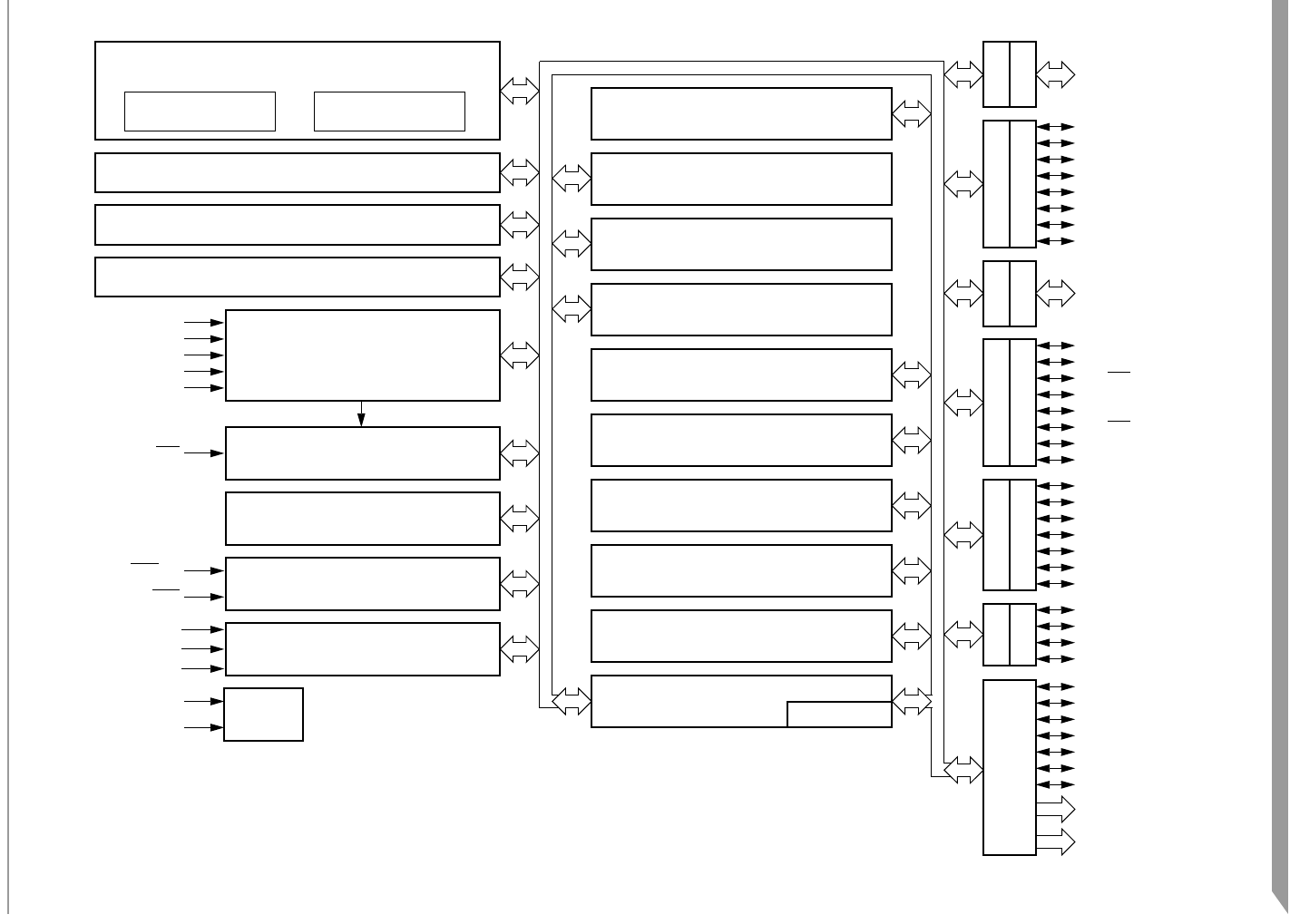
1.3 Block Diagram
Figure 1-1 shows the structure of the MC68HC08LN56/708LN56 block diagram.
MC68HC08LN56 • MC68HC708LN56 General Release Specification, Rev. 2.1
Freescale Semiconductor 19
Block Diagram
Figure 1-1. MC68HC08LN56/708LN56 Block Diagram
SERIAL PERIPHERAL INTERFACE
MODULE
BREAK
MODULE
CLOCK GENERATOR
MODULE
SYSTEM INTEGRATION
MODULE
ANALOG TO DIGITAL
CONVERTER MODULE
TIMER INTERFACE
MODULE
SERIAL PERIPHERAL INTERFACE
MODULE
LOW-VOLTAGE INHIBIT
MODULE
KEYBOARD INTERRUPT
MODULE
COMPUTER OPERATING PROPERLY
MODULE
IRQ
MODULE
PORTB
INTERNAL BUS
LCD CONTROLLER
MODULE
LCD RAM 160
PORTA
DDRA
ARITHMETIC/LOGIC
UNIT (ALU)
CPU
REGISTERS
M68HC08 CPU
CONTROL AND STATUS REGISTERS — 96 BYTES
USER EPROM / OTPROM— 56K BYTES
USER RAM — 1280 BYTES
SERIAL COMMUNICATIONS INTERFACE
MODULE
TIME BASE MODULE
POWER
POWER-ON RESET
MODULE
OSC1
OSC2
CGMXFC
VDDA
VSSA
DDRB
PORTC
DDRC
PA7/KB7–PA0/KB0
PORTE
DDRE
PE0/TCH0
PE1/TCH1
PE2/TCH2
PE3/TCH3
PE4/TCLK
PE5/TxD
PE6/RxD
PC7–PC0
PORTF
DDRF
PB0/AD0
PB1/AD1
PB2/AD2
PB3/AD3
PB4
PB5
PB6
PB7
DDRD
PORTD
PD0/MISO1
PD1/MOSI1
PD2/SS1
PD3/SCK1
PD4/SCK2
PD5/SS2
PD6/MOSI2
PD7/MISO2
VDD
VSS
LCD DRIVERS
VLL
VLLH
VLL1
VLL2
VLL5
VLL6
VLL7
RST
IRQ1/VPP
IRQ2
AVSS
AVDD
VRH
PF0
PF1
PF2
PF3
BP0–31
FP0–39
General Description
MC68HC08LN56 • MC68HC708LN56 General Release Specification, Rev. 2.1
20 Freescale Semiconductor
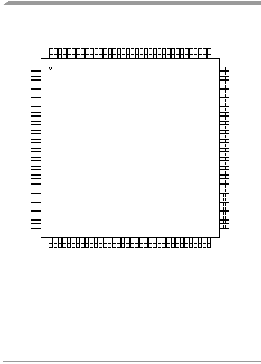
1.4 Pin Assignment
Figure 1-2. MC68HC08LN56/708LN56 Pin Assignment
1
2
3
4
5
6
7
8
9
10
11
12
13
14
15
16
17
18
19
20
21
22
23
24
25
26
27
28
FP2
FP1
FP0
BP15
BP14
BP13
BP12
BP11
BP10
BP9
BP8
BP7
BP6
BP5
BP4
BP3
BP2
BP1
BP0
VLL7
VLL6
CPFLT
VLL5
VLL2
VLL1
VLLH
VCP3
VCP4
29
30
31
32
33
34
35
36
37
38
39
40
41
42
43
44
45
46
47
48
49
50
51
52
53
54
55
56
57
58
59
60
61
62
63
64
65
66
67
68
69
70
71
72
108
107
106
105
104
103
102
101
100
99
98
97
96
95
94
93
92
91
90
89
88
87
86
85
84
83
82
81
80
79
78
77
76
75
74
73
144
143
142
141
140
139
138
137
136
135
134
133
132
131
130
129
128
127
126
125
124
123
122
121
120
119
118
117
116
115
114
113
112
111
110
109
VLL
VSS2
VDD2
RST
IRQ1
IRQ2
FP4
FP5
FP6
FP7
FP8
FP9
FP10
FP11
FP12
FP13
FP14
FP15
FP16
FP17
FP18
FP19
VSS1
FP20
FP21
FP22
FP23
FP24
FP25
FP26
FP27
FP28
FP29
FP30
FP31
FP32
FP33
FP34
FP35
FP36
FP37
FP3
FP39
BP31
BP30
BP29
BP28
BP27
BP26
BP25
BP24
BP23
BP22
BP21
BP20
BP19
BP18
BP17
BP16
VSS3
VDD3
PTC6
PTC5
PTC4
PTC3
PTC2
PTC0
PTE6/RxD
PTE5/TxD
PTE4/TCLK
PTE3/TCH3
PTE2/TCH2
PTE1/TCH1
PTE0/TCH0
PTA7/KBD7
PTA6/KBD6
FP38
OSC1
OSC2
CGMXFC
VSSA
AVSS
AVDD
VRH
PTB0/AD0
PTB1/AD1
PTB2/AD2
PTB3/AD3
PTB4
PTB5
PTB6
PTB7
PTD0/MISO1
PTD1/MOSI1
PTD2/SS1
PTD3/SCK1
CGND
P
TD4/SCK2
PTD5/SS2
PTD6/MOSI2
PTD7/MISO2
VDD1
PTF0
PTF1
PTF2
VDDA
PTF3
PTA0/KBD0
PTA1/KBD1
PTA2/KBD2
PTA3/KBD3
PTA4/KBD4
PTA5/KBD5
PTC1
VCP2
VCP1
Pin Assignment
MC68HC08LN56 • MC68HC708LN56 General Release Specification, Rev. 2.1
Freescale Semiconductor 21
1.4.1 Power Supply Pins (VDD3:VDD1–VSS3:VSS1)
VDD and VSS are the power supply and ground pins. The MCU operates from a single power supply.
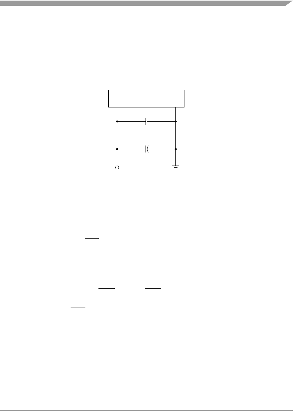
Fast signal transitions on MCU pins place high, short-duration current demands on the power supply. To
prevent noise problems, take special care to provide power supply bypassing at the MCU as Figure 1-3
shows. Place the C1 bypass capacitor as close to the MCU as possible. Use a high-frequency-response
ceramic capacitor for C1. C2 is an optional bulk current bypass capacitor for use in applications that
require the port pins to source high-current levels.
Figure 1-3. Power Supply Bypassing
1.4.2 Oscillator Pins (OSC1 and OSC2)
The OSC1 and OSC2 pins are the connections for the on-chip oscillator circuit. See Chapter 4 Clock
Generator Module (CGMB) for more information.
1.4.3 External Reset Pin (RST)
A logic zero on the RST pin forces the MCU to a known startup state. RST is bidirectional, allowing a reset
of the entire system. It is driven low when any internal reset source is asserted, therefore use open drain
outputs with resistive pullups on this pin. See Chapter 5 System Integration Module (SIM) for more
information.
1.4.4 External Interrupt Pins (IRQ1/VPP and IRQ2)
IRQ1/VPP is the asynchronous external interrupt pin. IRQ1/VPP is also the EPROM/OTPROM
programming power pin. IRQ2 is a second asynchronous external interrupt. See Chapter 5 System
Integration Module (SIM) and Chapter 8 External Interrupt Module (IRQ) for more information.
1.4.5 Clock Ground Pin (CGND)
CGND is the ground for the port output buffers and the ground return for the serial clock in the serial
peripheral interface module (SPI). See Chapter 11 Serial Peripheral Interface Module (SPI) for more
information.
NOTE
CGND must be grounded for proper MCU operation.
MCU
VDD
C2
C1
0.1 µF
VSS
VDD
+
NOTE: Component values shown represent typical applications

General Description
MC68HC08LN56 • MC68HC708LN56 General Release Specification, Rev. 2.1
22 Freescale Semiconductor
1.4.6 CGM Power Supply Pin (VDDA)
VDDA is the power supply pin for the analog portion of the clock generator module (CGM). See Chapter 4
Clock Generator Module (CGMB) for more information.
1.4.7 External Filter Capacitor Pin (CGMXFC)
CGMXFC is an external filter capacitor connection for the CGM. See Chapter 4 Clock Generator Module
(CGMB) for more information.
1.4.8 Port A Input/Output (I/O) Pins (PTA7/KBD7:PTA0/KBD0)
Port A is an 8-bit bidirectional I/O port. Any or all of the port pins can be programmed to serve as external
interrupt pins. See Chapter 13 I/O Ports and Chapter 9 Keyboard Module (KB) for more information.
1.4.9 Port B I/O Pins (PTB7:PTB4, PTB3/AD3:PTB0/AD0)
Port B is an 8-bit bidirectional I/O port that shares four of its pins with the analog-to-digital converter.
Chapter 14 Analog-to-Digital Converter (ADC) for more information.
1.4.10 Port C I/O Pins (PTC6:PTC0)
Port C is a 7-bit bidirectional I/O port. See Chapter 13 I/O Ports.
1.4.11 Port D I/O Pins (PTD7/MISO2:PTD0/MISO1)
Port D is an 8-bit bidirectional I/O port that shares its pins with the serial peripheral interface modules
(SPI). See Chapter 11 Serial Peripheral Interface Module (SPI) for more information.
1.4.12 A/D Converter Power Supply Pins and Reference (AVDD, AVSS, VRH)
AVDD and AVSS are the A/D converter power supply pins. See Chapter 14 Analog-to-Digital Converter
(ADC) for more information.
1.4.13 Port E I/O Pins (PTE6/RxD:PTE0/TCH0)
Port E is a 7-bit special function port that shares its pins with the SCI and the timer channels. See Chapter
12 Serial Communications Interface Module (SCI) and Chapter 10 Timer Interface Module (TIM) for more
information.
1.4.14 Port F I/O Pins (PTF3:PTF0)
Port F is a 4-bit general-purpose port. PTF3:PTF0 are capable of driving LEDs. See Chapter 13 I/O Ports
for more information.
1.4.15 LCD Back Planes (BP31:BP0)
BP31:BP0 are the LCD backplane drivers. See Chapter 15 Liquid Crystal Display Driver (LCD) for more
information.

LCD Driver Power Supply Pins (CPFLT, VLL7:VLL1, VLL, VLLH, and VCP4:VCP1)
MC68HC08LN56 • MC68HC708LN56 General Release Specification, Rev. 2.1
Freescale Semiconductor 23
1.4.16 LCD Driver Pins (FP39:FP0)
FP39:FP0 are the LCD frontplane drivers. See Chapter 15 Liquid Crystal Display Driver (LCD) for more
information.
1.5 LCD Driver Power Supply Pins (CPFLT, VLL7:VLL1, VLL, VLLH, and
VCP4:VCP1)
The LCD module requires multiple voltage levels, which are generated internally with a charge pump.
CPFLT and VLLH are pins for filter capacitors used by the charge pump. CPFLT should be tied to ground
through a 0.01 µF capacitor and VLLH through a 0.22 µF capacitor. VLL7:VLL1 are the power supply pins
for the LCD drivers which are used to generate the LCD charge pump voltage levels. Each should be tied
to ground through a 0.1 µF capacitor, with the exception of VLL7, which should use a 0.22 µF capacitor.
VLL is the supply input for the LCD digital logic and should be tied to the same potential as VDD, as well
as to a 0.1 µF capacitor to ground for noise filtering. VCP4:VCP1 are the pins used to connect the charge
pump to 0.1 µF switched capacitors. See Chapter 15 Liquid Crystal Display Driver (LCD) for more
information.
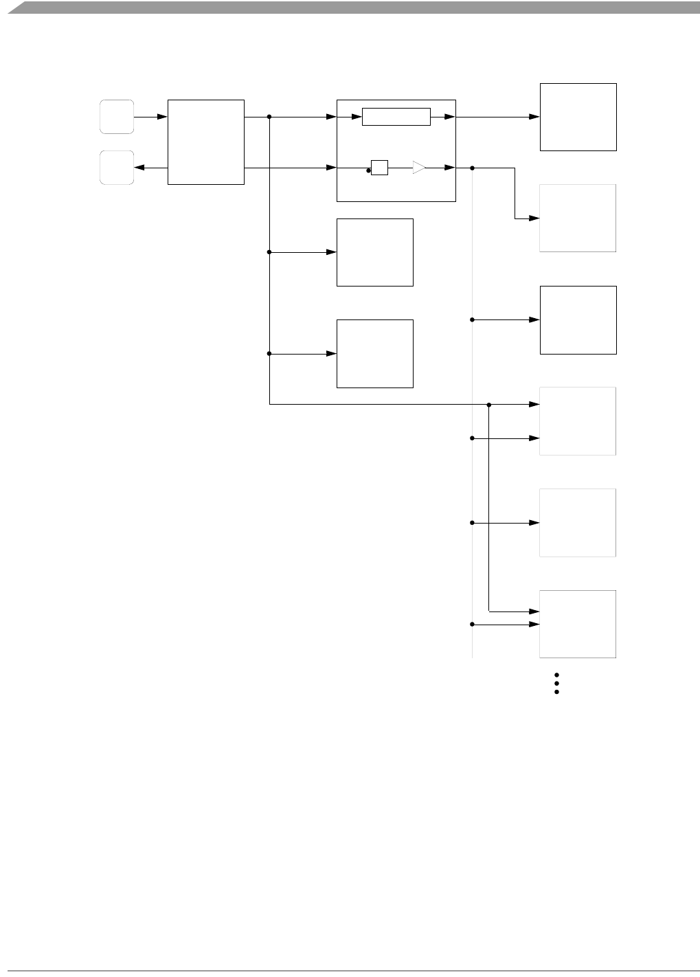
1.6 Clock Distribution
Each module in the MC68HC08LN56/708LN56 that requires a clock uses either a buffered raw oscillator
clock CGMXCLK or the system bus clock CGMOUT. CGMOUT is a divide-by-2 of either the PLL (if
engaged) or CGMXCLK. The internal bus clock is a divide-by-2 of CGMOUT.
General Description
MC68HC08LN56 • MC68HC708LN56 General Release Specification, Rev. 2.1
24 Freescale Semiconductor
Figure 1-4. Clock Distribution Block Diagram
OSC2
OSC1
CGMXCLK
CGM
XTAL
SIM
TBM
LCD
COP
CPU
TIM
SCI
SPI
ADC
INTERNAL
BUS CLOCK
CGMOUT
COP CLOCK
COUNTER
÷2

MC68HC08LN56 • MC68HC708LN56 General Release Specification, Rev. 2.1
Freescale Semiconductor 25
Chapter 2
Memory
2.1 Introduction
The CPU08 can address 64 Kbytes of memory space. The memory map, shown in Figure 2-1, includes:
• 57,384 bytes of EPROM or OTPROM
• 1280 bytes of RAM
• 40 bytes of user-defined vectors
• 240 bytes of monitor ROM
• 160 bytes of LCD RAM
2.2 I/O Section
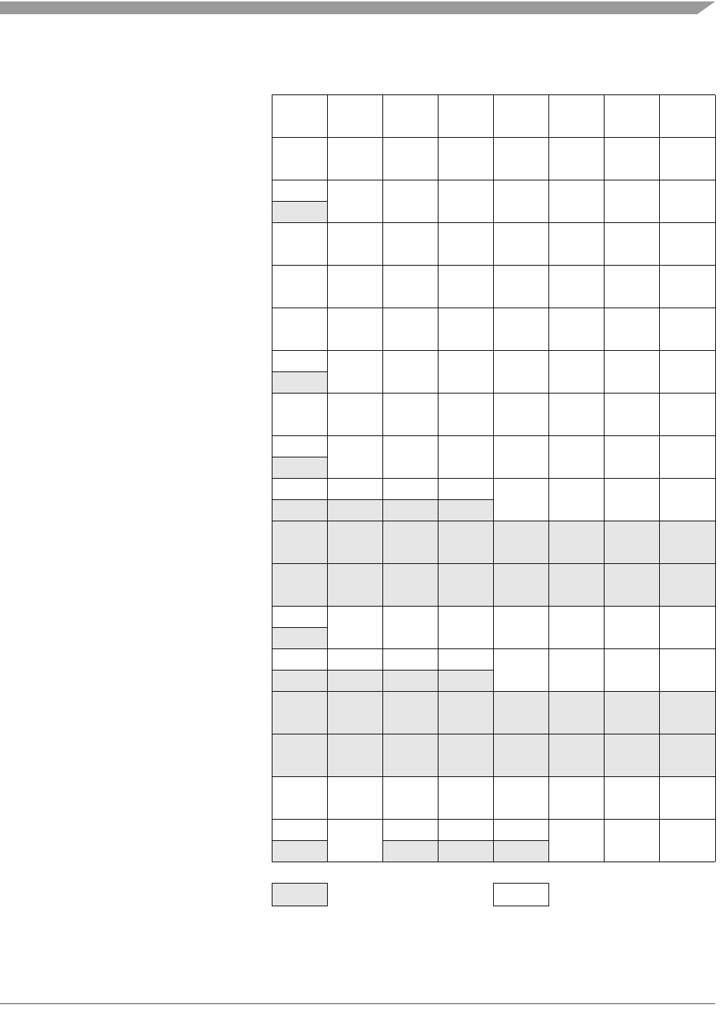
Addresses $0000:$004F, shown in Figure 2-2, contain most of the control, status, and data registers.
Additional I/O registers have the following addresses:
• $FE00 (SIM break status register, SBSR)
• $FE01 (SIM reset status register, SRSR)
• $FE03 (SIM break flag control register, SBFCR)
• $FE07 (EPROM control register, EPMCR)
• $FE0C and $FE0D (break address registers, BRKH and BRKL)
• $FE0E (break status and control register, BRKSCR)
• $FE0F (LVI status register, LVISR)
• $FFFF (COP control register, COPCTL)
Table 2-1 lists vector locations.

Memory
MC68HC08LN56 • MC68HC708LN56 General Release Specification, Rev. 2.1
26 Freescale Semiconductor
$0000
I/O REGISTERS
80 BYTES
$FE00 SIM BREAK STATUS REGISTER (SBSR)
↓$FE01 SIM RESET STATUS REGISTER (SRSR)
$004F $FE02 RESERVED
$0050
RAM
1280 BYTES
$FE03 SIM BREAK FLAG CONTROL REGISTER (SBFCR)
↓$FE04 INTERRUPT STATUS REGISTER 1 (INT1)
$054F $FE05 INTERRUPT STATUS REGISTER 2 (INT2)
$0550
RESERVED
2224 BYTES
$FE06 INTERRUPT STATUS REGISTER 3 (INT3)
↓$FE07 EPROM CONTROL REGISTER (EPMCR) LOWER
$0DFF $FE08 EPROM CONTROL REGISTER (EPMCR) UPPER
$0E00 LCD RAM
160 BYTES
(WITH 352 BYTES RESERVED)
↓
RESERVED
↓$FE0B
$0FFF $FE0C BREAK ADDRESS REGISTER HIGH (BRKH)
$1000
RESERVED
3584 BYTES
$FE0D BREAK ADDRESS REGISTER LOW (BRKL)
↓$FE0E BREAK STATUS AND CONTROL REGISTER (BRKSCR)
$1DFF $FE0F LVI STATUS REGISTER (LVISR)
$1E00
EPROM
57,344 BYTES
$FE10
MONITOR ROM
240 BYTES
↓↓
$FDFF $FEFF
$FF00
UNIMPLEMENTED
192 BYTES
↓
$FFBF
$FFC0
RESERVED
24 BYTES
↓
$FFD7
$FFD8
VECTORS
40 BYTES
↓
$FFFF
Figure 2-1. Memory Map
I/O Section
MC68HC08LN56 • MC68HC708LN56 General Release Specification, Rev. 2.1
Freescale Semiconductor 27
Addr. Name Bit 7654321Bit 0
$0000 Port A Data Register
(PTA)
R:
PTA7 PTA6 PTA5 PTA4 PTA3 PTA2 PTA1 PTA0
W:
$0001 Port B Data Register
(PTB)
R:
PTB7 PTB6 PTB25 PTB4 PTB3 PTB2 PTB1 PTB0
W:
$0002 Port C Data Register
(PTC)
R: 0
PTC6 PTC5 PTC4 PTC3 PTC2 PTC1 PTC0
W:
$0003 Port D Data Register
(PTD)
R:
PTD7 PTD6 PTD5 PTD4 PTD3 PTD2 PTD1 PTD0
W:
$0004 Data Direction Register A
(DDRA)
R:
DDRA7 DDRA6 DDRA5 DDRA4 DDRA3 DDRA2 DDRA1 DDRA0
W:
$0005 Data Direction Register B
(DDRB)
R:
DDRB7 DDRB6 DDRB5 DDRB4 DDRB3 DDRB2 DDRB1 DDRB0
W:
$0006 Data Direction Register C
(DDRC)
R: 0
DDRC6 DDRC5 DDRC4 DDRC3 DDRC2 DDRC1 DDRC0
W:
$0007 Data Direction Register D
(DDRD)
R:
DDRD7 DDRD6 DDRD5 DDRD4 DDRD3 DDRD2 DDRD1 DDRD0
W:
$0008 Port E Data Register
(PTE)
R: 0
PTE6 PTE5 PTE4 PTE3 PTE2 PTE1 PTE0
W:
$0009 Port F Data Register
(PTF)
R:0000
PTF3 PTF2 PTF1 PTF0
W:
$000A Reserved
R:
W:
$000B Reserved
R:
W:
$000C Data Direction Register E
(DDRE)
R: 0
DDRE6 DDRE5 DDRE4 DDRE3 DDRE2 DDRE1 DDRE0
W:
$000D Data Direction Register F
(DDRF)
R:0000
DDRF3 DDRF2 DDRF1 DDRF0
W:
$000E Reserved
R:
W:
$000F Reserved
R:
W:
$0010 SPI 1 Control Register
(SP1CR)
R:
SPRIE DMAS SPMSTR CPOL CPHA SPWOM SPE SPTIE
W:
$0011 SPI 1 Status and Control Register
(SP1SCR)
R: SPRF
OVRIE
OVRF MODF SPTE
MODIE SPR1 SPR0
W:
= Unimplemented R= Reserved
Figure 2-2. Control, Status, and Data Registers (Sheet 1 of 5)
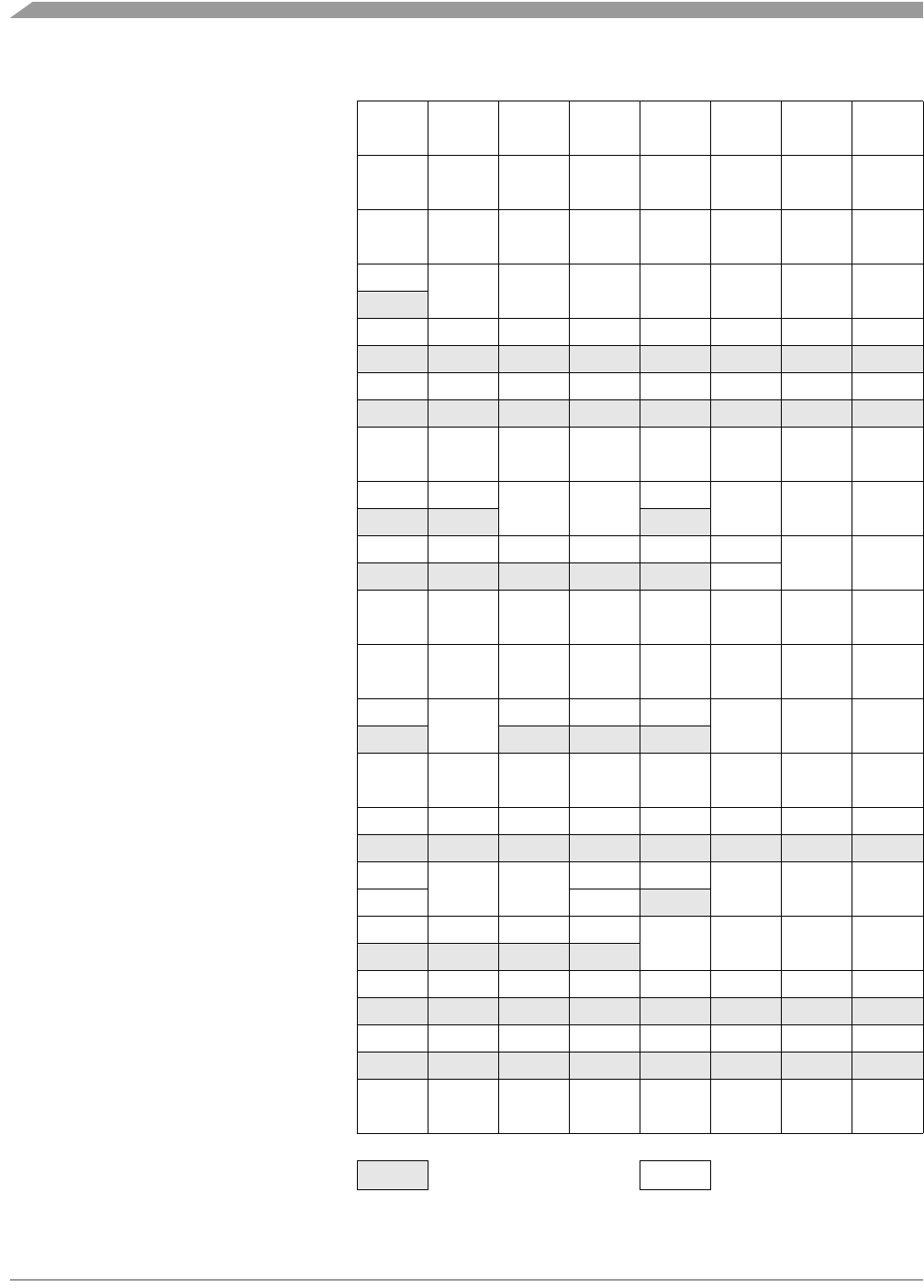
Memory
MC68HC08LN56 • MC68HC708LN56 General Release Specification, Rev. 2.1
28 Freescale Semiconductor
$0012 SPI 1 Data Register
(SP1DR)
R:
Bit 7654321Bit 0
W:
$0013 SCI Control Register 1
(SCC1)
R:
LOOPS ENSCI TXINV M WAKE ILTY PEN PTY
W:
$0014 SCI Control Register 2
(SCC2)
R:
SCTIE TCIE SCRIE ILIE TE RE RWU SBK
W:
$0015 SCI Control Register 3
(SCC3)
R: R8
T8 DMARE DMATE ORIE NEIE FEIE PEIE
W:
$0016 SCI Status Register 1
(SCS1)
R: SCTE TC SCRF IDLE OR NF FE PE
W:
$0017 SCI Status Register 2
(SCS2)
R:000000BKFRPF
W:
$0018 SCI Data Register
(SCDR)
R:
Bit 7654321Bit 0
W:
$0019 SCI Baud Rate Register
(SCBR)
R: 0 0
SCP1 SCP0
0
SCR2 SCR1 SCR0
W:
$001A Keyboard Status/Control
Register (KBSCR)
R:0000KEYF0
IMASKK MODEK
W: ACKK
$001B Keyboard Interrupt Control Register
(KBICR)
R:
KB7IE KB6IE KB5IE KB4IE KB3IE KB2IE KB1IE KB0IE
W:
$001C SPI 2 Control Register (SP2CR)
R:
SPRIE DMAS SP-
MSTR CPOL CPHA SPWOM SPE SPTIE
W:
$001D SPI 2 Status and Control Register
(SP2SCR)
R: SPRF
OVRIE
OVRF MODF SPTE
MODIE SPR1 SPR0
W:
$001E SPI 2 Data Register
(SP2DR)
R:
Bit 7654321Bit 0
W:
$001F Configuration Register
(CONFIG)
R: 0 LVISTOP LVIRST LVIPWR SSREC STOP COPD
W:
$0020 Timer Status and Control Register
(TSC)
R: TOF
TOIE TSTOP
00
PS2 PS1 PS0
W: 0 TRST
$0021 Timer DMA Select Register
(TDMA)
R:0000
DMA3S DMA2S DMA1S DMA0S
W:
$0022 Timer Counter Register High
(TCNTH)
R: Bit 15 14 13 12 11 10 9 Bit 8
W:
$0023 Timer Counter Register Low
(TCNTL)
R:Bit 7654321Bit 0
W:
$0024 Timer Modulo Register High
(TMODH)
R:
Bit 15 14 13 12 11 10 9 Bit 8
W:
Addr. Name Bit 7654321Bit 0
= Unimplemented R= Reserved
Figure 2-2. Control, Status, and Data Registers (Sheet 2 of 5)
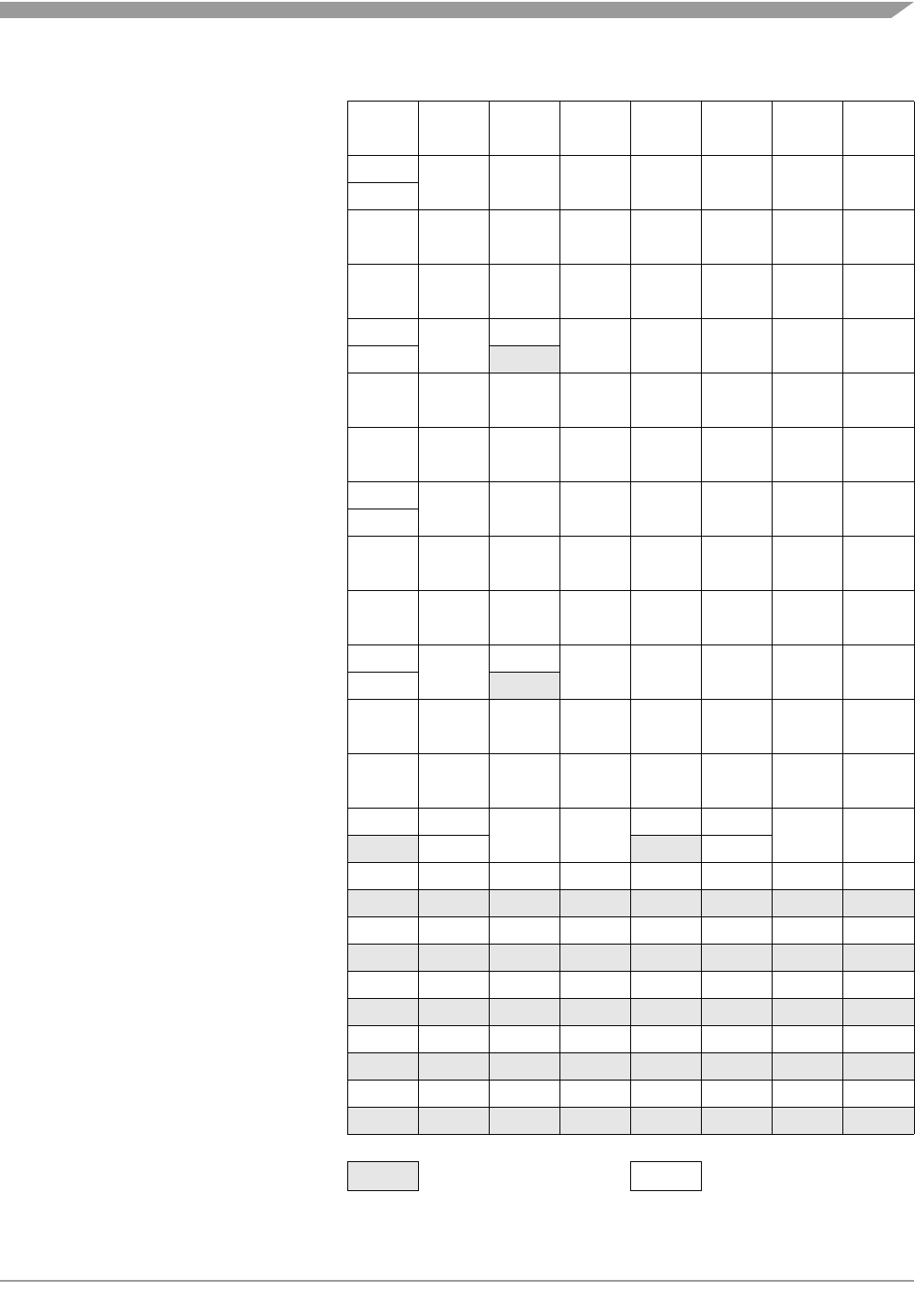
I/O Section
MC68HC08LN56 • MC68HC708LN56 General Release Specification, Rev. 2.1
Freescale Semiconductor 29
$0025 Timer Modulo Register Low
(TMODL)
R:
Bit 7654321Bit 0
W:
$0026 Timer Channel 0 Status and Control
Register (TSC0)
R: CH0F
CH0IE MS0B MS0A ELS0B ELS0A TOV0 CH0MAX
W: 0
$0027 Timer Channel 0 Register High
(TCH0H)
R:
Bit 15 14 13 12 11 10 9 Bit 8
W:
$0028 Timer Channel 0 Register Low
(TCH0L)
R:
Bit 7654321Bit 0
W:
$0029 Timer Channel 1 Status and Control
Register (TSC1)
R: CH1F
CH1IE
0
MS1A ELS1B ELS1A TOV1 CH1MAX
W: 0
$002A Timer Channel 1 Register High
(TCH1H)
R:
Bit 15 14 13 12 11 10 9 Bit 8
W:
$002B Timer Channel 1 Register Low
(TCH1L)
R:
Bit 7654321Bit 0
W:
$002C Timer Channel 2 Status and Control
Register (TSC2)
R: CH2F
CH2IE MS2B MS2A ELS2B ELS2A TOV2 CH2MAX
W: 0
$002D Timer Channel 2 Register High
(TCH2H)
R:
Bit 15 14 13 12 11 10 9 Bit 8
W:
$002E Timer Channel 2 Register Low
(TCH2L)
R:
Bit 7654321Bit 0
W:
$002F Timer Channel 3 Status and Control
Register (TSC3)
R: CH3F
CH3IE
0
MS3A ELS3B ELS3A TOV3 CH3MAX
W: 0
$0030 Timer Channel 3 Register High
(TCH3H)
R:
Bit 15 14 13 12 11 10 9 Bit 8
W:
$0031 Timer Channel 3 Register Low
(TCH3L)
R:
Bit 7654321Bit 0
W:
$0032 IRQ Status/Control Register
(ISCR)
R: IRQ2F 0
IMASK2 MODE2
IRQ1F 0
IMASK1 MODE1
W: ACK2 ACK1
$0033 LCD FrontPlane Latch 0
(LCDFL0)
R: FP7 FP6 FP5 FP4 FP3 FP2 FP1 FP0
W:
$0034 LCD FrontPlane Latch 1
(LCDFL1)
R: FP15 FP14 FP13 FP12 FP11 FP10 FP9 FP8
W:
$0035 LCD FrontPlane Latch 2
(LCDFL2)
R: FP23 FP22 FP21 FP20 FP19 FP18 FP17 FP16
W:
$0036 LCD FrontPlane Latch 3
(LCDFL3)
R: FP31 FP30 FP29 FP28 FP27 FP26 FP25 FP24
W:
$0037 LCD FrontPlane Latch 4
(LCDFL4)
R: FP39 FP38 FP37 FP36 FP35 FP34 FP33 FP32
W:
Addr. Name Bit 7654321Bit 0
= Unimplemented R= Reserved
Figure 2-2. Control, Status, and Data Registers (Sheet 3 of 5)
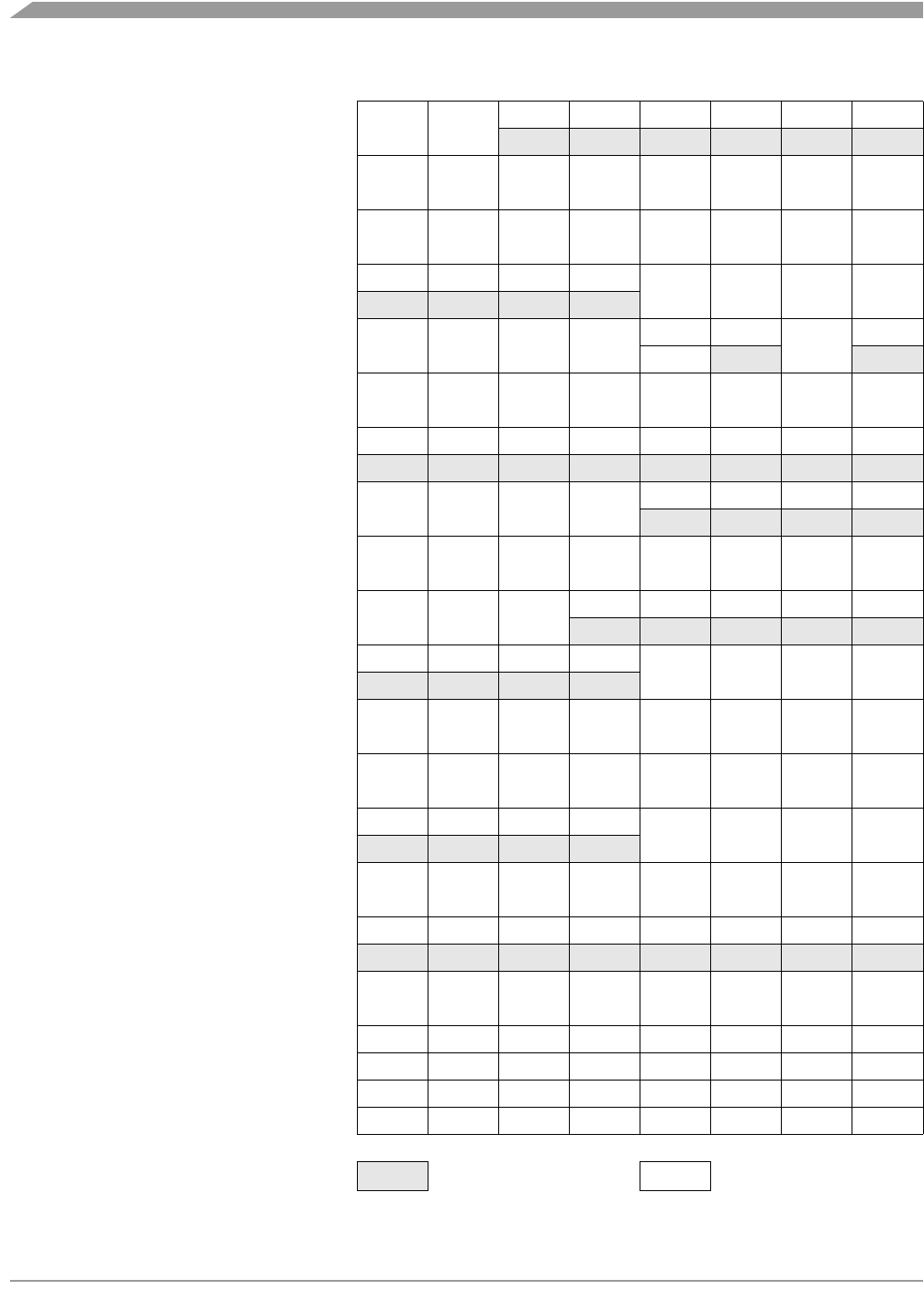
Memory
MC68HC08LN56 • MC68HC708LN56 General Release Specification, Rev. 2.1
30 Freescale Semiconductor
$0038 LCD Control Register
(LCDCR)
R:
DISON SUPV
RRRRRR
W:
$0039 LCD Contrast Control Register
(LCDCCR)
R:
CTCL7 CTCL6 CTCL5 CTCL4 CTCL3 CTCL2 CTCL1 CTCL0
W:
$003A LCD Prescale Divider Register
(LCDDIV)
R:
PE DIV6 DIV5 DIV4 DIV3 DIV2 DIV1 DIV0
W:
$003B LCD Frame Rate Register
(LCDFR)
R:0000
FR3 FR2 FR1 FR0
W:
$003F Time Base Control Register
(TBCR)
R:
TBIF TBIE TBR1 TBR0
00
TBON
0
W: TACK
$0040 A/D Control Register
(ADSCR)
R: COCO/
IDMAS AIEN ADC0 ADCH4 ADCH3 ADCH2 ADCH1 ADCH0
W:
$0041 A/D Data Register
(ADR)
R: AD7 AD6 AD5 AD4 AD3 AD2 AD1 AD 0
W:
$0042 A/D Clock Register
(ADCL)
R:
ADIV2 ADIV1 ADIV0 ADICLK
0000
W:
$004A PLL Control Register
(PCTL)
R:
PLLIE PLLF PLLON BCS PRE1 PRE0 VPR1 VPR0
W:
$004B PLL Bandwidth Control Register
(PBWC)
R:
AUTO LOCK ACQ
00000
W:
$004C PLL Multiplier Select High Register
(PMSH)
R:0000
MUL11 MUL10 MUL9 MUL8
W:
$004D PLL Multiplier Select Low Register
(PMSL)
R:
MUL7 MUL6 MUL5 MUL4 MUL3 MUL2 MUL1 MUL0
W:
$004E PLL VCO Select Range (PVRS)
R:
VRS7 VRS6 VRS5 VRS4 VRS3 VRS2 VRS1 VRS0
W:
$004F PLL Reference Divider Select Register
(PRDS)
R:0000
RDS3 RDX2 RDX1 RDX0
W:
$FE00 SIM Break Status Register
(SBSR)
R:
RRRRRRSBSW R
W:
$FE01 SIM Reset Status Register
(SRSR)
R: POR PIN COP ILOP ILAD 0 LVI 0
W:
$FE03 SIM Break Flag Control Register
(SBFCR)
R:
BCFERRRRRRR
W:
$FE04 Interrupt Status Register 1
(INT1)
R: I6 I5 I4 I3 I2 I1 0 0
W:RRRRRRRR
$FE05 Interrupt Status Register 2
(INT2)
R: I14 I13 I12 I11 I10 I9 I8 I7
W:RRRRRRRR
Addr. Name Bit 7654321Bit 0
= Unimplemented R= Reserved
Figure 2-2. Control, Status, and Data Registers (Sheet 4 of 5)
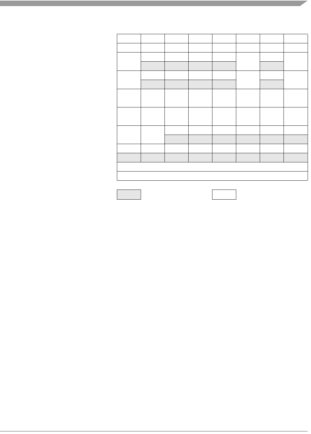
I/O Section
MC68HC08LN56 • MC68HC708LN56 General Release Specification, Rev. 2.1
Freescale Semiconductor 31
$FE06 Interrupt Status Register 3
(INT3)
R:0000I18I17I16I15
W:RRRRRRRR
$FE07 EPROM Control Register 1
(EPMCR1)
R:
EPMCR1
0000
ELAT1
0
EPGM1
W:
$FE08 EPROM Control Register 2
(EPMCR2)
R:
EPMCR2
0000
ELAT2
0
EPGM2
W:
$FE0C Break Address Register High
(BRKH)
R:
Bit 15 14 13 12 11 10 9 Bit 8
W:
$FE0D Break Address Register Low
(BRKL)
R:
Bit 7654321Bit 0
W:
$FE0E Break Status and Control Register
(BRKSCR)
R:
BRKE BRKA
000000
W:
$FE0F LVI Status Register
(LVISR)
R:LVIOUT0000000
W:
$FFFF COP Control Register
(COPCTL)
R: LOW BYTE OF RESET VECTOR
W: WRITING TO $FFFF CLEARS COP COUNTER
Addr. Name Bit 7654321Bit 0
= Unimplemented R= Reserved
Figure 2-2. Control, Status, and Data Registers (Sheet 5 of 5)
Memory
MC68HC08LN56 • MC68HC708LN56 General Release Specification, Rev. 2.1
32 Freescale Semiconductor
Table 2-1. Vector Addresses
Address Vector
Low
$FFD8:$FFD9 Time Base Module Vector (High:Low)
$FFDA:$FFDB A/D Vector (High:Low)
$FFDC:$FFDD Keyboard Vector (High:Low)
$FFDE:$FFDF IRQ2 Vector (High:Low)
$FFE0:$FFE1 SCI Transmit Vector (High:Low)
$FFE2:$FFE3 SCI Receive Vector (High:Low)
$FFE4:$FFE5 SCI Error Vector (High:Low)
$FFE6:$FFE7 SPI 2 Transmit Vector (High:Low)
$FFE8:$FFE9 SPI 2 Receive Vector (High:Low)
$FFEA:$FFEB SPI 1 Transmit Vector (High:Low)
$FFEC:$FFED SPI 1 Receive Vector (High:Low)
$FFEE:$FFEF TIM Overflow Vector (High:Low)
$FFF0:$FFF1 TIM Channel 3 Vector (High:Low)
$FFF2:$FFF3 TIM Channel 2 Vector (High:Low)
$FFF4:$FFF5 TIM Channel 1 Vector (High:Low)
$FFF6:$FFF7 TIM Channel 0 Vector (High:Low)
$FFF8:$FFF9 PLL Vector (High:Low)
$FFFA:$FFFB IRQ1 Vector (High:Low)
High
$FFFC:$FFFD SWI Vector (High:Low)
$FFFE:$FFFF Reset Vector (High:Low)
Priority

MC68HC08LN56 • MC68HC708LN56 General Release Specification, Rev. 2.1
Freescale Semiconductor 33
Chapter 3
Central Processing Unit (CPU)
3.1 Introduction
This section describes the central processor unit (CPU08, Version A). The M68HC08 CPU is an
enhanced and fully object-code-compatible version of the M68HC05 CPU. The CPU08 Reference Manual
(Freescale document number CPU08RM/AD) contains a description of the CPU instruction set,
addressing modes, and architecture.
3.2 Features
Features of the CPU include:
• Fully Upward, Object-Code Compatibility with M68HC05 Family
• 16-Bit Stack Pointer with Stack Manipulation Instructions
• 16-Bit Index Register with X-Register Manipulation Instructions
• 8-MHz CPU Internal Bus Frequency
• 64-Kbyte Program/Data Memory Space
• 16 Addressing Modes
• Memory-to-Memory Data Moves without Using Accumulator
• Fast 8-Bit by 8-Bit Multiply and 16-Bit by 8-Bit Divide Instructions
• Enhanced Binary-Coded Decimal (BCD) Data Handling
• Modular Architecture with Expandable Internal Bus Definition for Extension of Addressing Range
beyond 64 Kbytes
• Low-Power Stop and Wait Modes
3.3 CPU Registers
Figure 3-1 shows the five CPU registers. CPU registers are not part of the memory map.
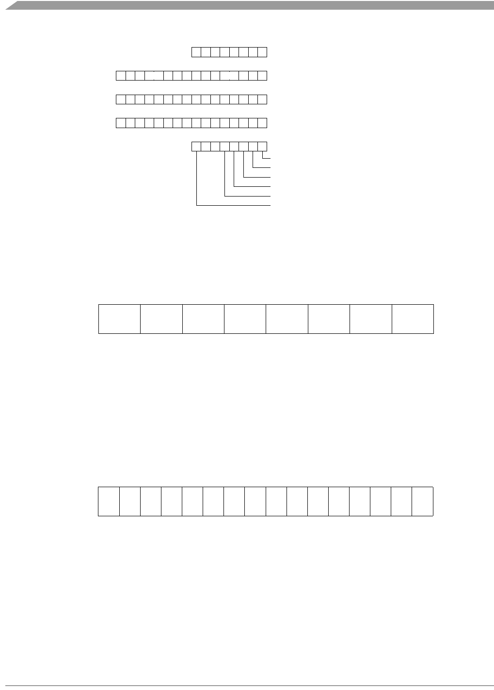
Central Processing Unit (CPU)
MC68HC08LN56 • MC68HC708LN56 General Release Specification, Rev. 2.1
34 Freescale Semiconductor
Figure 3-1. CPU Registers
3.3.1 Accumulator
The accumulator (A) is a general-purpose 8-bit register. The CPU uses the accumulator to hold operands
and the results of arithmetic/logic operations.
3.3.2 Index Register
The 16-bit index register (H:X) allows indexed addressing of a 64-Kbyte memory space. H is the upper
byte of the index register, and X is the lower byte. H:X is the concatenated 16-bit index register.
In the indexed addressing modes, the CPU uses the contents of the index register to determine the
conditional address of the operand.
The index register can serve also as a temporary data storage location.
ABit 7654321Bit 0
Read:
Write:
Reset: Unaffected by reset
Figure 3-2. Accumulator (A)
SP Bit
15 14 13 12 11 10 9 8 7 6 5 4 3 2 1
Bit
0
Read:
Write:
Reset:00000000XXXXXXXX
X = Indeterminate
Figure 3-3. Index Register (H:X)
ACCUMULATOR (A)
INDEX REGISTER (H:X)
STACK POINTER (SP)
PROGRAM COUNTER (PC)
CONDITION CODE REGISTER (CCR)
CARRY/BORROW FLAG
ZERO FLAG
NEGATIVE FLAG
INTERRUPT MASK
HALF-CARRY FLAG
TWO’S COMPLEMENT OVERFLOW FLAG
V11HINZC
H X
0
0
0
0
7
15
15
15
70
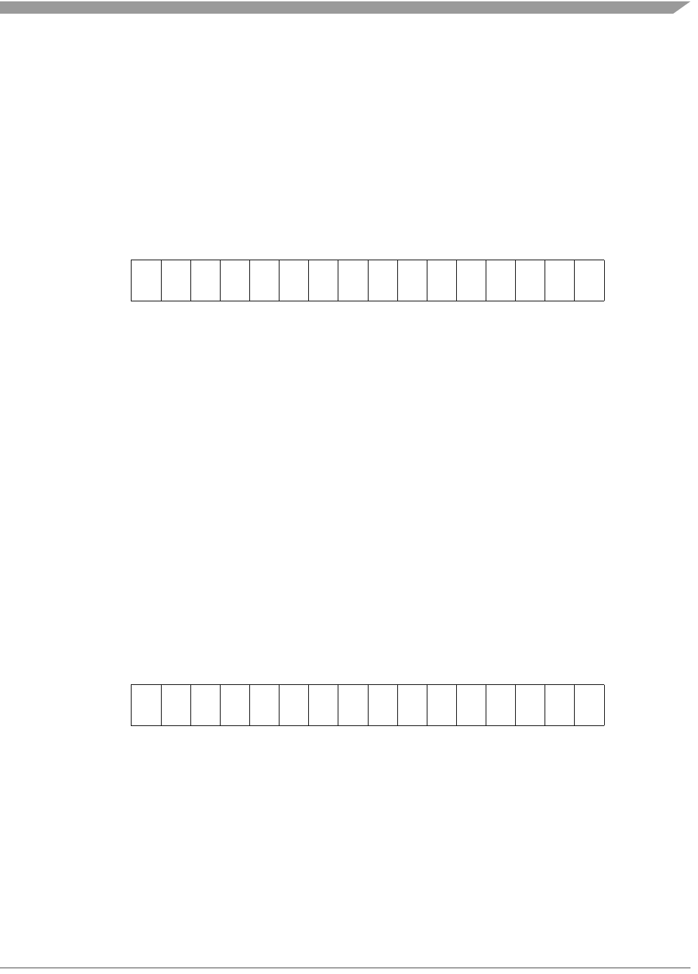
CPU Registers
MC68HC08LN56 • MC68HC708LN56 General Release Specification, Rev. 2.1
Freescale Semiconductor 35
3.3.3 Stack Pointer
The stack pointer (SP) is a 16-bit register that contains the address of the next location on the stack.
During a reset, the stack pointer is preset to $00FF. The reset stack pointer (RSP) instruction sets the
least significant byte to $FF and does not affect the most significant byte. The stack pointer decrements
as data is pushed onto the stack and increments as data is pulled from the stack.
In the stack pointer 8-bit offset and 16-bit offset addressing modes, the stack pointer can function as an
index register to access data on the stack. The CPU uses the contents of the stack pointer to determine
the conditional address of the operand.
NOTE
The location of the stack is arbitrary and may be relocated anywhere in
RAM. Moving the SP out of page zero ($0000 to $00FF) frees direct
address (page zero) space. For correct operation, the stack pointer must
point only to RAM locations.
3.3.4 Program Counter
The program counter (PC) is a 16-bit register that contains the address of the next instruction or operand
to be fetched.
Normally, the program counter automatically increments to the next sequential memory location every
time an instruction or operand is fetched. Jump, branch, and interrupt operations load the program
counter with an address other than that of the next sequential location.
During reset, the program counter is loaded with the reset vector address located at $FFFE and $FFFF.
The vector address is the address of the first instruction to be executed after exiting the reset state.
SP Bit
15 14 13 12 11 10 9 8 7 6 5 4 3 2 1
Bit
0
Read:
Write:
Reset:0000000011111111
Figure 3-4. Stack Pointer (SP)
PC Bit
15 14 13 12 11 10 9 8 7 6 5 4 3 2 1
Bit
0
Read:
Write:
Reset: Loaded with vector from $FFFE and $FFFF
Figure 3-5. Program Counter (PC)

Central Processing Unit (CPU)
MC68HC08LN56 • MC68HC708LN56 General Release Specification, Rev. 2.1
36 Freescale Semiconductor
3.3.5 Condition Code Register
The 8-bit condition code register (CCR) contains the interrupt mask and five flags that indicate the results
of the instruction just executed. Bits 6 and 5 are set permanently to logic one. The following paragraphs
describe the functions of the condition code register.
V — Overflow Flag
The CPU sets the overflow flag when a two's complement overflow occurs. The signed branch
instructions BGT, BGE, BLE, and BLT use the overflow flag.
1 = Overflow
0 = No overflow
H — Half-Carry Flag
The CPU sets the half-carry flag when a carry occurs between accumulator bits 3 and 4 during an ADD
or ADC operation. The half-carry flag is required for binary-coded decimal (BCD) arithmetic operations.
The DAA instruction uses the states of the H and C flags to determine the appropriate correction factor.
1 = Carry between bits 3 and 4
0 = No carry between bits 3 and 4
I — Interrupt Mask
When the interrupt mask is set, all maskable CPU interrupts are disabled. CPU interrupts are enabled
when the interrupt mask is cleared. When a CPU interrupt occurs, the interrupt mask is set
automatically after the CPU registers are saved on the stack, but before the interrupt vector is fetched.
1 = Interrupts disabled
0 = Interrupts enabled
NOTE
To maintain M6805 compatibility, the upper byte of the index register (H) is
not stacked automatically. If the interrupt service routine modifies H, then
the user must stack and unstack H using the PSHH and PULH instructions.
After the I bit is cleared, the highest-priority interrupt request is serviced first.
A return from interrupt (RTI) instruction pulls the CPU registers from the stack and restores the
interrupt mask from the stack. After any reset, the interrupt mask is set and can only be cleared by the
clear interrupt mask software instruction (CLI).
N — Negative flag
The CPU sets the negative flag when an arithmetic operation, logic operation, or data manipulation
produces a negative result, setting bit 7 of the result.
1 = Negative result
0 = Non-negative result
CCRBit 7654321Bit 0
Read: V11HI NZC
Write:
Reset:X11X1XXX
X = Indeterminate
Figure 3-6. Condition Code Register (CCR)

Arithmetic/Logic Unit
MC68HC08LN56 • MC68HC708LN56 General Release Specification, Rev. 2.1
Freescale Semiconductor 37
Z — Zero flag
The CPU sets the zero flag when an arithmetic operation, logic operation, or data manipulation
produces a result of $00.
1 = Zero result
0 = Non-zero result
C — Carry/Borrow Flag
The CPU sets the carry/borrow flag when an addition operation produces a carry out of bit 7 of the
accumulator or when a subtraction operation requires a borrow. Some instructions — such as bit test
and branch, shift, and rotate — also clear or set the carry/borrow flag.
1 = Carry out of bit 7
0 = No carry out of bit 7
3.4 Arithmetic/Logic Unit
The arithmetic/logic unit (ALU) performs the arithmetic and logic operations defined by the instruction set.
Refer to the CPU08 Reference Manual (Freescale document number CPU08RM/AD) for a description of
the instructions and addressing modes and more detail about CPU architecture.
3.5 CPU During Break Interrupts
If the break module is enabled, a break interrupt causes the CPU to execute the software interrupt
instruction (SWI) at the completion of the current CPU instruction. See Chapter 17 Break Module
(BREAK). The program counter vectors to $FFFC:$FFFD ($FEFC:$FEFD in monitor mode).
A return from interrupt instruction (RTI) in the break routine ends the break interrupt and returns the MCU
to normal operation if the break interrupt has been deasserted.

Central Processing Unit (CPU)
MC68HC08LN56 • MC68HC708LN56 General Release Specification, Rev. 2.1
38 Freescale Semiconductor

MC68HC08LN56 • MC68HC708LN56 General Release Specification, Rev. 2.1
Freescale Semiconductor 39
Chapter 4
Clock Generator Module (CGMB)
4.1 Introduction
This section describes the clock generator module (CGM, Version B). The CGM generates the crystal
clock signal, CGMXCLK, which operates at the frequency of the crystal. The CGM also generates the
base clock signal, CGMOUT, which is based on either the crystal clock divided by two or the phase-locked
loop (PLL) clock, CGMVCLK, divided by two. This is the clock from which the SIM derives the system
clocks, including the bus clock, which is at a frequency of CGMOUT/2. The PLL is a fully functional
frequency generator designed for use with crystals or ceramic resonators. The PLL can generate an
8-MHz bus frequency using a 32-kHz crystal.
4.2 Features
Features of the CGMB include:
• Phase-Locked Loop with Output Frequency in Integer Multiples of an Integer Dividend of the
Crystal Reference
• Low-Frequency Crystal Operation with Low-Power Operation and High-Output Frequency
Resolution
• Programmable Reference Divider for Even Greater Resolution
• Programmable Prescaler for Power-of-Two Increases in Frequency
• Programmable Hardware Voltage-Controlled Oscillator (VCO) for Low-Jitter Operation
• Automatic Bandwidth Control Mode for Low-Jitter Operation
• Automatic Frequency Lock Detector
• CPU Interrupt on Entry or Exit from Locked Condition
4.3 Functional Description
The CGMB consists of three major submodules:
• Crystal oscillator circuit — The crystal oscillator circuit generates the constant crystal frequency
clock, CGMXCLK.
• Phase-locked loop (PLL) — The PLL generates the programmable VCO frequency clock,
CGMVCLK.
• Base clock selector circuit — This software-controlled circuit selects either CGMXCLK divided by
two or the VCO clock, CGMVCLK, divided by two as the base clock, CGMOUT. The SIM derives
the system clocks from CGMOUT.
Figure 4-1 shows the structure of the CGM.
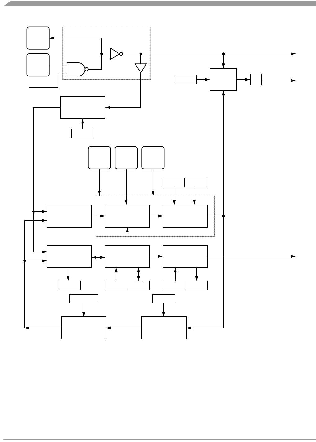
Clock Generator Module (CGMB)
MC68HC08LN56 • MC68HC708LN56 General Release Specification, Rev. 2.1
40 Freescale Semiconductor
Figure 4-1. CGMB Block Diagram
BCS
PHASE
DETECTOR
LOOP
FILTER
FREQUENCY
DIVIDER
VOLTAGE
CONTROLLED
OSCILLATOR
AUTOMATIC
MODE
CONTROL
LOCK
DETECTOR
CLOCK
CGMXCLK
CGMOUT
CGMVDV CGMVCLK
SIMOSCEN
CRYSTAL OSCILLATOR
INTERRUPT
CONTROL
CGMINT
CGMRDV
PLL ANALOG
÷ 2
CGMRCLK
OSC2
OSC1
SELECT
CIRCUIT
VDDA CGMXFC VSSA
LOCK AUTO ACQ
VPR[1:0]
PLLIE PLLF
MUL[11:0]
REFERENCE
DIVIDER
RDS[3:0]
VRS[7:0]
FREQUENCY
DIVIDER
PRE[1:0]

Functional Description
MC68HC08LN56 • MC68HC708LN56 General Release Specification, Rev. 2.1
Freescale Semiconductor 41
4.3.1 Crystal Oscillator Circuit
The crystal oscillator circuit consists of an inverting amplifier and an external crystal. The OSC1 pin is the
input to the amplifier and the OSC2 pin is the output. The SIMOSCEN signal from the system integration
module (SIM) enables the crystal oscillator circuit.
The CGMXCLK signal is the output of the crystal oscillator circuit and runs at a rate equal to the crystal
frequency. CGMXCLK is then buffered to produce CGMRCLK, the PLL reference clock.
CGMXCLK can be used by other modules which require precise timing for operation. The duty cycle of
CGMXCLK is not guaranteed to be 50% and depends on external factors, including the crystal and related
external components. An externally generated clock also can feed the OSC1 pin of the crystal oscillator
circuit. Connect the external clock to the OSC1 pin and let the OSC2 pin float.
4.3.2 Phase-Locked Loop Circuit (PLL)
The PLL is a frequency generator that can operate in either acquisition mode or tracking mode, depending
on the accuracy of the output frequency. The PLL can change between acquisition and tracking modes
either automatically or manually.
4.3.3 PLL Circuits
The PLL consists of these circuits:
• Voltage-controlled oscillator (VCO)
• Reference divider
• Frequency prescaler
• Modulo VCO frequency divider
• Phase detector
• Loop filter
• Lock detector
The operating range of the VCO is programmable for a wide range of frequencies and for maximum
immunity to external noise, including supply and CGM/XFC noise. The VCO frequency is bound to a
range from roughly one-half to twice the center-of-range frequency, fVRS. Modulating the voltage on the
CGM/XFC pin changes the frequency within this range. By design, fVRS is equal to the nominal
center-of-range frequency, fNOM, (38.4 kHz) times a linear factor L and a power-of-two factor E, or
(L ×2E)fNOM.
CGMRCLK is the PLL reference clock, a buffered version of CGMXCLK. CGMRCLK runs at a frequency,
fRCLK, and is fed to the PLL through a programmable modulo reference divider, which divides fRCLK by a
factor R. This feature allows frequency steps of higher resolution. The divider’s output is the final
reference clock, CGMRDV, running at a frequency fRDV =f
RCLK/R.
The VCO’s output clock, CGMVCLK, running at a frequency fVCLK is fed back through a programmable
prescale divider and a programmable modulo divider. The prescaler divides the VCO clock by a
power-of-two factor P and the modulo divider reduces the VCO clock by a factor, N. The dividers’ output
is the VCO feedback clock, CGMVDV, running at a frequency fVDV =f
VCLK/(N ×2P). (See 4.3.6
Programming the PLL for more information.)

Clock Generator Module (CGMB)
MC68HC08LN56 • MC68HC708LN56 General Release Specification, Rev. 2.1
42 Freescale Semiconductor
The phase detector then compares the VCO feedback clock, CGMVDV, with the final reference clock,
CGMRDV. A correction pulse is generated based on the phase difference between the two signals. The
loop filter then slightly alters the DC voltage on the external capacitor connected to CGM/XFC based on
the width and direction of the correction pulse. The filter can make fast or slow corrections depending on
its mode, described in 4.3.4 Acquisition and Tracking Modes. The value of the external capacitor and the
reference frequency determines the speed of the corrections and the stability of the PLL.
The lock detector compares the frequencies of the VCO feedback clock, CGMVDV, and the final
reference clock, CGMRDV. Therefore, the speed of the lock detector is directly proportional to the final
reference frequency, fRDV. The circuit determines the mode of the PLL and the lock condition based on
this comparison.
4.3.4 Acquisition and Tracking Modes
The PLL filter is manually or automatically configurable into one of two operating modes:
• Acquisition mode — In acquisition mode, the filter can make large frequency corrections to the
VCO. This mode is used at PLL startup or when the PLL has suffered a severe noise hit and the
VCO frequency is far off the desired frequency. When in acquisition mode, the ACQ bit is clear in
the PLL bandwidth control register. (See 4.5.2 PLL Bandwidth Control Register.)
• Tracking mode — In tracking mode, the filter makes only small corrections to the frequency of the
VCO. PLL jitter is much lower in tracking mode, but the response to noise is also slower. The PLL
enters tracking mode when the VCO frequency is nearly correct, such as when the PLL is selected
as the base clock source. (See 4.3.8 Base Clock Selector Circuit.) The PLL is automatically in
tracking mode when not in acquisition mode or when the ACQ bit is set.
4.3.5 Manual and Automatic PLL Bandwidth Modes
The PLL can change the bandwidth or operational mode of the loop filter manually or automatically.
Automatic mode is recommended for most users.
In automatic bandwidth control mode (AUTO = 1), the lock detector automatically switches between
acquisition and tracking modes. Automatic bandwidth control mode also is used to determine when the
VCO clock, CGMVCLK, is safe to use as the source for the base clock, CGMOUT. (See 4.5.2 PLL
Bandwidth Control Register.) If PLL interrupts are enabled, the software can wait for a PLL interrupt
request and then check the LOCK bit. If interrupts are disabled, software can poll the LOCK bit
continuously (during PLL startup, usually) or at periodic intervals. In either case, when the LOCK bit is set,
the VCO clock is safe to use as the source for the base clock. (See 4.3.8 Base Clock Selector Circuit.) If
the VCO is selected as the source for the base clock and the LOCK bit is clear, the PLL has suffered a
severe noise hit and the software must take appropriate action, depending on the application. (See 4.6
Interrupts for information and precautions on using interrupts.) The following conditions apply when the
PLL is in automatic bandwidth control mode:
•The ACQ
bit (See 4.5.2 PLL Bandwidth Control Register.) is a read-only indicator of the mode of
the filter. (See 4.3.4 Acquisition and Tracking Modes.)
•The ACQ
bit is set when the VCO frequency is within a certain tolerance, ∆TRK, and is cleared when
the VCO frequency is out of a certain tolerance, ∆UNT. (See 4.8 Acquisition/Lock Time
Specifications for more information.)
• The LOCK bit is a read-only indicator of the locked state of the PLL.

Functional Description
MC68HC08LN56 • MC68HC708LN56 General Release Specification, Rev. 2.1
Freescale Semiconductor 43
• The LOCK bit is set when the VCO frequency is within a certain tolerance, ∆LOCK, and is cleared
when the VCO frequency is out of a certain tolerance ∆UNL. (See 4.8 Acquisition/Lock Time
Specifications for more information.)
• CPU interrupts can occur if enabled (PLLIE = 1) when the PLL’s lock condition changes, toggling
the LOCK bit. (See 4.5.1 PLL Control Register.)
The PLL also may operate in manual mode (AUTO = 0). Manual mode is used by systems that do not
require an indicator of the lock condition for proper operation. Such systems typically operate well below
fBUSMAX.The following conditions apply when in manual mode:
•ACQ
is a writable control bit that controls the mode of the filter. Before turning on the PLL in manual
mode, the ACQ bit must be clear.
• Before entering tracking mode (ACQ = 1), software must wait a given time, tACQ (See 4.8
Acquisition/Lock Time Specifications.), after turning on the PLL by setting PLLON in the PLL
control register (PCTL).
• Software must wait a given time, tAL, after entering tracking mode before selecting the PLL as the
clock source to CGMOUT (BCS = 1).
• The LOCK bit is disabled.
• CPU interrupts from the CGMB are disabled.
4.3.6 Programming the PLL
The following procedure shows how to program the PLL.
NOTE
The round function in the following equations means that the real number
should be rounded to the nearest integer number.
1. Choose the desired bus frequency, fBUSDES.
2. Calculate the desired VCO frequency (four times the desired bus frequency).
3. Choose a practical PLL (crystal) reference frequency, fRCLK, and the reference clock divider, R.
Frequency errors to the PLL are corrected at a rate of fRCLK/R. For stability and lock time reduction,
this rate must be as fast as possible. The VCO frequency must be an integer multiple of this rate.
The relationship between the VCO frequency fVCLK and the reference frequency fRCLK is
P, the power of two multiplier, and N, the range multiplier, are integers.
In cases where desired bus frequency has some tolerance, choose fRCLK to a value determined
either by other module requirements (such as modules which are clocked by CGMXCLK), cost
requirements, or ideally, as high as the specified range allows. See Chapter 22 Preliminary
Electrical Specifications. Choose the reference divider R = 1. After choosing N and P (as shown
below), the actual bus frequency can be determined using equation in 2 above.
fVCLKDES 4f
BUSDES
×=
fVCLK
2PN
R
------------f
RCLK
()=
Clock Generator Module (CGMB)
MC68HC08LN56 • MC68HC708LN56 General Release Specification, Rev. 2.1
44 Freescale Semiconductor
When the tolerance on the bus frequency is tight, choose fRCLK to an integer divisor of fBUSDES,
and R = 1. If fRCLK cannot meet this requirement, use the following equation to solve for R with
practical choices of fRCLK, and choose the fRCLK that gives the lowest R.
4. Select a VCO frequency multiplier, N.
Reduce N/R to the lowest possible R.
5. If N is < Nmax, use P = 0. If N > Nmax, choose P using the table below:
Then recalculate N:
6. Calculate and verify the adequacy of the VCO and bus frequencies fVCLK and fBUS.
7. Select the VCO’s power-of-two range multiplier E, according to the following table:
Current N value P
0
1
2
3
Frequency Range E
0
1
2
NOTE: Do not program E to a value of 3.
R round RMAX
fVCLKDES
fRCLK
--------------------------------
⎝⎠
⎜⎟
⎛⎞
integer
fVCLKDES
fRCLK
--------------------------------
⎝⎠
⎜⎟
⎛⎞
–
⎩⎭
⎨⎬
⎧⎫
×=
N round
Rf
VCLKDES
×
fRCLK
------------------------------------------
⎝⎠
⎜⎟
⎛⎞
=
0N<N
max
≤
Nmax N<N
max 2×≤
Nmax 2×N<N
max 4×≤
Nmax 4×N<N
max 8×≤
N round
Rf
VCLKDES
×
fRCLK 2P
×
------------------------------------------
⎝⎠
⎜⎟
⎜⎟
⎛⎞
=
fVCLK 2PNR⁄×()fRCLK
×=
fBUS fVCLK
()4⁄=
0f
VCLK
<f
VRSMAX 4⁄≤
fVRSMAX 4⁄fVCLK
<f
VRSMAX 2⁄≤
fVRSMAX 2⁄fVCLK
<f
VRSMAX
≤

Functional Description
MC68HC08LN56 • MC68HC708LN56 General Release Specification, Rev. 2.1
Freescale Semiconductor 45
8. Select a VCO linear range multiplier, L, where fNOM = 38.4 KHz
9. Calculate and verify the adequacy of the VCO programmed center-of-range frequency, fVRS. The
center-of-range frequency is the midpoint between the minimum and maximum frequencies
attainable by the PLL.
For proper operation,
10. Verify the choice of P, R, N, E, and L by comparing fVCLK to fVRS and fVCLKDES. For proper operation,
fVCLK must be within the application’s tolerance of fVCLKDES, and fVRS must be as close as possible to
fVCLK.
NOTE
Exceeding the recommended maximum bus frequency or VCO frequency
can crash the MCU.
11. Program the PLL registers accordingly:
a. In the PRE bits of the PLL control register (PCTL), program the binary equivalent of P.
b. In the VPR bits of the PLL control register (PCTL), program the binary equivalent of E.
c. In the PLL multiplier select register low (PMSL) and the PLL multiplier select register high
(PMSH), program the binary equivalent of N.
d. In the PLL VCO range select register (PVRS), program the binary coded equivalent of L.
e. In the PLL reference divider select register (PRDS), program the binary coded equivalent of
R.
Table 4-1 provides a numeric example (numbers are in hexadecimal notation):
Table 4-1. Numeric Example
fBUS fRCLK EPNLR
8 MHz 32.768 kHz 2 0 3d1 d0 1
L round
fVCLK
2EfNOM
×
------------------------------
⎝⎠
⎜⎟
⎜⎟
⎛⎞
=
fVRS L2
E
×()fNOM
=
fVRS fVCLK
–fNOM 2E
×
2
------------------------------
≤

Clock Generator Module (CGMB)
MC68HC08LN56 • MC68HC708LN56 General Release Specification, Rev. 2.1
46 Freescale Semiconductor
4.3.7 Special Programming Exceptions
The programming method described in 4.3.6 Programming the PLL does not account for three possible
exceptions. A value of zero for R, N, or L is meaningless when used in the equations given. To account
for these exceptions:
A zero value for R or N is interpreted exactly the same as a value of one. A zero value for L disables the
PLL and prevents its selection as the source for the base clock. (See 4.3.8 Base Clock Selector Circuit.)
4.3.8 Base Clock Selector Circuit
This circuit is used to select either the crystal clock, CGMXCLK, or the VCO clock, CGMVCLK, as the
source of the base clock, CGMOUT. The two input clocks go through a transition control circuit that waits
up to three CGMXCLK cycles and three CGMVCLK cycles to change from one clock source to the other.
During this time, CGMOUT is held in stasis. The output of the transition control circuit is then divided by
two to correct the duty cycle. Therefore, the bus clock frequency, which is one-half of the base clock
frequency, is one-fourth the frequency of the selected clock (CGMXCLK or CGMVCLK).
The BCS bit in the PLL control register (PCTL) selects which clock drives CGMOUT. The VCO clock
cannot be selected as the base clock source if the PLL is not turned on. The PLL cannot be turned off if
the VCO clock is selected. The PLL cannot be turned on or off simultaneously with the selection or
deselection of the VCO clock. The VCO clock also cannot be selected as the base clock source if the
factor L is programmed to a zero. This value would set up a condition inconsistent with the operation of
the PLL, so that the PLL would be disabled and the crystal clock would be forced as the source of the
base clock.
4.3.9 CGMB External Connections
In its typical configuration, the CGMB requires seven external components. Five of these are for the
crystal oscillator and two are for the PLL.
The crystal oscillator is normally connected in a Pierce oscillator configuration, as shown in Figure 4-2.
Figure 4-2 shows only the logical representation of the internal components and may not represent actual
circuitry. The oscillator configuration uses five components:
•Crystal, X
1
• Fixed capacitor, C1
• Tuning capacitor, C2 (can also be a fixed capacitor)
• Feedback resistor, RB
• Series resistor, RS (optional)
The series resistor (RS) is included in the diagram to follow strict Pierce oscillator guidelines and may not
be required for all ranges of operation, especially with high frequency crystals. Refer to the crystal
manufacturer’s data for more information.
Figure 4-2 also shows the external components for the PLL:
• Bypass capacitor, CBYP
• Filter capacitor, CF
Routing should be done with great care to minimize signal cross talk and noise.
See Chapter 22 Preliminary Electrical Specifications for capacitor and resistor values.
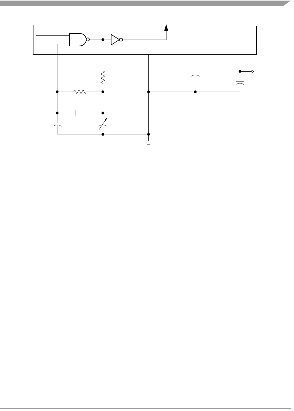
I/O Signals
MC68HC08LN56 • MC68HC708LN56 General Release Specification, Rev. 2.1
Freescale Semiconductor 47
Figure 4-2. CGMB External Connections
4.4 I/O Signals
The following paragraphs describe the CGMB I/O signals.
4.4.1 Crystal Amplifier Input Pin (OSC1)
The OSC1 pin is an input to the crystal oscillator amplifier.
4.4.2 Crystal Amplifier Output Pin (OSC2)
The OSC2 pin is the output of the crystal oscillator inverting amplifier.
4.4.3 External Filter Capacitor Pin (CGMXFC)
The CGMXFC pin is required by the loop filter to filter out phase corrections. A small external capacitor is
connected to this pin.
NOTE
To prevent noise problems, CF should be placed as close to the CGMXFC
pin as possible, with minimum routing distances and no routing of other
signals across the CF connection.
4.4.4 PLL Analog Power Pin (VDDA)
VDDA is a power pin used by the analog portions of the PLL. Connect the VDDA pin to the same voltage
potential as the VDD pin.
NOTE
Route VDDA carefully for maximum noise immunity and place bypass
capacitors as close as possible to the package.
C1C2
CF
SIMOSCEN
CGMXCLK
RB
X1
RS
*
CBYP
OSC1 OSC2 VSS CGMXFC VDDA
*RS can be zero (shorted) when used with higher-frequency crystals. Refer to manufacturer’s data.
VDD

Clock Generator Module (CGMB)
MC68HC08LN56 • MC68HC708LN56 General Release Specification, Rev. 2.1
48 Freescale Semiconductor
4.4.5 PLL Analog Ground Pin (VSSA)
VSSA is a ground pin used by the analog portions of the PLL. Connect the VSSA pin to the same voltage
potential as the VSS pin.
NOTE
Route VSSA carefully for maximum noise immunity and place bypass
capacitors as close as possible to the package.
4.4.6 Buffered Crystal Clock Output (CGMVOUT)
CGMVOUT buffers the OSC1 clock for external use.
4.4.7 CGMVSEL
CGMVSEL must be tied low or floated.
4.4.8 Oscillator Enable Signal (SIMOSCEN)
The SIMOSCEN signal comes from the system integration module (SIM) and enables the oscillator and
PLL.
4.4.9 Crystal Output Frequency Signal (CGMXCLK)
CGMXCLK is the crystal oscillator output signal. It runs at the full speed of the crystal (fXCLK) and comes
directly from the crystal oscillator circuit. Figure 4-2 shows only the logical relation of CGMXCLK to OSC1
and OSC2 and may not represent the actual circuitry. The duty cycle of CGMXCLK is unknown and may
depend on the crystal and other external factors. Also, the frequency and amplitude of CGMXCLK can be
unstable at startup.
4.4.10 CGMB Base Clock Output (CGMOUT)
CGMOUT is the clock output of the CGMB. This signal goes to the SIM, which generates the MCU clocks.
CGMOUT is a 50 percent duty cycle clock running at twice the bus frequency. CGMOUT is software
programmable to be either the oscillator output, CGMXCLK, divided by two or the VCO clock, CGMVCLK,
divided by two.
4.4.11 CGMB CPU Interrupt (CGMINT)
CGMINT is the interrupt signal generated by the PLL lock detector.
4.5 CGMB Registers
These registers control and monitor operation of the CGMB:
• PLL control register (PCTL) (See 4.5.1 PLL Control Register.)
• PLL bandwidth control register (PBWC) (See 4.5.2 PLL Bandwidth Control Register.)
• PLL multiplier select register high (PMSH) (See 4.5.3 PLL Multiplier Select Register High.)
• PLL multiplier select register low (PMSL) (See 4.5.4 PLL Multiplier Select Register Low.)
• PLL VCO range select register (PVRS) (See 4.5.5 PLL VCO Range Select Register.)
• PLL reference divider select register (PRDS) (See 4.5.6 PLL Reference Divider Select Register.)
CGMB Registers
MC68HC08LN56 • MC68HC708LN56 General Release Specification, Rev. 2.1
Freescale Semiconductor 49
Figure 4-3 is a summary of the CGMB registers.
4.5.1 PLL Control Register
The PLL control register contains the interrupt enable and flag bits, the on/off switch, the base clock
selector bit, the prescaler bits, and the VCO power of two range selector bits.
PLLIE — PLL Interrupt Enable Bit
This read/write bit enables the PLL to generate an interrupt request when the LOCK bit toggles, setting
the PLL flag, PLLF. When the AUTO bit in the PLL bandwidth control register (PBWC) is clear, PLLIE
cannot be written and reads as logic zero. Reset clears the PLLIE bit.
1 = PLL interrupts enabled
0 = PLL interrupts disabled
Bit 7654321Bit 0
PCTL
$004A
Read:
PLLIE
PLLF
PLLON BCS
PRE1 PRE0 VPR1 VPR0
Write:
PBWC
$004B
Read:
AUTO
LOCK
ACQ
0000
R
Write:
PMSH
$004C
Read:
MUL11 MUL10 MUL9 MUL8
Write:
PMSL
$004D
Read:
MUL7 MUL6 MUL5 MUL4 MUL3 MUL2 MUL1 MUL0
Write:
PVRS
$004E
Read:
VRS7 VRS6 VRS5 VRS4 VRS3 VRS2 VRS1 VRS0
Write:
PRDS
$004F
Read:
RDS3 RDS2 RDS1 RDS0
Write:
= Unimplemented R = Reserved
NOTES:
1. When AUTO = 0, PLLIE is forced clear and is read-only.
2. When AUTO = 0, PLLF and LOCK read as clear.
3. When AUTO = 1, ACQ is read-only.
4. When PLLON = 0 or VRS7:VRS0 = $0, BCS is forced clear and is read-only.
5. When PLLON = 1, the PLL programming register is read-only.
6. When BCS = 1, PLLON is forced set and is read-only.
Figure 4-3. CGMB I/O Register Summary
PCTL
$004A Bit 7 6 5 43210
Read:
PLLIE
PLLF
PLLON BCS PRE1 PRE0 VPR1 VPR0
Write:
Reset:00100000
= Unimplemented
Figure 4-4. PLL Control Register (PCTL)

Clock Generator Module (CGMB)
MC68HC08LN56 • MC68HC708LN56 General Release Specification, Rev. 2.1
50 Freescale Semiconductor
PLLF — PLL Interrupt Flag Bit
This read-only bit is set whenever the LOCK bit toggles. PLLF generates an interrupt request if the
PLLIE bit also is set. PLLF always reads as logic zero when the AUTO bit in the PLL bandwidth control
register (PBWC) is clear. Clear the PLLF bit by reading the PLL control register. Reset clears the PLLF
bit.
1 = Change in lock condition
0 = No change in lock condition
NOTE
Do not inadvertently clear the PLLF bit. Any read or read-modify-write
operation on the PLL control register clears the PLLF bit.
PLLON — PLL On Bit
This read/write bit activates the PLL and enables the VCO clock, CGMVCLK. PLLON cannot be
cleared if the VCO clock is driving the base clock, CGMOUT (BCS = 1). (See 4.3.8 Base Clock Selector
Circuit.) Reset sets this bit so that the loop can stabilize as the MCU is powering up.
1 = PLL on
0 = PLL off
BCS — Base Clock Select Bit
This read/write bit selects either the crystal oscillator output, CGMXCLK, or the VCO clock,
CGMVCLK, as the source of the CGM output, CGMOUT. CGMOUT frequency is one-half the
frequency of the selected clock. BCS cannot be set while the PLLON bit is clear. After toggling BCS,
it may take up to three CGMXCLK and three CGMVCLK cycles to complete the transition from one
source clock to the other. During the transition, CGMOUT is held in stasis. (See 4.3.8 Base Clock
Selector Circuit.) Reset clears the BCS bit.
1 = CGMVCLK divided by two drives CGMOUT
0 = CGMXCLK divided by two drives CGMOUT
NOTE
PLLON and BCS have built-in protection that prevents the base clock
selector circuit from selecting the VCO clock as the source of the base clock
if the PLL is off. Therefore, PLLON cannot be cleared when BCS is set, and
BCS cannot be set when PLLON is clear. If the PLL is off (PLLON = 0),
selecting CGMVCLK requires two writes to the PLL control register. (See
4.3.8 Base Clock Selector Circuit.)
PRE1 and PRE0 — Prescaler program bits
These read/write bits control a prescaler that selects the prescaler power-of-two multiplier P. (See
4.3.3 PLL Circuits and 4.3.6 Programming the PLL.) PRE1:PRE0 cannot be written when the PLLON
bit is set. Reset clears these bits.
Table 4-2. PRE[1:0] Programming
PRE[1:0] P Prescaler Multiplier
00 0 1
01 1 2
10 2 4
11 3 8
CGMB Registers
MC68HC08LN56 • MC68HC708LN56 General Release Specification, Rev. 2.1
Freescale Semiconductor 51
VPR[1:0] — VCO Power-of-Two Range Select Bits
These read/write bits control the VCO’s hardware power-of-two range multiplier E that, in conjunction
with L (See 4.3.3 PLL Circuits, 4.3.6 Programming the PLL and 4.5.5 PLL VCO Range Select
Register.) controls the hardware center-of-range frequency, fVRS. VPR1:VPR0 cannot be written when
the PLLON bit is set. Reset clears these bits.
4.5.2 PLL Bandwidth Control Register
The PLL bandwidth control register:
• Selects automatic or manual (software-controlled) bandwidth control mode
• Indicates when the PLL is locked
• In automatic bandwidth control mode, indicates when the PLL is in acquisition or tracking mode
• In manual operation, forces the PLL into acquisition or tracking mode
AUTO — Automatic Bandwidth Control Bit
This read/write bit selects automatic or manual bandwidth control. When initializing the PLL for manual
operation (AUTO = 0), clear the ACQ bit before turning on the PLL. Reset clears the AUTO bit.
1 = Automatic bandwidth control
0 = Manual bandwidth control
LOCK — Lock Indicator Bit
When the AUTO bit is set, LOCK is a read-only bit that becomes set when the VCO clock, CGMVCLK,
is locked (running at the programmed frequency). When the AUTO bit is clear, LOCK reads as logic
zero and has no meaning. The write one function of this bit is reserved for test, so this bit must always
be written a zero. Reset clears the LOCK bit.
1 = VCO frequency correct or locked
0 = VCO frequency incorrect or unlocked
Table 4-3. VPR1:VPR0 Programming
VPR1:VPR0 E VCO Power-of-Two
Range Multiplier
00 0 1
01 1 2
10 2 4
11 3 8
PBWC
$004B Bit 7 654321Bit 0
Read:
AUTO
LOCK
ACQ
0000
R
Write:
Reset:00000000
= Unimplemented R = Reserved
Figure 4-5. PLL Bandwidth Control Register (PBWC)
Clock Generator Module (CGMB)
MC68HC08LN56 • MC68HC708LN56 General Release Specification, Rev. 2.1
52 Freescale Semiconductor
ACQ — Acquisition Mode Bit
When the AUTO bit is set, ACQ is a read-only bit that indicates whether the PLL is in acquisition mode
or tracking mode. When the AUTO bit is clear, ACQ is a read/write bit that controls whether the PLL is
in acquisition or tracking mode.
In automatic bandwidth control mode (AUTO = 1), the last-written value from manual operation is
stored in a temporary location and is recovered when manual operation resumes. Reset clears this bit,
enabling acquisition mode.
1 = Tracking mode
0 = Acquisition mode
4.5.3 PLL Multiplier Select Register High
The PLL multiplier select register high contains the programming information for the high byte of the
modulo feedback divider.
MUL[11:8] — Multiplier select bits
These read/write bits control the high byte of the modulo feedback divider that selects the VCO
frequency multiplier N. (See 4.3.3 PLL Circuits and 4.3.6 Programming the PLL.) A value of $0000 in
the multiplier select registers configures the modulo feedback divider the same as a value of $0001.
Reset initializes the registers to $0040 for a default multiply value of 64.
NOTE
The multiplier select bits have built-in protection such that they cannot be
written when the PLL is on (PLLON = 1).
PMSH[7:4] — Unimplemented bits
These bits have no function and always read as logic zeros.
4.5.4 PLL Multiplier Select Register Low
The PLL multiplier select register low contains the programming information for the low byte of the modulo
feedback divider.
PMSH
$004CBit 7654321Bit 0
Read:0000
MUL11 MUL10 MUL9 MUL8
Write:
Reset:00000000
= Unimplemented
Figure 4-6. PLL Multiplier Select Register High (PMSH)
PMSL
$004DBit 7654321Bit 0
Read:
MUL7 MUL6 MUL5 MUL4 MUL3 MUL2 MUL1 MUL0
Write:
Reset:01000000
Figure 4-7. PLL Multiplier Select Register Low (PMSL)

CGMB Registers
MC68HC08LN56 • MC68HC708LN56 General Release Specification, Rev. 2.1
Freescale Semiconductor 53
MUL[7:0] — Multiplier select bits
These read/write bits control the low byte of the modulo feedback divider that selects the VCO
frequency multiplier, N. (See 4.3.3 PLL Circuits and 4.3.6 Programming the PLL.) MUL[7:0] cannot be
written when the PLLON bit in the PCTL is set. A value of $0000 in the multiplier select registers
configures the modulo feedback divider the same as a value of $0001. Reset initializes the register to
$40 for a default multiply value of 64.
NOTE
The multiplier select bits have built-in protection such that they cannot be
written when the PLL is on (PLLON = 1).
4.5.5 PLL VCO Range Select Register
The PLL VCO range select register contains the programming information required for the hardware
configuration of the VCO.
VRS[7:0] — VCO range select bits
These read/write bits control the hardware center-of-range linear multiplier L which, in conjunction with
E (See 4.3.3 PLL Circuits, 4.3.6 Programming the PLL and 4.5.1 PLL Control Register.), controls the
hardware center-of-range frequency, fVRS. VRS[7:0] cannot be written when the PLLON bit in the PCTL
is set. See 4.3.7 Special Programming Exceptions.) A value of $00 in the VCO range select register
disables the PLL and clears the BCS bit in the PLL control register (PCTL). (See 4.3.8 Base Clock
Selector Circuit and 4.3.7 Special Programming Exceptions.). Reset initializes the register to $40 for a
default range multiply value of 64.
NOTE
The VCO range select bits have built-in protection such that they cannot be
written when the PLL is on (PLLON = 1) and such that the VCO clock
cannot be selected as the source of the base clock (BCS = 1) if the VCO
range select bits are all clear.
The PLL VCO range select register must be programmed correctly.
Incorrect programming can result in failure of the PLL to achieve lock.
PVRS
$004E Bit 7 6 5 43210
Read:
VRS7 VRS6 VRS5 VRS4 VRS3 VRS2 VRS1 VRS0
Write:
Reset:01000000
Figure 4-8. PLL VCO Range Select Register (PVRS)

Clock Generator Module (CGMB)
MC68HC08LN56 • MC68HC708LN56 General Release Specification, Rev. 2.1
54 Freescale Semiconductor
4.5.6 PLL Reference Divider Select Register
The PLL reference divider select register contains the programming information for the modulo reference
divider.
RDS[3:0] — Reference Divider Select Bits
These read/write bits control the modulo reference divider that selects the reference division factor R.
(See 4.3.3 PLL Circuits and 4.3.6 Programming the PLL.) RDS[7:0] cannot be written when the PLLON
bit in the PCTL is set. A value of $00 in the reference divider select register configures the reference
divider the same as a value of $01. (See 4.3.7 Special Programming Exceptions.) Reset initializes the
register to $01 for a default divide value of 1.
NOTE
The reference divider select bits have built-in protection such that they
cannot be written when the PLL is on (PLLON = 1).
PRDS[7:4] — Unimplemented Bits
These bits have no function and always read as logic zeros.
4.6 Interrupts
When the AUTO bit is set in the PLL bandwidth control register (PBWC), the PLL can generate a CPU
interrupt request every time the LOCK bit changes state. The PLLIE bit in the PLL control register (PCTL)
enables CPU interrupts from the PLL. PLLF, the interrupt flag in the PCTL, becomes set whether
interrupts are enabled or not. When the AUTO bit is clear, CPU interrupts from the PLL are disabled and
PLLF reads as logic zero.
Software should read the LOCK bit after a PLL interrupt request to see if the request was due to an entry
into lock or an exit from lock. When the PLL enters lock, the VCO clock, CGMVCLK, divided by two can
be selected as the CGMOUT source by setting BCS in the PCTL. When the PLL exits lock, the VCO clock
frequency is corrupt, and appropriate precautions should be taken. If the application is not frequency
sensitive, interrupts should be disabled to prevent PLL interrupt service routines from impeding software
performance or from exceeding stack limitations.
NOTE
Software can select the CGMVCLK divided by two as the CGMOUT source
even if the PLL is not locked (LOCK = 0). Therefore, software should make
sure the PLL is locked before setting the BCS bit.
4.7 Special Modes
The WAIT instruction puts the MCU in low-power-consumption standby modes.
PRDS
$004FBit 7654321Bit 0
Read: 0 0 0 0
RDS3 RDS2 RDS1 RDS0
Write:
Reset:00000001
= Unimplemented
Figure 4-9. PLL Reference Divider Select Register (PRDS)

Acquisition/Lock Time Specifications
MC68HC08LN56 • MC68HC708LN56 General Release Specification, Rev. 2.1
Freescale Semiconductor 55
4.7.1 Wait Mode
The WAIT instruction does not affect the CGMB. Before entering wait mode, software can disengage and
turn off the PLL by clearing the BCS and PLLON bits in the PLL control register (PCTL) to save power.
Less power-sensitive applications can disengage the PLL without turning it off, so that the PLL clock is
immediately available at WAIT exit. This would also be the case when the PLL is to wake the MCU from
wait mode, such as when the PLL is first enabled and waiting for LOCK, or LOCK is lost.
4.7.2 CGMB During Break Interrupts
The system integration module (SIM) controls whether status bits in other modules can be cleared during
the break state. The BCFE bit in the SIM break flag control register (SBFCR) enables software to clear
status bits during the break state. (See 5.7.3 SIM Break Flag Control Register (SBFCR).)
To allow software to clear status bits during a break interrupt, write a logic one to the BCFE bit. If a status
bit is cleared during the break state, it remains cleared when the MCU exits the break state.
To protect the PLLF bit during the break state, write a logic zero to the BCFE bit. With BCFE at logic zero
(its default state), software can read and write the PLL control register during the break state without
affecting the PLLF bit.
4.8 Acquisition/Lock Time Specifications
The acquisition and lock times of the PLL are, in many applications, the most critical PLL design
parameters. Proper design and use of the PLL ensures the highest stability and lowest acquisition/lock
times.
4.8.1 Acquisition/Lock Time Definitions
Typical control systems refer to the acquisition time or lock time as the reaction time, within specified
tolerances, of the system to a step input. In a PLL, the step input occurs when the PLL is turned on or
when it suffers a noise hit. The tolerance is usually specified as a percent of the step input or when the
output settles to the desired value plus or minus a percent of the frequency change. Therefore, the
reaction time is constant in this definition, regardless of the size of the step input. For example, consider
a system with a 5 percent acquisition time tolerance. If a command instructs the system to change from
0 Hz to 1 MHz, the acquisition time is the time taken for the frequency to reach 1 MHz ±50 kHz. Fifty kHz
= 5% of the 1 MHz step input. If the system is operating at 1 MHz and suffers a –100 kHz noise hit, the
acquisition time is the time taken to return from 900 kHz to 1 MHz ±5 kHz. Five kHz = 5 percent of the
100-kHz step input.
Other systems refer to acquisition and lock times as the time the system takes to reduce the error between
the actual output and the desired output to within specified tolerances. Therefore, the acquisition or lock
time varies according to the original error in the output. Minor errors may not even be registered. Typical
PLL applications prefer to use this definition because the system requires the output frequency to be
within a certain tolerance of the desired frequency regardless of the size of the initial error.
The discrepancy in these definitions makes it difficult to specify an acquisition or lock time for a typical
PLL. Therefore, the definitions for acquisition and lock times for this module are:
• Acquisition time, tACQ, is the time the PLL takes to reduce the error between the actual output
frequency and the desired output frequency to less than the tracking mode entry tolerance, ∆TRK.
Acquisition time is based on an initial frequency error,

Clock Generator Module (CGMB)
MC68HC08LN56 • MC68HC708LN56 General Release Specification, Rev. 2.1
56 Freescale Semiconductor
(fDES – fORIG)/fDES, of not more than ±100 percent. In automatic bandwidth control mode (See 4.3.5
Manual and Automatic PLL Bandwidth Modes.), acquisition time expires when the ACQ bit
becomes set in the PLL bandwidth control register (PBWC).
• Lock time, tLOCK, is the time the PLL takes to reduce the error between the actual output frequency
and the desired output frequency to less than the lock mode entry tolerance, ∆LOCK. Lock time is
based on an initial frequency error, (fDES – fORIG)/fDES, of not more than ±100 percent. In automatic
bandwidth control mode, lock time expires when the LOCK bit becomes set in the PLL bandwidth
control register (PBWC). (See 4.3.5 Manual and Automatic PLL Bandwidth Modes.)
Obviously, the acquisition and lock times can vary according to how large the frequency error is and may
be shorter or longer in many cases.
4.8.2 Parametric Influences on Reaction Time
Acquisition and lock times are designed to be as short as possible while still providing the highest possible
stability. These reaction times are not constant, however. Many factors directly and indirectly affect the
acquisition time.
The most critical parameter which affects the reaction times of the PLL is the reference frequency, fRDV.
This frequency is the input to the phase detector and controls how often the PLL makes corrections. For
stability, the corrections must be small compared to the desired frequency, so several corrections are
required to reduce the frequency error. Therefore, the slower the reference the longer it takes to make
these corrections. This parameter is under user control via the choice of crystal frequency fXCLK and the R
value programmed in the reference divider. (See 4.3.3 PLL Circuits, 4.3.6 Programming the PLL, and
4.5.6 PLL Reference Divider Select Register.)
Another critical parameter is the external filter capacitor. The PLL modifies the voltage on the VCO by
adding or subtracting charge from this capacitor. Therefore, the rate at which the voltage changes for a
given frequency error (thus change in charge) is proportional to the capacitor size. The size of the
capacitor also is related to the stability of the PLL. If the capacitor is too small, the PLL cannot make small
enough adjustments to the voltage and the system cannot lock. If the capacitor is too large, the PLL may
not be able to adjust the voltage in a reasonable time. (See 4.8.3 Choosing a Filter Capacitor.)
Also important is the operating voltage potential applied to VDDA. The power supply potential alters the
characteristics of the PLL. A fixed value is best. Variable supplies, such as batteries, are acceptable if
they vary within a known range at very slow speeds. Noise on the power supply is not acceptable,
because it causes small frequency errors which continually change the acquisition time of the PLL.
Temperature and processing also can affect acquisition time because the electrical characteristics of the
PLL change. The part operates as specified as long as these influences stay within the specified limits.
External factors, however, can cause drastic changes in the operation of the PLL. These factors include
noise injected into the PLL through the filter capacitor, filter capacitor leakage, stray impedances on the
circuit board, and even humidity or circuit board contamination.
4.8.3 Choosing a Filter Capacitor
As described in 4.8.2 Parametric Influences on Reaction Time, the external filter capacitor, CF, is critical
to the stability and reaction time of the PLL. The PLL is also dependent on reference frequency and supply
voltage. The value of the capacitor must, therefore, be chosen with supply potential and reference

Acquisition/Lock Time Specifications
MC68HC08LN56 • MC68HC708LN56 General Release Specification, Rev. 2.1
Freescale Semiconductor 57
frequency in mind. For proper operation, the external filter capacitor must be chosen according to this
equation:
For the value of VDDA, choose the voltage potential at which the MCU is operating. If the power supply is
variable, choose a value near the middle of the range of possible supply values.
This equation does not always yield a commonly available capacitor size, so round to the nearest
available size. If the value is between two different sizes, choose the higher value for better stability.
Choosing the lower size may seem attractive for acquisition time improvement, but the PLL may become
unstable. Also, always choose a capacitor with a tight tolerance (±20 percent or better) and low
dissipation.
4.8.4 Reaction Time Calculation
The actual acquisition and lock times can be calculated using the equations below. These equations yield
nominal values under the following conditions:
• Correct selection of filter capacitor, CF (See 4.8.3 Choosing a Filter Capacitor.)
• Room temperature operation
• Negligible external leakage on CGMXFC
• Negligible noise
The K factor in the equations is derived from internal PLL parameters. KACQ is the K factor when the PLL
is configured in acquisition mode, and KTRK is the K factor when the PLL is configured in tracking mode.
(See 4.3.4 Acquisition and Tracking Modes.) Reaction time is based on an initial frequency error, (fDES –
fORIG)/fDES, of not more than ±100 percent.
NOTE
The inverse proportionality between the lock time and the reference
frequency.
In automatic bandwidth control mode, the acquisition and lock times are quantized into units based on the
reference frequency. (See 4.3.5 Manual and Automatic PLL Bandwidth Modes.) A certain number of clock
cycles, nACQ, is required to ascertain that the PLL is within the tracking mode entry tolerance, ∆TRK, before
exiting acquisition mode. A certain number of clock cycles, nTRK, is required to ascertain that the PLL is
within the lock mode entry tolerance, ∆LOCK. Therefore, the acquisition time, tACQ, is an integer multiple of
nACQ/fRDV, and the acquisition to lock time, tAL, is an integer multiple of nTRK/fRDV.
In manual mode, it is usually necessary to wait considerably longer than tLOCKMAX before selecting the PLL
clock (See 4.3.8 Base Clock Selector Circuit.), because the factors described in 4.8.2 Parametric
Influences on Reaction Time may slow the lock time considerably. Automatic bandwidth mode is
recommended for most users.
CFCFACT
VDDA
fRDV
-----------------
⎝⎠
⎜⎟
⎛⎞
=
tACQ
VDDA
fRDV
-----------------
⎝⎠
⎜⎟
⎛⎞
8
KACQ
-----------------
⎝⎠
⎛⎞
=
tAL
VDDA
fRDV
-----------------
⎝⎠
⎜⎟
⎛⎞
4
KTRK
----------------
⎝⎠
⎛⎞
=
tLOCKMAX tACQ tAL
+=256t
VRDV
+

Clock Generator Module (CGMB)
MC68HC08LN56 • MC68HC708LN56 General Release Specification, Rev. 2.1
58 Freescale Semiconductor
4.9 Numerical Electrical Specifications
Table 4-4 contains numerical specification limits on environmental inputs and module outputs.
Table 4-4. Electrical Specifications
Description Symbol Min Typ Max Notes
Operating Voltage VDD 1.8 V — 5.5 V
Operating Temperature T –40 oC25
oC 130 oC
Crystal Reference Frequency fRCLK — 38.4 kHz —
Range Nominal Multiplier (Hz)
fNOM
— 38.4 k — 4.0–5.5 V VDD only
Range Nominal Multiplier
Medium Voltage (Hz) — 38.4 k — 2.7–4.0 V VDD only
Range Nominal Multiplier
Low Voltage (Hz) — 38.4 k — 1.8–2.7 V VDD
VCO Center-of-Range
Frequency (Hz)
fVRS
38.4k — 80.0 M 4.0–5.5 V VDD only
Medium Voltage VCO Center-of-Range
Frequency (Hz) 38.4k — 40.0 M 2.7–4.0 V VDD only
Low Voltage VCO Nominal
Frequency (MHz) 38.4k — 10.0 M 1.8-2.7 V VDD
VCO Range Linear Range Multiplier L 1 64 255
VCO Power-of-Two Range Multiplier 2E118
VCO Multiply Factor N 1 64 4095
VCO Prescale Multiplier 2P118
Reference Divider Factor R 1 1 15
VCO Operating Frequency fVCLK fVRSMIN —fVRSMAX
Bus Operating Frequency (Hz) fBUS ——8 M
4.0–5.5 V VDD only
Bus Frequency (Hz)
Medium Voltage fBUS ——4 M
2.7–4.0 V VDD only
Bus Frequency (Hz)
Low Voltage fBUS ——2 M
1.8–2.7 V VDD only

Acquisition/Lock Time Specifications
MC68HC08LN56 • MC68HC708LN56 General Release Specification, Rev. 2.1
Freescale Semiconductor 59
4.10 Acquisition/Lock Time Specifications
Table 4-5 provides specifications for the entry and exit of acquisition and tracking modes, as well as
required manual mode delay times.
Table 4-5. Acquisition/Lock Time Specifications
Description Symbol Min Typ Max Notes
Filter Capacitor Multiply Factor CFACT — 0.0145 — F/s V
Acquisition Mode Time Factor KACQ —0.117—V
Tracking Mode Time Factor KTRK —0.021—V
Manual Mode Time to Stable tACQ —(8*VDDA)/
(fRDV*KACQ)
—If CF chosen correctly
Manual Stable to Lock Time tAL —(4*VDDA)/
(fRDV*KTRK)—If CF chosen correctly
Manual Acquisition Time tLOCK —tACQ+tAL —
Tracking Mode Entry Frequency
Tolerance ∆TRK 0—± 3.6%
Acquisition Mode Entry Frequency
Tolerance ∆ACQ ± 6.3% — ± 7.2%
LOCK Entry Frequency Tolerance ∆LOCK 0—± 0.9%
LOCK Exit Frequency Tolerance ∆UNL ± 0.9% — ± 1.8%
Reference Cycles Per Acquisition
Mode Measurement nACQ 32 —
Reference Cycles Per Tracking Mode
Measurement nTRK 128 —
Automatic Mode Time to Stable tACQ nACQ/fRDV
(8*VDDA)/
(fRDV*KACQ)
—If CF chosen correctly
Automatic Stable to Lock Time tAL nTRK/fRDV
(4*VDDA)/
(fRDV*KTRK)—If CF chosen correctly
Automatic Lock Time tLOCK —tACQ+tAL —

Clock Generator Module (CGMB)
MC68HC08LN56 • MC68HC708LN56 General Release Specification, Rev. 2.1
60 Freescale Semiconductor

MC68HC08LN56 • MC68HC708LN56 General Release Specification, Rev. 2.1
Freescale Semiconductor 61
Chapter 5
System Integration Module (SIM)
5.1 Introduction
This section describes the system integration module (SIM), which supports up to 24 external and/or
internal interrupts. Together with the CPU, the SIM controls all MCU activities. A block diagram of the SIM
is shown in Figure 5-2. Figure 5-1 is a summary of the SIM I/O registers. The SIM is a system state
controller that coordinates CPU and exception timing. The SIM is responsible for:
• Bus clock generation and control for CPU and peripherals
– Stop/wait/reset/break entry and recovery
– Internal clock control
• Master reset control, including power-on reset (POR) and COP timeout
• Interrupt control
– Acknowledge timing
– Arbitration control timing
– Vector address generation
• CPU enable/disable timing
• Modular architecture expandable to 128 interrupt sources
Table 5-1 shows the internal signal names used in this section.
Addr. Register Name Bit 7654321Bit 0
$FE00 SIM Break Status Register
(SBSR) R R R R R R SBSW R
$FE01 SIM Reset Status Register
(SRSR) POR PIN COP ILOP ILAD 0 LVI 0
$FE03 SIM Break Flag Control Register
(SBFCR) BCFE0000000
$FE04 Interrupt Status Register 1
(INT1) I6 I5 I4 I3 I2 I1 0 0
$FE05 Interrupt Status Register 2
(INT2) I14 I13 I12 I11 I10 I9 I8 I7
$FE06 Interrupt Status Register 3
(INT3) 0 0 0 0 I18 I17 I16 I15
R = Reserved for factory test
Figure 5-1. SIM I/O Register Summary
System Integration Module (SIM)
MC68HC08LN56 • MC68HC708LN56 General Release Specification, Rev. 2.1
62 Freescale Semiconductor
Figure 5-2. SIM Block Diagram
Table 5-1. Signal Name Conventions
Signal Name Description
CGMXCLK Buffered version of OSC1 from clock generator module (CGM)
CGMVCLK PLL output
CGMOUT PLL-based or OSC1-based clock output from CGM module
(Bus clock = CGMOUT divided by two)
IAB Internal address bus
IDB Internal data bus
PORRST Signal from the power-on reset module to the SIM
IRST Internal reset signal
R/W Read/write signal
STOP/WAIT
CLOCK
CONTROL CLOCK GENERATORS
POR CONTROL
RESET PIN CONTROL
SIM RESET STATUS REGISTER
INTERRUPT CONTROL
AND PRIORITY DECODE
MODULE STOP
MODULE WAIT
CPU STOP (FROM CPU)
CPU WAIT (FROM CPU)
SIMOSCEN (TO CGM)
CGMOUT (FROM CGM)
INTERNAL CLOCKS
MASTER
RESET
CONTROL
RESET
PIN LOGIC
LVI (FROM LVI MODULE)
ILLEGAL OPCODE (FROM CPU)
ILLEGAL ADDRESS (FROM ADDRESS
MAP DECODERS)
COP (FROM COP MODULE)
INTERRUPT SOURCES
CPU INTERFACE
RESET
CONTROL
SIM
COUNTER COP CLOCK
CGMXCLK (FROM CGM)
÷ 2
SIM Bus Clock Control and Generation
MC68HC08LN56 • MC68HC708LN56 General Release Specification, Rev. 2.1
Freescale Semiconductor 63
5.2 SIM Bus Clock Control and Generation
The bus clock generator provides system clock signals for the CPU and peripherals on the MCU. The
system clocks are generated from an incoming clock, CGMOUT, as shown in Figure 5-3. This clock can
come from either an external oscillator or from the on-chip PLL. (See Chapter 4 Clock Generator Module
(CGMB).)
Figure 5-3. CGM Clock Signals
5.2.1 Bus Timing
In user mode, the internal bus frequency is either the crystal oscillator output (CGMXCLK) divided by four
or the PLL output (CGMVCLK) divided by four. (See Chapter 8 External Interrupt Module (IRQ).)
5.2.2 Clock Start-Up from POR or LVI Reset
When the power-on reset module or the low-voltage inhibit module generates a reset, the clocks to the
CPU and peripherals are inactive and held in an inactive phase until after the 4096 CGMXCLK cycle POR
timeout has completed. The RST pin is driven low by the SIM during this entire period. The IBUS clocks
start upon completion of the timeout.
5.2.3 Clocks in Stop Mode and Wait Mode
Upon exit from stop mode by an interrupt, break, or reset, the SIM allows CGMXCLK to clock the SIM
counter. The CPU and peripheral clocks do not become active until after the stop delay timeout. This
timeout is selectable as 4096 or 32 CGMXCLK cycles. (See 5.6.2 Stop Mode.)
In wait mode, the CPU clocks are inactive. The SIM also produces two sets of clocks for other modules.
Refer to the wait mode subsection of each module to see if the module is active or inactive in wait mode.
Some modules can be programmed to be active in wait mode.
PLL
OSC1 CGMXCLK
÷ 2BUS CLOCK
GENERATORS
SIM
CGM
SIM COUNTER
PTC3
MONITOR MODE
CLOCK
SELECT
CIRCUIT
CGMVCLK
BCS
÷ 2
A
BS*
CGMOUT
*When S = 1,
CGMOUT = B
USER MODE
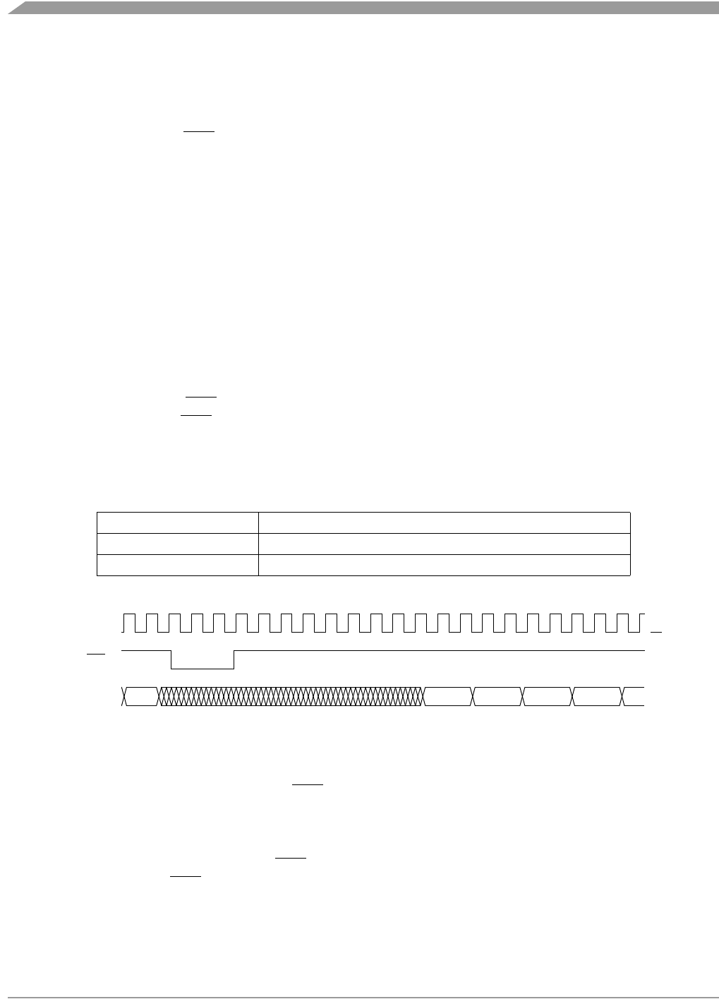
System Integration Module (SIM)
MC68HC08LN56 • MC68HC708LN56 General Release Specification, Rev. 2.1
64 Freescale Semiconductor
5.3 Reset and System Initialization
The MCU has these reset sources:
• Power-on reset module (POR)
• External reset pin (RST)
• Computer operating properly module (COP)
• Low-voltage inhibit module (LVI)
• Illegal opcode
• Illegal address
All of these resets produce the vector $FFFE:FFFF ($FEFE:FEFF in monitor mode) and assert the
internal reset signal (IRST). IRST causes all registers to be returned to their default values and all
modules to be returned to their reset states.
An internal reset clears the SIM counter (see 5.4 SIM Counter), but an external reset does not. Each of
the resets sets a corresponding bit in the SIM reset status register (SRSR). (See 5.7 SIM Registers.)
5.3.1 External Pin Reset
Pulling the asynchronous RST pin low halts all processing. The PIN bit of the SIM reset status register
(SRSR) is set as long as RST is held low for a minimum of 67 CGMXCLK cycles, assuming that neither
the POR nor the LVI was the source of the reset. See Table 5-2 for details. Figure 5-4 shows the relative
timing.
Figure 5-4. External Reset Timing
5.3.2 Active Resets from Internal Sources
All internal reset sources actively pull the RST pin low for 32 CGMXCLK cycles to allow resetting of
external peripherals. The internal reset signal IRST continues to be asserted for an additional 32 cycles.
See Figure 5-5. An internal reset can be caused by an illegal address, illegal opcode, COP timeout, LVI,
or POR. (See Figure 5-6.) Note that for LVI or POR resets, the SIM cycles through 4096 CGMXCLK
cycles during which the SIM forces the RST pin low. The internal reset signal then follows the sequence
from the falling edge of RST shown in Figure 5-5.
Table 5-2. PIN Bit Set Timing
Reset Type Number of Cycles Required to Set PIN
POR/LVI 4163 (4096 + 64 + 3)
All others 67 (64 + 3)
RST
IAB PC VECT H VECT L
CGMOUT
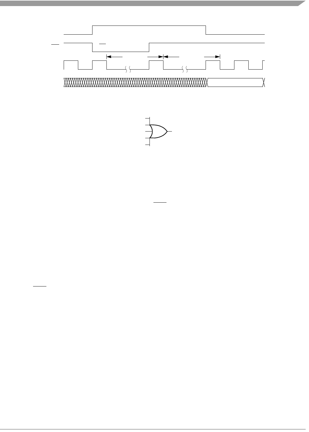
Reset and System Initialization
MC68HC08LN56 • MC68HC708LN56 General Release Specification, Rev. 2.1
Freescale Semiconductor 65
Figure 5-5. Internal Reset Timing
The COP reset is asynchronous to the bus clock.
Figure 5-6. Sources of Internal Reset
The active reset feature allows the part to issue a reset to peripherals and other chips within a system
built around the MCU.
5.3.2.1 Power-On Reset
When power is first applied to the MCU, the power-on reset module (POR) generates a pulse to indicate
that power-on has occurred. The external reset pin (RST) is held low while the SIM counter counts out
4096 CGMXCLK cycles. Sixty-four CGMXCLK cycles later, the CPU and memories are released from
reset to allow the reset vector sequence to occur.
At power-on, these events occur:
• A POR pulse is generated.
• The internal reset signal is asserted.
• The SIM enables CGMOUT.
• Internal clocks to the CPU and modules are held inactive for 4096 CGMXCLK cycles to allow
stabilization of the oscillator.
•The RST
pin is driven low during the oscillator stabilization time.
• The POR bit of the SIM reset status register (SRSR) is set and all other bits in the register are
cleared.
IRST
RST RST PULLED LOW BY MCU
IAB
32 CYCLES 32 CYCLES
VECTOR HIGH
CGMXCLK
ILLEGAL ADDRESS RST
ILLEGAL OPCODE RST
COPRST
LVI
POR
INTERNAL RESET
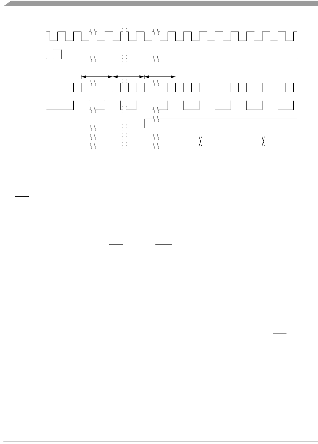
System Integration Module (SIM)
MC68HC08LN56 • MC68HC708LN56 General Release Specification, Rev. 2.1
66 Freescale Semiconductor
Figure 5-7. POR Recovery
5.3.2.2 Computer Operating Properly (COP) Reset
An input to the SIM is reserved for the COP reset signal. The overflow of the COP counter causes an
internal reset and sets the COP bit in the SIM reset status register (SRSR). The SIM actively pulls down
the RST pin for all internal reset sources.
To prevent a COP module timeout, write any value to location $FFFF. Writing to location $FFFF clears
the COP counter and bits 12 through 4 of the SIM counter. The SIM counter output, which occurs at least
every 213 – 24 CGMXCLK cycles, drives the COP counter. The COP should be serviced as soon as
possible out of reset to guarantee the maximum amount of time before the first timeout.
The COP module is disabled if the RST pin or the IRQ1/V<st-subsmallcaps>pp pin is held at VDD +V
HI
while the MCU is in monitor mode. The COP module can be disabled only through combinational logic
conditioned with the high voltage signal on the RST or the IRQ1/V<st-subsmallcaps>pp pin. This prevents
the COP from becoming disabled as a result of external noise. During a break state, VDD +V
HI on the RST
pin disables the COP module.
5.3.2.3 Illegal Opcode Reset
The SIM decodes signals from the CPU to detect illegal instructions. An illegal instruction sets the ILOP
bit in the SIM reset status register (SRSR) and causes a reset.
If the stop enable bit, STOP, in the mask option register is logic zero, the SIM treats the STOP instruction
as an illegal opcode and causes an illegal opcode reset. The SIM actively pulls down the RST pin for all
internal reset sources.
5.3.2.4 Illegal Address Reset
An opcode fetch from an unmapped address generates an illegal address reset. The SIM verifies that the
CPU is fetching an opcode prior to asserting the ILAD bit in the SIM reset status register (SRSR) and
resetting the MCU. A data fetch from an unmapped address does not generate a reset. The SIM actively
pulls down the RST pin for all internal reset sources.
PORRST
OSC1
CGMXCLK
CGMOUT
RST
IAB
4096
CYCLES
32
CYCLES
32
CYCLES
$FFFE $FFFF

SIM Counter
MC68HC08LN56 • MC68HC708LN56 General Release Specification, Rev. 2.1
Freescale Semiconductor 67
5.3.2.5 Low-Voltage Inhibit (LVI) Reset
The low-voltage inhibit module (LVI) asserts its output to the SIM when the VDD voltage falls to the LVITRIPF
voltage. The LVI bit in the SIM reset status register (SRSR) is set, and the external reset pin (RST) is held
low while the SIM counter counts out 4096 CGMXCLK cycles. Sixty-four CGMXCLK cycles later, the CPU
is released from reset to allow the reset vector sequence to occur. The SIM actively pulls down the RST
pin for all internal reset sources.
5.4 SIM Counter
The SIM counter is used by the power-on reset module (POR) and in stop mode recovery to allow the
oscillator time to stabilize before enabling the internal bus (IBUS) clocks. The SIM counter also serves as
a prescaler for the computer operating properly module (COP). The SIM counter overflow supplies the
clock for the COP module. The SIM counter is 13 bits long and is clocked by the falling edge of
CGMXCLK.
5.4.1 SIM Counter During Power-On Reset
The power-on reset module (POR) detects power applied to the MCU. At power-on, the POR circuit
asserts the signal PORRST. Once the SIM is initialized, it enables the clock generation module (CGM) to
drive the bus clock state machine.
5.4.2 SIM Counter During Stop Mode Recovery
The SIM counter also is used for stop mode recovery. The STOP instruction clears the SIM counter. After
an interrupt, break, or reset, the SIM senses the state of the short stop recovery bit, SSREC, in the mask
option register. If the SSREC bit is a logic one, then the stop recovery is reduced from the normal delay
of 4096 CGMXCLK cycles down to 32 CGMXCLK cycles. This is ideal for applications using canned
oscillators that do not require long startup times from stop mode. External crystal applications should use
the full stop recovery time, that is, with SSREC cleared.
5.4.3 SIM Counter and Reset States
External reset has no effect on the SIM counter. (See 5.6.2 Stop Mode for details.) The SIM counter is
free-running after all reset states. (See 5.3.2 Active Resets from Internal Sources for counter control and
internal reset recovery sequences.)
5.5 Exception Control
Normal, sequential program execution can be changed in three different ways:
• Interrupts
– Maskable hardware CPU interrupts
– Non-maskable software interrupt instruction (SWI)
• Reset
• Break interrupts
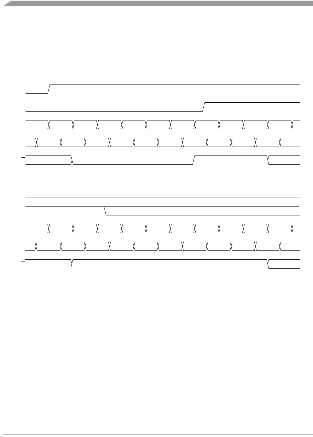
System Integration Module (SIM)
MC68HC08LN56 • MC68HC708LN56 General Release Specification, Rev. 2.1
68 Freescale Semiconductor
5.5.1 Interrupts
At the beginning of an interrupt, the CPU saves the CPU register contents on the stack and sets the
interrupt mask (I bit) to prevent additional interrupts. At the end of an interrupt, the RTI instruction
recovers the CPU register contents from the stack so that normal processing can resume. Figure 5-8
shows interrupt entry timing. Figure 5-9 shows interrupt recovery timing.
Figure 5-8. Interrupt Entry
Figure 5-9. Interrupt Recovery
Interrupts are latched, and arbitration is performed in the SIM at the start of interrupt processing. The
arbitration result is a constant that the CPU uses to determine which vector to fetch. Once an interrupt is
latched by the SIM, no other interrupt can take precedence, regardless of priority, until the latched
interrupt is serviced (or the I bit is cleared). (See Figure 5-10.)
MODULE
IDB
R/W
INTERRUPT
DUMMY SP SP – 1 SP – 2 SP – 3 SP – 4 VECT H VECT L START ADDR
IAB
DUMMY PC – 1[7:0] PC – 1[15:8] X A CCR V DATA H V DATA L OPCODE
I BIT
MODULE
IDB
R/W
INTERRUPT
SP – 4 SP – 3 SP – 2 SP – 1 SP PC PC + 1
IAB
CCR A X PC – 1 [7:0] PC – 1 [15:8] OPCODE OPERAND
I BIT
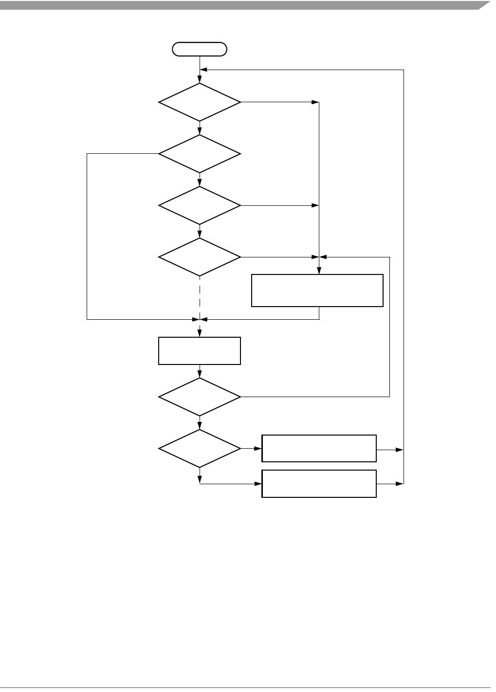
Exception Control
MC68HC08LN56 • MC68HC708LN56 General Release Specification, Rev. 2.1
Freescale Semiconductor 69
Figure 5-10. Interrupt Processing
NO
NO
NO
YES
NO
NO
YES
NO
YES
YES
AS MANY INTERRUPTS
I BIT SET?
FROM RESET
BREAK INTERRUPT?
I BIT SET?
IRQ0
INTERRUPT?
IRQ1
INTERRUPT?
SWI
INSTRUCTION?
RTI
INSTRUCTION?
FETCH NEXT
INSTRUCTION.
UNSTACK CPU REGISTERS.
STACK CPU REGISTERS.
SET I BIT.
LOAD PC WITH INTERRUPT VECTOR.
EXECUTE INSTRUCTION.
YES
YES
AS EXIST ON CHIP
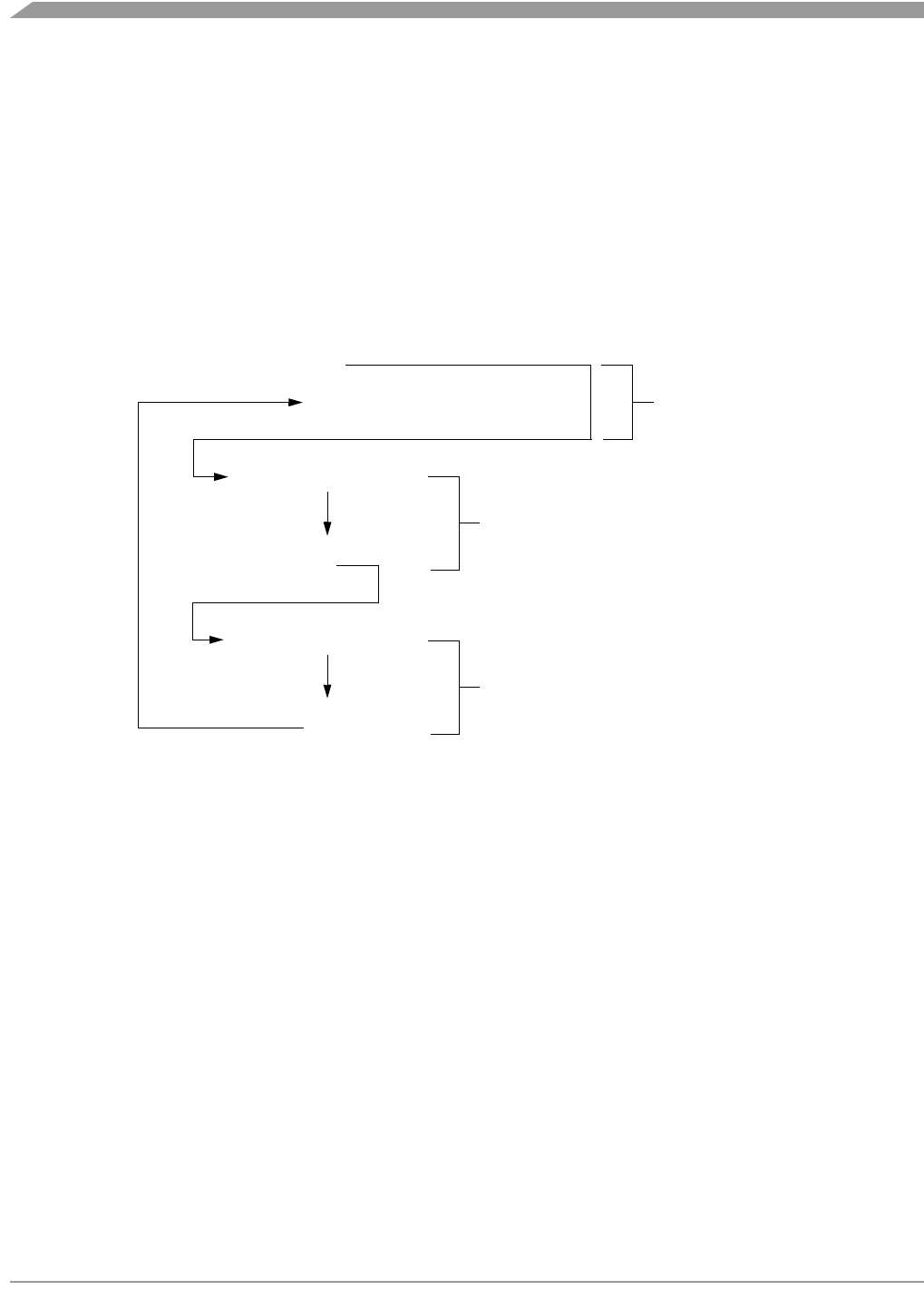
System Integration Module (SIM)
MC68HC08LN56 • MC68HC708LN56 General Release Specification, Rev. 2.1
70 Freescale Semiconductor
5.5.1.1 Hardware Interrupts
A hardware interrupt does not stop the current instruction. Processing of a hardware interrupt begins after
completion of the current instruction. When the current instruction is complete, the SIM checks all pending
hardware interrupts. If interrupts are not masked (I bit clear in the condition code register) and if the
corresponding interrupt enable bit is set, the SIM proceeds with interrupt processing; otherwise, the next
instruction is fetched and executed.
If more than one interrupt is pending at the end of an instruction execution, the highest priority interrupt is
serviced first. Figure 5-11 demonstrates what happens when two interrupts are pending. If an interrupt is
pending upon exit from the original interrupt service routine, the pending interrupt is serviced before the
LDA instruction is executed.
Figure 5-11. Interrupt Recognition Example
The LDA opcode is prefetched by both the INT1 and INT2 RTI instructions. However, in the case of the
INT1 RTI prefetch, this is a redundant operation.
NOTE
To maintain compatibility with the M6805 Family, the H register is not
pushed on the stack during interrupt entry. If the interrupt service routine
modifies the H register or uses the indexed addressing mode, software
should save the H register and then restore it prior to exiting the routine.
5.5.1.2 SWI Instruction
The SWI instruction is a non-maskable instruction that causes an interrupt regardless of the state of the
interrupt mask (I bit) in the condition code register.
NOTE
A software interrupt pushes PC onto the stack. A software interrupt does
not push PC – 1, as a hardware interrupt does.
CLI
LDA
INT1
PULH
RTI
INT2
BACKGROUND ROUTINE#$FF
PSHH
INT1 INTERRUPT SERVICE ROUTINE
PULH
RTI
PSHH
INT2 INTERRUPT SERVICE ROUTINE
Exception Control
MC68HC08LN56 • MC68HC708LN56 General Release Specification, Rev. 2.1
Freescale Semiconductor 71
5.5.1.3 Interrupt Status Registers
The flags in the interrupt status registers identify maskable interrupt sources. Table 5-3 summarizes the
interrupt sources and the interrupt status register flags that they set. The interrupt status registers can be
useful for debugging.
Table 5-3. Interrupt Sources
Interrupt Source Interrupt Status
Register Flag
Reset —
SWI Instruction —
IRQ1 Pin I1
PLL I2
TIM Channel 0 I3
TIM Channel 1 I4
TIM Channel 2 I5
TIM Channel 3 I6
TIM Overflow I7
SPI 1 Receiver I8
SPI 1 Transmitter I9
SPI 2 Receiver I10
SCI 2 Transmitter I11
SCI Error I12
SCI Receiver I13
SCI Transmitter I14
IRQ2 Pin I15
Keyboard Pin I16
A/D I17
TBM I18
System Integration Module (SIM)
MC68HC08LN56 • MC68HC708LN56 General Release Specification, Rev. 2.1
72 Freescale Semiconductor
Interrupt Status Register 1
I6–I1 — Interrupt Flags 1–6
These flags indicate the presence of interrupt requests from the sources shown in Table 5-3.
1 = Interrupt request present
0 = No interrupt request present
Bit 0 and Bit 1 — Always read 0
Interrupt Status Register 2
I14–I7 — Interrupt Flags 14–7
These flags indicate the presence of interrupt requests from the sources shown in Table 5-3.
1 = Interrupt request present
0 = No interrupt request present
Interrupt Status Register 3
Bits 7–4 — Always read 0
I18–I15 — Interrupt Flags 15–18
These flags indicate the presence of an interrupt request from the source shown in Table 5-3.
1 = Interrupt request present
0 = No interrupt request present
Address: $FE04
Bit 7654321Bit 0
Read:I6I5I4I3I2I1 0 0
Write:RRRRRRRR
Reset:00000000
R= Reserved
Figure 5-12. Interrupt Status Register 1 (INT1)
Address: $FE05
Bit 7654321Bit 0
Read: I14 I13 I12 I11 I10 I9 I8 I7
Write:RRRRRRRR
Reset:00000000
R= Reserved
Figure 5-13. Interrupt Status Register 2 (INT2)
Address: $FE06
Bit 7654321Bit 0
Read:0000I18I17I16I15
Write:RRRRRRRR
Reset:00000000
R= Reserved
Figure 5-14. Interrupt Status Register 3 (INT3)

Low-Power Modes
MC68HC08LN56 • MC68HC708LN56 General Release Specification, Rev. 2.1
Freescale Semiconductor 73
5.5.2 Reset
All reset sources always have equal and highest priority and cannot be arbitrated.
5.5.3 Break Interrupts
The break module can stop normal program flow at a software-programmable break point by asserting its
break interrupt output. (See Chapter 10 Timer Interface Module (TIM).) The SIM puts the CPU into the
break state by forcing it to the SWI vector location. Refer to the break interrupt subsection of each module
to see how each module is affected by the break state.
5.5.4 Status Flag Protection in Break Mode
The SIM controls whether status flags contained in other modules can be cleared during break mode. The
user can select whether flags are protected from being cleared by properly initializing the break clear flag
enable bit (BCFE) in the SIM break flag control register (SBFCR).
Protecting flags in break mode ensures that set flags will not be cleared while in break mode. This
protection allows registers to be freely read and written during break mode without losing status flag
information.
Setting the BCFE bit enables the clearing mechanisms. Once cleared in break mode, a flag remains
cleared even when break mode is exited. Status flags with a two-step clearing mechanism — for example,
a read of one register followed by the read or write of another — are protected, even when the first step
is accomplished prior to entering break mode. Upon leaving break mode, execution of the second step
will clear the flag as normal.
5.6 Low-Power Modes
Executing the WAIT or STOP instruction puts the MCU in a low-power-consumption mode for standby
situations. The SIM holds the CPU in a non-clocked state. The operation of each of these modes is
described in the following subsections. Both STOP and WAIT clear the interrupt mask (I) in the condition
code register, allowing interrupts to occur.
5.6.1 Wait Mode
In wait mode, the CPU clocks are inactive while the peripheral clocks continue to run. Figure 5-15 shows
the timing for wait mode entry.
A module that is active during wait mode can wake up the CPU with an interrupt if the interrupt is enabled.
Stacking for the interrupt begins one cycle after the WAIT instruction during which the interrupt occurred.
In wait mode, the CPU clocks are inactive. Refer to the wait mode subsection of each module to see if
the module is active or inactive in wait mode. Some modules can be programmed to be active in wait
mode.
Wait mode also can be exited by a reset or break. A break interrupt during wait mode sets the SIM break
stop/wait bit, SBSW, in the SIM break status register (SBSR). If the COP disable bit, COPD, in the mask
option register is logic zero, then the computer operating properly module (COP) is enabled and remains
active in wait mode.
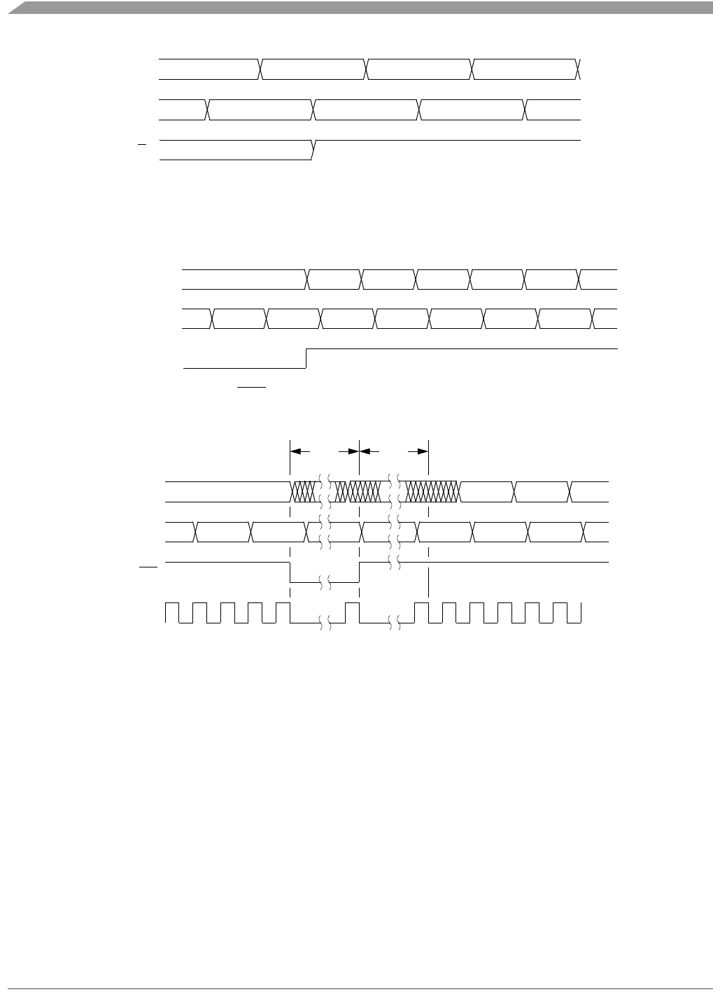
System Integration Module (SIM)
MC68HC08LN56 • MC68HC708LN56 General Release Specification, Rev. 2.1
74 Freescale Semiconductor
Figure 5-15. Wait Mode Entry Timing
Figure 5-16 and Figure 5-17 show the timing for WAIT recovery.
Figure 5-16. Wait Recovery from Interrupt or Break
Figure 5-17. Wait Recovery from Internal Reset
5.6.2 Stop Mode
In stop mode, the SIM counter is reset and the system clocks are disabled. An interrupt request from a
module can cause an exit from stop mode. Stacking for interrupts begins after the selected stop recovery
time has elapsed. Reset or break also causes an exit from stop mode.
The SIM disables the clock generator module outputs (CGMOUT and CGMXCLK) in stop mode, stopping
the CPU and peripherals. Stop recovery time is selectable using the SSREC bit in the mask option register
(MOR). If SSREC is set, stop recovery is reduced from the normal delay of 4096 CGMXCLK cycles down
to 32. This is ideal for applications using canned oscillators that do not require long startup times from
stop mode.
NOTE
External crystal applications should use the full stop recovery time by
clearing the SSREC bit.
WAIT ADDR + 1 SAME SAMEIAB
IDB PREVIOUS DATA NEXT OPCODE SAME
WAIT ADDR
SAME
R/W
NOTE: Previous data can be operand data or the WAIT opcode, depending on the
last instruction.
$6E0C$6E0B $00FF $00FE $00FD $00FC
$A6 $A6 $01 $0B $6E$A6
IAB
IDB
EXITSTOPWAIT
NOTE: EXITSTOPWAIT = RST pin, CPU interrupt, or break interrupt
IAB
IDB
RST
$A6 $A6
$6E0B RST VCT H RST VCT L
$A6
CGMXCLK
32
CYCLES
32
CYCLES
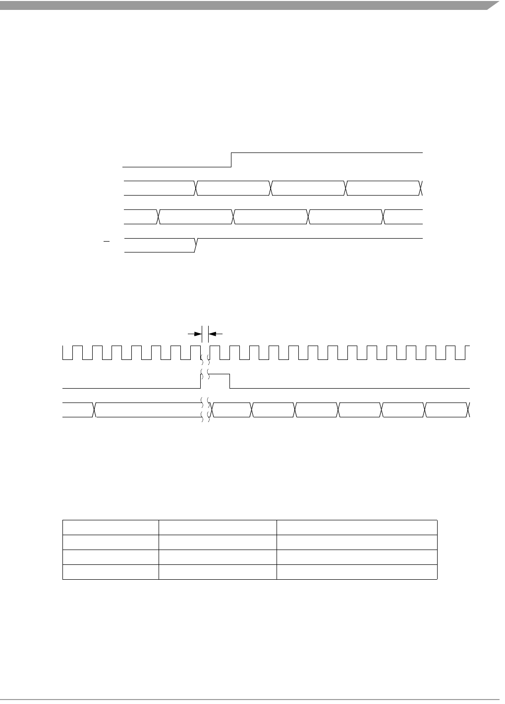
SIM Registers
MC68HC08LN56 • MC68HC708LN56 General Release Specification, Rev. 2.1
Freescale Semiconductor 75
A break interrupt during stop mode sets the SIM break stop/wait bit (SBSW) in the SIM break status
register (SBSR).
The SIM counter is held in reset from the execution of the STOP instruction until the beginning of stop
recovery. It is then used to time the recovery period. Figure 5-18 shows stop mode entry timing.
NOTE
To minimize stop current, all pins configured as inputs shown be driven to
a logic 1 or logic 0.
Figure 5-18. Stop Mode Entry Timing
Figure 5-19. Stop Mode Recovery from Interrupt or Break
5.7 SIM Registers
The SIM has three memory mapped registers. Table 5-4 shows the mapping of these registers.
Table 5-4. SIM Registers
Address Register Access Mode
$FE00 SBSR User
$FE01 SRSR User
$FE03 SBFCR User
STOP ADDR + 1 SAME SAMEIAB
IDB PREVIOUS DATA NEXT OPCODE SAME
STOP ADDR
SAME
R/W
CPUSTOP
NOTE: Previous data can be operand data or the STOP opcode, depending
on the last instruction.
CGMXCLK
INT/BREAK
IAB STOP + 2 STOP + 2 SP SP – 1 SP – 2 SP – 3
STOP +1
STOP RECOVERY PERIOD

System Integration Module (SIM)
MC68HC08LN56 • MC68HC708LN56 General Release Specification, Rev. 2.1
76 Freescale Semiconductor
5.7.1 SIM Break Status Register (SBSR)
The SIM break status register contains a flag to indicate that a break caused an exit from stop or wait
mode.
SBSW — SIM Break Stop/Wait
This status bit is useful in applications requiring a return to wait or stop mode after exiting from a break
interrupt. Clear SBSW by writing a logic zero to it. Reset clears SBSW.
1 = Stop mode or wait mode was exited by break interrupt
0 = Stop mode or wait mode was not exited by break interrupt
SBSW can be read within the break state SWI routine. The user can modify the return address on the
stack by subtracting one from it. The following code is an example of this. Writing zero to the SBSW bit
clears it.
SBSR
$FE00Bit 7654321Bit 0
Read:
RRRRRR
SBSW
R
Write: Note(1)
Reset: 0
R = Reserved for factory test
NOTE: 1. Writing a logic zero clears SBSW.
Figure 5-20. SIM Break Status Register (SBSR)
;
;
;
This code works if the H register has been pushed onto the stack in the break
service routine software. This code should be executed at the end of the break
service routine software.
HIBYTE EQU 5
LOBYTE EQU 6
; If not SBSW, do RTI
BRCLR SBSW,SBSR, RETURN ;
;
See if wait mode or stop mode was exited by
break.
TST LOBYTE,SP ;If RETURNLO is not zero,
BNE DOLO ;then just decrement low byte.
DEC HIBYTE,SP ;Else deal with high byte, too.
DOLO DEC LOBYTE,SP ;Point to WAIT/STOP opcode.
RETURN PULH
RTI
;Restore H register.

SIM Registers
MC68HC08LN56 • MC68HC708LN56 General Release Specification, Rev. 2.1
Freescale Semiconductor 77
5.7.2 SIM Reset Status Register (SRSR)
This register contains six flags that show the source of the last reset provided all previous reset status bits
have been cleared. Clear the SIM reset status register by reading it. A power-on reset sets the POR bit
and clears all other bits in the register.
POR — Power-On Reset Bit
1 = Last reset caused by POR circuit
0 = Read of SRSR
PIN — External Reset Bit
1 = Last reset caused by external reset pin (RST)
0 = POR or read of SRSR
COP — Computer Operating Properly Reset Bit
1 = Last reset caused by COP counter
0 = POR or read of SRSR
ILOP — Illegal Opcode Reset Bit
1 = Last reset caused by an illegal opcode
0 = POR or read of SRSR
ILAD — Illegal Address Reset Bit (opcode fetches only)
1 = Last reset caused by an opcode fetch from an illegal address
0 = POR or read of SRSR
LVI — Low-Voltage Inhibit Reset Bit
1 = Last reset caused by the LVI circuit
0 = POR or read of SRSR
SRSR
$FE01Bit 7654321Bit 0
Read: POR PIN COP ILOP ILAD 0 LVI 0
Write:
POR:10000000
= Unimplemented
Figure 5-21. SIM Reset Status Register (SRSR)

System Integration Module (SIM)
MC68HC08LN56 • MC68HC708LN56 General Release Specification, Rev. 2.1
78 Freescale Semiconductor
5.7.3 SIM Break Flag Control Register (SBFCR)
The SIM break control register contains a bit that enables software to clear status bits while the MCU is
in a break state.
BCFE — Break Clear Flag Enable Bit
This read/write bit enables software to clear status bits by accessing status registers while the MCU is
in a break state. To clear status bits during the break state, the BCFE bit must be set.
1 = Status bits clearable during break
0 = Status bits not clearable during break
SBFCR
$FE03Bit 7654321Bit 0
Read:
BCFERRRRRRR
Write:
Reset: 0
R = Reserved for factory test
Figure 5-22. SIM Break Flag Control Register (SBFCR)

MC68HC08LN56 • MC68HC708LN56 General Release Specification, Rev. 2.1
Freescale Semiconductor 79
Chapter 6
Random-Access Memory (RAM)
6.1 Introduction
This section describes the 1280 bytes of RAM.
6.2 Functional Description
Addresses $0050 through $054F are RAM locations. The location of the stack RAM is programmable.
The 16-bit stack pointer allows the stack to be anywhere in the 64-Kbyte memory space.
NOTE
For correct operation, the stack pointer must point only to RAM locations.
Within page zero are 160 bytes of RAM. Because the location of the stack RAM is programmable, all page
zero RAM locations can be used for I/O control and user data or code. When the stack pointer is moved
from its reset location at $00FF out of page zero, direct addressing mode instructions can efficiently
access all page zero RAM locations. Page zero RAM, therefore, provides ideal locations for frequently
accessed global variables.
Before processing an interrupt, the CPU uses five bytes of the stack to save the contents of the CPU
registers.
NOTE
For M6805 compatibility, the H register is not stacked.
During a subroutine call, the CPU uses two bytes of the stack to store the return address. The stack
pointer decrements during pushes and increments during pulls.
NOTE
Be careful when using nested subroutines. The CPU may overwrite data in
the RAM during a subroutine or during the interrupt stacking operation.

Random-Access Memory (RAM)
MC68HC08LN56 • MC68HC708LN56 General Release Specification, Rev. 2.1
80 Freescale Semiconductor
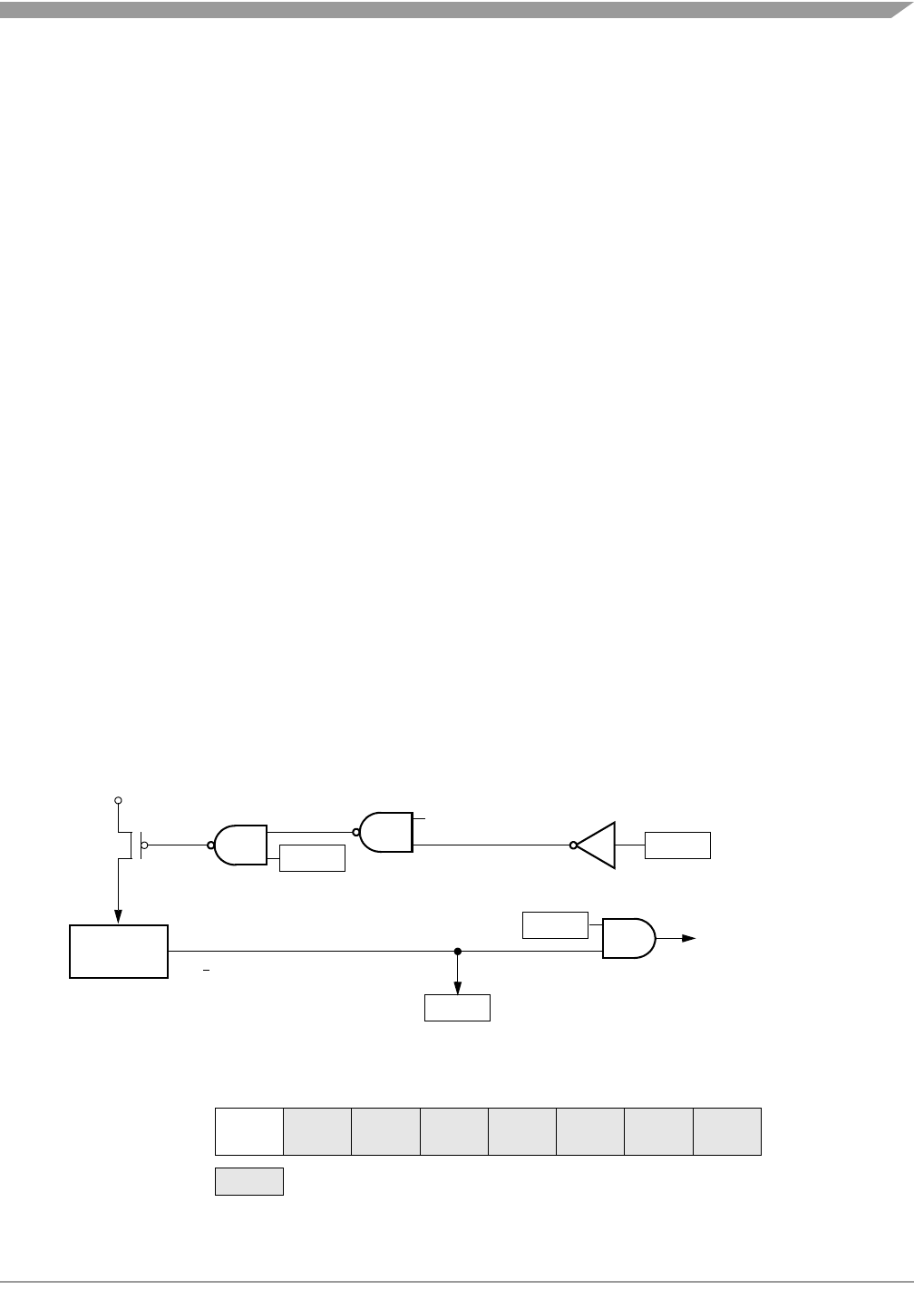
MC68HC08LN56 • MC68HC708LN56 General Release Specification, Rev. 2.1
Freescale Semiconductor 81
Chapter 7
Low-Voltage Inhibit (LVI)
7.1 Introduction
This section describes the low-voltage inhibit module (LVI27, Version A), which monitors the voltage on
the VDD and can force a reset when the VDD voltage falls to the LVI trip voltage.
7.2 Features
Features of the LVI module include:
• Programmable LVI Reset
• Status Flag to Monitor VDD
7.3 Functional Description
Figure 7-1 shows the structure of the LVI module. The LVI module contains a bandgap reference circuit
and comparator. The LVI power bit, LVIPWR, enables the LVI to monitor VDD voltage. The LVI reset bit,
LVIRST, enables the LVI module to generate a reset when VDD falls below a voltage, VLVR. LVIPWR and
LVIRST are in the configuration register. (See Chapter 19 Configuration Register (CONFIG).) Once an
LVI reset occurs, the MCU remains in reset until VDD rises above a voltage, VLVR + HLVR. The output of the
comparator controls the state of the LVIOUT flag in the LVI status register (LVISR).
An LVI reset also drives the RST pin low to provide low-voltage protection to external peripheral devices.
Figure 7-1. LVI Module Block Diagram
Register NameBit 7654321Bit 0Addr.
LVI Status Register
(LVISR) LVIOUT $FE0F
= Unimplemented
Figure 7-2. LVI I/O Register Summary
LOW VDD
LVIRST
VDD > LVITRIP = 0
VDD < LVITRIP = 1
LVIOUT
LVIPWR
DETECTOR
VDD
LVI RESET
(FROM CONFIG REG)
(FROM CONFIG REG)
LVISTO P
(FROM CONFIG REG)
STOP INSTRUCTION
Low-Voltage Inhibit (LVI)
MC68HC08LN56 • MC68HC708LN56 General Release Specification, Rev. 2.1
82 Freescale Semiconductor
7.3.1 Polled LVI Operation
In applications that can operate at VDD levels below the VLVR level, software can monitor VDD by polling
the LVIOUT bit while the LVI is enabled.
7.3.2 Forced Reset Operation
In applications that require VDD to remain above the VLVR trip level, enabling LVI resets allows the LVI
module to reset the MCU when VDD falls to the VLVR level. In the mask option register, the LVIPWR and
LVIRST bits must be at logic one to enable the LVI module and to enable LVI resets.
7.4 LVI Status Register (LVISR)
The LVI status register flags VDD voltages below the VLVR level.
LVIOUT — LVI Output Bit
This read-only flag becomes set when the VDD voltage falls below the VLVR trip voltage. (See Table
7-1.) Reset clears the LVIOUT bit.
7.5 LVI Interrupts
The LVI module does not generate interrupt requests.
7.6 Low-Power Modes
The STOP and WAIT instructions put the MCU in low-power-consumption standby modes.
7.6.1 Wait Mode
With the LVIPWR bit in the mask option register programmed to logic one, the LVI module is active after
a WAIT instruction.
With the LVIRST bit in the mask option register programmed to logic one, the LVI module can generate
a reset and bring the MCU out of wait mode.
Bit 7654321Bit 0
LVISR
$FE0F
Read:LVIOUT0000000
Write:
Reset:00000000
= Unimplemented
Figure 7-3. LVI Status Register (LVISR)
Table 7-1. LVIOUT Bit Indication
VDD LVIOUT
VDD > VLVR 0
VDD < VLVR 1
VLVR < VDD < VLVR + HLVR Previous Value

Low-Power Modes
MC68HC08LN56 • MC68HC708LN56 General Release Specification, Rev. 2.1
Freescale Semiconductor 83
7.6.2 Stop Mode
When the LVIPWR and LVISTOP bits in the mask option register are programmed to logic one, the LVI
module remains active after a STOP instruction.
NOTE
If the LVIPWR bit is at logic one, the LVISTOP bit must be at logic zero to
meet the minimum stop mode IDD specification.

Low-Voltage Inhibit (LVI)
MC68HC08LN56 • MC68HC708LN56 General Release Specification, Rev. 2.1
84 Freescale Semiconductor

MC68HC08LN56 • MC68HC708LN56 General Release Specification, Rev. 2.1
Freescale Semiconductor 85
Chapter 8
External Interrupt Module (IRQ)
8.1 Introduction
The IRQ provides two non-maskable interrupt inputs.
8.2 Features
Features of the IRQ module include:
• Two Dedicated External Interrupt Pins (IRQ1/VPP and IRQ2)
• Separate IRQ1 and IRQ2 Interrupt Control Bits
• Hysteresis Buffers
• Programmable Edge-only or Edge- and Level-Interrupt Sensitivity
• Automatic Interrupt Acknowledge
8.3 Functional Description
A logic zero applied to any of the external interrupt pins can latch a CPU interrupt request. Figure 8-1
shows the structure of the IRQ module.
Interrupt signals on the IRQ1/VPP pin are latched into the IRQ1 latch. Interrupt signals on the IRQ2 pin
are latched into the IRQ2 interrupt latch. An interrupt latch remains set until one of the following actions
occurs:
• Vector fetch — A vector fetch automatically generates an interrupt acknowledge signal that clears
the latch that caused the vector fetch.
• Software clear — Software can clear an interrupt latch by writing to the appropriate acknowledge
bit in the interrupt status and control register (ISCR). Writing a logic one to the ACK1 bit clears the
IRQ1 latch. Writing a logic one to the ACK2 bit clears the IRQ2 interrupt latch.
• Reset — A reset automatically clears both interrupt latches.
All of the external interrupt pins are falling-edge-triggered and are software-configurable to be both
falling-edge and low-level-triggered. The MODE1 bit in the ISCR controls the triggering sensitivity of the
IRQ1/VPP pin. The MODE2 bit controls the triggering sensitivity of the IRQ2 pin.
When an interrupt pin is edge-triggered only, the interrupt remains set until a vector fetch, software clear,
or reset occurs.
When an interrupt pin is both falling-edge and low-level-triggered, the interrupt remains set until both of
the following occur:
• Vector fetch or software clear
• Return of the interrupt pin to logic one
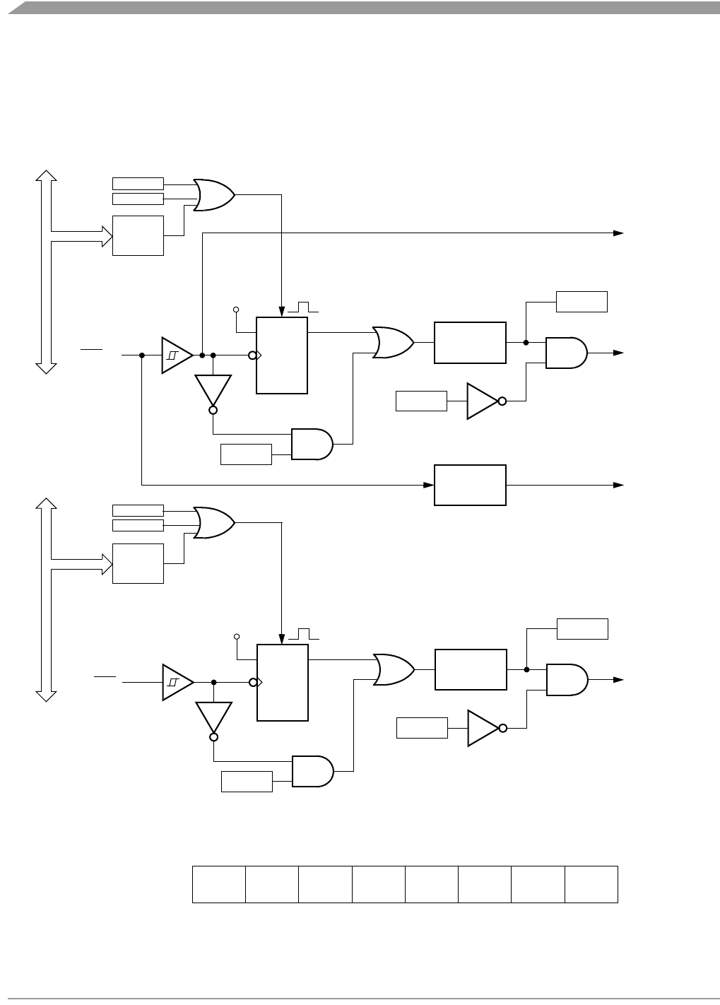
External Interrupt Module (IRQ)
MC68HC08LN56 • MC68HC708LN56 General Release Specification, Rev. 2.1
86 Freescale Semiconductor
The vector fetch or software clear can occur before or after the interrupt pin returns to logic one. As long
as the pin is low, the interrupt request remains pending. A reset will clear the latch and the MODEx control
bit, thereby clearing the interrupt even if the pin stays low.
When set, the IMASK1 and IMASK2 bits in the ISCR mask all external interrupt requests. A latched
interrupt request is not presented to the interrupt priority logic unless the corresponding IMASK bit is clear.
Figure 8-1. IRQ Module Block Diagram
Register NameBit 7654321Bit 0Addr.
IRQ Status/Control Register
(ISCR) IRQF2 ACK2 IMASK2 MODE2 IRQF1 ACK1 IMASK1 MODE1 $0032
Figure 8-2. IRQ I/O Register Summary
ACK1
IMASK1
DQ
CK
CLR
IRQ1
HIGH
INTERRUPT
TO MODE
SELECT
LOGIC
IRQ1
FF
REQUEST
IRQ1/VPP
VDD
MODE1
VOLTAGE
DETECT
SYNCHRO-
NIZER
IRQ1F
IMASK2
DQ
CK
CLR
IRQ2
INTERRUPT
IRQ2
FF
REQUEST
IRQ2
VDD
MODE2
SYNCHRO-
NIZER
IRQ2F
TO CPU FOR
BIL/BIH
INSTRUCTIONS
VECTOR
FETCH
DECODER
INTERNAL ADDRESS BUS
VECTOR
FETCH
DECODER
INTERNAL ADDRESS BUS
RESET
ACK2
RESET

Functional Description
MC68HC08LN56 • MC68HC708LN56 General Release Specification, Rev. 2.1
Freescale Semiconductor 87
8.3.1 IRQ1/VPP Pin
A logic zero on the IRQ1/VPP pin can latch an interrupt request into the IRQ1 latch. A vector fetch,
software clear, or reset clears the IRQ1 latch.
If the MODE1 bit is set, the IRQ1/VPP pin is both falling-edge-sensitive and low-level-sensitive. With
MODE1 set, both of the following actions must occur to clear IRQ1:
• Vector fetch or software clear — A vector fetch generates an interrupt acknowledge signal to clear
the latch. Software can generate the interrupt acknowledge signal by writing a logic one to the
ACK1 bit in the interrupt status and control register (ISCR). The ACK1 bit is useful in applications
that poll the IRQ1/VPP pin and require software to clear the IRQ1 latch. Writing to the ACK1 bit prior
to leaving an interrupt service routine can also prevent spurious interrupts due to noise. Setting
ACK1 does not affect subsequent transitions on the IRQ1/VPP pin. A falling edge that occurs after
writing to the ACK1 bit latches another interrupt request. If the IRQ1 mask bit, IMASK1, is clear,
the CPU loads the program counter with the vector address at locations $FFFA and $FFFB.
• Return of the IRQ1/VPP pin to logic one — As long as the IRQ1/VPP pin is at logic zero, IRQ1
remains active.
The vector fetch or software clear and the return of the IRQ1/VPP pin to logic one may occur in any order.
The interrupt request remains pending as long as the IRQ1/VPP pin is at logic zero. A reset will clear the
latch and the MODEx control bit, thereby clearing the interrupt even if the pin stays low.
If the MODE1 bit is clear, the IRQ1/VPP pin is falling-edge-sensitive only. With MODE1 clear, a vector
fetch or software clear immediately clears the IRQ1 latch.
The IRQF1 bit in the ISCR register can be used to check for pending interrupts. The IRQF1 bit is not
affected by the IMASK1 bit, which makes it useful in applications where polling is preferred.
Use the BIH or BIL instruction to read the logic level on the IRQ1/VPP pin.
NOTE
When using the level-sensitive interrupt trigger, avoid false interrupts by
masking interrupt requests in the interrupt routine.
8.3.2 IRQ2 Pin
A logic zero on the IRQ2 pin can latch an interrupt request into the IRQ2 interrupt latch. A vector fetch,
software clear, or reset clears the IRQ2 interrupt latch.
If the MODE2 bit is set, the IRQ2 pin is both falling-edge-sensitive and low-level-sensitive. With MODE2
set, both of the following actions must occur to clear IRQ2:
• Vector fetch or software clear, or reset — A vector fetch generates an interrupt acknowledge signal
to clear the latch. Software may generate the interrupt acknowledge signal by writing a logic one
to the ACK2 bit in the interrupt status and control register (ISCR). The ACK2 bit is useful in
applications that poll the IRQ2 pin and require software to clear the IRQ2 interrupt latch. Writing to
the ACK2 bit prior to leaving an interrupt service routine can also prevent spurious interrupts due
to noise. Setting ACK2 does not affect subsequent transitions on the IRQ2 pin. A falling edge that
occurs after writing to the ACK2 bit latches another interrupt request. If the IRQ2 mask bit, IMASK2,
is clear, the CPU loads the program counter with the vector address at locations $FFDE and
$FFDF.
• Return of the IRQ2 pin to logic one — As long as the IRQ2 pin is at logic zero, IRQ2 remains active.

External Interrupt Module (IRQ)
MC68HC08LN56 • MC68HC708LN56 General Release Specification, Rev. 2.1
88 Freescale Semiconductor
The vector fetch or software clear and the return of the IRQ2 pin to logic one can occur in any order. The
interrupt request remains pending as long as the IRQ2 pin is at logic zero. A reset will clear the latch and
the MODEx control bit, thereby clearing the interrupt even if the pin stays low.
If the MODE2 bit is clear, the IRQ2 pin is falling-edge-sensitive only. With MODE2 clear, a vector fetch or
software clear immediately clears the IRQ2 interrupt latch.
There is no direct way to determine the logic level on the IRQ2 pin. However, it is possible to use the
IRQF2 bit in the ISCR to infer the state of the IRQ2 pin. By writing a one to the MODE2 bit, the IRQF2 bit
in the ISCR will be the opposite value of the IRQ2 pin as long as the IRQ2 latch is cleared. (See Figure
8-1.) The IRQ2 latch can be cleared by writing a one to the acknowledge bit. Recall, however, that every
falling edge on the IRQ2 pin will set the IRQ2 latch, so an additional acknowledge is necessary after each
falling edge on IRQ2 to maintain the opposite relationship between IRQF2 and the IRQ2 pin. The user
may want to set the IMASK2 bit in the ISCR to prevent the IRQF2 from generating interrupts when used
in this manner.
NOTE
When using the level-sensitive interrupt trigger, avoid false interrupts by
masking interrupt requests in the interrupt routine.
8.4 IRQ Module During Break Interrupts
The system integration module (SIM) controls whether the IRQ1 and IRQ2 interrupt latches can be
cleared during the break state. The BCFE bit in the SIM break flag control register (SBFCR) enables
software to clear the latches during the break state. (See Chapter 5 System Integration Module (SIM).)
To allow software to clear the IRQ1 latch and the IRQ2 interrupt latch during a break interrupt, write a logic
one to the BCFE bit. If a latch is cleared during the break state, it remains cleared when the MCU exits
the break state.
To protect the latches during the break state, write a logic zero to the BCFE bit. With BCFE at logic zero
(its default state), writing to the ACK1 and ACK2 bits in the IRQ status and control register during the
break state has no effect on the IRQ latches.
8.5 IRQ Status and Control Register
The IRQ Status and Control Register (ISCR) controls and monitors operation of the IRQ module. The
ISCR has the following functions:
• Shows the state of the IRQ1 and IRQ2 interrupt flags
• Clears the IRQ1 and IRQ2 interrupt latches
• Masks IRQ1 and IRQ2 interrupt requests
• Controls triggering sensitivity of the IRQ1/VPP and IRQ2 interrupt pins

IRQ Status and Control Register
MC68HC08LN56 • MC68HC708LN56 General Release Specification, Rev. 2.1
Freescale Semiconductor 89
IRQ2F — IRQ2 Flag
This read-only status bit is high when the IRQ2 interrupt is pending.
1 = IRQ2 interrupt pending
0 = IRQ2 interrupt not pending
ACK2 — IRQ2 Interrupt Request Acknowledge Bit
Writing a logic one to this write-only bit clears the IRQ2 interrupt latch. ACK2 always reads as logic
zero. Reset clears ACK2.
IMASK2 — IRQ2 Interrupt Mask Bit
Writing a logic one to this read/write bit prevents the output of the IRQ2 interrupt latch from generating
interrupt requests. Reset clears IMASK2.
1 = IRQ2 pin interrupt requests disabled
0 = IRQ2 pin interrupt requests enabled
MODE2 — IRQ2 Interrupt Edge/Level Select Bit
This read/write bit controls the triggering sensitivity of the IRQ2 interrupt pins. Reset clears MODE2.
1 = IRQ2 interrupt requests on falling edges and low levels
0 = IRQ2 interrupt requests on falling edges only
IRQ1F — IRQ1 Flag
This read-only status bit is high when the IRQ1 interrupt is pending.
1 = IRQ1 interrupt pending
0 = IRQ1 interrupt not pending
ACK1 — IRQ1 Interrupt Request Acknowledge Bit
Writing a logic one to this write-only bit clears the IRQ1 latch. ACK1 always reads as logic zero. Reset
clears ACK1.
IMASK1 — IRQ1 Interrupt Mask Bit
Writing a logic one to this read/write bit disables IRQ1 interrupt requests. Reset clears IMASK1.
1 = IRQ1 interrupt requests disabled
0 = IRQ1 interrupt requests enabled
MODE1 — IRQ1 Edge/Level Select Bit
This read/write bit controls the triggering sensitivity of the IRQ1/VPP pin. Reset clears MODE1.
1 = IRQ1/VPP interrupt requests on falling edges and low levels
0 = IRQ1/VPP interrupt requests on falling edges only
ISCR
$0032Bit 7654321Bit 0
Read: IRQF2 0
IMASK2 MODE2
IRQF1 0
IMASK1 MODE1
Write: ACK2 ACK1
Reset:00000000
= Unimplemented
Figure 8-3. IRQ Status and Control Register (ISCR)

External Interrupt Module (IRQ)
MC68HC08LN56 • MC68HC708LN56 General Release Specification, Rev. 2.1
90 Freescale Semiconductor

MC68HC08LN56 • MC68HC708LN56 General Release Specification, Rev. 2.1
Freescale Semiconductor 91
Chapter 9
Keyboard Module (KB)
9.1 Introduction
The keyboard module provides eight independently maskable external interrupt pins.
9.2 Features
Features of the keyboard module:
• Eight Keyboard Interrupt Pins and Interrupt Masks
• Selectable Triggering Sensitivity
9.3 Functional Description
Writing to the KBIE7:KBIE0 bits in the keyboard interrupt enable register independently enables or
disables each port A pin as a keyboard interrupt pin. Enabling a keyboard interrupt pin also enables its
internal pullup device. A logic zero applied to an enabled keyboard interrupt pin will latch a keyboard
interrupt request.
The keyboard interrupt latch becomes set when one or more keyboard pins goes low after all were high.
The MODEK bit in the keyboard status and control register controls the triggering mode of the keyboard
interrupt.
• If the keyboard interrupt is edge-sensitive only, a falling edge on a keyboard pin does not latch an
interrupt request if another keyboard pin is already low. To prevent losing an interrupt request on
one pin because another pin is still low, software can disable the latter pin while it is low.
• If the keyboard interrupt is edge- and level-sensitive, an interrupt request is present as long as any
keyboard pin is low.
Addr. Register Name Bit 7654321Bit 0
$001A Keyboard Status/Control
Register (KBSCR)
Read:0000KEYF 0
IMASKK MODEK
Write: ACKK
Reset:00000000
$001B Keyboard Interrupt Control
Register (KBICR)
Read:
KB7IE KB6IE KB5IE KB4IE KB3IE KB2IE KB1IE KB0IE
Write:
Reset:00000000
= Unimplemented
Figure 9-1. KB I/O Register Summary
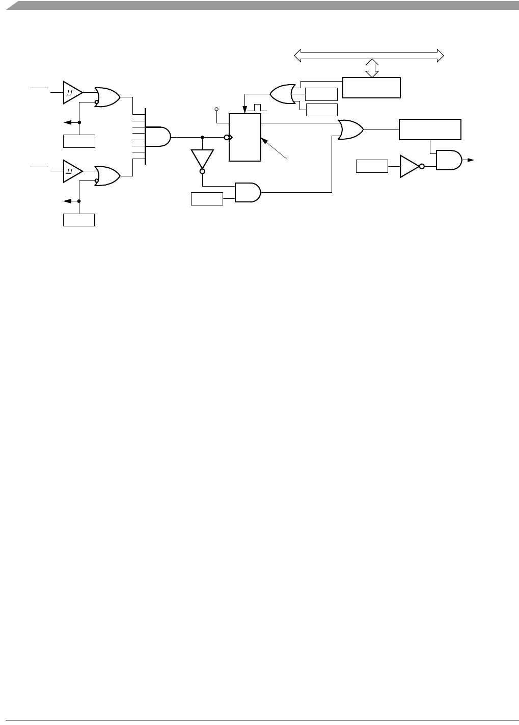
Keyboard Module (KB)
MC68HC08LN56 • MC68HC708LN56 General Release Specification, Rev. 2.1
92 Freescale Semiconductor
Figure 9-2. Keyboard Module Block Diagram
The MODEK bit in the keyboard status and control register controls the triggering sensitivity of the
keyboard interrupt latch. If the MODEK bit is set, the keyboard interrupt pins are both falling-edge- and
low-level-sensitive, and both of the following actions must occur to clear a keyboard interrupt:
• Vector fetch or software clear — A vector fetch generates an interrupt acknowledge signal to clear
the latch. Software can generate the interrupt acknowledge signal by writing a logic one to the
ACKK bit in the keyboard status and control register (KBSCR). The ACKK bit is useful in
applications that poll the keyboard interrupt pins and require software to clear the keyboard
interrupt latch. Writing to the ACKK bit prior to leaving an interrupt service routine can also prevent
spurious interrupts due to noise. Setting ACKK does not affect subsequent transitions on the
keyboard interrupt pins. A falling edge that occurs after writing to the ACKK bit latches another
interrupt request. If the keyboard interrupt mask bit, IMASKK, is clear, the CPU loads the program
counter with the vector address at locations $FFDC and $FFDD.
• Return of all enabled keyboard interrupt pins to logic one — As long as any enabled keyboard
interrupt pin is at logic zero, the keyboard interrupt remains set.
The vector fetch or software clear and the return of all enabled keyboard interrupt pins to logic one may
occur in any order. The interrupt request remains pending as long as any enabled keyboard interrupt pin
is at logic zero.
If the MODEK bit is clear, the keyboard interrupt pin is falling-edge- sensitive only. With MODEK clear, a
vector fetch or software clear immediately clears the keyboard interrupt latch.
Reset clears the keyboard interrupt latch and the MODEK bit, clearing the interrupt request even if a
keyboard interrupt pin stays at logic zero.
The keyboard flag bit (KEYF) in the keyboard status and control register can be used to see if a pending
interrupt exists. The KEYF bit is not affected by the keyboard interrupt mask bit (IMASKK) which makes
it useful in applications where polling is preferred.
To determine the logic level on a keyboard interrupt pin, use the data direction register to configure the
pin as an input and read the data register.
NOTE
Setting a keyboard interrupt enable bit (KBxIE) forces the corresponding
keyboard interrupt pin to be an input, overriding the data direction register.
However, the data direction register bit must be a logic zero for software to
read the pin.
SYNCHRONIZER
KB7IE
KB0IE
PTA7/KBD7
PTA0/KBD0
.
.
.
To pullup enable
KEYBOARD
INTERRUPT
DQ
CK
CLR
VDD
MODEK
IMASKK
KEYBOARD
INTERRUPT FF REQUEST
VECTOR FETCH
DECODER
ACKK
INTERNAL BUS
RESET
To pullup enable

Keyboard Initialization
MC68HC08LN56 • MC68HC708LN56 General Release Specification, Rev. 2.1
Freescale Semiconductor 93
9.4 Keyboard Initialization
When a keyboard interrupt pin is enabled, it takes time for the internal pull-up to reach a logic one, so it
is possible that an interrupt could occur when the pin is initially enabled.
To prevent this, it is recommended that the keyboard interrupt be masked with the IMASKK bit in the
KBSCR register before enabling the pin and that the ACKK bit be used to acknowledge the potential false
interrupt before setting IMASKK back to zero. An edge-only type of interrupt can be acknowledged
immediately after enabling the pin. An edge- and level-triggered interrupt must be acknowledged after a
delay which is dependant on the external load.
Another way to avoid a false interrupt is to set the appropriate bit of port A to an output driving a logic one,
before enabling the keyboard input.
9.5 I/O Registers
These registers control and monitor operation of the keyboard module:
• Keyboard status and control register (KBSCR)
• Keyboard interrupt enable register (KBIER)
9.5.1 Keyboard Status and Control Register (KBSCR)
The keyboard status and control register performs these functions:
• Flags keyboard interrupt requests
• Acknowledges keyboard interrupt requests
• Masks keyboard interrupt requests
• Controls keyboard latch triggering sensitivity
Bits 7–4 — Not used
These read-only bits always read as logic zeros.
KEYF — Keyboard Flag Bit
This read-only bit is set when a keyboard interrupt is pending. Reset clears the KEYF bit.
1 = Keyboard interrupt pending
0 = No keyboard interrupt pending
ACKK — Keyboard Acknowledge Bit
Writing a logic one to this read/write bit clears the keyboard interrupt latch. ACKK always reads as logic
zero. Reset clears ACKK.
KBSCR
$001A Bit 7 6 5 4321Bit 0
Read: 0 0 0 0 KEYF 0
IMASKK MODEK
Write: ACKK
Reset:00000000
= Unimplemented
Figure 9-3. Keyboard Status and Control Register (KBSCR)

Keyboard Module (KB)
MC68HC08LN56 • MC68HC708LN56 General Release Specification, Rev. 2.1
94 Freescale Semiconductor
IMASKK — Keyboard Interrupt Mask Bit
Writing a logic one to this read/write bit prevents the output of the keyboard interrupt mask from
generating interrupt requests. Reset clears the IMASKK bit.
1 = Keyboard interrupt requests disabled
0 = Keyboard interrupt requests enabled
MODEK — Keyboard Triggering Sensitivity Bit
This read/write bit controls the triggering sensitivity of the keyboard interrupt pins. Reset clears
MODEK.
1 = Keyboard interrupt requests on falling edges and low levels
0 = Keyboard interrupt requests on falling edges only
9.5.2 Keyboard Interrupt Enable Register (KBIER)
The keyboard interrupt enable register enables or disables each port A pin to operate as a keyboard
interrupt pin.
KBIE7:KBIE0 — Keyboard Interrupt Enable Bits
Each of these read/write bits enables the corresponding keyboard interrupt pin to latch interrupt
requests. Reset clears the keyboard interrupt enable register.
1 = PAx pin enabled as keyboard interrupt pin
0 = PAx pin not enabled as keyboard interrupt pin
9.6 Keyboard Module During Break Interrupts
The system integration module (SIM) controls whether the keyboard interrupt latch can be cleared during
the break state. The BCFE bit in the SIM break flag control register (SBFCR) enables software to clear
the latch during the break state.
To allow software to clear the keyboard interrupt latch during a break interrupt, write a logic one to the
BCFE bit. If a latch is cleared during the break state, it remains cleared when the MCU exits the break
state.
To protect the latch during the break state, write a logic zero to the BCFE bit. With BCFE at logic zero (its
default state), writing has no effect during the break state to the keyboard acknowledge bit (ACKK) in the
keyboard status and control register. (See 9.5.1 Keyboard Status and Control Register (KBSCR).)
Bit 7654321Bit 0
KBIER
$001B
Read:
KBIE7 KBIE6 KBIE5 KBIE4 KBIE3 KBIE2 KBIE1 KBIE0
Write:
Figure 9-4. Keyboard Interrupt Enable Register (KBIER)

MC68HC08LN56 • MC68HC708LN56 General Release Specification, Rev. 2.1
Freescale Semiconductor 95
Chapter 10
Timer Interface Module (TIM)
10.1 Introduction
This section describes the timer interface module (TIM4, Version B). The TIM is a four-channel timer that
provides a timing reference with input capture, output compare, and pulse-width-modulation functions.
Figure 10-1 is a block diagram of the TIM.
10.2 Features
Features of the TIM include:
• Four Input Capture/Output Compare Channels
– Rising-Edge, Falling-Edge, or Any-Edge Input Capture Trigger
– Set, Clear, or Toggle Output Compare Action
• Buffered and Unbuffered Pulse Width Modulation (PWM) Signal Generation
• Programmable TIM Clock Input
– Seven-Frequency Internal Bus Clock Prescaler Selection
– External TIM Clock Input (Bus Frequency ÷2 Maximum)
• Free-Running or Modulo Up-Count Operation
• Toggle Any Channel Pin on Overflow
• TIM Counter Stop and Reset Bits
• DMA Service Request Generation
• Modular Architecture Expandable to Eight Channels
10.3 Functional Description
NOTE
References to DMA and associated functions are only valid if the MCU has
a DMA module. If the MCU has no DMA, any DMA-related register bits
should be left in their reset state for expected MCU operation.
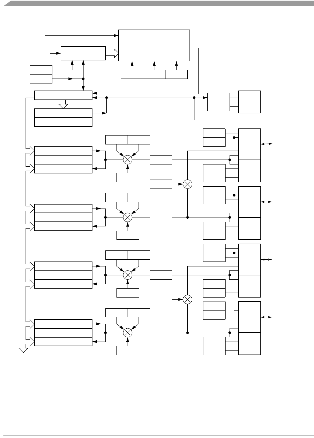
Timer Interface Module (TIM)
MC68HC08LN56 • MC68HC708LN56 General Release Specification, Rev. 2.1
96 Freescale Semiconductor
Figure 10-1. TIM Block Diagram
PRESCALER
PRESCALER SELECT
TCLK
INTERNAL
16-BIT COMPARATOR
PS2 PS1 PS0
16-BIT COMPARATOR
16-BIT LATCH
TCH0H:TCH0L
MS0A
ELS0B ELS0A PTE0
TOF
TOIE
INTER-
16-BIT COMPARATOR
16-BIT LATCH
TCH1H:TCH1L
16-BIT COMPARATOR
16-BIT LATCH
TCH2H:TCH2L
16-BIT COMPARATOR
16-BIT LATCH
TCH3H:TCH3L
CHANNEL 0
CHANNEL 1
CHANNEL 2
CHANNEL 3
TMODH:TMODL
TRST
TSTOP
TOV0
CH0IE
DMA0S
CH0F
ELS1B ELS1A
TOV1
CH1IE
DMA1S
CH1MAX
CH1F
ELS2B ELS2A
TOV2
CH2IE
DMA2S
CH2MAX
CH2F
ELS3B ELS3A
TOV3
CH3IE
DMA3S
CH3MAX
CH3F
CH0MAX
MS0B
MS2B
16-BIT COUNTER
INTERNAL BUS
BUS CLOCK
MS1A
MS2A
MS3A
PTE4/TCLK
PTE0/TCH0
PTE1/TCH1
PTE2/TCH2
PTE3/TCH3
LOGIC
RUPT
LOGIC
INTER-
RUPT
LOGIC
PTE1
LOGIC
INTER-
RUPT
LOGIC
PTE2
LOGIC
INTER-
RUPT
LOGIC
PTE3
LOGIC
INTER-
RUPT
LOGIC
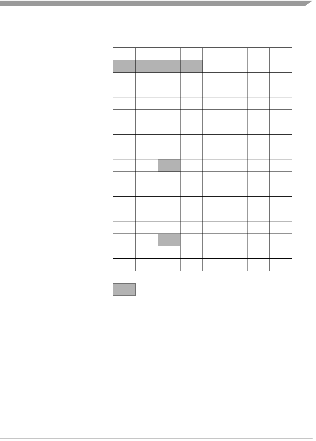
Functional Description
MC68HC08LN56 • MC68HC708LN56 General Release Specification, Rev. 2.1
Freescale Semiconductor 97
Table 10-1. TIM I/O Register Summary
Register Name Bit 7 6 5 4 3 2 1 Bit 0 Addr.
TIM Status/Control Register (TSC) TOF TOIE TSTOP TRST 0 PS2 PS1 PS0 $0020
TIM DMA Select Register (TDMA) DMAS3 DMAS2 DMAS1 DMAS0 $0021
TIM Counter Register High (TCNTH) Bit 15 14 13 12 11 10 9 Bit 8 $0022
TIM Counter Register Low (TCNTL) Bit 7 6 5 4 3 2 1 Bit 0 $0023
TIM Counter Modulo Reg. High (TMODH) Bit 15 14 13 12 11 10 9 Bit 8 $0024
TIM Counter Modulo Reg. Low (TMODL) Bit 7 6 5 4 3 2 1 Bit 0 $0025
TIM Channel 0 Status/Control Register (TSC0) CH0F CH0IE MS0B MS0A ELS0B ELS0A TOV0 CH0MAX $0026
TIM Channel 0 Register High (TCH0H) Bit 15 14 13 12 11 10 9 Bit 8 $0027
TIM Channel 0 Register Low (TCH0L) Bit 7 6 5 4 3 2 1 Bit 0 $0028
TIM Channel 1 Status/Control Register (TSC1) CH1F CH1IE MS1A ELS1B ELS1A TOV1 CH1MAX $0029
TIM Channel 1 Register High (TCH1H) Bit 15 14 13 12 11 10 9 Bit 8 $002A
TIM Channel 1 Register Low (TCH1L) Bit 7 6 5 4 3 2 1 Bit 0 $002B
TIM Channel 2 Status/Control Register (TSC2) CH2F CH2IE MS2B MS2A ELS2B ELS2A TOV2 CH2MAX $002C
TIM Channel 2 Register High (TCH2H) Bit 15 14 13 12 11 10 9 Bit 8 $002D
TIM Channel 2 Register Low (TCH2L) Bit 7 6 5 4 3 2 1 Bit 0 $002E
TIM Channel 3 Status/Control Register (TSC3) CH3F CH3IE MS3A ELS3B ELS3A TOV3 CH3MAX $002F
TIM Channel 3 Register High (TCH3H) Bit 15 14 13 12 11 10 9 Bit 8 $0030
TIM Channel 3 Register Low (TCH3L) Bit 7 6 5 4 3 2 1 Bit 0 $0031
= Unimplemented

Timer Interface Module (TIM)
MC68HC08LN56 • MC68HC708LN56 General Release Specification, Rev. 2.1
98 Freescale Semiconductor
Figure 10-1 shows the structure of the TIM. The central component of the TIM is the 16-bit TIM counter
that can operate as a free-running counter or a modulo up-counter. The TIM counter provides the timing
reference for the input capture and output compare functions. The TIM counter modulo registers,
TMODH:TMODL, control the modulo value of the TIM counter. Software can read the TIM counter value
at any time without affecting the counting sequence.
The four TIM channels are programmable independently as input capture or output compare channels.
10.3.1 TIM Counter Prescaler
The TIM clock source can be one of the seven prescaler outputs or the TIM clock pin, PTE4/TCLK. The
prescaler generates seven clock rates from the internal bus clock. The prescaler select bits, PS[2:0], in
the TIM status and control register select the TIM clock source.
10.3.2 Input Capture
With the input capture function, the TIM can capture the time at which an external event occurs. When an
active edge occurs on the pin of an input capture channel, the TIM latches the contents of the TIM counter
into the TIM channel registers, TCHxH:TCHxL. The polarity of the active edge is programmable. Input
captures can generate TIM CPU interrupt requests or TIM DMA service requests.
10.3.3 Output Compare
With the output compare function, the TIM can generate a periodic pulse with a programmable polarity,
duration, and frequency. When the counter reaches the value in the registers of an output compare
channel, the TIM can set, clear, or toggle the channel pin. Output compares can generate TIM CPU
interrupt requests or TIM DMA service requests.
10.3.4 Unbuffered Output Compare
Any output compare channel can generate unbuffered output compare pulses as described in 10.3.3
Output Compare. The pulses are unbuffered because changing the output compare value requires writing
the new value over the old value currently in the TIM channel registers.
An unsynchronized write to the TIM channel registers to change an output compare value could cause
incorrect operation for up to two counter overflow periods. For example, writing a new value before the
counter reaches the old value but after the counter reaches the new value prevents any compare during
that counter overflow period. Also, using a TIM overflow interrupt routine to write a new, smaller output
compare value may cause the compare to be missed. The TIM may pass the new value before it is written.
Use the following methods to synchronize unbuffered changes in the output compare value on channel x:
• When changing to a smaller value, enable channel x output compare interrupts and write the new
value in the output compare interrupt routine. The output compare interrupt occurs at the end of
the current output compare pulse. The interrupt routine has until the end of the counter overflow
period to write the new value.
• When changing to a larger output compare value, enable channel x TIM overflow interrupts and
write the new value in the TIM overflow interrupt routine. The TIM overflow interrupt occurs at the
end of the current counter overflow period. Writing a larger value in an output compare interrupt
routine (at the end of the current pulse) could cause two output compares to occur in the same
counter overflow period.

Functional Description
MC68HC08LN56 • MC68HC708LN56 General Release Specification, Rev. 2.1
Freescale Semiconductor 99
10.3.5 Buffered Output Compare
Channels 0 and 1 can be linked to form a buffered output compare channel whose output appears on the
PTE0/TCH0 pin. The TIM channel registers of the linked pair alternately control the output.
Setting the MS0B bit in TIM channel 0 status and control register (TSC0) links channel 0 and channel 1.
The output compare value in the TIM channel 0 registers initially controls the output on the PTE0/TCH0
pin. Writing to the TIM channel 1 registers enables the TIM channel 1 registers to synchronously control
the output after the TIM overflows. At each subsequent overflow, the TIM channel registers (0 or 1) that
control the output are the ones written to last. TSC0 controls and monitors the buffered output compare
function, and TIM channel 1 status and control register (TSC1) is unused. While the MS0B bit is set, the
channel 1 pin, PTE1/TCH1, is available as a general-purpose I/O pin.
Channels 2 and 3 can be linked to form a buffered output compare channel whose output appears on the
PTE2/TCH2 pin. The TIM channel registers of the linked pair alternately control the output.
Setting the MS2B bit in TIM channel 2 status and control register (TSC2) links channel 2 and channel 3.
The output compare value in the TIM channel 2 registers initially controls the output on the PTE2/TCH2
pin. Writing to the TIM channel 3 registers enables the TIM channel 3 registers to synchronously control
the output after the TIM overflows. At each subsequent overflow, the TIM channel registers (2 or 3) that
control the output are the ones written to last. TSC2 controls and monitors the buffered output compare
function, and TIM channel 3 status and control register (TSC3) is unused. While the MS2B bit is set, the
channel 3 pin, PTE3/TCH3, is available as a general-purpose I/O pin.
NOTE
In buffered output compare operation, do not write new output compare
values to the currently active channel registers. Writing to the active
channel registers is the same as generating unbuffered output compares.
10.3.6 Pulse Width Modulation (PWM)
By using the toggle-on-overflow feature with an output compare channel, the TIM can generate a PWM
signal. The value in the TIM counter modulo registers determines the period of the PWM signal. The
channel pin toggles when the counter reaches the value in the TIM counter modulo registers. The time
between overflows is the period of the PWM signal.
As Figure 10-2 shows, the output compare value in the TIM channel registers determines the pulse width
of the PWM signal. The time between overflow and output compare is the pulse width. Program the TIM
to clear the channel pin on output compare if the state of the PWM pulse is logic one. Program the TIM
to set the pin if the state of the PWM pulse is logic zero.
The value in the TIM counter modulo registers and the selected prescaler output determines the
frequency of the PWM output. The frequency of an 8-bit PWM signal is variable in 256 increments. Writing
$00FF (255) to the TIM counter modulo registers produces a PWM period of 256 times the internal bus
clock period if the prescaler select value is $000. See 10.8.1 TIM Status and Control Register (TSC).
The value in the TIM channel registers determines the pulse width of the PWM output. The pulse width of
an 8-bit PWM signal is variable in 256 increments. Writing $0080 (128) to the TIM channel registers
produces a duty cycle of 128/256 or 50%.

Timer Interface Module (TIM)
MC68HC08LN56 • MC68HC708LN56 General Release Specification, Rev. 2.1
100 Freescale Semiconductor
Figure 10-2. PWM Period and Pulse Width
10.3.7 Unbuffered PWM Signal Generation
Any output compare channel can generate unbuffered PWM pulses as described in 10.3.6 Pulse Width
Modulation (PWM). The pulses are unbuffered because changing the pulse width requires writing the new
pulse width value over the old value currently in the TIM channel registers.
An unsynchronized write to the TIM channel registers to change a pulse width value could cause incorrect
operation for up to two PWM periods. For example, writing a new value before the counter reaches the
old value but after the counter reaches the new value prevents any compare during that PWM period.
Also, using a TIM overflow interrupt routine to write a new, smaller pulse width value may cause the
compare to be missed. The TIM may pass the new value before it is written.
Use the following methods to synchronize unbuffered changes in the PWM pulse width on channel x:
• When changing to a shorter pulse width, enable channel x output compare interrupts and write the
new value in the output compare interrupt routine. The output compare interrupt occurs at the end
of the current pulse. The interrupt routine has until the end of the PWM period to write the new
value.
• When changing to a longer pulse width, enable channel x TIM overflow interrupts and write the new
value in the TIM overflow interrupt routine. The TIM overflow interrupt occurs at the end of the
current PWM period. Writing a larger value in an output compare interrupt routine (at the end of the
current pulse) could cause two output compares to occur in the same PWM period.
NOTE
In PWM signal generation, do not program the PWM channel to toggle on
output compare. Toggling on output compare prevents reliable 0% duty
cycle generation and removes the ability of the channel to self-correct in the
event of software error or noise. Toggling on output compare also can
cause incorrect PWM signal generation when changing the PWM pulse
width to a new, much larger value.
10.3.8 Buffered PWM Signal Generation
Channels 0 and 1 can be linked to form a buffered PWM channel whose output appears on the
PTE0/TCH0 pin. The TIM channel registers of the linked pair alternately control the pulse width of the
output.
PTEx/TCHx
PERIOD
PULSE
WIDTH
OVERFLOW OVERFLOW OVERFLOW
OUTPUT
COMPARE
OUTPUT
COMPARE
OUTPUT
COMPARE

Functional Description
MC68HC08LN56 • MC68HC708LN56 General Release Specification, Rev. 2.1
Freescale Semiconductor 101
Setting the MS0B bit in TIM channel 0 status and control register (TSC0) links channel 0 and channel 1.
The TIM channel 0 registers initially control the pulse width on the PTE0/TCH0 pin. Writing to the TIM
channel 1 registers enables the TIM channel 1 registers to synchronously control the pulse width at the
beginning of the next PWM period. At each subsequent overflow, the TIM channel registers (0 or 1) that
control the pulse width are the ones written to last. TSC0 controls and monitors the buffered PWM
function, and TIM channel 1 status and control register (TSC1) is unused. While the MS0B bit is set, the
channel 1 pin, PTE1/TCH1, is available as a general-purpose I/O pin.
Channels 2 and 3 can be linked to form a buffered PWM channel whose output appears on the
PTE2/TCH2 pin. The TIM channel registers of the linked pair alternately control the pulse width of the
output.
Setting the MS2B bit in TIM channel 2 status and control register (TSC2) links channel 2 and channel 3.
The TIM channel 2 registers initially control the pulse width on the PTE2/TCH2 pin. Writing to the TIM
channel 3 registers enables the TIM channel 3 registers to synchronously control the pulse width at the
beginning of the next PWM period. At each subsequent overflow, the TIM channel registers (2 or 3) that
control the pulse width are the ones written to last. TSC2 controls and monitors the buffered PWM
function, and TIM channel 3 status and control register (TSC3) is unused. While the MS2B bit is set, the
channel 3 pin, PTE3/TCH3, is available as a general-purpose I/O pin.
NOTE
In buffered PWM signal generation, do not write new pulse width values to
the currently active channel registers. Writing to the active channel
registers is the same as generating unbuffered PWM signals.
10.3.9 PWM Initialization
To ensure correct operation when generating unbuffered or buffered PWM signals, use the following
initialization procedure:
1. In the TIM status and control register (TSC):
a. Stop the TIM counter by setting the TIM stop bit, TSTOP.
b. Reset the TIM counter by setting the TIM reset bit, TRST.
2. In the TIM counter modulo registers (TMODH:TMODL), write the value for the required PWM
period.
3. In the TIM channel x registers (TCHxH:TCHxL), write the value for the required pulse width.
4. In TIM channel x status and control register (TSCx):
a. Write 0:1 (for unbuffered output compare or PWM signals) or 1:0 (for buffered output compare
or PWM signals) to the mode select bits, MSxB:MSxA. See Table 10-3.
b. Write 1 to the toggle-on-overflow bit, TOVx.
c. Write 1:0 (to clear output on compare) or 1:1 (to set output on compare) to the edge/level
select bits, ELSxB:ELSxA. The output action on compare must force the output to the
complement of the pulse width level. (See Table 10-3.)
NOTE
In PWM signal generation, do not program the PWM channel to toggle on
output compare. Toggling on output compare prevents reliable 0% duty
cycle generation and removes the ability of the channel to self-correct in the
event of software error or noise. Toggling on output compare can also

Timer Interface Module (TIM)
MC68HC08LN56 • MC68HC708LN56 General Release Specification, Rev. 2.1
102 Freescale Semiconductor
cause incorrect PWM signal generation when changing the PWM pulse
width to a new, much larger value.
5. In the TIM status control register (TSC), clear the TIM stop bit, TSTOP.
Setting MS0B links channels 0 and 1 and configures them for buffered PWM operation. The TIM channel
0 registers (TCH0H:TCH0L) initially control the buffered PWM output. TIM status control register 0
(TSCR0) controls and monitors the PWM signal from the linked channels. MS0B takes priority over MS0A.
Setting MS2B links channels 2 and 3 and configures them for buffered PWM operation. The TIM channel
2 registers (TCH2H:TCH2L) initially control the PWM output. TIM status control register 2 (TSCR2)
controls and monitors the PWM signal from the linked channels. MS2B takes priority over MS2A.
Clearing the toggle-on-overflow bit, TOVx, inhibits output toggles on TIM overflows. Subsequent output
compares try to force the output to a state it is already in and have no effect. The result is a 0% duty cycle
output.
Setting the channel x maximum duty cycle bit (CHxMAX) and clearing the TOVx bit generates a 100%
duty cycle output. (See 10.8.5 TIM Channel Status and Control Registers (TSC0:TSC3).)
10.4 Interrupts
The following TIM sources can generate interrupt requests:
• TIM overflow flag (TOF) — The TOF bit is set when the TIM counter value rolls over to $0000 after
matching the value in the TIM counter modulo registers. The TIM overflow interrupt enable bit,
TOIE, enables TIM overflow CPU interrupt requests. TOF and TOIE are in the TIM status and
control register.
• TIM channel flags (CH3F:CH0F) — The CHxF bit is set when an input capture or output compare
occurs on channel x. Channel x TIM CPU interrupt requests and TIM DMA service requests are
controlled by the channel x interrupt enable bit, CHxIE, and the channel x DMA select bit, DMAxS.
Channel x TIM CPU interrupt requests are enabled when CHxIE:DMAxS = 1:0. Channel x
TIM DMA service requests are enabled when CHxIE:DMAxS = 1:1. CHxF and CHxIE are in the
TIM channel x status and control register. DMAxS is in the TIM DMA select register.
10.5 Low-Power Modes
The WAIT and STOP instructions put the MCU in low-power- consumption standby modes.
10.5.1 Wait Mode
The TIM remains active after the execution of a WAIT instruction. In wait mode the TIM registers are not
accessible by the CPU. Any enabled CPU interrupt request from the TIM can bring the MCU out of wait
mode.
If TIM functions are not required during wait mode, reduce power consumption by stopping the TIM before
executing the WAIT instruction.
The DMA can service the TIM without exiting wait mode.

TIM During Break Interrupts
MC68HC08LN56 • MC68HC708LN56 General Release Specification, Rev. 2.1
Freescale Semiconductor 103
10.5.2 Stop Mode
The TIM is inactive after the execution of a STOP instruction. The STOP instruction does not affect
register conditions or the state of the TIM counter. TIM operation resumes when the MCU exits stop mode
after an external interrupt.
10.6 TIM During Break Interrupts
A break interrupt stops the TIM counter.
The system integration module (SIM) controls whether status bits in other modules can be cleared during
the break state. The BCFE bit in the SIM break flag control register (SBFCR) enables software to clear
status bits during the break state. See 5.7.3 SIM Break Flag Control Register (SBFCR).
To allow software to clear status bits during a break interrupt, write a logic one to the BCFE bit. If a status
bit is cleared during the break state, it remains cleared when the MCU exits the break state.
To protect status bits during the break state, write a logic zero to the BCFE bit. With BCFE at logic zero
(its default state), software can read and write I/O registers during the break state without affecting status
bits. Some status bits have a two-step read/write clearing procedure. If software does the first step on
such a bit before the break, the bit cannot change during the break state as long as BCFE is at logic zero.
After the break, doing the second step clears the status bit.
10.7 I/O Signals
Port E shares five of its pins with the TIM. PTE4/TCLK is an external clock input to the TIM prescaler. The
four TIM channel I/O pins are PTE0/TCH0, PTE1/TCH1, PTE2/TCH2, and PTE3/TCH3.
10.7.1 TIM Clock Pin (PTE4/TCLK)
PTE4/TCLK is an external clock input that can be the clock source for the TIM counter instead of the
prescaled internal bus clock. Select the PTE4/TCLK input by writing logic ones to the three prescaler
select bits, PS[2:0]. See 10.8.1 TIM Status and Control Register (TSC). The minimum TCLK pulse width,
TCLKLMIN or TCLKHMIN, is:
The maximum TCLK frequency is:
bus frequency ÷ 2
PTE4/TCLK is available as a general-purpose I/O pin when not used as the TIM clock input. When the
PTE4/TCLK pin is the TIM clock input, it is an input regardless of the state of the DDRE3 bit in data
direction register E.
10.7.2 TIM Channel I/O Pins (PTE0/TCH0:PTE3/TCH3)
Each channel I/O pin is programmable independently as an input capture pin or an output compare pin.
PTE0/TCH0 and PTE2/TCH2 can be configured as buffered output compare or buffered PWM pins.
1
bus frequency
------------------------------------- t SU
+

Timer Interface Module (TIM)
MC68HC08LN56 • MC68HC708LN56 General Release Specification, Rev. 2.1
104 Freescale Semiconductor
10.8 I/O Registers
These I/O registers control and monitor operation of the TIM:
• TIM status and control register (TSC)
• TIM DMA select register (TDMA)
• TIM control registers (TCNTH:TCNTL)
• TIM counter modulo registers (TMODH:TMODL)
• TIM channel status and control registers (TSC0, TSC1, TSC2, and TSC3)
• TIM channel registers (TCH0H:TCH0L, TCH1H:TCH1L, TCH2H:TCH2L, and TCH3H:TCH3L)
10.8.1 TIM Status and Control Register (TSC)
The TIM status and control register:
• Enables TIM overflow interrupts
• Flags TIM overflows
• Stops the TIM counter
• Resets the TIM counter
• Prescales the TIM counter clock
TOF — TIM Overflow Flag Bit
This read/write flag is set when the TIM counter resets to $0000 after reaching the modulo value
programmed in the TIM counter modulo registers. Clear TOF by reading the TIM status and control
register when TOF is set and then writing a logic zero to TOF. If another TIM overflow occurs before
the clearing sequence is complete, then writing logic zero to TOF has no effect. Therefore, a TOF
interrupt request cannot be lost due to inadvertent clearing of TOF. Reset clears the TOF bit. Writing
a logic one to TOF has no effect.
1 = TIM counter has reached modulo value
0 = TIM counter has not reached modulo value
TOIE — TIM Overflow Interrupt Enable Bit
This read/write bit enables TIM overflow interrupts when the TOF bit becomes set. Reset clears the
TOIE bit.
1 = TIM overflow interrupts enabled
0 = TIM overflow interrupts disabled
TSC
$0020Bit 7654321Bit 0
Read: TOF
TOIE TSTOP
00
PS2 PS1 PS0
Write: 0 TRST
Reset:00100000
= Unimplemented
Figure 10-3. TIM Status and Control Register (TSC)
I/O Registers
MC68HC08LN56 • MC68HC708LN56 General Release Specification, Rev. 2.1
Freescale Semiconductor 105
TSTOP — TIM Stop Bit
This read/write bit stops the TIM counter. Counting resumes when TSTOP is cleared. Reset sets the
TSTOP bit, stopping the TIM counter until software clears the TSTOP bit.
1 = TIM counter stopped
0 = TIM counter active
NOTE
Do not set the TSTOP bit before entering wait mode if the TIM is required
to exit wait mode.
TRST — TIM Reset Bit
Setting this write-only bit resets the TIM counter and the TIM prescaler. Setting TRST has no effect on
any other registers. Counting resumes from $0000. TRST is cleared automatically after the TIM
counter is reset and always reads as logic zero. Reset clears the TRST bit.
1 = Prescaler and TIM counter cleared
0 = No effect
NOTE
Setting the TSTOP and TRST bits simultaneously stops the TIM counter at
a value of $0000.
PS[2:0] — Prescaler Select Bits
These read/write bits select either the PTE4/TCLK pin or one of the seven prescaler outputs as the
input to the TIM counter as Table 10-2 shows. Reset clears the PS[2:0] bits.
Table 10-2. Prescaler Selection
PS[2:0] TIM Clock Source
000 Internal Bus Clock ÷1
001 Internal Bus Clock ÷ 2
010 Internal Bus Clock ÷ 4
011 Internal Bus Clock ÷ 8
100 Internal Bus Clock ÷ 16
101 Internal Bus Clock ÷ 32
110 Internal Bus Clock ÷ 64
111 PTE4/TCLK

Timer Interface Module (TIM)
MC68HC08LN56 • MC68HC708LN56 General Release Specification, Rev. 2.1
106 Freescale Semiconductor
10.8.2 TIM DMA Select Register (TDMA)
The TIM DMA select register enables either TIM CPU interrupt requests or TIM DMA service requests.
DMA3S — DMA Channel 3 Select Bit
This read/write bit enables TIM DMA service requests on channel 3. Reset clears the DMA3S bit.
1 = TIM DMA service requests enabled on channel 3
TIM CPU interrupt requests disabled on channel 3
0 = TIM DMA service requests disabled on channel 3
TIM CPU interrupt requests enabled on channel 3
DMA2S — DMA Channel 2 Select Bit
This read/write bit enables TIM DMA service requests on channel 2. Reset clears the DMA2S bit.
1 = TIM DMA service requests enabled on channel 2
TIM CPU interrupt requests disabled on channel 2
0 = TIM DMA service requests disabled on channel 2
TIM CPU interrupt requests enabled on channel 2
DMA1S — DMA Channel 1 Select Bit
This read/write bit enables TIM DMA service requests on channel 1. Reset clears the DMA1S bit.
1 = TIM DMA service requests enabled on channel 1
TIM CPU interrupt requests disabled on channel 1
0 = TIM DMA service requests disabled on channel 1
TIM CPU interrupt requests enabled on channel 1
DMA0S — DMA Channel 0 Select Bit
This read/write bit enables TIM DMA service requests on channel 0. Reset clears the DMA0S bit.
1 = TIM DMA service requests enabled on channel 0
TIM CPU interrupt requests disabled on channel 0
0 = TIM DMA service requests disabled on channel 0
TIM CPU interrupt requests enabled on channel 0
TDMA
$0021Bit 7654321Bit 0
Read:0000
DMA3S DMA2S DMA1S DMA0S
Write:
Reset:00000000
= Unimplemented
Figure 10-4. TIM DMA Select Register (TDMA)
I/O Registers
MC68HC08LN56 • MC68HC708LN56 General Release Specification, Rev. 2.1
Freescale Semiconductor 107
10.8.3 TIM Counter Registers (TCNTH:TCNTL)
The two read-only TIM counter registers contain the high and low bytes of the value in the TIM counter.
Reading the high byte (TCNTH) latches the contents of the low byte (TCNTL) into a buffer. Subsequent
reads of TCNTH do not affect the latched TCNTL value until TCNTL is read. Reset clears the TIM counter
registers. Setting the TIM reset bit (TRST) also clears the TIM counter registers
NOTE
If you read TCNTH during a break interrupt, be sure to unlatch TCNTL by
reading TCNTL before exiting the break interrupt. Otherwise, TCNTL
retains the value latched during the break.
10.8.4 TIM Counter Modulo Registers (TMODH:TMODL)
The read/write TIM modulo registers contain the modulo value for the TIM counter. When the TIM counter
reaches the modulo value, the overflow flag (TOF) becomes set, and the TIM counter resumes counting
from $0000 at the next clock. Writing to the high byte (TMODH) inhibits the TOF bit and overflow interrupts
until the low byte (TMODL) is written. Reset sets the TIM counter modulo registers.
NOTE
Reset the TIM counter before writing to the TIM counter modulo registers.
TCNTH
$0022Bit 7654321Bit 0
Read: Bit 15 14 13 12 11 10 9 Bit 8
Write:
Reset:00000000
TCNTL
$0023Bit 7654321Bit 0
Read:Bit 7654321Bit 0
Write:
Reset:00000000
= Unimplemented
Figure 10-5. TIM Counter Registers (TCNTH:TCNTL)
TMODH
$0024Bit 7654321Bit 0
Read:
Bit 15 14 13 12 11 10 9 Bit 8
Write:
Reset:11111111
TMODL
$0025Bit 7654321Bit 0
Read:
Bit 7654321Bit 0
Write:
Reset:11111111
Figure 10-6. TIM Counter Modulo Registers (TMODH:TMODL)
Timer Interface Module (TIM)
MC68HC08LN56 • MC68HC708LN56 General Release Specification, Rev. 2.1
108 Freescale Semiconductor
10.8.5 TIM Channel Status and Control Registers (TSC0:TSC3)
Each of the TIM channel status and control registers:
• Flags input captures and output compares
• Enables input capture and output compare interrupts
• Selects input capture, output compare, or PWM operation
• Selects high, low, or toggling output on output compare
• Selects rising edge, falling edge, or any edge as the active input capture trigger
• Selects output toggling on TIM overflow
• Selects 100% PWM duty cycle
• Selects buffered or unbuffered output compare/PWM operation
CHxF — Channel x Flag Bit
When channel x is an input capture channel, this read/write bit is set when an active edge occurs on
the channel x pin. When channel x is an output compare channel, CHxF is set when the value in the
TIM counter registers matches the value in the TIM channel x registers.
When TIM CPU interrupt requests are enabled (CHxIE:DMAxS = 1:0), clear CHxF by reading TIM
channel x status and control register with CHxF set and then writing a logic zero to CHxF. If another
interrupt request occurs before the clearing sequence is complete, then writing logic zero to CHxF has
no effect. Therefore, an interrupt request cannot be lost due to inadvertent clearing of CHxF.
TSC0
$0026Bit 7654321Bit 0
Read: CH0F
CH0IE MS0B MS0A ELS0B ELS0A TOV0 CH0MAX
Write: 0
Reset:00000000
TSC1
$0029Bit 7654321Bit 0
Read: CH1F
CH1IE
0
MS1A ELS1B ELS1A TOV1 CH1MAX
Write: 0
Reset:00000000
TSC2
$002CBit 7654321Bit 0
Read: CH2F
CH2IE MS2B MS2A ELS2B ELS2A TOV2 CH2MAX
Write: 0
Reset:00000000
TSC3
$002FBit 7654321Bit 0
Read: CH3F
CH3IE
0
MS3A ELS3B ELS3A TOV3 CH3MAX
Write: 0
Reset:00000000
= Unimplemented
Figure 10-7. TIM Channel Status and
Control Registers (TSC0:TSC3)

I/O Registers
MC68HC08LN56 • MC68HC708LN56 General Release Specification, Rev. 2.1
Freescale Semiconductor 109
When TIM DMA service requests are enabled (CHxIE:DMAxS = 1:1), clear CHxF by reading or writing
to the low byte of the TIM channel x registers (TCHxL).
Reset clears the CHxF bit. Writing a logic one to CHxF has no effect.
1 = Input capture or output compare on channel x
0 = No input capture or output compare on channel x
CHxIE — Channel x Interrupt Enable Bit
This read/write bit enables TIM CPU interrupts and TIM DMA service requests on channel x. The
DMAxS bit in the TIM DMA select register selects channel x TIM DMA service requests or TIM CPU
interrupt requests.
NOTE
TIM DMA service requests cannot be used in buffered PWM mode. In
buffered PWM mode, disable TIM DMA service requests by clearing the
DMAxS bit in the TIM DMA select register.
Reset clears the CHxIE bit.
1 = Channel x CPU interrupt requests and DMA service requests enabled
0 = Channel x CPU interrupt requests and DMA service requests disabled
MSxB — Mode Select Bit B
This read/write bit selects buffered output compare/PWM operation. MSxB exists only in the TIM
channel 0 and TIM channel 2 status and control registers.
Setting MS0B disables the channel 1 status and control register and reverts TCH1 to general-purpose
I/O.
Setting MS2B disables the channel 3 status and control register and reverts TCH3 to general-purpose
I/O.
Reset clears the MSxB bit.
1 = Buffered output compare/PWM operation enabled
0 = Buffered output compare/PWM operation disabled
MSxA — Mode Select Bit A
When ELSxB:A ≠ 00, this read/write bit selects either input capture operation or unbuffered output
compare/PWM operation. See Table 10-3.
1 = Unbuffered output compare/PWM operation
0 = Input capture operation
When ELSxB:A = 00, this read/write bit selects the initial output level of the TCHx pin. See Table 10-3.
Reset clears the MSxA bit.
1 = Initial output level low
0 = Initial output level high
NOTE
Before changing a channel function by writing to the MSxB or MSxA bit, set
the TSTOP and TRST bits in the TIM status and control register (TSC).
ELSxB and ELSxA — Edge/Level Select Bits
When channel x is an input capture channel, these read/write bits control the active edge-sensing logic
on channel x.
When channel x is an output compare channel, ELSxB and ELSxA control the channel x output
behavior when an output compare occurs.

Timer Interface Module (TIM)
MC68HC08LN56 • MC68HC708LN56 General Release Specification, Rev. 2.1
110 Freescale Semiconductor
When ELSxB and ELSxA are both clear, channel x is not connected to port E, and pin PTEx/TCHx is
available as a general-purpose I/O pin. Table 10-3 shows how ELSxB and ELSxA work. Reset clears
the ELSxB and ELSxA bits.
NOTE
Before enabling a TIM channel register for input capture operation, make
sure that the PTE/TCHx pin is stable for at least two bus clocks.
TOVx — Toggle On Overflow Bit
When channel x is an output compare channel, this read/write bit controls the behavior of the channel
x output when the TIM counter overflows. When channel x is an input capture channel, TOVx has no
effect. Reset clears the TOVx bit.
1 = Channel x pin toggles on TIM counter overflow.
0 = Channel x pin does not toggle on TIM counter overflow.
NOTE
When TOVx is set, a TIM counter overflow takes precedence over a
channel x output compare if both occur at the same time.
CHxMAX — Channel x Maximum Duty Cycle Bit
When the TOVx bit is at logic zero, setting the CHxMAX bit forces the duty cycle of buffered and
unbuffered PWM signals to 100%. As Figure 10-8 shows, the CHxMAX bit takes effect in the cycle after
it is set or cleared. The output stays at the 100% duty cycle level until the cycle after CHxMAX is
cleared.
Table 10-3. Mode, Edge, and Level Selection
MSxB:MSxA ELSxB:ELSxA Mode Configuration
X0 00
Output Preset
Pin under Port Control;
Initial Output Level High
X1 00 Pin under Port Control;
Initial Output Level Low
00 01
Input Capture
Capture on Rising Edge Only
00 10 Capture on Falling Edge Only
00 11 Capture on Rising or
Falling Edge
01 01 Output
Compare or
PWM
Toggle Output on Compare
01 10 Clear Output on Compare
01 11 Set Output on Compare
1X 01 Buffered Output
Compare or
Buffered PWM
Toggle Output on Compare
1X 10 Clear Output on Compare
1X 11 Set Output on Compare
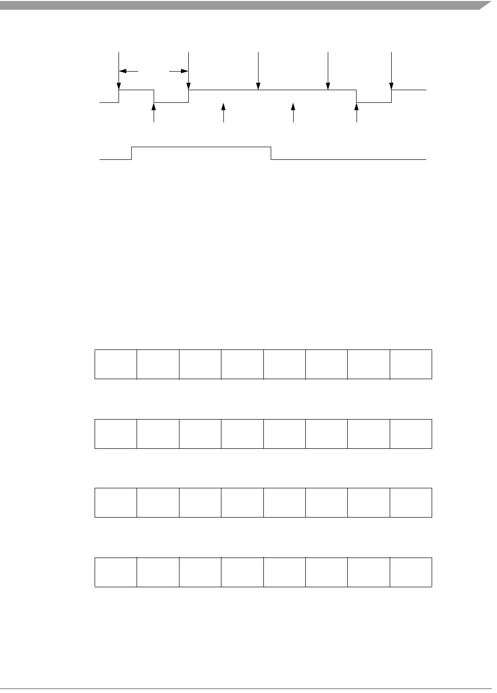
I/O Registers
MC68HC08LN56 • MC68HC708LN56 General Release Specification, Rev. 2.1
Freescale Semiconductor 111
Figure 10-8. CHxMAX Latency
10.8.6 TIM Channel Registers (TCH0H/L:TCH3H/L)
These read/write registers contain the captured TIM counter value of the input capture function or the
output compare value of the output compare function. The state of the TIM channel registers after reset
is unknown.
In input capture mode (MSxB:MSxA = 0:0), reading the high byte of the TIM channel x registers (TCHxH)
inhibits input captures until the low byte (TCHxL) is read.
In output compare mode (MSxB:MSxA ≠ 0:0), writing to the high byte of the TIM channel x registers
(TCHxH) inhibits output compares until the low byte (TCHxL) is written.
TCH0H
$0027Bit 7654321Bit 0
Read:
Bit 15 14 13 12 11 10 9 Bit 8
Write:
Reset: Indeterminate after reset
TCH0L
$0028Bit 7654321Bit 0
Read:
Bit 7654321Bit 0
Write:
Reset: Indeterminate after reset
TCH1H$
002ABit 7654321Bit 0
Read:
Bit 15 14 13 12 11 10 9 Bit 8
Write:
Reset: Indeterminate after reset
TCH1L$
002BBit 7654321Bit 0
Read:
Bit 7654321Bit 0
Write:
Reset: Indeterminate after reset
Figure 10-9. TIM Channel Registers
(TCH0H/L:TCH3H/L) (Sheet 1 of 2)
OUTPUT
OVERFLOW
PTEx/TCHx
PERIOD
CHxMAX
OVERFLOW OVERFLOW OVERFLOW OVERFLOW
COMPARE
OUTPUT
COMPARE
OUTPUT
COMPARE
OUTPUT
COMPARE

Timer Interface Module (TIM)
MC68HC08LN56 • MC68HC708LN56 General Release Specification, Rev. 2.1
112 Freescale Semiconductor
TCH2H$
002DBit 7654321Bit 0
Read:
Bit 15 14 13 12 11 10 9 Bit 8
Write:
Reset: Indeterminate after reset
TCH2L$
002EBit 7654321Bit 0
Read:
Bit 7654321Bit 0
Write:
Reset: Indeterminate after reset
TCH3H
$0030Bit 7654321Bit 0
Reset:
Bit 15 14 13 12 11 10 9 Bit 8
Write:
Reset: Indeterminate after reset
TCH3L$
0031Bit 7654321Bit 0
Read:
Bit 7654321Bit 0
Write:
Reset: Indeterminate after reset
Figure 10-9. TIM Channel Registers
(TCH0H/L:TCH3H/L) (Sheet 2 of 2)

MC68HC08LN56 • MC68HC708LN56 General Release Specification, Rev. 2.1
Freescale Semiconductor 113
Chapter 11
Serial Peripheral Interface Module (SPI)
11.1 Introduction
This section describes the serial peripheral interface module (SPI, Version C), which allows full-duplex,
synchronous, serial communications with peripheral devices.
11.2 Features
Features of the SPI module include:
• Full-Duplex Operation
• Master and Slave Modes
• Double-Buffered Operation with Separate Transmit and Receive Registers
• Four Master Mode Frequencies (Maximum = Bus Frequency ÷2)
• Maximum Slave Mode Frequency = Bus Frequency
• Clock Ground for Reduced Radio Frequency (RF) Interference
• Serial Clock with Programmable Polarity and Phase
• Two Separately Enabled Interrupts with DMA or CPU Service:
– SPRF (SPI Receiver Full)
– SPTE (SPI Transmitter Empty)
• Mode Fault Error Flag with CPU Interrupt Capability
• Overflow Error Flag with CPU Interrupt Capability
• Programmable Wired-OR Mode
•I
2C (Inter-Integrated Circuit) Compatibility
NOTE
References to DMA and associated functions are only valid if the MCU has
a DMA module. If the MCU has no DMA, any DMA related register bits
should be left in their reset state for expected MCU operation.
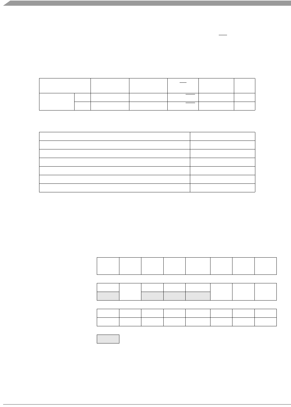
Serial Peripheral Interface Module (SPI)
MC68HC08LN56 • MC68HC708LN56 General Release Specification, Rev. 2.1
114 Freescale Semiconductor
11.3 Pin Name Conventions and I/O Register Addresses
The text that follows describes both SPI1 and SPI2. The SPI I/O pin names are SS (slave select), SPSCK
(SPI serial clock), CGND (clock ground), MOSI (master out slave in), and MISO (master in slave out). The
two SPIs share eight I/O pins with one parallel I/O ports. The full names of the SPI I/O pins are shown in
Table 11-1.
The generic pins names appear in the text that follows.
11.4 Functional Description
Figure 11-1 summarizes the SPI I/O registers and Figure 11-2 shows the structure of the SPI module.
Table 11-1. Pin Name Conventions
SPI Generic
Pin Names: MISO MOSI SS SCK CGND
Full SPI
Pin Names:
SPI1 PTD0/MISO1 PTD1/MOSI1 PTD2/SS1 PTD3/SCK1 CGND
SPI2 PTD7/MISO2 PTD6/MOSI2 PTD5/SS2 PTD4/SCK2 CGND
Table 11-2. I/O Register Addresses
Register Name Register Address
SPI1 Control Register (SPI1CR) $0010
SPI1 Status and Control Register (SPI1SCR) $0011
SPI1 Data Register (SPI1DR) $0012
SPI2 Control Register (SPI2CR) $001C
SPI2 Status and Control Register (SPI2SCR) $001D
SPI2 Data Register (SPI2DR) $001E
Register Name R/W Bit 7 6 5 4 3 2 1 Bit 0
SPI Control Register
(SPCR)
Read:
SPRIE DMAS SPMSTR CPOL CPHA SPWOM SPE SPTIE
Write:
Reset:0010 1 000
SPI Status and Control Register
(SPSCR)
Read: SPRF
ERRIE
OVRF MODF SPTE
MODFEN SPR1 SPR0
Write:
Reset:0000 1 000
SPI Data Register
(SPDR)
Read:R7R6R5R4 R3 R2R1R0
Write: T7 T6 T5 T4 T3 T2 T1 T0
Reset: Unaffected by reset
= Unimplemented
Figure 11-1. SPI I/O Register Summary
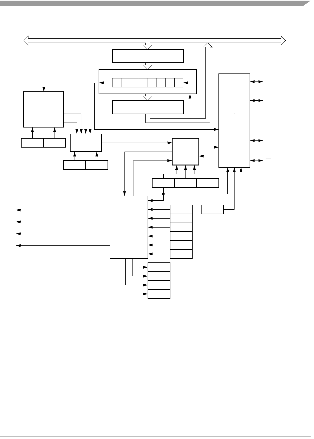
Functional Description
MC68HC08LN56 • MC68HC708LN56 General Release Specification, Rev. 2.1
Freescale Semiconductor 115
Figure 11-2. SPI Module Block Diagram
The SPI module allows full-duplex, synchronous, serial communication between the MCU and peripheral
devices, including other MCUs. Software can poll the SPI status flags or SPI operation can be
interrupt-driven. All SPI interrupts can be serviced by the CPU, and the transmitter empty (SPTE) and
receiver full (SPRF) flags can also be configured for DMA service.
During DMA transmissions, the DMA fetches data from memory for the SPI to transmit and/or the DMA
stores received data in memory.
The following paragraphs describe the operation of the SPI module.
TRANSMITTER CPU INTERRUPT REQUEST
RECEIVER DMA SERVICE REQUEST
RECEIVER/ERROR CPU INTERRUPT REQUEST
76543210
SPR1
SPMSTR
TRANSMIT DATA REGISTER
SHIFT REGISTER
SPR0
CGMOUT ÷ 2
CLOCK
SELECT
÷ 2
CLOCK
DIVIDER
÷ 8
÷ 32
÷ 128
CLOCK
LOGIC
CPHA CPOL
SPI
SPRIE
DMAS
SPE
SPWOM
SPRF
SPTE
OVRF
TRANSMITTER DMA SERVICE REQUEST
M
S
PIN
CONTROL
LOGIC
RECEIVE DATA REGISTER
SPTIE
SPE
INTERNAL BUS
(FROM SIM)
MODFEN
ERRIE
CONTROL
MODF
SPMSTR
MOSI
MISO
SPSCK
SS
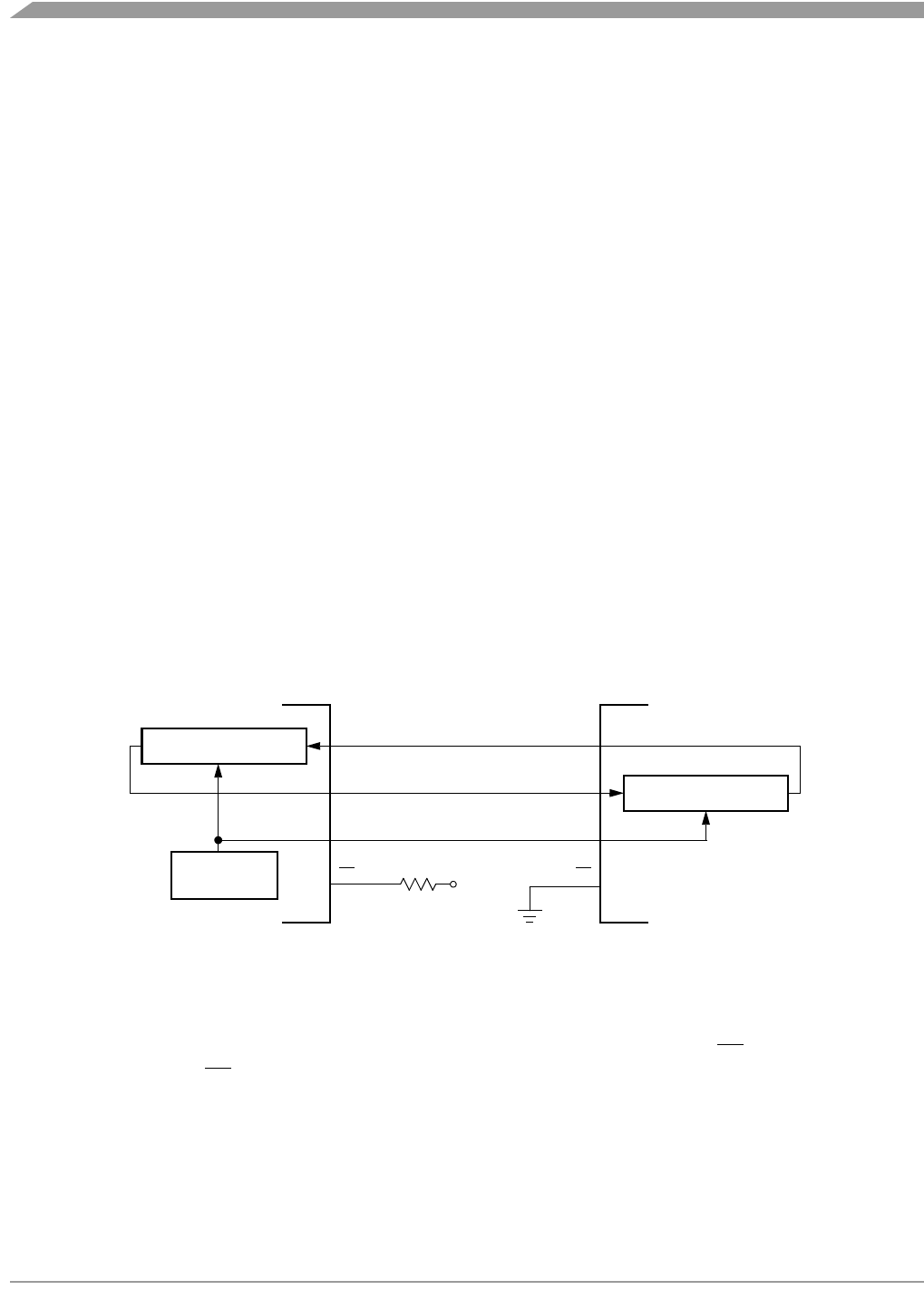
Serial Peripheral Interface Module (SPI)
MC68HC08LN56 • MC68HC708LN56 General Release Specification, Rev. 2.1
116 Freescale Semiconductor
11.4.1 Master Mode
The SPI operates in master mode when the SPI master bit, SPMSTR, is set.
NOTE
Configure the SPI modules as master or slave before enabling them.
Enable the master SPI before enabling the slave SPI. Disable the slave SPI
before disabling the master SPI. (See 11.13.1 SPI Control Register.)
Only a master SPI module can initiate transmissions. Software begins the transmission from a master SPI
module by writing to the transmit data register. If the shift register is empty, the byte immediately transfers
to the shift register, setting the SPI transmitter empty bit, SPTE. The byte begins shifting out on the MOSI
pin under the control of the serial clock. See Figure 11-3
The SPR1 and SPR0 bits control the baud rate generator and determine the speed of the shift register.
(See 11.13.2 SPI Status and Control Register.) Through the SPSCK pin, the baud rate generator of the
master also controls the shift register of the slave peripheral.
As the byte shifts out on the MOSI pin of the master, another byte shifts in from the slave on the master’s
MISO pin. The transmission ends when the receiver full bit, SPRF, becomes set. At the same time that
SPRF becomes set, the byte from the slave transfers to the receive data register. In normal operation,
SPRF signals the end of a transmission. Software clears SPRF by reading the SPI status and control
register with SPRF set and then reading the SPI data register. Writing to the SPI data register clears the
SPTE bit.
When the DMAS bit is set, the SPI status and control register does not have to be read to clear the SPRF
bit. A read of the SPI data register by either the CPU or the DMA clears the SPRF bit. A write to the SPI
data register by the CPU or by the DMA clears the SPTE bit.
Figure 11-3. Full-Duplex Master-Slave Connections
11.4.2 Slave Mode
The SPI operates in slave mode when the SPMSTR bit is clear. In slave mode the SPSCK pin is the input
for the serial clock from the master MCU. Before a data transmission occurs, the SS pin of the slave SPI
must be at logic zero. SS must remain low until the transmission is complete. (See 11.7.2 Mode Fault
Error.)
In a slave SPI module, data enters the shift register under the control of the serial clock from the master
SPI module. After a byte enters the shift register of a slave SPI, it transfers to the receive data register,
and the SPRF bit is set. To prevent an overflow condition, slave software then must read the receive data
register before another full byte enters the shift register.
SHIFT REGISTER
SHIFT REGISTER
BAUD RATE
GENERATOR
MASTER MCU SLAVE MCU
VDD
MOSI MOSI
MISO MISO
SPSCK SPSCK
SS SS

Transmission Formats
MC68HC08LN56 • MC68HC708LN56 General Release Specification, Rev. 2.1
Freescale Semiconductor 117
The maximum frequency of the SPSCK for an SPI configured as a slave is the bus clock speed (which is
twice as fast as the fastest master SPSCK clock that can be generated). The frequency of the SPSCK for
an SPI configured as a slave does not have to correspond to any SPI baud rate. The baud rate only
controls the speed of the SPSCK generated by an SPI configured as a master. Therefore, the frequency
of the SPSCK for an SPI configured as a slave can be any frequency less than or equal to the bus speed.
When the master SPI starts a transmission, the data in the slave shift register begins shifting out on the
MISO pin. The slave can load its shift register with a new byte for the next transmission by writing to its
transmit data register. The slave must write to its transmit data register at least one bus cycle before the
master starts the next transmission. Otherwise the byte already in the slave shift register shifts out on the
MISO pin. Data written to the slave shift register during a transmission remains in a buffer until the end of
the transmission.
When the clock phase bit (CPHA) is set, the first edge of SPSCK starts a transmission. When CPHA is
clear, the falling edge of SS starts a transmission. (See 11.5 Transmission Formats.)
NOTE
SPSCK must be in the proper idle state before the slave is enabled to
prevent SPSCK from appearing as a clock edge.
11.5 Transmission Formats
During an SPI transmission, data is simultaneously transmitted (shifted out serially) and received (shifted
in serially). A serial clock synchronizes shifting and sampling on the two serial data lines. A slave select
line allows selection of an individual slave SPI device; slave devices that are not selected do not interfere
with SPI bus activities. On a master SPI device, the slave select line can optionally be used to indicate
multiple-master bus contention.
11.5.1 Clock Phase and Polarity Controls
Software can select any of four combinations of serial clock (SPSCK) phase and polarity using two bits
in the SPI control register (SPCR). The clock polarity is specified by the CPOL control bit, which selects
an active high or low clock and has no significant effect on the transmission format.
The clock phase (CPHA) control bit selects one of two fundamentally different transmission formats. The
clock phase and polarity should be identical for the master SPI device and the communicating slave
device. In some cases, the phase and polarity are changed between transmissions to allow a master
device to communicate with peripheral slaves having different requirements.
NOTE
Before writing to the CPOL bit or the CPHA bit, disable the SPI by clearing
the SPI enable bit (SPE) .
11.5.2 Transmission Format When CPHA = 0
Figure 11-4 shows an SPI transmission in which CPHA is logic zero. The figure should not be used as a
replacement for data sheet parametric information.Two waveforms are shown for SPSCK: one for
CPOL = 0 and another for CPOL = 1. The diagram may be interpreted as a master or slave timing
diagram since the serial clock (SPSCK), master in/slave out (MISO), and master out/slave in (MOSI) pins
are directly connected between the master and the slave. The MISO signal is the output from the slave,
and the MOSI signal is the output from the master. The SS line is the slave select input to the slave. The
slave SPI drives its MISO output only when its slave select input (SS) is at logic zero, so that only the
Serial Peripheral Interface Module (SPI)
MC68HC08LN56 • MC68HC708LN56 General Release Specification, Rev. 2.1
118 Freescale Semiconductor
selected slave drives to the master. The SS pin of the master is not shown but is assumed to be inactive.
The SS pin of the master must be high or must be reconfigured as general-purpose I/O not affecting the
SPI. (See 11.7.2 Mode Fault Error.) When CPHA = 0, the first SPSCK edge is the MSB capture strobe.
Therefore the slave must begin driving its data before the first SPSCK edge, and a falling edge on the SS
pin is used to start the slave data transmission. The slave’s SS pin must be toggled back to high and then
low again between each byte transmitted as shown in Figure 11-5.
Figure 11-4. Transmission Format (CPHA = 0)
Figure 11-5. CPHA/SS Timing
When CPHA = 0 for a slave, the falling edge of SS indicates the beginning of the transmission. This
causes the SPI to leave its idle state and begin driving the MISO pin with the MSB of its data. Once the
transmission begins, no new data is allowed into the shift register from the transmit data register.
Therefore, the SPI data register of the slave must be loaded with transmit data before the falling edge of
SS. Any data written after the falling edge is stored in the transmit data register and transferred to the shift
register after the current transmission.
11.5.3 Transmission Format When CPHA = 1
Figure 11-6 shows an SPI transmission in which CPHA is logic one. The figure should not be used as a
replacement for data sheet parametric information. Two waveforms are shown for SPSCK: one for
CPOL = 0 and another for CPOL = 1. The diagram may be interpreted as a master or slave timing
diagram since the serial clock (SPSCK), master in/slave out (MISO), and master out/slave in (MOSI) pins
are directly connected between the master and the slave. The MISO signal is the output from the slave,
and the MOSI signal is the output from the master. The SS line is the slave select input to the slave. The
slave SPI drives its MISO output only when its slave select input (SS) is at logic zero, so that only the
selected slave drives to the master. The SS pin of the master is not shown but is assumed to be inactive.
The SS pin of the master must be high or must be reconfigured as general-purpose I/O not affecting the
BIT 6 BIT 5 BIT 4 BIT 3 BIT 2 BIT 1 LSB
MSB
BIT 6 BIT 5 BIT 4 BIT 3 BIT 2 BIT 1 LSB
MSB
12345678
SPSCK CYCLE #
(FOR REFERENCE)
SPSCK (CPOL = 0)
SPSCK (CPOL =1)
MOSI
(FROM MASTER)
MISO
(FROM SLAVE)
SS (TO SLAVE)
CAPTURE STROBE
BYTE 1 BYTE 3
MISO/MOSI BYTE 2
MASTER SS
SLAVE SS
(CPHA = 0)
SLAVE SS
(CPHA = 1)
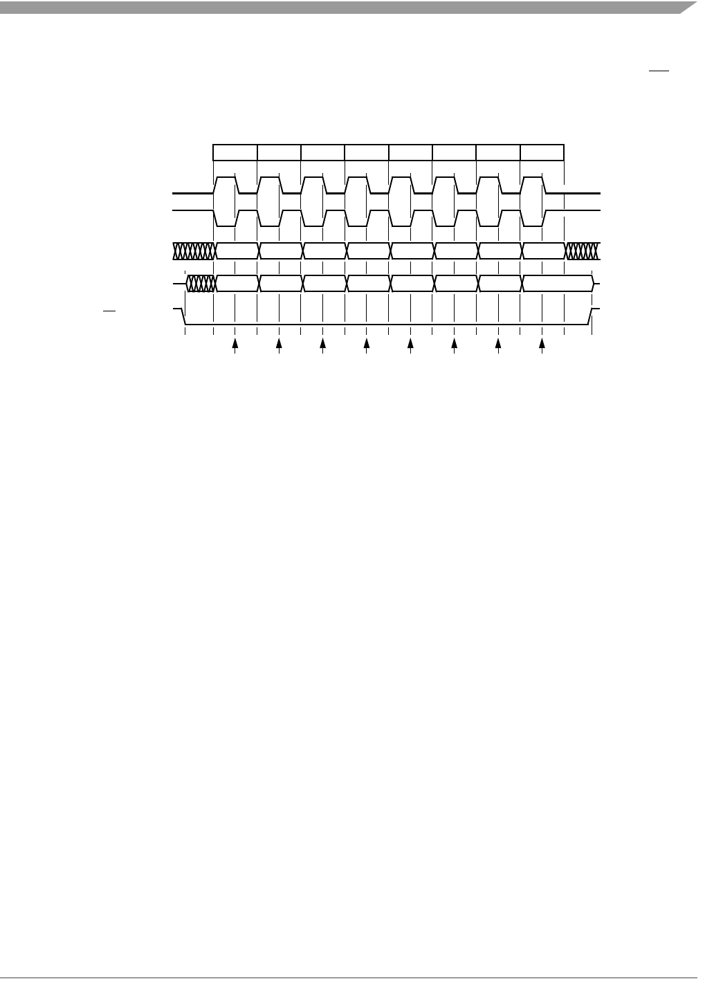
Queuing Transmission Data
MC68HC08LN56 • MC68HC708LN56 General Release Specification, Rev. 2.1
Freescale Semiconductor 119
SPI. (See 11.7.2 Mode Fault Error.) When CPHA = 1, the master begins driving its MOSI pin on the first
SPSCK edge. Therefore the slave uses the first SPSCK edge as a start transmission signal. The SS pin
can remain low between transmissions. This format may be preferable in systems having only one master
and only one slave driving the MISO data line.
Figure 11-6. Transmission Format (CPHA = 1)
When CPHA = 1 for a slave, the first edge of the SPSCK indicates the beginning of the transmission. This
causes the SPI to leave its idle state and begin driving the MISO pin with the MSB of its data. Once the
transmission begins, no new data is allowed into the shift register from the transmit data register.
Therefore, the SPI data register of the slave must be loaded with transmit data before the first edge of
SPSCK. Any data written after the first edge is stored in the transmit data register and transferred to the
shift register after the current transmission.
11.5.4 Transmission Initiation Latency
When the SPI is configured as a master (SPMSTR = 1), writing to the SPDR starts a transmission. CPHA
has no effect on the delay to the start of the transmission, but it does affect the initial state of the SPSCK
signal. When CPHA = 0, the SPSCK signal remains inactive for the first half of the first SPSCK cycle.
When CPHA = 1, the first SPSCK cycle begins with an edge on the SPSCK line from its inactive to its
active level. The SPI clock rate (selected by SPR1:SPR0) affects the delay from the write to SPDR and
the start of the SPI transmission. (See Figure 11-7.) The internal SPI clock in the master is a free-running
derivative of the internal MCU clock. To conserve power, it is enabled only when both the SPE and
SPMSTR bits are set. SPSCK edges occur halfway through the low time of the internal MCU clock. Since
the SPI clock is free-running, it is uncertain where the write to the SPDR occurs relative to the slower
SPSCK. This uncertainty causes the variation in the initiation delay shown in Figure 11-7. This delay is
no longer than a single SPI bit time. That is, the maximum delay is two MCU bus cycles for DIV2, eight
MCU bus cycles for DIV8, 32 MCU bus cycles for DIV32, and 128 MCU bus cycles for DIV128.
11.6 Queuing Transmission Data
The double-buffered transmit data register allows a data byte to be queued and transmitted. For an SPI
configured as a master, a queued data byte is transmitted immediately after the previous transmission
has completed. The SPI transmitter empty flag (SPTE) indicates when the transmit data buffer is ready
to accept new data. Write to the transmit data register only when the SPTE bit is high. Figure 11-8 shows
the timing associated with doing back-to-back transmissions with the SPI (SPSCK has CPHA:
CPOL = 1:0).
BIT 6 BIT 5 BIT 4 BIT 3 BIT 2 BIT 1 LSB
MSB
BIT 6 BIT 5 BIT 4 BIT 3 BIT 2 BIT 1 LSB
MSB
12345678
SPSCK CYCLE #
(FOR REFERENCE)
SPSCK (CPOL = 0)
SPSCK (CPOL =1)
MOSI
(FROM MASTER)
MISO
(FROM SLAVE)
SS (TO SLAVE)
CAPTURE STROBE
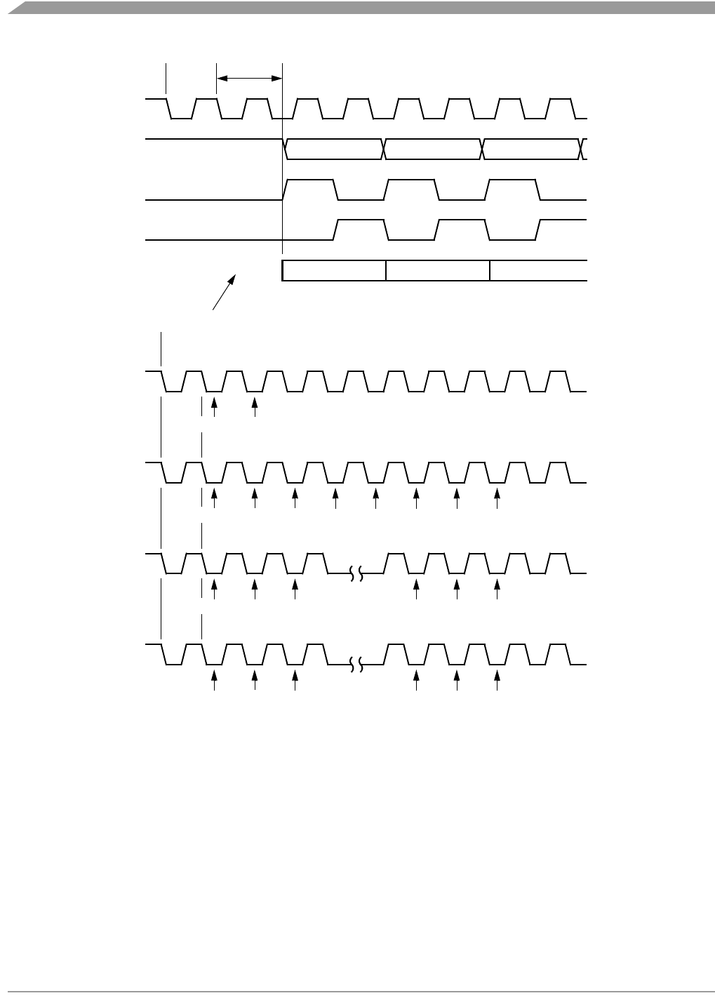
Serial Peripheral Interface Module (SPI)
MC68HC08LN56 • MC68HC708LN56 General Release Specification, Rev. 2.1
120 Freescale Semiconductor
Figure 11-7. Transmission Start Delay (Master)
The transmit data buffer allows back-to-back transmissions without the slave precisely timing its writes
between transmissions as in a system with a single data buffer. Also, if no new data is written to the data
buffer, the last value contained in the shift register is the next data word to be transmitted.
For an idle master or idle slave that has no data loaded into its transmit buffer, the SPTE is set again no
more than two bus cycles after the transmit buffer empties into the shift register. This allows the user to
queue up a 16-bit value to send. For an already active slave, the load of the shift register cannot occur
until the transmission is completed. This implies that a back-to-back write to the transmit data register is
not possible. The SPTE indicates when the next write can occur.
WRITE
TO SPDR INITIATION DELAY
BUS
MOSI
SPSCK
(CPHA = 1)
SPSCK
(CPHA = 0)
SPSCK CYCLE
NUMBER
MSB BIT 6
12
CLOCK
WRITE
TO SPDR
EARLIEST LATEST (SPSCK = INTERNAL CLOCK ÷ 2;
EARLIEST LATEST
2 POSSIBLE START POINTS)
(SPSCK = INTERNAL CLOCK ÷ 8;
8 POSSIBLE START POINTS)
EARLIEST LATEST(SPSCK = INTERNAL CLOCK ÷ 32;
32 POSSIBLE START POINTS)
EARLIEST LATEST(SPSCK = INTERNAL CLOCK ÷ 128;
128 POSSIBLE START POINTS)
WRITE
TO SPDR
WRITE
TO SPDR
WRITE
TO SPDR
BUS
CLOCK
BIT 5
3
BUS
CLOCK
BUS
CLOCK
BUS
CLOCK
⎧
⎨
⎩
⎮
⎮
⎮
⎮
⎮
INITIATION DELAY FROM WRITE SPDR TO TRANSFER BEGIN
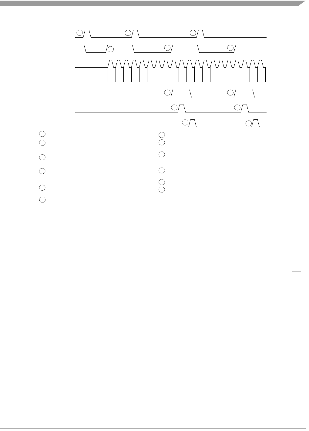
Error Conditions
MC68HC08LN56 • MC68HC708LN56 General Release Specification, Rev. 2.1
Freescale Semiconductor 121
Figure 11-8. SPRF/SPTE CPU Interrupt Timing
11.7 Error Conditions
The following flags signal SPI error conditions:
• Overflow (OVRF) — Failing to read the SPI data register before the next full byte enters the shift
register sets the OVRF bit. The new byte does not transfer to the receive data register, and the
unread byte still can be read. OVRF is in the SPI status and control register.
• Mode fault error (MODF) — The MODF bit indicates that the voltage on the slave select pin (SS)
is inconsistent with the mode of the SPI. MODF is in the SPI status and control register.
11.7.1 Overflow Error
The overflow flag (OVRF) becomes set if the receive data register still has unread data from a previous
transmission when the capture strobe of bit 1 of the next transmission occurs. The bit 1 capture strobe
occurs in the middle of SPSCK cycle 7. (See Figure 11-4 and Figure 11-6.) If an overflow occurs, all data
received after the overflow and before the OVRF bit is cleared does not transfer to the receive data
register and does not set the SPI receiver full bit (SPRF). The unread data that transferred to the receive
data register before the overflow occurred can still be read. Therefore, an overflow error always indicates
the loss of data. Clear the overflow flag by reading the SPI status and control register and then reading
the SPI data register.
OVRF generates a receiver/error CPU interrupt request if the error interrupt enable bit (ERRIE) is also
set. When the DMAS bit is low, the SPRF, MODF, and OVRF interrupts share the same CPU interrupt
vector. When the DMAS bit is high, SPRF generates a receiver DMA service request, and MODF and
OVRF can generate a receiver/error CPU interrupt request. (See Figure 11-12.) It is not possible to enable
BIT
3
MOSI
SPSCK
SPTE
WRITE TO SPDR 1
CPU WRITES BYTE 2 TO SPDR, QUEUEING BYTE 2
CPU WRITES BYTE 1 TO SPDR, CLEARING SPTE BIT.
BYTE 1 TRANSFERS FROM TRANSMIT DATA
3
1
2
2
3
5
REGISTER TO SHIFT REGISTER, SETTING SPTE BIT.
SPRF
READ SPSCR
MSB BIT
6
BIT
5
BIT
4
BIT
2
BIT
1
LSB MSB BIT
6
BIT
5
BIT
4
BIT
3
BIT
2
BIT
1
LSB MSB BIT
6
BYTE 2 TRANSFERS FROM TRANSMIT DATA
CPU WRITES BYTE 3 TO SPDR, QUEUEING BYTE
BYTE 3 TRANSFERS FROM TRANSMIT DATA
5
8
10
8
10
4FIRST INCOMING BYTE TRANSFERS FROM SHIFT
6CPU READS SPSCR WITH SPRF BIT SET.
4
6
9
SECOND INCOMING BYTE TRANSFERS FROM SHIFT
9
11
AND CLEARING SPTE BIT.
REGISTER TO SHIFT REGISTER, SETTING SPTE BIT.
REGISTER TO RECEIVE DATA REGISTER, SETTING
SPRF BIT.
3 AND CLEARING SPTE BIT.
REGISTER TO SHIFT REGISTER, SETTING SPTE BIT.
REGISTER TO RECEIVE DATA REGISTER, SETTING
SPRF BIT.
12 CPU READS SPDR, CLEARING SPRF BIT.
BIT
5
BIT
4
BYTE 1 BYTE 2 BYTE 3
712
READ SPDR
7CPU READS SPDR, CLEARING SPRF BIT.
11 CPU READS SPSCR WITH SPRF BIT SET.
(CPHA:CPOL = 1:0)
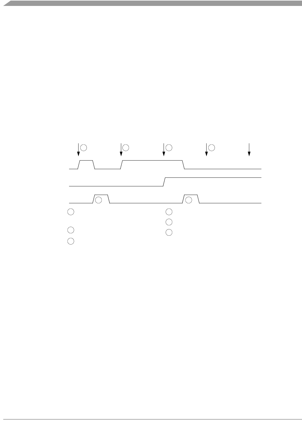
Serial Peripheral Interface Module (SPI)
MC68HC08LN56 • MC68HC708LN56 General Release Specification, Rev. 2.1
122 Freescale Semiconductor
MODF or OVRF individually to generate a receiver/error CPU interrupt request. However, leaving
MODFEN low prevents MODF from being set.
When the DMA is enabled to service the SPRF flag, it clears SPRF when it reads the receive data register.
The OVRF bit, however, still requires the two-step clearing mechanism of reading the flag when it is set
and then reading the receive data register. In this way, the DMA cannot directly clear the OVRF. However,
if the CPU reads the SPI status and control register with the OVRF bit set, and then the DMA reads the
receive data register, the OVRF bit is cleared.
OVRF interrupt requests to the CPU should be enabled when using the DMA to service the SPRF if there
is any chance that the overflow condition might occur. (See Figure 11-9.) Even if the DMA clears the
SPRF bit, no new data transfers from the shift register to the receive data register with the OVRF bit high.
This means that no new SPRF interrupt requests are generated until the CPU clears the OVRF bit. If the
CPU reads the data register to clear the OVRF bit, it could clear a pending SPRF service request to the
DMA.
Figure 11-9. Overflow Condition with DMA Service of SPRF
The overflow service routine may need to disable the DMA and manually recover since an overflow
indicates the loss of data. Loss of data may prevent the DMA from reaching its byte count.
If your application requires the DMA to bring the MCU out of wait mode, enable the OVRF bit to generate
CPU interrupt requests. An overflow condition in wait mode can cause the MCU to hang in wait mode
because the DMA cannot reach its byte count. Setting the error interrupt enable bit (ERRIE) in the SPI
status and control register enables the OVRF bit to bring the MCU out of wait mode.
If the CPU SPRF interrupt is enabled and the OVRF interrupt is not, watch for an overflow condition.
Figure 11-10 shows how it is possible to miss an overflow. The first part of Figure 11-10 shows how it is
possible to read the SPSCR and SPDR to clear the SPRF without problems. However, as illustrated by
the second transmission example, the OVRF bit can be set in between the time that SPSCR and SPDR
are read.
In this case, an overflow can easily be missed. Since no more SPRF interrupts can be generated until this
OVRF is serviced, it is not obvious that bytes are being lost as more transmissions are completed. To
prevent this, either enable the OVRF interrupt or do another read of the SPSCR following the read of the
SPDR. This ensures that the OVRF was not set before the SPRF was cleared and that future
DMA READS BYTE 1, CLEARING SPRF BIT.
BYTE 2 TRANSFERS FROM SHIFT
REGISTER TO DATA REGISTER,
SETTING SPRF BIT.
13
5
1
4
2
SPI RECEIVE
COMPLETE
OVRF
SPRF
DMA READ
OF SPDR
3
4BYTE 3 CAUSES OVERFLOW. BYTE 3 IS LOST.
5DMA READS BYTE 2, CLEARING SPRF BIT.
BYTE 1 BYTE 2 BYTE 3 BYTE 4 BYTE 5
BYTE 1 TRANSFERS FROM SHIFT
REGISTER TO DATA REGISTER,
2
SETTING SPRF BIT.
6BYTE 4 IS LOST. NO NEW SPRF DMA SERVICE
6
REQUESTS AND NO TRANSFERS TO DATA
REGISTER UNTIL OVRF IS CLEARED.
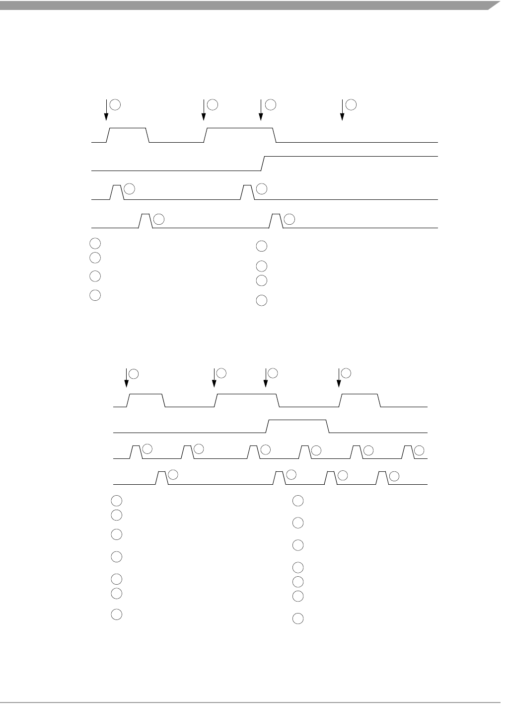
Error Conditions
MC68HC08LN56 • MC68HC708LN56 General Release Specification, Rev. 2.1
Freescale Semiconductor 123
transmissions can set the SPRF bit. Figure 11-11 illustrates this process. Generally, to avoid this second
SPSCR read, enable the OVRF to the CPU by setting the ERRIE bit.
Figure 11-10. Missed Read of Overflow Condition
Figure 11-11. Clearing SPRF When OVRF Interrupt Is Not Enabled
READ
READ
OVRF
SPRF
BYTE 1 BYTE 2 BYTE 3 BYTE 4
BYTE 1 SETS SPRF BIT.
CPU READS SPSCR WITH SPRF BIT SET
CPU READS BYTE 1 IN SPDR,
BYTE 2 SETS SPRF BIT.
CPU READS SPSCR WITH SPRF BIT SET
BYTE 3 SETS OVRF BIT. BYTE 3 IS LOST.
CPU READS BYTE 2 IN SPDR, CLEARING SPRF BIT,
BYTE 4 FAILS TO SET SPRF BIT BECAUSE
1
1
2
3
4
5
6
7
8
2
3
4
5
6
7
8
CLEARING SPRF BIT. BUT NOT OVRF BIT.
OVRF BIT IS NOT CLEARED. BYTE 4 IS LOST.
AND OVRF BIT CLEAR.
AND OVRF BIT CLEAR.
SPSCR
SPDR
READ
READ
OVRF
SPRF
BYTE 1 BYTE 2 BYTE 3 BYTE 4
1
BYTE 1 SETS SPRF BIT.
CPU READS SPSCR WITH SPRF BIT SET
CPU READS BYTE 1 IN SPDR,
CPU READS SPSCR AGAIN
BYTE 2 SETS SPRF BIT.
CPU READS SPSCR WITH SPRF BIT SET
BYTE 3 SETS OVRF BIT. BYTE 3 IS LOST.
CPU READS BYTE 2 IN SPDR,
CPU READS SPSCR AGAIN
CPU READS BYTE 2 SPDR,
BYTE 4 SETS SPRF BIT.
CPU READS SPSCR.
CPU READS BYTE 4 IN SPDR,
CPU READS SPSCR AGAIN
1
2
3
CLEARING SPRF BIT.
4
TO CHECK OVRF BIT.
5
6
7
8
9
CLEARING SPRF BIT.
TO CHECK OVRF BIT.
10
CLEARING OVRF BIT.
11
12
13
14
2
3
4
5
6
7
8
9
10
11
12
13
14
CLEARING SPRF BIT.
TO CHECK OVRF BIT.
SPI RECEIVE
COMPLETE
AND OVRF BIT CLEAR.
AND OVRF BIT CLEAR.
SPSCR
SPDR

Serial Peripheral Interface Module (SPI)
MC68HC08LN56 • MC68HC708LN56 General Release Specification, Rev. 2.1
124 Freescale Semiconductor
11.7.2 Mode Fault Error
Setting the SPMSTR bit selects master mode and configures the SPSCK and MOSI pins as outputs and
the MISO pin as an input. Clearing SPMSTR selects slave mode and configures the SPSCK and MOSI
pins as inputs and the MISO pin as an output. The mode fault bit, MODF, becomes set any time the state
of the slave select pin, SS, is inconsistent with the mode selected by SPMSTR. To prevent SPI pin
contention and damage to the MCU, a mode fault error occurs if:
•The SS pin of a slave SPI goes high during a transmission
•The SS
pin of a master SPI goes low at any time.
For the MODF flag to be set, the mode fault error enable bit (MODFEN) must be set. Clearing the
MODFEN bit does not clear the MODF flag but does prevent MODF from being set again after MODF is
cleared.
MODF generates a receiver/error CPU interrupt request if the error interrupt enable bit (ERRIE) is also
set. When the DMAS bit is low, the SPRF, MODF, and OVRF interrupts share the same CPU interrupt
vector. When the DMAS bit is high, SPRF generates a receiver DMA service request instead of a CPU
interrupt request, but MODF and OVRF can generate a receiver/error CPU interrupt request.
(See Figure 11-12.) It is not possible to enable MODF or OVRF individually to generate a receiver/error
CPU interrupt request. However, leaving MODFEN low prevents MODF from being set.
In a master SPI with the mode fault enable bit (MODFEN) set, the mode fault flag (MODF) is set if SS
goes to logic zero. A mode fault in a master SPI causes the following events to occur:
• If ERRIE = 1, the SPI generates an SPI receiver/error CPU interrupt request.
• The SPE bit is cleared.
• The SPTE bit is set.
• The SPI state counter is cleared.
• The data direction register of the shared I/O port regains control of port drivers.
NOTE
To prevent bus contention with another master SPI after a mode fault error,
clear all SPI bits of the data direction register of the shared I/O port before
enabling the SPI.
When configured as a slave (SPMSTR = 0), the MODF flag is set if SS goes high during a transmission.
When CPHA = 0, a transmission begins when SS goes low and ends once the incoming SPSCK goes
back to its idle level following the shift of the eighth data bit. When CPHA = 1, the transmission begins
when the SPSCK leaves its idle level and SS is already low. The transmission continues until the SPSCK
returns to its idle level following the shift of the last data bit. (See 11.5 Transmission Formats.)
NOTE
Setting the MODF flag does not clear the SPMSTR bit. The SPMSTR bit
has no function when SPE = 0. Reading SPMSTR when MODF = 1 shows
the difference between a MODF occurring when the SPI is a master and
when it is a slave.
When CPHA = 0, a MODF occurs if a slave is selected (SS is at logic 0) and
later unselected (SS is at logic 1) even if no SPSCK is sent to that slave.
This happens because SS at logic 0 indicates the start of the transmission
(MISO driven out with the value of MSB) for CPHA = 0. When CPHA = 1, a
slave can be selected and then later unselected with no transmission

Interrupts
MC68HC08LN56 • MC68HC708LN56 General Release Specification, Rev. 2.1
Freescale Semiconductor 125
occurring. Therefore, MODF does not occur since a transmission was
never begun.
In a slave SPI (MSTR = 0), the MODF bit generates an SPI receiver/error CPU interrupt request if the
ERRIE bit is set. The MODF bit does not clear the SPE bit or reset the SPI in any way. Software can abort
the SPI transmission by clearing the SPE bit of the slave.
NOTE
A logic one voltage on the SS pin of a slave SPI puts the MISO pin in a high
impedance state. Also, the slave SPI ignores all incoming SPSCK clocks,
even if it was already in the middle of a transmission.
To clear the MODF flag, read the SPSCR with the MODF bit set and then write to the SPCR register. This
entire clearing mechanism must occur with no MODF condition existing or else the flag is not cleared.
11.8 Interrupts
Four SPI status flags can be enabled to generate CPU interrupt requests or DMA service requests:
The DMA select bit (DMAS) controls whether SPTE and SPRF generate CPU interrupt requests or DMA
service requests. When DMAS = 0, reading the SPI status and control register with SPRF set and then
reading the receive data register clears SPRF. When DMAS = 1, any read of the receive data register
clears the SPRF flag. The clearing mechanism for the SPTE flag is always just a write to the transmit data
register.
The SPI transmitter interrupt enable bit (SPTIE) enables the SPTE flag to generate transmitter CPU
interrupt requests or transmitter DMA service requests, provided that the SPI is enabled (SPE = 1).
The SPI receiver interrupt enable bit (SPRIE) enables the SPRF bit to generate receiver CPU interrupt
requests or receiver DMA service requests, regardless of the state of the SPE bit. (See Figure 11-12.)
The error interrupt enable bit (ERRIE) enables both the MODF and OVRF bits to generate a receiver/error
CPU interrupt request.
The mode fault enable bit (MODFEN) can prevent the MODF flag from being set so that only the OVRF
bit is enabled by the ERRIE bit to generate receiver/error CPU interrupt requests.
Table 11-3. SPI Interrupts
Flag Request
SPTE
(Transmitter Empty)
SPI Transmitter CPU Interrupt Request (DMAS = 0, SPTIE = 1,SPE = 1)
SPI Transmitter DMA Service Request (DMAS = 1, SPTIE = 1, SPE = 1)
SPRF
(Receiver Full)
SPI Receiver CPU Interrupt Request (DMAS = 0, SPRIE = 1)
SPI Receiver DMA Service Request (DMAS = 1, SPRIE = 1)
OVRF
(Overflow) SPI Receiver/Error Interrupt Request (ERRIE = 1)
MODF
(Mode Fault) SPI Receiver/Error Interrupt Request (ERRIE = 1)
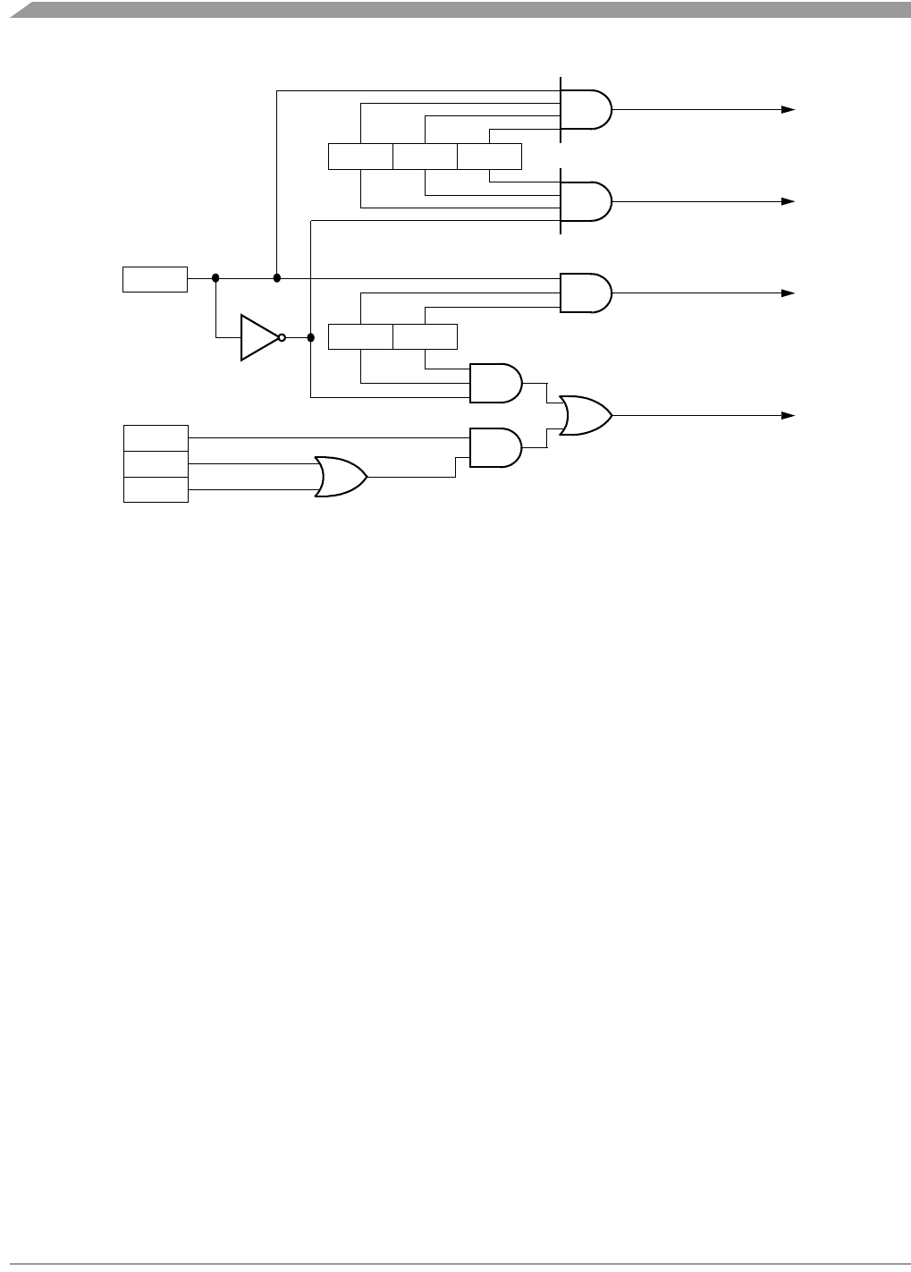
Serial Peripheral Interface Module (SPI)
MC68HC08LN56 • MC68HC708LN56 General Release Specification, Rev. 2.1
126 Freescale Semiconductor
Figure 11-12. SPI Interrupt Request Generation
The following sources in the SPI status and control register can generate CPU interrupt requests or DMA
service requests:
• SPI receiver full bit (SPRF) — The SPRF bit becomes set every time a byte transfers from the shift
register to the receive data register. If the SPI receiver interrupt enable bit, SPRIE, is also set,
SPRF can generate either an SPI receiver/error CPU interrupt request or an SPRF DMA service
request.
If the DMA select bit, DMAS, is clear, SPRF generates an SPRF CPU interrupt request. If DMAS
is set, SPRF generates an SPRF DMA service request.
• SPI transmitter empty (SPTE) — The SPTE bit becomes set every time a byte transfers from the
transmit data register to the shift register. If the SPI transmit interrupt enable bit, SPTIE, is also set,
SPTE can generate either an SPTE CPU interrupt request or an SPTE DMA service request.
If the DMAS bit is clear, SPTE generates an SPTE CPU interrupt request. If DMAS is set, SPTE
generates an SPTE DMA service request.
11.9 Resetting the SPI
Any system reset completely resets the SPI. Partial resets occur whenever the SPI enable bit (SPE) is
low. Whenever SPE is low, the following occurs:
• The SPTE flag is set
• Any transmission currently in progress is aborted
• The shift register is cleared
• The SPI state counter is cleared, making it ready for a new complete transmission
• All the SPI port logic is defaulted back to being general purpose I/O.
SPI TRANSMITTER
SPTE SPTIE
SPRFSPRIE
DMAS
ERRIE
MODF
OVRF
SPE
DMA SERVICE REQUEST
SPI TRANSMITTER
CPU INTERRUPT REQUEST
SPI RECEIVER
DMA SERVICE REQUEST
SPI RECEIVER/ERROR
CPU INTERRUPT REQUEST

Low-Power Modes
MC68HC08LN56 • MC68HC708LN56 General Release Specification, Rev. 2.1
Freescale Semiconductor 127
The following items are reset only by a system reset:
• All control bits in the SPCR register
• All control bits in the SPSCR register (MODFEN, ERRIE, SPR1, and SPR0)
• The status flags SPRF, OVRF, and MODF
By not resetting the control bits when SPE is low, the user can clear SPE between transmissions without
having to set all control bits again when SPE is set back high for the next transmission.
By not resetting the SPRF, OVRF, and MODF flags, the user can still service these interrupts after the
SPI has been disabled. The user can disable the SPI by writing 0 to the SPE bit. The SPI can also be
disabled by a mode fault occuring in an SPI that was configured as a master with the MODFEN bit set.
11.10 Low-Power Modes
The WAIT and STOP instructions put the MCU in low-power-consumption standby modes.
11.10.1 Wait Mode
The SPI module remains active after the execution of a WAIT instruction. In wait mode the SPI module
registers are not accessible by the CPU. Any enabled CPU interrupt request from the SPI module can
bring the MCU out of wait mode.
If SPI module functions are not required during wait mode, reduce power consumption by disabling the
SPI module before executing the WAIT instruction.
The DMA can service DMA service requests generated by the SPTE and SPRF flags without exiting wait
mode. To exit wait mode when an overflow condition occurs, enable the OVRF bit to generate CPU
interrupt requests by setting the error interrupt enable bit (ERRIE). (See 11.8 Interrupts.)
11.10.2 Stop Mode
The SPI module is inactive after the execution of a STOP instruction. The STOP instruction does not
affect register conditions. SPI operation resumes after an external interrupt. If stop mode is exited by
reset, any transfer in progress is aborted, and the SPI is reset.
11.11 SPI During Break Interrupts
The system integration module (SIM) controls whether status bits in other modules can be cleared during
the break state. The BCFE bit in the SIM break flag control register (SBFCR) enables software to clear
status bits during the break state. (See Chapter 5 System Integration Module (SIM).)
To allow software to clear status bits during a break interrupt, write a logic one to the BCFE bit. If a status
bit is cleared during the break state, it remains cleared when the MCU exits the break state.
To protect status bits during the break state, write a logic zero to the BCFE bit. With BCFE at logic zero
(its default state), software can read and write I/O registers during the break state without affecting status
bits. Some status bits have a two-step read/write clearing procedure. If software does the first step on
such a bit before the break, the bit cannot change during the break state as long as BCFE is at logic zero.
After the break, doing the second step clears the status bit.

Serial Peripheral Interface Module (SPI)
MC68HC08LN56 • MC68HC708LN56 General Release Specification, Rev. 2.1
128 Freescale Semiconductor
Since the SPTE bit cannot be cleared during a break with the BCFE bit cleared, a write to the transmit
data register in break mode does not initiate a transmission, nor is this data transferred into the shift
register. Therefore, a write to the SPDR in break mode with the BCFE bit cleared has no effect.
11.12 I/O Signals
The SPI module has five I/O pins and shares four of them with a parallel I/O port.
• MISO — Data received
• MOSI — Data transmitted
• SPSCK — Serial clock
•SS
— Slave select
• CGND — Clock ground
The SPI has limited inter-integrated circuit (I2C) capability (requiring software support) as a master in a
single-master environment. To communicate with I2C peripherals, MOSI becomes an open-drain output
when the SPWOM bit in the SPI control register is set. In I2C communication, the MOSI and MISO pins
are connected to a bidirectional pin from the I2C peripheral and through a pullup resistor to VDD.
11.12.1 MISO (Master In/Slave Out)
MISO is one of the two SPI module pins that transmits serial data. In full duplex operation, the MISO pin
of the master SPI module is connected to the MISO pin of the slave SPI module. The master SPI
simultaneously receives data on its MISO pin and transmits data from its MOSI pin.
Slave output data on the MISO pin is enabled only when the SPI is configured as a slave. The SPI is
configured as a slave when its SPMSTR bit is logic zero and its SS pin is at logic zero. To support a
multiple-slave system, a logic one on the SS pin puts the MISO pin in a high-impedance state.
When enabled, the SPI controls data direction of the MISO pin regardless of the state of the data direction
register of the shared I/O port.
11.12.2 MOSI (Master Out/Slave In)
MOSI is one of the two SPI module pins that transmits serial data. In full duplex operation, the MOSI pin
of the master SPI module is connected to the MOSI pin of the slave SPI module. The master SPI
simultaneously transmits data from its MOSI pin and receives data on its MISO pin.
When enabled, the SPI controls data direction of the MOSI pin regardless of the state of the data direction
register of the shared I/O port.
11.12.3 SPSCK (Serial Clock)
The serial clock synchronizes data transmission between master and slave devices. In a master MCU,
the SPSCK pin is the clock output. In a slave MCU, the SPSCK pin is the clock input. In full duplex
operation, the master and slave MCUs exchange a byte of data in eight serial clock cycles.
When enabled, the SPI controls data direction of the SPSCK pin regardless of the state of the data
direction register of the shared I/O port.
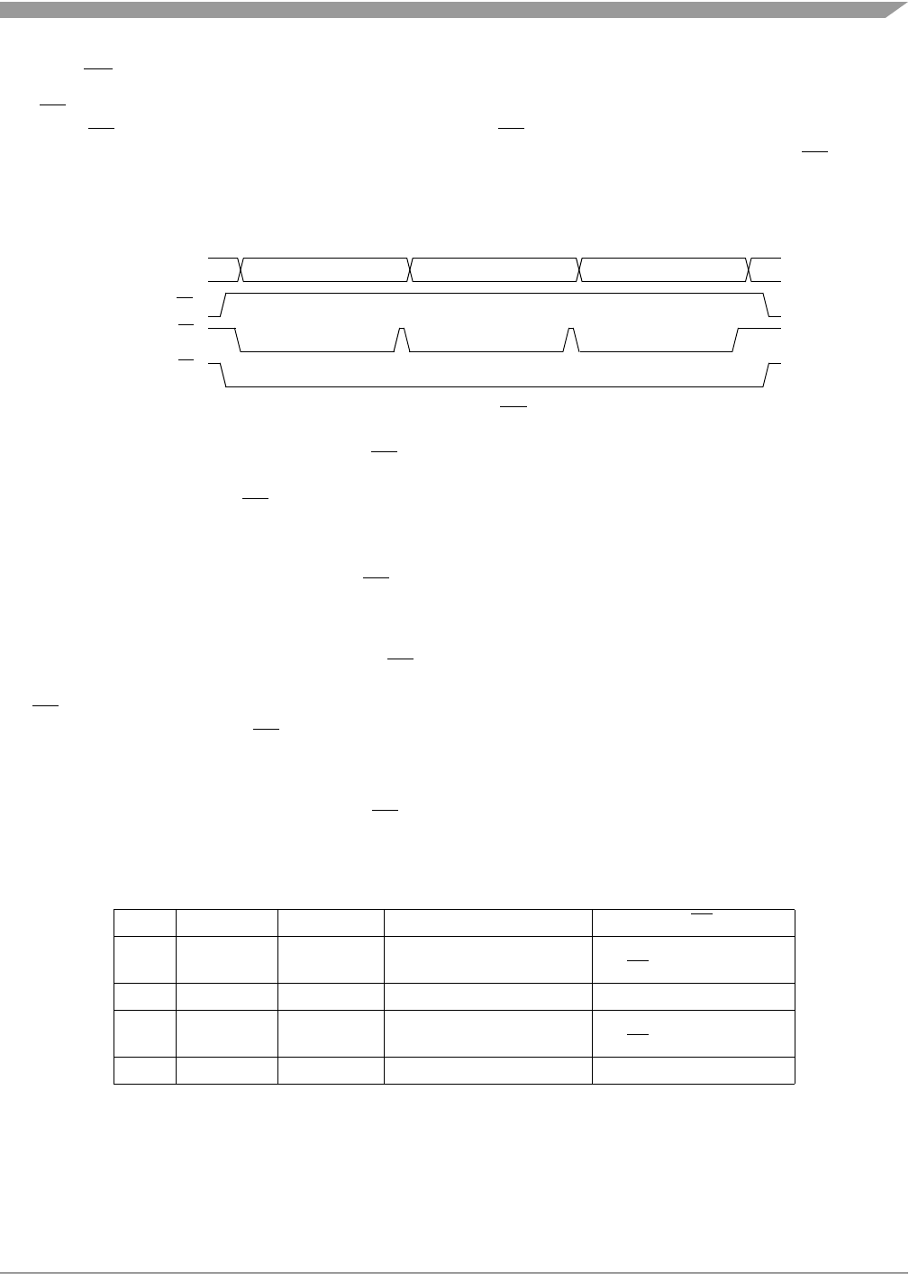
I/O Signals
MC68HC08LN56 • MC68HC708LN56 General Release Specification, Rev. 2.1
Freescale Semiconductor 129
11.12.4 SS (Slave Select)
The SS pin has various functions depending on the current state of the SPI. For an SPI configured as a
slave, the SS is used to select a slave. For CPHA = 0, the SS is used to define the start of a transmission.
(See 11.5 Transmission Formats.) Since it is used to indicate the start of a transmission, the SS must be
toggled high and low between each byte transmitted for the CPHA = 0 format. However, it can remain low
between transmissions for the CPHA = 1 format. See Figure 11-13.
Figure 11-13. CPHA/SS Timing
When an SPI is configured as a slave, the SS pin is always configured as an input. It cannot be used as
a general purpose I/O regardless of the state of the MODFEN control bit. However, the MODFEN bit can
still prevent the state of the SS from creating a MODF error. (See 11.13.2 SPI Status and Control
Register.)
NOTE
A logic one voltage on the SS pin of a slave SPI puts the MISO pin in a
high-impedance state. The slave SPI ignores all incoming SPSCK clocks,
even if it was already in the middle of a transmission.
When an SPI is configured as a master, the SS input can be used in conjunction with the MODF flag to
prevent multiple masters from driving MOSI and SPSCK. (See 11.7.2 Mode Fault Error.) For the state of
the SS pin to set the MODF flag, the MODFEN bit in the SPSCK register must be set. If the MODFEN bit
is low for an SPI master, the SS pin can be used as a general purpose I/O under the control of the data
direction register of the shared I/O port. With MODFEN high, it is an input-only pin to the SPI regardless
of the state of the data direction register of the shared I/O port.
The CPU can always read the state of the SS pin by configuring the appropriate pin as an input and
reading the port data register. (See Table 11-4.)
Table 11-4. SPI Configuration
SPE SPMSTR MODFEN SPI Configuration State of SS Logic
0X(1)
1. X = don’t care
X Not Enabled General-purpose I/O;
SS ignored by SPI
1 0 X Slave Input-only to SPI
1 1 0 Master without MODF General-purpose I/O;
SS ignored by SPI
1 1 1 Master with MODF Input-only to SPI
BYTE 1 BYTE 3
MISO/MOSI BYTE 2
MASTER SS
SLAVE SS
(CPHA = 0)
SLAVE SS
(CPHA = 1)

Serial Peripheral Interface Module (SPI)
MC68HC08LN56 • MC68HC708LN56 General Release Specification, Rev. 2.1
130 Freescale Semiconductor
11.12.5 CGND (Clock Ground)
CGND is the ground return for the serial clock pin, SPSCK, and the ground for the port output buffers. To
reduce the ground return path loop and minimize radio frequency (RF) emissions, connect the ground pin
of the slave to the CGND pin of the master.
11.13 I/O Registers
Three registers control and monitor SPI operation:
• SPI control register (SPCR)
• SPI status and control register (SPSCR)
• SPI data register (SPDR)
11.13.1 SPI Control Register
The SPI control register does the following:
• Enables SPI module interrupt requests
• Selects CPU interrupt requests or DMA service requests
• Configures the SPI module as master or slave
• Selects serial clock polarity and phase
• Configures the SPSCK, MOSI, and MISO pins as open-drain outputs
• Enables the SPI module
SPRIE — SPI Receiver Interrupt Enable Bit
This read/write bit enables CPU interrupt requests or DMA service requests generated by the SPRF
bit. The SPRF bit is set when a byte transfers from the shift register to the receive data register. Reset
clears the SPRIE bit.
1 = SPRF CPU interrupt requests or SPRF DMA service requests enabled
0 = SPRF CPU interrupt requests or SPRF DMA service requests disabled
DMAS —DMA Select Bit
This read/write bit selects DMA service requests when the SPI receiver full bit, SPRF, or the SPI
transmitter empty bit, SPTE, becomes set. Setting the DMAS bit disables SPRF CPU interrupt
requests and SPTE CPU interrupt requests. Reset clears the DMAS bit.
1 = SPRF DMA and SPTE DMA service requests enabled
(SPRF CPU and SPTE CPU interrupt requests disabled)
0 = SPRF DMA and SPTE DMA service requests disabled
(SPRF CPU and SPTE CPU interrupt requests enabled)
Address: $0010
Bit 7654321Bit 0
Read:
SPRIE DMAS SPMSTR CPOL CPHA SPWOM SPE SPTIE
Write:
Reset:00101000
Figure 11-14. SPI Control Register (SPCR)

I/O Registers
MC68HC08LN56 • MC68HC708LN56 General Release Specification, Rev. 2.1
Freescale Semiconductor 131
SPMSTR — SPI Master Bit
This read/write bit selects master mode operation or slave mode operation. Reset sets the SPMSTR
bit.
1 = Master mode
0 = Slave mode
CPOL — Clock Polarity Bit
This read/write bit determines the logic state of the SPSCK pin between transmissions. (Figure 11-4
and Figure 11-6.) To transmit data between SPI modules, the SPI modules must have identical CPOL
values. Reset clears the CPOL bit.
CPHA — Clock Phase Bit
This read/write bit controls the timing relationship between the serial clock and SPI data. (See Figure
11-4 and Figure 11-6.) To transmit data between SPI modules, the SPI modules must have identical
CPHA values. When CPHA = 0, the SS pin of the slave SPI module must be set to logic one between
bytes. (See Figure 11-13.) Reset sets the CPHA bit.
SPWOM — SPI Wired-OR Mode Bit
This read/write bit disables the pull-up devices on pins SPSCK, MOSI, and MISO so that those pins
become open-drain outputs.
1 = Wired-OR SPSCK, MOSI, and MISO pins
0 = Normal push-pull SPSCK, MOSI, and MISO pins
SPE — SPI Enable
This read/write bit enables the SPI module. Clearing SPE causes a partial reset of the SPI. (See 11.9
Resetting the SPI.) Reset clears the SPE bit.
1 = SPI module enabled
0 = SPI module disabled
SPTIE— SPI Transmit Interrupt Enable
This read/write bit enables CPU interrupt requests or DMA service requests generated by the SPTE
bit. SPTE is set when a byte transfers from the transmit data register to the shift register. Reset clears
the SPTIE bit.
1 = SPTE CPU interrupt requests or SPTE DMA service requests enabled
0 = SPTE CPU interrupt requests or SPTE DMA service requests disabled
11.13.2 SPI Status and Control Register
The SPI status and control register contains flags to signal the following conditions:
• Receive data register full
• Failure to clear SPRF bit before next byte is received (overflow error)
• Inconsistent logic level on SS pin (mode fault error)
• Transmit data register empty
The SPI status and control register also contains bits that perform the following functions:
• Enable error interrupts
• Enable mode fault error detection
• Select master SPI baud rate

Serial Peripheral Interface Module (SPI)
MC68HC08LN56 • MC68HC708LN56 General Release Specification, Rev. 2.1
132 Freescale Semiconductor
SPRF — SPI Receiver Full Bit
This clearable, read-only flag is set each time a byte transfers from the shift register to the receive data
register. SPRF generates a CPU interrupt request or a DMA service request if the SPRIE bit in the SPI
control register is set also.
The DMA select bit (DMAS) in the SPI control register determines whether SPRF generates an
SPRF CPU interrupt request or an SPRF DMA service request. During an SPRF CPU interrupt
(DMAS = 0), the CPU clears SPRF by reading the SPI status and control register with SPRF set and
then reading the SPI data register. During an SPRF DMA transmission (DMAS = 1), any read of the
SPI data register clears the SPRF bit.
Reset clears the SPRF bit.
1 = Receive data register full
0 = Receive data register not full
NOTE
When the DMA is configured to service the SPI (DMAS = 1), a read by the
CPU of the receive data register can inadvertently clear the SPRF bit and
cause the DMA to miss a service request.
ERRIE — Error Interrupt Enable Bit
This read/write bit enables the MODF and OVRF bits to generate CPU interrupt requests. Reset clears
the ERRIE bit.
1 = MODF and OVRF can generate CPU interrupt requests
0 = MODF and OVRF cannot generate CPU interrupt requests
OVRF — Overflow Bit
This clearable, read-only flag is set if software does not read the byte in the receive data register before
the next full byte enters the shift register. In an overflow condition, the byte already in the receive data
register is unaffected, and the byte that shifted in last is lost. Clear the OVRF bit by reading the SPI
status and control register with OVRF set and then reading the receive data register. Reset clears the
OVRF bit.
1 = Overflow
0 = No overflow
MODF — Mode Fault Bit
This clearable, read-only flag is set in a slave SPI if the SS pin goes high during a transmission with
the MODFEN bit set. In a master SPI, the MODF flag is set if the SS pin goes low at any time with the
MODFEN bit set. Clear the MODF bit by reading the SPI status and control register (SPSCR) with
MODF set and then writing to the SPI control register (SPCR). Reset clears the MODF bit.
1 = SS pin at inappropriate logic level
0 = SS pin at appropriate logic level
Address: $0011
Bit 7654321Bit 0
Read: SPRF
ERRIE
OVRF MODF SPTE
MODFEN SPR1 SPR0
Write:
Reset:00001000
= Unimplemented
Figure 11-15. SPI Status and Control Register (SPSCR)

I/O Registers
MC68HC08LN56 • MC68HC708LN56 General Release Specification, Rev. 2.1
Freescale Semiconductor 133
SPTE — SPI Transmitter Empty Bit
This clearable, read-only flag is set each time the transmit data register transfers a byte into the shift
register. SPTE generates an SPTE CPU interrupt request or an SPTE DMA service request if the
SPTIE bit in the SPI control register is set also.
NOTE
Do not write to the SPI data register unless the SPTE bit is high.
The DMA select bit (DMAS) in the SPI control register determines whether SPTE generates an
SPTE CPU interrupt request or an SPTE DMA service request. During an SPTE CPU interrupt
(DMAS = 0), the CPU clears the SPTE bit by writing to the transmit data register. During an SPTE DMA
transmission (DMAS = 1), the DMA automatically clears SPTE when it writes to the transmit data
register.
NOTE
When the DMA is configured to service the SPI (DMAS = 1), a write by the
CPU of the transmit data register can inadvertently clear the SPTE bit and
cause the DMA to miss a service request.
Reset sets the SPTE bit.
1 = Transmit data register empty
0 = Transmit data register not empty
MODFEN — Mode Fault Enable Bit
This read/write bit, when set to 1, allows the MODF flag to be set. If the MODF flag is set, clearing the
MODFEN does not clear the MODF flag. If the SPI is enabled as a master and the MODFEN bit is low,
then the SS pin is available as a general purpose I/O.
If the MODFEN bit is set, then this pin is not available as a general purpose I/O. When the SPI is
enabled as a slave, the SS pin is not available as a general purpose I/O regardless of the value of
MODFEN. (See 11.12.4 SS (Slave Select).)
If the MODFEN bit is low, the level of the SS pin does not affect the operation of an enabled SPI
configured as a master. For an enabled SPI configured as a slave, having MODFEN low only prevents
the MODF flag from being set. It does not affect any other part of SPI operation. (See 11.7.2 Mode
Fault Error.)
SPR1 and SPR0 — SPI Baud Rate Select Bits
In master mode, these read/write bits select one of four baud rates as shown in Table 11-5. SPR1 and
SPR0 have no effect in slave mode. Reset clears SPR1 and SPR0.
Use the following formula to calculate the SPI baud rate:
where:
CGMOUT = base clock output of the clock generator module (CGM)
BD = baud rate divisor
Table 11-5. SPI Master Baud Rate Selection
SPR1:SPR0 Baud Rate Divisor (BD)
00 2
01 8
10 32
11 128
Baud rate CGMOUT
2BD×
--------------------------=

Serial Peripheral Interface Module (SPI)
MC68HC08LN56 • MC68HC708LN56 General Release Specification, Rev. 2.1
134 Freescale Semiconductor
11.13.3 SPI Data Register
The SPI data register consists of the read-only receive data register and the write-only transmit data
register. Writing to the SPI data register writes data into the transmit data register. Reading the SPI data
register reads data from the receive data register. The transmit data and receive data registers are
separate registers that can contain different values. (See Figure 11-2.)
R7:R0/T7:T0 — Receive/Transmit Data Bits
NOTE
Do not use read-modify-write instructions on the SPI data register since the
register read is not the same as the register written.
Address: $0012
Bit 7654321Bit 0
Read:R7R6R5R4R3R2R1R0
Write: T7 T6 T5 T4 T3 T2 T1 T0
Reset: Indeterminate after reset
Figure 11-16. SPI Data Register (SPDR)

MC68HC08LN56 • MC68HC708LN56 General Release Specification, Rev. 2.1
Freescale Semiconductor 135
Chapter 12
Serial Communications Interface Module (SCI)
12.1 Introduction
The SCI allows asynchronous communications with peripheral devices and other MCUs.
NOTE
References to DMA and associated functions are only valid if the MCU has
a DMA module. If the MCU has no DMA, any DMA related register bits
should be left in their reset state for expected MCU operation.
12.2 Features
Features of the SCI module include:
• Full Duplex Operation
• Standard Mark/Space Non-Return-to-Zero (NRZ) Format
• 32 Programmable Baud Rates
• Programmable 8-Bit or 9-Bit Character Length
• Separately Enabled Transmitter and Receiver
• Separate Receiver and Transmitter CPU Interrupt Requests
• Separate Receiver and Transmitter DMA Service Requests
• Programmable Transmitter Output Polarity
• Two Receiver Wake-Up Methods:
– Idle Line Wake-Up
– Address Mark Wake-Up
• Interrupt-Driven Operation with Eight Interrupt Flags:
– Transmitter Empty
–Transmission Complete
– Receiver Full
– Idle Receiver Input
– Receiver Overrun
– Noise Error
– Framing Error
– Parity Error
• Receiver Framing Error Detection
• Hardware Parity Checking
• 1/16 Bit-Time Noise Detection

Serial Communications Interface Module (SCI)
MC68HC08LN56 • MC68HC708LN56 General Release Specification, Rev. 2.1
136 Freescale Semiconductor
12.3 Pin Name Conventions
The generic names of the SCI I/O pins are:
• RxD (receive data)
• TxD (transmit data)
SCI I/O lines are implemented by sharing parallel I/O port pins. The full name of an SCI input or output
reflects the name of the shared port pin. Table 12-1 shows the full names and the generic names of the
SCI I/O pins.The generic pin names appear in the text of this section.
12.4 Functional Description
Figure 12-1 shows the structure of the SCI module. The SCI allows full-duplex, asynchronous, NRZ serial
communication among the MCU and remote devices, including other MCUs. The transmitter and receiver
of the SCI operate independently, although they use the same baud rate generator. During normal
operation, the CPU monitors the status of the SCI, writes the data to be transmitted, and processes
received data. During DMA transfers, the DMA fetches data from memory for the SCI to transmit and/or
the DMA stores received data in memory.
Table 12-1. Pin Name Conventions
Generic Pin Names: RxD TxD
Full Pin Names: PTE6/RxD PTE5/TxD
Functional Description
MC68HC08LN56 • MC68HC708LN56 General Release Specification, Rev. 2.1
Freescale Semiconductor 137
Figure 12-1. SCI Module Block Diagram
SCTE
TC
SCRF
IDLE
OR
NF
FE
PE
SCTIE
TCIE
SCRIE
ILIE
TE
RE
RWU
SBK
R8
T8
DMATE
ORIE
FEIE
PEIE
BKF
RPF
SCI DATA
RECEIVE
SHIFT REGISTER
SCI DATA
REGISTER
TRANSMIT
SHIFT REGISTER
NEIE
M
WAKE
ILTY
FLAG
CONTROL
TRANSMIT
CONTROL
RECEIVE
CONTROL
DATA SELECTION
CONTROL
WAKE-UP
PTY
PEN
REGISTER
DMA
INTERRUPT
CONTROL
TRANSMITTER
INTERRUPT
CONTROL
RECEIVER
INTERRUPT
CONTROL
ERROR
INTERRUPT
CONTROL
CONTROL
DMARE
ENSCI
LOOPS
ENSCI
PTE6/RxD PTE5/TxD
INTERNAL BUS
TXINV
LOOPS
÷ 4
³ 16
PRE-
SCALER
BAUD RATE
GENERATOR
BUS CLOCK
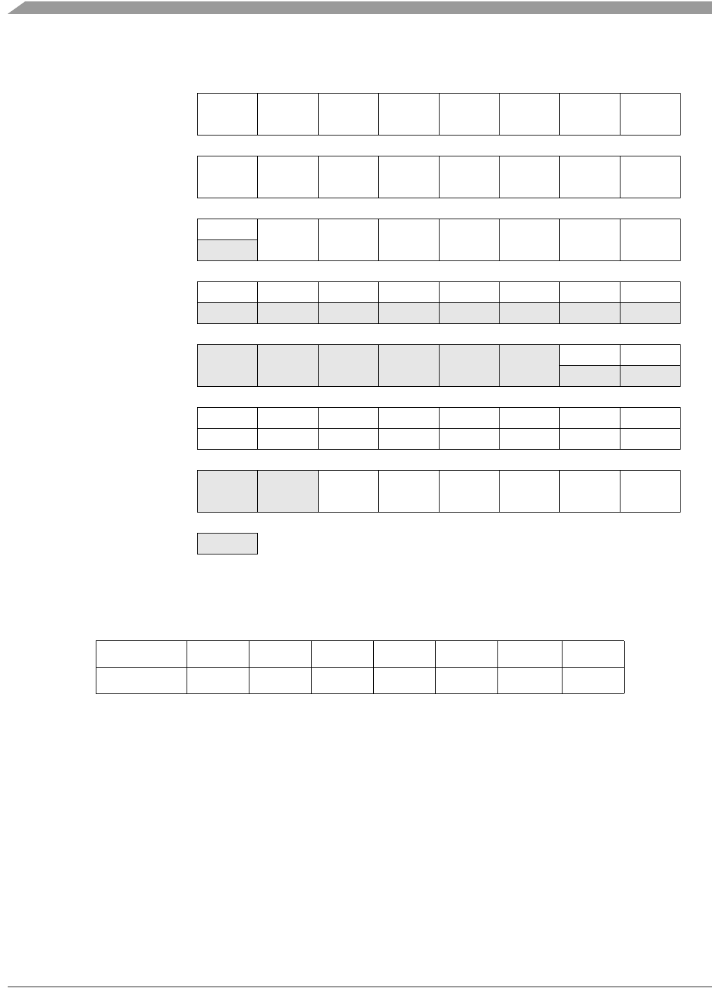
Serial Communications Interface Module (SCI)
MC68HC08LN56 • MC68HC708LN56 General Release Specification, Rev. 2.1
138 Freescale Semiconductor
Register Name Bit 7654321Bit 0
SCI Control Register 1
(SCC1)
Read:
LOOPS ENSCI TXINV M WAKE ILTY PEN PTY
Write:
Reset:00000000
SCI Control Register 2
(SCC2)
Read:
SCTIE TCIE SCRIE ILIE TE RE RWU SBK
Write:
Reset:00000000
SCI Control Register 3
(SCC3)
Read: R8
T8 DMARE DMATE ORIE NEIE FEIE PEIE
Write:
Reset:UU000000
SCI Status Register 1
(SCS1)
Read: SCTE TC SCRF IDLE OR NF FE PE
Write:
Reset:11000000
SCI Status Register 2
(SCS2)
Read: BKF RPF
Write:
Reset:00000000
SCI Data Register
(SCDR)
Read:R7R6R5R4R3R2R1R0
Write: T7 T6 T5 T4 T3 T2 T1 T0
Reset: Unaffected by reset
SCI Baud Rate Register
(SCBR)
Read:
SCP1 SCP0 R SCR2 SCR1 SCR0
Write:
Reset:00000000
= Unimplemented U = Unaffected R = Reserved
Figure 12-2. SCI I/O Register Summary
Table 12-2. SCI I/O Register Address Summary
Register: SCC1 SCC2 SCC3 SCS1 SCS2 SCDR SCBR
Address: $0013 $0014 $0015 $0016 $0017 $0018 $0019
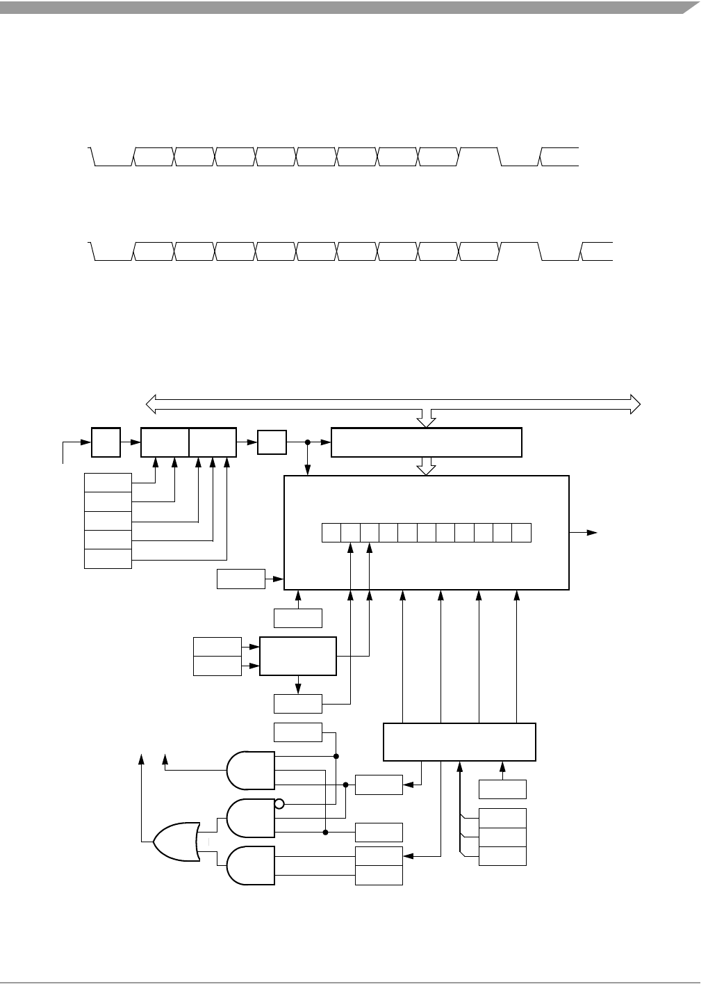
Functional Description
MC68HC08LN56 • MC68HC708LN56 General Release Specification, Rev. 2.1
Freescale Semiconductor 139
12.4.1 Data Format
The SCI uses the standard non-return-to-zero mark/space data format illustrated in Figure 12-3.
Figure 12-3. SCI Data Formats
12.4.2 Transmitter
Figure 12-4 shows the structure of the SCI transmitter.
Figure 12-4. SCI Transmitter
BIT 5
START
BIT BIT 0 BIT 1
NEXT
STOP
BIT
START
BIT
8-BIT DATA FORMAT
(BIT M IN SCC1 CLEAR)
START
BIT BIT 0
NEXT
STOP
BIT
START
BIT
9-BIT DATA FORMAT
(BIT M IN SCC1 SET)
BIT 1 BIT 2 BIT 3 BIT 4 BIT 5 BIT 6 BIT 7 BIT 8
BIT 2 BIT 3 BIT 4 BIT 6 BIT 7
PARITY
BIT
PARITY
BIT
DMATE
SCTE
PEN
PTY
H876543210L
11-BIT
TRANSMIT
STOP
START
T8
DMATE
SCTE
SCTIE
TCIE
SBK
TC
BUS CLOCK
PARITY
GENERATION
MSB
SCI DATA REGISTER
LOAD FROM SCDR
SHIFT ENABLE
PREAMBLE
(ALL ONES)
BREAK
(ALL ZEROS)
TRANSMITTER
CONTROL LOGIC
SHIFT REGISTER
DMATE
TC
SCTIE
TCIE
SCTE
TRANSMITTER CPU INTERRUPT REQUEST
TRANSMITTER DMA SERVICE REQUEST
M
ENSCI
LOOPS
TE
PTE5/Tx
TXINV
INTERNAL BUS
÷ 4PRE-
SCALER
SCP1
SCP0
SCR2
SCR1
SCR0
BAUD
DIVIDER ÷ 16
SCTIE
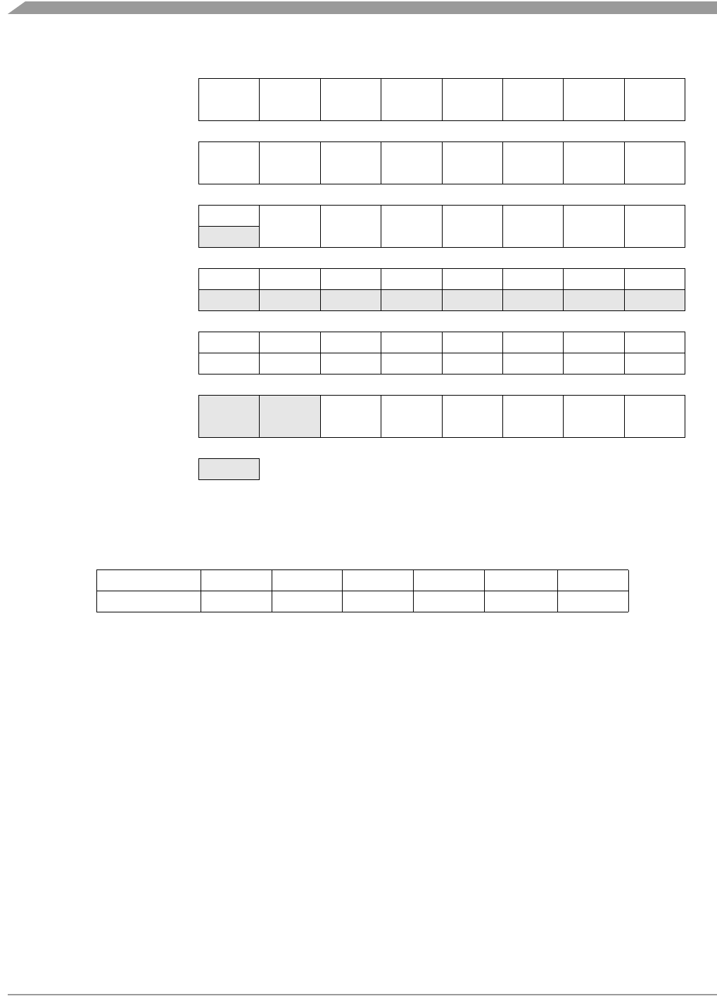
Serial Communications Interface Module (SCI)
MC68HC08LN56 • MC68HC708LN56 General Release Specification, Rev. 2.1
140 Freescale Semiconductor
12.4.2.1 Character Length
The transmitter can accommodate either 8-bit or 9-bit data. The state of the M bit in SCI control register 1
(SCC1) determines character length. When transmitting 9-bit data, bit T8 in SCI control register 3 (SCC3)
is the ninth bit (bit 8).
12.4.2.2 Character Transmission
During an SCI transmission, the transmit shift register shifts a character out to the PTE5/TxD pin. The SCI
data register (SCDR) is the write-only buffer between the internal data bus and the transmit shift register.
To initiate an SCI transmission:
1. Enable the SCI by writing a logic one to the enable SCI bit (ENSCI) in SCI control register 1
(SCC1).
2. Enable the transmitter by writing a logic one to the transmitter enable bit (TE) in SCI control
register 2 (SCC2).
3. Clear the SCI transmitter empty bit by first reading SCI status register 1 (SCS1) and then writing
to the SCDR. In a DMA transfer, the DMA automatically clears the SCTE bit by writing to the SCDR.
4. Repeat step 3 for each subsequent transmission.
Register Name Bit 7654321Bit 0
SCI Control Register 1
(SCC1)
Read:
LOOPS ENSCI TXINV M WAKE ILTY PEN PTY
Write:
Reset:00000000
SCI Control Register 2
(SCC2)
Read:
SCTIE TCIE SCRIE ILIE TE RE RWU SBK
Write:
Reset:00000000
SCI Control Register 3
(SCC3)
Read: R8
T8 DMARE DMATE ORIE NEIE FEIE PEIE
Write:
Reset:UU000000
SCI Status Register 1
(SCS1)
Read: SCTE TC SCRF IDLE OR NF FE PE
Write:
Reset:11000000
SCI Data Register
(SCDR)
Read:R7R6R5R4R3R2R1R0
Write: T7 T6 T5 T4 T3 T2 T1 T0
Reset: Unaffected by reset
SCI Baud Rate Register
(SCBR)
Read:
SCP1 SCP0 R SCR2 SCR1 SCR0
Write:
Reset:00000000
= Unimplemented U = Unaffected R = Reserved
Figure 12-5. SCI Transmitter I/O Register Summary
Table 12-3. SCI Transmitter I/O Address Summary
Register: SCC1 SCC2 SCC3 SCS1 SCDR SCBR
Address: $0013 $0014 $0015 $0016 $0018 $0019

Functional Description
MC68HC08LN56 • MC68HC708LN56 General Release Specification, Rev. 2.1
Freescale Semiconductor 141
At the start of a transmission, transmitter control logic automatically loads the transmit shift register with
a preamble of logic ones. After the preamble shifts out, control logic transfers the SCDR data into the
transmit shift register. A logic zero start bit automatically goes into the least significant bit position of the
transmit shift register. A logic one stop bit goes into the most significant bit position.
The SCI transmitter empty bit, SCTE, in SCS1 becomes set when the SCDR transfers a byte to the
transmit shift register. The SCTE bit indicates that the SCDR can accept new data from the internal data
bus. If the SCI transmit interrupt enable bit, SCTIE, in SCC2 is also set, the SCTE bit generates a
transmitter CPU interrupt request or a transmitter DMA service request.
The SCTE bit generates a transmitter DMA service request if the DMA transfer enable bit, DMATE, in SCI
control register 3 (SCC3) is set. Setting the DMATE bit enables the SCTE bit to generate transmitter DMA
service requests and disables transmitter CPU interrupt requests.
When the transmit shift register is not transmitting a character, the PTE5/TxD pin goes to the idle
condition, logic one. If at any time software clears the ENSCI bit in SCI control register 1 (SCC1), the
transmitter and receiver relinquish control of the port E pins.
12.4.2.3 Break Characters
Writing a logic one to the send break bit, SBK, in SCC2 loads the transmit shift register with a break
character. A break character contains all logic zeros and has no start, stop, or parity bit. Break character
length depends on the M bit in SCC1. As long as SBK is at logic one, transmitter logic continuously loads
break characters into the transmit shift register. After software clears the SBK bit, the shift register finishes
transmitting the last break character and then transmits at least one logic one. The automatic logic one at
the end of a break character guarantees the recognition of the start bit of the next character.
The SCI recognizes a break character when a start bit is followed by eight or nine logic zero data bits and
a logic zero where the stop bit should be. Receiving a break character has the following effects on SCI
registers:
• Sets the framing error bit (FE) in SCS1
• Sets the SCI receiver full bit (SCRF) in SCS1
• Clears the SCI data register (SCDR)
• Clears the R8 bit in SCC3
• Sets the break flag bit (BKF) in SCS2
• May set the overrun (OR), noise flag (NF), parity error (PE), or reception in progress flag (RPF) bits
12.4.2.4 Idle Characters
An idle character contains all logic ones and has no start, stop, or parity bit. Idle character length depends
on the M bit in SCC1. The preamble is a synchronizing idle character that begins every transmission.
If the TE bit is cleared during a transmission, the PTE5/TxD pin becomes idle after completion of the
transmission in progress. Clearing and then setting the TE bit during a transmission queues an idle
character to be sent after the character currently being transmitted.
NOTE
When queueing an idle character, return the TE bit to logic one before the
stop bit of the current character shifts out to the TxD pin. Setting TE after
the stop bit appears on TxD causes data previously written to the SCDR to
be lost.

Serial Communications Interface Module (SCI)
MC68HC08LN56 • MC68HC708LN56 General Release Specification, Rev. 2.1
142 Freescale Semiconductor
A good time to toggle the TE bit for a queued idle character is when the
SCTE bit becomes set and just before writing the next byte to the SCDR.
12.4.2.5 Inversion of Transmitted Output
The transmit inversion bit (TXINV) in SCI control register 1 (SCC1) reverses the polarity of transmitted
data. All transmitted values, including idle, break, start, and stop bits, are inverted when TXINV is at logic
one. (See 12.8.1 SCI Control Register 1 (SCC1).)
12.4.2.6 Transmitter Interrupts
The following conditions can generate CPU interrupt requests from the SCI transmitter:
• SCI transmitter empty (SCTE) — The SCTE bit in SCS1 indicates that the SCDR has transferred
a character to the transmit shift register. SCTE can generate a transmitter CPU interrupt request
or a transmitter DMA service request. Setting the SCI transmit interrupt enable bit, SCTIE, in SCC2
enables the SCTE bit to generate transmitter CPU interrupt requests. Setting both the SCTIE bit
and the DMA transfer enable bit, DMATE, in SCC3 enables the SCTE bit to generate transmitter
DMA service requests.
• Transmission complete (TC) — The TC bit in SCS1 indicates that the transmit shift register and the
SCDR are empty and that no break or idle character has been generated. The transmission
complete interrupt enable bit, TCIE, in SCC2 enables the TC bit to generate transmitter CPU
interrupt requests.
12.4.3 Receiver
Figure 12-6 shows the structure of the SCI receiver.
12.4.3.1 Character Length
The receiver can accommodate either 8-bit or 9-bit data. The state of the M bit in SCI control register 1
(SCC1) determines character length. When receiving 9-bit data, bit R8 in SCI control register 2 (SCC2)
is the ninth bit (bit 8). When receiving 8-bit data, bit R8 is a copy of the eighth bit (bit 7).
12.4.3.2 Character Reception
During an SCI reception, the receive shift register shifts characters in from the PTE6/RxD pin. The SCI
data register (SCDR) is the read-only buffer between the internal data bus and the receive shift register.
After a complete character shifts into the receive shift register, the data portion of the character transfers
to the SCDR. The SCI receiver full bit, SCRF, in SCI status register 1 (SCS1) becomes set, indicating that
the received byte can be read. If the SCI receive interrupt enable bit, SCRIE, in SCC2 is also set, the
SCRF bit generates a receiver CPU interrupt request or a receiver DMA service request.
The SCRF bit generates a receiver DMA service request if the DMA receive enable bit, DMARE, in SCI
control register 3 (SCC3) is set. Setting the DMARE bit enables the SCRF bit to generate receiver DMA
service requests and disables receiver CPU interrupt requests.
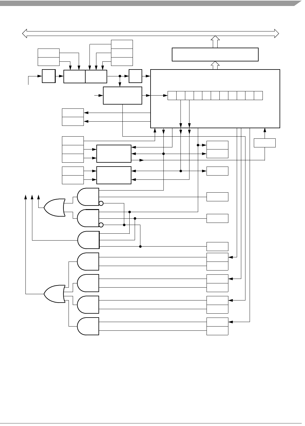
Functional Description
MC68HC08LN56 • MC68HC708LN56 General Release Specification, Rev. 2.1
Freescale Semiconductor 143
Figure 12-6. SCI Receiver Block Diagram
ALL ONES
ALL ZEROS
M
WAKE
ILTY
PEN
PTY
BKF
RPF
H876543210L
11-BIT
RECEIVE SHIFT REGISTER
STOP
START
DATA
RECOVERY
DMARE
SCRF
OR
ORIE
NF
NEIE
FE
FEIE
PE
PEIE
DMARE
SCRIE
SCRF
ILIE
IDLE
WAKE-UP
LOGIC
PARITY
CHECKING
MSB
ERROR CPU INTERRUPT REQUEST
DMA SERVICE REQUEST
CPU INTERRUPT REQUEST
SCI DATA REGISTER
R8
DMARE
ORIE
NEIE
FEIE
PEIE
SCRIE
ILIE
RWU
SCRF
IDLE
OR
NF
FE
PE
PTE6/RxD
INTERNAL BUS
PRE-
SCALER
BAUD
DIVIDER
÷ 4÷ 16
SCP1
SCP0
SCR2
SCR1
SCR0
BUS CLOCK
SCRIE
DMARE

Serial Communications Interface Module (SCI)
MC68HC08LN56 • MC68HC708LN56 General Release Specification, Rev. 2.1
144 Freescale Semiconductor
12.4.3.3 Data Sampling
The receiver samples the PTE6/RxD pin at the RT clock rate. The RT clock is an internal signal with a
frequency 16 times the baud rate. To adjust for baud rate mismatch, the RT clock is resynchronized at
the following times (see Figure 12-8):
• After every start bit
• After the receiver detects a data bit change from logic one to logic zero (after the majority of data
bit samples at RT8, RT9, and RT10 returns a valid logic one and the majority of the next RT8, RT9,
and RT10 samples returns a valid logic zero)
To locate the start bit, data recovery logic does an asynchronous search for a logic zero preceded by three
logic ones. When the falling edge of a possible start bit occurs, the RT clock begins to count to 16.
Register Name Bit 7654321Bit 0
SCI Control Register 1
(SCC1)
Read:
LOOPS ENSCI TXINV M WAKE ILTY PEN PTY
Write:
Reset:00000000
SCI Control Register 2
(SCC2)
Read:
SCTIE TCIE SCRIE ILIE TE RE RWU SBK
Write:
Reset:00000000
SCI Control Register 3
(SCC3)
Read: R8
T8 DMARE DMATE ORIE NEIE FEIE PEIE
Write:
Reset:UU000000
SCI Status Register 1
(SCS1)
Read: SCTE TC SCRF IDLE OR NF FE PE
Write:
Reset:11000000
SCI Status Register 2
(SCS2)
Read: BKF RPF
Write:
Reset:00000000
SCI Data Register
(SCDR)
Read:R7R6R5R4R3R2R1R0
Write: T7 T6 T5 T4 T3 T2 T1 T0
Reset: Unaffected by reset
SCI Baud Rate Register
(SCBR)
Read:
SCP1 SCP0 R SCR2 SCR1 SCR0
Write:
Reset:00000000
= Unimplemented U = Unaffected R = Reserved
Figure 12-7. SCI I/O Register Summary
Table 12-4. SCI Receiver I/O Address Summary
Register: SCC1 SCC2 SCC3 SCS1 SCS2 SCDR SCBR
Address: $0013 $0014 $0015 $0016 $0017 $0018 $0019
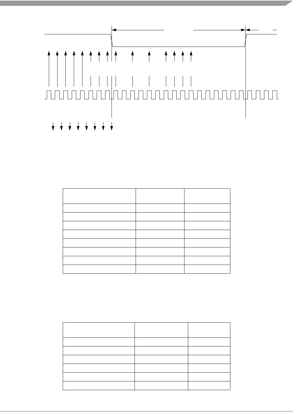
Functional Description
MC68HC08LN56 • MC68HC708LN56 General Release Specification, Rev. 2.1
Freescale Semiconductor 145
Figure 12-8. Receiver Data Sampling
To verify the start bit and to detect noise, data recovery logic takes samples at RT3, RT5, and RT7.
Table 12-5 summarizes the results of the start bit verification samples.
If start bit verification is not successful, the RT clock is reset and a new search for a start bit begins.
To determine the value of a data bit and to detect noise, recovery logic takes samples at RT8, RT9, and
RT10. Table 12-6 summarizes the results of the data bit samples.
Table 12-5. Start Bit Verification
RT3, RT5, and RT7
Samples
Start Bit
Verification Noise Flag
000 Yes 0
001 Yes 1
010 Yes 1
011 No 0
100 Yes 1
101 No 0
110 No 0
111 No 0
Table 12-6. Data Bit Recovery
RT8, RT9, and RT10
Samples
Data Bit
Determination Noise Flag
000 0 0
001 0 1
010 0 1
011 1 1
100 0 1
101 1 1
RT CLOCK
RESET
RT1
RT1
RT1
RT1
RT1
RT1
RT1
RT1
RT1
RT2
RT3
RT4
RT5
RT8
RT7
RT6
RT11
RT10
RT9
RT15
RT14
RT13
RT12
RT16
RT1
RT2
RT3
RT4
START BIT
QUALIFICATION
START BIT
VERIFICATION
DATA
SAMPLING
SAMPLES
RT
CLOCK
RT CLOCK
STATE
START BIT LSB
PTE6/RxD
Serial Communications Interface Module (SCI)
MC68HC08LN56 • MC68HC708LN56 General Release Specification, Rev. 2.1
146 Freescale Semiconductor
NOTE
The RT8, RT9, and RT10 samples do not affect start bit verification. If any
or all of the RT8, RT9, and RT10 start bit samples are logic ones following
a successful start bit verification, the noise flag (NF) is set and the receiver
assumes that the bit is a start bit.
To verify a stop bit and to detect noise, recovery logic takes samples at RT8, RT9, and RT10. Table 12-7
summarizes the results of the stop bit samples.
12.4.3.4 Framing Errors
If the data recovery logic does not detect a logic one where the stop bit should be in an incoming
character, it sets the framing error bit, FE, in SCS1. A break character also sets the FE bit because a
break character has no stop bit. The FE bit is set at the same time that the SCRF bit is set.
12.4.3.5 Baud Rate Tolerance
A transmitting device may be operating at a baud rate below or above the receiver baud rate.
Accumulated bit time misalignment can cause one of the three stop bit data samples to fall outside the
actual stop bit. Then a noise error occurs. If more than one of the samples is outside the stop bit, a framing
error occurs. In most applications, the baud rate tolerance is much more than the degree of misalignment
that is likely to occur.
As the receiver samples an incoming character, it resynchronizes the RT clock on any valid falling edge
within the character. Resynchronization within characters corrects misalignments between transmitter bit
times and receiver bit times.
110 1 1
111 1 0
Table 12-7. Stop Bit Recovery
RT8, RT9, and RT10
Samples
Framing
Error Flag Noise Flag
000 1 0
001 1 1
010 1 1
011 0 1
100 1 1
101 0 1
110 0 1
111 0 0
Table 12-6. Data Bit Recovery (Continued)
RT8, RT9, and RT10
Samples
Data Bit
Determination Noise Flag
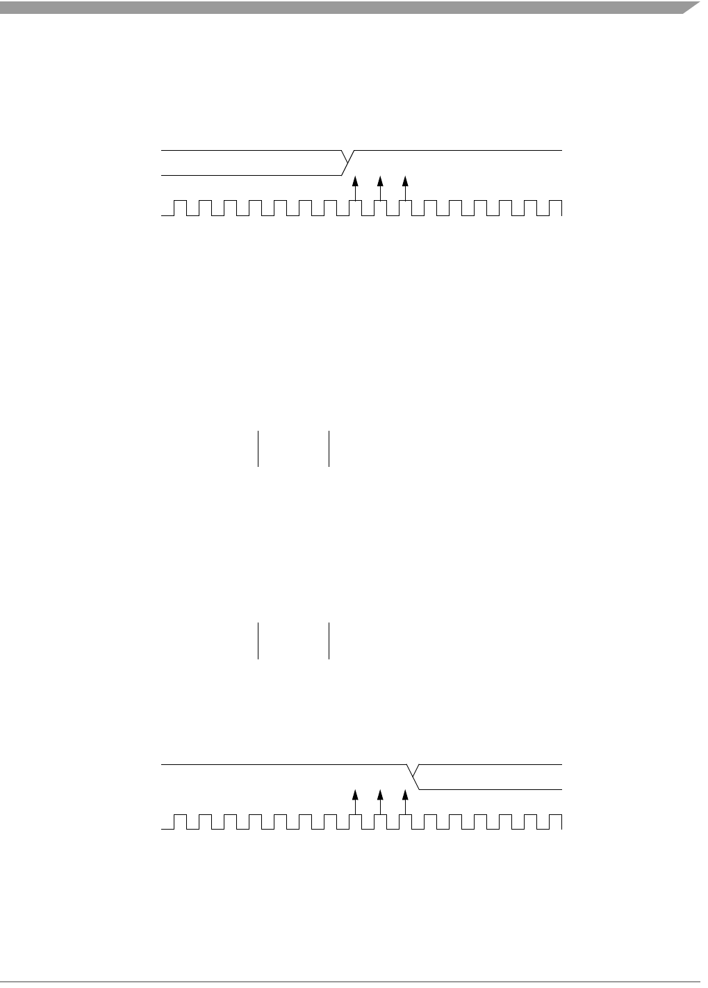
Functional Description
MC68HC08LN56 • MC68HC708LN56 General Release Specification, Rev. 2.1
Freescale Semiconductor 147
Slow Data Tolerance
Figure 12-9 shows how much a slow received character can be misaligned without causing a noise error
or a framing error. The slow stop bit begins at RT8 instead of RT1 but arrives in time for the stop bit data
samples at RT8, RT9, and RT10.
Figure 12-9. Slow Data
For an 8-bit character, data sampling of the stop bit takes the receiver
9 bit times ×16 RT cycles + 10 RT cycles = 154 RT cycles.
With the misaligned character shown in Figure 12-9, the receiver counts 154 RT cycles at the point when
the count of the transmitting device is 9 bit times ×16 RT cycles + 3 RT cycles = 147 RT cycles.
The maximum per cent difference between the receiver count and the transmitter count of a slow 8-bit
character with no errors is
For a 9-bit character, data sampling of the stop bit takes the receiver
10 bit times ×16 RT cycles + 10 RT cycles = 170 RT cycles.
With the misaligned character shown in Figure 12-9, the receiver counts 170 RT cycles at the point when
the count of the transmitting device is 10 bit times ×16 RT cycles + 3 RT cycles = 163 RT cycles.
The maximum per cent difference between the receiver count and the transmitter count of a slow 9-bit
character with no errors is
Fast Data Tolerance
Figure 12-10 shows how much a fast received character can be misaligned without causing a noise error
or a framing error. The fast stop bit ends at RT10 instead of RT16 but is still there for the stop bit data
samples at RT8, RT9, and RT10.
Figure 12-10. Fast Data
MSB STOP
RT1
RT2
RT3
RT4
RT5
RT6
RT7
RT8
RT9
RT10
RT11
RT12
RT13
RT14
RT15
RT16
DATA
SAMPLES
RECEIVER
RT CLOCK
154 147–
154
------------------------100×4.54%=
170 163–
170
------------------------100×4.12%=
IDLE OR NEXT CHARACTERSTOP
RT1
RT2
RT3
RT4
RT5
RT6
RT7
RT8
RT9
RT10
RT11
RT12
RT13
RT14
RT15
RT16
DATA
SAMPLES
RECEIVER
RT CLOCK

Serial Communications Interface Module (SCI)
MC68HC08LN56 • MC68HC708LN56 General Release Specification, Rev. 2.1
148 Freescale Semiconductor
For an 8-bit character, data sampling of the stop bit takes the receiver
9bittimes×16 RT cycles + 10 RT cycles = 154 RT cycles.
With the misaligned character shown in Figure 12-10, the receiver counts 154 RT cycles at the point when
the count of the transmitting device is 10 bit times ×16 RT cycles = 160 RT cycles.
The maximum per cent difference between the receiver count and the transmitter count of a fast 8-bit
character with no errors is
For a 9-bit character, data sampling of the stop bit takes the receiver
10 bit times ×16 RT cycles + 10 RT cycles = 170 RT cycles.
With the misaligned character shown in Figure 12-10, the receiver counts 170 RT cycles at the point when
the count of the transmitting device is 11 bit times ×16 RT cycles = 176 RT cycles.
The maximum per cent difference between the receiver count and the transmitter count of a fast 9-bit
character with no errors is
12.4.3.6 Receiver Wake-Up
So that the MCU can ignore transmissions intended only for other receivers in multiple-receiver systems,
the receiver can be put into a standby state. Setting the receiver wake-up bit, RWU, in SCC2 puts the
receiver into a standby state during which receiver interrupts are disabled.
Depending on the state of the WAKE bit in SCC1, either of two conditions on the PTE6/RxD pin can bring
the receiver out of the standby state:
• Address mark — An address mark is a logic one in the most significant bit position of a received
character. When the WAKE bit is set, an address mark wakes the receiver from the standby state
by clearing the RWU bit. The address mark also sets the SCI receiver full bit, SCRF. Software can
then compare the character containing the address mark to the user-defined address of the
receiver. If they are the same, the receiver remains awake and processes the characters that
follow. If they are not the same, software can set the RWU bit and put the receiver back into the
standby state.
• Idle input line condition — When the WAKE bit is clear, an idle character on the PTE6/RxD pin
wakes the receiver from the standby state by clearing the RWU bit. The idle character that wakes
the receiver does not set the receiver idle bit, IDLE, or the SCI receiver full bit, SCRF. The idle line
type bit, ILTY, determines whether the receiver begins counting logic ones as idle character bits
after the start bit or after the stop bit.
NOTE
With the WAKE bit clear, setting the RWU bit after the RxD pin has been
idle may cause the receiver to wake up immediately.
154 160–
154
------------------------100×3.90%
·
=
170 176–
170
------------------------100×3.53%=

Functional Description
MC68HC08LN56 • MC68HC708LN56 General Release Specification, Rev. 2.1
Freescale Semiconductor 149
12.4.3.7 Receiver Interrupts
The following sources can generate CPU interrupt requests from the SCI receiver:
• SCI receiver full (SCRF) — The SCRF bit in SCS1 indicates that the receive shift register has
transferred a character to the SCDR. SCRF can generate a receiver CPU interrupt request or a
receiver DMA service request. Setting the SCI receive interrupt enable bit, SCRIE, in SCC2
enables the SCRF bit to generate receiver CPU interrupts. Setting both the SCRIE bit and the DMA
receive enable bit, DMARE, in SCC3 enables receiver DMA service requests and disables receiver
CPU interrupt requests.
• Idle input (IDLE) — The IDLE bit in SCS1 indicates that 10 or 11 consecutive logic ones shifted in
from the PTE6/RxD pin. The idle line interrupt enable bit, ILIE, in SCC2 enables the IDLE bit to
generate CPU interrupt requests.
NOTE
When receiver DMA service requests are enabled (DMARE = 1), then
receiver CPU interrupt requests are disabled.
12.4.3.8 Error Interrupts
The following receiver error flags in SCS1 can generate CPU interrupt requests:
• Receiver overrun (OR) — The OR bit indicates that the receive shift register shifted in a new
character before the previous character was read from the SCDR. The previous character remains
in the SCDR, and the new character is lost. The overrun interrupt enable bit, ORIE, in SCC3
enables OR to generate SCI error CPU interrupt requests.
• Noise flag (NF) — The NF bit is set when the SCI detects noise on incoming data or break
characters, including start, data, and stop bits. The noise error interrupt enable bit, NEIE, in SCC3
enables NF to generate SCI error CPU interrupt requests.
• Framing error (FE) — The FE bit in SCS1 is set when a logic zero occurs where the receiver
expects a stop bit. The framing error interrupt enable bit, FEIE, in SCC3 enables FE to generate
SCI error CPU interrupt requests.
• Parity error (PE) — The PE bit in SCS1 is set when the SCI detects a parity error in incoming data.
The parity error interrupt enable bit, PEIE, in SCC3 enables PE to generate SCI error CPU interrupt
requests.
12.4.3.9 Error Flags During DMA Service Requests
When the DMA is servicing the SCI receiver, it clears the SCRF bit when it reads the SCI data register.
The DMA does not clear the other status bits (BKF or RPF), nor does it clear error flags (OR, NF, FE, and
PE). To clear error flags while the DMA is servicing the receiver, enable SCI error CPU interrupts and
clear the bits in an interrupt routine. The application may require retransmission in case of error. If the
application requires the receptions to continue, note the following latency considerations:
1. If interrupt latency is short enough for an error bit to be serviced before the next SCRF, then it can
be determined which byte caused the error. If interrupt latency is long enough for a new SCRF to
occur before servicing an error bit, then:
a. It cannot be determined whether the error bit being serviced is due to the byte in the SCI data
register or to a previous byte. Multiple errors can accumulate that correspond to different
bytes. In a message-based system, you may have to repeat the entire message.

Serial Communications Interface Module (SCI)
MC68HC08LN56 • MC68HC708LN56 General Release Specification, Rev. 2.1
150 Freescale Semiconductor
b. When the DMA is enabled to service the SCI receiver, merely reading the SCI data register
clears the SCRF bit. The second step in clearing an error bit, reading the SCI data register,
could inadvertently clear a new, unserviced SCRF that occurred during the error-servicing
routine. Then the DMA would ignore the byte that set the new SCRF, and the new byte would
be lost.
To prevent clearing of an unserviced SCRF bit, clear the SCRIE bit at the beginning of the
error-servicing interrupt routine and set it at the end. Clearing SCRIE disables DMA service
so that both a read of SCS1 and a read of SCDR are required to clear the SCRF bit. Setting
SCRIE enables DMA service so that the DMA can recognize a service request that occurred
during the error-servicing interrupt routine.
c. In the CPU interrupt routine to service error bits, do not use BRSET or BRCLR instructions.
BRSET and BRCLR read the SCS1 register, which is the first step in clearing the register.
Then the DMA could read the SCI data register, the second step in clearing it, thereby clearing
all error bits. The next read of the data register would miss any error bits that were set.
2. DMA latency should be short enough so that an SCRF is serviced before the next SCRF occurs.
If DMA latency is long enough for a new SCRF to occur before servicing an error bit, then:
a. Overruns occur. Set the ORIE bit to enable SCI error CPU interrupt requests and service the
overrun in an interrupt routine. In a message-based system, disable the DMA in the interrupt
routine and manually recover. Otherwise, the byte that was lost in the overrun could prevent
the DMA from reaching its byte count. If the DMA reaches its byte count in the following
message, two messages may be corrupted.
b. If the CPU does not service an overrun interrupt request, the DMA can eventually clear the
SCRF bit by reading the SCI data register. The OR bit remains set. Each time a new byte sets
the SCRF bit, new data transfers from the shift register to the SCI data register (provided that
another overrun does not occur), even though the OR bit is set. The DMA removed the
overrun condition by reading the data register, but the OR bit has not been cleared.
12.5 Low-Power Modes
The WAIT and STOP instructions put the MCU in low-power- consumption standby modes.
12.5.1 Wait Mode
The SCI module remains active after the execution of a WAIT instruction. In wait mode the SCI module
registers are not accessible by the CPU. Any enabled CPU interrupt request from the SCI module can
bring the MCU out of wait mode.
If SCI module functions are not required during wait mode, reduce power consumption by disabling the
module before executing the WAIT instruction.
The DMA can service the SCI without exiting wait mode.
12.5.2 Stop Mode
The SCI module is inactive after the execution of a STOP instruction. The STOP instruction does not
affect SCI register states. SCI module operation resumes after an external interrupt.
Because the internal clock is inactive during stop mode, entering stop mode during an SCI transmission
or reception results in invalid data.

SCI During Break Module Interrupts
MC68HC08LN56 • MC68HC708LN56 General Release Specification, Rev. 2.1
Freescale Semiconductor 151
12.6 SCI During Break Module Interrupts
The system integration module (SIM) controls whether status bits in other modules can be cleared during
the break state. The BCFE bit in the SIM break flag control register (SBFCR) enables software to clear
status bits during the break state.
To allow software to clear status bits during a break interrupt, write a logic one to the BCFE bit. If a status
bit is cleared during the break state, it remains cleared when the MCU exits the break state.
To protect status bits during the break state, write a logic zero to the BCFE bit. With BCFE at logic zero
(its default state), software can read and write I/O registers during the break state without affecting status
bits. Some status bits have a two-step read/write clearing procedure. If software does the first step on
such a bit before the break, the bit cannot change during the break state as long as BCFE is at logic zero.
After the break, doing the second step clears the status bit.
12.7 I/O Signals
Port E shares two of its pins with the SCI module. The two SCI I/O pins are:
• PTE5/TxD — Transmit data
• PTE6/RxD — Receive data
12.7.1 PTE5/TxD (Transmit Data)
The PTE5/TxD pin is the serial data output from the SCI transmitter. The SCI shares the PTE5/TxD pin
with port E. When the SCI is enabled, the PTE5/TxD pin is an output regardless of the state of the DDRE2
bit in data direction register E (DDRE).
12.7.2 PTE6/RxD (Receive Data)
The PTE6/RxD pin is the serial data input to the SCI receiver. The SCI shares the PTE6/RxD pin with
port E. When the SCI is enabled, the PTE6/RxD pin is an input regardless of the state of the DDRE1 bit
in data direction register E (DDRE).
12.8 I/O Registers
The following I/O registers control and monitor SCI operation:
• SCI control register 1 (SCC1)
• SCI control register 2 (SCC2)
• SCI control register 3 (SCC3)
• SCI status register 1 (SCS1)
• SCI status register 2 (SCS2)
• SCI data register (SCDR)
• SCI baud rate register (SCBR)

Serial Communications Interface Module (SCI)
MC68HC08LN56 • MC68HC708LN56 General Release Specification, Rev. 2.1
152 Freescale Semiconductor
12.8.1 SCI Control Register 1 (SCC1)
SCI control register 1:
• Enables loop mode operation
• Enables the SCI
• Controls output polarity
• Controls character length
• Controls SCI wake-up method
• Controls idle character detection
• Enables parity function
• Controls parity type
LOOPS — Loop Mode Select Bit
This read/write bit enables loop mode operation. In loop mode the PTE6/RxD pin is disconnected from
the SCI, and the transmitter output goes into the receiver input. Both the transmitter and the receiver
must be enabled to use loop mode. Reset clears the LOOPS bit.
1 = Loop mode enabled
0 = Normal operation enabled
ENSCI — Enable SCI Bit
This read/write bit enables the SCI and the SCI baud rate generator. Clearing ENSCI sets the SCTE
and TC bits in SCI status register 1 and disables transmitter interrupts. Reset clears the ENSCI bit.
1 = SCI enabled
0 = SCI disabled
TXINV — Transmit Inversion Bit
This read/write bit reverses the polarity of transmitted data. Reset clears the TXINV bit.
1 = Transmitter output inverted
0 = Transmitter output not inverted
NOTE
Setting the TXINV bit inverts all transmitted values, including idle, break,
start, and stop bits.
M — Mode (Character Length) Bit
This read/write bit determines whether SCI characters are eight or nine bits long. (See Table 12-8.)
The ninth bit can serve as an extra stop bit, as a receiver wake-up signal, or as a parity bit. Reset clears
the M bit.
1 = 9-bit SCI characters
0 = 8-bit SCI characters
SCC1
$0013Bit 7654321Bit 0
Read:
LOOPS ENSCI TXINV M WAKE ILTY PEN PTY
Write:
Reset:00000000
Figure 12-11. SCI Control Register 1 (SCC1)
I/O Registers
MC68HC08LN56 • MC68HC708LN56 General Release Specification, Rev. 2.1
Freescale Semiconductor 153
WAKE — Wake-Up Condition Bit
This read/write bit determines which condition wakes up the SCI: a logic one (address mark) in the
most significant bit position of a received character or an idle condition on the PTE6/RxD pin. Reset
clears the WAKE bit.
1 = Address mark wake-up
0 = Idle line wake-up
ILTY — Idle Line Type Bit
This read/write bit determines when the SCI starts counting logic ones as idle character bits. The
counting begins either after the start bit or after the stop bit. If the count begins after the start bit, then
a string of logic ones preceding the stop bit may cause false recognition of an idle character. Beginning
the count after the stop bit avoids false idle character recognition, but requires properly synchronized
transmissions. Reset clears the ILTY bit.
1 = Idle character bit count begins after stop bit
0 = Idle character bit count begins after start bit
PEN — Parity Enable Bit
This read/write bit enables the SCI parity function. (See Table 12-8.) When enabled, the parity function
inserts a parity bit in the most significant bit position. (See Figure 12-3.) Reset clears the PEN bit.
1 = Parity function enabled
0 = Parity function disabled
PTY — Parity Bit
This read/write bit determines whether the SCI generates and checks for odd parity or even parity.
(See Table 12-8.) Reset clears the PTY bit.
1 = Odd parity
0 = Even parity
NOTE
Changing the PTY bit in the middle of a transmission or reception can
generate a parity error.
Table 12-8. Character Format Selection
Control Bits Character Format
M PEN:PTY Start
Bits
Data
Bits Parity Stop
Bits
Character
Length
0 0X 1 8 None 1 10 bits
1 0X 1 9 None 1 11 bits
0 10 1 7 Even 1 10 bits
0 11 1 7 Odd 1 10 bits
1 10 1 8 Even 1 11 bits
1 11 1 8 Odd 1 11 bits

Serial Communications Interface Module (SCI)
MC68HC08LN56 • MC68HC708LN56 General Release Specification, Rev. 2.1
154 Freescale Semiconductor
12.8.2 SCI Control Register 2 (SCC2)
SCI control register 2 does the following:
• Enables the following CPU interrupt requests and DMA service requests:
– Enables the SCTE bit to generate transmitter CPU interrupt requests or transmitter DMA
service requests
– Enables the TC bit to generate transmitter CPU interrupt requests
– Enables the SCRF bit to generate receiver CPU interrupt requests or receiver DMA service
requests
– Enables the IDLE bit to generate receiver CPU interrupt requests
• Enables the transmitter
• Enables the receiver
• Enables SCI wake-up
• Transmits SCI break characters
SCTIE — SCI Transmit Interrupt Enable Bit
This read/write bit enables the SCTE bit to generate SCI transmitter CPU interrupt requests or DMA
service requests. Setting the SCTIE bit and clearing the DMA transfer enable bit, DMATE, in SCC3
enables the SCTE bit to generate CPU interrupt requests. Setting both the SCTIE and DMATE bits
enables the SCTE bit to generate DMA service requests. Reset clears the SCTIE bit.
1 = SCTE enabled to generate CPU interrupt or DMA service requests
0 = SCTE not enabled to generate CPU interrupt or DMA service requests
TCIE — Transmission Complete Interrupt Enable Bit
This read/write bit enables the TC bit to generate SCI transmitter CPU interrupt requests. Reset clears
the TCIE bit.
1 = TC enabled to generate CPU interrupt requests
0 = TC not enabled to generate CPU interrupt requests
SCRIE — SCI Receive Interrupt Enable Bit
This read/write bit enables the SCRF bit to generate SCI receiver CPU interrupt requests or SCI
receiver DMA service requests. Setting the SCRIE bit and clearing the DMA receive enable bit,
DMARE, in SCC3 enables the SCRF bit to generate CPU interrupt requests. Setting both SCRIE and
DMARE enables SCRF to generate DMA service requests. Reset clears the SCRIE bit.
1 = SCRF enabled to generate CPU interrupt or DMA service requests
0 = SCRF not enabled to generate CPU interrupt or DMA service requests
ILIE — Idle Line Interrupt Enable Bit
This read/write bit enables the IDLE bit to generate SCI receiver CPU interrupt requests. Reset clears
the ILIE bit.
1 = IDLE enabled to generate CPU interrupt requests
0 = IDLE not enabled to generate CPU interrupt requests
SCC2
$0014Bit 7654321Bit 0
Read:
SCTIE TCIE SCRIE ILIE TE RE RWU SBK
Write:
Reset:00000000
Figure 12-12. SCI Control Register 2 (SCC2)

I/O Registers
MC68HC08LN56 • MC68HC708LN56 General Release Specification, Rev. 2.1
Freescale Semiconductor 155
NOTE
When SCI receiver DMA service requests are enabled (DMARE = 1), then
SCI receiver CPU interrupt requests are disabled, and the state of the ILIE
bit has no effect.
TE — Transmitter Enable Bit
Setting this read/write bit begins the transmission by sending a preamble of 10 or 11 logic ones from
the transmit shift register to the PTE5/TxD pin. If software clears the TE bit, the transmitter completes
any transmission in progress before the PTE5/TxD returns to the idle condition (logic one). Clearing
and then setting TE during a transmission queues an idle character to be sent after the character
currently being transmitted. Reset clears the TE bit.
1 = Transmitter enabled
0 = Transmitter disabled
NOTE
Writing to the TE bit is not allowed when the enable SCI bit (ENSCI) is clear.
ENSCI is in SCI control register 1.
RE — Receiver Enable Bit
Setting this read/write bit enables the receiver. Clearing the RE bit disables the receiver but does not
affect receiver interrupt flag bits. Reset clears the RE bit.
1 = Receiver enabled
0 = Receiver disabled
NOTE
Writing to the RE bit is not allowed when the enable SCI bit (ENSCI) is
clear. ENSCI is in SCI control register 1.
RWU — Receiver Wake-Up Bit
This read/write bit puts the receiver in a standby state during which receiver interrupts are disabled.
The WAKE bit in SCC1 determines whether an idle input or an address mark brings the receiver out
of the standby state and clears the RWU bit. Reset clears the RWU bit.
1 = Standby state
0 = Normal operation
SBK — Send Break Bit
Setting and then clearing this read/write bit transmits a break character followed by a logic one. The
logic one after the break character guarantees recognition of a valid start bit. If SBK remains set, the
transmitter continuously transmits break characters with no logic ones between them. Reset clears the
SBK bit.
1 = Transmit break characters
0 = No break characters being transmitted
NOTE
Do not toggle the SBK bit immediately after setting the SCTE bit. Toggling
SBK before the preamble begins causes the SCI to send a break character
instead of a preamble.

Serial Communications Interface Module (SCI)
MC68HC08LN56 • MC68HC708LN56 General Release Specification, Rev. 2.1
156 Freescale Semiconductor
12.8.3 SCI Control Register 3 (SCC3)
SCI control register 3:
• Stores the ninth SCI data bit received and the ninth SCI data bit to be transmitted
• Enables SCI receiver full (SCRF) DMA service requests
• Enables SCI transmitter empty (SCTE) DMA service requests
• Enables these interrupts:
– Receiver overrun interrupts
– Noise error interrupts
– Framing error interrupts
– Parity error interrupts
R8 — Received Bit 8
When the SCI is receiving 9-bit characters, R8 is the read-only ninth bit (bit 8) of the received character.
R8 is received at the same time that the SCDR receives the other 8 bits.
When the SCI is receiving 8-bit characters, R8 is a copy of the eighth bit (bit 7). Reset has no effect on
the R8 bit.
T8 — Transmitted Bit 8
When the SCI is transmitting 9-bit characters, T8 is the read/write ninth bit (bit 8) of the transmitted
character. T8 is loaded into the transmit shift register at the same time that the SCDR is loaded into
the transmit shift register. Reset has no effect on the T8 bit.
DMARE — DMA Receive Enable Bit
This read/write bit enables the DMA to service SCI receiver DMA service requests generated by the
SCRF bit. Setting the DMARE bit disables SCI receiver CPU interrupt requests. Reset clears the
DMARE bit.
1 = DMA enabled to service SCI receiver DMA service requests generated by the SCRF bit (SCI
receiver CPU interrupt requests disabled)
0 = DMA not enabled to service SCI receiver DMA service requests generated by the SCRF bit (SCI
receiver CPU interrupt requests enabled)
NOTE
To enable the SCRF bit to generate DMA service requests, the SCI receive
interrupt enable bit (SCRIE) must be set.
DMATE — DMA Transfer Enable Bit
This read/write bit enables SCI transmitter empty (SCTE) DMA service requests. (See 12.8.4 SCI
Status Register 1 (SCS1).) Setting the DMATE bit disables SCTE CPU interrupt requests. Reset clears
DMATE.
1 = SCTE DMA service requests enabled; SCTE CPU interrupt requests disabled
0 = SCTE DMA service requests disabled; SCTE CPU interrupt requests enabled
SCC3
$0015Bit 7654321Bit 0
Read: R8
T8 DMARE DMATE ORIE NEIE FEIE PEIE
Write:
Reset:UU000000
= Unimplemented U = Unaffected
Figure 12-13. SCI Control Register 3 (SCC3)

I/O Registers
MC68HC08LN56 • MC68HC708LN56 General Release Specification, Rev. 2.1
Freescale Semiconductor 157
NOTE
To enable the SCTE bit to generate DMA service requests, the SCI transmit
interrupt enable bit (SCTIE) must be set.
ORIE — Receiver Overrun Interrupt Enable Bit
This read/write bit enables SCI error CPU interrupt requests generated by the receiver overrun bit, OR.
1 = SCI error CPU interrupt requests from OR bit enabled
0 = SCI error CPU interrupt requests from OR bit disabled
NEIE — Receiver Noise Error Interrupt Enable Bit
This read/write bit enables SCI error CPU interrupt requests generated by the noise error bit, NE.
Reset clears NEIE.
1 = SCI error CPU interrupt requests from NE bit enabled
0 = SCI error CPU interrupt requests from NE bit disabled
FEIE — Receiver Framing Error Interrupt Enable Bit
This read/write bit enables SCI error CPU interrupt requests generated by the framing error bit, FE.
Reset clears FEIE.
1 = SCI error CPU interrupt requests from FE bit enabled
0 = SCI error CPU interrupt requests from FE bit disabled
PEIE — Receiver Parity Error Interrupt Enable Bit
This read/write bit enables SCI receiver CPU interrupt requests generated by the parity error bit, PE.
(See 12.8.4 SCI Status Register 1 (SCS1).) Reset clears PEIE.
1 = SCI error CPU interrupt requests from PE bit enabled
0 = SCI error CPU interrupt requests from PE bit disabled
12.8.4 SCI Status Register 1 (SCS1)
SCI status register 1 contains flags to signal these conditions:
• Transfer of SCDR data to transmit shift register complete
• Transmission complete
• Transfer of receive shift register data to SCDR complete
• Receiver input idle
• Receiver overrun
• Noisy data
• Framing error
• Parity error
SCS1
$0016Bit 7654321Bit 0
Read: SCTE TC SCRF IDLE OR NF FE PE
Write:
Reset:11000000
= Unimplemented
Figure 12-14. SCI Status Register 1 (SCS1)

Serial Communications Interface Module (SCI)
MC68HC08LN56 • MC68HC708LN56 General Release Specification, Rev. 2.1
158 Freescale Semiconductor
SCTE — SCI Transmitter Empty Bit
This clearable, read-only bit is set when the SCDR transfers a character to the transmit shift register.
SCTE can generate an SCI transmitter CPU interrupt request or an SCI transmitter DMA service
request. When the SCTIE bit in SCC2 is set and the DMATE bit in SCC3 is clear, SCTE generates an
SCI transmitter CPU interrupt request. With both the SCTIE and DMATE bits set, SCTE generates an
SCI transmitter DMA service request. In normal operation, clear the SCTE bit by reading SCS1 with
SCTE set and then writing to SCDR. In DMA transfers, the DMA automatically clears the SCTE bit
when it writes to the SCDR. Reset sets the SCTE bit.
1 = SCDR data transferred to transmit shift register
0 = SCDR data not transferred to transmit shift register
NOTE
When DMATE = 1, a write by the CPU to the SCI data register can
inadvertently clear the SCTE bit and cause the DMA to miss a service
request.
Setting the TE bit for the first time also sets the SCTE bit. When enabling
SCI transmitter DMA service requests, set the TE bit after setting the
DMATE bit. Otherwise setting the TE and SCTIE bits generates an SCI
transmitter CPU interrupt request instead of a DMA service request.
TC — Transmission Complete Bit
This read-only bit is set when the SCTE bit is set, and no data, preamble, or break character is being
transmitted. TC generates an SCI transmitter CPU interrupt request if the TCIE bit in SCC2 is also set.
When the DMA services an SCI transmitter DMA service request, the DMA clears the TC bit by writing
to the SCDR. TC is automatically cleared when data, preamble or break is queued and ready to be
sent. There may be up to 1.5 transmitter clocks of latency between queueing data, preamble, and
break and the transmission actually starting. Reset sets the TC bit.
1 = No transmission in progress
0 = Transmission in progress
SCRF — SCI Receiver Full Bit
This clearable, read-only bit is set when the data in the receive shift register transfers to the SCI data
register. SCRF can generate an SCI receiver CPU interrupt request or an SCI receiver DMA service
request. When the SCRIE bit in SCC2 is set and the DMARE bit in SCC3 is clear, SCRF generates a
CPU interrupt request. With both the SCRIE and DMARE bits set, SCRF generates a DMA service
request. In normal operation, clear the SCRF bit by reading SCS1 with SCRF set and then reading the
SCDR. In DMA transfers, the DMA clears the SCRF bit when it reads the SCDR. Reset clears SCRF.
1 = Received data available in SCDR
0 = Data not available in SCDR
NOTE
When DMARE = 1, a read by the CPU of the SCI data register can
inadvertently clear the SCRF bit and cause the DMA to miss a service
request.
IDLE — Receiver Idle Bit
This clearable, read-only bit is set when 10 or 11 consecutive logic ones appear on the receiver input.
IDLE generates an SCI error CPU interrupt request if the ILIE bit in SCC2 is also set and the DMARE
bit in SCC3 is clear. Clear the IDLE bit by reading SCS1 with IDLE set and then reading the SCDR.
I/O Registers
MC68HC08LN56 • MC68HC708LN56 General Release Specification, Rev. 2.1
Freescale Semiconductor 159
After the receiver is enabled, it must receive a valid character that sets the SCRF bit before an idle
condition can set the IDLE bit. Also, after the IDLE bit has been cleared, a valid character must again
set the SCRF bit before an idle condition can set the IDLE bit. Reset clears the IDLE bit.
1 = Receiver input idle
0 = Receiver input active (or idle since the IDLE bit was cleared)
OR — Receiver Overrun Bit
This clearable, read-only bit is set when software fails to read the SCDR before the receive shift
register receives the next character. The OR bit generates an SCI error CPU interrupt request if the
ORIE bit in SCC3 is also set. The data in the shift register is lost, but the data already in the SCDR is
not affected. Clear the OR bit by reading SCS1 with OR set and then reading the SCDR. Reset clears
the OR bit.
1 = Receive shift register full and SCRF = 1
0 = No receiver overrun
Software latency may allow an overrun to occur between reads of SCS1 and SCDR in the flag-clearing
sequence. Figure 12-15 shows the normal flag-clearing sequence and an example of an overrun
caused by a delayed flag-clearing sequence. The delayed read of SCDR does not clear the OR bit
because OR was not set when SCS1 was read. Byte 2 caused the overrun and is lost. The next
flag-clearing sequence reads byte 3 in the SCDR instead of byte 2.
In applications that are subject to software latency or in which it is important to know which byte is lost
due to an overrun, the flag-clearing routine can check the OR bit in a second read of SCS1 after
reading the data register.
Figure 12-15. Flag Clearing Sequence
BYTE 1
NORMAL FLAG CLEARING SEQUENCE
READ SCS1
SCRF = 1
READ SCDR
(BYTE 1)
SCRF = 1
SCRF = 1
BYTE 2 BYTE 3 BYTE 4
OR = 0
READ SCS1
SCRF = 1
OR = 0
READ SCDR
(BYTE 2)
SCRF = 0
READ SCS1
SCRF = 1
OR = 0
SCRF = 1
SCRF = 0
READ SCDR
(BYTE 3)
SCRF = 0
BYTE 1
READ SCS1
SCRF = 1
READ SCDR
(BYTE 1)
SCRF = 1
SCRF = 1
BYTE 2 BYTE 3 BYTE 4
OR = 0
READ SCS1
SCRF = 1
OR = 1
READ SCDR
(BYTE 3)
DELAYED FLAG CLEARING SEQUENCE
OR = 1
SCRF = 1
OR = 1
SCRF = 0
OR = 1
SCRF = 0
OR = 0

Serial Communications Interface Module (SCI)
MC68HC08LN56 • MC68HC708LN56 General Release Specification, Rev. 2.1
160 Freescale Semiconductor
NF — Receiver Noise Flag Bit
This clearable, read-only bit is set when the SCI detects noise on the PTE6/RxD pin. NF generates an
NF CPU interrupt request if the NEIE bit in SCC3 is also set. Clear the NF bit by reading SCS1 and
then reading the SCDR. Reset clears the NF bit.
1 = Noise detected
0 = No noise detected
FE — Receiver Framing Error Bit
This clearable, read-only bit is set when a logic 0 is accepted as the stop bit. FE generates an SCI error
CPU interrupt request if the FEIE bit in SCC3 also is set. Clear the FE bit by reading SCS1 with FE set
and then reading the SCDR. Reset clears the FE bit.
1 = Framing error detected
0 = No framing error detected
PE — Receiver Parity Error Bit
This clearable, read-only bit is set when the SCI detects a parity error in incoming data. PE generates
a PE CPU interrupt request if the PEIE bit in SCC3 is also set. Clear the PE bit by reading SCS1 with
PE set and then reading the SCDR. Reset clears the PE bit.
1 = Parity error detected
0 = No parity error detected
12.8.5 SCI Status Register 2 (SCS2)
SCI status register 2 contains flags to signal the following conditions:
• Break character detected
• Incoming data
BKF — Break Flag Bit
This clearable, read-only bit is set when the SCI detects a break character on the PTE6/RxD pin. In
SCS1, the FE and SCRF bits are also set. In 9-bit character transmissions, the R8 bit in SCC3 is
cleared. BKF does not generate a CPU interrupt request or a DMA service request. Clear BKF by
reading SCS2 with BKF set and then reading the SCDR. Once cleared, BKF can become set again
only after logic ones again appear on the PTE6/RxD pin followed by another break character. Reset
clears the BKF bit.
1 = Break character detected
0 = No break character detected
SCS2
$0017Bit 7654321Bit 0
Read: BKF RPF
Write:
Reset:00000000
= Unimplemented
Figure 12-16. SCI Status Register 2 (SCS2)
I/O Registers
MC68HC08LN56 • MC68HC708LN56 General Release Specification, Rev. 2.1
Freescale Semiconductor 161
RPF — Reception in Progress Flag Bit
This read-only bit is set when the receiver detects a logic zero during the RT1 time period of the start
bit search. RPF does not generate an interrupt request. RPF is reset after the receiver detects false
start bits (usually from noise or a baud rate mismatch) or when the receiver detects an idle character.
Polling RPF before disabling the SCI module or entering stop mode can show whether a reception is
in progress.
1 = Reception in progress
0 = No reception in progress
12.8.6 SCI Data Register (SCDR)
The SCI data register is the buffer between the internal data bus and the receive and transmit shift
registers. Reset has no effect on data in the SCI data register.
R7/T7:R0/T0 — Receive/Transmit Data Bits
Reading address $0018 accesses the read-only received data bits, R7:R0. Writing to address $0018
writes the data to be transmitted, T7:T0. Reset has no effect on the SCI data register.
NOTE
Do not use read modify write instructions on the SCI data register.
12.8.7 SCI Baud Rate Register (SCBR)
The baud rate register selects the baud rate for both the receiver and the transmitter.
SCP1 and SCP0 — SCI Baud Rate Prescaler Bits
These read/write bits select the baud rate prescaler divisor as shown in Table 12-9. Reset clears SCP1
and SCP0.
SCDR
$0018Bit 7654321Bit 0
Read:R7R6R5R4R3R2R1R0
Write: T7 T6 T5 T4 T3 T2 T1 T0
Reset: Unaffected by reset
Figure 12-17. SCI Data Register (SCDR)
SCBR
$0019Bit 7654321Bit 0
Read:
SCP1 SCP0 R SCR2 SCR1 SCR0
Write:
Reset:00000000
= Unimplemented R = Reserved for Factory Test
Figure 12-18. SCI Baud Rate Register (SCBR)
Serial Communications Interface Module (SCI)
MC68HC08LN56 • MC68HC708LN56 General Release Specification, Rev. 2.1
162 Freescale Semiconductor
SCR2:SCR0 — SCI Baud Rate Select Bits
These read/write bits select the SCI baud rate divisor as shown in Table 12-10. Reset clears
SCR2:SCR0.
Use the following formula to calculate the SCI baud rate:
where:
fBUS = bus frequency
PD = prescaler divisor
BD = baud rate divisor
SCI_BDSRC is an input to the SCI. Normally it will be tied off low at the top level to select the bus clock
as the clock source. This makes the formula:
Table 12-11 shows the SCI baud rates that can be generated with a 4.9152-MHz bus clock.
Table 12-9. SCI Baud Rate Prescaling
SCP1:SCP0 Prescaler Divisor (PD)
00 1
01 3
10 4
11 13
Table 12-10. SCI Baud Rate Selection
SCR2:SCR1:SCR0 Baud Rate
Divisor (BD)
000 1
001 2
010 4
011 8
100 16
101 32
110 64
111 128
Baud rate f
BUS
64 PD BD××
------------------------------------=
Baud rate f
BUS
64 PD BD××
------------------------------------=

I/O Registers
MC68HC08LN56 • MC68HC708LN56 General Release Specification, Rev. 2.1
Freescale Semiconductor 163
Table 12-11. SCI Baud Rate Selection Examples
SCP1:SCP0 Prescaler
Divisor (PD) SCR2:SCR1:SCR0 Baud Rate
Divisor (BD)
Baud Rate
(fBUS = 4.9152 MHz)
00 1 000 1 76,800
00 1 001 2 38,400
00 1 010 4 19,200
00 1 011 8 9600
00 1 100 16 4800
00 1 101 32 2400
00 1 110 64 1200
00 1 111 128 600
01 3 000 1 25,600
01 3 001 2 12,800
01 3 010 4 6400
01 3 011 8 3200
01 3 100 16 1600
01 3 101 32 800
01 3 110 64 400
01 3 111 128 200
10 4 000 1 19,200
10 4 001 2 9600
10 4 010 4 4800
10 4 011 8 2400
10 4 100 16 1200
10 4 101 32 600
10 4 110 64 300
10 4 111 128 150
11 13 000 1 5908
11 13 001 2 2954
11 13 010 4 1477
11 13 011 8 739
11 13 100 16 369
11 13 101 32 185
11 13 110 64 92
11 13 111 128 46

Serial Communications Interface Module (SCI)
MC68HC08LN56 • MC68HC708LN56 General Release Specification, Rev. 2.1
164 Freescale Semiconductor

MC68HC08LN56 • MC68HC708LN56 General Release Specification, Rev. 2.1
Freescale Semiconductor 165
Chapter 13
I/O Ports
13.1 Introduction
Forty two (42) bidirectional input-output (I/O) pins form six parallel ports. All I/O pins are programmable
as inputs or outputs.
NOTE
Connect any unused I/O pins to an appropriate logic level, either VDD or VSS.
Although the I/O ports do not require termination for proper operation,
termination reduces excess current consumption and the possibility of
electrostatic damage.
Register NameBit 7654321Bit 0Addr.
Port A Data Register
(PTA) PTA7 PTA6 PTA5 PTA4 PTA3 PTA2 PTA1 PTA0 $0000
Port B Data Register
(PTB) PTB7 PTB6 PTB5 PTB4 PTB3 PTB2 PTB1 PTB0 $0001
Port C Data Register
(PTC) 0 PTC6 PTC5 PTC4 PTC3 PTC2 PTC1 PTC0 $0002
Port D Data Register
(PTD) PTD7 PTD6 PTD5 PTD4 PTD3 PTD2 PTD1 PTD0 $0003
Data Direction Register A
(DDRA) DDRA7 DDRA6 DDRA5 DDRA4 DDRA3 DDRA2 DDRA1 DDRA0 $0004
Data Direction Register B
(DDRB) DDRB7 DDRB6 DDRB5 DDRB4 DDRB3 DDRB2 DDRB1 DDRB0 $0005
Data Direction Register C
(DDRC) 0 DDRC6 DDRC5 DDRC4 DDRC3 DDRC2 DDRC1 DDRC0 $0006
Data Direction Register D
(DDRD) DDRD7 DDRD6 DDRD5 DDRD4 DDRD3 DDRD2 DDRD1 DDRD0 $0005
Port E Data Register
(PTE) 0 PTE6 PTE5 PTE4 PTE3 PTE2 PTE1 PTE0 $0008
Port F Data Register
(PTF) 0 0 0 0 PTF3 PTF2 PTF1 PTF0 $0009
Data Direction Register E
(DDRE) 0 DDRE6 DDRE5 DDRE4 DDRE3 DDRE2 DDRE1 DDRE0 $000C
Data Direction Register F
(DDRF) 0 0 0 0 DDRF3 DDRF2 DDRF1 DDRF0 $000D
Figure 13-1. I/O Ports
I/O Ports
MC68HC08LN56 • MC68HC708LN56 General Release Specification, Rev. 2.1
166 Freescale Semiconductor
Table 13-1. Port Control Register
Bits Summary (Sheet 1 of 2)
Port Bit DDR Module Control Pin
A
0 DDRA0
KBD
KB0IE PTA0/KBD0
1 DDRA1 KB1IE PTA1/KBD1
2 DDRA2 KB2IE PTA2/KBD2
3 DDRA3 KB3IE PTA3/KBD3
4 DDRA4 KB4IE PTA4/KBD4
5 DDRA5 KB5IE PTA5/KBD5
6 DDRA6 KB6IE PTA6/KBD6
7 DDRA7 KB7IE PTA7/KBD7
B
0 DDRB0
A/D
CH0 PTB0/AD0
1 DDRB1 CH1 PTB1/AD1
2 DDRB2 CH2 PTB2/AD2
3 DDRB3 CH3 PTB3/AD3
4 DDRB4 PTB4
5 DDRB5 PTB5
6 DDRB6 PTB6
7 DDRB7 PTB7
C
0 DDRC0 PTC0
1 DDRC1 PTC1
2 DDRC2 PTC2
3 DDRC3 PTC3
4 DDRC4 PTC4
5 DDRC5 PTC5
6 DDRC6 PTC6
D
0 DDRD0
SPI1
PTD0/MISO1
1 DDRD1 PTD1/MOSI1
2 DDRD2 PTD2/SS1
3 DDRD3 PTD3/SCK1
4 DDRD4
SPI2
PTD4/SCK2
5 DDRD5 PTD5/SS2
6 DDRD6 PTD6/MOSI2
7 DDRD7 PTD7/MISO2
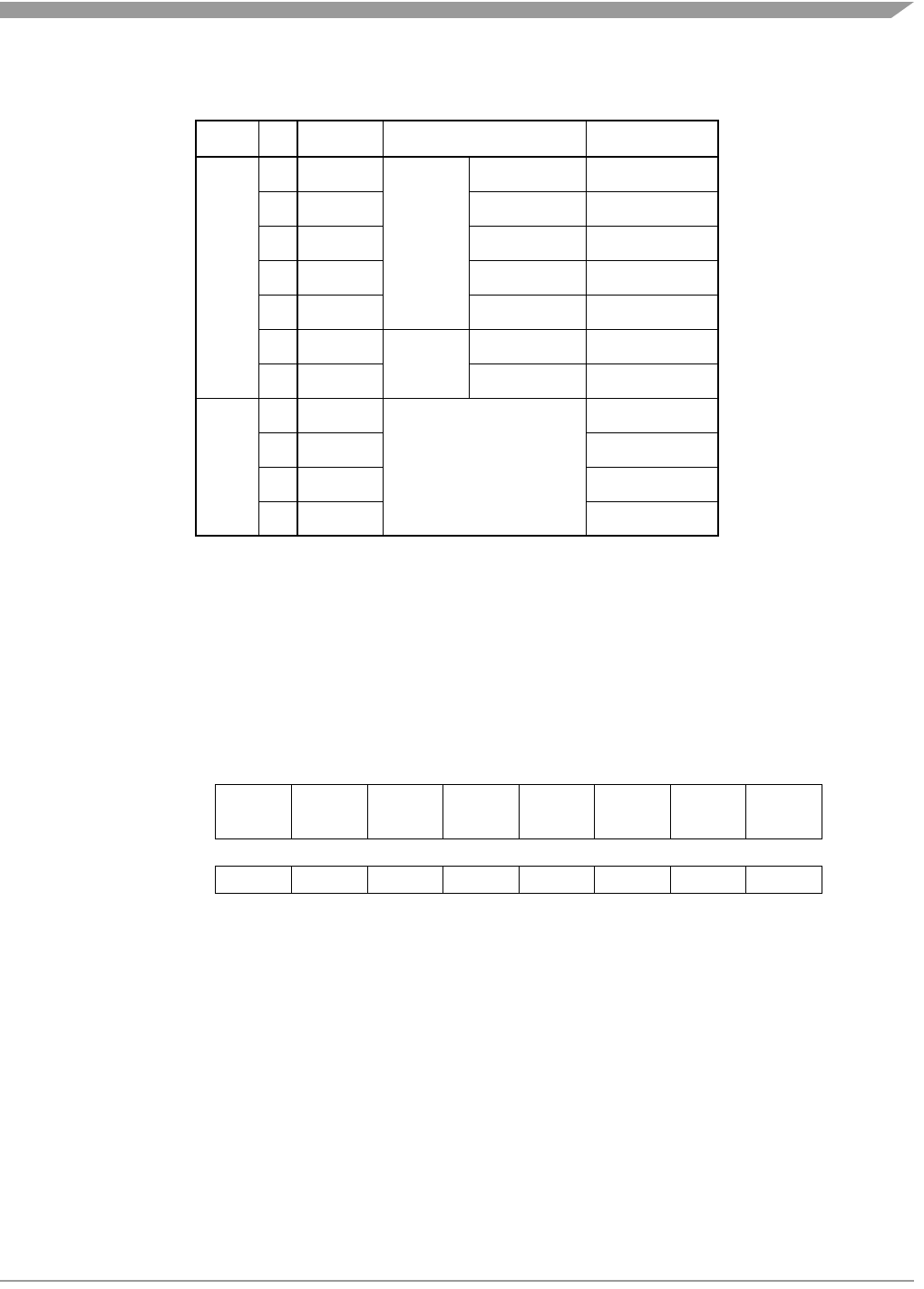
Port A
MC68HC08LN56 • MC68HC708LN56 General Release Specification, Rev. 2.1
Freescale Semiconductor 167
13.2 Port A
Port A is an 8-bit general-purpose bidirectional I/O port.
13.2.1 Port A Data Register
The port A data register contains a data latch for each of the eight port A pins.
PTA[7:0] — Port A Data Bits
These read/write bits are software programmable. Data direction of each port A pin is under the control
of the corresponding bit in data direction register A. Reset has no effect on port A data.
KBD[7:0] — Keyboard Inputs
The keyboard interrupt enable bits, KBIE[7:0], in the keyboard interrupt control register (KBICR),
enable the port A pins as external interrupt pins. (See Chapter 9 Keyboard Module (KB).)
E
0 DDRE0
TIM
PTE0/TCH0
1 DDRE1 PTE1/TCH1
2 DDRE2 PTE2/TCH2
3 DDRE3 PTE3/TCH3
4 DDRE4 PTE4/TCLK
5 DDRE5
SCI
PTE5/TxD
6 DDRE6 PTE6/RxD
F
0 DDRF0
—
PTF0
1 DDRF1 PTF1
2 DDRF2 PTF2
3 DDRF3 PTF3
PTA
$0000Bit 7654321Bit 0
Read:
PTA7 PTA6 PTA5 PTA4 PTA3 PTA2 PTA1 PTA0
Write:
Reset: Unaffected by reset
Alternate Function: KBD7 KBD6 KBD5 KBD4 KBD3 KBD2 KBD1 KBD0
Figure 13-2. Port A Data Register (PTA)
Table 13-1. Port Control Register
Bits Summary (Sheet 2 of 2)
Port Bit DDR Module Control Pin
I/O Ports
MC68HC08LN56 • MC68HC708LN56 General Release Specification, Rev. 2.1
168 Freescale Semiconductor
13.2.2 Data Direction Register A
Data direction register A determines whether each port A pin is an input or an output. Writing a logic one
to a DDRA bit enables the output buffer for the corresponding port A pin; a logic zero disables the output
buffer.
DDRA[7:0] — Data Direction Register A Bits
These read/write bits control port A data direction. Reset clears DDRA[7:0], configuring all port A pins
as inputs.
1 = Corresponding port A pin configured as output
0 = Corresponding port A pin configured as input
NOTE
Avoid glitches on port A pins by writing to the port A data register before
changing data direction register A bits from 0 to 1.
Figure 13-4 shows the port A I/O logic.
Figure 13-4. Port A I/O Circuit
When bit DDRAx is a logic one, reading address $0000 reads the PTAx data latch. When bit DDRAx is a
logic zero, reading address $0000 reads the voltage level on the pin. The data latch can always be written,
regardless of the state of its data direction bit. Table 13-2 summarizes the operation of the port A pins.
DDRA
$0004Bit 7654321Bit 0
Read:
DDRA7 DDRA6 DDRA5 DDRA4 DDRA3 DDRA2 DDRA1 DDRA0
Write:
Reset:00000000
Figure 13-3. Data Direction Register A (DDRA)
READ DDRA ($0004)
WRITE DDRA ($0004)
RESET
WRITE PTA ($0000)
READ PTA ($0000)
PTAx
DDRAx
PTAx
INTERNAL DATA BUS
Port B
MC68HC08LN56 • MC68HC708LN56 General Release Specification, Rev. 2.1
Freescale Semiconductor 169
13.3 Port B
Port B is an 8-bit special function port that shares four of its pins with the A/D converter module.
13.3.1 Port B Data Register
The port B data register contains a data latch for each of the eight port pins.
PTB[7:0] — Port B Data Bits
These read/write bits are software-programmable. Data direction of each port B pin is under the control
of the corresponding bit in data direction register B. Reset has no effect on port B data.
ADI[3:0] — Analog-to-Digital Input Bits
ADI[3:0] are pins used for the input channels to the analog-to-digital converter module. The channel
select bits in the A/D status and control register define which port B pin will be used as an A/D input
and overrides any control from the port I/O logic by forcing that pin as the input to the analog circuitry.
NOTE
Care must be taken when reading port B while applying analog voltages to
AD3:AD0 pins. If the appropriate A/D channel is not enabled, excessive
current drain may occur if analog voltages are applied to the PTBx/ANx pin,
while PTB is read as a digital input. Those ports not selected as analog
input channels are considered digital I/O ports.
Table 13-2. Port A Pin Functions
DDRA Bit PTA Bit I/O Pin Mode Accesses to DDRA Accesses to PTA
Read/Write Read Write
0X(1) Input, Hi-Z(2) DDRA[7:0] Pin PTA[7:0](3)
1 X Output DDRA[7:0] PTA[7:0] PTA[7:0]
NOTES:
1.X = don’t care
2.Hi-Z = high impedance
3.Writing affects data register, but does not affect input
PTB
$0001 Bit 7 6 5 4 3 2 1 Bit 0
Read:
PTB7 PTB6 PTB5 PTB4 PTB3 PTB2 PTB1 PTB0
Write:
Reset: Unaffected by reset
Alternate Function: ADI3 ADI2 ADI1 ADI0
Figure 13-5. Port B Data Register (PTB)
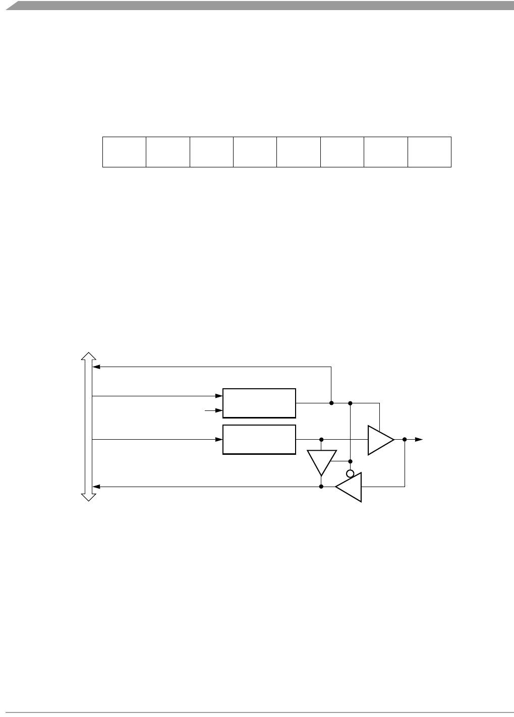
I/O Ports
MC68HC08LN56 • MC68HC708LN56 General Release Specification, Rev. 2.1
170 Freescale Semiconductor
13.3.2 Data Direction Register B
Data direction register B determines whether each port B pin is an input or an output. Writing a logic one
to a DDRB bit enables the output buffer for the corresponding port B pin; a logic zero disables the output
buffer.
DDRB[7:0] — Data Direction Register B Bits
These read/write bits control port B data direction. Reset clears DDRB[7:0], configuring all port B pins
as inputs.
1 = Corresponding port B pin configured as output
0 = Corresponding port B pin configured as input
NOTE
Avoid glitches on port B pins by writing to the port B data register before
changing data direction register B bits from 0 to 1.
Figure 13-7 shows the port B I/O logic.
Figure 13-7. Port B I/O Circuit
When bit DDRBx is a logic one, reading address $0001 reads the PTBx data latch. When bit DDRBx is a
logic zero, reading address $0001 reads the voltage level on the pin. The data latch can always be written,
regardless of the state of its data direction bit. Table 13-3 summarizes the operation of the port B pins.
DDRB
$0005Bit 7654321Bit 0
Read:
DDRB7 DDRB6 DDRB5 DDRB4 DDRB3 DDRB2 DDRB1 DDRB0
Write:
Reset:00000000
Figure 13-6. Data Direction Register B (DDRB)
READ DDRB ($0005)
WRITE DDRB ($0005)
RESET
WRITE PTB ($0001)
READ PTB ($0001)
PTBx
DDRBx
PTBx
INTERNAL DATA BUS
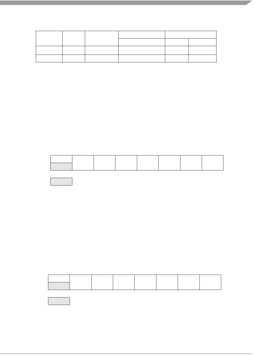
Port C
MC68HC08LN56 • MC68HC708LN56 General Release Specification, Rev. 2.1
Freescale Semiconductor 171
13.4 Port C
Port C is a 7-bit general-purpose bidirectional I/O port.
13.4.1 Port C Data Register
The port C data register contains a data latch for each of the seven port C pins.
PTC[6:0] — Port C Data Bits
These read/write bits are software-programmable. Data direction of each port C pin is under the control
of the corresponding bit in data direction register C. Reset has no effect on port C data.
13.4.2 Data Direction Register C
Data direction register C determines whether each port C pin is an input or an output. Writing a logic one
to a DDRC bit enables the output buffer for the corresponding port C pin; a logic zero disables the output
buffer.
Table 13-3. Port B Pin Functions
DDRB Bit PTB Bit I/O Pin Mode Accesses to DDRB Accesses to PTB
Read/Write Read Write
0X(1) Input, Hi-Z(2) DDRB[7:0] Pin PTB[7:0](3)
1 X Output DDRB[7:0] PTB[7:0] PTB[7:0]
NOTES:
1.X = don’t care
2.Hi-Z = high impedance
3.Writing affects data register, but does not affect input
PTC
$0002Bit 7654321Bit 0
Read: 0
PTC6 PTC5 PTC4 PTC3 PTC2 PTC1 PTC0
Write:
Reset: Unaffected by reset
= Unimplemented
Figure 13-8. Port C Data Register (PTC)
DDRC
$0006 Bit 7654321Bit 0
Read: 0
DDRC6 DDRC5 DDRC4 DDRC3 DDRC2 DDRC1 DDRC0
Write:
Reset:00000000
= Unimplemented
Figure 13-9. Data Direction Register C (DDRC)
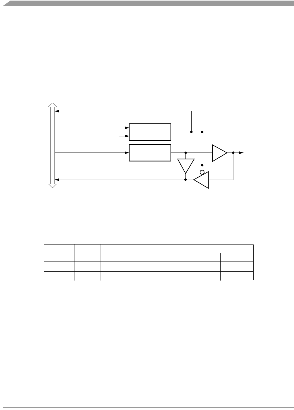
I/O Ports
MC68HC08LN56 • MC68HC708LN56 General Release Specification, Rev. 2.1
172 Freescale Semiconductor
DDRC[6:0] — Data Direction Register C Bits
These read/write bits control port C data direction. Reset clears DDRC[6:0], configuring all port C pins
as inputs.
1 = Corresponding port C pin configured as output
0 = Corresponding port C pin configured as input
NOTE
Avoid glitches on port C pins by writing to the port C data register before
changing data direction register C bits from 0 to 1.
Figure 13-10 shows the port C I/O logic.
Figure 13-10. Port C I/O Circuit
When bit DDRCx is a logic one, reading address $0002 reads the PTCx data latch. When bit DDRCx is
a logic zero, reading address $0002 reads the voltage level on the pin. The data latch can always be
written, regardless of the state of its data direction bit. Table 13-4 summarizes the operation of the port C
pins.
Table 13-4. Port C Pin Functions
DDRC Bit PTC Bit I/O Pin Mode Accesses to DDRC Accesses to PTC
Read/Write Read Write
0X(1) Input, Hi-Z(2) DDRC[6:0] Pin PTC[6:0](3)
1 X Output DDRC[6:0] PTC[6:0] PTC[6:0]
NOTES:
1.X = don’t care
2.Hi-Z = high impedance
3.Writing affects data register, but does not affect input
READ DDRC ($0006)
WRITE DDRC ($0006)
RESET
WRITE PTC ($0002)
READ PTC ($0002)
PTCx
DDRCx
PTCx
INTERNAL DATA BUS
Port D
MC68HC08LN56 • MC68HC708LN56 General Release Specification, Rev. 2.1
Freescale Semiconductor 173
13.5 Port D
Port D is an 8-bit special function port that shares all eight of its pins with two serial peripheral interface
modules (SPI).
13.5.1 Port D Data Register
The port D data register contains a data latch for each of the eight port D pins.
PTD[7:0] — Port D Data Bits
These read/write bits are software-programmable. Data direction of each port D pin is under the control
of the corresponding bit in data direction register D. Reset has no effect on port D data.
MISO1 — Master In/Slave Out1
The PTD0/MISO1 pin is the master in/slave out terminal of the SPI1 module. When the SPI enable bit,
SPE, is clear, the SPI module is disabled, and the PTD0/MISO1 pin is available for general-purpose
I/O.
Data direction register D (DDRD) does not affect the data direction of port D pins that are being used
by the SPI1 module. However, the DDRD bits always determine whether reading port D returns the
states of the latches or the states of the pins. See Table 13-5.
MOSI1 — Master Out/Slave In 1
The PTD1/MOSI1 pin is the master out/slave in terminal of the SPI1 module. When the SPE bit is clear,
the PTD1/MOSI1 pin is available for general-purpose I/O.
SS1 — Slave Select 1
The PTD2/SS1 pin is the slave select input of the SPI1 module. When the SPE bit is clear, or when
the SPI master bit, SPMSTR, is set, the PTD2/SS1 pin is available for general-purpose I/O. When the
SPI is enabled, the DDRB2 bit in data direction register B (DDRB) has no effect on the PTD2/SS1 pin.
SPSCK1 — SPI1 Serial Clock
The PTD3/SPSCK1 pin is the serial clock input of the SPI1 module. When the SPE bit is clear, the
PTD3/SPSCK1 pin is available for general-purpose I/O.
SPSCK2 — SPI2 Serial Clock
The PTD4/SPSCK2 pin is the serial clock input of the SPI2 module. When the SPE bit is clear, the
PTD4/SPSCK2 pin is available for general-purpose I/O.
SS2 — Slave Select 2
The PTD5/SS2 pin is the slave select input of the SPI2 module. When the SPE bit is clear, or when
the SPI master bit, SPMSTR, is set, the PTD5/SS2 pin is available for general-purpose I/O. When the
SPI2 is enabled, the DDRD5 bit in data direction register D(DDRD) has no effect on the PTD2/SS1 pin.
PTD
$0003 Bit 7654321Bit 0
Read:
PTD7 PTD6 PTD5 PTD4 PTD3 PTD2 PTD1 PTD0
Write:
Reset: Unaffected by reset
Alternate Function: MISO2 MOSI2 SS2 SPSCK2 SPSCK1 SS1MOSI1MISO1
Figure 13-11. Port D Data Register (PTD)
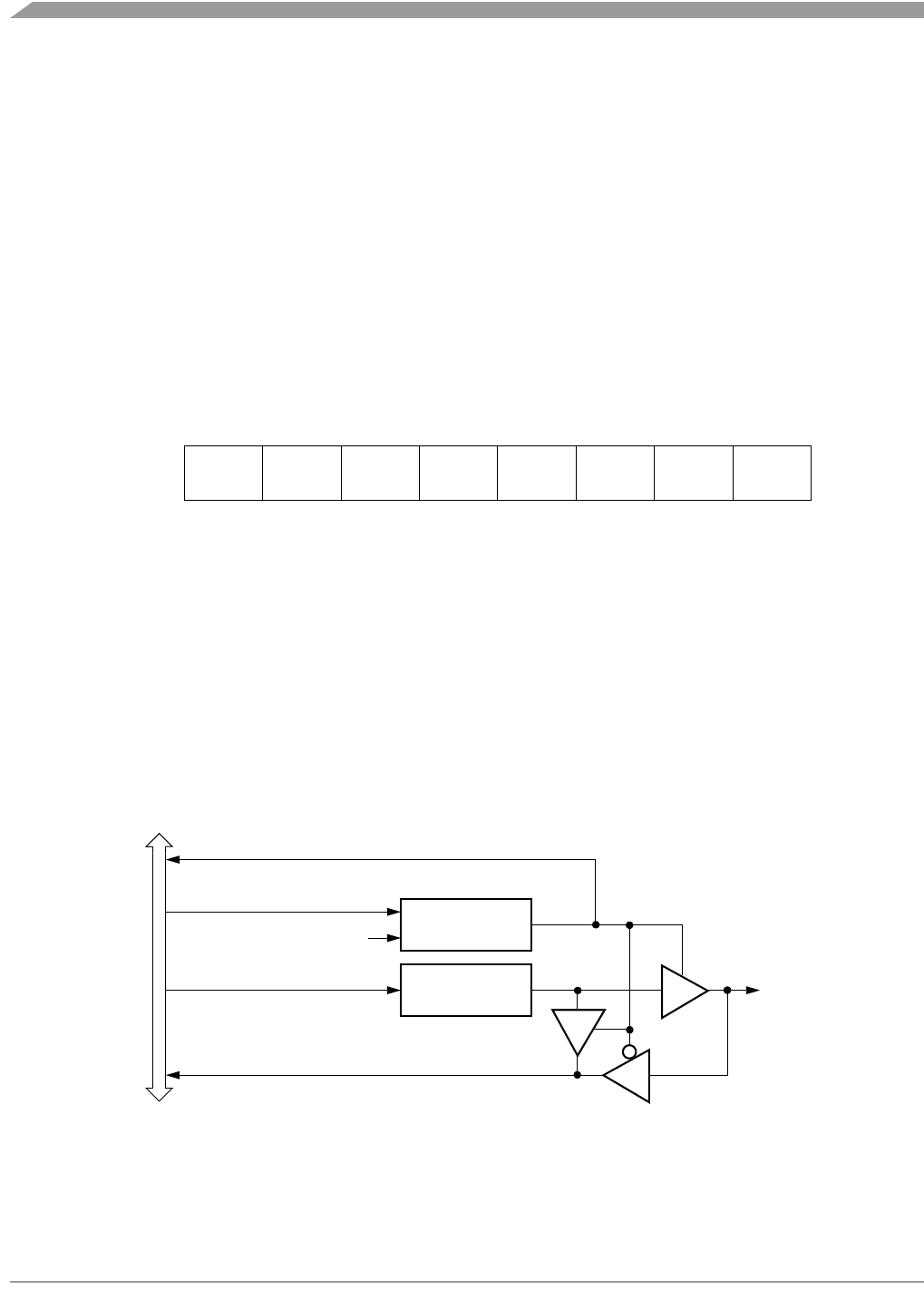
I/O Ports
MC68HC08LN56 • MC68HC708LN56 General Release Specification, Rev. 2.1
174 Freescale Semiconductor
MOSI2 — Master Out/Slave In 2
The PTD6/MOSI2 pin is the master out/slave in terminal of the SPI2 module. When the SPE bit is clear,
the PTD6/MOSI2 pin is available for general-purpose I/O.
MISO2 — Master In/Slave Out2
The PTD7/MISO2 pin is the master in/slave out terminal of the SPI2 module. When the SPI2 enable
bit, SPE2, is clear, the SPI2 module is disabled, and the PTD7/MISO2 pin is available for
general-purpose I/O.
13.5.2 Data Direction Register D
Data direction register D determines whether each port D pin is an input or an output. Writing a logic one
to a DDRD bit enables the output buffer for the corresponding port D pin; a logic zero disables the output
buffer.
DDRD[7:0] — Data Direction Register D Bits
These read/write bits control port D data direction. Reset clears DDRD[7:0], configuring all port D pins
as inputs.
1 = Corresponding port D pin configured as output
0 = Corresponding port D pin configured as input
NOTE
Avoid glitches on port D pins by writing to the port D data register before
changing data direction register D bits from 0 to 1.
Figure 13-13 shows the port D I/O logic.
Figure 13-13. Port D I/O Circuit
When bit DDRDx is a logic one, reading address $0003 reads the PTDx data latch. When bit DDRDx is
a logic zero, reading address $0003 reads the voltage level on the pin. The data latch can always be
DDRD
$000C Bit 7654321Bit 0
Read:
DDRD7 DDRD6 DDRD5 DDRD4 DDRD3 DDRD2 DDRD1 DDRD0
Write:
Reset:00000000
Figure 13-12. Data Direction Register D (DDRD)
READ DDRD ($0007)
WRITE DDRD ($0007)
RESET
WRITE PTD ($0003)
READ PTD ($0003)
PTDx
DDRDx
PTDx
INTERNAL DATA BUS
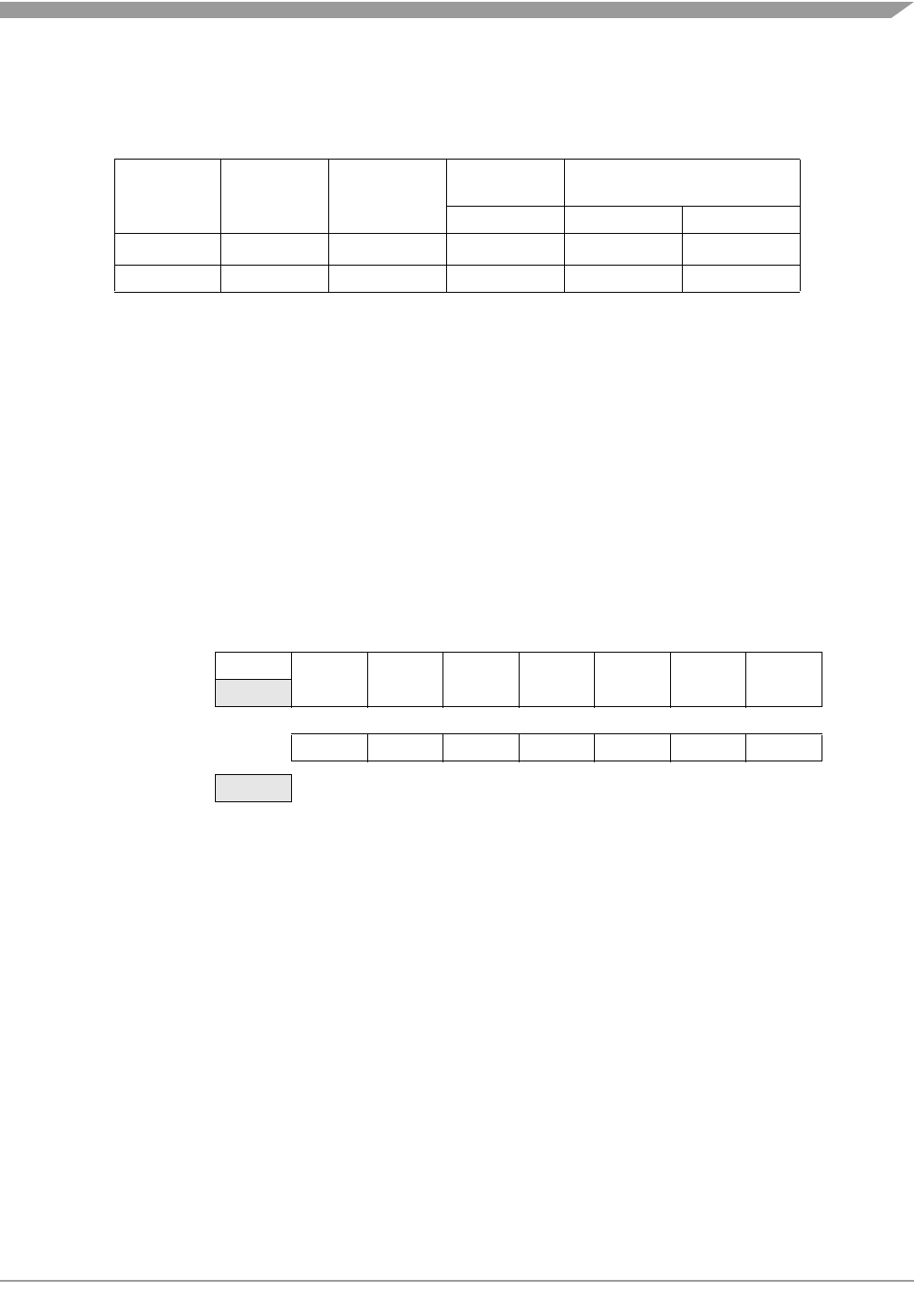
Port E
MC68HC08LN56 • MC68HC708LN56 General Release Specification, Rev. 2.1
Freescale Semiconductor 175
written, regardless of the state of its data direction bit. Table 13-5 summarizes the operation of the port D
pins.
13.6 Port E
Port E is a 7-bit special function port that shares five of its pins with the timer interface (TIM) module and
two of its pins with the serial communications interface module (SCI).
13.6.1 Port E Data Register
The port E data register contains a data latch for each of the seven port E pins.
PTE[6:0] — Port E Data Bits
PTE[6:0] are read/write, software programmable bits. Data direction of each port E pin is under the
control of the corresponding bit in data direction register E.
NOTE
Data direction register E (DDRE) does not affect the data direction of port
E pins that are being used by the TIM. However, the DDRE bits always
determine whether reading port E returns the states of the latches or the
states of the pins. See Table 13-6.
TCH[3:0] — Timer Channel I/O Bits
The PTE3/TCH3:PTE0/TCH0 pins are the TIM input capture/output compare pins. The edge/level
select bits, ELSxB:ELSxA, determine whether the PTE3/TCH3:PTE0/TCH0 pins are timer channel I/O
pins or general-purpose I/O pins. See Chapter 10 Timer Interface Module (TIM).
Table 13-5. Port D Pin Functions
DDRD Bit PTD Bit I/O Pin
Mode
Accesses to
DDRD Accesses to PTD
Read/Write Read Write
0X(1) Input, Hi-Z(2) DDRD[7:0] Pin PTD[7:0](3)
1 X Output DDRD[7:0] PTD[7:0] PTD[7:0]
NOTES:
1.X = don’t care
2.Hi-Z = high impedance
3.Writing affects data register, but does not affect input
PTE
$0008 Bit 7654321Bit 0
Read: 0
PTE6 PTE5 PTE4 PTE3 PTE2 PTE1 PTE0
Write:
Reset: Unaffected by reset
Alternate Function: RxD TxD TCLK TCH3 TCH2 TCH1 TCH0
= Unimplemented
Figure 13-14. Port E Data Register (PTE)
I/O Ports
MC68HC08LN56 • MC68HC708LN56 General Release Specification, Rev. 2.1
176 Freescale Semiconductor
TCLK — Timer Clock Input
The PTE4/TCLK pin is the external clock input for the TIM. The pre-scaler select bits, PS[2:0], select
PTE4/TCLK as the TIM clock input. See Chapter 10 Timer Interface Module (TIM). When not selected
as the TIM clock, PTE4/TCLK is available for general-purpose I/O.
TxD — SCI Transmit Data Output
The PTE5/TxD pin is the transmit data output for the SCI module. When the enable SCI bit, ENSCI, is
clear, the SCI module is disabled, and the PTE5/TxD pin is available for general-purpose I/O. See
Chapter 12 Serial Communications Interface Module (SCI).
NOTE
Data direction register E (DDRE) does not affect the data direction of port
E pins that are being used by the SCI module. However, the DDRE bits
always determine whether reading port E returns the states of the latches
or the states of the pins. See Table 13-6.
RxD — SCI Receive Data Input
The PTE7/RxD pin is the receive data input for the SCI module. When the enable SCI bit, ENSCI, is
clear, the SCI module is disabled, and the PTE1/RxD pin is available for general-purpose I/O. See
Chapter 12 Serial Communications Interface Module (SCI).
13.6.2 Data Direction Register E
Data direction register E determines whether each port E pin is an input or an output. Writing a logic one
to a DDRE bit enables the output buffer for the corresponding port E pin; a logic zero disables the output
buffer.
DDRE[6:0] — Data Direction Register E Bits
These read/write bits control port E data direction. Reset clears DDRE[6:0], configuring all port E pins
as inputs.
1 = Corresponding port E pin configured as output
0 = Corresponding port E pin configured as input
NOTE
Avoid glitches on port E pins by writing to the port E data register before
changing data direction register E bits from 0 to 1.
Figure 13-15 shows the port E I/O logic.
Figure 13-15. Port E I/O Circuit
READ DDRE ($000C)
WRITE DDRE ($000C)
RESET
WRITE PTE ($0008)
READ PTE ($0008)
PTEx
DDREx
PTEx
INTERNAL DATA BUS
Port F
MC68HC08LN56 • MC68HC708LN56 General Release Specification, Rev. 2.1
Freescale Semiconductor 177
When bit DDREx is a logic one, reading address $0008 reads the PTEx data latch. When bit DDREx is a
logic zero, reading address $0008 reads the voltage level on the pin. The data latch can always be written,
regardless of the state of its data direction bit. Table 13-6 summarizes the operation of the port E pins.
13.7 Port F
Port F is a 4-bit, general-purpose bidirectional I/O port.
13.7.1 Port F Data Register
The port F data register contains a data latch for each of the four port F pins.
PTF[3:0] — Port F Data Bits
These read/write bits are software programmable. Data direction of each port F pin is under the control
of the corresponding bit in data direction register F. Reset has no effect on PTF[3:0].
13.7.2 Data Direction Register F
Data direction register F determines whether each port F pin is an input or an output. Writing a logic one
to a DDRF bit enables the output buffer for the corresponding port F pin; a logic zero disables the output
buffer.
Table 13-6. Port E Pin Functions
DDRE Bit PTE Bit I/O Pin Mode Accesses to DDRE Accesses to PTE
Read/Write Read Write
0X(1) Input, Hi-Z(2) DDRE[6:0] Pin PTE[6:0](3)
1 X Output DDRE[6:0] PTE[6:0] PTE[6:0]
NOTES:
1.X = don’t care
2.Hi-Z = high impedance
3.Writing affects data register, but does not affect input
PTF
$0009 Bit 7654321Bit 0
Read:0000
PTF3 PTF2 PTF1 PTF0
Write:
Reset: Unaffected by reset
= Unimplemented
Figure 13-16. Port F Data Register (PTF)
DDRF
$000D Bit 7654321Bit 0
Read:0000
DDRF3 DDRF2 DDRF1 DDRF0
Write:
Reset:00000000
= Unimplemented
Figure 13-17. Data Direction Register F (DDRF)

I/O Ports
MC68HC08LN56 • MC68HC708LN56 General Release Specification, Rev. 2.1
178 Freescale Semiconductor
DDRF[3:0] — Data Direction Register F Bits
These read/write bits control port F data direction. Reset clears DDRF[3:0], configuring all port F pins
as inputs.
1 = Corresponding port F pin configured as output
0 = Corresponding port F pin configured as input
NOTE
Avoid glitches on port F pins by writing to the port F data register before
changing data direction register F bits from 0 to 1.
Figure 13-18 shows the port F I/O logic.
Figure 13-18. Port F I/O Circuit
When bit DDRFx is a logic one, reading address $0009 reads the PTFx data latch. When bit DDRFx is a
logic zero, reading address $0009 reads the voltage level on the pin. The data latch can always be written,
regardless of the state of its data direction bit. Table 13-7 summarizes the operation of the port F pins.
Table 13-7. Port F Pin Functions
DDRF Bit PTF Bit I/O Pin Mode Accesses to DDRF Accesses to PTF
Read/Write Read Write
0X(1) Input, Hi-Z(2) DDRF[3:0] Pin PTF[3:0](3)
1 X Output DDRF[3:0] PTF[3:0] PTF[3:0]
NOTES:
1.X = don’t care
2.Hi-Z = high impedance
3.Writing affects data register, but does not affect input
READ DDRF ($000D)
WRITE DDRF ($000D)
RESET
WRITE PTF ($0009)
READ PTF ($0009)
PTFx
DDRFx
PTFx
INTERNAL DATA BUS

MC68HC08LN56 • MC68HC708LN56 General Release Specification, Rev. 2.1
Freescale Semiconductor 179
Chapter 14
Analog-to-Digital Converter (ADC)
14.1 Introduction
This section describes the analog-to-digital converter. The ADC is an 8-bit analog-to-digital converter.
14.2 Features
Features of the ADC module include:
• Four Channels with Multiplexed Input
• Linear Successive Approximation
• 8-Bit Resolution
• Single or Continuous Conversion
• Conversion Complete Flag Or Conversion Complete Interrupt
• Selectable ADC Clock
14.3 Functional Description
The A/D provides four pins for sampling external sources at pins PTB3/AN3:PTB0/AN0. An analog
multiplexer allows the single ADC converter to select one of four ADC channels as ADC voltage in
(ADCVIN). ADCVIN is converted by the successive approximation register-based analog-to-digital
converter. When the conversion is completed, ADC places the result in the ADC data register and sets a
flag or generates an interrupt. (See Figure 14-1.)
NOTE
References to DMA and associated functions are only valid if the MCU has
a DMA module. If the MCU has no DMA, any DMA-related register bits
should be left in their reset state for expected MCU operation.
14.3.1 ADC Port I/O Pins
PTB3/AN3:PTB0/AN0 are general-purpose I/O pins that share with the ADC channels. The channel
select bits define which ADC channel/port pin will be used as the input signal. The ADC overrides the port
I/O logic by forcing that pin as input to the ADC. The remaining ADC channels/port pins are controlled by
the port I/O logic and can be used as general-purpose I/O. Writes to the port register or DDR will not have
any affect on the port pin that is selected by the ADC. Read of a port pin in use by the ADC will return a
logic zero.
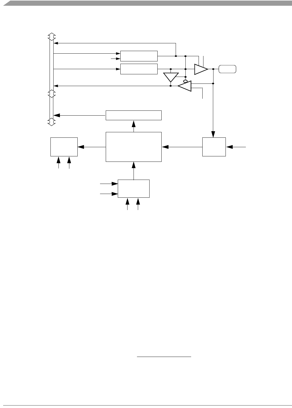
Analog-to-Digital Converter (ADC)
MC68HC08LN56 • MC68HC708LN56 General Release Specification, Rev. 2.1
180 Freescale Semiconductor
Figure 14-1. ADC Block Diagram
14.3.2 Voltage Conversion
When the input voltage to the ADC equals VRH, the ADC converts the signal to $FF (full scale). If the input
voltage equals AVSS, the ADC converts it to $00. Input voltages between VRH and AVSS are a straight-line
linear conversion. All other input voltages will result in $FF, if greater than VRH.
NOTE
Input voltage should not exceed the analog supply voltages.
14.3.3 Conversion Time
Conversion starts after a write to the ADSCR. Conversion time in terms of the number of bus cycles is a
function of oscillator frequency, bus frequency, and ADIV prescaler bits. For example, with an oscillator
frequency of 4 MHz, bus frequency of 8 MHz and ADC clock frequency of 1 MHz, one conversion will take
between 16 ADC and 17 ADC clock cycles or between 16 and 17 µs. There will be 128 bus cycles
between each conversion. Sample rate is approximately 60 kHz.
INTERNAL
DATA BUS
READ DDRB/DDRB
WRITE DDRB/DDRD
RESET
WRITE PTB
READ PTB
PTB/Dx
DDRBx
PTBx
INTERRUPT
LOGIC CHANNEL
SELECT
ADC
CLOCK
GENERATOR
CONVERSION
COMPLETE ADC VOLTAGE IN
(ADVIN)
ADC CLOCK
CGMXCLK
BUS CLOCK
ADCH[4:0]
ADC DATA REGISTER
AIEN COCO/IDMAS
DISABLE
DISABLE
(ADC CHANNEL X)
ADIV[2:0] ADICLK
16-17 ADC cycles
ADC frequency
Conversion Time =
Number of Bus Cycles = Conversion Time x Bus Frequency

Interrupts
MC68HC08LN56 • MC68HC708LN56 General Release Specification, Rev. 2.1
Freescale Semiconductor 181
14.3.4 Conversion
In the continuous conversion mode, the ADC data register will be filled with new data after each
conversion. Data from the previous conversion will be overwritten whether that data has been read or not.
Conversions will continue until the ADCO bit is cleared. The COCO/IDMAS bit is set after the first
conversion and will stay set until the next write of the ADC status and control register or the next read of
the ADC data register.
In the single conversion mode, conversion begins with a write to the ADSCR. Only one conversion occurs
between writes to the ADSCR.
14.3.5 Accuracy and Precision
The conversion process is monotonic and has no missing codes.
14.4 Interrupts
When the AIEN bit is set, the ADC module is capable of generating either CPU or DMA interrupts after
each ADC conversion. A CPU interrupt is generated if the COCO/IDMAS bit is at logic zero. If
COCO/IDMAS bit is set, a DMA interrupt is generated. The COCO/IDMAS bit is not used as a conversion
complete flag when interrupts are enabled.
14.5 Low-Power Modes
The WAIT and STOP instruction can put the MCU in low-power- consumption standby modes.
14.5.1 Wait mode
The ADC continues normal operation during wait mode. Any enabled CPU interrupt request from the ADC
can bring the MCU out of wait mode. If the ADC is not required to bring the MCU out of wait mode, power
down the ADC by setting ADCH[4:0] bits in the ADC status and control register before executing the WAIT
instruction.
14.5.2 Stop Mode
The ADC module is inactive after the execution of a STOP instruction. Any pending conversion is aborted.
ADC conversions resume when the MCU exits stop mode after an external interrupt. Allow one
conversion cycle to stabilize the analog circuitry.
14.6 I/O Signals
The ADC module has four pins shared with port B.
14.6.1 ADC Analog Power Pin (AVDD)
The ADC analog portion uses AVDD as its power pin. Connect the AVDD pin to the same voltage potential
as V<st-subsmallcaps>dd. External filtering may be necessary to ensure clean AVDD for good results.
NOTE
Route AVDD carefully for maximum noise immunity and place bypass
capacitors as close as possible to the package.

Analog-to-Digital Converter (ADC)
MC68HC08LN56 • MC68HC708LN56 General Release Specification, Rev. 2.1
182 Freescale Semiconductor
14.6.2 ADC Analog Ground Pin (AVSS)
The ADC analog portion uses AVSS as its ground pin. Connect the AVSS pin to the same voltage potential
as V<st-subsmallcaps>ss.
NOTE
Route AVSS cleanly to avoid any offset errors.
14.6.3 ADC Voltage Reference Pin (VRH)
VRH is the power supply for setting the reference voltage VRH. Connect the VRH pin to a voltage potential
<= AVDD, not less than 1.5 V.
NOTE
Route RRH cleanly to avoid any offset errors.
14.6.4 ADC Voltage In (ADVIN)
ADVIN is the input voltage signal from one of the four ADC channels to the ADC module.
14.7 I/O Registers
These I/O registers control and monitor operation of the ADC:
• ADC status and control register (ADSCR)
• ADC data register (ADR)
• ADC clock register (ADCLK)
14.7.1 ADC Status and Control Register
The following paragraphs describe the function of the ADC status and control register.
COCO/IDMAS — Conversions Complete/Interrupt DMA Select
When AIEN bit is a logic zero, the COCO/IDMAS is a read-only bit which is set each time a conversion
is completed except in the continuous conversion mode where it is set after the first conversion. This
bit is cleared whenever the ADC status and control register is written or whenever the ADC data
register is read.
If AIEN bit is a logic one, the COCO/IDMAS is a read/write bit which selects either CPU or DMA to
service the ADC interrupt request. Reset clears this bit.
1 = Conversion completed (AIEN = 0)/DMA interrupt (AIEN = 1)
0 = Conversion not completed (AIEN = 0)/CPU interrupt (AIEN = 1)
ADSCR
$0040Bit 7654321Bit 0
Read: COCO/
IDMAS AIEN ADCO ADCH4 ADCH3 ADCH2 ADCH1 ADCH0
Write:
Reset:00011111
Figure 14-2. ADC Status and Control Register (ADSCR)
I/O Registers
MC68HC08LN56 • MC68HC708LN56 General Release Specification, Rev. 2.1
Freescale Semiconductor 183
AIEN — ADC Interrupt Enable
When this bit is set, an interrupt is generated at the end of an ADC conversion. The interrupt signal is
cleared when the data register is read or the status/control register is written. Reset clears AIEN bit.
1 = ADC interrupt enabled
0 = ADC interrupt disabled
ADCO — ADC Continuous Conversion
When set, the ADC will convert samples continuously and update the ADR register at the end of each
conversion. Only one conversion is completed between writes to the ADSCR when this bit is cleared.
Reset clears the ADCO bit.
1 = Continuous ADC conversion
0 = One ADC conversion
ADCH[4:0] — ADC Channel Select Bits
ADCH4, ADCH3, ADCH2, ADCH1, and ADCH0 form a 5-bit field which is used to select one of 16 ADC
channels. Only four channels, ADCH[3:0], are available on this MCU. The channels are detailed in the
Table 14-1. Care should be taken when using a port pin as both an analog and digital input
simultaneously to prevent switching noise from corrupting the analog signal. (See Table 14-1.)
The ADC subsystem is turned off when the channel select bits are all set to one. This feature allows
for reduced power consumption for the MCU when the ADC is not being used.
NOTE
Recovery from the disabled state requires one conversion cycle to stabilize.
The voltage levels supplied from internal reference nodes as specified in Table 14-1 are used to verify
the operation of the ADC converter both in production test and for user applications.
Table 14-1. Mux Channel Select
ADCH4 ADCH3 ADCH2 ADCH1 ADCH0 Input Select
00000 PTB0/AD0
00001 PTB1/AD1
00010 PTB2/AD2
00011 PTB3/AD3
0 0 1 0 0 Reserved
↓↓↓↓↓ Reserved
1 1 0 1 1 Reserved
11100 VRH
11101 VRH
11110 AVSS
1 1 1 1 1 [ADC power off]
NOTE:
If any unused channels are selected, the resulting ADC conversion will be unknown.
Analog-to-Digital Converter (ADC)
MC68HC08LN56 • MC68HC708LN56 General Release Specification, Rev. 2.1
184 Freescale Semiconductor
14.7.2 ADC Data Register
One 8-bit result register is provided. This register is updated each time an ADC conversion completes.
14.7.3 ADC Clock Register
This register selects the clock frequency for the ADC.
ADIV2:ADIV0 — ADC Clock Prescaler Bits
ADIV2, ADIV1, and ADIV0 form a 3-bit field which selects the divide ratio used by the ADC to generate
the internal ADC clock. Table 14-2 shows the available clock configurations. The ADC clock should be
set to approximately 1 MHz.
ADICLK — ADC Input Clock Select
ADICLK selects either bus clock or CGMXCLK as the input clock source to generate the internal ADC
clock. Reset selects CGMXCLK as the ADC clock source.
If the external clock (CGMXCLK) is equal to or greater than 1 MHz, CGMXCLK can be used as the
clock source for the ADC. If CGMXCLK is less than 1 MHz, use the PLL-generated bus clock as the
clock source. As long as the internal ADC clock is at approximately 1 MHz, correct operation can be
guaranteed.
1 = Internal bus clock
0 = External clock (CGMXCLK)
ADR
$0041 Bit 7654321Bit 0
Read: AD7 AD6 AD5 AD4 AD3 AD2 AD1 AD0
Write:
Reset:00000000
= Unimplemented
Figure 14-3. ADC Data Register (ADR)
ADCLKR
$0042Bit 7654321Bit 0
Read: ADIV2 ADIV1 ADIV0 ADICLK 0000
Write:
Reset:00000000
= Unimplemented
Figure 14-4. ADC Clock Register (ADCLKR)
Table 14-2. ADC Clock Divide Ratio
ADIV2 ADIV1 ADIV0 ADC Clock Rate
0 0 0 ADC input clock /1
0 0 1 ADC input clock / 2
0 1 0 ADC input clock / 4
0 1 1 ADC input clock / 8
1 X X ADC input clock / 16
X = don’t care
1 MHz ADC input clock frequency
ADIV 2:0[]
-----------------------------------------------------------------------=

MC68HC08LN56 • MC68HC708LN56 General Release Specification, Rev. 2.1
Freescale Semiconductor 185
Chapter 15
Liquid Crystal Display Driver (LCD)
15.1 Introduction
The LCD driver module supports a 40 frontplane by 32 backplane display. This allows a maximum of 1280
LCD segments to be driven. Each segment is controlled by a corresponding bit in the LCD RAM. On reset
or on power-up, the drivers are disabled via a display ON (DISON) bit in the LCD control register
(LCDCR).
15.2 Features
Features of the LCD driver include:
• 40 Frontplane (FP) drivers by 32 Backplane (BP) Drivers
• 160 Bytes of Memory Mapped RAM Organized for Easy Bit-Mapped Character Display
• Internal Charge Pump Voltage Generator for Creation of Analog Voltage Levels
15.3 Functional Description
The LCD driver consists of five major submodules:
• Timing and control — contains registers and generates frame clock and backplane selects at the
programmed frequency to produce the waveforms
• Display RAM — contains the data to be displayed on the LCD panel
• Segment drivers — consists of 40 frontplane drivers
• Backplane drivers — consists of 32 backplane drivers
• Voltage generator — internal charge pump circuit to generate analog voltages
• Contrast control — 8-bit contrast resolution allowing analog voltages to remain constant over
operating range of power supply
Figure 15-1 shows a block diagram of the LCD driver module.
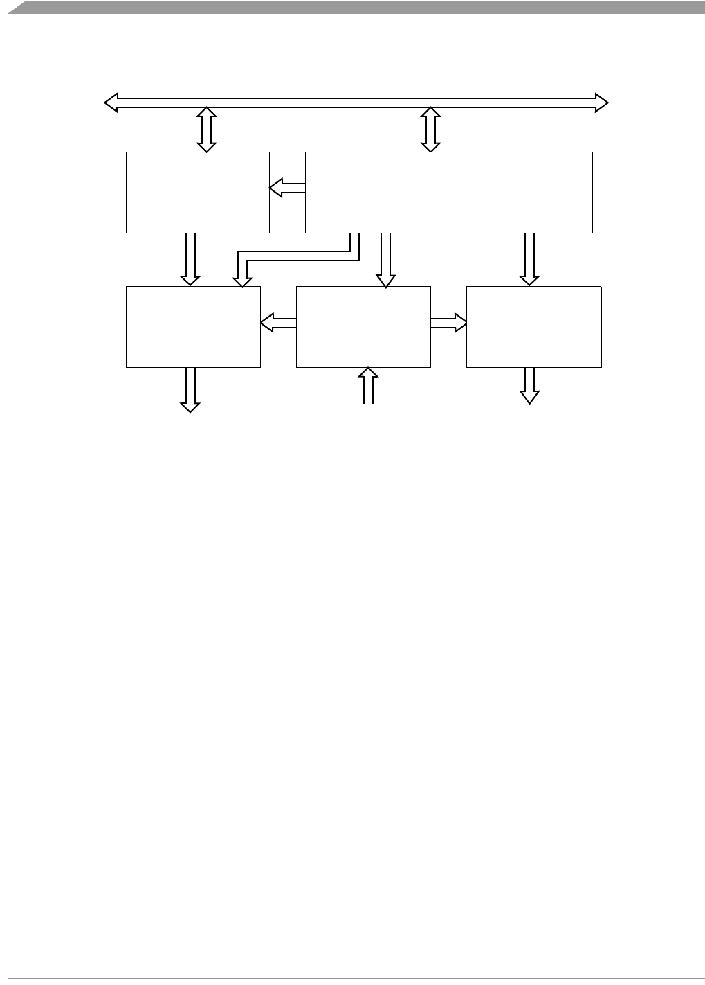
Liquid Crystal Display Driver (LCD)
MC68HC08LN56 • MC68HC708LN56 General Release Specification, Rev. 2.1
186 Freescale Semiconductor
Figure 15-1. LCD Driver Block Diagram
15.4 LCD RAM
The data to be displayed by the LCD is written to a 160-byte display RAM located between locations
$0E00:$0FFF in the memory map. The bits are organized as shown in Table 15-1, Table 15-2, and
Table 15-3 with a 1 stored in a given location, resulting in the corresponding display segment being
activated (turned on). The LCD RAM is a dual port RAM that interfaces with the internal address and data
buses of the MCU. It is possible to read from the LCD RAM locations for software-controlled scrolling.
If the LCD is disabled (DISON = 0 in the LCD control register), the 160 byte LCD RAM may be used as
general-purpose on-chip RAM.
If any of the frontplanes are unused, it is recommended that the corresponding locations in the LCD RAM
be written to a 0 to minimize the power consumption. In this case, the only consumed power due to the
unused frontplanes will be the switching between fields in the frame.
The LCD RAM is not initialized at power-on or by any reset. Therefore, it is recommended that valid data
be written to the LCD RAM before the DISON bit is enabled in the LCD control register.
BACKPLANE
DRIVERS
INTERNAL ADDRESS/ DATA/ CLOCKS
DISPLAY RAM
160 X 8
FRONTPLANE DRIVERS
VOLTAGE
GENERATOR/
FP0 :FP39
LCD VOLTAGE GENERATOR
CAPACITORS
CONTRAST
CONTROL
TIMING AND CONTROL LOGIC
BP0 :BP31
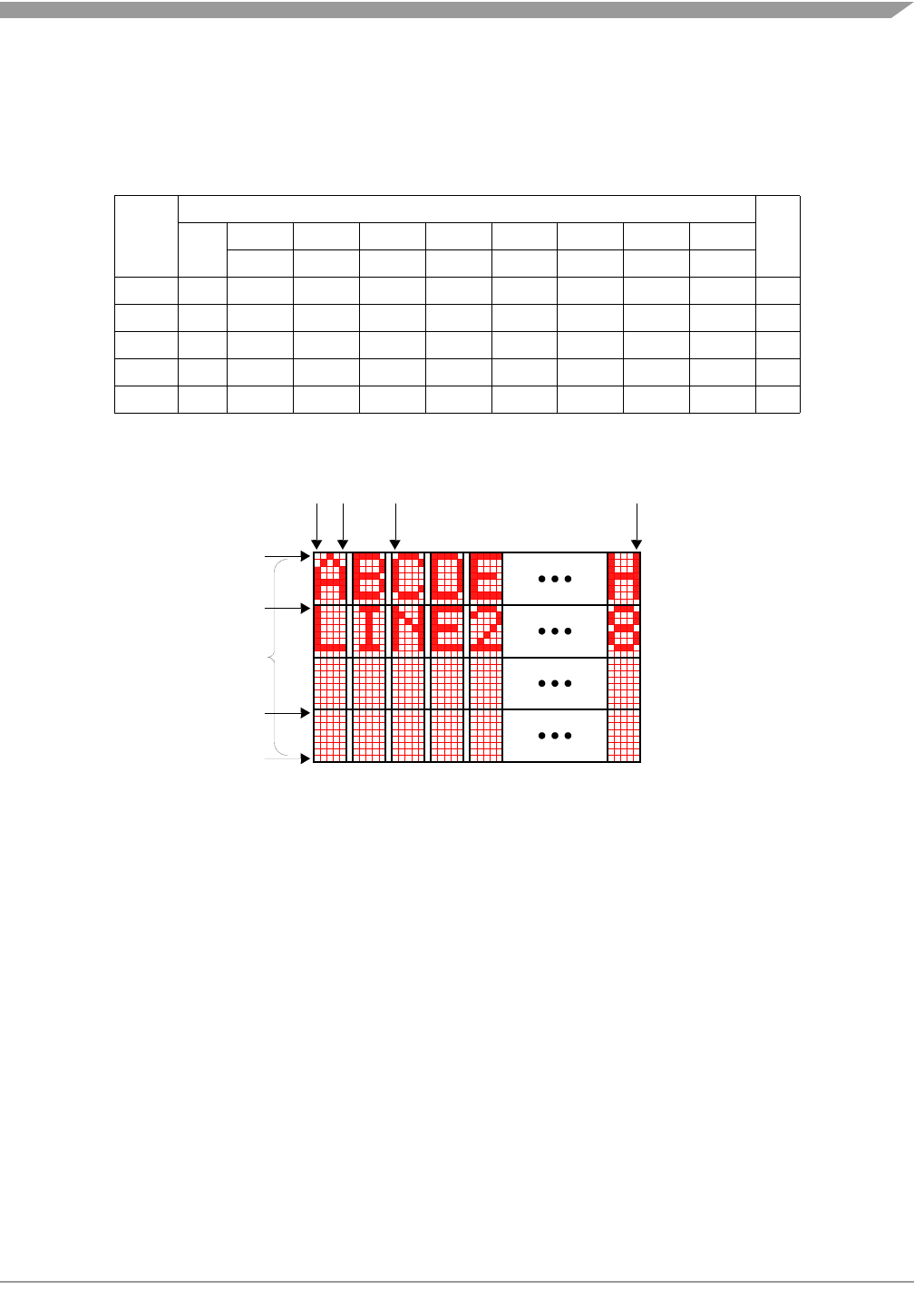
LCD RAM
MC68HC08LN56 • MC68HC708LN56 General Release Specification, Rev. 2.1
Freescale Semiconductor 187
15.4.1 LCD RAM Organization
As an example, to display the character A on the panel, the following data is written to the RAM as shown
in Table 15-1.
Figure 15-2. LCD Panel Dot Matrix Example
15.4.2 LCD RAM Memory Map
To display 40 frontplanes by 32 backplanes, only 160 bytes of RAM are required. However, holes in the
memory map exist for future expansion. This is shown in Table 15-2.
Table 15-1. LCD RAM Organization Example
ADDR
DATA
FP
Hex BP7BP6BP5BP4BP3BP2BP1BP0
Bit 7 Bit 6 Bit 5 Bit 4 Bit 3 Bit 2 Bit 1 Bit 0
$0E00 $7C 0 1 1 1 1 1 0 0 FP0
$0E01$1200010010FP1
$0E02$1100010001FP2
$0E03$1200010010FP3
$0E04 $7C 0 1 1 1 1 1 0 0 FP4
BP0
BP0-31
FP0
FP4
FP10
BP8
BP24
FP39
BP31
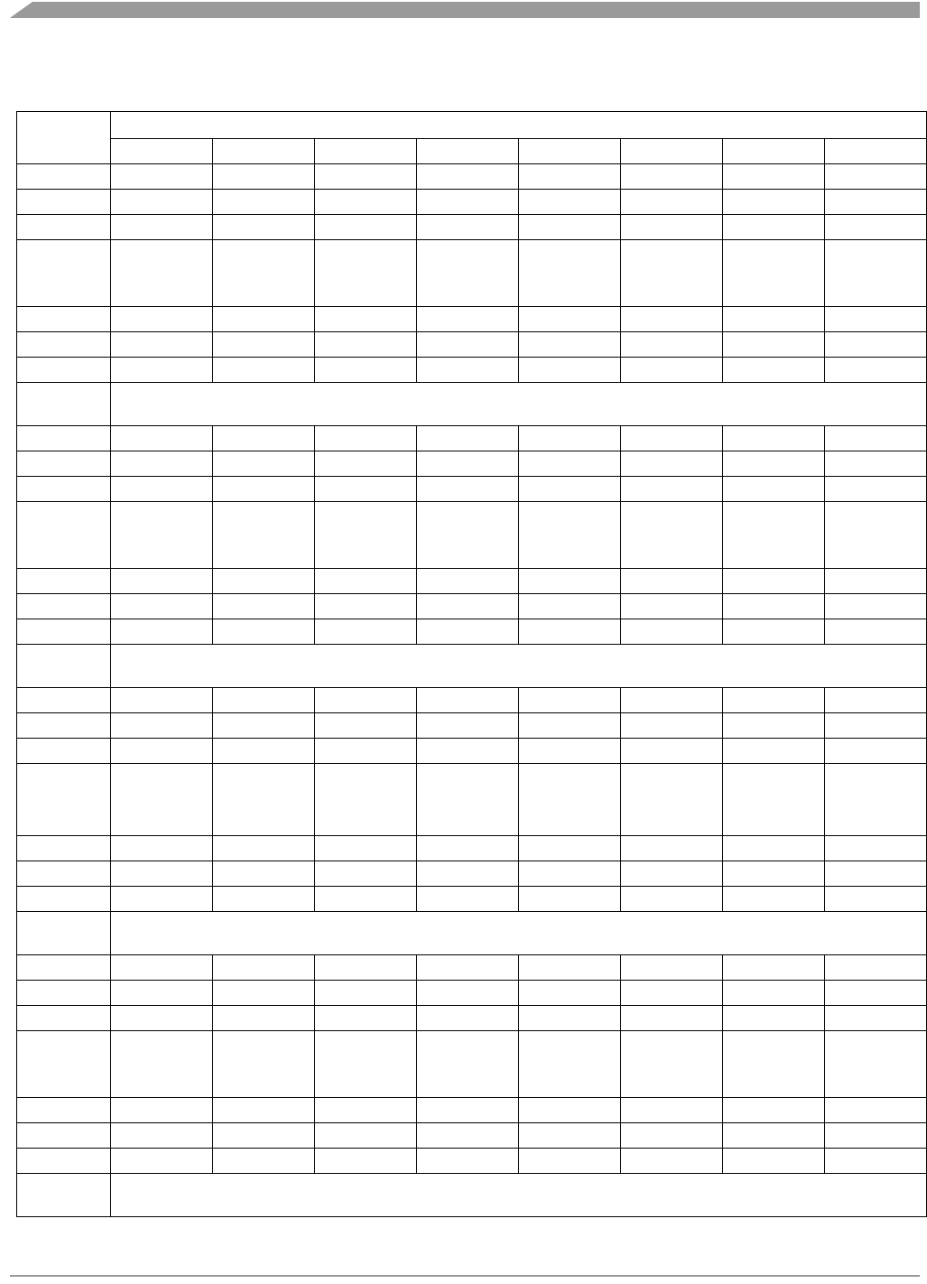
Liquid Crystal Display Driver (LCD)
MC68HC08LN56 • MC68HC708LN56 General Release Specification, Rev. 2.1
188 Freescale Semiconductor
Table 15-2. LCD RAM Memory Map
ADDR DATA
BIT 7 BIT 6 BIT 5 BIT 4 BIT 3 BIT 2 BIT 1 BIT 0
$0E00 FP0-BP7 FP0-BP6 FP0-BP5 FP0-BP4 FP0-BP3 FP0-BP2 FP0-BP1 FP0-BP0
$0E01 FP1-BP7 FP1-BP6 FP1-BP5 FP1-BP4 FP1-BP3 FP1-BP2 FP1-BP1 FP1-BP0
$0E02 FP2-BP7 FP2-BP6 FP2-BP5 FP2-BP4 FP2-BP3 FP2-BP2 FP2-BP1 FP2-BP0
.
.
.
.
.
.
.
.
.
.
.
.
.
.
.
.
.
.
.
.
.
.
.
.
.
.
.
$0E25 FP37-BP7 FP37-BP6 FP37-BP5 FP37-BP4 FP37-BP3 FP37-BP2 FP37-BP1 FP37-BP0
$0E26 FP38-BP7 FP38-BP6 FP38-BP5 FP38-BP4 FP38-BP3 FP38-BP2 FP38-BP1 FP38-BP0
$0E27 FP39-BP7 FP39-BP6 FP39-BP5 FP39-BP4 FP39-BP3 FP39-BP2 FP39-BP1 FP39-BP0
$0E28–
$0E7F Reserved for Future Expansion
$0E80 FP0-BP15 FP0-BP14 FP0-BP13 FP0-BP12 FP0-BP11 FP0-BP10 FP0-BP9 FP0-BP8
$0E81 FP1-BP15 F1-BP14 FP1-BP13 FP1-BP12 FP1-BP11 FP1-BP10 FP1-BP9 FP1-BP8
$0E82 FP2-BP15 F2-BP14 FP2-BP13 FP2-BP12 FP2-BP11 FP2-BP10 FP2-BP9 FP2-BP8
.
.
.
.
.
.
.
.
.
.
.
.
.
.
.
.
.
.
.
.
.
.
.
.
.
.
.
$0EA5 FP37-BP15 FP37-BP14 FP37-BP13 FP37-BP12 FP37-BP11 FP37-BP10 FP37-BP9 FP37-BP8
$0EA6 FP38-BP15 FP38-BP14 FP38-BP13 FP38-BP12 FP38-BP11 FP38-BP10 FP38-BP9 FP38-BP8
$0EA7 FP39-BP15 FP39-BP14 FP39-BP13 FP39-BP12 FP39-BP11 FP39-BP10 FP39-BP9 FP39-BP8
$0EA8–
$0EFF Reserved for Future Expansion
$0F00 FP0-BP23 FP0-BP22 FP0-BP21 FP0-BP20 FP0-BP19 FP0-BP18 FP0-BP17 FP0-BP16
$0F01 FP1-BP23 FP1-BP22 FP1-BP21 FP1-BP20 FP1-BP19 FP1-BP18 FP1-BP17 FP1-BP16
$0F02 FP2-BP23 FP2-BP22 FP2-BP21 FP2-BP20 FP2-BP19 FP2-BP18 FP2-BP17 FP2-BP16
.
.
.
.
.
.
.
.
.
.
.
.
.
.
.
.
.
.
.
.
.
.
.
.
.
.
.
$0F25 FP37-BP23 FP37-BP22 FP37-BP21 FP37-BP20 FP37-BP19 FP37-BP18 FP37-BP17 FP37-BP16
$0F26 FP38-BP23 FP38-BP22 FP38-BP21 FP38-BP20 FP38-BP19 FP38-BP18 FP38-BP17 FP38-BP16
$0F27 FP39-BP23 FP39-BP22 FP39-BP21 FP39-BP20 FP39-BP19 FP39-BP18 FP39-BP17 FP39-BP16
$0F28–
$0F7F Reserved for Future Expansion
$0F80 FP0-BP31 FP0-BP30 FP0-BP29 FP0-BP28 FP0-BP27 FP0-BP26 FP0-BP25 FP0-BP24
$0F81 FP1-BP31 FP1-BP30 FP1-BP29 FP1-BP28 FP1-BP27 FP1-BP26 FP1-BP25 FP1-BP24
$0F82 FP2-BP31 FP2-BP30 FP2-BP29 FP2-BP28 FP2-BP27 FP2-BP26 FP2-BP25 FP2-BP24
.
.
.
.
.
.
.
.
.
.
.
.
.
.
.
.
.
.
.
.
.
.
.
.
.
.
.
$0FA5 FP37-BP31 FP37-BP30 FP37-BP29 FP37-BP28 FP37-BP27 FP37-BP26 FP37-BP25 FP37-BP24
$0FA6 FP38-BP31 FP38-BP30 FP38-BP29 FP38-BP28 FP38-BP27 FP38-BP26 FP38-BP25 FP38-BP24
$0FA7 FP39-BP31 FP39-BP30 FP39-BP29 FP39-BP28 FP39-BP27 FP39-BP26 FP39-BP25 FP39-BP24
$0FA8–
$0FFF Reserved for Future Expansion

LCD Operation
MC68HC08LN56 • MC68HC708LN56 General Release Specification, Rev. 2.1
Freescale Semiconductor 189
15.5 LCD Operation
Figure 15-3 through Figure 15-8 show the backplane waveforms and some examples of frontplane
waveforms. Each on segment must have a high enough differential driving voltage (BP-FP) applied to it
once in each frame. The LCD driver module hardware uses the data in the LCD RAM to construct the
frontplane waveforms. The backplane waveforms are not affected by the data in the LCD RAM. During
wait mode, the LCD drivers function normally and will keep the display active if the DISON bit in the LCD
control register is set. During stop mode, the DISON bit should be turned off to allow all the frontplane and
backplane drivers to drive to VSS.
15.6 LCD Waveforms
The LCD waveforms are generated using multiple analog voltage levels to yield an on RMS voltage or off
RMS voltage at the intersection of each frontplane and backplane driver. The RMS voltage is defined to
be:
A frame consists of two fields. Field 1 and field 2 represent identical data at complimentary polarities to
obtain a 0 V average DC value required by the display crystal. During each field, the backplanes are
consecutively asserted. A more common style of backplane waveforms has a backplane switching to its
complementary value before the next backplane is asserted, which results in more switching and power
consumption. The field/frame approach is preferred for this reason. If data in the LCD RAM is not
changed, the same waveforms will be generated each frame.
In this section multiple examples showing the appropriate waveforms are presented.
VRMS
1
T
--- f 2(t)dt
∫
=
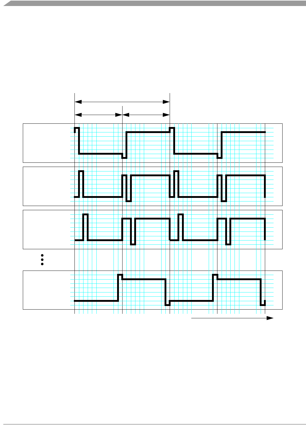
Liquid Crystal Display Driver (LCD)
MC68HC08LN56 • MC68HC708LN56 General Release Specification, Rev. 2.1
190 Freescale Semiconductor
15.6.1 Backplane Waveform
The backplane waveform is a periodic waveform that does not depend on the data to be displayed. For
32 backplanes that are multiplexed in time, each backplane driver waveform will have 1/64 of a frame
period at VLL7 in field 1, and 1/64 of a frame period at VSS in field 2 as shown in Figure 15-3. This is its
“active” time. The remaining 62/64 of the frame period is divided between VLL1 in field 1 and VLL6 in field 2.
Figure 15-3. Backplane (BP) Waveforms (1/32 Duty)
VSS
VLL6
VSS
VLL6
VSS
VLL6
VSS
VLL6
1/32 DUTY
VLL7
VLL1
BP0
1 FRAME
VLL7
VLL1
BP1
VLL7
VLL1
BP2
VLL7
VLL1
BP31
TIME
BP0
BP1
BP2
BP3
BP4
BP30
BP31
BP0
BP1
BP2
BP3
BP4
BP30
BP31
FIELD 1 FIELD 2
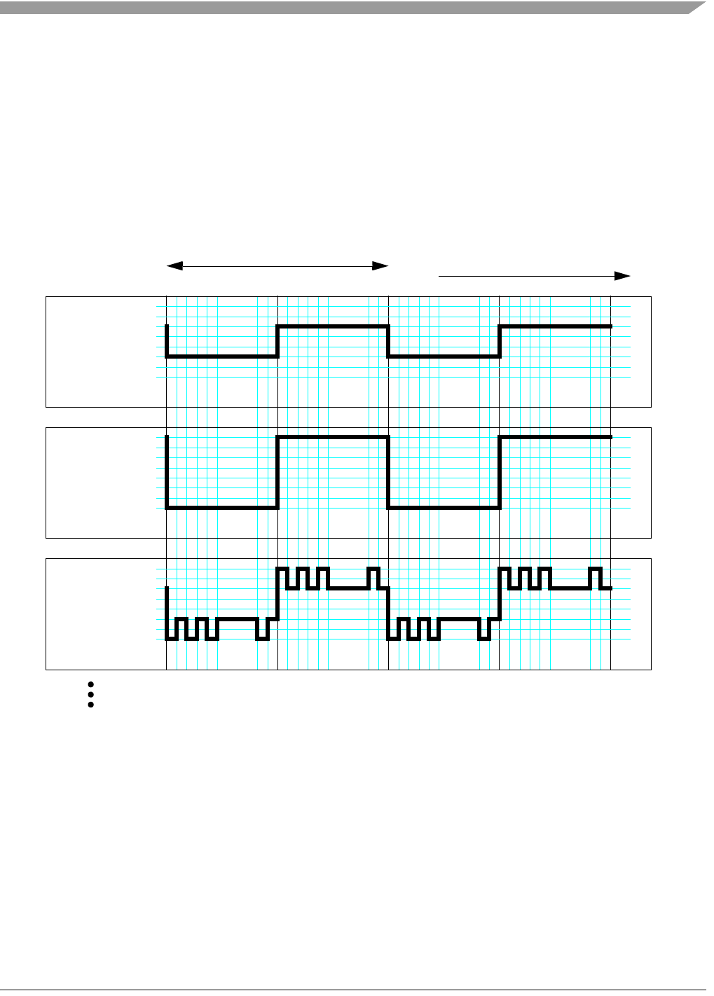
LCD Waveforms
MC68HC08LN56 • MC68HC708LN56 General Release Specification, Rev. 2.1
Freescale Semiconductor 191
15.6.2 Frontplane Waveform
The frontplane waveform is a periodic waveform that depends on the data to be displayed stored in the
RAM. For 32 backplanes that are multiplexed in time, each frontplane driver waveform will have 1/64 of
a frame period at VSS in field 1 and 1/64 of a frame period at VLL7 in field 2 for each segment that is on
and 1/64 of a frame period of VLL2 in field 1 and 1/64 of a frame period of VLL5 in field 2 for each segment
that is off, as shown in Figure 15-4.
Figure 15-4. Example Frontplane (FP) Waveforms (1/32 Duty)
1/32 DUTY
1 FRAME
TIME
VLL7
VLL5
VLL2
VSS
FP1
VLL7
VLL5
VLL2
VSS
FP0
VLL7
VLL5
VLL2
VSS
FP2
0
1
2
3
4
30
31
0
1
2
3
4
30
31
00000 0000000 0
11111 1111111 11
10 0 011 1100 011 1
DATA
DATA
DATA
0
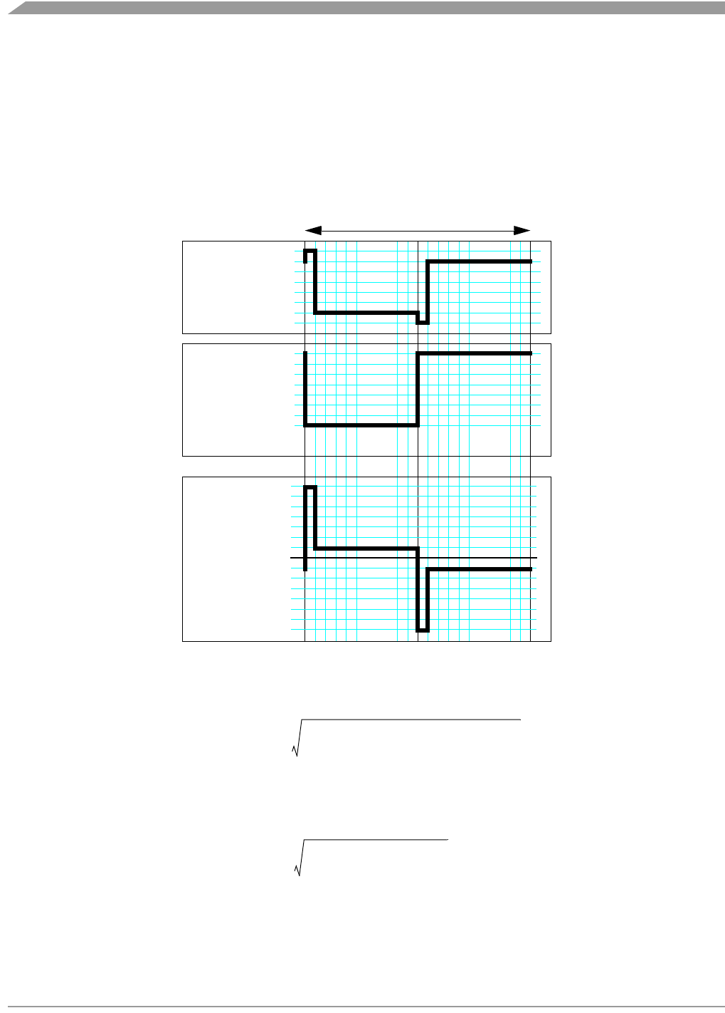
Liquid Crystal Display Driver (LCD)
MC68HC08LN56 • MC68HC708LN56 General Release Specification, Rev. 2.1
192 Freescale Semiconductor
15.6.3 Example Segment Waveforms and RMS Values
The voltage across a pixel (segment) of an LCD panel is the difference between the backplane (BP) and
the frontplane (FP) driver voltages where they intersect.
As an example, the waveforms for FP data of all ones and the voltage waveform for the segment at
BP0/FPx are shown in Figure 15-5.
Figure 15-5. LCD Waveforms Example for Data of 11...11111
The RMS voltage at the intersection of BP0 and FPx of Figure 15-5 is
Using VLL7 = 7.0 V and VLL1 = 1.0 V, the RMS voltage at the intersection of BP0 and FPx of Figure 15-5
will be
Thus, the segment at the intersection of BP0 and FPx should be turned on.
VSS
- VLL1
VSS
VLL6
VLL7
VLL1
BP0
VLL7
VLL5
VLL2
VSS
FPX
11...11111
VLL7
VLL5
VLL1
- VLL5
- VLL7
BP0–FPX
1 FRAME
1/32 DUTY
DATA 1 1 1 111 1111 111 1
VRMSA1
1
64
------ V L L 7 22 VLL1262Þ+Þ()Þ=
VRMSA1
1
64
------ 7221
262⋅+⋅()⋅1.5811V≈=
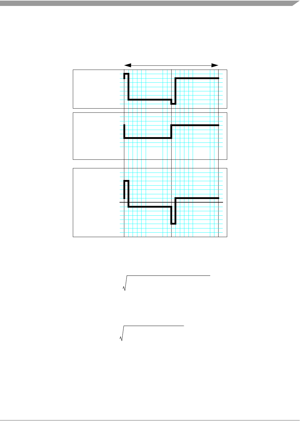
LCD Waveforms
MC68HC08LN56 • MC68HC708LN56 General Release Specification, Rev. 2.1
Freescale Semiconductor 193
Waveforms for FP data of all zeros and the voltage waveform for the segment at BP0/FPx are in Figure
15-6.
Figure 15-6. LCD Waveforms Example for Data of 00...00000
The RMS voltage at the intersection of BP0 and FPx of Figure 15-6 is
Using VLL5 = 5.0 V and VLL1 = 1.0 V, the RMS voltage at the intersection of BP0 and FPx of Figure 15-6
will be
Thus, the segment at the intersection of BP0 and FPx should be turned off.
VLL7
VLL6
VLL1
VSS
BP0
VLL7
VLL5
VLL2
VSS
FPX
00...00000
VLL7
VLL5
VLL1
VSS
- VLL1
- VLL5
- VLL7
BP0 - FPX
1 FRAME
1/32 DUTY
DATA 0 0 0 000 0000 000 0
VRMSA0
1
64
------ VLL522 VLL1262⋅+⋅()⋅=
VRMSA0
1
64
------ 5221
262⋅+⋅()⋅1.3229V≈=
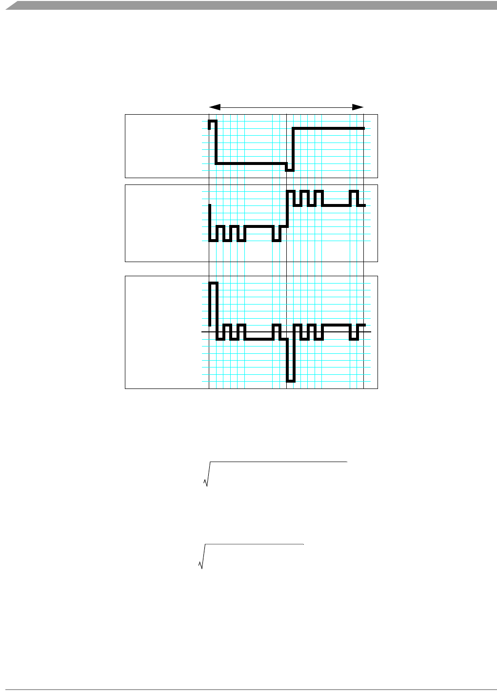
Liquid Crystal Display Driver (LCD)
MC68HC08LN56 • MC68HC708LN56 General Release Specification, Rev. 2.1
194 Freescale Semiconductor
Waveforms for FP data of alternating ones and zeros and the voltage waveform for the segment at
BP0/FPx are shown in Figure 15-7 and for the segment at BP1/FPx are shown in Figure 15-8.
Figure 15-7. LCD Waveforms Example for BP0 and
FP Data of 01...10101
The RMS voltage at the intersection of BP0 and FPx of Figure 15-7 is
Using VLL7 = 7.0 V and VLL1 = 1.0 V, the RMS voltage at the intersection of BP0 and FPx of Figure 15-7
will be
Thus, the segment at the intersection of BP0 and FPx should be turned on.
VLL7
VLL6
VLL1
VSS
BP0
VLL7
VLL5
VLL2
VSS
FPX
VLL7
VLL5
VLL1
VSS
- VLL1
- VLL5
- VLL7
BP0–FPX
1 FRAME
1/32 DUTY
10 0 011 1DATA 1 0 0 011 1
VRMST
1
64
------ VLL722 VLL1262⋅+⋅()⋅=
VRMST
1
64
------ 7221
262⋅+⋅()⋅1.5811V≈=
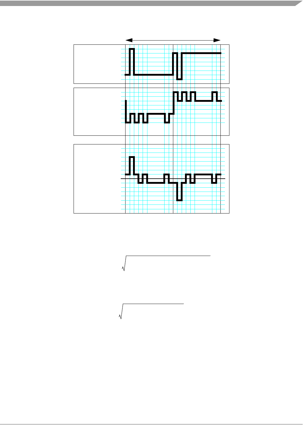
LCD Waveforms
MC68HC08LN56 • MC68HC708LN56 General Release Specification, Rev. 2.1
Freescale Semiconductor 195
Figure 15-8. LCD Waveforms Example for BP 1 and
FP Data of 01...10101
The RMS voltage at the intersection of BP1 and FPx of Figure 15-8 is
Using VLL5 = 5.0 V and VLL1 = 1.0 V, the RMS voltage at the intersection of BP1 and FPx of Figure 15-8
will be
Thus, the segment at the intersection of BP1 and FPx should be turned off.
NOTE
The difference in on and off voltages is only 0.258 V in this example. Only
the “active” time voltage determines the difference between the on and off
voltage. The voltages during the non-active time always contribute the
same amount to the total RMS voltage.
As another example, the waveforms for FP2 data to display the character A are shown in Figure 15-9.
The differential voltage for the BP4-FP2 pixel is shown.
VLL7
VLL6
VLL1
VSS
BP1
VLL7
VLL5
VLL2
VSS
FPX
VLL7
VLL5
VLL1
VSS
- VLL1
- VLL5
- VLL7
BP1 - FPX
1 FRAME
1/32 DUTY
10 0 011 1DATA 1 0 0 011 1
VRMST
1
64
------ VLL522 VLL1262⋅+⋅()⋅=
VRMST
1
64
------ 5221
262⋅+⋅()⋅1.3229V≈=
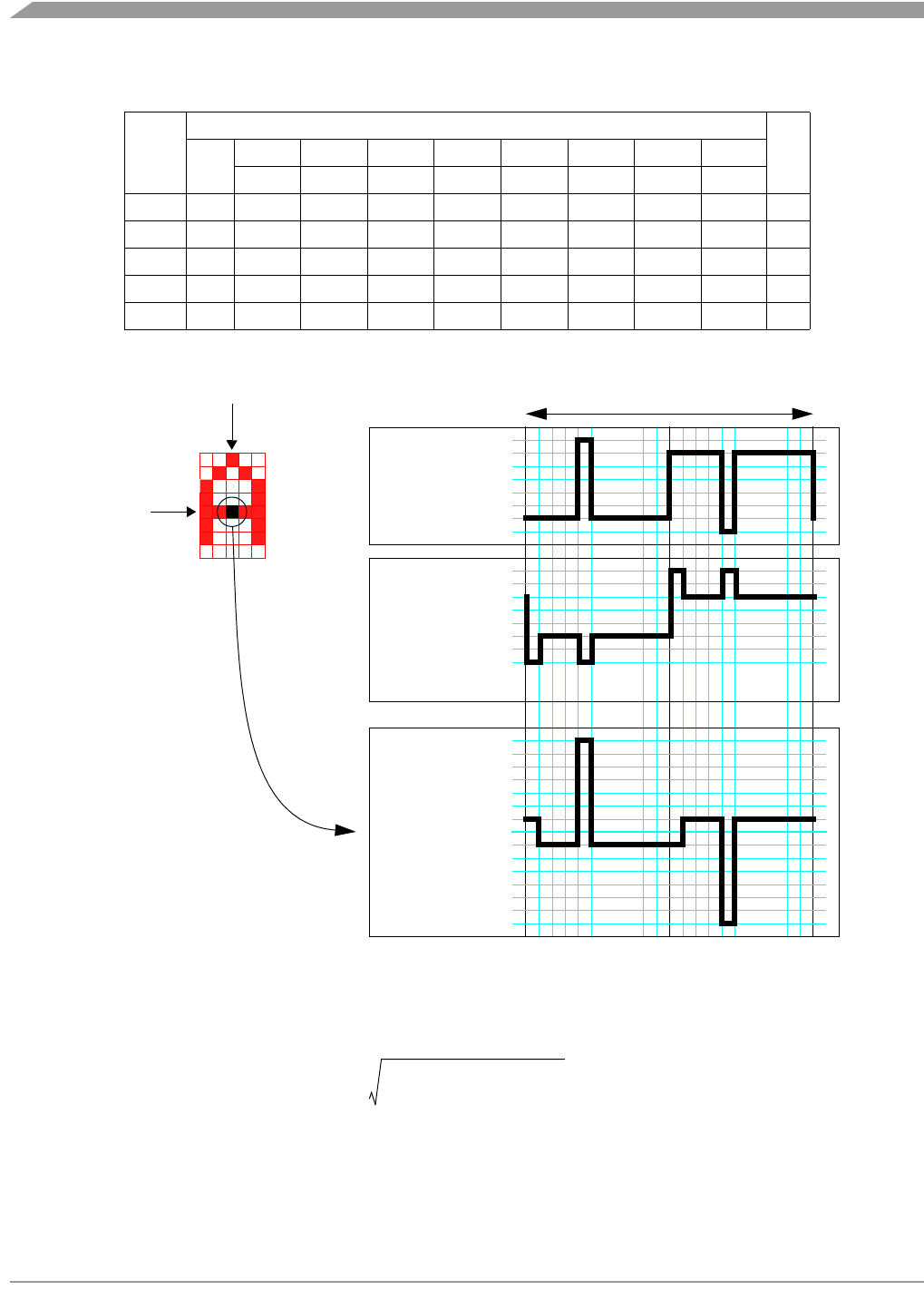
Liquid Crystal Display Driver (LCD)
MC68HC08LN56 • MC68HC708LN56 General Release Specification, Rev. 2.1
196 Freescale Semiconductor
Figure 15-9. LCD Waveform Example for Data of 00010001, Contents of $0E02
Using VLL7 = 7.0 V and VLL1 = 1.0 V, the RMS voltage at the intersection of BP4 and FP2 of Figure 15-9
will be
Table 15-3. LCD RAM Organization Example
Addr
Data
FP
Hex BP7 BP6 BP5 BP4 BP3 BP2 BP1 BP0
Bit 7 Bit 6 Bit 5 Bit 4 Bit 3 Bit 2 Bit 1 Bit 0
$0E00$7C01111100FP0
$0E01$1200010010FP1
$0E02$1100010001FP2
$0E03$1200010010FP3
$0E04$7C01111100FP4
BP0
BP1
BP2
BP3
BP4
BP5
FP0
FP1
FP2
FP3
FP4
FP5
VLL7
VLL6
VLL1
VSS
BP4
VLL7
VLL5
VLL2
VSS
FP2
VLL7
VLL5
VLL1
VSS
- VLL1
- VLL5
- VLL7
BP4 - FP2
1 FRAME
1/32 DUTY
10 0 001 0100 001 0
VRMST
1
64
------ 7221
262⋅+⋅()⋅1.5811V≈=

LCD Voltage Generation
MC68HC08LN56 • MC68HC708LN56 General Release Specification, Rev. 2.1
Freescale Semiconductor 197
15.6.4 RMS Voltages
The RMS voltages for the waveforms shown in the examples are generalized with this formula:
15.7 LCD Voltage Generation
The actual LCD analog voltages for the frontplane and backplane waveforms (shown in Table 15-5) are
generated by a charge pump, which uses external capacitors for charge storing and switching. A diagram
indicating external capacitance values for the charge pump is shown in Figure 15-10.
Upon power-up of the chip, the absolute value of the LCD charge pump voltage levels will be set as a
result of the reset condition of the LCD contrast control register (LCDCCR). The LCD system can be
disabled and have all frontplane and backplane drivers driven to VSS by clearing the DISON bit in the LCD
control register.
Figure 15-11 illustrates a conceptual block diagram of a resistive divider chain network used to produce
the various LCD waveforms outlined in the previous section. Software control of the contrast can be
accomplished by measurement of the supply voltage with the ADC, and based on this reading, selecting
the appropriate resistors by programming the contrast control bits (CC5:CC0) in the LCD contrast control
register (LCDCCR).
The SUPV bit in the LCD control register should also be programmed accordingly for 3 V or 5 V nominal
operation. The accuracy of this setting is determined by the accuracy of the reference voltage used by the
ADC as well as the quantization error due to the ADC and that of the digital-to-analog conversion done
by the contrast control circuitry. It is recommended that some means of manual contrast control
adjustment be available to the user of the system containing the microcontroller to achieve the desired
visual contrast on the LCD. Software controlled periodic adjustments of the contrast control register can
then be performed, combining the ADC reading of the supply with the manual user adjustment, into a
single value used in the LCD contrast control register (LCDCCR).
NOTE
For 5 V operation, set SUPV = 1, for 3 V operation SUPV = 0.
15.7.1 LCD Contrast Control
Contrast of the LCD display can be adjusted by setting the LCD contrast control register (LCDCCR). For
a desired value of VLL7, the following equation determines the decimal value to which the register should
be set.
VRMSON
1
64
------ 7
7
---VLL7⋅
⎝⎠
⎛⎞
221
7
---VLL7⋅
⎝⎠
⎛⎞
262⋅+⋅
⎝⎠
⎛⎞
⋅10
14
---------- VLL7⋅==
VRMSOFF
1
64
------ 5
7
---VLL7⋅
⎝⎠
⎛⎞
221
7
---VLL7⋅
⎝⎠
⎛⎞
262⋅+⋅
⎝⎠
⎛⎞
⋅7
14
------- VLL7⋅==
CC RND VLL7
VDD
---------------47.143 SUPV 94.286+⋅()160–
⎝⎠
⎛⎞
=
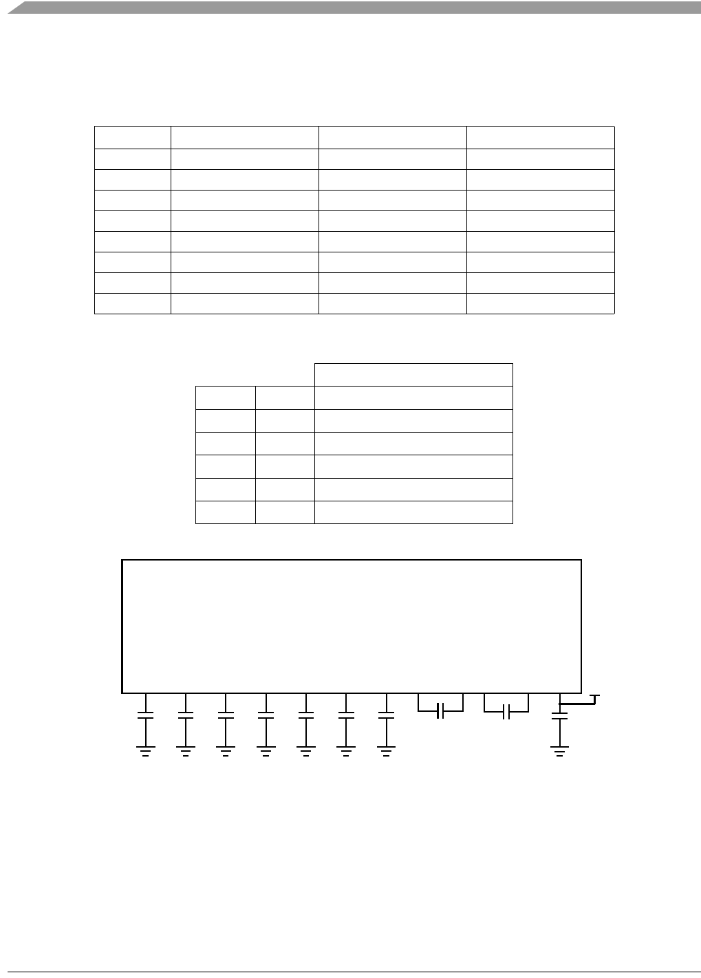
Liquid Crystal Display Driver (LCD)
MC68HC08LN56 • MC68HC708LN56 General Release Specification, Rev. 2.1
198 Freescale Semiconductor
For the allowed range of top voltages, Table 15-4 lists the VRMSON, VRMSOFF, and the difference between
them. This should be matched to the corresponding requirements of the LCD panel.
Figure 15-10. Charge Pump Capacitor Connection Diagram
Table 15-4. LCD RMS Voltages (1/7 bias)
VLL7 (V) VRMSON (V) VRMSOFF (V) VDIFF (V)
6.3 1.4230 1.1906 0.2324
6.4 1.4456 1.2095 0.2361
6.5 1.4682 1.2284 0.2398
6.6 1.4908 1.2473 0.2435
6.7 1.5134 1.2662 0.2472
6.8 1.5360 1.2851 0.2509
6.9 1.5586 1.3040 0.2546
7.0 1.5811 1.3229 0.2583
Table 15-5. LCD Voltages
VLL7 = 7.0 V, 1/7 Bias
VLL7 7/7 7.0 V
VLL6 6/7 6.0 V
VLL5 5/7 5.0 V
VLL2 2/7 2.0 V
VLL1 1/7 1.0 V
VSS 0/7 0.0 V
CHARGE PUMP PINS
VLL7 VLL6 VLL5 VLLH
VLL2 VLL1
CPFLT VLL
VCP1 VCP2 VCP3 VCP4
0.22 µF0.1 µF 0.22 µF0.1 µF0.1 µF0.1 µF0.1 µF0.1 µF0.01 µF0.1 µF
VDD
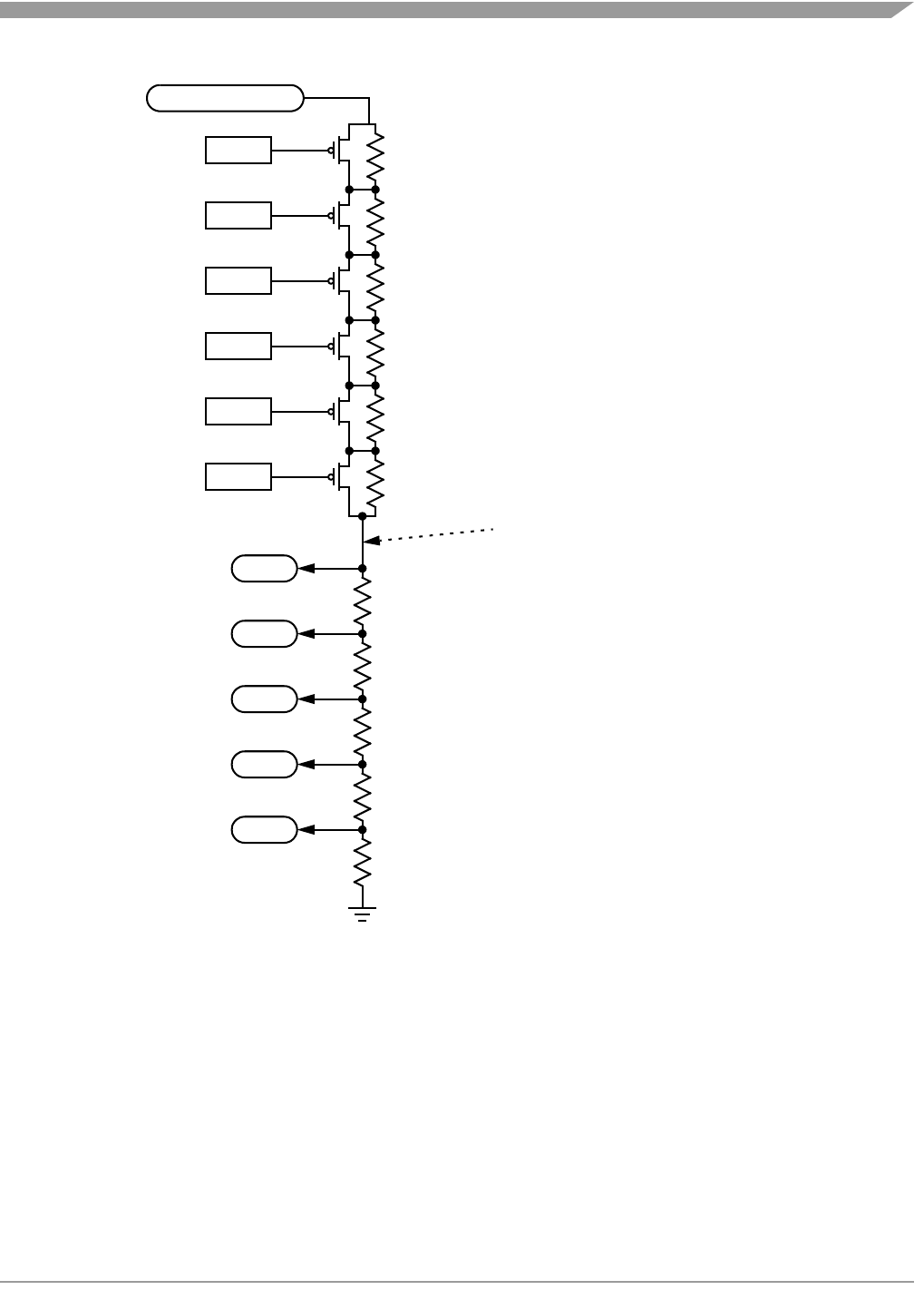
LCD Register Programming
MC68HC08LN56 • MC68HC708LN56 General Release Specification, Rev. 2.1
Freescale Semiconductor 199
Figure 15-11. Contrast Control Conceptual Block Diagram
15.8 LCD Register Programming
A frame consists of two complimentary fields. Thus, the frame frequency is 1/2 that of the field frequency.
See Figure 15-3 for the relationship of field and frame to the waveforms.
CGMXCLK provides the clock from which the LCD timing is derived. The prescaler bits (DIV6:DIV0) and
the prescaler enable bit (PE) in the LCD prescaler divider register (LCDDIV) are provided to adjust for
various CGMXCLK frequencies. They should be programmed to provide a reference clock of
approximately 32.768 kHz for the charge pump. If CGMXCLK frequency is 32.768 kHz, PE should be
cleared to allow CGMXCLK to become the charge pump clock. If CGMXCLK is much higher, then PE
32 RCC
16 RCC
8 RCC
4 RCC
2 RCC
1 RCC
RL
RL
3 RL
RL
RL
VLL7
VLL6
VLL5
VLL2
VLL1
CC0
CC1
CC2
CC3
CC4
CC5
2 VDD OR 3 VDD
VARIABLE BETWEEN 6.3 V — 7.0 V
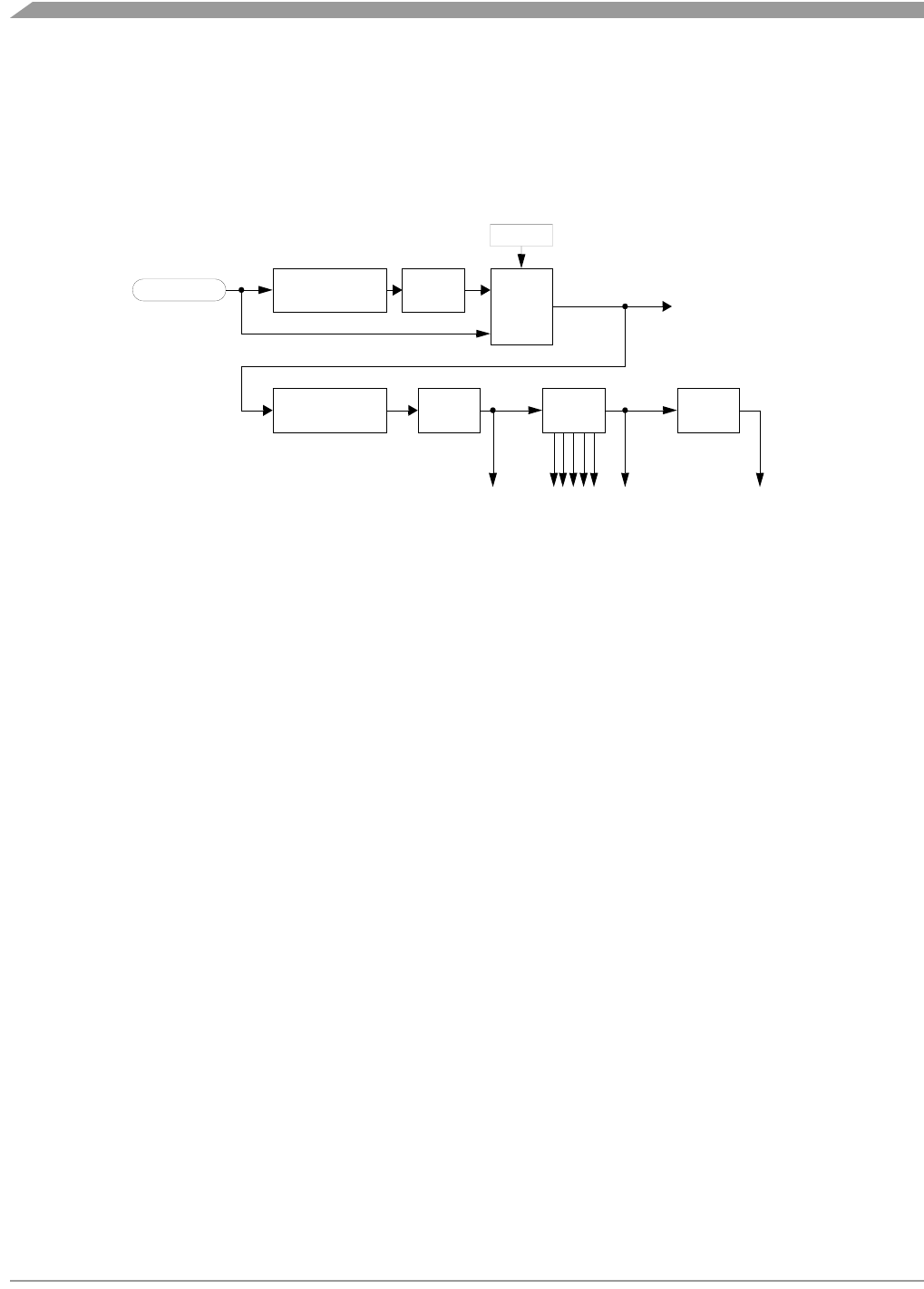
Liquid Crystal Display Driver (LCD)
MC68HC08LN56 • MC68HC708LN56 General Release Specification, Rev. 2.1
200 Freescale Semiconductor
should be set to enable the 7-bit programmable divider which is further divided by 4 to control the
reference clock. This allows for a maximum CGMXCLK frequency of approximately 16.6 MHz. See Figure
15-12.
The frame rate bits (FR3:FR0) in the LCD frame rate register (LCDFR) are provided to select an
appropriate frame/field rate. See Table 15-6.
Figure 15-12. LCD Frame Frequency Block Diagram
15.9 Programming the LCD
The LCD prescaler divider register (LCDDIV) should be set according to the following formula in order to
produce a charge pump frequency of 32.768 kHz.
where CPF is the charge pump frequency, CGMXCLK is the OSC1 (crystal) frequency; PE is the prescale
enable bit in LCDDIV, and DIV is the 7-bit divider.
For example if CGMXCLK = 5.12 MHz, PE should be set and DIV = 39. If CGMXCLK = 32.768 kHz, PE
should be cleared and the DIV bits will be disregarded.
NOTE
For correct operation, program PE and DIV[6:0] bits such that the charge
pump clock is approximately 32.768 KHz for a given CGMXCLK (crystal)
frequency.
The LCD frame rate register (LCDFR) should be set according to the following formula.
where CGMXCLK is the OSC1 (crystal) frequency; PE is the prescale enable bit in LCDDIV, DIV is the
7-bit divider, and FRAME is the desired frame rate.
Some examples of programmed frame frequencies are listed in Table 15-6.
³ DIV[6:0]
÷ 2
FIELD
FRAME
÷ 32÷ 2
CGMXCLK ÷ 4
PE
BACKPLANE
SEL
1
0
³ FR [3:0]
CHARGE PUMP CLOCK
≈ 32 kHz
SELECTS
BACKPLANE
CLOCK
DIV RND CGMXCLK
CPF 4 PE⋅⋅
---------------------------------
⎝⎠
⎛⎞
=
LCDFR CGMXCLK
DIV 4 PE⋅⋅()1PE–()+()FRAME 128⋅⋅
---------------------------------------------------------------------------------------------------------------
=
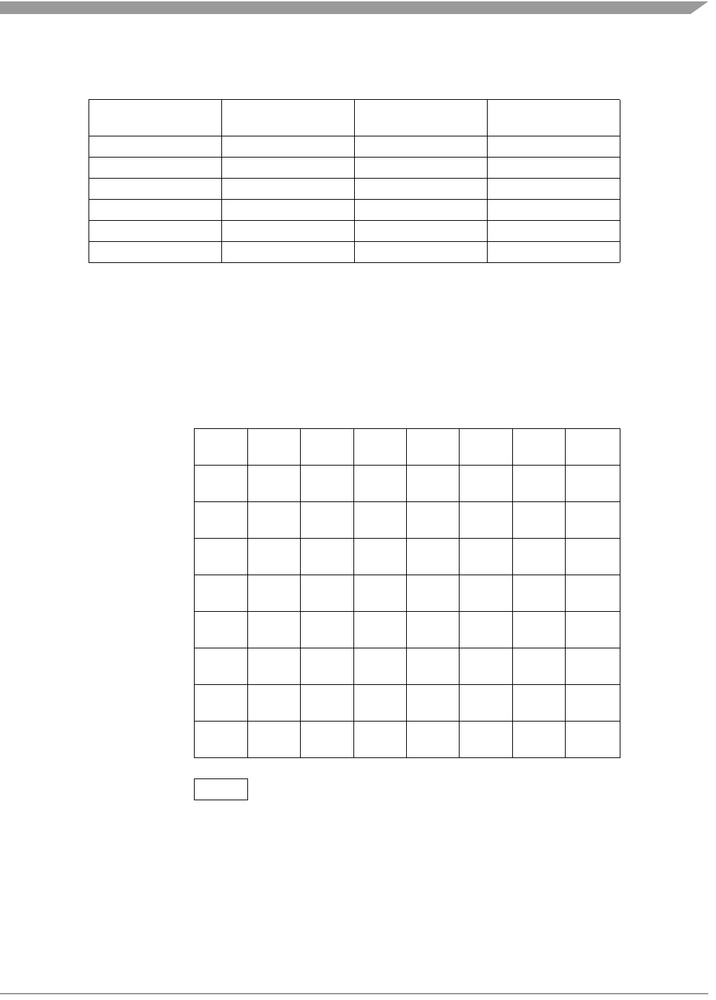
LCD Registers
MC68HC08LN56 • MC68HC708LN56 General Release Specification, Rev. 2.1
Freescale Semiconductor 201
15.10 LCD Registers
There are nine LCD registers. Four are control type registers: LCD control register (LCDCR), LCD
prescaler divider register (LCDDIV), LCD frame rate register (LCDFR), and LCD contrast control register
(LCDCCR). Five are read-only frontplane latch registers (LCDFL0:LCDFL4) that contain a latched version
of the frontplane data for the 40 frontplane drivers. Figure 15-13 shows a summary of the registers.
Table 15-6. Example LCD Field/Frame Frequencies Assuming
a Charge Pump Clock of 32.768 kHz
FR[3:0] Divider Frame
Frequency (Hz)
Field
Frequency (Hz)
0100 4 64 128
0101 5 51.2 102.4
0110 6 42.67 85.3
0111 7 36.57 73.1
1000 8 32 64
1001 9 28.4 56.9
Register Name Bit 7 6 5 4 3 2 1 Bit 0 Addr.
LCD Frontplane Latch 0
(LCDFL0) FP7 FP6 FP5 FP4 FP3 FP2 FP1 FP0 $0033
LCD Frontplane Latch 1
(LCDFL1) FP15 FP14 FP13 FP12 FP11 FP10 FP9 FP8 $0034
LCD Frontplane Latch 2
(LCDFL2) FP23 FP22 FP21 FP20 FP19 FP18 FP17 FP16 $0035
LCD Frontplane Latch 3
(LCDFL3) FP31 FP30 FP29 FP28 FP27 FP26 FP25 FP24 $0036
LCD Frontplane Latch 4
(LCDFL4) FP39 FP38 FP37 FP36 FP35 FP34 FP33 FP32 $0037
LCD Control Register
(LCDCR) DISONSUPVRRRRRR$0038
LCD Contrast Control Register
(LCDCCR) R R CC5 CC4 CC3 CC2 CC1 CC0 $0039
LCD Prescaler/Divider Register
(LCDDIV) PE DIV6 DIV5 DIV4 DIV3 DIV2 DIV1 DIV0 $003A
LCD Frame Rate Register
(LCDFR) 0 0 0 0 FR3 FR2 FR1 FR0 $003B
R = Reserved
Figure 15-13. LCD Register Summary
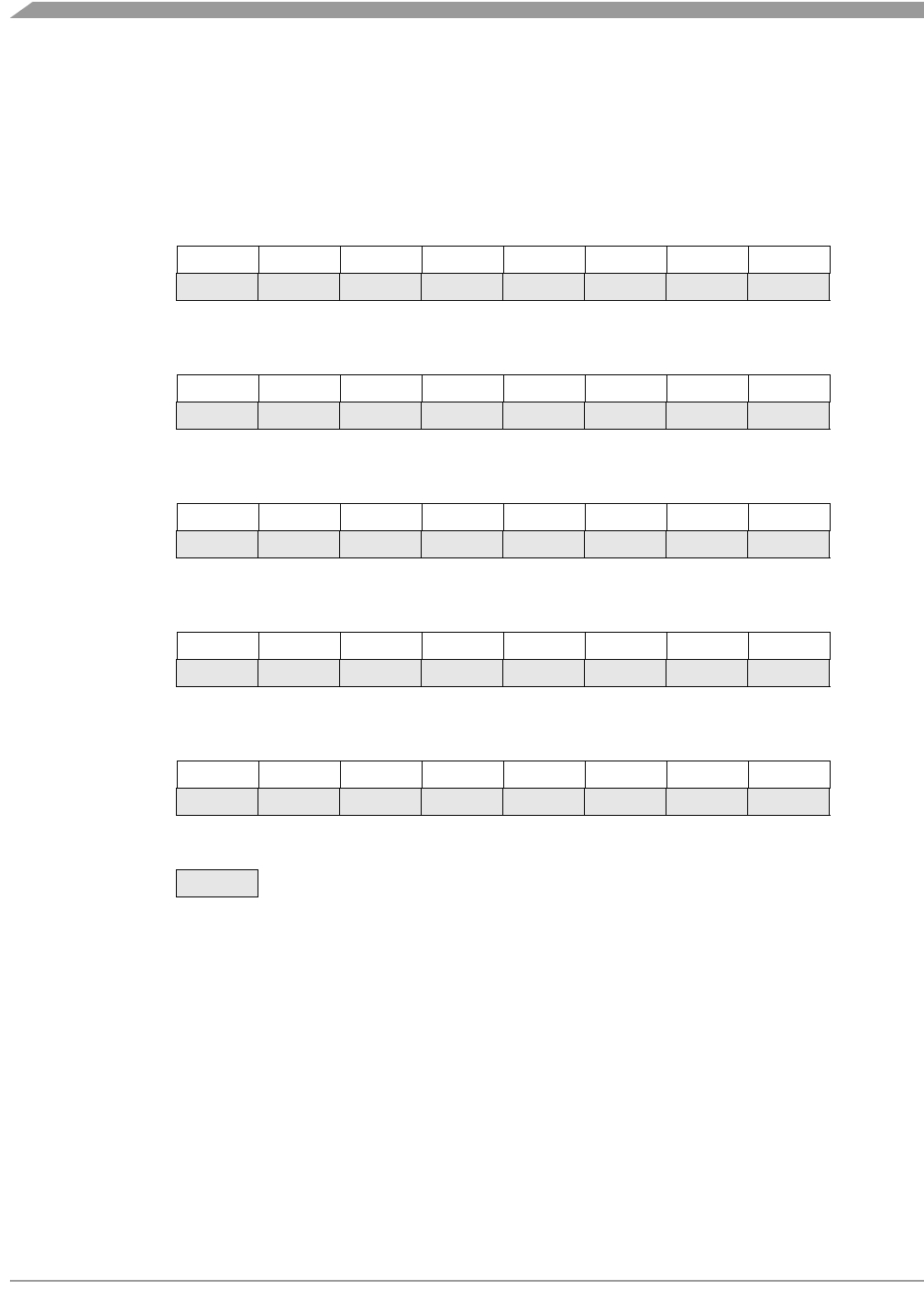
Liquid Crystal Display Driver (LCD)
MC68HC08LN56 • MC68HC708LN56 General Release Specification, Rev. 2.1
202 Freescale Semiconductor
15.10.1 LCD Frontplane Latch Registers (LCDFLx)
These read-only registers are a latched version of the frontplane data outputs from the LCD RAM for the
current backplane. This is provided for debug purposes and is not meant to be part of any user software
routine. These registers are reset to all zeros.
LCDFL0
$0033Bit 7654321Bit 0
Read: FP7 FP6 FP5 FP4 FP3 FP2 FP1 FP0
Write:
Reset:00000000
LCDFL1
$0034Bit 76554321Bit 0
Read: FP15 FP14 FP13 FP12 FP11 FP10 FP9 FP8
Write:
Reset:00000000
LCDFL2
$0035Bit 7654321Bit 0
Read: FP23 FP22 FP21 FP20 FP19 FP18 FP17 FP16
Write:
Reset:00000000
LCDFL3
$0036Bit 7654321Bit 0
Read: FP31 FP30 FP29 FP28 FP27 FP26 FP25 FP24
Write:
Reset:00000000
LCDFL4
$0037Bit 7654321Bit 0
Read: FP39 FP38 FP37 FP36 FP35 FP34 FP33 FP32
Write:
Reset:00000000
= Unimplemented
Figure 15-14. LCD Frontplane Latches
LCD Registers
MC68HC08LN56 • MC68HC708LN56 General Release Specification, Rev. 2.1
Freescale Semiconductor 203
15.10.2 LCD Control Register
DISON — LCD Display on Bit
This bit enables the charge pump and the driver timing logic and will enable the drivers when valid data
is latched from the RAM. If the LCD driver logic is disabled, the charge pump is turned off and the
timing logic is shut off to save power, and all the frontplane and backplane pins are driven at VSS. This
bit should be turned off prior to entering stop mode to prevent an average DC voltage from existing on
the FP and BP drivers for the duration of stop mode. Reset clears this bit.
1 = LCD display is enabled
0 = LCD display is disabled
SUPV — LCD Supply Voltage
This bit configures the charge pump appropriately based on a nominal VDD. Reset clears this bit.
1 = LCD nominal VDD = 5 V
0 = LCD nominal VDD = 3 V
15.10.3 LCD Contrast Control Register (LCDCCR)
CC5:CC0 — Contrast Contrast Control
These bits control the contrast control up to 64 levels.
LCDCR
$0038Bit 7654321Bit 0
Read:
DISONSUPVRRRRRR
Write:
Reset: 0 0
R = Reserved For Factory Test
Figure 15-15. LCD Control Register
LCDCCR
$0039 Bit 7654321Bit 0
Read:
R R CC5 CC4 CC3 CC2 CC1 CC0
Write:
Reset:00000000
R= Reserved
Figure 15-16. LCD Contrast Control Register
Table 15-7. LCD Contrast Control
CC[5:0] Contrast Control
111111 Highest VRMS Level
111110
. . .
00000 Lowest VRMS Level

Liquid Crystal Display Driver (LCD)
MC68HC08LN56 • MC68HC708LN56 General Release Specification, Rev. 2.1
204 Freescale Semiconductor
15.10.4 LCD Prescaler Divider Register (LCDDIV)
PE — Prescaler Enable
When this bit is set, the output of the 7-bit programmable divider which is further divided by 4 is used
as the charge pump reference clock and the input clock for generating the field and frame rates as
shown in Figure 15-12.
1 = Use XCLK/(DIV*4) as the reference clock source
0 = Use XCLK directly as the reference clock source
DIV6:DIV0 — LCD Prescaler Divider Ratio Selection
These bits can be programmed to provide a reference clock of approximately 32.768 kHz to the charge
pump and frame/field rate circuitry if PE = 1. If PE = 0, these bits are not used.
NOTE
Programming the prescale divider register with $00 when the PE bit is
enabled will result in the maximum divisible value with a 7-bit counter (=
128).
The LCD prescaler divider register should be configured and modified with
the LCD disabled (DISON = 0 in LCDCR).
15.10.5 LCD Frame Rate Register (LCDFR)
FR3:FR0 — LCD Frame Rate Selection
These bits can be programmed to select an appropriate field and frame rate. See Table 15-6. The
charge pump is optimized for a field frequency of 60 to 120 Hz. Therefore, this register should be
programmed accordingly.
NOTE
Programming the frame rate register with $00 is equivalent to division by
zero and will result in the maximum divisible value with a 4-bit counter = 16.
The LCD frame rate register should be configured and modified with the
LCD disabled (DISON = 0 in LCDCR).
LCDDIV
$003ABit 7654321Bit 0
Read:
PE DIV6 DIV5 DIV4 DIV3 DIV2 DIV1 DIV0
Write:
Reset:00000001
Figure 15-17. LCD Prescaler Divider Register
LCDFR
$003BBit 7654321Bit 0
Read:0000
FR3 FR2 FR1 FR0
Write:
Reset:00000001
= Unimplemented
Figure 15-18. LCD Frame Rate Register

Interrupts
MC68HC08LN56 • MC68HC708LN56 General Release Specification, Rev. 2.1
Freescale Semiconductor 205
15.11 Interrupts
The LCD module does not generate interrupts.
15.12 Low-Power Modes
The WAIT and STOP instructions put the MCU in low-power- consumption standby modes.
15.12.1 Wait Mode
The LCD remains active after the execution of a WAIT instruction but the LCD registers are not accessible
by the CPU. Therefore, the LCD RAM data cannot be modified. To make the LCD inactive in wait mode
(all FP/BP drivers drive VSS) the DISON bit in the LCD control register should be turned off prior to
executing the WAIT instruction.
15.12.2 Stop Mode
The LCD is inactive after execution of a STOP instruction because the STOP instruction halts the
oscillator. The STOP instruction does not affect register conditions. The DISON bit in the LCD control
register should be turned off prior to executing the STOP instruction to ensure that all FP/BP drivers
maintain a VSS level. This prevents an average DC offset voltage for the duration of stop mode.

Liquid Crystal Display Driver (LCD)
MC68HC08LN56 • MC68HC708LN56 General Release Specification, Rev. 2.1
206 Freescale Semiconductor
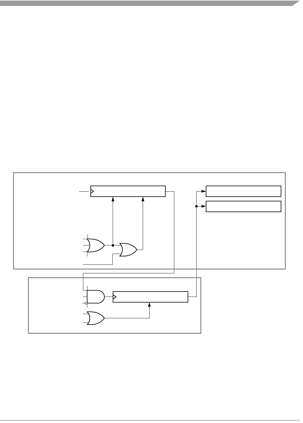
MC68HC08LN56 • MC68HC708LN56 General Release Specification, Rev. 2.1
Freescale Semiconductor 207
Chapter 16
Computer Operating Properly Module (COP)
16.1 Introduction
This section describes the computer operating properly module (COP, Version B), a free-running counter
that generates a reset if allowed to overflow. The COP module helps software recover from runaway code.
Prevent a COP reset by periodically clearing the COP counter.
16.2 Functional Description
Figure 16-1 shows the structure of the COP module.
Figure 16-1. COP Block Diagram
COPCTL WRITE
CGMXCLK
RESET VECTOR FETCH
SIM RESET CIRCUIT
SIM RESET STATUS REGISTER
INTERNAL RESET SOURCES(1)
STOP INSTRUCTION
SIM
CLEAR BITS 12–4
13-BIT SIM COUNTER
CLEAR ALL BITS
6-BIT COP COUNTER
COPD (FROM MOR)
RESET
COPCTL WRITE
CLEAR
COP MODULE
COPEN (FROM SIM)
COP COUNTER
NOTE:
1. See SIM section for more details.

Computer Operating Properly Module (COP)
MC68HC08LN56 • MC68HC708LN56 General Release Specification, Rev. 2.1
208 Freescale Semiconductor
The COP counter is a free-running 6-bit counter preceded by the 13-bit system integration module (SIM)
counter. If not cleared by software, the COP counter overflows and generates an asynchronous reset after
218 – 24 CGMXCLK cycles. With a 4.9152-MHz crystal, the COP timeout period is 53.3 ms. Writing any
value to location $FFFF before overflow occurs clears the COP counter and prevents reset.
A COP reset pulls the RST pin low for 32 CGMXCLK cycles and sets the COP bit in the SIM reset status
register (SRSR) (See SIM section for more details). Clear the COP immediately before entering or after
exiting stop mode to assure a full COP timeout period after entering or exiting stop mode. A CPU interrupt
routine or a DMA service routine can be used to clear the COP.
NOTE
Place COP clearing instructions in the main program and not in an interrupt
subroutine. Such an interrupt subroutine could keep the COP from
generating a reset even while the main program is not working properly.
16.3 I/O Signals
The following paragraphs describe the signals shown in Figure 16-1.
16.3.1 CGMXCLK
CGMXCLK is the crystal oscillator output signal. CGMXCLK frequency is equal to the crystal frequency.
16.3.2 STOP Instruction
The STOP instruction clears the SIM counter.
16.3.3 COPCTL Write
Writing any value to the COP control register (COPCTL) (See 16.4 COP Control Register (COPCTL))
clears the COP counter and clears bits 12 through 4 of the SIM counter. Reading the COP control register
returns the reset vector.
16.3.4 Power-On Reset
The power-on reset (POR) circuit in the SIM clears the SIM counter 4096 CGMXCLK cycles after
power-up.
16.3.5 Internal Reset
An internal reset clears the SIM counter and the COP counter.
16.3.6 Reset Vector Fetch
A reset vector fetch occurs when the vector address appears on the data bus. A reset vector fetch clears
the SIM counter.
16.3.7 COPD (COP Disable)
The COPD signal reflects the state of the COP disable bit (COPD) in the mask option register (MOR).
(See Chapter 19 Configuration Register (CONFIG) for more details.)

COP Control Register (COPCTL)
MC68HC08LN56 • MC68HC708LN56 General Release Specification, Rev. 2.1
Freescale Semiconductor 209
16.4 COP Control Register (COPCTL)
The COP control register is located at address $FFFF and overlaps the reset vector. Writing any value to
$FFFF clears the COP counter and starts a new timeout period. Reading location $FFFF returns the low
byte of the reset vector.
Figure 16-2. COP Control Register (COPCTL)
16.5 Interrupts
The COP does not generate CPU interrupt requests or DMA service requests.
16.6 Monitor Mode
The COP is disabled in monitor mode when VDD +V
HI is present on the IRQ1/VPP pin or on the RST pin.
16.7 Low-Power Modes
The WAIT and STOP instructions put the MCU in low-power- consumption standby modes.
16.7.1 Wait Mode
The COP continues to operate during wait mode. To prevent a COP reset during wait mode, periodically
clear the COP counter in a CPU interrupt routine or a DMA service routine.
16.7.2 Stop Mode
Stop mode turns off the CGMXCLK input to the COP and clears the SIM counter. Service the COP
immediately before entering or after exiting stop mode to ensure a full COP timeout period after entering
or exiting stop mode.
16.8 COP Module During Break Interrupts
The COP is disabled during a break interrupt when VDD +V
HI is present on the RST pin.
COPCTL
$FFFF Bit 7654321Bit 0
Read: Low Byte of Reset Vector
Write: Clear COP Counter
Reset: Unaffected by Reset

Computer Operating Properly Module (COP)
MC68HC08LN56 • MC68HC708LN56 General Release Specification, Rev. 2.1
210 Freescale Semiconductor

MC68HC08LN56 • MC68HC708LN56 General Release Specification, Rev. 2.1
Freescale Semiconductor 211
Chapter 17
Break Module (BREAK)
17.1 Introduction
This section describes the break module (Break, Version B). The break module can generate a break
interrupt that stops normal program flow at a defined address to enter a background program.
17.2 Features
Features of the break module include:
• Accessible I/O Registers during the Break Interrupt
• CPU-Generated Break Interrupts
• Software-Generated Break Interrupts
• COP Disabling during Break Interrupts
17.3 Functional Description
When the internal address bus matches the value written in the break address registers, the break module
issues a breakpoint signal (BKPT) to the SIM. The SIM then causes the CPU to load the instruction
register with a software interrupt instruction (SWI) after completion of the current CPU instruction. The
program counter vectors to $FFFC and $FFFD ($FEFC and $FEFD in monitor mode).
The following events can cause a break interrupt to occur:
• A CPU-generated address (the address in the program counter) matches the contents of the break
address registers.
• Software writes a logic one to the BRKA bit in the break status and control register.
When a CPU-generated address matches the contents of the break address registers, the break interrupt
begins after the CPU completes its current instruction. A return from interrupt instruction (RTI) in the break
routine ends the break interrupt and returns the MCU to normal operation. Figure 17-1 shows the structure
of the break module.
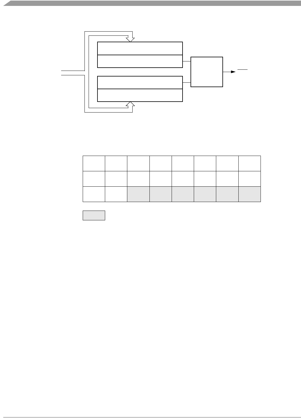
Break Module (BREAK)
MC68HC08LN56 • MC68HC708LN56 General Release Specification, Rev. 2.1
212 Freescale Semiconductor
Figure 17-1. Break Module Block Diagram
17.3.1 Flag Protection During Break Interrupts
The system integration module (SIM) controls whether or not module status bits can be cleared during
the break state. The BCFE bit in the SIM break flag control register (SBFCR) enables software to clear
status bits during the break state. (See 5.7.3 SIM Break Flag Control Register (SBFCR) and see the
Break Interrupts subsection for each module.)
17.3.2 CPU During Break Interrupts
The CPU starts a break interrupt by:
• Loading the instruction register with the SWI instruction
• Loading the program counter with $FFFC:$FFFD ($FEFC:$FEFD in monitor mode)
The break interrupt begins after completion of the CPU instruction in progress. If the break address
register match occurs on the last cycle of a CPU instruction, the break interrupt begins immediately.
17.3.3 TIM During Break Interrupts
A break interrupt stops the timer counter.
Register Name Bit 7654321Bit 0Addr.
Break Address Register High
(BRKH) Bit 15 14 13 12 11 10 9 Bit 8 $FE0C
Break Address Register Low
(BRKL) Bit 7654321Bit 0$FE0D
Break Status/Control Register
(BRKSCR) BRKE BRKA $FE0E
= Unimplemented
Figure 17-2. Break I/O Register Summary
IAB[15:8]
IAB[7:0]
8-BIT COMPARATOR
8-BIT COMPARATOR
CONTROL
BREAK ADDRESS REGISTER LOW
BREAK ADDRESS REGISTER HIGH
IAB[15:0]
BKPT
(TO SIM)
Break Module Registers
MC68HC08LN56 • MC68HC708LN56 General Release Specification, Rev. 2.1
Freescale Semiconductor 213
17.3.4 COP During Break Interrupts
The COP is disabled during a break interrupt when VDD +V
HI is present on the RST pin.
17.4 Break Module Registers
Three registers control and monitor operation of the break module:
• Break status and control register (BRKSCR)
• Break address register high (BRKH)
• Break address register low (BRKL)
17.4.1 Break Status and Control Register
The break status and control register contains break module enable and status bits.
BRKE — Break Enable Bit
This read/write bit enables breaks on break address register matches. Clear BRKE by writing a logic
zero to bit 7. Reset clears the BRKE bit.
1 = Breaks enabled on 16-bit address match
0 = Breaks disabled on 16-bit address match
BRKA — Break Active Bit
This read/write status and control bit is set when a break address match occurs. Writing a logic one to
BRKA generates a break interrupt. Clear BRKA by writing a logic zero to it before exiting the break
routine. Reset clears the BRKA bit.
1 = Break address match
0 = No break address match
BRKSCR
$FE0EBit 7654321Bit 0
Read:
BRKE BRKA
000000
Write:
Reset:00000000
= Unimplemented
Figure 17-3. Break Status and Control Register (BRKSCR)

Break Module (BREAK)
MC68HC08LN56 • MC68HC708LN56 General Release Specification, Rev. 2.1
214 Freescale Semiconductor
17.4.2 Break Address Registers
The break address registers contain the high and low bytes of the desired breakpoint address. Reset
clears the break address registers.
17.5 Low-Power Modes
The WAIT and STOP instructions put the MCU in low-power- consumption standby modes.
17.5.1 Wait Mode
If enabled, the break module is active in wait mode. In the break routine, the user can subtract one from
the return address on the stack if SBSW is set. (See 5.6 Low-Power Modes.) Clear the SBSW bit by
writing logic zero to it.
17.5.2 Stop Mode
A break interrupt causes exit from stop mode and sets the SBSW bit in the SIM break status register. See
5.7 SIM Registers.
BRKH
$FE0CBit 7654321Bit 0
Read:
Bit 15 14 13 12 11 10 9 Bit 8
Write:
Reset:00000000
BRKL
$FE0DBit 7654321Bit 0
Read:
Bit 7654321Bit 0
Write:
Reset:00000000
Figure 17-4. Break Address Registers (BRKH and BRKL)

MC68HC08LN56 • MC68HC708LN56 General Release Specification, Rev. 2.1
Freescale Semiconductor 215
Chapter 18
EPROM/OTPROM
18.1 Introduction
This section describes the non-volatile memory (EPROM/OTPROM).
18.2 Functional Description
An MCU with a quartz window has 56 Kbytes of erasable, programmable ROM (EPROM). The quartz
window allows EPROM erasure by using ultraviolet light. In an MCU without the quartz window, the
EPROM cannot be erased and serves as 56 Kbytes of one-time programmable ROM (OTPROM). An
unprogrammed or erased location reads as $00. Hardware interlocks are provided to protect stored data
corruption from accidental programming. These addresses are user EPROM/OTPROM locations:
• $1E00:$FDFF
• $FFD8:$FFFF (These locations are reserved for user-defined interrupt and reset vectors.)
Programming tools are available from Freescale. Contact your local Freescale representative for more
information.
NOTE
If the security feature is enabled, viewing of the EPROM/OTPROM
contents is prevented.(1)
18.3 EPROM/OTPROM Control Registers (EPMCR1, EPMCR2)
The EPROM control registers control EPROM/OTPROM programming.
1. No security feature is absolutely secure. However, Freescale’s strategy is to make reading or copying the EPROM/OTPROM
difficult for unauthorized users.
EPMCR1
$FE07Bit 7654321Bit 0
Read:R RRRR
ELAT1 REPGM1
Write:
Reset:0 0000000
EPMCR2
$FE08Bit 7654321Bit 0
Read:R RRRR
ELAT2 REPGM2
Write:
Reset:0 0000000
= Unimplemented R = Reserved
Figure 18-1. EPROM/OTPROM Control Registers (EPMCR1, EPMCR2)

EPROM/OTPROM
MC68HC08LN56 • MC68HC708LN56 General Release Specification, Rev. 2.1
216 Freescale Semiconductor
EPMCR1 is used to program addresses $1E00:$8DFF. EPMCR2 is used to program addresses
$8E00:$FDFF and $FFD8:$FFFF.
ELAT — EPROM/OTPROM Latch Control Bit
This read/write bit latches the address and data buses for programming the EPROM/OTPROM.
Clearing ELAT also clears the EPGM bit. EPROM/OTPROM data cannot be read when ELAT is set.
1 = Buses configured for EPROM/OTPROM programming
0 = Buses configured for normal operation
EPGM — EPROM/OTPROM Program Control Bit
This read/write bit applies the programming voltage from the IRQ1/VPP pin to the EPROM/OTPROM.
To write to the EPGM bit, the ELAT bit must be set already. Reset clears the EPGM bit.
1 = EPROM/OTPROM programming power switched on
0 = EPROM/OTPROM programming power switched off
Programming time of the array can be reduced by writing to both arrays simultaneously.
18.4 EPROM/OTPROM Programming
The unprogrammed state is a 0. Programming changes the state to a 1.
Use the following procedure to program a byte of EPROM/OTPROM:
1. Apply VDD + VPP to the IRQ1/VPP pin.
2. Set the ELAT bit.
NOTE
Writing logic ones to both the ELAT and EPGM bits with a single instruction
sets only the ELAT bit. EPGM must be set by a separate instruction in the
programming sequence.
3. Write to any user EPROM/OTPROM address.
NOTE
Writing to an invalid address prevents the programming voltage from being
applied.
4. Set the EPGM bit.
5. Wait for a time, tEPGM.
6. Clear the ELAT and EPGM bits.
Setting the ELAT bit configures the address and data buses to latch data for programming the array. Only
data written to a valid EPROM address will be latched. Attempts to read any other valid EPROM address
after step 2 will read the latched data written in step 3. Further writes to valid EPROM addresses after the
first write (step 3) are ignored.
The EPGM bit cannot be set if the ELAT bit is cleared. This is to ensure proper programming sequence.
If EPGM is set and a valid EPROM write occurred, VPP will be applied to the user EPROM array. When
the EPGM bit is cleared, the program voltage is removed from the array.
By latching the appropriate address and data with each of the two control registers, followed by setting of
each of the EPGM bits, programming time for the total array can be reduced by almost half.

MC68HC08LN56 • MC68HC708LN56 General Release Specification, Rev. 2.1
Freescale Semiconductor 217
Chapter 19
Configuration Register (CONFIG)
19.1 Introduction
This section describes the configuration register (CONFIG). The configuration register enables or
disables these options:
• Resets caused by the low voltage inhibit module (LVI)
• Power to the LVI module
• Stop mode recovery time (32 CGMXCLK cycles or 4096 CGMXCLK cycles)
•STOP instruction
• Computer operating properly module (COP)
19.2 Functional Description
The configuration register is used in the initialization of various options. The configuration register can be
written once after each reset. All of the configuration register bits are cleared during reset. Since the
various options affect the operation of the MCU, it is recommended that this register be written
immediately after reset. The configuration register is located at $001F. For compatibility, a write to the
ROM version of the MCU at this location will have no effect. The configuration register may be read at any
time.
NOTE
The CONFIG module is known as an MOR (mask option register) on a
ROM device. For references in the documentation which refer to the MOR
(mask option register), the CONFIG would be applicable for the
EPROM/OTPROM version of the device.
LVISTOP — LVI Enable in Stop Mode Bit
When the LVIPWR bit is set, LVISTOP enables the LVI to operated during stop mode.
1 = LVI not disabled during stop instruction
0 = LVI disabled during stop instruction
NOTE
To meet the stop mode IDD specification, LVISTOP must be 0.
CONFIG
$001F Bit 7 6 5 4 3 2 1 Bit 0
Read:
LVISTOP LVIRST LVIPWR SSREC STOP COPD
Write:
Reset:0000 0 000
Figure 19-1. Configuration Register (CONFIG)

Configuration Register (CONFIG)
MC68HC08LN56 • MC68HC708LN56 General Release Specification, Rev. 2.1
218 Freescale Semiconductor
LVIPWR — LVI Module Power Disable Bit
LVIPWR disables the LVI module. (See Section 7. Low-Voltage Inhibit (LVI).)
1 = LVI module power disabled
0 = LVI module power enabled
LVIRST — LVI Module Reset Disable Bit
LVIRST disables the reset signal from the LVI module. (See Section 7. Low-Voltage Inhibit (LVI).)
1 = LVI module reset disabled
0 = LVI module reset enabled
SSREC — Short Stop Recovery Bit
SSREC enables the CPU to exit stop mode with a delay of 32 CGMXCLK cycles instead of a
4096-CGMXCLK cycle delay.
1 = Stop mode recovery after 32 CGMXCLK cycles
0 = Stop mode recovery after 4096 CGMXCLK cycles
NOTE
Exiting stop mode by pulling reset will result in the long stop recovery.
If using an external crystal oscillator, do not set the SSREC bit.
STOP — STOP Instruction Enable Bit
STOP enables the STOP instruction.
1 = STOP instruction enabled
0 = STOP instruction treated as illegal opcode
COPD — COP Disable Bit
COPD disables the COP module. (See Section 16. Computer Operating Properly Module (COP).)
1 = COP module disabled
0 = COP module enabled
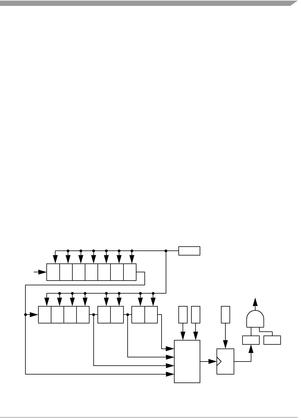
MC68HC08LN56 • MC68HC708LN56 General Release Specification, Rev. 2.1
Freescale Semiconductor 219
Chapter 20
Time Base Module (TBM)
20.1 Introduction
The time base module consists of a counter clocked by the crystal clock, which will generate periodic
interrupts at user selectable rates.
20.2 Features
Software programmable 1-Hz, 4-Hz, 16-Hz, and 256-Hz periodic interrupt using 32.768-kHz crystal.
20.3 Functional Description
NOTE
This module is designed for a 32.768-kHz oscillator.
This module can generate a periodic interrupt by dividing the crystal frequency, CGMXCLK. The counter
is initialized to all zeros when TBON bit is cleared. The counter, shown in Figure 20-1, starts counting
when the TBON bit is set. When the counter overflows at the tap selected by TBR1:TBR0, the TBIF bit
gets set. If the TBIE bit is set, an interrupt request is sent to the CPU. The TBIF flag is cleared by writing
a one to the TACK bit. The first time the TBIF flag is set after enabling the time base module, the interrupt
is generated at approximately half of the overflow period. Subsequent events occur at the exact period.
Figure 20-1. Time Base Block Diagram
÷2÷2÷2÷2÷2÷2÷2
÷2÷2÷2÷2÷2÷2÷2
÷ 128
÷ 32768
÷ 8192
÷ 2048
XTAL
SEL
00
01
10
11
TBIF
TBR1
TBR0
TBIE
TBMINT
TBON
÷2
R
TACK
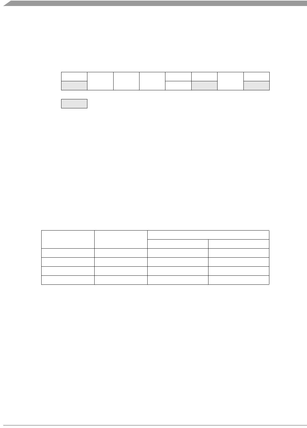
Time Base Module (TBM)
MC68HC08LN56 • MC68HC708LN56 General Release Specification, Rev. 2.1
220 Freescale Semiconductor
20.4 Time Base Register Description
The time base has one register, the TBCR, which is used to enable the time base interrupts and set the
rate.
Figure 20-2. Time Base Control Register
TBIF — Time Base Interrupt Flag
This read-only flag bit is set when the time base counter has rolled over.
1 = Time base interrupt pending
0 = Time base interrupt not pending
TBIE — Time Base Interrupt Enabled
This read/write bit enables the time base interrupt when the TBIF bit becomes set. Reset clears the
TBIE bit
1 = Time base interrupt is enabled
0 = Time base interrupt is disabled
TBR1:TBR0 — Time Base Rate Selection
These read/write bits are used to select the rate of time base interrupts as shown in Table 20-1.
NOTE
Do not change TBR1:TBR0 bits while the time base is enabled
(TBON = 1).
TACK— Time base ACKnowledge
The TACK bit is write only bit and always reads as 0. Writing a logic one to this bit clears TBIF, the time
base Interrupt flag bit. Writing a logic zero to this bit has no effect.
1 = Clear time base interrupt flag
0 = No effect
TBON — Time Base Enabled
This read/write bit enables the time base. Time base may be turned off to reduce power consumption
when its function is not necessary. The counter can be initialized by clearing and then setting this bit.
Reset clears the TBON bit.
1 = Time base is enabled
0 = Time base is disabled and the counter initialized to zeros
TBCR
$003FBit 7654321Bit 0
Read: TBIF
TBIE TBR1 TBR0
00
TBON
0
Write: TACK
Reset:00000000
= Unimplemented
Table 20-1. Time Base Rate Selection for OSC1 = 32.768 kHz
TBR1:TBR0 Divider TIME BASE INTERRUPT RATE
(Hz) (ms)
00 1/32768 1 1000
01 1/8192 4 250
10 1/2048 16 62.5
11 1/128 256 ~ 3.9

Interrupts
MC68HC08LN56 • MC68HC708LN56 General Release Specification, Rev. 2.1
Freescale Semiconductor 221
20.5 Interrupts
The time base module can interrupt the CPU on a regular basis with a rate defined by TBR1 and TBR0.
When the time base counter chain rolls over, the TBIF flag is set. If the TBIE bit is set, enabling the time
base interrupt, the counter chain overflow will generate a CPU interrupt request.
Interrupts must be acknowledged by writing a logic one to TACK bit.
20.6 Low-Power Modes
The WAIT and STOP instructions put the MCU in low-power- consumption standby modes.
20.6.1 Wait Mode
The time base module remains active after execution of the WAIT instruction. In WAIT mode the time
base register is not accessible by the CPU.
If the time base functions are not required during wait mode, reduce the power consumption by stopping
the time base before enabling the WAIT instruction.
20.6.2 Stop Mode
The time base is inactive after execution of the STOP instruction. The STOP instruction does not affect
register conditions or the state of the time base counter. The time base operation continues when the
MCU exits stop mode with an external interrupt, after the system clock resumes.

Time Base Module (TBM)
MC68HC08LN56 • MC68HC708LN56 General Release Specification, Rev. 2.1
222 Freescale Semiconductor

MC68HC08LN56 • MC68HC708LN56 General Release Specification, Rev. 2.1
Freescale Semiconductor 223
Chapter 21
Monitor ROM (MON)
21.1 Introduction
This section describes the use of the monitor ROM (MON08) firmware. Execution of code in the monitor
ROM in monitor mode allows complete testing of the MCU through a single-wire interface with a host
computer.
21.2 Features
Features of monitor mode include the following:
• Normal User-Mode Pin Functionality
• One Pin Dedicated to Serial Communication between Monitor ROM and Host Computer
• Standard Mark/Space Non-Return-to-Zero (NRZ) Communication with Host Computer
• Execution of Code in either RAM or ROM/EPROM
• (E)EPROM/OTPROM Programming
21.3 Functional Description
The monitor ROM receives and executes commands from a host computer. Figure 21-1 shows an
example circuit used to enter monitor mode and communicate with a host computer via a standard
RS-232 interface.
Simple monitor commands can access any memory address. In monitor mode, the MCU can execute
code in RAM which has been loaded by the host computer, while all MCU pins retain normal operating
mode functions. All communication between the host computer and the MCU is through the PTA0 pin, at
a chosen baud rate. A level-shifting and multiplexing interface is required between PTA0 and the host
computer. PTA0 is used in a wired-OR configuration and requires a pullup resistor.
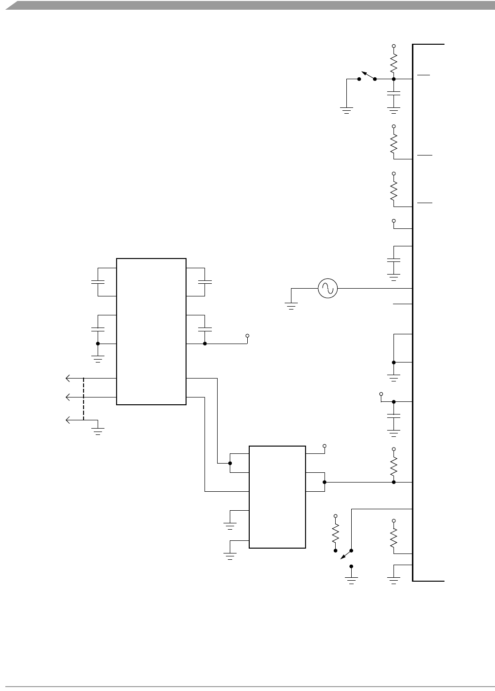
Monitor ROM (MON)
MC68HC08LN56 • MC68HC708LN56 General Release Specification, Rev. 2.1
224 Freescale Semiconductor
Figure 21-1. Monitor Mode Circuit
+
+
+
VDD
VDDA
VDD + VHi
VDD
MC145407
MC74HC125
RST
IRQ1
IRQ2
VDDA
CGMXFC
OSC1
OSC2
CGND
VSS
VDD
PA0
VDD
10 kΩ
0.1 µF
0.1 µF
10 kΩ
10 Ω
6
5
2
4
3
1
DB-25
2
3
7
20
18
17
19
16
15 VDD
VDD
VDD
10 µF
10 µF10 µF
10 µF
1
2
4
7
14
3
0.1 µF
10 kΩ
PC3
VDD
10 kΩ
B
A
NOTE: Position A — Bus clock = CGMXCLK ÷ 4 or CGMVCLK ÷ 4
Position B — Bus clock = CGMXCLK ÷ 2
(See
NOTE.)
56
+
VDD
10 kΩ
PC0
PC1

Functional Description
MC68HC08LN56 • MC68HC708LN56 General Release Specification, Rev. 2.1
Freescale Semiconductor 225
21.3.1 Entering Monitor Mode
Table 21-1 shows the pin conditions for entering monitor mode.
CGMOUT/2 is the internal bus clock frequency. If PTC3 is low upon monitor mode entry, CGMOUT is
equal to the frequency of CGMXCLK, which is a buffered version of the clock on the OSC1 pin. The bus
frequency in this case is a divide-by-two of the input clock. If PTC3 is high upon monitor mode entry, the
bus frequency will be a divide-by-four of the input clock if the PLL is not engaged. The PLL can be
engaged to multiply the bus frequency by programming the CGM. Refer to Chapter 4 Clock Generator
Module (CGMB) for information on how to program the PLL. When the PLL is used, PTC3 must be logic
one during monitor mode entry, and the bus frequency will be a divide-by-four of CGMVCLK, the output
clock of the PLL.
NOTE
Holding the PTC3 pin low when entering monitor mode causes a bypass of
a divide-by-two stage in the oscillator. In this case the CGMOUT frequency
is equal to the CGMXCLK (external clock) frequency. The OSC1 signal
must have a 50% duty cycle at maximum bus frequency.
Enter monitor mode with the pin configuration shown above by pulling RST low and then high. The rising
edge of RST latches monitor mode. Once monitor mode is latched, the values on the specified pins can
change.
Once out of reset, the MCU monitor mode firmware then sends a break signal (10 consecutive logic zeros)
to the host computer, indicating that it is ready to receive a command. The break signal also serves as a
timing reference to allow the host to determine the necessary baud rate.
Monitor mode uses different vectors for reset, SWI, and a break interrupt than those used in user mode.
The alternate vectors are in the $FE page instead of the $FF page, and allow code execution from the
internal monitor firmware instead of user code.
When the host computer has completed downloading code into the MCU RAM, this code can be executed
by driving PTA0 low while asserting RST low and then high. The internal monitor ROM firmware will
interpret the low on PTA0 as an indication to jump RAM, and execution control will then continue from
RAM. The location jumped to is always the second byte of RAM (i.e. the first RAM byte address + 1).
Execution of an SWI from the downloaded code will return program control to the internal monitor ROM
firmware. Alternatively, the host can send a RUN command, which executes an RTI, and this can be used
to send control to the address on the stack pointer.
The COP module is disabled in monitor mode as long as VDD +V
HI is applied to either the IRQ1/VPP pin
or the RST pin. (See Chapter 5 System Integration Module (SIM) for more information on modes of
operation.)
Table 21-1. Mode Selection
IRQ1/VPP
Pin
PTC0
Pin
PTC1
Pin
PTA0
Pin
PTC3
Pin Mode CGMOUT Bus
Frequency
VDD + VHI 1 0 1 1 Monitor or
VDD + VHI 1 0 1 0 Monitor CGMXCLK
CGMXCLK
2
----------------------------- CGMVCLK
2
----------------------------- CGMOUT
2
--------------------------
CGMOUT
2
--------------------------
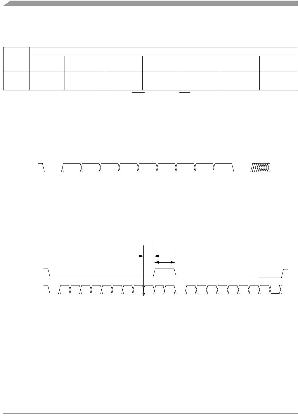
Monitor ROM (MON)
MC68HC08LN56 • MC68HC708LN56 General Release Specification, Rev. 2.1
226 Freescale Semiconductor
Table 21-2 is a summary of the differences between user mode and monitor mode.
21.3.2 Data Format
Communication with the monitor ROM is in standard non-return-to-zero (NRZ) mark/space data format.
(See Figure 21-2 and Figure 21-3.) Tramsmit and receive baud rates must be identical.
Figure 21-2. Monitor Data Format
21.3.3 Break Signal
A start bit (low) followed by nine low bits is a break signal. (See Figure 21-3.) When the monitor receives
a break signal, it drives the PTA0 pin high for the duration of two bits, and then echos back the break
signal.
Figure 21-3. Break Transaction
Table 21-2. Mode Differences
Modes
Functions
COP Reset
Vector High
Reset
Vector Low
Break
Vector High
Break
Vector Low
SWI
Vector High
SWI
Vector Low
User Enabled $FFFE $FFFF $FFFC $FFFD $FFFC $FFFD
Monitor Disabled(1)
1. If the high voltage (VDD + VHI) is removed from the IRQ1/VPP pin or the RST pin, the SIM asserts its COP enable output.
The COP is a mask option enabled or disabled by the COPD bit in the mask option register.
$FEFE $FEFF $FEFC $FEFD $FEFC $FEFD
BIT 5
START
BIT BIT 0 BIT 1
NEXT
STOP
BIT
START
BIT
BIT 2 BIT 3 BIT 4 BIT 6 BIT 7
01234567 01234567
NO STOP BIT
TWO BIT DELAY TIME BEFORE ZERO ECHO
BREAK
BIT TIME
START
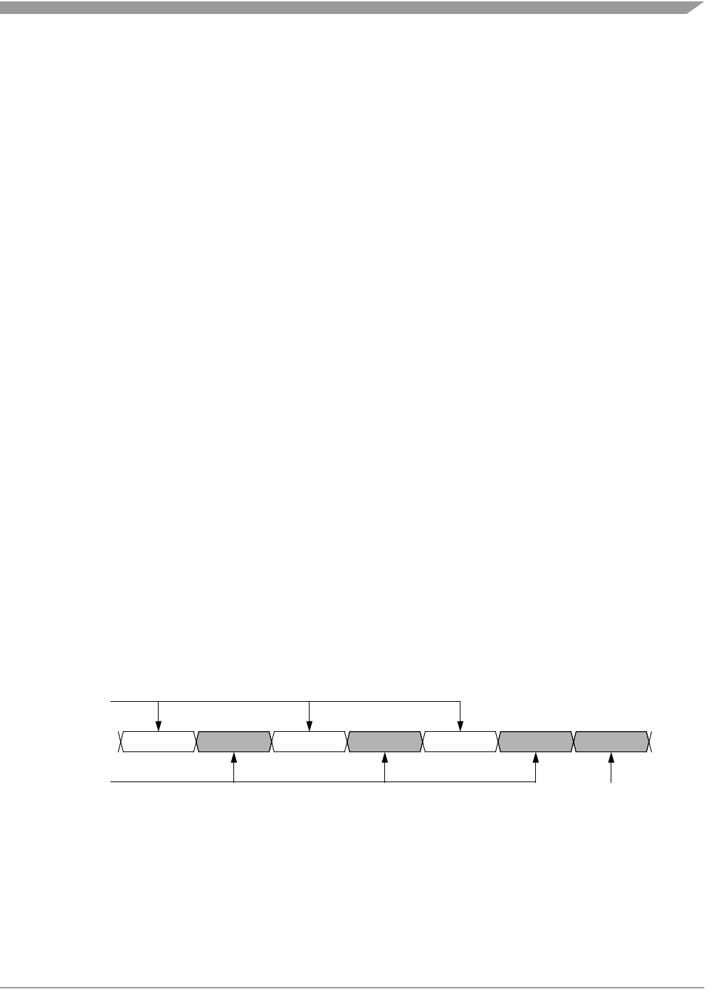
Functional Description
MC68HC08LN56 • MC68HC708LN56 General Release Specification, Rev. 2.1
Freescale Semiconductor 227
21.3.4 Baud Rate
The bus clock frequency for the MCU in monitor mode is determined by the external clock frequency, the
value on PTC3 during monitor mode entry, and whether or not the PLL is engaged. The internal monitor
firmware performs a division by 256 (for sampling data), therefore, the bus frequency divided by 256 is
the baud rate of the monitor mode data transfer.
For example, with a 4.9152-MHz external clock and the PTC3 pin at logic one during reset, data is
transferred between the monitor and host at 4800 baud. If the PTC3 pin is at logic zero during reset, the
monitor baud rate is 9600.
The internal PLL can be engaged to increase the baud rate of instruction transfer between the host and
the MCU and to increase the speed of program execution. Refer to Chapter 4 Clock Generator Module
(CGMB) for information on how to program the PLL. If use of the PLL is desired, the monitor mode must
be entered with PTC high. (See 21.3.1 Entering Monitor Mode.) Initially, the bus frequency is a
divide-by-four of the input clock. After the PLL is programmed, and enabled onto the bus, communication
between the host and MCU must be reestablished at the new baud rate. One way of accomplishing this
would be for the host to download a program into the MCU RAM that would program the PLL, and send
a new baud rate “flag” to the host just prior to engaging the PLL onto the bus. Upon completion of
execution, an SWI would return program control to the monitor firmware.
21.3.5 Commands
The monitor ROM firmware uses the following commands:
• READ (read memory)
• WRITE (write memory)
• IREAD (indexed read)
• IWRITE (indexed write)
• READSP (read stack pointer)
• RUN (run user program)
As the host computer sends commands through PTA0, the monitor ROM firmware immediately echoes
each received byte back to the PTA0 pin for error checking, as shown in the example command in
Figure 21-4.
Figure 21-4. Read Transaction
The resultant data of a read type of command appears after the echo of the last byte of the command.
A brief description of each monitor mode command follows.
A sequence of IREAD or IWRITE commands can access a block of memory sequentially over the full
64-Kbyte memory map.
ADDR. HIGHOPCODEOPCODE ADDR. HIGH ADDR. LOW ADDR. LOW DATA
ECHO
SENT TO
MONITOR
RESULT
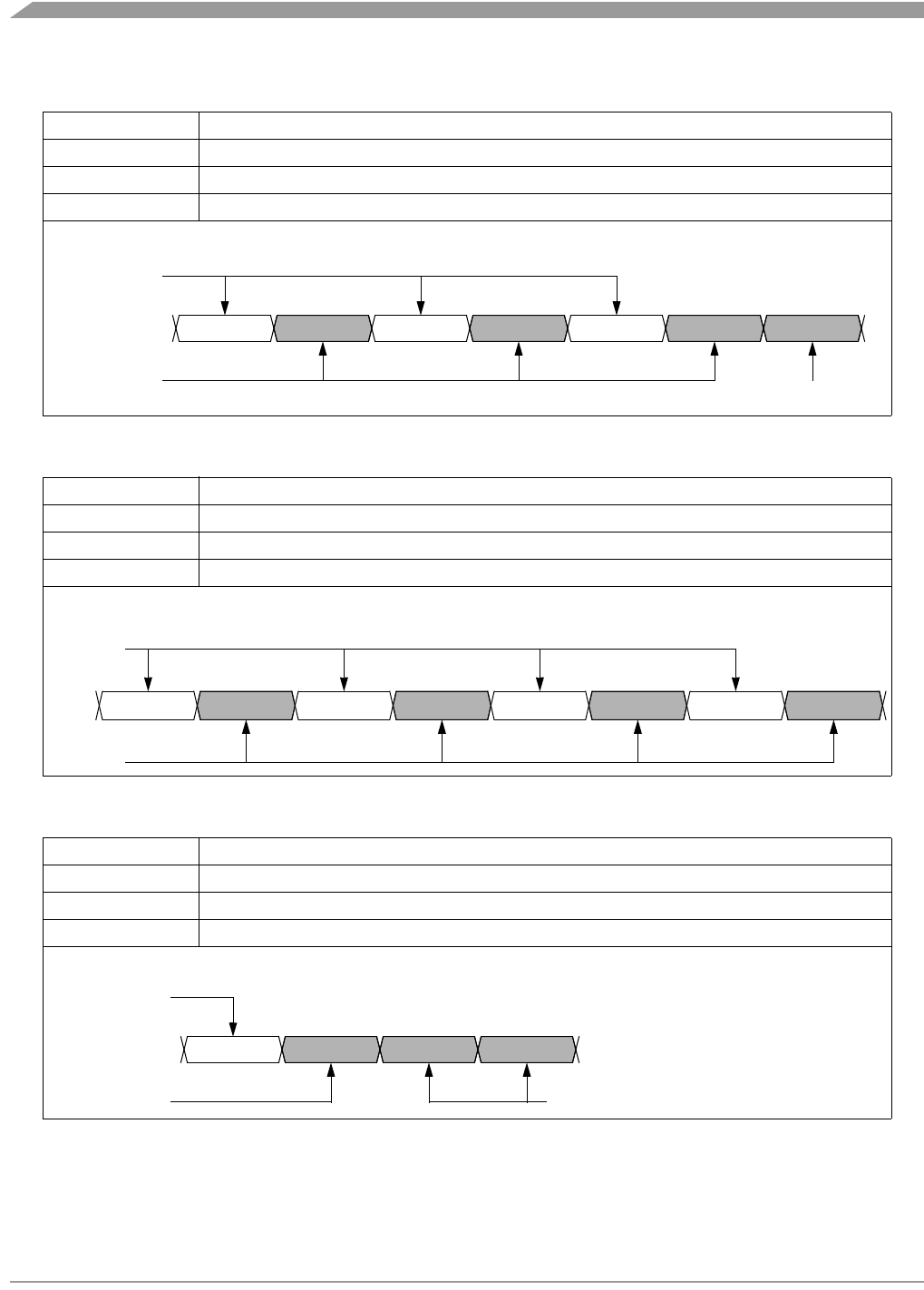
Monitor ROM (MON)
MC68HC08LN56 • MC68HC708LN56 General Release Specification, Rev. 2.1
228 Freescale Semiconductor
Table 21-3. READ (Read Memory) Command
Description Read byte from memory
Operand Specifies 2-byte address in high byte:low byte order
Data Returned Returns contents of specified address
Opcode $4A
Command Sequence
Table 21-4. WRITE (Write Memory) Command
Description Write byte to memory
Operand Specifies 2-byte address in high byte:low byte order; low byte followed by data byte
Data Returned None
Opcode $49
Command Sequence
Table 21-5. IREAD (Indexed Read) Command
Description Read next 2 bytes in memory from last address accessed
Operand Specifies 2-byte address in high byte:low byte order
Data Returned Returns contents of next two addresses
Opcode $1A
Command Sequence
ADDR. HIGHREADREAD ADDR. HIGH ADDR. LOW ADDR. LOW DATA
ECHO
SENT TO
MONITOR
RESULT
ADDR. HIGHWRITEWRITE ADDR. HIGH ADDR. LOW ADDR. LOW DATA
ECHO
SENT TO
MONITOR
DATA
DATAIREADIREAD DATA
ECHO
SENT TO
MONITOR
RESULT
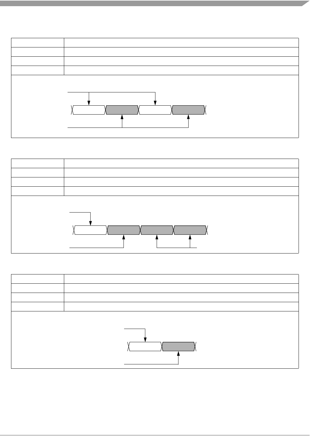
Functional Description
MC68HC08LN56 • MC68HC708LN56 General Release Specification, Rev. 2.1
Freescale Semiconductor 229
Table 21-6. IWRITE (Indexed Write) Command
Description Write to last address accessed + 1
Operand Specifies single data byte
Data Returned None
Opcode $19
Command Sequence
Table 21-7. READSP (Read Stack Pointer) Command
Description Reads stack pointer
Operand None
Data Returned Returns stack pointer in high byte:low byte order
Opcode $0C
Command Sequence
Table 21-8. RUN (Run User Program) Command
Description Executes RTI instruction
Operand None
Data Returned None
Opcode $28
Command Sequence
DATAIWRITEIWRITE DATA
ECHO
SENT TO
MONITOR
SP HIGHREADSPREADSP SP LOW
ECHO
SENT TO
MONITOR
RESULT
RUNRUN
ECHO
SENT TO
MONITOR

Monitor ROM (MON)
MC68HC08LN56 • MC68HC708LN56 General Release Specification, Rev. 2.1
230 Freescale Semiconductor

MC68HC08LN56 • MC68HC708LN56 General Release Specification, Rev. 2.1
Freescale Semiconductor 231
Chapter 22
Preliminary Electrical Specifications
22.1 Introduction
This section contains electrical and timing specifications. These values are design targets and have not
yet been tested.
22.2 Absolute Maximum Ratings
Maximum ratings are the extreme limits to which the microcontroller unit (MCU) can be exposed without
permanently damaging it.
The MCU contains circuitry to protect the inputs against damage from high static voltages; however, do
not apply voltages higher than those shown in the table below. Keep VIN and VOUT within the range
VSS ≤(VIN or VOUT)≤VDD. Connect unused inputs to the appropriate voltage level, either VSS or VDD.
NOTE
This device is not guaranteed to operate properly at the maximum ratings.
Refer to Table 22-4 and Table 22-5 for guaranteed operating conditions.
Table 22-1. Absolute Maximum Ratings(1)
1. Voltages referenced to VSS.
Characteristic Symbol Value Unit
Supply Voltage VDD –0.3 to +6.0 V
Input Voltage VIN VSS –0.3 to VDD +0.3 V
Programming Voltage VPP VSS –0.3 to 14.0 V
Maximum Current Per Pin Excluding VDD and VSS I± ±25 mA
Storage Temperature TSTG –55 to +150 °C
Maximum Current out of VSS IMVSS 100 mA
Maximum Current into VDD IMVDD 100 mA
Preliminary Electrical Specifications
MC68HC08LN56 • MC68HC708LN56 General Release Specification, Rev. 2.1
232 Freescale Semiconductor
22.3 Functional Operating Range
22.4 Thermal Characteristics
Table 22-2. Operating Range
Characteristic Symbol Value Unit
Operating Temperature Range TA0 to 85 °C
Operating Voltage Range (1)
1. LCD charge pump optimized for given ranges
VDD
3.3 ± ±10%
5.0 ± ±10% V
Table 22-3. Thermal Characteristics
Characteristic Symbol Value Unit
Thermal Resistance, 144-Pin TQFP θJA 46.1 °C/W
I/O Pin Power Dissipation PI/O User Determined W
Power Dissipation(1)
1. Power Dissipation is a function of temperature
PD
PD = (IDD x VDD) +
PI/O =
K/(TJ + 273 °C)
W
Constant(2)
2. K is a constant unique to the device. K can be determined for a known TA and
measured PD. With this value of K, PD and TJ can be determined for any value of TA.
KPD x (TA + 273 °C)
+ PD2 x θJA
W/°C
Average Junction Temperature TJTA + (PD x θJA)°C
Maximum Junction Temperature TJM 100 °C

DC Electrical Characteristics
MC68HC08LN56 • MC68HC708LN56 General Release Specification, Rev. 2.1
Freescale Semiconductor 233
22.5 DC Electrical Characteristics
Table 22-4. DC Electrical Characteristics (VDD = 5.0 Vdc ± 10%)(1)
1. VDD = 5.0 Vdc ±± 10%, VSS = 0 Vdc, TA = TL to TH, unless otherwise noted.
Characteristic Symbol Min Typ(2)
2. Typical values reflect average measurements at midpoint of voltage range, 25 °C only.
Max Unit
Output High Voltage
(ILOAD = –2.0 mA) All I/O pins VOH VDD –0.8 ——V
Output Low Voltage
(ILOAD = 1.6 mA) All I/O pins VOL ——0.4V
Input High Voltage
All Ports, IRQs, RESET, OSC1 VIH 0.7 x VDD —VDD V
Input Low Voltage
All Ports, IRQs, RESET, OSC1 VIL VSS —0.3 x VDD V
VDD Supply Current
Run (3)
Wait (4)
Stop (5)
25 °C
0 °C to 85 °C
25 °C with LVI Enabled
0 °C to 85 °C with LVI Enabled
3. Run (operating) IDD measured using external square wave clock source (fosc = 8.2 MHz). All inputs 0.2 V from rail. No dc
loads. Less than 100 pF on all outputs. CL = 20 pF on OSC2. All ports configured as inputs. OSC2 capacitance linearly
affects Run IDD. Measured with all modules enabled.
4. Wait IDD measured using external square wave clock source (fosc = 8.2 MHz). All inputs 0.2 V from rail. No dc loads. Less
than 100 pF on all outputs. CL = 20 pF on OSC2. All ports configured as inputs. OSC2 capacitance linearly affects Wait
IDD. Measured with PLL, LCD, LVI, and TBM enabled.
5. Stop IDD measured with OSC1 = VSS.
IDD
—
—
—
—
—
—
—
—
—
—
—
—
—
30
12
5
15
320
380
mA
mA
µA
µA
µA
µA
I/O Ports Hi-Z Leakage Current IIL ——± 10 µA
Input Current IIN ——±1µA
Capacitance
Ports (As Input or Output)
COUT
CIN
—
—
—
—
12
8pF
Low-Voltage Inhibit Reset VLVR 2.6 2.7 2.8 V
Low-Voltage Reset/Recover Hysteresis HLVR 60 80 100 mV
POR ReArm Voltage(6)
6. Maximum is highest voltage that POR is guaranteed.
VPOR 0—100mV
POR Rise Time Ramp Rate(7)
7. If minimum VDD is not reached before the internal POR reset is released, RST must be driven low externally until minimum
VDD is reached.
RPOR 0.035 — — V/ms
Monitor Mode Entry Voltage VHI 1.4 x VDD —2 x VDD V

Preliminary Electrical Specifications
MC68HC08LN56 • MC68HC708LN56 General Release Specification, Rev. 2.1
234 Freescale Semiconductor
Table 22-5. DC Electrical Characteristics (VDD = 3.3 Vdc ± 10%) (1)
Characteristic Symbol Min Typ(2) Max Unit
Output High Voltage
(ILOAD = –2.0 mA) all ports VOH VDD –0.8 — — V
Output Low Voltage
(ILOAD = 1.6 mA) all ports VOL ——0.4V
Input High Voltage
All ports, IRQs, RESET, OSC1 VIH 0.7 x VDD —V
DD V
Input Low Voltage
All ports, IRQs, RESET, OSC1 VIL VSS — 0.3 x VDD V
VDD Supply Current
Run (3)
Wait (4)
Stop (5)
25 °C
0 °C to 85 °C
25 °C with LVI Enabled
0 °C to 85 °C with LVI Enabled
IDD
—
—
—
—
—
—
—
—
—
—
—
—
—
10
6
3
10
200
250
mA
mA
µA
µA
µA
µA
I/O Ports Hi-Z Leakage Current IIL ——± 10 µA
Input Current IIN ——±11µA
Capacitance
Ports (as Input or Output)
COUT
CIN
—
—
—
—
12
8pF
Low Voltage Reset Inhibit VLVII 2.6 2.7 2.8 V
Low Voltage Reset Inhibit/Recover Hysteresis HLVI 60 80 100 mV
POR ReArm Voltage(6) VPOR 0—200mV
POR Rise Time Ramp Rate(7) RPOR .02 — — V/ms
Monitor Mode Entry Voltage VHI 1.6 x VDD —2 x VDD V
1. VDD = 3.3 Vdc ± 10%, VSS = 0 Vdc, TA = TL to TH, unless otherwise noted.
2. Typical values reflect average measurements at midpoint of voltage range, 25 °C only.
3. Run (operating) IDD measured using external square wave clock source (fosc = 8.2 MHz). All inputs 0.2 V from rail. No dc
loads. Less than 100 pF on all outputs. CL = 20 pF on OSC2. All ports configured as inputs. OSC2 capacitance linearly
affects Run IDD. Measured with all modules enabled.
4. Wait IDD measured using external square wave clock source (fosc = 8.2 MHz). All inputs 0.2 V from rail. No dc loads. Less
than 100 pF on all outputs. CL = 20 pF on OSC2. All ports configured as inputs. OSC2 capacitance linearly affects Wait
IDD. Measured with PLL, LCD, LVI, and TBM enabled.
5. Stop IDD measured with OSC1 = VSS.
6. Maximum is highest voltage that POR is guaranteed.
7. If minimum VDD is not reached before the internal POR reset is released, RST must be driven low externally until minimum
VDD is reached.
Control Timing
MC68HC08LN56 • MC68HC708LN56 General Release Specification, Rev. 2.1
Freescale Semiconductor 235
22.6 Control Timing
Table 22-6. Control Timing (VDD = 5.0 Vdc ± 10%)(1)
1. Vss = 0 Vdc; timing shown with respect to 20% VDD and 70% VSS unless note
Characteristic Symbol Min Max Unit
Frequency of Operation (2)
Crystal Option
External Clock Option(3)
2. See Table 22-13 and Table 22-14 for more information
3. No more than 10% duty cycle deviation from 50%
fOSC 32k
dc(4)
4. Some modules may require a minimum frequency greater than dc for proper operation; see appropriate Table for this in-
formation
100k
32M
Hz
Internal Operating Frequency fOP —8.0MHz
RESET input Pulse Width Low (5)
5. Minimum pulse width reset is guaranteed to be recognized; it is possible for a smaller pulse width to cause a reset.
tIRL 50 — ns
IRQ Interrupt Pulse Width Low (6)(Edge -Triggered)
6. Minimum pulse width is for guaranteed interrupt; it is possible for a smaller pulse width to be recognized
tILIH 50 — ns
Table 22-7. Control Timing (VDD = 3.3 Vdc ± 10%)(1)
1. Vss = 0 Vdc; timing shown with respect to 20% VDD and 70% VSS unless noted
Characteristic Symbol Min Max Unit
Frequency of Operation (2)
Crystal Option
External Clock Option(3)
2. See Table 22-11 and Table 22-12 for more information
3. No more than 10% duty cycle deviation from 50%
fOSC 32k
dc(4)
4. Some modules may require a minimum frequency greater than dc for proper operation; see appropriate Table for this in-
formation
100k
16M
Hz
Internal Operating Frequency fOP —4.0MHz
RESET input Pulse Width Low (5)
5. Minimum pulse width reset is guaranteed to be recognized; it is possible for a smaller pulse width to cause a reset.
tIRL 125 — ns
IRQ Interrupt Pulse Width Low(6) (Edge-Triggered)
6. Minimum pulse width is for guaranteed interrupt; it is possible for a smaller pulse width to be recognized
tILIH 125 — ns

Preliminary Electrical Specifications
MC68HC08LN56 • MC68HC708LN56 General Release Specification, Rev. 2.1
236 Freescale Semiconductor
22.7 Serial Peripheral Interface Characteristics
Table 22-8. Serial Peripheral Interface (SPI) Timing (VDD = 5.0 Vdc ± 10%) (1)
1. All timing is shown with respect to 20% VDD and 70% VDD, unless noted; assumes 100 pF load on all SPI pins
Diagram
Number(2)
2. Numbers refer to dimensions in Figure 22-1 and Figure 22-2
Characteristic Symbol Min Max Unit
Operating Frequency
Master
Slave
fOP(M)
fOP(S)
fOP/128
DC
fOP/2
fOP
MHz
1
Cycle Time
Master
Slave
tCYC(M)
tCYC(S)
2
1
128
–
tCYC
2 Enable Lead Time tLEAD(S) 15 ns
3 Enable Lag Time tLAG(S) 15 ns
4
Clock (SCK) High Time
Master
Slave
tSCKH(M)
tSCKH(S)
100
50
–
–
ns
5
Clock (SCK) Low Time
Master
Slave
tSCKL(M)
tSCKL(S)
100
50
–
–
ns
6
Data Setup Time (Inputs)
Master
Slave
tSU(M)
tSU(S)
45
5
–
–
ns
7
Data Hold Time (Inputs)
Master
Slave
tH(M)
tH(S)
0
15
–
–
ns
8
Access Time, Slave(3)
CPHA = 0
CHPA = 1
3. Time to data active from high-impedance state
tA(CP0)
tA(CP1)
0
0
40
20
ns
9Disable Time, Slave(4)
4. Hold time to high-impedance state
tDIS(S) –25ns
10
Data Valid Time (After enable edge)
Master
Slave(5)
5. With 100 pF on all SPI pins
tV(M)
tV(S)
–
–
10
40
ns
11
Data Hold Time (Outputs, after enable edge)
Master
Slave
tHO(M)
tHO(S)
0
5
–
–
ns

Serial Peripheral Interface Characteristics
MC68HC08LN56 • MC68HC708LN56 General Release Specification, Rev. 2.1
Freescale Semiconductor 237
Table 22-9. Serial Peripheral Interface (SPI) Timing (VDD = 3.3 Vdc ± 10%) (1)
1. All timing is shown with respect to 20% VDD and 70% VDD, unless noted; assumes 100 pF load on all SPI pins
Diagram
Number(2)
2. Numbers refer to dimensions in Figure 22-1 and Figure 22-2
Characteristic Symbol Min Max Unit
Operating Frequency
Master
Slave
fOP(M)
fOP(S)
fOP/128
DC
fOP/2
fOP
MHz
1
Cycle Time
Master
Slave
tCYC(M)
tCYC(S)
2
1
128
–
tCYC
2 Enable Lead Time tLEAD(S) 30 ns
3 Enable Lag Time tLAG(S) 30 ns
4
Clock (SCK) High Time
Master
Slave
tSCKH(M)
tSCKH(S)
200
100
–
–
ns
5
Clock (SCK) Low Time
Master
Slave
tSCKL(M)
tSCKL(S)
200
100
–
–
ns
6
Data Setup Time (Inputs)
Master
Slave
tSU(M)
tSU(S)
90
10
–
–
ns
7
Data Hold Time (Inputs)
Master
Slave
tH(M)
tH(S)
0
30
–
–
ns
8
Access Time, Slave(3)
CPHA = 0
CHPA = 1
3. Time to data active from high-impedance state
tA(CP0)
tA(CP1)
0
0
80
40
ns
9Disable Time, Slave(4)
4. Hold time to high-impedance state
tDIS(S) –50ns
10
Data Valid Time (After enable edge)
Master
Slave(5)
5. With 100 pF on all SPI pins
tV(M)
tV(S)
–
–
20
80
ns
11
Data Hold Time (Outputs, after enable edge)
Master
Slave
tHO(M)
tHO(S)
0
10
–
–
ns
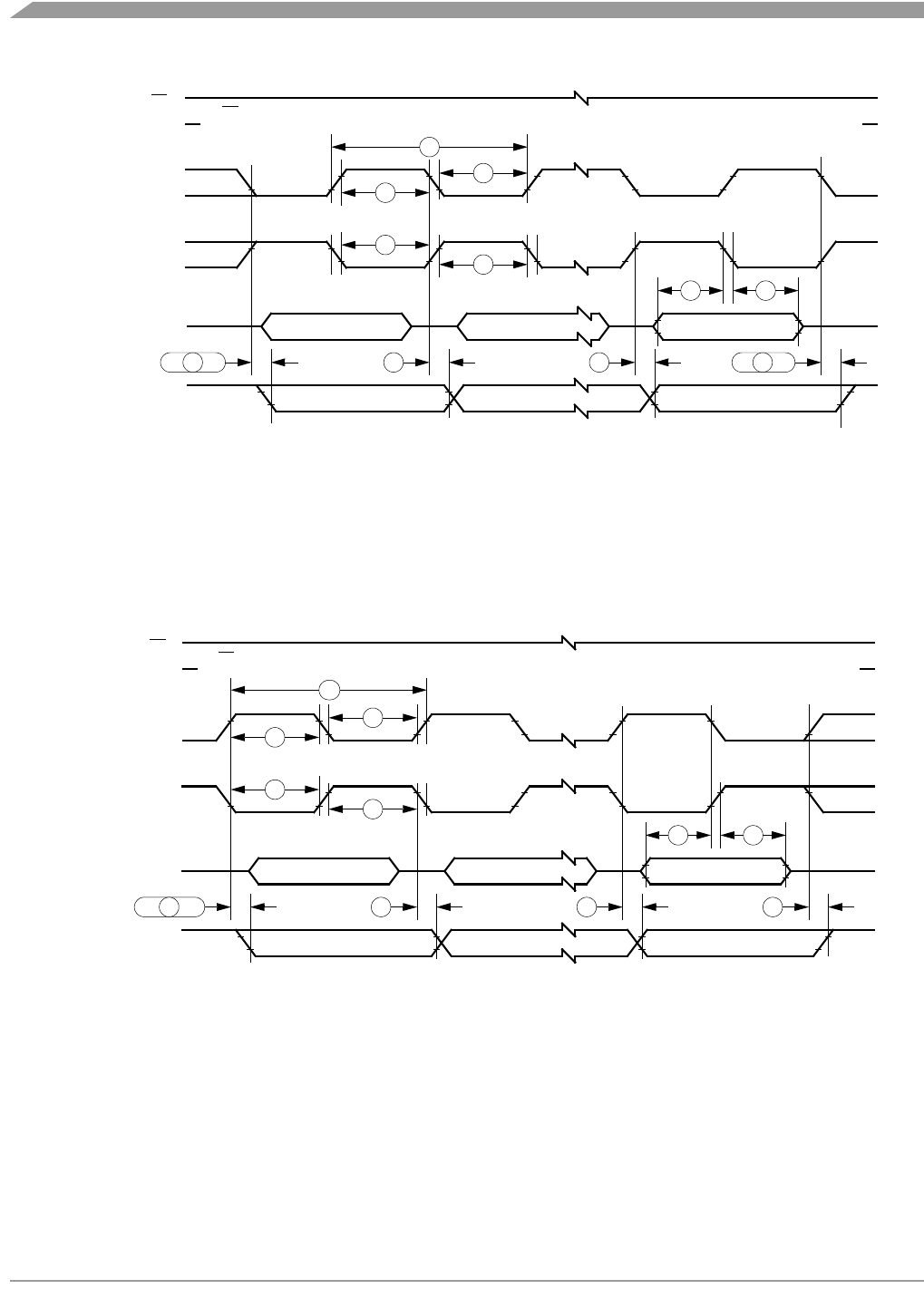
Preliminary Electrical Specifications
MC68HC08LN56 • MC68HC708LN56 General Release Specification, Rev. 2.1
238 Freescale Semiconductor
Figure 22-1. SPI Master Timing
NOTE
NOTE: This first clock edge is generated internally, but is not seen at the SCK pin.
SS pin of master held high.
MSB IN
SS
(INPUT)
SCK (CPOL = 0)
(OUTPUT)
SCK (CPOL = 1)
(OUTPUT)
MISO
(INPUT)
MOSI
(OUTPUT)
NOTE
4
5
5
1
4
BITS 6–1 LSB IN
MASTER MSB OUT BITS 6–1 MASTER LSB OUT
10 11 10 11
76
NOTE
NOTE: This last clock edge is generated internally, but is not seen at the SCK pin.
SS pin of master held high.
MSB IN
SS
(INPUT)
SCK (CPOL = 0)
(OUTPUT)
SCK (CPOL = 1)
(OUTPUT)
MISO
(INPUT)
MOSI
(OUTPUT)
NOTE
4
5
5
1
4
BITS 6–1 LSB IN
MASTER MSB OUT BITS 6–1 MASTER LSB OUT
10 11 10 11
76
a) SPI Master Timing (CPHA = 0)
b) SPI Master Timing (CPHA = 1)
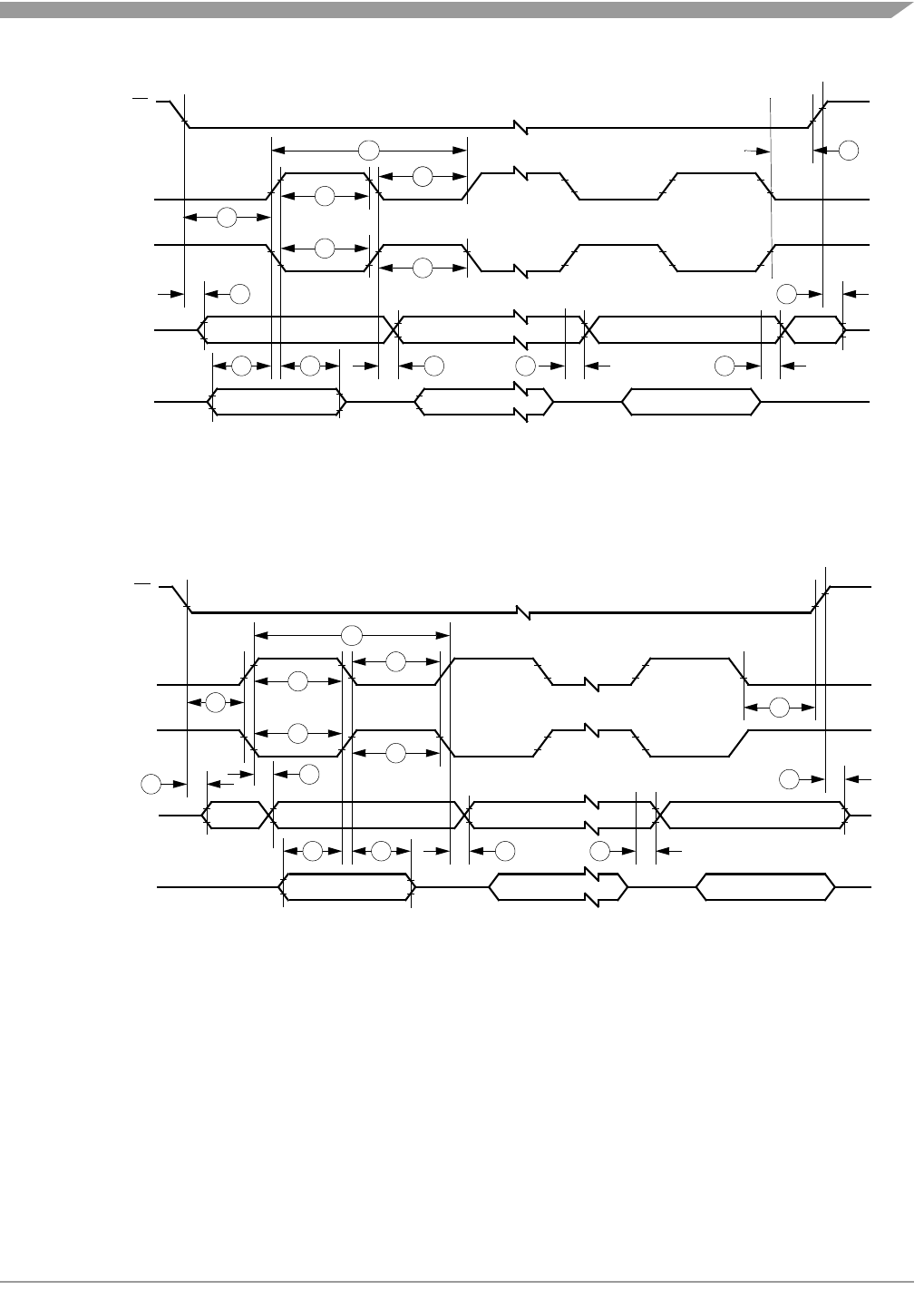
Serial Peripheral Interface Characteristics
MC68HC08LN56 • MC68HC708LN56 General Release Specification, Rev. 2.1
Freescale Semiconductor 239
Figure 22-2. SPI Slave Timing
NOTE: Not defined but normally MSB of character just received.
SLAVE
SS
(INPUT)
SCK (CPOL = 0)
(INPUT)
SCK (CPOL = 1)
(INPUT)
MISO
(INPUT)
MOSI
(OUTPUT)
4
5
5
1
4
MSB IN
BITS 6–1
8
610
11
11
NOTE
SLAVE LSB OUT
9
3
LSB IN
2
7
BITS 6–1
MSB OUT
NOTE: Not defined but normally LSB of character previously transmitted.
SLAVE
SS
(INPUT)
SCK (CPOL = 0)
(INPUT)
SCK (CPOL = 1)
(INPUT)
MISO
(OUTPUT)
MOSI
(INPUT)
4
5
5
1
4
MSB IN
BITS 6–1
8
610
NOTE SLAVE LSB OUT
9
3
LSB IN
2
7
BITS 6–1
MSB OUT
10
a) SPI Slave Timing (CPHA = 0)
b) SPI Slave Timing (CPHA = 1)
11
11
Preliminary Electrical Specifications
MC68HC08LN56 • MC68HC708LN56 General Release Specification, Rev. 2.1
240 Freescale Semiconductor
22.8 TImer Interface Module Characteristics
22.9 Clock Generation Module Electrical Characteristics
Table 22-10. TIM Timing
Characteristic Symbol Min Max Unit
Input Capture Pulse Width tTIH, tTIL 125 — ns
Input Clock Pulse Width tTCH, tTCL (1/fOP) + 5 — ns
Table 22-11. CGM Component Specifications
Characteristic Symbol Min Typ Max Notes
Crystal Load Capacitance CL— — — Consult Crystal Mfg. Data
Crystal Fixed Capacitance C1—2*C
L— Consult Crystal Mfg. Data
Crystal Tuning Capacitance C2—2*C
L— Consult Crystal Mfg. Data
Filter Capacitor CF—
CFACT*
(VDDA/
fXCLK)
—
Bypass Capacitor CBYP —0.1 µF—
CBYP must provide low AC
impedance from f = fXCLK/100
to 100*fVCLK, so series resis-
tance must be considered.
Table 22-12. CGM Operating Conditions
Characteristic Symbol Min Typ Max Notes
Crystal Reference Frequency fXCLK 32.0 kHz 38.4 kHz 100 kHz
Range Nominal Multiplier fNOM — 38.4 kHz —
VCO Center-of-Range Frequency
fVRS
38.4 kHz — 40.0 MHz 4.0–5.5 V VDD only
Medium Voltage VCO
Center-of-Range Frequency 38.4 kHz — 20.0 MHz 2.7–4.0 V VDD only
VCO Power-of-Two Range Multiplier 2E118
VCO Prescale Multiplier 2P118
Reference Divider Factor R 1 1 15
VCO Operating Frequency fVCLK fVRSMIN —f
VRSMAX

Clock Generation Module Electrical Characteristics
MC68HC08LN56 • MC68HC708LN56 General Release Specification, Rev. 2.1
Freescale Semiconductor 241
Table 22-13. CGM Acquisition/Lock Time Specifications
Description Symbol Min Typ Max Notes
Manual Mode Time to
Stable tACQ —(8*VDDA)/
(fX CLK*KACQ)
—If CF chosen correctly.
Manual Stable to Lock
Time tAL —(4*VDDA)/
(fX CLK*KTRK)—If CF chosen correctly.
Manual Acquisition Time tLOCK —tACQ+tAL —
Tracking Mode Entry
Frequency Tolerance ∆TRK 0—
± 3.6%
Acquisition Mode Entry
Frequency Tolerance ∆ACQ ±6.3% —± 7.2%
LOCK Entry Freq.
Tolerance ∆LOCK 0—
± 0.9%
LOCK Exit Freq.
Tolerance ∆UNL ±0.9% ± 1.8%
Reference cycles per
Acquisition Mode
Measurement
nACQ —32 —
Reference cycles per
Tracking Mode
Measurement
nTRK —128 —
Automatic Mode Time to
Stable tACQ
nACQ/
fXCLK
(8*VDDA)/
(fX CLK*KACQ)
—If CF chosen correctly.
Automatic Stable to
Lock Time tAL
nTRK/
fXCLK
(4*VDDA)/
(fX CLK*KTRK)—If CF chosen correctly.
Automatic Lock Time tLOCK —tACQ+tAL —
PLL Jitter (deviation of
average bus frequency
over 2 ms)
fJ0—
± (fCRYS)
*(.025%)
*((2PN/R)/4)
N = VCO frequency
multiplier(GBNT)

Preliminary Electrical Specifications
MC68HC08LN56 • MC68HC708LN56 General Release Specification, Rev. 2.1
242 Freescale Semiconductor
22.10 Analog-to-Digital Converter (ADC) Characteristics
Table 22-14. ADC Characteristics
Characteristic Symbol Min Max Unit Notes
Supply Voltage AVDD 3.0 5.5 V
AVDD should be tied to the
same potential as VDD via
separate traces.
Input Voltages VADIN
VREFH
0
1.5
AVDD
AVDD
VV
ADIN<=VRH
Resolution BAD 88Bits
Absolute Accuracy
(VREFL = 0 V,
VADCAP = 2 X VDDA)
AAD ± 1/2 ± 1 LSB Includes Quantization
ADC Internal Clock fADIC 500k 1.048M Hz tAIC = 1/fADIC
Conversion Range RAD AVss VRH V
Power-up Time tADPU 16 tAIC cycles
Conversion Time tADC 16 17 tAIC cycles
Sample Time tADS 5—
tAIC cycles
Monotocity MAD Guaranteed
Zero Input Reading ZADI 00 Hex VIN = AVss
Full-scale Reading FADI FF Hex VIN = VRH
Input Capacitance CADI — 20 pf Not tested
Memory Characteristics
MC68HC08LN56 • MC68HC708LN56 General Release Specification, Rev. 2.1
Freescale Semiconductor 243
22.11 Memory Characteristics
22.12 Liquid Crystal Display Driver Characteristics
Table 22-15. Memory Characteristics
Characteristic Symbol Min Typ Max Unit
EPROM Programming Voltage VEPGM —13.5— V
EPROM Data Retention Time tEDR — 10.0 — years
EPROM Programming Time tEPGM —1—ms/byte
RAM Data Retention Voltage VRDR .7 — — V
Table 22-16. LCD Driver Characteristics
Characteristic Min Typ Max Unit
VLL7 Average(1)
1. Average VLLX for contrast control set to nominal 7.0
6.93 7.0 7.07 V
VLL6 Average 5.93 6.0 6.07 V
VLL5 Average 4.93 5.0 5.07 V
VLL2Average 1.93 2.0 2.07 V
VLL1 Average 0.93 1.0 1.07 V
VLL7 Ripple 0—± 100 mV
VLL6 Ripple 0—± 250 mV
VLL5 Ripple 0—± 250 mV
VLL2 Ripple 0—± 250 mV
VLL1 Ripple 0—± 250 mV
LCD Contrast Control Voltage Range VLL7 6.3 — 7.0 V
LCD Contrast Control Voltage Range VLL6 5.4 — 6.0 V
LCD Contrast Control Voltage Range VLL5 4.5 — 5.0 V
LCD Contrast Control Voltage Range VLL2 1.8 — 2.0 V
LCD Contrast Control Voltage Range VLL1 0.9 — 1.0 V

Preliminary Electrical Specifications
MC68HC08LN56 • MC68HC708LN56 General Release Specification, Rev. 2.1
244 Freescale Semiconductor

How to Reach Us:
Home Page:
www.freescale.com
E-mail:
support@freescale.com
USA/Europe or Locations Not Listed:
Freescale Semiconductor
Technical Information Center, CH370
1300 N. Alma School Road
Chandler, Arizona 85224
+1-800-521-6274 or +1-480-768-2130
support@freescale.com
Europe, Middle East, and Africa:
Freescale Halbleiter Deutschland GmbH
Technical Information Center
Schatzbogen 7
81829 Muenchen, Germany
+44 1296 380 456 (English)
+46 8 52200080 (English)
+49 89 92103 559 (German)
+33 1 69 35 48 48 (French)
support@freescale.com
Japan:
Freescale Semiconductor Japan Ltd.
Headquarters
ARCO Tower 15F
1-8-1, Shimo-Meguro, Meguro-ku,
Tokyo 153-0064
Japan
0120 191014 or +81 3 5437 9125
support.japan@freescale.com
Asia/Pacific:
Freescale Semiconductor Hong Kong Ltd.
Technical Information Center
2 Dai King Street
Tai Po Industrial Estate
Tai Po, N.T., Hong Kong
+800 2666 8080
support.asia@freescale.com
For Literature Requests Only:
Freescale Semiconductor Literature Distribution Center
P.O. Box 5405
Denver, Colorado 80217
1-800-441-2447 or 303-675-2140
Fax: 303-675-2150
LDCForFreescaleSemiconductor@hibbertgroup.com
Information in this document is provided solely to enable system and software
implementers to use Freescale Semiconductor products. There are no express or
implied copyright licenses granted hereunder to design or fabricate any integrated
circuits or integrated circuits based on the information in this document.
Freescale Semiconductor reserves the right to make changes without further notice to
any products herein. Freescale Semiconductor makes no warranty, representation or
guarantee regarding the suitability of its products for any particular purpose, nor does
Freescale Semiconductor assume any liability arising out of the application or use of any
product or circuit, and specifically disclaims any and all liability, including without
limitation consequential or incidental damages. “Typical” parameters that may be
provided in Freescale Semiconductor data sheets and/or specifications can and do vary
in different applications and actual performance may vary over time. All operating
parameters, including “Typicals”, must be validated for each customer application by
customer’s technical experts. Freescale Semiconductor does not convey any license
under its patent rights nor the rights of others. Freescale Semiconductor products are
not designed, intended, or authorized for use as components in systems intended for
surgical implant into the body, or other applications intended to support or sustain life,
or for any other application in which the failure of the Freescale Semiconductor product
could create a situation where personal injury or death may occur. Should Buyer
purchase or use Freescale Semiconductor products for any such unintended or
unauthorized application, Buyer shall indemnify and hold Freescale Semiconductor and
its officers, employees, subsidiaries, affiliates, and distributors harmless against all
claims, costs, damages, and expenses, and reasonable attorney fees arising out of,
directly or indirectly, any claim of personal injury or death associated with such
unintended or unauthorized use, even if such claim alleges that Freescale
Semiconductor was negligent regarding the design or manufacture of the part.
Freescale™ and the Freescale logo are trademarks of Freescale Semiconductor, Inc.
All other product or service names are the property of their respective owners.
© Freescale Semiconductor, Inc. 2004. All rights reserved.
HC08LN56GRS
Rev. 2.1, 09/2005
RoHS-compliant and/or Pb- free versions of Freescale products have the functionality
and electrical characteristics of their non-RoHS-compliant and/or non-Pb- free
counterparts. For further information, see http://www.freescale.com or contact your
Freescale sales representative.
For information on Freescale.s Environmental Products program, go to
http://www.freescale.com/epp.
