GENERAL DESCRIPTION HUGE Reference Manual For The Nuvoton N76E003 Microcontroller
User Manual:
Open the PDF directly: View PDF ![]() .
.
Page Count: 261 [warning: Documents this large are best viewed by clicking the View PDF Link!]
- 1. General Description
- 2. Features
- 3. Block Diagram
- 4. Pin Configuration
- 5. Memory Organization
- 6. Special Function Register (SFR)
- 7. I/O Port Structure and Operation
- 8. Timer/Counter 0 and 1
- 9. Timer 2 and Input Capture
- 10. Timer 3
- 11. Watchdog Timer (WDT)
- 12. Self Wake-Up Timer (WKT)
- 13. Serial Port (UART)
- 14. Serial Peripheral Interface (SPI)
- 15. Inter-Integrated Circuit (I2C)
- 16. Pin Interrupt
- 17. Pulse Width Modulated (PWM)
- 18. 12-bit Analog-To-Digital Converter (ADC)
- 19. Timed Access Protection (TA)
- 20. Interrupt System
- 21. In-Application-Programming (IAP)
- 22. Power Management
- 23. Clock System
- 24. Power Monitoring
- 25. Reset
- 26. Auxiliary Features
- 27. On-Chip-Debugger (OCD)
- 28. CONFIG Bytes
- 29. In-Circuit-Programming (ICP)
- 30. Instruction Set
- 31. Electrical Characteristics
- 32. Package Dimensions
- 33. Document Revision History

N76E003 Datasheet
Oct 28, 2016 Page 1 of 261 Rev. 1.00
Nuvoton 1T 8051-based Microcontroller
N76E003
Datasheet

N76E003 Datasheet
Oct 28, 2016 Page 2 of 261 Rev. 1.00
TABLE OF CONTENTS
1. GENERAL DESCRIPTION ............................................................................................................................... 5
2. FEATURES ....................................................................................................................................................... 6
3. BLOCK DIAGRAM ............................................................................................................................................ 9
4. PIN CONFIGURATION ................................................................................................................................... 10
5. MEMORY ORGANIZATION ........................................................................................................................... 14
5.1 Program Memory .................................................................................................................................... 14
5.2 Data Memory .......................................................................................................................................... 16
5.3 On-Chip XRAM ....................................................................................................................................... 18
5.4 Non-Volatile Data Storage ...................................................................................................................... 18
6. SPECIAL FUNCTION REGISTER (SFR) ....................................................................................................... 19
6.1 ALL SFR DESCRIPTION ........................................................................................................................ 24
7. I/O PORT STRUCTURE AND OPERATION .................................................................................................. 81
7.1 Quasi-Bidirectional Mode ........................................................................................................................ 81
7.2 Push-Pull Mode ....................................................................................................................................... 82
7.3 Input-Only Mode ..................................................................................................................................... 83
7.4 Open-Drain Mode ................................................................................................................................... 83
7.5 Read-Modify-Write Instructions .............................................................................................................. 84
7.6 Control Registers of I/O Ports ................................................................................................................. 84
Input and Output Data Control ..................................................................................................... 85 7.6.1
Output Mode Control .................................................................................................................... 86 7.6.2
Input Type .................................................................................................................................... 88 7.6.3
Output Slew Rate Control ............................................................................................................ 90 7.6.4
8. TIMER/COUNTER 0 AND 1 ............................................................................................................................ 92
8.1 Mode 0 (13-Bit Timer) ............................................................................................................................. 95
8.2 Mode 1 (16-Bit Timer) ............................................................................................................................. 96
8.3 Mode 2 (8-Bit Auto-Reload Timer) .......................................................................................................... 96
8.4 Mode 3 (Two Separate 8-Bit Timers)...................................................................................................... 97
9. TIMER 2 AND INPUT CAPTURE ................................................................................................................... 99
9.1 Auto-Reload Mode ................................................................................................................................ 103
9.2 Compare Mode ..................................................................................................................................... 104
9.3 Input Capture Module ........................................................................................................................... 104
10. TIMER 3 ...................................................................................................................................................... 110
11. WATCHDOG TIMER (WDT) ....................................................................................................................... 112
11.1 Time-Out Reset Timer ........................................................................................................................ 114
11.2 General Purpose Timer ...................................................................................................................... 115
12. SELF WAKE-UP TIMER (WKT) ................................................................................................................. 117
13. SERIAL PORT (UART) ............................................................................................................................... 119
13.1 Mode 0 ................................................................................................................................................ 124
13.2 Mode 1 ................................................................................................................................................ 125
13.3 Mode 2 ................................................................................................................................................ 126
13.4 Mode 3 ................................................................................................................................................ 127
13.5 Baud Rate ........................................................................................................................................... 127
13.6 Framing Error Detection ..................................................................................................................... 131
13.7 Multiprocessor Communication .......................................................................................................... 131
13.8 Automatic Address Recognition .......................................................................................................... 132
14. SERIAL PERIPHERAL INTERFACE (SPI) ................................................................................................ 136
14.1 Functional Description ........................................................................................................................ 136
14.2 Operating Modes ................................................................................................................................ 142

N76E003 Datasheet
Oct 28, 2016 Page 3 of 261 Rev. 1.00
Master Mode ............................................................................................................................ 142 14.2.1
Slave Mode .............................................................................................................................. 142 14.2.2
14.3 Clock Formats and Data Transfer ....................................................................................................... 143
14.4 Slave Select Pin Configuration ........................................................................................................... 145
14.5 Mode Fault Detection .......................................................................................................................... 146
14.6 Write Collision Error ............................................................................................................................ 146
14.7 Overrun Error ...................................................................................................................................... 146
14.8 SPI Interrupt ........................................................................................................................................ 147
15. INTER-INTEGRATED CIRCUIT (I2C) ......................................................................................................... 148
15.1 Functional Description ........................................................................................................................ 148
START and STOP Condition ................................................................................................... 149 15.1.1
7-Bit Address with Data Format ............................................................................................... 150 15.1.2
Acknowledge ............................................................................................................................ 151 15.1.3
Arbitration ................................................................................................................................. 151 15.1.4
15.2 Control Registers of I2C ...................................................................................................................... 152
15.3 Operating Modes ................................................................................................................................ 156
Master Transmitter Mode ......................................................................................................... 156 15.3.1
Master Receiver Mode ............................................................................................................. 157 15.3.2
Slave Receiver Mode ............................................................................................................... 158 15.3.3
Slave Transmitter Mode ........................................................................................................... 159 15.3.4
General Call ............................................................................................................................. 160 15.3.5
Miscellaneous States ............................................................................................................... 161 15.3.6
15.4 Typical Structure of I2C Interrupt Service Routine .............................................................................. 162
15.5 I2C Time-Out ....................................................................................................................................... 166
15.6 I2C Interrupt ......................................................................................................................................... 167
16. PIN INTERRUPT ......................................................................................................................................... 168
17. PULSE WIDTH MODULATED (PWM) ....................................................................................................... 171
17.1 Functional Description ........................................................................................................................ 171
PWM Generator ....................................................................................................................... 171 17.1.1
PWM Types.............................................................................................................................. 180 17.1.2
Operation Modes ..................................................................................................................... 182 17.1.3
Mask Output Control ................................................................................................................ 185 17.1.4
Fault Brake ............................................................................................................................... 186 17.1.5
Polarity Control ........................................................................................................................ 187 17.1.6
17.2 PWM Interrupt ..................................................................................................................................... 188
18. 12-BIT ANALOG-TO-DIGITAL CONVERTER (ADC) ................................................................................ 190
18.1 Functional Description ........................................................................................................................ 190
ADC Operation ......................................................................................................................... 190 18.1.1
ADC Conversion Triggered by External Source ...................................................................... 191 18.1.2
ADC Conversion Result Comparator ....................................................................................... 192 18.1.3
18.2 Control Registers of ADC ................................................................................................................... 193
19. TIMED ACCESS PROTECTION (TA) ........................................................................................................ 197
20. INTERRUPT SYSTEM ................................................................................................................................ 199
20.1 Interrupt Overview............................................................................................................................... 199
20.2 Enabling Interrupts .............................................................................................................................. 200
20.3 Interrupt Priorities................................................................................................................................ 203
20.4 Interrupt Service.................................................................................................................................. 207
20.5 Interrupt Latency ................................................................................................................................. 208
20.6 External Interrupt Pins ........................................................................................................................ 208

N76E003 Datasheet
Oct 28, 2016 Page 4 of 261 Rev. 1.00
21. IN-APPLICATION-PROGRAMMING (IAP) ................................................................................................ 210
21.1 IAP Commands ................................................................................................................................... 213
21.2 IAP User Guide ................................................................................................................................... 214
21.3 Using Flash Memory as Data Storage ................................................................................................ 214
21.4 In-System-Programming (ISP) ............................................................................................................ 216
22. POWER MANAGEMENT ............................................................................................................................ 221
22.1 Power-Down Mode ............................................................................................................................. 222
23. CLOCK SYSTEM ........................................................................................................................................ 223
23.1 System Clock Sources ........................................................................................................................ 223
Internal Oscillators ................................................................................................................... 223 23.1.1
23.2 System Clock Switching ..................................................................................................................... 224
23.3 System Clock Divider .......................................................................................................................... 226
23.4 System Clock Output .......................................................................................................................... 226
24. POWER MONITORING .............................................................................................................................. 228
24.1 Power-On Reset (POR) ...................................................................................................................... 228
24.2 Brown-Out Detection (BOD) ............................................................................................................... 228
25. RESET ......................................................................................................................................................... 233
25.1 Power-On Reset ................................................................................................................................. 233
25.2 Brown-Out Reset ................................................................................................................................ 233
25.3 External Reset and Hard Fault Reset ................................................................................................. 234
25.4 Hard Fault Reset ................................................................................................................................. 235
25.5 Watchdog Timer Reset ....................................................................................................................... 235
25.6 Software Reset ................................................................................................................................... 235
25.7 Boot Select .......................................................................................................................................... 237
25.8 Reset State ......................................................................................................................................... 238
26. AUXILIARY FEATURES ............................................................................................................................. 239
26.1 Dual DPTRs ........................................................................................................................................ 239
26.2 96-bit UID ............................................................................................................................................ 240
27. ON-CHIP-DEBUGGER (OCD) .................................................................................................................... 241
27.1 Functional Description ........................................................................................................................ 241
27.2 Limitation of OCD................................................................................................................................ 241
28. CONFIG BYTES .......................................................................................................................................... 243
29. IN-CIRCUIT-PROGRAMMING (ICP) .......................................................................................................... 246
30. INSTRUCTION SET .................................................................................................................................... 247
31. ELECTRICAL CHARACTERISTICS .......................................................................................................... 251
31.1 Absolute Maximum Ratings ................................................................................................................ 251
31.2 D.C. Electrical Characteristics ............................................................................................................ 251
31.3 A.C. Electrical Characteristics ............................................................................................................ 253
31.4 Analog Electrical Characteristics ........................................................................................................ 255
31.5 ESD Characteristics ............................................................................................................................ 256
31.6 EFT Characteristics ............................................................................................................................ 256
31.7 Flash DC Electrical Characteristics .................................................................................................... 257
32. PACKAGE DIMENSIONS ........................................................................................................................... 258
32.1 20-pin TSSOP - 4.4 X 6.5 mm ............................................................................................................ 258
32.2 20-pin QFN 3.0 X 3.0 mm ................................................................................................................ 259
33. DOCUMENT REVISION HISTORY ............................................................................................................ 260

N76E003 Datasheet
Oct 28, 2016 Page 5 of 261 Rev. 1.00
1. GENERAL DESCRIPTION
The N76E003 is an embedded flash type, 8-bit high performance 1T 8051-based microcontroller. The
instruction set is fully compatible with the standard 80C51 and performance enhanced.
The N76E003 contains a up to 18K Bytes of main Flash called APROM, in which the contents of User
Code resides. The N76E003 Flash supports In-Application-Programming (IAP) function, which
enables on-chip firmware updates. IAP also makes it possible to configure any block of User Code
array to be used as non-volatile data storage, which is written by IAP and read by IAP or MOVC
instruction. There is an additional Flash called LDROM, in which the Boot Code normally resides for
carrying out In-System-Programming (ISP). The LDROM size is configurable with a maximum of 4K
Bytes. To facilitate programming and verification, the Flash allows to be programmed and read
electronically by parallel Writer or In-Circuit-Programming (ICP). Once the code is confirmed, user can
lock the code for security.
The N76E003 provides rich peripherals including 256 Bytes of SRAM, 768 Bytes of auxiliary RAM
(XRAM), Up to 18 general purpose I/O, two 16-bit Timers/Counters 0/1, one 16-bit Timer2 with three-
channel input capture module, one Watchdog Timer (WDT), one Self Wake-up Timer (WKT), one 16-
bit auto-reload Timer3 for general purpose or baud rate generator, two UARTs with frame error
detection and automatic address recognition, one SPI, one I2C, five enhanced PWM output channels,
eight-channel shared pin interrupt for all I/O, and one 12-bit ADC. The peripherals are equipped with
18 sources with 4-level-priority interrupts capability.
The N76E003 is equipped with three clock sources and supports switching on-the-fly via software. The
three clock sources include external clock input, 10 kHz internal oscillator, and one 16 MHz internal
precise oscillator that is factory trimmed to ±1% at room temperature. The N76E003 provides
additional power monitoring detection such as power-on reset and 4-level brown-out detection, which
stabilizes the power-on/off sequence for a high reliability system design.
The N76E003 microcontroller operation consumes a very low power with two economic power modes
to reduce power consumption - Idle and Power-down mode, which are software selectable. Idle
mode turns off the CPU clock but allows continuing peripheral operation. Power-down mode stops the
whole system clock for minimum power consumption. The system clock of the N76E003 can also be
slowed down by software clock divider, which allows for a flexibility between execution performance
and power consumption.
With high performance CPU core and rich well-designed peripherals, the N76E003 benefits to meet a
general purpose, home appliances, or motor control system accomplishment.

N76E003 Datasheet
Oct 28, 2016 Page 6 of 261 Rev. 1.00
2. FEATURES
- CPU:
Fully static design 8-bit high performance 1T 8051-based CMOS microcontroller.
Instruction set fully compatible with MCS-51.
4-priority-level interrupts capability.
Dual Data Pointers (DPTRs).
- Operating:
Wide supply voltage from 2.4V to 5.5V.
Wide operating frequency up to 16 MHz.
Industrial temperature grade: -40℃ to +105℃.
- Memory:
Up to 18K Bytes of APROM for User Code.
Configurable 4K/3K/2K/1K/0K Bytes of LDROM, which provides flexibility to user developed
Boot Code.
Flash Memory accumulated with pages of 128 Bytes each.
Built-in In-Application-Programmable (IAP).
Code lock for security.
256 Bytes on-chip RAM.
Additional 768 Bytes on-chip auxiliary RAM (XRAM) accessed by MOVX instruction.
- Clock sources:
16 MHz high-speed internal oscillator trimmed to ±1% when VDD 5.0V, ±2% in all conditions.
10 kHz low-speed internal oscillator.
External clock input.
On-the-fly clock source switch via software.
Programmable system clock divider up to 1/512.
- Peripherals:
Up to 17 general purpose I/O pins and one input-only pin. All output pins have individual 2-level
slew rate control.
Standard interrupt pins
and
.
Two 16-bit Timers/Counters 0 and 1 compatible with standard 8051.

N76E003 Datasheet
Oct 28, 2016 Page 7 of 261 Rev. 1.00
One 16-bit Timer 2 with three-channel input capture module and 9 input pin can be selected.
One 16-bit auto-reload Timer 3, which can be the baud rate clock source of UARTs.
One 16-bit PWM counter interrupt for timer.
One programmable Watchdog Timer (WDT) clocked by dedicated 10 kHz internal source.
One dedicated Self Wake-up Timer (WKT) for self-timed wake-up for power reduced modes.
Two full-duplex UART ports with frame error detection and automatic address recognition. TXD
and RXD pins of UART0 exchangeable via software.
One SPI port with master and slave modes, up to 8 Mbps when system clock is 16 MHz.
One I2C bus with master and slave modes, up to 400 kbps data rate.
Three pairs, six channels of pulse width modulator (PWM) output, 10 output pins can be
selected., up to 16-bit resolution, with different modes and Fault Brake function for motor
control.
Eight channels of pin interrupt, shared for all I/O ports, with variable configuration of edge/level
detection.
One 12-bit ADC, up to 500 ksps converting rate, hardware triggered and conversion result
compare facilitating motor control.
- Power management:
Two power reduced modes: Idle and Power-down mode.
- Power monitor:
Brown-out detection (BOD) with low power mode available, 4-level selection, interrupt or reset
options.
Power-on reset (POR).
- Strong ESD and EFT immunity.
- Development Tools:
Nuvoton On-Chip-Debugger (OCD) with KEILTM development environment.
Nuvoton In-Circuit-Programmer (ICP).
Nuvoton In-System-Programming (ISP) via UART.

N76E003 Datasheet
Oct 28, 2016 Page 8 of 261 Rev. 1.00
- Part numbers and packages:
Part Number
APROM
LDROM
Package
N76E003AT20
18K Bytes shared with LDROM
Up to 4K Bytes
TSSOP 20
N76E003AQ20
18K Bytes shared with LDROM
Up to 4K Bytes
QFN 20
N76E003 Datasheet
Oct 28, 2016 Page 9 of 261 Rev. 1.00
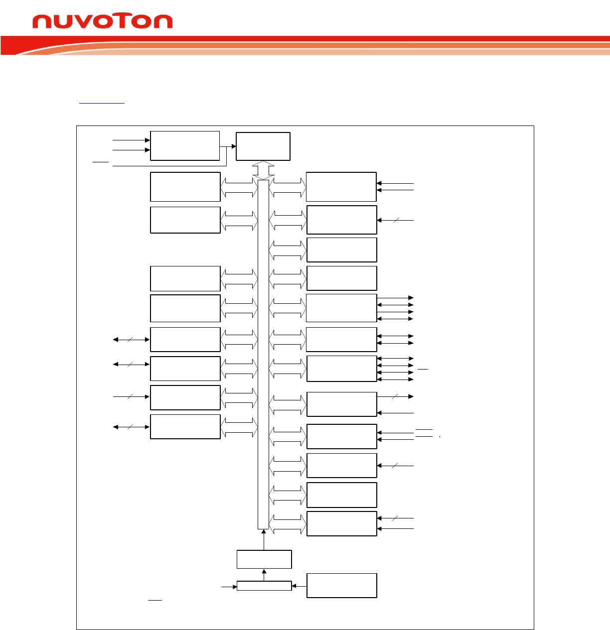
3. BLOCK DIAGRAM
Figure 3-1 shows the N76E003 functional block diagram and gives the outline of the device. User can
find all the peripheral functions of the device in the diagram.
1T High
Performance
8051 Core
Max. 18K Bytes
APROM Flash
256 Bytes
Internal RAM
768 Bytes
XRAM
(Auxiliary RAM)
P0
P1
P2
P3
PWM
Watchdog Timer
Clock Divider
Serial Ports
(UARTs)
Timer 0/1
Power-on Reset
and Brown-out
Detection
I2C
P0[7:0]
P1[7:0]
P20
P30
INT1 (P1.7)
INT0 (P3.0)
RXD (P0.7 or P0.6)
TXD (P0.6 or P0.7)
SDA (P1.4 or P1.6)
SCL (P1.3 or P0.2)
PWM0~PWM5
(P1.5, P1.4, P1.2, P1.1, P1.0, P0.0,
P0.1, P0[3:5])
8-bit Internal Bus
External Interrupt
T1 (P0.0)
T0 (P0.5)
VDD
GND
16 MHz/10 kHz
Internal RC
Oscillator
RST
8
8
1
System Clock
Power
Managment
10
Pin Interrupt Any Port
8
Timer 2
with
Input Capture
IC0~IC7
(P1.5, P1[2:0], P0.0, P0.1, P0[5:3])
[1] P2.0 is shared with RST.
[2] P3.0 is shared with XIN.
RXD_1 (P0.2)
TXD_1 (P1.6)
FB (P1.4)
SPI MISO (P0.1)
MOSI (P0.0)
SPCLK (P1.0)
SS (P1.5)
12-bit ADC AIN0~7 (P1.7, P3.0, P0[7:3], P0.1)
8
STADC (P1.3 or P0.4)
Self Wake-up
Timer
Max. 4K Bytes
LDROM Flash
Timer 3
[1]
[1]
XIN[2]
[2]
9
1
Figure 3-1. Functional Block Diagram

N76E003 Datasheet
Oct 28, 2016 Page 10 of 261 Rev. 1.00
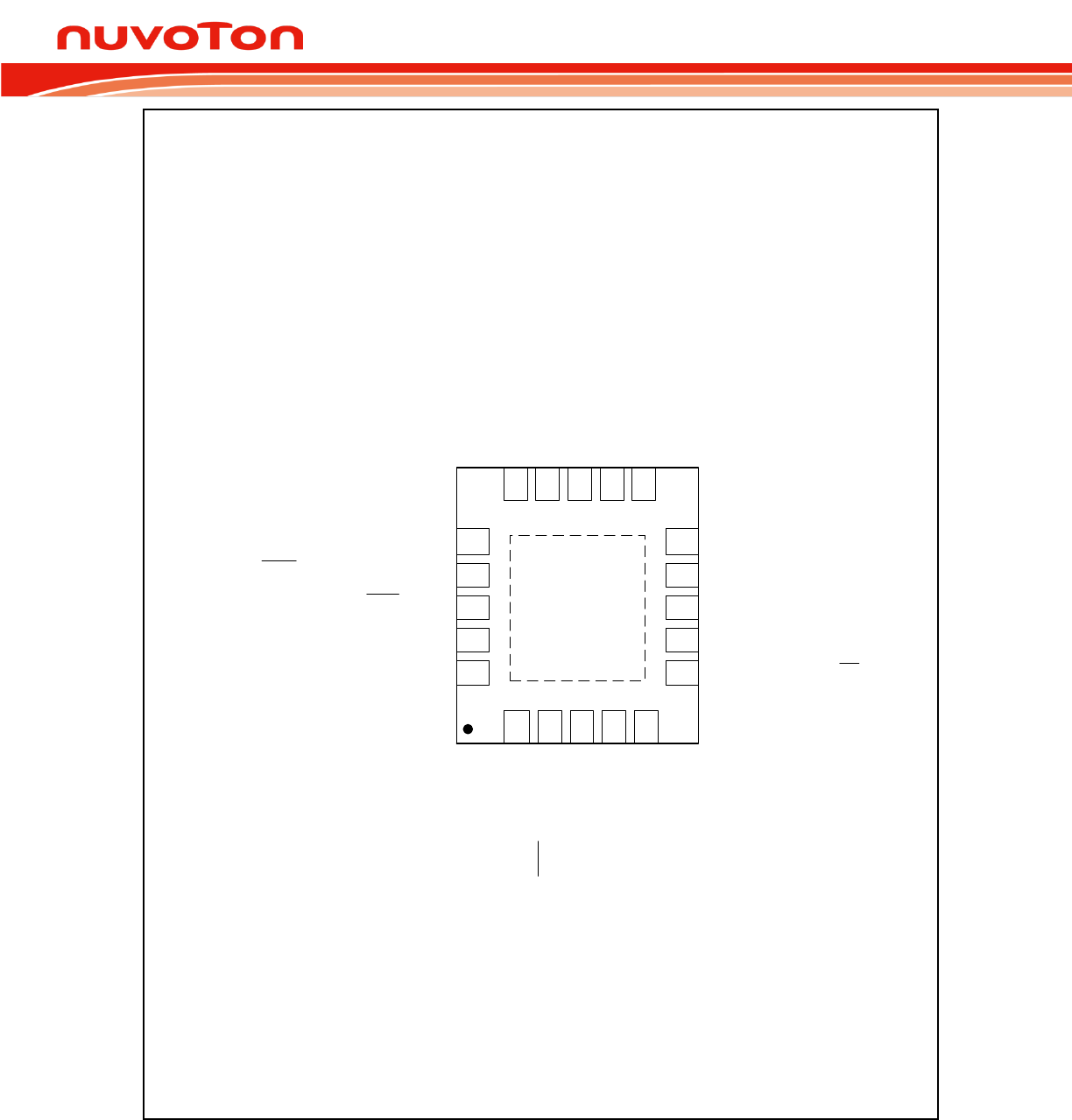
4. PIN CONFIGURATION
10
9
2
1
4
3
6
5
8
7
RST/P2.0
GND
18
19
16
17
14
15
12
13
11
20
VDD
N76E003AT20
[SDA]/TXD_1/ICPDA/OCDDA/P1.6
P1.3/SCL/[STADC]
P1.4/SDA/FB/PWM1
P1.1/PWM1/IC1/AIN7/CLO
P1.0/PWM2/IC2/SPCLK
P0.0/PWM3/IC3/MOSI/T1
P0.1/PWM4/IC4/MISO
P0.3/PWM5/IC5/AIN6
P0.4/AIN5/STADC/PWM3/IC3
TXD/AIN3/P0.6
RXD/AIN2/P0.7
INT0/OSCIN/AIN1/P3.0
PWM5/IC7/SS/P1.5
P0.2/ICPCK/OCDCK/RXD_1/[SCL]
INT1/AIN0/P1.7
PWM2/IC6/T0/AIN4/P0.5
P1.2/PWM0/IC0
1. [ ] alternate function remapping option (if the same alternate function is shown twice, it indicates an exclusive choice not a duplication of the
function).
Figure 4-1. Pin Assignment of TSSOP-20 Package
N76E003 Datasheet
Oct 28, 2016 Page 11 of 261 Rev. 1.00
21 GND
N76E003AQ20
15 14 13 12 11
10
9
8
7
6
21 3 4 5
16
17
18
19
20
AIN5/STADC/PWM3/IC3/P0.4
INT0/OSCIN/AIN1/P3.0
RST/P2.0
TXD/AIN3/P0.6
PWM2/IC6/T0/AIN4/P0.5
P1.4/SDA/FB/PWM1
P1.2/PWM0/IC0
P1.1/PWM1/IC1/AIN7/CLO
P1.0/PWM2/IC2/SPCLK
P1.5/PWM5/IC7/SS
P0.3/PWM5/IC5/AIN6
P0.2/ICPCK/OCDCK/RXD_1/[SCL]
P0.1/PWM4/IC4/MISO
P0.0/PWM3/IC3/MOSI/T1
P1.3/SCL/[STADC]
RXD/AIN2/P0.7
INT1/AIN0/P1.7
GND
[SDA]/TXD_1/ICPDA/OCDDA/P1.6
VDD
1. [ ] alternate function remapping option (if the same alternate function is shown twice, it indicates an exclusive choice not a
duplication of the function).
Figure 4-2. Pin Assignment of QFN-20 Package

N76E003 Datasheet
Oct 28, 2016 Page 12 of 261 Rev. 1.00
Pin Number
Symbol
Multi-Function Description[1]
TSSOP20
QFN20
9
5
VDD
POWER SUPPLY: Supply voltage VDD for operation.
7
3
GND
GROUND: Ground potential.
16
12
P0.0/PWM3/IC3/MOSI/T1
P0.0: Port 0 bit 0.
PWM3: PWM output channel 3.
MOSI: SPI master output/slave input.
IC3: Input capture channel 3.
T1: External count input to Timer/Counter 1 or its toggle
output.
17
13
P0.1/PWM4/IC4/MISO
P0.1: Port 0 bit 1.
PWM4: PWM output channel 4.
IC4: Input capture channel 4.
MISO: SPI master input/slave output.
18
14
P0.2/ICPCK/OCDCK/RXD
_1
/[SCL]
P0.2: Port 0 bit 2.
ICPCK: ICP clock input.
OCDCK: OCD clock input.
RXD_1: Serial port 1 receive input.
[SCL] [3]: I2C clock.
19
15
P0.3/PWM5/IC5/AIN6
P0.3: Port 0 bit 3.
PWM5: PWM output channel
IC5: Input capture channel 5.
AIN6: ADC input channel 6.
20
16
P0.4/AIN5/STADC/PWM3/
IC3
P0.4: Port 0 bit 4.
AIN5: ADC input channel 5.
STADC: External start ADC trigger
PWM3: PWM output channel 3.
IC3: Input capture channel 3.
1
20
P0.5/PWM2/IC6/T0/AIN4
P0.5: Port 0 bit 5.
PWM2: PWM output channel 2.
IC6: Input capture channel 6.
T0: External count input to Timer/Counter 0 or its toggle
output.
2
19
P0.6/TXD/AIN3
P0.6: Port 0 bit 6.
TXD[2]: Serial port 0 transmit data output.
AIN3: ADC input channel 3.
3
1
P0.7/RXD/AIN2
P0.7: Port 0 bit 7.
RXD: Serial port 0 receive input.
AIN2: ADC input channel 2.
15
7
P1.0/PWM2/IC2/SPCLK
P1.0: Port 1 bit 0.
PWM2: PWM output channel 2.
IC2: Input capture channel 2.
SPCLK: SPI clock.
14
8
P1.1/PWM1/IC1/AIN7/CL
O
P1.1: Port 1 bit 1
PWM1: PWM output channel 1.
IC1: Input capture channel 1.
AIN7: ADC input channel 7.
CLO: System clock output.
13
9
P1.2/PWM0/IC0
P1.2: Port 1 bit 2.
PWM0: PWM output channel 0.
IC0: Input capture channel 0.
12
11
P1.3/SCL/[STADC]
P1.3: Port 1 bit 3.
SCL: I2C clock.

N76E003 Datasheet
Oct 28, 2016 Page 13 of 261 Rev. 1.00
Pin Number
Symbol
Multi-Function Description[1]
TSSOP20
QFN20
[STADC] [4]: External start ADC trigger
11
10
P1.4/SDA/FB/PWM1
P1.4: Port 1 bit 4.
SDA: I2C data.
FB: Fault Brake input.
PWM1: PWM output channel 1.
10
6
P1.5/PWM5/IC7/
P1.5: Port 1 bit 5.
PWM5: PWM output channel 5.
IC7: Input capture channel 7.
: SPI slave select input.
8
4
P1.6/ICPDA/OCDDA/TXD
_1
/[SDA]
P1.6: Port 1 bit 6.
ICPDA: ICP data input or output.
OCDAT: OCD data input or output.
TXD_1: Serial port 1 transmit data output.
[SDA] [3]: I2C data.
6
2
P1.7/
/AIN0
P1.7: Port 1 bit 7.
: External interrupt 1 input.
AIN0: ADC input channel 0.
4
18
P2.0/
P2.0: Port 2 bit 0 input pin available when RPD
(CONFIG0.2) is programmed as 0.
:
pin is a Schmitt trigger input pin for hardware
device reset. A low on this pin resets the device.
pin
has an internal pull-up resistor allowing power-on reset by
simply connecting an external capacitor to GND.
5
17
P3.0/
/OSCIN/AIN1
P1.0: Port 3 bit 0 available when the internal oscillator is
used as the system clock.
: External interrupt 0 input.
XIN: If the ECLK mode is enabled, XIN is the external clock
input pin.
AIN1: ADC input channel 1.
[1] All I/O pins can be configured as a interrupt pin. This feature is not listed in multi-function description. See
Section 16. Pin Interrupt.
[2] TXD and RXD pins of UART0 are software exchangeable by UART0PX (AUXR1.2).
[3] [I2C] alternate function remapping option. I2C pins is software switched by I2CPX (I2CON.0).
[4] [STADC] alternate function remapping option. STADC pin is software switched by STADCPX(ADCCON1.6).
[5] PIOx register decides which pins are PWM or GPIO.

N76E003 Datasheet
Oct 28, 2016 Page 14 of 261 Rev. 1.00
5. MEMORY ORGANIZATION
A standard 80C51 based microcontroller divides the memory into two different sections, Program
Memory and Data Memory. The Program Memory is used to store the instruction codes, whereas the
Data Memory is used to store data or variations during the program execution.
The Data Memory occupies a separate address space from Program Memory. In N76E003, there are
256 Bytes of internal scratch-pad RAM. For many applications those need more internal RAM, the
N76E003 provides another on-chip 768 Bytes of RAM, which is called XRAM, accessed by MOVX
instruction.
The whole embedded flash, functioning as Program Memory, is divided into three blocks: Application
ROM (APROM) normally for User Code, Loader ROM (LDROM) normally for Boot Code, and CONFIG
bytes for hardware initialization. Actually, APROM and LDROM function in the same way but have
different size. Each block is accumulated page by page and the page size is 128 Bytes. The flash
control unit supports Erase, Program, and Read modes. The external writer tools though specific I/O
pins, In-Application-Programming (IAP), or In-System-Programming (ISP) can both perform these
modes.
5.1 Program Memory
The Program Memory stores the program codes to execute as shown in Figure 5-1. After any reset,
the CPU begins execution from location 0000H.
To service the interrupts, the interrupt service locations (called interrupt vectors) should be located in
the Program Memory. Each interrupt is assigned with a fixed location in the Program Memory. The
interrupt causes the CPU to jump to that location with where it commences execution of the interrupt
service routine (ISR). External Interrupt 0, for example, is assigned to location 0003H. If External
Interrupt 0 is going to be used, its service routine should begin at location 0003H. If the interrupt is not
going to be used, its service location is available as general purpose Program Memory.
The interrupt service locations are spaced at an interval of eight Bytes: 0003H for External Interrupt 0,
000BH for Timer 0, 0013H for External Interrupt 1, 001BH for Timer 1, etc. If an interrupt service
routine is short enough (as is often the case in control applications), it can reside entirely within the 8-
Byte interval. However longer service routines should use a JMP instruction to skip over subsequent
interrupt locations if other interrupts are in use.
The N76E003 provides two internal Program Memory blocks APROM and LDROM. Although they
both behave the same as the standard 8051 Program Memory, they play different rules according to
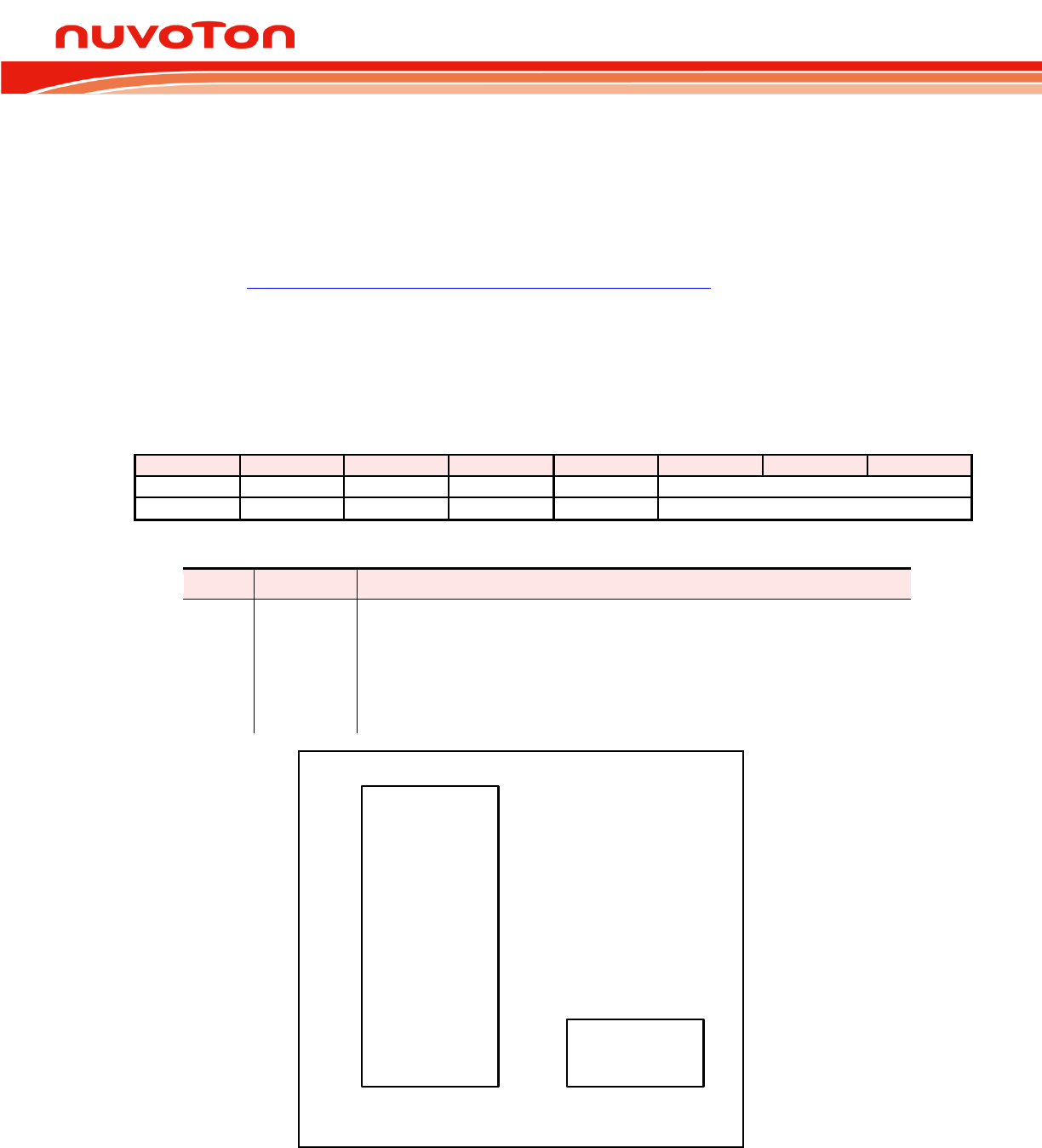
N76E003 Datasheet
Oct 28, 2016 Page 15 of 261 Rev. 1.00
their ROM size. The APROM on N76E003 can be up to 18K Bytes. User Code is normally put inside.
CPU fetches instructions here for execution. The MOVC instruction can also read this region.
The other individual Program Memory block is called LDROM. The normal function of LDROM is to
store the Boot Code for ISP. It can update APROM space and CONFIG bytes. The code in APROM
can also re-program LDROM. For ISP details and configuration bit setting related with APROM and
LDROM, see Section 21.4 In-System-Programming (ISP) 216. Note that APROM and
LDROM are hardware individual blocks, consequently if CPU re-boots from LDROM, CPU will
automatically re-vector Program Counter 0000H to the LDROM start address. Therefore, CPU
accounts the LDROM as an independent Program Memory and all interrupt vectors are independent
from APROM.
CONFIG1
7
6
5
4
3
2
1
0
-
-
-
-
-
LDSIZE[2:0]
-
-
-
-
-
R/W
Factory default value: 1111 1111b
Bit
Name
Description
2:0
LDSIZE[2:0]
LDROM size select
This field selects the size of LDROM.
111 = No LDROM. APROM is 18K Bytes.
110 = LDROM is 1K Bytes. APROM is 17K Bytes.
101 = LDROM is 2K Bytes. APROM is 16K Bytes.
100 = LDROM is 3K Bytes. APROM is 15K Bytes.
0xx = LDROM is 4K Bytes. APROM is 14K Bytes.
LDROM
0000H
0000H
0FFFH/
0BFFH/
07FFH/
03FFH/
0000H[1]
BS = 0 BS = 1
37FFH/
3BFFH/
3FFFH/
43FFH/
47FFH[1]
APROM
[1] The logic boundary addresses of APROM and LDROM are defined
by CONFIG1[2:0].
Figure 5-1. N76E003 Program Memory Map

N76E003 Datasheet
Oct 28, 2016 Page 16 of 261 Rev. 1.00
5.2 Data Memory
Figure 5-2 shows the internal Data Memory spaces available on N76E003. Internal Data Memory
occupies a separate address space from Program Memory. The internal Data Memory can be divided
into three blocks. They are the lower 128 Bytes of RAM, the upper 128 Bytes of RAM, and the 128
Bytes of SFR space. Internal Data Memory addresses are always 8-bit wide, which implies an address
space of only 256 Bytes. Direct addressing higher than 7FH will access the special function registers
(SFRs) space and indirect addressing higher than 7FH will access the upper 128 Bytes of RAM.
Although the SFR space and the upper 128 Bytes of RAM share the same logic address, 80H through
FFH, actually they are physically separate entities. Direct addressing to distinguish with the higher 128
Bytes of RAM can only access these SFRs. Sixteen addresses in SFR space are either byte-
addressable or bit-addressable. The bit-addressable SFRs are those whose addresses end in 0H or
8H.
The lower 128 Bytes of internal RAM are present in all 80C51 devices. The lowest 32 Bytes as
general purpose registers are grouped into 4 banks of 8 registers. Program instructions call these
registers as R0 to R7. Two bits RS0 and RS1 in the Program Status Word (PSW[3:4]) select which
Register Bank is used. It benefits more efficiency of code space, since register instructions are shorter
than instructions that use direct addressing. The next 16 Bytes above the general purpose registers
(byte-address 20H through 2FH) form a block of bit-addressable memory space (bit-address 00H
through 7FH). The 80C51 instruction set includes a wide selection of single-bit instructions, and the
128 bits in this area can be directly addressed by these instructions. The bit addresses in this area are
00H through 7FH.
Either direct or indirect addressing can access the lower 128 Bytes space. But the upper 128 Bytes can only be
accessed by indirect addressing.
Another application implemented with the whole block of internal 256 Bytes RAM is used for the stack.
This area is selected by the Stack Pointer (SP), which stores the address of the top of the stack.
Whenever a JMP, CALL or interrupt is invoked, the return address is placed on the stack. There is no
restriction as to where the stack can begin in the RAM. By default however, the Stack Pointer contains
07H at reset. User can then change this to any value desired. The SP will point to the last used value.
Therefore, the SP will be incremented and then address saved onto the stack. Conversely, while
popping from the stack the contents will be read first, and then the SP is decreased.
N76E003 Datasheet
Oct 28, 2016 Page 17 of 261 Rev. 1.00
Upper 128 Bytes
internal RAM
(indirect addressing)
00H
7FH
80H
FFH
Lower 128 Bytes
internal RAM
(direct or indirect
addressing)
SFR
(direct addressing)
0000H
02FFH
768 Bytes XRAM
(MOVX addressing)
Figure 5-2. Data Memory Map
Register Bank 0
Register Bank 1
Register Bank 2
Register Bank 3
03 02 01 0004050607
0B 0A 09 080C0D0E0F
13 12 11 1014151617
1B 1A 19 181C1D1E1F
23 22 21 2024252627
2B 2A 29 282C2D2E2F
33 32 31 30
34353637
3B 3A 39 383C3D3E3F
43 42 41 4044454647
4B 4A 49 484C4D4E4F
53 52 51 5054555657
5B 5A 59 585C5D5E5F
63 62 61 6064656667
6B 6A 69 686C6D6E
6F
73 72 71 7074757677
7B 7A 79 787C7D7E7F
Direct or Indirect Accessing RAM
Indirect Accessing RAM
00H
07H
28H
08H
0FH
10H
17H
18H
1FH
20H
21H
22H
23H
24H
25H
26H
27H
29H
2AH
2BH
2CH
2DH
2EH
2FH
30H
7FH
80H
FFH
00H
FFH
Bit-addressable
General Purpose Registers
General Purpose
Registers
Figure 5-3. Internal 256 Bytes RAM Addressing

N76E003 Datasheet
Oct 28, 2016 Page 18 of 261 Rev. 1.00
5.3 On-Chip XRAM
The N76E003 provides additional on-chip 768 bytes auxiliary RAM called XRAM to enlarge the RAM
space. It occupies the address space from 00H through FFH. The 768 bytes of XRAM are indirectly
accessed by move external instruction MOVX @DPTR or MOVX @Ri. (See the demo code below.)
Note that the stack pointer cannot be located in any part of XRAM.
XRAM demo code:
MOV R0,#23H ;write #5AH to XRAM with address @23H
MOV A,#5AH
MOVX @R0,A
MOV R1,#23H ;read from XRAM with address @23H
MOVX A,@R1
MOV DPTR,#0023H ;write #5BH to XRAM with address @0023H
MOV A,#5BH
MOVX @DPTR,A
MOV DPTR,#0023H ;read from XRAM with address @0023H
MOVX A,@DPTR
5.4 Non-Volatile Data Storage
By applying IAP, any page of APROM or LDROM can be used as non-volatile data storage. For IAP
details, please see Section 21. In-Application-Programming (IAP)210.
N76E003 Datasheet
Oct 28, 2016 Page 19 of 261 Rev. 1.00
6. SPECIAL FUNCTION REGISTER (SFR)
The N76E003 uses Special Function Registers (SFRs) to control and monitor peripherals and their
modes. The SFRs reside in the register locations 80 to FFH and are accessed by direct addressing
only. SFRs those end their addresses as 0H or 8H are bit-addressable. It is very useful in cases where
user would like to modify a particular bit directly without changing other bits via bit-field instructions. All
other SFRs are byte-addressable only. The N76E003 contains all the SFRs presenting in the standard
8051. However some additional SFRs are built in. Therefore, some of unused bytes in the original
8051 have been given new functions. The SFRs are listed below.
To accommodate more than 128 SFRs in the 0x80 to 0xFF address space, SFR paging has been
implemented. By default, all SFR accesses target SFR page 0. During device initialization, some
SFRs located on SFR page 1 may need to be accessed. The register SFRS is used to switch SFR
addressing page. Note that this register has TA write protection. Most of SFRs are available on both
SFR page 0 and 1.
SFRS SFR Page Selection (TA protected)
7
6
5
4
3
2
1
0
-
-
-
-
-
-
-
SFRPAGE
-
-
-
-
-
-
-
R/W
Address: 91H Reset value: 0000 0000b
Bit
Name
Description
0
SFRPAGE
SFR page select
0 = Instructions access SFR page 0.
1 = Instructions access SFR page 1.
Switch SFR page demo code:
MOV TA,#0AAH ;switch to SFR page 1
MOV TA,#55H
ORL SFRS,#01H
MOV TA,#0AAH ;switch to SFR page 0
MOV TA,#55H
ANL SFRS,#0FEH

N76E003 Datasheet
Oct 28, 2016 Page 20 of 261 Rev. 1.00
Table 6-1. SFR Memory Map
SFR
Page
Addr
0/8
1/9
2/A
3/B
4/C
5/D
6/E
7/F
0
1
F8
SCON_1
PDTEN
PDTCNT
PMEN
PMD
-
EIP1
-
EIPH1
-
0
1
F0
B
CAPCON3
CAPCON4
SPCR
SPCR2
SPSR
SPDR
-
AINDIDS
-
EIPH
-
0
1
E8
ADCCON0
PICON
PINEN
PIPEN
PIF
C2L
C2H
EIP
-
0
1
E0
ACC
ADCCON1
ADCCON2
ADCDLY
C0L
C0H
C1L
C1H
0
1
D8
PWMCON0
PWMPL
PWM0L
PWM1L
PWM2L
PWM3L
PIOCON0
PWMCON1
0
1
D0
PSW
PWMPH
PWM0H
PWM1H
PWM2H
PWM3H
PNP
FBD
0
1
C8
T2CON
T2MOD
RCMP2L
RCMP2H
TL2
PWM4L
TH2
PWM5L
ADCMPL
ADCMPH
0
1
C0
I2CON
I2ADDR
ADCRL
ADCRH
T3CON
PWM4H
RL3
PWM5H
RH3
PIOCON1
TA
0
1
B8
IP
SADEN
SADEN_1
SADDR_1
I2DAT
I2STAT
I2CLK
I2TOC
0
1
B0
P3
P0M1
P0S
P0M2
P0SR
P1M1
P1S
P1M2
P1SR
P2S
-
IPH
PWMINTC
0
1
A8
IE
SADDR
WDCON
BODCON1
P3M1
P3S
P3M2
P3SR
IAPFD
IAPCN
0
1
A0
P2
-
AUXR1
BODCON0
IAPTRG
IAPUEN
IAPAL
IAPAH
0
1
98
SCON
SBUF
SBUF_1
EIE
EIE1
-
-
CHPCON
0
1
90
P1
SFRS
CAPCON0
CAPCON1
CAPCON2
CKDIV
CKSWT
CKEN
0
1
88
TCON
TMOD
TL0
TL1
TH0
TH1
CKCON
WKCON
0
1
80
P0
SP
DPL
DPH
RCTRIM0
RCTRIM1
RWK
PCON
Unoccupied addresses in the SFR space marked in “-“ are reserved for future use. Accessing
these areas will have an indeterminate effect and should be avoided.
N76E003 Datasheet
Oct 28, 2016 Page 21 of 261 Rev. 1.00
Table 6-2. SFR Definitions and Reset Values
Symbol
Definition
Address
/(Page)
MSB LSB[1]
Reset Value[2]
EIPH1
Extensive interrupt
priority high 1
FFH/(0)
-
-
-
-
-
PWKTH
PT3H
PSH_1
0000 0000b
EIP1
Extensive interrupt
priority 1
FEH/(0)
-
-
-
-
-
PWKT
PT3
PS_1
0000 0000b
PMD
PWM mask data
FCH
-
-
PMD5
PMD4
PMD3
PMD2
PMD1
PMD0
0000 0000b
PMEN
PWM mask enable
FBH
-
-
PMEN5
PMEN4
PMEN3
PMEN2
PMEN1
PMEN0
0000 0000b
PDTCNT[4]
PWM dead-time counter
FAH
PDTCNT[7:0]
0000 0000b
PDTEN[4]
PWM dead-time enable
F9H
-
-
-
PDTCNT.8
-
PDT45EN
PDT23EN
PDT01EN
0000 0000b
SCON_1
Serial port 1 control
F8H
(FF)
SM0_1/
FE_1
(FE)
SM1_1
(FD)
SM2_1
(FC)
REN_1
(FB)
TB8_1
(FA)
RB8_1
(F9)
TI_1
(F8)
RI_1
0000 0000b
EIPH
Extensive interrupt
priority high
F7H
PT2H
PSPIH
PFBH
PWDTH
PPWMH
PCAPH
PPIH
PI2CH
0000 0000b
AINDIDS
ADC channel digital
input disable
F6H
P11DIDS
P03DIDS
P04DIDS
P05DIDS
P06DIDS
P07DIDS
P30DIDS
P17DIDS
0000 0000b
SPDR
SPI data
F5H(0)
SPDR[7:0]
0000 0000b
SPSR
SPI status
F4H
SPIF
WCOL
SPIOVF
MODF
DISMODF
-
-
-
0000 0000b
SPCR
SPI control
F3H(0)
SSOE
SPIEN
LSBFE
MSTR
CPOL
CPHA
SPR[1:0]
0000 0000b
SPCR2
SPI control 2
F3H(1)
-
-
-
-
-
-
SPIS[1:0]
0000 0000b
CAPCON4
Input capture control 4
F2H
-
-
-
-
CAP23
CAP22
CAP21
CAP20
0 0 0 0 0 0 0 0 b
CAPCON3
Input capture control 3
F1H
CAP13
CAP12
CAP11
CAP10
CAP03
CAP02
CAP01
CAP00
0 0 0 0 0 0 0 0 b
B
B register
F0H
(F7)
B.7
(F6)
B.6
(F5)
B.5
(F4)
B.4
(F3)
B.3
(F2)
B.2
(F1)
B.1
(F0)
B.0
0000 0000b
EIP
Extensive interrupt
priority
EFH
PT2
PSPI
PFB
PWDT
PPWM
PCAP
PPI
PI2C
0000 0 0 0 0 b
C2H
Input capture 2 high byte
EEH
C2H[7:0]
0000 0000b
C2L
Input capture 2 low byte
EDH
C2L[7:0]
0000 0000b
PIF
Pin interrupt flag
ECH
PIF7
PIF6
PIF5
PIF4
PIF3
PIF2
PIF1
PIF0
0000 0000b
PIPEN
Pin interrupt high
level/rising edge enable
EBH
PIPEN7
PIPEN6
PIPEN5
PIPEN4
PIPEN3
PIPEN2
PIPEN1
PIPEN0
0000 0000b
PINEN
Pin interrupt low
level/falling edge enable
EAH
PINEN7
PINEN6
PINEN5
PINEN4
PINEN3
PINEN2
PINEN1
PINEN0
0000 0000b
PICON
Pin interrupt control
E9H
PIT67
PIT45
PIT3
PIT2
PIT1
PIT0
PIPS[1:0]
0000 0000b
ADCCON0
ADC control 0
E8H
(EF)
ADCF
(EE)
ADCS
(ED)
ETGSEL1
(EC)
ETGSEL0
(EB)
ADCHS3
(EA)
ADCHS2
(E9)
ADCHS1
(E8)
ADCHS0
0000 0000b
C1H
Input capture 1 high byte
E7H
C1H[7:0]
0000 0000b
C1L
Input capture 1 low byte
E6H
C1L[7:0]
0000 0000b
C0H
Input capture 0 high byte
E5H
C0H[7:0]
0000 0000b
C0L
Input capture 0 low byte
E4H
C0L[7:0]
0000 0000b
ADCDLY
ADC trigger delay
E3H
ADCDLY[7:0]
0000 0000b
ADCCON2
ADC control 2
E2H
ADFBEN
ADCMPOP
ADCMPEN
ADCMPO
-
-
-
ADCDLY.8
0000 0000b
ADCCON1
ADC control 1
E1H
-
STADCPX
-
-
ETGTYP[1:0]
ADCEX
ADCEN
0000 0000b
ACC
Accumulator
E0H
(E7)
ACC.7
(E6)
ACC.6
(E5)
ACC.5
(E4)
ACC.4
(E3)
ACC.3
(E2)
ACC.2
(E1)
ACC.1
(E0)
ACC.0
0000 0000b
PWMCON1
PWM control 1
DFH
PWMMOD[1:0]
GP
PWMTYP
FBINEN
PWMDIV[2:0]
0000 0 0 0 0 b
PIOCON0
PWM I/O switch 0
DEH
-
-
PIO05
PIO04
PIO03
PIO02
PIO01
PIO00
0000 0000b
PWM3L
PWM3 duty low byte
DDH
PWM3[7:0]
0000 0000b
PWM2L
PWM2 duty low byte
DCH
PWM2[7:0]
0000 0000b
PWM1L
PWM1 duty low byte
DBH
PWM1[7:0]
0000 0000b
PWM0L
PWM0 duty low byte
DAH
PWM0[7:0]
0000 0000b
PWMPL
PWM period low byte
D9H
PWMP[7:0]
0000 0000b
PWMCON0
PWM control 0
D8H
(DF)
PWMRUN
(DE)
LOAD
(DD)
PWMF
(DC)
CLRPWM
(DB)
-
(DA)
-
(D9)
-
(D8)
-
0000 0000b
FBD
Brake data
D7H
FBF
FBINLS
FBD5
FBD4
FBD3
FBD2
FBD1
FBD0
0000 0000b
PNP
PWM negative polarity
D6H
-
-
PNP5
PNP4
PNP3
PNP2
PNP1
PNP0
0000 0000b
PWM3H
PWM3 duty high byte
D5H
PWM3[15:8]
0000 0000b
PWM2H
PWM2 duty high byte
D4H
PWM2[15:8]
0000 0000b
PWM1H
PWM1 duty high byte
D3H
PWM1[15:8]
0000 0000b
PWM0H
PWM0 duty high byte
D2H
PWM0[15:8]
0000 0000b
PWMPH
PWM period high byte
D1H
PWMP[15:8]
0000 0000b
PSW
Program status word
D0H
(D7)
CY
(D6)
AC
(D5)
F0
(D4)
RS1
(D3)
RS0
(D2)
OV
(D1)
-
(D0)
P
0000 0000b
ADCMPH
ADC compare high byte
CFH
ADCMP[11:4]
0000 0000b
ADCMPL
ADC compare low byte
CEH
-
-
-
-
ADCMP[3:0]
0000 0000b
PWM5L
PWM5 duty low byte
CDH(1)
PWM5[7:0]
0000 0000b
TH2
Timer 2 high byte
CDH(0)
TH2[7:0]
0000 0000b
PWM4L
PWM4 duty low byte
CCH(1)
PWM4[7:0]
0000 0000b
N76E003 Datasheet
Oct 28, 2016 Page 22 of 261 Rev. 1.00
Table 6-2. SFR Definitions and Reset Values
Symbol
Definition
Address
/(Page)
MSB LSB[1]
Reset Value[2]
TL2
Timer 2 low byte
CCH(0)
TL2[7:0]
0000 0000b
RCMP2H
Timer 2 compare high
byte
CBH
RCMP2H[7:0]
0000 0000b
RCMP2L
Timer 2 compare low
byte
CAH(0)
RCMP2L[7:0]
0000 0000b
T2MOD
Timer 2 mode
C9H
LDEN
T2DIV[2:0]
CAPCR
CMPCR
LDTS[1:0]
0000 0000b
T2CON
Timer 2 control
C8H
(CF)
TF2
(CE)
-
(CD)
-
(CC)
-
(CB)
-
(CA)
TR2
(C9)
-
(C8)
0000 0000b
TA
Timed access protection
C7H
TA[7:0]
0000 0000b
PIOCON1
PWM I/O switch 1
C6H(1)
-
-
PIO15
-
PIO13
PIO12
PIO11
-
0000 0000b
RH3
Timer 3 reload high byte
C6H(0)
RH3[7:0]
0000 0000b
PWM5H
PWM5 duty high byte
C5H(1)
PWM5[15:8]
0000 0000b
RL3
Timer 3 reload low byte
C5H(0)
RL3[7:0]
0000 0000b
PWM4H
PWM4 duty high byte
C4H(1)
PWM4[15:8]
0000 0000b
T3CON
Timer 3 control
C4H(0)
SMOD_1
SMOD0_1
BRCK
TF3
TR3
T3PS[2:0]
0000 0000b
ADCRH
ADC result high byte
C3H
ADCR[11:4]
0000 0000b
ADCRL
ADC result low byte
C2H
-
-
-
-
ADCR[3:0]
0000 0000b
I2ADDR
I2C own slave address
C1H
I2ADDR[7:1]
GC
0000 0000b
I2CON
I2C control
C0H
(C7)
-
(C6)
I2CEN
(C4)
STA
(C4)
STO
(C3)
SI
(C2)
AA
(C1)
-
(C0)
I2CPX
0000 0000b
I2TOC
I2C time-out counter
BFH
-
-
-
-
-
I2TOCEN
DIV
I2TOF
0000 0000b
I2CLK
I2C clock
BEH
I2CLK[7:0]
0000 1001b
I2STAT
I2C status
BDH
I2STAT[7:3]
0
0
0
1111 1000b
I2DAT
I2C data
BCH
I2DAT[7:0]
0000 0000b
SADDR_1
Slave 1 address
BBH
SADDR_1[7:0]
0000 0000b
SADEN_1
Slave 1 address mask
BAH
SADEN_1[7:0]
0000 0000b
SADEN
Slave 0 address mask
B9H
SADEN[7:0]
0000 0000b
IP
Interrupt priority
B8H
(BF)
-
(BE)
PADC
(BD)
PBOD
(BC)
PS
(BB)
PT1
(BA)
PX1
(B9)
PT0
(B8)
PX0
0000 0000b
PWMINTC
PWM Interrupt Control
B7H(1)
-
-
INTTYP1
INTTYP0
-
INTSEL2
INTSEL1
INTSEL0
0000 0000b
IPH
Interrupt priority high
B7H(0)
-
PADCH
PBODH
PSH
PT1H
PX1H
PT0H
PX0H
0000 0000b
P2S
P20 Setting and
Timer0/1 Output Enable
B5H
P20UP
-
-
-
T1OE
T0OE
-
P2S.0
0000 0000b
P1SR
P1 slew rate
B4H/(1)
P1SR.7
P1SR.6
P1SR.5
P1SR.4
P1SR.3
P1SR.2
P1SR.1
P1SR.0
0000 0000b
P1M2
P1 mode select 2
B4H/(0)
P1M2.7
P1M2.6
P1M2.5
P1M2.4
P1M2.3
P1M2.2
P1M2.1
P1M2.0
0000 0000b
P1S
P1 Schmitt trigger input
B3H/(1)
P1S.7
P1S.6
P1S.5
P1S.4
P1S.3
P1S.2
P1S.1
P1S.0
0000 0000b
P1M1
P1 mode select 1
B3H/(0)
P1M1.7
P1M1.6
P1M1.5
P1M1.4
P1M1.3
P1M1.2
P1M1.1
P1M1.0
1111 1111b
P0SR
P0 slew rate
B2H/(1)
P0SR.7
P0SR.6
P0SR.5
P0SR.4
P0SR.3
P0SR.2
P0SR.1
P0SR.0
0000 0000b
P0M2
P0 mode select 2
B2H/(0)
P0M2.7
P0M2.6
P0M2.5
P0M2.4
P0M2.3
P0M2.2
P0M2.1
P0M2.0
0000 0000b
P0S
P0 Schmitt trigger input
B1H/(1)
P0S.7
P0S.6
P0S.5
P0S.4
P0S.3
P0S.2
P0S.1
P0S.0
0000 0000b
P0M1
P0 mode select 1
B1H/(0)
P0M1.7
P0M1.6
P0M1.5
P0M1.4
P0M1.3
P0M1.2
P0M1.1
P0M1.0
1111 1111b
P3
Port 3
B0H
(B7)
0
(B6)
0
(B5)
0
(B4)
0
(B3)
0
(B2)
0
(B1)
0
(B0)
P3.0
Output latch,
0000 0001b
Input,
0000 000Xb[3]
IAPCN
IAP control
AFH
IAPA[17:16]
FOEN
FCEN
FCTRL[3:0]
0011 0000b
IAPFD
IAP flash data
AEH
IAPFD[7:0]
0000 0000b
P3SR
P3 slew rate
ADH/(1)
-
-
-
-
-
-
-
P3SR.0
0000 0000b
P3M2
P3 mode select 2
ADH/(0)
-
-
-
-
-
-
-
P3M2.0
0000 0000b
P3S
P3 Schmitt trigger input
ACH/(1)
-
-
-
-
-
-
-
P3S.0
0000 0000b
P3M1
P3 mode select 1
ACH/(0)
-
-
-
-
-
-
-
P3M1.0
0000 0001b
BODCON1[4]
Brown-out detection
control 1
ABH
-
-
-
-
-
LPBOD[1:0]
BODFLT
POR,
0000 0001b
Others,
0000 0UU Ub
WDCON[4]
Watchdog Timer control
AAH
WDTR
WDCLR
WDTF
WIDPD
WDTRF
WDPS[2:0]
POR,
0000 0111b
WDT,
0000 1UU Ub
Others,
0000 UUUUb
N76E003 Datasheet
Oct 28, 2016 Page 23 of 261 Rev. 1.00
Table 6-2. SFR Definitions and Reset Values
Symbol
Definition
Address
/(Page)
MSB LSB[1]
Reset Value[2]
SADDR
Slave 0 address
A9H
SADDR[7:0]
0000 0000b
IE
Interrupt enable
A8H
(AF)
EA
(AE)
EADC
(AD)
EBOD
(AC)
ES
(AB)
ET1
(AA)
EX1
(A9)
ET0
(A8)
EX0
0000 0000b
IAPAH
IAP address high byte
A7H
IAPA[15:8]
0000 0000b
IAPAL
IAP address low byte
A6H
IAPA[7:0]
0000 0000b
IAPUEN[4]
IAP update enable
A5H
-
-
-
-
-
CFUEN
LDUEN
APUEN
0000 0000b
IAPTRG[4]
IAP trigger
A4H
-
-
-
-
-
-
-
IAPGO
0000 0000b
BODCON0[4]
Brown-out detection
control 0
A3H
BODEN[5]
-
BOV[1:0][5]
BOF[6]
BORST[5]
BORF
BOS[7]
POR,
CCCC XC0Xb
BOD,
UUUU XU1Xb
Others,
UUUU XUUXb
AUXR1
Auxiliary register 1
A2H
SWRF
RSTPINF
HardF
-
GF2
UART0PX
0
DPS
POR,
0000 0000b
Software,
1U00 0000b
pin,
U100 0000b
Others,
UUU0 0000b
P2
Port 2
A0H
(A7)
0
(A6)
0
(A5)
0
(A4)
0
(A3)
0
(A2)
0
(A1)
0
(A0)
P2.0
Output latch,
0 0 0 0 0 0 0 X b
Input,
0000 000Xb[3]
CHPCON[4]
Chip control
9FH
SWRST
IAPFF
-
-
-
-
BS[5]
IAPEN
Software,
0000 00U0b
Others,
0000 00C0b
EIE1
Extensive interrupt
enable 1
9CH
-
-
-
-
-
EWKT
ET3
ES_1
0000 0000b
EIE
Extensive interrupt
enable
9BH
ET2
ESPI
EFB
EWDT
EPWM
ECAP
EPI
EI2C
0000 0000b
SBUF_1
Serial port 1 data buffer
9AH
SBUF_1[7:0]
0000 0000b
SBUF
Serial port 0 data buffer
99H
SBUF[7:0]
0000 0000b
SCON
Serial port 0 control
98H
(9F)
SM0/FE
(9E)
SM1
(9D)
SM2
(9C)
REN
(9B)
TB8
(9A)
RB8
(99)
TI
(98)
RI
0000 0 0 0 0 b
CKEN[4]
Clock enable
97H
EXTEN[1:0]
HIRCEN
-
-
-
-
CKSWTF
0011 0000b
CKSWT[4]
Clock switch
96H
-
-
HIRCST
-
ECLKST
OSC[1:0]
-
0011 0000b
CKDIV
Clock divider
95H
CKDIV[7:0]
0000 0000b
CAPCON2
Input capture control 2
94H
-
ENF2
ENF1
ENF0
-
-
-
-
0000 0000b
CAPCON1
Input capture control 1
93H
-
-
CAP2LS[1:0]
CAP1LS[1:0]
CAP0LS[1:0]
0000 0000b
CAPCON0
Input capture control 0
92H
-
CAPEN2
CAPEN1
CAPEN0
-
CAPF2
CAPF1
CAPF0
0000 0000b
SFRS[4]
SFR page selection
91H
-
-
-
-
-
-
-
SFRPSEL
0000 0000b
P1
Port 1
90H
(97)
P1.7
(96)
P1.6
(95)
P1.5
(94)
P1.4
(93)
P1.3
(92)
P1.2
(91)
P1.1
(90)
P1.0
Output latch,
1111 1111b
Input,
XXXX XXXXb[3]
WKCON
Self Wake-up Timer
control
8FH
-
-
-
WKTF
WKTR
WKPS[2:0]
0000 0000b
CKCON
Clock control
8EH
-
PWMCKS
-
T1M
T0M
-
CLOEN
-
0000 0000b
TH1
Timer 1 high byte
8DH
TH1[7:0]
0000 0000b
TH0
Timer 0 high byte
8CH
TH0[7:0]
0000 0000b
TL1
Timer 1 low byte
8BH
TL1[7:0]
0000 0000b
TL0
Timer 0 low byte
8AH
TL0[7:0]
0000 0000b
TMOD
Timer 0 and 1 mode
89H
GATE
M1
M0
GATE
M1
M0
0000 0000b
TCON
Timer 0 and 1control
88H
(8F)
TF1
(8E)
TR1
(8D)
TF0
(8C)
TR0
(8B)
IE1
(8A)
IT1
(89)
IE0
(88)
IT0
0000 0000b
PCON
Power control
87H
SMOD
SMOD0
-
POF
GF1
GF0
PD
IDL
POR,
0001 0000b
Others,
000U 0000b
RWK
Self Wake-up Timer
reload byte
86H
RWK[7:0]
0000 0000b
RCTRIM1
Internal RC trim value
low byte
85H
-
-
-
-
-
-
-
HIRCTRIM[0]
0000 0000b
RCTRIM0
Internal RC trim value
84H
HIRCTRIM[8:1]
0000 0000b
N76E003 Datasheet
Oct 28, 2016 Page 24 of 261 Rev. 1.00
Table 6-2. SFR Definitions and Reset Values
Symbol
Definition
Address
/(Page)
MSB LSB[1]
Reset Value[2]
high byte
DPH
Data pointer high byte
83H
DPTR[15:8]
0000 0000b
DPL
Data pointer low byte
82H
DPTR[7:0]
0000 0000b
SP
Stack pointer
81H
SP[7:0]
0000 0111b
P0
Port 0
80H
(87)
P0.7
(86)
P0.6
(85)
P0.5
(84)
P0.4
(83)
P0.3
(82)
P0.2
(81)
P0.1
(80)
P0.0
Output latch,
1111 1111b
Input,
XXXX XXXXb[3]
[1] ( ) item means the bit address in bit-addressable SFRs.
[2] Reset value symbol description. 0: logic 0; 1: logic 1; U: unchanged; C: see [5]; X: see [3], [6], and [7].
[3] All I/O pins are default input-only mode (floating) after reset. Reading back P2.0 is always 0 if RPD
(CONFIG0.2) remains un-programmed 1.
[4] These SFRs have TA protected writing.
[5] These SFRs have bits those are initialized according to CONFIG values after specified resets.
[6] BOF reset value depends on different setting of CONFIG2 and VDD voltage level. Please check Table 24-1.
[7] BOS is a read-only flag decided by VDD level while brown-out detection is enabled.
Bits marked in “-“ are reserved for future use. They must be kept in their own initial states.
Accessing these bits may cause an unpredictable effect.
6.1 ALL SFR DESCRIPTION
Following list all SFR description. For each SFR define also list in function IP chapter.
P0 Port 0 (Bit-addressable)
7
6
5
4
3
2
1
0
P0.7
P0.6
P0.5
P0.4
P0.3
P0.2
P0.1
P0.0
R/W
R/W
R/W
R/W
R/W
R/W
R/W
R/W
Address: 80H Reset value: 1111 1111b
Bit
Name
Description
7:0
P0[7:0]
Port 0
Port 0 is an maximum 8-bit general purpose I/O port.
SP Stack Pointer
7
6
5
4
3
2
1
0
SP[7:0]
R/W
Address: 81H Reset value: 0000 0111b
Bit
Name
Description
7:0
SP[7:0]
Stack pointer
The Stack Pointer stores the scratch-pad RAM address where the stack begins. It
is incremented before data is stored during PUSH or CALL instructions. Note that
the default value of SP is 07H. This causes the stack to begin at location 08H.
N76E003 Datasheet
Oct 28, 2016 Page 25 of 261 Rev. 1.00
DPL Data Pointer Low Byte
7
6
5
4
3
2
1
0
DPL[7:0]
R/W
Address: 82H Reset value: 0000 0000b
Bit
Name
Description
7:0
DPL[7:0]
Data pointer low byte
This is the low byte of 16-bit data pointer. DPL combined with DPH serve as a 16-
bit data pointer DPTR to access indirect addressed RAM or Program Memory.
DPS (AUXR1.0) bit decides which data pointer, DPTR or DPTR1, is activated.
DPH Data Pointer High Byte
7
6
5
4
3
2
1
0
DPH[7:0]
R/W
Address: 83H Reset value: 0000 0000b
Bit
Name
Description
7:0
DPH[7:0]
Data pointer high byte
This is the high byte of 16-bit data pointer. DPH combined with DPL serve as a
16-bit data pointer DPTR to access indirect addressed RAM or Program Memory.
DPS (AUXR1.0) bit decides which data pointer, DPTR or DPTR1, is activated.
RWK Self Wake-up Timer Reload Byte
7
6
5
4
3
2
1
0
RWK[7:0]
R/W
Address: 86H Reset value: 0000 0000b
Bit
Name
Description
7:0
RWK[7:0]
WKT reload byte
It holds the 8-bit reload value of WKT. Note that RWK should not be FFH if the
pre-scale is 1/1 for implement limitation.
PCON Power Control
7
6
5
4
3
2
1
0
SMOD
SMOD0
-
POF
GF1
GF0
PD
IDL
R/W
R/W
-
R/W
R/W
R/W
R/W
R/W
Address: 87H Reset value: see Table 6-2. SFR Definitions and Reset Values
Bit
Name
Description
7
SMOD
Serial port 0 double baud rate enable
Setting this bit doubles the serial port baud rate when UART0 is in Mode 2 or
when Timer 1 overflow is used as the baud rate source of UART0 Mode 1 or 3.
See Table 13-1. Serial Port 0 Mode Description for details.
6
SMOD0
Serial port 0 framing error flag access enable
0 = SCON.7 accesses to SM0 bit.
1 = SCON.7 accesses to FE bit.
N76E003 Datasheet
Oct 28, 2016 Page 26 of 261 Rev. 1.00
Bit
Name
Description
4
POF
Power-on reset flag
This bit will be set as 1 after a power-on reset. It indicates a cold reset, a power-on
reset complete. This bit remains its value after any other resets. This flag is
recommended to be cleared via software.
3
GF1
General purpose flag 1
The general purpose flag that can be set or cleared by user via software.
2
GF0
General purpose flag 0
The general purpose flag that can be set or cleared by user via software.
1
PD
Power-down mode
Setting this bit puts CPU into Power-down mode. Under this mode, both CPU and
peripheral clocks stop and Program Counter (PC) suspends. It provides the lowest
power consumption. After CPU is woken up from Power-down, this bit will be
automatically cleared via hardware and the program continue executing the
interrupt service routine (ISR) of the very interrupt source that woke the system up
before. After return from the ISR, the device continues execution at the instruction,
which follows the instruction that put the system into Power-down mode.
Note that If IDL bit and PD bit are set simultaneously, CPU will enter Power-down
mode. Then it does not go to Idle mode after exiting Power-down.
0
IDL
Idle mode
Setting this bit puts CPU into Idle mode. Under this mode, the CPU clock stops
and Program Counter (PC) suspends but all peripherals keep activated. After
CPU is woken up from Idle, this bit will be automatically cleared via hardware and
the program continue executing the ISR of the very interrupt source that woke the
system up before. After return from the ISR, the device continues execution at the
instruction which follows the instruction that put the system into Idle mode.
TCON Timer 0 and 1 Control (Bit-addressable)
7
6
5
4
3
2
1
0
TF1
TR1
TF0
TR0
IE1
IT1
IE0
IT0
R/W
R/W
R/W
R/W
R (level)
R/W (edge)
R/W
R (level)
R/W (edge)
R/W
Address: 88H Reset value: 0000 0000b
Bit
Name
Description
7
TF1
Timer 1 overflow flag
This bit is set when Timer 1 overflows. It is automatically cleared by hardware
when the program executes the Timer 1 interrupt service routine. This bit can be
set or cleared by software.
6
TR1
Timer 1 run control
0 = Timer 1 Disabled. Clearing this bit will halt Timer 1 and the current count will
be preserved in TH1 and TL1.
1 = Timer 1 Enabled.
5
TF0
Timer 0 overflow flag
This bit is set when Timer 0 overflows. It is automatically cleared via hardware
when the program executes the Timer 0 interrupt service routine. This bit can be
set or cleared by software.
4
TR0
Timer 0 run control
0 = Timer 0 Disabled. Clearing this bit will halt Timer 0 and the current count will
be preserved in TH0 and TL0.
1 = Timer 0 Enabled.
N76E003 Datasheet
Oct 28, 2016 Page 27 of 261 Rev. 1.00
Bit
Name
Description
3
IE1
External interrupt 1 edge flag
If IT1 = 1 (falling edge trigger), this flag will be set by hardware when a falling edge
is detected. It remain set until cleared via software or cleared by hardware in the
beginning of its interrupt service routine.
If IT1 = 0 (low level trigger), this flag follows the inverse of the
input sign
logic level. Software cannot control it.
2
IT1
External interrupt 1 type select
This bit selects by which type that
is triggered.
0 =
is low level triggered.
1 =
is falling edge triggered.
1
IE0
External interrupt 0 edge flag
If IT0 = 1 (falling edge trigger), this flag will be set by hardware when a falling edge
is detected. It remain set until cleared via software or cleared by hardware in the
beginning of its interrupt service routine.
If IT0 = 0 (low level trigger), this flag follows the inverse of the
input sign
logic level. Software cannot control it.
0
IT0
External interrupt 0 type select
This bit selects by which type that
is triggered.
0 =
is low level triggered.
1 =
is falling edge triggered.
TMOD Timer 0 and 1 Mode
7
6
5
4
3
2
1
0
GATE
M1
M0
GATE
M1
M0
R/W
R/W
R/W
R/W
R/W
R/W
R/W
R/W
Address: 89H Reset value: 0000 0000b
Bit
Name
Description
7
GATE
Timer 1 gate control
0 = Timer 1 will clock when TR1 is 1 regardless of
logic level.
1 = Timer 1 will clock only when TR1 is 1 and
is logic 1.
6
Timer 1 Counter/Timer select
0 = Timer 1 is incremented by internal system clock.
1 = Timer 1 is incremented by the falling edge of the external pin T1.
5
M1
Timer 1 mode select
M1
M0
Timer 1 Mode
0
0
Mode 0: 13-bit Timer/Counter
0
1
Mode 1: 16-bit Timer/Counter
1
0
Mode 2: 8-bit Timer/Counter with auto-reload from TH1
1
1
Mode 3: Timer 1 halted
4
M0
3
GATE
Timer 0 gate control
0 = Timer 0 will clock when TR0 is 1 regardless of
logic level.
1 = Timer 0 will clock only when TR0 is 1 and
is logic 1.
2
Timer 0 Counter/Timer select
0 = Timer 0 is incremented by internal system clock.
1 = Timer 0 is incremented by the falling edge of the external pin T0.
1
M1
Timer 0 mode select
N76E003 Datasheet
Oct 28, 2016 Page 28 of 261 Rev. 1.00
Bit
Name
Description
0
M0
M1
M0
Timer 0 Mode
0
0
Mode 0: 13-bit Timer/Counter
0
1
Mode 1: 16-bit Timer/Counter
1
0
Mode 2: 8-bit Timer/Counter with auto-reload from TH0
1
1
Mode 3: TL0 as a 8-bit Timer/Counter and TH0 as a 8-bit
Timer
TL0 Timer 0 Low Byte
7
6
5
4
3
2
1
0
TL0[7:0]
R/W
Address: 8AH Reset value: 0000 0000b
Bit
Name
Description
7:0
TL0[7:0]
Timer 0 low byte
The TL0 register is the low byte of the 16-bit counting register of Timer 0.
TL1 Timer 1 Low Byte
7
6
5
4
3
2
1
0
TL1[7:0]
R/W
Address: 8BH Reset value: 0000 0000b
Bit
Name
Description
7:0
TL1[7:0]
Timer 1 low byte
The TL1 register is the low byte of the 16-bit counting register of Timer 1.
TH0 Timer 0 High Byte
7
6
5
4
3
2
1
0
TH0[7:0]
R/W
Address: 8CH Reset value: 0000 0000b
Bit
Name
Description
7:0
TH0[7:0]
Timer 0 high byte
The TH0 register is the high byte of the 16-bit counting register of Timer 0.
TH1 Timer 1 High Byte
7
6
5
4
3
2
1
0
TH1[7:0]
R/W
Address: 8DH Reset value: 0000 0000b
Bit
Name
Description
7:0
TH1[7:0]
Timer 1 high byte
The TH1 register is the high byte of the 16-bit counting register of Timer 1.
N76E003 Datasheet
Oct 28, 2016 Page 29 of 261 Rev. 1.00
CKCON Clock Control
7
6
5
4
3
2
1
0
-
PWMCKS
-
T1M
T0M
-
CLOEN
-
-
R/W
-
R/W
R/W
-
R/W
-
Address: 8EH Reset value: 0000 0000b
Bit
Name
Description
6
PWMCKS
PWM clock source select
0 = The clock source of PWM is the system clock FSYS.
1 = The clock source of PWM is the overflow of Timer 1.
4
T1M
Timer 1 clock mode select
0 = The clock source of Timer 1 is the system clock divided by 12. It maintains
standard 8051 compatibility.
1 = The clock source of Timer 1 is direct the system clock.
3
T0M
Timer 0 clock mode select
0 = The clock source of Timer 0 is the system clock divided by 12. It maintains
standard 8051 compatibility.
1 = The clock source of Timer 0 is direct the system clock.
1
CLOEN
System clock output enable
0 = System clock output Disabled.
1 = System clock output Enabled from CLO pin (P1.1).
WKCON Self Wake-up Timer Control
7
6
5
4
3
2
1
0
-
-
-
WKTF
WKTR
WKPS[2:0]
-
-
-
R/W
R/W
R/W
Address: 8FH Reset value: 0000 0000b
Bit
Name
Description
4
WKTF
WKT overflow flag
This bit is set when WKT overflows. If the WKT interrupt and the global interrupt
are enabled, setting this bit will make CPU execute WKT interrupt service
routine. This bit is not automatically cleared via hardware and should be cleared
via software.
3
WKTR
WKT run control
0 = WKT is halted.
1 = WKT starts running.
Note that the reload register RWK can only be written when WKT is halted
(WKTR bit is 0). If WKT is written while WKTR is 1, result is unpredictable.
2:0
WKPS[2:0]
WKT pre-scalar
These bits determine the pre-scale of WKT clock.
000 = 1/1.
001 = 1/4.
010 = 1/16.
011 = 1/64.
100 = 1/256.
101 = 1/512.
110 = 1/1024.
111 = 1/2048.
N76E003 Datasheet
Oct 28, 2016 Page 30 of 261 Rev. 1.00
P1 Port 1 (Bit-addressable)
7
6
5
4
3
2
1
0
P1.7
P1.6
P1.5
P1.4
P1.3
P1.2
P1.1
P1.0
R/W
R/W
R/W
R/W
R/W
R/W
R/W
R/W
Address: 90H Reset value: 1111 1111b
Bit
Name
Description
7:0
P1[7:0]
Port 1
Port 1 is an maximum 8-bit general purpose I/O port.
SFRS SFR Page Selection (TA protected)
7
6
5
4
3
2
1
0
-
-
-
-
-
-
-
SFRPAGE
-
-
-
-
-
-
-
R/W
Address: 91H Reset value: 0000 0000b
Bit
Name
Description
0
SFRPAGE
SFR page select
0 = Instructions access SFR page 0.
1 = Instructions access SFR page 1.
CAPCON0 Input Capture Control 0
7
6
5
4
3
2
1
0
-
CAPEN2
CAPEN1
CAPEN0
-
CAPF2
CAPF1
CAPF0
-
R/W
R/W
R/W
-
R/W
R/W
R/W
Address: 92H Reset value: 0000 0000b
Bit
Name
Description
6
CAPEN2
Input capture 2 enable
0 = Input capture channel 2 Disabled.
1 = Input capture channel 2 Enabled.
5
CAPEN1
Input capture 1 enable
0 = Input capture channel 1 Disabled.
1 = Input capture channel 1 Enabled.
4
CAPEN0
Input capture 0 enable
0 = Input capture channel 0 Disabled.
1 = Input capture channel 0 Enabled.
2
CAPF2
Input capture 2 flag
This bit is set by hardware if the determined edge of input capture 2 occurs. This
bit should cleared by software.
1
CAPF1
Input capture 1 flag
This bit is set by hardware if the determined edge of input capture 1 occurs. This
bit should cleared by software.
0
CAPF0
Input capture 0 flag
This bit is set by hardware if the determined edge of input capture 0 occurs. This
bit should cleared by software.
N76E003 Datasheet
Oct 28, 2016 Page 31 of 261 Rev. 1.00
CAPCON1 Input Capture Control 1
7
6
5
4
3
2
1
0
-
-
CAP2LS[1:0]
CAP1LS[1:0]
CAP0LS[1:0]
-
-
R/W
R/W
R/W
Address: 93H Reset value: 0000 0000b
Bit
Name
Description
5:4
CAP2LS[1:0]
Input capture 2 level select
00 = Falling edge.
01 = Rising edge.
10 = Either Rising or falling edge.
11 = Reserved.
3:2
CAP1LS[1:0]
Input capture 1 level select
00 = Falling edge.
01 = Rising edge.
10 = Either Rising or falling edge.
11 = Reserved.
1:0
CAP0LS[1:0]
Input capture 0 level select
00 = Falling edge.
01 = Rising edge.
10 = Either Rising or falling edge.
11 = Reserved.
CAPCON2 Input Capture Control 2
7
6
5
4
3
2
1
0
-
ENF2
ENF1
ENF0
-
-
-
-
-
R/W
R/W
R/W
-
-
-
-
Address: 94H Reset value: 0000 0000b
Bit
Name
Description
6
ENF2
Enable noise filer on input capture 2
0 = Noise filter on input capture channel 2 Disabled.
1 = Noise filter on input capture channel 2 Enabled.
5
ENF1
Enable noise filer on input capture 1
0 = Noise filter on input capture channel 1 Disabled.
1 = Noise filter on input capture channel 1 Enabled.
4
ENF0
Enable noise filer on input capture 0
0 = Noise filter on input capture channel 0 Disabled.
1 = Noise filter on input capture channel 0 Enabled.
N76E003 Datasheet
Oct 28, 2016 Page 32 of 261 Rev. 1.00
CKDIV Clock Divider
7
6
5
4
3
2
1
0
CKDIV[7:0]
R/W
Address: 95H Reset value: 0000 0000b
Bit
Name
Description
7:0
CKDIV[7:0]
Clock divider
The system clock frequency FSYS follows the equation below according to
CKDIV value.
OSCSYS F=F
, while CKDIV = 00H, and
CKDIV×2
F
=F OSC
SYS
, while CKDIV = 01H to FFH.
CKSWT Clock Switch (TA protected)
7
6
5
4
3
2
1
0
-
-
HIRCST
LIRCST
ECLKST
OSC[1:0]
-
-
-
R
R
R
W
-
Address: 96H Reset value: 0011 0000b
Bit
Name
Description
7
-
Reserved
6
-
Reserved
5
HIRCST
High-speed internal oscillator 16 MHz status
0 = High-speed internal oscillator is not stable or disabled.
1 = High-speed internal oscillator is enabled and stable.
-
-
Reserved
3
ECLKST
External clock input status
0 = External clock input is not stable or disabled.
1 = External clock input is enabled and stable.
2:1
OSC[1:0]
Oscillator selection bits
This field selects the system clock source.
00 = Internal 16 MHz oscillator.
01 = External clock source according to EXTEN[1:0] (CKEN[7:6]) setting.
10 = Internal 10 kHz oscillator.
11 = Reserved.
Note that this field is write only. The read back value of this field may not
correspond to the present system clock source.

N76E003 Datasheet
Oct 28, 2016 Page 33 of 261 Rev. 1.00
CKEN Clock Enable (TA protected)
7
6
5
4
3
2
1
0
EXTEN[1:0]
HIRCEN
-
-
-
-
CKSWTF
R/W
R/W
-
-
-
-
R
Address: 97H Reset value: 0011 0000b
Bit
Name
Description
7:6
EXTEN[1:0]
External clock source enable
11 = External clock input via XIN Enabled.
Others = external clock input is disable. P30 work as general purpose I/O.
5
HIRCEN
High-speed internal oscillator 16 MHz enable
0 = The high-speed internal oscillator Disabled.
1 = The high-speed internal oscillator Enabled.
Note that once IAP is enabled by setting IAPEN (CHPCON.0), the high-speed
internal 16 MHz oscillator will be enabled automatically. The hardware will also
set HIRCEN and HIRCST bits. After IAPEN is cleared, HIRCEN and EHRCST
resume the original values.
4:1
-
Reserved
0
CKSWTF
Clock switch fault flag
0 = The previous system clock source switch was successful.
1 = User tried to switch to an instable or disabled clock source at the previous
system clock source switch. If switching to an instable clock source, this bit
remains 1 until the clock source is stable and switching is successful.
SCON Serial Port Control (Bit-addressable)
7
6
5
4
3
2
1
0
SM0/FE
SM1
SM2
REN
TB8
RB8
TI
RI
R/W
R/W
R/W
R/W
R/W
R/W
R/W
R/W
Address: 98H Reset value: 0000 0000b
Bit
Name
Description
7
SM0/FE
Serial port mode select
SMOD0 (PCON.6) = 0:
See Table 13-1. Serial Port 0 Mode Description for details.
SMOD0 (PCON.6) = 1:
SM0/FE bit is used as frame error (FE) status flag. It is cleared by software.
0 = Frame error (FE) did not occur.
1 = Frame error (FE) occurred and detected.
6
SM1

N76E003 Datasheet
Oct 28, 2016 Page 34 of 261 Rev. 1.00
Bit
Name
Description
5
SM2
Multiprocessor communication mode enable
The function of this bit is dependent on the serial port 0 mode.
Mode 0:
This bit select the baud rate between FSYS/12 and FSYS/2.
0 = The clock runs at FSYS/12 baud rate. It maintains standard 8051
compatibility.
1 = The clock runs at FSYS/2 baud rate for faster serial communica-
tion.
Mode 1:
This bit checks valid stop bit.
0 = Reception is always valid no matter the logic level of stop bit.
1 = Reception is valid only when the received stop bit is logic 1 and the
Mode 2 or 3:
For multiprocessor communication.
0 = Reception is always valid no matter the logic level of the 9th bit.
1 = Reception is valid only when the received 9th bit is logic 1 and the
4
REN
Receiving enable
0 = Serial port 0 reception Disabled.
1 = Serial port 0 reception Enabled in Mode 1,2, or 3. In Mode 0, reception is
initiated by the condition REN = 1 and RI = 0.
3
TB8
9th transmitted bit
This bit defines the state of the 9th transmission bit in serial port 0 Mode 2 or 3. It
is not used in Mode 0 or 1.
2
RB8
9th received bit
The bit identifies the logic level of the 9th received bit in serial port 0 Mode 2 or 3.
In Mode 1, RB8 is the logic level of the received stop bit. SM2 bit as logic 1 has
restriction for exception. RB8 is not used in Mode 0.
1
TI
Transmission interrupt flag
This flag is set by hardware when a data frame has been transmitted by the serial
port 0 after the 8th bit in Mode 0 or the last data bit in other modes. When the
serial port 0 interrupt is enabled, setting this bit causes the CPU to execute the
serial port 0 interrupt service routine. This bit should be cleared manually via
software.
0
RI
Receiving interrupt flag
This flag is set via hardware when a data frame has been received by the serial
port 0 after the 8th bit in Mode 0 or after sampling the stop bit in Mode 1, 2, or 3.
SM2 bit as logic 1 has restriction for exception. When the serial port 0 interrupt is
enabled, setting this bit causes the CPU to execute to the serial port 0 interrupt
service routine. This bit should be cleared manually via software.
N76E003 Datasheet
Oct 28, 2016 Page 35 of 261 Rev. 1.00
SBUF Serial Port 0 Data Buffer
7
6
5
4
3
2
1
0
SBUF[7:0]
R/W
Address: 99H Reset value: 0000 0000b
Bit
Name
Description
7:0
SBUF[7:0]
Serial port 0 data buffer
This byte actually consists two separate registers. One is the receiving resister,
and the other is the transmitting buffer. When data is moved to SBUF, it goes to
the transmitting buffer and is shifted for serial transmission. When data is moved
from SBUF, it comes from the receiving register.
The transmission is initiated through giving data to SBUF.
SBUF_1 Serial Port 1 Data Buffer
7
6
5
4
3
2
1
0
SBUF_1[7:0]
R/W
Address: 9AH Reset value: 0000 0000b
Bit
Name
Description
7:0
SBUF_1[7:0]
Serial port 1 data buffer
This byte actually consists two separate registers. One is the receiving resister,
and the other is the transmitting buffer. When data is moved to SBUF_1, it
goes to the transmitting buffer and is shifted for serial transmission. When data
is moved from SBUF_1, it comes from the receiving register.
The transmission is initiated through giving data to SBUF_1.
EIE Extensive Interrupt Enable
7
6
5
4
3
2
1
0
ET2
ESPI
EFB
EWDT
EPWM
ECAP
EPI
EI2C
R/W
R/W
R/W
R/W
R/W
R/W
R/W
R/W
Address: 9BH Reset value: 0000 0000b
Bit
Name
Description
7
ET2
Enable Timer 2 interrupt
0 = Timer 2 interrupt Disabled.
1 = Interrupt generated by TF2 (T2CON.7) Enabled.
6
ESPI
Enable SPI interrupt
0 = SPI interrupt Disabled.
1 = Interrupt generated by SPIF (SPSR.7), SPIOVF (SPSR.5), or MODF (SPSR.4)
Enable.
5
EFB
Enable Fault Brake interrupt
0 = Fault Brake interrupt Disabled.
1 = Interrupt generated by FBF (FBD.7) Enabled.
4
EWDT
Enable WDT interrupt
0 = WDT interrupt Disabled.
1 = Interrupt generated by WDTF (WDCON.5) Enabled.
N76E003 Datasheet
Oct 28, 2016 Page 36 of 261 Rev. 1.00
Bit
Name
Description
3
EPWM
Enable PWM interrupt
0 = PWM interrupt Disabled.
1 = Interrupt generated by PWMF (PWMCON0.5) Enabled.
2
ECAP
Enable input capture interrupt
0 = Input capture interrupt Disabled.
1 = Interrupt generated by any flags of CAPF[2:0] (CAPCON0[2:0]) Enabled.
1
EPI
Enable pin interrupt
0 = Pin interrupt Disabled.
1 = Interrupt generated by any flags in PIF register Enabled.
0
EI2C
Enable I2C interrupt
0 = I2C interrupt Disabled.
1 = Interrupt generated by SI (I2CON.3) or I2TOF (I2TOC.0) Enabled.
EIE1 Extensive Interrupt Enable 1
7
6
5
4
3
2
1
0
-
-
-
-
-
EWKT
ET3
ES_1
-
-
-
-
-
R/W
R/W
R/W
Address: 9CH Reset value: 0000 0000b
Bit
Name
Description
2
EWKT
Enable WKT interrupt
0 = WKT interrupt Disabled.
1 = Interrupt generated by WKTF (WKCON.4) Enabled.
1
ET3
Enable Timer 3 interrupt
0 = Timer 3 interrupt Disabled.
1 = Interrupt generated by TF3 (T3CON.4) Enabled.
0
ES_1
Enable serial port 1 interrupt
0 = Serial port 1 interrupt Disabled.
1 = Interrupt generated by TI_1 (SCON_1.1) or RI_1 (SCON_1.0) Enabled.
CHPCON Chip Control (TA protected)
7
6
5
4
3
2
1
0
SWRST
IAPFF
-
-
-
-
BS
IAPEN
W
R/W
-
-
-
-
R/W
R/W
Address: 9FH Reset value: see Table 6-2. SFR Definitions and Reset Values
Bit
Name
Description
6
IAPFF
IAP fault flag
The hardware will set this bit after IAPGO (ISPTRG.0) is set if any of the following
condition is met:
(1) The accessing address is oversize.
(2) IAPCN command is invalid.
(3) IAP erases or programs updating un-enabled block.
(4) IAP erasing or programming operates under VBOD while BOIAP (CONFIG2.5)
remains un-programmed 1 with BODEN (BODCON0.7) as 1 and BORST
(BODCON0.2) as 0.
This bit should be cleared via software.
0
IAPEN
IAP enable
N76E003 Datasheet
Oct 28, 2016 Page 37 of 261 Rev. 1.00
Bit
Name
Description
0 = IAP function Disabled.
1 = IAP function Enabled.
Once enabling IAP function, the HIRC will be turned on for timing control. To clear
IAPEN should always be the last instruction after IAP operation to stop internal
oscillator if reducing power consumption is concerned.
1
BS
Boot select
This bit defines from which block that MCU re-boots after all resets.
0 = MCU will re-boot from APROM after all resets.
1 = MCU will re-boot from LDROM after all resets.
0
IAPEN
IAP enable
0 = IAP function Disabled.
1 = IAP function Enabled.
Once enabling IAP function, the HIRC will be turned on for timing control. To clear
IAPEN should always be the last instruction after IAP operation to stop internal
oscillator if reducing power consumption is concerned.
P2 Port 2 (Bit-addressable)
7
6
5
4
3
2
1
0
0
0
0
0
0
0
0
P2.0
R
R
R
R
R
R
R
R
Address: A0H Reset value: 0000 000Xb
Bit
Name
Description
7:1
0
Reserved
The bits are always read as 0.
0
P2.0
Port 2 bit 0
P2.0 is an input-only pin when RPD (CONFIG0.2) is programmed as 0. When
leaving RPD un-programmed, P2.0 is always read as 0.
AUXR1 Auxiliary Register 1
7
6
5
4
3
2
1
0
SWRF
RSTPINF
HardF
-
GF2
UART0PX
0
DPS
R/W
R/W
R/W
-
R/W
R/W
R
R/W
Address: A2H Reset value: see Table 6-2. SFR Definitions and Reset Values
Bit
Name
Description
7
SWRF
Software reset flag
When the MCU is reset via software reset, this bit will be set via hardware. It is
recommended that the flag be cleared via software.
6
RSTPINF
External reset flag
When the MCU is reset by the external reset pin, this bit will be set via hardware.
It is recommended that the flag be cleared via software.
5
HardF
Hard Fault reset flag
Once Program Counter (PC) is over flash size, MCU will be reset and this bit will
be set via hardware. It is recommended that the flag be cleared via software.
Note: If MCU run in OCD debug mode and OCDEN = 0, hard fault reset will be
disabled and only HardF flag be asserted.
N76E003 Datasheet
Oct 28, 2016 Page 38 of 261 Rev. 1.00
Bit
Name
Description
3
GF2
General purpose flag 2
The general purpose flag that can be set or cleared by the user via software.
2
UART0PX
Serial port 0 pin exchange
0 = Assign RXD to P0.7 and TXD to P0.6 by default.
1 = Exchange RXD to P0.6 and TXD to P0.7.
Note that TXD and RXD will exchange immediately once setting or clearing this
bit. User should take care of not exchanging pins during transmission or
receiving. Or it may cause unpredictable situation and no warning alarms.
1
0
Reserved
This bit is always read as 0.
0
DPS
Data pointer select
0 = Data pointer 0 (DPTR) is active by default.
1 = Data pointer 1 (DPTR1) is active.
After DPS switches the activated data pointer, the previous inactivated data
pointer remains its original value unchanged.
BODCON0 Brown-out Detection Control 0 (TA protected)
7
6
5
4
3
2
1
0
BODEN[1]
BOV[1:0][1]
BOF[2]
BORST[1]
BORF
BOS
R/W
R/W
R/W
R/W
R/W
R
Address: A3H Reset value: see Table 6-2. SFR Definitions and Reset Values
Bit
Name
Description
7
BODEN
Brown-out detection enable
0 = Brown-out detection circuit off.
1 = Brown-out detection circuit on.
Note that BOD output is not available until 2~3 LIRC clocks after enabling.
6:4
BOV[1:0]
Brown-out voltage select
11 = VBOD is 2.2V.
10 = VBOD is 2.7V.
01 = VBOD is 3.7V.
00 = VBOD is 4.4V.
3
BOF
Brown-out interrupt flag
This flag will be set as logic 1 via hardware after a VDD dropping below or rising
above VBOD event occurs. If both EBOD (EIE.2) and EA (IE.7) are set, a brown-out
interrupt requirement will be generated. This bit should be cleared via software.
2
BORST
Brown-out reset enable
This bit decides whether a brown-out reset is caused by a power drop below VBOD.
0 = Brown-out reset when VDD drops below VBOD Disabled.
1 = Brown-out reset when VDD drops below VBOD Enabled.
1
BORF
Brown-out reset flag
When the MCU is reset by brown-out event, this bit will be set via hardware. This
flag is recommended to be cleared via software.
0
BOS
Brown-out status
This bit indicates the VDD voltage level comparing with VBOD while BOD circuit is
enabled. It keeps 0 if BOD is not enabled.
0 = VDD voltage level is higher than VBOD or BOD is disabled.
1 = VDD voltage level is lower than VBOD.
Note that this bit is read-only.
[1] BODEN, BOV[1:0], and BORST are initialized by being directly loaded from CONFIG2 bit 7,
[6:4], and 2 after all resets.
N76E003 Datasheet
Oct 28, 2016 Page 39 of 261 Rev. 1.00
[2] BOF reset value depends on different setting of CONFIG2 and VDD voltage level. Please check
Table 24-1.
IAPTRG IAP Trigger (TA protected)
7
6
5
4
3
2
1
0
-
-
-
-
-
-
-
IAPGO
-
-
-
-
-
-
-
W
Address: A4H Reset value: 0000 0000b
Bit
Name
Description
0
IAPGO
IAP go
IAP begins by setting this bit as logic 1. After this instruction, the CPU holds the
Program Counter (PC) and the IAP hardware automation takes over to control
the progress. After IAP action completed, the Program Counter continues to run
the following instruction. The IAPGO bit will be automatically cleared and always
read as logic 0.
Before triggering an IAP action, interrupts (if enabled) should be temporary
disabled for hardware limitation.
IAPUEN IAP Updating Enable (TA protected)
7
6
5
4
3
2
1
0
-
-
-
-
-
CFUEN
LDUEN
APUEN
-
-
-
-
-
R/W
R/W
R/W
Address: A5H Reset value: 0000 0000b
Bit
Name
Description
2
CFUEN
CONFIG bytes updated enable
0 = Inhibit erasing or programming CONFIG bytes by IAP.
1 = Allow erasing or programming CONFIG bytes by IAP.
1
LDUEN
LDROM updated enable
0 = Inhibit erasing or programming LDROM by IAP.
1 = Allow erasing or programming LDROM by IAP.
0
APUEN
APROM updated enable
0 = Inhibit erasing or programming APROM by IAP.
1 = Allow erasing or programming APROM by IAP.
IAPAL IAP Address Low Byte
7
6
5
4
3
2
1
0
IAPA[7:0]
R/W
Address: A6H Reset value: 0000 0000b
Bit
Name
Description
7:0
IAPA[7:0]
IAP address low byte
IAPAL contains address IAPA[7:0] for IAP operations.

N76E003 Datasheet
Oct 28, 2016 Page 40 of 261 Rev. 1.00
IAPAH IAP Address High Byte
7
6
5
4
3
2
1
0
IAPA[15:8]
R/W
Address: A7H Reset value: 0000 0000b
Bit
Name
Description
7:0
IAPA[15:8]
IAP address high byte
IAPAH contains address IAPA[15:8] for IAP operations.
IE Interrupt Enable (Bit-addressable)
7
6
5
4
3
2
1
0
EA
EADC
EBOD
ES
ET1
EX1
ET0
EX0
R/W
R/W
R/W
R/W
R/W
R/W
R/W
R/W
Address: A8H Reset value: 0000 0000b
Bit
Name
Description
7
EA
Enable all interrupt
This bit globally enables/disables all interrupts that are individually enabled.
0 = All interrupt sources Disabled.
1 = Each interrupt Enabled depending on its individual mask setting. Individual
interrupts will occur if enabled.
6
EADC
Enable ADC interrupt
0 = ADC interrupt Disabled.
1 = Interrupt generated by ADCF (ADCCON0.7) Enabled.
5
EBOD
Enable brown-out interrupt
0 = Brown-out detection interrupt Disabled.
1 = Interrupt generated by BOF (BODCON0.3) Enabled.
4
ES
Enable serial port 0 interrupt
0 = Serial port 0 interrupt Disabled.
1 = Interrupt generated by TI (SCON.1) or RI (SCON.0) Enabled.
3
ET1
Enable Timer 1 interrupt
0 = Timer 1 interrupt Disabled.
1 = Interrupt generated by TF1 (TCON.7) Enabled.
2
EX1
Enable external interrupt 1
0 = External interrupt 1 Disabled.
1 = Interrupt generated by
pin (P1.7) Enabled.
1
ET0
Enable Timer 0 interrupt
0 = Timer 0 interrupt Disabled.
1 = Interrupt generated by TF0 (TCON.5) Enabled.
0
EX0
Enable external interrupt 0
0 = External interrupt 0 Disabled.
1 = Interrupt generated by
pin (P3.0) Enabled.
N76E003 Datasheet
Oct 28, 2016 Page 41 of 261 Rev. 1.00
SADDR Slave 0 Address
7
6
5
4
3
2
1
0
SADDR[7:0]
R/W
Address: A9H Reset value: 0000 0000b
Bit
Name
Description
7:0
SADDR[7:0]
Slave 0 address
-
processor communication.
WDCON Watchdog Timer Control (TA protected)
7
6
5
4
3
2
1
0
WDTR
WDCLR
WDTF
WIDPD
WDTRF
WDPS[2:0]
R/W
R/W
R/W
R/W
R/W
R/W
Address: AAH Reset value: see Table 6-2. SFR Definitions and Reset Values
Bit
Name
Description
7
WDTR
WDT run
This bit is valid only when control bits in WDTEN[3:0] (CONFIG4[7:4]) are all 1.
At this time, WDT works as a general purpose timer.
0 = WDT Disabled.
1 = WDT Enabled. The WDT counter starts running.
6
WDCLR
WDT clear
Setting this bit will reset the WDT count to 00H. It puts the counter in a known
state and prohibit the system from unpredictable reset. The meaning of writing
and reading WDCLR bit is different.
Writing:
0 = No effect.
1 = Clearing WDT counter.
Reading:
0 = WDT counter is completely cleared.
1 = WDT counter is not yet cleared.
5
WDTF
WDT time-out flag
This bit indicates an overflow of WDT counter. This flag should be cleared by
software.
4
WIDPD
WDT running in Idle or Power-down mode
This bit is valid only when control bits in WDTEN[3:0] (CONFIG4[7:4]) are all 1. It
decides whether WDT runs in Idle or Power-down mode when WDT works as a
general purpose timer.
0 = WDT stops running during Idle or Power-down mode.
1 = WDT keeps running during Idle or Power-down mode.
3
WDTRF
WDT reset flag
When the MCU is reset by WDT time-out event, this bit will be set via hardware.
It is recommended that the flag be cleared via software.
2:0
WDPS[2:0]
WDT clock pre-scalar select
These bits determine the pre-scale of WDT clock from 1/1 through 1/256. See
Table 11-1. The default is the maximum pre-scale value.
[1] WDTRF will be cleared after power-on reset, be set after WDT reset, and remains unchanged
after any other resets.
[2] WDPS[2:0] are all set after power-on reset and keep unchanged after any reset other than
power-on reset.
N76E003 Datasheet
Oct 28, 2016 Page 42 of 261 Rev. 1.00
BODCON1 Brown-out Detection Control 1 (TA protected)
7
6
5
4
3
2
1
0
-
-
-
-
-
LPBOD[1:0]
BODFLT
-
-
-
-
-
R/W
R/W
Address: ABH Reset value: see Table 6-2. SFR Definitions and Reset Values
Bit
Name
Description
7:3
-
Reserved
2:1
LPBOD[1:0]
Low power BOD enable
00 = BOD normal mode. BOD circuit is always enabled.
01 = BOD low power mode 1 by turning on BOD circuit every 1.6 ms
periodically.
10 = BOD low power mode 2 by turning on BOD circuit every 6.4 ms
periodically.
11 = BOD low power mode 3 by turning on BOD circuit every 25.6 ms
periodically.
0
BODFLT
BOD filter control
BOD has a filter which counts 32 clocks of FSYS to filter the power noise when
MCU runs with HIRC, or ECLK as the system clock and BOD does not
operates in its low power mode (LPBOD[1:0] = [0, 0]). In other conditions, the
filter counts 2 clocks of LIRC.
Note that when CPU is halted in Power-down mode. The BOD output is
permanently filtered by 2 clocks of LIRC.
The BOD filter avoids the power noise to trigger BOD event. This bit controls
BOD filter enabled or disabled.
0 = BOD filter Disabled.
1 = BOD filter Enabled. (Power-on reset default value.)
N76E003 Datasheet
Oct 28, 2016 Page 43 of 261 Rev. 1.00
P3M1 Port 3 Mode Select 1
7
6
5
4
3
2
1
0
-
-
-
-
-
-
-
P3M1.0[3]
-
-
-
-
-
-
-
R/W
Address: ACH, Page: 0 Reset value: 0000 0001b
Bit
Name
Description
0
P3M1.0
Port 3 mode select 1
[3] P3M1 and P3M2 are used in combination to determine the I/O mode of each pin of P3. See Table 7-1.
Configuration for Different I/O Modes.
P3S Port 3 Schmitt Triggered Input
7
6
5
4
3
2
1
0
-
-
-
-
-
-
-
P3S.0
-
-
-
-
-
-
-
R/W
Address: ACH, Page: 1 Reset value: 0000 0000b
Bit
Name
Description
0
P3S.0
P3.0 Schmitt triggered input
0 = TTL level input of P3.0.
1 = Schmitt triggered input of P3.0.
P3M2 Port 3 Mode Select 2
7
6
5
4
3
2
1
0
-
-
-
-
-
-
-
P3M2.0[3]
-
-
-
-
-
-
-
R/W
Address: ADH, Page: 0 Reset value: 0000 0000b
Bit
Name
Description
0
P3M2.0
Port 3 mode select 2
[3] P3M1 and P3M2 are used in combination to determine the I/O mode of each pin of P3. See Table 7-1.
Configuration for Different I/O Modes.
P3SR Port 3 Slew Rate
7
6
5
4
3
2
1
0
-
-
-
-
-
-
-
P3SR.0
-
-
-
-
-
-
-
R/W
Address: ADH, Page: 1 Reset value: 0000 0000b
Bit
Name
Description
0
P3SR.0
P3.n slew rate
0 = P3.0 normal output slew rate.
1 = P3.0 high-speed output slew rate.
N76E003 Datasheet
Oct 28, 2016 Page 44 of 261 Rev. 1.00
IAPFD IAP Flash Data
7
6
5
4
3
2
1
0
IAPFD[7:0]
R/W
Address: AEH Reset value: 0000 0000b
Bit
Name
Description
7:0
IAPFD[7:0]
IAP flash data
This byte contains flash data, which is read from or is going to be written to the
Flash Memory. User should write data into IAPFD for program mode before
triggering IAP processing and read data from IAPFD for read/verify mode after
IAP processing is finished.
IAPCN IAP Control
7
6
5
4
3
2
1
0
IAPB[1:0]
FOEN
FCEN
FCTRL[3:0]
R/W
R/W
R/W
R/W
Address: AFH Reset value: 0011 0000b
Bit
Name
Description
7:6
IAPB[1:0]
IAP control
This byte is used for IAP command. For details, see Table 21-1. IAP Modes
and Command Codes.
5
FOEN
4
FCEN
3:0
FCTRL[3:0]
P3 Port 3 (Bit-addressable)
7
6
5
4
3
2
1
0
0
0
0
0
0
0
0
P3.0
R
R
R
R
R
R
R
R/W
Address: B0H Reset value: 0000 0001b
Bit
Name
Description
7:1
0
Reserved
The bits are always read as 0.
0
P3.0
Port 3 bit 0
P3.0 is available only when the internal oscillator is used as the system clock. At
this moment, P3.0 functions as a general purpose I/O.
If the system clock is not selected as the internal oscillator, P3.0 pin functions as
OSCIN. A write to P3.0 is invalid and P3.0 is always read as 0.
N76E003 Datasheet
Oct 28, 2016 Page 45 of 261 Rev. 1.00
P0M1 Port 0 Mode Select 1[1]
7
6
5
4
3
2
1
0
P0M1.7
P0M1.6
P0M1.5
P0M1.4
P0M1.3
P0M1.2
P0M1.1
P0M1.0
R/W
R/W
R/W
R/W
R/W
R/W
R/W
R/W
Address: B1H, Page: 0 Reset value: 1111 1111b
Bit
Name
Description
7:0
P0M1[7:0]
Port 0 mode select 1
[1] P0M1 and P0M2 are used in combination to determine the I/O mode of each pin of P0. See Table 7-1.
Configuration for Different I/O Modes.
P0M1.n
P0M2.n
I/O Type
0
0
Quasi-bidirectional
0
1
Push-pull
1
0
Input-only (high-impedance)
1
1
Open-drain
P0S Port 0 Schmitt Triggered Input
7
6
5
4
3
2
1
0
P0S.7
P0S.6
P0S.5
P0S.4
P0S.3
P0S.2
P0S.1
P0S.0
R/W
R/W
R/W
R/W
R/W
R/W
R/W
R/W
Address: B1H, Page: 1 Reset value: 0000 0000b
Bit
Name
Description
n
P0S.n
P0.n Schmitt triggered input
0 = TTL level input of P0.n.
1 = Schmitt triggered input of P0.n.
P0M2 Port 0 Mode Select 2[1]
7
6
5
4
3
2
1
0
P0M2.7
P0M2.6
P0M2.5
P0M2.4
P0M2.3
P0M2.2
P0M2.1
P0M2.0
R/W
R/W
R/W
R/W
R/W
R/W
R/W
R/W
Address: B2H, Page: 0 Reset value: 0000 0000b
Bit
Name
Description
7:0
P0M2[7:0]
Port 0 mode select 2
[1] P0M1 and P0M2 are used in combination to determine the I/O mode of each pin of P0. See Table 7-1.
Configuration for Different I/O Modes.
N76E003 Datasheet
Oct 28, 2016 Page 46 of 261 Rev. 1.00
P0SR Port 0 Slew Rate
7
6
5
4
3
2
1
0
P0SR.7
P0SR.6
P0SR.5
P0SR.4
P0SR.3
P0SR.2
P0SR.1
P0SR.0
R/W
R/W
R/W
R/W
R/W
R/W
R/W
R/W
Address: B2H, Page: 1 Reset value: 0000 0000b
Bit
Name
Description
n
P0SR.n
P0.n slew rate
0 = P0.n normal output slew rate.
1 = P0.n high-speed output slew rate.
P1M1 Port 1 Mode Select 1[2]
7
6
5
4
3
2
1
0
P1M1.7
P1M1.6
P1M1.5
P1M1.4
P1M1.3
P1M1.2
P1M1.1
P1M1.0
R/W
R/W
R/W
R/W
R/W
R/W
R/W
R/W
Address: B3H, Page: 0 Reset value: 1111 1111b
Bit
Name
Description
7:0
P1M1[7:0]
Port 1 mode select 1
[2] P1M1 and P1M2 are used in combination to determine the I/O mode of each pin of P1. See Table 7-1.
Configuration for Different I/O Modes.
P1S Port 1 Schmitt Triggered Input
7
6
5
4
3
2
1
0
P1S.7
P1S.6
P1S.5
P1S.4
P1S.3
P1S.2
P1S.1
P1S.0
R/W
R/W
R/W
R/W
R/W
R/W
R/W
R/W
Address: B3H, Page: 1 Reset value: 0000 0000b
Bit
Name
Description
n
P1S.n
P1.n Schmitt triggered input
0 = TTL level input of P1.n.
1 = Schmitt triggered input of P1.n.
P1M2 Port 1 Mode Select 2[2]
7
6
5
4
3
2
1
0
P1M2.7
P1M2.6
P1M2.5
P1M2.4
P1M2.3
P1M2.2
P1M2.1
P1M2.0
R/W
R/W
R/W
R/W
R/W
R/W
R/W
R/W
Address: B4H, Page: 0 Reset value: 0000 0000b
Bit
Name
Description
7:0
P1M2[7:0]
Port 1 mode select 2.
[2] P1M1 and P1M2 are used in combination to determine the I/O mode of each pin of P1. See Table 7-1.
Configuration for Different I/O Modes.
N76E003 Datasheet
Oct 28, 2016 Page 47 of 261 Rev. 1.00
P1SR Port 1 Slew Rate
7
6
5
4
3
2
1
0
P1SR.7
P1SR.6
P1SR.5
P1SR.4
P1SR.3
P1SR.2
P1SR.1
P1SR.0
R/W
R/W
R/W
R/W
R/W
R/W
R/W
R/W
Address: B4H, Page: 1 Reset value: 0000 0000b
Bit
Name
Description
n
P1SR.n
P1.n slew rate
0 = P1.n normal output slew rate.
1 = P1.n high-speed output slew rate.
P2S P20 Setting and Timer01 Output Enable
7
6
5
4
3
2
1
0
P20UP
-
-
-
T1OE
T0OE
-
P2S.0
R/W
-
-
-
R/W
R/W
-
R/W
Address: B5H Reset value: 0000 0000b
Bit
Name
Description
7
P20UP
P2.0 pull-up enable
0 = P2.0 pull-up Disabled.
1 = P2.0 pull-up Enabled.
This bit is valid only when RPD (CONFIG0.2) is programmed as 0. When
selecting as a
pin, the pull-up is always enabled.
3
T1OE
Timer 1 output enable
0 = Timer 1 output Disabled.
1 = Timer 1 output Enabled from T1 pin.
Note that Timer 1 output should
mode.
2
T0OE
Timer 0 output enable
0 = Timer 0 output Disabled.
1 = Timer 0 output Enabled from T0 pin.
mode.
0
P2S.0
P2.0 Schmitt triggered input
0 = TTL level input of P2.0.
1 = Schmitt triggered input of P2.0.
IPH Interrupt Priority High[2]
7
6
5
4
3
2
1
0
-
PADCH
PBODH
PSH
PT1H
PX1H
PT0H
PX0H
-
R/W
R/W
R/W
R/W
R/W
R/W
R/W
Address: B7H, Page0 Reset value: 0000 0000b
Bit
Name
Description
6
PADC
ADC interrupt priority high bit
5
PBOD
Brown-out detection interrupt priority high bit
4
PSH
Serial port 0 interrupt priority high bit
3
PT1H
Timer 1 interrupt priority high bit
N76E003 Datasheet
Oct 28, 2016 Page 48 of 261 Rev. 1.00
Bit
Name
Description
2
PX1H
External interrupt 1 priority high bit
1
PT0H
Timer 0 interrupt priority high bit
0
PX0H
External interrupt 0 priority high bit
[2] IPH is used in combination with the IP respectively to determine the priority of each interrupt
source. See Table 20-2. Interrupt Priority Level Setting for correct interrupt priority configuration.
PWMINTC PWM Interrupt Control
7
6
5
4
3
2
1
0
-
-
INTTYP1
INTTYP0
-
INTSEL2
INTSEL1
INTSEL0
-
-
R/W
R/W
-
R/W
R/W
R/W
Address: B7H, Page:1 Reset value: 0000 0000b
Bit
Name
Description
5:4
INTTYP[1:0]
PWM interrupt type select
These bit select PWM interrupt type.
00 = Falling edge on PWM0/1/2/3/4/5 pin.
01 = Rising edge on PWM0/1/2/3/4/5 pin.
10 = Central point of a PWM period.
11 = End point of a PWM period.
Note that the central point interrupt or the end point interrupt is only available
while PWM operates in center-aligned type.
2:0
INTSEL[2:0]
PWM interrupt pair select
These bits select which PWM channel asserts PWM interrupt when PWM
interrupt type is selected as falling or rising edge on PWM0/1/2/3/4/5 pin..
000 = PWM0.
001 = PWM1.
010 = PWM2.
011 = PWM3.
100 = PWM4.
101 = PWM5.
Others = PWM0.
IP Interrupt Priority (Bit-addressable)[1]
7
6
5
4
3
2
1
0
-
PADC
PBOD
PS
PT1
PX1
PT0
PX0
-
R/W
R/W
R/W
R/W
R/W
R/W
R/W
Address: B8H Reset value: 0000 0000b
Bit
Name
Description
6
PADC
ADC interrupt priority low bit
5
PBOD
Brown-out detection interrupt priority low bit
4
PS
Serial port 0 interrupt priority low bit
3
PT1
Timer 1 interrupt priority low bit
2
PX1
External interrupt 1 priority low bit
1
PT0
Timer 0 interrupt priority low bit
0
PX0
External interrupt 0 priority low bit
N76E003 Datasheet
Oct 28, 2016 Page 49 of 261 Rev. 1.00
[1] IP is used in combination with the IPH to determine the priority of each interrupt source. See Table 20-2.
Interrupt Priority Level Setting for correct interrupt priority configuration.
SADEN Slave 0 Address Mask
7
6
5
4
3
2
1
0
SADEN[7:0]
R/W
Address: B9H Reset value: 0000 0000b
Bit
Name
Description
7:0
SADEN[7:0]
Slave 0 address mask
This byte is a mask byte of UART0 that contains “don’t-care” bits (defined by
zeros) to form the device’s “Given” address. The don’t-care bits provide the
flexibility to address one or more slaves at a time.
SADEN_1 Slave 1 Address Mask
7
6
5
4
3
2
1
0
SADEN_1[7:0]
R/W
Address: BAH Reset value: 0000 0000b
Bit
Name
Description
7:0
SADEN_1[7:0]
Slave 1 address mask
This byte is a mask byte of UART1 that contains “don’t-care” bits (defined by
zeros) to form the device’s “Given” address. The don’t-care bits provide the
flexibility to address one or more slaves at a time.
SADDR_1 Slave 1 Address
7
6
5
4
3
2
1
0
SADDR_1[7:0]
R/W
Address: BBH Reset value: 0000 0000b
Bit
Name
Description
7:0
SADDR_1[7:0]
Slave 1 address
UART1 multi-
processor communication.
N76E003 Datasheet
Oct 28, 2016 Page 50 of 261 Rev. 1.00
I2DAT I2C Data
7
6
5
4
3
2
1
0
I2DAT[7:0]
R/W
Address: BCH Reset value: 0000 0000b
Bit
Name
Description
7:0
I2DAT[7:0]
I2C data
I2DAT contains a byte of the I2C data to be transmitted or a byte, which has just
received. Data in I2DAT remains as long as SI is logic 1. The result of reading
or writing I2DAT during I2C transceiving progress is unpredicted.
While data in I2DAT is shifted out, data on the bus is simultaneously being
shifted in to update I2DAT. I2DAT always shows the last byte that presented on
the I2C bus. Thus the event of lost arbitration, the original value of I2DAT
changes after the transaction.
I2STAT I2C Status
7
6
5
4
3
2
1
0
I2STAT[7:3]
0
0
0
R
R
R
R
Address: BDH Reset value: 1111 1000b
Bit
Name
Description
7:3
I2STAT[7:3]
I2C status code
The MSB five bits of I2STAT contains the status code. There are 27 possible
status codes. When I2STAT is F8H, no relevant state information is available
and SI flag keeps 0. All other 26 status codes correspond to the I2C states.
When each of these status is entered, SI will be set as logic 1 and a interrupt is
requested.
2:0
0
Reserved
The least significant three bits of I2STAT are always read as 0.

N76E003 Datasheet
Oct 28, 2016 Page 51 of 261 Rev. 1.00
I2CLK I2C Clock
7
6
5
4
3
2
1
0
I2CLK[7:0]
R/W
Address: BEH Reset value: 0000 1001b
Bit
Name
Description
7:0
I2CLK[7:0]
I2C clock setting
In master mode:
This register determines the clock rate of I2C bus when the device is in a master
mode. The clock rate follows the equation,
)1+CLK2I(×4
FSYS
.
The default value will make the clock rate of I2C bus 400k bps if the peripheral
clock is 16 MHz. Note that the I2CLK value of 00H and 01H are not valid. This is
an implement limitation.
In slave mode:
This byte has no effect. In slave mode, the I2C device will automatically
synchronize with any given clock rate up to 400k bps.
I2TOC I2C Time-out Counter
7
6
5
4
3
2
1
0
-
-
-
-
-
I2TOCEN
DIV
I2TOF
-
-
-
-
-
R/W
R/W
R/W
Address: BFH Reset value: 0000 0000b
Bit
Name
Description
2
I2TOCEN
I2C time-out counter enable
0 = I2C time-out counter Disabled.
1 = I2C time-out counter Enabled.
1
DIV
I2C time-out counter clock divider
0 = The clock of I2C time-out counter is FSYS/1.
1 = The clock of I2C time-out counter is FSYS/4.
0
I2TOF
I2C time-out flag
This flag is set by hardware if 14-bit I2C time-out counter overflows. It is cleared
by software.

N76E003 Datasheet
Oct 28, 2016 Page 52 of 261 Rev. 1.00
I2CON I2C Control (Bit-addressable)
7
6
5
4
3
2
1
0
-
I2CEN
STA
STO
SI
AA
-
I2CPX
-
R/W
R/W
R/W
R/W
R/W
-
R/W
Address: C0H Reset value: 0000 0000b
Bit
Name
Description
6
I2CEN
I2C bus enable
0 = I2C bus Disabled.
1 = I2C bus Enabled.
Before enabling the I2C, SCL and SDA port latches should be set to logic 1.
5
STA
START flag
When STA is set, the I2C generates a START condition if the bus is free. If the bus
is busy, the I2C waits for a STOP condition and generates a START condition
following.
If STA is set while the I2C is already in the master mode and one or more bytes
have been transmitted or received, the I2C generates a repeated START
condition.
Note that STA can be set anytime even in a slave mode, but STA is not hardware
automatically cleared after START or repeated START condition has been
detected. User should take care of it by clearing STA manually.
4
STO
STOP flag
When STO is set if the I2C is in the master mode, a STOP condition is transmitted
to the bus. STO is automatically cleared by hardware once the STOP condition
has been detected on the bus.
The STO flag setting is also used to recover the I2C device from the bus error
state (I2STAT as 00H). In this case, no STOP condition is transmitted to the I2C
bus.
If the STA and STO bits are both set and the device is original in the master
mode, the I2C bus will generate a STOP condition and immediately follow a
START condition. If the device is in slave mode, STA and STO simultaneous
setting should be avoid from issuing illegal I2C frames.
3
SI
I2C interrupt flag
SI flag is set by hardware when one of 26 possible I2C status (besides F8H status)
is entered. After SI is set, the software should read I2STAT register to determine
which step has been passed and take actions for next step.
SI is cleared by software. Before the SI is cleared, the low period of SCL line is
stretched. The transaction is suspended. It is useful for the slave device to deal
with previous data bytes until ready for receiving the next byte.
The serial transaction is suspended until SI is cleared by software. After SI is
cleared, I2C bus will continue to generate START or repeated START condition,
STOP condition, 8-bit data, or so on depending on the software configuration of
controlling byte or bits. Therefore, user should take care of it by preparing suitable
setting of registers before SI is software cleared.
N76E003 Datasheet
Oct 28, 2016 Page 53 of 261 Rev. 1.00
Bit
Name
Description
2
AA
Acknowledge assert flag
If the AA flag is set, an ACK (low level on SDA) will be returned during the
acknowledge clock pulse of the SCL line while the I2C device is a receiver or an
own-address-matching slave.
If the AA flag is cleared, a NACK (high level on SDA) will be returned during the
acknowledge clock pulse of the SCL line while the I2C device is a receiver or an
own-address-matching slave. A device with its own AA flag cleared will ignore its
own salve address and the General Call. Consequently, SI will note be asserted
and no interrupt is requested.
Note that if an addressed slave does not return an ACK under slave receiver
mode or not receive an ACK under slave transmitter mode, the slave device will
become a not addressed slave. It cannot receive any data until its AA flag is set
and a master addresses it again.
There is a special case of I2STAT value C8H occurs under slave transmitter
mode. Before the slave device transmit the last data byte to the master, AA flag
can be cleared as 0. Then after the last data byte transmitted, the slave device will
actively switch to not addressed slave mode of disconnecting with the master. The
further reading by the master will be all FFH.
0
I2CPX
I2C pins select
0 = Assign SCL to P1.3 and SDA to P1.4.
1 = Assign SCL to P0.2 and SDA to P1.6.
Note that I2C pins will exchange immediately once setting or clearing this bit.
I2ADDR I2C Own Slave Address
7
6
5
4
3
2
1
0
I2ADDR[7:1]
GC
R/W
R/W
Address: C1H Reset value: 0000 0000b
Bit
Name
Description
7:1
I2ADDR[7:1]
I2
In master mode:
These bits have no effect.
In slave mode:
These 7 bits define the slave address of this I2C device by user. The master
should address I2C device by sending the same address in the first byte data
after a START or a repeated START condition. If the AA flag is set, this I2C
device will acknowledge the master after receiving its own address and
become an addressed slave. Otherwise, the addressing from the master will
be ignored.
Note that I2ADDR[7:1] should not remain its default value of all 0, because
address 0x00 is reserved for General Call.
6
GC
General Call bit
In master mode:
This bit has no effect.
In slave mode:
0 = The General Call is always ignored.
1 = The General Call is recognized if AA flag is 1; otherwise, it is ignored if AA
is 0.
N76E003 Datasheet
Oct 28, 2016 Page 54 of 261 Rev. 1.00
ADCRL ADC Result Low Byte
7
6
5
4
3
2
1
0
-
-
-
-
ADCR[3:0]
-
-
-
-
R
Address: C2H Reset value: 0000 0000b
Bit
Name
Description
3:0
ADCR[3:0]
ADC result low byte
The least significant 4 bits of the ADC result stored in this register.
ADCRH ADC Result High Byte
7
6
5
4
3
2
1
0
ADCR[11:4]
R
Address: C3H Reset value: 0000 0000b
Bit
Name
Description
7:0
ADCR[11:4]
ADC result high byte
The most significant 8 bits of the ADC result stored in this register.
T3CON Timer 3 Control
7
6
5
4
3
2
1
0
SMOD_1
SMOD0_1
BRCK
TF3
TR3
T3PS[2:0]
R/W
R/W
R/W
R/W
R/W
R/W
Address: C4H, Page:0 Reset value: 0000 0000b
Bit
Name
Description
7
SMOD_1
Serial port 1 double baud rate enable
Setting this bit doubles the serial port baud rate when UART1 is in Mode 2. See
Table 13-2. Serial Port 1 Mode Description for details.
6
SMOD0_1
Serial port 1 framing error access enable
0 = SCON_1.7 accesses to SM0_1 bit.
1 = SCON_1.7 accesses to FE_1 bit.
5
BRCK
Serial port 0 baud rate clock source
This bit selects which Timer is used as the baud rate clock source when serial
port 0 is in Mode 1 or 3.
0 = Timer 1.
1 = Timer 3.
4
TF3
Timer 3 overflow flag
This bit is set when Timer 3 overflows. It is automatically cleared by hardware
when the program executes the Timer 3 interrupt service routine. This bit can be
set or cleared by software.
3
TR3
Timer 3 run control
0 = Timer 3 is halted.
1 = Timer 3 starts running.
Note that the reload registers RH3 and RL3 can only be written when Timer 3 is
halted (TR3 bit is 0). If any of RH3 or RL3 is written if TR3 is 1, result is
unpredictable.
N76E003 Datasheet
Oct 28, 2016 Page 55 of 261 Rev. 1.00
Bit
Name
Description
2:0
T3PS[2:0]
Timer 3 pre-scalar
These bits determine the scale of the clock divider for Timer 3.
000 = 1/1.
001 = 1/2.
010 = 1/4.
011 = 1/8.
100 = 1/16.
101 = 1/32.
110 = 1/64.
111 = 1/128.
PWM4H PWM4 Duty High Byte
7
6
5
4
3
2
1
0
PWM4[15:8]
R/W
Address: C4H, Page:1 reset value: 0000 0000b
Bit
Name
Description
7:0
PWM4[15:8]
PWM4 duty high byte
This byte with PWM4L controls the duty of the output signal PG4 from PWM
generator.
RL3 Timer 3 Reload Low Byte
7
6
5
4
3
2
1
0
RL3[7:0]
R/W
Address: C5H, Page:0 Reset value: 0000 0000b
Bit
Name
Description
7:0
RL3[7:0]
Timer 3 reload low byte
It holds the low byte of the reload value of Timer 3.
PWM5H PWM5 Duty High Byte
7
6
5
4
3
2
1
0
PWM5[15:8]
R/W
Address: C5H, Page:1 reset value: 0000 0000b
Bit
Name
Description
7:0
PWM5[15:8]
PWM5 duty high byte
This byte with PWM5L controls the duty of the output signal PG5 from PWM
generator.
N76E003 Datasheet
Oct 28, 2016 Page 56 of 261 Rev. 1.00
RH3 Timer 3 Reload High Byte
7
6
5
4
3
2
1
0
RH3[7:0]
R/W
Address: C6H, Page:0 Reset value: 0000 0000b
Bit
Name
Description
7:0
RH3[7:0]
Timer 3 reload high byte
It holds the high byte of the reload value of Time 3.
PIOCON1 PWM or I/O Select
7
6
5
4
3
2
1
0
-
-
PIO15
-
PIO13
PIO12
PIO11
-
-
-
R/W
-
R/W
R/W
R/W
-
Address: C6H, Page:1 Reset value: 0000 0000b
Bit
Name
Description
5
PIO15
P1.5/PWM5 pin function select
0 = P1.5/PWM5 pin functions as P1.5.
1 = P1.5/PWM5 pin functions as PWM5 output.
3
PIO13
P0.4/PWM3 pin function select
0 = P0.4/PWM3 pin functions as P0.4.
1 = P0.4/PWM3 pin functions as PWM3 output.
2
PIO12
P0.5/PWM2 pin function select
0 = P0.5/PWM2 pin functions as P0.5.
1 = P0.5/PWM2 pin functions as PWM2 output.
1
PIO11
P1.4/PWM1 pin function select
0 = P1.4/PWM1 pin functions as P1.4.
1 = P1.4/PWM1 pin functions as PWM1 output.
TA Timed Access
7
6
5
4
3
2
1
0
TA[7:0]
W
Address: C7H Reset value: 0000 0000b
Bit
Name
Description
7:0
TA[7:0]
Timed access
The timed access register controls the access to protected SFRs. To access
protected bits, user should first write AAH to the TA and immediately followed by a
write of 55H to TA. After these two steps, a writing permission window is opened
for 4 clock cycles during this period that user may write to protected SFRs.

N76E003 Datasheet
Oct 28, 2016 Page 57 of 261 Rev. 1.00
T2CON Timer 2 Control
7
6
5
4
3
2
1
0
TF2
-
-
-
-
TR2
-
R/W
-
-
-
-
R/W
-
R/W
Address: C8H Reset value: 0000 0000b
Bit
Name
Description
7
TF2
Timer 2 overflow flag
This bit is set when Timer 2 overflows or a compare match occurs. If the Timer 2
interrupt and the global interrupt are enable, setting this bit will make CPU execute
Timer 2 interrupt service routine. This bit is not automatically cleared via hardware
and should be cleared via software.
2
TR2
Timer 2 run control
0 = Timer 2 Disabled. Clearing this bit will halt Timer 2 and the current count will
be preserved in TH2 and TL2.
1 = Timer 2 Enabled.
0
Timer 2 compare or auto-reload mode select
This bit selects Timer 2 functioning mode.
0 = Auto-reload mode.
1 = Compare mode.
T2MOD Timer 2 Mode
7
6
5
4
3
2
1
0
LDEN
T2DIV[2:0]
CAPCR
CMPCR
LDTS[1:0]
R/W
R/W
R/W
R/W
R/W
Address: C9H Reset value: 0000 0000b
Bit
Name
Description
7
LDEN
Enable auto-reload
0 = Reloading RCMP2H and RCMP2L to TH2 and TL2 Disabled.
1 = Reloading RCMP2H and RCMP2L to TH2 and TL2 Enabled.
6:4
T2DIV[2:0]
Timer 2 clock divider
000 = Timer 2 clock divider is 1/1.
001 = Timer 2 clock divider is 1/4.
010 = Timer 2 clock divider is 1/16.
011 = Timer 2 clock divider is 1/32.
100 = Timer 2 clock divider is 1/64.
101 = Timer 2 clock divider is 1/128.
110 = Timer 2 clock divider is 1/256.
111 = Timer 2 clock divider is 1/512.
3
CAPCR
Capture auto-clear
This bit is valid only under Timer 2 auto-reload mode. It enables hardware auto-
clearing TH2 and TL2 counter registers after they have been transferred in to
RCMP2H and RCMP2L while a capture event occurs.
0 = Timer 2 continues counting when a capture event occurs.
1 = Timer 2 value is auto-cleared as 0000H when a capture event occurs.
2
CMPCR
Compare match auto-clear
This bit is valid only under Timer 2 compare mode. It enables hardware auto-
clearing TH2 and TL2 counter registers after a compare match occurs.
0 = Timer 2 continues counting when a compare match occurs.
1 = Timer 2 value is auto-cleared as 0000H when a compare match occurs.
N76E003 Datasheet
Oct 28, 2016 Page 58 of 261 Rev. 1.00
Bit
Name
Description
1:0
LDTS[1:0]
Auto-reload trigger select
These bits select the reload trigger event.
00 = Reload when Timer 2 overflows.
01 = Reload when input capture 0 event occurs.
10 = Reload when input capture 1 event occurs.
11 = Reload when input capture 2 event occurs.
RCMP2L Timer 2 Reload/Compare Low Byte
7
6
5
4
3
2
1
0
RCMP2L[7:0]
R/W
Address: CAH Reset value: 0000 0000b
Bit
Name
Description
7:0
RCMP2L[7:0]
Timer 2 reload/compare low byte
This register stores the low byte of compare value when Timer 2 is
configured in compare mode. Also it holds the low byte of the reload value in
auto-reload mode.
RCMP2H Timer 2 Reload/Compare High Byte
7
6
5
4
3
2
1
0
RCMP2H[7:0]
R/W
Address: CBH Reset value: 0000 0000b
Bit
Name
Description
7:0
RCMP2H[7:0]
Timer 2 reload/compare high byte
This register stores the high byte of compare value when Timer 2 is
configured in compare mode. Also it holds the high byte of the reload value
in auto-reload mode.
TL2 Timer 2 Low Byte
7
6
5
4
3
2
1
0
TL2[7:0]
R/W
Address: CCH, Page:0 Reset value: 0000 0000b
Bit
Name
Description
7:0
TL2[7:0]
Timer 2 low byte
The TL2 register is the low byte of the 16-bit counting register of Timer 2.
N76E003 Datasheet
Oct 28, 2016 Page 59 of 261 Rev. 1.00
PWM4L PWM4 Duty Low Byte
7
6
5
4
3
2
1
0
PWM4[7:0]
R/W
Address: CCH, Page:1 reset value: 0000 0000b
Bit
Name
Description
7:0
PWM4[7:0]
PWM4 duty low byte
This byte with PWM4H controls the duty of the output signal PG4 from PWM
generator.
TH2 Timer 2 High Byte
7
6
5
4
3
2
1
0
TH2[7:0]
R/W
Address: CDH, Page:0 Reset value: 0000 0000b
Bit
Name
Description
7:0
TH2[7:0]
Timer 2 high byte
The TH2 register is the high byte of the 16-bit counting register of Timer 2.
PWM5L PWM5 Duty Low Byte
7
6
5
4
3
2
1
0
PWM5[7:0]
R/W
Address: CDH, Page:1 reset value: 0000 0000b
Bit
Name
Description
7:0
PWM5[7:0]
PWM5 duty low byte
This byte with PWM5H controls the duty of the output signal PG5 from PWM
generator.
ADCMPL ADC Compare Low Byte
7
6
5
4
3
2
1
0
-
-
-
-
ADCMP[3:0]
-
-
-
-
W/R
Address: CEH Reset value: 0000 0000b
Bit
Name
Description
3:0
ADCMP[3:0]
ADC compare low byte
The least significant 4 bits of the ADC compare value stores in this register.
N76E003 Datasheet
Oct 28, 2016 Page 60 of 261 Rev. 1.00
ADCMPH ADC Compare High Byte
7
6
5
4
3
2
1
0
ADCMP[11:4]
W/R
Address: CFH Reset value: 0000 0000b
Bit
Name
Description
7:0
ADCMP[11:4]
ADC compare high byte
The most significant 8 bits of the ADC compare value stores in this register.
PSW Program Status Word (Bit-addressable)
7
6
5
4
3
2
1
0
CY
AC
F0
RS1
RS0
OV
F1
P
R/W
R/W
R/W
R/W
R/W
R/W
R/W
R
Address: D0H Reset value: 0000 0000b
Bit
Name
Description
7
CY
Carry flag
For a adding or subtracting operation, CY will be set when the previous operation
resulted in a carry-out from or a borrow-in to the Most Significant bit, otherwise
cleared.
If the previous operation is MUL or DIV, CY is always 0.
CY is affected by DA A instruction, which indicates that if the original BCD sum is
greater than 100.
For a CJNE branch, CY will be set if the first unsigned integer value is less than
the second one. Otherwise, CY will be cleared.
6
AC
Auxiliary carry
Set when the previous operation resulted in a carry-out from or a borrow-in to the
4th bit of the low order nibble, otherwise cleared.
5
F0
User flag 0
The general purpose flag that can be set or cleared by user.
4
RS1
Register bank selection bits
These two bits select one of four banks in which R0 to R7 locate.
RS1
RS0
Register Bank
RAM Address
0
0
0
00H to 07H
0
1
1
08H to 0FH
1
0
2
10H to 17H
1
1
3
18H to 1FH
3
RS0
2
OV
Overflow flag
OV is used for a signed character operands. For a ADD or ADDC instruction, OV
will be set if there is a carry out of bit 6 but not out of bit 7, or a carry out of bit 7
but not bit 6. Otherwise, OV is cleared. OV indicates a negative number produced
as the sum of two positive operands or a positive sum from two negative
operands. For a SUBB, OV is set if a borrow is needed into bit6 but not into bit 7,
or into bit7 but not bit 6. Otherwise, OV is cleared. OV indicates a negative
number produced when a negative value is subtracted from a positive value, or a
positive result when a positive number is subtracted from a negative number.
For a MUL, if the product is greater than 255 (00FFH), OV will be set. Otherwise, it
is cleared.
For a DIV, it is normally 0. However, if B had originally contained 00H, the values
returned in A and B will be undefined. Meanwhile, the OV will be set.
N76E003 Datasheet
Oct 28, 2016 Page 61 of 261 Rev. 1.00
Bit
Name
Description
1
F1
User flag 1
The general purpose flag that can be set or cleared by user via software.
0
P
Parity flag
Set to 1 to indicate an odd number of ones in the accumulator. Cleared for an
even number of ones. It performs even parity check.
Table 6-3. Instructions That Affect Flag Settings
Instruction
CY
OV
AC
Instruction
CY
OV
AC
ADD
X[1]
X
X
CLR C
0
ADDC
X
X
X
CPL C
X
SUBB
X
X
X
ANL C, bit
X
MUL
0
X
ANL C, /bit
X
DIV
0
X
ORL C, bit
X
DA A
X
ORL C, /bit
X
RRC A
X
MOV C, bit
X
RLC A
X
CJNE
X
SETB C
1
[1] X indicates the modification depends on the result of the instruction.
PWMPH PWM Period High Byte
7
6
5
4
3
2
1
0
PWMP[15:8]
R/W
Address: D1H reset value: 0000 0000b
Bit
Name
Description
7:0
PWMP[15:8]
PWM period high byte
This byte with PWMPL controls the period of the PWM generator signal.
PWM0H PWM0 Duty High Byte
7
6
5
4
3
2
1
0
PWM0[15:8]
R/W
Address: D2H reset value: 0000 0000b
Bit
Name
Description
7:0
PWM0[15:8]
PWM0 duty high byte
This byte with PWM0L controls the duty of the output signal PG0 from PWM
generator.
N76E003 Datasheet
Oct 28, 2016 Page 62 of 261 Rev. 1.00
PWM1H PWM1 Duty High Byte
7
6
5
4
3
2
1
0
PWM1[15:8]
R/W
Address: D3H reset value: 0000 0000b
Bit
Name
Description
7:0
PWM1[15:8]
PWM1 duty high byte
This byte with PWM1L controls the duty of the output signal PG1 from PWM
generator.
PWM2H PWM2 Duty High Byte
7
6
5
4
3
2
1
0
PWM2[15:8]
R/W
Address: D4H reset value: 0000 0000b
Bit
Name
Description
7:0
PWM2[15:8]
PWM2 duty high byte
This byte with PWM2L controls the duty of the output signal PG2 from PWM
generator.
PWM3H PWM3 Duty High Byte
7
6
5
4
3
2
1
0
PWM3[15:8]
R/W
Address: D5H reset value: 0000 0000b
Bit
Name
Description
7:0
PWM3[15:8]
PWM3 duty high byte
This byte with PWM3L controls the duty of the output signal PG3 from PWM
generator.
PNP PWM Negative Polarity
7
6
5
4
3
2
1
0
-
-
PNP5
PNP4
PNP3
PNP2
PNP1
PNP0
-
-
R/W
R/W
R/W
R/W
R/W
R/W
Address: D6H Reset value: 0000 0000b
Bit
Name
Description
n
PNPn
PWMn negative polarity output enable
0 = PWMn signal outputs directly on PWMn pin.
1 = PWMn signal outputs inversely on PWMn pin.
N76E003 Datasheet
Oct 28, 2016 Page 63 of 261 Rev. 1.00
FBD PWM Fault Brake Data
7
6
5
4
3
2
1
0
FBF
FBINLS
FBD5
FBD4
FBD3
FBD2
FBD1
FBD0
R/W
R/W
R/W
R/W
R/W
R/W
R/W
R/W
Address: D7H Reset value: 0000 0000b
Bit
Name
Description
7
FBF
Fault Brake flag
This flag is set when FBINEN is set as 1 and FB pin detects an edge, which
matches FBINLS (FBD.6) selection. This bit is cleared by software. After FBF is
cleared, Fault Brake data output will not be released until PWMRUN
(PWMCON0.7) is set.
6
FBINLS
FB pin input level selection
0 = Falling edge.
1 = Rising edge.
N
FBDn
PWMn Fault Brake data
0 = PWMn signal is overwritten by 0 once Fault Brake asserted.
1 = PWMn signal is overwritten by 1 once Fault Brake asserted.
PWMCON0 PWM Control 0 (Bit-addressable)
7
6
5
4
3
2
1
0
PWMRUN
LOAD
PWMF
CLRPWM
-
-
-
-
R/W
R/W
R/W
R/W
-
-
-
-
Address: D8H Reset value: 0000 0000b
Bit
Name
Description
7
PWMRUN
PWM run enable
0 = PWM stays in idle.
1 = PWM starts running.
6
LOAD
PWM new period and duty load
This bit is used to load period and duty control registers in their buffer if new
period or duty value needs to be updated. The loading will act while a PWM
period is completed. The new period and duty affected on the next PWM
cycle. After the loading is complete, LOAD will be automatically cleared via
hardware. The meaning of writing and reading LOAD bit is different.
Writing:
0 = No effect.
1 = Load new period and duty in their buffers while a PWM period is
completed.
Reading:
0 = A loading of new period and duty is finished.
1 = A loading of new period and duty is not yet finished.
5
PWMF
PWM flag
This flag is set according to definitions of INTSEL[2:0] and INTTYP[1:0] in
PWMINTC. This bit is cleared by software.
N76E003 Datasheet
Oct 28, 2016 Page 64 of 261 Rev. 1.00
Bit
Name
Description
4
CLRPWM
Clear PWM counter
Setting this bit clears the value of PWM 16-bit counter for resetting to 0000H.
After the counter value is cleared, CLRPWM will be automatically cleared via
hardware. The meaning of writing and reading CLRPWM bit is different.
Writing:
0 = No effect.
1 = Clearing PWM 16-bit counter.
Reading:
0 = PWM 16-bit counter is completely cleared.
1 = PWM 16-bit counter is not yet cleared.
PWMPL PWM Period Low Byte
7
6
5
4
3
2
1
0
PWMP[7:0]
R/W
Address: D9H reset value: 0000 0000b
Bit
Name
Description
7:0
PWMP[7:0]
PWM period low byte
This byte with PWMPH controls the period of the PWM generator signal.
PWM0L PWM0 Duty Low Byte
7
6
5
4
3
2
1
0
PWM0[7:0]
R/W
Address: DAH reset value: 0000 0000b
Bit
Name
Description
7:0
PWM0[7:0]
PWM0 duty low byte
This byte with PWM0H controls the duty of the output signal PG0 from PWM
generator.
PWM1L PWM/1 Duty Low Byte
7
6
5
4
3
2
1
0
PWM1[7:0]
R/W
Address: DBH reset value: 0000 0000b
Bit
Name
Description
7:0
PWM1[7:0]
PWM1 duty low byte
This byte with PWM1H controls the duty of the output signal PG1 from PWM
generator.
N76E003 Datasheet
Oct 28, 2016 Page 65 of 261 Rev. 1.00
PWM2L PWM2 Duty Low Byte
7
6
5
4
3
2
1
0
PWM2[7:0]
R/W
Address: DCH reset value: 0000 0000b
Bit
Name
Description
7:0
PWM2[7:0]
PWM2 duty low byte
This byte with PWM2H controls the duty of the output signal PG2 from PWM
generator.
PWM3L PWM3 Duty Low Byte
7
6
5
4
3
2
1
0
PWM3[7:0]
R/W
Address: DDH reset value: 0000 0000b
Bit
Name
Description
7:0
PWM3[7:0]
PWM3 duty low byte
This byte with PWM3H controls the duty of the output signal PG3 from PWM
generator.
PIOCON0 PWM or I/O Select
7
6
5
4
3
2
1
0
-
-
PIO05
PIO04
PIO03
PIO02
PIO01
PIO00
-
-
R/W
R/W
R/W
R/W
R/W
R/W
Address: DEH Reset value: 0000 0000b
Bit
Name
Description
5
PIO05
P0.3/PWM5 pin function select
0 = P0.3/PWM5 pin functions as P0.3.
1 = P0.3/PWM5 pin functions as PWM5 output.
4
PIO04
P0.1/PWM4 pin function select
0 = P0.1/PWM4 pin functions as P0.1.
1 = P0.1/PWM4 pin functions as PWM4 output.
3
PIO03
P0.0/PWM3 pin function select
0 = P0.0/PWM3 pin functions as P0.0.
1 = P0.0/PWM3 pin functions as PWM3 output.
2
PIO02
P1.0/PWM2 pin function select
0 = P1.0/PWM2 pin functions as P1.0.
1 = P1.0/PWM2 pin functions as PWM2 output.
1
PIO01
P1.1/PWM1 pin function select
0 = P1.1/PWM1 pin functions as P1.1.
1 = P1.1/PWM1 pin functions as PWM1 output.
0
PIO00
P1.2/PWM0 pin function select
0 = P1.2/PWM0 pin functions as P1.2.
1 = P1.2/PWM0 pin functions as PWM0 output.
N76E003 Datasheet
Oct 28, 2016 Page 66 of 261 Rev. 1.00
PWMCON1 PWM Control 1
7
6
5
4
3
2
1
0
PWMMOD[1:0]
GP
PWMTYP
FBINEN
PWMDIV[2:0]
R/W
R/W
R/W
R/W
R/W
Address: DFH Reset value: 0000 0000b
Bit
Name
Description
5
GP
Group mode enable
This bit enables the group mode. If enabled, the duty of first three pairs of
PWM are decided by PWM01H and PWM01L rather than their original duty
control registers.
0 = Group mode Disabled.
1 = Group mode Enabled.
2:0
PWMDIV[2:0]
PWM clock divider
This field decides the pre-scale of PWM clock source.
000 = 1/1.
001 = 1/2
010 = 1/4.
011 = 1/8.
100 = 1/16.
101 = 1/32.
110 = 1/64.
111 = 1/128.
A or ACC Accumulator (Bit-addressable)
7
6
5
4
3
2
1
0
ACC.7
ACC.6
ACC.5
ACC.4
ACC.3
ACC.2
ACC.1
ACC.0
R/W
R/W
R/W
R/W
R/W
R/W
R/W
R/W
Address: E0H Reset value: 0000 0000b
Bit
Name
Description
7:0
ACC[7:0]
Accumulator
The A or ACC register is the standard 80C51 accumulator for arithmetic operation.
ADCCON1 ADC Control 1
7
6
5
4
3
2
1
0
-
STADCPX
-
-
ETGTYP[1:0]
ADCEX
ADCEN
-
R/W
-
-
R/W
R/W
R/W
Address: E1H Reset value: 0000 0000b
Bit
Name
Description
6
STADCPX
External start ADC trigger pin select
0 = Assign STADC to P0.4.
1 = Assign STADC to P1.3.
Note that STADC will exchange immediately once setting or clearing this bit.

N76E003 Datasheet
Oct 28, 2016 Page 67 of 261 Rev. 1.00
Bit
Name
Description
3:2
ETGTYP[1:0]
External trigger type select
When ADCEX (ADCCON1.1) is set, these bits select which condition triggers
ADC conversion.
00 = Falling edge on PWM0/2/4 or STADC pin.
01 = Rising edge on PWM0/2/4 or STADC pin.
10 = Central point of a PWM period.
11 = End point of a PWM period.
Note that the central point interrupt or the period point interrupt is only
available for PWM center-aligned type.
1
ADCEX
ADC external conversion trigger select
This bit select the methods of triggering an A/D conversion.
0 = A/D conversion is started only via setting ADCS bit.
1 = A/D conversion is started via setting ADCS bit or by external trigger
source depending on ETGSEL[1:0] and ETGTYP[1:0]. Note that while
ADCS is 1 (busy in converting), the ADC will ignore the following external
trigger until ADCS is hardware cleared.
0
ADCEN
ADC enable
0 = ADC circuit off.
1 = ADC circuit on.
ADCCON2 ADC Control 2
7
6
5
4
3
2
1
0
ADFBEN
ADCMPOP
ADCMPEN
ADCMPO
-
-
-
ADCDLY.8
R/W
R/W
R/W
R
-
-
-
R/W
Address: E2H Reset value: 0000 0000b
Bit
Name
Description
7
ADFBEN
ADC compare result asserting Fault Brake enable
0 = ADC asserting Fault Brake Disabled.
1 = ADC asserting Fault Brake Enabled. Fault Brake is asserted once its
compare result ADCMPO is 1. Meanwhile, PWM channels output Fault
Brake data. PWMRUN (PWMCON0.7) will also be automatically cleared by
hardware. The PWM output resumes when PWMRUN is set again.
6
ADCMPOP
ADC comparator output polarity
0 = ADCMPO is 1 if ADCR[11:0] is greater than or equal to ADCMP[11:0].
1 = ADCMPO is 1 if ADCR[11:0] is less than ADCMP[11:0].
5
ADCMPEN
ADC result comparator enable
0 = ADC result comparator Disabled.
1 = ADC result comparator Enabled.
4
ADCMPO
ADC comparator output value
This bit is the output value of ADC result comparator based on the setting of
ACMPOP. This bit updates after every A/D conversion complete.
0
ADCDLY.8
ADC external trigger delay counter bit 8
See ADCDLY register.
N76E003 Datasheet
Oct 28, 2016 Page 68 of 261 Rev. 1.00
ADCDLY ADC Trigger Delay Counter
7
6
5
4
3
2
1
0
ADCDLY[7:0]
R/W
Address: E3H Reset value: 0000 0000b
Bit
Name
Description
7:0
ADCDLY[7:0]
ADC external trigger delay counter low byte
This 8-bit field combined with ADCCON2.0 forms a 9-bit counter. This counter
inserts a delay after detecting the external trigger. An A/D converting starts
after this period of delay.
External trigger delay time =
ADC
F
ADCDLY
.
Note that this field is valid only when ADCEX (ADCCON1.1) is set. User
should not modify ADCDLY during PWM run time if selecting PWM output as
the external ADC trigger source.
C0L Capture 0 Low Byte
7
6
5
4
3
2
1
0
C0L[7:0]
R/W
Address: E4H Reset value: 0000 0000b
Bit
Name
Description
7:0
C0L[7:0]
Input capture 0 result low byte
The C0L register is the low byte of the 16-bit result captured by input capture 0.
C0H Capture 0 High Byte
7
6
5
4
3
2
1
0
C0H[7:0]
R/W
Address: E5H Reset value: 0000 0000b
Bit
Name
Description
7:0
C0H[7:0]
Input capture 0 result high byte
The C0H register is the high byte of the 16-bit result captured by input capture 0.
C1L Capture 1 Low Byte
7
6
5
4
3
2
1
0
C1L[7:0]
R/W
Address: E6H Reset value: 0000 0000b
Bit
Name
Description
7:0
C1L[7:0]
Input capture 1 result low byte
The C1L register is the low byte of the 16-bit result captured by input capture 1.
N76E003 Datasheet
Oct 28, 2016 Page 69 of 261 Rev. 1.00
C1H Capture 1 High Byte
7
6
5
4
3
2
1
0
C1H[7:0]
R/W
Address: E7H Reset value: 0000 0000b
Bit
Name
Description
7:0
C1H[7:0]
Input capture 1 result high byte
The C1H register is the high byte of the 16-bit result captured by input capture 1.
ADCCON0 ADC Control 0 (Bit-addressable)
7
6
5
4
3
2
1
0
ADCF
ADCS
ETGSEL1
ETGSEL0
ADCHS3
ADCHS2
ADCHS1
ADCHS0
R/W
R/W
R/W
R/W
R/W
R/W
R/W
R/W
Address: E8H Reset value: 0000 0000b
Bit
Name
Description
7
ADCF
ADC flag
This flag is set when an A/D conversion is completed. The ADC result can be
read. While this flag is 1, ADC cannot start a new converting. This bit is
cleared by software.
6
ADCS
A/D converting software start trigger
Setting this bit 1 triggers an A/D conversion. This bit remains logic 1 during
A/D converting time and is automatically cleared via hardware right after
conversion complete. The meaning of writing and reading ADCS bit is
different.
Writing:
0 = No effect.
1 = Start an A/D converting.
Reading:
0 = ADC is in idle state.
1 = ADC is busy in converting.
5:4
ETGSEL[1:0]
External trigger source select
When ADCEX (ADCCON1.1) is set, these bits select which pin output
triggers ADC conversion.
00 = PWM0.
01 = PWM2.
10 = PWM4.
11 = STADC pin.
3:0
ADCHS[3:0]
A/D converting channel select
This filed selects the activating analog input source of ADC. If ADCEN is 0, all
inputs are disconnected.
0000 = AIN0.
0001 = AIN1.
0010 = AIN2.
0011 = AIN3.
0100 = AIN4.
0101 = AIN5.
0110 = AIN6.
0111 = AIN7
1000 = Internal band-gap voltage 1.22V.
Others = Reserved.
N76E003 Datasheet
Oct 28, 2016 Page 70 of 261 Rev. 1.00
PICON Pin Interrupt Control
7
6
5
4
3
2
1
0
PIT67
PIT45
PIT3
PIT2
PIT1
PIT0
PIPS[1:0]
R/W
R/W
R/W
R/W
R/W
R/W
R/W
Address: E9H Reset value: 0000 0000b
Bit
Name
Description
7
PIT67
Pin interrupt channel 6 and 7 type select
This bit selects which type that pin interrupt channel 6 and 7 is triggered.
0 = Level triggered.
1 = Edge triggered.
6
PIT45
Pin interrupt channel 4 and 5 type select
This bit selects which type that pin interrupt channel 4 and 5 is triggered.
0 = Level triggered.
1 = Edge triggered.
5
PIT3
Pin interrupt channel 3 type select
This bit selects which type that pin interrupt channel 3 is triggered.
0 = Level triggered.
1 = Edge triggered.
4
PIT2
Pin interrupt channel 2 type select
This bit selects which type that pin interrupt channel 2 is triggered.
0 = Level triggered.
1 = Edge triggered.
3
PIT1
Pin interrupt channel 1 type select
This bit selects which type that pin interrupt channel 1 is triggered.
0 = Level triggered.
1 = Edge triggered.
2
PIT0
Pin interrupt channel 0 type select
This bit selects which type that pin interrupt channel 0 is triggered.
0 = Level triggered.
1 = Edge triggered.
1:0
PIPS[:0]
Pin interrupt port select
This field selects which port is active as the 8-channel of pin interrupt.
00 = Port 0.
01 = Port 1.
10 = Port 2.
11 = Port 3.
PINEN Pin Interrupt Negative Polarity Enable.
7
6
5
4
3
2
1
0
PINEN7
PINEN6
PINEN5
PINEN4
PINEN3
PINEN2
PINEN1
PINEN0
R/W
R/W
R/W
R/W
R/W
R/W
R/W
R/W
Address: EAH Reset value: 0000 0000b
Bit
Name
Description
n
PINENn
Pin interrupt channel n negative polarity enable
This bit enables low-level/falling edge triggering pin interrupt channel n. The level
or edge triggered selection depends on each control bit PITn in PICON.
0 = Low-level/falling edge detect Disabled.
1 = Low-level/falling edge detect Enabled.
N76E003 Datasheet
Oct 28, 2016 Page 71 of 261 Rev. 1.00
PIPEN Pin Interrupt Positive Polarity Enable.
7
6
5
4
3
2
1
0
PIPEN7
PIPEN6
PIPEN5
PIPEN4
PIPEN3
PIPEN2
PIPEN1
PIPEN0
R/W
R/W
R/W
R/W
R/W
R/W
R/W
R/W
Address: EBH Reset value: 0000 0000b
Bit
Name
Description
n
PIPENn
Pin interrupt channel n positive polarity enable
This bit enables high-level/rising edge triggering pin interrupt channel n. The level
or edge triggered selection depends on each control bit PITn in PICON.
0 = High-level/rising edge detect Disabled.
1 = High-level/rising edge detect Enabled.
PIF Pin Interrupt Flags
7
6
5
4
3
2
1
0
PIF7
PIF6
PIF5
PIF4
PIF3
PIF2
PIF1
PIF0
R (level)
R/W (edge)
R (level)
R/W (edge)
R (level)
R/W (edge)
R (level)
R/W (edge)
R (level)
R/W (edge)
R (level)
R/W (edge)
R (level)
R/W (edge)
R (level)
R/W (edge)
Address: ECH Reset value: 0000 0000b
Bit
Name
Description
n
PIFn
Pin interrupt channel n flag
If the edge trigger is selected, this flag will be set by hardware if the channel n of
pin interrupt detects an enabled edge trigger. This flag should be cleared by
software.
level on the channel n of pin interrupt. Software cannot control it.
C2L Capture 2 Low Byte
7
6
5
4
3
2
1
0
C2L[7:0]
R/W
Address: EDH Reset value: 0000 0000b
Bit
Name
Description
7:0
C2L[7:0]
Input capture 2 result low byte
The C2L register is the low byte of the 16-bit result captured by input capture 2.
C2H Capture 2 High Byte
7
6
5
4
3
2
1
0
C2H[7:0]
R/W
Address: EEH Reset value: 0000 0000b
Bit
Name
Description
7:0
C2H[7:0]
Input capture 2 result high byte
The C2H register is the high byte of the 16-bit result captured by input capture 2.
N76E003 Datasheet
Oct 28, 2016 Page 72 of 261 Rev. 1.00
EIP Extensive Interrupt Priority[3]
7
6
5
4
3
2
1
0
PT2
PSPI
PFB
PWDT
PPWM
PCAP
PPI
PI2C
R/W
R/W
R/W
R/W
R/W
R/W
R/W
R/W
Address: EFH Reset value: 0000 0000b
Bit
Name
Description
7
PT2
Timer 2 interrupt priority low bit
6
PSPI
SPI interrupt priority low bit
5
PFB
Fault Brake interrupt priority low bit
4
PWDT
WDT interrupt priority low bit
3
PPWM
PWM interrupt priority low bit
2
PCAP
Input capture interrupt priority low bit
1
PPI
Pin interrupt priority low bit
0
PI2C
I2C interrupt priority low bit
[3] EIP is used in combination with the EIPH to determine the priority of each interrupt source. See Table
20-2. Interrupt Priority Level Setting for correct interrupt priority configuration.
B B Register (Bit-addressable)
7
6
5
4
3
2
1
0
B.7
B.6
B.5
B.4
B.3
B.2
B.1
B.0
R/W
R/W
R/W
R/W
R/W
R/W
R/W
R/W
Address: F0H Reset value: 0000 0000b
Bit
Name
Description
7:0
B[7:0]
B register
The B register is the other accumulator of the standard 80C51 .It is used mainly
for MUL and DIV instructions.
CAPCON3 Input Capture Control 3
7
6
5
4
3
2
1
0
CAP13
CAP12
CAP11
CAP10
CAP03
CAP02
CAP01
CAP00
R/W
R/W
R/W
R/W
R/W
R/W
R/W
R/W
Address: F1H Reset value: 0000 0000b
Bit
Name
Description
[7:4]
CAP1[3:0]
Input capture channel 0 input pin select
0000 = P1.2/IC0
0001 = P1.1/IC1
0010 = P1.0/IC2
0011 = P0.0/IC3
0100 = P0.4/IC3
0101 = P0.1/IC4
0110 = P0.3/IC5
0111 = P0.5/IC6
1000 = P1.5/IC7
others = P1.2/IC0
N76E003 Datasheet
Oct 28, 2016 Page 73 of 261 Rev. 1.00
Bit
Name
Description
[3:0]
CAP0[3:0]
Input capture channel 0 input pin select
0000 = P1.2/IC0
0001 = P1.1/IC1
0010 = P1.0/IC2
0011 = P0.0/IC3
0100 = P0.4/IC3
0101 = P0.1/IC4
0110 = P0.3/IC5
0111 = P0.5/IC6
1000 = P1.5/IC7
others = P1.2/IC0
CAPCON4 Input Capture Control 4
7
6
5
4
3
2
1
0
-
-
-
-
CAP23
CAP22
CAP21
CAP20
-
-
-
-
R/W
R/W
R/W
R/W
Address: F2H Reset value: 0000 0000b
Bit
Name
Description
[3:0]
CAP2[3:0]
Input capture channel 0 input pin select
0000 = P1.2/IC0
0001 = P1.1/IC1
0010 = P1.0/IC2
0011 = P0.0/IC3
0100 = P0.4/IC3
0101 = P0.1/IC4
0110 = P0.3/IC5
0111 = P0.5/IC6
1000 = P1.5/IC7
others = P1.2/IC0
SPCR Serial Peripheral Control Register
7
6
5
4
3
2
1
0
SSOE
SPIEN
LSBFE
MSTR
CPOL
CPHA
SPR1
SPR0
R/W
R/W
R/W
R/W
R/W
R/W
R/W
R/W
Address: F3H, page 0 Reset value: 0000 0000b
Bit
Name
Description
7
SSOE
Slave select output enable
This bit is used in combination with the DISMODF (SPSR.3) bit to determine the
feature of
pin as shown in Table 14-1. Slave Select Pin Configurations. This bit
takes effect only under MSTR = 1 and DISMODF = 1 condition.
0 =
functions as a general purpose I/O pin.
1 =
automatically goes low for each transmission when selecting external
Slave device and goes high during each idle state to de-select the Slave
device.
6
SPIEN
SPI enable
0 = SPI function Disabled.
1 = SPI function Enabled.
N76E003 Datasheet
Oct 28, 2016 Page 74 of 261 Rev. 1.00
Bit
Name
Description
5
LSBFE
LSB first enable
0 = The SPI data is transferred MSB first.
1 = The SPI data is transferred LSB first.
4
MSTR
Master mode enable
This bit switches the SPI operating between Master and Slave modes.
0 = The SPI is configured as Slave mode.
1 = The SPI is configured as Master mode.
3
CPOL
SPI clock polarity select
CPOL bit determines the idle state level of the SPI clock. See Figure 14-4. SPI
Clock Formats.
0 = The SPI clock is low in idle state.
1 = The SPI clock is high in idle state.
2
CPHA
SPI clock phase select
CPHA bit determines the data sampling edge of the SPI clock. See Figure 14-4.
SPI Clock Formats.
0 = The data is sampled on the first edge of the SPI clock.
1 = The data is sampled on the second edge of the SPI clock.
SPCR2 Serial Peripheral Control Register 2
7
6
5
4
3
2
1
0
-
-
-
-
-
-
SPIS1
SPIS0
-
-
-
-
-
-
R/W
R/W
Address: F3H, page 1 Reset value: 0000 0000b
Bit
Name
Description
7:2
-
Reserved
N76E003 Datasheet
Oct 28, 2016 Page 75 of 261 Rev. 1.00
Bit
Name
Description
1:0
SPIS[1:0]
SPI Interval time selection between adjacent bytes
SPIS[1:0] and CPHA select eight grades of SPI interval time selection between
adjacent bytes. As below table:
CPHA
SPIS1
SPIS0
SPI clock
0
0
0
0.5
0
0
1
1.0
0
1
0
1.5
0
1
1
2.0
1
0
0
1.0
1
0
1
1.5
1
1
0
2.0
1
1
1
2.5
SPIS[1:0] are valid only under Master mode (MSTR = 1).
SPSR Serial Peripheral Status Register
7
6
5
4
3
2
1
0
SPIF
WCOL
SPIOVF
MODF
DISMODF
-
-
-
R/W
R/W
R/W
R/W
R/W
-
-
-
Address: F4H Reset value: 0000 0000b
Bit
Name
Description
7
SPIF
SPI complete flag
This bit is set to logic 1 via hardware while an SPI data transfer is complete or an
receiving data has been moved into the SPI read buffer. If ESPI (EIE .0) and EA
are enabled, an SPI interrupt will be required. This bit should be cleared via
software. Attempting to write to SPDR is inhibited if SPIF is set.
6
WCOL
Write collision error flag
This bit indicates a write collision event. Once a write collision event occurs, this
bit will be set. It should be cleared via software.
5
SPIOVF
SPI overrun error flag
This bit indicates an overrun event. Once an overrun event occurs, this bit will be
set. If ESPI and EA are enabled, an SPI interrupt will be required. This bit should
be cleared via software.
4
MODF
Mode Fault error flag
This bit indicates a Mode Fault error event. If
pin is configured as Mode Fault
input (MSTR = 1 and DISMODF = 0) and
is pulled low by external devices, a
Mode Fault error occurs. Instantly MODF will be set as logic 1. If ESPI and EA
are enabled, an SPI interrupt will be required. This bit should be cleared via
software.
3
DISMODF
Disable Mode Fault error detection
This bit is used in combination with the SSOE (SPCR.7) bit to determine the
feature of
pin as shown in Table 14-1. Slave Select Pin Configurations.
DISMODF is valid only in Master mode (MSTR = 1).
0 = Mode Fault detection Enabled.
serves as input pin for Mode Fault
detection disregard of SSOE.
1 = Mode Fault detection Disabled. The feature of
follows SSOE bit.
N76E003 Datasheet
Oct 28, 2016 Page 76 of 261 Rev. 1.00
SPDR Serial Peripheral Data Register
7
6
5
4
3
2
1
0
SPDR[7:0]
R/W
Address: F5H Reset value: 0000 0000b
Bit
Name
Description
7:0
SPDR[7:0]
Serial peripheral data
This byte is used for transmitting or receiving data on SPI bus. A write of this
byte is a write to the shift register. A read of this byte is actually a read of the
read data buffer. In Master mode, a write to this register initiates transmission
and reception of a byte simultaneously.
AINDIDS ADC Channel Digital Input Disconnect
7
6
5
4
3
2
1
0
P11DIDS
P03DIDS
P04DIDS
P05DIDS
P06DIDS
P07DIDS
P30DIDS
P17DIDS
R/W
R/W
R/W
R/W
R/W
R/W
R/W
R/W
Address: F6H Reset value: 0000 0000b
Bit
Name
Description
n
PnnDIDS
ADC Channel digital input disable
0 = ADC channel n digital input Enabled.
1 = ADC channel n digital input Disabled. ADC channel n is read always 0.
EIPH Extensive Interrupt Priority High[4]
7
6
5
4
3
2
1
0
PT2H
PSPIH
PFBH
PWDTH
PPWMH
PCAPH
PPIH
PI2CH
R/W
R/W
R/W
R/W
R/W
R/W
R/W
R/W
Address: F7H Reset value: 0000 0000b
Bit
Name
Description
7
PT2H
Timer 2 interrupt priority high bit
6
PSPIH
SPI interrupt priority high bit
5
PFBH
Fault Brake interrupt priority high bit
4
PWDTH
WDT interrupt priority high bit
3
PPWMH
PWM interrupt priority high bit
2
PCAPH
Input capture interrupt priority high bit
1
PPIH
Pin interrupt priority high bit
0
PI2CH
I2C interrupt priority high bit
[4] EIPH is used in combination with the EIP to determine the priority of each interrupt source. See Table
20-2. Interrupt Priority Level Setting for correct interrupt priority configuration.
N76E003 Datasheet
Oct 28, 2016 Page 77 of 261 Rev. 1.00
SCON_1 Serial Port 1 Control (bit-addressable)
7
6
5
4
3
2
1
0
SM0_1/FE_1
SM1_1
SM2_1
REN_1
TB8_1
RB8_1
TI_1
RI_1
R/W
R/W
R/W
R/W
R/W
R/W
R/W
R/W
Address: F8H Reset value: 0000 0000b
Bit
Name
Description
7
SM0_1/FE_1
Serial port 1 mode select
SMOD0_1 (T3CON.6) = 0:
See Table 13-2. Serial Port 1 Mode Description for details.
SMOD0_1 (T3CON.6) = 1:
SM0_1/FE_1 bit is used as frame error (FE) status flag. It is cleared by
software.
0 = Frame error (FE) did not occur.
1 = Frame error (FE) occurred and detected.
6
SM1_1
5
SM2_1
Multiprocessor communication mode enable
The function of this bit is dependent on the serial port 1 mode.
Mode 0:
No effect.
Mode 1:
This bit checks valid stop bit.
0 = Reception is always valid no matter the logic level of stop bit.
1 = Reception is valid only when the received stop bit is logic 1 and
Mode 2 or 3:
For multiprocessor communication.
0 = Reception is always valid no matter the logic level of the 9th bit.
1 = Reception is valid only when the received 9th bit is logic 1 and
4
REN_1
Receiving enable
0 = Serial port 1 reception Disabled.
1 = Serial port 1 reception Enabled in Mode 1,2, or 3. In Mode 0, reception is
initiated by the condition REN_1 = 1 and RI_1 = 0.
3
TB8_1
9th transmitted bit
This bit defines the state of the 9th transmission bit in serial port 1 Mode 2 or 3.
It is not used in Mode 0 or 1.
2
RB8_1
9th received bit
The bit identifies the logic level of the 9th received bit in serial port 1 Mode 2 or
3. In Mode 1, RB8_1 is the logic level of the received stop bit. SM2_1 bit as
logic 1 has restriction for exception. RB8_1 is not used in Mode 0.
1
TI_1
Transmission interrupt flag
This flag is set by hardware when a data frame has been transmitted by the
serial port 1 after the 8th bit in Mode 0 or the last data bit in other modes. When
the serial port 1 interrupt is enabled, setting this bit causes the CPU to execute
the serial port 1 interrupt service routine. This bit must be cleared manually via
software.
N76E003 Datasheet
Oct 28, 2016 Page 78 of 261 Rev. 1.00
Bit
Name
Description
0
RI_1
Receiving interrupt flag
This flag is set via hardware when a data frame has been received by the serial
port 1 after the 8th bit in Mode 0 or after sampling the stop bit in Mode 1, 2, or
3. SM2_1 bit as logic 1 has restriction for exception. When the serial port 1
interrupt is enabled, setting this bit causes the CPU to execute to the serial port
1 interrupt service routine. This bit must be cleared manually via software.
PDTEN PWM Dead-time Enable (TA protected)
7
6
5
4
3
2
1
0
-
-
-
PDTCNT.8
-
PDT45EN
PDT23EN
PDT01EN
-
-
-
R/W
-
R/W
R/W
R/W
Address: F9H Reset value: 0000 0000b
Bit
Name
Description
4
PDTCNT.8
PWM dead-time counter bit 8
See PDTCNT register.
2
PDT45EN
PWM4/5 pair dead-time insertion enable
This bit is valid only when PWM4/5 is under complementary mode.
0 = No delay on GP4/GP5 pair signals.
1 = Insert dead-time delay on the rising edge of GP4/GP5 pair signals.
1
PDT23EN
PWM2/3 pair dead-time insertion enable
This bit is valid only when PWM2/3 is under complementary mode.
0 = No delay on GP2/GP3 pair signals.
1 = Insert dead-time delay on the rising edge of GP2/GP3 pair signals.
0
PDT01EN
PWM0/1 pair dead-time insertion enable
This bit is valid only when PWM0/1 is under complementary mode.
0 = No delay on GP0/GP1 pair signals.
1 = Insert dead-time delay on the rising edge of GP0/GP1 pair signals.
PDTCNT PWM Dead-time Counter (TA protected)
7
6
5
4
3
2
1
0
PDTCNT[7:0]
R/W
Address: FAH Reset value: 0000 0000b
Bit
Name
Description
7:0
PDTCNT[7:0]
PWM dead-time counter low byte
This 8-bit field combined with PDTEN.4 forms a 9-bit PWM dead-time counter
PDTCNT. This counter is valid only when PWM is under complementary mode
and the correspond PDTEN bit for PWM pair is set.
PWM dead-time =
SYS
F
1PDTCNT
.
Note that user should not modify PDTCNT during PWM run time.
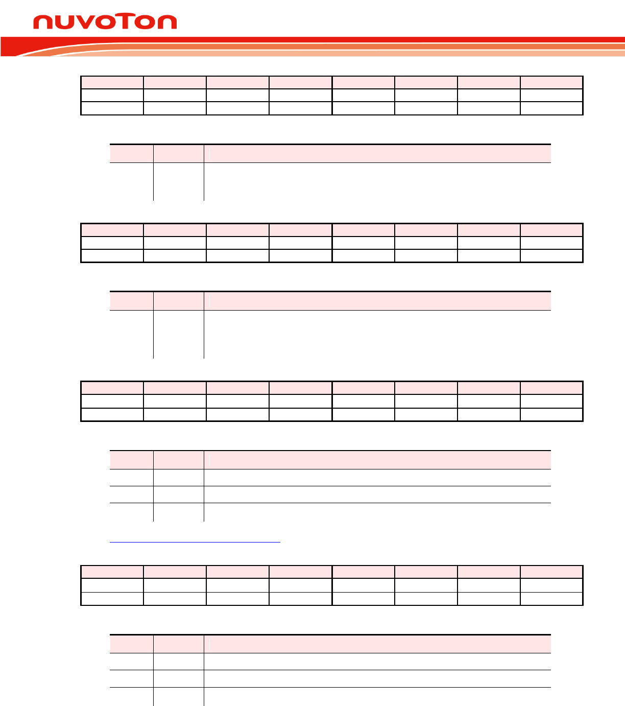
N76E003 Datasheet
Oct 28, 2016 Page 79 of 261 Rev. 1.00
PMEN PWM Mask Enable
7
6
5
4
3
2
1
0
-
-
PMEN5
PMEN4
PMEN3
PMEN2
PMEN1
PMEN0
-
-
R/W
R/W
R/W
R/W
R/W
R/W
Address: FBH Reset value: 0000 0000b
Bit
Name
Description
n
PMENn
PWMn mask enable
0 = PWMn signal outputs from its PWM generator.
1 = PWMn signal is masked by PMDn.
PMD PWM Mask Data
7
6
5
4
3
2
1
0
-
-
PMD5
PMD4
PMD3
PMD2
PMD1
PMD0
-
-
R/W
R/W
R/W
R/W
R/W
R/W
Address: FCH Reset value: 0000 0000b
Bit
Name
Description
n
PMDn
PWMn mask data
The PWMn signal outputs mask data once its corresponding PMENn is set.
0 = PWMn signal is masked by 0.
1 = PWMn signal is masked by 1.
EIP1 Extensive Interrupt Priority 1[5]
7
6
5
4
3
2
1
0
-
-
-
-
-
PWKT
PT3
PS_1
-
-
-
-
-
R/W
R/W
R/W
Address: FEH, Page: 0 Reset value: 0000 0000b
Bit
Name
Description
2
PWKT
WKT interrupt priority low bit
1
PT3
Timer 3 interrupt priority low bit
0
PS_1
Serial port 1 interrupt priority low bit
[5] EIP1 is used in combination with the EIPH1 to determine the priority of each interrupt source. See
Table 20-2. Interrupt Priority Level Setting for correct interrupt priority configuration.
EIPH1 Extensive Interrupt Priority High 1[6]
7
6
5
4
3
2
1
0
-
-
-
-
-
PWKTH
PT3H
PSH_1
-
-
-
-
-
R/W
R/W
R/W
Address: FFH, Page: 0 Reset value: 0000 0000b
Bit
Name
Description
2
PWKTH
WKT interrupt priority high bit
1
PT3H
Timer 3 interrupt priority high bit
0
PSH_1
Serial port 1 interrupt priority high bit


N76E003 Datasheet
Oct 28, 2016 Page 81 of 261 Rev. 1.00
7. I/O PORT STRUCTURE AND OPERATION
The N76E003 has a maximum of 26 bit-addressable general I/O pins grouped as 4 ports, P0 to P3.
Each port has its port control register (Px register). The writing and reading of a port control register
have different meanings. A write to port control register sets the port output latch logic value, whereas
a read gets the port pin logic state. All I/O pins except P2.0 can be configured individually as one of
four I/O modes by software. These four modes are quasi-bidirectional (standard 8051 port structure),
push-pull, input-only, and open-drain modes. Each port spends two special function registers PxM1
and PxM2 to select the I/O mode of port Px. The list below illustrates how to select the I/O mode of
Px.n. Note that the default configuration of is input-only (high-impedance) after any reset.
Table 7-1. Configuration for Different I/O Modes
PxM1.n
PxM2.n
I/O Type
0
0
Quasi-bidirectional
0
1
Push-pull
1
0
Input-only (high-impedance)
1
1
Open-drain
All I/O pins can be selected as TTL level inputs or Schmitt triggered inputs by selecting corresponding
bit in PxS register. Schmitt triggered input has better glitch suppression capability. All I/O pins also
have bit-controllable, slew rate select ability via software. The control registers are PxSR. By default,
the slew rate is slow. If user would like to increase the I/O output speed, setting the corresponding bit
in PxSR, the slew rate is selected in a faster level.
P2.0 is configured as an input-only pin when programming RPD (CONFIG0.2) as 0. Meanwhile, P2.0
is permanent in input-only mode and Schmitt triggered type. P2.0 also has an internal pull-up enabled
by P20UP (P2S.7). If RPD remains un-programmed, P2.0 pin functions as an external reset pin and
P2.0 is not available. A read of P2.0 bit is always 0. Meanwhile, the internal pull-up is always enabled.
7.1 Quasi-Bidirectional Mode
The quasi-bidirectional mode, as the standard 8051 I/O structure, can rule as both input and output.
When the port outputs a logic high, it is weakly driven, allowing an external device to pull the pin low.
When the pin is pulled low, it is driven strongly and able to sink a large current. In the quasi-
bidirectional I/O structure, there are three pull-high transistors. Each of them serves different
purposes. One of these pull-highs -high, is turned on whenever the port
latch contains logic 1-high sources a very small current that will pull the pin high
if it is left floating.
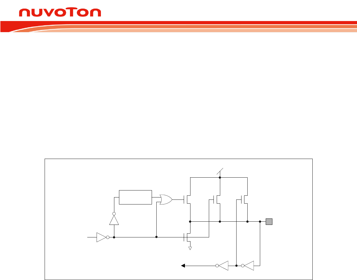
N76E003 Datasheet
Oct 28, 2016 Page 82 of 261 Rev. 1.00
A second pull--high, is turned on when the outside port pin itself is at logic 1
level. This pull-high provides the primary source current for a quasi-bidirectional pin that is outputting
1. If a pin which has logic 1 on it is p-high turns off, and
-high remains on. To pull the pin low under these conditions, the external
device has to sink enough current (larger than ITL -high and make the
voltage on the port pin below its input threshold (lower than VIL).
The third pull--high. This pull-high is used to speed up 0-to-1 transitions on a
quasi-bidirectional port pin when the port latch changes from logic 0 to logic 1. When this occurs, the
strong pull-high turns on for two-CPU-clock time to pull the port pin high quickly. Then it turns off and
-highs continue remaining the port pin high. The quasi-bidirectional port
structure is shown below.
Port Pin
2-CPU-clock
delay
Input
Port Latch
P P P
N
VDD
Strong Very
Weak Weak
Figure 7-1. Quasi-Bidirectional Mode Structure
7.2 Push-Pull Mode
The push-pull mode has the same pull-low structure as the quasi-bidirectional mode, but provides a
continuous strong pull-high when the port latch is written by logic 1. The push-pull mode is generally
used as output pin when more source current is needed for an output driving.
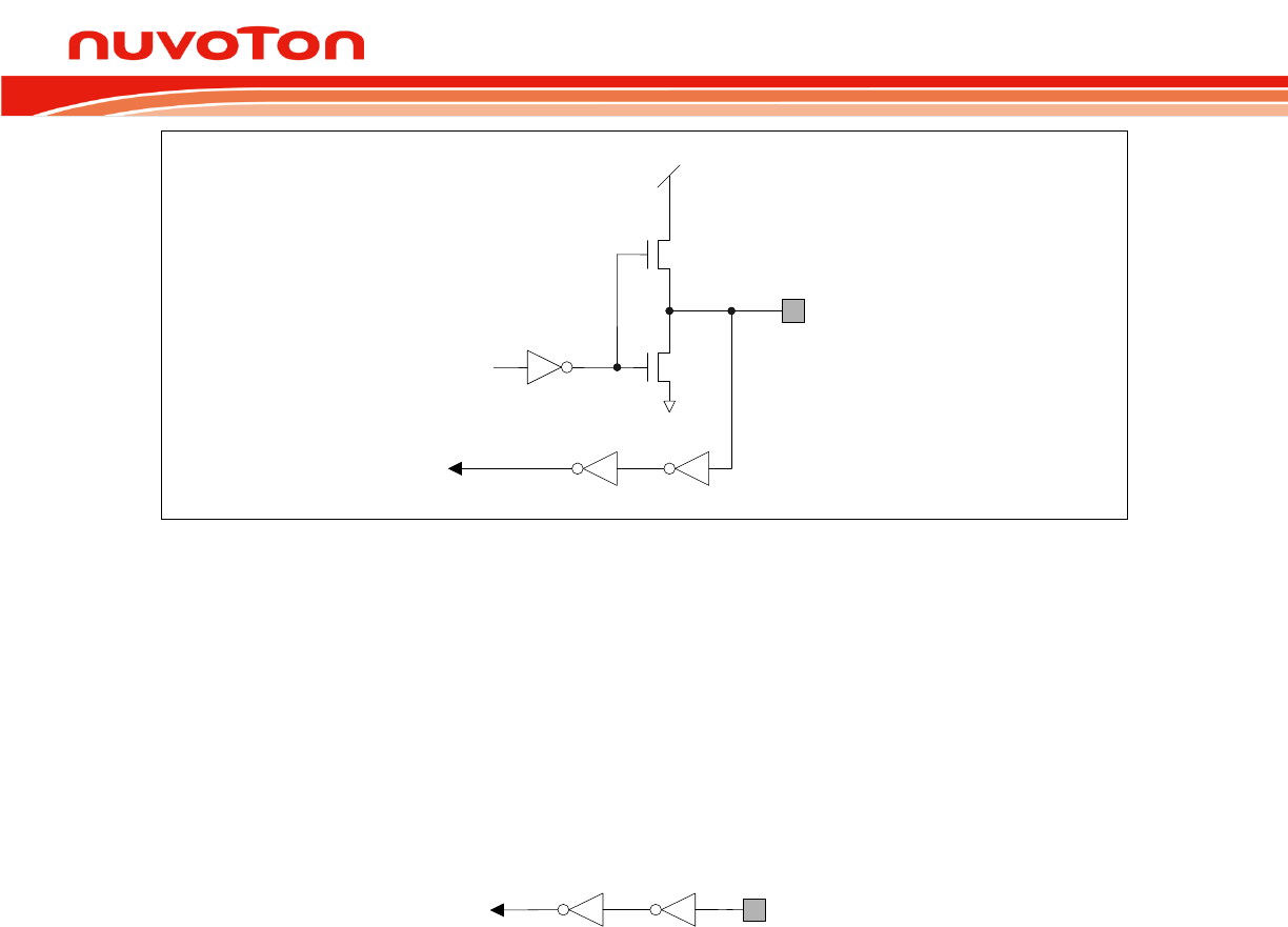
N76E003 Datasheet
Oct 28, 2016 Page 83 of 261 Rev. 1.00
Port Pin
Input
Port Latch
P
N
VDD
Strong
Figure 7-2. Push-Pull Mode Structure
7.3 Input-Only Mode
Input-only mode provides true high-impedance input path. Although a quasi-bidirectional mode I/O can
also be an input pin, but it requires relative strong input source. Input-only mode also benefits to power
consumption reduction for logic 0 input always consumes current from VDD if in quasi-bidirectional
mode. User needs to take care that an input-only mode pin should be given with a determined voltage
level by external devices or resistors. A floating pin will induce leakage current especially in Power-
down mode.
Port Pin
Input
Figure 7-3. Input-Only Mode Structure
7.4 Open-Drain Mode
The open-drain mode turns off all pull-high transistors and only drives the pull-low of the port pin when
the port latch is given by logic 0. If the port latch is logic 1, it behaves as if in input-only mode. To be
used as an output pin generally as I2C lines, an open-drain pin should add an external pull-high,
typically a resistor tied to VDD. User needs to take care that an open-drain pin with its port latch as
logic 1 should be given with a determined voltage level by external devices or resistors. A floating pin
will induce leakage current especially in Power-down mode.
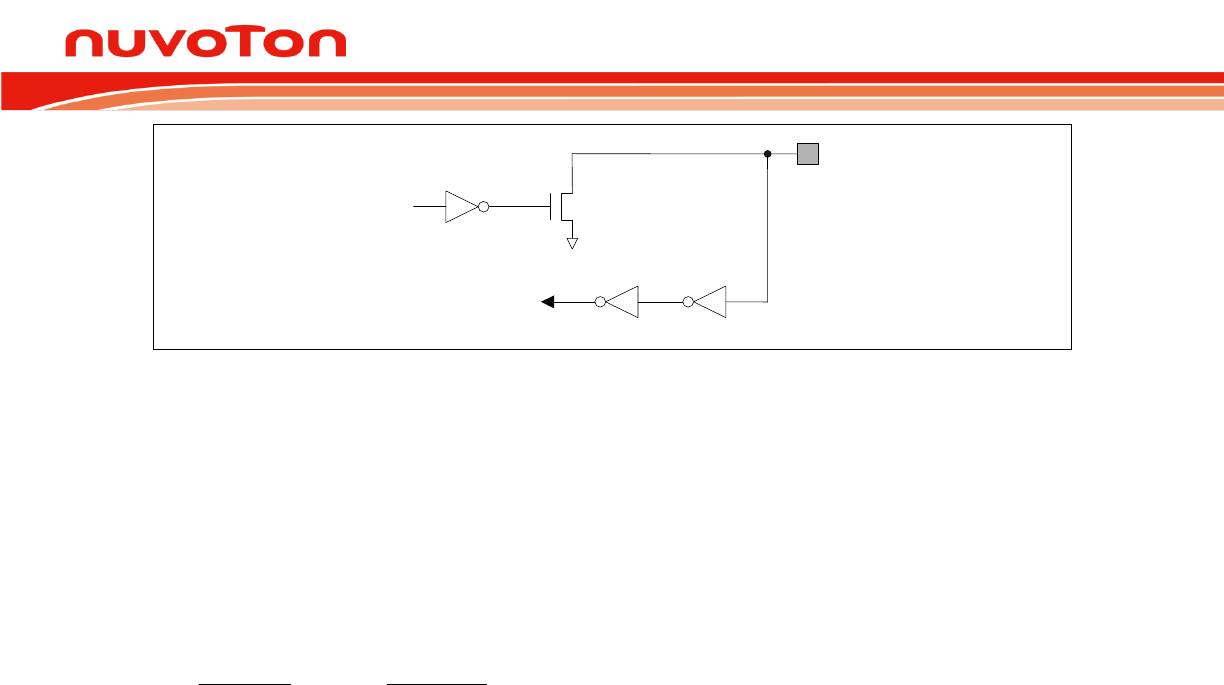
N76E003 Datasheet
Oct 28, 2016 Page 84 of 261 Rev. 1.00
Port Pin
Input
Port Latch N
Figure 7-4. Open-Drain Mode Structure
7.5 Read-Modify-Write Instructions
Instructions that read a byte from SFR -
Modify-
internal output latch rather than the external pin state. This kind of instructions read the port SFR
value, modify it and write back to the port SFR. Read-Modify-Write instructions are listed as
follows.
Instruction Description
ANL Logical AND. (ANL direct, A and ANL direct, #data)
ORL Logical OR. (ORL direct, A and ORL direct, #data)
XRL Logical exclusive OR. (XRL direct, A and XRL direct, #data)
JBC Jump if bit = 1 and clear it. (JBC bit, rel)
CPL Complement bit. (CPL bit)
INC Increment. (INC direct)
DEC Decrement. (DEC direct)
DJNZ Decrement and jump if not zero. (DJNZ direct, rel)
MOV bit, C Move carry to bit. (MOV bit, C)
CLR bit Clear bit. (CLR bit)
SETB bit Set bit. (SETB bit)
The last three seem not obviously -Modify-Write instructions but actually they are. They read
the entire port latch value, modify the changed bit, and then write the new value back to the port latch.
7.6 Control Registers of I/O Ports
The N76E003 has a lot of I/O control registers to provide flexibility in all kinds of applications. The
SFRs related with I/O ports can be categorized into four groups: input and output control, output mode
control, input type and sink current control, and output slew rate control. All of SFRs are listed as
follows.
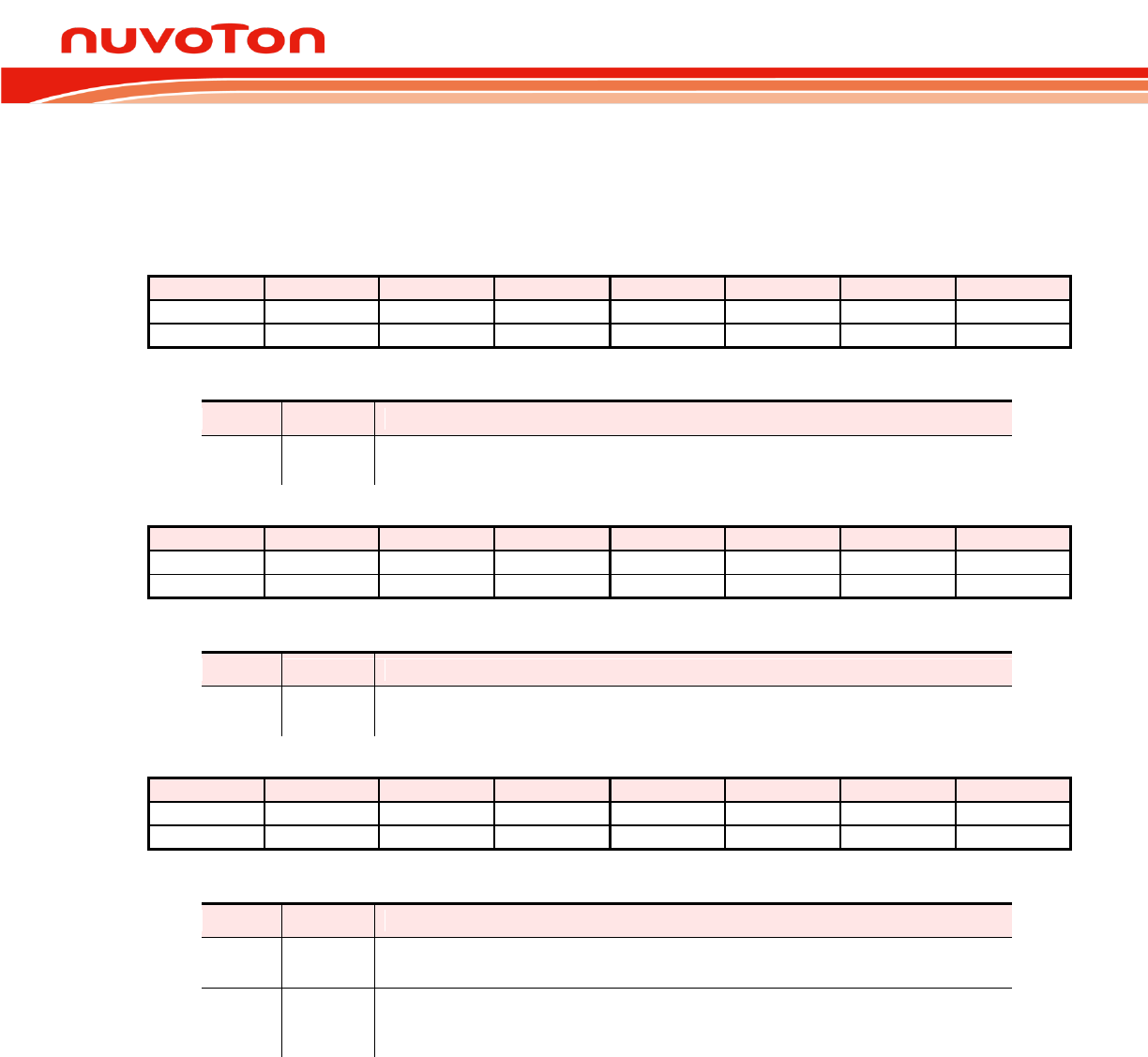
N76E003 Datasheet
Oct 28, 2016 Page 85 of 261 Rev. 1.00
Input and Output Data Control 7.6.1
These registers are I/O input and output data buffers. Reading gets the I/O input data. Writing forces
the data output. All of these registers are bit-addressable.
P0 Port 0 (Bit-addressable)
7
6
5
4
3
2
1
0
P0.7
P0.6
P0.5
P0.4
P0.3
P0.2
P0.1
P0.0
R/W
R/W
R/W
R/W
R/W
R/W
R/W
R/W
Address: 80H Reset value: 1111 1111b
Bit
Name
Description
7:0
P0[7:0]
Port 0
Port 0 is an maximum 8-bit general purpose I/O port.
P1 Port 1 (Bit-addressable)
7
6
5
4
3
2
1
0
P1.7
P1.6
P1.5
P1.4
P1.3
P1.2
P1.1
P1.0
R/W
R/W
R/W
R/W
R/W
R/W
R/W
R/W
Address: 90H Reset value: 1111 1111b
Bit
Name
Description
7:0
P1[7:0]
Port 1
Port 1 is an maximum 8-bit general purpose I/O port.
P2 Port 2 (Bit-addressable)
7
6
5
4
3
2
1
0
0
0
0
0
0
0
0
P2.0
R
R
R
R
R
R
R
R
Address: A0H Reset value: 0000 000Xb
Bit
Name
Description
7:1
0
Reserved
The bits are always read as 0.
0
P2.0
Port 2 bit 0
P2.0 is an input-only pin when RPD (CONFIG0.2) is programmed as 0. When
leaving RPD un-programmed, P2.0 is always read as 0.
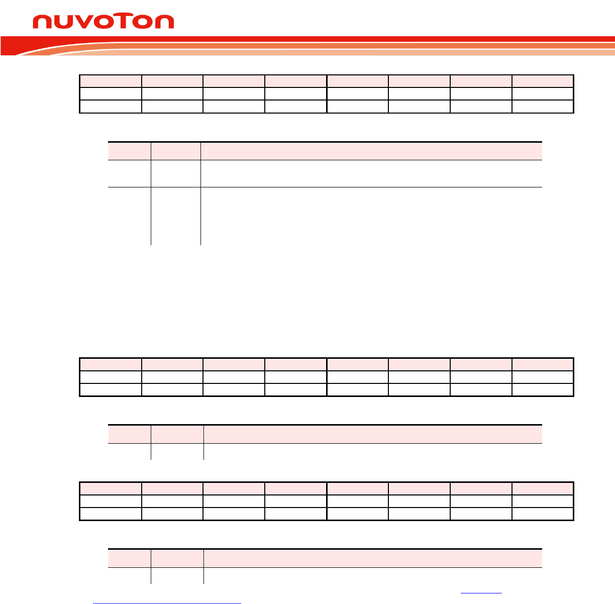
N76E003 Datasheet
Oct 28, 2016 Page 86 of 261 Rev. 1.00
P3 Port 3 (Bit-addressable)
7
6
5
4
3
2
1
0
0
0
0
0
0
0
0
P3.0
R
R
R
R
R
R
R
R/W
Address: B0H Reset value: 0000 0001b
Bit
Name
Description
7:1
0
Reserved
The bits are always read as 0.
0
P3.0
Port 3 bit 0
P3.0 is available only when the internal oscillator is used as the system clock. At
this moment, P3.0 functions as a general purpose I/O.
If the system clock is not selected as the internal oscillator, P3.0 pin functions as
OSCIN. A write to P3.0 is invalid and P3.0 is always read as 0.
Output Mode Control 7.6.2
These registers control output mode which is configurable among four modes: input-only, quasi-
bidirectional, push-pull, or open-drain. Each pin can be configured individually. There is also a pull-up
control for P2.0 in P2S.7.
P0M1 Port 0 Mode Select 1[1]
7
6
5
4
3
2
1
0
P0M1.7
P0M1.6
P0M1.5
P0M1.4
P0M1.3
P0M1.2
P0M1.1
P0M1.0
R/W
R/W
R/W
R/W
R/W
R/W
R/W
R/W
Address: B1H, Page: 0 Reset value: 1111 1111b
Bit
Name
Description
7:0
P0M1[7:0]
Port 0 mode select 1
P0M2 Port 0 Mode Select 2[1]
7
6
5
4
3
2
1
0
P0M2.7
P0M2.6
P0M2.5
P0M2.4
P0M2.3
P0M2.2
P0M2.1
P0M2.0
R/W
R/W
R/W
R/W
R/W
R/W
R/W
R/W
Address: B2H, Page: 0 Reset value: 0000 0000b
Bit
Name
Description
7:0
P0M2[7:0]
Port 0 mode select 2
[1] P0M1 and P0M2 are used in combination to determine the I/O mode of each pin of P0. See Table 7-1.
Configuration for Different I/O Modes.
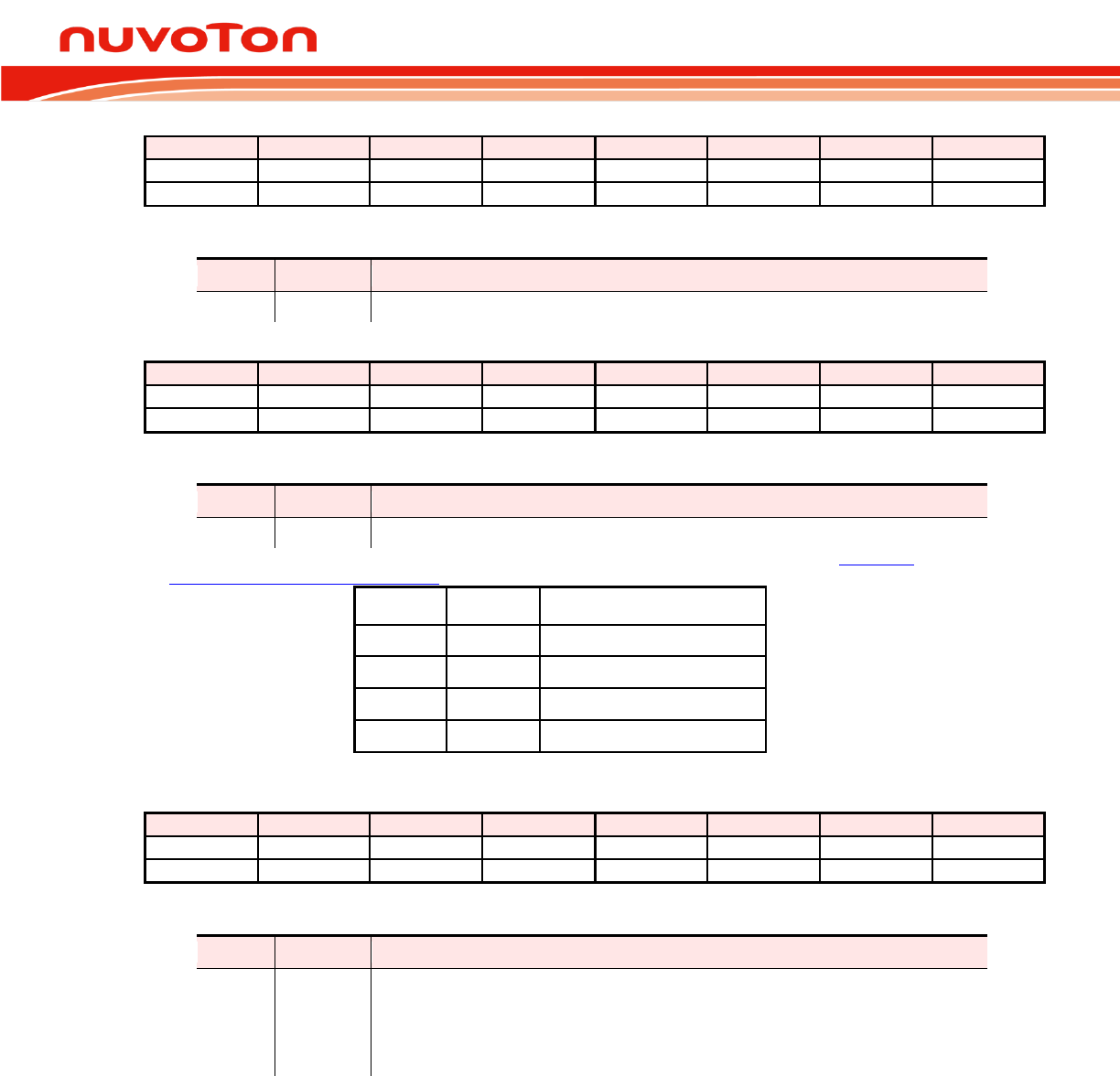
N76E003 Datasheet
Oct 28, 2016 Page 87 of 261 Rev. 1.00
P1M1 Port 1 Mode Select 1[2]
7
6
5
4
3
2
1
0
P1M1.7
P1M1.6
P1M1.5
P1M1.4
P1M1.3
P1M1.2
P1M1.1
P1M1.0
R/W
R/W
R/W
R/W
R/W
R/W
R/W
R/W
Address: B3H, Page: 0 Reset value: 1111 1111b
Bit
Name
Description
7:0
P1M1[7:0]
Port 1 mode select 1
P1M2 Port 1 Mode Select 2[2]
7
6
5
4
3
2
1
0
P1M2.7
P1M2.6
P1M2.5
P1M2.4
P1M2.3
P1M2.2
P1M2.1
P1M2.0
R/W
R/W
R/W
R/W
R/W
R/W
R/W
R/W
Address: B4H, Page: 0 Reset value: 0000 0000b
Bit
Name
Description
7:0
P1M2[7:0]
Port 1 mode select 2.
[2] P1M1 and P1M2 are used in combination to determine the I/O mode of each pin of P1. See Table 7-1.
Configuration for Different I/O Modes.
P1M1.n
P1M2.n
I/O Type
0
0
Quasi-bidirectional
0
1
Push-pull
1
0
Input-only (high-impedance)
1
1
Open-drain
P2S P20 Setting and Timer01 Output Enable
7
6
5
4
3
2
1
0
P20UP
-
-
-
T1OE
T0OE
-
P2S.0
R/W
-
-
-
R/W
R/W
-
R/W
Address: B5H Reset value: 0000 0000b
Bit
Name
Description
7
P20UP
P2.0 pull-up enable
0 = P2.0 pull-up Disabled.
1 = P2.0 pull-up Enabled.
This bit is valid only when RPD (CONFIG0.2) is programmed as 0. When
selecting as a
pin, the pull-up is always enabled.
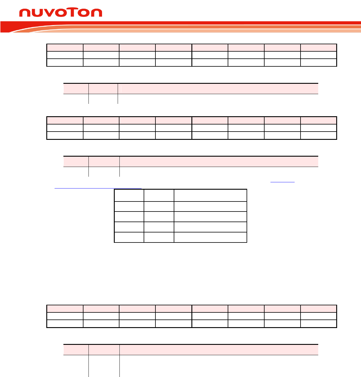
N76E003 Datasheet
Oct 28, 2016 Page 88 of 261 Rev. 1.00
P3M1 Port 3 Mode Select 1
7
6
5
4
3
2
1
0
-
-
-
-
-
-
-
P3M1.0[3]
-
-
-
-
-
-
-
R/W
Address: ACH, Page: 0 Reset value: 0000 0001b
Bit
Name
Description
0
P3M1.0
Port 3 mode select 1
P3M2 Port 3 Mode Select 2
7
6
5
4
3
2
1
0
-
-
-
-
-
-
-
P3M2.0[3]
-
-
-
-
-
-
-
R/W
Address: ADH, Page: 0 Reset value: 0000 0000b
Bit
Name
Description
0
P3M2.0
Port 3 mode select 2
[3] P3M1 and P3M2 are used in combination to determine the I/O mode of each pin of P3. See Table 7-1.
Configuration for Different I/O Modes.
P3M1.n
P3M2.n
I/O Type
0
0
Quasi-bidirectional
0
1
Push-pull
1
0
Input-only (high-impedance)
1
1
Open-drain
Input Type 7.6.3
Each I/O pin can be configured individually as TTL input or Schmitt triggered input. Note that all of PxS
registers are accessible by switching SFR page to page 1.
P0S Port 0 Schmitt Triggered Input
7
6
5
4
3
2
1
0
P0S.7
P0S.6
P0S.5
P0S.4
P0S.3
P0S.2
P0S.1
P0S.0
R/W
R/W
R/W
R/W
R/W
R/W
R/W
R/W
Address: B1H, Page: 1 Reset value: 0000 0000b
Bit
Name
Description
n
P0S.n
P0.n Schmitt triggered input
0 = TTL level input of P0.n.
1 = Schmitt triggered input of P0.n.

N76E003 Datasheet
Oct 28, 2016 Page 89 of 261 Rev. 1.00
P1S Port 1 Schmitt Triggered Input
7
6
5
4
3
2
1
0
P1S.7
P1S.6
P1S.5
P1S.4
P1S.3
P1S.2
P1S.1
P1S.0
R/W
R/W
R/W
R/W
R/W
R/W
R/W
R/W
Address: B3H, Page: 1 Reset value: 0000 0000b
Bit
Name
Description
7
P1S.7
P1.7 Schmitt triggered input
0 = TTL level input of P1.7.
1 = Schmitt triggered input of P1.7.
6
P1S.6
P1.6 Schmitt triggered input
0 = TTL level input of P1.6.
1 = Schmitt triggered input of P1.6.
5
P1S.5
P1.5 Schmitt triggered input
0 = TTL level input of P1.5.
1 = Schmitt triggered input of P1.5.
4
P1S.4
P1.4 Schmitt triggered input
0 = TTL level input of P1.4.
1 = Schmitt triggered input of P1.4.
3
P1S.3
P1.3 Schmitt triggered input
0 = TTL level input of P1.3.
1 = Schmitt triggered input of P1.3.
2
P1S.2
P1.2 Schmitt triggered input
0 = TTL level input of P1.2.
1 = Schmitt triggered input of P1.2.
1
P1S.1
P1.1 Schmitt triggered input
0 = TTL level input of P1.1.
1 = Schmitt triggered input of P1.1.
0
P1S.0
P1.0 Schmitt triggered input
0 = TTL level input of P1.0.
1 = Schmitt triggered input of P1.0.
P2S P20 Setting and Timer01 Output Enable
7
6
5
4
3
2
1
0
P20UP
-
-
-
T1OE
T0OE
-
P2S.0
R/W
-
-
-
R/W
R/W
-
R/W
Address: B5H Reset value: 0000 0000b
Bit
Name
Description
0
P2S.0
P2.0 Schmitt triggered input
0 = TTL level input of P2.0.
1 = Schmitt triggered input of P2.0.
N76E003 Datasheet
Oct 28, 2016 Page 90 of 261 Rev. 1.00
P3S Port 3 Schmitt Triggered Input
7
6
5
4
3
2
1
0
-
-
-
-
-
-
-
P3S.0
-
-
-
-
-
-
-
R/W
Address: ACH, Page: 1 Reset value: 0000 0000b
Bit
Name
Description
0
P3S.0
P3.0 Schmitt triggered input
0 = TTL level input of P3.0.
1 = Schmitt triggered input of P3.0.
Output Slew Rate Control
7.6.4
Slew rate for each I/O pin is configurable individually. By default, each pin is in normal slew rate mode.
User can set each control register bit to enable high-speed slew rate for the corresponding I/O pin.
Note that all PxSR registers are accessible by switching SFR page to page 1.
P0SR Port 0 Slew Rate
7
6
5
4
3
2
1
0
P0SR.7
P0SR.6
P0SR.5
P0SR.4
P0SR.3
P0SR.2
P0SR.1
P0SR.0
R/W
R/W
R/W
R/W
R/W
R/W
R/W
R/W
Address: B2H, Page: 1 Reset value: 0000 0000b
Bit
Name
Description
n
P0SR.n
P0.n slew rate
0 = P0.n normal output slew rate.
1 = P0.n high-speed output slew rate.
P1SR Port 1 Slew Rate
7
6
5
4
3
2
1
0
P1SR.7
P1SR.6
P1SR.5
P1SR.4
P1SR.3
P1SR.2
P1SR.1
P1SR.0
R/W
R/W
R/W
R/W
R/W
R/W
R/W
R/W
Address: B4H, Page: 1 Reset value: 0000 0000b
Bit
Name
Description
n
P1SR.n
P1.n slew rate
0 = P1.n normal output slew rate.
1 = P1.n high-speed output slew rate.
N76E003 Datasheet
Oct 28, 2016 Page 91 of 261 Rev. 1.00
P3SR Port 3 Slew Rate
7
6
5
4
3
2
1
0
-
-
-
-
-
-
-
P3SR.0
-
-
-
-
-
-
-
R/W
Address: ADH, Page: 1 Reset value: 0000 0000b
Bit
Name
Description
0
P3SR.0
P3.n slew rate
0 = P3.0 normal output slew rate.
1 = P3.0 high-speed output slew rate.

N76E003 Datasheet
Oct 28, 2016 Page 92 of 261 Rev. 1.00
8. TIMER/COUNTER 0 AND 1
Timer/Counter 0 and 1 on N76E003 are two 16-bit Timers/Counters. Each of them has two 8-bit
registers those form the 16-bit counting register. For Timer/Counter 0 they are TH0, the upper 8-bit
register, and TL0, the lower 8-bit register. Similarly Timer/Counter 1 has two 8-bit registers, TH1 and
TL1. TCON and TMOD can configure modes of Timer/Counter 0 and 1.
The Timer or Counter function is selected by the
bit in TMOD. Each Timer/Counter has its own
selection bit. TMOD.2 selects the function for Timer/Counter 0 and TMOD.6 selects the function for
Timer/Counter 1
When configured as a Timer, the timer counts the system clock cycles. The timer clock is 1/12 of the
system clock (FSYS) for standard 8051 capability or direct the system clock for enhancement, which is
selected by T0M (CKCON.3) bit for Timer 0 and T1M (CKCON.4) bit for Timer 1. In the Counter
mode, the countering register increases on the falling edge of the external input pin T0. If the sampled
value is high in one clock cycle and low in the next, a valid 1-to-0 transition is recognized on T0 or T1
pin.
The Timers 0 and 1 can be configured to automatically toggle a port output whenever a timer overflow
occurs. The same device pins that are used for the T0 and T1 count inputs are also used for the timer
toggle outputs. This function is enabled by control bits T0OE and T1OE in the P2S register, and apply
to Timer 0 and Timer 1 respectively. The port outputs will be logic 1 prior to the first timer overflow
when this mode is turned on. In order for this mode to function, the
bit should be cleared selecting
the system clock as the clock source for the timer.
Note that the TH0 (TH1) and TL0 (TL1) are accessed separately. It is strongly recommended that in
mode 0 or 1, user should stop Timer temporally by clearing TR0 (TR1) bit before reading from or
writing to TH0 (TH1) and TL0 (TL1). The free-running reading or writing may cause unpredictable
result.
TMOD Timer 0 and 1 Mode
7
6
5
4
3
2
1
0
GATE
M1
M0
GATE
M1
M0
R/W
R/W
R/W
R/W
R/W
R/W
R/W
R/W
Address: 89H Reset value: 0000 0000b
Bit
Name
Description
7
GATE
Timer 1 gate control
0 = Timer 1 will clock when TR1 is 1 regardless of
logic level.
1 = Timer 1 will clock only when TR1 is 1 and
is logic 1.
N76E003 Datasheet
Oct 28, 2016 Page 93 of 261 Rev. 1.00
Bit
Name
Description
6
Timer 1 Counter/Timer select
0 = Timer 1 is incremented by internal system clock.
1 = Timer 1 is incremented by the falling edge of the external pin T1.
5
M1
Timer 1 mode select
M1
M0
Timer 1 Mode
0
0
Mode 0: 13-bit Timer/Counter
0
1
Mode 1: 16-bit Timer/Counter
1
0
Mode 2: 8-bit Timer/Counter with auto-reload from TH1
1
1
Mode 3: Timer 1 halted
4
M0
3
GATE
Timer 0 gate control
0 = Timer 0 will clock when TR0 is 1 regardless of
logic level.
1 = Timer 0 will clock only when TR0 is 1 and
is logic 1.
2
Timer 0 Counter/Timer select
0 = Timer 0 is incremented by internal system clock.
1 = Timer 0 is incremented by the falling edge of the external pin T0.
1
M1
Timer 0 mode select
M1
M0
Timer 0 Mode
0
0
Mode 0: 13-bit Timer/Counter
0
1
Mode 1: 16-bit Timer/Counter
1
0
Mode 2: 8-bit Timer/Counter with auto-reload from TH0
1
1
Mode 3: TL0 as a 8-bit Timer/Counter and TH0 as a 8-bit
Timer
0
M0
TCON Timer 0 and 1 Control (Bit-addressable)
7
6
5
4
3
2
1
0
TF1
TR1
TF0
TR0
IE1
IT1
IE0
IT0
R/W
R/W
R/W
R/W
R (level)
R/W (edge)
R/W
R (level)
R/W (edge)
R/W
Address: 88H Reset value: 0000 0000b
Bit
Name
Description
7
TF1
Timer 1 overflow flag
This bit is set when Timer 1 overflows. It is automatically cleared by hardware
when the program executes the Timer 1 interrupt service routine. This bit can be
set or cleared by software.
6
TR1
Timer 1 run control
0 = Timer 1 Disabled. Clearing this bit will halt Timer 1 and the current count will
be preserved in TH1 and TL1.
1 = Timer 1 Enabled.
5
TF0
Timer 0 overflow flag
This bit is set when Timer 0 overflows. It is automatically cleared via hardware
when the program executes the Timer 0 interrupt service routine. This bit can be
set or cleared by software.
4
TR0
Timer 0 run control
0 = Timer 0 Disabled. Clearing this bit will halt Timer 0 and the current count will
be preserved in TH0 and TL0.
1 = Timer 0 Enabled.

N76E003 Datasheet
Oct 28, 2016 Page 94 of 261 Rev. 1.00
TL0 Timer 0 Low Byte
7
6
5
4
3
2
1
0
TL0[7:0]
R/W
Address: 8AH Reset value: 0000 0000b
Bit
Name
Description
7:0
TL0[7:0]
Timer 0 low byte
The TL0 register is the low byte of the 16-bit counting register of Timer 0.
TH0 Timer 0 High Byte
7
6
5
4
3
2
1
0
TH0[7:0]
R/W
Address: 8CH Reset value: 0000 0000b
Bit
Name
Description
7:0
TH0[7:0]
Timer 0 high byte
The TH0 register is the high byte of the 16-bit counting register of Timer 0.
TL1 Timer 1 Low Byte
7
6
5
4
3
2
1
0
TL1[7:0]
R/W
Address: 8BH Reset value: 0000 0000b
Bit
Name
Description
7:0
TL1[7:0]
Timer 1 low byte
The TL1 register is the low byte of the 16-bit counting register of Timer 1.
TH1 Timer 1 High Byte
7
6
5
4
3
2
1
0
TH1[7:0]
R/W
Address: 8DH Reset value: 0000 0000b
Bit
Name
Description
7:0
TH1[7:0]
Timer 1 high byte
The TH1 register is the high byte of the 16-bit counting register of Timer 1.
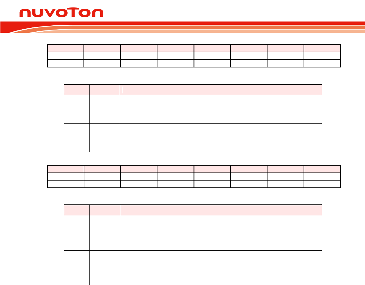
N76E003 Datasheet
Oct 28, 2016 Page 95 of 261 Rev. 1.00
CKCON Clock Control
7
6
5
4
3
2
1
0
-
PWMCKS
-
T1M
T0M
-
CLOEN
-
-
R/W
-
R/W
R/W
-
R/W
-
Address: 8EH Reset value: 0000 0000b
Bit
Name
Description
4
T1M
Timer 1 clock mode select
0 = The clock source of Timer 1 is the system clock divided by 12. It maintains
standard 8051 compatibility.
1 = The clock source of Timer 1 is direct the system clock.
3
T0M
Timer 0 clock mode select
0 = The clock source of Timer 0 is the system clock divided by 12. It maintains
standard 8051 compatibility.
1 = The clock source of Timer 0 is direct the system clock.
P2S P20 Setting and Timer01 Output Enable
7
6
5
4
3
2
1
0
P20UP
-
-
-
T1OE
T0OE
-
P2S.0
R/W
-
-
-
R/W
R/W
-
R/W
Address: B5H Reset value: 0000 0000b
Bit
Name
Description
3
T1OE
Timer 1 output enable
0 = Timer 1 output Disabled.
1 = Timer 1 output Enabled from T1 pin.
mode.
2
T0OE
Timer 0 output enable
0 = Timer 0 output Disabled.
1 = Timer 0 output Enabled from T0 pin.
mode.
8.1 Mode 0 (13-Bit Timer)
In Mode 0, the Timer/Counter is a 13-bit counter. The 13-bit counter consists of TH0 (TH1) and the
five lower bits of TL0 (TL1). The upper three bits of TL0 (TL1) are ignored. The Timer/Counter is
enabled when TR0 (TR1) is set and either GATE is 0 or
(
) is 1. Gate setting as 1 allows the
Timer to calculate the pulse width on external input pin
(
). When the 13-bit value moves
from 1FFFH to 0000H, the Timer overflow flag TF0 (TF1) is set and an interrupt occurs if enabled.
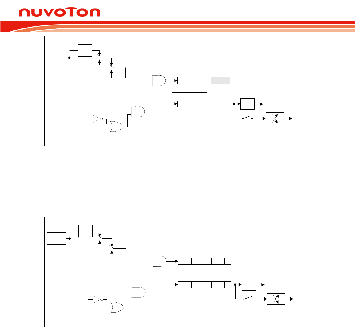
N76E003 Datasheet
Oct 28, 2016 Page 96 of 261 Rev. 1.00
TF0
(TF1)
TH0 (TH1)
TL0 (TL1)
Timer Interrupt
0 4 7
0 7
T0 (T1) pin
T0OE (P2S.2)
(T1OE(P2S.3))
0
1
T0 (T1) pin
C/T
GATE
TR0 (TR1)
FSYS
INT0 (INT1) pin
1/12 0
1
T0M (CKCON.3)
(T1M (CKCON.4))
Figure 8-1. Timer/Counters 0 and 1 in Mode 0
8.2 Mode 1 (16-Bit Timer)
Mode 1 is similar to Mode 0 except that the counting registers are fully used as a 16-bit counter. Roll-
over occurs when a count moves FFFFH to 0000H. The Timer overflow flag TF0 (TF1) of the relevant
Timer/Counter is set and an interrupt will occurs if enabled.
TF0
(TF1)
TH0 (TH1)
TL0 (TL1)
Timer Interrupt
0 7
0 7
T0 (T1) pin
T0OE (P2S.2)
(T1OE(P2S.3))
0
1
T0 (T1) pin
C/T
GATE
TR0 (TR1)
FSYS
INT0 (INT1) pin
1/12 0
1
T0M (CKCON.3)
(T1M (CKCON.4))
Figure 8-2. Timer/Counters 0 and 1 in Mode 1
8.3 Mode 2 (8-Bit Auto-Reload Timer)
In Mode 2, the Timer/Counter is in auto-reload mode. In this mode, TL0 (TL1) acts as an 8-bit count
register whereas TH0 (TH1) holds the reload value. When the TL0 (TL1) register overflow, the TF0
(TF1) bit in TCON is set and TL0 (TL1) is reloaded with the contents of TH0 (TH1) and the counting
process continues from here. The reload operation leaves the contents of the TH0 (TH1) register
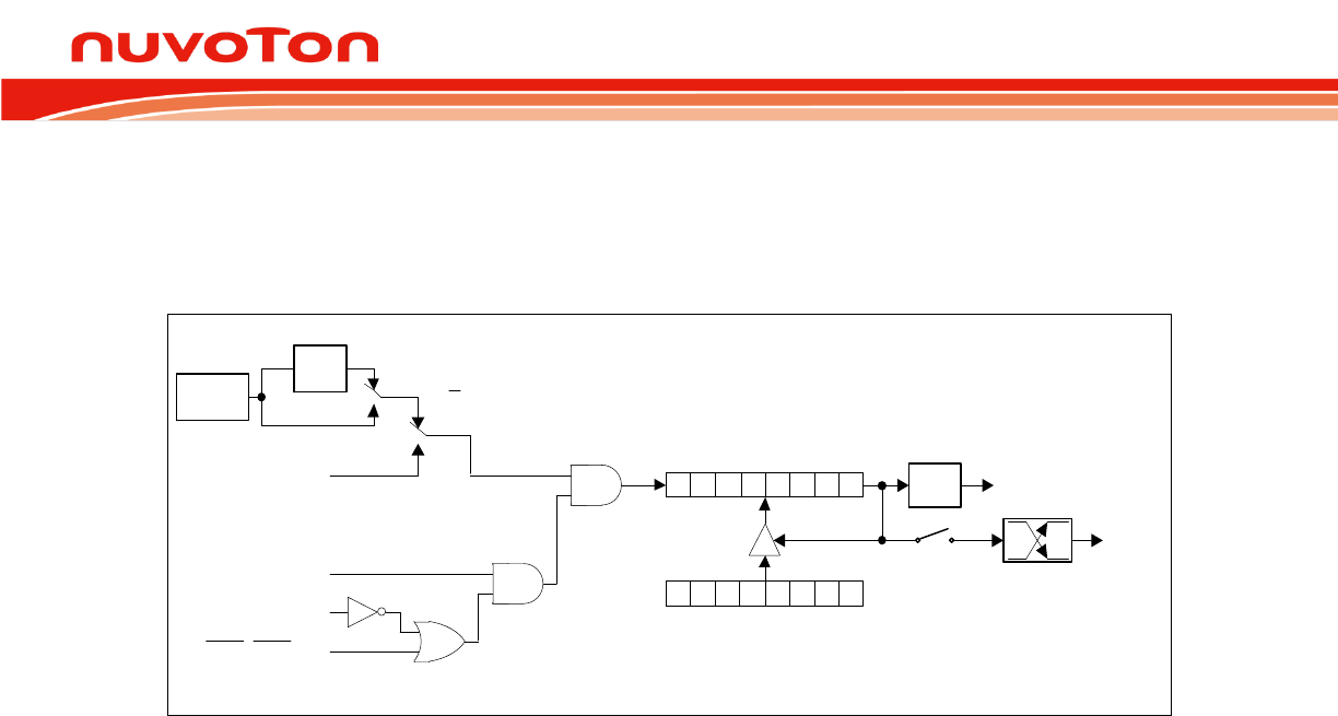
N76E003 Datasheet
Oct 28, 2016 Page 97 of 261 Rev. 1.00
unchanged. This feature is best suitable for UART baud rate generator for it runs without continuous
software intervention. Note that only Timer1 can be the baud rate source for UART. Counting is
enabled by setting the TR0 (TR1) bit as 1 and proper setting of GATE and
(
) pins. The
functions of GATE and
(
) pins are just the same as Mode 0 and 1.
TF0
(TF1)
TH0 (TH1)
TL0 (TL1)
Timer Interrupt
0 7
0 7
T0 (T1) pin
T0OE (P2S.2)
(T1OE(P2S.3))
0
1
T0 (T1) pin
C/T
GATE
TR0 (TR1)
FSYS
INT0 (INT1) pin
1/12 0
1
T0M (CKCON.3)
(T1M (CKCON.4))
Figure 8-3. Timer/Counters 0 and 1 in Mode 2
8.4 Mode 3 (Two Separate 8-Bit Timers)
Mode 3 has different operating methods for Timer 0 and Timer 1. For Timer/Counter 1, Mode 3 simply
freezes the counter. Timer/Counter 0, however, configures TL0 and TH0 as two separate 8 bit count
registers in this mode. TL0 uses the Timer/Counter 0 control bits
, GATE, TR0,
, and TF0.
The TL0 also can be used as a 1-to-0 transition counter on pin T0 as determined by
(TMOD.2).
TH0 is forced as a clock cycle counter and takes over the usage of TR1 and TF1 from Timer/Counter
1. Mode 3 is used in case that an extra 8 bit timer is needed. If Timer/Counter 0 is configured in Mode
3, Timer/Counter 1 can be turned on or off by switching it out of or into its own Mode 3. It can still be
used in Modes 0, 1 and 2 although its flexibility is restricted. It no longer has control over its overflow
flag TF1 and the enable bit TR1. However Timer 1 can still be used as a Timer/Counter and retains
the use of GATE,
pin and T1M. It can be used as a baud rate generator for the serial port or
other application not requiring an interrupt.
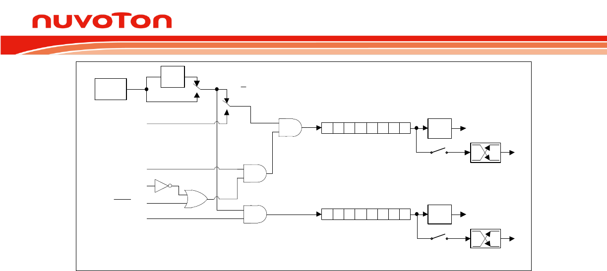
N76E003 Datasheet
Oct 28, 2016 Page 98 of 261 Rev. 1.00
TF0
TH0
TL0
Timer 0 Interrupt
0 7
0 7 TF1 Timer 1 Interrupt
TR1
GATE
TR0
INT0 pin
T0 pin
T0OE (P2S.2)
T1 pin
T1OE(P2S.3)
0
1
T0 pin
C/T
FSYS
1/12 0
1
T0M (CKCON.3)
Figure 8-4. Timer/Counter 0 in Mode 3
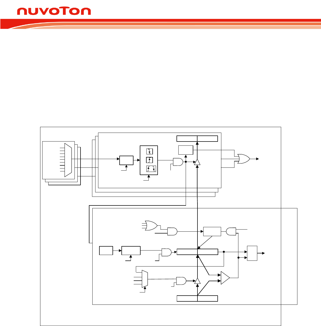
N76E003 Datasheet
Oct 28, 2016 Page 99 of 261 Rev. 1.00
9. TIMER 2 AND INPUT CAPTURE
Timer 2 is a 16-bit up counter cascaded with TH2, the upper 8 bits register, and TL2, the lower 8 bit
register. Equipped with RCMP2H and RCMP2L, Timer 2 can operate under compare mode and auto-
reload mode selected by
(T2CON.0). An 3-channel input capture module makes Timer 2
detect and measure the width or period of input pulses. The results of 3 input captures are stores in
C0H and C0L, C1H and C1L, C2H and C2L individually. The clock source of Timer 2 is from the
system clock pre-scaled by a clock divider with 8 different scales for wide field application. The clock is
enabled when TR2 (T2CON.2) is 1, and disabled when TR2 is 0. The following registers are related to
Timer 2 function.
TF2 Timer 2 Interrupt
Pre-scalarFSYS
RCMP2H
T2DIV[2:0]
(T2MOD[6:4])
RCMP2L
00
01
10
11
CAPF0
CAPF1
CAPF2 LDEN[1]
(T2MOD.7)
LDTS[1:0]
(T2MOD[1:0])
TR2
(T2CON.2)
Timer 2 Module
C0HC0L
Noise
Filter
ENF0
(CAPCON2.4) or
[00]
[01]
[10]
CAP0LS[1:0]
(CAPCON1[1:0])
CAPEN0
(CAPCON0.4)
Input Capture 0 Module
Input Capture 1 Module
Input Capture 2 Module
Input Capture Flags (CAPF[2:0])
CAPCR[1]
(T2MOD.3)
CAPF0
CAPF1
CAPF2 Clear Timer 2
[1] Once CAPCR and LDEN are both set, an input capture event only clears TH2 and TL2 without reloading RCMP2H and RCMP2L contents.
Input Capture Interrupt
CAPF0
CAPF1
CAPF2
CMPCR
(T2MOD.2)
Clear Timer 2
=
CAP0
CAP1
CAP2
TH2TL2
Clear
Counter
CAPF0
0000
0001
0010
0011
0100
0101
0110
0111
P1.5/IC7
P0.5/IC6
P0.3/IC5
P0.1/IC4
P0.0/IC3
P1.0/IC2
P1.1/IC1
P1.2/IC0
1000
P0.4/IC3
Figure 9-1. Timer 2 Block Diagram
N76E003 Datasheet
Oct 28, 2016 Page 100 of 261 Rev. 1.00
T2CON Timer 2 Control
7
6
5
4
3
2
1
0
TF2
-
-
-
-
TR2
-
R/W
-
-
-
-
R/W
-
R/W
Address: C8H Reset value: 0000 0000b
Bit
Name
Description
7
TF2
Timer 2 overflow flag
This bit is set when Timer 2 overflows or a compare match occurs. If the Timer 2
interrupt and the global interrupt are enable, setting this bit will make CPU execute
Timer 2 interrupt service routine. This bit is not automatically cleared via hardware
and should be cleared via software.
2
TR2
Timer 2 run control
0 = Timer 2 Disabled. Clearing this bit will halt Timer 2 and the current count will
be preserved in TH2 and TL2.
1 = Timer 2 Enabled.
0
Timer 2 compare or auto-reload mode select
This bit selects Timer 2 functioning mode.
0 = Auto-reload mode.
1 = Compare mode.
T2MOD Timer 2 Mode
7
6
5
4
3
2
1
0
LDEN
T2DIV[2:0]
CAPCR
CMPCR
LDTS[1:0]
R/W
R/W
R/W
R/W
R/W
Address: C9H Reset value: 0000 0000b
Bit
Name
Description
7
LDEN
Enable auto-reload
0 = Reloading RCMP2H and RCMP2L to TH2 and TL2 Disabled.
1 = Reloading RCMP2H and RCMP2L to TH2 and TL2 Enabled.
6:4
T2DIV[2:0]
Timer 2 clock divider
000 = Timer 2 clock divider is 1/1.
001 = Timer 2 clock divider is 1/4.
010 = Timer 2 clock divider is 1/16.
011 = Timer 2 clock divider is 1/32.
100 = Timer 2 clock divider is 1/64.
101 = Timer 2 clock divider is 1/128.
110 = Timer 2 clock divider is 1/256.
111 = Timer 2 clock divider is 1/512.
3
CAPCR
Capture auto-clear
This bit is valid only under Timer 2 auto-reload mode. It enables hardware auto-
clearing TH2 and TL2 counter registers after they have been transferred in to
RCMP2H and RCMP2L while a capture event occurs.
0 = Timer 2 continues counting when a capture event occurs.
1 = Timer 2 value is auto-cleared as 0000H when a capture event occurs.
2
CMPCR
Compare match auto-clear
This bit is valid only under Timer 2 compare mode. It enables hardware auto-
clearing TH2 and TL2 counter registers after a compare match occurs.
0 = Timer 2 continues counting when a compare match occurs.
1 = Timer 2 value is auto-cleared as 0000H when a compare match occurs.

N76E003 Datasheet
Oct 28, 2016 Page 101 of 261 Rev. 1.00
Bit
Name
Description
1:0
LDTS[1:0]
Auto-reload trigger select
These bits select the reload trigger event.
00 = Reload when Timer 2 overflows.
01 = Reload when input capture 0 event occurs.
10 = Reload when input capture 1 event occurs.
11 = Reload when input capture 2 event occurs.
RCMP2L Timer 2 Reload/Compare Low Byte
7
6
5
4
3
2
1
0
RCMP2L[7:0]
R/W
Address: CAH Reset value: 0000 0000b
Bit
Name
Description
7:0
RCMP2L[7:0]
Timer 2 reload/compare low byte
This register stores the low byte of compare value when Timer 2 is
configured in compare mode. Also it holds the low byte of the reload value in
auto-reload mode.
RCMP2H Timer 2 Reload/Compare High Byte
7
6
5
4
3
2
1
0
RCMP2H[7:0]
R/W
Address: CBH Reset value: 0000 0000b
Bit
Name
Description
7:0
RCMP2H[7:0]
Timer 2 reload/compare high byte
This register stores the high byte of compare value when Timer 2 is
configured in compare mode. Also it holds the high byte of the reload value
in auto-reload mode.
TL2 Timer 2 Low Byte
7
6
5
4
3
2
1
0
TL2[7:0]
R/W
Address: CCH, Page:0 Reset value: 0000 0000b
Bit
Name
Description
7:0
TL2[7:0]
Timer 2 low byte
The TL2 register is the low byte of the 16-bit counting register of Timer 2.

N76E003 Datasheet
Oct 28, 2016 Page 102 of 261 Rev. 1.00
TH2 Timer 2 High Byte
7
6
5
4
3
2
1
0
TH2[7:0]
R/W
Address: CDH, Page:0 Reset value: 0000 0000b
Bit
Name
Description
7:0
TH2[7:0]
Timer 2 high byte
The TH2 register is the high byte of the 16-bit counting register of Timer 2.
Note that the TH2 and TL2 are accessed separately. It is strongly recommended that user stops Timer
2 temporally by clearing TR2 bit before reading from or writing to TH2 and TL2. The free-running
reading or writing may cause unpredictable result.
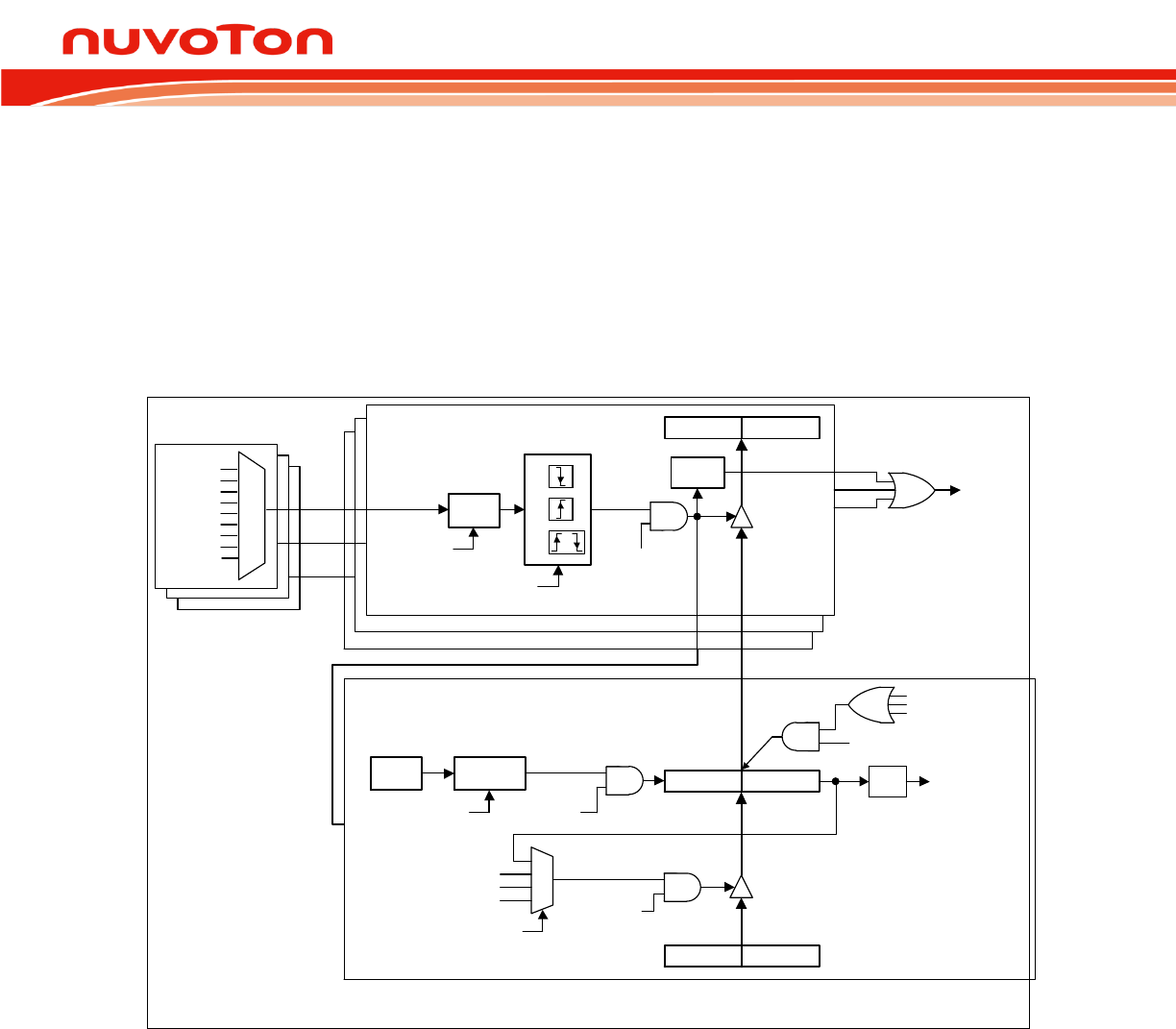
N76E003 Datasheet
Oct 28, 2016 Page 103 of 261 Rev. 1.00
9.1 Auto-Reload Mode
The Timer 2 is configured as auto-reload mode by clearing
. In this mode RCMP2H and
RCMP2L registers store the reload value. The contents in RCMP2H and RCMP2L transfer into TH2
and TL2 once the auto-reload event occurs if setting LDEN bit. The event can be the Timer 2 overflow
or one of the triggering event on any of enabled input capture channel depending on the LDTS[1:0]
(T2MOD[1:0]) selection. Note that once CAPCR (T2MOD.3) is set, an input capture event only clears
TH2 and TL2 without reloading RCMP2H and RCMP2L contents.
TF2 Timer 2 Interrupt
Pre-scalarFSYS
RCMP2H
T2DIV[2:0]
(T2MOD[6:4])
RCMP2L
TH2TL2
00
01
10
11
CAPF0
CAPF1
CAPF2 LDEN[1]
(T2MOD.7)
LDTS[1:0]
(T2MOD[1:0])
TR2
(T2CON.2)
Timer 2 Module
C0HC0L
Noise
Filter
ENF0
(CAPCON2.4) or
[00]
[01]
[10]
CAP0LS[1:0]
(CAPCON1[1:0])
CAPEN0
(CAPCON0.4)
CAPF0
Input Capture 0 Module
Input Capture 1 Module
Input Capture 2 Module
Input Capture Flags CAPF[2:0]
CAPCR[1]
(T2MOD.3)
CAPF0
CAPF1
CAPF2
Clear Timer 2
[1] Once CAPCR and LDEN are both set, an input capture event only clears TH2 and TL2 without reloading RCMP2H and RCMP2L contents.
Input Capture Interrupt
CAPF0
CAPF1
CAPF2
CAP0
CAP1
CAP2
0000
0001
0010
0011
0100
0101
0110
0111
P1.5/IC7
P0.5/IC6
P0.3/IC5
P0.1/IC4
P0.0/IC3
P1.0/IC2
P1.1/IC1
P1.2/IC0
1000
P0.4/IC3
Figure 9-2. Timer 2 Auto-Reload Mode and Input Capture Module Functional Block Diagram
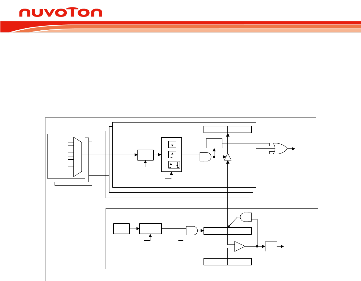
N76E003 Datasheet
Oct 28, 2016 Page 104 of 261 Rev. 1.00
9.2 Compare Mode
Timer 2 can also be configured as the compare mode by setting
. In this mode RCMP2H and
RCMP2L registers serve as the compare value registers. As Timer 2 up counting, TH2 and TL2 match
RCMP2H and RCMP2L, TF2 (T2CON.7) will be set by hardware to indicate a compare match event.
Setting CMPCR (T2MOD.2) makes the hardware to clear Timer 2 counter as 0000H automatically
after a compare match has occurred.
Input Capture Interrupt
CAPF0
CAPF1
CAPF2
TF2 Timer 2 Interrupt
Pre-scalarFSYS
RCMP2H
T2DIV[2:0]
(T2MOD[6:4])
RCMP2L
TH2
TL2
TR2
(T2CON.2)
Timer 2 Module
CMPCR
(T2MOD.2)
Clear Timer 2
=
C0HC0L
Noise
Filter
ENF0
(CAPCON2.4) or
[00]
[01]
[10]
CAP0LS[1:0]
(CAPCON1[1:0])
CAPEN0
(CAPCON0.4)
CAPF0
Input Capture 0 Module
Input Capture 1 Module
Input Capture 2 Module
CAP0
CAP1
CAP2
0000
0001
0010
0011
0100
0101
0110
0111
P1.5/IC7
P0.5/IC6
P0.3/IC5
P0.1/IC4
P0.0/IC3
P1.0/IC2
P1.1/IC1
P1.2/IC0
1000
P0.4/IC3
Figure 9-3. Timer 2 Compare Mode and Input Capture Module Functional Block Diagram
9.3 Input Capture Module
The input capture module along with Timer 2 implements the input capture function. The input capture
module is configured through CAPCON0~2 registers. The input capture module supports 3-channel
inputs (CAP0, CAP1, and CAP2) that share 9 I/O pins (P1.5, P1[2:0], P0.0, P0.1 and P0[5:3]). The pin
mux select through CAPCON3 and CAPCON4. Each input channel consists its own noise filter, which
is enabled via setting ENF0~2 (CAPCON2[6:4]). It filters input glitches smaller than four system clock
cycles. Input capture channels has their own independent edge detector but share the unique Timer
2. Each trigger edge detector is selected individually by setting corresponding bits in CAPCON1. It
supports positive edge capture, negative edge capture, or any edge capture. Each input capture
channel has to set its own enabling bit CAPEN0~2 (CAPCON0[6:4]) before use.

N76E003 Datasheet
Oct 28, 2016 Page 105 of 261 Rev. 1.00
While input capture channel is enabled and the selected edge trigger occurs, the content of the free
running Timer 2 counter, TH2 and TL2, will be captured, transferred, and stored into the capture
registers CnH and CnL. The edge triggering also causes CAPFn (CAPCON0.n) set by hardware. The
interrupt will also generate if the ECAP (EIE.2) and EA bit are both set. For three input capture flags
share the same interrupt vector, user should check CAPFn to confirm which channel comes the input
capture edge. These flags should be cleared by software.
The bit CAPCR (CAPCON2.3) benefits the implement of period calculation. Setting CAPCR makes the
hardware clear Timer 2 as 0000H automatically after the value of TH2 and TL2 have been captured
after an input capture edge event occurs. It eliminates the routine software overhead of writing 16-bit
counter or an arithmetic subtraction.
CAPCON0 Input Capture Control 0
7
6
5
4
3
2
1
0
-
CAPEN2
CAPEN1
CAPEN0
-
CAPF2
CAPF1
CAPF0
-
R/W
R/W
R/W
-
R/W
R/W
R/W
Address: 92H Reset value: 0000 0000b
Bit
Name
Description
6
CAPEN2
Input capture 2 enable
0 = Input capture channel 2 Disabled.
1 = Input capture channel 2 Enabled.
5
CAPEN1
Input capture 1 enable
0 = Input capture channel 1 Disabled.
1 = Input capture channel 1 Enabled.
4
CAPEN0
Input capture 0 enable
0 = Input capture channel 0 Disabled.
1 = Input capture channel 0 Enabled.
2
CAPF2
Input capture 2 flag
This bit is set by hardware if the determined edge of input capture 2 occurs. This
bit should cleared by software.
1
CAPF1
Input capture 1 flag
This bit is set by hardware if the determined edge of input capture 1 occurs. This
bit should cleared by software.
0
CAPF0
Input capture 0 flag
This bit is set by hardware if the determined edge of input capture 0 occurs. This
bit should cleared by software.
N76E003 Datasheet
Oct 28, 2016 Page 106 of 261 Rev. 1.00
CAPCON1 Input Capture Control 1
7
6
5
4
3
2
1
0
-
-
CAP2LS[1:0]
CAP1LS[1:0]
CAP0LS[1:0]
-
-
R/W
R/W
R/W
Address: 93H Reset value: 0000 0000b
Bit
Name
Description
5:4
CAP2LS[1:0]
Input capture 2 level select
00 = Falling edge.
01 = Rising edge.
10 = Either Rising or falling edge.
11 = Reserved.
3:2
CAP1LS[1:0]
Input capture 1 level select
00 = Falling edge.
01 = Rising edge.
10 = Either Rising or falling edge.
11 = Reserved.
1:0
CAP0LS[1:0]
Input capture 0 level select
00 = Falling edge.
01 = Rising edge.
10 = Either Rising or falling edge.
11 = Reserved.
CAPCON2 Input Capture Control 2
7
6
5
4
3
2
1
0
-
ENF2
ENF1
ENF0
-
-
-
-
-
R/W
R/W
R/W
-
-
-
-
Address: 94H Reset value: 0000 0000b
Bit
Name
Description
6
ENF2
Enable noise filer on input capture 2
0 = Noise filter on input capture channel 2 Disabled.
1 = Noise filter on input capture channel 2 Enabled.
5
ENF1
Enable noise filer on input capture 1
0 = Noise filter on input capture channel 1 Disabled.
1 = Noise filter on input capture channel 1 Enabled.
4
ENF0
Enable noise filer on input capture 0
0 = Noise filter on input capture channel 0 Disabled.
1 = Noise filter on input capture channel 0 Enabled.
C0L Capture 0 Low Byte
7
6
5
4
3
2
1
0
C0L[7:0]
R/W
Address: E4H Reset value: 0000 0000b
Bit
Name
Description
7:0
C0L[7:0]
Input capture 0 result low byte
The C0L register is the low byte of the 16-bit result captured by input capture 0.
N76E003 Datasheet
Oct 28, 2016 Page 107 of 261 Rev. 1.00
C0H Capture 0 High Byte
7
6
5
4
3
2
1
0
C0H[7:0]
R/W
Address: E5H Reset value: 0000 0000b
Bit
Name
Description
7:0
C0H[7:0]
Input capture 0 result high byte
The C0H register is the high byte of the 16-bit result captured by input capture 0.
C1L Capture 1 Low Byte
7
6
5
4
3
2
1
0
C1L[7:0]
R/W
Address: E6H Reset value: 0000 0000b
Bit
Name
Description
7:0
C1L[7:0]
Input capture 1 result low byte
The C1L register is the low byte of the 16-bit result captured by input capture 1.
C1H Capture 1 High Byte
7
6
5
4
3
2
1
0
C1H[7:0]
R/W
Address: E7H Reset value: 0000 0000b
Bit
Name
Description
7:0
C1H[7:0]
Input capture 1 result high byte
The C1H register is the high byte of the 16-bit result captured by input capture 1.
C2L Capture 2 Low Byte
7
6
5
4
3
2
1
0
C2L[7:0]
R/W
Address: EDH Reset value: 0000 0000b
Bit
Name
Description
7:0
C2L[7:0]
Input capture 2 result low byte
The C2L register is the low byte of the 16-bit result captured by input capture 2.

N76E003 Datasheet
Oct 28, 2016 Page 108 of 261 Rev. 1.00
C2H Capture 2 High Byte
7
6
5
4
3
2
1
0
C2H[7:0]
R/W
Address: EEH Reset value: 0000 0000b
Bit
Name
Description
7:0
C2H[7:0]
Input capture 2 result high byte
The C2H register is the high byte of the 16-bit result captured by input capture 2.
CAPCON3 Input Capture Control 3
7
6
5
4
3
2
1
0
CAP13
CAP12
CAP11
CAP10
CAP03
CAP02
CAP01
CAP00
R/W
R/W
R/W
R/W
R/W
R/W
R/W
R/W
Address: F1H Reset value: 0000 0000b
Bit
Name
Description
[7:4]
CAP1[3:0]
Input capture channel 0 input pin select
0000 = P1.2/IC0
0001 = P1.1/IC1
0010 = P1.0/IC2
0011 = P0.0/IC3
0100 = P0.4/IC3
0101 = P0.1/IC4
0110 = P0.3/IC5
0111 = P0.5/IC6
1000 = P1.5/IC7
others = P1.2/IC0
[3:0]
CAP0[3:0]
Input capture channel 0 input pin select
0000 = P1.2/IC0
0001 = P1.1/IC1
0010 = P1.0/IC2
0011 = P0.0/IC3
0100 = P0.4/IC3
0101 = P0.1/IC4
0110 = P0.3/IC5
0111 = P0.5/IC6
1000 = P1.5/IC7
others = P1.2/IC0
N76E003 Datasheet
Oct 28, 2016 Page 109 of 261 Rev. 1.00
CAPCON4 Input Capture Control 4
7
6
5
4
3
2
1
0
-
-
-
-
CAP23
CAP22
CAP21
CAP20
-
-
-
-
R/W
R/W
R/W
R/W
Address: F2H Reset value: 0000 0000b
Bit
Name
Description
[3:0]
CAP2[3:0]
Input capture channel 0 input pin select
0000 = P1.2/IC0
0001 = P1.1/IC1
0010 = P1.0/IC2
0011 = P0.0/IC3
0100 = P0.4/IC3
0101 = P0.1/IC4
0110 = P0.3/IC5
0111 = P0.5/IC6
1000 = P1.5/IC7
others = P1.2/IC0
N76E003 Datasheet
Oct 28, 2016 Page 110 of 261 Rev. 1.00
10. TIMER 3
Timer 3 is implemented simply as a 16-bit auto-reload, up-counting timer. The user can select the pre-
scale with T3PS[2:0] (T3CON[2:0]) and fill the reload value into RH3 and RL3 registers to determine
its overflow rate. User then can set TR3 (T3CON.3) to start counting. When the counter rolls over
FFFFH, TF3 (T3CON.4) is set as 1 and a reload is generated and causes the contents of the RH3 and
RL3 registers to be reloaded into the internal 16-bit counter. If ET3 (EIE1.1) is set as 1, Timer 3
interrupt service routine will be served. TF3 is auto-cleared by hardware after entering its interrupt
service routine.
Timer 3 can also be the baud rate clock source of both UARTs. For details, please see Section 13.5
Baud Rate127.
RL3
TR3
(T3CON.3)
FSYS Internal 16-bit Counter
0 7
RH3
0 7
Timer 3
Overflow
Pre-scalar
(1/1~1/128)
T3PS[2:0]
(T3CON[2:0])
TF3
(T3CON.4) Timer 3 Interrupt
Figure 10-1. Timer 3 Block Diagram
T3CON Timer 3 Control
7
6
5
4
3
2
1
0
SMOD_1
SMOD0_1
BRCK
TF3
TR3
T3PS[2:0]
R/W
R/W
R/W
R/W
R/W
R/W
Address: C4H, Page:0 Reset value: 0000 0000b
Bit
Name
Description
4
TF3
Timer 3 overflow flag
This bit is set when Timer 3 overflows. It is automatically cleared by hardware
when the program executes the Timer 3 interrupt service routine. This bit can be
set or cleared by software.
3
TR3
Timer 3 run control
0 = Timer 3 is halted.
1 = Timer 3 starts running.
Note that the reload registers RH3 and RL3 can only be written when Timer 3 is
halted (TR3 bit is 0). If any of RH3 or RL3 is written if TR3 is 1, result is
unpredictable.
N76E003 Datasheet
Oct 28, 2016 Page 111 of 261 Rev. 1.00
Bit
Name
Description
2:0
T3PS[2:0]
Timer 3 pre-scalar
These bits determine the scale of the clock divider for Timer 3.
000 = 1/1.
001 = 1/2.
010 = 1/4.
011 = 1/8.
100 = 1/16.
101 = 1/32.
110 = 1/64.
111 = 1/128.
RL3 Timer 3 Reload Low Byte
7
6
5
4
3
2
1
0
RL3[7:0]
R/W
Address: C5H, Page:0 Reset value: 0000 0000b
Bit
Name
Description
7:0
RL3[7:0]
Timer 3 reload low byte
It holds the low byte of the reload value of Timer 3.
RH3 Timer 3 Reload High Byte
7
6
5
4
3
2
1
0
RH3[7:0]
R/W
Address: C6H, Page:0 Reset value: 0000 0000b
Bit
Name
Description
7:0
RH3[7:0]
Timer 3 reload high byte
It holds the high byte of the reload value of Time 3.
N76E003 Datasheet
Oct 28, 2016 Page 112 of 261 Rev. 1.00
11. WATCHDOG TIMER (WDT)
The N76E003 provides one Watchdog Timer (WDT). It can be configured as a time-out reset timer to
reset whole device. Once the device runs in an abnormal status or hangs up by outward interference,
a WDT reset recover the system. It provides a system monitor, which improves the reliability of the
system. Therefore, WDT is especially useful for system that is susceptible to noise, power glitches, or
electrostatic discharge. The WDT also can be configured as a general purpose timer, of which the
periodic interrupt serves as an event timer or a durational system supervisor in a monitoring system,
which is able to operate during Idle or Power-down mode. WDTEN[3:0] (CONFIG4[7:4]) initialize the
WDT to operate as a time-out reset timer or a general purpose timer.
CONFIG4
7
6
5
4
3
2
1
0
WDTEN[3:0]
-
-
-
-
R/W
-
-
-
-
Factory default value: 1111 1111b
Bit
Name
Description
7:4
WDTEN[3:0]
WDT enable
This field configures the WDT behavior after MCU execution.
1111 = WDT is Disabled. WDT can be used as a general purpose timer via
software control.
0101 = WDT is Enabled as a time-out reset timer and it stops running during
Idle or Power-down mode.
Others = WDT is Enabled as a time-out reset timer and it keeps running during
Idle or Power-down mode.
The WDT is implemented with a set of divider that divides the low-speed internal oscillator clock
nominal 10 kHz. The divider output is selectable and determines the time-out interval. When the time-
out interval is fulfilled, it will wake the system up from Idle or Power-down mode and an interrupt event
will occur if WDT interrupt is enabled. If WDT is initialized as a time-out reset timer, a system reset will
occur after a period of delay if without any software action.
WDCON Watchdog Timer Control (TA protected)
7
6
5
4
3
2
1
0
WDTR
WDCLR
WDTF
WIDPD
WDTRF[1]
WDPS[2:0][2]
R/W
R/W
R/W
R/W
R/W
R/W
Address: AAH Reset value: see Table 6-2. SFR Definitions and Reset Values
Bit
Name
Description
7
WDTR
WDT run
This bit is valid only when control bits in WDTEN[3:0] (CONFIG4[7:4]) are all 1.
At this time, WDT works as a general purpose timer.
0 = WDT Disabled.
1 = WDT Enabled. The WDT counter starts running.

N76E003 Datasheet
Oct 28, 2016 Page 113 of 261 Rev. 1.00
Bit
Name
Description
6
WDCLR
WDT clear
Setting this bit will reset the WDT count to 00H. It puts the counter in a known
state and prohibit the system from unpredictable reset. The meaning of writing
and reading WDCLR bit is different.
Writing:
0 = No effect.
1 = Clearing WDT counter.
Reading:
0 = WDT counter is completely cleared.
1 = WDT counter is not yet cleared.
5
WDTF
WDT time-out flag
This bit indicates an overflow of WDT counter. This flag should be cleared by
software.
4
WIDPD
WDT running in Idle or Power-down mode
This bit is valid only when control bits in WDTEN[3:0] (CONFIG4[7:4]) are all 1. It
decides whether WDT runs in Idle or Power-down mode when WDT works as a
general purpose timer.
0 = WDT stops running during Idle or Power-down mode.
1 = WDT keeps running during Idle or Power-down mode.
3
WDTRF
WDT reset flag
When the CPU is reset by WDT time-out event, this bit will be set via hardware.
This flag is recommended to be cleared via software after reset.
2:0
WDPS[2:0]
WDT clock pre-scalar select
These bits determine the pre-scale of WDT clock from 1/1 through 1/256. See
Table 11-1. The default is the maximum pre-scale value.
[1] WDTRF will be cleared after power-on reset, be set after WDT reset, and remains unchanged after any other
resets.
[2] WDPS[2:0] are all set after power-on reset and keep unchanged after any reset other than power-on reset.
The Watchdog time-out interval is determined by the formula
64×
scalar divider clock×F
1
LIRC
, where
FLIRC is the frequency of internal 10 kHz oscillator. The following table shows an example of the
Watchdog time-out interval with different pre-scales.
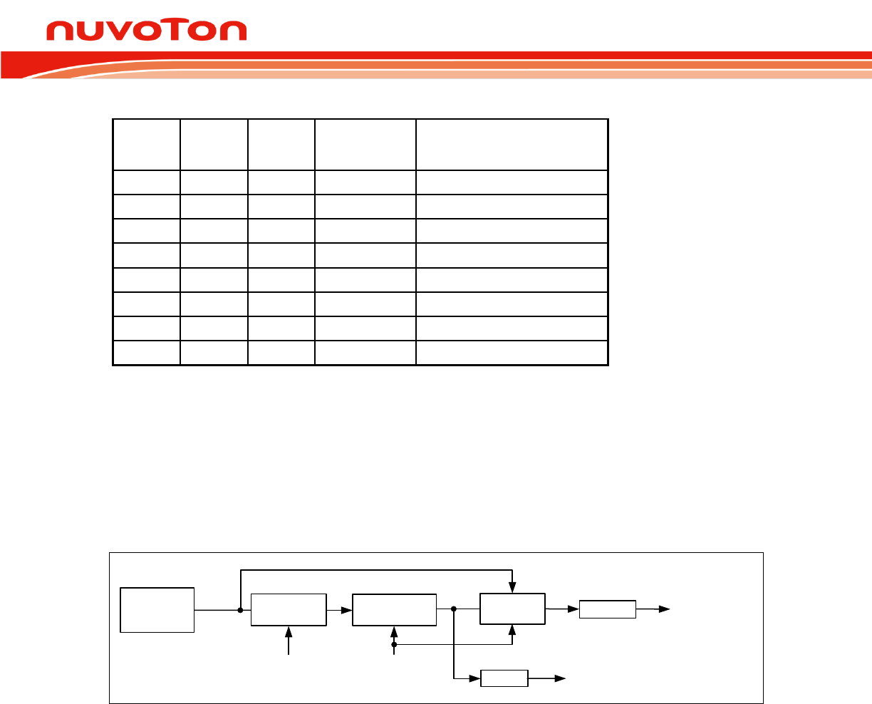
N76E003 Datasheet
Oct 28, 2016 Page 114 of 261 Rev. 1.00
Table 11-1. Watchdog Timer-out Interval Under Different Pre-scalars
WDPS.2
WDPS.1
WDPS.0
Clock Divider
Scale
Watchdog Time-out Interval
(FLIRC ~= 10 kHz)
0
0
0
1/1
6.40 ms
0
0
1
1/4
25.60 ms
0
1
0
1/8
51.20 ms
0
1
1
1/16
102.40 ms
1
0
0
1/32
204.80 ms
1
0
1
1/64
409.60 ms
1
1
0
1/128
819.20 ms
1
1
1
1/256
1.638 s
11.1 Time-Out Reset Timer
When the CONFIG bits WDTEN[3:0] (CONFIG4[7:4]) is not FH, the WDT is initialized as a time-out
reset timer. If WDTEN[3:0] is not 5H, the WDT is allowed to continue running after the system enters
Idle or Power-down mode. Note that when WDT is initialized as a time-out reset timer, WDTR and
WIDPD has no function.
FLIRC
WDCLR
WDPS[2:0]
WDT counter
(6-bit)
clear
overflow WDT Reset
512-clock
Delay
10 kHz
Internal
Oscillator
WDTRF
WDTF WDT Interrupt
clear
Pre-scalar
(1/1~1/256)
Figure 11-1. WDT as A Time-Out Reset Timer
After the device is powered and it starts to execute software code, the WDT starts counting
simultaneously. The time-out interval is selected by the three bits WDPS[2:0] (WDCON[2:0]). When
the selected time-out occurs, the WDT will set the interrupt flag WDTF (WDCON.5). If the WDT
interrupt enable bit EWDT (EIE.4) and global interrupt enable EA are both set, the WDT interrupt
routine will be executed. Meanwhile, an additional 512 clocks of the low-speed internal oscillator
delays to expect a counter clearing by setting WDCLR to avoid the system reset by WDT if the device
operates normally. If no counter reset by writing 1 to WDCLR during this 512-clock period, a WDT
reset will happen. Setting WDCLR bit is used to clear the counter of the WDT. This bit is self-cleared
for user monitoring it. Once a reset due to WDT occurs, the WDT reset flag WDTRF (WDCON.3) will
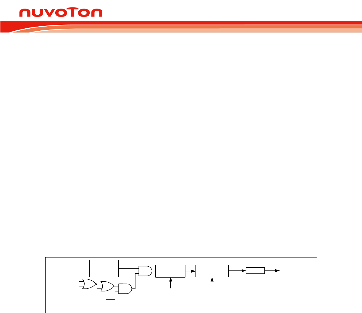
N76E003 Datasheet
Oct 28, 2016 Page 115 of 261 Rev. 1.00
be set. This bit keeps unchanged after any reset other than a power-on reset. User may clear WDTRF
via software. Note that all bits in WDCON require timed access writing.
NOTICE: WDT counter has been specially taken care. The hardware automatically clears WDT
counter and pre-scalar value after :
(1) Entering into or being woken-up from Idle or Power Down mode
(2) Any resets. It prevents unconscious system reset.
The main application of the WDT with time-out reset enabling is for the system monitor. This is
important in real-time control applications. In case of some power glitches or electro-magnetic
interference, CPU may begin to execute erroneous codes and operate in an unpredictable state. If this
is left unchecked the entire system may crash. Using the WDT during software development requires
setting WDCLR, it allows the code to run without any WDT reset. However If any erroneous code
executes by any interference, the instructions to clear the WDT counter will not be executed at the
required instants. Thus the WDT reset will occur to reset the system state from an erroneously
executing condition and recover the system.
11.2 General Purpose Timer
There is another application of the WDT, which is used as a simple, long period timer. When the
CONFIG bits WDTEN[3:0] (CONFIG4[7:4]) is FH, the WDT is initialized as a general purpose timer. In
this mode, WDTR and WIDPD are fully accessed via software.
FLIRC
IDL (PCON.0)
PD (PCON.1)
WIDPD
WDTR
WDCLR
WDPS[2:0]
WDT counter
(6-bit)
clear
overflow
10 kHz
Internal
Oscillator WDTF WDT Interrupt
Pre-scalar
(1/1~1/256)
Figure 11-2. Watchdog Timer Block Diagram
The WDT starts running by setting WDTR as 1 and halts by clearing WDTR as 0. The WDTF flag will
be set while the WDT completes the selected time interval. The software polls the WDTF flag to detect
a time-out. An interrupt will occur if the individual interrupt EWDT (EIE.4) and global interrupt enable
EA is set. WDT will continue counting. User should clear WDTF and wait for the next overflow by
polling WDTF flag or waiting for the interrupt occurrence.
In some application of low power consumption, the CPU usually stays in Idle mode when nothing
needs to be served to save power consumption. After a while the CPU will be woken up to check if

N76E003 Datasheet
Oct 28, 2016 Page 116 of 261 Rev. 1.00
anything needs to be served at an interval of programmed period implemented by Timer 0~3.
However, the current consumpt mA
mAPower-down mode when nothing needs to
be served, and has the ability of waking up at a programmable interval. The N76E003 is equipped with
this useful function by WDT waking up. It provides a very low power internal oscillator 10 kHz as the
clock source of the WDT. It is also able to count under Power-down mode and wake CPU up. The
demo code to accomplish this feature is shown below.
For Example:
ORG 0000H
LJMP START
ORG 0053H
LJMP WDT_ISR
ORG 0100H
;********************************************************************
;WDT interrupt service routine
;********************************************************************
WDT_ISR:
CLR EA
MOV TA,#0AAH
MOV TA,#55H
ANL WDCON,#11011111B ;clear WDT interrupt flag
SETB EA
RETI
;********************************************************************
;Start here
;********************************************************************
START:
MOV TA,#0AAH
MOV TA,#55H
ORL WDCON,#00010111B ;choose interval length and enable WDT running
during ;Power-down
SETB EWDT ;enable WDT interrupt
SETB EA
MOV TA,#0AAH
MOV TA,#55H
ORL WDCON,#10000000B ; WDT run
;********************************************************************
;Enter Power-down mode
;********************************************************************
LOOP:
ORL PCON,#02H
LJMP LOOP
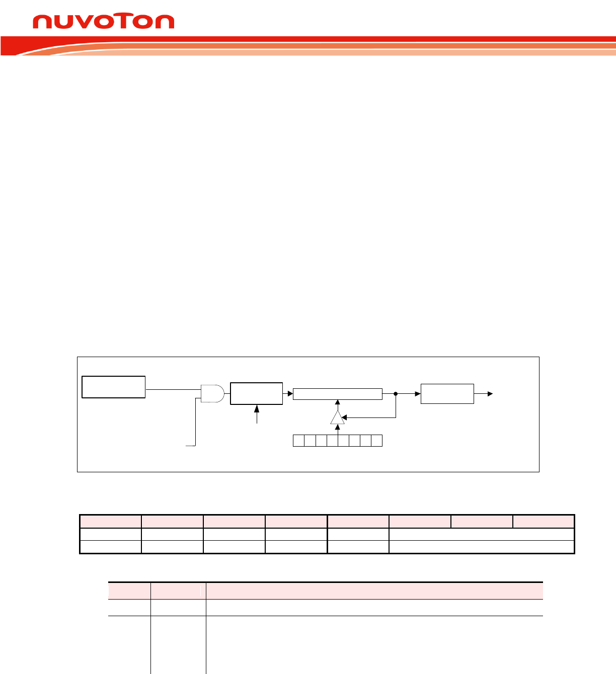
N76E003 Datasheet
Oct 28, 2016 Page 117 of 261 Rev. 1.00
12. SELF WAKE-UP TIMER (WKT)
The N76E003 has a dedicated Self Wake-up Timer (WKT), which serves for a periodic wake-up timer
in low power mode or for general purpose timer. WKT remains counting in Idle or Power-down mode.
When WKT is being used as a wake-up timer, a start of WKT can occur just prior to entering a power
management mode. WKT has one clock source, internal 10 kHz. Note that the system clock frequency
must be twice over WKT clock. If WKT starts counting, the selected clock source will remain active
once the device enters Idle or Power-down mode. Note that the selected clock source of WKT will not
automatically enabled along with WKT configuration. User should manually enable the selected clock
source and waiting for stability to ensure a proper operation.
The WKT is implemented simply as a 8-bit auto-reload, up-counting timer with pre-scale 1/1 to 1/2048
selected by WKPS[2:0] (WKCON[2:0]). User fills the reload value into RWK register to determine its
overflow rate. The WKTR (WKCON.3) can be set to start counting. When the counter rolls over FFH,
WKTF (WKCON.4) is set as 1 and a reload is generated and causes the contents of the RWK register
to be reloaded into the internal 8-bit counter. If EWKT (EIE1.2) is set as 1, WKT interrupt service
routine will be served.
WKTR
(WKCON.3)
Internal 8-bit Counter
RWK
0 7
WKT
Overflow
Pre-scalar
(1/1~1/2048)
WKPS[2:0]
(WKCON[2:0])
WKTF
(WKCON.4) WKT Interrupt
10 kHz Internal
Oscillator FLIRC
WKTCK
(WKCON.5)
Figure 12-1. Self Wake Up Timer Block Diagram
WKCON Self Wake-up Timer Control
7
6
5
4
3
2
1
0
-
-
-
WKTF
WKTR
WKPS[2:0]
-
-
-
R/W
R/W
R/W
Address: 8FH Reset value: 0000 0000b
Bit
Name
Description
5
-
Reserved
4
WKTF
WKT overflow flag
This bit is set when WKT overflows. If the WKT interrupt and the global interrupt
are enabled, setting this bit will make CPU execute WKT interrupt service
routine. This bit is not automatically cleared via hardware and should be cleared
via software.
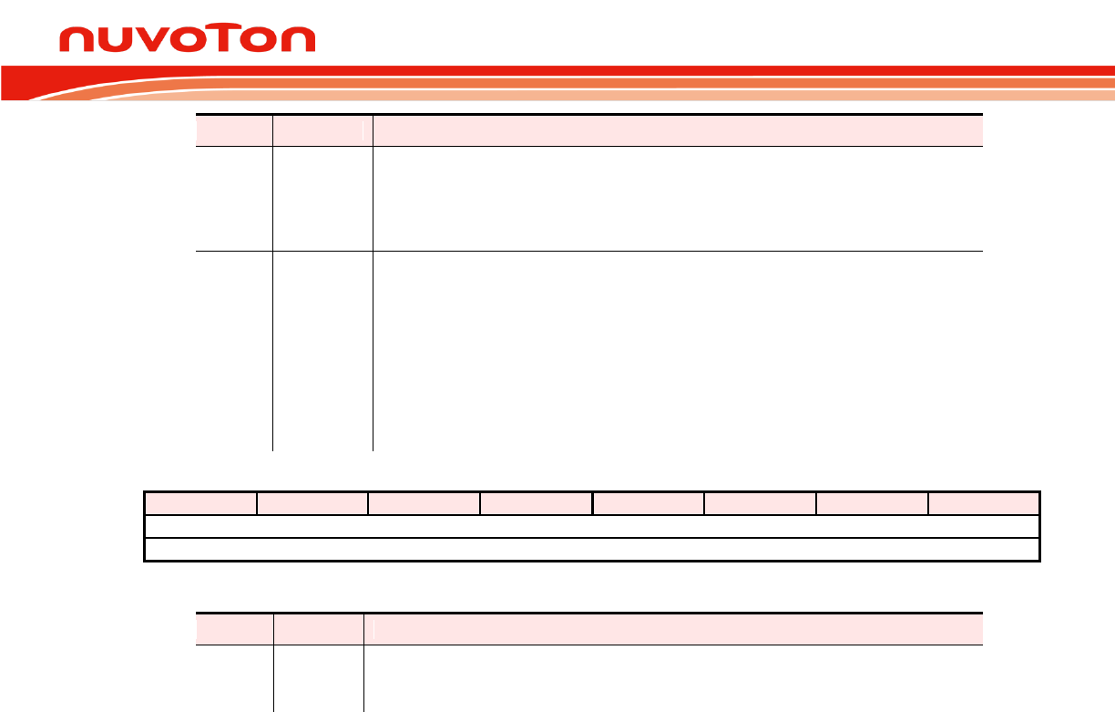
N76E003 Datasheet
Oct 28, 2016 Page 118 of 261 Rev. 1.00
Bit
Name
Description
3
WKTR
WKT run control
0 = WKT is halted.
1 = WKT starts running.
Note that the reload register RWK can only be written when WKT is halted
(WKTR bit is 0). If WKT is written while WKTR is 1, result is unpredictable.
2:0
WKPS[2:0]
WKT pre-scalar
These bits determine the pre-scale of WKT clock.
000 = 1/1.
001 = 1/4.
010 = 1/16.
011 = 1/64.
100 = 1/256.
101 = 1/512.
110 = 1/1024.
111 = 1/2048.
RWK Self Wake-up Timer Reload Byte
7
6
5
4
3
2
1
0
RWK[7:0]
R/W
Address: 86H Reset value: 0000 0000b
Bit
Name
Description
7:0
RWK[7:0]
WKT reload byte
It holds the 8-bit reload value of WKT. Note that RWK should not be FFH if the
pre-scale is 1/1 for implement limitation.
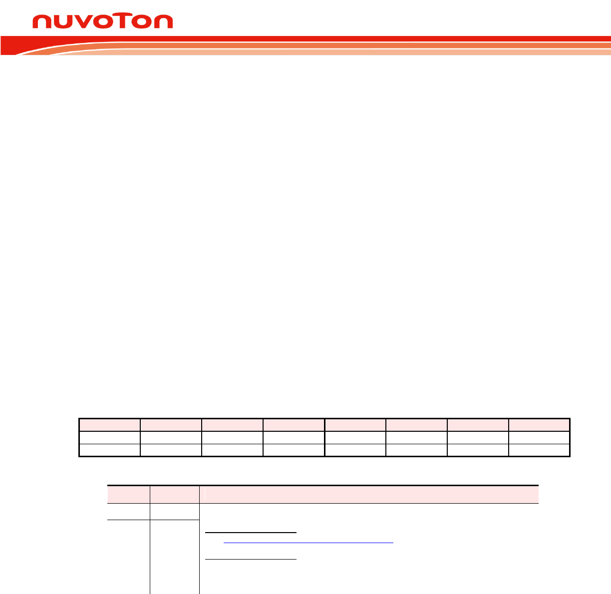
N76E003 Datasheet
Oct 28, 2016 Page 119 of 261 Rev. 1.00
13. SERIAL PORT (UART)
The N76E003 includes two enhanced full duplex serial ports enhanced with automatic address
recognition and framing error detection. As control bits of these two serial ports are implemented the
__1)
to indicate serial port 1 control bits for making a distinction between these two serial ports. Generally
speaking, in the following contents, there will not be any reference to serial port 1, but only to serial
port 0.
Each serial port supports one synchronous communication mode, Mode 0, and three modes of full
duplex UART (Universal Asynchronous Receiver and Transmitter), Mode 1, 2, and 3. This means it
can transmit and receive simultaneously. The serial port is also receiving-buffered, meaning it can
commence reception of a second byte before a previously received byte has been read from the
register. The receiving and transmitting registers are both accessed at SBUF. Writing to SBUF loads
the transmitting register, and reading SBUF accesses a physically separate receiving register. There
are four operation modes in serial port. In all four modes, transmission initiates by any instruction that
uses SBUF as a destination register. Note that before serial port function works, the port latch bits of
P0.7 and P0.6 (for RXD and TXD pins) or P0.2 and P1.6 (for RXD_1 and TXD_1 pins) have to be set
to 1. For application flexibility, TXD and RXD pins of serial port 0 can be exchanged by UART0PX
(AUXR1.2).
SCON Serial Port Control (Bit-addressable)
7
6
5
4
3
2
1
0
SM0/FE
SM1
SM2
REN
TB8
RB8
TI
RI
R/W
R/W
R/W
R/W
R/W
R/W
R/W
R/W
Address: 98H Reset value: 0000 0000b
Bit
Name
Description
7
SM0/FE
Serial port mode select
SMOD0 (PCON.6) = 0:
See Table 13-1. Serial Port 0 Mode Description for details.
SMOD0 (PCON.6) = 1:
SM0/FE bit is used as frame error (FE) status flag. It is cleared by software.
0 = Frame error (FE) did not occur.
1 = Frame error (FE) occurred and detected.
6
SM1

N76E003 Datasheet
Oct 28, 2016 Page 120 of 261 Rev. 1.00
Bit
Name
Description
5
SM2
Multiprocessor communication mode enable
The function of this bit is dependent on the serial port 0 mode.
Mode 0:
This bit select the baud rate between FSYS/12 and FSYS/2.
0 = The clock runs at FSYS/12 baud rate. It maintains standard 8051
compatibility.
1 = The clock runs at FSYS/2 baud rate for faster serial communica-
tion.
Mode 1:
This bit checks valid stop bit.
0 = Reception is always valid no matter the logic level of stop bit.
1 = Reception is valid only when the received stop bit is logic 1 and the
Mode 2 or 3:
For multiprocessor communication.
0 = Reception is always valid no matter the logic level of the 9th bit.
1 = Reception is valid only when the received 9th bit is logic 1 and the
4
REN
Receiving enable
0 = Serial port 0 reception Disabled.
1 = Serial port 0 reception Enabled in Mode 1,2, or 3. In Mode 0, reception is
initiated by the condition REN = 1 and RI = 0.
3
TB8
9th transmitted bit
This bit defines the state of the 9th transmission bit in serial port 0 Mode 2 or 3. It
is not used in Mode 0 or 1.
2
RB8
9th received bit
The bit identifies the logic level of the 9th received bit in serial port 0 Mode 2 or 3.
In Mode 1, RB8 is the logic level of the received stop bit. SM2 bit as logic 1 has
restriction for exception. RB8 is not used in Mode 0.
1
TI
Transmission interrupt flag
This flag is set by hardware when a data frame has been transmitted by the serial
port 0 after the 8th bit in Mode 0 or the last data bit in other modes. When the
serial port 0 interrupt is enabled, setting this bit causes the CPU to execute the
serial port 0 interrupt service routine. This bit should be cleared manually via
software.
0
RI
Receiving interrupt flag
This flag is set via hardware when a data frame has been received by the serial
port 0 after the 8th bit in Mode 0 or after sampling the stop bit in Mode 1, 2, or 3.
SM2 bit as logic 1 has restriction for exception. When the serial port 0 interrupt is
enabled, setting this bit causes the CPU to execute to the serial port 0 interrupt
service routine. This bit should be cleared manually via software.

N76E003 Datasheet
Oct 28, 2016 Page 121 of 261 Rev. 1.00
SCON_1 Serial Port 1 Control (bit-addressable)
7
6
5
4
3
2
1
0
SM0_1/FE_1
SM1_1
SM2_1
REN_1
TB8_1
RB8_1
TI_1
RI_1
R/W
R/W
R/W
R/W
R/W
R/W
R/W
R/W
Address: F8H Reset value: 0000 0000b
Bit
Name
Description
7
SM0_1/FE_1
Serial port 1 mode select
SMOD0_1 (T3CON.6) = 0:
See Table 13-2. Serial Port 1 Mode Description for details.
SMOD0_1 (T3CON.6) = 1:
SM0_1/FE_1 bit is used as frame error (FE) status flag. It is cleared by
software.
0 = Frame error (FE) did not occur.
1 = Frame error (FE) occurred and detected.
6
SM1_1
5
SM2_1
Multiprocessor communication mode enable
The function of this bit is dependent on the serial port 1 mode.
Mode 0:
No effect.
Mode 1:
This bit checks valid stop bit.
0 = Reception is always valid no matter the logic level of stop bit.
1 = Reception is valid only when the received stop bit is logic 1 and
Mode 2 or 3:
For multiprocessor communication.
0 = Reception is always valid no matter the logic level of the 9th bit.
1 = Reception is valid only when the received 9th bit is logic 1 and
4
REN_1
Receiving enable
0 = Serial port 1 reception Disabled.
1 = Serial port 1 reception Enabled in Mode 1,2, or 3. In Mode 0, reception is
initiated by the condition REN_1 = 1 and RI_1 = 0.
3
TB8_1
9th transmitted bit
This bit defines the state of the 9th transmission bit in serial port 1 Mode 2 or 3.
It is not used in Mode 0 or 1.
2
RB8_1
9th received bit
The bit identifies the logic level of the 9th received bit in serial port 1 Mode 2 or
3. In Mode 1, RB8_1 is the logic level of the received stop bit. SM2_1 bit as
logic 1 has restriction for exception. RB8_1 is not used in Mode 0.
1
TI_1
Transmission interrupt flag
This flag is set by hardware when a data frame has been transmitted by the
serial port 1 after the 8th bit in Mode 0 or the last data bit in other modes. When
the serial port 1 interrupt is enabled, setting this bit causes the CPU to execute
the serial port 1 interrupt service routine. This bit must be cleared manually via
software.
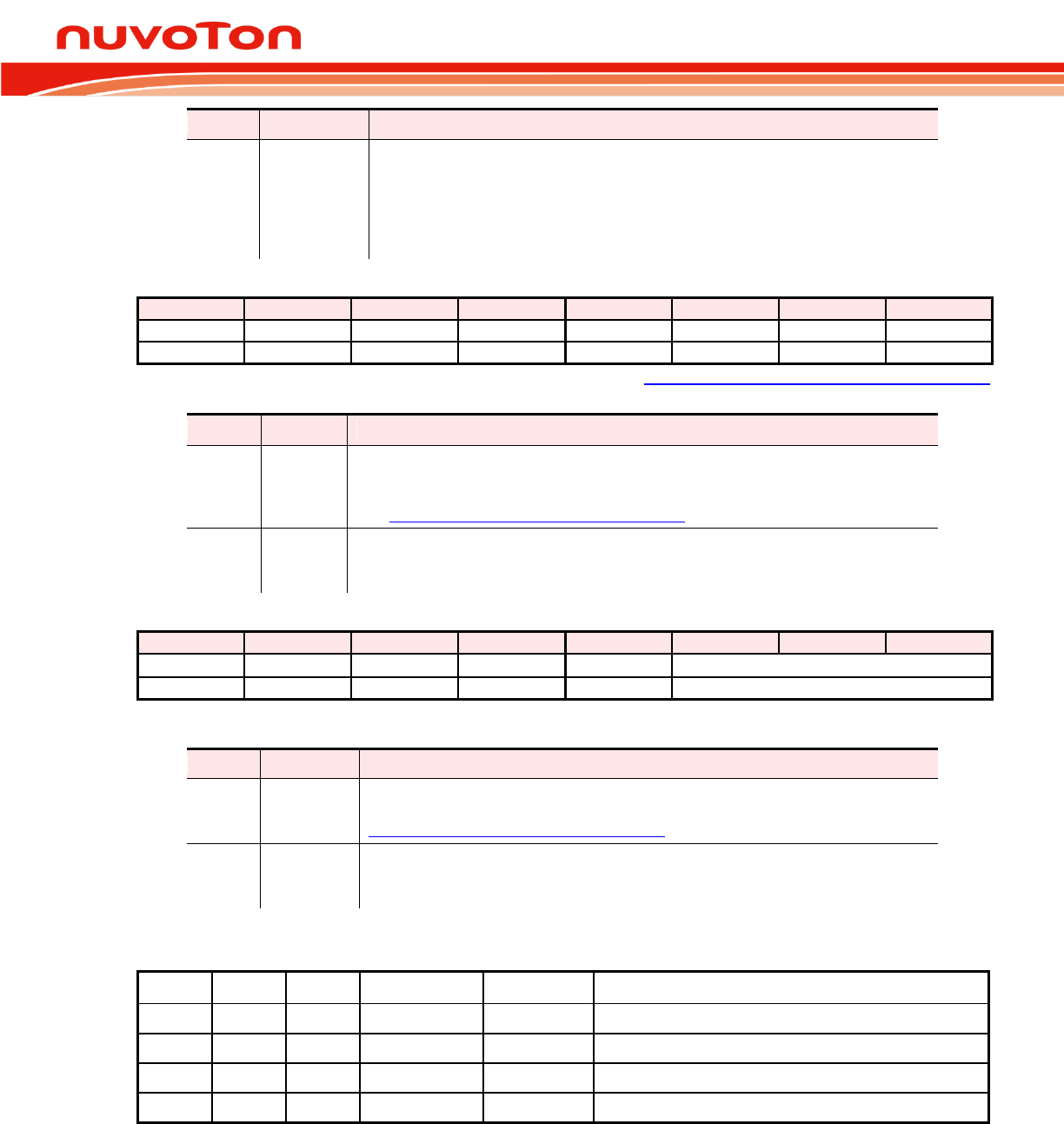
N76E003 Datasheet
Oct 28, 2016 Page 122 of 261 Rev. 1.00
Bit
Name
Description
0
RI_1
Receiving interrupt flag
This flag is set via hardware when a data frame has been received by the serial
port 1 after the 8th bit in Mode 0 or after sampling the stop bit in Mode 1, 2, or
3. SM2_1 bit as logic 1 has restriction for exception. When the serial port 1
interrupt is enabled, setting this bit causes the CPU to execute to the serial port
1 interrupt service routine. This bit must be cleared manually via software.
PCON Power Control
7
6
5
4
3
2
1
0
SMOD
SMOD0
-
POF
GF1
GF0
PD
IDL
R/W
R/W
-
R/W
R/W
R/W
R/W
R/W
Address: 87H Reset value: see Table 6-2. SFR Definitions and Reset Values
Bit
Name
Description
7
SMOD
Serial port 0 double baud rate enable
Setting this bit doubles the serial port baud rate when UART0 is in Mode 2 or
when Timer 1 overflow is used as the baud rate source of UART0 Mode 1 or 3.
See Table 13-1. Serial Port 0 Mode Description for details.
6
SMOD0
Serial port 0 framing error flag access enable
0 = SCON.7 accesses to SM0 bit.
1 = SCON.7 accesses to FE bit.
T3CON Timer 3 Control
7
6
5
4
3
2
1
0
SMOD_1
SMOD0_1
BRCK
TF3
TR3
T3PS[2:0]
R/W
R/W
R/W
R/W
R/W
R/W
Address: C4H, Page:0 Reset value: 0000 0000b
Bit
Name
Description
7
SMOD_1
Serial port 1 double baud rate enable
Setting this bit doubles the serial port baud rate when UART1 is in Mode 2. See
Table 13-2. Serial Port 1 Mode Description for details.
6
SMOD0_1
Serial port 1 framing error access enable
0 = SCON_1.7 accesses to SM0_1 bit.
1 = SCON_1.7 accesses to FE_1 bit.
Table 13-1. Serial Port 0 Mode Description
Mode
SM0
SM1
Description
Frame Bits
Baud Rate
0
0
0
Synchronous
8
FSYS divided by 12 or by 2[1]
1
0
1
Asynchronous
10
Timer 1/Timer 3 overflow rate divided by 32 or 16[2]
2
1
0
Asynchronous
11
FSYS divided by 32 or 64[2]
3
1
1
Asynchronous
11
Timer 1/Timer 3 overflow rate divided by 32 or 16[2]
[1] While SM2 (SCON.5) is logic 1.
[2] While SMOD (PCON.7) is logic 1.
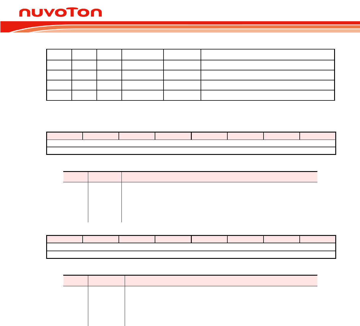
N76E003 Datasheet
Oct 28, 2016 Page 123 of 261 Rev. 1.00
Table 13-2. Serial Port 1 Mode Description
Mode
SM0
SM1
Description
Frame Bits
Baud Rate
0
0
0
Synchronous
8
FSYS divided by 12 or by 2[1]
1
0
1
Asynchronous
10
Timer 3 overflow rate divided by 16
2
1
0
Asynchronous
11
FSYS divided by 32 or 64[2]
3
1
1
Asynchronous
11
Timer 3 overflow rate divided by 16
[1] While SM2_1 (SCON_1.5) is logic 1.
[2] While SMOD_1 (T3CON.7) is logic 1.
SBUF Serial Port 0 Data Buffer
7
6
5
4
3
2
1
0
SBUF[7:0]
R/W
Address: 99H Reset value: 0000 0000b
Bit
Name
Description
7:0
SBUF[7:0]
Serial port 0 data buffer
This byte actually consists two separate registers. One is the receiving resister,
and the other is the transmitting buffer. When data is moved to SBUF, it goes to
the transmitting buffer and is shifted for serial transmission. When data is moved
from SBUF, it comes from the receiving register.
The transmission is initiated through giving data to SBUF.
SBUF_1 Serial Port 1 Data Buffer
7
6
5
4
3
2
1
0
SBUF_1[7:0]
R/W
Address: 9AH Reset value: 0000 0000b
Bit
Name
Description
7:0
SBUF_1[7:0]
Serial port 1 data buffer
This byte actually consists two separate registers. One is the receiving resister,
and the other is the transmitting buffer. When data is moved to SBUF_1, it
goes to the transmitting buffer and is shifted for serial transmission. When data
is moved from SBUF_1, it comes from the receiving register.
The transmission is initiated through giving data to SBUF_1.
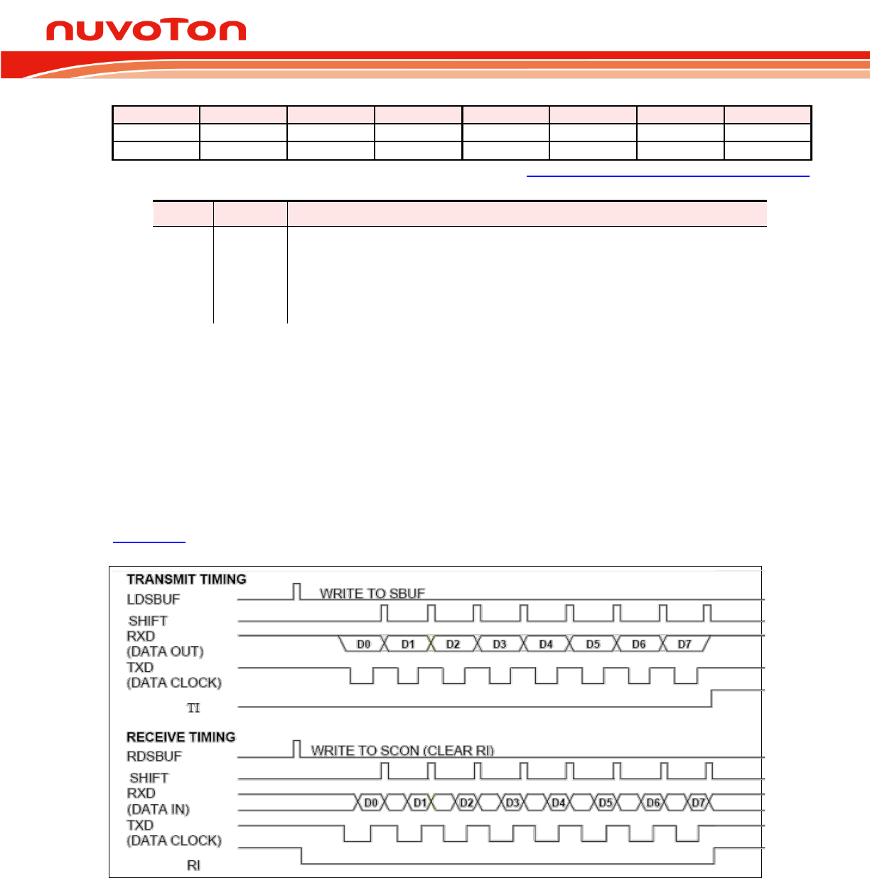
N76E003 Datasheet
Oct 28, 2016 Page 124 of 261 Rev. 1.00
AUXR1 Auxiliary Register 1
7
6
5
4
3
2
1
0
SWRF
RSTPINF
HardF
-
GF2
UART0PX
0
DPS
R/W
R/W
R/W
-
R/W
R/W
R
R/W
Address: A2H Reset value: see Table 6-2. SFR Definitions and Reset Values
Bit
Name
Description
2
UART0PX
Serial port 0 pin exchange
0 = Assign RXD to P0.7 and TXD to P0.6 by default.
1 = Exchange RXD to P0.6 and TXD to P0.7.
Note that TXD and RXD will exchange immediately once setting or clearing this
bit. User should take care of not exchanging pins during transmission or
receiving. Or it may cause unpredictable situation and no warning alarms.
13.1 Mode 0
Mode 0 provides synchronous communication with external devices. Serial data enters and exits
through RXD pin. TXD outputs the shift clocks. 8-bit frame of data are transmitted or received. Mode 0
therefore provides half-duplex communication because the transmitting or receiving data is via the
same data line RXD. The baud rate is enhanced to be selected as FSYS/12 if SM2 (SCON.5) is 0 or as
FSYS/2 if SM2 is 1. Note that whenever transmitting or receiving, the serial clock is always generated
by the MCU. Thus any device on the serial port in Mode 0 should accept the MCU as the master.
Figure 13-1 shows the associated timing of the serial port in Mode 0.
Figure 13-1. Serial Port Mode 0 Timing Diagram
As shown there is one bi-directional data line (RXD) and one shift clock line (TXD). The shift clocks
are used to shift data in or out of the serial port controller bit by bit for a serial communication. Data
bits enter or emit LSB first. The band rate is equal to the shift clock frequency.
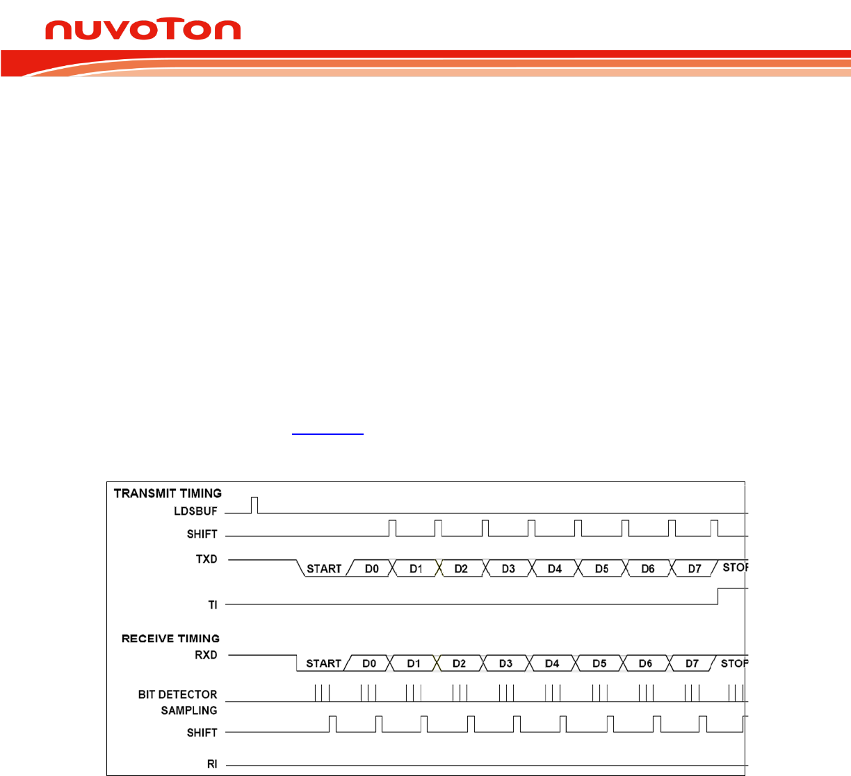
N76E003 Datasheet
Oct 28, 2016 Page 125 of 261 Rev. 1.00
Transmission is initiated by any instruction writes to SBUF. The control block will then shift out the
clocks and begin to transfer data until all 8 bits are complete. Then the transmitted flag TI (SCON.1)
will be set 1 to indicate one byte transmitting complete.
Reception is initiated by the condition REN (SCON.4) = 1 and RI (SCON.0) = 0. This condition tells the
serial port controller that there is data to be shifted in. This process will continue until 8 bits have been
received. Then the received flag RI will be set as 1. User can clear RI to triggering the next byte
reception.
13.2 Mode 1
Mode 1 supports asynchronous, full duplex serial communication. The asynchronous mode is
commonly used for communication with PCs, modems or other similar interfaces. In Mode 1, 10 bits
are transmitted through TXD or received through RXD including a start bit (logic 0), 8 data bits (LSB
first) and a stop bit (logic 1). The baud rate is determined by the Timer 1. SMOD (PCON.7) setting 1
makes the baud rate double. Figure 13-2 shows the associated timings of the serial port in Mode 1 for
transmitting and receiving.
Figure 13-2. Serial Port Mode 1 Timing Diagram
Transmission is initiated by any writing instructions to SBUF. Transmission takes place on TXD pin.
First the start bit comes out, the 8-bit data follows to be shifted out and then ends with a stop bit. After
the stop bit appears, TI (SCON.1) will be set to indicate one byte transmission complete. All bits are
shifted out depending on the rate determined by the baud rate generator.
Once the baud rate generator is activated and REN (SCON.4) is 1, the reception can begin at any
time. Reception is initiated by a detected 1-to-0 transition at RXD. Data will be sampled and shifted in
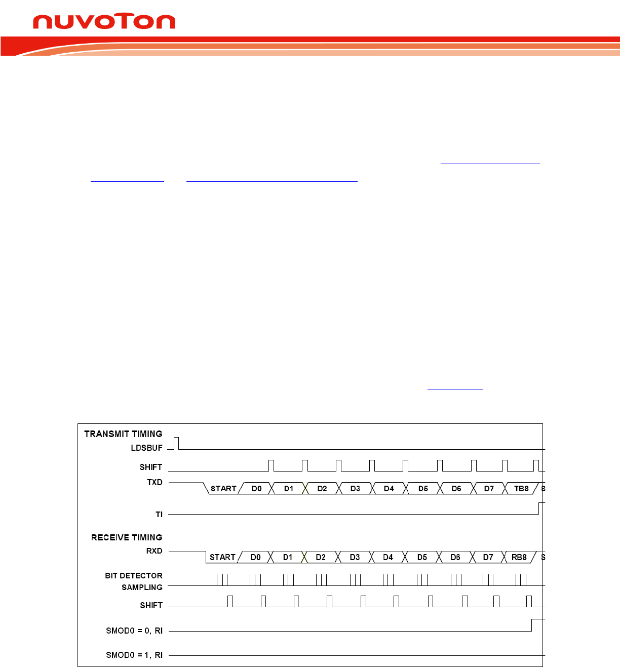
N76E003 Datasheet
Oct 28, 2016 Page 126 of 261 Rev. 1.00
at the selected baud rate. In the midst of the stop bit, certain conditions should be met to load SBUF
with the received data:
1. RI (SCON.0) = 0, and
2. Either SM2 (SCON.5) = 0, or the received stop bit = 1 while SM2 = 1 and the received data matches
13.7 Multiprocessor
Communication and 13.8 Automatic Address Recognition.)
If these conditions are met, then the SBUF will be loaded with the received data, the RB8 (SCON.2)
with stop bit, and RI will be set. If these conditions fail, there will be no data loaded and RI will remain
0. After above receiving progress, the serial control will look forward another 1-to-0 transition on RXD
pin to start next data reception.
13.3 Mode 2
Mode 2 supports asynchronous, full duplex serial communication. Different from Mode1, there are 11
bits to be transmitted or received. They are a start bit (logic 0), 8 data bits (LSB first), a programmable
9th bit TB8 or RB8 bit and a stop bit (logic 1). The most common use of 9th bit is to put the parity bit in it
or to label address or data frame for multiprocessor communication. The baud rate is fixed as 1/32 or
1/64 the system clock frequency depending on SMOD (PCON.7) bit. Figure 13-3 shows the
associated timings of the serial port in Mode 2 for transmitting and receiving.
Figure 13-3. Serial Port Mode 2 and 3 Timing Diagram

N76E003 Datasheet
Oct 28, 2016 Page 127 of 261 Rev. 1.00
Transmission is initiated by any writing instructions to SBUF. Transmission takes place on TXD pin.
First the start bit comes out, the 8-bit data and bit TB8 (SCON.3) follows to be shifted out and then
ends with a stop bit. After the stop bit appears, TI will be set to indicate the transmission complete.
While REN is set, the reception is allowed at any time. A falling edge of a start bit on RXD will initiate
the reception progress. Data will be sampled and shifted in at the selected baud rate. In the midst of
the stop bit, certain conditions should be met to load SBUF with the received data:
1. RI (SCON.0) = 0, and
2. Either SM2 (SCON.5) = 0, or the received 9th bit = 1 while SM2 = 1 and the received data matches
13.7 Multiprocessor
Communication and 13.8 Automatic Address Recognition.)
If these conditions are met, the SBUF will be loaded with the received data, the RB8(SCON.2) with the
received 9th bit and RI will be set. If these conditions fail, there will be no data loaded and RI will
remain 0. After above receiving progress, the serial control will look forward another 1-to-0 transition
on RXD pin to start next data reception.
13.4 Mode 3
Mode 3 has the same operation as Mode 2, except its baud rate clock source uses Timer 1 overflows
as its baud rate clocks. See Figure 13-3 for timing diagram of Mode 3. It has no difference from Mode
2.
13.5 Baud Rate
The baud rate source and speed for different modes of serial port is quite different from one another.
All cases are listed in Table 13-3. The user should calculate the baud rate according to their system
configuration.
In Mode 1 or 3, the baud rate clock source of UART0 can be selected from Timer 1 or Timer 3. User
can select the baud rate clock source by BRCK (T3CON.5). For UART1, its baud rate clock comes
only from Timer 3 as its unique clock source.

N76E003 Datasheet
Oct 28, 2016 Page 128 of 261 Rev. 1.00
T3CON Timer 3 Control
7
6
5
4
3
2
1
0
SMOD_1
SMOD0_1
BRCK
TF3
TR3
T3PS[2:0]
R/W
R/W
R/W
R/W
R/W
R/W
Address: C4H, Page:0 Reset value: 0000 0000b
Bit
Name
Description
5
BRCK
Serial port 0 baud rate clock source
This bit selects which Timer is used as the baud rate clock source when serial
port 0 is in Mode 1 or 3.
0 = Timer 1.
1 = Timer 3.
When using Timer 1 as the baud rate clock source, note that the Timer 1 interrupt should be disabled.
Timer 1 It can be in any of its three
running modes. However, in the most typical applications, it is configured for
auto-reload mode (Mode 2). If using Timer 3 as the baud rate generator, its interrupt should also be
disabled.
N76E003 Datasheet
Oct 28, 2016 Page 129 of 261 Rev. 1.00
Table 13-3. UART Baud Rate Formulas
UART Mode
Baud Rate Clock Source
Baud Rate
Formula
Number
0
System clock
12/FSYS
or
2/FSYS
[1]
1
2
System clock
64/FSYS
or
32/FSYS
[2]
2
1 or 3
Timer 1 (only for UART0)[3]
( )
1TH256×12
F
×
32
2SYS
SMOD
-
or
1TH256
F
×
32
2SYS
SMOD
-
[4]
3
Timer 3 (for UART0)
( )
}3RL,3RH{65536×scaleePr
F
×
32
2SYS
SMOD
--
[5]
4
Timer 3 (for UART1)
( )
}3RL,3RH{65536×scaleePr
F
×
16
1SYS
--
[5]
5
[1] SM2 (SCON.5) or SM2_1(SCON_1.5) is set as logic 1.
[2] SMOD (PCON.7) or SMOD_1(T3CON.7) is set as logic 1.
[3] Timer 1 is configured as a timer in auto-reload mode (Mode 2).
[4] T1M (CKCON.4) is set as logic 1. While SMOD is 1, TH1 should not be FFH.
[5] {RH3,RL3} in the formula means
3RL+3RH×256
. While SMOD is 1 and pre-scale is 1/1, {RH3,RL3} should
not be FFFFH.
Important: Since the limitation of baud rate generator, Suggest setting baud rate under 38400
when system timer base 16MHz HIRC value. Following show the baud rate value table show the
deviation upper 38400 baud rate.
HIRC
Target
Baud Rate
RHx
RLx
RHx + RLx
DEC Value
Actual
Baud Rate
Error %
16MHz
2400
0xFE
0x5F
65119
2398.081535
0.079%
4800
0xFF
0x30
65328
4807.692308
-0.160%
9600
0xFF
0x98
65432
9615.384615
-0.160%
19200
0xFF
0xCC
65484
19230.76923
-0.160%
38400
0xFF
0xE6
65510
38461.53846
-0.160%
57600
0xFF
0xEF
65519
58823.52941
-2.124%
115200
0xFF
0xF7
65527
111111.1111
3.549%
NOTE: RHx and RLx setting value base on baud rate formula 4 (SMOD =1) or 5 .
But In most application the baud rate 115200 is a common setting value. So we provide a special
function to modify HIRC to 16.6MHz. then the deviation of baud rate will be reasonable. Following
table shows the error value when HIRC and timer base modified.
HIRC
Target
RHx
RLx
RHx + RLx
Actual
Error %
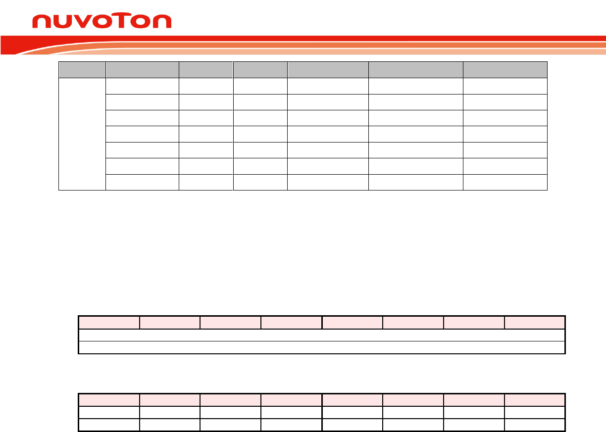
N76E003 Datasheet
Oct 28, 2016 Page 130 of 261 Rev. 1.00
Baud Rate
DEC Value
Baud Rate
16.6MHz
2400
0xFE
0x50
65104
2401.62037
-0.067%
4800
0xFF
0x28
65320
4803.240741
-0.067%
9600
0xFF
0x94
65428
9606.481481
-0.067%
19200
0xFF
0xCA
65482
19212.96296
-0.067%
38400
0xFF
0xE5
65509
38425.92593
-0.067%
57600
0xFF
0xEE
65518
57638.88889
-0.067%
115200
0xFF
0xF7
65527
115277.7778
-0.067%
NOTE: RHx and RLx setting value base on baud rate formula 4 (SMOD =1) or 5
N76E003 provide two bytes SFR to user trim HIRC value, default after reset the value is trim to
16MHz, once modify this SFR, the HIRC value will change. Suggest decrease reset value 15(dec.)
will trim HIRC to 16.6MHz.
Following two Byte combine the 9 bit internal RC trim value.
TRIMMAP0 High Speed Internal Oscillator 16 MHz Trim 0
7
6
5
4
3
2
1
0
HIRCTRIM[8:1]
R/W
Address: 84H Reset value: 16MHz HIRC value
TRIMMAP1 High Speed Internal Oscillator 16 MHz Trim 1
7
6
5
4
3
2
1
0
-
-
-
-
-
-
-
HIRCTRIM.0
-
-
-
-
-
-
-
R/W
Address: 85H Reset value: 16MHz HIRC value
Following is the demo code to modify HIRC to 16.6MHz,
sfr RCTRIM0 = 0x84;
sfr RCTRIM1 = 0x85;
bit BIT_TMP;
#define set_IAPEN BIT_TMP=EA;EA=0;TA=0xAA;TA=0x55;CHPCON|=SET_BIT0 ;EA=BIT_TMP
#define set_IAPGO BIT_TMP=EA;EA=0;TA=0xAA;TA=0x55;IAPTRG|=SET_BIT0 ;EA=BIT_TMP
#define clr_IAPEN BIT_TMP=EA;EA=0;TA=0xAA;TA=0x55;CHPCON&=~SET_BIT0;EA=BIT_TMP
unsigned char hircmap0,hircmap1;
unsigned int trimvalue16bit;
void MODIFY_HIRC_VLAUE(void)
{
set_IAPEN;
IAPAL = 0x30;
IAPAH = 0x00;
IAPCN = READ_UID;
set_IAPGO;
hircmap0 = IAPFD;
IAPAL = 0x31;
IAPAH = 0x00;

N76E003 Datasheet
Oct 28, 2016 Page 131 of 261 Rev. 1.00
set_IAPGO;
hircmap1 = IAPFD;
clr_IAPEN;
trimvalue16bit = ((hircmap0<<1)+(hircmap1&0x01));
trimvalue16bit = trimvalue16bit - 15;
hircmap1 = trimvalue16bit&0x01;
hircmap0 = trimvalue16bit>>1;
TA=0XAA;
TA=0X55;
RCTRIM0 = hircmap0;
TA=0XAA;
TA=0X55;
RCTRIM1 = hircmap1;
}
13.6 Framing Error Detection
Framing error detection is provided for asynchronous modes. (Mode 1, 2, or 3.) The framing error
occurs when a valid stop bit is not detected due to the bus noise or contention. The UART can detect
a framing error and notify the software.
The framing error bit, FE, is located in SCON.7. This bit normally serves as SM0. While the framing
error accessing enable bit SMOD0 (PCON.6) is set 1, it serves as FE flag. Actually, SM0 and FE
locate in different registers.
The FE bit will be set 1 via hardware while a framing error occurs. FE can be checked in UART
interrupt service routine if necessary. Note that SMOD0 should be 1 while reading or writing to FE. If
FE is set, any following frames received without frame error will not clear the FE flag. The clearing has
to be done via software.
13.7 Multiprocessor Communication
The N76E003 multiprocessor communication feature lets a master device send a multiple frame serial
message to a slave device in a multi-slave configuration. It does this without interrupting other slave
devices that may be on the same serial line. This feature can be used only in UART Mode 2 or 3. User
can enable this function by setting SM2 (SCON.5) as logic 1 so that when a byte of frame is received,
the serial interrupt will be generated only if the 9th bit is 1. (For Mode 2, the 9th bit is the stop bit.) When
the SM2 bit is 1, serial data frames that are received with the 9th bit as 0 do not generate an interrupt.
In this case, the 9th bit simply separates the slave address from the serial data.
When the master device wants to transmit a block of data to one of several slaves on a serial line, it
first sends out an address byte to identify the target slave. Note that in this case, an address byte
differs from a data byte. In an address byte, the 9th bit is 1 and in a data byte, it is 0. The address byte
interrupts all slaves so that each slave can examine the received byte and see if it is addressed by its
own slave address. The addressed slave then clears its SM2 bit and prepares to receive incoming

N76E003 Datasheet
Oct 28, 2016 Page 132 of 261 Rev. 1.00
data bytes. The SM2 bits of slaves that were not addressed remain set, and they continue operating
normally while ignoring the incoming data bytes.
Follow the steps below to configure multiprocessor communications:
1. Set all devices (masters and slaves) to UART Mode 2 or 3.
2. Write the SM2 bit of all the slave devices to 1.
3. The master devices transmission protocol is:
First byte: the address, identifying the target slave device, (9th bit = 1).
Next bytes: data, (9th bit = 0).
4. When the target slave receives the first byte, all of the slaves are interrupted because the 9th data
bit is 1. The targeted slave compares the address byte to its own address and then clears its SM2 bit
to receiving incoming data. The other slaves continue operating normally.
5. After all data bytes have been received, set SM2 back to 1 to wait for next address.
SM2 has no effect in Mode 0, and in Mode 1 can be used to check the validity of the stop bit. For
Mode 1 reception, if SM2 is 1, the receiving interrupt will not be issue unless a valid stop bit is
received.
13.8 Automatic Address Recognition
The automatic address recognition is a feature, which enhances the multiprocessor communication
feature by allowing the UART to recognize certain addresses in the serial bit stream by using
hardware to make the comparisons. This feature saves a great deal of software overhead by
eliminating the need for the software to examine every serial address, which passes by the serial port.
Only when the serial port recognizes its own address, the receiver sets RI bit to request an interrupt.
The automatic address recognition feature is enabled when the multiprocessor communication feature
is enabled, SM2 is set.
If desired, user may enable the automatic address recognition feature in Mode 1. In this configuration,
the stop bit takes the place of the ninth data bit. RI is set only when the received command frame
Using the automatic address recognition feature allows a master to selectively communicate with one
or more slaves by invoking the
N76E003 Datasheet
Oct 28, 2016 Page 133 of 261 Rev. 1.00
slave address mask, SADEN. SADEN is used to define which bits in the SADDR are to be used and
, which
address allows multiple slaves to be recognized while excluding others.
SADDR Slave 0 Address
7
6
5
4
3
2
1
0
SADDR[7:0]
R/W
Address: A9H Reset value: 0000 0000b
Bit
Name
Description
7:0
SADDR[7:0]
Slave 0 address
for UATR0 multi-
processor communication.
SADEN Slave 0 Address Mask
7
6
5
4
3
2
1
0
SADEN[7:0]
R/W
Address: B9H Reset value: 0000 0000b
Bit
Name
Description
7:0
SADEN[7:0]
Slave 0 address mask
This byte is a mask byte of UART0 that contains “don’t-care” bits (defined by
zeros) to form the device’s “Given” address. The don’t-care bits provide the
flexibility to address one or more slaves at a time.
SADDR_1 Slave 1 Address
7
6
5
4
3
2
1
0
SADDR_1[7:0]
R/W
Address: BBH Reset value: 0000 0000b
Bit
Name
Description
7:0
SADDR_1[7:0]
Slave 1 address
UART1 multi-
processor communication.
N76E003 Datasheet
Oct 28, 2016 Page 134 of 261 Rev. 1.00
SADEN_1 Slave 1 Address Mask
7
6
5
4
3
2
1
0
SADEN_1[7:0]
R/W
Address: BAH Reset value: 0000 0000b
Bit
Name
Description
7:0
SADEN_1[7:0]
Slave 1 address mask
This byte is a mask byte of UART1 that contains “don’t-care” bits (defined by
zeros) to form the device’s “Given” address. The don’t-care bits provide the
flexibility to address one or more slaves at a time.
The following examples will help to show the versatility of this scheme.
Example 1, slave 0:
SADDR = 11000000b
SADEN = 11111101b
Given = 110000X0b
Example 2, slave 1:
SADDR = 11000000b
SADEN = 11111110b
Given = 1100000Xb
In the above example SADDR is the same and the SADEN data is used to differentiate between the
two slaves. Slave 0 requires 0 in bit 0 and it ignores bit 1. Slave 1 requires 0 in bit 1 and bit 0 is
ignored. A unique address for Slave 0 would be 1100 0010 since slave 1 requires 0 in bit 1. A unique
address for slave 1 would be 11000001b since 1 in bit 0 will exclude slave 0. Both slaves can be
selected at the same time by an address, which has bit 0 = 0 (for slave 0) and bit 1 = 0 (for slave 1).
T
In a more complex system the following could be used to select slaves 1 and 2 while excluding slave
0:
Example 1, slave 0:
SADDR = 11000000b
SADEN = 11111001b
Given = 11000XX0b
Example 2, slave 1:
SADDR = 11100000b
SADEN = 11111010b
Given = 11100X0Xb

N76E003 Datasheet
Oct 28, 2016 Page 135 of 261 Rev. 1.00
Example 3, slave 2:
SADDR = 11000000b
SADEN = 11111100b
Given = 110000XXb
In the above example the differentiation among the 3 slaves is in the lower 3 address bits. Slave 0
requires that bit 0 = 0 and it can be uniquely addressed by 11100110b. Slave 1 requires that bit 1 = 0
and it can be uniquely addressed by 11100101b. Slave 2 requires that bit 2 = 0 and its unique address
is 11100011b. To select Slaves 0 and 1 and exclude Slave 2 use address 11100100b, since it is
necessary to make bit 2 = 1 to exclude slave 2.
-
SADDR = 01010110b
SADEN = 11111100b
Broadcast = 1111111Xb
-care bits provides flexibility in defining the Broadcast address, however in most
-
On reset, SADDR
serial port will reply to any address, and so that it is backwards compatible with the standard 80C51
microcontrollers that do not support automatic address recognition.
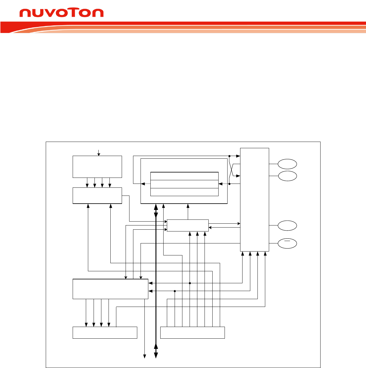
N76E003 Datasheet
Oct 28, 2016 Page 136 of 261 Rev. 1.00
14. SERIAL PERIPHERAL INTERFACE (SPI)
The N76E003 provides a Serial Peripheral Interface (SPI) block to support high-speed serial
communication. SPI is a full-duplex, high-speed, synchronous communication bus between
microcontrollers or other peripheral devices such as serial EEPROM, LCD driver, or D/A converter. It
provides either Master or Slave mode, high-speed rate up to FSYS/2, transfer complete and write
collision flag. For a multi-master system, SPI supports Master Mode Fault to protect a multi-master
conflict.
14.1 Functional Description
Divider
/2, /4, /8, /16
Select
MSB LSB
Pin Contorl Logic
MISO
MOSI
SPCLK
SS
SPI Status Control Logic
SPI Status Register SPI Control Register
Clock Logic
S
M
M
S
CLOCK
SPIF
WCOL
SPIOVF
MODF
DISMODF
SPI Interrupt
SPIEN
MSTR
MSTR
SSOE
DISMODF
SPR0
SPR1
SPR0
SPR1
CPHA
CPOL
MSTR
LSBFE
SPIEN
SSOE
SPIEN
Internal
Data Bus
FSYS
Write Data Buffer
8-bit Shift Register
Read Data Buffer
Figure 14-1. SPI Block Diagram
Figure 14-1. SPI Block Diagram shows SPI block diagram. It provides an overview of SPI architecture
in this device. The main blocks of SPI are the SPI control register logic, SPI status logic, clock rate
control logic, and pin control logic. For a serial data transfer or receiving, The SPI block exists a write
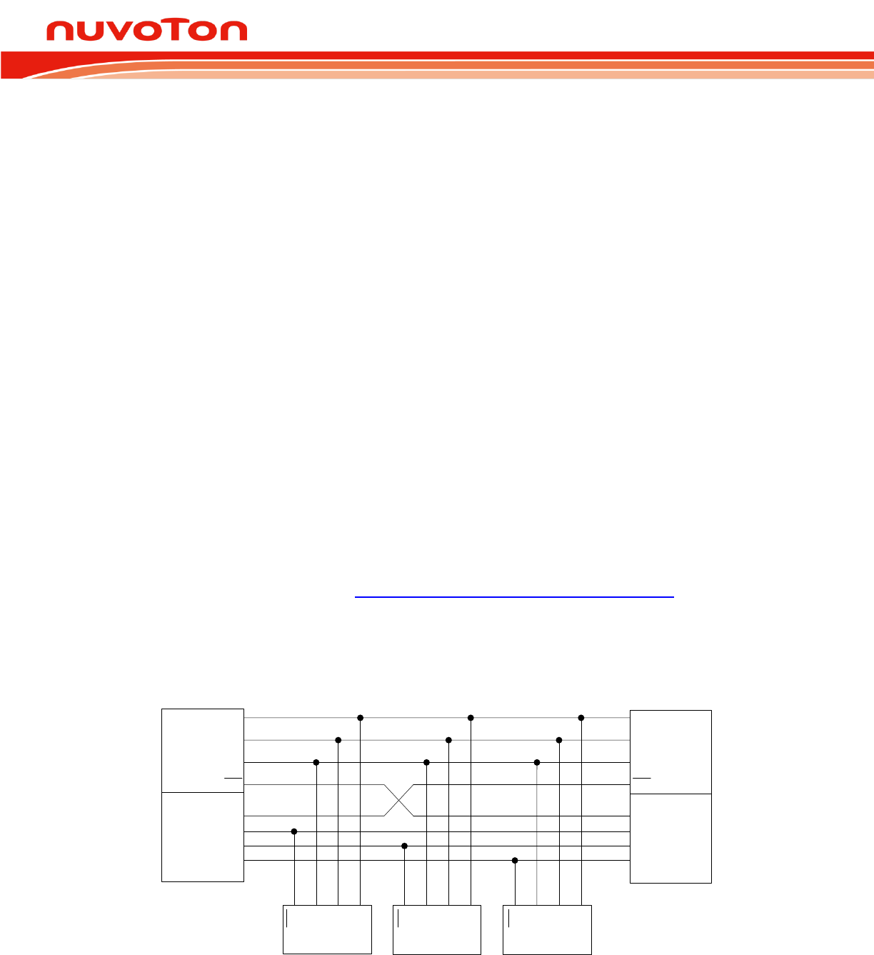
N76E003 Datasheet
Oct 28, 2016 Page 137 of 261 Rev. 1.00
data buffer, a shift out register and a read data buffer. It is double buffered in the receiving and
transmit directions. Transmit data can be written to the shifter until when the previous transfer is not
complete. Receiving logic consists of parallel read data buffer so the shift register is free to accept a
second data, as the first received data will be transferred to the read data buffer.
The four pins of SPI interface are Master-In/Slave-Out (MISO), Master-Out/Slave-In (MOSI), Shift
Clock (SPCLK), and Slave Select (
). The MOSI pin is used to transfer a 8-bit data in series from the
Master to the Slave. Therefore, MOSI is an output pin for Master device and an input for Slave.
Respectively, the MISO is used to receive a serial data from the Slave to the Master.
The SPCLK pin is the clock output in Master mode, but is the clock input in Slave mode. The shift
clock is used to synchronize the data movement both in and out of the devices through their MOSI and
MISO pins. The shift clock is driven by the Master mode device for eight clock cycles. Eight clocks
exchange one byte data on the serial lines. For the shift clock is always produced out of the Master
device, the system should never exist more than one device in Master mode for avoiding device
conflict.
Each Slave peripheral is selected by one Slave Select pin (
). The signal should stay low for any
Slave access. When
is driven high, the Slave device will be inactivated. If the system is multi-
slave, there should be only one Slave device selected at the same time. In the Master mode MCU, the
pin does not function and it can be configured as a general purpose I/O. However,
can be used
as Master Mode Fault detection (see Section 14.5 Mode Fault Detection146) via software
setting if multi-master environment exists. The N76E003 also provides auto-activating function to
toggle
between each byte-transfer.
MISO
MOSI
SPCLK
SS
I/O
PORT
0
1
2
3
I/O
PORT
0
1
2
3
SO
SI
SCK
SS
Slave device 1
Master/Slave
MCU1
MISO
MOSI
SPCLK
SS
Master/Slave
MCU2
SO
SI
SCK
SS
Slave device 2
SO
SI
SCK
SS
Slave device 3
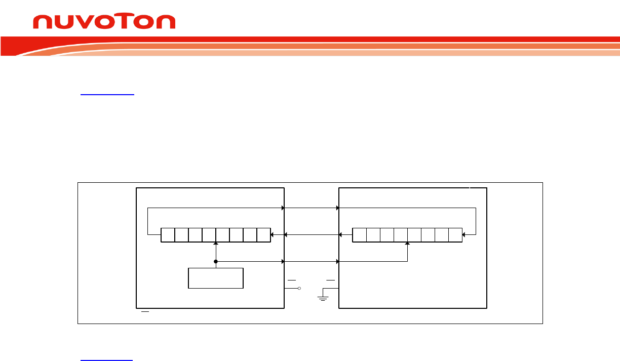
N76E003 Datasheet
Oct 28, 2016 Page 138 of 261 Rev. 1.00
Figure 14-2. SPI Multi-Master, Multi-Slave Interconnection
Figure 14-2 shows a typical interconnection of SPI devices. The bus generally connects devices
together through three signal wires, MOSI to MOSI, MISO to MISO, and SPCLK to SPCLK. The
Master devices select the individual Slave devices by using four pins of a parallel port to control the
four
pins. MCU1 and MCU2 play either Master or Slave mode. The
should be configured as
Master Mode Fault detection to avoid multi-master conflict.
SPI clock
generator
MISO MISO
MOSI MOSI
SPCLK SPCLK
GND
SS SS
7 6 5 4 3 2 1 0
SPI shift register
7 6 5 4 3 2 1 0
SPI shift register
Master MCU Slave MCU
*
* SS configuration follows DISMODF and SSOE bits.
Figure 14-3. SPI Single-Master, Single-Slave Interconnection
Figure 14-3 shows the simplest SPI system interconnection, single-master and signal-slave. During a
transfer, the Master shifts data out to the Slave via MOSI line. While simultaneously, the Master shifts
data in from the Slave via MISO line. The two shift registers in the Master MCU and the Slave MCU
can be considered as one 16-bit circular shift register. Therefore, while a transfer data pushed from
Master into Slave, the data in Slave will also be pulled in Master device respectively. The transfer
effectively exchanges the data, which was in the SPI shift registers of the two MCUs.
By default, SPI data is transferred MSB first. If the LSBFE (SPCR.5) is set, SPI data shifts LSB first.
This bit does not affect the position of the MSB and LSB in the data register. Note that all the following
description and figures are under the condition of LSBFE logic 0. MSB is transmitted and received
first.
There are three SPI registers to support its operations, including SPI control register (SPCR), SPI
status register (SPSR), and SPI data register (SPDR). These registers provide control, status, data
storage functions, and clock rate selection. The following registers relate to SPI function.
N76E003 Datasheet
Oct 28, 2016 Page 139 of 261 Rev. 1.00
SPCR Serial Peripheral Control Register
7
6
5
4
3
2
1
0
SSOE
SPIEN
LSBFE
MSTR
CPOL
CPHA
SPR1
SPR0
R/W
R/W
R/W
R/W
R/W
R/W
R/W
R/W
Address: F3H, page 0 Reset value: 0000 0000b
Bit
Name
Description
7
SSOE
Slave select output enable
This bit is used in combination with the DISMODF (SPSR.3) bit to determine the
feature of
pin as shown in Table 14-1. Slave Select Pin Configurations. This bit
takes effect only under MSTR = 1 and DISMODF = 1 condition.
0 =
functions as a general purpose I/O pin.
1 =
automatically goes low for each transmission when selecting external
Slave device and goes high during each idle state to de-select the Slave
device.
6
SPIEN
SPI enable
0 = SPI function Disabled.
1 = SPI function Enabled.
5
LSBFE
LSB first enable
0 = The SPI data is transferred MSB first.
1 = The SPI data is transferred LSB first.
4
MSTR
Master mode enable
This bit switches the SPI operating between Master and Slave modes.
0 = The SPI is configured as Slave mode.
1 = The SPI is configured as Master mode.
3
CPOL
SPI clock polarity select
CPOL bit determines the idle state level of the SPI clock. See Figure 14-4. SPI
Clock Formats.
0 = The SPI clock is low in idle state.
1 = The SPI clock is high in idle state.
2
CPHA
SPI clock phase select
CPHA bit determines the data sampling edge of the SPI clock. See Figure 14-4.
SPI Clock Formats.
0 = The data is sampled on the first edge of the SPI clock.
1 = The data is sampled on the second edge of the SPI clock.
N76E003 Datasheet
Oct 28, 2016 Page 140 of 261 Rev. 1.00
Bit
Name
Description
1:0
SPR[1:0]
SPI clock rate select
These two bits select four grades of SPI clock divider. The clock rates below are
illustrated under FSYS = 16 MHz condition.
SPR1
SPR0
Divider
SPI clock rate
0
0
2
8M bit/s
0
1
4
4M bit/s
1
0
8
2M bit/s
1
1
16
1M bit/s
SPR[1:0] are valid only under Master mode (MSTR = 1). If under Slave mode, the
clock will automatically synchronize with the external clock on SPICLK pin from
Master device up to FSYS/2 communication speed.
SPCR2 Serial Peripheral Control Register 2
7
6
5
4
3
2
1
0
-
-
-
-
-
-
SPIS1
SPIS0
-
-
-
-
-
-
R/W
R/W
Address: F3H, page 1 Reset value: 0000 0000b
Bit
Name
Description
7:2
-
Reserved
1:0
SPIS[1:0]
SPI Interval time selection between adjacent bytes
SPIS[1:0] and CPHA select eight grades of SPI interval time selection between
adjacent bytes. As below table:
CPHA
SPIS1
SPIS0
SPI clock
0
0
0
0.5
0
0
1
1.0
0
1
0
1.5
0
1
1
2.0
1
0
0
1.0
1
0
1
1.5
1
1
0
2.0
1
1
1
2.5
SPIS[1:0] are valid only under Master mode (MSTR = 1).

N76E003 Datasheet
Oct 28, 2016 Page 141 of 261 Rev. 1.00
Table 14-1. Slave Select Pin Configurations
DISMODF
SSOE
Master Mode (MSTR = 1)
Slave Mode (MSTR = 0)
0
X
input for Mode Fault
Input for Slave select
1
0
General purpose I/O
1
1
Automatic
output
SPSR Serial Peripheral Status Register
7
6
5
4
3
2
1
0
SPIF
WCOL
SPIOVF
MODF
DISMODF
-
-
-
R/W
R/W
R/W
R/W
R/W
-
-
-
Address: F4H Reset value: 0000 0000b
Bit
Name
Description
7
SPIF
SPI complete flag
This bit is set to logic 1 via hardware while an SPI data transfer is complete or an
receiving data has been moved into the SPI read buffer. If ESPI (EIE .0) and EA
are enabled, an SPI interrupt will be required. This bit should be cleared via
software. Attempting to write to SPDR is inhibited if SPIF is set.
6
WCOL
Write collision error flag
This bit indicates a write collision event. Once a write collision event occurs, this
bit will be set. It should be cleared via software.
5
SPIOVF
SPI overrun error flag
This bit indicates an overrun event. Once an overrun event occurs, this bit will be
set. If ESPI and EA are enabled, an SPI interrupt will be required. This bit should
be cleared via software.
4
MODF
Mode Fault error flag
This bit indicates a Mode Fault error event. If
pin is configured as Mode Fault
input (MSTR = 1 and DISMODF = 0) and
is pulled low by external devices, a
Mode Fault error occurs. Instantly MODF will be set as logic 1. If ESPI and EA
are enabled, an SPI interrupt will be required. This bit should be cleared via
software.
3
DISMODF
Disable Mode Fault error detection
This bit is used in combination with the SSOE (SPCR.7) bit to determine the
feature of
pin as shown in Table 14-1. Slave Select Pin Configurations.
DISMODF is valid only in Master mode (MSTR = 1).
0 = Mode Fault detection Enabled.
serves as input pin for Mode Fault
detection disregard of SSOE.
1 = Mode Fault detection Disabled. The feature of
follows SSOE bit.

N76E003 Datasheet
Oct 28, 2016 Page 142 of 261 Rev. 1.00
SPDR Serial Peripheral Data Register
7
6
5
4
3
2
1
0
SPDR[7:0]
R/W
Address: F5H Reset value: 0000 0000b
Bit
Name
Description
7:0
SPDR[7:0]
Serial peripheral data
This byte is used for transmitting or receiving data on SPI bus. A write of this
byte is a write to the shift register. A read of this byte is actually a read of the
read data buffer. In Master mode, a write to this register initiates transmission
and reception of a byte simultaneously.
14.2 Operating Modes
Master Mode 14.2.1
The SPI can operate in Master mode while MSTR (SPCR.4) is set as 1. Only one Master SPI device
can initiate transmissions. A transmission always begins by Master through writing to SPDR. The byte
written to SPDR begins shifting out on MOSI pin under the control of SPCLK. Simultaneously, another
byte shifts in from the Slave on the MISO pin. After 8-bit data transfer complete, SPIF (SPSR.7) will
automatically set via hardware to indicate one byte data transfer complete. At the same time, the data
received from the Slave is also transferred in SPDR. User can clear SPIF and read data out of SPDR.
Slave Mode 14.2.2
When MSTR is 0, the SPI operates in Slave mode. The SPCLK pin becomes input and it will be
clocked by another Master SPI device. The
pin also becomes input. The Master device cannot
exchange data with the Slave device until the
pin of the Slave device is externally pulled low.
Before data transmissions occurs, the
of the Slave device should be pulled and remain low until
the transmission is complete. If
goes high, the SPI is forced into idle state. If the
is forced to
high at the middle of transmission, the transmission will be aborted and the rest bits of the receiving
shifter buffer will be high and goes into idle state.
In Slave mode, data flows from the Master to the Slave on MOSI pin and flows from the Slave to the
Master on MISO pin. The data enters the shift register under the control of the SPCLK from the Master
device. After one byte is received in the shift register, it is immediately moved into the read data buffer
and the SPIF bit is set. A read of the SPDR is actually a read of the read data buffer. To prevent an
overrun and the loss of the byte that caused by the overrun, the Slave should read SPDR out and the
first SPIF should be cleared before a second transfer of data from the Master device comes in the
read data buffer.
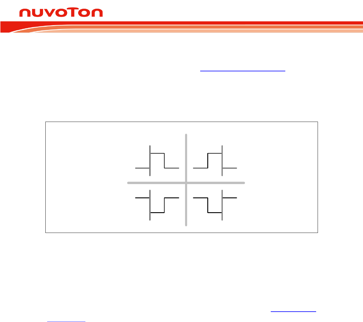
N76E003 Datasheet
Oct 28, 2016 Page 143 of 261 Rev. 1.00
14.3 Clock Formats and Data Transfer
To accommodate a wide variety of synchronous serial peripherals, the SPI has a clock polarity bit
CPOL (SPCR.3) and a clock phase bit CPHA (SPCR.2). Figure 14-4. SPI Clock Formats shows that
CPOL and CPHA compose four different clock formats. The CPOL bit denotes the SPCLK line level in
its idle state. The CPHA bit defines the edge on which the MOSI and MISO lines are sampled. The
CPOL and CPHA should be identical for the Master and Slave devices on the same system. To
Communicate in different data formats with one another will result undetermined result.
CPHA = 0 CPHA = 1
sample
CPOL = 0CPOL = 1
Clock Phase (CPHA)
Clock Polarity (CPOH)
sample
samplesample
Figure 14-4. SPI Clock Formats
In SPI, a Master device always initiates the transfer. If SPI is selected as Master mode (MSTR = 1)
and enabled (SPIEN = 1), writing to the SPI data register (SPDR) by the Master device starts the SPI
clock and data transfer. After shifting one byte out and receiving one byte in, the SPI clock stops and
SPIF (SPSR.7) is set in both Master and Slave. If SPI interrupt enable bit ESPI (EIE.0) is set 1 and
global interrupt is enabled (EA = 1), the interrupt service routine (ISR) of SPI will be executed.
Concerning the Slave mode, the
signal needs to be taken care. As shown in Figure 14-4. SPI
Clock Formats, when CPHA = 0, the first SPCLK edge is the sampling strobe of MSB (for an example
of LSBFE = 0, MSB first). Therefore, the Slave should shift its MSB data before the first SPCLK edge.
The falling edge of
is used for preparing the MSB on MISO line. The
pin therefore should
toggle high and then low between each successive serial byte. Furthermore, if the slave writes data to
the SPI data register (SPDR) while
is low, a write collision error occurs.
When CPHA = 1, the sampling edge thus locates on the second edge of SPCLK clock. The Slave
uses the first SPCLK clock to shift MSB out rather than the
falling edge. Therefore, the
line can
remain low between successive transfers. This format may be preferred in systems having single fixed
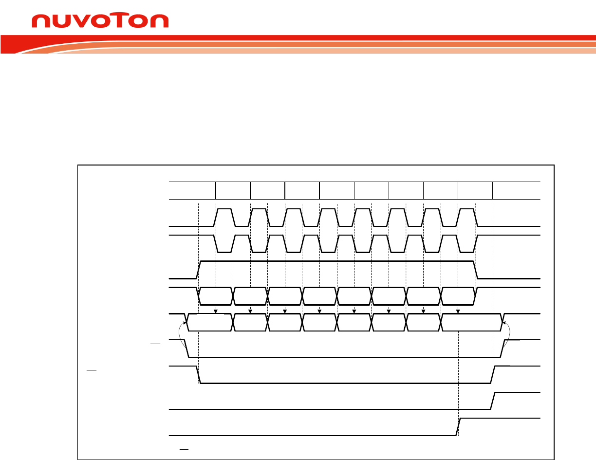
N76E003 Datasheet
Oct 28, 2016 Page 144 of 261 Rev. 1.00
Master and single fixed Slave. The
line of the unique Slave device can be tied to GND as long as
only CPHA = 1 clock mode is used.
The SPI should be configured before it is enabled (SPIEN = 1), or a change of LSBFE, MSTR,
CPOL, CPHA and SPR[1:0] will abort a transmission in progress and force the SPI system into
idle state. Prior to any configuration bit changed, SPIEN must be disabled first.
SPCLK Cycles
SPCLK (CPOL=0)
MOSI
SS output of Master[2]
SPIF (Master)
12345678
SPCLK (CPOL=1)
Transfer Progress[1]
(internal signal)
MSB
MISO 65432 1 LSB
MSB
Input to Slave SS
LSB
6 5 4 321
SPIF (Slave)
[1] Transfer progress starts by a writing SPDR of Master MCU.
[2] SS automatic output affects when MSTR = DISMODF = SSOE = 1.
SPCLK Cycles
Figure 14-5. SPI Clock and Data Format with CPHA = 0
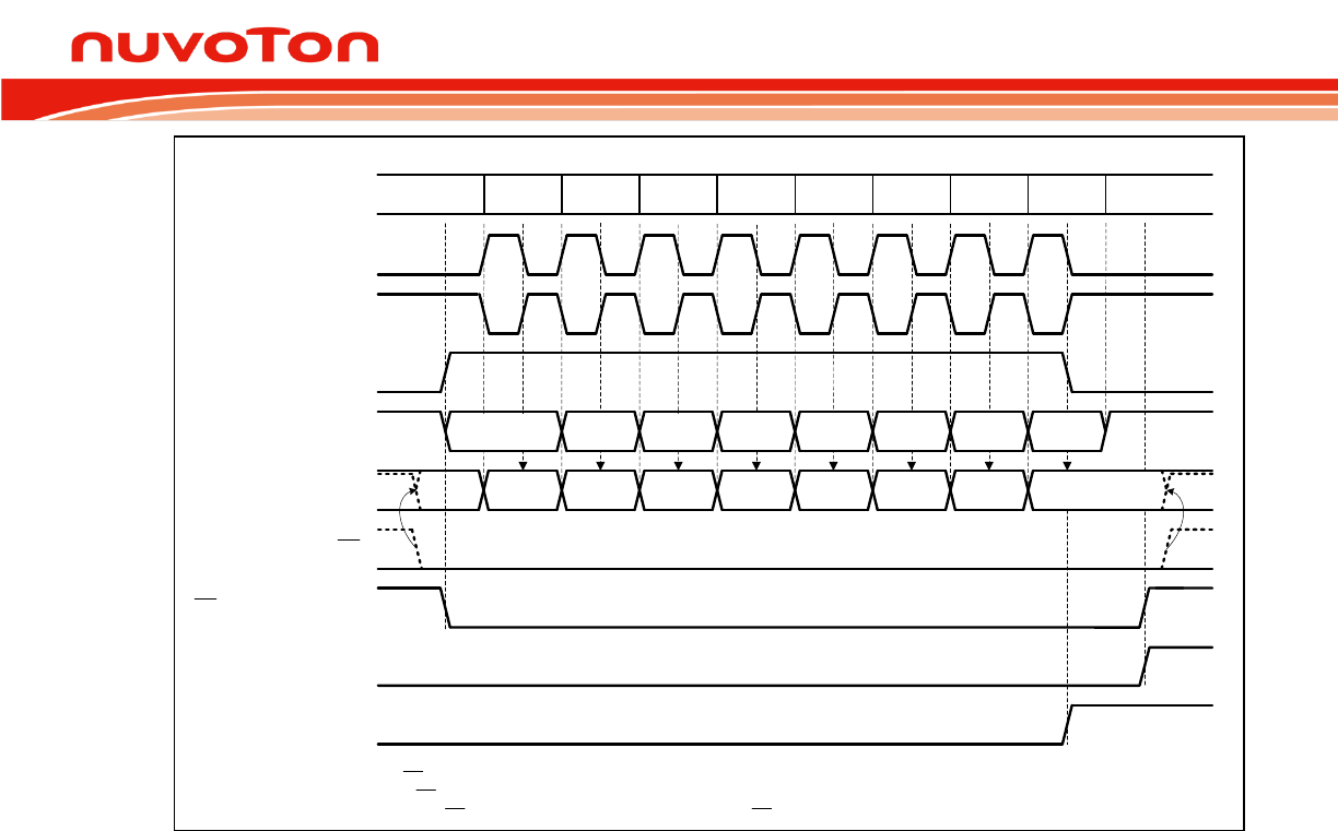
N76E003 Datasheet
Oct 28, 2016 Page 145 of 261 Rev. 1.00
Transfer Progress[1]
(internal signal)
SPCLK Cycles
SPCLK (CPOL=0)
MOSI
SS output of Master[2]
SPIF (Master)
12345678
SPCLK (CPOL=1)
MSB
MISO 65432 1 LSB
MSB
Input to Slave SS
LSB
6543 2 1
SPIF (Slave)
[1] Transfer progress starts by a writing SPDR of Master MCU.
[2] SS automatic output affects when DISMODF = SSOE = MSTR = 1.
[3] If SS of Slave is low, the MISO will be the LSB of previous data. Otherwise, MISO will be high.
[4] While SS stays low, the LSB will last its state. Once SS is released to high, MISO will switch to high level.
[3] [4]
SPCLK Cycles
Figure 14-6. SPI Clock and Data Format with CPHA = 1
14.4 Slave Select Pin Configuration
The N76E003 SPI gives a flexible
pin feature for different system requirements. When the SPI
operates as a Slave,
pin always rules as Slave select input. When the Master mode is enabled,
has three different functions according to DISMODF (SPSR.3) and SSOE (SPCR.7). By default,
DISMODF is 0. It means that the Mode Fault detection activates.
is configured as a input pin to
check if the Mode Fault appears. On the contrary, if DISMODF is 1, Mode Fault is inactivated and the
SSOE bit takes over to control the function of the
pin. While SSOE is 1, it means the Slave select
signal will generate automatically to select a Slave device. The
as output pin of the Master usually
connects with the
input pin of the Slave device. The
output automatically goes low for each
transmission when selecting external Slave device and goes high during each idle state to de-select
the Slave device. While SSOE is 0 and DISMODF is 1,
is no more used by the SPI and reverts to
be a general purpose I/O pin.

N76E003 Datasheet
Oct 28, 2016 Page 146 of 261 Rev. 1.00
14.5 Mode Fault Detection
The Mode Fault detection is useful in a system where more than one SPI devices might become
Masters at the same time. It may induce data contention. When the SPI device is configured as a
Master and the
input line is configured for Mode Fault input depending on Table 14-1. Slave Select
Pin Configurations, a Mode Fault error occurs once the
is pulled low by others. It indicates that
some other SPI device is trying to address this Master as if it is a Slave. Instantly the MSTR and
SPIEN control bits in the SPCR are cleared via hardware to disable SPI, Mode Fault flag MODF
(SPSR.4) is set and an interrupt is generated if ESPI (EIE .0) and EA are enabled.
14.6 Write Collision Error
The SPI is signal buffered in the transfer direction and double buffered in the receiving and transmit
direction. New data for transmission cannot be written to the shift register until the previous transaction
is complete. Write collision occurs while SPDR be written more than once while a transfer was in
progress. SPDR is double buffered in the transmit direction. Any writing to SPDR cause data to be
written directly into the SPI shift register. Once a write collision error is generated, WCOL (SPSR.6)
will be set as 1 via hardware to indicate a write collision. In this case, the current transferring data
continues its transmission. However the new data that caused the collision will be lost. Although the
SPI logic can detect write collisions in both Master and Slave modes, a write collision is normally a
Slave error because a Slave has no indicator when a Master initiates a transfer. During the receiving
of Slave, a write to SPDR causes a write collision in Slave mode. WCOL flag needs to be cleared via
software.
14.7 Overrun Error
For receiving data, the SPI is double buffered in the receiving direction. The received data is
transferred into a parallel read data buffer so the shifter is free to accept a second serial byte.
However, the received data should be read from SPDR before the next data has been completely
shifted in. As long as the first byte is read out of the read data buffer and SPIF is cleared before the
next byte is ready to be transferred, no overrun error condition occurs. Otherwise the overrun error
occurs. In this condition, the second byte data will not be successfully received into the read data
register and the previous data will remains. If overrun occur, SPIOVF (SPSR.5) will be set via
hardware. An SPIOVF setting will also require an interrupt if enabled. Figure 14-7. SPI Overrun
Waveform shows the relationship between the data receiving and the overrun error.
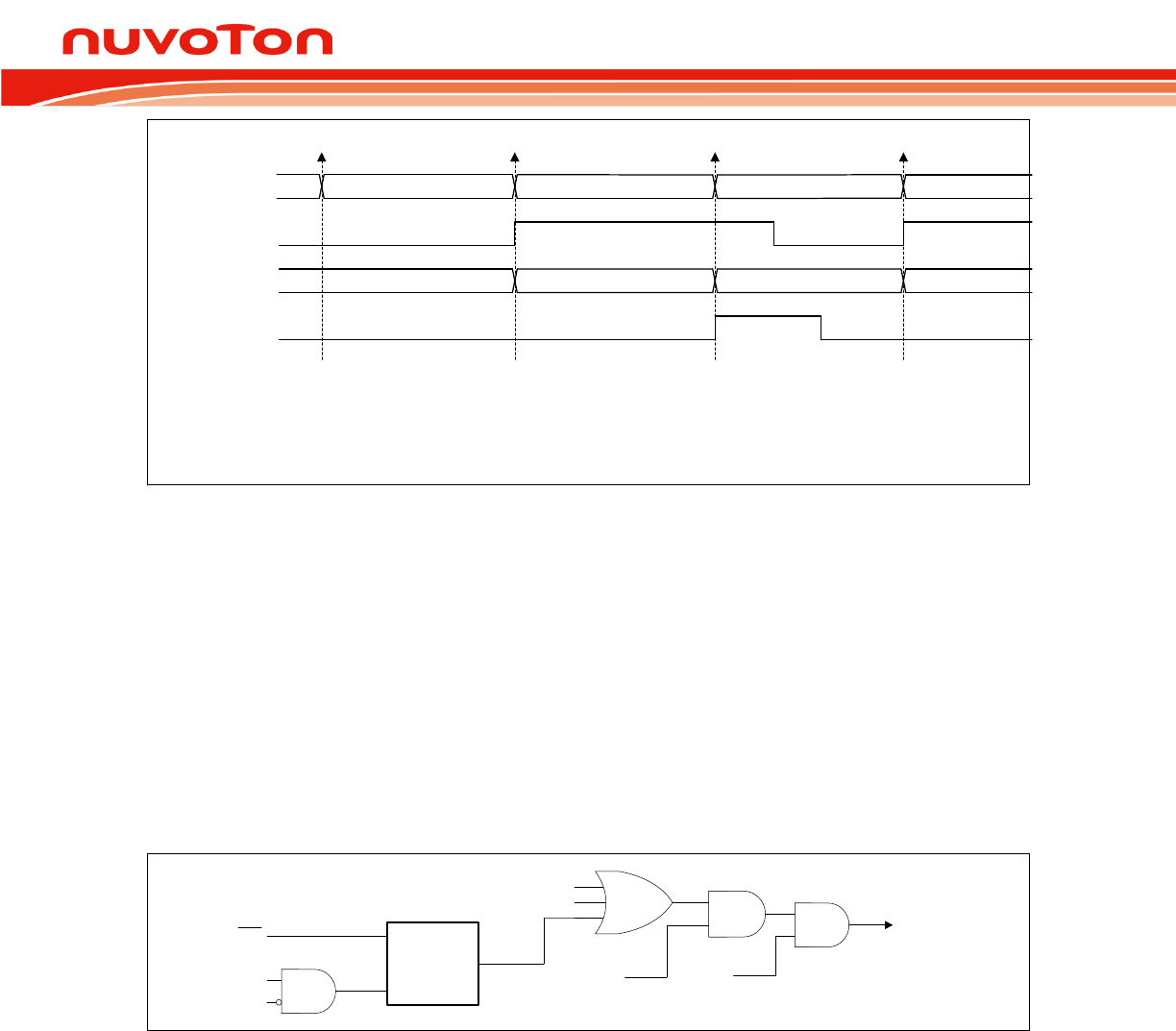
N76E003 Datasheet
Oct 28, 2016 Page 147 of 261 Rev. 1.00
Shifting Data[n] in Shifting Data[n+1] in
SPIF
Data[n] Data[n]
Read Data Buffer
Shift Register Shifting Data[n+2] in
SPIOVF
Data[n+2]
Data[n] Receiving Begins Data[n+1] Receiving Begins Data[n+2] Receiveing Begins
[1] When Data[n] is received, the SPIF will be set.
[2] If SPIF is not clear before Data[n+1] progress done, the SPIOVF will
be set. Data[n] will be kept in read data buffer but Data [n+1] will be lost.
[3] SPIF and SPIOVF must be cleared by software.
[4] When Data[n+2] is received, the SPIF will be set again.
[1]
[2]
[3]
[3]
[4]
Figure 14-7. SPI Overrun Waveform
14.8 SPI Interrupt
Three SPI status flags, SPIF, MODF, and SPIOVF, can generate an SPI event interrupt requests. All
of them locate in SPSR. SPIF will be set after completion of data transfer with external device or a
new data have been received and copied to SPDR. MODF becomes set to indicate a low level on
causing the Mode Fault state. SPIOVF denotes a receiving overrun error. If SPI interrupt mask is
enabled via setting ESPI (EIE.6) and EA is 1, CPU will executes the SPI interrupt service routine once
any of these three flags is set. User needs to check flags to determine what event caused the
interrupt. These three flags are software cleared.
SPIF
DISMODF
MSTR ESPI
(EIE.6)
SPI Interrupt
SPIOVF
Mode
Fault
Detection
SS MODF
EA
Figure 14-8. SPI Interrupt Request
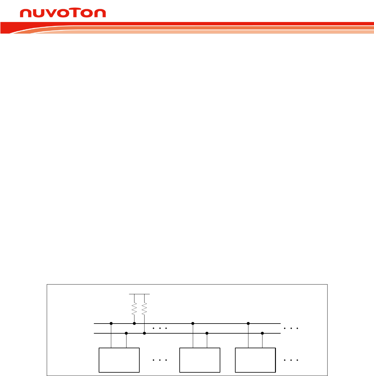
N76E003 Datasheet
Oct 28, 2016 Page 148 of 261 Rev. 1.00
15. INTER-INTEGRATED CIRCUIT (I2C)
The Inter-Integrated Circuit (I2C) bus serves as an serial interface between the microcontrollers and
the I2C devices such as EEPROM, LCD module, temperature sensor, and so on. The I2C bus used
two wires design (a serial data line SDA and a serial clock line SCL) to transfer information between
devices.
The I2C bus uses bi-directional data transfer between masters and slaves. There is no central master
and the multi-master system is allowed by arbitration between simultaneously transmitting masters.
The serial clock synchronization allows devices with different bit rates to communicate via one serial
bus. The I2C bus supports four transfer modes including master transmitter, master receiver, slave
receiver, and slave transmitter. The I2C interface only supports 7-bit addressing mode. A special mode
General Call is also available. The I2C can meet both standard (up to 100kbps) and fast (up to 400k
bps) speeds.
15.1 Functional Description
For a bi-directional transfer operation, the SDA and SCL pins should be open-drain pads. This
implements a wired-AND function, which is essential to the operation of the interface. A low level on a
I2C bus line is generated when one or more I2C generated when
all I2C -up resistors to pull the line high. In N76E003, user should
set output latches of SCL and SDA. As logic 1 before enabling the I2C function by setting I2CEN
(I2CON.6).
SDA SCL
Slave Device
SDA SCL
Other MCU
SDA
SCL
VDD
RUP RUP
SDA SCL
N76E003
Figure 15-1. I2C Bus Interconnection
The I2C is considered free when both lines are high. Meanwhile, any device, which can operate as a
master can occupy the bus and generate one transfer after generating a START condition. The bus
now is considered busy before the transfer ends by sending a STOP condition. The master generates
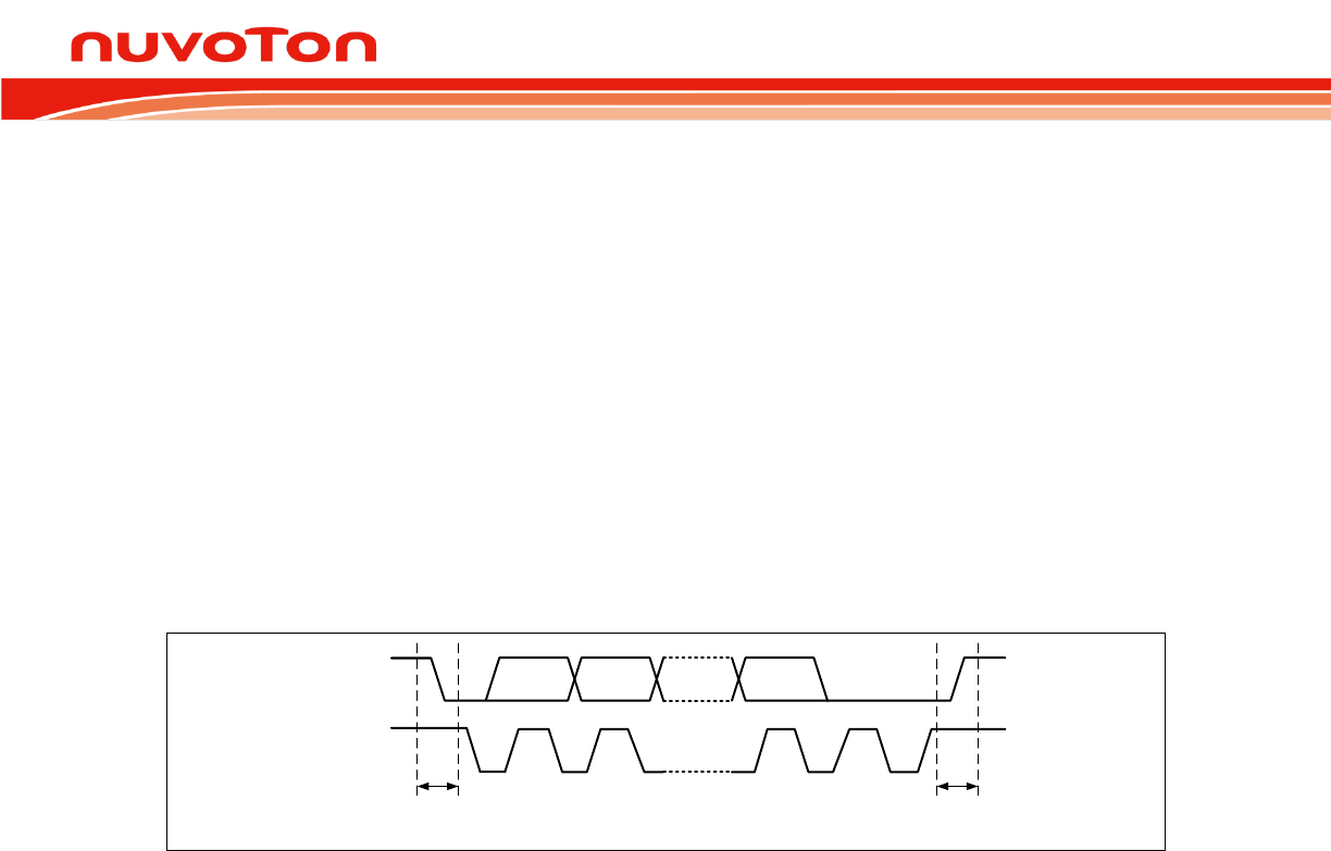
N76E003 Datasheet
Oct 28, 2016 Page 149 of 261 Rev. 1.00
all of the serial clock pulses and the START and STOP condition. However if there is no START
condition on the bus, all devices serve as not addressed slave. The hardware looks for its own slave
address or a General Call address. (The General Call address detection may be enabled or disabled
by GC (I2ADDR.0).) If the matched address is received, an interrupt is requested.
Every transaction on the I2C bus is 9 bits long, consisting of 8 data bits (MSB first) and a single
acknowledge bit. The number of bytes per transfer (defined as the time between a valid START and
STOP condition) is unrestricted but each byte has to be followed by an acknowledge bit. The master
device generates 8 clock pulse to send the 8-bit data. After the 8th falling edge of the SCL line, the
device outputting data on the SDA changes that pin to an input and reads in an acknowledge value on
the 9th clock pulse. After 9th clock pulse, the data receiving device can hold SCL line stretched low if
next receiving is not prepared ready. It forces the next byte transaction suspended. The data
transaction continues when the receiver releases the SCL line.
SDA
SCL
MSB LSB ACK
12 8 9
START
condition
STOP
condition
Figure 15-2. I2C Bus Protocol
START and STOP Condition 15.1.1
The protocol of the I2C bus defines two states to begin and end a transfer, START (S) and STOP (P)
conditions. A START condition is defined as a high-to-low transition on the SDA line while SCL line is
high. The STOP condition is defined as a low-to-high transition on the SDA line while SCL line is high.
A START or a STOP condition is always generated by the master and I2C bus is considered busy after
a START condition and free after a STOP condition. After issuing the STOP condition successful, the
original master device will release the control authority and turn back as a not addressed slave.
Consequently, the original addressed slave will become a not addressed slave. The I2C bus is free
and listens to next START condition of next transfer.
A data transfer is always terminated by a STOP condition generated by the master. However, if a
master still wishes to communicate on the bus, it can generate a repeated START (Sr) condition and
address the pervious or another slave without first generating a STOP condition. Various combinations
of read/write formats are then possible within such a transfer.
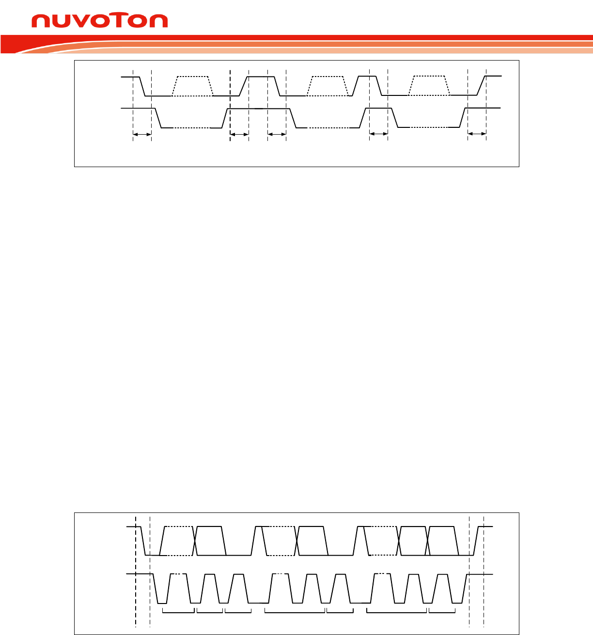
N76E003 Datasheet
Oct 28, 2016 Page 150 of 261 Rev. 1.00
SDA
SCL
START STOP START Repeated
START STOP
Figure 15-3. START, Repeated START, and STOP Conditions
7-Bit Address with Data Format
15.1.2
Following the START condition is generated, one byte of special data should be transmitted by the
master. It includes a 7-bit long slave address (SLA) following by an 8th bit, which is a data direction bit
(R/W), to address the target slave device and determine the direction of data flow. If R/W bit is 0, it
indicates that the master will write information to a selected slave. Also, if R/W bit is 1, it indicates that
the master will read information from the addressed slave. An address packet consisting of a slave
address and a read I or a write (W) bit is called SLA+R or SLA+W, respectively. A transmission
basically consists of a START condition, a SLA+W/R, one or more data packets and a STOP
condition. After the specified slave is addressed by SLA+W/R, the second and following 8-bit data
bytes issue by the master or the slave devices according to the R/W bit configuration.
There is , which can address all devices by giving the first
byte of data all 0. A General Call is used when a master wishes to transmit the same message to
several slaves in the system. When this address is used, other devices may respond with an
acknowledge or ignore it according to individual software configuration. If a device response the
General Call, it operates as like in the slave-receiver mode. Note that the address 0x00 is reserved for
General Call and cannot be used as a slave address, therefore, in theory, a 7-bit addressing I2C bus
accepts 127 devices with their slave addresses 1 to 127.
SDA
SCL
1-7 8 9 8 9
1-7 1-7
8 9
ADDRESS W/R ACKS PDATA ACK DATA ACK
Figure 15-4. Data Format of One I2C Transfer
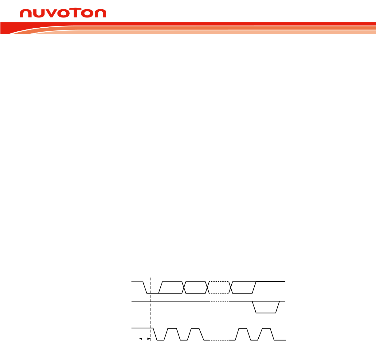
N76E003 Datasheet
Oct 28, 2016 Page 151 of 261 Rev. 1.00
During the data transaction period, the data on the SDA line should be stable during the high period of
the clock, and the data line can only change when SCL is low.
Acknowledge 15.1.3
The 9th SCL pulse for any transferred byte is dedicated as an Acknowledge (ACK). It allows receiving
devices (which can be the master or slave) to respond back to the transmitter (which also can be the
master or slave) by pulling the SDA line low. The acknowledge-related clock pulse is generated by the
master. The transmitter should release control of SDA line during the acknowledge clock pulse. The
ACK is an active-low signal, pulling the SDA line low during the clock pulse high duty, indicates to the
transmitter that the device has received the transmitted data. Commonly, a receiver, which has been
addressed is requested to generate an ACK after each byte has been received. When a slave receiver
does not acknowledge (NACK) the slave address, the SDA line should be left high by the slave so that
the mater can generate a STOP or a repeated START condition.
If a slave-receiver does acknowledge the slave address, it switches itself to not addressed slave mode
and cannot receive any more data bytes. This slave leaves the SDA line high. The master should
generate a STOP or a repeated START condition.
If a master-receiver is involved in a transfer, because the master controls the number of bytes in the
transfer, it should signal the end of data to the slave-transmitter by not generating an acknowledge on
the last byte. The slave-transmitter then switches to not addressed mode and releases the SDA line to
allow the master to generate a STOP or a repeated START condition.
SDA output by transmitter
SCL from master
12 8 9
START
condition
SDA output by receiver
SDA = 0, acknowledge (ACK)
SDA = 1, not acknowledge (NACK)
Clock pulse for
acknowledge bit
Figure 15-5. Acknowledge Bit
Arbitration 15.1.4
A master may start a transfer only if the bus is free. It is possible for two or more masters to generate
a START condition. In these situations, an arbitration scheme takes place on the SDA line, while SCL
is high. During arbitration, the first of the competing master devices to placea1 (high) on SDA while
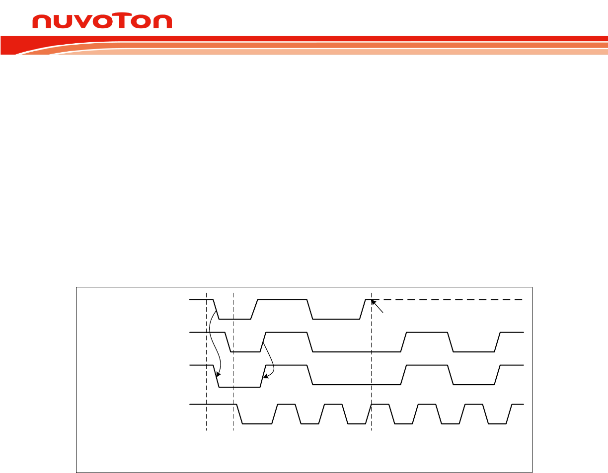
N76E003 Datasheet
Oct 28, 2016 Page 152 of 261 Rev. 1.00
another master transmitsa0 (low) switches off its data output stage because the level on the bus
does not match its own level. The arbitration lost master switches to the not addressed slave
immediately to detect its own slave address in the same serial transfer whether it is being addressed
by the winning master. It also releases SDA line to high level for not affecting the data transfer
continued by the winning master. However, the arbitration lost master continues generating clock
pulses on SCL line until the end of the byte in which it loses the arbitration.
Arbitration is carried out by all masters continuously monitoring the SDA line after outputting data. If
the value read from the SDA line does not match the value that the master has to output, it has lost
the arbitration. Note that a master can only lose arbitration when it outputs a high SDA value while
another master outputs a low value. Arbitration will continue until only one master remains, and this
may take many bits. Its first stage is a comparison of address bits, and if both masters are trying to
address the same device, arbitration continues on to the comparison of data bits or acknowledge bit.
DATA 1 from master 1
START
condition
Master 1 loses arbitration for DATA 1 ≠ SDA
It immediately switches to not addressed slave
and outputs high level
DATA 2 from master 2
SDA line
SCL line
Figure 15-6. Arbitration Procedure of Two Masters
Since control of the I2C bus is decided solely on the address or master code and data sent by
competing masters, there is no central master, nor any order of priority on the bus. Slaves are not
involved in the arbitration procedure.
15.2 Control Registers of I2C
There are five control registers to interface the I2C bus including I2CON, I2STAT, I2DAT, I2ADDR, and
I2CLK. These registers provide protocol control, status, data transmitting and receiving functions, and
clock rate configuration. For application flexibility, SDA and SCL pins can be exchanged by I2CPX
(I2CON.0). The following registers relate to I2C function.

N76E003 Datasheet
Oct 28, 2016 Page 153 of 261 Rev. 1.00
I2CON I2C Control (Bit-addressable)
7
6
5
4
3
2
1
0
-
I2CEN
STA
STO
SI
AA
-
I2CPX
-
R/W
R/W
R/W
R/W
R/W
-
R/W
Address: C0H Reset value: 0000 0000b
Bit
Name
Description
7
-
Reserved
6
I2CEN
I2C bus enable
0 = I2C bus Disabled.
1 = I2C bus Enabled.
Before enabling the I2C, SCL and SDA port latches should be set to logic 1.
5
STA
START flag
When STA is set, the I2C generates a START condition if the bus is free. If the bus
is busy, the I2C waits for a STOP condition and generates a START condition
following.
If STA is set while the I2C is already in the master mode and one or more bytes
have been transmitted or received, the I2C generates a repeated START
condition.
Note that STA can be set anytime even in a slave mode, but STA is not hardware
automatically cleared after START or repeated START condition has been
detected. User should take care of it by clearing STA manually.
4
STO
STOP flag
When STO is set if the I2C is in the master mode, a STOP condition is transmitted
to the bus. STO is automatically cleared by hardware once the STOP condition
has been detected on the bus.
The STO flag setting is also used to recover the I2C device from the bus error
state (I2STAT as 00H). In this case, no STOP condition is transmitted to the I2C
bus.
If the STA and STO bits are both set and the device is original in the master
mode, the I2C bus will generate a STOP condition and immediately follow a
START condition. If the device is in slave mode, STA and STO simultaneous
setting should be avoid from issuing illegal I2C frames.
3
SI
I2C interrupt flag
SI flag is set by hardware when one of 26 possible I2C status (besides F8H status)
is entered. After SI is set, the software should read I2STAT register to determine
which step has been passed and take actions for next step.
SI is cleared by software. Before the SI is cleared, the low period of SCL line is
stretched. The transaction is suspended. It is useful for the slave device to deal
with previous data bytes until ready for receiving the next byte.
The serial transaction is suspended until SI is cleared by software. After SI is
cleared, I2C bus will continue to generate START or repeated START condition,
STOP condition, 8-bit data, or so on depending on the software configuration of
controlling byte or bits. Therefore, user should take care of it by preparing suitable
setting of registers before SI is software cleared.

N76E003 Datasheet
Oct 28, 2016 Page 154 of 261 Rev. 1.00
Bit
Name
Description
2
AA
Acknowledge assert flag
If the AA flag is set, an ACK (low level on SDA) will be returned during the
acknowledge clock pulse of the SCL line while the I2C device is a receiver or an
own-address-matching slave.
If the AA flag is cleared, a NACK (high level on SDA) will be returned during the
acknowledge clock pulse of the SCL line while the I2C device is a receiver or an
own-address-matching slave. A device with its own AA flag cleared will ignore its
own salve address and the General Call. Consequently, SI will note be asserted
and no interrupt is requested.
Note that if an addressed slave does not return an ACK under slave receiver
mode or not receive an ACK under slave transmitter mode, the slave device will
become a not addressed slave. It cannot receive any data until its AA flag is set
and a master addresses it again.
There is a special case of I2STAT value C8H occurs under slave transmitter
mode. Before the slave device transmit the last data byte to the master, AA flag
can be cleared as 0. Then after the last data byte transmitted, the slave device will
actively switch to not addressed slave mode of disconnecting with the master. The
further reading by the master will be all FFH.
1
-
Reserved
0
I2CPX
I2C pins select
0 = Assign SCL to P1.3 and SDA to P1.4.
1 = Assign SCL to P0.2 and SDA to P1.6.
Note that I2C pins will exchange immediately once setting or clearing this bit.
I2STAT I2C Status
7
6
5
4
3
2
1
0
I2STAT[7:3]
0
0
0
R
R
R
R
Address: BDH Reset value: 1111 1000b
Bit
Name
Description
7:3
I2STAT[7:3]
I2C status code
The MSB five bits of I2STAT contains the status code. There are 27 possible
status codes. When I2STAT is F8H, no relevant state information is available
and SI flag keeps 0. All other 26 status codes correspond to the I2C states.
When each of these status is entered, SI will be set as logic 1 and a interrupt is
requested.
2:0
0
Reserved
The least significant three bits of I2STAT are always read as 0.

N76E003 Datasheet
Oct 28, 2016 Page 155 of 261 Rev. 1.00
I2DAT I2C Data
7
6
5
4
3
2
1
0
I2DAT[7:0]
R/W
Address: BCH Reset value: 0000 0000b
Bit
Name
Description
7:0
I2DAT[7:0]
I2C data
I2DAT contains a byte of the I2C data to be transmitted or a byte, which has just
received. Data in I2DAT remains as long as SI is logic 1. The result of reading
or writing I2DAT during I2C transceiving progress is unpredicted.
While data in I2DAT is shifted out, data on the bus is simultaneously being
shifted in to update I2DAT. I2DAT always shows the last byte that presented on
the I2C bus. Thus the event of lost arbitration, the original value of I2DAT
changes after the transaction.
I2ADDR I2C Own Slave Address
7
6
5
4
3
2
1
0
I2ADDR[7:1]
GC
R/W
R/W
Address: C1H Reset value: 0000 0000b
Bit
Name
Description
7:1
I2ADDR[7:1]
I2
In master mode:
These bits have no effect.
In slave mode:
These 7 bits define the slave address of this I2C device by user. The master
should address I2C device by sending the same address in the first byte data
after a START or a repeated START condition. If the AA flag is set, this I2C
device will acknowledge the master after receiving its own address and
become an addressed slave. Otherwise, the addressing from the master will
be ignored.
Note that I2ADDR[7:1] should not remain its default value of all 0, because
address 0x00 is reserved for General Call.
6
GC
General Call bit
In master mode:
This bit has no effect.
In slave mode:
0 = The General Call is always ignored.
1 = The General Call is recognized if AA flag is 1; otherwise, it is ignored if AA
is 0.

N76E003 Datasheet
Oct 28, 2016 Page 156 of 261 Rev. 1.00
I2CLK I2C Clock
7
6
5
4
3
2
1
0
I2CLK[7:0]
R/W
Address: BEH Reset value: 0000 1001b
Bit
Name
Description
7:0
I2CLK[7:0]
I2C clock setting
In master mode:
This register determines the clock rate of I2C bus when the device is in a master
mode. The clock rate follows the equation,
)1+CLK2I(×4
FSYS
.
The default value will make the clock rate of I2C bus 400k bps if the peripheral
clock is 16 MHz. Note that the I2CLK value of 00H and 01H are not valid. This is
an implement limitation.
In slave mode:
This byte has no effect. In slave mode, the I2C device will automatically
synchronize with any given clock rate up to 400k bps.
15.3 Operating Modes
In I2C protocol definition, there are four operating modes including master transmitter, master receiver,
slave receiver, and slave transmitter. There is also a special mode called General Call. Its operating is
similar to master transmitter mode.
Master Transmitter Mode 15.3.1
In the master transmitter mode, several bytes of data are transmitted to a slave receiver. The master
should prepare by setting desired clock rate in I2CLK. The master transmitter mode may now be
entered by setting STA (I2CON.5) bit as 1. The hardware will test the bus and generate a START
condition as soon as the bus becomes free. After a START condition is successfully produced, the SI
flag (I2CON.3) will be set and the status code in I2STAT show 08H. The progress is continued by
should then be cleared to commence SLA+W transaction.
After the SLA+W byte has been transmitted and an acknowledge (ACK) has been returned by the
addressed slave device, the SI flag is set again and I2STAT is read as 18H. The appropriate action to
be taken follows user defined communication protocol by sending data continuously. After all data is
transmitted, the master can send a STOP condition by setting STO (I2CON.4) and then clearing SI to
terminate the transmission. A repeated START condition can also be generated without sending
STOP condition to immediately initial another transmission.
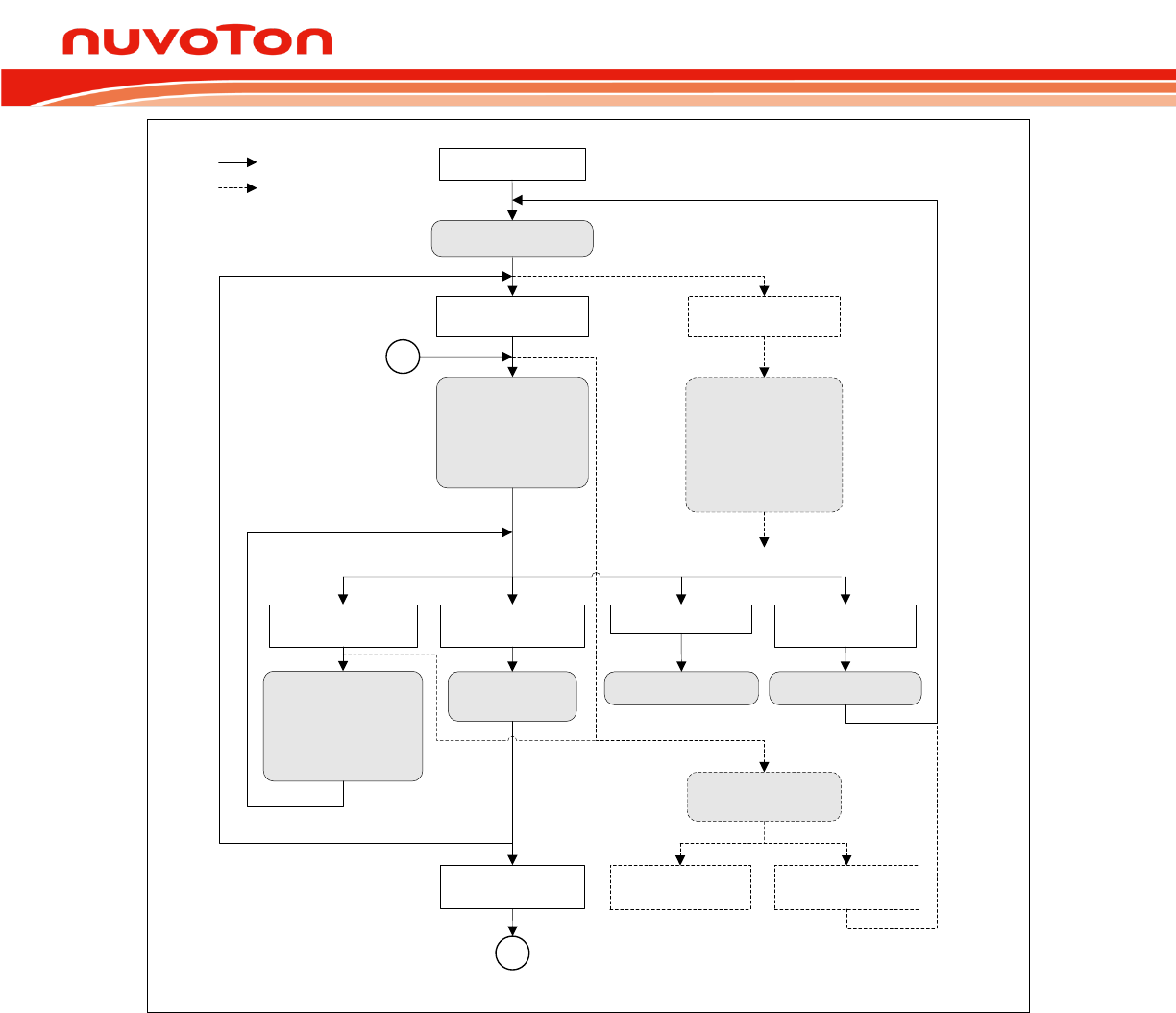
N76E003 Datasheet
Oct 28, 2016 Page 157 of 261 Rev. 1.00
08H
A START has been transmitted
(STA,STO,SI,AA) = (X,0,0,X)
I2DAT = SLA+W
SLA+W will be transmitted
(STA,STO,SI,AA) = (1,0,0,X)
A START will be transmitted
18H
SLA+W has been transmitted
ACK has been received
OR
20H
SLA+W has been transmitted
NACK has been received
(STA,STO,SI,AA)=(1,0,0,X)
A repeated START will be
transmitted
(STA,STO,SI,AA)=(0,0,0,X)
I2DAT = Data Byte
Data byte will be transmitted
(STA,STO,SI,AA)=(0,1,0,X)
A STOP will be transmitted
A STOP has been transmitted
(STA,STO,SI,AA)=(1,1,0,X)
A STOP followed by a
START will be transmitted
A STOP has been transmitted
28H
Data byte has been transmitted
ACK has been received
or
30H
Data byte has been transmitted
NACK has been received
10H
A repeated START has
been transmitted
(STA,STO,SI,AA) =(0,0,0,X)
I2DAT = SLA+R
SLA+R will be transmitted
38H
Arbitration lost in
SLA+W or Data byte
to master receiver
68H or 78H
Arbitration lost and addressed
as slave receiver
ACK has been transmitted
OR
B0H
Arbitration lost and addressed
as slave transmitter
ACK has been transmitted
(STA,STO,SI,AA)=(0,0,0,X)
Not addressed slave
will be entered
(STA,STO,SI,AA)=(1,0,0,X)
A START will be transmitted
when the bus becomes free
(STA,STO,SI,AA) = (X,0,0,1)
I2DAT = SLA+W
SLA+W will be transmitted
MR
MT
to corresponding
slave mode
Normal
Arbitration lost
Figure 15-7. Flow and Status of Master Transmitter Mode
Master Receiver Mode 15.3.2
In the master receiver mode, several bytes of data are received from a slave transmitter. The
transaction is initialized just as the master transmitter mode. Following the START condition, I2DAT
SLA+R byte is transmitted and an acknowledge bit has been returned, the SI flag is set again and
I2STAT is read as 40H. SI flag then should be cleared to receive data from the slave transmitter. If AA
flag (I2CON.2) is set, the master receiver will acknowledge the slave transmitter. If AA is cleared, the
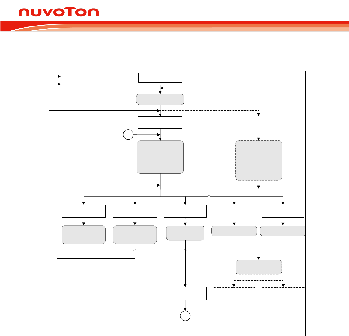
N76E003 Datasheet
Oct 28, 2016 Page 158 of 261 Rev. 1.00
master receiver will not acknowledge the slave and release the slave transmitter as a not addressed
slave. After that, the master can generate a STOP condition or a repeated START condition to
terminate the transmission or initial another one.
08H
A START has been transmitted
(STA,STO,SI,AA) = (X,0,0,X)
I2DAT = SLA+R
SLA+R will be transmitted
(STA,STO,SI,AA) = (1,0,0,X)
A START will be transmitted
40H
SLA+R has been transmitted
ACK has been received
OR
48H
SLA+R has been transmitted
NACK has been received
(STA,STO,SI,AA)=(1,0,0,X)
A repeated START will be
transmitted
(STA,STO,SI,AA)=(0,0,0,1)
Data byte will be received
ACK will be transmitted
(STA,STO,SI,AA)=(0,1,0,X)
A STOP will be transmitted
A STOP has been transmitted
(STA,STO,SI,AA)=(1,1,0,X)
A STOP followed by a
START will be transmitted
A STOP has been transmitted
50H
Data byte has been received
ACK has been transmitted
I2DAT = Data Byte
10H
A repeated START has
been transmitted
(STA,STO,SI,AA) =(0,0,0,X)
I2DAT = SLA+W
SLA+W will be transmitted
38H
Arbitration lost in NACK bit
to master transmitter
(STA,STO,SI,AA)=(0,0,0,X)
Not addressed slave
will be entered
(STA,STO,SI,AA)=(1,0,0,X)
A START will be transmitted
when the bus becomes free
(STA,STO,SI,AA)=(0,0,0,0)
Data byte will be received
NACK will be transmitted
58H
Data byte has been received
NACK has been transmitted
I2DAT = Data Byte
68H or 78H
Arbitration lost and addressed
as slave receiver
ACK has been transmitted
OR
B0H
Arbitration lost and addressed
as slave transmitter
ACK has been transmitted
(STA,STO,SI,AA) = (X,0,0,1)
I2DAT = SLA+R
SLA+R will be transmitted
MR
MT
to corresponding
slave mode
Normal
Arbitration lost
Figure 15-8. Flow and Status of Master Receiver Mode
Slave Receiver Mode 15.3.3
In the slave receiver mode, several bytes of data are received form a master transmitter. Before a
transmission is commenced, I2ADDR should be loaded with the address to which the device will
respond when addressed by a master. I2CLK does not affect in slave mode. The AA bit should be set
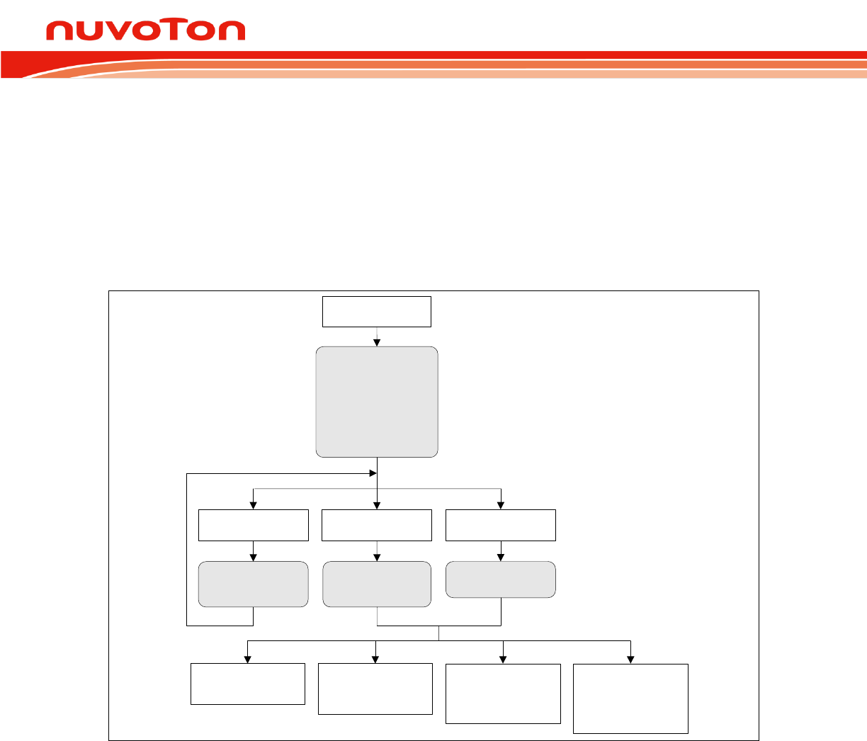
N76E003 Datasheet
Oct 28, 2016 Page 159 of 261 Rev. 1.00
to enable acknowledging its own slave address. After the initialization above, the I2C idles until it is
addressed by its own address
may also be entered if arbitration is lost.
After the slave is addressed by SLA+W, it should clear its SI flag to receive the data from the master
transmitter. If the AA bit is 0 during a transaction, the slave will return a non-acknowledge after the
next received data byte. The slave will also become not addressed and isolate with the master. It
cannot receive any byte of data with I2DAT remaining the previous byte of data, which is just received.
(STA,STO,SI,AA) = (0,0,0,1)
If own SLA+W is received,
ACK will be transmitted
60H
Own SLA+W has been received
ACK has been transmitted
I2DAT = own SLA+W
OR
68H
Arbitration lost and own SLA+W
has been received
ACK has been transmitted
I2DAT = own SLA+W
(STA,STO,SI,AA)=(X,0,0,0)
Data byte will be received
NACK will be transmitted
(STA,STO,SI,AA)=(0,0,0,0)
Not addressed slave
will be entered; no recognition
of own SLA or General Call
(STA,STO,SI,AA)=(0,0,0,1)
Not addressed slave will be
entered; own SLA will be
recognized; General Call will
be recognized if GC = 1
88H
Data byte has been received
NACK has been transmitted
I2DAT = Data Byte
A0H
A STOP or repeated START
has been received
(STA,STO,SI,AA)=(X,0,0,1)
Data byte will be received
ACK will be transmitted
80H
Data byte has been received
ACK has been transmitted
I2DAT = Data Byte
(STA,STO,SI,AA)=(1,0,0,0)
Not addressed slave will be
entered; no recognition of own
SLA or General Call;
A START will be transmitted
when the bus becomes free
(STA,STO,SI,AA)=(1,0,0,1)
Not addressed slave will be
entered; own SLA will be
recognized; General Call will
be recognized if GC = 1;
A START will be transmitted
when the bus becomes free
(STA,STO,SI,AA)=(X,0,0,X)
A STOP or repeated START
will be received
Figure 15-9. Flow and Status of Slave Receiver Mode
Slave Transmitter Mode 15.3.4
In the slave transmitter mode, several bytes of data are transmitted to a master receiver. After
I2ADDR and I2CON values are given, the I2C wait until it is addressed by its own address with the
After the slave is addressed by SLA+R, it should clear its SI flag to transmit the data to the master
receiver. Normally the master receiver will return an acknowledge after every byte of data is
s
N76E003 Datasheet
Oct 28, 2016 Page 160 of 261 Rev. 1.00
the transaction. It becomes a not addressed slave. If the AA flag is cleared during a transaction, the
not addressed.
(STA,STO,SI,AA) = (0,0,0,1)
If own SLA+R is received,
ACK will be transmitted
A8H
Own SLA+R has been received
ACK has been transmitted
I2DAT = own SLA+R
OR
B0H
Arbitration lost and own SLA+R
has been received
ACK has been transmitted
I2DAT = own SLA+R
(STA,STO,SI,AA)=(X,0,0,X)
I2DAT = Data Byte
Data byte will be transmitted
NACK will be received
(STA,STO,SI,AA)=(0,0,0,0)
Not addressed slave
will be entered; no recognition
of own SLA or General Call
(STA,STO,SI,AA)=(0,0,0,1)
Not addressed slave will be
entered; own SLA will be
recognized; General Call will
be recognized if GC = 1
C0H
Data byte has been transmitted
NACK has been received
A0H
A STOP or repeated START
has been received
(STA,STO,SI,AA)=(X,0,0,1)
I2DAT = Data Byte
Data byte will be transmitted
ACK will be received
B8H
Data byte has been transmitted
ACK has been received
(STA,STO,SI,AA)=(1,0,0,0)
Not addressed slave will be
entered; no recognition of own
SLA or General Call;
A START will be transmitted
when the bus becomes free
(STA,STO,SI,AA)=(1,0,0,1)
Not addressed slave will be
entered; own SLA will be
recognized; General Call will
be recognized if GC = 1;
A START will be transmitted
when the bus becomes free
(STA,STO,SI,AA)=(X,0,0,0)
I2DAT = Last Data Byte
Last data byte will be transmitted
ACK will be received
C8H
Last Data byte has been transmitted
ACK has been received
*
This flow is not recommended. If the MSB of next byte which the Slave is going to transmit is 0, it
will hold SDA line. The STOP or repeated START cannot be successfully generated by Master.
*
(STA,STO,SI,AA)=(X,0,0,X)
A STOP or repeated START
will be received
Figure 15-10. Flow and Status of Slave Transmitter Mode
General Call 15.3.5
slave address with data direction bit. Both GC (I2ADDR.0) bit and AA bit should be set as 1 to enable
acknowledging General Calls. The slave addressed by a General Call has different status code in
I2STAT with normal slave receiver mode. The General Call may also be produced if arbitration is lost.
N76E003 Datasheet
Oct 28, 2016 Page 161 of 261 Rev. 1.00
(STA,STO,SI,AA) = (0,0,0,1)
GC = 1
If General Call is received,
ACK will be transmitted
70H
General Call has been received
ACK has been transmitted
I2DAT = 00H
OR
78H
Arbitration lost and General Call
has been received
ACK has been transmitted
I2DAT = 00H
(STA,STO,SI,AA)=(X,0,0,0)
Data byte will be received
NACK will be transmitted
(STA,STO,SI,AA)=(0,0,0,0)
Not addressed slave
will be entered; no recognition
of own SLA or General Call
(STA,STO,SI,AA)=(0,0,0,1)
Not addressed slave will be
entered; own SLA will be
recognized; General Call will
be recognized if GC = 1
98H
Data byte has been received
NACK has been transmitted
I2DAT = Data Byte
A0H
A STOP or repeated START
has been received
(STA,STO,SI,AA)=(X,0,0,1)
Data byte will be received
ACK will be transmitted
90H
Data byte has been received
ACK has been transmitted
I2DAT = Data Byte
(STA,STO,SI,AA)=(1,0,0,0)
Not addressed slave will be
entered; no recognition of own
SLA or General Call;
A START will be transmitted
when the bus becomes free
(STA,STO,SI,AA)=(1,0,0,1)
Not addressed slave will be
entered; own SLA will be
recognized; General Call will
be recognized if GC = 1;
A START will be transmitted
when the bus becomes free
(STA,STO,SI,AA)=(X,0,0,X)
A STOP or repeated START
will be received
Figure 15-11. Flow and Status of General Call Mode
Miscellaneous States 15.3.6
There are two I2STAT status codes that do not correspond to the 25 defined states, which are
mentioned in previous sections. These are F8H and 00H states.
The first status code F8H indicates that no relevant information is available during each transaction.
Meanwhile, the SI flag is 0 and no I2C interrupt is required.
The other status code 00H means a bus error has occurred during a transaction. A bus error is caused
by a START or STOP condition appearing temporally at an illegal position such as the second through
eighth bits of an address or a data byte, and the acknowledge bit. When a bus error occurs, the SI flag
is set immediately. When a bus error is detected on the I2C bus, the operating device immediately
switches to the not addressed salve mode, releases SDA and SCL lines, sets the SI flag, and loads
I2STAT as 00H. To recover from a bus error, the STO bit should be set and then SI should be cleared.
After that, STO is cleared by hardware and release the I2C bus without issuing a real STOP condition
waveform on I2C bus.
N76E003 Datasheet
Oct 28, 2016 Page 162 of 261 Rev. 1.00
There is a special case if a START or a repeated START condition is not successfully generated for
I2C bus is obstructed by a low level on SDA line e.g. a slave device out of bit synchronization, the
problem can be solved by transmitting additional clock pulses on the SCL line. The I2C hardware
transmits additional clock pulses when the STA bit is set, but no START condition can be generated
because the SDA line is pulled low. When the SDA line is eventually released, a normal START
condition is transmitted, state 08H is entered, and the serial transaction continues. If a repeated
START condition is transmitted while SDA is obstructed low, the I2C hardware also performs the same
action as above. In this case, state 08H is entered instead of 10H after a successful START condition
is transmitted. Note that the software is not involved in solving these bus problems.
The following table is show the status display in I2STAT register of I2C number and description:
Master Mode
Slave Mode
STATUS
Description
STATUS
Description
0x08
Start
0xA0
Slave Transmit Repeat Start or Stop
0x10
Master Repeat Start
0xA8
Slave Transmit Address ACK
0x18
Master Transmit Address ACK
0xB0
Slave Transmit Arbitration Lost
0x20
Master Transmit Address NACK
0xB8
Slave Transmit Data ACK
0x28
Master Transmit Data ACK
0xC0
Slave Transmit Data NACK
0x30
Master Transmit Data NACK
0xC8
Slave Transmit Last Data ACK
0x38
Master Arbitration Lost
0x60
Slave Receive Address ACK
0x40
Master Receive Address ACK
0x68
Slave Receive Arbitration Lost
0x48
Master Receive Address NACK
0x80
Slave Receive Data ACK
0x50
Master Receive Data ACK
0x88
Slave Receive Data NACK
0x58
Master Receive Data NACK
0x70
GC mode Address ACK
0x00
Bus error
0x78
GC mode Arbitration Lost
0x90
GC mode Data ACK
0x98
GC mode Data NACK
0xF8
Bus Released
Note:
15.4 Typical Structure of I2C Interrupt Service Routine
The following software example in C language for KEILTM C51 compiler shows the typical structure of
the I2C interrupt service routine including the 26 state service routines and may be used as a base for
user applications. User can follow or modify it for their own application. If one or more of the five

N76E003 Datasheet
Oct 28, 2016 Page 163 of 261 Rev. 1.00
modes are not used, the associated state service routines may be removed, but care should be taken
that a deleted routine can never be invoked.
Void I2C_ISR (void) interrupt 6
{
switch (I2STAT)
{
//===============================================
//Bus Error, always put in ISR for noise handling
//===============================================
case 0x00: /*00H, bus error occurs*/
STO = 1; //recover from bus error
break;
//===========
//Master Mode
//===========
case 0x08: /*08H, a START transmitted*/
STA = 0; //STA bit should be cleared by
software
I2DAT = SLA_ADDR1; //load SLA+W/R
break;
case 0x10: /*10H, a repeated START transmitted*/
STA = 0;
I2DAT = SLA_ADDR2;
break;
//=======================
//Master Transmitter Mode
//=======================
case 0x18: /*18H, SLA+W transmitted, ACK
received*/
I2DAT = NEXT_SEND_DATA1; //load DATA
break;
case 0x20: /*20H, SLA+W transmitted, NACK
received*/
STO = 1; //transmit STOP
AA = 1; //ready for ACK own SLA+W/R or
General Call
break;
case 0x28: /*28H, DATA transmitted, ACK
received*/
if (Conti_TX_Data) //if continuing to send DATA
I2DAT = NEXT_SEND_DATA2;
else //if no DATA to be sent
{
STO = 1;
AA = 1;
}
break;
case 0x30: /*30H, DATA transmitted, NACK
received*/
STO = 1;
AA = 1;
break;
//===========
//Master Mode
//===========
case 0x38: /*38H, arbitration lost*/
STA = 1; //retry to transmit START if bus free
break;

N76E003 Datasheet
Oct 28, 2016 Page 164 of 261 Rev. 1.00
//====================
//Master Receiver Mode
//====================
case 0x40: /*40H, SLA+R transmitted, ACK
received*/
AA = 1; //ACK next received DATA
break;
case 0x48: /*48H, SLA+R transmitted, NACK
received*/
STO = 1;
AA = 1;
break;
case 0x50: /*50H, DATA received, ACK
transmitted*/
DATA_RECEIVED1 = I2DAT; //store received DATA
if (To_RX_Last_Data1) //if last DATA will be received
AA = 0; //not ACK next received DATA
else //if continuing receiving DATA
AA = 1;
break;
case 0x58: /*58H, DATA received, NACK
transmitted*/
DATA_RECEIVED_LAST1 = I2DAT;
STO = 1;
AA = 1;
break;
//====================================
//Slave Receiver and General Call Mode
//====================================
case 0x60: /*60H, own SLA+W received, ACK
returned*/
AA = 1;
break;
case 0x68: /*68H, arbitration lost in SLA+W/R
own SLA+W received, ACK returned */
AA = 0; //not ACK next received DATA after
//arbitration lost
STA = 1; //retry to transmit START if bus free
break;
case 0x70: /*70H, General Call received, ACK
returned */
AA = 1;
break;
case 0x78: /*78H, arbitration lost in SLA+W/R
General Call received, ACK
returned*/
AA = 0;
STA = 1;
break;
case 0x80: /*80H, previous own SLA+W, DATA
received,
ACK returned*/
DATA_RECEIVED2 = I2DAT;
if (To_RX_Last_Data2)
AA = 0;
else
AA = 1;
break;

N76E003 Datasheet
Oct 28, 2016 Page 165 of 261 Rev. 1.00
case 0x88: /*88H, previous own SLA+W, DATA
received,
NACK returned, not addressed SLAVE
mode
entered*/
DATA_RECEIVED_LAST2 = I2DAT;
AA = 1; //wait for ACK next Master addressing
break;
case 0x90: /*90H, previous General Call, DATA
received,
ACK returned*/
DATA_RECEIVED3 = I2DAT;
if (To_RX_Last_Data3)
AA = 0;
else
AA = 1;
break;
case 0x98: /*98H, previous General Call, DATA
received,
NACK returned, not addressed SLAVE
mode
entered*/
DATA_RECEIVED_LAST3 = I2DAT;
AA = 1;
break;
//==========
//Slave Mode
//==========
casE 0xA0: /*A0H, STOP or repeated START
received while
still addressed SLAVE mode*/
AA = 1;
break;
//======================
//Slave Transmitter Mode
//======================
casE 0xA8: /*A8H, own SLA+R received, ACK
returned*/
I2DAT = NEXT_SEND_DATA3;
AA = 1; //when AA is “1”, not last data to be
//transmitted
break;
casE 0xB0: /*B0H, arbitration lost in SLA+W/R
own SLA+R received, ACK returned */
I2DAT = DUMMY_DATA;
AA = 0; //when AA is “0”, last data to be
//transmitted
STA = 1; //retry to transmit START if bus free
break;
casE 0xB8: /*B8H, previous own SLA+R, DATA
transmitted,
ACK received*/
I2DAT = NEXT_SEND_DATA4;
if (To_TX_Last_Data) //if last DATA will be transmitted
AA = 0;
else
AA = 1;
break;
N76E003 Datasheet
Oct 28, 2016 Page 166 of 261 Rev. 1.00
casE 0xC0: /*C0H, previous own SLA+R, DATA
transmitted,
NACK received, not addressed SLAVE
mode
entered*/
AA = 1;
break;
casE 0xC8: /*C8H, previous own SLA+R, last DATA
trans-
mitted, ACK received, not addressed
SLAVE
AA = 1; mode entered*/
break;
}//end of switch (I2STAT)
SI = 0; //SI should be the last command of
I2C ISR
while(STO); //wait for STOP transmitted or bus
error
//free, STO is cleared by hardware
}//end of I2C_ISR
15.5 I2C Time-Out
There is a 14-bit time-out counter, which can be used to deal with the I2C bus hang-up. If the time-out
counter is enabled, the counter starts up counting until it overflows. Meanwhile I2TOF will be set by
hardware and requests I2C interrupt. When time-out counter is enabled, setting flag SI to high will
reset counter and restart counting up after SI is cleared. If the I2C bus hangs up, it causes the SI flag
not set for a period. The 14-bit time-out counter will overflow and require the interrupt service.
1
0
FSYS
1/4 14-bit I2C Time-out Counter I2TOF
Clear Counter
I2TOCEN
DIV
I2CEN
SI
Figure 15-12. I2C Time-Out Counter
N76E003 Datasheet
Oct 28, 2016 Page 167 of 261 Rev. 1.00
I2TOC I2C Time-out Counter
7
6
5
4
3
2
1
0
-
-
-
-
-
I2TOCEN
DIV
I2TOF
-
-
-
-
-
R/W
R/W
R/W
Address: BFH Reset value: 0000 0000b
Bit
Name
Description
2
I2TOCEN
I2C time-out counter enable
0 = I2C time-out counter Disabled.
1 = I2C time-out counter Enabled.
1
DIV
I2C time-out counter clock divider
0 = The clock of I2C time-out counter is FSYS/1.
1 = The clock of I2C time-out counter is FSYS/4.
0
I2TOF
I2C time-out flag
This flag is set by hardware if 14-bit I2C time-out counter overflows. It is cleared
by software.
15.6 I2C Interrupt
There are two I2C flags, SI and I2TOF. Both of them can generate an I2C event interrupt requests. If
I2C interrupt mask is enabled via setting EI2C (EIE.0) and EA as 1, CPU will execute the I2C interrupt
service routine once any of these two flags is set. User needs to check flags to determine what event
caused the interrupt. Both of I2C flags are cleared by software.
N76E003 Datasheet
Oct 28, 2016 Page 168 of 261 Rev. 1.00
16. PIN INTERRUPT
The N76E003 provides pin interrupt input for each I/O pin to detect pin state if button or keypad set is
used. A maximum 8-channel pin interrupt detection can be assigned by I/O port sharing. The pin
interrupt is generated when any key is pressed on a keyboard or keypad, which produces an edge or
level triggering event. Pin interrupt may be used to wake the CPU up from Idle or Power-down mode.
Each channel of pin interrupt can be enabled and polarity controlled independently by PIPEN and
PINEN register. PICON selects which port that the pin interrupt is active. It also defines which type of
pin interrupt is usd level detect or edge detect. Each channel also has its own interrupt flag. There
are total eight pin interrupt flags located in PIF register. The respective flags for each pin interrupt
channel allow the interrupt service routine to poll on which channel on which the interrupt event
occurs. All flags in PIF register are set by hardware and should be cleared by software.
Pin Interrupt
PIF0
PINEN0
PIPEN0
PIT0
PIF1
PINEN1
PIPEN1
PIT1
PIF7
PINEN7
PIPEN7
PIT67
PIPS[1:0]
(PICON[1:0])
P0.0
0
1
0
1
0
1
P1.0
P2.0
P3.0
P0.1
P1.1
P0.7
Reserved
P1.7
00
01
10
11
00
01
10
11
00
01
10
11
Pin Interrupt Channel 0
Pin Interrupt Channel 1
Pin Interrupt Channel 7
Reserved
Reserved
Reserved
Figure 16-1. Pin Interface Block Diagram

N76E003 Datasheet
Oct 28, 2016 Page 169 of 261 Rev. 1.00
Pin interrupt is generally used to detect an edge transient from peripheral devices like keyboard or
keypad. During idle state, the system prefers to enter Power-down mode to minimize power
consumption and waits for event trigger. Pin interrupt can wake up the device from Power-down mode.
PICON Pin Interrupt Control
7
6
5
4
3
2
1
0
PIT67
PIT45
PIT3
PIT2
PIT1
PIT0
PIPS[1:0]
R/W
R/W
R/W
R/W
R/W
R/W
R/W
Address: E9H Reset value: 0000 0000b
Bit
Name
Description
7
PIT67
Pin interrupt channel 6 and 7 type select
This bit selects which type that pin interrupt channel 6 and 7 is triggered.
0 = Level triggered.
1 = Edge triggered.
6
PIT45
Pin interrupt channel 4 and 5 type select
This bit selects which type that pin interrupt channel 4 and 5 is triggered.
0 = Level triggered.
1 = Edge triggered.
5
PIT3
Pin interrupt channel 3 type select
This bit selects which type that pin interrupt channel 3 is triggered.
0 = Level triggered.
1 = Edge triggered.
4
PIT2
Pin interrupt channel 2 type select
This bit selects which type that pin interrupt channel 2 is triggered.
0 = Level triggered.
1 = Edge triggered.
3
PIT1
Pin interrupt channel 1 type select
This bit selects which type that pin interrupt channel 1 is triggered.
0 = Level triggered.
1 = Edge triggered.
2
PIT0
Pin interrupt channel 0 type select
This bit selects which type that pin interrupt channel 0 is triggered.
0 = Level triggered.
1 = Edge triggered.
1:0
PIPS[:0]
Pin interrupt port select
This field selects which port is active as the 8-channel of pin interrupt.
00 = Port 0.
01 = Port 1.
10 = Port 2.
11 = Port 3.
N76E003 Datasheet
Oct 28, 2016 Page 170 of 261 Rev. 1.00
PINEN Pin Interrupt Negative Polarity Enable.
7
6
5
4
3
2
1
0
PINEN7
PINEN6
PINEN5
PINEN4
PINEN3
PINEN2
PINEN1
PINEN0
R/W
R/W
R/W
R/W
R/W
R/W
R/W
R/W
Address: EAH Reset value: 0000 0000b
Bit
Name
Description
n
PINENn
Pin interrupt channel n negative polarity enable
This bit enables low-level/falling edge triggering pin interrupt channel n. The level
or edge triggered selection depends on each control bit PITn in PICON.
0 = Low-level/falling edge detect Disabled.
1 = Low-level/falling edge detect Enabled.
PIPEN Pin Interrupt Positive Polarity Enable.
7
6
5
4
3
2
1
0
PIPEN7
PIPEN6
PIPEN5
PIPEN4
PIPEN3
PIPEN2
PIPEN1
PIPEN0
R/W
R/W
R/W
R/W
R/W
R/W
R/W
R/W
Address: EBH Reset value: 0000 0000b
Bit
Name
Description
n
PIPENn
Pin interrupt channel n positive polarity enable
This bit enables high-level/rising edge triggering pin interrupt channel n. The level
or edge triggered selection depends on each control bit PITn in PICON.
0 = High-level/rising edge detect Disabled.
1 = High-level/rising edge detect Enabled.
PIF Pin Interrupt Flags
7
6
5
4
3
2
1
0
PIF7
PIF6
PIF5
PIF4
PIF3
PIF2
PIF1
PIF0
R (level)
R/W (edge)
R (level)
R/W (edge)
R (level)
R/W (edge)
R (level)
R/W (edge)
R (level)
R/W (edge)
R (level)
R/W (edge)
R (level)
R/W (edge)
R (level)
R/W (edge)
Address: ECH Reset value: 0000 0000b
Bit
Name
Description
n
PIFn
Pin interrupt channel n flag
If the edge trigger is selected, this flag will be set by hardware if the channel n of
pin interrupt detects an enabled edge trigger. This flag should be cleared by
software.
level on the channel n of pin interrupt. Software cannot control it.

N76E003 Datasheet
Oct 28, 2016 Page 171 of 261 Rev. 1.00
17. PULSE WIDTH MODULATED (PWM)
The PWM (Pulse Width Modulation) signal is a useful control solution in wide application field. It can
used on motor driving, fan control, backlight brightness tuning, LED light dimming, or simulating as a
simple digital to analog converter output through a low pass filter circuit.
The N76E003 PWM is especially designed for motor control by providing three pairs, maximum 16-bit
resolution of PWM output with programmable period and duty. The architecture makes user easy to
drive the one-phase or three-phase brushless DC motor (BLDC), or three-phase AC induction motor.
Each of six PWM can be configured as one of independent mode, complementary mode, or
synchronous mode. If the complementary mode is used, a programmable dead-time insertion is
available to protect MOS turn-on simultaneously. The PWM waveform can be edge-aligned or center-
aligned with variable interrupt points.
17.1 Functional Description
PWM Generator 17.1.1
The PWM generator is clocked by the system clock or Timer 1 overflow divided by a PWM clock pre-
scalar selectable from 1/1~1/128. The PWM period is defined by effective 16-bit period registers,
{PWMPH, PWMPL}. The period is the same for all PWM channels for they share the same 16-bit
period counter. The duty of each PWM is determined independently by the value of duty registers
{PWM0H, PWM0L}, {PWM1H, PWM1L}, {PWM2H, PWM2L}, {PWM3H, PWM3L}, {PWM4H, PWM4L},
and {PWM5H, PWM5L}. With six duty registers, six PWM output can be generated independently with
different duty cycles. The interval and duty of PWM signal is generated by a 16-bit counter comparing
with the period and duty registers.
To facilitate the three-phase motor control, a group mode can be used by setting GP (PWMCON1.5),
which makes {PWM0H, PWM0L} and {PWM1H, PWM1L} duty register decide duties of the PWM
outputs. In a three-phase motor control application, two-group PWM outputs generally are given the
same duty cycle. When the group mode is enabled, {PWM2H, PWM2L}, {PWM3H, PWM3L},
{PWM4H, PWM4L} and {PWM5H, PWM5L} registers have no effect. This mean is {PWM2H, PWM2L}
and {PWM4H, PWM4L} both as same as {PWM0H, PWM0L}. Also {PWM3H, PWM3L} and {PWM5H,
PWM5L} are same as {PWM1H, PWM1L}.
Note that enabling PWM does not configure the I/O pins into their output mode automatically. User
should configure I/O output mode via software manually.
N76E003 Datasheet
Oct 28, 2016 Page 172 of 261 Rev. 1.00
16-bit
up/down
counter
PWM0/P1.2
PWM1/P1.1/P1.4
PWM2/P0.5/P1.0
Pre-scalar
INTSEL[1:0], INTTYP[1:0]
(PWMCON0[3:0])
PWMRUN
(PWMCON0.7)
CLRPWM
(PWMCON0.4)
PWMP
registers
LOAD (PWMCON0.6)
PWMF
(PWMCON0.5)
PWMP buffer
PWM0 buffer
PWM0 Register
0-to-1
PWM and
Fault Brake
output
control
PWMTYP
(PWMCON1.4)
edge/center
Interrupt
select/type
PWMDIV0[2:0]
(PWMCON1[2:0])
PG0
PWM interrupt
Brake event
(P1.4/FB)
0
1
Timer 1 overflow
PWMCKS
(CKCON.6)
FPWM
=
Counter
Matching(edgealigned)/
underflow(venter aligned)
FSYS
clear counter
=
PWM1 buffer
PWM1 Register
PG1
=
PWM2 buffer
PWM2 Register
=
PWM3 buffer
PWM3 Register
=
PWM4 buffer
PWM4 Register
=
PWM5 buffer
PWM5 Register
=
PG2
PG3
PG4
PG5
0
1
0
1
0
1
0
1
GP
(PWMCON1.5)
(PWMPH,
PWMPL)
(PWM0H,
PWM0L)
(PWM1H,
PWM1L)
(PWM2H,
PWM2L)
(PWM3H,
PWM3L)
(PWM4H,
PWM4L)
(PWM5H,
PWM5L)
PWM3/P0.0/P0.4
PWM4/P0.1
PWM5/P0.3/P1.5
Figure 17-1. PWM Block Diagram
The PWM counter generates six PWM signals called PG0, PG1, PG2, PG3, PG4, and PG5. These
signals will go through the PWM and Fault Brake output control circuit. It generates real PWM outputs
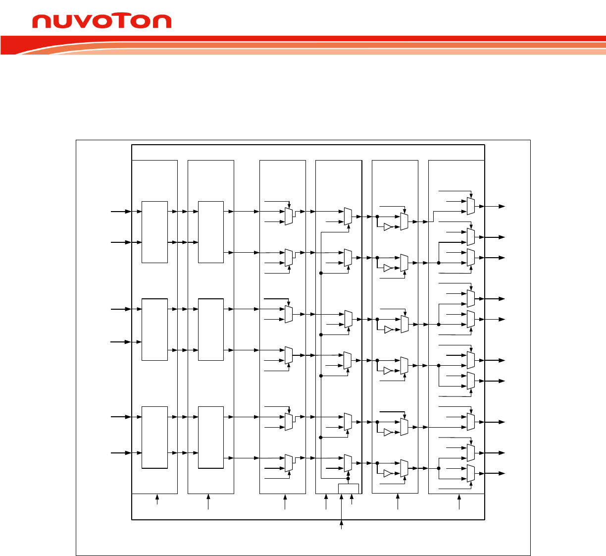
N76E003 Datasheet
Oct 28, 2016 Page 173 of 261 Rev. 1.00
on I/O pins. The output control circuit determines the PWM mode, dead-time insertion, mask output,
Fault Brake control, and PWM polarity. The last stage is a multiplexer of PWM output or I/O function.
User should set the PIOn bit to make the corresponding pin function as PWM output. Meanwhile, the
general purpose I/O function can be used.
PG0
PG1
PG2
PG3
PG4
PG5
FBINEN
(PWMCON1.3)
PWM and Fault Brake output control
PWM
mode
select
PWMMOD[1:0]
(PWMCON1[7:6])
Dead
time
insertion
PDTEN, PDTCNT
Mask
output
PMD0
PMEN0
PMD1
PMEN1
Brake
control PWM
polarity
Brake event
(P1.4/FB)
PG0_DT
PG1_DT
PWM0/1
mode
PWM0/1
dead
time
FBD0
FBD1
PNP0
PNP1
PMD2
PMEN2
PMD3
PMEN3
PG2_DT
PG3_DT
PWM2/3
mode
PWM2/3
dead
time
FBD2
FBD3
PNP2
PNP3
PMD4
PMEN4
PMD5
PMEN5
PG4_DT
PG5_DT
PWM4/5
mode
PWM4/5
dead
time
FBD4
FBD5
PNP4
PNP5
BRK
0
1
0
1
0
1
0
1
0
1
0
1
0
1
0
1
0
1
0
1
0
1
0
1
0
1
0
1
0
1
0
1
0
1
0
1
PMEN, PMD FBD PNP
P1.2
PIO00
0
1
P1.1
PIO01
0
1
P1.4
PIO11
0
1
P0.5
PIO02
0
1
P1.0
PIO12
0
1
P0.0
PIO03
0
1
P0.4
PIO13
0
1
P0.1
PIO04
0
1
P0.3
PIO05
0
1
P1.5
PIO15
0
1
PWM0/P1.2
PWM1/P1.1
PWM2/P0.5
PWM3/P0.0
PIOCON1,PIOCON0
PWM & I/O
switch
PWM1/P1.4
PWM2/P1.0
PWM3/P0.4
PWM5/P0.3
PWM5/P1.5
PWM4/P0.1
Figure 17-2. PWM and Fault Brake Output Control Block Diagram
User should follow the initialization steps below to start generating the PWM signal output. In the first
step by setting CLRPWM (PWMCON0.4), it ensures the 16-bit up counter reset for the accuracy of the
first duration. After initialization and setting {PWMPH, PWMPL} and all {PWMnH, PWMnL} registers,
PWMRUN (PWMCON0.7) can be set as logic 1 to trigger the 16-bit counter running. PWM starts to
generate waveform on its output pins. The hardware for all period and duty control registers are
double buffered designed. Therefore, {PWMPH, PWMPL} and all {PWMnH, PWMnL} registers can be
N76E003 Datasheet
Oct 28, 2016 Page 174 of 261 Rev. 1.00
written to at any time, but the period and duty cycle of PWM will not be updated immediately until the
LOAD (PWMCON0.6) is set and previous period is complete. This prevents glitches when updating
the PWM period or duty.
A loading of new period and duty by setting LOAD should be ensured complete by monitoring
it and waiting for a hardware automatic clearing LOAD bit. Any updating of PWM control
registers during LOAD bit as logic 1 will cause unpredictable output.
PWMCON0 PWM Control 0 (Bit-addressable)
7
6
5
4
3
2
1
0
PWMRUN
LOAD
PWMF
CLRPWM
-
-
-
-
R/W
R/W
R/W
R/W
-
-
-
-
Address: D8H Reset value: 0000 0000b
Bit
Name
Description
7
PWMRUN
PWM run enable
0 = PWM stays in idle.
1 = PWM starts running.
6
LOAD
PWM new period and duty load
This bit is used to load period and duty control registers in their buffer if new
period or duty value needs to be updated. The loading will act while a PWM
period is completed. The new period and duty affected on the next PWM
cycle. After the loading is complete, LOAD will be automatically cleared via
hardware. The meaning of writing and reading LOAD bit is different.
Writing:
0 = No effect.
1 = Load new period and duty in their buffers while a PWM period is
completed.
Reading:
0 = A loading of new period and duty is finished.
1 = A loading of new period and duty is not yet finished.
5
PWMF
PWM flag
This flag is set according to definitions of INTSEL[2:0] and INTTYP[1:0] in
PWMINTC. This bit is cleared by software.
4
CLRPWM
Clear PWM counter
Setting this bit clears the value of PWM 16-bit counter for resetting to 0000H.
After the counter value is cleared, CLRPWM will be automatically cleared via
hardware. The meaning of writing and reading CLRPWM bit is different.
Writing:
0 = No effect.
1 = Clearing PWM 16-bit counter.
Reading:
0 = PWM 16-bit counter is completely cleared.
1 = PWM 16-bit counter is not yet cleared.
N76E003 Datasheet
Oct 28, 2016 Page 175 of 261 Rev. 1.00
PWMCON1 PWM Control 1
7
6
5
4
3
2
1
0
PWMMOD[1:0]
GP
PWMTYP
FBINEN
PWMDIV[2:0]
R/W
R/W
R/W
R/W
R/W
Address: DFH Reset value: 0000 0000b
Bit
Name
Description
5
GP
Group mode enable
This bit enables the group mode. If enabled, the duty of first three pairs of
PWM are decided by PWM01H and PWM01L rather than their original duty
control registers.
0 = Group mode Disabled.
1 = Group mode Enabled.
2:0
PWMDIV[2:0]
PWM clock divider
This field decides the pre-scale of PWM clock source.
000 = 1/1.
001 = 1/2
010 = 1/4.
011 = 1/8.
100 = 1/16.
101 = 1/32.
110 = 1/64.
111 = 1/128.
CKCON Clock Control
7
6
5
4
3
2
1
0
-
PWMCKS
-
T1M
T0M
-
CLOEN
-
-
R/W
-
R/W
R/W
-
R/W
-
Address: 8EH Reset value: 0000 0000b
Bit
Name
Description
6
PWMCKS
PWM clock source select
0 = The clock source of PWM is the system clock FSYS.
1 = The clock source of PWM is the overflow of Timer 1.
PWMPL PWM Period Low Byte
7
6
5
4
3
2
1
0
PWMP[7:0]
R/W
Address: D9H reset value: 0000 0000b
Bit
Name
Description
7:0
PWMP[7:0]
PWM period low byte
This byte with PWMPH controls the period of the PWM generator signal.
N76E003 Datasheet
Oct 28, 2016 Page 176 of 261 Rev. 1.00
PWMPH PWM Period High Byte
7
6
5
4
3
2
1
0
PWMP[15:8]
R/W
Address: D1H reset value: 0000 0000b
Bit
Name
Description
7:0
PWMP[15:8]
PWM period high byte
This byte with PWMPL controls the period of the PWM generator signal.
PWM0L PWM0 Duty Low Byte
7
6
5
4
3
2
1
0
PWM0[7:0]
R/W
Address: DAH reset value: 0000 0000b
Bit
Name
Description
7:0
PWM0[7:0]
PWM0 duty low byte
This byte with PWM0H controls the duty of the output signal PG0 from PWM
generator.
PWM0H PWM0 Duty High Byte
7
6
5
4
3
2
1
0
PWM0[15:8]
R/W
Address: D2H reset value: 0000 0000b
Bit
Name
Description
7:0
PWM0[15:8]
PWM0 duty high byte
This byte with PWM0L controls the duty of the output signal PG0 from PWM
generator.
PWM1L PWM/1 Duty Low Byte
7
6
5
4
3
2
1
0
PWM1[7:0]
R/W
Address: DBH reset value: 0000 0000b
Bit
Name
Description
7:0
PWM1[7:0]
PWM1 duty low byte
This byte with PWM1H controls the duty of the output signal PG1 from PWM
generator.

N76E003 Datasheet
Oct 28, 2016 Page 177 of 261 Rev. 1.00
PWM1H PWM1 Duty High Byte
7
6
5
4
3
2
1
0
PWM1[15:8]
R/W
Address: D3H reset value: 0000 0000b
Bit
Name
Description
7:0
PWM1[15:8]
PWM1 duty high byte
This byte with PWM1L controls the duty of the output signal PG1 from PWM
generator.
PWM2L PWM2 Duty Low Byte
7
6
5
4
3
2
1
0
PWM2[7:0]
R/W
Address: DCH reset value: 0000 0000b
Bit
Name
Description
7:0
PWM2[7:0]
PWM2 duty low byte
This byte with PWM2H controls the duty of the output signal PG2 from PWM
generator.
PWM2H PWM2 Duty High Byte
7
6
5
4
3
2
1
0
PWM2[15:8]
R/W
Address: D4H reset value: 0000 0000b
Bit
Name
Description
7:0
PWM2[15:8]
PWM2 duty high byte
This byte with PWM2L controls the duty of the output signal PG2 from PWM
generator.
PWM3L PWM3 Duty Low Byte
7
6
5
4
3
2
1
0
PWM3[7:0]
R/W
Address: DDH reset value: 0000 0000b
Bit
Name
Description
7:0
PWM3[7:0]
PWM3 duty low byte
This byte with PWM3H controls the duty of the output signal PG3 from PWM
generator.

N76E003 Datasheet
Oct 28, 2016 Page 178 of 261 Rev. 1.00
PWM3H PWM3 Duty High Byte
7
6
5
4
3
2
1
0
PWM3[15:8]
R/W
Address: D5H reset value: 0000 0000b
Bit
Name
Description
7:0
PWM3[15:8]
PWM3 duty high byte
This byte with PWM3L controls the duty of the output signal PG3 from PWM
generator.
PWM4L PWM4 Duty Low Byte
7
6
5
4
3
2
1
0
PWM4[7:0]
R/W
Address: CCH, Page:1 reset value: 0000 0000b
Bit
Name
Description
7:0
PWM4[7:0]
PWM4 duty low byte
This byte with PWM4H controls the duty of the output signal PG4 from PWM
generator.
PWM4H PWM4 Duty High Byte
7
6
5
4
3
2
1
0
PWM4[15:8]
R/W
Address: C4H, Page:1 reset value: 0000 0000b
Bit
Name
Description
7:0
PWM4[15:8]
PWM4 duty high byte
This byte with PWM4L controls the duty of the output signal PG4 from PWM
generator.
PWM5L PWM5 Duty Low Byte
7
6
5
4
3
2
1
0
PWM5[7:0]
R/W
Address: CDH, Page:1 reset value: 0000 0000b
Bit
Name
Description
7:0
PWM5[7:0]
PWM5 duty low byte
This byte with PWM5H controls the duty of the output signal PG5 from PWM
generator.
N76E003 Datasheet
Oct 28, 2016 Page 179 of 261 Rev. 1.00
PWM5H PWM5 Duty High Byte
7
6
5
4
3
2
1
0
PWM5[15:8]
R/W
Address: C5H, Page:1 reset value: 0000 0000b
Bit
Name
Description
7:0
PWM5[15:8]
PWM5 duty high byte
This byte with PWM5L controls the duty of the output signal PG5 from PWM
generator.
PIOCON0 PWM or I/O Select
7
6
5
4
3
2
1
0
-
-
PIO05
PIO04
PIO03
PIO02
PIO01
PIO00
-
-
R/W
R/W
R/W
R/W
R/W
R/W
Address: DEH Reset value: 0000 0000b
Bit
Name
Description
5
PIO05
P0.3/PWM5 pin function select
0 = P0.3/PWM5 pin functions as P0.3.
1 = P0.3/PWM5 pin functions as PWM5 output.
4
PIO04
P0.1/PWM4 pin function select
0 = P0.1/PWM4 pin functions as P0.1.
1 = P0.1/PWM4 pin functions as PWM4 output.
3
PIO03
P0.0/PWM3 pin function select
0 = P0.0/PWM3 pin functions as P0.0.
1 = P0.0/PWM3 pin functions as PWM3 output.
2
PIO02
P1.0/PWM2 pin function select
0 = P1.0/PWM2 pin functions as P1.0.
1 = P1.0/PWM2 pin functions as PWM2 output.
1
PIO01
P1.1/PWM1 pin function select
0 = P1.1/PWM1 pin functions as P1.1.
1 = P1.1/PWM1 pin functions as PWM1 output.
0
PIO00
P1.2/PWM0 pin function select
0 = P1.2/PWM0 pin functions as P1.2.
1 = P1.2/PWM0 pin functions as PWM0 output.
PIOCON1 PWM or I/O Select
7
6
5
4
3
2
1
0
-
-
PIO15
-
PIO13
PIO12
PIO11
-
-
-
R/W
-
R/W
R/W
R/W
-
Address: C6H, Page:1 Reset value: 0000 0000b
Bit
Name
Description
5
PIO15
P1.5/PWM5 pin function select
0 = P1.5/PWM5 pin functions as P1.5.
1 = P1.5/PWM5 pin functions as PWM5 output.
N76E003 Datasheet
Oct 28, 2016 Page 180 of 261 Rev. 1.00
Bit
Name
Description
3
PIO13
P0.4/PWM3 pin function select
0 = P0.4/PWM3 pin functions as P0.4.
1 = P0.4/PWM3 pin functions as PWM3 output.
2
PIO12
P0.5/PWM2 pin function select
0 = P0.5/PWM2 pin functions as P0.5.
1 = P0.5/PWM2 pin functions as PWM2 output.
1
PIO11
P1.4/PWM1 pin function select
0 = P1.4/PWM1 pin functions as P1.4.
1 = P1.4/PWM1 pin functions as PWM1 output.
PWM Types
17.1.2
The PWM generator provides two PWM types: edge-aligned or center-aligned. PWM type is selected
by PWMTYP (PWMCON1.4).
PWMCON1 PWM Control 1
7
6
5
4
3
2
1
0
PWMMOD[1:0]
GP
PWMTYP
FBINEN
PWMDIV[2:0]
R/W
R/W
R/W
R/W
R/W
Address: DFH Reset value: 0000 0000b
Bit
Name
Description
4
PWMTYP
PWM type select
0 = Edge-aligned PWM.
1 = Center-aligned PWM.
17.1.2.1 Edge-Aligned Type
In edge-aligned mode, the 16-bit counter uses single slop operation by counting up from 0000H to
{PWMPH, PWMPL} and then starting from 0000H. The PWM generator signal (PGn before PWM and
Fault Brake output control) is cleared on the compare match of 16-bit counter and the duty register
{PWMnH, PWMnL} and set at the 16-bit counter is 0000H. The result PWM output waveform is left-
edge aligned.
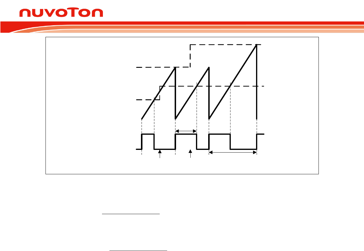
N76E003 Datasheet
Oct 28, 2016 Page 181 of 261 Rev. 1.00
PWMP (2nd)
PWMP (1st)
PWM01 (2nd)
PWM01 (1st)
PG01 output
Load
PWM01 (2nd)
Load
PWMP (2nd)
PWM01 (2nd)
duty valid
PWMP (2nd) period valid
12-bit counter
Figure 17-3. PWM Edge-aligned Type Waveform
The output frequency and duty cycle for edge-aligned PWM are given by following equations:
PWM frequency =
1}PWMPL,PWMPH{
FPWM
(FPWM is the PWM clock source frequency divided by
PWMDIV).
PWM high level duty =
1}PWMPL,PWMPH{
}PWMnL,PWMnH{
.
17.1.2.2 Center-Aligned Type
In center-aligned mode, the 16-bit counter use dual slop operation by counting up from 0000H to
{PWMPH, PWMPL} and then counting down from {PWMPH, PWMPL} to 0000H. The PGn signal is
cleared on the up-count compare match of 16-bit counter and the duty register {PWMnH, PWMnL} and
set on the down-count compare match. Center-aligned PWM may be used to generate non-
overlapping waveforms.
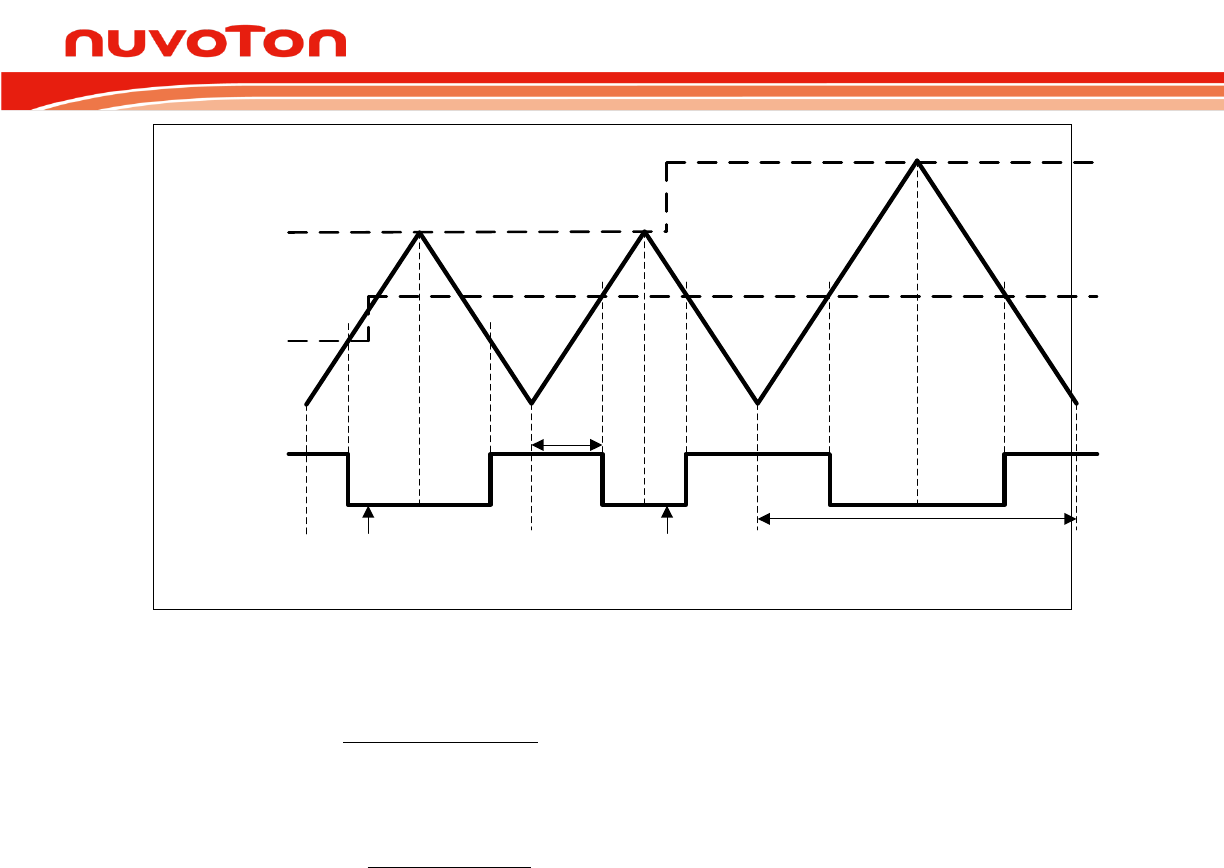
N76E003 Datasheet
Oct 28, 2016 Page 182 of 261 Rev. 1.00
PWMP (2nd)
PWMP (1st)
PWM01 (2nd)
PWM01 (1st)
PG01 output
Load
PWM01 (2nd)
Load
PWMP (2nd)
PWM01 (2nd)
duty valid
PWMP (2nd) period valid
12-bit counter
Figure 17-4. PWM Center-aligned Type Waveform
The output frequency and duty cycle for center-aligned PWM are given by following equations:
PWM frequency =
}PWMPL,PWMPH{×2
FPWM
(FPWM is the PWM clock source frequency divided by
PWMDIV).
PWM high level duty =
}PWMPL,PWMPH{
}PWMnL,PWMnH{
.
Operation Modes 17.1.3
After PGn signals pass through the first stage of the PWM and Fault Brake output control circuit. The
PWM mode selection circuit generates different kind of PWM output modes with six-channel, three-
pair signal PG0~PG5 . It supports independent mode, complementary mode, and synchronous mode.
N76E003 Datasheet
Oct 28, 2016 Page 183 of 261 Rev. 1.00
PWMCON1 PWM Control 1
7
6
5
4
3
2
1
0
PWMMOD[1:0]
GP
PWMTYP
FBINEN
PWMDIV[2:0]
R/W
R/W
R/W
R/W
R/W
Address: DFH Reset value: 0000 0000b
Bit
Name
Description
7:6
PWMMOD[1:0]
PWM mode select
00 = Independent mode.
01 = Complementary mode.
10 = Synchronized mode.
11 = Reserved.
17.1.3.1 Independent Mode
Independent mode is enabled when PWMMOD[1:0] (PWMCON1[7:6]) is [0:0]. It is the default mode of
PWM. PG0, PG1, PG2, PG3, PG4 and PG5 output PWM signals independently.
17.1.3.2 Complementary Mode with Dead-Time Insertion
Complementary mode is enabled when PWMMOD[1:0] = [0:1]. In this mode, PG0/2/4 output PWM
signals the same as the independent mode. However, PG1/3/5 output the out-phase PWM signals of
PG0/2/4 correspondingly, and ignore PG1/3/5 Duty register {PWMnH, PWMnL} (n:1/3/5). This mode
makes PG0/PG1 a PWM complementary pair and so on PG2/PG3 and PG4/PG5.
-
to prevent damage of the power switching device like GPIBs due to being active on simultaneously of
physically cannot switch on/off instantly. For the N76E003 PWM, each PWM pair share a 9-bit dead-
time down-counter PDTCNT used to produce the off time between two PWM signals in the same pair.
On implementation, a 0-to-1 signal edge delays after PDTCNT timer underflows. The timing diagram
illustrates the complementary mode with dead-time insertion of PG0/PG1 pair. Pairs of PG2/PG3 and
PG4/PG5 have the same dead-time circuit. Each pair has its own dead-time enabling bit in the field of
PDTEN[3:0].
Note that the PDTCNT and PDTEN registers are all TA write protection. The dead-time control are
also valid only when the PWM is configured in its complementary mode.
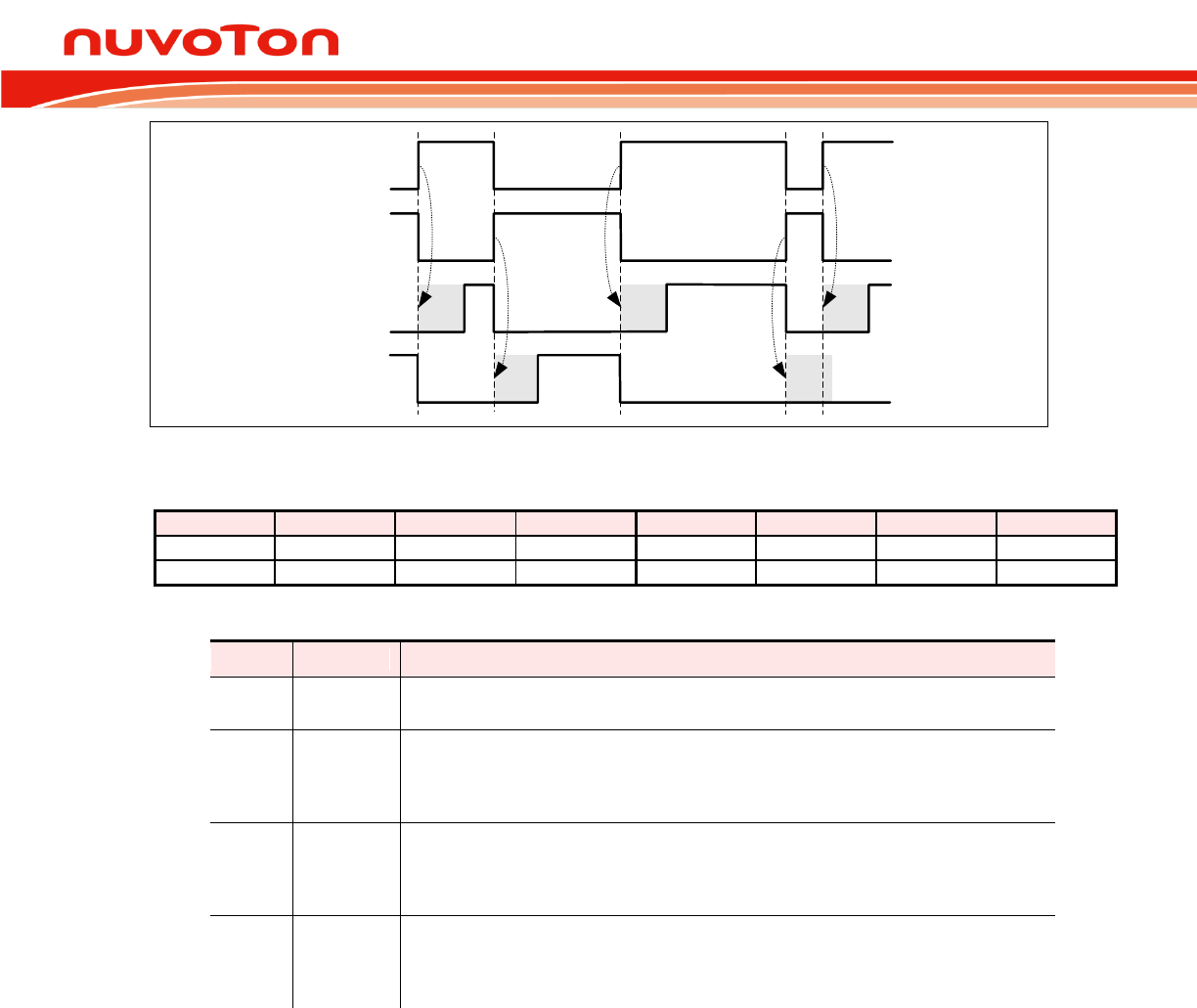
N76E003 Datasheet
Oct 28, 2016 Page 184 of 261 Rev. 1.00
PG0
PG1
PG0_DT
PG1_DT
Figure 17-5. PWM Complementary Mode with Dead-time Insertion
PDTEN PWM Dead-time Enable (TA protected)
7
6
5
4
3
2
1
0
-
-
-
PDTCNT.8
-
PDT45EN
PDT23EN
PDT01EN
-
-
-
R/W
-
R/W
R/W
R/W
Address: F9H Reset value: 0000 0000b
Bit
Name
Description
4
PDTCNT.8
PWM dead-time counter bit 8
See PDTCNT register.
2
PDT45EN
PWM4/5 pair dead-time insertion enable
This bit is valid only when PWM4/5 is under complementary mode.
0 = No delay on GP4/GP5 pair signals.
1 = Insert dead-time delay on the rising edge of GP4/GP5 pair signals.
1
PDT23EN
PWM2/3 pair dead-time insertion enable
This bit is valid only when PWM2/3 is under complementary mode.
0 = No delay on GP2/GP3 pair signals.
1 = Insert dead-time delay on the rising edge of GP2/GP3 pair signals.
0
PDT01EN
PWM0/1 pair dead-time insertion enable
This bit is valid only when PWM0/1 is under complementary mode.
0 = No delay on GP0/GP1 pair signals.
1 = Insert dead-time delay on the rising edge of GP0/GP1 pair signals.
N76E003 Datasheet
Oct 28, 2016 Page 185 of 261 Rev. 1.00
PDTCNT PWM Dead-time Counter (TA protected)
7
6
5
4
3
2
1
0
PDTCNT[7:0]
R/W
Address: FAH Reset value: 0000 0000b
Bit
Name
Description
7:0
PDTCNT[7:0]
PWM dead-time counter low byte
This 8-bit field combined with PDTEN.4 forms a 9-bit PWM dead-time counter
PDTCNT. This counter is valid only when PWM is under complementary mode
and the correspond PDTEN bit for PWM pair is set.
PWM dead-time =
SYS
F
1PDTCNT
.
Note that user should not modify PDTCNT during PWM run time.
17.1.3.3 Synchronous Mode
Synchronous mode is enabled when PWMMOD[1:0] = [1:0]. In this mode, PG0/2/4 output PWM
signals the same as the independent mode. PG1/3/5 output just the same in-phase PWM signals of
PG02/4 correspondingly.
Mask Output Control 17.1.4
Each PWM signal can be software masked by driving a specified level of PWM signal. The PWM
mask output function is quite useful when controlling Electrical Commutation Motor like a BLDC.
PMEN contains six bits, those determine which channel of PWM signal will be masked. PMD set the
individual mask level of each PWM channel. The default value of PMEN is 00H, which makes all
outputs of PWM channels follow signals from PWM generator. Note that the masked level is reversed
or not by PNP setting on PWM output pins.
PMEN PWM Mask Enable
7
6
5
4
3
2
1
0
-
-
PMEN5
PMEN4
PMEN3
PMEN2
PMEN1
PMEN0
-
-
R/W
R/W
R/W
R/W
R/W
R/W
Address: FBH Reset value: 0000 0000b
Bit
Name
Description
n
PMENn
PWMn mask enable
0 = PWMn signal outputs from its PWM generator.
1 = PWMn signal is masked by PMDn.
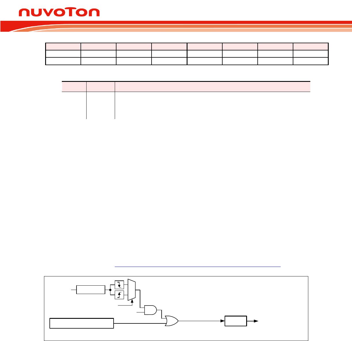
N76E003 Datasheet
Oct 28, 2016 Page 186 of 261 Rev. 1.00
PMD PWM Mask Data
7
6
5
4
3
2
1
0
-
-
PMD5
PMD4
PMD3
PMD2
PMD1
PMD0
-
-
R/W
R/W
R/W
R/W
R/W
R/W
Address: FCH Reset value: 0000 0000b
Bit
Name
Description
n
PMDn
PWMn mask data
The PWMn signal outputs mask data once its corresponding PMENn is set.
0 = PWMn signal is masked by 0.
1 = PWMn signal is masked by 1.
Fault Brake 17.1.5
The Fault Brake function is usually implemented in conjunction with an enhanced PWM circuit. It rules
as a fault detection input to protect the motor system from damage. Fault Brake pin input (FB) is valid
when FBINEN (PWMCON1.3) is set. When Fault Brake is asserted PWM signals will be individually
overwritten by FBD corresponding bits. PWMRUN (PWMCON0.7) will also be automatically cleared by
hardware to stop PWM generating. The PWM 16-bit counter will also be reset as 0000H. A indicating
flag FBF will be set by hardware to assert a Fault Brake interrupt if enabled. FBD data output remains
even after the FBF is cleared by software. User should resume the PWM output only by setting
PWMRUN again. Meanwhile the Fault Brake state will be released and PWM waveform outputs on
pins as usual. Fault Brake input has a polarity selection by FBINLS (FBD.6) bit. Note that the Fault
Brake signal feed in FB pin should be longer than eight-system-clock time for FB pin input has a
permanent 8/FSYS de-bouncing, which avoids fake Fault Brake event by input noise. The other path to
trigger a Fault Brake event is the ADC compare event. It asserts the Fault Brake behavior just the
same as FB pin input. See Sector 18.1.3 ADC Conversion Result Comparator page 192.
FBINEN
FB (P1.4)
ADC comparator ADC compare event
Fault Brake event
De-bounce
0
1
FBINLS
FBF Fault Brake interrupt
Figure 17-6. Fault Brake Function Block Diagram
N76E003 Datasheet
Oct 28, 2016 Page 187 of 261 Rev. 1.00
PWMCON1 PWM Control 1
7
6
5
4
3
2
1
0
PWMMOD[1:0]
GP
PWMTYP
FBINEN
PWMDIV[2:0]
R/W
R/W
R/W
R/W
R/W
Address: DFH Reset value: 0000 0000b
Bit
Name
Description
3
FBINEN
FB pin input enable
0 = PWM output Fault Braked by FB pin input Disabled.
1 = PWM output Fault Braked by FB pin input Enabled. Once an edge, which
matches FBINLS (FBD.6) selection, occurs on FB pin, PWM0~5 output
Fault Brake data in FBD register and PWM6/7 remains their states.
PWMRUN (PWMCON0.7) will also be automatically cleared by
hardware. The PWM output resumes when PWMRUN is set again.
FBD PWM Fault Brake Data
7
6
5
4
3
2
1
0
FBF
FBINLS
FBD5
FBD4
FBD3
FBD2
FBD1
FBD0
R/W
R/W
R/W
R/W
R/W
R/W
R/W
R/W
Address: D7H Reset value: 0000 0000b
Bit
Name
Description
7
FBF
Fault Brake flag
This flag is set when FBINEN is set as 1 and FB pin detects an edge, which
matches FBINLS (FBD.6) selection. This bit is cleared by software. After FBF is
cleared, Fault Brake data output will not be released until PWMRUN
(PWMCON0.7) is set.
6
FBINLS
FB pin input level selection
0 = Falling edge.
1 = Rising edge.
N
FBDn
PWMn Fault Brake data
0 = PWMn signal is overwritten by 0 once Fault Brake asserted.
1 = PWMn signal is overwritten by 1 once Fault Brake asserted.
Polarity Control 17.1.6
Each PWM output channel has its independent polarity control bit, PNP0~PNP5. The default is high
active level on all control fields implemented with positive logic. It means the power switch is ON when
PWM outputs high level and OFF when low level. User can easily configure all setting with positive
logic and then set PNP bit to make PWM actually outputs according to the negative logic.

N76E003 Datasheet
Oct 28, 2016 Page 188 of 261 Rev. 1.00
PNP PWM Negative Polarity
7
6
5
4
3
2
1
0
-
-
PNP5
PNP4
PNP3
PNP2
PNP1
PNP0
-
-
R/W
R/W
R/W
R/W
R/W
R/W
Address: D6H Reset value: 0000 0000b
Bit
Name
Description
n
PNPn
PWMn negative polarity output enable
0 = PWMn signal outputs directly on PWMn pin.
1 = PWMn signal outputs inversely on PWMn pin.
17.2 PWM Interrupt
The PWM module has a flag PWMF (PWMCON0.5) to indicate certain point of each complete PWM
period. The indicating PWM channel and point can be selected by INTSEL[2:0] and INTTYP[1:0]
(PWMINTC[2:0] and [5:4]). Note that the center point and the end point interrupts are only available
when PWM operates in its center-aligned type. PWMF is cleared by software.
PWMINTC PWM Interrupt Control
7
6
5
4
3
2
1
0
-
-
INTTYP1
INTTYP0
-
INTSEL2
INTSEL1
INTSEL0
-
-
R/W
R/W
-
R/W
R/W
R/W
Address: B7H, Page:1 Reset value: 0000 0000b
Bit
Name
Description
5:4
INTTYP[1:0]
PWM interrupt type select
These bit select PWM interrupt type.
00 = Falling edge on PWM0/1/2/3/4/5 pin.
01 = Rising edge on PWM0/1/2/3/4/5 pin.
10 = Central point of a PWM period.
11 = End point of a PWM period.
Note that the central point interrupt or the end point interrupt is only available
while PWM operates in center-aligned type.
2:0
INTSEL[2:0]
PWM interrupt pair select
These bits select which PWM channel asserts PWM interrupt when PWM
interrupt type is selected as falling or rising edge on PWM0/1/2/3/4/5 pin..
000 = PWM0.
001 = PWM1.
010 = PWM2.
011 = PWM3.
100 = PWM4.
101 = PWM5.
Others = PWM0.
The PWM interrupt related with PWM waveform is shown as figure below.
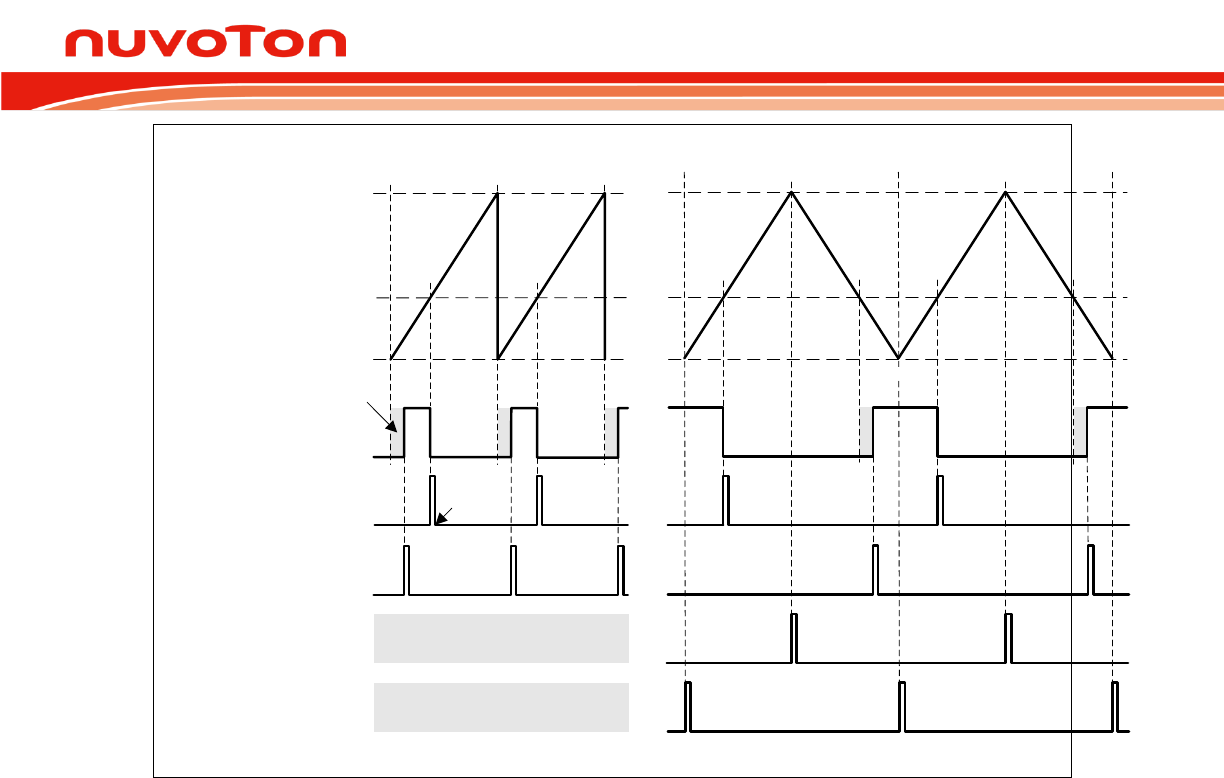
N76E003 Datasheet
Oct 28, 2016 Page 189 of 261 Rev. 1.00
Reserved
PWMF (central point)
(INTTYP[1:0] = [1:0])
PWMF (end point)
(INTTYP[1:0] = [1:1])
Central point
End point
PWM0/2/4 pin output
Software
clear
12-bit PWM counter
Dead time
PWMF (falling edge)
(INTTYP[1:0] = [0:0])
PWMF (rising edge)
(INTTYP[1:0] = [0:1])
Edge-aligned PWM Center-aligned PWM
Reserved
Figure 17-7. PWM Interrupt Type
Fault Brake event requests another interrupt, Fault Brake interrupt. It has different interrupt vector from
PWM interrupt. When either Fault Brake pin input event or ADC compare event occurs, FBF (FBD.7)
will be set by hardware. It generates Fault Brake interrupt if enabled. The Fault Brake interrupt enable
bit is EFB (EIE.5). FBF Is cleared via software.
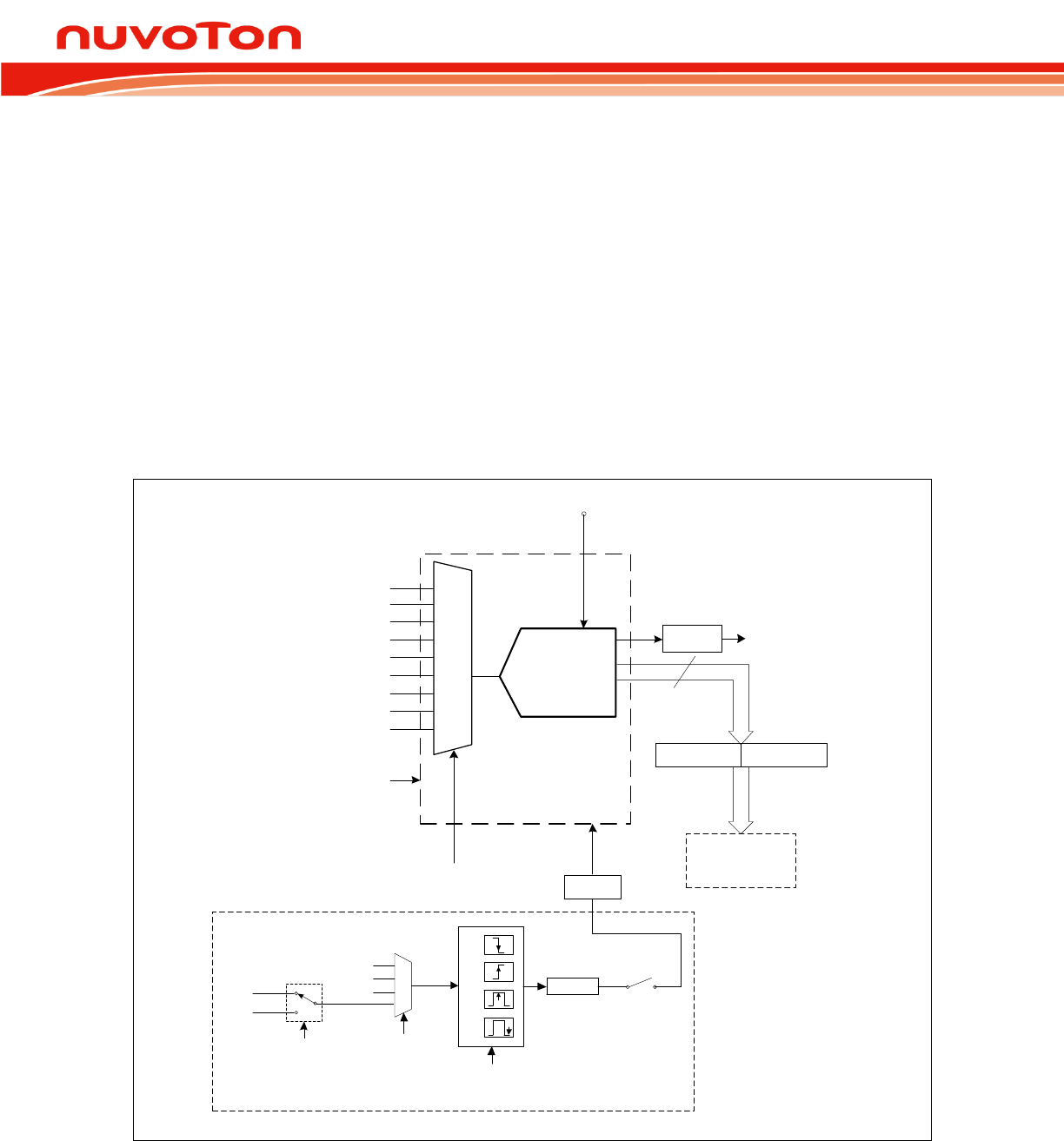
N76E003 Datasheet
Oct 28, 2016 Page 190 of 261 Rev. 1.00
18. 12-BIT ANALOG-TO-DIGITAL CONVERTER (ADC)
The N76E003 is embedded with a 12-bit SAR ADC. The ADC (analog-to-digital converter) allows
conversion of an analog input signal to a 12-bit binary representation of that signal. The N76E003 is
selected as 8-channel inputs in single end mode. The internal band-gap voltage 1.22V also can be the
internal ADC input. The analog input, multiplexed into one sample and hold circuit, charges a sample
and hold capacitor. The output of the sample and hold capacitor is the input into the converter. The
converter then generates a digital result of this analog level via successive approximation and stores
the result in the result registers.
18.1 Functional Description
ADC Operation 18.1.1
0000
0001
0010
0011
0100
0101
0110
0111
1000
AIN0
AIN1
AIN2
AIN3
AIN4
AIN5
AIN6
AIN7
Internal band-gap
ADCHS[3:0]
12-bit SAR
ADC
A/D convertion start
ADCRH ADCRL
12
ADCF ADC interrupt
ADC result
comparator
VREF
VDD
ADCEN
ADCS
STADCPX
0
1
P0.4
P1.3
ETGTYP[1:0]
(ADCCON1[3:2])
[00]
[01]
[10]
[11]
00
01
10
ETGSEL[1:0]
(ADCCON0[5:4])
PWM0
PWM2
PWM4 ADCDLY
External Trigger
11
STADC ADCEX
Figure 18-1. 12-bit ADC Block Diagram

N76E003 Datasheet
Oct 28, 2016 Page 191 of 261 Rev. 1.00
Before ADC operation, the ADC circuit should be enabled by setting ADCEN (ADCCON1.0). This
makes ADC circuit active. It consume extra power. Once ADC is not used, clearing ADCEN to turn off
ADC circuit saves power.
The ADC analog input pin should be specially considered. ADCHS[2:0] are channel selection bits that
control which channel is connected to the sample and hold circuit. User needs to configure selected
ADC input pins as input-only (high impedance) mode via respective bits in PxMn registers. This
configuration disconnects the digital output circuit of each selected ADC input pin. But the digital input
circuit still works. Digital input may cause the input buffer to induce leakage current. To disable the
digital input buffer, the respective bits in AINDIDS should be set. Configuration above makes selected
ADC analog input pins pure analog inputs to allow external feeding of the analog voltage signals. Also,
the ADC clock rate needs to be considered carefully. The ADC maximum clock frequency is listed in
Table 31-9. ADC Electrical Characteristics Clock above the maximum clock frequency degrades ADC
performance unpredictably.
An A/D conversion is initiated by setting the ADCS bit (ADCCON0.6). When the conversion is
complete, the hardware will clear ADCS automatically, set ADCF (ADCCON0.7) and generate an
interrupt if enabled. The new conversion result will also be stored in ADCRH (most significant 8 bits)
and ADCRL (least significant 4 bits). The 12-bit ADC result value is
REF
AIN
V
V
×4095
.
By the way, digital circuitry inside and outside the device generates noise which might affect the
accuracy of ADC measurements. If conversion accuracy is critical, the noise level can be reduced by
applying the following techniques:
1. Keep analog signal paths as short as possible. Make sure to run analog signals tracks well away
from high-speed digital tracks.
2. Place the device in Idle mode during a conversion.
3. If any AIN pins are used as digital outputs, it is essential that these do not switch while a conversion
is in progress.
ADC Conversion Triggered by External Source 18.1.2
Besides setting ADCS via software, the N76E003 is enhanced by supporting hardware triggering
method to start an A/D conversion. If ADCEX (ADCCON1.1) is set, edges or period points on selected
PWM channel or edges of STADC pin will automatically trigger an A/D conversion. (The hardware
trigger also sets ADCS by hardware.) For application flexibility, STADC pin can be exchanged by
STADCPX (ADCCON1.6).
N76E003 Datasheet
Oct 28, 2016 Page 192 of 261 Rev. 1.00
The effective condition is selected by ETGSEL (ADCCON0[5:4]) and ETGTYP (ADCCON1[3:2]). A
trigger delay can also be inserted between external trigger point and A/D conversion. The external
trigging ADC hardware with controllable trigger delay makes the N76E003 feasible for high
performance motor control. Note that during ADC is busy in converting (ADCS = 1), any conversion
triggered by software or hardware will be ignored and there is no warning presented.
ETGTYP[1:0]
(ADCCON1[3:2])
[00]
[01]
[10]
[11]
00
01
10
ETGSEL[1:0]
(ADCCON0[5:4])
PWM0
PWM2
PWM4 ADCDLY External Trigger
11
STADC
Figure 18-2. External Triggering ADC Circuit
ADC Conversion Result Comparator
18.1.3
The N76E003 ADC has a digital comparator, which compares the A/D conversion result with a 12-bit
constant value given in ACMPH and ACMPL registers. The ADC comparator is enabled by setting
ADCMPEN (ADCCON2.5) and each compare will be done on every A/D conversion complete
moment. ADCMPO (ADCCON2.4) shows the compare result according to its output polarity setting bit
ADCMPOP (ADCCON2.6). The ADC comparing result can trigger a PWM Fault Brake output directly.
This function is enabled when ADFBEN (ADCCON2.7). When ADCMPO is set, it generates a ADC
compare event and asserts Fault Brake. Please also see Sector 18.1.5Fault Brake129.
ADCR[11:0]
ADCMP[11:0]
+
-
ADCMPO
(ADCCON2.4)
0
1ADFBEN
(ADCCON2.7)
ADC compare event
ADCMPOP
(ADCCON2.6)
ADCMPEN
(ADCCON2.5)
Figure 18-3. ADC Result Comparator

N76E003 Datasheet
Oct 28, 2016 Page 193 of 261 Rev. 1.00
18.2 Control Registers of ADC
ADCCON0 ADC Control 0 (Bit-addressable)
7
6
5
4
3
2
1
0
ADCF
ADCS
ETGSEL1
ETGSEL0
ADCHS3
ADCHS2
ADCHS1
ADCHS0
R/W
R/W
R/W
R/W
R/W
R/W
R/W
R/W
Address: E8H Reset value: 0000 0000b
Bit
Name
Description
7
ADCF
ADC flag
This flag is set when an A/D conversion is completed. The ADC result can be
read. While this flag is 1, ADC cannot start a new converting. This bit is
cleared by software.
6
ADCS
A/D converting software start trigger
Setting this bit 1 triggers an A/D conversion. This bit remains logic 1 during
A/D converting time and is automatically cleared via hardware right after
conversion complete. The meaning of writing and reading ADCS bit is
different.
Writing:
0 = No effect.
1 = Start an A/D converting.
Reading:
0 = ADC is in idle state.
1 = ADC is busy in converting.
5:4
ETGSEL[1:0]
External trigger source select
When ADCEX (ADCCON1.1) is set, these bits select which pin output
triggers ADC conversion.
00 = PWM0.
01 = PWM2.
10 = PWM4.
11 = STADC pin.
3:0
ADCHS[3:0]
A/D converting channel select
This filed selects the activating analog input source of ADC. If ADCEN is 0, all
inputs are disconnected.
0000 = AIN0.
0001 = AIN1.
0010 = AIN2.
0011 = AIN3.
0100 = AIN4.
0101 = AIN5.
0110 = AIN6.
0111 = AIN7
1000 = Internal band-gap voltage 1.22V.
Others = Reserved.
N76E003 Datasheet
Oct 28, 2016 Page 194 of 261 Rev. 1.00
ADCCON1 ADC Control 1
7
6
5
4
3
2
1
0
-
STADCPX
-
-
ETGTYP[1:0]
ADCEX
ADCEN
-
R/W
-
-
R/W
R/W
R/W
Address: E1H Reset value: 0000 0000b
Bit
Name
Description
7
-
Reserved
6
STADCPX
External start ADC trigger pin select
0 = Assign STADC to P0.4.
1 = Assign STADC to P1.3.
Note that STADC will exchange immediately once setting or clearing this bit.
5:4
-
Reserved
3:2
ETGTYP[1:0]
External trigger type select
When ADCEX (ADCCON1.1) is set, these bits select which condition triggers
ADC conversion.
00 = Falling edge on PWM0/2/4 or STADC pin.
01 = Rising edge on PWM0/2/4 or STADC pin.
10 = Central point of a PWM period.
11 = End point of a PWM period.
Note that the central point interrupt or the period point interrupt is only
available for PWM center-aligned type.
1
ADCEX
ADC external conversion trigger select
This bit select the methods of triggering an A/D conversion.
0 = A/D conversion is started only via setting ADCS bit.
1 = A/D conversion is started via setting ADCS bit or by external trigger
source depending on ETGSEL[1:0] and ETGTYP[1:0]. Note that while
ADCS is 1 (busy in converting), the ADC will ignore the following external
trigger until ADCS is hardware cleared.
0
ADCEN
ADC enable
0 = ADC circuit off.
1 = ADC circuit on.
ADCCON2 ADC Control 2
7
6
5
4
3
2
1
0
ADFBEN
ADCMPOP
ADCMPEN
ADCMPO
-
-
-
ADCDLY.8
R/W
R/W
R/W
R
-
-
-
R/W
Address: E2H Reset value: 0000 0000b
Bit
Name
Description
7
ADFBEN
ADC compare result asserting Fault Brake enable
0 = ADC asserting Fault Brake Disabled.
1 = ADC asserting Fault Brake Enabled. Fault Brake is asserted once its
compare result ADCMPO is 1. Meanwhile, PWM channels output Fault
Brake data. PWMRUN (PWMCON0.7) will also be automatically cleared by
hardware. The PWM output resumes when PWMRUN is set again.
6
ADCMPOP
ADC comparator output polarity
0 = ADCMPO is 1 if ADCR[11:0] is greater than or equal to ADCMP[11:0].
1 = ADCMPO is 1 if ADCR[11:0] is less than ADCMP[11:0].
N76E003 Datasheet
Oct 28, 2016 Page 195 of 261 Rev. 1.00
Bit
Name
Description
5
ADCMPEN
ADC result comparator enable
0 = ADC result comparator Disabled.
1 = ADC result comparator Enabled.
4
ADCMPO
ADC comparator output value
This bit is the output value of ADC result comparator based on the setting of
ACMPOP. This bit updates after every A/D conversion complete.
3:1
-
Reserved
0
ADCDLY.8
ADC external trigger delay counter bit 8
See ADCDLY register.
AINDIDS ADC Channel Digital Input Disconnect
7
6
5
4
3
2
1
0
P11DIDS
P03DIDS
P04DIDS
P05DIDS
P06DIDS
P07DIDS
P30DIDS
P17DIDS
R/W
R/W
R/W
R/W
R/W
R/W
R/W
R/W
Address: F6H Reset value: 0000 0000b
Bit
Name
Description
n
AINnDIDS
ADC Channel digital input disable
0 = ADC channel n digital input Enabled.
1 = ADC channel n digital input Disabled. ADC channel n is read always 0.
ADCDLY ADC Trigger Delay Counter
7
6
5
4
3
2
1
0
ADCDLY[7:0]
R/W
Address: E3H Reset value: 0000 0000b
Bit
Name
Description
7:0
ADCDLY[7:0]
ADC external trigger delay counter low byte
This 8-bit field combined with ADCCON2.0 forms a 9-bit counter. This counter
inserts a delay after detecting the external trigger. An A/D converting starts
after this period of delay.
External trigger delay time =
ADC
F
ADCDLY
.
Note that this field is valid only when ADCEX (ADCCON1.1) is set. User
should not modify ADCDLY during PWM run time if selecting PWM output as
the external ADC trigger source.
ADCRH ADC Result High Byte
7
6
5
4
3
2
1
0
ADCR[11:4]
R
Address: C3H Reset value: 0000 0000b
Bit
Name
Description
7:0
ADCR[11:4]
ADC result high byte
The most significant 8 bits of the ADC result stored in this register.
N76E003 Datasheet
Oct 28, 2016 Page 196 of 261 Rev. 1.00
ADCRL ADC Result Low Byte
7
6
5
4
3
2
1
0
-
-
-
-
ADCR[3:0]
-
-
-
-
R
Address: C2H Reset value: 0000 0000b
Bit
Name
Description
3:0
ADCR[3:0]
ADC result low byte
The least significant 4 bits of the ADC result stored in this register.
ADCMPH ADC Compare High Byte
7
6
5
4
3
2
1
0
ADCMP[11:4]
W/R
Address: CFH Reset value: 0000 0000b
Bit
Name
Description
7:0
ADCMP[11:4]
ADC compare high byte
The most significant 8 bits of the ADC compare value stores in this register.
ADCMPL ADC Compare Low Byte
7
6
5
4
3
2
1
0
-
-
-
-
ADCMP[3:0]
-
-
-
-
W/R
Address: CEH Reset value: 0000 0000b
Bit
Name
Description
3:0
ADCMP[3:0]
ADC compare low byte
The least significant 4 bits of the ADC compare value stores in this register.
N76E003 Datasheet
Oct 28, 2016 Page 197 of 261 Rev. 1.00
19. TIMED ACCESS PROTECTION (TA)
The N76E003 has several features such as WDT and Brown-out detection that are crucial to proper
operation of the system. If leaving these control registers unprotected, errant code may write
undetermined value into them and results in incorrect operation and loss of control. To prevent this
risk, the N76E003 has a protection scheme, which limits the write access to critical SFRs. This
protection scheme is implemented using a timed access (TA). The following registers are related to
the TA process.
TA Timed Access
7
6
5
4
3
2
1
0
TA[7:0]
W
Address: C7H Reset value: 0000 0000b
Bit
Name
Description
7:0
TA[7:0]
Timed access
The timed access register controls the access to protected SFRs. To access
protected bits, user should first write AAH to the TA and immediately followed by a
write of 55H to TA. After these two steps, a writing permission window is opened
for 4 clock cycles during this period that user may write to protected SFRs.
In timed access method, the bits, which are protected, have a timed write enable window. A write is
successful only if this window is active, otherwise the write will be discarded. When the software writes
AAH to TA, a counter is started. This counter waits for 3 clock cycles looking for a write of 55H to TA.
If the second write of 55H occurs within 3 clock cycles of the first write of AAH, then the timed access
window is opened. It remains open for 4 clock cycles during which user may write to the protected bits.
After 4 clock cycles, this window automatically closes. Once the window closes, the procedure should
be repeated to write another protected bits. Not that the TA protected SFRs are required timed access
for writing but reading is not protected. User may read TA protected SFR without giving AAH and 55H
to TA register. The suggestion code for opening the timed access window is shown below.
(CLR EA) ;if any interrupt is enabled, disable temporally
MOV TA,#0AAH
MOV TA,#55H
(Instruction that writes a TA protected register)
(SETB EA) ;resume interrupts enabled
Any enabled interrupt should be disabled during this procedure to avoid delay between these three
writings. If there is no interrupt enabled, the CLR EA and SETB EA instructions can be left out.

N76E003 Datasheet
Oct 28, 2016 Page 198 of 261 Rev. 1.00
Examples of timed assess are shown to illustrate correct or incorrect writing process.
Example 1,
MOV TA,#0AAH ;3 clock cycles
MOV TA,#55H ;3 clock cycles
ORL WDCON,#data ;4 clock cycles
Example 2,
MOV TA,#0AAH ;3 clock cycles
MOV TA,#55H ;3 clock cycles
NOP ;1 clock cycle
ANL BODCON0,#data ;4 clock cycles
Example 3,
MOV TA,#0AAH ;3 clock cycles
MOV TA,#55H ;3 clock cycles
MOV WDCON,#data1 ;3 clock cycles
ORL BODCON0,#data2 ;4 clock cycles
Example 4,
MOV TA,#0AAH ;3 clock cycles
NOP ;1 clock cycle
MOV TA,#55H ;3 clock cycles
ANL BODCON0,#data ;4 clock cycles
In the first example, the writing to the protected bits is done before the 3-clock-cycle window closes. In
example 2, however, the writing to BODCON0 does not complete during the window opening, there
will be no change of the value of BODCON0. In example 3, the WDCON is successful written but the
BODCON0 write is out of the 3-clock-cycle window. Therefore, the BODCON0 value will not change
either. In Example 4, the second write 55H to TA completes after 3 clock cycles of the first write TA of
AAH, and thus the timed access window is not opened at all, and the write to the protected byte
affects nothing.
N76E003 Datasheet
Oct 28, 2016 Page 199 of 261 Rev. 1.00
20. INTERRUPT SYSTEM
20.1 Interrupt Overview
The purpose of the interrupt is to make the software deal with unscheduled or asynchronous events.
The N76E003 has a four-priority-level interrupt structure with 18 interrupt sources. Each of the
interrupt sources has an individual priority setting bits, interrupt vector and enable bit. In addition, the
interrupts can be globally enabled or disabled. When an interrupt occurs, the CPU is expected to
service the interrupt. This service is specified as an Interrupt Service Routine (ISR). The ISR resides
at a predetermined address as shown in Table 20-1. Interrupt Vectors. When the interrupt occurs if
enabled, the CPU will vector to the respective location depending on interrupt source, execute the
code at this location, stay in an interrupt service state until the ISR is done. Once an ISR has begun, it
can be interrupted only by a higher priority interrupt. The ISR should be terminated by a return from
interrupt instruction RETI. This instruction will force the CPU return to the instruction that would have
been next when the interrupt occurred.
Table 20-1. Interrupt Vectors
Source
Vector
Address
Vector
Number
Source
Vector
Address
Vector
Number
Reset
0000H
-
SPI interrupt
004BH
9
External interrupt 0
0003H
0
WDT interrupt
0053H
10
Timer 0 overflow
000BH
1
ADC interrupt
005BH
11
External interrupt 1
0013H
2
Input capture interrupt
0063H
12
Timer 1 overflow
001BH
3
PWM interrupt
006BH
13
Serial port 0 interrupt
0023H
4
Fault Brake interrupt
0073H
14
Timer 2 event
002BH
5
Serial port 1 interrupt
007BH
15
I2C status/timer-out interrupt
0033H
6
Timer 3 overflow
0083H
16
Pin interrupt
003BH
7
Self Wake-up Timer interrupt
008BH
17
Brown-out detection interrupt
0043H
8

N76E003 Datasheet
Oct 28, 2016 Page 200 of 261 Rev. 1.00
20.2 Enabling Interrupts
Each of individual interrupt sources can be enabled or disabled through the use of an associated
interrupt enable bit in the IE and EIE SFRs. There is also a global enable bit EA bit (IE.7), which can
be cleared to disable all the interrupts at once. It is set to enable all individually enabled interrupts.
Setting the EA bit to logic 0 disables all interrupt sources regardless of the individual interrupt-enable
settings. Note that interrupts which occur when the EA bit is set to logic 0 will be held in a pending
state, and will not be serviced until the EA bit is set back to logic 1. All interrupt flags that generate
interrupts can also be set via software. Thereby software initiated interrupts can be generated.
Note that every interrupts, if enabled, is generated by a setting as logic 1 of its interrupt flag no matter
by hardware or software. User should take care of each interrupt flag in its own interrupt service
routine (ISR). Most of interrupt flags should be cleared by writing it as logic 0 via software to avoid
recursive interrupt requests.
IE Interrupt Enable (Bit-addressable)
7
6
5
4
3
2
1
0
EA
EADC
EBOD
ES
ET1
EX1
ET0
EX0
R/W
R/W
R/W
R/W
R/W
R/W
R/W
R/W
Address: A8H Reset value: 0000 0000b
Bit
Name
Description
7
EA
Enable all interrupt
This bit globally enables/disables all interrupts that are individually enabled.
0 = All interrupt sources Disabled.
1 = Each interrupt Enabled depending on its individual mask setting. Individual
interrupts will occur if enabled.
6
EADC
Enable ADC interrupt
0 = ADC interrupt Disabled.
1 = Interrupt generated by ADCF (ADCCON0.7) Enabled.
5
EBOD
Enable brown-out interrupt
0 = Brown-out detection interrupt Disabled.
1 = Interrupt generated by BOF (BODCON0.3) Enabled.
4
ES
Enable serial port 0 interrupt
0 = Serial port 0 interrupt Disabled.
1 = Interrupt generated by TI (SCON.1) or RI (SCON.0) Enabled.
3
ET1
Enable Timer 1 interrupt
0 = Timer 1 interrupt Disabled.
1 = Interrupt generated by TF1 (TCON.7) Enabled.
2
EX1
Enable external interrupt 1
0 = External interrupt 1 Disabled.
1 = Interrupt generated by
pin (P1.7) Enabled.
1
ET0
Enable Timer 0 interrupt
0 = Timer 0 interrupt Disabled.
1 = Interrupt generated by TF0 (TCON.5) Enabled.
N76E003 Datasheet
Oct 28, 2016 Page 201 of 261 Rev. 1.00
Bit
Name
Description
0
EX0
Enable external interrupt 0
0 = External interrupt 0 Disabled.
1 = Interrupt generated by
pin (P3.0) Enabled.
EIE Extensive Interrupt Enable
7
6
5
4
3
2
1
0
ET2
ESPI
EFB
EWDT
EPWM
ECAP
EPI
EI2C
R/W
R/W
R/W
R/W
R/W
R/W
R/W
R/W
Address: 9BH Reset value: 0000 0000b
Bit
Name
Description
7
ET2
Enable Timer 2 interrupt
0 = Timer 2 interrupt Disabled.
1 = Interrupt generated by TF2 (T2CON.7) Enabled.
6
ESPI
Enable SPI interrupt
0 = SPI interrupt Disabled.
1 = Interrupt generated by SPIF (SPSR.7), SPIOVF (SPSR.5), or MODF (SPSR.4)
Enable.
5
EFB
Enable Fault Brake interrupt
0 = Fault Brake interrupt Disabled.
1 = Interrupt generated by FBF (FBD.7) Enabled.
4
EWDT
Enable WDT interrupt
0 = WDT interrupt Disabled.
1 = Interrupt generated by WDTF (WDCON.5) Enabled.
3
EPWM
Enable PWM interrupt
0 = PWM interrupt Disabled.
1 = Interrupt generated by PWMF (PWMCON0.5) Enabled.
2
ECAP
Enable input capture interrupt
0 = Input capture interrupt Disabled.
1 = Interrupt generated by any flags of CAPF[2:0] (CAPCON0[2:0]) Enabled.
1
EPI
Enable pin interrupt
0 = Pin interrupt Disabled.
1 = Interrupt generated by any flags in PIF register Enabled.
0
EI2C
Enable I2C interrupt
0 = I2C interrupt Disabled.
1 = Interrupt generated by SI (I2CON.3) or I2TOF (I2TOC.0) Enabled.
EIE1 Extensive Interrupt Enable 1
7
6
5
4
3
2
1
0
-
-
-
-
-
EWKT
ET3
ES_1
-
-
-
-
-
R/W
R/W
R/W
Address: 9CH Reset value: 0000 0000b
Bit
Name
Description
2
EWKT
Enable WKT interrupt
0 = WKT interrupt Disabled.
1 = Interrupt generated by WKTF (WKCON.4) Enabled.

N76E003 Datasheet
Oct 28, 2016 Page 202 of 261 Rev. 1.00
Bit
Name
Description
1
ET3
Enable Timer 3 interrupt
0 = Timer 3 interrupt Disabled.
1 = Interrupt generated by TF3 (T3CON.4) Enabled.
0
ES_1
Enable serial port 1 interrupt
0 = Serial port 1 interrupt Disabled.
1 = Interrupt generated by TI_1 (SCON_1.1) or RI_1 (SCON_1.0) Enabled.

N76E003 Datasheet
Oct 28, 2016 Page 203 of 261 Rev. 1.00
20.3 Interrupt Priorities
There are four priority levels for all interrupts. They are level highest, high, low, and lowest; and they
are represented by level 3, level 2, level 1, and level 0. The interrupt sources can be individually set to
one of four priority levels by setting their own priority bits. Table 20-2. Interrupt Priority Level Setting
lists four priority setting. Naturally, a low level priority interrupt can itself be interrupted by a high level
priority interrupt, but not by any same level interrupt or lower level. In addition, there exists a pre-
defined natural priority among the interrupts themselves. The natural priority comes into play when the
interrupt controller has to resolve simultaneous requests having the same priority level.
In case of multiple interrupts, the following rules apply:
1. While a low priority interrupt handler is running, if a high priority interrupt arrives, the handler will be
program.
2. If a high priority interrupt is running, it cannot be interrupted by any other source even if it is a high
priority interrupt which is higher in natural priority.
3. A low-priority interrupt handler will be invoked only if no other interrupt is already executing. Again,
the low priority interrupt cannot preempt another low priority interrupt, even if the later one is higher in
natural priority.
4. If two interrupts occur at the same time, the interrupt with higher priority will execute first. If both
interrupts are of the same priority, the interrupt which is higher in natural priority will be executed first.
This is the only context in which the natural priority matters.
This natural priority is defined as shown on Table 20-3. Characteristics of Each Interrupt Source. It
also summarizes the interrupt sources, flag bits, vector addresses, enable bits, priority bits, natural
priority and the permission to wake up the CPU from Power-down mode. For details of waking CPU up
from Power-down mode, please see Section 22.1 Power-Down Mode222.

N76E003 Datasheet
Oct 28, 2016 Page 204 of 261 Rev. 1.00
Table 20-2. Interrupt Priority Level Setting
Interrupt Priority Control Bits
Interrupt Priority Level
IPH / EIPH / EIPH1
IP / EIP / EIP2
0
0
Level 0 (lowest)
0
1
Level 1
1
0
Level 2
1
1
Level 3 (highest)
Table 20-3. Characteristics of Each Interrupt Source
Interrupt Source
Vector
Address
Interrupt Flag(s)
Enable Bit
Natural
Priority
Priority Control Bits
Power-down
Wake-up
Reset
0000H
-
Always
Enabled
Highest
-
Yes
External interrupt 0
0003H
IE0[1]
EX0
1
PX0, PX0H
Yes
Brown-out
0043H
BOF (BODCON0.3)
EBOD
2
PBOD, PBODH
Yes
Watchdog Timer
0053H
WDTF (WDCON.5)
EWDT
3
PWDT, PWDTH
Yes
Timer 0
000BH
TF0[2]
ET0
4
PT0, PT0H
No
I2C status/time-out
0033h
SI + I2TOF (I2TOC.0)
EI2C
5
PI2C, PI2CH
No
ADC
005Bh
ADCF
EADC
6
PADC, PADCH
No
External interrupt 1
0013H
IE1[1]
EX1
7
PX1, PX1H
Yes
Pin interrupt
003BH
PIF0 to PIF7 (PIF)[3]
EPI
8
PPI, PPIH
Yes
Timer 1
001BH
TF1[2]
ET1
9
PT1, PT1H
No
Serial port 0
0023H
RI + TI
ES
10
PS, PSH
No
Fault Brake event
0073h
FBF (FBD.7)
EFB
11
PFB, PFBH
No
SPI
004Bh
SPIF (SPSR.7) +
MODF (SPSR.4) +
SPIOVF (SPSR.5)
ESPI
12
PSPI, PSPIH
No
Timer 2
002BH
TF2[2]
ET2
13
PT2, PT2H
No
Input capture
0063H
CAPF[2:0]
(CAPCON0[2:0])
ECAP
14
PCAP, PCAPH
No
PWM interrupt
006BH
PWMF
EPWM
15
PPWM, PPWMH
No
Serial port 1
007BH
RI_1 + TI_1
ES_1
16
PS_1, PSH_1
No
Timer 3
0083H
TF3[2] (T3CON.4)
ET3
17
PT3, PT3H
No
Self Wake-up Timer
008BH
WKTF (WKCON.4)
EWKT
18
PWKT, PWKTH
Yes
[1] While the external interrupt pin is set as edge triggered (Itx = 1), its own flag Iex will be automatically cleared if
the interrupt service routine (ISR) is executed. While as level triggered (Itx = 0), Iex follows the inverse of
respective pin state. It is not controlled via software.
[2] TF0, TF1, or TF3 is automatically cleared if the interrupt service routine (ISR) is executed. On the contrary, be
aware that TF2 is not.
[3] If level triggered is selected for pin interrupt channel n, PIFn flag reflects the respective channel state. It is not
controlled via software.
N76E003 Datasheet
Oct 28, 2016 Page 205 of 261 Rev. 1.00
IP Interrupt Priority (Bit-addressable)[1]
7
6
5
4
3
2
1
0
-
PADC
PBOD
PS
PT1
PX1
PT0
PX0
-
R/W
R/W
R/W
R/W
R/W
R/W
R/W
Address: B8H Reset value: 0000 0000b
Bit
Name
Description
6
PADC
ADC interrupt priority low bit
5
PBOD
Brown-out detection interrupt priority low bit
4
PS
Serial port 0 interrupt priority low bit
3
PT1
Timer 1 interrupt priority low bit
2
PX1
External interrupt 1 priority low bit
1
PT0
Timer 0 interrupt priority low bit
0
PX0
External interrupt 0 priority low bit
[1] IP is used in combination with the IPH to determine the priority of each interrupt source. See Table 20-2.
Interrupt Priority Level Setting for correct interrupt priority configuration.
IPH Interrupt Priority High[2]
7
6
5
4
3
2
1
0
-
PADCH
PBODH
PSH
PT1H
PX1H
PT0H
PX0H
-
R/W
R/W
R/W
R/W
R/W
R/W
R/W
Address: B7H, Page0 Reset value: 0000 0000b
Bit
Name
Description
6
PADC
ADC interrupt priority high bit
5
PBOD
Brown-out detection interrupt priority high bit
4
PSH
Serial port 0 interrupt priority high bit
3
PT1H
Timer 1 interrupt priority high bit
2
PX1H
External interrupt 1 priority high bit
1
PT0H
Timer 0 interrupt priority high bit
0
PX0H
External interrupt 0 priority high bit
[2] IPH is used in combination with the IP respectively to determine the priority of each interrupt source. See
Table 20-2. Interrupt Priority Level Setting for correct interrupt priority configuration.
EIP Extensive Interrupt Priority[3]
7
6
5
4
3
2
1
0
PT2
PSPI
PFB
PWDT
PPWM
PCAP
PPI
PI2C
R/W
R/W
R/W
R/W
R/W
R/W
R/W
R/W
Address: EFH Reset value: 0000 0000b
Bit
Name
Description
7
PT2
Timer 2 interrupt priority low bit
6
PSPI
SPI interrupt priority low bit
5
PFB
Fault Brake interrupt priority low bit
N76E003 Datasheet
Oct 28, 2016 Page 206 of 261 Rev. 1.00
Bit
Name
Description
4
PWDT
WDT interrupt priority low bit
3
PPWM
PWM interrupt priority low bit
2
PCAP
Input capture interrupt priority low bit
1
PPI
Pin interrupt priority low bit
0
PI2C
I2C interrupt priority low bit
[3] EIP is used in combination with the EIPH to determine the priority of each interrupt source. See Table 20-2.
Interrupt Priority Level Setting for correct interrupt priority configuration.
EIPH Extensive Interrupt Priority High[4]
7
6
5
4
3
2
1
0
PT2H
PSPIH
PFBH
PWDTH
PPWMH
PCAPH
PPIH
PI2CH
R/W
R/W
R/W
R/W
R/W
R/W
R/W
R/W
Address: F7H Reset value: 0000 0000b
Bit
Name
Description
7
PT2H
Timer 2 interrupt priority high bit
6
PSPIH
SPI interrupt priority high bit
5
PFBH
Fault Brake interrupt priority high bit
4
PWDTH
WDT interrupt priority high bit
3
PPWMH
PWM interrupt priority high bit
2
PCAPH
Input capture interrupt priority high bit
1
PPIH
Pin interrupt priority high bit
0
PI2CH
I2C interrupt priority high bit
[4] EIPH is used in combination with the EIP to determine the priority of each interrupt source. See Table 20-2.
Interrupt Priority Level Setting for correct interrupt priority configuration.
EIP1 Extensive Interrupt Priority 1[5]
7
6
5
4
3
2
1
0
-
-
-
-
-
PWKT
PT3
PS_1
-
-
-
-
-
R/W
R/W
R/W
Address: FEH, Page: 0 Reset value: 0000 0000b
Bit
Name
Description
2
PWKT
WKT interrupt priority low bit
1
PT3
Timer 3 interrupt priority low bit
0
PS_1
Serial port 1 interrupt priority low bit
[5] EIP1 is used in combination with the EIPH1 to determine the priority of each interrupt source. See Table 20-2.
Interrupt Priority Level Setting for correct interrupt priority configuration.
N76E003 Datasheet
Oct 28, 2016 Page 207 of 261 Rev. 1.00
EIPH1 Extensive Interrupt Priority High 1[6]
7
6
5
4
3
2
1
0
-
-
-
-
-
PWKTH
PT3H
PSH_1
-
-
-
-
-
R/W
R/W
R/W
Address: FFH, Page: 0 Reset value: 0000 0000b
Bit
Name
Description
2
PWKTH
WKT interrupt priority high bit
1
PT3H
Timer 3 interrupt priority high bit
0
PSH_1
Serial port 1 interrupt priority high bit
[6] EIPH1 is used in combination with the EIP1 to determine the priority of each interrupt source. See Table 20-2.
Interrupt Priority Level Setting for correct interrupt priority configuration.
20.4 Interrupt Service
The interrupt flags are sampled every system clock cycle. In the same cycle, the sampled interrupts
are polled and their priority is resolved. If certain conditions are met then the hardware will execute an
internally generated LCALL instruction, which will vector the process to the appropriate interrupt vector
address. The conditions for generating the LCALL are,
1. An interrupt of equal or higher priority is not currently being serviced.
2. The current polling cycle is the last cycle of the instruction currently being executed.
3. The current instruction does not involve a write to any enabling or priority setting bits and is not a
RETI.
If any of these conditions are not met, then the LCALL will not be generated. The polling cycle is
repeated every system clock cycle. If an interrupt flag is active in one cycle but not responded to for
the above conditions are not met, if the flag is not still active when the blocking condition is removed,
the denied interrupt will not be serviced. This means that the interrupt flag, which was once active but
not serviced is not remembered. Every polling cycle is new.
The processor responds to a valid interrupt by executing an LCALL instruction to the appropriate
service routine. This action may or may not clear the flag, which caused the interrupt according to
different interrupt source. The hardware LCALL behaves exactly like the software LCALL instruction.
This instruction saves the Program Counter contents onto the Stack RAM but does not save the
Program Status Word (PSW). The PC is reloaded with the vector address of that interrupt, which
caused the LCALL. Execution continues from the vectored address until an RETI instruction is
executed. On execution of the RETI instruction, the processor pops the Stack and loads the PC with
the contents at the top of the stack. User should take care that the status of the stack. The processor
does not notice anything if the stack contents are modified and will proceed with execution from the

N76E003 Datasheet
Oct 28, 2016 Page 208 of 261 Rev. 1.00
address put back into PC. Note that a simple RET instruction would perform exactly the same process
as a RETI instruction, but it would not inform the Interrupt controller that the interrupt service routine is
completed. RET would leave the controller still thinking that the service routine is underway, making
future interrupts impossible.
20.5 Interrupt Latency
The response time for each interrupt source depends on several factors, such as the nature of the
interrupt and the instruction underway. Each interrupt flags are polled and priority decoded each
system clock cycle. If a request is active and all three previous conditions are met, then the hardware
generated LCALL is executed. This LCALL itself takes 4 clock cycles to be completed. Thus, there is a
minimum reaction time of 5 clock cycles between the interrupt flag being set and the interrupt service
routine being executed.
A longer response time should be anticipated if any of the three conditions are not met. If a higher or
equal priority is being serviced, then the interrupt latency time obviously depends on the nature of the
service routine currently being executed. If the polling cycle is not the last clock cycle of the instruction
being executed, then an additional delay is introduced. The maximum response time (if no other
interrupt is currently being serviced or the new interrupt is of greater priority) occurs if the device is
performing a RETI, and then executes a longest 6-clock-cycle instruction as the next instruction. From
the time an interrupt source is activated (not detected), the longest reaction time is 16 clock cycles.
This period includes 5 clock cycles to complete RETI, 6 clock cycles to complete the longest
instruction, 1 clock cycle to detect the interrupt, and 4 clock cycles to complete the hardware LCALL to
the interrupt vector location.
Thus in a single-interrupt system the interrupt response time will always be more than 5 clock cycles
and not more than 16 clock cycles.
20.6 External Interrupt Pins
The external interrupt
and
can be used as interrupt sources. They are selectable to be
either edge or level triggered depending on bits IT0 (TCON.0) and IT1 (TCON.2). The bits IE0
(TCON.1) and IE1 (TCON.3) are the flags those are checked to generate the interrupt. In the edge
triggered mode, the
or
inputs are sampled every system clock cycle. If the sample is high in
one cycle and low in the next, then a high to low transition is detected and the interrupts request flag
IE0 or IE1 will be set. Since the external interrupts are sampled every system clock, they have to be
held high or low for at least one system clock cycle. The IE0 and IE1 are automatically cleared when
the interrupt service routine is called. If the level triggered mode is selected, then the requesting
source has to hold the pin low till the interrupt is serviced. The IE0 and IE1 will not be cleared by the
N76E003 Datasheet
Oct 28, 2016 Page 209 of 261 Rev. 1.00
hardware on entering the service routine. In the level triggered mode, IE0 and IE1 follows the inverse
value of
and
pins. If interrupt pins continue to be held low even after the service routine is
completed, the processor will acknowledge another interrupt request from the same source. Both
and
can wake up the device from the Power-down mode.
TCON Timer 0 and 1 Control (Bit-addressable)
7
6
5
4
3
2
1
0
TF1
TR1
TF0
TR0
IE1
IT1
IE0
IT0
R/W
R/W
R/W
R/W
R (level)
R/W (edge)
R/W
R (level)
R/W (edge)
R/W
Address: 88H Reset value: 0000 0000b
Bit
Name
Description
3
IE1
External interrupt 1 edge flag
If IT1 = 1 (falling edge trigger), this flag will be set by hardware when a falling edge
is detected. It remain set until cleared via software or cleared by hardware in the
beginning of its interrupt service routine.
If IT1 = 0 (low level trigger), this flag follows the inverse of the
input sign
logic level. Software cannot control it.
2
IT1
External interrupt 1 type select
This bit selects by which type that
is triggered.
0 =
is low level triggered.
1 =
is falling edge triggered.
1
IE0
External interrupt 0 edge flag
If IT0 = 1 (falling edge trigger), this flag will be set by hardware when a falling edge
is detected. It remain set until cleared via software or cleared by hardware in the
beginning of its interrupt service routine.
If IT0 = 0 (low level trigger), this flag follows the inverse of the
input sign
logic level. Software cannot control it.
0
IT0
External interrupt 0 type select
This bit selects by which type that
is triggered.
0 =
is low level triggered.
1 =
is falling edge triggered.
N76E003 Datasheet
Oct 28, 2016 Page 210 of 261 Rev. 1.00
21. IN-APPLICATION-PROGRAMMING (IAP)
-time operation, to update flash data often takes long time. Furthermore, it is a quite
complex timing procedure to erase, program, or read flash data. The N76E003 carried out the flash
operation with convenient mechanism to help user re-programming the flash content by In-Application-
Programming (IAP). IAP is an in-circuit electrical erasure and programming method through software.
After IAP enabling by setting IAPEN (CHPCON.0 with TA protected) and setting the enable bit in
IAPUEN that allows the target block to be updated, user can easily fill the 16-bit target address in
IAPAH and IAPAL, data in IAPFD, and command in IAPCN. Then the IAP is ready to begin by setting
a triggering bit IAPGO (IAPTRG.0). Note that IAPTRG is also TA protected. At this moment, the CPU
holds the Program Counter and the built-in IAP automation takes over to control the internal charge-
pump for high voltage and the detail signal timing. The erase and program time is internally controlled
disregard of the operating voltage and frequency. Nominally, a page-erase time is 5 ms and a byte-
program time is 23.5 s. After IAP action completed, the Program Counter continues to run the
following instructions. The IAPGO bit will be automatically cleared. An IAP failure flag, IAPFF
(CHPCON.6), can be check whether the previous IAP operation was successful or not. Through this
progress, user can easily erase, program, and verify the Flash Memory by just taking care of pure
software.
The following registers are related to IAP processing.
CONFIG2
7
6
5
4
3
2
1
0
CBODEN
-
CBOV[1:0]
BOIAP
CBORST
-
-
R/W
-
R/W
R/W
R/W
-
-
Factory default value: 1111 1111b
Bit
Name
Description
3
BOIAP
Brown-out inhibiting IAP
This bit decide whether IAP erasing or programming is inhibited by brown-out
status. This bit is valid only when brown-out detection is enabled.
1 = IAP erasing or programming is inhibited if VDD is lower than VBOD.
0 = IAP erasing or programming is allowed under any workable VDD.
CHPCON Chip Control (TA protected)
7
6
5
4
3
2
1
0
SWRST
IAPFF
-
-
-
-
BS
IAPEN
W
R/W
-
-
-
-
R/W
R/W
Address: 9FH Reset value: see Table 6-2. SFR Definitions and Reset Values
Bit
Name
Description
6
IAPFF
IAP fault flag
N76E003 Datasheet
Oct 28, 2016 Page 211 of 261 Rev. 1.00
Bit
Name
Description
The hardware will set this bit after IAPGO (ISPTRG.0) is set if any of the following
condition is met:
(1) The accessing address is oversize.
(2) IAPCN command is invalid.
(3) IAP erases or programs updating un-enabled block.
(4) IAP erasing or programming operates under VBOD while BOIAP (CONFIG2.5)
remains un-programmed 1 with BODEN (BODCON0.7) as 1 and BORST
(BODCON0.2) as 0.
This bit should be cleared via software.
0
IAPEN
IAP enable
0 = IAP function Disabled.
1 = IAP function Enabled.
Once enabling IAP function, the HIRC will be turned on for timing control. To clear
IAPEN should always be the last instruction after IAP operation to stop internal
oscillator if reducing power consumption is concerned.
IAPUEN IAP Updating Enable (TA protected)
7
6
5
4
3
2
1
0
-
-
-
-
-
CFUEN
LDUEN
APUEN
-
-
-
-
-
R/W
R/W
R/W
Address: A5H Reset value: 0000 0000b
Bit
Name
Description
2
CFUEN
CONFIG bytes updated enable
0 = Inhibit erasing or programming CONFIG bytes by IAP.
1 = Allow erasing or programming CONFIG bytes by IAP.
1
LDUEN
LDROM updated enable
0 = Inhibit erasing or programming LDROM by IAP.
1 = Allow erasing or programming LDROM by IAP.
0
APUEN
APROM updated enable
0 = Inhibit erasing or programming APROM by IAP.
1 = Allow erasing or programming APROM by IAP.
IAPCN IAP Control
7
6
5
4
3
2
1
0
IAPB[1:0]
FOEN
FCEN
FCTRL[3:0]
R/W
R/W
R/W
R/W
Address: AFH Reset value: 0011 0000b
Bit
Name
Description
7:6
IAPB[1:0]
IAP control
This byte is used for IAP command. For details, see Table 21-1. IAP Modes
and Command Codes.
5
FOEN
4
FCEN
3:0
FCTRL[3:0]
N76E003 Datasheet
Oct 28, 2016 Page 212 of 261 Rev. 1.00
IAPAH IAP Address High Byte
7
6
5
4
3
2
1
0
IAPA[15:8]
R/W
Address: A7H Reset value: 0000 0000b
Bit
Name
Description
7:0
IAPA[15:8]
IAP address high byte
IAPAH contains address IAPA[15:8] for IAP operations.
IAPAL IAP Address Low Byte
7
6
5
4
3
2
1
0
IAPA[7:0]
R/W
Address: A6H Reset value: 0000 0000b
Bit
Name
Description
7:0
IAPA[7:0]
IAP address low byte
IAPAL contains address IAPA[7:0] for IAP operations.
IAPFD IAP Flash Data
7
6
5
4
3
2
1
0
IAPFD[7:0]
R/W
Address: AEH Reset value: 0000 0000b
Bit
Name
Description
7:0
IAPFD[7:0]
IAP flash data
This byte contains flash data, which is read from or is going to be written to the
Flash Memory. User should write data into IAPFD for program mode before
triggering IAP processing and read data from IAPFD for read/verify mode after
IAP processing is finished.
N76E003 Datasheet
Oct 28, 2016 Page 213 of 261 Rev. 1.00
IAPTRG IAP Trigger (TA protected)
7
6
5
4
3
2
1
0
-
-
-
-
-
-
-
IAPGO
-
-
-
-
-
-
-
W
Address: A4H Reset value: 0000 0000b
Bit
Name
Description
0
IAPGO
IAP go
IAP begins by setting this bit as logic 1. After this instruction, the CPU holds the
Program Counter (PC) and the IAP hardware automation takes over to control
the progress. After IAP action completed, the Program Counter continues to run
the following instruction. The IAPGO bit will be automatically cleared and always
read as logic 0.
Before triggering an IAP action, interrupts (if enabled) should be temporary
disabled for hardware limitation. The program process should follows below.
CLR EA
MOV TA,#0AAH
MOV TA,#55H
ORL IAPTRG,#01H
(SETB EA)
21.1 IAP Commands
The N76E003 provides a wide range of applications to perform IAP to APROM, LDROM, or CONFIG
bytes. The IAP action mode and the destination of the flash block are defined by IAP control register
IAPCN.
Table 21-1. IAP Modes and Command Codes
IAP Mode
IAPCN
IAPA[15:0]
{IAPAH, IAPAL}
IAPFD[7:0]
IAPB[1:0]
FOEN
FCEN
FCTRL[3:0]
Company ID read
XX[1]
0
0
1011
X
DAH
Device ID read
XX
0
0
1100
Low-byte DID: 0000H
High-byte DID: 0001H
Low-byte DID: 50H
High-byte DID: 36H
96-bit Unique Code read
XX
0
0
0100
0000H to 000BH
Data out
APROM page-erase
00
1
0
0010
Address in[2]
FFH
LDROM page-erase
01
1
0
0010
Address in[2]
FFH
APROM byte-program
00
1
0
0001
Address in
Data in
LDROM byte-program
01
1
0
0001
Address in
Data in
APROM byte-read
00
0
0
0000
Address in
Data out
LDROM byte-read
01
0
0
0000
Address in
Data out
All CONFIG bytes erase
11
1
0
0010
0000H
FFH

N76E003 Datasheet
Oct 28, 2016 Page 214 of 261 Rev. 1.00
IAP Mode
IAPCN
IAPA[15:0]
{IAPAH, IAPAL}
IAPFD[7:0]
IAPB[1:0]
FOEN
FCEN
FCTRL[3:0]
CONFIG byte-program
11
1
0
0001
CONFIG0: 0000H
CONFIG1: 0001H
CONFIG2: 0002H
CONFIG4: 0004H
Data in
CONFIG byte-read
11
0
0
0000
CONFIG0: 0000H
CONFIG1: 0001H
CONFIG2: 0002H
CONFIG4: 0004H
Data out
[1]
[2] Each page is 128 Bytes size. Therefore, the address should be the address pointed to the target page.
21.2 IAP User Guide
IAP facilitates the updating flash contents in a convenient way; however, user should follow some
restricted laws in order that the IAP operates correctly. Without noticing warnings will possible cause
undetermined results even serious damages of devices. Furthermore, this paragraph will also support
useful suggestions during IAP procedures.
(1) If no more IAP operation is needed, user should clear IAPEN (CHPCON.0). It will make the system
void to trigger IAP unaware. Furthermore, IAP requires the HIRC running. If the external clock source
is selected, disabling IAP will stop the HIRC for saving power consumption. Note that a write to IAPEN
is TA protected.
(2) When the LOCK bit (CONFIG0.1) is activated, IAP reading, writing, or erasing can still be valid.
During IAP progress, interrupts (if enabled) should be disabled temporally by clearing EA bit
for implement limitation.
Do not attempt to erase or program to a page that the code is currently executing. This will
cause unpredictable program behavior and may corrupt program data.
21.3 Using Flash Memory as Data Storage
In general application, there is a need of data storage, which is non-volatile so that it remains its
content even after the power is off. Therefore, in general application user can read back or update the
data, which rules as parameters or constants for system control. The Flash Memory array of the
N76E003 supports IAP function and any byte in the Flash Memory array may be read using the MOVC
instruction and thus is suitable for use as non-volatile data storage. IAP provides erase and program
function that makes it easy for one or more bytes within a page to be erased and programmed in a
routine. IAP performs . Be aware
of Flash Memory writing endurance of 100,000 cycles. A demo is illustrated as follows.

N76E003 Datasheet
Oct 28, 2016 Page 215 of 261 Rev. 1.00
Assembly demo code:
;******************************************************************************
; This code illustrates how to use IAP to make APROM 201h as a byte of
; Data Flash when user code is executed in APROM.
;******************************************************************************
PAGE_ERASE_AP EQU 00100010b
BYTE_PROGRAM_AP EQU 00100001b
ORG 0000h
MOV TA,#0Aah ;CHPCON is TA protected
MOV TA,#55h
ORL CHPCON,#00000001b ;IAPEN = 1, enable IAP mode
MOV TA,#0Aah ;IAPUEN is TA protected
MOV TA,#55h
ORL IAPUEN,#00000001b ;APUEN = 1, enable APROM update
MOV IAPCN,#PAGE_ERASE_AP ;Erase page 200h~27Fh
MOV IAPAH,#02h
MOV IAPAL,#00h
MOV IAPFD,#0FFh
MOV TA,#0Aah ;IAPTRG is TA protected
MOV TA,#55h
ORL IAPTRG,#00000001b ;write ‘1’ to IAPGO to trigger IAP process
MOV IAPCN,#BYTE_PROGRAM_AP ;Program 201h with 55h
MOV IAPAH,#02h
MOV IAPAL,#01h
MOV IAPFD,#55h
MOV TA,#0Aah
MOV TA,#55h
ORL IAPTRG,#00000001b
MOV TA,#0Aah
MOV TA,#55h
ANL IAPUEN,#11111110b ;APUEN = 0, disable APROM update
MOV TA,#0Aah
MOV TA,#55h
ANL CHPCON,#11111110b ;IAPEN = 0, disable IAP mode
MOV DPTR,#201h
CLR A
MOVC A,@A+DPTR ;Read content of address 201h
MOV P0,A
SJMP $

N76E003 Datasheet
Oct 28, 2016 Page 216 of 261 Rev. 1.00
C language demo code:
//******************************************************************************
// This code illustrates how to use IAP to make APROM 201h as a byte of
// Data Flash when user code is executed in APROM.
//******************************************************************************
#define PAGE_ERASE_AP 0x22
#define BYTE_PROGRAM_AP 0x21
/*Data Flash, as part of APROM, is read by MOVC. Data Flash can be defined as
128-element array in “code” area from absolute address 0x0200 */
volatile unsigned char code Data_Flash[128] _at_ 0x0200;
Main (void)
{
TA = 0xAA; //CHPCON is TA protected
TA = 0x55;
CHPCON |= 0x01; //IAPEN = 1, enable IAP mode
TA = 0xAA; //IAPUEN is TA protected
TA = 0x55;
IAPUEN |= 0x01; //APUEN = 1, enable APROM update
IAPCN = PAGE_ERASE_AP; //Erase page 200h~27Fh
IAPAH = 0x02;
IAPAL = 0x00;
IAPFD = 0xFF;
TA = 0xAA; //IAPTRG is TA protected
TA = 0x55;
IAPTRG |= 0x01; //write ‘1’ to IAPGO to trigger IAP process
IAPCN = BYTE_PROGRAM_AP; // Program 201h with 55h
IAPAH = 0x02;
IAPAL = 0x01;
IAPFD = 0x55;
TA = 0xAA;
TA = 0x55;
IAPTRG |= 0x01; //write ‘1’ to IAPGO to trigger IAP process
TA = 0xAA; //IAPUEN is TA protected
TA = 0x55;
IAPUEN &= ~0x01; //APUEN = 0, disable APROM update
TA = 0xAA; //CHPCON is TA protected
TA = 0x55;
CHPCON &= ~0x01; //IAPEN = 0, disable IAP mode
P0 = Data_Flash[1]; //Read content of address 200h+1
while(1);
}
21.4 In-System-Programming (ISP)
The Flash Memory supports both hardware programming and In-Application-Programming (IAP). If the
product is just under development or the end product needs firmware updating in the hand of an end
user, the hardware programming mode will make repeated programming difficult and inconvenient. In-

N76E003 Datasheet
Oct 28, 2016 Page 217 of 261 Rev. 1.00
System-Programming (ISP) makes it easy and possible. ISP performs Flash Memory updating without
removing the microcontroller from the system. It allows a device to be re-programmed under software
control. Furthermore, the capability to update the application firmware makes wide range of
applications possible.
User can develop a custom Boot Code that resides in LDROM. The maximum size of LDROM is 4K
Bytes. User developed Boot Code can be re-programmed by parallel writer or In-Circuit-Programming
(ICP) tool.
General speaking, an ISP is carried out by a communication between PC and MCU. PC transfers the
new User Code to MCU through serial port. Then Boot Code receives it and re-programs into User
Code through IAP commands. Nuvoton provides ISP firmware and PC application for N76E003. It
makes user quite easy perform ISP through UART port. Please visit Nuvoton 8-bit Microcontroller
website: Nuvoton 80C51 Microcontroller Technical Support. A simple ISP demo code is given below.
Assembly demo code:
;******************************************************************************
; This code illustrates how to do APROM and CONFIG IAP from LDROM.
; APROM are re-programmed by the code to output P1 as 55h and P0 as aah.
; The CONFIG2 is also updated to disable BOD reset.
; User needs to configure CONFIG0 = 0x7F, CONFIG1 = 0xFE, CONFIG2 = 0xFF.
;******************************************************************************
PAGE_ERASE_AP EQU 00100010b
BYTE_PROGRAM_AP EQU 00100001b
BYTE_READ_AP EQU 00000000b
ALL_ERASE_CONFIG EQU 11100010b
BYTE_PROGRAM_CONFIG EQU 11100001b
BYTE_READ_CONFIG EQU 11000000b
ORG 0000h
CLR EA ;disable all interrupts
CALL Enable_IAP
CALL Enable_AP_Update
CALL Erase_AP ;erase AP data
CALL Program_AP ;programming AP data
CALL Disable_AP_Update
CALL Program_AP_Verify ;verify Programmed AP data
CALL Read_CONFIG ;read back CONFIG2
CALL Enable_CONFIG_Update
CALL Erase_CONFIG ;erase CONFIG bytes
CALL Program_CONFIG ;programming CONFIG2 with new data
CALL Disable_CONFIG_Update
CALL Program_CONFIG_Verify ;verify Programmed CONFIG2
CALL Disable_IAP
MOV TA,#0Aah ;TA protection
MOV TA,#55h ;
ANL CHPCON,#11111101b ;BS = 0, reset to APROM
MOV TA,#0Aah

N76E003 Datasheet
Oct 28, 2016 Page 218 of 261 Rev. 1.00
MOV TA,#55h
ORL CHPCON,#80h ;software reset and reboot from APROM
SJMP $
;********************************************************************
; IAP Subroutine
;********************************************************************
Enable_IAP:
MOV TA,#0Aah ;CHPCON is TA protected
MOV TA,#55h
ORL CHPCON,#00000001b ;IAPEN = 1, enable IAP mode
RET
Disable_IAP:
MOV TA,#0Aah
MOV TA,#55h
ANL CHPCON,#11111110b ;IAPEN = 0, disable IAP mode
RET
Enable_AP_Update:
MOV TA,#0Aah ;IAPUEN is TA protected
MOV TA,#55h
ORL IAPUEN,#00000001b ;APUEN = 1, enable APROM update
RET
Disable_AP_Update:
MOV TA,#0Aah
MOV TA,#55h
ANL IAPUEN,#11111110b ;APUEN = 0, disable APROM update
RET
Enable_CONFIG_Update:
MOV TA,#0Aah
MOV TA,#55h
ORL IAPUEN,#00000100b ;CFUEN = 1, enable CONFIG update
RET
Disable_CONFIG_Update:
MOV TA,#0Aah
MOV TA,#55h
ANL IAPUEN,#11111011b ;CFUEN = 0, disable CONFIG update
RET
Trigger_IAP:
MOV TA,#0Aah ;IAPTRG is TA protected
MOV TA,#55h
ORL IAPTRG,#00000001b ;write ‘1’ to IAPGO to trigger IAP process
RET
;********************************************************************
; IAP APROM Function
;********************************************************************
Erase_AP:
MOV IAPCN,#PAGE_ERASE_AP
MOV IAPFD,#0FFh
MOV R0,#00h
Erase_AP_Loop:
MOV IAPAH,R0
MOV IAPAL,#00h
CALL Trigger_IAP
MOV IAPAL,#80h

N76E003 Datasheet
Oct 28, 2016 Page 219 of 261 Rev. 1.00
CALL Trigger_IAP
INC R0
CJNE R0,#44h,Erase_AP_Loop
RET
Program_AP:
MOV IAPCN,#BYTE_PROGRAM_AP
MOV IAPAH,#00h
MOV IAPAL,#00h
MOV DPTR,#AP_code
Program_AP_Loop:
CLR A
MOVC A,@A+DPTR
MOV IAPFD,A
CALL Trigger_IAP
INC DPTR
INC IAPAL
MOV A,IAPAL
CJNE A,#14,Program_AP_Loop
RET
Program_AP_Verify:
MOV IAPCN,#BYTE_READ_AP
MOV IAPAH,#00h
MOV IAPAL,#00h
MOV DPTR,#AP_code
Program_AP_Verify_Loop:
CALL Trigger_IAP
CLR A
MOVC A,@A+DPTR
MOV B,A
MOV A,IAPFD
CJNE A,B,Program_AP_Verify_Error
INC DPTR
INC IAPAL
MOV A,IAPAL
CJNE A,#14,Program_AP_Verify_Loop
RET
Program_AP_Verify_Error:
CALL Disable_IAP
MOV P0,#00h
SJMP $
;********************************************************************
; IAP CONFIG Function
;********************************************************************
Erase_CONFIG:
MOV IAPCN,#ALL_ERASE_CONFIG
MOV IAPAH,#00h
MOV IAPAL,#00h
MOV IAPFD,#0FFh
CALL Trigger_IAP
RET
Read_CONFIG:
MOV IAPCN,#BYTE_READ_CONFIG
MOV IAPAH,#00h
MOV IAPAL,#02h
CALL Trigger_IAP
MOV R7,IAPFD
RET

N76E003 Datasheet
Oct 28, 2016 Page 220 of 261 Rev. 1.00
Program_CONFIG:
MOV IAPCN,#BYTE_PROGRAM_CONFIG
MOV IAPAH,#00h
MOV IAPAL,#02h
MOV A,R7
ANL A,#11111011b
MOV IAPFD,A ;disable BOD reset
MOV R6,A ;temp data
CALL Trigger_IAP
RET
Program_CONFIG_Verify:
MOV IAPCN,#BYTE_READ_CONFIG
MOV IAPAH,#00h
MOV IAPAL,#02h
CALL Trigger_IAP
MOV B,R6
MOV A,IAPFD
CJNE A,B,Program_CONFIG_Verify_Error
RET
Program_CONFIG_Verify_Error:
CALL Disable_IAP
MOV P0,#00h
SJMP $
;********************************************************************
; APROM code
;********************************************************************
AP_code:
DB 75h,0B1h, 00h ;OPCODEs of “MOV P0M1,#0”
DB 75h,0B3h, 00h ;OPCODEs of “MOV P1M1,#0”
DB 75h, 90h, 55h ;OPCODEs of “MOV P1,#55h”
DB 75h,080h,0Aah ;OPCODEs of “MOV P0,#0Aah”
DB 80h,0Feh ;OPCODEs of “SJMP $”
END
N76E003 Datasheet
Oct 28, 2016 Page 221 of 261 Rev. 1.00
22. POWER MANAGEMENT
The N76E003 has several features that help user to control the power consumption of the device. The
power reduced feature has two option modes: Idle mode and Power-down mode, to save the power
consumption. For a stable current consumption, the state and mode of each pin should be taken care
of. The minimum power consumption can be attained by giving the pin state just the same as the
external pulls for example output 1 if pull-high is used or output 0 if pull-low. If the I/O pin is floating,
user is recommended to leave it as quasi-bidirectional mode. If P2.0 is configured as a input-only pin,
it should have an external pull-up or pull-low, or enable its internal pull-up by setting P20UP (P2S.7).
PCON Power Control
7
6
5
4
3
2
1
0
SMOD
SMOD0
-
POF
GF1
GF0
PD
IDL
R/W
R/W
-
R/W
R/W
R/W
R/W
R/W
Address: 87H Reset value: see Table 6-2. SFR Definitions and Reset Values
Bit
Name
Description
1
PD
Power-down mode
Setting this bit puts CPU into Power-down mode. Under this mode, both CPU and
peripheral clocks stop and Program Counter (PC) suspends. It provides the lowest
power consumption. After CPU is woken up from Power-down, this bit will be
automatically cleared via hardware and the program continue executing the
interrupt service routine (ISR) of the very interrupt source that woke the system up
before. After return from the ISR, the device continues execution at the instruction,
which follows the instruction that put the system into Power-down mode.
Note that If IDL bit and PD bit are set simultaneously, CPU will enter Power-down
mode. Then it does not go to Idle mode after exiting Power-down.
0
IDL
Idle mode
Setting this bit puts CPU into Idle mode. Under this mode, the CPU clock stops
and Program Counter (PC) suspends but all peripherals keep activated. After
CPU is woken up from Idle, this bit will be automatically cleared via hardware and
the program continue executing the ISR of the very interrupt source that woke the
system up before. After return from the ISR, the device continues execution at the
instruction which follows the instruction that put the system into Idle mode.
Idle Mode
Idle mode suspends CPU processing by holding the Program Counter. No program code are fetched
and run in Idle mode. It forces the CPU state to be frozen. The Program Counter (PC), Stack Pointer
(SP), Program Status Word (PSW), Accumulator (ACC), and the other registers hold their contents
during Idle mode. The port pins hold the logical states they had at the time Idle was activated.
Generally, it saves considerable power of typical half of the full operating power.
Since the clock provided for peripheral function logic circuit like timer or serial port still remain in Idle
mode, the CPU can be released from the Idle mode with any of enabled interrupt sources. User can
put the device into Idle mode by writing 1 to the bit IDL (PCON.0). The instruction that sets the IDL bit
is the last instruction that will be executed before the device enters Idle mode.

N76E003 Datasheet
Oct 28, 2016 Page 222 of 261 Rev. 1.00
The Idle mode can be terminated in two ways. First, as mentioned, any enabled interrupt will cause an
exit. It will automatically clear the IDL bit, terminate Idle mode, and the interrupt service routine (ISR)
will be executed. After using the RETI instruction to jump out of the ISR, execution of the program will
be the one following the instruction, which put the CPU into Idle mode. The second way to terminate
Idle mode is with any reset other than software reset. Remember that if Watchdog reset is used to exit
Idle mode, the WIDPD (WDCON.4) needs to be set 1 to let WDT keep running in Idle mode.
22.1 Power-Down Mode
Power-down mode is the lowest power state that the N76E003 can enter. It remain the power
consumption as A
functions like Timers or UART are frozen. Flash memory is put into its stop mode. All activity is
completely stopped and the power consumption is reduced to the lowest possible value. The device
can be put into Power-down mode by writing 1 to bit PD (PCON.1). The instruction that does this
action will be the last instruction to be executed before the device enters Power-down mode. In the
Power-down mode, RAM maintains its content. The port pins output the values held by their own state
before Power-down respectively.
There are several ways to exit the N76E003 from the Power-down mode. The first is with all resets
except software reset. Brown-out reset will also wake up CPU from Power-down mode. Be sure that
brown-out detection is enabled before the system enters Power-down. However, for least power
consumption, it is recommended to enable low power BOD in Power-down mode. Of course the
external pin reset and power-on reset will remove the Power-down status. After the external reset or
power-on reset. The CPU is initialized and start executing program code from the beginning.
The second way to wake the N76E003 up from the Power-down mode is by an enabled external
interrupt. The trigger on the external pin will asynchronously restart the system clock. After oscillator is
stable, the device executes the interrupt service routine (ISR) for the corresponding external interrupt.
After the ISR is completed, the program execution returns to the instruction after the one, which puts
the device into Power-down mode and continues. Interrupts that allows to wake up CPU from Power-
down mode includes external interrupt
and
, pin interrupt, WDT interrupt, WKT interrupt, and
brown-out interrupt.
N76E003 Datasheet
Oct 28, 2016 Page 223 of 261 Rev. 1.00
23. CLOCK SYSTEM
The N76E003 has a wide variety of clock sources and selection features that allow it to be used in a
wide range of applications while maximizing performance and minimizing power consumption. The
N76E003 provides three options of the system clock sources including internal oscillator, or external
clock from XIN pin via software. The N76E003 is embedded with two internal oscillators: one 10 kHz
low-speed and one 16 MHz high-speed, which is factory trimmed to ±2% under all conditions. A clock
divider CKDIV is also available on N76E003 for adjustment of the flexibility between power
consumption and operating performance.
16MHz Internal
Oscillator
XIN
OSC[1:0]
(CKSWT[2:1])
FOSC CPU
Peripherals
10 kHz
Internal
Oscillator
Flash
Memory
FHIRC
FLIRC
Clock
Divider FSYS
Watchdog
Timer
CKDIV
Clock
Filter
CLO (P1.1)
CLOEN
(CKCON.1)
FECLK
10
01
00
Self
Wake-up
Timer
[1] Default system clock source after power-on
[1]
Figure 23-1 Clock System Block Diagram
23.1 System Clock Sources
There are a total of three system clock sources selectable in the N76E003 including high-speed
internal oscillator, low-speed internal oscillator and external clock input. Each of them can be the
system clock source in the N76E003. Different active system clock sources also affect multi-function
of P3.0/XIN.
Internal Oscillators 23.1.1
There are two internal oscillators in the N76E003 one 16 MHz high-speed internal oscillator (HIRC)
and one 10 kHz low-speed (LIRC). Both of them can be selected as the system clock. HIRC can be

N76E003 Datasheet
Oct 28, 2016 Page 224 of 261 Rev. 1.00
enabled by setting HIRCEN (CKEN.5). LIRC is enabled after device is powered up. User can set
OSC[1:0] (CKSWT [2:1]) as [1,1] to select the HIRC as the system clock. By setting OSC[1:0] as [1,0],
LIRC will be selected as the system clock. Note that after the N76E003 is powered, HIRC and LIRC
will be both enabled and HIRC is default selected as the system clock source. While using internal
oscillators, XIN automatically switch as one general purpose I/O P3.0 to expend the number of general
purpose I/O. The I/O output mode of P3.0 can be selected by configuring P3M1 and P3M2 registers.
23.2 System Clock Switching
The N76E003 supports clock source switching on-the-fly by controlling CKSWT and CKEN registers
via software. It provides a wide flexibility in application. Note that these SFRs are writing TA protected
for precaution. With this clock source control, the clock source can be switched between the external
clock source and the internal oscillator, even between the high and low-speed internal oscillator.
However, during clock source switching, the device requires some amount of warm-up period for an
original disabled clock source. Therefore, use should follow steps below to ensure a complete clock
source switching. User can enable the target clock source by writing proper value into CKEN register,
wait for the clock source stable by polling its status bit in CKSWT register, and switch to the target
clock source by changing OSC[1:0] (CKSWT[2:1]). After these step, the clock source switching is
successful and then user can also disable the original clock source if power consumption is
concerned. Note that if not following the steps above, the hardware will take certain actions to deal
with such illegal operations as follows.
1. If user tries to disable the current clock source by changing CKEN value, the device will ignore this
action. The system clock will remain the original one and CKEN will remain the original value.
2. If user tries to switch the system clock source to a disabled one by changing OSC[1:0] value,
OSC[1:0] value will be updated right away. But the system clock will remain the original one and
CKSWTF flag will be set by hardware.
3. Once user switches the system clock source to an enabled but still instable one, the hardware will
wait for stabilization of the target clock source and then switch to it in the background. During this
waiting period, the device will continue executing the program with the original clock source and
CKSWTF will be set as 1. After the stable flag of the target clock source (see CKSWT[7:3]) is set and
the clock source switches successfully, CKSWTF will be cleared as 0 automatically by hardware.
N76E003 Datasheet
Oct 28, 2016 Page 225 of 261 Rev. 1.00
CKSWT Clock Switch (TA protected)
7
6
5
4
3
2
1
0
-
-
HIRCST
LIRCST
ECLKST
OSC[1:0]
-
-
-
R
R
R
W
-
Address: 96H Reset value: 0011 0000b
Bit
Name
Description
7
-
Reserved
6
-
Reserved
5
HIRCST
High-speed internal oscillator 16 MHz status
0 = High-speed internal oscillator is not stable or disabled.
1 = High-speed internal oscillator is enabled and stable.
-
-
Reserved
3
ECLKST
External clock input status
0 = External clock input is not stable or disabled.
1 = External clock input is enabled and stable.
2:1
OSC[1:0]
Oscillator selection bits
This field selects the system clock source.
00 = Internal 16 MHz oscillator.
01 = External clock source according to EXTEN[1:0] (CKEN[7:6]) setting.
10 = Internal 10 kHz oscillator.
11 = Reserved.
Note that this field is write only. The read back value of this field may not
correspond to the present system clock source.
CKEN Clock Enable (TA protected)
7
6
5
4
3
2
1
0
EXTEN[1:0]
HIRCEN
-
-
-
-
CKSWTF
R/W
R/W
-
-
-
-
R
Address: 97H Reset value: 0011 0000b
Bit
Name
Description
7:6
EXTEN[1:0]
External clock source enable
11 = External clock input via XIN Enabled.
Others = external clock input is disable. P30 work as general purpose I/O.
5
HIRCEN
High-speed internal oscillator 16 MHz enable
0 = The high-speed internal oscillator Disabled.
1 = The high-speed internal oscillator Enabled.
Note that once IAP is enabled by setting IAPEN (CHPCON.0), the high-speed
internal 16 MHz oscillator will be enabled automatically. The hardware will also
set HIRCEN and HIRCST bits. After IAPEN is cleared, HIRCEN and EHRCST
resume the original values.
4:1
-
Reserved
0
CKSWTF
Clock switch fault flag
0 = The previous system clock source switch was successful.
1 = User tried to switch to an instable or disabled clock source at the previous
system clock source switch. If switching to an instable clock source, this bit
remains 1 until the clock source is stable and switching is successful.
N76E003 Datasheet
Oct 28, 2016 Page 226 of 261 Rev. 1.00
23.3 System Clock Divider
The oscillator frequency (FOSC) can be divided down, by an integer, up to 1/510 by configuring a
dividing register, CKDIV, to provide the system clock (FSYS). This feature makes it possible to
temporarily run the MCU at a lower rate, reducing power consumption. By dividing the clock, the MCU
can retain the ability to respond to events other than those that can cause interrupts (i.e. events that
allow exiting the Idle mode) by executing its normal program at a lower rate. This can often result in
lower power consumption than in Idle mode. This can allow bypassing the oscillator start-up time in
cases where Power-down mode would otherwise be used. The value of CKDIV may be changed by
the program at any time without interrupting code execution.
CKDIV Clock Divider
7
6
5
4
3
2
1
0
CKDIV[7:0]
R/W
Address: 95H Reset value: 0000 0000b
Bit
Name
Description
7:0
CKDIV[7:0]
Clock divider
The system clock frequency FSYS follows the equation below according to
CKDIV value.
OSCSYS F=F
, while CKDIV = 00H, and
CKDIV×2
F
=F OSC
SYS
, while CKDIV = 01H to FFH.
23.4 System Clock Output
The N76E003 provides a CLO pin (P1.1) that outputs the system clock. Its frequency is the same as
FSYS. The output enable bit is CLOEN (CKCON.1). CLO output stops when device is put in its Power-
down mode because the system clock is turned off. Note that when noise problem or power
consumption is important issue, user had better not enable CLO output.
Reset value: 0000 0000b
CKCON Clock Control
7
6
5
4
3
2
1
0
-
PWMCKS
-
T1M
T0M
-
CLOEN
-
-
R/W
-
R/W
R/W
-
R/W
-
Address: 8EH, Page: 0

N76E003 Datasheet
Oct 28, 2016 Page 227 of 261 Rev. 1.00
Bit
Name
Description
1
CLOEN
System clock output enable
0 = System clock output Disabled.
1 = System clock output Enabled from CLO pin (P1.1).
N76E003 Datasheet
Oct 28, 2016 Page 228 of 261 Rev. 1.00
24. POWER MONITORING
To prevent incorrect execution during power up and power drop, The N76E003 provide two power
monitor functions, power-on detection and brown-out detection.
24.1 Power-On Reset (POR)
The power-on detection function is designed for detecting power up after power voltage reaches to a
level where system can work. After power-on detected, the POF (PCON.4) will be set 1 to indicate a
cold reset, a power-on reset complete. The POF flag can be cleared via software.
PCON Power Control
7
6
5
4
3
2
1
0
SMOD
SMOD0
-
POF
GF1
GF0
PD
IDL
R/W
R/W
-
R/W
R/W
R/W
R/W
R/W
Address: 87H Reset value: see Table 6-2. SFR Definitions and Reset Values
Bit
Name
Description
4
POF
Power-on reset flag
This bit will be set as 1 after a power-on reset. It indicates a cold reset, a power-on
reset complete. This bit remains its value after any other resets. This flag is
recommended to be cleared via software.
24.2 Brown-Out Detection (BOD)
The other power monitoring function brown-out detection (BOD) circuit is used for monitoring the VDD
level during execution. There are eight CONFIG selectable brown-out trigger levels available for wide
voltage applications. These eight nominal levels are 2.2V, 2.7V, 3.7V and 4.4V selected via setting
CBOV[1:0] (CONFIG2[5:4]). BOD level can also be changed by setting BOV[1:0] (BODCON0[6:4])
after power-on. When VDD drops to the selected brown-out trigger level (VBOD), the BOD logic will
either reset the MCU or request a brown-out interrupt. User may decide to being reset or generating a
brown-out interrupt according to different applications. VBOD also can be set by software after power-
on. Note that BOD output is not available until 2~3 LIRC clocks after software enabling.
The BOD will request the interrupt while VDD drops below VBOD while BORST (BODCON0.2) is 0. In
this case, BOF (BODCON0.3) will be set as 1. After user cleared this flag whereas VDD remains below
VBOD, BOF will not set again. BOF just acknowledge user a power drop occurs. The BOF will also be
set as 1 after VDD goes higher than VBOD to indicate a power resuming. The BOD circuit provides an
useful status indicator BOS (BODCON0.0), which is helpful to tell a brown-out event or power
resuming event occurrence. If the BORST bit is set as 1, this will enable brown-out reset function.
After a brown-out reset, BORF (BODCON0.1) will be set as 1 via hardware. It will not be altered by
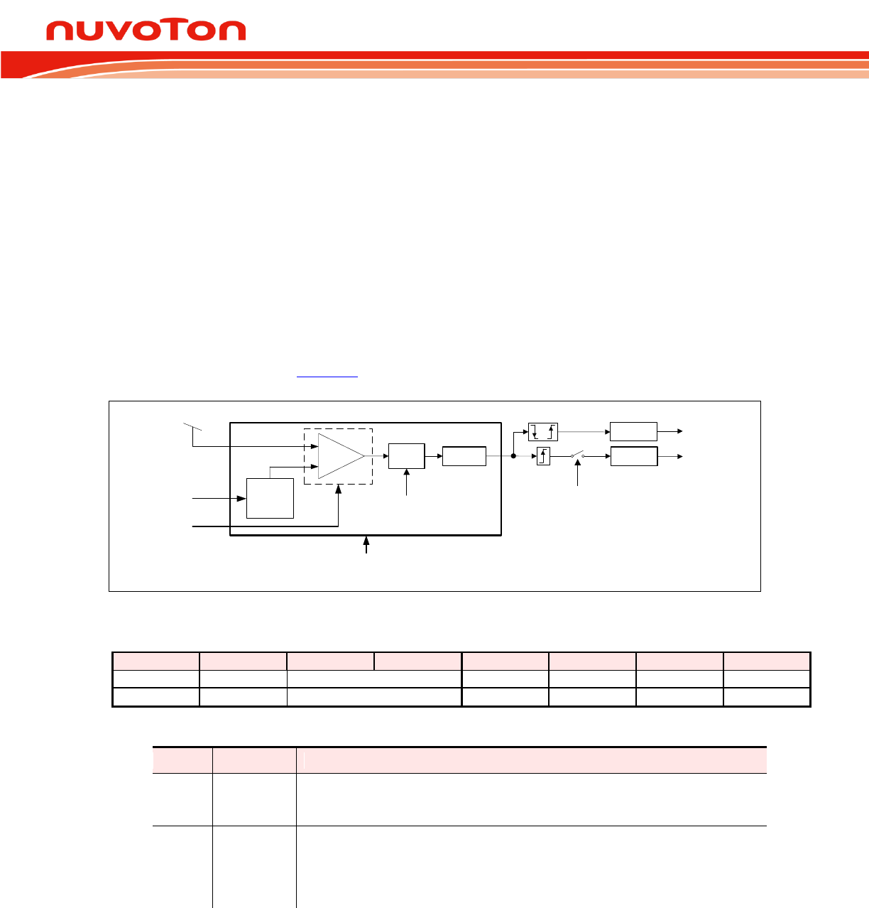
N76E003 Datasheet
Oct 28, 2016 Page 229 of 261 Rev. 1.00
reset other than power-on. This bit can be cleared by software. Note that all bits in BODCON0 is
writing protected by timed access (TA).
The N76E003 provides low power BOD mode for saving current consumption and remaining BOD
functionality with limited detection response. By setting LPBOD[1:0] (BODCON1[2:1]), the BOD circuit
can be periodically enabled to sense the power voltage nominally every 1.6 ms, 6.4 ms, or 25.6 ms. It
saves much power but also provides low-speed power voltage sensing. Note that the hysteresis
feature will disappear in low power BOD mode.
For a noise sensitive system, the N76E003 has a BOD filter which filters the power noise to avoid
BOD event triggering unconsciously. The BOD filter is enabled by default and can be disabled by
setting BODFLT (BODCON1.0) as 0 if user requires a rapid BOD response. The minimum brown-out
detect pulse width is listed in Table 24-2.
BOV[1:0]
Brownout Detection
VDD
+
-
VBOD
Voltage
Select
BODEN
BOS
BORST
Brown-out Reset
BOF Brown-out Interrupt
or
BORF
LPBOD[1:0]
BOD
Filter
BODFLT
Figure 24-1. Brown-out Detection Block Diagram
CONFIG2
7
6
5
4
3
2
1
0
CBODEN
-
CBOV[1:0]
BOIAP
CBORST
-
-
R/W
-
R/W
R/W
R/W
-
-
Factory default value: 1111 1111b
Bit
Name
Description
7
CBODEN
CONFIG brown-out detect enable
1 = Brown-out detection circuit on.
0 = Brown-out detection circuit off.
5:4
CBOV[1:0]
CONFIG brown-out voltage select
11 = VBOD is 2.2V.
10 = VBOD is 2.7V.
01 = VBOD is 3.7V.
00 = VBOD is 4.4V.

N76E003 Datasheet
Oct 28, 2016 Page 230 of 261 Rev. 1.00
Bit
Name
Description
2
CBORST
CONFIG brown-out reset enable
This bit decides whether a brown-out reset is caused by a power drop below
VBOD.
1 = Brown-out reset Enabled.
0 = Brown-out reset Disabled.
BODCON0 Brown-out Detection Control 0 (TA protected)
7
6
5
4
3
2
1
0
BODEN[1]
BOV[1:0][1]
BOF[2]
BORST[1]
BORF
BOS
R/W
R/W
R/W
R/W
R/W
R
Address: A3H Reset value: see Table 6-2. SFR Definitions and Reset Values
Bit
Name
Description
7
BODEN
Brown-out detection enable
0 = Brown-out detection circuit off.
1 = Brown-out detection circuit on.
Note that BOD output is not available until 2~3 LIRC clocks after enabling.
6:4
BOV[1:0]
Brown-out voltage select
11 = VBOD is 2.2V.
10 = VBOD is 2.7V.
01 = VBOD is 3.7V.
00 = VBOD is 4.4V.
3
BOF
Brown-out interrupt flag
This flag will be set as logic 1 via hardware after a VDD dropping below or rising
above VBOD event occurs. If both EBOD (EIE.2) and EA (IE.7) are set, a brown-out
interrupt requirement will be generated. This bit should be cleared via software.
2
BORST
Brown-out reset enable
This bit decides whether a brown-out reset is caused by a power drop below VBOD.
0 = Brown-out reset when VDD drops below VBOD Disabled.
1 = Brown-out reset when VDD drops below VBOD Enabled.
1
BORF
Brown-out reset flag
When the MCU is reset by brown-out event, this bit will be set via hardware. This
flag is recommended to be cleared via software.
0
BOS
Brown-out status
This bit indicates the VDD voltage level comparing with VBOD while BOD circuit is
enabled. It keeps 0 if BOD is not enabled.
0 = VDD voltage level is higher than VBOD or BOD is disabled.
1 = VDD voltage level is lower than VBOD.
Note that this bit is read-only.
[1] BODEN, BOV[1:0], and BORST are initialized by being directly loaded from CONFIG2 bit 7, [6:4], and 2 after
all resets.
[2] BOF reset value depends on different setting of CONFIG2 and VDD voltage level. Please check Table 24-1.
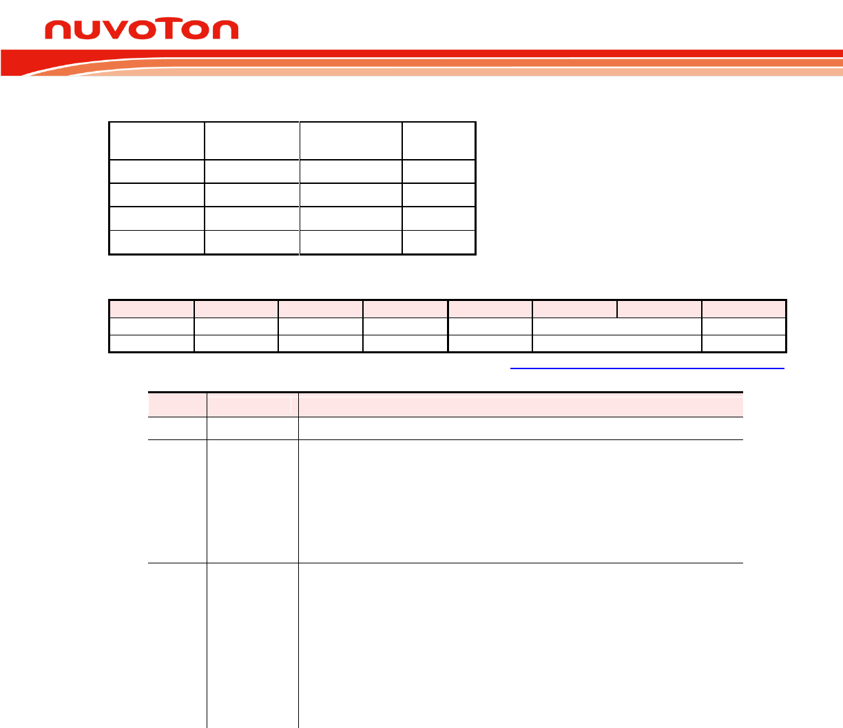
N76E003 Datasheet
Oct 28, 2016 Page 231 of 261 Rev. 1.00
Table 24-1. BOF Reset Value
CBODEN
(CONFIG2.7)
CBORST
(CONFIG2.2)
VDD Level
BOF
1
1
> VBOD always
0
1
0
< VBOD
1
1
0
> VBOD
0
0
X
X
0
BODCON1 Brown-out Detection Control 1 (TA protected)
7
6
5
4
3
2
1
0
-
-
-
-
-
LPBOD[1:0]
BODFLT
-
-
-
-
-
R/W
R/W
Address: ABH Reset value: see Table 6-2. SFR Definitions and Reset Values
Bit
Name
Description
7:3
-
Reserved
2:1
LPBOD[1:0]
Low power BOD enable
00 = BOD normal mode. BOD circuit is always enabled.
01 = BOD low power mode 1 by turning on BOD circuit every 1.6 ms
periodically.
10 = BOD low power mode 2 by turning on BOD circuit every 6.4 ms
periodically.
11 = BOD low power mode 3 by turning on BOD circuit every 25.6 ms
periodically.
0
BODFLT
BOD filter control
BOD has a filter which counts 32 clocks of FSYS to filter the power noise when
MCU runs with HIRC, or ECLK as the system clock and BOD does not
operates in its low power mode (LPBOD[1:0] = [0, 0]). In other conditions, the
filter counts 2 clocks of LIRC.
Note that when CPU is halted in Power-down mode. The BOD output is
permanently filtered by 2 clocks of LIRC.
The BOD filter avoids the power noise to trigger BOD event. This bit controls
BOD filter enabled or disabled.
0 = BOD filter Disabled.
1 = BOD filter Enabled. (Power-on reset default value.)

N76E003 Datasheet
Oct 28, 2016 Page 232 of 261 Rev. 1.00
Table 24-2. Minimum Brown-out Detect Pulse Width
BODFLT
(BODCON1.1)
BOD Operation Mode
System Clock
Source
Minimum Brown-out Detect
Pulse Width
0
Normal mode
(LPBOD[1:0] = [0,0])
Any clock source
Typ. 1s
Low power mode 1
(LPBOD[1:0] = [0,1])
Any clock source
16 (1/FLIRC)
Low power mode 2
(LPBOD[1:0] = [1,0])
Any clock source
64 (1/FLIRC)
Low power mode 3
(LPBOD[1:0] = [1,1])
Any clock source
256 (1/ FLIRC)
1
Normal mode
(LPBOD[1:0] = [0,0])
HIRC/ECLK
Normal operation: 32 (1/FSYS)
Idle mode: 32 (1/FSYS)
Power-down mode: 2 (1/FLIRC)
LIRC
2 (1/FLIRC)
Low power mode 1
(LPBOD[1:0] = [0,1])
Any clock source
18 (1/FLIRC)
Low power mode 2
(LPBOD[1:0] = [1,0])
Any clock source
66 (1/FLIRC)
Low power mode 3
(LPBOD[1:0] = [1,1])
Any clock source
258 (1/ FLIRC)
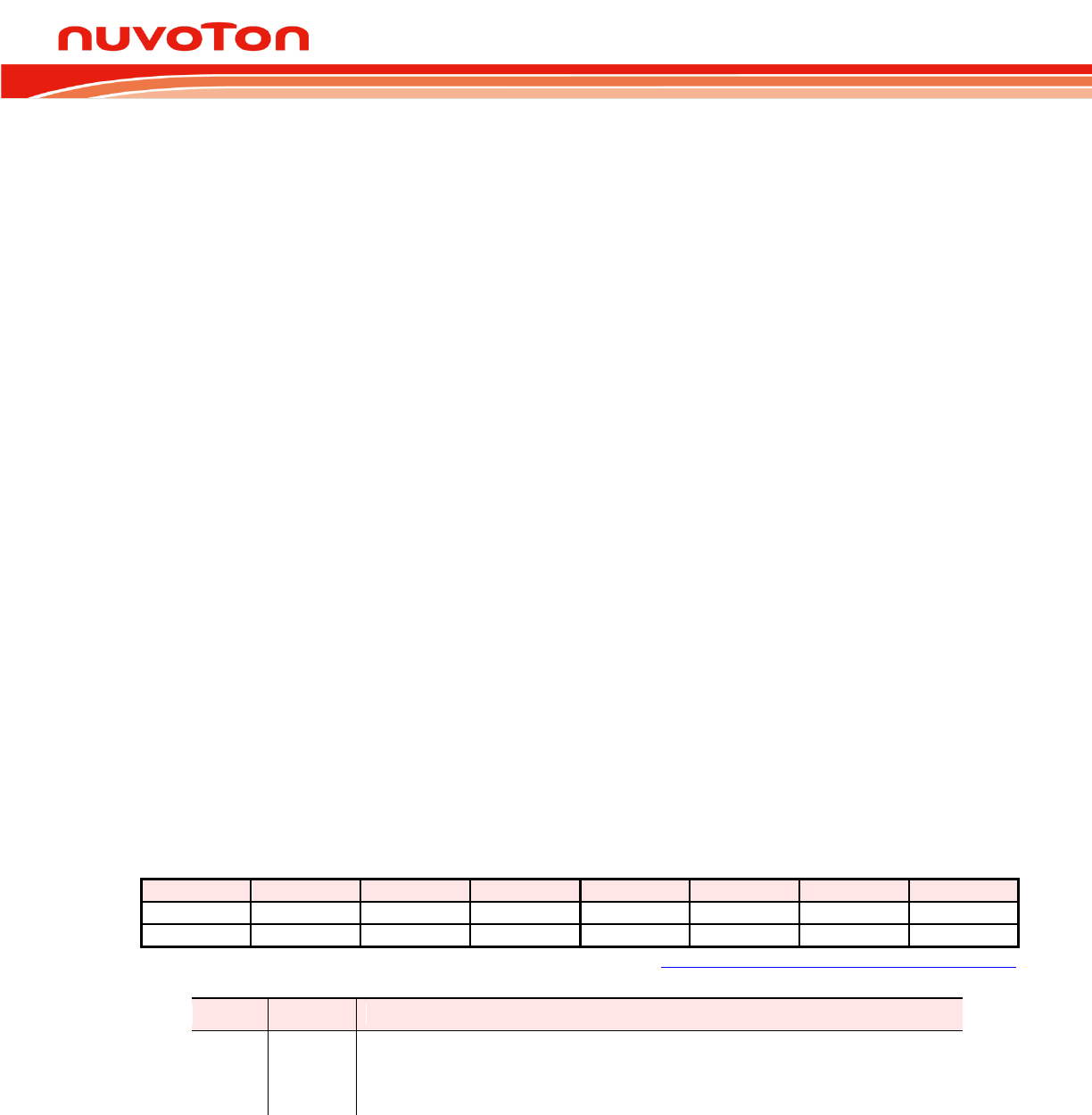
N76E003 Datasheet
Oct 28, 2016 Page 233 of 261 Rev. 1.00
25. RESET
The N76E003 has several options to place device in reset condition. It also offers the software flags to
indicate the source, which causes a reset. In general, most SFRs go to their Reset value irrespective
of the reset condition, but there are several reset source indicating flags whose state depends on the
source of reset. User can read back these flags to determine the cause of reset using software. There
are six ways of putting the device into reset state. They are power-on reset, brown-out reset, external
reset, hard fault reset, WDT reset, and software reset.
25.1 Power-On Reset
The N76E003 incorporates an internal power-on reset. During a power-on process of rising power
supply voltage VDD, the power-on reset will hold the MCU in reset mode when VDD is lower than the
voltage reference threshold. This design makes CPU not access program flash while the VDD is not
adequate performing the flash reading. If an undetermined operating code is read from the program
flash and executed, this will put CPU and even the whole system in to an erroneous state. After a
while, VDD rises above the threshold where the system can work, the selected oscillator will start and
then program code will execute from 0000H. At the same time, a power-on flag POF (PCON.4) will be
set 1 to indicate a cold reset, a power-on reset complete. Note that the contents of internal RAM will
be undetermined after a power-on. It is recommended that user gives initial values for the RAM block.
The POF is recommended to be cleared to 0 via software to check if a cold reset or warm reset
performed after the next reset occurs. If a cold reset caused by power off and on, POF will be set 1
again. If the reset is a warm reset caused by other reset sources, POF will remain 0. User may take a
different course to check other reset flags and deal with the warm reset event.
PCON Power Control
7
6
5
4
3
2
1
0
SMOD
SMOD0
-
POF
GF1
GF0
PD
IDL
R/W
R/W
-
R/W
R/W
R/W
R/W
R/W
Address: 87H Reset value: see Table 6-2. SFR Definitions and Reset Values
Bit
Name
Description
4
POF
Power-on reset flag
This bit will be set as 1 after a power-on reset. It indicates a cold reset, a power-on
reset complete. This bit remains its value after any other resets. It is
recommended that the flag be cleared via software.
25.2 Brown-Out Reset
The brown-out detection circuit is used for monitoring the VDD level during execution. When VDD drops
to the selected brown-out trigger level (VBOD), the brown-out detection logic will reset the MCU if
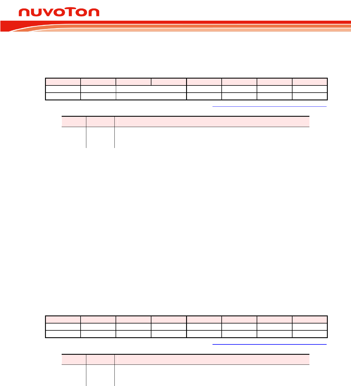
N76E003 Datasheet
Oct 28, 2016 Page 234 of 261 Rev. 1.00
BORST (BODCON0.2) setting 1. After a brown-out reset, BORF (BODCON0.1) will be set as 1 via
hardware. BORF will not be altered by any reset other than a power-on reset or brown-out reset itself.
This bit can be set or cleared by software.
BODCON0 Brown-out Detection Control 0 (TA protected)
7
6
5
4
3
2
1
0
BODEN
-
BOV[1:0]
BOF
BORST
BORF
BOS
R/W
-
R/W
R/W
R/W
R/W
R
Address: A3H Reset value: see Table 6-2. SFR Definitions and Reset Values
Bit
Name
Description
1
BORF
Brown-out reset flag
When the MCU is reset by brown-out event, this bit will be set via hardware. This
flag is recommended to be cleared via software.
25.3 External Reset and Hard Fault Reset
The external reset pin
is an input with a Schmitt trigger. An external reset is accomplished by
holding the
pin low for at least 24 system clock cycles to ensure detection of a valid hardware
reset signal. The reset circuitry then synchronously applies the internal reset signal. Thus, the reset is
a synchronous operation and requires the clock to be running to cause an external reset.
Once the device is in reset condition, it will remain as long as
pin is low. After the
high is
removed, the MCU will exit the reset state and begin code executing from address 0000H. If an
external reset applies while CPU is in Power-down mode, the way to trigger a hardware reset is
slightly different. Since the Power-down mode stops system clock, the reset signal will asynchronously
cause the system clock resuming. After the system clock is stable, MCU will enter the reset state.
There is a RSTPINF (AUXR1.6) flag, which indicates an external reset took place. After the external
reset, this bit will be set as 1 via hardware. RSTPINF will not change after any reset other than a
power-on reset or the external reset itself. This bit can be cleared via software.
AUXR1 Auxiliary Register 1
7
6
5
4
3
2
1
0
SWRF
RSTPINF
HardF
-
GF2
UART0PX
0
DPS
R/W
R/W
R/W
-
R/W
R/W
R
R/W
Address: A2H Reset value: see Table 6-2. SFR Definitions and Reset Values
Bit
Name
Description
6
RSTPINF
External reset flag
When the MCU is reset by the external reset pin, this bit will be set via hardware.
It is recommended that the flag be cleared via software.
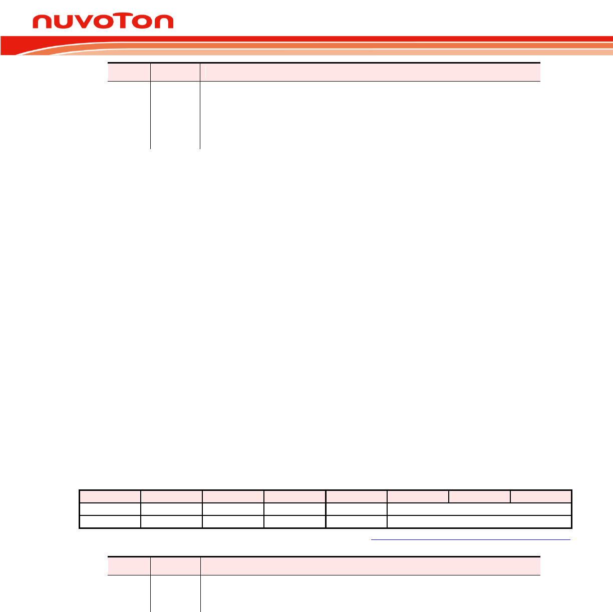
N76E003 Datasheet
Oct 28, 2016 Page 235 of 261 Rev. 1.00
Bit
Name
Description
5
HardF
Hard Fault reset flag
Once Program Counter (PC) is over flash size, MCU will be reset and this bit will
be set via hardware. It is recommended that the flag be cleared via software.
Note: If MCU run in OCD debug mode and OCDEN = 0, hard fault reset will be
disabled and only HardF flag be asserted.
25.4 Hard Fault Reset
If Program Counter (PC) is over flash size, Hard Fault reset will occur. After Hard Fault reset, HardF
(AUXR1.5) flag will be set via hardware. HardF will not change after any reset other than a power-on
reset or the Hard Fault reset itself. This bit can be cleared via software. If MCU run in OCD debug
mode and OCDEN = 0, hard fault reset will be disabled and only HardF flag be asserted.
25.5 Watchdog Timer Reset
The WDT is a free running timer with programmable time-out intervals and a dedicated internal clock
source. User can clear the WDT at any time, causing it to restart the counter. When the selected time-
out occurs but no software response taking place for a while, the WDT will reset the system directly
and CPU will begin execution from 0000H.
Once a reset due to WDT occurs, the WDT reset flag WDTRF (WDCON.3) will be set. This bit keeps
unchanged after any reset other than a power-on reset or WDT reset itself. User can clear WDTRF via
software.
WDCON Watchdog Timer Control (TA protected)
7
6
5
4
3
2
1
0
WDTR
WDCLR
WDTF
WIDPD
WDTRF
WDPS[2:0]
R/W
R/W
R/W
R/W
R/W
R/W
Address: AAH Reset value: see Table 6-2. SFR Definitions and Reset Values
Bit
Name
Description
3
WDTRF
WDT reset flag
When the MCU is reset by WDT time-out event, this bit will be set via hardware. It
is recommended that the flag be cleared via software.
25.6 Software Reset
The N76E003 provides a software reset, which allows the software to reset the whole system just
similar to an external reset, initializing the MCU as it reset state. The software reset is quite useful in
N76E003 Datasheet
Oct 28, 2016 Page 236 of 261 Rev. 1.00
the end of an ISP progress. For example, if an ISP of Boot Code updating User Code finishes, a
software reset can be asserted to re-boot CPU to execute new User Code immediately. Writing 1 to
SWRST (CHPCON.7) will trigger a software reset. Note that this bit is writing TA protection. The
instruction that sets the SWRST bit is the last instruction that will be executed before the device reset.
See demo code below.
If a software reset occurs, SWRF (AUXR.7) will be automatically set by hardware. User can check it
as the reset source indicator. SWRF keeps unchanged after any reset other than a power-on reset or
software reset itself. SWRF can be cleared via software.
CHPCON Chip Control (TA protected)
7
6
5
4
3
2
1
0
SWRST
IAPFF
-
-
-
-
BS
IAPEN
W
R/W
-
-
-
-
R/W
R/W
Address: 9FH Reset value: see Table 6-2. SFR Definitions and Reset Values
Bit
Name
Description
7
SWRST
Software reset
To set this bit as logic 1 will cause a software reset. It will automatically be cleared
via hardware after reset is finished.
AUXR1 Auxiliary Register 1
7
6
5
4
3
2
1
0
SWRF
RSTPINF
HardF
-
GF2
UART0PX
0
DPS
R/W
R/W
R/W
-
R/W
R/W
R
R/W
Address: A2H Reset value: see Table 6-2. SFR Definitions and Reset Values
Bit
Name
Description
7
SWRF
Software reset flag
When the MCU is reset via software reset, this bit will be set via hardware. It is
recommended that the flag be cleared via software.
The software demo code is listed below.
ANL AUXR1,#01111111b ;software reset flag clear
CLR EA
MOV TA,#0Aah
MOV TA,#55h
ORL CHPCON,#10000000b ;software reset
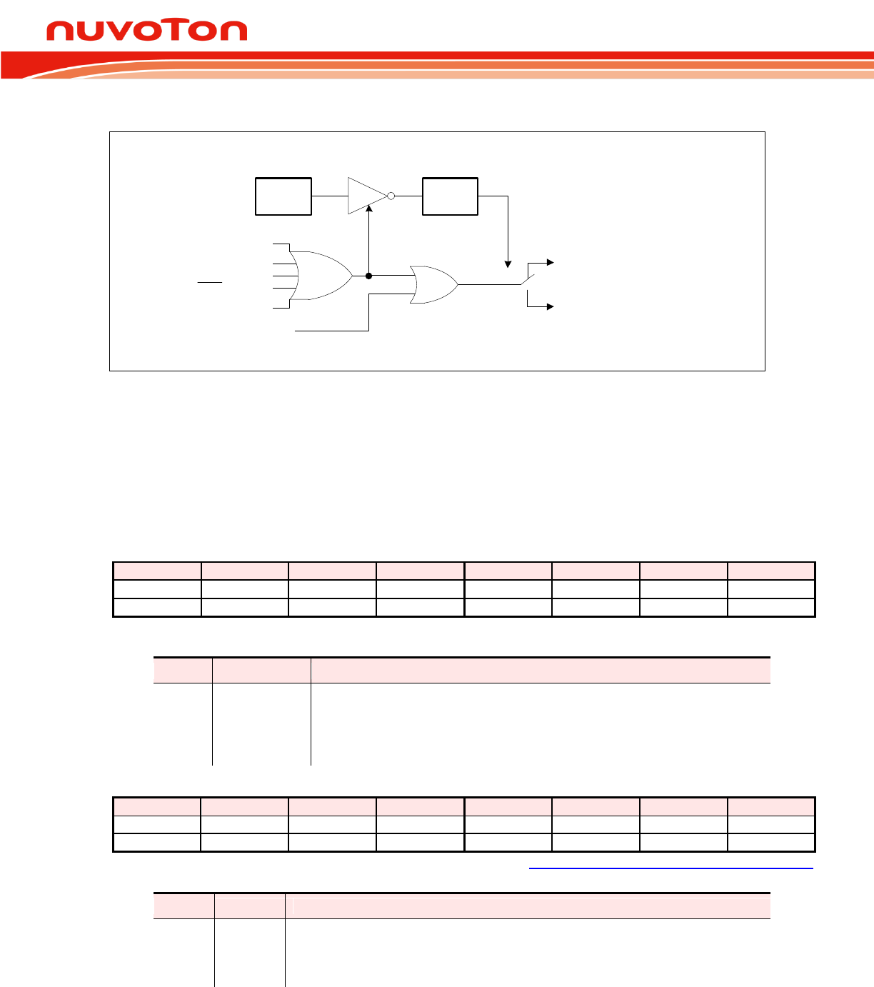
N76E003 Datasheet
Oct 28, 2016 Page 237 of 261 Rev. 1.00
25.7 Boot Select
RST pin reset
Brown-out reset
Software reset
Power-on reset Load
Reset and boot from LDROM
Reset and boot from APROM
CONFIG0.7 CHPCON.1
Watchgod Timer reset
BSCBS
BS = 0
BS = 1
Hard Fault reset
Figure 25-1. Boot Selecting Diagram
The N76E003 provides user a flexible boot selection for variant application. The SFR bit BS in
CHPCON.1 determines MCU booting from APROM or LDROM after any source of reset. If reset
occurs and BS is 0, MCU will reboot from address 0000H of APROM. Else, the CPU will reboot from
address 0000H of LDROM. Note that BS is loaded from the inverted value of CBS bit in CONFIG0.7
after all resets except software reset.
CONFIG0
7
6
5
4
3
2
1
0
CBS
-
OCDPWM
OCDEN
-
RPD
LOCK
-
R/W
-
R/W
R/W
-
R/W
R/W
-
Factory default value: 1111 1111b
Bit
Name
Description
7
CBS
CONFIG boot select
This bit defines from which block that MCU re-boots after resets except
software reset.
1 = MCU will re-boot from APROM after resets except software reset.
0 = MCU will re-boot from LDROM after resets except software reset.
CHPCON Chip Control (TA protected)
7
6
5
4
3
2
1
0
SWRST
IAPFF
-
-
-
-
BS[1]
IAPEN
W
R/W
-
-
-
-
R/W
R/W
Address: 9FH Reset value: see Table 6-2. SFR Definitions and Reset Values
Bit
Name
Description
1
BS
Boot select
This bit defines from which block that MCU re-boots after all resets.
0 = MCU will re-boot from APROM after all resets.
1 = MCU will re-boot from LDROM after all resets.

N76E003 Datasheet
Oct 28, 2016 Page 238 of 261 Rev. 1.00
[1] BS is initialized by being loaded from the inverted value of CBS bit in CONFIG0.7 after resets except software
reset. It keeps unchanged after software reset.
After the MCU is released from reset state, the hardware will always check the BS bit instead of
the CBS bit to determine from which block that the device reboots.
25.8 Reset State
The reset state besides power-on reset does not affect the on-chip RAM. The data in the RAM will be
preserved during the reset. After the power-on reset the RAM contents will be indeterminate.
After a reset, most of SFRs go to their initial values except bits, which are affected by different reset
events. See the notes of Table 6-2. SFR Definitions and Reset Values. The Program Counter is forced
to 0000H and held as long as the reset condition is applied. Note that the Stack Pointer is also reset to
07H and thus the stack contents may be effectively lost during the reset event even though the RAM
contents are not altered.
After a reset, all peripherals and interrupts are disabled. The I/O port latches resumes FFH and I/O
mode input-only.
N76E003 Datasheet
Oct 28, 2016 Page 239 of 261 Rev. 1.00
26. AUXILIARY FEATURES
26.1 Dual DPTRs
The original 8051 contains one DPTR (data pointer) only. With single DPTR, it is difficult to move data
form one address to another with wasting code size and low performance. The N76E003 provides two
data pointers. Thus, software can load both a source and a destination address when doing a block
move. Once loading, the software simply switches between DPTR and DPTR1 by the active data
pointer selection DPS (AUXR1.0) bit.
An example of 64 bytes block move with dual DPTRs is illustrated below. By giving source and
destination addresses in data pointers and activating cyclic makes block RAM data move more simple
and efficient than only one DPTR. The INC AUXR1 instruction is the shortest (2 bytes) instruction to
accomplish DPTR toggling rather than ORL or ANL. For AUXR1.1 contains a hard-wired 0, it allows
toggling of the DPS bit by incrementing AUXR1 without interfering with other bits in the register.
MOV R0,#64 ;number of bytes to move
MOV DPTR,#D_Addr ;load destination address
INC AUXR1 ;change active DPTR
MOV DPTR,#S_Addr ;load source address
LOOP:
MOVX A,@DPTR ;read source data byte
INC AUXR1 ;change DPTR to destination
MOVX @DPTR,A ;write data to destination
INC DPTR ;next destination address
INC AUXR1 ;change DPTR to source
INC DPTR ;next source address
DJNZ R0,LOOP
INC AUXR1 ;(optional) restore DPS
AUXR1 also contains a general purpose flag GF2 in its bit 3 that can be set or cleared by the user via
software.
DPL Data Pointer Low Byte
7
6
5
4
3
2
1
0
DPL[7:0]
R/W
Address: 82H reset value: 0000 0000b
Bit
Name
Description
7:0
DPL[7:0]
Data pointer low byte
This is the low byte of 16-bit data pointer. DPL combined with DPH serve as a 16-
bit data pointer DPTR to address non-scratch-pad memory or Program Memory.
DPS (DPS.0) bit decides which data pointer, DPTR or DPTR1, is activated.
N76E003 Datasheet
Oct 28, 2016 Page 240 of 261 Rev. 1.00
DPH Data Pointer High Byte
7
6
5
4
3
2
1
0
DPH[7:0]
R/W
Address: 83H reset value: 0000 0000b
Bit
Name
Description
7:0
DPH[7:0]
Data pointer high byte
This is the high byte of 16-bit data pointer. DPH combined with DPL serve as a
16-bit data pointer DPTR to address non-scratch-pad memory or Program
Memory. DPS (DPS.0) bit decides which data pointer, DPTR or DPTR1, is
activated.
AUXR1 Auxiliary Register 1
7
6
5
4
3
2
1
0
SWRF
RSTPINF
HardF
-
GF2
UART0PX
0
DPS
R/W
R/W
R/W
-
R/W
R/W
R
R/W
Address: A2H reset value: see Table 6-2. SFR Definitions and Reset Values
Bit
Name
Description
3
GF2
General purpose flag 2
The general purpose flag that can be set or cleared by the user via software.
1
0
Reserved
This bit is always read as 0.
0
DPS
Data pointer select
0 = Data pointer 0 (DPTR) is active by default.
1 = Data pointer 1 (DPTR1) is active.
After DPS switches the activated data pointer, the previous inactivated data
pointer remains its original value unchanged.
26.2 96-bit UID
Before shipping out, each N76E003 chip was factory pre-programmed with a 96-bit width serial number, which is
guaranteed to be unique. The serial number is called UID. The user can read the unique code only by IAP
command. Please see IAP Commands.

N76E003 Datasheet
Oct 28, 2016 Page 241 of 261 Rev. 1.00
27. ON-CHIP-DEBUGGER (OCD)
27.1 Functional Description
The N76E003 is embedded in an on-chip-debugger (OCD) providing developers with a low cost
method for debugging user code, which is available on each package. The OCD gives debug
capability of complete program flow control with eight hardware address breakpoints, single step, free
running, and non-intrusive commands for memory access. The OCD system does not occupy any
locations in the memory map and does not share any on-chip peripherals.
When the OCDEN (CONFIG0.4) is programmed as 0 and LOCK (CONFIG0.1) remains un-
programmed as 1, the OCD is activated. The OCD cannot operate if chip is locked. The OCD system
uses a two-wire serial interface, OCDDA and OCDCK, to establish communication between the target
device and the controlling debugger host. OCDDA is an input/output pin for debug data transfer and
OCDCK is an input pin for synchronization with OCDDA data. The P2.0/
pin is also necessary for
OCD mode entry and exit. The N76E003 supports OCD with Flash Memory control path by ICP writer
mode, which shares the same three pins of OCD interface.
The N76E003 uses OCDDA, OCDCK, and P2.0/
pins to interface with the OCD system. When
designing a system where OCD will be used, the following restrictions must be considered for correct
operation:
1. If P2.0/
is configured as external reset pin, it cannot be connected directly to VDD and any
external capacitors connected must be removed.
2. If P2.0/
is configured as input pin P2.0, any external input source must be isolated.
3. All external reset sources must be disconnected.
4. Any external component connected on OCDDA and OCDCK must be isolated.
27.2 Limitation of OCD
The N76E003 is a fully-featured microcontroller that multiplexes several functions on its limited I/O
pins. Some device functionality must be sacrificed to provide resources for OCD system. The OCD
has the following limitations:
1. The P2.0/
pin needs to be used for OCD mode selection. Therefore, neither P2.0 input nor an
external reset source can be emulated.

N76E003 Datasheet
Oct 28, 2016 Page 242 of 261 Rev. 1.00
2. The OCDDA pin is physically located on the same pin P1.6. Therefore, neither its I/O function nor
shared multi-functions can be emulated.
3. The OCDCK pin is physically located on the same pin as P0.2. Therefore, neither its I/O function
nor shared multi-functions can be emulated.
4. When the system is in Idle or Power-down mode, it is invalid to perform any accesses because
parts of the device may not be clocked. A read access could return garbage or a write access might
not succeed.
5. HIRC cannot be turned off because OCD uses this clock to monitor its internal status. The
instruction that turns off HIRC affects nothing if executing under debug mode. When CPU enters its
Power-down mode under debug mode, HIRC keeps turning on.
The N76E003 OCD system has another limitation that non-intrusive commands cannot be executed at
-intrusive commands allow a user to read or write
MCU memory locations or access status and control registers with the debug controller. A reading or
writing memory or control register space is allowed only when MCU is under halt condition after a
matching of the hardware address breakpoint or a single step running.
CONFIG0
7
6
5
4
3
2
1
0
CBS
-
OCDPWM
OCDEN
-
RPD
LOCK
-
R/W
-
R/W
R/W
-
R/W
R/W
-
Factory default value: 1111 1111b
Bit
Name
Description
5
OCDPWM
PWM output state under OCD halt
This bit decides the output state of PWM when OCD halts CPU.
1 = Tri-state pins those are used as PWM outputs.
0 = PWM continues.
Note that this bit is valid only when the corresponding PIO bit of PWM
channel is set as 1.
4
OCDEN
OCD enable
1 = OCD Disabled.
0 = OCD Enabled.
Note: If MCU run in OCD debug mode and OCDEN = 0, hard fault reset will
be disabled and only HardF flag be asserted.
N76E003 Datasheet
Oct 28, 2016 Page 243 of 261 Rev. 1.00
28. CONFIG BYTES
The N76E003 has several hardware configuration bytes, called CONFIG, those are used to configure
the hardware options such as the security bits, system clock source, and so on. These hardware
options can be re-configured through the parallel Writer, In-Circuit-Programming (ICP), or In-
Application-Programming (IAP). Several functions, which are defined by certain CONFIG bits are also
available to be re-configured by SFR. Therefore, there is a need to load such CONFIG bits into
respective SFR bits. Such loading will occur after resets. These SFR bits can be continuously
CONFIG bits marked as “-“should always keep un-programmed.
CONFIG0
7
6
5
4
3
2
1
0
CBS
-
OCDPWM
OCDEN
-
RPD
LOCK
-
R/W
-
R/W
R/W
-
R/W
R/W
-
Factory default value: 1111 1111b
Bit
Name
Description
7
CBS
CONFIG boot select
This bit defines from which block that MCU re-boots after resets except
software reset.
1 = MCU will re-boot from APROM after resets except software reset.
0 = MCU will re-boot from LDROM after resets except software reset.
5
OCDPWM
PWM output state under OCD halt
This bit decides the output state of PWM when OCD halts CPU.
1 = Tri-state pins those are used as PWM outputs.
0 = PWM continues.
Note that this bit is valid only when the corresponding PIO bit of PWM
channel is set as 1.
4
OCDEN
OCD enable
1 = OCD Disabled.
0 = OCD Enabled.
Note: If MCU run in OCD debug mode and OCDEN = 0, hard fault reset will
be disabled and only Hard F flag be asserted.
3
-
Reserved
2
RPD
Reset pin disable
1 = The reset function of P2.0/nRST pin Enabled. P2.0/nRST functions as the
external reset pin.
0 = The reset function of P2.0/nRST pin Disabled. P2.0/nRST functions as an
input-only pin P2.0.
N76E003 Datasheet
Oct 28, 2016 Page 244 of 261 Rev. 1.00
Bit
Name
Description
1
LOCK
Chip lock enable
1 = Chip is unlocked. Flash Memory is not locked. Their contents can be read
out through a parallel Writer/ICP programmer.
0 = Chip is locked. Whole Flash Memory is locked. Their contents read
through a parallel Writer or ICP programmer will be all blank (FFH).
Programming to Flash Memory is invalid.
Note that CONFIG bytes are always unlocked and can be read. Hence, once
the chip is locked, the CONFIG bytes cannot be erased or programmed
individually. The only way to disable chip lock is execute whole chip .
However, all data within the Flash Memory and CONFIG bits will be erased
when this procedure is executed.
If the chip is locked, it does not alter the IAP function.
CHPCON
CONFIG0
CBS
7
-
6
OCDPWM
5
OCDEN
4
-
3
RPD
2
LOCK
1
-
0
SWRST
7
IAPFF
6
-
5
-
4
-
3
-
2
BS
1
IAPEN
0
Software reset does not reload
Figure 28-1. CONFIG0 Any Reset Reloading
CONFIG1
7
6
5
4
3
2
1
0
-
-
-
-
-
LDSIZE[2:0]
-
-
-
-
-
R/W
Factory default value: 1111 1111b
Bit
Name
Description
2:0
LDSIZE[2:0]
LDROM size select
Part number is N76E003:
111 = No LDROM. APROM is 18K Bytes.
110 = LDROM is 1K Bytes. APROM is 17K Bytes.
101 = LDROM is 2K Bytes. APROM is 16K Bytes.
100 = LDROM is 3K Bytes. APROM is 15K Bytes.
0xx = LDROM is 4K Bytes. APROM is 14K Bytes.
CONFIG2
7
6
5
4
3
2
1
0
CBODEN
-
CBOV[1:0]
BOIAP
CBORST
-
-
R/W
-
R/W
R/W
R/W
-
-
Factory default value: 1111 1111b
Bit
Name
Description
7
CBODEN
CONFIG brown-out detect enable
1 = Brown-out detection circuit on.
0 = Brown-out detection circuit off.
6
-
Reserved
N76E003 Datasheet
Oct 28, 2016 Page 245 of 261 Rev. 1.00
Bit
Name
Description
5:4
CBOV[1:0]
CONFIG brown-out voltage select
11 = VBOD is 2.2V.
10 = VBOD is 2.7V.
01 = VBOD is 3.7V.
00 = VBOD is 4.4V.
3
BOIAP
Brown-out inhibiting IAP
This bit decides whether IAP erasing or programming is inhibited by brown-out
status. This bit is valid only when brown-out detection is enabled.
1 = IAP erasing or programming is inhibited if VDD is lower than VBOD.
0 = IAP erasing or programming is allowed under any workable VDD.
2
CBORST
CONFIG brown-out reset enable
This bit decides whether a brown-out reset is caused by a power drop below
VBOD.
1 = Brown-out reset Enabled.
0 = Brown-out reset Disabled.
BODCON0
CONFIG2
CBODEN
7
CBOV[1:0]
654
BOIAP
3
CBORST
2
-
1
-
0
BODEN
7
BOV[1:0]
654
BOF
3
BORST
2
BORF
1
BOS
0
-
-
Figure 28-2. CONFIG2 Power-On Reset Reloading
CONFIG4
7
6
5
4
3
2
1
0
WDTEN[3:0]
-
-
-
-
R/W
-
-
-
-
Factory default value: 1111 1111b
Bit
Name
Description
7:4
WDTEN[3:0]
WDT enable
This field configures the WDT behavior after MCU execution.
1111 = WDT is Disabled. WDT can be used as a general purpose timer via
software control.
0101 = WDT is Enabled as a time-out reset timer and it stops running during
Idle or Power-down mode.
Others = WDT is Enabled as a time-out reset timer and it keeps running during
Idle or Power-down mode.
3:0
-
Reserved

N76E003 Datasheet
Oct 28, 2016 Page 246 of 261 Rev. 1.00
29. IN-CIRCUIT-PROGRAMMING (ICP)
The Flash Memory can -Circuit-If the product is just under
development or the end product needs firmware updating in the hand of an end customer, the
hardware programming mode will make repeated programming difficult and inconvenient. ICP method
makes it easy and possible without removing the microcontroller from the system. ICP mode also
allows customers to manufacture circuit boards with un-programmed devices. Programming can be
done after the assembly process allowing the device to be programmed with the most recent firmware
or a customized firmware.
There are three signal pins,
, ICPDA, and ICPCK, involved in ICP function.
is used to enter
or exit ICP mode. ICPDA is the data input and output pin. ICPCK is the clock input pin, which
synchronizes the data shifted in to or out from MCU under programming. User should leave these
three pins plus VDD and GND pins on the circuit board to make ICP possible.
Nuvoton provides ICP tool for N76E003, which enables user to easily perform ICP through Nuvoton
ICP programmer. The ICP programmer developed by Nuvoton has been optimized according to the
electric characteristics of MCU. It also satisfies the stability and efficiency during production progress.
For more details, please visit Nuvoton 8-bit Microcontroller website: Nuvoton 80C51 Microcontroller
Technical Support.

N76E003 Datasheet
Oct 28, 2016 Page 247 of 261 Rev. 1.00
30. INSTRUCTION SET
The N76E003 executes all the instructions of the standard 80C51 family fully compatible with MCS-51.
However, the timing of each instruction is different for it uses high performance 1T 8051 core. The
architecture eliminates redundant bus states and implements parallel execution of fetching, decode,
and execution phases. The N76E003 uses one clock per machine-cycle. It leads to performance
improvement of rate 8.1 (in terms of MIPS) with respect to traditional 12T 80C51 device working at the
same clock frequency. However, the real speed improvement seen in any system will depend on the
instruction mix.
All instructions are coded within an 8-bit field called an OPCODE. This single byte should be fetched
from Program Memory. The OPCODE is decoded by the CPU. It determines what action the CPU will
take and whether more operation data is needed from memory. If no other data is needed, then only
one byte was required. Thus the instruction is called a one byte instruction. In some cases, more data
is needed, which is two or three byte instructions.
Table 30-1 lists all instructions for details. The note of the instruction set and addressing modes are
shown below.
Rn (n = 0~7) Register R0 to R7 of the currently selected Register Bank.
Direct 8-bIt could be an internal data RAM
location
(00H to 7FH) or an SFR (80H to FFH).
@RI (I = 0, 1) 8-bit internal data RAM location (00H to FFH) addressed indirectly
through re-
gister R0 or R1.
#data 8-bit constant included in the instruction.
#data16 16-bit constant included in the instruction.
Addr16 16-bit destination address. Used by LCALL and LJMP. A branch can
be any-
where within the Program Memory address space.
Addr11 11-bit destination address. Used by ACALL and AJMP. The branch will
be
within the same 2K-Byte page of Program Memory as the first byte of
the following instruction.
Rel -bit offset Byte. Used by SJMP and all
conditional
branches. The range is -128 to +127 Bytes relative to first byte of the
following
instruction.
Bit Direct addressed bit in internal data RAM or SFR.

N76E003 Datasheet
Oct 28, 2016 Page 248 of 261 Rev. 1.00
Table 30-1. Instruction Set
Instruction
OPCODE
Bytes
Clock Cycles
N76E003 V.S.
Tradition 80C51
Speed Ratio
NOP
00
1
1
12
ADD A, Rn
28~2F
1
2
6
ADD A, direct
25
2
3
4
ADD A, @Ri
26, 27
1
4
3
ADD A, #data
24
2
2
6
ADDC A, Rn
38~3F
1
2
6
ADDC A, direct
35
2
3
4
ADDC A, @Ri
36, 37
1
4
3
ADDC A, #data
34
2
2
6
SUBB A, Rn
98~9F
1
2
6
SUBB A, direct
95
2
3
4
SUBB A, @Ri
96, 97
1
4
3
SUBB A, #data
94
2
2
6
INC A
04
1
1
12
INC Rn
08~0F
1
3
4
INC direct
05
2
4
3
INC @Ri
06, 07
1
5
2.4
INC DPTR
A3
1
1
24
DEC A
14
1
1
12
DEC Rn
18~1F
1
3
4
DEC direct
15
2
4
3
DEC @Ri
16, 17
1
5
2.4
MUL AB
A4
1
4
12
DIV AB
84
1
4
12
DA A
D4
1
1
12
ANL A, Rn
58~5F
1
2
6
ANL A, direct
55
2
3
4
ANL A, @Ri
56, 57
1
4
3
ANL A, #data
54
2
2
6
ANL direct, A
52
2
4
3
ANL direct, #data
53
3
4
6
ORL A, Rn
48~4F
1
2
6
ORL A, direct
45
2
3
4
ORL A, @Ri
46, 47
1
4
3
ORL A, #data
44
2
2
6
ORL direct, A
42
2
4
3
ORL direct, #data
43
3
4
6
XRL A, Rn
68~6F
1
2
6
XRL A, direct
65
2
3
4
XRL A, @Ri
66, 67
1
4
3

N76E003 Datasheet
Oct 28, 2016 Page 249 of 261 Rev. 1.00
Table 30-1. Instruction Set
Instruction
OPCODE
Bytes
Clock Cycles
N76E003 V.S.
Tradition 80C51
Speed Ratio
XRL A, #data
64
2
2
6
XRL direct, A
62
2
4
3
XRL direct, #data
63
3
4
6
CLR A
E4
1
1
12
CPL A
F4
1
1
12
RL A
23
1
1
12
RLC A
33
1
1
12
RR A
03
1
1
12
RRC A
13
1
1
12
SWAP A
C4
1
1
12
MOV A, Rn
E8~EF
1
1
12
MOV A, direct
E5
2
3
4
MOV A, @Ri
E6, E7
1
4
3
MOV A, #data
74
2
2
6
MOV Rn, A
F8~FF
1
1
12
MOV Rn, direct
A8~AF
2
4
6
MOV Rn, #data
78~7F
2
2
6
MOV direct, A
F5
2
2
6
MOV direct, Rn
88~8F
2
3
8
MOV direct, direct
85
3
4
6
MOV direct, @Ri
86, 87
2
5
4.8
MOV direct, #data
75
3
3
8
MOV @Ri, A
F6, F7
1
3
4
MOV @Ri, direct
A6, A7
2
4
6
MOV @Ri, #data
76, 77
2
3
6
MOV DPTR, #data16
90
3
3
8
MOVC A, @A+DPTR
93
1
4
6
MOVC A, @A+PC
83
1
4
6
MOVX A, @Ri[1]
E2, E3
1
5
4.8
MOVX A, @DPTR[1]
E0
1
4
6
MOVX @Ri, A[1]
F2, F3
1
6
4
MOVX @DPTR, A[1]
F0
1
5
4.8
PUSH direct
C0
2
4
6
POP direct
D0
2
3
8
XCH A, Rn
C8~CF
1
2
6
XCH A, direct
C5
2
3
4
XCH A, @Ri
C6, C7
1
4
3
XCHD A, @Ri
D6, D7
1
5
2.4
CLR C
C3
1
1
12
CLR bit
C2
2
4
3

N76E003 Datasheet
Oct 28, 2016 Page 250 of 261 Rev. 1.00
Table 30-1. Instruction Set
Instruction
OPCODE
Bytes
Clock Cycles
N76E003 V.S.
Tradition 80C51
Speed Ratio
SETB C
D3
1
1
12
SETB bit
D2
2
4
3
CPL C
B3
1
1
12
CPL bit
B2
2
4
3
ANL C, bit
82
2
3
8
ANL C, /bit
B0
2
3
8
ORL C, bit
72
2
3
8
ORL C, /bit
A0
2
3
8
MOV C, bit
A2
2
3
4
MOV bit, C
92
2
4
6
ACALL addr11
11, 31, 51, 71,
91, B1, D1, F1[2]
2
4
6
LCALL addr16
12
3
4
6
RET
22
1
5
4.8
RETI
32
1
5
4.8
AJMP addr11
01, 21, 41, 61,
81, A1, C1, E1[3]
2
3
8
LJMP addr16
02
3
4
6
SJMP rel
80
2
3
8
JMP @A+DPTR
73
1
3
8
JZ rel
60
2
3
8
JNZ rel
70
2
3
8
JC rel
40
2
3
8
JNC rel
50
2
3
8
JB bit, rel
20
3
5
4.8
JNB bit, rel
30
3
5
4.8
JBC bit, rel
10
3
5
4.8
CJNE A, direct, rel
B5
3
5
4.8
CJNE A, #data, rel
B4
3
4
6
CJNE Rn, #data, rel
B8~BF
3
4
6
CJNE @Ri, #data, rel
B6, B7
3
6
4
DJNZ Rn, rel
D8~DF
2
4
6
DJNZ direct, rel
D5
3
5
4.8
[1] The N76E003 does not have external memory bus. MOVX instructions are used to access
internal XRAM.
[2] The most three significant bits in the 11-bit address [A10:A8] decide the ACALL hex code.
The code will be [A10,A9,A8,1,0,0,0,1].
[3] The most three significant bits in the 11-bit address [A10:A8] decide the AJMP hex code.
The code will be [A10,A9,A8,0,0,0,0,1].
N76E003 Datasheet
Oct 28, 2016 Page 251 of 261 Rev. 1.00
31. ELECTRICAL CHARACTERISTICS
31.1 Absolute Maximum Ratings
Parameter
Rating
Unit
Operating temperature under bias (TA)
-40 to +105
C
Storage temperature range
-55 to +150
C
Voltage on VDD pin to GND pin
-0.3 to +6.3
V
Voltage on any other pin to GND pin
-0.3 to (VDD+0.3)
V
Stresses at
to the device. It is a stress rating only and functional operation of the device at these or any other
conditions above those indicated in the operational sections of this specification is not implied.
Exposure to absolute maximum rating conditions may affect device reliability.
31.2 D.C. Electrical Characteristics
Table 31-1. D.C. Electrical Characteristics
(VDD VSS = 2.4 ~ 5.5 V, TA = 25 C)
Symbol
Parameter
Condition
Min.
Typ.
Max.
Unit
Supply voltage
VDD
Operating voltage
F = 0 to 16 MHz
2.4
-
5.5
V
I/O
VIL
Input low voltage
(I/O with TTL input)
VSS-0.3
-
0.2VDD-0.1
V
VIL1
Input low voltage
(I/O with Schmitt trigger input,
,
and XIN)
VSS-0.3
-
0.3VDD
V
VIH
Input high voltage
(I/O with TTL input)
0.2VDD+0.9
-
VDD+0.3
V
VIH1
Input high voltage
(I/O with Schmitt trigger input and
XIN)
0.7VDD
-
VDD+0.3
V
VIH2
Input high voltage (
)
0.8VDD
-
VDD+0.3
V
VOL
Output low voltage[1]
(Normal sink current strength, all
modes except input-only)
VDD = 5.5 V, IOL = 15 mA
-
-
0.4
V
VDD = 4.5 V, IOL = 13 mA
-
-
0.4
VDD = 3.0 V, IOL = 9 mA
-
-
0.4
VDD = 2.4 V, IOL = 7 mA
-
-
0.4

N76E003 Datasheet
Oct 28, 2016 Page 252 of 261 Rev. 1.00
Symbol
Parameter
Condition
Min.
Typ.
Max.
Unit
VOH
Output high voltage
(quasi-bidirectional mode)
VDD = 5.5 V, IOH = - 590 uA
2.4
-
-
V
VDD = 4.5 V, IOH = - 380
2.4
-
-
VDD = 3.0 V, IOH = - 100
2.4
-
-
VDD = 2.4 V, IOH = - 40
2.0
-
-
VOH1
Output high voltage
(push-pull mode)
VDD = 5.5 V, IOH = - 20 mA
2.4
-
-
V
VDD = 4.5 V, IOH = - 13 mA
2.4
-
-
VDD = 3.0 V, IOH = - 3.5 mA
2.4
-
-
VDD = 2.4 V, IOH = - 2 mA
2.0
-
-
IIL
Logical 0 input current
(quasi-bidirectional mode)
VDD = 5.5 V, VIN = 0.4 V
-
-
-50
ITL
Logical 1-to-0 transition current[2]
(quasi-bidirectional mode)
VDD = 5.5 V
--
-
-650
ILI
Input leakage current
(open-drain or input-only mode)
-
1
±10
RRST
pin internal pull-low resistor
50
-
600
Supply current
IDD
Normal operating current[3]
HIRC
-
3.3
3.9
mA
LIRC
-
170
240
IIDL
Idle mode current
HIRC
2.2
2.6
mA
LIRC
-
160
230
IPD
Power-down mode current (BOD
off)
TA = 25 ℃
-
6
8
TA = - 40 ℃ ~ +105 ℃
-
20
40
[1] Under steady state (non-transient) conditions, IOL must be externally limited as follows,
Maximum IOL per port pin: 15mA
Maximum total IOL for all outputs: 100mA
[2] Pins of all ports in quasi-bidirectional mode source a transition current when they are being externally driven
from 1 to 0. The transition current reaches its maximum value when VIN is approximately 2V.
[3]
quasi-bidirectional mode.
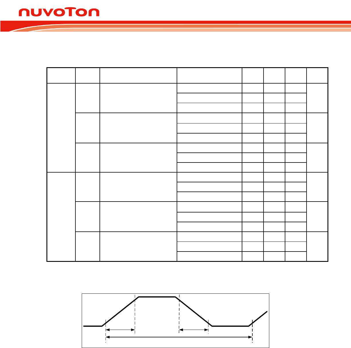
N76E003 Datasheet
Oct 28, 2016 Page 253 of 261 Rev. 1.00
31.3 A.C. Electrical Characteristics
Table 31-2. I/O Slew Rate A.C. Electrical Characteristics
PxSR.n
bit value
Symbol
Parameter
Condition
Min.
Typ.
Max.
Unit
0
FOUT
Maximum output frequency[1]
VDD = 5.0 V, CL = 30 pF
-
34
-
MHz
VDD = 3.3 V, CL = 30 pF
-
22.5
-
VDD = 2.4 V, CL = 30 pF
-
12.8
-
TR
Output low to high rising time
VDD = 5.0 V, CL = 30 pF
-
9.7
-
ns
VDD = 3.3 V, CL = 30 pF
-
12.5
-
VDD = 2.4 V, CL = 30 pF
-
16.4
-
TF
Output high to low falling time
VDD = 5.0 V, CL = 30 pF
-
6.6
-
ns
VDD = 3.3 V, CL = 30 pF
-
9.0
-
VDD = 2.4 V, CL = 30 pF
-
12.3
-
1
FOUT
Maximum output frequency[1]
VDD = 5.0 V, CL = 30 pF
-
39
-
MHz
VDD = 3.3 V, CL = 30 pF
-
27.5
-
VDD = 2.4 V, CL = 30 pF
-
17
-
TR
Output low to high rising time
VDD = 5.0 V, CL = 30 pF
-
9.5
-
ns
VDD = 3.3 V, CL = 30 pF
-
12.1
-
VDD = 2.4 V, CL = 30 pF
-
16
-
TF
Output high to low falling time
VDD = 5.0 V, CL = 30 pF
-
4.7
-
ns
VDD = 3.3 V, CL = 30 pF
-
6.2
-
VDD = 2.4 V, CL = 30 pF
-
8.3
-
[1] Maximum output frequency is achieved if ((TR + TF
below.
TRTF
T = 1/FOUT
10%
90% 90%
10%
Figure 31-1. I/O A.C. Characteristics Definition
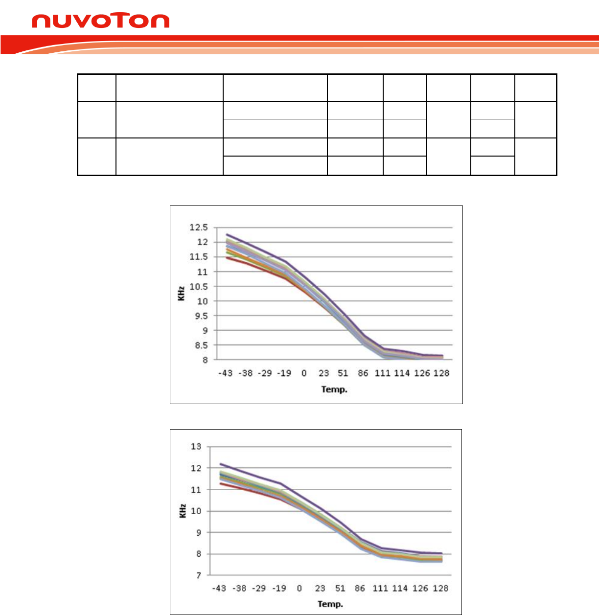
N76E003 Datasheet
Oct 28, 2016 Page 254 of 261 Rev. 1.00
Table 31-3. Internal Oscillator A.C. Electrical Characteristics
Symbol
Parameter
Condition
Frequency
Deviation
Min.
Typ.
Max.
Unit
FHIRC
High-speed 16 MHz
oscillator frequency
(HIRC)
TA = - 10℃ ~ +70℃
± 1 %
15.84
16
16.16
MHz
TA = - 40℃ ~ +105℃
± 2 %
15.68
16.32
FLIRC
Low-speed 10 kHz
oscillator frequency
(LIRC)
TA = + 25 ℃
± 10 %
9
10
11
kHz
TA = - 40 ℃ ~ +105 ℃[1]
± 35 %
6.5
13.5
[1] This value base on characterization results, not from product test.
Following shows LIRC value under full temperature condition:
Figure 31-2 LIRC deviation under VDD = 5.5 V
Figure 31-3 LIRC deviation under VDD = 2.4 V
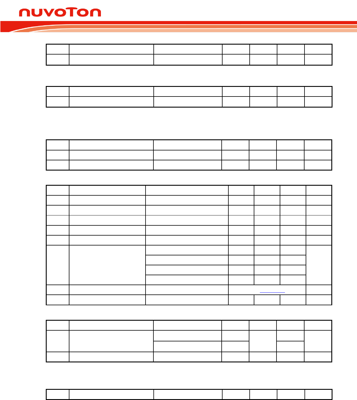
N76E003 Datasheet
Oct 28, 2016 Page 255 of 261 Rev. 1.00
Table 31-4. Power-Down Wake-Up A.C. Electrical Characteristics
Symbol
Parameter
Condition
Min.
Typ.
Max.
Unit
TPDWK
Power-down wake-up time
HIRC
-
30
-
Table 31-5. External Reset Pin A.C. Electrical Characteristics
Symbol
Parameter
Condition
Min.
Typ.
Max.
Unit
TRST
pin de-bounce timing
-
24/FSYS
450
31.4 Analog Electrical Characteristics
Table 31-6. POR Electrical Characteristics
Symbol
Parameter
Condition
Min.
Typ.
Max.
Unit
VPOR
Power-on reset voltage
1.3
1.4
1.5
V
TPORRD
Power-on reset release delay
-
5.5
-
ms
Table 31-7. BOD Electrical Characteristics
Symbol
Parameter
Condition
Min.
Typ.
Max.
Unit
VBOD0
Brown-out threshold 4.4V
BOV[1:0] = [0,0]
4.25
4.4
4.55
V
VBOD1
Brown-out threshold 3.7V
BOV[1:0] = [0,1]
3.55
3.7
3.85
V
VBOD2
Brown-out threshold 2.7V
BOV[1:0] = [1,0]
2.60
2.7
2.80
V
VBOD3
Brown-out threshold 2.2V
BOV[1:0] = [1,1]
2.10
2.2
2.30
V
VBODHYS
Brown-out hysteresis
LPBOD[1:0] = [0,0] only
-
50
200
mV
IBOD
Brown-out quiescent current
VDD = 5V, LPBOD[1:0] = [0,0]
-
147
184
A
VDD = 5V, LPBOD[1:0] = [0,1]
-
19
24
VDD = 5V, LPBOD[1:0] = [1,0]
-
5
7
VDD = 5V, LPBOD[1:0] = [1,1]
-
3
4
TBOD
Brown-out detect pulse width
See Table 24-2
-
TBODEN
Brown-out enable time
2
-
3
1/FLIRC
Table 31-8. Band-gap Electrical Characteristics
Symbol
Parameter
Condition
Min.
Typ.
Max.
Unit
VBG
Band-gap voltage
TA = + 25 ℃ (4%)
1.17
1.22
1.27
V
TA = +10 ℃ ~ +85 ℃[1]
1.14
1.3
TBGEN
Band-gap enable time
1
-
2
1/FLIRC
[1] This value base on characterization results, not from product test.
Table 31-9. ADC Electrical Characteristics
Symbol
Parameter
Condition
Min.
Typ.
Max.
Unit
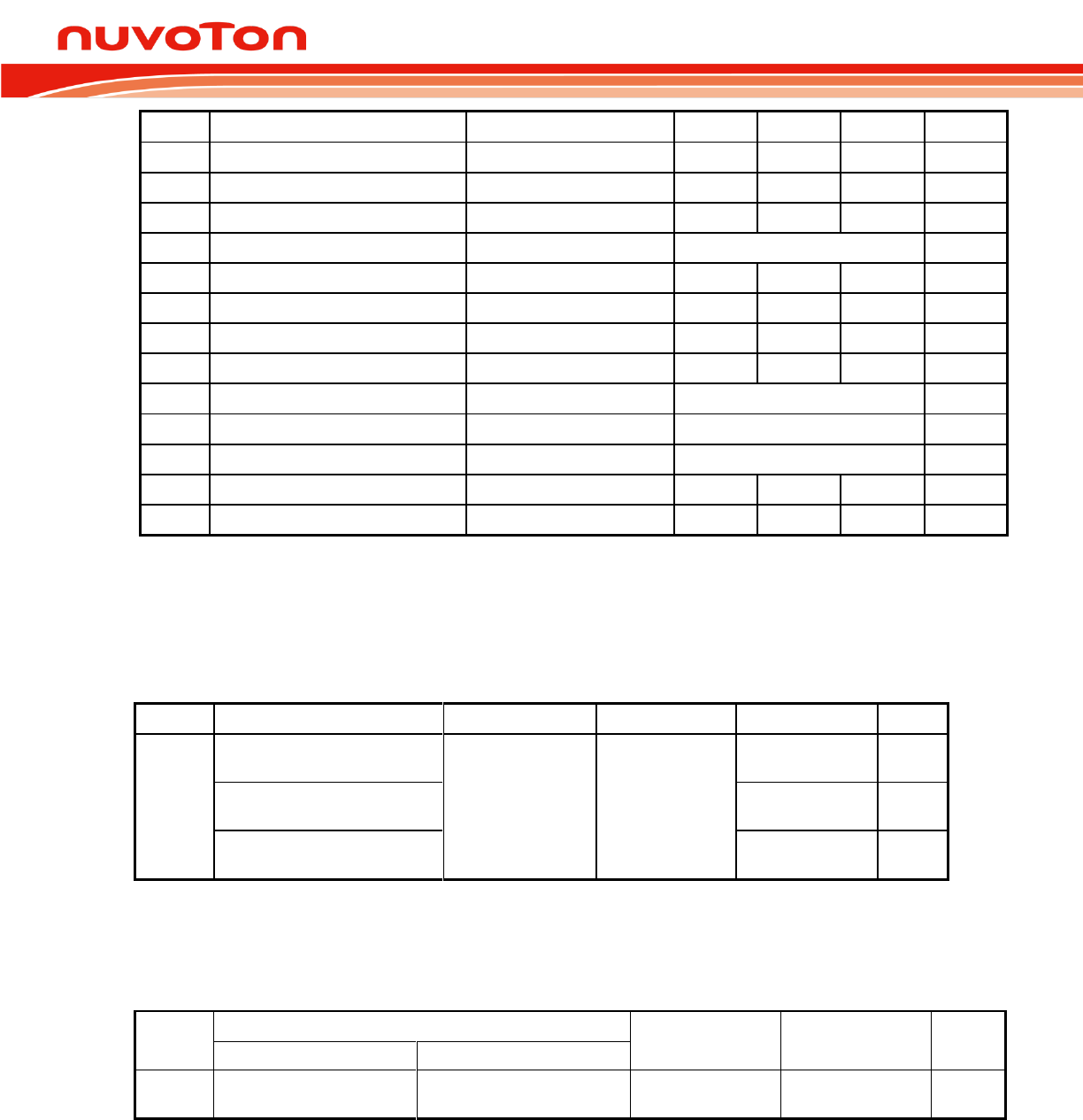
N76E003 Datasheet
Oct 28, 2016 Page 256 of 261 Rev. 1.00
Symbol
Parameter
Condition
Min.
Typ.
Max.
Unit
VAVDD
ADC operating voltage
2.7
-
5.5
V
IAVDD
ADC power supply current
VAVDD = 5V
-
300
-
VAIN
Analog input voltage
0
-
VAVDD
V
NR
Resolution
12
bit
DNL
Differential non-linearity error
-
4
-
LSB
INL
Integral non-linearity error
-
±3
-
LSB
OE
Offset error
-
±2
-
LSB
TUE
Total un-adjust error
-
8
-
LSB
-
Monotonicity
Guaranteed
-
FC
Conversion rate
500
ksps
Fs
Sampling rate [1]
380[1]
ksps
TADCEN
ADC enable time
15
uS
CIN
ADC input equivalent capacitor
3.6
pF
[1] This value base on code polling flag. If call interrupt subroutine need add entry and exit interrupt timing , the
sampling rate is about 290 ksps.
31.5 ESD Characteristics
Table 31-10 ESD Characteristics
Symbol
Ratings
Condition
Package
Maximum Value
Unit
VESD
Electrostatic discharge
(Human body mode)
TA = + 25 ℃
TSSOP 20
QFN 20
7000
V
Electrostatic discharge
(Machine mode)
400
V
Electrostatic discharge
(Device Charged mode)
1000
V
31.6 EFT Characteristics
Table 31-11 EFT Characteristics
Symbol
Condition
Package
Pass level
Unit
Fsys
BOD
HIRC
Disable / Enable
TSSOP 20
QFN 20
± 4400
V

N76E003 Datasheet
Oct 28, 2016 Page 257 of 261 Rev. 1.00
31.7 Flash DC Electrical Characteristics
Table 31-12 Flash DC Electrical Characteristics
Symbol
Parameter
Min.
Typ.
Max.
Unit
Condition
VFLA
Supply Voltage
1.62
1.8
1.98
V
NENDUR
Endurance
100,000
-
-
cycle
TRET
Data Retention
-
10
--
year
TA = + 25 ℃
TERASE
Page Erase Time
-
5
-
ms
1 page
TPROG
Program Time
-
10
-
us
1 byte
IDD1
Read Current
-
4
-
mA
IDD2
Program Current
-
4
-
mA
IDD3
Erase Current
-
2
-
mA
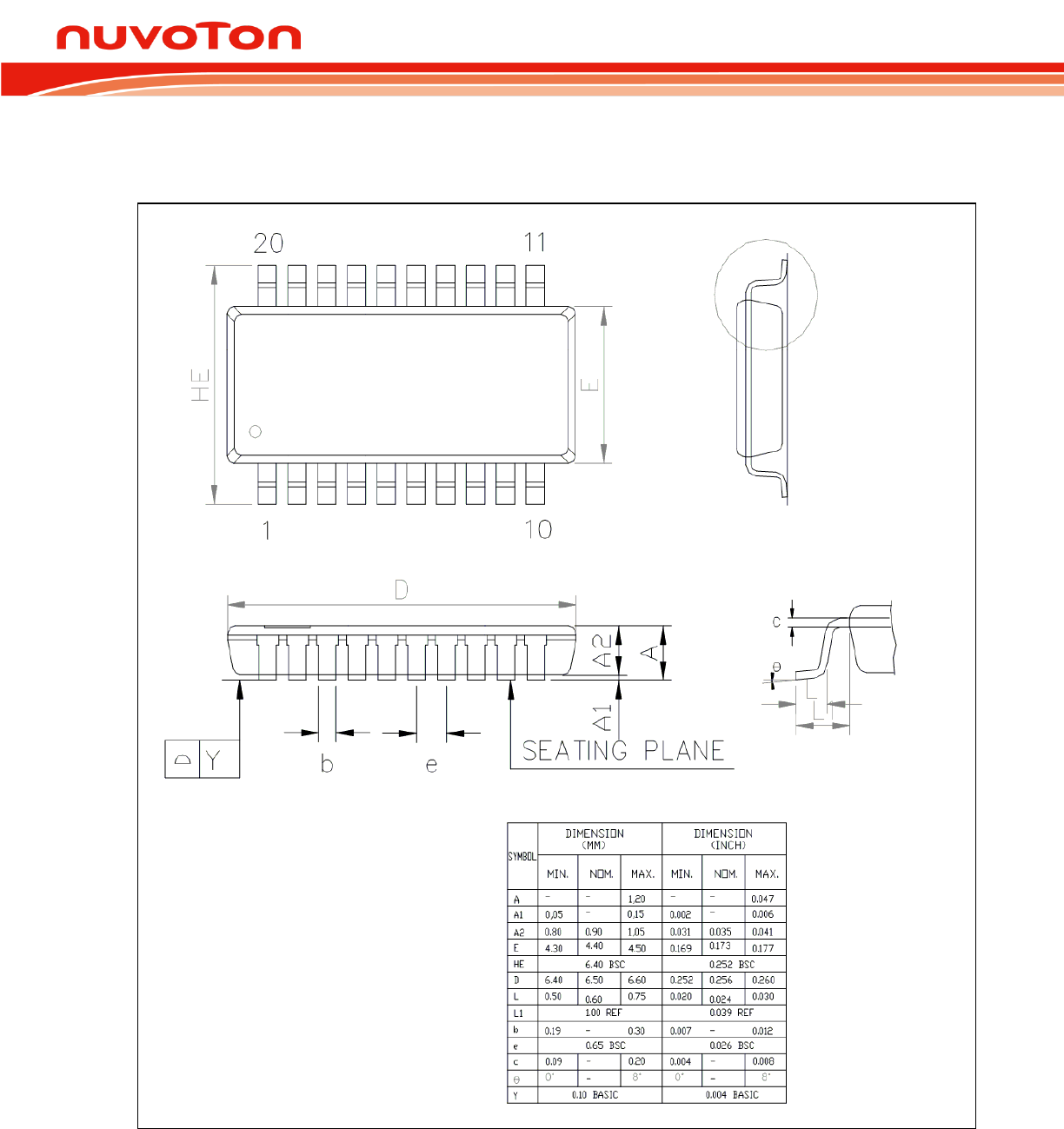
N76E003 Datasheet
Oct 28, 2016 Page 258 of 261 Rev. 1.00
32. PACKAGE DIMENSIONS
32.1 20-pin TSSOP - 4.4 X 6.5 mm
Figure 32-1. TSSOP-20 Package Dimension
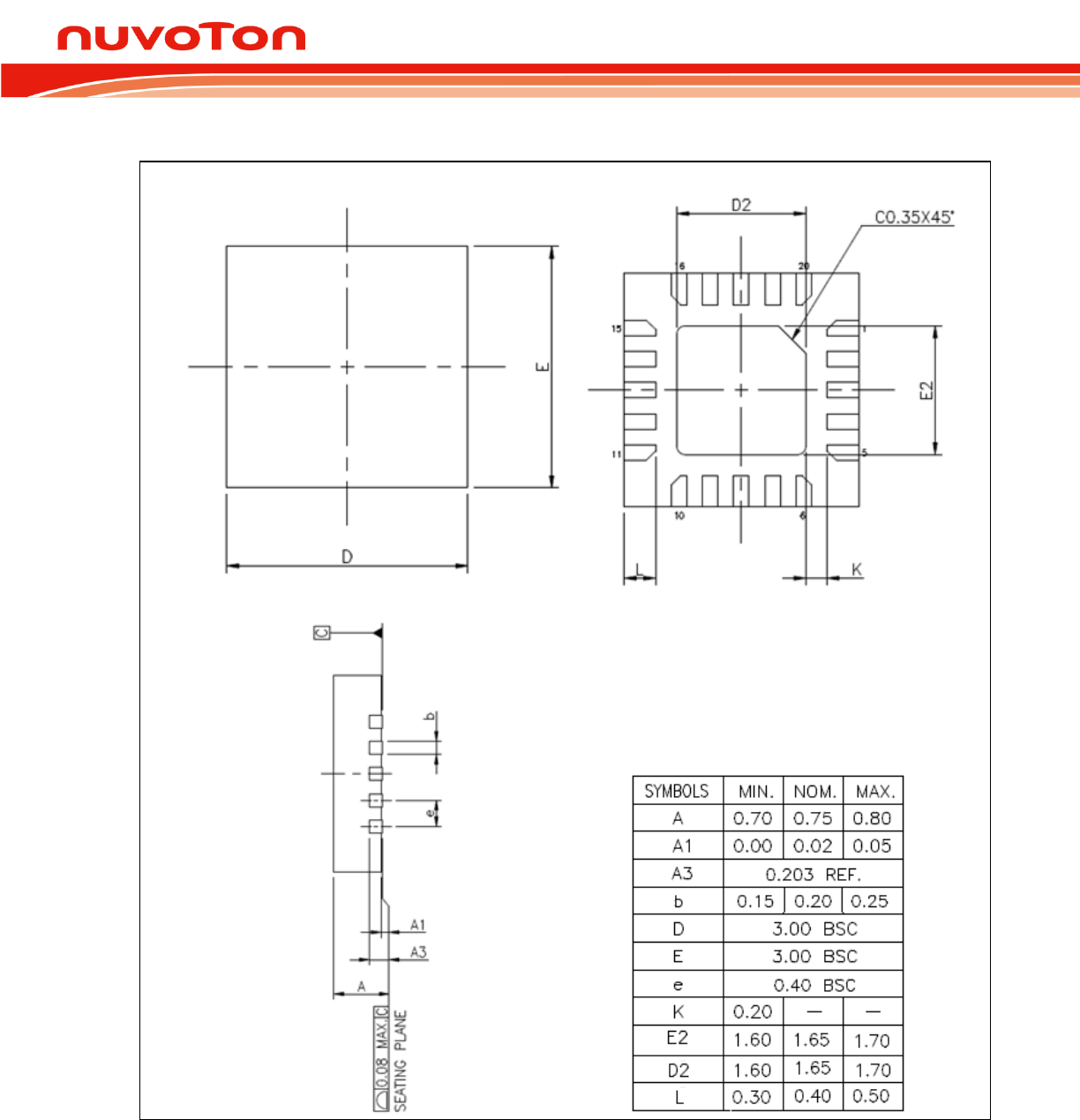
N76E003 Datasheet
Oct 28, 2016 Page 259 of 261 Rev. 1.00
32.2 20-pin QFN 3.0 X 3.0 mm
Figure 32-2. QFN-20 Package Dimension

N76E003 Datasheet
Oct 28, 2016 Page 260 of 261 Rev. 1.00
33. DOCUMENT REVISION HISTORY
Revision
Date
Description
V1.00
2016/10/28
Initial release

N76E003 Datasheet
Oct 28, 2016 Page 261 of 261 Rev. 1.00
Important Notice
Nuvoton Products are neither intended nor warranted for usage in systems or equipment, any
malfunction or failure of which may cause loss of human life, bodily injury or severe property
damage. Such applications are deemed,
Insecure usage includes, but is not limited to: equipment for surgical implementation, atomic
energy control instruments, airplane or spaceship instruments, the control or operation of
dynamic, brake or safety systems designed for vehicular use, traffic signal instruments, all
types of safety devices, and other applications intended to support or sustain life.
r shall indemnify the
damages and liabilities thus incurred by Nuvoton.
