Intel® 64 And IA 32 Architectures Software Developer’s Manual, Volume 3B: System Programming Guide, Part 2 Intel 2018 11 [Intel Manual Vol.3B
User Manual:
Open the PDF directly: View PDF ![]() .
.
Page Count: 632 [warning: Documents this large are best viewed by clicking the View PDF Link!]
- Chapter 14 Power and Thermal Management
- 14.1 Enhanced Intel Speedstep® Technology
- 14.2 P-State Hardware Coordination
- 14.3 System Software Considerations and Opportunistic processor Performance operation
- 14.4 Hardware-Controlled Performance States (HWP)
- 14.4.1 HWP Programming Interfaces
- 14.4.2 Enabling HWP
- 14.4.3 HWP Performance Range and Dynamic Capabilities
- 14.4.4 Managing HWP
- 14.4.5 HWP Feedback
- 14.4.6 HWP Notifications
- 14.4.7 Idle Logical Processor Impact on Core Frequency
- 14.4.8 Fast Write of Uncore MSR (Model Specific Feature)
- 14.4.9 Fast_IA32_HWP_REQUEST CPUID
- 14.4.10 Recommendations for OS use of HWP Controls
- 14.5 Hardware Duty Cycling (HDC)
- 14.6 MWAIT Extensions for Advanced Power Management
- 14.7 Thermal Monitoring and Protection
- 14.8 Package Level Thermal Management
- 14.9 Platform Specific Power Management Support
- Chapter 15 Machine-Check Architecture
- 15.1 Machine-Check Architecture
- 15.2 Compatibility with Pentium Processor
- 15.3 Machine-Check MSRs
- 15.4 Enhanced Cache Error reporting
- 15.5 Corrected Machine Check Error Interrupt
- 15.6 Recovery of Uncorrected Recoverable (UCR) Errors
- 15.7 Machine-Check Availability
- 15.8 Machine-Check Initialization
- 15.9 Interpreting the MCA Error Codes
- 15.10 Guidelines for Writing Machine-Check Software
- Chapter 16 Interpreting Machine-Check Error Codes
- 16.1 Incremental Decoding Information: Processor Family 06H Machine Error Codes For Machine Check
- 16.2 Incremental Decoding Information: Intel Core 2 Processor Family Machine Error Codes For Machine Check
- 16.3 Incremental Decoding Information: Processor Family with CPUID DisplayFamily_DisplayModel Signature 06_1AH, Machine Error Codes For Machine Check
- 16.4 Incremental Decoding Information: Processor Family with CPUID DisplayFamily_DisplayModel Signature 06_2DH, Machine Error Codes For Machine Check
- 16.5 Incremental Decoding Information: Processor Family with CPUID DisplayFamily_DisplayModel Signature 06_3EH, Machine Error Codes For Machine Check
- 16.6 Incremental Decoding Information: Processor Family with CPUID DisplayFamily_DisplayModel Signature 06_3FH, Machine Error Codes For Machine Check
- 16.7 Incremental Decoding Information: Processor Family with CPUID DisplayFamily_DisplayModel Signature 06_56H, Machine Error Codes For Machine Check
- 16.8 Incremental Decoding Information: Processor Family with CPUID DisplayFamily_DisplayModel Signature 06_4FH, Machine Error Codes For Machine Check
- 16.9 Incremental Decoding Information: Processor Family with CPUID DisplayFamily_DisplayModel Signature 06_55H, Machine Error Codes For Machine Check
- 16.10 Incremental Decoding Information: Processor Family with CPUID DisplayFamily_DisplayModel Signature 06_5FH, Machine Error Codes For Machine Check
- 16.11 Incremental Decoding Information: Processor Family 0FH Machine Error Codes For Machine Check
- Chapter 17 Debug, Branch Profile, TSC, and Intel® Resource Director Technology (Intel® RDT) Features
- 17.1 Overview of Debug Support Facilities
- 17.2 Debug Registers
- 17.3 Debug Exceptions
- 17.4 Last Branch, Interrupt, and Exception Recording Overview
- 17.4.1 IA32_DEBUGCTL MSR
- 17.4.2 Monitoring Branches, Exceptions, and Interrupts
- 17.4.3 Single-Stepping on Branches
- 17.4.4 Branch Trace Messages
- 17.4.5 Branch Trace Store (BTS)
- 17.4.6 CPL-Qualified Branch Trace Mechanism
- 17.4.7 Freezing LBR and Performance Counters on PMI
- 17.4.8 LBR Stack
- 17.4.9 BTS and DS Save Area
- 17.5 Last Branch, Interrupt, and Exception Recording (Intel® Core™ 2 Duo and Intel® Atom™ Processors)
- 17.6 Last Branch, Call Stack, Interrupt, and Exception Recording for Processors based on Goldmont Microarchitecture
- 17.7 Last Branch, Call Stack, Interrupt, and Exception Recording for Processors based on Goldmont Plus Microarchitecture
- 17.8 Last Branch, Interrupt and Exception Recording for Intel® Xeon Phi™ Processor 7200/5200/3200
- 17.9 Last Branch, Interrupt, and Exception Recording for Processors based on Intel® Microarchitecture code name Nehalem
- 17.10 Last Branch, Interrupt, and Exception Recording for Processors based on Intel® Microarchitecture code name Sandy Bridge
- 17.11 Last Branch, Call Stack, Interrupt, and Exception Recording for Processors based on Haswell Microarchitecture
- 17.12 Last Branch, Call Stack, Interrupt, and Exception Recording for Processors based on Skylake Microarchitecture
- 17.13 Last Branch, Interrupt, and Exception Recording (Processors based on Intel NetBurst® Microarchitecture)
- 17.14 Last Branch, Interrupt, and Exception Recording (Intel® Core™ Solo and Intel® Core™ Duo Processors)
- 17.15 Last Branch, Interrupt, and Exception Recording (Pentium M Processors)
- 17.16 Last Branch, Interrupt, and Exception Recording (P6 Family Processors)
- 17.17 Time-Stamp Counter
- 17.18 Intel® Resource Director Technology (Intel® RDT) Monitoring Features
- 17.18.1 Overview of Cache Monitoring Technology and Memory Bandwidth Monitoring
- 17.18.2 Enabling Monitoring: Usage Flow
- 17.18.3 Enumeration and Detecting Support of Cache Monitoring Technology and Memory Bandwidth Monitoring
- 17.18.4 Monitoring Resource Type and Capability Enumeration
- 17.18.5 Feature-Specific Enumeration
- 17.18.6 Monitoring Resource RMID Association
- 17.18.7 Monitoring Resource Selection and Reporting Infrastructure
- 17.18.8 Monitoring Programming Considerations
- 17.19 Intel® Resource Director Technology (Intel® RDT) Allocation Features
- 17.19.1 Introduction to Cache Allocation Technology (CAT)
- 17.19.2 Cache Allocation Technology Architecture
- 17.19.3 Code and Data Prioritization (CDP) Technology
- 17.19.4 Enabling Cache Allocation Technology Usage Flow
- 17.19.4.1 Enumeration and Detection Support of Cache Allocation Technology
- 17.19.4.2 Cache Allocation Technology: Resource Type and Capability Enumeration
- 17.19.4.3 Cache Allocation Technology: Cache Mask Configuration
- 17.19.4.4 Class of Service to Cache Mask Association: Common Across Allocation Features
- 17.19.5 Code and Data Prioritization (CDP): Enumerating and Enabling L3 CDP Technology
- 17.19.6 Code and Data Prioritization (CDP): Enumerating and Enabling L2 CDP Technology
- 17.19.6.1 Mapping Between L2 CDP Masks and L2 CAT Masks
- 17.19.6.2 Common L2 and L3 CDP Programming Considerations
- 17.19.6.3 Cache Allocation Technology Dynamic Configuration
- 17.19.6.4 Cache Allocation Technology Operation With Power Saving Features
- 17.19.6.5 Cache Allocation Technology Operation with Other Operating Modes
- 17.19.6.6 Associating Threads with CAT/CDP Classes of Service
- 17.19.7 Introduction to Memory Bandwidth Allocation
- Chapter 18 Performance Monitoring
- 18.1 Performance Monitoring Overview
- 18.2 Architectural Performance Monitoring
- 18.3 Performance Monitoring (Intel® Core™ Processors and Intel® Xeon® Processors)
- 18.3.1 Performance Monitoring for Processors Based on Intel® Microarchitecture Code Name Nehalem
- 18.3.2 Performance Monitoring for Processors Based on Intel® Microarchitecture Code Name Westmere
- 18.3.3 Intel® Xeon® Processor E7 Family Performance Monitoring Facility
- 18.3.4 Performance Monitoring for Processors Based on Intel® Microarchitecture Code Name Sandy Bridge
- 18.3.4.1 Global Counter Control Facilities In Intel® Microarchitecture Code Name Sandy Bridge
- 18.3.4.2 Counter Coalescence
- 18.3.4.3 Full Width Writes to Performance Counters
- 18.3.4.4 PEBS Support in Intel® Microarchitecture Code Name Sandy Bridge
- 18.3.4.5 Off-core Response Performance Monitoring
- 18.3.4.6 Uncore Performance Monitoring Facilities In Intel® Core™ i7-2xxx, Intel® Core™ i5-2xxx, Intel® Core™ i3-2xxx Processor Series
- 18.3.4.7 Intel® Xeon® Processor E5 Family Performance Monitoring Facility
- 18.3.4.8 Intel® Xeon® Processor E5 Family Uncore Performance Monitoring Facility
- 18.3.5 3rd Generation Intel® Core™ Processor Performance Monitoring Facility
- 18.3.6 4th Generation Intel® Core™ Processor Performance Monitoring Facility
- 18.3.6.1 Processor Event Based Sampling (PEBS) Facility
- 18.3.6.2 PEBS Data Format
- 18.3.6.3 PEBS Data Address Profiling
- 18.3.6.4 Off-core Response Performance Monitoring
- 18.3.6.5 Performance Monitoring and Intel® TSX
- 18.3.6.6 Uncore Performance Monitoring Facilities in the 4th Generation Intel® Core™ Processors
- 18.3.6.7 Intel® Xeon® Processor E5 v3 Family Uncore Performance Monitoring Facility
- 18.3.7 5th Generation Intel® Core™ Processor and Intel® Core™ M Processor Performance Monitoring Facility
- 18.3.8 6th Generation, 7th Generation and 8th Generation Intel® Core™ Processor Performance Monitoring Facility
- 18.4 Performance monitoring (Intel® Xeon™ Phi Processors)
- 18.5 Performance Monitoring (Intel® Atom™ Processors)
- 18.6 Performance Monitoring (Legacy Intel Processors)
- 18.6.1 Performance Monitoring (Intel® Core™ Solo and Intel® Core™ Duo Processors)
- 18.6.2 Performance Monitoring (Processors Based on Intel® Core™ Microarchitecture)
- 18.6.3 Performance Monitoring (Processors Based on Intel NetBurst® Microarchitecture)
- 18.6.3.1 ESCR MSRs
- 18.6.3.2 Performance Counters
- 18.6.3.3 CCCR MSRs
- 18.6.3.4 Debug Store (DS) Mechanism
- 18.6.3.5 Programming the Performance Counters for Non-Retirement Events
- 18.6.3.6 At-Retirement Counting
- 18.6.3.7 Tagging Mechanism for Replay_event
- 18.6.3.8 Processor Event-Based Sampling (PEBS)
- 18.6.3.9 Operating System Implications
- 18.6.4 Performance Monitoring and Intel Hyper-Threading Technology in Processors Based on Intel NetBurst® Microarchitecture
- 18.6.5 Performance Monitoring and Dual-Core Technology
- 18.6.6 Performance Monitoring on 64-bit Intel Xeon Processor MP with Up to 8-MByte L3 Cache
- 18.6.7 Performance Monitoring on L3 and Caching Bus Controller Sub-Systems
- 18.6.8 Performance Monitoring (P6 Family Processor)
- 18.6.9 Performance Monitoring (Pentium Processors)
- 18.7 Counting Clocks
- 18.7.1 Non-Halted Reference Clockticks
- 18.7.2 Cycle Counting and Opportunistic Processor Operation
- 18.7.3 Determining the Processor Base Frequency
- 18.7.3.1 For Intel® Processors Based on Microarchitecture Code Name Sandy Bridge, Ivy Bridge, Haswell and Broadwell
- 18.7.3.2 For Intel® Processors Based on Microarchitecture Code Name Nehalem
- 18.7.3.3 For Intel® Atom™ Processors Based on the Silvermont Microarchitecture (Including Intel Processors Based on Airmont Microarchitecture)
- 18.7.3.4 For Intel® Core™ 2 Processor Family and for Intel® Xeon® Processors Based on Intel Core Microarchitecture
- 18.8 IA32_PERF_CAPABILITIES MSR Enumeration
- Chapter 19 Performance Monitoring Events
- 19.1 Architectural Performance Monitoring Events
- 19.2 Performance Monitoring Events for Intel® Xeon® Processor Scalable Family
- 19.3 Performance Monitoring Events for 6th Generation, 7th Generation and 8th Generation Intel® Core™ Processors
- 19.4 Performance Monitoring Events for Intel® Xeon Phi™ Processor 3200, 5200, 7200 Series and Intel® Xeon Phi™ Processor 7215, 7285, 7295 Series
- 19.5 Performance Monitoring Events for the Intel® Core™ M and 5th Generation Intel® Core™ Processors
- 19.6 Performance Monitoring Events for the 4th Generation Intel® Core™ ProcessorS
- 19.7 Performance Monitoring Events for 3rd Generation Intel® Core™ ProcessorS
- 19.8 Performance Monitoring Events for 2nd Generation Intel® Core™ i7-2xxx, Intel® Core™ i5-2xxx, Intel® Core™ i3-2xxx Processor Series
- 19.9 Performance Monitoring Events for Intel® Core™ i7 Processor Family and Intel® Xeon® Processor Family
- 19.10 Performance Monitoring Events for processors based on Intel® microarchitecture Code Name Westmere
- 19.11 Performance Monitoring Events for Intel® Xeon® Processor 5200, 5400 Series and Intel® Core™2 Extreme Processors QX 9000 Series
- 19.12 Performance Monitoring Events for Intel® Xeon® Processor 3000, 3200, 5100, 5300 Series and Intel® Core™2 Duo ProcessorS
- 19.13 Performance Monitoring Events for Processors Based on the Goldmont Plus Microarchitecture
- 19.14 Performance Monitoring Events for Processors Based on the Goldmont Microarchitecture
- 19.15 Performance Monitoring Events for Processors Based on the Silvermont Microarchitecture
- 19.16 Performance Monitoring Events for 45 nm and 32 nm Intel® Atom™ Processors
- 19.17 Performance Monitoring Events for Intel® Core™ Solo and Intel® Core™ Duo Processors
- 19.18 Pentium® 4 and Intel® Xeon® Processor Performance Monitoring Events
- 19.19 Performance Monitoring Events for Intel® Pentium® M Processors
- 19.20 P6 Family Processor Performance Monitoring Events
- 19.21 Pentium Processor Performance Monitoring Events
- Chapter 20 8086 Emulation
- 20.1 Real-Address Mode
- 20.2 Virtual-8086 Mode
- 20.3 Interrupt and Exception Handling in Virtual-8086 Mode
- 20.4 Protected-Mode Virtual Interrupts
- Chapter 21 Mixing 16-Bit and 32-Bit Code
- Chapter 22 Architecture Compatibility
- 22.1 Processor Families and Categories
- 22.2 Reserved Bits
- 22.3 Enabling New Functions and Modes
- 22.4 Detecting the Presence of New Features Through Software
- 22.5 Intel MMX Technology
- 22.6 Streaming SIMD Extensions (SSE)
- 22.7 Streaming SIMD Extensions 2 (SSE2)
- 22.8 Streaming SIMD Extensions 3 (SSE3)
- 22.9 Additional Streaming SIMD Extensions
- 22.10 Intel Hyper-Threading Technology
- 22.11 Multi-Core Technology
- 22.12 Specific Features of Dual-Core Processor
- 22.13 New Instructions In the Pentium and Later IA-32 Processors
- 22.14 Obsolete Instructions
- 22.15 Undefined Opcodes
- 22.16 New Flags in the EFLAGS Register
- 22.17 Stack Operations and User Software
- 22.18 x87 FPU
- 22.18.1 Control Register CR0 Flags
- 22.18.2 x87 FPU Status Word
- 22.18.3 x87 FPU Control Word
- 22.18.4 x87 FPU Tag Word
- 22.18.5 Data Types
- 22.18.6 Floating-Point Exceptions
- 22.18.6.1 Denormal Operand Exception (#D)
- 22.18.6.2 Numeric Overflow Exception (#O)
- 22.18.6.3 Numeric Underflow Exception (#U)
- 22.18.6.4 Exception Precedence
- 22.18.6.5 CS and EIP For FPU Exceptions
- 22.18.6.6 FPU Error Signals
- 22.18.6.7 Assertion of the FERR# Pin
- 22.18.6.8 Invalid Operation Exception On Denormals
- 22.18.6.9 Alignment Check Exceptions (#AC)
- 22.18.6.10 Segment Not Present Exception During FLDENV
- 22.18.6.11 Device Not Available Exception (#NM)
- 22.18.6.12 Coprocessor Segment Overrun Exception
- 22.18.6.13 General Protection Exception (#GP)
- 22.18.6.14 Floating-Point Error Exception (#MF)
- 22.18.7 Changes to Floating-Point Instructions
- 22.18.7.1 FDIV, FPREM, and FSQRT Instructions
- 22.18.7.2 FSCALE Instruction
- 22.18.7.3 FPREM1 Instruction
- 22.18.7.4 FPREM Instruction
- 22.18.7.5 FUCOM, FUCOMP, and FUCOMPP Instructions
- 22.18.7.6 FPTAN Instruction
- 22.18.7.7 Stack Overflow
- 22.18.7.8 FSIN, FCOS, and FSINCOS Instructions
- 22.18.7.9 FPATAN Instruction
- 22.18.7.10 F2XM1 Instruction
- 22.18.7.11 FLD Instruction
- 22.18.7.12 FXTRACT Instruction
- 22.18.7.13 Load Constant Instructions
- 22.18.7.14 FXAM Instruction
- 22.18.7.15 FSAVE and FSTENV Instructions
- 22.18.8 Transcendental Instructions
- 22.18.9 Obsolete Instructions and Undefined Opcodes
- 22.18.10 WAIT/FWAIT Prefix Differences
- 22.18.11 Operands Split Across Segments and/or Pages
- 22.18.12 FPU Instruction Synchronization
- 22.19 Serializing Instructions
- 22.20 FPU and Math Coprocessor Initialization
- 22.21 Control Registers
- 22.22 Memory Management Facilities
- 22.23 Debug Facilities
- 22.24 Recognition of Breakpoints
- 22.25 Exceptions and/or Exception Conditions
- 22.26 Interrupts
- 22.27 Advanced Programmable Interrupt Controller (APIC)
- 22.28 Task Switching and TSs
- 22.29 Cache Management
- 22.30 Paging
- 22.31 Stack Operations and Supervisor Software
- 22.32 Mixing 16- and 32-Bit Segments
- 22.33 Segment and Address Wraparound
- 22.34 Store Buffers and Memory Ordering
- 22.35 Bus Locking
- 22.36 Bus Hold
- 22.37 Model-Specific Extensions to the IA-32
- 22.38 Two Ways to Run Intel 286 Processor Tasks
- 22.39 Initial State of Pentium, Pentium Pro and Pentium 4 Processors

Intel® 64 and IA-32 Architectures
Software Developer’s Manual
Volume 3B:
System Programming Guide, Part 2
NOTE: The Intel® 64 and IA-32 Architectures Software Developer's Manual consists of ten volumes:
Basic Architecture, Order Number 253665; Instruction Set Reference A-L, Order Number 253666;
Instruction Set Reference M-U, Order Number 253667; Instruction Set Reference V-Z, Order Number
326018; Instruction Set Reference, Order Number 334569; System Programming Guide, Part 1, Order
Number 253668; System Programming Guide, Part 2, Order Number 253669; System Programming
Guide, Part 3, Order Number 326019; System Programming Guide, Part 4, Order Number 332831;
Model-Specific Registers, Order Number 335592. Refer to all ten volumes when evaluating your design
needs.
Order Number: 253669-068US
November 2018

Intel technologies features and benefits depend on system configuration and may require enabled hardware, software, or service activation. Learn
more at intel.com, or from the OEM or retailer.
No computer system can be absolutely secure. Intel does not assume any liability for lost or stolen data or systems or any damages resulting
from such losses.
You may not use or facilitate the use of this document in connection with any infringement or other legal analysis concerning Intel products
described herein. You agree to grant Intel a non-exclusive, royalty-free license to any patent claim thereafter drafted which includes subject
matter disclosed herein.
No license (express or implied, by estoppel or otherwise) to any intellectual property rights is granted by this document.
The products described may contain design defects or errors known as errata which may cause the product to deviate from published specifica-
tions. Current characterized errata are available on request.
This document contains information on products, services and/or processes in development. All information provided here is subject to change
without notice. Contact your Intel representative to obtain the latest Intel product specifications and roadmaps
Copies of documents which have an order number and are referenced in this document, or other Intel literature, may be obtained by calling 1-
800-548-4725, or by visiting http://www.intel.com/design/literature.htm.
Intel, the Intel logo, Intel Atom, Intel Core, Intel SpeedStep, MMX, Pentium, VTune, and Xeon are trademarks of Intel Corporation in the U.S.
and/or other countries.
*Other names and brands may be claimed as the property of others.
Copyright © 1997-2018, Intel Corporation. All Rights Reserved.

Vol. 3B 14-1
CHAPTER 14
POWER AND THERMAL MANAGEMENT
This chapter describes facilities of Intel 64 and IA-32 architecture used for power management and thermal moni-
toring.
14.1 ENHANCED INTEL SPEEDSTEP® TECHNOLOGY
Enhanced Intel SpeedStep® Technology was introduced in the Pentium M processor. The technology enables the
management of processor power consumption via performance state transitions. These states are defined as
discrete operating points associated with different voltages and frequencies.
Enhanced Intel SpeedStep Technology differs from previous generations of Intel SpeedStep® Technology in two
ways:
•Centralization of the control mechanism and software interface in the processor by using model-specific
registers.
•Reduced hardware overhead; this permits more frequent performance state transitions.
Previous generations of the Intel SpeedStep Technology require processors to be a deep sleep state, holding off bus
master transfers for the duration of a performance state transition. Performance state transitions under the
Enhanced Intel SpeedStep Technology are discrete transitions to a new target frequency.
Support is indicated by CPUID, using ECX feature bit 07. Enhanced Intel SpeedStep Technology is enabled by
setting IA32_MISC_ENABLE MSR, bit 16. On reset, bit 16 of IA32_MISC_ENABLE MSR is cleared.
14.1.1 Software Interface For Initiating Performance State Transitions
State transitions are initiated by writing a 16-bit value to the IA32_PERF_CTL register, see Figure 14-2. If a transi-
tion is already in progress, transition to a new value will subsequently take effect.
Reads of IA32_PERF_CTL determine the last targeted operating point. The current operating point can be read from
IA32_PERF_STATUS. IA32_PERF_STATUS is updated dynamically.
The 16-bit encoding that defines valid operating points is model-specific. Applications and performance tools are
not expected to use either IA32_PERF_CTL or IA32_PERF_STATUS and should treat both as reserved. Performance
monitoring tools can access model-specific events and report the occurrences of state transitions.
14.2 P-STATE HARDWARE COORDINATION
The Advanced Configuration and Power Interface (ACPI) defines performance states (P-states) that are used to
facilitate system software’s ability to manage processor power consumption. Different P-states correspond to
different performance levels that are applied while the processor is actively executing instructions. Enhanced Intel
SpeedStep Technology supports P-states by providing software interfaces that control the operating frequency and
voltage of a processor.
With multiple processor cores residing in the same physical package, hardware dependencies may exist for a
subset of logical processors on a platform. These dependencies may impose requirements that impact the coordi-
nation of P-state transitions. As a result, multi-core processors may require an OS to provide additional software
support for coordinating P-state transitions for those subsets of logical processors.
ACPI firmware can choose to expose P-states as dependent and hardware-coordinated to OS power management
(OSPM) policy. To support OSPMs, multi-core processors must have additional built-in support for P-state hardware
coordination and feedback.
Intel 64 and IA-32 processors with dependent P-states amongst a subset of logical processors permit hardware
coordination of P-states and provide a hardware-coordination feedback mechanism using IA32_MPERF MSR and

14-2 Vol. 3B
POWER AND THERMAL MANAGEMENT
IA32_APERF MSR. See Figure 14-1 for an overview of the two 64-bit MSRs and the bullets below for a detailed
description.
•Use CPUID to check the P-State hardware coordination feedback capability bit. CPUID.06H.ECX[Bit 0] = 1
indicates IA32_MPERF MSR and IA32_APERF MSR are present.
•IA32_MPERF MSR (E7H) increments in proportion to a fixed frequency, which is configured when the processor
is booted.
•IA32_APERF MSR (E8H) increments in proportion to actual performance, while accounting for hardware coordi-
nation of P-state and TM1/TM2; or software initiated throttling.
•The MSRs are per logical processor; they measure performance only when the targeted processor is in the C0
state.
•Only the IA32_APERF/IA32_MPERF ratio is architecturally defined; software should not attach meaning to the
content of the individual of IA32_APERF or IA32_MPERF MSRs.
•When either MSR overflows, both MSRs are reset to zero and continue to increment.
•Both MSRs are full 64-bits counters. Each MSR can be written to independently. However, software should
follow the guidelines illustrated in Example 14-1.
If P-states are exposed by the BIOS as hardware coordinated, software is expected to confirm processor support
for P-state hardware coordination feedback and use the feedback mechanism to make P-state decisions. The OSPM
is expected to either save away the current MSR values (for determination of the delta of the counter ratio at a later
time) or reset both MSRs (execute WRMSR with 0 to these MSRs individually) at the start of the time window used
for making the P-state decision. When not resetting the values, overflow of the MSRs can be detected by checking
whether the new values read are less than the previously saved values.
Example 14-1 demonstrates steps for using the hardware feedback mechanism provided by IA32_APERF MSR and
IA32_MPERF MSR to determine a target P-state.
Example 14-1. Determine Target P-state From Hardware Coordinated Feedback
DWORD PercentBusy; // Percentage of processor time not idle.
// Measure “PercentBusy“ during previous sampling window.
// Typically, “PercentBusy“ is measure over a time scale suitable for
// power management decisions
//
// RDMSR of MCNT and ACNT should be performed without delay.
// Software needs to exercise care to avoid delays between
// the two RDMSRs (for example, interrupts).
MCNT = RDMSR(IA32_MPERF);
ACNT = RDMSR(IA32_APERF);
// PercentPerformance indicates the percentage of the processor
// that is in use. The calculation is based on the PercentBusy,
// that is the percentage of processor time not idle and the P-state
// hardware coordinated feedback using the ACNT/MCNT ratio.
// Note that both values need to be calculated over the same
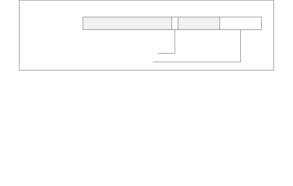
Figure 14-1. IA32_MPERF MSR and IA32_APERF MSR for P-state Coordination
63 0
IA32_MPERF (Addr: E7H)
630
IA32_APERF (Addr: E8H)

Vol. 3B 14-3
POWER AND THERMAL MANAGEMENT
// time window.
PercentPerformance = PercentBusy * (ACNT/MCNT);
// This example does not cover the additional logic or algorithms
// necessary to coordinate multiple logical processors to a target P-state.
TargetPstate = FindPstate(PercentPerformance);
if (TargetPstate ≠ currentPstate) {
SetPState(TargetPstate);
}
// WRMSR of MCNT and ACNT should be performed without delay.
// Software needs to exercise care to avoid delays between
// the two WRMSRs (for example, interrupts).
WRMSR(IA32_MPERF, 0);
WRMSR(IA32_APERF, 0);
14.3 SYSTEM SOFTWARE CONSIDERATIONS AND OPPORTUNISTIC PROCESSOR
PERFORMANCE OPERATION
An Intel 64 processor may support a form of processor operation that takes advantage of design headroom to
opportunistically increase performance. The Intel® Turbo Boost Technology can convert thermal headroom into
higher performance across multi-threaded and single-threaded workloads. The Intel® Dynamic Acceleration Tech-
nology feature can convert thermal headroom into higher performance if only one thread is active.
14.3.1 Intel® Dynamic Acceleration Technology
The Intel Core 2 Duo processor T 7700 introduces Intel Dynamic Acceleration Technology. Intel Dynamic Accelera-
tion Technology takes advantage of thermal design headroom and opportunistically allows a single core to operate
at a higher performance level when the operating system requests increased performance.
14.3.2 System Software Interfaces for Opportunistic Processor Performance Operation
Opportunistic processor performance operation, applicable to Intel Dynamic Acceleration Technology and Intel®
Turbo Boost Technology, has the following characteristics:
•A transition from a normal state of operation (e.g. Intel Dynamic Acceleration Technology/Turbo mode
disengaged) to a target state is not guaranteed, but may occur opportunistically after the corresponding enable
mechanism is activated, the headroom is available and certain criteria are met.
•The opportunistic processor performance operation is generally transparent to most application software.
•System software (BIOS and Operating system) must be aware of hardware support for opportunistic processor
performance operation and may need to temporarily disengage opportunistic processor performance operation
when it requires more predictable processor operation.
•When opportunistic processor performance operation is engaged, the OS should use hardware coordination
feedback mechanisms to prevent un-intended policy effects if it is activated during inappropriate situations.
14.3.2.1 Discover Hardware Support and Enabling of Opportunistic Processor Performance Operation
If an Intel 64 processor has hardware support for opportunistic processor performance operation, the power-on
default state of IA32_MISC_ENABLE[38] indicates the presence of such hardware support. For Intel 64 processors
that support opportunistic processor performance operation, the default value is 1, indicating its presence. For
processors that do not support opportunistic processor performance operation, the default value is 0. The power-
14-4 Vol. 3B
POWER AND THERMAL MANAGEMENT
on default value of IA32_MISC_ENABLE[38] allows BIOS to detect the presence of hardware support of opportu-
nistic processor performance operation.
IA32_MISC_ENABLE[38] is shared across all logical processors in a physical package. It is written by BIOS during
platform initiation to enable/disable opportunistic processor performance operation in conjunction of OS power
management capabilities, see Section 14.3.2.2. BIOS can set IA32_MISC_ENABLE[38] with 1 to disable opportu-
nistic processor performance operation; it must clear the default value of IA32_MISC_ENABLE[38] to 0 to enable
opportunistic processor performance operation. OS and applications must use CPUID leaf 06H if it needs to detect
processors that have opportunistic processor performance operation enabled.
When CPUID is executed with EAX = 06H on input, Bit 1 of EAX in Leaf 06H (i.e. CPUID.06H:EAX[1]) indicates
opportunistic processor performance operation, such as Intel Dynamic Acceleration Technology, has been enabled
by BIOS.
Opportunistic processor performance operation can be disabled by setting bit 38 of IA32_MISC_ENABLE. This
mechanism is intended for BIOS only. If IA32_MISC_ENABLE[38] is set, CPUID.06H:EAX[1] will return 0.
14.3.2.2 OS Control of Opportunistic Processor Performance Operation
There may be phases of software execution in which system software cannot tolerate the non-deterministic aspects
of opportunistic processor performance operation. For example, when calibrating a real-time workload to make a
CPU reservation request to the OS, it may be undesirable to allow the possibility of the processor delivering
increased performance that cannot be sustained after the calibration phase.
System software can temporarily disengage opportunistic processor performance operation by setting bit 32 of the
IA32_PERF_CTL MSR (0199H), using a read-modify-write sequence on the MSR. The opportunistic processor
performance operation can be re-engaged by clearing bit 32 in IA32_PERF_CTL MSR, using a read-modify-write
sequence. The DISENAGE bit in IA32_PERF_CTL is not reflected in bit 32 of the IA32_PERF_STATUS MSR (0198H),
and it is not shared between logical processors in a physical package. In order for OS to engage Intel Dynamic
Acceleration Technology/Turbo mode, the BIOS must:
•Enable opportunistic processor performance operation, as described in Section 14.3.2.1.
•Expose the operating points associated with Intel Dynamic Acceleration Technology/Turbo mode to the OS.
14.3.2.3 Required Changes to OS Power Management P-State Policy
Intel Dynamic Acceleration Technology and Intel Turbo Boost Technology can provide opportunistic performance
greater than the performance level corresponding to the Processor Base frequency of the processor (see CPUID’s
processor frequency information). System software can use a pair of MSRs to observe performance feedback. Soft-
ware must query for the presence of IA32_APERF and IA32_MPERF (see Section 14.2). The ratio between
IA32_APERF and IA32_MPERF is architecturally defined and a value greater than unity indicates performance
increase occurred during the observation period due to Intel Dynamic Acceleration Technology. Without incorpo-
rating such performance feedback, the target P-state evaluation algorithm can result in a non-optimal P-state
target.
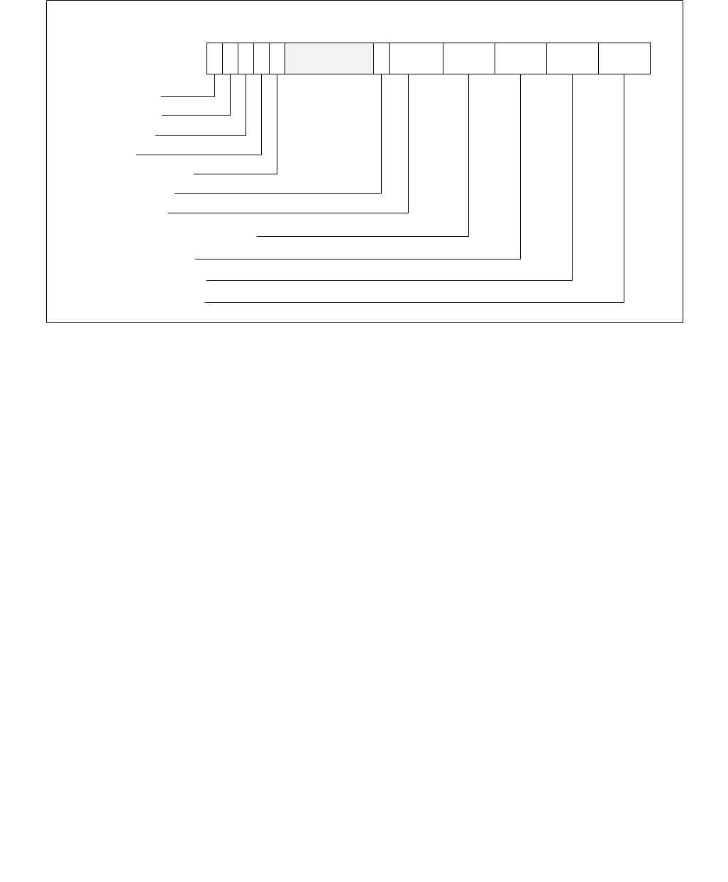
Figure 14-2. IA32_PERF_CTL Register
063 16 1533 32 31
Reserved
Enhanced Intel Speedstep® Technology Transition Target
Intel® Dynamic Acceleration Technology / Turbo DISENGAGE
Reserved

Vol. 3B 14-5
POWER AND THERMAL MANAGEMENT
There are other scenarios under which OS power management may want to disable Intel Dynamic Acceleration
Technology, some of these are listed below:
•When engaging ACPI defined passive thermal management, it may be more effective to disable Intel Dynamic
Acceleration Technology for the duration of passive thermal management.
•When the user has indicated a policy preference of power savings over performance, OS power management
may want to disable Intel Dynamic Acceleration Technology while that policy is in effect.
14.3.3 Intel® Turbo Boost Technology
Intel Turbo Boost Technology is supported in Intel Core i7 processors and Intel Xeon processors based on Intel®
microarchitecture code name Nehalem. It uses the same principle of leveraging thermal headroom to dynamically
increase processor performance for single-threaded and multi-threaded/multi-tasking environment. The program-
ming interface described in Section 14.3.2 also applies to Intel Turbo Boost Technology.
14.3.4 Performance and Energy Bias Hint support
Intel 64 processors may support additional software hint to guide the hardware heuristic of power management
features to favor increasing dynamic performance or conserve energy consumption.
Software can detect the processor's capability to support the performance-energy bias preference hint by exam-
ining bit 3 of ECX in CPUID leaf 6. The processor supports this capability if CPUID.06H:ECX.SETBH[bit 3] is set and
it also implies the presence of a new architectural MSR called IA32_ENERGY_PERF_BIAS (1B0H).
Software can program the lowest four bits of IA32_ENERGY_PERF_BIAS MSR with a value from 0 - 15. The values
represent a sliding scale, where a value of 0 (the default reset value) corresponds to a hint preference for highest
performance and a value of 15 corresponds to the maximum energy savings. A value of 7 roughly translates into a
hint to balance performance with energy consumption.
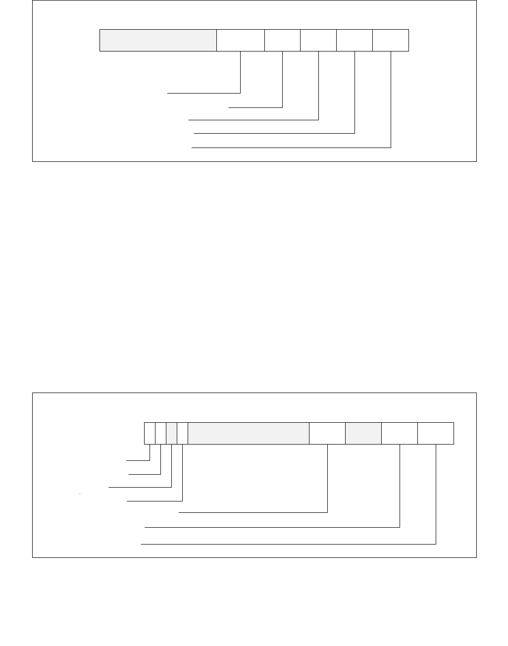
The layout of IA32_ENERGY_PERF_BIAS is shown in Figure 14-3. The scope of IA32_ENERGY_PERF_BIAS is per
logical processor, which means that each of the logical processors in the package can be programmed with a
different value. This may be especially important in virtualization scenarios, where the performance / energy
requirements of one logical processor may differ from the other. Conflicting “hints” from various logical processors
at higher hierarchy level will be resolved in favor of performance over energy savings.
Software can use whatever criteria it sees fit to program the MSR with an appropriate value. However, the value
only serves as a hint to the hardware and the actual impact on performance and energy savings is model specific.
14.4 HARDWARE-CONTROLLED PERFORMANCE STATES (HWP)
Intel processors may contain support for Hardware-Controlled Performance States (HWP), which autonomously
selects performance states while utilizing OS supplied performance guidance hints. The Enhanced Intel Speed-
Step® Technology provides a means for the OS to control and monitor discrete frequency-based operating points
via the IA32_PERF_CTL and IA32_PERF_STATUS MSRs.
Figure 14-3. IA32_ENERGY_PERF_BIAS Register
4 3 063
Reserved
Energy Policy Preference Hint

14-6 Vol. 3B
POWER AND THERMAL MANAGEMENT
In contrast, HWP is an implementation of the ACPI-defined Collaborative Processor Performance Control (CPPC),
which specifies that the platform enumerates a continuous, abstract unit-less, performance value scale that is not
tied to a specific performance state / frequency by definition. While the enumerated scale is roughly linear in terms
of a delivered integer workload performance result, the OS is required to characterize the performance value range
to comprehend the delivered performance for an applied workload.
When HWP is enabled, the processor autonomously selects performance states as deemed appropriate for the
applied workload and with consideration of constraining hints that are programmed by the OS. These OS-provided
hints include minimum and maximum performance limits, preference towards energy efficiency or performance,
and the specification of a relevant workload history observation time window. The means for the OS to override
HWP's autonomous selection of performance state with a specific desired performance target is also provided,
however, the effective frequency delivered is subject to the result of energy efficiency and performance optimiza-
tions.
14.4.1 HWP Programming Interfaces
The programming interfaces provided by HWP include the following:
•The CPUID instruction allows software to discover the presence of HWP support in an Intel processor. Specifi-
cally, execute CPUID instruction with EAX=06H as input will return 5 bit flags covering the following aspects in
bits 7 through 11 of CPUID.06H:EAX:
— Availability of HWP baseline resource and capability, CPUID.06H:EAX[bit 7]: If this bit is set, HWP provides
several new architectural MSRs: IA32_PM_ENABLE, IA32_HWP_CAPABILITIES, IA32_HWP_REQUEST,
IA32_HWP_STATUS.
— Availability of HWP Notification upon dynamic Guaranteed Performance change, CPUID.06H:EAX[bit 8]: If
this bit is set, HWP provides IA32_HWP_INTERRUPT MSR to enable interrupt generation due to dynamic
Performance changes and excursions.
— Availability of HWP Activity window control, CPUID.06H:EAX[bit 9]: If this bit is set, HWP allows software to
program activity window in the IA32_HWP_REQUEST MSR.
— Availability of HWP energy/performance preference control, CPUID.06H:EAX[bit 10]: If this bit is set, HWP
allows software to set an energy/performance preference hint in the IA32_HWP_REQUEST MSR.
— Availability of HWP package level control, CPUID.06H:EAX[bit 11]:If this bit is set, HWP provides the
IA32_HWP_REQUEST_PKG MSR to convey OS Power Management’s control hints for all logical processors
in the physical package.
Table 14-1. Architectural and Non-Architectural MSRs Related to HWP
Address Architectural Register Name Description
770H Y IA32_PM_ENABLE Enable/Disable HWP.
771H Y IA32_HWP_CAPABILITIES Enumerates the HWP performance range (static and dynamic).
772H Y IA32_HWP_REQUEST_PKG Conveys OSPM's control hints (Min, Max, Activity Window, Energy
Performance Preference, Desired) for all logical processor in the
physical package.
773H Y IA32_HWP_INTERRUPT Controls HWP native interrupt generation (Guaranteed Performance
changes, excursions).
774H Y IA32_HWP_REQUEST Conveys OSPM's control hints (Min, Max, Activity Window, Energy
Performance Preference, Desired) for a single logical processor.
775H Y IA32_HWP_PECI_REQUEST_INFO Conveys embedded system controller requests to override some of
the OS HWP Request settings via the PECI mechanism.
777H Y IA32_HWP_STATUS Status bits indicating changes to Guaranteed Performance and
excursions to Minimum Performance.
19CH Y IA32_THERM_STATUS[bits 15:12] Conveys reasons for performance excursions.
64EH N MSR_PPERF Productive Performance Count.

Vol. 3B 14-7
POWER AND THERMAL MANAGEMENT
•Additionally, HWP may provide a non-architectural MSR, MSR_PPERF, which provides a quantitative metric to
software of hardware’s view of workload scalability. This hardware’s view of workload scalability is implemen-
tation specific.
14.4.2 Enabling HWP
The layout of the IA32_PM_ENABLE MSR is shown in Figure 14-4. The bit fields are described below:
•HWP_ENABLE (bit 0, R/W1Once) — Software sets this bit to enable HWP with autonomous selection of
processor P-States. When set, the processor will disregard input from the legacy performance control interface
(IA32_PERF_CTL). Note this bit can only be enabled once from the default value. Once set, writes to the
HWP_ENABLE bit are ignored. Only RESET will clear this bit. Default = zero (0).
•Bits 63:1 are reserved and must be zero.
After software queries CPUID and verifies the processor’s support of HWP, system software can write 1 to
IA32_PM_ENABLE.HWP_ENABLE (bit 0) to enable hardware controlled performance states. The default value of
IA32_PM_ENABLE MSR at power-on is 0, i.e. HWP is disabled.
Additional MSRs associated with HWP may only be accessed after HWP is enabled, with the exception of
IA32_HWP_INTERRUPT and MSR_PPERF. Accessing the IA32_HWP_INTERRUPT MSR requires only HWP is present
as enumerated by CPUID but does not require enabling HWP.
IA32_PM_ENABLE is a package level MSR, i.e., writing to it from any logical processor within a package affects all
logical processors within that package.
14.4.3 HWP Performance Range and Dynamic Capabilities
The OS reads the IA32_HWP_CAPABILITIES MSR to comprehend the limits of the HWP-managed performance
range as well as the dynamic capability, which may change during processor operation. The enumerated perfor-
mance range values reported by IA32_HWP_CAPABILITIES directly map to initial frequency targets (prior to work-
load-specific frequency optimizations of HWP). However the mapping is processor family specific.
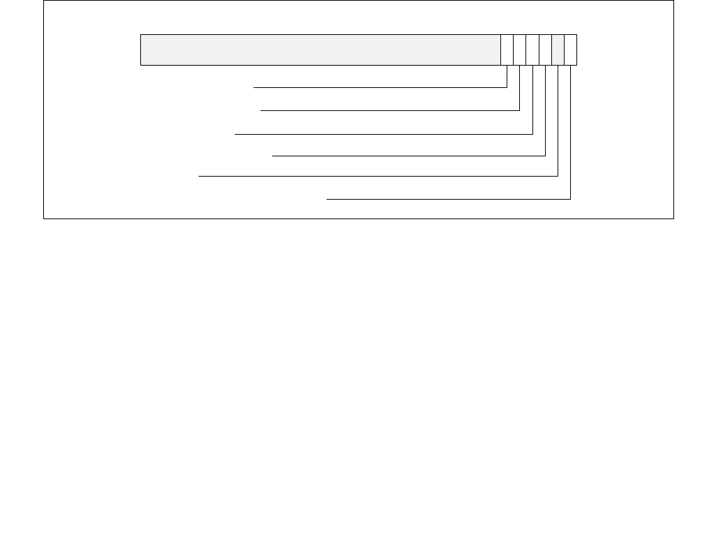
The layout of the IA32_HWP_CAPABILITIES MSR is shown in Figure 14-5. The bit fields are described below:
Figure 14-4. IA32_PM_ENABLE MSR
1 063
Reserved
HWP_ENABLE

14-8 Vol. 3B
POWER AND THERMAL MANAGEMENT
•Highest_Performance (bits 7:0, RO) — Value for the maximum non-guaranteed performance level.
•Guaranteed_Performance (bits 15:8, RO) — Current value for the guaranteed performance level. This
value can change dynamically as a result of internal or external constraints, e.g. thermal or power limits.
•Most_Efficient_Performance (bits 23:16, RO) — Current value of the most efficient performance level.
This value can change dynamically as a result of workload characteristics.
•Lowest_Performance (bits 31:24, RO) — Value for the lowest performance level that software can program
to IA32_HWP_REQUEST.
•Bits 63:32 are reserved and must be zero.
The value returned in the Guaranteed_Performance field is hardware's best-effort approximation of the avail-
able performance given current operating constraints. Changes to the Guaranteed_Performance value will
primarily occur due to a shift in operational mode. This includes a power or other limit applied by an external agent,
e.g. RAPL (see Figure 14.9.1), or the setting of a Configurable TDP level (see model-specific controls related to
Programmable TDP Limit in Chapter 2, “Model-Specific Registers (MSRs)” in the Intel® 64 and IA-32 Architectures
Software Developer’s Manual, Volume 4.). Notification of a change to the Guaranteed_Performance occurs via
interrupt (if configured) and the IA32_HWP_Status MSR. Changes to Guaranteed_Performance are indicated when
a macroscopically meaningful change in performance occurs i.e. sustained for greater than one second. Conse-
quently, notification of a change in Guaranteed Performance will typically occur no more frequently than once per
second. Rapid changes in platform configuration, e.g. docking / undocking, with corresponding changes to a
Configurable TDP level could potentially cause more frequent notifications.
The value returned by the Most_Efficient_Performance field provides the OS with an indication of the practical
lower limit for the IA32_HWP_REQUEST. The processor may not honor IA32_HWP_REQUEST.Maximum Perfor-
mance settings below this value.
14.4.4 Managing HWP
14.4.4.1 IA32_HWP_REQUEST MSR (Address: 0x774 Logical Processor Scope)
Typically, the operating system controls HWP operation for each logical processor via the writing of control hints /
constraints to the IA32_HWP_REQUEST MSR. The layout of the IA32_HWP_REQUEST MSR is shown in Figure 14-6.
The bit fields are described below Figure 14-6.
Operating systems can control HWP by writing both IA32_HWP_REQUEST and IA32_HWP_REQUEST_PKG MSRs
(see Section 14.4.4.2). Five valid bits within the IA32_HWP_REQUEST MSR let the operating system flexibly select
which of its five hint / constraint fields should be derived by the processor from the IA32_HWP_REQUEST MSR and
which should be derived from the IA32_HWP_REQUEST_PKG MSR. These five valid bits are supported if
CPUID[6].EAX[17] is set.
Figure 14-5. IA32_HWP_CAPABILITIES Register
063 8 716 1524 2332 31
Reserved
Most_Efficient_Performance
Guaranteed_Performance
Highest_Performance
Lowest_Performance
Vol. 3B 14-9
POWER AND THERMAL MANAGEMENT
When the IA32_HWP_REQUEST MSR Package Control bit is set, any valid bit that is NOT set indicates to the
processor to use the respective field value from the IA32_HWP_REQUEST_PKG MSR. Otherwise, the values are
derived from the IA32_HWP_REQUEST MSR. The valid bits are ignored when the IA32_HWP_REQUEST MSR
Package Control bit is zero.
•Minimum_Performance (bits 7:0, RW) — Conveys a hint to the HWP hardware. The OS programs the
minimum performance hint to achieve the required quality of service (QOS) or to meet a service level
agreement (SLA) as needed. Note that an excursion below the level specified is possible due to hardware
constraints. The default value of this field is IA32_HWP_CAPABILITIES.Lowest_Performance.
•Maximum_Performance (bits 15:8, RW) — Conveys a hint to the HWP hardware. The OS programs this
field to limit the maximum performance that is expected to be supplied by the HWP hardware. Excursions
above the limit requested by OS are possible due to hardware coordination between the processor cores and
other components in the package. The default value of this field is
IA32_HWP_CAPABILITIES.Highest_Performance.
•Desired_Performance (bits 23:16, RW) — Conveys a hint to the HWP hardware. When set to zero,
hardware autonomous selection determines the performance target. When set to a non-zero value (between
the range of Lowest_Performance and Highest_Performance of IA32_HWP_CAPABILITIES) conveys an explicit
performance request hint to the hardware; effectively disabling HW Autonomous selection. The
Desired_Performance input is non-constraining in terms of Performance and Energy Efficiency optimizations,
which are independently controlled. The default value of this field is 0.
•Energy_Performance_Preference (bits 31:24, RW) — Conveys a hint to the HWP hardware. The OS may
write a range of values from 0 (performance preference) to 0FFH (energy efficiency preference) to influence
the rate of performance increase /decrease and the result of the hardware's energy efficiency and performance
optimizations. The default value of this field is 80H. Note: If CPUID.06H:EAX[bit 10] indicates that this field is
not supported, HWP uses the value of the IA32_ENERGY_PERF_BIAS MSR to determine the energy efficiency /
performance preference.
•Activity_Window (bits 41:32, RW) — Conveys a hint to the HWP hardware specifying a moving workload
history observation window for performance/frequency optimizations. If 0, the hardware will determine the
appropriate window size. When writing a non-zero value to this field, this field is encoded in the format of bits
38:32 as a 7-bit mantissa and bits 41:39 as a 3-bit exponent value in powers of 10. The resultant value is in
microseconds. Thus, the minimal/maximum activity window size is 1 microsecond/1270 seconds. Combined
with the Energy_Performance_Preference input, Activity_Window influences the rate of performance increase
Figure 14-6. IA32_HWP_REQUEST Register
063 62 61 60 59 8 716 1524 2332 3143 42 41
Reserved
Energy_Performance_Preference
Activity_Window
Desired_Performance
Maximum_Performance
Minimum_Performance
Activity_Window Valid
EPP Valid
Desired Valid
Maximum Valid
Minimum Valid
Package_Control

14-10 Vol. 3B
POWER AND THERMAL MANAGEMENT
/ decrease. This non-zero hint only has meaning when Desired_Performance = 0. The default value of this field
is 0.
•Package_Control (bit 42, RW) — When set, causes this logical processor's IA32_HWP_REQUEST control
inputs to be derived from the IA32_HWP_REQUEST_PKG MSR.
•Bits 58:43 are reserved and must be zero.
•Activity_Window Valid (bit 59, RW) — When set, indicates to the processor to derive the Activity Window
field value from the IA32_HWP_REQUEST MSR even if the package control bit is set. Otherwise, derive it from
the IA32_HWP_REQUEST_PKG MSR. The default value of this field is 0.
•EPP Valid (bit 60, RW) — When set, indicates to the processor to derive the EPP field value from the
IA32_HWP_REQUEST MSR even if the package control bit is set. Otherwise, derive it from the
IA32_HWP_REQUEST_PKG MSR. The default value of this field is 0.
•Desired Valid (bit 61, RW) — When set, indicates to the processor to derive the Desired Performance field
value from the IA32_HWP_REQUEST MSR even if the package control bit is set. Otherwise, derive it from the
IA32_HWP_REQUEST_PKG MSR. The default value of this field is 0.
•Maximum Valid (bit 62, RW) — When set, indicates to the processor to derive the Maximum Performance
field value from the IA32_HWP_REQUEST MSR even if the package control bit is set. Otherwise, derive it from
the IA32_HWP_REQUEST_PKG MSR. The default value of this field is 0.
•Minimum Valid (bit 63, RW) — When set, indicates to the processor to derive the Minimum Performance field
value from the IA32_HWP_REQUEST MSR even if the package control bit is set. Otherwise, derive it from the
IA32_HWP_REQUEST_PKG MSR. The default value of this field is 0.
The HWP hardware clips and resolves the field values as necessary to the valid range. Reads return the last value
written not the clipped values.
Processors may support a subset of IA32_HWP_REQUEST fields as indicated by CPUID. Reads of non-supported
fields will return 0. Writes to non-supported fields are ignored.
The OS may override HWP's autonomous selection of performance state with a specific performance target by
setting the Desired_Performance field to a non-zero value, however, the effective frequency delivered is subject to
the result of energy efficiency and performance optimizations, which are influenced by the Energy Performance
Preference field.
Software may disable all hardware optimizations by setting Minimum_Performance = Maximum_Performance
(subject to package coordination).
Note: The processor may run below the Minimum_Performance level due to hardware constraints including: power,
thermal, and package coordination constraints. The processor may also run below the Minimum_Performance level
for short durations (few milliseconds) following C-state exit, and when Hardware Duty Cycling (see Section 14.5) is
enabled.
When the IA32_HWP_REQUEST MSR is set to fast access mode, writes of this MSR are posted, i.e., the WRMSR
instruction retires before the data reaches its destination within the processor. It may retire even before all
preceding IA stores are globally visible, i.e., it is not an architecturally serializing instruction anymore (no store
fence). A new CPUID bit indicates this new characteristic of the IA32_HWP_REQUEST MSR (see Section 14.4.8 for
additional details).
Vol. 3B 14-11
POWER AND THERMAL MANAGEMENT
14.4.4.2 IA32_HWP_REQUEST_PKG MSR (Address: 0x772 Package Scope)
The structure of the IA32_HWP_REQUEST_PKG MSR (package-level) is identical to the IA32_HWP_REQUEST MSR
with the exception of the the Package Control bit field and the five valid bit fields, which do not exist in the
IA32_HWP_REQUEST_PKG MSR. Field values written to this MSR apply to all logical processors within the physical
package with the exception of logical processors whose IA32_HWP_REQUEST.Package Control field is clear (zero).
Single P-state Control mode is only supported when IA32_HWP_REQUEST_PKG is not supported.
14.4.4.3 IA32_HWP_PECI_REQUEST_INFO MSR (Address 0x775 Package Scope)
When an embedded system controller is integrated in the platform, it can override some of the OS HWP Request
settings via the PECI mechanism. PECI initiated settings take precedence over the relevant fields in the
IA32_HWP_REQUEST MSR and in the IA32_HWP_REQUEST_PKG MSR, irrespective of the Package Control bit or
the Valid Bit values described above. PECI can independently control each of: Minimum Performance, Maximum
Performance and EPP fields. This MSR contains both the PECI induced values and the control bits that indicate
whether the embedded controller actually set the processor to use the respective value.
PECI override is supported if CPUID[6].EAX[16] is set.
Figure 14-7. IA32_HWP_REQUEST_PKG Register
Figure 14-8. IA32_HWP_PECI_REQUEST_INFO MSR
063 8 716 1524 2332 3142 41
Reserved
Energy_Performance_Preference
Activity_Window
Desired_Performance
Maximum_Performance
Minimum_Performance
063 62 61 60 59 8 716 1524 2332 31
Reserved
Energy_Performance_Preference
Maximum_Performance
Minimum_Performance
EPP PECI Override
Reserved
Max PECI Override
Min PECI Override
Reserved

14-12 Vol. 3B
POWER AND THERMAL MANAGEMENT
The layout of the IA32_HWP_PECI_REQUEST_INFO MSR is shown in Figure 14-8. This MSR is writable by the
embedded controller but is read-only by software executing on the CPU. This MSR has Package scope. The bit fields
are described below:
•Minimum_Performance (bits 7:0, RO) — Used by the OS to read the latest value of PECI minimum
performance input.
•Maximum_Performance (bits 15:8, RO) — Used by the OS to read the latest value of PECI maximum
performance input.
•Bits 23:16 are reserved and must be zero.
•Energy_Performance_Preference (bits 31:24, RO) — Used by the OS to read the latest value of PECI
energy performance preference input.
•Bits 59:32 are reserved and must be zero.
•EPP_PECI_Override (bit 60, RO) — Indicates whether PECI if currently overriding the Energy Performance
Preference input. If set(1), PECI is overriding the Energy Performance Preference input. If clear(0), OS has
control over Energy Performance Preference input.
•Bit 61 is reserved and must be zero.
•Max_PECI_Override (bit 62, RO) — Indicates whether PECI if currently overriding the Maximum
Performance input. If set(1), PECI is overriding the Maximum Performance input. If clear(0), OS has control
over Maximum Performance input.
•Min_PECI_Override (bit 63, RO) — Indicates whether PECI if currently overriding the Minimum Performance
input. If set(1), PECI is overriding the Minimum Performance input. If clear(0), OS has control over Minimum
Performance input.
HWP Request Field Hierarchical Resolution
HWP Request field resolution is fed by three MSRs: IA32_HWP_REQUEST, IA32_HWP_REQUEST_PKG and
IA32_HWP_PECI_REQUEST_INFO. The flow that the processor goes through to resolve which field value is chosen
is shown below.
For each of the two HWP Request fields; Desired and Activity Window:
If IA32_HWP_REQUEST.PACKAGE_CONTROL = 1 and IA32_HWP_REQUEST.<field> valid bit = 0
Resolved Field Value = IA32_HWP_REQUEST_PKG.<field>
Else
Resolved Field Value = IA32_HWP_REQUEST.<field>
For each of the three HWP Request fields; Min, Max and EPP:
If IA32_HWP_PECI_REQUEST_INFO.<field> PECI Override bit = 1
Resolved Field Value = IA32_HWP_PECI_REQUEST_INFO.<field>
Else if IA32_HWP_REQUEST.PACKAGE_CONTROL = 1 and IA32_HWP_REQUEST.<field> valid bit = 0
Resolved Field Value = IA32_HWP_REQUEST_PKG.<field>
Else
Resolved Field Value = IA32_HWP_REQUEST.<field>
14.4.5 HWP Feedback
The processor provides several types of feedback to the OS during HWP operation.
The IA32_MPERF MSR and IA32_APERF MSR mechanism (see Section 14.2) allows the OS to calculate the resultant
effective frequency delivered over a time period. Energy efficiency and performance optimizations directly impact
the resultant effective frequency delivered.
The layout of the IA32_HWP_STATUS MSR is shown in Figure 14-9. It provides feedback regarding changes to
IA32_HWP_CAPABILITIES.Guaranteed_Performance, IA32_HWP_CAPABILITIES.Highest_Performance, excursions
to IA32_HWP_CAPABILITIES.Minimum_Performance, and PECI_Override entry/exit events. The bit fields are
described below:
Vol. 3B 14-13
POWER AND THERMAL MANAGEMENT
•Guaranteed_Performance_Change (bit 0, RWC0) — If set (1), a change to Guaranteed_Performance has
occurred. Software should query IA32_HWP_CAPABILITIES.Guaranteed_Performance value to ascertain the
new Guaranteed Performance value and to assess whether to re-adjust HWP hints via IA32_HWP_REQUEST.
Software must clear this bit by writing a zero (0).
•Bit 1 is reserved and must be zero.
•Excursion_To_Minimum (bit 2, RWC0) — If set (1), an excursion to Minimum_Performance of
IA32_HWP_REQUEST has occurred. Software must clear this bit by writing a zero (0).
•Highest_Change (bit 3, RWC0) — If set (1), a change to Highest Performance has occurred. Software
should query IA32_HWP_CAPABILITIES to ascertain the new Highest Performance value. Software must clear
this bit by writing a zero (0). Interrupts upon Highest Performance change are supported if CPUID[6].EAX[15]
is set.
•PECI_Override_Entry (bit 4, RWC0) — If set (1), an embedded/management controller has started a PECI
override of one or more OS control hints (Min, Max, EPP) specified in IA32_HWP_REQUEST or
IA32_HWP_REQUEST_PKG. Software may query IA32_HWP_PECI_REQUEST_INFO MSR to ascertain which
fields are now overridden via the PECI mechanism and what their values are (see Section 14.4.4.3 for
additional details). Software must clear this bit by writing a zero (0). Interrupts upon PECI override entry are
supported if CPUID[6].EAX[16] is set.
•PECI_Override_Exit (bit 5, RWC0) — If set (1), an embedded/management controller has stopped
overriding one or more OS control hints (Min, Max, EPP) specified in IA32_HWP_REQUEST or
IA32_HWP_REQUEST_PKG. Software may query IA32_HWP_PECI_REQUEST_INFO MSR to ascertain which
fields are still overridden via the PECI mechanism and which fields are now back under software control (see
Section 14.4.4.3 for additional details). Software must clear this bit by writing a zero (0). Interrupts upon PECI
override exit are supported if CPUID[6].EAX[16] is set.
•Bits 63:6 are reserved and must be zero.
The status bits of IA32_HWP_STATUS must be cleared (0) by software so that a new status condition change will
cause the hardware to set the bit again and issue the notification. Status bits are not set for “normal” excursions,
e.g., running below Minimum Performance for short durations during C-state exit. Changes to
Guaranteed_Performance, Highest_Performance, excursions to Minimum_Performance, or PECI_Override
entry/exit will occur no more than once per second.
The OS can determine the specific reasons for a Guaranteed_Performance change or an excursion to
Minimum_Performance in IA32_HWP_REQUEST by examining the associated status and log bits reported in the
IA32_THERM_STATUS MSR. The layout of the IA32_HWP_STATUS MSR that HWP uses to support software query
of HWP feedback is shown in Figure 14-10. The bit fields of IA32_THERM_STATUS associated with HWP feedback
are described below (Bit fields of IA32_THERM_STATUS unrelated to HWP can be found in Section 14.7.5.2).
Figure 14-9. IA32_HWP_STATUS MSR
6 5 4 3 2 1 063
Reserved
Highest_Change
Excursion_To_Minimum
Reserved
Guaranteed_Performance_Change
PECI_Override_Entry
PECI_Override_Exit
14-14 Vol. 3B
POWER AND THERMAL MANAGEMENT
•Bits 11:0, See Section 14.7.5.2.
•Current Limit Status (bit 12, RO) — If set (1), indicates an electrical current limit (e.g. Electrical Design
Point/IccMax) is being exceeded and is adversely impacting energy efficiency optimizations.
•Current Limit Log (bit 13, RWC0) — If set (1), an electrical current limit has been exceeded that has
adversely impacted energy efficiency optimizations since the last clearing of this bit or a reset. This bit is sticky,
software may clear this bit by writing a zero (0).
•Cross-domain Limit Status (bit 14, RO) — If set (1), indicates another hardware domain (e.g. processor
graphics) is currently limiting energy efficiency optimizations in the processor core domain.
•Cross-domain Limit Log (bit 15, RWC0) — If set (1), indicates another hardware domain (e.g. processor
graphics) has limited energy efficiency optimizations in the processor core domain since the last clearing of this
bit or a reset. This bit is sticky, software may clear this bit by writing a zero (0).
•Bits 63:16, See Section 14.7.5.2.
14.4.5.1 Non-Architectural HWP Feedback
The Productive Performance (MSR_PPERF) MSR (non-architectural) provides hardware's view of workload scal-
ability, which is a rough assessment of the relationship between frequency and workload performance, to software.
The layout of the MSR_PPERF is shown in Figure 14-11.
•PCNT (bits 63:0, RO) — Similar to IA32_APERF but only counts cycles perceived by hardware as contributing
to instruction execution (e.g. unhalted and unstalled cycles). This counter increments at the same rate as
IA32_APERF, where the ratio of (ΔPCNT/ΔACNT) is an indicator of workload scalability (0% to 100%). Note that
values in this register are valid even when HWP is not enabled.
Figure 14-10. IA32_THERM_STATUS Register With HWP Feedback
Figure 14-11. MSR_PPERF MSR
63
0
Reserved
15
Reading Valid
12345810
16222327
Resolution in Deg. Celsius
Digital Readout
Thermal Threshold #2 Log
Thermal Threshold #2 Status
Thermal Threshold #1 Log
Thermal Threshold #1 Status
Critical Temperature Log
679
3132
Critical Temperature Status
PROCHOT# or FORCEPR# Log
PROCHOT# or FORCEPR# Event
Thermal Status Log
Thermal Status
11
Power Limit Notification Log
Power Limit Notification Status
14 13 12
Cross-domain Limit Log
Cross-domain Limit Status
Current Limit Log
Current Limit Status
63 0
PCNT - Productive Performance Count
Vol. 3B 14-15
POWER AND THERMAL MANAGEMENT
14.4.6 HWP Notifications
Processors may support interrupt-based notification of changes to HWP status as indicated by CPUID. If supported,
the IA32_HWP_INTERRUPT MSR is used to enable interrupt-based notifications. Notification events, when enabled,
are delivered using the existing thermal LVT entry. The layout of the IA32_HWP_INTERRUPT is shown in
Figure 14-12. The bit fields are described below:
•EN_Guaranteed_Performance_Change (bit 0, RW) — When set (1), an HWP Interrupt will be generated
whenever a change to the IA32_HWP_CAPABILITIES.Guaranteed_Performance occurs. The default value is 0
(Interrupt generation is disabled).
•EN_Excursion_Minimum (bit 1, RW) — When set (1), an HWP Interrupt will be generated whenever the
HWP hardware is unable to meet the IA32_HWP_REQUEST.Minimum_Performance setting. The default value is
0 (Interrupt generation is disabled).
•EN_Highest_Change (bit 2, RW) — When set (1), an HWP Interrupt will be generated whenever a change
to the IA32_HWP_CAPABILITIES.Highest_Performance occurs. The default value is 0 (interrupt generation is
disabled). Interrupts upon Highest Performance change are supported if CPUID[6].EAX[15] is set.
•EN_PECI_OVERRIDE (bit 3, RW) — When set (1), an HWP Interrupt will be generated whenever PECI starts
or stops overriding any of the three HWP fields described in Section 14.4.4.3. The default value is 0 (interrupt
generation is disabled). See Section 14.4.5 and Section 14.4.4.3 for details on how the OS learns what is the
current set of HWP fields that are overridden by PECI. Interrupts upon PECI override change are supported if
CPUID[6].EAX[16] is set.
•Bits 63:4 are reserved and must be zero.
14.4.7 Idle Logical Processor Impact on Core Frequency
Intel processors use one of two schemes for setting core frequency:
1. All cores share same frequency.
2. Each physical core is set to a frequency of its own.
In both cases the two logical processors that share a single physical core are set to the same frequency, so the
processor accounts for the IA32_HWP_REQUEST MSR fields of both logical processors when defining the core
frequency or the whole package frequency.
When CPUID[6].EAX[20] is set and only one logical processor of the two is active, while the other is idle (in any
C1 sub-state or in a deeper sleep state), only the active logical processor's IA32_HWP_REQUEST MSR fields
are considered, i.e., the HWP Request fields of a logical processor in the C1E sub-state or in a deeper sleep state
are ignored.
Note: when a logical processor is in C1 state its HWP Request fields are accounted for.
Figure 14-12. IA32_HWP_INTERRUPT MSR
4 3 2 1 063
Reserved
EN_PECI_OVERRIDE
EN_Highest_Change
EN_Excursion_Minimum
EN_Guaranteed_Performance_Change

14-16 Vol. 3B
POWER AND THERMAL MANAGEMENT
14.4.8 Fast Write of Uncore MSR (Model Specific Feature)
There are a few logical processor scope MSRs whose values need to be observed outside the logical processor. The
WRMSR instruction takes over 1000 cycles to complete (retire) for those MSRs. This overhead forces operating
systems to avoid writing them too often whereas in many cases it is preferable that the OS writes them quite
frequently for optimal power/performance operation of the processor.
The model specific “Fast Write MSR” feature reduces this overhead by an order of magnitude to a level of 100 cycles
for a selected subset of MSRs.
Note: Writes to Fast Write MSRs are posted, i.e., when the WRMSR instruction completes, the data may still be “in
transit” within the processor. Software can check the status by querying the processor to ensure data is already
visible outside the logical processor (see Section 14.4.8.3 for additional details). Once the data is visible outside the
logical processor, software is ensured that later writes by the same logical processor to the same MSR will be visible
later (will not bypass the earlier writes).
MSRs that are selected for Fast Write are specified in a special capability MSR (see Section 14.4.8.1). Architectural
MSRs that existed prior to the introduction of this feature and are selected for Fast Write, thus turning from slow to
fast write MSRs, will be noted as such via a new CPUID bit. New MSRs that are fast upon introduction will be docu-
mented as such without an additional CPUID bit.
Three model specific MSRs are associated with the feature itself. They enable enumerating, controlling and moni-
toring it. All three are logical processor scope.
14.4.8.1 FAST_UNCORE_MSRS_CAPABILITY (Address: 0x65F, Logical Processor Scope)
Operating systems or BIOS can read the FAST_UNCORE_MSRS_CAPABILITY MSR to enumerate those MSRs that
are Fast Write MSRs.
•FAST_IA32_HWP_REQUEST MSR (bit 0, RO) — When set (1), indicates that the IA32_HWP_REQUEST MSR
is supported as a Fast Write MSR. A value of 0 indicates the IA32_HWP_REQUEST MSR is not supported as a
Fast Write MSR.
•Bits 63:1 are reserved and must be zero.
14.4.8.2 FAST_UNCORE_MSRS_CTL (Address: 0x657, Logical Processor Scope)
Operating Systems or BIOS can use the FAST_UNCORE_MSRS_CTL MSR to opt-in or opt-out for fast write of
specific MSRs that are enabled for Fast Write by the processor.
Note: Not all MSRs that are selected for this feature will necessarily have this opt-in/opt-out option. They may be
supported in fast write mode only.
Figure 14-13. FAST_UNCORE_MSRS_CAPABILITY MSR
1 063
Reserved
FAST_IA32_HWP_REQUEST MSR

Vol. 3B 14-17
POWER AND THERMAL MANAGEMENT
•FAST_IA32_HWP_REQUEST_MSR_ENABLE (bit 0, RW) — When set (1), enables fast access mode for the
IA32_HWP_REQUEST MSR and sets the low latency, posted IA32_HWP_REQUESRT MSR' CPUID[6].EAX[18].
The default value is 0. Note that this bit can only be enabled once from the default value. Once set, writes to
this bit are ignored. Only RESET will clear this bit.
•Bits 63:1 are reserved and must be zero.
14.4.8.3 FAST_UNCORE_MSRS_STATUS (Address: 0x65E, Logical Processor Scope)
Software that executes the WRMSR instruction of a Fast Write MSR can check whether the data is already visible
outside the logical processor by reading the FAST_UNCORE_MSRS_STATUS MSR. For each Fast Write MSR there is
a status bit that indicates whether the data is already visible outside the logical processor or is still in “transit”.
•FAST_IA32_HWP_REQUEST_WRITE_STATUS (bit 0, RO) — Indicates whether the CPU is still in the
middle of writing IA32_HWP_REQUEST MSR, even after the WRMSR instruction has retired. A value of 1
indicates the last write of IA32_HWP_REQUEST is still ongoing. A value of 0 indicates the last write of
IA32_HWP_REQUEST is visible outside the logical processor.
•Bits 63:1 are reserved and must be zero.
14.4.9 Fast_IA32_HWP_REQUEST CPUID
IA32_HWP_REQUEST is an architectural MSR that exists in processors whose CPUID[6].EAX[7] is set (HWP BASE
is enabled). This MSR has logical processor scope, but after its contents are written the contents become visible
outside the logical processor. When the FAST_IA32_HWP_REQUEST CPUID[6].EAX[18] bit is set, writes to the
IA32_HWP_REQUEST MSR are visible outside the logical processor via the “Fast Write” feature described in Section
14.4.8.
14.4.10 Recommendations for OS use of HWP Controls
Common Cases of Using HWP
The default HWP control field values are expected to be suitable for many applications. The OS can enable autono-
mous HWP for these common cases by
Figure 14-14. FAST_UNCORE_MSRS_CTL MSR
Figure 14-15. FAST_UNCORE_MSRS_STATUS MSR
1 063
Reserved
FAST_IA32_HWP_REQUEST_MSR_ENABLE
1 063
Reserved
FAST_IA32_HWP_REQUEST_WRITE_STATUS

14-18 Vol. 3B
POWER AND THERMAL MANAGEMENT
•Setting IA32_HWP_REQUEST.Desired Performance = 0 (hardware autonomous selection determines the
performance target). Set IA32_HWP_REQUEST.Activity Window = 0 (enable HW dynamic selection of window
size).
To maximize HWP benefit for the common cases, the OS should set
•IA32_HWP_REQUEST.Minimum_Performance = IA32_HWP_CAPABILITIES.Lowest_Performance and
•IA32_HWP_REQUEST.Maximum_Performance = IA32_HWP_CAPABILITIES.Highest_Performance.
Setting IA32_HWP_REQUEST.Minimum_Performance = IA32_HWP_REQUEST.Maximum_Performance is function-
ally equivalent to using of the IA32_PERF_CTL interface and is therefore not recommended (bypassing HWP).
Calibrating HWP for Application-Specific HWP Optimization
In some applications, the OS may have Quality of Service requirements that may not be met by the default values.
The OS can characterize HWP by:
•keeping IA32_HWP_REQUEST.Minimum_Performance = IA32_HWP_REQUEST.Maximum_Performance to
prevent non-linearity in the characterization process,
•utilizing the range values enumerated from the IA32_HWP_CAPABILITIES MSR to program
IA32_HWP_REQUEST while executing workloads of interest and observing the power and performance result.
The power and performance result of characterization is also influenced by the IA32_HWP_REQUEST.Energy
Performance Preference field, which must also be characterized.
Characterization can be used to set IA32_HWP_REQUEST.Minimum_Performance to achieve the required QOS in
terms of performance. If IA32_HWP_REQUEST.Minimum_Performance is set higher than
IA32_HWP_CAPABILITIES.Guaranteed Performance then notification of excursions to Minimum Performance may
be continuous.
If autonomous selection does not deliver the required workload performance, the OS should assess the current
delivered effective frequency and for the duration of the specific performance requirement set
IA32_HWP_REQUEST.Desired_Performance ≠ 0 and adjust IA32_HWP_REQUEST.Energy_Performance_Preference
as necessary to achieve the required workload performance. The MSR_PPERF.PCNT value can be used to better
comprehend the potential performance result from adjustments to IA32_HWP_REQUEST.Desired_Performance.
The OS should set IA32_HWP_REQUEST.Desired_Performance = 0 to re-enable autonomous selection.
Tuning for Maximum Performance or Lowest Power Consumption
Maximum performance will be delivered by setting IA32_HWP_REQUEST.Minimum_Performance =
IA32_HWP_REQUEST.Maximum_Performance = IA32_HWP_CAPABILITIES.Highest_Performance and setting
IA32_HWP_REQUEST.Energy_Performance_Preference = 0 (performance preference).
Lowest power will be achieved by setting IA32_HWP_REQUEST.Minimum_Performance =
IA32_HWP_REQUEST.Maximum_Performance = IA32_HWP_CAPABILITIES.Lowest_Performance and setting
IA32_HWP_REQUEST.Energy_Performance_Preference = 0FFH (energy efficiency preference).
Mixing Logical Processor and Package Level HWP Field Settings
Using the IA32_HWP_REQUEST Package_Control bit and the five valid bits in that MSR, the OS can mix and match
between selecting the Logical Processor scope fields and the Package level fields. For example, the OS can set all
logical cores' IA32_HWP_REQUEST.Package_Control bit to ‘1’, and for those logical processors if it prefers a
different EPP value than the one set in the IA32_HWP_REQUEST_PKG MSR, the OS can set the desired EPP value
and the EPP valid bit. This overrides the package EPP value for only a subset of the logical processors in the
package.
Additional Guidelines
Set IA32_HWP_REQUEST.Energy_Performance_Preference as appropriate for the platform's current mode of oper-
ation. For example, a mobile platforms' setting may be towards performance preference when on AC power and
more towards energy efficiency when on DC power.

Vol. 3B 14-19
POWER AND THERMAL MANAGEMENT
The use of the Running Average Power Limit (RAPL) processor capability (see section 14.7.1) is highly recom-
mended when HWP is enabled. Use of IA32_HWP_Request.Maximum_Performance for thermal control is subject to
limitations and can adversely impact the performance of other processor components e.g. Graphics
If default values deliver undesirable performance latency in response to events, the OS should set
IA32_HWP_REQUEST. Activity_Window to a low (non-zero) value and
IA32_HWP_REQUEST.Energy_Performance_Preference towards performance (0) for the event duration.
Similarly, for “real-time” threads, set IA32_HWP_REQUEST.Energy_Performance_Preference towards performance
(0) and IA32_HWP_REQUEST. Activity_Window to a low value, e.g. 01H, for the duration of their execution.
When executing low priority work that may otherwise cause the hardware to deliver high performance, set
IA32_HWP_REQUEST. Activity_Window to a longer value and reduce the
IA32_HWP_Request.Maximum_Performance value as appropriate to control energy efficiency. Adjustments to
IA32_HWP_REQUEST.Energy_Performance_Preference may also be necessary.
14.5 HARDWARE DUTY CYCLING (HDC)
Intel processors may contain support for Hardware Duty Cycling (HDC), which enables the processor to autono-
mously force its components inside the physical package into idle state. For example, the processor may selectively
force only the processor cores into an idle state.
HDC is disabled by default on processors that support it. System software can dynamically enable or disable HDC
to force one or more components into an idle state or wake up those components previously forced into an idle
state. Forced Idling (and waking up) of multiple components in a physical package can be done with one WRMSR
to a packaged-scope MSR from any logical processor within the same package.
HDC does not delay events such as timer expiration, but it may affect the latency of short (less than 1 msec) soft-
ware threads, e.g. if a thread is forced to idle state just before completion and entering a “natural idle”.
HDC forced idle operation can be thought of as operating at a lower effective frequency. The effective average
frequency computed by software will include the impact of HDC forced idle.
The primary use of HDC is enable system software to manage low active workloads to increase the package level
C6 residency. Additionally, HDC can lower the effective average frequency in case or power or thermal limitation.
When HDC forces a logical processor, a processor core or a physical package to enter an idle state, its C-State is set
to C3 or deeper. The deep “C-states” referred to in this section are processor-specific C-states.
14.5.1 Hardware Duty Cycling Programming Interfaces
The programming interfaces provided by HDC include the following:
•The CPUID instruction allows software to discover the presence of HDC support in an Intel processor. Specifi-
cally, execute CPUID instruction with EAX=06H as input, bit 13 of EAX indicates the processor’s support of the
following aspects of HDC.
— Availability of HDC baseline resource, CPUID.06H:EAX[bit 13]: If this bit is set, HDC provides the following
architectural MSRs: IA32_PKG_HDC_CTL, IA32_PM_CTL1, and the IA32_THREAD_STALL MSRs.
•Additionally, HDC may provide several non-architectural MSR.
Table 14-2. Architectural and non-Architecture MSRs Related to HDC
Address Architec
tural
Register Name Description
DB0H Y IA32_PKG_HDC_CTL Package Enable/Disable HDC.
DB1H Y IA32_PM_CTL1 Per-logical-processor select control to allow/block HDC forced idling.
DB2H Y IA32_THREAD_STALL Accumulate stalled cycles on this logical processor due to HDC forced idling.
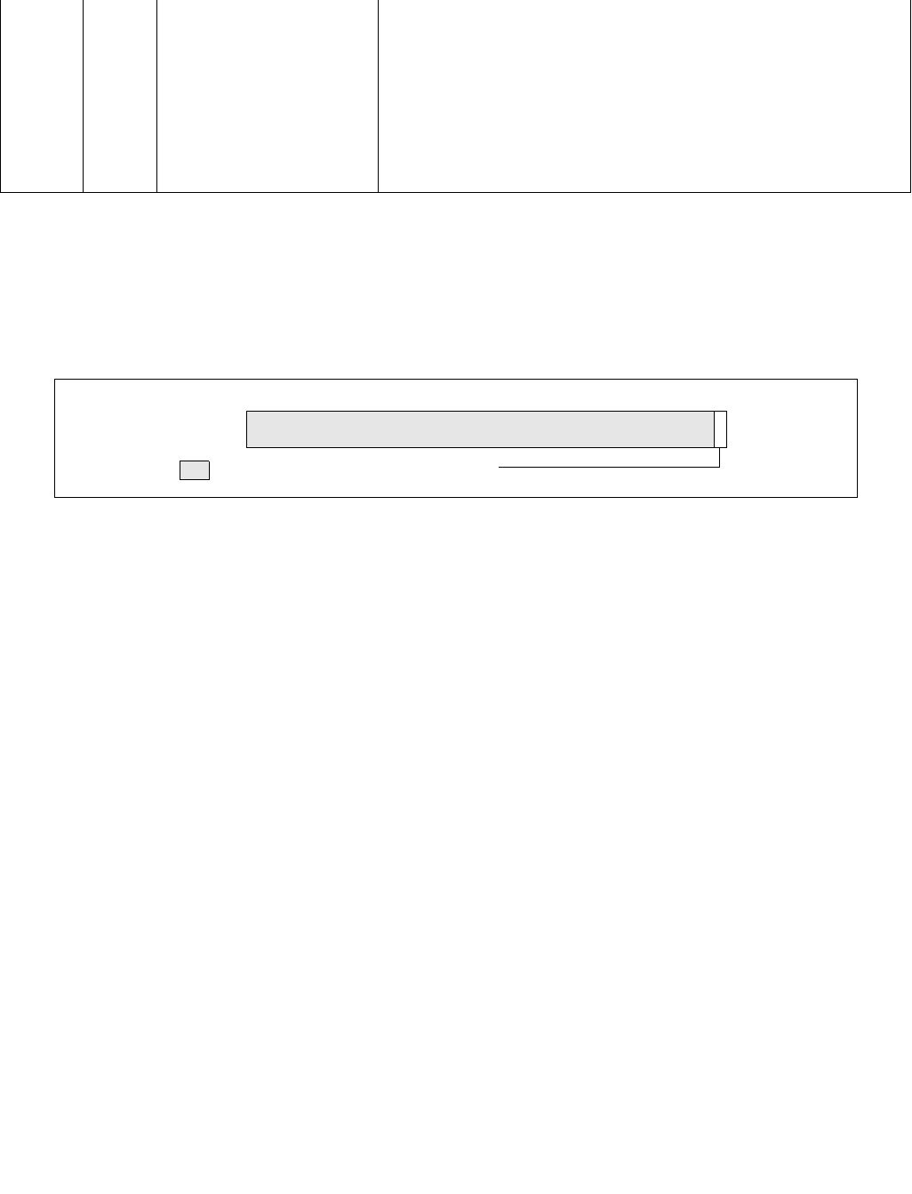
14-20 Vol. 3B
POWER AND THERMAL MANAGEMENT
14.5.2 Package level Enabling HDC
The layout of the IA32_PKG_HDC_CTL MSR is shown in Figure 14-16. IA32_PKG_HDC_CTL is a writable MSR from
any logical processor in a package. The bit fields are described below:
•HDC_PKG_Enable (bit 0, R/W) — Software sets this bit to enable HDC operation by allowing the processor
to force to idle all “HDC-allowed” (see Figure 14.5.3) logical processors in the package. Clearing this bit
disables HDC operation in the package by waking up all the processor cores that were forced into idle by a
previous ‘0’-to-’1’ transition in IA32_PKG_HDC_CTL.HDC_PKG_Enable. This bit is writable only if
CPUID.06H:EAX[bit 13] = 1. Default = zero (0).
•Bits 63:1 are reserved and must be zero.
After processor support is determined via CPUID, system software can enable HDC operation by setting
IA32_PKG_HDC_CTL.HDC_PKG_Enable to 1. At reset, IA32_PKG_HDC_CTL.HDC_PKG_Enable is cleared to 0. A
'0'-to-'1' transition in HDC_PKG_Enable allows the processor to force to idle all HDC-allowed (indicated by the non-
zero state of IA32_PM_CTL1[bit 0]) logical processors in the package. A ‘1’-to-’0’ transition wakes up those HDC
force-idled logical processors.
Software can enable or disable HDC using this package level control multiple times from any logical processor in the
package. Note the latency of writing a value to the package-visible IA32_PKG_HDC_CTL.HDC_PKG_Enable is
longer than the latency of a WRMSR operation to a Logical Processor MSR (as opposed to package level MSR) such
as: IA32_PM_CTL1 (described in Section 14.5.3). Propagation of the change in
IA32_PKG_HDC_CTL.HDC_PKG_Enable and reaching all HDC idled logical processor to be woken up may take on
the order of core C6 exit latency.
14.5.3 Logical-Processor Level HDC Control
The layout of the IA32_PM_CTL1 MSR is shown in Figure 14-17. Each logical processor in a package has its own
IA32_PM_CTL1 MSR. The bit fields are described below:
653H N MSR_CORE_HDC_RESIDENCY Core level stalled cycle counter due to HDC forced idling on one or more
logical processor.
655H N MSR_PKG_HDC_SHALLOW_RE
SIDENCY
Accumulate the cycles the package was in C21 state and at least one logical
processor was in forced idle
656H N MSR_PKG_HDC_DEEP_RESIDE
NCY
Accumulate the cycles the package was in the software specified Cx1 state
and at least one logical processor was in forced idle. Cx is specified in
MSR_PKG_HDC_CONFIG_CTL.
652H N MSR_PKG_HDC_CONFIG_CTL HDC configuration controls
NOTES:
1. The package “C-states” referred to in this section are processor-specific C-states.
Figure 14-16. IA32_PKG_HDC_CTL MSR
Table 14-2. Architectural and non-Architecture MSRs Related to HDC
63 0
Reserved
1
HDC_PKG_Enable
Reserved

Vol. 3B 14-21
POWER AND THERMAL MANAGEMENT
•HDC_Allow_Block (bit 0, R/W) — Software sets this bit to allow this logical processors to honor the
package-level IA32_PKG_HDC_CTL.HDC_PKG_Enable control. Clearing this bit prevents this logical processor
from using the HDC. This bit is writable only if CPUID.06H:EAX[bit 13] = 1. Default = one (1).
•Bits 63:1 are reserved and must be zero.
Fine-grain OS control of HDC operation at the granularity of per-logical-processor is provided by IA32_PM_CTL1.
At RESET, all logical processors are allowed to participate in HDC operation such that OS can manage HDC using
the package-level IA32_PKG_HDC_CTL.
Writes to IA32_PM_CTL1 complete with the latency that is typical to WRMSR to a Logical Processor level MSR.
When the OS chooses to manage HDC operation at per-logical-processor granularity, it can write to IA32_PM_CTL1
on one or more logical processors as desired. Each write to IA32_PM_CTL1 must be done by code that executes on
the logical processor targeted to be allowed into or blocked from HDC operation.
Blocking one logical processor for HDC operation may have package level impact. For example, the processor may
decide to stop duty cycling of all other Logical Processors as well.
The propagation of IA32_PKG_HDC_CTL.HDC_PKG_Enable in a package takes longer than a WRMSR to
IA32_PM_CTL1. The last completed write to IA32_PM_CTL1 on a logical processor will be honored when a ‘0’-to-’1’
transition of IA32_PKG_HDC_CTL.HDC_PKG_Enable arrives to a logical processor.
14.5.4 HDC Residency Counters
There is a collection of counters available for software to track various residency metrics related to HDC operation.
In general, HDC residency time is defined as the time in HDC forced idle state at the granularity of per-logical-
processor, per-core, or package. At the granularity of per-core/package-level HDC residency, at least one of the
logical processor in a core/package must be in the HDC forced idle state.
14.5.4.1 IA32_THREAD_STALL
Software can track per-logical-processor HDC residency using the architectural MSR IA32_THREAD_STALL.The
layout of the IA32_THREAD_STALL MSR is shown in Figure 14-18. Each logical processor in a package has its own
IA32_THREAD_STALL MSR. The bit fields are described below:
•Stall_Cycle_Cnt (bits 63:0, R/O) — Stores accumulated HDC forced-idle cycle count of this processor core
since last RESET. This counter increments at the same rate of the TSC. The count is updated only after the
logical processor exits from the forced idled C-state. At each update, the number of cycles that the logical
processor was stalled due to forced-idle will be added to the counter. This counter is available only if
CPUID.06H:EAX[bit 13] = 1. Default = zero (0).
Figure 14-17. IA32_PM_CTL1 MSR
Figure 14-18. IA32_THREAD_STALL MSR
63 0
Reserved
1
HDC_Allow_Block
Reserved
63 0
Stall_cycle_cnt
14-22 Vol. 3B
POWER AND THERMAL MANAGEMENT
A value of zero in IA32_THREAD_STALL indicates either HDC is not supported or the logical processor never
serviced any forced HDC idle. A non-zero value in IA32_THREAD_STALL indicates the HDC forced-idle residency
times of the logical processor. It also indicates the forced-idle cycles due to HDC that could appear as C0 time to
traditional OS accounting mechanisms (e.g. time-stamping OS idle/exit events).
Software can read IA32_THREAD_STALL irrespective of the state of IA32_PKG_HDC_CTL and IA32_PM_CTL1, as
long as CPUID.06H:EAX[bit 13] = 1.
14.5.4.2 Non-Architectural HDC Residency Counters
Processors that support HDC operation may provide the following model-specific HDC residency counters.
MSR_CORE_HDC_RESIDENCY
Software can track per-core HDC residency using the counter MSR_CORE_HDC_RESIDENCY. This counter incre-
ments when the core is in C3 state or deeper (all logical processors in this core are idle due to either HDC or other
mechanisms) and at least one of the logical processors is in HDC forced idle state. The layout of the
MSR_CORE_HDC_RESIDENCY is shown in Figure 14-19. Each processor core in a package has its own
MSR_CORE_HDC_RESIDENCY MSR. The bit fields are described below:
•Core_Cx_Duty_Cycle_Cnt (bits 63:0, R/O) — Stores accumulated HDC forced-idle cycle count of this
processor core since last RESET. This counter increments at the same rate of the TSC. The count is updated only
after core C-state exit from a forced idled C-state. At each update, the increment counts cycles when the core
is in a Cx state (all its logical processor are idle) and at least one logical processor in this core was forced into
idle state due to HDC. If CPUID.06H:EAX[bit 13] = 0, attempt to access this MSR will cause a #GP fault. Default
= zero (0).
A value of zero in MSR_CORE_HDC_RESIDENCY indicates either HDC is not supported or this processor core never
serviced any forced HDC idle.
MSR_PKG_HDC_SHALLOW_RESIDENCY
The counter MSR_PKG_HDC_SHALLOW_RESIDENCY allows software to track HDC residency time when the
package is in C2 state, all processor cores in the package are not active and at least one logical processor was
forced into idle state due to HDC. The layout of the MSR_PKG_HDC_SHALLOW_RESIDENCY is shown in
Figure 14-20. There is one MSR_PKG_HDC_SHALLOW_RESIDENCY per package. The bit fields are described
below:
•Pkg_Duty_Cycle_Cnt (bits 63:0, R/O) — Stores accumulated HDC forced-idle cycle count of this processor
core since last RESET. This counter increments at the same rate of the TSC.
Package shallow residency may be
implementation specific. In the initial implementation, the threshold is package C2-state.
The count is
updated only after package C2-state exit from a forced idled C-state. At each update, the increment counts
Figure 14-19. MSR_CORE_HDC_RESIDENCY MSR
Figure 14-20. MSR_PKG_HDC_SHALLOW_RESIDENCY MSR
63 0
Core_Cx_duty_cycle_cnt
63 0
Pkg_Duty_cycle_cnt
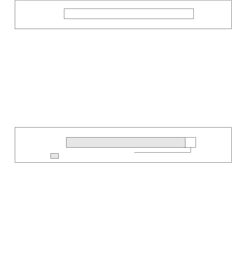
Vol. 3B 14-23
POWER AND THERMAL MANAGEMENT
cycles when the package is in C2 state and at least one processor core in this package was forced into idle state
due to HDC. If CPUID.06H:EAX[bit 13] = 0, attempt to access this MSR
may
cause a #GP fault. Default = zero
(0).
A value of zero in MSR_PKG_HDC_SHALLOW_RESIDENCY indicates either HDC is not supported or this processor
package never serviced any forced HDC idle.
MSR_PKG_HDC_DEEP_RESIDENCY
The counter MSR_PKG_HDC_DEEP_RESIDENCY allows software to track HDC residency time when the package is
in a software-specified package Cx state, all processor cores in the package are not active and at least one logical
processor was forced into idle state due to HDC. Selection of a specific package Cx state can be configured using
MSR_PKG_HDC_CONFIG. The layout of the MSR_PKG_HDC_DEEP_RESIDENCY is shown in Figure 14-21. There is
one MSR_PKG_HDC_DEEP_RESIDENCY per package. The bit fields are described below:
•Pkg_Cx_Duty_Cycle_Cnt (bits 63:0, R/O) — Stores accumulated HDC forced-idle cycle count of this
processor core since last RESET. This counter increments at the same rate of the TSC. The count is updated
only after package C-state exit from a forced idle state. At each update, the increment counts cycles when the
package is in the software-configured Cx state and at least one processor core in this package was forced into
idle state due to HDC. If CPUID.06H:EAX[bit 13] = 0, attempt to access this MSR
may
cause a #GP fault.
Default = zero (0).
A value of zero in MSR_PKG_HDC_SHALLOW_RESIDENCY indicates either HDC is not supported or this processor
package never serviced any forced HDC idle.
MSR_PKG_HDC_CONFIG
MSR_PKG_HDC_CONFIG allows software to configure the package Cx state that the counter
MSR_PKG_HDC_DEEP_RESIDENCY monitors. The layout of the MSR_PKG_HDC_CONFIG is shown in Figure 14-22.
There is one MSR_PKG_HDC_CONFIG per package. The bit fields are described below:
•Pkg_Cx_Monitor (bits 2:0, R/W) — Selects which package C-state the MSR_HDC_DEEP_RESIDENCY
counter will monitor. The encoding of the HDC_Cx_Monitor field are: 0: no-counting; 1: count package C2 only,
2: count package C3 and deeper; 3: count package C6 and deeper; 4: count package C7 and deeper; other
encodings are reserved. If CPUID.06H:EAX[bit 13] = 0, attempt to access this MSR
may
cause a #GP fault.
Default = zero (0).
•Bits 63:3 are reserved and must be zero.
Figure 14-21. MSR_PKG_HDC_DEEP_RESIDENCY MSR
Figure 14-22. MSR_PKG_HDC_CONFIG MSR
63 0
Pkg_Cx_duty_cycle_cnt
63 0
Reserved
2
HDC_Cx_Monitor
Reserved

14-24 Vol. 3B
POWER AND THERMAL MANAGEMENT
14.5.5 MPERF and APERF Counters Under HDC
HDC operation can be thought of as an average effective frequency drop due to all or some of the Logical Proces-
sors enter an idle state period.
By default, the IA32_MPERF counter counts during forced idle periods as if the logical processor was active. The
IA32_APERF counter does not count during forced idle state. This counting convention allows the OS to compute
the average effective frequency of the Logical Processor between the last MWAIT exit and the next MWAIT entry
(OS visible C0) by ΔACNT/ΔMCNT * TSC Frequency.
14.6 MWAIT EXTENSIONS FOR ADVANCED POWER MANAGEMENT
IA-32 processors may support a number of C-states1 that reduce power consumption for inactive states. Intel Core
Solo and Intel Core Duo processors support both deeper C-state and MWAIT extensions that can be used by OS to
implement power management policy.
Software should use CPUID to discover if a target processor supports the enumeration of MWAIT extensions. If
CPUID.05H.ECX[Bit 0] = 1, the target processor supports MWAIT extensions and their enumeration (see Chapter
4, “Instruction Set Reference, M-U,” of Intel® 64 and IA-32 Architectures Software Developer’s Manual, Volume
2B).
If CPUID.05H.ECX[Bit 1] = 1, the target processor supports using interrupts as break-events for MWAIT, even
when interrupts are disabled. Use this feature to measure C-state residency as follows:
•Software can write to bit 0 in the MWAIT Extensions register (ECX) when issuing an MWAIT to enter into a
processor-specific C-state or sub C-state.
•When a processor comes out of an inactive C-state or sub C-state, software can read a timestamp before an
interrupt service routine (ISR) is potentially executed.
CPUID.05H.EDX allows software to enumerate processor-specific C-states and sub C-states available for use with
MWAIT extensions. IA-32 processors may support more than one C-state of a given C-state type. These are called
sub C-states. Numerically higher C-state have higher power savings and latency (upon entering and exiting) than
lower-numbered C-state.
At CPL = 0, system software can specify desired C-state and sub C-state by using the MWAIT hints register (EAX).
Processors will not go to C-state and sub C-state deeper than what is specified by the hint register. If CPL > 0 and
if MONITOR/MWAIT is supported at CPL > 0, the processor will only enter C1-state (regardless of the C-state
request in the hints register).
Executing MWAIT generates an exception on processors operating at a privilege level where MONITOR/MWAIT are
not supported.
Figure 14-23. Example of Effective Frequency Reduction and Forced Idle Period of HDC
1. The processor-specific C-states defined in MWAIT extensions can map to ACPI defined C-state types (C0, C1, C2, C3). The mapping
relationship depends on the definition of a C-state by processor implementation and is exposed to OSPM by the BIOS using the ACPI
defined _CST table.
1600 MHz: 25% Utilization /75% Forced Idle
Effective Frequency @ 100% Utilization: 400 MHz
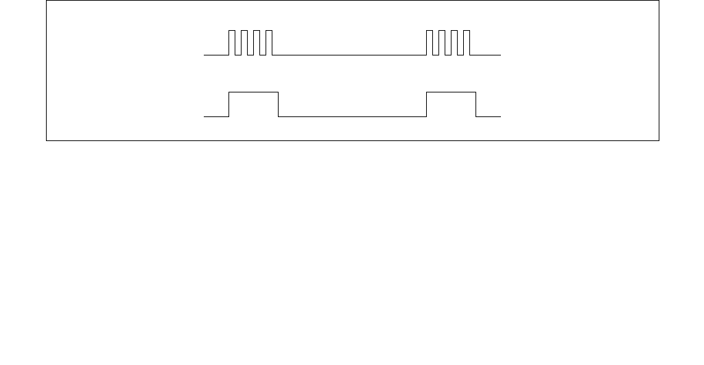
Vol. 3B 14-25
POWER AND THERMAL MANAGEMENT
NOTE
If MWAIT is used to enter a C-state (including sub C-state) that is numerically higher than C1, a
store to the address range armed by MONITOR instruction will cause the processor to exit MWAIT if
the store was originated by other processor agents. A store from non-processor agent may not
cause the processor to exit MWAIT.
14.7 THERMAL MONITORING AND PROTECTION
The IA-32 architecture provides the following mechanisms for monitoring temperature and controlling thermal
power:
1. The catastrophic shutdown detector forces processor execution to stop if the processor’s core temperature
rises above a preset limit.
2. Automatic and adaptive thermal monitoring mechanisms force the processor to reduce it’s power
consumption in order to operate within predetermined temperature limits.
3. The software controlled clock modulation mechanism permits operating systems to implement power
management policies that reduce power consumption; this is in addition to the reduction offered by automatic
thermal monitoring mechanisms.
4. On-die digital thermal sensor and interrupt mechanisms permit the OS to manage thermal conditions
natively without relying on BIOS or other system board components.
The first mechanism is not visible to software. The other three mechanisms are visible to software using processor
feature information returned by executing CPUID with EAX = 1.
The second mechanism includes:
•Automatic thermal monitoring provides two modes of operation. One mode modulates the clock duty cycle;
the second mode changes the processor’s frequency. Both modes are used to control the core temperature of
the processor.
•Adaptive thermal monitoring can provide flexible thermal management on processors made of multiple
cores.
The third mechanism modulates the clock duty cycle of the processor. As shown in Figure 14-24, the phrase ‘duty
cycle’ does not refer to the actual duty cycle of the clock signal. Instead it refers to the time period during which
the clock signal is allowed to drive the processor chip. By using the stop clock mechanism to control how often the
processor is clocked, processor power consumption can be modulated.
For previous automatic thermal monitoring mechanisms, software controlled mechanisms that changed processor
operating parameters to impact changes in thermal conditions. Software did not have native access to the native
thermal condition of the processor; nor could software alter the trigger condition that initiated software program
control.
The fourth mechanism (listed above) provides access to an on-die digital thermal sensor using a model-specific
register and uses an interrupt mechanism to alert software to initiate digital thermal monitoring.
Figure 14-24. Processor Modulation Through Stop-Clock Mechanism
Clock Applied to Processor
Stop-Clock Duty Cycle
25% Duty Cycle (example only)

14-26 Vol. 3B
POWER AND THERMAL MANAGEMENT
14.7.1 Catastrophic Shutdown Detector
P6 family processors introduced a thermal sensor that acts as a catastrophic shutdown detector. This catastrophic
shutdown detector was also implemented in Pentium 4, Intel Xeon and Pentium M processors. It is always enabled.
When processor core temperature reaches a factory preset level, the sensor trips and processor execution is halted
until after the next reset cycle.
14.7.2 Thermal Monitor
Pentium 4, Intel Xeon and Pentium M processors introduced a second temperature sensor that is factory-calibrated
to trip when the processor’s core temperature crosses a level corresponding to the recommended thermal design
envelop. The trip-temperature of the second sensor is calibrated below the temperature assigned to the cata-
strophic shutdown detector.
14.7.2.1 Thermal Monitor 1
The Pentium 4 processor uses the second temperature sensor in conjunction with a mechanism called Thermal
Monitor 1 (TM1) to control the core temperature of the processor. TM1 controls the processor’s temperature by
modulating the duty cycle of the processor clock. Modulation of duty cycles is processor model specific. Note that
the processors STPCLK# pin is not used here; the stop-clock circuitry is controlled internally.
Support for TM1 is indicated by CPUID.1:EDX.TM[bit 29] = 1.
TM1 is enabled by setting the thermal-monitor enable flag (bit 3) in IA32_MISC_ENABLE [see Chapter 2, “Model-
Specific Registers (MSRs)” in the Intel® 64 and IA-32 Architectures Software Developer’s Manual, Volume 4].
Following a power-up or reset, the flag is cleared, disabling TM1. BIOS is required to enable only one automatic
thermal monitoring modes. Operating systems and applications must not disable the operation of these mecha-
nisms.
14.7.2.2 Thermal Monitor 2
An additional automatic thermal protection mechanism, called Thermal Monitor 2 (TM2), was introduced in the
Intel Pentium M processor and also incorporated in newer models of the Pentium 4 processor family. Intel Core Duo
and Solo processors, and Intel Core 2 Duo processor family all support TM1 and TM2. TM2 controls the core
temperature of the processor by reducing the operating frequency and voltage of the processor and offers a higher
performance level for a given level of power reduction than TM1.
TM2 is triggered by the same temperature sensor as TM1. The mechanism to enable TM2 may be implemented
differently across various IA-32 processor families with different CPUID signatures in the family encoding value, but
will be uniform within an IA-32 processor family.
Support for TM2 is indicated by CPUID.1:ECX.TM2[bit 8] = 1.
14.7.2.3 Two Methods for Enabling TM2
On processors with CPUID family/model/stepping signature encoded as 0x69n or 0x6Dn (early Pentium M proces-
sors), TM2 is enabled if the TM_SELECT flag (bit 16) of the MSR_THERM2_CTL register is set to 1 (Figure 14-25)
and bit 3 of the IA32_MISC_ENABLE register is set to 1.
Following a power-up or reset, the TM_SELECT flag may be cleared. BIOS is required to enable either TM1 or TM2.
Operating systems and applications must not disable mechanisms that enable TM1 or TM2. If bit 3 of the
IA32_MISC_ENABLE register is set and TM_SELECT flag of the MSR_THERM2_CTL register is cleared, TM1 is
enabled.
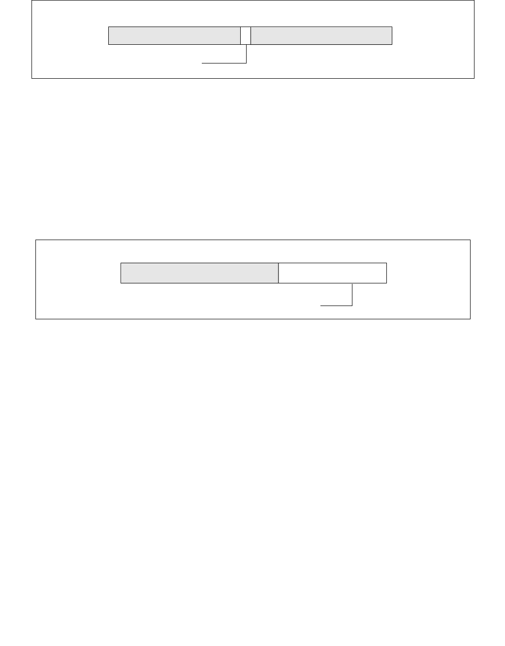
Vol. 3B 14-27
POWER AND THERMAL MANAGEMENT
On processors introduced after the Pentium 4 processor (this includes most Pentium M processors), the method
used to enable TM2 is different. TM2 is enable by setting bit 13 of IA32_MISC_ENABLE register to 1. This applies to
Intel Core Duo, Core Solo, and Intel Core 2 processor family.
The target operating frequency and voltage for the TM2 transition after TM2 is triggered is specified by the value
written to MSR_THERM2_CTL, bits 15:0 (Figure 14-26). Following a power-up or reset, BIOS is required to enable
at least one of these two thermal monitoring mechanisms. If both TM1 and TM2 are supported, BIOS may choose
to enable TM2 instead of TM1. Operating systems and applications must not disable the mechanisms that enable
TM1or TM2; and they must not alter the value in bits 15:0 of the MSR_THERM2_CTL register.
14.7.2.4 Performance State Transitions and Thermal Monitoring
If the thermal control circuitry (TCC) for thermal monitor (TM1/TM2) is active, writes to the IA32_PERF_CTL will
effect a new target operating point as follows:
•If TM1 is enabled and the TCC is engaged, the performance state transition can commence before the TCC is
disengaged.
•If TM2 is enabled and the TCC is engaged, the performance state transition specified by a write to the
IA32_PERF_CTL will commence after the TCC has disengaged.
14.7.2.5 Thermal Status Information
The status of the temperature sensor that triggers the thermal monitor (TM1/TM2) is indicated through the thermal
status flag and thermal status log flag in the IA32_THERM_STATUS MSR (see Figure 14-27).
The functions of these flags are:
•Thermal Status flag, bit 0 — When set, indicates that the processor core temperature is currently at the trip
temperature of the thermal monitor and that the processor power consumption is being reduced via either TM1
or TM2, depending on which is enabled. When clear, the flag indicates that the core temperature is below the
thermal monitor trip temperature. This flag is read only.
•Thermal Status Log flag, bit 1 — When set, indicates that the thermal sensor has tripped since the last
power-up or reset or since the last time that software cleared this flag. This flag is a sticky bit; once set it
remains set until cleared by software or until a power-up or reset of the processor. The default state is clear.
Figure 14-25. MSR_THERM2_CTL Register On Processors with CPUID Family/Model/Stepping Signature Encoded
as 0x69n or 0x6Dn
Figure 14-26. MSR_THERM2_CTL Register for Supporting TM2
TM_SELECT
Reserved
31 0
Reserved
16
63 0
Reserved
15
TM2 Transition Target

14-28 Vol. 3B
POWER AND THERMAL MANAGEMENT
After the second temperature sensor has been tripped, the thermal monitor (TM1/TM2) will remain engaged for a
minimum time period (on the order of 1 ms). The thermal monitor will remain engaged until the processor core
temperature drops below the preset trip temperature of the temperature sensor, taking hysteresis into account.
While the processor is in a stop-clock state, interrupts will be blocked from interrupting the processor. This holding
off of interrupts increases the interrupt latency, but does not cause interrupts to be lost. Outstanding interrupts
remain pending until clock modulation is complete.
The thermal monitor can be programmed to generate an interrupt to the processor when the thermal sensor is
tripped. The delivery mode, mask and vector for this interrupt can be programmed through the thermal entry in the
local APIC’s LVT (see Section 10.5.1, “Local Vector Table”). The low-temperature interrupt enable and high-
temperature interrupt enable flags in the IA32_THERM_INTERRUPT MSR (see Figure 14-28) control when the
interrupt is generated; that is, on a transition from a temperature below the trip point to above and/or vice-versa.
•High-Temperature Interrupt Enable flag, bit 0 — Enables an interrupt to be generated on the transition
from a low-temperature to a high-temperature when set; disables the interrupt when clear.(R/W).
•Low-Temperature Interrupt Enable flag, bit 1 — Enables an interrupt to be generated on the transition
from a high-temperature to a low-temperature when set; disables the interrupt when clear.
The thermal monitor interrupt can be masked by the thermal LVT entry. After a power-up or reset, the low-temper-
ature interrupt enable and high-temperature interrupt enable flags in the IA32_THERM_INTERRUPT MSR are
cleared (interrupts are disabled) and the thermal LVT entry is set to mask interrupts. This interrupt should be
handled either by the operating system or system management mode (SMM) code.
Note that the operation of the thermal monitoring mechanism has no effect upon the clock rate of the processor's
internal high-resolution timer (time stamp counter).
14.7.2.6 Adaptive Thermal Monitor
The Intel Core 2 Duo processor family supports enhanced thermal management mechanism, referred to as Adap-
tive Thermal Monitor (Adaptive TM).
Unlike TM2, Adaptive TM is not limited to one TM2 transition target. During a thermal trip event, Adaptive TM (if
enabled) selects an optimal target operating point based on whether or not the current operating point has effec-
tively cooled the processor.
Similar to TM2, Adaptive TM is enable by BIOS. The BIOS is required to test the TM1 and TM2 feature flags and
enable all available thermal control mechanisms (including Adaptive TM) at platform initiation.
Adaptive TM is available only to a subset of processors that support TM2.
Figure 14-27. IA32_THERM_STATUS MSR
Figure 14-28. IA32_THERM_INTERRUPT MSR
63 0
Reserved
12
Thermal Status
Thermal Status Log
63 0
Reserved
12
High-Temperature Interrupt Enable
Low-Temperature Interrupt Enable

Vol. 3B 14-29
POWER AND THERMAL MANAGEMENT
In each chip-multiprocessing (CMP) silicon die, each core has a unique thermal sensor that triggers independently.
These thermal sensor can trigger TM1 or TM2 transitions in the same manner as described in Section 14.7.2.1 and
Section 14.7.2.2. The trip point of the thermal sensor is not programmable by software since it is set during the
fabrication of the processor.
Each thermal sensor in a processor core may be triggered independently to engage thermal management features.
In Adaptive TM, both cores will transition to a lower frequency and/or lower voltage level if one sensor is triggered.
Triggering of this sensor is visible to software via the thermal interrupt LVT entry in the local APIC of a given core.
14.7.3 Software Controlled Clock Modulation
Pentium 4, Intel Xeon and Pentium M processors also support software-controlled clock modulation. This provides
a means for operating systems to implement a power management policy to reduce the power consumption of the
processor. Here, the stop-clock duty cycle is controlled by software through the IA32_CLOCK_MODULATION MSR
(see Figure 14-29).
The IA32_CLOCK_MODULATION MSR contains the following flag and field used to enable software-controlled clock
modulation and to select the clock modulation duty cycle:
•On-Demand Clock Modulation Enable, bit 4 — Enables on-demand software controlled clock modulation
when set; disables software-controlled clock modulation when clear.
•On-Demand Clock Modulation Duty Cycle, bits 1 through 3 — Selects the on-demand clock modulation
duty cycle (see Table 14-3). This field is only active when the on-demand clock modulation enable flag is set.
Note that the on-demand clock modulation mechanism (like the thermal monitor) controls the processor’s stop-
clock circuitry internally to modulate the clock signal. The STPCLK# pin is not used in this mechanism.
The on-demand clock modulation mechanism can be used to control processor power consumption. Power
management software can write to the IA32_CLOCK_MODULATION MSR to enable clock modulation and to select
a modulation duty cycle. If on-demand clock modulation and TM1 are both enabled and the thermal status of the
processor is hot (bit 0 of the IA32_THERM_STATUS MSR is set), clock modulation at the duty cycle specified by TM1
takes precedence, regardless of the setting of the on-demand clock modulation duty cycle.
Figure 14-29. IA32_CLOCK_MODULATION MSR
Table 14-3. On-Demand Clock Modulation Duty Cycle Field Encoding
Duty Cycle Field Encoding Duty Cycle
000B Reserved
001B 12.5% (Default)
010B 25.0%
011B 37.5%
100B 50.0%
101B 63.5%
110B 75%
111B 87.5%
63 0
Reserved
13
On-Demand Clock Modulation Duty Cycle
On-Demand Clock Modulation Enable
45
Reserved
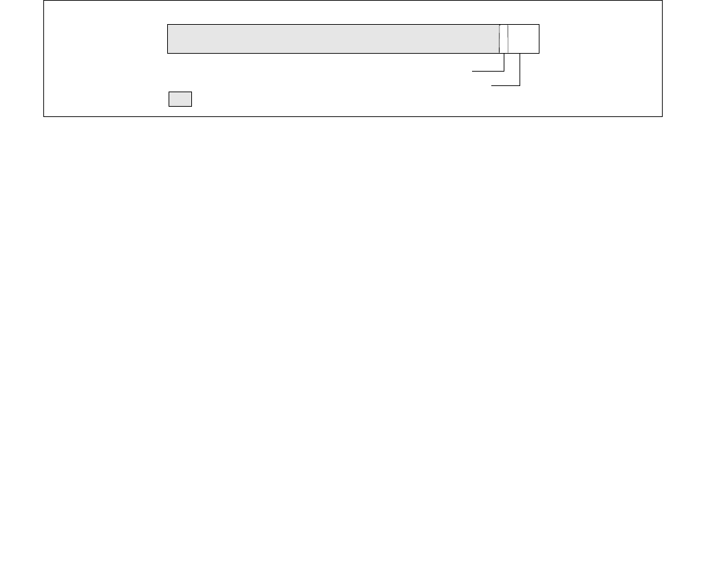
14-30 Vol. 3B
POWER AND THERMAL MANAGEMENT
For Hyper-Threading Technology enabled processors, the IA32_CLOCK_MODULATION register is duplicated for
each logical processor. In order for the On-demand clock modulation feature to work properly, the feature must be
enabled on all the logical processors within a physical processor. If the programmed duty cycle is not identical for
all the logical processors, the processor core clock will modulate to the highest duty cycle programmed for proces-
sors with any of the following CPUID DisplayFamily_DisplayModel signatures (see CPUID instruction in Chapter3,
“Instruction Set Reference, A-L” in the Intel® 64 and IA-32 Architectures Software Developer’s Manual, Volume
2A): 06_1A, 06_1C, 06_1E, 06_1F, 06_25, 06_26, 06_27, 06_2C, 06_2E, 06_2F, 06_35, 06_36, and 0F_xx. For all
other processors, if the programmed duty cycle is not identical for all logical processors in the same core, the
processor core will modulate at the lowest programmed duty cycle.
For multiple processor cores in a physical package, each processor core can modulate to a programmed duty cycle
independently.
For the P6 family processors, on-demand clock modulation was implemented through the chipset, which controlled
clock modulation through the processor’s STPCLK# pin.
14.7.3.1 Extension of Software Controlled Clock Modulation
Extension of the software controlled clock modulation facility supports on-demand clock modulation duty cycle with
4-bit dynamic range (increased from 3-bit range). Granularity of clock modulation duty cycle is increased to 6.25%
(compared to 12.5%).
Four bit dynamic range control is provided by using bit 0 in conjunction with bits 3:1 of the
IA32_CLOCK_MODULATION MSR (see Figure 14-30).
Extension to software controlled clock modulation is supported only if CPUID.06H:EAX[Bit 5] = 1. If
CPUID.06H:EAX[Bit 5] = 0, then bit 0 of IA32_CLOCK_MODULATION is reserved.
14.7.4 Detection of Thermal Monitor and Software Controlled
Clock Modulation Facilities
The ACPI flag (bit 22) of the CPUID feature flags indicates the presence of the IA32_THERM_STATUS,
IA32_THERM_INTERRUPT, IA32_CLOCK_MODULATION MSRs, and the xAPIC thermal LVT entry.
The TM1 flag (bit 29) of the CPUID feature flags indicates the presence of the automatic thermal monitoring facili-
ties that modulate clock duty cycles.
14.7.4.1 Detection of Software Controlled Clock Modulation Extension
Processor’s support of software controlled clock modulation extension is indicated by CPUID.06H:EAX[Bit 5] = 1.
14.7.5 On Die Digital Thermal Sensors
On die digital thermal sensor can be read using an MSR (no I/O interface). In Intel Core Duo processors, each core
has a unique digital sensor whose temperature is accessible using an MSR. The digital thermal sensor is the
preferred method for reading the die temperature because (a) it is located closer to the hottest portions of the die,
(b) it enables software to accurately track the die temperature and the potential activation of thermal throttling.
Figure 14-30. IA32_CLOCK_MODULATION MSR with Clock Modulation Extension
63 0
Reserved
3
Extended On-Demand Clock Modulation Duty Cycle
On-Demand Clock Modulation Enable
45
Reserved
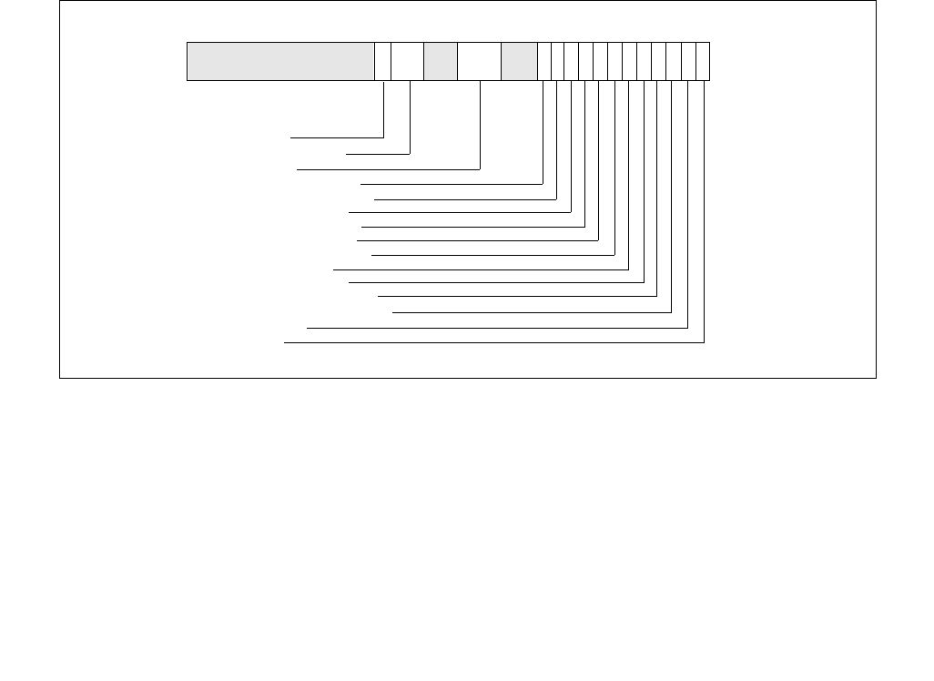
Vol. 3B 14-31
POWER AND THERMAL MANAGEMENT
14.7.5.1 Digital Thermal Sensor Enumeration
The processor supports a digital thermal sensor if CPUID.06H.EAX[0] = 1. If the processor supports digital thermal
sensor, EBX[bits 3:0] determine the number of thermal thresholds that are available for use.
Software sets thermal thresholds by using the IA32_THERM_INTERRUPT MSR. Software reads output of the digital
thermal sensor using the IA32_THERM_STATUS MSR.
14.7.5.2 Reading the Digital Sensor
Unlike traditional analog thermal devices, the output of the digital thermal sensor is a temperature relative to the
maximum supported operating temperature of the processor.
Temperature measurements returned by digital thermal sensors are always at or below TCC activation tempera-
ture. Critical temperature conditions are detected using the “Critical Temperature Status” bit. When this bit is set,
the processor is operating at a critical temperature and immediate shutdown of the system should occur. Once the
“Critical Temperature Status” bit is set, reliable operation is not guaranteed.
See Figure 14-31 for the layout of IA32_THERM_STATUS MSR. Bit fields include:
•Thermal Status (bit 0, RO) — This bit indicates whether the digital thermal sensor high-temperature output
signal (PROCHOT#) is currently active. Bit 0 = 1 indicates the feature is active. This bit may not be written by
software; it reflects the state of the digital thermal sensor.
•Thermal Status Log (bit 1, R/WC0) — This is a sticky bit that indicates the history of the thermal sensor
high temperature output signal (PROCHOT#). Bit 1 = 1 if PROCHOT# has been asserted since a previous
RESET or the last time software cleared the bit. Software may clear this bit by writing a zero.
•PROCHOT# or FORCEPR# Event (bit 2, RO) — Indicates whether PROCHOT# or FORCEPR# is being
asserted by another agent on the platform.
•PROCHOT# or FORCEPR# Log (bit 3, R/WC0) — Sticky bit that indicates whether PROCHOT# or
FORCEPR# has been asserted by another agent on the platform since the last clearing of this bit or a reset. If
bit 3 = 1, PROCHOT# or FORCEPR# has been externally asserted. Software may clear this bit by writing a zero.
External PROCHOT# assertions are only acknowledged if the Bidirectional Prochot feature is enabled.
•Critical Temperature Status (bit 4, RO) — Indicates whether the critical temperature detector output signal
is currently active. If bit 4 = 1, the critical temperature detector output signal is currently active.
Figure 14-31. IA32_THERM_STATUS Register
63
0
Reserved
15
Reading Valid
12345810
16222327
Resolution in Deg. Celsius
Digital Readout
Thermal Threshold #2 Log
Thermal Threshold #2 Status
Thermal Threshold #1 Log
Thermal Threshold #1 Status
Critical Temperature Log
679
3132
Critical Temperature Status
PROCHOT# or FORCEPR# Log
PROCHOT# or FORCEPR# Event
Thermal Status Log
Thermal Status
11
Power Limit Notification Log
Power Limit Notification Status

14-32 Vol. 3B
POWER AND THERMAL MANAGEMENT
•Critical Temperature Log (bit 5, R/WC0) — Sticky bit that indicates whether the critical temperature
detector output signal has been asserted since the last clearing of this bit or reset. If bit 5 = 1, the output
signal has been asserted. Software may clear this bit by writing a zero.
•Thermal Threshold #1 Status (bit 6, RO) — Indicates whether the actual temperature is currently higher
than or equal to the value set in Thermal Threshold #1. If bit 6 = 0, the actual temperature is lower. If
bit 6 = 1, the actual temperature is greater than or equal to TT#1. Quantitative information of actual
temperature can be inferred from Digital Readout, bits 22:16.
•Thermal Threshold #1 Log (bit 7, R/WC0) — Sticky bit that indicates whether the Thermal Threshold #1
has been reached since the last clearing of this bit or a reset. If bit 7 = 1, the Threshold #1 has been reached.
Software may clear this bit by writing a zero.
•Thermal Threshold #2 Status (bit 8, RO) — Indicates whether actual temperature is currently higher than
or equal to the value set in Thermal Threshold #2. If bit 8 = 0, the actual temperature is lower. If bit 8 = 1, the
actual temperature is greater than or equal to TT#2. Quantitative information of actual temperature can be
inferred from Digital Readout, bits 22:16.
•Thermal Threshold #2 Log (bit 9, R/WC0) — Sticky bit that indicates whether the Thermal Threshold #2
has been reached since the last clearing of this bit or a reset. If bit 9 = 1, the Thermal Threshold #2 has been
reached. Software may clear this bit by writing a zero.
•Power Limitation Status (bit 10, RO) — Indicates whether the processor is currently operating below OS-
requested P-state (specified in IA32_PERF_CTL) or OS-requested clock modulation duty cycle (specified in
IA32_CLOCK_MODULATION). This field is supported only if CPUID.06H:EAX[bit 4] = 1. Package level power
limit notification can be delivered independently to IA32_PACKAGE_THERM_STATUS MSR.
•Power Notification Log (bit 11, R/WCO) — Sticky bit that indicates the processor went below OS-requested
P-state or OS-requested clock modulation duty cycle since the last clearing of this or RESET. This field is
supported only if CPUID.06H:EAX[bit 4] = 1. Package level power limit notification is indicated independently
in IA32_PACKAGE_THERM_STATUS MSR.
•Digital Readout (bits 22:16, RO) — Digital temperature reading in 1 degree Celsius relative to the TCC
activation temperature.
0: TCC Activation temperature,
1: (TCC Activation - 1) , etc. See the processor’s data sheet for details regarding TCC activation.
A lower reading in the Digital Readout field (bits 22:16) indicates a higher actual temperature.
•Resolution in Degrees Celsius (bits 30:27, RO) — Specifies the resolution (or tolerance) of the digital
thermal sensor. The value is in degrees Celsius. It is recommended that new threshold values be offset from the
current temperature by at least the resolution + 1 in order to avoid hysteresis of interrupt generation.
•Reading Valid (bit 31, RO) — Indicates if the digital readout in bits 22:16 is valid. The readout is valid if
bit 31 = 1.
Changes to temperature can be detected using two thresholds (see Figure 14-32); one is set above and the other
below the current temperature. These thresholds have the capability of generating interrupts using the core's local
APIC which software must then service. Note that the local APIC entries used by these thresholds are also used by
the Intel® Thermal Monitor; it is up to software to determine the source of a specific interrupt.
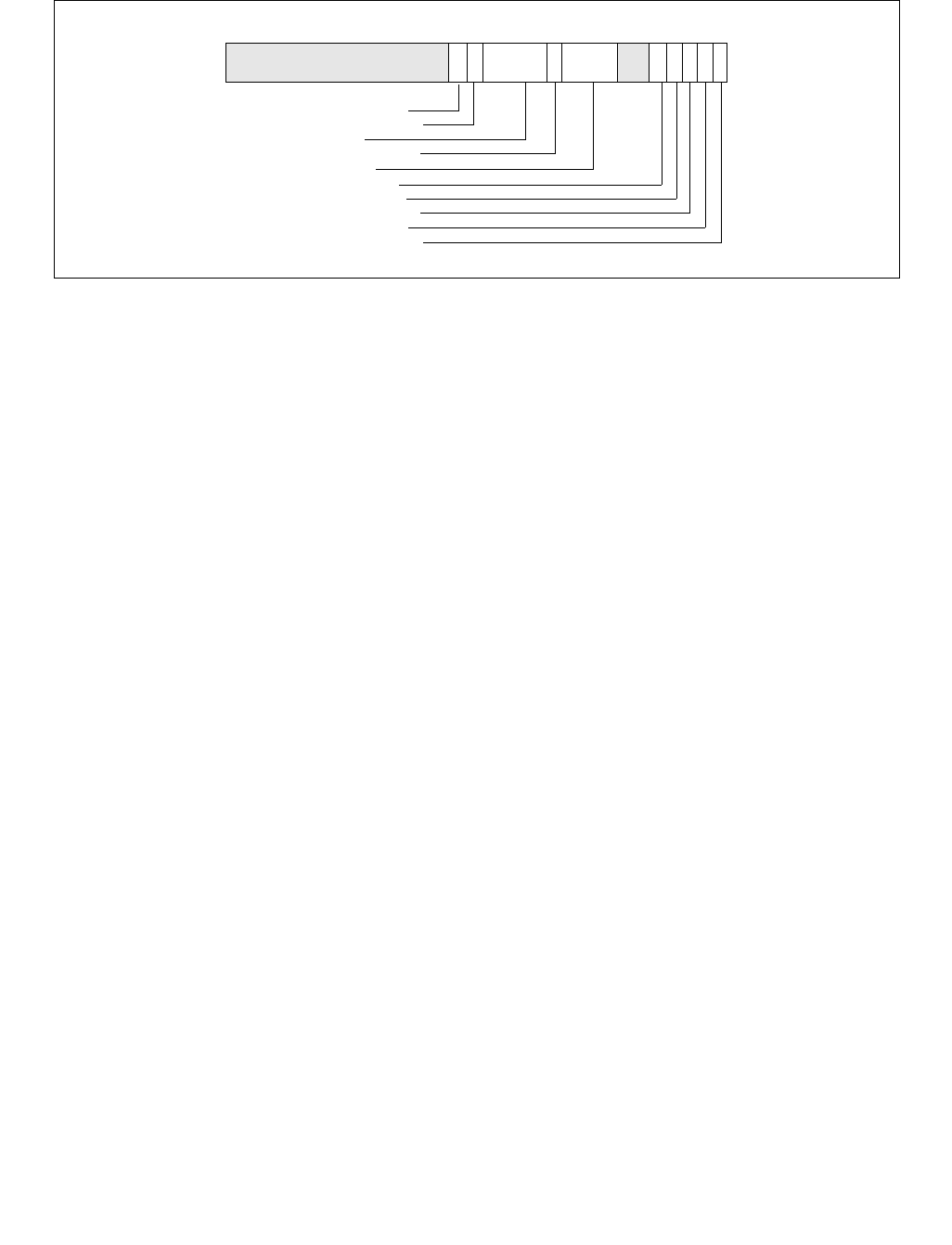
Vol. 3B 14-33
POWER AND THERMAL MANAGEMENT
See Figure 14-32 for the layout of IA32_THERM_INTERRUPT MSR. Bit fields include:
•High-Temperature Interrupt Enable (bit 0, R/W) — This bit allows the BIOS to enable the generation of
an interrupt on the transition from low-temperature to a high-temperature threshold. Bit 0 = 0 (default)
disables interrupts; bit 0 = 1 enables interrupts.
•Low-Temperature Interrupt Enable (bit 1, R/W) — This bit allows the BIOS to enable the generation of an
interrupt on the transition from high-temperature to a low-temperature (TCC de-activation). Bit 1 = 0 (default)
disables interrupts; bit 1 = 1 enables interrupts.
•PROCHOT# Interrupt Enable (bit 2, R/W) — This bit allows the BIOS or OS to enable the generation of an
interrupt when PROCHOT# has been asserted by another agent on the platform and the Bidirectional Prochot
feature is enabled. Bit 2 = 0 disables the interrupt; bit 2 = 1 enables the interrupt.
•FORCEPR# Interrupt Enable (bit 3, R/W) — This bit allows the BIOS or OS to enable the generation of an
interrupt when FORCEPR# has been asserted by another agent on the platform. Bit 3 = 0 disables the
interrupt; bit 3 = 1 enables the interrupt.
•Critical Temperature Interrupt Enable (bit 4, R/W) — Enables the generation of an interrupt when the
Critical Temperature Detector has detected a critical thermal condition. The recommended response to this
condition is a system shutdown. Bit 4 = 0 disables the interrupt; bit 4 = 1 enables the interrupt.
•Threshold #1 Value (bits 14:8, R/W) — A temperature threshold, encoded relative to the TCC Activation
temperature (using the same format as the Digital Readout). This threshold is compared against the Digital
Readout and is used to generate the Thermal Threshold #1 Status and Log bits as well as the Threshold #1
thermal interrupt delivery.
•Threshold #1 Interrupt Enable (bit 15, R/W) — Enables the generation of an interrupt when the actual
temperature crosses the Threshold #1 setting in any direction. Bit 15 = 1 enables the interrupt; bit 15 = 0
disables the interrupt.
•Threshold #2 Value (bits 22:16, R/W) —A temperature threshold, encoded relative to the TCC Activation
temperature (using the same format as the Digital Readout). This threshold is compared against the Digital
Readout and is used to generate the Thermal Threshold #2 Status and Log bits as well as the Threshold #2
thermal interrupt delivery.
•Threshold #2 Interrupt Enable (bit 23, R/W) — Enables the generation of an interrupt when the actual
temperature crosses the Threshold #2 setting in any direction. Bit 23 = 1enables the interrupt; bit 23 = 0
disables the interrupt.
•Power Limit Notification Enable (bit 24, R/W) — Enables the generation of power notification events when
the processor went below OS-requested P-state or OS-requested clock modulation duty cycle. This field is
supported only if CPUID.06H:EAX[bit 4] = 1. Package level power limit notification can be enabled indepen-
dently by IA32_PACKAGE_THERM_INTERRUPT MSR.
Figure 14-32. IA32_THERM_INTERRUPT Register
63 0
Reserved
15
Threshold #2 Interrupt Enable
1234581416222324
Threshold #2 Value
Threshold #1 Interrupt Enable
Threshold #1 Value
Overheat Interrupt Enable
FORCPR# Interrupt Enable
PROCHOT# Interrupt Enable
Low Temp. Interrupt Enable
High Temp. Interrupt Enable
25
Power Limit Notification Enable
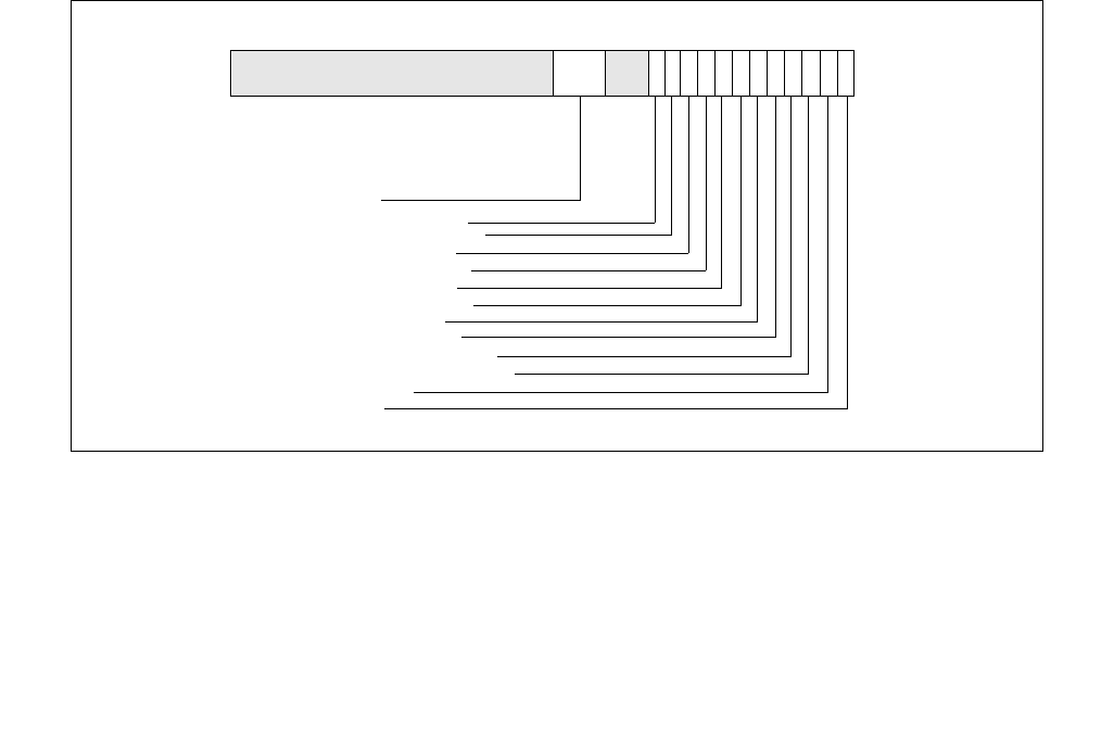
14-34 Vol. 3B
POWER AND THERMAL MANAGEMENT
14.7.6 Power Limit Notification
Platform firmware may be capable of specifying a power limit to restrict power delivered to a platform component,
such as a physical processor package. This constraint imposed by platform firmware may occasionally cause the
processor to operate below OS-requested P or T-state. A power limit notification event can be delivered using the
existing thermal LVT entry in the local APIC.
Software can enumerate the presence of the processor’s support for power limit notification by verifying
CPUID.06H:EAX[bit 4] = 1.
If CPUID.06H:EAX[bit 4] = 1, then IA32_THERM_INTERRUPT and IA32_THERM_STATUS provides the following
facility to manage power limit notification:
•Bits 10 and 11 in IA32_THERM_STATUS informs software of the occurrence of processor operating below OS-
requested P-state or clock modulation duty cycle setting (see Figure 14-31).
•Bit 24 in IA32_THERM_INTERRUPT enables the local APIC to deliver a thermal event when the processor went
below OS-requested P-state or clock modulation duty cycle setting (see Figure 14-32).
14.8 PACKAGE LEVEL THERMAL MANAGEMENT
The thermal management facilities like IA32_THERM_INTERRUPT and IA32_THERM_STATUS are often imple-
mented with a processor core granularity. To facilitate software manage thermal events from a package level gran-
ularity, two architectural MSR is provided for package level thermal management. The
IA32_PACKAGE_THERM_STATUS and IA32_PACKAGE_THERM_INTERRUPT MSRs use similar interfaces as
IA32_THERM_STATUS and IA32_THERM_INTERRUPT, but are shared in each physical processor package.
Software can enumerate the presence of the processor’s support for package level thermal management facility
(IA32_PACKAGE_THERM_STATUS and IA32_PACKAGE_THERM_INTERRUPT) by verifying CPUID.06H:EAX[bit 6] =
1.
The layout of IA32_PACKAGE_THERM_STATUS MSR is shown in Figure 14-33.
•Package Thermal Status (bit 0, RO) — This bit indicates whether the digital thermal sensor high-
temperature output signal (PROCHOT#) for the package is currently active. Bit 0 = 1 indicates the feature is
active. This bit may not be written by software; it reflects the state of the digital thermal sensor.
Figure 14-33. IA32_PACKAGE_THERM_STATUS Register
63
0
Reserved
15
12345810
16222327
PKG Digital Readout
PKG Thermal Threshold #2 Log
PKG Thermal Threshold #2 Status
PKG Thermal Threshold #1 Log
PKG Thermal Threshold #1 Status
PKG Critical Temperature Log
679
3132
PKG Critical Temperature Status
PKG PROCHOT# or FORCEPR# Log
PKG PROCHOT# or FORCEPR# Event
PKG Thermal Status Log
PKG Thermal Status
11
PKG Power Limit Notification Log
PKG Power Limit Notification Status

Vol. 3B 14-35
POWER AND THERMAL MANAGEMENT
•Package Thermal Status Log (bit 1, R/WC0) — This is a sticky bit that indicates the history of the thermal
sensor high temperature output signal (PROCHOT#) of the package. Bit 1 = 1 if package PROCHOT# has been
asserted since a previous RESET or the last time software cleared the bit. Software may clear this bit by writing
a zero.
•Package PROCHOT# Event (bit 2, RO) — Indicates whether package PROCHOT# is being asserted by
another agent on the platform.
•Package PROCHOT# Log (bit 3, R/WC0) — Sticky bit that indicates whether package PROCHOT# has been
asserted by another agent on the platform since the last clearing of this bit or a reset. If bit 3 = 1, package
PROCHOT# has been externally asserted. Software may clear this bit by writing a zero.
•Package Critical Temperature Status (bit 4, RO) — Indicates whether the package critical temperature
detector output signal is currently active. If bit 4 = 1, the package critical temperature detector output signal
is currently active.
•Package Critical Temperature Log (bit 5, R/WC0) — Sticky bit that indicates whether the package critical
temperature detector output signal has been asserted since the last clearing of this bit or reset. If bit 5 = 1, the
output signal has been asserted. Software may clear this bit by writing a zero.
•Package Thermal Threshold #1 Status (bit 6, RO) — Indicates whether the actual package temperature is
currently higher than or equal to the value set in Package Thermal Threshold #1. If bit 6 = 0, the actual
temperature is lower. If bit 6 = 1, the actual temperature is greater than or equal to PTT#1. Quantitative
information of actual package temperature can be inferred from Package Digital Readout, bits 22:16.
•Package Thermal Threshold #1 Log (bit 7, R/WC0) — Sticky bit that indicates whether the Package
Thermal Threshold #1 has been reached since the last clearing of this bit or a reset. If bit 7 = 1, the Package
Threshold #1 has been reached. Software may clear this bit by writing a zero.
•Package Thermal Threshold #2 Status (bit 8, RO) — Indicates whether actual package temperature is
currently higher than or equal to the value set in Package Thermal Threshold #2. If bit 8 = 0, the actual
temperature is lower. If bit 8 = 1, the actual temperature is greater than or equal to PTT#2. Quantitative
information of actual temperature can be inferred from Package Digital Readout, bits 22:16.
•Package Thermal Threshold #2 Log (bit 9, R/WC0) — Sticky bit that indicates whether the Package
Thermal Threshold #2 has been reached since the last clearing of this bit or a reset. If bit 9 = 1, the Package
Thermal Threshold #2 has been reached. Software may clear this bit by writing a zero.
•Package Power Limitation Status (bit 10, RO) — Indicates package power limit is forcing one ore more
processors to operate below OS-requested P-state. Note that package power limit violation may be caused by
processor cores or by devices residing in the uncore. Software can examine IA32_THERM_STATUS to
determine if the cause originates from a processor core (see Figure 14-31).
•Package Power Notification Log (bit 11, R/WCO) — Sticky bit that indicates any processor in the package
went below OS-requested P-state or OS-requested clock modulation duty cycle since the last clearing of this or
RESET.
•Package Digital Readout (bits 22:16, RO) — Package digital temperature reading in 1 degree Celsius
relative to the package TCC activation temperature.
0: Package TCC Activation temperature,
1: (PTCC Activation - 1) , etc. See the processor’s data sheet for details regarding PTCC activation.
A lower reading in the Package Digital Readout field (bits 22:16) indicates a higher actual temperature.
The layout of IA32_PACKAGE_THERM_INTERRUPT MSR is shown in Figure 14-34.
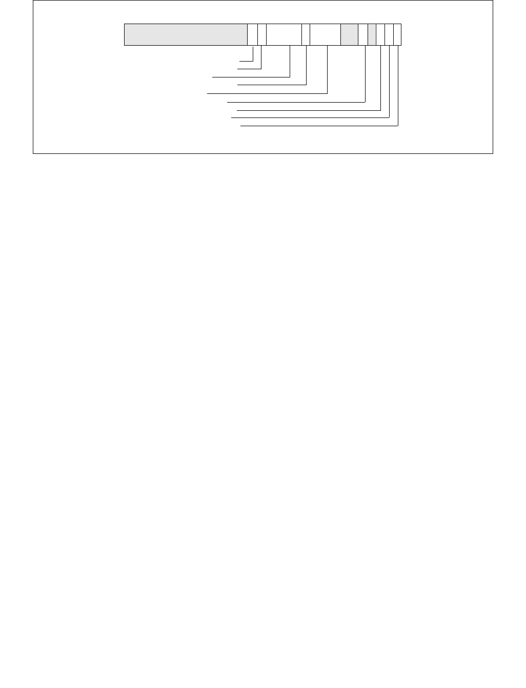
14-36 Vol. 3B
POWER AND THERMAL MANAGEMENT
•Package High-Temperature Interrupt Enable (bit 0, R/W) — This bit allows the BIOS to enable the
generation of an interrupt on the transition from low-temperature to a package high-temperature threshold.
Bit 0 = 0 (default) disables interrupts; bit 0 = 1 enables interrupts.
•Package Low-Temperature Interrupt Enable (bit 1, R/W) — This bit allows the BIOS to enable the
generation of an interrupt on the transition from high-temperature to a low-temperature (TCC de-activation).
Bit 1 = 0 (default) disables interrupts; bit 1 = 1 enables interrupts.
•Package PROCHOT# Interrupt Enable (bit 2, R/W) — This bit allows the BIOS or OS to enable the
generation of an interrupt when Package PROCHOT# has been asserted by another agent on the platform and
the Bidirectional Prochot feature is enabled. Bit 2 = 0 disables the interrupt; bit 2 = 1 enables the interrupt.
•Package Critical Temperature Interrupt Enable (bit 4, R/W) — Enables the generation of an interrupt
when the Package Critical Temperature Detector has detected a critical thermal condition. The recommended
response to this condition is a system shutdown. Bit 4 = 0 disables the interrupt; bit 4 = 1 enables the
interrupt.
•Package Threshold #1 Value (bits 14:8, R/W) — A temperature threshold, encoded relative to the
Package TCC Activation temperature (using the same format as the Digital Readout). This threshold is
compared against the Package Digital Readout and is used to generate the Package Thermal Threshold #1
Status and Log bits as well as the Package Threshold #1 thermal interrupt delivery.
•Package Threshold #1 Interrupt Enable (bit 15, R/W) — Enables the generation of an interrupt when the
actual temperature crosses the Package Threshold #1 setting in any direction. Bit 15 = 1 enables the interrupt;
bit 15 = 0 disables the interrupt.
•Package Threshold #2 Value (bits 22:16, R/W) —A temperature threshold, encoded relative to the PTCC
Activation temperature (using the same format as the Package Digital Readout). This threshold is compared
against the Package Digital Readout and is used to generate the Package Thermal Threshold #2 Status and Log
bits as well as the Package Threshold #2 thermal interrupt delivery.
•Package Threshold #2 Interrupt Enable (bit 23, R/W) — Enables the generation of an interrupt when the
actual temperature crosses the Package Threshold #2 setting in any direction. Bit 23 = 1 enables the interrupt;
bit 23 = 0 disables the interrupt.
•Package Power Limit Notification Enable (bit 24, R/W) — Enables the generation of package power
notification events.
14.8.1 Support for Passive and Active cooling
Passive and active cooling may be controlled by the OS power management agent through ACPI control methods.
On platforms providing package level thermal management facility described in the previous section, it is recom-
mended that active cooling (FAN control) should be driven by measuring the package temperature using the
IA32_PACKAGE_THERM_INTERRUPT MSR.
Figure 14-34. IA32_PACKAGE_THERM_INTERRUPT Register
63 0
Reserved
15
Pkg Threshold #2 Interrupt Enable
1234581416222324
Pkg Threshold #2 Value
Pkg Threshold #1 Interrupt Enable
Pkg Threshold #1 Value
Pkg Overheat Interrupt Enable
Pkg PROCHOT# Interrupt Enable
Pkg Low Temp. Interrupt Enable
Pkg High Temp. Interrupt Enable
25
Pkg Power Limit Notification Enable

Vol. 3B 14-37
POWER AND THERMAL MANAGEMENT
Passive cooling (frequency throttling) should be driven by measuring (a) the core and package temperatures, or
(b) only the package temperature. If measured package temperature led the power management agent to choose
which core to execute passive cooling, then all cores need to execute passive cooling. Core temperature is
measured using the IA32_THERMAL_STATUS and IA32_THERMAL_INTERRUPT MSRs. The exact implementation
details depend on the platform firmware and possible solutions include defining two different thermal zones (one
for core temperature and passive cooling and the other for package temperature and active cooling).
14.9 PLATFORM SPECIFIC POWER MANAGEMENT SUPPORT
This section covers power management interfaces that are not architectural but addresses the power management
needs of several platform specific components. Specifically, RAPL (Running Average Power Limit) interfaces provide
mechanisms to enforce power consumption limit. Power limiting usages have specific usages in client and server
platforms.
For client platform power limit control and for server platforms used in a data center, the following power and
thermal related usages are desirable:
•Platform Thermal Management: Robust mechanisms to manage component, platform, and group-level
thermals, either proactively or reactively (e.g., in response to a platform-level thermal trip point).
•Platform Power Limiting: More deterministic control over the system's power consumption, for example to
meet battery life targets on rack-level or container-level power consumption goals within a datacenter.
•Power/Performance Budgeting: Efficient means to control the power consumed (and therefore the sustained
performance delivered) within and across platforms.
The server and client usage models are addressed by RAPL interfaces, which expose multiple domains of power
rationing within each processor socket. Generally, these RAPL domains may be viewed to include hierarchically:
•Package domain is the processor die.
•Memory domain includes the directly-attached DRAM; an additional power plane may constitute a separate
domain.
In order to manage the power consumed across multiple sockets via RAPL, individual limits must be programmed
for each processor complex. Programming specific RAPL domain across multiple sockets is not supported.
14.9.1 RAPL Interfaces
RAPL interfaces consist of non-architectural MSRs. Each RAPL domain supports the following set of capabilities,
some of which are optional as stated below.
•Power limit - MSR interfaces to specify power limit, time window; lock bit, clamp bit etc.
•Energy Status - Power metering interface providing energy consumption information.
•Perf Status (Optional) - Interface providing information on the performance effects (regression) due to power
limits. It is defined as a duration metric that measures the power limit effect in the respective domain. The
meaning of duration is domain specific.
•Power Info (Optional) - Interface providing information on the range of parameters for a given domain,
minimum power, maximum power etc.
•Policy (Optional) - 4-bit priority information that is a hint to hardware for dividing budget between sub-domains
in a parent domain.
Each of the above capabilities requires specific units in order to describe them. Power is expressed in Watts, Time
is expressed in Seconds, and Energy is expressed in Joules. Scaling factors are supplied to each unit to make the
information presented meaningful in a finite number of bits. Units for power, energy, and time are exposed in the
read-only MSR_RAPL_POWER_UNIT MSR.
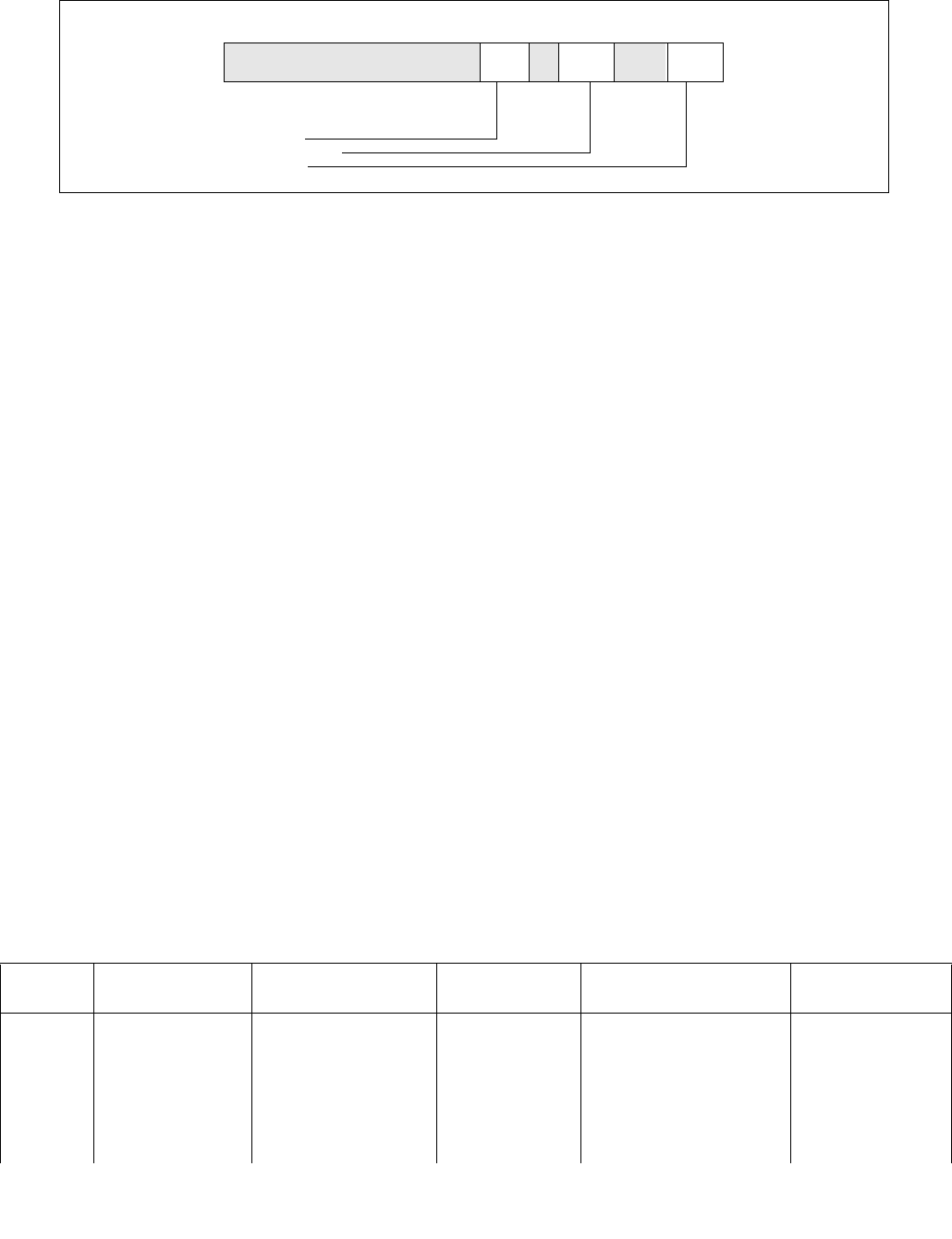
14-38 Vol. 3B
POWER AND THERMAL MANAGEMENT
MSR_RAPL_POWER_UNIT (Figure 14-35) provides the following information across all RAPL domains:
•Power Units (bits 3:0): Power related information (in Watts) is based on the multiplier, 1/ 2^PU; where PU is
an unsigned integer represented by bits 3:0. Default value is 0011b, indicating power unit is in 1/8 Watts
increment.
•Energy Status Units (bits 12:8): Energy related information (in Joules) is based on the multiplier, 1/2^ESU;
where ESU is an unsigned integer represented by bits 12:8. Default value is 10000b, indicating energy status
unit is in 15.3 micro-Joules increment.
•Time Units (bits 19:16): Time related information (in Seconds) is based on the multiplier, 1/ 2^TU; where TU
is an unsigned integer represented by bits 19:16. Default value is 1010b, indicating time unit is in 976 micro-
seconds increment.
14.9.2 RAPL Domains and Platform Specificity
The specific RAPL domains available in a platform vary across product segments. Platforms targeting the client
segment support the following RAPL domain hierarchy:
•Package
•Two power planes: PP0 and PP1 (PP1 may reflect to uncore devices)
Platforms targeting the server segment support the following RAPL domain hierarchy:
•Package
•Power plane: PP0
•DRAM
Each level of the RAPL hierarchy provides a respective set of RAPL interface MSRs. Table 14-4 lists the RAPL MSR
interfaces available for each RAPL domain. The power limit MSR of each RAPL domain is located at offset 0 relative
to an MSR base address which is non-architectural (see Chapter 2, “Model-Specific Registers (MSRs)” in the Intel®
64 and IA-32 Architectures Software Developer’s Manual, Volume 4). The energy status MSR of each domain is
located at offset 1 relative to the MSR base address of respective domain.
Figure 14-35. MSR_RAPL_POWER_UNIT Register
Table 14-4. RAPL MSR Interfaces and RAPL Domains
Domain Power Limit
(Offset 0)
Energy Status (Offset
1)
Policy
(Offset 2)
Perf Status
(Offset 3)
Power Info
(Offset 4)
PKG MSR_PKG_POWER_
LIMIT
MSR_PKG_ENERGY_STA
TUS
RESERVED MSR_PKG_PERF_STATUS MSR_PKG_POWER_I
NFO
DRAM MSR_DRAM_POWER
_LIMIT
MSR_DRAM_ENERGY_S
TATUS
RESERVED MSR_DRAM_PERF_STATUS MSR_DRAM_POWER
_INFO
PP0 MSR_PP0_POWER_
LIMIT
MSR_PP0_ENERGY_STA
TUS
MSR_PP0_POLICY MSR_PP0_PERF_STATUS RESERVED
63 0
Reserved
13 347812151920
Time units
Energy status units
Power units
16
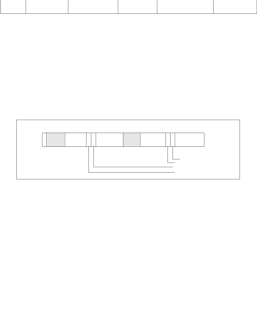
Vol. 3B 14-39
POWER AND THERMAL MANAGEMENT
The presence of the optional MSR interfaces (the three right-most columns of Table 14-4) may be model-specific.
See Chapter 2, “Model-Specific Registers (MSRs)” in the Intel® 64 and IA-32 Architectures Software Developer’s
Manual, Volume 4 for details.
14.9.3 Package RAPL Domain
The MSR interfaces defined for the package RAPL domain are:
•MSR_PKG_POWER_LIMIT allows software to set power limits for the package and measurement attributes
associated with each limit,
•MSR_PKG_ENERGY_STATUS reports measured actual energy usage,
•MSR_PKG_POWER_INFO reports the package power range information for RAPL usage.
MSR_PKG_PERF_STATUS can report the performance impact of power limiting, but its availability may be model-
specific.
MSR_PKG_POWER_LIMIT allows a software agent to define power limitation for the package domain. Power limita-
tion is defined in terms of average power usage (Watts) over a time window specified in MSR_PKG_POWER_LIMIT.
Two power limits can be specified, corresponding to time windows of different sizes. Each power limit provides
independent clamping control that would permit the processor cores to go below OS-requested state to meet the
power limits. A lock mechanism allow the software agent to enforce power limit settings. Once the lock bit is set,
the power limit settings are static and un-modifiable until next RESET.
The bit fields of MSR_PKG_POWER_LIMIT (Figure 14-36) are:
•Package Power Limit #1(bits 14:0): Sets the average power usage limit of the package domain corre-
sponding to time window # 1. The unit of this field is specified by the “Power Units” field of
MSR_RAPL_POWER_UNIT.
•Enable Power Limit #1(bit 15): 0 = disabled; 1 = enabled.
•Package Clamping Limitation #1 (bit 16): Allow going below OS-requested P/T state setting during time
window specified by bits 23:17.
•Time Window for Power Limit #1 (bits 23:17): Indicates the time window for power limit #1
Time limit = 2^Y * (1.0 + Z/4.0) * Time_Unit
Here “Y” is the unsigned integer value represented. by bits 21:17, “Z” is an unsigned integer represented by
bits 23:22. “Time_Unit” is specified by the “Time Units” field of MSR_RAPL_POWER_UNIT.
PP1 MSR_PP1_POWER_
LIMIT
MSR_PP1_ENERGY_STA
TUS
MSR_PP1_POLICY RESERVED RESERVED
Figure 14-36. MSR_PKG_POWER_LIMIT Register
Table 14-4. RAPL MSR Interfaces and RAPL Domains
63
Enable limit #1
Pkg clamping limit #1
Enable limit #2
Pkg clamping limit #2
31 24 23 15 0
Pkg Power Limit #1
48 47 3262 56 55 49 46 14
L
O
CPkg Power Limit #2
1617
K
Time window
Power Limit #2
Time window
Power Limit #1
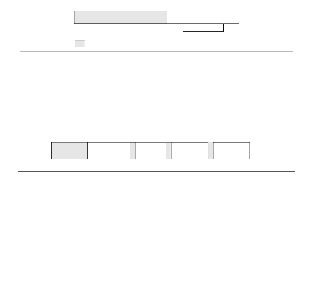
14-40 Vol. 3B
POWER AND THERMAL MANAGEMENT
•Package Power Limit #2(bits 46:32): Sets the average power usage limit of the package domain corre-
sponding to time window # 2. The unit of this field is specified by the “Power Units” field of
MSR_RAPL_POWER_UNIT.
•Enable Power Limit #2(bit 47): 0 = disabled; 1 = enabled.
•Package Clamping Limitation #2 (bit 48): Allow going below OS-requested P/T state setting during time
window specified by bits 23:17.
•Time Window for Power Limit #2 (bits 55:49): Indicates the time window for power limit #2
Time limit = 2^Y * (1.0 + Z/4.0) * Time_Unit
Here “Y” is the unsigned integer value represented. by bits 53:49, “Z” is an unsigned integer represented by
bits 55:54. “Time_Unit” is specified by the “Time Units” field of MSR_RAPL_POWER_UNIT. This field may have
a hard-coded value in hardware and ignores values written by software.
•Lock (bit 63): If set, all write attempts to this MSR are ignored until next RESET.
MSR_PKG_ENERGY_STATUS is a read-only MSR. It reports the actual energy use for the package domain. This MSR
is updated every ~1msec. It has a wraparound time of around 60 secs when power consumption is high, and may
be longer otherwise.
•Total Energy Consumed (bits 31:0): The unsigned integer value represents the total amount of energy
consumed since that last time this register is cleared. The unit of this field is specified by the “Energy Status
Units” field of MSR_RAPL_POWER_UNIT.
MSR_PKG_POWER_INFO is a read-only MSR. It reports the package power range information for RAPL usage. This
MSR provides maximum/minimum values (derived from electrical specification), thermal specification power of the
package domain. It also provides the largest possible time window for software to program the RAPL interface.
•Thermal Spec Power (bits 14:0): The unsigned integer value is the equivalent of thermal specification power
of the package domain. The unit of this field is specified by the “Power Units” field of MSR_RAPL_POWER_UNIT.
•Minimum Power (bits 30:16): The unsigned integer value is the equivalent of minimum power derived from
electrical spec of the package domain. The unit of this field is specified by the “Power Units” field of
MSR_RAPL_POWER_UNIT.
•Maximum Power (bits 46:32): The unsigned integer value is the equivalent of maximum power derived from
the electrical spec of the package domain. The unit of this field is specified by the “Power Units” field of
MSR_RAPL_POWER_UNIT.
Figure 14-37. MSR_PKG_ENERGY_STATUS MSR
Figure 14-38. MSR_PKG_POWER_INFO Register
63 0
Reserved
Total Energy Consumed
31
32
Reserved
63 31 30 15 0
Thermal Spec Power
48 47 32
54 53 46 14
Maximum Power
16
Maximum Time window Minimum Power
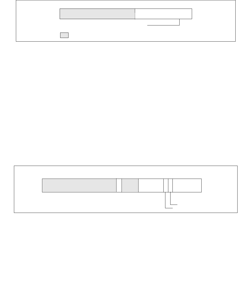
Vol. 3B 14-41
POWER AND THERMAL MANAGEMENT
•Maximum Time Window (bits 53:48): The unsigned integer value is the equivalent of largest acceptable
value to program the time window of MSR_PKG_POWER_LIMIT. The unit of this field is specified by the “Time
Units” field of MSR_RAPL_POWER_UNIT.
MSR_PKG_PERF_STATUS is a read-only MSR. It reports the total time for which the package was throttled due to
the RAPL power limits. Throttling in this context is defined as going below the OS-requested P-state or T-state. It
has a wrap-around time of many hours. The availability of this MSR is platform specific (see Chapter 2, “Model-
Specific Registers (MSRs)” in the Intel® 64 and IA-32 Architectures Software Developer’s Manual, Volume 4).
•Accumulated Package Throttled Time (bits 31:0): The unsigned integer value represents the cumulative
time (since the last time this register is cleared) that the package has throttled. The unit of this field is specified
by the “Time Units” field of MSR_RAPL_POWER_UNIT.
14.9.4 PP0/PP1 RAPL Domains
The MSR interfaces defined for the PP0 and PP1 domains are identical in layout. Generally, PP0 refers to the
processor cores. The availability of PP1 RAPL domain interface is platform-specific. For a client platform, the PP1
domain refers to the power plane of a specific device in the uncore. For server platforms, the PP1 domain is not
supported, but its PP0 domain supports the MSR_PP0_PERF_STATUS interface.
•MSR_PP0_POWER_LIMIT/MSR_PP1_POWER_LIMIT allow software to set power limits for the respective power
plane domain.
•MSR_PP0_ENERGY_STATUS/MSR_PP1_ENERGY_STATUS report actual energy usage on a power plane.
•MSR_PP0_POLICY/MSR_PP1_POLICY allow software to adjust balance for respective power plane.
MSR_PP0_PERF_STATUS can report the performance impact of power limiting, but it is not available in client plat-
forms.
MSR_PP0_POWER_LIMIT/MSR_PP1_POWER_LIMIT allow a software agent to define power limitation for the
respective power plane domain. A lock mechanism in each power plane domain allows the software agent to
enforce power limit settings independently. Once a lock bit is set, the power limit settings in that power plane are
static and un-modifiable until next RESET.
The bit fields of MSR_PP0_POWER_LIMIT/MSR_PP1_POWER_LIMIT (Figure 14-40) are:
Figure 14-39. MSR_PKG_PERF_STATUS MSR
Figure 14-40. MSR_PP0_POWER_LIMIT/MSR_PP1_POWER_LIMIT Register
63 0
Reserved
Accumulated pkg throttled time
31
32
Reserved
63
Enable limit
Clamping limit
30 24 23 15 0
Power Limit
31
32 14
L
O
C
1617
K
Time window
Power Limit
14-42 Vol. 3B
POWER AND THERMAL MANAGEMENT
•Power Limit (bits 14:0): Sets the average power usage limit of the respective power plane domain. The unit
of this field is specified by the “Power Units” field of MSR_RAPL_POWER_UNIT.
•Enable Power Limit (bit 15): 0 = disabled; 1 = enabled.
•Clamping Limitation (bit 16): Allow going below OS-requested P/T state setting during time window specified
by bits 23:17.
•Time Window for Power Limit (bits 23:17): Indicates the length of time window over which the power limit
#1 will be used by the processor. The numeric value encoded by bits 23:17 is represented by the product of
2^Y *F; where F is a single-digit decimal floating-point value between 1.0 and 1.3 with the fraction digit
represented by bits 23:22, Y is an unsigned integer represented by bits 21:17. The unit of this field is specified
by the “Time Units” field of MSR_RAPL_POWER_UNIT.
•Lock (bit 31): If set, all write attempts to the MSR and corresponding policy
MSR_PP0_POLICY/MSR_PP1_POLICY are ignored until next RESET.
MSR_PP0_ENERGY_STATUS/MSR_PP1_ENERGY_STATUS are read-only MSRs. They report the actual energy use
for the respective power plane domains. These MSRs are updated every ~1msec.
•Total Energy Consumed (bits 31:0): The unsigned integer value represents the total amount of energy
consumed since the last time this register was cleared. The unit of this field is specified by the “Energy Status
Units” field of MSR_RAPL_POWER_UNIT.
MSR_PP0_POLICY/MSR_PP1_POLICY provide balance power policy control for each power plane by providing
inputs to the power budgeting management algorithm. On platforms that support PP0 (IA cores) and PP1 (uncore
graphic device), the default values give priority to the non-IA power plane. These MSRs enable the PCU to balance
power consumption between the IA cores and uncore graphic device.
•Priority Level (bits 4:0): Priority level input to the PCU for respective power plane. PP0 covers the IA
processor cores, PP1 covers the uncore graphic device. The value 31 is considered highest priority.
MSR_PP0_PERF_STATUS is a read-only MSR. It reports the total time for which the PP0 domain was throttled due
to the power limits. This MSR is supported only in server platform. Throttling in this context is defined as going
below the OS-requested P-state or T-state.
Figure 14-41. MSR_PP0_ENERGY_STATUS/MSR_PP1_ENERGY_STATUS MSR
Figure 14-42. MSR_PP0_POLICY/MSR_PP1_POLICY Register
63 0
Reserved
Total Energy Consumed
31
32
Reserved
63 40
Priority Level
5
Vol. 3B 14-43
POWER AND THERMAL MANAGEMENT
•Accumulated PP0 Throttled Time (bits 31:0): The unsigned integer value represents the cumulative time
(since the last time this register is cleared) that the PP0 domain has throttled. The unit of this field is specified
by the “Time Units” field of MSR_RAPL_POWER_UNIT.
14.9.5 DRAM RAPL Domain
The MSR interfaces defined for the DRAM domains are supported only in the server platform. The MSR interfaces
are:
•MSR_DRAM_POWER_LIMIT allows software to set power limits for the DRAM domain and measurement
attributes associated with each limit.
•MSR_DRAM_ENERGY_STATUS reports measured actual energy usage.
•MSR_DRAM_POWER_INFO reports the DRAM domain power range information for RAPL usage.
•MSR_DRAM_PERF_STATUS can report the performance impact of power limiting.
MSR_DRAM_POWER_LIMIT allows a software agent to define power limitation for the DRAM domain. Power limita-
tion is defined in terms of average power usage (Watts) over a time window specified in
MSR_DRAM_POWER_LIMIT. A power limit can be specified along with a time window. A lock mechanism allow the
software agent to enforce power limit settings. Once the lock bit is set, the power limit settings are static and un-
modifiable until next RESET.
The bit fields of MSR_DRAM_POWER_LIMIT (Figure 14-44) are:
•DRAM Power Limit #1(bits 14:0): Sets the average power usage limit of the DRAM domain corresponding to
time window # 1. The unit of this field is specified by the “Power Units” field of MSR_RAPL_POWER_UNIT.
•Enable Power Limit #1(bit 15): 0 = disabled; 1 = enabled.
•Time Window for Power Limit (bits 23:17): Indicates the length of time window over which the power limit
will be used by the processor. The numeric value encoded by bits 23:17 is represented by the product of 2^Y
*F; where F is a single-digit decimal floating-point value between 1.0 and 1.3 with the fraction digit
represented by bits 23:22, Y is an unsigned integer represented by bits 21:17. The unit of this field is specified
by the “Time Units” field of MSR_RAPL_POWER_UNIT.
•Lock (bit 31): If set, all write attempts to this MSR are ignored until next RESET.
Figure 14-43. MSR_PP0_PERF_STATUS MSR
Figure 14-44. MSR_DRAM_POWER_LIMIT Register
63 0
Reserved
Accumulated PP0 throttled time
31
32
Reserved
63
Enable limit
Clamping limit
30 24 23 15 0
Power Limit
31
32 14
L
O
C
1617
K
Time window
Power Limit
14-44 Vol. 3B
POWER AND THERMAL MANAGEMENT
MSR_DRAM_ENERGY_STATUS is a read-only MSR. It reports the actual energy use for the DRAM domain. This MSR
is updated every ~1msec.
•Total Energy Consumed (bits 31:0): The unsigned integer value represents the total amount of energy
consumed since that last time this register is cleared. The unit of this field is specified by the “Energy Status
Units” field of MSR_RAPL_POWER_UNIT.
MSR_DRAM_POWER_INFO is a read-only MSR. It reports the DRAM power range information for RAPL usage. This
MSR provides maximum/minimum values (derived from electrical specification), thermal specification power of the
DRAM domain. It also provides the largest possible time window for software to program the RAPL interface.
•Thermal Spec Power (bits 14:0): The unsigned integer value is the equivalent of thermal specification power
of the DRAM domain. The unit of this field is specified by the “Power Units” field of MSR_RAPL_POWER_UNIT.
•Minimum Power (bits 30:16): The unsigned integer value is the equivalent of minimum power derived from
electrical spec of the DRAM domain. The unit of this field is specified by the “Power Units” field of
MSR_RAPL_POWER_UNIT.
•Maximum Power (bits 46:32): The unsigned integer value is the equivalent of maximum power derived from
the electrical spec of the DRAM domain. The unit of this field is specified by the “Power Units” field of
MSR_RAPL_POWER_UNIT.
•Maximum Time Window (bits 53:48): The unsigned integer value is the equivalent of largest acceptable
value to program the time window of MSR_DRAM_POWER_LIMIT. The unit of this field is specified by the “Time
Units” field of MSR_RAPL_POWER_UNIT.
MSR_DRAM_PERF_STATUS is a read-only MSR. It reports the total time for which the package was throttled due to
the RAPL power limits. Throttling in this context is defined as going below the OS-requested P-state or T-state. It
has a wrap-around time of many hours. The availability of this MSR is platform specific (see Chapter 2, “Model-
Specific Registers (MSRs)” in the Intel® 64 and IA-32 Architectures Software Developer’s Manual, Volume 4).
Figure 14-45. MSR_DRAM_ENERGY_STATUS MSR
Figure 14-46. MSR_DRAM_POWER_INFO Register
Figure 14-47. MSR_DRAM_PERF_STATUS MSR
63 0
Reserved
Total Energy Consumed
31
32
Reserved
63 31 30 15 0
Thermal Spec Power
48 47 32
54 53 46 14
Maximum Power
16
Maximum Time window Minimum Power
63 0
Reserved
Accumulated DRAM throttled time
31
32
Reserved

Vol. 3B 14-45
POWER AND THERMAL MANAGEMENT
•Accumulated Package Throttled Time (bits 31:0): The unsigned integer value represents the cumulative
time (since the last time this register is cleared) that the DRAM domain has throttled. The unit of this field is
specified by the “Time Units” field of MSR_RAPL_POWER_UNIT.

14-46 Vol. 3B
POWER AND THERMAL MANAGEMENT

Vol. 3B 15-1
CHAPTER 15
MACHINE-CHECK ARCHITECTURE
This chapter describes the machine-check architecture and machine-check exception mechanism found in the
Pentium 4, Intel Xeon, Intel Atom, and P6 family processors. See Chapter 6, “Interrupt 18—Machine-Check Excep-
tion (#MC),” for more information on machine-check exceptions. A brief description of the Pentium processor’s
machine check capability is also given.
Additionally, a signaling mechanism for software to respond to hardware corrected machine check error is covered.
15.1 MACHINE-CHECK ARCHITECTURE
The Pentium 4, Intel Xeon, Intel Atom, and P6 family processors implement a machine-check architecture that
provides a mechanism for detecting and reporting hardware (machine) errors, such as: system bus errors, ECC
errors, parity errors, cache errors, and TLB errors. It consists of a set of model-specific registers (MSRs) that are
used to set up machine checking and additional banks of MSRs used for recording errors that are detected.
The processor signals the detection of an uncorrected machine-check error by generating a machine-check excep-
tion (#MC), which is an abort class exception. The implementation of the machine-check architecture does not
ordinarily permit the processor to be restarted reliably after generating a machine-check exception. However, the
machine-check-exception handler can collect information about the machine-check error from the machine-check
MSRs.
Starting with 45 nm Intel 64 processor on which CPUID reports DisplayFamily_DisplayModel as 06H_1AH (see
CPUID instruction in Chapter 3, “Instruction Set Reference, A-L” in the Intel® 64 and IA-32 Architectures Software
Developer’s Manual, Volume 2A), the processor can report information on corrected machine-check errors and
deliver a programmable interrupt for software to respond to MC errors, referred to as corrected machine-check
error interrupt (CMCI). See Section 15.5 for detail.
Intel 64 processors supporting machine-check architecture and CMCI may also support an additional enhance-
ment, namely, support for software recovery from certain uncorrected recoverable machine check errors. See
Section 15.6 for detail.
15.2 COMPATIBILITY WITH PENTIUM PROCESSOR
The Pentium 4, Intel Xeon, Intel Atom, and P6 family processors support and extend the machine-check exception
mechanism introduced in the Pentium processor. The Pentium processor reports the following machine-check
errors:
•data parity errors during read cycles
•unsuccessful completion of a bus cycle
The above errors are reported using the P5_MC_TYPE and P5_MC_ADDR MSRs (implementation specific for the
Pentium processor). Use the RDMSR instruction to read these MSRs. See Chapter 2, “Model-Specific Registers
(MSRs)” in the Intel® 64 and IA-32 Architectures Software Developer’s Manual, Volume 4 for the addresses.
The machine-check error reporting mechanism that Pentium processors use is similar to that used in Pentium 4,
Intel Xeon, Intel Atom, and P6 family processors. When an error is detected, it is recorded in P5_MC_TYPE and
P5_MC_ADDR; the processor then generates a machine-check exception (#MC).
See Section 15.3.3, “Mapping of the Pentium Processor Machine-Check Errors to the Machine-Check Architecture,”
and Section 15.10.2, “Pentium Processor Machine-Check Exception Handling,” for information on compatibility
between machine-check code written to run on the Pentium processors and code written to run on P6 family
processors.

15-2 Vol. 3B
MACHINE-CHECK ARCHITECTURE
15.3 MACHINE-CHECK MSRS
Machine check MSRs in the Pentium 4, Intel Atom, Intel Xeon, and P6 family processors consist of a set of global
control and status registers and several error-reporting register banks. See Figure 15-1.
Each error-reporting bank is associated with a specific hardware unit (or group of hardware units) in the processor.
Use RDMSR and WRMSR to read and to write these registers.
15.3.1 Machine-Check Global Control MSRs
The machine-check global control MSRs include the IA32_MCG_CAP, IA32_MCG_STATUS, and optionally
IA32_MCG_CTL and IA32_MCG_EXT_CTL. See Chapter 2, “Model-Specific Registers (MSRs)” in the Intel® 64 and
IA-32 Architectures Software Developer’s Manual, Volume 4 for the addresses of these registers.
15.3.1.1 IA32_MCG_CAP MSR
The IA32_MCG_CAP MSR is a read-only register that provides information about the machine-check architecture of
the processor. Figure 15-2 shows the layout of the register.
Figure 15-1. Machine-Check MSRs
0
63 0
63
IA32_MCG_CAP MSR
IA32_MCG_STATUS MSR
Error-Reporting Bank Registers
0
63 0
63
IA32_MCi_CTL MSR
IA32_MCi_STATUS MSR
0
63 0
63
IA32_MCi_ADDR MSR
IA32_MCi_MISC MSR
Global Control MSRs (One Set for Each Hardware Unit)
0
63
IA32_MCG_CTL MSR
0
63
IA32_MCi_CTL2 MSR
0
63
IA32_MCG_EXT_CTL MSR
Vol. 3B 15-3
MACHINE-CHECK ARCHITECTURE
Where:
•Count field, bits 7:0 — Indicates the number of hardware unit error-reporting banks available in a particular
processor implementation.
•MCG_CTL_P (control MSR present) flag, bit 8 — Indicates that the processor implements the
IA32_MCG_CTL MSR when set; this register is absent when clear.
•MCG_EXT_P (extended MSRs present) flag, bit 9 — Indicates that the processor implements the extended
machine-check state registers found starting at MSR address 180H; these registers are absent when clear.
•MCG_CMCI_P (Corrected MC error counting/signaling extension present) flag, bit 10 — Indicates
(when set) that extended state and associated MSRs necessary to support the reporting of an interrupt on a
corrected MC error event and/or count threshold of corrected MC errors, is present. When this bit is set, it does
not imply this feature is supported across all banks. Software should check the availability of the necessary
logic on a bank by bank basis when using this signaling capability (i.e. bit 30 settable in individual
IA32_MCi_CTL2 register).
•MCG_TES_P (threshold-based error status present) flag, bit 11 — Indicates (when set) that bits 56:53
of the IA32_MCi_STATUS MSR are part of the architectural space. Bits 56:55 are reserved, and bits 54:53 are
used to report threshold-based error status. Note that when MCG_TES_P is not set, bits 56:53 of the
IA32_MCi_STATUS MSR are model-specific.
•MCG_EXT_CNT, bits 23:16 — Indicates the number of extended machine-check state registers present. This
field is meaningful only when the MCG_EXT_P flag is set.
•MCG_SER_P (software error recovery support present) flag, bit 24 — Indicates (when set) that the
processor supports software error recovery (see Section 15.6), and IA32_MCi_STATUS MSR bits 56:55 are
used to report the signaling of uncorrected recoverable errors and whether software must take recovery
actions for uncorrected errors. Note that when MCG_TES_P is not set, bits 56:53 of the IA32_MCi_STATUS MSR
are model-specific. If MCG_TES_P is set but MCG_SER_P is not set, bits 56:55 are reserved.
•MCG_EMC_P (Enhanced Machine Check Capability) flag, bit 25 — Indicates (when set) that the
processor supports enhanced machine check capabilities for firmware first signaling.
•MCG_ELOG_P (extended error logging) flag, bit 26 — Indicates (when set) that the processor allows
platform firmware to be invoked when an error is detected so that it may provide additional platform specific
information in an ACPI format “Generic Error Data Entry” that augments the data included in machine check
bank registers.
For additional information about extended error logging interface, see
https://www.intel.com/content/dam/www/public/us/en/documents/white-papers/enhanced-mca-logging-
xeon-paper.pdf.
Figure 15-2. IA32_MCG_CAP Register
MCG_TES_P[11]
MCG_EXT_CNT[23:16]
63 9
Reserved
101112
MCG_CMCI_P[10]
0
87
Count
MCG_EXT_P[9]
15162324
MCG_CTL_P[8]
MCG_SER_P[24]
25
MCG_ELOG_P[26]
27 26
MCG_LMCE_P[27]
MCG_EMC_P[25]
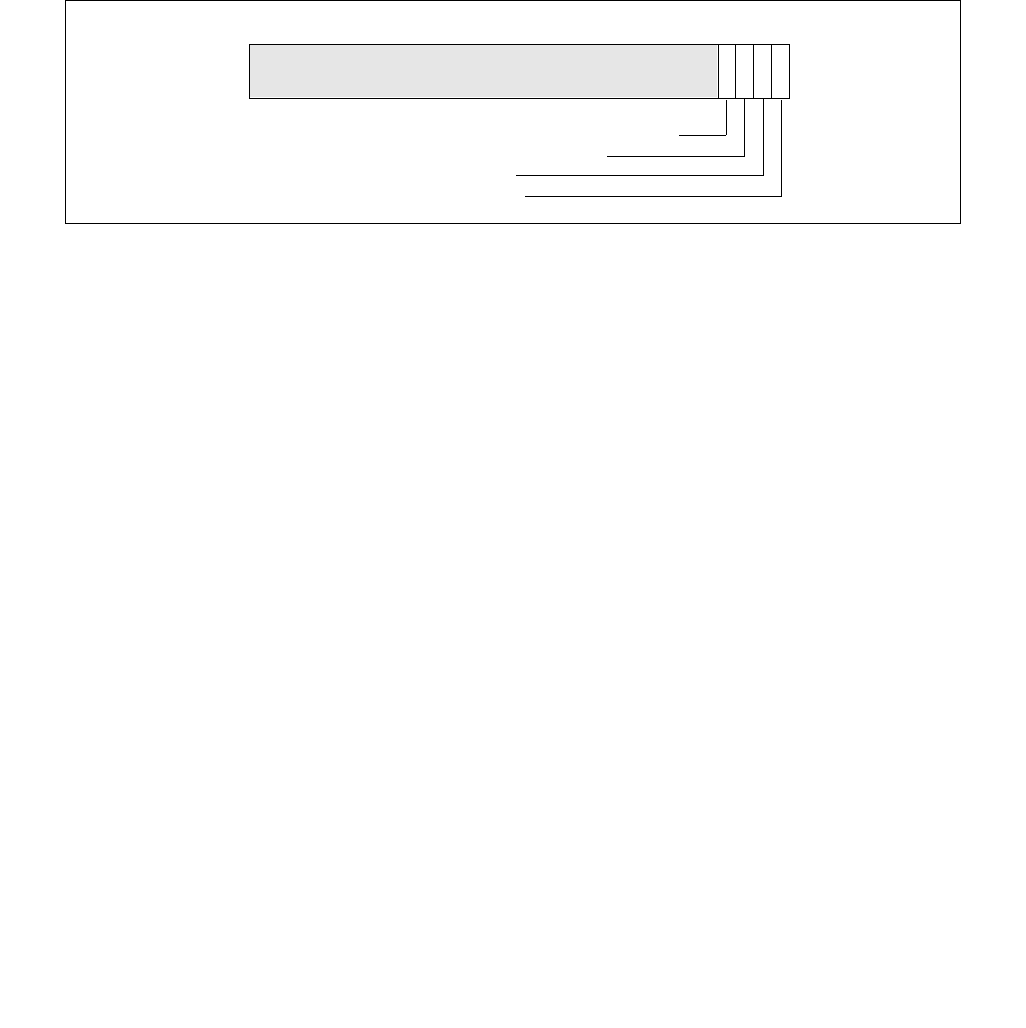
15-4 Vol. 3B
MACHINE-CHECK ARCHITECTURE
•MCG_LMCE_P (local machine check exception) flag, bit 27 — Indicates (when set) that the following
interfaces are present:
— an extended state LMCE_S (located in bit 3 of IA32_MCG_STATUS), and
— the IA32_MCG_EXT_CTL MSR, necessary to support Local Machine Check Exception (LMCE).
A non-zero MCG_LMCE_P indicates that, when LMCE is enabled as described in Section 15.3.1.5, some machine
check errors may be delivered to only a single logical processor.
The effect of writing to the IA32_MCG_CAP MSR is undefined.
15.3.1.2 IA32_MCG_STATUS MSR
The IA32_MCG_STATUS MSR describes the current state of the processor after a machine-check exception has
occurred (see Figure 15-3).
Where:
•RIPV (restart IP valid) flag, bit 0 — Indicates (when set) that program execution can be restarted reliably
at the instruction pointed to by the instruction pointer pushed on the stack when the machine-check exception
is generated. When clear, the program cannot be reliably restarted at the pushed instruction pointer.
•EIPV (error IP valid) flag, bit 1 — Indicates (when set) that the instruction pointed to by the instruction
pointer pushed onto the stack when the machine-check exception is generated is directly associated with the
error. When this flag is cleared, the instruction pointed to may not be associated with the error.
•MCIP (machine check in progress) flag, bit 2 — Indicates (when set) that a machine-check exception was
generated. Software can set or clear this flag. The occurrence of a second Machine-Check Event while MCIP is
set will cause the processor to enter a shutdown state. For information on processor behavior in the shutdown
state, please refer to the description in Chapter 6, “Interrupt and Exception Handling”: “Interrupt 8—Double
Fault Exception (#DF)”.
•LMCE_S (local machine check exception signaled), bit 3 — Indicates (when set) that a local machine-
check exception was generated. This indicates that the current machine-check event was delivered to only this
logical processor.
Bits 63:04 in IA32_MCG_STATUS are reserved. An attempt to write to IA32_MCG_STATUS with any value other
than 0 would result in #GP.
15.3.1.3 IA32_MCG_CTL MSR
The IA32_MCG_CTL MSR is present if the capability flag MCG_CTL_P is set in the IA32_MCG_CAP MSR.
IA32_MCG_CTL controls the reporting of machine-check exceptions. If present, writing 1s to this register enables
machine-check features and writing all 0s disables machine-check features. All other values are undefined and/or
implementation specific.
Figure 15-3. IA32_MCG_STATUS Register
EIPV—Error IP valid flag
MCIP—Machine check in progress flag
63 0
Reserved
123
E
I
P
V
M
C
I
P
R
I
P
V
RIPV—Restart IP valid flag
LMCE_S—Local machine check exception signaled

Vol. 3B 15-5
MACHINE-CHECK ARCHITECTURE
15.3.1.4 IA32_MCG_EXT_CTL MSR
The IA32_MCG_EXT_CTL MSR is present if the capability flag MCG_LMCE_P is set in the IA32_MCG_CAP MSR.
IA32_MCG_EXT_CTL.LMCE_EN (bit 0) allows the processor to signal some MCEs to only a single logical processor
in the system.
If MCG_LMCE_P is not set in IA32_MCG_CAP, or platform software has not enabled LMCE by setting
IA32_FEATURE_CONTROL.LMCE_ON (bit 20), any attempt to write or read IA32_MCG_EXT_CTL will result in #GP.
The IA32_MCG_EXT_CTL MSR is cleared on RESET.
Figure 15-4 shows the layout of the IA32_MCG_EXT_CTL register
where
•LMCE_EN (local machine check exception enable) flag, bit 0 - System software sets this to allow
hardware to signal some MCEs to only a single logical processor. System software can set LMCE_EN only if the
platform software has configured IA32_FEATURE_CONTROL as described in Section 15.3.1.5.
15.3.1.5 Enabling Local Machine Check
The intended usage of LMCE requires proper configuration by both platform software and system software. Plat-
form software can turn LMCE on by setting bit 20 (LMCE_ON) in IA32_FEATURE_CONTROL MSR (MSR address
3AH).
System software must ensure that both IA32_FEATURE_CONTROL.Lock (bit 0)and
IA32_FEATURE_CONTROL.LMCE_ON (bit 20) are set before attempting to set IA32_MCG_EXT_CTL.LMCE_EN (bit
0). When system software has enabled LMCE, then hardware will determine if a particular error can be delivered
only to a single logical processor. Software should make no assumptions about the type of error that hardware can
choose to deliver as LMCE. The severity and override rules stay the same as described in Table 15-8 to determine
the recovery actions.
15.3.2 Error-Reporting Register Banks
Each error-reporting register bank can contain the IA32_MCi_CTL, IA32_MCi_STATUS, IA32_MCi_ADDR, and
IA32_MCi_MISC MSRs. The number of reporting banks is indicated by bits [7:0] of IA32_MCG_CAP MSR (address
0179H). The first error-reporting register (IA32_MC0_CTL) always starts at address 400H.
See Chapter 2, “Model-Specific Registers (MSRs)” in the Intel® 64 and IA-32 Architectures Software Developer’s
Manual, Volume 4 for addresses of the error-reporting registers in the Pentium 4, Intel Atom, and Intel Xeon
processors; and for addresses of the error-reporting registers P6 family processors.
15.3.2.1 IA32_MCi_CTL MSRs
The IA32_MCi_CTL MSR controls signaling of #MC for errors produced by a particular hardware unit (or group of
hardware units). Each of the 64 flags (EEj) represents a potential error. Setting an EEj flag enables signaling #MC
of the associated error and clearing it disables signaling of the error. Error logging happens regardless of the setting
of these bits. The processor drops writes to bits that are not implemented. Figure 15-5 shows the bit fields of
IA32_MCi_CTL.
Figure 15-4. IA32_MCG_EXT_CTL Register
63 0
Reserved
1
LMCE_EN - system software control to enable/disable LMCE

15-6 Vol. 3B
MACHINE-CHECK ARCHITECTURE
NOTE
For P6 family processors, processors based on Intel Core microarchitecture (excluding those on
which on which CPUID reports DisplayFamily_DisplayModel as 06H_1AH and onward): the
operating system or executive software must not modify the contents of the IA32_MC0_CTL MSR.
This MSR is internally aliased to the EBL_CR_POWERON MSR and controls platform-specific error
handling features. System specific firmware (the BIOS) is responsible for the appropriate initial-
ization of the IA32_MC0_CTL MSR. P6 family processors only allow the writing of all 1s or all 0s to
the IA32_MCi_CTL MSR.
15.3.2.2 IA32_MCi_STATUS MSRS
Each IA32_MCi_STATUS MSR contains information related to a machine-check error if its VAL (valid) flag is set (see
Figure 15-6). Software is responsible for clearing IA32_MCi_STATUS MSRs by explicitly writing 0s to them; writing
1s to them causes a general-protection exception.
NOTE
Figure 15-6 depicts the IA32_MCi_STATUS MSR when IA32_MCG_CAP[24] = 1,
IA32_MCG_CAP[11] = 1 and IA32_MCG_CAP[10] = 1. When IA32_MCG_CAP[24] = 0 and
IA32_MCG_CAP[11] = 1, bits 56:55 is reserved and bits 54:53 for threshold-based error reporting.
When IA32_MCG_CAP[11] = 0, bits 56:53 are part of the “Other Information” field. The use of bits
54:53 for threshold-based error reporting began with Intel Core Duo processors, and is currently
used for cache memory. See Section 15.4, “Enhanced Cache Error reporting,” for more information.
When IA32_MCG_CAP[10] = 0, bits 52:38 are part of the “Other Information” field. The use of bits
52:38 for corrected MC error count is introduced with Intel 64 processor on which CPUID reports
DisplayFamily_DisplayModel as 06H_1AH.
Where:
•MCA (machine-check architecture) error code field, bits 15:0 — Specifies the machine-check archi-
tecture-defined error code for the machine-check error condition detected. The machine-check architecture-
defined error codes are guaranteed to be the same for all IA-32 processors that implement the machine-check
architecture. See Section 15.9, “Interpreting the MCA Error Codes,” and Chapter 16, “Interpreting Machine-
Check Error Codes”, for information on machine-check error codes.
•Model-specific error code field, bits 31:16 — Specifies the model-specific error code that uniquely
identifies the machine-check error condition detected. The model-specific error codes may differ among IA-32
processors for the same machine-check error condition. See Chapter 16, “Interpreting Machine-Check Error
Codes”for information on model-specific error codes.
•Reserved, Error Status, and Other Information fields, bits 56:32 —
•If IA32_MCG_CAP.MCG_EMC_P[bit 25] is 0, bits 37:32 contain “Other Information” that is implemen-
tation-specific and is not part of the machine-check architecture.
•If IA32_MCG_CAP.MCG_EMC_P is 1, “Other Information” is in bits 36:32. If bit 37 is 0, system firmware
has not changed the contents of IA32_MCi_STATUS. If bit 37 is 1, system firmware may have edited the
contents of IA32_MCi_STATUS.
•If IA32_MCG_CAP.MCG_CMCI_P[bit 10] is 0, bits 52:38 also contain “Other Information” (in the same
sense as bits 37:32).
Figure 15-5. IA32_MCi_CTL Register
EEj—Error reporting enable flag
63 0
123
E
E
0
1
E
E
0
2
E
E
0
0
E
E
6
1
E
E
6
2
E
E
6
3
62 61 . . . . .
(where j is 00 through 63)
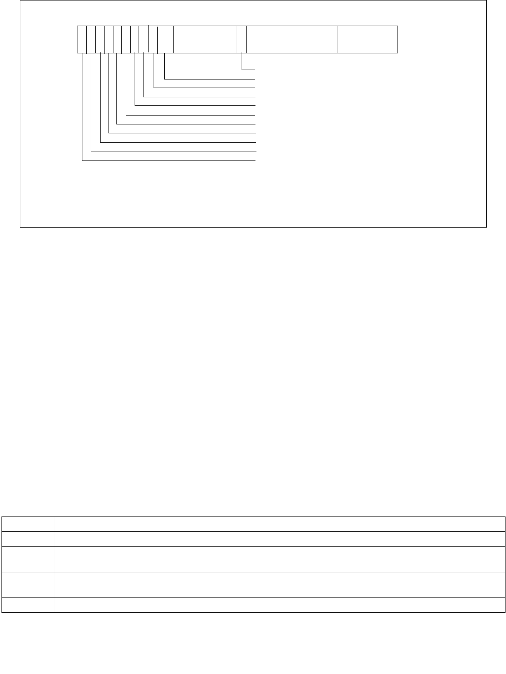
Vol. 3B 15-7
MACHINE-CHECK ARCHITECTURE
•If IA32_MCG_CAP[10] is 1, bits 52:38 are architectural (not model-specific). In this case, bits 52:38
reports the value of a 15 bit counter that increments each time a corrected error is observed by the MCA
recording bank. This count value will continue to increment until cleared by software. The most
significant bit, 52, is a sticky count overflow bit.
•If IA32_MCG_CAP[11] is 0, bits 56:53 also contain “Other Information” (in the same sense).
•If IA32_MCG_CAP[11] is 1, bits 56:53 are architectural (not model-specific). In this case, bits 56:53
have the following functionality:
•If IA32_MCG_CAP[24] is 0, bits 56:55 are reserved.
•If IA32_MCG_CAP[24] is 1, bits 56:55 are defined as follows:
•S (Signaling) flag, bit 56 - Signals the reporting of UCR errors in this MC bank. See Section 15.6.2
for additional detail.
•AR (Action Required) flag, bit 55 - Indicates (when set) that MCA error code specific recovery
action must be performed by system software at the time this error was signaled. See Section
15.6.2 for additional detail.
•If the UC bit (Figure 15-6) is 1, bits 54:53 are undefined.
•If the UC bit (Figure 15-6) is 0, bits 54:53 indicate the status of the hardware structure that
reported the threshold-based error. See Table 15-1.
Figure 15-6. IA32_MCi_STATUS Register
Table 15-1. Bits 54:53 in IA32_MCi_STATUS MSRs when IA32_MCG_CAP[11] = 1 and UC = 0
Bits 54:53 Meaning
00 No tracking - No hardware status tracking is provided for the structure reporting this event.
01 Green - Status tracking is provided for the structure posting the event; the current status is green (below threshold).
For more information, see Section 15.4, “Enhanced Cache Error reporting”.
10 Yellow - Status tracking is provided for the structure posting the event; the current status is yellow (above threshold).
For more information, see Section 15.4, “Enhanced Cache Error reporting”.
11 Reserved
63
Threshold-based error status (54:53)**
AR — Recovery action required for UCR error (55)***
S — Signaling an uncorrected recoverable (UCR) error (56)***
PCC — Processor context corrupted (57)
37 32 31 16 0
P
C
A
E
ADDRV — MCi_ADDR register valid (58)
MISCV — MCi_MISC register valid (59)
EN — Error reporting enabled (60)
UC — Uncorrected error (61)
OVER — Error overflow (62)
VAL — MCi_STATUS register valid (63)
C
MCA Error Code
US
R Other MSCOD Model
54 53 3862 61 60 59 58 57 56 55 52 15
V
A
L
O
V
E
R
CNSpecific Error Code Info
Corrected Error
Count
** When IA32_MCG_CAP[11] (MCG_TES_P) is not set, these bits are model-specific
(part of “Other Information”).
*** When IA32_MCG_CAP[11] or IA32_MCG_CAP[24] are not set, these bits are reserved, or
model-specific (part of “Other Information”).
36
* When IA32_MCG_CAP[25] (MCG_EMC_P) is set, bit 37 is not part of “Other Information”.
Firmware updated error status indicator (37)*

15-8 Vol. 3B
MACHINE-CHECK ARCHITECTURE
•PCC (processor context corrupt) flag, bit 57 — Indicates (when set) that the state of the processor might
have been corrupted by the error condition detected and that reliable restarting of the processor may not be
possible. When clear, this flag indicates that the error did not affect the processor’s state, and software may be
able to restart. When system software supports recovery, consult Section 15.10.4, “Machine-Check Software
Handler Guidelines for Error Recovery” for additional rules that apply.
•ADDRV (IA32_MCi_ADDR register valid) flag, bit 58 — Indicates (when set) that the IA32_MCi_ADDR
register contains the address where the error occurred (see Section 15.3.2.3, “IA32_MCi_ADDR MSRs”). When
clear, this flag indicates that the IA32_MCi_ADDR register is either not implemented or does not contain the
address where the error occurred. Do not read these registers if they are not implemented in the processor.
•MISCV (IA32_MCi_MISC register valid) flag, bit 59 — Indicates (when set) that the IA32_MCi_MISC
register contains additional information regarding the error. When clear, this flag indicates that the
IA32_MCi_MISC register is either not implemented or does not contain additional information regarding the
error. Do not read these registers if they are not implemented in the processor.
•EN (error enabled) flag, bit 60 — Indicates (when set) that the error was enabled by the associated EEj bit
of the IA32_MCi_CTL register.
•UC (error uncorrected) flag, bit 61 — Indicates (when set) that the processor did not or was not able to
correct the error condition. When clear, this flag indicates that the processor was able to correct the error
condition.
•OVER (machine check overflow) flag, bit 62 — Indicates (when set) that a machine-check error occurred
while the results of a previous error were still in the error-reporting register bank (that is, the VAL bit was
already set in the IA32_MCi_STATUS register). The processor sets the OVER flag and software is responsible for
clearing it. In general, enabled errors are written over disabled errors, and uncorrected errors are written over
corrected errors. Uncorrected errors are not written over previous valid uncorrected errors. When
MCG_CMCI_P is set, corrected errors may not set the OVER flag. Software can rely on corrected error count in
IA32_MCi_Status[52:38] to determine if any additional corrected errors may have occurred. For more infor-
mation, see Section 15.3.2.2.1, “Overwrite Rules for Machine Check Overflow”.
•VAL (IA32_MCi_STATUS register valid) flag, bit 63 — Indicates (when set) that the information within the
IA32_MCi_STATUS register is valid. When this flag is set, the processor follows the rules given for the OVER flag
in the IA32_MCi_STATUS register when overwriting previously valid entries. The processor sets the VAL flag
and software is responsible for clearing it.
15.3.2.2.1 Overwrite Rules for Machine Check Overflow
Table 15-2 shows the overwrite rules for how to treat a second event if the cache has already posted an event to
the MC bank – that is, what to do if the valid bit for an MC bank already is set to 1. When more than one structure
posts events in a given bank, these rules specify whether a new event will overwrite a previous posting or not.
These rules define a priority for uncorrected (highest priority), yellow, and green/unmonitored (lowest priority)
status.
In Table 15-2, the values in the two left-most columns are IA32_MCi_STATUS[54:53].
If a second event overwrites a previously posted event, the information (as guarded by individual valid bits) in the
MCi bank is entirely from the second event. Similarly, if a first event is retained, all of the information previously
posted for that event is retained. In general, when the logged error or the recent error is a corrected error, the
OVER bit (MCi_Status[62]) may be set to indicate an overflow. When MCG_CMCI_P is set in IA32_MCG_CAP,
system software should consult IA32_MCi_STATUS[52:38] to determine if additional corrected errors may have
Table 15-2. Overwrite Rules for Enabled Errors
First Event Second Event UC bit Color MCA Info
00/green 00/green 0 00/green either
00/green yellow 0 yellow second error
yellow 00/green 0 yellow first error
yellow yellow 0 yellow either
00/green/yellow UC 1 undefined second
UC 00/green/yellow 1 undefined first

Vol. 3B 15-9
MACHINE-CHECK ARCHITECTURE
occurred. Software may re-read IA32_MCi_STATUS, IA32_MCi_ADDR and IA32_MCi_MISC appropriately to ensure
data collected represent the last error logged.
After software polls a posting and clears the register, the valid bit is no longer set and therefore the meaning of the
rest of the bits, including the yellow/green/00 status field in bits 54:53, is undefined. The yellow/green indication
will only be posted for events associated with monitored structures – otherwise the unmonitored (00) code will be
posted in IA32_MCi_STATUS[54:53].
15.3.2.3 IA32_MCi_ADDR MSRs
The IA32_MCi_ADDR MSR contains the address of the code or data memory location that produced the machine-
check error if the ADDRV flag in the IA32_MCi_STATUS register is set (see Section 15-7, “IA32_MCi_ADDR MSR”).
The IA32_MCi_ADDR register is either not implemented or contains no address if the ADDRV flag in the
IA32_MCi_STATUS register is clear. When not implemented in the processor, all reads and writes to this MSR will
cause a general protection exception.
The address returned is an offset into a segment, linear address, or physical address. This depends on the error
encountered. When these registers are implemented, these registers can be cleared by explicitly writing 0s to
these registers. Writing 1s to these registers will cause a general-protection exception. See Figure 15-7.
15.3.2.4 IA32_MCi_MISC MSRs
The IA32_MCi_MISC MSR contains additional information describing the machine-check error if the MISCV flag in
the IA32_MCi_STATUS register is set. The IA32_MCi_MISC_MSR is either not implemented or does not contain
additional information if the MISCV flag in the IA32_MCi_STATUS register is clear.
When not implemented in the processor, all reads and writes to this MSR will cause a general protection exception.
When implemented in a processor, these registers can be cleared by explicitly writing all 0s to them; writing 1s to
them causes a general-protection exception to be generated. This register is not implemented in any of the error-
reporting register banks for the P6 or Intel Atom family processors.
If both MISCV and IA32_MCG_CAP[24] are set, the IA32_MCi_MISC_MSR is defined according to Figure 15-8 to
support software recovery of uncorrected errors (see Section 15.6).
Figure 15-7. IA32_MCi_ADDR MSR
Address
63 0
Reserved
35
36
Address*
63 0
Processor Without Support For Intel 64 Architecture
Processor With Support for Intel 64 Architecture
* Useful bits in this field depend on the address methodology in use when the
the register state is saved.
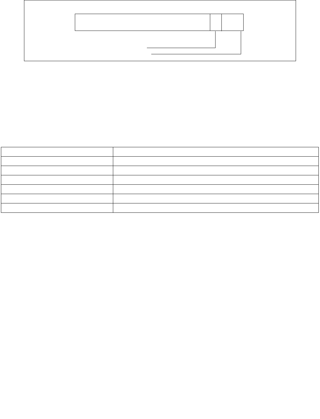
15-10 Vol. 3B
MACHINE-CHECK ARCHITECTURE
•Recoverable Address LSB (bits 5:0): The lowest valid recoverable address bit. Indicates the position of the least
significant bit (LSB) of the recoverable error address. For example, if the processor logs bits [43:9] of the
address, the LSB sub-field in IA32_MCi_MISC is 01001b (9 decimal). For this example, bits [8:0] of the
recoverable error address in IA32_MCi_ADDR should be ignored.
•Address Mode (bits 8:6): Address mode for the address logged in IA32_MCi_ADDR. The supported address
modes are given in Table 15-3.
•Model Specific Information (bits 63:9): Not architecturally defined.
15.3.2.4.2 IOMCA
Logging and Signaling of errors from PCI Express domain is governed by PCI Express Advanced Error Reporting
(AER) architecture. PCI Express architecture divides errors in two categories: Uncorrectable errors and Correctable
errors. Uncorrectable errors can further be classified as Fatal or Non-Fatal. Uncorrected IO errors are signaled to
the system software either as AER Message Signaled Interrupt (MSI) or via platform specific mechanisms such as
NMI. Generally, the signaling mechanism is controlled by BIOS and/or platform firmware. Certain processors
support an error handling mode, called IOMCA mode, where Uncorrected PCI Express errors are signaled in the
form of machine check exception and logged in machine check banks.
When a processor is in this mode, Uncorrected PCI Express errors are logged in the MCACOD field of the
IA32_MCi_STATUS register as Generic I/O error. The corresponding MCA error code is defined in Table 15-8.
IA32_MCi_Status [15:0] Simple Error Code Encoding. Machine check logging complements and does not replace
AER logging that occurs inside the PCI Express hierarchy. The PCI Express Root Complex and Endpoints continue to
log the error in accordance with PCI Express AER mechanism. In IOMCA mode, MCi_MISC register in the bank that
logged IOMCA can optionally contain information that link the Machine Check logs with the AER logs or proprietary
logs. In such a scenario, the machine check handler can utilize the contents of MCi_MISC to locate the next level of
error logs corresponding to the same error. Specifically, if MCi_Status.MISCV is 1 and MCACOD is 0x0E0B,
MCi_MISC contains the PCI Express address of the Root Complex device containing the AER Logs. Software can
consult the header type and class code registers in the Root Complex device's PCIe Configuration space to deter-
mine what type of device it is. This Root Complex device can either be a PCI Express Root Port, PCI Express Root
Complex Event Collector or a proprietary device.
Figure 15-8. UCR Support in IA32_MCi_MISC Register
Table 15-3. Address Mode in IA32_MCi_MISC[8:6]
IA32_MCi_MISC[8:6] Encoding Definition
000 Segment Offset
001 Linear Address
010 Physical Address
011 Memory Address
100 to 110 Reserved
111 Generic
Address Mode
63 0
Model Specific Information
6 5
Recoverable Address LSB
89
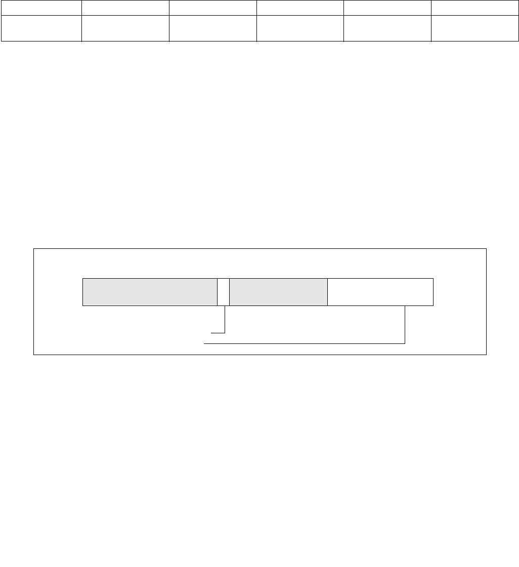
Vol. 3B 15-11
MACHINE-CHECK ARCHITECTURE
Errors that originate from PCI Express or Legacy Endpoints are logged in the corresponding Root Port in addition to
the generating device. If MISCV=1 and MCi_MISC contains the address of the Root Port or a Root Complex Event
collector, software can parse the AER logs to learn more about the error.
If MISCV=1 and MCi_MISC points to a device that is neither a Root Complex Event Collector not a Root Port, soft-
ware must consult the Vendor ID/Device ID and use device specific knowledge to locate and interpret the error log
registers. In some cases, the Root Complex device configuration space may not be accessible to the software and
both the Vendor and Device ID read as 0xFFFF.
•The format of MCi_MISC for IOMCA errors is shown in Table 15-4.
Refer to PCI Express Specification 3.0 for definition of PCI Express Requestor ID and AER architecture. Refer to PCI
Firmware Specification 3.0 for an explanation of PCI Ex-press Segment number and how software can access
configuration space of a PCI Ex-press device given the segment number and Requestor ID.
15.3.2.5 IA32_MCi_CTL2 MSRs
The IA32_MCi_CTL2 MSR provides the programming interface to use corrected MC error signaling capability that is
indicated by IA32_MCG_CAP[10] = 1. Software must check for the presence of IA32_MCi_CTL2 on a per-bank
basis.
When IA32_MCG_CAP[10] = 1, the IA32_MCi_CTL2 MSR for each bank exists, i.e. reads and writes to these MSR
are supported. However, signaling interface for corrected MC errors may not be supported in all banks.
The layout of IA32_MCi_CTL2 is shown in Figure 15-9:
•Corrected error count threshold, bits 14:0 — Software must initialize this field. The value is compared with
the corrected error count field in IA32_MCi_STATUS, bits 38 through 52. An overflow event is signaled to the
CMCI LVT entry (see Table 10-1) in the APIC when the count value equals the threshold value. The new LVT
entry in the APIC is at 02F0H offset from the APIC_BASE. If CMCI interface is not supported for a particular
bank (but IA32_MCG_CAP[10] = 1), this field will always read 0.
•CMCI_EN (Corrected error interrupt enable/disable/indicator), bits 30 — Software sets this bit to
enable the generation of corrected machine-check error interrupt (CMCI). If CMCI interface is not supported for
a particular bank (but IA32_MCG_CAP[10] = 1), this bit is writeable but will always return 0 for that bank. This
bit also indicates CMCI is supported or not supported in the corresponding bank. See Section 15.5 for details of
software detection of CMCI facility.
Table 15-4. Address Mode in IA32_MCi_MISC[8:6]
63:40 39:32 31:16 15:9 8:6 5:0
RSVD PCI Express Segment
number
PCI Express
Requestor ID
RSVD ADDR MODE1
NOTES:
1. Not Applicable if ADDRV=0.
RECOV ADDR LSB1
Figure 15-9. IA32_MCi_CTL2 Register
CMCI_EN—Enable/disable CMCI
63 15
Reserved
29
Corrected error count threshold
0
14
31 30
Reserved

15-12 Vol. 3B
MACHINE-CHECK ARCHITECTURE
Some microarchitectural sub-systems that are the source of corrected MC errors may be shared by more than one
logical processors. Consequently, the facilities for reporting MC errors and controlling mechanisms may be shared
by more than one logical processors. For example, the IA32_MCi_CTL2 MSR is shared between logical processors
sharing a processor core. Software is responsible to program IA32_MCi_CTL2 MSR in a consistent manner with
CMCI delivery and usage.
After processor reset, IA32_MCi_CTL2 MSRs are zero’ed.
15.3.2.6 IA32_MCG Extended Machine Check State MSRs
The Pentium 4 and Intel Xeon processors implement a variable number of extended machine-check state MSRs.
The MCG_EXT_P flag in the IA32_MCG_CAP MSR indicates the presence of these extended registers, and the
MCG_EXT_CNT field indicates the number of these registers actually implemented. See Section 15.3.1.1,
“IA32_MCG_CAP MSR.” Also see Table 15-5.
In processors with support for Intel 64 architecture, 64-bit machine check state MSRs are aliased to the legacy
MSRs. In addition, there may be registers beyond IA32_MCG_MISC. These may include up to five reserved MSRs
(IA32_MCG_RESERVED[1:5]) and save-state MSRs for registers introduced in 64-bit mode. See Table 15-6.
Table 15-5. Extended Machine Check State MSRs
in Processors Without Support for Intel 64 Architecture
MSR Address Description
IA32_MCG_EAX 180H Contains state of the EAX register at the time of the machine-check error.
IA32_MCG_EBX 181H Contains state of the EBX register at the time of the machine-check error.
IA32_MCG_ECX 182H Contains state of the ECX register at the time of the machine-check error.
IA32_MCG_EDX 183H Contains state of the EDX register at the time of the machine-check error.
IA32_MCG_ESI 184H Contains state of the ESI register at the time of the machine-check error.
IA32_MCG_EDI 185H Contains state of the EDI register at the time of the machine-check error.
IA32_MCG_EBP 186H Contains state of the EBP register at the time of the machine-check error.
IA32_MCG_ESP 187H Contains state of the ESP register at the time of the machine-check error.
IA32_MCG_EFLAGS 188H Contains state of the EFLAGS register at the time of the machine-check error.
IA32_MCG_EIP 189H Contains state of the EIP register at the time of the machine-check error.
IA32_MCG_MISC 18AH When set, indicates that a page assist or page fault occurred during DS normal
operation.
Table 15-6. Extended Machine Check State MSRs
In Processors With Support For Intel 64 Architecture
MSR Address Description
IA32_MCG_RAX 180H Contains state of the RAX register at the time of the machine-check error.
IA32_MCG_RBX 181H Contains state of the RBX register at the time of the machine-check error.
IA32_MCG_RCX 182H Contains state of the RCX register at the time of the machine-check error.
IA32_MCG_RDX 183H Contains state of the RDX register at the time of the machine-check error.
IA32_MCG_RSI 184H Contains state of the RSI register at the time of the machine-check error.
IA32_MCG_RDI 185H Contains state of the RDI register at the time of the machine-check error.
IA32_MCG_RBP 186H Contains state of the RBP register at the time of the machine-check error.
IA32_MCG_RSP 187H Contains state of the RSP register at the time of the machine-check error.
IA32_MCG_RFLAGS 188H Contains state of the RFLAGS register at the time of the machine-check error.
IA32_MCG_RIP 189H Contains state of the RIP register at the time of the machine-check error.

Vol. 3B 15-13
MACHINE-CHECK ARCHITECTURE
When a machine-check error is detected on a Pentium 4 or Intel Xeon processor, the processor saves the state of
the general-purpose registers, the R/EFLAGS register, and the R/EIP in these extended machine-check state MSRs.
This information can be used by a debugger to analyze the error.
These registers are read/write to zero registers. This means software can read them; but if software writes to
them, only all zeros is allowed. If software attempts to write a non-zero value into one of these registers, a general-
protection (#GP) exception is generated. These registers are cleared on a hardware reset (power-up or RESET),
but maintain their contents following a soft reset (INIT reset).
15.3.3 Mapping of the Pentium Processor Machine-Check Errors
to the Machine-Check Architecture
The Pentium processor reports machine-check errors using two registers: P5_MC_TYPE and P5_MC_ADDR. The
Pentium 4, Intel Xeon, Intel Atom, and P6 family processors map these registers to the IA32_MCi_STATUS and
IA32_MCi_ADDR in the error-reporting register bank. This bank reports on the same type of external bus errors
reported in P5_MC_TYPE and P5_MC_ADDR.
The information in these registers can then be accessed in two ways:
•By reading the IA32_MCi_STATUS and IA32_MCi_ADDR registers as part of a general machine-check exception
handler written for Pentium 4, Intel Atom and P6 family processors.
•By reading the P5_MC_TYPE and P5_MC_ADDR registers using the RDMSR instruction.
The second capability permits a machine-check exception handler written to run on a Pentium processor to be run
on a Pentium 4, Intel Xeon, Intel Atom, or P6 family processor. There is a limitation in that information returned by
the Pentium 4, Intel Xeon, Intel Atom, and P6 family processors is encoded differently than information returned
by the Pentium processor. To run a Pentium processor machine-check exception handler on a Pentium 4, Intel
Xeon, Intel Atom, or P6 family processor; the handler must be written to interpret P5_MC_TYPE encodings
correctly.
15.4 ENHANCED CACHE ERROR REPORTING
Starting with Intel Core Duo processors, cache error reporting was enhanced. In earlier Intel processors, cache
status was based on the number of correction events that occurred in a cache. In the new paradigm, called
“threshold-based error status”, cache status is based on the number of lines (ECC blocks) in a cache that incur
repeated corrections. The threshold is chosen by Intel, based on various factors. If a processor supports threshold-
based error status, it sets IA32_MCG_CAP[11] (MCG_TES_P) to 1; if not, to 0.
IA32_MCG_MISC 18AH When set, indicates that a page assist or page fault occurred during DS normal
operation.
IA32_MCG_
RSERVED[1:5]
18BH-
18FH
These registers, if present, are reserved.
IA32_MCG_R8 190H Contains state of the R8 register at the time of the machine-check error.
IA32_MCG_R9 191H Contains state of the R9 register at the time of the machine-check error.
IA32_MCG_R10 192H Contains state of the R10 register at the time of the machine-check error.
IA32_MCG_R11 193H Contains state of the R11 register at the time of the machine-check error.
IA32_MCG_R12 194H Contains state of the R12 register at the time of the machine-check error.
IA32_MCG_R13 195H Contains state of the R13 register at the time of the machine-check error.
IA32_MCG_R14 196H Contains state of the R14 register at the time of the machine-check error.
IA32_MCG_R15 197H Contains state of the R15 register at the time of the machine-check error.
Table 15-6. Extended Machine Check State MSRs
In Processors With Support For Intel 64 Architecture (Contd.)
MSR Address Description
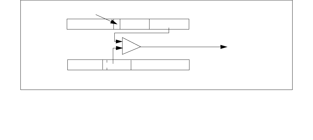
15-14 Vol. 3B
MACHINE-CHECK ARCHITECTURE
A processor that supports enhanced cache error reporting contains hardware that tracks the operating status of
certain caches and provides an indicator of their “health”. The hardware reports a “green” status when the number
of lines that incur repeated corrections is at or below a pre-defined threshold, and a “yellow” status when the
number of affected lines exceeds the threshold. Yellow status means that the cache reporting the event is operating
correctly, but you should schedule the system for servicing within a few weeks.
Intel recommends that you rely on this mechanism for structures supported by threshold-base error reporting.
The CPU/system/platform response to a yellow event should be less severe than its response to an uncorrected
error. An uncorrected error means that a serious error has actually occurred, whereas the yellow condition is a
warning that the number of affected lines has exceeded the threshold but is not, in itself, a serious event: the error
was corrected and system state was not compromised.
The green/yellow status indicator is not a foolproof early warning for an uncorrected error resulting from the failure
of two bits in the same ECC block. Such a failure can occur and cause an uncorrected error before the yellow
threshold is reached. However, the chance of an uncorrected error increases as the number of affected lines
increases.
15.5 CORRECTED MACHINE CHECK ERROR INTERRUPT
Corrected machine-check error interrupt (CMCI) is an architectural enhancement to the machine-check architec-
ture. It provides capabilities beyond those of threshold-based error reporting (Section 15.4). With threshold-based
error reporting, software is limited to use periodic polling to query the status of hardware corrected MC errors.
CMCI provides a signaling mechanism to deliver a local interrupt based on threshold values that software can
program using the IA32_MCi_CTL2 MSRs.
CMCI is disabled by default. System software is required to enable CMCI for each IA32_MCi bank that support the
reporting of hardware corrected errors if IA32_MCG_CAP[10] = 1.
System software use IA32_MCi_CTL2 MSR to enable/disable the CMCI capability for each bank and program
threshold values into IA32_MCi_CTL2 MSR. CMCI is not affected by the CR4.MCE bit, and it is not affected by the
IA32_MCi_CTL MSRs.
To detect the existence of thresholding for a given bank, software writes only bits 14:0 with the threshold value. If
the bits persist, then thresholding is available (and CMCI is available). If the bits are all 0's, then no thresholding
exists. To detect that CMCI signaling exists, software writes a 1 to bit 30 of the MCi_CTL2 register. Upon subsequent
read, if bit 30 = 0, no CMCI is available for this bank and no corrected or UCNA errors will be reported on this bank.
If bit 30 = 1, then CMCI is available and enabled.
15.5.1 CMCI Local APIC Interface
The operation of CMCI is depicted in Figure 15-10.
Figure 15-10. CMCI Behavior
Error threshold
63 0
MCi_CTL2
3031
Error count
53 0
Software write 1 to enable
Count overflow threshold -> CMCI LVT in local APIC
29 14
37
MCi_STATUS
3852
?=
APIC_BASE + 2F0H

Vol. 3B 15-15
MACHINE-CHECK ARCHITECTURE
CMCI interrupt delivery is configured by writing to the LVT CMCI register entry in the local APIC register space at
default address of APIC_BASE + 2F0H. A CMCI interrupt can be delivered to more than one logical processors if
multiple logical processors are affected by the associated MC errors. For example, if a corrected bit error in a cache
shared by two logical processors caused a CMCI, the interrupt will be delivered to both logical processors sharing
that microarchitectural sub-system. Similarly, package level errors may cause CMCI to be delivered to all logical
processors within the package. However, system level errors will not be handled by CMCI.
See Section 10.5.1, “Local Vector Table” for details regarding the LVT CMCI register.
15.5.2 System Software Recommendation for Managing CMCI and Machine Check Resources
System software must enable and manage CMCI, set up interrupt handlers to service CMCI interrupts delivered to
affected logical processors, program CMCI LVT entry, and query machine check banks that are shared by more
than one logical processors.
This section describes techniques system software can implement to manage CMCI initialization, service CMCI
interrupts in a efficient manner to minimize contentions to access shared MSR resources.
15.5.2.1 CMCI Initialization
Although a CMCI interrupt may be delivered to more than one logical processors depending on the nature of the
corrected MC error, only one instance of the interrupt service routine needs to perform the necessary service and
make queries to the machine-check banks. The following steps describes a technique that limits the amount of
work the system has to do in response to a CMCI.
•To provide maximum flexibility, system software should define per-thread data structure for each logical
processor to allow equal-opportunity and efficient response to interrupt delivery. Specifically, the per-thread
data structure should include a set of per-bank fields to track which machine check bank it needs to access in
response to a delivered CMCI interrupt. The number of banks that needs to be tracked is determined by
IA32_MCG_CAP[7:0].
•Initialization of per-thread data structure. The initialization of per-thread data structure must be done serially
on each logical processor in the system. The sequencing order to start the per-thread initialization between
different logical processor is arbitrary. But it must observe the following specific detail to satisfy the shared
nature of specific MSR resources:
a. Each thread initializes its data structure to indicate that it does not own any MC bank registers.
b. Each thread examines IA32_MCi_CTL2[30] indicator for each bank to determine if another thread has
already claimed ownership of that bank.
•If IA32_MCi_CTL2[30] had been set by another thread. This thread can not own bank i and should
proceed to step b. and examine the next machine check bank until all of the machine check banks are
exhausted.
•If IA32_MCi_CTL2[30] = 0, proceed to step c.
c. Check whether writing a 1 into IA32_MCi_CTL2[30] can return with 1 on a subsequent read to determine
this bank can support CMCI.
•If IA32_MCi_CTL2[30] = 0, this bank does not support CMCI. This thread can not own bank i and should
proceed to step b. and examine the next machine check bank until all of the machine check banks are
exhausted.
•If IA32_MCi_CTL2[30] = 1, modify the per-thread data structure to indicate this thread claims
ownership to the MC bank; proceed to initialize the error threshold count (bits 15:0) of that bank as
described in Chapter 15, “CMCI Threshold Management”. Then proceed to step b. and examine the next
machine check bank until all of the machine check banks are exhausted.
•After the thread has examined all of the machine check banks, it sees if it owns any MC banks to service CMCI.
If any bank has been claimed by this thread:
— Ensure that the CMCI interrupt handler has been set up as described in Chapter 15, “CMCI Interrupt
Handler”.
— Initialize the CMCI LVT entry, as described in Section 15.5.1, “CMCI Local APIC Interface”.

15-16 Vol. 3B
MACHINE-CHECK ARCHITECTURE
— Log and clear all of IA32_MCi_Status registers for the banks that this thread owns. This will allow new
errors to be logged.
15.5.2.2 CMCI Threshold Management
The Corrected MC error threshold field, IA32_MCi_CTL2[15:0], is architecturally defined. Specifically, all these bits
are writable by software, but different processor implementations may choose to implement less than 15 bits as
threshold for the overflow comparison with IA32_MCi_STATUS[52:38]. The following describes techniques that
software can manage CMCI threshold to be compatible with changes in implementation characteristics:
•Software can set the initial threshold value to 1 by writing 1 to IA32_MCi_CTL2[15:0]. This will cause overflow
condition on every corrected MC error and generates a CMCI interrupt.
•To increase the threshold and reduce the frequency of CMCI servicing:
a. Find the maximum threshold value a given processor implementation supports. The steps are:
•Write 7FFFH to IA32_MCi_CTL2[15:0],
•Read back IA32_MCi_CTL2[15:0], the lower 15 bits (14:0) is the maximum threshold supported by the
processor.
b. Increase the threshold to a value below the maximum value discovered using step a.
15.5.2.3 CMCI Interrupt Handler
The following describes techniques system software may consider to implement a CMCI service routine:
•The service routine examines its private per-thread data structure to check which set of MC banks it has
ownership. If the thread does not have ownership of a given MC bank, proceed to the next MC bank. Ownership
is determined at initialization time which is described in Section [Cross Reference to 14.5.2.1].
If the thread had claimed ownership to an MC bank, this technique will allow each logical processors to handle
corrected MC errors independently and requires no synchronization to access shared MSR resources. Consult
Example 15-5 for guidelines on logging when processing CMCI.
15.6 RECOVERY OF UNCORRECTED RECOVERABLE (UCR) ERRORS
Recovery of uncorrected recoverable machine check errors is an enhancement in machine-check architecture. The
first processor that supports this feature is 45 nm Intel 64 processor on which CPUID reports
DisplayFamily_DisplayModel as 06H_2EH (see CPUID instruction in Chapter 3, “Instruction Set Reference, A-L” in
the Intel® 64 and IA-32 Architectures Software Developer’s Manual, Volume 2A). This allow system software to
perform recovery action on certain class of uncorrected errors and continue execution.
15.6.1 Detection of Software Error Recovery Support
Software must use bit 24 of IA32_MCG_CAP (MCG_SER_P) to detect the presence of software error recovery
support (see Figure 15-2). When IA32_MCG_CAP[24] is set, this indicates that the processor supports software
error recovery. When this bit is clear, this indicates that there is no support for error recovery from the processor
and the primary responsibility of the machine check handler is logging the machine check error information and
shutting down the system.
The new class of architectural MCA errors from which system software can attempt recovery is called Uncorrected
Recoverable (UCR) Errors. UCR errors are uncorrected errors that have been detected and signaled but have not
corrupted the processor context. For certain UCR errors, this means that once system software has performed a
certain recovery action, it is possible to continue execution on this processor. UCR error reporting provides an error
containment mechanism for data poisoning. The machine check handler will use the error log information from the
error reporting registers to analyze and implement specific error recovery actions for UCR errors.

Vol. 3B 15-17
MACHINE-CHECK ARCHITECTURE
15.6.2 UCR Error Reporting and Logging
IA32_MCi_STATUS MSR is used for reporting UCR errors and existing corrected or uncorrected errors. The defini-
tions of IA32_MCi_STATUS, including bit fields to identify UCR errors, is shown in Figure 15-6. UCR errors can be
signaled through either the corrected machine check interrupt (CMCI) or machine check exception (MCE) path
depending on the type of the UCR error.
When IA32_MCG_CAP[24] is set, a UCR error is indicated by the following bit settings in the IA32_MCi_STATUS
register:
•Valid (bit 63) = 1
•UC (bit 61) = 1
•PCC (bit 57) = 0
Additional information from the IA32_MCi_MISC and the IA32_MCi_ADDR registers for the UCR error are available
when the ADDRV and the MISCV flags in the IA32_MCi_STATUS register are set (see Section 15.3.2.4). The MCA
error code field of the IA32_MCi_STATUS register indicates the type of UCR error. System software can interpret
the MCA error code field to analyze and identify the necessary recovery action for the given UCR error.
In addition, the IA32_MCi_STATUS register bit fields, bits 56:55, are defined (see Figure 15-6) to provide addi-
tional information to help system software to properly identify the necessary recovery action for the UCR error:
•S (Signaling) flag, bit 56 - Indicates (when set) that a machine check exception was generated for the UCR
error reported in this MC bank and system software needs to check the AR flag and the MCA error code fields in
the IA32_MCi_STATUS register to identify the necessary recovery action for this error. When the S flag in the
IA32_MCi_STATUS register is clear, this UCR error was not signaled via a machine check exception and instead
was reported as a corrected machine check (CMC). System software is not required to take any recovery action
when the S flag in the IA32_MCi_STATUS register is clear.
•AR (Action Required) flag, bit 55 - Indicates (when set) that MCA error code specific recovery action must be
performed by system software at the time this error was signaled. This recovery action must be completed
successfully before any additional work is scheduled for this processor. When the RIPV flag in the
IA32_MCG_STATUS is clear, an alternative execution stream needs to be provided; when the MCA error code
specific recovery specific recovery action cannot be successfully completed, system software must shut down
the system. When the AR flag in the IA32_MCi_STATUS register is clear, system software may still take MCA
error code specific recovery action but this is optional; system software can safely resume program execution
at the instruction pointer saved on the stack from the machine check exception when the RIPV flag in the
IA32_MCG_STATUS register is set.
Both the S and the AR flags in the IA32_MCi_STATUS register are defined to be sticky bits, which mean that once
set, the processor does not clear them. Only software and good power-on reset can clear the S and the AR-flags.
Both the S and the AR flags are only set when the processor reports the UCR errors (MCG_CAP[24] is set).
15.6.3 UCR Error Classification
With the S and AR flag encoding in the IA32_MCi_STATUS register, UCR errors can be classified as:
•Uncorrected no action required (UCNA) - is a UCR error that is not signaled via a machine check exception and,
instead, is reported to system software as a corrected machine check error. UCNA errors indicate that some
data in the system is corrupted, but the data has not been consumed and the processor state is valid and you
may continue execution on this processor. UCNA errors require no action from system software to continue
execution. A UNCA error is indicated with UC=1, PCC=0, S=0 and AR=0 in the IA32_MCi_STATUS register.
•Software recoverable action optional (SRAO) - a UCR error is signaled either via a machine check exception or
CMCI. System software recovery action is optional and not required to continue execution from this machine
check exception. SRAO errors indicate that some data in the system is corrupt, but the data has not been
consumed and the processor state is valid. SRAO errors provide the additional error information for system
software to perform a recovery action. An SRAO error when signaled as a machine check is indicated with
UC=1, PCC=0, S=1, EN=1 and AR=0 in the IA32_MCi_STATUS register. In cases when SRAO is signaled via
CMCI the error signature is indicated via UC=1, PCC=0, S=0. Recovery actions for SRAO errors are MCA error
code specific. The MISCV and the ADDRV flags in the IA32_MCi_STATUS register are set when the additional
error information is available from the IA32_MCi_MISC and the IA32_MCi_ADDR registers. System software
needs to inspect the MCA error code fields in the IA32_MCi_STATUS register to identify the specific recovery

15-18 Vol. 3B
MACHINE-CHECK ARCHITECTURE
action for a given SRAO error. If MISCV and ADDRV are not set, it is recommended that no system software
error recovery be performed however, system software can resume execution.
•Software recoverable action required (SRAR) - a UCR error that requires system software to take a recovery
action on this processor before scheduling another stream of execution on this processor. SRAR errors indicate
that the error was detected and raised at the point of the consumption in the execution flow. An SRAR error is
indicated with UC=1, PCC=0, S=1, EN=1 and AR=1 in the IA32_MCi_STATUS register. Recovery actions are
MCA error code specific. The MISCV and the ADDRV flags in the IA32_MCi_STATUS register are set when the
additional error information is available from the IA32_MCi_MISC and the IA32_MCi_ADDR registers. System
software needs to inspect the MCA error code fields in the IA32_MCi_STATUS register to identify the specific
recovery action for a given SRAR error. If MISCV and ADDRV are not set, it is recommended that system
software shutdown the system.
Table 15-7 summarizes UCR, corrected, and uncorrected errors.
15.6.4 UCR Error Overwrite Rules
In general, the overwrite rules are as follows:
•UCR errors will overwrite corrected errors.
•Uncorrected (PCC=1) errors overwrite UCR (PCC=0) errors.
•UCR errors are not written over previous UCR errors.
•Corrected errors do not write over previous UCR errors.
Regardless of whether the 1st error is retained or the 2nd error is overwritten over the 1st error, the OVER flag in
the IA32_MCi_STATUS register will be set to indicate an overflow condition. As the S flag and AR flag in the
IA32_MCi_STATUS register are defined to be sticky flags, a second event cannot clear these 2 flags once set,
however the MC bank information may be filled in for the 2nd error. The table below shows the overwrite rules and
how to treat a second error if the first event is already logged in a MC bank along with the resulting bit setting of
the UC, PCC, and AR flags in the IA32_MCi_STATUS register. As UCNA and SRA0 errors do not require recovery
action from system software to continue program execution, a system reset by system software is not required
unless the AR flag or PCC flag is set for the UCR overflow case (OVER=1, VAL=1, UC=1, PCC=0).
Table 15-7. MC Error Classifications
Type of Error1
NOTES:
1. SRAR, SRAO and UCNA errors are supported by the processor only when IA32_MCG_CAP[24] (MCG_SER_P) is set.
UC EN PCC S AR Signaling Software Action Example
Uncorrected Error (UC) 1 1 1 x x MCE If EN=1, reset the system, else log
and OK to keep the system running.
SRAR 1 1 0 1 1 MCE For known MCACOD, take specific
recovery action;
For unknown MCACOD, must
bugcheck.
If OVER=1, reset system, else take
specific recovery action.
Cache to processor load
error.
SRAO 1 x2
2. EN=1, S=1 when signaled via MCE. EN=x, S=0 when signaled via CMC.
0x
20 MCE/CMC For known MCACOD, take specific
recovery action;
For unknown MCACOD, OK to keep
the system running.
Patrol scrub and explicit
writeback poison errors.
UCNA 1 x 0 0 0 CMC Log the error and Ok to keep the
system running.
Poison detection error.
Corrected Error (CE) 0 x x x x CMC Log the error and no corrective
action required.
ECC in caches and
memory.

Vol. 3B 15-19
MACHINE-CHECK ARCHITECTURE
Table 15-8 lists overwrite rules for uncorrected errors, corrected errors, and uncorrected recoverable errors.
15.7 MACHINE-CHECK AVAILABILITY
The machine-check architecture and machine-check exception (#MC) are model-specific features. Software can
execute the CPUID instruction to determine whether a processor implements these features. Following the execu-
tion of the CPUID instruction, the settings of the MCA flag (bit 14) and MCE flag (bit 7) in EDX indicate whether the
processor implements the machine-check architecture and machine-check exception.
15.8 MACHINE-CHECK INITIALIZATION
To use the processors machine-check architecture, software must initialize the processor to activate the machine-
check exception and the error-reporting mechanism.
Example 15-1 gives pseudocode for performing this initialization. This pseudocode checks for the existence of the
machine-check architecture and exception; it then enables machine-check exception and the error-reporting
register banks. The pseudocode shown is compatible with the Pentium 4, Intel Xeon, Intel Atom, P6 family, and
Pentium processors.
Following power up or power cycling, IA32_MCi_STATUS registers are not guaranteed to have valid data until after
they are initially cleared to zero by software (as shown in the initialization pseudocode in Example 15-1). In addi-
tion, when using P6 family processors, software must set MCi_STATUS registers to zero when doing a soft-reset.
Example 15-1. Machine-Check Initialization Pseudocode
Check CPUID Feature Flags for MCE and MCA support
IF CPU supports MCE
THEN
IF CPU supports MCA
THEN
IF (IA32_MCG_CAP.MCG_CTL_P = 1)
(* IA32_MCG_CTL register is present *)
THEN
IA32_MCG_CTL ← FFFFFFFFFFFFFFFFH;
(* enables all MCA features *)
FI
IF (IA32_MCG_CAP.MCG_LMCE_P = 1 and IA32_FEATURE_CONTROL.LOCK = 1 and IA32_FEATURE_CONTROL.LMCE_ON= 1)
Table 15-8. Overwrite Rules for UC, CE, and UCR Errors
First Event Second Event UC PCC S AR MCA Bank Reset System
CE UCR 1 0 0 if UCNA, else 1 1 if SRAR, else 0 second yes, if AR=1
UCR CE 1 0 0 if UCNA, else 1 1 if SRAR, else 0 first yes, if AR=1
UCNA UCNA 1 0 0 0 first no
UCNA SRAO 1 0 1 0 first no
UCNA SRAR 1 0 1 1 first yes
SRAO UCNA 1 0 1 0 first no
SRAO SRAO 1 0 1 0 first no
SRAO SRAR 1 0 1 1 first yes
SRAR UCNA 1 0 1 1 first yes
SRAR SRAO 1 0 1 1 first yes
SRAR SRAR 1 0 1 1 first yes
UCR UC 1 1 undefined undefined second yes
UC UCR 1 1 undefined undefined first yes

15-20 Vol. 3B
MACHINE-CHECK ARCHITECTURE
(* IA32_MCG_EXT_CTL register is present and platform has enabled LMCE to permit system software to use LMCE *)
THEN
IA32_MCG_EXT_CTL ← IA32_MCG_EXT_CTL | 01H;
(* System software enables LMCE capability for hardware to signal MCE to a single logical processor*)
FI
(* Determine number of error-reporting banks supported *)
COUNT← IA32_MCG_CAP.Count;
MAX_BANK_NUMBER ← COUNT - 1;
IF (Processor Family is 6H and Processor EXTMODEL:MODEL is less than 1AH)
THEN
(* Enable logging of all errors except for MC0_CTL register *)
FOR error-reporting banks (1 through MAX_BANK_NUMBER)
DO
IA32_MCi_CTL ← 0FFFFFFFFFFFFFFFFH;
OD
ELSE
(* Enable logging of all errors including MC0_CTL register *)
FOR error-reporting banks (0 through MAX_BANK_NUMBER)
DO
IA32_MCi_CTL ← 0FFFFFFFFFFFFFFFFH;
OD
FI
(* BIOS clears all errors only on power-on reset *)
IF (BIOS detects Power-on reset)
THEN
FOR error-reporting banks (0 through MAX_BANK_NUMBER)
DO
IA32_MCi_STATUS ← 0;
OD
ELSE
FOR error-reporting banks (0 through MAX_BANK_NUMBER)
DO
(Optional for BIOS and OS) Log valid errors
(OS only) IA32_MCi_STATUS ← 0;
OD
FI
FI
Setup the Machine Check Exception (#MC) handler for vector 18 in IDT
Set the MCE bit (bit 6) in CR4 register to enable Machine-Check Exceptions
FI
15.9 INTERPRETING THE MCA ERROR CODES
When the processor detects a machine-check error condition, it writes a 16-bit error code to the MCA error code
field of one of the IA32_MCi_STATUS registers and sets the VAL (valid) flag in that register. The processor may also
write a 16-bit model-specific error code in the IA32_MCi_STATUS register depending on the implementation of the
machine-check architecture of the processor.
The MCA error codes are architecturally defined for Intel 64 and IA-32 processors. To determine the cause of a
machine-check exception, the machine-check exception handler must read the VAL flag for each
IA32_MCi_STATUS register. If the flag is set, the machine check-exception handler must then read the MCA error
code field of the register. It is the encoding of the MCA error code field [15:0] that determines the type of error
being reported and not the register bank reporting it.
There are two types of MCA error codes: simple error codes and compound error codes.

Vol. 3B 15-21
MACHINE-CHECK ARCHITECTURE
15.9.1 Simple Error Codes
Table 15-9 shows the simple error codes. These unique codes indicate global error information.
15.9.2 Compound Error Codes
Compound error codes describe errors related to the TLBs, memory, caches, bus and interconnect logic, and
internal timer. A set of sub-fields is common to all of compound errors. These sub-fields describe the type of
access, level in the cache hierarchy, and type of request. Table 15-10 shows the general form of the compound
error codes.
The “Interpretation” column in the table indicates the name of a compound error. The name is constructed by
substituting mnemonics for the sub-field names given within curly braces. For example, the error code
ICACHEL1_RD_ERR is constructed from the form:
{TT}CACHE{LL}_{RRRR}_ERR,
where {TT} is replaced by I, {LL} is replaced by L1, and {RRRR} is replaced by RD.
For more information on the “Form” and “Interpretation” columns, see Sections Section 15.9.2.1, “Correction
Report Filtering (F) Bit” through Section 15.9.2.5, “Bus and Interconnect Errors”.
Table 15-9. IA32_MCi_Status [15:0] Simple Error Code Encoding
Error Code Binary Encoding Meaning
No Error 0000 0000 0000 0000 No error has been reported to this bank of error-reporting
registers.
Unclassified 0000 0000 0000 0001 This error has not been classified into the MCA error classes.
Microcode ROM Parity Error 0000 0000 0000 0010 Parity error in internal microcode ROM
External Error 0000 0000 0000 0011 The BINIT# from another processor caused this processor to
enter machine check.1
FRC Error 0000 0000 0000 0100 FRC (functional redundancy check) master/slave error
Internal Parity Error 0000 0000 0000 0101 Internal parity error.
SMM Handler Code Access
Violation
0000 0000 0000 0110 An attempt was made by the SMM Handler to execute
outside the ranges specified by SMRR.
Internal Timer Error 0000 0100 0000 0000 Internal timer error.
I/O Error 0000 1110 0000 1011 generic I/O error.
Internal Unclassified 0000 01xx xxxx xxxx Internal unclassified errors. 2
NOTES:
1. BINIT# assertion will cause a machine check exception if the processor (or any processor on the same external bus) has BINIT#
observation enabled during power-on configuration (hardware strapping) and if machine check exceptions are enabled (by setting
CR4.MCE = 1).
2. At least one X must equal one. Internal unclassified errors have not been classified.
Table 15-10. IA32_MCi_Status [15:0] Compound Error Code Encoding
Type Form Interpretation
Generic Cache Hierarchy 000F 0000 0000 11LL Generic cache hierarchy error
TLB Errors 000F 0000 0001 TTLL {TT}TLB{LL}_ERR
Memory Controller Errors 000F 0000 1MMM CCCC {MMM}_CHANNEL{CCCC}_ERR
Cache Hierarchy Errors 000F 0001 RRRR TTLL {TT}CACHE{LL}_{RRRR}_ERR
Bus and Interconnect Errors 000F 1PPT RRRR IILL BUS{LL}_{PP}_{RRRR}_{II}_{T}_ERR
15-22 Vol. 3B
MACHINE-CHECK ARCHITECTURE
15.9.2.1 Correction Report Filtering (F) Bit
Starting with Intel Core Duo processors, bit 12 in the “Form” column in Table 15-10 is used to indicate that a partic-
ular posting to a log may be the last posting for corrections in that line/entry, at least for some time:
•0 in bit 12 indicates “normal” filtering (original P6/Pentium4/Atom/Xeon processor meaning).
•1 in bit 12 indicates “corrected” filtering (filtering is activated for the line/entry in the posting). Filtering means
that some or all of the subsequent corrections to this entry (in this structure) will not be posted. The enhanced
error reporting introduced with the Intel Core Duo processors is based on tracking the lines affected by
repeated corrections (see Section 15.4, “Enhanced Cache Error reporting”). This capability is indicated by
IA32_MCG_CAP[11]. Only the first few correction events for a line are posted; subsequent redundant
correction events to the same line are not posted. Uncorrected events are always posted.
The behavior of error filtering after crossing the yellow threshold is model-specific. Filtering has meaning only for
corrected errors (UC=0 in IA32_MCi_STATUS MSR). System software must ignore filtering bit (12) for uncorrected
errors.
15.9.2.2 Transaction Type (TT) Sub-Field
The 2-bit TT sub-field (Table 15-11) indicates the type of transaction (data, instruction, or generic). The sub-field
applies to the TLB, cache, and interconnect error conditions. Note that interconnect error conditions are primarily
associated with P6 family and Pentium processors, which utilize an external APIC bus separate from the system
bus. The generic type is reported when the processor cannot determine the transaction type.
15.9.2.3 Level (LL) Sub-Field
The 2-bit LL sub-field (see Table 15-12) indicates the level in the memory hierarchy where the error occurred (level
0, level 1, level 2, or generic). The LL sub-field also applies to the TLB, cache, and interconnect error conditions.
The Pentium 4, Intel Xeon, Intel Atom, and P6 family processors support two levels in the cache hierarchy and one
level in the TLBs. Again, the generic type is reported when the processor cannot determine the hierarchy level.
15.9.2.4 Request (RRRR) Sub-Field
The 4-bit RRRR sub-field (see Table 15-13) indicates the type of action associated with the error. Actions include
read and write operations, prefetches, cache evictions, and snoops. Generic error is returned when the type of
error cannot be determined. Generic read and generic write are returned when the processor cannot determine the
type of instruction or data request that caused the error. Eviction and snoop requests apply only to the caches. All
of the other requests apply to TLBs, caches and interconnects.
Table 15-11. Encoding for TT (Transaction Type) Sub-Field
Transaction Type Mnemonic Binary Encoding
Instruction I 00
Data D 01
Generic G 10
Table 15-12. Level Encoding for LL (Memory Hierarchy Level) Sub-Field
Hierarchy Level Mnemonic Binary Encoding
Level 0 L0 00
Level 1 L1 01
Level 2 L2 10
Generic LG 11
Table 15-13. Encoding of Request (RRRR) Sub-Field
Request Type Mnemonic Binary Encoding
Generic Error ERR 0000

Vol. 3B 15-23
MACHINE-CHECK ARCHITECTURE
15.9.2.5 Bus and Interconnect Errors
The bus and interconnect errors are defined with the 2-bit PP (participation), 1-bit T (time-out), and 2-bit II
(memory or I/O) sub-fields, in addition to the LL and RRRR sub-fields (see Table 15-14). The bus error conditions
are implementation dependent and related to the type of bus implemented by the processor. Likewise, the inter-
connect error conditions are predicated on a specific implementation-dependent interconnect model that describes
the connections between the different levels of the storage hierarchy. The type of bus is implementation depen-
dent, and as such is not specified in this document. A bus or interconnect transaction consists of a request involving
an address and a response.
15.9.2.6 Memory Controller Errors
The memory controller errors are defined with the 3-bit MMM (memory transaction type), and 4-bit CCCC
(channel) sub-fields. The encodings for MMM and CCCC are defined in Table 15-15.
Generic Read RD 0001
Generic Write WR 0010
Data Read DRD 0011
Data Write DWR 0100
Instruction Fetch IRD 0101
Prefetch PREFETCH 0110
Eviction EVICT 0111
Snoop SNOOP 1000
Table 15-14. Encodings of PP, T, and II Sub-Fields
Sub-Field Transaction Mnemonic Binary Encoding
PP (Participation) Local processor* originated request SRC 00
Local processor* responded to request RES 01
Local processor* observed error as third party OBS 10
Generic 11
T (Time-out) Request timed out TIMEOUT 1
Request did not time out NOTIMEOUT 0
II (Memory or I/O) Memory Access M 00
Reserved 01
I/O IO 10
Other transaction 11
NOTE:
* Local processor differentiates the processor reporting the error from other system components (including the APIC, other proces-
sors, etc.).
Table 15-15. Encodings of MMM and CCCC Sub-Fields
Sub-Field Transaction Mnemonic Binary Encoding
MMM Generic undefined request GEN 000
Memory read error RD 001
Memory write error WR 010
Address/Command Error AC 011
Memory Scrubbing Error MS 100
Reserved 101-111
Table 15-13. Encoding of Request (RRRR) Sub-Field (Contd.)
15-24 Vol. 3B
MACHINE-CHECK ARCHITECTURE
15.9.3 Architecturally Defined UCR Errors
Software recoverable compound error code are defined in this section.
15.9.3.1 Architecturally Defined SRAO Errors
The following two SRAO errors are architecturally defined.
•UCR Errors detected by memory controller scrubbing; and
•UCR Errors detected during L3 cache (L3) explicit writebacks.
The MCA error code encodings for these two architecturally-defined UCR errors corresponds to sub-classes of
compound MCA error codes (see Table 15-10). Their values and compound encoding format are given in Table
15-16.
Table 15-17 lists values of relevant bit fields of IA32_MCi_STATUS for architecturally defined SRAO errors.
For both the memory scrubbing and L3 explicit writeback errors, the ADDRV and MISCV flags in the
IA32_MCi_STATUS register are set to indicate that the offending physical address information is available from the
IA32_MCi_MISC and the IA32_MCi_ADDR registers. For the memory scrubbing and L3 explicit writeback errors,
the address mode in the IA32_MCi_MISC register should be set as physical address mode (010b) and the address
LSB information in the IA32_MCi_MISC register should indicate the lowest valid address bit in the address informa-
tion provided from the IA32_MCi_ADDR register.
MCE signal is broadcast to all logical processors as outlined in Section 15.10.4.1. If LMCE is supported and enabled,
some errors (not limited to UCR errors) may be delivered to only a single logical processor. System software should
consult IA32_MCG_STATUS.LMCE_S to determine if the MCE signaled is only to this logical processor.
CCCC Channel number CHN 0000-1110
Channel not specified 1111
Table 15-16. MCA Compound Error Code Encoding for SRAO Errors
Type MCACOD Value MCA Error Code Encoding1
NOTES:
1. Note that for both of these errors the correction report filtering (F) bit (bit 12) of the MCA error must be ignored.
Memory Scrubbing C0H - CFH 0000_0000_1100_CCCC
000F 0000 1MMM CCCC (Memory Controller Error), where
Memory subfield MMM = 100B (memory scrubbing)
Channel subfield CCCC = channel # or generic
L3 Explicit Writeback 17AH 0000_0001_0111_1010
000F 0001 RRRR TTLL (Cache Hierarchy Error) where
Request subfields RRRR = 0111B (Eviction)
Transaction Type subfields TT = 10B (Generic)
Level subfields LL = 10B
Table 15-17. IA32_MCi_STATUS Values for SRAO Errors
SRAO Error Valid OVER UC EN MISCV ADDRV PCC S AR MCACOD
Memory Scrubbing 1 0 1 x1
NOTES:
1. When signaled as MCE, EN=1 and S=1. If error was signaled via CMC, then EN=x, and S=0.
11 0x
10 C0H-CFH
L3 Explicit Writeback 1 0 1 x111 0x
10 17AH
Table 15-15. Encodings of MMM and CCCC Sub-Fields (Contd.)
Vol. 3B 15-25
MACHINE-CHECK ARCHITECTURE
IA32_MCi_STATUS banks can be shared by logical processors within a core or within the same package. So several
logical processors may find an SRAO error in the shared IA32_MCi_STATUS bank but other processors do not find
it in any of the IA32_MCi_STATUS banks. Table 15-18 shows the RIPV and EIPV flag indication in the
IA32_MCG_STATUS register for the memory scrubbing and L3 explicit writeback errors on both the reporting and
non-reporting logical processors.
15.9.3.2 Architecturally Defined SRAR Errors
The following two SRAR errors are architecturally defined.
•UCR Errors detected on data load; and
•UCR Errors detected on instruction fetch.
The MCA error code encodings for these two architecturally-defined UCR errors corresponds to sub-classes of
compound MCA error codes (see Table 15-10). Their values and compound encoding format are given in Table
15-19.
Table 15-20 lists values of relevant bit fields of IA32_MCi_STATUS for architecturally defined SRAR errors.
For both the data load and instruction fetch errors, the ADDRV and MISCV flags in the IA32_MCi_STATUS register
are set to indicate that the offending physical address information is available from the IA32_MCi_MISC and the
IA32_MCi_ADDR registers. For the memory scrubbing and L3 explicit writeback errors, the address mode in the
IA32_MCi_MISC register should be set as physical address mode (010b) and the address LSB information in the
IA32_MCi_MISC register should indicate the lowest valid address bit in the address information provided from the
IA32_MCi_ADDR register.
MCE signal is broadcast to all logical processors on the system on which the UCR errors are supported, except when
the processor supports LMCE and LMCE is enabled by system software (see Section 15.3.1.5). The
Table 15-18. IA32_MCG_STATUS Flag Indication for SRAO Errors
SRAO Type Reporting Logical Processors Non-reporting Logical Processors
RIPV EIPV RIPV EIPV
Memory Scrubbing 1010
L3 Explicit Writeback 1010
Table 15-19. MCA Compound Error Code Encoding for SRAR Errors
Type MCACOD Value MCA Error Code Encoding1
NOTES:
1. Note that for both of these errors the correction report filtering (F) bit (bit 12) of the MCA error must be ignored.
Data Load 134H 0000_0001_0011_0100
000F 0001 RRRR TTLL (Cache Hierarchy Error), where
Request subfield RRRR = 0011B (Data Load)
Transaction Type subfield TT= 01B (Data)
Level subfield LL = 00B (Level 0)
Instruction Fetch 150H 0000_0001_0101_0000
000F 0001 RRRR TTLL (Cache Hierarchy Error), where
Request subfield RRRR = 0101B (Instruction Fetch)
Transaction Type subfield TT= 00B (Instruction)
Level subfield LL = 00B (Level 0)
Table 15-20. IA32_MCi_STATUS Values for SRAR Errors
SRAR Error Valid OVER UC EN MISCV ADDRV PCC S AR MCACOD
Data Load 1 0 1 1 1 1 0 1 1 134H
Instruction Fetch 1 0 1 1 1 1 0 1 1 150H

15-26 Vol. 3B
MACHINE-CHECK ARCHITECTURE
IA32_MCG_STATUS MSR allows system software to distinguish the affected logical processor of an SRAR error
amongst logical processors that observed SRAR via MCi_STATUS bank.
Table 15-21 shows the RIPV and EIPV flag indication in the IA32_MCG_STATUS register for the data load and
instruction fetch errors on both the reporting and non-reporting logical processors. The recoverable SRAR error
reported by a processor may be continuable, where the system software can interpret the context of continuable
as follows: the error was isolated, contained. If software can rectify the error condition in the current instruction
stream, the execution context on that logical processor can be continued without loss of information.
SRAR Error And Affected Logical Processors
The affected logical processor is the one that has detected and raised an SRAR error at the point of the consump-
tion in the execution flow. The affected logical processor should find the Data Load or the Instruction Fetch error
information in the IA32_MCi_STATUS register that is reporting the SRAR error.
Table 15-21 list the actionable scenarios that system software can respond to an SRAR error on an affected logical
processor according to RIPV and EIPV values:
•Recoverable-Continuable SRAR Error (RIPV=1, EIPV=1):
For Recoverable-Continuable SRAR errors, the affected logical processor should find that both the
IA32_MCG_STATUS.RIPV and the IA32_MCG_STATUS.EIPV flags are set, indicating that system software may
be able to restart execution from the interrupted context if it is able to rectify the error condition. If system
software cannot rectify the error condition then it must treat the error as a recoverable error where restarting
execution with the interrupted context is not possible. Restarting without rectifying the error condition will
result in most cases with another SRAR error on the same instruction.
•Recoverable-not-continuable SRAR Error (RIPV=0, EIPV=x):
For Recoverable-not-continuable errors, the affected logical processor should find that either
— IA32_MCG_STATUS.RIPV= 0, IA32_MCG_STATUS.EIPV=1, or
— IA32_MCG_STATUS.RIPV= 0, IA32_MCG_STATUS.EIPV=0.
In either case, this indicates that the error is detected at the instruction pointer saved on the stack for this
machine check exception and restarting execution with the interrupted context is not possible. System
software may take the following recovery actions for the affected logical processor:
•The current executing thread cannot be continued. System software must terminate the interrupted
stream of execution and provide a new stream of execution on return from the machine check handler
for the affected logical processor.
SRAR Error And Non-Affected Logical Processors
The logical processors that observed but not affected by an SRAR error should find that the RIPV flag in the
IA32_MCG_STATUS register is set and the EIPV flag in the IA32_MCG_STATUS register is cleared, indicating that it
is safe to restart the execution at the instruction saved on the stack for the machine check exception on these
processors after the recovery action is successfully taken by system software.
Table 15-21. IA32_MCG_STATUS Flag Indication for SRAR Errors
SRAR Type Affected Logical Processor Non-Affected Logical Processors
RIPV EIPV Continuable RIPV EIPV Continuable
Recoverable-
continuable
11Yes
1
NOTES:
1. see the definition of the context of “continuable” above and additional detail below.
10Yes
Recoverable-not-
continuable
0xNo

Vol. 3B 15-27
MACHINE-CHECK ARCHITECTURE
15.9.4 Multiple MCA Errors
When multiple MCA errors are detected within a certain detection window, the processor may aggregate the
reporting of these errors together as a single event, i.e. a single machine exception condition. If this occurs,
system software may find multiple MCA errors logged in different MC banks on one logical processor or find
multiple MCA errors logged across different processors for a single machine check broadcast event. In order to
handle multiple UCR errors reported from a single machine check event and possibly recover from multiple errors,
system software may consider the following:
•Whether it can recover from multiple errors is determined by the most severe error reported on the system. If
the most severe error is found to be an unrecoverable error (VAL=1, UC=1, PCC=1 and EN=1) after system
software examines the MC banks of all processors to which the MCA signal is broadcast, recovery from the
multiple errors is not possible and system software needs to reset the system.
•When multiple recoverable errors are reported and no other fatal condition (e.g. overflowed condition for SRAR
error) is found for the reported recoverable errors, it is possible for system software to recover from the
multiple recoverable errors by taking necessary recovery action for each individual recoverable error. However,
system software can no longer expect one to one relationship with the error information recorded in the
IA32_MCi_STATUS register and the states of the RIPV and EIPV flags in the IA32_MCG_STATUS register as the
states of the RIPV and the EIPV flags in the IA32_MCG_STATUS register may indicate the information for the
most severe error recorded on the processor. System software is required to use the RIPV flag indication in the
IA32_MCG_STATUS register to make a final decision of recoverability of the errors and find the restart-ability
requirement after examining each IA32_MCi_STATUS register error information in the MC banks.
In certain cases where system software observes more than one SRAR error logged for a single logical
processor, it can no longer rely on affected threads as specified in Table 15-20 above. System software is
recommended to reset the system if this condition is observed.
15.9.5 Machine-Check Error Codes Interpretation
Chapter 16, “Interpreting Machine-Check Error Codes,” provides information on interpreting the MCA error code,
model-specific error code, and other information error code fields. For P6 family processors, information has been
included on decoding external bus errors. For Pentium 4 and Intel Xeon processors; information is included on
external bus, internal timer and cache hierarchy errors.
15.10 GUIDELINES FOR WRITING MACHINE-CHECK SOFTWARE
The machine-check architecture and error logging can be used in three different ways:
•To detect machine errors during normal instruction execution, using the machine-check exception (#MC).
•To periodically check and log machine errors.
•To examine recoverable UCR errors, determine software recoverability and perform recovery actions via a
machine-check exception handler or a corrected machine-check interrupt handler.
To use the machine-check exception, the operating system or executive software must provide a machine-check
exception handler. This handler may need to be designed specifically for each family of processors.
A special program or utility is required to log machine errors.
Guidelines for writing a machine-check exception handler or a machine-error logging utility are given in the
following sections.
15.10.1 Machine-Check Exception Handler
The machine-check exception (#MC) corresponds to vector 18. To service machine-check exceptions, a trap gate
must be added to the IDT. The pointer in the trap gate must point to a machine-check exception handler. Two
approaches can be taken to designing the exception handler:
1. The handler can merely log all the machine status and error information, then call a debugger or shut down the
system.

15-28 Vol. 3B
MACHINE-CHECK ARCHITECTURE
2. The handler can analyze the reported error information and, in some cases, attempt to correct the error and
restart the processor.
For Pentium 4, Intel Xeon, Intel Atom, P6 family, and Pentium processors; virtually all machine-check conditions
cannot be corrected (they result in abort-type exceptions). The logging of status and error information is therefore
a baseline implementation requirement.
When IA32_MCG_CAP[24] is clear, consider the following when writing a machine-check exception handler:
•To determine the nature of the error, the handler must read each of the error-reporting register banks. The
count field in the IA32_MCG_CAP register gives number of register banks. The first register of register bank 0
is at address 400H.
•The VAL (valid) flag in each IA32_MCi_STATUS register indicates whether the error information in the register
is valid. If this flag is clear, the registers in that bank do not contain valid error information and do not need to
be checked.
•To write a portable exception handler, only the MCA error code field in the IA32_MCi_STATUS register should be
checked. See Section 15.9, “Interpreting the MCA Error Codes,” for information that can be used to write an
algorithm to interpret this field.
•Correctable errors are corrected automatically by the processor. The UC flag in each IA32_MCi_STATUS reg-
ister indicates whether the processor automatically corrected an error.
•The RIPV, PCC, and OVER flags in each IA32_MCi_STATUS register indicate whether recovery from the error is
possible. If PCC or OVER are set, recovery is not possible. If RIPV is not set, program execution can not be
restarted reliably. When recovery is not possible, the handler typically records the error information and signals
an abort to the operating system.
•The RIPV flag in the IA32_MCG_STATUS register indicates whether the program can be restarted at the
instruction indicated by the instruction pointer (the address of the instruction pushed on the stack when the
exception was generated). If this flag is clear, the processor may still be able to be restarted (for debugging
purposes) but not without loss of program continuity.
•For unrecoverable errors, the EIPV flag in the IA32_MCG_STATUS register indicates whether the instruction
indicated by the instruction pointer pushed on the stack (when the exception was generated) is related to the
error. If the flag is clear, the pushed instruction may not be related to the error.
•The MCIP flag in the IA32_MCG_STATUS register indicates whether a machine-check exception was generated.
Before returning from the machine-check exception handler, software should clear this flag so that it can be
used reliably by an error logging utility. The MCIP flag also detects recursion. The machine-check architecture
does not support recursion. When the processor detects machine-check recursion, it enters the shutdown
state.
Example 15-2 gives typical steps carried out by a machine-check exception handler.

Vol. 3B 15-29
MACHINE-CHECK ARCHITECTURE
Example 15-2. Machine-Check Exception Handler Pseudocode
IF CPU supports MCE
THEN
IF CPU supports MCA
THEN
call errorlogging routine; (* returns restartability *)
FI;
ELSE (* Pentium(R) processor compatible *)
READ P5_MC_ADDR
READ P5_MC_TYPE;
report RESTARTABILITY to console;
FI;
IF error is not restartable
THEN
report RESTARTABILITY to console;
abort system;
FI;
CLEAR MCIP flag in IA32_MCG_STATUS;
15.10.2 Pentium Processor Machine-Check Exception Handling
Machine-check exception handler on P6 family, Intel Atom and later processor families, should follow the guidelines
described in Section 15.10.1 and Example 15-2 that check the processor’s support of MCA.
NOTE
On processors that support MCA (CPUID.1.EDX.MCA = 1) reading the P5_MC_TYPE and
P5_MC_ADDR registers may produce invalid data.
When machine-check exceptions are enabled for the Pentium processor (MCE flag is set in control register CR4),
the machine-check exception handler uses the RDMSR instruction to read the error type from the P5_MC_TYPE
register and the machine check address from the P5_MC_ADDR register. The handler then normally reports these
register values to the system console before aborting execution (see Example 15-2).
15.10.3 Logging Correctable Machine-Check Errors
The error handling routine for servicing the machine-check exceptions is responsible for logging uncorrected
errors.
If a machine-check error is correctable, the processor does not generate a machine-check exception for it. To
detect correctable machine-check errors, a utility program must be written that reads each of the machine-check
error-reporting register banks and logs the results in an accounting file or data structure. This utility can be imple-
mented in either of the following ways.
•A system daemon that polls the register banks on an infrequent basis, such as hourly or daily.
•A user-initiated application that polls the register banks and records the exceptions. Here, the actual polling
service is provided by an operating-system driver or through the system call interface.
•An interrupt service routine servicing CMCI can read the MC banks and log the error. Please refer to Section
15.10.4.2 for guidelines on logging correctable machine checks.
Example 15-3 gives pseudocode for an error logging utility.

15-30 Vol. 3B
MACHINE-CHECK ARCHITECTURE
Example 15-3. Machine-Check Error Logging Pseudocode
Assume that execution is restartable;
IF the processor supports MCA
THEN
FOR each bank of machine-check registers
DO
READ IA32_MCi_STATUS;
IF VAL flag in IA32_MCi_STATUS = 1
THEN
IF ADDRV flag in IA32_MCi_STATUS = 1
THEN READ IA32_MCi_ADDR;
FI;
IF MISCV flag in IA32_MCi_STATUS = 1
THEN READ IA32_MCi_MISC;
FI;
IF MCIP flag in IA32_MCG_STATUS = 1
(* Machine-check exception is in progress *)
AND PCC flag in IA32_MCi_STATUS = 1
OR RIPV flag in IA32_MCG_STATUS = 0
(* execution is not restartable *)
THEN
RESTARTABILITY = FALSE;
return RESTARTABILITY to calling procedure;
FI;
Save time-stamp counter and processor ID;
Set IA32_MCi_STATUS to all 0s;
Execute serializing instruction (i.e., CPUID);
FI;
OD;
FI;
If the processor supports the machine-check architecture, the utility reads through the banks of error-reporting
registers looking for valid register entries. It then saves the values of the IA32_MCi_STATUS, IA32_MCi_ADDR,
IA32_MCi_MISC and IA32_MCG_STATUS registers for each bank that is valid. The routine minimizes processing
time by recording the raw data into a system data structure or file, reducing the overhead associated with polling.
User utilities analyze the collected data in an off-line environment.
When the MCIP flag is set in the IA32_MCG_STATUS register, a machine-check exception is in progress and the
machine-check exception handler has called the exception logging routine.
Once the logging process has been completed the exception-handling routine must determine whether execution
can be restarted, which is usually possible when damage has not occurred (The PCC flag is clear, in the
IA32_MCi_STATUS register) and when the processor can guarantee that execution is restartable (the RIPV flag is
set in the IA32_MCG_STATUS register). If execution cannot be restarted, the system is not recoverable and the
exception-handling routine should signal the console appropriately before returning the error status to the Oper-
ating System kernel for subsequent shutdown.
The machine-check architecture allows buffering of exceptions from a given error-reporting bank although the
Pentium 4, Intel Xeon, Intel Atom, and P6 family processors do not implement this feature. The error logging
routine should provide compatibility with future processors by reading each hardware error-reporting bank's
IA32_MCi_STATUS register and then writing 0s to clear the OVER and VAL flags in this register. The error logging
utility should re-read the IA32_MCi_STATUS register for the bank ensuring that the valid bit is clear. The processor
will write the next error into the register bank and set the VAL flags.
Additional information that should be stored by the exception-logging routine includes the processor’s time-stamp
counter value, which provides a mechanism to indicate the frequency of exceptions. A multiprocessing operating
system stores the identity of the processor node incurring the exception using a unique identifier, such as the
processor’s APIC ID (see Section 10.8, “Handling Interrupts”).
The basic algorithm given in Example 15-3 can be modified to provide more robust recovery techniques. For
example, software has the flexibility to attempt recovery using information unavailable to the hardware. Specifi-
cally, the machine-check exception handler can, after logging carefully analyze the error-reporting registers when
the error-logging routine reports an error that does not allow execution to be restarted. These recovery techniques

Vol. 3B 15-31
MACHINE-CHECK ARCHITECTURE
can use external bus related model-specific information provided with the error report to localize the source of the
error within the system and determine the appropriate recovery strategy.
15.10.4 Machine-Check Software Handler Guidelines for Error Recovery
15.10.4.1 Machine-Check Exception Handler for Error Recovery
When writing a machine-check exception (MCE) handler to support software recovery from Uncorrected Recover-
able (UCR) errors, consider the following:
•When IA32_MCG_CAP [24] is zero, there are no recoverable errors supported and all machine-check are fatal
exceptions. The logging of status and error information is therefore a baseline implementation requirement.
•When IA32_MCG_CAP [24] is 1, certain uncorrected errors called uncorrected recoverable (UCR) errors may be
software recoverable. The handler can analyze the reported error information, and in some cases attempt to
recover from the uncorrected error and continue execution.
•For processors on which CPUID reports DisplayFamily_DisplayModel as 06H_0EH and onward, an MCA signal is
broadcast to all logical processors in the system (see CPUID instruction in Chapter 3, “Instruction Set
Reference, A-L” in the Intel® 64 and IA-32 Architectures Software Developer’s Manual, Volume 2A). Due to the
potentially shared machine check MSR resources among the logical processors on the same package/core, the
MCE handler may be required to synchronize with the other processors that received a machine check error and
serialize access to the machine check registers when analyzing, logging and clearing the information in the
machine check registers.
— On processors that indicate ability for local machine-check exception (MCG_LMCE_P), hardware can choose
to report the error to only a single logical processor if system software has enabled LMCE by setting
IA32_MCG_EXT_CTL[LMCE_EN] = 1 as outlined in Section 15.3.1.5.
•The VAL (valid) flag in each IA32_MCi_STATUS register indicates whether the error information in the register
is valid. If this flag is clear, the registers in that bank do not contain valid error information and should not be
checked.
•The MCE handler is primarily responsible for processing uncorrected errors. The UC flag in each
IA32_MCi_Status register indicates whether the reported error was corrected (UC=0) or uncorrected (UC=1).
The MCE handler can optionally log and clear the corrected errors in the MC banks if it can implement software
algorithm to avoid the undesired race conditions with the CMCI or CMC polling handler.
•For uncorrectable errors, the EIPV flag in the IA32_MCG_STATUS register indicates (when set) that the
instruction pointed to by the instruction pointer pushed onto the stack when the machine-check exception is
generated is directly associated with the error. When this flag is cleared, the instruction pointed to may not be
associated with the error.
•The MCIP flag in the IA32_MCG_STATUS register indicates whether a machine-check exception was generated.
When a machine check exception is generated, it is expected that the MCIP flag in the IA32_MCG_STATUS
register is set to 1. If it is not set, this machine check was generated by either an INT 18 instruction or some
piece of hardware signaling an interrupt with vector 18.
When IA32_MCG_CAP [24] is 1, the following rules can apply when writing a machine check exception (MCE)
handler to support software recovery:
•The PCC flag in each IA32_MCi_STATUS register indicates whether recovery from the error is possible for
uncorrected errors (UC=1). If the PCC flag is set for enabled uncorrected errors (UC=1 and EN=1), recovery is
not possible. When recovery is not possible, the MCE handler typically records the error information and signals
the operating system to reset the system.
•The RIPV flag in the IA32_MCG_STATUS register indicates whether restarting the program execution from the
instruction pointer saved on the stack for the machine check exception is possible. When the RIPV is set,
program execution can be restarted reliably when recovery is possible. If the RIPV flag is not set, program
execution cannot be restarted reliably. In this case the recovery algorithm may involve terminating the current
program execution and resuming an alternate thread of execution upon return from the machine check handler
when recovery is possible. When recovery is not possible, the MCE handler signals the operating system to
reset the system.

15-32 Vol. 3B
MACHINE-CHECK ARCHITECTURE
•When the EN flag is zero but the VAL and UC flags are one in the IA32_MCi_STATUS register, the reported
uncorrected error in this bank is not enabled. As uncorrected errors with the EN flag = 0 are not the source of
machine check exceptions, the MCE handler should log and clear non-enabled errors when the S bit is set and
should continue searching for enabled errors from the other IA32_MCi_STATUS registers. Note that when
IA32_MCG_CAP [24] is 0, any uncorrected error condition (VAL =1 and UC=1) including the one with the EN
flag cleared are fatal and the handler must signal the operating system to reset the system. For the errors that
do not generate machine check exceptions, the EN flag has no meaning.
•When the VAL flag is one, the UC flag is one, the EN flag is one and the PCC flag is zero in the IA32_MCi_STATUS
register, the error in this bank is an uncorrected recoverable (UCR) error. The MCE handler needs to examine
the S flag and the AR flag to find the type of the UCR error for software recovery and determine if software error
recovery is possible.
•When both the S and the AR flags are clear in the IA32_MCi_STATUS register for the UCR error (VAL=1, UC=1,
EN=x and PCC=0), the error in this bank is an uncorrected no-action required error (UCNA). UCNA errors are
uncorrected but do not require any OS recovery action to continue execution. These errors indicate that some
data in the system is corrupt, but that data has not been consumed and may not be consumed. If that data is
consumed a non-UNCA machine check exception will be generated. UCNA errors are signaled in the same way
as corrected machine check errors and the CMCI and CMC polling handler is primarily responsible for handling
UCNA errors. Like corrected errors, the MCA handler can optionally log and clear UCNA errors as long as it can
avoid the undesired race condition with the CMCI or CMC polling handler. As UCNA errors are not the source of
machine check exceptions, the MCA handler should continue searching for uncorrected or software recoverable
errors in all other MC banks.
•When the S flag in the IA32_MCi_STATUS register is set for the UCR error ((VAL=1, UC=1, EN=1 and PCC=0),
the error in this bank is software recoverable and it was signaled through a machine-check exception. The AR
flag in the IA32_MCi_STATUS register further clarifies the type of the software recoverable errors.
•When the AR flag in the IA32_MCi_STATUS register is clear for the software recoverable error (VAL=1, UC=1,
EN=1, PCC=0 and S=1), the error in this bank is a software recoverable action optional (SRAO) error. The MCE
handler and the operating system can analyze the IA32_MCi_STATUS [15:0] to implement MCA error code
specific optional recovery action, but this recovery action is optional. System software can resume the program
execution from the instruction pointer saved on the stack for the machine check exception when the RIPV flag
in the IA32_MCG_STATUS register is set.
•Even if the OVER flag in the IA32_MCi_STATUS register is set for the SRAO error (VAL=1, UC=1, EN=1, PCC=0,
S=1 and AR=0), the MCE handler can take recovery action for the SRAO error logged in the IA32_MCi_STATUS
register. Since the recovery action for SRAO errors is optional, restarting the program execution from the
instruction pointer saved on the stack for the machine check exception is still possible for the overflowed SRAO
error if the RIPV flag in the IA32_MCG_STATUS is set.
•When the AR flag in the IA32_MCi_STATUS register is set for the software recoverable error (VAL=1, UC=1,
EN=1, PCC=0 and S=1), the error in this bank is a software recoverable action required (SRAR) error. The MCE
handler and the operating system must take recovery action in order to continue execution after the machine-
check exception. The MCA handler and the operating system need to analyze the IA32_MCi_STATUS [15:0] to
determine the MCA error code specific recovery action. If no recovery action can be performed, the operating
system must reset the system.
•When the OVER flag in the IA32_MCi_STATUS register is set for the SRAR error (VAL=1, UC=1, EN=1, PCC=0,
S=1 and AR=1), the MCE handler cannot take recovery action as the information of the SRAR error in the
IA32_MCi_STATUS register was potentially lost due to the overflow condition. Since the recovery action for
SRAR errors must be taken, the MCE handler must signal the operating system to reset the system.
•When the MCE handler cannot find any uncorrected (VAL=1, UC=1 and EN=1) or any software recoverable
errors (VAL=1, UC=1, EN=1, PCC=0 and S=1) in any of the IA32_MCi banks of the processors, this is an
unexpected condition for the MCE handler and the handler should signal the operating system to reset the
system.
•Before returning from the machine-check exception handler, software must clear the MCIP flag in the
IA32_MCG_STATUS register. The MCIP flag is used to detect recursion. The machine-check architecture does
not support recursion. When the processor receives a machine check when MCIP is set, it automatically enters
the shutdown state.
Example 15-4 gives pseudocode for an MC exception handler that supports recovery of UCR.

Vol. 3B 15-33
MACHINE-CHECK ARCHITECTURE
Example 15-4. Machine-Check Error Handler Pseudocode Supporting UCR
MACHINE CHECK HANDLER: (* Called from INT 18 handler *)
NOERROR = TRUE;
ProcessorCount = 0;
IF CPU supports MCA
THEN
RESTARTABILITY = TRUE;
IF (Processor Family = 6 AND DisplayModel ≥ 0EH) OR (Processor Family > 6)
THEN
IF ( MCG_LMCE = 1)
MCA_BROADCAST = FALSE;
ELSE
MCA_BROADCAST = TRUE;
FI;
Acquire SpinLock;
ProcessorCount++; (* Allowing one logical processor at a time to examine machine check registers *)
CALL MCA ERROR PROCESSING; (* returns RESTARTABILITY and NOERROR *)
ELSE
MCA_BROADCAST = FALSE;
(* Implement a rendezvous mechanism with the other processors if necessary *)
CALL MCA ERROR PROCESSING;
FI;
ELSE (* Pentium(R) processor compatible *)
READ P5_MC_ADDR
READ P5_MC_TYPE;
RESTARTABILITY = FALSE;
FI;
IF NOERROR = TRUE
THEN
IF NOT (MCG_RIPV = 1 AND MCG_EIPV = 0)
THEN
RESTARTABILITY = FALSE;
FI
FI;
IF RESTARTABILITY = FALSE
THEN
Report RESTARTABILITY to console;
Reset system;
FI;
IF MCA_BROADCAST = TRUE
THEN
IF ProcessorCount = MAX_PROCESSORS
AND NOERROR = TRUE
THEN
Report RESTARTABILITY to console;
Reset system;
FI;
Release SpinLock;
Wait till ProcessorCount = MAX_PROCESSRS on system;
(* implement a timeout and abort function if necessary *)
FI;
CLEAR IA32_MCG_STATUS;
RESUME Execution;
(* End of MACHINE CHECK HANDLER*)
MCA ERROR PROCESSING: (* MCA Error Processing Routine called from MCA Handler *)
IF MCIP flag in IA32_MCG_STATUS = 0
THEN (* MCIP=0 upon MCA is unexpected *)
RESTARTABILITY = FALSE;
FI;

15-34 Vol. 3B
MACHINE-CHECK ARCHITECTURE
FOR each bank of machine-check registers
DO
CLEAR_MC_BANK = FALSE;
READ IA32_MCi_STATUS;
IF VAL Flag in IA32_MCi_STATUS = 1
THEN
IF UC Flag in IA32_MCi_STATUS = 1
THEN
IF Bit 24 in IA32_MCG_CAP = 0
THEN (* the processor does not support software error recovery *)
RESTARTABILITY = FALSE;
NOERROR = FALSE;
GOTO LOG MCA REGISTER;
FI;
(* the processor supports software error recovery *)
IF EN Flag in IA32_MCi_STATUS = 0 AND OVER Flag in IA32_MCi_STATUS=0
THEN (* It is a spurious MCA Log. Log and clear the register *)
CLEAR_MC_BANK = TRUE;
GOTO LOG MCA REGISTER;
FI;
IF PCC = 1 and EN = 1 in IA32_MCi_STATUS
THEN (* processor context might have been corrupted *)
RESTARTABILITY = FALSE;
ELSE (* It is a uncorrected recoverable (UCR) error *)
IF S Flag in IA32_MCi_STATUS = 0
THEN
IF AR Flag in IA32_MCi_STATUS = 0
THEN (* It is a uncorrected no action required (UCNA) error *)
GOTO CONTINUE; (* let CMCI and CMC polling handler to process *)
ELSE
RESTARTABILITY = FALSE; (* S=0, AR=1 is illegal *)
FI
FI;
IF RESTARTABILITY = FALSE
THEN (* no need to take recovery action if RESTARTABILITY is already false *)
NOERROR = FALSE;
GOTO LOG MCA REGISTER;
FI;
(* S in IA32_MCi_STATUS = 1 *)
IF AR Flag in IA32_MCi_STATUS = 1
THEN (* It is a software recoverable and action required (SRAR) error *)
IF OVER Flag in IA32_MCi_STATUS = 1
THEN
RESTARTABILITY = FALSE;
NOERROR = FALSE;
GOTO LOG MCA REGISTER;
FI
IF MCACOD Value in IA32_MCi_STATUS is recognized
AND Current Processor is an Affected Processor
THEN
Implement MCACOD specific recovery action;
CLEAR_MC_BANK = TRUE;
ELSE
RESTARTABILITY = FALSE;
FI;
ELSE (* It is a software recoverable and action optional (SRAO) error *)
IF OVER Flag in IA32_MCi_STATUS = 0 AND
MCACOD in IA32_MCi_STATUS is recognized
THEN
Implement MCACOD specific recovery action;
FI;
CLEAR_MC_BANK = TRUE;
FI; AR
FI; PCC
NOERROR = FALSE;

Vol. 3B 15-35
MACHINE-CHECK ARCHITECTURE
GOTO LOG MCA REGISTER;
ELSE (* It is a corrected error; continue to the next IA32_MCi_STATUS *)
GOTO CONTINUE;
FI; UC
FI; VAL
LOG MCA REGISTER:
SAVE IA32_MCi_STATUS;
If MISCV in IA32_MCi_STATUS
THEN
SAVE IA32_MCi_MISC;
FI;
IF ADDRV in IA32_MCi_STATUS
THEN
SAVE IA32_MCi_ADDR;
FI;
IF CLEAR_MC_BANK = TRUE
THEN
SET all 0 to IA32_MCi_STATUS;
If MISCV in IA32_MCi_STATUS
THEN
SET all 0 to IA32_MCi_MISC;
FI;
IF ADDRV in IA32_MCi_STATUS
THEN
SET all 0 to IA32_MCi_ADDR;
FI;
FI;
CONTINUE:
OD;
( *END FOR *)
RETURN;
(* End of MCA ERROR PROCESSING*)
15.10.4.2 Corrected Machine-Check Handler for Error Recovery
When writing a corrected machine check handler, which is invoked as a result of CMCI or called from an OS CMC
Polling dispatcher, consider the following:
•The VAL (valid) flag in each IA32_MCi_STATUS register indicates whether the error information in the register
is valid. If this flag is clear, the registers in that bank does not contain valid error information and does not need
to be checked.
•The CMCI or CMC polling handler is responsible for logging and clearing corrected errors. The UC flag in each
IA32_MCi_Status register indicates whether the reported error was corrected (UC=0) or not (UC=1).
•When IA32_MCG_CAP [24] is one, the CMC handler is also responsible for logging and clearing uncorrected no-
action required (UCNA) errors. When the UC flag is one but the PCC, S, and AR flags are zero in the
IA32_MCi_STATUS register, the reported error in this bank is an uncorrected no-action required (UCNA) error.
In cases when SRAO error are signaled as UCNA error via CMCI, software can perform recovery for those errors
identified in Table 15-16.
•In addition to corrected errors and UCNA errors, the CMC handler optionally logs uncorrected (UC=1 and
PCC=1), software recoverable machine check errors (UC=1, PCC=0 and S=1), but should avoid clearing those
errors from the MC banks. Clearing these errors may result in accidentally removing these errors before these
errors are actually handled and processed by the MCE handler for attempted software error recovery.
Example 15-5 gives pseudocode for a CMCI handler with UCR support.

15-36 Vol. 3B
MACHINE-CHECK ARCHITECTURE
Example 15-5. Corrected Error Handler Pseudocode with UCR Support
Corrected Error HANDLER: (* Called from CMCI handler or OS CMC Polling Dispatcher*)
IF CPU supports MCA
THEN
FOR each bank of machine-check registers
DO
READ IA32_MCi_STATUS;
IF VAL flag in IA32_MCi_STATUS = 1
THEN
IF UC Flag in IA32_MCi_STATUS = 0 (* It is a corrected error *)
THEN
GOTO LOG CMC ERROR;
ELSE
IF Bit 24 in IA32_MCG_CAP = 0
THEN
GOTO CONTINUE;
FI;
IF S Flag in IA32_MCi_STATUS = 0 AND AR Flag in IA32_MCi_STATUS = 0
THEN (* It is a uncorrected no action required error *)
GOTO LOG CMC ERROR
FI
IF EN Flag in IA32_MCi_STATUS = 0
THEN (* It is a spurious MCA error *)
GOTO LOG CMC ERROR
FI;
FI;
FI;
GOTO CONTINUE;
LOG CMC ERROR:
SAVE IA32_MCi_STATUS;
If MISCV Flag in IA32_MCi_STATUS
THEN
SAVE IA32_MCi_MISC;
SET all 0 to IA32_MCi_MISC;
FI;
IF ADDRV Flag in IA32_MCi_STATUS
THEN
SAVE IA32_MCi_ADDR;
SET all 0 to IA32_MCi_ADDR
FI;
SET all 0 to IA32_MCi_STATUS;
CONTINUE:
OD;
( *END FOR *)
FI;
Vol. 3B 16-1
CHAPTER 16
INTERPRETING MACHINE-CHECK
ERROR CODES
Encoding of the model-specific and other information fields is different across processor families. The differences
are documented in the following sections.
16.1 INCREMENTAL DECODING INFORMATION: PROCESSOR FAMILY 06H
MACHINE ERROR CODES FOR MACHINE CHECK
Section 16.1 provides information for interpreting additional model-specific fields for external bus errors relating to
processor family 06H. The references to processor family 06H refers to only IA-32 processors with CPUID signa-
tures listed in Table 16-1.
These errors are reported in the IA32_MCi_STATUS MSRs. They are reported architecturally as compound errors
with a general form of 0000 1PPT RRRR IILL in the MCA error code field. See Chapter 15 for information on the
interpretation of compound error codes. Incremental decoding information is listed in Table 16-2.
Table 16-1. CPUID DisplayFamily_DisplayModel Signatures for Processor Family 06H
DisplayFamily_DisplayModel Processor Families/Processor Number Series
06_0EH Intel Core Duo, Intel Core Solo processors
06_0DH Intel Pentium M processor
06_09H Intel Pentium M processor
06_7H, 06_08H, 06_0AH, 06_0BH Intel Pentium III Xeon Processor, Intel Pentium III Processor
06_03H, 06_05H Intel Pentium II Xeon Processor, Intel Pentium II Processor
06_01H Intel Pentium Pro Processor
Table 16-2. Incremental Decoding Information: Processor Family 06H Machine Error Codes For Machine Check
Type Bit No. Bit Function Bit Description
MCA error
codes1
15:0
Model specific
errors
18:16 Reserved Reserved
Model specific
errors
24:19 Bus queue request
type
000000 for BQ_DCU_READ_TYPE error
000010 for BQ_IFU_DEMAND_TYPE error
000011 for BQ_IFU_DEMAND_NC_TYPE error
000100 for BQ_DCU_RFO_TYPE error
000101 for BQ_DCU_RFO_LOCK_TYPE error
000110 for BQ_DCU_ITOM_TYPE error
001000 for BQ_DCU_WB_TYPE error
001010 for BQ_DCU_WCEVICT_TYPE error
001011 for BQ_DCU_WCLINE_TYPE error
001100 for BQ_DCU_BTM_TYPE error

16-2 Vol. 3B
INTERPRETING MACHINE-CHECK ERROR CODES
001101 for BQ_DCU_INTACK_TYPE error
001110 for BQ_DCU_INVALL2_TYPE error
001111 for BQ_DCU_FLUSHL2_TYPE error
010000 for BQ_DCU_PART_RD_TYPE error
010010 for BQ_DCU_PART_WR_TYPE error
010100 for BQ_DCU_SPEC_CYC_TYPE error
011000 for BQ_DCU_IO_RD_TYPE error
011001 for BQ_DCU_IO_WR_TYPE error
011100 for BQ_DCU_LOCK_RD_TYPE error
011110 for BQ_DCU_SPLOCK_RD_TYPE error
011101 for BQ_DCU_LOCK_WR_TYPE error
Model specific
errors
27:25 Bus queue error type 000 for BQ_ERR_HARD_TYPE error
001 for BQ_ERR_DOUBLE_TYPE error
010 for BQ_ERR_AERR2_TYPE error
100 for BQ_ERR_SINGLE_TYPE error
101 for BQ_ERR_AERR1_TYPE error
Model specific
errors
28 FRC error 1 if FRC error active
29 BERR 1 if BERR is driven
30 Internal BINIT 1 if BINIT driven for this processor
31 Reserved Reserved
Other
information
34:32 Reserved Reserved
35 External BINIT 1 if BINIT is received from external bus.
36 Response parity error This bit is asserted in IA32_MCi_STATUS if this component has received a parity
error on the RS[2:0]# pins for a response transaction. The RS signals are checked
by the RSP# external pin.
37 Bus BINIT This bit is asserted in IA32_MCi_STATUS if this component has received a hard
error response on a split transaction one access that has needed to be split across
the 64-bit external bus interface into two accesses).
38 Timeout BINIT This bit is asserted in IA32_MCi_STATUS if this component has experienced a ROB
time-out, which indicates that no micro-instruction has been retired for a
predetermined period of time.
A ROB time-out occurs when the 15-bit ROB time-out counter carries a 1 out of its
high order bit. 2 The timer is cleared when a micro-instruction retires, an exception
is detected by the core processor, RESET is asserted, or when a ROB BINIT occurs.
The ROB time-out counter is prescaled by the 8-bit PIC timer which is a divide by
128 of the bus clock the bus clock is 1:2, 1:3, 1:4 of the core clock). When a carry
out of the 8-bit PIC timer occurs, the ROB counter counts up by one. While this bit
is asserted, it cannot be overwritten by another error.
41:39 Reserved Reserved
42 Hard error This bit is asserted in IA32_MCi_STATUS if this component has initiated a bus
transactions which has received a hard error response. While this bit is asserted, it
cannot be overwritten.
Table 16-2. Incremental Decoding Information: Processor Family 06H Machine Error Codes For Machine Check
Type Bit No. Bit Function Bit Description

Vol. 3B 16-3
INTERPRETING MACHINE-CHECK ERROR CODES
16.2 INCREMENTAL DECODING INFORMATION: INTEL CORE 2 PROCESSOR
FAMILY MACHINE ERROR CODES FOR MACHINE CHECK
Table 16-4 provides information for interpreting additional model-specific fields for external bus errors relating to
processor based on Intel Core microarchitecture, which implements the P4 bus specification. Table 16-3 lists the
CPUID signatures for Intel 64 processors that are covered by Table 16-4. These errors are reported in the
IA32_MCi_STATUS MSRs. They are reported architecturally as compound errors with a general form of
0000 1PPT RRRR IILL in the MCA error code field. See Chapter 15 for information on the interpretation of
compound error codes.
43 IERR This bit is asserted in IA32_MCi_STATUS if this component has experienced a
failure that causes the IERR pin to be asserted. While this bit is asserted, it cannot
be overwritten.
44 AERR This bit is asserted in IA32_MCi_STATUS if this component has initiated 2 failing
bus transactions which have failed due to Address Parity Errors AERR asserted).
While this bit is asserted, it cannot be overwritten.
45 UECC The Uncorrectable ECC error bit is asserted in IA32_MCi_STATUS for uncorrected
ECC errors. While this bit is asserted, the ECC syndrome field will not be
overwritten.
46 CECC The correctable ECC error bit is asserted in IA32_MCi_STATUS for corrected ECC
errors.
54:47 ECC syndrome The ECC syndrome field in IA32_MCi_STATUS contains the 8-bit ECC syndrome only
if the error was a correctable/uncorrectable ECC error and there wasn't a previous
valid ECC error syndrome logged in IA32_MCi_STATUS.
A previous valid ECC error in IA32_MCi_STATUS is indicated by
IA32_MCi_STATUS.bit45 uncorrectable error occurred) being asserted. After
processing an ECC error, machine-check handling software should clear
IA32_MCi_STATUS.bit45 so that future ECC error syndromes can be logged.
56:55 Reserved Reserved.
Status register
validity
indicators1
63:57
NOTES:
1. These fields are architecturally defined. Refer to Chapter 15, “Machine-Check Architecture,” for more information.
2. For processors with a CPUID signature of 06_0EH, a ROB time-out occurs when the 23-bit ROB time-out counter carries a 1 out of its
high order bit.
Table 16-3. CPUID DisplayFamily_DisplayModel Signatures for Processors Based on Intel Core Microarchitecture
DisplayFamily_DisplayModel Processor Families/Processor Number Series
06_1DH Intel Xeon Processor 7400 series.
06_17H Intel Xeon Processor 5200, 5400 series, Intel Core 2 Quad processor Q9650.
06_0FH Intel Xeon Processor 3000, 3200, 5100, 5300, 7300 series, Intel Core 2 Quad, Intel Core 2 Extreme,
Intel Core 2 Duo processors, Intel Pentium dual-core processors.
Table 16-2. Incremental Decoding Information: Processor Family 06H Machine Error Codes For Machine Check
Type Bit No. Bit Function Bit Description

16-4 Vol. 3B
INTERPRETING MACHINE-CHECK ERROR CODES
Table 16-4. Incremental Bus Error Codes of Machine Check for Processors
Based on Intel Core Microarchitecture
Type Bit No. Bit Function Bit Description
MCA error
codes1
15:0
Model specific
errors
18:16 Reserved Reserved
Model specific
errors
24:19 Bus queue request
type
‘000001 for BQ_PREF_READ_TYPE error
000000 for BQ_DCU_READ_TYPE error
000010 for BQ_IFU_DEMAND_TYPE error
000011 for BQ_IFU_DEMAND_NC_TYPE error
000100 for BQ_DCU_RFO_TYPE error
000101 for BQ_DCU_RFO_LOCK_TYPE error
000110 for BQ_DCU_ITOM_TYPE error
001000 for BQ_DCU_WB_TYPE error
001010 for BQ_DCU_WCEVICT_TYPE error
001011 for BQ_DCU_WCLINE_TYPE error
001100 for BQ_DCU_BTM_TYPE error
001101 for BQ_DCU_INTACK_TYPE error
001110 for BQ_DCU_INVALL2_TYPE error
001111 for BQ_DCU_FLUSHL2_TYPE error
010000 for BQ_DCU_PART_RD_TYPE error
010010 for BQ_DCU_PART_WR_TYPE error
010100 for BQ_DCU_SPEC_CYC_TYPE error
011000 for BQ_DCU_IO_RD_TYPE error
011001 for BQ_DCU_IO_WR_TYPE error
011100 for BQ_DCU_LOCK_RD_TYPE error
011110 for BQ_DCU_SPLOCK_RD_TYPE error
011101 for BQ_DCU_LOCK_WR_TYPE error
100100 for BQ_L2_WI_RFO_TYPE error
100110 for BQ_L2_WI_ITOM_TYPE error
Model specific
errors
27:25 Bus queue error type ‘001 for Address Parity Error
‘010 for Response Hard Error
‘011 for Response Parity Error
Model specific
errors
28 MCE Driven 1 if MCE is driven
29 MCE Observed 1 if MCE is observed
30 Internal BINIT 1 if BINIT driven for this processor
31 BINIT Observed 1 if BINIT is observed for this processor
Other
information
33:32 Reserved Reserved
34 PIC and FSB data
parity
Data Parity detected on either PIC or FSB access
35 Reserved Reserved

Vol. 3B 16-5
INTERPRETING MACHINE-CHECK ERROR CODES
16.2.1 Model-Specific Machine Check Error Codes for Intel Xeon Processor 7400 Series
Intel Xeon processor 7400 series has machine check register banks that generally follows the description of
Chapter 15 and Section 16.2. Additional error codes specific to Intel Xeon processor 7400 series is describe in this
section.
MC4_STATUS[63:0] is the main error logging for the processor’s L3 and front side bus errors for Intel Xeon
processor 7400 series. It supports the L3 Errors, Bus and Interconnect Errors Compound Error Codes in the MCA
Error Code Field.
36 Response parity error This bit is asserted in IA32_MCi_STATUS if this component has received a parity
error on the RS[2:0]# pins for a response transaction. The RS signals are checked
by the RSP# external pin.
37 FSB address parity Address parity error detected:
1 = Address parity error detected
0 = No address parity error
38 Timeout BINIT This bit is asserted in IA32_MCi_STATUS if this component has experienced a ROB
time-out, which indicates that no micro-instruction has been retired for a
predetermined period of time.
A ROB time-out occurs when the 23-bit ROB time-out counter carries a 1 out of its
high order bit. The timer is cleared when a micro-instruction retires, an exception is
detected by the core processor, RESET is asserted, or when a ROB BINIT occurs.
The ROB time-out counter is prescaled by the 8-bit PIC timer which is a divide by
128 of the bus clock the bus clock is 1:2, 1:3, 1:4 of the core clock). When a carry
out of the 8-bit PIC timer occurs, the ROB counter counts up by one. While this bit
is asserted, it cannot be overwritten by another error.
41:39 Reserved Reserved
42 Hard error This bit is asserted in IA32_MCi_STATUS if this component has initiated a bus
transactions which has received a hard error response. While this bit is asserted, it
cannot be overwritten.
43 IERR This bit is asserted in IA32_MCi_STATUS if this component has experienced a
failure that causes the IERR pin to be asserted. While this bit is asserted, it cannot
be overwritten.
44 Reserved Reserved
45 Reserved Reserved
46 Reserved Reserved
54:47 Reserved Reserved
56:55 Reserved Reserved.
Status register
validity
indicators1
63:57
NOTES:
1. These fields are architecturally defined. Refer to Chapter 15, “Machine-Check Architecture,” for more information.
Table 16-4. Incremental Bus Error Codes of Machine Check for Processors
Based on Intel Core Microarchitecture (Contd.)
Type Bit No. Bit Function Bit Description

16-6 Vol. 3B
INTERPRETING MACHINE-CHECK ERROR CODES
16.2.1.1 Processor Machine Check Status Register
Incremental MCA Error Code Definition
Intel Xeon processor 7400 series use compound MCA Error Codes for logging its Bus internal machine check
errors, L3 Errors, and Bus/Interconnect Errors. It defines incremental Machine Check error types
(IA32_MC6_STATUS[15:0]) beyond those defined in Chapter 15. Table 16-5 lists these incremental MCA error
code types that apply to IA32_MC6_STATUS. Error code details are specified in MC6_STATUS [31:16] (see
Section 16.2.2), the “Model Specific Error Code” field. The information in the “Other_Info” field
(MC4_STATUS[56:32]) is common to the three processor error types and contains a correctable event count and
specifies the MC6_MISC register format.
The Bold faced binary encodings are the only encodings used by the processor for MC4_STATUS[15:0].
16.2.2 Intel Xeon Processor 7400 Model Specific Error Code Field
16.2.2.1 Processor Model Specific Error Code Field
Type B: Bus and Interconnect Error
Note: The Model Specific Error Code field in MC6_STATUS (bits 31:16).
Table 16-5. Incremental MCA Error Code Types for Intel Xeon Processor 7400
Processor MCA_Error_Code (MC6_STATUS[15:0])
Type Error Code Binary Encoding Meaning
C Internal Error 0000 0100 0000 0000 Internal Error Type Code
BBus and
Interconnect
Error
0000 100x 0000 1111 Not used but this encoding is reserved for compatibility with other MCA
implementations
0000 101x 0000 1111 Not used but this encoding is reserved for compatibility with other MCA
implementations
0000 110x 0000 1111 Not used but this encoding is reserved for compatibility with other MCA
implementations
0000 1110 0000 1111 Bus and Interconnection Error Type Code
0000 1111 0000 1111 Not used but this encoding is reserved for compatibility with other MCA
implementations
Table 16-6. Type B Bus and Interconnect Error Codes
Bit Num Sub-Field Name Description
16 FSB Request Parity Parity error detected during FSB request phase
19:17 Reserved
20 FSB Hard Fail Response “Hard Failure“ response received for a local transaction
21 FSB Response Parity Parity error on FSB response field detected
22 FSB Data Parity FSB data parity error on inbound data detected
31:23 --- Reserved

Vol. 3B 16-7
INTERPRETING MACHINE-CHECK ERROR CODES
16.2.2.2 Processor Model Specific Error Code Field
Type C: Cache Bus Controller Error
16.3 INCREMENTAL DECODING INFORMATION: PROCESSOR FAMILY WITH
CPUID DISPLAYFAMILY_DISPLAYMODEL SIGNATURE 06_1AH, MACHINE
ERROR CODES FOR MACHINE CHECK
Table 16-8 through Table 16-12 provide information for interpreting additional model-specific fields for memory
controller errors relating to the processor family with CPUID DisplayFamily_DisplaySignature 06_1AH, which
supports Intel QuickPath Interconnect links. Incremental MC error codes related to the Intel QPI links are reported
in the register banks IA32_MC0 and IA32_MC1, incremental error codes for internal machine check is reported in
the register bank IA32_MC7, and incremental error codes for the memory controller unit is reported in the register
banks IA32_MC8.
Table 16-7. Type C Cache Bus Controller Error Codes
MC4_STATUS[31:16] (MSCE) Value Error Description
0000_0000_0000_0001 0001H Inclusion Error from Core 0
0000_0000_0000_0010 0002H Inclusion Error from Core 1
0000_0000_0000_0011 0003H Write Exclusive Error from Core 0
0000_0000_0000_0100 0004H Write Exclusive Error from Core 1
0000_0000_0000_0101 0005H Inclusion Error from FSB
0000_0000_0000_0110 0006H SNP Stall Error from FSB
0000_0000_0000_0111 0007H Write Stall Error from FSB
0000_0000_0000_1000 0008H FSB Arb Timeout Error
0000_0000_0000_1010 000AH Inclusion Error from Core 2
0000_0000_0000_1011 000BH Write Exclusive Error from Core 2
0000_0010_0000_0000 0200H Internal Timeout error
0000_0011_0000_0000 0300H Internal Timeout Error
0000_0100_0000_0000 0400H Intel® Cache Safe Technology Queue Full Error or Disabled-ways-in-a-set overflow
0000_0101_0000_0000 0500H Quiet cycle Timeout Error (correctable)
1100_0000_0000_0010 C002H Correctable ECC event on outgoing Core 0 data
1100_0000_0000_0100 C004H Correctable ECC event on outgoing Core 1 data
1100_0000_0000_1000 C008H Correctable ECC event on outgoing Core 2 data
1110_0000_0000_0010 E002H Uncorrectable ECC error on outgoing Core 0 data
1110_0000_0000_0100 E004H Uncorrectable ECC error on outgoing Core 1 data
1110_0000_0000_1000 E008H Uncorrectable ECC error on outgoing Core 2 data
— all other encodings — Reserved

16-8 Vol. 3B
INTERPRETING MACHINE-CHECK ERROR CODES
16.3.1 Intel QPI Machine Check Errors
Table 16-8. Intel QPI Machine Check Error Codes for IA32_MC0_STATUS and IA32_MC1_STATUS
Table 16-9. Intel QPI Machine Check Error Codes for IA32_MC0_MISC and IA32_MC1_MISC
16.3.2 Internal Machine Check Errors
Table 16-10. Machine Check Error Codes for IA32_MC7_STATUS
Type Bit No. Bit Function Bit Description
MCA error codes1
NOTES:
1. These fields are architecturally defined. Refer to Chapter 15, “Machine-Check Architecture,” for more information.
15:0 MCACOD Bus error format: 1PPTRRRRIILL
Model specific errors
16 Header Parity if 1, QPI Header had bad parity
17 Data Parity If 1, QPI Data packet had bad parity
18 Retries Exceeded If 1, number of QPI retries was exceeded
19 Received Poison if 1, Received a data packet that was marked as poisoned by the sender
21:20 Reserved Reserved
22 Unsupported Message If 1, QPI received a message encoding it does not support
23 Unsupported Credit If 1, QPI credit type is not supported.
24 Receive Flit Overrun If 1, Sender sent too many QPI flits to the receiver.
25 Received Failed
Response
If 1, Indicates that sender sent a failed response to receiver.
26 Receiver Clock Jitter If 1, clock jitter detected in the internal QPI clocking
56:27 Reserved Reserved
Status register
validity indicators1
63:57
Type Bit No. Bit Function Bit Description
Model specific errors1
NOTES:
1. Which of these fields are valid depends on the error type.
7:0 QPI Opcode Message class and opcode from the packet with the error
13:8 RTId QPI Request Transaction ID
15:14 Reserved Reserved
18:16 RHNID QPI Requestor/Home Node ID
23:19 Reserved Reserved
24 IIB QPI Interleave/Head Indication Bit
Type Bit No. Bit Function Bit Description
MCA error codes1 15:0 MCACOD
Model specific errors

Vol. 3B 16-9
INTERPRETING MACHINE-CHECK ERROR CODES
16.3.3 Memory Controller Errors
23:16 Reserved Reserved
31:24 Reserved except for
the following
00h - No Error
03h - Reset firmware did not complete
08h - Received an invalid CMPD
0Ah - Invalid Power Management Request
0Dh - Invalid S-state transition
11h - VID controller does not match POC controller selected
1Ah - MSID from POC does not match CPU MSID
56:32 Reserved Reserved
Status register validity
indicators1
63:57
NOTES:
1. These fields are architecturally defined. Refer to Chapter 15, “Machine-Check Architecture,” for more information.
Table 16-11. Incremental Memory Controller Error Codes of Machine Check for IA32_MC8_STATUS
Type Bit No. Bit Function Bit Description
MCA error codes1
NOTES:
1. These fields are architecturally defined. Refer to Chapter 15, “Machine-Check Architecture,” for more information.
15:0 MCACOD Memory error format: 1MMMCCCC
Model specific errors
16 Read ECC error if 1, ECC occurred on a read
17 RAS ECC error If 1, ECC occurred on a scrub
18 Write parity error If 1, bad parity on a write
19 Redundancy loss if 1, Error in half of redundant memory
20 Reserved Reserved
21 Memory range error If 1, Memory access out of range
22 RTID out of range If 1, Internal ID invalid
23 Address parity error If 1, bad address parity
24 Byte enable parity
error
If 1, bad enable parity
Other information 37:25 Reserved Reserved
52:38 CORE_ERR_CNT Corrected error count
56:53 Reserved Reserved
Status register validity
indicators1
63:57
Type Bit No. Bit Function Bit Description

16-10 Vol. 3B
INTERPRETING MACHINE-CHECK ERROR CODES
Table 16-12. Incremental Memory Controller Error Codes of Machine Check for IA32_MC8_MISC
16.4 INCREMENTAL DECODING INFORMATION: PROCESSOR FAMILY WITH CPUID
DISPLAYFAMILY_DISPLAYMODEL SIGNATURE 06_2DH, MACHINE ERROR
CODES FOR MACHINE CHECK
Table 16-13 through Table 16-15 provide information for interpreting additional model-specific fields for memory
controller errors relating to the processor family with CPUID DisplayFamily_DisplaySignature 06_2DH, which
supports Intel QuickPath Interconnect links. Incremental MC error codes related to the Intel QPI links are reported
in the register banks IA32_MC6 and IA32_MC7, incremental error codes for internal machine check error from PCU
controller is reported in the register bank IA32_MC4, and incremental error codes for the memory controller unit is
reported in the register banks IA32_MC8-IA32_MC11.
16.4.1 Internal Machine Check Errors
Table 16-13. Machine Check Error Codes for IA32_MC4_STATUS
Type Bit No. Bit Function Bit Description
Model specific errors1
NOTES:
1. Which of these fields are valid depends on the error type.
7:0 RTId Transaction Tracker ID
15:8 Reserved Reserved
17:16 DIMM DIMM ID which got the error
19:18 Channel Channel ID which got the error
31:20 Reserved Reserved
63:32 Syndrome ECC Syndrome
Type Bit No. Bit Function Bit Description
MCA error
codes1
15:0 MCACOD
Model specific
errors
19:16 Reserved except for
the following
0000b - No Error
0001b - Non_IMem_Sel
0010b - I_Parity_Error
0011b - Bad_OpCode
0100b - I_Stack_Underflow
0101b - I_Stack_Overflow
0110b - D_Stack_Underflow
0111b - D_Stack_Overflow
1000b - Non-DMem_Sel
1001b - D_Parity_Error

Vol. 3B 16-11
INTERPRETING MACHINE-CHECK ERROR CODES
16.4.2 Intel QPI Machine Check Errors
Table 16-14. Intel QPI MC Error Codes for IA32_MC6_STATUS and IA32_MC7_STATUS
16.4.3 Integrated Memory Controller Machine Check Errors
MC error codes associated with integrated memory controllers are reported in the MSRs IA32_MC8_STATUS-
IA32_MC11_STATUS. The supported error codes are follows the architectural MCACOD definition type 1MMMCCCC
(see Chapter 15, “Machine-Check Architecture,”). MSR_ERROR_CONTROL.[bit 1] can enable additional informa-
23:20 Reserved Reserved
31:24 Reserved except for
the following
00h - No Error
0Dh - MC_IMC_FORCE_SR_S3_TIMEOUT
0Eh - MC_CPD_UNCPD_ST_TIMEOUT
0Fh - MC_PKGS_SAFE_WP_TIMEOUT
43h - MC_PECI_MAILBOX_QUIESCE_TIMEOUT
5Ch - MC_MORE_THAN_ONE_LT_AGENT
60h - MC_INVALID_PKGS_REQ_PCH
61h - MC_INVALID_PKGS_REQ_QPI
62h - MC_INVALID_PKGS_RES_QPI
63h - MC_INVALID_PKGC_RES_PCH
64h - MC_INVALID_PKG_STATE_CONFIG
70h - MC_WATCHDG_TIMEOUT_PKGC_SLAVE
71h - MC_WATCHDG_TIMEOUT_PKGC_MASTER
72h - MC_WATCHDG_TIMEOUT_PKGS_MASTER
7ah - MC_HA_FAILSTS_CHANGE_DETECTED
81h - MC_RECOVERABLE_DIE_THERMAL_TOO_HOT
56:32 Reserved Reserved
Status register
validity
indicators1
63:57
NOTES:
1. These fields are architecturally defined. Refer to Chapter 15, “Machine-Check Architecture,” for more information.
Type Bit No. Bit Function Bit Description
MCA error
codes1
NOTES:
1. These fields are architecturally defined. Refer to Chapter 15, “Machine-Check Architecture,” for more information.
15:0 MCACOD Bus error format: 1PPTRRRRIILL
Model specific
errors
56:16 Reserved Reserved
Status register
validity
indicators1
63:57
Type Bit No. Bit Function Bit Description

16-12 Vol. 3B
INTERPRETING MACHINE-CHECK ERROR CODES
tion logging of the IMC. The additional error information logged by the IMC is stored in IA32_MCi_STATUS and
IA32_MCi_MISC; (i = 8, 11).
Table 16-15. Intel IMC MC Error Codes for IA32_MCi_STATUS (i= 8, 11)
Table 16-16. Intel IMC MC Error Codes for IA32_MCi_MISC (i= 8, 11)
Type Bit No. Bit Function Bit Description
MCA error codes1
NOTES:
1. These fields are architecturally defined. Refer to Chapter 15, “Machine-Check Architecture,” for more information.
15:0 MCACOD Bus error format: 1PPTRRRRIILL
Model specific
errors
31:16 Reserved except for
the following
001H - Address parity error
002H - HA Wrt buffer Data parity error
004H - HA Wrt byte enable parity error
008H - Corrected patrol scrub error
010H - Uncorrected patrol scrub error
020H - Corrected spare error
040H - Uncorrected spare error
Model specific
errors
36:32 Other info When MSR_ERROR_CONTROL.[1] is set, allows the iMC to log first device
error when corrected error is detected during normal read.
37 Reserved Reserved
56:38 See Chapter 15, “Machine-Check Architecture,”
Status register
validity indicators1
63:57
Type Bit No. Bit Function Bit Description
MCA addr info1
NOTES:
1. These fields are architecturally defined. Refer to Chapter 15, “Machine-Check Architecture,” for more information.
8:0 See Chapter 15, “Machine-Check Architecture,”
Model specific
errors
13:9 • When MSR_ERROR_CONTROL.[1] is set, allows the iMC to log second device
error when corrected error is detected during normal read.
• Otherwise contain parity error if MCi_Status indicates HA_WB_Data or
HA_W_BE parity error.
Model specific
errors
29:14 ErrMask_1stErrDev When MSR_ERROR_CONTROL.[1] is set, allows the iMC to log first-device error bit
mask.
Model specific
errors
45:30 ErrMask_2ndErrDev When MSR_ERROR_CONTROL.[1] is set, allows the iMC to log second-device error
bit mask.
50:46 FailRank_1stErrDev When MSR_ERROR_CONTROL.[1] is set, allows the iMC to log first-device error
failing rank.
55:51 FailRank_2ndErrDev When MSR_ERROR_CONTROL.[1] is set, allows the iMC to log second-device error
failing rank.
58:56 Reserved Reserved
61:59 Reserved Reserved
62 Valid_1stErrDev When MSR_ERROR_CONTROL.[1] is set, indicates the iMC has logged valid data
from the first correctable error in a memory device.
63 Valid_2ndErrDev When MSR_ERROR_CONTROL.[1] is set, indicates the iMC has logged valid data due
to a second correctable error in a memory device. Use this information only after
there is valid first error info indicated by bit 62.

Vol. 3B 16-13
INTERPRETING MACHINE-CHECK ERROR CODES
16.5 INCREMENTAL DECODING INFORMATION: PROCESSOR FAMILY WITH
CPUID DISPLAYFAMILY_DISPLAYMODEL SIGNATURE 06_3EH, MACHINE
ERROR CODES FOR MACHINE CHECK
Intel Xeon processor E5 v2 family and Intel Xeon processor E7 v2 family are based on the Ivy Bridge-EP microar-
chitecture and can be identified with CPUID DisplayFamily_DisplaySignature 06_3EH. Incremental error codes for
internal machine check error from PCU controller is reported in the register bank IA32_MC4, Table lists model-
specific fields to interpret error codes applicable to IA32_MC4_STATUS. Incremental MC error codes related to the
Intel QPI links are reported in the register banks IA32_MC5. Information listed in Table 16-14 for QPI MC error
code apply to IA32_MC5_STATUS. Incremental error codes for the memory controller unit is reported in the
register banks IA32_MC9-IA32_MC16. Table 16-18 lists model-specific error codes apply to IA32_MCi_STATUS, i
= 9-16.
16.5.1 Internal Machine Check Errors
Table 16-17. Machine Check Error Codes for IA32_MC4_STATUS
Type Bit No. Bit Function Bit Description
MCA error codes1 15:0 MCACOD
Model specific errors 19:16 Reserved except for
the following
0000b - No Error
0001b - Non_IMem_Sel
0010b - I_Parity_Error
0011b - Bad_OpCode
0100b - I_Stack_Underflow
0101b - I_Stack_Overflow
0110b - D_Stack_Underflow
0111b - D_Stack_Overflow
1000b - Non-DMem_Sel
1001b - D_Parity_Error
23:20 Reserved Reserved
31:24 Reserved except for
the following
00h - No Error
0Dh - MC_IMC_FORCE_SR_S3_TIMEOUT
0Eh - MC_CPD_UNCPD_ST_TIMEOUT
0Fh - MC_PKGS_SAFE_WP_TIMEOUT
43h - MC_PECI_MAILBOX_QUIESCE_TIMEOUT
44h - MC_CRITICAL_VR_FAILED
45h - MC_ICC_MAX-NOTSUPPORTED
5Ch - MC_MORE_THAN_ONE_LT_AGENT
60h - MC_INVALID_PKGS_REQ_PCH
61h - MC_INVALID_PKGS_REQ_QPI
62h - MC_INVALID_PKGS_RES_QPI
63h - MC_INVALID_PKGC_RES_PCH
64h - MC_INVALID_PKG_STATE_CONFIG
70h - MC_WATCHDG_TIMEOUT_PKGC_SLAVE
71h - MC_WATCHDG_TIMEOUT_PKGC_MASTER
72h - MC_WATCHDG_TIMEOUT_PKGS_MASTER

16-14 Vol. 3B
INTERPRETING MACHINE-CHECK ERROR CODES
16.5.2 Integrated Memory Controller Machine Check Errors
MC error codes associated with integrated memory controllers are reported in the MSRs IA32_MC9_STATUS-
IA32_MC16_STATUS. The supported error codes are follows the architectural MCACOD definition type 1MMMCCCC
(see Chapter 15, “Machine-Check Architecture,”).
MSR_ERROR_CONTROL.[bit 1] can enable additional information logging of the IMC. The additional error informa-
tion logged by the IMC is stored in IA32_MCi_STATUS and IA32_MCi_MISC; (i = 9-16).
Table 16-18. Intel IMC MC Error Codes for IA32_MCi_STATUS (i= 9-16)
7Ah - MC_HA_FAILSTS_CHANGE_DETECTED
7Bh - MC_PCIE_R2PCIE-RW_BLOCK_ACK_TIMEOUT
81h - MC_RECOVERABLE_DIE_THERMAL_TOO_HOT
56:32 Reserved Reserved
Status register
validity indicators1
63:57
NOTES:
1. These fields are architecturally defined. Refer to Chapter 15, “Machine-Check Architecture,” for more information.
Type Bit No. Bit Function Bit Description
MCA error codes1
NOTES:
1. These fields are architecturally defined. Refer to Chapter 15, “Machine-Check Architecture,” for more information.
15:0 MCACOD Memory Controller error format: 000F 0000 1MMM CCCC
Model specific
errors
31:16 Reserved except for
the following
001H - Address parity error
002H - HA Wrt buffer Data parity error
004H - HA Wrt byte enable parity error
008H - Corrected patrol scrub error
010H - Uncorrected patrol scrub error
020H - Corrected spare error
040H - Uncorrected spare error
080H - Corrected memory read error. (Only applicable with iMC’s “Additional
Error logging” Mode-1 enabled.)
100H - iMC, WDB, parity errors
36:32 Other info When MSR_ERROR_CONTROL.[1] is set, logs an encoded value from the first error
device.
37 Reserved Reserved
56:38 See Chapter 15, “Machine-Check Architecture,”
Status register
validity indicators1
63:57
Type Bit No. Bit Function Bit Description

Vol. 3B 16-15
INTERPRETING MACHINE-CHECK ERROR CODES
Table 16-19. Intel IMC MC Error Codes for IA32_MCi_MISC (i= 9-16)
16.6 INCREMENTAL DECODING INFORMATION: PROCESSOR FAMILY WITH
CPUID DISPLAYFAMILY_DISPLAYMODEL SIGNATURE 06_3FH, MACHINE
ERROR CODES FOR MACHINE CHECK
Intel Xeon processor E5 v3 family is based on the Haswell-E microarchitecture and can be identified with CPUID
DisplayFamily_DisplaySignature 06_3FH. Incremental error codes for internal machine check error from PCU
controller is reported in the register bank IA32_MC4, Table 16-20 lists model-specific fields to interpret error codes
applicable to IA32_MC4_STATUS. Incremental MC error codes related to the Intel QPI links are reported in the
register banks IA32_MC5, IA32_MC20, and IA32_MC21. Information listed in Table 16-21 for QPI MC error codes.
Incremental error codes for the memory controller unit is reported in the register banks IA32_MC9-IA32_MC16.
Table 16-22 lists model-specific error codes apply to IA32_MCi_STATUS, i = 9-16.
Type Bit No. Bit Function Bit Description
MCA addr info1
NOTES:
1. These fields are architecturally defined. Refer to Chapter 15, “Machine-Check Architecture,” for more information.
8:0 See Chapter 15, “Machine-Check Architecture,”
Model specific
errors
13:9 If the error logged is MCWrDataPar error or MCWrBEPar error, this field is the WDB
ID that has the parity error. OR if the second error logged is a correctable read
error, MC logs the second error device in this field.
Model specific
errors
29:14 ErrMask_1stErrDev When MSR_ERROR_CONTROL.[1] is set, allows the iMC to log first-device error bit
mask.
Model specific
errors
45:30 ErrMask_2ndErrDev When MSR_ERROR_CONTROL.[1] is set, allows the iMC to log second-device error
bit mask.
50:46 FailRank_1stErrDev When MSR_ERROR_CONTROL.[1] is set, allows the iMC to log first-device error
failing rank.
55:51 FailRank_2ndErrDev When MSR_ERROR_CONTROL.[1] is set, allows the iMC to log second-device error
failing rank.
61:56 Reserved
62 Valid_1stErrDev When MSR_ERROR_CONTROL.[1] is set, indicates the iMC has logged valid data
from a correctable error from memory read associated with first error device.
63 Valid_2ndErrDev When MSR_ERROR_CONTROL.[1] is set, indicates the iMC has logged valid data due
to a second correctable error in a memory device. Use this information only after
there is valid first error info indicated by bit 62.

16-16 Vol. 3B
INTERPRETING MACHINE-CHECK ERROR CODES
16.6.1 Internal Machine Check Errors
Table 16-20. Machine Check Error Codes for IA32_MC4_STATUS
Type Bit No. Bit Function Bit Description
MCA error codes1
NOTES:
1. These fields are architecturally defined. Refer to Chapter 15, “Machine-Check Architecture,” for more information.
15:0 MCACOD
MCACOD215:0 Internal Errors 0402h - PCU internal Errors
0403h - PCU internal Errors
0406h - Intel TXT Errors
0407h - Other UBOX internal Errors.
On an IERR caused by a core 3-strike the IA32_MC3_STATUS (MLC) is copied
to the IA32_MC4_STATUS (After a 3-strike, the core MCA banks will be
unavailable).
Model specific errors 19:16 Reserved except for
the following
0000b - No Error
00xxb - PCU internal error
23:20 Reserved Reserved
31:24 Reserved except for
the following
00h - No Error
09h - MC_MESSAGE_CHANNEL_TIMEOUT
13h - MC_DMI_TRAINING_TIMEOUT
15h - MC_DMI_CPU_RESET_ACK_TIMEOUT
1Eh - MC_VR_ICC_MAX_LT_FUSED_ICC_MAX
25h - MC_SVID_COMMAND_TIMEOUT
29h - MC_VR_VOUT_MAC_LT_FUSED_SVID
2Bh - MC_PKGC_WATCHDOG_HANG_CBZ_DOWN
2Ch - MC_PKGC_WATCHDOG_HANG_CBZ_UP
44h - MC_CRITICAL_VR_FAILED
46h - MC_VID_RAMP_DOWN_FAILED
49h - MC_SVID_WRITE_REG_VOUT_MAX_FAILED
4Bh - MC_BOOT_VID_TIMEOUT. Timeout setting boot VID for DRAM 0.
4Fh - MC_SVID_COMMAND_ERROR.
52h - MC_FIVR_CATAS_OVERVOL_FAULT.
53h - MC_FIVR_CATAS_OVERCUR_FAULT.
57h - MC_SVID_PKGC_REQUEST_FAILED
58h - MC_SVID_IMON_REQUEST_FAILED
59h - MC_SVID_ALERT_REQUEST_FAILED
62h - MC_INVALID_PKGS_RSP_QPI
64h - MC_INVALID_PKG_STATE_CONFIG
67h - MC_HA_IMC_RW_BLOCK_ACK_TIMEOUT
6Ah - MC_MSGCH_PMREQ_CMP_TIMEOUT
72h - MC_WATCHDG_TIMEOUT_PKGS_MASTER
81h - MC_RECOVERABLE_DIE_THERMAL_TOO_HOT
56:32 Reserved Reserved
Status register
validity indicators1
63:57

Vol. 3B 16-17
INTERPRETING MACHINE-CHECK ERROR CODES
16.6.2 Intel QPI Machine Check Errors
MC error codes associated with the Intel QPI agents are reported in the MSRs IA32_MC5_STATUS,
IA32_MC20_STATUS, and IA32_MC21_STATUS. The supported error codes follow the architectural MCACOD defi-
nition type 1PPTRRRRIILL (see Chapter 15, “Machine-Check Architecture,”).
Table 16-21 lists model-specific fields to interpret error codes applicable to IA32_MC5_STATUS,
IA32_MC20_STATUS, and IA32_MC21_STATUS.
Table 16-21. Intel QPI MC Error Codes for IA32_MCi_STATUS (i = 5, 20, 21)
16.6.3 Integrated Memory Controller Machine Check Errors
MC error codes associated with integrated memory controllers are reported in the MSRs IA32_MC9_STATUS-
IA32_MC16_STATUS. The supported error codes follow the architectural MCACOD definition type 1MMMCCCC (see
Chapter 15, “Machine-Check Architecture,”).
MSR_ERROR_CONTROL.[bit 1] can enable additional information logging of the IMC. The additional error informa-
tion logged by the IMC is stored in IA32_MCi_STATUS and IA32_MCi_MISC; (i = 9-16).
2. The internal error codes may be model-specific.
Type Bit No. Bit Function Bit Description
MCA error
codes1
NOTES:
1. These fields are architecturally defined. Refer to Chapter 15, “Machine-Check Architecture,” for more information.
15:0 MCACOD Bus error format: 1PPTRRRRIILL
Model specific
errors
31:16 MSCOD 02h - Intel QPI physical layer detected drift buffer alarm.
03h - Intel QPI physical layer detected latency buffer rollover.
10h - Intel QPI link layer detected control error from R3QPI.
11h - Rx entered LLR abort state on CRC error.
12h - Unsupported or undefined packet.
13h - Intel QPI link layer control error.
15h - RBT used un-initialized value.
20h - Intel QPI physical layer detected a QPI in-band reset but aborted initialization
21h - Link failover data self-healing
22h - Phy detected in-band reset (no width change).
23h - Link failover clock failover
30h -Rx detected CRC error - successful LLR after Phy re-init.
31h -Rx detected CRC error - successful LLR without Phy re-init.
All other values are reserved.
37:32 Reserved Reserved
52:38 Corrected Error Cnt
56:53 Reserved Reserved
Status register
validity
indicators1
63:57

16-18 Vol. 3B
INTERPRETING MACHINE-CHECK ERROR CODES
Table 16-22. Intel IMC MC Error Codes for IA32_MCi_STATUS (i= 9-16)
Table 16-23. Intel IMC MC Error Codes for IA32_MCi_MISC (i= 9-16)
Type Bit No. Bit Function Bit Description
MCA error codes1
NOTES:
1. These fields are architecturally defined. Refer to Chapter 15, “Machine-Check Architecture,” for more information.
15:0 MCACOD Memory Controller error format: 0000 0000 1MMM CCCC
Model specific
errors
31:16 Reserved except for
the following
0001H - DDR3 address parity error
0002H - Uncorrected HA write data error
0004H - Uncorrected HA data byte enable error
0008H - Corrected patrol scrub error
0010H - Uncorrected patrol scrub error
0020H - Corrected spare error
0040H - Uncorrected spare error
0080H - Corrected memory read error. (Only applicable with iMC’s “Additional
Error logging” Mode-1 enabled.)
0100H - iMC, write data buffer parity errors
0200H - DDR4 command address parity error
36:32 Other info When MSR_ERROR_CONTROL.[1] is set, logs an encoded value from the first error
device.
37 Reserved Reserved
56:38 See Chapter 15, “Machine-Check Architecture,”
Status register
validity indicators1
63:57
Type Bit No. Bit Function Bit Description
MCA addr info1 8:0 See Chapter 15, “Machine-Check Architecture,”
Model specific
errors
13:9 If the error logged is MCWrDataPar error or MCWrBEPar error, this field is the WDB
ID that has the parity error. OR if the second error logged is a correctable read
error, MC logs the second error device in this field.
Model specific
errors
29:14 ErrMask_1stErrDev When MSR_ERROR_CONTROL.[1] is set, allows the iMC to log first-device error bit
mask.
Model specific
errors
45:30 ErrMask_2ndErrDev When MSR_ERROR_CONTROL.[1] is set, allows the iMC to log second-device error
bit mask.
50:46 FailRank_1stErrDev When MSR_ERROR_CONTROL.[1] is set, allows the iMC to log first-device error
failing rank.
55:51 FailRank_2ndErrDev When MSR_ERROR_CONTROL.[1] is set, allows the iMC to log second-device error
failing rank.
61:56 Reserved
62 Valid_1stErrDev When MSR_ERROR_CONTROL.[1] is set, indicates the iMC has logged valid data
from a correctable error from memory read associated with first error device.
63 Valid_2ndErrDev When MSR_ERROR_CONTROL.[1] is set, indicates the iMC has logged valid data due
to a second correctable error in a memory device. Use this information only after
there is valid first error info indicated by bit 62.

Vol. 3B 16-19
INTERPRETING MACHINE-CHECK ERROR CODES
16.7 INCREMENTAL DECODING INFORMATION: PROCESSOR FAMILY WITH
CPUID DISPLAYFAMILY_DISPLAYMODEL SIGNATURE 06_56H, MACHINE
ERROR CODES FOR MACHINE CHECK
Intel Xeon processor D family is based on the Broadwell microarchitecture and can be identified with CPUID
DisplayFamily_DisplaySignature 06_56H. Incremental error codes for internal machine check error from PCU
controller is reported in the register bank IA32_MC4, Table 16-24 lists model-specific fields to interpret error codes
applicable to IA32_MC4_STATUS. Incremental error codes for the memory controller unit is reported in the register
banks IA32_MC9-IA32_MC10. Table 16-18 lists model-specific error codes apply to IA32_MCi_STATUS, i = 9-10.
16.7.1 Internal Machine Check Errors
Table 16-24. Machine Check Error Codes for IA32_MC4_STATUS
NOTES:
1. These fields are architecturally defined. Refer to Chapter 15, “Machine-Check Architecture,” for more information.
Type Bit No. Bit Function Bit Description
MCA error codes1 15:0 MCACOD
MCACOD215:0 internal Errors 0402h - PCU internal Errors
0403h - internal Errors
0406h - Intel TXT Errors
0407h - Other UBOX internal Errors.
On an IERR caused by a core 3-strike the IA32_MC3_STATUS (MLC) is copied
to the IA32_MC4_STATUS (After a 3-strike, the core MCA banks will be
unavailable).
Model specific errors 19:16 Reserved except for
the following
0000b - No Error
00x1b - PCU internal error
001xb - PCU internal error
23:20 Reserved except for
the following
x1xxb - UBOX error
31:24 Reserved except for
the following
00h - No Error
09h - MC_MESSAGE_CHANNEL_TIMEOUT
13h - MC_DMI_TRAINING_TIMEOUT
15h - MC_DMI_CPU_RESET_ACK_TIMEOUT
1Eh - MC_VR_ICC_MAX_LT_FUSED_ICC_MAX
25h - MC_SVID_COMMAND_TIMEOUT
26h - MCA_PKGC_DIRECT_WAKE_RING_TIMEOUT
29h - MC_VR_VOUT_MAC_LT_FUSED_SVID
2Bh - MC_PKGC_WATCHDOG_HANG_CBZ_DOWN
2Ch - MC_PKGC_WATCHDOG_HANG_CBZ_UP
44h - MC_CRITICAL_VR_FAILED
46h - MC_VID_RAMP_DOWN_FAILED
49h - MC_SVID_WRITE_REG_VOUT_MAX_FAILED

16-20 Vol. 3B
INTERPRETING MACHINE-CHECK ERROR CODES
16.7.2 Integrated Memory Controller Machine Check Errors
MC error codes associated with integrated memory controllers are reported in the MSRs IA32_MC9_STATUS-
IA32_MC10_STATUS. The supported error codes follow the architectural MCACOD definition type 1MMMCCCC (see
Chapter 15, “Machine-Check Architecture,”).
MSR_ERROR_CONTROL.[bit 1] can enable additional information logging of the IMC. The additional error informa-
tion logged by the IMC is stored in IA32_MCi_STATUS and IA32_MCi_MISC; (i = 9-10).
Table 16-25. Intel IMC MC Error Codes for IA32_MCi_STATUS (i= 9-10)
4Bh - MC_PP1_BOOT_VID_TIMEOUT. Timeout setting boot VID for DRAM 0.
4Fh - MC_SVID_COMMAND_ERROR.
52h - MC_FIVR_CATAS_OVERVOL_FAULT.
53h - MC_FIVR_CATAS_OVERCUR_FAULT.
57h - MC_SVID_PKGC_REQUEST_FAILED
58h - MC_SVID_IMON_REQUEST_FAILED
59h - MC_SVID_ALERT_REQUEST_FAILED
62h - MC_INVALID_PKGS_RSP_QPI
64h - MC_INVALID_PKG_STATE_CONFIG
67h - MC_HA_IMC_RW_BLOCK_ACK_TIMEOUT
6Ah - MC_MSGCH_PMREQ_CMP_TIMEOUT
72h - MC_WATCHDG_TIMEOUT_PKGS_MASTER
81h - MC_RECOVERABLE_DIE_THERMAL_TOO_HOT
56:32 Reserved Reserved
Status register
validity indicators1
63:57
NOTES:
1. These fields are architecturally defined. Refer to Chapter 15, “Machine-Check Architecture,” for more information.
2. The internal error codes may be model-specific.
Type Bit No. Bit Function Bit Description
MCA error codes1 15:0 MCACOD Memory Controller error format: 0000 0000 1MMM CCCC
Model specific
errors
31:16 Reserved except for
the following
0001H - DDR3 address parity error
0002H - Uncorrected HA write data error
0004H - Uncorrected HA data byte enable error
0008H - Corrected patrol scrub error
0010H - Uncorrected patrol scrub error
0100H - iMC, write data buffer parity errors
0200H - DDR4 command address parity error
36:32 Other info Reserved
37 Reserved Reserved
56:38 See Chapter 15, “Machine-Check Architecture,”
Status register
validity indicators1
63:57
Type Bit No. Bit Function Bit Description

Vol. 3B 16-21
INTERPRETING MACHINE-CHECK ERROR CODES
16.8 INCREMENTAL DECODING INFORMATION: PROCESSOR FAMILY WITH
CPUID DISPLAYFAMILY_DISPLAYMODEL SIGNATURE 06_4FH, MACHINE
ERROR CODES FOR MACHINE CHECK
Next Generation Intel Xeon processor E5 family is based on the Broadwell microarchitecture and can be identified
with CPUID DisplayFamily_DisplaySignature 06_4FH. Incremental error codes for internal machine check error
from PCU controller is reported in the register bank IA32_MC4, Table 16-20 in Section 16.6.1lists model-specific
fields to interpret error codes applicable to IA32_MC4_STATUS.
Incremental MC error codes related to the Intel QPI links are reported in the register banks IA32_MC5,
IA32_MC20, and IA32_MC21. Information listed in Table 16-21 of Section 16.6.1 covers QPI MC error codes.
16.8.1 Integrated Memory Controller Machine Check Errors
MC error codes associated with integrated memory controllers are reported in the MSRs IA32_MC9_STATUS-
IA32_MC16_STATUS. The supported error codes follow the architectural MCACOD definition type 1MMMCCCC (see
Chapter 15, “Machine-Check Architecture”).
Table 16-26 lists model-specific error codes apply to IA32_MCi_STATUS, i = 9-16.
Table 16-26. Intel IMC MC Error Codes for IA32_MCi_STATUS (i= 9-16)
NOTES:
1. These fields are architecturally defined. Refer to Chapter 15, “Machine-Check Architecture,” for more information.
Type Bit No. Bit Function Bit Description
MCA error codes1
NOTES:
1. These fields are architecturally defined. Refer to Chapter 15, “Machine-Check Architecture,” for more information.
15:0 MCACOD Memory Controller error format: 0000 0000 1MMM CCCC
Model specific
errors
31:16 Reserved except for
the following
0001H - DDR3 address parity error
0002H - Uncorrected HA write data error
0004H - Uncorrected HA data byte enable error
0008H - Corrected patrol scrub error
0010H - Uncorrected patrol scrub error
0020H - Corrected spare error
0040H - Uncorrected spare error
0100H - iMC, write data buffer parity errors
0200H - DDR4 command address parity error
36:32 Other info Reserved
37 Reserved Reserved
56:38 See Chapter 15, “Machine-Check Architecture,”
Status register
validity indicators1
63:57

16-22 Vol. 3B
INTERPRETING MACHINE-CHECK ERROR CODES
16.8.2 Home Agent Machine Check Errors
MC error codes associated with mirrored memory corrections are reported in the MSRs IA32_MC7_MISC and
IA32_MC8_MISC. Table 16-27 lists model-specific error codes apply to IA32_MCi_MISC, i = 7, 8.
Table 16-27. Intel HA MC Error Codes for IA32_MCi_MISC (i= 7, 8)
16.9 INCREMENTAL DECODING INFORMATION: PROCESSOR FAMILY WITH CPUID
DISPLAYFAMILY_DISPLAYMODEL SIGNATURE 06_55H, MACHINE ERROR
CODES FOR MACHINE CHECK
In future Intel Xeon processors with CPUID DisplayFamily_DisplaySignature 06_55H, incremental error codes for
internal machine check errors from the PCU controller are reported in the register bank IA32_MC4. Table 16-28 in
Section 16.9.1 lists model-specific fields to interpret error codes applicable to IA32_MC4_STATUS.
16.9.1 Internal Machine Check Errors
Table 16-28. Machine Check Error Codes for IA32_MC4_STATUS
Bit No. Bit Function Bit Description
5:0 LSB See Figure 15-8.
8:6 Address Mode See Table 15-3.
40:9 Reserved Reserved
41 Failover Error occurred at a pair of mirrored memory channels. Error was corrected by mirroring with
channel failover.
42 Mirrorcorr Error was corrected by mirroring and primary channel scrubbed successfully.
63:43 Reserved Reserved
Type Bit No. Bit Function Bit Description
MCA error codes1 15:0 MCACOD
MCACOD215:0 internal Errors 0402h - PCU internal Errors
0403h - PCU internal Errors
0406h - Intel TXT Errors
0407h - Other UBOX internal Errors.
On an IERR caused by a core 3-strike the IA32_MC3_STATUS (MLC) is copied
to the IA32_MC4_STATUS (After a 3-strike, the core MCA banks will be
unavailable).
Model specific errors 19:16 Reserved except for
the following
0000b - No Error
00xxb - PCU internal error

Vol. 3B 16-23
INTERPRETING MACHINE-CHECK ERROR CODES
23:20 Reserved Reserved
31:24 Reserved except for
the following
00h - No Error
0Dh - MCA_DMI_TRAINING_TIMEOUT
0Fh - MCA_DMI_CPU_RESET_ACK_TIMEOUT
10h - MCA_MORE_THAN_ONE_LT_AGENT
1Eh - MCA_BIOS_RST_CPL_INVALID_SEQ
1Fh - MCA_BIOS_INVALID_PKG_STATE_CONFIG
25h - MCA_MESSAGE_CHANNEL_TIMEOUT
27h - MCA_MSGCH_PMREQ_CMP_TIMEOUT
30h - MCA_PKGC_DIRECT_WAKE_RING_TIMEOUT
31h - MCA_PKGC_INVALID_RSP_PCH
33h - MCA_PKGC_WATCHDOG_HANG_CBZ_DOWN
34h - MCA_PKGC_WATCHDOG_HANG_CBZ_UP
38h - MCA_PKGC_WATCHDOG_HANG_C3_UP_SF
40h - MCA_SVID_VCCIN_VR_ICC_MAX_FAILURE
41h - MCA_SVID_COMMAND_TIMEOUT
42h - MCA_SVID_VCCIN_VR_VOUT_MAX_FAILURE
43h - MCA_SVID_CPU_VR_CAPABILITY_ERROR
44h - MCA_SVID_CRITICAL_VR_FAILED
45h - MCA_SVID_SA_ITD_ERROR
46h - MCA_SVID_READ_REG_FAILED
47h - MCA_SVID_WRITE_REG_FAILED
48h - MCA_SVID_PKGC_INIT_FAILED
49h - MCA_SVID_PKGC_CONFIG_FAILED
4Ah - MCA_SVID_PKGC_REQUEST_FAILED
4Bh - MCA_SVID_IMON_REQUEST_FAILED
4Ch - MCA_SVID_ALERT_REQUEST_FAILED
4Dh - MCA_SVID_MCP_VP_ABSENT_OR_RAMP_ERROR
4Eh - MCA_SVID_UNEXPECTED_MCP_VP_DETECTED
51h - MCA_FIVR_CATAS_OVERVOL_FAULT
52h - MCA_FIVR_CATAS_OVERCUR_FAULT
58h - MCA_WATCHDG_TIMEOUT_PKGC_SLAVE
59h - MCA_WATCHDG_TIMEOUT_PKGC_MASTER
5Ah - MCA_WATCHDG_TIMEOUT_PKGS_MASTER
61h - MCA_PKGS_CPD_UNPCD_TIMEOUT
63h - MCA_PKGS_INVALID_REQ_PCH
64h - MCA_PKGS_INVALID_REQ_INTERNAL
65h - MCA_PKGS_INVALID_RSP_INTERNAL
6Bh - MCA_PKGS_SMBUS_VPP_PAUSE_TIMEOUT
81h - MC_RECOVERABLE_DIE_THERMAL_TOO_HOT
52:32 Reserved Reserved
54:53 CORR_ERR_STATUS Reserved
Type Bit No. Bit Function Bit Description

16-24 Vol. 3B
INTERPRETING MACHINE-CHECK ERROR CODES
16.9.2 Interconnect Machine Check Errors
MC error codes associated with the link interconnect agents are reported in the MSRs IA32_MC5_STATUS,
IA32_MC12_STATUS, IA32_MC19_STATUS. The supported error codes follow the architectural MCACOD definition
type 1PPTRRRRIILL (see Chapter 15, “Machine-Check Architecture”).
Table 16-29 lists model-specific fields to interpret error codes applicable to IA32_MCi_STATUS, i= 5, 12, 19.
Table 16-29. Interconnect MC Error Codes for IA32_MCi_STATUS, i = 5, 12, 19
56:55 Reserved Reserved
Status register
validity indicators1
63:57
NOTES:
1. These fields are architecturally defined. Refer to Chapter 15, “Machine-Check Architecture,” for more information.
2. The internal error codes may be model-specific.
Type Bit No. Bit Function Bit Description
MCA error
codes1
15:0 MCACOD Bus error format: 1PPTRRRRIILL
The two supported compound error codes:
- 0x0C0F - Unsupported/Undefined Packet
- 0x0E0F - For all other corrected and uncorrected errors
Model specific
errors
21:16 MSCOD The encoding of Uncorrectable (UC) errors are:
00h - UC Phy Initialization Failure.
01h - UC Phy detected drift buffer alarm.
02h - UC Phy detected latency buffer rollover.
10h - UC link layer Rx detected CRC error: unsuccessful LLR entered abort state
11h - UC LL Rx unsupported or undefined packet.
12h - UC LL or Phy control error.
13h - UC LL Rx parameter exchange exception.
1fh - UC LL detected control error from the link-mesh interface
The encoding of correctable (COR) errors are:
20h - COR Phy initialization abort
21h - COR Phy reset
22h - COR Phy lane failure, recovery in x8 width.
23h - COR Phy L0c error corrected without Phy reset
24h - COR Phy L0c error triggering Phy reset
25h - COR Phy L0p exit error corrected with Phy reset
30h - COR LL Rx detected CRC error - successful LLR without Phy re-init.
31h - COR LL Rx detected CRC error - successful LLR with Phy re-init.
All other values are reserved.
Type Bit No. Bit Function Bit Description
Vol. 3B 16-25
INTERPRETING MACHINE-CHECK ERROR CODES
16.9.3 Integrated Memory Controller Machine Check Errors
MC error codes associated with integrated memory controllers are reported in the MSRs IA32_MC13_STATUS-
IA32_MC16_STATUS. The supported error codes follow the architectural MCACOD definition type 1MMMCCCC (see
Chapter 15, “Machine-Check Architecture”).
31:22 MSCOD_SPARE The definition below applies to MSCOD 12h (UC LL or Phy Control Errors)
[Bit 22] : Phy Control Error
[Bit 23] : Unexpected Retry.Ack flit
[Bit 24] : Unexpected Retry.Req flit
[Bit 25] : RF parity error
[Bit 26] : Routeback Table error
[Bit 27] : unexpected Tx Protocol flit (EOP, Header or Data)
[Bit 28] : Rx Header-or-Credit BGF credit overflow/underflow
[Bit 29] : Link Layer Reset still in progress when Phy enters L0 (Phy training should
not be enabled until after LL reset is complete as indicated by
KTILCL.LinkLayerReset going back to 0).
[Bit 30] : Link Layer reset initiated while protocol traffic not idle
[Bit 31] : Link Layer Tx Parity Error
37:32 Reserved Reserved
52:38 Corrected Error Cnt
56:53 Reserved Reserved
Status register
validity
indicators1
63:57
NOTES:
1. These fields are architecturally defined. Refer to Chapter 15, “Machine-Check Architecture,” for more information.
Type Bit No. Bit Function Bit Description

16-26 Vol. 3B
INTERPRETING MACHINE-CHECK ERROR CODES
Table 16-30. Intel IMC MC Error Codes for IA32_MCi_STATUS (i= 13-16)
16.9.4 M2M Machine Check Errors
MC error codes associated with M2M are reported in the MSRs IA32_MC7_STATUS, IA32_MC8_STATUS. The
supported error codes follow the architectural MCACOD definition type 1MMMCCCC (see Chapter 15, “Machine-
Check Architecture,”).
Type Bit No. Bit Function Bit Description
MCA error codes1
NOTES:
1. These fields are architecturally defined. Refer to Chapter 15, “Machine-Check Architecture,” for more information.
15:0 MCACOD Memory Controller error format: 0000 0000 1MMM CCCC
Model specific
errors
31:16 Reserved except for
the following
0001H - Address parity error
0002H - HA write data parity error
0004H - HA write byte enable parity error
0008H - Corrected patrol scrub error
0010H - Uncorrected patrol scrub error
0020H - Corrected spare error
0040H - Uncorrected spare error
0080H - Any HA read error
0100H - WDB read parity error
0200H - DDR4 command address parity error
0400H - Uncorrected address parity error
0800H - Unrecognized request type
0801H - Read response to an invalid scoreboard entry
0802H - Unexpected read response
0803H - DDR4 completion to an invalid scoreboard entry
0804H - Completion to an invalid scoreboard entry
0805H - Completion FIFO overflow
0806H - Correctable parity error
0807H - Uncorrectable error
0808H - Interrupt received while outstanding interrupt was not ACKed
0809H - ERID FIFO overflow
080aH - Error on Write credits
080bH - Error on Read credits
080cH - Scheduler error
080dH - Error event
36:32 Other info MC logs the first error device. This is an encoded 5-bit value of the device.
37 Reserved Reserved
56:38 See Chapter 15, “Machine-Check Architecture,”
Status register
validity indicators1
63:57

Vol. 3B 16-27
INTERPRETING MACHINE-CHECK ERROR CODES
Table 16-31. M2M MC Error Codes for IA32_MCi_STATUS (i= 7-8)
16.9.5 Home Agent Machine Check Errors
MC error codes associated with mirrored memory corrections are reported in the MSRs IA32_MC7_MISC and
IA32_MC8_MISC. Table 16-32 lists model-specific error codes apply to IA32_MCi_MISC, i = 7, 8.
Table 16-32. Intel HA MC Error Codes for IA32_MCi_MISC (i= 7, 8)
Type Bit No. Bit Function Bit Description
MCA error codes1
NOTES:
1. These fields are architecturally defined. Refer to Chapter 15, “Machine-Check Architecture,” for more information.
15:0 MCACOD Compound error format: 0000 0000 1MMM CCCC
Model specific
errors
16 MscodDataRdErr Logged an MC read data error
17 Reserved Reserved
18 MscodPtlWrErr Logged an MC partial write data error
19 MscodFullWrErr Logged a full write data error
20 MscodBgfErr Logged an M2M clock-domain-crossing buffer (BGF) error
21 MscodTimeOut Logged an M2M time out
22 MscodParErr Logged an M2M tracker parity error
23 MscodBucket1Err Logged a fatal Bucket1 error
31:24 Reserved Reserved
36:32 Other info MC logs the first error device. This is an encoded 5-bit value of the device.
37 Reserved Reserved
56:38 See Chapter 15, “Machine-Check Architecture,”
Status register
validity indicators1
63:57
Bit No. Bit Function Bit Description
5:0 LSB See Figure 15-8.
8:6 Address Mode See Table 15-3.
40:9 Reserved Reserved
61:41 Reserved Reserved
62 Mirrorcorr Error was corrected by mirroring and primary channel scrubbed successfully.
63 Failover Error occurred at a pair of mirrored memory channels. Error was corrected by mirroring with
channel failover.
16-28 Vol. 3B
INTERPRETING MACHINE-CHECK ERROR CODES
16.10 INCREMENTAL DECODING INFORMATION: PROCESSOR FAMILY WITH CPUID
DISPLAYFAMILY_DISPLAYMODEL SIGNATURE 06_5FH, MACHINE ERROR
CODES FOR MACHINE CHECK
In future Intel® Atom™ processors based on Goldmont Microarchitecture with CPUID
DisplayFamily_DisplaySignature 06_5FH (code name Denverton), incremental error codes for the memory
controller unit are reported in the register banks IA32_MC6 and IA32_MC7. Table 16-33 in Section 16.10.1 lists
model-specific fields to interpret error codes applicable to IA32_MCi_STATUS, i = 6, 7.
16.10.1 Integrated Memory Controller Machine Check Errors
MC error codes associated with integrated memory controllers are reported in the MSRs IA32_MC6_STATUS and
IA32_MC7_STATUS. The supported error codes follow the architectural MCACOD definition type 1MMMCCCC (see
Chapter 15, “Machine-Check Architecture”).
Table 16-33. Intel IMC MC Error Codes for IA32_MCi_STATUS (i= 6, 7)
Type Bit No. Bit Function Bit Description
MCA error codes1
NOTES:
1. These fields are architecturally defined. Refer to Chapter 15, “Machine-Check Architecture,” for more information.
15:0 MCACOD
Model specific errors 31:16 Reserved except for
the following
01h - Cmd/Addr parity
02h - Corrected Demand/Patrol Scrub Error
04h - Uncorrected patrol scrub error
08h - Uncorrected demand read error
10h - WDB read ECC
36:32 Other info
37 Reserved
56:38 See Chapter 15, “Machine-Check Architecture”.
Status register
validity indicators1
63:57

Vol. 3B 16-29
INTERPRETING MACHINE-CHECK ERROR CODES
16.11 INCREMENTAL DECODING INFORMATION: PROCESSOR FAMILY 0FH
MACHINE ERROR CODES FOR MACHINE CHECK
Table 16-34 provides information for interpreting additional family 0FH model-specific fields for external bus
errors. These errors are reported in the IA32_MCi_STATUS MSRs. They are reported architecturally) as compound
errors with a general form of 0000 1PPT RRRR IILL in the MCA error code field. See Chapter 15 for information on
the interpretation of compound error codes.
Table 16-10 provides information on interpreting additional family 0FH, model specific fields for cache hierarchy
errors. These errors are reported in one of the IA32_MCi_STATUS MSRs. These errors are reported, architecturally,
as compound errors with a general form of 0000 0001 RRRR TTLL in the MCA error code field. See Chapter 15 for
how to interpret the compound error code.
16.11.1 Model-Specific Machine Check Error Codes for Intel Xeon Processor MP 7100 Series
Intel Xeon processor MP 7100 series has 5 register banks which contains information related to Machine Check
Errors. MCi_STATUS[63:0] refers to all 5 register banks. MC0_STATUS[63:0] through MC3_STATUS[63:0] is the
same as on previous generation of Intel Xeon processors within Family 0FH. MC4_STATUS[63:0] is the main error
Table 16-34. Incremental Decoding Information: Processor Family 0FH Machine Error Codes For Machine Check
Type Bit No. Bit Function Bit Description
MCA error
codes1
NOTES:
1. These fields are architecturally defined. Refer to Chapter 15, “Machine-Check Architecture,” for more information.
15:0
Model-specific
error codes
16 FSB address parity Address parity error detected:
1 = Address parity error detected
0 = No address parity error
17 Response hard fail Hardware failure detected on response
18 Response parity Parity error detected on response
19 PIC and FSB data parity Data Parity detected on either PIC or FSB access
20 Processor Signature =
00000F04H: Invalid PIC
request
All other processors:
Reserved
Processor Signature = 00000F04H. Indicates error due to an invalid PIC
request access was made to PIC space with WB memory):
1 = Invalid PIC request error
0 = No Invalid PIC request error
Reserved
21 Pad state machine The state machine that tracks P and N data-strobe relative timing has
become unsynchronized or a glitch has been detected.
22 Pad strobe glitch Data strobe glitch
23 Pad address glitch Address strobe glitch
Other
Information
56:24 Reserved Reserved
Status
register
validity
indicators1
63:57

16-30 Vol. 3B
INTERPRETING MACHINE-CHECK ERROR CODES
logging for the processor’s L3 and front side bus errors. It supports the L3 Errors, Bus and Interconnect Errors
Compound Error Codes in the MCA Error Code Field.
16.11.1.1 Processor Machine Check Status Register
MCA Error Code Definition
Intel Xeon processor MP 7100 series use compound MCA Error Codes for logging its CBC internal machine check
errors, L3 Errors, and Bus/Interconnect Errors. It defines additional Machine Check error types
(IA32_MC4_STATUS[15:0]) beyond those defined in Chapter 15. Table 16-36 lists these model-specific MCA
error codes. Error code details are specified in MC4_STATUS [31:16] (see Section 16.11.3), the “Model Specific
Error Code” field. The information in the “Other_Info” field (MC4_STATUS[56:32]) is common to the three
processor error types and contains a correctable event count and specifies the MC4_MISC register format.
Table 16-35. MCi_STATUS Register Bit Definition
Bit Field Name Bits Description
MCA_Error_Code 15:0 Specifies the machine check architecture defined error code for the machine check error condition
detected. The machine check architecture defined error codes are guaranteed to be the same for all
Intel Architecture processors that implement the machine check architecture. See tables below
Model_Specific_E
rror_Code
31:16 Specifies the model specific error code that uniquely identifies the machine check error condition
detected. The model specific error codes may differ among Intel Architecture processors for the same
Machine Check Error condition. See tables below
Other_Info 56:32 The functions of the bits in this field are implementation specific and are not part of the machine check
architecture. Software that is intended to be portable among Intel Architecture processors should not
rely on the values in this field.
PCC 57 Processor Context Corrupt flag indicates that the state of the processor might have been corrupted by
the error condition detected and that reliable restarting of the processor may not be possible. When
clear, this flag indicates that the error did not affect the processor's state. This bit will always be set for
MC errors which are not corrected.
ADDRV 58 MC_ADDR register valid flag indicates that the MC_ADDR register contains the address where the error
occurred. When clear, this flag indicates that the MC_ADDR register does not contain the address where
the error occurred. The MC_ADDR register should not be read if the ADDRV bit is clear.
MISCV 59 MC_MISC register valid flag indicates that the MC_MISC register contains additional
information regarding the error. When clear, this flag indicates that the MC_MISC register does not
contain additional information regarding the error. MC_MISC should not be read if the MISCV bit is not
set.
EN 60 Error enabled flag indicates that reporting of the machine check exception for this error was enabled by
the associated flag bit of the MC_CTL register. Note that correctable errors do not have associated
enable bits in the MC_CTL register so the EN bit should be clear when a correctable error is logged.
UC 61 Error uncorrected flag indicates that the processor did not correct the error condition. When clear, this
flag indicates that the processor was able to correct the event condition.
OVER 62 Machine check overflow flag indicates that a machine check error occurred while the results of a
previous error were still in the register bank (i.e., the VAL bit was already set in the
MC_STATUS register). The processor sets the OVER flag and software is responsible for clearing it.
Enabled errors are written over disabled errors, and uncorrected errors are written over corrected
events. Uncorrected errors are not written over previous valid uncorrected errors.
VAL 63 MC_STATUS register valid flag indicates that the information within the MC_STATUS register is valid.
When this flag is set, the processor follows the rules given for the OVER flag in the MC_STATUS register
when overwriting previously valid entries. The processor sets the VAL flag and software is responsible
for clearing it.

Vol. 3B 16-31
INTERPRETING MACHINE-CHECK ERROR CODES
The Bold faced binary encodings are the only encodings used by the processor for MC4_STATUS[15:0].
16.11.2 Other_Info Field (all MCA Error Types)
The MC4_STATUS[56:32] field is common to the processor's three MCA error types (A, B & C).
Table 16-36. Incremental MCA Error Code for Intel Xeon Processor MP 7100
Processor MCA_Error_Code (MC4_STATUS[15:0])
Type Error Code Binary Encoding Meaning
C Internal Error 0000 0100 0000 0000 Internal Error Type Code
A L3 Tag Error 0000 0001 0000 1011 L3 Tag Error Type Code
BBus and
Interconnect
Error
0000 100x 0000 1111 Not used but this encoding is reserved for compatibility with other MCA
implementations
0000 101x 0000 1111 Not used but this encoding is reserved for compatibility with other MCA
implementations
0000 110x 0000 1111 Not used but this encoding is reserved for compatibility with other MCA
implementations
0000 1110 0000 1111 Bus and Interconnection Error Type Code
0000 1111 0000 1111 Not used but this encoding is reserved for compatibility with other MCA
implementations
Table 16-37. Other Information Field Bit Definition
Bit Field Name Bits Description
39:32 8-bit Correctable
Event Count
Holds a count of the number of correctable events since cold reset. This is a saturating counter;
the counter begins at 1 (with the first error) and saturates at a count of 255.
41:40 MC4_MISC
format type
The value in this field specifies the format of information in the MC4_MISC register. Currently,
only two values are defined. Valid only when MISCV is asserted.
43:42 – Reserved
51:44 ECC syndrome ECC syndrome value for a correctable ECC event when the “Valid ECC syndrome” bit is asserted
52 Valid ECC
syndrome
Set when correctable ECC event supplies the ECC syndrome
54:53 Threshold-Based
Error Status
00: No tracking - No hardware status tracking is provided for the structure reporting this event.
01: Green - Status tracking is provided for the structure posting the event; the current status is
green (below threshold).
10: Yellow - Status tracking is provided for the structure posting the event; the current status is
yellow (above threshold).
11: Reserved for future use
Valid only if Valid bit (bit 63) is set
Undefined if the UC bit (bit 61) is set
56:55 – Reserved

16-32 Vol. 3B
INTERPRETING MACHINE-CHECK ERROR CODES
16.11.3 Processor Model Specific Error Code Field
16.11.3.1 MCA Error Type A: L3 Error
Note: The Model Specific Error Code field in MC4_STATUS (bits 31:16).
16.11.3.2 Processor Model Specific Error Code Field Type B: Bus and Interconnect Error
Note: The Model Specific Error Code field in MC4_STATUS (bits 31:16).
Exactly one of the bits defined in the preceding table will be set for a Bus and Interconnect Error. The Data ECC can
be correctable or uncorrectable (the MC4_STATUS.UC bit, of course, distinguishes between correctable and uncor-
rectable cases with the Other_Info field possibly providing the ECC Syndrome for correctable errors). All other
errors for this processor MCA Error Type are uncorrectable.
Table 16-38. Type A: L3 Error Codes
Bit
Num
Sub-Field
Name
Description Legal Value(s)
18:16 L3 Error
Code
Describes the L3
error
encountered
000 - No error
001 - More than one way reporting a correctable event
010 - More than one way reporting an uncorrectable error
011 - More than one way reporting a tag hit
100 - No error
101 - One way reporting a correctable event
110 - One way reporting an uncorrectable error
111 - One or more ways reporting a correctable event while one or more ways are
reporting an uncorrectable error
20:19 – Reserved 00
31:21 – Fixed pattern 0010_0000_000
Table 16-39. Type B Bus and Interconnect Error Codes
Bit Num Sub-Field Name Description
16 FSB Request Parity Parity error detected during FSB request phase
17 Core0 Addr Parity Parity error detected on Core 0 request’s address field
18 Core1 Addr Parity Parity error detected on Core 1 request’s address field
19 Reserved
20 FSB Response Parity Parity error on FSB response field detected
21 FSB Data Parity FSB data parity error on inbound data detected
22 Core0 Data Parity Data parity error on data received from Core 0 detected
23 Core1 Data Parity Data parity error on data received from Core 1 detected
24 IDS Parity Detected an Enhanced Defer parity error (phase A or phase B)
25 FSB Inbound Data ECC Data ECC event to error on inbound data (correctable or uncorrectable)
26 FSB Data Glitch Pad logic detected a data strobe ‘glitch’ (or sequencing error)
27 FSB Address Glitch Pad logic detected a request strobe ‘glitch’ (or sequencing error)
31:28 --- Reserved

Vol. 3B 16-33
INTERPRETING MACHINE-CHECK ERROR CODES
16.11.3.3 Processor Model Specific Error Code Field Type C: Cache Bus Controller Error
Table 16-40. Type C Cache Bus Controller Error Codes
MC4_STATUS[31:16] (MSCE) Value Error Description
0000_0000_0000_0001 0001H Inclusion Error from Core 0
0000_0000_0000_0010 0002H Inclusion Error from Core 1
0000_0000_0000_0011 0003H Write Exclusive Error from Core 0
0000_0000_0000_0100 0004H Write Exclusive Error from Core 1
0000_0000_0000_0101 0005H Inclusion Error from FSB
0000_0000_0000_0110 0006H SNP Stall Error from FSB
0000_0000_0000_0111 0007H Write Stall Error from FSB
0000_0000_0000_1000 0008H FSB Arb Timeout Error
0000_0000_0000_1001 0009H CBC OOD Queue Underflow/overflow
0000_0001_0000_0000 0100H Enhanced Intel SpeedStep Technology TM1-TM2 Error
0000_0010_0000_0000 0200H Internal Timeout error
0000_0011_0000_0000 0300H Internal Timeout Error
0000_0100_0000_0000 0400H Intel® Cache Safe Technology Queue Full Error or Disabled-ways-in-a-set overflow
1100_0000_0000_0001 C001H Correctable ECC event on outgoing FSB data
1100_0000_0000_0010 C002H Correctable ECC event on outgoing Core 0 data
1100_0000_0000_0100 C004H Correctable ECC event on outgoing Core 1 data
1110_0000_0000_0001 E001H Uncorrectable ECC error on outgoing FSB data
1110_0000_0000_0010 E002H Uncorrectable ECC error on outgoing Core 0 data
1110_0000_0000_0100 E004H Uncorrectable ECC error on outgoing Core 1 data
— all other encodings — Reserved

16-34 Vol. 3B
INTERPRETING MACHINE-CHECK ERROR CODES
All errors - except for the correctable ECC types - in this table are uncorrectable. The correctable ECC events may
supply the ECC syndrome in the Other_Info field of the MC4_STATUS MSR.
Table 16-41. Decoding Family 0FH Machine Check Codes for Cache Hierarchy Errors
Type Bit No. Bit Function Bit Description
MCA error
codes1
NOTES:
1. These fields are architecturally defined. Refer to Chapter 15, “Machine-Check Architecture,” for more information.
15:0
Model
specific error
codes
17:16 Tag Error Code Contains the tag error code for this machine check error:
00 = No error detected
01 = Parity error on tag miss with a clean line
10 = Parity error/multiple tag match on tag hit
11 = Parity error/multiple tag match on tag miss
19:18 Data Error Code Contains the data error code for this machine check error:
00 = No error detected
01 = Single bit error
10 = Double bit error on a clean line
11 = Double bit error on a modified line
20 L3 Error This bit is set if the machine check error originated in the L3 it can be ignored for
invalid PIC request errors):
1 = L3 error
0 = L2 error
21 Invalid PIC Request Indicates error due to invalid PIC request access was made to PIC space with WB
memory):
1 = Invalid PIC request error
0 = No invalid PIC request error
31:22 Reserved Reserved
Other
Information
39:32 8-bit Error Count Holds a count of the number of errors since reset. The counter begins at 0 for the
first error and saturates at a count of 255.
56:40 Reserved Reserved
Status
register
validity
indicators1
63:57

Vol. 3B 17-1
CHAPTER 17
DEBUG, BRANCH PROFILE, TSC, AND INTEL® RESOURCE DIRECTOR
TECHNOLOGY (INTEL® RDT) FEATURES
Intel 64 and IA-32 architectures provide debug facilities for use in debugging code and monitoring performance.
These facilities are valuable for debugging application software, system software, and multitasking operating
systems. Debug support is accessed using debug registers (DR0 through DR7) and model-specific registers
(MSRs):
•Debug registers hold the addresses of memory and I/O locations called breakpoints. Breakpoints are user-
selected locations in a program, a data-storage area in memory, or specific I/O ports. They are set where a
programmer or system designer wishes to halt execution of a program and examine the state of the processor
by invoking debugger software. A debug exception (#DB) is generated when a memory or I/O access is made
to a breakpoint address.
•MSRs monitor branches, interrupts, and exceptions; they record addresses of the last branch, interrupt or
exception taken and the last branch taken before an interrupt or exception.
•Time stamp counter is described in Section 17.17, “Time-Stamp Counter”.
•Features which allow monitoring of shared platform resources such as the L3 cache are described in Section
17.18, “Intel® Resource Director Technology (Intel® RDT) Monitoring Features”.
•Features which enable control over shared platform resources are described in Section 17.19, “Intel® Resource
Director Technology (Intel® RDT) Allocation Features”.
17.1 OVERVIEW OF DEBUG SUPPORT FACILITIES
The following processor facilities support debugging and performance monitoring:
•Debug exception (#DB) — Transfers program control to a debug procedure or task when a debug event
occurs.
•Breakpoint exception (#BP) — See breakpoint instruction (INT3) below.
•Breakpoint-address registers (DR0 through DR3) — Specifies the addresses of up to 4 breakpoints.
•Debug status register (DR6) — Reports the conditions that were in effect when a debug or breakpoint
exception was generated.
•Debug control register (DR7) — Specifies the forms of memory or I/O access that cause breakpoints to be
generated.
•T (trap) flag, TSS — Generates a debug exception (#DB) when an attempt is made to switch to a task with
the T flag set in its TSS.
•RF (resume) flag, EFLAGS register — Suppresses multiple exceptions to the same instruction.
•TF (trap) flag, EFLAGS register — Generates a debug exception (#DB) after every execution of an
instruction.
•Breakpoint instruction (INT3) — Generates a breakpoint exception (#BP) that transfers program control to
the debugger procedure or task. This instruction is an alternative way to set instruction breakpoints. It is
especially useful when more than four breakpoints are desired, or when breakpoints are being placed in the
source code.
•Last branch recording facilities — Store branch records in the last branch record (LBR) stack MSRs for the
most recent taken branches, interrupts, and/or exceptions in MSRs. A branch record consist of a branch-from
and a branch-to instruction address. Send branch records out on the system bus as branch trace messages
(BTMs).
These facilities allow a debugger to be called as a separate task or as a procedure in the context of the current
program or task. The following conditions can be used to invoke the debugger:
•Task switch to a specific task.
17-2 Vol. 3B
DEBUG, BRANCH PROFILE, TSC, AND INTEL® RESOURCE DIRECTOR TECHNOLOGY (INTEL® RDT) FEATURES
•Execution of the breakpoint instruction.
•Execution of any instruction.
•Execution of an instruction at a specified address.
•Read or write to a specified memory address/range.
•Write to a specified memory address/range.
•Input from a specified I/O address/range.
•Output to a specified I/O address/range.
•Attempt to change the contents of a debug register.
17.2 DEBUG REGISTERS
Eight debug registers (see Figure 17-1 for 32-bit operation and Figure 17-2 for 64-bit operation) control the debug
operation of the processor. These registers can be written to and read using the move to/from debug register form
of the MOV instruction. A debug register may be the source or destination operand for one of these instructions.
Figure 17-1. Debug Registers
31 24 23 22 21 20 19 16 15 13
14 12 11 870
DR7
L
Reserved
0
123456
910
1718
252627282930
G
0
L
1
L
2
L
3
G
3
L
E
G
E
G
2
G
1
0 0
G
D
R/W
0
LEN
0
R/W
1
LEN
1
R/W
2
LEN
2
R/W
3
LEN
3
31 16 15 13
14 12 11 870
DR6
B
0
123456
910
B
1
B
2
B
3
011 11 1 111
B
D
B
S
B
T
31 0
DR5
31 0
DR4
31 0
DR3
Breakpoint 3 Linear Address
31 0
DR2Breakpoint 2 Linear Address
31 0
DR1
Breakpoint 1 Linear Address
31 0
DR0Breakpoint 0 Linear Address
0
Reserved (set to 1)
1
R
T
M
R
T
M

Vol. 3B 17-3
DEBUG, BRANCH PROFILE, TSC, AND INTEL® RESOURCE DIRECTOR TECHNOLOGY (INTEL® RDT) FEATURES
Debug registers are privileged resources; a MOV instruction that accesses these registers can only be executed in
real-address mode, in SMM or in protected mode at a CPL of 0. An attempt to read or write the debug registers
from any other privilege level generates a general-protection exception (#GP).
The primary function of the debug registers is to set up and monitor from 1 to 4 breakpoints, numbered 0 though
3. For each breakpoint, the following information can be specified:
•The linear address where the breakpoint is to occur.
•The length of the breakpoint location: 1, 2, 4, or 8 bytes (refer to the notes in Section 17.2.4).
•The operation that must be performed at the address for a debug exception to be generated.
•Whether the breakpoint is enabled.
•Whether the breakpoint condition was present when the debug exception was generated.
The following paragraphs describe the functions of flags and fields in the debug registers.
17.2.1 Debug Address Registers (DR0-DR3)
Each of the debug-address registers (DR0 through DR3) holds the 32-bit linear address of a breakpoint (see
Figure 17-1). Breakpoint comparisons are made before physical address translation occurs. The contents of debug
register DR7 further specifies breakpoint conditions.
17.2.2 Debug Registers DR4 and DR5
Debug registers DR4 and DR5 are reserved when debug extensions are enabled (when the DE flag in control
register CR4 is set) and attempts to reference the DR4 and DR5 registers cause invalid-opcode exceptions (#UD).
When debug extensions are not enabled (when the DE flag is clear), these registers are aliased to debug registers
DR6 and DR7.
17.2.3 Debug Status Register (DR6)
The debug status register (DR6) reports debug conditions that were sampled at the time the last debug exception
was generated (see Figure 17-1). Updates to this register only occur when an exception is generated. The flags in
this register show the following information:
•B0 through B3 (breakpoint condition detected) flags (bits 0 through 3) — Indicates (when set) that its
associated breakpoint condition was met when a debug exception was generated. These flags are set if the
condition described for each breakpoint by the LENn, and R/Wn flags in debug control register DR7 is true. They
may or may not be set if the breakpoint is not enabled by the Ln or the Gn flags in register DR7. Therefore on
a #DB, a debug handler should check only those B0-B3 bits which correspond to an enabled breakpoint.
•BD (debug register access detected) flag (bit 13) — Indicates that the next instruction in the instruction
stream accesses one of the debug registers (DR0 through DR7). This flag is enabled when the GD (general
detect) flag in debug control register DR7 is set. See Section 17.2.4, “Debug Control Register (DR7),” for
further explanation of the purpose of this flag.
•BS (single step) flag (bit 14) — Indicates (when set) that the debug exception was triggered by the single-
step execution mode (enabled with the TF flag in the EFLAGS register). The single-step mode is the highest-
priority debug exception. When the BS flag is set, any of the other debug status bits also may be set.
•BT (task switch) flag (bit 15) — Indicates (when set) that the debug exception resulted from a task switch
where the T flag (debug trap flag) in the TSS of the target task was set. See Section 7.2.1, “Task-State
Segment (TSS),” for the format of a TSS. There is no flag in debug control register DR7 to enable or disable this
exception; the T flag of the TSS is the only enabling flag.
•RTM (restricted transactional memory) flag (bit 16) — Indicates (when clear) that a debug exception
(#DB) or breakpoint exception (#BP) occurred inside an RTM region while advanced debugging of RTM trans-
actional regions was enabled (see Section 17.3.3). This bit is set for any other debug exception (including all
those that occur when advanced debugging of RTM transactional regions is not enabled). This bit is always 1 if
the processor does not support RTM.

17-4 Vol. 3B
DEBUG, BRANCH PROFILE, TSC, AND INTEL® RESOURCE DIRECTOR TECHNOLOGY (INTEL® RDT) FEATURES
Certain debug exceptions may clear bits 0-3. The remaining contents of the DR6 register are never cleared by the
processor. To avoid confusion in identifying debug exceptions, debug handlers should clear the register (except
bit 16, which they should set) before returning to the interrupted task.
17.2.4 Debug Control Register (DR7)
The debug control register (DR7) enables or disables breakpoints and sets breakpoint conditions (see Figure 17-1).
The flags and fields in this register control the following things:
•L0 through L3 (local breakpoint enable) flags (bits 0, 2, 4, and 6) — Enables (when set) the breakpoint
condition for the associated breakpoint for the current task. When a breakpoint condition is detected and its
associated Ln flag is set, a debug exception is generated. The processor automatically clears these flags on
every task switch to avoid unwanted breakpoint conditions in the new task.
•G0 through G3 (global breakpoint enable) flags (bits 1, 3, 5, and 7) — Enables (when set) the
breakpoint condition for the associated breakpoint for all tasks. When a breakpoint condition is detected and its
associated Gn flag is set, a debug exception is generated. The processor does not clear these flags on a task
switch, allowing a breakpoint to be enabled for all tasks.
•LE and GE (local and global exact breakpoint enable) flags (bits 8, 9) — This feature is not supported in
the P6 family processors, later IA-32 processors, and Intel 64 processors. When set, these flags cause the
processor to detect the exact instruction that caused a data breakpoint condition. For backward and forward
compatibility with other Intel processors, we recommend that the LE and GE flags be set to 1 if exact
breakpoints are required.
•RTM (restricted transactional memory) flag (bit 11) — Enables (when set) advanced debugging of RTM
transactional regions (see Section 17.3.3). This advanced debugging is enabled only if IA32_DEBUGCTL.RTM is
also set.
•GD (general detect enable) flag (bit 13) — Enables (when set) debug-register protection, which causes a
debug exception to be generated prior to any MOV instruction that accesses a debug register. When such a
condition is detected, the BD flag in debug status register DR6 is set prior to generating the exception. This
condition is provided to support in-circuit emulators.
When the emulator needs to access the debug registers, emulator software can set the GD flag to prevent
interference from the program currently executing on the processor.
The processor clears the GD flag upon entering to the debug exception handler, to allow the handler access to
the debug registers.
•R/W0 through R/W3 (read/write) fields (bits 16, 17, 20, 21, 24, 25, 28, and 29) — Specifies the
breakpoint condition for the corresponding breakpoint. The DE (debug extensions) flag in control register CR4
determines how the bits in the R/Wn fields are interpreted. When the DE flag is set, the processor interprets
bits as follows:
00 — Break on instruction execution only.
01 — Break on data writes only.
10 — Break on I/O reads or writes.
11 — Break on data reads or writes but not instruction fetches.
When the DE flag is clear, the processor interprets the R/Wn bits the same as for the Intel386™ and Intel486™
processors, which is as follows:
00 — Break on instruction execution only.
01 — Break on data writes only.
10 — Undefined.
11 — Break on data reads or writes but not instruction fetches.
•LEN0 through LEN3 (Length) fields (bits 18, 19, 22, 23, 26, 27, 30, and 31) — Specify the size of the
memory location at the address specified in the corresponding breakpoint address register (DR0 through DR3).
These fields are interpreted as follows:
00 — 1-byte length.
01 — 2-byte length.
10 — Undefined (or 8 byte length, see note below).
11 — 4-byte length.

Vol. 3B 17-5
DEBUG, BRANCH PROFILE, TSC, AND INTEL® RESOURCE DIRECTOR TECHNOLOGY (INTEL® RDT) FEATURES
If the corresponding RWn field in register DR7 is 00 (instruction execution), then the LENn field should also be 00.
The effect of using other lengths is undefined. See Section 17.2.5, “Breakpoint Field Recognition,” below.
NOTES
For Pentium® 4 and Intel® Xeon® processors with a CPUID signature corresponding to family 15
(model 3, 4, and 6), break point conditions permit specifying 8-byte length on data read/write with
an of encoding 10B in the LENn field.
Encoding 10B is also supported in processors based on Intel Core microarchitecture or enhanced
Intel Core microarchitecture, the respective CPUID signatures corresponding to family 6, model 15,
and family 6, DisplayModel value 23 (see CPUID instruction in Chapter 3, “Instruction Set
Reference, A-L” in the Intel® 64 and IA-32 Architectures Software Developer’s Manual, Volume
2A). The Encoding 10B is supported in processors based on Intel® Atom™ microarchitecture, with
CPUID signature of family 6, DisplayModel value 1CH. The encoding 10B is undefined for other
processors.
17.2.5 Breakpoint Field Recognition
Breakpoint address registers (debug registers DR0 through DR3) and the LENn fields for each breakpoint define a
range of sequential byte addresses for a data or I/O breakpoint. The LENn fields permit specification of a 1-, 2-, 4-
or 8-byte range, beginning at the linear address specified in the corresponding debug register (DRn). Two-byte
ranges must be aligned on word boundaries; 4-byte ranges must be aligned on doubleword boundaries, 8-byte
ranges must be aligned on quadword boundaries. I/O addresses are zero-extended (from 16 to 32 bits, for
comparison with the breakpoint address in the selected debug register). These requirements are enforced by the
processor; it uses LENn field bits to mask the lower address bits in the debug registers. Unaligned data or I/O
breakpoint addresses do not yield valid results.
A data breakpoint for reading or writing data is triggered if any of the bytes participating in an access is within the
range defined by a breakpoint address register and its LENn field. Table 17-1 provides an example setup of debug
registers and data accesses that would subsequently trap or not trap on the breakpoints.
A data breakpoint for an unaligned operand can be constructed using two breakpoints, where each breakpoint is
byte-aligned and the two breakpoints together cover the operand. The breakpoints generate exceptions only for
the operand, not for neighboring bytes.
Instruction breakpoint addresses must have a length specification of 1 byte (the LENn field is set to 00). Instruction
breakpoints for other operand sizes are undefined. The processor recognizes an instruction breakpoint address
only when it points to the first byte of an instruction. If the instruction has prefixes, the breakpoint address must
point to the first prefix.

17-6 Vol. 3B
DEBUG, BRANCH PROFILE, TSC, AND INTEL® RESOURCE DIRECTOR TECHNOLOGY (INTEL® RDT) FEATURES
17.2.6 Debug Registers and Intel® 64 Processors
For Intel 64 architecture processors, debug registers DR0–DR7 are 64 bits. In 16-bit or 32-bit modes (protected
mode and compatibility mode), writes to a debug register fill the upper 32 bits with zeros. Reads from a debug
register return the lower 32 bits. In 64-bit mode, MOV DRn instructions read or write all 64 bits. Operand-size
prefixes are ignored.
In 64-bit mode, the upper 32 bits of DR6 and DR7 are reserved and must be written with zeros. Writing 1 to any of
the upper 32 bits results in a #GP(0) exception (see Figure 17-2). All 64 bits of DR0–DR3 are writable by software.
However, MOV DRn instructions do not check that addresses written to DR0–DR3 are in the linear-address limits of
the processor implementation (address matching is supported only on valid addresses generated by the processor
implementation). Break point conditions for 8-byte memory read/writes are supported in all modes.
17.3 DEBUG EXCEPTIONS
The Intel 64 and IA-32 architectures dedicate two interrupt vectors to handling debug exceptions: vector 1 (debug
exception, #DB) and vector 3 (breakpoint exception, #BP). The following sections describe how these exceptions
are generated and typical exception handler operations.
Table 17-1. Breakpoint Examples
Debug Register Setup
Debug Register R/WnBreakpoint Address LENn
DR0
DR1
DR2
DR3
R/W0 = 11 (Read/Write)
R/W1 = 01 (Write)
R/W2 = 11 (Read/Write)
R/W3 = 01 (Write)
A0001H
A0002H
B0002H
C0000H
LEN0 = 00 (1 byte)
LEN1 = 00 (1 byte)
LEN2 = 01) (2 bytes)
LEN3 = 11 (4 bytes)
Data Accesses
Operation Address Access Length
(In Bytes)
Data operations that trap
- Read or write
- Read or write
- Write
- Write
- Read or write
- Read or write
- Read or write
- Write
- Write
- Write
A0001H
A0001H
A0002H
A0002H
B0001H
B0002H
B0002H
C0000H
C0001H
C0003H
1
2
1
2
4
1
2
4
2
1
Data operations that do not trap
- Read or write
- Read
- Read or write
- Read or write
- Read
- Read or write
A0000H
A0002H
A0003H
B0000H
C0000H
C0004H
1
1
4
2
2
4
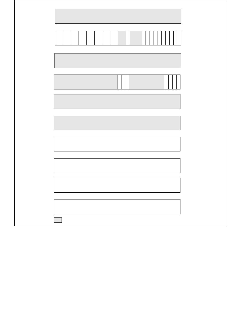
Vol. 3B 17-7
DEBUG, BRANCH PROFILE, TSC, AND INTEL® RESOURCE DIRECTOR TECHNOLOGY (INTEL® RDT) FEATURES
17.3.1 Debug Exception (#DB)—Interrupt Vector 1
The debug-exception handler is usually a debugger program or part of a larger software system. The processor
generates a debug exception for any of several conditions. The debugger checks flags in the DR6 and DR7 registers
to determine which condition caused the exception and which other conditions might apply. Table 17-2 shows the
states of these flags following the generation of each kind of breakpoint condition.
Instruction-breakpoint and general-detect condition (see Section 17.3.1.3, “General-Detect Exception Condition”)
result in faults; other debug-exception conditions result in traps. The debug exception may report one or both at
one time. The following sections describe each class of debug exception.
Figure 17-2. DR6/DR7 Layout on Processors Supporting Intel® 64 Architecture
31 24 23 22 21 20 19 16 15 13
14 12 11 870
DR7
L
Reserved
0
123456
910
1718
252627282930
G
0
L
1
L
2
L
3
G
3
L
E
G
E
G
2
G
1
G
D
R/W
0
LEN
0
R/W
1
LEN
1
R/W
2
LEN
2
R/W
3
LEN
3
31 16 15 13
14 12 11 870
DR6
B
0
123456
910
B
1
B
2
B
3
0111111111
B
D
B
S
B
T
63 32
63 32
DR6
DR7
00 001
Reserved (set to 1)
63 0
DR3
Breakpoint 3 Linear Address
63 0
DR2Breakpoint 2 Linear Address
63 0
DR1
Breakpoint 1 Linear Address
63 0
DR0Breakpoint 0 Linear Address
63 0
DR5
63 0
DR4

17-8 Vol. 3B
DEBUG, BRANCH PROFILE, TSC, AND INTEL® RESOURCE DIRECTOR TECHNOLOGY (INTEL® RDT) FEATURES
The INT1 instruction generates a debug exception as a trap. Hardware vendors may use the INT1 instruction for
hardware debug. For that reason, Intel recommends software vendors instead use the INT3 instruction for software
breakpoints.
See also: Chapter 6, “Interrupt 1—Debug Exception (#DB),” in the Intel® 64 and IA-32 Architectures Software
Developer’s Manual, Volume 3A.
17.3.1.1 Instruction-Breakpoint Exception Condition
The processor reports an instruction breakpoint when it attempts to execute an instruction at an address specified
in a breakpoint-address register (DR0 through DR3) that has been set up to detect instruction execution (R/W flag
is set to 0). Upon reporting the instruction breakpoint, the processor generates a fault-class, debug exception
(#DB) before it executes the target instruction for the breakpoint.
Instruction breakpoints are the highest priority debug exceptions. They are serviced before any other exceptions
detected during the decoding or execution of an instruction. However, if an instruction breakpoint is placed on an
instruction located immediately after a POP SS/MOV SS instruction, the breakpoint will be suppressed as if
EFLAGS.RF were 1 (see the next paragraph and Section 6.8.3, “Masking Exceptions and Interrupts When
Switching Stacks,” of the Intel® 64 and IA-32 Architectures Software Developer’s Manual, Volume 3A).
Because the debug exception for an instruction breakpoint is generated before the instruction is executed, if the
instruction breakpoint is not removed by the exception handler; the processor will detect the instruction breakpoint
again when the instruction is restarted and generate another debug exception. To prevent looping on an instruction
breakpoint, the Intel 64 and IA-32 architectures provide the RF flag (resume flag) in the EFLAGS register (see
Section 2.3, “System Flags and Fields in the EFLAGS Register,” in the Intel® 64 and IA-32 Architectures Software
Developer’s Manual, Volume 3A). When the RF flag is set, the processor ignores instruction breakpoints.
All Intel 64 and IA-32 processors manage the RF flag as follows. The RF Flag is cleared at the start of the instruction
after the check for instruction breakpoints, CS limit violations, and FP exceptions. Task Switches and IRETD/IRETQ
instructions transfer the RF image from the TSS/stack to the EFLAGS register.
When calling an event handler, Intel 64 and IA-32 processors establish the value of the RF flag in the EFLAGS image
pushed on the stack:
•For any fault-class exception except a debug exception generated in response to an instruction breakpoint, the
value pushed for RF is 1.
•For any interrupt arriving after any iteration of a repeated string instruction but the last iteration, the value
pushed for RF is 1.
Table 17-2. Debug Exception Conditions
Debug or Breakpoint Condition DR6 Flags Tested DR7 Flags Tested Exception Class
Single-step trap BS = 1 Trap
Instruction breakpoint, at addresses defined by DRn and
LENn
Bn = 1 and
(Gn or Ln = 1)
R/Wn = 0 Fault
Data write breakpoint, at addresses defined by DRn and
LENn
Bn = 1 and
(Gn or Ln = 1)
R/Wn = 1 Trap
I/O read or write breakpoint, at addresses defined by DRn
and LENn
Bn = 1 and
(Gn or Ln = 1)
R/Wn = 2 Trap
Data read or write (but not instruction fetches), at
addresses defined by DRn and LENn
Bn = 1 and
(Gn or Ln = 1)
R/Wn = 3 Trap
General detect fault, resulting from an attempt to modify
debug registers (usually in conjunction with in-circuit
emulation)
BD = 1 None Fault
Task switch BT = 1 None Trap
INT1 instruction None None Trap

Vol. 3B 17-9
DEBUG, BRANCH PROFILE, TSC, AND INTEL® RESOURCE DIRECTOR TECHNOLOGY (INTEL® RDT) FEATURES
•For any trap-class exception generated by any iteration of a repeated string instruction but the last iteration,
the value pushed for RF is 1.
•For other cases, the value pushed for RF is the value that was in EFLAG.RF at the time the event handler was
called. This includes:
— Debug exceptions generated in response to instruction breakpoints
— Hardware-generated interrupts arriving between instructions (including those arriving after the last
iteration of a repeated string instruction)
— Trap-class exceptions generated after an instruction completes (including those generated after the last
iteration of a repeated string instruction)
— Software-generated interrupts (RF is pushed as 0, since it was cleared at the start of the software interrupt)
As noted above, the processor does not set the RF flag prior to calling the debug exception handler for debug
exceptions resulting from instruction breakpoints. The debug exception handler can prevent recurrence of the
instruction breakpoint by setting the RF flag in the EFLAGS image on the stack. If the RF flag in the EFLAGS image
is set when the processor returns from the exception handler, it is copied into the RF flag in the EFLAGS register by
IRETD/IRETQ or a task switch that causes the return. The processor then ignores instruction breakpoints for the
duration of the next instruction. (Note that the POPF, POPFD, and IRET instructions do not transfer the RF image
into the EFLAGS register.) Setting the RF flag does not prevent other types of debug-exception conditions (such as,
I/O or data breakpoints) from being detected, nor does it prevent non-debug exceptions from being generated.
For the Pentium processor, when an instruction breakpoint coincides with another fault-type exception (such as a
page fault), the processor may generate one spurious debug exception after the second exception has been
handled, even though the debug exception handler set the RF flag in the EFLAGS image. To prevent a spurious
exception with Pentium processors, all fault-class exception handlers should set the RF flag in the EFLAGS image.
17.3.1.2 Data Memory and I/O Breakpoint Exception Conditions
Data memory and I/O breakpoints are reported when the processor attempts to access a memory or I/O address
specified in a breakpoint-address register (DR0 through DR3) that has been set up to detect data or I/O accesses
(R/W flag is set to 1, 2, or 3). The processor generates the exception after it executes the instruction that made the
access, so these breakpoint condition causes a trap-class exception to be generated.
Because data breakpoints are traps, an instruction that writes memory overwrites the original data before the
debug exception generated by a data breakpoint is generated. If a debugger needs to save the contents of a write
breakpoint location, it should save the original contents before setting the breakpoint. The handler can report the
saved value after the breakpoint is triggered. The address in the debug registers can be used to locate the new
value stored by the instruction that triggered the breakpoint.
If a data breakpoint is detected during an iteration of a string instruction executed with fast-string operation (see
Section 7.3.9.3 of Intel® 64 and IA-32 Architectures Software Developer’s Manual, Volume 1), delivery of the
resulting debug exception may be delayed until completion of the corresponding group of iterations.
Intel486 and later processors ignore the GE and LE flags in DR7. In Intel386 processors, exact data breakpoint
matching does not occur unless it is enabled by setting the LE and/or the GE flags.
For repeated INS and OUTS instructions that generate an I/O-breakpoint debug exception, the processor gener-
ates the exception after the completion of the first iteration. Repeated INS and OUTS instructions generate a data-
breakpoint debug exception after the iteration in which the memory address breakpoint location is accessed.
If an execution of the MOV or POP instruction loads the SS register and encounters a data breakpoint, the resulting
debug exception is delivered after completion of the next instruction (the one after the MOV or POP).
Any pending data or I/O breakpoints are lost upon delivery of an exception. For example, if a machine-check
exception (#MC) occurs following an instruction that encounters a data breakpoint (but before the resulting debug
exception is delivered), the data breakpoint is lost. If a MOV or POP instruction that loads the SS register encoun-
ters a data breakpoint, the data breakpoint is lost if the next instruction causes a fault.
Delivery of events due to INT n, INT3, or INTO does not cause a loss of data breakpoints. If a MOV or POP instruc-
tion that loads the SS register encounters a data breakpoint, and the next instruction is software interrupt (INT n,
INT3, or INTO), a debug exception (#DB) resulting from a data breakpoint will be delivered after the transition to
the software-interrupt handler. The #DB handler should account for the fact that the #DB may have been delivered

17-10 Vol. 3B
DEBUG, BRANCH PROFILE, TSC, AND INTEL® RESOURCE DIRECTOR TECHNOLOGY (INTEL® RDT) FEATURES
after a invocation of a software-interrupt handler, and in particular that the CPL may have changed between recog-
nition of the data breakpoint and delivery of the #DB.
17.3.1.3 General-Detect Exception Condition
When the GD flag in DR7 is set, the general-detect debug exception occurs when a program attempts to access any
of the debug registers (DR0 through DR7) at the same time they are being used by another application, such as an
emulator or debugger. This protection feature guarantees full control over the debug registers when required. The
debug exception handler can detect this condition by checking the state of the BD flag in the DR6 register. The
processor generates the exception before it executes the MOV instruction that accesses a debug register, which
causes a fault-class exception to be generated.
17.3.1.4 Single-Step Exception Condition
The processor generates a single-step debug exception if (while an instruction is being executed) it detects that the
TF flag in the EFLAGS register is set. The exception is a trap-class exception, because the exception is generated
after the instruction is executed. The processor will not generate this exception after the instruction that sets the
TF flag. For example, if the POPF instruction is used to set the TF flag, a single-step trap does not occur until after
the instruction that follows the POPF instruction.
The processor clears the TF flag before calling the exception handler. If the TF flag was set in a TSS at the time of
a task switch, the exception occurs after the first instruction is executed in the new task.
The TF flag normally is not cleared by privilege changes inside a task. The INT n, INT3, and INTO instructions,
however, do clear this flag. Therefore, software debuggers that single-step code must recognize and emulate INT n
or INTO instructions rather than executing them directly. To maintain protection, the operating system should
check the CPL after any single-step trap to see if single stepping should continue at the current privilege level.
The interrupt priorities guarantee that, if an external interrupt occurs, single stepping stops. When both an external
interrupt and a single-step interrupt occur together, the single-step interrupt is processed first. This operation
clears the TF flag. After saving the return address or switching tasks, the external interrupt input is examined
before the first instruction of the single-step handler executes. If the external interrupt is still pending, then it is
serviced. The external interrupt handler does not run in single-step mode. To single step an interrupt handler,
single step an INT n instruction that calls the interrupt handler.
If an occurrence of the MOV or POP instruction loads the SS register executes with EFLAGS.TF = 1, no single-step
debug exception occurs following the MOV or POP instruction.
17.3.1.5 Task-Switch Exception Condition
The processor generates a debug exception after a task switch if the T flag of the new task's TSS is set. This excep-
tion is generated after program control has passed to the new task, and prior to the execution of the first instruc-
tion of that task. The exception handler can detect this condition by examining the BT flag of the DR6 register.
If entry 1 (#DB) in the IDT is a task gate, the T bit of the corresponding TSS should not be set. Failure to observe
this rule will put the processor in a loop.
17.3.2 Breakpoint Exception (#BP)—Interrupt Vector 3
The breakpoint exception (interrupt 3) is caused by execution of an INT3 instruction. See Chapter 6,
“Interrupt 3—Breakpoint Exception (#BP).” Debuggers use breakpoint exceptions in the same way that they use
the breakpoint registers; that is, as a mechanism for suspending program execution to examine registers and
memory locations. With earlier IA-32 processors, breakpoint exceptions are used extensively for setting instruction
breakpoints.
With the Intel386 and later IA-32 processors, it is more convenient to set breakpoints with the breakpoint-address
registers (DR0 through DR3). However, the breakpoint exception still is useful for breakpointing debuggers,
because a breakpoint exception can call a separate exception handler. The breakpoint exception is also useful when
it is necessary to set more breakpoints than there are debug registers or when breakpoints are being placed in the
source code of a program under development.

Vol. 3B 17-11
DEBUG, BRANCH PROFILE, TSC, AND INTEL® RESOURCE DIRECTOR TECHNOLOGY (INTEL® RDT) FEATURES
17.3.3 Debug Exceptions, Breakpoint Exceptions, and Restricted Transactional Memory
(RTM)
Chapter 16, “Programming with Intel® Transactional Synchronization Extensions,” of Intel® 64 and IA-32 Archi-
tectures Software Developer’s Manual, Volume 1 describes Restricted Transactional Memory (RTM). This is an
instruction-set interface that allows software to identify transactional regions (or critical sections) using the
XBEGIN and XEND instructions.
Execution of an RTM transactional region begins with an XBEGIN instruction. If execution of the region successfully
reaches an XEND instruction, the processor ensures that all memory operations performed within the region
appear to have occurred instantaneously when viewed from other logical processors. Execution of an RTM transac-
tion region does not succeed if the processor cannot commit the updates atomically. When this happens, the
processor rolls back the execution, a process referred to as a transactional abort. In this case, the processor
discards all updates performed in the region, restores architectural state to appear as if the execution had not
occurred, and resumes execution at a fallback instruction address that was specified with the XBEGIN instruction.
If debug exception (#DB) or breakpoint exception (#BP) occurs within an RTM transaction region, a transactional
abort occurs, the processor sets EAX[4], and no exception is delivered.
Software can enable advanced debugging of RTM transactional regions by setting DR7.RTM[bit 11] and
IA32_DEBUGCTL.RTM[bit 15]. If these bits are both set, the transactional abort caused by a #DB or #BP within an
RTM transaction region does not resume execution at the fallback instruction address specified with the XBEGIN
instruction that begin the region. Instead, execution is resumed at that XBEGIN instruction, and a #DB is deliv-
ered. (A #DB is delivered even if the transactional abort was caused by a #BP.) Such a #DB will clear
DR6.RTM[bit 16] (all other debug exceptions set DR6[16]).
17.4 LAST BRANCH, INTERRUPT, AND EXCEPTION RECORDING OVERVIEW
P6 family processors introduced the ability to set breakpoints on taken branches, interrupts, and exceptions, and
to single-step from one branch to the next. This capability has been modified and extended in the Pentium 4, Intel
Xeon, Pentium M, Intel® Core™ Solo, Intel® Core™ Duo, Intel® Core™2 Duo, Intel® Core™ i7 and Intel® Atom™
processors to allow logging of branch trace messages in a branch trace store (BTS) buffer in memory.
See the following sections for processor specific implementation of last branch, interrupt and exception recording:
— Section 17.5, “Last Branch, Interrupt, and Exception Recording (Intel® Core™ 2 Duo and Intel® Atom™
Processors)”
— Section 17.6, “Last Branch, Call Stack, Interrupt, and Exception Recording for Processors based on
Goldmont Microarchitecture”
— Section 17.9, “Last Branch, Interrupt, and Exception Recording for Processors based on Intel® Microarchi-
tecture code name Nehalem”
— Section 17.10, “Last Branch, Interrupt, and Exception Recording for Processors based on Intel® Microar-
chitecture code name Sandy Bridge”
— Section 17.11, “Last Branch, Call Stack, Interrupt, and Exception Recording for Processors based on
Haswell Microarchitecture”
— Section 17.12, “Last Branch, Call Stack, Interrupt, and Exception Recording for Processors based on
Skylake Microarchitecture”
— Section 17.14, “Last Branch, Interrupt, and Exception Recording (Intel® Core™ Solo and Intel® Core™
Duo Processors)”
— Section 17.15, “Last Branch, Interrupt, and Exception Recording (Pentium M Processors)”
— Section 17.16, “Last Branch, Interrupt, and Exception Recording (P6 Family Processors)”
The following subsections of Section 17.4 describe common features of profiling branches. These features are
generally enabled using the IA32_DEBUGCTL MSR (older processor may have implemented a subset or model-
specific features, see definitions of MSR_DEBUGCTLA, MSR_DEBUGCTLB, MSR_DEBUGCTL).
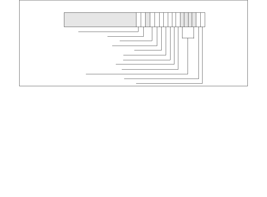
17-12 Vol. 3B
DEBUG, BRANCH PROFILE, TSC, AND INTEL® RESOURCE DIRECTOR TECHNOLOGY (INTEL® RDT) FEATURES
17.4.1 IA32_DEBUGCTL MSR
The IA32_DEBUGCTL MSR provides bit field controls to enable debug trace interrupts, debug trace stores, trace
messages enable, single stepping on branches, last branch record recording, and to control freezing of LBR stack
or performance counters on a PMI request. IA32_DEBUGCTL MSR is located at register address 01D9H.
See Figure 17-3 for the MSR layout and the bullets below for a description of the flags:
•LBR (last branch/interrupt/exception) flag (bit 0) — When set, the processor records a running trace of
the most recent branches, interrupts, and/or exceptions taken by the processor (prior to a debug exception
being generated) in the last branch record (LBR) stack. For more information, see the Section 17.5.1, “LBR
Stack” (Intel® Core™2 Duo and Intel® Atom™ Processor Family) and Section 17.9.1, “LBR Stack” (processors
based on Intel® Microarchitecture code name Nehalem).
•BTF (single-step on branches) flag (bit 1) — When set, the processor treats the TF flag in the EFLAGS
register as a “single-step on branches” flag rather than a “single-step on instructions” flag. This mechanism
allows single-stepping the processor on taken branches. See Section 17.4.3, “Single-Stepping on Branches,”
for more information about the BTF flag.
•TR (trace message enable) flag (bit 6) — When set, branch trace messages are enabled. When the
processor detects a taken branch, interrupt, or exception; it sends the branch record out on the system bus as
a branch trace message (BTM). See Section 17.4.4, “Branch Trace Messages,” for more information about the
TR flag.
•BTS (branch trace store) flag (bit 7) — When set, the flag enables BTS facilities to log BTMs to a memory-
resident BTS buffer that is part of the DS save area. See Section 17.4.9, “BTS and DS Save Area.”
•BTINT (branch trace interrupt) flag (bit 8) — When set, the BTS facilities generate an interrupt when the
BTS buffer is full. When clear, BTMs are logged to the BTS buffer in a circular fashion. See Section 17.4.5, “Branch
Trace Store (BTS),” for a description of this mechanism.
•BTS_OFF_OS (branch trace off in privileged code) flag (bit 9) — When set, BTS or BTM is skipped if CPL
is 0. See Section 17.13.2.
•BTS_OFF_USR (branch trace off in user code) flag (bit 10) — When set, BTS or BTM is skipped if CPL is
greater than 0. See Section 17.13.2.
•FREEZE_LBRS_ON_PMI flag (bit 11) — When set, the LBR stack is frozen on a hardware PMI request (e.g.
when a counter overflows and is configured to trigger PMI). See Section 17.4.7 for details.
•FREEZE_PERFMON_ON_PMI flag (bit 12) — When set, the performance counters (IA32_PMCx and
IA32_FIXED_CTRx) are frozen on a PMI request. See Section 17.4.7 for details.
•FREEZE_WHILE_SMM (bit 14) — If this bit is set, upon the delivery of an SMI, the processor will clear all the
enable bits of IA32_PERF_GLOBAL_CTRL, save a copy of the content of IA32_DEBUGCTL and disable LBR, BTF,
Figure 17-3. IA32_DEBUGCTL MSR for Processors based
on Intel Core microarchitecture
31
TR — Trace messages enable
BTINT — Branch trace interrupt
BTF — Single-step on branches
LBR — Last branch/interrupt/exception
Reserved
87654321 0
BTS — Branch trace store
Reserved
910
BTS_OFF_OS — BTS off in OS
BTS_OFF_USR — BTS off in user code
FREEZE_LBRS_ON_PMI
FREEZE_PERFMON_ON_PMI
1112
14
FREEZE_WHILE_SMM
15
RTM

Vol. 3B 17-13
DEBUG, BRANCH PROFILE, TSC, AND INTEL® RESOURCE DIRECTOR TECHNOLOGY (INTEL® RDT) FEATURES
TR, and BTS fields of IA32_DEBUGCTL before transferring control to the SMI handler. Subsequently, the enable
bits of IA32_PERF_GLOBAL_CTRL will be set to 1, the saved copy of IA32_DEBUGCTL prior to SMI delivery will
be restored, after the SMI handler issues RSM to complete its service. Note that system software must check if
the processor supports the IA32_DEBUGCTL.FREEZE_WHILE_SMM control bit.
IA32_DEBUGCTL.FREEZE_WHILE_SMM is supported if IA32_PERF_CAPABILITIES.FREEZE_WHILE_SMM[Bit
12] is reporting 1. See Section 18.8 for details of detecting the presence of IA32_PERF_CAPABILITIES MSR.
•RTM (bit 15) — If this bit is set, advanced debugging of RTM transactional regions is enabled if DR7.RTM is
also set. See Section 17.3.3.
17.4.2 Monitoring Branches, Exceptions, and Interrupts
When the LBR flag (bit 0) in the IA32_DEBUGCTL MSR is set, the processor automatically begins recording branch
records for taken branches, interrupts, and exceptions (except for debug exceptions) in the LBR stack MSRs.
When the processor generates a debug exception (#DB), it automatically clears the LBR flag before executing the
exception handler. This action does not clear previously stored LBR stack MSRs.
A debugger can use the linear addresses in the LBR stack to re-set breakpoints in the breakpoint address registers
(DR0 through DR3). This allows a backward trace from the manifestation of a particular bug toward its source.
On some processors, if the LBR flag is cleared and TR flag in the IA32_DEBUGCTL MSR remains set, the processor
will continue to update LBR stack MSRs. This is because those processors use the entries in the LBR stack in the
process of generating BTM/BTS records. A #DB does not automatically clear the TR flag.
17.4.3 Single-Stepping on Branches
When software sets both the BTF flag (bit 1) in the IA32_DEBUGCTL MSR and the TF flag in the EFLAGS register,
the processor generates a single-step debug exception only after instructions that cause a branch.1 This mecha-
nism allows a debugger to single-step on control transfers caused by branches. This “branch single stepping” helps
isolate a bug to a particular block of code before instruction single-stepping further narrows the search. The
processor clears the BTF flag when it generates a debug exception. The debugger must set the BTF flag before
resuming program execution to continue single-stepping on branches.
17.4.4 Branch Trace Messages
Setting the TR flag (bit 6) in the IA32_DEBUGCTL MSR enables branch trace messages (BTMs). Thereafter, when
the processor detects a branch, exception, or interrupt, it sends a branch record out on the system bus as a BTM.
A debugging device that is monitoring the system bus can read these messages and synchronize operations with
taken branch, interrupt, and exception events.
When interrupts or exceptions occur in conjunction with a taken branch, additional BTMs are sent out on the bus,
as described in Section 17.4.2, “Monitoring Branches, Exceptions, and Interrupts.”
For P6 processor family, Pentium M processor family, processors based on Intel Core microarchitecture, TR and LBR
bits can not be set at the same time due to hardware limitation. The content of LBR stack is undefined when TR is
set.
For processors with Intel NetBurst microarchitecture, Intel Atom processors, and Intel Core and related Intel Xeon
processors both starting with the Nehalem microarchitecture, the processor can collect branch records in the LBR
stack and at the same time send/store BTMs when both the TR and LBR flags are set in the IA32_DEBUGCTL MSR
(or the equivalent MSR_DEBUGCTLA, MSR_DEBUGCTLB).
The following exception applies:
•BTM may not be observable on Intel Atom processor families that do not provide an externally visible system
bus (i.e., processors based on the Silvermont microarchitecture or later).
1. Executions of CALL, IRET, and JMP that cause task switches never cause single-step debug exceptions (regardless of the value of the
BTF flag). A debugger desiring debug exceptions on switches to a task should set the T flag (debug trap flag) in the TSS of that task.
See Section 7.2.1, “Task-State Segment (TSS).”

17-14 Vol. 3B
DEBUG, BRANCH PROFILE, TSC, AND INTEL® RESOURCE DIRECTOR TECHNOLOGY (INTEL® RDT) FEATURES
17.4.4.1 Branch Trace Message Visibility
Branch trace message (BTM) visibility is implementation specific and limited to systems with a front side bus
(FSB). BTMs may not be visible to newer system link interfaces or a system bus that deviates from a traditional
FSB.
17.4.5 Branch Trace Store (BTS)
A trace of taken branches, interrupts, and exceptions is useful for debugging code by providing a method of deter-
mining the decision path taken to reach a particular code location. The LBR flag (bit 0) of IA32_DEBUGCTL provides
a mechanism for capturing records of taken branches, interrupts, and exceptions and saving them in the last
branch record (LBR) stack MSRs, setting the TR flag for sending them out onto the system bus as BTMs. The branch
trace store (BTS) mechanism provides the additional capability of saving the branch records in a memory-resident
BTS buffer, which is part of the DS save area. The BTS buffer can be configured to be circular so that the most
re cent branc h recor ds are always ava ilable or it can be configured to gen era te an interrup t when the buff er is nearly
full so that all the branch records can be saved. The BTINT flag (bit 8) can be used to enable the generation of inter-
rupt when the BTS buffer is full. See Section 17.4.9.2, “Setting Up the DS Save Area.” for additional details.
Setting this flag (BTS) alone can greatly reduce the performance of the processor. CPL-qualified branch trace
storing mechanism can help mitigate the performance impact of sending/logging branch trace messages.
17.4.6 CPL-Qualified Branch Trace Mechanism
CPL-qualified branch trace mechanism is available to a subset of Intel 64 and IA-32 processors that support the
branch trace storing mechanism. The processor supports the CPL-qualified branch trace mechanism if
CPUID.01H:ECX[bit 4] = 1.
The CPL-qualified branch trace mechanism is described in Section 17.4.9.4. System software can selectively specify
CPL qualification to not send/store Branch Trace Messages associated with a specified privilege level. Two bit fields,
BTS_OFF_USR (bit 10) and BTS_OFF_OS (bit 9), are provided in the debug control register to specify the CPL of
BTMs that will not be logged in the BTS buffer or sent on the bus.
17.4.7 Freezing LBR and Performance Counters on PMI
Many issues may generate a performance monitoring interrupt (PMI); a PMI service handler will need to determine
cause to handle the situation. Two capabilities that allow a PMI service routine to improve branch tracing and
performance monitoring are available for processors supporting architectural performance monitoring version 2 or
greater (i.e. CPUID.0AH:EAX[7:0] > 1). These capabilities provides the following interface in IA32_DEBUGCTL to
reduce runtime overhead of PMI servicing, profiler-contributed skew effects on analysis or counter metrics:
•Freezing LBRs on PMI (bit 11)— Allows the PMI service routine to ensure the content in the LBR stack are
associated with the target workload and not polluted by the branch flows of handling the PMI. Depending on the
version ID enumerated by CPUID.0AH:EAX.ArchPerfMonVerID[bits 7:0], two flavors are supported:
— Legacy Freeze_LBR_on_PMI is supported for ArchPerfMonVerID <= 3 and ArchPerfMonVerID >1. If
IA32_DEBUGCTL.Freeze_LBR_On_PMI = 1, the LBR is frozen on the overflowed condition of the buffer
area, the processor clears the LBR bit (bit 0) in IA32_DEBUGCTL. Software must then re-enable
IA32_DEBUGCTL.LBR to resume recording branches. When using this feature, software should be careful
about writes to IA32_DEBUGCTL to avoid re-enabling LBRs by accident if they were just disabled.
— Streamlined Freeze_LBR_on_PMI is supported for ArchPerfMonVerID >= 4. If
IA32_DEBUGCTL.Freeze_LBR_On_PMI = 1, the processor behaves as follows:
•sets IA32_PERF_GLOBAL_STATUS.LBR_Frz =1 to disable recording, but does not change the LBR bit
(bit 0) in IA32_DEBUGCTL. The LBRs are frozen on the overflowed condition of the buffer area.
•Freezing PMCs on PMI (bit 12) — Allows the PMI service routine to ensure the content in the performance
counters are associated with the target workload and not polluted by the PMI and activities within the PMI
service routine. Depending on the version ID enumerated by CPUID.0AH:EAX.ArchPerfMonVerID[bits 7:0], two
flavors are supported:

Vol. 3B 17-15
DEBUG, BRANCH PROFILE, TSC, AND INTEL® RESOURCE DIRECTOR TECHNOLOGY (INTEL® RDT) FEATURES
— Legacy Freeze_Perfmon_on_PMI is supported for ArchPerfMonVerID <= 3 and ArchPerfMonVerID >1. If
IA32_DEBUGCTL.Freeze_Perfmon_On_PMI = 1, the performance counters are frozen on the counter
overflowed condition when the processor clears the IA32_PERF_GLOBAL_CTRL MSR (see Figure 18-3). The
PMCs affected include both general-purpose counters and fixed-function counters (see Section 18.6.2.1,
“Fixed-function Performance Counters”). Software must re-enable counts by writing 1s to the corre-
sponding enable bits in IA32_PERF_GLOBAL_CTRL before leaving a PMI service routine to continue counter
operation.
— Streamlined Freeze_Perfmon_on_PMI is supported for ArchPerfMonVerID >= 4. The processor behaves as
follows:
•sets IA32_PERF_GLOBAL_STATUS.CTR_Frz =1 to disable counting on a counter overflow condition, but
does not change the IA32_PERF_GLOBAL_CTRL MSR.
Freezing LBRs and PMCs on PMIs (both legacy and streamlined operation) occur when one of the following applies:
•A performance counter had an overflow and was programmed to signal a PMI in case of an overflow.
— For the general-purpose counters; enabling PMI is done by setting bit 20 of the IA32_PERFEVTSELx
register.
— For the fixed-function counters; enabling PMI is done by setting the 3rd bit in the corresponding 4-bit
control field of the MSR_PERF_FIXED_CTR_CTRL register (see Figure 18-1) or IA32_FIXED_CTR_CTRL MSR
(see Figure 18-2).
•The PEBS buffer is almost full and reaches the interrupt threshold.
•The BTS buffer is almost full and reaches the interrupt threshold.
Table 17-3 compares the interaction of the processor with the PMI handler using the legacy versus streamlined
Freeza_Perfmon_On_PMI interface.
Table 17-3. Legacy and Streamlined Operation with Freeze_Perfmon_On_PMI = 1, Counter Overflowed
Legacy Freeze_Perfmon_On_PMI Streamlined Freeze_Perfmon_On_PMI Comment
Processor freezes the counters on overflow Processor freezes the counters on overflow Unchanged
Processor clears IA32_PERF_GLOBAL_CTRL Processor set
IA32_PERF_GLOBAL_STATUS.CTR_FTZ
Handler reads IA32_PERF_GLOBAL_STATUS
(0x38E) to examine which counter(s) overflowed
mask = RDMSR(0x38E) Similar
Handler services the PMI Handler services the PMI Unchanged
Handler writes 1s to
IA32_PERF_GLOBAL_OVF_CTL (0x390)
Handler writes mask into
IA32_PERF_GLOBAL_OVF_RESET (0x390)
Processor clears IA32_PERF_GLOBAL_STATUS Processor clears IA32_PERF_GLOBAL_STATUS Unchanged
Handler re-enables IA32_PERF_GLOBAL_CTRL None Reduced software overhead

17-16 Vol. 3B
DEBUG, BRANCH PROFILE, TSC, AND INTEL® RESOURCE DIRECTOR TECHNOLOGY (INTEL® RDT) FEATURES
17.4.8 LBR Stack
The last branch record stack and top-of-stack (TOS) pointer MSRs are supported across Intel 64 and IA-32
processor families. However, the number of MSRs in the LBR stack and the valid range of TOS pointer value can
vary between different processor families. Table 17-4 lists the LBR stack size and TOS pointer range for several
processor families according to the CPUID signatures of DisplayFamily_DisplayModel encoding (see CPUID instruc-
tion in Chapter 3 of Intel® 64 and IA-32 Architectures Software Developer’s Manual, Volume 2A).
The last branch recording mechanism tracks not only branch instructions (like JMP, Jcc, LOOP and CALL instruc-
tions), but also other operations that cause a change in the instruction pointer (like external interrupts, traps and
faults). The branch recording mechanisms generally employs a set of MSRs, referred to as last branch record (LBR)
stack. The size and exact locations of the LBR stack are generally model-specific (see Chapter 2, “Model-Specific
Registers (MSRs)” in the Intel® 64 and IA-32 Architectures Software Developer’s Manual, Volume 4 for model-
specific MSR addresses).
•Last Branch Record (LBR) Stack — The LBR consists of N pairs of MSRs (N is listed in the LBR stack size
column of Table 17-4) that store source and destination address of recent branches (see Figure 17-3):
— MSR_LASTBRANCH_0_FROM_IP (address is model specific) through the next consecutive (N-1) MSR
address store source addresses.
— MSR_LASTBRANCH_0_TO_IP (address is model specific ) through the next consecutive (N-1) MSR address
store destination addresses.
•Last Branch Record Top-of-Stack (TOS) Pointer — The lowest significant M bits of the TOS Pointer MSR
(MSR_LASTBRANCH_TOS, address is model specific) contains an M-bit pointer to the MSR in the LBR stack that
contains the most recent branch, interrupt, or exception recorded. The valid range of the M-bit POS pointer is
given in Table 17-4.
17.4.8.1 LBR Stack and Intel® 64 Processors
LBR MSRs are 64-bits. In 64-bit mode, last branch records store the full address. Outside of 64-bit mode, the upper
32-bits of branch addresses will be stored as 0.
Table 17-4. LBR Stack Size and TOS Pointer Range
DisplayFamily_DisplayModel Size of LBR Stack Component of an LBR Entry Range of TOS Pointer
06_5CH, 06_5FH 32 FROM_IP, TO_IP 0 to 31
06_4EH, 06_5EH, 06_8EH, 06_9EH, 06_55H,
06_66H, 06_7AH, 06_67H, 06_6AH, 06_6CH,
06_7DH, 06_7EH
32 FROM_IP, TO_IP, LBR_INFO1
NOTES:
1. See Section 17.12.
0 to 31
06_3DH, 06_47H, 06_4FH, 06_56H, 06_3CH,
06_45H, 06_46H, 06_3FH, 06_2AH, 06_2DH,
06_3AH, 06_3EH, 06_1AH, 06_1EH, 06_1FH,
06_2EH, 06_25H, 06_2CH, 06_2FH
16 FROM_IP, TO_IP 0 to 15
06_17H, 06_1DH, 06_0FH 4FROM_IP, TO_IP0 to 3
06_37H, 06_4AH, 06_4CH, 06_4DH, 06_5AH,
06_5DH, 06_1CH, 06_26H, 06_27H, 06_35H,
06_36H
8FROM_IP, TO_IP0 to 7

Vol. 3B 17-17
DEBUG, BRANCH PROFILE, TSC, AND INTEL® RESOURCE DIRECTOR TECHNOLOGY (INTEL® RDT) FEATURES
Software should query an architectural MSR IA32_PERF_CAPABILITIES[5:0] about the format of the address that
is stored in the LBR stack. Four formats are defined by the following encoding:
—000000B (32-bit record format) — Stores 32-bit offset in current CS of respective source/destination,
—000001B (64-bit LIP record format) — Stores 64-bit linear address of respective source/destination,
—000010B (64-bit EIP record format) — Stores 64-bit offset (effective address) of respective
source/destination.
—000011B (64-bit EIP record format) and Flags — Stores 64-bit offset (effective address) of respective
source/destination. Misprediction info is reported in the upper bit of 'FROM' registers in the LBR stack. See
LBR stack details below for flag support and definition.
—000100B (64-bit EIP record format), Flags and TSX — Stores 64-bit offset (effective address) of
respective source/destination. Misprediction and TSX info are reported in the upper bits of ‘FROM’ registers
in the LBR stack.
—000101B (64-bit EIP record format), Flags, TSX, LBR_INFO — Stores 64-bit offset (effective
address) of respective source/destination. Misprediction, TSX, and elapsed cycles since the last LBR update
are reported in the LBR_INFO MSR stack.
—000110B (64-bit LIP record format), Flags, Cycles — Stores 64-bit linear address (CS.Base +
effective address) of respective source/destination. Misprediction info is reported in the upper bits of
'FROM' registers in the LBR stack. Elapsed cycles since the last LBR update are reported in the upper 16 bits
of the 'TO' registers in the LBR stack (see Section 17.6).
—000111B (64-bit LIP record format), Flags, LBR_INFO — Stores 64-bit linear address (CS.Base +
effective address) of respective source/destination. Misprediction, and elapsed cycles since the last LBR
update are reported in the LBR_INFO MSR stack.
Processor’s support for the architectural MSR IA32_PERF_CAPABILITIES is provided by
CPUID.01H:ECX[PERF_CAPAB_MSR] (bit 15).
17.4.8.2 LBR Stack and IA-32 Processors
The LBR MSRs in IA-32 processors introduced prior to Intel 64 architecture store the 32-bit “To Linear Address” and
“From Linear Address“ using the high and low half of each 64-bit MSR.
17.4.8.3 Last Exception Records and Intel 64 Architecture
Intel 64 and IA-32 processors also provide MSRs that store the branch record for the last branch taken prior to an
exception or an interrupt. The location of the last exception record (LER) MSRs are model specific. The MSRs that
store last exception records are 64-bits. If IA-32e mode is disabled, only the lower 32-bits of the address is
recorded. If IA-32e mode is enabled, the processor writes 64-bit values into the MSR. In 64-bit mode, last excep-
tion records store 64-bit addresses; in compatibility mode, the upper 32-bits of last exception records are cleared.
Figure 17-4. 64-bit Address Layout of LBR MSR
63
Source Address
0
0
63
Destination Address
MSR_LASTBRANCH_0_FROM_IP through MSR_LASTBRANCH_(N-1)_FROM_IP
MSR_LASTBRANCH_0_TO_IP through MSR_LASTBRANCH_(N-1)_TO_IP

17-18 Vol. 3B
DEBUG, BRANCH PROFILE, TSC, AND INTEL® RESOURCE DIRECTOR TECHNOLOGY (INTEL® RDT) FEATURES
17.4.9 BTS and DS Save Area
The Debug store (DS) feature flag (bit 21), returned by CPUID.1:EDX[21] indicates that the processor provides
the debug store (DS) mechanism. The DS mechanism allows:
•BTMs to be stored in a memory-resident BTS buffer. See Section 17.4.5, “Branch Trace Store (BTS).”
•Processor event-based sampling (PEBS) also uses the DS save area provided by debug store mechanism. The
capability of PEBS varies across different microarchitectures. See Section 18.6.2.4, “Processor Event Based
Sampling (PEBS),” and the relevant PEBS sub-sections across the core PMU sections in Chapter 18, “Perfor-
mance Monitoring.”
When CPUID.1:EDX[21] is set:
•The BTS_UNAVAILABLE and PEBS_UNAVAILABLE flags in the IA32_MISC_ENABLE MSR indicate (when clear)
the availability of the BTS and PEBS facilities, including the ability to set the BTS and BTINT bits in the
appropriate DEBUGCTL MSR.
•The IA32_DS_AREA MSR exists and points to the DS save area.
The debug store (DS) save area is a software-designated area of memory that is used to collect the following two
types of information:
•Branch records — When the BTS flag in the IA32_DEBUGCTL MSR is set, a branch record is stored in the BTS
buffer in the DS save area whenever a taken branch, interrupt, or exception is detected.
•PEBS records — When a performance counter is configured for PEBS, a PEBS record is stored in the PEBS
buffer in the DS save area after the counter overflow occurs. This record contains the architectural state of the
processor (state of the 8 general purpose registers, EIP register, and EFLAGS register) at the next occurrence
of the PEBS event that caused the counter to overflow. When the state information has been logged, the
counter is automatically reset to a specified value, and event counting begins again. The content layout of a
PEBS record varies across different implementations that support PEBS. See Section 18.6.2.4.2 for details of
enumerating PEBS record format.
NOTES
Prior to processors based on the Goldmont microarchitecture, PEBS facility only supports a subset
of implementation-specific precise events. See Section 18.5.3.1 for a PEBS enhancement that can
generate records for both precise and non-precise events.
The DS save area and recording mechanism are disabled on INIT, processor Reset or transition to
system-management mode (SMM) or IA-32e mode. It is similarly disabled on the generation of a
machine-check exception on 45nm and 32nm Intel Atom processors and on processors with
Netburst or Intel Core microarchitecture.
The BTS and PEBS facilities may not be available on all processors. The availability of these facilities
is indicated by the BTS_UNAVAILABLE and PEBS_UNAVAILABLE flags, respectively, in the
IA32_MISC_ENABLE MSR (see Chapter 2, “Model-Specific Registers (MSRs)” in the Intel® 64 and
IA-32 Architectures Software Developer’s Manual, Volume 4).
The DS save area is divided into three parts: buffer management area, branch trace store (BTS) buffer, and PEBS
buffer (see Figure 17-5). The buffer management area is used to define the location and size of the BTS and PEBS
buffers. The processor then uses the buffer management area to keep track of the branch and/or PEBS records in
their respective buffers and to record the performance counter reset value. The linear address of the first byte of
the DS buffer management area is specified with the IA32_DS_AREA MSR.
The fields in the buffer management area are as follows:
•BTS buffer base — Linear address of the first byte of the BTS buffer. This address should point to a natural
doubleword boundary.
•BTS index — Linear address of the first byte of the next BTS record to be written to. Initially, this address
should be the same as the address in the BTS buffer base field.
•BTS absolute maximum — Linear address of the next byte past the end of the BTS buffer. This address should
be a multiple of the BTS record size (12 bytes) plus 1.
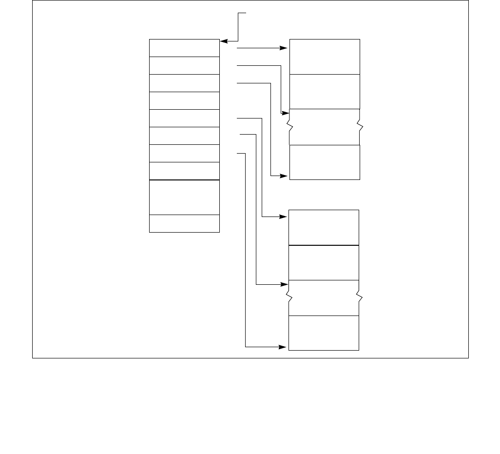
Vol. 3B 17-19
DEBUG, BRANCH PROFILE, TSC, AND INTEL® RESOURCE DIRECTOR TECHNOLOGY (INTEL® RDT) FEATURES
•BTS interrupt threshold — Linear address of the BTS record on which an interrupt is to be generated. This
address must point to an offset from the BTS buffer base that is a multiple of the BTS record size. Also, it must
be several records short of the BTS absolute maximum address to allow a pending interrupt to be handled prior
to processor writing the BTS absolute maximum record.
•PEBS buffer base — Linear address of the first byte of the PEBS buffer. This address should point to a natural
doubleword boundary.
•PEBS index — Linear address of the first byte of the next PEBS record to be written to. Initially, this address
should be the same as the address in the PEBS buffer base field.
•PEBS absolute maximum — Linear address of the next byte past the end of the PEBS buffer. This address
should be a multiple of the PEBS record size (40 bytes) plus 1.
•PEBS interrupt threshold — Linear address of the PEBS record on which an interrupt is to be generated. This
address must point to an offset from the PEBS buffer base that is a multiple of the PEBS record size. Also, it
must be several records short of the PEBS absolute maximum address to allow a pending interrupt to be
handled prior to processor writing the PEBS absolute maximum record.
•PEBS counter reset value — A 64-bit value that the counter is to be set to when a PEBS record is written. Bits
beyond the size of the counter are ignored. This value allows state information to be collected regularly every
time the specified number of events occur.
Figure 17-5. DS Save Area Example1
NOTES:
1. This example represents the format for a system that supports PEBS on only one counter.
BTS Buffer Base
BTS Index
BTS Absolute
BTS Interrupt
PEBS Absolute
PEBS Interrupt
PEBS
Maximum
Maximum
Threshold
PEBS Index
PEBS Buffer Base
Threshold
Counter Reset
Reserved
0H
4H
8H
CH
10H
14H
18H
1CH
20H
24H
30H
Branch Record 0
Branch Record 1
Branch Record n
PEBS Record 0
PEBS Record 1
PEBS Record n
BTS Buffer
PEBS Buffer
DS Buffer Management Area
IA32_DS_AREA MSR
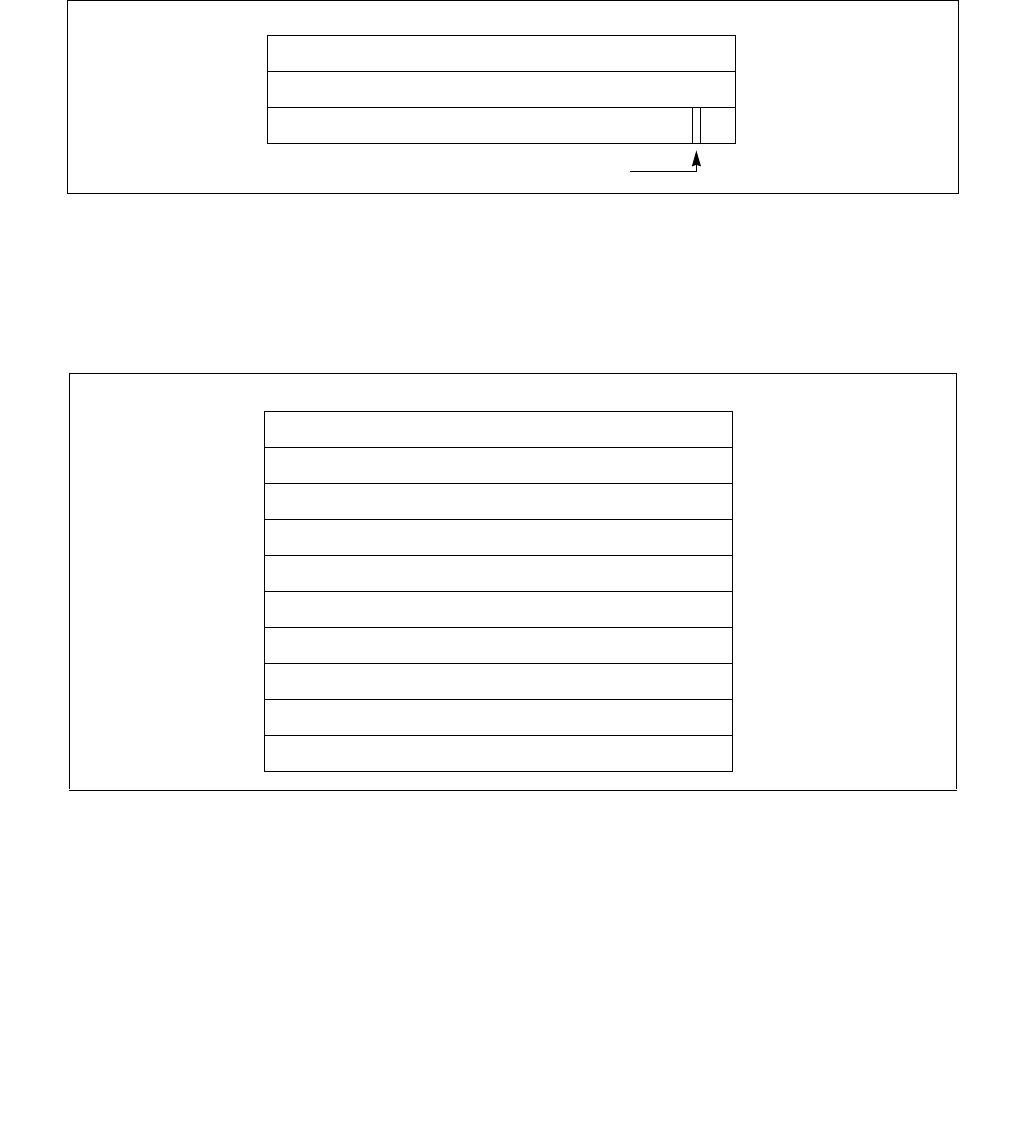
17-20 Vol. 3B
DEBUG, BRANCH PROFILE, TSC, AND INTEL® RESOURCE DIRECTOR TECHNOLOGY (INTEL® RDT) FEATURES
Figure 17-6 shows the structure of a 12-byte branch record in the BTS buffer. The fields in each record are as
follows:
•Last branch from — Linear address of the instruction from which the branch, interrupt, or exception was
taken.
•Last branch to — Linear address of the branch target or the first instruction in the interrupt or exception
service routine.
•Branch predicted — Bit 4 of field indicates whether the branch that was taken was predicted (set) or not
predicted (clear).
Figure 17-7 shows the structure of the 40-byte PEBS records. Nominally the register values are those at the begin-
ning of the instruction that caused the event. However, there are cases where the registers may be logged in a
partially modified state. The linear IP field shows the value in the EIP register translated from an offset into the
current code segment to a linear address.
17.4.9.1 64 Bit Format of the DS Save Area
When DTES64 = 1 (CPUID.1.ECX[2] = 1), the structure of the DS save area is shown in Figure 17-8.
When DTES64 = 0 (CPUID.1.ECX[2] = 0) and IA-32e mode is active, the structure of the DS save area is shown in
Figure 17-8. If IA-32e mode is not active the structure of the DS save area is as shown in Figure 17-5.
Figure 17-6. 32-bit Branch Trace Record Format
Figure 17-7. PEBS Record Format
Last Branch From
Last Branch To
Branch Predicted
0H
4H
8H
0
31 4
EFLAGS
0H
4H
8H
0
31
Linear IP
10H
18H
14H
1CH
20H
24H
CH
EAX
EBX
ECX
EDX
ESI
EDI
EBP
ESP
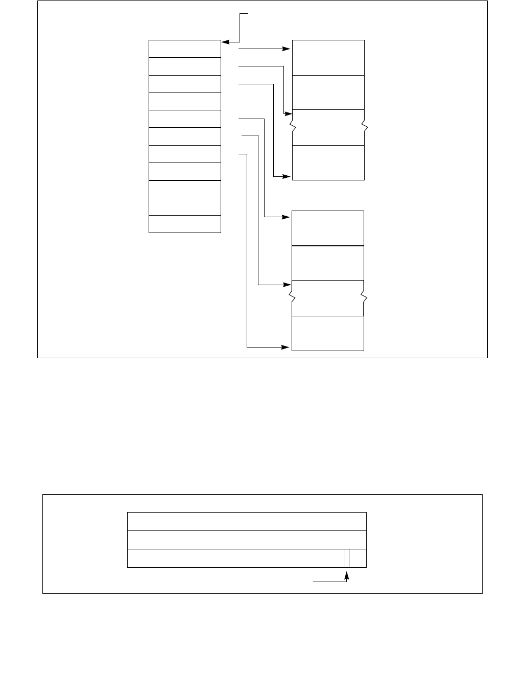
Vol. 3B 17-21
DEBUG, BRANCH PROFILE, TSC, AND INTEL® RESOURCE DIRECTOR TECHNOLOGY (INTEL® RDT) FEATURES
The IA32_DS_AREA MSR holds the 64-bit linear address of the first byte of the DS buffer management area. The
structure of a branch trace record is similar to that shown in Figure 17-6, but each field is 8 bytes in length. This
makes each BTS record 24 bytes (see Figure 17-9). The structure of a PEBS record is similar to that shown in
Figure 17-7, but each field is 8 bytes in length and architectural states include register R8 through R15. This makes
the size of a PEBS record in 64-bit mode 144 bytes (see Figure 17-10).
Figure 17-8. IA-32e Mode DS Save Area Example1
NOTES:
1. This example represents the format for a system that supports PEBS on only one counter.
Figure 17-9. 64-bit Branch Trace Record Format
BTS Buffer Base
BTS Index
BTS Absolute
BTS Interrupt
PEBS Absolute
PEBS Interrupt
PEBS
Maximum
Maximum
Threshold
PEBS Index
PEBS Buffer Base
Threshold
Counter Reset
Reserved
0H
8H
10H
18H
20H
28H
30H
38H
40H
48H
50H
Branch Record 0
Branch Record 1
Branch Record n
PEBS Record 0
PEBS Record 1
PEBS Record n
BTS Buffer
PEBS Buffer
DS Buffer Management Area
IA32_DS_AREA MSR
Last Branch From
Last Branch To
Branch Predicted
0H
8H
10H
0
63 4

17-22 Vol. 3B
DEBUG, BRANCH PROFILE, TSC, AND INTEL® RESOURCE DIRECTOR TECHNOLOGY (INTEL® RDT) FEATURES
Fields in the buffer management area of a DS save area are described in Section 17.4.9.
The format of a branch trace record and a PEBS record are the same as the 64-bit record formats shown in Figures
17-9 and Figures 17-10, with the exception that the branch predicted bit is not supported by Intel Core microarchi-
tecture or Intel Atom microarchitecture. The 64-bit record formats for BTS and PEBS apply to DS save area for all
operating modes.
The procedures used to program IA32_DEBUGCTL MSR to set up a BTS buffer or a CPL-qualified BTS are described
in Section 17.4.9.3 and Section 17.4.9.4.
Required elements for writing a DS interrupt service routine are largely the same on processors that support using
DS Save area for BTS or PEBS records. However, on processors based on Intel NetBurst® microarchitecture, re-
enabling counting requires writing to CCCRs. But a DS interrupt service routine on processors supporting architec-
tural performance monitoring should:
•Re-enable the enable bits in IA32_PERF_GLOBAL_CTRL MSR if it is servicing an overflow PMI due to PEBS.
•Clear overflow indications by writing to IA32_PERF_GLOBAL_OVF_CTRL when a counting configuration is
changed. This includes bit 62 (ClrOvfBuffer) and the overflow indication of counters used in either PEBS or
general-purpose counting (specifically: bits 0 or 1; see Figures 18-3).
17.4.9.2 Setting Up the DS Save Area
To save branch records with the BTS buffer, the DS save area must first be set up in memory as described in the
following procedure (See Section 18.6.2.4.1, “Setting up the PEBS Buffer,” for instructions for setting up a PEBS
buffer, respectively, in the DS save area):
1. Create the DS buffer management information area in memory (see Section 17.4.9, “BTS and DS Save Area,”
and Section 17.4.9.1, “64 Bit Format of the DS Save Area”). Also see the additional notes in this section.
2. Write the base linear address of the DS buffer management area into the IA32_DS_AREA MSR.
3. Set up the performance counter entry in the xAPIC LVT for fixed delivery and edge sensitive. See Section
10.5.1, “Local Vector Table.”
4. Establish an interrupt handler in the IDT for the vector associated with the performance counter entry in the
xAPIC LVT.
Figure 17-10. 64-bit PEBS Record Format
RFLAGS
0H
8H
10H
0
63
RIP
20H
30H
28H
38H
40H
48H
18H
RAX
RBX
RCX
RDX
RSI
RDI
RBP
RSP
R8
...
R15
50H
...
88H
Vol. 3B 17-23
DEBUG, BRANCH PROFILE, TSC, AND INTEL® RESOURCE DIRECTOR TECHNOLOGY (INTEL® RDT) FEATURES
5. Write an interrupt service routine to handle the interrupt. See Section 17.4.9.5, “Writing the DS Interrupt
Service Routine.”
The following restrictions should be applied to the DS save area.
•The three DS save area sections should be allocated from a non-paged pool, and marked accessed and dirty. It
is the responsibility of the operating system to keep the pages that contain the buffer present and to mark
them accessed and dirty. The implication is that the operating system cannot do “lazy” page-table entry
propagation for these pages.
•The DS save area can be larger than a page, but the pages must be mapped to contiguous linear addresses.
The buffer may share a page, so it need not be aligned on a 4-KByte boundary. For performance reasons, the
base of the buffer must be aligned on a doubleword boundary and should be aligned on a cache line boundary.
•It is recommended that the buffer size for the BTS buffer and the PEBS buffer be an integer multiple of the
corresponding record sizes.
•The precise event records buffer should be large enough to hold the number of precise event records that can
occur while waiting for the interrupt to be serviced.
•The DS save area should be in kernel space. It must not be on the same page as code, to avoid triggering self-
modifying code actions.
•There are no memory type restrictions on the buffers, although it is recommended that the buffers be
designated as WB memory type for performance considerations.
•Either the system must be prevented from entering A20M mode while DS save area is active, or bit 20 of all
addresses within buffer bounds must be 0.
•Pages that contain buffers must be mapped to the same physical addresses for all processes, such that any
change to control register CR3 will not change the DS addresses.
•The DS save area is expected to used only on systems with an enabled APIC. The LVT Performance Counter
entry in the APCI must be initialized to use an interrupt gate instead of the trap gate.
17.4.9.3 Setting Up the BTS Buffer
Three flags in the MSR_DEBUGCTLA MSR (see Table 17-5), IA32_DEBUGCTL (see Figure 17-3), or
MSR_DEBUGCTLB (see Figure 17-16) control the generation of branch records and storing of them in the BTS
buffer; these are TR, BTS, and BTINT. The TR flag enables the generation of BTMs. The BTS flag determines
whether the BTMs are sent out on the system bus (clear) or stored in the BTS buffer (set). BTMs cannot be simul-
taneously sent to the system bus and logged in the BTS buffer. The BTINT flag enables the generation of an inter-
rupt when the BTS buffer is full. When this flag is clear, the BTS buffer is a circular buffer.
The following procedure describes how to set up a DS Save area to collect branch records in the BTS buffer:
1. Place values in the BTS buffer base, BTS index, BTS absolute maximum, and BTS interrupt threshold fields of
the DS buffer management area to set up the BTS buffer in memory.
2. Set the TR and BTS flags in the IA32_DEBUGCTL for Intel Core Solo and Intel Core Duo processors or later
processors (or MSR_DEBUGCTLA MSR for processors based on Intel NetBurst Microarchitecture; or
MSR_DEBUGCTLB for Pentium M processors).
3. Clear the BTINT flag in the corresponding IA32_DEBUGCTL (or MSR_DEBUGCTLA MSR; or MSR_DEBUGCTLB)
if a circular BTS buffer is desired.
Table 17-5. IA32_DEBUGCTL Flag Encodings
TR BTS BTINT Description
0 X X Branch trace messages (BTMs) off
1 0 X Generate BTMs
1 1 0 Store BTMs in the BTS buffer, used here as a circular buffer
1 1 1 Store BTMs in the BTS buffer, and generate an interrupt when the buffer is nearly full

17-24 Vol. 3B
DEBUG, BRANCH PROFILE, TSC, AND INTEL® RESOURCE DIRECTOR TECHNOLOGY (INTEL® RDT) FEATURES
NOTES
If the buffer size is set to less than the minimum allowable value (i.e. BTS absolute maximum < 1
+ size of BTS record), the results of BTS is undefined.
In order to prevent generating an interrupt, when working with circular BTS buffer, SW need to set
BTS interrupt threshold to a value greater than BTS absolute maximum (fields of the DS buffer
management area). It's not enough to clear the BTINT flag itself only.
17.4.9.4 Setting Up CPL-Qualified BTS
If the processor supports CPL-qualified last branch recording mechanism, the generation of branch records and
storing of them in the BTS buffer are determined by: TR, BTS, BTS_OFF_OS, BTS_OFF_USR, and BTINT. The
encoding of these five bits are shown in Table 17-6.
17.4.9.5 Writing the DS Interrupt Service Routine
The BTS, non-precise event-based sampling, and PEBS facilities share the same interrupt vector and interrupt
service routine (called the debug store interrupt service routine or DS ISR). To handle BTS, non-precise event-
based sampling, and PEBS interrupts: separate handler routines must be included in the DS ISR. Use the following
guidelines when writing a DS ISR to handle BTS, non-precise event-based sampling, and/or PEBS interrupts.
•The DS interrupt service routine (ISR) must be part of a kernel driver and operate at a current privilege level of
0 to secure the buffer storage area.
•Because the BTS, non-precise event-based sampling, and PEBS facilities share the same interrupt vector, the
DS ISR must check for all the possible causes of interrupts from these facilities and pass control on to the
appropriate handler.
BTS and PEBS buffer overflow would be the sources of the interrupt if the buffer index matches/exceeds the
interrupt threshold specified. Detection of non-precise event-based sampling as the source of the interrupt is
accomplished by checking for counter overflow.
•There must be separate save areas, buffers, and state for each processor in an MP system.
•Upon entering the ISR, branch trace messages and PEBS should be disabled to prevent race conditions during
access to the DS save area. This is done by clearing TR flag in the IA32_DEBUGCTL (or MSR_DEBUGCTLA MSR)
and by clearing the precise event enable flag in the MSR_PEBS_ENABLE MSR. These settings should be
restored to their original values when exiting the ISR.
•The processor will not disable the DS save area when the buffer is full and the circular mode has not been
selected. The current DS setting must be retained and restored by the ISR on exit.
Table 17-6. CPL-Qualified Branch Trace Store Encodings
TR BTS BTS_OFF_OS BTS_OFF_USR BTINT Description
0 X X X X Branch trace messages (BTMs) off
1 0 X X X Generates BTMs but do not store BTMs
1 1 0 0 0 Store all BTMs in the BTS buffer, used here as a circular buffer
1 1 1 0 0 Store BTMs with CPL > 0 in the BTS buffer
1 1 0 1 0 Store BTMs with CPL = 0 in the BTS buffer
1 1 1 1 X Generate BTMs but do not store BTMs
1 1 0 0 1 Store all BTMs in the BTS buffer; generate an interrupt when the
buffer is nearly full
1 1 1 0 1 Store BTMs with CPL > 0 in the BTS buffer; generate an interrupt
when the buffer is nearly full
1 1 0 1 1 Store BTMs with CPL = 0 in the BTS buffer; generate an interrupt
when the buffer is nearly full

Vol. 3B 17-25
DEBUG, BRANCH PROFILE, TSC, AND INTEL® RESOURCE DIRECTOR TECHNOLOGY (INTEL® RDT) FEATURES
•After reading the data in the appropriate buffer, up to but not including the current index into the buffer, the ISR
must reset the buffer index to the beginning of the buffer. Otherwise, everything up to the index will look like
new entries upon the next invocation of the ISR.
•The ISR must clear the mask bit in the performance counter LVT entry.
•The ISR must re-enable the counters to count via IA32_PERF_GLOBAL_CTRL/IA32_PERF_GLOBAL_OVF_CTRL
if it is servicing an overflow PMI due to PEBS (or via CCCR's ENABLE bit on processor based on Intel NetBurst
microarchitecture).
•The Pentium 4 Processor and Intel Xeon Processor mask PMIs upon receiving an interrupt. Clear this condition
before leaving the interrupt handler.
17.5 LAST BRANCH, INTERRUPT, AND EXCEPTION RECORDING (INTEL® CORE™ 2
DUO AND INTEL® ATOM™ PROCESSORS)
The Intel Core 2 Duo processor family and Intel Xeon processors based on Intel Core microarchitecture or
enhanced Intel Core microarchitecture provide last branch interrupt and exception recording. The facilities
described in this section also apply to 45 nm and 32 nm Intel Atom processors. These capabilities are similar to
those found in Pentium 4 processors, including support for the following facilities:
•Debug Trace and Branch Recording Control — The IA32_DEBUGCTL MSR provide bit fields for software to
configure mechanisms related to debug trace, branch recording, branch trace store, and performance counter
operations. See Section 17.4.1 for a description of the flags. See Figure 17-3 for the MSR layout.
•Last branch record (LBR) stack — There are a collection of MSR pairs that store the source and destination
addresses related to recently executed branches. See Section 17.5.1.
•Monitoring and single-stepping of branches, exceptions, and interrupts
— See Section 17.4.2 and Section 17.4.3. In addition, the ability to freeze the LBR stack on a PMI request is
available.
— 45 nm and 32 nm Intel Atom processors clear the TR flag when the FREEZE_LBRS_ON_PMI flag is set.
•Branch trace messages — See Section 17.4.4.
•Last exception records — See Section 17.13.3.
•Branch trace store and CPL-qualified BTS — See Section 17.4.5.
•FREEZE_LBRS_ON_PMI flag (bit 11) — see Section 17.4.7 for legacy Freeze_LBRs_On_PMI operation.
•FREEZE_PERFMON_ON_PMI flag (bit 12) — see Section 17.4.7 for legacy Freeze_Perfmon_On_PMI
operation.
•FREEZE_WHILE_SMM (bit 14) — FREEZE_WHILE_SMM is supported if
IA32_PERF_CAPABILITIES.FREEZE_WHILE_SMM[Bit 12] is reporting 1. See Section 17.4.1.
17.5.1 LBR Stack
The last branch record stack and top-of-stack (TOS) pointer MSRs are supported across Intel Core 2, Intel Atom
processor families, and Intel processors based on Intel NetBurst microarchitecture.
Four pairs of MSRs are supported in the LBR stack for Intel Core 2 processors families and Intel processors based
on Intel NetBurst microarchitecture:
•Last Branch Record (LBR) Stack
— MSR_LASTBRANCH_0_FROM_IP (address 40H) through MSR_LASTBRANCH_3_FROM_IP (address 43H)
store source addresses
— MSR_LASTBRANCH_0_TO_IP (address 60H) through MSR_LASTBRANCH_3_TO_IP (address 63H) store
destination addresses

17-26 Vol. 3B
DEBUG, BRANCH PROFILE, TSC, AND INTEL® RESOURCE DIRECTOR TECHNOLOGY (INTEL® RDT) FEATURES
•Last Branch Record Top-of-Stack (TOS) Pointer — The lowest significant 2 bits of the TOS Pointer MSR
(MSR_LASTBRANCH_TOS, address 1C9H) contains a pointer to the MSR in the LBR stack that contains the most
recent branch, interrupt, or exception recorded.
Eight pairs of MSRs are supported in the LBR stack for 45 nm and 32 nm Intel Atom processors:
•Last Branch Record (LBR) Stack
— MSR_LASTBRANCH_0_FROM_IP (address 40H) through MSR_LASTBRANCH_7_FROM_IP (address 47H)
store source addresses
— MSR_LASTBRANCH_0_TO_IP (address 60H) through MSR_LASTBRANCH_7_TO_IP (address 67H) store
destination addresses
•Last Branch Record Top-of-Stack (TOS) Pointer — The lowest significant 3 bits of the TOS Pointer MSR
(MSR_LASTBRANCH_TOS, address 1C9H) contains a pointer to the MSR in the LBR stack that contains the most
recent branch, interrupt, or exception recorded.
The address format written in the FROM_IP/TO_IP MSRS may differ between processors. Software should query
IA32_PERF_CAPABILITIES[5:0] and consult Section 17.4.8.1. The behavior of the MSR_LER_TO_LIP and the
MSR_LER_FROM_LIP MSRs corresponds to that of the LastExceptionToIP and LastExceptionFromIP MSRs found in
P6 family processors.
17.5.2 LBR Stack in Intel Atom Processors based on the Silvermont Microarchitecture
The last branch record stack and top-of-stack (TOS) pointer MSRs are supported in Intel Atom processors based on
the Silvermont and Airmont microarchitectures. Eight pairs of MSRs are supported in the LBR stack.
LBR filtering is supported. Filtering of LBRs based on a combination of CPL and branch type conditions is supported.
When LBR filtering is enabled, the LBR stack only captures the subset of branches that are specified by
MSR_LBR_SELECT. The layout of MSR_LBR_SELECT is described in Table 17-11.
17.6 LAST BRANCH, CALL STACK, INTERRUPT, AND EXCEPTION RECORDING
FOR PROCESSORS BASED ON GOLDMONT MICROARCHITECTURE
Processors based on the Goldmont microarchitecture extend the capabilities described in Section 17.5.2 with the
following enhancements:
•Supports new LBR format encoding 00110b in IA32_PERF_CAPABILITIES[5:0].
•Size of LBR stack increased to 32. Each entry includes MSR_LASTBRANCH_x_FROM_IP (address 0x680..0x69f)
and MSR_LASTBRANCH_x_TO_IP (address 0x6c0..0x6df).
• LBR call stack filtering supported. The layout of MSR_LBR_SELECT is described in Table 17-13.
• Elapsed cycle information is added to MSR_LASTBRANCH_x_TO_IP. Format is shown in Table 17-7.
• Misprediction info is reported in the upper bits of MSR_LASTBRANCH_x_FROM_IP. MISPRED bit format is
shown in Table 17-8.
• Streamlined Freeze_LBRs_On_PMI operation; see Section 17.12.2.
• LBR MSRs may be cleared when MWAIT is used to request a C-state that is numerically higher than C1; see
Section 17.12.3.
Table 17-7. MSR_LASTBRANCH_x_TO_IP for the Goldmont Microarchitecture
Bit Field Bit Offset Access Description
Data 47:0 R/W This is the “branch to“ address. See Section 17.4.8.1 for address format.
Cycle Count
(Saturating)
63:48 R/W Elapsed core clocks since last update to the LBR stack.

Vol. 3B 17-27
DEBUG, BRANCH PROFILE, TSC, AND INTEL® RESOURCE DIRECTOR TECHNOLOGY (INTEL® RDT) FEATURES
17.7 LAST BRANCH, CALL STACK, INTERRUPT, AND EXCEPTION RECORDING
FOR PROCESSORS BASED ON GOLDMONT PLUS MICROARCHITECTURE
Next generation Intel Atom processors are based on the Goldmont Plus microarchitecture. Processors based on the
Goldmont Plus microarchitecture extend the capabilities described in Section 17.6 with the following changes:
• Enumeration of new LBR format: encoding 00111b in IA32_PERF_CAPABILITIES[5:0] is supported, see
Section 17.4.8.1.
• Each LBR stack entry consists of three MSRs:
— MSR_LASTBRANCH_x_FROM_IP, the layout is simplified, see Table 17-9.
— MSR_LASTBRANCH_x_TO_IP, the layout is the same as Table 17-9.
— MSR_LBR_INFO_x, stores branch prediction flag, TSX info, and elapsed cycle data. Layout is the same as
Tab le 17 -16.
17.8 LAST BRANCH, INTERRUPT AND EXCEPTION RECORDING FOR INTEL®
XEON PHI™ PROCESSOR 7200/5200/3200
The last branch record stack and top-of-stack (TOS) pointer MSRs are supported in the Intel® Xeon Phi™ processor
7200/5200/3200 series based on the Knights Landing microarchitecture. Eight pairs of MSRs are supported in the
LBR stack, per thread:
•Last Branch Record (LBR) Stack
— MSR_LASTBRANCH_0_FROM_IP (address 680H) through MSR_LASTBRANCH_7_FROM_IP (address 687H)
store source addresses.
— MSR_LASTBRANCH_0_TO_IP (address 6C0H) through MSR_LASTBRANCH_7_TO_IP (address 6C7H) store
destination addresses.
•Last Branch Record Top-of-Stack (TOS) Pointer — The lowest significant 3 bits of the TOS Pointer MSR
(MSR_LASTBRANCH_TOS, address 1C9H) contains a pointer to the MSR in the LBR stack that contains the
most recent branch, interrupt, or exception recorded.
LBR filtering is supported. Filtering of LBRs based on a combination of CPL and branch type conditions is supported.
When LBR filtering is enabled, the LBR stack only captures the subset of branches that are specified by
MSR_LBR_SELECT. The layout of MSR_LBR_SELECT is described in Table 17-11.
The address format written in the FROM_IP/TO_IP MSRS may differ between processors. Software should query
IA32_PERF_CAPABILITIES[5:0] and consult Section 17.4.8.1.The behavior of the MSR_LER_TO_LIP and the
MSR_LER_FROM_LIP MSRs corresponds to that of the LastExceptionToIP and LastExceptionFromIP MSRs found in
the P6 family processors.
17.9 LAST BRANCH, INTERRUPT, AND EXCEPTION RECORDING FOR
PROCESSORS BASED ON INTEL® MICROARCHITECTURE CODE NAME
NEHALEM
The processors based on Intel® microarchitecture code name Nehalem and Intel® microarchitecture code name
Westmere support last branch interrupt and exception recording. These capabilities are similar to those found in
Intel Core 2 processors and adds additional capabilities:
•Debug Trace and Branch Recording Control — The IA32_DEBUGCTL MSR provides bit fields for software to
configure mechanisms related to debug trace, branch recording, branch trace store, and performance counter
operations. See Section 17.4.1 for a description of the flags. See Figure 17-11 for the MSR layout.
•Last branch record (LBR) stack — There are 16 MSR pairs that store the source and destination addresses
related to recently executed branches. See Section 17.9.1.
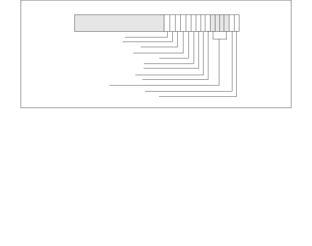
17-28 Vol. 3B
DEBUG, BRANCH PROFILE, TSC, AND INTEL® RESOURCE DIRECTOR TECHNOLOGY (INTEL® RDT) FEATURES
•Monitoring and single-stepping of branches, exceptions, and interrupts — See Section 17.4.2 and
Section 17.4.3. In addition, the ability to freeze the LBR stack on a PMI request is available.
•Branch trace messages — The IA32_DEBUGCTL MSR provides bit fields for software to enable each logical
processor to generate branch trace messages. See Section 17.4.4. However, not all BTM messages are
observable using the Intel® QPI link.
•Last exception records — See Section 17.13.3.
•Branch trace store and CPL-qualified BTS — See Section 17.4.6 and Section 17.4.5.
•FREEZE_LBRS_ON_PMI flag (bit 11) — see Section 17.4.7 for legacy Freeze_LBRs_On_PMI operation.
•FREEZE_PERFMON_ON_PMI flag (bit 12) — see Section 17.4.7 for legacy Freeze_Perfmon_On_PMI
operation.
•UNCORE_PMI_EN (bit 13) — When set. this logical processor is enabled to receive an counter overflow
interrupt form the uncore.
•FREEZE_WHILE_SMM (bit 14) — FREEZE_WHILE_SMM is supported if
IA32_PERF_CAPABILITIES.FREEZE_WHILE_SMM[Bit 12] is reporting 1. See Section 17.4.1.
Processors based on Intel microarchitecture code name Nehalem provide additional capabilities:
•Independent control of uncore PMI — The IA32_DEBUGCTL MSR provides a bit field (see Figure 17-11) for
software to enable each logical processor to receive an uncore counter overflow interrupt.
•LBR filtering — Processors based on Intel microarchitecture code name Nehalem support filtering of LBR
based on combination of CPL and branch type conditions. When LBR filtering is enabled, the LBR stack only
captures the subset of branches that are specified by MSR_LBR_SELECT.
Figure 17-11. IA32_DEBUGCTL MSR for Processors based
on Intel microarchitecture code name Nehalem
31
TR — Trace messages enable
BTINT — Branch trace interrupt
BTF — Single-step on branches
LBR — Last branch/interrupt/exception
Reserved
87654321 0
BTS — Branch trace store
Reserved
910
BTS_OFF_OS — BTS off in OS
BTS_OFF_USR — BTS off in user code
FREEZE_LBRS_ON_PMI
FREEZE_PERFMON_ON_PMI
11
12
14
FREEZE_WHILE_SMM
UNCORE_PMI_EN
13
Vol. 3B 17-29
DEBUG, BRANCH PROFILE, TSC, AND INTEL® RESOURCE DIRECTOR TECHNOLOGY (INTEL® RDT) FEATURES
17.9.1 LBR Stack
Processors based on Intel microarchitecture code name Nehalem provide 16 pairs of MSR to record last branch
record information. The layout of each MSR pair is shown in Table 17-8 and Table 17-9.
Processors based on Intel microarchitecture code name Nehalem have an LBR MSR Stack as shown in Table 17-10.
Table 17-10. LBR Stack Size and TOS Pointer Range
17.9.2 Filtering of Last Branch Records
MSR_LBR_SELECT is cleared to zero at RESET, and LBR filtering is disabled, i.e. all branches will be captured.
MSR_LBR_SELECT provides bit fields to specify the conditions of subsets of branches that will not be captured in
the LBR. The layout of MSR_LBR_SELECT is shown in Table 17-11.
Table 17-8. MSR_LASTBRANCH_x_FROM_IP
Bit Field Bit Offset Access Description
Data 47:0 R/W This is the “branch from” address. See Section 17.4.8.1 for address format.
SIGN_EXt 62:48 R/W Signed extension of bit 47 of this register.
MISPRED 63 R/W When set, indicates either the target of the branch was mispredicted and/or the
direction (taken/non-taken) was mispredicted; otherwise, the target branch was
predicted.
Table 17-9. MSR_LASTBRANCH_x_TO_IP
Bit Field Bit Offset Access Description
Data 47:0 R/W This is the “branch to” address. See Section 17.4.8.1 for address format
SIGN_EXt 63:48 R/W Signed extension of bit 47 of this register.
DisplayFamily_DisplayModel Size of LBR Stack Range of TOS Pointer
06_1AH 16 0 to 15
Table 17-11. MSR_LBR_SELECT for Intel microarchitecture code name Nehalem
Bit Field Bit Offset Access Description
CPL_EQ_0 0 R/W When set, do not capture branches ending in ring 0
CPL_NEQ_0 1 R/W When set, do not capture branches ending in ring >0
JCC 2 R/W When set, do not capture conditional branches
NEAR_REL_CALL 3 R/W When set, do not capture near relative calls
NEAR_IND_CALL 4 R/W When set, do not capture near indirect calls
NEAR_RET 5 R/W When set, do not capture near returns
NEAR_IND_JMP 6 R/W When set, do not capture near indirect jumps
NEAR_REL_JMP 7 R/W When set, do not capture near relative jumps
FAR_BRANCH 8 R/W When set, do not capture far branches
Reserved 63:9 Must be zero

17-30 Vol. 3B
DEBUG, BRANCH PROFILE, TSC, AND INTEL® RESOURCE DIRECTOR TECHNOLOGY (INTEL® RDT) FEATURES
17.10 LAST BRANCH, INTERRUPT, AND EXCEPTION RECORDING FOR
PROCESSORS BASED ON INTEL® MICROARCHITECTURE CODE NAME
SANDY BRIDGE
Generally, all of the last branch record, interrupt and exception recording facility described in Section 17.9, “Last
Branch, Interrupt, and Exception Recording for Processors based on Intel® Microarchitecture code name
Nehalem”, apply to processors based on Intel microarchitecture code name Sandy Bridge. For processors based on
Intel microarchitecture code name Ivy Bridge, the same holds true.
One difference of note is that MSR_LBR_SELECT is shared between two logical processors in the same core. In Intel
microarchitecture code name Sandy Bridge, each logical processor has its own MSR_LBR_SELECT. The filtering
semantics for “Near_ind_jmp” and “Near_rel_jmp” has been enhanced, see Table 17-12.
17.11 LAST BRANCH, CALL STACK, INTERRUPT, AND EXCEPTION RECORDING
FOR PROCESSORS BASED ON HASWELL MICROARCHITECTURE
Generally, all of the last branch record, interrupt and exception recording facility described in Section 17.10, “Last
Branch, Interrupt, and Exception Recording for Processors based on Intel® Microarchitecture code name Sandy
Bridge”, apply to next generation processors based on Intel microarchitecture code name Haswell.
The LBR facility also supports an alternate capability to profile call stack profiles. Configuring the LBR facility to
conduct call stack profiling is by writing 1 to the MSR_LBR_SELECT.EN_CALLSTACK[bit 9]; see Table 17-13. If
MSR_LBR_SELECT.EN_CALLSTACK is clear, the LBR facility will capture branches normally as described in Section
17.10.
Table 17-12. MSR_LBR_SELECT for Intel® microarchitecture code name Sandy Bridge
Bit Field Bit Offset Access Description
CPL_EQ_0 0 R/W When set, do not capture branches ending in ring 0
CPL_NEQ_0 1 R/W When set, do not capture branches ending in ring >0
JCC 2 R/W When set, do not capture conditional branches
NEAR_REL_CALL 3 R/W When set, do not capture near relative calls
NEAR_IND_CALL 4 R/W When set, do not capture near indirect calls
NEAR_RET 5 R/W When set, do not capture near returns
NEAR_IND_JMP 6 R/W When set, do not capture near indirect jumps except near indirect calls and near returns
NEAR_REL_JMP 7 R/W When set, do not capture near relative jumps except near relative calls.
FAR_BRANCH 8 R/W When set, do not capture far branches
Reserved 63:9 Must be zero
Table 17-13. MSR_LBR_SELECT for Intel® microarchitecture code name Haswell
Bit Field Bit Offset Access Description
CPL_EQ_0 0 R/W When set, do not capture branches ending in ring 0
CPL_NEQ_0 1 R/W When set, do not capture branches ending in ring >0
JCC 2 R/W When set, do not capture conditional branches
NEAR_REL_CALL 3 R/W When set, do not capture near relative calls
NEAR_IND_CALL 4 R/W When set, do not capture near indirect calls
NEAR_RET 5 R/W When set, do not capture near returns
NEAR_IND_JMP 6 R/W When set, do not capture near indirect jumps except near indirect calls and near returns
NEAR_REL_JMP 7 R/W When set, do not capture near relative jumps except near relative calls.

Vol. 3B 17-31
DEBUG, BRANCH PROFILE, TSC, AND INTEL® RESOURCE DIRECTOR TECHNOLOGY (INTEL® RDT) FEATURES
The call stack profiling capability is an enhancement of the LBR facility. The LBR stack is a ring buffer typically used
to profile control flow transitions resulting from branches. However, the finite depth of the LBR stack often become
less effective when profiling certain high-level languages (e.g. C++), where a transition of the execution flow is
accompanied by a large number of leaf function calls, each of which returns an individual parameter to form the list
of parameters for the main execution function call. A long list of such parameters returned by the leaf functions
would serve to flush the data captured in the LBR stack, often losing the main execution context.
When the call stack feature is enabled, the LBR stack will capture unfiltered call data normally, but as return
instructions are executed the last captured branch record is flushed from the on-chip registers in a last-in first-out
(LIFO) manner. Thus, branch information relative to leaf functions will not be captured, while preserving the call
stack information of the main line execution path.
The configuration of the call stack facility is summarized below:
•Set IA32_DEBUGCTL.LBR (bit 0) to enable the LBR stack to capture branch records. The source and target
addresses of the call branches will be captured in the 16 pairs of From/To LBR MSRs that form the LBR stack.
•Program the Top of Stack (TOS) MSR that points to the last valid from/to pair. This register is incremented by
1, modulo 16, before recording the next pair of addresses.
•Program the branch filtering bits of MSR_LBR_SELECT (bits 0:8) as desired.
•Program the MSR_LBR_SELECT to enable LIFO filtering of return instructions with:
— The following bits in MSR_LBR_SELECT must be set to ‘1’: JCC, NEAR_IND_JMP, NEAR_REL_JMP,
FAR_BRANCH, EN_CALLSTACK;
— The following bits in MSR_LBR_SELECT must be cleared: NEAR_REL_CALL, NEAR-IND_CALL, NEAR_RET;
— At most one of CPL_EQ_0, CPL_NEQ_0 is set.
Note that when call stack profiling is enabled, “zero length calls” are excluded from writing into the LBRs. (A “zero
length call” uses the attribute of the call instruction to push the immediate instruction pointer on to the stack and
then pops off that address into a register. This is accomplished without any matching return on the call.)
17.11.1 LBR Stack Enhancement
Processors based on Intel microarchitecture code name Haswell provide 16 pairs of MSR to record last branch
record information. The layout of each MSR pair is enumerated by IA32_PERF_CAPABILITIES[5:0] = 04H, and is
shown in Table 17-14 and Table 17-9.
FAR_BRANCH 8 R/W When set, do not capture far branches
EN_CALLSTACK19 Enable LBR stack to use LIFO filtering to capture Call stack profile
Reserved 63:10 Must be zero
NOTES:
1. Must set valid combination of bits 0-8 in conjunction with bit 9 (as described below), otherwise the contents of the LBR MSRs are
undefined.
Table 17-14. MSR_LASTBRANCH_x_FROM_IP with TSX Information
Bit Field Bit Offset Access Description
Data 47:0 R/W This is the “branch from” address. See Section 17.4.8.1 for address format.
SIGN_EXT 60:48 R/W Signed extension of bit 47 of this register.
TSX_ABORT 61 R/W When set, indicates a TSX Abort entry
LBR_FROM: EIP at the time of the TSX Abort
LBR_TO: EIP of the start of HLE region, or EIP of the RTM Abort Handler
IN_TSX 62 R/W When set, indicates the entry occurred in a TSX region
Table 17-13. MSR_LBR_SELECT for Intel® microarchitecture code name Haswell
Bit Field Bit Offset Access Description
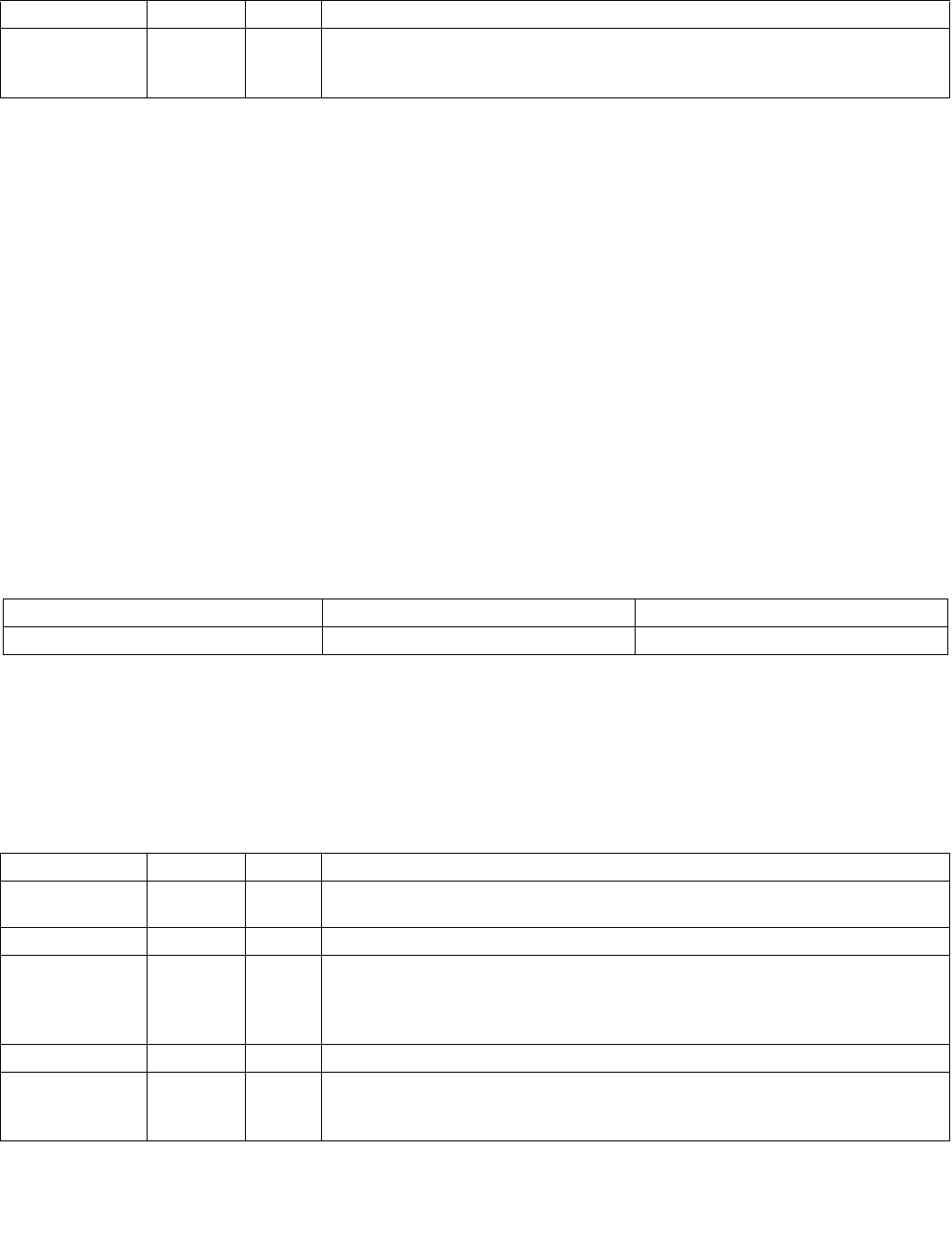
17-32 Vol. 3B
DEBUG, BRANCH PROFILE, TSC, AND INTEL® RESOURCE DIRECTOR TECHNOLOGY (INTEL® RDT) FEATURES
17.12 LAST BRANCH, CALL STACK, INTERRUPT, AND EXCEPTION RECORDING
FOR PROCESSORS BASED ON SKYLAKE MICROARCHITECTURE
Processors based on the Skylake microarchitecture provide a number of enhancement with storing last branch
records:
•enumeration of new LBR format: encoding 00101b in IA32_PERF_CAPABILITIES[5:0] is supported, see Section
17.4.8.1.
•Each LBR stack entry consists of a triplets of MSRs:
— MSR_LASTBRANCH_x_FROM_IP, the layout is simplified, see Table 17-9.
— MSR_LASTBRANCH_x_TO_IP, the layout is the same as Table 17-9.
— MSR_LBR_INFO_x, stores branch prediction flag, TSX info, and elapsed cycle data.
•Size of LBR stack increased to 32.
Processors based on the Skylake microarchitecture supports the same LBR filtering capabilities as described in
Table 17-13.
Table 17-15. LBR Stack Size and TOS Pointer Range
17.12.1 MSR_LBR_INFO_x MSR
The layout of each MSR_LBR_INFO_x MSR is shown in Table 17-16.
MISPRED 63 R/W When set, indicates either the target of the branch was mispredicted and/or the
direction (taken/non-taken) was mispredicted; otherwise, the target branch was
predicted.
DisplayFamily_DisplayModel Size of LBR Stack Range of TOS Pointer
06_4EH, 06_5EH 32 0 to 31
Table 17-16. MSR_LBR_INFO_x
Bit Field Bit Offset Access Description
Cycle Count
(saturating)
15:0 R/W Elapsed core clocks since last update to the LBR stack.
Reserved 60:16 R/W Reserved
TSX_ABORT 61 R/W When set, indicates a TSX Abort entry
LBR_FROM: EIP at the time of the TSX Abort
LBR_TO: EIP of the start of HLE region OR
EIP of the RTM Abort Handler
IN_TSX 62 R/W When set, indicates the entry occurred in a TSX region.
MISPRED 63 R/W When set, indicates either the target of the branch was mispredicted and/or the
direction (taken/non-taken) was mispredicted; otherwise, the target branch was
predicted.
Table 17-14. MSR_LASTBRANCH_x_FROM_IP with TSX Information (Contd.)
Bit Field Bit Offset Access Description

Vol. 3B 17-33
DEBUG, BRANCH PROFILE, TSC, AND INTEL® RESOURCE DIRECTOR TECHNOLOGY (INTEL® RDT) FEATURES
17.12.2 Streamlined Freeze_LBRs_On_PMI Operation
The FREEZE_LBRS_ON_PMI feature causes the LBRs to be frozen on a hardware request for a PMI. This prevents
the LBRs from being overwritten by new branches, allowing the PMI handler to examine the control flow that
preceded the PMI generation. Architectural performance monitoring version 4 and above supports a streamlined
FREEZE_LBRs_ON_PMI operation for PMI service routine that replaces the legacy FREEZE_LBRs_ON_PMI opera-
tion (see Section 17.4.7).
While the legacy FREEZE_LBRS_ON_PMI clear the LBR bit in the IA32_DEBUGCTL MSR on a PMI request, the
streamlined FREEZE_LBRS_ON_PMI will set the LBR_FRZ bit in IA32_PERF_GLOBAL_STATUS. Branches will not
cause the LBRs to be updated when LBR_FRZ is set. Software can clear LBR_FRZ at the same time as it clears over-
flow bits by setting the LBR_FRZ bit as well as the needed overflow bit when writing to
IA32_PERF_GLOBAL_STATUS_RESET MSR.
This streamlined behavior avoids race conditions between software and processor writes to IA32_DEBUGCTL that
are possible with FREEZE_LBRS_ON_PMI clearing of the LBR enable.
17.12.3 LBR Behavior and Deep C-State
When MWAIT is used to request a C-state that is numerically higher than C1, then LBR state may be initialized to
zero depending on optimized “waiting” state that is selected by the processor The affected LBR states include the
FROM, TO, INFO, LAST_BRANCH, LER and LBR_TOS registers. The LBR enable bit and LBR_FROZEN bit are not
affected. The LBR-time of the first LBR record inserted after an exit from such a C-state request will be zero.
17.13 LAST BRANCH, INTERRUPT, AND EXCEPTION RECORDING (PROCESSORS
BASED ON INTEL NETBURST® MICROARCHITECTURE)
Pentium 4 and Intel Xeon processors based on Intel NetBurst microarchitecture provide the following methods for
recording taken branches, interrupts and exceptions:
•Store branch records in the last branch record (LBR) stack MSRs for the most recent taken branches,
interrupts, and/or exceptions in MSRs. A branch record consist of a branch-from and a branch-to instruction
address.
•Send the branch records out on the system bus as branch trace messages (BTMs).
•Log BTMs in a memory-resident branch trace store (BTS) buffer.
To support these functions, the processor provides the following MSRs and related facilities:
•MSR_DEBUGCTLA MSR — Enables last branch, interrupt, and exception recording; single-stepping on taken
branches; branch trace messages (BTMs); and branch trace store (BTS). This register is named DebugCtlMSR
in the P6 family processors.
•Debug store (DS) feature flag (CPUID.1:EDX.DS[bit 21]) — Indicates that the processor provides the
debug store (DS) mechanism, which allows BTMs to be stored in a memory-resident BTS buffer.
•CPL-qualified debug store (DS) feature flag (CPUID.1:ECX.DS-CPL[bit 4]) — Indicates that the
processor provides a CPL-qualified debug store (DS) mechanism, which allows software to selectively skip
sending and storing BTMs, according to specified current privilege level settings, into a memory-resident BTS
buffer.
•IA32_MISC_ENABLE MSR — Indicates that the processor provides the BTS facilities.
•Last branch record (LBR) stack — The LBR stack is a circular stack that consists of four MSRs
(MSR_LASTBRANCH_0 through MSR_LASTBRANCH_3) for the Pentium 4 and Intel Xeon processor family
[CPUID family 0FH, models 0H-02H]. The LBR stack consists of 16 MSR pairs
(MSR_LASTBRANCH_0_FROM_IP through MSR_LASTBRANCH_15_FROM_IP and
MSR_LASTBRANCH_0_TO_IP through MSR_LASTBRANCH_15_TO_IP) for the Pentium 4 and Intel Xeon
processor family [CPUID family 0FH, model 03H].
•Last branch record top-of-stack (TOS) pointer — The TOS Pointer MSR contains a 2-bit pointer (0-3) to
the MSR in the LBR stack that contains the most recent branch, interrupt, or exception recorded for the
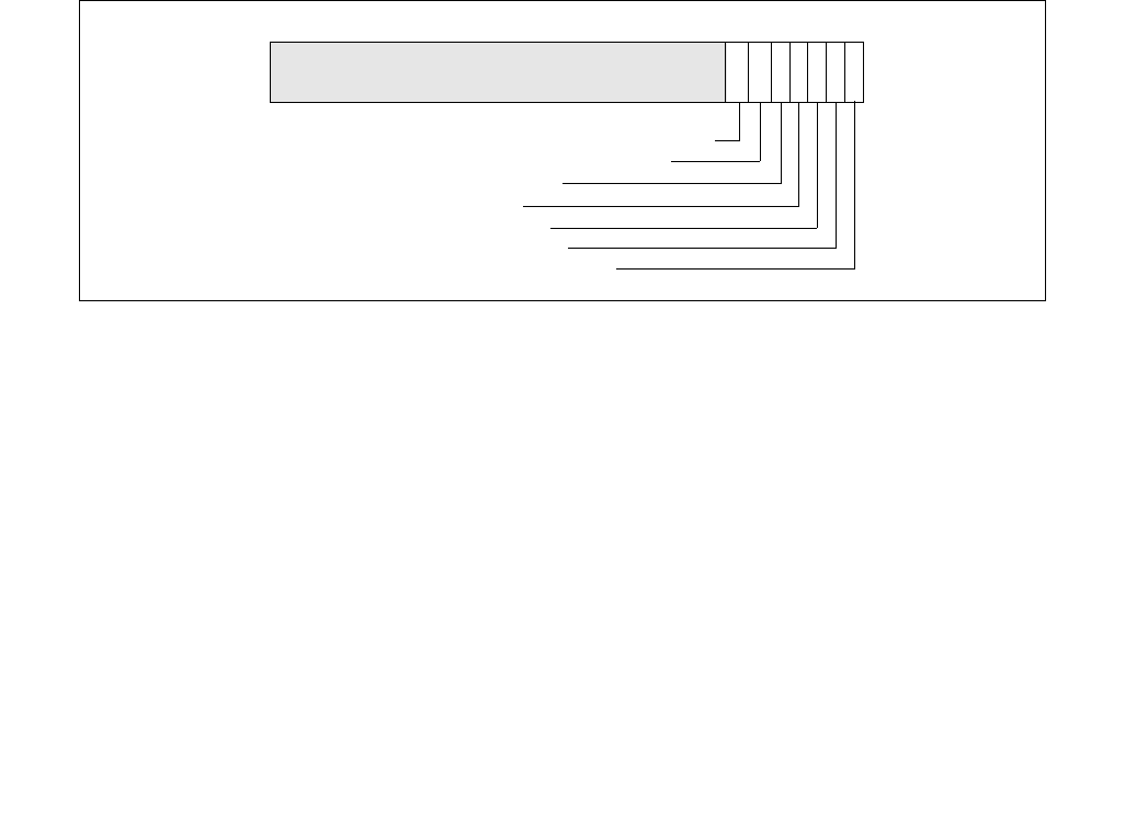
17-34 Vol. 3B
DEBUG, BRANCH PROFILE, TSC, AND INTEL® RESOURCE DIRECTOR TECHNOLOGY (INTEL® RDT) FEATURES
Pentium 4 and Intel Xeon processor family [CPUID family 0FH, models 0H-02H]. This pointer becomes a 4-bit
pointer (0-15) for the Pentium 4 and Intel Xeon processor family [CPUID family 0FH, model 03H]. See also:
Table 17-17, Figure 17-12, and Section 17.13.2, “LBR Stack for Processors Based on Intel NetBurst® Microar-
chitecture.”
•Last exception record — See Section 17.13.3, “Last Exception Records.”
17.13.1 MSR_DEBUGCTLA MSR
The MSR_DEBUGCTLA MSR enables and disables the various last branch recording mechanisms described in the
previous section. This register can be written to using the WRMSR instruction, when operating at privilege level 0
or when in real-address mode. A protected-mode operating system procedure is required to provide user access to
this register. Figure 17-12 shows the flags in the MSR_DEBUGCTLA MSR. The functions of these flags are as
follows:
•LBR (last branch/interrupt/exception) flag (bit 0) — When set, the processor records a running trace of
the most recent branches, interrupts, and/or exceptions taken by the processor (prior to a debug exception
being generated) in the last branch record (LBR) stack. Each branch, interrupt, or exception is recorded as a
64-bit branch record. The processor clears this flag whenever a debug exception is generated (for example,
when an instruction or data breakpoint or a single-step trap occurs). See Section 17.13.2, “LBR Stack for
Processors Based on Intel NetBurst® Microarchitecture.”
•BTF (single-step on branches) flag (bit 1) — When set, the processor treats the TF flag in the EFLAGS
register as a “single-step on branches” flag rather than a “single-step on instructions” flag. This mechanism
allows single-stepping the processor on taken branches. See Section 17.4.3, “Single-Stepping on Branches.”
•TR (trace message enable) flag (bit 2) — When set, branch trace messages are enabled. Thereafter, when
the processor detects a taken branch, interrupt, or exception, it sends the branch record out on the system bus
as a branch trace message (BTM). See Section 17.4.4, “Branch Trace Messages.”
•BTS (branch trace store) flag (bit 3) — When set, enables the BTS facilities to log BTMs to a memory-
resident BTS buffer that is part of the DS save area. See Section 17.4.9, “BTS and DS Save Area.”
•BTINT (branch trace interrupt) flag (bits 4) — When set, the BTS facilities generate an interrupt when the
BTS buffer is full. When clear, BTMs are logged to the BTS buffer in a circular fashion. See Section 17.4.5, “Branch
Trace Store (BTS).”
•BTS_OFF_OS (disable ring 0 branch trace store) flag (bit 5) — When set, enables the BTS facilities to
skip sending/logging CPL_0 BTMs to the memory-resident BTS buffer. See Section 17.13.2, “LBR Stack for
Processors Based on Intel NetBurst® Microarchitecture.”
•BTS_OFF_USR (disable ring 0 branch trace store) flag (bit 6) — When set, enables the BTS facilities to
skip sending/logging non-CPL_0 BTMs to the memory-resident BTS buffer. See Section 17.13.2, “LBR Stack for
Processors Based on Intel NetBurst® Microarchitecture.”
Figure 17-12. MSR_DEBUGCTLA MSR for Pentium 4 and Intel Xeon Processors
31
TR — Trace messages enable
BTINT — Branch trace interrupt
BTF — Single-step on branches
LBR — Last branch/interrupt/exception
543210
BTS — Branch trace store
Reserved
6
7
BTS_OFF_OS — Disable storing CPL_0 BTS
BTS_OFF_USR — Disable storing non-CPL_0 BTS
Vol. 3B 17-35
DEBUG, BRANCH PROFILE, TSC, AND INTEL® RESOURCE DIRECTOR TECHNOLOGY (INTEL® RDT) FEATURES
NOTE
The initial implementation of BTS_OFF_USR and BTS_OFF_OS in MSR_DEBUGCTLA is shown in
Figure 17-12. The BTS_OFF_USR and BTS_OFF_OS fields may be implemented on other model-
specific debug control register at different locations.
See Chapter 2, “Model-Specific Registers (MSRs)” in the Intel® 64 and IA-32 Architectures Software Developer’s
Manual, Volume 4 for a detailed description of each of the last branch recording MSRs.
17.13.2 LBR Stack for Processors Based on Intel NetBurst® Microarchitecture
The LBR stack is made up of LBR MSRs that are treated by the processor as a circular stack. The TOS pointer
(MSR_LASTBRANCH_TOS MSR) points to the LBR MSR (or LBR MSR pair) that contains the most recent (last)
branch record placed on the stack. Prior to placing a new branch record on the stack, the TOS is incremented by 1.
When the TOS pointer reaches it maximum value, it wraps around to 0. See Table 17-17 and Figure 17-12.
Table 17-17. LBR MSR Stack Size and TOS Pointer Range for the Pentium® 4 and the Intel®Xeon®Processor Family
The registers in the LBR MSR stack and the MSR_LASTBRANCH_TOS MSR are read-only and can be read using the
RDMSR instruction.
Figure 17-13 shows the layout of a branch record in an LBR MSR (or MSR pair). Each branch record consists of two
linear addresses, which represent the “from” and “to” instruction pointers for a branch, interrupt, or exception. The
contents of the from and to addresses differ, depending on the source of the branch:
•Taken branch — If the record is for a taken branch, the “from” address is the address of the branch instruction
and the “to” address is the target instruction of the branch.
•Interrupt — If the record is for an interrupt, the “from” address the return instruction pointer (RIP) saved for
the interrupt and the “to” address is the address of the first instruction in the interrupt handler routine. The RIP
is the linear address of the next instruction to be executed upon returning from the interrupt handler.
•Exception — If the record is for an exception, the “from” address is the linear address of the instruction that
caused the exception to be generated and the “to” address is the address of the first instruction in the
exception handler routine.
DisplayFamily_DisplayModel Size of LBR Stack Range of TOS Pointer
Family 0FH, Models 0H-02H; MSRs at locations 1DBH-1DEH. 40 to 3
Family 0FH, Models; MSRs at locations 680H-68FH. 16 0 to 15
Family 0FH, Model 03H; MSRs at locations 6C0H-6CFH. 16 0 to 15

17-36 Vol. 3B
DEBUG, BRANCH PROFILE, TSC, AND INTEL® RESOURCE DIRECTOR TECHNOLOGY (INTEL® RDT) FEATURES
Additional information is saved if an exception or interrupt occurs in conjunction with a branch instruction. If a
branch instruction generates a trap type exception, two branch records are stored in the LBR stack: a branch record
for the branch instruction followed by a branch record for the exception.
If a branch instruction is immediately followed by an interrupt, a branch record is stored in the LBR stack for the
branch instruction followed by a record for the interrupt.
17.13.3 Last Exception Records
The Pentium 4, Intel Xeon, Pentium M, Intel® Core™ Solo, Intel® Core™ Duo, Intel® Core™2 Duo, Intel® Core™ i7
and Intel® Atom™ processors provide two MSRs (the MSR_LER_TO_LIP and the MSR_LER_FROM_LIP MSRs) that
duplicate the functions of the LastExceptionToIP and LastExceptionFromIP MSRs found in the P6 family processors.
The MSR_LER_TO_LIP and MSR_LER_FROM_LIP MSRs contain a branch record for the last branch that the
processor took prior to an exception or interrupt being generated.
17.14 LAST BRANCH, INTERRUPT, AND EXCEPTION RECORDING (INTEL® CORE™
SOLO AND INTEL® CORE™ DUO PROCESSORS)
Intel Core Solo and Intel Core Duo processors provide last branch interrupt and exception recording. This capability
is almost identical to that found in Pentium 4 and Intel Xeon processors. There are differences in the stack and in
some MSR names and locations.
Note the following:
•IA32_DEBUGCTL MSR — Enables debug trace interrupt, debug trace store, trace messages enable,
performance monitoring breakpoint flags, single stepping on branches, and last branch. IA32_DEBUGCTL MSR
is located at register address 01D9H.
See Figure 17-14 for the layout and the entries below for a description of the flags:
—LBR (last branch/interrupt/exception) flag (bit 0) — When set, the processor records a running trace
of the most recent branches, interrupts, and/or exceptions taken by the processor (prior to a debug
exception being generated) in the last branch record (LBR) stack. For more information, see the “Last
Branch Record (LBR) Stack” below.
—BTF (single-step on branches) flag (bit 1) — When set, the processor treats the TF flag in the EFLAGS
register as a “single-step on branches” flag rather than a “single-step on instructions” flag. This mechanism
Figure 17-13. LBR MSR Branch Record Layout for the Pentium 4
and Intel Xeon Processor Family
63
From Linear Address
0
To Linear Address
63
From Linear Address
0
0
63
To Linear Address
32 - 31
MSR_LASTBRANCH_0 through MSR_LASTBRANCH_3
CPUID Family 0FH, Models 0H-02H
Reserved
CPUID Family 0FH, Model 03H-04H
Reserved
MSR_LASTBRANCH_0_FROM_IP through MSR_LASTBRANCH_15_FROM_IP
32 - 31
32 - 31
MSR_LASTBRANCH_0_TO_IP through MSR_LASTBRANCH_15_TO_IP
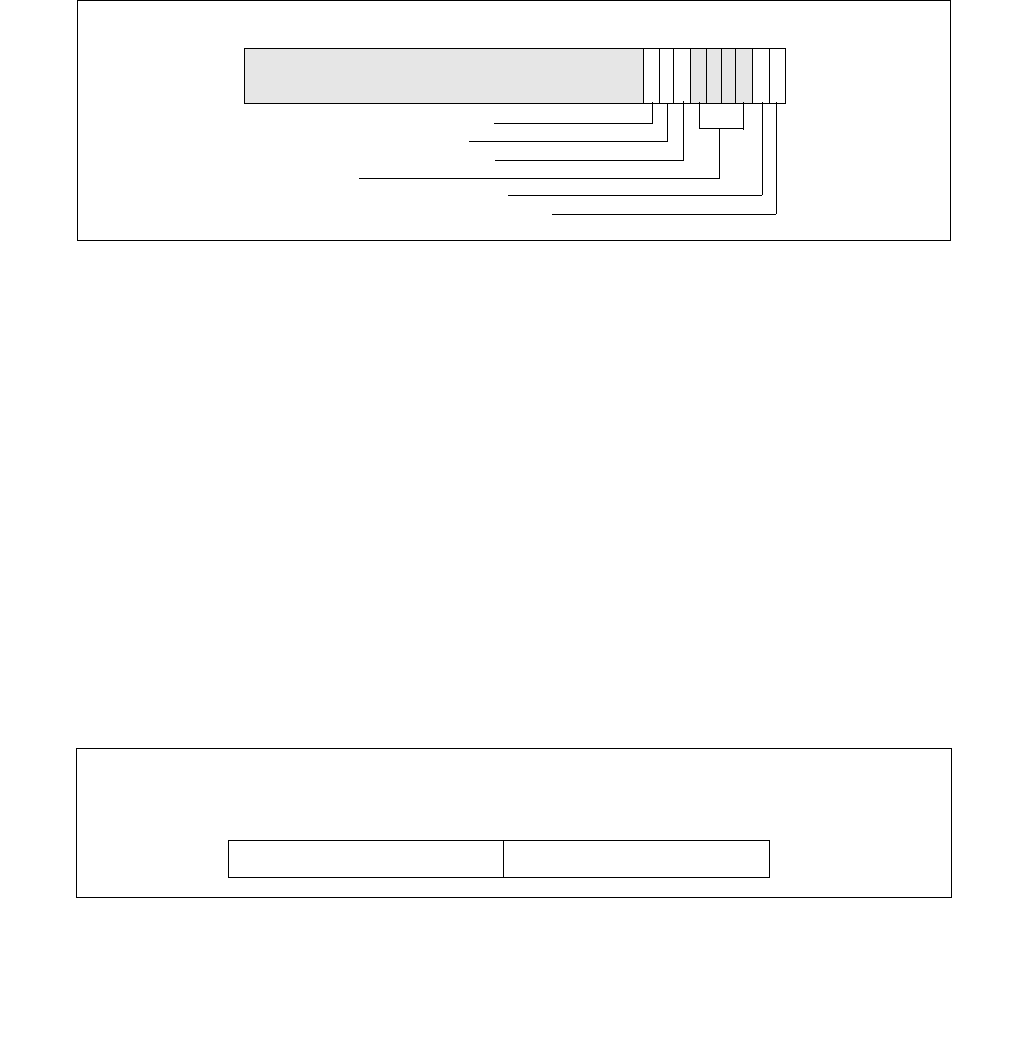
Vol. 3B 17-37
DEBUG, BRANCH PROFILE, TSC, AND INTEL® RESOURCE DIRECTOR TECHNOLOGY (INTEL® RDT) FEATURES
allows single-stepping the processor on taken branches. See Section 17.4.3, “Single-Stepping on
Branches,” for more information about the BTF flag.
—TR (trace message enable) flag (bit 6) — When set, branch trace messages are enabled. When the
processor detects a taken branch, interrupt, or exception; it sends the branch record out on the system bus
as a branch trace message (BTM). See Section 17.4.4, “Branch Trace Messages,” for more information
about the TR flag.
—BTS (branch trace store) flag (bit 7) — When set, the flag enables BTS facilities to log BTMs to a
memory-resident BTS buffer that is part of the DS save area. See Section 17.4.9, “BTS and DS Save Area.”
—BTINT (branch trace interrupt) flag (bits 8) — When set, the BTS facilities generate an interrupt when
the BTS buffer is full. When clear, BTMs are logged to the BTS buffer in a circular fashion. See Section 17.4.5,
“Branch Trace Store (BTS),” for a description of this mechanism.
•Debug store (DS) feature flag (bit 21), returned by the CPUID instruction — Indicates that the
processor provides the debug store (DS) mechanism, which allows BTMs to be stored in a memory-resident
BTS buffer. See Section 17.4.5, “Branch Trace Store (BTS).”
•Last Branch Record (LBR) Stack — The LBR stack consists of 8 MSRs (MSR_LASTBRANCH_0 through
MSR_LASTBRANCH_7); bits 31-0 hold the ‘from’ address, bits 63-32 hold the ‘to’ address (MSR addresses start
at 40H). See Figure 17-15.
•Last Branch Record Top-of-Stack (TOS) Pointer — The TOS Pointer MSR contains a 3-bit pointer (bits 2-
0) to the MSR in the LBR stack that contains the most recent branch, interrupt, or exception recorded. For Intel
Core Solo and Intel Core Duo processors, this MSR is located at register address 01C9H.
For compatibility, the Intel Core Solo and Intel Core Duo processors provide two 32-bit MSRs (the
MSR_LER_TO_LIP and the MSR_LER_FROM_LIP MSRs) that duplicate functions of the LastExceptionToIP and Last-
ExceptionFromIP MSRs found in P6 family processors.
For details, see Section 17.12, “Last Branch, Call Stack, Interrupt, and Exception Recording for Processors based
on Skylake Microarchitecture,” and Section 2.19, “MSRs In Intel® Core™ Solo and Intel® Core™ Duo Processors” in
the Intel® 64 and IA-32 Architectures Software Developer’s Manual, Volume 4.
Figure 17-14. IA32_DEBUGCTL MSR for Intel Core Solo
and Intel Core Duo Processors
Figure 17-15. LBR Branch Record Layout for the Intel Core Solo
and Intel Core Duo Processor
31
TR — Trace messages enable
BTINT — Branch trace interrupt
BTF — Single-step on branches
LBR — Last branch/interrupt/exception
Reserved
87654321 0
BTS — Branch trace store
Reserved
0
63
From Linear Address
To Linear Address
32 - 31
MSR_LASTBRANCH_0 through MSR_LASTBRANCH_7
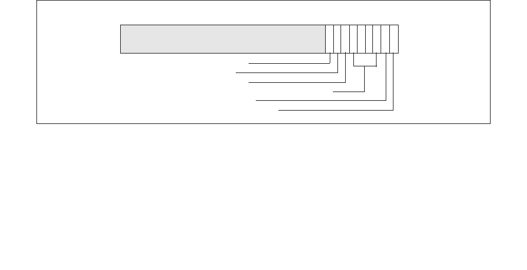
17-38 Vol. 3B
DEBUG, BRANCH PROFILE, TSC, AND INTEL® RESOURCE DIRECTOR TECHNOLOGY (INTEL® RDT) FEATURES
17.15 LAST BRANCH, INTERRUPT, AND EXCEPTION RECORDING (PENTIUM M
PROCESSORS)
Like the Pentium 4 and Intel Xeon processor family, Pentium M processors provide last branch interrupt and excep-
tion recording. The capability operates almost identically to that found in Pentium 4 and Intel Xeon processors.
There are differences in the shape of the stack and in some MSR names and locations. Note the following:
•MSR_DEBUGCTLB MSR — Enables debug trace interrupt, debug trace store, trace messages enable,
performance monitoring breakpoint flags, single stepping on branches, and last branch. For Pentium M
processors, this MSR is located at register address 01D9H. See Figure 17-16 and the entries below for a
description of the flags.
—LBR (last branch/interrupt/exception) flag (bit 0) — When set, the processor records a running trace
of the most recent branches, interrupts, and/or exceptions taken by the processor (prior to a debug
exception being generated) in the last branch record (LBR) stack. For more information, see the “Last
Branch Record (LBR) Stack” bullet below.
—BTF (single-step on branches) flag (bit 1) — When set, the processor treats the TF flag in the EFLAGS
register as a “single-step on branches” flag rather than a “single-step on instructions” flag. This mechanism
allows single-stepping the processor on taken branches. See Section 17.4.3, “Single-Stepping on
Branches,” for more information about the BTF flag.
—PBi (performance monitoring/breakpoint pins) flags (bits 5-2) — When these flags are set, the
performance monitoring/breakpoint pins on the processor (BP0#, BP1#, BP2#, and BP3#) report
breakpoint matches in the corresponding breakpoint-address registers (DR0 through DR3). The processor
asserts then deasserts the corresponding BPi# pin when a breakpoint match occurs. When a PBi flag is
clear, the performance monitoring/breakpoint pins report performance events. Processor execution is not
affected by reporting performance events.
—TR (trace message enable) flag (bit 6) — When set, branch trace messages are enabled. When the
processor detects a taken branch, interrupt, or exception, it sends the branch record out on the system bus
as a branch trace message (BTM). See Section 17.4.4, “Branch Trace Messages,” for more information
about the TR flag.
—BTS (branch trace store) flag (bit 7) — When set, enables the BTS facilities to log BTMs to a memory-
resident BTS buffer that is part of the DS save area. See Section 17.4.9, “BTS and DS Save Area.”
—BTINT (branch trace interrupt) flag (bits 8) — When set, the BTS facilities generate an interrupt when
the BTS buffer is full. When clear, BTMs are logged to the BTS buffer in a circular fashion. See Section 17.4.5,
“Branch Trace Store (BTS),” for a description of this mechanism.
•Debug store (DS) feature flag (bit 21), returned by the CPUID instruction — Indicates that the
processor provides the debug store (DS) mechanism, which allows BTMs to be stored in a memory-resident
BTS buffer. See Section 17.4.5, “Branch Trace Store (BTS).”
Figure 17-16. MSR_DEBUGCTLB MSR for Pentium M Processors
31
TR — Trace messages enable
BTINT — Branch trace interrupt
BTF — Single-step on branches
LBR — Last branch/interrupt/exception
Reserved
87654321 0
BTS — Branch trace store
PB3/2/1/0 — Performance monitoring breakpoint flags

Vol. 3B 17-39
DEBUG, BRANCH PROFILE, TSC, AND INTEL® RESOURCE DIRECTOR TECHNOLOGY (INTEL® RDT) FEATURES
•Last Branch Record (LBR) Stack — The LBR stack consists of 8 MSRs (MSR_LASTBRANCH_0 through
MSR_LASTBRANCH_7); bits 31-0 hold the ‘from’ address, bits 63-32 hold the ‘to’ address. For Pentium M
Processors, these pairs are located at register addresses 040H-047H. See Figure 17-17.
•Last Branch Record Top-of-Stack (TOS) Pointer — The TOS Pointer MSR contains a 3-bit pointer (bits 2-
0) to the MSR in the LBR stack that contains the most recent branch, interrupt, or exception recorded. For
Pentium M Processors, this MSR is located at register address 01C9H.
For more detail on these capabilities, see Section 17.13.3, “Last Exception Records,” and Section 2.20, “MSRs In
the Pentium M Processor” in the Intel® 64 and IA-32 Architectures Software Developer’s Manual, Volume 4.
17.16 LAST BRANCH, INTERRUPT, AND EXCEPTION
RECORDING (P6 FAMILY PROCESSORS)
The P6 family processors provide five MSRs for recording the last branch, interrupt, or exception taken by the
processor: DEBUGCTLMSR, LastBranchToIP, LastBranchFromIP, LastExceptionToIP, and LastExceptionFromIP.
These registers can be used to collect last branch records, to set breakpoints on branches, interrupts, and excep-
tions, and to single-step from one branch to the next.
See Chapter 2, “Model-Specific Registers (MSRs)” in the Intel® 64 and IA-32 Architectures Software Developer’s
Manual, Volume 4 for a detailed description of each of the last branch recording MSRs.
17.16.1 DEBUGCTLMSR Register
The version of the DEBUGCTLMSR register found in the P6 family processors enables last branch, interrupt, and
exception recording; taken branch breakpoints; the breakpoint reporting pins; and trace messages. This register
can be written to using the WRMSR instruction, when operating at privilege level 0 or when in real-address mode.
A protected-mode operating system procedure is required to provide user access to this register. Figure 17-18
shows the flags in the DEBUGCTLMSR register for the P6 family processors. The functions of these flags are as
follows:
•LBR (last branch/interrupt/exception) flag (bit 0) — When set, the processor records the source and
target addresses (in the LastBranchToIP, LastBranchFromIP, LastExceptionToIP, and LastExceptionFromIP
MSRs) for the last branch and the last exception or interrupt taken by the processor prior to a debug exception
being generated. The processor clears this flag whenever a debug exception, such as an instruction or data
breakpoint or single-step trap occurs.
Figure 17-17. LBR Branch Record Layout for the Pentium M Processor
0
63
From Linear Address
To Linear Address
32 - 31
MSR_LASTBRANCH_0 through MSR_LASTBRANCH_7

17-40 Vol. 3B
DEBUG, BRANCH PROFILE, TSC, AND INTEL® RESOURCE DIRECTOR TECHNOLOGY (INTEL® RDT) FEATURES
•BTF (single-step on branches) flag (bit 1) — When set, the processor treats the TF flag in the EFLAGS
register as a “single-step on branches” flag. See Section 17.4.3, “Single-Stepping on Branches.”
•PBi (performance monitoring/breakpoint pins) flags (bits 2 through 5) — When these flags are set,
the performance monitoring/breakpoint pins on the processor (BP0#, BP1#, BP2#, and BP3#) report
breakpoint matches in the corresponding breakpoint-address registers (DR0 through DR3). The processor
asserts then deasserts the corresponding BPi# pin when a breakpoint match occurs. When a PBi flag is clear,
the performance monitoring/breakpoint pins report performance events. Processor execution is not affected by
reporting performance events.
•TR (trace message enable) flag (bit 6) — When set, trace messages are enabled as described in Section
17.4.4, “Branch Trace Messages.” Setting this flag greatly reduces the performance of the processor. When
trace messages are enabled, the values stored in the LastBranchToIP, LastBranchFromIP, LastExceptionToIP,
and LastExceptionFromIP MSRs are undefined.
17.16.2 Last Branch and Last Exception MSRs
The LastBranchToIP and LastBranchFromIP MSRs are 32-bit registers for recording the instruction pointers for the
last branch, interrupt, or exception that the processor took prior to a debug exception being generated. When a
branch occurs, the processor loads the address of the branch instruction into the LastBranchFromIP MSR and loads
the target address for the branch into the LastBranchToIP MSR.
When an interrupt or exception occurs (other than a debug exception), the address of the instruction that was
interrupted by the exception or interrupt is loaded into the LastBranchFromIP MSR and the address of the exception
or interrupt handler that is called is loaded into the LastBranchToIP MSR.
The LastExceptionToIP and LastExceptionFromIP MSRs (also 32-bit registers) record the instruction pointers for
the last branch that the processor took prior to an exception or interrupt being generated. When an exception or
interrupt occurs, the contents of the LastBranchToIP and LastBranchFromIP MSRs are copied into these registers
before the to and from addresses of the exception or interrupt are recorded in the LastBranchToIP and LastBranch-
FromIP MSRs.
These registers can be read using the RDMSR instruction.
Note that the values stored in the LastBranchToIP, LastBranchFromIP, LastExceptionToIP, and LastExceptionFromIP
MSRs are offsets into the current code segment, as opposed to linear addresses, which are saved in last branch
records for the Pentium 4 and Intel Xeon processors.
17.16.3 Monitoring Branches, Exceptions, and Interrupts
When the LBR flag in the DEBUGCTLMSR register is set, the processor automatically begins recording branches that
it takes, exceptions that are generated (except for debug exceptions), and interrupts that are serviced. Each time
a branch, exception, or interrupt occurs, the processor records the to and from instruction pointers in the Last-
BranchToIP and LastBranchFromIP MSRs. In addition, for interrupts and exceptions, the processor copies the
contents of the LastBranchToIP and LastBranchFromIP MSRs into the LastExceptionToIP and LastExceptionFromIP
MSRs prior to recording the to and from addresses of the interrupt or exception.
Figure 17-18. DEBUGCTLMSR Register (P6 Family Processors)
31
TR — Trace messages enable
PBi — Performance monitoring/breakpoint pins
BTF — Single-step on branches
LBR — Last branch/interrupt/exception
76543210
P
B
2
P
B
1
P
B
0
B
T
F
T
R
L
B
R
P
B
3
Reserved

Vol. 3B 17-41
DEBUG, BRANCH PROFILE, TSC, AND INTEL® RESOURCE DIRECTOR TECHNOLOGY (INTEL® RDT) FEATURES
When the processor generates a debug exception (#DB), it automatically clears the LBR flag before executing the
exception handler, but does not touch the last branch and last exception MSRs. The addresses for the last branch,
interrupt, or exception taken are thus retained in the LastBranchToIP and LastBranchFromIP MSRs and the
addresses of the last branch prior to an interrupt or exception are retained in the LastExceptionToIP, and LastEx-
ceptionFromIP MSRs.
The debugger can use the last branch, interrupt, and/or exception addresses in combination with code-segment
selectors retrieved from the stack to reset breakpoints in the breakpoint-address registers (DR0 through DR3),
allowing a backward trace from the manifestation of a particular bug toward its source. Because the instruction
pointers recorded in the LastBranchToIP, LastBranchFromIP, LastExceptionToIP, and LastExceptionFromIP MSRs
are offsets into a code segment, software must determine the segment base address of the code segment associ-
ated with the control transfer to calculate the linear address to be placed in the breakpoint-address registers. The
segment base address can be determined by reading the segment selector for the code segment from the stack
and using it to locate the segment descriptor for the segment in the GDT or LDT. The segment base address can
then be read from the segment descriptor.
Before resuming program execution from a debug-exception handler, the handler must set the LBR flag again to re-
enable last branch and last exception/interrupt recording.
17.17 TIME-STAMP COUNTER
The Intel 64 and IA-32 architectures (beginning with the Pentium processor) define a time-stamp counter mecha-
nism that can be used to monitor and identify the relative time occurrence of processor events. The counter’s archi-
tecture includes the following components:
•TSC flag — A feature bit that indicates the availability of the time-stamp counter. The counter is available in an
if the function CPUID.1:EDX.TSC[bit 4] = 1.
•IA32_TIME_STAMP_COUNTER MSR (called TSC MSR in P6 family and Pentium processors) — The MSR used
as the counter.
•RDTSC instruction — An instruction used to read the time-stamp counter.
•TSD flag — A control register flag is used to enable or disable the time-stamp counter (enabled if
CR4.TSD[bit 2] = 1).
The time-stamp counter (as implemented in the P6 family, Pentium, Pentium M, Pentium 4, Intel Xeon, Intel Core
Solo and Intel Core Duo processors and later processors) is a 64-bit counter that is set to 0 following a RESET of
the processor. Following a RESET, the counter increments even when the processor is halted by the HLT instruction
or the external STPCLK# pin. Note that the assertion of the external DPSLP# pin may cause the time-stamp
counter to stop.
Processor families increment the time-stamp counter differently:
•For Pentium M processors (family [06H], models [09H, 0DH]); for Pentium 4 processors, Intel Xeon processors
(family [0FH], models [00H, 01H, or 02H]); and for P6 family processors: the time-stamp counter increments
with every internal processor clock cycle.
The internal processor clock cycle is determined by the current core-clock to bus-clock ratio. Intel®
SpeedStep® technology transitions may also impact the processor clock.
•For Pentium 4 processors, Intel Xeon processors (family [0FH], models [03H and higher]); for Intel Core Solo
and Intel Core Duo processors (family [06H], model [0EH]); for the Intel Xeon processor 5100 series and Intel
Core 2 Duo processors (family [06H], model [0FH]); for Intel Core 2 and Intel Xeon processors (family [06H],
DisplayModel [17H]); for Intel Atom processors (family [06H],
DisplayModel [1CH]): the time-stamp counter increments at a constant rate. That rate may be set by the
maximum core-clock to bus-clock ratio of the processor or may be set by the maximum resolved frequency at
which the processor is booted. The maximum resolved frequency may differ from the processor base
frequency, see Section 18.7.2 for more detail. On certain processors, the TSC frequency may not be the same
as the frequency in the brand string.
The specific processor configuration determines the behavior. Constant TSC behavior ensures that the duration
of each clock tick is uniform and supports the use of the TSC as a wall clock timer even if the processor core
changes frequency. This is the architectural behavior moving forward.

17-42 Vol. 3B
DEBUG, BRANCH PROFILE, TSC, AND INTEL® RESOURCE DIRECTOR TECHNOLOGY (INTEL® RDT) FEATURES
NOTE
To determine average processor clock frequency, Intel recommends the use of performance
monitoring logic to count processor core clocks over the period of time for which the average is
required. See Section 18.6.4.5, “Counting Clocks on systems with Intel Hyper-Threading
Technology in Processors Based on Intel NetBurst® Microarchitecture,” and Chapter 19, “Perfor-
mance Monitoring Events,” for more information.
The RDTSC instruction reads the time-stamp counter and is guaranteed to return a monotonically increasing
unique value whenever executed, except for a 64-bit counter wraparound. Intel guarantees that the time-stamp
counter will not wraparound within 10 years after being reset. The period for counter wrap is longer for Pentium 4,
Intel Xeon, P6 family, and Pentium processors.
Normally, the RDTSC instruction can be executed by programs and procedures running at any privilege level and in
virtual-8086 mode. The TSD flag allows use of this instruction to be restricted to programs and procedures running
at privilege level 0. A secure operating system would set the TSD flag during system initialization to disable user
access to the time-stamp counter. An operating system that disables user access to the time-stamp counter should
emulate the instruction through a user-accessible programming interface.
The RDTSC instruction is not serializing or ordered with other instructions. It does not necessarily wait until all
previous instructions have been executed before reading the counter. Similarly, subsequent instructions may begin
execution before the RDTSC instruction operation is performed.
The RDMSR and WRMSR instructions read and write the time-stamp counter, treating the time-stamp counter as an
ordinary MSR (address 10H). In the Pentium 4, Intel Xeon, and P6 family processors, all 64-bits of the time-stamp
counter are read using RDMSR (just as with RDTSC). When WRMSR is used to write the time-stamp counter on
processors before family [0FH], models [03H, 04H]: only the low-order 32-bits of the time-stamp counter can be
written (the high-order 32 bits are cleared to 0). For family [0FH], models [03H, 04H, 06H]; for family [06H]],
model [0EH, 0FH]; for family [06H]], DisplayModel [17H, 1AH, 1CH, 1DH]: all 64 bits are writable.
17.17.1 Invariant TSC
The time stamp counter in newer processors may support an enhancement, referred to as invariant TSC.
Processor’s support for invariant TSC is indicated by CPUID.80000007H:EDX[8].
The invariant TSC will run at a constant rate in all ACPI P-, C-. and T-states. This is the architectural behavior
moving forward. On processors with invariant TSC support, the OS may use the TSC for wall clock timer services
(instead of ACPI or HPET timers). TSC reads are much more efficient and do not incur the overhead associated with
a ring transition or access to a platform resource.
17.17.2 IA32_TSC_AUX Register and RDTSCP Support
Processors based on Intel microarchitecture code name Nehalem provide an auxiliary TSC register, IA32_TSC_AUX
that is designed to be used in conjunction with IA32_TSC. IA32_TSC_AUX provides a 32-bit field that is initialized
by privileged software with a signature value (for example, a logical processor ID).
The primary usage of IA32_TSC_AUX in conjunction with IA32_TSC is to allow software to read the 64-bit time
stamp in IA32_TSC and signature value in IA32_TSC_AUX with the instruction RDTSCP in an atomic operation.
RDTSCP returns the 64-bit time stamp in EDX:EAX and the 32-bit TSC_AUX signature value in ECX. The atomicity
of RDTSCP ensures that no context switch can occur between the reads of the TSC and TSC_AUX values.
Support for RDTSCP is indicated by CPUID.80000001H:EDX[27]. As with RDTSC instruction, non-ring 0 access is
controlled by CR4.TSD (Time Stamp Disable flag).
User mode software can use RDTSCP to detect if CPU migration has occurred between successive reads of the TSC.
It can also be used to adjust for per-CPU differences in TSC values in a NUMA system.

Vol. 3B 17-43
DEBUG, BRANCH PROFILE, TSC, AND INTEL® RESOURCE DIRECTOR TECHNOLOGY (INTEL® RDT) FEATURES
17.17.3 Time-Stamp Counter Adjustment
Software can modify the value of the time-stamp counter (TSC) of a logical processor by using the WRMSR instruc-
tion to write to the IA32_TIME_STAMP_COUNTER MSR (address 10H). Because such a write applies only to that
logical processor, software seeking to synchronize the TSC values of multiple logical processors must perform these
writes on each logical processor. It may be difficult for software to do this in a way than ensures that all logical
processors will have the same value for the TSC at a given point in time.
The synchronization of TSC adjustment can be simplified by using the 64-bit IA32_TSC_ADJUST MSR (address
3BH). Like the IA32_TIME_STAMP_COUNTER MSR, the IA32_TSC_ADJUST MSR is maintained separately for each
logical processor. A logical processor maintains and uses the IA32_TSC_ADJUST MSR as follows:
•On RESET, the value of the IA32_TSC_ADJUST MSR is 0.
•If an execution of WRMSR to the IA32_TIME_STAMP_COUNTER MSR adds (or subtracts) value X from the TSC,
the logical processor also adds (or subtracts) value X from the IA32_TSC_ADJUST MSR.
•If an execution of WRMSR to the IA32_TSC_ADJUST MSR adds (or subtracts) value X from that MSR, the logical
processor also adds (or subtracts) value X from the TSC.
Unlike the TSC, the value of the IA32_TSC_ADJUST MSR changes only in response to WRMSR (either to the MSR
itself, or to the IA32_TIME_STAMP_COUNTER MSR). Its value does not otherwise change as time elapses. Software
seeking to adjust the TSC can do so by using WRMSR to write the same value to the IA32_TSC_ADJUST MSR on
each logical processor.
Processor support for the IA32_TSC_ADJUST MSR is indicated by CPUID.(EAX=07H, ECX=0H):EBX.TSC_ADJUST
(bit 1).
17.17.4 Invariant Time-Keeping
The invariant TSC is based on the invariant timekeeping hardware (called Always Running Timer or ART), that runs
at the core crystal clock frequency. The ratio defined by CPUID leaf 15H expresses the frequency relationship
between the ART hardware and TSC.
If CPUID.15H:EBX[31:0] != 0 and CPUID.80000007H:EDX[InvariantTSC] = 1, the following linearity relationship
holds between TSC and the ART hardware:
TSC_Value = (ART_Value * CPUID.15H:EBX[31:0] )/ CPUID.15H:EAX[31:0] + K
Where 'K' is an offset that can be adjusted by a privileged agent2.
When ART hardware is reset, both invariant TSC and K are also reset.
17.18 INTEL® RESOURCE DIRECTOR TECHNOLOGY (INTEL® RDT) MONITORING
FEATURES
The Intel Resource Director Technology (Intel RDT) feature set provides a set of monitoring capabilities including
Cache Monitoring Technology (CMT) and Memory Bandwidth Monitoring (MBM). The Intel® Xeon® processor E5 v3
family introduced resource monitoring capability in each logical processor to measure specific platform shared
resource metrics, for example, L3 cache occupancy. The programming interface for these monitoring features is
described in this section. Two features within the monitoring feature set provided are described - Cache Monitoring
Technology (CMT) and Memory Bandwidth Monitoring.
Cache Monitoring Technology (CMT) allows an Operating System, Hypervisor or similar system management agent
to determine the usage of cache by applications running on the platform. The initial implementation is directed at
L3 cache monitoring (currently the last level cache in most server platforms).
Memory Bandwidth Monitoring (MBM), introduced in the Intel® Xeon® processor E5 v4 family, builds on the CMT
infrastructure to allow monitoring of bandwidth from one level of the cache hierarchy to the next - in this case
2. IA32_TSC_ADJUST MSR and the TSC-offset field in the VM execution controls of VMCS are some of the common interfaces that priv-
ileged software can use to manage the time stamp counter for keeping time

17-44 Vol. 3B
DEBUG, BRANCH PROFILE, TSC, AND INTEL® RESOURCE DIRECTOR TECHNOLOGY (INTEL® RDT) FEATURES
focusing on the L3 cache, which is typically backed directly by system memory. As a result of this implementation,
memory bandwidth can be monitored.
The monitoring mechanisms described provide the following key shared infrastructure features:
•A mechanism to enumerate the presence of the monitoring capabilities within the platform (via a CPUID feature
bit).
•A framework to enumerate the details of each sub-feature (including CMT and MBM, as discussed later, via
CPUID leaves and sub-leaves).
•A mechanism for the OS or Hypervisor to indicate a software-defined ID for each of the software threads (appli-
cations, virtual machines, etc.) that are scheduled to run on a logical processor. These identifiers are known as
Resource Monitoring IDs (RMIDs).
•Mechanisms in hardware to monitor cache occupancy and bandwidth statistics as applicable to a given product
generation on a per software-id basis.
•Mechanisms for the OS or Hypervisor to read back the collected metrics such as L3 occupancy or Memory
Bandwidth for a given software ID at any point during runtime.
17.18.1 Overview of Cache Monitoring Technology and Memory Bandwidth Monitoring
The shared resource monitoring features described in this chapter provide a layer of abstraction between applica-
tions and logical processors through the use of Resource Monitoring IDs (RMIDs). Each logical processor in the
system can be assigned an RMID independently, or multiple logical processors can be assigned to the same RMID
value (e.g., to track an application with multiple threads). For each logical processor, only one RMID value is active
at a time. This is enforced by the IA32_PQR_ASSOC MSR, which specifies the active RMID of a logical processor.
Writing to this MSR by software changes the active RMID of the logical processor from an old value to a new value.
The underlying platform shared resource monitoring hardware tracks cache metrics such as cache utilization and
misses as a result of memory accesses according to the RMIDs and reports monitored data via a counter register
(IA32_QM_CTR). The specific event types supported vary by generation and can be enumerated via CPUID. Before
reading back monitored data software must configure an event selection MSR (IA32_QM_EVTSEL) to specify which
metric is to be reported, and the specific RMID for which the data should be returned.
Processor support of the monitoring framework and sub-features such as CMT is reported via the CPUID instruc-
tion. The resource type available to the monitoring framework is enumerated via a new leaf function in CPUID.
Reading and writing to the monitoring MSRs requires the RDMSR and WRMSR instructions.
The Cache Monitoring Technology feature set provides the following unique mechanisms:
•A mechanism to enumerate the presence and details of the CMT feature as applicable to a given level of the
cache hierarchy, independent of other monitoring features.
•CMT-specific event codes to read occupancy for a given level of the cache hierarchy.
The Memory Bandwidth Monitoring feature provides the following unique mechanisms:
•A mechanism to enumerate the presence and details of the MBM feature as applicable to a given level of the
cache hierarchy, independent of other monitoring features.
•MBM-specific event codes to read bandwidth out to the next level of the hierarchy and various sub-event codes
to read more specific metrics as discussed later (e.g., total bandwidth vs. bandwidth only from local memory
controllers on the same package).
17.18.2 Enabling Monitoring: Usage Flow
Figure 17-19 illustrates the key steps for OS/VMM to detect support of shared resource monitoring features such as
CMT and enable resource monitoring for available resource types and monitoring events.
Vol. 3B 17-45
DEBUG, BRANCH PROFILE, TSC, AND INTEL® RESOURCE DIRECTOR TECHNOLOGY (INTEL® RDT) FEATURES
17.18.3 Enumeration and Detecting Support of Cache Monitoring Technology and Memory
Bandwidth Monitoring
Software can query processor support of shared resource monitoring features capabilities by executing CPUID
instruction with EAX = 07H, ECX = 0H as input. If CPUID.(EAX=07H, ECX=0):EBX.PQM[bit 12] reports 1, the
processor provides the following programming interfaces for shared resource monitoring, including Cache Moni-
toring Technology:
•CPUID leaf function 0FH (Shared Resource Monitoring Enumeration leaf) provides information on available
resource types (see Section 17.18.4), and monitoring capabilities for each resource type (see Section
17.18.5). Note CMT and MBM capabilities are enumerated as separate event vectors using shared enumeration
infrastructure under a given resource type.
•IA32_PQR_ASSOC.RMID: The per-logical-processor MSR, IA32_PQR_ASSOC, that OS/VMM can use to assign
an RMID to each logical processor, see Section 17.18.6.
•IA32_QM_EVTSEL: This MSR specifies an Event ID (EvtID) and an RMID which the platform uses to look up and
provide monitoring data in the monitoring counter, IA32_QM_CTR, see Section 17.18.7.
•IA32_QM_CTR: This MSR reports monitored resource data when available along with bits to allow software to
check for error conditions and verify data validity.
Software must follow the following sequence of enumeration to discover Cache Monitoring Technology capabilities:
1. Execute CPUID with EAX=0 to discover the “cpuid_maxLeaf” supported in the processor;
2. If cpuid_maxLeaf >= 7, then execute CPUID with EAX=7, ECX= 0 to verify CPUID.(EAX=07H,
ECX=0):EBX.PQM[bit 12] is set;
3. If CPUID.(EAX=07H, ECX=0):EBX.PQM[bit 12] = 1, then execute CPUID with EAX=0FH, ECX= 0 to query
available resource types that support monitoring;
4. If CPUID.(EAX=0FH, ECX=0):EDX.L3[bit 1] = 1, then execute CPUID with EAX=0FH, ECX= 1 to query the
specific capabilities of L3 Cache Monitoring Technology (CMT) and Memory Bandwidth Monitoring.
5. If CPUID.(EAX=0FH, ECX=0):EDX reports additional resource types supporting monitoring, then execute
CPUID with EAX=0FH, ECX set to a corresponding resource type ID (ResID) as enumerated by the bit position
of CPUID.(EAX=0FH, ECX=0):EDX.
17.18.4 Monitoring Resource Type and Capability Enumeration
CPUID leaf function 0FH (Shared Resource Monitoring Enumeration leaf) provides one sub-leaf (sub-function 0)
that reports shared enumeration infrastructure, and one or more sub-functions that report feature-specific
enumeration data:
•Monitoring leaf sub-function 0 enumerates available resources that support monitoring, i.e. executing CPUID
with EAX=0FH and ECX=0H. In the initial implementation, L3 cache is the only resource type available. Each
Figure 17-19. Platform Shared Resource Monitoring Usage Flow
CPUID.(7,0):EBX.12
On OS/VMM Initialization
CPUID.(0FH,0):EDX[31:1]
PQM Capability
Enumeration
IA32_PQR_ASSOC.RMID
On Context Switch
Set RMID to monitor
the scheduled app
Periodical Resource
IA32_QM_EVTSEL
Configure event type
Read monitored data
CPUID.(0FH,1):ECX[31:0]
CPUID.(0FH,1):EDX[31:0]
CPUID.(0FH,1):EBX[31:0]
CPUID[ WRMSR RDMSR/WRMSR
Selection/Reporting
IA32_QM_CTR
CPUID.(0FH,0):EBX[31:0]

17-46 Vol. 3B
DEBUG, BRANCH PROFILE, TSC, AND INTEL® RESOURCE DIRECTOR TECHNOLOGY (INTEL® RDT) FEATURES
supported resource type is represented by a bit in CPUID.(EAX=0FH, ECX=0):EDX[31:1]. The bit position
corresponds to the sub-leaf index (ResID) that software must use to query details of the monitoring capability
of that resource type (see Figure 17-21 and Figure 17-22). Reserved bits of CPUID.(EAX=0FH,
ECX=0):EDX[31:2] correspond to unsupported sub-leaves of the CPUID.0FH leaf. Additionally,
CPUID.(EAX=0FH, ECX=0H):EBX reports the highest RMID value of any resource type that supports monitoring
in the processor.
17.18.5 Feature-Specific Enumeration
Each additional sub-leaf of CPUID.(EAX=0FH, ECX=ResID) enumerates the specific details for software to program
Monitoring MSRs using the resource type associated with the given ResID.
Note that in future Monitoring implementations the meanings of the returned registers may vary in other sub-
leaves that are not yet defined. The registers will be specified and defined on a per-ResID basis.
For each supported Cache Monitoring resource type, hardware supports only a finite number of RMIDs.
CPUID.(EAX=0FH, ECX=1H).ECX enumerates the highest RMID value that can be monitored with this resource
type, see Figure 17-21.
CPUID.(EAX=0FH, ECX=1H).EDX specifies a bit vector that is used to look up the EventID (See Figure 17-22 and
Table 17-18) that software must program with IA32_QM_EVTSEL in order to retrieve event data. After software
configures IA32_QMEVTSEL with the desired RMID and EventID, it can read the resulting data from IA32_QM_CTR.
The raw numerical value reported from IA32_QM_CTR can be converted to the final value (occupancy in bytes or
bandwidth in bytes per sampled time period) by multiplying the counter value by the value from CPUID.(EAX=0FH,
ECX=1H).EBX, see Figure 17-21.
Figure 17-20. CPUID.(EAX=0FH, ECX=0H) Monitoring Resource Type Enumeration
Figure 17-21. L3 Cache Monitoring Capability Enumeration Data (CPUID.(EAX=0FH, ECX=1H) )
0
2
31
CPUID.(EAX=0FH, ECX=0H) Output: (EAX: Reserved; ECX: Reserved)
EDX L
EBX
0
31
Highest RMID Value of Any Resource Type (Zero-Based)
3
1
Reserved
CPUID.(EAX=0FH, ECX=1H) Output: (EAX: Reserved)
ECX
0
31
Highest RMID Value of This Resource Type (Zero-Based)
EBX
0
31
Upscaling Factor to Total Occupancy (Bytes) Upscaling Factor
MaxRMID
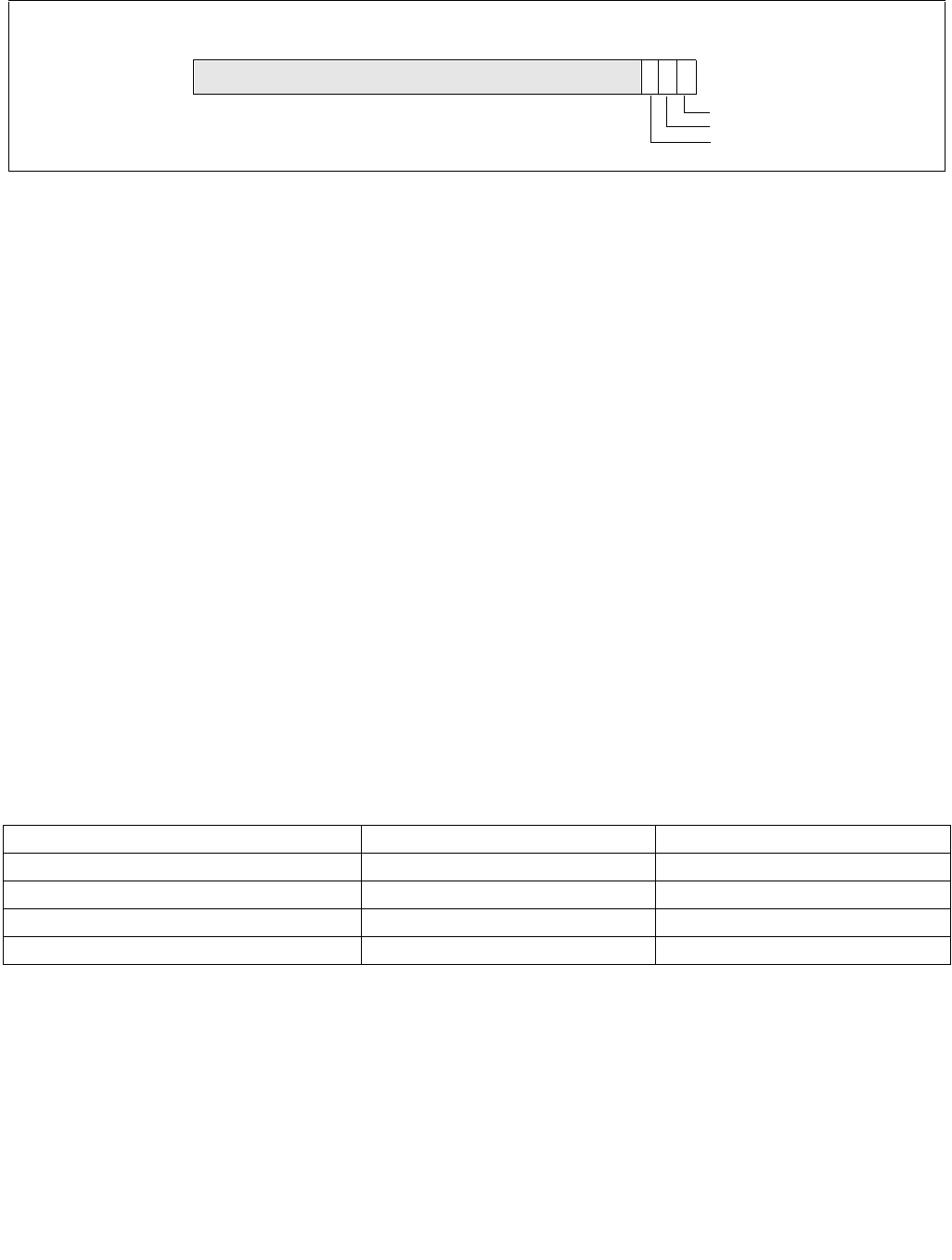
Vol. 3B 17-47
DEBUG, BRANCH PROFILE, TSC, AND INTEL® RESOURCE DIRECTOR TECHNOLOGY (INTEL® RDT) FEATURES
17.18.5.1 Cache Monitoring Technology
On processors for which Cache Monitoring Technology supports the L3 cache occupancy event, CPUID.(EAX=0FH,
ECX=1H).EDX would return with only bit 0 set. The corresponding event ID can be looked up from Table 17-18.
The L3 occupancy data accumulated in IA32_QM_CTR can be converted to total occupancy (in bytes) by multi-
plying with CPUID.(EAX=0FH, ECX=1H).EBX.
Event codes for Cache Monitoring Technology are discussed in the next section.
17.18.5.2 Memory Bandwidth Monitoring
On processors that monitoring supports Memory Bandwidth Monitoring using ResID=1 (L3), two additional bits will
be set in the vector at CPUID.(EAX=0FH, ECX=1H).EDX:
•CPUID.(EAX=0FH, ECX=1H).EDX[bit 1]: indicates the L3 total external bandwidth monitoring event is
supported if set. This event monitors the L3 total external bandwidth to the next level of the cache hierarchy,
including all demand and prefetch misses from the L3 to the next hierarchy of the memory system. In most
platforms, this represents memory bandwidth.
•CPUID.(EAX=0FH, ECX=1H).EDX[bit 2]: indicates L3 local memory bandwidth monitoring event is supported if
set. This event monitors the L3 external bandwidth satisfied by the local memory. In most platforms that
support this event, L3 requests are likely serviced by a memory system with non-uniform memory archi-
tecture. This allows bandwidth to off-package memory resources to be tracked by subtracting local from total
bandwidth (for instance, bandwidth over QPI to a memory controller on another physical processor could be
tracked by subtraction).
The corresponding Event ID can be looked up from Table 17-18. The L3 bandwidth data accumulated in
IA32_QM_CTR can be converted to total bandwidth (in bytes) using CPUID.(EAX=0FH, ECX=1H).EBX.
Table 17-18. Monitoring Supported Event IDs
17.18.6 Monitoring Resource RMID Association
After Monitoring and sub-features has been enumerated, software can begin using the monitoring features. The
first step is to associate a given software thread (or multiple threads as part of an application, VM, group of appli-
cations or other abstraction) with an RMID.
Note that the process of associating an RMID with a given software thread is the same for all shared resource moni-
toring features (CMT, MBM), and a given RMID number has the same meaning from the viewpoint of any logical
processors in a package. Stated another way, a thread may be associated in a 1:1 mapping with an RMID, and that
Figure 17-22. L3 Cache Monitoring Capability Enumeration Event Type Bit Vector (CPUID.(EAX=0FH, ECX=1H) )
Event Type Event ID Context
L3 Cache Occupancy 01H Cache Monitoring Technology
L3 Total External Bandwidth 02H MBM
L3 Local External Bandwidth 03H MBM
Reserved All other event codes N/A
0231
EDX
1
Reserved
EventTypeBitMask
3
L3 Occupancy
L3 Total BW
L3 Local BW
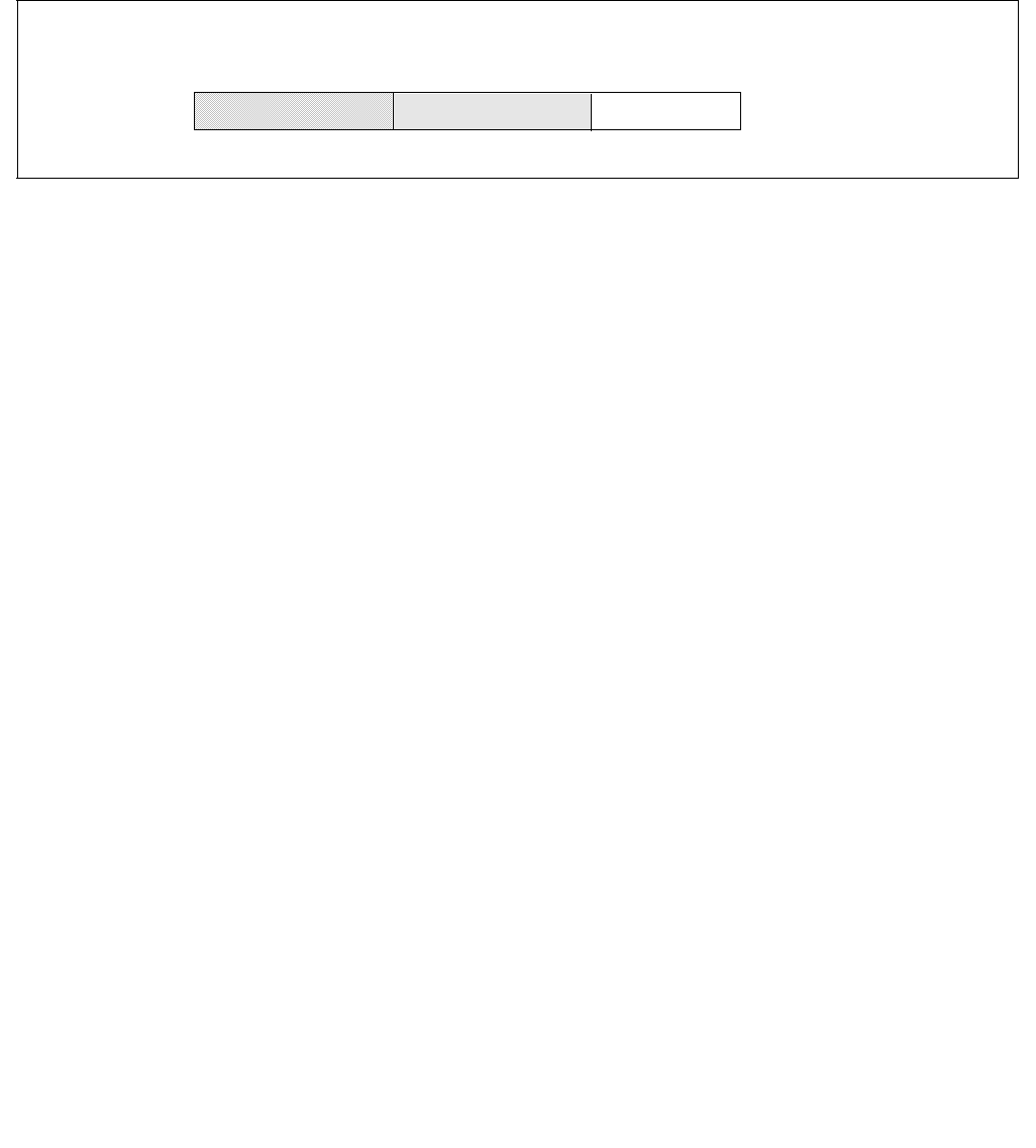
17-48 Vol. 3B
DEBUG, BRANCH PROFILE, TSC, AND INTEL® RESOURCE DIRECTOR TECHNOLOGY (INTEL® RDT) FEATURES
RMID may allow cache occupancy, memory bandwidth information or other monitoring data to be read back later
with monitoring event codes (retrieving data is discussed in a previous section).
The association of an application thread with an RMID requires an OS to program the per-logical-processor MSR
IA32_PQR_ASSOC at context swap time (updates may also be made at any other arbitrary points during program
execution such as application phase changes). The IA32_PQR_ASSOC MSR specifies the active RMID that moni-
toring hardware will use to tag internal operations, such as L3 cache requests. The layout of the MSR is shown in
Figure 17-23. Software specifies the active RMID to monitor in the IA32_PQR_ASSOC.RMID field. The width of the
RMID field can vary from one implementation to another, and is derived from Ceil (LOG2 ( 1 + CPUID.(EAX=0FH,
ECX=0):EBX[31:0])). The value of IA32_PQR_ASSOC after power-on is 0.
In the initial implementation, the width of the RMID field is up to 10 bits wide, zero-referenced and fully encoded.
However, software must use CPUID to query the maximum RMID supported by the processor. If a value larger than
the maximum RMID is written to IA32_PQR_ASSOC.RMID, a #GP(0) fault will be generated.
RMIDs have a global scope within the physical package- if an RMID is assigned to one logical processor then the
same RMID can be used to read multiple thread attributes later (for example, L3 cache occupancy or external
bandwidth from the L3 to the next level of the cache hierarchy). In a multiple LLC platform the RMIDs are to be
reassigned by the OS or VMM scheduler when an application is migrated across LLCs.
Note that in a situation where Monitoring supports multiple resource types, some upper range of RMIDs (e.g. RMID
31) may only be supported by one resource type but not by another resource type.
17.18.7 Monitoring Resource Selection and Reporting Infrastructure
The reporting mechanism for Cache Monitoring Technology and other related features is architecturally exposed as
an MSR pair that can be programmed and read to measure various metrics such as the L3 cache occupancy (CMT)
and bandwidths (MBM) depending on the level of Monitoring support provided by the platform. Data is reported
back on a per-RMID basis. These events do not trigger based on event counts or trigger APIC interrupts (e.g. no
Performance Monitoring Interrupt occurs based on counts). Rather, they are used to sample counts explicitly.
The MSR pair for the shared resource monitoring features (CMT, MBM) is separate from and not shared with archi-
tectural Perfmon counters, meaning software can use these monitoring features simultaneously with the Perfmon
counters.
Access to the aggregated monitoring information is accomplished through the following programmable monitoring
MSRs:
•IA32_QM_EVTSEL: This MSR provides a role similar to the event select MSRs for programmable performance
monitoring described in Chapter 18. The simplified layout of the MSR is shown in Figure 17-24. Bits
IA32_QM_EVTSEL.EvtID (bits 7:0) specify an event code of a supported resource type for hardware to report
monitored data associated with IA32_QM_EVTSEL.RMID (bits 41:32). Software can configure
IA32_QM_EVTSEL.RMID with any RMID that is active within the physical processor. The width of
IA32_QM_EVTSEL.RMID matches that of IA32_PQR_ASSOC.RMID. Supported event codes for the
IA32_QM_EVTSEL register are shown in Table 17-18. Note that valid event codes may not necessarily map
directly to the bit position used to enumerate support for the resource via CPUID.
Software can program an RMID / Event ID pair into the IA32_QM_EVTSEL MSR bit field to select an RMID to
read a particular counter for a given resource. The currently supported list of Monitoring Event IDs is discussed
in Section 17.18.5, which covers feature-specific details.
Figure 17-23. IA32_PQR_ASSOC MSR
0
10
63
Width of IA32_PQR_ASSOC.RMID field: Log2 ( CPUID.(EAX=0FH, ECX=0H).EBX[31:0] +1)
RMID
9
Reserved IA32_PQR_ASSOC
Reserved for CLOS*
32 31
*See Section 17.18
Vol. 3B 17-49
DEBUG, BRANCH PROFILE, TSC, AND INTEL® RESOURCE DIRECTOR TECHNOLOGY (INTEL® RDT) FEATURES
Thread access to the IA32_QM_EVTSEL and IA32_QM_CTR MSR pair should be serialized to avoid situations
where one thread changes the RMID/EvtID just before another thread reads monitoring data from
IA32_QM_CTR.
•IA32_QM_CTR: This MSR reports monitored data when available. It contains three bit fields. If software
configures an unsupported RMID or event type in IA32_QM_EVTSEL, then IA32_QM_CTR.Error (bit 63) will be
set, indicating there is no valid data to report. If IA32_QM_CTR.Unavailable (bit 62) is set, it indicates
monitored data for the RMID is not available, and IA32_QM_CTR.data (bits 61:0) should be ignored. Therefore,
IA32_QM_CTR.data (bits 61:0) is valid only if bit 63 and 62 are both clear. For Cache Monitoring Technology,
software can convert IA32_QM_CTR.data into cache occupancy or bandwidth metrics expressed in bytes by
multiplying with the conversion factor from CPUID.(EAX=0FH, ECX=1H).EBX.
17.18.8 Monitoring Programming Considerations
Figure 17-23 illustrates how system software can program IA32_QOSEVTSEL and IA32_QM_CTR to perform
resource monitoring.
Though the field provided in IA32_QM_CTR allows for up to 62 bits of data to be returned, often a subset of bits are
used. With Cache Monitoring Technology for instance, the number of bits used will be proportional to the base-two
logarithm of the total cache size divided by the Upscaling Factor from CPUID.
In Memory Bandwidth Monitoring the initial counter size is 24 bits, and retrieving the value at 1Hz or faster is suffi-
cient to ensure at most one rollover per sampling period. Any future changes to counter width will be enumerated
to software.
Figure 17-24. IA32_QM_EVTSEL and IA32_QM_CTR MSRs
Figure 17-25. Software Usage of Cache Monitoring Resources
063
IA32_QM_CTR
U
61
E Resource Monitoring Data
03163
RMID
7
Reserved IA32_QM_EVTSEL
Reserved
41 3242 8
EvtID
RMID
063
Monitoring Data
IA32_QM_CTR MSR
62
Availability
Error
763
Reserved
41
RMID
Resource Monitoring ID
0
EvtID
32
Reserved
Event ID
IA32_QOSEVTSEL MSR
System Software
Event ID Counter Data

17-50 Vol. 3B
DEBUG, BRANCH PROFILE, TSC, AND INTEL® RESOURCE DIRECTOR TECHNOLOGY (INTEL® RDT) FEATURES
17.18.8.1 Monitoring Dynamic Configuration
Both the IA32_QM_EVTSEL and IA32_PQR_ASSOC registers are accessible and modifiable at any time during
execution using RDMSR/WRMSR unless otherwise noted. When writing to these MSRs a #GP(0) will be generated
if any of the following conditions occur:
•A reserved bit is modified,
•An RMID exceeding the maxRMID is used.
17.18.8.2 Monitoring Operation With Power Saving Features
Note that some advanced power management features such as deep package C-states may shrink the L3 cache
and cause CMT occupancy count to be reduced. MBM bandwidth counts may increase due to flushing cached data
out of L3.
17.18.8.3 Monitoring Operation with Other Operating Modes
The states in IA32_PQR_ASSOC and monitoring counter are unmodified across an SMI delivery. Thus, the execu-
tion of SMM handler code and SMM handler’s data can manifest as spurious contribution in the monitored data.
It is possible for an SMM handle r to min imize the impact on o f spuri ous contribution in the QOS monitor ing counters
by reserving a dedicated RMID for monitoring the SMM handler. Such an SMM handler can save the previously
configured QOS Monitoring state immediately upon entering SMM, and restoring the QOS monitoring state back to
the prev-SMM RMID upon exit.
17.18.8.4 Monitoring Operation with RAS Features
In general the Reliability, Availability and Serviceability (RAS) features present in Intel Platforms are not expected
to significantly affect shared resource monitoring counts. In cases where software RAS features cause memory
copies or cache accesses these may be tracked and may influence the shared resource monitoring counter values.
17.19 INTEL® RESOURCE DIRECTOR TECHNOLOGY (INTEL® RDT) ALLOCATION
FEATURES
The Intel Resource Director Technology (Intel RDT) feature set provides a set of allocation (resource control) capa-
bilities including Cache Allocation Technology (CAT) and Code and Data Prioritization (CDP). The Intel Xeon
processor E5 v4 family (and a subset of communication-focused processors in the Intel Xeon E5 v3 family) intro-
duce capabilities to configure and make use of the Cache Allocation Technology (CAT) mechanisms on the L3 cache.
Certain Intel Atom processors also provide support for control over the L2 cache, with capabilities as described
below. The programming interface for Cache Allocation Technology and for the more general allocation capabilities
are described in the rest of this chapter. The CAT and CDP capabilities, where architecturally supported, may be
detected and enumerated in software using the CPUID instruction, as described in this chapter.
The Intel Xeon Processor Scalable Family introduces the Memory Bandwidth Allocation (MBA) feature which
provides indirect control over the memory bandwidth available to CPU cores, and is discussed later in this chapter.
17.19.1 Introduction to Cache Allocation Technology (CAT)
Cache Allocation Technology enables an Operating System (OS), Hypervisor /Virtual Machine Manager (VMM) or
similar system service management agent to specify the amount of cache space into which an application can fill
(as a hint to hardware - certain features such as power management may override CAT settings). Specialized user-
level implementations with minimal OS support are also possible, though not necessarily recommended (see notes
below for OS/Hypervisor with respect to ring 3 software and virtual guests). Depending on the processor family, L2
or L3 cache allocation capability may be provided, and the technology is designed to scale across multiple cache
levels and technology generations.
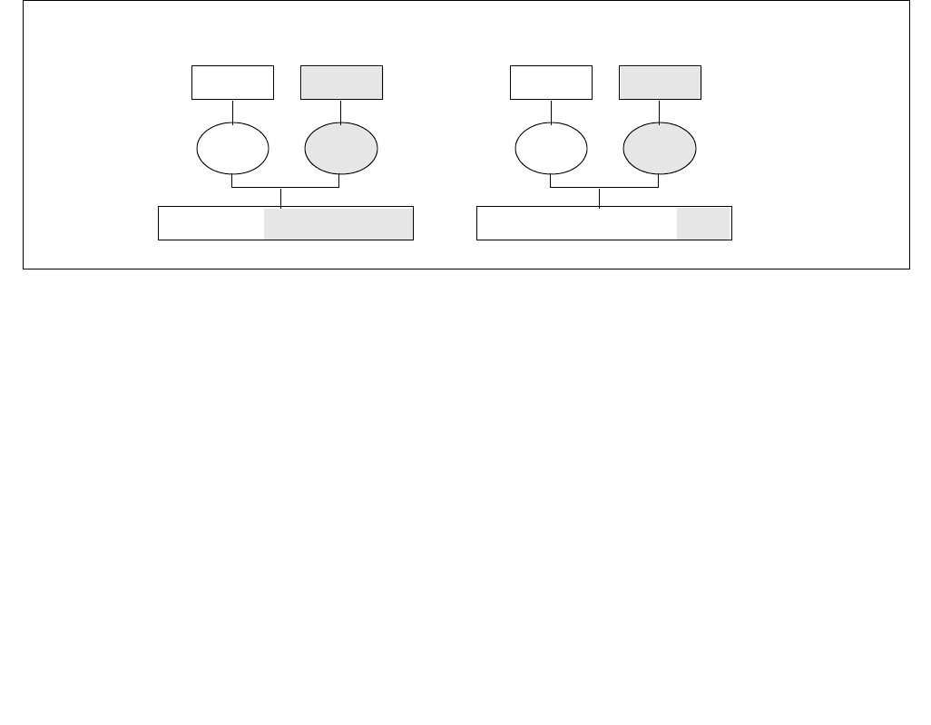
Vol. 3B 17-51
DEBUG, BRANCH PROFILE, TSC, AND INTEL® RESOURCE DIRECTOR TECHNOLOGY (INTEL® RDT) FEATURES
Software can determine which levels are supported in a given platform programmatically using CPUID as described
in the following sections.
The CAT mechanisms defined in this document provide the following key features:
•A mechanism to enumerate platform Cache Allocation Technology capabilities and available resource types that
provides CAT control capabilities. For implementations that support Cache Allocation Technology, CPUID
provides enumeration support to query which levels of the cache hierarchy are supported and specific CAT
capabilities, such as the max allocation bitmask size,
•A mechanism for the OS or Hypervisor to configure the amount of a resource available to a particular Class of
Service via a list of allocation bitmasks,
•Mechanisms for the OS or Hypervisor to signal the Class of Service to which an application belongs, and
•Hardware mechanisms to guide the LLC fill policy when an application has been designated to belong to a
specific Class of Service.
Note that for many usages, an OS or Hypervisor may not want to expose Cache Allocation Technology mechanisms
to Ring3 software or virtualized guests.
The Cache Allocation Technology feature enables more cache resources (i.e. cache space) to be made available for
high priority applications based on guidance from the execution environment as shown in Figure 17-26. The archi-
tecture also allows dynamic resource reassignment during runtime to further optimize the performance of the high
priority application with minimal degradation to the low priority app. Additionally, resources can be rebalanced for
system throughput benefit across uses cases of OSes, VMMs, containers and other scenarios by managing the
CPUID and MSR interfaces. This section describes the hardware and software support required in the platform
including what is required of the execution environment (i.e. OS/VMM) to support such resource control. Note that
in Figure 17-26 the L3 Cache is shown as an example resource.
17.19.2 Cache Allocation Technology Architecture
The fundamental goal of Cache Allocation Technology is to enable resource allocation based on application priority
or Class of Service (COS or CLOS). The processor exposes a set of Classes of Service into which applications (or
individual threads) can be assigned. Cache allocation for the respective applications or threads is then restricted
based on the class with which they are associated. Each Class of Service can be configured using capacity bitmasks
(CBMs) which represent capacity and indicate the degree of overlap and isolation between classes. For each logical
processor there is a register exposed (referred to here as the IA32_PQR_ASSOC MSR or PQR) to allow the OS/VMM
to specify a COS when an application, thread or VM is scheduled.
The usage of Classes of Service (COS) are consistent across resources and a COS may have multiple resource
control attributes attached, which reduces software overhead at context swap time. Rather than adding new types
of COS tags per resource for instance, the COS management overhead is constant. Cache allocation for the indi-
cated application/thread/container/VM is then controlled automatically by the hardware based on the class and the
bitmask associated with that class. Bitmasks are configured via the IA32_resourceType_MASK_n MSRs, where
resourceType indicates a resource type (e.g. “L3” for the L3 cache) and “n” indicates a COS number.
The basic ingredients of Cache Allocation Technology are as follows:
Figure 17-26. Cache Allocation Technology Enables Allocation of More Resources to High Priority Applications
Without CAT
Core 0
Shared LLC, Low priority got more cache
Lo Pri App
Hi Pri App
Core 1 Core 0
Shared LLC, High priority got more cache
Lo Pri App
Hi Pri App
Core 1
With CAT
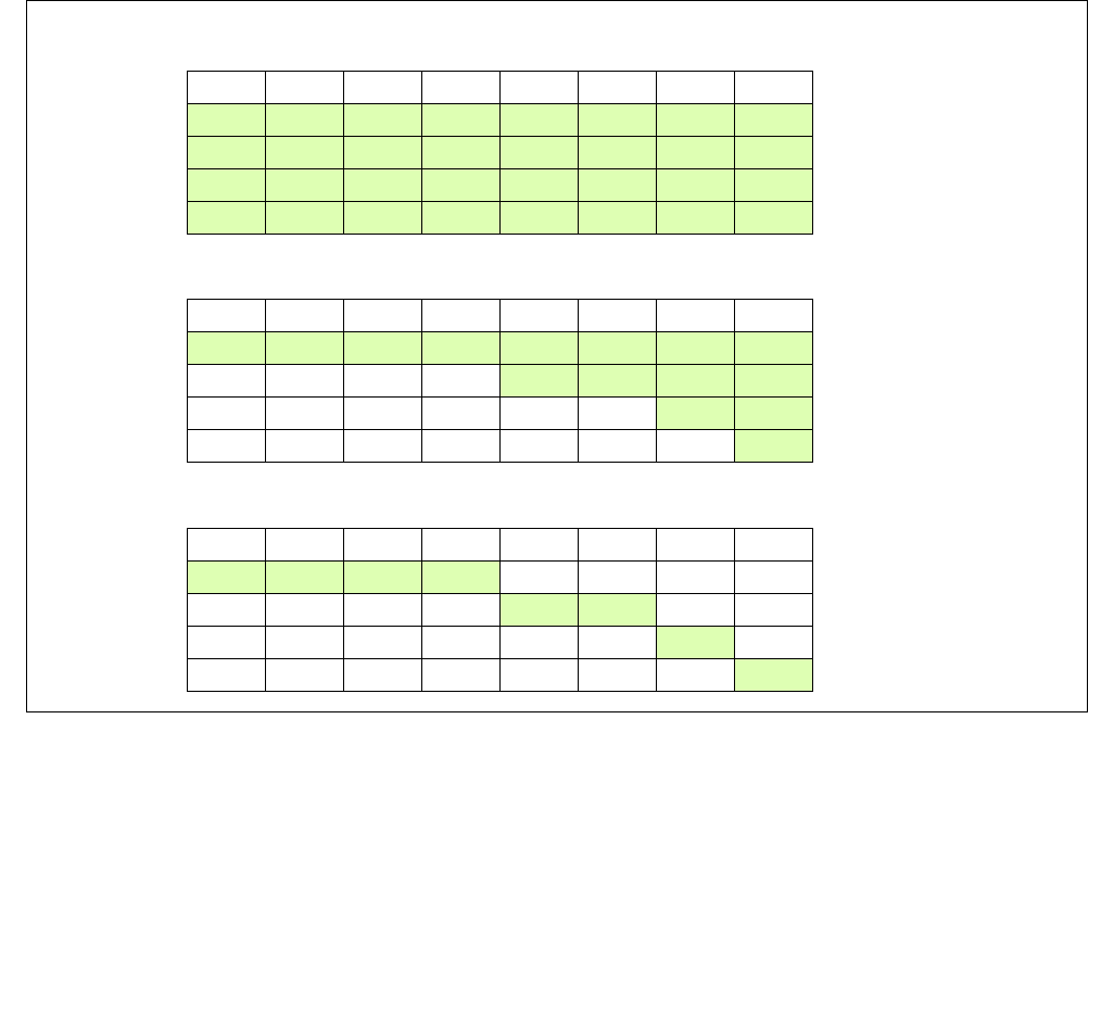
17-52 Vol. 3B
DEBUG, BRANCH PROFILE, TSC, AND INTEL® RESOURCE DIRECTOR TECHNOLOGY (INTEL® RDT) FEATURES
•An architecturally exposed mechanism using CPUID to indicate whether CAT is supported, and what resource
types are available which can be controlled,
•For each available resourceType, CPUID also enumerates the total number of Classes of Services and the length
of the capacity bitmasks that can be used to enforce cache allocation to applications on the platform,
•An architecturally exposed mechanism to allow the execution environment (OS/VMM) to configure the behavior
of different classes of service using the bitmasks available,
•An architecturally exposed mechanism to allow the execution environment (OS/VMM) to assign a COS to an
executing software thread (i.e. associating the active CR3 of a logical processor with the COS in
IA32_PQR_ASSOC),
•Implementation-dependent mechanisms to indicate which COS is associated with a memory access and to
enforce the cache allocation on a per COS basis.
A capacity bitmask (CBM) provides a hint to the hardware indicating the cache space an application should be
limited to as well as providing an indication of overlap and isolation in the CAT-capable cache from other applica-
tions contending for the cache. The bit length of the capacity mask available generally depends on the configuration
of the cache and is specified in the enumeration process for CAT in CPUID (this may vary between models in a
processor family as well). Similarly, other parameters such as the number of supported COS may vary for each
resource type, and these details can be enumerated via CPUID.
Sample cache capacity bitmasks for a bit length of 8 are shown in Figure 17-27. Please note that all (and only)
contiguous '1' combinations are allowed (e.g. FFFFH, 0FF0H, 003CH, etc.). Attempts to program a value without
contiguous '1's (including zero) will result in a general protection fault (#GP(0)). It is generally expected that in
way-based implementations, one capacity mask bit corresponds to some number of ways in cache, but the specific
mapping is implementation-dependent. In all cases, a mask bit set to '1' specifies that a particular Class of Service
can allocate into the cache subset represented by that bit. A value of '0' in a mask bit specifies that a Class of
Figure 17-27. Examples of Cache Capacity Bitmasks
M7 M6 M5 M4 M3 M2 M1 M0
AAAAAAAA
AAAAAAAA
AAAAAAAA
AAAAAAAA
COS0
COS1
COS2
COS3
Default Bitmask
M7 M6 M5 M4 M3 M2 M1 M0
AAAA
A A
A
A
COS0
COS1
COS2
COS3
Isolated Bitmask
M7 M6 M5 M4 M3 M2 M1 M0
AAAAAAAA
AAAA
A A
A
COS0
COS1
COS2
COS3
Overlapped Bitmask
Vol. 3B 17-53
DEBUG, BRANCH PROFILE, TSC, AND INTEL® RESOURCE DIRECTOR TECHNOLOGY (INTEL® RDT) FEATURES
Service cannot allocate into the given cache subset. In general, allocating more cache to a given application is
usually beneficial to its performance.
Figure 17-27 also shows three examples of sets of Cache Capacity Bitmasks. For simplicity these are represented
as 8-bit vectors, though this may vary depending on the implementation and how the mask is mapped to the avail-
able cache capacity. The first example shows the default case where all 4 Classes of Service (the total number of
COS are implementation-dependent) have full access to the cache. The second case shows an overlapped case,
which would allow some lower-priority threads share cache space with the highest priority threads. The third case
shows various non-overlapped partitioning schemes. As a matter of software policy for extensibility COS0 should
typically be considered and configured as the highest priority COS, followed by COS1, and so on, though there is
no hardware restriction enforcing this mapping. When the system boots all threads are initialized to COS0, which
has full access to the cache by default.
Though the representation of the CBMs looks similar to a way-based mapping they are independent of any specific
enforcement implementation (e.g. way partitioning.) Rather, this is a convenient manner to represent capacity,
overlap and isolation of cache space. For example, executing a POPCNT instruction (population count of set bits) on
the capacity bitmask can provide the fraction of cache space that a class of service can allocate into. In addition to
the fraction, the exact location of the bits also shows whether the class of service overlaps with other classes of
service or is entirely isolated in terms of cache space used.
Figure 17-28 shows how the Cache Capacity Bitmasks and the per-logical-processor Class of Service are logically
used to enable Cache Allocation Technology. All (and only) contiguous 1's in the CBM are permitted. The length of
a CBM may vary from resource to resource or between processor generations and can be enumerated using CPUID.
From the available mask set and based on the goals of the OS/VMM (shared or isolated cache, etc.) bitmasks are
selected and associated with different classes of service. For the available Classes of Service the associated CBMs
can be programmed via the global set of CAT configuration registers (in the case of L3 CAT, via the
IA32_L3_MASK_n MSRs, where “n” is the Class of Service, starting from zero). In all architectural implementations
supporting CPUID it is possible to change the CBMs dynamically, during program execution, unless stated other-
wise by Intel.
The currently running application's Class of Service is communicated to the hardware through the per-logical-
processor PQR MSR (IA32_PQR_ASSOC MSR). When the OS schedules an application thread on a logical processor,
Figure 17-28. Class of Service and Cache Capacity Bitmasks
Set 1
Set 2
....
Cache Subsystem
Config
Tag with Cache
Enforcement
Set n
way 1
......
way 16
Enforce Mask
Capacity bitmask 3
COS 3
Capacity bitmask 3
COS 2
Capacity bitmask 3
COS 1
Capacity bitmask 3
COS 0
Cache Allocation
Transaction
COS
COS = 2
Mem Request
Class of Service
Application
Memory Request
Set Class of Service
Association
in IA32_PQR
OS Context
Switch
Configure CBM for
Enum/Confg
each Class of Service
Enumerate
Enforcement

17-54 Vol. 3B
DEBUG, BRANCH PROFILE, TSC, AND INTEL® RESOURCE DIRECTOR TECHNOLOGY (INTEL® RDT) FEATURES
the application thread is associated with a specific COS (i.e. the corresponding COS in the PQR) and all requests to
the CAT-capable resource from that logical processor are tagged with that COS (in other words, the application
thread is configured to belong to a specific COS). The cache subsystem uses this tagged request information to
enforce QoS. The capacity bitmask may be mapped into a way bitmask (or a similar enforcement entity based on
the implementation) at the cache before it is applied to the allocation policy. For example, the capacity bitmask can
be an 8-bit mask and the enforcement may be accomplished using a 16-way bitmask for a cache enforcement
implementation based on way partitioning.
The following sections describe extensions of CAT such as Code and Data Prioritization (CDP), followed by details
on specific features such as L3 CAT, L3 CDP, L2 CAT, and L2 CDP. Depending on the specific processor a mix of
features may be supported, and CPUID provides enumeration capabilities to enable software to dynamically detect
the set of supported features.
17.19.3 Code and Data Prioritization (CDP) Technology
Code and Data Prioritization Technology is an extension of CAT. CDP enables isolation and separate prioritization of
code and data fetches to the L2 or L3 cache in a software configurable manner, depending on hardware support,
which can enable workload prioritization and tuning of cache capacity to the characteristics of the workload. CDP
extends Cache Allocation Technology (CAT) by providing separate code and data masks per Class of Service (COS).
Support for the L2 CDP feature and the L3 CDP features are separately enumerated (via CPUID) and separately
controlled (via remapping the L2 CAT MSRs or L3 CAT MSRs respectively). Section 17.19.6.3 and Section 17.19.7
provide details on enumerating, controlling and enabling L3 and L2 CDP respectively, while this section provides a
general overview.
The L3 CDP feature was first introduced on the Intel Xeon E5 v4 family of server processors, as an extension to L3
CAT. The L2 CDP feature is first introduced on future Intel Atom family processors, as an extension to L2 CAT.
By default, CDP is disabled on the processor. If the CAT MSRs are used without enabling CDP, the processor oper-
ates in a traditional CAT-only mode. When CDP is enabled,
•the CAT mask MSRs are re-mapped into interleaved pairs of mask MSRs for data or code fetches (see
Figure 17-29),
•the range of COS for CAT is re-indexed, with the lower-half of the COS range available for CDP.
Using the CDP feature, virtual isolation between code and data can be configured on the L2 or L3 cache if desired,
similar to how some processor cache levels provide separate L1 data and L1 instruction caches.
Like the CAT feature, CDP may be dynamically configured by privileged software at any point during normal system
operation, including dynamically enabling or disabling the feature provided that certain software configuration
requirements are met (see Section 17.19.5).
An example of the operating mode of CDP is shown in Figure 17-29. Shown at the top are traditional CAT usage
models where capacity masks map 1:1 with a COS number to enable control over the cache space which a given
COS (and thus applications, threads or VMs) may occupy. Shown at the bottom are example mask configurations
where CDP is enabled, and each COS number maps 1:2 to two masks, one for code and one for data. This enables
code and data to be either overlapped or isolated to varying degrees either globally or on a per-COS basis,
depending on application and system needs.
Vol. 3B 17-55
DEBUG, BRANCH PROFILE, TSC, AND INTEL® RESOURCE DIRECTOR TECHNOLOGY (INTEL® RDT) FEATURES
When CDP is enabled, the existing mask space for CAT-only operation is split. As an example if the system supports
16 CAT-only COS, when CDP is enabled the same MSR interfaces are used, however half of the masks correspond
to code, half correspond to data, and the effective number of COS is reduced by half. Code/Data masks are defined
per-COS and interleaved in the MSR space as described in subsequent sections.
In cases where CPUID exposes a non-even number of supported Classes of Service for the CAT or CDP features,
software using CDP should use the lower matched pairs of code/data masks, and any upper unpaired masks should
not be used. As an example, if CPUID exposes 5 CLOS, when CDP is enabled then two code/data pairs are available
(masks 0/1 for CLOS[0] data/code and masks 2/3 for CLOS[1] data/code), however the upper un-paired mask
should not be used (mask 4 in this case) or undefined behavior may result.
17.19.4 Enabling Cache Allocation Technology Usage Flow
Figure 17-30 illustrates the key steps for OS/VMM to detect support of Cache Allocation Technology and enable
priority-based resource allocation for a CAT-capable resource.
Figure 17-29. Code and Data Capacity Bitmasks of CDP
1111000000000000
00001 1 0000000000
0000001111100000
0000000001110000
0000000000001111
0000000000001111
COS0.Data
COS0.Code
COS1.Data
COS1.Code
CAT with
1111000000000000
0000111100000000
000000001 1 000000
0000000011111111
COS0
COS1
COS2
COS3
Traditional
CAT
CDP
Other COS.Data
Example of Code/Data Prioritization Usage - 16 bit Capacity Masks
Example of CAT-Only Usage - 16 bit Capacity Masks
Other COS.Code
2
17-56 Vol. 3B
DEBUG, BRANCH PROFILE, TSC, AND INTEL® RESOURCE DIRECTOR TECHNOLOGY (INTEL® RDT) FEATURES
Enumeration and configuration of L2 CAT is similar to L3 CAT, however CPUID details and MSR addresses differ.
Common CLOS are used across the features.
17.19.4.1 Enumeration and Detection Support of Cache Allocation Technology
Software can query processor support of CAT capabilities by executing CPUID instruction with EAX = 07H, ECX =
0H as input. If CPUID.(EAX=07H, ECX=0):EBX.PQE[bit 15] reports 1, the processor supports software control over
shared processor resources. Software must use CPUID leaf 10H to enumerate additional details of available
resource types, classes of services and capability bitmasks. The programming interfaces provided by Cache Alloca-
tion Technology include:
•CPUID leaf function 10H (Cache Allocation Technology Enumeration leaf) and its sub-functions provide
information on available resource types, and CAT capability for each resource type (see Section 17.19.4.2).
•IA32_L3_MASK_n: A range of MSRs is provided for each resource type, each MSR within that range specifying
a software-configured capacity bitmask for each class of service. For L3 with Cache Allocation support, the CBM
is specified using one of the IA32_L3_QOS_MASK_n MSR, where 'n' corresponds to a number within the
supported range of COS, i.e. the range between 0 and CPUID.(EAX=10H, ECX=ResID):EDX[15:0], inclusive.
See Section 17.19.4.3 for details.
•IA32_L2_MASK_n: A range of MSRs is provided for L2 Cache Allocation Technology, enabling software control
over the amount of L2 cache available for each CLOS. Similar to L3 CAT, a CBM is specified for each CLOS using
the set of registers, IA32_L2_QOS_MASK_n MSR, where 'n' ranges from zero to the maximum CLOS number
reported for L2 CAT in CPUID. See Section 17.19.4.3 for details.
The L2 mask MSRs are scoped at the same level as the L2 cache (similarly, the L3 mask MSRs are scoped at the
same level as the L3 cache). Software may determine which logical processors share an MSR (for instance local
to a core, or shared across multiple cores) by performing a write to one of these MSRs and noting which logical
threads observe the change. Example flows for a similar method to determine register scope are described in
Section 15.5.2, “System Software Recommendation for Managing CMCI and Machine Check Resources”.
Software may also use CPUID leaf 4 to determine the maximum number of logical processor IDs that may share
a given level of the cache.
•IA32_PQR_ASSOC.CLOS: The IA32_PQR_ASSOC MSR provides a COS field that OS/VMM can use to assign a
logical processor to an available COS. The set of COS are common across all allocation features, meaning that
multiple features may be supported in the same processor without additional software COS management
overhead at context swap time. See Section 17.19.4.4 for details.
17.19.4.2 Cache Allocation Technology: Resource Type and Capability Enumeration
CPUID leaf function 10H (Cache Allocation Technology Enumeration leaf) provides two or more sub-functions:
•CAT Enumeration leaf sub-function 0 enumerates available resource types that support allocation control, i.e.
by executing CPUID with EAX=10H and ECX=0H. Each supported resource type is represented by a bit field in
Figure 17-30. Cache Allocation Technology Usage Flow
CPUID.(7,0):EBX.15
On OS/VMM Initialization
CPUID.(10H,0):EBX[31:1]
CQE Capability
Enumeration
IA32_L3_QOS_MASK_0
Cache Allocation Configuration
...
Configure CBM
per COS
On Context Switch
IA32_PQR_ASSOC
Set COS for scheduled
thread context
IA32_L3_QOS_MASK_n
CPUID.(10H,1):EAX[4:0]
CPUID.(10H,1):EDX[15:0]
CPUID.(10H,1):EBX[
CPUID[ WRMSR WRMSR
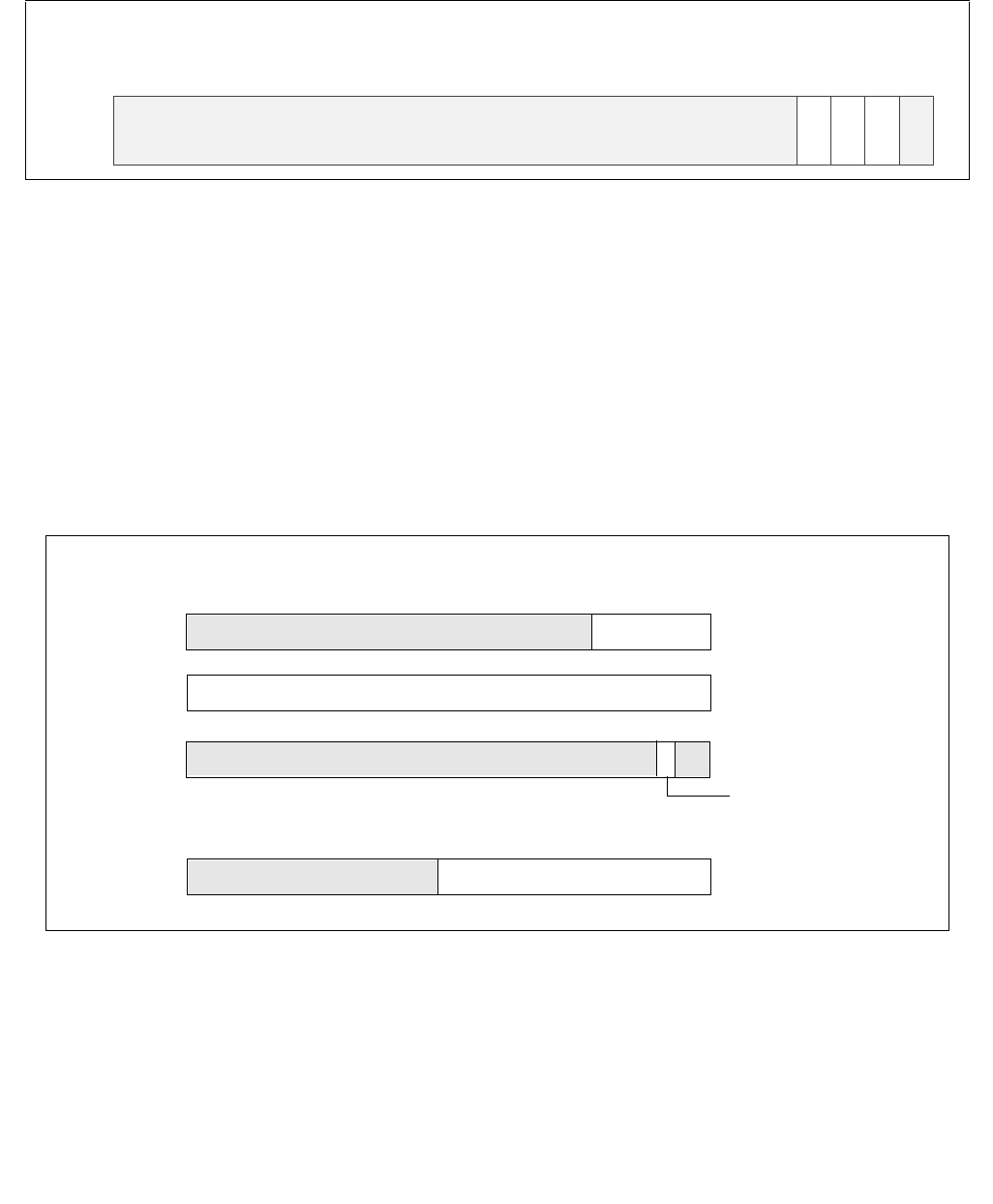
Vol. 3B 17-57
DEBUG, BRANCH PROFILE, TSC, AND INTEL® RESOURCE DIRECTOR TECHNOLOGY (INTEL® RDT) FEATURES
CPUID.(EAX=10H, ECX=0):EBX[31:1]. The bit position of each set bit corresponds to a Resource ID (ResID),
for instance ResID=1 is used to indicate L3 CAT support, and ResID=2 indicates L2 CAT support. The ResID is
also the sub-leaf index that software must use to query details of the CAT capability of that resource type (see
Figure 17-31).
— For ECX>0, EAX[4:0] reports the length of the capacity bitmask length (ECX=1 or 2 for L2 CAT or L3 CAT
respectively) using minus-one notation, e.g., a value of 15 corresponds to the capacity bitmask having
length of 16 bits. Bits 31:5 of EAX are reserved.
•Sub-functions of CPUID.EAX=10H with a non-zero ECX input matching a supported ResID enumerate the
specific enforcement details of the corresponding ResID. The capabilities enumerated include the length of the
capacity bitmasks and the number of Classes of Service for a given ResID. Software should query the capability
of each available ResID that supports CAT from a sub-leaf of leaf 10H using the sub-leaf index reported by the
corresponding non-zero bit in CPUID.(EAX=10H, ECX=0):EBX[31:1] in order to obtain additional feature
details.
•CAT capability for L3 is enumerated by CPUID.(EAX=10H, ECX=1H), see Figure 17-32. The specific CAT
capabilities reported by CPUID.(EAX=10H, ECX=1) are:
— CPUID.(EAX=10H, ECX=ResID=1):EAX[4:0] reports the length of the capacity bitmask length using
minus-one notation, i.e. a value of 15 corresponds to the capability bitmask having length of 16 bits. Bits
31:5 of EAX are reserved.
— CPUID.(EAX=10H, ECX=1):EBX[31:0] reports a bit mask. Each set bit within the length of the CBM
indicates the corresponding unit of the L3 allocation may be used by other entities in the platform (e.g. an
Figure 17-31. CPUID.(EAX=10H, ECX=0H) Available Resource Type Identification
Figure 17-32. L3 Cache Allocation Technology and CDP Enumeration
M
B
A
L
2
L
3
4 3 2 1 0
EBX
31
CPUID.(EAX=10H, ECX=0) Output: (EAX: Reserved; ECX: Reserved; EDX: Reserved)
Reserved
0
16
31
CPUID.(EAX=10H, ECX=ResID=1) Output:
EDX
ECX
0
31
Reserved
15
EBX
0
31
Bitmask of Shareable Resource with Other executing entities
Reserved COS_MAX
0
5
31
EAX
4
Reserved CBM_LEN
12
CDP
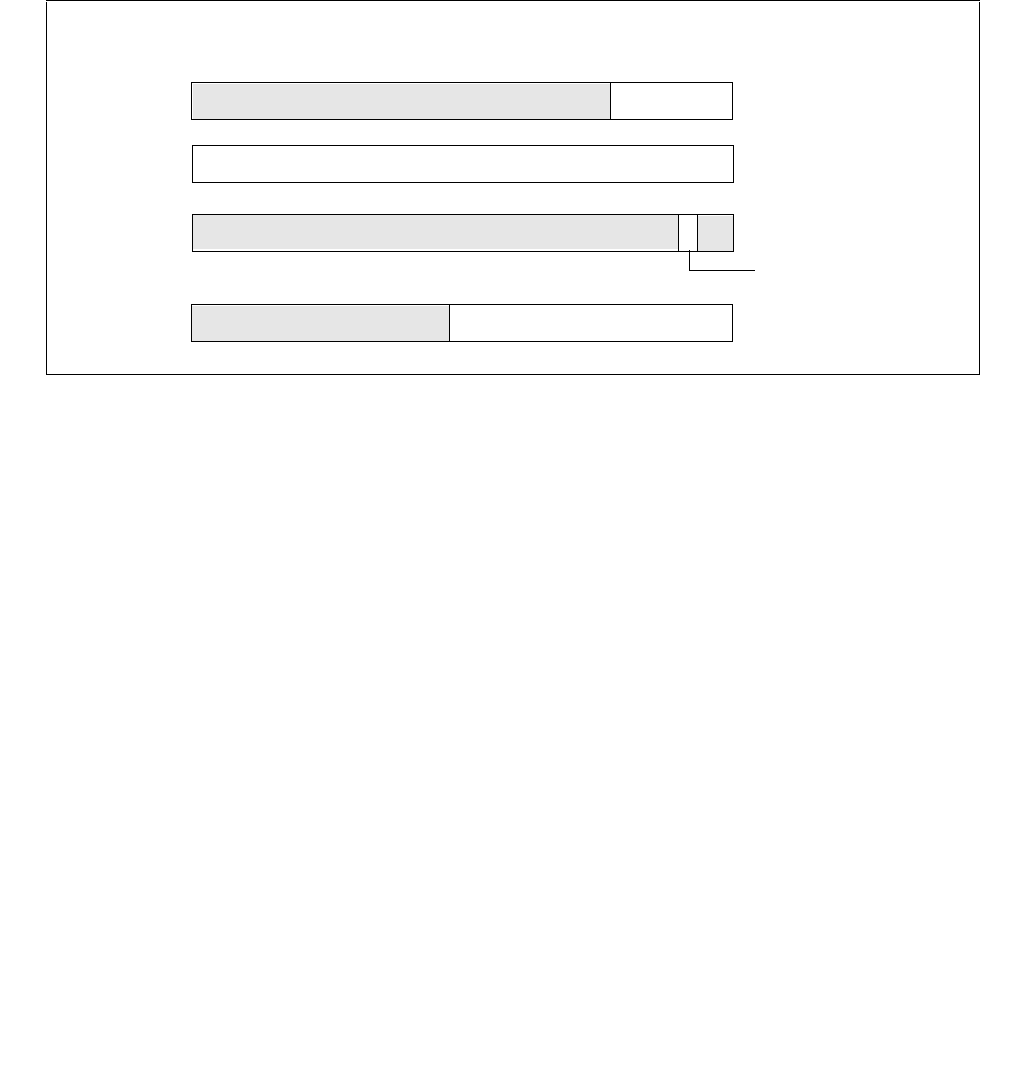
17-58 Vol. 3B
DEBUG, BRANCH PROFILE, TSC, AND INTEL® RESOURCE DIRECTOR TECHNOLOGY (INTEL® RDT) FEATURES
integrated graphics engine or hardware units outside the processor core and have direct access to L3). Each
cleared bit within the length of the CBM indicates the corresponding allocation unit can be configured to
implement a priority-based allocation scheme chosen by an OS/VMM without interference with other
hardware agents in the system. Bits outside the length of the CBM are reserved.
— CPUID.(EAX=10H, ECX=1):ECX.CDP[bit 2]: If 1, indicates L3 Code and Data Prioritization Technology is
supported (see Section 17.19.5). Other bits of CPUID.(EAX=10H, ECX=1):ECX are reserved.
— CPUID.(EAX=10H, ECX=1):EDX[15:0] reports the maximum COS supported for the resource (COS are
zero-referenced, meaning a reported value of '15' would indicate 16 total supported COS). Bits 31:16 are
reserved.
•CAT capability for L2 is enumerated by CPUID.(EAX=10H, ECX=2H), see Figure 17-33. The specific CAT
capabilities reported by CPUID.(EAX=10H, ECX=2) are:
— CPUID.(EAX=10H, ECX=ResID=2):EAX[4:0] reports the length of the capacity bitmask length using
minus-one notation, i.e. a value of 15 corresponds to the capability bitmask having length of 16 bits. Bits
31:5 of EAX are reserved.
— CPUID.(EAX=10H, ECX=2):EBX[31:0] reports a bit mask. Each set bit within the length of the CBM
indicates the corresponding unit of the L2 allocation may be used by other entities in the platform. Each
cleared bit within the length of the CBM indicates the corresponding allocation unit can be configured to
implement a priority-based allocation scheme chosen by an OS/VMM without interference with other
hardware agents in the system. Bits outside the length of the CBM are reserved.
— CPUID.(EAX=10H, ECX=2):ECX.CDP[bit 2]: If 1, indicates L2 Code and Data Prioritization Technology is
supported (see Section 17.19.6). Other bits of CPUID.(EAX=10H, ECX=2):ECX are reserved.
— CPUID.(EAX=10H, ECX=2):EDX[15:0] reports the maximum COS supported for the resource (COS are
zero-referenced, meaning a reported value of '15' would indicate 16 total supported COS). Bits 31:16 are
reserved.
A note on migration of Classes of Service (COS): Software should minimize migrations of COS across logical
processors (across threads or cores), as a reduction in the performance of the Cache Allocation Technology feature
may result if COS are migrated frequently. This is aligned with the industry-standard practice of minimizing unnec-
essary thread migrations across processor cores in order to avoid excessive time spent warming up processor
caches after a migration. In general, for best performance, minimize thread migration and COS migration across
processor logical threads and processor cores.
Figure 17-33. L2 Cache Allocation Technology
0
16
31
CPUID.(EAX=10H, ECX=ResID=2) Output:
EDX
ECX
0
31
15
EBX
0
31
Bitmask of Shareable Resource with Other executing entities
Reserved COS_MAX
0
5
31
EAX
4
Reserved CBM_LEN
Reserved
CDP
12
Vol. 3B 17-59
DEBUG, BRANCH PROFILE, TSC, AND INTEL® RESOURCE DIRECTOR TECHNOLOGY (INTEL® RDT) FEATURES
17.19.4.3 Cache Allocation Technology: Cache Mask Configuration
After determining the length of the capacity bitmasks (CBM) and number of COS supported using CPUID (see
Section 17.19.4.2), each COS needs to be programmed with a CBM to dictate its available cache via a write to the
corresponding IA32_resourceType_MASK_n register, where 'n' corresponds to a number within the supported
range of COS, i.e. the range between 0 and CPUID.(EAX=10H, ECX=ResID):EDX[15:0], inclusive, and
'resourceType' corresponds to a specific resource as enumerated by the set bits of CPUID.(EAX=10H,
ECX=0):EAX[31:1], for instance, ‘L2’ or ‘L3’ cache.
A hierarchy of MSRs is reserved for Cache Allocation Technology registers of the form
IA32_resourceType_MASK_n:
•From 0C90H through 0D8FH (inclusive), providing support for multiple sub-ranges to support varying resource
types. The first supported resourceType is 'L3', corresponding to the L3 cache in a platform. The MSRs range
from 0C90H through 0D0FH (inclusive), enables support for up to 128 L3 CAT Classes of Service.
•Within the same CAT range hierarchy, another set of registers is defined for resourceType 'L2', corresponding
to the L2 cache in a platform, and MSRs IA32_L2_MASK_n are defined for n=[0,63] at addresses 0D10H
through 0D4FH (inclusive).
Figure 17-34 and Figure 17-35 provide an overview of the relevant registers.
All CAT configuration registers can be accessed using the standard RDMSR / WRMSR instructions.
Note that once L3 or L2 CAT masks are configured, threads can be grouped into Classes of Service (COS) using the
IA32_PQR_ASSOC MSR as described in Chapter 17, “Class of Service to Cache Mask Association: Common Across
Allocation Features”.
17.19.4.4 Class of Service to Cache Mask Association: Common Across Allocation Features
After configuring the available classes of service with the preferred set of capacity bitmasks, the OS/VMM can set
the IA32_PQR_ASSOC.COS of a logical processor to the class of service with the desired CBM when a thread
Figure 17-34. IA32_PQR_ASSOC, IA32_L3_MASK_n MSRs
Figure 17-35. IA32_L2_MASK_n MSRs
0
10
63
RMID
9
Reserved IA32_PQR_ASSOC
IA32_L3_MASK_n
03163
Reserved IA32_L3_MASK_0
32
Bit_Mask
31
COS
....
03163
Reserved
32
Bit_Mask
IA32_L2_MASK_n
03163
Reserved IA32_L2_MASK_0
32
Bit_Mask
....
03163
Reserved
32
Bit_Mask

17-60 Vol. 3B
DEBUG, BRANCH PROFILE, TSC, AND INTEL® RESOURCE DIRECTOR TECHNOLOGY (INTEL® RDT) FEATURES
context switch occurs. This allows the OS/VMM to indicate which class of service an executing thread/VM belongs
within. Each logical processor contains an instance of the IA32_PQR_ASSOC register at MSR location 0C8FH, and
Figure 17-34 shows the bit field layout for this register. Bits[63:32] contain the COS field for each logical processor.
Note that placing the RMID field within the same PQR register enables both RMID and CLOS to be swapped at
context swap time for simultaneous use of monitoring and allocation features with a single register write for effi-
ciency.
When CDP is enabled, Specifying a COS value in IA32_PQR_ASSOC.COS greater than MAX_COS_CDP =(
CPUID.(EAX=10H, ECX=1):EDX[15:0] >> 1) will cause undefined performance impact to code and data fetches.
In all cases, code and data masks for L2 and L3 CDP should be programmed with at least one bit set.
Note that if the IA32_PQR_ASSOC.COS is never written then the CAT capability defaults to using COS 0, which in
turn is set to the default mask in IA32_L3_MASK_0 - which is all “1”s (on reset). This essentially disables the
enforcement feature by default or for legacy operating systems and software.
See Section 17.19.7, “Introduction to Memory Bandwidth Allocation” for important COS programming consider-
ations including maximum values when using CAT and CDP.
17.19.5 Code and Data Prioritization (CDP): Enumerating and Enabling L3 CDP Technology
L3 CDP is an extension of L3 CAT. The presence of the L3 CDP feature is enumerated via CPUID.(EAX=10H,
ECX=1):ECX.CDP[bit 2] (see Figure 17-32). Most of the CPUID.(EAX=10H, ECX=1) sub-leaf data that applies to
CAT also apply to CDP. However, CPUID.(EAX=10H, ECX=1):EDX.COS_MAX_CAT specifies the maximum COS
applicable to CAT-only operation. For CDP operations, COS_MAX_CDP is equal to (CPUID.(EAX=10H,
ECX=1):EDX.COS_MAX_CAT >>1).
If CPUID.(EAX=10H, ECX=1):ECX.CDP[bit 2] =1, the processor supports CDP and provides a new MSR
IA32_L3_QOS_CFG at address 0C81H. The layout of IA32_L3_QOS_CFG is shown in Figure 17-36. The bit field
definition of IA32_L3_QOS_CFG are:
•Bit 0: L3 CDP Enable. If set, enables CDP, maps CAT mask MSRs into pairs of Data Mask and Code Mask MSRs.
The maximum allowed value to write into IA32_PQR_ASSOC.COS is COS_MAX_CDP.
•Bits 63:1: Reserved. Attempts to write to reserved bits result in a #GP(0).
IA32_L3_QOS_CFG default values are all 0s at RESET, the mask MSRs are all 1s. Hence, all logical processors are
initialized in COS0 allocated with the entire L3 with CDP disabled, until software programs CAT and CDP. The scope
of the IA32_L3_QOS_CFG MSR is defined to be the same scope as the L3 cache (e.g., typically per processor
socket). Refer to Section 17.19.7 for software considerations while enabling or disabling L3 CDP.
17.19.5.1 Mapping Between L3 CDP Masks and CAT Masks
When CDP is enabled, the existing CAT mask MSR space is re-mapped to provide a code mask and a data mask per
COS. The re-mapping is shown in Table 17-19.
Figure 17-36. Layout of IA32_L3_QOS_CFG
0263 1
Reserved
IA32_L3_QOS_CFG
3
L3 CDP Enable

Vol. 3B 17-61
DEBUG, BRANCH PROFILE, TSC, AND INTEL® RESOURCE DIRECTOR TECHNOLOGY (INTEL® RDT) FEATURES
Table 17-19. Re-indexing of COS Numbers and Mapping to CAT/CDP Mask MSRs
One can derive the MSR address for the data mask or code mask for a given COS number ‘n’ by:
•data_mask_address (n) = base + (n <<1), where base is the address of IA32_L3_QOS_MASK_0.
•code_mask_address (n) = base + (n <<1) +1.
When CDP is enabled, each COS is mapped 1:2 with mask MSRs, with one mask enabling programmatic control
over data fill location and one mask enabling control over code placement. A variety of overlapped and isolated
mask configurations are possible (see the example in Figure 17-29).
Mask MSR field definitions remain the same. Capacity masks must be formed of contiguous set bits, with a length
of 1 bit or longer and should not exceed the maximum mask length specified in CPUID. As examples, valid masks
on a cache with max bitmask length of 16b (from CPUID) include 0xFFFF, 0xFF00, 0x00FF, 0x00F0, 0x0001,
0x0003 and so on. Maximum valid mask lengths are unchanged whether CDP is enabled or disabled, and writes of
invalid mask values may lead to undefined behavior. Writes to reserved bits will generate #GP(0).
17.19.6 Code and Data Prioritization (CDP): Enumerating and Enabling L2 CDP Technology
L2 CDP is an extension of the L2 CAT feature. The presence of the L2 CDP feature is enumerated via
CPUID.(EAX=10H, ECX=2):ECX.CDP[bit 2] (see Figure 17-33). Most of the CPUID.(EAX=10H, ECX=2) sub-leaf
data that applies to CAT also apply to CDP. However, CPUID.(EAX=10H, ECX=2):EDX.COS_MAX_CAT specifies the
maximum COS applicable to CAT-only operation. For CDP operations, COS_MAX_CDP is equal to
(CPUID.(EAX=10H, ECX=2):EDX.COS_MAX_CAT >>1).
If CPUID.(EAX=10H, ECX=2):ECX.CDP[bit 2] =1, the processor supports L2 CDP and provides a new MSR
IA32_L2_QOS_CFG at address 0C82H. The layout of IA32_L2_QOS_CFG is shown in Figure 17-37. The bit field
definition of IA32_L2_QOS_CFG are:
•Bit 0: L2 CDP Enable. If set, enables CDP, maps CAT mask MSRs into pairs of Data Mask and Code Mask MSRs.
The maximum allowed value to write into IA32_PQR_ASSOC.COS is COS_MAX_CDP.
•Bits 63:1: Reserved. Attempts to write to reserved bits result in a #GP(0).
Mask MSR CAT-only Operation CDP Operation
IA32_L3_QOS_Mask_0 COS0 COS0.Data
IA32_L3_QOS_Mask_1 COS1 COS0.Code
IA32_L3_QOS_Mask_2 COS2 COS1.Data
IA32_L3_QOS_Mask_3 COS3 COS1.Code
IA32_L3_QOS_Mask_4 COS4 COS2.Data
IA32_L3_QOS_Mask_5 COS5 COS2.Code
.... .... ....
IA32_L3_QOS_Mask_’2n’ COS’2n’ COS’n’.Data
IA32_L3_QOS_Mask_’2n+1’ COS’2n+1’ COS’n’.Code
Figure 17-37. Layout of IA32_L2_QOS_CFG
0263 1
Reserved
IA32_L2_QOS_CFG
3
L2 CDP Enable

17-62 Vol. 3B
DEBUG, BRANCH PROFILE, TSC, AND INTEL® RESOURCE DIRECTOR TECHNOLOGY (INTEL® RDT) FEATURES
IA32_L2_QOS_CFG default values are all 0s at RESET, and the mask MSRs are all 1s. Hence all logical processors
are initialized in COS0 allocated with the entire L2 available and with CDP disabled, until software programs CAT
and CDP. The IA32_L2_QOS_CFG MSR is defined at the same scope as the L2 cache, typically at the module level
for Intel Atom processors for instance. In processors with multiple modules present it is recommended to program
the IA32_L2_QOS_CFG MSR consistently across all modules for simplicity.
17.19.6.1 Mapping Between L2 CDP Masks and L2 CAT Masks
When CDP is enabled, the existing CAT mask MSR space is re-mapped to provide a code mask and a data mask per
COS. This remapping is the same as the remapping shown in Table 17-19 for L3 CDP, but for the L2 MSR block
(IA32_L2_QOS_MASK_n) instead of the L3 MSR block (IA32_L3_QOS_MASK_n). The same code / data mask
mapping algorithm applies to remapping the MSR block between code and data masks.
As with L3 CDP, when L2 CDP is enabled, each COS is mapped 1:2 with mask MSRs, with one mask enabling
programmatic control over data fill location and one mask enabling control over code placement. A variety of over-
lapped and isolated mask configurations are possible (see the example in Figure 17-29).
Mask MSR field definitions for L2 CDP remain the same as for L2 CAT. Capacity masks must be formed of contiguous
set bits, with a length of 1 bit or longer and should not exceed the maximum mask length specified in CPUID. As
examples, valid masks on a cache with max bitmask length of 16b (from CPUID) include 0xFFFF, 0xFF00, 0x00FF,
0x00F0, 0x0001, 0x0003 and so on. Maximum valid mask lengths are unchanged whether CDP is enabled or
disabled, and writes of invalid mask values may lead to undefined behavior. Writes to reserved bits will generate
#GP(0).
17.19.6.2 Common L2 and L3 CDP Programming Considerations
Before enabling or disabling L2 or L3 CDP, software should write all 1's to all of the corresponding CAT/CDP masks
to ensure proper behavior (e.g., the IA32_L3_QOS_Mask_n set of MSRs for the L3 CAT feature). When enabling
CDP, software should also ensure that only COS number which are valid in CDP operation is used, otherwise unde-
fined behavior may result. For instance in a case with 16 CAT COS, since COS are reduced by half when CDP is
enabled, software should ensure that only COS 0-7 are in use before enabling CDP (along with writing 1's to all
mask bits before enabling or disabling CDP).
Software should also account for the fact that mask interpretations change when CDP is enabled or disabled,
meaning for instance that a CAT mask for a given COS may become a code mask for a different Class of Service
when CDP is enabled. In order to simplify this behavior and prevent unintended remapping software should
consider resetting all threads to COS[0] before enabling or disabling CDP.
17.19.6.3 Cache Allocation Technology Dynamic Configuration
All Resource Director Technology (RDT) interfaces including the IA32_PQR_ASSOC MSR, CAT/CDP masks, MBA
delay values and CQM/MBM registers are accessible and modifiable at any time during execution using
RDMSR/WRMSR unless otherwise noted. When writing to these MSRs a #GP(0) will be generated if any of the
following conditions occur:
•A reserved bit is modified,
•Accessing a QOS mask register outside the supported COS (the max COS number is specified in
CPUID.(EAX=10H, ECX=ResID):EDX[15:0]), or
•Writing a COS greater than the supported maximum (specified as the maximum value of CPUID.(EAX=10H,
ECX=ResID):EDX[15:0] for all valid ResID values) is written to the IA32_PQR_ASSOC.CLOS field.
When CDP is enabled, specifying a COS value in IA32_PQR_ASSOC.COS outside of the lower half of the COS space
will cause undefined performance impact to code and data fetches due to MSR space re-indexing into code/data
masks when CDP is enabled.
When reading the IA32_PQR_ASSOC register the currently programmed COS on the core will be returned.
When reading an IA32_resourceType_MASK_n register the current capacity bit mask for COS 'n' will be returned.
As noted previously, software should minimize migrations of COS across logical processors (across threads or
cores), as a reduction in the accuracy of the Cache Allocation feature may result if COS are migrated frequently.

Vol. 3B 17-63
DEBUG, BRANCH PROFILE, TSC, AND INTEL® RESOURCE DIRECTOR TECHNOLOGY (INTEL® RDT) FEATURES
This is aligned with the industry standard practice of minimizing unnecessary thread migrations across processor
cores in order to avoid excessive time spent warming up processor caches after a migration. In general, for best
performance, minimize thread migration and COS migration across processor logical threads and processor cores.
17.19.6.4 Cache Allocation Technology Operation With Power Saving Features
Note that the Cache Allocation Technology feature cannot be used to enforce cache coherency, and that some
advanced power management features such as C-states which may shrink or power off various caches within the
system may interfere with CAT hints - in such cases the CAT bitmasks are ignored and the other features take
precedence. If the highest possible level of CAT differentiation or determinism is required, disable any power-
saving features which shrink the caches or power off caches. The details of the power management interfaces are
typically implementation-specific, but can be found at Intel® 64 and IA-32 Architectures Software Developer’s
Manual, Volume 3C.
If software requires differentiation between threads but not absolute determinism then in many cases it is possible
to leave power-saving cache shrink features enabled, which can provide substantial power savings and increase
battery life in mobile platforms. In such cases when the caches are powered off (e.g., package C-states) the entire
cache of a portion thereof may be powered off. Upon resuming an active state any new incoming data to the cache
will be filled subject to the cache capacity bitmasks. Any data in the cache prior to the cache shrink or power off
may have been flushed to memory during the process of entering the idle state, however, and is not guaranteed to
remain in the cache. If differentiation between threads is the goal of system software then this model allows
substantial power savings while continuing to deliver performance differentiation. If system software needs
optimal determinism then power saving modes which flush portions of the caches and power them off should be
disabled.
NOTE
IA32_PQR_ASSOC is saved and restored across C6 entry/exit. Similarly, the mask register contents
are saved across package C-state entry/exit and are not lost.
17.19.6.5 Cache Allocation Technology Operation with Other Operating Modes
The states in IA32_PQR_ASSOC and mask registers are unmodified across an SMI delivery. Thus, the execution of
SMM handler code can interact with the Cache Allocation Technology resource and manifest some degree of non-
determinism to the non-SMM software stack. An SMM handler may also perform certain system-level or power
management practices that affect CAT operation.
It is possible for an SMM handler to minimize the impact on data determinism in the cache by reserving a COS with
a dedicated partition in the cache. Such an SMM handler can switch to the dedicated COS immediately upon
entering SMM, and switching back to the previously running COS upon exit.
17.19.6.6 Associating Threads with CAT/CDP Classes of Service
Threads are associated with Classes of Service (CLOS) via the per-logical-processor IA32_PQR_ASSOC MSR. The
same COS concept applies to both CAT and CDP (for instance, COS[5] means the same thing whether CAT or CDP
is in use, and the COS has associated resource usage constraint attributes including cache capacity masks). The
mapping of COS to mask MSRs does change when CDP is enabled, according to the following guidelines:
•In CAT-only Mode - one set of bitmasks in one mask MSR control both code and data.
— Each COS number map 1:1 with a capacity mask on the applicable resource (e.g., L3 cache).
•When CDP is enabled,
— Two mask sets exist for each COS number, one for code, one for data.
— Masks for code/data are interleaved in the MSR address space (see Table 17-19).
17-64 Vol. 3B
DEBUG, BRANCH PROFILE, TSC, AND INTEL® RESOURCE DIRECTOR TECHNOLOGY (INTEL® RDT) FEATURES
17.19.7 Introduction to Memory Bandwidth Allocation
The Memory Bandwidth Allocation (MBA) feature provides indirect and approximate control over memory band-
width available per-core, and was introduced on the Intel Xeon Processor Scalable Family. This feature provides a
method to control applications which may be over-utilizing bandwidth relative to their priority in environments such
as the data-center.
The MBA feature uses existing constructs from the Resource Director Technology (RDT) feature set including
Classes of Service (CLOS). A given CLOS used for L3 CAT for instance means the same thing as a CLOS used for
MBA. Infrastructure such as the MSR used to associate a thread with a CLOS (the IA32_PQR_ASSOC_MSR) and
some elements of the CPUID enumeration (such as CPUID leaf 10H) are shared.
•The high-level implementation of Memory Bandwidth Allocation is shown in Figure 17-38.
As shown in Figure 17-38 the MBA feature introduces a programmable request rate controller between the cores
and the high-speed interconnect, enabling indirect control over memory bandwidth for cores over-utilizing band-
width relative to their priority. For instance, high-priority cores may be run un-throttled, but lower priority cores
generating an excessive amount of traffic may be throttled to enable more bandwidth availability for the high-
priority cores.
Since MBA uses a programmable rate controller between the cores and the interconnect, higher-level shared
caches and memory controller, bandwidth to these caches may also be reduced, so care should be taken to throttle
only bandwidth-intense applications which do not use the off-core caches effectively.
The throttling values exposed by MBA are approximate, and are calibrated to specific traffic patterns. As work-load
characteristics vary, the throttling values provided may affect each workload differently. In cases where precise
control is needed, the Memory Bandwidth Monitoring (MBM) feature can be used as input to a software controller
which makes decisions about the MBA throttling level to apply.
Enumeration and configuration details are discussed below followed by usage model considerations.
Figure 17-38. A High-Level Overview of the MBA Feature
Shared L3 Cache – With CAT Cache space available to
high-priority application
Cache space available to
low-priority application
High-Speed Interconnect
Core[n]
Private L2
Programmable
Request Rate
Controller
Core[0]
Private L2
Programmable
Request Rate
Controller
Chip Multiprocessor Platform
Memory
Controller
New MBA Feature
.
.
.

Vol. 3B 17-65
DEBUG, BRANCH PROFILE, TSC, AND INTEL® RESOURCE DIRECTOR TECHNOLOGY (INTEL® RDT) FEATURES
17.19.7.1 Memory Bandwidth Allocation Enumeration
Similar to other RDT features, enumeration of the presence and details of the MBA feature is provided via a sub-
leaf of the CPUID instruction.
Key components of the enumeration are as follows.
•Support for the MBA feature on the processor, and if MBA is supported, the following details:
— Number of supported Classes of Service (CLOS) for the processor.
— The maximum MBA delay value supported (which also implicitly provides a definition of the granularity).
— An indication of whether the delay values which can be programmed are linearly spaced or not.
The presence of any of the RDT features which enable control over shared platform resources is enumerated by
executing CPUID instruction with EAX = 07H, ECX = 0H as input. If CPUID.(EAX=07H, ECX=0):EBX.PQE[bit 15]
reports 1, the processor supports software control over shared processor resources. Software may then use CPUID
leaf 10H to enumerate additional details on the specific controls provided.
Through CPUID leaf 10H software may determine whether MBA is supported on the platform. Specifically, as shown
in Figure 17-31, bit 3 of the EBX register indicates whether MBA is supported on the processor, and the bit position
(3) constitutes a Resource ID (ResID) which allows enumeration of MBA details. For instance, if bit 3 is supported
this implies the presence of CPUID.10H.[ResID=3] as shown in Figure 17-38 which provides the following details.
•CPUID.(EAX=10H, ECX=ResID=3):EAX[11:0] reports the maximum MBA throttling value supported, minus
one. For instance, a value of 89 indicates that a maximum throttling value of 90 is supported. Additionally, in
cases where a linear interface (see below) is supported then one hundred minus the maximum throttling value
indicates the granularity, 10% in this example.
•CPUID.(EAX=10H, ECX=ResID=3):EBX is reserved.
•CPUID.(EAX=10H, ECX=ResID=3):ECX[2] reports whether the response of the delay values is linear (see
text).
•CPUID.(EAX=10H, ECX=ResID=3):EDX[15:0] reports the number of Classes of Service (CLOS) supported for
the feature (minus one). For instance, a reported value of 15 implies a maximum of 16 supported MBA CLOS.
The number of CLOS supported for the MBA feature may or may not align with other resources such as L3 CAT. In
cases where the RDT features support different numbers of CLOS the lowest numerical CLOS support the common
set of features, while higher CLOS may support a subset. For instance, if L3 CAT supports 8 CLOS while MBA
supports 4 CLOS, all 8 CLOS would have L3 CAT masks available for cache control, but the upper 4 CLOS would not
offer MBA support. In this case the upper 4 CLOS would not be subject to any throttling control. Software can
manage supported resources / CLOS in order to either have consistent capabilities across CLOS by using the
common subset or enable more flexibility by selectively applying resource control where needed based on careful
CLOS and thread mapping. In all cases, CLOS[0] supports all RDT resource control features present on the plat-
form.
Discussion on the interpretation and usage of the MBA delay values is provided in Section 17.19.7.2 on MBA config-
uration.

17-66 Vol. 3B
DEBUG, BRANCH PROFILE, TSC, AND INTEL® RESOURCE DIRECTOR TECHNOLOGY (INTEL® RDT) FEATURES
17.19.7.2 Memory Bandwidth Allocation Configuration
The configuration of MBA takes consists of two processes once enumeration is complete.
•Association of threads to Classes of Service (CLOS) - accomplished in a common fashion across RDT features
as described in Section 17.19.7.1 via the IA32_PQR_ASSOC MSR. As with features such as L3 CAT, software
may update the CLOS field of the PQR MSR at context swap time in order to maintain the proper association of
software threads to Classes of Service on the hardware. While logical processors may each be associated with
independent CLOS, see Section 17.19.7.3 for important usage model considerations (initial versions of the MBA
feature select the maximum delay value across threads).
•Configuration of the per-CLOS delay values, accomplished via the IA32_L2_QoS_Ext_BW_Thrtl_n MSR set
shown in Table 17-20.
The MBA delay values which may be programmed range from zero (implying zero delay, and full bandwidth avail-
able) to the maximum (MBA_MAX) specified in CPUID as discussed in Section 17.19.7.1. The throttling values are
approximate and do not sum to 100% across CLOS, rather they should be viewed as a maximum bandwidth "cap"
per-CLOS.
Software may select an MBA delay value then write the value into one or more of the
IA32_L2_QoS_Ext_BW_Thrtl_n MSRs to update the delay values applied for a specific CLOS. As shown in Table
17.20 the base address of the MSRs is at D50H, and the range corresponds to the maximum supported CLOS from
CPUID.(EAX=10H, ECX=ResID=1):EDX[15:0] as described in Section 17.19.7.1. For instance, if 16 CLOS are
supported then the valid MSR range will extend from D50H through D5F inclusive.
Figure 17-39. CPUID.(EAX=10H, ECX=3H) MBA Feature Details Identification
11 0
EAX
31
CPUID.(EAX = 10H, ECX = ResID = 3) Output:
Reserved
EBX Reserved
ECX Reserved
EDX Reserved
MBA_MAX-1
031
31
31
2 1 0
16 15 0
MBA_Lin_Rsp
COS_MAX

Vol. 3B 17-67
DEBUG, BRANCH PROFILE, TSC, AND INTEL® RESOURCE DIRECTOR TECHNOLOGY (INTEL® RDT) FEATURES
Table 17-20. MBA Delay Value MSRs
The definition for the MBA delay value MSRs is provided in Figure 17.39. The lower 16 bits are used for MBA delay
values, and values from zero to the maximum from the CPUID MBA_MAX-1 value are supported. Values outside
this range will generate #GP(0).
If linear input throttling values are indicated by CPUID.(EAX=10H, ECX=ResID=3):ECX[bit 2] then values from
zero through the MBA_MAX field from CPUID.(EAX=10H, ECX=ResID=3):EAX[11:0] are supported as inputs. In
the linear mode the input precision is defined as 100-(MBA_MAX). For instance, if the MBA_MAX value is 90, the
input precision is 10%. Values not an even multiple of the precision (e.g., 12%) will be rounded down (e.g., to 10%
delay applied).
•If linear values are not supported (CPUID.(EAX=10H, ECX=ResID=3):ECX[bit 2] = 0) then input delay values
are powers-of-two from zero to the MBA_MAX value from CPUID. In this case any values not a power of two will
be rounded down the next nearest power of two.
Note that the throttling values provided to software are calibrated through specific traffic patterns, however as
workload characteristics may vary the response precision and linearity of the delay values will vary across
products, and should be treated as approximate values only.
17.19.7.3 Memory Bandwidth Allocation Usage Considerations
As the memory bandwidth control that MBA provides is indirect and approximate, using the feature with a closed-
loop controller to also monitor memory bandwidth and how effectively the applications use the cache (via the
Cache Monitoring Technology feature) may provide additional value. This approach also allows administrators to
provide a band-width target or set-point which a controller could use to guide MBA throttling values applied, and
this allows bandwidth control independent of the execution characteristics of the application.
As control is provided per processor core (the max of the delay values of the per-thread CLOS applied to the core)
care should be taking in scheduling threads so as to not inadvertently place a high-priority thread (with zero
intended MBA throttling) next to a low-priority thread (with MBA throttling intended), which would lead to inadver-
tent throttling of the high-priority thread.
Delay Value MSR Address
IA32_L2_QoS_Ext_BW_Thrtl_0 D50H
IA32_L2_QoS_Ext_BW_Thrtl_1 D51H
IA32_L2_QoS_Ext_BW_Thrtl_2 D52H
.... ....
IA32_L2_QoS_Ext_BW_Thrtl_'COS_MAX' D50H + COS_MAX from CPUID.10H.3
Figure 17-40. IA32_L2_QoS_Ext_BW_Thrtl_n MSR Definition
16 15 063
Base MSR Address = 0xD50
IA32_L2_QOS_Ext_BW_Thrtl_n MSR
Reserved MBA Delay Value

17-68 Vol. 3B
DEBUG, BRANCH PROFILE, TSC, AND INTEL® RESOURCE DIRECTOR TECHNOLOGY (INTEL® RDT) FEATURES

Vol. 3B 18-1
CHAPTER 18
PERFORMANCE MONITORING
Intel 64 and IA-32 architectures provide facilities for monitoring performance via a PMU (Performance Monitoring
Unit).
18.1 PERFORMANCE MONITORING OVERVIEW
Performance monitoring was introduced in the Pentium processor with a set of model-specific performance-moni-
toring counter MSRs. These counters permit selection of processor performance parameters to be monitored and
measured. The information obtained from these counters can be used for tuning system and compiler perfor-
mance.
In Intel P6 family of processors, the performance monitoring mechanism was enhanced to permit a wider selection
of events to be monitored and to allow greater control events to be monitored. Next, Intel processors based on
Intel NetBurst microarchitecture introduced a distributed style of performance monitoring mechanism and perfor-
mance events.
The performance monitoring mechanisms and performance events defined for the Pentium, P6 family, and Intel
processors based on Intel NetBurst microarchitecture are not architectural. They are all model specific (not
compatible among processor families). Intel Core Solo and Intel Core Duo processors support a set of architectural
performance events and a set of non-architectural performance events. Newer Intel processor generations support
enhanced architectural performance events and non-architectural performance events.
Starting with Intel Core Solo and Intel Core Duo processors, there are two classes of performance monitoring capa-
bilities. The first class supports events for monitoring performance using counting or interrupt-based event
sampling usage. These events are non-architectural and vary from one processor model to another. They are
similar to those available in Pentium M processors. These non-architectural performance monitoring events are
specific to the microarchitecture and may change with enhancements. They are discussed in Section 18.6.3,
“Performance Monitoring (Processors Based on Intel NetBurst® Microarchitecture).” Non-architectural events for a
given microarchitecture cannot be enumerated using CPUID; and they are listed in Chapter 19, “Performance
Monitoring Events.”
The second class of performance monitoring capabilities is referred to as architectural performance monitoring.
This class supports the same counting and Interrupt-based event sampling usages, with a smaller set of available
events. The visible behavior of architectural performance events is consistent across processor implementations.
Availability of architectural performance monitoring capabilities is enumerated using the CPUID.0AH. These events
are discussed in Section 18.2.
See also:
— Section 18.2, “Architectural Performance Monitoring”
— Section 18.3, “Performance Monitoring (Intel® Core™ Processors and Intel® Xeon® Processors)”
•Section 18.3.1, “Performance Monitoring for Processors Based on Intel® Microarchitecture Code Name
Nehalem”
•Section 18.3.2, “Performance Monitoring for Processors Based on Intel® Microarchitecture Code Name
Westmere”
•Section 18.3.3, “Intel® Xeon® Processor E7 Family Performance Monitoring Facility”
•Section 18.3.4, “Performance Monitoring for Processors Based on Intel® Microarchitecture Code Name
Sandy Bridge”
•Section 18.3.5, “3rd Generation Intel® Core™ Processor Performance Monitoring Facility”
•Section 18.3.6, “4th Generation Intel® Core™ Processor Performance Monitoring Facility”
•Section 18.3.7, “5th Generation Intel® Core™ Processor and Intel® Core™ M Processor Performance
Monitoring Facility”

18-2 Vol. 3B
PERFORMANCE MONITORING
•Section 18.3.8, “6th Generation, 7th Generation and 8th Generation Intel® Core™ Processor
Performance Monitoring Facility”
— Section 18.4, “Performance monitoring (Intel® Xeon™ Phi Processors)”
•Section 18.4.1, “Intel® Xeon Phi™ Processor 7200/5200/3200 Performance Monitoring”
— Section 18.5, “Performance Monitoring (Intel® Atom™ Processors)”
•Section 18.5.1, “Performance Monitoring (45 nm and 32 nm Intel® Atom™ Processors)”
•Section 18.5.2, “Performance Monitoring for Silvermont Microarchitecture”
•Section 18.5.3, “Performance Monitoring for Goldmont Microarchitecture”
•Section 18.5.4, “Performance Monitoring for Goldmont Plus Microarchitecture”
— Section 18.6, “Performance Monitoring (Legacy Intel Processors)”
•Section 18.6.1, “Performance Monitoring (Intel® Core™ Solo and Intel® Core™ Duo Processors)”
•Section 18.6.2, “Performance Monitoring (Processors Based on Intel® Core™ Microarchitecture)”
•Section 18.6.3, “Performance Monitoring (Processors Based on Intel NetBurst® Microarchitecture)”
•Section 18.6.4, “Performance Monitoring and Intel Hyper-Threading Technology in Processors Based on
Intel NetBurst® Microarchitecture”
•Section 18.6.4.5, “Counting Clocks on systems with Intel Hyper-Threading Technology in
Processors Based on Intel NetBurst® Microarchitecture”
•Section 18.6.5, “Performance Monitoring and Dual-Core Technology”
•Section 18.6.6, “Performance Monitoring on 64-bit Intel Xeon Processor MP with Up to 8-MByte L3
Cache”
•Section 18.6.7, “Performance Monitoring on L3 and Caching Bus Controller Sub-Systems”
•Section 18.6.8, “Performance Monitoring (P6 Family Processor)”
•Section 18.6.9, “Performance Monitoring (Pentium Processors)”
— Section 18.7, “Counting Clocks”
— Section 18.8, “IA32_PERF_CAPABILITIES MSR Enumeration”
18.2 ARCHITECTURAL PERFORMANCE MONITORING
Performance monitoring events are architectural when they behave consistently across microarchitectures. Intel
Core Solo and Intel Core Duo processors introduced architectural performance monitoring. The feature provides a
mechanism for software to enumerate performance events and provides configuration and counting facilities for
events.
Architectural performance monitoring does allow for enhancement across processor implementations. The
CPUID.0AH leaf provides version ID for each enhancement. Intel Core Solo and Intel Core Duo processors support
base level functionality identified by version ID of 1. Processors based on Intel Core microarchitecture support, at
a minimum, the base level functionality of architectural performance monitoring. Intel Core 2 Duo processor T
7700 and newer processors based on Intel Core microarchitecture support both the base level functionality and
enhanced architectural performance monitoring identified by version ID of 2.
45 nm and 32 nm Intel Atom processors and Intel Atom processors based on the Silvermont microarchitecture
support the functionality provided by versionID 1, 2, and 3; CPUID.0AH:EAX[7:0] reports versionID = 3 to indicate
the aggregate of architectural performance monitoring capabilities. Intel Atom processors based on the Airmont
microarchitecture support the same performance monitoring capabilities as those based on the Silvermont micro-
architecture.
Intel Core processors and related Intel Xeon processor families based on the Nehalem through Broadwell microar-
chitectures support version ID 1, 2, and 3. Intel processors based on the Skylake, Kaby Lake and Coffee Lake
microarchitectures support versionID 4.

Vol. 3B 18-3
PERFORMANCE MONITORING
Next generation Intel Atom processors are based on the Goldmont microarchitecture. Intel processors based on
the Goldmont microarchitecture support versionID 4.
18.2.1 Architectural Performance Monitoring Version 1
Configuring an architectural performance monitoring event involves programming performance event select regis-
ters. There are a finite number of performance event select MSRs (IA32_PERFEVTSELx MSRs). The result of a
performance monitoring event is reported in a performance monitoring counter (IA32_PMCx MSR). Performance
monitoring counters are paired with performance monitoring select registers.
Performance monitoring select registers and counters are architectural in the following respects:
•Bit field layout of IA32_PERFEVTSELx is consistent across microarchitectures.
•Addresses of IA32_PERFEVTSELx MSRs remain the same across microarchitectures.
•Addresses of IA32_PMC MSRs remain the same across microarchitectures.
•Each logical processor has its own set of IA32_PERFEVTSELx and IA32_PMCx MSRs. Configuration facilities and
counters are not shared between logical processors sharing a processor core.
Architectural performance monitoring provides a CPUID mechanism for enumerating the following information:
•Number of performance monitoring counters available to software in a logical processor (each
IA32_PERFEVTSELx MSR is paired to the corresponding IA32_PMCx MSR).
•Number of bits supported in each IA32_PMCx.
•Number of architectural performance monitoring events supported in a logical processor.
Software can use CPUID to discover architectural performance monitoring availability (CPUID.0AH). The architec-
tural performance monitoring leaf provides an identifier corresponding to the version number of architectural
performance monitoring available in the processor.
The version identifier is retrieved by querying CPUID.0AH:EAX[bits 7:0] (see Chapter 3, “Instruction Set Refer-
ence, A-L,” in the Intel® 64 and IA-32 Architectures Software Developer’s Manual, Volume 2A). If the version iden-
tifier is greater than zero, architectural performance monitoring capability is supported. Software queries the
CPUID.0AH for the version identifier first; it then analyzes the value returned in CPUID.0AH.EAX, CPUID.0AH.EBX
to determine the facilities available.
In the initial implementation of architectural performance monitoring; software can determine how many
IA32_PERFEVTSELx/ IA32_PMCx MSR pairs are supported per core, the bit-width of PMC, and the number of archi-
tectural performance monitoring events available.
18.2.1.1 Architectural Performance Monitoring Version 1 Facilities
Architectural performance monitoring facilities include a set of performance monitoring counters and performance
event select registers. These MSRs have the following properties:
•IA32_PMCx MSRs start at address 0C1H and occupy a contiguous block of MSR address space; the number of
MSRs per logical processor is reported using CPUID.0AH:EAX[15:8]. Note that this may vary from the number
of physical counters present on the hardware, because an agent running at a higher privilege level (e.g., a
VMM) may not expose all counters.
•IA32_PERFEVTSELx MSRs start at address 186H and occupy a contiguous block of MSR address space. Each
performance event select register is paired with a corresponding performance counter in the 0C1H address
block.
•The bit width of an IA32_PMCx MSR is reported using the CPUID.0AH:EAX[23:16]. This the number of valid bits
for read operation. On write operations, the lower-order 32 bits of the MSR may be written with any value, and
the high-order bits are sign-extended from the value of bit 31.
•Bit field layout of IA32_PERFEVTSELx MSRs is defined architecturally.
18-4 Vol. 3B
PERFORMANCE MONITORING
See Figure 18-1 for the bit field layout of IA32_PERFEVTSELx MSRs. The bit fields are:
•Event select field (bits 0 through 7) — Selects the event logic unit used to detect microarchitectural
conditions (see Table 18-1, for a list of architectural events and their 8-bit codes). The set of values for this field
is defined architecturally; each value corresponds to an event logic unit for use with an architectural
performance event. The number of architectural events is queried using CPUID.0AH:EAX. A processor may
support only a subset of pre-defined values.
•Unit mask (UMASK) field (bits 8 through 15) — These bits qualify the condition that the selected event
logic unit detects. Valid UMASK values for each event logic unit are specific to the unit. For each architectural
performance event, its corresponding UMASK value defines a specific microarchitectural condition.
A pre-defined microarchitectural condition associated with an architectural event may not be applicable to a
given processor. The processor then reports only a subset of pre-defined architectural events. Pre-defined
architectural events are listed in Table 18-1; support for pre-defined architectural events is enumerated using
CPUID.0AH:EBX. Architectural performance events available in the initial implementation are listed in Table
19-1.
•USR (user mode) flag (bit 16) — Specifies that the selected microarchitectural condition is counted when
the logical processor is operating at privilege levels 1, 2 or 3. This flag can be used with the OS flag.
•OS (operating system mode) flag (bit 17) — Specifies that the selected microarchitectural condition is
counted when the logical processor is operating at privilege level 0. This flag can be used with the USR flag.
•E (edge detect) flag (bit 18) — Enables (when set) edge detection of the selected microarchitectural
condition. The logical processor counts the number of deasserted to asserted transitions for any condition that
can be expressed by the other fields. The mechanism does not permit back-to-back assertions to be distin-
guished.
This mechanism allows software to measure not only the fraction of time spent in a particular state, but also the
average length of time spent in such a state (for example, the time spent waiting for an interrupt to be
serviced).
•PC (pin control) flag (bit 19) — When set, the logical processor toggles the PMi pins and increments the
counter when performance-monitoring events occur; when clear, the processor toggles the PMi pins when the
counter overflows. The toggling of a pin is defined as assertion of the pin for a single bus clock followed by
deassertion.
•INT (APIC interrupt enable) flag (bit 20) — When set, the logical processor generates an exception
through its local APIC on counter overflow.
•EN (Enable Counters) Flag (bit 22) — When set, performance counting is enabled in the corresponding
performance-monitoring counter; when clear, the corresponding counter is disabled. The event logic unit for a
UMASK must be disabled by setting IA32_PERFEVTSELx[bit 22] = 0, before writing to IA32_PMCx.
•INV (invert) flag (bit 23) — When set, inverts the counter-mask (CMASK) comparison, so that both greater
than or equal to and less than comparisons can be made (0: greater than or equal; 1: less than). Note if
counter-mask is programmed to zero, INV flag is ignored.
Figure 18-1. Layout of IA32_PERFEVTSELx MSRs
31
INV—Invert counter mask
EN—Enable counters
INT—APIC interrupt enable
PC—Pin control
870
Event Select
E—Edge detect
OS—Operating system mode
USR—User Mode
Counter Mask E
E
N
I
N
T
19 1618 15172021222324
Reserved
I
N
V
P
C
U
S
R
O
SUnit Mask (UMASK)
(CMASK)
63

Vol. 3B 18-5
PERFORMANCE MONITORING
•Counter mask (CMASK) field (bits 24 through 31) — When this field is not zero, a logical processor
compares this mask to the events count of the detected microarchitectural condition during a single cycle. If
the event count is greater than or equal to this mask, the counter is incremented by one. Otherwise the counter
is not incremented.
This mask is intended for software to characterize microarchitectural conditions that can count multiple
occurrences per cycle (for example, two or more instructions retired per clock; or bus queue occupations). If
the counter-mask field is 0, then the counter is incremented each cycle by the event count associated with
multiple occurrences.
18.2.1.2 Pre-defined Architectural Performance Events
Table 18-1 lists architecturally defined events.
A processor that supports architectural performance monitoring may not support all the predefined architectural
performance events (Table 18-1). The non-zero bits in CPUID.0AH:EBX indicate the events that are not available.
The behavior of each architectural performance event is expected to be consistent on all processors that support
that event. Minor variations between microarchitectures are noted below:
•UnHalted Core Cycles — Event select 3CH, Umask 00H
This event counts core clock cycles when the clock signal on a specific core is running (not halted). The counter
does not advance in the following conditions:
— an ACPI C-state other than C0 for normal operation
—HLT
— STPCLK# pin asserted
— being throttled by TM1
— during the frequency switching phase of a performance state transition (see Chapter 14, “Power and
Thermal Management”)
The performance counter for this event counts across performance state transitions using different core clock
frequencies
•Instructions Retired — Event select C0H, Umask 00H
This event counts the number of instructions at retirement. For instructions that consist of multiple micro-ops,
this event counts the retirement of the last micro-op of the instruction. An instruction with a REP prefix counts
as one instruction (not per iteration). Faults before the retirement of the last micro-op of a multi-ops instruction
are not counted.
This event does not increment under VM-exit conditions. Counters continue counting during hardware
interrupts, traps, and inside interrupt handlers.
Table 18-1. UMask and Event Select Encodings for Pre-Defined Architectural Performance Events
Bit Position
CPUID.AH.EBX
Event Name UMask Event Select
0UnHalted Core Cycles 00H 3CH
1 Instruction Retired 00H C0H
2UnHalted Reference Cycles01H 3CH
3LLC Reference 4FH 2EH
4 LLC Misses 41H 2EH
5 Branch Instruction Retired 00H C4H
6Branch Misses Retired00H C5H

18-6 Vol. 3B
PERFORMANCE MONITORING
•UnHalted Reference Cycles — Event select 3CH, Umask 01H
This event counts reference clock cycles at a fixed frequency while the clock signal on the core is running. The
event counts at a fixed frequency, irrespective of core frequency changes due to performance state transitions.
Processors may implement this behavior differently. Current implementations use the core crystal clock, TSC or
the bus clock. Because the rate may differ between implementations, software should calibrate it to a time
source with known frequency.
•Last Level Cache References — Event select 2EH, Umask 4FH
This event counts requests originating from the core that reference a cache line in the last level on-die cache.
The event count includes speculation and cache line fills due to the first-level cache hardware prefetcher, but
may exclude cache line fills due to other hardware-prefetchers.
Because cache hierarchy, cache sizes and other implementation-specific characteristics; value comparison to
estimate performance differences is not recommended.
•Last Level Cache Misses — Event select 2EH, Umask 41H
This event counts each cache miss condition for references to the last level on-die cache. The event count may
include speculation and cache line fills due to the first-level cache hardware prefetcher, but may exclude cache
line fills due to other hardware-prefetchers.
Because cache hierarchy, cache sizes and other implementation-specific characteristics; value comparison to
estimate performance differences is not recommended.
•Branch Instructions Retired — Event select C4H, Umask 00H
This event counts branch instructions at retirement. It counts the retirement of the last micro-op of a branch
instruction.
•All Branch Mispredict Retired — Event select C5H, Umask 00H
This event counts mispredicted branch instructions at retirement. It counts the retirement of the last micro-op
of a branch instruction in the architectural path of execution and experienced misprediction in the branch
prediction hardware.
Branch prediction hardware is implementation-specific across microarchitectures; value comparison to
estimate performance differences is not recommended.
NOTE
Programming decisions or software precisians on functionality should not be based on the event
values or dependent on the existence of performance monitoring events.
18.2.2 Architectural Performance Monitoring Version 2
The enhanced features provided by architectural performance monitoring version 2 include the following:
•Fixed-function performance counter register and associated control register — Three of the architec-
tural performance events are counted using three fixed-function MSRs (IA32_FIXED_CTR0 through
IA32_FIXED_CTR2). Each of the fixed-function PMC can count only one architectural performance event.
Configuring the fixed-function PMCs is done by writing to bit fields in the MSR (IA32_FIXED_CTR_CTRL) located
at address 38DH. Unlike configuring performance events for general-purpose PMCs (IA32_PMCx) via UMASK
field in (IA32_PERFEVTSELx), configuring, programming IA32_FIXED_CTR_CTRL for fixed-function PMCs do
not require any UMASK.
Vol. 3B 18-7
PERFORMANCE MONITORING
•Simplified event programming — Most frequent operation in programming performance events are
enabling/disabling event counting and checking the status of counter overflows. Architectural performance
event version 2 provides three architectural MSRs:
— IA32_PERF_GLOBAL_CTRL allows software to enable/disable event counting of all or any combination of
fixed-function PMCs (IA32_FIXED_CTRx) or any general-purpose PMCs via a single WRMSR.
— IA32_PERF_GLOBAL_STATUS allows software to query counter overflow conditions on any combination of
fixed-function PMCs or general-purpose PMCs via a single RDMSR.
— IA32_PERF_GLOBAL_OVF_CTRL allows software to clear counter overflow conditions on any combination of
fixed-function PMCs or general-purpose PMCs via a single WRMSR.
•PMI Overhead Mitigation — Architectural performance monitoring version 2 introduces two bit field interface
in IA32_DEBUGCTL for PMI service routine to accumulate performance monitoring data and LBR records with
reduced perturbation from servicing the PMI. The two bit fields are:
— IA32_DEBUGCTL.Freeze_LBR_On_PMI(bit 11). In architectural performance monitoring version 2, only the
legacy semantic behavior is supported. See Section 17.4.7 for details of the legacy Freeze LBRs on PMI
control.
— IA32_DEBUGCTL.Freeze_PerfMon_On_PMI(bit 12). In architectural performance monitoring version 2,
only the legacy semantic behavior is supported. See Section 17.4.7 for details of the legacy Freeze LBRs on
PMI control.
The facilities provided by architectural performance monitoring version 2 can be queried from CPUID leaf 0AH by
examining the content of register EDX:
•Bits 0 through 4 of CPUID.0AH.EDX indicates the number of fixed-function performance counters available per
core,
•Bits 5 through 12 of CPUID.0AH.EDX indicates the bit-width of fixed-function performance counters. Bits
beyond the width of the fixed-function counter are reserved and must be written as zeros.
NOTE
Early generation of processors based on Intel Core microarchitecture may report in
CPUID.0AH:EDX of support for version 2 but indicating incorrect information of version 2 facilities.
The IA32_FIXED_CTR_CTRL MSR include multiple sets of 4-bit field, each 4 bit field controls the operation of a
fixed-function performance counter. Figure 18-2 shows the layout of 4-bit controls for each fixed-function PMC.
Two sub-fields are currently defined within each control. The definitions of the bit fields are:
Figure 18-2. Layout of IA32_FIXED_CTR_CTRL MSR
Cntr2 — Controls for IA32_FIXED_CTR2
Cntr1 — Controls for IA32_FIXED_CTR1
PMI — Enable PMI on overflow
Cntr0 — Controls for IA32_FIXED_CTR0
87 0
ENABLE — 0: disable; 1: OS; 2: User; 3: All ring levels
E
N
P
M
I
11 312 1
Reserved
63 2
E
N
E
N
495
P
P
M
M
I
I
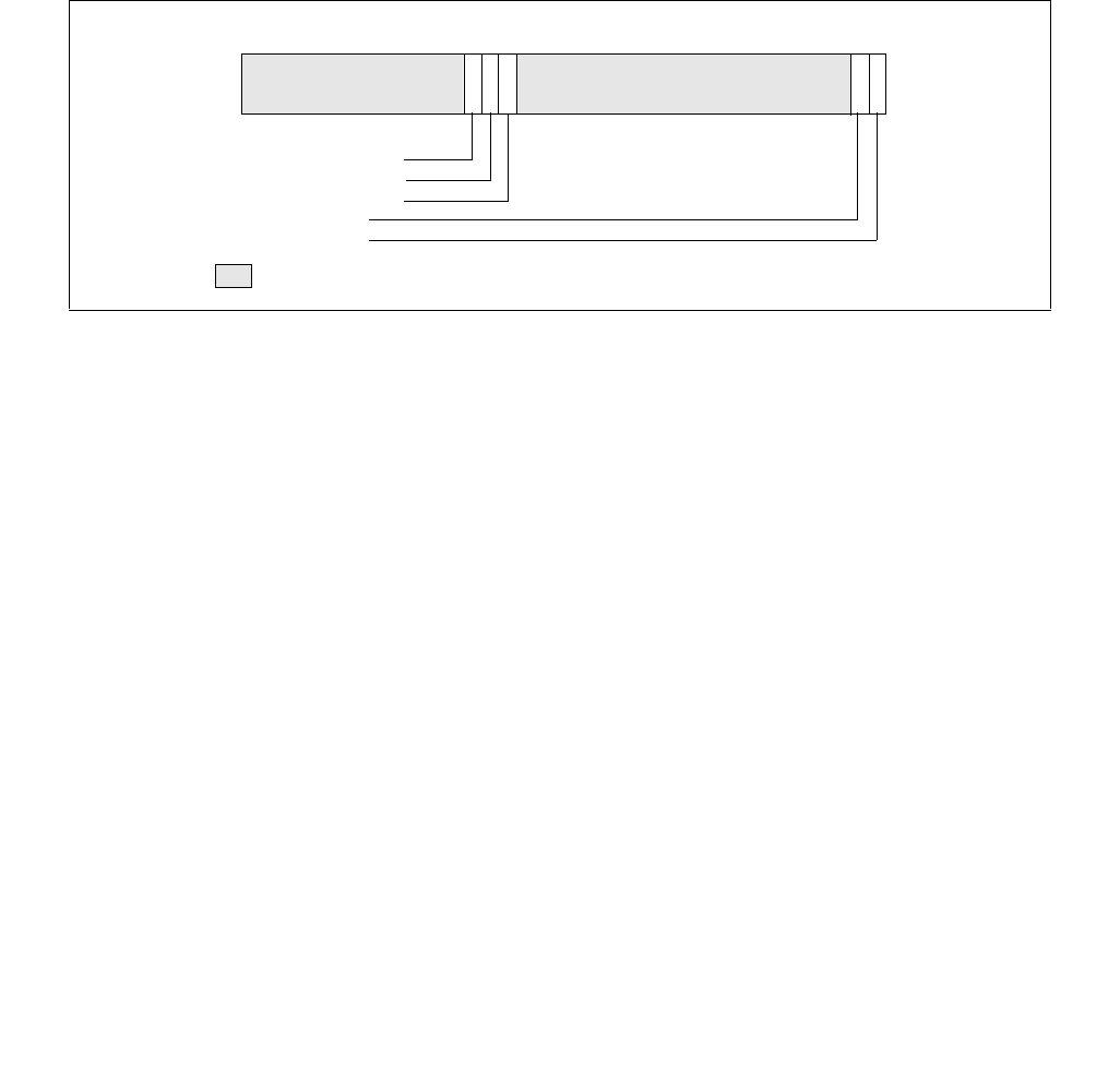
18-8 Vol. 3B
PERFORMANCE MONITORING
•Enable field (lowest 2 bits within each 4-bit control) — When bit 0 is set, performance counting is
enabled in the corresponding fixed-function performance counter to increment while the target condition
associated with the architecture performance event occurred at ring 0. When bit 1 is set, performance counting
is enabled in the corresponding fixed-function performance counter to increment while the target condition
associated with the architecture performance event occurred at ring greater than 0. Writing 0 to both bits stops
the performance counter. Writing a value of 11B enables the counter to increment irrespective of privilege
levels.
•PMI field (the fourth bit within each 4-bit control) — When set, the logical processor generates an
exception through its local APIC on overflow condition of the respective fixed-function counter.
IA32_PERF_GLOBAL_CTRL MSR provides single-bit controls to enable counting of each performance counter.
Figure 18-3 shows the layout of IA32_PERF_GLOBAL_CTRL. Each enable bit in IA32_PERF_GLOBAL_CTRL is
AND’ed with the enable bits for all privilege levels in the respective IA32_PERFEVTSELx or
IA32_PERF_FIXED_CTR_CTRL MSRs to start/stop the counting of respective counters. Counting is enabled if the
AND’ed results is true; counting is disabled when the result is false.
The behavior of the fixed function performance counters supported by architectural performance version 2 is
expected to be consistent on all processors that support those counters, and is defined as follows.
Figure 18-3. Layout of IA32_PERF_GLOBAL_CTRL MSR
IA32_FIXED_CTR2 enable
IA32_FIXED_CTR1 enable
IA32_FIXED_CTR0 enable
IA32_PMC1 enable
210
IA32_PMC0 enable
3132333435
Reserved
63

Vol. 3B 18-9
PERFORMANCE MONITORING
IA32_PERF_GLOBAL_STATUS MSR provides single-bit status for software to query the overflow condition of each
performance counter. IA32_PERF_GLOBAL_STATUS[bit 62] indicates overflow conditions of the DS area data
buffer. IA32_PERF_GLOBAL_STATUS[bit 63] provides a CondChgd bit to indicate changes to the state of perfor-
mance monitoring hardware. Figure 18-4 shows the layout of IA32_PERF_GLOBAL_STATUS. A value of 1 in bits 0,
1, 32 through 34 indicates a counter overflow condition has occurred in the associated counter.
When a performance counter is configured for PEBS, overflow condition in the counter generates a performance-
monitoring interrupt signaling a PEBS event. On a PEBS event, the processor stores data records into the buffer
area (see Section 18.15.5), clears the counter overflow status., and sets the “OvfBuffer” bit in
IA32_PERF_GLOBAL_STATUS.
Table 18-2. Association of Fixed-Function Performance Counters with Architectural Performance Events
Fixed-Function Performance Counter Address Event Mask Mnemonic Description
MSR_PERF_FIXED_CTR0/IA32_FIXED_CTR0 309H INST_RETIRED.ANY This event counts the number of
instructions that retire execution. For
instructions that consist of multiple
uops, this event counts the
retirement of the last uop of the
instruction. The counter continues
counting during hardware interrupts,
traps, and in-side interrupt handlers.
MSR_PERF_FIXED_CTR1//IA32_FIXED_CTR1 30AH CPU_CLK_UNHALTED.THREAD
CPU_CLK_UNHALTED.CORE
The CPU_CLK_UNHALTED.THREAD
event counts the number of core
cycles while the logical processor is
not in a halt state.
If there is only one logical processor
in a processor core,
CPU_CLK_UNHALTED.CORE counts
the unhalted cycles of the processor
core.
The core frequency may change from
time to time due to transitions
associated with Enhanced Intel
SpeedStep Technology or TM2. For
this reason this event may have a
changing ratio with regards to time.
MSR_PERF_FIXED_CTR2//IA32_FIXED_CTR2 30BH CPU_CLK_UNHALTED.REF_TSC This event counts the number of
reference cycles at the TSC rate
when the core is not in a halt state
and not in a TM stop-clock state. The
core enters the halt state when it is
running the HLT instruction or the
MWAIT instruction. This event is not
affected by core frequency changes
(e.g., P states) but counts at the same
frequency as the time stamp counter.
This event can approximate elapsed
time while the core was not in a halt
state and not in a TM stopclock state.
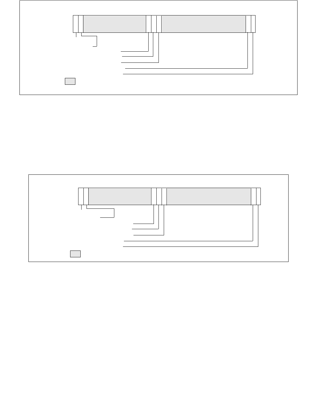
18-10 Vol. 3B
PERFORMANCE MONITORING
IA32_PERF_GLOBAL_OVF_CTL MSR allows software to clear overflow indicator(s) of any general-purpose or fixed-
function counters via a single WRMSR. Software should clear overflow indications when
•Setting up new values in the event select and/or UMASK field for counting or interrupt-based event sampling.
•Reloading counter values to continue collecting next sample.
•Disabling event counting or interrupt-based event sampling.
The layout of IA32_PERF_GLOBAL_OVF_CTL is shown in Figure 18-5.
18.2.3 Architectural Performance Monitoring Version 3
Processors supporting architectural performance monitoring version 3 also supports version 1 and 2, as well as
capability enumerated by CPUID leaf 0AH. Specifically, version 3 provides the following enhancement in perfor-
mance monitoring facilities if a processor core comprising of more than one logical processor, i.e. a processor core
supporting Intel Hyper-Threading Technology or simultaneous multi-threading capability:
•AnyThread counting for processor core supporting two or more logical processors. The interface that supports
AnyThread counting include:
— Each IA32_PERFEVTSELx MSR (starting at MSR address 186H) support the bit field layout defined in Figure
18-6.
Figure 18-4. Layout of IA32_PERF_GLOBAL_STATUS MSR
Figure 18-5. Layout of IA32_PERF_GLOBAL_OVF_CTRL MSR
62
IA32_FIXED_CTR2 Overflow
IA32_FIXED_CTR1 Overflow
IA32_FIXED_CTR0 Overflow
IA32_PMC1 Overflow
210
IA32_PMC0 Overflow
3132333435
Reserved
63
CondChgd
OvfDSBuffer
62
IA32_FIXED_CTR2 ClrOverflow
IA32_FIXED_CTR1 ClrOverflow
IA32_FIXED_CTR0 ClrOverflow
IA32_PMC1 ClrOverflow
210
IA32_PMC0 ClrOverflow
3132333435
Reserved
63
ClrCondChgd
ClrOvfDSBuffer
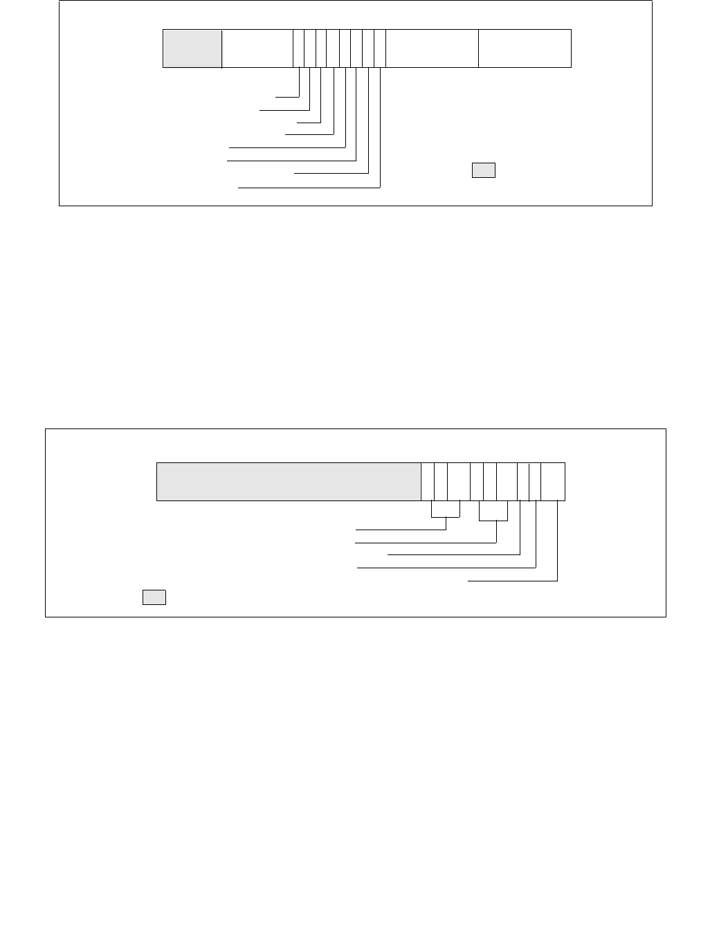
Vol. 3B 18-11
PERFORMANCE MONITORING
Bit 21 (AnyThread) of IA32_PERFEVTSELx is supported in architectural performance monitoring version 3 for
processor core comprising of two or more logical processors. When set to 1, it enables counting the associated
event conditions (including matching the thread’s CPL with the OS/USR setting of IA32_PERFEVTSELx)
occurring across all logical processors sharing a processor core. When bit 21 is 0, the counter only increments
the associated event conditions (including matching the thread’s CPL with the OS/USR setting of
IA32_PERFEVTSELx) occurring in the logical processor which programmed the IA32_PERFEVTSELx MSR.
— Each fixed-function performance counter IA32_FIXED_CTRx (starting at MSR address 309H) is configured
by a 4-bit control block in the IA32_PERF_FIXED_CTR_CTRL MSR. The control block also allow thread-
specificity configuration using an AnyThread bit. The layout of IA32_PERF_FIXED_CTR_CTRL MSR is
shown.
Each control block for a fixed-function performance counter provides a AnyThread (bit position 2 + 4*N, N=
0, 1, etc.) bit. When set to 1, it enables counting the associated event conditions (including matching the
thread’s CPL with the ENABLE setting of the corresponding control block of IA32_PERF_FIXED_CTR_CTRL)
occurring across all logical processors sharing a processor core. When an AnyThread bit is 0 in
IA32_PERF_FIXED_CTR_CTRL, the corresponding fixed counter only increments the associated event
conditions occurring in the logical processor which programmed the IA32_PERF_FIXED_CTR_CTRL MSR.
•The IA32_PERF_GLOBAL_CTRL, IA32_PERF_GLOBAL_STATUS, IA32_PERF_GLOBAL_OVF_CTRL MSRs provide
single-bit controls/status for each general-purpose and fixed-function performance counter. Figure 18-8 and
Figure 18-9 show the layout of these MSRs for N general-purpose performance counters (where N is reported
by CPUID.0AH:EAX[15:8]) and three fixed-function counters.
Figure 18-6. Layout of IA32_PERFEVTSELx MSRs Supporting Architectural Performance Monitoring Version 3
Figure 18-7. IA32_FIXED_CTR_CTRL MSR Supporting Architectural Performance Monitoring Version 3
31
INV—Invert counter mask
EN—Enable counters
INT—APIC interrupt enable
PC—Pin control
870
Event Select
E—Edge detect
OS—Operating system mode
USR—User Mode
Counter Mask E
E
N
I
N
T
19 1618 15172021222324
Reserved
I
N
V
P
C
U
S
R
O
SUnit Mask (UMASK)
(CMASK)
63
ANY—Any Thread
A
N
Y
Cntr2 — Controls for IA32_FIXED_CTR2
Cntr1 — Controls for IA32_FIXED_CTR1
PMI — Enable PMI on overflow on IA32_FIXED_CTR0
AnyThread — AnyThread for IA32_FIXED_CTR0
87 0
ENABLE — IA32_FIXED_CTR0. 0: disable; 1: OS; 2: User; 3: All ring levels
E
N
P
M
I
11 312 1
Reserved
63 2
E
N
E
N
495
P
P
M
M
I
I
A
N
Y
A
N
Y
A
N
Y
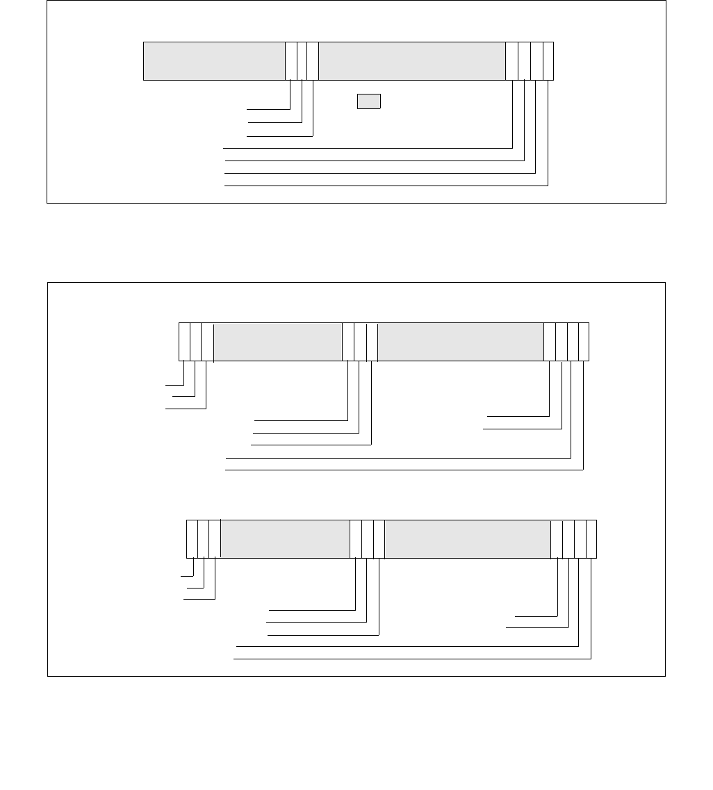
18-12 Vol. 3B
PERFORMANCE MONITORING
NOTE
The number of general-purpose performance monitoring counters (i.e., N in Figure 18-9) can vary
across processor generations within a processor family, across processor families, or could be
different depending on the configuration chosen at boot time in the BIOS regarding Intel Hyper
Threading Technology, (e.g. N=2 for 45 nm Intel Atom processors; N =4 for processors based on
the Nehalem microarchitecture; for processors based on the Sandy Bridge microarchitecture, N =
4 if Intel Hyper Threading Technology is active and N=8 if not active). In addition, the number of
counters may vary from the number of physical counters present on the hardware, because an
agent running at a higher privilege level (e.g., a VMM) may not expose all counters.
Figure 18-8. Layout of Global Performance Monitoring Control MSR
Figure 18-9. Global Performance Monitoring Overflow Status and Control MSRs
IA32_FIXED_CTR2 enable
IA32_FIXED_CTR1 enable
IA32_FIXED_CTR0 enable
IA32_PMC(N-1) enable
.. 10
.................... enable
3132333435
Reserved
63 ..N
IA32_PMC1 enable
IA32_PMC0 enable
Global Enable Controls IA32_PERF_GLOBAL_CTRL
62
IA32_FIXED_CTR2 Overflow
IA32_FIXED_CTR1 Overflow
IA32_FIXED_CTR0 Overflow
IA32_PMC1 Overflow
.. 10
IA32_PMC0 Overflow
3132333435
63
CondChgd
OvfDSBuffer
..N
...................... Overflow
IA32_PMC(N-1) Overflow
Global Overflow Status IA32_PERF_GLOBAL_STATUS
62
IA32_FIXED_CTR2 ClrOverflow
IA32_FIXED_CTR1 ClrOverflow
IA32_FIXED_CTR0 ClrOverflow
IA32_PMC1 ClrOverflow
.. 10
IA32_PMC0 ClrOverflow
3132333435
63
ClrCondChgd
ClrOvfDSBuffer
Global Overflow Status IA32_PERF_GLOBAL_OVF_CTRL
........................ ClrOverflow
IA32_PMC(N-1) ClrOverflow
N..
ClrOvfUncore
OvfUncore
61

Vol. 3B 18-13
PERFORMANCE MONITORING
18.2.3.1 AnyThread Counting and Software Evolution
The motivation for characterizing software workload over multiple software threads running on multiple logical
processors of the same processor core originates from a time earlier than the introduction of the AnyThread inter-
face in IA32_PERFEVTSELx and IA32_FIXED_CTR_CTRL. While AnyThread counting provides some benefits in
simple software environments of an earlier era, the evolution contemporary software environments introduce
certain concepts and pre-requisites that AnyThread counting does not comply with.
One example is the proliferation of software environments that support multiple virtual machines (VM) under VMX
(see Chapter 23, “Introduction to Virtual-Machine Extensions”) where each VM represents a domain separated
from one another.
A Virtual Machine Monitor (VMM) that manages the VMs may allow individual VM to employ performance moni-
toring facilities to profiles the performance characteristics of a workload. The use of the Anythread interface in
IA32_PERFEVTSELx and IA32_FIXED_CTR_CTRL is discouraged with software environments supporting virtualiza-
tion or requiring domain separation.
Specifically, Intel recommends VMM:
•configure the MSR bitmap to cause VM-exits for WRMSR to IA32_PERFEVTSELx and IA32_FIXED_CTR_CTRL in
VMX non-Root operation (see CHAPTER 24 for additional information),
•clear the AnyThread bit of IA32_PERFEVTSELx and IA32_FIXED_CTR_CTRL in the MSR-load lists for VM exits
and VM entries (see CHAPTER 24, CHAPTER 26, and CHAPTER 27).
Even when operating in simpler legacy software environments which might not emphasize the pre-requisites of a
virtualized software environment, the use of the AnyThread interface should be moderated and follow any event-
specific guidance where explicitly noted (see relevant sections of Chapter 19, “Performance Monitoring Events”).
18.2.4 Architectural Performance Monitoring Version 4
Processors supporting architectural performance monitoring version 4 also supports version 1, 2, and 3, as well as
capability enumerated by CPUID leaf 0AH. Version 4 introduced a streamlined PMI overhead mitigation interface
that replaces the legacy semantic behavior but retains the same control interface in
IA32_DEBUGCTL.Freeze_LBRs_On_PMI and Freeze_PerfMon_On_PMI. Specifically version 4 provides the following
enhancement:
•New indicators (LBR_FRZ, CTR_FRZ) in IA32_PERF_GLOBAL_STATUS, see Section 18.2.4.1.
•Streamlined Freeze/PMI Overhead management interfaces to use IA32_DEBUGCTL.Freeze_LBRs_On_PMI and
IA32_DEBUGCTL.Freeze_PerfMon_On_PMI: see Section 18.2.4.1. Legacy semantics of Freeze_LBRs_On_PMI
and Freeze_PerfMon_On_PMI (applicable to version 2 and 3) are not supported with version 4 or higher.
•Fine-grain separation of control interface to manage overflow/status of IA32_PERF_GLOBAL_STATUS and
read-only performance counter enabling interface in IA32_PERF_GLOBAL_STATUS: see Section 18.2.4.2.
•Performance monitoring resource in-use MSR to facilitate cooperative sharing protocol between perfmon-
managing privilege agents.
18.2.4.1 Enhancement in IA32_PERF_GLOBAL_STATUS
The IA32_PERF_GLOBAL_STATUS MSR provides the following indicators with architectural performance monitoring
version 4:
•IA32_PERF_GLOBAL_STATUS.LBR_FRZ[bit 58]: This bit is set due to the following conditions:
— IA32_DEBUGCTL.FREEZE_LBR_ON_PMI has been set by the profiling agent, and
— A performance counter, configured to generate PMI, has overflowed to signal a PMI. Consequently the LBR
stack is frozen.
Effectively, the IA32_PERF_GLOBAL_STATUS.LBR_FRZ bit also serve as an read-only control to enable
capturing data in the LBR stack. To enable capturing LBR records, the following expression must hold with
architectural perfmon version 4 or higher:
— (IA32_DEBUGCTL.LBR & (!IA32_PERF_GLOBAL_STATUS.LBR_FRZ) ) =1
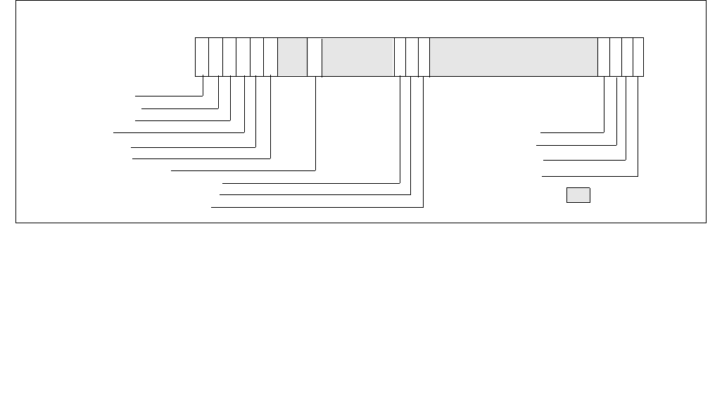
18-14 Vol. 3B
PERFORMANCE MONITORING
•IA32_PERF_GLOBAL_STATUS.CTR_FRZ[bit 59]: This bit is set due to the following conditions:
— IA32_DEBUGCTL.FREEZE_PERFMON_ON_PMI has been set by the profiling agent, and
— A performance counter, configured to generate PMI, has overflowed to signal a PMI. Consequently, all the
performance counters are frozen.
Effectively, the IA32_PERF_GLOBAL_STATUS.CTR_FRZ bit also serve as an read-only control to enable
programmable performance counters and fixed counters in the core PMU. To enable counting with the
performance counters, the following expression must hold with architectural perfmon version 4 or higher:
•(IA32_PERFEVTSELn.EN & IA32_PERF_GLOBAL_CTRL.PMCn &
(!IA32_PERF_GLOBAL_STATUS.CTR_FRZ) ) = 1 for programmable counter ‘n’, or
•(IA32_PERF_FIXED_CRTL.ENi & IA32_PERF_GLOBAL_CTRL.FCi &
(!IA32_PERF_GLOBAL_STATUS.CTR_FRZ) ) = 1 for fixed counter ‘i’
The read-only enable interface IA32_PERF_GLOBAL_STATUS.CTR_FRZ provides a more efficient flow for a PMI
handler to use IA32_DEBUGCTL.Freeza_Perfmon_On_PMI to filter out data that may distort target workload anal-
ysis, see Table 17-3. It should be noted the IA32_PERF_GLOBAL_CTRL register continue to serve as the primary
interface to control all performance counters of the logical processor.
For example, when the Freeze-On-PMI mode is not being used, a PMI handler would be setting
IA32_PERF_GLOBAL_CTRL as the very last step to commence the overall operation after configuring the individual
counter registers, controls and PEBS facility. This does not only assure atomic monitoring but also avoids unneces-
sary complications (e.g. race conditions) when software attempts to change the core PMU configuration while some
counters are kept enabled.
Additionally, IA32_PERF_GLOBAL_STATUS.TraceToPAPMI[bit 55]: On processors that support Intel Processor Trace
and configured to store trace output packets to physical memory using the ToPA scheme, bit 55 is set when a PMI
occurred due to a ToPA entry memory buffer was completely filled.
IA32_PERF_GLOBAL_STATUS also provides an indicator to distinguish interaction of performance monitoring oper-
ations with other side-band activities, which apply Intel SGX on processors that support SGX (For additional infor-
mation about Intel SGX, see “Intel® Software Guard Extensions Programming Reference”.):
•IA32_PERF_GLOBAL_STATUS.ASCI[bit 60]: This bit is set when data accumulated in any of the configured
performance counters (i.e. IA32_PMCx or IA32_FIXED_CTRx) may include contributions from direct or indirect
operation of Intel SGX to protect an enclave (since the last time IA32_PERF_GLOBAL_STATUS.ASCI was
cleared).
Note, a processor’s support for IA32_PERF_GLOBAL_STATUS.TraceToPAPMI[bit 55] is enumerated as a result of
CPUID enumerated capability of Intel Processor Trace and the use of the ToPA buffer scheme. Support of
IA32_PERF_GLOBAL_STATUS.ASCI[bit 60] is enumerated by the CPUID enumeration of Intel SGX.
Figure 18-10. IA32_PERF_GLOBAL_STATUS MSR and Architectural Perfmon Version 4
Reserved
62
IA32_FIXED_CTR2 Overflow
IA32_FIXED_CTR1 Overflow
IA32_FIXED_CTR0 Overflow
TraceToPAPMI
.. 10
IA32_PMC0 Overflow
3132333435
63
CondChgd
OvfDSBuffer
..N
...................... Overflow
IA32_PMC(N-1) Overflow
OvfUncore
61
IA32_PMC1 Overflow
60 59 58 55
ASCI
LBR_Frz
CTR_Frz
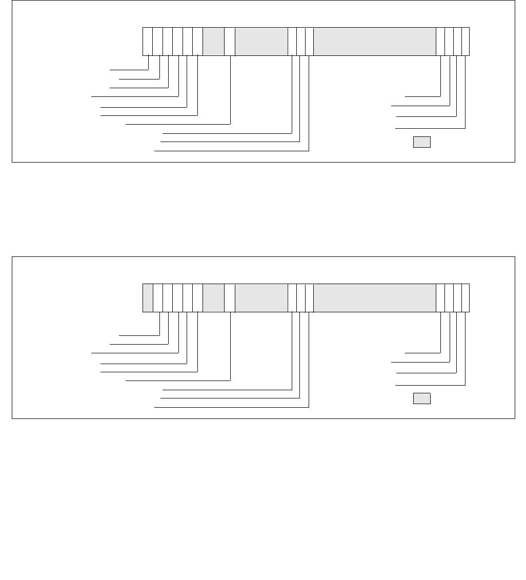
Vol. 3B 18-15
PERFORMANCE MONITORING
18.2.4.2 IA32_PERF_GLOBAL_STATUS_RESET and IA32_PERF_GLOBAL_STATUS_SET MSRS
With architectural performance monitoring version 3 and lower, clearing of the set bits in
IA32_PERF_GLOBAL_STATUS MSR by software is done via IA32_PERF_GLOBAL_OVF_CTRL MSR. Starting with
architectural performance monitoring version 4, software can manage the overflow and other indicators in
IA32_PERF_GLOBAL_STATUS using separate interfaces to set or clear individual bits.
The address and the architecturally-defined bits of IA32_PERF_GLOBAL_OVF_CTRL is inherited by
IA32_PERF_GLOBAL_STATUS_RESET (see Figure 18-11). Further, IA32_PERF_GLOBAL_STATUS_RESET provides
additional bit fields to clear the new indicators in IA32_PERF_GLOBAL_STATUS described in Section 18.2.4.1.
The IA32_PERF_GLOBAL_STATUS_SET MSR is introduced with architectural performance monitoring version 4. It
allows software to set individual bits in IA32_PERF_GLOBAL_STATUS. The IA32_PERF_GLOBAL_STATUS_SET
interface can be used by a VMM to virtualize the state of IA32_PERF_GLOBAL_STATUS across VMs.
18.2.4.3 IA32_PERF_GLOBAL_INUSE MSR
In a contemporary software environment, multiple privileged service agents may wish to employ the processor’s
performance monitoring facilities. The IA32_MISC_ENABLE.PERFMON_AVAILABLE[bit 7] interface could not serve
Figure 18-11. IA32_PERF_GLOBAL_STATUS_RESET MSR and Architectural Perfmon Version 4
Figure 18-12. IA32_PERF_GLOBAL_STATUS_SET MSR and Architectural Perfmon Version 4
Reserved
62
Clr IA32_FIXED_CTR2 Ovf
Clr IA32_FIXED_CTR1 Ovf
Clr IA32_FIXED_CTR0 Ovf
Clr TraceToPAPMI
.. 10
Clr IA32_PMC0 Ovf
3132333435
63
Clr CondChgd
Clr OvfDSBuffer
..N
Clr ...................... Ovf
Clr IA32_PMC(N-1) Ovf
Clr OvfUncore
61
Clr IA32_PMC1 Ovf
60 59 58 55
Clr ASCI
Clr LBR_Frz
Clr CTR_Frz
Reserved
Set IA32_FIXED_CTR2 Ovf
Set IA32_FIXED_CTR1 Ovf
Set IA32_FIXED_CTR0 Ovf
Set TraceToPAPMI
.. 10
Set IA32_PMC0 Ovf
3132333435
Set OvfDSBuffer
..N
Set ...................... Ovf
Set IA32_PMC(N-1) Ovf
Set OvfUncore
Set IA32_PMC1 Ovf
55
Set ASCI
Set LBR_Frz
Set CTR_Frz
63 62 61 60 59 58
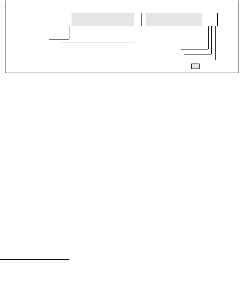
18-16 Vol. 3B
PERFORMANCE MONITORING
the need of multiple agent adequately. A white paper, “Performance Monitoring Unit Sharing Guideline”1, proposed
a cooperative sharing protocol that is voluntary for participating software agents.
Architectural performance monitoring version 4 introduces a new MSR, IA32_PERF_GLOBAL_INUSE, that simplifies
the task of multiple cooperating agents to implement the sharing protocol.
The layout of IA32_PERF_GLOBAL_INUSE is shown in Figure 18-13.
The IA32_PERF_GLOBAL_INUSE MSR provides an “InUse” bit for each programmable performance counter and
fixed counter in the processor. Additionally, it includes an indicator if the PMI mechanism has been configured by a
profiling agent.
•IA32_PERF_GLOBAL_INUSE.PERFEVTSEL0_InUse[bit 0]: This bit reflects the logical state of
(IA32_PERFEVTSEL0[7:0] != 0).
•IA32_PERF_GLOBAL_INUSE.PERFEVTSEL1_InUse[bit 1]: This bit reflects the logical state of
(IA32_PERFEVTSEL1[7:0] != 0).
•IA32_PERF_GLOBAL_INUSE.PERFEVTSEL2_InUse[bit 2]: This bit reflects the logical state of
(IA32_PERFEVTSEL2[7:0] != 0).
•IA32_PERF_GLOBAL_INUSE.PERFEVTSELn_InUse[bit n]: This bit reflects the logical state of
(IA32_PERFEVTSELn[7:0] != 0), n < CPUID.0AH:EAX[15:8].
•IA32_PERF_GLOBAL_INUSE.FC0_InUse[bit 32]: This bit reflects the logical state of
(IA32_FIXED_CTR_CTRL[1:0] != 0).
•IA32_PERF_GLOBAL_INUSE.FC1_InUse[bit 33]: This bit reflects the logical state of
(IA32_FIXED_CTR_CTRL[5:4] != 0).
•IA32_PERF_GLOBAL_INUSE.FC2_InUse[bit 34]: This bit reflects the logical state of
(IA32_FIXED_CTR_CTRL[9:8] != 0).
•IA32_PERF_GLOBAL_INUSE.PMI_InUse[bit 63]: This bit is set if any one of the following bit is set:
— IA32_PERFEVTSELn.INT[bit 20], n < CPUID.0AH:EAX[15:8].
— IA32_FIXED_CTR_CTRL.ENi_PMI, i = 0, 1, 2.
— Any IA32_PEBS_ENABLES bit which enables PEBS for a general-purpose or fixed-function performance
counter.
1. Available at http://www.intel.com/sdm
Figure 18-13. IA32_PERF_GLOBAL_INUSE MSR and Architectural Perfmon Version 4
Reserved
PMI InUse
FIXED_CTR2 InUse
FIXED_CTR1 InUse
.. 10
PERFEVTSEL0 InUse
3132333435
63 ..N
....................... InUse
PERFEVTSEL(N-1) InUse
PERFEVTSEL1 InUse
FIXED_CTR0 InUse
N = CPUID.0AH:EAX[15:8]

Vol. 3B 18-17
PERFORMANCE MONITORING
18.2.5 Full-Width Writes to Performance Counter Registers
The general-purpose performance counter registers IA32_PMCx are writable via WRMSR instruction. However, the
value written into IA32_PMCx by WRMSR is the signed extended 64-bit value of the EAX[31:0] input of WRMSR.
A processor that supports full-width writes to the general-purpose performance counters enumerated by
CPUID.0AH:EAX[15:8] will set IA32_PERF_CAPABILITIES[13] to enumerate its full-width-write capability See
Figure 18-63.
If IA32_PERF_CAPABILITIES.FW_WRITE[bit 13] =1, each IA32_PMCi is accompanied by a corresponding alias
address starting at 4C1H for IA32_A_PMC0.
The bit width of the performance monitoring counters is specified in CPUID.0AH:EAX[23:16].
If IA32_A_PMCi is present, the 64-bit input value (EDX:EAX) of WRMSR to IA32_A_PMCi will cause IA32_PMCi to
be updated by:
COUNTERWIDTH = CPUID.0AH:EAX[23:16] bit width of the performance monitoring counter
IA32_PMCi[COUNTERWIDTH-1:32] ← EDX[COUNTERWIDTH-33:0]);
IA32_PMCi[31:0] ← EAX[31:0];
EDX[63:COUNTERWIDTH] are reserved
18.3 PERFORMANCE MONITORING (INTEL® CORE™ PROCESSORS AND INTEL®
XEON® PROCESSORS)
18.3.1 Performance Monitoring for Processors Based on Intel® Microarchitecture Code Name
Nehalem
Intel Core i7 processor family2 supports architectural performance monitoring capability with version ID 3 (see
Section 18.2.3) and a host of non-architectural monitoring capabilities. The Intel Core i7 processor family is based
on Intel® microarchitecture code name Nehalem, and provides four general-purpose performance counters
(IA32_PMC0, IA32_PMC1, IA32_PMC2, IA32_PMC3) and three fixed-function performance counters
(IA32_FIXED_CTR0, IA32_FIXED_CTR1, IA32_FIXED_CTR2) in the processor core.
Non-architectural performance monitoring in Intel Core i7 processor family uses the IA32_PERFEVTSELx MSR to
configure a set of non-architecture performance monitoring events to be counted by the corresponding general-
purpose performance counter. The list of non-architectural performance monitoring events is listed in Table 19-29.
Non-architectural performance monitoring events fall into two broad categories:
•Performance monitoring events in the processor core: These include many events that are similar to
performance monitoring events available to processor based on Intel Core microarchitecture. Additionally,
there are several enhancements in the performance monitoring capability for detecting microarchitectural
conditions in the processor core or in the interaction of the processor core to the off-core sub-systems in the
physical processor package. The off-core sub-systems in the physical processor package is loosely referred to
as “uncore“.
•Performance monitoring events in the uncore: The uncore sub-system is shared by more than one processor
cores in the physical processor package. It provides additional performance monitoring facility outside of
IA32_PMCx and performance monitoring events that are specific to the uncore sub-system.
Architectural and non-architectural performance monitoring events in Intel Core i7 processor family support thread
qualification using bit 21 of IA32_PERFEVTSELx MSR.
The bit fields within each IA32_PERFEVTSELx MSR are defined in Figure 18-6 and described in Section 18.2.1.1 and
Section 18.2.3.
2. Intel Xeon processor 5500 series and 3400 series are also based on Intel microarchitecture code name Nehalem; the performance
monitoring facilities described in this section generally also apply.
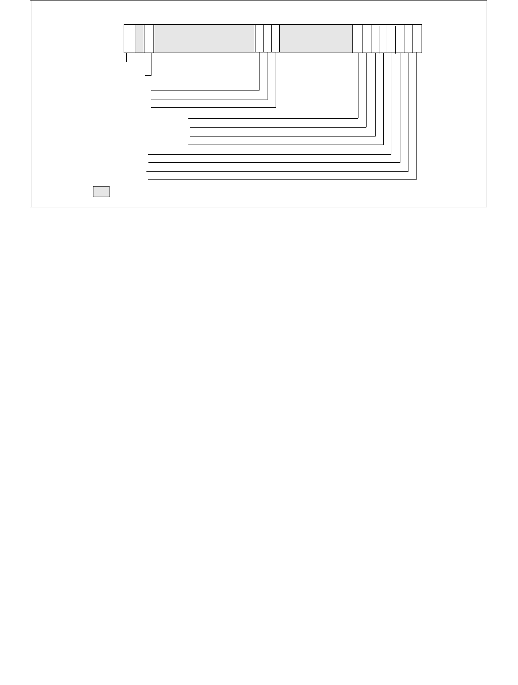
18-18 Vol. 3B
PERFORMANCE MONITORING
18.3.1.1 Enhancements of Performance Monitoring in the Processor Core
The notable enhancements in the monitoring of performance events in the processor core include:
•Four general purpose performance counters, IA32_PMCx, associated counter configuration MSRs,
IA32_PERFEVTSELx, and global counter control MSR supporting simplified control of four counters. Each of the
four performance counter can support processor event based sampling (PEBS) and thread-qualification of
architectural and non-architectural performance events. Width of IA32_PMCx supported by hardware has been
increased. The width of counter reported by CPUID.0AH:EAX[23:16] is 48 bits. The PEBS facility in Intel micro-
architecture code name Nehalem has been enhanced to include new data format to capture additional infor-
mation, such as load latency.
•Load latency sampling facility. Average latency of memory load operation can be sampled using load-latency
facility in processors based on Intel microarchitecture code name Nehalem. This field measures the load latency
from load's first dispatch of till final data writeback from the memory subsystem. The latency is reported for
retired demand load operations and in core cycles (it accounts for re-dispatches). This facility is used in
conjunction with the PEBS facility.
•Off-core response counting facility. This facility in the processor core allows software to count certain
transaction responses between the processor core to sub-systems outside the processor core (uncore).
Counting off-core response requires additional event qualification configuration facility in conjunction with
IA32_PERFEVTSELx. Two off-core response MSRs are provided to use in conjunction with specific event codes
that must be specified with IA32_PERFEVTSELx.
NOTE
The number of counters available to software may vary from the number of physical counters
present on the hardware, because an agent running at a higher privilege level (e.g., a VMM) may
not expose all counters. CPUID.0AH:EAX[15:8] reports the MSRs available to software; see Section
18.2.1.
18.3.1.1.1 Processor Event Based Sampling (PEBS)
All four general-purpose performance counters, IA32_PMCx, can be used for PEBS if the performance event
supports PEBS. Software uses IA32_MISC_ENABLE[7] and IA32_MISC_ENABLE[12] to detect whether the perfor-
mance monitoring facility and PEBS functionality are supported in the processor. The MSR IA32_PEBS_ENABLE
provides 4 bits that software must use to enable which IA32_PMCx overflow condition will cause the PEBS record to
be captured.
Figure 18-14. IA32_PERF_GLOBAL_STATUS MSR
CHG (R/W)
OVF_PMI (R/W)
87 0
32 31
Reserved
63 2
4
31 56
62 6061
OVF_PC7 (R/O), if CCNT>7
OVF_PC6 (R/O), if CCNT>6
OVF_PC5 (R/O), if CCNT>5
OVF_PC4 (R/O), if CCNT>4
OVF_PC3 (R/O)
OVF_PC2 (R/O)
OVF_PC1 (R/O)
OVF_PC0 (R/O)
RESET Value — 00000000_00000000H
OVF_FC2 (R/O)
OVF_FC1 (R/O)
353433
OVF_FC0 (R/O)
CCNT: CPUID.AH:EAX[15:8]
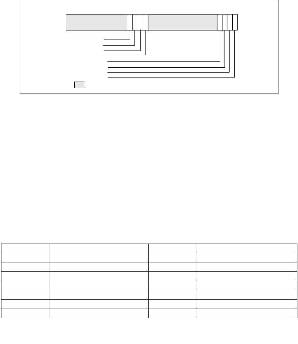
Vol. 3B 18-19
PERFORMANCE MONITORING
Additionally, the PEBS record is expanded to allow latency information to be captured. The MSR
IA32_PEBS_ENABLE provides 4 additional bits that software must use to enable latency data recording in the PEBS
record upon the respective IA32_PMCx overflow condition. The layout of IA32_PEBS_ENABLE for processors based
on Intel microarchitecture code name Nehalem is shown in Figure 18-15.
When a counter is enabled to capture machine state (PEBS_EN_PMCx = 1), the processor will write machine state
information to a memory buffer specified by software as detailed below. When the counter IA32_PMCx overflows
from maximum count to zero, the PEBS hardware is armed.
Upon occurrence of the next PEBS event, the PEBS hardware triggers an assist and causes a PEBS record to be
written. The format of the PEBS record is indicated by the bit field IA32_PERF_CAPABILITIES[11:8] (see
Figure 18-63).
The behavior of PEBS assists is reported by IA32_PERF_CAPABILITIES[6] (see Figure 18-63). The return instruc-
tion pointer (RIP) reported in the PEBS record will point to the instruction after (+1) the instruction that causes the
PEBS assist. The machine state reported in the PEBS record is the machine state after the instruction that causes
the PEBS assist is retired. For instance, if the instructions:
mov eax, [eax] ; causes PEBS assist
nop
are executed, the PEBS record will report the address of the nop, and the value of EAX in the PEBS record will show
the value read from memory, not the target address of the read operation.
The PEBS record format is shown in Table 18-3, and each field in the PEBS record is 64 bits long. The PEBS record
format, along with debug/store area storage format, does not change regardless of IA-32e mode is active or not.
CPUID.01H:ECX.DTES64[bit 2] reports whether the processor's DS storage format support is mode-independent.
When set, it uses 64-bit DS storage format.
Figure 18-15. Layout of IA32_PEBS_ENABLE MSR
Table 18-3. PEBS Record Format for Intel Core i7 Processor Family
Byte Offset Field Byte Offset Field
00H R/EFLAGS 58H R9
08HR/EIP 60HR10
10HR/EAX 68HR11
18HR/EBX 70HR12
20HR/ECX 78HR13
28HR/EDX 80HR14
30HR/ESI 88HR15
LL_EN_PMC3 (R/W)
LL_EN_PMC2 (R/W)
87 0
LL_EN_PMC1 (R/W)
32 3
33 1
Reserved
63 24
31 5
6
343536
PEBS_EN_PMC3 (R/W)
PEBS_EN_PMC2 (R/W)
PEBS_EN_PMC1 (R/W)
PEBS_EN_PMC0 (R/W)
LL_EN_PMC0 (R/W)
RESET Value — 00000000_00000000H

18-20 Vol. 3B
PERFORMANCE MONITORING
In IA-32e mode, the full 64-bit value is written to the register. If the processor is not operating in IA-32e mode, 32-
bit value is written to registers with bits 63:32 zeroed. Registers not defined when the processor is not in IA-32e
mode are written to zero.
Bytes AFH:90H are enhancement to the PEBS record format. Support for this enhanced PEBS record format is indi-
cated by IA32_PERF_CAPABILITIES[11:8] encoding of 0001B.
The value written to bytes 97H:90H is the state of the IA32_PERF_GLOBAL_STATUS register before the PEBS assist
occurred. This value is written so software can determine which counters overflowed when this PEBS record was
written. Note that this field indicates the overflow status for all counters, regardless of whether they were
programmed for PEBS or not.
Programming PEBS Facility
Only a subset of non-architectural performance events in the processor support PEBS. The subset of precise events
are listed in Table 18-68. In addition to using IA32_PERFEVTSELx to specify event unit/mask settings and setting
the EN_PMCx bit in the IA32_PEBS_ENABLE register for the respective counter, the software must also initialize the
DS_BUFFER_MANAGEMENT_AREA data structure in memory to support capturing PEBS records for precise events.
NOTE
PEBS events are only valid when the following fields of IA32_PERFEVTSELx are all zero: AnyThread,
Edge, Invert, CMask.
The beginning linear address of the DS_BUFFER_MANAGEMENT_AREA data structure must be programmed into
the IA32_DS_AREA register. The layout of the DS_BUFFER_MANAGEMENT_AREA is shown in Figure 18-16.
•PEBS Buffer Base: This field is programmed with the linear address of the first byte of the PEBS buffer
allocated by software. The processor reads this field to determine the base address of the PEBS buffer. Software
should allocate this memory from the non-paged pool.
•PEBS Index: This field is initially programmed with the same value as the PEBS Buffer Base field, or the
beginning linear address of the PEBS buffer. The processor reads this field to determine the location of the next
PEBS record to write to. After a PEBS record has been written, the processor also updates this field with the
address of the next PEBS record to be written. The figure above illustrates the state of PEBS Index after the first
PEBS record is written.
•PEBS Absolute Maximum: This field represents the absolute address of the maximum length of the allocated
PEBS buffer plus the starting address of the PEBS buffer. The processor will not write any PEBS record beyond
the end of PEBS buffer, when PEBS Index equals PEBS Absolute Maximum. No signaling is generated when
PEBS buffer is full. Software must reset the PEBS Index field to the beginning of the PEBS buffer address to
continue capturing PEBS records.
38H R/EDI 90H IA32_PERF_GLOBAL_STATUS
40H R/EBP 98H Data Linear Address
48H R/ESP A0H Data Source Encoding
50H R8 A8H Latency value (core cycles)
Table 18-3. PEBS Record Format for Intel Core i7 Processor Family
Byte Offset Field Byte Offset Field
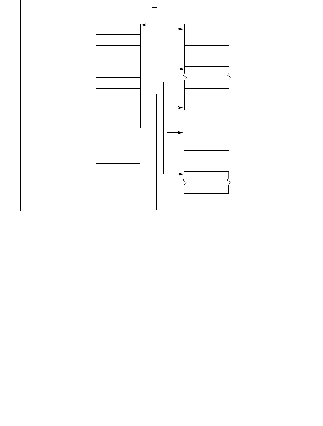
Vol. 3B 18-21
PERFORMANCE MONITORING
•PEBS Interrupt Threshold: This field specifies the threshold value to trigger a performance interrupt and
notify software that the PEBS buffer is nearly full. This field is programmed with the linear address of the first
byte of the PEBS record within the PEBS buffer that represents the threshold record. After the processor writes
a PEBS record and updates PEBS Index, if the PEBS Index reaches the threshold value of this field, the
processor will generate a performance interrupt. This is the same interrupt that is generated by a performance
counter overflow, as programmed in the Performance Monitoring Counters vector in the Local Vector Table of
the Local APIC. When a performance interrupt due to PEBS buffer full is generated, the
IA32_PERF_GLOBAL_STATUS.PEBS_Ovf bit will be set.
•PEBS CounterX Reset: This field allows software to set up PEBS counter overflow condition to occur at a rate
useful for profiling workload, thereby generating multiple PEBS records to facilitate characterizing the profile
the execution of test code. After each PEBS record is written, the processor checks each counter to see if it
overflowed and was enabled for PEBS (the corresponding bit in IA32_PEBS_ENABLED was set). If these
conditions are met, then the reset value for each overflowed counter is loaded from the DS Buffer Management
Area. For example, if counter IA32_PMC0 caused a PEBS record to be written, then the value of “PEBS Counter
0 Reset” would be written to counter IA32_PMC0. If a counter is not enabled for PEBS, its value will not be
modified by the PEBS assist.
Performance Counter Prioritization
Performance monitoring interrupts are triggered by a counter transitioning from maximum count to zero
(assuming IA32_PerfEvtSelX.INT is set). This same transition will cause PEBS hardware to arm, but not trigger.
PEBS hardware triggers upon detection of the first PEBS event after the PEBS hardware has been armed (a 0 to 1
transition of the counter). At this point, a PEBS assist will be undertaken by the processor.
Figure 18-16. PEBS Programming Environment
BTS Buffer Base
BTS Index
BTS Absolute
BTS Interrupt
PEBS Absolute
PEBS Interrupt
PEBS
Maximum
Maximum
Threshold
PEBS Index
PEBS Buffer Base
Threshold
Counter0 Reset
Reserved
0H
8H
10H
18H
20H
28H
30H
38H
40H
48H
50H
Branch Record 0
Branch Record 1
Branch Record n
PEBS Record 0
PEBS Record 1
PEBS Record n
BTS Buffer
PEBS Buffer
DS Buffer Management Area
IA32_DS_AREA MSR
58H
60H
PEBS
Counter1 Reset
PEBS
Counter2 Reset
PEBS
Counter3 Reset

18-22 Vol. 3B
PERFORMANCE MONITORING
Performance counters (fixed and general-purpose) are prioritized in index order. That is, counter IA32_PMC0 takes
precedence over all other counters. Counter IA32_PMC1 takes precedence over counters IA32_PMC2 and
IA32_PMC3, and so on. This means that if simultaneous overflows or PEBS assists occur, the appropriate action will
be taken for the highest priority performance counter. For example, if IA32_PMC1 cause an overflow interrupt and
IA32_PMC2 causes an PEBS assist simultaneously, then the overflow interrupt will be serviced first.
The PEBS threshold interrupt is triggered by the PEBS assist, and is by definition prioritized lower than the PEBS
assist. Hardware will not generate separate interrupts for each counter that simultaneously overflows. General-
purpose performance counters are prioritized over fixed counters.
If a counter is programmed with a precise (PEBS-enabled) event and programmed to generate a counter overflow
interrupt, the PEBS assist is serviced before the counter overflow interrupt is serviced. If in addition the PEBS inter-
rupt threshold is met, the
threshold interrupt is generated after the PEBS assist completes, followed by the counter overflow interrupt (two
separate interrupts are generated).
Uncore counters may be programmed to interrupt one or more processor cores (see Section 18.3.1.2). It is
possible for interrupts posted from the uncore facility to occur coincident with counter overflow interrupts from the
processor core. Software must check core and uncore status registers to determine the exact origin of counter
overflow interrupts.
18.3.1.1.2 Load Latency Performance Monitoring Facility
The load latency facility provides software a means to characterize the average load latency to different levels of
cache/memory hierarchy. This facility requires processor supporting enhanced PEBS record format in the PEBS
buffer, see Table 18-3. This field measures the load latency from load's first dispatch of till final data writeback from
the memory subsystem. The latency is reported for retired demand load operations and in core cycles (it accounts
for re-dispatches).
To use this feature software must assure:
•One of the IA32_PERFEVTSELx MSR is programmed to specify the event unit MEM_INST_RETIRED, and the
LATENCY_ABOVE_THRESHOLD event mask must be specified (IA32_PerfEvtSelX[15:0] = 100H). The corre-
sponding counter IA32_PMCx will accumulate event counts for architecturally visible loads which exceed the
programmed latency threshold specified separately in a MSR. Stores are ignored when this event is
programmed. The CMASK or INV fields of the IA32_PerfEvtSelX register used for counting load latency must be
0. Writing other values will result in undefined behavior.
•The MSR_PEBS_LD_LAT_THRESHOLD MSR is programmed with the desired latency threshold in core clock
cycles. Loads with latencies greater than this value are eligible for counting and latency data reporting. The
minimum value that may be programmed in this register is 3 (the minimum detectable load latency is 4 core
clock cycles).
•The PEBS enable bit in the IA32_PEBS_ENABLE register is set for the corresponding IA32_PMCx counter
register. This means that both the PEBS_EN_CTRX and LL_EN_CTRX bits must be set for the counter(s) of
interest. For example, to enable load latency on counter IA32_PMC0, the IA32_PEBS_ENABLE register must be
programmed with the 64-bit value 00000001_00000001H.
When the load-latency facility is enabled, load operations are randomly selected by hardware and tagged to carry
information related to data source locality and latency. Latency and data source information of tagged loads are
updated internally.
When a PEBS assist occurs, the last update of latency and data source information are captured by the assist and
written as part of the PEBS record. The PEBS sample after value (SAV), specified in PEBS CounterX Reset, operates
orthogonally to the tagging mechanism. Loads are randomly tagged to collect latency data. The SAV controls the
number of tagged loads with latency information that will be written into the PEBS record field by the PEBS assists.
The load latency data written to the PEBS record will be for the last tagged load operation which retired just before
the PEBS assist was invoked.
The load-latency information written into a PEBS record (see Table 18-3, bytes AFH:98H) consists of:
•Data Linear Address: This is the linear address of the target of the load operation.
•Latency Value: This is the elapsed cycles of the tagged load operation between dispatch to GO, measured in
processor core clock domain.
Vol. 3B 18-23
PERFORMANCE MONITORING
•Data Source: The encoded value indicates the origin of the data obtained by the load instruction. The
encoding is shown in Table 18-4. In the descriptions local memory refers to system memory physically
attached to a processor package, and remote memory referrals to system memory physically attached to
another processor package.
The layout of MSR_PEBS_LD_LAT_THRESHOLD is shown in Figure 18-17.
Bits 15:0 specifies the threshold load latency in core clock cycles. Performance events with latencies greater than
this value are counted in IA32_PMCx and their latency information is reported in the PEBS record. Otherwise, they
are ignored. The minimum value that may be programmed in this field is 3.
Table 18-4. Data Source Encoding for Load Latency Record
Encoding Description
00H Unknown L3 cache miss
01H Minimal latency core cache hit. This request was satisfied by the L1 data cache.
02H Pending core cache HIT. Outstanding core cache miss to same cache-line address was already underway.
03H This data request was satisfied by the L2.
04H L3 HIT. Local or Remote home requests that hit L3 cache in the uncore with no coherency actions required (snooping).
05H L3 HIT. Local or Remote home requests that hit the L3 cache and was serviced by another processor core with a cross
core snoop where no modified copies were found. (clean).
06H L3 HIT. Local or Remote home requests that hit the L3 cache and was serviced by another processor core with a cross
core snoop where modified copies were found. (HITM).
07H1
NOTES:
1. Bit 7 is supported only for processor with CPUID DisplayFamily_DisplayModel signature of 06_2A, and 06_2E; otherwise it is
reserved.
Reserved/LLC Snoop HitM. Local or Remote home requests that hit the last level cache and was serviced by another
core with a cross core snoop where modified copies found
08H L3 MISS. Local homed requests that missed the L3 cache and was serviced by forwarded data following a cross
package snoop where no modified copies found. (Remote home requests are not counted).
09H Reserved
0AH L3 MISS. Local home requests that missed the L3 cache and was serviced by local DRAM (go to shared state).
0BH L3 MISS. Remote home requests that missed the L3 cache and was serviced by remote DRAM (go to shared state).
0CH L3 MISS. Local home requests that missed the L3 cache and was serviced by local DRAM (go to exclusive state).
0DH L3 MISS. Remote home requests that missed the L3 cache and was serviced by remote DRAM (go to exclusive state).
0EH I/O, Request of input/output operation
0FH The request was to un-cacheable memory.
Figure 18-17. Layout of MSR_PEBS_LD_LAT MSR
1615 0
Reserved
63
THRHLD - Load latency threshold
RESET Value — 00000000_00000000H
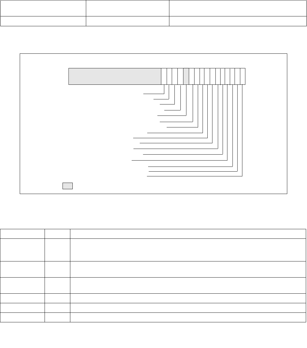
18-24 Vol. 3B
PERFORMANCE MONITORING
18.3.1.1.3 Off-core Response Performance Monitoring in the Processor Core
Programming a performance event using the off-core response facility can choose any of the four
IA32_PERFEVTSELx MSR with specific event codes and predefine mask bit value. Each event code for off-core
response monitoring requires programming an associated configuration MSR, MSR_OFFCORE_RSP_0. There is only
one off-core response configuration MSR. Table 18-5 lists the event code, mask value and additional off-core
configuration MSR that must be programmed to count off-core response events using IA32_PMCx.
The layout of MSR_OFFCORE_RSP_0 is shown in Figure 18-18. Bits 7:0 specifies the request type of a transaction
request to the uncore. Bits 15:8 specifies the response of the uncore subsystem.
Table 18-5. Off-Core Response Event Encoding
Event code in
IA32_PERFEVTSELx
Mask Value in
IA32_PERFEVTSELx Required Off-core Response MSR
B7H 01H MSR_OFFCORE_RSP_0 (address 1A6H)
Figure 18-18. Layout of MSR_OFFCORE_RSP_0 and MSR_OFFCORE_RSP_1 to Configure Off-core Response Events
Table 18-6. MSR_OFFCORE_RSP_0 and MSR_OFFCORE_RSP_1 Bit Field Definition
Bit Name Offset Description
DMND_DATA_RD 0 (R/W). Counts the number of demand and DCU prefetch data reads of full and partial cachelines as well
as demand data page table entry cacheline reads. Does not count L2 data read prefetches or
instruction fetches.
DMND_RFO 1 (R/W). Counts the number of demand and DCU prefetch reads for ownership (RFO) requests generated
by a write to data cacheline. Does not count L2 RFO.
DMND_IFETCH 2 (R/W). Counts the number of demand instruction cacheline reads and L1 instruction cacheline
prefetches.
WB 3 (R/W). Counts the number of writeback (modified to exclusive) transactions.
PF_DATA_RD 4 (R/W). Counts the number of data cacheline reads generated by L2 prefetchers.
PF_RFO 5 (R/W). Counts the number of RFO requests generated by L2 prefetchers.
RESPONSE TYPE — NON_DRAM (R/W)
RESPONSE TYPE — LOCAL_DRAM (R/W)
RESPONSE TYPE — REMOTE_DRAM (R/W)
RESPONSE TYPE — REMOTE_CACHE_FWD (R/W)
87 0
RESPONSE TYPE — RESERVED
11 312 1
Reserved
63 2
495610131415
RESPONSE TYPE — OTHER_CORE_HITM (R/W)
RESPONSE TYPE — OTHER_CORE_HIT_SNP (R/W)
RESPONSE TYPE — UNCORE_HIT (R/W)
REQUEST TYPE — OTHER (R/W)
REQUEST TYPE — PF_IFETCH (R/W)
REQUEST TYPE — PF_RFO (R/W)
REQUEST TYPE — PF_DATA_RD (R/W)
REQUEST TYPE — WB (R/W)
REQUEST TYPE — DMND_IFETCH (R/W)
REQUEST TYPE — DMND_RFO (R/W)
REQUEST TYPE — DMND_DATA_RD (R/W)
RESET Value — 00000000_00000000H

Vol. 3B 18-25
PERFORMANCE MONITORING
18.3.1.2 Performance Monitoring Facility in the Uncore
The “uncore” in Intel microarchitecture code name Nehalem refers to subsystems in the physical processor
package that are shared by multiple processor cores. Some of the sub-systems in the uncore include the L3 cache,
Intel QuickPath Interconnect link logic, and integrated memory controller. The performance monitoring facilities
inside the uncore operates in the same clock domain as the uncore (U-clock domain), which is usually different
from the processor core clock domain. The uncore performance monitoring facilities described in this section apply
to Intel Xeon processor 5500 series and processors with the following CPUID signatures: 06_1AH, 06_1EH, 06_1FH
(see Chapter 2, “Model-Specific Registers (MSRs)” in the Intel® 64 and IA-32 Architectures Software Developer’s
Manual, Volume 4). An overview of the uncore performance monitoring facilities is described separately.
The performance monitoring facilities available in the U-clock domain consist of:
•Eight General-purpose counters (MSR_UNCORE_PerfCntr0 through MSR_UNCORE_PerfCntr7). The counters
are 48 bits wide. Each counter is associated with a configuration MSR, MSR_UNCORE_PerfEvtSelx, to specify
event code, event mask and other event qualification fields. A set of global uncore performance counter
enabling/overflow/status control MSRs are also provided for software.
•Performance monitoring in the uncore provides an address/opcode match MSR that provides event qualification
control based on address value or QPI command opcode.
•One fixed-function counter, MSR_UNCORE_FixedCntr0. The fixed-function uncore counter increments at the
rate of the U-clock when enabled.
The frequency of the uncore clock domain can be determined from the uncore clock ratio which is available in
the PCI configuration space register at offset C0H under device number 0 and Function 0.
18.3.1.2.1 Uncore Performance Monitoring Management Facility
MSR_UNCORE_PERF_GLOBAL_CTRL provides bit fields to enable/disable general-purpose and fixed-function coun-
ters in the uncore. Figure 18-19 shows the layout of MSR_UNCORE_PERF_GLOBAL_CTRL for an uncore that is
shared by four processor cores in a physical package.
•EN_PCn (bit n, n = 0, 7): When set, enables counting for the general-purpose uncore counter
MSR_UNCORE_PerfCntr n.
•EN_FC0 (bit 32): When set, enables counting for the fixed-function uncore counter MSR_UNCORE_FixedCntr0.
PF_IFETCH 6 (R/W). Counts the number of code reads generated by L2 prefetchers.
OTHER 7 (R/W). Counts one of the following transaction types, including L3 invalidate, I/O, full or partial writes,
WC or non-temporal stores, CLFLUSH, Fences, lock, unlock, split lock.
UNCORE_HIT 8 (R/W). L3 Hit: local or remote home requests that hit L3 cache in the uncore with no coherency actions
required (snooping).
OTHER_CORE_HI
T_SNP
9 (R/W). L3 Hit: local or remote home requests that hit L3 cache in the uncore and was serviced by
another core with a cross core snoop where no modified copies were found (clean).
OTHER_CORE_HI
TM
10 (R/W). L3 Hit: local or remote home requests that hit L3 cache in the uncore and was serviced by
another core with a cross core snoop where modified copies were found (HITM).
Reserved 11 Reserved
REMOTE_CACHE_
FWD
12 (R/W). L3 Miss: local homed requests that missed the L3 cache and was serviced by forwarded data
following a cross package snoop where no modified copies found. (Remote home requests are not
counted)
REMOTE_DRAM 13 (R/W). L3 Miss: remote home requests that missed the L3 cache and were serviced by remote DRAM.
LOCAL_DRAM 14 (R/W). L3 Miss: local home requests that missed the L3 cache and were serviced by local DRAM.
NON_DRAM 15 (R/W). Non-DRAM requests that were serviced by IOH.
Table 18-6. MSR_OFFCORE_RSP_0 and MSR_OFFCORE_RSP_1 Bit Field Definition (Contd.)
Bit Name Offset Description
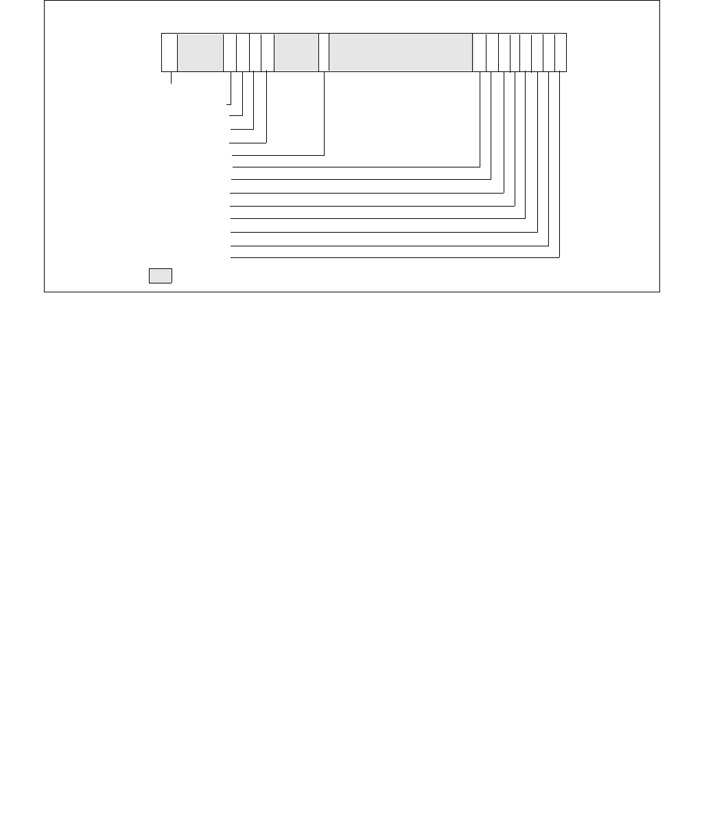
18-26 Vol. 3B
PERFORMANCE MONITORING
•EN_PMI_COREn (bit n, n = 0, 3 if four cores are present): When set, processor core n is programmed to receive
an interrupt signal from any interrupt enabled uncore counter. PMI delivery due to an uncore counter overflow
is enabled by setting IA32_DEBUGCTL.Offcore_PMI_EN to 1.
•PMI_FRZ (bit 63): When set, all U-clock uncore counters are disabled when any one of them signals a
performance interrupt. Software must explicitly re-enable the counter by setting the enable bits in
MSR_UNCORE_PERF_GLOBAL_CTRL upon exit from the ISR.
MSR_UNCORE_PERF_GLOBAL_STATUS provides overflow status of the U-clock performance counters in the
uncore. This is a read-only register. If an overflow status bit is set the corresponding counter has overflowed. The
register provides a condition change bit (bit 63) which can be quickly checked by software to determine if a signif-
icant change has occurred since the last time the condition change status was cleared. Figure 18-20 shows the
layout of MSR_UNCORE_PERF_GLOBAL_STATUS.
•OVF_PCn (bit n, n = 0, 7): When set, indicates general-purpose uncore counter MSR_UNCORE_PerfCntr n has
overflowed.
•OVF_FC0 (bit 32): When set, indicates the fixed-function uncore counter MSR_UNCORE_FixedCntr0 has
overflowed.
•OVF_PMI (bit 61): When set indicates that an uncore counter overflowed and generated an interrupt request.
•CHG (bit 63): When set indicates that at least one status bit in MSR_UNCORE_PERF_GLOBAL_STATUS register
has changed state.
Figure 18-19. Layout of MSR_UNCORE_PERF_GLOBAL_CTRL MSR
PMI_FRZ (R/W)
EN_PMI_CORE3 (R/W)
EN_PMI_CORE2 (R/W)
EN_PMI_CORE1 (R/W)
87 0
EN_PMI_CORE0 (R/W)
32 3
48 1
Reserved
63 2
4
31 56
62 495051
EN_PC7 (R/W)
EN_PC6 (R/W)
EN_PC5 (R/W)
EN_PC4 (R/W)
EN_PC3 (R/W)
EN_PC2 (R/W)
EN_PC1 (R/W)
EN_PC0 (R/W)
EN_FC0 (R/W)
RESET Value — 00000000_00000000H
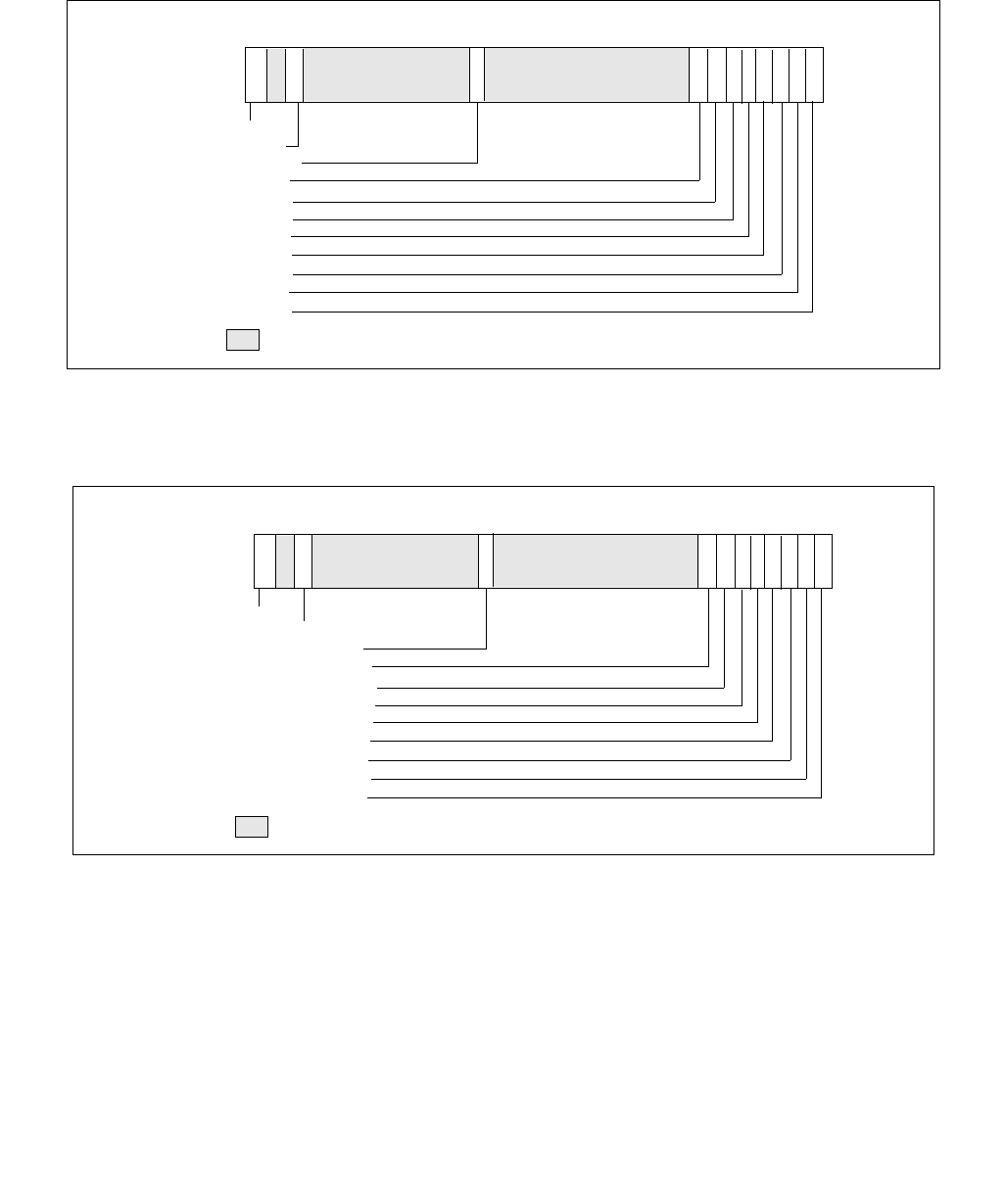
Vol. 3B 18-27
PERFORMANCE MONITORING
MSR_UNCORE_PERF_GLOBAL_OVF_CTRL allows software to clear the status bits in the
UNCORE_PERF_GLOBAL_STATUS register. This is a write-only register, and individual status bits in the global
status register are cleared by writing a binary one to the corresponding bit in this register. Writing zero to any bit
position in this register has no effect on the uncore PMU hardware.
Figure 18-21 shows the layout of MSR_UNCORE_PERF_GLOBAL_OVF_CTRL.
•CLR_OVF_PCn (bit n, n = 0, 7): Set this bit to clear the overflow status for general-purpose uncore counter
MSR_UNCORE_PerfCntr n. Writing a value other than 1 is ignored.
•CLR_OVF_FC0 (bit 32): Set this bit to clear the overflow status for the fixed-function uncore counter
MSR_UNCORE_FixedCntr0. Writing a value other than 1 is ignored.
•CLR_OVF_PMI (bit 61): Set this bit to clear the OVF_PMI flag in MSR_UNCORE_PERF_GLOBAL_STATUS. Writing
a value other than 1 is ignored.
•CLR_CHG (bit 63): Set this bit to clear the CHG flag in MSR_UNCORE_PERF_GLOBAL_STATUS register. Writing
a value other than 1 is ignored.
Figure 18-20. Layout of MSR_UNCORE_PERF_GLOBAL_STATUS MSR
Figure 18-21. Layout of MSR_UNCORE_PERF_GLOBAL_OVF_CTRL MSR
CHG (R/W)
OVF_PMI (R/W)
87 0
32 31
Reserved
63 2
4
31 56
62 6061
OVF_PC7 (R/O)
OVF_PC6 (R/O)
OVF_PC5 (R/O)
OVF_PC4 (R/O)
OVF_PC3 (R/O)
OVF_PC2 (R/O)
OVF_PC1 (R/O)
OVF_PC0 (R/O)
OVF_FC0 (R/O)
RESET Value — 00000000_00000000H
CLR_CHG (WO1)
CLR_OVF_PMI (WO1)
87 0
32 31
Reserved
63 2
4
31 56
62 6061
CLR_OVF_PC7 (WO1)
CLR_OVF_PC6 (WO1)
CLR_OVF_PC5 (WO1)
CLR_OVF_PC4 (WO1)
CLR_OVF_PC3 (WO1)
CLR_OVF_PC2 (WO1)
CLR_OVF_PC1 (WO1)
CLR_OVF_PC0 (WO1)
CLR_OVF_FC0 (WO1)
RESET Value — 00000000_00000000H
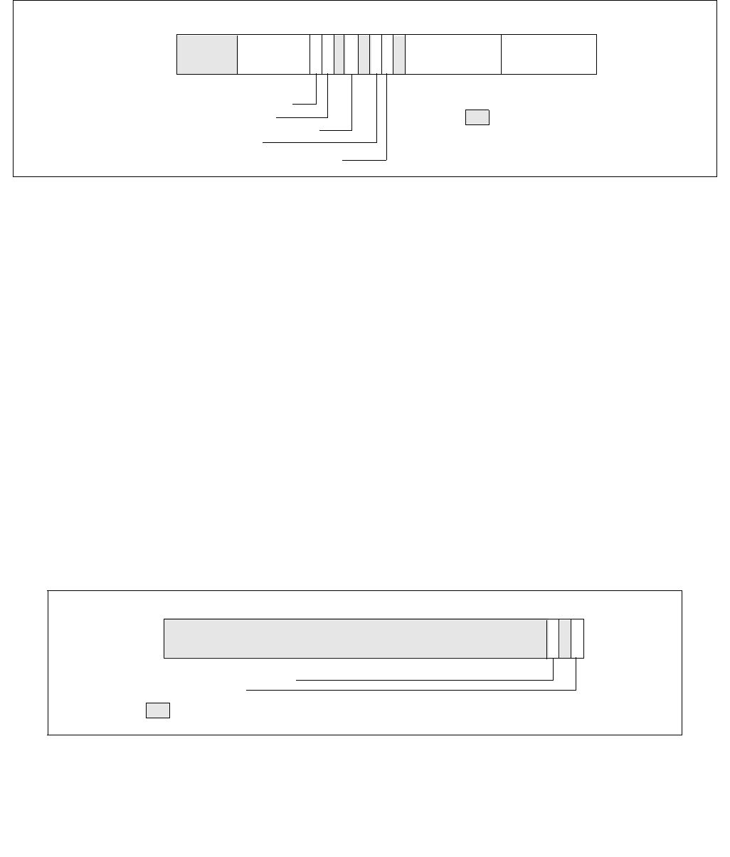
18-28 Vol. 3B
PERFORMANCE MONITORING
18.3.1.2.2 Uncore Performance Event Configuration Facility
MSR_UNCORE_PerfEvtSel0 through MSR_UNCORE_PerfEvtSel7 are used to select performance event and
configure the counting behavior of the respective uncore performance counter. Each uncore PerfEvtSel MSR is
paired with an uncore performance counter. Each uncore counter must be locally configured using the corre-
sponding MSR_UNCORE_PerfEvtSelx and counting must be enabled using the respective EN_PCx bit in
MSR_UNCORE_PERF_GLOBAL_CTRL. Figure 18-22 shows the layout of MSR_UNCORE_PERFEVTSELx.
•Event Select (bits 7:0): Selects the event logic unit used to detect uncore events.
•Unit Mask (bits 15:8) : Condition qualifiers for the event selection logic specified in the Event Select field.
•OCC_CTR_RST (bit17): When set causes the queue occupancy counter associated with this event to be cleared
(zeroed). Writing a zero to this bit will be ignored. It will always read as a zero.
•Edge Detect (bit 18): When set causes the counter to increment when a deasserted to asserted transition
occurs for the conditions that can be expressed by any of the fields in this register.
•PMI (bit 20): When set, the uncore will generate an interrupt request when this counter overflowed. This
request will be routed to the logical processors as enabled in the PMI enable bits (EN_PMI_COREx) in the
register MSR_UNCORE_PERF_GLOBAL_CTRL.
•EN (bit 22): When clear, this counter is locally disabled. When set, this counter is locally enabled and counting
starts when the corresponding EN_PCx bit in MSR_UNCORE_PERF_GLOBAL_CTRL is set.
•INV (bit 23): When clear, the Counter Mask field is interpreted as greater than or equal to. When set, the
Counter Mask field is interpreted as less than.
•Counter Mask (bits 31:24): When this field is clear, it has no effect on counting. When set to a value other than
zero, the logical processor compares this field to the event counts on each core clock cycle. If INV is clear and
the event counts are greater than or equal to this field, the counter is incremented by one. If INV is set and the
event counts are less than this field, the counter is incremented by one. Otherwise the counter is not incre-
mented.
Figure 18-23 shows the layout of MSR_UNCORE_FIXED_CTR_CTRL.
Figure 18-22. Layout of MSR_UNCORE_PERFEVTSELx MSRs
Figure 18-23. Layout of MSR_UNCORE_FIXED_CTR_CTRL MSR
31
INV—Invert counter mask
EN—Enable counters
E—Edge detect
OCC_CTR_RST—Rest Queue Occ
870
Event Select
Counter Mask
19 1618 15172021222324
Reserved
Unit Mask (UMASK)
(CMASK)
63
PMI—Enable PMI on overflow
RESET Value — 00000000_00000000H
87 031
Reserved
63 245
6
PMI - Generate PMI on overflow
EN - Enable
RESET Value — 00000000_00000000H
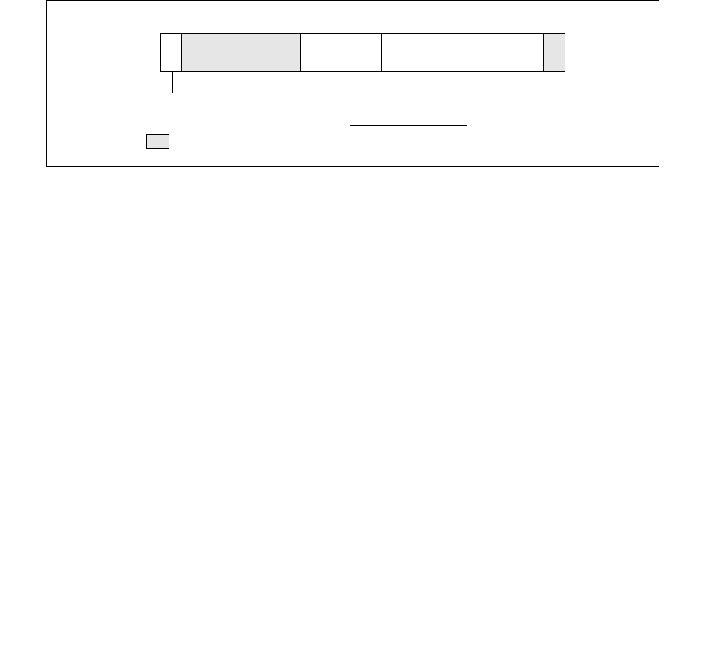
Vol. 3B 18-29
PERFORMANCE MONITORING
•EN (bit 0): When clear, the uncore fixed-function counter is locally disabled. When set, it is locally enabled and
counting starts when the EN_FC0 bit in MSR_UNCORE_PERF_GLOBAL_CTRL is set.
•PMI (bit 2): When set, the uncore will generate an interrupt request when the uncore fixed-function counter
overflowed. This request will be routed to the logical processors as enabled in the PMI enable bits
(EN_PMI_COREx) in the register MSR_UNCORE_PERF_GLOBAL_CTRL.
Both the general-purpose counters (MSR_UNCORE_PerfCntr) and the fixed-function counter
(MSR_UNCORE_FixedCntr0) are 48 bits wide. They support both counting and interrupt based sampling usages.
The event logic unit can filter event counts to specific regions of code or transaction types incoming to the home
node logic.
18.3.1.2.3 Uncore Address/Opcode Match MSR
The Event Select field [7:0] of MSR_UNCORE_PERFEVTSELx is used to select different uncore event logic unit.
When the event “ADDR_OPCODE_MATCH” is selected in the Event Select field, software can filter uncore perfor-
mance events according to transaction address and certain transaction responses. The address filter and transac-
tion response filtering requires the use of MSR_UNCORE_ADDR_OPCODE_MATCH register. The layout is shown in
Figure 18-24.
•Addr (bits 39:3): The physical address to match if “MatchSel“ field is set to select address match. The uncore
performance counter will increment if the lowest 40-bit incoming physical address (excluding bits 2:0) for a
transaction request matches bits 39:3.
•Opcode (bits 47:40) : Bits 47:40 allow software to filter uncore transactions based on QPI link message
class/packed header opcode. These bits are consists two sub-fields:
— Bits 43:40 specify the QPI packet header opcode.
— Bits 47:44 specify the QPI message classes.
Table 18-7 lists the encodings supported in the opcode field.
Figure 18-24. Layout of MSR_UNCORE_ADDR_OPCODE_MATCH MSR
60
MatchSel—Select addr/Opcode
Opcode—Opcode and Message
320
40 394748
Reserved
ADDR
63
ADDR—Bits 39:4 of physical address
RESET Value — 00000000_00000000H
Opcode

18-30 Vol. 3B
PERFORMANCE MONITORING
•MatchSel (bits 63:61): Software specifies the match criteria according to the following encoding:
— 000B: Disable addr_opcode match hardware.
— 100B: Count if only the address field matches.
— 010B: Count if only the opcode field matches.
— 110B: Count if either opcode field matches or the address field matches.
— 001B: Count only if both opcode and address field match.
— Other encoding are reserved.
18.3.1.3 Intel® Xeon® Processor 7500 Series Performance Monitoring Facility
The performance monitoring facility in the processor core of Intel® Xeon® processor 7500 series are the same as
those supported in Intel Xeon processor 5500 series. The uncore subsystem in Intel Xeon processor 7500 series are
significantly different The uncore performance monitoring facility consist of many distributed units associated with
individual logic control units (referred to as boxes) within the uncore subsystem. A high level block diagram of the
various box units of the uncore is shown in Figure 18-25.
Uncore PMUs are programmed via MSR interfaces. Each of the distributed uncore PMU units have several general-
purpose counters. Each counter requires an associated event select MSR, and may require additional MSRs to
configure sub-event conditions. The uncore PMU MSRs associated with each box can be categorized based on its
functional scope: per-counter, per-box, or global across the uncore. The number counters available in each box
type are different. Each box generally provides a set of MSRs to enable/disable, check status/overflow of multiple
counters within each box.
Table 18-7. Opcode Field Encoding for MSR_UNCORE_ADDR_OPCODE_MATCH
Opcode [43:40] QPI Message Class
Home Request
[47:44] = 0000B
Snoop Response
[47:44] = 0001B
Data Response
[47:44] = 1110B
1
DMND_IFETCH 2 2
WB 3 3
PF_DATA_RD 4 4
PF_RFO 5 5
PF_IFETCH 6 6
OTHER 7 7
NON_DRAM 15 15
Vol. 3B 18-31
PERFORMANCE MONITORING
Table 18-8 summarizes the number MSRs for uncore PMU for each box.
The W-Box provides 4 general-purpose counters, each requiring an event select configuration MSR, similar to the
general-purpose counters in other boxes. There is also a fixed-function counter that increments clockticks in the
uncore clock domain.
For C,S,B,M,R, and W boxes, each box provides an MSR to enable/disable counting, configuring PMI of multiple
counters within the same box, this is somewhat similar the “global control“ programming interface,
IA32_PERF_GLOBAL_CTRL, offered in the core PMU. Similarly status information and counter overflow control for
multiple counters within the same box are also provided in C,S,B,M,R, and W boxes.
In the U-Box, MSR_U_PMON_GLOBAL_CTL provides overall uncore PMU enable/disable and PMI configuration
control. The scope of status information in the U-box is at per-box granularity, in contrast to the per-box status
information MSR (in the C,S,B,M,R, and W boxes) providing status information of individual counter overflow. The
difference in scope also apply to the overflow control MSR in the U-Box versus those in the other Boxes.
Figure 18-25. Distributed Units of the Uncore of Intel® Xeon® Processor 7500 Series
Table 18-8. Uncore PMU MSR Summary
Box # of Boxes Counters per Box
Counter
Width
General
Purpose
Global
Enable Sub-control MSRs
C-Box 8 6 48 Yes per-box None
S-Box 2 4 48 Yes per-box Match/Mask
B-Box 2 4 48 Yes per-box Match/Mask
M-Box 2 6 48 Yes per-box Yes
R-Box 1 16 ( 2 port, 8 per port) 48 Yes per-box Yes
W-Box 1 4 48 Yes per-box None
148Noper-boxNone
U-Box 1 1 48 Yes uncore None
PBox
L3 Cache
PBoxPBox PBox UBox
WBox
RBox BBoxBBoxMBox MBox PBoxPBox
SBox SBox
CBox CBoxCBoxCBox CBoxCBox CBox
CBox
4 Intel QPI Links
SMI Channels
SMI Channels

18-32 Vol. 3B
PERFORMANCE MONITORING
The individual MSRs that provide uncore PMU interfaces are listed in Chapter 2, “Model-Specific Registers (MSRs)”
in the Intel® 64 and IA-32 Architectures Software Developer’s Manual, Volume 4, Table 2-16 under the general
naming style of MSR_%box#%_PMON_%scope_function%, where %box#% designates the type of box and zero-
based index if there are more the one box of the same type, %scope_function% follows the examples below:
•Multi-counter enabling MSRs: MSR_U_PMON_GLOBAL_CTL, MSR_S0_PMON_BOX_CTL,
MSR_C7_PMON_BOX_CTL, etc.
•Multi-counter status MSRs: MSR_U_PMON_GLOBAL_STATUS, MSR_S0_PMON_BOX_STATUS,
MSR_C7_PMON_BOX_STATUS, etc.
•Multi-counter overflow control MSRs: MSR_U_PMON_GLOBAL_OVF_CTL, MSR_S0_PMON_BOX_OVF_CTL,
MSR_C7_PMON_BOX_OVF_CTL, etc.
•Performance counters MSRs: the scope is implicitly per counter, e.g. MSR_U_PMON_CTR,
MSR_S0_PMON_CTR0, MSR_C7_PMON_CTR5, etc.
•Event select MSRs: the scope is implicitly per counter, e.g. MSR_U_PMON_EVNT_SEL,
MSR_S0_PMON_EVNT_SEL0, MSR_C7_PMON_EVNT_SEL5, etc
•Sub-control MSRs: the scope is implicitly per-box granularity, e.g. MSR_M0_PMON_TIMESTAMP,
MSR_R0_PMON_IPERF0_P1, MSR_S1_PMON_MATCH.
Details of uncore PMU MSR bit field definitions can be found in a separate document “Intel Xeon Processor 7500
Series Uncore Performance Monitoring Guide“.
18.3.2 Performance Monitoring for Processors Based on Intel® Microarchitecture Code Name
Westmere
All of the performance monitoring programming interfaces (architectural and non-architectural core PMU facilities,
and uncore PMU) described in Section 18.6.3 also apply to processors based on Intel® microarchitecture code
name Westmere.
Table 18-5 describes a non-architectural performance monitoring event (event code 0B7H) and associated
MSR_OFFCORE_RSP_0 (address 1A6H) in the core PMU. This event and a second functionally equivalent offcore
response event using event code 0BBH and MSR_OFFCORE_RSP_1 (address 1A7H) are supported in processors
based on Intel microarchitecture code name Westmere. The event code and event mask definitions of Non-archi-
tectural performance monitoring events are listed in Table 19-29.
The load latency facility is the same as described in Section 18.3.1.1.2, but added enhancement to provide more
information in the data source encoding field of each load latency record. The additional information relates to
STLB_MISS and LOCK, see Table 18-13.
18.3.3 Intel® Xeon® Processor E7 Family Performance Monitoring Facility
The performance monitoring facility in the processor core of the Intel® Xeon® processor E7 family is the same as
those supported in the Intel Xeon processor 5600 series3. The uncore subsystem in the Intel Xeon processor E7
family is similar to those of the Intel Xeon processor 7500 series. The high level construction of the uncore sub-
system is similar to that shown in Figure 18-25, with the additional capability that up to 10 C-Box units are
supported.
3. Exceptions are indicated for event code 0FH in Table 19-21; and valid bits of data source encoding field of each load
latency record is limited to bits 5:4 of Tab l e 18 - 13.

Vol. 3B 18-33
PERFORMANCE MONITORING
Table 18-9 summarizes the number MSRs for uncore PMU for each box.
Details of the uncore performance monitoring facility of Intel Xeon Processor E7 family is available in the “Intel®
Xeon® Processor E7 Uncore Performance Monitoring Programming Reference Manual”.
18.3.4 Performance Monitoring for Processors Based on Intel® Microarchitecture Code Name
Sandy Bridge
Intel® Core™ i7-2xxx, Intel® Core™ i5-2xxx, Intel® Core™ i3-2xxx processor series, and Intel® Xeon® processor
E3-1200 family are based on Intel microarchitecture code name Sandy Bridge; this section describes the perfor-
mance monitoring facilities provided in the processor core. The core PMU supports architectural performance moni-
toring capability with version ID 3 (see Section 18.2.3) and a host of non-architectural monitoring capabilities.
Architectural performance monitoring version 3 capabilities are described in Section 18.2.3.
The core PMU’s capability is similar to those described in Section 18.3.1.1 and Section 18.6.3, with some differ-
ences and enhancements relative to Intel microarchitecture code name Westmere summarized in Table 18-10.
Table 18-9. Uncore PMU MSR Summary for Intel® Xeon® Processor E7 Family
Box # of Boxes Counters per Box
Counter
Width
General
Purpose
Global
Enable Sub-control MSRs
C-Box 10 6 48 Yes per-box None
S-Box 2 4 48 Yes per-box Match/Mask
B-Box 2 4 48 Yes per-box Match/Mask
M-Box 2 6 48 Yes per-box Yes
R-Box 1 16 ( 2 port, 8 per port) 48 Yes per-box Yes
W-Box 1 4 48 Yes per-box None
148Noper-boxNone
U-Box 1 1 48 Yes uncore None
Table 18-10. Core PMU Comparison
Box
Intel® microarchitecture code
name Sandy Bridge
Intel® microarchitecture code
name Westmere Comment
# of Fixed counters per
thread
3 3 Use CPUID to enumerate # of
counters. See Section 18.2.1.
# of general-purpose
counters per core
8 8 Use CPUID to enumerate # of
counters. See Section 18.2.1.
Counter width (R,W) R:48, W: 32/48 R:48, W:32 See Section 18.2.2.
# of programmable counters
per thread
4 or (8 if a core not shared by two
threads)
4 Use CPUID to enumerate # of
counters. See Section 18.2.1.
PMI Overhead Mitigation • Freeze_Perfmon_on_PMI with
legacy semantics.
•Freeze_on_LBR with legacy
semantics for branch profiling.
• Freeze_while_SMM.
•Freeze_Perfmon_on_PMI
with legacy semantics.
•Freeze_on_LBR with legacy
semantics for branch
profiling.
• Freeze_while_SMM.
See Section 17.4.7.
Processor Event Based
Sampling (PEBS) Events
See Table 18-12.See Table 18-68.IA32_PMC4-IA32_PMC7 do
not support PEBS.
18-34 Vol. 3B
PERFORMANCE MONITORING
18.3.4.1 Global Counter Control Facilities In Intel® Microarchitecture Code Name Sandy Bridge
The number of general-purpose performance counters visible to a logical processor can vary across Processors
based on Intel microarchitecture code name Sandy Bridge. Software must use CPUID to determine the number
performance counters/event select registers (See Section 18.2.1.1).
Figure 18-42 depicts the layout of IA32_PERF_GLOBAL_CTRL MSR. The enable bits (PMC4_EN, PMC5_EN,
PMC6_EN, PMC7_EN) corresponding to IA32_PMC4-IA32_PMC7 are valid only if CPUID.0AH:EAX[15:8] reports a
value of ‘8’. If CPUID.0AH:EAX[15:8] = 4, attempts to set the invalid bits will cause #GP.
Each enable bit in IA32_PERF_GLOBAL_CTRL is AND’ed with the enable bits for all privilege levels in the respective
IA32_PERFEVTSELx or IA32_PERF_FIXED_CTR_CTRL MSRs to start/stop the counting of respective counters.
Counting is enabled if the AND’ed results is true; counting is disabled when the result is false.
IA32_PERF_GLOBAL_STATUS MSR provides single-bit status used by software to query the overflow condition of
each performance counter. IA32_PERF_GLOBAL_STATUS[bit 62] indicates overflow conditions of the DS area data
buffer (see Figure 18-27). A value of 1 in each bit of the PMCx_OVF field indicates an overflow condition has
occurred in the associated counter.
PEBS-Load Latency See Section 18.3.4.4.2;
• Data source encoding
• STLB miss encoding
• Lock transaction encoding
Data source encoding
PEBS-Precise Store Section 18.3.4.4.3 No
PEBS-PDIR Yes (using precise
INST_RETIRED.ALL).
No
Off-core Response Event MSR 1A6H and 1A7H, extended
request and response types.
MSR 1A6H and 1A7H, limited
response types.
Nehalem supports 1A6H
only.
Figure 18-26. IA32_PERF_GLOBAL_CTRL MSR in Intel® Microarchitecture Code Name Sandy Bridge
Table 18-10. Core PMU Comparison (Contd.)
Box
Intel® microarchitecture code
name Sandy Bridge
Intel® microarchitecture code
name Westmere Comment
FIXED_CTR2 enable
FIXED_CTR1 enable
FIXED_CTR0 enable
PMC7_EN (if PMC7 present)
210
PMC6_EN (if PMC6 present)
3132333435
Reserved
63
PMC5_EN (if PMC5 present)
PMC4_EN (if PMC4 present)
PMC3_EN
PMC2_EN
PMC1_EN
Valid if CPUID.0AH:EAX[15:8] = 8, else reserved.
PMC0_EN
87 65 43
Vol. 3B 18-35
PERFORMANCE MONITORING
When a performance counter is configured for PEBS, an overflow condition in the counter will arm PEBS. On the
subsequent event following overflow, the processor will generate a PEBS event. On a PEBS event, the processor will
perform bounds checks based on the parameters defined in the DS Save Area (see Section 17.4.9). Upon
successful bounds checks, the processor will store the data record in the defined buffer area, clear the counter
overflow status, and reload the counter. If the bounds checks fail, the PEBS will be skipped entirely. In the event
that the PEBS buffer fills up, the processor will set the OvfBuffer bit in MSR_PERF_GLOBAL_STATUS.
IA32_PERF_GLOBAL_OVF_CTL MSR allows software to clear overflow the indicators for general-purpose or fixed-
function counters via a single WRMSR (see Figure 18-28). Clear overflow indications when:
•Setting up new values in the event select and/or UMASK field for counting or interrupt based sampling.
•Reloading counter values to continue sampling.
•Disabling event counting or interrupt based sampling.
Figure 18-27. IA32_PERF_GLOBAL_STATUS MSR in Intel® Microarchitecture Code Name Sandy Bridge
Figure 18-28. IA32_PERF_GLOBAL_OVF_CTRL MSR in Intel microarchitecture code name Sandy Bridge
62
FIXED_CTR2 Overflow (RO)
FIXED_CTR1 Overflow (RO)
FIXED_CTR0 Overflow (RO)
PMC7_OVF (RO, If PMC7 present)
210
PMC6_OVF (RO, If PMC6 present)
3132333435
Reserved
63
CondChgd
Ovf_DSBuffer
87 65 43
PMC5_OVF (RO, If PMC5 present)
PMC4_OVF (RO, If PMC4 present)
PMC3_OVF (RO)
PMC2_OVF (RO)
PMC1_OVF (RO)
PMC0_OVF (RO)
Valid if CPUID.0AH:EAX[15:8] = 8; else reserved
Ovf_UncorePMU
61
62
FIXED_CTR2 ClrOverflow
FIXED_CTR1 ClrOverflow
FIXED_CTR0 ClrOverflow
PMC7_ClrOvf (if PMC7 present)
210
PMC6_ClrOvf (if PMC6 present)
3132333435
Reserved
63
ClrCondChgd
ClrOvfDSBuffer
87 6 5 43
PMC5_ClrOvf (if PMC5 present)
PMC4_ClrOvf (if PMC4 present)
PMC3_ClrOvf
PMC2_ClrOvf
PMC1_ClrOvf
PMC0_ClrOvf
Valid if CPUID.0AH:EAX[15:8] = 8; else reserved
ClrOvfUncore

18-36 Vol. 3B
PERFORMANCE MONITORING
18.3.4.2 Counter Coalescence
In processors based on Intel microarchitecture code name Sandy Bridge, each processor core implements eight
general-purpose counters. CPUID.0AH:EAX[15:8] will report the number of counters visible to software.
If a processor core is shared by two logical processors, each logical processors can access up to four counters
(IA32_PMC0-IA32_PMC3). This is the same as in the prior generation for processors based on Intel microarchitec-
ture code name Nehalem.
If a processor core is not shared by two logical processors, up to eight general-purpose counters are visible. If
CPUID.0AH:EAX[15:8] reports 8 counters, then IA32_PMC4-IA32_PMC7 would occupy MSR addresses 0C5H
through 0C8H. Each counter is accompanied by an event select MSR (IA32_PERFEVTSEL4-IA32_PERFEVTSEL7).
If CPUID.0AH:EAX[15:8] report 4, access to IA32_PMC4-IA32_PMC7, IA32_PMC4-IA32_PMC7 will cause #GP.
Writing 1’s to bit position 7:4 of IA32_PERF_GLOBAL_CTRL, IA32_PERF_GLOBAL_STATUS, or
IA32_PERF_GLOBAL_OVF_CTL will also cause #GP.
18.3.4.3 Full Width Writes to Performance Counters
Processors based on Intel microarchitecture code name Sandy Bridge support full-width writes to the general-
purpose counters, IA32_PMCx. Support of full-width writes are enumerated by
IA32_PERF_CAPABILITIES.FW_WRITES[13] (see Section 18.2.4).
The default behavior of IA32_PMCx is unchanged, i.e. WRMSR to IA32_PMCx results in a sign-extended 32-bit
value of the input EAX written into IA32_PMCx. Full-width writes must issue WRMSR to a dedicated alias MSR
address for each IA32_PMCx.
Software must check the presence of full-width write capability and the presence of the alias address IA32_A_PMCx
by testing IA32_PERF_CAPABILITIES[13].
18.3.4.4 PEBS Support in Intel® Microarchitecture Code Name Sandy Bridge
Processors based on Intel microarchitecture code name Sandy Bridge support PEBS, similar to those offered in
prior generation, with several enhanced features. The key components and differences of PEBS facility relative to
Intel microarchitecture code name Westmere is summarized in Table 18-11.
Only IA32_PMC0 through IA32_PMC3 support PEBS.
Table 18-11. PEBS Facility Comparison
Box
Intel® microarchitecture code name
Sandy Bridge
Intel® microarchitecture
code name Westmere Comment
Valid IA32_PMCx PMC0-PMC3 PMC0-PMC3 No PEBS on PMC4-PMC7.
PEBS Buffer Programming Section 18.3.1.1.1 Section 18.3.1.1.1 Unchanged
IA32_PEBS_ENABLE
Layout
Figure 18-29 Figure 18-15
PEBS record layout Physical Layout same as Table 18-3. Table 18-3 Enhanced fields at offsets 98H,
A0H, A8H.
PEBS Events See Table 18-12. See Table 18-68. IA32_PMC4-IA32_PMC7 do not
support PEBS.
PEBS-Load Latency See Table 18-13. Table 18-4
PEBS-Precise Store Yes; see Section 18.3.4.4.3. No IA32_PMC3 only
PEBS-PDIR Yes No IA32_PMC1 only
PEBS skid from EventingIP 1 (or 2 if micro+macro fusion) 1
SAMPLING Restriction Small SAV(CountDown) value incur higher overhead than prior
generation.
Vol. 3B 18-37
PERFORMANCE MONITORING
NOTE
PEBS events are only valid when the following fields of IA32_PERFEVTSELx are all zero: AnyThread,
Edge, Invert, CMask.
In a PMU with PDIR capability, PEBS behavior is unpredictable if IA32_PERFEVTSELx or IA32_PMCx
is changed for a PEBS-enabled counter while an event is being counted. To avoid this, changes to
the programming or value of a PEBS-enabled counter should be performed when the counter is
disabled.
In IA32_PEBS_ENABLE MSR, bit 63 is defined as PS_ENABLE: When set, this enables IA32_PMC3 to capture
precise store information. Only IA32_PMC3 supports the precise store facility. In typical usage of PEBS, the bit
fields in IA32_PEBS_ENABLE are written to when the agent software starts PEBS operation; the enabled bit fields
should be modified only when re-programming another PEBS event or cleared when the agent uses the perfor-
mance counters for non-PEBS operations.
18.3.4.4.1 PEBS Record Format
The layout of PEBS records physically identical to those shown in Table 18-3, but the fields at offset 98H, A0H and
A8H have been enhanced to support additional PEBS capabilities.
•Load/Store Data Linear Address (Offset 98H): This field will contain the linear address of the source of the load,
or linear address of the destination of the store.
•Data Source /Store Status (Offset A0H):When load latency is enabled, this field will contain three piece of
information (including an encoded value indicating the source which satisfied the load operation). The source
field encodings are detailed in Table 18-4. When precise store is enabled, this field will contain information
indicating the status of the store, as detailed in Table 19.
•Latency Value/0 (Offset A8H): When load latency is enabled, this field contains the latency in cycles to service
the load. This field is not meaningful when precise store is enabled and will be written to zero in that case. Upon
writing the PEBS record, microcode clears the overflow status bits in the IA32_PERF_GLOBAL_STATUS corre-
sponding to those counters that both overflowed and were enabled in the IA32_PEBS_ENABLE register. The
status bits of other counters remain unaffected.
The number PEBS events has expanded. The list of PEBS events supported in Intel microarchitecture code name
Sandy Bridge is shown in Table 18-12.
Figure 18-29. Layout of IA32_PEBS_ENABLE MSR
LL_EN_PMC3 (R/W)
LL_EN_PMC2 (R/W)
87 0
LL_EN_PMC1 (R/W)
32 3
33 1
Reserved
63 24
31 5
6
343536
PEBS_EN_PMC3 (R/W)
PEBS_EN_PMC2 (R/W)
PEBS_EN_PMC1 (R/W)
PEBS_EN_PMC0 (R/W)
LL_EN_PMC0 (R/W)
RESET Value — 00000000_00000000H
62
PS_EN (R/W)

18-38 Vol. 3B
PERFORMANCE MONITORING
18.3.4.4.2 Load Latency Performance Monitoring Facility
The load latency facility in Intel microarchitecture code name Sandy Bridge is similar to that in prior microarchitec-
ture. It provides software a means to characterize the average load latency to different levels of cache/memory
hierarchy. This facility requires processor supporting enhanced PEBS record format in the PEBS buffer, see
Table 18-3 and Section 18.3.4.4.1. This field measures the load latency from load's first dispatch of till final data
writeback from the memory subsystem. The latency is reported for retired demand load operations and in core
cycles (it accounts for re-dispatches).
To use this feature software must assure:
•One of the IA32_PERFEVTSELx MSR is programmed to specify the event unit MEM_TRANS_RETIRED, and the
LATENCY_ABOVE_THRESHOLD event mask must be specified (IA32_PerfEvtSelX[15:0] = 1CDH). The corre-
sponding counter IA32_PMCx will accumulate event counts for architecturally visible loads which exceed the
programmed latency threshold specified separately in a MSR. Stores are ignored when this event is
Table 18-12. PEBS Performance Events for Intel® Microarchitecture Code Name Sandy Bridge
Event Name Event Select Sub-event UMask
INST_RETIRED C0H PREC_DIST 01H1
NOTES:
1. Only available on IA32_PMC1.
UOPS_RETIRED C2H All 01H
Retire_Slots 02H
BR_INST_RETIRED C4H Conditional 01H
Near_Call 02H
All_branches 04H
Near_Return 08H
Near_Taken 20H
BR_MISP_RETIRED C5H Conditional 01H
Near_Call 02H
All_branches 04H
Not_Taken 10H
Taken 20H
MEM_UOPS_RETIRED D0H STLB_MISS_LOADS 11H
STLB_MISS_STORE 12H
LOCK_LOADS 21H
SPLIT_LOADS 41H
SPLIT_STORES 42H
ALL_LOADS 81H
ALL_STORES 82H
MEM_LOAD_UOPS_RETIRED D1H L1_Hit 01H
L2_Hit 02H
L3_Hit 04H
Hit_LFB 40H
MEM_LOAD_UOPS_LLC_HIT_RETIRED D2H XSNP_Miss 01H
XSNP_Hit 02H
XSNP_Hitm 04H
XSNP_None 08H
Vol. 3B 18-39
PERFORMANCE MONITORING
programmed. The CMASK or INV fields of the IA32_PerfEvtSelX register used for counting load latency must be
0. Writing other values will result in undefined behavior.
•The MSR_PEBS_LD_LAT_THRESHOLD MSR is programmed with the desired latency threshold in core clock
cycles. Loads with latencies greater than this value are eligible for counting and latency data reporting. The
minimum value that may be programmed in this register is 3 (the minimum detectable load latency is 4 core
clock cycles).
•The PEBS enable bit in the IA32_PEBS_ENABLE register is set for the corresponding IA32_PMCx counter
register. This means that both the PEBS_EN_CTRX and LL_EN_CTRX bits must be set for the counter(s) of
interest. For example, to enable load latency on counter IA32_PMC0, the IA32_PEBS_ENABLE register must be
programmed with the 64-bit value 00000001.00000001H.
•When Load latency event is enabled, no other PEBS event can be configured with other counters.
When the load-latency facility is enabled, load operations are randomly selected by hardware and tagged to carry
information related to data source locality and latency. Latency and data source information of tagged loads are
updated internally. The MEM_TRANS_RETIRED event for load latency counts only tagged retired loads. If a load is
cancelled it will not be counted and the internal state of the load latency facility will not be updated. In this case the
hardware will tag the next available load.
When a PEBS assist occurs, the last update of latency and data source information are captured by the assist and
written as part of the PEBS record. The PEBS sample after value (SAV), specified in PEBS CounterX Reset, operates
orthogonally to the tagging mechanism. Loads are randomly tagged to collect latency data. The SAV controls the
number of tagged loads with latency information that will be written into the PEBS record field by the PEBS assists.
The load latency data written to the PEBS record will be for the last tagged load operation which retired just before
the PEBS assist was invoked.
The physical layout of the PEBS records is the same as shown in Table 18-3. The specificity of Data Source entry at
offset A0H has been enhanced to report three pieces of information.
The layout of MSR_PEBS_LD_LAT_THRESHOLD is the same as shown in Figure 18-17.
18.3.4.4.3 Precise Store Facility
Processors based on Intel microarchitecture code name Sandy Bridge offer a precise store capability that comple-
ments the load latency facility. It provides a means to profile store memory references in the system.
Precise stores leverage the PEBS facility and provide additional information about sampled stores. Having precise
memory reference events with linear address information for both loads and stores can help programmers improve
data structure layout, eliminate remote node references, and identify cache-line conflicts in NUMA systems.
Only IA32_PMC3 can be used to capture precise store information. After enabling this facility, counter overflows
will initiate the generation of PEBS records as previously described in PEBS. Upon counter overflow hardware
captures the linear address and other status information of the next store that retires. This information is then
written to the PEBS record.
To enable the precise store facility, software must complete the following steps. Please note that the precise store
facility relies on the PEBS facility, so the PEBS configuration requirements must be completed before attempting to
capture precise store information.
•Complete the PEBS configuration steps.
Table 18-13. Layout of Data Source Field of Load Latency Record
Field Position Description
Source 3:0 See Table 18-4
STLB_MISS 4 0: The load did not miss the STLB (hit the DTLB or STLB).
1: The load missed the STLB.
Lock 5 0: The load was not part of a locked transaction.
1: The load was part of a locked transaction.
Reserved 63:6 Reserved

18-40 Vol. 3B
PERFORMANCE MONITORING
•Program the MEM_TRANS_RETIRED.PRECISE_STORE event in IA32_PERFEVTSEL3. Only counter 3
(IA32_PMC3) supports collection of precise store information.
•Set IA32_PEBS_ENABLE[3] and IA32_PEBS_ENABLE[63]. This enables IA32_PMC3 as a PEBS counter and
enables the precise store facility, respectively.
The precise store information written into a PEBS record affects entries at offset 98H, A0H and A8H of Table 18-3.
The specificity of Data Source entry at offset A0H has been enhanced to report three piece of information.
18.3.4.4.4 Precise Distribution of Instructions Retired (PDIR)
Upon triggering a PEBS assist, there will be a finite delay between the time the counter overflows and when the
microcode starts to carry out its data collection obligations. INST_RETIRED is a very common event that is used to
sample where performance bottleneck happened and to help identify its location in instruction address space. Even
if the delay is constant in core clock space, it invariably manifest as variable “skids” in instruction address space.
This creates a challenge for programmers to profile a workload and pinpoint the location of bottlenecks.
The core PMU in processors based on Intel microarchitecture code name Sandy Bridge include a facility referred to
as precise distribution of Instruction Retired (PDIR).
The PDIR facility mitigates the “skid” problem by providing an early indication of when the INST_RETIRED counter
is about to overflow, allowing the machine to more precisely trap on the instruction that actually caused the counter
overflow thus eliminating skid.
PDIR applies only to the INST_RETIRED.ALL precise event, and must use IA32_PMC1 with PerfEvtSel1 property
configured and bit 1 in the IA32_PEBS_ENABLE set to 1. INST_RETIRED.ALL is a non-architectural performance
event, it is not supported in prior generation microarchitectures. Additionally, on processors with CPUID
DisplayFamily_DisplayModel signatures of 06_2A and 06_2D, the tool that programs PDIR should quiesce the rest
of the programmable counters in the core when PDIR is active.
18.3.4.5 Off-core Response Performance Monitoring
The core PMU in processors based on Intel microarchitecture code name Sandy Bridge provides off-core response
facility similar to prior generation. Off-core response can be programmed only with a specific pair of event select
and counter MSR, and with specific event codes and predefine mask bit value in a dedicated MSR to specify attri-
butes of the off-core transaction. Two event codes are dedicated for off-core response event programming. Each
event code for off-core response monitoring requires programming an associated configuration MSR,
MSR_OFFCORE_RSP_x. Table 18-15 lists the event code, mask value and additional off-core configuration MSR
that must be programmed to count off-core response events using IA32_PMCx.
Table 18-14. Layout of Precise Store Information In PEBS Record
Field Offset Description
Store Data
Linear Address
98H The linear address of the destination of the store.
Store Status A0H L1D Hit (Bit 0): The store hit the data cache closest to the core (lowest latency cache) if this bit is set,
otherwise the store missed the data cache.
STLB Miss (bit 4): The store missed the STLB if set, otherwise the store hit the STLB
Locked Access (bit 5): The store was part of a locked access if set, otherwise the store was not part of a
locked access.
Reserved A8H Reserved
Vol. 3B 18-41
PERFORMANCE MONITORING
The layout of MSR_OFFCORE_RSP_0 and MSR_OFFCORE_RSP_1 are shown in Figure 18-30 and Figure 18-31. Bits
15:0 specifies the request type of a transaction request to the uncore. Bits 30:16 specifies supplier information,
bits 37:31 specifies snoop response information.
Table 18-15. Off-Core Response Event Encoding
Counter Event code UMask Required Off-core Response MSR
PMC0-3 B7H 01H MSR_OFFCORE_RSP_0 (address 1A6H)
PMC0-3 BBH 01H MSR_OFFCORE_RSP_1 (address 1A7H)
Figure 18-30. Request_Type Fields for MSR_OFFCORE_RSP_x
Table 18-16. MSR_OFFCORE_RSP_x Request_Type Field Definition
Bit Name Offset Description
DMND_DATA_RD 0 (R/W). Counts the number of demand data reads of full and partial cachelines as well as demand data
page table entry cacheline reads. Does not count L2 data read prefetches or instruction fetches.
DMND_RFO 1 (R/W). Counts the number of demand and DCU prefetch reads for ownership (RFO) requests generated
by a write to data cacheline. Does not count L2 RFO prefetches.
DMND_IFETCH 2 (R/W). Counts the number of demand instruction cacheline reads and L1 instruction cacheline
prefetches.
WB 3 (R/W). Counts the number of writeback (modified to exclusive) transactions.
PF_DATA_RD 4 (R/W). Counts the number of data cacheline reads generated by L2 prefetchers.
PF_RFO 5 (R/W). Counts the number of RFO requests generated by L2 prefetchers.
PF_IFETCH 6 (R/W). Counts the number of code reads generated by L2 prefetchers.
PF_LLC_DATA_RD 7 (R/W). L2 prefetcher to L3 for loads.
PF_LLC_RFO 8 (R/W). RFO requests generated by L2 prefetcher
PF_LLC_IFETCH 9 (R/W). L2 prefetcher to L3 for instruction fetches.
BUS_LOCKS 10 (R/W). Bus lock and split lock requests
STRM_ST 11 (R/W). Streaming store requests
OTHER 15 (R/W). Any other request that crosses IDI, including I/O.
RESPONSE TYPE — Other (R/W)
RESERVED
87 0
REQUEST TYPE — STRM_ST (R/W)
11 312 1
Reserved
63 2
495610131415
REQUEST TYPE — BUS_LOCKS (R/W)
REQUEST TYPE — PF_LLC_IFETCH (R/W)
REQUEST TYPE — PF_LLC_RFO (R/W)
REQUEST TYPE — PF_LLC_DATA_RD (R/W)
REQUEST TYPE — PF_IFETCH (R/W)
REQUEST TYPE — PF_RFO (R/W)
REQUEST TYPE — PF_DATA_RD (R/W)
REQUEST TYPE — WB (R/W)
REQUEST TYPE — DMND_IFETCH (R/W)
REQUEST TYPE — DMND_RFO (R/W)
REQUEST TYPE — DMND_DATA_RD (R/W)
RESET Value — 00000000_00000000H
37
See Figure 18-30
18-42 Vol. 3B
PERFORMANCE MONITORING
To properly program this extra register, software must set at least one request type bit and a valid response type
pattern. Otherwise, the event count reported will be zero. It is permissible and useful to set multiple request and
response type bits in order to obtain various classes of off-core response events. Although MSR_OFFCORE_RSP_x
allow an agent software to program numerous combinations that meet the above guideline, not all combinations
produce meaningful data.
To specify a complete offcore response filter, software must properly program bits in the request and response type
fields. A valid request type must have at least one bit set in the non-reserved bits of 15:0. A valid response type
must be a non-zero value of the following expression:
ANY | [(‘OR’ of Supplier Info Bits) & (‘OR’ of Snoop Info Bits)]
If “ANY“ bit is set, the supplier and snoop info bits are ignored.
Figure 18-31. Response_Supplier and Snoop Info Fields for MSR_OFFCORE_RSP_x
Table 18-17. MSR_OFFCORE_RSP_x Response Supplier Info Field Definition
Subtype Bit Name Offset Description
Common Any 16 (R/W). Catch all value for any response types.
Supplier
Info
NO_SUPP 17 (R/W). No Supplier Information available
LLC_HITM 18 (R/W). M-state initial lookup stat in L3.
LLC_HITE 19 (R/W). E-state
LLC_HITS 20 (R/W). S-state
LLC_HITF 21 (R/W). F-state
LOCAL 22 (R/W). Local DRAM Controller
Reserved 30:23 Reserved
RESPONSE TYPE — NON_DRAM (R/W)
RSPNS_SNOOP — HITM (R/W)
16
RSPNS_SNOOP — HIT_FWD
33 1934 17
Reserved
63 182031 212232353637
RSPNS_SNOOP — HIT_NO_FWD (R/W)
RSPNS_SNOOP — SNP_MISS (R/W)
RSPNS_SNOOP — SNP_NOT_NEEDED (R/W)
RSPNS_SNOOP — SNPl_NONE (R/W)
RSPNS_SUPPLIER — RESERVED
RSPNS_SUPPLIER — LLC_HITF (R/W)
RSPNS_SUPPLIER — LLC_HITS (R/W)
RSPNS_SUPPLIER — LLC_HITE (R/W)
RSPNS_SUPPLIER — LLC_HITM (R/W)
RSPNS_SUPPLIER — No_SUPP (R/W)
RSPNS_SUPPLIER — ANY (R/W)
RESET Value — 00000000_00000000H
RSPNS_SUPPLIER — Local
Vol. 3B 18-43
PERFORMANCE MONITORING
18.3.4.6 Uncore Performance Monitoring Facilities In Intel® Core™ i7-2xxx, Intel® Core™ i5-2xxx,
Intel® Core™ i3-2xxx Processor Series
The uncore sub-system in Intel® Core™ i7-2xxx, Intel® Core™ i5-2xxx, Intel® Core™ i3-2xxx processor series
provides a unified L3 that can support up to four processor cores. The L3 cache consists multiple slices, each slice
interface with a processor via a coherence engine, referred to as a C-Box. Each C-Box provides dedicated facility of
MSRs to select uncore performance monitoring events and each C-Box event select MSR is paired with a counter
register, similar in style as those described in Section 18.3.1.2.2. The ARB unit in the uncore also provides its local
performance counters and event select MSRs. The layout of the event select MSRs in the C-Boxes and the ARB unit
are shown in Figure 18-32.
Table 18-18. MSR_OFFCORE_RSP_x Snoop Info Field Definition
Subtype Bit Name Offset Description
Snoop
Info
SNP_NONE 31 (R/W). No details on snoop-related information
SNP_NOT_NEEDED 32 (R/W). No snoop was needed to satisfy the request.
SNP_MISS 33 (R/W). A snoop was needed and it missed all snooped caches:
-For LLC Hit, ReslHitl was returned by all cores
-For LLC Miss, Rspl was returned by all sockets and data was returned from DRAM.
SNP_NO_FWD 34 (R/W). A snoop was needed and it hits in at least one snooped cache. Hit denotes a cache-
line was valid before snoop effect. This includes:
-Snoop Hit w/ Invalidation (LLC Hit, RFO)
-Snoop Hit, Left Shared (LLC Hit/Miss, IFetch/Data_RD)
-Snoop Hit w/ Invalidation and No Forward (LLC Miss, RFO Hit S)
In the LLC Miss case, data is returned from DRAM.
SNP_FWD 35 (R/W). A snoop was needed and data was forwarded from a remote socket. This includes:
-Snoop Forward Clean, Left Shared (LLC Hit/Miss, IFetch/Data_RD/RFT).
HITM 36 (R/W). A snoop was needed and it HitM-ed in local or remote cache. HitM denotes a cache-
line was in modified state before effect as a results of snoop. This includes:
-Snoop HitM w/ WB (LLC miss, IFetch/Data_RD)
-Snoop Forward Modified w/ Invalidation (LLC Hit/Miss, RFO)
-Snoop MtoS (LLC Hit, IFetch/Data_RD).
NON_DRAM 37 (R/W). Target was non-DRAM system address. This includes MMIO transactions.
Figure 18-32. Layout of Uncore PERFEVTSEL MSR for a C-Box Unit or the ARB Unit
28
INV—Invert counter mask
EN—Enable counter
E—Edge detect
870
Event Select
Counter Mask
19 1618 15172021222324
Reserved
Unit Mask (UMASK)
(CMASK)
63
OVF_EN—Overflow forwarding
RESET Value — 00000000_00000000H
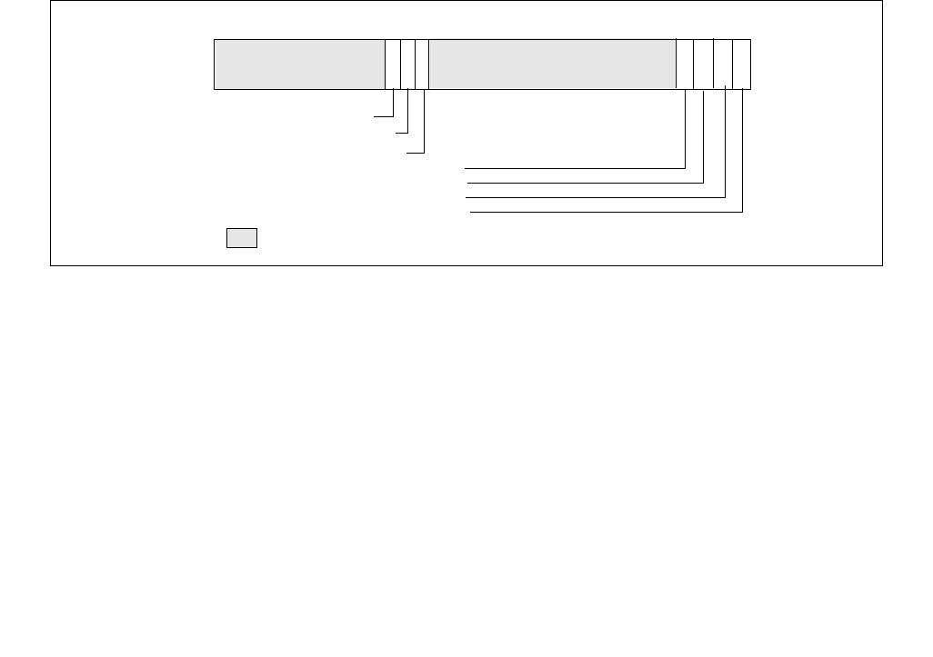
18-44 Vol. 3B
PERFORMANCE MONITORING
The bit fields of the uncore event select MSRs for a C-box unit or the ARB unit are summarized below:
•Event_Select (bits 7:0) and UMASK (bits 15:8): Specifies the microarchitectural condition to count in a local
uncore PMU counter, see Table 19-18.
•E (bit 18): Enables edge detection filtering, if 1.
•OVF_EN (bit 20): Enables the overflow indicator from the uncore counter forwarded to
MSR_UNC_PERF_GLOBAL_CTRL, if 1.
•EN (bit 22): Enables the local counter associated with this event select MSR.
•INV (bit 23): Event count increments with non-negative value if 0, with negated value if 1.
•CMASK (bits 28:24): Specifies a positive threshold value to filter raw event count input.
At the uncore domain level, there is a master set of control MSRs that centrally manages all the performance moni-
toring facility of uncore units. Figure 18-33 shows the layout of the uncore domain global control.
When an uncore counter overflows, a PMI can be routed to a processor core. Bits 3:0 of
MSR_UNC_PERF_GLOBAL_CTRL can be used to select which processor core to handle the uncore PMI. Software
must then write to bit 13 of IA32_DEBUGCTL (at address 1D9H) to enable this capability.
•PMI_SEL_Core#: Enables the forwarding of an uncore PMI request to a processor core, if 1. If bit 30 (WakePMI)
is ‘1’, a wake request is sent to the respective processor core prior to sending the PMI.
•EN: Enables the fixed uncore counter, the ARB counters, and the CBO counters in the uncore PMU, if 1. This bit
is cleared if bit 31 (FREEZE) is set and any enabled uncore counters overflow.
•WakePMI: Controls sending a wake request to any halted processor core before issuing the uncore PMI request.
If a processor core was halted and not sent a wake request, the uncore PMI will not be serviced by the
processor core.
•FREEZE: Provides the capability to freeze all uncore counters when an overflow condition occurs in a unit
counter. When this bit is set, and a counter overflow occurs, the uncore PMU logic will clear the global enable bit
(bit 29).
Figure 18-33. Layout of MSR_UNC_PERF_GLOBAL_CTRL MSR for Uncore
FREEZE—Freeze counters
EN—Enable all uncore counters
0
2829303132
Reserved
63
WakePMI—Wake cores on PMI
RESET Value — 00000000_00000000H
4321
PMI_Sel_Core3 — Uncore PMI to core 3
PMI_Sel_Core2 — Uncore PMI to core 2
PMI_Sel_Core1 — Uncore PMI to core 1
PMI_Sel_Core0 — Uncore PMI to core 0

Vol. 3B 18-45
PERFORMANCE MONITORING
Additionally, there is also a fixed counter, counting uncore clockticks, for the uncore domain. Table 18-19 summa-
rizes the number MSRs for uncore PMU for each box.
18.3.4.6.1 Uncore Performance Monitoring Events
There are certain restrictions on the uncore performance counters in each C-Box. Specifically,
•Occupancy events are supported only with counter 0 but not counter 1.
•Other uncore C-Box events can be programmed with either counter 0 or 1.
The C-Box uncore performance events described in Table 19-18 can collect performance characteristics of transac-
tions initiated by processor core. In that respect, they are similar to various sub-events in the
OFFCORE_RESPONSE family of performance events in the core PMU. Information such as data supplier locality
(LLC HIT/MISS) and snoop responses can be collected via OFFCORE_RESPONSE and qualified on a per-thread
basis.
On the other hand, uncore performance event logic can not associate its counts with the same level of per-thread
qualification attributes as the core PMU events can. Therefore, whenever similar event programming capabilities
are available from both core PMU and uncore PMU, the recommendation is that utilizing the core PMU events may
be less affected by artifacts, complex interactions and other factors.
18.3.4.7 Intel® Xeon® Processor E5 Family Performance Monitoring Facility
The Intel® Xeon® Processor E5 Family (and Intel® Core™ i7-3930K Processor) are based on Intel microarchitec-
ture code name Sandy Bridge-E. While the processor cores share the same microarchitecture as those of the Intel®
Xeon® Processor E3 Family and 2nd generation Intel Core i7-2xxx, Intel Core i5-2xxx, Intel Core i3-2xxx processor
series, the uncore subsystems are different. An overview of the uncore performance monitoring facilities of the
Intel Xeon processor E5 family (and Intel Core i7-3930K processor) is described in Section 18.3.4.8.
Thus, the performance monitoring facilities in the processor core generally are the same as those described in
Section 18.6.3 through Section 18.3.4.5. However, the MSR_OFFCORE_RSP_0/MSR_OFFCORE_RSP_1 Response
Supplier Info field shown in Table 18-17 applies to Intel Core Processors with CPUID signature of
DisplayFamily_DisplayModel encoding of 06_2AH; Intel Xeon processor with CPUID signature of
DisplayFamily_DisplayModel encoding of 06_2DH supports an additional field for remote DRAM controller shown in
Table 18-20. Additionally, the are some small differences in the non-architectural performance monitoring events
(see Table 19-16).
Table 18-19. Uncore PMU MSR Summary
Box # of Boxes
Counters per
Box
Counter
Width
General
Purpose
Global
Enable Comment
C-Box SKU specific 2 44 Yes Per-box Up to 4, seeTable 2-20
MSR_UNC_CBO_CONFIG
ARB 1 2 44 Yes Uncore
Fixed
Counter
N.A. N.A. 48 No Uncore
18-46 Vol. 3B
PERFORMANCE MONITORING
18.3.4.8 Intel® Xeon® Processor E5 Family Uncore Performance Monitoring Facility
The uncore subsystem in the Intel Xeon processor E5-2600 product family has some similarities with those of the
Intel Xeon processor E7 family. Within the uncore subsystem, localized performance counter sets are provided at
logic control unit scope. For example, each Cbox caching agent has a set of local performance counters, and the
power controller unit (PCU) has its own local performance counters. Up to 8 C-Box units are supported in the
uncore sub-system.
Table 18-21 summarizes the uncore PMU facilities providing MSR interfaces.
Details of the uncore performance monitoring facility of Intel Xeon Processor E5 family is available in “Intel®
Xeon® Processor E5 Uncore Performance Monitoring Programming Reference Manual”. The MSR-based uncore PMU
interfaces are listed in Table 2-23.
18.3.5 3rd Generation Intel® Core™ Processor Performance Monitoring Facility
The 3rd generation Intel® Core™ processor family and Intel® Xeon® processor E3-1200v2 product family are
based on the Ivy Bridge microarchitecture. The performance monitoring facilities in the processor core generally
are the same as those described in Section 18.6.3 through Section 18.3.4.5. The non-architectural performance
monitoring events supported by the processor core are listed in Table 19-16.
18.3.5.1 Intel® Xeon® Processor E5 v2 and E7 v2 Family Uncore Performance Monitoring Facility
The uncore subsystem in the Intel Xeon processor E5 v2 and Intel Xeon Processor E7 v2 product families are based
on the Ivy Bridge-E microarchitecture. There are some similarities with those of the Intel Xeon processor E5 family
based on the Sandy Bridge microarchitecture. Within the uncore subsystem, localized performance counter sets
are provided at logic control unit scope.
Details of the uncore performance monitoring facility of Intel Xeon Processor E5 v2 and Intel Xeon Processor E7 v2
families are available in “Intel® Xeon® Processor E5 v2 and E7 v2 Uncore Performance Monitoring Programming
Reference Manual”. The MSR-based uncore PMU interfaces are listed in Table 2-27.
Table 18-20. MSR_OFFCORE_RSP_x Supplier Info Field Definitions
Subtype Bit Name Offset Description
Common Any 16 (R/W). Catch all value for any response types.
Supplier Info NO_SUPP 17 (R/W). No Supplier Information available
LLC_HITM 18 (R/W). M-state initial lookup stat in L3.
LLC_HITE 19 (R/W). E-state
LLC_HITS 20 (R/W). S-state
LLC_HITF 21 (R/W). F-state
LOCAL 22 (R/W). Local DRAM Controller
Remote 30:23 (R/W): Remote DRAM Controller (either all 0s or all 1s)
Table 18-21. Uncore PMU MSR Summary for Intel® Xeon® Processor E5 Family
Box # of Boxes Counters per Box
Counter
Width
General
Purpose
Global
Enable Sub-control MSRs
C-Box 8 4 44 Yes per-box None
PCU 1 4 48 Yes per-box Match/Mask
U-Box 1 2 44 Yes uncore None

Vol. 3B 18-47
PERFORMANCE MONITORING
18.3.6 4th Generation Intel® Core™ Processor Performance Monitoring Facility
The 4th generation Intel® Core™ processor and Intel® Xeon® processor E3-1200 v3 product family are based on
the Haswell microarchitecture. The core PMU supports architectural performance monitoring capability with version
ID 3 (see Section 18.2.3) and a host of non-architectural monitoring capabilities.
Architectural performance monitoring version 3 capabilities are described in Section 18.2.3.
The core PMU’s capability is similar to those described in Section 18.6.3 through Section 18.3.4.5, with some
differences and enhancements summarized in Table 18-22. Additionally, the core PMU provides some enhance-
ment to support performance monitoring when the target workload contains instruction streams using Intel®
Transactional Synchronization Extensions (TSX), see Section 18.3.6.5. For details of Intel TSX, see Chapter 16,
“Programming with Intel® Transactional Synchronization Extensions” of Intel® 64 and IA-32 Architectures Soft-
ware Developer’s Manual, Volume 1.
Table 18-22. Core PMU Comparison
Box
Intel® microarchitecture code
name Haswell
Intel® microarchitecture code
name Sandy Bridge Comment
# of Fixed counters per thread 3 3 Use CPUID to enumerate
# of counters. See
Section 18.2.1.
# of general-purpose counters
per core
8 8 Use CPUID to enumerate
# of counters. See
Section 18.2.1.
Counter width (R,W) R:48, W: 32/48 R:48, W: 32/48 See Section 18.2.2.
# of programmable counters per
thread
4 or (8 if a core not shared by two
threads)
4 or (8 if a core not shared by
two threads)
Use CPUID to enumerate
# of counters. See
Section 18.2.1.
PMI Overhead Mitigation • Freeze_Perfmon_on_PMI with
legacy semantics.
•Freeze_on_LBR with legacy
semantics for branch profiling.
• Freeze_while_SMM.
•Freeze_Perfmon_on_PMI
with legacy semantics.
•Freeze_on_LBR with legacy
semantics for branch
profiling.
• Freeze_while_SMM.
See Section 17.4.7.
Processor Event Based Sampling
(PEBS) Events
See Table 18-12 and Section
18.3.6.5.1.
See Table 18-12. IA32_PMC4-IA32_PMC7
do not support PEBS.
PEBS-Load Latency See Section 18.3.4.4.2. See Section 18.3.4.4.2.
PEBS-Precise Store No, replaced by Data Address
profiling.
Section 18.3.4.4.3
PEBS-PDIR Yes (using precise
INST_RETIRED.ALL)
Yes (using precise
INST_RETIRED.ALL)
PEBS-EventingIP Yes No
Data Address Profiling Yes No
LBR Profiling Yes Yes
Call Stack Profiling Yes, see Section 17.11. No Use LBR facility.
Off-core Response Event MSR 1A6H and 1A7H; extended
request and response types.
MSR 1A6H and 1A7H; extended
request and response types.
Intel TSX support for Perfmon See Section 18.3.6.5. No

18-48 Vol. 3B
PERFORMANCE MONITORING
18.3.6.1 Processor Event Based Sampling (PEBS) Facility
The PEBS facility in the 4th Generation Intel Core processor is similar to those in processors based on Intel micro-
architecture code name Sandy Bridge, with several enhanced features. The key components and differences of
PEBS facility relative to Intel microarchitecture code name Sandy Bridge is summarized in Table 18-23.
Only IA32_PMC0 through IA32_PMC3 support PEBS.
NOTE
PEBS events are only valid when the following fields of IA32_PERFEVTSELx are all zero: AnyThread,
Edge, Invert, CMask.
In a PMU with PDIR capability, PEBS behavior is unpredictable if IA32_PERFEVTSELx or IA32_PMCx
is changed for a PEBS-enabled counter while an event is being counted. To avoid this, changes to
the programming or value of a PEBS-enabled counter should be performed when the counter is
disabled.
18.3.6.2 PEBS Data Format
The PEBS record format for the 4th Generation Intel Core processor is shown in Table 18-24. The PEBS record
format, along with debug/store area storage format, does not change regardless of whether IA-32e mode is active
or not. CPUID.01H:ECX.DTES64[bit 2] reports whether the processor's DS storage format support is mode-inde-
pendent. When set, it uses 64-bit DS storage format.
Table 18-23. PEBS Facility Comparison
Box
Intel® microarchitecture code
name Haswell
Intel® microarchitecture code
name Sandy Bridge Comment
Valid IA32_PMCx PMC0-PMC3 PMC0-PMC3 No PEBS on PMC4-PMC7
PEBS Buffer Programming Section 18.3.1.1.1 Section 18.3.1.1.1 Unchanged
IA32_PEBS_ENABLE Layout Figure 18-15 Figure 18-29
PEBS record layout Table 18-24; enhanced fields at
offsets 98H, A0H, A8H, B0H.
Table 18-3; enhanced fields at
offsets 98H, A0H, A8H.
Precise Events See Table 18-12. See Table 18-12. IA32_PMC4-IA32_PMC7 do not
support PEBS.
PEBS-Load Latency See Table 18-13. Table 18-13
PEBS-Precise Store No, replaced by data address
profiling.
Yes; see Section 18.3.4.4.3.
PEBS-PDIR Yes Yes IA32_PMC1 only.
PEBS skid from EventingIP 1 (or 2 if micro+macro fusion) 1
SAMPLING Restriction Small SAV(CountDown) value incur higher overhead than prior
generation.

Vol. 3B 18-49
PERFORMANCE MONITORING
The layout of PEBS records are almost identical to those shown in Table 18-3. Offset B0H is a new field that records
the eventing IP address of the retired instruction that triggered the PEBS assist.
The PEBS records at offsets 98H, A0H, and ABH record data gathered from three of the PEBS capabilities in prior
processor generations: load latency facility (Section 18.3.4.4.2), PDIR (Section 18.3.4.4.4), and the equivalent
capability of precise store in prior generation (see Section 18.3.6.3).
In the core PMU of the 4th generation Intel Core processor, load latency facility and PDIR capabilities are
unchanged. However, precise store is replaced by an enhanced capability, data address profiling, that is not
restricted to store address. Data address profiling also records information in PEBS records at offsets 98H, A0H,
and ABH.
18.3.6.3 PEBS Data Address Profiling
The Data Linear Address facility is also abbreviated as DataLA. The facility is a replacement or extension of the
precise store facility in previous processor generations. The DataLA facility complements the load latency facility by
providing a means to profile load and store memory references in the system, leverages the PEBS facility, and
provides additional information about sampled loads and stores. Having precise memory reference events with
linear address information for both loads and stores provides information to improve data structure layout, elimi-
nate remote node references, and identify cache-line conflicts in NUMA systems.
The DataLA facility in the 4th generation processor supports the following events configured to use PEBS:
Table 18-24. PEBS Record Format for 4th Generation Intel Core Processor Family
Byte Offset Field Byte Offset Field
00H R/EFLAGS 60H R10
08H R/EIP 68H R11
10H R/EAX 70H R12
18H R/EBX 78H R13
20H R/ECX 80H R14
28H R/EDX 88H R15
30H R/ESI 90H IA32_PERF_GLOBAL_STATUS
38H R/EDI 98H Data Linear Address
40H R/EBP A0H Data Source Encoding
48H R/ESP A8H Latency value (core cycles)
50H R8 B0H EventingIP
58H R9 B8H TX Abort Information (Section
18.3.6.5.1)
Table 18-25. Precise Events That Supports Data Linear Address Profiling
Event Name Event Name
MEM_UOPS_RETIRED.STLB_MISS_LOADS MEM_UOPS_RETIRED.STLB_MISS_STORES
MEM_UOPS_RETIRED.LOCK_LOADS MEM_UOPS_RETIRED.SPLIT_STORES
MEM_UOPS_RETIRED.SPLIT_LOADS MEM_UOPS_RETIRED.ALL_STORES
MEM_UOPS_RETIRED.ALL_LOADS MEM_LOAD_UOPS_LLC_MISS_RETIRED.LOCAL_DRAM
MEM_LOAD_UOPS_RETIRED.L1_HIT MEM_LOAD_UOPS_RETIRED.L2_HIT
MEM_LOAD_UOPS_RETIRED.L3_HIT MEM_LOAD_UOPS_RETIRED.L1_MISS
MEM_LOAD_UOPS_RETIRED.L2_MISS MEM_LOAD_UOPS_RETIRED.L3_MISS
MEM_LOAD_UOPS_RETIRED.HIT_LFB MEM_LOAD_UOPS_L3_HIT_RETIRED.XSNP_MISS

18-50 Vol. 3B
PERFORMANCE MONITORING
DataLA can use any one of the IA32_PMC0-IA32_PMC3 counters. Counter overflows will initiate the generation of
PEBS records. Upon counter overflow, hardware captures the linear address and possible other status information
of the retiring memory uop. This information is then written to the PEBS record that is subsequently generated.
To enable the DataLA facility, software must complete the following steps. Please note that the DataLA facility relies
on the PEBS facility, so the PEBS configuration requirements must be completed before attempting to capture
DataLA information.
•Complete the PEBS configuration steps.
•Program the an event listed in Table 18-25 using any one of IA32_PERFEVTSEL0-IA32_PERFEVTSEL3.
•Set the corresponding IA32_PEBS_ENABLE.PEBS_EN_CTRx bit. This enables the corresponding IA32_PMCx as
a PEBS counter and enables the DataLA facility.
When the DataLA facility is enabled, the relevant information written into a PEBS record affects entries at offsets
98H, A0H and A8H, as shown in Table 18-26.
18.3.6.3.1 EventingIP Record
The PEBS record layout for processors based on Intel microarchitecture code name Haswell adds a new field at
offset 0B0H. This is the eventingIP field that records the IP address of the retired instruction that triggered the
PEBS assist. The EIP/RIP field at offset 08H records the IP address of the next instruction to be executed following
the PEBS assist.
18.3.6.4 Off-core Response Performance Monitoring
The core PMU facility to collect off-core response events are similar to those described in Section 18.3.4.5. The
event codes are listed in Table 18-15. Each event code for off-core response monitoring requires programming an
associated configuration MSR, MSR_OFFCORE_RSP_x. Software must program MSR_OFFCORE_RSP_x according
to:
•Transaction request type encoding (bits 15:0): see Table 18-27.
•Supplier information (bits 30:16): see Table 18-28.
•Snoop response information (bits 37:31): see Table 18-18.
MEM_LOAD_UOPS_L3_HIT_RETIRED.XSNP_HIT MEM_LOAD_UOPS_L3_HIT_RETIRED.XSNP_HITM
UOPS_RETIRED.ALL (if load or store is tagged) MEM_LOAD_UOPS_LLC_HIT_RETIRED.XSNP_NONE
Table 18-26. Layout of Data Linear Address Information In PEBS Record
Field Offset Description
Data Linear
Address
98H The linear address of the load or the destination of the store.
Store Status A0H • DCU Hit (Bit 0): The store hit the data cache closest to the core (L1 cache) if this bit is set, otherwise
the store missed the data cache. This information is valid only for the following store events:
UOPS_RETIRED.ALL (if store is tagged),
MEM_UOPS_RETIRED.STLB_MISS_STORES,
MEM_UOPS_RETIRED.SPLIT_STORES, MEM_UOPS_RETIRED.ALL_STORES
• Other bits are zero, The STLB_MISS, LOCK bit information can be obtained by programming the
corresponding store event in Table 18-25.
Reserved A8H Always zero.
Table 18-25. Precise Events That Supports Data Linear Address Profiling (Contd.)
Event Name Event Name

Vol. 3B 18-51
PERFORMANCE MONITORING
The supplier information field listed in Table 18-28. The fields vary across products (according to CPUID signa-
tures) and is noted in the description.
Table 18-27. MSR_OFFCORE_RSP_x Request_Type Definition (Haswell microarchitecture)
Bit Name Offset Description
DMND_DATA_RD 0 (R/W). Counts the number of demand data reads of full and partial cachelines as well as demand data
page table entry cacheline reads. Does not count L2 data read prefetches or instruction fetches.
DMND_RFO 1 (R/W). Counts the number of demand and DCU prefetch reads for ownership (RFO) requests generated
by a write to data cacheline. Does not count L2 RFO prefetches.
DMND_IFETCH 2 (R/W). Counts the number of demand instruction cacheline reads and L1 instruction cacheline
prefetches.
COREWB 3 (R/W). Counts the number of modified cachelines written back.
PF_DATA_RD 4 (R/W). Counts the number of data cacheline reads generated by L2 prefetchers.
PF_RFO 5 (R/W). Counts the number of RFO requests generated by L2 prefetchers.
PF_IFETCH 6 (R/W). Counts the number of code reads generated by L2 prefetchers.
PF_L3_DATA_RD 7 (R/W). Counts the number of data cacheline reads generated by L3 prefetchers.
PF_L3_RFO 8 (R/W). Counts the number of RFO requests generated by L3 prefetchers.
PF_L3_CODE_RD 9 (R/W). Counts the number of code reads generated by L3 prefetchers.
SPLIT_LOCK_UC_
LOCK
10 (R/W). Counts the number of lock requests that split across two cachelines or are to UC memory.
STRM_ST 11 (R/W). Counts the number of streaming store requests electronically.
Reserved 12-14 Reserved
OTHER 15 (R/W). Any other request that crosses IDI, including I/O.
Table 18-28. MSR_OFFCORE_RSP_x Supplier Info Field Definition (CPUID Signature 06_3CH, 06_46H)
Subtype Bit Name Offset Description
Common Any 16 (R/W). Catch all value for any response types.
Supplier
Info
NO_SUPP 17 (R/W). No Supplier Information available
L3_HITM 18 (R/W). M-state initial lookup stat in L3.
L3_HITE 19 (R/W). E-state
L3_HITS 20 (R/W). S-state
Reserved 21 Reserved
LOCAL 22 (R/W). Local DRAM Controller
Reserved 30:23 Reserved

18-52 Vol. 3B
PERFORMANCE MONITORING
18.3.6.4.1 Off-core Response Performance Monitoring in Intel Xeon Processors E5 v3 Series
Table 18-28 lists the supplier information field that apply to Intel Xeon processor E5 v3 series (CPUID signature
06_3FH).
18.3.6.5 Performance Monitoring and Intel® TSX
Chapter 16 of Intel® 64 and IA-32 Architectures Software Developer’s Manual, Volume 1 describes the details of
Intel® Transactional Synchronization Extensions (Intel® TSX). This section describes performance monitoring
support for Intel TSX.
If a processor supports Intel TSX, the core PMU enhances it’s IA32_PERFEVTSELx MSR with two additional bit fields
for event filtering. Support for Intel TSX is indicated by either (a) CPUID.(EAX=7, ECX=0):RTM[bit 11]=1, or (b) if
CPUID.07H.EBX.HLE [bit 4] = 1. The TSX-enhanced layout of IA32_PERFEVTSELx is shown in Figure 18-34. The
two additional bit fields are:
Table 18-29. MSR_OFFCORE_RSP_x Supplier Info Field Definition (CPUID Signature 06_45H)
Subtype Bit Name Offset Description
Common Any 16 (R/W). Catch all value for any response types.
Supplier
Info
NO_SUPP 17 (R/W). No Supplier Information available
L3_HITM 18 (R/W). M-state initial lookup stat in L3.
L3_HITE 19 (R/W). E-state
L3_HITS 20 (R/W). S-state
Reserved 21 Reserved
L4_HIT_LOCAL_L4 22 (R/W). L4 Cache
L4_HIT_REMOTE_HOP0_L4 23 (R/W). L4 Cache
L4_HIT_REMOTE_HOP1_L4 24 (R/W). L4 Cache
L4_HIT_REMOTE_HOP2P_L4 25 (R/W). L4 Cache
Reserved 30:26 Reserved
Table 18-30. MSR_OFFCORE_RSP_x Supplier Info Field Definition
Subtype Bit Name Offset Description
Common Any 16 (R/W). Catch all value for any response types.
Supplier
Info
NO_SUPP 17 (R/W). No Supplier Information available
L3_HITM 18 (R/W). M-state initial lookup stat in L3.
L3_HITE 19 (R/W). E-state
L3_HITS 20 (R/W). S-state
L3_HITF 21 (R/W). F-state
LOCAL 22 (R/W). Local DRAM Controller
Reserved 26:23 Reserved
L3_MISS_REMOTE_HOP0 27 (R/W). Hop 0 Remote supplier
L3_MISS_REMOTE_HOP1 28 (R/W). Hop 1 Remote supplier
L3_MISS_REMOTE_HOP2P 29 (R/W). Hop 2 or more Remote supplier
Reserved 30 Reserved
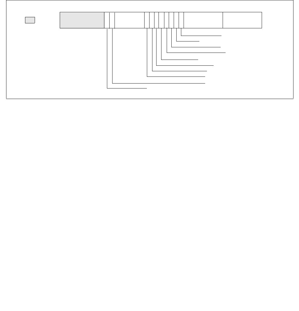
Vol. 3B 18-53
PERFORMANCE MONITORING
•IN_TX (bit 32): When set, the counter will only include counts that occurred inside a transactional region,
regardless of whether that region was aborted or committed. This bit may only be set if the processor supports
HLE or RTM.
•IN_TXCP (bit 33): When set, the counter will not include counts that occurred inside of an aborted transac-
tional region. This bit may only be set if the processor supports HLE or RTM. This bit may only be set for
IA32_PERFEVTSEL2.
When the IA32_PERFEVTSELx MSR is programmed with both IN_TX=0 and IN_TXCP=0 on a processor that
supports Intel TSX, the result in a counter may include detectable conditions associated with a transaction code
region for its aborted execution (if any) and completed execution.
In the initial implementation, software may need to take pre-caution when using the IN_TXCP bit. see Table 2-28.
A common usage of setting IN_TXCP=1 is to capture the number of events that were discarded due to a transac-
tional abort. With IA32_PMC2 configured to count in such a manner, then when a transactional region aborts, the
value for that counter is restored to the value it had prior to the aborted transactional region. As a result, any
updates performed to the counter during the aborted transactional region are discarded.
On the other hand, setting IN_TX=1 can be used to drill down on the performance characteristics of transactional
code regions. When a PMCx is configured with the corresponding IA32_PERFEVTSELx.IN_TX=1, only eventing
conditions that occur inside transactional code regions are propagated to the event logic and reflected in the
counter result. Eventing conditions specified by IA32_PERFEVTSELx but occurring outside a transactional region
are discarded. The following example illustrates using three counters to drill down cycles spent inside and outside
of transactional regions:
•Program IA32_PERFEVTSEL2 to count Unhalted_Core_Cycles with (IN_TXCP=1, IN_TX=0), such that
IA32_PMC2 will count cycles spent due to aborted TSX transactions;
•Program IA32_PERFEVTSEL0 to count Unhalted_Core_Cycles with (IN_TXCP=0, IN_TX=1), such that
IA32_PMC0 will count cycles spent by the transactional code regions;
•Program IA32_PERFEVTSEL1 to count Unhalted_Core_Cycles with (IN_TXCP=0, IN_TX=0), such that
IA32_PMC1 will count total cycles spent by the non-transactional code and transactional code regions.
Additionally, a number of performance events are solely focused on characterizing the execution of Intel TSX trans-
actional code, they are listed in Table 19-10.
18.3.6.5.1 Intel TSX and PEBS Support
If a PEBS event would have occurred inside a transactional region, then the transactional region first aborts, and
then the PEBS event is processed.
Figure 18-34. Layout of IA32_PERFEVTSELx MSRs Supporting Intel TSX
31
INV—Invert counter mask
EN—Enable counters
INT—APIC interrupt enable
PC—Pin control
870
Event Select
E—Edge detect
OS—Operating system mode
USR—User Mode
Counter Mask E
E
N
I
N
T
19 1618 15172021222324
Reserved I
N
V
P
C
U
S
R
O
SUnit Mask (UMASK)
(CMASK)
63
ANY—Any Thread
A
N
Y
34
IN_TX—In Trans. Rgn
IN_TXCP—In Tx exclude abort (PERFEVTSEL2 Only)

18-54 Vol. 3B
PERFORMANCE MONITORING
Two of the TSX performance monitoring events in Table 19-10 also support using PEBS facility to capture additional
information. They are:
•HLE_RETIRED.ABORT ED (encoding C8H mask 04H),
•RTM_RETIRED.ABORTED (encoding C9H mask 04H).
A transactional abort (HLE_RETIRED.ABORTED,RTM_RETIRED.ABORTED) can also be programmed to cause PEBS
events. In this scenario, a PEBS event is processed following the abort.
Pending a PEBS record inside of a transactional region will cause a transactional abort. If a PEBS record was pended
at the time of the abort or on an overflow of the TSX PEBS events listed above, only the following PEBS entries will
be valid (enumerated by PEBS entry offset B8H bits[33:32] to indicate an HLE abort or an RTM abort):
•Offset B0H: EventingIP,
•Offset B8H: TX Abort Information
These fields are set for all PEBS events.
•Offset 08H (RIP/EIP) corresponds to the instruction following the outermost XACQUIRE in HLE or the first
instruction of the fallback handler of the outermost XBEGIN instruction in RTM. This is useful to identify the
aborted transactional region.
In the case of HLE, an aborted transaction will restart execution deterministically at the start of the HLE region. In
the case of RTM, an aborted transaction will transfer execution to the RTM fallback handler.
The layout of the TX Abort Information field is given in Table 18-31.
18.3.6.6 Uncore Performance Monitoring Facilities in the 4th Generation Intel® Core™ Processors
The uncore sub-system in the 4th Generation Intel® Core™ processors provides its own performance monitoring
facility. The uncore PMU facility provides dedicated MSRs to select uncore performance monitoring events in a
similar manner as those described in Section 18.3.4.6.
The ARB unit and each C-Box provide local pairs of event select MSR and counter register. The layout of the event
select MSRs in the C-Boxes are identical as shown in Figure 18-32.
At the uncore domain level, there is a master set of control MSRs that centrally manages all the performance moni-
toring facility of uncore units. Figure 18-33 shows the layout of the uncore domain global control.
Additionally, there is also a fixed counter, counting uncore clockticks, for the uncore domain. Table 18-19 summa-
rizes the number MSRs for uncore PMU for each box.
Table 18-31. TX Abort Information Field Definition
Bit Name Offset Description
Cycles_Last_TX 31:0 The number of cycles in the last TSX region, regardless of whether that region had aborted or
committed.
HLE_Abort 32 If set, the abort information corresponds to an aborted HLE execution
RTM_Abort 33 If set, the abort information corresponds to an aborted RTM execution
Instruction_Abort 34 If set, the abort was associated with the instruction corresponding to the eventing IP (offset
0B0H) within the transactional region.
Non_Instruction_Abort 35 If set, the instruction corresponding to the eventing IP may not necessarily be related to the
transactional abort.
Retry 36 If set, retrying the transactional execution may have succeeded.
Data_Conflict 37 If set, another logical processor conflicted with a memory address that was part of the
transactional region that aborted.
Capacity Writes 38 If set, the transactional region aborted due to exceeding resources for transactional writes.
Capacity Reads 39 If set, the transactional region aborted due to exceeding resources for transactional reads.
Reserved 63:40 Reserved
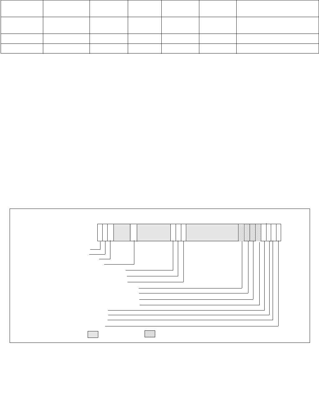
Vol. 3B 18-55
PERFORMANCE MONITORING
The uncore performance events for the C-Box and ARB units are listed in Table 19-11.
18.3.6.7 Intel® Xeon® Processor E5 v3 Family Uncore Performance Monitoring Facility
Details of the uncore performance monitoring facility of Intel Xeon Processor E5 v3 families are available in “Intel®
Xeon® Processor E5 v3 Uncore Performance Monitoring Programming Reference Manual”. The MSR-based uncore
PMU interfaces are listed in Table 2-32.
18.3.7 5th Generation Intel® Core™ Processor and Intel® Core™ M Processor Performance
Monitoring Facility
The 5th Generation Intel® Core™ processor and the Intel® Core™ M processor families are based on the Broadwell
microarchitecture. The core PMU supports architectural performance monitoring capability with version ID 3 (see
Section 18.2.3) and a host of non-architectural monitoring capabilities.
Architectural performance monitoring version 3 capabilities are described in Section 18.2.3.
The core PMU has the same capability as those described in Section 18.3.6. IA32_PERF_GLOBAL_STATUS provide
a bit indicator (bit 55) for PMI handler to distinguish PMI due to output buffer overflow condition due to accumu-
lating packet data from Intel Processor Trace.
Details of Intel Processor Trace is described in Chapter 35, “Intel® Processor Trace”.
IA32_PERF_GLOBAL_OVF_CTRL MSR provide a corresponding reset control bit.
Table 18-32. Uncore PMU MSR Summary
Box # of Boxes
Counters per
Box
Counter
Width
General
Purpose
Global
Enable Comment
C-Box SKU specific 2 44 Yes Per-box Up to 4, seeTable 2-20
MSR_UNC_CBO_CONFIG
ARB 1 2 44 Yes Uncore
Fixed Counter N.A. N.A. 48 No Uncore
Figure 18-35. IA32_PERF_GLOBAL_STATUS MSR in Broadwell Microarchitecture
62
FIXED_CTR2 Overflow (RO)
FIXED_CTR1 Overflow (RO)
FIXED_CTR0 Overflow (RO)
PMC7_OVF (RO, If PMC7 present)
21
0
PMC6_OVF (RO, If PMC6 present)
3132333435
Reserved
63
CondChgd
Ovf_Buffer
87 65 43
PMC5_OVF (RO, If PMC5 present)
PMC4_OVF (RO, If PMC4 present)
PMC3_OVF (RO)
PMC2_OVF (RO)
PMC1_OVF (RO)
PMC0_OVF (RO)
Valid if CPUID.0AH:EAX[15:8] = 8; else reserved
Ovf_UncorePMU
61
Trace_ToPA_PMI
55
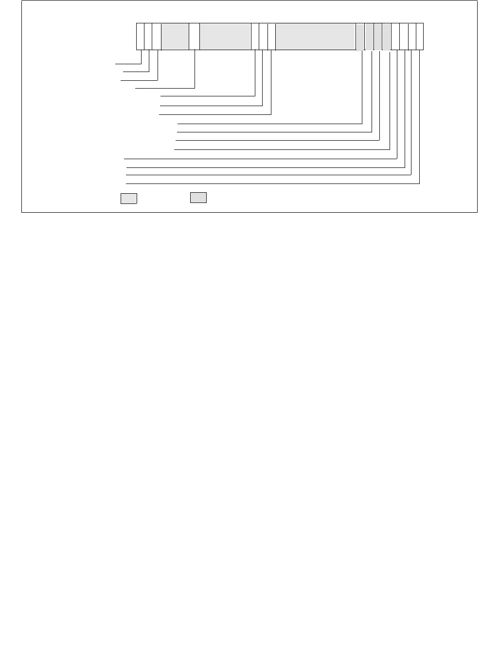
18-56 Vol. 3B
PERFORMANCE MONITORING
The specifics of non-architectural performance events are listed in Chapter 19, “Performance Monitoring Events”.
18.3.8 6th Generation, 7th Generation and 8th Generation Intel® Core™ Processor
Performance Monitoring Facility
The 6th generation Intel® Core™ processor is based on the Skylake microarchitecture. The 7th generation Intel®
Core™ processor is based on the Kaby Lake microarchitecture. The 8th generation Intel® Core™ processor is based
on the Coffee Lake microarchitecture. For these microarchitectures, the core PMU supports architectural perfor-
mance monitoring capability with version ID 4 (see Section 18.2.4) and a host of non-architectural monitoring
capabilities.
Architectural performance monitoring version 4 capabilities are described in Section 18.2.4.
The core PMU’s capability is similar to those described in Section 18.6.3 through Section 18.3.4.5, with some differ-
ences and enhancements summarized in Table 18-22. Additionally, the core PMU provides some enhancement to
support performance monitoring when the target workload contains instruction streams using Intel® Transactional
Synchronization Extensions (TSX), see Section 18.3.6.5. For details of Intel TSX, see Chapter 16, “Programming with
Intel® Transactional Synchronization Extensions” of Intel® 64 and IA-32 Architectures Software Developer’s
Manual, Volume 1.
Performance monitoring result may be affected by side-band activity on processors that support Intel SGX, details
are described in Chapter 42, “Enclave Code Debug and Profiling”.
Figure 18-36. IA32_PERF_GLOBAL_OVF_CTRL MSR in Broadwell microarchitecture
62
FIXED_CTR2 ClrOverflow
FIXED_CTR1 ClrOverflow
FIXED_CTR0 ClrOverflow
PMC7_ClrOvf (if PMC7 present)
210
PMC6_ClrOvf (if PMC6 present)
3132333435
Reserved
63
ClrCondChgd
ClrOvfDSBuffer
87 65 43
PMC5_ClrOvf (if PMC5 present)
PMC4_ClrOvf (if PMC4 present)
PMC3_ClrOvf
PMC2_ClrOvf
PMC1_ClrOvf
PMC0_ClrOvf
Valid if CPUID.0AH:EAX[15:8] = 8; else reserved
ClrOvfUncore
ClrTraceToPA_PMI
61 55

Vol. 3B 18-57
PERFORMANCE MONITORING
Table 18-33. Core PMU Comparison
Box Intel® Microarchitecture Code Name
Skylake, Kaby Lake and Coffee Lake
Intel® Microarchitecture Code
Name Haswell and Broadwell
Comment
# of Fixed counters per thread 3 3 Use CPUID to
enumerate # of
counters. See
Section 18.2.1.
# of general-purpose counters
per core
8 8 Use CPUID to
enumerate # of
counters. See
Section 18.2.1.
Counter width (R,W) R:48, W: 32/48 R:48, W: 32/48 See Section 18.2.2.
# of programmable counters
per thread
4 or (8 if a core not shared by two
threads)
4 or (8 if a core not shared by two
threads)
Use CPUID to
enumerate # of
counters. See
Section 18.2.1.
Architectural Perfmon version 4 3 See Section 18.2.4
PMI Overhead Mitigation • Freeze_Perfmon_on_PMI with
streamlined semantics.
• Freeze_on_LBR with streamlined
semantics.
• Freeze_while_SMM.
• Freeze_Perfmon_on_PMI with
legacy semantics.
•Freeze_on_LBR with legacy
semantics for branch profiling.
• Freeze_while_SMM.
See Section 17.4.7.
Legacy semantics
not supported with
version 4 or higher.
Counter and Buffer Overflow
Status Management
•Query via
IA32_PERF_GLOBAL_STATUS
•Reset via
IA32_PERF_GLOBAL_STATUS_RESET
•Set via
IA32_PERF_GLOBAL_STATUS_SET
• Query via
IA32_PERF_GLOBAL_STATUS
•Reset via
IA32_PERF_GLOBAL_OVF_CTRL
See Section 18.2.4.
IA32_PERF_GLOBAL_STATUS
Indicators of
Overflow/Overhead/Interferen
ce
• Individual counter overflow
• PEBS buffer overflow
•ToPA buffer overflow
• CTR_Frz, LBR_Frz, ASCI
• Individual counter overflow
•PEBS buffer overflow
• ToPA buffer overflow
(applicable to Broadwell
microarchitecture)
See Section 18.2.4.
Enable control in
IA32_PERF_GLOBAL_STATUS
•CTR_Frz
•LBR_Frz
NA See Section
18.2.4.1.
Perfmon Counter In-Use
Indicator
Query IA32_PERF_GLOBAL_INUSE NA See Section
18.2.4.3.
Precise Events See Table 18-36. See Table 18-12. IA32_PMC4-PMC7
do not support
PEBS.
PEBS for front end events See Section 18.3.8.1.4. No
LBR Record Format Encoding 000101b 000100b Section 17.4.8.1
LBR Size 32 entries 16 entries
LBR Entry From_IP/To_IP/LBR_Info triplet From_IP/To_IP pair Section 17.12
LBR Timing Yes No Section 17.12.1
Call Stack Profiling Yes, see Section 17.11 Yes, see Section 17.11 Use LBR facility
Off-core Response Event MSR 1A6H and 1A7H; Extended request
and response types.
MSR 1A6H and 1A7H; Extended
request and response types.
Intel TSX support for Perfmon See Section 18.3.6.5. See Section 18.3.6.5.

18-58 Vol. 3B
PERFORMANCE MONITORING
18.3.8.1 Processor Event Based Sampling (PEBS) Facility
The PEBS facility in the 6th generation, 7th generation and 8th generation Intel Core processors provides a number
enhancement relative to PEBS in processors based on Haswell/Broadwell microarchitectures. The key components
and differences of PEBS facility relative to Haswell/Broadwell microarchitecture is summarized in Table 18-34.
Only IA32_PMC0 through IA32_PMC3 support PEBS.
NOTES
Precise events are only valid when the following fields of IA32_PERFEVTSELx are all zero:
AnyThread, Edge, Invert, CMask.
In a PMU with PDIR capability, PEBS behavior is unpredictable if IA32_PERFEVTSELx or IA32_PMCx
is changed for a PEBS-enabled counter while an event is being counted. To avoid this, changes to
the programming or value of a PEBS-enabled counter should be performed when the counter is
disabled.
18.3.8.1.1 PEBS Data Format
The PEBS record format for the 6th generation, 7th generation and 8th generation Intel Core processors is
reporting with encoding 0011b in IA32_PERF_CAPABILITIES[11:8]. The lay out is shown in Table 18-35. The PEBS
record format, along with debug/store area storage format, does not change regardless of whether IA-32e mode is
active or not. CPUID.01H:ECX.DTES64[bit 2] reports whether the processor's DS storage format support is mode-
independent. When set, it uses 64-bit DS storage format.
Table 18-34. PEBS Facility Comparison
Box Intel® Microarchitecture Code
Name Skylake, Kaby Lake
and Coffee Lake
Intel® Microarchitecture Code
Name Haswell and Broadwell
Comment
Valid IA32_PMCx PMC0-PMC3 PMC0-PMC3 No PEBS on PMC4-PMC7.
PEBS Buffer Programming Section 18.3.1.1.1 Section 18.3.1.1.1 Unchanged
IA32_PEBS_ENABLE Layout Figure 18-15 Figure 18-15
PEBS-EventingIP Yes Yes
PEBS record format encoding 0011b 0010b
PEBS record layout Table 18-35; enhanced fields
at offsets 98H- B8H; and TSC
record field at C0H.
Table 18-24; enhanced fields at
offsets 98H, A0H, A8H, B0H.
Multi-counter PEBS
resolution
PEBS record 90H resolves the
eventing counter overflow.
PEBS record 90H reflects
IA32_PERF_GLOBAL_STATUS.
Precise Events See Table 18-36. See Table 18-12. IA32_PMC4-IA32_PMC7 do not
support PEBS.
PEBS-PDIR Yes Yes IA32_PMC1 only.
PEBS-Load Latency See Section 18.3.4.4.2. See Section 18.3.4.4.2.
Data Address Profiling Yes Yes
FrontEnd event support FrontEnd_Retried event and
MSR_PEBS_FRONTEND.
No IA32_PMC0-PMC3 only.

Vol. 3B 18-59
PERFORMANCE MONITORING
The layout of PEBS records are largely identical to those shown in Table 18-24.
The PEBS records at offsets 98H, A0H, and ABH record data gathered from three of the PEBS capabilities in prior
processor generations: load latency facility (Section 18.3.4.4.2), PDIR (Section 18.3.4.4.4), and data address
profiling (Section 18.3.6.3).
In the core PMU of the 6th generation, 7th generation and 8th generation Intel Core processors, load latency
facility and PDIR capabilities and data address profiling are unchanged relative to the 4th generation and 5th
generation Intel Core processors. Similarly, precise store is replaced by data address profiling.
With format 0010b, a snapshot of the IA32_PERF_GLOBAL_STATUS may be useful to resolve the situations when
more than one of IA32_PMICx have been configured to collect PEBS data and two consecutive overflows of the
PEBS-enabled counters are sufficiently far apart in time. It is also possible for the image at 90H to indicate multiple
PEBS-enabled counters have overflowed. In the latter scenario, software cannot to correlate the PEBS record entry
to the multiple overflowed bits.
With PEBS record format encoding 0011b, offset 90H reports the “applicable counter” field, which is a multi-
counter PEBS resolution index allowing software to correlate the PEBS record entry with the eventing PEBS over-
flow when multiple counters are configured to record PEBS records. Additionally, offset C0H captures a snapshot of
the TSC that provides a time line annotation for each PEBS record entry.
18.3.8.1.2 PEBS Events
The list of precise events supported for PEBS in the Skylake, Kaby Lake and Coffee Lake microarchitectures is
shown in Table 18-36.
Table 18-35. PEBS Record Format for 6th Generation, 7th Generation
and 8th Generation Intel Core Processor Families
Byte Offset Field Byte Offset Field
00H R/EFLAGS 68H R11
08H R/EIP 70H R12
10H R/EAX 78H R13
18H R/EBX 80H R14
20H R/ECX 88H R15
28H R/EDX 90H Applicable Counter
30H R/ESI 98H Data Linear Address
38H R/EDI A0H Data Source Encoding
40H R/EBP A8H Latency value (core cycles)
48H R/ESP B0H EventingIP
50H R8 B8H TX Abort Information (Section 18.3.6.5.1)
58H R9 C0H TSC
60H R10

18-60 Vol. 3B
PERFORMANCE MONITORING
18.3.8.1.3 Data Address Profiling
The PEBS Data address profiling on the 6th generation, 7th generation and 8th generation Intel Core processors is
largely unchanged from the prior generation. When the DataLA facility is enabled, the relevant information written
into a PEBS record affects entries at offsets 98H, A0H and A8H, as shown in Table 18-26.
Table 18-36. Precise Events for the Skylake, Kaby Lake and Coffee Lake Microarchitectures
Event Name Event Select Sub-event UMask
INST_RETIRED C0H PREC_DIST101H
ALL_CYCLES201H
OTHER_ASSISTS C1H ANY 3FH
BR_INST_RETIRED C4H CONDITIONAL 01H
NEAR_CALL 02H
ALL_BRANCHES 04H
NEAR_RETURN 08H
NEAR_TAKEN 20H
FAR_BRACHES 40H
BR_MISP_RETIRED C5H CONDITIONAL 01H
ALL_BRANCHES 04H
NEAR_TAKEN 20H
FRONTEND_RETIRED C6H <Programmable3>01H
HLE_RETIRED C8H ABORTED 04H
RTM_RETIRED C9H ABORTED 04H
MEM_INST_RETIRED2D0H LOCK_LOADS 21H
SPLIT_LOADS 41H
SPLIT_STORES 42H
ALL_LOADS 81H
ALL_STORES 82H
MEM_LOAD_RETIRED4D1H L1_HIT 01H
L2_HIT 02H
L3_HIT 04H
L1_MISS 08H
L2_MISS 10H
L3_MISS 20H
HIT_LFB 40H
MEM_LOAD_L3_HIT_RETIRED2D2H XSNP_MISS 01H
XSNP_HIT 02H
XSNP_HITM 04H
XSNP_NONE 08H
NOTES:
1. Only available on IA32_PMC1.
2. INST_RETIRED.ALL_CYCLES is configured with additional parameters of cmask = 10 and INV = 1
3. Subevents are specified using MSR_PEBS_FRONTEND, see Section 18.3.8.2
4. Instruction with at least one load uop experiencing the condition specified in the UMask.

Vol. 3B 18-61
PERFORMANCE MONITORING
18.3.8.1.4 PEBS Facility for Front End Events
In the 6th generation, 7th generation and 8th generation Intel Core processors, the PEBS facility has been
extended to allow capturing PEBS data for some microarchitectural conditions related to front end events. The
frontend microarchitectural conditions supported by PEBS requires the following interfaces:
•The IA32_PERFEVTSELx MSR must select “FrontEnd_Retired” (C6H) in the EventSelect field (bits 7:0) and
umask = 01H,
•The “FRONTEND_RETIRED” event employs a new MSR, MSR_PEBS_FRONTEND, to specify the supported
frontend event details, see Table 18-38.
•Program the PEBS_EN_PMCx field of IA32_PEBS_ENABLE MSR as required.
Note the AnyThread field of IA32_PERFEVTSELx is ignored by the processor for the “FRONTEND_RETIRED” event.
The sub-event encodings supported by MSR_PEBS_FRONTEND.EVTSEL is given in Table 18-38.
Table 18-37. Layout of Data Linear Address Information In PEBS Record
Field Offset Description
Data Linear
Address
98H The linear address of the load or the destination of the store.
Store Status A0H • DCU Hit (Bit 0): The store hit the data cache closest to the core (L1 cache) if this bit is set, otherwise
the store missed the data cache. This information is valid only for the following store events:
UOPS_RETIRED.ALL (if store is tagged),
MEM_INST_RETIRED.STLB_MISS_STORES,
MEM_INST_RETIRED.ALL_STORES,
MEM_INST_RETIRED.SPLIT_STORES.
• Other bits are zero.
Reserved A8H Always zero.
Table 18-38. FrontEnd_Retired Sub-Event Encodings Supported by MSR_PEBS_FRONTEND.EVTSEL
Sub-Event Name EVTSEL Description
DSB_MISS 11H Retired Instructions which experienced decode stream buffer (DSB) miss.
L1I_MISS 12H The fetch of retired Instructions which experienced Instruction L1 Cache true miss1. Additional
requests to the same cache line as an in-flight L1I cache miss will not be counted.
NOTES:
1. A true miss is the first miss for a cacheline/page (excluding secondary misses that fall into same cacheline/page).
L2_MISS 13H The fetch of retired Instructions which experienced L2 Cache true miss. Additional requests to the
same cache line as an in-flight MLC cache miss will not be counted.
ITLB_MISS 14H The fetch of retired Instructions which experienced ITLB true miss. Additional requests to the same
cache line as an in-flight ITLB miss will not be counted.
STLB_MISS 15H The fetch of retired Instructions which experienced STLB true miss. Additional requests to the
same cache line as an in-flight STLB miss will not be counted.
IDQ_READ_BUBBLES 6H An IDQ read bubble is defined as any one of the 4 allocation slots of IDQ that is not filled by the
front-end on any cycle where there is no back end stall. Using the threshold and latency fields in
MSR_PEBS_FRONTEND allows counting of IDQ read bubbles of various magnitude and duration.
Latency controls the number of cycles and Threshold controls the number of allocation slots that
contain bubbles.
The event counts if and only if a sequence of at least FE_LATENCY consecutive cycles contain at
least FE_TRESHOLD number of bubbles each.

18-62 Vol. 3B
PERFORMANCE MONITORING
The layout of MSR_PEBS_FRONTEND is given in Table 18-39.
18.3.8.1.5 FRONTEND_RETIRED
The FRONTEND_RETIRED event is designed to help software developers identify exact instructions that caused
front-end issues. There are some instances in which the event will, by design, the under-counting scenarios include
the following:
•The event counts only retired (non-speculative) front-end events, i.e. events from just true program execution
path are counted.
•The event will count once per cacheline (at most). If a cacheline contains multiple instructions which caused
front-end misses, the count will be only 1 for that line.
•If the multibyte sequence of an instruction spans across two cachelines and causes a miss it will be recorded
once. If there were additional misses in the second cacheline, they will not be counted separately.
•If a multi-uop instruction exceeds the allocation width of one cycle, the bubbles associated with these uops will
be counted once per that instruction.
•If 2 instructions are fused (macro-fusion), and either of them or both cause front-end misses, it will be counted
once for the fused instruction.
•If a front-end (miss) event occurs outside instruction boundary (e.g. due to processor handling of architectural
event), it may be reported for the next instruction to retire.
18.3.8.2 Off-core Response Performance Monitoring
The core PMU facility to collect off-core response events are similar to those described in Section 18.3.4.5. Each
event code for off-core response monitoring requires programming an associated configuration MSR,
MSR_OFFCORE_RSP_x. Software must program MSR_OFFCORE_RSP_x according to:
•Transaction request type encoding (bits 15:0): see Table 18-40.
•Supplier information (bits 29:16): see Table 18-41.
•Snoop response information (bits 37:30): see Table 18-42.
Table 18-39. MSR_PEBS_FRONTEND Layout
Bit Name Offset Description
EVTSEL 7:0 Encodes the sub-event within FrontEnd_Retired that can use PEBS facility, see Table 18-38.
IDQ_Bubble_Length 19:8 Specifies the threshold of continuously elapsed cycles for the specified width of bubbles when
counting IDQ_READ_BUBBLES event.
IDQ_Bubble_Width 22:20 Specifies the threshold of simultaneous bubbles when counting IDQ_READ_BUBBLES event.
Reserved 63:23 Reserved

Vol. 3B 18-63
PERFORMANCE MONITORING
Table 18-41 lists the supplier information field that applies to 6th generation, 7th generation and 8th generation
Intel Core processors. (6th generation Intel Core processor CPUID signatures: 06_4EH, 06_5EH; 7th generation
and 8th generation Intel Core processor CPUID signatures: 06_8EH, 06_9EH).
Table 18-42 lists the snoop information field that apply to processors with CPUID signatures 06_4EH, 06_5EH,
06_8EH, 06_9E, and 06_55H.
Table 18-40. MSR_OFFCORE_RSP_x Request_Type Definition (Skylake, Kaby Lake
and Coffee Lake Microarchitectures)
Bit Name Offset Description
DMND_DATA_RD 0 (R/W). Counts the number of demand data reads of full cachelines as well as demand data page table
entry cacheline reads. Does not count hw or sw prefetches.
DMND_RFO 1 (R/W). Counts the number of demand reads for ownership (RFO) requests generated by a write to data
cacheline. Does not count L2 RFO prefetches.
DMND_IFETCH 2 (R/W). Counts the number of demand instruction cacheline reads and L1 instruction cacheline
prefetches.
Reserved 14:3 Reserved
OTHER 15 (R/W). Counts miscellaneous requests, such as I/O and un-cacheable accesses.
Table 18-41. MSR_OFFCORE_RSP_x Supplier Info Field Definition
(CPUID Signatures 06_4EH, 06_5EH and 06_8EH, 06_9EH)
Subtype Bit Name Offset Description
Common Any 16 (R/W). Catch all value for any response types.
Supplier
Info
NO_SUPP 17 (R/W). No Supplier Information available.
L3_HITM 18 (R/W). M-state initial lookup stat in L3.
L3_HITE 19 (R/W). E-state
L3_HITS 20 (R/W). S-state
Reserved 21 Reserved
L4_HIT 22 (R/W). L4 Cache (if L4 is present in the processor)
Reserved 25:23 Reserved
DRAM 26 (R/W). Local Node
Reserved 29:27 Reserved
SPL_HIT 30 (R/W). L4 cache super line hit (if L4 is present in the processor)

18-64 Vol. 3B
PERFORMANCE MONITORING
18.3.8.2.1 Off-core Response Performance Monitoring for the Intel® Xeon® Processor Scalable Family
The following tables list the requestor and supplier information fields that apply to the Intel® Xeon® Processor
Scalable Family.
•Transaction request type encoding (bits 15:0): see Table 18-43.
•Supplier information (bits 29:16): see Table 18-44.
•Snoop response information has not been changed and is the same as in (bits 37:30): see Table 18-42.
Table 18-42. MSR_OFFCORE_RSP_x Snoop Info Field Definition
(CPUID Signatures 06_4EH, 06_5EH, 06_8EH, 06_9E and 06_55H)
Subtype Bit Name Offset Description
Snoop Info SPL_HIT 30 (R/W). L4 cache super line hit (if L4 is present in the processor).
SNOOP_NONE 31 (R/W). No details on snoop-related information.
SNOOP_NOT_NEEDED 32 (R/W). No snoop was needed to satisfy the request.
SNOOP_MISS 33 (R/W). A snoop was needed and it missed all snooped caches:
-For LLC Hit, ReslHitl was returned by all cores.
-For LLC Miss, Rspl was returned by all sockets and data was returned
from DRAM.
SNOOP_HIT_NO_FWD 34 (R/W). A snoop was needed and it hits in at least one snooped cache.
Hit denotes a cache-line was valid before snoop effect. This includes:
-Snoop Hit w/ Invalidation (LLC Hit, RFO).
-Snoop Hit, Left Shared (LLC Hit/Miss, IFetch/Data_RD).
-Snoop Hit w/ Invalidation and No Forward (LLC Miss, RFO Hit S).
In the LLC Miss case, data is returned from DRAM.
SNOOP_HIT_WITH_FWD 35 (R/W). A snoop was needed and data was forwarded from a remote
socket. This includes:
-Snoop Forward Clean, Left Shared (LLC Hit/Miss,
IFetch/Data_RD/RFT).
SNOOP_HITM 36 (R/W). A snoop was needed and it HitM-ed in local or remote cache.
HitM denotes a cache-line was in modified state before effect as a
results of snoop. This includes:
-Snoop HitM w/ WB (LLC miss, IFetch/Data_RD).
-Snoop Forward Modified w/ Invalidation (LLC Hit/Miss, RFO).
-Snoop MtoS (LLC Hit, IFetch/Data_RD).
SNOOP_NON_DRAM 37 (R/W). Target was non-DRAM system address. This includes MMIO
transactions.

Vol. 3B 18-65
PERFORMANCE MONITORING
Table 18-44 lists the supplier information field that applies to the Intel Xeon Processor Scalable Family (CPUID
signature: 06_55H).
Table 18-43. MSR_OFFCORE_RSP_x Request_Type Definition (Intel® Xeon® Processor Scalable Family)
Bit Name Offset Description
DEMAND_DATA_RD 0 (R/W). Counts the number of demand data reads of full cachelines as well as demand data page
table entry cacheline reads. Does not count hw or sw prefetches.
DEMAND_RFO 1 (R/W). Counts the number of demand reads for ownership (RFO) requests generated by a write
to data cacheline. Does not count L2 RFO prefetches.
DEMAND_CODE_RD 2 (R/W). Counts the number of demand instruction cacheline reads and L1 instruction cacheline
prefetches.
Reserved 3 Reserved.
PF_L2_DATA_RD 4 (R/W). Counts the number of prefetch data reads into L2.
PF_L2_RFO 5 (R/W). Counts the number of RFO Requests generated by the MLC prefetches to L2.
Reserved 6 Reserved.
PF_L3_DATA_RD 7 (R/W). Counts the number of MLC data read prefetches into L3.
PF_L3_RFO 8 (R/W). Counts the number of RFO requests generated by MLC prefetches to L3.
Reserved 9 Reserved.
PF_L1D_AND_SW 10 (R/W). Counts data cacheline reads generated by hardware L1 data cache prefetcher or software
prefetch requests.
Reserved 14:11 Reserved.
OTHER 15 (R/W). Counts miscellaneous requests, such as I/O and un-cacheable accesses.
Table 18-44. MSR_OFFCORE_RSP_x Supplier Info Field Definition (CPUID Signature 06_55H)
Subtype Bit Name Offset Description
Common Any 16 (R/W). Catch all value for any response types.
Supplier
Info
SUPPLIER_NONE 17 (R/W). No Supplier Information available.
L3_HIT_M 18 (R/W). M-state initial lookup stat in L3.
L3_HIT_E 19 (R/W). E-state
L3_HIT_S 20 (R/W). S-state
L3_HIT_F 21 (R/W). F-state
Reserved 25:22 Reserved.
L3_MISS_LOCAL_DRAM 26 (R/W). L3 Miss: local home requests that missed the L3 cache and
were serviced by local DRAM.
L3_MISS_REMOTE_HOP0_DRAM 27 (R/W). Hop 0 Remote supplier.
L3_MISS_REMOTE_HOP1_DRAM 28 (R/W). Hop 1 Remote supplier.
L3_MISS_REMOTE_HOP2P_DRAM 29 (R/W). Hop 2 or more Remote supplier.
Reserved 30 Reserved.

18-66 Vol. 3B
PERFORMANCE MONITORING
18.4 PERFORMANCE MONITORING (INTEL® XEON™ PHI PROCESSORS)
NOTE
This section also applies to the Intel® Xeon Phi™ Processor 7215, 7285, 7295 Series based on
Knights Mill microarchitecture.
18.4.1 Intel® Xeon Phi™ Processor 7200/5200/3200 Performance Monitoring
The Intel® Xeon Phi™ processor 7200/5200/3200 series are based on the Knights Landing microarchitecture. The
performance monitoring capabilities are distributed between its tiles (pair of processor cores) and untile
(connecting many tiles in a physical processor package). Functional details of the tiles and untile of the Knights
Landing microarchitecture can be found in Chapter 16 of Intel® 64 and IA-32 Architectures Optimization Reference
Manual.
A complete description of the tile and untile PMU programming interfaces for Intel Xeon Phi processors based on the
Knights Landing microarchitecture can be found in the Technical Document section at
http://www.intel.com/content/www/us/en/processors/xeon/xeon-phi-detail.html.
A tile contains a pair of cores attached to a shared L2 cache and is similar to those found in Intel® Atom™ proces-
sors based on the Silvermont microarchitecture. The processor provides several new capabilities on top of the
Silvermont performance monitoring facilities.
The processor supports architectural performance monitoring capability with version ID 3 (see Section 18.2.3) and
a host of non-architectural performance monitoring capabilities. The processor provides two general-purpose
performance counters (IA32_PMC0, IA32_PMC1) and three fixed-function performance counters
(IA32_FIXED_CTR0, IA32_FIXED_CTR1, IA32_FIXED_CTR2).
Non-architectural performance monitoring in the processor also uses the IA32_PERFEVTSELx MSR to configure a
set of non-architecture performance monitoring events to be counted by the corresponding general-purpose
performance counter.
The bit fields within each IA32_PERFEVTSELx MSR are defined in Figure 18-6 and described in Section 18.2.1.1 and
Section 18.2.3 in the SDM. The processor supports AnyThread counting in three architectural performance moni-
toring events.
18.4.1.1 Enhancements of Performance Monitoring in the Intel® Xeon Phi™ processor Tile
The Intel® Xeon Phi™ processor tile includes the following enhancements to the Silvermont microarchitecture.
•AnyThread support. This facility is limited to following three architectural events: Instructions Retired, Unhalted
Core Cycles, Unhalted Reference Cycles using IA32_FIXED_CTR0-2 and Unhalted Core Cycles, Unhalted
Reference Cycles using IA32_PERFEVTSELx.
•PEBS-DLA (Processor Event-Based Sampling-Data Linear Address) fields. The processor provides memory
address in addition to the Silvermont PEBS record support on select events. The PEBS recording format as
reported by IA32_PERF_CAPABILITIES [11:8] is 2.
•Off-core response counting facility. This facility in the processor core allows software to count certain
transaction responses between the processor tile to subsystems outside the tile (untile). Counting off-core
response requires additional event qualification configuration facility in conjunction with IA32_PERFEVTSELx.
Two off-core response MSRs are provided to use in conjunction with specific event codes that must be specified
with IA32_PERFEVTSELx. Two cores do not share the off-core response MSRs. Knights Landing expands off-
core response capability to match the processor untile changes.
•Average request latency measurement. The off-core response counting facility can be combined to use two
performance counters to count the occurrences and weighted cycles of transaction requests. This facility is
updated to match the processor untile changes.

Vol. 3B 18-67
PERFORMANCE MONITORING
18.4.1.1.1 Processor Event-Based Sampling
The processor supports processor event based sampling (PEBS). PEBS is supported using IA32_PMC0 (see also
Section 17.4.9, “BTS and DS Save Area”).
PEBS uses a debug store mechanism to store a set of architectural state information for the processor. The infor-
mation provides architectural state of the instruction executed after the instruction that caused the event (See
Section 18.6.2.4).
The list of PEBS events supported in the processor is shown in the following table.
Table 18-45. PEBS Performance Events for the Knights Landing Microarchitecture
Event Name Event Select Sub-event UMask Data Linear
Address Support
BR_INST_RETIRED C4H ALL_BRANCHES 00H No
JCC 7EH No
TAKEN_JCC FEH No
CALL F9H No
REL_CALL FDH No
IND_CALL FBH No
NON_RETURN_IND EBH No
FAR_BRANCH BFH No
RETURN F7H No
BR_MISP_RETIRED C5H ALL_BRANCHES 00H No
JCC 7EH No
TAKEN_JCC FEH No
IND_CALL FBH No
NON_RETURN_IND EBH No
RETURN F7H No
MEM_UOPS_RETIRED 04H L2_HIT_LOADS 02H Yes
L2_MISS_LOADS 04H Yes
DLTB_MISS_LOADS 08H Yes
RECYCLEQ 03H LD_BLOCK_ST_FORWARD 01H Yes
LD_SPLITS 08H Yes

18-68 Vol. 3B
PERFORMANCE MONITORING
The PEBS record format 2 supported by processors based on the Knights Landing microarchitecture is shown in
Table 18-46, and each field in the PEBS record is 64 bits long.
18.4.1.1.2 Offcore Response Event
Event number 0B7H support offcore response monitoring using an associated configuration MSR,
MSR_OFFCORE_RSP0 (address 1A6H) in conjunction with umask value 01H or MSR_OFFCORE_RSP1 (address
1A7H) in conjunction with umask value 02H. Table 18-47 lists the event code, mask value and additional off-core
configuration MSR that must be programmed to count off-core response events using IA32_PMCx.
Some of the MSR_OFFCORE_RESP [0,1] register bits are not valid in this processor and their use is reserved. The
layout of MSR_OFFCORE_RSP0 and MSR_OFFCORE_RSP1 registers are defined in Table 18-48. Bits 15:0 specifies
the request type of a transaction request to the uncore. Bits 30:16 specifies supplier information, bits 37:31 spec-
ifies snoop response information.
Additionally, MSR_OFFCORE_RSP0 provides bit 38 to enable measurement of average latency of specific type of
offcore transaction requests using two programmable counter simultaneously, see Section 18.5.2.3 for details.
Table 18-46. PEBS Record Format for the Knights Landing Microarchitecture
Byte Offset Field Byte Offset Field
00H R/EFLAGS 60H R10
08H R/EIP 68H R11
10H R/EAX 70H R12
18H R/EBX 78H R13
20H R/ECX 80H R14
28H R/EDX 88H R15
30H R/ESI 90H IA32_PERF_GLOBAL_STATUS
38H R/EDI 98H PSDLA
40H R/EBP A0H Reserved
48H R/ESP A8H Reserved
50H R8 B0H EventingRIP
58H R9 B8H Reserved
Table 18-47. OffCore Response Event Encoding
Counter Event code UMask Required Off-core Response MSR
PMC0-1 B7H 01H MSR_OFFCORE_RSP0 (address 1A6H)
PMC0-1 B7H 02H MSR_OFFCORE_RSP1 (address 1A7H)

Vol. 3B 18-69
PERFORMANCE MONITORING
Table 18-48. Bit fields of the MSR_OFFCORE_RESP [0, 1] Registers
Main Sub-field Bit Name Description
Request Type 0 DEMAND_DATA_RD Demand cacheable data and L1 prefetch data reads.
1 DEMAND_RFO Demand cacheable data writes.
2 DEMAND_CODE_RD Demand code reads and prefetch code reads.
3 Reserved Reserved.
4 Reserved Reserved.
5 PF_L2_RFO L2 data RFO prefetches (includes PREFETCHW instruction).
6 PF_L2_CODE_RD L2 code HW prefetches.
7 PARTIAL_READS Partial reads (UC or WC).
8 PARTIAL_WRITES Partial writes (UC or WT or WP). Valid only for
OFFCORE_RESP_1 event. Should only be used on PMC1.
This bit is reserved for OFFCORE_RESP_0 event.
9 UC_CODE_READS UC code reads.
10 BUS_LOCKS Bus locks and split lock requests.
11 FULL_STREAMING_STO
RES
Full streaming stores (WC). Valid only for OFFCORE_RESP_1
event. Should only be used on PMC1. This bit is reserved for
OFFCORE_RESP_0 event.
12 SW_PREFETCH Software prefetches.
13 PF_L1_DATA_RD L1 data HW prefetches.
14 PARTIAL_STREAMING_
STORES
Partial streaming stores (WC). Valid only for
OFFCORE_RESP_1 event. Should only be used on PMC1.
This bit is reserved for OFFCORE_RESP_0 event.
15 ANY_REQUEST Account for any requests.
Response Type Any 16 ANY_RESPONSE Account for any response.
Data Supply from
Untile
17 NO_SUPP No Supplier Details.
18 Reserved Reserved.
19 L2_HIT_OTHER_TILE_N
EAR
Other tile L2 hit E Near.
20 Reserved Reserved.
21 MCDRAM_NEAR MCDRAM Local.
22 MCDRAM_FAR_OR_L2_
HIT_OTHER_TILE_FAR
MCDRAM Far or Other tile L2 hit far.
23 DRAM_NEAR DRAM Local.
24 DRAM_FAR DRAM Far.
Data Supply from
within same tile
25 L2_HITM_THIS_TILE M-state.
26 L2_HITE_THIS_TILE E-state.
27 L2_HITS_THIS_TILE S-state.
28 L2_HITF_THIS_TILE F-state.
29 Reserved Reserved.
30 Reserved Reserved.

18-70 Vol. 3B
PERFORMANCE MONITORING
18.4.1.1.3 Average Offcore Request Latency Measurement
Measurement of average latency of offcore transaction requests can be enabled using MSR_OFFCORE_RSP0.[bit
38] with the choice of request type specified in MSR_OFFCORE_RSP0.[bit 15:0].
Refer to Section 18.5.2.3, “Average Offcore Request Latency Measurement,” for typical usage. Note that
MSR_OFFCORE_RESPx registers are not shared between cores in Knights Landing. This allows one core to measure
average latency while other core is measuring different offcore response events.
18.5 PERFORMANCE MONITORING (INTEL® ATOM™ PROCESSORS)
18.5.1 Performance Monitoring (45 nm and 32 nm Intel® Atom™ Processors)
45 nm and 32 nm Intel Atom processors report architectural performance monitoring versionID = 3 (supporting the
aggregate capabilities of versionID 1, 2, and 3; see Section 18.2.3) and a host of non-architectural monitoring
capabilities. These 45 nm and 32 nm Intel Atom processors provide two general-purpose performance counters
(IA32_PMC0, IA32_PMC1) and three fixed-function performance counters (IA32_FIXED_CTR0, IA32_FIXED_CTR1,
IA32_FIXED_CTR2).
NOTE
The number of counters available to software may vary from the number of physical counters
present on the hardware, because an agent running at a higher privilege level (e.g., a VMM) may
not expose all counters. CPUID.0AH:EAX[15:8] reports the MSRs available to software; see Section
18.2.1.
Non-architectural performance monitoring in Intel Atom processor family uses the IA32_PERFEVTSELx MSR to
configure a set of non-architecture performance monitoring events to be counted by the corresponding general-
purpose performance counter. The list of non-architectural performance monitoring events is listed in Table 19-29.
Architectural and non-architectural performance monitoring events in 45 nm and 32 nm Intel Atom processors
support thread qualification using bit 21 (AnyThread) of IA32_PERFEVTSELx MSR, i.e. if
IA32_PERFEVTSELx.AnyThread =1, event counts include monitored conditions due to either logical processors in
the same processor core.
Snoop Info; Only
Valid in case of
Data Supply from
Untile
31 SNOOP_NONE None of the cores were snooped.
32 NO_SNOOP_NEEDED No snoop was needed to satisfy the request.
33 Reserved Reserved.
34 Reserved Reserved.
35 HIT_OTHER_TILE_FWD Snoop request hit in the other tile with data forwarded.
36 HITM_OTHER_TILE A snoop was needed and it HitM-ed in other core's L1 cache.
HitM denotes a cache-line was in modified state before
effect as a result of snoop.
37 NON_DRAM Target was non-DRAM system address. This includes MMIO
transactions.
Outstanding
requests
Weighted cycles 38 OUTSTANDING (Valid
only for
MSR_OFFCORE_RESP0.
Should only be used on
PMC0. This bit is
reserved for
MSR_OFFCORE_RESP1).
If set, counts total number of weighted cycles of any
outstanding offcore requests with data response. Valid only
for OFFCORE_RESP_0 event. Should only be used on PMC0.
This bit is reserved for OFFCORE_RESP_1 event.
Table 18-48. Bit fields of the MSR_OFFCORE_RESP [0, 1] Registers (Contd.)
Main Sub-field Bit Name Description

Vol. 3B 18-71
PERFORMANCE MONITORING
The bit fields within each IA32_PERFEVTSELx MSR are defined in Figure 18-6 and described in Section 18.2.1.1 and
Section 18.2.3.
Valid event mask (Umask) bits are listed in Chapter 19. The UMASK field may contain sub-fields that provide the
same qualifying actions like those listed in Table 18-61, Table 18-62, Table 18-63, and Table 18-64. One or more
of these sub-fields may apply to specific events on an event-by-event basis. Details are listed in Table 19-29 in
Chapter 19, “Performance Monitoring Events.” Precise Event Based Monitoring is supported using IA32_PMC0 (see
also Section 17.4.9, “BTS and DS Save Area”).
18.5.2 Performance Monitoring for Silvermont Microarchitecture
Intel processors based on the Silvermont microarchitecture report architectural performance monitoring versionID
= 3 (see Section 18.2.3) and a host of non-architectural monitoring capabilities. Intel processors based on the
Silvermont microarchitecture provide two general-purpose performance counters (IA32_PMC0, IA32_PMC1) and
three fixed-function performance counters (IA32_FIXED_CTR0, IA32_FIXED_CTR1, IA32_FIXED_CTR2). Intel
Atom processors based on the Airmont microarchitecture support the same performance monitoring capabilities as
those based on the Silvermont microarchitecture.
Non-architectural performance monitoring in the Silvermont microarchitecture uses the IA32_PERFEVTSELx MSR
to configure a set of non-architecture performance monitoring events to be counted by the corresponding general-
purpose performance counter. The list of non-architectural performance monitoring events is listed in Table 19-28.
The bit fields (except bit 21) within each IA32_PERFEVTSELx MSR are defined in Figure 18-6 and described in
Section 18.2.1.1 and Section 18.2.3. Architectural and non-architectural performance monitoring events in the
Silvermont microarchitecture ignore the AnyThread qualification regardless of its setting in IA32_PERFEVTSELx
MSR.
18.5.2.1 Enhancements of Performance Monitoring in the Processor Core
The notable enhancements in the monitoring of performance events in the processor core include:
•The width of counter reported by CPUID.0AH:EAX[23:16] is 40 bits.
•Off-core response counting facility. This facility in the processor core allows software to count certain
transaction responses between the processor core to sub-systems outside the processor core (uncore).
Counting off-core response requires additional event qualification configuration facility in conjunction with
IA32_PERFEVTSELx. Two off-core response MSRs are provided to use in conjunction with specific event codes
that must be specified with IA32_PERFEVTSELx.
•Average request latency measurement. The off-core response counting facility can be combined to use two
performance counters to count the occurrences and weighted cycles of transaction requests.
18.5.2.1.1 Processor Event Based Sampling (PEBS)
In the Silvermont microarchitecture, the PEBS facility can be used with precise events. PEBS is supported using
IA32_PMC0 (see also Section 17.4.9).
PEBS uses a debug store mechanism to store a set of architectural state information for the processor. The infor-
mation provides architectural state of the instruction executed after the instruction that caused the event (See
Section 18.6.2.4).
The list of precise events supported in the Silvermont microarchitecture is shown in Table 18-49.
Table 18-49. PEBS Performance Events for the Silvermont Microarchitecture
Event Name Event Select Sub-event UMask
BR_INST_RETIRED C4H ALL_BRANCHES 00H
JCC 7EH
TAKEN_JCC FEH
CALL F9H
REL_CALL FDH

18-72 Vol. 3B
PERFORMANCE MONITORING
PEBS Record Format The PEBS record format supported by processors based on the Intel Silvermont microarchitec-
ture is shown in Table 18-50, and each field in the PEBS record is 64 bits long.
18.5.2.2 Offcore Response Event
Event number 0B7H support offcore response monitoring using an associated configuration MSR,
MSR_OFFCORE_RSP0 (address 1A6H) in conjunction with umask value 01H or MSR_OFFCORE_RSP1 (address
1A7H) in conjunction with umask value 02H. Table 18-51 lists the event code, mask value and additional off-core
configuration MSR that must be programmed to count off-core response events using IA32_PMCx.
IND_CALL FBH
NON_RETURN_IND EBH
FAR_BRANCH BFH
RETURN F7H
BR_MISP_RETIRED C5H ALL_BRANCHES 00H
JCC 7EH
TAKEN_JCC FEH
IND_CALL FBH
NON_RETURN_IND EBH
RETURN F7H
MEM_UOPS_RETIRED 04H L2_HIT_LOADS 02H
L2_MISS_LOADS 04H
DLTB_MISS_LOADS 08H
HITM 20H
REHABQ 03H LD_BLOCK_ST_FORWARD 01H
LD_SPLITS 08H
Table 18-50. PEBS Record Format for the Silvermont Microarchitecture
Byte Offset Field Byte Offset Field
00H R/EFLAGS 60H R10
08H R/EIP 68H R11
10H R/EAX 70H R12
18H R/EBX 78H R13
20H R/ECX 80H R14
28H R/EDX 88H R15
30H R/ESI 90H IA32_PERF_GLOBAL_STATUS
38H R/EDI 98H Reserved
40H R/EBP A0H Reserved
48H R/ESP A8H Reserved
50H R8 B0H EventingRIP
58H R9 B8H Reserved
Table 18-49. PEBS Performance Events for the Silvermont Microarchitecture (Contd.)
Event Name Event Select Sub-event UMask
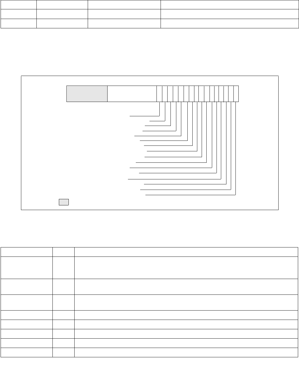
Vol. 3B 18-73
PERFORMANCE MONITORING
In the Silvermont microarchitecture, each MSR_OFFCORE_RSPx is shared by two processor cores.
The layout of MSR_OFFCORE_RSP0 and MSR_OFFCORE_RSP1 are shown in Figure 18-37 and Figure 18-38. Bits
15:0 specifies the request type of a transaction request to the uncore. Bits 30:16 specifies supplier information,
bits 37:31 specifies snoop response information.
Additionally, MSR_OFFCORE_RSP0 provides bit 38 to enable measurement of average latency of specific type of
offcore transaction requests using two programmable counter simultaneously, see Section 18.5.2.3 for details.
Table 18-51. OffCore Response Event Encoding
Counter Event code UMask Required Off-core Response MSR
PMC0-1 B7H 01H MSR_OFFCORE_RSP0 (address 1A6H)
PMC0-1 B7H 02H MSR_OFFCORE_RSP1 (address 1A7H)
Figure 18-37. Request_Type Fields for MSR_OFFCORE_RSPx
Table 18-52. MSR_OFFCORE_RSPx Request_Type Field Definition
Bit Name Offset Description
DMND_DATA_RD 0 (R/W). Counts the number of demand and DCU prefetch data reads of full and partial cachelines as
well as demand data page table entry cacheline reads. Does not count L2 data read prefetches or
instruction fetches.
DMND_RFO 1 (R/W). Counts the number of demand and DCU prefetch reads for ownership (RFO) requests
generated by a write to data cacheline. Does not count L2 RFO prefetches.
DMND_IFETCH 2 (R/W). Counts the number of demand instruction cacheline reads and L1 instruction cacheline
prefetches.
WB 3 (R/W). Counts the number of writeback (modified to exclusive) transactions.
PF_DATA_RD 4 (R/W). Counts the number of data cacheline reads generated by L2 prefetchers.
PF_RFO 5 (R/W). Counts the number of RFO requests generated by L2 prefetchers.
PF_IFETCH 6 (R/W). Counts the number of code reads generated by L2 prefetchers.
PARTIAL_READ 7 (R/W). Counts the number of demand reads of partial cache lines (including UC and WC).
RESPONSE TYPE — Other (R/W)
REQUEST TYPE — PARTIAL_STRM_ST (R/W)
87 0
REQUEST TYPE — STRM_ST (R/W)
11 312 1
Reserved
63 2
495610131415
REQUEST TYPE — BUS_LOCKS (R/W)
REQUEST TYPE — UC_IFETCH (R/W)
REQUEST TYPE — PARTIAL_WRITE (R/W)
REQUEST TYPE — PARTIAL_READ (R/W)
REQUEST TYPE — PF_IFETCH (R/W)
REQUEST TYPE — PF_RFO (R/W)
REQUEST TYPE — PF_DATA_RD (R/W)
REQUEST TYPE — WB (R/W)
REQUEST TYPE — DMND_IFETCH (R/W)
REQUEST TYPE — DMND_RFO (R/W)
REQUEST TYPE — DMND_DATA_RD (R/W)
RESET Value — 00000000_00000000H
37
See Figure 18-30
REQUEST TYPE — PF_DATA_RD (R/W)
REQUEST TYPE — SW_PREFETCH (R/W)
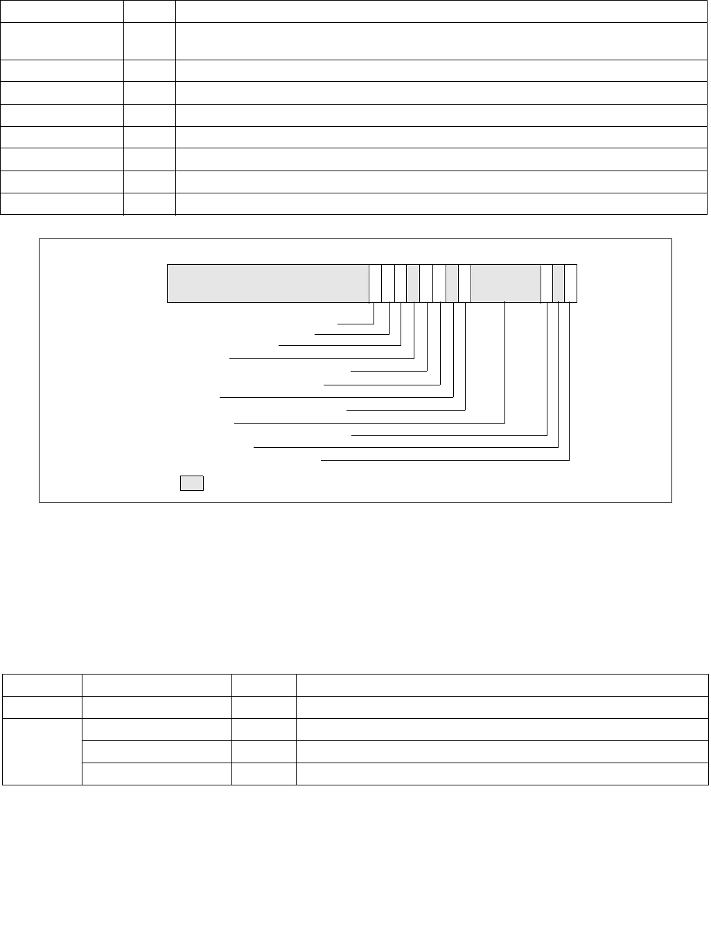
18-74 Vol. 3B
PERFORMANCE MONITORING
To properly program this extra register, software must set at least one request type bit (Table 18-52) and a valid
response type pattern (Table 18-53, Table 18-54). Otherwise, the event count reported will be zero. It is permis-
sible and useful to set multiple request and response type bits in order to obtain various classes of off-core
response events. Although MSR_OFFCORE_RSPx allow an agent software to program numerous combinations that
meet the above guideline, not all combinations produce meaningful data.
PARTIAL_WRITE 8 (R/W). Counts the number of demand RFO requests to write to partial cache lines (includes UC, WT
and WP)
UC_IFETCH 9 (R/W). Counts the number of UC instruction fetches.
BUS_LOCKS 10 (R/W). Bus lock and split lock requests
STRM_ST 11 (R/W). Streaming store requests
SW_PREFETCH 12 (R/W). Counts software prefetch requests
PF_DATA_RD 13 (R/W). Counts DCU hardware prefetcher data read requests
PARTIAL_STRM_ST 14 (R/W). Streaming store requests
ANY 15 (R/W). Any request that crosses IDI, including I/O.
Figure 18-38. Response_Supplier and Snoop Info Fields for MSR_OFFCORE_RSPx
Table 18-53. MSR_OFFCORE_RSP_x Response Supplier Info Field Definition
Subtype Bit Name Offset Description
Common ANY_RESPONSE 16 (R/W). Catch all value for any response types.
Supplier Info Reserved 17 Reserved
L2_HIT 18 (R/W). Cache reference hit L2 in either M/E/S states.
Reserved 30:19 Reserved
Table 18-52. MSR_OFFCORE_RSPx Request_Type Field Definition (Contd.)
Bit Name Offset Description
RESPONSE TYPE — NON_DRAM (R/W)
RSPNS_SNOOP — HITM (R/W)
16
RESERVED
33 1934 17
Reserved
63 182031 212232353637
RSPNS_SNOOP — SNOOP_HIT (R/W)
RSPNS_SNOOP — SNOOP_MISS (R/W)
RESERVED
RSPNS_SNOOP — SNOOP_NONE (R/W)
RESERVED
RSPNS_SUPPLIER — L2_HIT (R/W)
RESERVED
RSPNS_SUPPLIER — ANY (R/W)
RESET Value — 00000000_00000000H
38
AVG LATENCY — ENABLE AVG LATENCY(R/W)

Vol. 3B 18-75
PERFORMANCE MONITORING
To specify a complete offcore response filter, software must properly program bits in the request and response type
fields. A valid request type must have at least one bit set in the non-reserved bits of 15:0. A valid response type
must be a non-zero value of the following expression:
ANY | [(‘OR’ of Supplier Info Bits) & (‘OR’ of Snoop Info Bits)]
If “ANY” bit is set, the supplier and snoop info bits are ignored.
18.5.2.3 Average Offcore Request Latency Measurement
Average latency for offcore transactions can be determined by using both MSR_OFFCORE_RSP registers. Using two
performance monitoring counters, program the two OFFCORE_RESPONSE event encodings into the corresponding
IA32_PERFEVTSELx MSRs. Count the weighted cycles via MSR_OFFCORE_RSP0 by programming a request type in
MSR_OFFCORE_RSP0.[15:0] and setting MSR_OFFCORE_RSP0.OUTSTANDING[38] to 1, white setting the
remaining bits to 0. Count the number of requests via MSR_OFFCORE_RSP1 by programming the same request
type from MSR_OFFCORE_RSP0 into MSR_OFFCORE_RSP1[bit 15:0], and setting
MSR_OFFCORE_RSP1.ANY_RESPONSE[16] = 1, while setting the remaining bits to 0. The average latency can be
obtained by dividing the value of the IA32_PMCx register that counted weight cycles by the register that counted
requests.
18.5.3 Performance Monitoring for Goldmont Microarchitecture
Intel Atom processors based on the Goldmont microarchitecture report architectural performance monitoring
versionID = 4 (see Section 18.2.4) and support non-architectural monitoring capabilities described in this section.
Architectural performance monitoring version 4 capabilities are described in Section 18.2.4.
The bit fields (except bit 21) within each IA32_PERFEVTSELx MSR are defined in Figure 18-6 and described in
Section 18.2.1.1 and Section 18.2.3. The Goldmont microarchitecture does not support Hyper-Threading and thus
architectural and non-architectural performance monitoring events ignore the AnyThread qualification regardless
of its setting in the IA32_PERFEVTSELx MSR. However, Goldmont does not set the AnyThread deprecation bit
(CPUID.0AH:EDX[15]).
The core PMU’s capability is similar to that of the Silvermont microarchitecture described in Section 18.5.2 , with
some differences and enhancements summarized in Table 18-55.
Table 18-54. MSR_OFFCORE_RSPx Snoop Info Field Definition
Subtype Bit Name Offset Description
Snoop
Info
SNP_NONE 31 (R/W). No details on snoop-related information.
Reserved 32 Reserved
SNOOP_MISS 33 (R/W). Counts the number of snoop misses when L2 misses.
SNOOP_HIT 34 (R/W). Counts the number of snoops hit in the other module where no modified copies
were found.
Reserved 35 Reserved
HITM 36 (R/W). Counts the number of snoops hit in the other module where modified copies
were found in other core's L1 cache.
NON_DRAM 37 (R/W). Target was non-DRAM system address. This includes MMIO transactions.
AVG_LATENCY 38 (R/W). Enable average latency measurement by counting weighted cycles of
outstanding offcore requests of the request type specified in bits 15:0 and any
response (bits 37:16 cleared to 0).
This bit is available in MSR_OFFCORE_RESP0. The weighted cycles is accumulated in the
specified programmable counter IA32_PMCx and the occurrence of specified requests
are counted in the other programmable counter.

18-76 Vol. 3B
PERFORMANCE MONITORING
Table 18-55. Core PMU Comparison Between the Goldmont and Silvermont Microarchitectures
Box The Goldmont microarchitecture The Silvermont microarchitecture Comment
# of Fixed counters per core 3 3 Use CPUID to enumerate
# of counters. See
Section 18.2.1.
# of general-purpose
counters per core
4 2 Use CPUID to enumerate
# of counters. See
Section 18.2.1.
Counter width (R,W) R:48, W: 32/48 R:40, W:32 See Section 18.2.2.
Architectural Performance
Monitoring version ID
4 3 Use CPUID to enumerate
# of counters. See
Section 18.2.1.
PMI Overhead Mitigation • Freeze_Perfmon_on_PMI with
streamlined semantics.
•Freeze_LBR_on_PMI with
streamlined semantics for
branch profiling.
•Freeze_Perfmon_on_PMI with
legacy semantics.
•Freeze_LBR_on_PMI with legacy
semantics for branch profiling.
See Section 17.4.7.
Legacy semantics not
supported with version 4
or higher.
Counter and Buffer
Overflow Status
Management
•Query via
IA32_PERF_GLOBAL_STATUS
•Reset via
IA32_PERF_GLOBAL_STATUS_R
ESET
•Set via
IA32_PERF_GLOBAL_STATUS_S
ET
• Query via
IA32_PERF_GLOBAL_STATUS
•Reset via
IA32_PERF_GLOBAL_OVF_CTRL
See Section 18.2.4.
IA32_PERF_GLOBAL_STATU
S Indicators of
Overflow/Overhead/Interfer
ence
• Individual counter overflow
• PEBS buffer overflow
•ToPA buffer overflow
• CTR_Frz, LBR_Frz
• Individual counter overflow
•PEBS buffer overflow
See Section 18.2.4.
Enable control in
IA32_PERF_GLOBAL_STATU
S
• CTR_Frz,
•LBR_Frz
No See Section 18.2.4.1.
Perfmon Counter In-Use
Indicator
Query IA32_PERF_GLOBAL_INUSE No See Section 18.2.4.3.
Processor Event Based
Sampling (PEBS) Events
General-Purpose Counter 0 only.
Supports all events (precise and
non-precise). Precise events are
listed in Table 18-56.
See Section 18.5.2.1.1. General-
Purpose Counter 0 only. Only
supports precise events (see
Table 18-49).
IA32_PMC0 only.
PEBS record format
encoding
0011b 0010b
Reduce skid PEBS IA32_PMC0 only No
Data Address Profiling Yes No
PEBS record layout Table 18-57; enhanced fields at
offsets 90H- 98H; and TSC record
field at C0H.
Table 18-50.
PEBS EventingIP Yes Yes
Off-core Response Event MSR 1A6H and 1A7H, each core
has its own register.
MSR 1A6H and 1A7H, shared by a
pair of cores.
Nehalem supports 1A6H
only.

Vol. 3B 18-77
PERFORMANCE MONITORING
18.5.3.1 Processor Event Based Sampling (PEBS)
Processor event based sampling (PEBS) on the Goldmont microarchitecture is enhanced over prior generations
with respect to sampling support of precise events and non-precise events. In the Goldmont microarchitecture,
PEBS is supported using IA32_PMC0 for all events (see Section 17.4.9).
PEBS uses a debug store mechanism to store a set of architectural state information for the processor at the time
the sample was generated.
Precise events work the same way on Goldmont microarchitecture as on the Silvermont microarchitecture. The
record will be generated after an instruction that causes the event when the counter is already overflowed and will
capture the architectural state at this point (see Section 18.6.2.4 and Section 17.4.9). The eventingIP in the record
will indicate the instruction that caused the event. The list of precise events supported in the Goldmont microarchi-
tecture is shown in Table 18-56.
In the Goldmont microarchitecture, the PEBS facility also supports the use of non-precise events to record
processor state information into PEBS records with the same format as with precise events.
However, a non-precise event may not be attributable to a particular retired instruction or the time of instruction
execution. When the counter overflows, a PEBS record will be generated at the next opportunity. Consider the
event ICACHE.HIT. When the counter overflows, the processor is fetching future instructions. The PEBS record will
be generated at the next opportunity and capture the state at the processor's current retirement point. It is likely
that the instruction fetch that caused the event to increment was beyond that current retirement point. Other
examples of non-precise events are CPU_CLK_UNHALTED.CORE_P and HARDWARE_INTERRUPTS.RECEIVED.
CPU_CLK_UNHALTED.CORE_P will increment each cycle that the processor is awake. When the counter over-flows,
there may be many instructions in various stages of execution. Additionally, zero, one or multiple instructions may
be retired the cycle that the counter overflows. HARDWARE_INTERRUPTS.RECEIVED increments independent of
any instructions being executed. For all non-precise events, the PEBS record will be generated at the next oppor-
tunity, after the counter has overflowed. The PEBS facility thus allows for identification of the instructions which
were executing when the event overflowed.
After generating a record for a non-precise event, the PEBS facility reloads the counter and resumes execution, just
as is done for precise events. Unlike interrupt-based sampling, which requires an interrupt service routine to collect
the sample and reload the counter, the PEBS facility can collect samples even when interrupts are masked and
without using NMI. Since a PEBS record is generated immediately when a counter for a non-precise event is
enabled, it may also be generated after an overflow is set by an MSR write to IA32_PERF_GLOBAL_STATUS_SET.
Table 18-56. Precise Events Supported by the Goldmont Microarchitecture
Event Name Event Select Sub-event UMask
LD_BLOCKS 03H DATA_UNKNOWN 01H
STORE_FORWARD 02H
4K_ALIAS 04H
UTLB_MISS 08H
ALL_BLOCK 10H
MISALIGN_MEM_REF 13H LOAD_PAGE_SPLIT 02H
STORE_PAGE_SPLIT 04H
INST_RETIRED C0H ANY 00H
UOPS_RETITRED C2H ANY 00H
LD_SPLITSMS 01H
BR_INST_RETIRED C4H ALL_BRANCHES 00H
JCC 7EH
TAKEN_JCC FEH
CALL F9H
REL_CALL FDH
IND_CALL FBH

18-78 Vol. 3B
PERFORMANCE MONITORING
The PEBS record format supported by processors based on the Intel Goldmont microarchitecture is shown in
Table 18-57, and each field in the PEBS record is 64 bits long.
NON_RETURN_IND EBH
FAR_BRANCH BFH
RETURN F7H
BR_MISP_RETIRED C5H ALL_BRANCHES 00H
JCC 7EH
TAKEN_JCC FEH
IND_CALL FBH
NON_RETURN_IND EBH
RETURN F7H
MEM_UOPS_RETIRED D0H ALL_LOADS 81H
ALL_STORES 82H
ALL 83H
DLTB_MISS_LOADS 11H
DLTB_MISS_STORES 12H
DLTB_MISS 13H
MEM_LOAD_UOPS_RETIRED D1H L1_HIT 01H
L2_HIT 02H
L1_MISS 08H
L2_MISS 10H
HITM 20H
WCB_HIT 40H
DRAM_HIT 80H
Table 18-57. PEBS Record Format for the Goldmont Microarchitecture
Byte Offset Field Byte Offset Field
00H R/EFLAGS 68H R11
08H R/EIP 70H R12
10H R/EAX 78H R13
18H R/EBX 80H R14
20H R/ECX 88H R15
28H R/EDX 90H Applicable Counters
30H R/ESI 98H Data Linear Address
38H R/EDI A0H Reserved
40H R/EBP A8H Reserved
48H R/ESP B0H EventingRIP
50H R8 B8H Reserved
58H R9 C0H TSC
60H R10
Table 18-56. Precise Events Supported by the Goldmont Microarchitecture (Contd.)
Event Name Event Select Sub-event UMask

Vol. 3B 18-79
PERFORMANCE MONITORING
On Goldmont microarchitecture, all 64 bits of architectural registers are written into the PEBS record regardless of
processor mode.
With PEBS record format encoding 0011b, offset 90H reports the "Applicable Counter" field, which indicates which
counters actually requested generating a PEBS record. This allows software to correlate the PEBS record entry
properly with the instruction that caused the event even when multiple counters are configured to record PEBS
records and multiple bits are set in the field. Additionally, offset C0H captures a snapshot of the TSC that provides
a time line annotation for each PEBS record entry.
18.5.3.1.1 PEBS Data Linear Address Profiling
Goldmont supports the Data Linear Address field introduced in Haswell. It does not support the Data Source
Encoding or Latency Value fields that are also part of Data Address Profiling; those fields are present in the record
but are reserved.
For Goldmont microarchitecture, the Data Linear Address field will record the linear address of memory accesses in
the previous instruction (e.g. the one that triggered a precise event that caused the PEBS record to be generated).
Goldmont microarchitecture may record a Data Linear Address for the instruction that caused the event even for
events not related to memory accesses. This may differ from other microarchitectures.
18.5.3.1.2 Reduced Skid PEBS
For precise events, upon triggering a PEBS assist, there will be a finite delay between the time the counter over-
flows and when the microcode starts to carry out its data collection obligations. The Reduced Skid mechanism miti-
gates the “skid” problem by providing an early indication of when the counter is about to overflow, allowing the
machine to more precisely trap on the instruction that actually caused the counter overflow thus greatly reducing
skid.
This mechanism is a superset of the PDIR mechanism available in the Sandy Bridge microarchitecture. See Section
18.3.4.4.4
In the Goldmont microarchitecture, the mechanism applies to all precise events including, INST_RETIRED, except
for UOPS_RETIRED. However, the Reduced Skid mechanism is disabled for any counter when the INV, ANY, E, or
CMASK fields are set.
For the Reduced Skid mechanism to operate correctly, the performance monitoring counters should not be recon-
figured or modified when they are running with PEBS enabled. The counters need to be disabled (e.g. via
IA32_PERF_GLOBAL_CTRL MSR) before changes to the configuration (e.g. what event is specified in
IA32_PERFEVTSELx or whether PEBS is enabled for that counter via IA32_PEBS_ENABLE) or counter value (MSR
write to IA32_PMCx and IA32_A_PMCx).
18.5.3.1.3 Enhancements to IA32_PERF_GLOBAL_STATUS.OvfDSBuffer[62]
In addition to IA32_PERF_GLOBAL_STATUS.OvfDSBuffer[62] being set when PEBS_Index reaches the
PEBS_Interrupt_Theshold, the bit is also set when PEBS_Index is out of bounds. That is, the bit will be set when
PEBS_Index < PEBS_Buffer_Base or PEBS_Index > PEBS_Absolute_Maximum. Note that when an out of bound
condition is encountered, the overflow bits in IA32_PERF_GLOBAL_STATUS will be cleared according to Applicable
Counters, however the IA32_PMCx values will not be reloaded with the Reset values stored in the DS_AREA.
18.5.3.2 Offcore Response Event
Event number 0B7H support offcore response monitoring using an associated configuration MSR,
MSR_OFFCORE_RSP0 (address 1A6H) in conjunction with umask value 01H or MSR_OFFCORE_RSP1 (address
1A7H) in conjunction with umask value 02H. Table 18-51 lists the event code, mask value and additional off-core
configuration MSR that must be programmed to count off-core response events using IA32_PMCx.
The Goldmont microarchitecture provides unique pairs of MSR_OFFCORE_RSPx registers per core.
The layout of MSR_OFFCORE_RSP0 and MSR_OFFCORE_RSP1 are organized as follows:
•Bits 15:0 specifies the request type of a transaction request to the uncore. This is described in Table 18-58.
•Bits 30:16 specifies common supplier information or an L2 Hit, and is described in Table 18-53.

18-80 Vol. 3B
PERFORMANCE MONITORING
•If L2 misses, then Bits 37:31 can be used to specify snoop response information and is described in
Table 18-59.
•For outstanding requests, bit 38 can enable measurement of average latency of specific type of offcore
transaction requests using two programmable counter simultaneously; see Section 18.5.2.3 for details.
To properly program this extra register, software must set at least one request type bit (Table 18-52) and a valid
response type pattern (either Table 18-53 or Table 18-59). Otherwise, the event count reported will be zero. It is
permissible and useful to set multiple request and response type bits in order to obtain various classes of off-core
response events. Although MSR_OFFCORE_RSPx allow an agent software to program numerous combinations that
meet the above guideline, not all combinations produce meaningful data.
Table 18-58. MSR_OFFCORE_RSPx Request_Type Field Definition
Bit Name Offset Description
DEMAND_DATA_RD 0 (R/W) Counts cacheline read requests due to demand reads (excludes prefetches).
DEMAND_RFO 1 (R/W) Counts cacheline read for ownership (RFO) requests due to demand writes
(excludes prefetches).
DEMAND_CODE_RD 2 (R/W) Counts demand instruction cacheline and I-side prefetch requests that miss the
instruction cache.
COREWB 3 (R/W) Counts writeback transactions caused by L1 or L2 cache evictions.
PF_L2_DATA_RD 4 (R/W) Counts data cacheline reads generated by hardware L2 cache prefetcher.
PF_L2_RFO 5 (R/W) Counts reads for ownership (RFO) requests generated by L2 prefetcher.
Reserved 6 Reserved.
PARTIAL_READS 7 (R/W) Counts demand data partial reads, including data in uncacheable (UC) or
uncacheable (WC) write combining memory types.
PARTIAL_WRITES 8 (R/W) Counts partial writes, including uncacheable (UC), write through (WT) and write
protected (WP) memory type writes.
UC_CODE_READS 9 (R/W) Counts code reads in uncacheable (UC) memory region.
BUS_LOCKS 10 (R/W) Counts bus lock and split lock requests.
FULL_STREAMING_STORES 11 (R/W) Counts full cacheline writes due to streaming stores.
SW_PREFETCH 12 (R/W) Counts cacheline requests due to software prefetch instructions.
PF_L1_DATA_RD 13 (R/W) Counts data cacheline reads generated by hardware L1 data cache prefetcher.
PARTIAL_STREAMING_STORES 14 (R/W) Counts partial cacheline writes due to streaming stores.
ANY_REQUEST 15 (R/W) Counts requests to the uncore subsystem.
Table 18-59. MSR_OFFCORE_RSPx For L2 Miss and Outstanding Requests
Subtype Bit Name Offset Description
L2_MISS
(Snoop Info)
Reserved 32:31 Reserved
L2_MISS.SNOOP_MISS_O
R_NO_SNOOP_NEEDED
33 (R/W). A true miss to this module, for which a snoop request missed the other
module or no snoop was performed/needed.
L2_MISS.HIT_OTHER_CO
RE_NO_FWD
34 (R/W) A snoop hit in the other processor module, but no data forwarding is
required.
Reserved 35 Reserved
L2_MISS.HITM_OTHER_C
ORE
36 (R/W) Counts the number of snoops hit in the other module or other core's L1
where modified copies were found.
L2_MISS.NON_DRAM 37 (R/W) Target was a non-DRAM system address. This includes MMIO transactions.

Vol. 3B 18-81
PERFORMANCE MONITORING
To specify a complete offcore response filter, software must properly program bits in the request and response type
fields. A valid request type must have at least one bit set in the non-reserved bits of 15:0. A valid response type
must be a non-zero value of the following expression:
[ANY ‘OR’ (L2 Hit) ] ‘XOR’ ( Snoop Info Bits) ‘XOR’ (Avg Latency)
18.5.3.3 Average Offcore Request Latency Measurement
In Goldmont microarchitecture, measurement of average latency of offcore transaction requests is the same as
described in Section 18.5.2.3.
18.5.4 Performance Monitoring for Goldmont Plus Microarchitecture
Intel Atom processors based on the Goldmont Plus microarchitecture report architectural performance monitoring
versionID = 4 and support non-architectural monitoring capabilities described in this section.
Architectural performance monitoring version 4 capabilities are described in Section 18.2.4.
Goldmont Plus performance monitoring capabilities are similar to Goldmont capabilities. The differences are in
specific events and in which counters support PEBS. Goldmont Plus introduces the ability for fixed performance
monitoring counters to generate PEBS records.
Goldmont Plus will set the AnyThread deprecation CPUID bit (CPUID.0AH:EDX[15]) to indicate that the Any-Thread
bits in IA32_PERFEVTSELx and IA32_FIXED_CTR_CTRL have no effect.
The core PMU's capability is similar to that of the Goldmont microarchitecture described in Section 18.6.3, with
some differences and enhancements summarized in Table 18-60.
Outstanding
requests1
OUTSTANDING 38 (R/W) Counts weighted cycles of outstanding offcore requests of the request type
specified in bits 15:0, from the time the XQ receives the request and any
response is received. Bits 37:16 must be set to 0. This bit is only available in
MSR_OFFCORE_RESP0.
NOTES:
1. See Section 18.5.2.3, “Average Offcore Request Latency Measurement” for details on how to use this bit to extract average latency.
Table 18-60. Core PMU Comparison Between the Goldmont Plus and Goldmont Microarchitectures
Box Goldmont Plus Microarchitecture Goldmont Microarchitecture Comment
# of Fixed counters per core 3 3 Use CPUID to enumerate
# of counters. See
Section 18.2.1.
# of general-purpose
counters per core
4 4 Use CPUID to enumerate
# of counters. See
Section 18.2.1.
Counter width (R,W) R:48, W: 32/48 R:48, W: 32/48 No change.
Architectural Performance
Monitoring version ID
4 4 No change.
Processor Event Based
Sampling (PEBS) Events
All General-Purpose and Fixed
counters. Each General-Purpose
counter supports all events (precise
and non-precise).
General-Purpose Counter 0 only.
Supports all events (precise and
non-precise). Precise events are
listed in Table 18-56.
Goldmont Plus supports
PEBS on all counters.
PEBS record format
encoding
0011b 0011b No change.
Table 18-59. MSR_OFFCORE_RSPx For L2 Miss and Outstanding Requests (Contd.)
Subtype Bit Name Offset Description
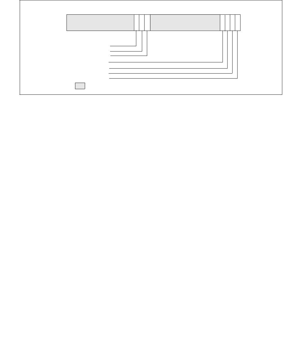
18-82 Vol. 3B
PERFORMANCE MONITORING
18.5.4.1 Extended PEBS
The Extended PEBS feature, introduced in Goldmont Plus microarchitecture, supports PEBS (Processor Event Based
Sampling) on a fixed-function performance counters as well as all four general purpose counters (PMC0-3). PEBS
can be enabled for the four general purpose counters using PEBS_EN_PMCi bits of IA32_PEBS_ENABLE (i = 0, 1, 2,
3). PEBS can be enabled for the 3 fixed function counters using the PEBS_EN_FIXEDi bits of IA32_PEBS_ENABLE (I
= 0, 1, 2).
Similar to Goldmont microarchitecture, Goldmont Plus microarchitecture processors can generate PEBS record
events on both precise as well as non-precise events.
A PEBS record due to a precise event will be generated after an instruction that causes the event when the counter
has already overflowed. A PEBS record due to a non-precise event will occur at the next opportunity after the
counter has overflowed, including immediately after an overflow is set by an MSR write.
IA32_FIXED_CTR0 counts instructions retired and is a precise event. IA32_FIXED_CTR1 counts unhalted core
cycles and is a non-precise event. IA32_FIXED_CTR2 counts unhalted reference cycles and is a non-precise event.
The Applicable Counter field at offset 90H of the PEBS record indicates which counters caused the PEBS record to
be generated. It is in the same format as the enable bits for each counter in IA32_PEBS_ENABLE. As an example,
an Applicable Counter field with bits 2 and 32 set would indicate that both general purpose counter 2 and fixed
function counter 0 generated the PEBS record.
•To properly use PEBS for the additional counters, software will need to set up the counter reset values in PEBS
portion of the DS_BUFFER_MANAGEMENT_AREA data structure that is indicated by the IA32_DS_AREA
register. The layout of the DS_BUFFER_MANAGEMENT_AREA for Goldmont Plus is shown in Figure 18-40. When
a counter generates a PEBS records, the appropriate counter reset values will be loaded into that counter. In
the above example where general purpose counter 2 and fixed function counter 0 generated the PEBS record,
general purpose counter 2 would be reloaded with the value contained in PEBS GP Counter 2 Reset (offset 50H)
and fixed function counter 0 would be reloaded with the value contained in PEBS Fixed Counter 0 Reset (offset
80H).
Figure 18-39. Layout of IA32_PEBS_ENABLE MSR
PEBS_EN_FIXED2 (R/W)
87 0
PEBS_EN_FIXED1 (R/W)
31
Reserved
63 245
6
35 34 33 32 31
PEBS_EN_PMC3 (R/W)
PEBS_EN_PMC2 (R/W)
PEBS_EN_PMC1 (R/W)
PEBS_EN_PMC0 (R/W)
PEBS_EN_FIXED0 (R/W)
RESET Value — 00000000_00000000H
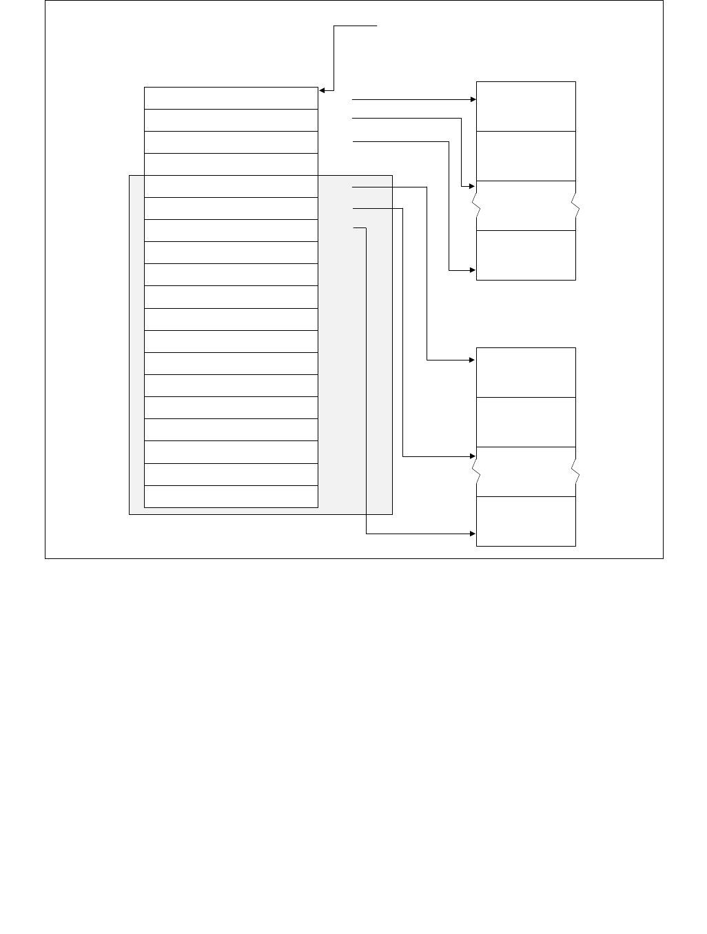
Vol. 3B 18-83
PERFORMANCE MONITORING
18.5.4.2 Reduced Skid PEBS
Goldmont Plus microarchitecture processors supports the Reduced Skid PEBS feature described in Section
18.5.3.1.2 on the IA32_PMC0 counter. Although Goldmont Plus adds support for generating PEBS records for
precise events on the other general-purpose and fixed-function performance counters, those counters do not
support the Reduced Skid PEBS feature.
18.6 PERFORMANCE MONITORING (LEGACY INTEL PROCESSORS)
18.6.1 Performance Monitoring (Intel® Core™ Solo and Intel® Core™ Duo Processors)
In Intel Core Solo and Intel Core Duo processors, non-architectural performance monitoring events are
programmed using the same facilities (see Figure 18-1) used for architectural performance events.
Non-architectural performance events use event select values that are model-specific. Event mask (Umask) values
are also specific to event logic units. Some microarchitectural conditions detectable by a Umask value may have
Figure 18-40. PEBS Programming Environment
00H
08H
10H
18H
20H
28H
30H
38H
40H
48H
50H
58H
60H
68H
70H
78H
80H
88H
90H
PEBS Fixed Counter 1 Reset
PEBS Fixed Counter 0 Reset
63 BTS Buffer Base 0
BTS Index
BTS Absolute Maximum
BTS Interrupt Threshold
PEBS Buffer Base
PEBS Index
PEBS Absolute Maximum
PEBS Interrupt Threshold
PEBS GP Counter 0 Reset
PEBS GP Counter 1 Reset
PEBS GP Counter 2 Reset
PEBS GP Counter 3 Reset
Reserved
Reserved
Reserved
Reserved
PEBS Fixed Counter 2 Reset
PEBS Config Buffer
DS Buffer Management
Branch Record 0
Branch Record 1
Branch Record n
BTS Buffer
PEBS Record 0
PEBS Record 1
PEBS Record n
PEBS Buffer
IA32_DS_AREA MSR
18-84 Vol. 3B
PERFORMANCE MONITORING
specificity related to processor topology (see Section 8.6, “Detecting Hardware Multi-Threading Support and
Topology,” in the Intel® 64 and IA-32 Architectures Software Developer’s Manual, Volume 3A). As a result, the unit
mask field (for example, IA32_PERFEVTSELx[bits 15:8]) may contain sub-fields that specify topology information
of processor cores.
The sub-field layout within the Umask field may support two-bit encoding that qualifies the relationship between a
microarchitectural condition and the originating core. This data is shown in Table 18-61. The two-bit encoding for
core-specificity is only supported for a subset of Umask values (see Chapter 19, “Performance Monitoring Events”)
and for Intel Core Duo processors. Such events are referred to as core-specific events.
Some microarchitectural conditions allow detection specificity only at the boundary of physical processors. Some
bus events belong to this category, providing specificity between the originating physical processor (a bus agent)
versus other agents on the bus. Sub-field encoding for agent specificity is shown in Table 18-62.
Some microarchitectural conditions are detectable only from the originating core. In such cases, unit mask does
not support core-specificity or agent-specificity encodings. These are referred to as core-only conditions.
Some microarchitectural conditions allow detection specificity that includes or excludes the action of hardware
prefetches. A two-bit encoding may be supported to qualify hardware prefetch actions. Typically, this applies only
to some L2 or bus events. The sub-field encoding for hardware prefetch qualification is shown in Table 18-63.
Some performance events may (a) support none of the three event-specific qualification encodings (b) may
support core-specificity and agent specificity simultaneously (c) or may support core-specificity and hardware
prefetch qualification simultaneously. Agent-specificity and hardware prefetch qualification are mutually exclusive.
In addition, some L2 events permit qualifications that distinguish cache coherent states. The sub-field definition for
cache coherency state qualification is shown in Table 18-64. If no bits in the MESI qualification sub-field are set for
an event that requires setting MESI qualification bits, the event count will not increment.
Table 18-61. Core Specificity Encoding within a Non-Architectural Umask
IA32_PERFEVTSELx MSRs
Bit 15:14 Encoding Description
11B All cores
10B Reserved
01B This core
00B Reserved
Table 18-62. Agent Specificity Encoding within a Non-Architectural Umask
IA32_PERFEVTSELx MSRs
Bit 13 Encoding Description
0This agent
1 Include all agents
Table 18-63. HW Prefetch Qualification Encoding within a Non-Architectural Umask
IA32_PERFEVTSELx MSRs
Bit 13:12 Encoding Description
11B All inclusive
10B Reserved
01B Hardware prefetch only
00B Exclude hardware prefetch
Vol. 3B 18-85
PERFORMANCE MONITORING
18.6.2 Performance Monitoring (Processors Based on Intel® Core™ Microarchitecture)
In addition to architectural performance monitoring, processors based on the Intel Core microarchitecture support
non-architectural performance monitoring events.
Architectural performance events can be collected using general-purpose performance counters. Non-architectural
performance events can be collected using general-purpose performance counters (coupled with two
IA32_PERFEVTSELx MSRs for detailed event configurations), or fixed-function performance counters (see Section
18.6.2.1). IA32_PERFEVTSELx MSRs are architectural; their layout is shown in Figure 18-1. Starting with Intel
Core 2 processor T 7700, fixed-function performance counters and associated counter control and status MSR
becomes part of architectural performance monitoring version 2 facilities (see also Section 18.2.2).
Non-architectural performance events in processors based on Intel Core microarchitecture use event select values
that are model-specific. Valid event mask (Umask) bits are listed in Chapter 19. The UMASK field may contain sub-
fields identical to those listed in Table 18-61, Table 18-62, Table 18-63, and Table 18-64. One or more of these
sub-fields may apply to specific events on an event-by-event basis. Details are listed in Table 19-25 in Chapter 19,
“Performance Monitoring Events.”
In addition, the UMASK filed may also contain a sub-field that allows detection specificity related to snoop
responses. Bits of the snoop response qualification sub-field are defined in Table 18-65.
There are also non-architectural events that support qualification of different types of snoop operation. The corre-
sponding bit field for snoop type qualification are listed in Table 18-66.
No more than one sub-field of MESI, snoop response, and snoop type qualification sub-fields can be supported in a
performance event.
Table 18-64. MESI Qualification Definitions within a Non-Architectural Umask
IA32_PERFEVTSELx MSRs
Bit Position 11:8 Description
Bit 11 Counts modified state
Bit 10 Counts exclusive state
Bit 9 Counts shared state
Bit 8 Counts Invalid state
Table 18-65. Bus Snoop Qualification Definitions within a Non-Architectural Umask
IA32_PERFEVTSELx MSRs
Bit Position 11:8 Description
Bit 11 HITM response
Bit 10 Reserved
Bit 9 HIT response
Bit 8 CLEAN response
Table 18-66. Snoop Type Qualification Definitions within a Non-Architectural Umask
IA32_PERFEVTSELx MSRs
Bit Position 9:8 Description
Bit 9 CMP2I snoops
Bit 8 CMP2S snoops
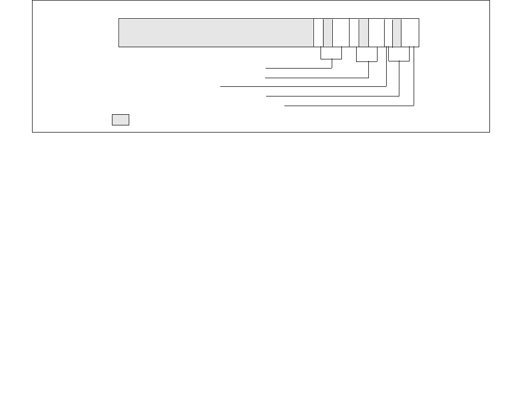
18-86 Vol. 3B
PERFORMANCE MONITORING
NOTE
Software must write known values to the performance counters prior to enabling the counters. The
content of general-purpose counters and fixed-function counters are undefined after INIT or RESET.
18.6.2.1 Fixed-function Performance Counters
Processors based on Intel Core microarchitecture provide three fixed-function performance counters. Bits beyond
the width of the fixed counter are reserved and must be written as zeros. Model-specific fixed-function performance
counters on processors that support Architectural Perfmon version 1 are 40 bits wide.
Each of the fixed-function counter is dedicated to count a pre-defined performance monitoring events. See Table
18-2 for details of the PMC addresses and what these events count.
Programming the fixed-function performance counters does not involve any of the IA32_PERFEVTSELx MSRs, and
does not require specifying any event masks. Instead, the MSR MSR_PERF_FIXED_CTR_CTRL provides multiple
sets of 4-bit fields; each 4-bit field controls the operation of a fixed-function performance counter (PMC). See
Figures 18-41. Two sub-fields are defined for each control. See Figure 18-41; bit fields are:
•Enable field (low 2 bits in each 4-bit control) — When bit 0 is set, performance counting is enabled in the
corresponding fixed-function performance counter to increment when the target condition associated with the
architecture performance event occurs at ring 0.
When bit 1 is set, performance counting is enabled in the corresponding fixed-function performance counter to
increment when the target condition associated with the architecture performance event occurs at ring greater
than 0.
Writing 0 to both bits stops the performance counter. Writing 11B causes the counter to increment irrespective
of privilege levels.
•PMI field (fourth bit in each 4-bit control) — When set, the logical processor generates an exception
through its local APIC on overflow condition of the respective fixed-function counter.
18.6.2.2 Global Counter Control Facilities
Processors based on Intel Core microarchitecture provides simplified performance counter control that simplifies
the most frequent operations in programming performance events, i.e. enabling/disabling event counting and
checking the status of counter overflows. This is done by the following three MSRs:
•MSR_PERF_GLOBAL_CTRL enables/disables event counting for all or any combination of fixed-function PMCs
(MSR_PERF_FIXED_CTRx) or general-purpose PMCs via a single WRMSR.
•MSR_PERF_GLOBAL_STATUS allows software to query counter overflow conditions on any combination of
fixed-function PMCs (MSR_PERF_FIXED_CTRx) or general-purpose PMCs via a single RDMSR.
•MSR_PERF_GLOBAL_OVF_CTRL allows software to clear counter overflow conditions on any combination of
fixed-function PMCs (MSR_PERF_FIXED_CTRx) or general-purpose PMCs via a single WRMSR.
Figure 18-41. Layout of MSR_PERF_FIXED_CTR_CTRL MSR
Cntr2 — Controls for MSR_PERF_FIXED_CTR2
Cntr1 — Controls for MSR_PERF_FIXED_CTR1
PMI — Enable PMI on overflow
Cntr0 — Controls for MSR_PERF_FIXED_CTR0
87 0
ENABLE — 0: disable; 1: OS; 2: User; 3: All ring levels
E
N
P
M
I
11 312 1
Reserved
63 2
E
N
E
N
495
P
PM
M
I
I
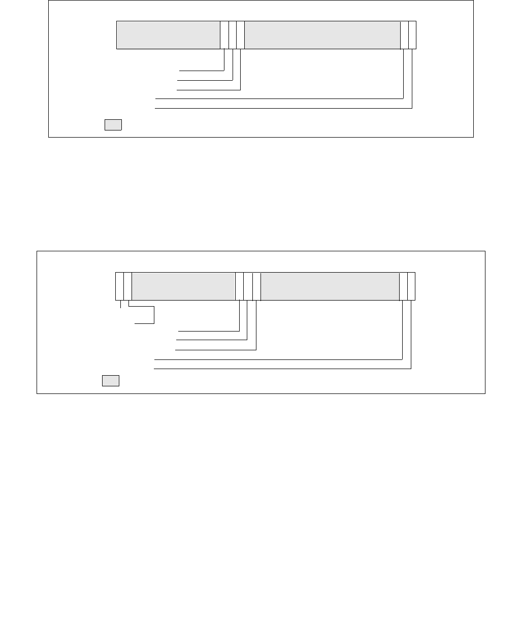
Vol. 3B 18-87
PERFORMANCE MONITORING
MSR_PERF_GLOBAL_CTRL MSR provides single-bit controls to enable counting in each performance counter (see
Figure 18-42). Each enable bit in MSR_PERF_GLOBAL_CTRL is AND’ed with the enable bits for all privilege levels in
the respective IA32_PERFEVTSELx or MSR_PERF_FIXED_CTR_CTRL MSRs to start/stop the counting of respective
counters. Counting is enabled if the AND’ed results is true; counting is disabled when the result is false.
MSR_PERF_GLOBAL_STATUS MSR provides single-bit status used by software to query the overflow condition of
each performance counter. MSR_PERF_GLOBAL_STATUS[bit 62] indicates overflow conditions of the DS area data
buffer. MSR_PERF_GLOBAL_STATUS[bit 63] provides a CondChgd bit to indicate changes to the state of perfor-
mance monitoring hardware (see Figure 18-43). A value of 1 in bits 34:32, 1, 0 indicates an overflow condition has
occurred in the associated counter.
When a performance counter is configured for PEBS, an overflow condition in the counter will arm PEBS. On the
subsequent event following overflow, the processor will generate a PEBS event. On a PEBS event, the processor will
perform bounds checks based on the parameters defined in the DS Save Area (see Section 17.4.9). Upon
successful bounds checks, the processor will store the data record in the defined buffer area, clear the counter
overflow status, and reload the counter. If the bounds checks fail, the PEBS will be skipped entirely. In the event
that the PEBS buffer fills up, the processor will set the OvfBuffer bit in MSR_PERF_GLOBAL_STATUS.
MSR_PERF_GLOBAL_OVF_CTL MSR allows software to clear overflow the indicators for general-purpose or fixed-
function counters via a single WRMSR (see Figure 18-44). Clear overflow indications when:
•Setting up new values in the event select and/or UMASK field for counting or interrupt-based event sampling.
•Reloading counter values to continue collecting next sample.
•Disabling event counting or interrupt-based event sampling.
Figure 18-42. Layout of MSR_PERF_GLOBAL_CTRL MSR
Figure 18-43. Layout of MSR_PERF_GLOBAL_STATUS MSR
FIXED_CTR2 enable
FIXED_CTR1 enable
FIXED_CTR0 enable
PMC1 enable
210
PMC0 enable
3132333435
Reserved
63
62
FIXED_CTR2 Overflow
FIXED_CTR1 Overflow
FIXED_CTR0 Overflow
PMC1 Overflow
210
PMC0 Overflow
3132333435
Reserved
63
CondChgd
OvfBuffer
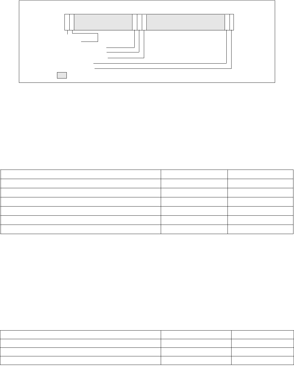
18-88 Vol. 3B
PERFORMANCE MONITORING
18.6.2.3 At-Retirement Events
Many non-architectural performance events are impacted by the speculative nature of out-of-order execution. A
subset of non-architectural performance events on processors based on Intel Core microarchitecture are enhanced
with a tagging mechanism (similar to that found in Intel NetBurst® microarchitecture) that exclude contributions
that arise from speculative execution. The at-retirement events available in processors based on Intel Core micro-
architecture does not require special MSR programming control (see Section 18.6.3.6, “At-Retirement Counting”),
but is limited to IA32_PMC0. See Table 18-67 for a list of events available to processors based on Intel Core micro-
architecture.
18.6.2.4 Processor Event Based Sampling (PEBS)
Processors based on Intel Core microarchitecture also support processor event based sampling (PEBS). This
feature was introduced by processors based on Intel NetBurst microarchitecture.
PEBS uses a debug store mechanism and a performance monitoring interrupt to store a set of architectural state
information for the processor. The information provides architectural state of the instruction executed after the
instruction that caused the event (See Section 18.6.2.4.2 and Section 17.4.9).
In cases where the same instruction causes BTS and PEBS to be activated, PEBS is processed before BTS are
processed. The PMI request is held until the processor completes processing of PEBS and BTS.
For processors based on Intel Core microarchitecture, precise events that can be used with PEBS are listed in
Table 18-68. The procedure for detecting availability of PEBS is the same as described in Section 18.6.3.8.1.
Figure 18-44. Layout of MSR_PERF_GLOBAL_OVF_CTRL MSR
Table 18-67. At-Retirement Performance Events for Intel Core Microarchitecture
Event Name UMask Event Select
ITLB_MISS_RETIRED 00H C9H
MEM_LOAD_RETIRED.L1D_MISS 01H CBH
MEM_LOAD_RETIRED.L1D_LINE_MISS 02H CBH
MEM_LOAD_RETIRED.L2_MISS 04H CBH
MEM_LOAD_RETIRED.L2_LINE_MISS 08H CBH
MEM_LOAD_RETIRED.DTLB_MISS 10H CBH
Table 18-68. PEBS Performance Events for Intel Core Microarchitecture
Event Name UMask Event Select
INSTR_RETIRED.ANY_P 00H C0H
X87_OPS_RETIRED.ANY FEH C1H
BR_INST_RETIRED.MISPRED 00H C5H
62
FIXED_CTR2 ClrOverflow
FIXED_CTR1 ClrOverflow
FIXED_CTR0 ClrOverflow
PMC1 ClrOverflow
210
PMC0 ClrOverflow
3132333435
Reserved
63
ClrCondChgd
ClrOvfBuffer

Vol. 3B 18-89
PERFORMANCE MONITORING
18.6.2.4.1 Setting up the PEBS Buffer
For processors based on Intel Core microarchitecture, PEBS is available using IA32_PMC0 only. Use the following
procedure to set up the processor and IA32_PMC0 counter for PEBS:
1. Set up the precise event buffering facilities. Place values in the precise event buffer base, precise event index,
precise event absolute maximum, precise event interrupt threshold, and precise event counter reset fields of
the DS buffer management area. In processors based on Intel Core microarchitecture, PEBS records consist of
64-bit address entries. See Figure 17-8 to set up the precise event records buffer in memory.
2. Enable PEBS. Set the Enable PEBS on PMC0 flag (bit 0) in IA32_PEBS_ENABLE MSR.
3. Set up the IA32_PMC0 performance counter and IA32_PERFEVTSEL0 for an event listed in Table 18-68.
18.6.2.4.2 PEBS Record Format
The PEBS record format may be extended across different processor implementations. The
IA32_PERF_CAPABILITES MSR defines a mechanism for software to handle the evolution of PEBS record format in
processors that support architectural performance monitoring with version id equals 2 or higher. The bit fields of
IA32_PERF_CAPABILITES are defined in Table 2-2 of Chapter 2, “Model-Specific Registers (MSRs)” in the Intel®
64 and IA-32 Architectures Software Developer’s Manual, Volume 4. The relevant bit fields that governs PEBS are:
•PEBSTrap [bit 6]: When set, PEBS recording is trap-like. After the PEBS-enabled counter has overflowed, PEBS
record is recorded for the next PEBS-able event at the completion of the sampled instruction causing the PEBS
event. When clear, PEBS recording is fault-like. The PEBS record is recorded before the sampled instruction
causing the PEBS event.
•PEBSSaveArchRegs [bit 7]: When set, PEBS will save architectural register and state information according to
the encoded value of the PEBSRecordFormat field. When clear, only the return instruction pointer and flags are
recorded. On processors based on Intel Core microarchitecture, this bit is always 1
•PEBSRecordFormat [bits 11:8]: Valid encodings are:
— 0000B: Only general-purpose registers, instruction pointer and RFLAGS registers are saved in each PEBS
record (seeSection 18.6.3.8).
— 0001B: PEBS record includes additional information of IA32_PERF_GLOBAL_STATUS and load latency data.
(seeSection 18.3.1.1.1).
— 0010B: PEBS record includes additional information of IA32_PERF_GLOBAL_STATUS, load latency data,
and TSX tuning information. (seeSection 18.3.6.2).
— 0011B: PEBS record includes additional information of load latency data, TSX tuning information, TSC data,
and the applicable counter field replaces IA32_PERF_GLOBAL_STATUS at offset 90H. (see Section
18.3.8.1.1).
18.6.2.4.3 Writing a PEBS Interrupt Service Routine
The PEBS facilities share the same interrupt vector and interrupt service routine (called the DS ISR) with the Inter-
rupt-based event sampling and BTS facilities. To handle PEBS interrupts, PEBS handler code must be included in
the DS ISR. See Section 17.4.9.1, “64 Bit Format of the DS Save Area,” for guidelines when writing the DS ISR.
SIMD_INST_RETIRED.ANY 1FH C7H
MEM_LOAD_RETIRED.L1D_MISS 01H CBH
MEM_LOAD_RETIRED.L1D_LINE_MISS 02H CBH
MEM_LOAD_RETIRED.L2_MISS 04H CBH
MEM_LOAD_RETIRED.L2_LINE_MISS 08H CBH
MEM_LOAD_RETIRED.DTLB_MISS 10H CBH
Table 18-68. PEBS Performance Events for Intel Core Microarchitecture (Contd.)
Event Name UMask Event Select

18-90 Vol. 3B
PERFORMANCE MONITORING
The service routine can query MSR_PERF_GLOBAL_STATUS to determine which counter(s) caused of overflow
condition. The service routine should clear overflow indicator by writing to MSR_PERF_GLOBAL_OVF_CTL.
A comparison of the sequence of requirements to program PEBS for processors based on Intel Core and Intel
NetBurst microarchitectures is listed in Table 18-69.
18.6.2.4.4 Re-configuring PEBS Facilities
When software needs to reconfigure PEBS facilities, it should allow a quiescent period between stopping the prior
event counting and setting up a new PEBS event. The quiescent period is to allow any latent residual PEBS records
to complete its capture at their previously specified buffer address (provided by IA32_DS_AREA).
18.6.3 Performance Monitoring (Processors Based on Intel NetBurst® Microarchitecture)
The performance monitoring mechanism provided in processors based on Intel NetBurst microarchitecture is
different from that provided in the P6 family and Pentium processors. While the general concept of selecting,
Table 18-69. Requirements to Program PEBS
For Processors based on Intel Core
microarchitecture
For Processors based on Intel NetBurst
microarchitecture
Verify PEBS support of
processor/OS.
• IA32_MISC_ENABLE.EMON_AVAILABE (bit 7) is set.
• IA32_MISC_ENABLE.PEBS_UNAVAILABE (bit 12) is clear.
Ensure counters are in disabled. On initial set up or changing event configurations,
write MSR_PERF_GLOBAL_CTRL MSR (38FH) with 0.
On subsequent entries:
• Clear all counters if “Counter Freeze on PMI“ is not
enabled.
• If IA32_DebugCTL.Freeze is enabled, counters are
automatically disabled.
Counters MUST be stopped before writing.1
NOTES:
1. Counters read while enabled are not guaranteed to be precise with event counts that occur in timing proximity to the RDMSR.
Optional
Disable PEBS. Clear ENABLE PMC0 bit in IA32_PEBS_ENABLE MSR
(3F1H).
Optional
Check overflow conditions. Check MSR_PERF_GLOBAL_STATUS MSR (38EH)
handle any overflow conditions.
Check OVF flag of each CCCR for overflow
condition
Clear overflow status. Clear MSR_PERF_GLOBAL_STATUS MSR (38EH)
using IA32_PERF_GLOBAL_OVF_CTRL MSR (390H).
Clear OVF flag of each CCCR.
Write “sample-after“ values. Configure the counter(s) with the sample after value.
Configure specific counter
configuration MSR.
• Set local enable bit 22 - 1.
• Do NOT set local counter PMI/INT bit, bit 20 - 0.
• Event programmed must be PEBS capable.
• Set appropriate OVF_PMI bits - 1.
• Only CCCR for MSR_IQ_COUNTER4
support PEBS.
Allocate buffer for PEBS states. Allocate a buffer in memory for the precise information.
Program the IA32_DS_AREA MSR. Program the IA32_DS_AREA MSR.
Configure the PEBS buffer
management records.
Configure the PEBS buffer management records in the DS buffer management area.
Configure/Enable PEBS. Set Enable PMC0 bit in IA32_PEBS_ENABLE MSR
(3F1H).
Configure MSR_PEBS_ENABLE,
MSR_PEBS_MATRIX_VERT and
MSR_PEBS_MATRIX_HORZ as needed.
Enable counters. Set Enable bits in MSR_PERF_GLOBAL_CTRL MSR
(38FH).
Set each CCCR enable bit 12 - 1.

Vol. 3B 18-91
PERFORMANCE MONITORING
filtering, counting, and reading performance events through the WRMSR, RDMSR, and RDPMC instructions is
unchanged, the setup mechanism and MSR layouts are incompatible with the P6 family and Pentium processor
mechanisms. Also, the RDPMC instruction has been extended to support faster reading of counters and to read all
performance counters available in processors based on Intel NetBurst microarchitecture.
The event monitoring mechanism consists of the following facilities:
•The IA32_MISC_ENABLE MSR, which indicates the availability in an Intel 64 or IA-32 processor of the
performance monitoring and processor event-based sampling (PEBS) facilities.
•Event selection control (ESCR) MSRs for selecting events to be monitored with specific performance counters.
The number available differs by family and model (43 to 45).
•18 performance counter MSRs for counting events.
•18 counter configuration control (CCCR) MSRs, with one CCCR associated with each performance counter.
CCCRs sets up an associated performance counter for a specific method of counting.
•A debug store (DS) save area in memory for storing PEBS records.
•The IA32_DS_AREA MSR, which establishes the location of the DS save area.
•The debug store (DS) feature flag (bit 21) returned by the CPUID instruction, which indicates the availability of
the DS mechanism.
•The MSR_PEBS_ENABLE MSR, which enables the PEBS facilities and replay tagging used in at-retirement event
counting.
•A set of predefined events and event metrics that simplify the setting up of the performance counters to count
specific events.
Table 18-70 lists the performance counters and their associated CCCRs, along with the ESCRs that select events to
be counted for each performance counter. Predefined event metrics and events are listed in Chapter 19, “Perfor-
mance Monitoring Events.”
Table 18-70. Performance Counter MSRs and Associated CCCR and
ESCR MSRs (Processors Based on Intel NetBurst Microarchitecture)
Counter CCCR ESCR
Name No. Addr Name Addr Name No. Addr
MSR_BPU_COUNTER0 0 300H MSR_BPU_CCCR0 360H MSR_BSU_ESCR0
MSR_FSB_ESCR0
MSR_MOB_ESCR0
MSR_PMH_ESCR0
MSR_BPU_ESCR0
MSR_IS_ESCR0
MSR_ITLB_ESCR0
MSR_IX_ESCR0
7
6
2
4
0
1
3
5
3A0H
3A2H
3AAH
3ACH
3B2H
3B4H
3B6H
3C8H
MSR_BPU_COUNTER1 1 301H MSR_BPU_CCCR1 361H MSR_BSU_ESCR0
MSR_FSB_ESCR0
MSR_MOB_ESCR0
MSR_PMH_ESCR0
MSR_BPU_ESCR0
MSR_IS_ESCR0
MSR_ITLB_ESCR0
MSR_IX_ESCR0
7
6
2
4
0
1
3
5
3A0H
3A2H
3AAH
3ACH
3B2H
3B4H
3B6H
3C8H
MSR_BPU_COUNTER2 2 302H MSR_BPU_CCCR2 362H MSR_BSU_ESCR1
MSR_FSB_ESCR1
MSR_MOB_ESCR1
MSR_PMH_ESCR1
MSR_BPU_ESCR1
MSR_IS_ESCR1
MSR_ITLB_ESCR1
MSR_IX_ESCR1
7
6
2
4
0
1
3
5
3A1H
3A3H
3ABH
3ADH
3B3H
3B5H
3B7H
3C9H

18-92 Vol. 3B
PERFORMANCE MONITORING
MSR_BPU_COUNTER3 3 303H MSR_BPU_CCCR3 363H MSR_BSU_ESCR1
MSR_FSB_ESCR1
MSR_MOB_ESCR1
MSR_PMH_ESCR1
MSR_BPU_ESCR1
MSR_IS_ESCR1
MSR_ITLB_ESCR1
MSR_IX_ESCR1
7
6
2
4
0
1
3
5
3A1H
3A3H
3ABH
3ADH
3B3H
3B5H
3B7H
3C9H
MSR_MS_COUNTER0 4 304H MSR_MS_CCCR0 364H MSR_MS_ESCR0
MSR_TBPU_ESCR0
MSR_TC_ESCR0
0
2
1
3C0H
3C2H
3C4H
MSR_MS_COUNTER1 5 305H MSR_MS_CCCR1 365H MSR_MS_ESCR0
MSR_TBPU_ESCR0
MSR_TC_ESCR0
0
2
1
3C0H
3C2H
3C4H
MSR_MS_COUNTER2 6 306H MSR_MS_CCCR2 366H MSR_MS_ESCR1
MSR_TBPU_ESCR1
MSR_TC_ESCR1
0
2
1
3C1H
3C3H
3C5H
MSR_MS_COUNTER3 7 307H MSR_MS_CCCR3 367H MSR_MS_ESCR1
MSR_TBPU_ESCR1
MSR_TC_ESCR1
0
2
1
3C1H
3C3H
3C5H
MSR_FLAME_COUNTER0 8 308H MSR_FLAME_CCCR0 368H MSR_FIRM_ESCR0
MSR_FLAME_ESCR0
MSR_DAC_ESCR0
MSR_SAAT_ESCR0
MSR_U2L_ESCR0
1
0
5
2
3
3A4H
3A6H
3A8H
3AEH
3B0H
MSR_FLAME_COUNTER1 9 309H MSR_FLAME_CCCR1 369H MSR_FIRM_ESCR0
MSR_FLAME_ESCR0
MSR_DAC_ESCR0
MSR_SAAT_ESCR0
MSR_U2L_ESCR0
1
0
5
2
3
3A4H
3A6H
3A8H
3AEH
3B0H
MSR_FLAME_COUNTER2 10 30AH MSR_FLAME_CCCR2 36AH MSR_FIRM_ESCR1
MSR_FLAME_ESCR1
MSR_DAC_ESCR1
MSR_SAAT_ESCR1
MSR_U2L_ESCR1
1
0
5
2
3
3A5H
3A7H
3A9H
3AFH
3B1H
MSR_FLAME_COUNTER3 11 30BH MSR_FLAME_CCCR3 36BH MSR_FIRM_ESCR1
MSR_FLAME_ESCR1
MSR_DAC_ESCR1
MSR_SAAT_ESCR1
MSR_U2L_ESCR1
1
0
5
2
3
3A5H
3A7H
3A9H
3AFH
3B1H
MSR_IQ_COUNTER0 12 30CH MSR_IQ_CCCR0 36CH MSR_CRU_ESCR0
MSR_CRU_ESCR2
MSR_CRU_ESCR4
MSR_IQ_ESCR01
MSR_RAT_ESCR0
MSR_SSU_ESCR0
MSR_ALF_ESCR0
4
5
6
0
2
3
1
3B8H
3CCH
3E0H
3BAH
3BCH
3BEH
3CAH
MSR_IQ_COUNTER1 13 30DH MSR_IQ_CCCR1 36DH MSR_CRU_ESCR0
MSR_CRU_ESCR2
MSR_CRU_ESCR4
MSR_IQ_ESCR01
MSR_RAT_ESCR0
MSR_SSU_ESCR0
MSR_ALF_ESCR0
4
5
6
0
2
3
1
3B8H
3CCH
3E0H
3BAH
3BCH
3BEH
3CAH
Table 18-70. Performance Counter MSRs and Associated CCCR and
ESCR MSRs (Processors Based on Intel NetBurst Microarchitecture) (Contd.)
Counter CCCR ESCR
Name No. Addr Name Addr Name No. Addr

Vol. 3B 18-93
PERFORMANCE MONITORING
The types of events that can be counted with these performance monitoring facilities are divided into two classes:
non-retirement events and at-retirement events.
•Non-retirement events (see Table 19-31) are events that occur any time during instruction execution (such as
bus transactions or cache transactions).
•At-retirement events (see Table 19-32) are events that are counted at the retirement stage of instruction
execution, which allows finer granularity in counting events and capturing machine state.
The at-retirement counting mechanism includes facilities for tagging μops that have encountered a particular
performance event during instruction execution. Tagging allows events to be sorted between those that
occurred on an execution path that resulted in architectural state being committed at retirement as well as
events that occurred on an execution path where the results were eventually cancelled and never committed to
architectural state (such as, the execution of a mispredicted branch).
The Pentium 4 and Intel Xeon processor performance monitoring facilities support the three usage models
described below. The first two models can be used to count both non-retirement and at-retirement events; the
third model is used to count a subset of at-retirement events:
•Event counting — A performance counter is configured to count one or more types of events. While the
counter is counting, software reads the counter at selected intervals to determine the number of events that
have been counted between the intervals.
•Interrupt-based event sampling — A performance counter is configured to count one or more types of
events and to generate an interrupt when it overflows. To trigger an overflow, the counter is preset to a
modulus value that will cause the counter to overflow after a specific number of events have been counted.
When the counter overflows, the processor generates a performance monitoring interrupt (PMI). The interrupt
service routine for the PMI then records the return instruction pointer (RIP), resets the modulus, and restarts
MSR_IQ_COUNTER2 14 30EH MSR_IQ_CCCR2 36EH MSR_CRU_ESCR1
MSR_CRU_ESCR3
MSR_CRU_ESCR5
MSR_IQ_ESCR11
MSR_RAT_ESCR1
MSR_ALF_ESCR1
4
5
6
0
2
1
3B9H
3CDH
3E1H
3BBH
3BDH
3CBH
MSR_IQ_COUNTER3 15 30FH MSR_IQ_CCCR3 36FH MSR_CRU_ESCR1
MSR_CRU_ESCR3
MSR_CRU_ESCR5
MSR_IQ_ESCR11
MSR_RAT_ESCR1
MSR_ALF_ESCR1
4
5
6
0
2
1
3B9H
3CDH
3E1H
3BBH
3BDH
3CBH
MSR_IQ_COUNTER4 16 310H MSR_IQ_CCCR4 370H MSR_CRU_ESCR0
MSR_CRU_ESCR2
MSR_CRU_ESCR4
MSR_IQ_ESCR01
MSR_RAT_ESCR0
MSR_SSU_ESCR0
MSR_ALF_ESCR0
4
5
6
0
2
3
1
3B8H
3CCH
3E0H
3BAH
3BCH
3BEH
3CAH
MSR_IQ_COUNTER5 17 311H MSR_IQ_CCCR5 371H MSR_CRU_ESCR1
MSR_CRU_ESCR3
MSR_CRU_ESCR5
MSR_IQ_ESCR11
MSR_RAT_ESCR1
MSR_ALF_ESCR1
4
5
6
0
2
1
3B9H
3CDH
3E1H
3BBH
3BDH
3CBH
NOTES:
1. MSR_IQ_ESCR0 and MSR_IQ_ESCR1 are available only on early processor builds (family 0FH, models 01H-02H). These MSRs are not
available on later versions.
Table 18-70. Performance Counter MSRs and Associated CCCR and
ESCR MSRs (Processors Based on Intel NetBurst Microarchitecture) (Contd.)
Counter CCCR ESCR
Name No. Addr Name Addr Name No. Addr
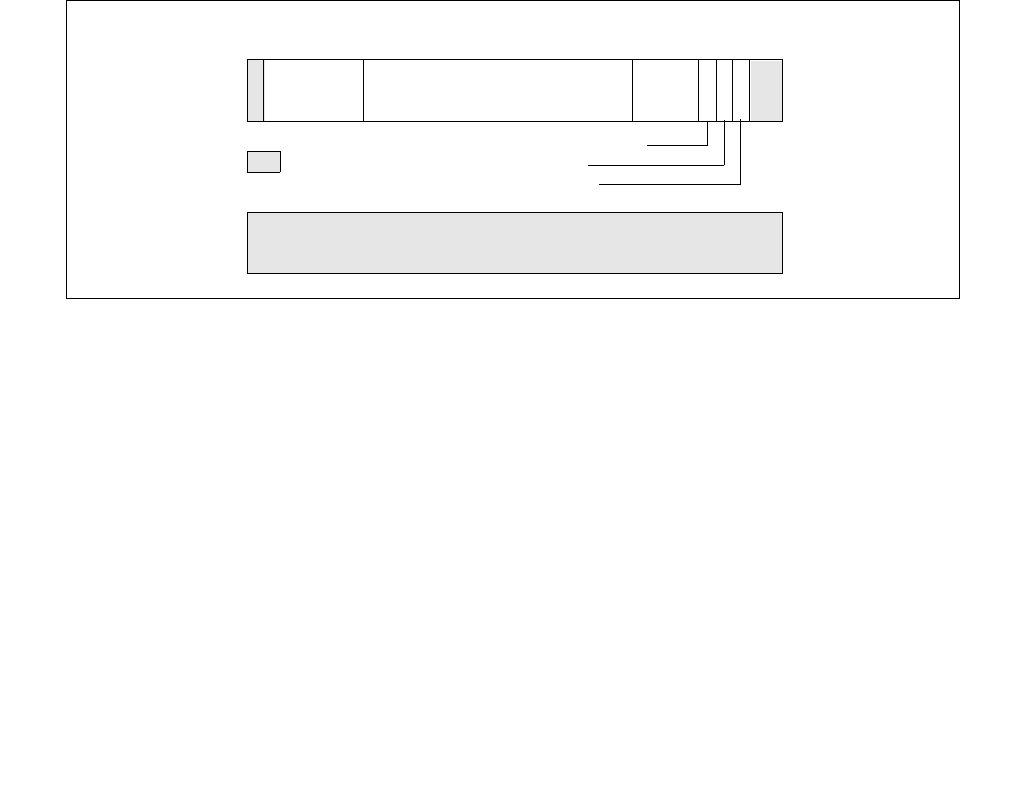
18-94 Vol. 3B
PERFORMANCE MONITORING
the counter. Code performance can be analyzed by examining the distribution of RIPs with a tool like the
VTune™ Performance Analyzer.
•Processor event-based sampling (PEBS) — In PEBS, the processor writes a record of the architectural
state of the processor to a memory buffer after the counter overflows. The records of architectural state
provide additional information for use in performance tuning. Processor-based event sampling can be used to
count only a subset of at-retirement events. PEBS captures more precise processor state information compared
to interrupt based event sampling, because the latter need to use the interrupt service routine to re-construct
the architectural states of processor.
The following sections describe the MSRs and data structures used for performance monitoring in the Pentium 4
and Intel Xeon processors.
18.6.3.1 ESCR MSRs
The 45 ESCR MSRs (see Table 18-70) allow software to select specific events to be countered. Each ESCR is usually
associated with a pair of performance counters (see Table 18-70) and each performance counter has several ESCRs
associated with it (allowing the events counted to be selected from a variety of events).
Figure 18-45 shows the layout of an ESCR MSR. The functions of the flags and fields are:
•USR flag, bit 2 — When set, events are counted when the processor is operating at a current privilege level
(CPL) of 1, 2, or 3. These privilege levels are generally used by application code and unprotected operating
system code.
•OS flag, bit 3 — When set, events are counted when the processor is operating at CPL of 0. This privilege level
is generally reserved for protected operating system code. (When both the OS and USR flags are set, events
are counted at all privilege levels.)
•Tag enable, bit 4 — When set, enables tagging of μops to assist in at-retirement event counting; when clear,
disables tagging. See Section 18.6.3.6, “At-Retirement Counting.”
•Tag value field, bits 5 through 8 — Selects a tag value to associate with a μop to assist in at-retirement
event counting.
•Event mask field, bits 9 through 24 — Selects events to be counted from the event class selected with the
event select field.
•Event select field, bits 25 through 30) — Selects a class of events to be counted. The events within this
class that are counted are selected with the event mask field.
When setting up an ESCR, the event select field is used to select a specific class of events to count, such as retired
branches. The event mask field is then used to select one or more of the specific events within the class to be
counted. For example, when counting retired branches, four different events can be counted: branch not taken
predicted, branch not taken mispredicted, branch taken predicted, and branch taken mispredicted. The OS and
Figure 18-45. Event Selection Control Register (ESCR) for Pentium 4
and Intel Xeon Processors without Intel HT Technology Support
31 24 8 0123492530
63 32
Reserved
Event Mask
Event
Select
USR
OS
5
Tag Enable
Tag
Value
Reserved

Vol. 3B 18-95
PERFORMANCE MONITORING
USR flags allow counts to be enabled for events that occur when operating system code and/or application code are
being executed. If neither the OS nor USR flag is set, no events will be counted.
The ESCRs are initialized to all 0s on reset. The flags and fields of an ESCR are configured by writing to the ESCR
using the WRMSR instruction. Table 18-70 gives the addresses of the ESCR MSRs.
Writing to an ESCR MSR does not enable counting with its associated performance counter; it only selects the event
or events to be counted. The CCCR for the selected performance counter must also be configured. Configuration of
the CCCR includes selecting the ESCR and enabling the counter.
18.6.3.2 Performance Counters
The performance counters in conjunction with the counter configuration control registers (CCCRs) are used for
filtering and counting the events selected by the ESCRs. Processors based on Intel NetBurst microarchitecture
provide 18 performance counters organized into 9 pairs. A pair of performance counters is associated with a partic-
ular subset of events and ESCR’s (see Table 18-70). The counter pairs are partitioned into four groups:
•The BPU group, includes two performance counter pairs:
— MSR_BPU_COUNTER0 and MSR_BPU_COUNTER1.
— MSR_BPU_COUNTER2 and MSR_BPU_COUNTER3.
•The MS group, includes two performance counter pairs:
— MSR_MS_COUNTER0 and MSR_MS_COUNTER1.
— MSR_MS_COUNTER2 and MSR_MS_COUNTER3.
•The FLAME group, includes two performance counter pairs:
— MSR_FLAME_COUNTER0 and MSR_FLAME_COUNTER1.
— MSR_FLAME_COUNTER2 and MSR_FLAME_COUNTER3.
•The IQ group, includes three performance counter pairs:
— MSR_IQ_COUNTER0 and MSR_IQ_COUNTER1.
— MSR_IQ_COUNTER2 and MSR_IQ_COUNTER3.
— MSR_IQ_COUNTER4 and MSR_IQ_COUNTER5.
The MSR_IQ_COUNTER4 counter in the IQ group provides support for the PEBS.
Alternate counters in each group can be cascaded: the first counter in one pair can start the first counter in the
second pair and vice versa. A similar cascading is possible for the second counters in each pair. For example, within
the BPU group of counters, MSR_BPU_COUNTER0 can start MSR_BPU_COUNTER2 and vice versa, and
MSR_BPU_COUNTER1 can start MSR_BPU_COUNTER3 and vice versa (see Section 18.6.3.5.6, “Cascading Coun-
ters”). The cascade flag in the CCCR register for the performance counter enables the cascading of counters.
Each performance counter is 40-bits wide (see Figure 18-46). The RDPMC instruction is intended to allow reading
of either the full counter-width (40-bits) or, if ECX[31] is set to 1, the low 32-bits of the counter. Reading the low
32-bits is faster than reading the full counter width and is appropriate in situations where the count is small enough
to be contained in 32 bits. In such cases, counter bits 31:0 are written to EAX, while 0 is written to EDX.
The RDPMC instruction can be used by programs or procedures running at any privilege level and in virtual-8086
mode to read these counters. The PCE flag in control register CR4 (bit 8) allows the use of this instruction to be
restricted to only programs and procedures running at privilege level 0.
Figure 18-46. Performance Counter (Pentium 4 and Intel Xeon Processors)
63 32
Reserved
31 0
Counter
39
Counter

18-96 Vol. 3B
PERFORMANCE MONITORING
The RDPMC instruction is not serializing or ordered with other instructions. Thus, it does not necessarily wait until
all previous instructions have been executed before reading the counter. Similarly, subsequent instructions may
begin execution before the RDPMC instruction operation is performed.
Only the operating system, executing at privilege level 0, can directly manipulate the performance counters, using
the RDMSR and WRMSR instructions. A secure operating system would clear the PCE flag during system initializa-
tion to disable direct user access to the performance-monitoring counters, but provide a user-accessible program-
ming interface that emulates the RDPMC instruction.
Some uses of the performance counters require the counters to be preset before counting begins (that is, before
the counter is enabled). This can be accomplished by writing to the counter using the WRMSR instruction. To set a
counter to a specified number of counts before overflow, enter a 2s complement negative integer in the counter.
The counter will then count from the preset value up to -1 and overflow. Writing to a performance counter in a
Pentium 4 or Intel Xeon processor with the WRMSR instruction causes all 40 bits of the counter to be written.
18.6.3.3 CCCR MSRs
Each of the 18 performance counters has one CCCR MSR associated with it (see Table 18-70). The CCCRs control
the filtering and counting of events as well as interrupt generation. Figure 18-47 shows the layout of an CCCR MSR.
The functions of the flags and fields are as follows:
•Enable flag, bit 12 — When set, enables counting; when clear, the counter is disabled. This flag is cleared on
reset.
•ESCR select field, bits 13 through 15 — Identifies the ESCR to be used to select events to be counted with
the counter associated with the CCCR.
•Compare flag, bit 18 — When set, enables filtering of the event count; when clear, disables filtering. The
filtering method is selected with the threshold, complement, and edge flags.
•Complement flag, bit 19 — Selects how the incoming event count is compared with the threshold value.
When set, event counts that are less than or equal to the threshold value result in a single count being delivered
to the performance counter; when clear, counts greater than the threshold value result in a count being
delivered to the performance counter (see Section 18.6.3.5.2, “Filtering Events”). The complement flag is not
active unless the compare flag is set.
•Threshold field, bits 20 through 23 — Selects the threshold value to be used for comparisons. The
processor examines this field only when the compare flag is set, and uses the complement flag setting to
determine the type of threshold comparison to be made. The useful range of values that can be entered in this
field depend on the type of event being counted (see Section 18.6.3.5.2, “Filtering Events”).
•Edge flag, bit 24 — When set, enables rising edge (false-to-true) edge detection of the threshold comparison
output for filtering event counts; when clear, rising edge detection is disabled. This flag is active only when the
compare flag is set.
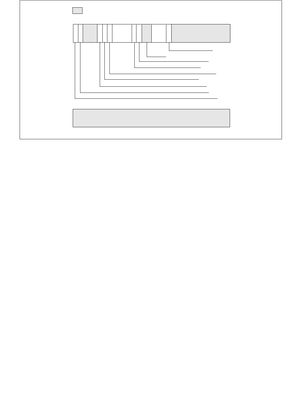
Vol. 3B 18-97
PERFORMANCE MONITORING
•FORCE_OVF flag, bit 25 — When set, forces a counter overflow on every counter increment; when clear,
overflow only occurs when the counter actually overflows.
•OVF_PMI flag, bit 26 — When set, causes a performance monitor interrupt (PMI) to be generated when the
counter overflows occurs; when clear, disables PMI generation. Note that the PMI is generated on the next
event count after the counter has overflowed.
•Cascade flag, bit 30 — When set, enables counting on one counter of a counter pair when its alternate
counter in the other the counter pair in the same counter group overflows (see Section 18.6.3.2, “Performance
Counters,” for further details); when clear, disables cascading of counters.
•OVF flag, bit 31 — Indicates that the counter has overflowed when set. This flag is a sticky flag that must be
explicitly cleared by software.
The CCCRs are initialized to all 0s on reset.
The events that an enabled performance counter actually counts are selected and filtered by the following flags and
fields in the ESCR and CCCR registers and in the qualification order given:
1. The event select and event mask fields in the ESCR select a class of events to be counted and one or more
event types within the class, respectively.
2. The OS and USR flags in the ESCR selected the privilege levels at which events will be counted.
3. The ESCR select field of the CCCR selects the ESCR. Since each counter has several ESCRs associated with it,
one ESCR must be chosen to select the classes of events that may be counted.
4. The compare and complement flags and the threshold field of the CCCR select an optional threshold to be used
in qualifying an event count.
5. The edge flag in the CCCR allows events to be counted only on rising-edge transitions.
The qualification order in the above list implies that the filtered output of one “stage” forms the input for the next.
For instance, events filtered using the privilege level flags can be further qualified by the compare and complement
flags and the threshold field, and an event that matched the threshold criteria, can be further qualified by edge
detection.
The uses of the flags and fields in the CCCRs are discussed in greater detail in Section 18.6.3.5, “Programming the
Performance Counters for Non-Retirement Events.”
Figure 18-47. Counter Configuration Control Register (CCCR)
63 32
Reserved
Reserved
Reserved: Must be set to 11B
Compare
Enable
31 24 23 20 19 16 15 12 11 0
1718
2526272930
Edge
FORCE_OVF
OVF_PMI
Threshold
Cascade
OVF
Complement
Reserved
13
ESCR
Select
Reserved

18-98 Vol. 3B
PERFORMANCE MONITORING
18.6.3.4 Debug Store (DS) Mechanism
The debug store (DS) mechanism was introduced with processors based on Intel NetBurst microarchitecture to
allow various types of information to be collected in memory-resident buffers for use in debugging and tuning
programs. The DS mechanism can be used to collect two types of information: branch records and processor event-
based sampling (PEBS) records. The availability of the DS mechanism in a processor is indicated with the DS
feature flag (bit 21) returned by the CPUID instruction.
See Section 17.4.5, “Branch Trace Store (BTS),” and Section 18.6.3.8, “Processor Event-Based Sampling (PEBS),”
for a description of these facilities. Records collected with the DS mechanism are saved in the DS save area. See
Section 17.4.9, “BTS and DS Save Area.”
18.6.3.5 Programming the Performance Counters for Non-Retirement Events
The basic steps to program a performance counter and to count events include the following:
1. Select the event or events to be counted.
2. For each event, select an ESCR that supports the event using the values in the ESCR restrictions row in Table
19-31, Chapter 19.
3. Match the CCCR Select value and ESCR name in Table 19-31 to a value listed in Table 18-70; select a CCCR and
performance counter.
4. Set up an ESCR for the specific event or events to be counted and the privilege levels at which the are to be
counted.
5. Set up the CCCR for the performance counter by selecting the ESCR and the desired event filters.
6. Set up the CCCR for optional cascading of event counts, so that when the selected counter overflows its
alternate counter starts.
7. Set up the CCCR to generate an optional performance monitor interrupt (PMI) when the counter overflows. If
PMI generation is enabled, the local APIC must be set up to deliver the interrupt to the processor and a handler
for the interrupt must be in place.
8. Enable the counter to begin counting.
18.6.3.5.1 Selecting Events to Count
Table 19-32 in Chapter 19 lists a set of at-retirement events for processors based on Intel NetBurst microarchitec-
ture. For each event listed in Table 19-32, setup information is provided. Table 18-71 gives an example of one of
the events.
Table 18-71. Event Example
Event Name Event Parameters Parameter Value Description
branch_retired Counts the retirement of a branch. Specify one or more mask bits to select
any combination of branch taken, not-taken, predicted and mispredicted.
ESCR restrictions MSR_CRU_ESCR2
MSR_CRU_ESCR3
See Table 15-3 for the addresses of the ESCR MSRs.
Counter numbers per
ESCR
ESCR2: 12, 13, 16
ESCR3: 14, 15, 17
The counter numbers associated with each ESCR are provided. The
performance counters and corresponding CCCRs can be obtained from
Table 15-3.
ESCR Event Select 06H ESCR[31:25]
ESCR Event Mask
Bit 0: MMNP
1: MMNM
2: MMTP
3: MMTM
ESCR[24:9]
Branch Not-taken Predicted
Branch Not-taken Mispredicted
Branch Taken Predicted
Branch Taken Mispredicted
CCCR Select 05H CCCR[15:13]

Vol. 3B 18-99
PERFORMANCE MONITORING
For Table 19-31 and Table 19-32, Chapter 19, the name of the event is listed in the Event Name column and
parameters that define the event and other information are listed in the Event Parameters column. The Parameter
Value and Description columns give specific parameters for the event and additional description information.
Entries in the Event Parameters column are described below.
•ESCR restrictions — Lists the ESCRs that can be used to program the event. Typically only one ESCR is
needed to count an event.
•Counter numbers per ESCR — Lists which performance counters are associated with each ESCR. Table 18-70
gives the name of the counter and CCCR for each counter number. Typically only one counter is needed to
count the event.
•ESCR event select — Gives the value to be placed in the event select field of the ESCR to select the event.
•ESCR event mask — Gives the value to be placed in the Event Mask field of the ESCR to select sub-events to
be counted. The parameter value column defines the documented bits with relative bit position offset starting
from 0, where the absolute bit position of relative offset 0 is bit 9 of the ESCR. All undocumented bits are
reserved and should be set to 0.
•CCCR select — Gives the value to be placed in the ESCR select field of the CCCR associated with the counter
to select the ESCR to be used to define the event. This value is not the address of the ESCR; it is the number of
the ESCR from the Number column in Table 18-70.
•Event specific notes — Gives additional information about the event, such as the name of the same or a
similar event defined for the P6 family processors.
•Can support PEBS — Indicates if PEBS is supported for the event (only supplied for at-retirement events
listed in Table 19-32.)
•Requires additional MSR for tagging — Indicates which if any additional MSRs must be programmed to
count the events (only supplied for the at-retirement events listed in Table 19-32.)
NOTE
The performance-monitoring events listed in Chapter 19, “Performance Monitoring Events,” are
intended to be used as guides for performance tuning. The counter values reported are not
guaranteed to be absolutely accurate and should be used as a relative guide for tuning. Known
discrepancies are documented where applicable.
The following procedure shows how to set up a performance counter for basic counting; that is, the counter is set
up to count a specified event indefinitely, wrapping around whenever it reaches its maximum count. This procedure
is continued through the following four sections.
Using information in Table 19-31, Chapter 19, an event to be counted can be selected as follows:
1. Select the event to be counted.
2. Select the ESCR to be used to select events to be counted from the ESCRs field.
3. Select the number of the counter to be used to count the event from the Counter Numbers Per ESCR field.
4. Determine the name of the counter and the CCCR associated with the counter, and determine the MSR
addresses of the counter, CCCR, and ESCR from Table 18-70.
5. Use the WRMSR instruction to write the ESCR Event Select and ESCR Event Mask values into the appropriate
fields in the ESCR. At the same time set or clear the USR and OS flags in the ESCR as desired.
6. Use the WRMSR instruction to write the CCCR Select value into the appropriate field in the CCCR.
Event Specific Notes P6: EMON_BR_INST_RETIRED
Can Support PEBS No
Requires Additional
MSRs for Tagging
No
Table 18-71. Event Example (Contd.)
Event Name Event Parameters Parameter Value Description
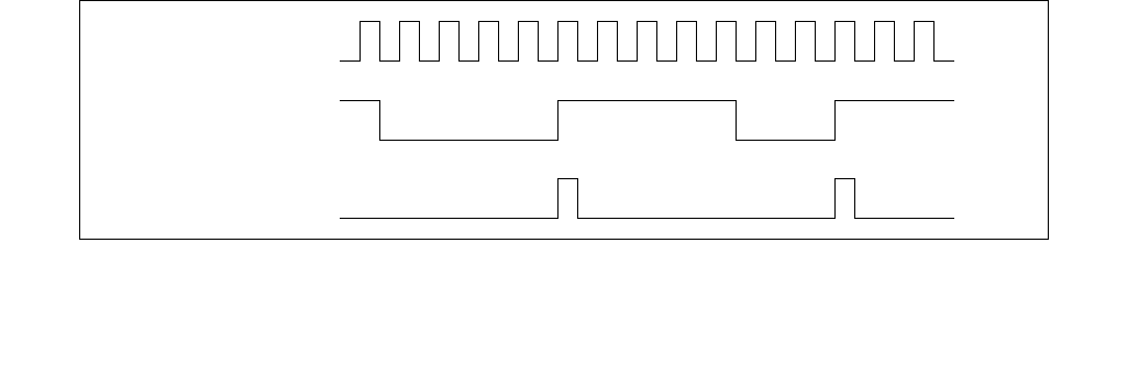
18-100 Vol. 3B
PERFORMANCE MONITORING
NOTE
Typically all the fields and flags of the CCCR will be written with one WRMSR instruction; however,
in this procedure, several WRMSR writes are used to more clearly demonstrate the uses of the
various CCCR fields and flags.
This setup procedure is continued in the next section, Section 18.6.3.5.2, “Filtering Events.”
18.6.3.5.2 Filtering Events
Each counter receives up to 4 input lines from the processor hardware from which it is counting events. The counter
treats these inputs as binary inputs (input 0 has a value of 1, input 1 has a value of 2, input 3 has a value of 4, and
input 3 has a value of 8). When a counter is enabled, it adds this binary input value to the counter value on each
clock cycle. For each clock cycle, the value added to the counter can then range from 0 (no event) to 15.
For many events, only the 0 input line is active, so the counter is merely counting the clock cycles during which the
0 input is asserted. However, for some events two or more input lines are used. Here, the counters threshold
setting can be used to filter events. The compare, complement, threshold, and edge fields control the filtering of
counter increments by input value.
If the compare flag is set, then a “greater than” or a “less than or equal to” comparison of the input value vs. a
threshold value can be made. The complement flag selects “less than or equal to” (flag set) or “greater than” (flag
clear). The threshold field selects a threshold value of from 0 to 15. For example, if the complement flag is cleared
and the threshold field is set to 6, than any input value of 7 or greater on the 4 inputs to the counter will cause the
counter to be incremented by 1, and any value less than 7 will cause an increment of 0 (or no increment) of the
counter. Conversely, if the complement flag is set, any value from 0 to 6 will increment the counter and any value
from 7 to 15 will not increment the counter. Note that when a threshold condition has been satisfied, the input to
the counter is always 1, not the input value that is presented to the threshold filter.
The edge flag provides further filtering of the counter inputs when a threshold comparison is being made. The edge
flag is only active when the compare flag is set. When the edge flag is set, the resulting output from the threshold
filter (a value of 0 or 1) is used as an input to the edge filter. Each clock cycle, the edge filter examines the last and
current input values and sends a count to the counter only when it detects a “rising edge” event; that is, a false-to-
true transition. Figure 18-48 illustrates rising edge filtering.
The following procedure shows how to configure a CCCR to filter events using the threshold filter and the edge filter.
This procedure is a continuation of the setup procedure introduced in Section 18.6.3.5.1, “Selecting Events to
Count.”
7. (Optional) To set up the counter for threshold filtering, use the WRMSR instruction to write values in the CCCR
compare and complement flags and the threshold field:
— Set the compare flag.
— Set or clear the complement flag for less than or equal to or greater than comparisons, respectively.
— Enter a value from 0 to 15 in the threshold field.
8. (Optional) Select rising edge filtering by setting the CCCR edge flag.
This setup procedure is continued in the next section, Section 18.6.3.5.3, “Starting Event Counting.”
Figure 18-48. Effects of Edge Filtering
Output from
Threshold Filter
Counter Increments
On Rising Edge
(False-to-True)
Processor Clock

Vol. 3B 18-101
PERFORMANCE MONITORING
18.6.3.5.3 Starting Event Counting
Event counting by a performance counter can be initiated in either of two ways. The typical way is to set the enable
flag in the counter’s CCCR. Following the instruction to set the enable flag, event counting begins and continues
until it is stopped (see Section 18.6.3.5.5, “Halting Event Counting”).
The following procedural step shows how to start event counting. This step is a continuation of the setup procedure
introduced in Section 18.6.3.5.2, “Filtering Events.”
9. To start event counting, use the WRMSR instruction to set the CCCR enable flag for the performance counter.
This setup procedure is continued in the next section, Section 18.6.3.5.4, “Reading a Performance Counter’s
Count.”
The second way that a counter can be started by using the cascade feature. Here, the overflow of one counter auto-
matically starts its alternate counter (see Section 18.6.3.5.6, “Cascading Counters”).
18.6.3.5.4 Reading a Performance Counter’s Count
Performance counters can be read using either the RDPMC or RDMSR instructions. The enhanced functions of the
RDPMC instruction (including fast read) are described in Section 18.6.3.2, “Performance Counters.” These instruc-
tions can be used to read a performance counter while it is counting or when it is stopped.
The following procedural step shows how to read the event counter. This step is a continuation of the setup proce-
dure introduced in Section 18.6.3.5.3, “Starting Event Counting.”
10. To read a performance counters current event count, execute the RDPMC instruction with the counter number
obtained from Table 18-70 used as an operand.
This setup procedure is continued in the next section, Section 18.6.3.5.5, “Halting Event Counting.”
18.6.3.5.5 Halting Event Counting
After a performance counter has been started (enabled), it continues counting indefinitely. If the counter overflows
(goes one count past its maximum count), it wraps around and continues counting. When the counter wraps
around, it sets its OVF flag to indicate that the counter has overflowed. The OVF flag is a sticky flag that indicates
that the counter has overflowed at least once since the OVF bit was last cleared.
To halt counting, the CCCR enable flag for the counter must be cleared.
The following procedural step shows how to stop event counting. This step is a continuation of the setup procedure
introduced in Section 18.6.3.5.4, “Reading a Performance Counter’s Count.”
11. To stop event counting, execute a WRMSR instruction to clear the CCCR enable flag for the performance
counter.
To halt a cascaded counter (a counter that was started when its alternate counter overflowed), either clear the
Cascade flag in the cascaded counter’s CCCR MSR or clear the OVF flag in the alternate counter’s CCCR MSR.
18.6.3.5.6 Cascading Counters
As described in Section 18.6.3.2, “Performance Counters,” eighteen performance counters are implemented in
pairs. Nine pairs of counters and associated CCCRs are further organized as four blocks: BPU, MS, FLAME, and IQ
(see Table 18-70). The first three blocks contain two pairs each. The IQ block contains three pairs of counters (12
through 17) with associated CCCRs (MSR_IQ_CCCR0 through MSR_IQ_CCCR5).
The first 8 counter pairs (0 through 15) can be programmed using ESCRs to detect performance monitoring events.
Pairs of ESCRs in each of the four blocks allow many different types of events to be counted. The cascade flag in
the CCCR MSR allows nested monitoring of events to be performed by cascading one counter to a second counter
located in another pair in the same block (see Figure 18-47 for the location of the flag).
Counters 0 and 1 form the first pair in the BPU block. Either counter 0 or 1 can be programmed to detect an event
via MSR_MO B_ESCR0. Counters 0 and 2 can be cascaded in any order, as can counters 1 and 3. It’s possible to set
up 4 counters in the same block to cascade on two pairs of independent events. The pairing described also applies
to subsequent blocks. Since the IQ PUB has two extra counters, cascading operates somewhat differently if 16 and
17 are involved. In the IQ block, counter 16 can only be cascaded from counter 14 (not from 12); counter 14
18-102 Vol. 3B
PERFORMANCE MONITORING
cannot be cascaded from counter 16 using the CCCR cascade bit mechanism. Similar restrictions apply to counter
17.
Example 18-1. Counting Events
Assume a scenario where counter X is set up to count 200 occurrences of event A; then counter Y is set up to count
400 occurrences of event B. Each counter is set up to count a specific event and overflow to the next counter. In the
above example, counter X is preset for a count of -200 and counter Y for a count of -400; this setup causes the
counters to overflow on the 200th and 400th counts respectively.
Continuing this scenario, counter X is set up to count indefinitely and wraparound on overflow. This is described in
the basic performance counter setup procedure that begins in Section 18.6.3.5.1, “Selecting Events to Count.”
Counter Y is set up with the cascade flag in its associated CCCR MSR set to 1 and its enable flag set to 0.
To begin the nested counting, the enable bit for the counter X is set. Once enabled, counter X counts until it over-
flows. At this point, counter Y is automatically enabled and begins counting. Thus counter X overflows after 200
occurrences of event A. Counter Y then starts, counting 400 occurrences of event B before overflowing. When
performance counters are cascaded, the counter Y would typically be set up to generate an interrupt on overflow.
This is described in Section 18.6.3.5.8, “Generating an Interrupt on Overflow.”
The cascading counters mechanism can be used to count a single event. The counting begins on one counter then
continues on the second counter after the first counter overflows. This technique doubles the number of event
counts that can be recorded, since the contents of the two counters can be added together.
18.6.3.5.7 EXTENDED CASCADING
Extended cascading is a model-specific feature in the Intel NetBurst microarchitecture with CPUID
DisplayFamily_DisplayModel 0F_02, 0F_03, 0F_04, 0F_06. This feature uses bit 11 in CCCRs associated with the IQ
block. See Table 18-72.
The extended cascading feature can be adapted to the Interrupt based sampling usage model for performance
monitoring. However, it is known that performance counters do not generate PMI in cascade mode or extended
cascade mode due to an erratum. This erratum applies to processors with CPUID DisplayFamily_DisplayModel
signature of 0F_02. For processors with CPUID DisplayFamily_DisplayModel signature of 0F_00 and 0F_01, the
erratum applies to processors with stepping encoding greater than 09H.
Counters 16 and 17 in the IQ block are frequently used in processor event-based sampling or at-retirement
counting of events indicating a stalled condition in the pipeline. Neither counter 16 or 17 can initiate the cascading
of counter pairs using the cascade bit in a CCCR.
Extended cascading permits performance monitoring tools to use counters 16 and 17 to initiate cascading of two
counters in the IQ block. Extended cascading from counter 16 and 17 is conceptually similar to cascading other
counters, but instead of using CASCADE bit of a CCCR, one of the four CASCNTxINTOy bits is used.
Example 18-2. Scenario for Extended Cascading
A usage scenario for extended cascading is to sample instructions retired on logical processor 1 after the first 4096
instructions retired on logical processor 0. A procedure to program extended cascading in this scenario is outlined
below:
Table 18-72. CCR Names and Bit Positions
CCCR Name:Bit Position Bit Name Description
MSR_IQ_CCCR1|2:11 Reserved
MSR_IQ_CCCR0:11 CASCNT4INTO0 Allow counter 4 to cascade into counter 0
MSR_IQ_CCCR3:11 CASCNT5INTO3 Allow counter 5 to cascade into counter 3
MSR_IQ_CCCR4:11 CASCNT5INTO4 Allow counter 5 to cascade into counter 4
MSR_IQ_CCCR5:11 CASCNT4INTO5 Allow counter 4 to cascade into counter 5

Vol. 3B 18-103
PERFORMANCE MONITORING
1. Write the value 0 to counter 12.
2. Write the value 04000603H to MSR_CRU_ESCR0 (corresponding to selecting the NBOGNTAG and NBOGTAG
event masks with qualification restricted to logical processor 1).
3. Write the value 04038800H to MSR_IQ_CCCR0. This enables CASCNT4INTO0 and OVF_PMI. An ISR can sample
on instruction addresses in this case (do not set ENABLE, or CASCADE).
4. Write the value FFFFF000H into counter 16.1.
5. Write the value 0400060CH to MSR_CRU_ESCR2 (corresponding to selecting the NBOGNTAG and NBOGTAG
event masks with qualification restricted to logical processor 0).
6. Write the value 00039000H to MSR_IQ_CCCR4 (set ENABLE bit, but not OVF_PMI).
Another use for cascading is to locate stalled execution in a multithreaded application. Assume MOB replays in
thread B cause thread A to stall. Getting a sample of the stalled execution in this scenario could be accomplished
by:
1. Set up counter B to count MOB replays on thread B.
2. Set up counter A to count resource stalls on thread A; set its force overflow bit and the appropriate CASCNTx-
INTOy bit.
3. Use the performance monitoring interrupt to capture the program execution data of the stalled thread.
18.6.3.5.8 Generating an Interrupt on Overflow
Any performance counter can be configured to generate a performance monitor interrupt (PMI) if the counter over-
flows. The PMI interrupt service routine can then collect information about the state of the processor or program
when overflow occurred. This information can then be used with a tool like the Intel® VTune™ Performance
Analyzer to analyze and tune program performance.
To enable an interrupt on counter overflow, the OVR_PMI flag in the counter’s associated CCCR MSR must be set.
When overflow occurs, a PMI is generated through the local APIC. (Here, the performance counter entry in the local
vector table [LVT] is set up to deliver the interrupt generated by the PMI to the processor.)
The PMI service routine can use the OVF flag to determine which counter overflowed when multiple counters have
been configured to generate PMIs. Also, note that these processors mask PMIs upon receiving an interrupt. Clear
this condition before leaving the interrupt handler.
When generating interrupts on overflow, the performance counter being used should be preset to value that will
cause an overflow after a specified number of events are counted plus 1. The simplest way to select the preset
value is to write a negative number into the counter, as described in Section 18.6.3.5.6, “Cascading Counters.”
Here, however, if an interrupt is to be generated after 100 event counts, the counter should be preset to minus 100
plus 1 (-100 + 1), or -99. The counter will then overflow after it counts 99 events and generate an interrupt on the
next (100th) event counted. The difference of 1 for this count enables the interrupt to be generated immediately
after the selected event count has been reached, instead of waiting for the overflow to be propagation through the
counter.
Because of latency in the microarchitecture between the generation of events and the generation of interrupts on
overflow, it is sometimes difficult to generate an interrupt close to an event that caused it. In these situations, the
FORCE_OVF flag in the CCCR can be used to improve reporting. Setting this flag causes the counter to overflow on
every counter increment, which in turn triggers an interrupt after every counter increment.
18.6.3.5.9 Counter Usage Guideline
There are some instances where the user must take care to configure counting logic properly, so that it is not
powered down. To use any ESCR, even when it is being used just for tagging, (any) one of the counters that the
particular ESCR (or its paired ESCR) can be connected to should be enabled. If this is not done, 0 counts may
result. Likewise, to use any counter, there must be some event selected in a corresponding ESCR (other than
no_event, which generally has a select value of 0).

18-104 Vol. 3B
PERFORMANCE MONITORING
18.6.3.6 At-Retirement Counting
At-retirement counting provides a means counting only events that represent work committed to architectural
state and ignoring work that was performed speculatively and later discarded.
One example of this speculative activity is branch prediction. When a branch misprediction occurs, the results of
instructions that were decoded and executed down the mispredicted path are canceled. If a performance counter
was set up to count all executed instructions, the count would include instructions whose results were canceled as
well as those whose results committed to architectural state.
To provide finer granularity in event counting in these situations, the performance monitoring facilities provided in
the Pentium 4 and Intel Xeon processors provide a mechanism for tagging events and then counting only those
tagged events that represent committed results. This mechanism is called “at-retirement counting.”
Tables 19-32 through 19-36 list predefined at-retirement events and event metrics that can be used to for tagging
events when using at retirement counting. The following terminology is used in describing at-retirement counting:
•Bogus, non-bogus, retire — In at-retirement event descriptions, the term “bogus” refers to instructions or
μops that must be canceled because they are on a path taken from a mispredicted branch. The terms “retired”
and “non-bogus” refer to instructions or μops along the path that results in committed architectural state
changes as required by the program being executed. Thus instructions and μops are either bogus or non-bogus,
but not both. Several of the Pentium 4 and Intel Xeon processors’ performance monitoring events (such as,
Instruction_Retired and Uops_Retired in Table 19-32) can count instructions or μops that are retired based on
the characterization of bogus” versus non-bogus.
•Tagging — Tagging is a means of marking μops that have encountered a particular performance event so they
can be counted at retirement. During the course of execution, the same event can happen more than once per
μop and a direct count of the event would not provide an indication of how many μops encountered that event.
The tagging mechanisms allow a μop to be tagged once during its lifetime and thus counted once at retirement.
The retired suffix is used for performance metrics that increment a count once per μop, rather than once per
event. For example, a μop may encounter a cache miss more than once during its life time, but a “Miss Retired”
metric (that counts the number of retired μops that encountered a cache miss) will increment only once for that
μop. A “Miss Retired” metric would be useful for characterizing the performance of the cache hierarchy for a
particular instruction sequence. Details of various performance metrics and how these can be constructed using
the Pentium 4 and Intel Xeon processors performance events are provided in the Intel Pentium 4 Processor
Optimization Reference Manual (see Section 1.4, “Related Literature”).
•Replay — To maximize performance for the common case, the Intel NetBurst microarchitecture aggressively
schedules μops for execution before all the conditions for correct execution are guaranteed to be satisfied. In
the event that all of these conditions are not satisfied, μops must be reissued. The mechanism that the Pentium
4 and Intel Xeon processors use for this reissuing of μops is called replay. Some examples of replay causes are
cache misses, dependence violations, and unforeseen resource constraints. In normal operation, some number
of replays is common and unavoidable. An excessive number of replays is an indication of a performance
problem.
•Assist — When the hardware needs the assistance of microcode to deal with some event, the machine takes
an assist. One example of this is an underflow condition in the input operands of a floating-point operation. The
hardware must internally modify the format of the operands in order to perform the computation. Assists clear
the entire machine of μops before they begin and are costly.
18.6.3.6.1 Using At-Retirement Counting
Processors based on Intel NetBurst microarchitecture allow counting both events and μops that encountered a
specified event. For a subset of the at-retirement events listed in Table 19-32, a μop may be tagged when it
encounters that event. The tagging mechanisms can be used in Interrupt-based event sampling, and a subset of
these mechanisms can be used in PEBS. There are four independent tagging mechanisms, and each mechanism
uses a different event to count μops tagged with that mechanism:
•Front-end tagging — This mechanism pertains to the tagging of μops that encountered front-end events (for
example, trace cache and instruction counts) and are counted with the Front_end_event event.
•Execution tagging — This mechanism pertains to the tagging of μops that encountered execution events (for
example, instruction types) and are counted with the Execution_Event event.

Vol. 3B 18-105
PERFORMANCE MONITORING
•Replay tagging — This mechanism pertains to tagging of μops whose retirement is replayed (for example, a
cache miss) and are counted with the Replay_event event. Branch mispredictions are also tagged with this
mechanism.
•No tags — This mechanism does not use tags. It uses the Instr_retired and the Uops_ retired events.
Each tagging mechanism is independent from all others; that is, a μop that has been tagged using one mechanism
will not be detected with another mechanism’s tagged-μop detector. For example, if μops are tagged using the
front-end tagging mechanisms, the Replay_event will not count those as tagged μops unless they are also tagged
using the replay tagging mechanism. However, execution tags allow up to four different types of μops to be counted
at retirement through execution tagging.
The independence of tagging mechanisms does not hold when using PEBS. When using PEBS, only one tagging
mechanism should be used at a time.
Certain kinds of μops that cannot be tagged, including I/O, uncacheable and locked accesses, returns, and far
transfers.
Table 19-32 lists the performance monitoring events that support at-retirement counting: specifically the
Front_end_event, Execution_event, Replay_event, Inst_retired and Uops_retired events. The following sections
describe the tagging mechanisms for using these events to tag μop and count tagged μops.
18.6.3.6.2 Tagging Mechanism for Front_end_event
The Front_end_event counts μops that have been tagged as encountering any of the following events:
•μop decode events — Tagging μops for μop decode events requires specifying bits in the ESCR associated with
the performance-monitoring event, Uop_type.
•Trace cache events — Tagging μops for trace cache events may require specifying certain bits in the
MSR_TC_PRECISE_EVENT MSR (see Table 19-34).
Table 19-32 describes the Front_end_event and Table 19-34 describes metrics that are used to set up a
Front_end_event count.
The MSRs specified in the Table 19-32 that are supported by the front-end tagging mechanism must be set and one
or both of the NBOGUS and BOGUS bits in the Front_end_event event mask must be set to count events. None of
the events currently supported requires the use of the MSR_TC_PRECISE_EVENT MSR.
18.6.3.6.3 Tagging Mechanism For Execution_event
Table 19-32 describes the Execution_event and Table 19-35 describes metrics that are used to set up an
Execution_event count.
The execution tagging mechanism differs from other tagging mechanisms in how it causes tagging. One upstream
ESCR is used to specify an event to detect and to specify a tag value (bits 5 through 8) to identify that event. A
second downstream ESCR is used to detect μops that have been tagged with that tag value identifier using
Execution_event for the event selection.
The upstream ESCR that counts the event must have its tag enable flag (bit 4) set and must have an appropriate
tag value mask entered in its tag value field. The 4-bit tag value mask specifies which of tag bits should be set for
a particular μop. The value selected for the tag value should coincide with the event mask selected in the down-
stream ESCR. For example, if a tag value of 1 is set, then the event mask of NBOGUS0 should be enabled, corre-
spondingly in the downstream ESCR. The downstream ESCR detects and counts tagged μops. The normal (not tag
value) mask bits in the downstream ESCR specify which tag bits to count. If any one of the tag bits selected by the
mask is set, the related counter is incremented by one. This mechanism is summarized in the Table 19-35 metrics
that are supported by the execution tagging mechanism. The tag enable and tag value bits are irrelevant for the
downstream ESCR used to select the Execution_event.
The four separate tag bits allow the user to simultaneously but distinctly count up to four execution events at
retirement. (This applies for interrupt-based event sampling. There are additional restrictions for PEBS as noted in
Section 18.6.3.8.3, “Setting Up the PEBS Buffer.”) It is also possible to detect or count combinations of events by
setting multiple tag value bits in the upstream ESCR or multiple mask bits in the downstream ESCR. For example,
use a tag value of 3H in the upstream ESCR and use NBOGUS0/NBOGUS1 in the downstream ESCR event mask.

18-106 Vol. 3B
PERFORMANCE MONITORING
18.6.3.7 Tagging Mechanism for Replay_event
Table 19-32 describes the Replay_event and Table 19-36 describes metrics that are used to set up an
Replay_event count.
The replay mechanism enables tagging of μops for a subset of all replays before retirement. Use of the replay
mechanism requires selecting the type of μop that may experience the replay in the MSR_PEBS_MATRIX_VERT
MSR and selecting the type of event in the MSR_PEBS_ENABLE MSR. Replay tagging must also be enabled with the
UOP_Tag flag (bit 24) in the MSR_PEBS_ENABLE MSR.
The Table 19-36 lists the metrics that are support the replay tagging mechanism and the at-retirement events that
use the replay tagging mechanism, and specifies how the appropriate MSRs need to be configured. The replay tags
defined in Table A-5 also enable Processor Event-Based Sampling (PEBS, see Section 17.4.9). Each of these replay
tags can also be used in normal sampling by not setting Bit 24 nor Bit 25 in IA_32_PEBS_ENABLE_MSR. Each of
these metrics requires that the Replay_Event (see Table 19-32) be used to count the tagged μops.
18.6.3.8 Processor Event-Based Sampling (PEBS)
The debug store (DS) mechanism in processors based on Intel NetBurst microarchitecture allow two types of infor-
mation to be collected for use in debugging and tuning programs: PEBS records and BTS records. See Section
17.4.5, “Branch Trace Store (BTS),” for a description of the BTS mechanism.
PEBS permits the saving of precise architectural information associated with one or more performance events in
the precise event records buffer, which is part of the DS save area (see Section 17.4.9, “BTS and DS Save Area”).
To use this mechanism, a counter is configured to overflow after it has counted a preset number of events. After
the counter overflows, the processor copies the current state of the general-purpose and EFLAGS registers and
instruction pointer into a record in the precise event records buffer. The processor then resets the count in the
performance counter and restarts the counter. When the precise event records buffer is nearly full, an interrupt is
generated, allowing the precise event records to be saved. A circular buffer is not supported for precise event
records.
PEBS is supported only for a subset of the at-retirement events: Execution_event, Front_end_event, and
Replay_event. Also, PEBS can only be carried out using the one performance counter, the MSR_IQ_COUNTER4
MSR.
In processors based on Intel Core microarchitecture, a similar PEBS mechanism is also supported using IA32_PMC0
and IA32_PERFEVTSEL0 MSRs (See Section 18.6.2.4).
18.6.3.8.1 Detection of the Availability of the PEBS Facilities
The DS feature flag (bit 21) returned by the CPUID instruction indicates (when set) the availability of the DS mech-
anism in the processor, which supports the PEBS (and BTS) facilities. When this bit is set, the following PEBS facil-
ities are available:
•The PEBS_UNAVAILABLE flag in the IA32_MISC_ENABLE MSR indicates (when clear) the availability of the
PEBS facilities, including the MSR_PEBS_ENABLE MSR.
•The enable PEBS flag (bit 24) in the MSR_PEBS_ENABLE MSR allows PEBS to be enabled (set) or disabled
(clear).
•The IA32_DS_AREA MSR can be programmed to point to the DS save area.
18.6.3.8.2 Setting Up the DS Save Area
Section 17.4.9.2, “Setting Up the DS Save Area,” describes how to set up and enable the DS save area. This proce-
dure is common for PEBS and BTS.
18.6.3.8.3 Setting Up the PEBS Buffer
Only the MSR_IQ_COUNTER4 performance counter can be used for PEBS. Use the following procedure to set up the
processor and this counter for PEBS:

Vol. 3B 18-107
PERFORMANCE MONITORING
1. Set up the precise event buffering facilities. Place values in the precise event buffer base, precise event index,
precise event absolute maximum, and precise event interrupt threshold, and precise event counter reset fields
of the DS buffer management area (see Figure 17-5) to set up the precise event records buffer in memory.
2. Enable PEBS. Set the Enable PEBS flag (bit 24) in MSR_PEBS_ENABLE MSR.
3. Set up the MSR_IQ_COUNTER4 performance counter and its associated CCCR and one or more ESCRs for PEBS
as described in Tables 19-32 through 19-36.
18.6.3.8.4 Writing a PEBS Interrupt Service Routine
The PEBS facilities share the same interrupt vector and interrupt service routine (called the DS ISR) with the non-
precise event-based sampling and BTS facilities. To handle PEBS interrupts, PEBS handler code must be included in
the DS ISR. See Section 17.4.9.5, “Writing the DS Interrupt Service Routine,” for guidelines for writing the DS ISR.
18.6.3.8.5 Other DS Mechanism Implications
The DS mechanism is not available in the SMM. It is disabled on transition to the SMM mode. Similarly the DS
mechanism is disabled on the generation of a machine check exception and is cleared on processor RESET and
INIT.
The DS mechanism is available in real address mode.
18.6.3.9 Operating System Implications
The DS mechanism can be used by the operating system as a debugging extension to facilitate failure analysis.
When using this facility, a 25 to 30 times slowdown can be expected due to the effects of the trace store occurring
on every taken branch.
Depending upon intended usage, the instruction pointers that are part of the branch records or the PEBS records
need to have an association with the corresponding process. One solution requires the ability for the DS specific
operating system module to be chained to the context switch. A separate buffer can then be maintained for each
process of interest and the MSR pointing to the configuration area saved and setup appropriately on each context
switch.
If the BTS facility has been enabled, then it must be disabled and state stored on transition of the system to a sleep
state in which processor context is lost. The state must be restored on return from the sleep state.
It is required t hat an i nterrupt gate be used for the DS interrupt as opposed to a trap gate to prevent the generation
of an endless interrupt loop.
Pages that contain buffers must have mappings to the same physical address for all processes/logical processors,
such that any change to CR3 will not change DS addresses. If this requirement cannot be satisfied (that is, the
feature is enabled on a per thread/process basis), then the operating system must ensure that the feature is
enabled/disabled appropriately in the context switch code.
18.6.4 Performance Monitoring and Intel Hyper-Threading Technology in Processors Based
on Intel NetBurst® Microarchitecture
The performance monitoring capability of processors based on Intel NetBurst microarchitecture and supporting
Intel Hyper-Threading Technology is similar to that described in Section 18.6.3. However, the capability is
extended so that:
•Performance counters can be programmed to select events qualified by logical processor IDs.
•Performance monitoring interrupts can be directed to a specific logical processor within the physical processor.
The sections below describe performance counters, event qualification by logical processor ID, and special purpose
bits in ESCRs/CCCRs. They also describe MSR_PEBS_ENABLE, MSR_PEBS_MATRIX_VERT, and
MSR_TC_PRECISE_EVENT.
18-108 Vol. 3B
PERFORMANCE MONITORING
18.6.4.1 ESCR MSRs
Figure 18-49 shows the layout of an ESCR MSR in processors supporting Intel Hyper-Threading Technology.
The functions of the flags and fields are as follows:
•T1_USR flag, bit 0 — When set, events are counted when thread 1 (logical processor 1) is executing at a
current privilege level (CPL) of 1, 2, or 3. These privilege levels are generally used by application code and
unprotected operating system code.
•T1_OS flag, bit 1 — When set, events are counted when thread 1 (logical processor 1) is executing at CPL of
0. This privilege level is generally reserved for protected operating system code. (When both the T1_OS and
T1_USR flags are set, thread 1 events are counted at all privilege levels.)
•T0_USR flag, bit 2 — When set, events are counted when thread 0 (logical processor 0) is executing at a CPL
of 1, 2, or 3.
•T0_OS flag, bit 3 — When set, events are counted when thread 0 (logical processor 0) is executing at CPL of
0. (When both the T0_OS and T0_USR flags are set, thread 0 events are counted at all privilege levels.)
•Tag enable, bit 4 — When set, enables tagging of μops to assist in at-retirement event counting; when clear,
disables tagging. See Section 18.6.3.6, “At-Retirement Counting.”
•Tag value field, bits 5 through 8 — Selects a tag value to associate with a μop to assist in at-retirement
event counting.
•Event mask field, bits 9 through 24 — Selects events to be counted from the event class selected with the
event select field.
•Event select field, bits 25 through 30) — Selects a class of events to be counted. The events within this
class that are counted are selected with the event mask field.
The T0_OS and T0_USR flags and the T1_OS and T1_USR flags allow event counting and sampling to be specified
for a specific logical processor (0 or 1) within an Intel Xeon processor MP (See also: Section 8.4.5, “Identifying
Logical Processors in an MP System,” in the Intel® 64 and IA-32 Architectures Software Developer’s Manual,
Volume 3A).
Not all performance monitoring events can be detected within an Intel Xeon processor MP on a per logical processor
basis (see Section 18.6.4.4, “Performance Monitoring Events”). Some sub-events (specified by an event mask bits)
are counted or sampled without regard to which logical processor is associated with the detected event.
18.6.4.2 CCCR MSRs
Figure 18-50 shows the layout of a CCCR MSR in processors supporting Intel Hyper-Threading Technology. The
functions of the flags and fields are as follows:
Figure 18-49. Event Selection Control Register (ESCR) for the Pentium 4 Processor, Intel Xeon Processor
and Intel Xeon Processor MP Supporting Hyper-Threading Technology
31 24 8 0123492530
63 32
Reserved
Event Mask
Event
Select
T0_USR
T0_OS
5
Tag Enable
Tag
Value
T1_USR
T1_OS
Reserved
Vol. 3B 18-109
PERFORMANCE MONITORING
•Enable flag, bit 12 — When set, enables counting; when clear, the counter is disabled. This flag is cleared on
reset
•ESCR select field, bits 13 through 15 — Identifies the ESCR to be used to select events to be counted with
the counter associated with the CCCR.
•Active thread field, bits 16 and 17 — Enables counting depending on which logical processors are active
(executing a thread). This field enables filtering of events based on the state (active or inactive) of the logical
processors. The encodings of this field are as follows:
00 — None. Count only when neither logical processor is active.
01 — Single. Count only when one logical processor is active (either 0 or 1).
10 — Both. Count only when both logical processors are active.
11 — Any. Count when either logical processor is active.
A halted logical processor or a logical processor in the “wait for SIPI” state is considered inactive.
•Compare flag, bit 18 — When set, enables filtering of the event count; when clear, disables filtering. The
filtering method is selected with the threshold, complement, and edge flags.
•Complement flag, bit 19 — Selects how the incoming event count is compared with the threshold value.
When set, event counts that are less than or equal to the threshold value result in a single count being
delivered to the performance counter; when clear, counts greater than the threshold value result in a count
being delivered to the performance counter (see Section 18.6.3.5.2, “Filtering Events”). The compare flag is
not active unless the compare flag is set.
•Threshold field, bits 20 through 23 — Selects the threshold value to be used for comparisons. The
processor examines this field only when the compare flag is set, and uses the complement flag setting to
determine the type of threshold comparison to be made. The useful range of values that can be entered in this
field depend on the type of event being counted (see Section 18.6.3.5.2, “Filtering Events”).
•Edge flag, bit 24 — When set, enables rising edge (false-to-true) edge detection of the threshold comparison
output for filtering event counts; when clear, rising edge detection is disabled. This flag is active only when the
compare flag is set.
•FORCE_OVF flag, bit 25 — When set, forces a counter overflow on every counter increment; when clear,
overflow only occurs when the counter actually overflows.
Figure 18-50. Counter Configuration Control Register (CCCR)
63 32
Reserved
Reserved
Active Thread
Compare
Enable
31 24 23 20 19 16 15 12 11 0
1718
2526272930
Edge
FORCE_OVF
OVF_PMI_T0
Threshold
Cascade
OVF
Complement
Reserved
13
ESCR
Select
OVF_PMI_T1
Reserved

18-110 Vol. 3B
PERFORMANCE MONITORING
•OVF_PMI_T0 flag, bit 26 — When set, causes a performance monitor interrupt (PMI) to be sent to logical
processor 0 when the counter overflows occurs; when clear, disables PMI generation for logical processor 0.
Note that the PMI is generate on the next event count after the counter has overflowed.
•OVF_PMI_T1 flag, bit 27 — When set, causes a performance monitor interrupt (PMI) to be sent to logical
processor 1 when the counter overflows occurs; when clear, disables PMI generation for logical processor 1.
Note that the PMI is generate on the next event count after the counter has overflowed.
•Cascade flag, bit 30 — When set, enables counting on one counter of a counter pair when its alternate
counter in the other the counter pair in the same counter group overflows (see Section 18.6.3.2, “Performance
Counters,” for further details); when clear, disables cascading of counters.
•OVF flag, bit 31 — Indicates that the counter has overflowed when set. This flag is a sticky flag that must be
explicitly cleared by software.
18.6.4.3 IA32_PEBS_ENABLE MSR
In a processor supporting Intel Hyper-Threading Technology and based on the Intel NetBurst microarchitecture,
PEBS is enabled and qualified with two bits in the MSR_PEBS_ENABLE MSR: bit 25 (ENABLE_PEBS_MY_THR) and
26 (ENABLE_PEBS_OTH_THR) respectively. These bits do not explicitly identify a specific logical processor by logic
processor ID(T0 or T1); instead, they allow a software agent to enable PEBS for subsequent threads of execution
on the same logical processor on which the agent is running (“my thread”) or for the other logical processor in the
physical package on which the agent is not running (“other thread”).
PEBS is supported for only a subset of the at-retirement events: Execution_event, Front_end_event, and
Replay_event. Also, PEBS can be carried out only with two performance counters: MSR_IQ_CCCR4 (MSR address
370H) for logical processor 0 and MSR_IQ_CCCR5 (MSR address 371H) for logical processor 1.
Performance monitoring tools should use a processor affinity mask to bind the kernel mode components that need
to modify the ENABLE_PEBS_MY_THR and ENABLE_PEBS_OTH_THR bits in the MSR_PEBS_ENABLE MSR to a
specific logical processor. This is to prevent these kernel mode components from migrating between different
logical processors due to OS scheduling.
18.6.4.4 Performance Monitoring Events
All of the events listed in Table 19-31 and 19-32 are available in an Intel Xeon processor MP. When Intel Hyper-
Threading Technology is active, many performance monitoring events can be can be qualified by the logical
processor ID, which corresponds to bit 0 of the initial APIC ID. This allows for counting an event in any or all of the
logical processors. However, not all the events have this logic processor specificity, or thread specificity.
Here, each event falls into one of two categories:
•Thread specific (TS) — The event can be qualified as occurring on a specific logical processor.
•Thread independent (TI) — The event cannot be qualified as being associated with a specific logical
processor.
Table 19-37 gives logical processor specific information (TS or TI) for each of the events described in Tables 19-31
and 19-32. If for example, a TS event occurred in logical processor T0, the counting of the event (as shown in Table
18-73) depends only on the setting of the T0_USR and T0_OS flags in the ESCR being used to set up the event
counter. The T1_USR and T1_OS flags have no effect on the count.
Table 18-73. Effect of Logical Processor and CPL Qualification
for Logical-Processor-Specific (TS) Events
T1_OS/T1_USR = 00 T1_OS/T1_USR = 01 T1_OS/T1_USR = 11 T1_OS/T1_USR = 10
T0_OS/T0_USR = 00 Zero count Counts while T1 in USR Counts while T1 in OS or
USR
Counts while T1 in OS
T0_OS/T0_USR = 01 Counts while T0 in USR Counts while T0 in USR
or T1 in USR
Counts while (a) T0 in
USR or (b) T1 in OS or (c)
T1 in USR
Counts while (a) T0 in OS
or (b) T1 in OS

Vol. 3B 18-111
PERFORMANCE MONITORING
When a bit in the event mask field is TI, the effect of specifying bit-0-3 of the associated ESCR are described in
Table 15-6. For events that are marked as TI in Chapter 19, the effect of selectively specifying T0_USR, T0_OS,
T1_USR, T1_OS bits is shown in Table 18-74.
T0_OS/T0_USR = 11 Counts while T0 in OS or
USR
Counts while (a) T0 in OS
or (b) T0 in USR or (c) T1
in USR
Counts irrespective of
CPL, T0, T1
Counts while (a) T0 in OS
or (b) or T0 in USR or (c)
T1 in OS
T0_OS/T0_USR = 10 Counts T0 in OS Counts T0 in OS or T1 in
USR
Counts while (a)T0 in Os
or (b) T1 in OS or (c) T1
in USR
Counts while (a) T0 in OS
or (b) T1 in OS
Table 18-73. Effect of Logical Processor and CPL Qualification
for Logical-Processor-Specific (TS) Events

18-112 Vol. 3B
PERFORMANCE MONITORING
18.6.4.5 Counting Clocks on systems with Intel Hyper-Threading Technology in Processors Based on
Intel NetBurst® Microarchitecture
18.6.4.5.1 Non-Halted Clockticks
Use the following procedure to program ESCRs and CCCRs to obtain non-halted clockticks on processors based on
Intel NetBurst microarchitecture:
1. Select an ESCR for the global_power_events and specify the RUNNING sub-event mask and the desired
T0_OS/T0_USR/T1_OS/T1_USR bits for the targeted processor.
2. Select an appropriate counter.
3. Enable counting in the CCCR for that counter by setting the enable bit.
18.6.4.5.2 Non-Sleep Clockticks
Performance monitoring counters can be configured to count clockticks whenever the performance monitoring
hardware is not powered-down. To count Non-sleep Clockticks with a performance-monitoring counter, do the
following:
1. Select one of the 18 counters.
2. Select any of the ESCRs whose events the selected counter can count. Set its event select to anything other
than “no_event”; the counter may be disabled if this is not done.
3. Turn threshold comparison on in the CCCR by setting the compare bit to “1”.
4. Set the threshold to “15” and the complement to “1” in the CCCR. Since no event can exceed this threshold, the
threshold condition is met every cycle and the counter counts every cycle. Note that this overrides any qualifi-
cation (e.g. by CPL) specified in the ESCR.
5. Enable counting in the CCCR for the counter by setting the enable bit.
In most cases, the counts produced by the non-halted and non-sleep metrics are equivalent if the physical package
supports one logical processor and is not placed in a power-saving state. Operating systems may execute an HLT
instruction and place a physical processor in a power-saving state.
On processors that support Intel Hyper-Threading Technology (Intel HT Technology), each physical package can
support two or more logical processors. Current implementation of Intel HT Technology provides two logical proces-
sors for each physical processor. While both logical processors can execute two threads simultaneously, one logical
processor may halt to allow the other logical processor to execute without sharing execution resources between
two logical processors.
Non-halted Clockticks can be set up to count the number of processor clock cycles for each logical processor when-
ever the logical processor is not halted (the count may include some portion of the clock cycles for that logical
processor to complete a transition to a halted state). Physical processors that support Intel HT Technology enter
into a power-saving state if all logical processors halt.
Table 18-74. Effect of Logical Processor and CPL Qualification
for Non-logical-Processor-specific (TI) Events
T1_OS/T1_USR = 00 T1_OS/T1_USR = 01 T1_OS/T1_USR = 11 T1_OS/T1_USR = 10
T0_OS/T0_USR = 00 Zero count Counts while (a) T0 in
USR or (b) T1 in USR
Counts irrespective of
CPL, T0, T1
Counts while (a) T0 in OS
or (b) T1 in OS
T0_OS/T0_USR = 01 Counts while (a) T0 in
USR or (b) T1 in USR
Counts while (a) T0 in
USR or (b) T1 in USR
Counts irrespective of
CPL, T0, T1
Counts irrespective of
CPL, T0, T1
T0_OS/T0_USR = 11 Counts irrespective of
CPL, T0, T1
Counts irrespective of
CPL, T0, T1
Counts irrespective of
CPL, T0, T1
Counts irrespective of
CPL, T0, T1
T0_OS/T0_USR = 0 Counts while (a) T0 in OS
or (b) T1 in OS
Counts irrespective of
CPL, T0, T1
Counts irrespective of
CPL, T0, T1
Counts while (a) T0 in OS
or (b) T1 in OS
Vol. 3B 18-113
PERFORMANCE MONITORING
The Non-sleep Clockticks mechanism uses a filtering mechanism in CCCRs. The mechanism will continue to incre-
ment as long as one logical processor is not halted or in a power-saving state. Applications may cause a processor
to enter into a power-saving state by using an OS service that transfers control to an OS's idle loop. The idle loop
then may place the processor into a power-saving state after an implementation-dependent period if there is no
work for the processor.
18.6.5 Performance Monitoring and Dual-Core Technology
The performance monitoring capability of dual-core processors duplicates the microarchitectural resources of a
single-core processor implementation. Each processor core has dedicated performance monitoring resources.
In the case of Pentium D processor, each logical processor is associated with dedicated resources for performance
monitoring. In the case of Pentium processor Extreme edition, each processor core has dedicated resources, but
two logical processors in the same core share performance monitoring resources (see Section 18.6.4, “Perfor-
mance Monitoring and Intel Hyper-Threading Technology in Processors Based on Intel NetBurst® Microarchitec-
ture”).
18.6.6 Performance Monitoring on 64-bit Intel Xeon Processor MP with Up to 8-MByte L3
Cache
The 64-bit Intel Xeon processor MP with up to 8-MByte L3 cache has a CPUID signature of family [0FH], model
[03H or 04H]. Performance monitoring capabilities available to Pentium 4 and Intel Xeon processors with the same
values (see Section 18.1 and Section 18.6.4) apply to the 64-bit Intel Xeon processor MP with an L3 cache.
The level 3 cache is connected between the system bus and IOQ through additional control logic. See Figure 18-51.
Additional performance monitoring capabilities and facilities unique to 64-bit Intel Xeon processor MP with an L3
cache are described in this section. The facility for monitoring events consists of a set of dedicated model-specific
registers (MSRs), each dedicated to a specific event. Programming of these MSRs requires using RDMSR/WRMSR
instructions with 64-bit values.
The lower 32-bits of the MSRs at addresses 107CC through 107D3 are treated as 32 bit performance counter regis-
ters. These performance counters can be accessed using RDPMC instruction with the index starting from 18
through 25. The EDX register returns zero when reading these 8 PMCs.
The performance monitoring capabilities consist of four events. These are:
Figure 18-51. Block Diagram of 64-bit Intel Xeon Processor MP with 8-MByte L3
iBUSQ and iSNPQ
System Bus
3rd Level Cache
8 or 4 -way
IOQ
iFSB
Processor Core
(Front end, Execution,
Retirement, L1, L2
18-114 Vol. 3B
PERFORMANCE MONITORING
•IBUSQ event — This event detects the occurrence of micro-architectural conditions related to the iBUSQ unit.
It provides two MSRs: MSR_IFSB_IBUSQ0 and MSR_IFSB_IBUSQ1. Configure sub-event qualification and
enable/disable functions using the high 32 bits of these MSRs. The low 32 bits act as a 32-bit event counter.
Counting starts after software writes a non-zero value to one or more of the upper 32 bits. See Figure 18-52.
•ISNPQ event — This event detects the occurrence of microarchitectural conditions related to the iSNPQ unit.
It provides two MSRs: MSR_IFSB_ISNPQ0 and MSR_IFSB_ISNPQ1. Configure sub-event qualifications and
enable/disable functions using the high 32 bits of the MSRs. The low 32-bits act as a 32-bit event counter.
Counting starts after software writes a non-zero value to one or more of the upper 32-bits. See Figure 18-53.
•EFSB event — This event can detect the occurrence of micro-architectural conditions related to the iFSB unit
or system bus. It provides two MSRs: MSR_EFSB_DRDY0 and MSR_EFSB_DRDY1. Configure sub-event qualifi-
cations and enable/disable functions using the high 32 bits of the 64-bit MSR. The low 32-bit act as a 32-bit
event counter. Counting starts after software writes a non-zero value to one or more of the qualification bits in
the upper 32-bits of the MSR. See Figure 18-54.
Figure 18-52. MSR_IFSB_IBUSQx, Addresses: 107CCH and 107CDH
Figure 18-53. MSR_IFSB_ISNPQx, Addresses: 107CEH and 107CFH
L3_state_match
46 3845 37 36 3334
Saturate
Fill_match
Eviction_match
Snoop_match
Type_match
T1_match
T0_match
Reserved
63 56 55 48 3249
57585960 35
11
32 bit event count
MSR_IFSB_IBUSQx, Addresses: 107CCH and 107CDH
31 0
L3_state_match
46 3845 37 36 3334
Saturate
Snoop_match
Type_match
T1_match
T0_match
Reserved
63 56 55 48 32
57585960 35
39
Agent_match
MSR_IFSB_ISNPQx, Addresses: 107CEH and 107CFH
32 bit event count
0
31

Vol. 3B 18-115
PERFORMANCE MONITORING
•IBUSQ Latency event — This event accumulates weighted cycle counts for latency measurement of transac-
tions in the iBUSQ unit. The count is enabled by setting MSR_IFSB_CTRL6[bit 26] to 1; the count freezes after
software sets MSR_IFSB_CTRL6[bit 26] to 0. MSR_IFSB_CNTR7 acts as a 64-bit event counter for this event.
See Figure 18-55.
18.6.7 Performance Monitoring on L3 and Caching Bus Controller Sub-Systems
The Intel Xeon processor 7400 series and Dual-Core Intel Xeon processor 7100 series employ a distinct L3/caching
bus controller sub-system. These sub-system have a unique set of performance monitoring capability and
programming interfaces that are largely common between these two processor families.
Intel Xeon processor 7400 series are based on 45 nm enhanced Intel Core microarchitecture. The CPUID signature
is indicated by DisplayFamily_DisplayModel value of 06_1DH (see CPUID instruction in Chapter 3, “Instruction Set
Reference, A-L” in the Intel® 64 and IA-32 Architectures Software Developer’s Manual, Volume 2A). Intel Xeon
processor 7400 series have six processor cores that share an L3 cache.
Dual-Core Intel Xeon processor 7100 series are based on Intel NetBurst microarchitecture, have a CPUID signature
of family [0FH], model [06H] and a unified L3 cache shared between two cores. Each core in an Intel Xeon
processor 7100 series supports Intel Hyper-Threading Technology, providing two logical processors per core.
Both Intel Xeon processor 7400 series and Intel Xeon processor 7100 series support multi-processor configurations
using system bus interfaces. In Intel Xeon processor 7400 series, the L3/caching bus controller sub-system
provides three Simple Direct Interface (SDI) to service transactions originated the XQ-replacement SDI logic in
each dual-core modules. In Intel Xeon processor 7100 series, the IOQ logic in each processor core is replaced with
a Simple Direct Interface (SDI) logic. The L3 cache is connected between the system bus and the SDI through
Figure 18-54. MSR_EFSB_DRDYx, Addresses: 107D0H and 107D1H
Figure 18-55. MSR_IFSB_CTL6, Address: 107D2H;
MSR_IFSB_CNTR7, Address: 107D3H
Other
49 38
50 37 36 3334
Saturate
Own Reserved
63 56 55 48 32
57585960 35
39
31 0
32 bit event count
MSR_EFSB_DRDYx, Addresses: 107D0H and 107D1H
Reserved
MSR_IFSB_CTL6 Address: 107D2H
MSR_IFSB_CNTR7 Address: 107D3H
Enable
63 0
5759
63 0
64 bit event count
18-116 Vol. 3B
PERFORMANCE MONITORING
additional control logic. See Figure 18-56 for the block configuration of six processor cores and the L3/Caching bus
controller sub-system in Intel Xeon processor 7400 series. Figure 18-56 shows the block configuration of two
processor cores (four logical processors) and the L3/Caching bus controller sub-system in Intel Xeon processor
7100 series.
Almost all of the performance monitoring capabilities available to processor cores with the same CPUID signatures
(see Section 18.1 and Section 18.6.4) apply to Intel Xeon processor 7100 series. The MSRs used by performance
monitoring interface are shared between two logical processors in the same processor core.
The performance monitoring capabilities available to processor with DisplayFamily_DisplayModel signature 06_17H
also apply to Intel Xeon processor 7400 series. Each processor core provides its own set of MSRs for performance
monitoring interface.
The IOQ_allocation and IOQ_active_entries events are not supported in Intel Xeon processor 7100 series and 7400
series. Additional performance monitoring capabilities applicable to the L3/caching bus controller sub-system are
described in this section.
Figure 18-56. Block Diagram of Intel Xeon Processor 7400 Series
SDI interface
L2
SDI interface
L2
L3
GBSQ, GSNPQ,
GINTQ, ...
FSB
SDI
SDI interface
L2
Core Core Core Core Core Core
Vol. 3B 18-117
PERFORMANCE MONITORING
18.6.7.1 Overview of Performance Monitoring with L3/Caching Bus Controller
The facility for monitoring events consists of a set of dedicated model-specific registers (MSRs). There are eight
event select/counting MSRs that are dedicated to counting events associated with specified microarchitectural
conditions. Programming of these MSRs requires using RDMSR/WRMSR instructions with 64-bit values. In addition,
an MSR MSR_EMON_L3_GL_CTL provides simplified interface to control freezing, resetting, re-enabling operation
of any combination of these event select/counting MSRs.
The eight MSRs dedicated to count occurrences of specific conditions are further divided to count three sub-classes
of microarchitectural conditions:
•Two MSRs (MSR_EMON_L3_CTR_CTL0 and MSR_EMON_L3_CTR_CTL1) are dedicated to counting GBSQ
events. Up to two GBSQ events can be programmed and counted simultaneously.
•Two MSRs (MSR_EMON_L3_CTR_CTL2 and MSR_EMON_L3_CTR_CTL3) are dedicated to counting GSNPQ
events. Up to two GBSQ events can be programmed and counted simultaneously.
•Four MSRs (MSR_EMON_L3_CTR_CTL4, MSR_EMON_L3_CTR_CTL5, MSR_EMON_L3_CTR_CTL6, and
MSR_EMON_L3_CTR_CTL7) are dedicated to counting external bus operations.
The bit fields in each of eight MSRs share the following common characteristics:
•Bits 63:32 is the event control field that includes an event mask and other bit fields that control counter
operation. The event mask field specifies details of the microarchitectural condition, and its definition differs
across GBSQ, GSNPQ, FSB.
•Bits 31:0 is the event count field. If the specified condition is met during each relevant clock domain of the
event logic, the matched condition signals the counter logic to increment the associated event count field. The
lower 32-bits of these 8 MSRs at addresses 107CC through 107D3 are treated as 32 bit performance counter
registers.
In Dual-Core Intel Xeon processor 7100 series, the uncore performance counters can be accessed using RDPMC
instruction with the index starting from 18 through 25. The EDX register returns zero when reading these 8 PMCs.
In Intel Xeon processor 7400 series, RDPMC with ECX between 2 and 9 can be used to access the eight uncore
performance counter/control registers.
Figure 18-57. Block Diagram of Intel Xeon Processor 7100 Series
SDI interface
Processor core
SDI interface
Processor core
L3
GBSQ, GSNPQ,
GINTQ, ...
FSB
SDI
Logica
l
processor
Logica
l
processor
Logica
l
processor
Logica
l
processor
18-118 Vol. 3B
PERFORMANCE MONITORING
18.6.7.2 GBSQ Event Interface
The layout of MSR_EMON_L3_CTR_CTL0 and MSR_EMON_L3_CTR_CTL1 is given in Figure 18-58. Counting starts
after software writes a non-zero value to one or more of the upper 32 bits.
The event mask field (bits 58:32) consists of the following eight attributes:
•Agent_Select (bits 35:32): The definition of this field differs slightly between Intel Xeon processor 7100 and
7400.
For Intel Xeon processor 7100 series, each bit specifies a logical processor in the physical package. The lower
two bits corresponds to two logical processors in the first processor core, the upper two bits corresponds to two
logical processors in the second processor core. 0FH encoding matches transactions from any logical processor.
For Intel Xeon processor 7400 series, each bit of [34:32] specifies the SDI logic of a dual-core module as the
originator of the transaction. A value of 0111B in bits [35:32] specifies transaction from any processor core.
•Data_Flow (bits 37:36): Bit 36 specifies demand transactions, bit 37 specifies prefetch transactions.
•Type_Match (bits 43:38): Specifies transaction types. If all six bits are set, event count will include all
transaction types.
•Snoop_Match: (bits 46:44): The three bits specify (in ascending bit position) clean snoop result, HIT snoop
result, and HITM snoop results respectively.
•L3_State (bits 53:47): Each bit specifies an L2 coherency state.
•Core_Module_Select (bits 55:54): The valid encodings for L3 lookup differ slightly between Intel Xeon
processor 7100 and 7400.
For Intel Xeon processor 7100 series,
— 00B: Match transactions from any core in the physical package
— 01B: Match transactions from this core only
— 10B: Match transactions from the other core in the physical package
— 11B: Match transaction from both cores in the physical package
For Intel Xeon processor 7400 series,
— 00B: Match transactions from any dual-core module in the physical package
— 01B: Match transactions from this dual-core module only
— 10B: Match transactions from either one of the other two dual-core modules in the physical package
Figure 18-58. MSR_EMON_L3_CTR_CTL0/1, Addresses: 107CCH/107CDH
Core_module_select
44 3843 37 3654 53
Saturate
Cross_snoop
Fill_eviction
Snoop_match
Type_match
Data_flow
Agent_select
Reserved
63 56 55 46 324757
585960 35
32 bit event count
0
31
MSR_EMON_L3_CTR_CTL0/1, Addresses: 107CCH/107CDH
L3_state

Vol. 3B 18-119
PERFORMANCE MONITORING
— 11B: Match transaction from more than one dual-core modules in the physical package
•Fill_Eviction (bits 57:56): The valid encodings are
— 00B: Match any transactions
— 01B: Match transactions that fill L3
— 10B: Match transactions that fill L3 without an eviction
— 11B: Match transaction fill L3 with an eviction
•Cross_Snoop (bit 58): The encodings are \
— 0B: Match any transactions
— 1B: Match cross snoop transactions
For each counting clock domain, if all eight attributes match, event logic signals to increment the event count field.
18.6.7.3 GSNPQ Event Interface
The layout of MSR_EMON_L3_CTR_CTL2 and MSR_EMON_L3_CTR_CTL3 is given in Figure 18-59. Counting starts
after software writes a non-zero value to one or more of the upper 32 bits.
The event mask field (bits 58:32) consists of the following six attributes:
•Agent_Select (bits 37:32): The definition of this field differs slightly between Intel Xeon processor 7100 and
7400.
•For Intel Xeon processor 7100 series, each of the lowest 4 bits specifies a logical processor in the physical
package. The lowest two bits corresponds to two logical processors in the first processor core, the next two bits
corresponds to two logical processors in the second processor core. Bit 36 specifies other symmetric agent
transactions. Bit 37 specifies central agent transactions. 3FH encoding matches transactions from any logical
processor.
For Intel Xeon processor 7400 series, each of the lowest 3 bits specifies a dual-core module in the physical
package. Bit 37 specifies central agent transactions.
•Type_Match (bits 43:38): Specifies transaction types. If all six bits are set, event count will include any
transaction types.
•Snoop_Match: (bits 46:44): The three bits specify (in ascending bit position) clean snoop result, HIT snoop
result, and HITM snoop results respectively.
•L2_State (bits 53:47): Each bit specifies an L3 coherency state.
•Core_Module_Select (bits 56:54): Bit 56 enables Core_Module_Select matching. If bit 56 is clear,
Core_Module_Select encoding is ignored. The valid encodings for the lower two bits (bit 55, 54) differ slightly
between Intel Xeon processor 7100 and 7400.
For Intel Xeon processor 7100 series, if bit 56 is set, the valid encodings for the lower two bits (bit 55, 54) are
— 00B: Match transactions from only one core (irrespective which core) in the physical package
— 01B: Match transactions from this core and not the other core
— 10B: Match transactions from the other core in the physical package, but not this core
— 11B: Match transaction from both cores in the physical package
For Intel Xeon processor 7400 series, if bit 56 is set, the valid encodings for the lower two bits (bit 55, 54) are
— 00B: Match transactions from only one dual-core module (irrespective which module) in the physical
package.
— 01B: Match transactions from one or more dual-core modules.
— 10B: Match transactions from two or more dual-core modules.
— 11B: Match transaction from all three dual-core modules in the physical package.
•Block_Snoop (bit 57): specifies blocked snoop.
For each counting clock domain, if all six attributes match, event logic signals to increment the event count field.
18-120 Vol. 3B
PERFORMANCE MONITORING
18.6.7.4 FSB Event Interface
The layout of MSR_EMON_L3_CTR_CTL4 through MSR_EMON_L3_CTR_CTL7 is given in Figure 18-60. Counting
starts after software writes a non-zero value to one or more of the upper 32 bits.
The event mask field (bits 58:32) is organized as follows:
•Bit 58: must set to 1.
•FSB_Submask (bits 57:32): Specifies FSB-specific sub-event mask.
The FSB sub-event mask defines a set of independent attributes. The event logic signals to increment the associ-
ated event count field if one of the attribute matches. Some of the sub-event mask bit counts durations. A duration
event increments at most once per cycle.
18.6.7.4.1 FSB Sub-Event Mask Interface
•FSB_type (bit 37:32): Specifies different FSB transaction types originated from this physical package.
•FSB_L_clear (bit 38): Count clean snoop results from any source for transaction originated from this physical
package.
•FSB_L_hit (bit 39): Count HIT snoop results from any source for transaction originated from this physical
package.
Figure 18-59. MSR_EMON_L3_CTR_CTL2/3, Addresses: 107CEH/107CFH
Figure 18-60. MSR_EMON_L3_CTR_CTL4/5/6/7, Addresses: 107D0H-107D3H
L2_state
46 3844 37 3643
54
Saturate
Snoop_match
Type_match
Reserved
63 56 55 47 32
57585960 53 39
Agent_match
MSR_EMON_L3_CTR_CTL2/3, Addresses: 107CEH/107CFH
Block_snoop
Core_select
32 bit event count
0
31
1
49 38
50 37 36 3334
Saturate
FSB submask
Reserved
63 56 55 48 32
57585960 3539
MSR_EMON_L3_CTR_CTL4/5/6/7, Addresses: 107D0H-107D3H
32 bit event count
0
31

Vol. 3B 18-121
PERFORMANCE MONITORING
•FSB_L_hitm (bit 40): Count HITM snoop results from any source for transaction originated from this physical
package.
•FSB_L_defer (bit 41): Count DEFER responses to this processor’s transactions.
•FSB_L_retry (bit 42): Count RETRY responses to this processor’s transactions.
•FSB_L_snoop_stall (bit 43): Count snoop stalls to this processor’s transactions.
•FSB_DBSY (bit 44): Count DBSY assertions by this processor (without a concurrent DRDY).
•FSB_DRDY (bit 45): Count DRDY assertions by this processor.
•FSB_BNR (bit 46): Count BNR assertions by this processor.
•FSB_IOQ_empty (bit 47): Counts each bus clocks when the IOQ is empty.
•FSB_IOQ_full (bit 48): Counts each bus clocks when the IOQ is full.
•FSB_IOQ_active (bit 49): Counts each bus clocks when there is at least one entry in the IOQ.
•FSB_WW_data (bit 50): Counts back-to-back write transaction’s data phase.
•FSB_WW_issue (bit 51): Counts back-to-back write transaction request pairs issued by this processor.
•FSB_WR_issue (bit 52): Counts back-to-back write-read transaction request pairs issued by this processor.
•FSB_RW_issue (bit 53): Counts back-to-back read-write transaction request pairs issued by this processor.
•FSB_other_DBSY (bit 54): Count DBSY assertions by another agent (without a concurrent DRDY).
•FSB_other_DRDY (bit 55): Count DRDY assertions by another agent.
•FSB_other_snoop_stall (bit 56): Count snoop stalls on the FSB due to another agent.
•FSB_other_BNR (bit 57): Count BNR assertions from another agent.
18.6.7.5 Common Event Control Interface
The MSR_EMON_L3_GL_CTL MSR provides simplified access to query overflow status of the GBSQ, GSNPQ, FSB
event counters. It also provides control bit fields to freeze, unfreeze, or reset those counters. The following bit
fields are supported:
•GL_freeze_cmd (bit 0): Freeze the event counters specified by the GL_event_select field.
•GL_unfreeze_cmd (bit 1): Unfreeze the event counters specified by the GL_event_select field.
•GL_reset_cmd (bit 2): Clear the event count field of the event counters specified by the GL_event_select field.
The event select field is not affected.
•GL_event_select (bit 23:16): Selects one or more event counters to subject to specified command operations
indicated by bits 2:0. Bit 16 corresponds to MSR_EMON_L3_CTR_CTL0, bit 23 corresponds to
MSR_EMON_L3_CTR_CTL7.
•GL_event_status (bit 55:48): Indicates the overflow status of each event counters. Bit 48 corresponds to
MSR_EMON_L3_CTR_CTL0, bit 55 corresponds to MSR_EMON_L3_CTR_CTL7.
In the event control field (bits 63:32) of each MSR, if the saturate control (bit 59, see Figure 18-58 for example) is
set, the event logic forces the value FFFF_FFFFH into the event count field instead of incrementing it.
18.6.8 Performance Monitoring (P6 Family Processor)
The P6 family processors provide two 40-bit performance counters, allowing two types of events to be monitored
simultaneously. These can either count events or measure duration. When counting events, a counter increments
each time a specified event takes place or a specified number of events takes place. When measuring duration, it
counts the number of processor clocks that occur while a specified condition is true. The counters can count events
or measure durations that occur at any privilege level.
Table 19-40, Chapter 19, lists the events that can be counted with the P6 family performance monitoring counters.
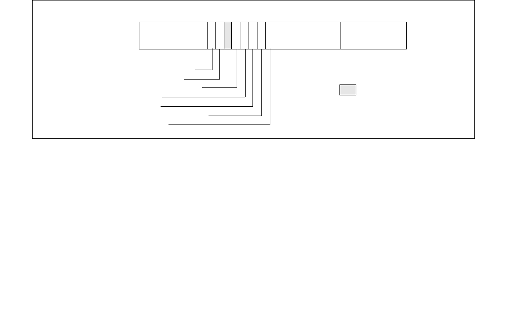
18-122 Vol. 3B
PERFORMANCE MONITORING
NOTE
The performance-monitoring events listed in Chapter 19 are intended to be used as guides for
performance tuning. Counter values reported are not guaranteed to be accurate and should be
used as a relative guide for tuning. Known discrepancies are documented where applicable.
The performance-monitoring counters are supported by four MSRs: the performance event select MSRs
(PerfEvtSel0 and PerfEvtSel1) and the performance counter MSRs (PerfCtr0 and PerfCtr1). These registers can be
read from and written to using the RDMSR and WRMSR instructions, respectively. They can be accessed using these
instructions only when operating at privilege level 0. The PerfCtr0 and PerfCtr1 MSRs can be read from any privilege
level using the RDPMC (read performance-monitoring counters) instruction.
NOTE
The PerfEvtSel0, PerfEvtSel1, PerfCtr0, and PerfCtr1 MSRs and the events listed in Table 19-40 are
model-specific for P6 family processors. They are not guaranteed to be available in other IA-32
processors.
18.6.8.1 PerfEvtSel0 and PerfEvtSel1 MSRs
The PerfEvtSel0 and PerfEvtSel1 MSRs control the operation of the performance-monitoring counters, with one
register used to set up each counter. They specify the events to be counted, how they should be counted, and the
privilege levels at which counting should take place. Figure 18-61 shows the flags and fields in these MSRs.
The functions of the flags and fields in the PerfEvtSel0 and PerfEvtSel1 MSRs are as follows:
•Event select field (bits 0 through 7) — Selects the event logic unit to detect certain microarchitectural
conditions (see Table 19-40, for a list of events and their 8-bit codes).
•Unit mask (UMASK) field (bits 8 through 15) — Further qualifies the event logic unit selected in the event
select field to detect a specific microarchitectural condition. For example, for some cache events, the mask is
used as a MESI-protocol qualifier of cache states (see Table 19-40).
•USR (user mode) flag (bit 16) — Specifies that events are counted only when the processor is operating at
privilege levels 1, 2 or 3. This flag can be used in conjunction with the OS flag.
•OS (operating system mode) flag (bit 17) — Specifies that events are counted only when the processor is
operating at privilege level 0. This flag can be used in conjunction with the USR flag.
•E (edge detect) flag (bit 18) — Enables (when set) edge detection of events. The processor counts the
number of deasserted to asserted transitions of any condition that can be expressed by the other fields. The
mechanism is limited in that it does not permit back-to-back assertions to be distinguished. This mechanism
allows software to measure not only the fraction of time spent in a particular state, but also the average length
of time spent in such a state (for example, the time spent waiting for an interrupt to be serviced).
Figure 18-61. PerfEvtSel0 and PerfEvtSel1 MSRs
31
INV—Invert counter mask
EN—Enable counters*
INT—APIC interrupt enable
PC—Pin control
87 0
Event Select
E—Edge detect
OS—Operating system mode
USR—User Mode *Only available in PerfEvtSel0.
Counter Mask E
E
N
I
N
T
19 1618 15172021222324
Reserved
I
N
V
P
C
U
S
R
O
SUnit Mask (UMASK)
(CMASK)

Vol. 3B 18-123
PERFORMANCE MONITORING
•PC (pin control) flag (bit 19) — When set, the processor toggles the PMi pins and increments the counter
when performance-monitoring events occur; when clear, the processor toggles the PMi pins when the counter
overflows. The toggling of a pin is defined as assertion of the pin for a single bus clock followed by deassertion.
•INT (APIC interrupt enable) flag (bit 20) — When set, the processor generates an exception through its
local APIC on counter overflow.
•EN (Enable Counters) Flag (bit 22) — This flag is only present in the PerfEvtSel0 MSR. When set,
performance counting is enabled in both performance-monitoring counters; when clear, both counters are
disabled.
•INV (invert) flag (bit 23) — When set, inverts the counter-mask (CMASK) comparison, so that both greater
than or equal to and less than comparisons can be made (0: greater than or equal; 1: less than). Note if
counter-mask is programmed to zero, INV flag is ignored.
•Counter mask (CMASK) field (bits 24 through 31) — When nonzero, the processor compares this mask to
the number of events counted during a single cycle. If the event count is greater than or equal to this mask, the
counter is incremented by one. Otherwise the counter is not incremented. This mask can be used to count
events only if multiple occurrences happen per clock (for example, two or more instructions retired per clock).
If the counter-mask field is 0, then the counter is incremented each cycle by the number of events that
occurred that cycle.
18.6.8.2 PerfCtr0 and PerfCtr1 MSRs
The performance-counter MSRs (PerfCtr0 and PerfCtr1) contain the event or duration counts for the selected
events being counted. The RDPMC instruction can be used by programs or procedures running at any privilege level
and in virtual-8086 mode to read these counters. The PCE flag in control register CR4 (bit 8) allows the use of this
instruction to be restricted to only programs and procedures running at privilege level 0.
The RDPMC instruction is not serializing or ordered with other instructions. Thus, it does not necessarily wait until
all previous instructions have been executed before reading the counter. Similarly, subsequent instructions may
begin execution before the RDPMC instruction operation is performed.
Only the operating system, executing at privilege level 0, can directly manipulate the performance counters, using
the RDMSR and WRMSR instructions. A secure operating system would clear the PCE flag during system initializa-
tion to disable direct user access to the performance-monitoring counters, but provide a user-accessible program-
ming interface that emulates the RDPMC instruction.
The WRMSR instruction cannot arbitrarily write to the performance-monitoring counter MSRs (PerfCtr0 and
PerfCtr1). Instead, the lower-order 32 bits of each MSR may be written with any value, and the high-order 8 bits
are sign-extended according to the value of bit 31. This operation allows writing both positive and negative values
to the performance counters.
18.6.8.3 Starting and Stopping the Performance-Monitoring Counters
The performance-monitoring counters are started by writing valid setup information in the PerfEvtSel0 and/or
PerfEvtSel1 MSRs and setting the enable counters flag in the PerfEvtSel0 MSR. If the setup is valid, the counters
begin counting following the execution of a WRMSR instruction that sets the enable counter flag. The counters can
be stopped by clearing the enable counters flag or by clearing all the bits in the PerfEvtSel0 and PerfEvtSel1 MSRs.
Counter 1 alone can be stopped by clearing the PerfEvtSel1 MSR.
18.6.8.4 Event and Time-Stamp Monitoring Software
To use the performance-monitoring counters and time-stamp counter, the operating system needs to provide an
event-monitoring device driver. This driver should include procedures for handling the following operations:
•Feature checking.
•Initialize and start counters.
•Stop counters.
•Read the event counters.
•Read the time-stamp counter.

18-124 Vol. 3B
PERFORMANCE MONITORING
The event monitor feature determination procedure must check whether the current processor supports the perfor-
mance-monitoring counters and time-stamp counter. This procedure compares the family and model of the
processor returned by the CPUID instruction with those of processors known to support performance monitoring.
(The Pentium and P6 family processors support performance counters.) The procedure also checks the MSR and
TSC flags returned to register EDX by the CPUID instruction to determine if the MSRs and the RDTSC instruction are
supported.
The initialize and start counters procedure sets the PerfEvtSel0 and/or PerfEvtSel1 MSRs for the events to be
counted and the method used to count them and initializes the counter MSRs (PerfCtr0 and PerfCtr1) to starting
counts. The stop counters procedure stops the performance counters (see Section 18.6.8.3, “Starting and Stopping
the Performance-Monitoring Counters”).
The read counters procedure reads the values in the PerfCtr0 and PerfCtr1 MSRs, and a read time-stamp counter
procedure reads the time-stamp counter. These procedures would be provided in lieu of enabling the RDTSC and
RDPMC instructions that allow application code to read the counters.
18.6.8.5 Monitoring Counter Overflow
The P6 family processors provide the option of generating a local APIC interrupt when a performance-monitoring
counter overflows. This mechanism is enabled by setting the interrupt enable flag in either the PerfEvtSel0 or the
PerfEvtSel1 MSR. The primary use of this option is for statistical performance sampling.
To use this option, the operating system should do the following things on the processor for which performance
events are required to be monitored:
•Provide an interrupt vector for handling the counter-overflow interrupt.
•Initialize the APIC PERF local vector entry to enable handling of performance-monitor counter overflow events.
•Provide an entry in the IDT that points to a stub exception handler that returns without executing any instruc-
tions.
•Provide an event monitor driver that provides the actual interrupt handler and modifies the reserved IDT entry
to point to its interrupt routine.
When interrupted by a counter overflow, the interrupt handler needs to perform the following actions:
•Save the instruction pointer (EIP register), code-segment selector, TSS segment selector, counter values and
other relevant information at the time of the interrupt.
•Reset the counter to its initial setting and return from the interrupt.
An event monitor application utility or another application program can read the information collected for analysis
of the performance of the profiled application.
18.6.9 Performance Monitoring (Pentium Processors)
The Pentium processor provides two 40-bit performance counters, which can be used to count events or measure
duration. The counters are supported by three MSRs: the control and event select MSR (CESR) and the perfor-
mance counter MSRs (CTR0 and CTR1). These can be read from and written to using the RDMSR and WRMSR
instructions, respectively. They can be accessed using these instructions only when operating at privilege level 0.
Each counter has an associated external pin (PM0/BP0 and PM1/BP1), which can be used to indicate the state of the
counter to external hardware.
NOTES
The CESR, CTR0, and CTR1 MSRs and the events listed in Table 19-41 are model-specific for the
Pentium processor.
The performance-monitoring events listed in Chapter 19 are intended to be used as guides for
performance tuning. Counter values reported are not guaranteed to be accurate and should be
used as a relative guide for tuning. Known discrepancies are documented where applicable.
Vol. 3B 18-125
PERFORMANCE MONITORING
18.6.9.1 Control and Event Select Register (CESR)
The 32-bit control and event select MSR (CESR) controls the operation of performance-monitoring counters CTR0
and CTR1 and the associated pins (see Figure 18-62). To control each counter, the CESR register contains a 6-bit
event select field (ES0 and ES1), a pin control flag (PC0 and PC1), and a 3-bit counter control field (CC0 and CC1).
The functions of these fields are as follows:
•ES0 and ES1 (event select) fields (bits 0-5, bits 16-21) — Selects (by entering an event code in the field)
up to two events to be monitored. See Table 19-41 for a list of available event codes.
•CC0 and CC1 (counter control) fields (bits 6-8, bits 22-24) — Controls the operation of the counter.
Control codes are as follows:
000 — Count nothing (counter disabled).
001 — Count the selected event while CPL is 0, 1, or 2.
010 — Count the selected event while CPL is 3.
011 — Count the selected event regardless of CPL.
100 — Count nothing (counter disabled).
101 — Count clocks (duration) while CPL is 0, 1, or 2.
110 — Count clocks (duration) while CPL is 3.
111 — Count clocks (duration) regardless of CPL.
The highest order bit selects between counting events and counting clocks (duration); the middle bit enables
counting when the CPL is 3; and the low-order bit enables counting when the CPL is 0, 1, or 2.
•PC0 and PC1 (pin control) flags (bits 9, 25) — Selects the function of the external performance-monitoring
counter pin (PM0/BP0 and PM1/BP1). Setting one of these flags to 1 causes the processor to assert its
associated pin when the counter has overflowed; setting the flag to 0 causes the pin to be asserted when the
counter has been incremented. These flags permit the pins to be individually programmed to indicate the
overflow or incremented condition. The external signalling of the event on the pins will lag the internal event by
a few clocks as the signals are latched and buffered.
While a counter need not be stopped to sample its contents, it must be stopped and cleared or preset before
switching to a new event. It is not possible to set one counter separately. If only one event needs to be changed,
the CESR register must be read, the appropriate bits modified, and all bits must then be written back to CESR. At
reset, all bits in the CESR register are cleared.
18.6.9.2 Use of the Performance-Monitoring Pins
When performance-monitor pins PM0/BP0 and/or PM1/BP1 are configured to indicate when the performance-
monitor counter has incremented and an “occurrence event” is being counted, the associated pin is asserted (high)
each time the event occurs. When a “duration event” is being counted, the associated PM pin is asserted for the
Figure 18-62. CESR MSR (Pentium Processor Only)
31
PC1—Pin control 1
CC1—Counter control 1
ES1—Event select 1
PC0—Pin control 0
80
CC0—Counter control 0
ES0—Event select 0
16 152122
24
Reserved
95
6
ESOCC0
P
C
0
ES1
CC1
P
C
1
2526 10

18-126 Vol. 3B
PERFORMANCE MONITORING
entire duration of the event. When the performance-monitor pins are configured to indicate when the counter has
overflowed, the associated PM pin is asserted when the counter has overflowed.
When the PM0/BP0 and/or PM1/BP1 pins are configured to signal that a counter has incremented, it should be
noted that although the counters may increment by 1 or 2 in a single clock, the pins can only indicate that the event
occurred. Moreover, since the internal clock frequency may be higher than the external clock frequency, a single
external clock may correspond to multiple internal clocks.
A “count up to” function may be provided when the event pin is programmed to signal an overflow of the counter.
Because the counters are 40 bits, a carry out of bit 39 indicates an overflow. A counter may be preset to a specific
value less then 240 − 1. After the counter has been enabled and the prescribed number of events has transpired,
the counter will overflow.
Approximately 5 clocks later, the overflow is indicated externally and appropriate action, such as signaling an inter-
rupt, may then be taken.
The PM0/BP0 and PM1/BP1 pins also serve to indicate breakpoint matches during in-circuit emulation, during which
time the counter increment or overflow function of these pins is not available. After RESET, the PM0/BP0 and
PM1/BP1 pins are configured for performance monitoring, however a hardware debugger may reconfigure these
pins to indicate breakpoint matches.
18.6.9.3 Events Counted
Events that performance-monitoring counters can be set to count and record (using CTR0 and CTR1) are divided in
two categories: occurrence and duration:
•Occurrence events — Counts are incremented each time an event takes place. If PM0/BP0 or PM1/BP1 pins
are used to indicate when a counter increments, the pins are asserted each clock counters increment. But if an
event happens twice in one clock, the counter increments by 2 (the pins are asserted only once).
•Duration events — Counters increment the total number of clocks that the condition is true. When used to
indicate when counters increment, PM0/BP0 and/or PM1/BP1 pins are asserted for the duration.
18.7 COUNTING CLOCKS
The count of cycles, also known as clockticks, forms the basis for measuring how long a program takes to execute.
Clockticks are also used as part of efficiency ratios like cycles per instruction (CPI). Processor clocks may stop
ticking under circumstances like the following:
•The processor is halted when there is nothing for the CPU to do. For example, the processor may halt to save
power while the computer is servicing an I/O request. When Intel Hyper-Threading Technology is enabled, both
logical processors must be halted for performance-monitoring counters to be powered down.
•The processor is asleep as a result of being halted or because of a power-management scheme. There are
different levels of sleep. In the some deep sleep levels, the time-stamp counter stops counting.
In addition, processor core clocks may undergo transitions at different ratios relative to the processor’s bus clock
frequency. Some of the situations that can cause processor core clock to undergo frequency transitions include:
•TM2 transitions.
•Enhanced Intel SpeedStep Technology transitions (P-state transitions).
For Intel processors that support TM2, the processor core clocks may operate at a frequency that differs from the
Processor Base frequency (as indicated by processor frequency information reported by CPUID instruction). See
Section 18.7.2 for more detail.
Due to the above considerations there are several important clocks referenced in this manual:
•Base Clock — The frequency of this clock is the frequency of the processor when the processor is not in turbo
mode, and not being throttled via Intel SpeedStep.
•Maximum Clock — This is the maximum frequency of the processor when turbo mode is at the highest point.
•Bus Clock — These clockticks increment at a fixed frequency and help coordinate the bus on some systems.

Vol. 3B 18-127
PERFORMANCE MONITORING
•Core Crystal Clock — This is a clock that runs at fixed frequency; it coordinates the clocks on all packages
across the system.
•Non-halted Clockticks — Measures clock cycles in which the specified logical processor is not halted and is
not in any power-saving state. When Intel Hyper-Threading Technology is enabled, ticks can be measured on a
per-logical-processor basis. There are also performance events on dual-core processors that measure
clockticks per logical processor when the processor is not halted.
•Non-sleep Clockticks — Measures clock cycles in which the specified physical processor is not in a sleep
mode or in a power-saving state. These ticks cannot be measured on a logical-processor basis.
•Time-stamp Counter — See Section 17.17, “Time-Stamp Counter”.
•Reference Clockticks — TM2 or Enhanced Intel SpeedStep technology are two examples of processor
features that can cause processor core clockticks to represent non-uniform tick intervals due to change of bus
ratios. Performance events that counts clockticks of a constant reference frequency was introduced Intel Core
Duo and Intel Core Solo processors. The mechanism is further enhanced on processors based on Intel Core
microarchitecture.
Some processor models permit clock cycles to be measured when the physical processor is not in deep sleep (by
using the time-stamp counter and the RDTSC instruction). Note that such ticks cannot be measured on a per-
logical-processor basis. See Section 17.17, “Time-Stamp Counter,” for detail on processor capabilities.
The first two methods use performance counters and can be set up to cause an interrupt upon overflow (for
sampling). They may also be useful where it is easier for a tool to read a performance counter than to use a time
stamp counter (the timestamp counter is accessed using the RDTSC instruction).
For applications with a significant amount of I/O, there are two ratios of interest:
•Non-halted CPI — Non-halted clockticks/instructions retired measures the CPI for phases where the CPU was
being used. This ratio can be measured on a logical-processor basis when Intel Hyper-Threading Technology is
enabled.
•Nominal CPI — Time-stamp counter ticks/instructions retired measures the CPI over the duration of a
program, including those periods when the machine halts while waiting for I/O.
18.7.1 Non-Halted Reference Clockticks
Software can use UnHalted Reference Cycles on either a general purpose performance counter using event mask
0x3C and umask 0x01 or on fixed function performance counter 2 to count at a constant rate. These events count
at a consistent rate irrespective of P-state, TM2, or frequency transitions that may occur to the processor. The
UnHalted Reference Cycles event may count differently on the general purpose event and fixed counter.
18.7.2 Cycle Counting and Opportunistic Processor Operation
As a result of the state transitions due to opportunistic processor performance operation (see Chapter 14, “Power
and Thermal Management”), a logical processor or a processor core can operate at frequency different from the
Processor Base frequency.
The following items are expected to hold true irrespective of when opportunistic processor operation causes state
transitions:
•The time stamp counter operates at a fixed-rate frequency of the processor.
•The IA32_MPERF counter increments at a fixed frequency irrespective of any transitions caused by opportu-
nistic processor operation.
•The IA32_FIXED_CTR2 counter increments at the same TSC frequency irrespective of any transitions caused
by opportunistic processor operation.
•The Local APIC timer operation is unaffected by opportunistic processor operation.
•The TSC, IA32_MPERF, and IA32_FIXED_CTR2 operate at close to the maximum non-turbo frequency, which is
equal to the product of scalable bus frequency and maximum non-turbo ratio.

18-128 Vol. 3B
PERFORMANCE MONITORING
18.7.3 Determining the Processor Base Frequency
For Intel processors in which the nominal core crystal clock frequency is enumerated in CPUID.15H.ECX and the
core crystal clock ratio is encoded in CPUID.15H (see Table 3-8 “Information Returned by CPUID Instruction”), the
nominal TSC frequency can be determined by using the following equation:
Nominal TSC frequency = ( CPUID.15H.ECX[31:0] * CPUID.15H.EBX[31:0] ) ÷ CPUID.15H.EAX[31:0]
For Intel processors in which CPUID.15H.EBX[31:0] ÷ CPUID.0x15.EAX[31:0] is enumerated but CPUID.15H.ECX
is not enumerated, Table 18-75 can be used to look up the nominal core crystal clock frequency.
18.7.3.1 For Intel® Processors Based on Microarchitecture Code Name Sandy Bridge, Ivy Bridge,
Haswell and Broadwell
The scalable bus frequency is encoded in the bit field MSR_PLATFORM_INFO[15:8] and the nominal TSC frequency
can be determined by multiplying this number by a bus speed of 100 MHz.
18.7.3.2 For Intel® Processors Based on Microarchitecture Code Name Nehalem
The scalable bus frequency is encoded in the bit field MSR_PLATFORM_INFO[15:8] and the nominal TSC frequency
can be determined by multiplying this number by a bus speed of 133.33 MHz.
18.7.3.3 For Intel® Atom™ Processors Based on the Silvermont Microarchitecture (Including Intel
Processors Based on Airmont Microarchitecture)
The scalable bus frequency is encoded in the bit field MSR_PLATFORM_INFO[15:8] and the nominal TSC frequency
can be determined by multiplying this number by the scalable bus frequency. The scalable bus frequency is
encoded in the bit field MSR_FSB_FREQ[2:0] for Intel Atom processors based on the Silvermont microarchitecture,
and in bit field MSR_FSB_FREQ[3:0] for processors based on the Airmont microarchitecture; see Chapter 2,
“Model-Specific Registers (MSRs)” in the Intel® 64 and IA-32 Architectures Software Developer’s Manual, Volume
4.
Table 18-75. Nominal Core Crystal Clock Frequency
Processor Families/Processor Number Series1
NOTES:
1. For any processor in which CPUID.15H is enumerated and MSR_PLATFORM_INFO[15:8] (which gives the scalable bus frequency) is
available, a more accurate frequency can be obtained by using CPUID.15H.
Nominal Core Crystal Clock Frequency
Intel® Xeon® Processor Scalable Family with CPUID signature 06_55H. 25 MHz
6th and 7th generation Intel® Core™ processors and Intel® Xeon® W Processor Family. 24 MHz
Next Generation Intel® Atom™ processors based on Goldmont Microarchitecture with
CPUID signature 06_5CH (does not include Intel Xeon processors).
19.2 MHz

Vol. 3B 18-129
PERFORMANCE MONITORING
18.7.3.4 For Intel® Core™ 2 Processor Family and for Intel® Xeon® Processors Based on Intel Core
Microarchitecture
For processors based on Intel Core microarchitecture, the scalable bus frequency is encoded in the bit field
MSR_FSB_FREQ[2:0] at (0CDH), see Chapter 2, “Model-Specific Registers (MSRs)” in the Intel® 64 and IA-32
Architectures Software Developer’s Manual, Volume 4. The maximum resolved bus ratio can be read from the
following bit field:
•If XE operation is disabled, the maximum resolved bus ratio can be read in MSR_PLATFORM_ID[12:8]. It
corresponds to the Processor Base frequency.
•IF XE operation is enabled, the maximum resolved bus ratio is given in MSR_PERF_STATUS[44:40], it
corresponds to the maximum XE operation frequency configured by BIOS.
XE operation of an Intel 64 processor is implementation specific. XE operation can be enabled only by BIOS. If
MSR_PERF_STATUS[31] is set, XE operation is enabled. The MSR_PERF_STATUS[31] field is read-only.
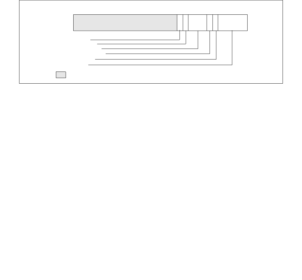
18-130 Vol. 3B
PERFORMANCE MONITORING
18.8 IA32_PERF_CAPABILITIES MSR ENUMERATION
The layout of IA32_PERF_CAPABILITIES MSR is shown in Figure 18-63, it provides enumeration of a variety of
interfaces:
•IA32_PERF_CAPABILITIES.LBR_FMT[bits 5:0]: encodes the LBR format, details are described in Section
17.4.8.1.
•IA32_PERF_CAPABILITIES.PEBSTrap[6]: Trap/Fault-like indicator of PEBS recording assist, see Section
18.6.2.4.2.
•IA32_PERF_CAPABILITIES.PEBSArchRegs[7]: Indicator of PEBS assist save architectural registers, see Section
18.6.2.4.2.
•IA32_PERF_CAPABILITIES.PEBS_FMT[bits 11:8]: Specifies the encoding of the layout of PEBS records, see
Section 18.6.2.4.2.
•IA32_PERF_CAPABILITIES.FREEZE_WHILE_SMM[12]: Indicates IA32_DEBUGCTL.FREEZE_WHILE_SMM is
supported if 1, see Section 18.8.1.
•IA32_PERF_CAPABILITIES.FULL_WRITE[13]: Indicates the processor supports IA32_A_PMCx interface for
updating bits 32 and above of IA32_PMCx, see Section 18.2.5.
18.8.1 Filtering of SMM Handler Overhead
When performance monitoring facilities and/or branch profiling facilities (see Section 17.5, “Last Branch, Interrupt,
and Exception Recording (Intel® Core™ 2 Duo and Intel® Atom™ Processors)”) are enabled, these facilities
capture event counts, branch records and branch trace messages occurring in a logical processor. The occurrence
of interrupts, instruction streams due to various interrupt handlers all contribute to the results recorded by these
facilities.
If CPUID.01H:ECX.PDCM[bit 15] is 1, the processor supports the IA32_PERF_CAPABILITIES MSR. If
IA32_PERF_CAPABILITIES.FREEZE_WHILE_SMM[Bit 12] is 1, the processor supports the ability for system soft-
ware using performance monitoring and/or branch profiling facilities to filter out the effects of servicing system
management interrupts.
If the FREEZE_WHILE_SMM capability is enabled on a logical processor and after an SMI is delivered, the processor
will clear all the enable bits of IA32_PERF_GLOBAL_CTRL, save a copy of the content of IA32_DEBUGCTL and
disable LBR, BTF, TR, and BTS fields of IA32_DEBUGCTL before transferring control to the SMI handler.
The enable bits of IA32_PERF_GLOBAL_CTRL will be set to 1, the saved copy of IA32_DEBUGCTL prior to SMI
delivery will be restored , after the SMI handler issues RSM to complete its servicing.
It is the responsibility of the SMM code to ensure the state of the performance monitoring and branch profiling facil-
ities are preserved upon entry or until prior to exiting the SMM. If any of this state is modified due to actions by the
SMM code, the SMM code is required to restore such state to the values present at entry to the SMM handler.
System software is allowed to set IA32_DEBUGCTL.FREEZE_WHILE_SMM[bit 14] to 1 only supported as indicated
by IA32_PERF_CAPABILITIES.FREEZE_WHILE_SMM[Bit 12] reporting 1.
Figure 18-63. Layout of IA32_PERF_CAPABILITIES MSR
SMM_FREEZE (R/O)
PEBS_REC_FMT (R/O)
87 0
12 31
Reserved
63 2
4
11 56
PEBS_TRAP (R/O)
LBR_FMT (R/O)
PEBS_ARCH_REG (R/O)
13
FW_WRITE (R/O)

Vol. 3B 19-1
CHAPTER 19
PERFORMANCE MONITORING EVENTS
NOTE
The event tables listed this chapter provide information for tool developers to support architectural
and model-specific performance monitoring events. The tables are up to date at processor launch,
but are subject to changes. The most up to date event tables and additional details of performance
event implementation can be found here:
1) In the document titled “Intel® 64 and IA32 Architectures Performance Monitoring Events”,
Document number: 335279, located here:
https://software.intel.com/sites/default/files/managed/8b/6e/335279_performance_monitoring_
events_guide.pdf.
These event tables are also available on the web and are located at:
https://download.01.org/perfmon/index/.
2) Performance monitoring event files for Intel processors are hosted by the Intel Open Source
Technology Center. These files can be downloaded here: https://download.01.org/perfmon/.
This chapter lists the performance monitoring events that can be monitored with the Intel 64 or IA-32 processors.
The ability to monitor performance events and the events that can be monitored in these processors are mostly
model-specific, except for architectural performance events, described in Section 19.1.
Model-specific performance events are listed for each generation of microarchitecture:
•Section 19.2 - Processors based on Skylake microarchitecture
•Section 19.3 - Processors based on Skylake, Kaby Lake and Coffee Lake microarchitectures
•Section 19.4 - Processors based on Knights Landing and Knights Mill microarchitectures
•Section 19.5 - Processors based on Broadwell microarchitecture
•Section 19.6 - Processors based on Haswell microarchitecture
•Section 19.6.1 - Processors based on Haswell-E microarchitecture
•Section 19.7 - Processors based on Ivy Bridge microarchitecture
•Section 19.7.1 - Processors based on Ivy Bridge-E microarchitecture
•Section 19.8 - Processors based on Sandy Bridge microarchitecture
•Section 19.9 - Processors based on Intel® microarchitecture code name Nehalem
•Section 19.10 - Processors based on Intel® microarchitecture code name Westmere
•Section 19.11 - Processors based on Enhanced Intel® Core™ microarchitecture
•Section 19.12 - Processors based on Intel® Core™ microarchitecture
•Section 19.13 - Processors based on the Goldmont microarchitecture
•Section 19.15 - Processors based on the Silvermont microarchitecture
•Section 19.15.1 - Processors based on the Airmont microarchitecture
•Section 19.16 - 45 nm and 32 nm Intel® Atom™ Processors
•Section 19.17 - Intel® Core™ Solo and Intel® Core™ Duo processors
•Section 19.18 - Processors based on Intel NetBurst® microarchitecture
•Section 19.19 - Pentium® M family processors
•Section 19.20 - P6 family processors
•Section 19.21 - Pentium® processors

19-2 Vol. 3B
PERFORMANCE MONITORING EVENTS
NOTE
These performance monitoring events are intended to be used as guides for performance tuning.
The counter values reported by the performance monitoring events are approximate and believed
to be useful as relative guides for tuning software. Known discrepancies are documented where
applicable.
All performance event encodings not documented in the appropriate tables for the given processor
are considered reserved, and their use will result in undefined counter updates with associated
overflow actions.
19.1 ARCHITECTURAL PERFORMANCE MONITORING EVENTS
Architectural performance events are introduced in Intel Core Solo and Intel Core Duo processors. They are also
supported on processors based on Intel Core microarchitecture. Table 19-1 lists pre-defined architectural perfor-
mance events that can be configured using general-purpose performance counters and associated event-select
registers.
Fixed-function performance counters count only events defined in Table 19-2.
Table 19-1. Architectural Performance Events
Event
Num. Event Mask Name
Umask
Value Description
3CH UnHalted Core Cycles 00H Counts core clock cycles whenever the logical processor is in C0 state
(not halted). The frequency of this event varies with state transitions in
the core.
3CH UnHalted Reference Cycles1
NOTES:
1. Current implementations count at core crystal clock, TSC, or bus clock frequency.
01H Counts at a fixed frequency whenever the logical processor is in C0
state (not halted).
C0H Instructions Retired 00H Counts when the last uop of an instruction retires.
2EH LLC Reference 4FH Counts requests originating from the core that reference a cache line in
the last level on-die cache.
2EH LLC Misses 41H Counts each cache miss condition for references to the last level on-die
cache.
C4H Branch Instruction Retired 00H Counts when the last uop of a branch instruction retires.
C5H Branch Misses Retired 00H Counts when the last uop of a branch instruction retires which
corrected misprediction of the branch prediction hardware at execution
time.
Table 19-2. Fixed-Function Performance Counter and Pre-defined Performance Events
Fixed-Function Performance
Counter Address Event Mask Mnemonic Description
IA32_PERF_FIXED_CTR0 309H Inst_Retired.Any This event counts the number of instructions that retire
execution. For instructions that consist of multiple micro-
ops, this event counts the retirement of the last micro-op
of the instruction. The counter continues counting during
hardware interrupts, traps, and inside interrupt handlers.

Vol. 3B 19-3
PERFORMANCE MONITORING EVENTS
19.2 PERFORMANCE MONITORING EVENTS FOR INTEL® XEON® PROCESSOR
SCALABLE FAMILY
The Intel® Xeon® Processor Scalable Family is based on the Skylake microarchitecture. These processors support
the architectural performance monitoring events listed in Table 19-1. Fixed counters in the core PMU support the
architecture events defined in Table 19-2. Model-specific performance monitoring events in the processor core are
listed in Table 19-4. The events in Table 19-4 apply to processors with CPUID signature of
DisplayFamily_DisplayModel encoding with the following value: 06_55H .
The comment column in Table 19-4 uses abbreviated letters to indicate additional conditions applicable to the
Event Mask Mnemonic. For event umasks listed in Table 19-4 that do not show “AnyT”, users should refrain from
programming “AnyThread =1” in IA32_PERF_EVTSELx.
IA32_PERF_FIXED_CTR1 30AH CPU_CLK_UNHALTED.THRE
AD/CPU_CLK_UNHALTED.C
ORE/CPU_CLK_UNHALTED.
THREAD_ANY
The CPU_CLK_UNHALTED.THREAD event counts the
number of core cycles while the logical processor is not in
a halt state.
If there is only one logical processor in a processor core,
CPU_CLK_UNHALTED.CORE counts the unhalted cycles of
the processor core.
If there are more than one logical processor in a processor
core, CPU_CLK_UNHALTED.THREAD_ANY is supported by
programming IA32_FIXED_CTR_CTRL[bit 6]AnyThread =
1.
The core frequency may change from time to time due to
transitions associated with Enhanced Intel SpeedStep
Technology or TM2. For this reason this event may have a
changing ratio with regards to time.
IA32_PERF_FIXED_CTR2 30BH CPU_CLK_UNHALTED.REF_
TSC
This event counts the number of reference cycles at the
TSC rate when the core is not in a halt state and not in a
TM stop-clock state. The core enters the halt state when
it is running the HLT instruction or the MWAIT instruction.
This event is not affected by core frequency changes (e.g.,
P states) but counts at the same frequency as the time
stamp counter. This event can approximate elapsed time
while the core was not in a halt state and not in a TM
stopclock state.
Table 19-2. Fixed-Function Performance Counter and Pre-defined Performance Events (Contd.)
Fixed-Function Performance
Counter Address Event Mask Mnemonic Description

19-4 Vol. 3B
PERFORMANCE MONITORING EVENTS
Table 19-3. Performance Events of the Processor Core Supported in
Intel® Xeon® Processor Scalable Family with Skylake Microarchitecture
Event
Num.
Umask
Value
Event Mask Mnemonic Description Comment
00H 01H INST_RETIRED.ANY Counts the number of instructions retired from
execution. For instructions that consist of multiple
micro-ops, Counts the retirement of the last micro-op of
the instruction. Counting continues during hardware
interrupts, traps, and inside interrupt handlers. Notes:
INST_RETIRED.ANY is counted by a designated fixed
counter, leaving the four (eight when Hyperthreading is
disabled) programmable counters available for other
events. INST_RETIRED.ANY_P is counted by a
programmable counter and it is an architectural
performance event. Counting: Faulting executions of
GETSEC/VM entry/VM Exit/MWait will not count as
retired instructions.
Fixed Counter
00H 02H CPU_CLK_UNHALTED.THREAD Counts the number of core cycles while the thread is
not in a halt state. The thread enters the halt state
when it is running the HLT instruction. This event is a
component in many key event ratios. The core
frequency may change from time to time due to
transitions associated with Enhanced Intel SpeedStep
Technology or TM2. For this reason this event may
have a changing ratio with regards to time. When the
core frequency is constant, this event can approximate
elapsed time while the core was not in the halt state. It
is counted on a dedicated fixed counter, leaving the
four (eight when Hyperthreading is disabled)
programmable counters available for other events.
Fixed Counter
00H 02H CPU_CLK_UNHALTED.THREAD_
ANY
Core cycles when at least one thread on the physical
core is not in halt state.
AnyThread=1

Vol. 3B 19-5
PERFORMANCE MONITORING EVENTS
00H 03H CPU_CLK_UNHALTED.REF_TSC Counts the number of reference cycles when the core is
not in a halt state. The core enters the halt state when
it is running the HLT instruction or the MWAIT
instruction. This event is not affected by core
frequency changes (for example, P states, TM2
transitions) but has the same incrementing frequency
as the time stamp counter. This event can approximate
elapsed time while the core was not in a halt state. This
event has a constant ratio with the
CPU_CLK_UNHALTED.REF_XCLK event. It is counted on
a dedicated fixed counter, leaving the four (eight when
Hyperthreading is disabled) programmable counters
available for other events. Note: On all current
platforms this event stops counting during ‘throttling
(TM)’ states duty off periods the processor is ‘halted’.
The counter update is done at a lower clock rate then
the core clock the overflow status bit for this counter
may appear ‘sticky’. After the counter has overflowed
and software clears the overflow status bit and resets
the counter to less than MAX. The reset value to the
counter is not clocked immediately so the overflow
status bit will flip “high (1)” and generate another PMI
(if enabled) after which the reset value gets clocked
into the counter. Therefore, software will get the
interrupt, read the overflow status bit ‘1 for bit 34
while the counter value is less than MAX. Software
should ignore this case.
Fixed Counter
03H 02H LD_BLOCKS.STORE_FORWARD Counts how many times the load operation got the true
Block-on-Store blocking code preventing store
forwarding. This includes cases when: a. preceding
store conflicts with the load (incomplete overlap), b.
store forwarding is impossible due to u-arch limitations,
c. preceding lock RMW operations are not forwarded, d.
store has the no-forward bit set (uncacheable/page-
split/masked stores), e. all-blocking stores are used
(mostly, fences and port I/O), and others. The most
common case is a load blocked due to its address range
overlapping with a preceding smaller uncompleted
store. Note: This event does not take into account cases
of out-of-SW-control (for example, SbTailHit), unknown
physical STA, and cases of blocking loads on store due
to being non-WB memory type or a lock. These cases
are covered by other events. See the table of not
supported store forwards in the Optimization Guide.
03H 08H LD_BLOCKS.NO_SR The number of times that split load operations are
temporarily blocked because all resources for handling
the split accesses are in use.
07H 01H LD_BLOCKS_PARTIAL.ADDRESS
_ALIAS
Counts false dependencies in MOB when the partial
comparison upon loose net check and dependency was
resolved by the Enhanced Loose net mechanism. This
may not result in high performance penalties. Loose net
checks can fail when loads and stores are 4k aliased.
Table 19-3. Performance Events of the Processor Core Supported in
Intel® Xeon® Processor Scalable Family with Skylake Microarchitecture (Contd.)
Event
Num.
Umask
Value
Event Mask Mnemonic Description Comment

19-6 Vol. 3B
PERFORMANCE MONITORING EVENTS
08H 01H DTLB_LOAD_MISSES.MISS_CAUS
ES_A_WALK
Counts demand data loads that caused a page walk of
any page size (4K/2M/4M/1G). This implies it missed in
all TLB levels, but the walk need not have completed.
08H 02H DTLB_LOAD_MISSES.WALK_COM
PLETED_4K
Counts demand data loads that caused a completed
page walk (4K page size). This implies it missed in all
TLB levels. The page walk can end with or without a
fault.
08H 04H DTLB_LOAD_MISSES.WALK_COM
PLETED_2M_4M
Counts demand data loads that caused a completed
page walk (2M and 4M page sizes). This implies it
missed in all TLB levels. The page walk can end with or
without a fault.
08H 08H DTLB_LOAD_MISSES.WALK_COM
PLETED_1G
Counts load misses in all DTLB levels that cause a
completed page walk (1G page size). The page walk can
end with or without a fault.
08H 0EH DTLB_LOAD_MISSES.WALK_COM
PLETED
Counts demand data loads that caused a completed
page walk of any page size (4K/2M/4M/1G). This implies
it missed in all TLB levels. The page walk can end with
or without a fault.
08H 10H DTLB_LOAD_MISSES.WALK_PEN
DING
Counts 1 per cycle for each PMH that is busy with a
page walk for a load. EPT page walk duration are
excluded in Skylake microarchitecture.
08H 10H DTLB_LOAD_MISSES.WALK_ACT
IVE
Counts cycles when at least one PMH (Page Miss
Handler) is busy with a page walk for a load.
CounterMask=1
CMSK1
08H 20H DTLB_LOAD_MISSES.STLB_HIT Counts loads that miss the DTLB (Data TLB) and hit the
STLB (Second level TLB).
0DH 01H INT_MISC.RECOVERY_CYCLES Core cycles the Resource allocator was stalled due to
recovery from an earlier branch misprediction or
machine clear event.
0DH 01H INT_MISC.RECOVERY_CYCLES_A
NY
Core cycles the allocator was stalled due to recovery
from earlier clear event for any thread running on the
physical core (e.g. misprediction or memory nuke).
AnyThread=1 AnyT
0DH 80H INT_MISC.CLEAR_RESTEER_CYC
LES
Cycles the issue-stage is waiting for front-end to fetch
from resteered path following branch misprediction or
machine clear events.
0EH 01H UOPS_ISSUED.ANY Counts the number of uops that the Resource
Allocation Table (RAT) issues to the Reservation Station
(RS).
0EH 01H UOPS_ISSUED.STALL_CYCLES Counts cycles during which the Resource Allocation
Table (RAT) does not issue any uops to the reservation
station (RS) for the current thread.
CounterMask=1
Invert=1 CMSK1, INV
0EH 02H UOPS_ISSUED.VECTOR_WIDTH_
MISMATCH
Counts the number of Blend Uops issued by the
Resource Allocation Table (RAT) to the reservation
station (RS) in order to preserve upper bits of vector
registers. Starting with the Skylake microarchitecture,
these Blend uops are needed since every Intel SSE
instruction executed in Dirty Upper State needs to
preserve bits 128-255 of the destination register. For
more information, refer to Mixing Intel AVX and Intel
SSE Code section of the Optimization Guide.
Table 19-3. Performance Events of the Processor Core Supported in
Intel® Xeon® Processor Scalable Family with Skylake Microarchitecture (Contd.)
Event
Num.
Umask
Value
Event Mask Mnemonic Description Comment

Vol. 3B 19-7
PERFORMANCE MONITORING EVENTS
0EH 20H UOPS_ISSUED.SLOW_LEA Number of slow LEA uops being allocated. A uop is
generally considered SlowLea if it has 3 sources (e.g. 2
sources + immediate) regardless if as a result of LEA
instruction or not.
14H 01H ARITH.DIVIDER_ACTIVE Cycles when divide unit is busy executing divide or
square root operations. Accounts for integer and
floating-point operations.
CounterMask=1
24H 21H L2_RQSTS.DEMAND_DATA_RD_
MISS
Counts the number of demand Data Read requests that
miss L2 cache. Only not rejected loads are counted.
24H 22H L2_RQSTS.RFO_MISS Counts the RFO (Read-for-Ownership) requests that
miss L2 cache.
24H 24H L2_RQSTS.CODE_RD_MISS Counts L2 cache misses when fetching instructions.
24H 27H L2_RQSTS.ALL_DEMAND_MISS Demand requests that miss L2 cache.
24H 38H L2_RQSTS.PF_MISS Counts requests from the L1/L2/L3 hardware
prefetchers or Load software prefetches that miss L2
cache.
24H 3FH L2_RQSTS.MISS All requests that miss L2 cache.
24H 41H L2_RQSTS.DEMAND_DATA_RD_
HIT
Counts the number of demand Data Read requests that
hit L2 cache. Only non rejected loads are counted.
24H 42H L2_RQSTS.RFO_HIT Counts the RFO (Read-for-Ownership) requests that hit
L2 cache.
24H 44H L2_RQSTS.CODE_RD_HIT Counts L2 cache hits when fetching instructions, code
reads.
24H D8H L2_RQSTS.PF_HIT Counts requests from the L1/L2/L3 hardware
prefetchers or Load software prefetches that hit L2
cache.
24H E1H L2_RQSTS.ALL_DEMAND_DATA
_RD
Counts the number of demand Data Read requests
(including requests from L1D hardware prefetchers).
These loads may hit or miss L2 cache. Only non rejected
loads are counted.
24H E2H L2_RQSTS.ALL_RFO Counts the total number of RFO (read for ownership)
requests to L2 cache. L2 RFO requests include both
L1D demand RFO misses as well as L1D RFO
prefetches.
24H E4H L2_RQSTS.ALL_CODE_RD Counts the total number of L2 code requests.
24H E7H L2_RQSTS.ALL_DEMAND_REFE
RENCES
Demand requests to L2 cache.
24H F8H L2_RQSTS.ALL_PF Counts the total number of requests from the L2
hardware prefetchers.
24H FFH L2_RQSTS.REFERENCES All L2 requests.
28H 07H CORE_POWER.LVL0_TURBO_LIC
ENSE
Core cycles where the core was running with power-
delivery for baseline license level 0. This includes non-
AVX codes, SSE, AVX 128-bit, and low-current AVX
256-bit codes.
Table 19-3. Performance Events of the Processor Core Supported in
Intel® Xeon® Processor Scalable Family with Skylake Microarchitecture (Contd.)
Event
Num.
Umask
Value
Event Mask Mnemonic Description Comment

19-8 Vol. 3B
PERFORMANCE MONITORING EVENTS
28H 18H CORE_POWER.LVL1_TURBO_LIC
ENSE
Core cycles where the core was running with power-
delivery for license level 1. This includes high current
AVX 256-bit instructions as well as low current AVX
512-bit instructions.
28H 20H CORE_POWER.LVL2_TURBO_LIC
ENSE
Core cycles where the core was running with power-
delivery for license level 2 (introduced in Skylake
Server microarchitecture). This includes high current
AVX 512-bit instructions.
28H 40H CORE_POWER.THROTTLE Core cycles the out-of-order engine was throttled due
to a pending power level request.
2EH 41H LONGEST_LAT_CACHE.MISS Counts core-originated cacheable requests that miss
the L3 cache (Longest Latency cache). Requests include
data and code reads, Reads-for-Ownership (RFOs),
speculative accesses and hardware prefetches from L1
and L2. It does not include all misses to the L3.
See Table 19-1.
2EH 4FH LONGEST_LAT_CACHE.REFEREN
CE
Counts core-originated cacheable requests to the L3
cache (Longest Latency cache). Requests include data
and code reads, Reads-for-Ownership (RFOs),
speculative accesses and hardware prefetches from L1
and L2. It does not include all accesses to the L3.
See Table 19-1.
3CH 00H CPU_CLK_UNHALTED.THREAD_
P
This is an architectural event that counts the number of
thread cycles while the thread is not in a halt state. The
thread enters the halt state when it is running the HLT
instruction. The core frequency may change from time
to time due to power or thermal throttling. For this
reason, this event may have a changing ratio with
regards to wall clock time.
See Table 19-1.
3CH 00H CPU_CLK_UNHALTED.THREAD_
P_ANY
Core cycles when at least one thread on the physical
core is not in halt state.
AnyThread=1 AnyT
3CH 00H CPU_CLK_UNHALTED.RING0_TR
ANS
Counts when the Current Privilege Level (CPL)
transitions from ring 1, 2 or 3 to ring 0 (Kernel).
EdgeDetect=1
CounterMask=1
3CH 01H CPU_CLK_THREAD_UNHALTED.
REF_XCLK
Core crystal clock cycles when the thread is unhalted. See Table 19-1.
3CH 01H CPU_CLK_THREAD_UNHALTED.
REF_XCLK_ANY
Core crystal clock cycles when at least one thread on
the physical core is unhalted.
AnyThread=1 AnyT
3CH 01H CPU_CLK_UNHALTED.REF_XCLK Core crystal clock cycles when the thread is unhalted. See Table 19-1.
3CH 01H CPU_CLK_UNHALTED.REF_XCLK
_ANY
Core crystal clock cycles when at least one thread on
the physical core is unhalted.
AnyThread=1 AnyT
3CH 02H CPU_CLK_THREAD_UNHALTED.
ONE_THREAD_ACTIVE
Core crystal clock cycles when this thread is unhalted
and the other thread is halted.
3CH 02H CPU_CLK_UNHALTED.ONE_THR
EAD_ACTIVE
Core crystal clock cycles when this thread is unhalted
and the other thread is halted.
Table 19-3. Performance Events of the Processor Core Supported in
Intel® Xeon® Processor Scalable Family with Skylake Microarchitecture (Contd.)
Event
Num.
Umask
Value
Event Mask Mnemonic Description Comment

Vol. 3B 19-9
PERFORMANCE MONITORING EVENTS
48H 01H L1D_PEND_MISS.PENDING Counts duration of L1D miss outstanding, that is each
cycle number of Fill Buffers (FB) outstanding required
by Demand Reads. FB either is held by demand loads, or
it is held by non-demand loads and gets hit at least
once by demand. The valid outstanding interval is
defined until the FB deallocation by one of the
following ways: from FB allocation, if FB is allocated by
demand from the demand Hit FB, if it is allocated by
hardware or software prefetch.Note: In the L1D, a
Demand Read contains cacheable or noncacheable
demand loads, including ones causing cache-line splits
and reads due to page walks resulted from any request
type.
48H 01H L1D_PEND_MISS.PENDING_CYCL
ES
Counts duration of L1D miss outstanding in cycles. CounterMask=1
CMSK1
48H 01H L1D_PEND_MISS.PENDING_CYCL
ES_ANY
Cycles with L1D load Misses outstanding from any
thread on physical core.
CounterMask=1
AnyThread=1
CMSK1, AnyT
48H 02H L1D_PEND_MISS.FB_FULL Number of times a request needed a FB (Fill Buffer)
entry but there was no entry available for it. A request
includes cacheable/uncacheable demands that are load,
store or SW prefetch instructions.
49H 01H DTLB_STORE_MISSES.MISS_CAU
SES_A_WALK
Counts demand data stores that caused a page walk of
any page size (4K/2M/4M/1G). This implies it missed in
all TLB levels, but the walk need not have completed.
49H 02H DTLB_STORE_MISSES.WALK_CO
MPLETED_4K
Counts demand data stores that caused a completed
page walk (4K page size). This implies it missed in all
TLB levels. The page walk can end with or without a
fault.
49H 04H DTLB_STORE_MISSES.WALK_CO
MPLETED_2M_4M
Counts demand data stores that caused a completed
page walk (2M and 4M page sizes). This implies it
missed in all TLB levels. The page walk can end with or
without a fault.
49H 08H DTLB_STORE_MISSES.WALK_CO
MPLETED_1G
Counts store misses in all DTLB levels that cause a
completed page walk (1G page size). The page walk can
end with or without a fault.
49H 0EH DTLB_STORE_MISSES.WALK_CO
MPLETED
Counts demand data stores that caused a completed
page walk of any page size (4K/2M/4M/1G). This implies
it missed in all TLB levels. The page walk can end with
or without a fault.
49H 10H DTLB_STORE_MISSES.WALK_PE
NDING
Counts 1 per cycle for each PMH that is busy with a
page walk for a store. EPT page walk duration are
excluded in Skylake microarchitecture.
49H 10H DTLB_STORE_MISSES.WALK_AC
TIVE
Counts cycles when at least one PMH (Page Miss
Handler) is busy with a page walk for a store.
CounterMask=1
CMSK1
49H 20H DTLB_STORE_MISSES.STLB_HIT Stores that miss the DTLB (Data TLB) and hit the STLB
(2nd Level TLB).
Table 19-3. Performance Events of the Processor Core Supported in
Intel® Xeon® Processor Scalable Family with Skylake Microarchitecture (Contd.)
Event
Num.
Umask
Value
Event Mask Mnemonic Description Comment

19-10 Vol. 3B
PERFORMANCE MONITORING EVENTS
4CH 01H LOAD_HIT_PRE.SW_PF Counts all not software-prefetch load dispatches that
hit the fill buffer (FB) allocated for the software
prefetch. It can also be incremented by some lock
instructions. So it should only be used with profiling so
that the locks can be excluded by ASM (Assembly File)
inspection of the nearby instructions.
4FH 10H EPT.WALK_PENDING Counts cycles for each PMH (Page Miss Handler) that is
busy with an EPT (Extended Page Table) walk for any
request type.
51H 01H L1D.REPLACEMENT Counts L1D data line replacements including
opportunistic replacements, and replacements that
require stall-for-replace or block-for-replace.
54H 01H TX_MEM.ABORT_CONFLICT Number of times a TSX line had a cache conflict.
54H 02H TX_MEM.ABORT_CAPACITY Number of times a transactional abort was signaled due
to a data capacity limitation for transactional reads or
writes.
54H 04H TX_MEM.ABORT_HLE_STORE_T
O_ELIDED_LOCK
Number of times a TSX Abort was triggered due to a
non-release/commit store to lock.
54H 08H TX_MEM.ABORT_HLE_ELISION_
BUFFER_NOT_EMPTY
Number of times a TSX Abort was triggered due to
commit but Lock Buffer not empty.
54H 10H TX_MEM.ABORT_HLE_ELISION_
BUFFER_MISMATCH
Number of times a TSX Abort was triggered due to
release/commit but data and address mismatch.
54H 20H TX_MEM.ABORT_HLE_ELISION_
BUFFER_UNSUPPORTED_ALIGN
MENT
Number of times a TSX Abort was triggered due to
attempting an unsupported alignment from Lock
Buffer.
54H 40H TX_MEM.HLE_ELISION_BUFFER
_FULL
Number of times we could not allocate Lock Buffer.
5DH 01H TX_EXEC.MISC1 Unfriendly TSX abort triggered by a flowmarker.
5DH 02H TX_EXEC.MISC2 Unfriendly TSX abort triggered by a vzeroupper
instruction.
5DH 04H TX_EXEC.MISC3 Unfriendly TSX abort triggered by a nest count that is
too deep.
5DH 08H TX_EXEC.MISC4 RTM region detected inside HLE.
5DH 10H TX_EXEC.MISC5 Counts the number of times an HLE XACQUIRE
instruction was executed inside an RTM transactional
region.
5EH 01H RS_EVENTS.EMPTY_CYCLES Counts cycles during which the reservation station (RS)
is empty for the thread.; Note: In ST-mode, not active
thread should drive 0. This is usually caused by
severely costly branch mispredictions, or allocator/FE
issues.
5EH 01H RS_EVENTS.EMPTY_END Counts end of periods where the Reservation Station
(RS) was empty. Could be useful to precisely locate
front-end Latency Bound issues.
EdgeDetect=1
CounterMask=1
Invert=1 CMSK1, INV
Table 19-3. Performance Events of the Processor Core Supported in
Intel® Xeon® Processor Scalable Family with Skylake Microarchitecture (Contd.)
Event
Num.
Umask
Value
Event Mask Mnemonic Description Comment

Vol. 3B 19-11
PERFORMANCE MONITORING EVENTS
60H 01H OFFCORE_REQUESTS_OUTSTAN
DING.DEMAND_DATA_RD
Counts the number of offcore outstanding Demand
Data Read transactions in the super queue (SQ) every
cycle. A transaction is considered to be in the Offcore
outstanding state between L2 miss and transaction
completion sent to requestor. See the corresponding
Umask under OFFCORE_REQUESTS. Note: A prefetch
promoted to Demand is counted from the promotion
point.
60H 01H OFFCORE_REQUESTS_OUTSTAN
DING.CYCLES_WITH_DEMAND_D
ATA_RD
Counts cycles when offcore outstanding Demand Data
Read transactions are present in the super queue (SQ).
A transaction is considered to be in the Offcore
outstanding state between L2 miss and transaction
completion sent to requestor (SQ de-allocation).
CounterMask=1
CMSK1
60H 01H OFFCORE_REQUESTS_OUTSTAN
DING.DEMAND_DATA_RD_GE_6
Cycles with at least 6 offcore outstanding Demand Data
Read transactions in uncore queue.
CounterMask=6
CMSK6
60H 02H OFFCORE_REQUESTS_OUTSTAN
DING.DEMAND_CODE_RD
Counts the number of offcore outstanding Code Reads
transactions in the super queue every cycle. The
'Offcore outstanding' state of the transaction lasts
from the L2 miss until the sending transaction
completion to requestor (SQ deallocation). See the
corresponding Umask under OFFCORE_REQUESTS.
CounterMask=1
CMSK1
60H 02H OFFCORE_REQUESTS_OUTSTAN
DING.CYCLES_WITH_DEMAND_C
ODE_RD
Counts the number of offcore outstanding Code Reads
transactions in the super queue every cycle. The
'Offcore outstanding' state of the transaction lasts
from the L2 miss until the sending transaction
completion to requestor (SQ deallocation). See the
corresponding Umask under OFFCORE_REQUESTS.
CMSK1
60H 04H OFFCORE_REQUESTS_OUTSTAN
DING.DEMAND_RFO
Counts the number of offcore outstanding RFO (store)
transactions in the super queue (SQ) every cycle. A
transaction is considered to be in the Offcore
outstanding state between L2 miss and transaction
completion sent to requestor (SQ de-allocation). See
corresponding Umask under OFFCORE_REQUESTS.
CounterMask=1
CMSK1
60H 04H OFFCORE_REQUESTS_OUTSTAN
DING.CYCLES_WITH_DEMAND_R
FO
Counts the number of offcore outstanding demand rfo
Reads transactions in the super queue every cycle. The
'Offcore outstanding' state of the transaction lasts
from the L2 miss until the sending transaction
completion to requestor (SQ deallocation). See the
corresponding Umask under OFFCORE_REQUESTS.
CMSK1
60H 08H OFFCORE_REQUESTS_OUTSTAN
DING.ALL_DATA_RD
Counts the number of offcore outstanding cacheable
Core Data Read transactions in the super queue every
cycle. A transaction is considered to be in the Offcore
outstanding state between L2 miss and transaction
completion sent to requestor (SQ de-allocation). See
corresponding Umask under OFFCORE_REQUESTS.
60H 08H OFFCORE_REQUESTS_OUTSTAN
DING.CYCLES_WITH_DATA_RD
Counts cycles when offcore outstanding cacheable Core
Data Read transactions are present in the super queue.
A transaction is considered to be in the Offcore
outstanding state between L2 miss and transaction
completion sent to requestor (SQ de-allocation). See
corresponding Umask under OFFCORE_REQUESTS.
CounterMask=1
CMSK1
Table 19-3. Performance Events of the Processor Core Supported in
Intel® Xeon® Processor Scalable Family with Skylake Microarchitecture (Contd.)
Event
Num.
Umask
Value
Event Mask Mnemonic Description Comment

19-12 Vol. 3B
PERFORMANCE MONITORING EVENTS
60H 10H OFFCORE_REQUESTS_OUTSTAN
DING.L3_MISS_DEMAND_DATA_
RD
Counts number of Offcore outstanding Demand Data
Read requests that miss L3 cache in the superQ every
cycle.
60H 10H OFFCORE_REQUESTS_OUTSTAN
DING.CYCLES_WITH_L3_MISS_D
EMAND_DATA_RD
Cycles with at least 1 Demand Data Read requests who
miss L3 cache in the superQ.
CounterMask=1
CMSK1
60H 10H OFFCORE_REQUESTS_OUTSTAN
DING.L3_MISS_DEMAND_DATA_
RD_GE_6
Cycles with at least 6 Demand Data Read requests that
miss L3 cache in the superQ.
CounterMask=6
CMSK6
79H 04H IDQ.MITE_UOPS Counts the number of uops delivered to Instruction
Decode Queue (IDQ) from the MITE path. Counting
includes uops that may 'bypass' the IDQ. This also
means that uops are not being delivered from the
Decode Stream Buffer (DSB).
79H 04H IDQ.MITE_CYCLES Counts cycles during which uops are being delivered to
Instruction Decode Queue (IDQ) from the MITE path.
Counting includes uops that may 'bypass' the IDQ.
CounterMask=1
CMSK1
79H 08H IDQ.DSB_UOPS Counts the number of uops delivered to Instruction
Decode Queue (IDQ) from the Decode Stream Buffer
(DSB) path. Counting includes uops that may ‘bypass’
the IDQ.
79H 08H IDQ.DSB_CYCLES Counts cycles during which uops are being delivered to
Instruction Decode Queue (IDQ) from the Decode
Stream Buffer (DSB) path. Counting includes uops that
may 'bypass' the IDQ.
CounterMask=1
CMSK1
79H 10H IDQ.MS_DSB_CYCLES Counts cycles during which uops initiated by Decode
Stream Buffer (DSB) are being delivered to Instruction
Decode Queue (IDQ) while the Microcode Sequencer
(MS) is busy. Counting includes uops that may 'bypass'
the IDQ.
CounterMask=1
79H 18H IDQ.ALL_DSB_CYCLES_4_UOPS Counts the number of cycles 4 uops were delivered to
Instruction Decode Queue (IDQ) from the Decode
Stream Buffer (DSB) path. Count includes uops that may
'bypass' the IDQ.
CounterMask=4
CMSK4
79H 18H IDQ.ALL_DSB_CYCLES_ANY_UO
PS
Counts the number of cycles uops were delivered to
Instruction Decode Queue (IDQ) from the Decode
Stream Buffer (DSB) path. Count includes uops that may
'bypass' the IDQ.
CounterMask=1
CMSK1
79H 20H IDQ.MS_MITE_UOPS Counts the number of uops initiated by MITE and
delivered to Instruction Decode Queue (IDQ) while the
Microcode Sequencer (MS) is busy. Counting includes
uops that may 'bypass' the IDQ.
79H 24H IDQ.ALL_MITE_CYCLES_4_UOPS Counts the number of cycles 4 uops were delivered to
the Instruction Decode Queue (IDQ) from the MITE
(legacy decode pipeline) path. Counting includes uops
that may 'bypass' the IDQ. During these cycles uops are
not being delivered from the Decode Stream Buffer
(DSB).
CounterMask=4
CMSK4
Table 19-3. Performance Events of the Processor Core Supported in
Intel® Xeon® Processor Scalable Family with Skylake Microarchitecture (Contd.)
Event
Num.
Umask
Value
Event Mask Mnemonic Description Comment

Vol. 3B 19-13
PERFORMANCE MONITORING EVENTS
79H 24H IDQ.ALL_MITE_CYCLES_ANY_UO
PS
Counts the number of cycles uops were delivered to
the Instruction Decode Queue (IDQ) from the MITE
(legacy decode pipeline) path. Counting includes uops
that may 'bypass' the IDQ. During these cycles uops are
not being delivered from the Decode Stream Buffer
(DSB).
CounterMask=1
CMSK1
79H 30H IDQ.MS_CYCLES Counts cycles during which uops are being delivered to
Instruction Decode Queue (IDQ) while the Microcode
Sequencer (MS) is busy. Counting includes uops that
may 'bypass' the IDQ. Uops maybe initiated by Decode
Stream Buffer (DSB) or MITE.
CounterMask=1
CMSK1
79H 30H IDQ.MS_SWITCHES Number of switches from DSB (Decode Stream Buffer)
or MITE (legacy decode pipeline) to the Microcode
Sequencer.
EdgeDetect=1
CounterMask=1
EDGE
79H 30H IDQ.MS_UOPS Counts the total number of uops delivered by the
Microcode Sequencer (MS). Any instruction over 4 uops
will be delivered by the MS. Some instructions such as
transcendentals may additionally generate uops from
the MS.
80H 04H ICACHE_16B.IFDATA_STALL Cycles where a code line fetch is stalled due to an L1
instruction cache miss. The legacy decode pipeline
works at a 16 Byte granularity.
83H 01H ICACHE_64B.IFTAG_HIT Instruction fetch tag lookups that hit in the instruction
cache (L1I). Counts at 64-byte cache-line granularity.
83H 02H ICACHE_64B.IFTAG_MISS Instruction fetch tag lookups that miss in the
instruction cache (L1I). Counts at 64-byte cache-line
granularity.
83H 04H ICACHE_64B.IFTAG_STALL Cycles where a code fetch is stalled due to L1
instruction cache tag miss.
85H 01H ITLB_MISSES.MISS_CAUSES_A_
WALK
Counts page walks of any page size (4K/2M/4M/1G)
caused by a code fetch. This implies it missed in the
ITLB and further levels of TLB, but the walk need not
have completed.
85H 02H ITLB_MISSES.WALK_COMPLETE
D_4K
Counts completed page walks (4K page size) caused by
a code fetch. This implies it missed in the ITLB and
further levels of TLB. The page walk can end with or
without a fault.
85H 04H ITLB_MISSES.WALK_COMPLETE
D_2M_4M
Counts completed page walks of any page size
(4K/2M/4M/1G) caused by a code fetch. This implies it
missed in the ITLB and further levels of TLB. The page
walk can end with or without a fault.
85H 08H ITLB_MISSES.WALK_COMPLETE
D_1G
Counts store misses in all DTLB levels that cause a
completed page walk (1G page size). The page walk can
end with or without a fault.
85H 0EH ITLB_MISSES.WALK_COMPLETE
D
Counts completed page walks (2M and 4M page sizes)
caused by a code fetch. This implies it missed in the
ITLB and further levels of TLB. The page walk can end
with or without a fault.
Table 19-3. Performance Events of the Processor Core Supported in
Intel® Xeon® Processor Scalable Family with Skylake Microarchitecture (Contd.)
Event
Num.
Umask
Value
Event Mask Mnemonic Description Comment

19-14 Vol. 3B
PERFORMANCE MONITORING EVENTS
85H 10H ITLB_MISSES.WALK_PENDING Counts 1 per cycle for each PMH that is busy with a
page walk for an instruction fetch request. EPT page
walk duration are excluded in Skylake
microarchitecture.
85H 10H ITLB_MISSES.WALK_ACTIVE Cycles when at least one PMH is busy with a page walk
for code (instruction fetch) request. EPT page walk
duration are excluded in Skylake microarchitecture.
CounterMask=1
85H 20H ITLB_MISSES.STLB_HIT Instruction fetch requests that miss the ITLB and hit
the STLB.
87H 01H ILD_STALL.LCP Counts cycles that the Instruction Length decoder (ILD)
stalls occurred due to dynamically changing prefix
length of the decoded instruction (by operand size
prefix instruction 0x66, address size prefix instruction
0x67 or REX.W for Intel64). Count is proportional to the
number of prefixes in a 16B-line. This may result in a
three-cycle penalty for each LCP (Length changing
prefix) in a 16-byte chunk.
9CH 01H IDQ_UOPS_NOT_DELIVERED.CO
RE
Counts the number of uops not delivered to Resource
Allocation Table (RAT) per thread adding “4 – x” ? when
Resource Allocation Table (RAT) is not stalled and
Instruction Decode Queue (IDQ) delivers x uops to
Resource Allocation Table (RAT) (where x belongs to
{0,1,2,3}). Counting does not cover cases when: a. IDQ-
Resource Allocation Table (RAT) pipe serves the other
thread. b. Resource Allocation Table (RAT) is stalled for
the thread (including uop drops and clear BE
conditions). c. Instruction Decode Queue (IDQ) delivers
four uops.
9CH 01H IDQ_UOPS_NOT_DELIVERED.CYC
LES_0_UOPS_DELIV.CORE
Counts, on the per-thread basis, cycles when no uops
are delivered to Resource Allocation Table (RAT).
IDQ_Uops_Not_Delivered.core =4.
CounterMask=4
CMSK4
9CH 01H IDQ_UOPS_NOT_DELIVERED.CYC
LES_LE_1_UOP_DELIV.CORE
Counts, on the per-thread basis, cycles when less than
1 uop is delivered to Resource Allocation Table (RAT).
IDQ_Uops_Not_Delivered.core >= 3.
CounterMask=3
CMSK3
9CH 01H IDQ_UOPS_NOT_DELIVERED.CYC
LES_LE_2_UOP_DELIV.CORE
Cycles with less than 2 uops delivered by the front end. CounterMask=2
CMSK2
9CH 01H IDQ_UOPS_NOT_DELIVERED.CYC
LES_LE_3_UOP_DELIV.CORE
Cycles with less than 3 uops delivered by the front end. CounterMask=1
CMSK1
9CH 01H IDQ_UOPS_NOT_DELIVERED.CYC
LES_FE_WAS_OK
Counts cycles FE delivered 4 uops or Resource
Allocation Table (RAT) was stalling FE.
CounterMask=1
Invert=1 CMSK, INV
A1H 01H UOPS_DISPATCHED_PORT.PORT
_0
Counts, on the per-thread basis, cycles during which at
least one uop is dispatched from the Reservation
Station (RS) to port 0.
A1H 02H UOPS_DISPATCHED_PORT.PORT
_1
Counts, on the per-thread basis, cycles during which at
least one uop is dispatched from the Reservation
Station (RS) to port 1.
A1H 04H UOPS_DISPATCHED_PORT.PORT
_2
Counts, on the per-thread basis, cycles during which at
least one uop is dispatched from the Reservation
Station (RS) to port 2.
Table 19-3. Performance Events of the Processor Core Supported in
Intel® Xeon® Processor Scalable Family with Skylake Microarchitecture (Contd.)
Event
Num.
Umask
Value
Event Mask Mnemonic Description Comment

Vol. 3B 19-15
PERFORMANCE MONITORING EVENTS
A1H 08H UOPS_DISPATCHED_PORT.PORT
_3
Counts, on the per-thread basis, cycles during which at
least one uop is dispatched from the Reservation
Station (RS) to port 3.
A1H 10H UOPS_DISPATCHED_PORT.PORT
_4
Counts, on the per-thread basis, cycles during which at
least one uop is dispatched from the Reservation
Station (RS) to port 4.
A1H 20H UOPS_DISPATCHED_PORT.PORT
_5
Counts, on the per-thread basis, cycles during which at
least one uop is dispatched from the Reservation
Station (RS) to port 5.
A1H 40H UOPS_DISPATCHED_PORT.PORT
_6
Counts, on the per-thread basis, cycles during which at
least one uop is dispatched from the Reservation
Station (RS) to port 6.
A1H 80H UOPS_DISPATCHED_PORT.PORT
_7
Counts, on the per-thread basis, cycles during which at
least one uop is dispatched from the Reservation
Station (RS) to port 7.
A2H 01H RESOURCE_STALLS.ANY Counts resource-related stall cycles. Reasons for stalls
can be as follows: a. *any* u-arch structure got full (LB,
SB, RS, ROB, BOB, LM, Physical Register Reclaim Table
(PRRT), or Physical History Table (PHT) slots). b. *any*
u-arch structure got empty (like INT/SIMD FreeLists). c.
FPU control word (FPCW), MXCSR.and others. This
counts cycles that the pipeline back end blocked uop
delivery from the front end.
A2H 08H RESOURCE_STALLS.SB Counts allocation stall cycles caused by the store buffer
(SB) being full. This counts cycles that the pipeline back
end blocked uop delivery from the front end.
A3H 01H CYCLE_ACTIVITY.CYCLES_L2_MI
SS
Cycles while L2 cache miss demand load is outstanding. CounterMask=1
CMSK1
A3H 02H CYCLE_ACTIVITY.CYCLES_L3_MI
SS
Cycles while L3 cache miss demand load is outstanding. CounterMask=2
CMSK2
A3H 04H CYCLE_ACTIVITY.STALLS_TOTAL Total execution stalls. CounterMask=4
CMSK4
A3H 05H CYCLE_ACTIVITY.STALLS_L2_MI
SS
Execution stalls while L2 cache miss demand load is
outstanding.
CounterMask=5
CMSK5
A3H 06H CYCLE_ACTIVITY.STALLS_L3_MI
SS
Execution stalls while L3 cache miss demand load is
outstanding.
CounterMask=6
CMSK6
A3H 08H CYCLE_ACTIVITY.CYCLES_L1D_M
ISS
Cycles while L1 cache miss demand load is outstanding. CounterMask=8
CMSK8
A3H 0CH CYCLE_ACTIVITY.STALLS_L1D_M
ISS
Execution stalls while L1 cache miss demand load is
outstanding.
CounterMask=12
CMSK12
A3H 10H CYCLE_ACTIVITY.CYCLES_MEM_
ANY
Cycles while memory subsystem has an outstanding
load.
CounterMask=16
CMSK16
A3H 14H CYCLE_ACTIVITY.STALLS_MEM_
ANY
Execution stalls while memory subsystem has an
outstanding load.
CounterMask=20
CMSK20
A6H 01H EXE_ACTIVITY.EXE_BOUND_0_P
ORTS
Counts cycles during which no uops were executed on
all ports and Reservation Station (RS) was not empty.
Table 19-3. Performance Events of the Processor Core Supported in
Intel® Xeon® Processor Scalable Family with Skylake Microarchitecture (Contd.)
Event
Num.
Umask
Value
Event Mask Mnemonic Description Comment

19-16 Vol. 3B
PERFORMANCE MONITORING EVENTS
A6H 02H EXE_ACTIVITY.1_PORTS_UTIL Counts cycles during which a total of 1 uop was
executed on all ports and Reservation Station (RS) was
not empty.
A6H 04H EXE_ACTIVITY.2_PORTS_UTIL Counts cycles during which a total of 2 uops were
executed on all ports and Reservation Station (RS) was
not empty.
A6H 08H EXE_ACTIVITY.3_PORTS_UTIL Cycles total of 3 uops are executed on all ports and
Reservation Station (RS) was not empty.
A6H 10H EXE_ACTIVITY.4_PORTS_UTIL Cycles total of 4 uops are executed on all ports and
Reservation Station (RS) was not empty.
A6H 40H EXE_ACTIVITY.BOUND_ON_STO
RES
Cycles where the Store Buffer was full and no
outstanding load.
A8H 01H LSD.UOPS Number of uops delivered to the back-end by the LSD
(Loop Stream Detector).
A8H 01H LSD.CYCLES_ACTIVE Counts the cycles when at least one uop is delivered by
the LSD (Loop-stream detector).
CounterMask=1
CMSK1
A8H 01H LSD.CYCLES_4_UOPS Counts the cycles when 4 uops are delivered by the
LSD (Loop-stream detector).
CounterMask=4
CMSK4
ABH 02H DSB2MITE_SWITCHES.PENALTY
_CYCLES
Counts Decode Stream Buffer (DSB)-to-MITE switch
true penalty cycles. These cycles do not include uops
routed through because of the switch itself, for
example, when Instruction Decode Queue (IDQ) pre-
allocation is unavailable, or Instruction Decode Queue
(IDQ) is full. SBD-to-MITE switch true penalty cycles
happen after the merge mux (MM) receives Decode
Stream Buffer (DSB) Sync-indication until receiving the
first MITE uop. MM is placed before Instruction Decode
Queue (IDQ) to merge uops being fed from the MITE
and Decode Stream Buffer (DSB) paths. Decode Stream
Buffer (DSB) inserts the Sync-indication whenever a
Decode Stream Buffer (DSB)-to-MITE switch
occurs.Penalty: A Decode Stream Buffer (DSB) hit
followed by a Decode Stream Buffer (DSB) miss can
cost up to six cycles in which no uops are delivered to
the IDQ. Most often, such switches from the Decode
Stream Buffer (DSB) to the legacy pipeline cost 0 to 2
cycles.
AEH 01H ITLB.ITLB_FLUSH Counts the number of flushes of the big or small ITLB
pages. Counting include both TLB Flush (covering all
sets) and TLB Set Clear (set-specific).
B0H 01H OFFCORE_REQUESTS.DEMAND_
DATA_RD
Counts the Demand Data Read requests sent to uncore.
Use it in conjunction with
OFFCORE_REQUESTS_OUTSTANDING to determine
average latency in the uncore.
B0H 02H OFFCORE_REQUESTS.DEMAND_
CODE_RD
Counts both cacheable and non-cacheable code read
requests.
B0H 04H OFFCORE_REQUESTS.DEMAND_
RFO
Counts the demand RFO (read for ownership) requests
including regular RFOs, locks, ItoM.
Table 19-3. Performance Events of the Processor Core Supported in
Intel® Xeon® Processor Scalable Family with Skylake Microarchitecture (Contd.)
Event
Num.
Umask
Value
Event Mask Mnemonic Description Comment

Vol. 3B 19-17
PERFORMANCE MONITORING EVENTS
B0H 08H OFFCORE_REQUESTS.ALL_DATA
_RD
Counts the demand and prefetch data reads. All Core
Data Reads include cacheable 'Demands' and L2
prefetchers (not L3 prefetchers). Counting also covers
reads due to page walks resulted from any request
type.
B0H 10H OFFCORE_REQUESTS.L3_MISS_
DEMAND_DATA_RD
Demand Data Read requests who miss L3 cache.
B0H 80H OFFCORE_REQUESTS.ALL_REQU
ESTS
Counts memory transactions reached the super queue
including requests initiated by the core, all L3
prefetches, page walks, etc.
B1H 01H UOPS_EXECUTED.THREAD Number of uops to be executed per-thread each cycle.
B1H 01H UOPS_EXECUTED.STALL_CYCLE
S
Counts cycles during which no uops were dispatched
from the Reservation Station (RS) per thread.
CounterMask=1
Invert=1 CMSK, INV
B1H 01H UOPS_EXECUTED.CYCLES_GE_1
_UOP_EXEC
Cycles where at least 1 uop was executed per-thread. CounterMask=1
CMSK1
B1H 01H UOPS_EXECUTED.CYCLES_GE_2
_UOPS_EXEC
Cycles where at least 2 uops were executed per-thread. CounterMask=2
CMSK2
B1H 01H UOPS_EXECUTED.CYCLES_GE_3
_UOPS_EXEC
Cycles where at least 3 uops were executed per-thread. CounterMask=3
CMSK3
B1H 01H UOPS_EXECUTED.CYCLES_GE_4
_UOPS_EXEC
Cycles where at least 4 uops were executed per-thread. CounterMask=4
CMSK4
B1H 02H UOPS_EXECUTED.CORE Number of uops executed from any thread.
B1H 02H UOPS_EXECUTED.CORE_CYCLES
_GE_1
Cycles at least 1 micro-op is executed from any thread
on physical core.
CounterMask=1
CMSK1
B1H 02H UOPS_EXECUTED.CORE_CYCLES
_GE_2
Cycles at least 2 micro-op is executed from any thread
on physical core.
CounterMask=2
CMSK2
B1H 02H UOPS_EXECUTED.CORE_CYCLES
_GE_3
Cycles at least 3 micro-op is executed from any thread
on physical core.
CounterMask=3
CMSK3
B1H 02H UOPS_EXECUTED.CORE_CYCLES
_GE_4
Cycles at least 4 micro-op is executed from any thread
on physical core.
CounterMask=4
CMSK4
B1H 02H UOPS_EXECUTED.CORE_CYCLES
_NONE
Cycles with no micro-ops executed from any thread on
physical core.
CounterMask=1
Invert=1 CMSK1, INV
B1H 10H UOPS_EXECUTED.X87 Counts the number of x87 uops executed.
B2H 01H OFFCORE_REQUESTS_BUFFER.S
Q_FULL
Counts the number of cases when the offcore requests
buffer cannot take more entries for the core. This can
happen when the superqueue does not contain eligible
entries, or when L1D writeback pending FIFO requests
is full. Note: Writeback pending FIFO has six entries.
BDH 01H TLB_FLUSH.DTLB_THREAD Counts the number of DTLB flush attempts of the
thread-specific entries.
BDH 20H TLB_FLUSH.STLB_ANY Counts the number of any STLB flush attempts (such as
entire, VPID, PCID, InvPage, CR3 write, etc.).
C0H 00H INST_RETIRED.ANY_P Counts the number of instructions (EOMs) retired.
Counting covers macro-fused instructions individually
(that is, increments by two).
See Table 19-1.
Table 19-3. Performance Events of the Processor Core Supported in
Intel® Xeon® Processor Scalable Family with Skylake Microarchitecture (Contd.)
Event
Num.
Umask
Value
Event Mask Mnemonic Description Comment

19-18 Vol. 3B
PERFORMANCE MONITORING EVENTS
C0H 01H INST_RETIRED.PREC_DIST A version of INST_RETIRED that allows for a more
unbiased distribution of samples across instructions
retired. It utilizes the Precise Distribution of
Instructions Retired (PDIR) feature to mitigate some
bias in how retired instructions get sampled.
Precise event capable
Requires PEBS on
General Counter
1(PDIR).
C1H 3FH OTHER_ASSISTS.ANY Number of times a microcode assist is invoked by HW
other than FP-assist. Examples include AD (page Access
Dirty) and AVX* related assists.
C2H 01H UOPS_RETIRED.STALL_CYCLES This is a non-precise version (that is, does not use
PEBS) of the event that counts cycles without actually
retired uops.
CounterMask=1
Invert=1 CMSK1, INV
C2H 01H UOPS_RETIRED.TOTAL_CYCLES Number of cycles using always true condition (uops_ret
< 16) applied to non PEBS uops retired event.
CounterMask=10
Invert=1 CMSK10,
INV
C2H 02H UOPS_RETIRED.RETIRE_SLOTS Counts the retirement slots used.
C3H 01H MACHINE_CLEARS.COUNT Number of machine clears (nukes) of any type. EdgeDetect=1
CounterMask=1
CMSK1, EDG
C3H 02H MACHINE_CLEARS.MEMORY_OR
DERING
Counts the number of memory ordering Machine Clears
detected. Memory Ordering Machine Clears can result
from one of the following: a. memory disambiguation, b.
external snoop, or c. cross SMT-HW-thread snoop
(stores) hitting load buffer.
C3H 04H MACHINE_CLEARS.SMC Counts self-modifying code (SMC) detected, which
causes a machine clear.
C4H 00H BR_INST_RETIRED.ALL_BRANC
HES
Counts all (macro) branch instructions retired. Precise event capable.
See Table 19-1.
C4H 01H BR_INST_RETIRED.CONDITIONA
L
This is a non-precise version (that is, does not use
PEBS) of the event that counts conditional branch
instructions retired.
Precise event capable.
PS
C4H 02H BR_INST_RETIRED.NEAR_CALL This is a non-precise version (that is, does not use
PEBS) of the event that counts both direct and indirect
near call instructions retired.
Precise event capable.
PS
C4H 08H BR_INST_RETIRED.NEAR_RETU
RN
This is a non-precise version (that is, does not use
PEBS) of the event that counts return instructions
retired.
Precise event capable.
PS
C4H 10H BR_INST_RETIRED.NOT_TAKEN This is a non-precise version (that is, does not use
PEBS) of the event that counts not taken branch
instructions retired.
C4H 20H BR_INST_RETIRED.NEAR_TAKE
N
This is a non-precise version (that is, does not use
PEBS) of the event that counts taken branch
instructions retired.
Precise event capable.
PS
C4H 40H BR_INST_RETIRED.FAR_BRANC
H
This is a non-precise version (that is, does not use
PEBS) of the event that counts far branch instructions
retired.
Precise event capable.
PS
Table 19-3. Performance Events of the Processor Core Supported in
Intel® Xeon® Processor Scalable Family with Skylake Microarchitecture (Contd.)
Event
Num.
Umask
Value
Event Mask Mnemonic Description Comment

Vol. 3B 19-19
PERFORMANCE MONITORING EVENTS
C5H 00H BR_MISP_RETIRED.ALL_BRANC
HES
Counts all the retired branch instructions that were
mispredicted by the processor. A branch misprediction
occurs when the processor incorrectly predicts the
destination of the branch. When the misprediction is
discovered at execution, all the instructions executed in
the wrong (speculative) path must be discarded, and
the processor must start fetching from the correct
path.
Precise event capable.
See Table 19-1.
C5H 01H BR_MISP_RETIRED.CONDITIONA
L
This is a non-precise version (that is, does not use
PEBS) of the event that counts mispredicted conditional
branch instructions retired.
Precise event capable.
PS
C5H 02H BR_MISP_RETIRED.NEAR_CALL Counts both taken and not taken retired mispredicted
direct and indirect near calls, including both register and
memory indirect.
Precise event capable.
C5H 20H BR_MISP_RETIRED.NEAR_TAKE
N
Number of near branch instructions retired that were
mispredicted and taken.
Precise event capable.
PS
C6H 01H FRONTEND_RETIRED.DSB_MISS Counts retired Instructions that experienced DSB
(Decode stream buffer, i.e. the decoded instruction-
cache) miss.
Precise event capable.
C6H 01H FRONTEND_RETIRED.L1I_MISS Retired Instructions who experienced Instruction L1
Cache true miss.
Precise event capable.
C6H 01H FRONTEND_RETIRED.L2_MISS Retired Instructions who experienced Instruction L2
Cache true miss.
Precise event capable.
C6H 01H FRONTEND_RETIRED.ITLB_MISS Counts retired Instructions that experienced iTLB
(Instruction TLB) true miss.
Precise event capable.
C6H 01H FRONTEND_RETIRED.STLB_MIS
S
Counts retired Instructions that experienced STLB (2nd
level TLB) true miss.
Precise event capable.
C6H 01H FRONTEND_RETIRED.LATENCY_
GE_2
Retired instructions that are fetched after an interval
where the front end delivered no uops for a period of 2
cycles which was not interrupted by a back-end stall.
Precise event capable.
C6H 01H FRONTEND_RETIRED.LATENCY_
GE_4
Retired instructions that are fetched after an interval
where the front end delivered no uops for a period of 4
cycles which was not interrupted by a back-end stall.
Precise event capable.
C6H 01H FRONTEND_RETIRED.LATENCY_
GE_8
Counts retired instructions that are delivered to the
back end after a front-end stall of at least 8 cycles.
During this period the front end delivered no uops.
Precise event capable.
C6H 01H FRONTEND_RETIRED.LATENCY_
GE_16
Counts retired instructions that are delivered to the
back end after a front-end stall of at least 16 cycles.
During this period the front end delivered no uops.
Precise event capable.
C6H 01H FRONTEND_RETIRED.LATENCY_
GE_32
Counts retired instructions that are delivered to the
back end after a front-end stall of at least 32 cycles.
During this period the front end delivered no uops.
Precise event capable.
C6H 01H FRONTEND_RETIRED.LATENCY_
GE_64
Retired instructions that are fetched after an interval
where the front end delivered no uops for a period of
64 cycles which was not interrupted by a back-end
stall.
Precise event capable.
Table 19-3. Performance Events of the Processor Core Supported in
Intel® Xeon® Processor Scalable Family with Skylake Microarchitecture (Contd.)
Event
Num.
Umask
Value
Event Mask Mnemonic Description Comment

19-20 Vol. 3B
PERFORMANCE MONITORING EVENTS
C6H 01H FRONTEND_RETIRED.LATENCY_
GE_128
Retired instructions that are fetched after an interval
where the front end delivered no uops for a period of
128 cycles which was not interrupted by a back-end
stall.
Precise event capable.
C6H 01H FRONTEND_RETIRED.LATENCY_
GE_256
Retired instructions that are fetched after an interval
where the front end delivered no uops for a period of
256 cycles which was not interrupted by a back-end
stall.
Precise event capable.
C6H 01H FRONTEND_RETIRED.LATENCY_
GE_512
Retired instructions that are fetched after an interval
where the front end delivered no uops for a period of
512 cycles which was not interrupted by a back-end
stall.
Precise event capable.
C6H 01H FRONTEND_RETIRED.LATENCY_
GE_2_BUBBLES_GE_1
Counts retired instructions that are delivered to the
back end after the front end had at least 1 bubble-slot
for a period of 2 cycles. A bubble-slot is an empty issue-
pipeline slot while there was no RAT stall.
Precise event capable.
C6H 01H FRONTEND_RETIRED.LATENCY_
GE_2_BUBBLES_GE_2
Retired instructions that are fetched after an interval
where the front end had at least 2 bubble-slots for a
period of 2 cycles which was not interrupted by a back-
end stall.
Precise event capable.
C6H 01H FRONTEND_RETIRED.LATENCY_
GE_2_BUBBLES_GE_3
Retired instructions that are fetched after an interval
where the front end had at least 3 bubble-slots for a
period of 2 cycles which was not interrupted by a back-
end stall.
Precise event capable.
C7H 01H FP_ARITH_INST_RETIRED.SCAL
AR_DOUBLE
Number of SSE/AVX computational scalar double
precision floating-point instructions retired. Each count
represents 1 computation. Applies to SSE* and AVX*
scalar double precision floating-point instructions: ADD
SUB MUL DIV MIN MAX SQRT FM(N)ADD/SUB.
FM(N)ADD/SUB instructions count twice as they
perform multiple calculations per element.
Software may treat
each count as one DP
FLOP.
C7H 02H FP_ARITH_INST_RETIRED.SCAL
AR_SINGLE
Number of SSE/AVX computational scalar single
precision floating-point instructions retired. Each count
represents 1 computation. Applies to SSE* and AVX*
scalar single precision floating-point instructions: ADD
SUB MUL DIV MIN MAX RCP RSQRT SQRT
FM(N)ADD/SUB. FM(N)ADD/SUB instructions count
twice as they perform multiple calculations per
element.
Software may treat
each count as one SP
FLOP.
C7H 04H FP_ARITH_INST_RETIRED.128B
_PACKED_DOUBLE
Number of SSE/AVX computational 128-bit packed
double precision floating-point instructions retired.
Each count represents 2 computations. Applies to SSE*
and AVX* packed double precision floating-point
instructions: ADD SUB MUL DIV MIN MAX SQRT DPP
FM(N)ADD/SUB. DPP and FM(N)ADD/SUB instructions
count twice as they perform multiple calculations per
element.
Software may treat
each count as two DP
FLOPs.
Table 19-3. Performance Events of the Processor Core Supported in
Intel® Xeon® Processor Scalable Family with Skylake Microarchitecture (Contd.)
Event
Num.
Umask
Value
Event Mask Mnemonic Description Comment

Vol. 3B 19-21
PERFORMANCE MONITORING EVENTS
C7H 08H FP_ARITH_INST_RETIRED.128B
_PACKED_SINGLE
Number of SSE/AVX computational 128-bit packed
single precision floating-point instructions retired. Each
count represents 4 computations. Applies to SSE* and
AVX* packed single precision floating-point
instructions: ADD SUB MUL DIV MIN MAX RCP RSQRT
SQRT DPP FM(N)ADD/SUB. DPP and FM(N)ADD/SUB
instructions count twice as they perform multiple
calculations per element.
Software may treat
each count as four SP
FLOPs.
C7H 10H FP_ARITH_INST_RETIRED.256B
_PACKED_DOUBLE
Number of SSE/AVX computational 256-bit packed
double precision floating-point instructions retired.
Each count represents 4 computations. Applies to SSE*
and AVX* packed double precision floating-point
instructions: ADD SUB MUL DIV MIN MAX SQRT DPP
FM(N)ADD/SUB. DPP and FM(N)ADD/SUB instructions
count twice as they perform multiple calculations per
element.
Software may treat
each count as four DP
FLOPs.
C7H 20H FP_ARITH_INST_RETIRED.256B
_PACKED_SINGLE
Number of SSE/AVX computational 256-bit packed
single precision floating-point instructions retired. Each
count represents 8 computations. Applies to SSE* and
AVX* packed single precision floating-point
instructions: ADD SUB MUL DIV MIN MAX RCP RSQRT
SQRT DPP FM(N)ADD/SUB. DPP and FM(N)ADD/SUB
instructions count twice as they perform multiple
calculations per element.
Software may treat
each count as eight
SP FLOPs.
C7H 40H FP_ARITH_INST_RETIRED.512B
_PACKED_DOUBLE
Number of Packed Double-Precision FP arithmetic
instructions (use operation multiplier of 8).
Only applicable when
AVX-512 is enabled.
C7H 80H FP_ARITH_INST_RETIRED.512B
_PACKED_SINGLE
Number of Packed Single-Precision FP arithmetic
instructions (use operation multiplier of 16).
Only applicable when
AVX-512 is enabled.
C8H 01H HLE_RETIRED.START Number of times we entered an HLE region. Does not
count nested transactions.
C8H 02H HLE_RETIRED.COMMIT Number of times HLE commit succeeded.
C8H 04H HLE_RETIRED.ABORTED Number of times HLE abort was triggered. Precise event capable.
C8H 08H HLE_RETIRED.ABORTED_MEM Number of times an HLE execution aborted due to
various memory events (e.g., read/write capacity and
conflicts).
C8H 10H HLE_RETIRED.ABORTED_TIMER Number of times an HLE execution aborted due to
hardware timer expiration.
C8H 20H HLE_RETIRED.ABORTED_UNFRI
ENDLY
Number of times an HLE execution aborted due to HLE-
unfriendly instructions and certain unfriendly events
(such as AD assists etc.).
C8H 40H HLE_RETIRED.ABORTED_MEMT
YPE
Number of times an HLE execution aborted due to
incompatible memory type.
C8H 80H HLE_RETIRED.ABORTED_EVENT
S
Number of times an HLE execution aborted due to
unfriendly events (such as interrupts).
C9H 01H RTM_RETIRED.START Number of times we entered an RTM region. Does not
count nested transactions.
C9H 02H RTM_RETIRED.COMMIT Number of times RTM commit succeeded.
C9H 04H RTM_RETIRED.ABORTED Number of times RTM abort was triggered. Precise event capable.
Table 19-3. Performance Events of the Processor Core Supported in
Intel® Xeon® Processor Scalable Family with Skylake Microarchitecture (Contd.)
Event
Num.
Umask
Value
Event Mask Mnemonic Description Comment

19-22 Vol. 3B
PERFORMANCE MONITORING EVENTS
C9H 08H RTM_RETIRED.ABORTED_MEM Number of times an RTM execution aborted due to
various memory events (e.g. read/write capacity and
conflicts).
C9H 10H RTM_RETIRED.ABORTED_TIMER Number of times an RTM execution aborted due to
uncommon conditions.
C9H 20H RTM_RETIRED.ABORTED_UNFRI
ENDLY
Number of times an RTM execution aborted due to
HLE-unfriendly instructions.
C9H 40H RTM_RETIRED.ABORTED_MEMT
YPE
Number of times an RTM execution aborted due to
incompatible memory type.
C9H 80H RTM_RETIRED.ABORTED_EVENT
S
Number of times an RTM execution aborted due to
none of the previous 4 categories (e.g. interrupt).
CAH 1EH FP_ASSIST.ANY Counts cycles with any input and output SSE or x87 FP
assist. If an input and output assist are detected on the
same cycle the event increments by 1.
CounterMask=1
CMSK1
CBH 01H HW_INTERRUPTS.RECEIVED Counts the number of hardware interruptions received
by the processor.
CCH 20H ROB_MISC_EVENTS.LBR_INSERT
S
Increments when an entry is added to the Last Branch
Record (LBR) array (or removed from the array in case
of RETURNs in call stack mode). The event requires LBR
enable via IA32_DEBUGCTL MSR and branch type
selection via MSR_LBR_SELECT.
CDH 01H MEM_TRANS_RETIRED.LOAD_L
ATENCY_GT_4
Counts loads when the latency from first dispatch to
completion is greater than 4 cycles. Reported latency
may be longer than just the memory latency.
Precise event capable.
Specify threshold in
MSR 3F6H.
CDH 01H MEM_TRANS_RETIRED.LOAD_L
ATENCY_GT_8
Counts loads when the latency from first dispatch to
completion is greater than 8 cycles. Reported latency
may be longer than just the memory latency.
Precise event capable.
Specify threshold in
MSR 3F6H.
CDH 01H MEM_TRANS_RETIRED.LOAD_L
ATENCY_GT_16
Counts loads when the latency from first dispatch to
completion is greater than 16 cycles. Reported latency
may be longer than just the memory latency.
Precise event capable.
Specify threshold in
MSR 3F6H.
CDH 01H MEM_TRANS_RETIRED.LOAD_L
ATENCY_GT_32
Counts loads when the latency from first dispatch to
completion is greater than 32 cycles. Reported latency
may be longer than just the memory latency.
Precise event capable.
Specify threshold in
MSR 3F6H.
CDH 01H MEM_TRANS_RETIRED.LOAD_L
ATENCY_GT_64
Counts loads when the latency from first dispatch to
completion is greater than 64 cycles. Reported latency
may be longer than just the memory latency.
Precise event capable.
Specify threshold in
MSR 3F6H.
CDH 01H MEM_TRANS_RETIRED.LOAD_L
ATENCY_GT_128
Counts loads when the latency from first dispatch to
completion is greater than 128 cycles. Reported latency
may be longer than just the memory latency.
Precise event capable.
Specify threshold in
MSR 3F6H.
CDH 01H MEM_TRANS_RETIRED.LOAD_L
ATENCY_GT_256
Counts loads when the latency from first dispatch to
completion is greater than 256 cycles. Reported latency
may be longer than just the memory latency.
Precise event capable.
Specify threshold in
MSR 3F6H.
CDH 01H MEM_TRANS_RETIRED.LOAD_L
ATENCY_GT_512
Counts loads when the latency from first dispatch to
completion is greater than 512 cycles. Reported latency
may be longer than just the memory latency.
Precise event capable.
Specify threshold in
MSR 3F6H.
D0H 11H MEM_INST_RETIRED.STLB_MISS
_LOADS
Retired load instructions that miss the STLB. Precise event capable.
PSDLA
Table 19-3. Performance Events of the Processor Core Supported in
Intel® Xeon® Processor Scalable Family with Skylake Microarchitecture (Contd.)
Event
Num.
Umask
Value
Event Mask Mnemonic Description Comment

Vol. 3B 19-23
PERFORMANCE MONITORING EVENTS
D0H 12H MEM_INST_RETIRED.STLB_MISS
_STORES
Retired store instructions that miss the STLB. Precise event capable.
PSDLA
D0H 21H MEM_INST_RETIRED.LOCK_LOA
DS
Retired load instructions with locked access. Precise event capable.
PSDLA
D0H 41H MEM_INST_RETIRED.SPLIT_LOA
DS
Counts retired load instructions that split across a
cacheline boundary.
Precise event capable.
PSDLA
D0H 42H MEM_INST_RETIRED.SPLIT_STO
RES
Counts retired store instructions that split across a
cacheline boundary.
Precise event capable.
PSDLA
D0H 81H MEM_INST_RETIRED.ALL_LOAD
S
All retired load instructions. Precise event capable.
PSDLA
D0H 82H MEM_INST_RETIRED.ALL_STOR
ES
All retired store instructions. Precise event capable.
PSDLA
D1H 01H MEM_LOAD_RETIRED.L1_HIT Counts retired load instructions with at least one uop
that hit in the L1 data cache. This event includes all SW
prefetches and lock instructions regardless of the data
source.
Precise event capable.
PSDLA
D1H 02H MEM_LOAD_RETIRED.L2_HIT Retired load instructions with L2 cache hits as data
sources.
Precise event capable.
PSDLA
D1H 04H MEM_LOAD_RETIRED.L3_HIT Counts retired load instructions with at least one uop
that hit in the L3 cache.
Precise event capable.
PSDLA
D1H 08H MEM_LOAD_RETIRED.L1_MISS Counts retired load instructions with at least one uop
that missed in the L1 cache.
Precise event capable.
PSDLA
D1H 10H MEM_LOAD_RETIRED.L2_MISS Retired load instructions missed L2 cache as data
sources.
Precise event capable.
PSDLA
D1H 20H MEM_LOAD_RETIRED.L3_MISS Counts retired load instructions with at least one uop
that missed in the L3 cache.
Precise event capable.
PSDLA
D1H 40H MEM_LOAD_RETIRED.FB_HIT Counts retired load instructions with at least one uop
was load missed in L1 but hit FB (Fill Buffers) due to
preceding miss to the same cache line with data not
ready.
Precise event capable.
PSDLA
D2H 01H MEM_LOAD_L3_HIT_RETIRED.X
SNP_MISS
Retired load instructions which data sources were L3
hit and cross-core snoop missed in on-pkg core cache.
Precise event capable.
PSDLA
D2H 02H MEM_LOAD_L3_HIT_RETIRED.X
SNP_HIT
Retired load instructions which data sources were L3
and cross-core snoop hits in on-pkg core cache.
Precise event capable.
PSDLA
D2H 04H MEM_LOAD_L3_HIT_RETIRED.X
SNP_HITM
Retired load instructions which data sources were HitM
responses from shared L3.
Precise event capable.
PSDLA
D2H 08H MEM_LOAD_L3_HIT_RETIRED.X
SNP_NONE
Retired load instructions which data sources were hits
in L3 without snoops required.
Precise event capable.
PSDLA
D3H 01H MEM_LOAD_L3_MISS_RETIRED.
LOCAL_DRAM
Retired load instructions which data sources missed L3
but serviced from local DRAM.
Precise event capable.
D3H 02H MEM_LOAD_L3_MISS_RETIRED.
REMOTE_DRAM
Retired load instructions which data sources missed L3
but serviced from remote dram.
Precise event capable.
D3H 04H MEM_LOAD_L3_MISS_RETIRED.
REMOTE_HITM
Retired load instructions whose data sources was
remote HITM.
Precise event capable.
D3H 08H MEM_LOAD_L3_MISS_RETIRED.
REMOTE_FWD
Retired load instructions whose data sources was
forwarded from a remote cache.
Table 19-3. Performance Events of the Processor Core Supported in
Intel® Xeon® Processor Scalable Family with Skylake Microarchitecture (Contd.)
Event
Num.
Umask
Value
Event Mask Mnemonic Description Comment

19-24 Vol. 3B
PERFORMANCE MONITORING EVENTS
19.3 PERFORMANCE MONITORING EVENTS FOR 6TH GENERATION, 7TH
GENERATION AND 8TH GENERATION INTEL® CORE™ PROCESSORS
6th Generation Intel® Core™ processors are based on the Skylake microarchitecture. They support the architec-
tural performance monitoring events listed in Table 19-1. Fixed counters in the core PMU support the architecture
events defined in Table 19-2. Model-specific performance monitoring events in the processor core are listed in
Table 19-4. The events in Table 19-4 apply to processors with CPUID signature of DisplayFamily_DisplayModel
encoding with the following values: 06_4EH and 06_5EH. Table 19-10 lists performance events supporting Intel
TSX (see Section 18.3.6.5) and the events are applicable to processors based on Skylake microarchitecture. Where
Skylake microarchitecture implements TSX-related event semantics that differ from Table 19-10, they are listed in
Tab l e 1 9 -5.
7th Generation Intel® Core™ processors are based on the Kaby Lake microarchitecture. 8th Generation Intel®
Core™ processors are based on the Coffee Lake microarchitecture. Model-specific performance monitoring events
in the processor core for these processors are listed in Table 19-4. The events in Table 19-4 apply to processors
with CPUID signature of DisplayFamily_DisplayModel encoding with the following values: 06_8EH and 06_9EH.
D4H 04H MEM_LOAD_MISC_RETIRED.UC Retired instructions with at least 1 uncacheable load or
lock.
Precise event capable.
E6H 01H BACLEARS.ANY Counts the number of times the front-end is resteered
when it finds a branch instruction in a fetch line. This
occurs for the first time a branch instruction is fetched
or when the branch is not tracked by the BPU (Branch
Prediction Unit) anymore.
F0H 40H L2_TRANS.L2_WB Counts L2 writebacks that access L2 cache.
F1H 1FH L2_LINES_IN.ALL Counts the number of L2 cache lines filling the L2.
Counting does not cover rejects.
F2H 01H L2_LINES_OUT.SILENT Counts the number of lines that are silently dropped by
L2 cache when triggered by an L2 cache fill. These lines
are typically in Shared state. A non-threaded event.
F2H 02H L2_LINES_OUT.NON_SILENT Counts the number of lines that are evicted by L2 cache
when triggered by an L2 cache fill. Those lines can be
either in modified state or clean state. Modified lines
may either be written back to L3 or directly written to
memory and not allocated in L3. Clean lines may either
be allocated in L3 or dropped.
F2H 04H L2_LINES_OUT.USELESS_PREF Counts the number of lines that have been hardware
prefetched but not used and now evicted by L2 cache.
F2H 04H L2_LINES_OUT.USELESS_HWPF Counts the number of lines that have been hardware
prefetched but not used and now evicted by L2 cache.
F4H 10H SQ_MISC.SPLIT_LOCK Counts the number of cache line split locks sent to the
uncore.
FEH 02H IDI_MISC.WB_UPGRADE Counts number of cache lines that are allocated and
written back to L3 with the intention that they are
more likely to be reused shortly.
FEH 04H IDI_MISC.WB_DOWNGRADE Counts number of cache lines that are dropped and not
written back to L3 as they are deemed to be less likely
to be reused shortly.
Table 19-3. Performance Events of the Processor Core Supported in
Intel® Xeon® Processor Scalable Family with Skylake Microarchitecture (Contd.)
Event
Num.
Umask
Value
Event Mask Mnemonic Description Comment

Vol. 3B 19-25
PERFORMANCE MONITORING EVENTS
The comment column in Table 19-4 uses abbreviated letters to indicate additional conditions applicable to the
Event Mask Mnemonic. For event umasks listed in Table 19-4 that do not show “AnyT”, users should refrain from
programming “AnyThread =1” in IA32_PERF_EVTSELx.
Table 19-4. Performance Events of the Processor Core Supported by
Skylake, Kaby Lake and Coffee Lake Microarchitectures
Event
Num.
Umask
Value Event Mask Mnemonic Description Comment
03H 02H LD_BLOCKS.STORE_FORWARD Loads blocked by overlapping with store buffer that
cannot be forwarded.
03H 08H LD_BLOCKS.NO_SR The number of times that split load operations are
temporarily blocked because all resources for handling
the split accesses are in use.
07H 01H LD_BLOCKS_PARTIAL.ADDRESS
_ALIAS
False dependencies in MOB due to partial compare on
address.
08H 01H DTLB_LOAD_MISSES.MISS_CAUS
ES_A_WALK
Load misses in all TLB levels that cause a page walk of
any page size.
08H 0EH DTLB_LOAD_MISSES.WALK_COM
PLETED
Load misses in all TLB levels causes a page walk that
completes. (All page sizes.)
08H 10H DTLB_LOAD_MISSES.WALK_PEN
DING
Counts 1 per cycle for each PMH that is busy with a
page walk for a load.
08H 10H DTLB_LOAD_MISSES.WALK_ACT
IVE
Cycles when at least one PMH is busy with a walk for a
load.
CMSK1
08H 20H DTLB_LOAD_MISSES.STLB_HIT Loads that miss the DTLB but hit STLB.
0DH 01H INT_MISC.RECOVERY_CYCLES Core cycles the allocator was stalled due to recovery
from earlier machine clear event for this thread (for
example, misprediction or memory order conflict).
0DH 01H INT_MISC.RECOVERY_CYCLES_A
NY
Core cycles the allocator was stalled due to recovery
from earlier machine clear event for any logical thread
in this processor core.
AnyT
0DH 80H INT_MISC.CLEAR_RESTEER_CYC
LES
Cycles the issue-stage is waiting for front end to fetch
from resteered path following branch misprediction or
machine clear events.
0EH 01H UOPS_ISSUED.ANY The number of uops issued by the RAT to RS.
0EH 01H UOPS_ISSUED.STALL_CYCLES Cycles when the RAT does not issue uops to RS for the
thread.
CMSK1, INV
0EH 02H UOPS_ISSUED.VECTOR_WIDTH_
MISMATCH
Uops inserted at issue-stage in order to preserve upper
bits of vector registers.
0EH 20H UOPS_ISSUED.SLOW_LEA Number of slow LEA or similar uops allocated. Such uop
has 3 sources (for example, 2 sources + immediate)
regardless of whether it is a result of LEA instruction or
not.
14H 01H ARITH.FPU_DIVIDER_ACTIVE Cycles when divider is busy executing divide or square
root operations. Accounts for FP operations including
integer divides.
24H 21H L2_RQSTS.DEMAND_DATA_RD_
MISS
Demand Data Read requests that missed L2, no rejects.
24H 22H L2_RQSTS.RFO_MISS RFO requests that missed L2.
24H 24H L2_RQSTS.CODE_RD_MISS L2 cache misses when fetching instructions.
24H 27H L2_RQSTS.ALL_DEMAND_MISS Demand requests that missed L2.

19-26 Vol. 3B
PERFORMANCE MONITORING EVENTS
24H 38H L2_RQSTS.PF_MISS Requests from the L1/L2/L3 hardware prefetchers or
load software prefetches that miss L2 cache.
24H 3FH L2_RQSTS.MISS All requests that missed L2.
24H 41H L2_RQSTS.DEMAND_DATA_RD_
HIT
Demand Data Read requests that hit L2 cache.
24H 42H L2_RQSTS.RFO_HIT RFO requests that hit L2 cache.
24H 44H L2_RQSTS.CODE_RD_HIT L2 cache hits when fetching instructions.
24H D8H L2_RQSTS.PF_HIT Prefetches that hit L2.
24H E1H L2_RQSTS.ALL_DEMAND_DATA
_RD
All demand data read requests to L2.
24H E2H L2_RQSTS.ALL_RFO All L RFO requests to L2.
24H E4H L2_RQSTS.ALL_CODE_RD All L2 code requests.
24H E7H L2_RQSTS.ALL_DEMAND_REFE
RENCES
All demand requests to L2.
24H F8H L2_RQSTS.ALL_PF All requests from the L1/L2/L3 hardware prefetchers
or load software prefetches.
24H EFH L2_RQSTS.REFERENCES All requests to L2.
2EH 4FH LONGEST_LAT_CACHE.REFEREN
CE
This event counts requests originating from the core
that reference a cache line in the L3 cache.
See Table 19-1.
2EH 41H LONGEST_LAT_CACHE.MISS This event counts each cache miss condition for
references to the L3 cache.
See Table 19-1.
3CH 00H CPU_CLK_UNHALTED.THREAD_
P
Cycles while the logical processor is not in a halt state. See Table 19-1.
3CH 00H CPU_CLK_UNHALTED.THREAD_
P_ANY
Cycles while at least one logical processor is not in a
halt state.
AnyT
3CH 01H CPU_CLK_THREAD_UNHALTED.
REF_XCLK
Core crystal clock cycles when the thread is unhalted. See Table 19-1.
3CH 01H CPU_CLK_THREAD_UNHALTED.
REF_XCLK_ANY
Core crystal clock cycles when at least one thread on
the physical core is unhalted.
AnyT
3CH 02H CPU_CLK_THREAD_UNHALTED.
ONE_THREAD_ACTIVE
Core crystal clock cycles when this thread is unhalted
and the other thread is halted.
48H 01H L1D_PEND_MISS.PENDING Increments the number of outstanding L1D misses
every cycle.
48H 01H L1D_PEND_MISS.PENDING_CYCL
ES
Cycles with at least one outstanding L1D misses from
this logical processor.
CMSK1
48H 01H L1D_PEND_MISS.PENDING_CYCL
ES_ANY
Cycles with at least one outstanding L1D misses from
any logical processor in this core.
CMSK1, AnyT
48H 02H L1D_PEND_MISS.FB_FULL Number of times a request needed a FB entry but there
was no entry available for it. That is, the FB
unavailability was the dominant reason for blocking the
request. A request includes cacheable/uncacheable
demand that is load, store or SW prefetch. HWP are
excluded.
49H 01H DTLB_STORE_MISSES.MISS_CAU
SES_A_WALK
Store misses in all TLB levels that cause page walks.
Table 19-4. Performance Events of the Processor Core Supported by
Skylake, Kaby Lake and Coffee Lake Microarchitectures (Contd.)
Event
Num.
Umask
Value Event Mask Mnemonic Description Comment

Vol. 3B 19-27
PERFORMANCE MONITORING EVENTS
49H 0EH DTLB_STORE_MISSES.WALK_CO
MPLETED
Counts completed page walks in any TLB levels due to
store misses (all page sizes).
49H 10H DTLB_STORE_MISSES.WALK_PE
NDING
Counts 1 per cycle for each PMH that is busy with a
page walk for a store.
49H 10H DTLB_STORE_MISSES.WALK_AC
TIVE
Cycles when at least one PMH is busy with a page walk
for a store.
CMSK1
49H 20H DTLB_STORE_MISSES.STLB_HIT Store misses that missed DTLB but hit STLB.
4CH 01H LOAD_HIT_PRE.HW_PF Demand load dispatches that hit fill buffer allocated for
software prefetch.
4FH 10H EPT.WALK_PENDING Counts 1 per cycle for each PMH that is busy with an
EPT walk for any request type.
51H 01H L1D.REPLACEMENT Counts the number of lines brought into the L1 data
cache.
5EH 01H RS_EVENTS.EMPTY_CYCLES Cycles the RS is empty for the thread.
5EH 01H RS_EVENTS.EMPTY_END Counts end of periods where the Reservation Station
(RS) was empty. Could be useful to precisely locate
Front-end Latency Bound issues.
CMSK1, INV
60H 01H OFFCORE_REQUESTS_OUTSTAN
DING.DEMAND_DATA_RD
Increment each cycle of the number of offcore
outstanding Demand Data Read transactions in SQ to
uncore.
60H 01H OFFCORE_REQUESTS_OUTSTAN
DING.CYCLES_WITH_DEMAND_D
ATA_RD
Cycles with at least one offcore outstanding Demand
Data Read transactions in SQ to uncore.
CMSK1
60H 01H OFFCORE_REQUESTS_OUTSTAN
DING.DEMAND_DATA_RD_GE_6
Cycles with at least 6 offcore outstanding Demand Data
Read transactions in SQ to uncore.
CMSK6
60H 02H OFFCORE_REQUESTS_OUTSTAN
DING.DEMAND_CODE_RD
Increment each cycle of the number of offcore
outstanding demand code read transactions in SQ to
uncore.
60H 02H OFFCORE_REQUESTS_OUTSTAN
DING.CYCLES_WITH_DEMAND_C
ODE_RD
Cycles with at least one offcore outstanding demand
code read transactions in SQ to uncore.
CMSK1
60H 04H OFFCORE_REQUESTS_OUTSTAN
DING.DEMAND_RFO
Increment each cycle of the number of offcore
outstanding RFO store transactions in SQ to uncore. Set
Cmask=1 to count cycles.
60H 04H OFFCORE_REQUESTS_OUTSTAN
DING.CYCLES_WITH_DEMAND_R
FO
Cycles with at least one offcore outstanding RFO
transactions in SQ to uncore.
CMSK1
60H 08H OFFCORE_REQUESTS_OUTSTAN
DING.ALL_DATA_RD
Increment each cycle of the number of offcore
outstanding cacheable data read transactions in SQ to
uncore. Set Cmask=1 to count cycles.
60H 08H OFFCORE_REQUESTS_OUTSTAN
DING.CYCLES_WITH_DATA_RD
Cycles with at least one offcore outstanding data read
transactions in SQ to uncore.
CMSK1
60H 10H OFFCORE_REQUESTS_OUTSTAN
DING.L3_MISS_DEMAND_DATA_
RD
Increment each cycle of the number of offcore
outstanding demand data read requests from SQ that
missed L3.
Table 19-4. Performance Events of the Processor Core Supported by
Skylake, Kaby Lake and Coffee Lake Microarchitectures (Contd.)
Event
Num.
Umask
Value Event Mask Mnemonic Description Comment

19-28 Vol. 3B
PERFORMANCE MONITORING EVENTS
60H 10H OFFCORE_REQUESTS_OUTSTAN
DING.CYCLES_WITH_L3_MISS_D
EMAND_DATA_RD
Cycles with at least one offcore outstanding demand
data read requests from SQ that missed L3.
CMSK1
60H 10H OFFCORE_REQUESTS_OUTSTAN
DING.L3_MISS_DEMAND_DATA_
RD_GE_6
Cycles with at least one offcore outstanding demand
data read requests from SQ that missed L3.
CMSK6
63H 02H LOCK_CYCLES.CACHE_LOCK_DU
RATION
Cycles in which the L1D is locked.
79H 04H IDQ.MITE_UOPS Increment each cycle # of uops delivered to IDQ from
MITE path.
79H 04H IDQ.MITE_CYCLES Cycles when uops are being delivered to IDQ from MITE
path.
CMSK1
79H 08H IDQ.DSB_UOPS Increment each cycle. # of uops delivered to IDQ from
DSB path.
79H 08H IDQ.DSB_CYCLES Cycles when uops are being delivered to IDQ from DSB
path.
CMSK1
79H 10H IDQ.MS_DSB_UOPS Increment each cycle # of uops delivered to IDQ by DSB
when MS_busy.
79H 18H IDQ.ALL_DSB_CYCLES_ANY_UO
PS
Cycles DSB is delivered at least one uops. CMSK1
79H 18H IDQ.ALL_DSB_CYCLES_4_UOPS Cycles DSB is delivered four uops. CMSK4
79H 20H IDQ.MS_MITE_UOPS Increment each cycle # of uops delivered to IDQ by
MITE when MS_busy.
79H 24H IDQ.ALL_MITE_CYCLES_ANY_UO
PS
Counts cycles MITE is delivered at least one uops. CMSK1
79H 24H IDQ.ALL_MITE_CYCLES_4_UOPS Counts cycles MITE is delivered four uops. CMSK4
79H 30H IDQ.MS_UOPS Increment each cycle # of uops delivered to IDQ while
MS is busy.
79H 30H IDQ.MS_SWITCHES Number of switches from DSB or MITE to MS. EDG
79H 30H IDQ.MS_CYCLES Cycles MS is delivered at least one uops. CMSK1
80H 04H ICACHE_16B.IFDATA_STALL Cycles where a code fetch is stalled due to L1
instruction cache miss.
80H 04H ICACHE_64B.IFDATA_STALL Cycles where a code fetch is stalled due to L1
instruction cache tag miss.
83H 01H ICACHE_64B.IFTAG_HIT Instruction fetch tag lookups that hit in the instruction
cache (L1I). Counts at 64-byte cache-line granularity.
83H 02H ICACHE_64B.IFTAG_MISS Instruction fetch tag lookups that miss in the
instruction cache (L1I). Counts at 64-byte cache-line
granularity.
85H 01H ITLB_MISSES.MISS_CAUSES_A_
WALK
Misses at all ITLB levels that cause page walks.
85H 0EH ITLB_MISSES.WALK_COMPLETE
D
Counts completed page walks in any TLB level due to
code fetch misses (all page sizes).
85H 10H ITLB_MISSES.WALK_PENDING Counts 1 per cycle for each PMH that is busy with a
page walk for an instruction fetch request.
Table 19-4. Performance Events of the Processor Core Supported by
Skylake, Kaby Lake and Coffee Lake Microarchitectures (Contd.)
Event
Num.
Umask
Value Event Mask Mnemonic Description Comment

Vol. 3B 19-29
PERFORMANCE MONITORING EVENTS
85H 20H ITLB_MISSES.STLB_HIT ITLB misses that hit STLB.
87H 01H ILD_STALL.LCP Stalls caused by changing prefix length of the
instruction.
9CH 01H IDQ_UOPS_NOT_DELIVERED.CO
RE
Count issue pipeline slots where no uop was delivered
from the front end to the back end when there is no
back-end stall.
9CH 01H IDQ_UOPS_NOT_DELIVERED.CYC
LES_0_UOP_DELIV.CORE
Cycles which 4 issue pipeline slots had no uop delivered
from the front end to the back end when there is no
back-end stall.
CMSK4
9CH 01H IDQ_UOPS_NOT_DELIVERED.CYC
LES_LE_n_UOP_DELIV.CORE
Cycles which “4-n” issue pipeline slots had no uop
delivered from the front end to the back end when
there is no back-end stall.
Set CMSK = 4-n; n = 1,
2, 3
9CH 01H IDQ_UOPS_NOT_DELIVERED.CYC
LES_FE_WAS_OK
Cycles which front end delivered 4 uops or the RAT was
stalling FE.
CMSK, INV
A1H 01H UOPS_DISPATCHED_PORT.PORT
_0
Counts the number of cycles in which a uop is
dispatched to port 0.
A1H 02H UOPS_DISPATCHED_PORT.PORT
_1
Counts the number of cycles in which a uop is
dispatched to port 1.
A1H 04H UOPS_DISPATCHED_PORT.PORT
_2
Counts the number of cycles in which a uop is
dispatched to port 2.
A1H 08H UOPS_DISPATCHED_PORT.PORT
_3
Counts the number of cycles in which a uop is
dispatched to port 3.
A1H 10H UOPS_DISPATCHED_PORT.PORT
_4
Counts the number of cycles in which a uop is
dispatched to port 4.
A1H 20H UOPS_DISPATCHED_PORT.PORT
_5
Counts the number of cycles in which a uop is
dispatched to port 5.
A1H 40H UOPS_DISPATCHED_PORT.PORT
_6
Counts the number of cycles in which a uop is
dispatched to port 6.
A1H 80H UOPS_DISPATCHED_PORT.PORT
_7
Counts the number of cycles in which a uop is
dispatched to port 7.
A2H 01H RESOURCE_STALLS.ANY Resource-related stall cycles.
A2H 08H RESOURCE_STALLS.SB Cycles stalled due to no store buffers available (not
including draining form sync).
A3H 01H CYCLE_ACTIVITY.CYCLES_L2_MI
SS
Cycles while L2 cache miss demand load is outstanding. CMSK1
A3H 02H CYCLE_ACTIVITY.CYCLES_L3_MI
SS
Cycles while L3 cache miss demand load is outstanding. CMSK2
A3H 04H CYCLE_ACTIVITY.STALLS_TOTAL Total execution stalls. CMSK4
A3H 05H CYCLE_ACTIVITY.STALLS_L2_MI
SS
Execution stalls while L2 cache miss demand load is
outstanding.
CMSK5
A3H 06H CYCLE_ACTIVITY.STALLS_L3_MI
SS
Execution stalls while L3 cache miss demand load is
outstanding.
CMSK6
A3H 08H CYCLE_ACTIVITY.CYCLES_L1D_M
ISS
Cycles while L1 data cache miss demand load is
outstanding.
CMSK8
A3H 0CH CYCLE_ACTIVITY.STALLS_L1D_M
ISS
Execution stalls while L1 data cache miss demand load
is outstanding.
CMSK12
Table 19-4. Performance Events of the Processor Core Supported by
Skylake, Kaby Lake and Coffee Lake Microarchitectures (Contd.)
Event
Num.
Umask
Value Event Mask Mnemonic Description Comment

19-30 Vol. 3B
PERFORMANCE MONITORING EVENTS
A3H 10H CYCLE_ACTIVITY.CYCLES_MEM_
ANY
Cycles while memory subsystem has an outstanding
load.
CMSK16
A3H 14H CYCLE_ACTIVITY.STALLS_MEM_
ANY
Execution stalls while memory subsystem has an
outstanding load.
CMSK20
A6H 01H EXE_ACTIVITY.EXE_BOUND_0_P
ORTS
Cycles for which no uops began execution, the
Reservation Station was not empty, the Store Buffer
was full and there was no outstanding load.
A6H 02H EXE_ACTIVITY.1_PORTS_UTIL Cycles for which one uop began execution on any port,
and the Reservation Station was not empty.
A6H 04H EXE_ACTIVITY.2_PORTS_UTIL Cycles for which two uops began execution, and the
Reservation Station was not empty.
A6H 08H EXE_ACTIVITY.3_PORTS_UTIL Cycles for which three uops began execution, and the
Reservation Station was not empty.
A6H 04H EXE_ACTIVITY.4_PORTS_UTIL Cycles for which four uops began execution, and the
Reservation Station was not empty.
A6H 40H EXE_ACTIVITY.BOUND_ON_STO
RES
Cycles where the Store Buffer was full and no
outstanding load.
A8H 01H LSD.UOPS Number of uops delivered by the LSD.
A8H 01H LSD.CYCLES_ACTIVE Cycles with at least one uop delivered by the LSD and
none from the decoder.
CMSK1
A8H 01H LSD.CYCLES_4_UOPS Cycles with 4 uops delivered by the LSD and none from
the decoder.
CMSK4
ABH 02H DSB2MITE_SWITCHES.PENALTY
_CYCLES
DSB-to-MITE switch true penalty cycles.
AEH 01H ITLB.ITLB_FLUSH Flushing of the Instruction TLB (ITLB) pages, includes
4k/2M/4M pages.
B0H 01H OFFCORE_REQUESTS.DEMAND_
DATA_RD
Demand data read requests sent to uncore.
B0H 02H OFFCORE_REQUESTS.DEMAND_
CODE_RD
Demand code read requests sent to uncore.
B0H 04H OFFCORE_REQUESTS.DEMAND_
RFO
Demand RFO read requests sent to uncore, including
regular RFOs, locks, ItoM.
B0H 08H OFFCORE_REQUESTS.ALL_DATA
_RD
Data read requests sent to uncore (demand and
prefetch).
B0H 10H OFFCORE_REQUESTS.L3_MISS_
DEMAND_DATA_RD
Demand data read requests that missed L3.
B0H 80H OFFCORE_REQUESTS.ALL_REQU
ESTS
Any memory transaction that reached the SQ.
B1H 01H UOPS_EXECUTED.THREAD Counts the number of uops that begin execution across
all ports.
B1H 01H UOPS_EXECUTED.STALL_CYCLE
S
Cycles where there were no uops that began execution. CMSK, INV
B1H 01H UOPS_EXECUTED.CYCLES_GE_1
_UOP_EXEC
Cycles where there was at least one uop that began
execution.
CMSK1
B1H 01H UOPS_EXECUTED.CYCLES_GE_2
_UOP_EXEC
Cycles where there were at least two uops that began
execution.
CMSK2
Table 19-4. Performance Events of the Processor Core Supported by
Skylake, Kaby Lake and Coffee Lake Microarchitectures (Contd.)
Event
Num.
Umask
Value Event Mask Mnemonic Description Comment

Vol. 3B 19-31
PERFORMANCE MONITORING EVENTS
B1H 01H UOPS_EXECUTED.CYCLES_GE_3
_UOP_EXEC
Cycles where there were at least three uops that began
execution.
CMSK3
B1H 01H UOPS_EXECUTED.CYCLES_GE_4
_UOP_EXEC
Cycles where there were at least four uops that began
execution.
CMSK4
B1H 02H UOPS_EXECUTED.CORE Counts the number of uops from any logical processor
in this core that begin execution.
B1H 02H UOPS_EXECUTED.CORE_CYCLES
_GE_1
Cycles where there was at least one uop, from any
logical processor in this core, that began execution.
CMSK1
B1H 02H UOPS_EXECUTED.CORE_CYCLES
_GE_2
Cycles where there were at least two uops, from any
logical processor in this core, that began execution.
CMSK2
B1H 02H UOPS_EXECUTED.CORE_CYCLES
_GE_3
Cycles where there were at least three uops, from any
logical processor in this core, that began execution.
CMSK3
B1H 02H UOPS_EXECUTED.CORE_CYCLES
_GE_4
Cycles where there were at least four uops, from any
logical processor in this core, that began execution.
CMSK4
B1H 02H UOPS_EXECUTED.CORE_CYCLES
_NONE
Cycles where there were no uops from any logical
processor in this core that began execution.
CMSK1, INV
B1H 10H UOPS_EXECUTED.X87 Counts the number of X87 uops that begin execution.
B2H 01H OFF_CORE_REQUEST_BUFFER.S
Q_FULL
Offcore requests buffer cannot take more entries for
this core.
B7H 01H OFF_CORE_RESPONSE_0 See Section 18.3.4.5, “Off-core Response Performance
Monitoring”.
Requires MSR 01A6H
BBH 01H OFF_CORE_RESPONSE_1 See Section 18.3.4.5, “Off-core Response Performance
Monitoring”.
Requires MSR 01A7H
BDH 01H TLB_FLUSH.DTLB_THREAD DTLB flush attempts of the thread-specific entries.
BDH 01H TLB_FLUSH.STLB_ANY STLB flush attempts.
C0H 00H INST_RETIRED.ANY_P Number of instructions at retirement. See Table 19-1.
C0H 01H INST_RETIRED.PREC_DIST Precise instruction retired event with HW to reduce
effect of PEBS shadow in IP distribution.
PMC1 only;
C0H 01H INST_RETIRED.TOTAL_CYCLES Number of cycles using always true condition applied to
PEBS instructions retired event.
CMSK10, PS
C1H 3FH OTHER_ASSISTS.ANY Number of times a microcode assist is invoked by HW
other than FP-assist. Examples include AD (page Access
Dirty) and AVX* related assists.
C2H 01H UOPS_RETIRED.STALL_CYCLES Cycles without actually retired uops. CMSK1, INV
C2H 01H UOPS_RETIRED.TOTAL_CYCLES Cycles with less than 10 actually retired uops. CMSK10, INV
C2H 02H UOPS_RETIRED.RETIRE_SLOTS Retirement slots used.
C3H 01H MACHINE_CLEARS.COUNT Number of machine clears of any type. CMSK1, EDG
C3H 02H MACHINE_CLEARS.MEMORY_OR
DERING
Counts the number of machine clears due to memory
order conflicts.
C3H 04H MACHINE_CLEARS.SMC Number of self-modifying-code machine clears
detected.
C4H 00H BR_INST_RETIRED.ALL_BRANC
HES
Branch instructions that retired. See Table 19-1.
C4H 01H BR_INST_RETIRED.CONDITIONA
L
Counts the number of conditional branch instructions
retired.
PS
Table 19-4. Performance Events of the Processor Core Supported by
Skylake, Kaby Lake and Coffee Lake Microarchitectures (Contd.)
Event
Num.
Umask
Value Event Mask Mnemonic Description Comment

19-32 Vol. 3B
PERFORMANCE MONITORING EVENTS
C4H 02H BR_INST_RETIRED.NEAR_CALL Direct and indirect near call instructions retired. PS
C4H 04H BR_INST_RETIRED.ALL_BRANC
HES
Counts the number of branch instructions retired. PS
C4H 08H BR_INST_RETIRED.NEAR_RETU
RN
Counts the number of near return instructions retired. PS
C4H 10H BR_INST_RETIRED.NOT_TAKEN Counts the number of not taken branch instructions
retired.
C4H 20H BR_INST_RETIRED.NEAR_TAKE
N
Number of near taken branches retired. PS
C4H 40H BR_INST_RETIRED.FAR_BRANC
H
Number of far branches retired. PS
C5H 00H BR_MISP_RETIRED.ALL_BRANC
HES
Mispredicted branch instructions at retirement. See Table 19-1.
C5H 01H BR_MISP_RETIRED.CONDITIONA
L
Mispredicted conditional branch instructions retired. PS
C5H 04H BR_MISP_RETIRED.ALL_BRANC
HES
Mispredicted macro branch instructions retired. PS
C5H 20H BR_MISP_RETIRED.NEAR_TAKE
N
Number of near branch instructions retired that were
mispredicted and taken.
PS
C6H 01H FRONTEND_RETIRED.DSB_MISS Retired instructions which experienced DSB miss.
Specify MSR_PEBS_FRONTEND.EVTSEL=11H.
PS
C6H 01H FRONTEND_RETIRED.L1I_MISS Retired instructions which experienced instruction L1
cache true miss. Specify
MSR_PEBS_FRONTEND.EVTSEL=12H.
PS
C6H 01H FRONTEND_RETIRED.L2_MISS Retired instructions which experienced L2 cache true
miss. Specify MSR_PEBS_FRONTEND.EVTSEL=13H.
PS
C6H 01H FRONTEND_RETIRED.ITLB_MISS Retired instructions which experienced ITLB true miss.
Specify MSR_PEBS_FRONTEND.EVTSEL=14H.
PS
C6H 01H FRONTEND_RETIRED.STLB_MIS
S
Retired instructions which experienced STLB true miss.
Specify MSR_PEBS_FRONTEND.EVTSEL=15H.
PS
C6H 01H FRONTEND_RETIRED.LATENCY_
GE_16
Retired instructions that are fetched after an interval
where the front end delivered no uops for at least 16
cycles. Specify the following fields in
MSR_PEBS_FRONTEND: EVTSEL=16H,
IDQ_Bubble_Length =16, IDQ_Bubble_Width = 4.
PS
C6H 01H FRONTEND_RETIRED.LATENCY_
GE_2_BUBBLES_GE_m
Retired instructions that are fetched after an interval
where the front end had ‘m’ IDQ slots delivered, no uops
for at least 2 cycles. Specify the following fields in
MSR_PEBS_FRONTEND: EVTSEL=16H,
IDQ_Bubble_Length =2, IDQ_Bubble_Width = m.
PS, m = 1, 2, 3
C7H 01H FP_ARITH_INST_RETIRED.SCAL
AR_DOUBLE
Number of double-precision, floating-point, scalar
SSE/AVX computational instructions that are retired.
Each scalar FMA instruction counts as 2.
Software may treat
each count as one DP
FLOP.
C7H 02H FP_ARITH_INST_RETIRED.SCAL
AR_SINGLE
Number of single-precision, floating-point, scalar
SSE/AVX computational instructions that are retired.
Each scalar FMA instruction counts as 2.
Software may treat
each count as one SP
FLOP.
Table 19-4. Performance Events of the Processor Core Supported by
Skylake, Kaby Lake and Coffee Lake Microarchitectures (Contd.)
Event
Num.
Umask
Value Event Mask Mnemonic Description Comment

Vol. 3B 19-33
PERFORMANCE MONITORING EVENTS
C7H 04H FP_ARITH_INST_RETIRED.128B
_PACKED_DOUBLE
Number of double-precision, floating-point, 128-bit
SSE/AVX computational instructions that are retired.
Each 128-bit FMA or (V)DPPD instruction counts as 2.
Software may treat
each count as two DP
FLOPs.
C7H 08H FP_ARITH_INST_RETIRED.128B
_PACKED_SINGLE
Number of single-precision, floating-point, 128-bit
SSE/AVX computational instructions that are retired.
Each 128-bit FMA or (V)DPPS instruction counts as 2.
Software may treat
each count as four SP
FLOPs.
C7H 10H FP_ARITH_INST_RETIRED.256B
_PACKED_DOUBLE
Number of double-precision, floating-point, 256-bit
SSE/AVX computational instructions that are retired.
Each 256-bit FMA instruction counts as 2.
Software may treat
each count as four DP
FLOPs.
C7H 20H FP_ARITH_INST_RETIRED.256B
_PACKED_SINGLE
Number of single-precision, floating-point, 256-bit
SSE/AVX computational instructions that are retired.
Each 256-bit FMA or VDPPS instruction counts as 2.
Software may treat
each count as eight
SP FLOPs.
CAH 1EH FP_ASSIST.ANY Cycles with any input/output SSE* or FP assists. CMSK1
CBH 01H HW_INTERRUPTS.RECEIVED Number of hardware interrupts received by the
processor.
CCH 20H ROB_MISC_EVENTS.LBR_INSERT
S
Increments when an entry is added to the Last Branch
Record (LBR) array (or removed from the array in case
of RETURNs in call stack mode). The event requires LBR
enable via IA32_DEBUGCTL MSR and branch type
selection via MSR_LBR_SELECT.
CDH 01H MEM_TRANS_RETIRED.LOAD_L
ATENCY
Randomly sampled loads whose latency is above a user
defined threshold. A small fraction of the overall loads
are sampled due to randomization.
Specify threshold in
MSR 3F6H.
PSDLA
D0H 11H MEM_INST_RETIRED.STLB_MISS
_LOADS
Retired load instructions that miss the STLB. PSDLA
D0H 12H MEM_INST_RETIRED.STLB_MISS
_STORES
Retired store instructions that miss the STLB. PSDLA
D0H 21H MEM_INST_RETIRED.LOCK_LOA
DS
Retired load instructions with locked access. PSDLA
D0H 41H MEM_INST_RETIRED.SPLIT_LOA
DS
Number of load instructions retired with cache-line
splits that may impact performance.
PSDLA
D0H 42H MEM_INST_RETIRED.SPLIT_STO
RES
Number of store instructions retired with line-split. PSDLA
D0H 81H MEM_INST_RETIRED.ALL_LOAD
S
All retired load instructions. PSDLA
D0H 82H MEM_INST_RETIRED.ALL_STOR
ES
All retired store instructions. PSDLA
D1H 01H MEM_LOAD_RETIRED.L1_HIT Retired load instructions with L1 cache hits as data
sources.
PSDLA
D1H 02H MEM_LOAD_RETIRED.L2_HIT Retired load instructions with L2 cache hits as data
sources.
PSDLA
D1H 04H MEM_LOAD_RETIRED.L3_HIT Retired load instructions with L3 cache hits as data
sources.
PSDLA
D1H 08H MEM_LOAD_RETIRED.L1_MISS Retired load instructions missed L1 cache as data
sources.
PSDLA
D1H 10H MEM_LOAD_RETIRED.L2_MISS Retired load instructions missed L2. Unknown data
source excluded.
PSDLA
Table 19-4. Performance Events of the Processor Core Supported by
Skylake, Kaby Lake and Coffee Lake Microarchitectures (Contd.)
Event
Num.
Umask
Value Event Mask Mnemonic Description Comment

19-34 Vol. 3B
PERFORMANCE MONITORING EVENTS
Table 19-10 lists performance events supporting Intel TSX (see Section 18.3.6.5) and the events are applicable to
processors based on Skylake microarchitecture. Where Skylake microarchitecture implements TSX-related event
semantics that differ from Table 19-10, they are listed in Table 19-5.
19.4 PERFORMANCE MONITORING EVENTS FOR INTEL® XEON PHI™ PROCESSOR
3200, 5200, 7200 SERIES AND INTEL® XEON PHI™ PROCESSOR 7215,
7285, 7295 SERIES
The Intel® Xeon Phi™ processor 3200/5200/7200 series is based on the Knights Landing microarchitecture with
CPUID DisplayFamily_DisplayModel signature 06_57H. The Intel® Xeon Phi™ processor 7215/7285/7295 series is
based on the Knights Mill microarchitecture with CPUID DisplayFamily_DisplayModel signature 06_85H. Model-
specific performance monitoring events in these processor cores are listed in Table 19-6. The events in Table 19-6
D1H 20H MEM_LOAD_RETIRED.L3_MISS Retired load instructions missed L3. Excludes unknown
data source.
PSDLA
D1H 40H MEM_LOAD_RETIRED.FB_HIT Retired load instructions where data sources were load
uops missed L1 but hit FB due to preceding miss to the
same cache line with data not ready.
PSDLA
D2H 01H MEM_LOAD_L3_HIT_RETIRED.X
SNP_MISS
Retired load instructions where data sources were L3
hit and cross-core snoop missed in on-pkg core cache.
PSDLA
D2H 02H MEM_LOAD_L3_HIT_RETIRED.X
SNP_HIT
Retired load Instructions where data sources were L3
and cross-core snoop hits in on-pkg core cache.
PSDLA
D2H 04H MEM_LOAD_L3_HIT_RETIRED.X
SNP_HITM
Retired load instructions where data sources were HitM
responses from shared L3.
PSDLA
D2H 08H MEM_LOAD_L3_HIT_RETIRED.X
SNP_NONE
Retired load instructions where data sources were hits
in L3 without snoops required.
PSDLA
E6H 01H BACLEARS.ANY Number of front end re-steers due to BPU
misprediction.
F0H 40H L2_TRANS.L2_WB L2 writebacks that access L2 cache.
F1H 07H L2_LINES_IN.ALL L2 cache lines filling L2.
CMSK1: Counter Mask = 1 required; CMSK4: CounterMask = 4 required; CMSK6: CounterMask = 6 required; CMSK8: CounterMask = 8
required; CMSK10: CounterMask = 10 required; CMSK12: CounterMask = 12 required; CMSK16: CounterMask = 16 required; CMSK20:
CounterMask = 20 required.
AnyT: AnyThread = 1 required.
INV: Invert = 1 required.
EDG: EDGE = 1 required.
PSDLA: Also supports PEBS and DataLA.
PS: Also supports PEBS.
Table 19-5. Intel® TSX Performance Event Addendum in Processors based on Skylake Microarchitecture
Event
Num.
Umask
Value Event Mask Mnemonic Description Comment
54H 02H TX_MEM.ABORT_CAPACITY Number of times a transactional abort was signaled due
to a data capacity limitation for transactional reads or
writes.
Table 19-4. Performance Events of the Processor Core Supported by
Skylake, Kaby Lake and Coffee Lake Microarchitectures (Contd.)
Event
Num.
Umask
Value Event Mask Mnemonic Description Comment

Vol. 3B 19-35
PERFORMANCE MONITORING EVENTS
apply to processors with CPUID signature of DisplayFamily_DisplayModel encoding with the following values:
06_57H and 06_85H.
Table 19-6. Performance Events of the Processor Core Supported by
Knights Landing and Knights Mill Microarchitectures
Event
Num.
Umask
Value Event Mask Mnemonic Description Comment
03H 01H RECYCLEQ.LD_BLOCK_ST_FORW
ARD
Counts the number of occurrences a retired load gets
blocked because its address partially overlaps with a
store.
PSDLA
03H 02H RECYCLEQ.LD_BLOCK_STD_NOT
READY
Counts the number of occurrences a retired load gets
blocked because its address overlaps with a store
whose data is not ready.
03H 04H RECYCLEQ.ST_SPLITS Counts the number of occurrences a retired store that
is a cache line split. Each split should be counted only
once.
03H 08H RECYCLEQ.LD_SPLITS Counts the number of occurrences a retired load that is
a cache line split. Each split should be counted only
once.
PSDLA
03H 10H RECYCLEQ.LOCK Counts all the retired locked loads. It does not include
stores because we would double count if we count
stores.
03H 20H RECYCLEQ.STA_FULL Counts the store micro-ops retired that were pushed in
the recycle queue because the store address buffer is
full.
03H 40H RECYCLEQ.ANY_LD Counts any retired load that was pushed into the
recycle queue for any reason.
03H 80H RECYCLEQ.ANY_ST Counts any retired store that was pushed into the
recycle queue for any reason.
04H 01H MEM_UOPS_RETIRED.L1_MISS_
LOADS
Counts the number of load micro-ops retired that miss
in L1 D cache.
04H 02H MEM_UOPS_RETIRED.L2_HIT_L
OADS
Counts the number of load micro-ops retired that hit in
the L2.
PSDLA
04H 04H MEM_UOPS_RETIRED.L2_MISS_
LOADS
Counts the number of load micro-ops retired that miss
in the L2.
PSDLA
04H 08H MEM_UOPS_RETIRED.DTLB_MIS
S_LOADS
Counts the number of load micro-ops retired that cause
a DTLB miss.
PSDLA
04H 10H MEM_UOPS_RETIRED.UTLB_MIS
S_LOADS
Counts the number of load micro-ops retired that
caused micro TLB miss.
04H 20H MEM_UOPS_RETIRED.HITM Counts the loads retired that get the data from the
other core in the same tile in M state.
04H 40H MEM_UOPS_RETIRED.ALL_LOAD
S
Counts all the load micro-ops retired.
04H 80H MEM_UOPS_RETIRED.ALL_STOR
ES
Counts all the store micro-ops retired.
05H 01H PAGE_WALKS.D_SIDE_WALKS Counts the total D-side page walks that are completed
or started. The page walks started in the speculative
path will also be counted.
EdgeDetect=1
05H 01H PAGE_WALKS.D_SIDE_CYCLES Counts the total number of core cycles for all the D-side
page walks. The cycles for page walks started in
speculative path will also be included.
05H 02H PAGE_WALKS.I_SIDE_WALKS Counts the total I-side page walks that are completed. EdgeDetect=1

19-36 Vol. 3B
PERFORMANCE MONITORING EVENTS
05H 02H PAGE_WALKS.I_SIDE_CYCLES Counts the total number of core cycles for all the I-side
page walks. The cycles for page walks started in
speculative path will also be included.
05H 03H PAGE_WALKS.WALKS Counts the total page walks that are completed (I-side
and D-side).
EdgeDetect=1
05H 03H PAGE_WALKS.CYCLES Counts the total number of core cycles for all the page
walks. The cycles for page walks started in speculative
path will also be included.
2EH 41H LONGEST_LAT_CACHE.MISS Counts the number of L2 cache misses. Also called
L2_REQUESTS_MISS.
2EH 4FH LONGEST_LAT_CACHE.REFEREN
CE
Counts the total number of L2 cache references. Also
called L2_REQUESTS_REFERENCE.
30H 00H L2_REQUESTS_REJECT.ALL Counts the number of MEC requests from the L2Q that
reference a cache line (cacheable requests) excluding
SW prefetches filling only to L2 cache and L1 evictions
(automatically excludes L2HWP, UC, WC) that were
rejected - Multiple repeated rejects should be counted
multiple times.
31H 00H CORE_REJECT_L2Q.ALL Counts the number of MEC requests that were not
accepted into the L2Q because of any L2 queue reject
condition. There is no concept of at-ret here. It might
include requests due to instructions in the speculative
path.
3CH 00H CPU_CLK_UNHALTED.THREAD_
P
Counts the number of unhalted core clock cycles.
3CH 01H CPU_CLK_UNHALTED.REF Counts the number of unhalted reference clock cycles.
3EH 04H L2_PREFETCHER.ALLOC_XQ Counts the number of L2HWP allocated into XQ GP.
80H 01H ICACHE.HIT Counts all instruction fetches that hit the instruction
cache.
80H 02H ICACHE.MISSES Counts all instruction fetches that miss the instruction
cache or produce memory requests. An instruction
fetch miss is counted only once and not once for every
cycle it is outstanding.
80H 03H ICACHE.ACCESSES Counts all instruction fetches, including uncacheable
fetches.
86H 04H FETCH_STALL.ICACHE_FILL_PEN
DING_CYCLES
Counts the number of core cycles the fetch stalls
because of an icache miss. This is a cumulative count of
core cycles the fetch stalled for all icache misses.
B7H 01H OFFCORE_RESPONSE_0 See Section 18.4.1.1.2. Requires
MSR_OFFCORE_RESP
0 to specify request
type and response.
B7H 02H OFFCORE_RESPONSE_1 See Section 18.4.1.1.2. Requires
MSR_OFFCORE_RESP
1 to specify request
type and response.
C0H 00H INST_RETIRED.ANY_P Counts the total number of instructions retired. PS
Table 19-6. Performance Events of the Processor Core Supported by
Knights Landing and Knights Mill Microarchitectures
Event
Num.
Umask
Value Event Mask Mnemonic Description Comment

Vol. 3B 19-37
PERFORMANCE MONITORING EVENTS
C2H 01H UOPS_RETIRED.MS Counts the number of micro-ops retired that are from
the complex flows issued by the micro-sequencer (MS).
C2H 10H UOPS_RETIRED.ALL Counts the number of micro-ops retired.
C2H 20H UOPS_RETIRED.SCALAR_SIMD Counts the number of scalar SSE, AVX, AVX2, and AVX-
512 micro-ops except for loads (memory-to-register
mov-type micro ops), division and sqrt.
C2H 40H UOPS_RETIRED.PACKED_SIMD Counts the number of packed SSE, AVX, AVX2, and
AVX-512 micro-ops (both floating point and integer)
except for loads (memory-to-register mov-type micro-
ops), packed byte and word multiplies.
C3H 01H MACHINE_CLEARS.SMC Counts the number of times that the machine clears
due to program modifying data within 1K of a recently
fetched code page.
C3H 02H MACHINE_CLEARS.MEMORY_OR
DERING
Counts the number of times the machine clears due to
memory ordering hazards.
C3H 04H MACHINE_CLEARS.FP_ASSIST Counts the number of floating operations retired that
required microcode assists.
C3H 08H MACHINE_CLEARS.ALL Counts all machine clears.
C4H 00H BR_INST_RETIRED.ALL_BRANC
HES
Counts the number of branch instructions retired. PS
C4H 7EH BR_INST_RETIRED.JCC Counts the number of JCC branch instructions retired. PS
C4H BFH BR_INST_RETIRED.FAR_BRANC
H
Counts the number of far branch instructions retired. PS
C4H EBH BR_INST_RETIRED.NON_RETUR
N_IND
Counts the number of branch instructions retired that
were near indirect CALL or near indirect JMP.
PS
C4H F7H BR_INST_RETIRED.RETURN Counts the number of near RET branch instructions
retired.
PS
C4H F9H BR_INST_RETIRED.CALL Counts the number of near CALL branch instructions
retired.
PS
C4H FBH BR_INST_RETIRED.IND_CALL Counts the number of near indirect CALL branch
instructions retired.
PS
C4H FDH BR_INST_RETIRED.REL_CALL Counts the number of near relative CALL branch
instructions retired.
PS
C4H FEH BR_INST_RETIRED.TAKEN_JCC Counts the number of branch instructions retired that
were taken conditional jumps.
PS
C5H 00H BR_MISP_RETIRED.ALL_BRANC
HES
Counts the number of mispredicted branch instructions
retired.
PS
C5H 7EH BR_MISP_RETIRED.JCC Counts the number of mispredicted JCC branch
instructions retired.
PS
C5H BFH BR_MISP_RETIRED.FAR_BRANC
H
Counts the number of mispredicted far branch
instructions retired.
PS
C5H EBH BR_MISP_RETIRED.NON_RETUR
N_IND
Counts the number of mispredicted branch instructions
retired that were near indirect CALL or near indirect
JMP.
PS
C5H F7H BR_MISP_RETIRED.RETURN Counts the number of mispredicted near RET branch
instructions retired.
PS
Table 19-6. Performance Events of the Processor Core Supported by
Knights Landing and Knights Mill Microarchitectures
Event
Num.
Umask
Value Event Mask Mnemonic Description Comment

19-38 Vol. 3B
PERFORMANCE MONITORING EVENTS
C5H F9H BR_MISP_RETIRED.CALL Counts the number of mispredicted near CALL branch
instructions retired.
PS
C5H FBH BR_MISP_RETIRED.IND_CALL Counts the number of mispredicted near indirect CALL
branch instructions retired.
PS
C5H FDH BR_MISP_RETIRED.REL_CALL Counts the number of mispredicted near relative CALL
branch instructions retired.
PS
C5H FEH BR_MISP_RETIRED.TAKEN_JCC Counts the number of mispredicted branch instructions
retired that were taken conditional jumps.
PS
CAH 01H NO_ALLOC_CYCLES.ROB_FULL Counts the number of core cycles when no micro-ops
are allocated and the ROB is full.
CAH 04H NO_ALLOC_CYCLES.MISPREDICT
S
Counts the number of core cycles when no micro-ops
are allocated and the alloc pipe is stalled waiting for a
mispredicted branch to retire.
CAH 20H NO_ALLOC_CYCLES.RAT_STALL Counts the number of core cycles when no micro-ops
are allocated and a RATstall (caused by reservation
station full) is asserted.
CAH 90H NO_ALLOC_CYCLES.NOT_DELIVE
RED
Counts the number of core cycles when no micro-ops
are allocated, the IQ is empty, and no other condition is
blocking allocation.
CAH 7FH NO_ALLOC_CYCLES.ALL Counts the total number of core cycles when no micro-
ops are allocated for any reason.
CBH 01H RS_FULL_STALL.MEC Counts the number of core cycles when allocation
pipeline is stalled and is waiting for a free MEC
reservation station entry.
CBH 1FH RS_FULL_STALL.ALL Counts the total number of core cycles the allocation
pipeline is stalled when any one of the reservation
stations is full.
CDH 01H CYCLES_DIV_BUSY.ALL Cycles the number of core cycles when divider is busy.
Does not imply a stall waiting for the divider.
E6H 01H BACLEARS.ALL Counts the number of times the front end resteers for
any branch as a result of another branch handling
mechanism in the front end.
E6H 08H BACLEARS.RETURN Counts the number of times the front end resteers for
RET branches as a result of another branch handling
mechanism in the front end.
E6H 10H BACLEARS.COND Counts the number of times the front end resteers for
conditional branches as a result of another branch
handling mechanism in the front end.
E7H 01H MS_DECODED.MS_ENTRY Counts the number of times the MSROM starts a flow
of uops.
PS: Also supports PEBS.
PSDLA: Also supports PEBS and DataLA.
Table 19-6. Performance Events of the Processor Core Supported by
Knights Landing and Knights Mill Microarchitectures
Event
Num.
Umask
Value Event Mask Mnemonic Description Comment

Vol. 3B 19-39
PERFORMANCE MONITORING EVENTS
19.5 PERFORMANCE MONITORING EVENTS FOR THE INTEL®CORE™ M AND 5TH
GENERATION INTEL® CORE™ PROCESSORS
The Intel® Core™ M processors, the 5th generation Intel® Core™ processors and the Intel Xeon processor E3 1200
v4 product family are based on the Broadwell microarchitecture. They support the architectural performance moni-
toring events listed in Table 19-1. Model-specific performance monitoring events in the processor core are listed in
Table 19-7. The events in Table 19-7 apply to processors with CPUID signature of DisplayFamily_DisplayModel
encoding with the following values: 06_3DH and 06_47H. Table 19-10 lists performance events supporting Intel
TSX (see Section 18.3.6.5) and the events are available on processors based on Broadwell microarchitecture. Fixed
counters in the core PMU support the architecture events defined in Table 19-2.
Model-specific performance monitoring events that are located in the uncore sub-system are implementation
specific between different platforms using processors based on Broadwell microarchitecture and with different
DisplayFamily_DisplayModel signatures. Processors with CPUID signature of DisplayFamily_DisplayModel 06_3DH
and 06_47H support uncore performance events listed in Table 19-11.
Table 19-7. Performance Events of the Processor Core Supported by Broadwell Microarchitecture
Event
Num.
Umask
Value Event Mask Mnemonic Description Comment
03H 02H LD_BLOCKS.STORE_FORWARD Loads blocked by overlapping with store buffer that
cannot be forwarded.
03H 08H LD_BLOCKS.NO_SR The number of times that split load operations are
temporarily blocked because all resources for
handling the split accesses are in use.
05H 01H MISALIGN_MEM_REF.LOADS Speculative cache-line split load uops dispatched to
L1D.
05H 02H MISALIGN_MEM_REF.STORES Speculative cache-line split store-address uops
dispatched to L1D.
07H 01H LD_BLOCKS_PARTIAL.ADDRESS
_ALIAS
False dependencies in MOB due to partial compare
on address.
08H 01H DTLB_LOAD_MISSES.MISS_CAUS
ES_A_WALK
Load misses in all TLB levels that cause a page walk
of any page size.
08H 02H DTLB_LOAD_MISSES.WALK_COM
PLETED_4K
Completed page walks due to demand load misses
that caused 4K page walks in any TLB levels.
08H 10H DTLB_LOAD_MISSES.WALK_DUR
ATION
Cycle PMH is busy with a walk.
08H 20H DTLB_LOAD_MISSES.STLB_HIT_
4K
Load misses that missed DTLB but hit STLB (4K).
0DH 03H INT_MISC.RECOVERY_CYCLES Cycles waiting to recover after Machine Clears
except JEClear. Set Cmask= 1.
Set Edge to count
occurrences.
0EH 01H UOPS_ISSUED.ANY Increments each cycle the # of uops issued by the
RAT to RS. Set Cmask = 1, Inv = 1, Any= 1to count
stalled cycles of this core.
Set Cmask = 1, Inv = 1to
count stalled cycles.
0EH 10H UOPS_ISSUED.FLAGS_MERGE Number of flags-merge uops allocated. Such uops
add delay.
0EH 20H UOPS_ISSUED.SLOW_LEA Number of slow LEA or similar uops allocated. Such
uop has 3 sources (for example, 2 sources +
immediate) regardless of whether it is a result of
LEA instruction or not.
0EH 40H UOPS_ISSUED.SiNGLE_MUL Number of multiply packed/scalar single precision
uops allocated.

19-40 Vol. 3B
PERFORMANCE MONITORING EVENTS
14H 01H ARITH.FPU_DIV_ACTIVE Cycles when divider is busy executing divide
operations.
24H 21H L2_RQSTS.DEMAND_DATA_RD_
MISS
Demand data read requests that missed L2, no
rejects.
24H 41H L2_RQSTS.DEMAND_DATA_RD_
HIT
Demand data read requests that hit L2 cache.
24H 50H L2_RQSTS.L2_PF_HIT Counts all L2 HW prefetcher requests that hit L2.
24H 30H L2_RQSTS.L2_PF_MISS Counts all L2 HW prefetcher requests that missed
L2.
24H E1H L2_RQSTS.ALL_DEMAND_DATA
_RD
Counts any demand and L1 HW prefetch data load
requests to L2.
24H E2H L2_RQSTS.ALL_RFO Counts all L2 store RFO requests.
24H E4H L2_RQSTS.ALL_CODE_RD Counts all L2 code requests.
24H F8H L2_RQSTS.ALL_PF Counts all L2 HW prefetcher requests.
27H 50H L2_DEMAND_RQSTS.WB_HIT Not rejected writebacks that hit L2 cache.
2EH 4FH LONGEST_LAT_CACHE.REFEREN
CE
This event counts requests originating from the core
that reference a cache line in the last level cache.
See Table 19-1.
2EH 41H LONGEST_LAT_CACHE.MISS This event counts each cache miss condition for
references to the last level cache.
See Table 19-1.
3CH 00H CPU_CLK_UNHALTED.THREAD_
P
Counts the number of thread cycles while the thread
is not in a halt state. The thread enters the halt state
when it is running the HLT instruction. The core
frequency may change from time to time due to
power or thermal throttling.
See Table 19-1.
3CH 01H CPU_CLK_THREAD_UNHALTED.
REF_XCLK
Increments at the frequency of XCLK (100 MHz)
when not halted.
See Table 19-1.
48H 01H L1D_PEND_MISS.PENDING Increments the number of outstanding L1D misses
every cycle. Set Cmask = 1 and Edge =1 to count
occurrences.
Counter 2 only.
Set Cmask = 1 to count
cycles.
49H 01H DTLB_STORE_MISSES.MISS_CAU
SES_A_WALK
Miss in all TLB levels causes a page walk of any page
size (4K/2M/4M/1G).
49H 02H DTLB_STORE_MISSES.WALK_CO
MPLETED_4K
Completed page walks due to store misses in one or
more TLB levels of 4K page structure.
49H 10H DTLB_STORE_MISSES.WALK_DU
RATION
Cycles PMH is busy with this walk.
49H 20H DTLB_STORE_MISSES.STLB_HIT
_4K
Store misses that missed DTLB but hit STLB (4K).
4CH 02H LOAD_HIT_PRE.HW_PF Non-SW-prefetch load dispatches that hit fill buffer
allocated for H/W prefetch.
4FH 10H EPT.WALK_CYCLES Cycles of Extended Page Table walks.
51H 01H L1D.REPLACEMENT Counts the number of lines brought into the L1 data
cache.
58H 04H MOVE_ELIMINATION.INT_NOT_E
LIMINATED
Number of integer move elimination candidate uops
that were not eliminated.
58H 08H MOVE_ELIMINATION.SIMD_NOT_
ELIMINATED
Number of SIMD move elimination candidate uops
that were not eliminated.
Table 19-7. Performance Events of the Processor Core Supported by Broadwell Microarchitecture (Contd.)
Event
Num.
Umask
Value Event Mask Mnemonic Description Comment

Vol. 3B 19-41
PERFORMANCE MONITORING EVENTS
58H 01H MOVE_ELIMINATION.INT_ELIMIN
ATED
Number of integer move elimination candidate uops
that were eliminated.
58H 02H MOVE_ELIMINATION.SIMD_ELIMI
NATED
Number of SIMD move elimination candidate uops
that were eliminated.
5CH 01H CPL_CYCLES.RING0 Unhalted core cycles when the thread is in ring 0. Use Edge to count
transition.
5CH 02H CPL_CYCLES.RING123 Unhalted core cycles when the thread is not in ring 0.
5EH 01H RS_EVENTS.EMPTY_CYCLES Cycles the RS is empty for the thread.
60H 01H OFFCORE_REQUESTS_OUTSTAN
DING.DEMAND_DATA_RD
Offcore outstanding demand data read transactions
in SQ to uncore. Set Cmask=1 to count cycles.
Use only when HTT is off.
60H 02H OFFCORE_REQUESTS_OUTSTAN
DING.DEMAND_CODE_RD
Offcore outstanding demand code read transactions
in SQ to uncore. Set Cmask=1 to count cycles.
Use only when HTT is off.
60H 04H OFFCORE_REQUESTS_OUTSTAN
DING.DEMAND_RFO
Offcore outstanding RFO store transactions in SQ to
uncore. Set Cmask=1 to count cycles.
Use only when HTT is off.
60H 08H OFFCORE_REQUESTS_OUTSTAN
DING.ALL_DATA_RD
Offcore outstanding cacheable data read
transactions in SQ to uncore. Set Cmask=1 to count
cycles.
Use only when HTT is off.
63H 01H LOCK_CYCLES.SPLIT_LOCK_UC_
LOCK_DURATION
Cycles in which the L1D and L2 are locked, due to a
UC lock or split lock.
63H 02H LOCK_CYCLES.CACHE_LOCK_DU
RATION
Cycles in which the L1D is locked.
79H 02H IDQ.EMPTY Counts cycles the IDQ is empty.
79H 04H IDQ.MITE_UOPS Increment each cycle # of uops delivered to IDQ from
MITE path. Set Cmask = 1 to count cycles.
Can combine Umask 04H
and 20H.
79H 08H IDQ.DSB_UOPS Increment each cycle # of uops delivered to IDQ from
DSB path. Set Cmask = 1 to count cycles.
Can combine Umask 08H
and 10H.
79H 10H IDQ.MS_DSB_UOPS Increment each cycle # of uops delivered to IDQ
when MS_busy by DSB. Set Cmask = 1 to count
cycles. Add Edge=1 to count # of delivery.
Can combine Umask 04H,
08H.
79H 20H IDQ.MS_MITE_UOPS Increment each cycle # of uops delivered to IDQ
when MS_busy by MITE. Set Cmask = 1 to count
cycles.
Can combine Umask 04H,
08H.
79H 30H IDQ.MS_UOPS Increment each cycle # of uops delivered to IDQ from
MS by either DSB or MITE. Set Cmask = 1 to count
cycles.
Can combine Umask 04H,
08H.
79H 18H IDQ.ALL_DSB_CYCLES_ANY_UO
PS
Counts cycles DSB is delivered at least one uops. Set
Cmask = 1.
79H 18H IDQ.ALL_DSB_CYCLES_4_UOPS Counts cycles DSB is delivered four uops. Set Cmask
= 4.
79H 24H IDQ.ALL_MITE_CYCLES_ANY_UO
PS
Counts cycles MITE is delivered at least one uop. Set
Cmask = 1.
79H 24H IDQ.ALL_MITE_CYCLES_4_UOPS Counts cycles MITE is delivered four uops. Set Cmask
= 4.
79H 3CH IDQ.MITE_ALL_UOPS Number of uops delivered to IDQ from any path.
80H 02H ICACHE.MISSES Number of Instruction Cache, Streaming Buffer and
Victim Cache Misses. Includes UC accesses.
Table 19-7. Performance Events of the Processor Core Supported by Broadwell Microarchitecture (Contd.)
Event
Num.
Umask
Value Event Mask Mnemonic Description Comment

19-42 Vol. 3B
PERFORMANCE MONITORING EVENTS
85H 01H ITLB_MISSES.MISS_CAUSES_A_
WALK
Misses in ITLB that cause a page walk of any page
size.
85H 02H ITLB_MISSES.WALK_COMPLETE
D_4K
Completed page walks due to misses in ITLB 4K page
entries.
85H 10H ITLB_MISSES.WALK_DURATION Cycle PMH is busy with a walk.
85H 20H ITLB_MISSES.STLB_HIT_4K ITLB misses that hit STLB (4K).
87H 01H ILD_STALL.LCP Stalls caused by changing prefix length of the
instruction.
88H 01H BR_INST_EXEC.COND Qualify conditional near branch instructions
executed, but not necessarily retired.
Must combine with
umask 40H, 80H.
88H 02H BR_INST_EXEC.DIRECT_JMP Qualify all unconditional near branch instructions
excluding calls and indirect branches.
Must combine with
umask 80H.
88H 04H BR_INST_EXEC.INDIRECT_JMP_
NON_CALL_RET
Qualify executed indirect near branch instructions
that are not calls or returns.
Must combine with
umask 80H.
88H 08H BR_INST_EXEC.RETURN_NEAR Qualify indirect near branches that have a return
mnemonic.
Must combine with
umask 80H.
88H 10H BR_INST_EXEC.DIRECT_NEAR_C
ALL
Qualify unconditional near call branch instructions,
excluding non-call branch, executed.
Must combine with
umask 80H.
88H 20H BR_INST_EXEC.INDIRECT_NEAR
_CALL
Qualify indirect near calls, including both register and
memory indirect, executed.
Must combine with
umask 80H.
88H 40H BR_INST_EXEC.NONTAKEN Qualify non-taken near branches executed. Applicable to umask 01H
only.
88H 80H BR_INST_EXEC.TAKEN Qualify taken near branches executed. Must combine
with 01H,02H, 04H, 08H, 10H, 20H.
88H FFH BR_INST_EXEC.ALL_BRANCHES Counts all near executed branches (not necessarily
retired).
89H 01H BR_MISP_EXEC.COND Qualify conditional near branch instructions
mispredicted.
Must combine with
umask 40H, 80H.
89H 04H BR_MISP_EXEC.INDIRECT_JMP_
NON_CALL_RET
Qualify mispredicted indirect near branch
instructions that are not calls or returns.
Must combine with
umask 80H.
89H 08H BR_MISP_EXEC.RETURN_NEAR Qualify mispredicted indirect near branches that
have a return mnemonic.
Must combine with
umask 80H.
89H 10H BR_MISP_EXEC.DIRECT_NEAR_C
ALL
Qualify mispredicted unconditional near call branch
instructions, excluding non-call branch, executed.
Must combine with
umask 80H.
89H 20H BR_MISP_EXEC.INDIRECT_NEAR
_CALL
Qualify mispredicted indirect near calls, including
both register and memory indirect, executed.
Must combine with
umask 80H.
89H 40H BR_MISP_EXEC.NONTAKEN Qualify mispredicted non-taken near branches
executed.
Applicable to umask 01H
only.
89H 80H BR_MISP_EXEC.TAKEN Qualify mispredicted taken near branches executed.
Must combine with 01H,02H, 04H, 08H, 10H, 20H.
89H FFH BR_MISP_EXEC.ALL_BRANCHES Counts all near executed branches (not necessarily
retired).
9CH 01H IDQ_UOPS_NOT_DELIVERED.CO
RE
Count issue pipeline slots where no uop was
delivered from the front end to the back end when
there is no back end stall.
Use Cmask to qualify uop
b/w.
A1H 01H UOPS_DISPATCHED_PORT.PORT
_0
Counts the number of cycles in which a uop is
dispatched to port 0.
Set AnyThread to count
per core.
Table 19-7. Performance Events of the Processor Core Supported by Broadwell Microarchitecture (Contd.)
Event
Num.
Umask
Value Event Mask Mnemonic Description Comment

Vol. 3B 19-43
PERFORMANCE MONITORING EVENTS
A1H 02H UOPS_DISPATCHED_PORT.PORT
_1
Counts the number of cycles in which a uop is
dispatched to port 1.
Set AnyThread to count
per core.
A1H 04H UOPS_DISPATCHED_PORT.PORT
_2
Counts the number of cycles in which a uop is
dispatched to port 2.
Set AnyThread to count
per core.
A1H 08H UOPS_DISPATCHED_PORT.PORT
_3
Counts the number of cycles in which a uop is
dispatched to port 3.
Set AnyThread to count
per core.
A1H 10H UOPS_DISPATCHED_PORT.PORT
_4
Counts the number of cycles in which a uop is
dispatched to port 4.
Set AnyThread to count
per core.
A1H 20H UOPS_DISPATCHED_PORT.PORT
_5
Counts the number of cycles in which a uop is
dispatched to port 5.
Set AnyThread to count
per core.
A1H 40H UOPS_DISPATCHED_PORT.PORT
_6
Counts the number of cycles in which a uop is
dispatched to port 6.
Set AnyThread to count
per core.
A1H 80H UOPS_DISPATCHED_PORT.PORT
_7
Counts the number of cycles in which a uop is
dispatched to port 7.
Set AnyThread to count
per core.
A2H 01H RESOURCE_STALLS.ANY Cycles Allocation is stalled due to resource related
reason.
A2H 04H RESOURCE_STALLS.RS Cycles stalled due to no eligible RS entry available.
A2H 08H RESOURCE_STALLS.SB Cycles stalled due to no store buffers available (not
including draining form sync).
A2H 10H RESOURCE_STALLS.ROB Cycles stalled due to re-order buffer full.
A8H 01H LSD.UOPS Number of uops delivered by the LSD.
ABH 02H DSB2MITE_SWITCHES.PENALTY
_CYCLES
Cycles of delay due to Decode Stream Buffer to MITE
switches.
AEH 01H ITLB.ITLB_FLUSH Counts the number of ITLB flushes; includes
4k/2M/4M pages.
B0H 01H OFFCORE_REQUESTS.DEMAND_
DATA_RD
Demand data read requests sent to uncore. Use only when HTT is off.
B0H 02H OFFCORE_REQUESTS.DEMAND_
CODE_RD
Demand code read requests sent to uncore. Use only when HTT is off.
B0H 04H OFFCORE_REQUESTS.DEMAND_
RFO
Demand RFO read requests sent to uncore, including
regular RFOs, locks, ItoM.
Use only when HTT is off.
B0H 08H OFFCORE_REQUESTS.ALL_DATA
_RD
Data read requests sent to uncore (demand and
prefetch).
Use only when HTT is off.
B1H 01H UOPS_EXECUTED.THREAD Counts total number of uops to be executed per-
logical-processor each cycle.
Use Cmask to count stall
cycles.
B1H 02H UOPS_EXECUTED.CORE Counts total number of uops to be executed per-core
each cycle.
Do not need to set ANY.
B7H 01H OFF_CORE_RESPONSE_0 See Section 18.3.4.5, “Off-core Response
Performance Monitoring”.
Requires MSR 01A6H.
BBH 01H OFF_CORE_RESPONSE_1 See Section 18.3.4.5, “Off-core Response
Performance Monitoring”.
Requires MSR 01A7H.
BCH 11H PAGE_WALKER_LOADS.DTLB_L1 Number of DTLB page walker loads that hit in the
L1+FB.
BCH 21H PAGE_WALKER_LOADS.ITLB_L1 Number of ITLB page walker loads that hit in the
L1+FB.
BCH 12H PAGE_WALKER_LOADS.DTLB_L2 Number of DTLB page walker loads that hit in the L2.
Table 19-7. Performance Events of the Processor Core Supported by Broadwell Microarchitecture (Contd.)
Event
Num.
Umask
Value Event Mask Mnemonic Description Comment

19-44 Vol. 3B
PERFORMANCE MONITORING EVENTS
BCH 22H PAGE_WALKER_LOADS.ITLB_L2 Number of ITLB page walker loads that hit in the L2.
BCH 14H PAGE_WALKER_LOADS.DTLB_L3 Number of DTLB page walker loads that hit in the L3.
BCH 24H PAGE_WALKER_LOADS.ITLB_L3 Number of ITLB page walker loads that hit in the L3.
BCH 18H PAGE_WALKER_LOADS.DTLB_M
EMORY
Number of DTLB page walker loads from memory.
C0H 00H INST_RETIRED.ANY_P Number of instructions at retirement. See Table 19-1.
C0H 01H INST_RETIRED.PREC_DIST Precise instruction retired event with HW to reduce
effect of PEBS shadow in IP distribution.
PMC1 only.
C0H 02H INST_RETIRED.X87 FP operations retired. X87 FP operations that have
no exceptions.
C1H 08H OTHER_ASSISTS.AVX_TO_SSE Number of transitions from AVX-256 to legacy SSE
when penalty applicable.
C1H 10H OTHER_ASSISTS.SSE_TO_AVX Number of transitions from SSE to AVX-256 when
penalty applicable.
C1H 40H OTHER_ASSISTS.ANY_WB_ASSI
ST
Number of microcode assists invoked by HW upon
uop writeback.
C2H 01H UOPS_RETIRED.ALL Counts the number of micro-ops retired.
Use cmask=1 and invert to count active cycles or
stalled cycles.
Supports PEBS and
DataLA, use Any=1 for
core granular.
C2H 02H UOPS_RETIRED.RETIRE_SLOTS Counts the number of retirement slots used each
cycle.
Supports PEBS.
C3H 01H MACHINE_CLEARS.CYCLES Counts cycles while a machine clears stalled forward
progress of a logical processor or a processor core.
C3H 02H MACHINE_CLEARS.MEMORY_OR
DERING
Counts the number of machine clears due to memory
order conflicts.
C3H 04H MACHINE_CLEARS.SMC Number of self-modifying-code machine clears
detected.
C3H 20H MACHINE_CLEARS.MASKMOV Counts the number of executed AVX masked load
operations that refer to an illegal address range with
the mask bits set to 0.
C4H 00H BR_INST_RETIRED.ALL_BRANC
HES
Branch instructions at retirement. See Table 19-1.
C4H 01H BR_INST_RETIRED.CONDITIONA
L
Counts the number of conditional branch instructions
retired.
Supports PEBS.
C4H 02H BR_INST_RETIRED.NEAR_CALL Direct and indirect near call instructions retired. Supports PEBS.
C4H 04H BR_INST_RETIRED.ALL_BRANC
HES
Counts the number of branch instructions retired. Supports PEBS.
C4H 08H BR_INST_RETIRED.NEAR_RETU
RN
Counts the number of near return instructions
retired.
Supports PEBS.
C4H 10H BR_INST_RETIRED.NOT_TAKEN Counts the number of not taken branch instructions
retired.
C4H 20H BR_INST_RETIRED.NEAR_TAKE
N
Number of near taken branches retired. Supports PEBS.
C4H 40H BR_INST_RETIRED.FAR_BRANC
H
Number of far branches retired.
Table 19-7. Performance Events of the Processor Core Supported by Broadwell Microarchitecture (Contd.)
Event
Num.
Umask
Value Event Mask Mnemonic Description Comment

Vol. 3B 19-45
PERFORMANCE MONITORING EVENTS
C5H 00H BR_MISP_RETIRED.ALL_BRANC
HES
Mispredicted branch instructions at retirement. See Table 19-1.
C5H 01H BR_MISP_RETIRED.CONDITIONA
L
Mispredicted conditional branch instructions retired. Supports PEBS.
C5H 04H BR_MISP_RETIRED.ALL_BRANC
HES
Mispredicted macro branch instructions retired. Supports PEBS.
CAH 02H FP_ASSIST.X87_OUTPUT Number of X87 FP assists due to output values.
CAH 04H FP_ASSIST.X87_INPUT Number of X87 FP assists due to input values.
CAH 08H FP_ASSIST.SIMD_OUTPUT Number of SIMD FP assists due to output values.
CAH 10H FP_ASSIST.SIMD_INPUT Number of SIMD FP assists due to input values.
CAH 1EH FP_ASSIST.ANY Cycles with any input/output SSE* or FP assists.
CCH 20H ROB_MISC_EVENTS.LBR_INSER
TS
Count cases of saving new LBR records by hardware.
CDH 01H MEM_TRANS_RETIRED.LOAD_L
ATENCY
Randomly sampled loads whose latency is above a
user defined threshold. A small fraction of the overall
loads are sampled due to randomization.
Specify threshold in MSR
3F6H.
D0H 11H MEM_UOPS_RETIRED.STLB_MIS
S_LOADS
Retired load uops that miss the STLB. Supports PEBS and
DataLA.
D0H 12H MEM_UOPS_RETIRED.STLB_MIS
S_STORES
Retired store uops that miss the STLB. Supports PEBS and
DataLA.
D0H 21H MEM_UOPS_RETIRED.LOCK_LOA
DS
Retired load uops with locked access. Supports PEBS and
DataLA.
D0H 41H MEM_UOPS_RETIRED.SPLIT_LO
ADS
Retired load uops that split across a cacheline
boundary.
Supports PEBS and
DataLA.
D0H 42H MEM_UOPS_RETIRED.SPLIT_ST
ORES
Retired store uops that split across a cacheline
boundary.
Supports PEBS and
DataLA.
D0H 81H MEM_UOPS_RETIRED.ALL_LOAD
S
All retired load uops. Supports PEBS and
DataLA.
D0H 82H MEM_UOPS_RETIRED.ALL_STOR
ES
All retired store uops. Supports PEBS and
DataLA.
D1H 01H MEM_LOAD_UOPS_RETIRED.L1_
HIT
Retired load uops with L1 cache hits as data sources. Supports PEBS and
DataLA.
D1H 02H MEM_LOAD_UOPS_RETIRED.L2_
HIT
Retired load uops with L2 cache hits as data sources. Supports PEBS and
DataLA.
D1H 04H MEM_LOAD_UOPS_RETIRED.L3_
HIT
Retired load uops with L3 cache hits as data sources. Supports PEBS and
DataLA.
D1H 08H MEM_LOAD_UOPS_RETIRED.L1_
MISS
Retired load uops missed L1 cache as data sources. Supports PEBS and
DataLA.
D1H 10H MEM_LOAD_UOPS_RETIRED.L2_
MISS
Retired load uops missed L2. Unknown data source
excluded.
Supports PEBS and
DataLA.
D1H 20H MEM_LOAD_UOPS_RETIRED.L3_
MISS
Retired load uops missed L3. Excludes unknown data
source.
Supports PEBS and
DataLA.
D1H 40H MEM_LOAD_UOPS_RETIRED.HIT
_LFB
Retired load uops where data sources were load
uops missed L1 but hit FB due to preceding miss to
the same cache line with data not ready.
Supports PEBS and
DataLA.
Table 19-7. Performance Events of the Processor Core Supported by Broadwell Microarchitecture (Contd.)
Event
Num.
Umask
Value Event Mask Mnemonic Description Comment

19-46 Vol. 3B
PERFORMANCE MONITORING EVENTS
Table 19-10 lists performance events supporting Intel TSX (see Section 18.3.6.5) and the events are applicable to
processors based on Broadwell microarchitecture. Where Broadwell microarchitecture implements TSX-related
event semantics that differ from Table 19-10, they are listed in Table 19-8.
19.6 PERFORMANCE MONITORING EVENTS FOR THE 4TH GENERATION
INTEL®CORE™ PROCESSORS
4th generation Intel® Core™ processors and Intel Xeon processor E3-1200 v3 product family are based on the
Haswell microarchitecture. They support the architectural performance monitoring events listed in Table 19-1.
Model-specific performance monitoring events in the processor core are listed in Table 19-9. The events in Table
D2H 01H MEM_LOAD_UOPS_L3_HIT_RETI
RED.XSNP_MISS
Retired load uops where data sources were L3 hit
and cross-core snoop missed in on-pkg core cache.
Supports PEBS and
DataLA.
D2H 02H MEM_LOAD_UOPS_L3_HIT_RETI
RED.XSNP_HIT
Retired load uops where data sources were L3 and
cross-core snoop hits in on-pkg core cache.
Supports PEBS and
DataLA.
D2H 04H MEM_LOAD_UOPS_L3_HIT_RETI
RED.XSNP_HITM
Retired load uops where data sources were HitM
responses from shared L3.
Supports PEBS and
DataLA.
D2H 08H MEM_LOAD_UOPS_L3_HIT_RETI
RED.XSNP_NONE
Retired load uops where data sources were hits in
L3 without snoops required.
Supports PEBS and
DataLA.
D3H 01H MEM_LOAD_UOPS_L3_MISS_RE
TIRED.LOCAL_DRAM
Retired load uops where data sources missed L3 but
serviced from local dram.
Supports PEBS and
DataLA.
F0H 01H L2_TRANS.DEMAND_DATA_RD Demand data read requests that access L2 cache.
F0H 02H L2_TRANS.RFO RFO requests that access L2 cache.
F0H 04H L2_TRANS.CODE_RD L2 cache accesses when fetching instructions.
F0H 08H L2_TRANS.ALL_PF Any MLC or L3 HW prefetch accessing L2, including
rejects.
F0H 10H L2_TRANS.L1D_WB L1D writebacks that access L2 cache.
F0H 20H L2_TRANS.L2_FILL L2 fill requests that access L2 cache.
F0H 40H L2_TRANS.L2_WB L2 writebacks that access L2 cache.
F0H 80H L2_TRANS.ALL_REQUESTS Transactions accessing L2 pipe.
F1H 01H L2_LINES_IN.I L2 cache lines in I state filling L2. Counting does not cover
rejects.
F1H 02H L2_LINES_IN.S L2 cache lines in S state filling L2. Counting does not cover
rejects.
F1H 04H L2_LINES_IN.E L2 cache lines in E state filling L2. Counting does not cover
rejects.
F1H 07H L2_LINES_IN.ALL L2 cache lines filling L2. Counting does not cover
rejects.
F2H 05H L2_LINES_OUT.DEMAND_CLEAN Clean L2 cache lines evicted by demand.
Table 19-8. Intel® TSX Performance Event Addendum in Processors Based on Broadwell Microarchitecture
Event
Num.
Umask
Value Event Mask Mnemonic Description Comment
54H 02H TX_MEM.ABORT_CAPACITY Number of times a transactional abort was signaled due
to a data capacity limitation for transactional reads or
writes.
Table 19-7. Performance Events of the Processor Core Supported by Broadwell Microarchitecture (Contd.)
Event
Num.
Umask
Value Event Mask Mnemonic Description Comment

Vol. 3B 19-47
PERFORMANCE MONITORING EVENTS
19-9 apply to processors with CPUID signature of DisplayFamily_DisplayModel encoding with the following values:
06_3CH, 06_45H and 06_46H. Table 19-10 lists performance events focused on supporting Intel TSX (see Section
18.3.6.5). Fixed counters in the core PMU support the architecture events defined in Table 19-2.
Additional information on event specifics (e.g., derivative events using specific IA32_PERFEVTSELx modifiers, limi-
tations, special notes and recommendations) can be found at https://software.intel.com/en-us/forums/software-
tuning-performance-optimization-platform-monitoring.
Table 19-9. Performance Events in the Processor Core of 4th Generation Intel® Core™ Processors
Event
Num.
Umask
Value Event Mask Mnemonic Description Comment
03H 02H LD_BLOCKS.STORE_FORWARD Loads blocked by overlapping with store buffer that
cannot be forwarded.
03H 08H LD_BLOCKS.NO_SR The number of times that split load operations are
temporarily blocked because all resources for
handling the split accesses are in use.
05H 01H MISALIGN_MEM_REF.LOADS Speculative cache-line split load uops dispatched to
L1D.
05H 02H MISALIGN_MEM_REF.STORES Speculative cache-line split store-address uops
dispatched to L1D.
07H 01H LD_BLOCKS_PARTIAL.ADDRESS
_ALIAS
False dependencies in MOB due to partial compare
on address.
08H 01H DTLB_LOAD_MISSES.MISS_CAUS
ES_A_WALK
Misses in all TLB levels that cause a page walk of any
page size.
08H 02H DTLB_LOAD_MISSES.WALK_COM
PLETED_4K
Completed page walks due to demand load misses
that caused 4K page walks in any TLB levels.
08H 04H DTLB_LOAD_MISSES.WALK_COM
PLETED_2M_4M
Completed page walks due to demand load misses
that caused 2M/4M page walks in any TLB levels.
08H 0EH DTLB_LOAD_MISSES.WALK_COM
PLETED
Completed page walks in any TLB of any page size
due to demand load misses.
08H 10H DTLB_LOAD_MISSES.WALK_DUR
ATION
Cycle PMH is busy with a walk.
08H 20H DTLB_LOAD_MISSES.STLB_HIT_
4K
Load misses that missed DTLB but hit STLB (4K).
08H 40H DTLB_LOAD_MISSES.STLB_HIT_
2M
Load misses that missed DTLB but hit STLB (2M).
08H 60H DTLB_LOAD_MISSES.STLB_HIT Number of cache load STLB hits. No page walk.
08H 80H DTLB_LOAD_MISSES.PDE_CACH
E_MISS
DTLB demand load misses with low part of linear-to-
physical address translation missed.
0DH 03H INT_MISC.RECOVERY_CYCLES Cycles waiting to recover after Machine Clears
except JEClear. Set Cmask= 1.
Set Edge to count
occurrences.
0EH 01H UOPS_ISSUED.ANY Increments each cycle the # of uops issued by the
RAT to RS. Set Cmask = 1, Inv = 1, Any= 1 to count
stalled cycles of this core.
Set Cmask = 1, Inv = 1to
count stalled cycles.
0EH 10H UOPS_ISSUED.FLAGS_MERGE Number of flags-merge uops allocated. Such uops
add delay.
0EH 20H UOPS_ISSUED.SLOW_LEA Number of slow LEA or similar uops allocated. Such
uop has 3 sources (for example, 2 sources +
immediate) regardless of whether it is a result of
LEA instruction or not.

19-48 Vol. 3B
PERFORMANCE MONITORING EVENTS
0EH 40H UOPS_ISSUED.SiNGLE_MUL Number of multiply packed/scalar single precision
uops allocated.
24H 21H L2_RQSTS.DEMAND_DATA_RD_
MISS
Demand data read requests that missed L2, no
rejects.
24H 41H L2_RQSTS.DEMAND_DATA_RD_
HIT
Demand data read requests that hit L2 cache.
24H E1H L2_RQSTS.ALL_DEMAND_DATA
_RD
Counts any demand and L1 HW prefetch data load
requests to L2.
24H 42H L2_RQSTS.RFO_HIT Counts the number of store RFO requests that hit
the L2 cache.
24H 22H L2_RQSTS.RFO_MISS Counts the number of store RFO requests that miss
the L2 cache.
24H E2H L2_RQSTS.ALL_RFO Counts all L2 store RFO requests.
24H 44H L2_RQSTS.CODE_RD_HIT Number of instruction fetches that hit the L2 cache.
24H 24H L2_RQSTS.CODE_RD_MISS Number of instruction fetches that missed the L2
cache.
24H 27H L2_RQSTS.ALL_DEMAND_MISS Demand requests that miss L2 cache.
24H E7H L2_RQSTS.ALL_DEMAND_REFE
RENCES
Demand requests to L2 cache.
24H E4H L2_RQSTS.ALL_CODE_RD Counts all L2 code requests.
24H 50H L2_RQSTS.L2_PF_HIT Counts all L2 HW prefetcher requests that hit L2.
24H 30H L2_RQSTS.L2_PF_MISS Counts all L2 HW prefetcher requests that missed
L2.
24H F8H L2_RQSTS.ALL_PF Counts all L2 HW prefetcher requests.
24H 3FH L2_RQSTS.MISS All requests that missed L2.
24H FFH L2_RQSTS.REFERENCES All requests to L2 cache.
27H 50H L2_DEMAND_RQSTS.WB_HIT Not rejected writebacks that hit L2 cache.
2EH 4FH LONGEST_LAT_CACHE.REFEREN
CE
This event counts requests originating from the core
that reference a cache line in the last level cache.
See Table 19-1.
2EH 41H LONGEST_LAT_CACHE.MISS This event counts each cache miss condition for
references to the last level cache.
See Table 19-1.
3CH 00H CPU_CLK_UNHALTED.THREAD_
P
Counts the number of thread cycles while the thread
is not in a halt state. The thread enters the halt state
when it is running the HLT instruction. The core
frequency may change from time to time due to
power or thermal throttling.
See Table 19-1.
3CH 01H CPU_CLK_THREAD_UNHALTED.
REF_XCLK
Increments at the frequency of XCLK (100 MHz)
when not halted.
See Table 19-1.
48H 01H L1D_PEND_MISS.PENDING Increments the number of outstanding L1D misses
every cycle. Set Cmask = 1 and Edge =1 to count
occurrences.
Counter 2 only.
Set Cmask = 1 to count
cycles.
49H 01H DTLB_STORE_MISSES.MISS_CAU
SES_A_WALK
Miss in all TLB levels causes a page walk of any page
size (4K/2M/4M/1G).
49H 02H DTLB_STORE_MISSES.WALK_CO
MPLETED_4K
Completed page walks due to store misses in one or
more TLB levels of 4K page structure.
Table 19-9. Performance Events in the Processor Core of 4th Generation Intel® Core™ Processors (Contd.)
Event
Num.
Umask
Value Event Mask Mnemonic Description Comment

Vol. 3B 19-49
PERFORMANCE MONITORING EVENTS
49H 04H DTLB_STORE_MISSES.WALK_CO
MPLETED_2M_4M
Completed page walks due to store misses in one or
more TLB levels of 2M/4M page structure.
49H 0EH DTLB_STORE_MISSES.WALK_CO
MPLETED
Completed page walks due to store miss in any TLB
levels of any page size (4K/2M/4M/1G).
49H 10H DTLB_STORE_MISSES.WALK_DU
RATION
Cycles PMH is busy with this walk.
49H 20H DTLB_STORE_MISSES.STLB_HIT
_4K
Store misses that missed DTLB but hit STLB (4K).
49H 40H DTLB_STORE_MISSES.STLB_HIT
_2M
Store misses that missed DTLB but hit STLB (2M).
49H 60H DTLB_STORE_MISSES.STLB_HIT Store operations that miss the first TLB level but hit
the second and do not cause page walks.
49H 80H DTLB_STORE_MISSES.PDE_CAC
HE_MISS
DTLB store misses with low part of linear-to-physical
address translation missed.
4CH 01H LOAD_HIT_PRE.SW_PF Non-SW-prefetch load dispatches that hit fill buffer
allocated for S/W prefetch.
4CH 02H LOAD_HIT_PRE.HW_PF Non-SW-prefetch load dispatches that hit fill buffer
allocated for H/W prefetch.
51H 01H L1D.REPLACEMENT Counts the number of lines brought into the L1 data
cache.
58H 04H MOVE_ELIMINATION.INT_NOT_E
LIMINATED
Number of integer move elimination candidate uops
that were not eliminated.
58H 08H MOVE_ELIMINATION.SIMD_NOT_
ELIMINATED
Number of SIMD move elimination candidate uops
that were not eliminated.
58H 01H MOVE_ELIMINATION.INT_ELIMIN
ATED
Number of integer move elimination candidate uops
that were eliminated.
58H 02H MOVE_ELIMINATION.SIMD_ELIMI
NATED
Number of SIMD move elimination candidate uops
that were eliminated.
5CH 01H CPL_CYCLES.RING0 Unhalted core cycles when the thread is in ring 0. Use Edge to count
transition.
5CH 02H CPL_CYCLES.RING123 Unhalted core cycles when the thread is not in ring 0.
5EH 01H RS_EVENTS.EMPTY_CYCLES Cycles the RS is empty for the thread.
60H 01H OFFCORE_REQUESTS_OUTSTAN
DING.DEMAND_DATA_RD
Offcore outstanding demand data read transactions
in SQ to uncore. Set Cmask=1 to count cycles.
Use only when HTT is off.
60H 02H OFFCORE_REQUESTS_OUTSTAN
DING.DEMAND_CODE_RD
Offcore outstanding Demand code Read transactions
in SQ to uncore. Set Cmask=1 to count cycles.
Use only when HTT is off.
60H 04H OFFCORE_REQUESTS_OUTSTAN
DING.DEMAND_RFO
Offcore outstanding RFO store transactions in SQ to
uncore. Set Cmask=1 to count cycles.
Use only when HTT is off.
60H 08H OFFCORE_REQUESTS_OUTSTAN
DING.ALL_DATA_RD
Offcore outstanding cacheable data read
transactions in SQ to uncore. Set Cmask=1 to count
cycles.
Use only when HTT is off.
63H 01H LOCK_CYCLES.SPLIT_LOCK_UC_
LOCK_DURATION
Cycles in which the L1D and L2 are locked, due to a
UC lock or split lock.
63H 02H LOCK_CYCLES.CACHE_LOCK_DU
RATION
Cycles in which the L1D is locked.
79H 02H IDQ.EMPTY Counts cycles the IDQ is empty.
Table 19-9. Performance Events in the Processor Core of 4th Generation Intel® Core™ Processors (Contd.)
Event
Num.
Umask
Value Event Mask Mnemonic Description Comment

19-50 Vol. 3B
PERFORMANCE MONITORING EVENTS
79H 04H IDQ.MITE_UOPS Increment each cycle # of uops delivered to IDQ from
MITE path. Set Cmask = 1 to count cycles.
Can combine Umask 04H
and 20H.
79H 08H IDQ.DSB_UOPS Increment each cycle. # of uops delivered to IDQ
from DSB path. Set Cmask = 1 to count cycles.
Can combine Umask 08H
and 10H.
79H 10H IDQ.MS_DSB_UOPS Increment each cycle # of uops delivered to IDQ
when MS_busy by DSB. Set Cmask = 1 to count
cycles. Add Edge=1 to count # of delivery.
Can combine Umask 04H,
08H.
79H 20H IDQ.MS_MITE_UOPS Increment each cycle # of uops delivered to IDQ
when MS_busy by MITE. Set Cmask = 1 to count
cycles.
Can combine Umask 04H,
08H.
79H 30H IDQ.MS_UOPS Increment each cycle # of uops delivered to IDQ from
MS by either DSB or MITE. Set Cmask = 1 to count
cycles.
Can combine Umask 04H,
08H.
79H 18H IDQ.ALL_DSB_CYCLES_ANY_UO
PS
Counts cycles DSB is delivered at least one uops. Set
Cmask = 1.
79H 18H IDQ.ALL_DSB_CYCLES_4_UOPS Counts cycles DSB is delivered four uops. Set Cmask
= 4.
79H 24H IDQ.ALL_MITE_CYCLES_ANY_UO
PS
Counts cycles MITE is delivered at least one uop. Set
Cmask = 1.
79H 24H IDQ.ALL_MITE_CYCLES_4_UOPS Counts cycles MITE is delivered four uops. Set Cmask
= 4.
79H 3CH IDQ.MITE_ALL_UOPS # of uops delivered to IDQ from any path.
80H 02H ICACHE.MISSES Number of Instruction Cache, Streaming Buffer and
Victim Cache Misses. Includes UC accesses.
85H 01H ITLB_MISSES.MISS_CAUSES_A_
WALK
Misses in ITLB that causes a page walk of any page
size.
85H 02H ITLB_MISSES.WALK_COMPLETE
D_4K
Completed page walks due to misses in ITLB 4K page
entries.
85H 04H ITLB_MISSES.WALK_COMPLETE
D_2M_4M
Completed page walks due to misses in ITLB 2M/4M
page entries.
85H 0EH ITLB_MISSES.WALK_COMPLETE
D
Completed page walks in ITLB of any page size.
85H 10H ITLB_MISSES.WALK_DURATION Cycle PMH is busy with a walk.
85H 20H ITLB_MISSES.STLB_HIT_4K ITLB misses that hit STLB (4K).
85H 40H ITLB_MISSES.STLB_HIT_2M ITLB misses that hit STLB (2M).
85H 60H ITLB_MISSES.STLB_HIT ITLB misses that hit STLB. No page walk.
87H 01H ILD_STALL.LCP Stalls caused by changing prefix length of the
instruction.
87H 04H ILD_STALL.IQ_FULL Stall cycles due to IQ is full.
88H 01H BR_INST_EXEC.COND Qualify conditional near branch instructions
executed, but not necessarily retired.
Must combine with
umask 40H, 80H.
88H 02H BR_INST_EXEC.DIRECT_JMP Qualify all unconditional near branch instructions
excluding calls and indirect branches.
Must combine with
umask 80H.
88H 04H BR_INST_EXEC.INDIRECT_JMP_
NON_CALL_RET
Qualify executed indirect near branch instructions
that are not calls or returns.
Must combine with
umask 80H.
Table 19-9. Performance Events in the Processor Core of 4th Generation Intel® Core™ Processors (Contd.)
Event
Num.
Umask
Value Event Mask Mnemonic Description Comment

Vol. 3B 19-51
PERFORMANCE MONITORING EVENTS
88H 08H BR_INST_EXEC.RETURN_NEAR Qualify indirect near branches that have a return
mnemonic.
Must combine with
umask 80H.
88H 10H BR_INST_EXEC.DIRECT_NEAR_C
ALL
Qualify unconditional near call branch instructions,
excluding non-call branch, executed.
Must combine with
umask 80H.
88H 20H BR_INST_EXEC.INDIRECT_NEAR
_CALL
Qualify indirect near calls, including both register and
memory indirect, executed.
Must combine with
umask 80H.
88H 40H BR_INST_EXEC.NONTAKEN Qualify non-taken near branches executed. Applicable to umask 01H
only.
88H 80H BR_INST_EXEC.TAKEN Qualify taken near branches executed. Must combine
with 01H,02H, 04H, 08H, 10H, 20H.
88H FFH BR_INST_EXEC.ALL_BRANCHES Counts all near executed branches (not necessarily
retired).
89H 01H BR_MISP_EXEC.COND Qualify conditional near branch instructions
mispredicted.
Must combine with
umask 40H, 80H.
89H 04H BR_MISP_EXEC.INDIRECT_JMP_
NON_CALL_RET
Qualify mispredicted indirect near branch
instructions that are not calls or returns.
Must combine with
umask 80H.
89H 08H BR_MISP_EXEC.RETURN_NEAR Qualify mispredicted indirect near branches that
have a return mnemonic.
Must combine with
umask 80H.
89H 10H BR_MISP_EXEC.DIRECT_NEAR_C
ALL
Qualify mispredicted unconditional near call branch
instructions, excluding non-call branch, executed.
Must combine with
umask 80H.
89H 20H BR_MISP_EXEC.INDIRECT_NEAR
_CALL
Qualify mispredicted indirect near calls, including
both register and memory indirect, executed.
Must combine with
umask 80H.
89H 40H BR_MISP_EXEC.NONTAKEN Qualify mispredicted non-taken near branches
executed.
Applicable to umask 01H
only.
89H 80H BR_MISP_EXEC.TAKEN Qualify mispredicted taken near branches executed.
Must combine with 01H,02H, 04H, 08H, 10H, 20H.
89H FFH BR_MISP_EXEC.ALL_BRANCHES Counts all near executed branches (not necessarily
retired).
9CH 01H IDQ_UOPS_NOT_DELIVERED.CO
RE
Count issue pipeline slots where no uop was
delivered from the front end to the back end when
there is no back-end stall.
Use Cmask to qualify uop
b/w.
A1H 01H UOPS_EXECUTED_PORT.PORT_
0
Cycles which a uop is dispatched on port 0 in this
thread.
Set AnyThread to count
per core.
A1H 02H UOPS_EXECUTED_PORT.PORT_
1
Cycles which a uop is dispatched on port 1 in this
thread.
Set AnyThread to count
per core.
A1H 04H UOPS_EXECUTED_PORT.PORT_
2
Cycles which a uop is dispatched on port 2 in this
thread.
Set AnyThread to count
per core.
A1H 08H UOPS_EXECUTED_PORT.PORT_
3
Cycles which a uop is dispatched on port 3 in this
thread.
Set AnyThread to count
per core.
A1H 10H UOPS_EXECUTED_PORT.PORT_
4
Cycles which a uop is dispatched on port 4 in this
thread.
Set AnyThread to count
per core.
A1H 20H UOPS_EXECUTED_PORT.PORT_
5
Cycles which a uop is dispatched on port 5 in this
thread.
Set AnyThread to count
per core.
A1H 40H UOPS_EXECUTED_PORT.PORT_
6
Cycles which a uop is dispatched on port 6 in this
thread.
Set AnyThread to count
per core.
A1H 80H UOPS_EXECUTED_PORT.PORT_
7
Cycles which a uop is dispatched on port 7 in this
thread
Set AnyThread to count
per core.
Table 19-9. Performance Events in the Processor Core of 4th Generation Intel® Core™ Processors (Contd.)
Event
Num.
Umask
Value Event Mask Mnemonic Description Comment

19-52 Vol. 3B
PERFORMANCE MONITORING EVENTS
A2H 01H RESOURCE_STALLS.ANY Cycles allocation is stalled due to resource related
reason.
A2H 04H RESOURCE_STALLS.RS Cycles stalled due to no eligible RS entry available.
A2H 08H RESOURCE_STALLS.SB Cycles stalled due to no store buffers available (not
including draining form sync).
A2H 10H RESOURCE_STALLS.ROB Cycles stalled due to re-order buffer full.
A3H 01H CYCLE_ACTIVITY.CYCLES_L2_PE
NDING
Cycles with pending L2 miss loads. Set Cmask=2 to
count cycle.
Use only when HTT is off.
A3H 02H CYCLE_ACTIVITY.CYCLES_LDM_
PENDING
Cycles with pending memory loads. Set Cmask=2 to
count cycle.
A3H 05H CYCLE_ACTIVITY.STALLS_L2_PE
NDING
Number of loads missed L2. Use only when HTT is off.
A3H 08H CYCLE_ACTIVITY.CYCLES_L1D_P
ENDING
Cycles with pending L1 data cache miss loads. Set
Cmask=8 to count cycle.
PMC2 only.
A3H 0CH CYCLE_ACTIVITY.STALLS_L1D_P
ENDING
Execution stalls due to L1 data cache miss loads. Set
Cmask=0CH.
PMC2 only.
A8H 01H LSD.UOPS Number of uops delivered by the LSD.
AEH 01H ITLB.ITLB_FLUSH Counts the number of ITLB flushes, includes
4k/2M/4M pages.
B0H 01H OFFCORE_REQUESTS.DEMAND_
DATA_RD
Demand data read requests sent to uncore. Use only when HTT is off.
B0H 02H OFFCORE_REQUESTS.DEMAND_
CODE_RD
Demand code read requests sent to uncore. Use only when HTT is off.
B0H 04H OFFCORE_REQUESTS.DEMAND_
RFO
Demand RFO read requests sent to uncore, including
regular RFOs, locks, ItoM.
Use only when HTT is off.
B0H 08H OFFCORE_REQUESTS.ALL_DATA
_RD
Data read requests sent to uncore (demand and
prefetch).
Use only when HTT is off.
B1H 02H UOPS_EXECUTED.CORE Counts total number of uops to be executed per-core
each cycle.
Do not need to set ANY.
B7H 01H OFF_CORE_RESPONSE_0 See Table 18-28 or Table 18-29. Requires MSR 01A6H.
BBH 01H OFF_CORE_RESPONSE_1 See Table 18-28 or Table 18-29. Requires MSR 01A7H.
BCH 11H PAGE_WALKER_LOADS.DTLB_L1 Number of DTLB page walker loads that hit in the
L1+FB.
BCH 21H PAGE_WALKER_LOADS.ITLB_L1 Number of ITLB page walker loads that hit in the
L1+FB.
BCH 12H PAGE_WALKER_LOADS.DTLB_L2 Number of DTLB page walker loads that hit in the L2.
BCH 22H PAGE_WALKER_LOADS.ITLB_L2 Number of ITLB page walker loads that hit in the L2.
BCH 14H PAGE_WALKER_LOADS.DTLB_L3 Number of DTLB page walker loads that hit in the L3.
BCH 24H PAGE_WALKER_LOADS.ITLB_L3 Number of ITLB page walker loads that hit in the L3.
BCH 18H PAGE_WALKER_LOADS.DTLB_M
EMORY
Number of DTLB page walker loads from memory.
BCH 28H PAGE_WALKER_LOADS.ITLB_ME
MORY
Number of ITLB page walker loads from memory.
BDH 01H TLB_FLUSH.DTLB_THREAD DTLB flush attempts of the thread-specific entries.
BDH 20H TLB_FLUSH.STLB_ANY Count number of STLB flush attempts.
Table 19-9. Performance Events in the Processor Core of 4th Generation Intel® Core™ Processors (Contd.)
Event
Num.
Umask
Value Event Mask Mnemonic Description Comment

Vol. 3B 19-53
PERFORMANCE MONITORING EVENTS
C0H 00H INST_RETIRED.ANY_P Number of instructions at retirement. See Table 19-1.
C0H 01H INST_RETIRED.PREC_DIST Precise instruction retired event with HW to reduce
effect of PEBS shadow in IP distribution.
PMC1 only.
C1H 08H OTHER_ASSISTS.AVX_TO_SSE Number of transitions from AVX-256 to legacy SSE
when penalty applicable.
C1H 10H OTHER_ASSISTS.SSE_TO_AVX Number of transitions from SSE to AVX-256 when
penalty applicable.
C1H 40H OTHER_ASSISTS.ANY_WB_ASSI
ST
Number of microcode assists invoked by HW upon
uop writeback.
C2H 01H UOPS_RETIRED.ALL Counts the number of micro-ops retired. Use
Cmask=1 and invert to count active cycles or stalled
cycles.
Supports PEBS and
DataLA; use Any=1 for
core granular.
C2H 02H UOPS_RETIRED.RETIRE_SLOTS Counts the number of retirement slots used each
cycle.
Supports PEBS.
C3H 02H MACHINE_CLEARS.MEMORY_OR
DERING
Counts the number of machine clears due to memory
order conflicts.
C3H 04H MACHINE_CLEARS.SMC Number of self-modifying-code machine clears
detected.
C3H 20H MACHINE_CLEARS.MASKMOV Counts the number of executed AVX masked load
operations that refer to an illegal address range with
the mask bits set to 0.
C4H 00H BR_INST_RETIRED.ALL_BRANC
HES
Branch instructions at retirement. See Table 19-1.
C4H 01H BR_INST_RETIRED.CONDITIONA
L
Counts the number of conditional branch instructions
retired.
Supports PEBS.
C4H 02H BR_INST_RETIRED.NEAR_CALL Direct and indirect near call instructions retired. Supports PEBS.
C4H 04H BR_INST_RETIRED.ALL_BRANC
HES
Counts the number of branch instructions retired. Supports PEBS.
C4H 08H BR_INST_RETIRED.NEAR_RETU
RN
Counts the number of near return instructions
retired.
Supports PEBS.
C4H 10H BR_INST_RETIRED.NOT_TAKEN Counts the number of not taken branch instructions
retired.
C4H 20H BR_INST_RETIRED.NEAR_TAKE
N
Number of near taken branches retired. Supports PEBS.
C4H 40H BR_INST_RETIRED.FAR_BRANC
H
Number of far branches retired.
C5H 00H BR_MISP_RETIRED.ALL_BRANC
HES
Mispredicted branch instructions at retirement. See Table 19-1.
C5H 01H BR_MISP_RETIRED.CONDITIONA
L
Mispredicted conditional branch instructions retired. Supports PEBS.
C5H 04H BR_MISP_RETIRED.ALL_BRANC
HES
Mispredicted macro branch instructions retired. Supports PEBS.
C5H 20H BR_MISP_RETIRED.NEAR_TAKE
N
Number of near branch instructions retired that
were taken but mispredicted.
CAH 02H FP_ASSIST.X87_OUTPUT Number of X87 FP assists due to output values.
CAH 04H FP_ASSIST.X87_INPUT Number of X87 FP assists due to input values.
Table 19-9. Performance Events in the Processor Core of 4th Generation Intel® Core™ Processors (Contd.)
Event
Num.
Umask
Value Event Mask Mnemonic Description Comment

19-54 Vol. 3B
PERFORMANCE MONITORING EVENTS
CAH 08H FP_ASSIST.SIMD_OUTPUT Number of SIMD FP assists due to output values.
CAH 10H FP_ASSIST.SIMD_INPUT Number of SIMD FP assists due to input values.
CAH 1EH FP_ASSIST.ANY Cycles with any input/output SSE* or FP assists.
CCH 20H ROB_MISC_EVENTS.LBR_INSER
TS
Count cases of saving new LBR records by hardware.
CDH 01H MEM_TRANS_RETIRED.LOAD_L
ATENCY
Randomly sampled loads whose latency is above a
user defined threshold. A small fraction of the overall
loads are sampled due to randomization.
Specify threshold in MSR
3F6H.
D0H 11H MEM_UOPS_RETIRED.STLB_MIS
S_LOADS
Retired load uops that miss the STLB. Supports PEBS and
DataLA.
D0H 12H MEM_UOPS_RETIRED.STLB_MIS
S_STORES
Retired store uops that miss the STLB. Supports PEBS and
DataLA.
D0H 21H MEM_UOPS_RETIRED.LOCK_LOA
DS
Retired load uops with locked access. Supports PEBS and
DataLA.
D0H 41H MEM_UOPS_RETIRED.SPLIT_LO
ADS
Retired load uops that split across a cacheline
boundary.
Supports PEBS and
DataLA.
D0H 42H MEM_UOPS_RETIRED.SPLIT_ST
ORES
Retired store uops that split across a cacheline
boundary.
Supports PEBS and
DataLA.
D0H 81H MEM_UOPS_RETIRED.ALL_LOAD
S
All retired load uops. Supports PEBS and
DataLA.
D0H 82H MEM_UOPS_RETIRED.ALL_STOR
ES
All retired store uops. Supports PEBS and
DataLA.
D1H 01H MEM_LOAD_UOPS_RETIRED.L1_
HIT
Retired load uops with L1 cache hits as data sources. Supports PEBS and
DataLA.
D1H 02H MEM_LOAD_UOPS_RETIRED.L2_
HIT
Retired load uops with L2 cache hits as data sources. Supports PEBS and
DataLA.
D1H 04H MEM_LOAD_UOPS_RETIRED.L3_
HIT
Retired load uops with L3 cache hits as data sources. Supports PEBS and
DataLA.
D1H 08H MEM_LOAD_UOPS_RETIRED.L1_
MISS
Retired load uops missed L1 cache as data sources. Supports PEBS and
DataLA.
D1H 10H MEM_LOAD_UOPS_RETIRED.L2_
MISS
Retired load uops missed L2. Unknown data source
excluded.
Supports PEBS and
DataLA.
D1H 20H MEM_LOAD_UOPS_RETIRED.L3_
MISS
Retired load uops missed L3. Excludes unknown data
source .
Supports PEBS and
DataLA.
D1H 40H MEM_LOAD_UOPS_RETIRED.HIT
_LFB
Retired load uops which data sources were load uops
missed L1 but hit FB due to preceding miss to the
same cache line with data not ready.
Supports PEBS and
DataLA.
D2H 01H MEM_LOAD_UOPS_L3_HIT_RETI
RED.XSNP_MISS
Retired load uops which data sources were L3 hit
and cross-core snoop missed in on-pkg core cache.
Supports PEBS and
DataLA.
D2H 02H MEM_LOAD_UOPS_L3_HIT_RETI
RED.XSNP_HIT
Retired load uops which data sources were L3 and
cross-core snoop hits in on-pkg core cache.
Supports PEBS and
DataLA.
D2H 04H MEM_LOAD_UOPS_L3_HIT_RETI
RED.XSNP_HITM
Retired load uops which data sources were HitM
responses from shared L3.
Supports PEBS and
DataLA.
D2H 08H MEM_LOAD_UOPS_L3_HIT_RETI
RED.XSNP_NONE
Retired load uops which data sources were hits in L3
without snoops required.
Supports PEBS and
DataLA.
D3H 01H MEM_LOAD_UOPS_L3_MISS_RE
TIRED.LOCAL_DRAM
Retired load uops which data sources missed L3 but
serviced from local dram.
Supports PEBS and
DataLA.
Table 19-9. Performance Events in the Processor Core of 4th Generation Intel® Core™ Processors (Contd.)
Event
Num.
Umask
Value Event Mask Mnemonic Description Comment

Vol. 3B 19-55
PERFORMANCE MONITORING EVENTS
E6H 1FH BACLEARS.ANY Number of front end re-steers due to BPU
misprediction.
F0H 01H L2_TRANS.DEMAND_DATA_RD Demand data read requests that access L2 cache.
F0H 02H L2_TRANS.RFO RFO requests that access L2 cache.
F0H 04H L2_TRANS.CODE_RD L2 cache accesses when fetching instructions.
F0H 08H L2_TRANS.ALL_PF Any MLC or L3 HW prefetch accessing L2, including
rejects.
F0H 10H L2_TRANS.L1D_WB L1D writebacks that access L2 cache.
F0H 20H L2_TRANS.L2_FILL L2 fill requests that access L2 cache.
F0H 40H L2_TRANS.L2_WB L2 writebacks that access L2 cache.
F0H 80H L2_TRANS.ALL_REQUESTS Transactions accessing L2 pipe.
F1H 01H L2_LINES_IN.I L2 cache lines in I state filling L2. Counting does not cover
rejects.
F1H 02H L2_LINES_IN.S L2 cache lines in S state filling L2. Counting does not cover
rejects.
F1H 04H L2_LINES_IN.E L2 cache lines in E state filling L2. Counting does not cover
rejects.
F1H 07H L2_LINES_IN.ALL L2 cache lines filling L2. Counting does not cover
rejects.
F2H 05H L2_LINES_OUT.DEMAND_CLEAN Clean L2 cache lines evicted by demand.
F2H 06H L2_LINES_OUT.DEMAND_DIRTY Dirty L2 cache lines evicted by demand.
Table 19-10. Intel TSX Performance Events in Processors Based on Haswell Microarchitecture
Event
Num.
Umask
Value Event Mask Mnemonic Description Comment
54H 01H TX_MEM.ABORT_CONFLICT Number of times a transactional abort was signaled due
to a data conflict on a transactionally accessed address.
54H 02H TX_MEM.ABORT_CAPACITY_W
RITE
Number of times a transactional abort was signaled due
to a data capacity limitation for transactional writes.
54H 04H TX_MEM.ABORT_HLE_STORE_
TO_ELIDED_LOCK
Number of times a HLE transactional region aborted due
to a non XRELEASE prefixed instruction writing to an
elided lock in the elision buffer.
54H 08H TX_MEM.ABORT_HLE_ELISION
_BUFFER_NOT_EMPTY
Number of times an HLE transactional execution aborted
due to NoAllocatedElisionBuffer being non-zero.
54H 10H TX_MEM.ABORT_HLE_ELISION
_BUFFER_MISMATCH
Number of times an HLE transactional execution aborted
due to XRELEASE lock not satisfying the address and
value requirements in the elision buffer.
54H 20H TX_MEM.ABORT_HLE_ELISION
_BUFFER_UNSUPPORTED_ALI
GNMENT
Number of times an HLE transactional execution aborted
due to an unsupported read alignment from the elision
buffer.
54H 40H TX_MEM.HLE_ELISION_BUFFE
R_FULL
Number of times HLE lock could not be elided due to
ElisionBufferAvailable being zero.
Table 19-9. Performance Events in the Processor Core of 4th Generation Intel® Core™ Processors (Contd.)
Event
Num.
Umask
Value Event Mask Mnemonic Description Comment

19-56 Vol. 3B
PERFORMANCE MONITORING EVENTS
5DH 01H TX_EXEC.MISC1 Counts the number of times a class of instructions that
may cause a transactional abort was executed. Since this
is the count of execution, it may not always cause a
transactional abort.
5DH 02H TX_EXEC.MISC2 Counts the number of times a class of instructions (for
example, vzeroupper) that may cause a transactional
abort was executed inside a transactional region.
5DH 04H TX_EXEC.MISC3 Counts the number of times an instruction execution
caused the transactional nest count supported to be
exceeded.
5DH 08H TX_EXEC.MISC4 Counts the number of times an XBEGIN instruction was
executed inside an HLE transactional region.
5DH 10H TX_EXEC.MISC5 Counts the number of times an instruction with HLE-
XACQUIRE semantic was executed inside an RTM
transactional region.
C8H 01H HLE_RETIRED.START Number of times an HLE execution started. IF HLE is supported.
C8H 02H HLE_RETIRED.COMMIT Number of times an HLE execution successfully
committed.
C8H 04H HLE_RETIRED.ABORTED Number of times an HLE execution aborted due to any
reasons (multiple categories may count as one). Supports
PEBS.
C8H 08H HLE_RETIRED.ABORTED_MEM Number of times an HLE execution aborted due to
various memory events (for example, read/write
capacity and conflicts).
C8H 10H HLE_RETIRED.ABORTED_TIME
R
Number of times an HLE execution aborted due to
uncommon conditions.
C8H 20H HLE_RETIRED.ABORTED_UNFR
IENDLY
Number of times an HLE execution aborted due to HLE-
unfriendly instructions.
C8H 40H HLE_RETIRED.ABORTED_MEM
TYPE
Number of times an HLE execution aborted due to
incompatible memory type.
C8H 80H HLE_RETIRED.ABORTED_EVEN
TS
Number of times an HLE execution aborted due to none
of the previous 4 categories (for example, interrupts).
C9H 01H RTM_RETIRED.START Number of times an RTM execution started. IF RTM is supported.
C9H 02H RTM_RETIRED.COMMIT Number of times an RTM execution successfully
committed.
C9H 04H RTM_RETIRED.ABORTED Number of times an RTM execution aborted due to any
reasons (multiple categories may count as one). Supports
PEBS.
Table 19-10. Intel TSX Performance Events in Processors Based on Haswell Microarchitecture
Event
Num.
Umask
Value Event Mask Mnemonic Description Comment

Vol. 3B 19-57
PERFORMANCE MONITORING EVENTS
Model-specific performance monitoring events that are located in the uncore sub-system are implementation
specific between different platforms using processors based on Haswell microarchitecture and with different
DisplayFamily_DisplayModel signatures. Processors with CPUID signature of DisplayFamily_DisplayModel 06_3CH
and 06_45H support performance events listed in Table 19-11.
C9H 08H RTM_RETIRED.ABORTED_MEM Number of times an RTM execution aborted due to
various memory events (for example, read/write
capacity and conflicts).
IF RTM is supported.
C9H 10H RTM_RETIRED.ABORTED_TIME
R
Number of times an RTM execution aborted due to
uncommon conditions.
C9H 20H RTM_RETIRED.ABORTED_UNF
RIENDLY
Number of times an RTM execution aborted due to HLE-
unfriendly instructions.
C9H 40H RTM_RETIRED.ABORTED_MEM
TYPE
Number of times an RTM execution aborted due to
incompatible memory type.
C9H 80H RTM_RETIRED.ABORTED_EVE
NTS
Number of times an RTM execution aborted due to none
of the previous 4 categories (for example, interrupt).
Table 19-11. Uncore Performance Events in the 4th Generation Intel® Core™ Processors
Event
Num.1
Umask
Value Event Mask Mnemonic Description Comment
22H 01H UNC_CBO_XSNP_RESPONSE.M
ISS
A snoop misses in some processor core. Must combine with
one of the umask
values of 20H, 40H,
80H.
22H 02H UNC_CBO_XSNP_RESPONSE.I
NVAL
A snoop invalidates a non-modified line in some
processor core.
22H 04H UNC_CBO_XSNP_RESPONSE.H
IT
A snoop hits a non-modified line in some processor
core.
22H 08H UNC_CBO_XSNP_RESPONSE.H
ITM
A snoop hits a modified line in some processor core.
22H 10H UNC_CBO_XSNP_RESPONSE.I
NVAL_M
A snoop invalidates a modified line in some processor
core.
22H 20H UNC_CBO_XSNP_RESPONSE.E
XTERNAL_FILTER
Filter on cross-core snoops initiated by this Cbox due
to external snoop request.
Must combine with at
least one of 01H, 02H,
04H, 08H, 10H.
22H 40H UNC_CBO_XSNP_RESPONSE.X
CORE_FILTER
Filter on cross-core snoops initiated by this Cbox due
to processor core memory request.
22H 80H UNC_CBO_XSNP_RESPONSE.E
VICTION_FILTER
Filter on cross-core snoops initiated by this Cbox due
to L3 eviction.
34H 01H UNC_CBO_CACHE_LOOKUP.M L3 lookup request that access cache and found line in
M-state.
Must combine with
one of the umask
values of 10H, 20H,
40H, 80H.
34H 06H UNC_CBO_CACHE_LOOKUP.ES L3 lookup request that access cache and found line in E
or S state.
34H 08H UNC_CBO_CACHE_LOOKUP.I L3 lookup request that access cache and found line in I-
state.
34H 10H UNC_CBO_CACHE_LOOKUP.RE
AD_FILTER
Filter on processor core initiated cacheable read
requests. Must combine with at least one of 01H, 02H,
04H, 08H.
Table 19-10. Intel TSX Performance Events in Processors Based on Haswell Microarchitecture
Event
Num.
Umask
Value Event Mask Mnemonic Description Comment

19-58 Vol. 3B
PERFORMANCE MONITORING EVENTS
19.6.1 Performance Monitoring Events in the Processor Core of Intel Xeon Processor E5 v3
Family
Model-specific performance monitoring events in the processor core that are applicable only to Intel Xeon
processor E5 v3 family based on the Haswell-E microarchitecture, with CPUID signature of
DisplayFamily_DisplayModel 06_3FH, are listed in Table 19-12. The performance events listed in Table 19-9 and
Table 19-10 also apply Intel Xeon processor E5 v3 family, except that the OFF_CORE_RESPONSE_x event listed in
Table 19-9 should reference Table 18-30.
Uncore performance monitoring events for Intel Xeon Processor E5 v3 families are described in “Intel® Xeon®
Processor E5 v3 Uncore Performance Monitoring Programming Reference Manual”.
34H 20H UNC_CBO_CACHE_LOOKUP.WR
ITE_FILTER
Filter on processor core initiated cacheable write
requests. Must combine with at least one of 01H, 02H,
04H, 08H.
34H 40H UNC_CBO_CACHE_LOOKUP.EX
TSNP_FILTER
Filter on external snoop requests. Must combine with
at least one of 01H, 02H, 04H, 08H.
34H 80H UNC_CBO_CACHE_LOOKUP.AN
Y_REQUEST_FILTER
Filter on any IRQ or IPQ initiated requests including
uncacheable, non-coherent requests. Must combine
with at least one of 01H, 02H, 04H, 08H.
80H 01H UNC_ARB_TRK_OCCUPANCY.A
LL
Counts cycles weighted by the number of requests
waiting for data returning from the memory controller.
Accounts for coherent and non-coherent requests
initiated by IA cores, processor graphic units, or L3.
Counter 0 only.
81H 01H UNC_ARB_TRK_REQUEST.ALL Counts the number of coherent and in-coherent
requests initiated by IA cores, processor graphic units,
or L3.
81H 20H UNC_ARB_TRK_REQUEST.WRI
TES
Counts the number of allocated write entries, include
full, partial, and L3 evictions.
81H 80H UNC_ARB_TRK_REQUEST.EVIC
TIONS
Counts the number of L3 evictions allocated.
83H 01H UNC_ARB_COH_TRK_OCCUPA
NCY.ALL
Cycles weighted by number of requests pending in
Coherency Tracker.
Counter 0 only.
84H 01H UNC_ARB_COH_TRK_REQUES
T.ALL
Number of requests allocated in Coherency Tracker.
NOTES:
1. The uncore events must be programmed using MSRs located in specific performance monitoring units in the uncore. UNC_CBO*
events are supported using MSR_UNC_CBO* MSRs; UNC_ARB* events are supported using MSR_UNC_ARB*MSRs.
Table 19-12. Performance Events Applicable only to the Processor Core of Intel® Xeon® Processor E5 v3 Family
Event
Num.
Umask
Value Event Mask Mnemonic Description Comment
D3H 04H MEM_LOAD_UOPS_L3_MISS_RE
TIRED.REMOTE_DRAM
Retired load uops whose data sources were remote
DRAM (snoop not needed, Snoop Miss).
Supports PEBS.
D3H 10H MEM_LOAD_UOPS_L3_MISS_RE
TIRED.REMOTE_HITM
Retired load uops whose data sources were remote
cache HITM.
Supports PEBS.
D3H 20H MEM_LOAD_UOPS_L3_MISS_RE
TIRED.REMOTE_FWD
Retired load uops whose data sources were forwards
from a remote cache.
Supports PEBS.
Table 19-11. Uncore Performance Events in the 4th Generation Intel® Core™ Processors (Contd.)
Event
Num.1
Umask
Value Event Mask Mnemonic Description Comment

Vol. 3B 19-59
PERFORMANCE MONITORING EVENTS
19.7 PERFORMANCE MONITORING EVENTS FOR 3RD GENERATION
INTEL®CORE™ PROCESSORS
3rd generation Intel® Core™ processors and Intel Xeon processor E3-1200 v2 product family are based on Intel
microarchitecture code name Ivy Bridge. They support architectural performance monitoring events listed in Table
19-1. Model-specific performance monitoring events in the processor core are listed in Table 19-13. The events in
Table 19-13 apply to processors with CPUID signature of DisplayFamily_DisplayModel encoding with the following
values: 06_3AH. Fixed counters in the core PMU support the architecture events defined in Table 19-24.
Additional information on event specifics (e.g. derivative events using specific IA32_PERFEVTSELx modifiers, limi-
tations, special notes and recommendations) can be found at found at https://software.intel.com/en-
us/forums/software-tuning-performance-optimization-platform-monitoring.
Table 19-13. Performance Events In the Processor Core of 3rd Generation Intel® Core™ i7, i5, i3 Processors
Event
Num.
Umask
Value Event Mask Mnemonic Description Comment
03H 02H LD_BLOCKS.STORE_FORWARD Loads blocked by overlapping with store buffer that
cannot be forwarded.
03H 08H LD_BLOCKS.NO_SR The number of times that split load operations are
temporarily blocked because all resources for
handling the split accesses are in use.
05H 01H MISALIGN_MEM_REF.LOADS Speculative cache-line split load uops dispatched to
L1D.
05H 02H MISALIGN_MEM_REF.STORES Speculative cache-line split Store-address uops
dispatched to L1D.
07H 01H LD_BLOCKS_PARTIAL.ADDRESS_
ALIAS
False dependencies in MOB due to partial compare
on address.
08H 81H DTLB_LOAD_MISSES.MISS_CAUSE
S_A_WALK
Misses in all TLB levels that cause a page walk of
any page size from demand loads.
08H 82H DTLB_LOAD_MISSES.WALK_COM
PLETED
Misses in all TLB levels that caused page walk
completed of any size by demand loads.
08H 84H DTLB_LOAD_MISSES.WALK_DUR
ATION
Cycle PMH is busy with a walk due to demand loads.
08H 88H DTLB_LOAD_MISSES.LARGE_PAG
E_WALK_DURATION
Page walk for a large page completed for Demand
load.
0EH 01H UOPS_ISSUED.ANY Increments each cycle the # of Uops issued by the
RAT to RS. Set Cmask = 1, Inv = 1, Any= 1to count
stalled cycles of this core.
Set Cmask = 1, Inv = 1to
count stalled cycles.
0EH 10H UOPS_ISSUED.FLAGS_MERGE Number of flags-merge uops allocated. Such uops
adds delay.
0EH 20H UOPS_ISSUED.SLOW_LEA Number of slow LEA or similar uops allocated. Such
uop has 3 sources (e.g. 2 sources + immediate)
regardless if as a result of LEA instruction or not.
0EH 40H UOPS_ISSUED.SiNGLE_MUL Number of multiply packed/scalar single precision
uops allocated.
10H 01H FP_COMP_OPS_EXE.X87 Counts number of X87 uops executed.
10H 10H FP_COMP_OPS_EXE.SSE_FP_PAC
KED_DOUBLE
Counts number of SSE* or AVX-128 double
precision FP packed uops executed.
10H 20H FP_COMP_OPS_EXE.SSE_FP_SCA
LAR_SINGLE
Counts number of SSE* or AVX-128 single precision
FP scalar uops executed.
10H 40H FP_COMP_OPS_EXE.SSE_PACKED
SINGLE
Counts number of SSE* or AVX-128 single precision
FP packed uops executed.

19-60 Vol. 3B
PERFORMANCE MONITORING EVENTS
10H 80H FP_COMP_OPS_EXE.SSE_SCALAR
_DOUBLE
Counts number of SSE* or AVX-128 double
precision FP scalar uops executed.
11H 01H SIMD_FP_256.PACKED_SINGLE Counts 256-bit packed single-precision floating-
point instructions.
11H 02H SIMD_FP_256.PACKED_DOUBLE Counts 256-bit packed double-precision floating-
point instructions.
14H 01H ARITH.FPU_DIV_ACTIVE Cycles that the divider is active, includes INT and FP.
Set 'edge =1, cmask=1' to count the number of
divides.
24H 01H L2_RQSTS.DEMAND_DATA_RD_H
IT
Demand Data Read requests that hit L2 cache.
24H 03H L2_RQSTS.ALL_DEMAND_DATA_
RD
Counts any demand and L1 HW prefetch data load
requests to L2.
24H 04H L2_RQSTS.RFO_HITS Counts the number of store RFO requests that hit
the L2 cache.
24H 08H L2_RQSTS.RFO_MISS Counts the number of store RFO requests that miss
the L2 cache.
24H 0CH L2_RQSTS.ALL_RFO Counts all L2 store RFO requests.
24H 10H L2_RQSTS.CODE_RD_HIT Number of instruction fetches that hit the L2 cache.
24H 20H L2_RQSTS.CODE_RD_MISS Number of instruction fetches that missed the L2
cache.
24H 30H L2_RQSTS.ALL_CODE_RD Counts all L2 code requests.
24H 40H L2_RQSTS.PF_HIT Counts all L2 HW prefetcher requests that hit L2.
24H 80H L2_RQSTS.PF_MISS Counts all L2 HW prefetcher requests that missed
L2.
24H C0H L2_RQSTS.ALL_PF Counts all L2 HW prefetcher requests.
27H 01H L2_STORE_LOCK_RQSTS.MISS RFOs that miss cache lines.
27H 08H L2_STORE_LOCK_RQSTS.HIT_M RFOs that hit cache lines in M state.
27H 0FH L2_STORE_LOCK_RQSTS.ALL RFOs that access cache lines in any state.
28H 01H L2_L1D_WB_RQSTS.MISS Not rejected writebacks that missed LLC.
28H 04H L2_L1D_WB_RQSTS.HIT_E Not rejected writebacks from L1D to L2 cache lines
in E state.
28H 08H L2_L1D_WB_RQSTS.HIT_M Not rejected writebacks from L1D to L2 cache lines
in M state.
28H 0FH L2_L1D_WB_RQSTS.ALL Not rejected writebacks from L1D to L2 cache lines
in any state.
2EH 4FH LONGEST_LAT_CACHE.REFERENC
E
This event counts requests originating from the
core that reference a cache line in the last level
cache.
See Table 19-1
2EH 41H LONGEST_LAT_CACHE.MISS This event counts each cache miss condition for
references to the last level cache.
See Table 19-1
3CH 00H CPU_CLK_UNHALTED.THREAD_P Counts the number of thread cycles while the
thread is not in a halt state. The thread enters the
halt state when it is running the HLT instruction.
The core frequency may change from time to time
due to power or thermal throttling.
See Table 19-1.
Table 19-13. Performance Events In the Processor Core of 3rd Generation Intel® Core™ i7, i5, i3 Processors (Contd.)
Event
Num.
Umask
Value Event Mask Mnemonic Description Comment

Vol. 3B 19-61
PERFORMANCE MONITORING EVENTS
3CH 01H CPU_CLK_THREAD_UNHALTED.R
EF_XCLK
Increments at the frequency of XCLK (100 MHz)
when not halted.
See Table 19-1.
48H 01H L1D_PEND_MISS.PENDING Increments the number of outstanding L1D misses
every cycle. Set Cmask = 1 and Edge =1 to count
occurrences.
PMC2 only;
Set Cmask = 1 to count
cycles.
49H 01H DTLB_STORE_MISSES.MISS_CAUS
ES_A_WALK
Miss in all TLB levels causes a page walk of any
page size (4K/2M/4M/1G).
49H 02H DTLB_STORE_MISSES.WALK_CO
MPLETED
Miss in all TLB levels causes a page walk that
completes of any page size (4K/2M/4M/1G).
49H 04H DTLB_STORE_MISSES.WALK_DUR
ATION
Cycles PMH is busy with this walk.
49H 10H DTLB_STORE_MISSES.STLB_HIT Store operations that miss the first TLB level but hit
the second and do not cause page walks.
4CH 01H LOAD_HIT_PRE.SW_PF Non-SW-prefetch load dispatches that hit fill buffer
allocated for S/W prefetch.
4CH 02H LOAD_HIT_PRE.HW_PF Non-SW-prefetch load dispatches that hit fill buffer
allocated for H/W prefetch.
51H 01H L1D.REPLACEMENT Counts the number of lines brought into the L1 data
cache.
58H 04H MOVE_ELIMINATION.INT_NOT_EL
IMINATED
Number of integer Move Elimination candidate uops
that were not eliminated.
58H 08H MOVE_ELIMINATION.SIMD_NOT_E
LIMINATED
Number of SIMD Move Elimination candidate uops
that were not eliminated.
58H 01H MOVE_ELIMINATION.INT_ELIMINA
TED
Number of integer Move Elimination candidate uops
that were eliminated.
58H 02H MOVE_ELIMINATION.SIMD_ELIMIN
ATED
Number of SIMD Move Elimination candidate uops
that were eliminated.
5CH 01H CPL_CYCLES.RING0 Unhalted core cycles when the thread is in ring 0. Use Edge to count
transition.
5CH 02H CPL_CYCLES.RING123 Unhalted core cycles when the thread is not in ring
0.
5EH 01H RS_EVENTS.EMPTY_CYCLES Cycles the RS is empty for the thread.
5FH 04H DTLB_LOAD_MISSES.STLB_HIT Counts load operations that missed 1st level DTLB
but hit the 2nd level.
60H 01H OFFCORE_REQUESTS_OUTSTAN
DING.DEMAND_DATA_RD
Offcore outstanding Demand Data Read
transactions in SQ to uncore. Set Cmask=1 to count
cycles.
60H 02H OFFCORE_REQUESTS_OUTSTAN
DING.DEMAND_CODE_RD
Offcore outstanding Demand Code Read
transactions in SQ to uncore. Set Cmask=1 to count
cycles.
60H 04H OFFCORE_REQUESTS_OUTSTAN
DING.DEMAND_RFO
Offcore outstanding RFO store transactions in SQ to
uncore. Set Cmask=1 to count cycles.
60H 08H OFFCORE_REQUESTS_OUTSTAN
DING.ALL_DATA_RD
Offcore outstanding cacheable data read
transactions in SQ to uncore. Set Cmask=1 to count
cycles.
63H 01H LOCK_CYCLES.SPLIT_LOCK_UC_L
OCK_DURATION
Cycles in which the L1D and L2 are locked, due to a
UC lock or split lock.
Table 19-13. Performance Events In the Processor Core of 3rd Generation Intel® Core™ i7, i5, i3 Processors (Contd.)
Event
Num.
Umask
Value Event Mask Mnemonic Description Comment

19-62 Vol. 3B
PERFORMANCE MONITORING EVENTS
63H 02H LOCK_CYCLES.CACHE_LOCK_DUR
ATION
Cycles in which the L1D is locked.
79H 02H IDQ.EMPTY Counts cycles the IDQ is empty.
79H 04H IDQ.MITE_UOPS Increment each cycle # of uops delivered to IDQ
from MITE path. Set Cmask = 1 to count cycles.
Can combine Umask 04H
and 20H.
79H 08H IDQ.DSB_UOPS Increment each cycle. # of uops delivered to IDQ
from DSB path. Set Cmask = 1 to count cycles.
Can combine Umask 08H
and 10H.
79H 10H IDQ.MS_DSB_UOPS Increment each cycle # of uops delivered to IDQ
when MS_busy by DSB. Set Cmask = 1 to count
cycles. Add Edge=1 to count # of delivery.
Can combine Umask 04H,
08H.
79H 20H IDQ.MS_MITE_UOPS Increment each cycle # of uops delivered to IDQ
when MS_busy by MITE. Set Cmask = 1 to count
cycles.
Can combine Umask 04H,
08H.
79H 30H IDQ.MS_UOPS Increment each cycle # of uops delivered to IDQ
from MS by either DSB or MITE. Set Cmask = 1 to
count cycles.
Can combine Umask 04H,
08H.
79H 18H IDQ.ALL_DSB_CYCLES_ANY_UOP
S
Counts cycles DSB is delivered at least one uops.
Set Cmask = 1.
79H 18H IDQ.ALL_DSB_CYCLES_4_UOPS Counts cycles DSB is delivered four uops. Set Cmask
= 4.
79H 24H IDQ.ALL_MITE_CYCLES_ANY_UOP
S
Counts cycles MITE is delivered at least one uops.
Set Cmask = 1.
79H 24H IDQ.ALL_MITE_CYCLES_4_UOPS Counts cycles MITE is delivered four uops. Set
Cmask = 4.
79H 3CH IDQ.MITE_ALL_UOPS # of uops delivered to IDQ from any path.
80H 04H ICACHE.IFETCH_STALL Cycles where a code-fetch stalled due to L1
instruction-cache miss or an iTLB miss.
80H 02H ICACHE.MISSES Number of Instruction Cache, Streaming Buffer and
Victim Cache Misses. Includes UC accesses.
85H 01H ITLB_MISSES.MISS_CAUSES_A_W
ALK
Misses in all ITLB levels that cause page walks.
85H 02H ITLB_MISSES.WALK_COMPLETED Misses in all ITLB levels that cause completed page
walks.
85H 04H ITLB_MISSES.WALK_DURATION Cycle PMH is busy with a walk.
85H 10H ITLB_MISSES.STLB_HIT Number of cache load STLB hits. No page walk.
87H 01H ILD_STALL.LCP Stalls caused by changing prefix length of the
instruction.
87H 04H ILD_STALL.IQ_FULL Stall cycles due to IQ is full.
88H 01H BR_INST_EXEC.COND Qualify conditional near branch instructions
executed, but not necessarily retired.
Must combine with
umask 40H, 80H.
88H 02H BR_INST_EXEC.DIRECT_JMP Qualify all unconditional near branch instructions
excluding calls and indirect branches.
Must combine with
umask 80H.
88H 04H BR_INST_EXEC.INDIRECT_JMP_N
ON_CALL_RET
Qualify executed indirect near branch instructions
that are not calls or returns.
Must combine with
umask 80H.
88H 08H BR_INST_EXEC.RETURN_NEAR Qualify indirect near branches that have a return
mnemonic.
Must combine with
umask 80H.
Table 19-13. Performance Events In the Processor Core of 3rd Generation Intel® Core™ i7, i5, i3 Processors (Contd.)
Event
Num.
Umask
Value Event Mask Mnemonic Description Comment

Vol. 3B 19-63
PERFORMANCE MONITORING EVENTS
88H 10H BR_INST_EXEC.DIRECT_NEAR_C
ALL
Qualify unconditional near call branch instructions,
excluding non-call branch, executed.
Must combine with
umask 80H.
88H 20H BR_INST_EXEC.INDIRECT_NEAR_
CALL
Qualify indirect near calls, including both register
and memory indirect, executed.
Must combine with
umask 80H.
88H 40H BR_INST_EXEC.NONTAKEN Qualify non-taken near branches executed. Applicable to umask 01H
only.
88H 80H BR_INST_EXEC.TAKEN Qualify taken near branches executed. Must
combine with 01H,02H, 04H, 08H, 10H, 20H.
88H FFH BR_INST_EXEC.ALL_BRANCHES Counts all near executed branches (not necessarily
retired).
89H 01H BR_MISP_EXEC.COND Qualify conditional near branch instructions
mispredicted.
Must combine with
umask 40H, 80H.
89H 04H BR_MISP_EXEC.INDIRECT_JMP_N
ON_CALL_RET
Qualify mispredicted indirect near branch
instructions that are not calls or returns.
Must combine with
umask 80H.
89H 08H BR_MISP_EXEC.RETURN_NEAR Qualify mispredicted indirect near branches that
have a return mnemonic.
Must combine with
umask 80H.
89H 10H BR_MISP_EXEC.DIRECT_NEAR_C
ALL
Qualify mispredicted unconditional near call branch
instructions, excluding non-call branch, executed.
Must combine with
umask 80H.
89H 20H BR_MISP_EXEC.INDIRECT_NEAR_
CALL
Qualify mispredicted indirect near calls, including
both register and memory indirect, executed.
Must combine with
umask 80H.
89H 40H BR_MISP_EXEC.NONTAKEN Qualify mispredicted non-taken near branches
executed.
Applicable to umask 01H
only.
89H 80H BR_MISP_EXEC.TAKEN Qualify mispredicted taken near branches executed.
Must combine with 01H,02H, 04H, 08H, 10H, 20H.
89H FFH BR_MISP_EXEC.ALL_BRANCHES Counts all near executed branches (not necessarily
retired).
9CH 01H IDQ_UOPS_NOT_DELIVERED.COR
E
Count issue pipeline slots where no uop was
delivered from the front end to the back end when
there is no back-end stall.
Use Cmask to qualify uop
b/w.
A1H 01H UOPS_DISPATCHED_PORT.PORT_
0
Cycles which a Uop is dispatched on port 0.
A1H 02H UOPS_DISPATCHED_PORT.PORT_
1
Cycles which a Uop is dispatched on port 1.
A1H 0CH UOPS_DISPATCHED_PORT.PORT_
2
Cycles which a Uop is dispatched on port 2.
A1H 30H UOPS_DISPATCHED_PORT.PORT_
3
Cycles which a Uop is dispatched on port 3.
A1H 40H UOPS_DISPATCHED_PORT.PORT_
4
Cycles which a Uop is dispatched on port 4.
A1H 80H UOPS_DISPATCHED_PORT.PORT_
5
Cycles which a Uop is dispatched on port 5.
A2H 01H RESOURCE_STALLS.ANY Cycles Allocation is stalled due to Resource Related
reason.
A2H 04H RESOURCE_STALLS.RS Cycles stalled due to no eligible RS entry available.
A2H 08H RESOURCE_STALLS.SB Cycles stalled due to no store buffers available (not
including draining form sync).
A2H 10H RESOURCE_STALLS.ROB Cycles stalled due to re-order buffer full.
Table 19-13. Performance Events In the Processor Core of 3rd Generation Intel® Core™ i7, i5, i3 Processors (Contd.)
Event
Num.
Umask
Value Event Mask Mnemonic Description Comment

19-64 Vol. 3B
PERFORMANCE MONITORING EVENTS
A3H 01H CYCLE_ACTIVITY.CYCLES_L2_PEN
DING
Cycles with pending L2 miss loads. Set AnyThread
to count per core.
A3H 02H CYCLE_ACTIVITY.CYCLES_LDM_P
ENDING
Cycles with pending memory loads. Set AnyThread
to count per core.
Restricted to counters 0-
3 when HTT is disabled.
A3H 04H CYCLE_ACTIVITY.CYCLES_NO_EX
ECUTE
Cycles of dispatch stalls. Set AnyThread to count
per core.
Restricted to counters 0-
3 when HTT is disabled.
A3H 05H CYCLE_ACTIVITY.STALLS_L2_PEN
DING
Number of loads missed L2. Restricted to counters 0-
3 when HTT is disabled.
A3H 06H CYCLE_ACTIVITY.STALLS_LDM_P
ENDING
Restricted to counters 0-
3 when HTT is disabled.
A3H 08H CYCLE_ACTIVITY.CYCLES_L1D_PE
NDING
Cycles with pending L1 cache miss loads. Set
AnyThread to count per core.
PMC2 only.
A3H 0CH CYCLE_ACTIVITY.STALLS_L1D_PE
NDING
Execution stalls due to L1 data cache miss loads.
Set Cmask=0CH.
PMC2 only.
A8H 01H LSD.UOPS Number of Uops delivered by the LSD.
ABH 01H DSB2MITE_SWITCHES.COUNT Number of DSB to MITE switches.
ABH 02H DSB2MITE_SWITCHES.PENALTY_
CYCLES
Cycles DSB to MITE switches caused delay.
ACH 08H DSB_FILL.EXCEED_DSB_LINES DSB Fill encountered > 3 DSB lines.
AEH 01H ITLB.ITLB_FLUSH Counts the number of ITLB flushes, includes
4k/2M/4M pages.
B0H 01H OFFCORE_REQUESTS.DEMAND_D
ATA_RD
Demand data read requests sent to uncore.
B0H 02H OFFCORE_REQUESTS.DEMAND_C
ODE_RD
Demand code read requests sent to uncore.
B0H 04H OFFCORE_REQUESTS.DEMAND_R
FO
Demand RFO read requests sent to uncore,
including regular RFOs, locks, ItoM.
B0H 08H OFFCORE_REQUESTS.ALL_DATA_
RD
Data read requests sent to uncore (demand and
prefetch).
B1H 01H UOPS_EXECUTED.THREAD Counts total number of uops to be executed per-
thread each cycle. Set Cmask = 1, INV =1 to count
stall cycles.
B1H 02H UOPS_EXECUTED.CORE Counts total number of uops to be executed per-
core each cycle.
Do not need to set ANY.
B7H 01H OFFCORE_RESPONSE_0 See Section 18.3.4.5, “Off-core Response
Performance Monitoring”.
Requires MSR 01A6H.
BBH 01H OFFCORE_RESPONSE_1 See Section 18.3.4.5, “Off-core Response
Performance Monitoring”.
Requires MSR 01A7H.
BDH 01H TLB_FLUSH.DTLB_THREAD DTLB flush attempts of the thread-specific entries.
BDH 20H TLB_FLUSH.STLB_ANY Count number of STLB flush attempts.
C0H 00H INST_RETIRED.ANY_P Number of instructions at retirement. See Table 19-1.
C0H 01H INST_RETIRED.PREC_DIST Precise instruction retired event with HW to reduce
effect of PEBS shadow in IP distribution.
PMC1 only.
C1H 08H OTHER_ASSISTS.AVX_STORE Number of assists associated with 256-bit AVX
store operations.
Table 19-13. Performance Events In the Processor Core of 3rd Generation Intel® Core™ i7, i5, i3 Processors (Contd.)
Event
Num.
Umask
Value Event Mask Mnemonic Description Comment

Vol. 3B 19-65
PERFORMANCE MONITORING EVENTS
C1H 10H OTHER_ASSISTS.AVX_TO_SSE Number of transitions from AVX-256 to legacy SSE
when penalty applicable.
C1H 20H OTHER_ASSISTS.SSE_TO_AVX Number of transitions from SSE to AVX-256 when
penalty applicable.
C1H 80H OTHER_ASSISTS.WB Number of times microcode assist is invoked by
hardware upon uop writeback.
C2H 01H UOPS_RETIRED.ALL Counts the number of micro-ops retired, Use
cmask=1 and invert to count active cycles or stalled
cycles.
Supports PEBS, use
Any=1 for core granular.
C2H 02H UOPS_RETIRED.RETIRE_SLOTS Counts the number of retirement slots used each
cycle.
Supports PEBS.
C3H 02H MACHINE_CLEARS.MEMORY_ORD
ERING
Counts the number of machine clears due to
memory order conflicts.
C3H 04H MACHINE_CLEARS.SMC Number of self-modifying-code machine clears
detected.
C3H 20H MACHINE_CLEARS.MASKMOV Counts the number of executed AVX masked load
operations that refer to an illegal address range
with the mask bits set to 0.
C4H 00H BR_INST_RETIRED.ALL_BRANCH
ES
Branch instructions at retirement. See Table 19-1.
C4H 01H BR_INST_RETIRED.CONDITIONAL Counts the number of conditional branch
instructions retired.
Supports PEBS.
C4H 02H BR_INST_RETIRED.NEAR_CALL Direct and indirect near call instructions retired. Supports PEBS.
C4H 04H BR_INST_RETIRED.ALL_BRANCH
ES
Counts the number of branch instructions retired. Supports PEBS.
C4H 08H BR_INST_RETIRED.NEAR_RETUR
N
Counts the number of near return instructions
retired.
Supports PEBS.
C4H 10H BR_INST_RETIRED.NOT_TAKEN Counts the number of not taken branch instructions
retired.
Supports PEBS.
C4H 20H BR_INST_RETIRED.NEAR_TAKEN Number of near taken branches retired. Supports PEBS.
C4H 40H BR_INST_RETIRED.FAR_BRANCH Number of far branches retired. Supports PEBS.
C5H 00H BR_MISP_RETIRED.ALL_BRANCH
ES
Mispredicted branch instructions at retirement. See Table 19-1.
C5H 01H BR_MISP_RETIRED.CONDITIONAL Mispredicted conditional branch instructions retired. Supports PEBS.
C5H 04H BR_MISP_RETIRED.ALL_BRANCH
ES
Mispredicted macro branch instructions retired. Supports PEBS.
C5H 20H BR_MISP_RETIRED.NEAR_TAKEN Mispredicted taken branch instructions retired. Supports PEBS.
CAH 02H FP_ASSIST.X87_OUTPUT Number of X87 FP assists due to output values. Supports PEBS.
CAH 04H FP_ASSIST.X87_INPUT Number of X87 FP assists due to input values. Supports PEBS.
CAH 08H FP_ASSIST.SIMD_OUTPUT Number of SIMD FP assists due to output values. Supports PEBS.
CAH 10H FP_ASSIST.SIMD_INPUT Number of SIMD FP assists due to input values.
CAH 1EH FP_ASSIST.ANY Cycles with any input/output SSE* or FP assists.
CCH 20H ROB_MISC_EVENTS.LBR_INSERT
S
Count cases of saving new LBR records by
hardware.
Table 19-13. Performance Events In the Processor Core of 3rd Generation Intel® Core™ i7, i5, i3 Processors (Contd.)
Event
Num.
Umask
Value Event Mask Mnemonic Description Comment

19-66 Vol. 3B
PERFORMANCE MONITORING EVENTS
CDH 01H MEM_TRANS_RETIRED.LOAD_LA
TENCY
Randomly sampled loads whose latency is above a
user defined threshold. A small fraction of the
overall loads are sampled due to randomization.
Specify threshold in MSR
3F6H. PMC 3 only.
CDH 02H MEM_TRANS_RETIRED.PRECISE_
STORE
Sample stores and collect precise store operation
via PEBS record. PMC3 only.
See Section 18.3.4.4.3.
D0H 11H MEM_UOPS_RETIRED.STLB_MISS
_LOADS
Retired load uops that miss the STLB. Supports PEBS.
D0H 12H MEM_UOPS_RETIRED.STLB_MISS
_STORES
Retired store uops that miss the STLB. Supports PEBS.
D0H 21H MEM_UOPS_RETIRED.LOCK_LOA
DS
Retired load uops with locked access. Supports PEBS.
D0H 41H MEM_UOPS_RETIRED.SPLIT_LOA
DS
Retired load uops that split across a cacheline
boundary.
Supports PEBS.
D0H 42H MEM_UOPS_RETIRED.SPLIT_STO
RES
Retired store uops that split across a cacheline
boundary.
Supports PEBS.
D0H 81H MEM_UOPS_RETIRED.ALL_LOADS All retired load uops. Supports PEBS.
D0H 82H MEM_UOPS_RETIRED.ALL_STORE
S
All retired store uops. Supports PEBS.
D1H 01H MEM_LOAD_UOPS_RETIRED.L1_
HIT
Retired load uops with L1 cache hits as data
sources.
Supports PEBS.
D1H 02H MEM_LOAD_UOPS_RETIRED.L2_
HIT
Retired load uops with L2 cache hits as data
sources.
Supports PEBS.
D1H 04H MEM_LOAD_UOPS_RETIRED.LLC_
HIT
Retired load uops whose data source was LLC hit
with no snoop required.
Supports PEBS.
D1H 08H MEM_LOAD_UOPS_RETIRED.L1_
MISS
Retired load uops whose data source followed an
L1 miss.
Supports PEBS.
D1H 10H MEM_LOAD_UOPS_RETIRED.L2_
MISS
Retired load uops that missed L2, excluding
unknown sources.
Supports PEBS.
D1H 20H MEM_LOAD_UOPS_RETIRED.LLC_
MISS
Retired load uops whose data source is LLC miss. Supports PEBS.
Restricted to counters 0-
3 when HTT is disabled.
D1H 40H MEM_LOAD_UOPS_RETIRED.HIT_
LFB
Retired load uops which data sources were load
uops missed L1 but hit FB due to preceding miss to
the same cache line with data not ready.
Supports PEBS.
D2H 01H MEM_LOAD_UOPS_LLC_HIT_RETI
RED.XSNP_MISS
Retired load uops whose data source was an on-
package core cache LLC hit and cross-core snoop
missed.
Supports PEBS.
D2H 02H MEM_LOAD_UOPS_LLC_HIT_RETI
RED.XSNP_HIT
Retired load uops whose data source was an on-
package LLC hit and cross-core snoop hits.
Supports PEBS.
D2H 04H MEM_LOAD_UOPS_LLC_HIT_RETI
RED.XSNP_HITM
Retired load uops whose data source was an on-
package core cache with HitM responses.
Supports PEBS.
D2H 08H MEM_LOAD_UOPS_LLC_HIT_RETI
RED.XSNP_NONE
Retired load uops whose data source was LLC hit
with no snoop required.
Supports PEBS.
D3H 01H MEM_LOAD_UOPS_LLC_MISS_RE
TIRED.LOCAL_DRAM
Retired load uops whose data source was local
memory (cross-socket snoop not needed or missed).
Supports PEBS.
E6H 1FH BACLEARS.ANY Number of front end re-steers due to BPU
misprediction.
Table 19-13. Performance Events In the Processor Core of 3rd Generation Intel® Core™ i7, i5, i3 Processors (Contd.)
Event
Num.
Umask
Value Event Mask Mnemonic Description Comment

Vol. 3B 19-67
PERFORMANCE MONITORING EVENTS
19.7.1 Performance Monitoring Events in the Processor Core of Intel Xeon Processor E5 v2
Family and Intel Xeon Processor E7 v2 Family
Model-specific performance monitoring events in the processor core that are applicable only to Intel Xeon
processor E5 v2 family and Intel Xeon processor E7 v2 family based on the Ivy Bridge-E microarchitecture, with
CPUID signature of DisplayFamily_DisplayModel 06_3EH, are listed in Table 19-14.
F0H 01H L2_TRANS.DEMAND_DATA_RD Demand Data Read requests that access L2 cache.
F0H 02H L2_TRANS.RFO RFO requests that access L2 cache.
F0H 04H L2_TRANS.CODE_RD L2 cache accesses when fetching instructions.
F0H 08H L2_TRANS.ALL_PF Any MLC or LLC HW prefetch accessing L2, including
rejects.
F0H 10H L2_TRANS.L1D_WB L1D writebacks that access L2 cache.
F0H 20H L2_TRANS.L2_FILL L2 fill requests that access L2 cache.
F0H 40H L2_TRANS.L2_WB L2 writebacks that access L2 cache.
F0H 80H L2_TRANS.ALL_REQUESTS Transactions accessing L2 pipe.
F1H 01H L2_LINES_IN.I L2 cache lines in I state filling L2. Counting does not cover
rejects.
F1H 02H L2_LINES_IN.S L2 cache lines in S state filling L2. Counting does not cover
rejects.
F1H 04H L2_LINES_IN.E L2 cache lines in E state filling L2. Counting does not cover
rejects.
F1H 07H L2_LINES_IN.ALL L2 cache lines filling L2. Counting does not cover
rejects.
F2H 01H L2_LINES_OUT.DEMAND_CLEAN Clean L2 cache lines evicted by demand.
F2H 02H L2_LINES_OUT.DEMAND_DIRTY Dirty L2 cache lines evicted by demand.
F2H 04H L2_LINES_OUT.PF_CLEAN Clean L2 cache lines evicted by the MLC prefetcher.
F2H 08H L2_LINES_OUT.PF_DIRTY Dirty L2 cache lines evicted by the MLC prefetcher.
F2H 0AH L2_LINES_OUT.DIRTY_ALL Dirty L2 cache lines filling the L2. Counting does not cover
rejects.
Table 19-14. Performance Events Applicable Only to the Processor Core of
Intel® Xeon® Processor E5 v2 Family and Intel® Xeon® Processor E7 v2 Family
Event
Num.
Umask
Value Event Mask Mnemonic Description Comment
D3H 03H MEM_LOAD_UOPS_LLC_MISS_R
ETIRED.LOCAL_DRAM
Retired load uops whose data sources were local
DRAM (snoop not needed, Snoop Miss, or Snoop Hit
data not forwarded).
Supports PEBS.
D3H 0CH MEM_LOAD_UOPS_LLC_MISS_R
ETIRED.REMOTE_DRAM
Retired load uops whose data source was remote
DRAM (snoop not needed, Snoop Miss, or Snoop Hit
data not forwarded).
Supports PEBS.
D3H 10H MEM_LOAD_UOPS_LLC_MISS_R
ETIRED.REMOTE_HITM
Retired load uops whose data sources were remote
HITM.
Supports PEBS.
D3H 20H MEM_LOAD_UOPS_LLC_MISS_R
ETIRED.REMOTE_FWD
Retired load uops whose data sources were forwards
from a remote cache.
Supports PEBS.
Table 19-13. Performance Events In the Processor Core of 3rd Generation Intel® Core™ i7, i5, i3 Processors (Contd.)
Event
Num.
Umask
Value Event Mask Mnemonic Description Comment

19-68 Vol. 3B
PERFORMANCE MONITORING EVENTS
19.8 PERFORMANCE MONITORING EVENTS FOR 2ND GENERATION
INTEL®CORE™ I7-2XXX, INTEL®CORE™ I5-2XXX, INTEL®CORE™ I3-2XXX
PROCESSOR SERIES
2nd generation Intel® Core™ i7-2xxx, Intel® Core™ i5-2xxx, Intel® Core™ i3-2xxx processor series, and Intel
Xeon processor E3-1200 product family are based on the Intel microarchitecture code name Sandy Bridge. They
support architectural performance monitoring events listed in Table 19-1. Model-specific performance monitoring
events in the processor core are listed in Table 19-15, Table 19-16, and Table 19-17. The events in Table 19-15
apply to processors with CPUID signature of DisplayFamily_DisplayModel encoding with the following values:
06_2AH and 06_2DH. The events in Table 19-16 apply to processors with CPUID signature 06_2AH. The events in
Table 19-17 apply to processors with CPUID signature 06_2DH. Fixed counters in the core PMU support the archi-
tecture events defined in Table 19-2.
Additional information on event specifics (e.g. derivative events using specific IA32_PERFEVTSELx modifiers, limi-
tations, special notes and recommendations) can be found at found at https://software.intel.com/en-
us/forums/software-tuning-performance-optimization-platform-monitoring.
Table 19-15. Performance Events In the Processor Core Common to 2nd Generation Intel® Core™ i7-2xxx, Intel®
Core™ i5-2xxx, Intel® Core™ i3-2xxx Processor Series and Intel® Xeon® Processors E3 and E5 Family
Event
Num.
Umask
Value Event Mask Mnemonic Description Comment
03H 01H LD_BLOCKS.DATA_UNKNOWN Blocked loads due to store buffer blocks with
unknown data.
03H 02H LD_BLOCKS.STORE_FORWARD Loads blocked by overlapping with store buffer that
cannot be forwarded.
03H 08H LD_BLOCKS.NO_SR # of Split loads blocked due to resource not
available.
03H 10H LD_BLOCKS.ALL_BLOCK Number of cases where any load is blocked but has
no DCU miss.
05H 01H MISALIGN_MEM_REF.LOADS Speculative cache-line split load uops dispatched to
L1D.
05H 02H MISALIGN_MEM_REF.STORES Speculative cache-line split Store-address uops
dispatched to L1D.
07H 01H LD_BLOCKS_PARTIAL.ADDRES
S_ALIAS
False dependencies in MOB due to partial compare
on address.
07H 08H LD_BLOCKS_PARTIAL.ALL_STA
_BLOCK
The number of times that load operations are
temporarily blocked because of older stores, with
addresses that are not yet known. A load operation
may incur more than one block of this type.
08H 01H DTLB_LOAD_MISSES.MISS_CA
USES_A_WALK
Misses in all TLB levels that cause a page walk of
any page size.
08H 02H DTLB_LOAD_MISSES.WALK_CO
MPLETED
Misses in all TLB levels that caused page walk
completed of any size.
08H 04H DTLB_LOAD_MISSES.WALK_DU
RATION
Cycle PMH is busy with a walk.
08H 10H DTLB_LOAD_MISSES.STLB_HIT Number of cache load STLB hits. No page walk.
0DH 03H INT_MISC.RECOVERY_CYCLES Cycles waiting to recover after Machine Clears or
JEClear. Set Cmask= 1.
Set Edge to count
occurrences.
0DH 40H INT_MISC.RAT_STALL_CYCLES Cycles RAT external stall is sent to IDQ for this
thread.

Vol. 3B 19-69
PERFORMANCE MONITORING EVENTS
0EH 01H UOPS_ISSUED.ANY Increments each cycle the # of Uops issued by the
RAT to RS. Set Cmask = 1, Inv = 1, Any= 1to count
stalled cycles of this core.
Set Cmask = 1, Inv = 1to
count stalled cycles.
10H 01H FP_COMP_OPS_EXE.X87 Counts number of X87 uops executed.
10H 10H FP_COMP_OPS_EXE.SSE_FP_P
ACKED_DOUBLE
Counts number of SSE* double precision FP packed
uops executed.
10H 20H FP_COMP_OPS_EXE.SSE_FP_S
CALAR_SINGLE
Counts number of SSE* single precision FP scalar
uops executed.
10H 40H FP_COMP_OPS_EXE.SSE_PACK
ED SINGLE
Counts number of SSE* single precision FP packed
uops executed.
10H 80H FP_COMP_OPS_EXE.SSE_SCAL
AR_DOUBLE
Counts number of SSE* double precision FP scalar
uops executed.
11H 01H SIMD_FP_256.PACKED_SINGLE Counts 256-bit packed single-precision floating-
point instructions.
11H 02H SIMD_FP_256.PACKED_DOUBL
E
Counts 256-bit packed double-precision floating-
point instructions.
14H 01H ARITH.FPU_DIV_ACTIVE Cycles that the divider is active, includes INT and FP.
Set 'edge =1, cmask=1' to count the number of
divides.
17H 01H INSTS_WRITTEN_TO_IQ.INSTS Counts the number of instructions written into the
IQ every cycle.
24H 01H L2_RQSTS.DEMAND_DATA_RD
_HIT
Demand Data Read requests that hit L2 cache.
24H 03H L2_RQSTS.ALL_DEMAND_DAT
A_RD
Counts any demand and L1 HW prefetch data load
requests to L2.
24H 04H L2_RQSTS.RFO_HITS Counts the number of store RFO requests that hit
the L2 cache.
24H 08H L2_RQSTS.RFO_MISS Counts the number of store RFO requests that miss
the L2 cache.
24H 0CH L2_RQSTS.ALL_RFO Counts all L2 store RFO requests.
24H 10H L2_RQSTS.CODE_RD_HIT Number of instruction fetches that hit the L2 cache.
24H 20H L2_RQSTS.CODE_RD_MISS Number of instruction fetches that missed the L2
cache.
24H 30H L2_RQSTS.ALL_CODE_RD Counts all L2 code requests.
24H 40H L2_RQSTS.PF_HIT Requests from L2 Hardware prefetcher that hit L2.
24H 80H L2_RQSTS.PF_MISS Requests from L2 Hardware prefetcher that missed
L2.
24H C0H L2_RQSTS.ALL_PF Any requests from L2 Hardware prefetchers.
27H 01H L2_STORE_LOCK_RQSTS.MISS RFOs that miss cache lines.
27H 04H L2_STORE_LOCK_RQSTS.HIT_
E
RFOs that hit cache lines in E state.
27H 08H L2_STORE_LOCK_RQSTS.HIT_
M
RFOs that hit cache lines in M state.
27H 0FH L2_STORE_LOCK_RQSTS.ALL RFOs that access cache lines in any state.
Table 19-15. Performance Events In the Processor Core Common to 2nd Generation Intel® Core™ i7-2xxx, Intel®
Core™ i5-2xxx, Intel® Core™ i3-2xxx Processor Series and Intel® Xeon® Processors E3 and E5 Family (Contd.)
Event
Num.
Umask
Value Event Mask Mnemonic Description Comment

19-70 Vol. 3B
PERFORMANCE MONITORING EVENTS
28H 01H L2_L1D_WB_RQSTS.MISS Not rejected writebacks from L1D to L2 cache lines
that missed L2.
28H 02H L2_L1D_WB_RQSTS.HIT_S Not rejected writebacks from L1D to L2 cache lines
in S state.
28H 04H L2_L1D_WB_RQSTS.HIT_E Not rejected writebacks from L1D to L2 cache lines
in E state.
28H 08H L2_L1D_WB_RQSTS.HIT_M Not rejected writebacks from L1D to L2 cache lines
in M state.
28H 0FH L2_L1D_WB_RQSTS.ALL Not rejected writebacks from L1D to L2 cache.
2EH 4FH LONGEST_LAT_CACHE.REFERE
NCE
This event counts requests originating from the
core that reference a cache line in the last level
cache.
See Table 19-1.
2EH 41H LONGEST_LAT_CACHE.MISS This event counts each cache miss condition for
references to the last level cache.
See Table 19-1.
3CH 00H CPU_CLK_UNHALTED.THREAD
_P
Counts the number of thread cycles while the
thread is not in a halt state. The thread enters the
halt state when it is running the HLT instruction.
The core frequency may change from time to time
due to power or thermal throttling.
See Table 19-1.
3CH 01H CPU_CLK_THREAD_UNHALTED
.REF_XCLK
Increments at the frequency of XCLK (100 MHz)
when not halted.
See Table 19-1.
48H 01H L1D_PEND_MISS.PENDING Increments the number of outstanding L1D misses
every cycle. Set Cmask = 1 and Edge =1 to count
occurrences.
PMC2 only;
Set Cmask = 1 to count
cycles.
49H 01H DTLB_STORE_MISSES.MISS_CA
USES_A_WALK
Miss in all TLB levels causes a page walk of any page
size (4K/2M/4M/1G).
49H 02H DTLB_STORE_MISSES.WALK_C
OMPLETED
Miss in all TLB levels causes a page walk that
completes of any page size (4K/2M/4M/1G).
49H 04H DTLB_STORE_MISSES.WALK_D
URATION
Cycles PMH is busy with this walk.
49H 10H DTLB_STORE_MISSES.STLB_HI
T
Store operations that miss the first TLB level but hit
the second and do not cause page walks.
4CH 01H LOAD_HIT_PRE.SW_PF Not SW-prefetch load dispatches that hit fill buffer
allocated for S/W prefetch.
4CH 02H LOAD_HIT_PRE.HW_PF Not SW-prefetch load dispatches that hit fill buffer
allocated for H/W prefetch.
4EH 02H HW_PRE_REQ.DL1_MISS Hardware Prefetch requests that miss the L1D
cache. A request is being counted each time it
access the cache & miss it, including if a block is
applicable or if hit the Fill Buffer for example.
This accounts for both L1
streamer and IP-based
(IPP) HW prefetchers.
51H 01H L1D.REPLACEMENT Counts the number of lines brought into the L1 data
cache.
51H 02H L1D.ALLOCATED_IN_M Counts the number of allocations of modified L1D
cache lines.
51H 04H L1D.EVICTION Counts the number of modified lines evicted from
the L1 data cache due to replacement.
Table 19-15. Performance Events In the Processor Core Common to 2nd Generation Intel® Core™ i7-2xxx, Intel®
Core™ i5-2xxx, Intel® Core™ i3-2xxx Processor Series and Intel® Xeon® Processors E3 and E5 Family (Contd.)
Event
Num.
Umask
Value Event Mask Mnemonic Description Comment

Vol. 3B 19-71
PERFORMANCE MONITORING EVENTS
51H 08H L1D.ALL_M_REPLACEMENT Cache lines in M state evicted out of L1D due to
Snoop HitM or dirty line replacement.
59H 20H PARTIAL_RAT_STALLS.FLAGS_
MERGE_UOP
Increments the number of flags-merge uops in flight
each cycle. Set Cmask = 1 to count cycles.
59H 40H PARTIAL_RAT_STALLS.SLOW_
LEA_WINDOW
Cycles with at least one slow LEA uop allocated.
59H 80H PARTIAL_RAT_STALLS.MUL_SI
NGLE_UOP
Number of Multiply packed/scalar single precision
uops allocated.
5BH 0CH RESOURCE_STALLS2.ALL_FL_
EMPTY
Cycles stalled due to free list empty. PMC0-3 only regardless
HTT.
5BH 0FH RESOURCE_STALLS2.ALL_PRF
_CONTROL
Cycles stalled due to control structures full for
physical registers.
5BH 40H RESOURCE_STALLS2.BOB_FUL
L
Cycles Allocator is stalled due Branch Order Buffer.
5BH 4FH RESOURCE_STALLS2.OOO_RS
RC
Cycles stalled due to out of order resources full.
5CH 01H CPL_CYCLES.RING0 Unhalted core cycles when the thread is in ring 0. Use Edge to count
transition.
5CH 02H CPL_CYCLES.RING123 Unhalted core cycles when the thread is not in ring
0.
5EH 01H RS_EVENTS.EMPTY_CYCLES Cycles the RS is empty for the thread.
60H 01H OFFCORE_REQUESTS_OUTSTA
NDING.DEMAND_DATA_RD
Offcore outstanding Demand Data Read
transactions in SQ to uncore. Set Cmask=1 to count
cycles.
60H 04H OFFCORE_REQUESTS_OUTSTA
NDING.DEMAND_RFO
Offcore outstanding RFO store transactions in SQ to
uncore. Set Cmask=1 to count cycles.
60H 08H OFFCORE_REQUESTS_OUTSTA
NDING.ALL_DATA_RD
Offcore outstanding cacheable data read
transactions in SQ to uncore. Set Cmask=1 to count
cycles.
63H 01H LOCK_CYCLES.SPLIT_LOCK_UC
_LOCK_DURATION
Cycles in which the L1D and L2 are locked, due to a
UC lock or split lock.
63H 02H LOCK_CYCLES.CACHE_LOCK_D
URATION
Cycles in which the L1D is locked.
79H 02H IDQ.EMPTY Counts cycles the IDQ is empty.
79H 04H IDQ.MITE_UOPS Increment each cycle # of uops delivered to IDQ
from MITE path. Set Cmask = 1 to count cycles.
Can combine Umask 04H
and 20H.
79H 08H IDQ.DSB_UOPS Increment each cycle. # of uops delivered to IDQ
from DSB path. Set Cmask = 1 to count cycles.
Can combine Umask 08H
and 10H.
79H 10H IDQ.MS_DSB_UOPS Increment each cycle # of uops delivered to IDQ
when MS busy by DSB. Set Cmask = 1 to count
cycles MS is busy. Set Cmask=1 and Edge =1 to
count MS activations.
Can combine Umask 08H
and 10H.
79H 20H IDQ.MS_MITE_UOPS Increment each cycle # of uops delivered to IDQ
when MS is busy by MITE. Set Cmask = 1 to count
cycles.
Can combine Umask 04H
and 20H.
Table 19-15. Performance Events In the Processor Core Common to 2nd Generation Intel® Core™ i7-2xxx, Intel®
Core™ i5-2xxx, Intel® Core™ i3-2xxx Processor Series and Intel® Xeon® Processors E3 and E5 Family (Contd.)
Event
Num.
Umask
Value Event Mask Mnemonic Description Comment

19-72 Vol. 3B
PERFORMANCE MONITORING EVENTS
79H 30H IDQ.MS_UOPS Increment each cycle # of uops delivered to IDQ
from MS by either DSB or MITE. Set Cmask = 1 to
count cycles.
Can combine Umask 04H,
08H and 30H.
80H 02H ICACHE.MISSES Number of Instruction Cache, Streaming Buffer and
Victim Cache Misses. Includes UC accesses.
85H 01H ITLB_MISSES.MISS_CAUSES_A
_WALK
Misses in all ITLB levels that cause page walks.
85H 02H ITLB_MISSES.WALK_COMPLET
ED
Misses in all ITLB levels that cause completed page
walks.
85H 04H ITLB_MISSES.WALK_DURATIO
N
Cycle PMH is busy with a walk.
85H 10H ITLB_MISSES.STLB_HIT Number of cache load STLB hits. No page walk.
87H 01H ILD_STALL.LCP Stalls caused by changing prefix length of the
instruction.
87H 04H ILD_STALL.IQ_FULL Stall cycles due to IQ is full.
88H 41H BR_INST_EXEC.NONTAKEN_CO
NDITIONAL
Not-taken macro conditional branches.
88H 81H BR_INST_EXEC.TAKEN_CONDI
TIONAL
Taken speculative and retired conditional branches.
88H 82H BR_INST_EXEC.TAKEN_DIRECT
_JUMP
Taken speculative and retired conditional branches
excluding calls and indirects.
88H 84H BR_INST_EXEC.TAKEN_INDIRE
CT_JUMP_NON_CALL_RET
Taken speculative and retired indirect branches
excluding calls and returns.
88H 88H BR_INST_EXEC.TAKEN_INDIRE
CT_NEAR_RETURN
Taken speculative and retired indirect branches that
are returns.
88H 90H BR_INST_EXEC.TAKEN_DIRECT
_NEAR_CALL
Taken speculative and retired direct near calls.
88H A0H BR_INST_EXEC.TAKEN_INDIRE
CT_NEAR_CALL
Taken speculative and retired indirect near calls.
88H C1H BR_INST_EXEC.ALL_CONDITIO
NAL
Speculative and retired conditional branches.
88H C2H BR_INST_EXEC.ALL_DIRECT_J
UMP
Speculative and retired conditional branches
excluding calls and indirects.
88H C4H BR_INST_EXEC.ALL_INDIRECT
_JUMP_NON_CALL_RET
Speculative and retired indirect branches excluding
calls and returns.
88H C8H BR_INST_EXEC.ALL_INDIRECT
_NEAR_RETURN
Speculative and retired indirect branches that are
returns.
88H D0H BR_INST_EXEC.ALL_NEAR_CA
LL
Speculative and retired direct near calls.
88H FFH BR_INST_EXEC.ALL_BRANCHE
S
Speculative and retired branches.
89H 41H BR_MISP_EXEC.NONTAKEN_CO
NDITIONAL
Not-taken mispredicted macro conditional branches.
89H 81H BR_MISP_EXEC.TAKEN_CONDI
TIONAL
Taken speculative and retired mispredicted
conditional branches.
Table 19-15. Performance Events In the Processor Core Common to 2nd Generation Intel® Core™ i7-2xxx, Intel®
Core™ i5-2xxx, Intel® Core™ i3-2xxx Processor Series and Intel® Xeon® Processors E3 and E5 Family (Contd.)
Event
Num.
Umask
Value Event Mask Mnemonic Description Comment

Vol. 3B 19-73
PERFORMANCE MONITORING EVENTS
89H 84H BR_MISP_EXEC.TAKEN_INDIRE
CT_JUMP_NON_CALL_RET
Taken speculative and retired mispredicted indirect
branches excluding calls and returns.
89H 88H BR_MISP_EXEC.TAKEN_RETUR
N_NEAR
Taken speculative and retired mispredicted indirect
branches that are returns.
89H 90H BR_MISP_EXEC.TAKEN_DIRECT
_NEAR_CALL
Taken speculative and retired mispredicted direct
near calls.
89H A0H BR_MISP_EXEC.TAKEN_INDIRE
CT_NEAR_CALL
Taken speculative and retired mispredicted indirect
near calls.
89H C1H BR_MISP_EXEC.ALL_CONDITIO
NAL
Speculative and retired mispredicted conditional
branches.
89H C4H BR_MISP_EXEC.ALL_INDIRECT
_JUMP_NON_CALL_RET
Speculative and retired mispredicted indirect
branches excluding calls and returns.
89H D0H BR_MISP_EXEC.ALL_NEAR_CA
LL
Speculative and retired mispredicted direct near
calls.
89H FFH BR_MISP_EXEC.ALL_BRANCHE
S
Speculative and retired mispredicted branches.
9CH 01H IDQ_UOPS_NOT_DELIVERED.C
ORE
Count issue pipeline slots where no uop was
delivered from the front end to the back end when
there is no back-end stall.
Use Cmask to qualify uop
b/w.
A1H 01H UOPS_DISPATCHED_PORT.POR
T_0
Cycles which a Uop is dispatched on port 0.
A1H 02H UOPS_DISPATCHED_PORT.POR
T_1
Cycles which a Uop is dispatched on port 1.
A1H 0CH UOPS_DISPATCHED_PORT.POR
T_2
Cycles which a Uop is dispatched on port 2.
A1H 30H UOPS_DISPATCHED_PORT.POR
T_3
Cycles which a Uop is dispatched on port 3.
A1H 40H UOPS_DISPATCHED_PORT.POR
T_4
Cycles which a Uop is dispatched on port 4.
A1H 80H UOPS_DISPATCHED_PORT.POR
T_5
Cycles which a Uop is dispatched on port 5.
A2H 01H RESOURCE_STALLS.ANY Cycles Allocation is stalled due to Resource Related
reason.
A2H 02H RESOURCE_STALLS.LB Counts the cycles of stall due to lack of load buffers.
A2H 04H RESOURCE_STALLS.RS Cycles stalled due to no eligible RS entry available.
A2H 08H RESOURCE_STALLS.SB Cycles stalled due to no store buffers available (not
including draining form sync).
A2H 10H RESOURCE_STALLS.ROB Cycles stalled due to re-order buffer full.
A2H 20H RESOURCE_STALLS.FCSW Cycles stalled due to writing the FPU control word.
A3H 01H CYCLE_ACTIVITY.CYCLES_L2_P
ENDING
Cycles with pending L2 miss loads. Set AnyThread
to count per core.
A3H 02H CYCLE_ACTIVITY.CYCLES_L1D_
PENDING
Cycles with pending L1 cache miss loads. Set
AnyThread to count per core.
PMC2 only.
A3H 04H CYCLE_ACTIVITY.CYCLES_NO_
DISPATCH
Cycles of dispatch stalls. Set AnyThread to count per
core.
PMC0-3 only.
Table 19-15. Performance Events In the Processor Core Common to 2nd Generation Intel® Core™ i7-2xxx, Intel®
Core™ i5-2xxx, Intel® Core™ i3-2xxx Processor Series and Intel® Xeon® Processors E3 and E5 Family (Contd.)
Event
Num.
Umask
Value Event Mask Mnemonic Description Comment

19-74 Vol. 3B
PERFORMANCE MONITORING EVENTS
A3H 05H CYCLE_ACTIVITY.STALL_CYCLE
S_L2_PENDING
PMC0-3 only.
A3H 06H CYCLE_ACTIVITY.STALL_CYCLE
S_L1D_PENDING
PMC2 only.
A8H 01H LSD.UOPS Number of Uops delivered by the LSD.
ABH 01H DSB2MITE_SWITCHES.COUNT Number of DSB to MITE switches.
ABH 02H DSB2MITE_SWITCHES.PENALT
Y_CYCLES
Cycles DSB to MITE switches caused delay.
ACH 02H DSB_FILL.OTHER_CANCEL Cases of cancelling valid DSB fill not because of
exceeding way limit.
ACH 08H DSB_FILL.EXCEED_DSB_LINES DSB Fill encountered > 3 DSB lines.
AEH 01H ITLB.ITLB_FLUSH Counts the number of ITLB flushes; includes
4k/2M/4M pages.
B0H 01H OFFCORE_REQUESTS.DEMAND
_DATA_RD
Demand data read requests sent to uncore.
B0H 04H OFFCORE_REQUESTS.DEMAND
_RFO
Demand RFO read requests sent to uncore, including
regular RFOs, locks, ItoM.
B0H 08H OFFCORE_REQUESTS.ALL_DAT
A_RD
Data read requests sent to uncore (demand and
prefetch).
B1H 01H UOPS_DISPATCHED.THREAD Counts total number of uops to be dispatched per-
thread each cycle. Set Cmask = 1, INV =1 to count
stall cycles.
PMC0-3 only regardless
HTT.
B1H 02H UOPS_DISPATCHED.CORE Counts total number of uops to be dispatched per-
core each cycle.
Do not need to set ANY.
B2H 01H OFFCORE_REQUESTS_BUFFER
.SQ_FULL
Offcore requests buffer cannot take more entries
for this thread core.
B6H 01H AGU_BYPASS_CANCEL.COUNT Counts executed load operations with all the
following traits: 1. Addressing of the format [base +
offset], 2. The offset is between 1 and 2047, 3. The
address specified in the base register is in one page
and the address [base+offset] is in another page.
B7H 01H OFF_CORE_RESPONSE_0 See Section 18.3.4.5, “Off-core Response
Performance Monitoring”.
Requires MSR 01A6H.
BBH 01H OFF_CORE_RESPONSE_1 See Section 18.3.4.5, “Off-core Response
Performance Monitoring”.
Requires MSR 01A7H.
BDH 01H TLB_FLUSH.DTLB_THREAD DTLB flush attempts of the thread-specific entries.
BDH 20H TLB_FLUSH.STLB_ANY Count number of STLB flush attempts.
BFH 05H L1D_BLOCKS.BANK_CONFLICT
_CYCLES
Cycles when dispatched loads are cancelled due to
L1D bank conflicts with other load ports.
Cmask=1.
C0H 00H INST_RETIRED.ANY_P Number of instructions at retirement. See Table 19-1.
C0H 01H INST_RETIRED.PREC_DIST Precise instruction retired event with HW to reduce
effect of PEBS shadow in IP distribution.
PMC1 only; must quiesce
other PMCs.
C1H 02H OTHER_ASSISTS.ITLB_MISS_R
ETIRED
Instructions that experienced an ITLB miss.
Table 19-15. Performance Events In the Processor Core Common to 2nd Generation Intel® Core™ i7-2xxx, Intel®
Core™ i5-2xxx, Intel® Core™ i3-2xxx Processor Series and Intel® Xeon® Processors E3 and E5 Family (Contd.)
Event
Num.
Umask
Value Event Mask Mnemonic Description Comment

Vol. 3B 19-75
PERFORMANCE MONITORING EVENTS
C1H 08H OTHER_ASSISTS.AVX_STORE Number of assists associated with 256-bit AVX
store operations.
C1H 10H OTHER_ASSISTS.AVX_TO_SSE Number of transitions from AVX-256 to legacy SSE
when penalty applicable.
C1H 20H OTHER_ASSISTS.SSE_TO_AVX Number of transitions from SSE to AVX-256 when
penalty applicable.
C2H 01H UOPS_RETIRED.ALL Counts the number of micro-ops retired, Use
cmask=1 and invert to count active cycles or stalled
cycles.
Supports PEBS.
C2H 02H UOPS_RETIRED.RETIRE_SLOTS Counts the number of retirement slots used each
cycle.
Supports PEBS.
C3H 02H MACHINE_CLEARS.MEMORY_O
RDERING
Counts the number of machine clears due to
memory order conflicts.
C3H 04H MACHINE_CLEARS.SMC Counts the number of times that a program writes
to a code section.
C3H 20H MACHINE_CLEARS.MASKMOV Counts the number of executed AVX masked load
operations that refer to an illegal address range
with the mask bits set to 0.
C4H 00H BR_INST_RETIRED.ALL_BRAN
CHES
Branch instructions at retirement. See Table 19-1.
C4H 01H BR_INST_RETIRED.CONDITION
AL
Counts the number of conditional branch
instructions retired.
Supports PEBS.
C4H 02H BR_INST_RETIRED.NEAR_CALL Direct and indirect near call instructions retired. Supports PEBS.
C4H 04H BR_INST_RETIRED.ALL_BRAN
CHES
Counts the number of branch instructions retired. Supports PEBS.
C4H 08H BR_INST_RETIRED.NEAR_RET
URN
Counts the number of near return instructions
retired.
Supports PEBS.
C4H 10H BR_INST_RETIRED.NOT_TAKE
N
Counts the number of not taken branch instructions
retired.
C4H 20H BR_INST_RETIRED.NEAR_TAK
EN
Number of near taken branches retired. Supports PEBS.
C4H 40H BR_INST_RETIRED.FAR_BRAN
CH
Number of far branches retired.
C5H 00H BR_MISP_RETIRED.ALL_BRAN
CHES
Mispredicted branch instructions at retirement. See Table 19-1.
C5H 01H BR_MISP_RETIRED.CONDITION
AL
Mispredicted conditional branch instructions retired. Supports PEBS.
C5H 02H BR_MISP_RETIRED.NEAR_CAL
L
Direct and indirect mispredicted near call
instructions retired.
Supports PEBS.
C5H 04H BR_MISP_RETIRED.ALL_BRAN
CHES
Mispredicted macro branch instructions retired. Supports PEBS.
C5H 10H BR_MISP_RETIRED.NOT_TAKE
N
Mispredicted not taken branch instructions retired. Supports PEBS.
C5H 20H BR_MISP_RETIRED.TAKEN Mispredicted taken branch instructions retired. Supports PEBS.
CAH 02H FP_ASSIST.X87_OUTPUT Number of X87 assists due to output value.
Table 19-15. Performance Events In the Processor Core Common to 2nd Generation Intel® Core™ i7-2xxx, Intel®
Core™ i5-2xxx, Intel® Core™ i3-2xxx Processor Series and Intel® Xeon® Processors E3 and E5 Family (Contd.)
Event
Num.
Umask
Value Event Mask Mnemonic Description Comment

19-76 Vol. 3B
PERFORMANCE MONITORING EVENTS
CAH 04H FP_ASSIST.X87_INPUT Number of X87 assists due to input value.
CAH 08H FP_ASSIST.SIMD_OUTPUT Number of SIMD FP assists due to output values.
CAH 10H FP_ASSIST.SIMD_INPUT Number of SIMD FP assists due to input values.
CAH 1EH FP_ASSIST.ANY Cycles with any input/output SSE* or FP assists.
CCH 20H ROB_MISC_EVENTS.LBR_INSE
RTS
Count cases of saving new LBR records by
hardware.
CDH 01H MEM_TRANS_RETIRED.LOAD_
LATENCY
Randomly sampled loads whose latency is above a
user defined threshold. A small fraction of the
overall loads are sampled due to randomization.
PMC3 only.
Specify threshold in MSR
3F6H.
CDH 02H MEM_TRANS_RETIRED.PRECIS
E_STORE
Sample stores and collect precise store operation
via PEBS record. PMC3 only.
See Section 18.3.4.4.3.
D0H 11H MEM_UOPS_RETIRED.STLB_MI
SS_LOADS
Retired load uops that miss the STLB. Supports PEBS. PMC0-3
only regardless HTT.
D0H 12H MEM_UOPS_RETIRED.STLB_MI
SS_STORES
Retired store uops that miss the STLB. Supports PEBS. PMC0-3
only regardless HTT.
D0H 21H MEM_UOPS_RETIRED.LOCK_LO
ADS
Retired load uops with locked access. Supports PEBS. PMC0-3
only regardless HTT.
D0H 41H MEM_UOPS_RETIRED.SPLIT_L
OADS
Retired load uops that split across a cacheline
boundary.
Supports PEBS. PMC0-3
only regardless HTT.
D0H 42H MEM_UOPS_RETIRED.SPLIT_S
TORES
Retired store uops that split across a cacheline
boundary.
Supports PEBS. PMC0-3
only regardless HTT.
D0H 81H MEM_UOPS_RETIRED.ALL_LOA
DS
All retired load uops. Supports PEBS. PMC0-3
only regardless HTT.
D0H 82H MEM_UOPS_RETIRED.ALL_STO
RES
All retired store uops. Supports PEBS. PMC0-3
only regardless HTT.
D1H 01H MEM_LOAD_UOPS_RETIRED.L
1_HIT
Retired load uops with L1 cache hits as data
sources.
Supports PEBS. PMC0-3
only regardless HTT.
D1H 02H MEM_LOAD_UOPS_RETIRED.L
2_HIT
Retired load uops with L2 cache hits as data
sources.
Supports PEBS.
D1H 04H MEM_LOAD_UOPS_RETIRED.LL
C_HIT
Retired load uops which data sources were data hits
in LLC without snoops required.
Supports PEBS.
D1H 20H MEM_LOAD_UOPS_RETIRED.LL
C_MISS
Retired load uops which data sources were data
missed LLC (excluding unknown data source).
Supports PEBS.
D1H 40H MEM_LOAD_UOPS_RETIRED.HI
T_LFB
Retired load uops which data sources were load
uops missed L1 but hit FB due to preceding miss to
the same cache line with data not ready.
Supports PEBS.
D2H 01H MEM_LOAD_UOPS_LLC_HIT_R
ETIRED.XSNP_MISS
Retired load uops whose data source was an on-
package core cache LLC hit and cross-core snoop
missed.
Supports PEBS.
D2H 02H MEM_LOAD_UOPS_LLC_HIT_R
ETIRED.XSNP_HIT
Retired load uops whose data source was an on-
package LLC hit and cross-core snoop hits.
Supports PEBS.
D2H 04H MEM_LOAD_UOPS_LLC_HIT_R
ETIRED.XSNP_HITM
Retired load uops whose data source was an on-
package core cache with HitM responses.
Supports PEBS.
D2H 08H MEM_LOAD_UOPS_LLC_HIT_R
ETIRED.XSNP_NONE
Retired load uops whose data source was LLC hit
with no snoop required.
Supports PEBS.
Table 19-15. Performance Events In the Processor Core Common to 2nd Generation Intel® Core™ i7-2xxx, Intel®
Core™ i5-2xxx, Intel® Core™ i3-2xxx Processor Series and Intel® Xeon® Processors E3 and E5 Family (Contd.)
Event
Num.
Umask
Value Event Mask Mnemonic Description Comment

Vol. 3B 19-77
PERFORMANCE MONITORING EVENTS
Non-architecture performance monitoring events in the processor core that are applicable only to Intel processors
with CPUID signature of DisplayFamily_DisplayModel 06_2AH are listed in Table 19-16.
E6H 01H BACLEARS.ANY Counts the number of times the front end is re-
steered, mainly when the BPU cannot provide a
correct prediction and this is corrected by other
branch handling mechanisms at the front end.
F0H 01H L2_TRANS.DEMAND_DATA_RD Demand Data Read requests that access L2 cache.
F0H 02H L2_TRANS.RFO RFO requests that access L2 cache.
F0H 04H L2_TRANS.CODE_RD L2 cache accesses when fetching instructions.
F0H 08H L2_TRANS.ALL_PF L2 or LLC HW prefetches that access L2 cache. Including rejects.
F0H 10H L2_TRANS.L1D_WB L1D writebacks that access L2 cache.
F0H 20H L2_TRANS.L2_FILL L2 fill requests that access L2 cache.
F0H 40H L2_TRANS.L2_WB L2 writebacks that access L2 cache.
F0H 80H L2_TRANS.ALL_REQUESTS Transactions accessing L2 pipe.
F1H 01H L2_LINES_IN.I L2 cache lines in I state filling L2. Counting does not cover
rejects.
F1H 02H L2_LINES_IN.S L2 cache lines in S state filling L2. Counting does not cover
rejects.
F1H 04H L2_LINES_IN.E L2 cache lines in E state filling L2. Counting does not cover
rejects.
F1H 07H L2_LINES_IN.ALL L2 cache lines filling L2. Counting does not cover
rejects.
F2H 01H L2_LINES_OUT.DEMAND_CLEA
N
Clean L2 cache lines evicted by demand.
F2H 02H L2_LINES_OUT.DEMAND_DIRT
Y
Dirty L2 cache lines evicted by demand.
F2H 04H L2_LINES_OUT.PF_CLEAN Clean L2 cache lines evicted by L2 prefetch.
F2H 08H L2_LINES_OUT.PF_DIRTY Dirty L2 cache lines evicted by L2 prefetch.
F2H 0AH L2_LINES_OUT.DIRTY_ALL Dirty L2 cache lines filling the L2. Counting does not cover
rejects.
F4H 10H SQ_MISC.SPLIT_LOCK Split locks in SQ.
Table 19-16. Performance Events applicable only to the Processor core for 2nd Generation Intel® Core™ i7-2xxx,
Intel® Core™ i5-2xxx, Intel® Core™ i3-2xxx Processor Series
Event
Num.
Umask
Value Event Mask Mnemonic Description Comment
D2H 01H MEM_LOAD_UOPS_LLC_HIT_R
ETIRED.XSNP_MISS
Retired load uops which data sources were LLC hit and
cross-core snoop missed in on-pkg core cache.
Supports PEBS. PMC0-
3 only regardless HTT.
D2H 02H MEM_LOAD_UOPS_LLC_HIT_R
ETIRED.XSNP_HIT
Retired load uops which data sources were LLC and
cross-core snoop hits in on-pkg core cache.
Supports PEBS.
D2H 04H MEM_LOAD_UOPS_LLC_HIT_R
ETIRED.XSNP_HITM
Retired load uops which data sources were HitM
responses from shared LLC.
Supports PEBS.
D2H 08H MEM_LOAD_UOPS_LLC_HIT_R
ETIRED.XSNP_NONE
Retired load uops which data sources were hits in LLC
without snoops required.
Supports PEBS.
Table 19-15. Performance Events In the Processor Core Common to 2nd Generation Intel® Core™ i7-2xxx, Intel®
Core™ i5-2xxx, Intel® Core™ i3-2xxx Processor Series and Intel® Xeon® Processors E3 and E5 Family (Contd.)
Event
Num.
Umask
Value Event Mask Mnemonic Description Comment

19-78 Vol. 3B
PERFORMANCE MONITORING EVENTS
D4H 02H MEM_LOAD_UOPS_MISC_RETI
RED.LLC_MISS
Retired load uops with unknown information as data
source in cache serviced the load.
Supports PEBS. PMC0-
3 only regardless HTT.
B7H/BBH 01H OFF_CORE_RESPONSE_N Sub-events of OFF_CORE_RESPONSE_N (suffix N = 0,
1) programmed using MSR 01A6H/01A7H with values
shown in the comment column.
OFFCORE_RESPONSE.ALL_CODE_RD.LLC_HIT_N 10003C0244H
OFFCORE_RESPONSE.ALL_CODE_RD.LLC_HIT.NO_SNOOP_NEEDED_N 1003C0244H
OFFCORE_RESPONSE.ALL_CODE_RD.LLC_HIT.SNOOP_MISS_N 2003C0244H
OFFCORE_RESPONSE.ALL_CODE_RD.LLC_HIT.MISS_DRAM_N 300400244H
OFFCORE_RESPONSE.ALL_DATA_RD.LLC_HIT.ANY_RESPONSE_N 3F803C0091H
OFFCORE_RESPONSE.ALL_DATA_RD.LLC_MISS.DRAM_N 300400091H
OFFCORE_RESPONSE.ALL_PF_CODE_RD.LLC_HIT.ANY_RESPONSE_N 3F803C0240H
OFFCORE_RESPONSE.ALL_PF_CODE_RD.LLC_HIT.HIT_OTHER_CORE_NO_FWD_N 4003C0240H
OFFCORE_RESPONSE.ALL_PF_CODE_RD.LLC_HIT.HITM_OTHER_CORE_N 10003C0240H
OFFCORE_RESPONSE.ALL_PF_CODE_RD.LLC_HIT.NO_SNOOP_NEEDED_N 1003C0240H
OFFCORE_RESPONSE.ALL_PF_CODE_RD.LLC_HIT.SNOOP_MISS_N 2003C0240H
OFFCORE_RESPONSE.ALL_PF_CODE_RD.LLC_MISS.DRAM_N 300400240H
OFFCORE_RESPONSE.ALL_PF_DATA_RD.LLC_MISS.DRAM_N 300400090H
OFFCORE_RESPONSE.ALL_PF_RFO.LLC_HIT.ANY_RESPONSE_N 3F803C0120H
OFFCORE_RESPONSE.ALL_PF_RFO.LLC_HIT.HIT_OTHER_CORE_NO_FWD_N 4003C0120H
OFFCORE_RESPONSE.ALL_PF_RFO.LLC_HIT.HITM_OTHER_CORE_N 10003C0120H
OFFCORE_RESPONSE.ALL_PF_RfO.LLC_HIT.NO_SNOOP_NEEDED_N 1003C0120H
OFFCORE_RESPONSE.ALL_PF_RFO.LLC_HIT.SNOOP_MISS_N 2003C0120H
OFFCORE_RESPONSE.ALL_PF_RFO.LLC_MISS.DRAM_N 300400120H
OFFCORE_RESPONSE.ALL_READS.LLC_MISS.DRAM_N 3004003F7H
OFFCORE_RESPONSE.ALL_RFO.LLC_HIT.ANY_RESPONSE_N 3F803C0122H
OFFCORE_RESPONSE.ALL_RFO.LLC_HIT.HIT_OTHER_CORE_NO_FWD_N 4003C0122H
OFFCORE_RESPONSE.ALL_RFO.LLC_HIT.HITM_OTHER_CORE_N 10003C0122H
OFFCORE_RESPONSE.ALL_RFO.LLC_HIT.NO_SNOOP_NEEDED_N 1003C0122H
OFFCORE_RESPONSE.ALL_RFO.LLC_HIT.SNOOP_MISS_N 2003C0122H
OFFCORE_RESPONSE.ALL_RFO.LLC_MISS.DRAM_N 300400122H
OFFCORE_RESPONSE.DEMAND_CODE_RD.LLC_HIT.HIT_OTHER_CORE_NO_FWD_N 4003C0004H
OFFCORE_RESPONSE.DEMAND_CODE_RD.LLC_HIT.HITM_OTHER_CORE_N 10003C0004H
OFFCORE_RESPONSE.DEMAND_CODE_RD.LLC_HIT.NO_SNOOP_NEEDED_N 1003C0004H
OFFCORE_RESPONSE.DEMAND_CODE_RD.LLC_HIT.SNOOP_MISS_N 2003C0004H
OFFCORE_RESPONSE.DEMAND_CODE_RD.LLC_MISS.DRAM_N 300400004H
OFFCORE_RESPONSE.DEMAND_DATA_RD.LLC_MISS.DRAM_N 300400001H
OFFCORE_RESPONSE.DEMAND_RFO.LLC_HIT.ANY_RESPONSE_N 3F803C0002H
OFFCORE_RESPONSE.DEMAND_RFO.LLC_HIT.HIT_OTHER_CORE_NO_FWD_N 4003C0002H
OFFCORE_RESPONSE.DEMAND_RFO.LLC_HIT.HITM_OTHER_CORE_N 10003C0002H
Table 19-16. Performance Events applicable only to the Processor core for 2nd Generation Intel® Core™ i7-2xxx,
Intel® Core™ i5-2xxx, Intel® Core™ i3-2xxx Processor Series (Contd.)
Event
Num.
Umask
Value Event Mask Mnemonic Description Comment

Vol. 3B 19-79
PERFORMANCE MONITORING EVENTS
Non-architecture performance monitoring events in the processor core that are applicable only to Intel Xeon
processor E5 family (and Intel Core i7-3930 processor) based on Intel microarchitecture code name Sandy Bridge,
with CPUID signature of DisplayFamily_DisplayModel 06_2DH, are listed in Table 19-17.
OFFCORE_RESPONSE.DEMAND_RFO.LLC_HIT.NO_SNOOP_NEEDED_N 1003C0002H
OFFCORE_RESPONSE.DEMAND_RFO.LLC_HIT.SNOOP_MISS_N 2003C0002H
OFFCORE_RESPONSE.DEMAND_RFO.LLC_MISS.DRAM_N 300400002H
OFFCORE_RESPONSE.OTHER.ANY_RESPONSE_N 18000H
OFFCORE_RESPONSE.PF_L2_CODE_RD.LLC_HIT.HIT_OTHER_CORE_NO_FWD_N 4003C0040H
OFFCORE_RESPONSE.PF_L2_CODE_RD.LLC_HIT.HITM_OTHER_CORE_N 10003C0040H
OFFCORE_RESPONSE.PF_L2_CODE_RD.LLC_HIT.NO_SNOOP_NEEDED_N 1003C0040H
OFFCORE_RESPONSE.PF_L2_CODE_RD.LLC_HIT.SNOOP_MISS_N 2003C0040H
OFFCORE_RESPONSE.PF_L2_CODE_RD.LLC_MISS.DRAM_N 300400040H
OFFCORE_RESPONSE.PF_L2_DATA_RD.LLC_MISS.DRAM_N 300400010H
OFFCORE_RESPONSE.PF_L2_RFO.LLC_HIT.ANY_RESPONSE_N 3F803C0020H
OFFCORE_RESPONSE.PF_L2_RFO.LLC_HIT.HIT_OTHER_CORE_NO_FWD_N 4003C0020H
OFFCORE_RESPONSE.PF_L2_RFO.LLC_HIT.HITM_OTHER_CORE_N 10003C0020H
OFFCORE_RESPONSE.PF_L2_RFO.LLC_HIT.NO_SNOOP_NEEDED_N 1003C0020H
OFFCORE_RESPONSE.PF_L2_RFO.LLC_HIT.SNOOP_MISS_N 2003C0020H
OFFCORE_RESPONSE.PF_L2_RFO.LLC_MISS.DRAM_N 300400020H
OFFCORE_RESPONSE.PF_LLC_CODE_RD.LLC_HIT.HIT_OTHER_CORE_NO_FWD_N 4003C0200H
OFFCORE_RESPONSE.PF_LLC_CODE_RD.LLC_HIT.HITM_OTHER_CORE_N 10003C0200H
OFFCORE_RESPONSE.PF_LLC_CODE_RD.LLC_HIT.NO_SNOOP_NEEDED_N 1003C0200H
OFFCORE_RESPONSE.PF_LLC_CODE_RD.LLC_HIT.SNOOP_MISS_N 2003C0200H
OFFCORE_RESPONSE.PF_LLC_CODE_RD.LLC_MISS.DRAM_N 300400200H
OFFCORE_RESPONSE.PF_LLC_DATA_RD.LLC_MISS.DRAM_N 300400080H
OFFCORE_RESPONSE.PF_LLC_RFO.LLC_HIT.ANY_RESPONSE_N 3F803C0100H
OFFCORE_RESPONSE.PF_LLC_RFO.LLC_HIT.HIT_OTHER_CORE_NO_FWD_N 4003C0100H
OFFCORE_RESPONSE.PF_LLC_RFO.LLC_HIT.HITM_OTHER_CORE_N 10003C0100H
OFFCORE_RESPONSE.PF_LLC_RFO.LLC_HIT.NO_SNOOP_NEEDED_N 1003C0100H
OFFCORE_RESPONSE.PF_LLC_RFO.LLC_HIT.SNOOP_MISS_N 2003C0100H
OFFCORE_RESPONSE.PF_LLC_RFO.LLC_MISS.DRAM_N 300400100H
Table 19-17. Performance Events Applicable only to the Processor Core of
Intel® Xeon® Processor E5 Family
Event
Num.
Umask
Value Event Mask Mnemonic Description Comment
CDH 01H MEM_TRANS_RETIRED.LOAD_
LATENCY
Additional Configuration: Disable BL bypass and direct2core, and if the memory
is remotely homed. The count is not reliable If the memory is locally homed.
D1H 04H MEM_LOAD_UOPS_RETIRED.LL
C_HIT
Additional Configuration: Disable BL bypass. Supports PEBS.
Table 19-16. Performance Events applicable only to the Processor core for 2nd Generation Intel® Core™ i7-2xxx,
Intel® Core™ i5-2xxx, Intel® Core™ i3-2xxx Processor Series (Contd.)
Event
Num.
Umask
Value Event Mask Mnemonic Description Comment

19-80 Vol. 3B
PERFORMANCE MONITORING EVENTS
Model-specific performance monitoring events that are located in the uncore sub-system are implementation
specific between different platforms using processors based on Intel microarchitecture code name Sandy Bridge.
Processors with CPUID signature of DisplayFamily_DisplayModel 06_2AH support performance events listed in
Table 19-18.
D1H 20H MEM_LOAD_UOPS_RETIRED.LL
C_MISS
Additional Configuration: Disable BL bypass and direct2core. Supports PEBS.
D2H 01H MEM_LOAD_UOPS_LLC_HIT_R
ETIRED.XSNP_MISS
Additional Configuration: Disable bypass. Supports PEBS.
D2H 02H MEM_LOAD_UOPS_LLC_HIT_R
ETIRED.XSNP_HIT
Additional Configuration: Disable bypass. Supports PEBS.
D2H 04H MEM_LOAD_UOPS_LLC_HIT_R
ETIRED.XSNP_HITM
Additional Configuration: Disable bypass. Supports PEBS.
D2H 08H MEM_LOAD_UOPS_LLC_HIT_R
ETIRED.XSNP_NONE
Additional Configuration: Disable bypass. Supports PEBS.
D3H 01H MEM_LOAD_UOPS_LLC_MISS_
RETIRED.LOCAL_DRAM
Retired load uops which data sources were data
missed LLC but serviced by local DRAM. Supports
PEBS.
Disable BL bypass and
direct2core (see MSR
3C9H).
D3H 04H MEM_LOAD_UOPS_LLC_MISS_
RETIRED.REMOTE_DRAM
Retired load uops which data sources were data
missed LLC but serviced by remote DRAM. Supports
PEBS.
Disable BL bypass and
direct2core (see MSR
3C9H).
B7H/BB
H
01H OFF_CORE_RESPONSE_N Sub-events of OFF_CORE_RESPONSE_N (suffix N = 0,
1) programmed using MSR 01A6H/01A7H with values
shown in the comment column.
OFFCORE_RESPONSE.DEMAND_CODE_RD.LLC_MISS.ANY_RESPONSE_N 3FFFC00004H
OFFCORE_RESPONSE.DEMAND_CODE_RD.LLC_MISS.LOCAL_DRAM_N 600400004H
OFFCORE_RESPONSE.DEMAND_CODE_RD.LLC_MISS.REMOTE_DRAM_N 67F800004H
OFFCORE_RESPONSE.DEMAND_CODE_RD.LLC_MISS.REMOTE_HIT_FWD_N 87F800004H
OFFCORE_RESPONSE.DEMAND_CODE_RD.LLC_MISS.REMOTE_HITM_N 107FC00004H
OFFCORE_RESPONSE.DEMAND_DATA_RD.LLC_MISS.ANY_DRAM_N 67FC00001H
OFFCORE_RESPONSE.DEMAND_DATA_RD.LLC_MISS.ANY_RESPONSE_N 3F803C0001H
OFFCORE_RESPONSE.DEMAND_DATA_RD.LLC_MISS.LOCAL_DRAM_N 600400001H
OFFCORE_RESPONSE.DEMAND_DATA_RD.LLC_MISS.REMOTE_DRAM_N 67F800001H
OFFCORE_RESPONSE.DEMAND_DATA_RD.LLC_MISS.REMOTE_HIT_FWD_N 87F800001H
OFFCORE_RESPONSE.DEMAND_DATA_RD.LLC_MISS.REMOTE_HITM_N 107FC00001H
OFFCORE_RESPONSE.PF_L2_CODE_RD.LLC_MISS.ANY_RESPONSE_N 3F803C0040H
OFFCORE_RESPONSE.PF_L2_DATA_RD.LLC_MISS.ANY_DRAM_N 67FC00010H
OFFCORE_RESPONSE.PF_L2_DATA_RD.LLC_MISS.ANY_RESPONSE_N 3F803C0010H
OFFCORE_RESPONSE.PF_L2_DATA_RD.LLC_MISS.LOCAL_DRAM_N 600400010H
OFFCORE_RESPONSE.PF_L2_DATA_RD.LLC_MISS.REMOTE_DRAM_N 67F800010H
OFFCORE_RESPONSE.PF_L2_DATA_RD.LLC_MISS.REMOTE_HIT_FWD_N 87F800010H
OFFCORE_RESPONSE.PF_L2_DATA_RD.LLC_MISS.REMOTE_HITM_N 107FC00010H
OFFCORE_RESPONSE.PF_LLC_CODE_RD.LLC_MISS.ANY_RESPONSE_N 3FFFC00200H
OFFCORE_RESPONSE.PF_LLC_DATA_RD.LLC_MISS.ANY_RESPONSE_N 3FFFC00080H
Table 19-17. Performance Events Applicable only to the Processor Core of
Intel® Xeon® Processor E5 Family
Event
Num.
Umask
Value Event Mask Mnemonic Description Comment

Vol. 3B 19-81
PERFORMANCE MONITORING EVENTS
Table 19-18. Performance Events In the Processor Uncore for 2nd Generation
Intel® Core™ i7-2xxx, Intel® Core™ i5-2xxx, Intel® Core™ i3-2xxx Processor Series
Event
Num.1
Umask
Value Event Mask Mnemonic Description Comment
22H 01H UNC_CBO_XSNP_RESPONSE.M
ISS
A snoop misses in some processor core. Must combine with
one of the umask
values of 20H, 40H,
80H.
22H 02H UNC_CBO_XSNP_RESPONSE.I
NVAL
A snoop invalidates a non-modified line in some
processor core.
22H 04H UNC_CBO_XSNP_RESPONSE.H
IT
A snoop hits a non-modified line in some processor
core.
22H 08H UNC_CBO_XSNP_RESPONSE.H
ITM
A snoop hits a modified line in some processor core.
22H 10H UNC_CBO_XSNP_RESPONSE.I
NVAL_M
A snoop invalidates a modified line in some processor
core.
22H 20H UNC_CBO_XSNP_RESPONSE.E
XTERNAL_FILTER
Filter on cross-core snoops initiated by this Cbox due
to external snoop request.
Must combine with at
least one of 01H, 02H,
04H, 08H, 10H.
22H 40H UNC_CBO_XSNP_RESPONSE.X
CORE_FILTER
Filter on cross-core snoops initiated by this Cbox due
to processor core memory request.
22H 80H UNC_CBO_XSNP_RESPONSE.E
VICTION_FILTER
Filter on cross-core snoops initiated by this Cbox due
to LLC eviction.
34H 01H UNC_CBO_CACHE_LOOKUP.M LLC lookup request that access cache and found line in
M-state.
Must combine with
one of the umask
values of 10H, 20H,
40H, 80H.
34H 02H UNC_CBO_CACHE_LOOKUP.E LLC lookup request that access cache and found line in
E-state.
34H 04H UNC_CBO_CACHE_LOOKUP.S LLC lookup request that access cache and found line in
S-state.
34H 08H UNC_CBO_CACHE_LOOKUP.I LLC lookup request that access cache and found line in
I-state.
34H 10H UNC_CBO_CACHE_LOOKUP.RE
AD_FILTER
Filter on processor core initiated cacheable read
requests. Must combine with at least one of 01H, 02H,
04H, 08H.
34H 20H UNC_CBO_CACHE_LOOKUP.WR
ITE_FILTER
Filter on processor core initiated cacheable write
requests. Must combine with at least one of 01H, 02H,
04H, 08H.
34H 40H UNC_CBO_CACHE_LOOKUP.EX
TSNP_FILTER
Filter on external snoop requests. Must combine with
at least one of 01H, 02H, 04H, 08H.
34H 80H UNC_CBO_CACHE_LOOKUP.AN
Y_REQUEST_FILTER
Filter on any IRQ or IPQ initiated requests including
uncacheable, non-coherent requests. Must combine
with at least one of 01H, 02H, 04H, 08H.
80H 01H UNC_ARB_TRK_OCCUPANCY.A
LL
Counts cycles weighted by the number of requests
waiting for data returning from the memory controller.
Accounts for coherent and non-coherent requests
initiated by IA cores, processor graphic units, or LLC.
Counter 0 only.
81H 01H UNC_ARB_TRK_REQUEST.ALL Counts the number of coherent and in-coherent
requests initiated by IA cores, processor graphic units,
or LLC.
81H 20H UNC_ARB_TRK_REQUEST.WRI
TES
Counts the number of allocated write entries, include
full, partial, and LLC evictions.
81H 80H UNC_ARB_TRK_REQUEST.EVIC
TIONS
Counts the number of LLC evictions allocated.

19-82 Vol. 3B
PERFORMANCE MONITORING EVENTS
19.9 PERFORMANCE MONITORING EVENTS FOR INTEL®CORE™ I7 PROCESSOR
FAMILY AND INTEL® XEON® PROCESSOR FAMILY
Processors based on the Intel microarchitecture code name Nehalem support the architectural and model-specific
performance monitoring events listed in Table 19-1 and Table 19-19. The events in Table 19-19 generally applies
to processors with CPUID signature of DisplayFamily_DisplayModel encoding with the following values: 06_1AH,
06_1EH, 06_1FH, and 06_2EH. However, Intel Xeon processors with CPUID signature of
DisplayFamily_DisplayModel 06_2EH have a small number of events that are not supported in processors with
CPUID signature 06_1AH, 06_1EH, and 06_1FH. These events are noted in the comment column.
In addition, these processors (CPUID signature of DisplayFamily_DisplayModel 06_1AH, 06_1EH, 06_1FH) also
support the following model-specific, product-specific uncore performance monitoring events listed in Table 19-20.
Fixed counters in the core PMU support the architecture events defined in Table 19-2.
83H 01H UNC_ARB_COH_TRK_OCCUPA
NCY.ALL
Cycles weighted by number of requests pending in
Coherency Tracker.
Counter 0 only.
84H 01H UNC_ARB_COH_TRK_REQUES
T.ALL
Number of requests allocated in Coherency Tracker.
NOTES:
1. The uncore events must be programmed using MSRs located in specific performance monitoring units in the uncore. UNC_CBO*
events are supported using MSR_UNC_CBO* MSRs; UNC_ARB* events are supported using MSR_UNC_ARB*MSRs.
Table 19-19. Performance Events In the Processor Core for
Intel® Core™ i7 Processor and Intel® Xeon® Processor 5500 Series
Event
Num.
Umask
Value Event Mask Mnemonic Description Comment
04H 07H SB_DRAIN.ANY Counts the number of store buffer drains.
06H 04H STORE_BLOCKS.AT_RET Counts number of loads delayed with at-Retirement
block code. The following loads need to be executed
at retirement and wait for all senior stores on the
same thread to be drained: load splitting across 4K
boundary (page split), load accessing uncacheable
(UC or WC) memory, load lock, and load with page
table in UC or WC memory region.
06H 08H STORE_BLOCKS.L1D_BLOCK Cacheable loads delayed with L1D block code.
07H 01H PARTIAL_ADDRESS_ALIAS Counts false dependency due to partial address
aliasing.
08H 01H DTLB_LOAD_MISSES.ANY Counts all load misses that cause a page walk.
08H 02H DTLB_LOAD_MISSES.WALK_CO
MPLETED
Counts number of completed page walks due to load
miss in the STLB.
08H 10H DTLB_LOAD_MISSES.STLB_HIT Number of cache load STLB hits.
08H 20H DTLB_LOAD_MISSES.PDE_MIS
S
Number of DTLB cache load misses where the low
part of the linear to physical address translation
was missed.
08H 80H DTLB_LOAD_MISSES.LARGE_W
ALK_COMPLETED
Counts number of completed large page walks due
to load miss in the STLB.
Table 19-18. Performance Events In the Processor Uncore for 2nd Generation
Intel® Core™ i7-2xxx, Intel® Core™ i5-2xxx, Intel® Core™ i3-2xxx Processor Series (Contd.)
Event
Num.1
Umask
Value Event Mask Mnemonic Description Comment

Vol. 3B 19-83
PERFORMANCE MONITORING EVENTS
0BH 01H MEM_INST_RETIRED.LOADS Counts the number of instructions with an
architecturally-visible load retired on the
architected path.
0BH 02H MEM_INST_RETIRED.STORES Counts the number of instructions with an
architecturally-visible store retired on the
architected path.
0BH 10H MEM_INST_RETIRED.LATENCY
_ABOVE_THRESHOLD
Counts the number of instructions exceeding the
latency specified with ld_lat facility.
In conjunction with ld_lat
facility.
0CH 01H MEM_STORE_RETIRED.DTLB_
MISS
The event counts the number of retired stores that
missed the DTLB. The DTLB miss is not counted if
the store operation causes a fault. Does not counter
prefetches. Counts both primary and secondary
misses to the TLB.
0EH 01H UOPS_ISSUED.ANY Counts the number of Uops issued by the Register
Allocation Table to the Reservation Station, i.e. the
UOPs issued from the front end to the back end.
0EH 01H UOPS_ISSUED.STALLED_CYCLE
S
Counts the number of cycles no Uops issued by the
Register Allocation Table to the Reservation
Station, i.e. the UOPs issued from the front end to
the back end.
Set “invert=1, cmask =
1“.
0EH 02H UOPS_ISSUED.FUSED Counts the number of fused Uops that were issued
from the Register Allocation Table to the
Reservation Station.
0FH 01H MEM_UNCORE_RETIRED.L3_D
ATA_MISS_UNKNOWN
Counts number of memory load instructions retired
where the memory reference missed L3 and data
source is unknown.
Available only for CPUID
signature 06_2EH.
0FH 02H MEM_UNCORE_RETIRED.OTHE
R_CORE_L2_HITM
Counts number of memory load instructions retired
where the memory reference hit modified data in a
sibling core residing on the same socket.
0FH 08H MEM_UNCORE_RETIRED.REMO
TE_CACHE_LOCAL_HOME_HIT
Counts number of memory load instructions retired
where the memory reference missed the L1, L2 and
L3 caches and HIT in a remote socket's cache. Only
counts locally homed lines.
0FH 10H MEM_UNCORE_RETIRED.REMO
TE_DRAM
Counts number of memory load instructions retired
where the memory reference missed the L1, L2 and
L3 caches and was remotely homed. This includes
both DRAM access and HITM in a remote socket's
cache for remotely homed lines.
0FH 20H MEM_UNCORE_RETIRED.LOCA
L_DRAM
Counts number of memory load instructions retired
where the memory reference missed the L1, L2 and
L3 caches and required a local socket memory
reference. This includes locally homed cachelines
that were in a modified state in another socket.
0FH 80H MEM_UNCORE_RETIRED.UNCA
CHEABLE
Counts number of memory load instructions retired
where the memory reference missed the L1, L2 and
L3 caches and to perform I/O.
Available only for CPUID
signature 06_2EH.
Table 19-19. Performance Events In the Processor Core for
Intel® Core™ i7 Processor and Intel® Xeon® Processor 5500 Series (Contd.)
Event
Num.
Umask
Value Event Mask Mnemonic Description Comment

19-84 Vol. 3B
PERFORMANCE MONITORING EVENTS
10H 01H FP_COMP_OPS_EXE.X87 Counts the number of FP Computational Uops
Executed. The number of FADD, FSUB, FCOM,
FMULs, integer MULs and IMULs, FDIVs, FPREMs,
FSQRTS, integer DIVs, and IDIVs. This event does
not distinguish an FADD used in the middle of a
transcendental flow from a separate FADD
instruction.
10H 02H FP_COMP_OPS_EXE.MMX Counts number of MMX Uops executed.
10H 04H FP_COMP_OPS_EXE.SSE_FP Counts number of SSE and SSE2 FP uops executed.
10H 08H FP_COMP_OPS_EXE.SSE2_INT
EGER
Counts number of SSE2 integer uops executed.
10H 10H FP_COMP_OPS_EXE.SSE_FP_P
ACKED
Counts number of SSE FP packed uops executed.
10H 20H FP_COMP_OPS_EXE.SSE_FP_S
CALAR
Counts number of SSE FP scalar uops executed.
10H 40H FP_COMP_OPS_EXE.SSE_SING
LE_PRECISION
Counts number of SSE* FP single precision uops
executed.
10H 80H FP_COMP_OPS_EXE.SSE_DOU
BLE_PRECISION
Counts number of SSE* FP double precision uops
executed.
12H 01H SIMD_INT_128.PACKED_MPY Counts number of 128 bit SIMD integer multiply
operations.
12H 02H SIMD_INT_128.PACKED_SHIFT Counts number of 128 bit SIMD integer shift
operations.
12H 04H SIMD_INT_128.PACK Counts number of 128 bit SIMD integer pack
operations.
12H 08H SIMD_INT_128.UNPACK Counts number of 128 bit SIMD integer unpack
operations.
12H 10H SIMD_INT_128.PACKED_LOGIC
AL
Counts number of 128 bit SIMD integer logical
operations.
12H 20H SIMD_INT_128.PACKED_ARITH Counts number of 128 bit SIMD integer arithmetic
operations.
12H 40H SIMD_INT_128.SHUFFLE_MOV
E
Counts number of 128 bit SIMD integer shuffle and
move operations.
13H 01H LOAD_DISPATCH.RS Counts number of loads dispatched from the
Reservation Station that bypass the Memory Order
Buffer.
13H 02H LOAD_DISPATCH.RS_DELAYED Counts the number of delayed RS dispatches at the
stage latch. If an RS dispatch cannot bypass to LB, it
has another chance to dispatch from the one-cycle
delayed staging latch before it is written into the
LB.
13H 04H LOAD_DISPATCH.MOB Counts the number of loads dispatched from the
Reservation Station to the Memory Order Buffer.
13H 07H LOAD_DISPATCH.ANY Counts all loads dispatched from the Reservation
Station.
Table 19-19. Performance Events In the Processor Core for
Intel® Core™ i7 Processor and Intel® Xeon® Processor 5500 Series (Contd.)
Event
Num.
Umask
Value Event Mask Mnemonic Description Comment

Vol. 3B 19-85
PERFORMANCE MONITORING EVENTS
14H 01H ARITH.CYCLES_DIV_BUSY Counts the number of cycles the divider is busy
executing divide or square root operations. The
divide can be integer, X87 or Streaming SIMD
Extensions (SSE). The square root operation can be
either X87 or SSE.
Set 'edge =1, invert=1, cmask=1' to count the
number of divides.
Count may be incorrect
When SMT is on.
14H 02H ARITH.MUL Counts the number of multiply operations executed.
This includes integer as well as floating point
multiply operations but excludes DPPS mul and
MPSAD.
Count may be incorrect
When SMT is on.
17H 01H INST_QUEUE_WRITES Counts the number of instructions written into the
instruction queue every cycle.
18H 01H INST_DECODED.DEC0 Counts number of instructions that require decoder
0 to be decoded. Usually, this means that the
instruction maps to more than 1 uop.
19H 01H TWO_UOP_INSTS_DECODED An instruction that generates two uops was
decoded.
1EH 01H INST_QUEUE_WRITE_CYCLES This event counts the number of cycles during
which instructions are written to the instruction
queue. Dividing this counter by the number of
instructions written to the instruction queue
(INST_QUEUE_WRITES) yields the average number
of instructions decoded each cycle. If this number is
less than four and the pipe stalls, this indicates that
the decoder is failing to decode enough instructions
per cycle to sustain the 4-wide pipeline.
If SSE* instructions that
are 6 bytes or longer
arrive one after another,
then front end
throughput may limit
execution speed.
20H 01H LSD_OVERFLOW Counts number of loops that can’t stream from the
instruction queue.
24H 01H L2_RQSTS.LD_HIT Counts number of loads that hit the L2 cache. L2
loads include both L1D demand misses as well as
L1D prefetches. L2 loads can be rejected for various
reasons. Only non rejected loads are counted.
24H 02H L2_RQSTS.LD_MISS Counts the number of loads that miss the L2 cache.
L2 loads include both L1D demand misses as well as
L1D prefetches.
24H 03H L2_RQSTS.LOADS Counts all L2 load requests. L2 loads include both
L1D demand misses as well as L1D prefetches.
24H 04H L2_RQSTS.RFO_HIT Counts the number of store RFO requests that hit
the L2 cache. L2 RFO requests include both L1D
demand RFO misses as well as L1D RFO prefetches.
Count includes WC memory requests, where the
data is not fetched but the permission to write the
line is required.
24H 08H L2_RQSTS.RFO_MISS Counts the number of store RFO requests that miss
the L2 cache. L2 RFO requests include both L1D
demand RFO misses as well as L1D RFO prefetches.
Table 19-19. Performance Events In the Processor Core for
Intel® Core™ i7 Processor and Intel® Xeon® Processor 5500 Series (Contd.)
Event
Num.
Umask
Value Event Mask Mnemonic Description Comment

19-86 Vol. 3B
PERFORMANCE MONITORING EVENTS
24H 0CH L2_RQSTS.RFOS Counts all L2 store RFO requests. L2 RFO requests
include both L1D demand RFO misses as well as
L1D RFO prefetches.
24H 10H L2_RQSTS.IFETCH_HIT Counts number of instruction fetches that hit the
L2 cache. L2 instruction fetches include both L1I
demand misses as well as L1I instruction
prefetches.
24H 20H L2_RQSTS.IFETCH_MISS Counts number of instruction fetches that miss the
L2 cache. L2 instruction fetches include both L1I
demand misses as well as L1I instruction
prefetches.
24H 30H L2_RQSTS.IFETCHES Counts all instruction fetches. L2 instruction fetches
include both L1I demand misses as well as L1I
instruction prefetches.
24H 40H L2_RQSTS.PREFETCH_HIT Counts L2 prefetch hits for both code and data.
24H 80H L2_RQSTS.PREFETCH_MISS Counts L2 prefetch misses for both code and data.
24H C0H L2_RQSTS.PREFETCHES Counts all L2 prefetches for both code and data.
24H AAH L2_RQSTS.MISS Counts all L2 misses for both code and data.
24H FFH L2_RQSTS.REFERENCES Counts all L2 requests for both code and data.
26H 01H L2_DATA_RQSTS.DEMAND.I_S
TATE
Counts number of L2 data demand loads where the
cache line to be loaded is in the I (invalid) state, i.e., a
cache miss. L2 demand loads are both L1D demand
misses and L1D prefetches.
26H 02H L2_DATA_RQSTS.DEMAND.S_S
TATE
Counts number of L2 data demand loads where the
cache line to be loaded is in the S (shared) state. L2
demand loads are both L1D demand misses and L1D
prefetches.
26H 04H L2_DATA_RQSTS.DEMAND.E_S
TATE
Counts number of L2 data demand loads where the
cache line to be loaded is in the E (exclusive) state.
L2 demand loads are both L1D demand misses and
L1D prefetches.
26H 08H L2_DATA_RQSTS.DEMAND.M_
STATE
Counts number of L2 data demand loads where the
cache line to be loaded is in the M (modified) state.
L2 demand loads are both L1D demand misses and
L1D prefetches.
26H 0FH L2_DATA_RQSTS.DEMAND.ME
SI
Counts all L2 data demand requests. L2 demand
loads are both L1D demand misses and L1D
prefetches.
26H 10H L2_DATA_RQSTS.PREFETCH.I_
STATE
Counts number of L2 prefetch data loads where the
cache line to be loaded is in the I (invalid) state, i.e., a
cache miss.
26H 20H L2_DATA_RQSTS.PREFETCH.S
_STATE
Counts number of L2 prefetch data loads where the
cache line to be loaded is in the S (shared) state. A
prefetch RFO will miss on an S state line, while a
prefetch read will hit on an S state line.
26H 40H L2_DATA_RQSTS.PREFETCH.E
_STATE
Counts number of L2 prefetch data loads where the
cache line to be loaded is in the E (exclusive) state.
Table 19-19. Performance Events In the Processor Core for
Intel® Core™ i7 Processor and Intel® Xeon® Processor 5500 Series (Contd.)
Event
Num.
Umask
Value Event Mask Mnemonic Description Comment

Vol. 3B 19-87
PERFORMANCE MONITORING EVENTS
26H 80H L2_DATA_RQSTS.PREFETCH.M
_STATE
Counts number of L2 prefetch data loads where the
cache line to be loaded is in the M (modified) state.
26H F0H L2_DATA_RQSTS.PREFETCH.M
ESI
Counts all L2 prefetch requests.
26H FFH L2_DATA_RQSTS.ANY Counts all L2 data requests.
27H 01H L2_WRITE.RFO.I_STATE Counts number of L2 demand store RFO requests
where the cache line to be loaded is in the I (invalid)
state, i.e., a cache miss. The L1D prefetcher does
not issue a RFO prefetch.
This is a demand RFO
request.
27H 02H L2_WRITE.RFO.S_STATE Counts number of L2 store RFO requests where the
cache line to be loaded is in the S (shared) state.
The L1D prefetcher does not issue a RFO prefetch.
This is a demand RFO
request.
27H 08H L2_WRITE.RFO.M_STATE Counts number of L2 store RFO requests where the
cache line to be loaded is in the M (modified) state.
The L1D prefetcher does not issue a RFO prefetch.
This is a demand RFO
request.
27H 0EH L2_WRITE.RFO.HIT Counts number of L2 store RFO requests where the
cache line to be loaded is in either the S, E or M
states. The L1D prefetcher does not issue a RFO
prefetch.
This is a demand RFO
request.
27H 0FH L2_WRITE.RFO.MESI Counts all L2 store RFO requests. The L1D
prefetcher does not issue a RFO prefetch.
This is a demand RFO
request.
27H 10H L2_WRITE.LOCK.I_STATE Counts number of L2 demand lock RFO requests
where the cache line to be loaded is in the I (invalid)
state, for example, a cache miss.
27H 20H L2_WRITE.LOCK.S_STATE Counts number of L2 lock RFO requests where the
cache line to be loaded is in the S (shared) state.
27H 40H L2_WRITE.LOCK.E_STATE Counts number of L2 demand lock RFO requests
where the cache line to be loaded is in the E
(exclusive) state.
27H 80H L2_WRITE.LOCK.M_STATE Counts number of L2 demand lock RFO requests
where the cache line to be loaded is in the M
(modified) state.
27H E0H L2_WRITE.LOCK.HIT Counts number of L2 demand lock RFO requests
where the cache line to be loaded is in either the S,
E, or M state.
27H F0H L2_WRITE.LOCK.MESI Counts all L2 demand lock RFO requests.
28H 01H L1D_WB_L2.I_STATE Counts number of L1 writebacks to the L2 where
the cache line to be written is in the I (invalid) state,
i.e., a cache miss.
28H 02H L1D_WB_L2.S_STATE Counts number of L1 writebacks to the L2 where
the cache line to be written is in the S state.
28H 04H L1D_WB_L2.E_STATE Counts number of L1 writebacks to the L2 where
the cache line to be written is in the E (exclusive)
state.
28H 08H L1D_WB_L2.M_STATE Counts number of L1 writebacks to the L2 where
the cache line to be written is in the M (modified)
state.
Table 19-19. Performance Events In the Processor Core for
Intel® Core™ i7 Processor and Intel® Xeon® Processor 5500 Series (Contd.)
Event
Num.
Umask
Value Event Mask Mnemonic Description Comment

19-88 Vol. 3B
PERFORMANCE MONITORING EVENTS
28H 0FH L1D_WB_L2.MESI Counts all L1 writebacks to the L2 .
2EH 4FH L3_LAT_CACHE.REFERENCE This event counts requests originating from the
core that reference a cache line in the last level
cache. The event count includes speculative traffic
but excludes cache line fills due to a L2 hardware-
prefetch. Because cache hierarchy, cache sizes and
other implementation-specific characteristics; value
comparison to estimate performance differences is
not recommended.
See Table 19-1.
2EH 41H L3_LAT_CACHE.MISS This event counts each cache miss condition for
references to the last level cache. The event count
may include speculative traffic but excludes cache
line fills due to L2 hardware-prefetches. Because
cache hierarchy, cache sizes and other
implementation-specific characteristics; value
comparison to estimate performance differences is
not recommended.
See Table 19-1.
3CH 00H CPU_CLK_UNHALTED.THREAD
_P
Counts the number of thread cycles while the
thread is not in a halt state. The thread enters the
halt state when it is running the HLT instruction.
The core frequency may change from time to time
due to power or thermal throttling.
See Table 19-1.
3CH 01H CPU_CLK_UNHALTED.REF_P Increments at the frequency of TSC when not
halted.
See Table 19-1.
40H 01H L1D_CACHE_LD.I_STATE Counts L1 data cache read requests where the
cache line to be loaded is in the I (invalid) state, i.e.
the read request missed the cache.
Counter 0, 1 only.
40H 02H L1D_CACHE_LD.S_STATE Counts L1 data cache read requests where the
cache line to be loaded is in the S (shared) state.
Counter 0, 1 only.
40H 04H L1D_CACHE_LD.E_STATE Counts L1 data cache read requests where the
cache line to be loaded is in the E (exclusive) state.
Counter 0, 1 only.
40H 08H L1D_CACHE_LD.M_STATE Counts L1 data cache read requests where the
cache line to be loaded is in the M (modified) state.
Counter 0, 1 only.
40H 0FH L1D_CACHE_LD.MESI Counts L1 data cache read requests. Counter 0, 1 only.
41H 02H L1D_CACHE_ST.S_STATE Counts L1 data cache store RFO requests where the
cache line to be loaded is in the S (shared) state.
Counter 0, 1 only.
41H 04H L1D_CACHE_ST.E_STATE Counts L1 data cache store RFO requests where the
cache line to be loaded is in the E (exclusive) state.
Counter 0, 1 only.
41H 08H L1D_CACHE_ST.M_STATE Counts L1 data cache store RFO requests where
cache line to be loaded is in the M (modified) state.
Counter 0, 1 only.
42H 01H L1D_CACHE_LOCK.HIT Counts retired load locks that hit in the L1 data
cache or hit in an already allocated fill buffer. The
lock portion of the load lock transaction must hit in
the L1D.
The initial load will pull
the lock into the L1 data
cache. Counter 0, 1 only.
42H 02H L1D_CACHE_LOCK.S_STATE Counts L1 data cache retired load locks that hit the
target cache line in the shared state.
Counter 0, 1 only.
42H 04H L1D_CACHE_LOCK.E_STATE Counts L1 data cache retired load locks that hit the
target cache line in the exclusive state.
Counter 0, 1 only.
Table 19-19. Performance Events In the Processor Core for
Intel® Core™ i7 Processor and Intel® Xeon® Processor 5500 Series (Contd.)
Event
Num.
Umask
Value Event Mask Mnemonic Description Comment

Vol. 3B 19-89
PERFORMANCE MONITORING EVENTS
42H 08H L1D_CACHE_LOCK.M_STATE Counts L1 data cache retired load locks that hit the
target cache line in the modified state.
Counter 0, 1 only.
43H 01H L1D_ALL_REF.ANY Counts all references (uncached, speculated and
retired) to the L1 data cache, including all loads and
stores with any memory types. The event counts
memory accesses only when they are actually
performed. For example, a load blocked by unknown
store address and later performed is only counted
once.
The event does not
include non-memory
accesses, such as I/O
accesses. Counter 0, 1
only.
43H 02H L1D_ALL_REF.CACHEABLE Counts all data reads and writes (speculated and
retired) from cacheable memory, including locked
operations.
Counter 0, 1 only.
49H 01H DTLB_MISSES.ANY Counts the number of misses in the STLB which
causes a page walk.
49H 02H DTLB_MISSES.WALK_COMPLET
ED
Counts number of misses in the STLB which
resulted in a completed page walk.
49H 10H DTLB_MISSES.STLB_HIT Counts the number of DTLB first level misses that
hit in the second level TLB. This event is only
relevant if the core contains multiple DTLB levels.
49H 20H DTLB_MISSES.PDE_MISS Number of DTLB misses caused by low part of
address, includes references to 2M pages because
2M pages do not use the PDE.
49H 80H DTLB_MISSES.LARGE_WALK_C
OMPLETED
Counts number of misses in the STLB which
resulted in a completed page walk for large pages.
4CH 01H LOAD_HIT_PRE Counts load operations sent to the L1 data cache
while a previous SSE prefetch instruction to the
same cache line has started prefetching but has not
yet finished.
4EH 01H L1D_PREFETCH.REQUESTS Counts number of hardware prefetch requests
dispatched out of the prefetch FIFO.
4EH 02H L1D_PREFETCH.MISS Counts number of hardware prefetch requests that
miss the L1D. There are two prefetchers in the L1D.
A streamer, which predicts lines sequentially after
this one should be fetched, and the IP prefetcher
that remembers access patterns for the current
instruction. The streamer prefetcher stops on an
L1D hit, while the IP prefetcher does not.
4EH 04H L1D_PREFETCH.TRIGGERS Counts number of prefetch requests triggered by
the Finite State Machine and pushed into the
prefetch FIFO. Some of the prefetch requests are
dropped due to overwrites or competition between
the IP index prefetcher and streamer prefetcher.
The prefetch FIFO contains 4 entries.
51H 01H L1D.REPL Counts the number of lines brought into the L1 data
cache.
Counter 0, 1 only.
51H 02H L1D.M_REPL Counts the number of modified lines brought into
the L1 data cache.
Counter 0, 1 only.
51H 04H L1D.M_EVICT Counts the number of modified lines evicted from
the L1 data cache due to replacement.
Counter 0, 1 only.
Table 19-19. Performance Events In the Processor Core for
Intel® Core™ i7 Processor and Intel® Xeon® Processor 5500 Series (Contd.)
Event
Num.
Umask
Value Event Mask Mnemonic Description Comment

19-90 Vol. 3B
PERFORMANCE MONITORING EVENTS
51H 08H L1D.M_SNOOP_EVICT Counts the number of modified lines evicted from
the L1 data cache due to snoop HITM intervention.
Counter 0, 1 only.
52H 01H L1D_CACHE_PREFETCH_LOCK
_FB_HIT
Counts the number of cacheable load lock
speculated instructions accepted into the fill buffer.
53H 01H L1D_CACHE_LOCK_FB_HIT Counts the number of cacheable load lock
speculated or retired instructions accepted into the
fill buffer.
63H 01H CACHE_LOCK_CYCLES.L1D_L2 Cycle count during which the L1D and L2 are locked.
A lock is asserted when there is a locked memory
access, due to uncacheable memory, a locked
operation that spans two cache lines, or a page walk
from an uncacheable page table.
Counter 0, 1 only. L1D
and L2 locks have a very
high performance
penalty and it is highly
recommended to avoid
such accesses.
63H 02H CACHE_LOCK_CYCLES.L1D Counts the number of cycles that cacheline in the
L1 data cache unit is locked.
Counter 0, 1 only.
6CH 01H IO_TRANSACTIONS Counts the number of completed I/O transactions.
80H 01H L1I.HITS Counts all instruction fetches that hit the L1
instruction cache.
80H 02H L1I.MISSES Counts all instruction fetches that miss the L1I
cache. This includes instruction cache misses,
streaming buffer misses, victim cache misses and
uncacheable fetches. An instruction fetch miss is
counted only once and not once for every cycle it is
outstanding.
80H 03H L1I.READS Counts all instruction fetches, including uncacheable
fetches that bypass the L1I.
80H 04H L1I.CYCLES_STALLED Cycle counts for which an instruction fetch stalls
due to a L1I cache miss, ITLB miss or ITLB fault.
82H 01H LARGE_ITLB.HIT Counts number of large ITLB hits.
85H 01H ITLB_MISSES.ANY Counts the number of misses in all levels of the ITLB
which causes a page walk.
85H 02H ITLB_MISSES.WALK_COMPLET
ED
Counts number of misses in all levels of the ITLB
which resulted in a completed page walk.
87H 01H ILD_STALL.LCP Cycles Instruction Length Decoder stalls due to
length changing prefixes: 66, 67 or REX.W (for Intel
64) instructions which change the length of the
decoded instruction.
87H 02H ILD_STALL.MRU Instruction Length Decoder stall cycles due to Brand
Prediction Unit (PBU) Most Recently Used (MRU)
bypass.
87H 04H ILD_STALL.IQ_FULL Stall cycles due to a full instruction queue.
87H 08H ILD_STALL.REGEN Counts the number of regen stalls.
87H 0FH ILD_STALL.ANY Counts any cycles the Instruction Length Decoder is
stalled.
88H 01H BR_INST_EXEC.COND Counts the number of conditional near branch
instructions executed, but not necessarily retired.
Table 19-19. Performance Events In the Processor Core for
Intel® Core™ i7 Processor and Intel® Xeon® Processor 5500 Series (Contd.)
Event
Num.
Umask
Value Event Mask Mnemonic Description Comment

Vol. 3B 19-91
PERFORMANCE MONITORING EVENTS
88H 02H BR_INST_EXEC.DIRECT Counts all unconditional near branch instructions
excluding calls and indirect branches.
88H 04H BR_INST_EXEC.INDIRECT_NON
_CALL
Counts the number of executed indirect near
branch instructions that are not calls.
88H 07H BR_INST_EXEC.NON_CALLS Counts all non-call near branch instructions
executed, but not necessarily retired.
88H 08H BR_INST_EXEC.RETURN_NEA
R
Counts indirect near branches that have a return
mnemonic.
88H 10H BR_INST_EXEC.DIRECT_NEAR
_CALL
Counts unconditional near call branch instructions,
excluding non-call branch, executed.
88H 20H BR_INST_EXEC.INDIRECT_NEA
R_CALL
Counts indirect near calls, including both register
and memory indirect, executed.
88H 30H BR_INST_EXEC.NEAR_CALLS Counts all near call branches executed, but not
necessarily retired.
88H 40H BR_INST_EXEC.TAKEN Counts taken near branches executed, but not
necessarily retired.
88H 7FH BR_INST_EXEC.ANY Counts all near executed branches (not necessarily
retired). This includes only instructions and not
micro-op branches. Frequent branching is not
necessarily a major performance issue. However
frequent branch mispredictions may be a problem.
89H 01H BR_MISP_EXEC.COND Counts the number of mispredicted conditional near
branch instructions executed, but not necessarily
retired.
89H 02H BR_MISP_EXEC.DIRECT Counts mispredicted macro unconditional near
branch instructions, excluding calls and indirect
branches (should always be 0).
89H 04H BR_MISP_EXEC.INDIRECT_NO
N_CALL
Counts the number of executed mispredicted
indirect near branch instructions that are not calls.
89H 07H BR_MISP_EXEC.NON_CALLS Counts mispredicted non-call near branches
executed, but not necessarily retired.
89H 08H BR_MISP_EXEC.RETURN_NEA
R
Counts mispredicted indirect branches that have a
rear return mnemonic.
89H 10H BR_MISP_EXEC.DIRECT_NEAR
_CALL
Counts mispredicted non-indirect near calls
executed, (should always be 0).
89H 20H BR_MISP_EXEC.INDIRECT_NEA
R_CALL
Counts mispredicted indirect near calls executed,
including both register and memory indirect.
89H 30H BR_MISP_EXEC.NEAR_CALLS Counts all mispredicted near call branches executed,
but not necessarily retired.
89H 40H BR_MISP_EXEC.TAKEN Counts executed mispredicted near branches that
are taken, but not necessarily retired.
89H 7FH BR_MISP_EXEC.ANY Counts the number of mispredicted near branch
instructions that were executed, but not
necessarily retired.
Table 19-19. Performance Events In the Processor Core for
Intel® Core™ i7 Processor and Intel® Xeon® Processor 5500 Series (Contd.)
Event
Num.
Umask
Value Event Mask Mnemonic Description Comment

19-92 Vol. 3B
PERFORMANCE MONITORING EVENTS
A2H 01H RESOURCE_STALLS.ANY Counts the number of Allocator resource related
stalls. Includes register renaming buffer entries,
memory buffer entries. In addition to resource
related stalls, this event counts some other events.
Includes stalls arising during branch misprediction
recovery, such as if retirement of the mispredicted
branch is delayed and stalls arising while store
buffer is draining from synchronizing operations.
Does not include stalls
due to SuperQ (off core)
queue full, too many
cache misses, etc.
A2H 02H RESOURCE_STALLS.LOAD Counts the cycles of stall due to lack of load buffer
for load operation.
A2H 04H RESOURCE_STALLS.RS_FULL This event counts the number of cycles when the
number of instructions in the pipeline waiting for
execution reaches the limit the processor can
handle. A high count of this event indicates that
there are long latency operations in the pipe
(possibly load and store operations that miss the L2
cache, or instructions dependent upon instructions
further down the pipeline that have yet to retire.
When RS is full, new
instructions cannot enter
the reservation station
and start execution.
A2H 08H RESOURCE_STALLS.STORE This event counts the number of cycles that a
resource related stall will occur due to the number
of store instructions reaching the limit of the
pipeline, (i.e. all store buffers are used). The stall
ends when a store instruction commits its data to
the cache or memory.
A2H 10H RESOURCE_STALLS.ROB_FULL Counts the cycles of stall due to re-order buffer full.
A2H 20H RESOURCE_STALLS.FPCW Counts the number of cycles while execution was
stalled due to writing the floating-point unit (FPU)
control word.
A2H 40H RESOURCE_STALLS.MXCSR Stalls due to the MXCSR register rename occurring
to close to a previous MXCSR rename. The MXCSR
provides control and status for the MMX registers.
A2H 80H RESOURCE_STALLS.OTHER Counts the number of cycles while execution was
stalled due to other resource issues.
A6H 01H MACRO_INSTS.FUSIONS_DECO
DED
Counts the number of instructions decoded that are
macro-fused but not necessarily executed or
retired.
A7H 01H BACLEAR_FORCE_IQ Counts number of times a BACLEAR was forced by
the Instruction Queue. The IQ is also responsible for
providing conditional branch prediction direction
based on a static scheme and dynamic data
provided by the L2 Branch Prediction Unit. If the
conditional branch target is not found in the Target
Array and the IQ predicts that the branch is taken,
then the IQ will force the Branch Address Calculator
to issue a BACLEAR. Each BACLEAR asserted by the
BAC generates approximately an 8 cycle bubble in
the instruction fetch pipeline.
A8H 01H LSD.UOPS Counts the number of micro-ops delivered by loop
stream detector.
Use cmask=1 and invert
to count cycles.
AEH 01H ITLB_FLUSH Counts the number of ITLB flushes.
Table 19-19. Performance Events In the Processor Core for
Intel® Core™ i7 Processor and Intel® Xeon® Processor 5500 Series (Contd.)
Event
Num.
Umask
Value Event Mask Mnemonic Description Comment

Vol. 3B 19-93
PERFORMANCE MONITORING EVENTS
B0H 40H OFFCORE_REQUESTS.L1D_WR
ITEBACK
Counts number of L1D writebacks to the uncore.
B1H 01H UOPS_EXECUTED.PORT0 Counts number of uops executed that were issued
on port 0. Port 0 handles integer arithmetic, SIMD
and FP add uops.
B1H 02H UOPS_EXECUTED.PORT1 Counts number of uops executed that were issued
on port 1. Port 1 handles integer arithmetic, SIMD,
integer shift, FP multiply and FP divide uops.
B1H 04H UOPS_EXECUTED.PORT2_COR
E
Counts number of uops executed that were issued
on port 2. Port 2 handles the load uops. This is a
core count only and cannot be collected per thread.
B1H 08H UOPS_EXECUTED.PORT3_COR
E
Counts number of uops executed that were issued
on port 3. Port 3 handles store uops. This is a core
count only and cannot be collected per thread.
B1H 10H UOPS_EXECUTED.PORT4_COR
E
Counts number of uops executed that where issued
on port 4. Port 4 handles the value to be stored for
the store uops issued on port 3. This is a core count
only and cannot be collected per thread.
B1H 1FH UOPS_EXECUTED.CORE_ACTIV
E_CYCLES_NO_PORT5
Counts cycles when the uops executed were issued
from any ports except port 5. Use Cmask=1 for
active cycles; Cmask=0 for weighted cycles. Use
CMask=1, Invert=1 to count P0-4 stalled cycles. Use
Cmask=1, Edge=1, Invert=1 to count P0-4 stalls.
B1H 20H UOPS_EXECUTED.PORT5 Counts number of uops executed that where issued
on port 5.
B1H 3FH UOPS_EXECUTED.CORE_ACTIV
E_CYCLES
Counts cycles when the uops are executing. Use
Cmask=1 for active cycles; Cmask=0 for weighted
cycles. Use CMask=1, Invert=1 to count P0-4 stalled
cycles. Use Cmask=1, Edge=1, Invert=1 to count P0-
4 stalls.
B1H 40H UOPS_EXECUTED.PORT015 Counts number of uops executed that where issued
on port 0, 1, or 5.
Use cmask=1, invert=1
to count stall cycles.
B1H 80H UOPS_EXECUTED.PORT234 Counts number of uops executed that where issued
on port 2, 3, or 4.
B2H 01H OFFCORE_REQUESTS_SQ_FUL
L
Counts number of cycles the SQ is full to handle off-
core requests.
B7H 01H OFF_CORE_RESPONSE_0 See Section 18.3.1.1.3, “Off-core Response
Performance Monitoring in the Processor Core”.
Requires programming
MSR 01A6H.
B8H 01H SNOOP_RESPONSE.HIT Counts HIT snoop response sent by this thread in
response to a snoop request.
B8H 02H SNOOP_RESPONSE.HITE Counts HIT E snoop response sent by this thread in
response to a snoop request.
B8H 04H SNOOP_RESPONSE.HITM Counts HIT M snoop response sent by this thread in
response to a snoop request.
BBH 01H OFF_CORE_RESPONSE_1 See Section 18.6.3, “Performance Monitoring
(Processors Based on Intel NetBurst®
Microarchitecture)”.
Requires programming
MSR 01A7H.
Table 19-19. Performance Events In the Processor Core for
Intel® Core™ i7 Processor and Intel® Xeon® Processor 5500 Series (Contd.)
Event
Num.
Umask
Value Event Mask Mnemonic Description Comment

19-94 Vol. 3B
PERFORMANCE MONITORING EVENTS
C0H 00H INST_RETIRED.ANY_P See Table 19-1.
Notes: INST_RETIRED.ANY is counted by a
designated fixed counter. INST_RETIRED.ANY_P is
counted by a programmable counter and is an
architectural performance event. Event is
supported if CPUID.A.EBX[1] = 0.
Counting: Faulting
executions of
GETSEC/VM entry/VM
Exit/MWait will not count
as retired instructions.
C0H 02H INST_RETIRED.X87 Counts the number of MMX instructions retired.
C0H 04H INST_RETIRED.MMX Counts the number of floating point computational
operations retired: floating point computational
operations executed by the assist handler and sub-
operations of complex floating point instructions
like transcendental instructions.
C2H 01H UOPS_RETIRED.ANY Counts the number of micro-ops retired, (macro-
fused=1, micro-fused=2, others=1; maximum count
of 8 per cycle). Most instructions are composed of
one or two micro-ops. Some instructions are
decoded into longer sequences such as repeat
instructions, floating point transcendental
instructions, and assists.
Use cmask=1 and invert
to count active cycles or
stalled cycles.
C2H 02H UOPS_RETIRED.RETIRE_SLOTS Counts the number of retirement slots used each
cycle.
C2H 04H UOPS_RETIRED.MACRO_FUSE
D
Counts number of macro-fused uops retired.
C3H 01H MACHINE_CLEARS.CYCLES Counts the cycles machine clear is asserted.
C3H 02H MACHINE_CLEARS.MEM_ORDE
R
Counts the number of machine clears due to
memory order conflicts.
C3H 04H MACHINE_CLEARS.SMC Counts the number of times that a program writes
to a code section. Self-modifying code causes a
severe penalty in all Intel 64 and IA-32 processors.
The modified cache line is written back to the L2
and L3caches.
C4H 00H BR_INST_RETIRED.ALL_BRAN
CHES
Branch instructions at retirement. See Table 19-1.
C4H 01H BR_INST_RETIRED.CONDITION
AL
Counts the number of conditional branch
instructions retired.
C4H 02H BR_INST_RETIRED.NEAR_CAL
L
Counts the number of direct & indirect near
unconditional calls retired.
C5H 00H BR_MISP_RETIRED.ALL_BRAN
CHES
Mispredicted branch instructions at retirement. See Table 19-1.
C5H 02H BR_MISP_RETIRED.NEAR_CAL
L
Counts mispredicted direct & indirect near
unconditional retired calls.
C7H 01H SSEX_UOPS_RETIRED.PACKED
_SINGLE
Counts SIMD packed single-precision floating point
Uops retired.
C7H 02H SSEX_UOPS_RETIRED.SCALAR
_SINGLE
Counts SIMD scalar single-precision floating point
Uops retired.
C7H 04H SSEX_UOPS_RETIRED.PACKED
_DOUBLE
Counts SIMD packed double-precision floating point
Uops retired.
Table 19-19. Performance Events In the Processor Core for
Intel® Core™ i7 Processor and Intel® Xeon® Processor 5500 Series (Contd.)
Event
Num.
Umask
Value Event Mask Mnemonic Description Comment

Vol. 3B 19-95
PERFORMANCE MONITORING EVENTS
C7H 08H SSEX_UOPS_RETIRED.SCALAR
_DOUBLE
Counts SIMD scalar double-precision floating point
Uops retired.
C7H 10H SSEX_UOPS_RETIRED.VECTOR
_INTEGER
Counts 128-bit SIMD vector integer Uops retired.
C8H 20H ITLB_MISS_RETIRED Counts the number of retired instructions that
missed the ITLB when the instruction was fetched.
CBH 01H MEM_LOAD_RETIRED.L1D_HIT Counts number of retired loads that hit the L1 data
cache.
CBH 02H MEM_LOAD_RETIRED.L2_HIT Counts number of retired loads that hit the L2 data
cache.
CBH 04H MEM_LOAD_RETIRED.L3_UNS
HARED_HIT
Counts number of retired loads that hit their own,
unshared lines in the L3 cache.
CBH 08H MEM_LOAD_RETIRED.OTHER_
CORE_L2_HIT_HITM
Counts number of retired loads that hit in a sibling
core's L2 (on die core). Since the L3 is inclusive of all
cores on the package, this is an L3 hit. This counts
both clean and modified hits.
CBH 10H MEM_LOAD_RETIRED.L3_MISS Counts number of retired loads that miss the L3
cache. The load was satisfied by a remote socket,
local memory or an IOH.
CBH 40H MEM_LOAD_RETIRED.HIT_LFB Counts number of retired loads that miss the L1D
and the address is located in an allocated line fill
buffer and will soon be committed to cache. This is
counting secondary L1D misses.
CBH 80H MEM_LOAD_RETIRED.DTLB_MI
SS
Counts the number of retired loads that missed the
DTLB. The DTLB miss is not counted if the load
operation causes a fault. This event counts loads
from cacheable memory only. The event does not
count loads by software prefetches. Counts both
primary and secondary misses to the TLB.
CCH 01H FP_MMX_TRANS.TO_FP Counts the first floating-point instruction following
any MMX instruction. You can use this event to
estimate the penalties for the transitions between
floating-point and MMX technology states.
CCH 02H FP_MMX_TRANS.TO_MMX Counts the first MMX instruction following a
floating-point instruction. You can use this event to
estimate the penalties for the transitions between
floating-point and MMX technology states.
CCH 03H FP_MMX_TRANS.ANY Counts all transitions from floating point to MMX
instructions and from MMX instructions to floating
point instructions. You can use this event to
estimate the penalties for the transitions between
floating-point and MMX technology states.
D0H 01H MACRO_INSTS.DECODED Counts the number of instructions decoded, (but
not necessarily executed or retired).
D1H 02H UOPS_DECODED.MS Counts the number of Uops decoded by the
Microcode Sequencer, MS. The MS delivers uops
when the instruction is more than 4 uops long or a
microcode assist is occurring.
Table 19-19. Performance Events In the Processor Core for
Intel® Core™ i7 Processor and Intel® Xeon® Processor 5500 Series (Contd.)
Event
Num.
Umask
Value Event Mask Mnemonic Description Comment

19-96 Vol. 3B
PERFORMANCE MONITORING EVENTS
D1H 04H UOPS_DECODED.ESP_FOLDING Counts number of stack pointer (ESP) instructions
decoded: push, pop, call, ret, etc. ESP instructions do
not generate a Uop to increment or decrement ESP.
Instead, they update an ESP_Offset register that
keeps track of the delta to the current value of the
ESP register.
D1H 08H UOPS_DECODED.ESP_SYNC Counts number of stack pointer (ESP) sync
operations where an ESP instruction is corrected by
adding the ESP offset register to the current value
of the ESP register.
D2H 01H RAT_STALLS.FLAGS Counts the number of cycles during which
execution stalled due to several reasons, one of
which is a partial flag register stall. A partial register
stall may occur when two conditions are met: 1) an
instruction modifies some, but not all, of the flags in
the flag register and 2) the next instruction, which
depends on flags, depends on flags that were not
modified by this instruction.
D2H 02H RAT_STALLS.REGISTERS This event counts the number of cycles instruction
execution latency became longer than the defined
latency because the instruction used a register that
was partially written by previous instruction.
D2H 04H RAT_STALLS.ROB_READ_POR
T
Counts the number of cycles when ROB read port
stalls occurred, which did not allow new micro-ops
to enter the out-of-order pipeline. Note that, at this
stage in the pipeline, additional stalls may occur at
the same cycle and prevent the stalled micro-ops
from entering the pipe. In such a case, micro-ops
retry entering the execution pipe in the next cycle
and the ROB-read port stall is counted again.
D2H 08H RAT_STALLS.SCOREBOARD Counts the cycles where we stall due to
microarchitecturally required serialization.
Microcode scoreboarding stalls.
D2H 0FH RAT_STALLS.ANY Counts all Register Allocation Table stall cycles due
to: Cycles when ROB read port stalls occurred,
which did not allow new micro-ops to enter the
execution pipe. Cycles when partial register stalls
occurred. Cycles when flag stalls occurred. Cycles
floating-point unit (FPU) status word stalls occurred.
To count each of these conditions separately use
the events: RAT_STALLS.ROB_READ_PORT,
RAT_STALLS.PARTIAL, RAT_STALLS.FLAGS, and
RAT_STALLS.FPSW.
D4H 01H SEG_RENAME_STALLS Counts the number of stall cycles due to the lack of
renaming resources for the ES, DS, FS, and GS
segment registers. If a segment is renamed but not
retired and a second update to the same segment
occurs, a stall occurs in the front end of the pipeline
until the renamed segment retires.
D5H 01H ES_REG_RENAMES Counts the number of times the ES segment
register is renamed.
Table 19-19. Performance Events In the Processor Core for
Intel® Core™ i7 Processor and Intel® Xeon® Processor 5500 Series (Contd.)
Event
Num.
Umask
Value Event Mask Mnemonic Description Comment

Vol. 3B 19-97
PERFORMANCE MONITORING EVENTS
DBH 01H UOP_UNFUSION Counts unfusion events due to floating-point
exception to a fused uop.
E0H 01H BR_INST_DECODED Counts the number of branch instructions decoded.
E5H 01H BPU_MISSED_CALL_RET Counts number of times the Branch Prediction Unit
missed predicting a call or return branch.
E6H 01H BACLEAR.CLEAR Counts the number of times the front end is
resteered, mainly when the Branch Prediction Unit
cannot provide a correct prediction and this is
corrected by the Branch Address Calculator at the
front end. This can occur if the code has many
branches such that they cannot be consumed by
the BPU. Each BACLEAR asserted by the BAC
generates approximately an 8 cycle bubble in the
instruction fetch pipeline. The effect on total
execution time depends on the surrounding code.
E6H 02H BACLEAR.BAD_TARGET Counts number of Branch Address Calculator clears
(BACLEAR) asserted due to conditional branch
instructions in which there was a target hit but the
direction was wrong. Each BACLEAR asserted by
the BAC generates approximately an 8 cycle bubble
in the instruction fetch pipeline.
E8H 01H BPU_CLEARS.EARLY Counts early (normal) Branch Prediction Unit clears:
BPU predicted a taken branch after incorrectly
assuming that it was not taken.
The BPU clear leads to 2
cycle bubble in the front
end.
E8H 02H BPU_CLEARS.LATE Counts late Branch Prediction Unit clears due to
Most Recently Used conflicts. The PBU clear leads
to a 3 cycle bubble in the front end.
F0H 01H L2_TRANSACTIONS.LOAD Counts L2 load operations due to HW prefetch or
demand loads.
F0H 02H L2_TRANSACTIONS.RFO Counts L2 RFO operations due to HW prefetch or
demand RFOs.
F0H 04H L2_TRANSACTIONS.IFETCH Counts L2 instruction fetch operations due to HW
prefetch or demand ifetch.
F0H 08H L2_TRANSACTIONS.PREFETCH Counts L2 prefetch operations.
F0H 10H L2_TRANSACTIONS.L1D_WB Counts L1D writeback operations to the L2.
F0H 20H L2_TRANSACTIONS.FILL Counts L2 cache line fill operations due to load, RFO,
L1D writeback or prefetch.
F0H 40H L2_TRANSACTIONS.WB Counts L2 writeback operations to the L3.
F0H 80H L2_TRANSACTIONS.ANY Counts all L2 cache operations.
F1H 02H L2_LINES_IN.S_STATE Counts the number of cache lines allocated in the
L2 cache in the S (shared) state.
F1H 04H L2_LINES_IN.E_STATE Counts the number of cache lines allocated in the
L2 cache in the E (exclusive) state.
F1H 07H L2_LINES_IN.ANY Counts the number of cache lines allocated in the
L2 cache.
F2H 01H L2_LINES_OUT.DEMAND_CLEA
N
Counts L2 clean cache lines evicted by a demand
request.
Table 19-19. Performance Events In the Processor Core for
Intel® Core™ i7 Processor and Intel® Xeon® Processor 5500 Series (Contd.)
Event
Num.
Umask
Value Event Mask Mnemonic Description Comment

19-98 Vol. 3B
PERFORMANCE MONITORING EVENTS
Model-specific performance monitoring events that are located in the uncore sub-system are implementation
specific between different platforms using processors based on Intel microarchitecture code name Nehalem.
Processors with CPUID signature of DisplayFamily_DisplayModel 06_1AH, 06_1EH, and 06_1FH support perfor-
mance events listed in Table 19-20.
F2H 02H L2_LINES_OUT.DEMAND_DIRT
Y
Counts L2 dirty (modified) cache lines evicted by a
demand request.
F2H 04H L2_LINES_OUT.PREFETCH_CLE
AN
Counts L2 clean cache line evicted by a prefetch
request.
F2H 08H L2_LINES_OUT.PREFETCH_DIR
TY
Counts L2 modified cache line evicted by a prefetch
request.
F2H 0FH L2_LINES_OUT.ANY Counts all L2 cache lines evicted for any reason.
F4H 10H SQ_MISC.SPLIT_LOCK Counts the number of SQ lock splits across a cache
line.
F6H 01H SQ_FULL_STALL_CYCLES Counts cycles the Super Queue is full. Neither of the
threads on this core will be able to access the
uncore.
F7H 01H FP_ASSIST.ALL Counts the number of floating point operations
executed that required micro-code assist
intervention. Assists are required in the following
cases: SSE instructions (denormal input when the
DAZ flag is off or underflow result when the FTZ
flag is off); x87 instructions (NaN or denormal are
loaded to a register or used as input from memory,
division by 0 or underflow output).
F7H 02H FP_ASSIST.OUTPUT Counts number of floating point micro-code assist
when the output value (destination register) is
invalid.
F7H 04H FP_ASSIST.INPUT Counts number of floating point micro-code assist
when the input value (one of the source operands
to an FP instruction) is invalid.
FDH 01H SIMD_INT_64.PACKED_MPY Counts number of SID integer 64 bit packed multiply
operations.
FDH 02H SIMD_INT_64.PACKED_SHIFT Counts number of SID integer 64 bit packed shift
operations.
FDH 04H SIMD_INT_64.PACK Counts number of SID integer 64 bit pack
operations.
FDH 08H SIMD_INT_64.UNPACK Counts number of SID integer 64 bit unpack
operations.
FDH 10H SIMD_INT_64.PACKED_LOGICA
L
Counts number of SID integer 64 bit logical
operations.
FDH 20H SIMD_INT_64.PACKED_ARITH Counts number of SID integer 64 bit arithmetic
operations.
FDH 40H SIMD_INT_64.SHUFFLE_MOVE Counts number of SID integer 64 bit shift or move
operations.
Table 19-19. Performance Events In the Processor Core for
Intel® Core™ i7 Processor and Intel® Xeon® Processor 5500 Series (Contd.)
Event
Num.
Umask
Value Event Mask Mnemonic Description Comment

Vol. 3B 19-99
PERFORMANCE MONITORING EVENTS
Table 19-20. Performance Events In the Processor Uncore for
Intel® Core™ i7 Processor and Intel® Xeon® Processor 5500 Series
Event
Num.
Umask
Value Event Mask Mnemonic Description Comment
00H 01H UNC_GQ_CYCLES_FULL.READ_
TRACKER
Uncore cycles Global Queue read tracker is full.
00H 02H UNC_GQ_CYCLES_FULL.WRITE
_TRACKER
Uncore cycles Global Queue write tracker is full.
00H 04H UNC_GQ_CYCLES_FULL.PEER_
PROBE_TRACKER
Uncore cycles Global Queue peer probe tracker is full.
The peer probe tracker queue tracks snoops from the
IOH and remote sockets.
01H 01H UNC_GQ_CYCLES_NOT_EMPTY
.READ_TRACKER
Uncore cycles were Global Queue read tracker has at
least one valid entry.
01H 02H UNC_GQ_CYCLES_NOT_EMPTY
.WRITE_TRACKER
Uncore cycles were Global Queue write tracker has at
least one valid entry.
01H 04H UNC_GQ_CYCLES_NOT_EMPTY
.PEER_PROBE_TRACKER
Uncore cycles were Global Queue peer probe tracker
has at least one valid entry. The peer probe tracker
queue tracks IOH and remote socket snoops.
03H 01H UNC_GQ_ALLOC.READ_TRACK
ER
Counts the number of tread tracker allocate to
deallocate entries. The GQ read tracker allocate to
deallocate occupancy count is divided by the count to
obtain the average read tracker latency.
03H 02H UNC_GQ_ALLOC.RT_L3_MISS Counts the number GQ read tracker entries for which a
full cache line read has missed the L3. The GQ read
tracker L3 miss to fill occupancy count is divided by
this count to obtain the average cache line read L3
miss latency. The latency represents the time after
which the L3 has determined that the cache line has
missed. The time between a GQ read tracker allocation
and the L3 determining that the cache line has missed
is the average L3 hit latency. The total L3 cache line
read miss latency is the hit latency + L3 miss latency.
03H 04H UNC_GQ_ALLOC.RT_TO_L3_RE
SP
Counts the number of GQ read tracker entries that are
allocated in the read tracker queue that hit or miss the
L3. The GQ read tracker L3 hit occupancy count is
divided by this count to obtain the average L3 hit
latency.
03H 08H UNC_GQ_ALLOC.RT_TO_RTID_
ACQUIRED
Counts the number of GQ read tracker entries that are
allocated in the read tracker, have missed in the L3
and have not acquired a Request Transaction ID. The
GQ read tracker L3 miss to RTID acquired occupancy
count is divided by this count to obtain the average
latency for a read L3 miss to acquire an RTID.
03H 10H UNC_GQ_ALLOC.WT_TO_RTID
_ACQUIRED
Counts the number of GQ write tracker entries that
are allocated in the write tracker, have missed in the
L3 and have not acquired a Request Transaction ID.
The GQ write tracker L3 miss to RTID occupancy count
is divided by this count to obtain the average latency
for a write L3 miss to acquire an RTID.
03H 20H UNC_GQ_ALLOC.WRITE_TRAC
KER
Counts the number of GQ write tracker entries that
are allocated in the write tracker queue that miss the
L3. The GQ write tracker occupancy count is divided by
this count to obtain the average L3 write miss latency.

19-100 Vol. 3B
PERFORMANCE MONITORING EVENTS
03H 40H UNC_GQ_ALLOC.PEER_PROBE
_TRACKER
Counts the number of GQ peer probe tracker (snoop)
entries that are allocated in the peer probe tracker
queue that miss the L3. The GQ peer probe occupancy
count is divided by this count to obtain the average L3
peer probe miss latency.
04H 01H UNC_GQ_DATA.FROM_QPI Cycles Global Queue Quickpath Interface input data
port is busy importing data from the Quickpath
Interface. Each cycle the input port can transfer 8 or
16 bytes of data.
04H 02H UNC_GQ_DATA.FROM_QMC Cycles Global Queue Quickpath Memory Interface input
data port is busy importing data from the Quickpath
Memory Interface. Each cycle the input port can
transfer 8 or 16 bytes of data.
04H 04H UNC_GQ_DATA.FROM_L3 Cycles GQ L3 input data port is busy importing data
from the Last Level Cache. Each cycle the input port
can transfer 32 bytes of data.
04H 08H UNC_GQ_DATA.FROM_CORES_
02
Cycles GQ Core 0 and 2 input data port is busy
importing data from processor cores 0 and 2. Each
cycle the input port can transfer 32 bytes of data.
04H 10H UNC_GQ_DATA.FROM_CORES_
13
Cycles GQ Core 1 and 3 input data port is busy
importing data from processor cores 1 and 3. Each
cycle the input port can transfer 32 bytes of data.
05H 01H UNC_GQ_DATA.TO_QPI_QMC Cycles GQ QPI and QMC output data port is busy
sending data to the Quickpath Interface or Quickpath
Memory Interface. Each cycle the output port can
transfer 32 bytes of data.
05H 02H UNC_GQ_DATA.TO_L3 Cycles GQ L3 output data port is busy sending data to
the Last Level Cache. Each cycle the output port can
transfer 32 bytes of data.
05H 04H UNC_GQ_DATA.TO_CORES Cycles GQ Core output data port is busy sending data
to the Cores. Each cycle the output port can transfer
32 bytes of data.
06H 01H UNC_SNP_RESP_TO_LOCAL_H
OME.I_STATE
Number of snoop responses to the local home that L3
does not have the referenced cache line.
06H 02H UNC_SNP_RESP_TO_LOCAL_H
OME.S_STATE
Number of snoop responses to the local home that L3
has the referenced line cached in the S state.
06H 04H UNC_SNP_RESP_TO_LOCAL_H
OME.FWD_S_STATE
Number of responses to code or data read snoops to
the local home that the L3 has the referenced cache
line in the E state. The L3 cache line state is changed
to the S state and the line is forwarded to the local
home in the S state.
06H 08H UNC_SNP_RESP_TO_LOCAL_H
OME.FWD_I_STATE
Number of responses to read invalidate snoops to the
local home that the L3 has the referenced cache line in
the M state. The L3 cache line state is invalidated and
the line is forwarded to the local home in the M state.
06H 10H UNC_SNP_RESP_TO_LOCAL_H
OME.CONFLICT
Number of conflict snoop responses sent to the local
home.
Table 19-20. Performance Events In the Processor Uncore for
Intel® Core™ i7 Processor and Intel® Xeon® Processor 5500 Series (Contd.)
Event
Num.
Umask
Value Event Mask Mnemonic Description Comment

Vol. 3B 19-101
PERFORMANCE MONITORING EVENTS
06H 20H UNC_SNP_RESP_TO_LOCAL_H
OME.WB
Number of responses to code or data read snoops to
the local home that the L3 has the referenced line
cached in the M state.
07H 01H UNC_SNP_RESP_TO_REMOTE
_HOME.I_STATE
Number of snoop responses to a remote home that L3
does not have the referenced cache line.
07H 02H UNC_SNP_RESP_TO_REMOTE
_HOME.S_STATE
Number of snoop responses to a remote home that L3
has the referenced line cached in the S state.
07H 04H UNC_SNP_RESP_TO_REMOTE
_HOME.FWD_S_STATE
Number of responses to code or data read snoops to a
remote home that the L3 has the referenced cache
line in the E state. The L3 cache line state is changed
to the S state and the line is forwarded to the remote
home in the S state.
07H 08H UNC_SNP_RESP_TO_REMOTE
_HOME.FWD_I_STATE
Number of responses to read invalidate snoops to a
remote home that the L3 has the referenced cache
line in the M state. The L3 cache line state is
invalidated and the line is forwarded to the remote
home in the M state.
07H 10H UNC_SNP_RESP_TO_REMOTE
_HOME.CONFLICT
Number of conflict snoop responses sent to the local
home.
07H 20H UNC_SNP_RESP_TO_REMOTE
_HOME.WB
Number of responses to code or data read snoops to a
remote home that the L3 has the referenced line
cached in the M state.
07H 24H UNC_SNP_RESP_TO_REMOTE
_HOME.HITM
Number of HITM snoop responses to a remote home.
08H 01H UNC_L3_HITS.READ Number of code read, data read and RFO requests that
hit in the L3.
08H 02H UNC_L3_HITS.WRITE Number of writeback requests that hit in the L3.
Writebacks from the cores will always result in L3 hits
due to the inclusive property of the L3.
08H 04H UNC_L3_HITS.PROBE Number of snoops from IOH or remote sockets that hit
in the L3.
08H 03H UNC_L3_HITS.ANY Number of reads and writes that hit the L3.
09H 01H UNC_L3_MISS.READ Number of code read, data read and RFO requests that
miss the L3.
09H 02H UNC_L3_MISS.WRITE Number of writeback requests that miss the L3.
Should always be zero as writebacks from the cores
will always result in L3 hits due to the inclusive
property of the L3.
09H 04H UNC_L3_MISS.PROBE Number of snoops from IOH or remote sockets that
miss the L3.
09H 03H UNC_L3_MISS.ANY Number of reads and writes that miss the L3.
0AH 01H UNC_L3_LINES_IN.M_STATE Counts the number of L3 lines allocated in M state. The
only time a cache line is allocated in the M state is
when the line was forwarded in M state is forwarded
due to a Snoop Read Invalidate Own request.
0AH 02H UNC_L3_LINES_IN.E_STATE Counts the number of L3 lines allocated in E state.
0AH 04H UNC_L3_LINES_IN.S_STATE Counts the number of L3 lines allocated in S state.
Table 19-20. Performance Events In the Processor Uncore for
Intel® Core™ i7 Processor and Intel® Xeon® Processor 5500 Series (Contd.)
Event
Num.
Umask
Value Event Mask Mnemonic Description Comment

19-102 Vol. 3B
PERFORMANCE MONITORING EVENTS
0AH 08H UNC_L3_LINES_IN.F_STATE Counts the number of L3 lines allocated in F state.
0AH 0FH UNC_L3_LINES_IN.ANY Counts the number of L3 lines allocated in any state.
0BH 01H UNC_L3_LINES_OUT.M_STATE Counts the number of L3 lines victimized that were in
the M state. When the victim cache line is in M state,
the line is written to its home cache agent which can
be either local or remote.
0BH 02H UNC_L3_LINES_OUT.E_STATE Counts the number of L3 lines victimized that were in
the E state.
0BH 04H UNC_L3_LINES_OUT.S_STATE Counts the number of L3 lines victimized that were in
the S state.
0BH 08H UNC_L3_LINES_OUT.I_STATE Counts the number of L3 lines victimized that were in
the I state.
0BH 10H UNC_L3_LINES_OUT.F_STATE Counts the number of L3 lines victimized that were in
the F state.
0BH 1FH UNC_L3_LINES_OUT.ANY Counts the number of L3 lines victimized in any state.
20H 01H UNC_QHL_REQUESTS.IOH_RE
ADS
Counts number of Quickpath Home Logic read
requests from the IOH.
20H 02H UNC_QHL_REQUESTS.IOH_WR
ITES
Counts number of Quickpath Home Logic write
requests from the IOH.
20H 04H UNC_QHL_REQUESTS.REMOTE
_READS
Counts number of Quickpath Home Logic read
requests from a remote socket.
20H 08H UNC_QHL_REQUESTS.REMOTE
_WRITES
Counts number of Quickpath Home Logic write
requests from a remote socket.
20H 10H UNC_QHL_REQUESTS.LOCAL_
READS
Counts number of Quickpath Home Logic read
requests from the local socket.
20H 20H UNC_QHL_REQUESTS.LOCAL_
WRITES
Counts number of Quickpath Home Logic write
requests from the local socket.
21H 01H UNC_QHL_CYCLES_FULL.IOH Counts uclk cycles all entries in the Quickpath Home
Logic IOH are full.
21H 02H UNC_QHL_CYCLES_FULL.REM
OTE
Counts uclk cycles all entries in the Quickpath Home
Logic remote tracker are full.
21H 04H UNC_QHL_CYCLES_FULL.LOCA
L
Counts uclk cycles all entries in the Quickpath Home
Logic local tracker are full.
22H 01H UNC_QHL_CYCLES_NOT_EMPT
Y.IOH
Counts uclk cycles all entries in the Quickpath Home
Logic IOH is busy.
22H 02H UNC_QHL_CYCLES_NOT_EMPT
Y.REMOTE
Counts uclk cycles all entries in the Quickpath Home
Logic remote tracker is busy.
22H 04H UNC_QHL_CYCLES_NOT_EMPT
Y.LOCAL
Counts uclk cycles all entries in the Quickpath Home
Logic local tracker is busy.
23H 01H UNC_QHL_OCCUPANCY.IOH QHL IOH tracker allocate to deallocate read occupancy.
23H 02H UNC_QHL_OCCUPANCY.REMOT
E
QHL remote tracker allocate to deallocate read
occupancy.
23H 04H UNC_QHL_OCCUPANCY.LOCAL QHL local tracker allocate to deallocate read
occupancy.
Table 19-20. Performance Events In the Processor Uncore for
Intel® Core™ i7 Processor and Intel® Xeon® Processor 5500 Series (Contd.)
Event
Num.
Umask
Value Event Mask Mnemonic Description Comment

Vol. 3B 19-103
PERFORMANCE MONITORING EVENTS
24H 02H UNC_QHL_ADDRESS_CONFLIC
TS.2WAY
Counts number of QHL Active Address Table (AAT)
entries that saw a max of 2 conflicts. The AAT is a
structure that tracks requests that are in conflict. The
requests themselves are in the home tracker entries.
The count is reported when an AAT entry deallocates.
24H 04H UNC_QHL_ADDRESS_CONFLIC
TS.3WAY
Counts number of QHL Active Address Table (AAT)
entries that saw a max of 3 conflicts. The AAT is a
structure that tracks requests that are in conflict. The
requests themselves are in the home tracker entries.
The count is reported when an AAT entry deallocates.
25H 01H UNC_QHL_CONFLICT_CYCLES.I
OH
Counts cycles the Quickpath Home Logic IOH Tracker
contains two or more requests with an address
conflict. A max of 3 requests can be in conflict.
25H 02H UNC_QHL_CONFLICT_CYCLES.
REMOTE
Counts cycles the Quickpath Home Logic Remote
Tracker contains two or more requests with an
address conflict. A max of 3 requests can be in conflict.
25H 04H UNC_QHL_CONFLICT_CYCLES.
LOCAL
Counts cycles the Quickpath Home Logic Local Tracker
contains two or more requests with an address
conflict. A max of 3 requests can be in conflict.
26H 01H UNC_QHL_TO_QMC_BYPASS Counts number or requests to the Quickpath Memory
Controller that bypass the Quickpath Home Logic. All
local accesses can be bypassed. For remote requests,
only read requests can be bypassed.
27H 01H UNC_QMC_NORMAL_FULL.RE
AD.CH0
Uncore cycles all the entries in the DRAM channel 0
medium or low priority queue are occupied with read
requests.
27H 02H UNC_QMC_NORMAL_FULL.RE
AD.CH1
Uncore cycles all the entries in the DRAM channel 1
medium or low priority queue are occupied with read
requests.
27H 04H UNC_QMC_NORMAL_FULL.RE
AD.CH2
Uncore cycles all the entries in the DRAM channel 2
medium or low priority queue are occupied with read
requests.
27H 08H UNC_QMC_NORMAL_FULL.WRI
TE.CH0
Uncore cycles all the entries in the DRAM channel 0
medium or low priority queue are occupied with write
requests.
27H 10H UNC_QMC_NORMAL_FULL.WRI
TE.CH1
Counts cycles all the entries in the DRAM channel 1
medium or low priority queue are occupied with write
requests.
27H 20H UNC_QMC_NORMAL_FULL.WRI
TE.CH2
Uncore cycles all the entries in the DRAM channel 2
medium or low priority queue are occupied with write
requests.
28H 01H UNC_QMC_ISOC_FULL.READ.C
H0
Counts cycles all the entries in the DRAM channel 0
high priority queue are occupied with isochronous
read requests.
28H 02H UNC_QMC_ISOC_FULL.READ.C
H1
Counts cycles all the entries in the DRAM channel
1high priority queue are occupied with isochronous
read requests.
Table 19-20. Performance Events In the Processor Uncore for
Intel® Core™ i7 Processor and Intel® Xeon® Processor 5500 Series (Contd.)
Event
Num.
Umask
Value Event Mask Mnemonic Description Comment

19-104 Vol. 3B
PERFORMANCE MONITORING EVENTS
28H 04H UNC_QMC_ISOC_FULL.READ.C
H2
Counts cycles all the entries in the DRAM channel 2
high priority queue are occupied with isochronous
read requests.
28H 08H UNC_QMC_ISOC_FULL.WRITE.C
H0
Counts cycles all the entries in the DRAM channel 0
high priority queue are occupied with isochronous
write requests.
28H 10H UNC_QMC_ISOC_FULL.WRITE.C
H1
Counts cycles all the entries in the DRAM channel 1
high priority queue are occupied with isochronous
write requests.
28H 20H UNC_QMC_ISOC_FULL.WRITE.C
H2
Counts cycles all the entries in the DRAM channel 2
high priority queue are occupied with isochronous
write requests.
29H 01H UNC_QMC_BUSY.READ.CH0 Counts cycles where Quickpath Memory Controller has
at least 1 outstanding read request to DRAM channel
0.
29H 02H UNC_QMC_BUSY.READ.CH1 Counts cycles where Quickpath Memory Controller has
at least 1 outstanding read request to DRAM channel
1.
29H 04H UNC_QMC_BUSY.READ.CH2 Counts cycles where Quickpath Memory Controller has
at least 1 outstanding read request to DRAM channel
2.
29H 08H UNC_QMC_BUSY.WRITE.CH0 Counts cycles where Quickpath Memory Controller has
at least 1 outstanding write request to DRAM channel
0.
29H 10H UNC_QMC_BUSY.WRITE.CH1 Counts cycles where Quickpath Memory Controller has
at least 1 outstanding write request to DRAM channel
1.
29H 20H UNC_QMC_BUSY.WRITE.CH2 Counts cycles where Quickpath Memory Controller has
at least 1 outstanding write request to DRAM channel
2.
2AH 01H UNC_QMC_OCCUPANCY.CH0 IMC channel 0 normal read request occupancy.
2AH 02H UNC_QMC_OCCUPANCY.CH1 IMC channel 1 normal read request occupancy.
2AH 04H UNC_QMC_OCCUPANCY.CH2 IMC channel 2 normal read request occupancy.
2BH 01H UNC_QMC_ISSOC_OCCUPANCY.
CH0
IMC channel 0 issoc read request occupancy.
2BH 02H UNC_QMC_ISSOC_OCCUPANCY.
CH1
IMC channel 1 issoc read request occupancy.
2BH 04H UNC_QMC_ISSOC_OCCUPANCY.
CH2
IMC channel 2 issoc read request occupancy.
2BH 07H UNC_QMC_ISSOC_READS.ANY IMC issoc read request occupancy.
2CH 01H UNC_QMC_NORMAL_READS.C
H0
Counts the number of Quickpath Memory Controller
channel 0 medium and low priority read requests. The
QMC channel 0 normal read occupancy divided by this
count provides the average QMC channel 0 read
latency.
Table 19-20. Performance Events In the Processor Uncore for
Intel® Core™ i7 Processor and Intel® Xeon® Processor 5500 Series (Contd.)
Event
Num.
Umask
Value Event Mask Mnemonic Description Comment

Vol. 3B 19-105
PERFORMANCE MONITORING EVENTS
2CH 02H UNC_QMC_NORMAL_READS.C
H1
Counts the number of Quickpath Memory Controller
channel 1 medium and low priority read requests. The
QMC channel 1 normal read occupancy divided by this
count provides the average QMC channel 1 read
latency.
2CH 04H UNC_QMC_NORMAL_READS.C
H2
Counts the number of Quickpath Memory Controller
channel 2 medium and low priority read requests. The
QMC channel 2 normal read occupancy divided by this
count provides the average QMC channel 2 read
latency.
2CH 07H UNC_QMC_NORMAL_READS.A
NY
Counts the number of Quickpath Memory Controller
medium and low priority read requests. The QMC
normal read occupancy divided by this count provides
the average QMC read latency.
2DH 01H UNC_QMC_HIGH_PRIORITY_RE
ADS.CH0
Counts the number of Quickpath Memory Controller
channel 0 high priority isochronous read requests.
2DH 02H UNC_QMC_HIGH_PRIORITY_RE
ADS.CH1
Counts the number of Quickpath Memory Controller
channel 1 high priority isochronous read requests.
2DH 04H UNC_QMC_HIGH_PRIORITY_RE
ADS.CH2
Counts the number of Quickpath Memory Controller
channel 2 high priority isochronous read requests.
2DH 07H UNC_QMC_HIGH_PRIORITY_RE
ADS.ANY
Counts the number of Quickpath Memory Controller
high priority isochronous read requests.
2EH 01H UNC_QMC_CRITICAL_PRIORIT
Y_READS.CH0
Counts the number of Quickpath Memory Controller
channel 0 critical priority isochronous read requests.
2EH 02H UNC_QMC_CRITICAL_PRIORIT
Y_READS.CH1
Counts the number of Quickpath Memory Controller
channel 1 critical priority isochronous read requests.
2EH 04H UNC_QMC_CRITICAL_PRIORIT
Y_READS.CH2
Counts the number of Quickpath Memory Controller
channel 2 critical priority isochronous read requests.
2EH 07H UNC_QMC_CRITICAL_PRIORIT
Y_READS.ANY
Counts the number of Quickpath Memory Controller
critical priority isochronous read requests.
2FH 01H UNC_QMC_WRITES.FULL.CH0 Counts number of full cache line writes to DRAM
channel 0.
2FH 02H UNC_QMC_WRITES.FULL.CH1 Counts number of full cache line writes to DRAM
channel 1.
2FH 04H UNC_QMC_WRITES.FULL.CH2 Counts number of full cache line writes to DRAM
channel 2.
2FH 07H UNC_QMC_WRITES.FULL.ANY Counts number of full cache line writes to DRAM.
2FH 08H UNC_QMC_WRITES.PARTIAL.C
H0
Counts number of partial cache line writes to DRAM
channel 0.
2FH 10H UNC_QMC_WRITES.PARTIAL.C
H1
Counts number of partial cache line writes to DRAM
channel 1.
2FH 20H UNC_QMC_WRITES.PARTIAL.C
H2
Counts number of partial cache line writes to DRAM
channel 2.
2FH 38H UNC_QMC_WRITES.PARTIAL.A
NY
Counts number of partial cache line writes to DRAM.
30H 01H UNC_QMC_CANCEL.CH0 Counts number of DRAM channel 0 cancel requests.
30H 02H UNC_QMC_CANCEL.CH1 Counts number of DRAM channel 1 cancel requests.
Table 19-20. Performance Events In the Processor Uncore for
Intel® Core™ i7 Processor and Intel® Xeon® Processor 5500 Series (Contd.)
Event
Num.
Umask
Value Event Mask Mnemonic Description Comment

19-106 Vol. 3B
PERFORMANCE MONITORING EVENTS
30H 04H UNC_QMC_CANCEL.CH2 Counts number of DRAM channel 2 cancel requests.
30H 07H UNC_QMC_CANCEL.ANY Counts number of DRAM cancel requests.
31H 01H UNC_QMC_PRIORITY_UPDATE
S.CH0
Counts number of DRAM channel 0 priority updates. A
priority update occurs when an ISOC high or critical
request is received by the QHL and there is a matching
request with normal priority that has already been
issued to the QMC. In this instance, the QHL will send
a priority update to QMC to expedite the request.
31H 02H UNC_QMC_PRIORITY_UPDATE
S.CH1
Counts number of DRAM channel 1 priority updates. A
priority update occurs when an ISOC high or critical
request is received by the QHL and there is a matching
request with normal priority that has already been
issued to the QMC. In this instance, the QHL will send a
priority update to QMC to expedite the request.
31H 04H UNC_QMC_PRIORITY_UPDATE
S.CH2
Counts number of DRAM channel 2 priority updates. A
priority update occurs when an ISOC high or critical
request is received by the QHL and there is a matching
request with normal priority that has already been
issued to the QMC. In this instance, the QHL will send
a priority update to QMC to expedite the request.
31H 07H UNC_QMC_PRIORITY_UPDATE
S.ANY
Counts number of DRAM priority updates. A priority
update occurs when an ISOC high or critical request is
received by the QHL and there is a matching request
with normal priority that has already been issued to
the QMC. In this instance, the QHL will send a priority
update to QMC to expedite the request.
33H 04H UNC_QHL_FRC_ACK_CNFLTS.L
OCAL
Counts number of Force Acknowledge Conflict
messages sent by the Quickpath Home Logic to the
local home.
40H 01H UNC_QPI_TX_STALLED_SINGL
E_FLIT.HOME.LINK_0
Counts cycles the Quickpath outbound link 0 HOME
virtual channel is stalled due to lack of a VNA and VN0
credit. Note that this event does not filter out when a
flit would not have been selected for arbitration
because another virtual channel is getting arbitrated.
40H 02H UNC_QPI_TX_STALLED_SINGL
E_FLIT.SNOOP.LINK_0
Counts cycles the Quickpath outbound link 0 SNOOP
virtual channel is stalled due to lack of a VNA and VN0
credit. Note that this event does not filter out when a
flit would not have been selected for arbitration
because another virtual channel is getting arbitrated.
40H 04H UNC_QPI_TX_STALLED_SINGL
E_FLIT.NDR.LINK_0
Counts cycles the Quickpath outbound link 0 non-data
response virtual channel is stalled due to lack of a VNA
and VN0 credit. Note that this event does not filter out
when a flit would not have been selected for
arbitration because another virtual channel is getting
arbitrated.
40H 08H UNC_QPI_TX_STALLED_SINGL
E_FLIT.HOME.LINK_1
Counts cycles the Quickpath outbound link 1 HOME
virtual channel is stalled due to lack of a VNA and VN0
credit. Note that this event does not filter out when a
flit would not have been selected for arbitration
because another virtual channel is getting arbitrated.
Table 19-20. Performance Events In the Processor Uncore for
Intel® Core™ i7 Processor and Intel® Xeon® Processor 5500 Series (Contd.)
Event
Num.
Umask
Value Event Mask Mnemonic Description Comment

Vol. 3B 19-107
PERFORMANCE MONITORING EVENTS
40H 10H UNC_QPI_TX_STALLED_SINGL
E_FLIT.SNOOP.LINK_1
Counts cycles the Quickpath outbound link 1 SNOOP
virtual channel is stalled due to lack of a VNA and VN0
credit. Note that this event does not filter out when a
flit would not have been selected for arbitration
because another virtual channel is getting arbitrated.
40H 20H UNC_QPI_TX_STALLED_SINGL
E_FLIT.NDR.LINK_1
Counts cycles the Quickpath outbound link 1 non-data
response virtual channel is stalled due to lack of a VNA
and VN0 credit. Note that this event does not filter out
when a flit would not have been selected for
arbitration because another virtual channel is getting
arbitrated.
40H 07H UNC_QPI_TX_STALLED_SINGL
E_FLIT.LINK_0
Counts cycles the Quickpath outbound link 0 virtual
channels are stalled due to lack of a VNA and VN0
credit. Note that this event does not filter out when a
flit would not have been selected for arbitration
because another virtual channel is getting arbitrated.
40H 38H UNC_QPI_TX_STALLED_SINGL
E_FLIT.LINK_1
Counts cycles the Quickpath outbound link 1 virtual
channels are stalled due to lack of a VNA and VN0
credit. Note that this event does not filter out when a
flit would not have been selected for arbitration
because another virtual channel is getting arbitrated.
41H 01H UNC_QPI_TX_STALLED_MULTI
_FLIT.DRS.LINK_0
Counts cycles the Quickpath outbound link 0 Data
Response virtual channel is stalled due to lack of VNA
and VN0 credits. Note that this event does not filter
out when a flit would not have been selected for
arbitration because another virtual channel is getting
arbitrated.
41H 02H UNC_QPI_TX_STALLED_MULTI
_FLIT.NCB.LINK_0
Counts cycles the Quickpath outbound link 0 Non-
Coherent Bypass virtual channel is stalled due to lack
of VNA and VN0 credits. Note that this event does not
filter out when a flit would not have been selected for
arbitration because another virtual channel is getting
arbitrated.
41H 04H UNC_QPI_TX_STALLED_MULTI
_FLIT.NCS.LINK_0
Counts cycles the Quickpath outbound link 0 Non-
Coherent Standard virtual channel is stalled due to lack
of VNA and VN0 credits. Note that this event does not
filter out when a flit would not have been selected for
arbitration because another virtual channel is getting
arbitrated.
41H 08H UNC_QPI_TX_STALLED_MULTI
_FLIT.DRS.LINK_1
Counts cycles the Quickpath outbound link 1 Data
Response virtual channel is stalled due to lack of VNA
and VN0 credits. Note that this event does not filter
out when a flit would not have been selected for
arbitration because another virtual channel is getting
arbitrated.
41H 10H UNC_QPI_TX_STALLED_MULTI
_FLIT.NCB.LINK_1
Counts cycles the Quickpath outbound link 1 Non-
Coherent Bypass virtual channel is stalled due to lack
of VNA and VN0 credits. Note that this event does not
filter out when a flit would not have been selected for
arbitration because another virtual channel is getting
arbitrated.
Table 19-20. Performance Events In the Processor Uncore for
Intel® Core™ i7 Processor and Intel® Xeon® Processor 5500 Series (Contd.)
Event
Num.
Umask
Value Event Mask Mnemonic Description Comment

19-108 Vol. 3B
PERFORMANCE MONITORING EVENTS
41H 20H UNC_QPI_TX_STALLED_MULTI
_FLIT.NCS.LINK_1
Counts cycles the Quickpath outbound link 1 Non-
Coherent Standard virtual channel is stalled due to lack
of VNA and VN0 credits. Note that this event does not
filter out when a flit would not have been selected for
arbitration because another virtual channel is getting
arbitrated.
41H 07H UNC_QPI_TX_STALLED_MULTI
_FLIT.LINK_0
Counts cycles the Quickpath outbound link 0 virtual
channels are stalled due to lack of VNA and VN0
credits. Note that this event does not filter out when a
flit would not have been selected for arbitration
because another virtual channel is getting arbitrated.
41H 38H UNC_QPI_TX_STALLED_MULTI
_FLIT.LINK_1
Counts cycles the Quickpath outbound link 1 virtual
channels are stalled due to lack of VNA and VN0
credits. Note that this event does not filter out when a
flit would not have been selected for arbitration
because another virtual channel is getting arbitrated.
42H 02H UNC_QPI_TX_HEADER.BUSY.LI
NK_0
Number of cycles that the header buffer in the
Quickpath Interface outbound link 0 is busy.
42H 08H UNC_QPI_TX_HEADER.BUSY.LI
NK_1
Number of cycles that the header buffer in the
Quickpath Interface outbound link 1 is busy.
43H 01H UNC_QPI_RX_NO_PPT_CREDI
T.STALLS.LINK_0
Number of cycles that snoop packets incoming to the
Quickpath Interface link 0 are stalled and not sent to
the GQ because the GQ Peer Probe Tracker (PPT) does
not have any available entries.
43H 02H UNC_QPI_RX_NO_PPT_CREDI
T.STALLS.LINK_1
Number of cycles that snoop packets incoming to the
Quickpath Interface link 1 are stalled and not sent to
the GQ because the GQ Peer Probe Tracker (PPT) does
not have any available entries.
60H 01H UNC_DRAM_OPEN.CH0 Counts number of DRAM Channel 0 open commands
issued either for read or write. To read or write data,
the referenced DRAM page must first be opened.
60H 02H UNC_DRAM_OPEN.CH1 Counts number of DRAM Channel 1 open commands
issued either for read or write. To read or write data,
the referenced DRAM page must first be opened.
60H 04H UNC_DRAM_OPEN.CH2 Counts number of DRAM Channel 2 open commands
issued either for read or write. To read or write data,
the referenced DRAM page must first be opened.
61H 01H UNC_DRAM_PAGE_CLOSE.CH0 DRAM channel 0 command issued to CLOSE a page due
to page idle timer expiration. Closing a page is done by
issuing a precharge.
61H 02H UNC_DRAM_PAGE_CLOSE.CH1 DRAM channel 1 command issued to CLOSE a page due
to page idle timer expiration. Closing a page is done by
issuing a precharge.
61H 04H UNC_DRAM_PAGE_CLOSE.CH2 DRAM channel 2 command issued to CLOSE a page due
to page idle timer expiration. Closing a page is done by
issuing a precharge.
Table 19-20. Performance Events In the Processor Uncore for
Intel® Core™ i7 Processor and Intel® Xeon® Processor 5500 Series (Contd.)
Event
Num.
Umask
Value Event Mask Mnemonic Description Comment

Vol. 3B 19-109
PERFORMANCE MONITORING EVENTS
62H 01H UNC_DRAM_PAGE_MISS.CH0 Counts the number of precharges (PRE) that were
issued to DRAM channel 0 because there was a page
miss. A page miss refers to a situation in which a page
is currently open and another page from the same
bank needs to be opened. The new page experiences a
page miss. Closing of the old page is done by issuing a
precharge.
62H 02H UNC_DRAM_PAGE_MISS.CH1 Counts the number of precharges (PRE) that were
issued to DRAM channel 1 because there was a page
miss. A page miss refers to a situation in which a page
is currently open and another page from the same
bank needs to be opened. The new page experiences a
page miss. Closing of the old page is done by issuing a
precharge.
62H 04H UNC_DRAM_PAGE_MISS.CH2 Counts the number of precharges (PRE) that were
issued to DRAM channel 2 because there was a page
miss. A page miss refers to a situation in which a page
is currently open and another page from the same
bank needs to be opened. The new page experiences a
page miss. Closing of the old page is done by issuing a
precharge.
63H 01H UNC_DRAM_READ_CAS.CH0 Counts the number of times a read CAS command was
issued on DRAM channel 0.
63H 02H UNC_DRAM_READ_CAS.AUTO
PRE_CH0
Counts the number of times a read CAS command was
issued on DRAM channel 0 where the command issued
used the auto-precharge (auto page close) mode.
63H 04H UNC_DRAM_READ_CAS.CH1 Counts the number of times a read CAS command was
issued on DRAM channel 1.
63H 08H UNC_DRAM_READ_CAS.AUTO
PRE_CH1
Counts the number of times a read CAS command was
issued on DRAM channel 1 where the command issued
used the auto-precharge (auto page close) mode.
63H 10H UNC_DRAM_READ_CAS.CH2 Counts the number of times a read CAS command was
issued on DRAM channel 2.
63H 20H UNC_DRAM_READ_CAS.AUTO
PRE_CH2
Counts the number of times a read CAS command was
issued on DRAM channel 2 where the command issued
used the auto-precharge (auto page close) mode.
64H 01H UNC_DRAM_WRITE_CAS.CH0 Counts the number of times a write CAS command was
issued on DRAM channel 0.
64H 02H UNC_DRAM_WRITE_CAS.AUTO
PRE_CH0
Counts the number of times a write CAS command was
issued on DRAM channel 0 where the command issued
used the auto-precharge (auto page close) mode.
64H 04H UNC_DRAM_WRITE_CAS.CH1 Counts the number of times a write CAS command was
issued on DRAM channel 1.
64H 08H UNC_DRAM_WRITE_CAS.AUTO
PRE_CH1
Counts the number of times a write CAS command was
issued on DRAM channel 1 where the command issued
used the auto-precharge (auto page close) mode.
64H 10H UNC_DRAM_WRITE_CAS.CH2 Counts the number of times a write CAS command was
issued on DRAM channel 2.
Table 19-20. Performance Events In the Processor Uncore for
Intel® Core™ i7 Processor and Intel® Xeon® Processor 5500 Series (Contd.)
Event
Num.
Umask
Value Event Mask Mnemonic Description Comment

19-110 Vol. 3B
PERFORMANCE MONITORING EVENTS
Intel Xeon processors with CPUID signature of DisplayFamily_DisplayModel 06_2EH have a distinct uncore sub-
system that is significantly different from the uncore found in processors with CPUID signature 06_1AH, 06_1EH,
and 06_1FH. Model-specific performance monitoring events for its uncore will be available in future documentation.
19.10 PERFORMANCE MONITORING EVENTS FOR PROCESSORS BASED ON
INTEL®MICROARCHITECTURE CODE NAME WESTMERE
Intel 64 processors based on Intel® microarchitecture code name Westmere support the architectural and model-
specific performance monitoring events listed in Table 19-1 and Table 19-21. Table 19-21 applies to processors
with CPUID signature of DisplayFamily_DisplayModel encoding with the following values: 06_25H, 06_2CH. In
addition, these processors (CPUID signature of DisplayFamily_DisplayModel 06_25H, 06_2CH) also support the
following model-specific, product-specific uncore performance monitoring events listed in Table 19-22. Fixed coun-
ters support the architecture events defined in Table 19-2.
64H 20H UNC_DRAM_WRITE_CAS.AUTO
PRE_CH2
Counts the number of times a write CAS command was
issued on DRAM channel 2 where the command issued
used the auto-precharge (auto page close) mode.
65H 01H UNC_DRAM_REFRESH.CH0 Counts number of DRAM channel 0 refresh commands.
DRAM loses data content over time. In order to keep
correct data content, the data values have to be
refreshed periodically.
65H 02H UNC_DRAM_REFRESH.CH1 Counts number of DRAM channel 1 refresh commands.
DRAM loses data content over time. In order to keep
correct data content, the data values have to be
refreshed periodically.
65H 04H UNC_DRAM_REFRESH.CH2 Counts number of DRAM channel 2 refresh commands.
DRAM loses data content over time. In order to keep
correct data content, the data values have to be
refreshed periodically.
66H 01H UNC_DRAM_PRE_ALL.CH0 Counts number of DRAM Channel 0 precharge-all
(PREALL) commands that close all open pages in a
rank. PREALL is issued when the DRAM needs to be
refreshed or needs to go into a power down mode.
66H 02H UNC_DRAM_PRE_ALL.CH1 Counts number of DRAM Channel 1 precharge-all
(PREALL) commands that close all open pages in a
rank. PREALL is issued when the DRAM needs to be
refreshed or needs to go into a power down mode.
66H 04H UNC_DRAM_PRE_ALL.CH2 Counts number of DRAM Channel 2 precharge-all
(PREALL) commands that close all open pages in a
rank. PREALL is issued when the DRAM needs to be
refreshed or needs to go into a power down mode.
Table 19-21. Performance Events In the Processor Core for
Processors Based on Intel® Microarchitecture Code Name Westmere
Event
Num.
Umask
Value Event Mask Mnemonic Description Comment
03H 02H LOAD_BLOCK.OVERLAP_STOR
E
Loads that partially overlap an earlier store.
04H 07H SB_DRAIN.ANY All Store buffer stall cycles.
Table 19-20. Performance Events In the Processor Uncore for
Intel® Core™ i7 Processor and Intel® Xeon® Processor 5500 Series (Contd.)
Event
Num.
Umask
Value Event Mask Mnemonic Description Comment

Vol. 3B 19-111
PERFORMANCE MONITORING EVENTS
05H 02H MISALIGN_MEMORY.STORE All store referenced with misaligned address.
06H 04H STORE_BLOCKS.AT_RET Counts number of loads delayed with at-Retirement
block code. The following loads need to be executed
at retirement and wait for all senior stores on the
same thread to be drained: load splitting across 4K
boundary (page split), load accessing uncacheable
(UC or WC) memory, load lock, and load with page
table in UC or WC memory region.
06H 08H STORE_BLOCKS.L1D_BLOCK Cacheable loads delayed with L1D block code.
07H 01H PARTIAL_ADDRESS_ALIAS Counts false dependency due to partial address
aliasing.
08H 01H DTLB_LOAD_MISSES.ANY Counts all load misses that cause a page walk.
08H 02H DTLB_LOAD_MISSES.WALK_C
OMPLETED
Counts number of completed page walks due to load
miss in the STLB.
08H 04H DTLB_LOAD_MISSES.WALK_CY
CLES
Cycles PMH is busy with a page walk due to a load
miss in the STLB.
08H 10H DTLB_LOAD_MISSES.STLB_HI
T
Number of cache load STLB hits.
08H 20H DTLB_LOAD_MISSES.PDE_MIS
S
Number of DTLB cache load misses where the low
part of the linear to physical address translation
was missed.
0BH 01H MEM_INST_RETIRED.LOADS Counts the number of instructions with an
architecturally-visible load retired on the
architected path.
0BH 02H MEM_INST_RETIRED.STORES Counts the number of instructions with an
architecturally-visible store retired on the
architected path.
0BH 10H MEM_INST_RETIRED.LATENCY
_ABOVE_THRESHOLD
Counts the number of instructions exceeding the
latency specified with ld_lat facility.
In conjunction with ld_lat
facility.
0CH 01H MEM_STORE_RETIRED.DTLB_
MISS
The event counts the number of retired stores that
missed the DTLB. The DTLB miss is not counted if
the store operation causes a fault. Does not counter
prefetches. Counts both primary and secondary
misses to the TLB.
0EH 01H UOPS_ISSUED.ANY Counts the number of Uops issued by the Register
Allocation Table to the Reservation Station, i.e. the
UOPs issued from the front end to the back end.
0EH 01H UOPS_ISSUED.STALLED_CYCL
ES
Counts the number of cycles no uops issued by the
Register Allocation Table to the Reservation
Station, i.e. the UOPs issued from the front end to
the back end.
Set “invert=1, cmask =
1“.
0EH 02H UOPS_ISSUED.FUSED Counts the number of fused Uops that were issued
from the Register Allocation Table to the
Reservation Station.
0FH 01H MEM_UNCORE_RETIRED.UNK
NOWN_SOURCE
Load instructions retired with unknown LLC miss
(Precise Event).
Applicable to one and
two sockets.
0FH 02H MEM_UNCORE_RETIRED.OHTE
R_CORE_L2_HIT
Load instructions retired that HIT modified data in
sibling core (Precise Event).
Applicable to one and
two sockets.
Table 19-21. Performance Events In the Processor Core for
Processors Based on Intel® Microarchitecture Code Name Westmere (Contd.)
Event
Num.
Umask
Value Event Mask Mnemonic Description Comment

19-112 Vol. 3B
PERFORMANCE MONITORING EVENTS
0FH 04H MEM_UNCORE_RETIRED.REMO
TE_HITM
Load instructions retired that HIT modified data in
remote socket (Precise Event).
Applicable to two
sockets only.
0FH 08H MEM_UNCORE_RETIRED.LOCA
L_DRAM_AND_REMOTE_CACH
E_HIT
Load instructions retired local dram and remote
cache HIT data sources (Precise Event).
Applicable to one and
two sockets.
0FH 10H MEM_UNCORE_RETIRED.REMO
TE_DRAM
Load instructions retired remote DRAM and remote
home-remote cache HITM (Precise Event).
Applicable to two
sockets only.
0FH 20H MEM_UNCORE_RETIRED.OTHE
R_LLC_MISS
Load instructions retired other LLC miss (Precise
Event).
Applicable to two
sockets only.
0FH 80H MEM_UNCORE_RETIRED.UNCA
CHEABLE
Load instructions retired I/O (Precise Event). Applicable to one and
two sockets.
10H 01H FP_COMP_OPS_EXE.X87 Counts the number of FP Computational Uops
Executed. The number of FADD, FSUB, FCOM,
FMULs, integer MULs and IMULs, FDIVs, FPREMs,
FSQRTS, integer DIVs, and IDIVs. This event does
not distinguish an FADD used in the middle of a
transcendental flow from a separate FADD
instruction.
10H 02H FP_COMP_OPS_EXE.MMX Counts number of MMX Uops executed.
10H 04H FP_COMP_OPS_EXE.SSE_FP Counts number of SSE and SSE2 FP uops executed.
10H 08H FP_COMP_OPS_EXE.SSE2_INT
EGER
Counts number of SSE2 integer uops executed.
10H 10H FP_COMP_OPS_EXE.SSE_FP_P
ACKED
Counts number of SSE FP packed uops executed.
10H 20H FP_COMP_OPS_EXE.SSE_FP_S
CALAR
Counts number of SSE FP scalar uops executed.
10H 40H FP_COMP_OPS_EXE.SSE_SING
LE_PRECISION
Counts number of SSE* FP single precision uops
executed.
10H 80H FP_COMP_OPS_EXE.SSE_DOU
BLE_PRECISION
Counts number of SSE* FP double precision uops
executed.
12H 01H SIMD_INT_128.PACKED_MPY Counts number of 128 bit SIMD integer multiply
operations.
12H 02H SIMD_INT_128.PACKED_SHIFT Counts number of 128 bit SIMD integer shift
operations.
12H 04H SIMD_INT_128.PACK Counts number of 128 bit SIMD integer pack
operations.
12H 08H SIMD_INT_128.UNPACK Counts number of 128 bit SIMD integer unpack
operations.
12H 10H SIMD_INT_128.PACKED_LOGIC
AL
Counts number of 128 bit SIMD integer logical
operations.
12H 20H SIMD_INT_128.PACKED_ARIT
H
Counts number of 128 bit SIMD integer arithmetic
operations.
12H 40H SIMD_INT_128.SHUFFLE_MOV
E
Counts number of 128 bit SIMD integer shuffle and
move operations.
Table 19-21. Performance Events In the Processor Core for
Processors Based on Intel® Microarchitecture Code Name Westmere (Contd.)
Event
Num.
Umask
Value Event Mask Mnemonic Description Comment

Vol. 3B 19-113
PERFORMANCE MONITORING EVENTS
13H 01H LOAD_DISPATCH.RS Counts number of loads dispatched from the
Reservation Station that bypass the Memory Order
Buffer.
13H 02H LOAD_DISPATCH.RS_DELAYED Counts the number of delayed RS dispatches at the
stage latch. If an RS dispatch cannot bypass to LB, it
has another chance to dispatch from the one-cycle
delayed staging latch before it is written into the
LB.
13H 04H LOAD_DISPATCH.MOB Counts the number of loads dispatched from the
Reservation Station to the Memory Order Buffer.
13H 07H LOAD_DISPATCH.ANY Counts all loads dispatched from the Reservation
Station.
14H 01H ARITH.CYCLES_DIV_BUSY Counts the number of cycles the divider is busy
executing divide or square root operations. The
divide can be integer, X87 or Streaming SIMD
Extensions (SSE). The square root operation can be
either X87 or SSE. Set 'edge =1, invert=1, cmask=1'
to count the number of divides.
Count may be incorrect
When SMT is on.
14H 02H ARITH.MUL Counts the number of multiply operations executed.
This includes integer as well as floating point
multiply operations but excludes DPPS mul and
MPSAD.
Count may be incorrect
When SMT is on.
17H 01H INST_QUEUE_WRITES Counts the number of instructions written into the
instruction queue every cycle.
18H 01H INST_DECODED.DEC0 Counts number of instructions that require decoder
0 to be decoded. Usually, this means that the
instruction maps to more than 1 uop.
19H 01H TWO_UOP_INSTS_DECODED An instruction that generates two uops was
decoded.
1EH 01H INST_QUEUE_WRITE_CYCLES This event counts the number of cycles during
which instructions are written to the instruction
queue. Dividing this counter by the number of
instructions written to the instruction queue
(INST_QUEUE_WRITES) yields the average number
of instructions decoded each cycle. If this number is
less than four and the pipe stalls, this indicates that
the decoder is failing to decode enough instructions
per cycle to sustain the 4-wide pipeline.
If SSE* instructions that
are 6 bytes or longer
arrive one after another,
then front end
throughput may limit
execution speed.
20H 01H LSD_OVERFLOW Number of loops that cannot stream from the
instruction queue.
24H 01H L2_RQSTS.LD_HIT Counts number of loads that hit the L2 cache. L2
loads include both L1D demand misses as well as
L1D prefetches. L2 loads can be rejected for various
reasons. Only non rejected loads are counted.
24H 02H L2_RQSTS.LD_MISS Counts the number of loads that miss the L2 cache.
L2 loads include both L1D demand misses as well as
L1D prefetches.
24H 03H L2_RQSTS.LOADS Counts all L2 load requests. L2 loads include both
L1D demand misses as well as L1D prefetches.
Table 19-21. Performance Events In the Processor Core for
Processors Based on Intel® Microarchitecture Code Name Westmere (Contd.)
Event
Num.
Umask
Value Event Mask Mnemonic Description Comment

19-114 Vol. 3B
PERFORMANCE MONITORING EVENTS
24H 04H L2_RQSTS.RFO_HIT Counts the number of store RFO requests that hit
the L2 cache. L2 RFO requests include both L1D
demand RFO misses as well as L1D RFO prefetches.
Count includes WC memory requests, where the
data is not fetched but the permission to write the
line is required.
24H 08H L2_RQSTS.RFO_MISS Counts the number of store RFO requests that miss
the L2 cache. L2 RFO requests include both L1D
demand RFO misses as well as L1D RFO prefetches.
24H 0CH L2_RQSTS.RFOS Counts all L2 store RFO requests. L2 RFO requests
include both L1D demand RFO misses as well as L1D
RFO prefetches.
24H 10H L2_RQSTS.IFETCH_HIT Counts number of instruction fetches that hit the
L2 cache. L2 instruction fetches include both L1I
demand misses as well as L1I instruction
prefetches.
24H 20H L2_RQSTS.IFETCH_MISS Counts number of instruction fetches that miss the
L2 cache. L2 instruction fetches include both L1I
demand misses as well as L1I instruction
prefetches.
24H 30H L2_RQSTS.IFETCHES Counts all instruction fetches. L2 instruction fetches
include both L1I demand misses as well as L1I
instruction prefetches.
24H 40H L2_RQSTS.PREFETCH_HIT Counts L2 prefetch hits for both code and data.
24H 80H L2_RQSTS.PREFETCH_MISS Counts L2 prefetch misses for both code and data.
24H C0H L2_RQSTS.PREFETCHES Counts all L2 prefetches for both code and data.
24H AAH L2_RQSTS.MISS Counts all L2 misses for both code and data.
24H FFH L2_RQSTS.REFERENCES Counts all L2 requests for both code and data.
26H 01H L2_DATA_RQSTS.DEMAND.I_S
TATE
Counts number of L2 data demand loads where the
cache line to be loaded is in the I (invalid) state, i.e., a
cache miss. L2 demand loads are both L1D demand
misses and L1D prefetches.
26H 02H L2_DATA_RQSTS.DEMAND.S_
STATE
Counts number of L2 data demand loads where the
cache line to be loaded is in the S (shared) state. L2
demand loads are both L1D demand misses and L1D
prefetches.
26H 04H L2_DATA_RQSTS.DEMAND.E_
STATE
Counts number of L2 data demand loads where the
cache line to be loaded is in the E (exclusive) state.
L2 demand loads are both L1D demand misses and
L1D prefetches.
26H 08H L2_DATA_RQSTS.DEMAND.M_
STATE
Counts number of L2 data demand loads where the
cache line to be loaded is in the M (modified) state.
L2 demand loads are both L1D demand misses and
L1D prefetches.
26H 0FH L2_DATA_RQSTS.DEMAND.ME
SI
Counts all L2 data demand requests. L2 demand
loads are both L1D demand misses and L1D
prefetches.
Table 19-21. Performance Events In the Processor Core for
Processors Based on Intel® Microarchitecture Code Name Westmere (Contd.)
Event
Num.
Umask
Value Event Mask Mnemonic Description Comment

Vol. 3B 19-115
PERFORMANCE MONITORING EVENTS
26H 10H L2_DATA_RQSTS.PREFETCH.I_
STATE
Counts number of L2 prefetch data loads where the
cache line to be loaded is in the I (invalid) state, i.e., a
cache miss.
26H 20H L2_DATA_RQSTS.PREFETCH.S
_STATE
Counts number of L2 prefetch data loads where the
cache line to be loaded is in the S (shared) state. A
prefetch RFO will miss on an S state line, while a
prefetch read will hit on an S state line.
26H 40H L2_DATA_RQSTS.PREFETCH.E
_STATE
Counts number of L2 prefetch data loads where the
cache line to be loaded is in the E (exclusive) state.
26H 80H L2_DATA_RQSTS.PREFETCH.M
_STATE
Counts number of L2 prefetch data loads where the
cache line to be loaded is in the M (modified) state.
26H F0H L2_DATA_RQSTS.PREFETCH.M
ESI
Counts all L2 prefetch requests.
26H FFH L2_DATA_RQSTS.ANY Counts all L2 data requests.
27H 01H L2_WRITE.RFO.I_STATE Counts number of L2 demand store RFO requests
where the cache line to be loaded is in the I (invalid)
state, i.e., a cache miss. The L1D prefetcher does
not issue a RFO prefetch.
This is a demand RFO
request.
27H 02H L2_WRITE.RFO.S_STATE Counts number of L2 store RFO requests where the
cache line to be loaded is in the S (shared) state.
The L1D prefetcher does not issue a RFO prefetch.
This is a demand RFO
request.
27H 08H L2_WRITE.RFO.M_STATE Counts number of L2 store RFO requests where the
cache line to be loaded is in the M (modified) state.
The L1D prefetcher does not issue a RFO prefetch.
This is a demand RFO
request.
27H 0EH L2_WRITE.RFO.HIT Counts number of L2 store RFO requests where the
cache line to be loaded is in either the S, E or M
states. The L1D prefetcher does not issue a RFO
prefetch.
This is a demand RFO
request.
27H 0FH L2_WRITE.RFO.MESI Counts all L2 store RFO requests. The L1D
prefetcher does not issue a RFO prefetch.
This is a demand RFO
request.
27H 10H L2_WRITE.LOCK.I_STATE Counts number of L2 demand lock RFO requests
where the cache line to be loaded is in the I (invalid)
state, i.e., a cache miss.
27H 20H L2_WRITE.LOCK.S_STATE Counts number of L2 lock RFO requests where the
cache line to be loaded is in the S (shared) state.
27H 40H L2_WRITE.LOCK.E_STATE Counts number of L2 demand lock RFO requests
where the cache line to be loaded is in the E
(exclusive) state.
27H 80H L2_WRITE.LOCK.M_STATE Counts number of L2 demand lock RFO requests
where the cache line to be loaded is in the M
(modified) state.
27H E0H L2_WRITE.LOCK.HIT Counts number of L2 demand lock RFO requests
where the cache line to be loaded is in either the S,
E, or M state.
27H F0H L2_WRITE.LOCK.MESI Counts all L2 demand lock RFO requests.
Table 19-21. Performance Events In the Processor Core for
Processors Based on Intel® Microarchitecture Code Name Westmere (Contd.)
Event
Num.
Umask
Value Event Mask Mnemonic Description Comment

19-116 Vol. 3B
PERFORMANCE MONITORING EVENTS
28H 01H L1D_WB_L2.I_STATE Counts number of L1 writebacks to the L2 where
the cache line to be written is in the I (invalid) state,
i.e., a cache miss.
28H 02H L1D_WB_L2.S_STATE Counts number of L1 writebacks to the L2 where
the cache line to be written is in the S state.
28H 04H L1D_WB_L2.E_STATE Counts number of L1 writebacks to the L2 where
the cache line to be written is in the E (exclusive)
state.
28H 08H L1D_WB_L2.M_STATE Counts number of L1 writebacks to the L2 where
the cache line to be written is in the M (modified)
state.
28H 0FH L1D_WB_L2.MESI Counts all L1 writebacks to the L2 .
2EH 41H L3_LAT_CACHE.MISS Counts uncore Last Level Cache misses. Because
cache hierarchy, cache sizes and other
implementation-specific characteristics; value
comparison to estimate performance differences is
not recommended.
See Table 19-1.
2EH 4FH L3_LAT_CACHE.REFERENCE Counts uncore Last Level Cache references.
Because cache hierarchy, cache sizes and other
implementation-specific characteristics; value
comparison to estimate performance differences is
not recommended.
See Table 19-1.
3CH 00H CPU_CLK_UNHALTED.THREAD
_P
Counts the number of thread cycles while the
thread is not in a halt state. The thread enters the
halt state when it is running the HLT instruction.
The core frequency may change from time to time
due to power or thermal throttling.
See Table 19-1.
3CH 01H CPU_CLK_UNHALTED.REF_P Increments at the frequency of TSC when not
halted.
See Table 19-1.
49H 01H DTLB_MISSES.ANY Counts the number of misses in the STLB which
causes a page walk.
49H 02H DTLB_MISSES.WALK_COMPLE
TED
Counts number of misses in the STLB which
resulted in a completed page walk.
49H 04H DTLB_MISSES.WALK_CYCLES Counts cycles of page walk due to misses in the
STLB.
49H 10H DTLB_MISSES.STLB_HIT Counts the number of DTLB first level misses that
hit in the second level TLB. This event is only
relevant if the core contains multiple DTLB levels.
49H 20H DTLB_MISSES.PDE_MISS Number of DTLB misses caused by low part of
address, includes references to 2M pages because
2M pages do not use the PDE.
49H 80H DTLB_MISSES.LARGE_WALK_C
OMPLETED
Counts number of completed large page walks due
to misses in the STLB.
4CH 01H LOAD_HIT_PRE Counts load operations sent to the L1 data cache
while a previous SSE prefetch instruction to the
same cache line has started prefetching but has not
yet finished.
Counter 0, 1 only.
Table 19-21. Performance Events In the Processor Core for
Processors Based on Intel® Microarchitecture Code Name Westmere (Contd.)
Event
Num.
Umask
Value Event Mask Mnemonic Description Comment

Vol. 3B 19-117
PERFORMANCE MONITORING EVENTS
4EH 01H L1D_PREFETCH.REQUESTS Counts number of hardware prefetch requests
dispatched out of the prefetch FIFO.
Counter 0, 1 only.
4EH 02H L1D_PREFETCH.MISS Counts number of hardware prefetch requests that
miss the L1D. There are two prefetchers in the L1D.
A streamer, which predicts lines sequentially after
this one should be fetched, and the IP prefetcher
that remembers access patterns for the current
instruction. The streamer prefetcher stops on an
L1D hit, while the IP prefetcher does not.
Counter 0, 1 only.
4EH 04H L1D_PREFETCH.TRIGGERS Counts number of prefetch requests triggered by
the Finite State Machine and pushed into the
prefetch FIFO. Some of the prefetch requests are
dropped due to overwrites or competition between
the IP index prefetcher and streamer prefetcher.
The prefetch FIFO contains 4 entries.
Counter 0, 1 only.
4FH 10H EPT.WALK_CYCLES Counts Extended Page walk cycles.
51H 01H L1D.REPL Counts the number of lines brought into the L1 data
cache.
Counter 0, 1 only.
51H 02H L1D.M_REPL Counts the number of modified lines brought into
the L1 data cache.
Counter 0, 1 only.
51H 04H L1D.M_EVICT Counts the number of modified lines evicted from
the L1 data cache due to replacement.
Counter 0, 1 only.
51H 08H L1D.M_SNOOP_EVICT Counts the number of modified lines evicted from
the L1 data cache due to snoop HITM intervention.
Counter 0, 1 only.
52H 01H L1D_CACHE_PREFETCH_LOCK
_FB_HIT
Counts the number of cacheable load lock
speculated instructions accepted into the fill buffer.
60H 01H OFFCORE_REQUESTS_OUTST
ANDING.DEMAND.READ_DATA
Counts weighted cycles of offcore demand data
read requests. Does not include L2 prefetch
requests.
Counter 0.
60H 02H OFFCORE_REQUESTS_OUTST
ANDING.DEMAND.READ_CODE
Counts weighted cycles of offcore demand code
read requests. Does not include L2 prefetch
requests.
Counter 0.
60H 04H OFFCORE_REQUESTS_OUTST
ANDING.DEMAND.RFO
Counts weighted cycles of offcore demand RFO
requests. Does not include L2 prefetch requests.
Counter 0.
60H 08H OFFCORE_REQUESTS_OUTST
ANDING.ANY.READ
Counts weighted cycles of offcore read requests of
any kind. Include L2 prefetch requests.
Counter 0.
63H 01H CACHE_LOCK_CYCLES.L1D_L2 Cycle count during which the L1D and L2 are locked.
A lock is asserted when there is a locked memory
access, due to uncacheable memory, a locked
operation that spans two cache lines, or a page walk
from an uncacheable page table. This event does
not cause locks, it merely detects them.
Counter 0, 1 only. L1D
and L2 locks have a very
high performance
penalty and it is highly
recommended to avoid
such accesses.
63H 02H CACHE_LOCK_CYCLES.L1D Counts the number of cycles that cacheline in the
L1 data cache unit is locked.
Counter 0, 1 only.
6CH 01H IO_TRANSACTIONS Counts the number of completed I/O transactions.
80H 01H L1I.HITS Counts all instruction fetches that hit the L1
instruction cache.
Table 19-21. Performance Events In the Processor Core for
Processors Based on Intel® Microarchitecture Code Name Westmere (Contd.)
Event
Num.
Umask
Value Event Mask Mnemonic Description Comment

19-118 Vol. 3B
PERFORMANCE MONITORING EVENTS
80H 02H L1I.MISSES Counts all instruction fetches that miss the L1I
cache. This includes instruction cache misses,
streaming buffer misses, victim cache misses and
uncacheable fetches. An instruction fetch miss is
counted only once and not once for every cycle it is
outstanding.
80H 03H L1I.READS Counts all instruction fetches, including uncacheable
fetches that bypass the L1I.
80H 04H L1I.CYCLES_STALLED Cycle counts for which an instruction fetch stalls
due to a L1I cache miss, ITLB miss or ITLB fault.
82H 01H LARGE_ITLB.HIT Counts number of large ITLB hits.
85H 01H ITLB_MISSES.ANY Counts the number of misses in all levels of the ITLB
which causes a page walk.
85H 02H ITLB_MISSES.WALK_COMPLET
ED
Counts number of misses in all levels of the ITLB
which resulted in a completed page walk.
85H 04H ITLB_MISSES.WALK_CYCLES Counts ITLB miss page walk cycles.
85H 10H ITLB_MISSES.STLB_HIT Counts number of ITLB first level miss but second
level hits.
85H 80H ITLB_MISSES.LARGE_WALK_C
OMPLETED
Counts number of completed large page walks due
to misses in the STLB.
87H 01H ILD_STALL.LCP Cycles Instruction Length Decoder stalls due to
length changing prefixes: 66, 67 or REX.W (for Intel
64) instructions which change the length of the
decoded instruction.
87H 02H ILD_STALL.MRU Instruction Length Decoder stall cycles due to Brand
Prediction Unit (PBU) Most Recently Used (MRU)
bypass.
87H 04H ILD_STALL.IQ_FULL Stall cycles due to a full instruction queue.
87H 08H ILD_STALL.REGEN Counts the number of regen stalls.
87H 0FH ILD_STALL.ANY Counts any cycles the Instruction Length Decoder is
stalled.
88H 01H BR_INST_EXEC.COND Counts the number of conditional near branch
instructions executed, but not necessarily retired.
88H 02H BR_INST_EXEC.DIRECT Counts all unconditional near branch instructions
excluding calls and indirect branches.
88H 04H BR_INST_EXEC.INDIRECT_NO
N_CALL
Counts the number of executed indirect near branch
instructions that are not calls.
88H 07H BR_INST_EXEC.NON_CALLS Counts all non-call near branch instructions
executed, but not necessarily retired.
88H 08H BR_INST_EXEC.RETURN_NEA
R
Counts indirect near branches that have a return
mnemonic.
88H 10H BR_INST_EXEC.DIRECT_NEAR
_CALL
Counts unconditional near call branch instructions,
excluding non-call branch, executed.
88H 20H BR_INST_EXEC.INDIRECT_NEA
R_CALL
Counts indirect near calls, including both register
and memory indirect, executed.
Table 19-21. Performance Events In the Processor Core for
Processors Based on Intel® Microarchitecture Code Name Westmere (Contd.)
Event
Num.
Umask
Value Event Mask Mnemonic Description Comment

Vol. 3B 19-119
PERFORMANCE MONITORING EVENTS
88H 30H BR_INST_EXEC.NEAR_CALLS Counts all near call branches executed, but not
necessarily retired.
88H 40H BR_INST_EXEC.TAKEN Counts taken near branches executed, but not
necessarily retired.
88H 7FH BR_INST_EXEC.ANY Counts all near executed branches (not necessarily
retired). This includes only instructions and not
micro-op branches. Frequent branching is not
necessarily a major performance issue. However
frequent branch mispredictions may be a problem.
89H 01H BR_MISP_EXEC.COND Counts the number of mispredicted conditional near
branch instructions executed, but not necessarily
retired.
89H 02H BR_MISP_EXEC.DIRECT Counts mispredicted macro unconditional near
branch instructions, excluding calls and indirect
branches (should always be 0).
89H 04H BR_MISP_EXEC.INDIRECT_NO
N_CALL
Counts the number of executed mispredicted
indirect near branch instructions that are not calls.
89H 07H BR_MISP_EXEC.NON_CALLS Counts mispredicted non-call near branches
executed, but not necessarily retired.
89H 08H BR_MISP_EXEC.RETURN_NEA
R
Counts mispredicted indirect branches that have a
rear return mnemonic.
89H 10H BR_MISP_EXEC.DIRECT_NEAR
_CALL
Counts mispredicted non-indirect near calls
executed, (should always be 0).
89H 20H BR_MISP_EXEC.INDIRECT_NE
AR_CALL
Counts mispredicted indirect near calls executed,
including both register and memory indirect.
89H 30H BR_MISP_EXEC.NEAR_CALLS Counts all mispredicted near call branches executed,
but not necessarily retired.
89H 40H BR_MISP_EXEC.TAKEN Counts executed mispredicted near branches that
are taken, but not necessarily retired.
89H 7FH BR_MISP_EXEC.ANY Counts the number of mispredicted near branch
instructions that were executed, but not
necessarily retired.
A2H 01H RESOURCE_STALLS.ANY Counts the number of Allocator resource related
stalls. Includes register renaming buffer entries,
memory buffer entries. In addition to resource
related stalls, this event counts some other events.
Includes stalls arising during branch misprediction
recovery, such as if retirement of the mispredicted
branch is delayed and stalls arising while store
buffer is draining from synchronizing operations.
Does not include stalls
due to SuperQ (off core)
queue full, too many
cache misses, etc.
A2H 02H RESOURCE_STALLS.LOAD Counts the cycles of stall due to lack of load buffer
for load operation.
Table 19-21. Performance Events In the Processor Core for
Processors Based on Intel® Microarchitecture Code Name Westmere (Contd.)
Event
Num.
Umask
Value Event Mask Mnemonic Description Comment

19-120 Vol. 3B
PERFORMANCE MONITORING EVENTS
A2H 04H RESOURCE_STALLS.RS_FULL This event counts the number of cycles when the
number of instructions in the pipeline waiting for
execution reaches the limit the processor can
handle. A high count of this event indicates that
there are long latency operations in the pipe
(possibly load and store operations that miss the L2
cache, or instructions dependent upon instructions
further down the pipeline that have yet to retire.
When RS is full, new
instructions cannot enter
the reservation station
and start execution.
A2H 08H RESOURCE_STALLS.STORE This event counts the number of cycles that a
resource related stall will occur due to the number
of store instructions reaching the limit of the
pipeline, (i.e. all store buffers are used). The stall
ends when a store instruction commits its data to
the cache or memory.
A2H 10H RESOURCE_STALLS.ROB_FULL Counts the cycles of stall due to re-order buffer full.
A2H 20H RESOURCE_STALLS.FPCW Counts the number of cycles while execution was
stalled due to writing the floating-point unit (FPU)
control word.
A2H 40H RESOURCE_STALLS.MXCSR Stalls due to the MXCSR register rename occurring
to close to a previous MXCSR rename. The MXCSR
provides control and status for the MMX registers.
A2H 80H RESOURCE_STALLS.OTHER Counts the number of cycles while execution was
stalled due to other resource issues.
A6H 01H MACRO_INSTS.FUSIONS_DECO
DED
Counts the number of instructions decoded that are
macro-fused but not necessarily executed or
retired.
A7H 01H BACLEAR_FORCE_IQ Counts number of times a BACLEAR was forced by
the Instruction Queue. The IQ is also responsible for
providing conditional branch prediction direction
based on a static scheme and dynamic data
provided by the L2 Branch Prediction Unit. If the
conditional branch target is not found in the Target
Array and the IQ predicts that the branch is taken,
then the IQ will force the Branch Address Calculator
to issue a BACLEAR. Each BACLEAR asserted by the
BAC generates approximately an 8 cycle bubble in
the instruction fetch pipeline.
A8H 01H LSD.UOPS Counts the number of micro-ops delivered by loop
stream detector.
Use cmask=1 and invert
to count cycles.
AEH 01H ITLB_FLUSH Counts the number of ITLB flushes.
B0H 01H OFFCORE_REQUESTS.DEMAN
D.READ_DATA
Counts number of offcore demand data read
requests. Does not count L2 prefetch requests.
B0H 02H OFFCORE_REQUESTS.DEMAN
D.READ_CODE
Counts number of offcore demand code read
requests. Does not count L2 prefetch requests.
B0H 04H OFFCORE_REQUESTS.DEMAN
D.RFO
Counts number of offcore demand RFO requests.
Does not count L2 prefetch requests.
B0H 08H OFFCORE_REQUESTS.ANY.REA
D
Counts number of offcore read requests. Includes
L2 prefetch requests.
Table 19-21. Performance Events In the Processor Core for
Processors Based on Intel® Microarchitecture Code Name Westmere (Contd.)
Event
Num.
Umask
Value Event Mask Mnemonic Description Comment

Vol. 3B 19-121
PERFORMANCE MONITORING EVENTS
B0H 10H OFFCORE_REQUESTS.ANY.RFO Counts number of offcore RFO requests. Includes L2
prefetch requests.
B0H 40H OFFCORE_REQUESTS.L1D_WR
ITEBACK
Counts number of L1D writebacks to the uncore.
B0H 80H OFFCORE_REQUESTS.ANY Counts all offcore requests.
B1H 01H UOPS_EXECUTED.PORT0 Counts number of uops executed that were issued
on port 0. Port 0 handles integer arithmetic, SIMD
and FP add uops.
B1H 02H UOPS_EXECUTED.PORT1 Counts number of uops executed that were issued
on port 1. Port 1 handles integer arithmetic, SIMD,
integer shift, FP multiply and FP divide uops.
B1H 04H UOPS_EXECUTED.PORT2_COR
E
Counts number of uops executed that were issued
on port 2. Port 2 handles the load uops. This is a
core count only and cannot be collected per thread.
B1H 08H UOPS_EXECUTED.PORT3_COR
E
Counts number of uops executed that were issued
on port 3. Port 3 handles store uops. This is a core
count only and cannot be collected per thread.
B1H 10H UOPS_EXECUTED.PORT4_COR
E
Counts number of uops executed that where issued
on port 4. Port 4 handles the value to be stored for
the store uops issued on port 3. This is a core count
only and cannot be collected per thread.
B1H 1FH UOPS_EXECUTED.CORE_ACTI
VE_CYCLES_NO_PORT5
Counts number of cycles there are one or more
uops being executed and were issued on ports 0-4.
This is a core count only and cannot be collected per
thread.
B1H 20H UOPS_EXECUTED.PORT5 Counts number of uops executed that where issued
on port 5.
B1H 3FH UOPS_EXECUTED.CORE_ACTI
VE_CYCLES
Counts number of cycles there are one or more
uops being executed on any ports. This is a core
count only and cannot be collected per thread.
B1H 40H UOPS_EXECUTED.PORT015 Counts number of uops executed that where issued
on port 0, 1, or 5.
Use cmask=1, invert=1
to count stall cycles.
B1H 80H UOPS_EXECUTED.PORT234 Counts number of uops executed that where issued
on port 2, 3, or 4.
B2H 01H OFFCORE_REQUESTS_SQ_FUL
L
Counts number of cycles the SQ is full to handle off-
core requests.
B3H 01H SNOOPQ_REQUESTS_OUTSTA
NDING.DATA
Counts weighted cycles of snoopq requests for
data. Counter 0 only.
Use cmask=1 to count
cycles not empty.
B3H 02H SNOOPQ_REQUESTS_OUTSTA
NDING.INVALIDATE
Counts weighted cycles of snoopq invalidate
requests. Counter 0 only.
Use cmask=1 to count
cycles not empty.
B3H 04H SNOOPQ_REQUESTS_OUTSTA
NDING.CODE
Counts weighted cycles of snoopq requests for
code. Counter 0 only.
Use cmask=1 to count
cycles not empty.
B4H 01H SNOOPQ_REQUESTS.CODE Counts the number of snoop code requests.
B4H 02H SNOOPQ_REQUESTS.DATA Counts the number of snoop data requests.
B4H 04H SNOOPQ_REQUESTS.INVALID
ATE
Counts the number of snoop invalidate requests.
Table 19-21. Performance Events In the Processor Core for
Processors Based on Intel® Microarchitecture Code Name Westmere (Contd.)
Event
Num.
Umask
Value Event Mask Mnemonic Description Comment

19-122 Vol. 3B
PERFORMANCE MONITORING EVENTS
B7H 01H OFF_CORE_RESPONSE_0 See Section 18.3.1.1.3, “Off-core Response
Performance Monitoring in the Processor Core”.
Requires programming
MSR 01A6H.
B8H 01H SNOOP_RESPONSE.HIT Counts HIT snoop response sent by this thread in
response to a snoop request.
B8H 02H SNOOP_RESPONSE.HITE Counts HIT E snoop response sent by this thread in
response to a snoop request.
B8H 04H SNOOP_RESPONSE.HITM Counts HIT M snoop response sent by this thread in
response to a snoop request.
BBH 01H OFF_CORE_RESPONSE_1 See Section 18.3.1.1.3, “Off-core Response
Performance Monitoring in the Processor Core”.
Use MSR 01A7H.
C0H 00H INST_RETIRED.ANY_P See Table 19-1.
Notes: INST_RETIRED.ANY is counted by a
designated fixed counter. INST_RETIRED.ANY_P is
counted by a programmable counter and is an
architectural performance event. Event is
supported if CPUID.A.EBX[1] = 0.
Counting: Faulting
executions of
GETSEC/VM entry/VM
Exit/MWait will not count
as retired instructions.
C0H 02H INST_RETIRED.X87 Counts the number of floating point computational
operations retired: floating point computational
operations executed by the assist handler and sub-
operations of complex floating point instructions
like transcendental instructions.
C0H 04H INST_RETIRED.MMX Counts the number of retired: MMX instructions.
C2H 01H UOPS_RETIRED.ANY Counts the number of micro-ops retired, (macro-
fused=1, micro-fused=2, others=1; maximum count
of 8 per cycle). Most instructions are composed of
one or two micro-ops. Some instructions are
decoded into longer sequences such as repeat
instructions, floating point transcendental
instructions, and assists.
Use cmask=1 and invert
to count active cycles or
stalled cycles.
C2H 02H UOPS_RETIRED.RETIRE_SLOT
S
Counts the number of retirement slots used each
cycle.
C2H 04H UOPS_RETIRED.MACRO_FUSE
D
Counts number of macro-fused uops retired.
C3H 01H MACHINE_CLEARS.CYCLES Counts the cycles machine clear is asserted.
C3H 02H MACHINE_CLEARS.MEM_ORDE
R
Counts the number of machine clears due to
memory order conflicts.
C3H 04H MACHINE_CLEARS.SMC Counts the number of times that a program writes
to a code section. Self-modifying code causes a
severe penalty in all Intel 64 and IA-32 processors.
The modified cache line is written back to the L2
and L3caches.
C4H 00H BR_INST_RETIRED.ALL_BRAN
CHES
Branch instructions at retirement. See Table 19-1.
C4H 01H BR_INST_RETIRED.CONDITION
AL
Counts the number of conditional branch
instructions retired.
C4H 02H BR_INST_RETIRED.NEAR_CAL
L
Counts the number of direct & indirect near
unconditional calls retired.
Table 19-21. Performance Events In the Processor Core for
Processors Based on Intel® Microarchitecture Code Name Westmere (Contd.)
Event
Num.
Umask
Value Event Mask Mnemonic Description Comment

Vol. 3B 19-123
PERFORMANCE MONITORING EVENTS
C5H 00H BR_MISP_RETIRED.ALL_BRAN
CHES
Mispredicted branch instructions at retirement. See Table 19-1.
C5H 01H BR_MISP_RETIRED.CONDITION
AL
Counts mispredicted conditional retired calls.
C5H 02H BR_MISP_RETIRED.NEAR_CAL
L
Counts mispredicted direct & indirect near
unconditional retired calls.
C5H 04H BR_MISP_RETIRED.ALL_BRAN
CHES
Counts all mispredicted retired calls.
C7H 01H SSEX_UOPS_RETIRED.PACKED
_SINGLE
Counts SIMD packed single-precision floating-point
uops retired.
C7H 02H SSEX_UOPS_RETIRED.SCALAR
_SINGLE
Counts SIMD scalar single-precision floating-point
uops retired.
C7H 04H SSEX_UOPS_RETIRED.PACKED
_DOUBLE
Counts SIMD packed double-precision floating-point
uops retired.
C7H 08H SSEX_UOPS_RETIRED.SCALAR
_DOUBLE
Counts SIMD scalar double-precision floating-point
uops retired.
C7H 10H SSEX_UOPS_RETIRED.VECTOR
_INTEGER
Counts 128-bit SIMD vector integer uops retired.
C8H 20H ITLB_MISS_RETIRED Counts the number of retired instructions that
missed the ITLB when the instruction was fetched.
CBH 01H MEM_LOAD_RETIRED.L1D_HIT Counts number of retired loads that hit the L1 data
cache.
CBH 02H MEM_LOAD_RETIRED.L2_HIT Counts number of retired loads that hit the L2 data
cache.
CBH 04H MEM_LOAD_RETIRED.L3_UNS
HARED_HIT
Counts number of retired loads that hit their own,
unshared lines in the L3 cache.
CBH 08H MEM_LOAD_RETIRED.OTHER_
CORE_L2_HIT_HITM
Counts number of retired loads that hit in a sibling
core's L2 (on die core). Since the L3 is inclusive of all
cores on the package, this is an L3 hit. This counts
both clean and modified hits.
CBH 10H MEM_LOAD_RETIRED.L3_MISS Counts number of retired loads that miss the L3
cache. The load was satisfied by a remote socket,
local memory or an IOH.
CBH 40H MEM_LOAD_RETIRED.HIT_LFB Counts number of retired loads that miss the L1D
and the address is located in an allocated line fill
buffer and will soon be committed to cache. This is
counting secondary L1D misses.
CBH 80H MEM_LOAD_RETIRED.DTLB_MI
SS
Counts the number of retired loads that missed the
DTLB. The DTLB miss is not counted if the load
operation causes a fault. This event counts loads
from cacheable memory only. The event does not
count loads by software prefetches. Counts both
primary and secondary misses to the TLB.
CCH 01H FP_MMX_TRANS.TO_FP Counts the first floating-point instruction following
any MMX instruction. You can use this event to
estimate the penalties for the transitions between
floating-point and MMX technology states.
Table 19-21. Performance Events In the Processor Core for
Processors Based on Intel® Microarchitecture Code Name Westmere (Contd.)
Event
Num.
Umask
Value Event Mask Mnemonic Description Comment

19-124 Vol. 3B
PERFORMANCE MONITORING EVENTS
CCH 02H FP_MMX_TRANS.TO_MMX Counts the first MMX instruction following a
floating-point instruction. You can use this event to
estimate the penalties for the transitions between
floating-point and MMX technology states.
CCH 03H FP_MMX_TRANS.ANY Counts all transitions from floating point to MMX
instructions and from MMX instructions to floating
point instructions. You can use this event to
estimate the penalties for the transitions between
floating-point and MMX technology states.
D0H 01H MACRO_INSTS.DECODED Counts the number of instructions decoded, (but not
necessarily executed or retired).
D1H 01H UOPS_DECODED.STALL_CYCLE
S
Counts the cycles of decoder stalls. INV=1, Cmask=
1.
D1H 02H UOPS_DECODED.MS Counts the number of Uops decoded by the
Microcode Sequencer, MS. The MS delivers uops
when the instruction is more than 4 uops long or a
microcode assist is occurring.
D1H 04H UOPS_DECODED.ESP_FOLDIN
G
Counts number of stack pointer (ESP) instructions
decoded: push, pop, call, ret, etc. ESP instructions do
not generate a Uop to increment or decrement ESP.
Instead, they update an ESP_Offset register that
keeps track of the delta to the current value of the
ESP register.
D1H 08H UOPS_DECODED.ESP_SYNC Counts number of stack pointer (ESP) sync
operations where an ESP instruction is corrected by
adding the ESP offset register to the current value
of the ESP register.
D2H 01H RAT_STALLS.FLAGS Counts the number of cycles during which
execution stalled due to several reasons, one of
which is a partial flag register stall. A partial register
stall may occur when two conditions are met: 1) an
instruction modifies some, but not all, of the flags in
the flag register and 2) the next instruction, which
depends on flags, depends on flags that were not
modified by this instruction.
D2H 02H RAT_STALLS.REGISTERS This event counts the number of cycles instruction
execution latency became longer than the defined
latency because the instruction used a register that
was partially written by previous instruction.
D2H 04H RAT_STALLS.ROB_READ_POR
T
Counts the number of cycles when ROB read port
stalls occurred, which did not allow new micro-ops
to enter the out-of-order pipeline. Note that, at this
stage in the pipeline, additional stalls may occur at
the same cycle and prevent the stalled micro-ops
from entering the pipe. In such a case, micro-ops
retry entering the execution pipe in the next cycle
and the ROB-read port stall is counted again.
D2H 08H RAT_STALLS.SCOREBOARD Counts the cycles where we stall due to
microarchitecturally required serialization.
Microcode scoreboarding stalls.
Table 19-21. Performance Events In the Processor Core for
Processors Based on Intel® Microarchitecture Code Name Westmere (Contd.)
Event
Num.
Umask
Value Event Mask Mnemonic Description Comment

Vol. 3B 19-125
PERFORMANCE MONITORING EVENTS
D2H 0FH RAT_STALLS.ANY Counts all Register Allocation Table stall cycles due
to: Cycles when ROB read port stalls occurred,
which did not allow new micro-ops to enter the
execution pipe, Cycles when partial register stalls
occurred, Cycles when flag stalls occurred, Cycles
floating-point unit (FPU) status word stalls occurred.
To count each of these conditions separately use
the events: RAT_STALLS.ROB_READ_PORT,
RAT_STALLS.PARTIAL, RAT_STALLS.FLAGS, and
RAT_STALLS.FPSW.
D4H 01H SEG_RENAME_STALLS Counts the number of stall cycles due to the lack of
renaming resources for the ES, DS, FS, and GS
segment registers. If a segment is renamed but not
retired and a second update to the same segment
occurs, a stall occurs in the front end of the pipeline
until the renamed segment retires.
D5H 01H ES_REG_RENAMES Counts the number of times the ES segment
register is renamed.
DBH 01H UOP_UNFUSION Counts unfusion events due to floating point
exception to a fused uop.
E0H 01H BR_INST_DECODED Counts the number of branch instructions decoded.
E5H 01H BPU_MISSED_CALL_RET Counts number of times the Branch Prediction Unit
missed predicting a call or return branch.
E6H 01H BACLEAR.CLEAR Counts the number of times the front end is
resteered, mainly when the Branch Prediction Unit
cannot provide a correct prediction and this is
corrected by the Branch Address Calculator at the
front end. This can occur if the code has many
branches such that they cannot be consumed by
the BPU. Each BACLEAR asserted by the BAC
generates approximately an 8 cycle bubble in the
instruction fetch pipeline. The effect on total
execution time depends on the surrounding code.
E6H 02H BACLEAR.BAD_TARGET Counts number of Branch Address Calculator clears
(BACLEAR) asserted due to conditional branch
instructions in which there was a target hit but the
direction was wrong. Each BACLEAR asserted by
the BAC generates approximately an 8 cycle bubble
in the instruction fetch pipeline.
E8H 01H BPU_CLEARS.EARLY Counts early (normal) Branch Prediction Unit clears:
BPU predicted a taken branch after incorrectly
assuming that it was not taken.
The BPU clear leads to 2
cycle bubble in the front
end.
E8H 02H BPU_CLEARS.LATE Counts late Branch Prediction Unit clears due to
Most Recently Used conflicts. The PBU clear leads
to a 3 cycle bubble in the front end.
ECH 01H THREAD_ACTIVE Counts cycles threads are active.
F0H 01H L2_TRANSACTIONS.LOAD Counts L2 load operations due to HW prefetch or
demand loads.
Table 19-21. Performance Events In the Processor Core for
Processors Based on Intel® Microarchitecture Code Name Westmere (Contd.)
Event
Num.
Umask
Value Event Mask Mnemonic Description Comment

19-126 Vol. 3B
PERFORMANCE MONITORING EVENTS
F0H 02H L2_TRANSACTIONS.RFO Counts L2 RFO operations due to HW prefetch or
demand RFOs.
F0H 04H L2_TRANSACTIONS.IFETCH Counts L2 instruction fetch operations due to HW
prefetch or demand ifetch.
F0H 08H L2_TRANSACTIONS.PREFETC
H
Counts L2 prefetch operations.
F0H 10H L2_TRANSACTIONS.L1D_WB Counts L1D writeback operations to the L2.
F0H 20H L2_TRANSACTIONS.FILL Counts L2 cache line fill operations due to load, RFO,
L1D writeback or prefetch.
F0H 40H L2_TRANSACTIONS.WB Counts L2 writeback operations to the L3.
F0H 80H L2_TRANSACTIONS.ANY Counts all L2 cache operations.
F1H 02H L2_LINES_IN.S_STATE Counts the number of cache lines allocated in the L2
cache in the S (shared) state.
F1H 04H L2_LINES_IN.E_STATE Counts the number of cache lines allocated in the L2
cache in the E (exclusive) state.
F1H 07H L2_LINES_IN.ANY Counts the number of cache lines allocated in the L2
cache.
F2H 01H L2_LINES_OUT.DEMAND_CLEA
N
Counts L2 clean cache lines evicted by a demand
request.
F2H 02H L2_LINES_OUT.DEMAND_DIRT
Y
Counts L2 dirty (modified) cache lines evicted by a
demand request.
F2H 04H L2_LINES_OUT.PREFETCH_CL
EAN
Counts L2 clean cache line evicted by a prefetch
request.
F2H 08H L2_LINES_OUT.PREFETCH_DIR
TY
Counts L2 modified cache line evicted by a prefetch
request.
F2H 0FH L2_LINES_OUT.ANY Counts all L2 cache lines evicted for any reason.
F4H 04H SQ_MISC.LRU_HINTS Counts number of Super Queue LRU hints sent to
L3.
F4H 10H SQ_MISC.SPLIT_LOCK Counts the number of SQ lock splits across a cache
line.
F6H 01H SQ_FULL_STALL_CYCLES Counts cycles the Super Queue is full. Neither of the
threads on this core will be able to access the
uncore.
F7H 01H FP_ASSIST.ALL Counts the number of floating point operations
executed that required micro-code assist
intervention. Assists are required in the following
cases: SSE instructions, (Denormal input when the
DAZ flag is off or Underflow result when the FTZ
flag is off): x87 instructions, (NaN or denormal are
loaded to a register or used as input from memory,
Division by 0 or Underflow output).
F7H 02H FP_ASSIST.OUTPUT Counts number of floating point micro-code assist
when the output value (destination register) is
invalid.
F7H 04H FP_ASSIST.INPUT Counts number of floating point micro-code assist
when the input value (one of the source operands
to an FP instruction) is invalid.
Table 19-21. Performance Events In the Processor Core for
Processors Based on Intel® Microarchitecture Code Name Westmere (Contd.)
Event
Num.
Umask
Value Event Mask Mnemonic Description Comment

Vol. 3B 19-127
PERFORMANCE MONITORING EVENTS
Model-specific performance monitoring events of the uncore sub-system for processors with CPUID signature of
DisplayFamily_DisplayModel 06_25H, 06_2CH, and 06_1FH support performance events listed in Table 19-22.
FDH 01H SIMD_INT_64.PACKED_MPY Counts number of SID integer 64 bit packed multiply
operations.
FDH 02H SIMD_INT_64.PACKED_SHIFT Counts number of SID integer 64 bit packed shift
operations.
FDH 04H SIMD_INT_64.PACK Counts number of SID integer 64 bit pack
operations.
FDH 08H SIMD_INT_64.UNPACK Counts number of SID integer 64 bit unpack
operations.
FDH 10H SIMD_INT_64.PACKED_LOGICA
L
Counts number of SID integer 64 bit logical
operations.
FDH 20H SIMD_INT_64.PACKED_ARITH Counts number of SID integer 64 bit arithmetic
operations.
FDH 40H SIMD_INT_64.SHUFFLE_MOVE Counts number of SID integer 64 bit shift or move
operations.
Table 19-22. Performance Events In the Processor Uncore for
Processors Based on Intel® Microarchitecture Code Name Westmere
Event
Num.
Umask
Value Event Mask Mnemonic Description Comment
00H 01H UNC_GQ_CYCLES_FULL.READ_
TRACKER
Uncore cycles Global Queue read tracker is full.
00H 02H UNC_GQ_CYCLES_FULL.WRITE
_TRACKER
Uncore cycles Global Queue write tracker is full.
00H 04H UNC_GQ_CYCLES_FULL.PEER_
PROBE_TRACKER
Uncore cycles Global Queue peer probe tracker is full.
The peer probe tracker queue tracks snoops from the
IOH and remote sockets.
01H 01H UNC_GQ_CYCLES_NOT_EMPTY
.READ_TRACKER
Uncore cycles were Global Queue read tracker has at
least one valid entry.
01H 02H UNC_GQ_CYCLES_NOT_EMPTY
.WRITE_TRACKER
Uncore cycles were Global Queue write tracker has at
least one valid entry.
01H 04H UNC_GQ_CYCLES_NOT_EMPTY
.PEER_PROBE_TRACKER
Uncore cycles were Global Queue peer probe tracker
has at least one valid entry. The peer probe tracker
queue tracks IOH and remote socket snoops.
02H 01H UNC_GQ_OCCUPANCY.READ_T
RACKER
Increments the number of queue entries (code read,
data read, and RFOs) in the tread tracker. The GQ read
tracker allocate to deallocate occupancy count is
divided by the count to obtain the average read tracker
latency.
03H 01H UNC_GQ_ALLOC.READ_TRACK
ER
Counts the number of tread tracker allocate to
deallocate entries. The GQ read tracker allocate to
deallocate occupancy count is divided by the count to
obtain the average read tracker latency.
Table 19-21. Performance Events In the Processor Core for
Processors Based on Intel® Microarchitecture Code Name Westmere (Contd.)
Event
Num.
Umask
Value Event Mask Mnemonic Description Comment

19-128 Vol. 3B
PERFORMANCE MONITORING EVENTS
03H 02H UNC_GQ_ALLOC.RT_L3_MISS Counts the number GQ read tracker entries for which a
full cache line read has missed the L3. The GQ read
tracker L3 miss to fill occupancy count is divided by
this count to obtain the average cache line read L3
miss latency. The latency represents the time after
which the L3 has determined that the cache line has
missed. The time between a GQ read tracker allocation
and the L3 determining that the cache line has missed
is the average L3 hit latency. The total L3 cache line
read miss latency is the hit latency + L3 miss latency.
03H 04H UNC_GQ_ALLOC.RT_TO_L3_RE
SP
Counts the number of GQ read tracker entries that are
allocated in the read tracker queue that hit or miss the
L3. The GQ read tracker L3 hit occupancy count is
divided by this count to obtain the average L3 hit
latency.
03H 08H UNC_GQ_ALLOC.RT_TO_RTID_
ACQUIRED
Counts the number of GQ read tracker entries that are
allocated in the read tracker, have missed in the L3 and
have not acquired a Request Transaction ID. The GQ
read tracker L3 miss to RTID acquired occupancy count
is divided by this count to obtain the average latency
for a read L3 miss to acquire an RTID.
03H 10H UNC_GQ_ALLOC.WT_TO_RTID_
ACQUIRED
Counts the number of GQ write tracker entries that are
allocated in the write tracker, have missed in the L3
and have not acquired a Request Transaction ID. The
GQ write tracker L3 miss to RTID occupancy count is
divided by this count to obtain the average latency for
a write L3 miss to acquire an RTID.
03H 20H UNC_GQ_ALLOC.WRITE_TRAC
KER
Counts the number of GQ write tracker entries that are
allocated in the write tracker queue that miss the L3.
The GQ write tracker occupancy count is divided by
this count to obtain the average L3 write miss latency.
03H 40H UNC_GQ_ALLOC.PEER_PROBE
_TRACKER
Counts the number of GQ peer probe tracker (snoop)
entries that are allocated in the peer probe tracker
queue that miss the L3. The GQ peer probe occupancy
count is divided by this count to obtain the average L3
peer probe miss latency.
04H 01H UNC_GQ_DATA.FROM_QPI Cycles Global Queue Quickpath Interface input data
port is busy importing data from the Quickpath
Interface. Each cycle the input port can transfer 8 or
16 bytes of data.
04H 02H UNC_GQ_DATA.FROM_QMC Cycles Global Queue Quickpath Memory Interface input
data port is busy importing data from the Quickpath
Memory Interface. Each cycle the input port can
transfer 8 or 16 bytes of data.
04H 04H UNC_GQ_DATA.FROM_L3 Cycles GQ L3 input data port is busy importing data
from the Last Level Cache. Each cycle the input port
can transfer 32 bytes of data.
04H 08H UNC_GQ_DATA.FROM_CORES_
02
Cycles GQ Core 0 and 2 input data port is busy
importing data from processor cores 0 and 2. Each
cycle the input port can transfer 32 bytes of data.
Table 19-22. Performance Events In the Processor Uncore for
Processors Based on Intel® Microarchitecture Code Name Westmere (Contd.)
Event
Num.
Umask
Value Event Mask Mnemonic Description Comment

Vol. 3B 19-129
PERFORMANCE MONITORING EVENTS
04H 10H UNC_GQ_DATA.FROM_CORES_
13
Cycles GQ Core 1 and 3 input data port is busy
importing data from processor cores 1 and 3. Each
cycle the input port can transfer 32 bytes of data.
05H 01H UNC_GQ_DATA.TO_QPI_QMC Cycles GQ QPI and QMC output data port is busy
sending data to the Quickpath Interface or Quickpath
Memory Interface. Each cycle the output port can
transfer 32 bytes of data.
05H 02H UNC_GQ_DATA.TO_L3 Cycles GQ L3 output data port is busy sending data to
the Last Level Cache. Each cycle the output port can
transfer 32 bytes of data.
05H 04H UNC_GQ_DATA.TO_CORES Cycles GQ Core output data port is busy sending data
to the Cores. Each cycle the output port can transfer
32 bytes of data.
06H 01H UNC_SNP_RESP_TO_LOCAL_H
OME.I_STATE
Number of snoop responses to the local home that L3
does not have the referenced cache line.
06H 02H UNC_SNP_RESP_TO_LOCAL_H
OME.S_STATE
Number of snoop responses to the local home that L3
has the referenced line cached in the S state.
06H 04H UNC_SNP_RESP_TO_LOCAL_H
OME.FWD_S_STATE
Number of responses to code or data read snoops to
the local home that the L3 has the referenced cache
line in the E state. The L3 cache line state is changed
to the S state and the line is forwarded to the local
home in the S state.
06H 08H UNC_SNP_RESP_TO_LOCAL_H
OME.FWD_I_STATE
Number of responses to read invalidate snoops to the
local home that the L3 has the referenced cache line in
the M state. The L3 cache line state is invalidated and
the line is forwarded to the local home in the M state.
06H 10H UNC_SNP_RESP_TO_LOCAL_H
OME.CONFLICT
Number of conflict snoop responses sent to the local
home.
06H 20H UNC_SNP_RESP_TO_LOCAL_H
OME.WB
Number of responses to code or data read snoops to
the local home that the L3 has the referenced line
cached in the M state.
07H 01H UNC_SNP_RESP_TO_REMOTE_
HOME.I_STATE
Number of snoop responses to a remote home that L3
does not have the referenced cache line.
07H 02H UNC_SNP_RESP_TO_REMOTE_
HOME.S_STATE
Number of snoop responses to a remote home that L3
has the referenced line cached in the S state.
07H 04H UNC_SNP_RESP_TO_REMOTE_
HOME.FWD_S_STATE
Number of responses to code or data read snoops to a
remote home that the L3 has the referenced cache
line in the E state. The L3 cache line state is changed
to the S state and the line is forwarded to the remote
home in the S state.
07H 08H UNC_SNP_RESP_TO_REMOTE_
HOME.FWD_I_STATE
Number of responses to read invalidate snoops to a
remote home that the L3 has the referenced cache
line in the M state. The L3 cache line state is
invalidated and the line is forwarded to the remote
home in the M state.
07H 10H UNC_SNP_RESP_TO_REMOTE_
HOME.CONFLICT
Number of conflict snoop responses sent to the local
home.
Table 19-22. Performance Events In the Processor Uncore for
Processors Based on Intel® Microarchitecture Code Name Westmere (Contd.)
Event
Num.
Umask
Value Event Mask Mnemonic Description Comment

19-130 Vol. 3B
PERFORMANCE MONITORING EVENTS
07H 20H UNC_SNP_RESP_TO_REMOTE_
HOME.WB
Number of responses to code or data read snoops to a
remote home that the L3 has the referenced line
cached in the M state.
07H 24H UNC_SNP_RESP_TO_REMOTE_
HOME.HITM
Number of HITM snoop responses to a remote home.
08H 01H UNC_L3_HITS.READ Number of code read, data read and RFO requests that
hit in the L3.
08H 02H UNC_L3_HITS.WRITE Number of writeback requests that hit in the L3.
Writebacks from the cores will always result in L3 hits
due to the inclusive property of the L3.
08H 04H UNC_L3_HITS.PROBE Number of snoops from IOH or remote sockets that hit
in the L3.
08H 03H UNC_L3_HITS.ANY Number of reads and writes that hit the L3.
09H 01H UNC_L3_MISS.READ Number of code read, data read and RFO requests that
miss the L3.
09H 02H UNC_L3_MISS.WRITE Number of writeback requests that miss the L3.
Should always be zero as writebacks from the cores
will always result in L3 hits due to the inclusive
property of the L3.
09H 04H UNC_L3_MISS.PROBE Number of snoops from IOH or remote sockets that
miss the L3.
09H 03H UNC_L3_MISS.ANY Number of reads and writes that miss the L3.
0AH 01H UNC_L3_LINES_IN.M_STATE Counts the number of L3 lines allocated in M state. The
only time a cache line is allocated in the M state is
when the line was forwarded in M state is forwarded
due to a Snoop Read Invalidate Own request.
0AH 02H UNC_L3_LINES_IN.E_STATE Counts the number of L3 lines allocated in E state.
0AH 04H UNC_L3_LINES_IN.S_STATE Counts the number of L3 lines allocated in S state.
0AH 08H UNC_L3_LINES_IN.F_STATE Counts the number of L3 lines allocated in F state.
0AH 0FH UNC_L3_LINES_IN.ANY Counts the number of L3 lines allocated in any state.
0BH 01H UNC_L3_LINES_OUT.M_STATE Counts the number of L3 lines victimized that were in
the M state. When the victim cache line is in M state,
the line is written to its home cache agent which can
be either local or remote.
0BH 02H UNC_L3_LINES_OUT.E_STATE Counts the number of L3 lines victimized that were in
the E state.
0BH 04H UNC_L3_LINES_OUT.S_STATE Counts the number of L3 lines victimized that were in
the S state.
0BH 08H UNC_L3_LINES_OUT.I_STATE Counts the number of L3 lines victimized that were in
the I state.
0BH 10H UNC_L3_LINES_OUT.F_STATE Counts the number of L3 lines victimized that were in
the F state.
0BH 1FH UNC_L3_LINES_OUT.ANY Counts the number of L3 lines victimized in any state.
0CH 01H UNC_GQ_SNOOP.GOTO_S Counts the number of remote snoops that have
requested a cache line be set to the S state.
Table 19-22. Performance Events In the Processor Uncore for
Processors Based on Intel® Microarchitecture Code Name Westmere (Contd.)
Event
Num.
Umask
Value Event Mask Mnemonic Description Comment

Vol. 3B 19-131
PERFORMANCE MONITORING EVENTS
0CH 02H UNC_GQ_SNOOP.GOTO_I Counts the number of remote snoops that have
requested a cache line be set to the I state.
0CH 04H UNC_GQ_SNOOP.GOTO_S_HIT_
E
Counts the number of remote snoops that have
requested a cache line be set to the S state from E
state.
Requires writing MSR
301H with mask = 2H.
0CH 04H UNC_GQ_SNOOP.GOTO_S_HIT_
F
Counts the number of remote snoops that have
requested a cache line be set to the S state from F
(forward) state.
Requires writing MSR
301H with mask = 8H.
0CH 04H UNC_GQ_SNOOP.GOTO_S_HIT_
M
Counts the number of remote snoops that have
requested a cache line be set to the S state from M
state.
Requires writing MSR
301H with mask = 1H.
0CH 04H UNC_GQ_SNOOP.GOTO_S_HIT_
S
Counts the number of remote snoops that have
requested a cache line be set to the S state from S
state.
Requires writing MSR
301H with mask = 4H.
0CH 08H UNC_GQ_SNOOP.GOTO_I_HIT_
E
Counts the number of remote snoops that have
requested a cache line be set to the I state from E
state.
Requires writing MSR
301H with mask = 2H.
0CH 08H UNC_GQ_SNOOP.GOTO_I_HIT_
F
Counts the number of remote snoops that have
requested a cache line be set to the I state from F
(forward) state.
Requires writing MSR
301H with mask = 8H.
0CH 08H UNC_GQ_SNOOP.GOTO_I_HIT_
M
Counts the number of remote snoops that have
requested a cache line be set to the I state from M
state.
Requires writing MSR
301H with mask = 1H.
0CH 08H UNC_GQ_SNOOP.GOTO_I_HIT_
S
Counts the number of remote snoops that have
requested a cache line be set to the I state from S
state.
Requires writing MSR
301H with mask = 4H.
20H 01H UNC_QHL_REQUESTS.IOH_RE
ADS
Counts number of Quickpath Home Logic read requests
from the IOH.
20H 02H UNC_QHL_REQUESTS.IOH_WRI
TES
Counts number of Quickpath Home Logic write
requests from the IOH.
20H 04H UNC_QHL_REQUESTS.REMOTE
_READS
Counts number of Quickpath Home Logic read requests
from a remote socket.
20H 08H UNC_QHL_REQUESTS.REMOTE
_WRITES
Counts number of Quickpath Home Logic write
requests from a remote socket.
20H 10H UNC_QHL_REQUESTS.LOCAL_
READS
Counts number of Quickpath Home Logic read requests
from the local socket.
20H 20H UNC_QHL_REQUESTS.LOCAL_
WRITES
Counts number of Quickpath Home Logic write
requests from the local socket.
21H 01H UNC_QHL_CYCLES_FULL.IOH Counts uclk cycles all entries in the Quickpath Home
Logic IOH are full.
21H 02H UNC_QHL_CYCLES_FULL.REMO
TE
Counts uclk cycles all entries in the Quickpath Home
Logic remote tracker are full.
21H 04H UNC_QHL_CYCLES_FULL.LOCA
L
Counts uclk cycles all entries in the Quickpath Home
Logic local tracker are full.
22H 01H UNC_QHL_CYCLES_NOT_EMPT
Y.IOH
Counts uclk cycles all entries in the Quickpath Home
Logic IOH is busy.
Table 19-22. Performance Events In the Processor Uncore for
Processors Based on Intel® Microarchitecture Code Name Westmere (Contd.)
Event
Num.
Umask
Value Event Mask Mnemonic Description Comment

19-132 Vol. 3B
PERFORMANCE MONITORING EVENTS
22H 02H UNC_QHL_CYCLES_NOT_EMPT
Y.REMOTE
Counts uclk cycles all entries in the Quickpath Home
Logic remote tracker is busy.
22H 04H UNC_QHL_CYCLES_NOT_EMPT
Y.LOCAL
Counts uclk cycles all entries in the Quickpath Home
Logic local tracker is busy.
23H 01H UNC_QHL_OCCUPANCY.IOH QHL IOH tracker allocate to deallocate read occupancy.
23H 02H UNC_QHL_OCCUPANCY.REMOT
E
QHL remote tracker allocate to deallocate read
occupancy.
23H 04H UNC_QHL_OCCUPANCY.LOCAL QHL local tracker allocate to deallocate read
occupancy.
24H 02H UNC_QHL_ADDRESS_CONFLIC
TS.2WAY
Counts number of QHL Active Address Table (AAT)
entries that saw a max of 2 conflicts. The AAT is a
structure that tracks requests that are in conflict. The
requests themselves are in the home tracker entries.
The count is reported when an AAT entry deallocates.
24H 04H UNC_QHL_ADDRESS_CONFLIC
TS.3WAY
Counts number of QHL Active Address Table (AAT)
entries that saw a max of 3 conflicts. The AAT is a
structure that tracks requests that are in conflict. The
requests themselves are in the home tracker entries.
The count is reported when an AAT entry deallocates.
25H 01H UNC_QHL_CONFLICT_CYCLES.I
OH
Counts cycles the Quickpath Home Logic IOH Tracker
contains two or more requests with an address
conflict. A max of 3 requests can be in conflict.
25H 02H UNC_QHL_CONFLICT_CYCLES.
REMOTE
Counts cycles the Quickpath Home Logic Remote
Tracker contains two or more requests with an
address conflict. A max of 3 requests can be in conflict.
25H 04H UNC_QHL_CONFLICT_CYCLES.L
OCAL
Counts cycles the Quickpath Home Logic Local Tracker
contains two or more requests with an address
conflict. A max of 3 requests can be in conflict.
26H 01H UNC_QHL_TO_QMC_BYPASS Counts number or requests to the Quickpath Memory
Controller that bypass the Quickpath Home Logic. All
local accesses can be bypassed. For remote requests,
only read requests can be bypassed.
28H 01H UNC_QMC_ISOC_FULL.READ.C
H0
Counts cycles all the entries in the DRAM channel 0
high priority queue are occupied with isochronous read
requests.
28H 02H UNC_QMC_ISOC_FULL.READ.C
H1
Counts cycles all the entries in the DRAM channel
1high priority queue are occupied with isochronous
read requests.
28H 04H UNC_QMC_ISOC_FULL.READ.C
H2
Counts cycles all the entries in the DRAM channel 2
high priority queue are occupied with isochronous read
requests.
28H 08H UNC_QMC_ISOC_FULL.WRITE.C
H0
Counts cycles all the entries in the DRAM channel 0
high priority queue are occupied with isochronous
write requests.
28H 10H UNC_QMC_ISOC_FULL.WRITE.C
H1
Counts cycles all the entries in the DRAM channel 1
high priority queue are occupied with isochronous
write requests.
Table 19-22. Performance Events In the Processor Uncore for
Processors Based on Intel® Microarchitecture Code Name Westmere (Contd.)
Event
Num.
Umask
Value Event Mask Mnemonic Description Comment

Vol. 3B 19-133
PERFORMANCE MONITORING EVENTS
28H 20H UNC_QMC_ISOC_FULL.WRITE.C
H2
Counts cycles all the entries in the DRAM channel 2
high priority queue are occupied with isochronous
write requests.
29H 01H UNC_QMC_BUSY.READ.CH0 Counts cycles where Quickpath Memory Controller has
at least 1 outstanding read request to DRAM channel
0.
29H 02H UNC_QMC_BUSY.READ.CH1 Counts cycles where Quickpath Memory Controller has
at least 1 outstanding read request to DRAM channel
1.
29H 04H UNC_QMC_BUSY.READ.CH2 Counts cycles where Quickpath Memory Controller has
at least 1 outstanding read request to DRAM channel
2.
29H 08H UNC_QMC_BUSY.WRITE.CH0 Counts cycles where Quickpath Memory Controller has
at least 1 outstanding write request to DRAM channel
0.
29H 10H UNC_QMC_BUSY.WRITE.CH1 Counts cycles where Quickpath Memory Controller has
at least 1 outstanding write request to DRAM channel
1.
29H 20H UNC_QMC_BUSY.WRITE.CH2 Counts cycles where Quickpath Memory Controller has
at least 1 outstanding write request to DRAM channel
2.
2AH 01H UNC_QMC_OCCUPANCY.CH0 IMC channel 0 normal read request occupancy.
2AH 02H UNC_QMC_OCCUPANCY.CH1 IMC channel 1 normal read request occupancy.
2AH 04H UNC_QMC_OCCUPANCY.CH2 IMC channel 2 normal read request occupancy.
2AH 07H UNC_QMC_OCCUPANCY.ANY Normal read request occupancy for any channel.
2BH 01H UNC_QMC_ISSOC_OCCUPANCY.
CH0
IMC channel 0 issoc read request occupancy.
2BH 02H UNC_QMC_ISSOC_OCCUPANCY.
CH1
IMC channel 1 issoc read request occupancy.
2BH 04H UNC_QMC_ISSOC_OCCUPANCY.
CH2
IMC channel 2 issoc read request occupancy.
2BH 07H UNC_QMC_ISSOC_READS.ANY IMC issoc read request occupancy.
2CH 01H UNC_QMC_NORMAL_READS.C
H0
Counts the number of Quickpath Memory Controller
channel 0 medium and low priority read requests. The
QMC channel 0 normal read occupancy divided by this
count provides the average QMC channel 0 read
latency.
2CH 02H UNC_QMC_NORMAL_READS.C
H1
Counts the number of Quickpath Memory Controller
channel 1 medium and low priority read requests. The
QMC channel 1 normal read occupancy divided by this
count provides the average QMC channel 1 read
latency.
2CH 04H UNC_QMC_NORMAL_READS.C
H2
Counts the number of Quickpath Memory Controller
channel 2 medium and low priority read requests. The
QMC channel 2 normal read occupancy divided by this
count provides the average QMC channel 2 read
latency.
Table 19-22. Performance Events In the Processor Uncore for
Processors Based on Intel® Microarchitecture Code Name Westmere (Contd.)
Event
Num.
Umask
Value Event Mask Mnemonic Description Comment

19-134 Vol. 3B
PERFORMANCE MONITORING EVENTS
2CH 07H UNC_QMC_NORMAL_READS.A
NY
Counts the number of Quickpath Memory Controller
medium and low priority read requests. The QMC
normal read occupancy divided by this count provides
the average QMC read latency.
2DH 01H UNC_QMC_HIGH_PRIORITY_RE
ADS.CH0
Counts the number of Quickpath Memory Controller
channel 0 high priority isochronous read requests.
2DH 02H UNC_QMC_HIGH_PRIORITY_RE
ADS.CH1
Counts the number of Quickpath Memory Controller
channel 1 high priority isochronous read requests.
2DH 04H UNC_QMC_HIGH_PRIORITY_RE
ADS.CH2
Counts the number of Quickpath Memory Controller
channel 2 high priority isochronous read requests.
2DH 07H UNC_QMC_HIGH_PRIORITY_RE
ADS.ANY
Counts the number of Quickpath Memory Controller
high priority isochronous read requests.
2EH 01H UNC_QMC_CRITICAL_PRIORITY
_READS.CH0
Counts the number of Quickpath Memory Controller
channel 0 critical priority isochronous read requests.
2EH 02H UNC_QMC_CRITICAL_PRIORITY
_READS.CH1
Counts the number of Quickpath Memory Controller
channel 1 critical priority isochronous read requests.
2EH 04H UNC_QMC_CRITICAL_PRIORITY
_READS.CH2
Counts the number of Quickpath Memory Controller
channel 2 critical priority isochronous read requests.
2EH 07H UNC_QMC_CRITICAL_PRIORITY
_READS.ANY
Counts the number of Quickpath Memory Controller
critical priority isochronous read requests.
2FH 01H UNC_QMC_WRITES.FULL.CH0 Counts number of full cache line writes to DRAM
channel 0.
2FH 02H UNC_QMC_WRITES.FULL.CH1 Counts number of full cache line writes to DRAM
channel 1.
2FH 04H UNC_QMC_WRITES.FULL.CH2 Counts number of full cache line writes to DRAM
channel 2.
2FH 07H UNC_QMC_WRITES.FULL.ANY Counts number of full cache line writes to DRAM.
2FH 08H UNC_QMC_WRITES.PARTIAL.C
H0
Counts number of partial cache line writes to DRAM
channel 0.
2FH 10H UNC_QMC_WRITES.PARTIAL.C
H1
Counts number of partial cache line writes to DRAM
channel 1.
2FH 20H UNC_QMC_WRITES.PARTIAL.C
H2
Counts number of partial cache line writes to DRAM
channel 2.
2FH 38H UNC_QMC_WRITES.PARTIAL.A
NY
Counts number of partial cache line writes to DRAM.
30H 01H UNC_QMC_CANCEL.CH0 Counts number of DRAM channel 0 cancel requests.
30H 02H UNC_QMC_CANCEL.CH1 Counts number of DRAM channel 1 cancel requests.
30H 04H UNC_QMC_CANCEL.CH2 Counts number of DRAM channel 2 cancel requests.
30H 07H UNC_QMC_CANCEL.ANY Counts number of DRAM cancel requests.
31H 01H UNC_QMC_PRIORITY_UPDATE
S.CH0
Counts number of DRAM channel 0 priority updates. A
priority update occurs when an ISOC high or critical
request is received by the QHL and there is a matching
request with normal priority that has already been
issued to the QMC. In this instance, the QHL will send a
priority update to QMC to expedite the request.
Table 19-22. Performance Events In the Processor Uncore for
Processors Based on Intel® Microarchitecture Code Name Westmere (Contd.)
Event
Num.
Umask
Value Event Mask Mnemonic Description Comment

Vol. 3B 19-135
PERFORMANCE MONITORING EVENTS
31H 02H UNC_QMC_PRIORITY_UPDATE
S.CH1
Counts number of DRAM channel 1 priority updates. A
priority update occurs when an ISOC high or critical
request is received by the QHL and there is a matching
request with normal priority that has already been
issued to the QMC. In this instance, the QHL will send a
priority update to QMC to expedite the request.
31H 04H UNC_QMC_PRIORITY_UPDATE
S.CH2
Counts number of DRAM channel 2 priority updates. A
priority update occurs when an ISOC high or critical
request is received by the QHL and there is a matching
request with normal priority that has already been
issued to the QMC. In this instance, the QHL will send a
priority update to QMC to expedite the request.
31H 07H UNC_QMC_PRIORITY_UPDATE
S.ANY
Counts number of DRAM priority updates. A priority
update occurs when an ISOC high or critical request is
received by the QHL and there is a matching request
with normal priority that has already been issued to
the QMC. In this instance, the QHL will send a priority
update to QMC to expedite the request.
32H 01H UNC_IMC_RETRY.CH0 Counts number of IMC DRAM channel 0 retries. DRAM
retry only occurs when configured in RAS mode.
32H 02H UNC_IMC_RETRY.CH1 Counts number of IMC DRAM channel 1 retries. DRAM
retry only occurs when configured in RAS mode.
32H 04H UNC_IMC_RETRY.CH2 Counts number of IMC DRAM channel 2 retries. DRAM
retry only occurs when configured in RAS mode.
32H 07H UNC_IMC_RETRY.ANY Counts number of IMC DRAM retries from any channel.
DRAM retry only occurs when configured in RAS mode.
33H 01H UNC_QHL_FRC_ACK_CNFLTS.I
OH
Counts number of Force Acknowledge Conflict
messages sent by the Quickpath Home Logic to the
IOH.
33H 02H UNC_QHL_FRC_ACK_CNFLTS.R
EMOTE
Counts number of Force Acknowledge Conflict
messages sent by the Quickpath Home Logic to the
remote home.
33H 04H UNC_QHL_FRC_ACK_CNFLTS.L
OCAL
Counts number of Force Acknowledge Conflict
messages sent by the Quickpath Home Logic to the
local home.
33H 07H UNC_QHL_FRC_ACK_CNFLTS.A
NY
Counts number of Force Acknowledge Conflict
messages sent by the Quickpath Home Logic.
34H 01H UNC_QHL_SLEEPS.IOH_ORDER Counts number of occurrences a request was put to
sleep due to IOH ordering (write after read) conflicts.
While in the sleep state, the request is not eligible to
be scheduled to the QMC.
34H 02H UNC_QHL_SLEEPS.REMOTE_O
RDER
Counts number of occurrences a request was put to
sleep due to remote socket ordering (write after read)
conflicts. While in the sleep state, the request is not
eligible to be scheduled to the QMC.
34H 04H UNC_QHL_SLEEPS.LOCAL_ORD
ER
Counts number of occurrences a request was put to
sleep due to local socket ordering (write after read)
conflicts. While in the sleep state, the request is not
eligible to be scheduled to the QMC.
Table 19-22. Performance Events In the Processor Uncore for
Processors Based on Intel® Microarchitecture Code Name Westmere (Contd.)
Event
Num.
Umask
Value Event Mask Mnemonic Description Comment

19-136 Vol. 3B
PERFORMANCE MONITORING EVENTS
34H 08H UNC_QHL_SLEEPS.IOH_CONFLI
CT
Counts number of occurrences a request was put to
sleep due to IOH address conflicts. While in the sleep
state, the request is not eligible to be scheduled to the
QMC.
34H 10H UNC_QHL_SLEEPS.REMOTE_C
ONFLICT
Counts number of occurrences a request was put to
sleep due to remote socket address conflicts. While in
the sleep state, the request is not eligible to be
scheduled to the QMC.
34H 20H UNC_QHL_SLEEPS.LOCAL_CON
FLICT
Counts number of occurrences a request was put to
sleep due to local socket address conflicts. While in the
sleep state, the request is not eligible to be scheduled
to the QMC.
35H 01H UNC_ADDR_OPCODE_MATCH.I
OH
Counts number of requests from the IOH,
address/opcode of request is qualified by mask value
written to MSR 396H. The following mask values are
supported:
0: NONE
40000000_00000000H:RSPFWDI
40001A00_00000000H:RSPFWDS
40001D00_00000000H:RSPIWB
Match opcode/address
by writing MSR 396H
with mask supported
mask value.
35H 02H UNC_ADDR_OPCODE_MATCH.R
EMOTE
Counts number of requests from the remote socket,
address/opcode of request is qualified by mask value
written to MSR 396H. The following mask values are
supported:
0: NONE
40000000_00000000H:RSPFWDI
40001A00_00000000H:RSPFWDS
40001D00_00000000H:RSPIWB
Match opcode/address
by writing MSR 396H
with mask supported
mask value.
35H 04H UNC_ADDR_OPCODE_MATCH.L
OCAL
Counts number of requests from the local socket,
address/opcode of request is qualified by mask value
written to MSR 396H. The following mask values are
supported:
0: NONE
40000000_00000000H:RSPFWDI
40001A00_00000000H:RSPFWDS
40001D00_00000000H:RSPIWB
Match opcode/address
by writing MSR 396H
with mask supported
mask value.
40H 01H UNC_QPI_TX_STALLED_SINGL
E_FLIT.HOME.LINK_0
Counts cycles the Quickpath outbound link 0 HOME
virtual channel is stalled due to lack of a VNA and VN0
credit. Note that this event does not filter out when a
flit would not have been selected for arbitration
because another virtual channel is getting arbitrated.
40H 02H UNC_QPI_TX_STALLED_SINGL
E_FLIT.SNOOP.LINK_0
Counts cycles the Quickpath outbound link 0 SNOOP
virtual channel is stalled due to lack of a VNA and VN0
credit. Note that this event does not filter out when a
flit would not have been selected for arbitration
because another virtual channel is getting arbitrated.
Table 19-22. Performance Events In the Processor Uncore for
Processors Based on Intel® Microarchitecture Code Name Westmere (Contd.)
Event
Num.
Umask
Value Event Mask Mnemonic Description Comment

Vol. 3B 19-137
PERFORMANCE MONITORING EVENTS
40H 04H UNC_QPI_TX_STALLED_SINGL
E_FLIT.NDR.LINK_0
Counts cycles the Quickpath outbound link 0 non-data
response virtual channel is stalled due to lack of a VNA
and VN0 credit. Note that this event does not filter out
when a flit would not have been selected for
arbitration because another virtual channel is getting
arbitrated.
40H 08H UNC_QPI_TX_STALLED_SINGL
E_FLIT.HOME.LINK_1
Counts cycles the Quickpath outbound link 1 HOME
virtual channel is stalled due to lack of a VNA and VN0
credit. Note that this event does not filter out when a
flit would not have been selected for arbitration
because another virtual channel is getting arbitrated.
40H 10H UNC_QPI_TX_STALLED_SINGL
E_FLIT.SNOOP.LINK_1
Counts cycles the Quickpath outbound link 1 SNOOP
virtual channel is stalled due to lack of a VNA and VN0
credit. Note that this event does not filter out when a
flit would not have been selected for arbitration
because another virtual channel is getting arbitrated.
40H 20H UNC_QPI_TX_STALLED_SINGL
E_FLIT.NDR.LINK_1
Counts cycles the Quickpath outbound link 1 non-data
response virtual channel is stalled due to lack of a VNA
and VN0 credit. Note that this event does not filter out
when a flit would not have been selected for
arbitration because another virtual channel is getting
arbitrated.
40H 07H UNC_QPI_TX_STALLED_SINGL
E_FLIT.LINK_0
Counts cycles the Quickpath outbound link 0 virtual
channels are stalled due to lack of a VNA and VN0
credit. Note that this event does not filter out when a
flit would not have been selected for arbitration
because another virtual channel is getting arbitrated.
40H 38H UNC_QPI_TX_STALLED_SINGL
E_FLIT.LINK_1
Counts cycles the Quickpath outbound link 1 virtual
channels are stalled due to lack of a VNA and VN0
credit. Note that this event does not filter out when a
flit would not have been selected for arbitration
because another virtual channel is getting arbitrated.
41H 01H UNC_QPI_TX_STALLED_MULTI
_FLIT.DRS.LINK_0
Counts cycles the Quickpath outbound link 0 Data
Response virtual channel is stalled due to lack of VNA
and VN0 credits. Note that this event does not filter
out when a flit would not have been selected for
arbitration because another virtual channel is getting
arbitrated.
41H 02H UNC_QPI_TX_STALLED_MULTI
_FLIT.NCB.LINK_0
Counts cycles the Quickpath outbound link 0 Non-
Coherent Bypass virtual channel is stalled due to lack
of VNA and VN0 credits. Note that this event does not
filter out when a flit would not have been selected for
arbitration because another virtual channel is getting
arbitrated.
41H 04H UNC_QPI_TX_STALLED_MULTI
_FLIT.NCS.LINK_0
Counts cycles the Quickpath outbound link 0 Non-
Coherent Standard virtual channel is stalled due to lack
of VNA and VN0 credits. Note that this event does not
filter out when a flit would not have been selected for
arbitration because another virtual channel is getting
arbitrated.
Table 19-22. Performance Events In the Processor Uncore for
Processors Based on Intel® Microarchitecture Code Name Westmere (Contd.)
Event
Num.
Umask
Value Event Mask Mnemonic Description Comment

19-138 Vol. 3B
PERFORMANCE MONITORING EVENTS
41H 08H UNC_QPI_TX_STALLED_MULTI
_FLIT.DRS.LINK_1
Counts cycles the Quickpath outbound link 1 Data
Response virtual channel is stalled due to lack of VNA
and VN0 credits. Note that this event does not filter
out when a flit would not have been selected for
arbitration because another virtual channel is getting
arbitrated.
41H 10H UNC_QPI_TX_STALLED_MULTI
_FLIT.NCB.LINK_1
Counts cycles the Quickpath outbound link 1 Non-
Coherent Bypass virtual channel is stalled due to lack
of VNA and VN0 credits. Note that this event does not
filter out when a flit would not have been selected for
arbitration because another virtual channel is getting
arbitrated.
41H 20H UNC_QPI_TX_STALLED_MULTI
_FLIT.NCS.LINK_1
Counts cycles the Quickpath outbound link 1 Non-
Coherent Standard virtual channel is stalled due to lack
of VNA and VN0 credits. Note that this event does not
filter out when a flit would not have been selected for
arbitration because another virtual channel is getting
arbitrated.
41H 07H UNC_QPI_TX_STALLED_MULTI
_FLIT.LINK_0
Counts cycles the Quickpath outbound link 0 virtual
channels are stalled due to lack of VNA and VN0
credits. Note that this event does not filter out when a
flit would not have been selected for arbitration
because another virtual channel is getting arbitrated.
41H 38H UNC_QPI_TX_STALLED_MULTI
_FLIT.LINK_1
Counts cycles the Quickpath outbound link 1 virtual
channels are stalled due to lack of VNA and VN0
credits. Note that this event does not filter out when a
flit would not have been selected for arbitration
because another virtual channel is getting arbitrated.
42H 01H UNC_QPI_TX_HEADER.FULL.LI
NK_0
Number of cycles that the header buffer in the
Quickpath Interface outbound link 0 is full.
42H 02H UNC_QPI_TX_HEADER.BUSY.LI
NK_0
Number of cycles that the header buffer in the
Quickpath Interface outbound link 0 is busy.
42H 04H UNC_QPI_TX_HEADER.FULL.LI
NK_1
Number of cycles that the header buffer in the
Quickpath Interface outbound link 1 is full.
42H 08H UNC_QPI_TX_HEADER.BUSY.LI
NK_1
Number of cycles that the header buffer in the
Quickpath Interface outbound link 1 is busy.
43H 01H UNC_QPI_RX_NO_PPT_CREDI
T.STALLS.LINK_0
Number of cycles that snoop packets incoming to the
Quickpath Interface link 0 are stalled and not sent to
the GQ because the GQ Peer Probe Tracker (PPT) does
not have any available entries.
43H 02H UNC_QPI_RX_NO_PPT_CREDI
T.STALLS.LINK_1
Number of cycles that snoop packets incoming to the
Quickpath Interface link 1 are stalled and not sent to
the GQ because the GQ Peer Probe Tracker (PPT) does
not have any available entries.
60H 01H UNC_DRAM_OPEN.CH0 Counts number of DRAM Channel 0 open commands
issued either for read or write. To read or write data,
the referenced DRAM page must first be opened.
Table 19-22. Performance Events In the Processor Uncore for
Processors Based on Intel® Microarchitecture Code Name Westmere (Contd.)
Event
Num.
Umask
Value Event Mask Mnemonic Description Comment

Vol. 3B 19-139
PERFORMANCE MONITORING EVENTS
60H 02H UNC_DRAM_OPEN.CH1 Counts number of DRAM Channel 1 open commands
issued either for read or write. To read or write data,
the referenced DRAM page must first be opened.
60H 04H UNC_DRAM_OPEN.CH2 Counts number of DRAM Channel 2 open commands
issued either for read or write. To read or write data,
the referenced DRAM page must first be opened.
61H 01H UNC_DRAM_PAGE_CLOSE.CH0 DRAM channel 0 command issued to CLOSE a page due
to page idle timer expiration. Closing a page is done by
issuing a precharge.
61H 02H UNC_DRAM_PAGE_CLOSE.CH1 DRAM channel 1 command issued to CLOSE a page due
to page idle timer expiration. Closing a page is done by
issuing a precharge.
61H 04H UNC_DRAM_PAGE_CLOSE.CH2 DRAM channel 2 command issued to CLOSE a page due
to page idle timer expiration. Closing a page is done by
issuing a precharge.
62H 01H UNC_DRAM_PAGE_MISS.CH0 Counts the number of precharges (PRE) that were
issued to DRAM channel 0 because there was a page
miss. A page miss refers to a situation in which a page
is currently open and another page from the same
bank needs to be opened. The new page experiences a
page miss. Closing of the old page is done by issuing a
precharge.
62H 02H UNC_DRAM_PAGE_MISS.CH1 Counts the number of precharges (PRE) that were
issued to DRAM channel 1 because there was a page
miss. A page miss refers to a situation in which a page
is currently open and another page from the same
bank needs to be opened. The new page experiences a
page miss. Closing of the old page is done by issuing a
precharge.
62H 04H UNC_DRAM_PAGE_MISS.CH2 Counts the number of precharges (PRE) that were
issued to DRAM channel 2 because there was a page
miss. A page miss refers to a situation in which a page
is currently open and another page from the same
bank needs to be opened. The new page experiences a
page miss. Closing of the old page is done by issuing a
precharge.
63H 01H UNC_DRAM_READ_CAS.CH0 Counts the number of times a read CAS command was
issued on DRAM channel 0.
63H 02H UNC_DRAM_READ_CAS.AUTO
PRE_CH0
Counts the number of times a read CAS command was
issued on DRAM channel 0 where the command issued
used the auto-precharge (auto page close) mode.
63H 04H UNC_DRAM_READ_CAS.CH1 Counts the number of times a read CAS command was
issued on DRAM channel 1.
63H 08H UNC_DRAM_READ_CAS.AUTO
PRE_CH1
Counts the number of times a read CAS command was
issued on DRAM channel 1 where the command issued
used the auto-precharge (auto page close) mode.
63H 10H UNC_DRAM_READ_CAS.CH2 Counts the number of times a read CAS command was
issued on DRAM channel 2.
Table 19-22. Performance Events In the Processor Uncore for
Processors Based on Intel® Microarchitecture Code Name Westmere (Contd.)
Event
Num.
Umask
Value Event Mask Mnemonic Description Comment

19-140 Vol. 3B
PERFORMANCE MONITORING EVENTS
63H 20H UNC_DRAM_READ_CAS.AUTO
PRE_CH2
Counts the number of times a read CAS command was
issued on DRAM channel 2 where the command issued
used the auto-precharge (auto page close) mode.
64H 01H UNC_DRAM_WRITE_CAS.CH0 Counts the number of times a write CAS command was
issued on DRAM channel 0.
64H 02H UNC_DRAM_WRITE_CAS.AUTO
PRE_CH0
Counts the number of times a write CAS command was
issued on DRAM channel 0 where the command issued
used the auto-precharge (auto page close) mode.
64H 04H UNC_DRAM_WRITE_CAS.CH1 Counts the number of times a write CAS command was
issued on DRAM channel 1.
64H 08H UNC_DRAM_WRITE_CAS.AUTO
PRE_CH1
Counts the number of times a write CAS command was
issued on DRAM channel 1 where the command issued
used the auto-precharge (auto page close) mode.
64H 10H UNC_DRAM_WRITE_CAS.CH2 Counts the number of times a write CAS command was
issued on DRAM channel 2.
64H 20H UNC_DRAM_WRITE_CAS.AUTO
PRE_CH2
Counts the number of times a write CAS command was
issued on DRAM channel 2 where the command issued
used the auto-precharge (auto page close) mode.
65H 01H UNC_DRAM_REFRESH.CH0 Counts number of DRAM channel 0 refresh commands.
DRAM loses data content over time. In order to keep
correct data content, the data values have to be
refreshed periodically.
65H 02H UNC_DRAM_REFRESH.CH1 Counts number of DRAM channel 1 refresh commands.
DRAM loses data content over time. In order to keep
correct data content, the data values have to be
refreshed periodically.
65H 04H UNC_DRAM_REFRESH.CH2 Counts number of DRAM channel 2 refresh commands.
DRAM loses data content over time. In order to keep
correct data content, the data values have to be
refreshed periodically.
66H 01H UNC_DRAM_PRE_ALL.CH0 Counts number of DRAM Channel 0 precharge-all
(PREALL) commands that close all open pages in a rank.
PREALL is issued when the DRAM needs to be
refreshed or needs to go into a power down mode.
66H 02H UNC_DRAM_PRE_ALL.CH1 Counts number of DRAM Channel 1 precharge-all
(PREALL) commands that close all open pages in a rank.
PREALL is issued when the DRAM needs to be
refreshed or needs to go into a power down mode.
66H 04H UNC_DRAM_PRE_ALL.CH2 Counts number of DRAM Channel 2 precharge-all
(PREALL) commands that close all open pages in a rank.
PREALL is issued when the DRAM needs to be
refreshed or needs to go into a power down mode.
67H 01H UNC_DRAM_THERMAL_THROT
TLED
Uncore cycles DRAM was throttled due to its
temperature being above the thermal throttling
threshold.
80H 01H UNC_THERMAL_THROTTLING_
TEMP.CORE_0
Cycles that the PCU records that core 0 is above the
thermal throttling threshold temperature.
Table 19-22. Performance Events In the Processor Uncore for
Processors Based on Intel® Microarchitecture Code Name Westmere (Contd.)
Event
Num.
Umask
Value Event Mask Mnemonic Description Comment

Vol. 3B 19-141
PERFORMANCE MONITORING EVENTS
80H 02H UNC_THERMAL_THROTTLING_
TEMP.CORE_1
Cycles that the PCU records that core 1 is above the
thermal throttling threshold temperature.
80H 04H UNC_THERMAL_THROTTLING_
TEMP.CORE_2
Cycles that the PCU records that core 2 is above the
thermal throttling threshold temperature.
80H 08H UNC_THERMAL_THROTTLING_
TEMP.CORE_3
Cycles that the PCU records that core 3 is above the
thermal throttling threshold temperature.
81H 01H UNC_THERMAL_THROTTLED_
TEMP.CORE_0
Cycles that the PCU records that core 0 is in the power
throttled state due to core’s temperature being above
the thermal throttling threshold.
81H 02H UNC_THERMAL_THROTTLED_
TEMP.CORE_1
Cycles that the PCU records that core 1 is in the power
throttled state due to core’s temperature being above
the thermal throttling threshold.
81H 04H UNC_THERMAL_THROTTLED_
TEMP.CORE_2
Cycles that the PCU records that core 2 is in the power
throttled state due to core’s temperature being above
the thermal throttling threshold.
81H 08H UNC_THERMAL_THROTTLED_
TEMP.CORE_3
Cycles that the PCU records that core 3 is in the power
throttled state due to core’s temperature being above
the thermal throttling threshold.
82H 01H UNC_PROCHOT_ASSERTION Number of system assertions of PROCHOT indicating
the entire processor has exceeded the thermal limit.
83H 01H UNC_THERMAL_THROTTLING_
PROCHOT.CORE_0
Cycles that the PCU records that core 0 is a low power
state due to the system asserting PROCHOT the entire
processor has exceeded the thermal limit.
83H 02H UNC_THERMAL_THROTTLING_
PROCHOT.CORE_1
Cycles that the PCU records that core 1 is a low power
state due to the system asserting PROCHOT the entire
processor has exceeded the thermal limit.
83H 04H UNC_THERMAL_THROTTLING_
PROCHOT.CORE_2
Cycles that the PCU records that core 2 is a low power
state due to the system asserting PROCHOT the entire
processor has exceeded the thermal limit.
83H 08H UNC_THERMAL_THROTTLING_
PROCHOT.CORE_3
Cycles that the PCU records that core 3 is a low power
state due to the system asserting PROCHOT the entire
processor has exceeded the thermal limit.
84H 01H UNC_TURBO_MODE.CORE_0 Uncore cycles that core 0 is operating in turbo mode.
84H 02H UNC_TURBO_MODE.CORE_1 Uncore cycles that core 1 is operating in turbo mode.
84H 04H UNC_TURBO_MODE.CORE_2 Uncore cycles that core 2 is operating in turbo mode.
84H 08H UNC_TURBO_MODE.CORE_3 Uncore cycles that core 3 is operating in turbo mode.
85H 02H UNC_CYCLES_UNHALTED_L3_
FLL_ENABLE
Uncore cycles that at least one core is unhalted and all
L3 ways are enabled.
86H 01H UNC_CYCLES_UNHALTED_L3_
FLL_DISABLE
Uncore cycles that at least one core is unhalted and all
L3 ways are disabled.
Table 19-22. Performance Events In the Processor Uncore for
Processors Based on Intel® Microarchitecture Code Name Westmere (Contd.)
Event
Num.
Umask
Value Event Mask Mnemonic Description Comment

19-142 Vol. 3B
PERFORMANCE MONITORING EVENTS
19.11 PERFORMANCE MONITORING EVENTS FOR INTEL®XEON® PROCESSOR
5200, 5400 SERIES AND INTEL®CORE™2 EXTREME PROCESSORS QX
9000 SERIES
Processors based on the Enhanced Intel Core microarchitecture support the architectural and model-specific
performance monitoring events listed in Table 19-1 and Table 19-25. In addition, they also support the following
model-specific performance monitoring events listed in Table 19-23. Fixed counters support the architecture
events defined in Table 19-24.
19.12 PERFORMANCE MONITORING EVENTS FOR INTEL®XEON® PROCESSOR
3000, 3200, 5100, 5300 SERIES AND INTEL®CORE™2 DUO PROCESSORS
Processors based on the Intel® Core™ microarchitecture support architectural and model-specific performance
monitoring events.
Fixed-function performance counters are introduced first on processors based on Intel Core microarchitecture.
Table 19-24 lists pre-defined performance events that can be counted using fixed-function performance counters.
Table 19-23. Performance Events for Processors Based on Enhanced Intel Core Microarchitecture
Event
Num.
Umask
Value Event Mask Mnemonic Description Comment
C0H 08H INST_RETIRED.VM_HOST Instruction retired while in VMX root operations.
D2H 10H RAT_STAALS.OTHER_SERIALIZ
ATION_STALLS
This event counts the number of stalls due to other
RAT resource serialization not counted by Umask
value 0FH.
Table 19-24. Fixed-Function Performance Counter and Pre-defined Performance Events
Fixed-Function Performance
Counter Address Event Mask Mnemonic Description
MSR_PERF_FIXED_
CTR0/IA32_PERF_FIXED_CTR0
309H Inst_Retired.Any This event counts the number of instructions that
retire execution. For instructions that consist of
multiple micro-ops, this event counts the retirement
of the last micro-op of the instruction. The counter
continues counting during hardware interrupts, traps,
and inside interrupt handlers.
MSR_PERF_FIXED_
CTR1/IA32_PERF_FIXED_CTR1
30AH CPU_CLK_UNHALTED.CORE This event counts the number of core cycles while the
core is not in a halt state. The core enters the halt
state when it is running the HLT instruction. This
event is a component in many key event ratios.
The core frequency may change from time to time
due to transitions associated with Enhanced Intel
SpeedStep Technology or TM2. For this reason this
event may have a changing ratio with regards to time.
When the core frequency is constant, this event can
approximate elapsed time while the core was not in
halt state.
MSR_PERF_FIXED_
CTR2/IA32_PERF_FIXED_CTR2
30BH CPU_CLK_UNHALTED.REF This event counts the number of reference cycles
when the core is not in a halt state and not in a TM
stop-clock state. The core enters the halt state when
it is running the HLT instruction or the MWAIT
instruction.

Vol. 3B 19-143
PERFORMANCE MONITORING EVENTS
Table 19-25 lists general-purpose model-specific performance monitoring events supported in processors based on
Intel® Core™ microarchitecture. For convenience, Table 19-25 also includes architectural events and describes
minor model-specific behavior where applicable. Software must use a general-purpose performance counter to
count events listed in Table 19-25.
This event is not affected by core frequency changes
(e.g., P states) but counts at the same frequency as
the time stamp counter. This event can approximate
elapsed time while the core was not in halt state and
not in a TM stop-clock state.
This event has a constant ratio with the
CPU_CLK_UNHALTED.BUS event.
Table 19-25. Performance Events in Processors Based on Intel® Core™ Microarchitecture
Event
Num
Umask
Value Event Name Definition
Description and
Comment
03H 02H LOAD_BLOCK.STA Loads blocked by a
preceding store with
unknown address.
This event indicates that loads are blocked by preceding
stores. A load is blocked when there is a preceding store to
an address that is not yet calculated. The number of events
is greater or equal to the number of load operations that
were blocked.
If the load and the store are always to different addresses,
check why the memory disambiguation mechanism is not
working. To avoid such blocks, increase the distance
between the store and the following load so that the store
address is known at the time the load is dispatched.
03H 04H LOAD_BLOCK.STD Loads blocked by a
preceding store with
unknown data.
This event indicates that loads are blocked by preceding
stores. A load is blocked when there is a preceding store to
the same address and the stored data value is not yet
known. The number of events is greater or equal to the
number of load operations that were blocked.
To avoid such blocks, increase the distance between the
store and the dependent load, so that the store data is
known at the time the load is dispatched.
03H 08H LOAD_BLOCK.
OVERLAP_STORE
Loads that partially
overlap an earlier
store, or 4-Kbyte
aliased with a previous
store.
This event indicates that loads are blocked due to a variety
of reasons. Some of the triggers for this event are when a
load is blocked by a preceding store, in one of the following:
• Some of the loaded byte locations are written by the
preceding store and some are not.
• The load is from bytes written by the preceding store,
the store is aligned to its size and either:
• The load’s data size is one or two bytes and it is not
aligned to the store.
• The load’s data size is of four or eight bytes and the load
is misaligned.
Table 19-24. Fixed-Function Performance Counter and Pre-defined Performance Events (Contd.)
Fixed-Function Performance
Counter Address Event Mask Mnemonic Description

19-144 Vol. 3B
PERFORMANCE MONITORING EVENTS
• The load is from bytes written by the preceding store,
the store is misaligned and the load is not aligned on the
beginning of the store.
• The load is split over an eight byte boundary (excluding
16-byte loads).
• The load and store have the same offset relative to the
beginning of different 4-KByte pages. This case is also
called 4-KByte aliasing.
• In all these cases the load is blocked until after the
blocking store retires and the stored data is committed to
the cache hierarchy.
03H 10H LOAD_BLOCK.
UNTIL_RETIRE
Loads blocked until
retirement.
This event indicates that load operations were blocked until
retirement. The number of events is greater or equal to the
number of load operations that were blocked.
This includes mainly uncacheable loads and split loads (loads
that cross the cache line boundary) but may include other
cases where loads are blocked until retirement.
03H 20H LOAD_BLOCK.L1D Loads blocked by the
L1 data cache.
This event indicates that loads are blocked due to one or
more reasons. Some triggers for this event are:
• The number of L1 data cache misses exceeds the
maximum number of outstanding misses supported by
the processor. This includes misses generated as result of
demand fetches, software prefetches or hardware
prefetches.
• Cache line split loads.
• Partial reads, such as reads to un-cacheable memory, I/O
instructions and more.
• A locked load operation is in progress. The number of
events is greater or equal to the number of load
operations that were blocked.
04H 01H SB_DRAIN_
CYCLES
Cycles while stores are
blocked due to store
buffer drain.
This event counts every cycle during which the store buffer
is draining. This includes:
• Serializing operations such as CPUID
• Synchronizing operations such as XCHG
• Interrupt acknowledgment
• Other conditions, such as cache flushing
04H 02H STORE_BLOCK.
ORDER
Cycles while store is
waiting for a
preceding store to be
globally observed.
This event counts the total duration, in number of cycles,
which stores are waiting for a preceding stored cache line to
be observed by other cores.
This situation happens as a result of the strong store
ordering behavior, as defined in “Memory Ordering,” Chapter
8, Intel® 64 and IA-32 Architectures Software Developer’s
Manual, Volume 3A.
The stall may occur and be noticeable if there are many
cases when a store either misses the L1 data cache or hits a
cache line in the Shared state. If the store requires a bus
transaction to read the cache line then the stall ends when
snoop response for the bus transaction arrives.
04H08HSTORE_BLOCK.
SNOOP
A store is blocked due
to a conflict with an
external or internal
snoop.
This event counts the number of cycles the store port was
used for snooping the L1 data cache and a store was stalled
by the snoop. The store is typically resubmitted one cycle
later.
Table 19-25. Performance Events in Processors Based on Intel® Core™ Microarchitecture (Contd.)
Event
Num
Umask
Value Event Name Definition
Description and
Comment

Vol. 3B 19-145
PERFORMANCE MONITORING EVENTS
06H00H SEGMENT_REG_
LOADS
Number of segment
register loads.
This event counts the number of segment register load
operations. Instructions that load new values into segment
registers cause a penalty.
This event indicates performance issues in 16-bit code. If
this event occurs frequently, it may be useful to calculate
the number of instructions retired per segment register
load. If the resulting calculation is low (on average a small
number of instructions are executed between segment
register loads), then the code’s segment register usage
should be optimized.
As a result of branch misprediction, this event is speculative
and may include segment register loads that do not actually
occur. However, most segment register loads are internally
serialized and such speculative effects are minimized.
07H00H SSE_PRE_EXEC.
NTA
Streaming SIMD
Extensions (SSE)
Prefetch NTA
instructions executed.
This event counts the number of times the SSE instruction
prefetchNTA is executed.
This instruction prefetches the data to the L1 data cache.
07H01H SSE_PRE_EXEC.L1 Streaming SIMD
Extensions (SSE)
PrefetchT0
instructions executed.
This event counts the number of times the SSE instruction
prefetchT0 is executed. This instruction prefetches the data
to the L1 data cache and L2 cache.
07H02H SSE_PRE_EXEC.L2 Streaming SIMD
Extensions (SSE)
PrefetchT1 and
PrefetchT2
instructions executed.
This event counts the number of times the SSE instructions
prefetchT1 and prefetchT2 are executed. These
instructions prefetch the data to the L2 cache.
07H 03H SSE_PRE_
EXEC.STORES
Streaming SIMD
Extensions (SSE)
Weakly-ordered store
instructions executed.
This event counts the number of times SSE non-temporal
store instructions are executed.
08H01H DTLB_MISSES.
ANY
Memory accesses that
missed the DTLB.
This event counts the number of Data Table Lookaside
Buffer (DTLB) misses. The count includes misses detected
as a result of speculative accesses.
Typically a high count for this event indicates that the code
accesses a large number of data pages.
08H02H DTLB_MISSES
.MISS_LD
DTLB misses due to
load operations.
This event counts the number of Data Table Lookaside
Buffer (DTLB) misses due to load operations.
This count includes misses detected as a result of
speculative accesses.
08H04H DTLB_MISSES.L0_MISS_LD L0 DTLB misses due to
load operations.
This event counts the number of level 0 Data Table
Lookaside Buffer (DTLB0) misses due to load operations.
This count includes misses detected as a result of
speculative accesses. Loads that miss that DTLB0 and hit
the DTLB1 can incur two-cycle penalty.
Table 19-25. Performance Events in Processors Based on Intel® Core™ Microarchitecture (Contd.)
Event
Num
Umask
Value Event Name Definition
Description and
Comment

19-146 Vol. 3B
PERFORMANCE MONITORING EVENTS
08H08H DTLB_MISSES.
MISS_ST
TLB misses due to
store operations.
This event counts the number of Data Table Lookaside
Buffer (DTLB) misses due to store operations.
This count includes misses detected as a result of
speculative accesses. Address translation for store
operations is performed in the DTLB1.
09H 01H MEMORY_
DISAMBIGUATION.RESET
Memory
disambiguation reset
cycles.
This event counts the number of cycles during which
memory disambiguation misprediction occurs. As a result
the execution pipeline is cleaned and execution of the
mispredicted load instruction and all succeeding instructions
restarts.
This event occurs when the data address accessed by a load
instruction, collides infrequently with preceding stores, but
usually there is no collision. It happens rarely, and may have
a penalty of about 20 cycles.
09H 02H MEMORY_DISAMBIGUATIO
N.SUCCESS
Number of loads
successfully
disambiguated.
This event counts the number of load operations that were
successfully disambiguated. Loads are preceded by a store
with an unknown address, but they are not blocked.
0CH01HPAGE_WALKS
.COUNT
Number of page-walks
executed.
This event counts the number of page-walks executed due
to either a DTLB or ITLB miss.
The page walk duration, PAGE_WALKS.CYCLES, divided by
number of page walks is the average duration of a page
walk. The average can hint whether most of the page-walks
are satisfied by the caches or cause an L2 cache miss.
0CH02HPAGE_WALKS.
CYCLES
Duration of page-
walks in core cycles.
This event counts the duration of page-walks in core cycles.
The paging mode in use typically affects the duration of
page walks.
Page walk duration divided by number of page walks is the
average duration of page-walks. The average can hint at
whether most of the page-walks are satisfied by the caches
or cause an L2 cache miss.
10H00H FP_COMP_OPS
_EXE
Floating point
computational micro-
ops executed.
This event counts the number of floating point
computational micro-ops executed.
Use IA32_PMC0 only.
11H00H FP_ASSIST Floating point assists. This event counts the number of floating point operations
executed that required micro-code assist intervention.
Assists are required in the following cases:
• Streaming SIMD Extensions (SSE) instructions:
• Denormal input when the DAZ (Denormals Are Zeros) flag
is off
• Underflow result when the FTZ (Flush To Zero) flag is off
•X87 instructions:
• NaN or denormal are loaded to a register or used as input
from memory
• Division by 0
•Underflow output
Use IA32_PMC1 only.
12H00H MUL Multiply operations
executed.
This event counts the number of multiply operations
executed. This includes integer as well as floating point
multiply operations.
Use IA32_PMC1 only.
Table 19-25. Performance Events in Processors Based on Intel® Core™ Microarchitecture (Contd.)
Event
Num
Umask
Value Event Name Definition
Description and
Comment

Vol. 3B 19-147
PERFORMANCE MONITORING EVENTS
13H00HDIV Divide operations
executed.
This event counts the number of divide operations
executed. This includes integer divides, floating point
divides and square-root operations executed.
Use IA32_PMC1 only.
14H00HCYCLES_DIV
_BUSY
Cycles the divider
busy.
This event counts the number of cycles the divider is busy
executing divide or square root operations. The divide can
be integer, X87 or Streaming SIMD Extensions (SSE). The
square root operation can be either X87 or SSE.
Use IA32_PMC0 only.
18H00HIDLE_DURING
_DIV
Cycles the divider is
busy and all other
execution units are
idle.
This event counts the number of cycles the divider is busy
(with a divide or a square root operation) and no other
execution unit or load operation is in progress.
Load operations are assumed to hit the L1 data cache. This
event considers only micro-ops dispatched after the divider
started operating.
Use IA32_PMC0 only.
19H00H DELAYED_
BYPASS.FP
Delayed bypass to FP
operation.
This event counts the number of times floating point
operations use data immediately after the data was
generated by a non-floating point execution unit. Such cases
result in one penalty cycle due to data bypass between the
units.
Use IA32_PMC1 only.
19H01H DELAYED_
BYPASS.SIMD
Delayed bypass to
SIMD operation.
This event counts the number of times SIMD operations use
data immediately after the data was generated by a non-
SIMD execution unit. Such cases result in one penalty cycle
due to data bypass between the units.
Use IA32_PMC1 only.
19H02H DELAYED_
BYPASS.LOAD
Delayed bypass to
load operation.
This event counts the number of delayed bypass penalty
cycles that a load operation incurred.
When load operations use data immediately after the data
was generated by an integer execution unit, they may
(pending on certain dynamic internal conditions) incur one
penalty cycle due to delayed data bypass between the units.
Use IA32_PMC1 only.
21HSee
Table
18-61
L2_ADS.(Core) Cycles L2 address bus
is in use.
This event counts the number of cycles the L2 address bus
is being used for accesses to the L2 cache or bus queue. It
can count occurrences for this core or both cores.
23H See
Table
18-61
L2_DBUS_BUSY
_RD.(Core)
Cycles the L2
transfers data to the
core.
This event counts the number of cycles during which the L2
data bus is busy transferring data from the L2 cache to the
core. It counts for all L1 cache misses (data and instruction)
that hit the L2 cache.
This event can count occurrences for this core or both cores.
Table 19-25. Performance Events in Processors Based on Intel® Core™ Microarchitecture (Contd.)
Event
Num
Umask
Value Event Name Definition
Description and
Comment

19-148 Vol. 3B
PERFORMANCE MONITORING EVENTS
24H Combin
ed mask
from
Table
18-61
and
Table
18-63
L2_LINES_IN.
(Core, Prefetch)
L2 cache misses. This event counts the number of cache lines allocated in the
L2 cache. Cache lines are allocated in the L2 cache as a
result of requests from the L1 data and instruction caches
and the L2 hardware prefetchers to cache lines that are
missing in the L2 cache.
This event can count occurrences for this core or both cores.
It can also count demand requests and L2 hardware
prefetch requests together or separately.
25HSee
Table
18-61
L2_M_LINES_IN.
(Core)
L2 cache line
modifications.
This event counts whenever a modified cache line is written
back from the L1 data cache to the L2 cache.
This event can count occurrences for this core or both cores.
26HSee
Table
18-61
and
Table
18-63
L2_LINES_OUT.
(Core, Prefetch)
L2 cache lines evicted. This event counts the number of L2 cache lines evicted.
This event can count occurrences for this core or both cores.
It can also count evictions due to demand requests and L2
hardware prefetch requests together or separately.
27HSee
Table
18-61
and
Table
18-63
L2_M_LINES_OUT.(Core,
Prefetch)
Modified lines evicted
from the L2 cache.
This event counts the number of L2 modified cache lines
evicted. These lines are written back to memory unless they
also exist in a modified-state in one of the L1 data caches.
This event can count occurrences for this core or both cores.
It can also count evictions due to demand requests and L2
hardware prefetch requests together or separately.
28HCom-
bined
mask
from
Table
18-61
and
Table
18-64
L2_IFETCH.(Core, Cache
Line State)
L2 cacheable
instruction fetch
requests.
This event counts the number of instruction cache line
requests from the IFU. It does not include fetch requests
from uncacheable memory. It does not include ITLB miss
accesses.
This event can count occurrences for this core or both cores.
It can also count accesses to cache lines at different MESI
states.
29H Combin
ed mask
from
Table
18-61,
Table
18-63,
and
Table
18-64
L2_LD.(Core, Prefetch,
Cache Line State)
L2 cache reads. This event counts L2 cache read requests coming from the
L1 data cache and L2 prefetchers.
The event can count occurrences:
• For this core or both cores.
• Due to demand requests and L2 hardware prefetch
requests together or separately.
• Of accesses to cache lines at different MESI states.
2AH See
Table
18-61
and
Table
18-64
L2_ST.(Core, Cache Line
State)
L2 store requests. This event counts all store operations that miss the L1 data
cache and request the data from the L2 cache.
The event can count occurrences for this core or both cores.
It can also count accesses to cache lines at different MESI
states.
Table 19-25. Performance Events in Processors Based on Intel® Core™ Microarchitecture (Contd.)
Event
Num
Umask
Value Event Name Definition
Description and
Comment

Vol. 3B 19-149
PERFORMANCE MONITORING EVENTS
2BHSee
Table
18-61
and
Table
18-64
L2_LOCK.(Core, Cache Line
State)
L2 locked accesses. This event counts all locked accesses to cache lines that
miss the L1 data cache.
The event can count occurrences for this core or both cores.
It can also count accesses to cache lines at different MESI
states.
2EHSee
Table
18-61,
Table
18-63,
and
Table
18-64
L2_RQSTS.(Core, Prefetch,
Cache Line State)
L2 cache requests. This event counts all completed L2 cache requests. This
includes L1 data cache reads, writes, and locked accesses,
L1 data prefetch requests, instruction fetches, and all L2
hardware prefetch requests.
This event can count occurrences:
• For this core or both cores.
• Due to demand requests and L2 hardware prefetch
requests together, or separately.
• Of accesses to cache lines at different MESI states.
2EH41H L2_RQSTS.SELF.
DEMAND.I_STATE
L2 cache demand
requests from this
core that missed the
L2.
This event counts all completed L2 cache demand requests
from this core that miss the L2 cache. This includes L1 data
cache reads, writes, and locked accesses, L1 data prefetch
requests, and instruction fetches.
This is an architectural performance event.
2EH4FH L2_RQSTS.SELF.
DEMAND.MESI
L2 cache demand
requests from this
core.
This event counts all completed L2 cache demand requests
from this core. This includes L1 data cache reads, writes,
and locked accesses, L1 data prefetch requests, and
instruction fetches.
This is an architectural performance event.
30HSee
Table
18-61,
Table
18-63,
and
Table
18-64
L2_REJECT_BUSQ.(Core,
Prefetch, Cache Line State)
Rejected L2 cache
requests.
This event indicates that a pending L2 cache request that
requires a bus transaction is delayed from moving to the bus
queue. Some of the reasons for this event are:
• The bus queue is full.
• The bus queue already holds an entry for a cache line in
the same set.
The number of events is greater or equal to the number of
requests that were rejected.
• For this core or both cores.
• Due to demand requests and L2 hardware prefetch
requests together, or separately.
• Of accesses to cache lines at different MESI states.
32HSee
Table
18-61
L2_NO_REQ.(Core) Cycles no L2 cache
requests are pending.
This event counts the number of cycles that no L2 cache
requests were pending from a core. When using the
BOTH_CORE modifier, the event counts only if none of the
cores have a pending request. The event counts also when
one core is halted and the other is not halted.
The event can count occurrences for this core or both cores.
3AH00H EIST_TRANS Number of Enhanced
Intel SpeedStep
Technology (EIST)
transitions.
This event counts the number of transitions that include a
frequency change, either with or without voltage change.
This includes Enhanced Intel SpeedStep Technology (EIST)
and TM2 transitions.
The event is incremented only while the counting core is in
C0 state. Since transitions to higher-numbered CxE states
and TM2 transitions include a frequency change or voltage
transition, the event is incremented accordingly.
Table 19-25. Performance Events in Processors Based on Intel® Core™ Microarchitecture (Contd.)
Event
Num
Umask
Value Event Name Definition
Description and
Comment

19-150 Vol. 3B
PERFORMANCE MONITORING EVENTS
3BHC0H THERMAL_TRIP Number of thermal
trips.
This event counts the number of thermal trips. A thermal
trip occurs whenever the processor temperature exceeds
the thermal trip threshold temperature.
Following a thermal trip, the processor automatically
reduces frequency and voltage. The processor checks the
temperature every millisecond and returns to normal when
the temperature falls below the thermal trip threshold
temperature.
3CH00HCPU_CLK_
UNHALTED.
CORE_P
Core cycles when core
is not halted.
This event counts the number of core cycles while the core
is not in a halt state. The core enters the halt state when it
is running the HLT instruction. This event is a component in
many key event ratios.
The core frequency may change due to transitions
associated with Enhanced Intel SpeedStep Technology or
TM2. For this reason, this event may have a changing ratio in
regard to time.
When the core frequency is constant, this event can give
approximate elapsed time while the core not in halt state.
This is an architectural performance event.
3CH01HCPU_CLK_
UNHALTED.BUS
Bus cycles when core
is not halted.
This event counts the number of bus cycles while the core is
not in the halt state. This event can give a measurement of
the elapsed time while the core was not in the halt state.
The core enters the halt state when it is running the HLT
instruction.
The event also has a constant ratio with
CPU_CLK_UNHALTED.REF event, which is the maximum bus
to processor frequency ratio.
Non-halted bus cycles are a component in many key event
ratios.
3CH02HCPU_CLK_
UNHALTED.NO
_OTHER
Bus cycles when core
is active and the other
is halted.
This event counts the number of bus cycles during which
the core remains non-halted and the other core on the
processor is halted.
This event can be used to determine the amount of
parallelism exploited by an application or a system. Divide
this event count by the bus frequency to determine the
amount of time that only one core was in use.
40HSee
Table
18-64
L1D_CACHE_LD.
(Cache Line State)
L1 cacheable data
reads.
This event counts the number of data reads from cacheable
memory. Locked reads are not counted.
41HSee
Table
18-64
L1D_CACHE_ST.
(Cache Line State)
L1 cacheable data
writes.
This event counts the number of data writes to cacheable
memory. Locked writes are not counted.
42HSee
Table
18-64
L1D_CACHE_
LOCK.(Cache Line State)
L1 data cacheable
locked reads.
This event counts the number of locked data reads from
cacheable memory.
Table 19-25. Performance Events in Processors Based on Intel® Core™ Microarchitecture (Contd.)
Event
Num
Umask
Value Event Name Definition
Description and
Comment

Vol. 3B 19-151
PERFORMANCE MONITORING EVENTS
42H 10HL1D_CACHE_
LOCK_DURATION
Duration of L1 data
cacheable locked
operation.
This event counts the number of cycles during which any
cache line is locked by any locking instruction.
Locking happens at retirement and therefore the event does
not occur for instructions that are speculatively executed.
Locking duration is shorter than locked instruction execution
duration.
43H 01H L1D_ALL_REF All references to the
L1 data cache.
This event counts all references to the L1 data cache,
including all loads and stores with any memory types.
The event counts memory accesses only when they are
actually performed. For example, a load blocked by unknown
store address and later performed is only counted once.
The event includes non-cacheable accesses, such as I/O
accesses.
43H02HL1D_ALL_
CACHE_REF
L1 Data cacheable
reads and writes.
This event counts the number of data reads and writes from
cacheable memory, including locked operations.
This event is a sum of:
• L1D_CACHE_LD.MESI
• L1D_CACHE_ST.MESI
• L1D_CACHE_LOCK.MESI
45H0FHL1D_REPL Cache lines allocated
in the L1 data cache.
This event counts the number of lines brought into the L1
data cache.
46H00H L1D_M_REPL Modified cache lines
allocated in the L1
data cache.
This event counts the number of modified lines brought into
the L1 data cache.
47H 00H L1D_M_EVICT Modified cache lines
evicted from the L1
data cache.
This event counts the number of modified lines evicted from
the L1 data cache, whether due to replacement or by snoop
HITM intervention.
48H00HL1D_PEND_
MISS
Total number of
outstanding L1 data
cache misses at any
cycle.
This event counts the number of outstanding L1 data cache
misses at any cycle. An L1 data cache miss is outstanding
from the cycle on which the miss is determined until the
first chunk of data is available. This event counts:
• All cacheable demand requests.
• L1 data cache hardware prefetch requests.
• Requests to write through memory.
• Requests to write combine memory.
Uncacheable requests are not counted. The count of this
event divided by the number of L1 data cache misses,
L1D_REPL, is the average duration in core cycles of an L1
data cache miss.
49H 01H L1D_SPLIT.LOADS Cache line split loads
from the L1 data
cache.
This event counts the number of load operations that span
two cache lines. Such load operations are also called split
loads. Split load operations are executed at retirement.
49H02HL1D_SPLIT.
STORES
Cache line split stores
to the L1 data cache.
This event counts the number of store operations that span
two cache lines.
4BH00HSSE_PRE_
MISS.NTA
Streaming SIMD
Extensions (SSE)
Prefetch NTA
instructions missing all
cache levels.
This event counts the number of times the SSE instructions
prefetchNTA were executed and missed all cache levels.
Due to speculation an executed instruction might not retire.
This instruction prefetches the data to the L1 data cache.
Table 19-25. Performance Events in Processors Based on Intel® Core™ Microarchitecture (Contd.)
Event
Num
Umask
Value Event Name Definition
Description and
Comment

19-152 Vol. 3B
PERFORMANCE MONITORING EVENTS
4BH01HSSE_PRE_
MISS.L1
Streaming SIMD
Extensions (SSE)
PrefetchT0
instructions missing all
cache levels.
This event counts the number of times the SSE instructions
prefetchT0 were executed and missed all cache levels.
Due to speculation executed instruction might not retire.
The prefetchT0 instruction prefetches data to the L2 cache
and L1 data cache.
4BH 02H SSE_PRE_
MISS.L2
Streaming SIMD
Extensions (SSE)
PrefetchT1 and
PrefetchT2
instructions missing all
cache levels.
This event counts the number of times the SSE instructions
prefetchT1 and prefetchT2 were executed and missed all
cache levels.
Due to speculation, an executed instruction might not retire.
The prefetchT1 and PrefetchNT2 instructions prefetch data
to the L2 cache.
4CH 00H LOAD_HIT_PRE Load operations
conflicting with a
software prefetch to
the same address.
This event counts load operations sent to the L1 data cache
while a previous Streaming SIMD Extensions (SSE) prefetch
instruction to the same cache line has started prefetching
but has not yet finished.
4EH 10H L1D_PREFETCH.
REQUESTS
L1 data cache prefetch
requests.
This event counts the number of times the L1 data cache
requested to prefetch a data cache line. Requests can be
rejected when the L2 cache is busy and resubmitted later or
lost.
All requests are counted, including those that are rejected.
60H See
Table
18-61
and
Table
18-62.
BUS_REQUEST_
OUTSTANDING.
(Core and Bus Agents)
Outstanding cacheable
data read bus
requests duration.
This event counts the number of pending full cache line read
transactions on the bus occurring in each cycle. A read
transaction is pending from the cycle it is sent on the bus
until the full cache line is received by the processor.
The event counts only full-line cacheable read requests from
either the L1 data cache or the L2 prefetchers. It does not
count Read for Ownership transactions, instruction byte
fetch transactions, or any other bus transaction.
61H See
Table
18-62.
BUS_BNR_DRV.
(Bus Agents)
Number of Bus Not
Ready signals
asserted.
This event counts the number of Bus Not Ready (BNR)
signals that the processor asserts on the bus to suspend
additional bus requests by other bus agents.
A bus agent asserts the BNR signal when the number of
data and snoop transactions is close to the maximum that
the bus can handle. To obtain the number of bus cycles
during which the BNR signal is asserted, multiply the event
count by two.
While this signal is asserted, new transactions cannot be
submitted on the bus. As a result, transaction latency may
have higher impact on program performance.
62HSee
Table
18-62.
BUS_DRDY_
CLOCKS.(Bus Agents)
Bus cycles when data
is sent on the bus.
This event counts the number of bus cycles during which
the DRDY (Data Ready) signal is asserted on the bus. The
DRDY signal is asserted when data is sent on the bus. With
the 'THIS_AGENT' mask this event counts the number of bus
cycles during which this agent (the processor) writes data
on the bus back to memory or to other bus agents. This
includes all explicit and implicit data writebacks, as well as
partial writes.
With the 'ALL_AGENTS' mask, this event counts the number
of bus cycles during which any bus agent sends data on the
bus. This includes all data reads and writes on the bus.
Table 19-25. Performance Events in Processors Based on Intel® Core™ Microarchitecture (Contd.)
Event
Num
Umask
Value Event Name Definition
Description and
Comment

Vol. 3B 19-153
PERFORMANCE MONITORING EVENTS
63HSee
Table
18-61
and
Table
18-62.
BUS_LOCK_
CLOCKS.(Core and Bus
Agents)
Bus cycles when a
LOCK signal asserted.
This event counts the number of bus cycles, during which
the LOCK signal is asserted on the bus. A LOCK signal is
asserted when there is a locked memory access, due to:
• Uncacheable memory.
• Locked operation that spans two cache lines.
• Page-walk from an uncacheable page table.
Bus locks have a very high performance penalty and it is
highly recommended to avoid such accesses.
64HSee
Table
18-61.
BUS_DATA_
RCV.(Core)
Bus cycles while
processor receives
data.
This event counts the number of bus cycles during which
the processor is busy receiving data.
65HSee
Table
18-61
and
Table
18-62.
BUS_TRANS_BRD.(Core
and Bus Agents)
Burst read bus
transactions.
This event counts the number of burst read transactions
including:
• L1 data cache read misses (and L1 data cache hardware
prefetches).
• L2 hardware prefetches by the DPL and L2 streamer.
• IFU read misses of cacheable lines.
It does not include RFO transactions.
66H See
Table
18-61
and
Table
18-62.
BUS_TRANS_RFO.(Core
and Bus Agents)
RFO bus transactions. This event counts the number of Read For Ownership (RFO)
bus transactions, due to store operations that miss the L1
data cache and the L2 cache. It also counts RFO bus
transactions due to locked operations.
67H See
Table
18-61
and
Table
18-62.
BUS_TRANS_WB.
(Core and Bus Agents)
Explicit writeback bus
transactions.
This event counts all explicit writeback bus transactions due
to dirty line evictions. It does not count implicit writebacks
due to invalidation by a snoop request.
68H See
Table
18-61
and
Table
18-62.
BUS_TRANS_
IFETCH.(Core and Bus
Agents)
Instruction-fetch bus
transactions.
This event counts all instruction fetch full cache line bus
transactions.
69HSee
Table
18-61
and
Table
18-62.
BUS_TRANS_
INVAL.(Core and Bus
Agents)
Invalidate bus
transactions.
This event counts all invalidate transactions. Invalidate
transactions are generated when:
• A store operation hits a shared line in the L2 cache.
• A full cache line write misses the L2 cache or hits a
shared line in the L2 cache.
6AH See
Table
18-61
and
Table
18-62.
BUS_TRANS_
PWR.(Core and Bus Agents)
Partial write bus
transaction.
This event counts partial write bus transactions.
Table 19-25. Performance Events in Processors Based on Intel® Core™ Microarchitecture (Contd.)
Event
Num
Umask
Value Event Name Definition
Description and
Comment

19-154 Vol. 3B
PERFORMANCE MONITORING EVENTS
6BH See
Table
18-61
and
Table
18-62.
BUS_TRANS
_P.(Core and Bus Agents)
Partial bus
transactions.
This event counts all (read and write) partial bus
transactions.
6CH See
Table
18-61
and
Table
18-62.
BUS_TRANS_IO.(Core and
Bus Agents)
IO bus transactions. This event counts the number of completed I/O bus
transactions as a result of IN and OUT instructions. The
count does not include memory mapped IO.
6DH See
Table
18-61
and
Table
18-62.
BUS_TRANS_
DEF.(Core and Bus Agents)
Deferred bus
transactions.
This event counts the number of deferred transactions.
6EHSee
Table
18-61
and
Table
18-62.
BUS_TRANS_
BURST.(Core and Bus
Agents)
Burst (full cache-line)
bus transactions.
This event counts burst (full cache line) transactions
including:
•Burst reads.
•RFOs.
•Explicit writebacks.
•Write combine lines.
6FH See
Table
18-61
and
Table
18-62.
BUS_TRANS_
MEM.(Core and Bus Agents)
Memory bus
transactions.
This event counts all memory bus transactions including:
•Burst transactions.
• Partial reads and writes - invalidate transactions.
The BUS_TRANS_MEM count is the sum of
BUS_TRANS_BURST, BUS_TRANS_P and BUS_TRANS_IVAL.
70H See
Table
18-61
and
Table
18-62.
BUS_TRANS_
ANY.(Core and Bus Agents)
All bus transactions. This event counts all bus transactions. This includes:
• Memory transactions.
• IO transactions (non memory-mapped).
• Deferred transaction completion.
• Other less frequent transactions, such as interrupts.
77H See
Table
18-61
and
Table
18-65.
EXT_SNOOP.
(Bus Agents, Snoop
Response)
External snoops. This event counts the snoop responses to bus transactions.
Responses can be counted separately by type and by bus
agent.
With the 'THIS_AGENT' mask, the event counts snoop
responses from this processor to bus transactions sent by
this processor. With the 'ALL_AGENTS' mask the event
counts all snoop responses seen on the bus.
78H See
Table
18-61
and
Table
18-66.
CMP_SNOOP.(Core, Snoop
Type)
L1 data cache
snooped by other core.
This event counts the number of times the L1 data cache is
snooped for a cache line that is needed by the other core in
the same processor. The cache line is either missing in the
L1 instruction or data caches of the other core, or is
available for reading only and the other core wishes to write
the cache line.
Table 19-25. Performance Events in Processors Based on Intel® Core™ Microarchitecture (Contd.)
Event
Num
Umask
Value Event Name Definition
Description and
Comment

Vol. 3B 19-155
PERFORMANCE MONITORING EVENTS
The snoop operation may change the cache line state. If the
other core issued a read request that hit this core in E state,
typically the state changes to S state in this core. If the
other core issued a read for ownership request (due a write
miss or hit to S state) that hits this core's cache line in E or S
state, this typically results in invalidation of the cache line in
this core. If the snoop hits a line in M state, the state is
changed at a later opportunity.
These snoops are performed through the L1 data cache
store port. Therefore, frequent snoops may conflict with
extensive stores to the L1 data cache, which may increase
store latency and impact performance.
7AH See
Table
18-62.
BUS_HIT_DRV.
(Bus Agents)
HIT signal asserted. This event counts the number of bus cycles during which
the processor drives the HIT# pin to signal HIT snoop
response.
7BH See
Table
18-62.
BUS_HITM_DRV.
(Bus Agents)
HITM signal asserted. This event counts the number of bus cycles during which
the processor drives the HITM# pin to signal HITM snoop
response.
7DH See
Table
18-61.
BUSQ_EMPTY.
(Core)
Bus queue empty. This event counts the number of cycles during which the
core did not have any pending transactions in the bus queue.
It also counts when the core is halted and the other core is
not halted.
This event can count occurrences for this core or both cores.
7EH See
Table
18-61
and
Table
18-62.
SNOOP_STALL_
DRV.(Core and Bus Agents)
Bus stalled for snoops. This event counts the number of times that the bus snoop
stall signal is asserted. To obtain the number of bus cycles
during which snoops on the bus are prohibited, multiply the
event count by two.
During the snoop stall cycles, no new bus transactions
requiring a snoop response can be initiated on the bus. A
bus agent asserts a snoop stall signal if it cannot response
to a snoop request within three bus cycles.
7FH See
Table
18-61.
BUS_IO_WAIT.
(Core)
IO requests waiting in
the bus queue.
This event counts the number of core cycles during which IO
requests wait in the bus queue. With the SELF modifier this
event counts IO requests per core.
With the BOTH_CORE modifier, this event increments by one
for any cycle for which there is a request from either core.
80H 00H L1I_READS Instruction fetches. This event counts all instruction fetches, including
uncacheable fetches that bypass the Instruction Fetch Unit
(IFU).
81H 00H L1I_MISSES Instruction Fetch Unit
misses.
This event counts all instruction fetches that miss the
Instruction Fetch Unit (IFU) or produce memory requests.
This includes uncacheable fetches.
An instruction fetch miss is counted only once and not once
for every cycle it is outstanding.
82H 02H ITLB.SMALL_MISS ITLB small page
misses.
This event counts the number of instruction fetches from
small pages that miss the ITLB.
82H 10H ITLB.LARGE_MISS ITLB large page
misses.
This event counts the number of instruction fetches from
large pages that miss the ITLB.
Table 19-25. Performance Events in Processors Based on Intel® Core™ Microarchitecture (Contd.)
Event
Num
Umask
Value Event Name Definition
Description and
Comment

19-156 Vol. 3B
PERFORMANCE MONITORING EVENTS
82H 40H ITLB.FLUSH ITLB flushes. This event counts the number of ITLB flushes. This usually
happens upon CR3 or CR0 writes, which are executed by
the operating system during process switches.
82H12H ITLB.MISSES ITLB misses. This event counts the number of instruction fetches from
either small or large pages that miss the ITLB.
83H02H INST_QUEUE.FULL Cycles during which
the instruction queue
is full.
This event counts the number of cycles during which the
instruction queue is full. In this situation, the core front end
stops fetching more instructions. This is an indication of
very long stalls in the back-end pipeline stages.
86H00HCYCLES_L1I_
MEM_STALLED
Cycles during which
instruction fetches
stalled.
This event counts the number of cycles for which an
instruction fetch stalls, including stalls due to any of the
following reasons:
• Instruction Fetch Unit cache misses.
• Instruction TLB misses.
• Instruction TLB faults.
87H00H ILD_STALL Instruction Length
Decoder stall cycles
due to a length
changing prefix.
This event counts the number of cycles during which the
instruction length decoder uses the slow length decoder.
Usually, instruction length decoding is done in one cycle.
When the slow decoder is used, instruction decoding
requires 6 cycles.
The slow decoder is used in the following cases:
• Operand override prefix (66H) preceding an instruction
with immediate data.
• Address override prefix (67H) preceding an instruction
with a modr/m in real, big real, 16-bit protected or 32-bit
protected modes.
To avoid instruction length decoding stalls, generate code
using imm8 or imm32 values instead of imm16 values. If
you must use an imm16 value, store the value in a register
using “mov reg, imm32” and use the register format of the
instruction.
88H 00H BR_INST_EXEC Branch instructions
executed.
This event counts all executed branches (not necessarily
retired). This includes only instructions and not micro-op
branches.
Frequent branching is not necessarily a major performance
issue. However frequent branch mispredictions may be a
problem.
89H 00H BR_MISSP_EXEC Mispredicted branch
instructions executed.
This event counts the number of mispredicted branch
instructions that were executed.
8AH 00H BR_BAC_
MISSP_EXEC
Branch instructions
mispredicted at
decoding.
This event counts the number of branch instructions that
were mispredicted at decoding.
8BH 00H BR_CND_EXEC Conditional branch
instructions executed.
This event counts the number of conditional branch
instructions executed, but not necessarily retired.
8CH 00H BR_CND_
MISSP_EXEC
Mispredicted
conditional branch
instructions executed.
This event counts the number of mispredicted conditional
branch instructions that were executed.
8DH 00H BR_IND_EXEC Indirect branch
instructions executed.
This event counts the number of indirect branch instructions
that were executed.
Table 19-25. Performance Events in Processors Based on Intel® Core™ Microarchitecture (Contd.)
Event
Num
Umask
Value Event Name Definition
Description and
Comment

Vol. 3B 19-157
PERFORMANCE MONITORING EVENTS
8EH 00H BR_IND_MISSP
_EXEC
Mispredicted indirect
branch instructions
executed.
This event counts the number of mispredicted indirect
branch instructions that were executed.
8FH 00H BR_RET_EXEC RET instructions
executed.
This event counts the number of RET instructions that were
executed.
90H 00H BR_RET_
MISSP_EXEC
Mispredicted RET
instructions executed.
This event counts the number of mispredicted RET
instructions that were executed.
91H 00H BR_RET_BAC_
MISSP_EXEC
RET instructions
executed mispredicted
at decoding.
This event counts the number of RET instructions that were
executed and were mispredicted at decoding.
92H 00H BR_CALL_EXEC CALL instructions
executed.
This event counts the number of CALL instructions
executed.
93H 00H BR_CALL_
MISSP_EXEC
Mispredicted CALL
instructions executed.
This event counts the number of mispredicted CALL
instructions that were executed.
94H 00H BR_IND_CALL_
EXEC
Indirect CALL
instructions executed.
This event counts the number of indirect CALL instructions
that were executed.
97H 00H BR_TKN_
BUBBLE_1
Branch predicted
taken with bubble 1.
The events BR_TKN_BUBBLE_1 and BR_TKN_BUBBLE_2
together count the number of times a taken branch
prediction incurred a one-cycle penalty. The penalty incurs
when:
• Too many taken branches are placed together. To avoid
this, unroll loops and add a non-taken branch in the
middle of the taken sequence.
• The branch target is unaligned. To avoid this, align the
branch target.
98H 00H BR_TKN_
BUBBLE_2
Branch predicted
taken with bubble 2.
The events BR_TKN_BUBBLE_1 and BR_TKN_BUBBLE_2
together count the number of times a taken branch
prediction incurred a one-cycle penalty. The penalty incurs
when:
• Too many taken branches are placed together. To avoid
this, unroll loops and add a non-taken branch in the
middle of the taken sequence.
• The branch target is unaligned. To avoid this, align the
branch target.
A0H 00H RS_UOPS_
DISPATCHED
Micro-ops dispatched
for execution.
This event counts the number of micro-ops dispatched for
execution. Up to six micro-ops can be dispatched in each
cycle.
A1H 01H RS_UOPS_
DISPATCHED.PORT0
Cycles micro-ops
dispatched for
execution on port 0.
This event counts the number of cycles for which micro-ops
dispatched for execution. Each cycle, at most one micro-op
can be dispatched on the port. Issue Ports are described in
Intel® 64 and IA-32 Architectures Optimization Reference
Manual. Use IA32_PMC0 only.
A1H 02H RS_UOPS_
DISPATCHED.PORT1
Cycles micro-ops
dispatched for
execution on port 1.
This event counts the number of cycles for which micro-ops
dispatched for execution. Each cycle, at most one micro-op
can be dispatched on the port. Use IA32_PMC0 only.
A1H 04H RS_UOPS_
DISPATCHED.PORT2
Cycles micro-ops
dispatched for
execution on port 2.
This event counts the number of cycles for which micro-ops
dispatched for execution. Each cycle, at most one micro-op
can be dispatched on the port. Use IA32_PMC0 only.
Table 19-25. Performance Events in Processors Based on Intel® Core™ Microarchitecture (Contd.)
Event
Num
Umask
Value Event Name Definition
Description and
Comment

19-158 Vol. 3B
PERFORMANCE MONITORING EVENTS
A1H 08H RS_UOPS_
DISPATCHED.PORT3
Cycles micro-ops
dispatched for
execution on port 3.
This event counts the number of cycles for which micro-ops
dispatched for execution. Each cycle, at most one micro-op
can be dispatched on the port. Use IA32_PMC0 only.
A1H 10H RS_UOPS_
DISPATCHED.PORT4
Cycles micro-ops
dispatched for
execution on port 4.
This event counts the number of cycles for which micro-ops
dispatched for execution. Each cycle, at most one micro-op
can be dispatched on the port. Use IA32_PMC0 only.
A1H 20H RS_UOPS_
DISPATCHED.PORT5
Cycles micro-ops
dispatched for
execution on port 5.
This event counts the number of cycles for which micro-ops
dispatched for execution. Each cycle, at most one micro-op
can be dispatched on the port. Use IA32_PMC0 only.
AAH 01H MACRO_INSTS.
DECODED
Instructions decoded. This event counts the number of instructions decoded (but
not necessarily executed or retired).
AAH 08H MACRO_INSTS.
CISC_DECODED
CISC Instructions
decoded.
This event counts the number of complex instructions
decoded. Complex instructions usually have more than four
micro-ops. Only one complex instruction can be decoded at a
time.
ABH 01H ESP.SYNCH ESP register content
synchron-ization.
This event counts the number of times that the ESP register
is explicitly used in the address expression of a load or store
operation, after it is implicitly used, for example by a push or
a pop instruction.
ESP synch micro-op uses resources from the rename pipe-
stage and up to retirement. The expected ratio of this event
divided by the number of ESP implicit changes is 0,2. If the
ratio is higher, consider rearranging your code to avoid ESP
synchronization events.
ABH 02H ESP.ADDITIONS ESP register automatic
additions.
This event counts the number of ESP additions performed
automatically by the decoder. A high count of this event is
good, since each automatic addition performed by the
decoder saves a micro-op from the execution units.
To maximize the number of ESP additions performed
automatically by the decoder, choose instructions that
implicitly use the ESP, such as PUSH, POP, CALL, and RET
instructions whenever possible.
B0H 00H SIMD_UOPS_EXEC SIMD micro-ops
executed (excluding
stores).
This event counts all the SIMD micro-ops executed. It does
not count MOVQ and MOVD stores from register to memory.
B1H 00H SIMD_SAT_UOP_
EXEC
SIMD saturated
arithmetic micro-ops
executed.
This event counts the number of SIMD saturated arithmetic
micro-ops executed.
B3H 01H SIMD_UOP_
TYPE_EXEC.MUL
SIMD packed multiply
micro-ops executed.
This event counts the number of SIMD packed multiply
micro-ops executed.
B3H 02H SIMD_UOP_TYPE_EXEC.SHI
FT
SIMD packed shift
micro-ops executed.
This event counts the number of SIMD packed shift micro-
ops executed.
B3H 04H SIMD_UOP_TYPE_EXEC.PA
CK
SIMD pack micro-ops
executed.
This event counts the number of SIMD pack micro-ops
executed.
B3H 08H SIMD_UOP_TYPE_EXEC.UN
PACK
SIMD unpack micro-
ops executed.
This event counts the number of SIMD unpack micro-ops
executed.
B3H 10H SIMD_UOP_TYPE_EXEC.LO
GICAL
SIMD packed logical
micro-ops executed.
This event counts the number of SIMD packed logical micro-
ops executed.
Table 19-25. Performance Events in Processors Based on Intel® Core™ Microarchitecture (Contd.)
Event
Num
Umask
Value Event Name Definition
Description and
Comment

Vol. 3B 19-159
PERFORMANCE MONITORING EVENTS
B3H 20H SIMD_UOP_TYPE_EXEC.ARI
THMETIC
SIMD packed
arithmetic micro-ops
executed.
This event counts the number of SIMD packed arithmetic
micro-ops executed.
C0H 00H INST_RETIRED.
ANY_P
Instructions retired. This event counts the number of instructions that retire
execution. For instructions that consist of multiple micro-
ops, this event counts the retirement of the last micro-op of
the instruction. The counter continues counting during
hardware interrupts, traps, and inside interrupt handlers.
INST_RETIRED.ANY_P is an architectural performance
event.
C0H 01H INST_RETIRED.
LOADS
Instructions retired,
which contain a load.
This event counts the number of instructions retired that
contain a load operation.
C0H 02H INST_RETIRED.
STORES
Instructions retired,
which contain a store.
This event counts the number of instructions retired that
contain a store operation.
C0H 04H INST_RETIRED.
OTHER
Instructions retired,
with no load or store
operation.
This event counts the number of instructions retired that do
not contain a load or a store operation.
C1H 01H X87_OPS_
RETIRED.FXCH
FXCH instructions
retired.
This event counts the number of FXCH instructions retired.
Modern compilers generate more efficient code and are less
likely to use this instruction. If you obtain a high count for
this event consider recompiling the code.
C1H FEH X87_OPS_
RETIRED.ANY
Retired floating-point
computational
operations (precise
event).
This event counts the number of floating-point
computational operations retired. It counts:
• Floating point computational operations executed by the
assist handler.
•Sub-operations of complex floating-point instructions like
transcendental instructions.
This event does not count:
• Floating-point computational operations that cause traps
or assists.
• Floating-point loads and stores.
When this event is captured with the precise event
mechanism, the collected samples contain the address of
the instruction that was executed immediately after the
instruction that caused the event.
C2H 01H UOPS_RETIRED.
LD_IND_BR
Fused load+op or
load+indirect branch
retired.
This event counts the number of retired micro-ops that
fused a load with another operation. This includes:
• Fusion of a load and an arithmetic operation, such as with
the following instruction: ADD EAX, [EBX] where the
content of the memory location specified by EBX register
is loaded, added to EXA register, and the result is stored
in EAX.
• Fusion of a load and a branch in an indirect branch
operation, such as with the following instructions:
• JMP [RDI+200]
•RET
• Fusion decreases the number of micro-ops in the
processor pipeline. A high value for this event count
indicates that the code is using the processor resources
effectively.
Table 19-25. Performance Events in Processors Based on Intel® Core™ Microarchitecture (Contd.)
Event
Num
Umask
Value Event Name Definition
Description and
Comment

19-160 Vol. 3B
PERFORMANCE MONITORING EVENTS
C2H 02H UOPS_RETIRED.
STD_STA
Fused store address +
data retired.
This event counts the number of store address calculations
that are fused with store data emission into one micro-op.
Traditionally, each store operation required two micro-ops.
This event counts fusion of retired micro-ops only. Fusion
decreases the number of micro-ops in the processor
pipeline. A high value for this event count indicates that the
code is using the processor resources effectively.
C2H 04H UOPS_RETIRED.
MACRO_FUSION
Retired instruction
pairs fused into one
micro-op.
This event counts the number of times CMP or TEST
instructions were fused with a conditional branch
instruction into one micro-op. It counts fusion by retired
micro-ops only.
Fusion decreases the number of micro-ops in the processor
pipeline. A high value for this event count indicates that the
code uses the processor resources more effectively.
C2H 07H UOPS_RETIRED.
FUSED
Fused micro-ops
retired.
This event counts the total number of retired fused micro-
ops. The counts include the following fusion types:
• Fusion of load operation with an arithmetic operation or
with an indirect branch (counted by event
UOPS_RETIRED.LD_IND_BR)
• Fusion of store address and data (counted by event
UOPS_RETIRED.STD_STA)
• Fusion of CMP or TEST instruction with a conditional
branch instruction (counted by event
UOPS_RETIRED.MACRO_FUSION)
Fusion decreases the number of micro-ops in the processor
pipeline. A high value for this event count indicates that the
code is using the processor resources effectively.
C2H 08H UOPS_RETIRED.
NON_FUSED
Non-fused micro-ops
retired.
This event counts the number of micro-ops retired that
were not fused.
C2H 0FH UOPS_RETIRED.
ANY
Micro-ops retired. This event counts the number of micro-ops retired. The
processor decodes complex macro instructions into a
sequence of simpler micro-ops. Most instructions are
composed of one or two micro-ops.
Some instructions are decoded into longer sequences such
as repeat instructions, floating point transcendental
instructions, and assists. In some cases micro-op sequences
are fused or whole instructions are fused into one micro-op.
See other UOPS_RETIRED events for differentiating retired
fused and non-fused micro-ops.
C3H 01H MACHINE_
NUKES.SMC
Self-Modifying Code
detected.
This event counts the number of times that a program
writes to a code section. Self-modifying code causes a
severe penalty in all Intel 64 and IA-32 processors.
Table 19-25. Performance Events in Processors Based on Intel® Core™ Microarchitecture (Contd.)
Event
Num
Umask
Value Event Name Definition
Description and
Comment

Vol. 3B 19-161
PERFORMANCE MONITORING EVENTS
C3H 04H MACHINE_NUKES.MEM_OR
DER
Execution pipeline
restart due to memory
ordering conflict or
memory
disambiguation
misprediction.
This event counts the number of times the pipeline is
restarted due to either multi-threaded memory ordering
conflicts or memory disambiguation misprediction.
A multi-threaded memory ordering conflict occurs when a
store, which is executed in another core, hits a load that is
executed out of order in this core but not yet retired. As a
result, the load needs to be restarted to satisfy the memory
ordering model.
See Chapter 8, “Multiple-Processor Management” in the
Intel® 64 and IA-32 Architectures Software Developer’s
Manual, Volume 3A.
To count memory disambiguation mispredictions, use the
event MEMORY_DISAMBIGUATION.RESET.
C4H 00H BR_INST_RETIRED.ANY Retired branch
instructions.
This event counts the number of branch instructions retired.
This is an architectural performance event.
C4H 01H BR_INST_RETIRED.PRED_N
OT_
TAKEN
Retired branch
instructions that were
predicted not-taken.
This event counts the number of branch instructions retired
that were correctly predicted to be not-taken.
C4H 02H BR_INST_RETIRED.MISPRE
D_NOT_
TAKEN
Retired branch
instructions that were
mispredicted not-
taken.
This event counts the number of branch instructions retired
that were mispredicted and not-taken.
C4H 04H BR_INST_RETIRED.PRED_T
AKEN
Retired branch
instructions that were
predicted taken.
This event counts the number of branch instructions retired
that were correctly predicted to be taken.
C4H 08H BR_INST_RETIRED.MISPRE
D_TAKEN
Retired branch
instructions that were
mispredicted taken.
This event counts the number of branch instructions retired
that were mispredicted and taken.
C4H 0CH BR_INST_RETIRED.TAKEN Retired taken branch
instructions.
This event counts the number of branches retired that were
taken.
C5H 00H BR_INST_RETIRED.MISPRE
D
Retired mispredicted
branch instructions.
(precise event)
This event counts the number of retired branch instructions
that were mispredicted by the processor. A branch
misprediction occurs when the processor predicts that the
branch would be taken, but it is not, or vice-versa.
This is an architectural performance event.
C6H 01H CYCLES_INT_
MASKED
Cycles during which
interrupts are
disabled.
This event counts the number of cycles during which
interrupts are disabled.
C6H 02H CYCLES_INT_
PENDING_AND
_MASKED
Cycles during which
interrupts are pending
and disabled.
This event counts the number of cycles during which there
are pending interrupts but interrupts are disabled.
C7H 01H SIMD_INST_
RETIRED.PACKED_SINGLE
Retired SSE packed-
single instructions.
This event counts the number of SSE packed-single
instructions retired.
C7H 02H SIMD_INST_
RETIRED.SCALAR_SINGLE
Retired SSE scalar-
single instructions.
This event counts the number of SSE scalar-single
instructions retired.
C7H 04H SIMD_INST_
RETIRED.PACKED_DOUBLE
Retired SSE2 packed-
double instructions.
This event counts the number of SSE2 packed-double
instructions retired.
C7H 08H SIMD_INST_
RETIRED.SCALAR_DOUBLE
Retired SSE2 scalar-
double instructions.
This event counts the number of SSE2 scalar-double
instructions retired.
Table 19-25. Performance Events in Processors Based on Intel® Core™ Microarchitecture (Contd.)
Event
Num
Umask
Value Event Name Definition
Description and
Comment

19-162 Vol. 3B
PERFORMANCE MONITORING EVENTS
C7H 10H SIMD_INST_
RETIRED.VECTOR
Retired SSE2 vector
integer instructions.
This event counts the number of SSE2 vector integer
instructions retired.
C7H 1FH SIMD_INST_
RETIRED.ANY
Retired Streaming
SIMD instructions
(precise event).
This event counts the overall number of retired SIMD
instructions that use XMM registers. To count each type of
SIMD instruction separately, use the following events:
• SIMD_INST_RETIRED.PACKED_SINGLE
• SIMD_INST_RETIRED.SCALAR_SINGLE
• SIMD_INST_RETIRED.PACKED_DOUBLE
• SIMD_INST_RETIRED.SCALAR_DOUBLE
• and SIMD_INST_RETIRED.VECTOR
When this event is captured with the precise event
mechanism, the collected samples contain the address of
the instruction that was executed immediately after the
instruction that caused the event.
C8H 00H HW_INT_RCV Hardware interrupts
received.
This event counts the number of hardware interrupts
received by the processor.
C9H 00H ITLB_MISS_
RETIRED
Retired instructions
that missed the ITLB.
This event counts the number of retired instructions that
missed the ITLB when they were fetched.
CAH 01H SIMD_COMP_
INST_RETIRED.
PACKED_SINGLE
Retired computational
SSE packed-single
instructions.
This event counts the number of computational SSE packed-
single instructions retired. Computational instructions
perform arithmetic computations (for example: add, multiply
and divide).
Instructions that perform load and store operations or
logical operations, like XOR, OR, and AND are not counted by
this event.
CAH 02H SIMD_COMP_
INST_RETIRED.
SCALAR_SINGLE
Retired computational
SSE scalar-single
instructions.
This event counts the number of computational SSE scalar-
single instructions retired. Computational instructions
perform arithmetic computations (for example: add, multiply
and divide).
Instructions that perform load and store operations or
logical operations, like XOR, OR, and AND are not counted by
this event.
CAH 04H SIMD_COMP_
INST_RETIRED.
PACKED_DOUBLE
Retired computational
SSE2 packed-double
instructions.
This event counts the number of computational SSE2
packed-double instructions retired. Computational
instructions perform arithmetic computations (for example:
add, multiply and divide).
Instructions that perform load and store operations or
logical operations, like XOR, OR, and AND are not counted by
this event.
CAH 08H SIMD_COMP_INST_RETIRE
D.SCALAR_DOUBLE
Retired computational
SSE2 scalar-double
instructions.
This event counts the number of computational SSE2 scalar-
double instructions retired. Computational instructions
perform arithmetic computations (for example: add, multiply
and divide).
Instructions that perform load and store operations or
logical operations, like XOR, OR, and AND are not counted by
this event.
Table 19-25. Performance Events in Processors Based on Intel® Core™ Microarchitecture (Contd.)
Event
Num
Umask
Value Event Name Definition
Description and
Comment

Vol. 3B 19-163
PERFORMANCE MONITORING EVENTS
CBH 01H MEM_LOAD_
RETIRED.L1D
_MISS
Retired loads that miss
the L1 data cache
(precise event).
This event counts the number of retired load operations
that missed the L1 data cache. This includes loads from
cache lines that are currently being fetched, due to a
previous L1 data cache miss to the same cache line.
This event counts loads from cacheable memory only. The
event does not count loads by software prefetches.
When this event is captured with the precise event
mechanism, the collected samples contain the address of
the instruction that was executed immediately after the
instruction that caused the event.
Use IA32_PMC0 only.
CBH 02H MEM_LOAD_
RETIRED.L1D_
LINE_MISS
L1 data cache line
missed by retired
loads (precise event).
This event counts the number of load operations that miss
the L1 data cache and send a request to the L2 cache to
fetch the missing cache line. That is the missing cache line
fetching has not yet started.
The event count is equal to the number of cache lines
fetched from the L2 cache by retired loads.
This event counts loads from cacheable memory only. The
event does not count loads by software prefetches.
The event might not be counted if the load is blocked (see
LOAD_BLOCK events).
When this event is captured with the precise event
mechanism, the collected samples contain the address of
the instruction that was executed immediately after the
instruction that caused the event.
Use IA32_PMC0 only.
CBH 04H MEM_LOAD_
RETIRED.L2_MISS
Retired loads that miss
the L2 cache (precise
event).
This event counts the number of retired load operations
that missed the L2 cache.
This event counts loads from cacheable memory only. It
does not count loads by software prefetches.
When this event is captured with the precise event
mechanism, the collected samples contain the address of
the instruction that was executed immediately after the
instruction that caused the event.
Use IA32_PMC0 only.
Table 19-25. Performance Events in Processors Based on Intel® Core™ Microarchitecture (Contd.)
Event
Num
Umask
Value Event Name Definition
Description and
Comment

19-164 Vol. 3B
PERFORMANCE MONITORING EVENTS
CBH 08H MEM_LOAD_
RETIRED.L2_LINE_MISS
L2 cache line missed
by retired loads
(precise event).
This event counts the number of load operations that miss
the L2 cache and result in a bus request to fetch the missing
cache line. That is the missing cache line fetching has not
yet started.
This event count is equal to the number of cache lines
fetched from memory by retired loads.
This event counts loads from cacheable memory only. The
event does not count loads by software prefetches.
The event might not be counted if the load is blocked (see
LOAD_BLOCK events).
When this event is captured with the precise event
mechanism, the collected samples contain the address of
the instruction that was executed immediately after the
instruction that caused the event.
Use IA32_PMC0 only.
CBH 10H MEM_LOAD_
RETIRED.DTLB_
MISS
Retired loads that miss
the DTLB (precise
event).
This event counts the number of retired loads that missed
the DTLB. The DTLB miss is not counted if the load
operation causes a fault.
This event counts loads from cacheable memory only. The
event does not count loads by software prefetches.
When this event is captured with the precise event
mechanism, the collected samples contain the address of
the instruction that was executed immediately after the
instruction that caused the event.
Use IA32_PMC0 only.
CCH 01H FP_MMX_TRANS_TO_MMX Transitions from
Floating Point to MMX
Instructions.
This event counts the first MMX instructions following a
floating-point instruction. Use this event to estimate the
penalties for the transitions between floating-point and
MMX states.
CCH 02H FP_MMX_TRANS_TO_FP Transitions from MMX
Instructions to
Floating Point
Instructions.
This event counts the first floating-point instructions
following any MMX instruction. Use this event to estimate
the penalties for the transitions between floating-point and
MMX states.
CDH 00H SIMD_ASSIST SIMD assists invoked. This event counts the number of SIMD assists invoked. SIMD
assists are invoked when an EMMS instruction is executed,
changing the MMX state in the floating point stack.
CEH 00H SIMD_INSTR_
RETIRED
SIMD Instructions
retired.
This event counts the number of retired SIMD instructions
that use MMX registers.
CFH 00H SIMD_SAT_INSTR_RETIRED Saturated arithmetic
instructions retired.
This event counts the number of saturated arithmetic SIMD
instructions that retired.
D2H 01H RAT_STALLS.
ROB_READ_PORT
ROB read port stalls
cycles.
This event counts the number of cycles when ROB read port
stalls occurred, which did not allow new micro-ops to enter
the out-of-order pipeline.
Note that, at this stage in the pipeline, additional stalls may
occur at the same cycle and prevent the stalled micro-ops
from entering the pipe. In such a case, micro-ops retry
entering the execution pipe in the next cycle and the ROB-
read-port stall is counted again.
Table 19-25. Performance Events in Processors Based on Intel® Core™ Microarchitecture (Contd.)
Event
Num
Umask
Value Event Name Definition
Description and
Comment

Vol. 3B 19-165
PERFORMANCE MONITORING EVENTS
D2H 02H RAT_STALLS.
PARTIAL_CYCLES
Partial register stall
cycles.
This event counts the number of cycles instruction
execution latency became longer than the defined latency
because the instruction uses a register that was partially
written by previous instructions.
D2H 04H RAT_STALLS.
FLAGS
Flag stall cycles. This event counts the number of cycles during which
execution stalled due to several reasons, one of which is a
partial flag register stall.
A partial register stall may occur when two conditions are
met:
• An instruction modifies some, but not all, of the flags in
the flag register.
• The next instruction, which depends on flags, depends on
flags that were not modified by this instruction.
D2H 08H RAT_STALLS.
FPSW
FPU status word stall. This event indicates that the FPU status word (FPSW) is
written. To obtain the number of times the FPSW is written
divide the event count by 2.
The FPSW is written by instructions with long latency; a
small count may indicate a high penalty.
D2H 0FH RAT_STALLS.
ANY
All RAT stall cycles. This event counts the number of stall cycles due to
conditions described by:
• RAT_STALLS.ROB_READ_PORT
•RAT_STALLS.PARTIAL
•RAT_STALLS.FLAGS
•RAT_STALLS.FPSW.
D4H 01H SEG_RENAME_
STALLS.ES
Segment rename stalls
- ES.
This event counts the number of stalls due to the lack of
renaming resources for the ES segment register. If a
segment is renamed, but not retired and a second update to
the same segment occurs, a stall occurs in the front end of
the pipeline until the renamed segment retires.
D4H 02H SEG_RENAME_
STALLS.DS
Segment rename stalls
- DS.
This event counts the number of stalls due to the lack of
renaming resources for the DS segment register. If a
segment is renamed, but not retired and a second update to
the same segment occurs, a stall occurs in the front end of
the pipeline until the renamed segment retires.
D4H 04H SEG_RENAME_
STALLS.FS
Segment rename stalls
- FS.
This event counts the number of stalls due to the lack of
renaming resources for the FS segment register.
If a segment is renamed, but not retired and a second
update to the same segment occurs, a stall occurs in the
front end of the pipeline until the renamed segment retires.
D4H 08H SEG_RENAME_
STALLS.GS
Segment rename stalls
- GS.
This event counts the number of stalls due to the lack of
renaming resources for the GS segment register.
If a segment is renamed, but not retired and a second
update to the same segment occurs, a stall occurs in the
front end of the pipeline until the renamed segment retires.
D4H 0FH SEG_RENAME_
STALLS.ANY
Any (ES/DS/FS/GS)
segment rename stall.
This event counts the number of stalls due to the lack of
renaming resources for the ES, DS, FS, and GS segment
registers.
If a segment is renamed but not retired and a second update
to the same segment occurs, a stall occurs in the front end
of the pipeline until the renamed segment retires.
Table 19-25. Performance Events in Processors Based on Intel® Core™ Microarchitecture (Contd.)
Event
Num
Umask
Value Event Name Definition
Description and
Comment

19-166 Vol. 3B
PERFORMANCE MONITORING EVENTS
D5H 01H SEG_REG_
RENAMES.ES
Segment renames -
ES.
This event counts the number of times the ES segment
register is renamed.
D5H 02H SEG_REG_
RENAMES.DS
Segment renames -
DS.
This event counts the number of times the DS segment
register is renamed.
D5H 04H SEG_REG_
RENAMES.FS
Segment renames -
FS.
This event counts the number of times the FS segment
register is renamed.
D5H 08H SEG_REG_
RENAMES.GS
Segment renames -
GS.
This event counts the number of times the GS segment
register is renamed.
D5H 0FH SEG_REG_
RENAMES.ANY
Any (ES/DS/FS/GS)
segment rename.
This event counts the number of times any of the four
segment registers (ES/DS/FS/GS) is renamed.
DCH 01H RESOURCE_
STALLS.ROB_FULL
Cycles during which
the ROB full.
This event counts the number of cycles when the number of
instructions in the pipeline waiting for retirement reaches
the limit the processor can handle.
A high count for this event indicates that there are long
latency operations in the pipe (possibly load and store
operations that miss the L2 cache, and other instructions
that depend on these cannot execute until the former
instructions complete execution). In this situation new
instructions cannot enter the pipe and start execution.
DCH 02H RESOURCE_
STALLS.RS_FULL
Cycles during which
the RS full.
This event counts the number of cycles when the number of
instructions in the pipeline waiting for execution reaches
the limit the processor can handle.
A high count of this event indicates that there are long
latency operations in the pipe (possibly load and store
operations that miss the L2 cache, and other instructions
that depend on these cannot execute until the former
instructions complete execution). In this situation new
instructions cannot enter the pipe and start execution.
DCH 04 RESOURCE_
STALLS.LD_ST
Cycles during which
the pipeline has
exceeded load or store
limit or waiting to
commit all stores.
This event counts the number of cycles while resource-
related stalls occur due to:
• The number of load instructions in the pipeline reached
the limit the processor can handle. The stall ends when a
loading instruction retires.
• The number of store instructions in the pipeline reached
the limit the processor can handle. The stall ends when a
storing instruction commits its data to the cache or
memory.
• There is an instruction in the pipe that can be executed
only when all previous stores complete and their data is
committed in the caches or memory. For example, the
SFENCE and MFENCE instructions require this behavior.
DCH 08H RESOURCE_
STALLS.FPCW
Cycles stalled due to
FPU control word
write.
This event counts the number of cycles while execution was
stalled due to writing the floating-point unit (FPU) control
word.
DCH 10H RESOURCE_
STALLS.BR_MISS_CLEAR
Cycles stalled due to
branch misprediction.
This event counts the number of cycles after a branch
misprediction is detected at execution until the branch and
all older micro-ops retire. During this time new micro-ops
cannot enter the out-of-order pipeline.
Table 19-25. Performance Events in Processors Based on Intel® Core™ Microarchitecture (Contd.)
Event
Num
Umask
Value Event Name Definition
Description and
Comment

Vol. 3B 19-167
PERFORMANCE MONITORING EVENTS
DCH 1FH RESOURCE_
STALLS.ANY
Resource related
stalls.
This event counts the number of cycles while resource-
related stalls occurs for any conditions described by the
following events:
• RESOURCE_STALLS.ROB_FULL
• RESOURCE_STALLS.RS_FULL
• RESOURCE_STALLS.LD_ST
• RESOURCE_STALLS.FPCW
• RESOURCE_STALLS.BR_MISS_CLEAR
E0H 00H BR_INST_
DECODED
Branch instructions
decoded.
This event counts the number of branch instructions
decoded.
E4H 00H BOGUS_BR Bogus branches. This event counts the number of byte sequences that were
mistakenly detected as taken branch instructions.
This results in a BACLEAR event. This occurs mainly after
task switches.
E6H 00H BACLEARS BACLEARS asserted. This event counts the number of times the front end is
resteered, mainly when the BPU cannot provide a correct
prediction and this is corrected by other branch handling
mechanisms at the front and. This can occur if the code has
many branches such that they cannot be consumed by the
BPU.
Each BACLEAR asserted costs approximately 7 cycles of
instruction fetch. The effect on total execution time
depends on the surrounding code.
F0H 00H PREF_RQSTS_UP Upward prefetches
issued from DPL.
This event counts the number of upward prefetches issued
from the Data Prefetch Logic (DPL) to the L2 cache. A
prefetch request issued to the L2 cache cannot be cancelled
and the requested cache line is fetched to the L2 cache.
F8H 00H PREF_RQSTS_DN Downward prefetches
issued from DPL.
This event counts the number of downward prefetches
issued from the Data Prefetch Logic (DPL) to the L2 cache. A
prefetch request issued to the L2 cache cannot be cancelled
and the requested cache line is fetched to the L2 cache.
Table 19-25. Performance Events in Processors Based on Intel® Core™ Microarchitecture (Contd.)
Event
Num
Umask
Value Event Name Definition
Description and
Comment

19-168 Vol. 3B
PERFORMANCE MONITORING EVENTS
19.13 PERFORMANCE MONITORING EVENTS FOR PROCESSORS BASED ON THE
GOLDMONT PLUS MICROARCHITECTURE
Intel Atom processors based on the Goldmont Plus microarchitecture support the architectural performance moni-
toring events listed in Table 19-1 and fixed-function performance events using a fixed counter. They also support
the following performance monitoring events listed in Table 19-27. These events apply to processors with CPUID
signature of 06_7AH. In addition, processors based on the Goldmont Plus microarchitecture also support the
events listed in Table 19-27 (see Section 19.14, “Performance Monitoring Events for Processors Based on the Gold-
mont Microarchitecture”). For an event listed in Table 19-27 that also appears in the model-specific tables of prior
generations, Table 19-27 supersedes prior generation tables.
Performance monitoring event descriptions may refer to terminology described in Section B.2, “Intel® Xeon®
processor 5500 Series,” in Appendix B of the Intel® 64 and IA-32 Architectures Optimization Reference Manual.
In Goldmont Plus microarchitecture, performance monitoring events that support Processor Event Based Sampling
(PEBS) and PEBS records that contain processor state information that are associated with at-retirement tagging
are marked by “Precise Event”.
Table 19-26. Performance Events for the Goldmont Plus Microarchitecture
Event
Num.
Umask
Value Event Name Description Comment
00H 01H INST_RETIRED.ANY Counts the number of instructions that retire execution. For
instructions that consist of multiple uops, this event counts the
retirement of the last uop of the instruction. The counter continues
counting during hardware interrupts, traps, and inside interrupt
handlers. This event uses fixed counter 0. You cannot collect a PEBS
record for this event.
Fixed Event,
Precise Event,
Not Reduced
Skid
08H 02H DTLB_LOAD_MISSES.W
ALK_COMPLETED_4K
Counts page walks completed due to demand data loads (including SW
prefetches) whose address translations missed in all TLB levels and
were mapped to 4K pages. The page walks can end with or without a
page fault.
08H 04H DTLB_LOAD_MISSES.W
ALK_COMPLETED_2M_
4M
Counts page walks completed due to demand data loads (including SW
prefetches) whose address translations missed in all TLB levels and
were mapped to 2M or 4M pages. The page walks can end with or
without a page fault.
08H 08H DTLB_LOAD_MISSES.W
ALK_COMPLETED_1GB
Counts page walks completed due to demand data loads (including SW
prefetches) whose address translations missed in all TLB levels and
were mapped to 1GB pages. The page walks can end with or without a
page fault.
08H 10H DTLB_LOAD_MISSES.W
ALK_PENDING
Counts once per cycle for each page walk occurring due to a load
(demand data loads or SW prefetches). Includes cycles spent traversing
the Extended Page Table (EPT). Average cycles per walk can be
calculated by dividing by the number of walks.
49H 02H DTLB_STORE_MISSES.W
ALK_COMPLETED_4K
Counts page walks completed due to demand data stores whose
address translations missed in the TLB and were mapped to 4K pages.
The page walks can end with or without a page fault.
49H 04H DTLB_STORE_MISSES.W
ALK_COMPLETED_2M_
4M
Counts page walks completed due to demand data stores whose
address translations missed in the TLB and were mapped to 2M or 4M
pages. The page walks can end with or without a page fault.
49H 08H DTLB_STORE_MISSES.W
ALK_COMPLETED_1GB
Counts page walks completed due to demand data stores whose
address translations missed in the TLB and were mapped to 1GB pages.
The page walks can end with or without a page fault.
49H 10H DTLB_STORE_MISSES.W
ALK_PENDING
Counts once per cycle for each page walk occurring due to a demand
data store. Includes cycles spent traversing the Extended Page Table
(EPT). Average cycles per walk can be calculated by dividing by the
number of walks.

Vol. 3B 19-169
PERFORMANCE MONITORING EVENTS
19.14 PERFORMANCE MONITORING EVENTS FOR PROCESSORS BASED ON THE
GOLDMONT MICROARCHITECTURE
Intel Atom processors based on the Goldmont microarchitecture support the architectural performance monitoring
events listed in Table 19-1 and fixed-function performance events using a fixed counter. In addition, they also
support the following model-specific performance monitoring events listed in Table 19-27. These events apply to
processors with CPUID signatures of 06_5CH, 06_5FH, and 06_7AH.
Performance monitoring event descriptions may refer to terminology described in Section B.2, “Intel® Xeon®
processor 5500 Series,” in Appendix B of the Intel® 64 and IA-32 Architectures Optimization Reference Manual.
In Goldmont microarchitecture, performance monitoring events that support Processor Event Based Sampling
(PEBS) and PEBS records that contain processor state information that are associated with at-retirement tagging
are marked by “Precise Event”.
4FH 10H EPT.WALK_PENDING Counts once per cycle for each page walk only while traversing the
Extended Page Table (EPT), and does not count during the rest of the
translation. The EPT is used for translating Guest-Physical Addresses to
Physical Addresses for Virtual Machine Monitors (VMMs). Average
cycles per walk can be calculated by dividing the count by number of
walks.
85H 02H ITLB_MISSES.WALK_CO
MPLETED_4K
Counts page walks completed due to instruction fetches whose address
translations missed in the TLB and were mapped to 4K pages. The page
walks can end with or without a page fault.
85H 04H ITLB_MISSES.WALK_CO
MPLETED_2M_4M
Counts page walks completed due to instruction fetches whose address
translations missed in the TLB and were mapped to 2M or 4M pages.
The page walks can end with or without a page fault.
85H 08H ITLB_MISSES.WALK_CO
MPLETED_1GB
Counts page walks completed due to instruction fetches whose address
translations missed in the TLB and were mapped to 1GB pages. The
page walks can end with or without a page fault.
85H 10H ITLB_MISSES.WALK_PE
NDING
Counts once per cycle for each page walk occurring due to an
instruction fetch. Includes cycles spent traversing the Extended Page
Table (EPT). Average cycles per walk can be calculated by dividing by
the number of walks.
BDH 20H TLB_FLUSHES.STLB_AN
Y
Counts STLB flushes. The TLBs are flushed on instructions like INVLPG
and MOV to CR3.
C3H 20H MACHINE_CLEARS.PAGE
_FAULT
Counts the number of times that the machines clears due to a page
fault. Covers both I-side and D-side (Loads/Stores) page faults. A page
fault occurs when either page is not present, or an access violation.
Table 19-27. Performance Events for the Goldmont Microarchitecture
Event
Num.
Umask
Value Event Name Description Comment
03H 10H LD_BLOCKS.ALL_BLOCK Counts anytime a load that retires is blocked for any reason. Precise Event
03H 08H LD_BLOCKS.UTLB_MISS Counts loads blocked because they are unable to find their physical
address in the micro TLB (UTLB).
Precise Event
03H 02H LD_BLOCKS.STORE_FO
RWARD
Counts a load blocked from using a store forward because of an
address/size mismatch; only one of the loads blocked from each store
will be counted.
Precise Event
Table 19-26. Performance Events for the Goldmont Plus Microarchitecture (Contd.)
Event
Num.
Umask
Value Event Name Description Comment

19-170 Vol. 3B
PERFORMANCE MONITORING EVENTS
03H 01H LD_BLOCKS.DATA_UNK
NOWN
Counts a load blocked from using a store forward, but did not occur
because the store data was not available at the right time. The forward
might occur subsequently when the data is available.
Precise Event
03H 04H LD_BLOCKS.4K_ALIAS Counts loads that block because their address modulo 4K matches a
pending store.
Precise Event
05H 01H PAGE_WALKS.D_SIDE_C
YCLES
Counts every core cycle when a Data-side (walks due to data operation)
page walk is in progress.
05H 02H PAGE_WALKS.I_SIDE_CY
CLES
Counts every core cycle when an Instruction-side (walks due to an
instruction fetch) page walk is in progress.
05H 03H PAGE_WALKS.CYCLES Counts every core cycle a page-walk is in progress due to either a data
memory operation, or an instruction fetch.
0EH 00H UOPS_ISSUED.ANY Counts uops issued by the front end and allocated into the back end of
the machine. This event counts uops that retire as well as uops that
were speculatively executed but didn't retire. The sort of speculative
uops that might be counted includes, but is not limited to those uops
issued in the shadow of a mispredicted branch, those uops that are
inserted during an assist (such as for a denormal floating-point result),
and (previously allocated) uops that might be canceled during a
machine clear.
13H 02H MISALIGN_MEM_REF.LO
AD_PAGE_SPLIT
Counts when a memory load of a uop that spans a page boundary (a
split) is retired.
Precise Event
13H 04H MISALIGN_MEM_REF.ST
ORE_PAGE_SPLIT
Counts when a memory store of a uop that spans a page boundary (a
split) is retired.
Precise Event
2EH 4FH LONGEST_LAT_CACHE.
REFERENCE
Counts memory requests originating from the core that reference a
cache line in the L2 cache.
2EH 41H LONGEST_LAT_CACHE.
MISS
Counts memory requests originating from the core that miss in the L2
cache.
30H 00H L2_REJECT_XQ.ALL Counts the number of demand and prefetch transactions that the L2
XQ rejects due to a full or near full condition which likely indicates back
pressure from the intra-die interconnect (IDI) fabric. The XQ may reject
transactions from the L2Q (non-cacheable requests), L2 misses and L2
write-back victims.
31H 00H CORE_REJECT_L2Q.ALL Counts the number of demand and L1 prefetcher requests rejected by
the L2Q due to a full or nearly full condition which likely indicates back
pressure from L2Q. It also counts requests that would have gone
directly to the XQ, but are rejected due to a full or nearly full condition,
indicating back pressure from the IDI link. The L2Q may also reject
transactions from a core to ensure fairness between cores, or to delay
a core's dirty eviction when the address conflicts with incoming
external snoops.
3CH 00H CPU_CLK_UNHALTED.C
ORE_P
Core cycles when core is not halted. This event uses a programmable
general purpose performance counter.
3CH 01H CPU_CLK_UNHALTED.R
EF
Reference cycles when core is not halted. This event uses a
programmable general purpose performance counter.
51H 01H DL1.DIRTY_EVICTION Counts when a modified (dirty) cache line is evicted from the data L1
cache and needs to be written back to memory. No count will occur if
the evicted line is clean, and hence does not require a writeback.
Table 19-27. Performance Events for the Goldmont Microarchitecture (Contd.)
Event
Num.
Umask
Value Event Name Description Comment

Vol. 3B 19-171
PERFORMANCE MONITORING EVENTS
80H 01H ICACHE.HIT Counts requests to the Instruction Cache (ICache) for one or more
bytes in an ICache Line and that cache line is in the Icache (hit). The
event strives to count on a cache line basis, so that multiple accesses
which hit in a single cache line count as one ICACHE.HIT. Specifically, the
event counts when straight line code crosses the cache line boundary,
or when a branch target is to a new line, and that cache line is in the
ICache. This event counts differently than Intel processors based on
the Silvermont microarchitecture.
80H 02H ICACHE.MISSES Counts requests to the Instruction Cache (ICache) for one or more
bytes in an ICache Line and that cache line is not in the Icache (miss).
The event strives to count on a cache line basis, so that multiple
accesses which miss in a single cache line count as one ICACHE.MISS.
Specifically, the event counts when straight line code crosses the cache
line boundary, or when a branch target is to a new line, and that cache
line is not in the ICache. This event counts differently than Intel
processors based on the Silvermont microarchitecture.
80H 03H ICACHE.ACCESSES Counts requests to the Instruction Cache (ICache) for one or more
bytes in an ICache Line. The event strives to count on a cache line basis,
so that multiple fetches to a single cache line count as one
ICACHE.ACCESS. Specifically, the event counts when accesses from
straight line code crosses the cache line boundary, or when a branch
target is to a new line. This event counts differently than Intel
processors based on the Silvermont microarchitecture.
81H 04H ITLB.MISS Counts the number of times the machine was unable to find a
translation in the Instruction Translation Lookaside Buffer (ITLB) for a
linear address of an instruction fetch. It counts when new translations
are filled into the ITLB. The event is speculative in nature, but will not
count translations (page walks) that are begun and not finished, or
translations that are finished but not filled into the ITLB.
86H 00H FETCH_STALL.ALL Counts cycles that fetch is stalled due to any reason. That is, the
decoder queue is able to accept bytes, but the fetch unit is unable to
provide bytes. This will include cycles due to an ITLB miss, ICache miss
and other events.
86H 01H FETCH_STALL.ITLB_FIL
L_PENDING_CYCLES
Counts cycles that fetch is stalled due to an outstanding ITLB miss.
That is, the decoder queue is able to accept bytes, but the fetch unit is
unable to provide bytes due to an ITLB miss. Note: this event is not the
same as page walk cycles to retrieve an instruction translation.
86H 02H FETCH_STALL.ICACHE_F
ILL_PENDING_CYCLES
Counts cycles that an ICache miss is outstanding, and instruction fetch
is stalled. That is, the decoder queue is able to accept bytes, but the
fetch unit is unable to provide bytes, while an Icache miss is
outstanding. Note this event is not the same as cycles to retrieve an
instruction due to an Icache miss. Rather, it is the part of the
Instruction Cache (ICache) miss time where no bytes are available for
the decoder.
Table 19-27. Performance Events for the Goldmont Microarchitecture (Contd.)
Event
Num.
Umask
Value Event Name Description Comment

19-172 Vol. 3B
PERFORMANCE MONITORING EVENTS
9CH 00H UOPS_NOT_DELIVERED.
ANY
This event is used to measure front-end inefficiencies, i.e., when the
front end of the machine is not delivering uops to the back end and the
back end has not stalled. This event can be used to identify if the
machine is truly front-end bound. When this event occurs, it is an
indication that the front end of the machine is operating at less than its
theoretical peak performance.
Background: We can think of the processor pipeline as being divided
into 2 broader parts: the front end and the back end. The front end is
responsible for fetching the instruction, decoding into uops in machine
understandable format and putting them into a uop queue to be
consumed by the back end. The back end then takes these uops and
allocates the required resources. When all resources are ready, uops are
executed. If the back end is not ready to accept uops from the front
end, then we do not want to count these as front-end bottlenecks.
However, whenever we have bottlenecks in the back end, we will have
allocation unit stalls and eventually force the front end to wait until the
back end is ready to receive more uops. This event counts only when
the back end is requesting more micro-uops and the front end is not
able to provide them. When 3 uops are requested and no uops are
delivered, the event counts 3. When 3 are requested, and only 1 is
delivered, the event counts 2. When only 2 are delivered, the event
counts 1. Alternatively stated, the event will not count if 3 uops are
delivered, or if the back end is stalled and not requesting any uops at
all. Counts indicate missed opportunities for the front end to deliver a
uop to the back end. Some examples of conditions that cause front-end
efficiencies are: Icache misses, ITLB misses, and decoder restrictions
that limit the front-end bandwidth.
Known Issues: Some uops require multiple allocation slots. These uops
will not be charged as a front end 'not delivered' opportunity, and will
be regarded as a back-end problem. For example, the INC instruction
has one uop that requires 2 issue slots. A stream of INC instructions will
not count as UOPS_NOT_DELIVERED, even though only one instruction
can be issued per clock. The low uop issue rate for a stream of INC
instructions is considered to be a back-end issue.
B7H 01H,
02H
OFFCORE_RESPONSE Requires MSR_OFFCORE_RESP[0,1] to specify request type and
response. (Duplicated for both MSRs.)
C0H 00H INST_RETIRED.ANY_P Counts the number of instructions that retire execution. For
instructions that consist of multiple uops, this event counts the
retirement of the last uop of the instruction. The event continues
counting during hardware interrupts, traps, and inside interrupt
handlers. This is an architectural performance event. This event uses a
programmable general purpose performance counter. *This event is a
Precise Event: the EventingRIP field in the PEBS record is precise to the
address of the instruction which caused the event.
Note: Because PEBS records can be collected only on IA32_PMC0, only
one event can use the PEBS facility at a time.
Precise Event
C2H 00H UOPS_RETIRED.ANY Counts uops which have retired. Precise Event,
Not Reduced
Skid
Table 19-27. Performance Events for the Goldmont Microarchitecture (Contd.)
Event
Num.
Umask
Value Event Name Description Comment

Vol. 3B 19-173
PERFORMANCE MONITORING EVENTS
C2H 01H UOPS_RETIRED.MS Counts uops retired that are from the complex flows issued by the
micro-sequencer (MS). Counts both the uops from a micro-coded
instruction, and the uops that might be generated from a micro-coded
assist.
Precise Event,
Not Reduced
Skid
C2H 08H UOPS_RETIRED.FPDIV Counts the number of floating point divide uops retired. Precise Event
C2H 10H UOPS_RETIRED.IDIV Counts the number of integer divide uops retired. Precise Event
C3H 01H MACHINE_CLEARS.SMC Counts the number of times that the processor detects that a program
is writing to a code section and has to perform a machine clear because
of that modification. Self-modifying code (SMC) causes a severe penalty
in all Intel architecture processors.
C3H 02H MACHINE_CLEARS.MEM
ORY_ORDERING
Counts machine clears due to memory ordering issues. This occurs
when a snoop request happens and the machine is uncertain if memory
ordering will be preserved as another core is in the process of
modifying the data.
C3H 04H MACHINE_CLEARS.FP_A
SSIST
Counts machine clears due to floating-point (FP) operations needing
assists. For instance, if the result was a floating-point denormal, the
hardware clears the pipeline and reissues uops to produce the correct
IEEE compliant denormal result.
C3H 08H MACHINE_CLEARS.DISA
MBIGUATION
Counts machine clears due to memory disambiguation. Memory
disambiguation happens when a load which has been issued conflicts
with a previous un-retired store in the pipeline whose address was not
known at issue time, but is later resolved to be the same as the load
address.
C3H 00H MACHINE_CLEARS.ALL Counts machine clears for any reason.
C4H 00H BR_INST_RETIRED.ALL_
BRANCHES
Counts branch instructions retired for all branch types. This is an
architectural performance event.
Precise Event
C4H 7EH BR_INST_RETIRED.JCC Counts retired Jcc (Jump on Conditional Code/Jump if Condition is Met)
branch instructions retired, including both when the branch was taken
and when it was not taken.
Precise Event
C4H 80H BR_INST_RETIRED.ALL_
TAKEN_BRANCHES
Counts the number of taken branch instructions retired. Precise Event
C4H FEH BR_INST_RETIRED.TAK
EN_JCC
Counts Jcc (Jump on Conditional Code/Jump if Condition is Met) branch
instructions retired that were taken and does not count when the Jcc
branch instruction were not taken.
Precise Event
C4H F9H BR_INST_RETIRED.CALL Counts near CALL branch instructions retired. Precise Event
C4H FDH BR_INST_RETIRED.REL_
CALL
Counts near relative CALL branch instructions retired. Precise Event
C4H FBH BR_INST_RETIRED.IND_
CALL
Counts near indirect CALL branch instructions retired. Precise Event
C4H F7H BR_INST_RETIRED.RET
URN
Counts near return branch instructions retired. Precise Event
C4H EBH BR_INST_RETIRED.NON
_RETURN_IND
Counts near indirect call or near indirect jmp branch instructions retired. Precise Event
C4H BFH BR_INST_RETIRED.FAR
_BRANCH
Counts far branch instructions retired. This includes far jump, far call
and return, and Interrupt call and return.
Precise Event
C5H 00H BR_MISP_RETIRED.ALL
_BRANCHES
Counts mispredicted branch instructions retired including all branch
types.
Precise Event
Table 19-27. Performance Events for the Goldmont Microarchitecture (Contd.)
Event
Num.
Umask
Value Event Name Description Comment

19-174 Vol. 3B
PERFORMANCE MONITORING EVENTS
C5H 7EH BR_MISP_RETIRED.JCC Counts mispredicted retired Jcc (Jump on Conditional Code/Jump if
Condition is Met) branch instructions retired, including both when the
branch was supposed to be taken and when it was not supposed to be
taken (but the processor predicted the opposite condition).
Precise Event
C5H FEH BR_MISP_RETIRED.TAK
EN_JCC
Counts mispredicted retired Jcc (Jump on Conditional Code/Jump if
Condition is Met) branch instructions retired that were supposed to be
taken but the processor predicted that it would not be taken.
Precise Event
C5H FBH BR_MISP_RETIRED.IND_
CALL
Counts mispredicted near indirect CALL branch instructions retired,
where the target address taken was not what the processor predicted.
Precise Event
C5H F7H BR_MISP_RETIRED.RET
URN
Counts mispredicted near RET branch instructions retired, where the
return address taken was not what the processor predicted.
Precise Event
C5H EBH BR_MISP_RETIRED.NON
_RETURN_IND
Counts mispredicted branch instructions retired that were near indirect
call or near indirect jmp, where the target address taken was not what
the processor predicted.
Precise Event
CAH 01H ISSUE_SLOTS_NOT_CO
NSUMED.RESOURCE_FU
LL
Counts the number of issue slots per core cycle that were not
consumed because of a full resource in the back end. Including but not
limited to resources include the Re-order Buffer (ROB), reservation
stations (RS), load/store buffers, physical registers, or any other
needed machine resource that is currently unavailable. Note that uops
must be available for consumption in order for this event to fire. If a
uop is not available (Instruction Queue is empty), this event will not
count.
CAH 02H ISSUE_SLOTS_NOT_CO
NSUMED.RECOVERY
Counts the number of issue slots per core cycle that were not
consumed by the back end because allocation is stalled waiting for a
mispredicted jump to retire or other branch-like conditions (e.g. the
event is relevant during certain microcode flows). Counts all issue slots
blocked while within this window, including slots where uops were not
available in the Instruction Queue.
CAH 00H ISSUE_SLOTS_NOT_CO
NSUMED.ANY
Counts the number of issue slots per core cycle that were not
consumed by the back end due to either a full resource in the back end
(RESOURCE_FULL), or due to the processor recovering from some
event (RECOVERY).
CBH 01H HW_INTERRUPTS.RECEI
VED
Counts hardware interrupts received by the processor.
CBH 02H HW_INTERRUPTS.MASK
ED
Counts the number of core cycles during which interrupts are masked
(disabled). Increments by 1 each core cycle that EFLAGS.IF is 0,
regardless of whether interrupts are pending or not.
CBH 04H HW_INTERRUPTS.PENDI
NG_AND_MASKED
Counts core cycles during which there are pending interrupts, but
interrupts are masked (EFLAGS.IF = 0).
CDH 00H CYCLES_DIV_BUSY.ALL Counts core cycles if either divide unit is busy.
CDH 01H CYCLES_DIV_BUSY.IDIV Counts core cycles if the integer divide unit is busy.
CDH 02H CYCLES_DIV_BUSY.FPDI
V
Counts core cycles if the floating point divide unit is busy.
D0H 81H MEM_UOPS_RETIRED.A
LL_LOADS
Counts the number of load uops retired. Precise Event
D0H 82H MEM_UOPS_RETIRED.A
LL_STORES
Counts the number of store uops retired. Precise Event
Table 19-27. Performance Events for the Goldmont Microarchitecture (Contd.)
Event
Num.
Umask
Value Event Name Description Comment

Vol. 3B 19-175
PERFORMANCE MONITORING EVENTS
D0H 83H MEM_UOPS_RETIRED.A
LL
Counts the number of memory uops retired that are either a load or a
store or both.
Precise Event
D0H 11H MEM_UOPS_RETIRED.D
TLB_MISS_LOADS
Counts load uops retired that caused a DTLB miss. Precise Event
D0H 12H MEM_UOPS_RETIRED.D
TLB_MISS_STORES
Counts store uops retired that caused a DTLB miss. Precise Event
D0H 13H MEM_UOPS_RETIRED.D
TLB_MISS
Counts uops retired that had a DTLB miss on load, store or either.
Note that when two distinct memory operations to the same page miss
the DTLB, only one of them will be recorded as a DTLB miss.
Precise Event
D0H 21H MEM_UOPS_RETIRED.L
OCK_LOADS
Counts locked memory uops retired. This includes 'regular' locks and
bus locks. To specifically count bus locks only, see the offcore response
event. A locked access is one with a lock prefix, or an exchange to
memory.
Precise Event
D0H 41H MEM_UOPS_RETIRED.S
PLIT_LOADS
Counts load uops retired where the data requested spans a 64 byte
cache line boundary.
Precise Event
D0H 42H MEM_UOPS_RETIRED.S
PLIT_STORES
Counts store uops retired where the data requested spans a 64 byte
cache line boundary.
Precise Event
D0H 43H MEM_UOPS_RETIRED.S
PLIT
Counts memory uops retired where the data requested spans a 64
byte cache line boundary.
Precise Event
D1H 01H MEM_LOAD_UOPS_RETI
RED.L1_HIT
Counts load uops retired that hit the L1 data cache. Precise Event
D1H 08H MEM_LOAD_UOPS_RETI
RED.L1_MISS
Counts load uops retired that miss the L1 data cache. Precise Event
D1H 02H MEM_LOAD_UOPS_RETI
RED.L2_HIT
Counts load uops retired that hit in the L2 cache. Precise Event
0xD1H 10H MEM_LOAD_UOPS_RETI
RED.L2_MISS
Counts load uops retired that miss in the L2 cache. Precise Event
D1H 20H MEM_LOAD_UOPS_RETI
RED.HITM
Counts load uops retired where the cache line containing the data was
in the modified state of another core or modules cache (HITM). More
specifically, this means that when the load address was checked by
other caching agents (typically another processor) in the system, one
of those caching agents indicated that they had a dirty copy of the
data. Loads that obtain a HITM response incur greater latency than
most that is typical for a load. In addition, since HITM indicates that
some other processor had this data in its cache, it implies that the data
was shared between processors, or potentially was a lock or
semaphore value. This event is useful for locating sharing, false
sharing, and contended locks.
Precise Event
Table 19-27. Performance Events for the Goldmont Microarchitecture (Contd.)
Event
Num.
Umask
Value Event Name Description Comment

19-176 Vol. 3B
PERFORMANCE MONITORING EVENTS
19.15 PERFORMANCE MONITORING EVENTS FOR PROCESSORS BASED ON THE
SILVERMONT MICROARCHITECTURE
Processors based on the Silvermont microarchitecture support the architectural performance monitoring events
listed in Table 19-1 and fixed-function performance events using fixed counter. In addition, they also support the
following model-specific performance monitoring events listed in Table 19-28. These processors have the CPUID
signatures of 06_37H, 06_4AH, 06_4DH, 06_5AH, and 06_5DH.
Performance monitoring event descriptions may refer to terminology described in Section B.2, “Intel® Xeon®
processor 5500 Series,” in Appendix B of the Intel® 64 and IA-32 Architectures Optimization Reference Manual.
D1H 40H MEM_LOAD_UOPS_RETI
RED.WCB_HIT
Counts memory load uops retired where the data is retrieved from the
WCB (or fill buffer), indicating that the load found its data while that
data was in the process of being brought into the L1 cache. Typically a
load will receive this indication when some other load or prefetch
missed the L1 cache and was in the process of retrieving the cache line
containing the data, but that process had not yet finished (and written
the data back to the cache). For example, consider load X and Y, both
referencing the same cache line that is not in the L1 cache. If load X
misses cache first, it obtains and WCB (or fill buffer) begins the process
of requesting the data. When load Y requests the data, it will either hit
the WCB, or the L1 cache, depending on exactly what time the request
to Y occurs.
Precise Event
D1H 80H MEM_LOAD_UOPS_RETI
RED.DRAM_HIT
Counts memory load uops retired where the data is retrieved from
DRAM. Event is counted at retirement, so the speculative loads are
ignored. A memory load can hit (or miss) the L1 cache, hit (or miss) the
L2 cache, hit DRAM, hit in the WCB or receive a HITM response.
Precise Event
E6H 01H BACLEARS.ALL Counts the number of times a BACLEAR is signaled for any reason,
including, but not limited to indirect branch/call, Jcc (Jump on Conditional
Code/Jump if Condition is Met) branch, unconditional branch/call, and
returns.
E6H 08H BACLEARS.RETURN Counts BACLEARS on return instructions.
E6H 10H BACLEARS.COND Counts BACLEARS on Jcc (Jump on Conditional Code/Jump if Condition is
Met) branches.
E7H 01H MS_DECODED.MS_ENTR
Y
Counts the number of times the Microcode Sequencer (MS) starts a
flow of uops from the MSROM. It does not count every time a uop is
read from the MSROM. The most common case that this counts is when
a micro-coded instruction is encountered by the front end of the
machine. Other cases include when an instruction encounters a fault,
trap, or microcode assist of any sort that initiates a flow of uops. The
event will count MS startups for uops that are speculative, and
subsequently cleared by branch mispredict or a machine clear.
E9H 01H DECODE_RESTRICTION.
PREDECODE_WRONG
Counts the number of times the prediction (from the pre-decode cache)
for instruction length is incorrect.
Table 19-27. Performance Events for the Goldmont Microarchitecture (Contd.)
Event
Num.
Umask
Value Event Name Description Comment

Vol. 3B 19-177
PERFORMANCE MONITORING EVENTS
Table 19-28. Performance Events for Silvermont Microarchitecture
Event
Num.
Umask
Value Event Name Definition Description and Comment
03H01H REHABQ.LD_BLOCK_S
T_FORWARD
Loads blocked due to
store forward
restriction.
This event counts the number of retired loads that were
prohibited from receiving forwarded data from the store
because of address mismatch.
03H02H REHABQ.LD_BLOCK_S
TD_NOTREADY
Loads blocked due to
store data not ready.
This event counts the cases where a forward was technically
possible, but did not occur because the store data was not
available at the right time.
03H04H REHABQ.ST_SPLITS Store uops that split
cache line boundary.
This event counts the number of retire stores that experienced
cache line boundary splits.
03H08H REHABQ.LD_SPLITS Load uops that split
cache line boundary.
This event counts the number of retire loads that experienced
cache line boundary splits.
03H10HREHABQ.LOCK Uops with lock
semantics.
This event counts the number of retired memory operations
with lock semantics. These are either implicit locked instructions
such as the XCHG instruction or instructions with an explicit
LOCK prefix (F0H).
03H20H REHABQ.STA_FULL Store address buffer
full.
This event counts the number of retired stores that are delayed
because there is not a store address buffer available.
03H40H REHABQ.ANY_LD Any reissued load uops. This event counts the number of load uops reissued from
Rehabq.
03H80H REHABQ.ANY_ST Any reissued store
uops.
This event counts the number of store uops reissued from
Rehabq.
04H 01H MEM_UOPS_RETIRED.L
1_MISS_LOADS
Loads retired that
missed L1 data cache.
This event counts the number of load ops retired that miss in L1
Data cache. Note that prefetch misses will not be counted.
04H 02H MEM_UOPS_RETIRED.L
2_HIT_LOADS
Loads retired that hit
L2.
This event counts the number of load micro-ops retired that hit
L2.
04H 04H MEM_UOPS_RETIRED.L
2_MISS_LOADS
Loads retired that
missed L2.
This event counts the number of load micro-ops retired that
missed L2.
04H 08H MEM_UOPS_RETIRED.
DTLB_MISS_LOADS
Loads missed DTLB. This event counts the number of load ops retired that had DTLB
miss.
04H 10H MEM_UOPS_RETIRED.
UTLB_MISS
Loads missed UTLB. This event counts the number of load ops retired that had UTLB
miss.
04H 20H MEM_UOPS_RETIRED.
HITM
Cross core or cross
module hitm.
This event counts the number of load ops retired that got data
from the other core or from the other module.
04H 40H MEM_UOPS_RETIRED.
ALL_LOADS
All Loads. This event counts the number of load ops retired.
04H 80H MEM_UOP_RETIRED.A
LL_STORES
All Stores. This event counts the number of store ops retired.
05H 01H PAGE_WALKS.D_SIDE_
CYCLES
Duration of D-side
page-walks in core
cycles.
This event counts every cycle when a D-side (walks due to a
load) page walk is in progress. Page walk duration divided by
number of page walks is the average duration of page-walks.
Edge trigger bit must be cleared. Set Edge to count the number
of page walks.
05H 02H PAGE_WALKS.I_SIDE_C
YCLES
Duration of I-side page-
walks in core cycles.
This event counts every cycle when an I-side (walks due to an
instruction fetch) page walk is in progress. Page walk duration
divided by number of page walks is the average duration of
page-walks.
Edge trigger bit must be cleared. Set Edge to count the number
of page walks.

19-178 Vol. 3B
PERFORMANCE MONITORING EVENTS
05H 03H PAGE_WALKS.WALKS Total number of page-
walks that are
completed (I-side and
D-side).
This event counts when a data (D) page walk or an instruction (I)
page walk is completed or started. Since a page walk implies a
TLB miss, the number of TLB misses can be counted by counting
the number of pagewalks.
Edge trigger bit must be set. Clear Edge to count the number of
cycles.
2EH 41H LONGEST_LAT_CACHE.
MISS
L2 cache request
misses.
This event counts the total number of L2 cache references and
the number of L2 cache misses respectively.
L3 is not supported in Silvermont microarchitecture.
2EH 4FH LONGEST_LAT_CACHE.
REFERENCE
L2 cache requests
from this core.
This event counts requests originating from the core that
references a cache line in the L2 cache.
L3 is not supported in Silvermont microarchitecture.
30H 00H L2_REJECT_XQ.ALL Counts the number of
request from the L2
that were not accepted
into the XQ.
This event counts the number of demand and prefetch
transactions that the L2 XQ rejects due to a full or near full
condition which likely indicates back pressure from the IDI link.
The XQ may reject transactions from the L2Q (non-cacheable
requests), BBS (L2 misses) and WOB (L2 write-back victims).
31H 00H CORE_REJECT_L2Q.ALL Counts the number of
request that were not
accepted into the L2Q
because the L2Q is
FULL.
This event counts the number of demand and L1 prefetcher
requests rejected by the L2Q due to a full or nearly full condition
which likely indicates back pressure from L2Q. It also counts
requests that would have gone directly to the XQ, but are
rejected due to a full or nearly full condition, indicating back
pressure from the IDI link. The L2Q may also reject transactions
from a core to insure fairness between cores, or to delay a core's
dirty eviction when the address conflicts incoming external
snoops. (Note that L2 prefetcher requests that are dropped are
not counted by this event.).
3CH 00H CPU_CLK_UNHALTED.C
ORE_P
Core cycles when core
is not halted.
This event counts the number of core cycles while the core is not
in a halt state. The core enters the halt state when it is running
the HLT instruction. In mobile systems the core frequency may
change from time to time. For this reason this event may have a
changing ratio with regards to time.
N/A N/A CPU_CLK_UNHALTED.C
ORE
Core cycles when core
is not halted.
This uses the fixed counter 1 to count the same condition as
CPU_CLK_UNHALTED.CORE_P does.
3CH 01H CPU_CLK_UNHALTED.R
EF_P
Bus cycles when core is
not halted.
This event counts the number of bus cycles that the core is not
in a halt state. The core enters the halt state when it is running
the HLT instruction.
In mobile systems the core frequency may change from time.
This event is not affected by core frequency changes.
N/A N/A CPU_CLK_UNHALTED.R
EF_TSC
Reference cycles when
core is not halted.
This event counts the number of reference cycles at a TSC rate
that the core is not in a halt state. The core enters the halt state
when it is running the HLT instruction.
In mobile systems the core frequency may change from time.
This event is not affected by core frequency changes.
80H 01H ICACHE.HIT Instruction fetches
from Icache.
This event counts all instruction fetches from the instruction
cache.
80H 02H ICACHE.MISSES Icache miss. This event counts all instruction fetches that miss the
Instruction cache or produce memory requests. This includes
uncacheable fetches. An instruction fetch miss is counted only
once and not once for every cycle it is outstanding.
Table 19-28. Performance Events for Silvermont Microarchitecture
Event
Num.
Umask
Value Event Name Definition Description and Comment

Vol. 3B 19-179
PERFORMANCE MONITORING EVENTS
80H 03H ICACHE.ACCESSES Instruction fetches. This event counts all instruction fetches, including uncacheable
fetches.
B7H 01H OFFCORE_RESPONSE_
0
See Section 18.5.2.2. Requires MSR_OFFCORE_RESP0 to specify request type and
response.
B7H 02H OFFCORE_RESPONSE_
1
See Section 18.5.2.2. Requires MSR_OFFCORE_RESP1 to specify request type and
response.
C0H 00H INST_RETIRED.ANY_P Instructions retired
(PEBS supported with
IA32_PMC0).
This event counts the number of instructions that retire
execution. For instructions that consist of multiple micro-ops,
this event counts the retirement of the last micro-op of the
instruction. The counter continues counting during hardware
interrupts, traps, and inside interrupt handlers.
N/A N/A INST_RETIRED.ANY Instructions retired. This uses the fixed counter 0 to count the same condition as
INST_RETIRED.ANY_P does.
C2H 01H UOPS_RETIRED.MS MSROM micro-ops
retired.
This event counts the number of micro-ops retired that were
supplied from MSROM.
C2H 10H UOPS_RETIRED.ALL Micro-ops retired. This event counts the number of micro-ops retired.
C3H 01H MACHINE_CLEARS.SMC Self-Modifying Code
detected.
This event counts the number of times that a program writes to
a code section. Self-modifying code causes a severe penalty in all
Intel® architecture processors.
C3H 02H MACHINE_CLEARS.ME
MORY_ORDERING
Stalls due to Memory
ordering.
This event counts the number of times that pipeline was cleared
due to memory ordering issues.
C3H 04H MACHINE_CLEARS.FP_
ASSIST
Stalls due to FP assists. This event counts the number of times that pipeline stalled due
to FP operations needing assists.
C3H 08H MACHINE_CLEARS.ALL Stalls due to any
causes.
This event counts the number of times that pipeline stalled due
to due to any causes (including SMC, MO, FP assist, etc.).
C4H 00H BR_INST_RETIRED.ALL
_BRANCHES
Retired branch
instructions.
This event counts the number of branch instructions retired.
C4H 7EH BR_INST_RETIRED.JCC Retired branch
instructions that were
conditional jumps.
This event counts the number of branch instructions retired that
were conditional jumps.
C4H BFH BR_INST_RETIRED.FAR
_BRANCH
Retired far branch
instructions.
This event counts the number of far branch instructions retired.
C4H EBH BR_INST_RETIRED.NO
N_RETURN_IND
Retired instructions of
near indirect Jmp or
call.
This event counts the number of branch instructions retired that
were near indirect call or near indirect jmp.
C4H F7H BR_INST_RETIRED.RET
URN
Retired near return
instructions.
This event counts the number of near RET branch instructions
retired.
C4H F9H BR_INST_RETIRED.CAL
L
Retired near call
instructions.
This event counts the number of near CALL branch instructions
retired.
C4H FBH BR_INST_RETIRED.IND
_CALL
Retired near indirect
call instructions.
This event counts the number of near indirect CALL branch
instructions retired.
C4H FDH BR_INST_RETIRED.REL
_CALL
Retired near relative
call instructions.
This event counts the number of near relative CALL branch
instructions retired.
C4H FEH BR_INST_RETIRED.TAK
EN_JCC
Retired conditional
jumps that were taken.
This event counts the number of branch instructions retired that
were conditional jumps and taken.
C5H 00H BR_MISP_RETIRED.ALL
_BRANCHES
Retired mispredicted
branch instructions.
This event counts the number of mispredicted branch
instructions retired.
Table 19-28. Performance Events for Silvermont Microarchitecture
Event
Num.
Umask
Value Event Name Definition Description and Comment

19-180 Vol. 3B
PERFORMANCE MONITORING EVENTS
C5H 7EH BR_MISP_RETIRED.JCC Retired mispredicted
conditional jumps.
This event counts the number of mispredicted branch
instructions retired that were conditional jumps.
C5H BFH BR_MISP_RETIRED.FA
R
Retired mispredicted
far branch instructions.
This event counts the number of mispredicted far branch
instructions retired.
C5H EBH BR_MISP_RETIRED.NO
N_RETURN_IND
Retired mispredicted
instructions of near
indirect Jmp or call.
This event counts the number of mispredicted branch
instructions retired that were near indirect call or near indirect
jmp.
C5H F7H BR_MISP_RETIRED.RE
TURN
Retired mispredicted
near return
instructions.
This event counts the number of mispredicted near RET branch
instructions retired.
C5H F9H BR_MISP_RETIRED.CAL
L
Retired mispredicted
near call instructions.
This event counts the number of mispredicted near CALL branch
instructions retired.
C5H FBH BR_MISP_RETIRED.IND
_CALL
Retired mispredicted
near indirect call
instructions.
This event counts the number of mispredicted near indirect CALL
branch instructions retired.
C5H FDH BR_MISP_RETIRED.REL
_CALL
Retired mispredicted
near relative call
instructions
This event counts the number of mispredicted near relative CALL
branch instructions retired.
C5H FEH BR_MISP_RETIRED.TA
KEN_JCC
Retired mispredicted
conditional jumps that
were taken.
This event counts the number of mispredicted branch
instructions retired that were conditional jumps and taken.
CAH 01H NO_ALLOC_CYCLES.RO
B_FULL
Counts the number of
cycles when no uops
are allocated and the
ROB is full (less than 2
entries available).
Counts the number of cycles when no uops are allocated and the
ROB is full (less than 2 entries available).
CAH 20H NO_ALLOC_CYCLES.RA
T_STALL
Counts the number of
cycles when no uops
are allocated and a
RATstall is asserted.
Counts the number of cycles when no uops are allocated and a
RATstall is asserted.
CAH 3FH NO_ALLOC_CYCLES.AL
L
Front end not
delivering.
This event counts the number of cycles when the front end does
not provide any instructions to be allocated for any reason.
CAH 50H NO_ALLOC_CYCLES.NO
T_DELIVERED
Front end not
delivering back end not
stalled.
This event counts the number of cycles when the front end does
not provide any instructions to be allocated but the back end is
not stalled.
CBH 01H RS_FULL_STALL.MEC MEC RS full. This event counts the number of cycles the allocation pipe line
stalled due to the RS for the MEC cluster is full.
CBH 1FH RS_FULL_STALL.ALL Any RS full. This event counts the number of cycles that the allocation pipe
line stalled due to any one of the RS is full.
CDH 01H CYCLES_DIV_BUSY.AN
Y
Divider Busy. This event counts the number of cycles the divider is busy.
E6H 01H BACLEARS.ALL BACLEARS asserted for
any branch.
This event counts the number of baclears for any type of branch.
E6H 08H BACLEARS.RETURN BACLEARS asserted for
return branch.
This event counts the number of baclears for return branches.
Table 19-28. Performance Events for Silvermont Microarchitecture
Event
Num.
Umask
Value Event Name Definition Description and Comment

Vol. 3B 19-181
PERFORMANCE MONITORING EVENTS
19.15.1 Performance Monitoring Events for Processors Based on the Airmont
Microarchitecture
Intel processors based on the Airmont microarchitecture support the same architectural and the model-specific
performance monitoring events as processors based on the Silvermont microarchitecture. All of the events listed
in Table 19-28 apply. These processors have the CPUID signatures that include 06_4CH.
19.16 PERFORMANCE MONITORING EVENTS FOR 45 NM AND 32 NM
INTEL®ATOM™ PROCESSORS
45 nm and 32 nm processors based on the Intel® Atom™ microarchitecture support the architectural performance
monitoring events listed in Table 19-1 and fixed-function performance events using fixed counter listed in Table
19-24. In addition, they also support the following model-specific performance monitoring events listed in Table
19-29.
E6H 10H BACLEARS.COND BACLEARS asserted for
conditional branch.
This event counts the number of baclears for conditional
branches.
E7H 01H MS_DECODED.MS_ENT
RY
MS Decode starts. This event counts the number of times the MSROM starts a flow
of UOPS.
Table 19-29. Performance Events for 45 nm, 32 nm Intel® Atom™ Processors
Event
Num.
Umask
Value Event Name Definition Description and Comment
02H81H STORe_FORWARDS.GO
OD
Good store forwards. This event counts the number of times store data was
forwarded directly to a load.
06H00H SEGMENT_REG_
LOADS.ANY
Number of segment
register loads.
This event counts the number of segment register load
operations. Instructions that load new values into segment
registers cause a penalty. This event indicates performance
issues in 16-bit code. If this event occurs frequently, it may be
useful to calculate the number of instructions retired per
segment register load. If the resulting calculation is low (on
average a small number of instructions are executed between
segment register loads), then the code’s segment register
usage should be optimized.
As a result of branch misprediction, this event is speculative and
may include segment register loads that do not actually occur.
However, most segment register loads are internally serialized
and such speculative effects are minimized.
07H01H PREFETCH.PREFETCHT
0
Streaming SIMD
Extensions (SSE)
PrefetchT0
instructions executed.
This event counts the number of times the SSE instruction
prefetchT0 is executed. This instruction prefetches the data to
the L1 data cache and L2 cache.
07H06HPREFETCH.SW_L2 Streaming SIMD
Extensions (SSE)
PrefetchT1 and
PrefetchT2
instructions executed.
This event counts the number of times the SSE instructions
prefetchT1 and prefetchT2 are executed. These instructions
prefetch the data to the L2 cache.
Table 19-28. Performance Events for Silvermont Microarchitecture
Event
Num.
Umask
Value Event Name Definition Description and Comment

19-182 Vol. 3B
PERFORMANCE MONITORING EVENTS
07H08H PREFETCH.PREFETCHN
TA
Streaming SIMD
Extensions (SSE)
Prefetch NTA
instructions executed.
This event counts the number of times the SSE instruction
prefetchNTA is executed. This instruction prefetches the data
to the L1 data cache.
08H 07H DATA_TLB_MISSES.DT
LB_MISS
Memory accesses that
missed the DTLB.
This event counts the number of Data Table Lookaside Buffer
(DTLB) misses. The count includes misses detected as a result
of speculative accesses. Typically a high count for this event
indicates that the code accesses a large number of data pages.
08H 05H DATA_TLB_MISSES.DT
LB_MISS_LD
DTLB misses due to
load operations.
This event counts the number of Data Table Lookaside Buffer
(DTLB) misses due to load operations. This count includes
misses detected as a result of speculative accesses.
08H 09H DATA_TLB_MISSES.L0
_DTLB_MISS_LD
L0_DTLB misses due to
load operations.
This event counts the number of L0_DTLB misses due to load
operations. This count includes misses detected as a result of
speculative accesses.
08H 06H DATA_TLB_MISSES.DT
LB_MISS_ST
DTLB misses due to
store operations.
This event counts the number of Data Table Lookaside Buffer
(DTLB) misses due to store operations. This count includes
misses detected as a result of speculative accesses.
0CH 03H PAGE_WALKS.WALKS Number of page-walks
executed.
This event counts the number of page-walks executed due to
either a DTLB or ITLB miss. The page walk duration,
PAGE_WALKS.CYCLES, divided by number of page walks is the
average duration of a page walk. This can hint to whether most
of the page-walks are satisfied by the caches or cause an L2
cache miss.
Edge trigger bit must be set.
0CH 03H PAGE_WALKS.CYCLES Duration of page-walks
in core cycles.
This event counts the duration of page-walks in core cycles. The
paging mode in use typically affects the duration of page walks.
Page walk duration divided by number of page walks is the
average duration of page-walks. This can hint at whether most
of the page-walks are satisfied by the caches or cause an L2
cache miss.
Edge trigger bit must be cleared.
10H 01H X87_COMP_OPS_EXE.
ANY.S
Floating point
computational micro-
ops executed.
This event counts the number of x87 floating point
computational micro-ops executed.
10H 81H X87_COMP_OPS_EXE.
ANY.AR
Floating point
computational micro-
ops retired.
This event counts the number of x87 floating point
computational micro-ops retired.
11H 01H FP_ASSIST Floating point assists. This event counts the number of floating point operations
executed that required micro-code assist intervention. These
assists are required in the following cases.
X87 instructions:
1. NaN or denormal are loaded to a register or used as input
from memory.
2. Division by 0.
3. Underflow output.
Table 19-29. Performance Events for 45 nm, 32 nm Intel® Atom™ Processors (Contd.)
Event
Num.
Umask
Value Event Name Definition Description and Comment

Vol. 3B 19-183
PERFORMANCE MONITORING EVENTS
11H 81H FP_ASSIST.AR Floating point assists. This event counts the number of floating point operations
executed that required micro-code assist intervention. These
assists are required in the following cases.
X87 instructions:
1. NaN or denormal are loaded to a register or used as input
from memory.
2. Division by 0.
3. Underflow output.
12H 01H MUL.S Multiply operations
executed.
This event counts the number of multiply operations executed.
This includes integer as well as floating point multiply
operations.
12H 81H MUL.AR Multiply operations
retired.
This event counts the number of multiply operations retired.
This includes integer as well as floating point multiply
operations.
13H 01H DIV.S Divide operations
executed.
This event counts the number of divide operations executed.
This includes integer divides, floating point divides and square-
root operations executed.
13H 81H DIV.AR Divide operations
retired.
This event counts the number of divide operations retired. This
includes integer divides, floating point divides and square-root
operations executed.
14H 01H CYCLES_DIV_BUSY Cycles the driver is
busy.
This event counts the number of cycles the divider is busy
executing divide or square root operations. The divide can be
integer, X87 or Streaming SIMD Extensions (SSE). The square
root operation can be either X87 or SSE.
21H See
Table
18-61
L2_ADS Cycles L2 address bus
is in use.
This event counts the number of cycles the L2 address bus is
being used for accesses to the L2 cache or bus queue.
This event can count occurrences for this core or both cores.
22H See
Table
18-61
L2_DBUS_BUSY Cycles the L2 cache
data bus is busy.
This event counts core cycles during which the L2 cache data
bus is busy transferring data from the L2 cache to the core. It
counts for all L1 cache misses (data and instruction) that hit the
L2 cache. The count will increment by two for a full cache-line
request.
24H See
Table
18-61
and
Table
18-63
L2_LINES_IN L2 cache misses. This event counts the number of cache lines allocated in the L2
cache. Cache lines are allocated in the L2 cache as a result of
requests from the L1 data and instruction caches and the L2
hardware prefetchers to cache lines that are missing in the L2
cache.
This event can count occurrences for this core or both cores.
This event can also count demand requests and L2 hardware
prefetch requests together or separately.
25H See
Table
18-61
L2_M_LINES_IN L2 cache line
modifications.
This event counts whenever a modified cache line is written
back from the L1 data cache to the L2 cache.
This event can count occurrences for this core or both cores.
Table 19-29. Performance Events for 45 nm, 32 nm Intel® Atom™ Processors (Contd.)
Event
Num.
Umask
Value Event Name Definition Description and Comment

19-184 Vol. 3B
PERFORMANCE MONITORING EVENTS
26H See
Table
18-61
and
Table
18-63
L2_LINES_OUT L2 cache lines evicted. This event counts the number of L2 cache lines evicted.
This event can count occurrences for this core or both cores.
This event can also count evictions due to demand requests and
L2 hardware prefetch requests together or separately.
27H See
Table
18-61
and
Table
18-63
L2_M_LINES_OUT Modified lines evicted
from the L2 cache.
This event counts the number of L2 modified cache lines
evicted. These lines are written back to memory unless they
also exist in a shared-state in one of the L1 data caches.
This event can count occurrences for this core or both cores.
This event can also count evictions due to demand requests and
L2 hardware prefetch requests together or separately.
28H See
Table
18-61
and
Table
18-64
L2_IFETCH L2 cacheable
instruction fetch
requests.
This event counts the number of instruction cache line requests
from the ICache. It does not include fetch requests from
uncacheable memory. It does not include ITLB miss accesses.
This event can count occurrences for this core or both cores.
This event can also count accesses to cache lines at different
MESI states.
29H See
Table
18-61,
Table
18-63
and
Table
18-64
L2_LD L2 cache reads. This event counts L2 cache read requests coming from the L1
data cache and L2 prefetchers.
This event can count occurrences for this core or both cores.
This event can count occurrences
- for this core or both cores.
- due to demand requests and L2 hardware prefetch requests
together or separately.
- of accesses to cache lines at different MESI states.
2AH See
Table
18-61
and
Table
18-64
L2_ST L2 store requests. This event counts all store operations that miss the L1 data
cache and request the data from the L2 cache.
This event can count occurrences for this core or both cores.
This event can also count accesses to cache lines at different
MESI states.
2BH See
Table
18-61
and
Table
18-64
L2_LOCK L2 locked accesses. This event counts all locked accesses to cache lines that miss
the L1 data cache.
This event can count occurrences for this core or both cores.
This event can also count accesses to cache lines at different
MESI states.
2EH See
Table
18-61,
Table
18-63
and
Table
18-64
L2_RQSTS L2 cache requests. This event counts all completed L2 cache requests. This
includes L1 data cache reads, writes, and locked accesses, L1
data prefetch requests, instruction fetches, and all L2 hardware
prefetch requests.
This event can count occurrences
- for this core or both cores.
- due to demand requests and L2 hardware prefetch requests
together, or separately.
- of accesses to cache lines at different MESI states.
Table 19-29. Performance Events for 45 nm, 32 nm Intel® Atom™ Processors (Contd.)
Event
Num.
Umask
Value Event Name Definition Description and Comment

Vol. 3B 19-185
PERFORMANCE MONITORING EVENTS
2EH 41H L2_RQSTS.SELF.DEMA
ND.I_STATE
L2 cache demand
requests from this core
that missed the L2.
This event counts all completed L2 cache demand requests
from this core that miss the L2 cache. This includes L1 data
cache reads, writes, and locked accesses, L1 data prefetch
requests, and instruction fetches.
This is an architectural performance event.
2EH 4FH L2_RQSTS.SELF.DEMA
ND.MESI
L2 cache demand
requests from this
core.
This event counts all completed L2 cache demand requests
from this core. This includes L1 data cache reads, writes, and
locked accesses, L1 data prefetch requests, and instruction
fetches.
This is an architectural performance event.
30H See
Table
18-61,
Table
18-63
and
Table
18-64
L2_REJECT_BUSQ Rejected L2 cache
requests.
This event indicates that a pending L2 cache request that
requires a bus transaction is delayed from moving to the bus
queue. Some of the reasons for this event are:
- The bus queue is full.
- The bus queue already holds an entry for a cache line in the
same set.
The number of events is greater or equal to the number of
requests that were rejected.
- For this core or both cores.
- Due to demand requests and L2 hardware prefetch requests
together, or separately.
- Of accesses to cache lines at different MESI states.
32H See
Table
18-61
L2_NO_REQ Cycles no L2 cache
requests are pending.
This event counts the number of cycles that no L2 cache
requests are pending.
3AH 00H EIST_TRANS Number of Enhanced
Intel SpeedStep(R)
Technology (EIST)
transitions.
This event counts the number of Enhanced Intel SpeedStep(R)
Technology (EIST) transitions that include a frequency change,
either with or without VID change. This event is incremented
only while the counting core is in C0 state. In situations where
an EIST transition was caused by hardware as a result of CxE
state transitions, those EIST transitions will also be registered
in this event.
Enhanced Intel Speedstep Technology transitions are commonly
initiated by OS, but can be initiated by HW internally. For
example: CxE states are C-states (C1,C2,C3…) which not only
place the CPU into a sleep state by turning off the clock and
other components, but also lower the voltage (which reduces
the leakage power consumption). The same is true for thermal
throttling transition which uses Enhanced Intel Speedstep
Technology internally.
3BH C0H THERMAL_TRIP Number of thermal
trips.
This event counts the number of thermal trips. A thermal trip
occurs whenever the processor temperature exceeds the
thermal trip threshold temperature. Following a thermal trip,
the processor automatically reduces frequency and voltage.
The processor checks the temperature every millisecond, and
returns to normal when the temperature falls below the
thermal trip threshold temperature.
Table 19-29. Performance Events for 45 nm, 32 nm Intel® Atom™ Processors (Contd.)
Event
Num.
Umask
Value Event Name Definition Description and Comment

19-186 Vol. 3B
PERFORMANCE MONITORING EVENTS
3CH 00H CPU_CLK_UNHALTED.C
ORE_P
Core cycles when core
is not halted.
This event counts the number of core cycles while the core is
not in a halt state. The core enters the halt state when it is
running the HLT instruction. This event is a component in many
key event ratios.
In mobile systems the core frequency may change from time to
time. For this reason this event may have a changing ratio with
regards to time. In systems with a constant core frequency, this
event can give you a measurement of the elapsed time while
the core was not in halt state by dividing the event count by the
core frequency.
-This is an architectural performance event.
- The event CPU_CLK_UNHALTED.CORE_P is counted by a
programmable counter.
- The event CPU_CLK_UNHALTED.CORE is counted by a
designated fixed counter, leaving the two programmable
counters available for other events.
3CH 01H CPU_CLK_UNHALTED.B
US
Bus cycles when core is
not halted.
This event counts the number of bus cycles while the core is not
in the halt state. This event can give you a measurement of the
elapsed time while the core was not in the halt state, by
dividing the event count by the bus frequency. The core enters
the halt state when it is running the HLT instruction.
The event also has a constant ratio with
CPU_CLK_UNHALTED.REF event, which is the maximum bus to
processor frequency ratio.
Non-halted bus cycles are a component in many key event
ratios.
3CH 02H CPU_CLK_UNHALTED.
NO_OTHER
Bus cycles when core is
active and the other is
halted.
This event counts the number of bus cycles during which the
core remains non-halted, and the other core on the processor is
halted.
This event can be used to determine the amount of parallelism
exploited by an application or a system. Divide this event count
by the bus frequency to determine the amount of time that
only one core was in use.
40H 21H L1D_CACHE.LD L1 Cacheable Data
Reads.
This event counts the number of data reads from cacheable
memory.
40H 22H L1D_CACHE.ST L1 Cacheable Data
Writes.
This event counts the number of data writes to cacheable
memory.
60H See
Table
18-61
and
Table
18-62.
BUS_REQUEST_OUTST
ANDING
Outstanding cacheable
data read bus requests
duration.
This event counts the number of pending full cache line read
transactions on the bus occurring in each cycle. A read
transaction is pending from the cycle it is sent on the bus until
the full cache line is received by the processor. NOTE: This
event is thread-independent and will not provide a count per
logical processor when AnyThr is disabled.
Table 19-29. Performance Events for 45 nm, 32 nm Intel® Atom™ Processors (Contd.)
Event
Num.
Umask
Value Event Name Definition Description and Comment

Vol. 3B 19-187
PERFORMANCE MONITORING EVENTS
61H See
Table
18-62.
BUS_BNR_DRV Number of Bus Not
Ready signals asserted.
This event counts the number of Bus Not Ready (BNR) signals
that the processor asserts on the bus to suspend additional bus
requests by other bus agents. A bus agent asserts the BNR
signal when the number of data and snoop transactions is close
to the maximum that the bus can handle.
While this signal is asserted, new transactions cannot be
submitted on the bus. As a result, transaction latency may have
higher impact on program performance. NOTE: This event is
thread-independent and will not provide a count per logical
processor when AnyThr is disabled.
62H See
Table
18-62.
BUS_DRDY_CLOCKS Bus cycles when data
is sent on the bus.
This event counts the number of bus cycles during which the
DRDY (Data Ready) signal is asserted on the bus. The DRDY
signal is asserted when data is sent on the bus.
This event counts the number of bus cycles during which this
agent (the processor) writes data on the bus back to memory or
to other bus agents. This includes all explicit and implicit data
writebacks, as well as partial writes.
Note: This event is thread-independent and will not provide a
count per logical processor when AnyThr is disabled.
63H See
Table
18-61
and
Table
18-62.
BUS_LOCK_CLOCKS Bus cycles when a
LOCK signal is asserted.
This event counts the number of bus cycles, during which the
LOCK signal is asserted on the bus. A LOCK signal is asserted
when there is a locked memory access, due to:
- Uncacheable memory.
- Locked operation that spans two cache lines.
- Page-walk from an uncacheable page table.
Bus locks have a very high performance penalty and it is highly
recommended to avoid such accesses. NOTE: This event is
thread-independent and will not provide a count per logical
processor when AnyThr is disabled.
64H See
Table
18-61.
BUS_DATA_RCV Bus cycles while
processor receives
data.
This event counts the number of cycles during which the
processor is busy receiving data. NOTE: This event is thread-
independent and will not provide a count per logical processor
when AnyThr is disabled.
65H See
Table
18-61
and
Table
18-62.
BUS_TRANS_BRD Burst read bus
transactions.
This event counts the number of burst read transactions
including:
- L1 data cache read misses (and L1 data cache hardware
prefetches).
- L2 hardware prefetches by the DPL and L2 streamer.
- IFU read misses of cacheable lines.
It does not include RFO transactions.
66H See
Table
18-61
and
Table
18-62.
BUS_TRANS_RFO RFO bus transactions. This event counts the number of Read For Ownership (RFO) bus
transactions, due to store operations that miss the L1 data
cache and the L2 cache. This event also counts RFO bus
transactions due to locked operations.
Table 19-29. Performance Events for 45 nm, 32 nm Intel® Atom™ Processors (Contd.)
Event
Num.
Umask
Value Event Name Definition Description and Comment

19-188 Vol. 3B
PERFORMANCE MONITORING EVENTS
67H See
Table
18-61
and
Table
18-62.
BUS_TRANS_WB Explicit writeback bus
transactions.
This event counts all explicit writeback bus transactions due to
dirty line evictions. It does not count implicit writebacks due to
invalidation by a snoop request.
68H See
Table
18-61
and
Table
18-62.
BUS_TRANS_IFETCH Instruction-fetch bus
transactions.
This event counts all instruction fetch full cache line bus
transactions.
69H See
Table
18-61
and
Table
18-62.
BUS_TRANS_INVAL Invalidate bus
transactions.
This event counts all invalidate transactions. Invalidate
transactions are generated when:
- A store operation hits a shared line in the L2 cache.
- A full cache line write misses the L2 cache or hits a shared line
in the L2 cache.
6AH See
Table
18-61
and
Table
18-62.
BUS_TRANS_PWR Partial write bus
transaction.
This event counts partial write bus transactions.
6BH See
Table
18-61
and
Table
18-62.
BUS_TRANS_P Partial bus
transactions.
This event counts all (read and write) partial bus transactions.
6CH See
Table
18-61
and
Table
18-62.
BUS_TRANS_IO IO bus transactions. This event counts the number of completed I/O bus
transactions as a result of IN and OUT instructions. The count
does not include memory mapped IO.
6DH See
Table
18-61
and
Table
18-62.
BUS_TRANS_DEF Deferred bus
transactions.
This event counts the number of deferred transactions.
6EH See
Table
18-61
and
Table
18-62.
BUS_TRANS_BURST Burst (full cache-line)
bus transactions.
This event counts burst (full cache line) transactions including:
- Burst reads.
- RFOs.
- Explicit writebacks.
- Write combine lines.
Table 19-29. Performance Events for 45 nm, 32 nm Intel® Atom™ Processors (Contd.)
Event
Num.
Umask
Value Event Name Definition Description and Comment

Vol. 3B 19-189
PERFORMANCE MONITORING EVENTS
6FH See
Table
18-61
and
Table
18-62.
BUS_TRANS_MEM Memory bus
transactions.
This event counts all memory bus transactions including:
- Burst transactions.
- Partial reads and writes.
- Invalidate transactions.
The BUS_TRANS_MEM count is the sum of
BUS_TRANS_BURST, BUS_TRANS_P and BUS_TRANS_INVAL.
70H See
Table
18-61
and
Table
18-62.
BUS_TRANS_ANY All bus transactions. This event counts all bus transactions. This includes:
- Memory transactions.
- IO transactions (non memory-mapped).
- Deferred transaction completion.
- Other less frequent transactions, such as interrupts.
77H See
Table
18-61
and
Table
18-64.
EXT_SNOOP External snoops. This event counts the snoop responses to bus transactions.
Responses can be counted separately by type and by bus agent.
Note: This event is thread-independent and will not provide a
count per logical processor when AnyThr is disabled.
7AH See
Table
18-62.
BUS_HIT_DRV HIT signal asserted. This event counts the number of bus cycles during which the
processor drives the HIT# pin to signal HIT snoop response.
Note: This event is thread-independent and will not provide a
count per logical processor when AnyThr is disabled.
7BH See
Table
18-62.
BUS_HITM_DRV HITM signal asserted. This event counts the number of bus cycles during which the
processor drives the HITM# pin to signal HITM snoop response.
NOTE: This event is thread-independent and will not provide a
count per logical processor when AnyThr is disabled.
7DH See
Table
18-61.
BUSQ_EMPTY Bus queue is empty. This event counts the number of cycles during which the core
did not have any pending transactions in the bus queue.
Note: This event is thread-independent and will not provide a
count per logical processor when AnyThr is disabled.
7EH See
Table
18-61
and
Table
18-62.
SNOOP_STALL_DRV Bus stalled for snoops. This event counts the number of times that the bus snoop stall
signal is asserted. During the snoop stall cycles no new bus
transactions requiring a snoop response can be initiated on the
bus.
Note: This event is thread-independent and will not provide a
count per logical processor when AnyThr is disabled.
7FH See
Table
18-61.
BUS_IO_WAIT IO requests waiting in
the bus queue.
This event counts the number of core cycles during which IO
requests wait in the bus queue. This event counts IO requests
from the core.
80H 03H ICACHE.ACCESSES Instruction fetches. This event counts all instruction fetches, including uncacheable
fetches.
80H 02H ICACHE.MISSES Icache miss. This event counts all instruction fetches that miss the
Instruction cache or produce memory requests. This includes
uncacheable fetches. An instruction fetch miss is counted only
once and not once for every cycle it is outstanding.
82H 04H ITLB.FLUSH ITLB flushes. This event counts the number of ITLB flushes.
82H 02H ITLB.MISSES ITLB misses. This event counts the number of instruction fetches that miss
the ITLB.
Table 19-29. Performance Events for 45 nm, 32 nm Intel® Atom™ Processors (Contd.)
Event
Num.
Umask
Value Event Name Definition Description and Comment

19-190 Vol. 3B
PERFORMANCE MONITORING EVENTS
AAH 02H MACRO_INSTS.CISC_DE
CODED
CISC macro instructions
decoded.
This event counts the number of complex instructions decoded,
but not necessarily executed or retired. Only one complex
instruction can be decoded at a time.
AAH 03H MACRO_INSTS.ALL_DE
CODED
All Instructions
decoded.
This event counts the number of instructions decoded.
B0H 00H SIMD_UOPS_EXEC.S SIMD micro-ops
executed (excluding
stores).
This event counts all the SIMD micro-ops executed. This event
does not count MOVQ and MOVD stores from register to
memory.
B0H 80H SIMD_UOPS_EXEC.AR SIMD micro-ops retired
(excluding stores).
This event counts the number of SIMD saturated arithmetic
micro-ops executed.
B1H 00H SIMD_SAT_UOP_EXEC.
S
SIMD saturated
arithmetic micro-ops
executed.
This event counts the number of SIMD saturated arithmetic
micro-ops executed.
B1H 80H SIMD_SAT_UOP_EXEC.
AR
SIMD saturated
arithmetic micro-ops
retired.
This event counts the number of SIMD saturated arithmetic
micro-ops retired.
B3H 01H SIMD_UOP_TYPE_EXE
C.MUL.S
SIMD packed multiply
micro-ops executed.
This event counts the number of SIMD packed multiply micro-
ops executed.
B3H 81H SIMD_UOP_TYPE_EXE
C.MUL.AR
SIMD packed multiply
micro-ops retired.
This event counts the number of SIMD packed multiply micro-
ops retired.
B3H 02H SIMD_UOP_TYPE_EXE
C.SHIFT.S
SIMD packed shift
micro-ops executed.
This event counts the number of SIMD packed shift micro-ops
executed.
B3H 82H SIMD_UOP_TYPE_EXE
C.SHIFT.AR
SIMD packed shift
micro-ops retired.
This event counts the number of SIMD packed shift micro-ops
retired.
B3H 04H SIMD_UOP_TYPE_EXE
C.PACK.S
SIMD pack micro-ops
executed.
This event counts the number of SIMD pack micro-ops executed.
B3H 84H SIMD_UOP_TYPE_EXE
C.PACK.AR
SIMD pack micro-ops
retired.
This event counts the number of SIMD pack micro-ops retired.
B3H 08H SIMD_UOP_TYPE_EXE
C.UNPACK.S
SIMD unpack micro-ops
executed.
This event counts the number of SIMD unpack micro-ops
executed.
B3H 88H SIMD_UOP_TYPE_EXE
C.UNPACK.AR
SIMD unpack micro-ops
retired.
This event counts the number of SIMD unpack micro-ops retired.
B3H 10H SIMD_UOP_TYPE_EXE
C.LOGICAL.S
SIMD packed logical
micro-ops executed.
This event counts the number of SIMD packed logical micro-ops
executed.
B3H 90H SIMD_UOP_TYPE_EXE
C.LOGICAL.AR
SIMD packed logical
micro-ops retired.
This event counts the number of SIMD packed logical micro-ops
retired.
B3H 20H SIMD_UOP_TYPE_EXE
C.ARITHMETIC.S
SIMD packed arithmetic
micro-ops executed.
This event counts the number of SIMD packed arithmetic micro-
ops executed.
B3H A0H SIMD_UOP_TYPE_EXE
C.ARITHMETIC.AR
SIMD packed arithmetic
micro-ops retired.
This event counts the number of SIMD packed arithmetic micro-
ops retired.
C0H 00H INST_RETIRED.ANY_P Instructions retired
(precise event).
This event counts the number of instructions that retire
execution. For instructions that consist of multiple micro-ops,
this event counts the retirement of the last micro-op of the
instruction. The counter continues counting during hardware
interrupts, traps, and inside interrupt handlers.
Table 19-29. Performance Events for 45 nm, 32 nm Intel® Atom™ Processors (Contd.)
Event
Num.
Umask
Value Event Name Definition Description and Comment

Vol. 3B 19-191
PERFORMANCE MONITORING EVENTS
N/A 00H INST_RETIRED.ANY Instructions retired. This event counts the number of instructions that retire
execution. For instructions that consist of multiple micro-ops,
this event counts the retirement of the last micro-op of the
instruction. The counter continues counting during hardware
interrupts, traps, and inside interrupt handlers.
C2H 10H UOPS_RETIRED.ANY Micro-ops retired. This event counts the number of micro-ops retired. The
processor decodes complex macro instructions into a sequence
of simpler micro-ops. Most instructions are composed of one or
two micro-ops. Some instructions are decoded into longer
sequences such as repeat instructions, floating point
transcendental instructions, and assists. In some cases micro-op
sequences are fused or whole instructions are fused into one
micro-op. See other UOPS_RETIRED events for differentiating
retired fused and non-fused micro-ops.
C3H 01H MACHINE_CLEARS.SMC Self-Modifying Code
detected.
This event counts the number of times that a program writes to
a code section. Self-modifying code causes a severe penalty in
all Intel® architecture processors.
C4H 00H BR_INST_RETIRED.AN
Y
Retired branch
instructions.
This event counts the number of branch instructions retired.
This is an architectural performance event.
C4H 01H BR_INST_RETIRED.PRE
D_NOT_TAKEN
Retired branch
instructions that were
predicted not-taken.
This event counts the number of branch instructions retired
that were correctly predicted to be not-taken.
C4H 02H BR_INST_RETIRED.MIS
PRED_NOT_TAKEN
Retired branch
instructions that were
mispredicted not-
taken.
This event counts the number of branch instructions retired
that were mispredicted and not-taken.
C4H 04H BR_INST_RETIRED.PRE
D_TAKEN
Retired branch
instructions that were
predicted taken.
This event counts the number of branch instructions retired
that were correctly predicted to be taken.
C4H 08H BR_INST_RETIRED.MIS
PRED_TAKEN
Retired branch
instructions that were
mispredicted taken.
This event counts the number of branch instructions retired
that were mispredicted and taken.
C4H 0AH BR_INST_RETIRED.MIS
PRED
Retired mispredicted
branch instructions
(precise event).
This event counts the number of retired branch instructions
that were mispredicted by the processor. A branch
misprediction occurs when the processor predicts that the
branch would be taken, but it is not, or vice-versa. Mispredicted
branches degrade the performance because the processor
starts executing instructions along a wrong path it predicts.
When the misprediction is discovered, all the instructions
executed in the wrong path must be discarded, and the
processor must start again on the correct path.
Using the Profile-Guided Optimization (PGO) features of the
Intel® C++ compiler may help reduce branch mispredictions. See
the compiler documentation for more information on this
feature.
Table 19-29. Performance Events for 45 nm, 32 nm Intel® Atom™ Processors (Contd.)
Event
Num.
Umask
Value Event Name Definition Description and Comment

19-192 Vol. 3B
PERFORMANCE MONITORING EVENTS
To determine the branch misprediction ratio, divide the
BR_INST_RETIRED.MISPRED event count by the number of
BR_INST_RETIRED.ANY event count. To determine the number
of mispredicted branches per instruction, divide the number of
mispredicted branches by the INST_RETIRED.ANY event count.
To measure the impact of the branch mispredictions use the
event RESOURCE_STALLS.BR_MISS_CLEAR.
Tips:
- See the optimization guide for tips on reducing branch
mispredictions.
- PGO's purpose is to have straight line code for the most
frequent execution paths, reducing branches taken and
increasing the “basic block” size, possibly also reducing the code
footprint or working-set.
C4H 0CH BR_INST_RETIRED.TAK
EN
Retired taken branch
instructions.
This event counts the number of branches retired that were
taken.
C4H 0FH BR_INST_RETIRED.AN
Y1
Retired branch
instructions.
This event counts the number of branch instructions retired
that were mispredicted. This event is a duplicate of
BR_INST_RETIRED.MISPRED.
C5H 00H BR_INST_RETIRED.MIS
PRED
Retired mispredicted
branch instructions
(precise event).
This event counts the number of retired branch instructions
that were mispredicted by the processor. A branch
misprediction occurs when the processor predicts that the
branch would be taken, but it is not, or vice-versa. Mispredicted
branches degrade the performance because the processor
starts executing instructions along a wrong path it predicts.
When the misprediction is discovered, all the instructions
executed in the wrong path must be discarded, and the
processor must start again on the correct path.
Using the Profile-Guided Optimization (PGO) features of the
Intel® C++ compiler may help reduce branch mispredictions. See
the compiler documentation for more information on this
feature.
To determine the branch misprediction ratio, divide the
BR_INST_RETIRED.MISPRED event count by the number of
BR_INST_RETIRED.ANY event count. To determine the number
of mispredicted branches per instruction, divide the number of
mispredicted branches by the INST_RETIRED.ANY event count.
To measure the impact of the branch mispredictions use the
event RESOURCE_STALLS.BR_MISS_CLEAR.
Tips:
- See the optimization guide for tips on reducing branch
mispredictions.
- PGO's purpose is to have straight line code for the most
frequent execution paths, reducing branches taken and
increasing the “basic block” size, possibly also reducing the code
footprint or working-set.
C6H 01H CYCLES_INT_MASKED.
CYCLES_INT_MASKED
Cycles during which
interrupts are disabled.
This event counts the number of cycles during which interrupts
are disabled.
C6H 02H CYCLES_INT_MASKED.
CYCLES_INT_PENDING
_AND_MASKED
Cycles during which
interrupts are pending
and disabled.
This event counts the number of cycles during which there are
pending interrupts but interrupts are disabled.
Table 19-29. Performance Events for 45 nm, 32 nm Intel® Atom™ Processors (Contd.)
Event
Num.
Umask
Value Event Name Definition Description and Comment

Vol. 3B 19-193
PERFORMANCE MONITORING EVENTS
C7H 01H SIMD_INST_RETIRED.P
ACKED_SINGLE
Retired Streaming
SIMD Extensions (SSE)
packed-single
instructions.
This event counts the number of SSE packed-single instructions
retired.
C7H 02H SIMD_INST_RETIRED.S
CALAR_SINGLE
Retired Streaming
SIMD Extensions (SSE)
scalar-single
instructions.
This event counts the number of SSE scalar-single instructions
retired.
C7H 04H SIMD_INST_RETIRED.P
ACKED_DOUBLE
Retired Streaming
SIMD Extensions 2
(SSE2) packed-double
instructions.
This event counts the number of SSE2 packed-double
instructions retired.
C7H 08H SIMD_INST_RETIRED.S
CALAR_DOUBLE
Retired Streaming
SIMD Extensions 2
(SSE2) scalar-double
instructions.
This event counts the number of SSE2 scalar-double
instructions retired.
C7H 10H SIMD_INST_RETIRED.V
ECTOR
Retired Streaming
SIMD Extensions 2
(SSE2) vector
instructions.
This event counts the number of SSE2 vector instructions
retired.
C7H 1FH SIMD_INST_RETIRED.A
NY
Retired Streaming
SIMD instructions.
This event counts the overall number of SIMD instructions
retired. To count each type of SIMD instruction separately, use
the following events:
SIMD_INST_RETIRED.PACKED_SINGLE
SIMD_INST_RETIRED.SCALAR_SINGLE
SIMD_INST_RETIRED.PACKED_DOUBLE
SIMD_INST_RETIRED.SCALAR_DOUBLE
SIMD_INST_RETIRED.VECTOR.
C8H 00H HW_INT_RCV Hardware interrupts
received.
This event counts the number of hardware interrupts received
by the processor. This event will count twice for dual-pipe
micro-ops.
CAH 01H SIMD_COMP_INST_RET
IRED.PACKED_SINGLE
Retired computational
Streaming SIMD
Extensions (SSE)
packed-single
instructions.
This event counts the number of computational SSE packed-
single instructions retired. Computational instructions perform
arithmetic computations, like add, multiply and divide.
Instructions that perform load and store operations or logical
operations, like XOR, OR, and AND are not counted by this
event.
CAH 02H SIMD_COMP_INST_RET
IRED.SCALAR_SINGLE
Retired computational
Streaming SIMD
Extensions (SSE)
scalar-single
instructions.
This event counts the number of computational SSE scalar-
single instructions retired. Computational instructions perform
arithmetic computations, like add, multiply and divide.
Instructions that perform load and store operations or logical
operations, like XOR, OR, and AND are not counted by this
event.
CAH 04H SIMD_COMP_INST_RET
IRED.PACKED_DOUBLE
Retired computational
Streaming SIMD
Extensions 2 (SSE2)
packed-double
instructions.
This event counts the number of computational SSE2 packed-
double instructions retired. Computational instructions perform
arithmetic computations, like add, multiply and divide.
Instructions that perform load and store operations or logical
operations, like XOR, OR, and AND are not counted by this
event.
Table 19-29. Performance Events for 45 nm, 32 nm Intel® Atom™ Processors (Contd.)
Event
Num.
Umask
Value Event Name Definition Description and Comment

19-194 Vol. 3B
PERFORMANCE MONITORING EVENTS
CAH 08H SIMD_COMP_INST_RET
IRED.SCALAR_DOUBLE
Retired computational
Streaming SIMD
Extensions 2 (SSE2)
scalar-double
instructions.
This event counts the number of computational SSE2 scalar-
double instructions retired. Computational instructions perform
arithmetic computations, like add, multiply and divide.
Instructions that perform load and store operations or logical
operations, like XOR, OR, and AND are not counted by this
event.
CBH 01H MEM_LOAD_RETIRED.L
2_HIT
Retired loads that hit
the L2 cache (precise
event).
This event counts the number of retired load operations that
missed the L1 data cache and hit the L2 cache.
CBH 02H MEM_LOAD_RETIRED.L
2_MISS
Retired loads that miss
the L2 cache (precise
event).
This event counts the number of retired load operations that
missed the L2 cache.
CBH 04H MEM_LOAD_RETIRED.D
TLB_MISS
Retired loads that miss
the DTLB (precise
event).
This event counts the number of retired loads that missed the
DTLB. The DTLB miss is not counted if the load operation causes
a fault.
CDH 00H SIMD_ASSIST SIMD assists invoked. This event counts the number of SIMD assists invoked. SIMD
assists are invoked when an EMMS instruction is executed after
MMX™ technology code has changed the MMX state in the
floating point stack. For example, these assists are required in
the following cases.
Streaming SIMD Extensions (SSE) instructions:
1. Denormal input when the DAZ (Denormals Are Zeros) flag is
off.
2. Underflow result when the FTZ (Flush To Zero) flag is off.
CEH 00H SIMD_INSTR_RETIRED SIMD Instructions
retired.
This event counts the number of SIMD instructions that retired.
CFH 00H SIMD_SAT_INSTR_RETI
RED
Saturated arithmetic
instructions retired.
This event counts the number of saturated arithmetic SIMD
instructions that retired.
E0H 01H BR_INST_DECODED Branch instructions
decoded.
This event counts the number of branch instructions decoded.
E4H 01H BOGUS_BR Bogus branches. This event counts the number of byte sequences that were
mistakenly detected as taken branch instructions. This results
in a BACLEAR event and the BTB is flushed. This occurs mainly
after task switches.
E6H 01H BACLEARS.ANY BACLEARS asserted. This event counts the number of times the front end is
redirected for a branch prediction, mainly when an early branch
prediction is corrected by other branch handling mechanisms in
the front end. This can occur if the code has many branches
such that they cannot be consumed by the branch predictor.
Each Baclear asserted costs approximately 7 cycles. The effect
on total execution time depends on the surrounding code.
Table 19-29. Performance Events for 45 nm, 32 nm Intel® Atom™ Processors (Contd.)
Event
Num.
Umask
Value Event Name Definition Description and Comment

Vol. 3B 19-195
PERFORMANCE MONITORING EVENTS
19.17 PERFORMANCE MONITORING EVENTS FOR INTEL® CORE™ SOLO AND
INTEL® CORE™ DUO PROCESSORS
Table 19-30 lists model-specific performance events for Intel® Core™ Duo processors. If a model-specific event
requires qualification in core specificity, it is indicated in the comment column. Table 19-30 also applies to Intel®
Core™ Solo processors; bits in the unit mask corresponding to core-specificity are reserved and should be 00B.
Table 19-30. Performance Events in Intel® Core™ Solo and Intel® Core™ Duo Processors
Event
Num.
Event Mask
Mnemonic
Umask
Value Description Comment
03H LD_Blocks 00H Load operations delayed due to store buffer blocks.
The preceding store may be blocked due to
unknown address, unknown data, or conflict due to
partial overlap between the load and store.
04H SD_Drains 00H Cycles while draining store buffers.
05H Misalign_Mem_Ref 00H Misaligned data memory references (MOB splits of
loads and stores).
06H Seg_Reg_Loads 00H Segment register loads.
07H SSE_PrefNta_Ret 00H SSE software prefetch instruction PREFETCHNTA
retired.
07H SSE_PrefT1_Ret 01H SSE software prefetch instruction PREFETCHT1
retired.
07H SSE_PrefT2_Ret 02H SSE software prefetch instruction PREFETCHT2
retired.
07H SSE_NTStores_Ret 03H SSE streaming store instruction retired.
10H FP_Comps_Op_Exe 00H FP computational Instruction executed. FADD,
FSUB, FCOM, FMULs, MUL, IMUL, FDIVs, DIV, IDIV,
FPREMs, FSQRT are included; but exclude FADD or
FMUL used in the middle of a transcendental
instruction.
11H FP_Assist 00H FP exceptions experienced microcode assists. IA32_PMC1 only.
12H Mul 00H Multiply operations (a speculative count, including
FP and integer multiplies).
IA32_PMC1 only.
13H Div 00H Divide operations (a speculative count, including FP
and integer divisions).
IA32_PMC1 only.
14H Cycles_Div_Busy 00H Cycles the divider is busy. IA32_PMC0 only.
21H L2_ADS 00H L2 Address strobes. Requires core-
specificity.
22H Dbus_Busy 00H Core cycle during which data bus was busy
(increments by 4).
Requires core-
specificity.
23H Dbus_Busy_Rd 00H Cycles data bus is busy transferring data to a core
(increments by 4).
Requires core-
specificity.
24H L2_Lines_In 00H L2 cache lines allocated. Requires core-specificity
and HW prefetch
qualification.
25H L2_M_Lines_In 00H L2 Modified-state cache lines allocated. Requires core-
specificity.
26H L2_Lines_Out 00H L2 cache lines evicted. Requires core-specificity
and HW prefetch
qualification.
27H L2_M_Lines_Out 00H L2 Modified-state cache lines evicted.

19-196 Vol. 3B
PERFORMANCE MONITORING EVENTS
28H L2_IFetch Requires MESI
qualification
L2 instruction fetches from instruction fetch unit
(includes speculative fetches).
Requires core-
specificity.
29H L2_LD Requires MESI
qualification
L2 cache reads. Requires core-
specificity.
2AH L2_ST Requires MESI
qualification
L2 cache writes (includes speculation). Requires core-
specificity.
2EH L2_Rqsts Requires MESI
qualification
L2 cache reference requests. Requires core-
specificity, HW prefetch
qualification.
30H L2_Reject_Cycles Requires MESI
qualification
Cycles L2 is busy and rejecting new requests.
32H L2_No_Request_
Cycles
Requires MESI
qualification
Cycles there is no request to access L2.
3AH EST_Trans_All 00H Any Intel Enhanced SpeedStep(R) Technology
transitions.
3AH EST_Trans_All 10H Intel Enhanced SpeedStep Technology frequency
transitions.
3BH Thermal_Trip C0H Duration in a thermal trip based on the current core
clock.
Use edge trigger to
count occurrence.
3CH NonHlt_Ref_Cycles 01H Non-halted bus cycles.
3CH Serial_Execution_
Cycles
02H Non-halted bus cycles of this core executing code
while the other core is halted.
40H DCache_Cache_LD Requires MESI
qualification
L1 cacheable data read operations.
41H DCache_Cache_ST Requires MESI
qualification
L1 cacheable data write operations.
42H DCache_Cache_
Lock
Requires MESI
qualification
L1 cacheable lock read operations to invalid state.
43H Data_Mem_Ref 01H L1 data read and writes of cacheable and non-
cacheable types.
44H Data_Mem_Cache_
Ref
02H L1 data cacheable read and write operations.
45H DCache_Repl 0FH L1 data cache line replacements.
46H DCache_M_Repl 00H L1 data M-state cache line allocated.
47H DCache_M_Evict 00H L1 data M-state cache line evicted.
48H DCache_Pend_Miss 00H Weighted cycles of L1 miss outstanding. Use Cmask =1 to count
duration.
49H Dtlb_Miss 00H Data references that missed TLB.
4BH SSE_PrefNta_Miss 00H PREFETCHNTA missed all caches.
4BH SSE_PrefT1_Miss 01H PREFETCHT1 missed all caches.
4BH SSE_PrefT2_Miss 02H PREFETCHT2 missed all caches.
4BH SSE_NTStores_
Miss
03H SSE streaming store instruction missed all caches.
4FH L1_Pref_Req 00H L1 prefetch requests due to DCU cache misses. May overcount if
request re-submitted.
Table 19-30. Performance Events in Intel® Core™ Solo and Intel® Core™ Duo Processors (Contd.)
Event
Num.
Event Mask
Mnemonic
Umask
Value Description Comment

Vol. 3B 19-197
PERFORMANCE MONITORING EVENTS
60H Bus_Req_
Outstanding
00; Requires core-
specificity, and agent
specificity
Weighted cycles of cacheable bus data read
requests. This event counts full-line read request
from DCU or HW prefetcher, but not RFO, write,
instruction fetches, or others.
Use Cmask =1 to count
duration.
Use Umask bit 12 to
include HWP or exclude
HWP separately.
61H Bus_BNR_Clocks 00H External bus cycles while BNR asserted.
62H Bus_DRDY_Clocks 00H External bus cycles while DRDY asserted. Requires agent
specificity.
63H Bus_Locks_Clocks 00H External bus cycles while bus lock signal asserted. Requires core
specificity.
64H Bus_Data_Rcv 40H Number of data chunks received by this processor.
65H Bus_Trans_Brd See comment. Burst read bus transactions (data or code). Requires core
specificity.
66H Bus_Trans_RFO See comment. Completed read for ownership (RFO) transactions. Requires agent
specificity.
Requires core
specificity.
Each transaction counts
its address strobe.
Retried transaction may
be counted more than
once.
68H Bus_Trans_Ifetch See comment. Completed instruction fetch transactions.
69H Bus_Trans_Inval See comment. Completed invalidate transactions.
6AH Bus_Trans_Pwr See comment. Completed partial write transactions.
6BH Bus_Trans_P See comment. Completed partial transactions (include partial read
+ partial write + line write).
6CH Bus_Trans_IO See comment. Completed I/O transactions (read and write).
6DH Bus_Trans_Def 20H Completed defer transactions. Requires core
specificity.
Retried transaction may
be counted more than
once.
67H Bus_Trans_WB C0H Completed writeback transactions from DCU (does
not include L2 writebacks).
Requires agent
specificity.
Each transaction counts
its address strobe.
Retried transaction may
be counted more than
once.
6EH Bus_Trans_Burst C0H Completed burst transactions (full line transactions
include reads, write, RFO, and writebacks).
6FH Bus_Trans_Mem C0H Completed memory transactions. This includes
Bus_Trans_Burst + Bus_Trans_P+Bus_Trans_Inval.
70H Bus_Trans_Any C0H Any completed bus transactions.
77H Bus_Snoops 00H Counts any snoop on the bus. Requires MESI
qualification.
Requires agent
specificity.
78H DCU_Snoop_To_
Share
01H DCU snoops to share-state L1 cache line due to L1
misses.
Requires core
specificity.
7DH Bus_Not_In_Use 00H Number of cycles there is no transaction from the
core.
Requires core
specificity.
7EH Bus_Snoop_Stall 00H Number of bus cycles while bus snoop is stalled.
80H ICache_Reads 00H Number of instruction fetches from ICache,
streaming buffers (both cacheable and uncacheable
fetches).
Table 19-30. Performance Events in Intel® Core™ Solo and Intel® Core™ Duo Processors (Contd.)
Event
Num.
Event Mask
Mnemonic
Umask
Value Description Comment

19-198 Vol. 3B
PERFORMANCE MONITORING EVENTS
81H ICache_Misses 00H Number of instruction fetch misses from ICache,
streaming buffers.
85H ITLB_Misses 00H Number of iITLB misses.
86H IFU_Mem_Stall 00H Cycles IFU is stalled while waiting for data from
memory.
87H ILD_Stall 00H Number of instruction length decoder stalls (Counts
number of LCP stalls).
88H Br_Inst_Exec 00H Branch instruction executed (includes speculation).
89H Br_Missp_Exec 00H Branch instructions executed and mispredicted at
execution (includes branches that do not have
prediction or mispredicted).
8AH Br_BAC_Missp_
Exec
00H Branch instructions executed that were
mispredicted at front end.
8BH Br_Cnd_Exec 00H Conditional branch instructions executed.
8CH Br_Cnd_Missp_
Exec
00H Conditional branch instructions executed that were
mispredicted.
8DH Br_Ind_Exec 00H Indirect branch instructions executed.
8EH Br_Ind_Missp_Exec 00H Indirect branch instructions executed that were
mispredicted.
8FH Br_Ret_Exec 00H Return branch instructions executed.
90H Br_Ret_Missp_Exec 00H Return branch instructions executed that were
mispredicted.
91H Br_Ret_BAC_Missp_
Exec
00H Return branch instructions executed that were
mispredicted at the front end.
92H Br_Call_Exec 00H Return call instructions executed.
93H Br_Call_Missp_Exec 00H Return call instructions executed that were
mispredicted.
94H Br_Ind_Call_Exec 00H Indirect call branch instructions executed.
A2H Resource_Stall 00H Cycles while there is a resource related stall
(renaming, buffer entries) as seen by allocator.
B0H MMX_Instr_Exec 00H Number of MMX instructions executed (does not
include MOVQ and MOVD stores).
B1H SIMD_Int_Sat_Exec 00H Number of SIMD Integer saturating instructions
executed.
B3H SIMD_Int_Pmul_
Exec
01H Number of SIMD Integer packed multiply
instructions executed.
B3H SIMD_Int_Psft_Exec 02H Number of SIMD Integer packed shift instructions
executed.
B3H SIMD_Int_Pck_Exec 04H Number of SIMD Integer pack operations instruction
executed.
B3H SIMD_Int_Upck_
Exec
08H Number of SIMD Integer unpack instructions
executed.
B3H SIMD_Int_Plog_
Exec
10H Number of SIMD Integer packed logical instructions
executed.
B3H SIMD_Int_Pari_Exec 20H Number of SIMD Integer packed arithmetic
instructions executed.
Table 19-30. Performance Events in Intel® Core™ Solo and Intel® Core™ Duo Processors (Contd.)
Event
Num.
Event Mask
Mnemonic
Umask
Value Description Comment

Vol. 3B 19-199
PERFORMANCE MONITORING EVENTS
C0H Instr_Ret 00H Number of instruction retired (Macro fused
instruction count as 2).
C1H FP_Comp_Instr_Ret 00H Number of FP compute instructions retired (X87
instruction or instruction that contains X87
operations).
Use IA32_PMC0 only.
C2H Uops_Ret 00H Number of micro-ops retired (include fused uops).
C3H SMC_Detected 00H Number of times self-modifying code condition
detected.
C4H Br_Instr_Ret 00H Number of branch instructions retired.
C5H Br_MisPred_Ret 00H Number of mispredicted branch instructions retired.
C6H Cycles_Int_Masked 00H Cycles while interrupt is disabled.
C7H Cycles_Int_Pedning_
Masked
00H Cycles while interrupt is disabled and interrupts are
pending.
C8H HW_Int_Rx 00H Number of hardware interrupts received.
C9H Br_Taken_Ret 00H Number of taken branch instruction retired.
CAH Br_MisPred_Taken_
Ret
00H Number of taken and mispredicted branch
instructions retired.
CCH MMX_FP_Trans 00H Number of transitions from MMX to X87.
CCH FP_MMX_Trans 01H Number of transitions from X87 to MMX.
CDH MMX_Assist 00H Number of EMMS executed.
CEH MMX_Instr_Ret 00H Number of MMX instruction retired.
D0H Instr_Decoded 00H Number of instruction decoded.
D7H ESP_Uops 00H Number of ESP folding instruction decoded.
D8H SIMD_FP_SP_Ret 00H Number of SSE/SSE2 single precision instructions
retired (packed and scalar).
D8H SIMD_FP_SP_S_
Ret
01H Number of SSE/SSE2 scalar single precision
instructions retired.
D8H SIMD_FP_DP_P_
Ret
02H Number of SSE/SSE2 packed double precision
instructions retired.
D8H SIMD_FP_DP_S_
Ret
03H Number of SSE/SSE2 scalar double precision
instructions retired.
D8H SIMD_Int_128_Ret 04H Number of SSE2 128 bit integer instructions
retired.
D9H SIMD_FP_SP_P_
Comp_Ret
00H Number of SSE/SSE2 packed single precision
compute instructions retired (does not include AND,
OR, XOR).
D9H SIMD_FP_SP_S_
Comp_Ret
01H Number of SSE/SSE2 scalar single precision
compute instructions retired (does not include AND,
OR, XOR).
D9H SIMD_FP_DP_P_
Comp_Ret
02H Number of SSE/SSE2 packed double precision
compute instructions retired (does not include AND,
OR, XOR).
D9H SIMD_FP_DP_S_
Comp_Ret
03H Number of SSE/SSE2 scalar double precision
compute instructions retired (does not include AND,
OR, XOR).
Table 19-30. Performance Events in Intel® Core™ Solo and Intel® Core™ Duo Processors (Contd.)
Event
Num.
Event Mask
Mnemonic
Umask
Value Description Comment

19-200 Vol. 3B
PERFORMANCE MONITORING EVENTS
19.18 PENTIUM® 4 AND INTEL® XEON® PROCESSOR PERFORMANCE
MONITORING EVENTS
Tables 19-31, 19-32 and 19-33 list performance monitoring events that can be counted or sampled on processors
based on Intel NetBurst® microarchitecture. Table 19-31 lists the non-retirement events, and Table 19-32 lists the
at-retirement events. Tables 19-34, 19-35, and 19-36 describes three sets of parameters that are available for
three of the at-retirement counting events defined in Table 19-32. Table 19-37 shows which of the non-retirement
and at retirement events are logical processor specific (TS) (see Section 18.6.4.4, “Performance Monitoring
Events”) and which are non-logical processor specific (TI).
Some of the Pentium 4 and Intel Xeon processor performance monitoring events may be available only to specific
models. The performance monitoring events listed in Tables 19-31 and 19-32 apply to processors with CPUID
signature that matches family encoding 15, model encoding 0, 1, 2 3, 4, or 6. Table applies to processors with a
CPUID signature that matches family encoding 15, model encoding 3, 4 or 6.
The functionality of performance monitoring events in Pentium 4 and Intel Xeon processors is also available when
IA-32e mode is enabled.
DAH Fused_Uops_Ret 00H All fused uops retired.
DAH Fused_Ld_Uops_
Ret
01H Fused load uops retired.
DAH Fused_St_Uops_Ret 02H Fused store uops retired.
DBH Unfusion 00H Number of unfusion events in the ROB (due to
exception).
E0H Br_Instr_Decoded 00H Branch instructions decoded.
E2H BTB_Misses 00H Number of branches the BTB did not produce a
prediction.
E4H Br_Bogus 00H Number of bogus branches.
E6H BAClears 00H Number of BAClears asserted.
F0H Pref_Rqsts_Up 00H Number of hardware prefetch requests issued in
forward streams.
F8H Pref_Rqsts_Dn 00H Number of hardware prefetch requests issued in
backward streams.
Table 19-31. Performance Monitoring Events Supported by Intel NetBurst® Microarchitecture
for Non-Retirement Counting
Event Name Event Parameters Parameter Value Description
TC_deliver_mode This event counts the duration (in clock cycles) of the operating
modes of the trace cache and decode engine in the processor
package. The mode is specified by one or more of the event mask
bits.
ESCR restrictions MSR_TC_ESCR0
MSR_TC_ESCR1
Counter numbers
per ESCR
ESCR0: 4, 5
ESCR1: 6, 7
ESCR Event Select 01H ESCR[31:25]
Table 19-30. Performance Events in Intel® Core™ Solo and Intel® Core™ Duo Processors (Contd.)
Event
Num.
Event Mask
Mnemonic
Umask
Value Description Comment

Vol. 3B 19-201
PERFORMANCE MONITORING EVENTS
ESCR Event Mask
Bit
0: DD
1: DB
2: DI
ESCR[24:9]
Both logical processors are in deliver mode.
Logical processor 0 is in deliver mode and logical processor 1 is in
build mode.
Logical processor 0 is in deliver mode and logical processor 1 is
either halted, under a machine clear condition or transitioning to a
long microcode flow.
3: BD
4: BB
Logical processor 0 is in build mode and logical processor 1 is in
deliver mode.
Both logical processors are in build mode.
5: BI Logical processor 0 is in build mode and logical processor 1 is either
halted, under a machine clear condition or transitioning to a long
microcode flow.
6: ID
7: IB
Logical processor 0 is either halted, under a machine clear condition
or transitioning to a long microcode flow. Logical processor 1 is in
deliver mode.
Logical processor 0 is either halted, under a machine clear condition
or transitioning to a long microcode flow. Logical processor 1 is in
build mode.
CCCR Select 01H CCCR[15:13]
Event Specific
Notes
If only one logical processor is available from a physical processor
package, the event mask should be interpreted as logical processor 1
is halted. Event mask bit 2 was previously known as “DELIVER”, bit 5
was previously known as “BUILD”.
BPU_fetch_
request
This event counts instruction fetch requests of specified request
type by the Branch Prediction unit. Specify one or more mask bits to
qualify the request type(s).
ESCR restrictions MSR_BPU_ESCR0
MSR_BPU_ESCR1
Counter numbers
per ESCR
ESCR0: 0, 1
ESCR1: 2, 3
ESCR Event Select 03H ESCR[31:25]
ESCR Event Mask
Bit 0: TCMISS
ESCR[24:9]
Trace cache lookup miss
CCCR Select 00H CCCR[15:13]
Table 19-31. Performance Monitoring Events Supported by Intel NetBurst® Microarchitecture
for Non-Retirement Counting (Contd.)
Event Name Event Parameters Parameter Value Description

19-202 Vol. 3B
PERFORMANCE MONITORING EVENTS
ITLB_reference This event counts translations using the Instruction Translation
Look-aside Buffer (ITLB).
ESCR restrictions MSR_ITLB_ESCR0
MSR_ITLB_ESCR1
Counter numbers
per ESCR
ESCR0: 0, 1
ESCR1: 2, 3
ESCR Event Select 18H ESCR[31:25]
ESCR Event Mask
Bit
0: HIT
1: MISS
2: HIT_UC
ESCR[24:9]
ITLB hit
ITLB miss
Uncacheable ITLB hit
CCCR Select 03H CCCR[15:13]
Event Specific
Notes
All page references regardless of the page size are looked up as
actual 4-KByte pages. Use the page_walk_type event with the
ITMISS mask for a more conservative count.
memory_cancel This event counts the canceling of various type of request in the
Data cache Address Control unit (DAC). Specify one or more mask
bits to select the type of requests that are canceled.
ESCR restrictions MSR_DAC_ESCR0
MSR_DAC_ESCR1
Counter numbers
per ESCR
ESCR0: 8, 9
ESCR1: 10, 11
ESCR Event Select 02H ESCR[31:25]
ESCR Event Mask
Bit
2: ST_RB_FULL
3: 64K_CONF
ESCR[24:9]
Replayed because no store request buffer is available.
Conflicts due to 64-KByte aliasing.
CCCR Select 05H CCCR[15:13]
Event Specific
Notes
All_CACHE_MISS includes uncacheable memory in count.
memory_
complete
This event counts the completion of a load split, store split,
uncacheable (UC) split, or UC load. Specify one or more mask bits to
select the operations to be counted.
ESCR restrictions MSR_SAAT_ESCR0
MSR_SAAT_ESCR1
Counter numbers
per ESCR
ESCR0: 8, 9
ESCR1: 10, 11
ESCR Event Select 08H ESCR[31:25]
Table 19-31. Performance Monitoring Events Supported by Intel NetBurst® Microarchitecture
for Non-Retirement Counting (Contd.)
Event Name Event Parameters Parameter Value Description

Vol. 3B 19-203
PERFORMANCE MONITORING EVENTS
ESCR Event Mask
Bit
0: LSC
1: SSC
ESCR[24:9]
Load split completed, excluding UC/WC loads.
Any split stores completed.
CCCR Select 02H CCCR[15:13]
load_port_replay This event counts replayed events at the load port. Specify one or
more mask bits to select the cause of the replay.
ESCR restrictions MSR_SAAT_ESCR0
MSR_SAAT_ESCR1
Counter numbers
per ESCR
ESCR0: 8, 9
ESCR1: 10, 11
ESCR Event Select 04H ESCR[31:25]
ESCR Event Mask
Bit 1: SPLIT_LD
ESCR[24:9]
Split load.
CCCR Select 02H CCCR[15:13]
Event Specific
Notes
Must use ESCR1 for at-retirement counting.
store_port_replay This event counts replayed events at the store port. Specify one or
more mask bits to select the cause of the replay.
ESCR restrictions MSR_SAAT_ESCR0
MSR_SAAT_ESCR1
Counter numbers
per ESCR
ESCR0: 8, 9
ESCR1: 10, 11
ESCR Event Select 05H ESCR[31:25]
ESCR Event Mask
Bit 1: SPLIT_ST
ESCR[24:9]
Split store
CCCR Select 02H CCCR[15:13]
Event Specific
Notes
Must use ESCR1 for at-retirement counting.
MOB_load_replay This event triggers if the memory order buffer (MOB) caused a load
operation to be replayed. Specify one or more mask bits to select the
cause of the replay.
ESCR restrictions MSR_MOB_ESCR0
MSR_MOB_ESCR1
Counter numbers
per ESCR
ESCR0: 0, 1
ESCR1: 2, 3
ESCR Event Select 03H ESCR[31:25]
Table 19-31. Performance Monitoring Events Supported by Intel NetBurst® Microarchitecture
for Non-Retirement Counting (Contd.)
Event Name Event Parameters Parameter Value Description

19-204 Vol. 3B
PERFORMANCE MONITORING EVENTS
ESCR Event Mask
Bit
1: NO_STA
3: NO_STD
ESCR[24:9]
Replayed because of unknown store address.
Replayed because of unknown store data.
4: PARTIAL_DATA
5: UNALGN_ADDR
Replayed because of partially overlapped data access between the
load and store operations.
Replayed because the lower 4 bits of the linear address do not
match between the load and store operations.
CCCR Select 02H CCCR[15:13]
page_walk_type This event counts various types of page walks that the page miss
handler (PMH) performs.
ESCR restrictions MSR_PMH_
ESCR0
MSR_PMH_
ESCR1
Counter numbers
per ESCR
ESCR0: 0, 1
ESCR1: 2, 3
ESCR Event Select 01H ESCR[31:25]
ESCR Event Mask
Bit
0: DTMISS
1: ITMISS
ESCR[24:9]
Page walk for a data TLB miss (either load or store).
Page walk for an instruction TLB miss.
CCCR Select 04H CCCR[15:13]
BSQ_cache
_reference
This event counts cache references (2nd level cache or 3rd level
cache) as seen by the bus unit.
Specify one or more mask bit to select an access according to the
access type (read type includes both load and RFO, write type
includes writebacks and evictions) and the access result (hit, misses).
ESCR restrictions MSR_BSU_
ESCR0
MSR_BSU_
ESCR1
Counter numbers
per ESCR
ESCR0: 0, 1
ESCR1: 2, 3
ESCR Event Select 0CH ESCR[31:25]
Table 19-31. Performance Monitoring Events Supported by Intel NetBurst® Microarchitecture
for Non-Retirement Counting (Contd.)
Event Name Event Parameters Parameter Value Description

Vol. 3B 19-205
PERFORMANCE MONITORING EVENTS
Bit
0: RD_2ndL_HITS
1: RD_2ndL_HITE
2: RD_2ndL_HITM
3: RD_3rdL_HITS
ESCR[24:9]
Read 2nd level cache hit Shared (includes load and RFO).
Read 2nd level cache hit Exclusive (includes load and RFO).
Read 2nd level cache hit Modified (includes load and RFO).
Read 3rd level cache hit Shared (includes load and RFO).
4: RD_3rdL_HITE
5: RD_3rdL_HITM
Read 3rd level cache hit Exclusive (includes load and RFO).
Read 3rd level cache hit Modified (includes load and RFO).
ESCR Event Mask 8: RD_2ndL_MISS
9: RD_3rdL_MISS
10: WR_2ndL_MISS
Read 2nd level cache miss (includes load and RFO).
Read 3rd level cache miss (includes load and RFO).
A Writeback lookup from DAC misses the 2nd level cache (unlikely to
happen).
CCCR Select 07H CCCR[15:13]
Event Specific
Notes
1: The implementation of this event in current Pentium 4 and Xeon
processors treats either a load operation or a request for
ownership (RFO) request as a “read” type operation.
2: Currently this event causes both over and undercounting by as
much as a factor of two due to an erratum.
3: It is possible for a transaction that is started as a prefetch to
change the transaction's internal status, making it no longer a
prefetch. or change the access result status (hit, miss) as seen by
this event.
IOQ_allocation This event counts the various types of transactions on the bus. A
count is generated each time a transaction is allocated into the IOQ
that matches the specified mask bits. An allocated entry can be a
sector (64 bytes) or a chunks of 8 bytes.
Requests are counted once per retry. The event mask bits constitute
4 bit fields. A transaction type is specified by interpreting the values
of each bit field.
Specify one or more event mask bits in a bit field to select the value
of the bit field.
Each field (bits 0-4 are one field) are independent of and can be
ORed with the others. The request type field is further combined
with bit 5 and 6 to form a binary expression. Bits 7 and 8 form a bit
field to specify the memory type of the target address.
Bits 13 and 14 form a bit field to specify the source agent of the
request. Bit 15 affects read operation only. The event is triggered by
evaluating the logical expression: (((Request type) OR Bit 5 OR Bit 6)
OR (Memory type)) AND (Source agent).
Table 19-31. Performance Monitoring Events Supported by Intel NetBurst® Microarchitecture
for Non-Retirement Counting (Contd.)
Event Name Event Parameters Parameter Value Description

19-206 Vol. 3B
PERFORMANCE MONITORING EVENTS
ESCR restrictions MSR_FSB_ESCR0,
MSR_FSB_ESCR1
Counter numbers
per ESCR
ESCR0: 0, 1;
ESCR1: 2, 3
ESCR Event Select 03H ESCR[31:25]
ESCR Event Mask
Bits
0-4 (single field)
5: ALL_READ
6: ALL_WRITE
7: MEM_UC
8: MEM_WC
ESCR[24:9]
Bus request type (use 00001 for invalid or default).
Count read entries.
Count write entries.
Count UC memory access entries.
Count WC memory access entries.
9: MEM_WT
10: MEM_WP
Count write-through (WT) memory access entries.
Count write-protected (WP) memory access entries.
11: MEM_WB
13: OWN
Count WB memory access entries.
Count all store requests driven by processor, as opposed to other
processor or DMA.
14: OTHER
15: PREFETCH
Count all requests driven by other processors or DMA.
Include HW and SW prefetch requests in the count.
CCCR Select 06H CCCR[15:13]
Event Specific
Notes
1: If PREFETCH bit is cleared, sectors fetched using prefetch are
excluded in the counts. If PREFETCH bit is set, all sectors or chunks
read are counted.
2: Specify the edge trigger in CCCR to avoid double counting.
3: The mapping of interpreted bit field values to transaction types
may differ with different processor model implementations of the
Pentium 4 processor family. Applications that program
performance monitoring events should use CPUID to determine
processor models when using this event. The logic equations that
trigger the event are model-specific (see 4a and 4b below).
4a:For Pentium 4 and Xeon Processors starting with CPUID Model
field encoding equal to 2 or greater, this event is triggered by
evaluating the logical expression ((Request type) and (Bit 5 or Bit
6) and (Memory type) and (Source agent)).
4b:For Pentium 4 and Xeon Processors with CPUID Model field
encoding less than 2, this event is triggered by evaluating the
logical expression [((Request type) or Bit 5 or Bit 6) or (Memory
type)] and (Source agent). Note that event mask bits for memory
type are ignored if either ALL_READ or ALL_WRITE is specified.
5: This event is known to ignore CPL in early implementations of
Pentium 4 and Xeon Processors. Both user requests and OS
requests are included in the count. This behavior is fixed starting
with Pentium 4 and Xeon Processors with CPUID signature F27H
(Family 15, Model 2, Stepping 7).
Table 19-31. Performance Monitoring Events Supported by Intel NetBurst® Microarchitecture
for Non-Retirement Counting (Contd.)
Event Name Event Parameters Parameter Value Description

Vol. 3B 19-207
PERFORMANCE MONITORING EVENTS
6: For write-through (WT) and write-protected (WP) memory types,
this event counts reads as the number of 64-byte sectors. Writes
are counted by individual chunks.
7: For uncacheable (UC) memory types, this event counts the
number of 8-byte chunks allocated.
8: For Pentium 4 and Xeon Processors with CPUID Signature less
than F27H, only MSR_FSB_ESCR0 is available.
IOQ_active_
entries
This event counts the number of entries (clipped at 15) in the IOQ
that are active. An allocated entry can be a sector (64 bytes) or a
chunks of 8 bytes.
The event must be programmed in conjunction with IOQ_allocation.
Specify one or more event mask bits to select the transactions that
is counted.
ESCR restrictions MSR_FSB_ESCR1
Counter numbers
per ESCR
ESCR1: 2, 3
ESCR Event Select 01AH ESCR[30:25]
ESCR Event Mask
Bits
0-4 (single field)
5: ALL_READ
6: ALL_WRITE
7: MEM_UC
8: MEM_WC
ESCR[24:9]
Bus request type (use 00001 for invalid or default).
Count read entries.
Count write entries.
Count UC memory access entries.
Count WC memory access entries.
9: MEM_WT
10: MEM_WP
Count write-through (WT) memory access entries.
Count write-protected (WP) memory access entries.
11: MEM_WB
13: OWN
Count WB memory access entries.
Count all store requests driven by processor, as opposed to other
processor or DMA.
14: OTHER
15: PREFETCH
Count all requests driven by other processors or DMA.
Include HW and SW prefetch requests in the count.
CCCR Select 06H CCCR[15:13]
Event Specific
Notes
1: Specified desired mask bits in ESCR0 and ESCR1.
2: See the ioq_allocation event for descriptions of the mask bits.
3: Edge triggering should not be used when counting cycles.
4: The mapping of interpreted bit field values to transaction types
may differ across different processor model implementations of
the Pentium 4 processor family. Applications that programs
performance monitoring events should use the CPUID instruction
to detect processor models when using this event. The logical
expression that triggers this event as describe below:
5a:For Pentium 4 and Xeon Processors starting with CPUID MODEL
field encoding equal to 2 or greater, this event is triggered by
evaluating the logical expression ((Request type) and (Bit 5 or Bit
6) and (Memory type) and (Source agent)).
Table 19-31. Performance Monitoring Events Supported by Intel NetBurst® Microarchitecture
for Non-Retirement Counting (Contd.)
Event Name Event Parameters Parameter Value Description

19-208 Vol. 3B
PERFORMANCE MONITORING EVENTS
5b:For Pentium 4 and Xeon Processors starting with CPUID MODEL
field encoding less than 2, this event is triggered by evaluating
the logical expression [((Request type) or Bit 5 or Bit 6) or
(Memory type)] and (Source agent). Event mask bits for memory
type are ignored if either ALL_READ or ALL_WRITE is specified.
5c: This event is known to ignore CPL in the current implementations
of Pentium 4 and Xeon Processors Both user requests and OS
requests are included in the count.
6: An allocated entry can be a full line (64 bytes) or in individual
chunks of 8 bytes.
FSB_data_
activity
This event increments once for each DRDY or DBSY event that
occurs on the front side bus. The event allows selection of a specific
DRDY or DBSY event.
ESCR restrictions MSR_FSB_ESCR0
MSR_FSB_ESCR1
Counter numbers
per ESCR
ESCR0: 0, 1
ESCR1: 2, 3
ESCR Event Select 17H ESCR[31:25]
ESCR Event Mask
Bit 0:
ESCR[24:9]
DRDY_DRV Count when this processor drives data onto the bus - includes writes
and implicit writebacks.
Asserted two processor clock cycles for partial writes and 4
processor clocks (usually in consecutive bus clocks) for full line
writes.
1: DRDY_OWN Count when this processor reads data from the bus - includes loads
and some PIC transactions. Asserted two processor clock cycles for
partial reads and 4 processor clocks (usually in consecutive bus
clocks) for full line reads.
Count DRDY events that we drive.
Count DRDY events sampled that we own.
2: DRDY_OTHER Count when data is on the bus but not being sampled by the
processor. It may or may not be being driven by this processor.
Asserted two processor clock cycles for partial transactions and 4
processor clocks (usually in consecutive bus clocks) for full line
transactions.
3: DBSY_DRV Count when this processor reserves the bus for use in the next bus
cycle in order to drive data. Asserted for two processor clock cycles
for full line writes and not at all for partial line writes.
May be asserted multiple times (in consecutive bus clocks) if we stall
the bus waiting for a cache lock to complete.
4: DBSY_OWN Count when some agent reserves the bus for use in the next bus
cycle to drive data that this processor will sample.
Asserted for two processor clock cycles for full line writes and not at
all for partial line writes. May be asserted multiple times (all one bus
clock apart) if we stall the bus for some reason.
Table 19-31. Performance Monitoring Events Supported by Intel NetBurst® Microarchitecture
for Non-Retirement Counting (Contd.)
Event Name Event Parameters Parameter Value Description

Vol. 3B 19-209
PERFORMANCE MONITORING EVENTS
5:DBSY_OTHER Count when some agent reserves the bus for use in the next bus
cycle to drive data that this processor will NOT sample. It may or may
not be being driven by this processor.
Asserted two processor clock cycles for partial transactions and 4
processor clocks (usually in consecutive bus clocks) for full line
transactions.
CCCR Select 06H CCCR[15:13]
Event Specific
Notes
Specify edge trigger in the CCCR MSR to avoid double counting.
DRDY_OWN and DRDY_OTHER are mutually exclusive; similarly for
DBSY_OWN and DBSY_OTHER.
BSQ_allocation This event counts allocations in the Bus Sequence Unit (BSQ)
according to the specified mask bit encoding. The event mask bits
consist of four sub-groups:
•Request type.
•Request length.
• Memory type.
• Sub-group consisting mostly of independent bits (bits 5, 6, 7, 8, 9,
and 10).
Specify an encoding for each sub-group.
ESCR restrictions MSR_BSU_ESCR0
Counter numbers
per ESCR
ESCR0: 0, 1
ESCR Event Select 05H ESCR[31:25]
ESCR Event Mask Bit
0: REQ_TYPE0
1: REQ_TYPE1
ESCR[24:9]
Request type encoding (bit 0 and 1) are:
0 – Read (excludes read invalidate).
1 – Read invalidate.
2 – Write (other than writebacks).
3 – Writeback (evicted from cache). (public)
2: REQ_LEN0
3: REQ_LEN1
Request length encoding (bit 2, 3) are:
0 – 0 chunks
1 – 1 chunks
3 – 8 chunks
5: REQ_IO_TYPE
6: REQ_LOCK_
TYPE
7: REQ_CACHE_
TYPE
Request type is input or output.
Request type is bus lock.
Request type is cacheable.
8: REQ_SPLIT_
TYPE
9: REQ_DEM_TYPE
10: REQ_ORD_
TYPE
Request type is a bus 8-byte chunk split across 8-byte boundary.
Request type is a demand if set. Request type is HW.SW prefetch
if 0.
Request is an ordered type.
Table 19-31. Performance Monitoring Events Supported by Intel NetBurst® Microarchitecture
for Non-Retirement Counting (Contd.)
Event Name Event Parameters Parameter Value Description

19-210 Vol. 3B
PERFORMANCE MONITORING EVENTS
11: MEM_TYPE0
12: MEM_TYPE1
13: MEM_TYPE2
Memory type encodings (bit 11-13) are:
0 – UC
1 – WC
4 – WT
5 – WP
6 – WB
CCCR Select 07H CCCR[15:13]
Event Specific
Notes
1: Specify edge trigger in CCCR to avoid double counting.
2: A writebacks to 3rd level cache from 2nd level cache counts as a
separate entry, this is in additional to the entry allocated for a
request to the bus.
3: A read request to WB memory type results in a request to the
64-byte sector, containing the target address, followed by a
prefetch request to an adjacent sector.
4: For Pentium 4 and Xeon processors with CPUID model encoding
value equals to 0 and 1, an allocated BSQ entry includes both the
demand sector and prefetched 2nd sector.
5: An allocated BSQ entry for a data chunk is any request less than
64 bytes.
6a:This event may undercount for requests of split type transactions
if the data address straddled across modulo-64 byte boundary.
6b:This event may undercount for requests of read request of
16-byte operands from WC or UC address.
6c:This event may undercount WC partial requests originated from
store operands that are
dwords.
bsq_active_
entries
This event represents the number of BSQ entries (clipped at 15)
currently active (valid) which meet the subevent mask criteria during
allocation in the BSQ. Active request entries are allocated on the BSQ
until de-allocated.
De-allocation of an entry does not necessarily imply the request is
filled. This event must be programmed in conjunction with
BSQ_allocation. Specify one or more event mask bits to select the
transactions that is counted.
ESCR restrictions ESCR1
Counter numbers
per ESCR
ESCR1: 2, 3
ESCR Event Select 06H ESCR[30:25]
ESCR Event Mask ESCR[24:9]
CCCR Select 07H CCCR[15:13]
Event Specific
Notes
1: Specified desired mask bits in ESCR0 and ESCR1.
2: See the BSQ_allocation event for descriptions of the mask bits.
3: Edge triggering should not be used when counting cycles.
4: This event can be used to estimate the latency of a transaction
from allocation to de-allocation in the BSQ. The latency observed
by BSQ_allocation includes the latency of FSB, plus additional
overhead.
Table 19-31. Performance Monitoring Events Supported by Intel NetBurst® Microarchitecture
for Non-Retirement Counting (Contd.)
Event Name Event Parameters Parameter Value Description

Vol. 3B 19-211
PERFORMANCE MONITORING EVENTS
5: Additional overhead may include the time it takes to issue two
requests (the sector by demand and the adjacent sector via
prefetch). Since adjacent sector prefetches have lower priority
that demand fetches, on a heavily used system there is a high
probability that the adjacent sector prefetch will have to wait
until the next bus arbitration.
6: For Pentium 4 and Xeon processors with CPUID model encoding
value less than 3, this event is updated every clock.
7: For Pentium 4 and Xeon processors with CPUID model encoding
value equals to 3 or 4, this event is updated every other clock.
SSE_input_assist This event counts the number of times an assist is requested to
handle problems with input operands for SSE/SSE2/SSE3 operations;
most notably denormal source operands when the DAZ bit is not set.
Set bit 15 of the event mask to use this event.
ESCR restrictions MSR_FIRM_ESCR0
MSR_FIRM_ESCR1
Counter numbers
per ESCR
ESCR0: 8, 9
ESCR1: 10, 11
ESCR Event Select 34H ESCR[31:25]
ESCR Event Mask
15: ALL
ESCR[24:9]
Count assists for SSE/SSE2/SSE3 μops.
CCCR Select 01H CCCR[15:13]
Event Specific
Notes
1: Not all requests for assists are actually taken. This event is known
to overcount in that it counts requests for assists from
instructions on the non-retired path that do not incur a
performance penalty. An assist is actually taken only for non-
bogus μops. Any appreciable counts for this event are an
indication that the DAZ or FTZ bit should be set and/or the source
code should be changed to eliminate the condition.
2: Two common situations for an SSE/SSE2/SSE3 operation needing
an assist are: (1) when a denormal constant is used as an input and
the Denormals-Are-Zero (DAZ) mode is not set, (2) when the input
operand uses the underflowed result of a previous
SSE/SSE2/SSE3 operation and neither the DAZ nor Flush-To-Zero
(FTZ) modes are set.
3: Enabling the DAZ mode prevents SSE/SSE2/SSE3 operations from
needing assists in the first situation. Enabling the FTZ mode
prevents SSE/SSE2/SSE3 operations from needing assists in the
second situation.
packed_SP_uop This event increments for each packed single-precision μop,
specified through the event mask for detection.
ESCR restrictions MSR_FIRM_ESCR0
MSR_FIRM_ESCR1
Counter numbers
per ESCR
ESCR0: 8, 9
ESCR1: 10, 11
ESCR Event Select 08H ESCR[31:25]
Table 19-31. Performance Monitoring Events Supported by Intel NetBurst® Microarchitecture
for Non-Retirement Counting (Contd.)
Event Name Event Parameters Parameter Value Description

19-212 Vol. 3B
PERFORMANCE MONITORING EVENTS
ESCR Event Mask
Bit 15: ALL
ESCR[24:9]
Count all μops operating on packed single-precision operands.
CCCR Select 01H CCCR[15:13]
Event Specific
Notes
1: If an instruction contains more than one packed SP μops, each
packed SP μop that is specified by the event mask will be counted.
2: This metric counts instances of packed memory μops in a repeat
move string.
packed_DP_uop This event increments for each packed double-precision μop,
specified through the event mask for detection.
ESCR restrictions MSR_FIRM_ESCR0
MSR_FIRM_ESCR1
Counter numbers
per ESCR
ESCR0: 8, 9
ESCR1: 10, 11
ESCR Event Select 0CH ESCR[31:25]
ESCR Event Mask
Bit 15: ALL
ESCR[24:9]
Count all μops operating on packed double-precision operands.
CCCR Select 01H CCCR[15:13]
Event Specific
Notes
If an instruction contains more than one packed DP μops, each
packed DP μop that is specified by the event mask will be counted.
scalar_SP_uop This event increments for each scalar single-precision μop, specified
through the event mask for detection.
ESCR restrictions MSR_FIRM_ESCR0
MSR_FIRM_ESCR1
Counter numbers
per ESCR
ESCR0: 8, 9
ESCR1: 10, 11
ESCR Event Select 0AH ESCR[31:25]
ESCR Event Mask
Bit 15: ALL
ESCR[24:9]
Count all μops operating on scalar single-precision operands.
CCCR Select 01H CCCR[15:13]
Event Specific
Notes
If an instruction contains more than one scalar SP μops, each scalar
SP μop that is specified by the event mask will be counted.
scalar_DP_uop This event increments for each scalar double-precision μop, specified
through the event mask for detection.
ESCR restrictions MSR_FIRM_ESCR0
MSR_FIRM_ESCR1
Counter numbers
per ESCR
ESCR0: 8, 9
ESCR1: 10, 11
ESCR Event Select 0EH ESCR[31:25]
ESCR Event Mask
Bit 15: ALL
ESCR[24:9]
Count all μops operating on scalar double-precision operands.
CCCR Select 01H CCCR[15:13]
Table 19-31. Performance Monitoring Events Supported by Intel NetBurst® Microarchitecture
for Non-Retirement Counting (Contd.)
Event Name Event Parameters Parameter Value Description

Vol. 3B 19-213
PERFORMANCE MONITORING EVENTS
Event Specific
Notes
If an instruction contains more than one scalar DP μops, each scalar
DP μop that is specified by the event mask is counted.
64bit_MMX_uop This event increments for each MMX instruction, which operate on
64-bit SIMD operands.
ESCR restrictions MSR_FIRM_ESCR0
MSR_FIRM_ESCR1
Counter numbers
per ESCR
ESCR0: 8, 9
ESCR1: 10, 11
ESCR Event Select 02H ESCR[31:25]
ESCR Event Mask
Bit 15: ALL
ESCR[24:9]
Count all μops operating on 64- bit SIMD integer operands in memory
or MMX registers.
CCCR Select 01H CCCR[15:13]
Event Specific
Notes
If an instruction contains more than one 64-bit MMX μops, each 64-
bit MMX μop that is specified by the event mask will be counted.
128bit_MMX_uop This event increments for each integer SIMD SSE2 instruction, which
operate on 128-bit SIMD operands.
ESCR restrictions MSR_FIRM_ESCR0
MSR_FIRM_ESCR1
Counter numbers
per ESCR
ESCR0: 8, 9
ESCR1: 10, 11
ESCR Event Select 1AH ESCR[31:25]
ESCR Event Mask
Bit 15: ALL
ESCR[24:9]
Count all μops operating on 128-bit SIMD integer operands in
memory or XMM registers.
CCCR Select 01H CCCR[15:13]
Event Specific
Notes
If an instruction contains more than one 128-bit MMX μops, each
128-bit MMX μop that is specified by the event mask will be counted.
x87_FP_uop This event increments for each x87 floating-point μop, specified
through the event mask for detection.
ESCR restrictions MSR_FIRM_ESCR0
MSR_FIRM_ESCR1
Counter numbers
per ESCR
ESCR0: 8, 9
ESCR1: 10, 11
ESCR Event Select 04H ESCR[31:25]
ESCR Event Mask
Bit 15: ALL
ESCR[24:9]
Count all x87 FP μops.
CCCR Select 01H CCCR[15:13]
Table 19-31. Performance Monitoring Events Supported by Intel NetBurst® Microarchitecture
for Non-Retirement Counting (Contd.)
Event Name Event Parameters Parameter Value Description

19-214 Vol. 3B
PERFORMANCE MONITORING EVENTS
Event Specific
Notes
1: If an instruction contains more than one x87 FP μops, each x87
FP μop that is specified by the event mask will be counted.
2: This event does not count x87 FP μop for load, store, move
between registers.
TC_misc This event counts miscellaneous events detected by the TC. The
counter will count twice for each occurrence.
ESCR restrictions MSR_TC_ESCR0
MSR_TC_ESCR1
Counter numbers
per ESCR
ESCR0: 4, 5
ESCR1: 6, 7
ESCR Event Select 06H ESCR[31:25]
CCCR Select 01H CCCR[15:13]
ESCR Event Mask
Bit 4: FLUSH
ESCR[24:9]
Number of flushes
global_power
_events
This event accumulates the time during which a processor is not
stopped.
ESCR restrictions MSR_FSB_ESCR0
MSR_FSB_ESCR1
Counter numbers
per ESCR
ESCR0: 0, 1
ESCR1: 2, 3
ESCR Event Select 013H ESCR[31:25]
ESCR Event Mask Bit 0: Running ESCR[24:9]
The processor is active (includes the handling of HLT STPCLK and
throttling.
CCCR Select 06H CCCR[15:13]
tc_ms_xfer This event counts the number of times that uop delivery changed
from TC to MS ROM.
ESCR restrictions MSR_MS_ESCR0
MSR_MS_ESCR1
Counter numbers
per ESCR
ESCR0: 4, 5
ESCR1: 6, 7
ESCR Event Select 05H ESCR[31:25]
ESCR Event Mask
Bit 0: CISC
ESCR[24:9]
A TC to MS transfer occurred.
CCCR Select 0H CCCR[15:13]
uop_queue_
writes
This event counts the number of valid uops written to the uop
queue. Specify one or more mask bits to select the source type of
writes.
ESCR restrictions MSR_MS_ESCR0
MSR_MS_ESCR1
Counter numbers
per ESCR
ESCR0: 4, 5
ESCR1: 6, 7
Table 19-31. Performance Monitoring Events Supported by Intel NetBurst® Microarchitecture
for Non-Retirement Counting (Contd.)
Event Name Event Parameters Parameter Value Description

Vol. 3B 19-215
PERFORMANCE MONITORING EVENTS
ESCR Event Select 09H ESCR[31:25]
ESCR Event Mask
Bit
0: FROM_TC_
BUILD
ESCR[24:9]
The uops being written are from TC build mode.
1: FROM_TC_
DELIVER
2: FROM_ROM
The uops being written are from TC deliver mode.
The uops being written are from microcode ROM.
CCCR Select 0H CCCR[15:13]
retired_mispred
_branch_type
This event counts retiring mispredicted branches by type.
ESCR restrictions MSR_TBPU_ESCR0
MSR_TBPU_ESCR1
Counter numbers
per ESCR
ESCR0: 4, 5
ESCR1: 6, 7
ESCR Event Select 05H ESCR[30:25]
ESCR Event Mask
Bit
1: CONDITIONAL
2: CALL
ESCR[24:9]
Conditional jumps.
Indirect call branches.
3: RETURN
4: INDIRECT
Return branches.
Returns, indirect calls, or indirect jumps.
CCCR Select 02H CCCR[15:13]
Event Specific
Notes
This event may overcount conditional branches if:
• Mispredictions cause the trace cache and delivery engine to build
new traces.
• When the processor's pipeline is being cleared.
retired_branch
_type
This event counts retiring branches by type. Specify one or more
mask bits to qualify the branch by its type.
ESCR restrictions MSR_TBPU_ESCR0
MSR_TBPU_ESCR1
Counter numbers
per ESCR
ESCR0: 4, 5
ESCR1: 6, 7
ESCR Event Select 04H ESCR[30:25]
ESCR Event Mask
Bit
1: CONDITIONAL
2: CALL
ESCR[24:9]
Conditional jumps.
Direct or indirect calls.
3: RETURN
4: INDIRECT
Return branches.
Returns, indirect calls, or indirect jumps.
CCCR Select 02H CCCR[15:13]
Table 19-31. Performance Monitoring Events Supported by Intel NetBurst® Microarchitecture
for Non-Retirement Counting (Contd.)
Event Name Event Parameters Parameter Value Description

19-216 Vol. 3B
PERFORMANCE MONITORING EVENTS
Event Specific
Notes
This event may overcount conditional branches if :
• Mispredictions cause the trace cache and delivery engine to build
new traces.
• When the processor's pipeline is being cleared.
resource_stall This event monitors the occurrence or latency of stalls in the
Allocator.
ESCR restrictions MSR_ALF_ESCR0
MSR_ALF_ESCR1
Counter numbers
per ESCR
ESCR0: 12, 13, 16
ESCR1: 14, 15, 17
ESCR Event Select 01H ESCR[30:25]
Event Masks
Bit
ESCR[24:9]
5: SBFULL A Stall due to lack of store buffers.
CCCR Select 01H CCCR[15:13]
Event Specific
Notes
This event may not be supported in all models of the processor
family.
WC_Buffer This event counts Write Combining Buffer operations that are
selected by the event mask.
ESCR restrictions MSR_DAC_ESCR0
MSR_DAC_ESCR1
Counter numbers
per ESCR
ESCR0: 8, 9
ESCR1: 10, 11
ESCR Event Select 05H ESCR[30:25]
Event Masks
Bit
ESCR[24:9]
0: WCB_EVICTS WC Buffer evictions of all causes.
1: WCB_FULL_
EVICT
WC Buffer eviction: no WC buffer is available.
CCCR Select 05H CCCR[15:13]
Event Specific
Notes
This event is useful for detecting the subset of 64K aliasing cases
that are more costly (i.e. 64K aliasing cases involving stores) as long
as there are no significant contributions due to write combining
buffer full or hit-modified conditions.
b2b_cycles This event can be configured to count the number back-to-back bus
cycles using sub-event mask bits 1 through 6.
ESCR restrictions MSR_FSB_ESCR0
MSR_FSB_ESCR1
Counter numbers
per ESCR
ESCR0: 0, 1
ESCR1: 2, 3
ESCR Event Select 016H ESCR[30:25]
Event Masks Bit ESCR[24:9]
Table 19-31. Performance Monitoring Events Supported by Intel NetBurst® Microarchitecture
for Non-Retirement Counting (Contd.)
Event Name Event Parameters Parameter Value Description

Vol. 3B 19-217
PERFORMANCE MONITORING EVENTS
CCCR Select 03H CCCR[15:13]
Event Specific
Notes
This event may not be supported in all models of the processor
family.
bnr This event can be configured to count bus not ready conditions using
sub-event mask bits 0 through 2.
ESCR restrictions MSR_FSB_ESCR0
MSR_FSB_ESCR1
Counter numbers
per ESCR
ESCR0: 0, 1
ESCR1: 2, 3
ESCR Event Select 08H ESCR[30:25]
Event Masks Bit ESCR[24:9]
CCCR Select 03H CCCR[15:13]
Event Specific
Notes
This event may not be supported in all models of the processor
family.
snoop This event can be configured to count snoop hit modified bus traffic
using sub-event mask bits 2, 6 and 7.
ESCR restrictions MSR_FSB_ESCR0
MSR_FSB_ESCR1
Counter numbers
per ESCR
ESCR0: 0, 1
ESCR1: 2, 3
ESCR Event Select 06H ESCR[30:25]
Event Masks Bit ESCR[24:9]
CCCR Select 03H CCCR[15:13]
Event Specific
Notes
This event may not be supported in all models of the processor
family.
Response This event can be configured to count different types of responses
using sub-event mask bits 1,2, 8, and 9.
ESCR restrictions MSR_FSB_ESCR0
MSR_FSB_ESCR1
Counter numbers
per ESCR
ESCR0: 0, 1
ESCR1: 2, 3
ESCR Event Select 04H ESCR[30:25]
Event Masks Bit ESCR[24:9]
CCCR Select 03H CCCR[15:13]
Event Specific
Notes
This event may not be supported in all models of the processor
family.
Table 19-31. Performance Monitoring Events Supported by Intel NetBurst® Microarchitecture
for Non-Retirement Counting (Contd.)
Event Name Event Parameters Parameter Value Description

19-218 Vol. 3B
PERFORMANCE MONITORING EVENTS
Table 19-32. Performance Monitoring Events For Intel NetBurst® Microarchitecture
for At-Retirement Counting
Event Name Event Parameters Parameter Value Description
front_end_event This event counts the retirement of tagged μops, which are specified
through the front-end tagging mechanism. The event mask specifies
bogus or non-bogus μops.
ESCR restrictions MSR_CRU_ESCR2
MSR_CRU_ESCR3
Counter numbers
per ESCR
ESCR2: 12, 13, 16
ESCR3: 14, 15, 17
ESCR Event Select 08H ESCR[31:25]
ESCR Event Mask
Bit
0: NBOGUS
1: BOGUS
ESCR[24:9]
The marked μops are not bogus.
The marked μops are bogus.
CCCR Select 05H CCCR[15:13]
Can Support PEBS Yes
Require Additional
MSRs for tagging
Selected ESCRs
and/or MSR_TC_
PRECISE_EVENT
See list of metrics supported by Front_end tagging in Table A-3
execution_event This event counts the retirement of tagged μops, which are specified
through the execution tagging mechanism.
The event mask allows from one to four types of μops to be
specified as either bogus or non-bogus μops to be tagged.
ESCR restrictions MSR_CRU_ESCR2
MSR_CRU_ESCR3
Counter numbers
per ESCR
ESCR2: 12, 13, 16
ESCR3: 14, 15, 17
ESCR Event Select 0CH ESCR[31:25]
ESCR Event Mask
Bit
0: NBOGUS0
1: NBOGUS1
2: NBOGUS2
3: NBOGUS3
4: BOGUS0
5: BOGUS1
6: BOGUS2
7: BOGUS3
ESCR[24:9]
The marked μops are not bogus.
The marked μops are not bogus.
The marked μops are not bogus.
The marked μops are not bogus.
The marked μops are bogus.
The marked μops are bogus.
The marked μops are bogus.
The marked μops are bogus.
CCCR Select 05H CCCR[15:13]
Event Specific
Notes
Each of the 4 slots to specify the bogus/non-bogus μops must be
coordinated with the 4 TagValue bits in the ESCR (for example,
NBOGUS0 must accompany a ‘1’ in the lowest bit of the TagValue
field in ESCR, NBOGUS1 must accompany a ‘1’ in the next but lowest
bit of the TagValue field).
Can Support PEBS Yes

Vol. 3B 19-219
PERFORMANCE MONITORING EVENTS
Require Additional
MSRs for tagging
An ESCR for an
upstream event
See list of metrics supported by execution tagging in Table A-4.
replay_event This event counts the retirement of tagged μops, which are specified
through the replay tagging mechanism. The event mask specifies
bogus or non-bogus μops.
ESCR restrictions MSR_CRU_ESCR2
MSR_CRU_ESCR3
Counter numbers
per ESCR
ESCR2: 12, 13, 16
ESCR3: 14, 15, 17
ESCR Event Select 09H ESCR[31:25]
ESCR Event Mask
Bit
0: NBOGUS
1: BOGUS
ESCR[24:9]
The marked μops are not bogus.
The marked μops are bogus.
CCCR Select 05H CCCR[15:13]
Event Specific
Notes
Supports counting tagged μops with additional MSRs.
Can Support PEBS Yes
Require Additional
MSRs for tagging
IA32_PEBS_
ENABLE
MSR_PEBS_
MATRIX_VERT
Selected ESCR
See list of metrics supported by replay tagging in Table A-5.
instr_retired This event counts instructions that are retired during a clock cycle.
Mask bits specify bogus or non-bogus (and whether they are tagged
using the front-end tagging mechanism).
ESCR restrictions MSR_CRU_ESCR0
MSR_CRU_ESCR1
Counter numbers
per ESCR
ESCR0: 12, 13, 16
ESCR1: 14, 15, 17
ESCR Event Select 02H ESCR[31:25]
ESCR Event Mask
Bit
0: NBOGUSNTAG
1: NBOGUSTAG
ESCR[24:9]
Non-bogus instructions that are not tagged.
Non-bogus instructions that are tagged.
2: BOGUSNTAG
3: BOGUSTAG
Bogus instructions that are not tagged.
Bogus instructions that are tagged.
CCCR Select 04H CCCR[15:13]
Event Specific
Notes
1: The event count may vary depending on the microarchitectural
states of the processor when the event detection is enabled.
2: The event may count more than once for some instructions with
complex uop flows and were interrupted before retirement.
Table 19-32. Performance Monitoring Events For Intel NetBurst® Microarchitecture
for At-Retirement Counting (Contd.)
Event Name Event Parameters Parameter Value Description

19-220 Vol. 3B
PERFORMANCE MONITORING EVENTS
Can Support PEBS No
uops_retired This event counts μops that are retired during a clock cycle. Mask bits
specify bogus or non-bogus.
ESCR restrictions MSR_CRU_ESCR0
MSR_CRU_ESCR1
Counter numbers
per ESCR
ESCR0: 12, 13, 16
ESCR1: 14, 15, 17
ESCR Event Select 01H ESCR[31:25]
ESCR Event Mask
Bit
0: NBOGUS
1: BOGUS
ESCR[24:9]
The marked μops are not bogus.
The marked μops are bogus.
CCCR Select 04H CCCR[15:13]
Event Specific
Notes
P6: EMON_UOPS_RETIRED
Can Support PEBS No
uop_type This event is used in conjunction with the front-end at-retirement
mechanism to tag load and store μops.
ESCR restrictions MSR_RAT_ESCR0
MSR_RAT_ESCR1
Counter numbers
per ESCR
ESCR0: 12, 13, 16
ESCR1: 14, 15, 17
ESCR Event Select 02H ESCR[31:25]
ESCR Event Mask
Bit
1: TAGLOADS
2: TAGSTORES
ESCR[24:9]
The μop is a load operation.
The μop is a store operation.
CCCR Select 02H CCCR[15:13]
Event Specific
Notes
Setting the TAGLOADS and TAGSTORES mask bits does not cause a
counter to increment. They are only used to tag uops.
Can Support PEBS No
branch_retired This event counts the retirement of a branch. Specify one or more
mask bits to select any combination of taken, not-taken, predicted
and mispredicted.
ESCR restrictions MSR_CRU_ESCR2
MSR_CRU_ESCR3
See Table 18-70 for the addresses of the ESCR MSRs
Counter numbers
per ESCR
ESCR2: 12, 13, 16
ESCR3: 14, 15, 17
The counter numbers associated with each ESCR are provided. The
performance counters and corresponding CCCRs can be obtained
from Table 18-70.
ESCR Event Select 06H ESCR[31:25]
Table 19-32. Performance Monitoring Events For Intel NetBurst® Microarchitecture
for At-Retirement Counting (Contd.)
Event Name Event Parameters Parameter Value Description

Vol. 3B 19-221
PERFORMANCE MONITORING EVENTS
ESCR Event Mask
Bit
0: MMNP
1: MMNM
2: MMTP
3: MMTM
ESCR[24:9]
Branch not-taken predicted
Branch not-taken mispredicted
Branch taken predicted
Branch taken mispredicted
CCCR Select 05H CCCR[15:13]
Event Specific
Notes
P6: EMON_BR_INST_RETIRED
Can Support PEBS No
mispred_branch_
retired
This event represents the retirement of mispredicted branch
instructions.
ESCR restrictions MSR_CRU_ESCR0
MSR_CRU_ESCR1
Counter numbers
per ESCR
ESCR0: 12, 13, 16
ESCR1: 14, 15, 17
ESCR Event Select 03H ESCR[31:25]
ESCR Event Mask
Bit 0: NBOGUS
ESCR[24:9]
The retired instruction is not bogus.
CCCR Select 04H CCCR[15:13]
Can Support PEBS No
x87_assist This event counts the retirement of x87 instructions that required
special handling.
Specifies one or more event mask bits to select the type of
assistance.
ESCR restrictions MSR_CRU_ESCR2
MSR_CRU_ESCR3
Counter numbers
per ESCR
ESCR2: 12, 13, 16
ESCR3: 14, 15, 17
ESCR Event Select 03H ESCR[31:25]
ESCR Event Mask
Bit
0: FPSU
1: FPSO
ESCR[24:9]
Handle FP stack underflow.
Handle FP stack overflow.
2: POAO
3: POAU
4: PREA
Handle x87 output overflow.
Handle x87 output underflow.
Handle x87 input assist.
CCCR Select 05H CCCR[15:13]
Can Support PEBS No
Table 19-32. Performance Monitoring Events For Intel NetBurst® Microarchitecture
for At-Retirement Counting (Contd.)
Event Name Event Parameters Parameter Value Description

19-222 Vol. 3B
PERFORMANCE MONITORING EVENTS
machine_clear This event increments according to the mask bit specified while the
entire pipeline of the machine is cleared. Specify one of the mask bit
to select the cause.
ESCR restrictions MSR_CRU_ESCR2
MSR_CRU_ESCR3
Counter numbers
per ESCR
ESCR2: 12, 13, 16
ESCR3: 14, 15, 17
ESCR Event Select 02H ESCR[31:25]
ESCR Event Mask
Bit
0: CLEAR
ESCR[24:9]
Counts for a portion of the many cycles while the machine is cleared
for any cause. Use Edge triggering for this bit only to get a count of
occurrence versus a duration.
2: MOCLEAR
6: SMCLEAR
Increments each time the machine is cleared due to memory ordering
issues.
Increments each time the machine is cleared due to self-modifying
code issues.
CCCR Select 05H CCCR[15:13]
Can Support PEBS No
Table 19-33. Intel NetBurst® Microarchitecture Model-Specific Performance Monitoring Events
(For Model Encoding 3, 4 or 6)
Event Name Event Parameters Parameter Value Description
instr_completed This event counts instructions that have completed and retired
during a clock cycle. Mask bits specify whether the instruction is
bogus or non-bogus and whether they are:
ESCR restrictions MSR_CRU_ESCR0
MSR_CRU_ESCR1
Counter numbers
per ESCR
ESCR0: 12, 13, 16
ESCR1: 14, 15, 17
ESCR Event Select 07H ESCR[31:25]
ESCR Event Mask
Bit
0: NBOGUS
1: BOGUS
ESCR[24:9]
Non-bogus instructions
Bogus instructions
CCCR Select 04H CCCR[15:13]
Event Specific
Notes
This metric differs from instr_retired, since it counts instructions
completed, rather than the number of times that instructions started.
Can Support PEBS No
Table 19-32. Performance Monitoring Events For Intel NetBurst® Microarchitecture
for At-Retirement Counting (Contd.)
Event Name Event Parameters Parameter Value Description

Vol. 3B 19-223
PERFORMANCE MONITORING EVENTS
Table 19-34. List of Metrics Available for Front_end Tagging (For Front_end Event Only)
Front-end metric1MSR_
TC_PRECISE_EVENT
MSR Bit field
Additional MSR Event mask value for
Front_end_event
memory_loads None Set TAGLOADS bit in ESCR corresponding to
event Uop_Type.
NBOGUS
memory_stores None Set TAGSTORES bit in the ESCR corresponding
to event Uop_Type.
NBOGUS
NOTES:
1. There may be some undercounting of front end events when there is an overflow or underflow of the floating point stack.
Table 19-35. List of Metrics Available for Execution Tagging (For Execution Event Only)
Execution metric Upstream ESCR TagValue in
Upstream ESCR
Event mask value for
execution_event
packed_SP_retired Set ALL bit in event mask, TagUop bit in ESCR of
packed_SP_uop.
1NBOGUS0
packed_DP_retired Set ALL bit in event mask, TagUop bit in ESCR of
packed_DP_uop.
1NBOGUS0
scalar_SP_retired Set ALL bit in event mask, TagUop bit in ESCR of
scalar_SP_uop.
1NBOGUS0
scalar_DP_retired Set ALL bit in event mask, TagUop bit in ESCR of
scalar_DP_uop.
1NBOGUS0
128_bit_MMX_retired Set ALL bit in event mask, TagUop bit in ESCR of
128_bit_MMX_uop.
1NBOGUS0
64_bit_MMX_retired Set ALL bit in event mask, TagUop bit in ESCR of
64_bit_MMX_uop.
1NBOGUS0
X87_FP_retired Set ALL bit in event mask, TagUop bit in ESCR of
x87_FP_uop.
1NBOGUS0
X87_SIMD_memory_m
oves_retired
Set ALLP0, ALLP2 bits in event mask, TagUop bit in
ESCR of X87_SIMD_ moves_uop.
1NBOGUS0
Table 19-36. List of Metrics Available for Replay Tagging (For Replay Event Only)
Replay metric1IA32_PEBS_
ENABLE Field
to Set
MSR_PEBS_
MATRIX_VERT Bit
Field to Set
Additional MSR/ Event
Event Mask Value for
Replay_event
1stL_cache_load
_miss_retired
Bit 0, Bit 24,
Bit 25
Bit 0 None NBOGUS
2ndL_cache_load
_miss_retired2
Bit 1, Bit 24,
Bit 25
Bit 0 None NBOGUS
DTLB_load_miss
_retired
Bit 2, Bit 24,
Bit 25
Bit 0 None NBOGUS
DTLB_store_miss
_retired
Bit 2, Bit 24,
Bit 25
Bit 1 None NBOGUS
DTLB_all_miss
_retired
Bit 2, Bit 24,
Bit 25
Bit 0, Bit 1 None NBOGUS
Tagged_mispred_
branch
Bit 15, Bit 16, Bit 24,
Bit 25
Bit 4 None NBOGUS

19-224 Vol. 3B
PERFORMANCE MONITORING EVENTS
MOB_load
_replay_retired3
Bit 9, Bit 24,
Bit 25
Bit 0 Select MOB_load_replay
event and set
PARTIAL_DATA and
UNALGN_ADDR bit.
NBOGUS
split_load_retired Bit 10, Bit 24,
Bit 25
Bit 0 Select load_port_replay
event with the
MSR_SAAT_ESCR1 MSR
and set the SPLIT_LD mask
bit.
NBOGUS
split_store_retired Bit 10, Bit 24,
Bit 25
Bit 1 Select store_port_replay
event with the
MSR_SAAT_ESCR0 MSR
and set the SPLIT_ST mask
bit.
NBOGUS
NOTES:
1. Certain kinds of μops cannot be tagged. These include I/O operations, UC and locked accesses, returns, and far transfers.
2. 2nd-level misses retired does not count all 2nd-level misses. It only includes those references that are found to be misses by the fast
detection logic and not those that are later found to be misses.
3. While there are several causes for a MOB replay, the event counted with this event mask setting is the case where the data from a
load that would otherwise be forwarded is not an aligned subset of the data from a preceding store.
Table 19-36. List of Metrics Available for Replay Tagging (For Replay Event Only) (Contd.)
Replay metric1IA32_PEBS_
ENABLE Field
to Set
MSR_PEBS_
MATRIX_VERT Bit
Field to Set
Additional MSR/ Event
Event Mask Value for
Replay_event

Vol. 3B 19-225
PERFORMANCE MONITORING EVENTS
Table 19-37. Event Mask Qualification for Logical Processors
Event Type Event Name Event Masks, ESCR[24:9] TS or TI
Non-Retirement BPU_fetch_request Bit 0: TCMISS TS
Non-Retirement BSQ_allocation Bit
0: REQ_TYPE0 TS
1: REQ_TYPE1 TS
2: REQ_LEN0 TS
3: REQ_LEN1 TS
5: REQ_IO_TYPE TS
6: REQ_LOCK_TYPE TS
7: REQ_CACHE_TYPE TS
8: REQ_SPLIT_TYPE TS
9: REQ_DEM_TYPE TS
10: REQ_ORD_TYPE TS
11: MEM_TYPE0 TS
12: MEM_TYPE1 TS
13: MEM_TYPE2 TS
Non-Retirement BSQ_cache_reference Bit
0: RD_2ndL_HITS TS
1: RD_2ndL_HITE TS
2: RD_2ndL_HITM TS
3: RD_3rdL_HITS TS
4: RD_3rdL_HITE TS
5: RD_3rdL_HITM TS
6: WR_2ndL_HIT TS
7: WR_3rdL_HIT TS
8: RD_2ndL_MISS TS
9: RD_3rdL_MISS TS
10: WR_2ndL_MISS TS
11: WR_3rdL_MISS TS
Non-Retirement memory_cancel Bit
2: ST_RB_FULL TS
3: 64K_CONF TS
Non-Retirement SSE_input_assist Bit 15: ALL TI
Non-Retirement 64bit_MMX_uop Bit 15: ALL TI
Non-Retirement packed_DP_uop Bit 15: ALL TI
Non-Retirement packed_SP_uop Bit 15: ALL TI
Non-Retirement scalar_DP_uop Bit 15: ALL TI
Non-Retirement scalar_SP_uop Bit 15: ALL TI
Non-Retirement 128bit_MMX_uop Bit 15: ALL TI
Non-Retirement x87_FP_uop Bit 15: ALL TI

19-226 Vol. 3B
PERFORMANCE MONITORING EVENTS
Non-Retirement x87_SIMD_moves_uop Bit
3: ALLP0 TI
4: ALLP2 TI
Non-Retirement FSB_data_activity Bit
0: DRDY_DRV TI
1: DRDY_OWN TI
2: DRDY_OTHER TI
3: DBSY_DRV TI
4: DBSY_OWN TI
5: DBSY_OTHER TI
Non-Retirement IOQ_allocation Bit
0: ReqA0 TS
1: ReqA1 TS
2: ReqA2 TS
3: ReqA3 TS
4: ReqA4 TS
5: ALL_READ TS
6: ALL_WRITE TS
7: MEM_UC TS
8: MEM_WC TS
9: MEM_WT TS
10: MEM_WP TS
11: MEM_WB TS
13: OWN TS
14: OTHER TS
15: PREFETCH TS
Non-Retirement IOQ_active_entries Bit
0: ReqA0
TS
1:ReqA1 TS
2: ReqA2 TS
3: ReqA3 TS
4: ReqA4 TS
5: ALL_READ TS
6: ALL_WRITE TS
7: MEM_UC TS
8: MEM_WC TS
9: MEM_WT TS
10: MEM_WP TS
11: MEM_WB TS
Table 19-37. Event Mask Qualification for Logical Processors (Contd.)
Event Type Event Name Event Masks, ESCR[24:9] TS or TI

Vol. 3B 19-227
PERFORMANCE MONITORING EVENTS
13: OWN TS
14: OTHER TS
15: PREFETCH TS
Non-Retirement global_power_events Bit 0: RUNNING TS
Non-Retirement ITLB_reference Bit
0: HIT TS
1: MISS TS
2: HIT_UC TS
Non-Retirement MOB_load_replay Bit
1: NO_STA TS
3: NO_STD TS
4: PARTIAL_DATA TS
5: UNALGN_ADDR TS
Non-Retirement page_walk_type Bit
0: DTMISS TI
1: ITMISS TI
Non-Retirement uop_type Bit
1: TAGLOADS TS
2: TAGSTORES TS
Non-Retirement load_port_replay Bit 1: SPLIT_LD TS
Non-Retirement store_port_replay Bit 1: SPLIT_ST TS
Non-Retirement memory_complete Bit
0: LSC TS
1: SSC TS
2: USC TS
3: ULC TS
Non-Retirement retired_mispred_branch_
type
Bit
0: UNCONDITIONAL TS
1: CONDITIONAL TS
2: CALL TS
3: RETURN TS
4: INDIRECT TS
Non-Retirement retired_branch_type Bit
0: UNCONDITIONAL TS
1: CONDITIONAL TS
2: CALL TS
3: RETURN TS
4: INDIRECT TS
Table 19-37. Event Mask Qualification for Logical Processors (Contd.)
Event Type Event Name Event Masks, ESCR[24:9] TS or TI

19-228 Vol. 3B
PERFORMANCE MONITORING EVENTS
Non-Retirement tc_ms_xfer Bit
0: CISC TS
Non-Retirement tc_misc Bit
4: FLUSH TS
Non-Retirement TC_deliver_mode Bit
0: DD TI
1: DB TI
2: DI TI
3: BD TI
4: BB TI
5: BI TI
6: ID TI
7: IB TI
Non-Retirement uop_queue_writes Bit
0: FROM_TC_BUILD TS
1: FROM_TC_DELIVER TS
2: FROM_ROM TS
Non-Retirement resource_stall Bit 5: SBFULL TS
Non-Retirement WC_Buffer Bit TI
0: WCB_EVICTS TI
1: WCB_FULL_EVICT TI
2: WCB_HITM_EVICT TI
At Retirement instr_retired Bit
0: NBOGUSNTAG TS
1: NBOGUSTAG TS
2: BOGUSNTAG TS
3: BOGUSTAG TS
At Retirement machine_clear Bit
0: CLEAR TS
2: MOCLEAR TS
6: SMCCLEAR TS
At Retirement front_end_event Bit
0: NBOGUS TS
1: BOGUS TS
At Retirement replay_event Bit
0: NBOGUS TS
1: BOGUS TS
At Retirement execution_event Bit
0: NONBOGUS0 TS
1: NONBOGUS1 TS
Table 19-37. Event Mask Qualification for Logical Processors (Contd.)
Event Type Event Name Event Masks, ESCR[24:9] TS or TI

Vol. 3B 19-229
PERFORMANCE MONITORING EVENTS
19.19 PERFORMANCE MONITORING EVENTS FOR INTEL® PENTIUM® M
PROCESSORS
The Pentium M processor’s performance monitoring events are based on monitoring events for the P6 family of
processors. All of these performance events are model specific for the Pentium M processor and are not available
in this form in other processors. Table 19-38 lists the performance monitoring events that were added in the
Pentium M processor.
2: NONBOGUS2 TS
3: NONBOGUS3 TS
4: BOGUS0 TS
5: BOGUS1 TS
6: BOGUS2 TS
7: BOGUS3 TS
At Retirement x87_assist Bit
0: FPSU TS
1: FPSO TS
2: POAO TS
3: POAU TS
4: PREA TS
At Retirement branch_retired Bit
0: MMNP TS
1: MMNM TS
2: MMTP TS
3: MMTM TS
At Retirement mispred_branch_retired Bit 0: NBOGUS TS
At Retirement uops_retired Bit
0: NBOGUS TS
1: BOGUS TS
At Retirement instr_completed Bit
0: NBOGUS TS
1: BOGUS TS
Table 19-37. Event Mask Qualification for Logical Processors (Contd.)
Event Type Event Name Event Masks, ESCR[24:9] TS or TI

19-230 Vol. 3B
PERFORMANCE MONITORING EVENTS
Table 19-38. Performance Monitoring Events on Intel® Pentium® M Processors
Name Hex Values Descriptions
Power Management
EMON_EST_TRANS 58H Number of Enhanced Intel SpeedStep technology transitions:
Mask = 00H - All transitions
Mask = 02H - Only Frequency transitions
EMON_THERMAL_TRIP 59H Duration/Occurrences in thermal trip; to count number of thermal trips: bit
22 in PerfEvtSel0/1 needs to be set to enable edge detect.
BPU
BR_INST_EXEC 88H Branch instructions that were executed (not necessarily retired).
BR_MISSP_EXEC 89H Branch instructions executed that were mispredicted at execution.
BR_BAC_MISSP_EXEC 8AH Branch instructions executed that were mispredicted at front end (BAC).
BR_CND_EXEC 8BH Conditional branch instructions that were executed.
BR_CND_MISSP_EXEC 8CH Conditional branch instructions executed that were mispredicted.
BR_IND_EXEC 8DH Indirect branch instructions executed.
BR_IND_MISSP_EXEC 8EH Indirect branch instructions executed that were mispredicted.
BR_RET_EXEC 8FH Return branch instructions executed.
BR_RET_MISSP_EXEC 90H Return branch instructions executed that were mispredicted at execution.
BR_RET_BAC_MISSP_EXEC 91H Return branch instructions executed that were mispredicted at front end
(BAC).
BR_CALL_EXEC 92H CALL instruction executed.
BR_CALL_MISSP_EXEC 93H CALL instruction executed and miss predicted.
BR_IND_CALL_EXEC 94H Indirect CALL instructions executed.
Decoder
EMON_SIMD_INSTR_RETIRED CEH Number of retired MMX instructions.
EMON_SYNCH_UOPS D3H Sync micro-ops
EMON_ESP_UOPS D7H Total number of micro-ops
EMON_FUSED_UOPS_RET DAH Number of retired fused micro-ops:
Mask = 0 - Fused micro-ops
Mask = 1 - Only load+Op micro-ops
Mask = 2 - Only std+sta micro-ops
EMON_UNFUSION DBH Number of unfusion events in the ROB, happened on a FP exception to a
fused µop.
Prefetcher
EMON_PREF_RQSTS_UP F0H Number of upward prefetches issued.
EMON_PREF_RQSTS_DN F8H Number of downward prefetches issued.

Vol. 3B 19-231
PERFORMANCE MONITORING EVENTS
A number of P6 family processor performance monitoring events are modified for the Pentium M processor. Table
19-39 lists the performance monitoring events that were changed in the Pentium M processor, and differ from
performance monitoring events for the P6 family of processors.
19.20 P6 FAMILY PROCESSOR PERFORMANCE MONITORING EVENTS
Table 19-40 lists the events that can be counted with the performance monitoring counters and read with the
RDPMC instruction for the P6 family processors. The unit column gives the microarchitecture or bus unit that
produces the event; the event number column gives the hexadecimal number identifying the event; the mnemonic
event name column gives the name of the event; the unit mask column gives the unit mask required (if any); the
description column describes the event; and the comments column gives additional information about the event.
All of these performance events are model specific for the P6 family processors and are not available in this form in
the Pentium 4 processors or the Pentium processors. Some events (such as those added in later generations of the
P6 family processors) are only available in specific processors in the P6 family. All performance event encodings not
listed in Table 19-40 are reserved and their use will result in undefined counter results.
See the end of the table for notes related to certain entries in the table.
Table 19-39. Performance Monitoring Events Modified on Intel® Pentium® M Processors
Name Hex
Values
Descriptions
CPU_CLK_UNHALTED 79H Number of cycles during which the processor is not halted, and not in a thermal trip.
EMON_SSE_SSE2_INST_
RETIRED
D8H Streaming SIMD Extensions Instructions Retired:
Mask = 0 – SSE packed single and scalar single
Mask = 1 – SSE scalar-single
Mask = 2 – SSE2 packed-double
Mask = 3 – SSE2 scalar-double
EMON_SSE_SSE2_COMP_INST_
RETIRED
D9H Computational SSE Instructions Retired:
Mask = 0 – SSE packed single
Mask = 1 – SSE Scalar-single
Mask = 2 – SSE2 packed-double
Mask = 3 – SSE2 scalar-double
L2_LD 29H L2 data loads Mask[0] = 1 – count I state lines
Mask[1] = 1 – count S state lines
Mask[2] = 1 – count E state lines
Mask[3] = 1 – count M state lines
Mask[5:4]:
00H – Excluding hardware-prefetched lines
01H - Hardware-prefetched lines only
02H/03H – All (HW-prefetched lines and non HW --
Prefetched lines)
L2_LINES_IN 24H L2 lines allocated
L2_LINES_OUT 26H L2 lines evicted
L2_M_LINES_OUT 27H Lw M-state lines evicted

19-232 Vol. 3B
PERFORMANCE MONITORING EVENTS
Table 19-40. Events That Can Be Counted with the P6 Family Performance Monitoring Counters
Unit
Event
Num.
Mnemonic Event
Name
Unit
Mask Description Comments
Data Cache
Unit (DCU)
43H DATA_MEM_REFS 00H All loads from any memory type. All stores
to any memory type. Each part of a split is
counted separately. The internal logic counts
not only memory loads and stores, but also
internal retries.
80-bit floating-point accesses are double
counted, since they are decomposed into a
16-bit exponent load and a 64-bit mantissa
load. Memory accesses are only counted
when they are actually performed (such as a
load that gets squashed because a previous
cache miss is outstanding to the same
address, and which finally gets performed, is
only counted once).
Does not include I/O accesses, or other
nonmemory accesses.
45H DCU_LINES_IN 00H Total lines allocated in DCU.
46H DCU_M_LINES_IN 00H Number of M state lines allocated in DCU.
47H DCU_M_LINES_
OUT
00H Number of M state lines evicted from DCU.
This includes evictions via snoop HITM,
intervention or replacement.
48H DCU_MISS_
OUTSTANDING
00H Weighted number of cycles while a DCU miss
is outstanding, incremented by the number
of outstanding cache misses at any
particular time.
Cacheable read requests only are
considered.
Uncacheable requests are excluded.
Read-for-ownerships are counted, as well as
line fills, invalidates, and stores.
An access that also misses the L2
is short-changed by 2 cycles (i.e., if
counts N cycles, should be N+2
cycles).
Subsequent loads to the same
cache line will not result in any
additional counts.
Count value not precise, but still
useful.
Instruction
Fetch Unit
(IFU)
80H IFU_IFETCH 00H Number of instruction fetches, both
cacheable and noncacheable, including UC
fetches.
81H IFU_IFETCH_
MISS
00H Number of instruction fetch misses
All instruction fetches that do not hit the IFU
(i.e., that produce memory requests). This
includes UC accesses.
85H ITLB_MISS 00H Number of ITLB misses.
86H IFU_MEM_STALL 00H Number of cycles instruction fetch is stalled,
for any reason.
Includes IFU cache misses, ITLB misses, ITLB
faults, and other minor stalls.
87H ILD_STALL 00H Number of cycles that the instruction length
decoder is stalled.
L2 Cache128H L2_IFETCH MESI
0FH
Number of L2 instruction fetches.
This event indicates that a normal
instruction fetch was received by the L2.

Vol. 3B 19-233
PERFORMANCE MONITORING EVENTS
The count includes only L2 cacheable
instruction fetches; it does not include UC
instruction fetches.
It does not include ITLB miss accesses.
29H L2_LD MESI
0FH
Number of L2 data loads.
This event indicates that a normal, unlocked,
load memory access was received by the L2.
It includes only L2 cacheable memory
accesses; it does not include I/O accesses,
other nonmemory accesses, or memory
accesses such as UC/WT memory accesses.
It does include L2 cacheable TLB miss
memory accesses.
2AH L2_ST MESI
0FH
Number of L2 data stores.
This event indicates that a normal, unlocked,
store memory access was received by the
L2.
it indicates that the DCU sent a read-for-
ownership request to the L2. It also includes
Invalid to Modified requests sent by the DCU
to the L2.
It includes only L2 cacheable memory
accesses; it does not include I/O accesses,
other nonmemory accesses, or memory
accesses such as UC/WT memory accesses.
It includes TLB miss memory accesses.
24H L2_LINES_IN 00H Number of lines allocated in the L2.
26H L2_LINES_OUT 00H Number of lines removed from the L2 for
any reason.
25H L2_M_LINES_INM 00H Number of modified lines allocated in the L2.
27H L2_M_LINES_
OUTM
00H Number of modified lines removed from the
L2 for any reason.
2EH L2_RQSTS MESI
0FH
Total number of L2 requests.
21H L2_ADS 00H Number of L2 address strobes.
22H L2_DBUS_BUSY 00H Number of cycles during which the L2 cache
data bus was busy.
23H L2_DBUS_BUSY_
RD
00H Number of cycles during which the data bus
was busy transferring read data from L2 to
the processor.
External
Bus Logic
(EBL)2
62H BUS_DRDY_
CLOCKS
00H
(Self)
20H
(Any)
Number of clocks during which DRDY# is
asserted.
Utilization of the external system data bus
during data transfers.
Unit Mask = 00H counts bus clocks
when the processor is driving
DRDY#.
Unit Mask = 20H counts in
processor clocks when any agent is
driving DRDY#.
Table 19-40. Events That Can Be Counted with the P6 Family Performance Monitoring Counters (Contd.)
Unit
Event
Num.
Mnemonic Event
Name
Unit
Mask Description Comments

19-234 Vol. 3B
PERFORMANCE MONITORING EVENTS
63H BUS_LOCK_
CLOCKS
00H
(Self)
20H
(Any)
Number of clocks during which LOCK# is
asserted on the external system bus.3
Always counts in processor clocks.
60H BUS_REQ_
OUTSTANDING
00H
(Self)
Number of bus requests outstanding.
This counter is incremented by the number
of cacheable read bus requests outstanding
in any given cycle.
Counts only DCU full-line cacheable
reads, not RFOs, writes, instruction
fetches, or anything else. Counts
“waiting for bus to complete” (last
data chunk received).
65H BUS_TRAN_BRD 00H
(Self)
20H
(Any)
Number of burst read transactions.
66H BUS_TRAN_RFO 00H
(Self)
20H
(Any)
Number of completed read for ownership
transactions.
67H BUS_TRANS_WB 00H
(Self)
20H
(Any)
Number of completed write back
transactions.
68H BUS_TRAN_
IFETCH
00H
(Self)
20H
(Any)
Number of completed instruction fetch
transactions.
69H BUS_TRAN_INVA
L
00H
(Self)
20H
(Any)
Number of completed invalidate
transactions.
6AH BUS_TRAN_PWR 00H
(Self)
20H
(Any)
Number of completed partial write
transactions.
6BH BUS_TRANS_P 00H
(Self)
20H
(Any)
Number of completed partial transactions.
6CH BUS_TRANS_IO 00H
(Self)
20H
(Any)
Number of completed I/O transactions.
6DH BUS_TRAN_DEF 00H
(Self)
20H
(Any)
Number of completed deferred transactions.
Table 19-40. Events That Can Be Counted with the P6 Family Performance Monitoring Counters (Contd.)
Unit
Event
Num.
Mnemonic Event
Name
Unit
Mask Description Comments

Vol. 3B 19-235
PERFORMANCE MONITORING EVENTS
6EH BUS_TRAN_
BURST
00H
(Self)
20H
(Any)
Number of completed burst transactions.
70H BUS_TRAN_ANY 00H
(Self)
20H
(Any)
Number of all completed bus transactions.
Address bus utilization can be calculated
knowing the minimum address bus
occupancy.
Includes special cycles, etc.
6FH BUS_TRAN_MEM 00H
(Self)
20H
(Any)
Number of completed memory transactions.
64H BUS_DATA_RCV 00H
(Self)
Number of bus clock cycles during which this
processor is receiving data.
61H BUS_BNR_DRV 00H
(Self)
Number of bus clock cycles during which this
processor is driving the BNR# pin.
7AH BUS_HIT_DRV 00H
(Self)
Number of bus clock cycles during which this
processor is driving the HIT# pin.
Includes cycles due to snoop stalls.
The event counts correctly, but
BPMi (breakpoint monitor) pins
function as follows based on the
setting of the PC bits (bit 19 in the
PerfEvtSel0 and PerfEvtSel1
registers):
• If the core-clock-to- bus-clock
ratio is 2:1 or 3:1, and a PC bit is
set, the BPMi pins will be
asserted for a single clock when
the counters overflow.
• If the PC bit is clear, the
processor toggles the BPMi pins
when the counter overflows.
• If the clock ratio is not 2:1 or 3:1,
the BPMi pins will not function
for these performance
monitoring counter events.
7BH BUS_HITM_DRV 00H
(Self)
Number of bus clock cycles during which this
processor is driving the HITM# pin.
Includes cycles due to snoop stalls.
The event counts correctly, but
BPMi (breakpoint monitor) pins
function as follows based on the
setting of the PC bits (bit 19 in the
PerfEvtSel0 and PerfEvtSel1
registers):
• If the core-clock-to- bus-clock
ratio is 2:1 or 3:1, and a PC bit is
set, the BPMi pins will be
asserted for a single clock when
the counters overflow.
Table 19-40. Events That Can Be Counted with the P6 Family Performance Monitoring Counters (Contd.)
Unit
Event
Num.
Mnemonic Event
Name
Unit
Mask Description Comments

19-236 Vol. 3B
PERFORMANCE MONITORING EVENTS
• If the PC bit is clear, the
processor toggles the BPMipins
when the counter overflows.
• If the clock ratio is not 2:1 or 3:1,
the BPMi pins will not function
for these performance
monitoring counter events.
7EH BUS_SNOOP_
STALL
00H
(Self)
Number of clock cycles during which the bus
is snoop stalled.
Floating-
Point Unit
C1H FLOPS 00H Number of computational floating-point
operations retired.
Excludes floating-point computational
operations that cause traps or assists.
Includes floating-point computational
operations executed by the assist handler.
Includes internal sub-operations for complex
floating-point instructions like
transcendentals.
Excludes floating-point loads and stores.
Counter 0 only.
10H FP_COMP_OPS_
EXE
00H Number of computational floating-point
operations executed.
The number of FADD, FSUB, FCOM, FMULs,
integer MULs and IMULs, FDIVs, FPREMs,
FSQRTS, integer DIVs, and IDIVs.
This number does not include the number of
cycles, but the number of operations.
This event does not distinguish an FADD
used in the middle of a transcendental flow
from a separate FADD instruction.
Counter 0 only.
11H FP_ASSIST 00H Number of floating-point exception cases
handled by microcode.
Counter 1 only.
This event includes counts due to
speculative execution.
12H MUL 00H Number of multiplies.
This count includes integer as well as FP
multiplies and is speculative.
Counter 1 only.
13H DIV 00H Number of divides.
This count includes integer as well as FP
divides and is speculative.
Counter 1 only.
14H CYCLES_DIV_
BUSY
00H Number of cycles during which the divider is
busy, and cannot accept new divides.
This includes integer and FP divides, FPREM,
FPSQRT, etc. and is speculative.
Counter 0 only.
Table 19-40. Events That Can Be Counted with the P6 Family Performance Monitoring Counters (Contd.)
Unit
Event
Num.
Mnemonic Event
Name
Unit
Mask Description Comments

Vol. 3B 19-237
PERFORMANCE MONITORING EVENTS
Memory
Ordering
03H LD_BLOCKS 00H Number of load operations delayed due to
store buffer blocks.
Includes counts caused by preceding stores
whose addresses are unknown, preceding
stores whose addresses are known but
whose data is unknown, and preceding
stores that conflicts with the load but which
incompletely overlap the load.
04H SB_DRAINS 00H Number of store buffer drain cycles.
Incremented every cycle the store buffer is
draining.
Draining is caused by serializing operations
like CPUID, synchronizing operations like
XCHG, interrupt acknowledgment, as well as
other conditions (such as cache flushing).
05H MISALIGN_
MEM_REF
00H Number of misaligned data memory
references.
Incremented by 1 every cycle, during which
either the processor’s load or store pipeline
dispatches a misaligned μop.
Counting is performed if it is the first or
second half, or if it is blocked, squashed, or
missed.
In this context, misaligned means crossing a
64-bit boundary.
MISALIGN_MEM_
REF is only an approximation to the
true number of misaligned memory
references.
The value returned is roughly
proportional to the number of
misaligned memory accesses (the
size of the problem).
07H EMON_KNI_PREF
_DISPATCHED
Number of Streaming SIMD extensions
prefetch/weakly-ordered instructions
dispatched (speculative prefetches are
included in counting):
Counters 0 and 1. Pentium III
processor only.
00H
01H
02H
03H
0: prefetch NTA
1: prefetch T1
2: prefetch T2
3: weakly ordered stores
4BH EMON_KNI_PREF
_MISS
Number of prefetch/weakly-ordered
instructions that miss all caches:
Counters 0 and 1. Pentium III
processor only.
00H
01H
02H
03H
0: prefetch NTA
1: prefetch T1
2: prefetch T2
3: weakly ordered stores
Instruction
Decoding
and
Retirement
C0H INST_RETIRED 00H Number of instructions retired. A hardware interrupt received
during/after the last iteration of
the REP STOS flow causes the
counter to undercount by 1
instruction.
An SMI received while executing a
HLT instruction will cause the
performance counter to not count
the RSM instruction and
undercount by 1.
Table 19-40. Events That Can Be Counted with the P6 Family Performance Monitoring Counters (Contd.)
Unit
Event
Num.
Mnemonic Event
Name
Unit
Mask Description Comments

19-238 Vol. 3B
PERFORMANCE MONITORING EVENTS
C2H UOPS_RETIRED 00H Number of μops retired.
D0H INST_DECODED 00H Number of instructions decoded.
D8H EMON_KNI_INST_
RETIRED
00H
01H
Number of Streaming SIMD extensions
retired:
0: packed & scalar
1: scalar
Counters 0 and 1. Pentium III
processor only.
D9H EMON_KNI_
COMP_
INST_RET
00H
01H
Number of Streaming SIMD extensions
computation instructions retired:
0: packed and scalar
1: scalar
Counters 0 and 1. Pentium III
processor only.
Interrupts C8H HW_INT_RX 00H Number of hardware interrupts received.
C6H CYCLES_INT_
MASKED
00H Number of processor cycles for which
interrupts are disabled.
C7H CYCLES_INT_
PENDING_
AND_MASKED
00H Number of processor cycles for which
interrupts are disabled and interrupts are
pending.
Branches C4H BR_INST_
RETIRED
00H Number of branch instructions retired.
C5H BR_MISS_PRED_
RETIRED
00H Number of mispredicted branches retired.
C9H BR_TAKEN_
RETIRED
00H Number of taken branches retired.
CAH BR_MISS_PRED_
TAKEN_RET
00H Number of taken mispredictions branches
retired.
E0H BR_INST_
DECODED
00H Number of branch instructions decoded.
E2H BTB_MISSES 00H Number of branches for which the BTB did
not produce a prediction.
E4H BR_BOGUS 00H Number of bogus branches.
E6H BACLEARS 00H Number of times BACLEAR is asserted.
This is the number of times that a static
branch prediction was made, in which the
branch decoder decided to make a branch
prediction because the BTB did not.
Stalls A2H RESOURCE_
STALLS
00H Incremented by 1 during every cycle for
which there is a resource related stall.
Includes register renaming buffer entries,
memory buffer entries.
Table 19-40. Events That Can Be Counted with the P6 Family Performance Monitoring Counters (Contd.)
Unit
Event
Num.
Mnemonic Event
Name
Unit
Mask Description Comments

Vol. 3B 19-239
PERFORMANCE MONITORING EVENTS
Does not include stalls due to bus queue full,
too many cache misses, etc.
In addition to resource related stalls, this
event counts some other events.
Includes stalls arising during branch
misprediction recovery, such as if retirement
of the mispredicted branch is delayed and
stalls arising while store buffer is draining
from synchronizing operations.
D2H PARTIAL_RAT_
STALLS
00H Number of cycles or events for partial stalls.
This includes flag partial stalls.
Segment
Register
Loads
06H SEGMENT_REG_
LOADS
00H Number of segment register loads.
Clocks 79H CPU_CLK_
UNHALTED
00H Number of cycles during which the
processor is not halted.
MMX Unit B0H MMX_INSTR_
EXEC
00H Number of MMX Instructions Executed. Available in Intel Celeron, Pentium II
and Pentium II Xeon processors
only.
Does not account for MOVQ and
MOVD stores from register to
memory.
B1H MMX_SAT_
INSTR_EXEC
00H Number of MMX Saturating Instructions
Executed.
Available in Pentium II and Pentium
III processors only.
B2H MMX_UOPS_
EXEC
0FH Number of MMX μops Executed. Available in Pentium II and Pentium
III processors only.
B3H MMX_INSTR_
TYPE_EXEC
01H
02H
04H
MMX packed multiply instructions executed.
MMX packed shift instructions executed.
MMX pack operation instructions executed.
Available in Pentium II and Pentium
III processors only.
08H
10H
20H
MMX unpack operation instructions
executed.
MMX packed logical instructions executed.
MMX packed arithmetic instructions
executed.
CCH FP_MMX_TRANS 00H
01H
Transitions from MMX instruction to
floating-point instructions.
Transitions from floating-point instructions
to MMX instructions.
Available in Pentium II and Pentium
III processors only.
CDH MMX_ASSIST 00H Number of MMX Assists (that is, the number
of EMMS instructions executed).
Available in Pentium II and Pentium
III processors only.
CEH MMX_INSTR_RET 00H Number of MMX Instructions Retired. Available in Pentium II processors
only.
Segment
Register
Renaming
D4H SEG_RENAME_
STALLS
Number of Segment Register Renaming
Stalls:
Available in Pentium II and Pentium
III processors only.
Table 19-40. Events That Can Be Counted with the P6 Family Performance Monitoring Counters (Contd.)
Unit
Event
Num.
Mnemonic Event
Name
Unit
Mask Description Comments

19-240 Vol. 3B
PERFORMANCE MONITORING EVENTS
19.21 PENTIUM PROCESSOR PERFORMANCE MONITORING EVENTS
Table 19-41 lists the events that can be counted with the performance monitoring counters for the Pentium
processor. The Event Number column gives the hexadecimal code that identifies the event and that is entered in the
ES0 or ES1 (event select) fields of the CESR MSR. The Mnemonic Event Name column gives the name of the event,
and the Description and Comments columns give detailed descriptions of the events. Most events can be counted
with either counter 0 or counter 1; however, some events can only be counted with only counter 0 or only counter
1 (as noted).
NOTE
The events in the table that are shaded are implemented only in the Pentium processor with MMX
technology.
02H
04H
08H
0FH
Segment register ES
Segment register DS
Segment register FS
Segment register FS
Segment registers
ES + DS + FS + GS
D5H SEG_REG_
RENAMES
Number of Segment Register Renames: Available in Pentium II and Pentium
III processors only.
01H
02H
04H
08H
0FH
Segment register ES
Segment register DS
Segment register FS
Segment register FS
Segment registers
ES + DS + FS + GS
D6H RET_SEG_
RENAMES
00H Number of segment register rename events
retired.
Available in Pentium II and Pentium
III processors only.
NOTES:
1. Several L2 cache events, where noted, can be further qualified using the Unit Mask (UMSK) field in the PerfEvtSel0 and
PerfEvtSel1 registers. The lower 4 bits of the Unit Mask field are used in conjunction with L2 events to indicate the cache state or
cache states involved.
The P6 family processors identify cache states using the “MESI” protocol and consequently each bit in the Unit Mask field repre-
sents one of the four states: UMSK[3] = M (8H) state, UMSK[2] = E (4H) state, UMSK[1] = S (2H) state, and UMSK[0] = I (1H) state.
UMSK[3:0] = MESI” (FH) should be used to collect data for all states; UMSK = 0H, for the applicable events, will result in nothing
being counted.
2. All of the external bus logic (EBL) events, except where noted, can be further qualified using the Unit Mask (UMSK) field in the
PerfEvtSel0 and PerfEvtSel1 registers.
Bit 5 of the UMSK field is used in conjunction with the EBL events to indicate whether the processor should count transactions that
are self- generated (UMSK[5] = 0) or transactions that result from any processor on the bus (UMSK[5] = 1).
3. L2 cache locks, so it is possible to have a zero count.
Table 19-40. Events That Can Be Counted with the P6 Family Performance Monitoring Counters (Contd.)
Unit
Event
Num.
Mnemonic Event
Name
Unit
Mask Description Comments

Vol. 3B 19-241
PERFORMANCE MONITORING EVENTS
Table 19-41. Events That Can Be Counted with Pentium Processor Performance Monitoring Counters
Event
Num.
Mnemonic Event
Name Description Comments
00H DATA_READ Number of memory data reads
(internal data cache hit and miss
combined).
Split cycle reads are counted individually. Data Memory
Reads that are part of TLB miss processing are not
included. These events may occur at a maximum of two
per clock. I/O is not included.
01H DATA_WRITE Number of memory data writes
(internal data cache hit and miss
combined); I/O not included.
Split cycle writes are counted individually. These events
may occur at a maximum of two per clock. I/O is not
included.
0H2 DATA_TLB_MISS Number of misses to the data cache
translation look-aside buffer.
03H DATA_READ_MISS Number of memory read accesses that
miss the internal data cache whether
or not the access is cacheable or
noncacheable.
Additional reads to the same cache line after the first
BRDY# of the burst line fill is returned but before the final
(fourth) BRDY# has been returned, will not cause the
counter to be incremented additional times.
Data accesses that are part of TLB miss processing are
not included. Accesses directed to I/O space are not
included.
04H DATA WRITE MISS Number of memory write accesses
that miss the internal data cache
whether or not the access is cacheable
or noncacheable.
Data accesses that are part of TLB miss processing are
not included. Accesses directed to I/O space are not
included.
05H WRITE_HIT_TO_
M-_OR_E-
STATE_LINES
Number of write hits to exclusive or
modified lines in the data cache.
These are the writes that may be held up if EWBE# is
inactive. These events may occur a maximum of two per
clock.
06H DATA_CACHE_
LINES_
WRITTEN_BACK
Number of dirty lines (all) that are
written back, regardless of the cause.
Replacements and internal and external snoops can all
cause writeback and are counted.
07H EXTERNAL_
SNOOPS
Number of accepted external snoops
whether they hit in the code cache or
data cache or neither.
Assertions of EADS# outside of the sampling interval are
not counted, and no internal snoops are counted.
08H EXTERNAL_DATA_
CACHE_SNOOP_
HITS
Number of external snoops to the data
cache.
Snoop hits to a valid line in either the data cache, the data
line fill buffer, or one of the write back buffers are all
counted as hits.
09H MEMORY ACCESSES
IN BOTH PIPES
Number of data memory reads or
writes that are paired in both pipes of
the pipeline.
These accesses are not necessarily run in parallel due to
cache misses, bank conflicts, etc.
0AH BANK CONFLICTS Number of actual bank conflicts.
0BH MISALIGNED DATA
MEMORY OR I/O
REFERENCES
Number of memory or I/O reads or
writes that are misaligned.
A 2- or 4-byte access is misaligned when it crosses a 4-
byte boundary; an 8-byte access is misaligned when it
crosses an 8-byte boundary. Ten byte accesses are
treated as two separate accesses of 8 and 2 bytes each.
0CH CODE READ Number of instruction reads; whether
the read is cacheable or noncacheable.
Individual 8-byte noncacheable instruction reads are
counted.
0DH CODE TLB MISS Number of instruction reads that miss
the code TLB whether the read is
cacheable or noncacheable.
Individual 8-byte noncacheable instruction reads are
counted.
0EH CODE CACHE MISS Number of instruction reads that miss
the internal code cache; whether the
read is cacheable or noncacheable.
Individual 8-byte noncacheable instruction reads are
counted.

19-242 Vol. 3B
PERFORMANCE MONITORING EVENTS
0FH ANY SEGMENT
REGISTER LOADED
Number of writes into any segment
register in real or protected mode
including the LDTR, GDTR, IDTR, and
TR.
Segment loads are caused by explicit segment register
load instructions, far control transfers, and task switches.
Far control transfers and task switches causing a privilege
level change will signal this event twice. Interrupts and
exceptions may initiate a far control transfer.
10H Reserved
11H Reserved
12H Branches Number of taken and not taken
branches, including: conditional
branches, jumps, calls, returns,
software interrupts, and interrupt
returns.
Also counted as taken branches are serializing
instructions, VERR and VERW instructions, some segment
descriptor loads, hardware interrupts (including FLUSH#),
and programmatic exceptions that invoke a trap or fault
handler. The pipe is not necessarily flushed.
The number of branches actually executed is measured,
not the number of predicted branches.
13H BTB_HITS Number of BTB hits that occur. Hits are counted only for those instructions that are
actually executed.
14H TAKEN_BRANCH_
OR_BTB_HIT
Number of taken branches or BTB hits
that occur.
This event type is a logical OR of taken branches and BTB
hits. It represents an event that may cause a hit in the
BTB. Specifically, it is either a candidate for a space in the
BTB or it is already in the BTB.
15H PIPELINE FLUSHES Number of pipeline flushes that occur
Pipeline flushes are caused by BTB
misses on taken branches,
mispredictions, exceptions, interrupts,
and some segment descriptor loads.
The counter will not be incremented for serializing
instructions (serializing instructions cause the prefetch
queue to be flushed but will not trigger the Pipeline
Flushed event counter) and software interrupts (software
interrupts do not flush the pipeline).
16H INSTRUCTIONS_
EXECUTED
Number of instructions executed (up
to two per clock).
Invocations of a fault handler are considered instructions.
All hardware and software interrupts and exceptions will
also cause the count to be incremented. Repeat prefixed
string instructions will only increment this counter once
despite the fact that the repeat loop executes the same
instruction multiple times until the loop criteria is
satisfied.
This applies to all the Repeat string instruction prefixes
(i.e., REP, REPE, REPZ, REPNE, and REPNZ). This counter
will also only increment once per each HLT instruction
executed regardless of how many cycles the processor
remains in the HALT state.
17H INSTRUCTIONS_
EXECUTED_ V PIPE
Number of instructions executed in
the V_pipe.
The event indicates the number of
instructions that were paired.
This event is the same as the 16H event except it only
counts the number of instructions actually executed in
the V-pipe.
18H BUS_CYCLE_
DURATION
Number of clocks while a bus cycle is in
progress.
This event measures bus use.
The count includes HLDA, AHOLD, and BOFF# clocks.
19H WRITE_BUFFER_
FULL_STALL_
DURATION
Number of clocks while the pipeline is
stalled due to full write buffers.
Full write buffers stall data memory read misses, data
memory write misses, and data memory write hits to S-
state lines. Stalls on I/O accesses are not included.
Table 19-41. Events That Can Be Counted with Pentium Processor Performance Monitoring Counters (Contd.)
Event
Num.
Mnemonic Event
Name Description Comments

Vol. 3B 19-243
PERFORMANCE MONITORING EVENTS
1AH WAITING_FOR_
DATA_MEMORY_
READ_STALL_
DURATION
Number of clocks while the pipeline is
stalled while waiting for data memory
reads.
Data TLB Miss processing is also included in the count. The
pipeline stalls while a data memory read is in progress
including attempts to read that are not bypassed while a
line is being filled.
1BH STALL ON WRITE
TO AN E- OR M-
STATE LINE
Number of stalls on writes to E- or M-
state lines.
1CH LOCKED BUS CYCLE Number of locked bus cycles that occur
as the result of the LOCK prefix or
LOCK instruction, page-table updates,
and descriptor table updates.
Only the read portion of the locked read-modify-write is
counted. Split locked cycles (SCYC active) count as two
separate accesses. Cycles restarted due to BOFF# are not
re-counted.
1DH I/O READ OR WRITE
CYCLE
Number of bus cycles directed to I/O
space.
Misaligned I/O accesses will generate two bus cycles. Bus
cycles restarted due to BOFF# are not re-counted.
1EH NONCACHEABLE_
MEMORY_READS
Number of noncacheable instruction or
data memory read bus cycles.
The count includes read cycles caused
by TLB misses, but does not include
read cycles to I/O space.
Cycles restarted due to BOFF# are not re-counted.
1FH PIPELINE_AGI_
STALLS
Number of address generation
interlock (AGI) stalls.
An AGI occurring in both the U- and V-
pipelines in the same clock signals this
event twice.
An AGI occurs when the instruction in the execute stage
of either of U- or V-pipelines is writing to either the index
or base address register of an instruction in the D2
(address generation) stage of either the U- or V- pipelines.
20H Reserved
21H Reserved
22H FLOPS Number of floating-point operations
that occur.
Number of floating-point adds, subtracts, multiplies,
divides, remainders, and square roots are counted. The
transcendental instructions consist of multiple adds and
multiplies and will signal this event multiple times.
Instructions generating the divide-by-zero, negative
square root, special operand, or stack exceptions will not
be counted.
Instructions generating all other floating-point exceptions
will be counted. The integer multiply instructions and
other instructions which use the x87 FPU will be counted.
23H BREAKPOINT
MATCH ON DR0
REGISTER
Number of matches on register DR0
breakpoint.
The counters is incremented regardless if the breakpoints
are enabled or not. However, if breakpoints are not
enabled, code breakpoint matches will not be checked for
instructions executed in the V-pipe and will not cause this
counter to be incremented. (They are checked on
instruction executed in the U-pipe only when breakpoints
are not enabled.)
These events correspond to the signals driven on the
BP[3:0] pins. Refer to Chapter 17, “Debug, Branch Profile,
TSC, and Intel® Resource Director Technology (Intel® RDT)
Features” for more information.
24H BREAKPOINT
MATCH ON DR1
REGISTER
Number of matches on register DR1
breakpoint.
See comment for 23H event.
Table 19-41. Events That Can Be Counted with Pentium Processor Performance Monitoring Counters (Contd.)
Event
Num.
Mnemonic Event
Name Description Comments

19-244 Vol. 3B
PERFORMANCE MONITORING EVENTS
25H BREAKPOINT
MATCH ON DR2
REGISTER
Number of matches on register DR2
breakpoint.
See comment for 23H event.
26H BREAKPOINT
MATCH ON DR3
REGISTER
Number of matches on register DR3
breakpoint.
See comment for 23H event.
27H HARDWARE
INTERRUPTS
Number of taken INTR and NMI
interrupts.
28H DATA_READ_OR_
WRITE
Number of memory data reads and/or
writes (internal data cache hit and
miss combined).
Split cycle reads and writes are counted individually. Data
Memory Reads that are part of TLB miss processing are
not included. These events may occur at a maximum of
two per clock. I/O is not included.
29H DATA_READ_MISS
OR_WRITE MISS
Number of memory read and/or write
accesses that miss the internal data
cache, whether or not the access is
cacheable or noncacheable.
Additional reads to the same cache line after the first
BRDY# of the burst line fill is returned but before the final
(fourth) BRDY# has been returned, will not cause the
counter to be incremented additional times.
Data accesses that are part of TLB miss processing are
not included. Accesses directed to I/O space are not
included.
2AH BUS_OWNERSHIP_
LATENCY
(Counter 0)
The time from LRM bus ownership
request to bus ownership granted
(that is, the time from the earlier of a
PBREQ (0), PHITM# or HITM#
assertion to a PBGNT assertion)
The ratio of the 2AH events counted on counter 0 and
counter 1 is the average stall time due to bus ownership
conflict.
2AH BUS OWNERSHIP
TRANSFERS
(Counter 1)
The number of buss ownership
transfers (that is, the number of
PBREQ (0) assertions
The ratio of the 2AH events counted on counter 0 and
counter 1 is the average stall time due to bus ownership
conflict.
2BH MMX_
INSTRUCTIONS_
EXECUTED_
U-PIPE (Counter 0)
Number of MMX instructions executed
in the U-pipe
2BH MMX_
INSTRUCTIONS_
EXECUTED_
V-PIPE (Counter 1)
Number of MMX instructions executed
in the V-pipe
2CH CACHE_M-
STATE_LINE_
SHARING
(Counter 0)
Number of times a processor identified
a hit to a modified line due to a
memory access in the other processor
(PHITM (O))
If the average memory latencies of the system are known,
this event enables the user to count the Write Backs on
PHITM(O) penalty and the Latency on Hit Modified(I)
penalty.
2CH CACHE_LINE_
SHARING
(Counter 1)
Number of shared data lines in the L1
cache (PHIT (O))
2DH EMMS_
INSTRUCTIONS_
EXECUTED (Counter
0)
Number of EMMS instructions
executed
Table 19-41. Events That Can Be Counted with Pentium Processor Performance Monitoring Counters (Contd.)
Event
Num.
Mnemonic Event
Name Description Comments

Vol. 3B 19-245
PERFORMANCE MONITORING EVENTS
2DH TRANSITIONS_
BETWEEN_MMX_
AND_FP_
INSTRUCTIONS
(Counter 1)
Number of transitions between MMX
and floating-point instructions or vice
versa
An even count indicates the processor
is in MMX state. an odd count indicates
it is in FP state.
This event counts the first floating-point instruction
following an MMX instruction or first MMX instruction
following a floating-point instruction.
The count may be used to estimate the penalty in
transitions between floating-point state and MMX state.
2EH BUS_UTILIZATION_
DUE_TO_
PROCESSOR_
ACTIVITY
(Counter 0)
Number of clocks the bus is busy due
to the processor’s own activity (the
bus activity that is caused by the
processor)
2EH WRITES_TO_
NONCACHEABLE_
MEMORY
(Counter 1)
Number of write accesses to
noncacheable memory
The count includes write cycles caused by TLB misses and
I/O write cycles.
Cycles restarted due to BOFF# are not re-counted.
2FH SATURATING_
MMX_
INSTRUCTIONS_
EXECUTED (Counter
0)
Number of saturating MMX
instructions executed, independently
of whether they actually saturated.
2FH SATURATIONS_
PERFORMED
(Counter 1)
Number of MMX instructions that used
saturating arithmetic when at least
one of its results actually saturated
If an MMX instruction operating on 4 doublewords
saturated in three out of the four results, the counter will
be incremented by one only.
30H NUMBER_OF_
CYCLES_NOT_IN_
HALT_STATE
(Counter 0)
Number of cycles the processor is not
idle due to HLT instruction
This event will enable the user to calculate “net CPI”. Note
that during the time that the processor is executing the
HLT instruction, the Time-Stamp Counter is not disabled.
Since this event is controlled by the Counter Controls CC0,
CC1 it can be used to calculate the CPI at CPL=3, which
the TSC cannot provide.
30H DATA_CACHE_
TLB_MISS_
STALL_DURATION
(Counter 1)
Number of clocks the pipeline is stalled
due to a data cache translation look-
aside buffer (TLB) miss
31H MMX_
INSTRUCTION_
DATA_READS
(Counter 0)
Number of MMX instruction data reads
31H MMX_
INSTRUCTION_
DATA_READ_
MISSES
(Counter 1)
Number of MMX instruction data read
misses
32H FLOATING_POINT_S
TALLS_DURATION
(Counter 0)
Number of clocks while pipe is stalled
due to a floating-point freeze
32H TAKEN_BRANCHES
(Counter 1)
Number of taken branches
Table 19-41. Events That Can Be Counted with Pentium Processor Performance Monitoring Counters (Contd.)
Event
Num.
Mnemonic Event
Name Description Comments

19-246 Vol. 3B
PERFORMANCE MONITORING EVENTS
33H D1_STARVATION_
AND_FIFO_IS_
EMPTY
(Counter 0)
Number of times D1 stage cannot
issue ANY instructions since the FIFO
buffer is empty
The D1 stage can issue 0, 1, or 2 instructions per clock if
those are available in an instructions FIFO buffer.
33H D1_STARVATION_
AND_ONLY_ONE_
INSTRUCTION_IN_
FIFO
(Counter 1)
Number of times the D1 stage issues a
single instruction (since the FIFO
buffer had just one instruction ready)
The D1 stage can issue 0, 1, or 2 instructions per clock if
those are available in an instructions FIFO buffer.
When combined with the previously defined events,
Instruction Executed (16H) and Instruction Executed in
the V-pipe (17H), this event enables the user to calculate
the numbers of time pairing rules prevented issuing of
two instructions.
34H MMX_
INSTRUCTION_
DATA_WRITES
(Counter 0)
Number of data writes caused by MMX
instructions
34H MMX_
INSTRUCTION_
DATA_WRITE_
MISSES
(Counter 1)
Number of data write misses caused
by MMX instructions
35H PIPELINE_
FLUSHES_DUE_
TO_WRONG_
BRANCH_
PREDICTIONS
(Counter 0)
Number of pipeline flushes due to
wrong branch predictions resolved in
either the E-stage or the WB-stage
The count includes any pipeline flush due to a branch that
the pipeline did not follow correctly. It includes cases
where a branch was not in the BTB, cases where a branch
was in the BTB but was mispredicted, and cases where a
branch was correctly predicted but to the wrong address.
Branches are resolved in either the Execute stage
(E-stage) or the Writeback stage (WB-stage). In the later
case, the misprediction penalty is larger by one clock. The
difference between the 35H event count in counter 0 and
counter 1 is the number of E-stage resolved branches.
35H PIPELINE_
FLUSHES_DUE_
TO_WRONG_
BRANCH_
PREDICTIONS_
RESOLVED_IN_
WB-STAGE
(Counter 1)
Number of pipeline flushes due to
wrong branch predictions resolved in
the WB-stage
See note for event 35H (Counter 0).
36H MISALIGNED_
DATA_MEMORY_
REFERENCE_ON_
MMX_
INSTRUCTIONS
(Counter 0)
Number of misaligned data memory
references when executing MMX
instructions
36H PIPELINE_
ISTALL_FOR_MMX_
INSTRUCTION_
DATA_MEMORY_
READS
(Counter 1)
Number clocks during pipeline stalls
caused by waits form MMX instruction
data memory reads
T3:
Table 19-41. Events That Can Be Counted with Pentium Processor Performance Monitoring Counters (Contd.)
Event
Num.
Mnemonic Event
Name Description Comments

Vol. 3B 19-247
PERFORMANCE MONITORING EVENTS
37H MISPREDICTED_
OR_
UNPREDICTED_
RETURNS
(Counter 1)
Number of returns predicted
incorrectly or not predicted at all
The count is the difference between the total number of
executed returns and the number of returns that were
correctly predicted. Only RET instructions are counted (for
example, IRET instructions are not counted).
37H PREDICTED_
RETURNS
(Counter 1)
Number of predicted returns (whether
they are predicted correctly and
incorrectly
Only RET instructions are counted (for example, IRET
instructions are not counted).
38H MMX_MULTIPLY_
UNIT_INTERLOCK
(Counter 0)
Number of clocks the pipe is stalled
since the destination of previous MMX
multiply instruction is not ready yet
The counter will not be incremented if there is another
cause for a stall. For each occurrence of a multiply
interlock, this event will be counted twice (if the stalled
instruction comes on the next clock after the multiply) or
by once (if the stalled instruction comes two clocks after
the multiply).
38H MOVD/MOVQ_
STORE_STALL_
DUE_TO_
PREVIOUS_MMX_
OPERATION
(Counter 1)
Number of clocks a MOVD/MOVQ
instruction store is stalled in D2 stage
due to a previous MMX operation with
a destination to be used in the store
instruction.
39H RETURNS
(Counter 0)
Number or returns executed. Only RET instructions are counted; IRET instructions are
not counted. Any exception taken on a RET instruction
and any interrupt recognized by the processor on the
instruction boundary prior to the execution of the RET
instruction will also cause this counter to be incremented.
39H Reserved
3AH BTB_FALSE_
ENTRIES
(Counter 0)
Number of false entries in the Branch
Target Buffer
False entries are causes for misprediction other than a
wrong prediction.
3AH BTB_MISS_
PREDICTION_ON_
NOT-TAKEN_
BRANCH
(Counter 1)
Number of times the BTB predicted a
not-taken branch as taken
3BH FULL_WRITE_
BUFFER_STALL_
DURATION_
WHILE_
EXECUTING_MMX_I
NSTRUCTIONS
(Counter 0)
Number of clocks while the pipeline is
stalled due to full write buffers while
executing MMX instructions
3BH STALL_ON_MMX_
INSTRUCTION_
WRITE_TO E-_OR_
M-STATE_LINE
(Counter 1)
Number of clocks during stalls on MMX
instructions writing to E- or M-state
lines
Table 19-41. Events That Can Be Counted with Pentium Processor Performance Monitoring Counters (Contd.)
Event
Num.
Mnemonic Event
Name Description Comments

19-248 Vol. 3B
PERFORMANCE MONITORING EVENTS

Vol. 3B 20-1
CHAPTER 20
8086 EMULATION
IA-32 processors (beginning with the Intel386 processor) provide two ways to execute new or legacy programs
that are assembled and/or compiled to run on an Intel 8086 processor:
•Real-address mode.
•Virtual-8086 mode.
Figure 2-3 shows the relationship of these operating modes to protected mode and system management mode
(SMM).
When the processor is powered up or reset, it is placed in the real-address mode. This operating mode almost
exactly duplicates the execution environment of the Intel 8086 processor, with some extensions. Virtually any
program assembled and/or compiled to run on an Intel 8086 processor will run on an IA-32 processor in this mode.
When running in protected mode, the processor can be switched to virtual-8086 mode to run 8086 programs. This
mode also duplicates the execution environment of the Intel 8086 processor, with extensions. In virtual-8086
mode, an 8086 program runs as a separate protected-mode task. Legacy 8086 programs are thus able to run
under an operating system (such as Microsoft Windows*) that takes advantage of protected mode and to use
protected-mode facilities, such as the protected-mode interrupt- and exception-handling facilities. Protected-mode
multitasking permits multiple virtual-8086 mode tasks (with each task running a separate 8086 program) to be run
on the processor along with other non-virtual-8086 mode tasks.
This section describes both the basic real-address mode execution environment and the virtual-8086-mode execu-
tion environment, available on the IA-32 processors beginning with the Intel386 processor.
20.1 REAL-ADDRESS MODE
The IA-32 architecture’s real-address mode runs programs written for the Intel 8086, Intel 8088, Intel 80186, and
Intel 80188 processors, or for the real-address mode of the Intel 286, Intel386, Intel486, Pentium, P6 family,
Pentium 4, and Intel Xeon processors.
The execution environment of the processor in real-address mode is designed to duplicate the execution environ-
ment of the Intel 8086 processor. To an 8086 program, a processor operating in real-address mode behaves like a
high-speed 8086 processor. The principal features of this architecture are defined in Chapter 3, “Basic Execution
Environment”, of the Intel® 64 and IA-32 Architectures Software Developer’s Manual, Volume 1.
The following is a summary of the core features of the real-address mode execution environment as would be seen
by a program written for the 8086:
•The processor supports a nominal 1-MByte physical address space (see Section 20.1.1, “Address Translation in
Real-Address Mode”, for specific details). This address space is divided into segments, each of which can be up
to 64 KBytes in length. The base of a segment is specified with a 16-bit segment selector, which is shifted left
by 4 bits to form a 20-bit offset from address 0 in the address space. An operand within a segment is addressed
with a 16-bit offset from the base of the segment. A physical address is thus formed by adding the offset to the
20-bit segment base (see Section 20.1.1, “Address Translation in Real-Address Mode”).
•All operands in “native 8086 code” are 8-bit or 16-bit values. (Operand size override prefixes can be used to
access 32-bit operands.)
•Eight 16-bit general-purpose registers are provided: AX, BX, CX, DX, SP, BP, SI, and DI. The extended 32 bit
registers (EAX, EBX, ECX, EDX, ESP, EBP, ESI, and EDI) are accessible to programs that explicitly perform a size
override operation.
•Four segment registers are provided: CS, DS, SS, and ES. (The FS and GS registers are accessible to programs
that explicitly access them.) The CS register contains the segment selector for the code segment; the DS and
ES registers contain segment selectors for data segments; and the SS register contains the segment selector
for the stack segment.
•The 8086 16-bit instruction pointer (IP) is mapped to the lower 16-bits of the EIP register. Note this register is
a 32-bit register and unintentional address wrapping may occur.

20-2 Vol. 3B
8086 EMULATION
•The 16-bit FLAGS register contains status and control flags. (This register is mapped to the 16 least significant
bits of the 32-bit EFLAGS register.)
•All of the Intel 8086 instructions are supported (see Section 20.1.3, “Instructions Supported in Real-Address
Mode”).
•A single, 16-bit-wide stack is provided for handling procedure calls and invocations of interrupt and exception
handlers. This stack is contained in the stack segment identified with the SS register. The SP (stack pointer)
register contains an offset into the stack segment. The stack grows down (toward lower segment offsets) from
the stack pointer. The BP (base pointer) register also contains an offset into the stack segment that can be used
as a pointer to a parameter list. When a CALL instruction is executed, the processor pushes the current
instruction pointer (the 16 least-significant bits of the EIP register and, on far calls, the current value of the CS
register) onto the stack. On a return, initiated with a RET instruction, the processor pops the saved instruction
pointer from the stack into the EIP register (and CS register on far returns). When an implicit call to an interrupt
or exception handler is executed, the processor pushes the EIP, CS, and EFLAGS (low-order 16-bits only)
registers onto the stack. On a return from an interrupt or exception handler, initiated with an IRET instruction,
the processor pops the saved instruction pointer and EFLAGS image from the stack into the EIP, CS, and
EFLAGS registers.
•A single interrupt table, called the “interrupt vector table” or “interrupt table,” is provided for handling
interrupts and exceptions (see Figure 20-2). The interrupt table (which has 4-byte entries) takes the place of
the interrupt descriptor table (IDT, with 8-byte entries) used when handling protected-mode interrupts and
exceptions. Interrupt and exception vector numbers provide an index to entries in the interrupt table. Each
entry provides a pointer (called a “vector”) to an interrupt- or exception-handling procedure. See Section
20.1.4, “Interrupt and Exception Handling”, for more details. It is possible for software to relocate the IDT by
means of the LIDT instruction on IA-32 processors beginning with the Intel386 processor.
•The x87 FPU is active and available to execute x87 FPU instructions in real-address mode. Programs written to
run on the Intel 8087 and Intel 287 math coprocessors can be run in real-address mode without modification.
The following extensions to the Intel 8086 execution environment are available in the IA-32 architecture’s real-
address mode. If backwards compatibility to Intel 286 and Intel 8086 processors is required, these features should
not be used in new programs written to run in real-address mode.
•Two additional segment registers (FS and GS) are available.
•Many of the integer and system instructions that have been added to later IA-32 processors can be executed in
real-address mode (see Section 20.1.3, “Instructions Supported in Real-Address Mode”).
•The 32-bit operand prefix can be used in real-address mode programs to execute the 32-bit forms of instruc-
tions. This prefix also allows real-address mode programs to use the processor’s 32-bit general-purpose
registers.
•The 32-bit address prefix can be used in real-address mode programs, allowing 32-bit offsets.
The following sections describe address formation, registers, available instructions, and interrupt and exception
handling in real-address mode. For information on I/O in real-address mode, see Chapter 18, “Input/Output”, of
the Intel® 64 and IA-32 Architectures Software Developer’s Manual, Volume 1.
20.1.1 Address Translation in Real-Address Mode
In real-address mode, the processor does not interpret segment selectors as indexes into a descriptor table;
instead, it uses them directly to form linear addresses as the 8086 processor does. It shifts the segment selector
left by 4 bits to form a 20-bit base address (see Figure 20-1). The offset into a segment is added to the base
address to create a linear address that maps directly to the physical address space.
When using 8086-style address translation, it is possible to specify addresses larger than 1 MByte. For example,
with a segment selector value of FFFFH and an offset of FFFFH, the linear (and physical) address would be 10FFEFH
(1 megabyte plus 64 KBytes). The 8086 processor, which can form addresses only up to 20 bits long, truncates the
high-order bit, thereby “wrapping” this address to FFEFH. When operating in real-address mode, however, the
processor does not truncate such an address and uses it as a physical address. (Note, however, that for IA-32
processors beginning with the Intel486 processor, the A20M# signal can be used in real-address mode to mask
address line A20, thereby mimicking the 20-bit wrap-around behavior of the 8086 processor.) Care should be take
to ensure that A20M# based address wrapping is handled correctly in multiprocessor based system.

Vol. 3B 20-3
8086 EMULATION
The IA-32 processors beginning with the Intel386 processor can generate 32-bit offsets using an address override
prefix; however, in real-address mode, the value of a 32-bit offset may not exceed FFFFH without causing an
exception.
For full compatibility with Intel 286 real-address mode, pseudo-protection faults (interrupt 12 or 13) occur if a 32-
bit offset is generated outside the range 0 through FFFFH.
20.1.2 Registers Supported in Real-Address Mode
The register set available in real-address mode includes all the registers defined for the 8086 processor plus the
new registers introduced in later IA-32 processors, such as the FS and GS segment registers, the debug registers,
the control registers, and the floating-point unit registers. The 32-bit operand prefix allows a real-address mode
program to use the 32-bit general-purpose registers (EAX, EBX, ECX, EDX, ESP, EBP, ESI, and EDI).
20.1.3 Instructions Supported in Real-Address Mode
The following instructions make up the core instruction set for the 8086 processor. If backwards compatibility to
the Intel 286 and Intel 8086 processors is required, only these instructions should be used in a new program
written to run in real-address mode.
•Move (MOV) instructions that move operands between general-purpose registers, segment registers, and
between memory and general-purpose registers.
•The exchange (XCHG) instruction.
•Load segment register instructions LDS and LES.
•Arithmetic instructions ADD, ADC, SUB, SBB, MUL, IMUL, DIV, IDIV, INC, DEC, CMP, and NEG.
•Logical instructions AND, OR, XOR, and NOT.
•Decimal instructions DAA, DAS, AAA, AAS, AAM, and AAD.
•Stack instructions PUSH and POP (to general-purpose registers and segment registers).
•Type conversion instructions CWD, CDQ, CBW, and CWDE.
•Shift and rotate instructions SAL, SHL, SHR, SAR, ROL, ROR, RCL, and RCR.
•TEST instruction.
•Control instructions JMP, Jcc, CALL, RET, LOOP, LOOPE, and LOOPNE.
•Interrupt instructions INT n, INTO, and IRET.
•EFLAGS control instructions STC, CLC, CMC, CLD, STD, LAHF, SAHF, PUSHF, and POPF.
•I/O instructions IN, INS, OUT, and OUTS.
•Load effective address (LEA) instruction, and translate (XLATB) instruction.
Figure 20-1. Real-Address Mode Address Translation
19 0
16-bit Segment Selector
3
0 0 0 0
Base
19 0
16-bit Effective Address
15
0 0 0 0
Offset
0
20-bit Linear Address
Linear
Address
+
=
4
16
19

20-4 Vol. 3B
8086 EMULATION
•LOCK prefix.
•Repeat prefixes REP, REPE, REPZ, REPNE, and REPNZ.
•Processor halt (HLT) instruction.
•No operation (NOP) instruction.
The following instructions, added to later IA-32 processors (some in the Intel 286 processor and the remainder in
the Intel386 processor), can be executed in real-address mode, if backwards compatibility to the Intel 8086
processor is not required.
•Move (MOV) instructions that operate on the control and debug registers.
•Load segment register instructions LSS, LFS, and LGS.
•Generalized multiply instructions and multiply immediate data.
•Shift and rotate by immediate counts.
•Stack instructions PUSHA, PUSHAD, POPA and POPAD, and PUSH immediate data.
•Move with sign extension instructions MOVSX and MOVZX.
•Long-displacement Jcc instructions.
•Exchange instructions CMPXCHG, CMPXCHG8B, and XADD.
•String instructions MOVS, CMPS, SCAS, LODS, and STOS.
•Bit test and bit scan instructions BT, BTS, BTR, BTC, BSF, and BSR; the byte-set-on condition instruction SETcc;
and the byte swap (BSWAP) instruction.
•Double shift instructions SHLD and SHRD.
•EFLAGS control instructions PUSHF and POPF.
•ENTER and LEAVE control instructions.
•BOUND instruction.
•CPU identification (CPUID) instruction.
•System instructions CLTS, INVD, WINVD, INVLPG, LGDT, SGDT, LIDT, SIDT, LMSW, SMSW, RDMSR, WRMSR,
RDTSC, and RDPMC.
Execution of any of the other IA-32 architecture instructions (not given in the previous two lists) in real-address
mode result in an invalid-opcode exception (#UD) being generated.
20.1.4 Interrupt and Exception Handling
When operating in real-address mode, software must provide interrupt and exception-handling facilities that are
separate from those provided in protected mode. Even during the early stages of processor initialization when the
processor is still in real-address mode, elementary real-address mode interrupt and exception-handling facilities
must be provided to insure reliable operation of the processor, or the initialization code must insure that no inter-
rupts or exceptions will occur.
The IA-32 processors handle interrupts and exceptions in real-address mode similar to the way they handle them
in protected mode. When a processor receives an interrupt or generates an exception, it uses the vector number of
the interrupt or exception as an index into the interrupt table. (In protected mode, the interrupt table is called the
interrupt descriptor table (IDT), but in real-address mode, the table is usually called the interrupt vector
table, or simply the interrupt table.) The entry in the interrupt vector table provides a pointer to an interrupt- or
exception-handler procedure. (The pointer consists of a segment selector for a code segment and a 16-bit offset
into the segment.) The processor performs the following actions to make an implicit call to the selected handler:
1. Pushes the current values of the CS and EIP registers onto the stack. (Only the 16 least-significant bits of the
EIP register are pushed.)
2. Pushes the low-order 16 bits of the EFLAGS register onto the stack.
3. Clears the IF flag in the EFLAGS register to disable interrupts.
4. Clears the TF, RF, and AC flags, in the EFLAGS register.
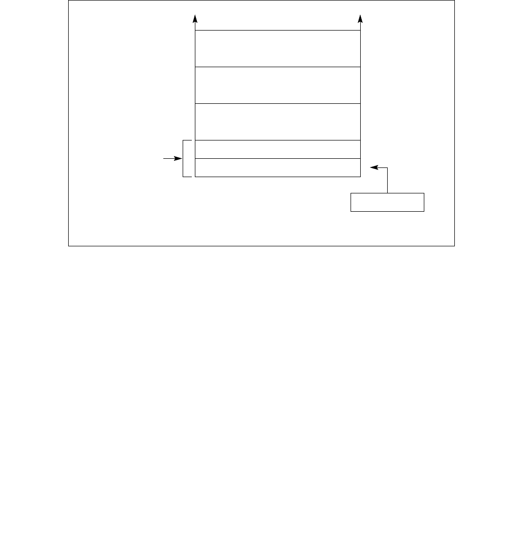
Vol. 3B 20-5
8086 EMULATION
5. Transfers program control to the location specified in the interrupt vector table.
An IRET instruction at the end of the handler procedure reverses these steps to return program control to the inter-
rupted program. Exceptions do not return error codes in real-address mode.
The interrupt vector table is an array of 4-byte entries (see Figure 20-2). Each entry consists of a far pointer to a
handler procedure, made up of a segment selector and an offset. The processor scales the interrupt or exception
vector by 4 to obtain an offset into the interrupt table. Following reset, the base of the interrupt vector table is
located at physical address 0 and its limit is set to 3FFH. In the Intel 8086 processor, the base address and limit of
the interrupt vector table cannot be changed. In the later IA-32 processors, the base address and limit of the inter-
rupt vector table are contained in the IDTR register and can be changed using the LIDT instruction.
(For backward compatibility to Intel 8086 processors, the default base address and limit of the interrupt vector
table should not be changed.)
Table 20-1 shows the interrupt and exception vectors that can be generated in real-address mode and virtual-8086
mode, and in the Intel 8086 processor. See Chapter 6, “Interrupt and Exception Handling”, for a description of the
exception conditions.
20.2 VIRTUAL-8086 MODE
Virtual-8086 mode is actually a special type of a task that runs in protected mode. When the operating-system or
executive switches to a virtual-8086-mode task, the processor emulates an Intel 8086 processor. The execution
environment of the processor while in the 8086-emulation state is the same as is described in Section 20.1, “Real-
Address Mode” for real-address mode, including the extensions. The major difference between the two modes is
that in virtual-8086 mode the 8086 emulator uses some protected-mode services (such as the protected-mode
interrupt and exception-handling and paging facilities).
Figure 20-2. Interrupt Vector Table in Real-Address Mode
0
2
4
8
12
0
15
Segment Selector
Offset
* Interrupt vector number 0 selects entry 0
Interrupt Vector 0*
Entry 1
Entry 2
Entry 3
Up to Entry 255
IDTR
(called “interrupt vector 0”) in the interrupt
vector table. Interrupt vector 0 in turn
points to the start of the interrupt handler
for interrupt 0.

20-6 Vol. 3B
8086 EMULATION
As in real-address mode, any new or legacy program that has been assembled and/or compiled to run on an Intel
8086 processor will run in a virtual-8086-mode task. And several 8086 programs can be run as virtual-8086-mode
tasks concurrently with normal protected-mode tasks, using the processor’s multitasking facilities.
20.2.1 Enabling Virtual-8086 Mode
The processor runs in virtual-8086 mode when the VM (virtual machine) flag in the EFLAGS register is set. This flag
can only be set when the processor switches to a new protected-mode task or resumes virtual-8086 mode via an
IRET instruction.
System software cannot change the state of the VM flag directly in the EFLAGS register (for example, by using the
POPFD instruction). Instead it changes the flag in the image of the EFLAGS register stored in the TSS or on the
stack following a call to an interrupt- or exception-handler procedure. For example, software sets the VM flag in the
EFLAGS image in the TSS when first creating a virtual-8086 task.
The processor tests the VM flag under three general conditions:
•When loading segment registers, to determine whether to use 8086-style address translation.
•When decoding instructions, to determine which instructions are not supported in virtual-8086 mode and which
instructions are sensitive to IOPL.
Table 20-1. Real-Address Mode Exceptions and Interrupts
Vector
No.
Description Real-Address Mode Virtual-8086 Mode Intel 8086 Processor
0 Divide Error (#DE) Yes Yes Yes
1 Debug Exception (#DB) Yes Yes No
2 NMI Interrupt Yes Yes Yes
3 Breakpoint (#BP) Yes Yes Yes
4 Overflow (#OF) Yes Yes Yes
5 BOUND Range Exceeded (#BR) Yes Yes Reserved
6 Invalid Opcode (#UD) Yes Yes Reserved
7 Device Not Available (#NM) Yes Yes Reserved
8 Double Fault (#DF) Yes Yes Reserved
9 (Intel reserved. Do not use.) Reserved Reserved Reserved
10 Invalid TSS (#TS) Reserved Yes Reserved
11 Segment Not Present (#NP) Reserved Yes Reserved
12 Stack Fault (#SS) Yes Yes Reserved
13 General Protection (#GP)* Yes Yes Reserved
14 Page Fault (#PF) Reserved Yes Reserved
15 (Intel reserved. Do not use.) Reserved Reserved Reserved
16 Floating-Point Error (#MF) Yes Yes Reserved
17 Alignment Check (#AC) Reserved Yes Reserved
18 Machine Check (#MC) Yes Yes Reserved
19-31 (Intel reserved. Do not use.) Reserved Reserved Reserved
32-255 User Defined Interrupts Yes Yes Yes
NOTE:
* In the real-address mode, vector 13 is the segment overrun exception. In protected and virtual-8086 modes, this exception cov-
ers all general-protection error conditions, including traps to the virtual-8086 monitor from virtual-8086 mode.

Vol. 3B 20-7
8086 EMULATION
•When checking privileged instructions, on page accesses, or when performing other permission checks.
(Virtual-8086 mode always executes at CPL 3.)
20.2.2 Structure of a Virtual-8086 Task
A virtual-8086-mode task consists of the following items:
•A 32-bit TSS for the task.
•The 8086 program.
•A virtual-8086 monitor.
•8086 operating-system services.
The TSS of the new task must be a 32-bit TSS, not a 16-bit TSS, because the 16-bit TSS does not load the most-
significant word of the EFLAGS register, which contains the VM flag. All TSS’s, stacks, data, and code used to handle
exceptions when in virtual-8086 mode must also be 32-bit segments.
The processor enters virtual-8086 mode to run the 8086 program and returns to protected mode to run the virtual-
8086 monitor.
The virtual-8086 monitor is a 32-bit protected-mode code module that runs at a CPL of 0. The monitor consists of
initialization, interrupt- and exception-handling, and I/O emulation procedures that emulate a personal computer
or other 8086-based platform. Typically, the monitor is either part of or closely associated with the protected-mode
general-protection (#GP) exception handler, which also runs at a CPL of 0. As with any protected-mode code
module, code-segment descriptors for the virtual-8086 monitor must exist in the GDT or in the task’s LDT. The
virtual-8086 monitor also may need data-segment descriptors so it can examine the IDT or other parts of the 8086
program in the first 1 MByte of the address space. The linear addresses above 10FFEFH are available for the
monitor, the operating system, and other system software.
The 8086 operating-system services consists of a kernel and/or operating-system procedures that the 8086
program makes calls to. These services can be implemented in either of the following two ways:
•They can be included in the 8086 program. This approach is desirable for either of the following reasons:
— The 8086 program code modifies the 8086 operating-system services.
— There is not sufficient development time to merge the 8086 operating-system services into main operating
system or executive.
•They can be implemented or emulated in the virtual-8086 monitor. This approach is desirable for any of the
following reasons:
— The 8086 operating-system procedures can be more easily coordinated among several virtual-8086 tasks.
— Memory can be saved by not duplicating 8086 operating-system procedure code for several virtual-8086
tasks.
— The 8086 operating-system procedures can be easily emulated by calls to the main operating system or
executive.
The approach chosen for implementing the 8086 operating-system services may result in different virtual-8086-
mode tasks using different 8086 operating-system services.
20.2.3 Paging of Virtual-8086 Tasks
Even though a program running in virtual-8086 mode can use only 20-bit linear addresses, the processor converts
these addresses into 32-bit linear addresses before mapping them to the physical address space. If paging is being
used, the 8086 address space for a program running in virtual-8086 mode can be paged and located in a set of
pages in physical address space. If paging is used, it is transparent to the program running in virtual-8086 mode
just as it is for any task running on the processor.
Paging is not necessary for a single virtual-8086-mode task, but paging is useful or necessary in the following situ-
ations:

20-8 Vol. 3B
8086 EMULATION
•When running multiple virtual-8086-mode tasks. Here, paging allows the lower 1 MByte of the linear address
space for each virtual-8086-mode task to be mapped to a different physical address location.
•When emulating the 8086 address-wraparound that occurs at 1 MByte. When using 8086-style address trans-
lation, it is possible to specify addresses larger than 1 MByte. These addresses automatically wraparound in the
Intel 8086 processor (see Section 20.1.1, “Address Translation in Real-Address Mode”). If any 8086 programs
depend on address wraparound, the same effect can be achieved in a virtual-8086-mode task by mapping the
linear addresses between 100000H and 110000H and linear addresses between 0 and 10000H to the same
physical addresses.
•When sharing the 8086 operating-system services or ROM code that is common to several 8086 programs
running as different 8086-mode tasks.
•When redirecting or trapping references to memory-mapped I/O devices.
20.2.4 Protection within a Virtual-8086 Task
Protection is not enforced between the segments of an 8086 program. Either of the following techniques can be
used to protect the system software running in a virtual-8086-mode task from the 8086 program:
•Reserve the first 1 MByte plus 64 KBytes of each task’s linear address space for the 8086 program. An 8086
processor task cannot generate addresses outside this range.
•Use the U/S flag of page-table entries to protect the virtual-8086 monitor and other system software in the
virtual-8086 mode task space. When the processor is in virtual-8086 mode, the CPL is 3. Therefore, an 8086
processor program has only user privileges. If the pages of the virtual-8086 monitor have supervisor privilege,
they cannot be accessed by the 8086 program.
20.2.5 Entering Virtual-8086 Mode
Figure 20-3 summarizes the methods of entering and leaving virtual-8086 mode. The processor switches to
virtual-8086 mode in either of the following situations:
•Task switch when the VM flag is set to 1 in the EFLAGS register image stored in the TSS for the task. Here the
task switch can be initiated in either of two ways:
— A CALL or JMP instruction.
— An IRET instruction, where the NT flag in the EFLAGS image is set to 1.
•Return from a protected-mode interrupt or exception handler when the VM flag is set to 1 in the EFLAGS
register image on the stack.
When a task switch is used to enter virtual-8086 mode, the TSS for the virtual-8086-mode task must be a 32-bit
TSS. (If the new TSS is a 16-bit TSS, the upper word of the EFLAGS register is not in the TSS, causing the processor
to clear the VM flag when it loads the EFLAGS register.) The processor updates the VM flag prior to loading the
segment registers from their images in the new TSS. The new setting of the VM flag determines whether the
processor interprets the contents of the segment registers as 8086-style segment selectors or protected-mode
segment selectors. When the VM flag is set, the segment registers are loaded from the TSS, using 8086-style
address translation to form base addresses.
See Section 20.3, “Interrupt and Exception Handling in Virtual-8086 Mode”, for information on entering virtual-
8086 mode on a return from an interrupt or exception handler.
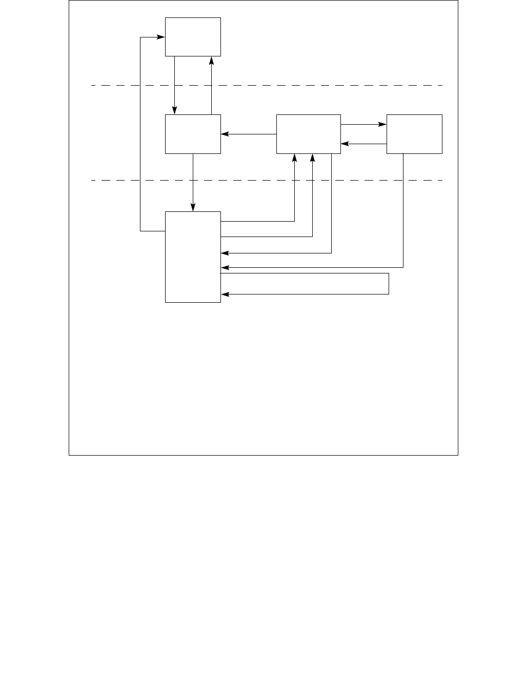
Vol. 3B 20-9
8086 EMULATION
20.2.6 Leaving Virtual-8086 Mode
The processor can leave the virtual-8086 mode only through an interrupt or exception. The following are situations
where an interrupt or exception will lead to the processor leaving virtual-8086 mode (see Figure 20-3):
•The processor services a hardware interrupt generated to signal the suspension of execution of the virtual-
8086 application. This hardware interrupt may be generated by a timer or other external mechanism. Upon
receiving the hardware interrupt, the processor enters protected mode and switches to a protected-mode (or
another virtual-8086 mode) task either through a task gate in the protected-mode IDT or through a trap or
interrupt gate that points to a handler that initiates a task switch. A task switch from a virtual-8086 task to
another task loads the EFLAGS register from the TSS of the new task. The value of the VM flag in the new
EFLAGS determines if the new task executes in virtual-8086 mode or not.
•The processor services an exception caused by code executing the virtual-8086 task or services a hardware
interrupt that “belongs to” the virtual-8086 task. Here, the processor enters protected mode and services the
Figure 20-3. Entering and Leaving Virtual-8086 Mode
Monitor
Virtual-8086
Real Mode
Code
Protected-
Mode Tasks
Virtual-8086
Mode Tasks
(8086
Programs)
Protected-
Mode Interrupt
and Exception
Handlers
Task Switch1
VM = 1
Protected
Mode
Virtual-8086
Mode
Real-Address
Mode
RESET
PE=1 PE=0 or
RESET
#GP Exception3
CALL
RET
Task Switch
VM=0
Redirect Interrupt to 8086 Program
Interrupt or Exception Handler6
IRET4
Interrupt or
Exception2
VM = 0
NOTES:
- CALL or JMP where the VM flag in the EFLAGS image is 1.
- IRET where VM is 1 and NT is 1.
4. Normal return from protected-mode interrupt or exception handler.
3. General-protection exception caused by software interrupt (INT n), IRET,
POPF, PUSHF, IN, or OUT when IOPL is less than 3.
2. Hardware interrupt or exception; software interrupt (INT n) when IOPL is 3.
5. A return from the 8086 monitor to redirect an interrupt or exception back
to an interrupt or exception handler in the 8086 program running in virtual-
6. Internal redirection of a software interrupt (INT n) when VME is 1,
IOPL is <3, and the redirection bit is 1.
IRET5
8086 mode.
1. Task switch carried out in either of two ways:

20-10 Vol. 3B
8086 EMULATION
exception or hardware interrupt through the protected-mode IDT (normally through an interrupt or trap gate)
and the protected-mode exception- and interrupt-handlers. The processor may handle the exception or
interrupt within the context of the virtual 8086 task and return to virtual-8086 mode on a return from the
handler procedure. The processor may also execute a task switch and handle the exception or interrupt in the
context of another task.
•The processor services a software interrupt generated by code executing in the virtual-8086 task (such as a
software interrupt to call a MS-DOS* operating system routine). The processor provides several methods of
handling these software interrupts, which are discussed in detail in Section 20.3.3, “Class 3—Software
Interrupt Handling in Virtual-8086 Mode”. Most of them involve the processor entering protected mode, often
by means of a general-protection (#GP) exception. In protected mode, the processor can send the interrupt to
the virtual-8086 monitor for handling and/or redirect the interrupt back to the application program running in
virtual-8086 mode task for handling.
IA-32 processors that incorporate the virtual mode extension (enabled with the VME flag in control register
CR4) are capable of redirecting software-generated interrupts back to the program’s interrupt handlers without
leaving virtual-8086 mode. See Section 20.3.3.4, “Method 5: Software Interrupt Handling”, for more
information on this mechanism.
•A hardware reset initiated by asserting the RESET or INIT pin is a special kind of interrupt. When a RESET or
INIT is signaled while the processor is in virtual-8086 mode, the processor leaves virtual-8086 mode and enters
real-address mode.
•Execution of the HLT instruction in virtual-8086 mode will cause a general-protection (GP#) fault, which the
protected-mode handler generally sends to the virtual-8086 monitor. The virtual-8086 monitor then
determines the correct execution sequence after verifying that it was entered as a result of a HLT execution.
See Section 20.3, “Interrupt and Exception Handling in Virtual-8086 Mode”, for information on leaving virtual-8086
mode to handle an interrupt or exception generated in virtual-8086 mode.
20.2.7 Sensitive Instructions
When an IA-32 processor is running in virtual-8086 mode, the CLI, STI, PUSHF, POPF, INT n, and IRET instructions
are sensitive to IOPL. The IN, INS, OUT, and OUTS instructions, which are sensitive to IOPL in protected mode, are
not sensitive in virtual-8086 mode.
The CPL is always 3 while running in virtual-8086 mode; if the IOPL is less than 3, an attempt to use the IOPL-sensi-
tive instructions listed above triggers a general-protection exception (#GP). These instructions are sensitive to
IOPL to give the virtual-8086 monitor a chance to emulate the facilities they affect.
20.2.8 Virtual-8086 Mode I/O
Many 8086 programs written for non-multitasking systems directly access I/O ports. This practice may cause prob-
lems in a multitasking environment. If more than one program accesses the same port, they may interfere with
each other. Most multitasking systems require application programs to access I/O ports through the operating
system. This results in simplified, centralized control.
The processor provides I/O protection for creating I/O that is compatible with the environment and transparent to
8086 programs. Designers may take any of several possible approaches to protecting I/O ports:
•Protect the I/O address space and generate exceptions for all attempts to perform I/O directly.
•Let the 8086 program perform I/O directly.
•Generate exceptions on attempts to access specific I/O ports.
•Generate exceptions on attempts to access specific memory-mapped I/O ports.
The method of controlling access to I/O ports depends upon whether they are I/O-port mapped or memory
mapped.

Vol. 3B 20-11
8086 EMULATION
20.2.8.1 I/O-Port-Mapped I/O
The I/O permission bit map in the TSS can be used to generate exceptions on attempts to access specific I/O port
addresses. The I/O permission bit map of each virtual-8086-mode task determines which I/O addresses generate
exceptions for that task. Because each task may have a different I/O permission bit map, the addresses that
generate exceptions for one task may be different from the addresses for another task. This differs from protected
mode in which, if the CPL is less than or equal to the IOPL, I/O access is allowed without checking the I/O permis-
sion bit map. See Chapter 18, “Input/Output”, in the Intel® 64 and IA-32 Architectures Software Developer’s
Manual, Volume 1, for more information about the I/O permission bit map.
20.2.8.2 Memory-Mapped I/O
In systems which use memory-mapped I/O, the paging facilities of the processor can be used to generate excep-
tions for attempts to access I/O ports. The virtual-8086 monitor may use paging to control memory-mapped I/O in
these ways:
•Map part of the linear address space of each task that needs to perform I/O to the physical address space
where I/O ports are placed. By putting the I/O ports at different addresses (in different pages), the paging
mechanism can enforce isolation between tasks.
•Map part of the linear address space to pages that are not-present. This generates an exception whenever a
task attempts to perform I/O to those pages. System software then can interpret the I/O operation being
attempted.
Software emulation of the I/O space may require too much operating system intervention under some conditions.
In these cases, it may be possible to generate an exception for only the first attempt to access I/O. The system
software then may determine whether a program can be given exclusive control of I/O temporarily, the protection
of the I/O space may be lifted, and the program allowed to run at full speed.
20.2.8.3 Special I/O Buffers
Buffers of intelligent controllers (for example, a bit-mapped frame buffer) also can be emulated using page
mapping. The linear space for the buffer can be mapped to a different physical space for each virtual-8086-mode
task. The virtual-8086 monitor then can control which virtual buffer to copy onto the real buffer in the physical
address space.
20.3 INTERRUPT AND EXCEPTION HANDLING IN VIRTUAL-8086 MODE
When the processor receives an interrupt or detects an exception condition while in virtual-8086 mode, it invokes
an interrupt or exception handler, just as it does in protected or real-address mode. The interrupt or exception
handler that is invoked and the mechanism used to invoke it depends on the class of interrupt or exception that has
been detected or generated and the state of various system flags and fields.
In virtual-8086 mode, the interrupts and exceptions are divided into three classes for the purposes of handling:
•Class 1 — All processor-generated exceptions and all hardware interrupts, including the NMI interrupt and the
hardware interrupts sent to the processor’s external interrupt delivery pins. All class 1 exceptions and
interrupts are handled by the protected-mode exception and interrupt handlers.
•Class 2 — Special case for maskable hardware interrupts (Section 6.3.2, “Maskable Hardware Interrupts”)
when the virtual mode extensions are enabled.
•Class 3 — All software-generated interrupts, that is interrupts generated with the INT n instruction1.
The method the processor uses to handle class 2 and 3 interrupts depends on the setting of the following flags and
fields:
•IOPL field (bits 12 and 13 in the EFLAGS register) — Controls how class 3 software interrupts are handled
when the processor is in virtual-8086 mode (see Section 2.3, “System Flags and Fields in the EFLAGS
1. The INT 3 instruction is a special case (see the description of the INT n instruction in Chapter 3, “Instruction Set Reference, A-L”, of
the Intel® 64 and IA-32 Architectures Software Developer’s Manual, Volume 2A).

20-12 Vol. 3B
8086 EMULATION
Register”). This field also controls the enabling of the VIF and VIP flags in the EFLAGS register when the VME
flag is set. The VIF and VIP flags are provided to assist in the handling of class 2 maskable hardware interrupts.
•VME flag (bit 0 in control register CR4) — Enables the virtual mode extension for the processor when set
(see Section 2.5, “Control Registers”).
•Software interrupt redirection bit map (32 bytes in the TSS, see Figure 20-5) — Contains 256 flags
that indicates how class 3 software interrupts should be handled when they occur in virtual-8086 mode. A
software interrupt can be directed either to the interrupt and exception handlers in the currently running 8086
program or to the protected-mode interrupt and exception handlers.
•The virtual interrupt flag (VIF) and virtual interrupt pending flag (VIP) in the EFLAGS register —
Provides virtual interrupt support for the handling of class 2 maskable hardware interrupts (see Section
20.3.2, “Class 2—Maskable Hardware Interrupt Handling in Virtual-8086 Mode Using the Virtual Interrupt
Mechanism”).
NOTE
The VME flag, software interrupt redirection bit map, and VIF and VIP flags are only available in
IA-32 processors that support the virtual mode extensions. These extensions were introduced in
the IA-32 architecture with the Pentium processor.
The following sections describe the actions that processor takes and the possible actions of interrupt and exception
handlers for the two classes of interrupts described in the previous paragraphs. These sections describe three
possible types of interrupt and exception handlers:
•Protected-mode interrupt and exceptions handlers — These are the standard handlers that the processor
calls through the protected-mode IDT.
•Virtual-8086 monitor interrupt and exception handlers — These handlers are resident in the virtual-8086
monitor, and they are commonly accessed through a general-protection exception (#GP, interrupt 13) that is
directed to the protected-mode general-protection exception handler.
•8086 program interrupt and exception handlers — These handlers are part of the 8086 program that is
running in virtual-8086 mode.
The following sections describe how these handlers are used, depending on the selected class and method of inter-
rupt and exception handling.
20.3.1 Class 1—Hardware Interrupt and Exception Handling in Virtual-8086 Mode
In virtual-8086 mode, the Pentium, P6 family, Pentium 4, and Intel Xeon processors handle hardware interrupts
and exceptions in the same manner as they are handled by the Intel486 and Intel386 processors. They invoke the
protected-mode interrupt or exception handler that the interrupt or exception vector points to in the IDT. Here, the
IDT entry must contain either a 32-bit trap or interrupt gate or a task gate. The following sections describe various
ways that a virtual-8086 mode interrupt or exception can be handled after the protected-mode handler has been
invoked.
See Section 20.3.2, “Class 2—Maskable Hardware Interrupt Handling in Virtual-8086 Mode Using the Virtual Inter-
rupt Mechanism”, for a description of the virtual interrupt mechanism that is available for handling maskable hard-
ware interrupts while in virtual-8086 mode. When this mechanism is either not available or not enabled, maskable
hardware interrupts are handled in the same manner as exceptions, as described in the following sections.
20.3.1.1 Handling an Interrupt or Exception Through a Protected-Mode Trap or Interrupt Gate
When an interrupt or exception vector points to a 32-bit trap or interrupt gate in the IDT, the gate must in turn point
to a nonconforming, privilege-level 0, code segment. When accessing this code segment, processor performs the
following steps.
1. Switches to 32-bit protected mode and privilege level 0.
2. Saves the state of the processor on the privilege-level 0 stack. The states of the EIP, CS, EFLAGS, ESP, SS, ES,
DS, FS, and GS registers are saved (see Figure 20-4).
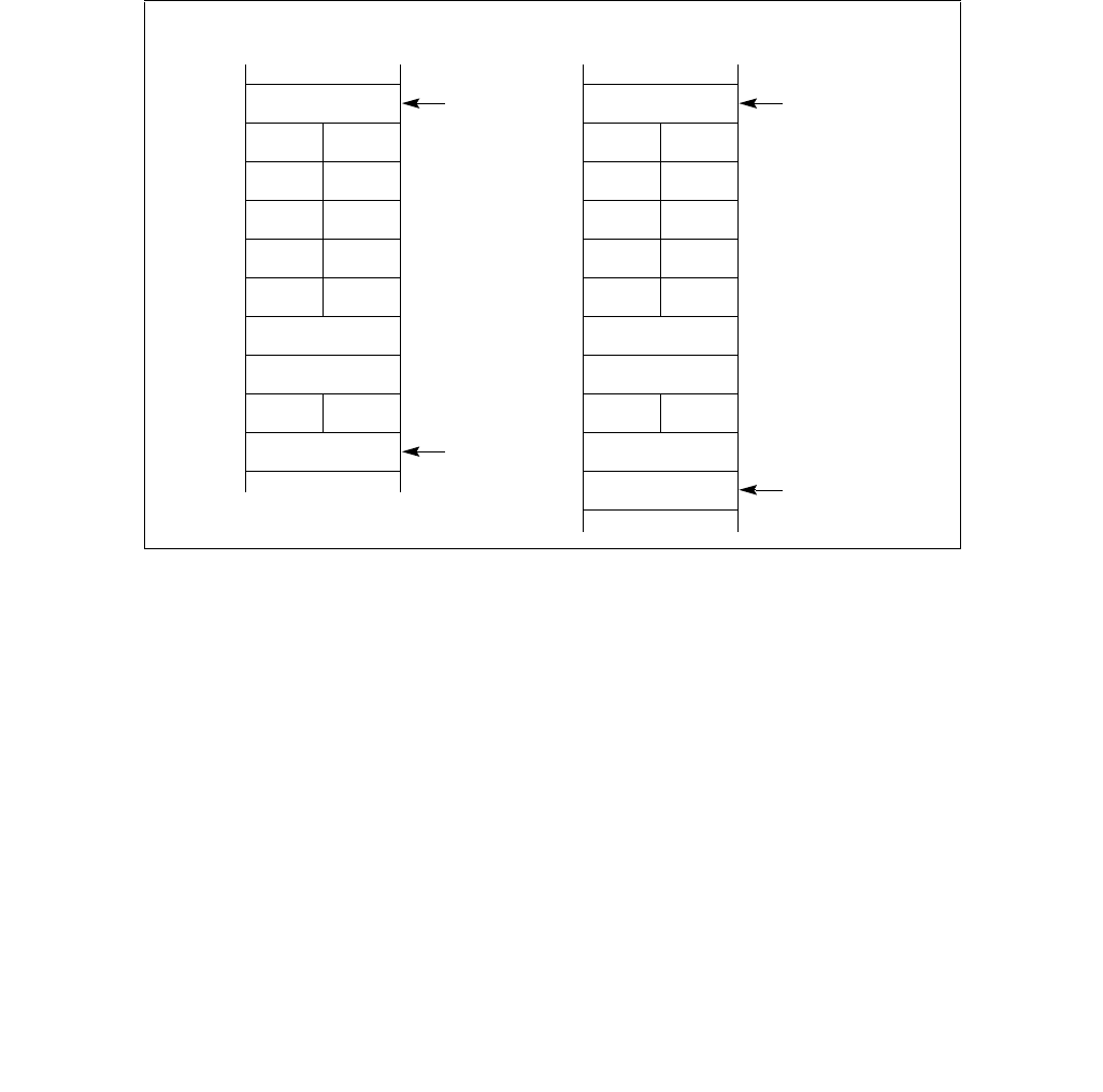
Vol. 3B 20-13
8086 EMULATION
3. Clears the segment registers. Saving the DS, ES, FS, and GS registers on the stack and then clearing the
registers lets the interrupt or exception handler safely save and restore these registers regardless of the type
segment selectors they contain (protected-mode or 8086-style). The interrupt and exception handlers, which
may be called in the context of either a protected-mode task or a virtual-8086-mode task, can use the same
code sequences for saving and restoring the registers for any task. Clearing these registers before execution of
the IRET instruction does not cause a trap in the interrupt handler. Interrupt procedures that expect values in
the segment registers or that return values in the segment registers must use the register images saved on the
stack for privilege level 0.
4. Clears VM, NT, RF and TF flags (in the EFLAGS register). If the gate is an interrupt gate, clears the IF flag.
5. Begins executing the selected interrupt or exception handler.
If the trap or interrupt gate references a procedure in a conforming segment or in a segment at a privilege level
other than 0, the processor generates a general-protection exception (#GP). Here, the error code is the segment
selector of the code segment to which a call was attempted.
Interrupt and exception handlers can examine the VM flag on the stack to determine if the interrupted procedure
was running in virtual-8086 mode. If so, the interrupt or exception can be handled in one of three ways:
•The protected-mode interrupt or exception handler that was called can handle the interrupt or exception.
•The protected-mode interrupt or exception handler can call the virtual-8086 monitor to handle the interrupt or
exception.
•The virtual-8086 monitor (if called) can in turn pass control back to the 8086 program’s interrupt and exception
handler.
If the interrupt or exception is handled with a protected-mode handler, the handler can return to the interrupted
program in virtual-8086 mode by executing an IRET instruction. This instruction loads the EFLAGS and segment
registers from the images saved in the privilege level 0 stack (see Figure 20-4). A set VM flag in the EFLAGS image
causes the processor to switch back to virtual-8086 mode. The CPL at the time the IRET instruction is executed
must be 0, otherwise the processor does not change the state of the VM flag.
Figure 20-4. Privilege Level 0 Stack After Interrupt or
Exception in Virtual-8086 Mode
Unused
Old GS
Old ESP
With Error Code
ESP from
Old FS
Old DS
Old ES
Old SS
Old EFLAGS
Old CS
Old EIP
Error Code New ESP
TSS
Unused
Old GS
Old ESP
Without Error Code
ESP from
Old FS
Old DS
Old ES
Old SS
Old EFLAGS
Old CS
Old EIP New ESP
TSS

20-14 Vol. 3B
8086 EMULATION
The virtual-8086 monitor runs at privilege level 0, like the protected-mode interrupt and exception handlers. It is
commonly closely tied to the protected-mode general-protection exception (#GP, vector 13) handler. If the
protected-mode interrupt or exception handler calls the virtual-8086 monitor to handle the interrupt or exception,
the return from the virtual-8086 monitor to the interrupted virtual-8086 mode program requires two return
instructions: a RET instruction to return to the protected-mode handler and an IRET instruction to return to the
interrupted program.
The virtual-8086 monitor has the option of directing the interrupt and exception back to an interrupt or exception
handler that is part of the interrupted 8086 program, as described in Section 20.3.1.2, “Handling an Interrupt or
Exception With an 8086 Program Interrupt or Exception Handler”.
20.3.1.2 Handling an Interrupt or Exception With an 8086 Program Interrupt or Exception Handler
Because it was designed to run on an 8086 processor, an 8086 program running in a virtual-8086-mode task
contains an 8086-style interrupt vector table, which starts at linear address 0. If the virtual-8086 monitor correctly
directs an interrupt or exception vector back to the virtual-8086-mode task it came from, the handlers in the 8086
program can handle the interrupt or exception. The virtual-8086 monitor must carry out the following steps to send
an interrupt or exception back to the 8086 program:
1. Use the 8086 interrupt vector to locate the appropriate handler procedure in the 8086 program interrupt table.
2. Store the EFLAGS (low-order 16 bits only), CS and EIP values of the 8086 program on the privilege-level 3
stack. This is the stack that the virtual-8086-mode task is using. (The 8086 handler may use or modify this
information.)
3. Change the return link on the privilege-level 0 stack to point to the privilege-level 3 handler procedure.
4. Execute an IRET instruction to pass control to the 8086 program handler.
5. When the IRET instruction from the privilege-level 3 handler triggers a general-protection exception (#GP) and
thus effectively again calls the virtual-8086 monitor, restore the return link on the privilege-level 0 stack to
point to the original, interrupted, privilege-level 3 procedure.
6. Copy the low order 16 bits of the EFLAGS image from the privilege-level 3 stack to the privilege-level 0 stack
(because some 8086 handlers modify these flags to return information to the code that caused the interrupt).
7. Execute an IRET instruction to pass control back to the interrupted 8086 program.
Note that if an operating system intends to support all 8086 MS-DOS-based programs, it is necessary to use the
actual 8086 interrupt and exception handlers supplied with the program. The reason for this is that some programs
modify their own interrupt vector table to substitute (or hook in series) their own specialized interrupt and excep-
tion handlers.
20.3.1.3 Handling an Interrupt or Exception Through a Task Gate
When an interrupt or exception vector points to a task gate in the IDT, the processor performs a task switch to the
selected interrupt- or exception-handling task. The following actions are carried out as part of this task switch:
1. The EFLAGS register with the VM flag set is saved in the current TSS.
2. The link field in the TSS of the called task is loaded with the segment selector of the TSS for the interrupted
virtual-8086-mode task.
3. The EFLAGS register is loaded from the image in the new TSS, which clears the VM flag and causes the
processor to switch to protected mode.
4. The NT flag in the EFLAGS register is set.
5. The processor begins executing the selected interrupt- or exception-handler task.
When an IRET instruction is executed in the handler task and the NT flag in the EFLAGS register is set, the proces-
sors switches from a protected-mode interrupt- or exception-handler task back to a virtual-8086-mode task. Here,
the EFLAGS and segment registers are loaded from images saved in the TSS for the virtual-8086-mode task. If the
VM flag is set in the EFLAGS image, the processor switches back to virtual-8086 mode on the task switch. The CPL
at the time the IRET instruction is executed must be 0, otherwise the processor does not change the state of the
VM flag.

Vol. 3B 20-15
8086 EMULATION
20.3.2 Class 2—Maskable Hardware Interrupt Handling in Virtual-8086 Mode Using the
Virtual Interrupt Mechanism
Maskable hardware interrupts are those interrupts that are delivered through the INTR# pin or through an inter-
rupt request to the local APIC (see Section 6.3.2, “Maskable Hardware Interrupts”). These interrupts can be inhib-
ited (masked) from interrupting an executing program or task by clearing the IF flag in the EFLAGS register.
When the VME flag in control register CR4 is set and the IOPL field in the EFLAGS register is less than 3, two addi-
tional flags are activated in the EFLAGS register:
•VIF (virtual interrupt) flag, bit 19 of the EFLAGS register.
•VIP (virtual interrupt pending) flag, bit 20 of the EFLAGS register.
These flags provide the virtual-8086 monitor with more efficient control over handling maskable hardware inter-
rupts that occur during virtual-8086 mode tasks. They also reduce interrupt-handling overhead, by eliminating the
need for all IF related operations (such as PUSHF, POPF, CLI, and STI instructions) to trap to the virtual-8086
monitor. The purpose and use of these flags are as follows.
NOTE
The VIF and VIP flags are only available in IA-32 processors that support the virtual mode
extensions. These extensions were introduced in the IA-32 architecture with the Pentium
processor. When this mechanism is either not available or not enabled, maskable hardware
interrupts are handled as class 1 interrupts. Here, if VIF and VIP flags are needed, the virtual-8086
monitor can implement them in software.
Existing 8086 programs commonly set and clear the IF flag in the EFLAGS register to enable and disable maskable
hardware interrupts, respectively; for example, to disable interrupts while handling another interrupt or an excep-
tion. This practice works well in single task environments, but can cause problems in multitasking and multiple-
processor environments, where it is often desirable to prevent an application program from having direct control
over the handling of hardware interrupts. When using earlier IA-32 processors, this problem was often solved by
creating a virtual IF flag in software. The IA-32 processors (beginning with the Pentium processor) provide hard-
ware support for this virtual IF flag through the VIF and VIP flags.
The VIF flag is a virtualized version of the IF flag, which an application program running from within a virtual-8086
task can used to control the handling of maskable hardware interrupts. When the VIF flag is enabled, the CLI and
STI instructions operate on the VIF flag instead of the IF flag. When an 8086 program executes the CLI instruction,
the processor clears the VIF flag to request that the virtual-8086 monitor inhibit maskable hardware interrupts
from interrupting program execution; when it executes the STI instruction, the processor sets the VIF flag
requesting that the virtual-8086 monitor enable maskable hardware interrupts for the 8086 program. But actually
the IF flag, managed by the operating system, always controls whether maskable hardware interrupts are enabled.
Also, if under these circumstances an 8086 program tries to read or change the IF flag using the PUSHF or POPF
instructions, the processor will change the VIF flag instead, leaving IF unchanged.
The VIP flag provides software a means of recording the existence of a deferred (or pending) maskable hardware
interrupt. This flag is read by the processor but never explicitly written by the processor; it can only be written by
software.
If the IF flag is set and the VIF and VIP flags are enabled, and the processor receives a maskable hardware inter-
rupt (interrupt vector 0 through 255), the processor performs and the interrupt handler software should perform
the following operations:
1. The processor invokes the protected-mode interrupt handler for the interrupt received, as described in the
following steps. These steps are almost identical to those described for method 1 interrupt and exception
handling in Section 20.3.1.1, “Handling an Interrupt or Exception Through a Protected-Mode Trap or Interrupt
Gate”:
a. Switches to 32-bit protected mode and privilege level 0.
b. Saves the state of the processor on the privilege-level 0 stack. The states of the EIP, CS, EFLAGS, ESP, SS,
ES, DS, FS, and GS registers are saved (see Figure 20-4).
c. Clears the segment registers.

20-16 Vol. 3B
8086 EMULATION
d. Clears the VM flag in the EFLAGS register.
e. Begins executing the selected protected-mode interrupt handler.
2. The recommended action of the protected-mode interrupt handler is to read the VM flag from the EFLAGS
image on the stack. If this flag is set, the handler makes a call to the virtual-8086 monitor.
3. The virtual-8086 monitor should read the VIF flag in the EFLAGS register.
— If the VIF flag is clear, the virtual-8086 monitor sets the VIP flag in the EFLAGS image on the stack to
indicate that there is a deferred interrupt pending and returns to the protected-mode handler.
— If the VIF flag is set, the virtual-8086 monitor can handle the interrupt if it “belongs” to the 8086 program
running in the interrupted virtual-8086 task; otherwise, it can call the protected-mode interrupt handler to
handle the interrupt.
4. The protected-mode handler executes a return to the program executing in virtual-8086 mode.
5. Upon returning to virtual-8086 mode, the processor continues execution of the 8086 program.
When the 8086 program is ready to receive maskable hardware interrupts, it executes the STI instruction to set the
VIF flag (enabling maskable hardware interrupts). Prior to setting the VIF flag, the processor automatically checks
the VIP flag and does one of the following, depending on the state of the flag:
•If the VIP flag is clear (indicating no pending interrupts), the processor sets the VIF flag.
•If the VIP flag is set (indicating a pending interrupt), the processor generates a general-protection exception
(#GP).
The recommended action of the protected-mode general-protection exception handler is to then call the virtual-
8086 monitor and let it handle the pending interrupt. After handling the pending interrupt, the typical action of the
virtual-8086 monitor is to clear the VIP flag and set the VIF flag in the EFLAGS image on the stack, and then
execute a return to the virtual-8086 mode. The next time the processor receives a maskable hardware interrupt, it
will then handle it as described in steps 1 through 5 earlier in this section.
If the processor finds that both the VIF and VIP flags are set at the beginning of an instruction, it generates a
general-protection exception. This action allows the virtual-8086 monitor to handle the pending interrupt for the
virtual-8086 mode task for which the VIF flag is enabled. Note that this situation can only occur immediately
following execution of a POPF or IRET instruction or upon entering a virtual-8086 mode task through a task switch.
Note that the states of the VIF and VIP flags are not modified in real-address mode or during transitions between
real-address and protected modes.
NOTE
The virtual interrupt mechanism described in this section is also available for use in protected
mode, see Section 20.4, “Protected-Mode Virtual Interrupts”.
20.3.3 Class 3—Software Interrupt Handling in Virtual-8086 Mode
When the processor receives a software interrupt (an interrupt generated with the INT n instruction) while in
virtual-8086 mode, it can use any of six different methods to handle the interrupt. The method selected depends
on the settings of the VME flag in control register CR4, the IOPL field in the EFLAGS register, and the software inter-
rupt redirection bit map in the TSS. Table 20-2 lists the six methods of handling software interrupts in virtual-8086
mode and the respective settings of the VME flag, IOPL field, and the bits in the interrupt redirection bit map for
each method. The table also summarizes the various actions the processor takes for each method.
The VME flag enables the virtual mode extensions for the Pentium and later IA-32 processors. When this flag is
clear, the processor responds to interrupts and exceptions in virtual-8086 mode in the same manner as an Intel386
or Intel486 processor does. When this flag is set, the virtual mode extension provides the following enhancements
to virtual-8086 mode:
•Speeds up the handling of software-generated interrupts in virtual-8086 mode by allowing the processor to
bypass the virtual-8086 monitor and redirect software interrupts back to the interrupt handlers that are part of
the currently running 8086 program.
•Supports virtual interrupts for software written to run on the 8086 processor.

Vol. 3B 20-17
8086 EMULATION
The IOPL value interacts with the VME flag and the bits in the interrupt redirection bit map to determine how
specific software interrupts should be handled.
The software interrupt redirection bit map (see Figure 20-5) is a 32-byte field in the TSS. This map is located
directly below the I/O permission bit map in the TSS. Each bit in the interrupt redirection bit map is mapped to an
interrupt vector. Bit 0 in the interrupt redirection bit map (which maps to vector zero in the interrupt table) is
located at the I/O base map address in the TSS minus 32 bytes. When a bit in this bit map is set, it indicates that
the associated software interrupt (interrupt generated with an INT n instruction) should be handled through the
protected-mode IDT and interrupt and exception handlers. When a bit in this bit map is clear, the processor redi-
rects the associated software interrupt back to the interrupt table in the 8086 program (located at linear address 0
in the program’s address space).
NOTE
The software interrupt redirection bit map does not affect hardware generated interrupts and
exceptions. Hardware generated interrupts and exceptions are always handled by the protected-
mode interrupt and exception handlers.
Table 20-2. Software Interrupt Handling Methods While in Virtual-8086 Mode
Method VME IOPL
Bit in
Redir.
Bitmap* Processor Action
1 0 3 X Interrupt directed to a protected-mode interrupt handler:
• Switches to privilege-level 0 stack
• Pushes GS, FS, DS and ES onto privilege-level 0 stack
• Pushes SS, ESP, EFLAGS, CS and EIP of interrupted task onto privilege-level 0 stack
• Clears VM, RF, NT, and TF flags
• If serviced through interrupt gate, clears IF flag
• Clears GS, FS, DS and ES to 0
• Sets CS and EIP from interrupt gate
2 0 < 3 X Interrupt directed to protected-mode general-protection exception (#GP) handler.
3 1 < 3 1 Interrupt directed to a protected-mode general-protection exception (#GP) handler; VIF and VIP
flag support for handling class 2 maskable hardware interrupts.
4 1 3 1 Interrupt directed to protected-mode interrupt handler: (see method 1 processor action).
5 1 3 0 Interrupt redirected to 8086 program interrupt handler:
• Pushes EFLAGS
• Pushes CS and EIP (lower 16 bits only)
• Clears IF flag
• Clears TF flag
• Loads CS and EIP (lower 16 bits only) from selected entry in the interrupt vector table of the
current virtual-8086 task
6 1 < 3 0 Interrupt redirected to 8086 program interrupt handler; VIF and VIP flag support for handling class
2 maskable hardware interrupts:
• Pushes EFLAGS with IOPL set to 3 and VIF copied to IF
• Pushes CS and EIP (lower 16 bits only)
•Clears the VIF flag
• Clears TF flag
• Loads CS and EIP (lower 16 bits only) from selected entry in the interrupt vector table of the
current virtual-8086 task
NOTE:
* When set to 0, software interrupt is redirected back to the 8086 program interrupt handler; when set to 1, interrupt is directed to
protected-mode handler.
20-18 Vol. 3B
8086 EMULATION
Redirecting software interrupts back to the 8086 program potentially speeds up interrupt handling because a
switch back and forth between virtual-8086 mode and protected mode is not required. This latter interrupt-
handling technique is particularly useful for 8086 operating systems (such as MS-DOS) that use the INT n instruc-
tion to call operating system procedures.
The CPUID instruction can be used to verify that the virtual mode extension is implemented on the processor. Bit 1
of the feature flags register (EDX) indicates the availability of the virtual mode extension (see “CPUID—CPU Iden-
tification” in Chapter 3, “Instruction Set Reference, A-L”, of the Intel® 64 and IA-32 Architectures Software Devel-
oper’s Manual, Volume 2A).
The following sections describe the six methods (or mechanisms) for handling software interrupts in virtual-8086
mode. See Section 20.3.2, “Class 2—Maskable Hardware Interrupt Handling in Virtual-8086 Mode Using the Virtual
Interrupt Mechanism”, for a description of the use of the VIF and VIP flags in the EFLAGS register for handling
maskable hardware interrupts.
20.3.3.1 Method 1: Software Interrupt Handling
When the VME flag in control register CR4 is clear and the IOPL field is 3, a Pentium or later IA-32 processor
handles software interrupts in the same manner as they are handled by an Intel386 or Intel486 processor. It
executes an implicit call to the interrupt handler in the protected-mode IDT pointed to by the interrupt vector. See
Section 20.3.1, “Class 1—Hardware Interrupt and Exception Handling in Virtual-8086 Mode”, for a complete
description of this mechanism and its possible uses.
20.3.3.2 Methods 2 and 3: Software Interrupt Handling
When a software interrupt occurs in virtual-8086 mode and the method 2 or 3 conditions are present, the processor
generates a general-protection exception (#GP). Method 2 is enabled when the VME flag is set to 0 and the IOPL
value is less than 3. Here the IOPL value is used to bypass the protected-mode interrupt handlers and cause any
software interrupt that occurs in virtual-8086 mode to be treated as a protected-mode general-protection excep-
tion (#GP). The general-protection exception handler calls the virtual-8086 monitor, which can then emulate an
8086-program interrupt handler or pass control back to the 8086 program’s handler, as described in Section
20.3.1.2, “Handling an Interrupt or Exception With an 8086 Program Interrupt or Exception Handler”.
Method 3 is enabled when the VME flag is set to 1, the IOPL value is less than 3, and the corresponding bit for the
software interrupt in the software interrupt redirection bit map is set to 1. Here, the processor performs the same
Figure 20-5. Software Interrupt Redirection Bit Map in TSS
I/O Map Base
Task-State Segment (TSS)
64H
31 24 23 0
11111111
I/O Permission Bit Map
0
I/O map
base must
not exceed
DFFFH.
Last byte of
bit
map must be
Software Interrupt Redirection Bit Map (32 Bytes)

Vol. 3B 20-19
8086 EMULATION
operation as it does for method 2 software interrupt handling. If the corresponding bit for the software interrupt in
the software interrupt redirection bit map is set to 0, the interrupt is handled using method 6 (see Section 20.3.3.5,
“Method 6: Software Interrupt Handling”).
20.3.3.3 Method 4: Software Interrupt Handling
Method 4 handling is enabled when the VME flag is set to 1, the IOPL value is 3, and the bit for the interrupt vector
in the redirection bit map is set to 1. Method 4 software interrupt handling allows method 1 style handling when the
virtual mode extension is enabled; that is, the interrupt is directed to a protected-mode handler (see Section
20.3.3.1, “Method 1: Software Interrupt Handling”).
20.3.3.4 Method 5: Software Interrupt Handling
Method 5 software interrupt handling provides a streamlined method of redirecting software interrupts (invoked
with the INT n instruction) that occur in virtual 8086 mode back to the 8086 program’s interrupt vector table and
its interrupt handlers. Method 5 handling is enabled when the VME flag is set to 1, the IOPL value is 3, and the bit
for the interrupt vector in the redirection bit map is set to 0. The processor performs the following actions to make
an implicit call to the selected 8086 program interrupt handler:
1. Pushes the low-order 16 bits of the EFLAGS register onto the stack.
2. Pushes the current values of the CS and EIP registers onto the current stack. (Only the 16 least-significant bits
of the EIP register are pushed and no stack switch occurs.)
3. Clears the IF flag in the EFLAGS register to disable interrupts.
4. Clears the TF flag, in the EFLAGS register.
5. Locates the 8086 program interrupt vector table at linear address 0 for the 8086-mode task.
6. Loads the CS and EIP registers with values from the interrupt vector table entry pointed to by the interrupt
vector number. Only the 16 low-order bits of the EIP are loaded and the 16 high-order bits are set to 0. The
interrupt vector table is assumed to be at linear address 0 of the current virtual-8086 task.
7. Begins executing the selected interrupt handler.
An IRET instruction at the end of the handler procedure reverses these steps to return program control to the inter-
rupted 8086 program.
Note that with method 5 handling, a mode switch from virtual-8086 mode to protected mode does not occur. The
processor remains in virtual-8086 mode throughout the interrupt-handling operation.
The method 5 handling actions are virtually identical to the actions the processor takes when handling software
interrupts in real-address mode. The benefit of using method 5 handling to access the 8086 program handlers is
that it avoids the overhead of methods 2 and 3 handling, which requires first going to the virtual-8086 monitor,
then to the 8086 program handler, then back again to the virtual-8086 monitor, before returning to the interrupted
8086 program (see Section 20.3.1.2, “Handling an Interrupt or Exception With an 8086 Program Interrupt or
Exception Handler”).
NOTE
Methods 1 and 4 handling can handle a software interrupt in a virtual-8086 task with a regular
protected-mode handler, but this approach requires all virtual-8086 tasks to use the same software
interrupt handlers, which generally does not give sufficient latitude to the programs running in the
virtual-8086 tasks, particularly MS-DOS programs.
20.3.3.5 Method 6: Software Interrupt Handling
Method 6 handling is enabled when the VME flag is set to 1, the IOPL value is less than 3, and the bit for the inter-
rupt or exception vector in the redirection bit map is set to 0. With method 6 interrupt handling, software interrupts
are handled in the same manner as was described for method 5 handling (see Section 20.3.3.4, “Method 5: Soft-
ware Interrupt Handling”).

20-20 Vol. 3B
8086 EMULATION
Method 6 differs from method 5 in that with the IOPL value set to less than 3, the VIF and VIP flags in the EFLAGS
register are enabled, providing virtual interrupt support for handling class 2 maskable hardware interrupts (see
Section 20.3.2, “Class 2—Maskable Hardware Interrupt Handling in Virtual-8086 Mode Using the Virtual Interrupt
Mechanism”). These flags provide the virtual-8086 monitor with an efficient means of handling maskable hardware
interrupts that occur during a virtual-8086 mode task. Also, because the IOPL value is less than 3 and the VIF flag
is enabled, the information pushed on the stack by the processor when invoking the interrupt handler is slightly
different between methods 5 and 6 (see Table 20-2).
20.4 PROTECTED-MODE VIRTUAL INTERRUPTS
The IA-32 processors (beginning with the Pentium processor) also support the VIF and VIP flags in the EFLAGS
register in protected mode by setting the PVI (protected-mode virtual interrupt) flag in the CR4 register. Setting the
PVI flag allows applications running at privilege level 3 to execute the CLI and STI instructions without causing a
general-protection exception (#GP) or affecting hardware interrupts.
When the PVI flag is set to 1, the CPL is 3, and the IOPL is less than 3, the STI and CLI instructions set and clear
the VIF flag in the EFLAGS register, leaving IF unaffected. In this mode of operation, an application running in
protected mode and at a CPL of 3 can inhibit interrupts in the same manner as is described in Section 20.3.2, “Class
2—Maskable Hardware Interrupt Handling in Virtual-8086 Mode Using the Virtual Interrupt Mechanism”, for a
virtual-8086 mode task. When the application executes the CLI instruction, the processor clears the VIF flag. If the
processor receives a maskable hardware interrupt, the processor invokes the protected-mode interrupt handler.
This handler checks the state of the VIF flag in the EFLAGS register. If the VIF flag is clear (indicating that the active
task does not want to have interrupts handled now), the handler sets the VIP flag in the EFLAGS image on the stack
and returns to the privilege-level 3 application, which continues program execution. When the application executes
a STI instruction to set the VIF flag, the processor automatically invokes the general-protection exception handler,
which can then handle the pending interrupt. After handing the pending interrupt, the handler typically sets the VIF
flag and clears the VIP flag in the EFLAGS image on the stack and executes a return to the application program. The
next time the processor receives a maskable hardware interrupt, the processor will handle it in the normal manner
for interrupts received while the processor is operating at a CPL of 3.
If the protected-mode virtual interrupt extension is enabled, CPL = 3, and the processor finds that both the VIF and
VIP flags are set at the beginning of an instruction, a general-protection exception is generated.
Because the protected-mode virtual interrupt extension changes only the treatment of EFLAGS.IF (by having CLI
and STI update EFLAGS.VIF instead), it affects only the masking of maskable hardware interrupts (interrupt
vectors 32 through 255). NMI interrupts and exceptions are handled in the normal manner.
(When protected-mode virtual interrupts are disabled (that is, when the PVI flag in control register CR4 is set to 0,
the CPL is less than 3, or the IOPL value is 3), then the CLI and STI instructions execute in a manner compatible
with the Intel486 processor. That is, if the CPL is greater (less privileged) than the I/O privilege level (IOPL), a
general-protection exception occurs. If the IOPL value is 3, CLI and STI clear or set the IF flag, respectively.)
PUSHF, POPF, IRET and INT are executed like in the Intel486 processor, regardless of whether protected-mode
virtual interrupts are enabled.
It is only possible to enter virtual-8086 mode through a task switch or the execution of an IRET instruction, and it
is only possible to leave virtual-8086 mode by faulting to a protected-mode interrupt handler (typically the general-
protection exception handler, which in turn calls the virtual 8086-mode monitor). In both cases, the EFLAGS
register is saved and restored. This is not true, however, in protected mode when the PVI flag is set and the
processor is not in virtual-8086 mode. Here, it is possible to call a procedure at a different privilege level, in which
case the EFLAGS register is not saved or modified. However, the states of VIF and VIP flags are never examined by
the processor when the CPL is not 3.
Vol. 3B 21-1
CHAPTER 21
MIXING 16-BIT AND 32-BIT CODE
Program modules written to run on IA-32 processors can be either 16-bit modules or 32-bit modules. Table 21-1
shows the characteristic of 16-bit and 32-bit modules.
The IA-32 processors function most efficiently when executing 32-bit program modules. They can, however, also
execute 16-bit program modules, in any of the following ways:
•In real-address mode.
•In virtual-8086 mode.
•System management mode (SMM).
•As a protected-mode task, when the code, data, and stack segments for the task are all configured as a 16-bit
segments.
•By integrating 16-bit and 32-bit segments into a single protected-mode task.
•By integrating 16-bit operations into 32-bit code segments.
Real-address mode, virtual-8086 mode, and SMM are native 16-bit modes. A legacy program assembled and/or
compiled to run on an Intel 8086 or Intel 286 processor should run in real-address mode or virtual-8086 mode
without modification. Sixteen-bit program modules can also be written to run in real-address mode for handling
system initialization or to run in SMM for handling system management functions. See Chapter 20, “8086 Emula-
tion,” for detailed information on real-address mode and virtual-8086 mode; see Chapter 34, “System Manage-
ment Mode,” for information on SMM.
This chapter describes how to integrate 16-bit program modules with 32-bit program modules when operating in
protected mode and how to mix 16-bit and 32-bit code within 32-bit code segments.
21.1 DEFINING 16-BIT AND 32-BIT PROGRAM MODULES
The following IA-32 architecture mechanisms are used to distinguish between and support 16-bit and 32-bit
segments and operations:
•The D (default operand and address size) flag in code-segment descriptors.
•The B (default stack size) flag in stack-segment descriptors.
•16-bit and 32-bit call gates, interrupt gates, and trap gates.
•Operand-size and address-size instruction prefixes.
•16-bit and 32-bit general-purpose registers.
The D flag in a code-segment descriptor determines the default operand-size and address-size for the instructions
of a code segment. (In real-address mode and virtual-8086 mode, which do not use segment descriptors, the
default is 16 bits.) A code segment with its D flag set is a 32-bit segment; a code segment with its D flag clear is a
16-bit segment.
Table 21-1. Characteristics of 16-Bit and 32-Bit Program Modules
Characteristic 16-Bit Program Modules 32-Bit Program Modules
Segment Size 0 to 64 KBytes 0 to 4 GBytes
Operand Sizes 8 bits and 16 bits 8 bits and 32 bits
Pointer Offset Size (Address Size) 16 bits 32 bits
Stack Pointer Size 16 Bits 32 Bits
Control Transfers Allowed to Code Segments
of This Size
16 Bits 32 Bits

21-2 Vol. 3B
MIXING 16-BIT AND 32-BIT CODE
The B flag in the stack-segment descriptor specifies the size of stack pointer (the 32-bit ESP register or the 16-bit
SP register) used by the processor for implicit stack references. The B flag for all data descriptors also controls
upper address range for expand down segments.
When transferring program control to another code segment through a call gate, interrupt gate, or trap gate, the
operand size used during the transfer is determined by the type of gate used (16-bit or 32-bit), (not by the D-flag
or prefix of the transfer instruction). The gate type determines how return information is saved on the stack (or
stacks).
For most efficient and trouble-free operation of the processor, 32-bit programs or tasks should have the D flag in
the code-segment descriptor and the B flag in the stack-segment descriptor set, and 16-bit programs or tasks
should have these flags clear. Program control transfers from 16-bit segments to 32-bit segments (and vice versa)
are handled most efficiently through call, interrupt, or trap gates.
Instruction prefixes can be used to override the default operand size and address size of a code segment. These
prefixes can be used in real-address mode as well as in protected mode and virtual-8086 mode. An operand-size or
address-size prefix only changes the size for the duration of the instruction.
21.2 MIXING 16-BIT AND 32-BIT OPERATIONS WITHIN A CODE SEGMENT
The following two instruction prefixes allow mixing of 32-bit and 16-bit operations within one segment:
•The operand-size prefix (66H)
•The address-size prefix (67H)
These prefixes reverse the default size selected by the D flag in the code-segment descriptor. For example, the
processor can interpret the (MOV mem, reg) instruction in any of four ways:
•In a 32-bit code segment:
— Moves 32 bits from a 32-bit register to memory using a 32-bit effective address.
— If preceded by an operand-size prefix, moves 16 bits from a 16-bit register to memory using a 32-bit
effective address.
— If preceded by an address-size prefix, moves 32 bits from a 32-bit register to memory using a 16-bit
effective address.
— If preceded by both an address-size prefix and an operand-size prefix, moves 16 bits from a 16-bit register
to memory using a 16-bit effective address.
•In a 16-bit code segment:
— Moves 16 bits from a 16-bit register to memory using a 16-bit effective address.
— If preceded by an operand-size prefix, moves 32 bits from a 32-bit register to memory using a 16-bit
effective address.
— If preceded by an address-size prefix, moves 16 bits from a 16-bit register to memory using a 32-bit
effective address.
— If preceded by both an address-size prefix and an operand-size prefix, moves 32 bits from a 32-bit register
to memory using a 32-bit effective address.
The previous examples show that any instruction can generate any combination of operand size and address size
regardless of whether the instruction is in a 16- or 32-bit segment. The choice of the 16- or 32-bit default for a code
segment is normally based on the following criteria:
•Performance — Always use 32-bit code segments when possible. They run much faster than 16-bit code
segments on P6 family processors, and somewhat faster on earlier IA-32 processors.
•The operating system the code segment will be running on — If the operating system is a 16-bit
operating system, it may not support 32-bit program modules.
•Mode of operation — If the code segment is being designed to run in real-address mode, virtual-8086 mode,
or SMM, it must be a 16-bit code segment.

Vol. 3B 21-3
MIXING 16-BIT AND 32-BIT CODE
•Backward compatibility to earlier IA-32 processors — If a code segment must be able to run on an Intel
8086 or Intel 286 processor, it must be a 16-bit code segment.
21.3 SHARING DATA AMONG MIXED-SIZE CODE SEGMENTS
Data segments can be accessed from both 16-bit and 32-bit code segments. When a data segment that is larger
than 64 KBytes is to be shared among 16- and 32-bit code segments, the data that is to be accessed from the 16-
bit code segments must be located within the first 64 KBytes of the data segment. The reason for this is that 16-
bit pointers by definition can only point to the first 64 KBytes of a segment.
A stack that spans less than 64 KBytes can be shared by both 16- and 32-bit code segments. This class of stacks
includes:
•Stacks in expand-up segments with the G (granularity) and B (big) flags in the stack-segment descriptor clear.
•Stacks in expand-down segments with the G and B flags clear.
•Stacks in expand-up segments with the G flag set and the B flag clear and where the stack is contained
completely within the lower 64 KBytes. (Offsets greater than FFFFH can be used for data, other than the stack,
which is not shared.)
See Section 3.4.5, “Segment Descriptors,” for a description of the G and B flags and the expand-down stack type.
The B flag cannot, in general, be used to change the size of stack used by a 16-bit code segment. This flag controls
the size of the stack pointer only for implicit stack references such as those caused by interrupts, exceptions, and
the PUSH, POP, CALL, and RET instructions. It does not control explicit stack references, such as accesses to
parameters or local variables. A 16-bit code segment can use a 32-bit stack only if the code is modified so that all
explicit references to the stack are preceded by the 32-bit address-size prefix, causing those references to use 32-
bit addressing and explicit writes to the stack pointer are preceded by a 32-bit operand-size prefix.
In 32-bit, expand-down segments, all offsets may be greater than 64 KBytes; therefore, 16-bit code cannot use
this kind of stack segment unless the code segment is modified to use 32-bit addressing.
21.4 TRANSFERRING CONTROL AMONG MIXED-SIZE CODE SEGMENTS
There are three ways for a procedure in a 16-bit code segment to safely make a call to a 32-bit code segment:
•Make the call through a 32-bit call gate.
•Make a 16-bit call to a 32-bit interface procedure. The interface procedure then makes a 32-bit call to the
intended destination.
•Modify the 16-bit procedure, inserting an operand-size prefix before the call, to change it to a 32-bit call.
Likewise, there are three ways for procedure in a 32-bit code segment to safely make a call to a 16-bit code
segment:
•Make the call through a 16-bit call gate. Here, the EIP value at the CALL instruction cannot exceed FFFFH.
•Make a 32-bit call to a 16-bit interface procedure. The interface procedure then makes a 16-bit call to the
intended destination.
•Modify the 32-bit procedure, inserting an operand-size prefix before the call, changing it to a 16-bit call. Be
certain that the return offset does not exceed FFFFH.
These methods of transferring program control overcome the following architectural limitations imposed on calls
between 16-bit and 32-bit code segments:
•Pointers from 16-bit code segments (which by default can only be 16 bits) cannot be used to address data or
code located beyond FFFFH in a 32-bit segment.
•The operand-size attributes for a CALL and its companion RETURN instruction must be the same to maintain
stack coherency. This is also true for implicit calls to interrupt and exception handlers and their companion IRET
instructions.
•A 32-bit parameters (particularly a pointer parameter) greater than FFFFH cannot be squeezed into a 16-bit
parameter location on a stack.

21-4 Vol. 3B
MIXING 16-BIT AND 32-BIT CODE
•The size of the stack pointer (SP or ESP) changes when switching between 16-bit and 32-bit code segments.
These limitations are discussed in greater detail in the following sections.
21.4.1 Code-Segment Pointer Size
For control-transfer instructions that use a pointer to identify the next instruction (that is, those that do not use
gates), the operand-size attribute determines the size of the offset portion of the pointer. The implications of this
rule are as follows:
•A JMP, CALL, or RET instruction from a 32-bit segment to a 16-bit segment is always possible using a 32-bit
operand size, providing the 32-bit pointer does not exceed FFFFH.
•A JMP, CALL, or RET instruction from a 16-bit segment to a 32-bit segment cannot address a destination greater
than FFFFH, unless the instruction is given an operand-size prefix.
See Section 21.4.5, “Writing Interface Procedures,” for an interface procedure that can transfer program control
from 16-bit segments to destinations in 32-bit segments beyond FFFFH.
21.4.2 Stack Management for Control Transfer
Because the stack is managed differently for 16-bit procedure calls than for 32-bit calls, the operand-size attribute
of the RET instruction must match that of the CALL instruction (see Figure 21-1). On a 16-bit call, the processor
pushes the contents of the 16-bit IP register and (for calls between privilege levels) the 16-bit SP register. The
matching RET instruction must also use a 16-bit operand size to pop these 16-bit values from the stack into the 16-
bit registers.
A 32-bit CALL instruction pushes the contents of the 32-bit EIP register and (for inter-privilege-level calls) the 32-
bit ESP register. Here, the matching RET instruction must use a 32-bit operand size to pop these 32-bit values from
the stack into the 32-bit registers. If the two parts of a CALL/RET instruction pair do not have matching operand
sizes, the stack will not be managed correctly and the values of the instruction pointer and stack pointer will not be
restored to correct values.
Vol. 3B 21-5
MIXING 16-BIT AND 32-BIT CODE
While executing 32-bit code, if a call is made to a 16-bit code segment which is at the same or a more privileged
level (that is, the DPL of the called code segment is less than or equal to the CPL of the calling code segment)
through a 16-bit call gate, then the upper 16-bits of the ESP register may be unreliable upon returning to the 32-
bit code segment (that is, after executing a RET in the 16-bit code segment).
When the CALL instruction and its matching RET instruction are in code segments that have D flags with the same
values (that is, both are 32-bit code segments or both are 16-bit code segments), the default settings may be
used. When the CALL instruction and its matching RET instruction are in segments which have different D-flag
settings, an operand-size prefix must be used.
21.4.2.1 Controlling the Operand-Size Attribute For a Call
Three things can determine the operand-size of a call:
•The D flag in the segment descriptor for the calling code segment.
•An operand-size instruction prefix.
•The type of call gate (16-bit or 32-bit), if a call is made through a call gate.
When a call is made with a pointer (rather than a call gate), the D flag for the calling code segment determines the
operand-size for the CALL instruction. This operand-size attribute can be overridden by prepending an operand-
size prefix to the CALL instruction. So, for example, if the D flag for a code segment is set for 16 bits and the
operand-size prefix is used with a CALL instruction, the processor will cause the information stored on the stack to
Figure 21-1. Stack after Far 16- and 32-Bit Calls
SP
After 16-bit Call
PARM 1
IP SP
SS
PARM 2
CS
031
SS
EIP
After 32-bit Call
CS
ESP
ESP
PARM 2
PARM 1
031
With Privilege Transition
Stack
Growth
After 16-bit Call
PARM 1
IP SP
PARM 2
CS
031
Without Privilege Transition
Stack
Growth
After 32-bit Call
PARM 1
ESP
PARM 2
CS
031
EIP
Undefined

21-6 Vol. 3B
MIXING 16-BIT AND 32-BIT CODE
be stored in 32-bit format. If the call is to a 32-bit code segment, the instructions in that code segment will be able
to read the stack coherently. Also, a RET instruction from the 32-bit code segment without an operand-size prefix
will maintain stack coherency with the 16-bit code segment being returned to.
When a CALL instruction references a call-gate descriptor, the type of call is determined by the type of call gate (16-
bit or 32-bit). The offset to the destination in the code segment being called is taken from the gate descriptor;
therefore, if a 32-bit call gate is used, a procedure in a 16-bit code segment can call a procedure located more than
64 KBytes from the base of a 32-bit code segment, because a 32-bit call gate uses a 32-bit offset.
Note that regardless of the operand size of the call and how it is determined, the size of the stack pointer used (SP
or ESP) is always controlled by the B flag in the stack-segment descriptor currently in use (that is, when B is clear,
SP is used, and when B is set, ESP is used).
An unmodified 16-bit code segment that has run successfully on an 8086 processor or in real-mode on a later IA-
32 architecture processor will have its D flag clear and will not use operand-size override prefixes. As a result, all
CALL instructions in this code segment will use the 16-bit operand-size attribute. Procedures in these code
segments can be modified to safely call procedures to 32-bit code segments in either of two ways:
•Relink the CALL instruction to point to 32-bit call gates (see Section 21.4.2.2, “Passing Parameters With a
Gate”).
•Add a 32-bit operand-size prefix to each CALL instruction.
21.4.2.2 Passing Parameters With a Gate
When referencing 32-bit gates with 16-bit procedures, it is important to consider the number of parameters passed
in each procedure call. The count field of the gate descriptor specifies the size of the parameter string to copy from
the current stack to the stack of a more privileged (numerically lower privilege level) procedure. The count field of
a 16-bit gate specifies the number of 16-bit words to be copied, whereas the count field of a 32-bit gate specifies
the number of 32-bit doublewords to be copied. The count field for a 32-bit gate must thus be half the size of the
number of words being placed on the stack by a 16-bit procedure. Also, the 16-bit procedure must use an even
number of words as parameters.
21.4.3 Interrupt Control Transfers
A program-control transfer caused by an exception or interrupt is always carried out through an interrupt or trap
gate (located in the IDT). Here, the type of the gate (16-bit or 32-bit) determines the operand-size attribute used
in the implicit call to the exception or interrupt handler procedure in another code segment.
A 32-bit interrupt or trap gate provides a safe interface to a 32-bit exception or interrupt handler when the excep-
tion or interrupt occurs in either a 32-bit or a 16-bit code segment. It is sometimes impractical, however, to place
exception or interrupt handlers in 16-bit code segments, because only 16-bit return addresses are saved on the
stack. If an exception or interrupt occurs in a 32-bit code segment when the EIP was greater than FFFFH, the 16-
bit handler procedure cannot provide the correct return address.
21.4.4 Parameter Translation
When segment offsets or pointers (which contain segment offsets) are passed as parameters between 16-bit and
32-bit procedures, some translation is required. If a 32-bit procedure passes a pointer to data located beyond 64
KBytes to a 16-bit procedure, the 16-bit procedure cannot use it. Except for this limitation, interface code can
perform any format conversion between 32-bit and 16-bit pointers that may be needed.
Parameters passed by value between 32-bit and 16-bit code also may require translation between 32-bit and 16-
bit formats. The form of the translation is application-dependent.
21.4.5 Writing Interface Procedures
Placing interface code between 32-bit and 16-bit procedures can be the solution to the following interface prob-
lems:

Vol. 3B 21-7
MIXING 16-BIT AND 32-BIT CODE
•Allowing procedures in 16-bit code segments to call procedures with offsets greater than FFFFH in 32-bit code
segments.
•Matching operand-size attributes between companion CALL and RET instructions.
•Translating parameters (data), including managing parameter strings with a variable count or an odd number
of 16-bit words.
•The possible invalidation of the upper bits of the ESP register.
The interface procedure is simplified where these rules are followed.
1. The interface procedure must reside in a 32-bit code segment (the D flag for the code-segment descriptor is
set).
2. All procedures that may be called by 16-bit procedures must have offsets not greater than FFFFH.
3. All return addresses saved by 16-bit procedures must have offsets not greater than FFFFH.
The interface procedure becomes more complex if any of these rules are violated. For example, if a 16-bit proce-
dure calls a 32-bit procedure with an entry point beyond FFFFH, the interface procedure will need to provide the
offset to the entry point. The mapping between 16- and 32-bit addresses is only performed automatically when a
call gate is used, because the gate descriptor for a call gate contains a 32-bit address. When a call gate is not used,
the interface code must provide the 32-bit address.
The structure of the interface procedure depends on the types of calls it is going to support, as follows:
•Calls from 16-bit procedures to 32-bit procedures — Calls to the interface procedure from a 16-bit code
segment are made with 16-bit CALL instructions (by default, because the D flag for the calling code-segment
descriptor is clear), and 16-bit operand-size prefixes are used with RET instructions to return from the interface
procedure to the calling procedure. Calls from the interface procedure to 32-bit procedures are performed with
32-bit CALL instructions (by default, because the D flag for the interface procedure’s code segment is set), and
returns from the called procedures to the interface procedure are performed with 32-bit RET instructions (also
by default).
•Calls from 32-bit procedures to 16-bit procedures — Calls to the interface procedure from a 32-bit code
segment are made with 32-bit CALL instructions (by default), and returns to the calling procedure from the
interface procedure are made with 32-bit RET instructions (also by default). Calls from the interface procedure
to 16-bit procedures require the CALL instructions to have the operand-size prefixes, and returns from the
called procedures to the interface procedure are performed with 16-bit RET instructions (by default).

21-8 Vol. 3B
MIXING 16-BIT AND 32-BIT CODE

Vol. 3B 22-1
CHAPTER 22
ARCHITECTURE COMPATIBILITY
Intel 64 and IA-32 processors are binary compatible. Compatibility means that, within limited constraints,
programs that execute on previous generations of processors will produce identical results when executed on later
processors. The compatibility constraints and any implementation differences between the Intel 64 and IA-32
processors are described in this chapter.
Each new processor has enhanced the software visible architecture from that found in earlier Intel 64 and IA-32
processors. Those enhancements have been defined with consideration for compatibility with previous and future
processors. This chapter also summarizes the compatibility considerations for those extensions.
22.1 PROCESSOR FAMILIES AND CATEGORIES
IA-32 processors are referred to in several different ways in this chapter, depending on the type of compatibility
information being related, as described in the following:
•IA-32 Processors — All the Intel processors based on the Intel IA-32 Architecture, which include the
8086/88, Intel 286, Intel386, Intel486, Pentium, Pentium Pro, Pentium II, Pentium III, Pentium 4, and Intel
Xeon processors.
•32-bit Processors — All the IA-32 processors that use a 32-bit architecture, which include the Intel386,
Intel486, Pentium, Pentium Pro, Pentium II, Pentium III, Pentium 4, and Intel Xeon processors.
•16-bit Processors — All the IA-32 processors that use a 16-bit architecture, which include the 8086/88 and
Intel 286 processors.
•P6 Family Processors — All the IA-32 processors that are based on the P6 microarchitecture, which include
the Pentium Pro, Pentium II, and Pentium III processors.
•Pentium® 4 Processors — A family of IA-32 and Intel 64 processors that are based on the Intel NetBurst®
microarchitecture.
•Intel® Pentium® M Processors — A family of IA-32 processors that are based on the Intel Pentium M
processor microarchitecture.
•Intel® Core™ Duo and Solo Processors — Families of IA-32 processors that are based on an improved Intel
Pentium M processor microarchitecture.
•Intel® Xeon® Processors — A family of IA-32 and Intel 64 processors that are based on the Intel NetBurst
microarchitecture. This family includes the Intel Xeon processor and the Intel Xeon processor MP based on the
Intel NetBurst microarchitecture. Intel Xeon processors 3000, 3100, 3200, 3300, 3200, 5100, 5200, 5300,
5400, 7200, 7300 series are based on Intel Core microarchitectures and support Intel 64 architecture.
•Pentium® D Processors — A family of dual-core Intel 64 processors that provides two processor cores in a
physical package. Each core is based on the Intel NetBurst microarchitecture.
•Pentium® Processor Extreme Editions — A family of dual-core Intel 64 processors that provides two
processor cores in a physical package. Each core is based on the Intel NetBurst microarchitecture and supports
Intel Hyper-Threading Technology.
•Intel® Core™ 2 Processor family— A family of Intel 64 processors that are based on the Intel Core microar-
chitecture. Intel Pentium Dual-Core processors are also based on the Intel Core microarchitecture.
•Intel® Atom™ Processors — A family of IA-32 and Intel 64 processors. 45 nm Intel Atom processors are
based on the Intel Atom microarchitecture. 32 nm Intel Atom processors are based on newer microarchitec-
tures including the Silvermont microarchitecture and the Airmont microarchitecture. Each generation of Intel
Atom processors can be identified by the CPUID’s DisplayFamily_DisplayModel signature; see Table 2-1 “CPUID
Signature Values of DisplayFamily_DisplayModel” in Chapter 2, “Model-Specific Registers (MSRs)” of the
Intel® 64 and IA-32 Architectures Software Developer’s Manual, Volume 4.

22-2 Vol. 3B
ARCHITECTURE COMPATIBILITY
22.2 RESERVED BITS
Throughout this manual, certain bits are marked as reserved in many register and memory layout descriptions.
When bits are marked as undefined or reserved, it is essential for compatibility with future processors that software
treat these bits as having a future, though unknown effect. Software should follow these guidelines in dealing with
reserved bits:
•Do not depend on the states of any reserved bits when testing the values of registers or memory locations that
contain such bits. Mask out the reserved bits before testing.
•Do not depend on the states of any reserved bits when storing them to memory or to a register.
•Do not depend on the ability to retain information written into any reserved bits.
•When loading a register, always load the reserved bits with the values indicated in the documentation, if any, or
reload them with values previously read from the same register.
Software written for existing IA-32 processor that handles reserved bits correctly will port to future IA-32 proces-
sors without generating protection exceptions.
22.3 ENABLING NEW FUNCTIONS AND MODES
Most of the new control functions defined for the P6 family and Pentium processors are enabled by new mode flags
in the control registers (primarily register CR4). This register is undefined for IA-32 processors earlier than the
Pentium processor. Attempting to access this register with an Intel486 or earlier IA-32 processor results in an
invalid-opcode exception (#UD). Consequently, programs that execute correctly on the Intel486 or earlier IA-32
processor cannot erroneously enable these functions. Attempting to set a reserved bit in register CR4 to a value
other than its original value results in a general-protection exception (#GP). So, programs that execute on the P6
family and Pentium processors cannot erroneously enable functions that may be implemented in future IA-32
processors.
The P6 family and Pentium processors do not check for attempts to set reserved bits in model-specific registers;
however these bits may be checked on more recent processors. It is the obligation of the software writer to enforce
this discipline. These reserved bits may be used in future Intel processors.
22.4 DETECTING THE PRESENCE OF NEW FEATURES THROUGH SOFTWARE
Software can check for the presence of new architectural features and extensions in either of two ways:
1. Test for the presence of the feature or extension. Software can test for the presence of new flags in the EFLAGS
register and control registers. If these flags are reserved (meaning not present in the processor executing the
test), an exception is generated. Likewise, software can attempt to execute a new instruction, which results in
an invalid-opcode exception (#UD) being generated if it is not supported.
2. Execute the CPUID instruction. The CPUID instruction (added to the IA-32 in the Pentium processor) indicates
the presence of new features directly.
See Chapter 19, “Processor Identification and Feature Determination,” in the Intel® 64 and IA-32 Architectures
Software Developer’s Manual, Volume 1, for detailed information on detecting new processor features and exten-
sions.
22.5 INTEL MMX TECHNOLOGY
The Pentium processor with MMX technology introduced the MMX technology and a set of MMX instructions to the
IA-32. The MMX instructions are described in Chapter 9, “Programming with Intel® MMX™ Technology,” in the
Intel® 64 and IA-32 Architectures Software Developer’s Manual, Volume 1, and in the Intel® 64 and IA-32 Archi-
tectures Software Developer’s Manual, Volumes 2A, 2B, 2C & 2D. The MMX technology and MMX instructions are
also included in the Pentium II, Pentium III, Pentium 4, and Intel Xeon processors.

Vol. 3B 22-3
ARCHITECTURE COMPATIBILITY
22.6 STREAMING SIMD EXTENSIONS (SSE)
The Streaming SIMD Extensions (SSE) were introduced in the Pentium III processor. The SSE extensions consist of
a new set of instructions and a new set of registers. The new registers include the eight 128-bit XMM registers and
the 32-bit MXCSR control and status register. These instructions and registers are designed to allow SIMD compu-
tations to be made on single-precision floating-point numbers. Several of these new instructions also operate in the
MMX registers. SSE instructions and registers are described in Section 10, “Programming with Streaming SIMD
Extensions (SSE),” in the Intel® 64 and IA-32 Architectures Software Developer’s Manual, Volume 1, and in the
Intel® 64 and IA-32 Architectures Software Developer’s Manual, Volumes 2A, 2B, 2C & 2D.
22.7 STREAMING SIMD EXTENSIONS 2 (SSE2)
The Streaming SIMD Extensions 2 (SSE2) were introduced in the Pentium 4 and Intel Xeon processors. They
consist of a new set of instructions that operate on the XMM and MXCSR registers and perform SIMD operations on
double-precision floating-point values and on integer values. Several of these new instructions also operate in the
MMX registers. SSE2 instructions and registers are described in Chapter 11, “Programming with Streaming SIMD
Extensions 2 (SSE2),” in the Intel® 64 and IA-32 Architectures Software Developer’s Manual, Volume 1, and in the
Intel® 64 and IA-32 Architectures Software Developer’s Manual, Volumes 2A, 2B, 2C & 2D.
22.8 STREAMING SIMD EXTENSIONS 3 (SSE3)
The Streaming SIMD Extensions 3 (SSE3) were introduced in Pentium 4 processors supporting Intel Hyper-
Threading Technology and Intel Xeon processors. SSE3 extensions include 13 instructions. Ten of these 13 instruc-
tions support the single instruction multiple data (SIMD) execution model used with SSE/SSE2 extensions. One
SSE3 instruction accelerates x87 style programming for conversion to integer. The remaining two instructions
(MONITOR and MWAIT) accelerate synchronization of threads. SSE3 instructions are described in Chapter 12,
“Programming with SSE3, SSSE3 and SSE4,” in the Intel® 64 and IA-32 Architectures Software Developer’s
Manual, Volume 1, and in the Intel® 64 and IA-32 Architectures Software Developer’s Manual, Volumes 2A, 2B, 2C
&2D.
22.9 ADDITIONAL STREAMING SIMD EXTENSIONS
The Supplemental Streaming SIMD Extensions 3 (SSSE3) were introduced in the Intel Core 2 processor and Intel
Xeon processor 5100 series. Streaming SIMD Extensions 4 provided 54 new instructions introduced in 45 nm Intel
Xeon processors and Intel Core 2 processors. SSSE3, SSE4.1 and SSE4.2 instructions are described in Chapter 12,
“Programming with SSE3, SSSE3 and SSE4,” in the Intel® 64 and IA-32 Architectures Software Developer’s
Manual, Volume 1, and in the Intel® 64 and IA-32 Architectures Software Developer’s Manual, Volumes 2A, 2B, 2C
&2D.
22.10 INTEL HYPER-THREADING TECHNOLOGY
Intel Hyper-Threading Technology provides two logical processors that can execute two separate code streams
(called threads) concurrently by using shared resources in a single processor core or in a physical package.
This feature was introduced in the Intel Xeon processor MP and later steppings of the Intel Xeon processor, and
Pentium 4 processors supporting Intel Hyper-Threading Technology. The feature is also found in the Pentium
processor Extreme Edition. See also: Section 8.7, “Intel® Hyper-Threading Technology Architecture.”
45 nm and 32 nm Intel Atom processors support Intel Hyper-Threading Technology.
Intel Atom processors based on Silvermont and Airmont microarchitectures do not support Intel Hyper-Threading
Technology

22-4 Vol. 3B
ARCHITECTURE COMPATIBILITY
22.11 MULTI-CORE TECHNOLOGY
The Pentium D processor and Pentium processor Extreme Edition provide two processor cores in each physical
processor package. See also: Section 8.5, “Intel® Hyper-Threading Technology and Intel® Multi-Core Technology,”
and Section 8.8, “Multi-Core Architecture.” Intel Core 2 Duo, Intel Pentium Dual-Core processors, Intel Xeon
processors 3000, 3100, 5100, 5200 series provide two processor cores in each physical processor package. Intel
Core 2 Extreme, Intel Core 2 Quad processors, Intel Xeon processors 3200, 3300, 5300, 5400, 7300 series provide
two processor cores in each physical processor package.
22.12 SPECIFIC FEATURES OF DUAL-CORE PROCESSOR
Dual-core processors may have some processor-specific features. Use CPUID feature flags to detect the availability
features. Note the following:
•CPUID Brand String — On Pentium processor Extreme Edition, the process will report the correct brand string
only after the correct microcode updates are loaded.
•Enhanced Intel SpeedStep Technology — This feature is supported in Pentium D processor but not in
Pentium processor Extreme Edition.
22.13 NEW INSTRUCTIONS IN THE PENTIUM AND LATER IA-32 PROCESSORS
Table 22-1 identifies the instructions introduced into the IA-32 in the Pentium processor and later IA-32 proces-
sors.
22.13.1 Instructions Added Prior to the Pentium Processor
The following instructions were added in the Intel486 processor:
•BSWAP (byte swap) instruction.
•XADD (exchange and add) instruction.
•CMPXCHG (compare and exchange) instruction.
•ΙNVD (invalidate cache) instruction.
•WBINVD (write-back and invalidate cache) instruction.
•INVLPG (invalidate TLB entry) instruction.
Table 22-1. New Instruction in the Pentium Processor and Later IA-32 Processors
Instruction CPUID Identification Bits Introduced In
CMOVcc (conditional move) EDX, Bit 15 Pentium Pro processor
FCMOVcc (floating-point conditional move) EDX, Bits 0 and 15
FCOMI (floating-point compare and set EFLAGS) EDX, Bits 0 and 15
RDPMC (read performance monitoring counters) EAX, Bits 8-11, set to 6H;
see Note 1
UD2 (undefined) EAX, Bits 8-11, set to 6H
CMPXCHG8B (compare and exchange 8 bytes) EDX, Bit 8 Pentium processor
CPUID (CPU identification) None; see Note 2
RDTSC (read time-stamp counter) EDX, Bit 4
RDMSR (read model-specific register) EDX, Bit 5
WRMSR (write model-specific register) EDX, Bit 5

Vol. 3B 22-5
ARCHITECTURE COMPATIBILITY
The following instructions were added in the Intel386 processor:
•LSS, LFS, and LGS (load SS, FS, and GS registers).
•Long-displacement conditional jumps.
•Single-bit instructions.
•Bit scan instructions.
•Double-shift instructions.
•Byte set on condition instruction.
•Move with sign/zero extension.
•Generalized multiply instruction.
•MOV to and from control registers.
•MOV to and from test registers (now obsolete).
•MOV to and from debug registers.
•RSM (resume from SMM). This instruction was introduced in the Intel386 SL and Intel486 SL processors.
The following instructions were added in the Intel 387 math coprocessor:
•FPREM1.
•FUCOM, FUCOMP, and FUCOMPP.
22.14 OBSOLETE INSTRUCTIONS
The MOV to and from test registers instructions were removed from the Pentium processor and future IA-32
processors. Execution of these instructions generates an invalid-opcode exception (#UD).
22.15 UNDEFINED OPCODES
All new instructions defined for Intel 64 and IA-32 processors use binary encodings that were reserved on earlier-
generation processors. Generally, attempting to execute a reserved opcode results in an invalid-opcode (#UD)
exception being generated. Consequently, programs that execute correctly on earlier-generation processors
cannot erroneously execute these instructions and thereby produce unexpected results when executed on later
Intel 64 processors.
For compatibility with prior generations, there are a few reserved opcodes which do not result in a #UD but rather
result in the same behavior as certain defined instructions. In the interest of standardization, it is recommended
that software not use the opcodes given below but instead use those defined in the Intel® 64 and IA-32 Architec-
tures Software Developer’s Manual, Volumes 2A, 2B, 2C & 2D.
The following items enumerate those reserved opcodes (referring in some cases to opcode groups as defined in
Appendix A, “Opcode Map” of the Intel® 64 and IA-32 Architectures Software Developer’s Manual, Volume 2D).
•Immediate Group 1 - When not in 64-bit mode, instructions encoded with opcode 82H result in the behavior
of the corresponding instructions encoded with opcode 80H. Depending on the Op/Reg field of the ModR/M
MMX Instructions EDX, Bit 23
NOTES:
1. The RDPMC instruction was introduced in the P6 family of processors and added to later model Pentium processors. This instruc-
tion is model specific in nature and not architectural.
2. The CPUID instruction is available in all Pentium and P6 family processors and in later models of the Intel486 processors. The ability
to set and clear the ID flag (bit 21) in the EFLAGS register indicates the availability of the CPUID instruction.
Table 22-1. New Instruction in the Pentium Processor and Later IA-32 Processors (Contd.)
Instruction CPUID Identification Bits Introduced In

22-6 Vol. 3B
ARCHITECTURE COMPATIBILITY
Byte, these opcodes are the byte forms of ADD, OR, ADC, SBB, AND, SUB, XOR, CMP. (In 64-bit mode, these
opcodes cause a #UD.)
•Shift Group 2 /6 - Instructions encoded with opcodes C0H, C1H, D0H, D1H, D2H, and D3H with value 110B in
the Op/Reg field (/6) of the ModR/M Byte result in the behavior of the corresponding instructions with value
100B in the Op/Reg field (/4). These are various forms of the SAL/SHL instruction.
•Unary Group 3 /1 - Instructions encoded with opcodes F6H and F7H with value 001B in the Op/Reg field (/01)
of the ModR/M Byte result in the behavior of the corresponding instructions with value 000B in the Op/Reg field
(/0). These are various forms of the TEST instruction.
•Reserved NOP - Instructions encoded with the opcode 0F0DH or with the opcodes 0F18H through 0F1FH
result in the behavior of the NOP (No Operation) instruction, except for those opcodes defined in the the Intel®
64 and IA-32 Architectures Software Developer’s Manual, Volumes 2A, 2B, 2C & 2D. The opcodes not so
defined are considered "Reserved NOP" and may be used for future instructions which have no defined impact
on existing architectural state. These reserved NOP opcodes are decoded with a ModR/M byte and typical
instruction prefix options but still result in the behavior of the NOP instruction.
•x87 Opcodes - There are several groups of x87 opcodes which provide the same behavior as other x87
instructions. See Section 22.18.9 for the complete list.
There are a few reserved opcodes that provide unique behavior but do not provide capabilities that are not already
available in the main instructions defined in the Intel® 64 and IA-32 Architectures Software Developer’s Manual,
Volumes 2A, 2B, 2C & 2D.
•D6H - When not in 64-bit mode SALC - Set AL to Cary flag. IF (CF=1), AL=FF, ELSE, AL=0 (#UD in 64-bit
mode)
•x87 Opcodes - There are a few x87 opcodes with subtly different behavior from existing x87 instructions. See
Section 22.18.9 for details.
22.16 NEW FLAGS IN THE EFLAGS REGISTER
The section titled “EFLAGS Register” in Chapter 3, “Basic Execution Environment,” of the Intel® 64 and IA-32
Architectures Software Developer’s Manual, Volume 1, shows the configuration of flags in the EFLAGS register for
the P6 family processors. No new flags have been added to this register in the P6 family processors. The flags
added to this register in the Pentium and Intel486 processors are described in the following sections.
The following flags were added to the EFLAGS register in the Pentium processor:
•VIF (virtual interrupt flag), bit 19.
•VIP (virtual interrupt pending), bit 20.
•ID (identification flag), bit 21.
The AC flag (bit 18) was added to the EFLAGS register in the Intel486 processor.
22.16.1 Using EFLAGS Flags to Distinguish Between 32-Bit IA-32 Processors
The following bits in the EFLAGS register that can be used to differentiate between the 32-bit IA-32 processors:
•Bit 18 (the AC flag) can be used to distinguish an Intel386 processor from the P6 family, Pentium, and Intel486
processors. Since it is not implemented on the Intel386 processor, it will always be clear.
•Bit 21 (the ID flag) indicates whether an application can execute the CPUID instruction. The ability to set and
clear this bit indicates that the processor is a P6 family or Pentium processor. The CPUID instruction can then
be used to determine which processor.
•Bits 19 (the VIF flag) and 20 (the VIP flag) will always be zero on processors that do not support virtual mode
extensions, which includes all 32-bit processors prior to the Pentium processor.
See Chapter 19, “Processor Identification and Feature Determination,” in the Intel® 64 and IA-32 Architectures
Software Developer’s Manual, Volume 1, for more information on identifying processors.

Vol. 3B 22-7
ARCHITECTURE COMPATIBILITY
22.17 STACK OPERATIONS AND USER SOFTWARE
This section identifies the differences in stack implementation between the various IA-32 processors.
22.17.1 PUSH SP
The P6 family, Pentium, Intel486, Intel386, and Intel 286 processors push a different value on the stack for a PUSH
SP instruction than the 8086 processor. The 32-bit processors push the value of the SP register before it is decre-
mented as part of the push operation; the 8086 processor pushes the value of the SP register after it is decre-
mented. If the value pushed is important, replace PUSH SP instructions with the following three instructions:
PUSH BP
MOV BP, SP
XCHG BP, [BP]
This code functions as the 8086 processor PUSH SP instruction on the P6 family, Pentium, Intel486, Intel386, and
Intel 286 processors.
22.17.2 EFLAGS Pushed on the Stack
The setting of the stored values of bits 12 through 15 (which includes the IOPL field and the NT flag) in the EFLAGS
register by the PUSHF instruction, by interrupts, and by exceptions is different with the 32-bit IA-32 processors
than with the 8086 and Intel 286 processors. The differences are as follows:
•8086 processor—bits 12 through 15 are always set.
•Intel 286 processor—bits 12 through 15 are always cleared in real-address mode.
•32-bit processors in real-address mode—bit 15 (reserved) is always cleared, and bits 12 through 14 have the
last value loaded into them.
22.18 X87 FPU
This section addresses the issues that must be faced when porting floating-point software designed to run on
earlier IA-32 processors and math coprocessors to a Pentium 4, Intel Xeon, P6 family, or Pentium processor with
integrated x87 FPU. To software, a Pentium 4, Intel Xeon, or P6 family processor looks very much like a Pentium
processor. Floating-point software which runs on a Pentium or Intel486 DX processor, or on an Intel486 SX
processor/Intel 487 SX math coprocessor system or an Intel386 processor/Intel 387 math coprocessor system,
will run with at most minor modifications on a Pentium 4, Intel Xeon, or P6 family processor. To port code directly
from an Intel 286 processor/Intel 287 math coprocessor system or an Intel 8086 processor/8087 math copro-
cessor system to a Pentium 4, Intel Xeon, P6 family, or Pentium processor, certain additional issues must be
addressed.
In the following sections, the term “32-bit x87 FPUs” refers to the P6 family, Pentium, and Intel486 DX processors,
and to the Intel 487 SX and Intel 387 math coprocessors; the term “16-bit IA-32 math coprocessors” refers to the
Intel 287 and 8087 math coprocessors.
22.18.1 Control Register CR0 Flags
The ET, NE, and MP flags in control register CR0 control the interface between the integer unit of an IA-32 processor
and either its internal x87 FPU or an external math coprocessor. The effect of these flags in the various IA-32
processors are described in the following paragraphs.
The ET (extension type) flag (bit 4 of the CR0 register) is used in the Intel386 processor to indicate whether the
math coprocessor in the system is an Intel 287 math coprocessor (flag is clear) or an Intel 387 DX math copro-
cessor (flag is set). This bit is hardwired to 1 in the P6 family, Pentium, and Intel486 processors.
The NE (Numeric Exception) flag (bit 5 of the CR0 register) is used in the P6 family, Pentium, and Intel486 proces-
sors to determine whether unmasked floating-point exceptions are reported internally through interrupt vector 16

22-8 Vol. 3B
ARCHITECTURE COMPATIBILITY
(flag is set) or externally through an external interrupt (flag is clear). On a hardware reset, the NE flag is initialized
to 0, so software using the automatic internal error-reporting mechanism must set this flag to 1. This flag is nonex-
istent on the Intel386 processor.
As on the Intel 286 and Intel386 processors, the MP (monitor coprocessor) flag (bit 1 of register CR0) determines
whether the WAIT/FWAIT instructions or waiting-type floating-point instructions trap when the context of the x87
FPU is different from that of the currently-executing task. If the MP and TS flag are set, then a WAIT/FWAIT instruc-
tion and waiting instructions will cause a device-not-available exception (interrupt vector 7). The MP flag is used on
the Intel 286 and Intel386 processors to support the use of a WAIT/FWAIT instruction to wait on a device other
than a math coprocessor. The device reports its status through the BUSY# pin. Since the P6 family, Pentium, and
Intel486 processors do not have such a pin, the MP flag has no relevant use and should be set to 1 for normal oper-
ation.
22.18.2 x87 FPU Status Word
This section identifies differences to the x87 FPU status word for the different IA-32 processors and math coproces-
sors, the reason for the differences, and their impact on software.
22.18.2.1 Condition Code Flags (C0 through C3)
The following information pertains to differences in the use of the condition code flags (C0 through C3) located in
bits 8, 9, 10, and 14 of the x87 FPU status word.
After execution of an FINIT instruction or a hardware reset on a 32-bit x87 FPU, the condition code flags are set to
0. The same operations on a 16-bit IA-32 math coprocessor leave these flags intact (they contain their prior value).
This difference in operation has no impact on software and provides a consistent state after reset.
Transcendental instruction results in the core range of the P6 family and Pentium processors may differ from the
Intel486 DX processor and Intel 487 SX math coprocessor by 2 to 3 units in the last place (ulps)—(see “Transcen-
dental Instruction Accuracy” in Chapter 8, “Programming with the x87 FPU,” of the Intel® 64 and IA-32 Architec-
tures Software Developer’s Manual, Volume 1). As a result, the value saved in the C1 flag may also differ.
After an incomplete FPREM/FPREM1 instruction, the C0, C1, and C3 flags are set to 0 on the 32-bit x87 FPUs. After
the same operation on a 16-bit IA-32 math coprocessor, these flags are left intact.
On the 32-bit x87 FPUs, the C2 flag serves as an incomplete flag for the FTAN instruction. On the 16-bit IA-32 math
coprocessors, the C2 flag is undefined for the FPTAN instruction. This difference has no impact on software,
because Intel 287 or 8087 programs do not check C2 after an FPTAN instruction. The use of this flag on later
processors allows fast checking of operand range.
22.18.2.2 Stack Fault Flag
When unmasked stack overflow or underflow occurs on a 32-bit x87 FPU, the IE flag (bit 0) and the SF flag (bit 6)
of the x87 FPU status word are set to indicate a stack fault and condition code flag C1 is set or cleared to indicate
overflow or underflow, respectively. When unmasked stack overflow or underflow occurs on a 16-bit IA-32 math
coprocessor, only the IE flag is set. Bit 6 is reserved on these processors. The addition of the SF flag on a 32-bit x87
FPU has no impact on software. Existing exception handlers need not change, but may be upgraded to take advan-
tage of the additional information.
22.18.3 x87 FPU Control Word
Only affine closure is supported for infinity control on a 32-bit x87 FPU. The infinity control flag (bit 12 of the x87
FPU control word) remains programmable on these processors, but has no effect. This change was made to
conform to the IEEE Standard 754 for Binary Floating-Point Arithmetic. On a 16-bit IA-32 math coprocessor, both
affine and projective closures are supported, as determined by the setting of bit 12. After a hardware reset, the
default value of bit 12 is projective. Software that requires projective infinity arithmetic may give different results.

Vol. 3B 22-9
ARCHITECTURE COMPATIBILITY
22.18.4 x87 FPU Tag Word
When loading the tag word of a 32-bit x87 FPU, using an FLDENV, FRSTOR, or FXRSTOR (Pentium III processor only)
instruction, the processor examines the incoming tag and classifies the location only as empty or non-empty. Thus,
tag values of 00, 01, and 10 are interpreted by the processor to indicate a non-empty location. The tag value of 11
is interpreted by the processor to indicate an empty location. Subsequent operations on a non-empty register
always examine the value in the register, not the value in its tag. The FSTENV, FSAVE, and FXSAVE (Pentium III
processor only) instructions examine the non-empty registers and put the correct values in the tags before storing
the tag word.
The corresponding tag for a 16-bit IA-32 math coprocessor is checked before each register access to determine the
class of operand in the register; the tag is updated after every change to a register so that the tag always reflects
the most recent status of the register. Software can load a tag with a value that disagrees with the contents of a
register (for example, the register contains a valid value, but the tag says special). Here, the 16-bit IA-32 math
coprocessors honor the tag and do not examine the register.
Software written to run on a 16-bit IA-32 math coprocessor may not operate correctly on a 16-bit x87 FPU, if it
uses the FLDENV, FRSTOR, or FXRSTOR instructions to change tags to values (other than to empty) that are
different from actual register contents.
The encoding in the tag word for the 32-bit x87 FPUs for unsupported data formats (including pseudo-zero and
unnormal) is special (10B), to comply with IEEE Standard 754. The encoding in the 16-bit IA-32 math coprocessors
for pseudo-zero and unnormal is valid (00B) and the encoding for other unsupported data formats is special (10B).
Code that recognizes the pseudo-zero or unnormal format as valid must therefore be changed if it is ported to a 32-
bit x87 FPU.
22.18.5 Data Types
This section discusses the differences of data types for the various x87 FPUs and math coprocessors.
22.18.5.1 NaNs
The 32-bit x87 FPUs distinguish between signaling NaNs (SNaNs) and quiet NaNs (QNaNs). These x87 FPUs only
generate QNaNs and normally do not generate an exception upon encountering a QNaN. An invalid-operation
exception (#I) is generated only upon encountering a SNaN, except for the FCOM, FIST, and FBSTP instructions,
which also generates an invalid-operation exceptions for a QNaNs. This behavior matches IEEE Standard 754.
The 16-bit IA-32 math coprocessors only generate one kind of NaN (the equivalent of a QNaN), but the raise an
invalid-operation exception upon encountering any kind of NaN.
When porting software written to run on a 16-bit IA-32 math coprocessor to a 32-bit x87 FPU, uninitialized memory
locations that contain QNaNs should be changed to SNaNs to cause the x87 FPU or math coprocessor to fault when
uninitialized memory locations are referenced.
22.18.5.2 Pseudo-zero, Pseudo-NaN, Pseudo-infinity, and Unnormal Formats
The 32-bit x87 FPUs neither generate nor support the pseudo-zero, pseudo-NaN, pseudo-infinity, and unnormal
formats. Whenever they encounter them in an arithmetic operation, they raise an invalid-operation exception. The
16-bit IA-32 math coprocessors define and support special handling for these formats. Support for these formats
was dropped to conform with IEEE Standard 754 for Binary Floating-Point Arithmetic.
This change should not impact software ported from 16-bit IA-32 math coprocessors to 32-bit x87 FPUs. The 32-
bit x87 FPUs do not generate these formats, and therefore will not encounter them unless software explicitly loads
them in the data registers. The only affect may be in how software handles the tags in the tag word (see also:
Section 22.18.4, “x87 FPU Tag Word”).
22.18.6 Floating-Point Exceptions
This section identifies the implementation differences in exception handling for floating-point instructions in the
various x87 FPUs and math coprocessors.

22-10 Vol. 3B
ARCHITECTURE COMPATIBILITY
22.18.6.1 Denormal Operand Exception (#D)
When the denormal operand exception is masked, the 32-bit x87 FPUs automatically normalize denormalized
numbers when possible; whereas, the 16-bit IA-32 math coprocessors return a denormal result. A program written
to run on a 16-bit IA-32 math coprocessor that uses the denormal exception solely to normalize denormalized
operands is redundant when run on the 32-bit x87 FPUs. If such a program is run on 32-bit x87 FPUs, performance
can be improved by masking the denormal exception. Floating-point programs run faster when the FPU performs
normalization of denormalized operands.
The denormal operand exception is not raised for transcendental instructions and the FXTRACT instruction on the
16-bit IA-32 math coprocessors. This exception is raised for these instructions on the 32-bit x87 FPUs. The excep-
tion handlers ported to these latter processors need to be changed only if the handlers gives special treatment to
different opcodes.
22.18.6.2 Numeric Overflow Exception (#O)
On the 32-bit x87 FPUs, when the numeric overflow exception is masked and the rounding mode is set to chop
(toward 0), the result is the largest positive or smallest negative number. The 16-bit IA-32 math coprocessors do
not signal the overflow exception when the masked response is not ∞; that is, they signal overflow only when the
rounding control is not set to round to 0. If rounding is set to chop (toward 0), the result is positive or negative ∞.
Under the most common rounding modes, this difference has no impact on existing software.
If rounding is toward 0 (chop), a program on a 32-bit x87 FPU produces, under overflow conditions, a result that is
different in the least significant bit of the significand, compared to the result on a 16-bit IA-32 math coprocessor.
The reason for this difference is IEEE Standard 754 compatibility.
When the overflow exception is not masked, the precision exception is flagged on the 32-bit x87 FPUs. When the
result is stored in the stack, the significand is rounded according to the precision control (PC) field of the FPU
control word or according to the opcode. On the 16-bit IA-32 math coprocessors, the precision exception is not
flagged and the significand is not rounded. The impact on existing software is that if the result is stored on the
stack, a program running on a 32-bit x87 FPU produces a different result under overflow conditions than on a 16-
bit IA-32 math coprocessor. The difference is apparent only to the exception handler. This difference is for IEEE
Standard 754 compatibility.
22.18.6.3 Numeric Underflow Exception (#U)
When the underflow exception is masked on the 32-bit x87 FPUs, the underflow exception is signaled when the
result is tiny and inexact (see Section 4.9.1.5, “Numeric Underflow Exception (#U)” in Intel® 64 and IA-32 Archi-
tectures Software Developer’s Manual, Volume 1). When the underflow exception is unmasked and the instruction
is supposed to store the result on the stack, the significand is rounded to the appropriate precision (according to
the PC flag in the FPU control word, for those instructions controlled by PC, otherwise to extended precision), after
adjusting the exponent.
22.18.6.4 Exception Precedence
There is no difference in the precedence of the denormal-operand exception on the 32-bit x87 FPUs, whether it be
masked or not. When the denormal-operand exception is not masked on the 16-bit IA-32 math coprocessors, it
takes precedence over all other exceptions. This difference causes no impact on existing software, but some
unneeded normalization of denormalized operands is prevented on the Intel486 processor and Intel 387 math
coprocessor.
22.18.6.5 CS and EIP For FPU Exceptions
On the Intel 32-bit x87 FPUs, the values from the CS and EIP registers saved for floating-point exceptions point to
any prefixes that come before the floating-point instruction. On the 8087 math coprocessor, the saved CS and IP
registers points to the floating-point instruction.

Vol. 3B 22-11
ARCHITECTURE COMPATIBILITY
22.18.6.6 FPU Error Signals
The floating-point error signals to the P6 family, Pentium, and Intel486 processors do not pass through an interrupt
controller; an INT# signal from an Intel 387, Intel 287 or 8087 math coprocessors does. If an 8086 processor uses
another exception for the 8087 interrupt, both exception vectors should call the floating-point-error exception
handler. Some instructions in a floating-point-error exception handler may need to be deleted if they use the inter-
rupt controller. The P6 family, Pentium, and Intel486 processors have signals that, with the addition of external
logic, support reporting for emulation of the interrupt mechanism used in many personal computers.
On the P6 family, Pentium, and Intel486 processors, an undefined floating-point opcode will cause an invalid-
opcode exception (#UD, interrupt vector 6). Undefined floating-point opcodes, like legal floating-point opcodes,
cause a device not available exception (#NM, interrupt vector 7) when either the TS or EM flag in control register
CR0 is set. The P6 family, Pentium, and Intel486 processors do not check for floating-point error conditions on
encountering an undefined floating-point opcode.
22.18.6.7 Assertion of the FERR# Pin
When using the MS-DOS compatibility mode for handing floating-point exceptions, the FERR# pin must be
connected to an input to an external interrupt controller. An external interrupt is then generated when the FERR#
output drives the input to the interrupt controller and the interrupt controller in turn drives the INTR pin on the
processor.
For the P6 family and Intel386 processors, an unmasked floating-point exception always causes the FERR# pin to
be asserted upon completion of the instruction that caused the exception. For the Pentium and Intel486 proces-
sors, an unmasked floating-point exception may cause the FERR# pin to be asserted either at the end of the
instruction causing the exception or immediately before execution of the next floating-point instruction. (Note that
the next floating-point instruction would not be executed until the pending unmasked exception has been
handled.) See Appendix D, “Guidelines for Writing x87 FPU Extension Handlers,” in the Intel® 64 and IA-32 Archi-
tectures Software Developer’s Manual, Volume 1, for a complete description of the required mechanism for
handling floating-point exceptions using the MS-DOS compatibility mode.
Using FERR# and IGNNE# to handle floating-point exception is deprecated by modern operating systems; this
approach also limits newer processors to operate with one logical processor active.
22.18.6.8 Invalid Operation Exception On Denormals
An invalid-operation exception is not generated on the 32-bit x87 FPUs upon encountering a denormal value when
executing a FSQRT, FDIV, or FPREM instruction or upon conversion to BCD or to integer. The operation proceeds by
first normalizing the value. On the 16-bit IA-32 math coprocessors, upon encountering this situation, the invalid-
operation exception is generated. This difference has no impact on existing software. Software running on the 32-
bit x87 FPUs continues to execute in cases where the 16-bit IA-32 math coprocessors trap. The reason for this
change was to eliminate an exception from being raised.
22.18.6.9 Alignment Check Exceptions (#AC)
If alignment checking is enabled, a misaligned data operand on the P6 family, Pentium, and Intel486 processors
causes an alignment check exception (#AC) when a program or procedure is running at privilege-level 3, except
for the stack portion of the FSAVE/FNSAVE, FXSAVE, FRSTOR, and FXRSTOR instructions.
22.18.6.10 Segment Not Present Exception During FLDENV
On the Intel486 processor, when a segment not present exception (#NP) occurs in the middle of an FLDENV
instruction, it can happen that part of the environment is loaded and part not. In such cases, the FPU control word
is left with a value of 007FH. The P6 family and Pentium processors ensure the internal state is correct at all times
by attempting to read the first and last bytes of the environment before updating the internal state.

22-12 Vol. 3B
ARCHITECTURE COMPATIBILITY
22.18.6.11 Device Not Available Exception (#NM)
The device-not-available exception (#NM, interrupt 7) will occur in the P6 family, Pentium, and Intel486 processors
as described in Section 2.5, “Control Registers,” Table 2-2, and Chapter 6, “Interrupt 7—Device Not Available
Exception (#NM).”
22.18.6.12 Coprocessor Segment Overrun Exception
The coprocessor segment overrun exception (interrupt 9) does not occur in the P6 family, Pentium, and Intel486
processors. In situations where the Intel 387 math coprocessor would cause an interrupt 9, the P6 family, Pentium,
and Intel486 processors simply abort the instruction. To avoid undetected segment overruns, it is recommended
that the floating-point save area be placed in the same page as the TSS. This placement will prevent the FPU envi-
ronment from being lost if a page fault occurs during the execution of an FLDENV, FRSTOR, or FXRSTOR instruction
while the operating system is performing a task switch.
22.18.6.13 General Protection Exception (#GP)
A general-protection exception (#GP, interrupt 13) occurs if the starting address of a floating-point operand falls
outside a segment’s size. An exception handler should be included to report these programming errors.
22.18.6.14 Floating-Point Error Exception (#MF)
In real mode and protected mode (not including virtual-8086 mode), interrupt vector 16 must point to the floating-
point exception handler. In virtual-8086 mode, the virtual-8086 monitor can be programmed to accommodate a
different location of the interrupt vector for floating-point exceptions.
22.18.7 Changes to Floating-Point Instructions
This section identifies the differences in floating-point instructions for the various Intel FPU and math coprocessor
architectures, the reason for the differences, and their impact on software.
22.18.7.1 FDIV, FPREM, and FSQRT Instructions
The 32-bit x87 FPUs support operations on denormalized operands and, when detected, an underflow exception
can occur, for compatibility with the IEEE Standard 754. The 16-bit IA-32 math coprocessors do not operate on
denormalized operands or return underflow results. Instead, they generate an invalid-operation exception when
they detect an underflow condition. An existing underflow exception handler will require change only if it gives
different treatment to different opcodes. Also, it is possible that fewer invalid-operation exceptions will occur.
22.18.7.2 FSCALE Instruction
With the 32-bit x87 FPUs, the range of the scaling operand is not restricted. If (0 < | ST(1) < 1), the scaling factor
is 0; therefore, ST(0) remains unchanged. If the rounded result is not exact or if there was a loss of accuracy
(masked underflow), the precision exception is signaled. With the 16-bit IA-32 math coprocessors, the range of the
scaling operand is restricted. If (0 < | ST(1) | < 1), the result is undefined and no exception is signaled. The
impact of this difference on exiting software is that different results are delivered on the 32-bit and 16-bit FPUs and
math coprocessors when (0 < | ST(1) | < 1).
22.18.7.3 FPREM1 Instruction
The 32-bit x87 FPUs compute a partial remainder according to IEEE Standard 754. This instruction does not exist
on the 16-bit IA-32 math coprocessors. The availability of the FPREM1 instruction has is no impact on existing soft-
ware.

Vol. 3B 22-13
ARCHITECTURE COMPATIBILITY
22.18.7.4 FPREM Instruction
On the 32-bit x87 FPUs, the condition code flags C0, C3, C1 in the status word correctly reflect the three low-order
bits of the quotient following execution of the FPREM instruction. On the 16-bit IA-32 math coprocessors, the
quotient bits are incorrect when performing a reduction of (64N + M) when (N ≥ 1) and M is 1 or 2. This difference
does not affect existing software; software that works around the bug should not be affected.
22.18.7.5 FUCOM, FUCOMP, and FUCOMPP Instructions
When executing the FUCOM, FUCOMP, and FUCOMPP instructions, the 32-bit x87 FPUs perform unordered compare
according to IEEE Standard 754. These instructions do not exist on the 16-bit IA-32 math coprocessors. The avail-
ability of these new instructions has no impact on existing software.
22.18.7.6 FPTAN Instruction
On the 32-bit x87 FPUs, the range of the operand for the FPTAN instruction is much less restricted (| ST(0) | < 263)
than on earlier math coprocessors. The instruction reduces the operand internally using an internal π/4 constant
that is more accurate. The range of the operand is restricted to (| ST(0) | < π/4) on the 16-bit IA-32 math copro-
cessors; the operand must be reduced to this range using FPREM. This change has no impact on existing software.
See also sections 8.3.8 and section 8.3.10 of the Intel® 64 and IA-32 Architectures Software Developer’s Manual,
Volume 1 for more information on the accuracy of the FPTAN instruction.
22.18.7.7 Stack Overflow
On the 32-bit x87 FPUs, if an FPU stack overflow occurs when the invalid-operation exception is masked, the FPU
returns the real, integer, or BCD-integer indefinite value to the destination operand, depending on the instruction
being executed. On the 16-bit IA-32 math coprocessors, the original operand remains unchanged following a stack
overflow, but it is loaded into register ST(1). This difference has no impact on existing software.
22.18.7.8 FSIN, FCOS, and FSINCOS Instructions
On the 32-bit x87 FPUs, these instructions perform three common trigonometric functions. These instructions do
not exist on the 16-bit IA-32 math coprocessors. The availability of these instructions has no impact on existing
software, but using them provides a performance upgrade. See also sections 8.3.8 and section 8.3.10 of the Intel®
64 and IA-32 Architectures Software Developer’s Manual, Volume 1 for more information on the accuracy of the
FSIN, FCOS, and FSINCOS instructions.
22.18.7.9 FPATAN Instruction
On the 32-bit x87 FPUs, the range of operands for the FPATAN instruction is unrestricted. On the 16-bit IA-32 math
coprocessors, the absolute value of the operand in register ST(0) must be smaller than the absolute value of the
operand in register ST(1). This difference has impact on existing software.
22.18.7.10 F2XM1 Instruction
The 32-bit x87 FPUs support a wider range of operands (–1 < ST (0) < + 1) for the F2XM1 instruction. The
supported operand range for the 16-bit IA-32 math coprocessors is (0 ≤ST(0) ≤0.5). This difference has no impact
on existing software.
22.18.7.11 FLD Instruction
On the 32-bit x87 FPUs, when using the FLD instruction to load an extended-real value, a denormal-operand
exception is not generated because the instruction is not arithmetic. The 16-bit IA-32 math coprocessors do report
a denormal-operand exception in this situation. This difference does not affect existing software.
On the 32-bit x87 FPUs, loading a denormal value that is in single- or double-real format causes the value to be
converted to extended-real format. Loading a denormal value on the 16-bit IA-32 math coprocessors causes the

22-14 Vol. 3B
ARCHITECTURE COMPATIBILITY
value to be converted to an unnormal. If the next instruction is FXTRACT or FXAM, the 32-bit x87 FPUs will give a
different result than the 16-bit IA-32 math coprocessors. This change was made for IEEE Standard 754 compati-
bility.
On the 32-bit x87 FPUs, loading an SNaN that is in single- or double-real format causes the FPU to generate an
invalid-operation exception. The 16-bit IA-32 math coprocessors do not raise an exception when loading a signaling
NaN. The invalid-operation exception handler for 16-bit math coprocessor software needs to be updated to handle
this condition when porting software to 32-bit FPUs. This change was made for IEEE Standard 754 compatibility.
22.18.7.12 FXTRACT Instruction
On the 32-bit x87 FPUs, if the operand is 0 for the FXTRACT instruction, the divide-by-zero exception is reported
and –∞ is delivered to register ST(1). If the operand is +∞, no exception is reported. If the operand is 0 on the 16-
bit IA-32 math coprocessors, 0 is delivered to register ST(1) and no exception is reported. If the operand is +∞, the
invalid-operation exception is reported. These differences have no impact on existing software. Software usually
bypasses 0 and ∞. This change is due to the IEEE Standard 754 recommendation to fully support the “logb” func-
tion.
22.18.7.13 Load Constant Instructions
On 32-bit x87 FPUs, rounding control is in effect for the load constant instructions. Rounding control is not in effect
for the 16-bit IA-32 math coprocessors. Results for the FLDPI, FLDLN2, FLDLG2, and FLDL2E instructions are the
same as for the 16-bit IA-32 math coprocessors when rounding control is set to round to nearest or round to +∞.
They are the same for the FLDL2T instruction when rounding control is set to round to nearest, round to –∞, or
round to zero. Results are different from the 16-bit IA-32 math coprocessors in the least significant bit of the
mantissa if rounding control is set to round to –∞ or round to 0 for the FLDPI, FLDLN2, FLDLG2, and FLDL2E instruc-
tions; they are different for the FLDL2T instruction if round to +∞ is specified. These changes were implemented for
compatibility with IEEE Standard 754 for Floating-Point Arithmetic recommendations.
22.18.7.14 FXAM Instruction
With the 32-bit x87 FPUs, if the FPU encounters an empty register when executing the FXAM instruction, it not
generate combinations of C0 through C3 equal to 1101 or 1111. The 16-bit IA-32 math coprocessors may generate
these combinations, among others. This difference has no impact on existing software; it provides a performance
upgrade to provide repeatable results.
22.18.7.15 FSAVE and FSTENV Instructions
With the 32-bit x87 FPUs, the address of a memory operand pointer stored by FSAVE or FSTENV is undefined if the
previous floating-point instruction did not refer to memory
22.18.8 Transcendental Instructions
The floating-point results of the P6 family and Pentium processors for transcendental instructions in the core range
may differ from the Intel486 processors by about 2 or 3 ulps (see “Transcendental Instruction Accuracy” in Chapter
8, “Programming with the x87 FPU,” of the Intel® 64 and IA-32 Architectures Software Developer’s Manual,
Volume 1). Condition code flag C1 of the status word may differ as a result. The exact threshold for underflow and
overflow will vary by a few ulps. The P6 family and Pentium processors’ results will have a worst case error of less
than 1 ulp when rounding to the nearest-even and less than 1.5 ulps when rounding in other modes. The transcen-
dental instructions are guaranteed to be monotonic, with respect to the input operands, throughout the domain
supported by the instruction.
Transcendental instructions may generate different results in the round-up flag (C1) on the 32-bit x87 FPUs. The
round-up flag is undefined for these instructions on the 16-bit IA-32 math coprocessors. This difference has no
impact on existing software.

Vol. 3B 22-15
ARCHITECTURE COMPATIBILITY
22.18.9 Obsolete Instructions and Undefined Opcodes
The 8087 math coprocessor instructions FENI and FDISI, and the Intel 287 math coprocessor instruction FSETPM
are treated as integer NOP instructions in the 32-bit x87 FPUs. If these opcodes are detected in the instruction
stream, no specific operation is performed and no internal states are affected. FSETPM informed the Intel 287 math
coprocessor that the processor was in protected mode. The 32-bit x87 FPUs handle all addressing and exception-
pointer information, whether in protected mode or not.
For compatibility with prior generations there are a few reserved x87 opcodes which do not result in an invalid-
opcode (#UD) exception, but rather result in the same behavior as existing defined x87 instructions. In the interest
of standardization, it is recommended that the opcodes defined in the Intel® 64 and IA-32 Architectures Software
Developer’s Manual, Volumes 2A, 2B, 2C & 2D be used for these operations for standardization.
•DCD0H through DCD7H - Behaves the same as FCOM, D8D0H through D8D7H.
•DCD8H through DCDFH - Behaves the same as FCOMP, D8D8H through D8DFH.
•D0C8H through D0CFH - Behaves the same as FXCH, D9C8H through D9CFH.
•DED0H through DED7H - Behaves the same as FCOMP, D8D8H through D8DFH.
•DFD0H through DFD7H - Behaves the same as FSTP, DDD8H through DDDFH.
•DFC8H through DFCFH - Behaves the same as FXCH, D9C8H through D9CFH.
•DFD8H through DFDFH - Behaves the same as FSTP, DDD8H through DDDFH.
There are a few reserved x87 opcodes which provide unique behavior but do not provide capabilities which are not
already available in the main instructions defined in the Intel® 64 and IA-32 Architectures Software Developer’s
Manual, Volumes 2A, 2B, 2C & 2D.
•D9D8H through D9DFH - Behaves the same as FSTP (DDD8H through DDDFH) but won't cause a stack
underflow exception.
•DFC0H through DFC7H - Behaves the same as FFREE (DDC0H through DDD7H) with the addition of an x87
stack POP.
22.18.10 WAIT/FWAIT Prefix Differences
On the Intel486 processor, when a WAIT/FWAIT instruction precedes a floating-point instruction (one which itself
automatically synchronizes with the previous floating-point instruction), the WAIT/FWAIT instruction is treated as
a no-op. Pending floating-point exceptions from a previous floating-point instruction are processed not on the
WAIT/FWAIT instruction but on the floating-point instruction following the WAIT/FWAIT instruction. In such a case,
the report of a floating-point exception may appear one instruction later on the Intel486 processor than on a P6
family or Pentium FPU, or on Intel 387 math coprocessor.
22.18.11 Operands Split Across Segments and/or Pages
On the P6 family, Pentium, and Intel486 processor FPUs, when the first half of an operand to be written is inside a
page or segment and the second half is outside, a memory fault can cause the first half to be stored but not the
second half. In this situation, the Intel 387 math coprocessor stores nothing.
22.18.12 FPU Instruction Synchronization
On the 32-bit x87 FPUs, all floating-point instructions are automatically synchronized; that is, the processor auto-
matically waits until the previous floating-point instruction has completed before completing the next floating-point
instruction. No explicit WAIT/FWAIT instructions are required to assure this synchronization. For the 8087 math
coprocessors, explicit waits are required before each floating-point instruction to ensure synchronization. Although
8087 programs having explicit WAIT instructions execute perfectly on the 32-bit IA-32 processors without reas-
sembly, these WAIT instructions are unnecessary.

22-16 Vol. 3B
ARCHITECTURE COMPATIBILITY
22.19 SERIALIZING INSTRUCTIONS
Certain instructions have been defined to serialize instruction execution to ensure that modifications to flags, regis-
ters and memory are completed before the next instruction is executed (or in P6 family processor terminology
“committed to machine state”). Because the P6 family processors use branch-prediction and out-of-order execu-
tion techniques to improve performance, instruction execution is not generally serialized until the results of an
executed instruction are committed to machine state (see Chapter 2, “Intel® 64 and IA-32 Architectures,” in the
Intel® 64 and IA-32 Architectures Software Developer’s Manual, Volume 1).
As a result, at places in a program or task where it is critical to have execution completed for all previous instruc-
tions before executing the next instruction (for example, at a branch, at the end of a procedure, or in multipro-
cessor dependent code), it is useful to add a serializing instruction. See Section 8.3, “Serializing Instructions,” for
more information on serializing instructions.
22.20 FPU AND MATH COPROCESSOR INITIALIZATION
Table 9-1 shows the states of the FPUs in the P6 family, Pentium, Intel486 processors and of the Intel 387 math
coprocessor and Intel 287 coprocessor following a power-up, reset, or INIT, or following the execution of an
FINIT/FNINIT instruction. The following is some additional compatibility information concerning the initialization of
x87 FPUs and math coprocessors.
22.20.1 Intel®387 and Intel®287 Math Coprocessor Initialization
Following an Intel386 processor reset, the processor identifies its coprocessor type (Intel®287 or Intel®387 DX
math coprocessor) by sampling its ERROR# input some time after the falling edge of RESET# signal and before
execution of the first floating-point instruction. The Intel 287 coprocessor keeps its ERROR# output in inactive
state after hardware reset; the Intel 387 coprocessor keeps its ERROR# output in active state after hardware
reset.
Upon hardware reset or execution of the FINIT/FNINIT instruction, the Intel 387 math coprocessor signals an error
condition. The P6 family, Pentium, and Intel486 processors, like the Intel 287 coprocessor, do not.
22.20.2 Intel486 SX Processor and Intel 487 SX Math Coprocessor Initialization
When initializing an Intel486 SX processor and an Intel 487 SX math coprocessor, the initialization routine should
check the presence of the math coprocessor and should set the FPU related flags (EM, MP, and NE) in control
register CR0 accordingly (see Section 2.5, “Control Registers,” for a complete description of these flags). Table
22-2 gives the recommended settings for these flags when the math coprocessor is present. The FSTCW instruction
will give a value of FFFFH for the Intel486 SX microprocessor and 037FH for the Intel 487 SX math coprocessor.

Vol. 3B 22-17
ARCHITECTURE COMPATIBILITY
The EM and MP flags in register CR0 are interpreted as shown in Table 22-3.
Following is an example code sequence to initialize the system and check for the presence of Intel486 SX
processor/Intel 487 SX math coprocessor.
fninit
fstcw mem_loc
mov ax, mem_loc
cmp ax, 037fh
jz Intel487_SX_Math_CoProcessor_present ;ax=037fh
jmp Intel486_SX_microprocessor_present ;ax=ffffh
If the Intel 487 SX math coprocessor is not present, the following code can be run to set the CR0 register for the
Intel486 SX processor.
mov eax, cr0
and eax, fffffffdh ;make MP=0
or eax, 0024h ;make EM=1, NE=1
mov cr0, eax
This initialization will cause any floating-point instruction to generate a device not available exception (#NH), inter-
rupt 7. The software emulation will then take control to execute these instructions. This code is not required if an
Intel 487 SX math coprocessor is present in the system. In that case, the typical initialization routine for the
Intel486 SX microprocessor will be adequate.
Also, when designing an Intel486 SX processor based system with an Intel 487 SX math coprocessor, timing loops
should be independent of frequency and clocks per instruction. One way to attain this is to implement these loops
in hardware and not in software (for example, BIOS).
22.21 CONTROL REGISTERS
The following sections identify the new control registers and control register flags and fields that were introduced
to the 32-bit IA-32 in various processor families. See Figure 2-7 for the location of these flags and fields in the
control registers.
Table 22-2. Recommended Values of the EM, MP, and NE Flags for Intel486 SX Microprocessor/Intel 487 SX Math
Coprocessor System
CR0 Flags Intel486 SX Processor Only Intel 487 SX Math Coprocessor Present
EM 1 0
MP 0 1
NE 1 0, for MS-DOS* systems
1, for user-defined exception handler
Table 22-3. EM and MP Flag Interpretation
EM MP Interpretation
0 0 Floating-point instructions are passed to FPU; WAIT/FWAIT and other waiting-type instructions
ignore TS.
0 1 Floating-point instructions are passed to FPU; WAIT/FWAIT and other waiting-type instructions
test TS.
1 0 Floating-point instructions trap to emulator; WAIT/FWAIT and other waiting-type instructions
ignore TS.
1 1 Floating-point instructions trap to emulator; WAIT/FWAIT and other waiting-type instructions
test TS.

22-18 Vol. 3B
ARCHITECTURE COMPATIBILITY
The Pentium III processor introduced one new control flag in control register CR4:
•OSXMMEXCPT (bit 10) — The OS will set this bit if it supports unmasked SIMD floating-point exceptions.
The Pentium II processor introduced one new control flag in control register CR4:
•OSFXSR (bit 9) — The OS supports saving and restoring the Pentium III processor state during context
switches.
The Pentium Pro processor introduced three new control flags in control register CR4:
•PAE (bit 5) — Physical address extension. Enables paging mechanism to reference extended physical addresses
when set; restricts physical addresses to 32 bits when clear (see also: Section 22.22.1.1, “Physical Memory
Addressing Extension”).
•PGE (bit 7) — Page global enable. Inhibits flushing of frequently-used or shared pages on CR3 writes (see also:
Section 22.22.1.2, “Global Pages”).
•PCE (bit 8) — Performance-monitoring counter enable. Enables execution of the RDPMC instruction at any
protection level.
The content of CR4 is 0H following a hardware reset.
Control register CR4 was introduced in the Pentium processor. This register contains flags that enable certain new
extensions provided in the Pentium processor:
•VME — Virtual-8086 mode extensions. Enables support for a virtual interrupt flag in virtual-8086 mode (see
Section 20.3, “Interrupt and Exception Handling in Virtual-8086 Mode”).
•PVI — Protected-mode virtual interrupts. Enables support for a virtual interrupt flag in protected mode (see
Section 20.4, “Protected-Mode Virtual Interrupts”).
•TSD — Time-stamp disable. Restricts the execution of the RDTSC instruction to procedures running at
privileged level 0.
•DE — Debugging extensions. Causes an undefined opcode (#UD) exception to be generated when debug
registers DR4 and DR5 are references for improved performance (see Section 22.23.3, “Debug Registers DR4
and DR5”).
•PSE — Page size extensions. Enables 4-MByte pages with 32-bit paging when set (see Section 4.3, “32-Bit
Paging”).
•MCE — Machine-check enable. Enables the machine-check exception, allowing exception handling for certain
hardware error conditions (see Chapter 15, “Machine-Check Architecture”).
The Intel486 processor introduced five new flags in control register CR0:
•NE — Numeric error. Enables the normal mechanism for reporting floating-point numeric errors.
•WP — Write protect. Write-protects read-only pages against supervisor-mode accesses.
•AM — Alignment mask. Controls whether alignment checking is performed. Operates in conjunction with the AC
(Alignment Check) flag.
•NW — Not write-through. Enables write-throughs and cache invalidation cycles when clear and disables invali-
dation cycles and write-throughs that hit in the cache when set.
•CD — Cache disable. Enables the internal cache when clear and disables the cache when set.
The Intel486 processor introduced two new flags in control register CR3:
•PCD — Page-level cache disable. The state of this flag is driven on the PCD# pin during bus cycles that are not
paged, such as interrupt acknowledge cycles, when paging is enabled. The PCD# pin is used to control caching
in an external cache on a cycle-by-cycle basis.
•PWT — Page-level write-through. The state of this flag is driven on the PWT# pin during bus cycles that are not
paged, such as interrupt acknowledge cycles, when paging is enabled. The PWT# pin is used to control write
through in an external cache on a cycle-by-cycle basis.

Vol. 3B 22-19
ARCHITECTURE COMPATIBILITY
22.22 MEMORY MANAGEMENT FACILITIES
The following sections describe the new memory management facilities available in the various IA-32 processors
and some compatibility differences.
22.22.1 New Memory Management Control Flags
The Pentium Pro processor introduced three new memory management features: physical memory addressing
extension, the global bit in page-table entries, and general support for larger page sizes. These features are only
available when operating in protected mode.
22.22.1.1 Physical Memory Addressing Extension
The new PAE (physical address extension) flag in control register CR4, bit 5, may enable additional address lines
on the processor, allowing extended physical addresses. This option can only be used when paging is enabled,
using a new page-table mechanism provided to support the larger physical address range (see Section 4.1, “Paging
Modes and Control Bits”).
22.22.1.2 Global Pages
The new PGE (page global enable) flag in control register CR4, bit 7, provides a mechanism for preventing
frequently used pages from being flushed from the translation lookaside buffer (TLB). When this flag is set,
frequently used pages (such as pages containing kernel procedures or common data tables) can be marked global
by setting the global flag in a page-directory or page-table entry.
On a task switch or a write to control register CR3 (which normally causes the TLBs to be flushed), the entries in
the TLB marked global are not flushed. Marking pages global in this manner prevents unnecessary reloading of the
TLB due to TLB misses on frequently used pages. See Section 4.10, “Caching Translation Information” for a
detailed description of this mechanism.
22.22.1.3 Larger Page Sizes
The P6 family processors support large page sizes. For 32-bit paging, this facility is enabled with the PSE (page size
extension) flag in control register CR4, bit 4. When this flag is set, the processor supports either 4-KByte or 4-
MByte page sizes. PAE paging and 4-level paging1 support 2-MByte pages regardless of the value of CR4.PSE (see
Section 4.4, “PAE Paging” and Section 4.5, “4-Level Paging”). See Chapter 4, “Paging,” for more information about
large page sizes.
22.22.2 CD and NW Cache Control Flags
The CD and NW flags in control register CR0 were introduced in the Intel486 processor. In the P6 family and
Pentium processors, these flags are used to implement a writeback strategy for the data cache; in the Intel486
processor, they implement a write-through strategy. See Table 11-5 for a comparison of these bits on the P6 family,
Pentium, and Intel486 processors. For complete information on caching, see Chapter 11, “Memory Cache Control.”
22.22.3 Descriptor Types and Contents
Operating-system code that manages space in descriptor tables often contains an invalid value in the access-rights
field of descriptor-table entries to identify unused entries. Access rights values of 80H and 00H remain invalid for
the P6 family, Pentium, Intel486, Intel386, and Intel 286 processors. Other values that were invalid on the Intel
286 processor may be valid on the 32-bit processors because uses for these bits have been defined.
1. Earlier versions of this manual used the term “IA-32e paging” to identify 4-level paging.

22-20 Vol. 3B
ARCHITECTURE COMPATIBILITY
22.22.4 Changes in Segment Descriptor Loads
On the Intel386 processor, loading a segment descriptor always causes a locked read and write to set the accessed
bit of the descriptor. On the P6 family, Pentium, and Intel486 processors, the locked read and write occur only if the
bit is not already set.
22.23 DEBUG FACILITIES
The P6 family and Pentium processors include extensions to the Intel486 processor debugging support for break-
points. To use the new breakpoint features, it is necessary to set the DE flag in control register CR4.
22.23.1 Differences in Debug Register DR6
It is not possible to write a 1 to reserved bit 12 in debug status register DR6 on the P6 family and Pentium proces-
sors; however, it is possible to write a 1 in this bit on the Intel486 processor. See Table 9-1 for the different setting
of this register following a power-up or hardware reset.
22.23.2 Differences in Debug Register DR7
The P6 family and Pentium processors determines the type of breakpoint access by the R/W0 through R/W3 fields
in debug control register DR7 as follows:
00 Break on instruction execution only.
01 Break on data writes only.
10 Undefined if the DE flag in control register CR4 is cleared; break on I/O reads or writes but not instruction
fetches if the DE flag in control register CR4 is set.
11 Break on data reads or writes but not instruction fetches.
On the P6 family and Pentium processors, reserved bits 11, 12, 14 and 15 are hard-wired to 0. On the Intel486
processor, however, bit 12 can be set. See Table 9-1 for the different settings of this register following a power-up
or hardware reset.
22.23.3 Debug Registers DR4 and DR5
Although the DR4 and DR5 registers are documented as reserved, previous generations of processors aliased refer-
ences to these registers to debug registers DR6 and DR7, respectively. When debug extensions are not enabled
(the DE flag in control register CR4 is cleared), the P6 family and Pentium processors remain compatible with
existing software by allowing these aliased references. When debug extensions are enabled (the DE flag is set),
attempts to reference registers DR4 or DR5 will result in an invalid-opcode exception (#UD).
22.24 RECOGNITION OF BREAKPOINTS
For the Pentium processor, it is recommended that debuggers execute the LGDT instruction before returning to the
program being debugged to ensure that breakpoints are detected. This operation does not need to be performed
on the P6 family, Intel486, or Intel386 processors.
The implementation of test registers on the Intel486 processor used for testing the cache and TLB has been rede-
signed using MSRs on the P6 family and Pentium processors. (Note that MSRs used for this function are different
on the P6 family and Pentium processors.) The MOV to and from test register instructions generate invalid-opcode
exceptions (#UD) on the P6 family processors.

Vol. 3B 22-21
ARCHITECTURE COMPATIBILITY
22.25 EXCEPTIONS AND/OR EXCEPTION CONDITIONS
This section describes the new exceptions and exception conditions added to the 32-bit IA-32 processors and
implementation differences in existing exception handling. See Chapter 6, “Interrupt and Exception Handling,” for
a detailed description of the IA-32 exceptions.
The Pentium III processor introduced new state with the XMM registers. Computations involving data in these regis-
ters can produce exceptions. A new MXCSR control/status register is used to determine which exception or excep-
tions have occurred. When an exception associated with the XMM registers occurs, an interrupt is generated.
•SIMD floating-point exception (#XM, interrupt 19) — New exceptions associated with the SIMD floating-point
registers and resulting computations.
No new exceptions were added with the Pentium Pro and Pentium II processors. The set of available exceptions is
the same as for the Pentium processor. However, the following exception condition was added to the IA-32 with the
Pentium Pro processor:
•Machine-check exception (#MC, interrupt 18) — New exception conditions. Many exception conditions have
been added to the machine-check exception and a new architecture has been added for handling and reporting
on hardware errors. See Chapter 15, “Machine-Check Architecture,” for a detailed description of the new
conditions.
The following exceptions and/or exception conditions were added to the IA-32 with the Pentium processor:
•Machine-check exception (#MC, interrupt 18) — New exception. This exception reports parity and other
hardware errors. It is a model-specific exception and may not be implemented or implemented differently in
future processors. The MCE flag in control register CR4 enables the machine-check exception. When this bit is
clear (which it is at reset), the processor inhibits generation of the machine-check exception.
•General-protection exception (#GP, interrupt 13) — New exception condition added. An attempt to write a 1 to
a reserved bit position of a special register causes a general-protection exception to be generated.
•Page-fault exception (#PF, interrupt 14) — New exception condition added. When a 1 is detected in any of the
reserved bit positions of a page-table entry, page-directory entry, or page-directory pointer during address
translation, a page-fault exception is generated.
The following exception was added to the Intel486 processor:
•Alignment-check exception (#AC, interrupt 17) — New exception. Reports unaligned memory references when
alignment checking is being performed.
The following exceptions and/or exception conditions were added to the Intel386 processor:
•Divide-error exception (#DE, interrupt 0)
— Change in exception handling. Divide-error exceptions on the Intel386 processors always leave the saved
CS:IP value pointing to the instruction that failed. On the 8086 processor, the CS:IP value points to the next
instruction.
— Change in exception handling. The Intel386 processors can generate the largest negative number as a
quotient for the IDIV instruction (80H and 8000H). The 8086 processor generates a divide-error exception
instead.
•Invalid-opcode exception (#UD, interrupt 6) — New exception condition added. Improper use of the LOCK
instruction prefix can generate an invalid-opcode exception.
•Page-fault exception (#PF, interrupt 14) — New exception condition added. If paging is enabled in a 16-bit
program, a page-fault exception can be generated as follows. Paging can be used in a system with 16-bit tasks
if all tasks use the same page directory. Because there is no place in a 16-bit TSS to store the PDBR register,
switching to a 16-bit task does not change the value of the PDBR register. Tasks ported from the Intel 286
processor should be given 32-bit TSSs so they can make full use of paging.
•General-protection exception (#GP, interrupt 13) — New exception condition added. The Intel386 processor
sets a limit of 15 bytes on instruction length. The only way to violate this limit is by putting redundant prefixes
before an instruction. A general-protection exception is generated if the limit on instruction length is violated.
The 8086 processor has no instruction length limit.

22-22 Vol. 3B
ARCHITECTURE COMPATIBILITY
22.25.1 Machine-Check Architecture
The Pentium Pro processor introduced a new architecture to the IA-32 for handling and reporting on machine-check
exceptions. This machine-check architecture (described in detail in Chapter 15, “Machine-Check Architecture”)
greatly expands the ability of the processor to report on internal hardware errors.
22.25.2 Priority of Exceptions
The priority of exceptions are broken down into several major categories:
1. Traps on the previous instruction
2. External interrupts
3. Faults on fetching the next instruction
4. Faults in decoding the next instruction
5. Faults on executing an instruction
There are no changes in the priority of these major categories between the different processors, however, excep-
tions within these categories are implementation dependent and may change from processor to processor.
22.25.3 Exception Conditions of Legacy SIMD Instructions Operating on MMX Registers
MMX instructions and a subset of SSE, SSE2, SSSE3 instructions operate on MMX registers. The exception condi-
tions of these instructions are described in the following tables.
Table 22-4. Exception Conditions for Legacy SIMD/MMX Instructions with FP Exception and 16-Byte Alignment
Exception
Real
Virtual-8086
Protected and
Compatibility
64-bit
Cause of Exception
Invalid Opcode,
#UD
X X X X If an unmasked SIMD floating-point exception and CR4.OSXMMEXCPT[bit 10] = 0.
XX XX
If CR0.EM[bit 2] = 1.
If CR4.OSFXSR[bit 9] = 0.
X X X X If preceded by a LOCK prefix (F0H)
X X X X If any corresponding CPUID feature flag is ‘0’
#MF X X X X If there is a pending X87 FPU exception
#NM X X X X If CR0.TS[bit 3]=1
Stack, SS(0) X For an illegal address in the SS segment
X If a memory address referencing the SS segment is in a non-canonical form
General Protec-
tion, #GP(0)
X X X X Legacy SSE: Memory operand is not 16-byte aligned
X For an illegal memory operand effective address in the CS, DS, ES, FS or GS segments.
X If the memory address is in a non-canonical form.
X X If any part of the operand lies outside the effective address space from 0 to FFFFH
#PF(fault-code) X X X For a page fault
#XM X X X X If an unmasked SIMD floating-point exception and CR4.OSXMMEXCPT[bit 10] = 1
Applicable
Instructions
CVTPD2PI, CVTTPD2PI

Vol. 3B 22-23
ARCHITECTURE COMPATIBILITY
Table 22-5. Exception Conditions for Legacy SIMD/MMX Instructions with XMM and FP Exception
Exception
Real
Virtual-8086
Protected and
Compatibility
64-bit
Cause of Exception
Invalid Opcode, #UD
X X X X If an unmasked SIMD floating-point exception and CR4.OSXMMEXCPT[bit 10] = 0.
XXXX
If CR0.EM[bit 2] = 1.
If CR4.OSFXSR[bit 9] = 0.
X X X X If preceded by a LOCK prefix (F0H)
X X X X If any corresponding CPUID feature flag is ‘0’
#MF X X X X If there is a pending X87 FPU exception
#NM X X X X If CR0.TS[bit 3]=1
Stack, SS(0) X For an illegal address in the SS segment
X If a memory address referencing the SS segment is in a non-canonical form
General Protection,
#GP(0)
XFor an illegal memory operand effective address in the CS, DS, ES, FS or GS seg-
ments.
X If the memory address is in a non-canonical form.
XX If any part of the operand lies outside the effective address space from 0 to
FFFFH
#PF(fault-code) X X X For a page fault
Alignment Check
#AC(0) XXX
If alignment checking is enabled and an unaligned memory reference is made while
the current privilege level is 3.
SIMD Floating-point
Exception, #XM X X X X If an unmasked SIMD floating-point exception and CR4.OSXMMEXCPT[bit 10] = 1
Applicable Instruc-
tions
CVTPI2PS, CVTPS2PI, CVTTPS2PI
22-24 Vol. 3B
ARCHITECTURE COMPATIBILITY
Table 22-6. Exception Conditions for Legacy SIMD/MMX Instructions with XMM and without FP Exception
Exception
Real
Virtual-8086
Protected and
Compatibility
64-bit
Cause of Exception
Invalid Opcode, #UD
XXXX
If CR0.EM[bit 2] = 1.
If CR4.OSFXSR[bit 9] = 0.
X X X X If preceded by a LOCK prefix (F0H)
X X X X If any corresponding CPUID feature flag is ‘0’
#MF1
NOTES:
1. Applies to “CVTPI2PD xmm, mm” but not “CVTPI2PD xmm, m64”.
X X X X If there is a pending X87 FPU exception
#NM X X X X If CR0.TS[bit 3]=1
Stack, SS(0) X For an illegal address in the SS segment
X If a memory address referencing the SS segment is in a non-canonical form
General Protection,
#GP(0)
XFor an illegal memory operand effective address in the CS, DS, ES, FS or GS seg-
ments.
X If the memory address is in a non-canonical form.
XX If any part of the operand lies outside the effective address space from 0 to
FFFFH
#PF(fault-code) X X X For a page fault
Alignment Check
#AC(0) XXX
If alignment checking is enabled and an unaligned memory reference is made
while the current privilege level is 3.
Applicable Instruc-
tions
CVTPI2PD
Vol. 3B 22-25
ARCHITECTURE COMPATIBILITY
Table 22-7. Exception Conditions for SIMD/MMX Instructions with Memory Reference
Exception
Real
Virtual-8086
Protected and
Compatibility
64-bit
Cause of Exception
Invalid Opcode, #UD
X X X X If CR0.EM[bit 2] = 1.
X X X X If preceded by a LOCK prefix (F0H)
X X X X If any corresponding CPUID feature flag is ‘0’
#MF X X X X If there is a pending X87 FPU exception
#NM X X X X If CR0.TS[bit 3]=1
Stack, SS(0) X For an illegal address in the SS segment
X If a memory address referencing the SS segment is in a non-canonical form
General Protection,
#GP(0)
XFor an illegal memory operand effective address in the CS, DS, ES, FS or GS seg-
ments.
X If the memory address is in a non-canonical form.
X X If any part of the operand lies outside the effective address space from 0 to FFFFH
#PF(fault-code) X X X For a page fault
Alignment Check
#AC(0) XXX
If alignment checking is enabled and an unaligned memory reference is made while
the current privilege level is 3.
Applicable Instruc-
tions
PABSB, PABSD, PABSW, PACKSSWB, PACKSSDW, PACKUSWB, PADDB, PADDD, PADDQ, PADDW, PADDSB,
PADDSW, PADDUSB, PADDUSW, PALIGNR, PAND, PANDN, PAVGB, PAVGW, PCMPEQB, PCMPEQD, PCMPEQW,
PCMPGTB, PCMPGTD, PCMPGTW, PHADDD, PHADDW, PHADDSW, PHSUBD, PHSUBW, PHSUBSW, PINSRW,
PMADDUBSW, PMADDWD, PMAXSW, PMAXUB, PMINSW, PMINUB, PMULHRSW, PMULHUW, PMULHW, PMULLW,
PMULUDQ, PSADBW, PSHUFB, PSHUFW, PSIGNB PSIGND PSIGNW, PSLLW, PSLLD, PSLLQ, PSRAD, PSRAW,
PSRLW, PSRLD, PSRLQ, PSUBB, PSUBD, PSUBQ, PSUBW, PSUBSB, PSUBSW, PSUBUSB, PSUBUSW,
PUNPCKHBW, PUNPCKHWD, PUNPCKHDQ, PUNPCKLBW, PUNPCKLWD, PUNPCKLDQ, PXOR
22-26 Vol. 3B
ARCHITECTURE COMPATIBILITY
Table 22-8. Exception Conditions for Legacy SIMD/MMX Instructions without FP Exception
Exception
Real
Virtual-8086
Protected and
Compatibility
64-bit
Cause of Exception
Invalid Opcode, #UD
XX XX
If CR0.EM[bit 2] = 1.
If ModR/M.mod ≠ 11b1
NOTES:
1. Applies to MASKMOVQ only.
X X X X If preceded by a LOCK prefix (F0H)
X X X X If any corresponding CPUID feature flag is ‘0’
#MF X X X X If there is a pending X87 FPU exception
#NM X X X X If CR0.TS[bit 3]=1
Stack, SS(0) X For an illegal address in the SS segment
X If a memory address referencing the SS segment is in a non-canonical form
#GP(0)
X
For an illegal memory operand effective address in the CS, DS, ES, FS or GS seg-
ments.
If the destination operand is in a non-writable segment.2
If the DS, ES, FS, or GS register contains a NULL segment selector.3
2. Applies to MASKMOVQ and MOVQ (mmreg) only.
3. Applies to MASKMOVQ only.
X If the memory address is in a non-canonical form.
X X If any part of the operand lies outside the effective address space from 0 to FFFFH
#PF(fault-code) X X X For a page fault
#AC(0) X X X If alignment checking is enabled and an unaligned memory reference is made while
the current privilege level is 3.
Applicable Instruc-
tions
MASKMOVQ, MOVNTQ, “MOVQ (mmreg)”
Vol. 3B 22-27
ARCHITECTURE COMPATIBILITY
22.26 INTERRUPTS
The following differences in handling interrupts are found among the IA-32
processors.
22.26.1 Interrupt Propagation Delay
External hardware interrupts may be recognized on different instruction boundaries on the P6 family, Pentium,
Intel486, and Intel386 processors, due to the superscaler designs of the P6 family and Pentium processors. There-
fore, the EIP pushed onto the stack when servicing an interrupt may be different for the P6 family, Pentium,
Intel486, and Intel386 processors.
22.26.2 NMI Interrupts
After an NMI interrupt is recognized by the P6 family, Pentium, Intel486, Intel386, and Intel 286 processors, the
NMI interrupt is masked until the first IRET instruction is executed, unlike the 8086 processor.
22.26.3 IDT Limit
The LIDT instruction can be used to set a limit on the size of the IDT. A double-fault exception (#DF) is generated
if an interrupt or exception attempts to read a vector beyond the limit. Shutdown then occurs on the 32-bit IA-32
processors if the double-fault handler vector is beyond the limit. (The 8086 processor does not have a shutdown
mode nor a limit.)
22.27 ADVANCED PROGRAMMABLE INTERRUPT CONTROLLER (APIC)
The Advanced Programmable Interrupt Controller (APIC), referred to in this book as the local APIC, was intro-
duced into the IA-32 processors with the Pentium processor (beginning with the 735/90 and 815/100 models) and
is included in the Pentium 4, Intel Xeon, and P6 family processors. The features and functions of the local APIC are
derived from the Intel 82489DX external APIC, which was used with the Intel486 and early Pentium processors.
Additional refinements of the local APIC architecture were incorporated in the Pentium 4 and Intel Xeon processors.
Table 22-9. Exception Conditions for Legacy SIMD/MMX Instructions without Memory Reference
Exception
Real
Virtual-8086
Protected and
Compatibility
64-bit
Cause of Exception
Invalid Opcode, #UD
X X X X If CR0.EM[bit 2] = 1.
X X X X If preceded by a LOCK prefix (F0H)
X X X X If any corresponding CPUID feature flag is ‘0’
#MF X X X X If there is a pending X87 FPU exception
#NM X X If CR0.TS[bit 3]=1
Applicable Instruc-
tions
PEXTRW, PMOVMSKB

22-28 Vol. 3B
ARCHITECTURE COMPATIBILITY
22.27.1 Software Visible Differences Between the Local APIC and the 82489DX
The following features in the local APIC features differ from those found in the 82489DX external APIC:
•When the local APIC is disabled by clearing the APIC software enable/disable flag in the spurious-interrupt
vector MSR, the state of its internal registers are unaffected, except that the mask bits in the LVT are all set to
block local interrupts to the processor. Also, the local APIC ceases accepting IPIs except for INIT, SMI, NMI, and
start-up IPIs. In the 82489DX, when the local unit is disabled, all the internal registers including the IRR, ISR
and TMR are cleared and the mask bits in the LVT are set. In this state, the 82489DX local unit will accept only
the reset deassert message.
•In the local APIC, NMI and INIT (except for INIT deassert) are always treated as edge triggered interrupts, even
if programmed otherwise. In the 82489DX, these interrupts are always level triggered.
•In the local APIC, IPIs generated through the ICR are always treated as edge triggered (except INIT Deassert).
In the 82489DX, the ICR can be used to generate either edge or level triggered IPIs.
•In the local APIC, the logical destination register supports 8 bits; in the 82489DX, it supports 32 bits.
•In the local APIC, the APIC ID register is 4 bits wide; in the 82489DX, it is 8 bits wide.
•The remote read delivery mode provided in the 82489DX and local APIC for Pentium processors is not
supported in the local APIC in the Pentium 4, Intel Xeon, and P6 family processors.
•For the 82489DX, in the lowest priority delivery mode, all the target local APICs specified by the destination
field participate in the lowest priority arbitration. For the local APIC, only those local APICs which have free
interrupt slots will participate in the lowest priority arbitration.
22.27.2 New Features Incorporated in the Local APIC for the P6 Family and Pentium
Processors
The local APIC in the Pentium and P6 family processors have the following new features not found in the 82489DX
external APIC.
•Cluster addressing is supported in logical destination mode.
•Focus processor checking can be enabled/disabled.
•Interrupt input signal polarity can be programmed for the LINT0 and LINT1 pins.
•An SMI IPI is supported through the ICR and I/O redirection table.
•An error status register is incorporated into the LVT to log and report APIC errors.
In the P6 family processors, the local APIC incorporates an additional LVT register to handle performance moni-
toring counter interrupts.
22.27.3 New Features Incorporated in the Local APIC of the Pentium 4 and Intel Xeon
Processors
The local APIC in the Pentium 4 and Intel Xeon processors has the following new features not found in the P6 family
and Pentium processors and in the 82489DX.
•The local APIC ID is extended to 8 bits.
•An thermal sensor register is incorporated into the LVT to handle thermal sensor interrupts.
•The the ability to deliver lowest-priority interrupts to a focus processor is no longer supported.
•The flat cluster logical destination mode is not supported.
22.28 TASK SWITCHING AND TSS
This section identifies the implementation differences of task switching, additions to the TSS and the handling of
TSSs and TSS segment selectors.

Vol. 3B 22-29
ARCHITECTURE COMPATIBILITY
22.28.1 P6 Family and Pentium Processor TSS
When the virtual mode extensions are enabled (by setting the VME flag in control register CR4), the TSS in the P6
family and Pentium processors contain an interrupt redirection bit map, which is used in virtual-8086 mode to redi-
rect interrupts back to an 8086 program.
22.28.2 TSS Selector Writes
During task state saves, the Intel486 processor writes 2-byte segment selectors into a 32-bit TSS, leaving the
upper 16 bits undefined. For performance reasons, the P6 family and Pentium processors write 4-byte segment
selectors into the TSS, with the upper 2 bytes being 0. For compatibility reasons, code should not depend on the
value of the upper 16 bits of the selector in the TSS.
22.28.3 Order of Reads/Writes to the TSS
The order of reads and writes into the TSS is processor dependent. The P6 family and Pentium processors may
generate different page-fault addresses in control register CR2 in the same TSS area than the Intel486 and
Intel386 processors, if a TSS crosses a page boundary (which is not recommended).
22.28.4 Using A 16-Bit TSS with 32-Bit Constructs
Task switches using 16-bit TSSs should be used only for pure 16-bit code. Any new code written using 32-bit
constructs (operands, addressing, or the upper word of the EFLAGS register) should use only 32-bit TSSs. This is
due to the fact that the 32-bit processors do not save the upper 16 bits of EFLAGS to a 16-bit TSS. A task switch
back to a 16-bit task that was executing in virtual mode will never re-enable the virtual mode, as this flag was not
saved in the upper half of the EFLAGS value in the TSS. Therefore, it is strongly recommended that any code using
32-bit constructs use a 32-bit TSS to ensure correct behavior in a multitasking environment.
22.28.5 Differences in I/O Map Base Addresses
The Intel486 processor considers the TSS segment to be a 16-bit segment and wraps around the 64K boundary.
Any I/O accesses check for permission to access this I/O address at the I/O base address plus the I/O offset. If the
I/O map base address exceeds the specified limit of 0DFFFH, an I/O access will wrap around and obtain the permis-
sion for the I/O address at an incorrect location within the TSS. A TSS limit violation does not occur in this situation
on the Intel486 processor. However, the P6 family and Pentium processors consider the TSS to be a 32-bit segment
and a limit violation occurs when the I/O base address plus the I/O offset is greater than the TSS limit. By following
the recommended specification for the I/O base address to be less than 0DFFFH, the Intel486 processor will not
wrap around and access incorrect locations within the TSS for I/O port validation and the P6 family and Pentium
processors will not experience general-protection exceptions (#GP). Figure 22-1 demonstrates the different areas
accessed by the Intel486 and the P6 family and Pentium processors.
22-30 Vol. 3B
ARCHITECTURE COMPATIBILITY
22.29 CACHE MANAGEMENT
The P6 family processors include two levels of internal caches: L1 (level 1) and L2 (level 2). The L1 cache is divided
into an instruction cache and a data cache; the L2 cache is a general-purpose cache. See Section 11.1, “Internal
Caches, TLBs, and Buffers,” for a description of these caches. (Note that although the Pentium II processor L2
cache is physically located on a separate chip in the cassette, it is considered an internal cache.)
The Pentium processor includes separate level 1 instruction and data caches. The data cache supports a writeback
(or alternatively write-through, on a line by line basis) policy for memory updates.
The Intel486 processor includes a single level 1 cache for both instructions and data.
The meaning of the CD and NW flags in control register CR0 have been redefined for the P6 family and Pentium
processors. For these processors, the recommended value (00B) enables writeback for the data cache of the
Pentium processor and for the L1 data cache and L2 cache of the P6 family processors. In the Intel486 processor,
setting these flags to (00B) enables write-through for the cache.
External system hardware can force the Pentium processor to disable caching or to use the write-through cache
policy should that be required. In the P6 family processors, the MTRRs can be used to override the CD and NW flags
(see Table 11-6).
The P6 family and Pentium processors support page-level cache management in the same manner as the Intel486
processor by using the PCD and PWT flags in control register CR3, the page-directory entries, and the page-table
entries. The Intel486 processor, however, is not affected by the state of the PWT flag since the internal cache of the
Intel486 processor is a write-through cache.
22.29.1 Self-Modifying Code with Cache Enabled
On the Intel486 processor, a write to an instruction in the cache will modify it in both the cache and memory. If the
instruction was prefetched before the write, however, the old version of the instruction could be the one executed.
To prevent this problem, it is necessary to flush the instruction prefetch unit of the Intel486 processor by coding a
jump instruction immediately after any write that modifies an instruction. The P6 family and Pentium processors,
however, check whether a write may modify an instruction that has been prefetched for execution. This check is
based on the linear address of the instruction. If the linear address of an instruction is found to be present in the
Figure 22-1. I/O Map Base Address Differences
Intel486 Processor
FFFFH
I/O Map
Base Addres
FFFFH
FFFFH + 10H = FH
for I/O Validation
0H
FFFFH
FFFFH
I/O access at port 10H checks
0H
FFFFH + 10H = Outside Segment
for I/O Validation
bitmap at I/O address FFFFH + 10H,
which exceeds segment limit.
Wrap around does not occur,
general-protection exception (#GP)
I/O access at port 10H checks
bitmap at I/O map base address
FFFFH + 10H = offset 10H.
Offset FH from beginning of
TSS segment results because
P6 family and Pentium Processors
I/O Map
Base Addres
occurs. wraparound occurs.

Vol. 3B 22-31
ARCHITECTURE COMPATIBILITY
prefetch queue, the P6 family and Pentium processors flush the prefetch queue, eliminating the need to code a
jump instruction after any writes that modify an instruction.
Because the linear address of the write is checked against the linear address of the instructions that have been
prefetched, special care must be taken for self-modifying code to work correctly when the physical addresses of the
instruction and the written data are the same, but the linear addresses differ. In such cases, it is necessary to
execute a serializing operation to flush the prefetch queue after the write and before executing the modified
instruction. See Section 8.3, “Serializing Instructions,” for more information on serializing instructions.
NOTE
The check on linear addresses described above is not in practice a concern for compatibility. Appli-
cations that include self-modifying code use the same linear address for modifying and fetching the
instruction. System software, such as a debugger, that might possibly modify an instruction using
a different linear address than that used to fetch the instruction must execute a serializing
operation, such as IRET, before the modified instruction is executed.
22.29.2 Disabling the L3 Cache
A unified third-level (L3) cache in processors based on Intel NetBurst microarchitecture (see Section 11.1,
“Internal Caches, TLBs, and Buffers”) provides the third-level cache disable flag, bit 6 of the IA32_MISC_ENABLE
MSR. The third-level cache disable flag allows the L3 cache to be disabled and enabled, independently of the L1 and
L2 caches (see Section 11.5.4, “Disabling and Enabling the L3 Cache”). The third-level cache disable flag applies
only to processors based on Intel NetBurst microarchitecture. Processors with L3 and based on other microarchi-
tectures do not support the third-level cache disable flag.
22.30 PAGING
This section identifies enhancements made to the paging mechanism and implementation differences in the paging
mechanism for various IA-32 processors.
22.30.1 Large Pages
The Pentium processor extended the memory management/paging facilities of the IA-32 to allow large (4 MBytes)
pages sizes (see Section 4.3, “32-Bit Paging”). The first P6 family processor (the Pentium Pro processor) added a
2 MByte page size to the IA-32 in conjunction with the physical address extension (PAE) feature (see Section 4.4,
“PAE Paging”).
The availability of large pages with 32-bit paging on any IA-32 processor can be determined via feature bit 3 (PSE)
of register EDX after the CPUID instruction has been execution with an argument of 1. (Large pages are always
available with PAE paging and 4-level paging.) Intel processors that do not support the CPUID instruction support
only 32-bit paging and do not support page size enhancements. (See “CPUID—CPU Identification” in Chapter 3,
“Instruction Set Reference, A-L,” in the Intel® 64 and IA-32 Architectures Software Developer’s Manual, Volume
2A for more information on the CPUID instruction.)
22.30.2 PCD and PWT Flags
The PCD and PWT flags were introduced to the IA-32 in the Intel486 processor to control the caching of pages:
•PCD (page-level cache disable) flag—Controls caching on a page-by-page basis.
•PWT (page-level write-through) flag—Controls the write-through/writeback caching policy on a page-by-page
basis. Since the internal cache of the Intel486 processor is a write-through cache, it is not affected by the state
of the PWT flag.

22-32 Vol. 3B
ARCHITECTURE COMPATIBILITY
22.30.3 Enabling and Disabling Paging
Paging is enabled and disabled by loading a value into control register CR0 that modifies the PG flag. For backward
and forward compatibility with all IA-32 processors, Intel recommends that the following operations be performed
when enabling or disabling paging:
1. Execute a MOV CR0, REG instruction to either set (enable paging) or clear (disable paging) the PG flag.
2. Execute a near JMP instruction.
The sequence bounded by the MOV and JMP instructions should be identity mapped (that is, the instructions should
reside on a page whose linear and physical addresses are identical).
For the P6 family processors, the MOV CR0, REG instruction is serializing, so the jump operation is not required.
However, for backwards compatibility, the JMP instruction should still be included.
22.31 STACK OPERATIONS AND SUPERVISOR SOFTWARE
This section identifies the differences in the stack mechanism for the various IA-32 processors.
22.31.1 Selector Pushes and Pops
When pushing a segment selector onto the stack, the Pentium 4, Intel Xeon, P6 family, and Intel486 processors
decrement the ESP register by the operand size and then write 2 bytes. If the operand size is 32-bits, the upper two
bytes of the write are not modified. The Pentium processor decrements the ESP register by the operand size and
determines the size of the write by the operand size. If the operand size is 32-bits, the upper two bytes are written
as 0s.
When popping a segment selector from the stack, the Pentium 4, Intel Xeon, P6 family, and Intel486 processors
read 2 bytes and increment the ESP register by the operand size of the instruction. The Pentium processor deter-
mines the size of the read from the operand size and increments the ESP register by the operand size.
It is possible to align a 32-bit selector push or pop such that the operation generates an exception on a Pentium
processor and not on an Pentium 4, Intel Xeon, P6 family, or Intel486 processor. This could occur if the third and/or
fourth byte of the operation lies beyond the limit of the segment or if the third and/or fourth byte of the operation
is locate on a non-present or inaccessible page.
For a POP-to-memory instruction that meets the following conditions:
•The stack segment size is 16-bit.
•Any 32-bit addressing form with the SIB byte specifying ESP as the base register.
•The initial stack pointer is FFFCH (32-bit operand) or FFFEH (16-bit operand) and will wrap around to 0H as a
result of the POP operation.
The result of the memory write is implementation-specific. For example, in P6 family processors, the result of the
memory write is SS:0H plus any scaled index and displacement. In Pentium processors, the result of the memory
write may be either a stack fault (real mode or protected mode with stack segment size of 64 KByte), or write to
SS:10000H plus any scaled index and displacement (protected mode and stack segment size exceeds 64 KByte).
22.31.2 Error Code Pushes
The Intel486 processor implements the error code pushed on the stack as a 16-bit value. When pushed onto a 32-
bit stack, the Intel486 processor only pushes 2 bytes and updates ESP by 4. The P6 family and Pentium processors’
error code is a full 32 bits with the upper 16 bits set to zero. The P6 family and Pentium processors, therefore, push
4 bytes and update ESP by 4. Any code that relies on the state of the upper 16 bits may produce inconsistent
results.

Vol. 3B 22-33
ARCHITECTURE COMPATIBILITY
22.31.3 Fault Handling Effects on the Stack
During the handling of certain instructions, such as CALL and PUSHA, faults may occur in different sequences for
the different processors. For example, during far calls, the Intel486 processor pushes the old CS and EIP before a
possible branch fault is resolved. A branch fault is a fault from a branch instruction occurring from a segment limit
or access rights violation. If a branch fault is taken, the Intel486 and P6 family processors will have corrupted
memory below the stack pointer. However, the ESP register is backed up to make the instruction restartable. The
P6 family processors issue the branch before the pushes. Therefore, if a branch fault does occur, these processors
do not corrupt memory below the stack pointer. This implementation difference, however, does not constitute a
compatibility problem, as only values at or above the stack pointer are considered to be valid. Other operations
that encounter faults may also corrupt memory below the stack pointer and this behavior may vary on different
implementations.
22.31.4 Interlevel RET/IRET From a 16-Bit Interrupt or Call Gate
If a call or interrupt is made from a 32-bit stack environment through a 16-bit gate, only 16 bits of the old ESP can
be pushed onto the stack. On the subsequent RET/IRET, the 16-bit ESP is popped but the full 32-bit ESP is updated
since control is being resumed in a 32-bit stack environment. The Intel486 processor writes the SS selector into the
upper 16 bits of ESP. The P6 family and Pentium processors write zeros into the upper 16 bits.
22.32 MIXING 16- AND 32-BIT SEGMENTS
The features of the 16-bit Intel 286 processor are an object-code compatible subset of those of the 32-bit IA-32
processors. The D (default operation size) flag in segment descriptors indicates whether the processor treats a
code or data segment as a 16-bit or 32-bit segment; the B (default stack size) flag in segment descriptors indicates
whether the processor treats a stack segment as a 16-bit or 32-bit segment.
The segment descriptors used by the Intel 286 processor are supported by the 32-bit IA-32 processors if the Intel-
reserved word (highest word) of the descriptor is clear. On the 32-bit IA-32 processors, this word includes the
upper bits of the base address and the segment limit.
The segment descriptors for data segments, code segments, local descriptor tables (there are no descriptors for
global descriptor tables), and task gates are the same for the 16- and 32-bit processors. Other 16-bit descriptors
(TSS segment, call gate, interrupt gate, and trap gate) are supported by the 32-bit processors.
The 32-bit processors also have descriptors for TSS segments, call gates, interrupt gates, and trap gates that
support the 32-bit architecture. Both kinds of descriptors can be used in the same system.
For those segment descriptors common to both 16- and 32-bit processors, clear bits in the reserved word cause the
32-bit processors to interpret these descriptors exactly as an Intel 286 processor does, that is:
•Base Address — The upper 8 bits of the 32-bit base address are clear, which limits base addresses to 24 bits.
•Limit — The upper 4 bits of the limit field are clear, restricting the value of the limit field to 64 KBytes.
•Granularity bit — The G (granularity) flag is clear, indicating the value of the 16-bit limit is interpreted in units
of 1 byte.
•Big bit — In a data-segment descriptor, the B flag is clear in the segment descriptor used by the 32-bit
processors, indicating the segment is no larger than 64 KBytes.
•Default bit — In a code-segment descriptor, the D flag is clear, indicating 16-bit addressing and operands are
the default. In a stack-segment descriptor, the D flag is clear, indicating use of the SP register (instead of the
ESP register) and a 64-KByte maximum segment limit.
For information on mixing 16- and 32-bit code in applications, see Chapter 21, “Mixing 16-Bit and 32-Bit Code.”
22.33 SEGMENT AND ADDRESS WRAPAROUND
This section discusses differences in segment and address wraparound between the P6 family, Pentium, Intel486,
Intel386, Intel 286, and 8086 processors.

22-34 Vol. 3B
ARCHITECTURE COMPATIBILITY
22.33.1 Segment Wraparound
On the 8086 processor, an attempt to access a memory operand that crosses offset 65,535 or 0FFFFH or offset 0
(for example, moving a word to offset 65,535 or pushing a word when the stack pointer is set to 1) causes the
offset to wrap around modulo 65,536 or 010000H. With the Intel 286 processor, any base and offset combination
that addresses beyond 16 MBytes wraps around to the 1 MByte of the address space. The P6 family, Pentium,
Intel486, and Intel386 processors in real-address mode generate an exception in these cases:
•A general-protection exception (#GP) if the segment is a data segment (that is, if the CS, DS, ES, FS, or GS
register is being used to address the segment).
•A stack-fault exception (#SS) if the segment is a stack segment (that is, if the SS register is being used).
An exception to this behavior occurs when a stack access is data aligned, and the stack pointer is pointing to the
last aligned piece of data that size at the top of the stack (ESP is FFFFFFFCH). When this data is popped, no
segment limit violation occurs and the stack pointer will wrap around to 0.
The address space of the P6 family, Pentium, and Intel486 processors may wraparound at 1 MByte in real-address
mode. An external A20M# pin forces wraparound if enabled. On Intel 8086 processors, it is possible to specify
addresses greater than 1 MByte. For example, with a selector value FFFFH and an offset of FFFFH, the effective
address would be 10FFEFH (1 MByte plus 65519 bytes). The 8086 processor, which can form addresses up to 20
bits long, truncates the uppermost bit, which “wraps” this address to FFEFH. However, the P6 family, Pentium, and
Intel486 processors do not truncate this bit if A20M# is not enabled.
If a stack operation wraps around the address limit, shutdown occurs. (The 8086 processor does not have a shut-
down mode or a limit.)
The behavior when executing near the limit of a 4-GByte selector (limit = FFFFFFFFH) is different between the
Pentium Pro and the Pentium 4 family of processors. On the Pentium Pro, instructions which cross the limit -- for
example, a two byte instruction such as INC EAX that is encoded as FFH C0H starting exactly at the limit faults for
a segment violation (a one byte instruction at FFFFFFFFH does not cause an exception). Using the Pentium 4 micro-
processor family, neither of these situations causes a fault.
Segment wraparound and the functionality of A20M# is used primarily by older operating systems and not used by
modern operating systems. On newer Intel 64 processors, A20M# may be absent.
22.34 STORE BUFFERS AND MEMORY ORDERING
The Pentium 4, Intel Xeon, and P6 family processors provide a store buffer for temporary storage of writes (stores)
to memory (see Section 11.10, “Store Buffer”). Writes stored in the store buffer(s) are always written to memory
in program order, with the exception of “fast string” store operations (see Section 8.2.4, “Fast-String Operation and
Out-of-Order Stores”).
The Pentium processor has two store buffers, one corresponding to each of the pipelines. Writes in these buffers
are always written to memory in the order they were generated by the processor core.
It should be noted that only memory writes are buffered and I/O writes are not. The Pentium 4, Intel Xeon, P6
family, Pentium, and Intel486 processors do not synchronize the completion of memory writes on the bus and
instruction execution after a write. An I/O, locked, or serializing instruction needs to be executed to synchronize
writes with the next instruction (see Section 8.3, “Serializing Instructions”).
The Pentium 4, Intel Xeon, and P6 family processors use processor ordering to maintain consistency in the order
that data is read (loaded) and written (stored) in a program and the order the processor actually carries out the
reads and writes. With this type of ordering, reads can be carried out speculatively and in any order, reads can pass
buffered writes, and writes to memory are always carried out in program order. (See Section 8.2, “Memory
Ordering,” for more information about processor ordering.) The Pentium III processor introduced a new instruction
to serialize writes and make them globally visible. Memory ordering issues can arise between a producer and a
consumer of data. The SFENCE instruction provides a performance-efficient way of ensuring ordering between
routines that produce weakly-ordered results and routines that consume this data.
No re-ordering of reads occurs on the Pentium processor, except under the condition noted in Section 8.2.1,
“Memory Ordering in the Intel® Pentium® and Intel486™ Processors,” and in the following paragraph describing the
Intel486 processor.

Vol. 3B 22-35
ARCHITECTURE COMPATIBILITY
Specifically, the store buffers are flushed before the IN instruction is executed. No reads (as a result of cache miss)
are reordered around previously generated writes sitting in the store buffers. The implication of this is that the
store buffers will be flushed or emptied before a subsequent bus cycle is run on the external bus.
On both the Intel486 and Pentium processors, under certain conditions, a memory read will go onto the external
bus before the pending memory writes in the buffer even though the writes occurred earlier in the program execu-
tion. A memory read will only be reordered in front of all writes pending in the buffers if all writes pending in the
buffers are cache hits and the read is a cache miss. Under these conditions, the Intel486 and Pentium processors
will not read from an external memory location that needs to be updated by one of the pending writes.
During a locked bus cycle, the Intel486 processor will always access external memory, it will never look for the
location in the on-chip cache. All data pending in the Intel486 processor's store buffers will be written to memory
before a locked cycle is allowed to proceed to the external bus. Thus, the locked bus cycle can be used for elimi-
nating the possibility of reordering read cycles on the Intel486 processor. The Pentium processor does check its
cache on a read-modify-write access and, if the cache line has been modified, writes the contents back to memory
before locking the bus. The P6 family processors write to their cache on a read-modify-write operation (if the
access does not split across a cache line) and does not write back to system memory. If the access does split across
a cache line, it locks the bus and accesses system memory.
I/O reads are never reordered in front of buffered memory writes on an IA-32 processor. This ensures an update of
all memory locations before reading the status from an I/O device.
22.35 BUS LOCKING
The Intel 286 processor performs the bus locking differently than the Intel P6 family, Pentium, Intel486, and
Intel386 processors. Programs that use forms of memory locking specific to the Intel 286 processor may not run
properly when run on later processors.
A locked instruction is guaranteed to lock only the area of memory defined by the destination operand, but may
lock a larger memory area. For example, typical 8086 and Intel 286 configurations lock the entire physical memory
space. Programmers should not depend on this.
On the Intel 286 processor, the LOCK prefix is sensitive to IOPL. If the CPL is greater than the IOPL, a general-
protection exception (#GP) is generated. On the Intel386 DX, Intel486, and Pentium, and P6 family processors, no
check against IOPL is performed.
The Pentium processor automatically asserts the LOCK# signal when acknowledging external interrupts. After
signaling an interrupt request, an external interrupt controller may use the data bus to send the interrupt vector to
the processor. After receiving the interrupt request signal, the processor asserts LOCK# to insure that no other
data appears on the data bus until the interrupt vector is received. This bus locking does not occur on the P6 family
processors.
22.36 BUS HOLD
Unlike the 8086 and Intel 286 processors, but like the Intel386 and Intel486 processors, the P6 family and Pentium
processors respond to requests for control of the bus from other potential bus masters, such as DMA controllers,
between transfers of parts of an unaligned operand, such as two words which form a doubleword. Unlike the
Intel386 processor, the P6 family, Pentium and Intel486 processors respond to bus hold during reset initialization.
22.37 MODEL-SPECIFIC EXTENSIONS TO THE IA-32
Certain extensions to the IA-32 are specific to a processor or family of IA-32 processors and may not be imple-
mented or implemented in the same way in future processors. The following sections describe these model-specific
extensions. The CPUID instruction indicates the availability of some of the model-specific features.

22-36 Vol. 3B
ARCHITECTURE COMPATIBILITY
22.37.1 Model-Specific Registers
The Pentium processor introduced a set of model-specific registers (MSRs) for use in controlling hardware functions
and performance monitoring. To access these MSRs, two new instructions were added to the IA-32 architecture:
read MSR (RDMSR) and write MSR (WRMSR). The MSRs in the Pentium processor are not guaranteed to be dupli-
cated or provided in the next generation IA-32 processors.
The P6 family processors greatly increased the number of MSRs available to software. See Chapter 2, “Model-
Specific Registers (MSRs)” in the Intel® 64 and IA-32 Architectures Software Developer’s Manual, Volume 4 for a
complete list of the available MSRs. The new registers control the debug extensions, the performance counters, the
machine-check exception capability, the machine-check architecture, and the MTRRs. These registers are acces-
sible using the RDMSR and WRMSR instructions. Specific information on some of these new MSRs is provided in the
following sections. As with the Pentium processor MSR, the P6 family processor MSRs are not guaranteed to be
duplicated or provided in the next generation IA-32 processors.
22.37.2 RDMSR and WRMSR Instructions
The RDMSR (read model-specific register) and WRMSR (write model-specific register) instructions recognize a
much larger number of model-specific registers in the P6 family processors. (See “RDMSR—Read from Model
Specific Register” and “WRMSR—Write to Model Specific Register” in the Intel® 64 and IA-32 Architectures Soft-
ware Developer’s Manual, Volumes 2A, 2B, 2C & 2D for more information.)
22.37.3 Memory Type Range Registers
Memory type range registers (MTRRs) are a new feature introduced into the IA-32 in the Pentium Pro processor.
MTRRs allow the processor to optimize memory operations for different types of memory, such as RAM, ROM, frame
buffer memory, and memory-mapped I/O.
MTRRs are MSRs that contain an internal map of how physical address ranges are mapped to various types of
memory. The processor uses this internal memory map to determine the cacheability of various physical memory
locations and the optimal method of accessing memory locations. For example, if a memory location is specified in
an MTRR as write-through memory, the processor handles accesses to this location as follows. It reads data from
that location in lines and caches the read data or maps all writes to that location to the bus and updates the cache
to maintain cache coherency. In mapping the physical address space with MTRRs, the processor recognizes five
types of memory: uncacheable (UC), uncacheable, speculatable, write-combining (WC), write-through (WT),
write-protected (WP), and writeback (WB).
Earlier IA-32 processors (such as the Intel486 and Pentium processors) used the KEN# (cache enable) pin and
external logic to maintain an external memory map and signal cacheable accesses to the processor. The MTRR
mechanism simplifies hardware designs by eliminating the KEN# pin and the external logic required to drive it.
See Chapter 9, “Processor Management and Initialization,” and Chapter 2, “Model-Specific Registers (MSRs)” in the
Intel® 64 and IA-32 Architectures Software Developer’s Manual, Volume 4 for more information on the MTRRs.
22.37.4 Machine-Check Exception and Architecture
The Pentium processor introduced a new exception called the machine-check exception (#MC, interrupt 18). This
exception is used to detect hardware-related errors, such as a parity error on a read cycle.
The P6 family processors extend the types of errors that can be detected and that generate a machine-check
exception. It also provides a new machine-check architecture for recording information about a machine-check
error and provides extended recovery capability.
The machine-check architecture provides several banks of reporting registers for recording machine-check errors.
Each bank of registers is associated with a specific hardware unit in the processor. The primary focus of the
machine checks is on bus and interconnect operations; however, checks are also made of translation lookaside
buffer (TLB) and cache operations.

Vol. 3B 22-37
ARCHITECTURE COMPATIBILITY
The machine-check architecture can correct some errors automatically and allow for reliable restart of instruction
execution. It also collects sufficient information for software to use in correcting other machine errors not corrected
by hardware.
See Chapter 15, “Machine-Check Architecture,” for more information on the machine-check exception and the
machine-check architecture.
22.37.5 Performance-Monitoring Counters
The P6 family and Pentium processors provide two performance-monitoring counters for use in monitoring internal
hardware operations. The number of performance monitoring counters and associated programming interfaces
may be implementation specific for Pentium 4 processors, Pentium M processors. Later processors may have
implemented these as part of an architectural performance monitoring feature. The architectural and non-architec-
tural performance monitoring interfaces for different processor families are described in Chapter 18, “Performance
Monitoring,”. Chapter 19, “Performance Monitoring Events.” lists all the events that can be counted for architectural
performance monitoring events and non-architectural events. The counters are set up, started, and stopped using
two MSRs and the RDMSR and WRMSR instructions. For the P6 family processors, the current count for a particular
counter can be read using the new RDPMC instruction.
The performance-monitoring counters are useful for debugging programs, optimizing code, diagnosing system fail-
ures, or refining hardware designs. See Chapter 18, “Performance Monitoring,” for more information on these
counters.
22.38 TWO WAYS TO RUN INTEL 286 PROCESSOR TASKS
When porting 16-bit programs to run on 32-bit IA-32 processors, there are two approaches to consider:
•Porting an entire 16-bit software system to a 32-bit processor, complete with the old operating system, loader,
and system builder. Here, all tasks will have 16-bit TSSs. The 32-bit processor is being used as if it were a faster
version of the 16-bit processor.
•Porting selected 16-bit applications to run in a 32-bit processor environment with a 32-bit operating system,
loader, and system builder. Here, the TSSs used to represent 286 tasks should be changed to 32-bit TSSs. It is
possible to mix 16 and 32-bit TSSs, but the benefits are small and the problems are great. All tasks in a 32-bit
software system should have 32-bit TSSs. It is not necessary to change the 16-bit object modules themselves;
TSSs are usually constructed by the operating system, by the loader, or by the system builder. See Chapter 21,
“Mixing 16-Bit and 32-Bit Code,” for more detailed information about mixing 16-bit and 32-bit code.
Because the 32-bit processors use the contents of the reserved word of 16-bit segment descriptors, 16-bit
programs that place values in this word may not run correctly on the 32-bit processors.
22.39 INITIAL STATE OF PENTIUM, PENTIUM PRO AND PENTIUM 4 PROCESSORS
Table 22-10 shows the state of the flags and other registers following power-up for the Pentium, Pentium Pro and
Pentium 4 processors. The state of control register CR0 is 60000010H (see Figure 9-1 “Contents of CR0 Register
after Reset” in the Intel® 64 and IA-32 Architectures Software Developer’s Manual, Volume 3A). This places the
processor in real-address mode with paging disabled.
Table 22-10. Processor State Following Power-up/Reset/INIT for Pentium, Pentium Pro and Pentium 4 Processors
Register Pentium 4 Processor Pentium Pro Processor Pentium Processor
EFLAGS100000002H 00000002H 00000002H
EIP 0000FFF0H 0000FFF0H 0000FFF0H
CR0 60000010H260000010H260000010H2
CR2, CR3, CR4 00000000H 00000000H 00000000H

22-38 Vol. 3B
ARCHITECTURE COMPATIBILITY
CS Selector = F000H
Base = FFFF0000H
Limit = FFFFH
AR = Present, R/W, Accessed
Selector = F000H
Base = FFFF0000H
Limit = FFFFH
AR = Present, R/W, Accessed
Selector = F000H
Base = FFFF0000H
Limit = FFFFH
AR = Present, R/W, Accessed
SS, DS, ES, FS, GS Selector = 0000H
Base = 00000000H
Limit = FFFFH
AR = Present, R/W, Accessed
Selector = 0000H
Base = 00000000H
Limit = FFFFH
AR = Present, R/W, Accessed
Selector = 0000H
Base = 00000000H
Limit = FFFFH
AR = Present, R/W, Accessed
EDX 00000FxxH 000n06xxH3 000005xxH
EAX 040404
EBX, ECX, ESI, EDI, EBP,
ESP
00000000H 00000000H 00000000H
ST0 through ST75Pwr up or Reset: +0.0
FINIT/FNINIT: Unchanged
Pwr up or Reset: +0.0
FINIT/FNINIT: Unchanged
Pwr up or Reset: +0.0
FINIT/FNINIT: Unchanged
x87 FPU Control
Word5
Pwr up or Reset: 0040H
FINIT/FNINIT: 037FH
Pwr up or Reset: 0040H
FINIT/FNINIT: 037FH
Pwr up or Reset: 0040H
FINIT/FNINIT: 037FH
x87 FPU Status Word5Pwr up or Reset: 0000H
FINIT/FNINIT: 0000H
Pwr up or Reset: 0000H
FINIT/FNINIT: 0000H
Pwr up or Reset: 0000H
FINIT/FNINIT: 0000H
x87 FPU Tag Word5Pwr up or Reset: 5555H
FINIT/FNINIT: FFFFH
Pwr up or Reset: 5555H
FINIT/FNINIT: FFFFH
Pwr up or Reset: 5555H
FINIT/FNINIT: FFFFH
x87 FPU Data
Operand and CS Seg.
Selectors5
Pwr up or Reset: 0000H
FINIT/FNINIT: 0000H
Pwr up or Reset: 0000H
FINIT/FNINIT: 0000H
Pwr up or Reset: 0000H
FINIT/FNINIT: 0000H
x87 FPU Data
Operand and Inst.
Pointers5
Pwr up or Reset:
00000000H
FINIT/FNINIT: 00000000H
Pwr up or Reset:
00000000H
FINIT/FNINIT: 00000000H
Pwr up or Reset:
00000000H
FINIT/FNINIT: 00000000H
MM0 through MM75Pwr up or Reset:
0000000000000000H
INIT or FINIT/FNINIT:
Unchanged
Pentium II and Pentium III
Processors Only—
Pwr up or Reset:
0000000000000000H
INIT or FINIT/FNINIT:
Unchanged
Pentium with MMX Technology
Only—
Pwr up or Reset:
0000000000000000H
INIT or FINIT/FNINIT:
Unchanged
XMM0 through XMM7 Pwr up or Reset: 0H
INIT: Unchanged
If CPUID.01H:SSE is 1 —
Pwr up or Reset: 0H
INIT: Unchanged
NA
MXCSR Pwr up or Reset: 1F80H
INIT: Unchanged
Pentium III processor only-
Pwr up or Reset: 1F80H
INIT: Unchanged
NA
GDTR, IDTR Base = 00000000H
Limit = FFFFH
AR = Present, R/W
Base = 00000000H
Limit = FFFFH
AR = Present, R/W
Base = 00000000H
Limit = FFFFH
AR = Present, R/W
LDTR, Task Register Selector = 0000H
Base = 00000000H
Limit = FFFFH
AR = Present, R/W
Selector = 0000H
Base = 00000000H
Limit = FFFFH
AR = Present, R/W
Selector = 0000H
Base = 00000000H
Limit = FFFFH
AR = Present, R/W
DR0, DR1, DR2, DR3 00000000H 00000000H 00000000H
DR6 FFFF0FF0H FFFF0FF0H FFFF0FF0H
Table 22-10. Processor State Following Power-up/Reset/INIT for Pentium, Pentium Pro and Pentium 4 Processors
Register Pentium 4 Processor Pentium Pro Processor Pentium Processor

Vol. 3B 22-39
ARCHITECTURE COMPATIBILITY
DR7 00000400H 00000400H 00000400H
Time-Stamp Counter Power up or Reset: 0H
INIT: Unchanged
Power up or Reset: 0H
INIT: Unchanged
Power up or Reset: 0H
INIT: Unchanged
Perf. Counters and
Event Select
Power up or Reset: 0H
INIT: Unchanged
Power up or Reset: 0H
INIT: Unchanged
Power up or Reset: 0H
INIT: Unchanged
All Other MSRs Pwr up or Reset:
Undefined
INIT: Unchanged
Pwr up or Reset:
Undefined
INIT: Unchanged
Pwr up or Reset:
Undefined
INIT: Unchanged
Data and Code Cache,
TLBs
Invalid6Invalid6Invalid6
Fixed MTRRs Pwr up or Reset: Disabled
INIT: Unchanged
Pwr up or Reset: Disabled
INIT: Unchanged
Not Implemented
Variable MTRRs Pwr up or Reset: Disabled
INIT: Unchanged
Pwr up or Reset: Disabled
INIT: Unchanged
Not Implemented
Machine-Check
Architecture
Pwr up or Reset:
Undefined
INIT: Unchanged
Pwr up or Reset:
Undefined
INIT: Unchanged
Not Implemented
APIC Pwr up or Reset: Enabled
INIT: Unchanged
Pwr up or Reset: Enabled
INIT: Unchanged
Pwr up or Reset: Enabled
INIT: Unchanged
R8-R1570000000000000000H 0000000000000000H N.A.
XMM8-XMM157Pwr up or Reset: 0H
INIT: Unchanged
Pwr up or Reset: 0H
INIT: Unchanged
N.A.
NOTES:
1. The 10 most-significant bits of the EFLAGS register are undefined following a reset. Software should not depend on the states of
any of these bits.
2. The CD and NW flags are unchanged, bit 4 is set to 1, all other bits are cleared.
3. Where “n” is the Extended Model Value for the respective processor.
4. If Built-In Self-Test (BIST) is invoked on power up or reset, EAX is 0 only if all tests passed. (BIST cannot be invoked during an INIT.)
5. The state of the x87 FPU and MMX registers is not changed by the execution of an INIT.
6. Internal caches are invalid after power-up and RESET, but left unchanged with an INIT.
7. If the processor supports IA-32e mode.
Table 22-10. Processor State Following Power-up/Reset/INIT for Pentium, Pentium Pro and Pentium 4 Processors
Register Pentium 4 Processor Pentium Pro Processor Pentium Processor

22-40 Vol. 3B
ARCHITECTURE COMPATIBILITY
