K_227 K 227
User Manual: K_227
Open the PDF directly: View PDF ![]() .
.
Page Count: 75

INSTRUCTION MAMlAL
Model 227
(and Model 2271 Programing Optionj
OCOPYEICHT 1976, KEITHLEY INSTRUMENTS, INC.
FOURTH PRINTING, JAN. 1978, CLE"!%LAND, OHIO, U.S.A.

MODEL 227
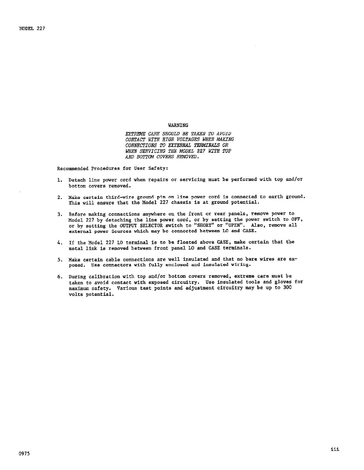
WARNING
EXTREME CARE SHOULD BE TAILFN TO AVOID
CONTACT WITR RIGH VOLTAGES WREN MAKING
CONNECTIONS n, EXTh?2NAL TERMIIULS OR
WREN SERVICING TRE MODEL 227 WITX TOP
AND BOTT(3.l COVERS RZMOVEV.
Recommended Procedures for User Safety:
2. Make certain third-wire ground pin an line power card ls connected fo earth ground.
This will ensure that the Model 227 chassis is at ground potential.
3. Before making connections anywhere on the front or rear panels, remove power to
Model 227 by detaching the line power cord, or by setting the power switch to OFF,
or by setting the OUTPUT SELECTOR switch to "SHORT" or "OPEN". Also, remove all
external power Sources which may be connected between LO and CASE.
4. If the Model 227 LO terminal is to be floated above CASE, make certain that the
metal link is removed between front panel LO and CASE terminals.
5. Make certain cable connections are well insulated and that no bare wires are ex-
posed. Use connectors with fully enclosed and insulated virinS.
6. During calibration with top and/or bottom covers removed, extreme care must be
taken to avoid contact with exposed circuitry. Use insulated tools and gloves for
maximm safety. Various test points and adjustment circuitry my be up to 300
volts potential.
0975 iii
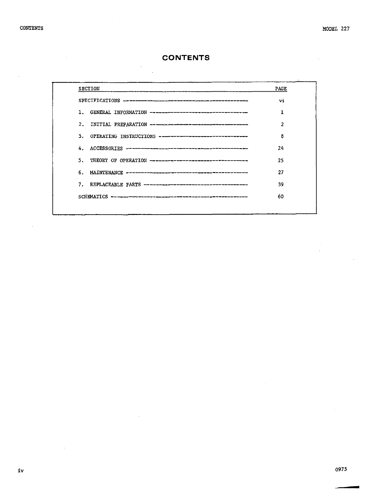
CONTENTS MODEL 227
CONTENTS
SECTION PAGE
SPECIFICATIONS __-__-_----_-_____________________ vi
1. GE- I&?,,mTION __-----_________-____________ 1
2. INITIAI. PREPARATION __--------___------_--- 2
3. ,,PE&Q-ING INS'fRUCTIONS --________-__-______----- 8
4. *CcESSlJRIES _----__---_-__-_____---------------- 24
5. THEORY OF OPEP\ATION __--________________----------- 25
6. MAINTEN)JCE ---_--___---__-_____---------------- 27
7. REPmCE&,LE PARTS __-______--___-___-____I___ 39
SYNDICS --__--------_____------------------------ 60
iv
0975
MODEL 227
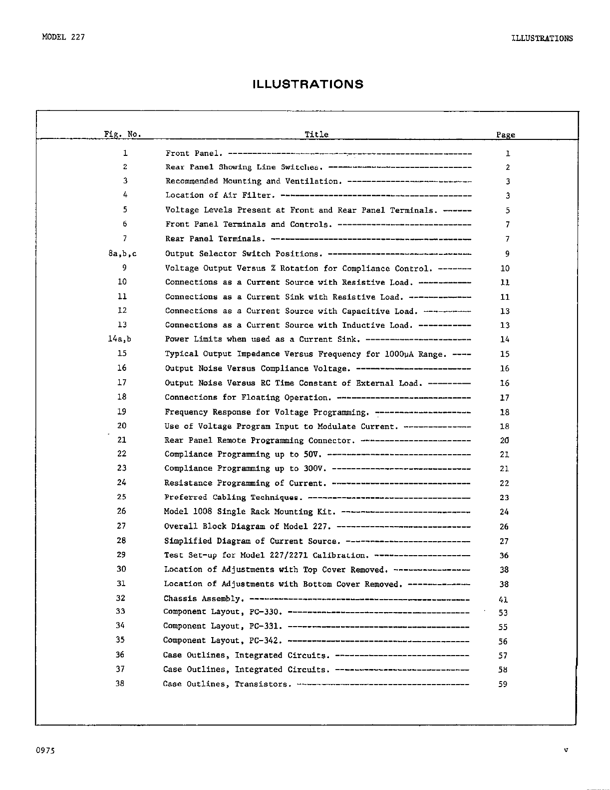
ILLUSTRATIONS
Fig. No. Title
Page
1
FrQ"f panel. ____________-__-__--______I_____________----- 1
2 Rear Panel Showing Line Switches. --------------------------- 2
3 Recommended Mounting and Ventilation. ------------------------ 3
4 LQc*tiQ" of *ir Filter. ------------------------------------- 3
5 Voltage Levels Present at Front and Rear Panel Terminals. ------ 5
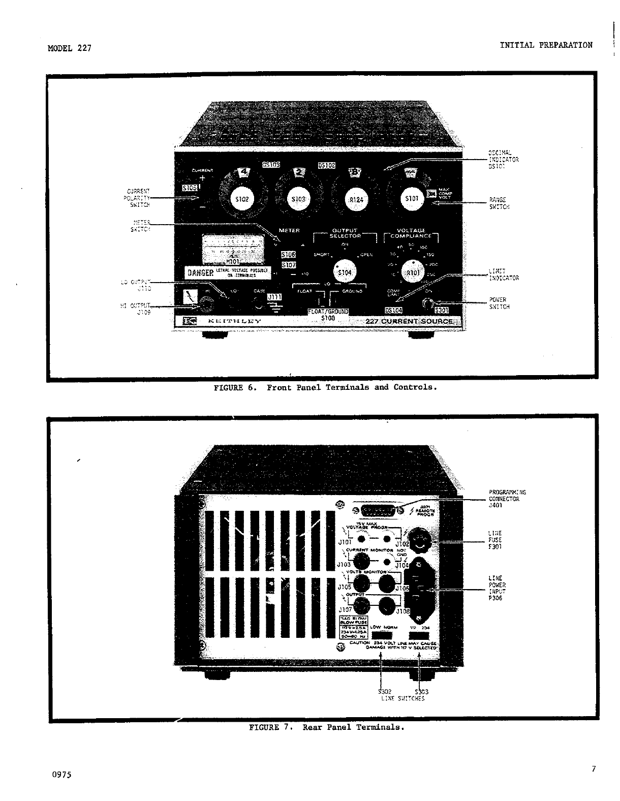
6 Front Panel Terminals and Controls. ---------------__-_--------- 7
7 Rear p**e1 Terminals. -------------------------------------- 7
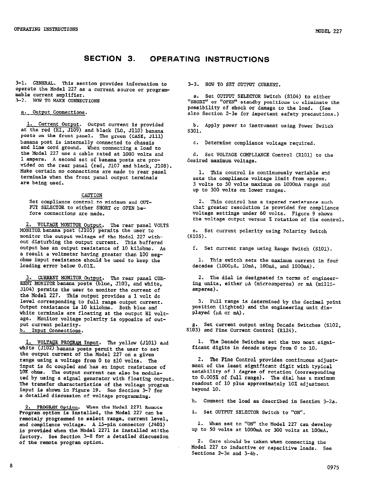
8a.b.c Output Selector Switch Positions. ------------------------------ 9
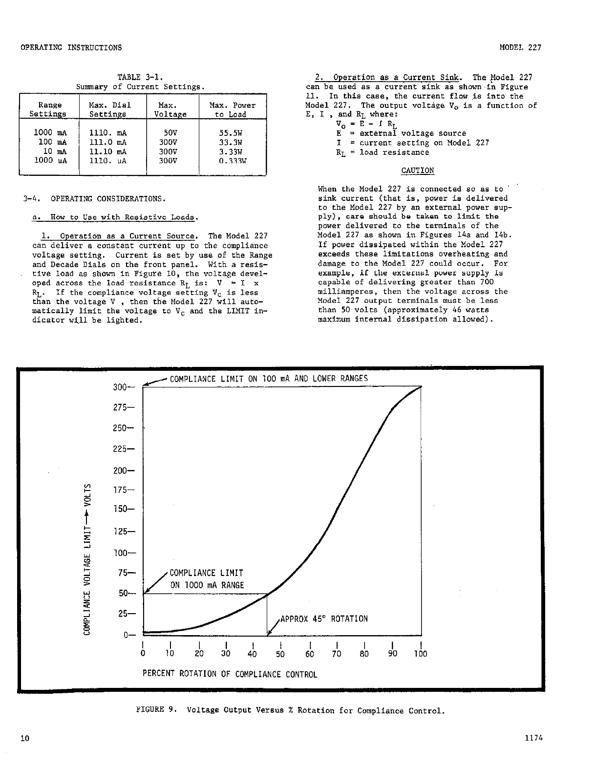
9 Voltage Output Versus % Rotation for Compliance Control. ------- 10
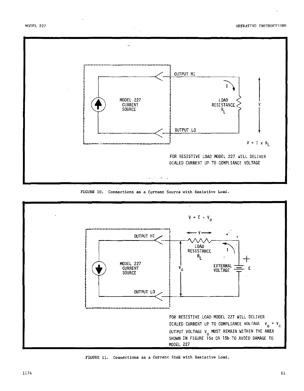
10 Connections as a Current Source with Resistive Load. ---------- 11
11 Connectians es a Current Sink wirh Resistive Load. ------------ 11
12 Connections as a Current Source with Capacitive Load. ---------- 13
13 Connecrfo"s as a Currenr Source with Inductive Load. ---------- 13
14a,b Power Limits when used as a Current Sink. --------------------- 14
15 Typical Output Impedance
Versus
Frequency for lOOOvA Range. ---- 15
16 Output Noise Versus Compliance
Voltage.
--------------------- 16
17 Output Noise Versus RC Time Conetant of External Load. ------- 16
18 Connections for Floating Operation. --------------------------- 17
19 Frequency Response for Voltage Programming. ------------------- 18
20 Use of Voltage Program Inpur to Modulate Current. -------------- 18
21 Rear panel Remote Progrenrming Connector. -------------------- 20
22 Compliance Progranrming to 5OV. ----------------------------
up 21
23 Compliance Programming to 3OOV. ----------------------------
up 21
24
Resistance Programming
of Current. --------------------------- 22
25 Preferred Cabling Te.=,,"iques. __-______________--------------- 23
26 Model 1008 Single Rack Mounting Kit. ------------------------ 24
27 Overall Block Diagram of Model 227. ---------------------------- 26
28 Simplified Diagram of Current Source. ------------------------- 27
29 Test Set-up for Model 22712271 Calibration. ------------------- 36
30 Location of Adjustments with Top Cover Removed. --------------- 38
31 Location of Adjustments with Bottom Cover Removed. ------------- 38
32 Chassis
Assembly.
---------_______________________________----- 41
33 Compo"e"t
Layout,
PC-330. ------------____-____________________ 53
34 component Layout, PC-331. ----------------------------------- 55
35 Component Layout, PC-342. ------------_-______________________ 56
36
Case Outlines, Integrated Circuits. ---------_--_-----_-----
57
37 Case Outlines, Integrated Circuits. ------------------------- 58
38 Case Ourlines, Transistors. __-_-------__-------____________ 59
0975
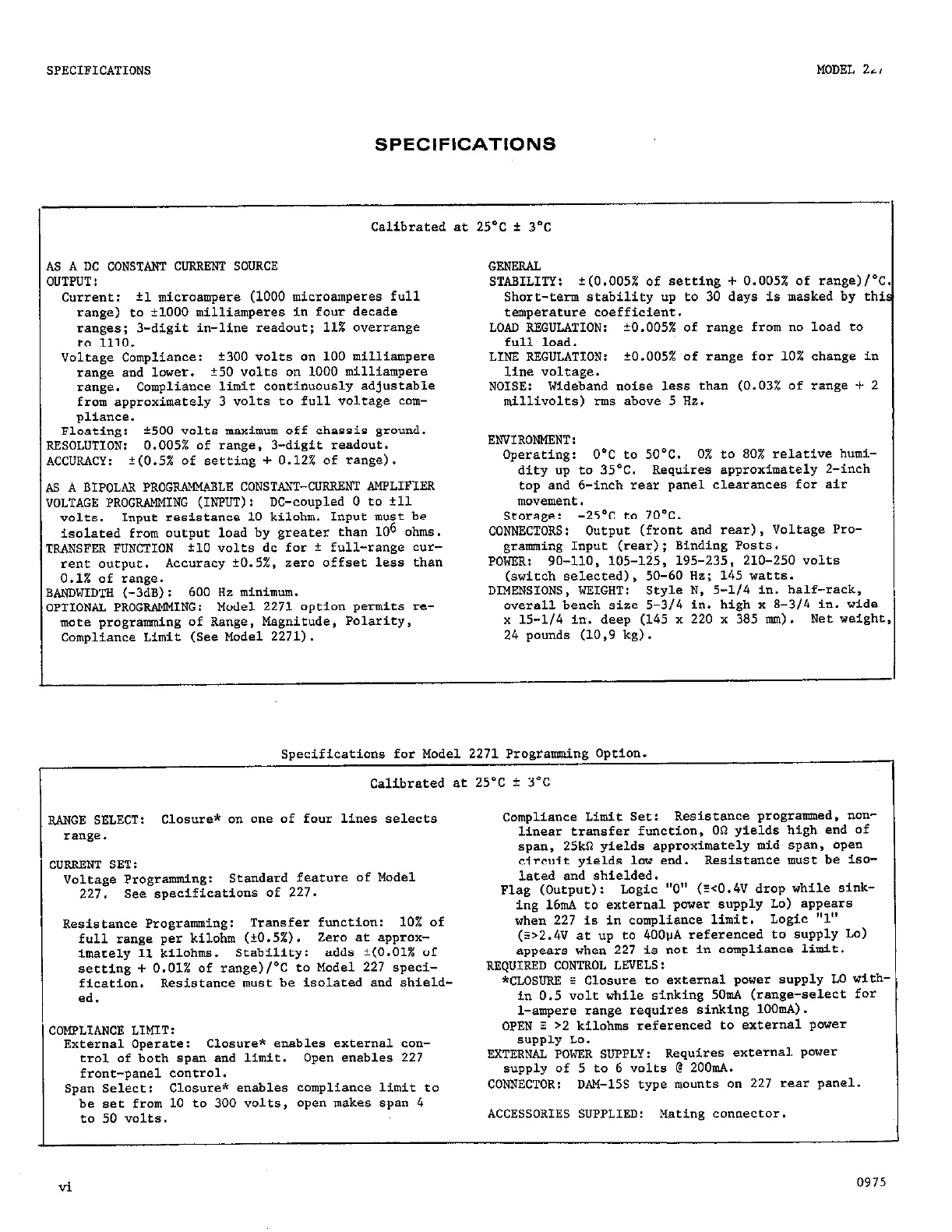
SPECIFICATIONS MODEL ZL,
SPECIFICATIONS
Calibrated et 25'C " 3*C
AS A DC CONSTANT CURRSNT SOURCE
OUTPUT:
current : ?l microampere (1000 microamperes full
range) to tlOO0 milliamperes in four decade
ranges; 3-digit in-line readout; 11% overrange
to 1110.
Voltage Compliance: *300 volts on 100 milliampere
range and lauer. f50 volts on 1000 milliampere
range. Compliance limit continuously adjustable
from appraximately 3 volts t0 full voltage cam-
plialXe.
Floating: 1500 volts maximum off chassis ground.
RESOLUTION: 0.005% af range, 3-digit readout.
ACCURACY: ?(0.5% of Betting + 0.12% of range).
AS A BIPOLAR PROGRAMMABLE
CONSTANT-C”RRRN’f
AMPLIFIER
VOLTAGE PROGRAMMING (INPUT): DC-coupled o to tll
volts. Input resistance 10 kilohm. Input must be
isolated from Output load by greater than 106 ohms.
TRANSFER FUNCTION t10 volts dc for f full-range CUT-
rent OUtpUt. Accuracy *0.5%, zero offset less than
0.1% of range.
BANDWIDTH (-3dB): 600 Hz minimum.
OPTIONAL PROGRAMMING:
Model 2271 option permits re-
mote programming of Range, Magnitude, Polarity,
Compliance Limit (See Model 2271).
GENERAL
STABILITY: C(O.O05% of Betting + 0.005% of =ange)/Y
Short-tefm stability up to 30 days is masked by thi
temperature coefficient.
LOAD R!.?GULATION: t0.005% of range from no load to
full load.
LINE REGULATION: +O.OOS% of range for 10% change in
line voltage.
NOISE: Wideband noise less than (0.03% of range + 2
millivolts) ~llls above 5 Hz.
ENVIRONMENT:
operating: O'C to 50°c. 0% to 80% relative humi-
dity up to 35'C. Requires approximately Z-inch
top and 6-inch rear panel clearances for air
movement *
storage: -25'=C to 70°C.
CONNECTORS: Output (front and rear), Voltage Pro-
gramring Input (rear); Binding Post=.
POWER: 90-110, 105-125, 195-235, 210-250 volts
(switch selected), 50-60 Hz; 145 watts.
DIMENSIONS, WEIGHT: Style N, 5-l/4 in. half-rack,
overall bench size 5-314 in. high x S-314 in. wide
x 15-l/4 in. deep (145 x 220 x 385 mm). Net weight
24 pounds (lo,9 kg).
Specifications for Model 2271 Programming Option.
Calibrated et 25'C i: 3°C
$.NGE SELECT:
Closure* on ane af four lines
selects
conlp11ance Limit set: Resistance programmed, nan-
range. linear transfer function, OR yields high end of
span, 25ko yields approximately mid span, open
:uRRRNT SET: circuit yields law end. Resistance must be iso-
Voltage Programming: Standard feature of Model lated end shielded.
227. see specifications of 227. Flag (Output): Logic "0" (sO.4V drop while sink-
ing 16mA t0 external power supply LO) appears
Resistance
Programming: Transfer function: 10% of when 227 16 in compliance limit. Logic "1"
full range per kilohm (?O.S%). Zero at approx- @2.4V at up to 400vA referenced to supply LO)
imately 11 kilohms. Stability: adds +(0.01X of appears when 227 is not in compliance limit.
setting + 0.01% of range)/"C to Model 227 speci- RRQUIRRD CONTROL LEVELS:
fication. Resistance must be isolated end shield- *CLOSUP.R z Closure to external power supply LO with,
ed. in 0.5 vale while sinking 5OmA (range-select for
l-ampere range requires sinking lOOmA).
:Ol@LIANCE LIMIT: OPEN E >2
kilohms referenced t0 external po"e=
External operate: Closure" enables external can- supply LO.
rrol af both span and limit. Open enables 227
EXTERNAL
POWER SUPPLY:
Requires external PO”e=
front-panel control. supply of 5 te 6 volts @ ZOO&..
span Select: Closure* enables compliance limit to CONNECTOR: DAM-15s type mounts on 227 =ee= panel.
be set fram 10 to 300 volts, open makes span 4
fO 50 volts. ACCESSORIES SUPPLIED: Mating connector.
vi 0975
MODEL 227
SECTION 1. GENERAL INFORMATION
GENERA,. INFORMATION
l-l. INTRODUCTION. The Model 227 is a dc current
source with full range current from 1 milliampere to
1000 milliamperes. The Model 227 provides a compli-
ance up to 300 volts on lmA, lOmA, and lOOmA ranges
or up to 50 volts on 1OOOmA range. The output is bi-
polar. Load regulation is ?0.005% of range from no
load to full load.
l-2. FEATURES.
a. Three digit readout has least significant
digit continuously adjustable using Fine Current
Control. Typical setability is 1 degree of rota-
tion (which corresponds to 0.005% of full range).
b. Compliance limit is adjustable up to 300 valcs.
e. Outpur can be floated to i500 volts above case.
d. Voltage programming input is standard.
e. Model 2271 Programming option is available
factory installed.
1-3. WARRANTY INPORMATION. The warranty ,is stated
on the inside front c.over of the manual. If there
is a need far service, contact your Keithley repre-
sentative or authorized repair facility as given in
our catalog. The Service Form supplied at the back
of the manual should be used to provide the repair
facility with adequare information concerning any
difficulty.
1-4. CHANGE
NOTICE.
Improvements or changes to the
instrument not incorporated into rhe manual will be
explained on a yellow change notice sheet attached
to the inside back cover of the manual.
1-5. PROGRAMMING OPTION. The Model 2271 is a fac-
tory-installed option which enables remote program-
ming of range, magnitude, polarity, and compliance.
Current magnitude and compliance can be resistance
programmed. Range and compliance maximum are selec-
ted by means of closure to external power supply com-
cm*. An external +5 volt supply is required to ener-
gize relay coils in the Model 2271.
0975 1
INITIAL PREPARATION MODEL 227
SECTION 2. INITIAL PREPARATION
2-l. GENERAL. This section provides information
needed for incoming inspection and preparation for
use.
2-2. INSPECTION. The Model 227 was carefully in-
spected both mechanically and electrically before
shipment. Upon receiving the instrument, check for
any obvious damage which may have occurred during
transit. Report any damages to the shipping agent.
To verify the electrical specifications, follow the
procedures in Section 5.
2-3. PREPARATION FOR "SE.
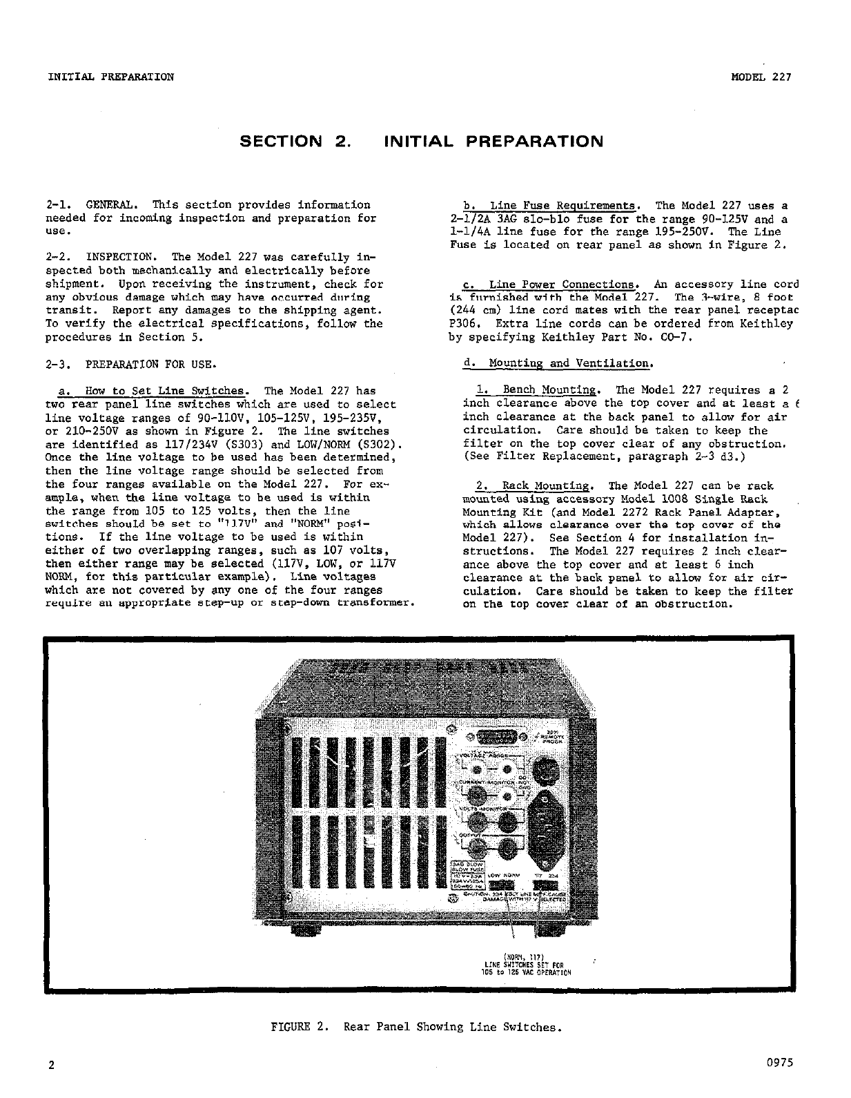
a. How to Set Line Switches. The Model 227 has
two rear panel line switches which are used to select
line voltage ranges of 90-llOV, 105-125V, 195-235V,
or ZlO-250V as shown in Figure 2. The line switches
are identified as 117/234V (S303) and LOW/NORM (5302).
Once the line voltage to be used has been derermined,
then the line voltage range should be selected from
the four ranges available an the Model 227. For ex-
ample, when the line voltage to be used is within
the range from 105 to 125 volts, then the line
switches should be set
fo “117V”
and "NORM" pasi-
tions . If the line voltage to be used is within
either of two overlapping ranges, such as 107 volts,
then either range may be selected (117V,
LOW,
or 117V
NORM, for this particular example). Line voltages
which are not covered by my one of the four rages
require an appropriate step-up or step-down transformer.
b. Line Fuse Requirements. The Model 227 uses a
2-1/2A 3AG slo-blo fuse for the range 90-125V and a
l-1/4A line fuse for the range
195-25OV. The
Line
Fuse is located an rear panel a8 shown in Figure 2.
C. Line Power Connections. An accessory line cord
ia furnished with the Model 227. The 3-wire, 8 foot
(244 cm) line cord mates with the rear panel receptac
P306. Extra line cords can be ordered from Keithley
by specifying Keithley Part NO. CO-7.
d. Mounting and Ventilation.
1. Bench Mounting. The Model 227 requires a 2
inch c1earanc.e above the tar, cover and ar least a 6
inch clearance at the back panel to allow for air
circulation. Care should be taken to keep the
filter an the top cover clear of any obstruction.
(See Filter Replacement, paragraph 2-3 d3.)
2. Rack Mounting. The Model 227 can be rack
mounted usins accessorv Model 1008 Sinele Rack
Mounting
Kit (and Model 2272 Rack Panel Adapter,
which allows clearance over the tap cover of the
Model 227). See Section 4 for installation in-
structions. The Model 227 requires 2 inch clear-
ance above the top cover and at least 6 inch
clearance at the back panel to allow for air cir-
CUlEdOlI.
Care should be taken to keep the filter
on the tap cover clear of an obstruction.
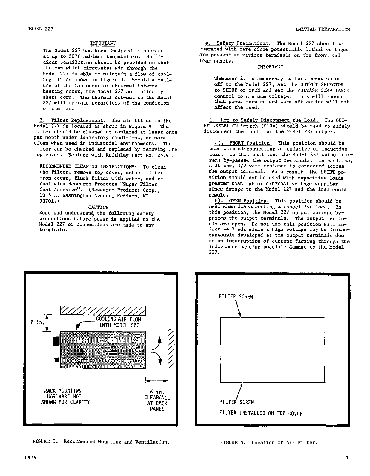
FIGURE 2.
Rear
Panel Showing Line Switches.
0975
MODEL 22,
IMPORTANT
The Model 227 has been designed to operate
at up to 5O'C ambient temperature. Suffi-
cient ventilation should be provided so that
the fan which circulates air through the
Model 227 is able to maintain a flow af.cool-
ing air as shown in Figure 3. Should a fail-
"re of the fan occur or abnormal internal
heating occur, the Model 227 automatically
shuts down. The thermal c"t-""t in the Model
227 will operate regardless of the condition
of the fan.
3. Filter Replacement. The air filter in the
Model 227 is located as shown in Figure 4. The
filter should be cleaned or replaced at least once
per month under laboratory conditions, or more
often when used in industrial environments. The
filter can be checked and replaced by removing the
top ccNer. Replace with Keithley Part No. 25791.
RECOMMENDED CLEANING INSTRUCTIONS: To clean
the filter, remove top cover, detach filter
from cover, flush filter with water, and re-
coat with Research Products "Super Filter
Coat Adhesive". (Research Products Corp.,
1015 E. Washington Avenue, Madison, WI.
53701.)
CAUTION
Read and underera"< the following safety
Precautions before power is applied to the
Model 227 or co"nections are made co any
tKGIi"SlS.
INITIAL PREPARATION
e. Safety
Precautions.
The Model 227 should be
operated with care since potentially lethal voltages
are present at various terminals on the front and
rear panels.
IMPORTANT
whenever it is **ce**ary to turn power on or
off to the Model 227, set the OUTPUT SELECTOR
to SHORT or OPEN and set the VOLTAGE COMPLIANCE
control to minimum voltage. This will ensure
that power turn an and t"fn off action "ill not
affect the load.
1. How co Safely Disconnect the Load. The OUT-
PUT SELECTOR Switch (SlO4) should be used to safely
disconnect the load from the Model 227 o"tp"t.
a). SHORT Position. This position should be
used when disconnecting a resistive or inductive
load.
In
this position, the Model 227 output cur-
renf by-passes the output terminals. In addirion,
a 10 ohm, l/2 watt resistor is connected across
the o"tp"t terminal. As a result, th.e SHORT po-
sition should not be used with capacitive loads
greater than l!,F or external voltage supplies
since damage to the Model 227 and the load could
result.
b).
OPEN Position. This position should be
used when disconnertina a caxacitive load. 1n
this position, the Mod;1 227'auQut current by-
passes the output terminals. The output termin-
als are open. Do not use this position with in-
ductive loads since a high voltage may be instan-
taneously developed at the output terminals due
to an interruption of current flawing through the
inductance causing possible damage to the Model
227.
RACK MOUNTING
HARDWARE NOT
SHOWN FOR CLARITY
6 in.
CLEARANCE
AT BACK
PANEL
FILTER SCREW
\
III
I
FILTER SCREW
FILTER INSTALLED ON TOP COVER
FIGURE 3. Recommended Mounting and Ventilation.
0975
FIGURE 4. Location of Air Filter.
INITIAL
PREPARATION MODEL 227
2. How to Safely Use Front and Rear Terminals.
(See Figure 5 and Table 2-l for a complete listing
of all voltages present.)
4. Front and Rear Panel HI Terminal 0109,
5107). These terminals provide current output up
to the maximum compliance voltage as set on rhe
Model 227 (either by front panel range switch or
by Model 2271 Remote Programming). As a result,
the terminals can be up to 305 volts above LO
(Black) depending o" range selected. If ehe LO
eerminal is floating at 500 volts above CASE
(Green), the" up to 805 volts can be present at
HI. Far operator safety, set COMPLIANCE LIMIT
to minimum or set OUTPUT SELECTOR Switch to "SHORT"
or "OPEN".
b). Front and Rear Panel LO Terminal.
Ter-
minals JllO (Black) and J108 (Black) can be at
500 volts if
LO
is floating above CASE (Green).
c).
VOLTAGE PROGRAMMING Terminal. Terminals
JlOl (Blue) and 5102 (Black) float at output HI
potential and can be up to 306 volts above oufp"f
LO (Black).
d). CURRENT MONITOR Terminals. Terminals 5103
and 3104 float at output HI potential and can be
up to 305 vales above ouepue LO.
e) .
VOLTS MONITOR Terminal. Terminal J105 is
a buffered oucpur and can be up to 305 volrs
above output
LO. Terminal 5106 at the same
po-
teneia1 as
output LO.
TABLE 2-l.
Voltages at Front and Rear Panel Terminals.
Maximum Voltage
Ci*C"it Referenced ea CASE Jill
Desig. Grounded
LO I Floating LO
J109 (Front)
305 " 805 "
5107 (Rear) 305 " 805 "
OUTPUT LO
OUTPUT
LO
JllO (Front) 0"
I
500 "
JlO8 (Rear) 0" 500 "
VOLTS
MONITOR HI
VOLTS MONITOR LO J105
5106 I
305 "
I
805 "
0" 500 "
CURRENT MONITOR HI*
5103 I
305 " I 805 "
CURRENT
MONITOR
LO*
5104
306 V 806 "
VOLT PROGRAM HI*
VOLT PROGRAM LO* JlOl
I
306 "
I
806 "
5102
306 " 806 "
RESISTANCE PROGRAM In* 5401, pi" 2 306 " RO6 "
RESISTANCE PROGRAM Lo* 5401, pi" 10 306 " 806 "
*IMPORTANT
These terminals are
fused by FlOl which is a type 8AG fast-acting fuse
rated at 0.125 amperes. A short circuit to output LO will cause the
fuse to blow within 5 seconds. w: Instantaneous currenf could
exceed ZOOmA until fuse blows.
1174
MODEL
227
INITIAL
PREPARATION
t
WMNING! THESE POINTS CAN SAVE
A COMPLIANCE VOLTAGE UP TO 305
VOLTS AT 100 MILLIAMPERES. EX-
CEPT FOR OUTPUT RIGS ALL POINTS
ARE INTEZ?NALLY FUSED.
CURRENT MONITOR
J104
0.125A 1V
5103
VOLTS MONITOR HI
J105
REAR PANEL
5107
*
J108
OUTPUT LO
FRONT PANEL
t
OUTPUT HI
J109
E
LOAD
JllO
OUTPUT LO
S108
FLOAT/GROUND
SWITCH
Jill
= FR
A
THIRD WIRE -L
ON LINE CORD
FIGURE 5.
""lt=ge Levels Present at Front
and Rear Panel
Tern,inals.
5
INITIAL PREPARATION MODEL 227
00*t*01 or C""*ector
Front Panel
Power Switch (S301)
OUTPUT SELECTOR Switch (S104)
Description
Paraaraph
Applies power to instrument. 3-3b
Sets output configuration. (Should be used to safely dis- 2-3e
connect the output load.)
Range Switch (SlOl) Sets full range current in decade stepe (lOOOuA, lOmA, lOOmA, 3-3f
end 1OOOmA).
Decade Selector Switches (S102, S103) These switches are used with Fine Current Control to set cur- 3-3g
rent output. Each switch has discrete decade steps from 1
to 10, while the Fine Current Control is continuously ad-
justable.
Fine Current Control (R124) Adjusts current between 0.000 to 0.011 times full range. 3-3g
This control is continuously adjustable. Typical set-
ability of 1 degree of rotation or 0.005% of full range.
C"RRENT Polarity Switch (S105) sees output polarity. 3-3e
VOLTAGE COMPLIANCE (RlOl) Adjusts compliance voltage limit up to 300 volts. 3-3d
XZETER "/A Switch (S106) Sets meter to read voltage or current.
'IETER Xl/X10 Switch (5107) Sets meter sensitivity for scale factor of Xl or x10.
COMP
LIMIT
Indicator (X104) Indicates compliance limit mode when lighted. 3-4a.l
Dutput RI (JlOS) C""necti"" to output HI. (In parallel with 5107.) 3-2al
Output LO (JllO)* Connection to output LO. (In parallel with 5108.) 3-2al
CASE (X11)* Chassis ground.
FLOAT/GROUND Switch (SlO8) (Connected to third wire ground.) 3-2al
Connects LO end CASE when set to GROUND.
Rear Panel
REMOTE
PROGRAM (5401)
TOLTAGE PROGRAM (JlOl, 5102)
CURRENT MONITOR (5103, 5104)
VOLTS MONITOR (JlO5, 5106)
3utput HI, LO (5107, 5108)
Provides inputs and outputs for range, current, end voltage 3-2b2
control. (Available when Model 2271 option is installed.)
Provides input for voltage programing. 3-2bl
Provides output for monitoring current (1" = Full Range). 3-2a3
Provides output for monitoring voltage (up to 300 volts) 3-2a2
Outputs which are in parallel with front panel HI and LO. 3-2al
NOTE*
On some models a Shorting link is provided to connecf LO end CASE. On models presently manufactured,
banana type terminals are used instead of binding post type and the shorting link is no longer used. A
front panel FLOAT/GROUND Switch has been added to permit a connection between LO end CASE for grounded
applications.
0975
I
MODEL 227 INITIAL PREPARATION i
I
-
0975 7
OPERATING INSTRUCTIONS
SECTION 3. OPERATING INSTRUCTIONS
MODEL 227
3-1. GENERAL. This section provides information to
operate the Model 227 es a current eource or progrem-
meble current amplifier.
3-2.
HOW
TO MAKE CONNECTIONS
8. OutPut Co""ectio"s.
1. current Output. Output current is provided
at the red (HI, JlO9) and black (LO, JllO) be"e"e
p0st.8
OXI the front panel. The green (CASE, ~111)
banana post is internally connected to chassis
and line cord ground. Whe",connecti"g a load to
the Model 227 "se a cable rated at 1000 volts and
1 ampere. A second set of banana posts are pro-
vided on the rear panel (red, 5107 end black, 5108).
Make certain no connections are made to rear panel
terminals when the front panel output terminals
are being used.
Set compliance contwl to minimum and OUT-
PUT SELECTOR to either SHORT or OPEN be-
fore co""ecti,,"s are made.
2. VOLTAGE MONITOR Output. The rear panel VOLTS
MONITORbanana post (JlOS)
permits
the user‘ to
monitor the out&t voltage bf the Model 227 with-
out disturbing the outp,,t current. This buffered
output has a" output resistance of 10 kilohms. As
a result a voltmeter having greeter than 100 meg-
ohms input resistance should be used to keep the
loading error below 0.01%.
3. CURRENT MONITOR Output. The rear panel CUR-
RENT MONITORbanana posts (blue. 3103. and white.
5104) permits the usa to &,"itbr the current of
the Model 227. This output provides a 1 volt dc
level corresponding to full range output curre"t.
Output resistance is 10 kilohms. Both blue and
white terminals are floatine. at the outhit HI voit-
age. Monitor
voltage polarity is opposite of o"t-
put current polarity.
b. Input connect.ions.
1. VOLTAGE PROGRAM Input. The yellow (5101) a.ld
white (5102) banana poets petit the user to set
the o"tput current of the Model 227 ofi a given
range wing a voltage from 0 to t10 volts. The
input is dc coupled and has 8" input resistance of
1OK ohms. The o"tput current can also be modula-
ted by using e signal generator with floating o"tput.
The transfer characteristics of the voltage program
input is show" in Figure 19. See Section 3-7 for
a detailed discussion of voltage programming.
2. PROGRAM Option. When the Model 2231 Remote
Program option is installed, the Model 227 can be
remotely programmed to select range, current level,
and compliance voltage. A 15-pi" connector (5401)
is provided when the Model 2271 is installed atlthe
factory.' See Section 3-S for a detailed discussion
of the remote program option.
3-3. HOW TO SET OUTPUT CURRENT.
a. Set OUTPUT SELECTOR Switch (S104) to either
"SHORT" or "OPEN" standby positions to eliminate the
possibility of shock or damage to the load. (See
also Section 2-3e for important safety precautions.)
b. Apply power to instrument using Power'Switch
s301.
C. Determine compliance voltage required.
d. Set VOLTAGE COMPLIANCE Control (RlOl) to the
desired maximum voltage.
1. This control is continuously variable end
sets the compliance voltage limit from apprax.
3 volts to 50 volts maximum on 1OOOm.A range and
up to 300 volts on lower ranges.
2. This control has a tapered resistance such
that greater resolution is provided far compliance
voltage settings under 60 volts. Figure 9 shows
the voltage output vereus % rotation of the control.
&5,. Set current polarity using Polarity Switch
f. Set current range using Range Witch (SlOl).
1. This-switch sets the maximum current in fout
decades (lOOO@. lOmA, lOOmA, and 1OOOmA).
2. The dial is designated in terms of engineer-
ing units, either PA (microamperes) or mA (milli-
amperes).
3. Full range is determined by the decimal point
position (lighted) and the engineering unit die-
played (PA or mA).
Set current outpltt using Decade Switches (S102.
Sl!;) and Fine Current Control (R124).
1. The Decade Switches set the two most signi-
ficant digits in decade steps from 0 to 10.
2. The Fine Control provides continuous adjust-
ment of the least significant digit with typical
setability of 1 degree of rotation (corresponding
to 0.005% of full range). The dial has a maximum
readout of 10 plus approximately 10% adjustment
beyond 10.
h. Connect the load es described in Section 3-2a.
i. Sef OUTPUT SELECTOR Switch to "ON".
1. When set to "ON" the Model 227 can develop
"P to 50 volts at 100OmA or 300 volts at lOOmA.
2. Care should be take" when connecting the
Model 227 to inductive or capacitive loads. see
Sections 2-3e and 3-4b.
0975
MODEL 227 OPERATlNG INSTRUCTIONS
FIGURE 8a.
"OPEN" POSITION
NO VOLTAGE IS DEVELOPE
ACROSS OUTPUT TERMINAL
FIGURE 8b.
"ON" POSITION
FIGURE 8~.
"SHORT" POSITION
NO VOLTAGE IS DEVELOPE
ACROSS OUTPUT TERMINAL
Si
I..
2 IUTPUT HI
I
SHORT
3
I
.“7‘
1
I-
i( IUTPUT LO
7
.I
. . . . . . . . . . . . . . . . . . * . . . . . . . . . . . . . . . . . . . . . . . . . . . . . . . . . . . . . . . . . . .
‘..
iI KITPUT HI
T
LOAD
II XITPUT LO 1
-i
.:
LOAD
OPEN I cfo4c 1
iC
- y
IUTPUT HI
I
1
LOAD
1 i 1 < /001PuT LD 1
. . . . . . . . . . . . . . . . . . . . . . . . . . . . . . . . . . . . . . . . . . . . . . . . . . . . . . ..-...... :
V=IxR
1174
FIGURE Sa,b,c. Output Selector Switch Positions.
9
OPERATING INSTRUCTIONS MODEL 227
TABLE 3-1. 2. Operation as a Current Sink. The Model 227
Sumnary of Current Settings. can be used as a current sink as shown.& Figure
11. In this case, the current flow is into rhe
Range Max. Dial Max. Max. Power Model 227. The output voltzige V, is a function of
Settings Settings Voltage to Load E, I , and RL where:
1000 mA 1110. mA 5ov ", = E - I RL
55.5w
E = external voltage source
100 mA 111.0 r&A
3oov 33.3w
I = c"rrent setting on Model 227
10 mA
11.10 mA. 3oov 3.338
1000 UA RL = load resistance
1110. "A 3oov 0.333w m
3-4. OPERATING CONSIDERATIONS.
a. How to Use with Resistive Loads.
1. Operation as a Current Source. The Model 227
can deliver a constant current UD to the compliance
voltage setting. Current
is
set-by use
of the Range
and Decade Dials an the franc panel. With a resis-
tive load as shown in Figure 10, the voltage devel-
oped across the load resistance RL is: V = I x
RL. If the compliance voltage setting V, is less
than the voltage V , then the Model 227 "ill auto-
matically limit the voltage to V, and the LIMIT in-
dicator will be lighted.
When the Model 227 is connected so a6 to. .'
sink current (that is, power is delivered
to the Model 227 by an external power sup-
ply),
care should be taken to limit the
power delivered to the terminals of the
Model 227 as shown in Figures 14a and 14b.
If power dissipated within the Model 227
exceeds these limitations overheating and
damage to the Model 227 could occur. For
example, if the external power supply is
capable of delivering greater than 700
milliamperes, then the voltage across the
Model 227 output terminals must be less
than 50 volts (approximately 46 watts
maximum internal dissipation allowed).
,nn_ /COMPLIANCE LIMIT ON 100 MA AND LOWER RANGES
275-
250-
225-
zoo-
COMPLIANCE LIMIT
ON 1000 mA RANGE
2 25-
5
APPROX 45' ROTATION
O-
b 20 ;o 3b 4b 50 6b 7b 20 do d0
PERCENT ROTATION OF COMPLIANCE CONTROL
FIGURE 9. Voltage
Output
Versus
% Rotation for Compliance Control.
10 1174
MODEL 22,
OPERATING INSTRUCTIONS
.,...........................................~....... *..i
~ +% 1. RESk;j 1
; . . . . . . . . . . %" . . . . . ..-.............*....... ~ . . . . . . . . . . . i V- IxRt
FOR RESISTIVE LOAD MODEL 227 WILL DELIVER
DIALED CURRENT UP TO COMPLIANCE VOLTAGE
FIGURE 10. Connections as a Current Source with Resistive Load.
V=E-V 0
FOR RESISTIVE LOAD MODEL 227 WILL DELIVER
DIALED CURRENT UP TO COMPLIANCE VOLTAGE VO = Vc
OUTPUT VOLTAGE VO MUST REMAIN WITHIN THE AREA
SHOWN IN FIGURE 15a OR 15b TO AVOID DAMAGE TO
MODEL 227
FIGURE 11. Connections as a Current Sink with Resistive Load.
1174 11
OPERATING
INSTRUCTIONS MODEL 227
b. How to Use with Capacitive or Inductive Loads.
1. Capacitive Load. When a capacitive load is
connected, the Model 227 delivers a constant cur-
rent until the voltage developed reaches the com-
pliance voltage setting V,. The voltage V, charges
to a maximum V, according to the fallowing equation:
V, = $ I I
dt up to Vc (maximum)
where C = load capacitance
When using a capacitive load, it is preferred to
"se the "OPEN" standby position when not making
measurements to avoid shock hazard due to compli-
ance voltage at the o"tp"t terminals. Do not "se
ehe "SHORT" position since the voltage on the cap-
acitive load will be discharged.
2. Inductive Load. When an inductive load is
connected, the Model 227 delivers a constant cur-
rent the same as for a resistive load. However, to
maintain stability the ratio load inductance L
(Henries)
to
load
resistance R
(ohms) should be
smaller than approximately lo-&. This ratio is
non-linear and depends on the amount of inductance
and the range so that larger values of L/R may be
needed to prevent oscillations. A typical calcula-
tion of the L-Co-R ratio is as follows:
For R = 1000 ohms and L = 1 millihenry,
L,R = 1 x 10-311
lO"Q = 1 x 10-S
If oscillations occur at the output, add series re-
sistance to lower the L-to-R ratio. When using an
inductive load, it is preferred to use the "SHORT"
standby position when not making measurements to
avoid shock hazard due to open terminals. Also,
the current should be dialed to zero before dis-
connecting an inductive load.
C. How to Use the Compliance Control. The compli-
amce control sets the maximum comcJiance from BDI)TOX-
irately 3 volts to 50 volts on the 1OOOmA range'and
from approximately 3 volts to 300 volts on lmA, lOmA,
and lOOmA ranges. The compliance voltage should be pre-
set with no load connected. The front panel irieter can
be used as a guide to setting compliance. (set
METER switches to V and Xl or Xl0 as appropriate.)
The rear panel
VOLTS
MONITOR
output can
be used to
adjust the compliance more accurately. Use a volt-
meter with an input resistance of at least 100 meg-
ohms to avoid loading error at VOLTS MONITOR o"tp"t.
The control has a tapered characteristic such that
the first 50% of rotation represents a variation
from 3 to 60 volts to allow more resolution at lower
COmpliSnCSS.
3-5. MEASUREM%NT
CONSIDERATIONS.
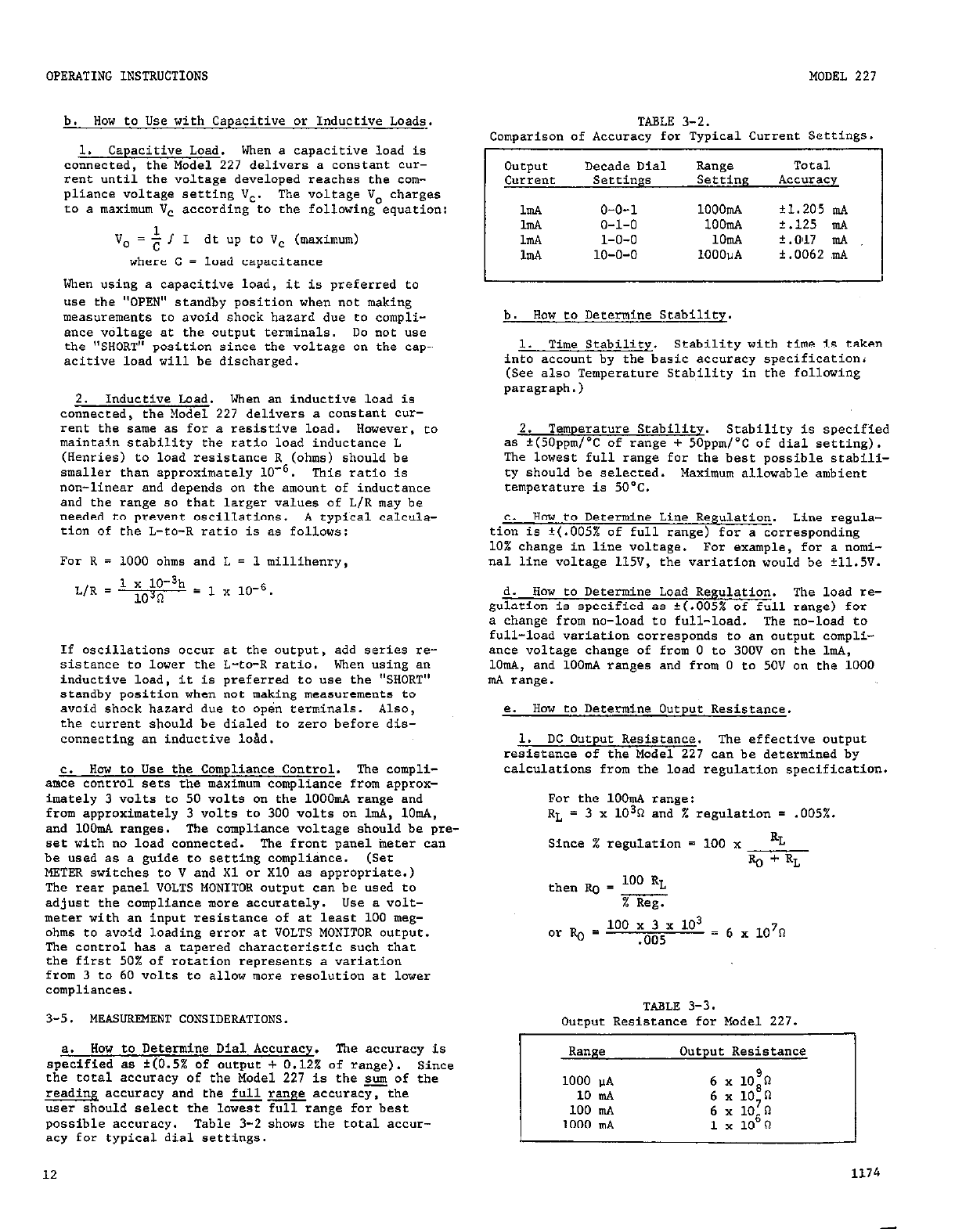
a. How to Determine Dial Accuracy. The accuracy is
specified as f(0.5% of o"tp"t + 0.12% of range). Since
the total accuracy of the Model 227 is the sum of the
reading accuracy and the full range acc"rac;;-the
user should select the lowest full range for best
possible accuracy. Table 3-2 shows the total accur-
acy for typical dial settings.
12
TABLE 3-2.
comparison of Accuracy for Typical current settings.
Output Decade Did Range Total
current Settings settiw, Accuracy
1mA o-o-1 lOOOm4
il.205 ISA
1mA O-1-0 lOOmA t.125 mA
lll!A 1-o-o 1omA
0'17 mA
l!llA 10-O-O 1OOOliA
f.0062 .mA
b. HOW to Determine Stability.
1. Time Stability. Stability wirh time is taken
into account by the basic accuracy specification;
(See also Temperature Stability in the fallowing
paragraph.)
2. Temperature Stability. Stability is specified
as k(SOppm/'C
of range + 50ppml'C of dial setting).
The lowest full range for the best possible stabili-
ty should be selected. Maximum allowable ambient
temperature is 5O'C.
c. How to Determine Line Regulation. Line regula-
tion is t(.OO5% of full range) for a corresponding
10% change in line voltage. For example, far a nami-
nal line voltage 115V, the variation would be +11.5V.
d. How to Determine Load Regulation. The load re-
gulation is specified as ?(.005% of full range) for
a change from no-load to full-load. The no-load to
full-load variation corresponds co an output campli-
ace voltage change of from 0 to 3OOv on the lmA,
lOmA, and lOOmA ranges and from 0 to 50V on the 1000
mA range.
e. How to Determine 0"tp"t Resistance.
1. DC Output
Resistance.
The effective output
resistance of the Model 227 can be determined by
calculations from the load regulation specification.
For the lOOmA range:
RL = 3
x lOSO and % regulation = .005%.
Since % regulation - 100 x RL
Ro + RL
then RIJ = 100 RL
mgr
or R. = 100 x 3 x 103
.005 = 6 x 10⁷n
TABLE 3-3.
Output Resisfance for Model 227.
Range
1000
“A
10 mA
100 mA
1000 mA
Output Resistance
6
x 10'0
6
x 10'0
6
x 10'0
1 x lo60
1174
FOR CAPACITIVE LOAD MODEL 227 WILL DELIVER
DIALED CURRENT UNTIL COMPLIANCE VOLTAGE ",
IS REACHED
FIGURE 12. Connections as a Current Source with Capacitive road.
: . . . . . . . . . . . . . . . . . . . . . . . . . . . . . . . . . . . . . . . . . . . . . ..-... ~
LOAD
INDUCTANCE
CL)
% . . .._........_.._..................................i
FOR INDUCTIVE LOAD MODEL 227 WILL DELIVER
DIALED CURRENT UP TO COMPLIANCE VOLTAGE
FIGURE 13. Connecrions as a current source with Inductive Load.
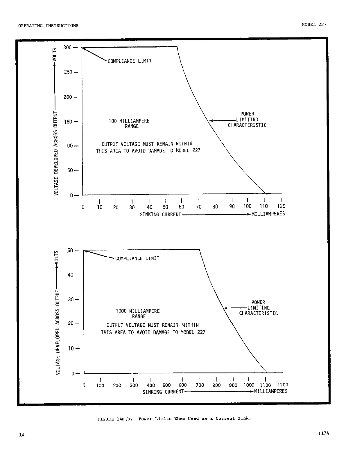
OPERATING 1NSTR"CTIONS
MODEL 227
\
COMPLIANCE LIMIT
\
100 MILLIAMPERE
RANGE CHARACTERISTIC
OUTPUT VOLTAGE MUST REMAIN WITHIN
THIS AREA TO AVOID DAMAGE TO MODEL 227
\
I I I I I I I I I I I I I
0 10 20 30 40 50 60 70 80 90 100 110 120
SINKING CURRENT *MILLIAMPERES
r
G
COMPLIANCE LIMIT
I
40-
5
it:
2 30-
z 1000 MILLIAMPERE
2 RANGE CHARACTERISTIC
2 20- OUTPUT VOLTAGE MUST REMAIN WITHIN
E:
% THIS AREA TO AVOID DAMAGE TO MODEL 227
d
z 10'
s
5
z n-
I I I I I I I I I I I
0 IdO 200 300 400 500 600 7:O 800 900 1000 1100 1200
SINKING CURRENT *MILLIAMPERES
14 1174
MODEL 227 OPEiATING INSTRUCTIONS
lO’Q--
109 -
108 -
5
2 lo3 -Jo1 ’
0.01
I
I I I
2 0.1 100 1000 10K
FREQUENCY
- HZ
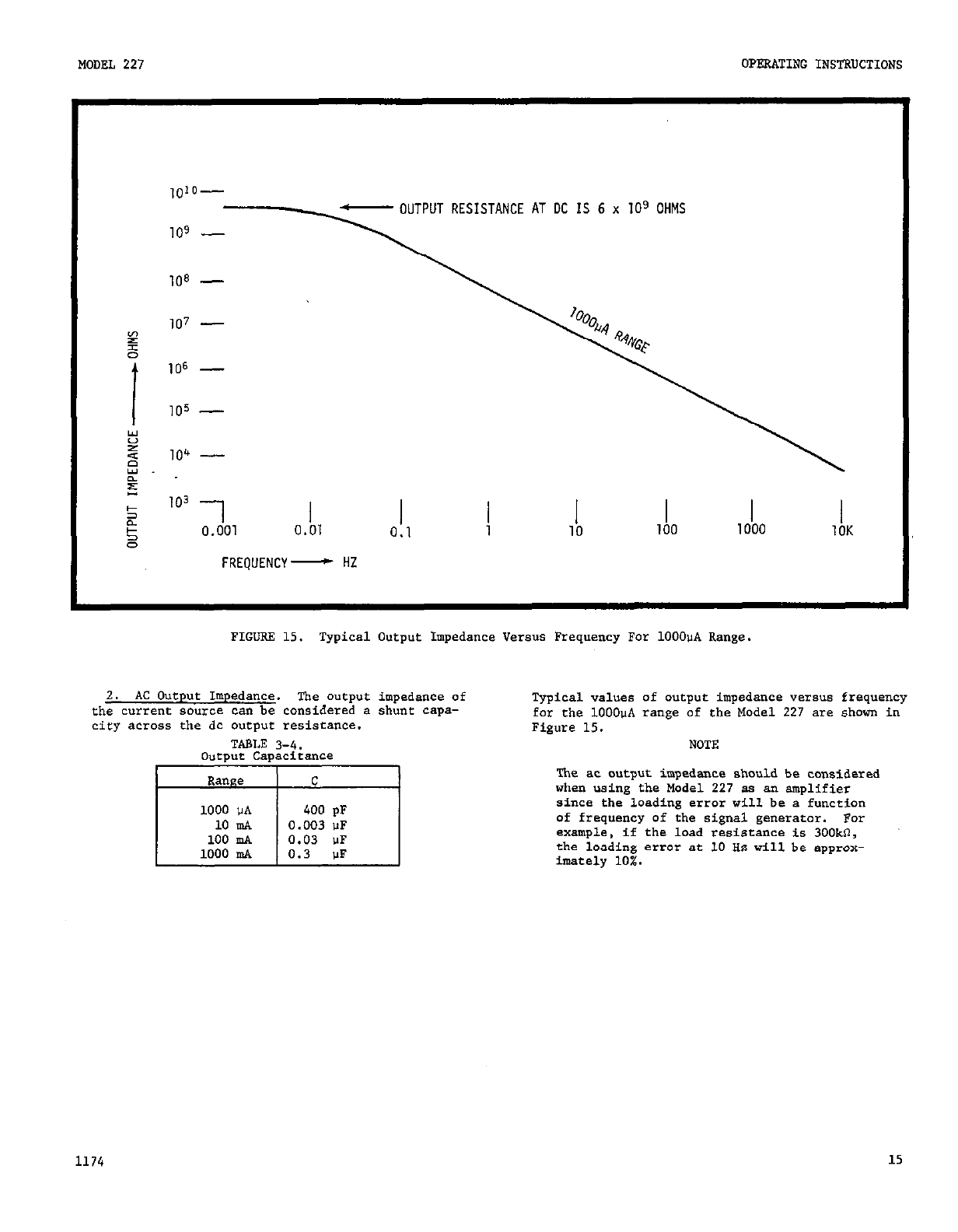
FIGURE 15. Typical Output Impedance Versus Frequency For lOOOvA Range.
2. AC Output Impedance. The output impedance of
the current source can be considered a shunt capa-
city across the dc output resistance.
TABLE 3-4.
output Capacifance
Typical values of output impedance versus frequency
far the IOOOpA range of the Model 227 are show! in
Figme 15.
NOTE
The ac output impedance should be considered
when using the Model 227 as an amplifier
since the loading error will be a function
of frequency of the signal generator. For
example, if the load resistance is 300k0,
the loading error at 10 HZ will be approx-
1174 15
OPERATING
INSTRUCTIONS
MODEL 227
f. How to Determine Output Noise. The Model 227
output noise is composed of two components: line
frequency ripple (lZO/lOQ Hz) and high frequency noise.
1. Line Frequency Ripple. This noise is essen-
tially a constant percentage of range.
2. High Frequency Noise. This noise is a con-
*t*nt voltage.
The sum of the t"o components can bg platted versus
compliance voltage 88 shcwn in FigFre 16. The rms of
range-current noise as a percent of the Model 227
range cm be obtained in two ways. First, the percent
noise at a specific compliance voltage can be deter-
mined. For example, for a compliance voltage of 5
volts, the percent noise would be 0.07% as read from
Figure 16 of 5 volts or 0.0035 volts rms. Secondly,
by multipIyi"g the percent noise (0.07%) times the
Model 227 range, a resultant current noise con be de-
termined. For example, for a 5 volt compliance and a
1OOOuA
full range, the rms current noise would be
0.07% x lOOOvA - 0.7uA. From Figure 16, it is evident
that a low compliance voltage high-frequency noise is
dominant. At high compliance voltages, line frequency
ripple is dominant. If high frequency noise at low
compliance voltages is objectional, a filter capacitor
my be placed acr"ss the load. A typical frequency
versus noise plot is shown in Figure 17 for 1 volt
compliance. For a give" RC the noise as a % of full
range can be read directly.
0.3-
-
1 10 100 1000
COMPLIANCE VOLTAGE
. _..
FIGDIE 16. OUtput Noise Versus Compliance "alrage,
0.3-
-
"a.1 '
I I Illll' I I I lllll' I I I IIIII'
1.0 10 100
TIME CONSTANT CRC) -MICROSECONDS
MODEL 227 OPERATING INSTRUCTIONS
MODEL 227
CURRENT
SnllRrF
_I_ _I_
- - -. . -- - - -. . --
OUTPUT LO< 1 1 E OUTPUT LO< 1 1 E; 1 I
"RVLJI"" "RVLJI""
. . . . . . . . . . . . . . . . ..” . . . . . . . . . . . . . . . . . . . . . . . . . . . . ..-.. j . . . . . . . . . . . . . . . . .." . . . . . . . . . . . . . . . . . . . . . . . . . . . . ..-... - -L. v= v=
- - Et
-E- -
FOR RESISTIVE LOAD MODEL 227 WILL DELIVER
DIALED CURRENT UP TO COMPLIANCE VOLTAGE V. = Vc
OR UNTIL CURRENT LIMIT OF EXTERNAL
VOLTAGE SOURCE IS EXCEEDED
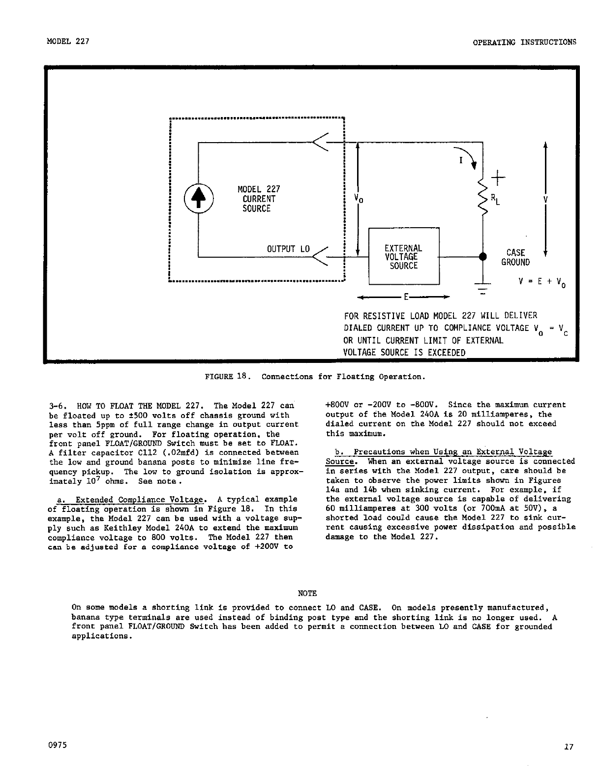
FIGURE 18.
Connections for Floating Operation.
A
filter capacitor Cl12 (.OZmfd) is connected between
3-6.
the low and ground banana posts to minimize line fre-
HOW TO FLOAT THE MODEL 227. The Model 227 can
quency pickup. The low to ground isolation is approx-
be floated up to rt500 volts off chassis ground with
imately 10' ohms. gee note.
less than 5ppm of full range change in outpur current
per volt off ground. For floating operation, the
fronr
panel FLOAT/GROUND Switch must be set to FLOAT.
a. Extended Compliance Voltage. A typical example
of flaatine ooeration is shown in Fieure lg. In this
example, the Model 227 can be used w&h a voltage sup-
ply such as Keithley Model
240A
to extend the maximum
compliance voltage to 800 volts. The Model 227 then
can be adjusted far a compliance voltage of +2OOV to
b. Precautions when "elng a" &xternaL YoUage
Source.
+eoov or
-200v to -8OOV.
When a" external voltage source is connected
in series with the Model 227 output, care should be
Since the maximum current
take" to observe the power limits shown in Figures
output of the Model 240A is 20 milliamperes, the
14a and 14b when sinking current. For example, if
the external voltage source is capable of delivering
dialed current on the Model 227 should not exceed
60 milliamperes at 300 Volts (or 7oomA at 50x9, a
shorted load could cause the Model 227 to sink cur-
rent causing excessive power dissipation and possible
damage to the Model 227.
this maximum.
0975
NOTE
0" some models a shorting link is provided to connect LO and CASE. On models presently manufactured,
banana type terminals are used instead of binding post type and the shorting link is "a longer used. A
front panel FLOAT/GROUND Switch has bee" added to permit a connection between LO and CASE for grounded
applications.
17

OPERATING INSTRUCTIONS MODEL
'227
DC li'OO 1000
I I I I I III 1 I I I IIlll'°K
AT DC AN INPUT OF 1OV SETS THE CURRENT OUTPUT TO FULL RANGE (10-0-O DIALED CURRENT)
O-
2 -
-
E 1
E 1
k2 -
I
2 -
tli-1Ol
2 - AT 600 HZ
- -
B -
-
gz 1
z -
K -
2 -202
1DK
FREQUENCY - HZ
FIGURE 19. Frequency Response for Voltage Programing
FRONT PANEL
DIAL SETTING
VOLTAGE
PROGRAM MODULATED
INPUT OUTPUT
SIGNAL % MODEL b OUTPUT
GENERATOR 227 LOAD
CLIPPING - -.-\,
TYPICAL OUTPUT FOR
COMPLIANCE LIMIT LESS
THAN PEAK OUTPUT.
0
FIGURE 20. "se of "olfage Program Input to Modulate Current.
MODEL 227
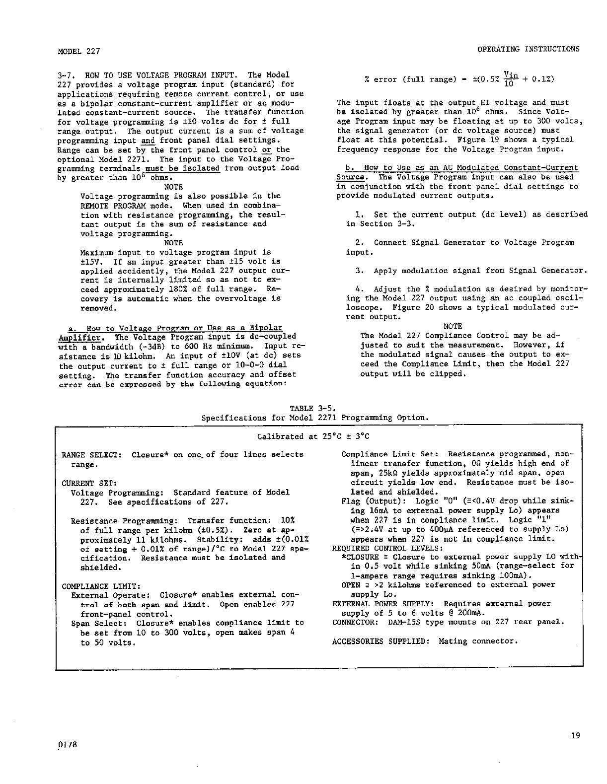
3-7.
HOW TO USE VOLTAGE PROGRAM INPUT. The Model
227 provides a voltage program input (standard) for
applications requiring remote current control, or use
as a bipolar constant-cu==ent amplifier o= ac modu-
lated constant-cu==ent source. The transfer function
for voltage programming is +I0 volts dc for t full
range output. The output current is a sum Of Voltage
programming input & front panel dial settings.
Range can he set by the front panel controls the
optional Model 2271. The input to the Voltage Pro-
graming terminals must be isolated from output load
h" ereat.er than 106 Ohms.
NOTE
Voltage programming is also possible in the
REMOTE
PROGRAM mode. When used in cambina-
tion with resistance programming, the resul-
tant output is the sum of resistance and
"drag?? programming.
NOTE
Maximum input to voltage program input is
t15v. If an input greater rhan e15 volt is
applied accidently, the Model 227 o"fp"t CUT-
rent is internally limited so as naf to ex-
teed approximately 180% of full range. Re-
covery is automatic "he" the avervo1rage is
removed.
a. How to Voltage Program or use as a Bipolar
Amplifier. The Voltage Program input is dc-coupled
rh L bandwidth (-3dB) fo 600 Hz minimum. 1wut re-
setting:
The transfer function accuracy and offset
error can be expressed by the fallowing equation:
OPERATING INSTR"CTIONS
% error (full range) = i(O.5% $ + 0.1%)
The input floats at the output HI volrage and must
be isolated by greater than lo6 ohms. Since Volf-
age Program input may he floating at up to 300 volts,
the signal generator (or dc voltage source) must
float at this potential. Figure 19 shows a typical
frequency response for the Voltage Program inpur.
h. Ho" to "se as an
AC
Modulated Constant-Current
Source. The Voltage Program input can also be used
in conjunction with the front panel dial settings to
provide modulated current outputs.
1. get the current output (dc level) as described
in section 3-3.
2. con*ect sign*1 Generator to Voltage Program
input.
3. Apply modulation signal from Signal Generator.
4.
Adjust the % modulation as desired by monitor-
ing the Model 227 output using an ac coupled oscil-
1OSCOp~. Figure 20 shows a typical modulated CUT-
rent ourpur.
NOTE
The Model 227 Compliance Control may be ad-
justed to suit the measu=ement. However, if
the modulated signal causes the output to ex-
ceed the Compliance Limit. then the Model 227
output will be clipped.
TABLE 3-5.
Snecificarians for Model 2271 Proaranrminn Option.
Calibrated at 25'C 2 3'C
RANGE SELECT: Closure* on ane.of fovr lines selects Compliance Limit Set: Resistance programmed, non-
range. linear transfer function, 00 yields high end of
span, 25kn yields approximately aid span, open
CVRRENT SET: circuit yields low end. Resistance must be iso-
Voltage Programming: Standard feature of Model laced and shielded.
227.
gee specifications of 227. Flag (Output): Logic "0" (xO.4V drop while sink-
ing 16nA to external power supply LO) appears
Resistance Programming: Transfer function: 10% when 227 is in compliance limit. Logic "1"
of full range per kilohm (t0.5%). Zero at ap- (:>2.4V at up to
400,iA
referenced to supply Lo)
proximately 11 kilahms. Stability: adds t(O.Ol% appears when 227 is not in compliance limit.
of setting + 0.01% of =ange)/'C to Model 227 spe- REQUIRRE CONTROL LEVVELS:
c3xication. Resistance must be isolated and *CLOSURE s closure to external power supply LO with
shielded. in
0.5
volt while sinking 5OmA (range-select for
l-ampere range requires sinking lOOmA).
COMPLIANCE ISMIT: OPEN z .2 kilohms referenced to external power
External operate: Closure* enables external co"- supply LO.
tral of both spa,, and limit. Open enables 227 EXTERNAL POWER SUPPLY: Requires external pawe=
front-panel control. supply of 5 to 6 volts @ 2ooaA.
span Select: Closure* enables compliance limit to CONNECTOR:
DAM-15s
type mounfs on 227 rear panel.
be set from 10 to 300 volts, open makes span 4
to
50
volts. ACCESSORIES SUPPLIED: Mating con*ecto=.
19
OPERATING INSTRUCTIONS MODEL 227
-Pin No.
6
7
8
9
10
11
12
13
14
15
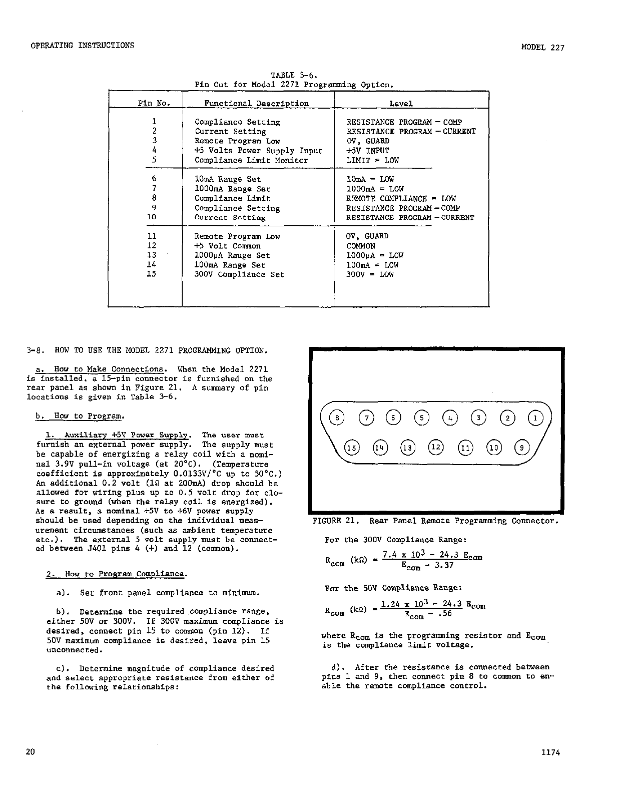
TABLE 3-6.
Pin Out for Model 2271 Progr;
Functional Description
Compliance Setting
Current Setting
Remote Program LOW
t5 Volts Power Supply Input
Compliance Limit Monitor
lOmA Range set
1OOOmA Range See
Compliance Limit
Compliance Setting
Current setting
Remote Program Low
+5 Volt common
10001lA Range Set
lOOmA Range set
300V Compliance Set
RESISTANCE PROGRAM-COMP
RESISTANCE PROGRAM -CURRENT
1000&4 = LO"
REMOTE COMPLIANCE = LOW I
RESISTANCE PROGRAM-COMP
RESISTANCE PROGRAM--CURRENT
3-a.
HOW TO
"SE THE MODEL 2271 PROGRAMMING OPTION.
a. HOW to Make Connections. When the Model 2271
is installed, a 15-pi" connector is furnished on the
rear panel as shorn-i" Figure 21. A summary of pin
locaeions is given in Table 3-6.
1. Auxiliary +5V Power Supply. The user must
furnish m external rmwer sumlv. The sumh must
be capable of energizing a r& coil with'ae"omi-
nal 3.9V pull-in voltage (at 20'0. (Temperature
coefficient is approximately 0.0133Vf'C up t" 50°C.)
A" additimal 0.2 ""lt (10 at 2OOmA) drop should he
allowed for wiring plus up fo 0.5 volt drop for clo-
sure Co graund (when rbe relay coil is energized).
As a result, a nominal +5V to +6" power supply
should be used depending on the individual meas-
urement circumstances (such as ambient temperature
.ZC.). The external 5 volt supply musf be connecr-
ed between 5401 pins 4 (+) and 12 (common).
I I
FIGURE 21. Rear Panel Remote Programming Connector.
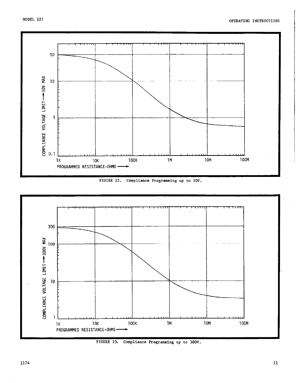
For the 300"
Compliance Range:
2. HO" to Pro~.ram Compliance.
R
com WO =
7.4 x 10³ - 24.3 Ecom
Ecom - 3.37
4.
Set front panel compliance t" minimum.
b). Determine the required compliance range,
either 50V or 300V. If
300V
maximum compliance is
desired, c""nect pi" 15 to common (pi" 12). If
50V maximum compliance is desired, leave pin 15
unconnected.
For the SOV Compliance Range:
RcOm (kR) = 1.24 x LO3 - 24.3 EcOm
&ml -
.56
where R,, is the programming resistor and Scorn
is the compliance limit voltage.
4. Determine magnitude of compliance desired d). After the resistance is connected between
and select appropriate resistance from either of pins 1 and 9, the" connect pi" a to coma" fo en-
the following relationships: able the remoee compliance control.
1174
MODEL 227
OPERATING INSTRUCTIONS
1K 10K 1OOK 1M 10M 1OOM
PROGRAMMED RESISTANCE-OHMS-
FIGURE 22. Compliance Programming up to SOV.
ll
1K 10K 1OOK 1M 10M 1OOM
PROGRAMMED RESISTANCE-OHMS-
FIGURE 23. Compliance Programming up to 3OOV.
1174 21
OPERATING
INSTRUCTIONS MODEL
227
PRO&RAMMED RESISTANCE-
If resistance ex-
ceeds 23kR, the
Model 227 will go
into current limit.
Recovery is auto-
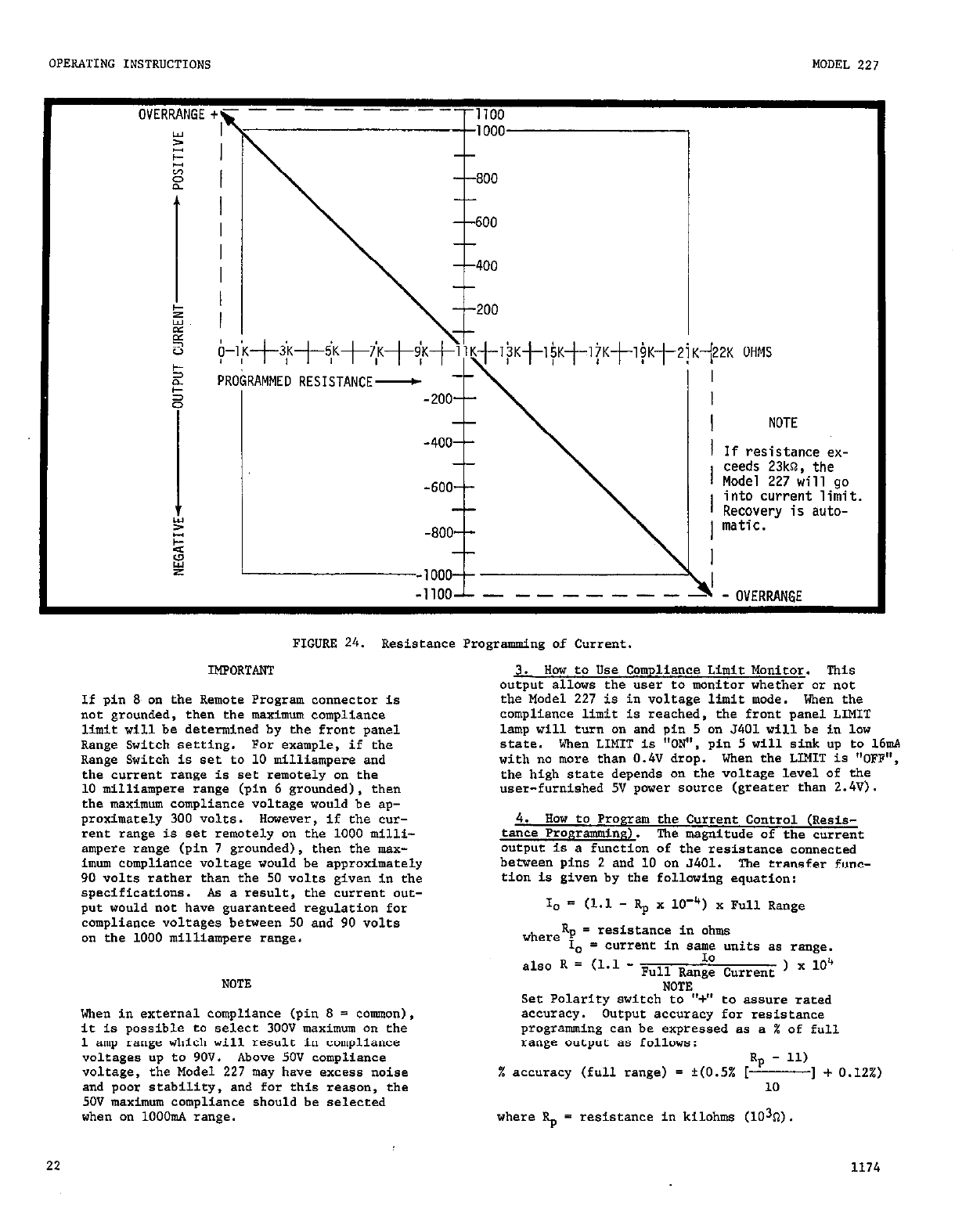
FIGURE 24. Resistance Programming of current.
IMPORTANT
If pin 8 on the Rem"te Program connect"r is
not grounded, then the maximum compliance
limit will be determined by the front panel
Range Switch setting. For example, if the
Range Switch is eet to 10 milliampere and
the current range is sef remotely on the
10 milliampere range (pi" 6 grounded), then
the
maximum
compliance voltage would be ap-
proximately 300 volts. Hcwever, if the cur-
rent range is sef remotely on the 1000 milli-
ampere range (pi"
7
grounded), then the max-
imum compliance voltage would he approximately
90 volts rather than the 50 volts given in the
*pec1fic*ti0**. As a result, the current ~,a-
put would not have guaranteed regulation for
compliance voltages beween 50 and 90 volts
on the 1000 milliampere range.
NOTE
When in external compliance (pin 8 = common),
if is possible to select
300V
maximum on rhe
1 amp range which will result in compliance
voltages up to 9ov.
Above 5ov
compliance
voltage, the Model
227 may
have excess noise
and poor stability, and for this reason, the
50V maximum compliance should be selected
when on 1OOOmA range.
3.
How to Use Compliance Limit Monitor. This
output allavs the user to manitar whether or not
the Model
227 is in
voltage limit mode. When the
compliance limit is reached, the front panel LIMIT
lamp will turn on and pin 5 on 5401 will be in low
state. When LIMIT is "ON", pi" 5 will sink up to l&A
with no more than 0.4V drop. When the LIMIT is "OFF",
rhe high stare depends on the voltage level of the
user-furnished 5V pwer source (greater than 2.4V).
4.
How to Program the Current Control (nesis-
tance Pro~ramminp). The magnitude of the current
O”tp”t is a
function of the resistance connected
between pins 2 and 10 on 5401. The transfer func-
tion is given by the follaring equation:
= (1.1 - Rp x lo-+) x Full Range
whe:IR = resistance in ohms
F. = current in same units as rmge.
also R =
(1.1 - IO
Full Range Current ) x 104
NOTE
Set Polarity switch t" "+" to assure rated
accuracy. Output accuracy for resistance
programming can be expressed as a 4 of full
range output 88 follows:
5: accuracy (full range) = +(0.5x [
Rp - 11)
] + 0.12%)
10
"here Rp = resistance in kilohms (103$,).
22
1174
REMOTE
PROGRAMMING TRIAXIAL
CONNECTOR CABLE
5401
BOX-WITHIN-BOX
CONFIGURATION
t---- ---_I
f
CASE 1 GROUND
RESISTANCE BETWEEN 540; PIN 10 AND CHASSIS OR
MODEL 227 LOW SHOULD BE AT LEAST 1012 OHMS TO
MAINTAIN ACCURACY TO WITHIN 0.005%. ALSO, RE-
SISTANCE BETWEEN 5401 PINS 1 AND 9 SHOULD BE
GREATER THAN 109 OHMS.
FOT example, for full range output Rp = 21kO. and
% accuracy equals the following:
% accuracy = ?(0.5% r++ + 0.12%:)
= 20.62%
(of full range)
5. "ow to Program Range. Range can be set to
any of the four ranges by grounding the appropriate
line as shown in Table 3-7. TO use the Model 2271.
set the Range switch to REMOTE PROGRAM.
TABLE 3-7.
Remote Range Selection.
I I
Condition of Lines I
Ranae Desired 1 Pin 6 1 Pin 7 1 Pin 13 I Pin 14
1mA OPEN OPEN GND OPEN I
NOTE
When range changing, if all four pins are
open simultaneously, the Model 227 will not
have a currenf output (output terminals are
open). To avoid relay arcing either program
the currenf back to zero or make-before-
break the connections to the range lines when
changing range. If more than one pin is
closed, the higher current range is enabled.
For example, if all four pins are closed to
ground, the 1000mA range is selected. Typ-
ical pull-in time for all relays is 30 milli-
seconds. 'Qpical release time is 10 milli-
seconds.
1174
NOTE
n,e temperature coefficient of the Model
2271 adds $(0.01% of setting/"C + 0.01%
of range/Y) to the Model 227 Specifica-
tions. Thus the total Model 22712271 toe-
fficient could be expressed as 1-(*0.015%
of
serting/oc
+ 0.015% of range/*C). For
remote programing, the temperature coeffi-
cient can be expressed as fOllOWS:
%T.C. (full range) = i-(0.015 [EP$-+ + O.OlS)/"C.
RX example, at a full range setting, the
t.c. = to.o3%/?z.
6.
Preferred Cabling Techniques. Since the
Model 227 could be affected by excessive cable
capacity, a triaxial cable (shield within a
shield) should be used with the inner shield
connected to pin 2 on 5401, and the outer shield
connected to CASE. Insulation between shields
should be rated at 1000 volts especially for
floating applications. Box-within-a-box can-
srruction should be used for all circuitry used
in resistance programming.
NOTE
The maximum allowable capacitance berween
5401 pins 1 or 10 and chassis is 300pF un-
less compensating capacitance Cp is instal-
led across the current programming resistor
Rp as follows:
Cp - [%C - 1 x 1O-7l where R,, - load resistance
23
MODEL 227
SECTION 4. ACCESSORIES
Model 1008 Single Rack Mounting Kit.
Applications: The Model 1008 adapts Keithley Style
"N" instruments for S-114 in. x 19 in. mounting with
11 in. depth behind front panel. The kit is also
useable with 14 in. depth instruments.
Parts List:
Item Keithley
NO. Description WY. Part No.
1 Half Rack Panel 1
25815B
2
Bracket Angle 1
26757C
3
Bracket Angle 1
26794C
4
Phillips Screws (5/g") 6
/B-32
5
Phillips Screws (l/Z")
4 #6-32
6 Socket Screws (318") 2 1110-32
7
Phillips Screws (5/V)
4 116-32
8
Kep Nut, #6-32 4
86-32
Assembly Instructions:
1. Secure Half Rack Panel (Item 1) to Bracket
Angle (Item 2) using two socket screws (Item 6).
2. Remove
Side Dress Panels (left and right) from
instrument.
3. Secure Bracket Angles (left and right) to in-
strument. (Half Rack Panel may be located on the
left or right to suit mounting requirements.) Use
Phillips Screws (Items 4 and 5) as shown in Figure
26 for 14 in. depth instruments. Use longer screw
(Item 7) and Kep nut (Item 8) for 11 in. depth in-
*trume*t* .
FIGURE 26.
Model 1006 Single Rack Mounting Kit.
24 0975
MODEL 227
SECTION
THEORY OF OPERATION
5. THEORY OF OPERATION
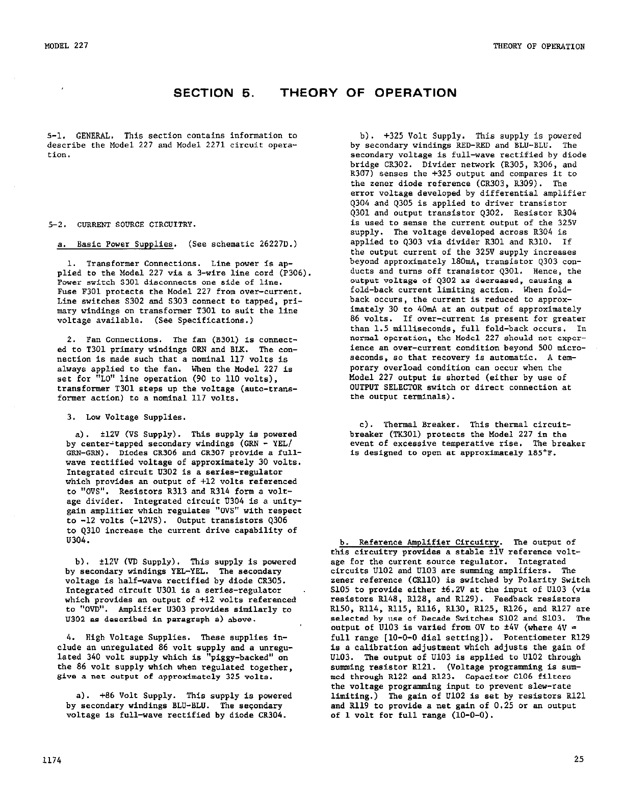
5-l. GENERAL. This section contains information to
describe Lhe blade1 227 and Model 2271 circuit opera-
cion.
5-2. CumENT SOURCE CIRCUITRY.
a. Basic Power Supplies. (See schematic 26227D.)
1. Transformer Connections. Line power is ap-
plied to the Model 227 via a 3-wire line c"rd (P306)
Power switch 5301 disconnects one side of line.
Fuse F301 protects the Model 227 from over-c"rre"t.
Line switches 5302 and S303 connect to tapped, pri-
mary windings on transformer T301 to suit the line
voltage available. (See Specifications.)
2. Pa* cannections.
The fan (B301) is connect-
ed to T301 primary windings ORN and BLK. The con-
nection is made such that a nominal 117 volts is
always applied to the fan. When the Model 227 is
set for "LO" line operation (90 to 110 volts),
transformer T301 steps up the voltage (auta-rrans-
former action) to a nominal 117 Volts.
3.
LO" Voltage Supplies.
a) . *12v (VS supply). This supply is Powered
byc~~ndy;fTLtaPPed secondary windings (GRN - YEL/
. Diodes CR306 and CR307 Prbvide a full-
wave rectified voltage of approximately 30 volts.
Integrated circuit U302 is a series-regulator
which Provides a" output of +12 volts referenced
to "OVS". Resistors 8313 and R314 form a volt-
age divider. Integrated circuit 0304 is a unity-
gain amplifier which regulates "OVS" with respect
to -12 volts (-12VS). output tr*nsistors q306
to 4310 increase the current drive capability of
u304.
b). 112v
(vc Supply). This supply is powered
by secondary windings TEL-YRL. The secondary
voltage is half-wave rectified by diode CR305.
Integrated circuit U301 is a series-regulator
which provides a" output of +12 volts referenced
to "OVD". Amplifier U303 provides similarly to
U302 as described in paragraph a) above.
4. High Voltage Supplies. These supplies in-
clude an unregulated 86 volt supply and a unregu-
lated 340 volt supply which is "piggy-backed" on
the 86 volt supply which when regulated together,
give a "et output of approximately 325 volts.
4. +86 Volt Supply. This supply is powered
by secondary windings BLU-BLU. The seGondary
voltage is full-wave rectified by diode CR304.
b).
+325 Volt Supply. This supply is powered
by secondary windings RED-RED and XL"-EL". The
secondary
voltage
is full-wave rectified by diode
bridge CR302. Divider network (R305, R306, and
R307)
senses the +325 output and compares it to
the zener diode reference (CR303, R309). The
error voltage developed by differential amplifier
q304 and Q305 is applied to driver transistor
Q3Ol
and output transistor q302. Resistor R304
is used to sense the current output of the 325"
S"PPlY. The voltage developed across R304 is
applied to q303 via divider R301 and R310. If
the Output current of the
325V
supply increases
beyond approximately 18OmA. transistor Q303 con-
ducts and turns off transistor Q301. Hence, the
output voltage of q302 IS decreased, causing a
fold-back current limiting action. When fald-
back occurs, the current is reduced to approx-
imately 30 to 4OmA at a" output of approximately
86
volts. If oyer-current is present for greater
than 1.5 milliseconds, full fold-back occurs. I"
normal operation, the Model 227 should "of exper-
ience an over-current condition beyond 500 micro-
seconds, so that recovery is automatic. A tem-
porary overload condition can occur when the
Model 227 output is shorted (either by use of
OUTPUT SELECTOR witch or direct connection at
the output terminals).
4.
Therm& Breaker. This them1 circuit-
breaker ('X301) protects the Model 227 in the
event of excessive temperative rise. The breaker
is designed to open at approximately 185OF.
b. Reference Amplifier Circuitry. The output of
this circuitrv urovides a stable +lV reference valt-
age for the &e"t source regulator. Integrated
circuits U102 and "103 are summing amplifiers. The
sener reference (CRllO) is switched by Polarity Switch
S105 to provide either +6.2V at the input of U103 (via
resistors R148, R128, and
R129).
Feedback resistors
R150, R114, R115, Rl16, Rl30, R125, R126, and R127 are
selected by use of Decade Switches S102 and S103. The
output of U103 is varied from OV t"
+4V
(where 4V =
full range [10-O-O dial setting]). Potentiometer R129
is a calibration adjustment which adjusts the gain of
U103. The output of Ill03 is applied to U102 through
summing resistor R121. (Voltage programing is su*
med through R122 and R123. Capacitor Cl06 filrerr,
the voltage programming input to prevent slew-rate
limiting.) The gain of U102 is set by resistors R121
and RllV to provide a "et gain of 0.25 or an output
of 1 volt for full range (10-0-O).
1174 25
THEORY OF OPERATION MODEL 227
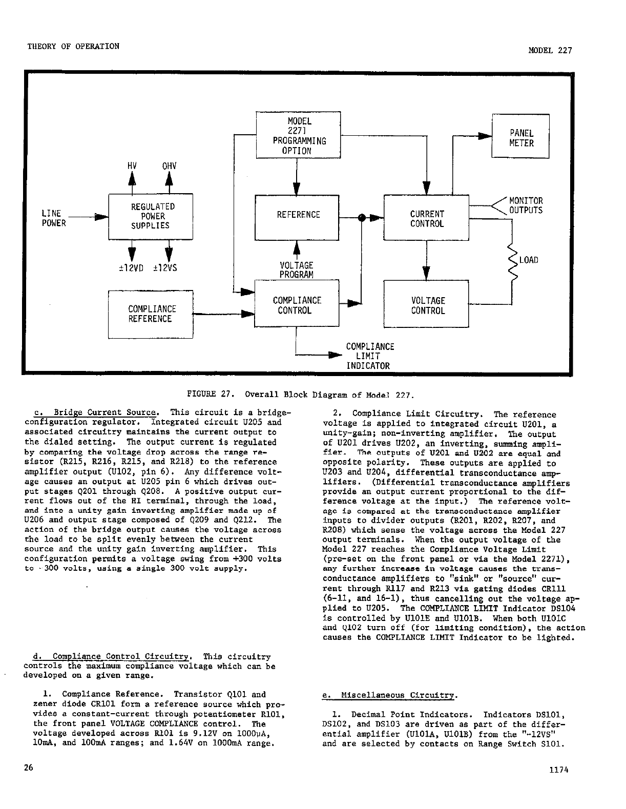
HV OHV
LINE
POWER
*12vo *12vs VOLTAGE
PROGRAM
L) COMPLIANCE + VOLTAGE
COMPLIANCE b CONTROL CONTROL
REFERENCE
( LIMIT
COMPLIANCE
INDICATOR
FIGURE 27. Overall Block Diagram of Model 227.
C.
Bridge Current Source. This circuit is a bridge-
confinuration renularor. Integrated circuit "205 and
associated circuitry maintains-the current output to
the dialed setting. The output current is regulated
by comparing the voltage drop across the range re-
sistor (R215, R216, R215, and R218) to the reference
amplifier output (U102, pin 6). Any difference volt-
age causes a" output at U205 pi" 6 which drives out-
put stages Q201 through Q208. A positive output cur-
rent flows out of the RI terminal, through the load,
and into a unity gain inverting amplifier made up of
U206 and output stage composed of Q209 and Q212. The
action of the bridge output causes the voltage across
the load co be split evenly between the current
source and the unity gain inverting amplifier. This
configuration permits a voltage swing from +300 volts
to -300 volts, using a single 300 volt supply.
d. Compliance Control Circuitry. This circuitry
controls the maximum compliance voltage which can be
developed on a give" range.
1. Compliance Reference.
Transistor
QlOl and
zener diode CR101 form a reference source which pro-
vides a constant-current through potentiometer RlOl,
the front panel VOLTAGE COMPLIANCE control. The
voltage developed across RlOl is 9.12V on lOOOvA,
lOmA, and lOOmA ranges; and 1.64V "n 1OOOmA range.
26
2. Compliance
Limit
Circuitry.
The
reference
voltage is applied to integrated circuit "201, a
unity-gain; non-inverting amplifier. The "utput
of U201 drives U202, a" inverting, summing ampli-
fier. The outputs of U201 and U202 are equal and
apposite polarity. These outputs are applied t"
U7.03 and U204, differential transconductance amp-
lifiers. (Differential transconducrance amplifiers
provide a" output current proportional to the dif-
ference voltage at the input.) The reference volt-
age is compared at the transconductance amplifier
inputs to divider outputs (R201, R202, R207, and
R208) which sense the voltage across the Model 227
output terminals. When the output voltage of the
Model 227 reaches the Compliance Voltage Limit
(pre-set on the front panel or via the Model 2271),
any further increase in voltage causes the trans-
conductance amplifiers to "sink" or %ource" cur-
rent through R117 and R213 via gating diodes CR111
(6-11, and 16-l), thus cancelling out the voltage ap-
plied t" U205. The COMPLIANCE LIMIT Indicator DS104
is controlled by UlOlE and UlOlB. When both UlOlC
and Q102 turn off (for limiting condition), the action
causes the COMPLIANCE LIMIT Indicator to be lighted.
e. Miscellaneous Circuitry.
1. Decimal Point Indicators. Indicators DSlOl,
DS102, and DS103 are driven as part of the differ-
ential amplifier (UlOlA, UlOlB) from the "-12VS"
and are selected by contacts on Range Switch SlOl.
1174
MODEL 227 THEORY OF OPERATION
I
REF I
I- I I
1 COMPLIANCE b
OUTPU
HI
FIGORF, 28.
Simplified Diagram of Current Source.
2. output Selector Switch (5104). This switch
disconnects the output terminals from the current
SO"TCe. see operating Inser"ctio"s, Section 3 for
a discussion of switching.
3. Volts Monitor Circuit. This output is pro-
vided by integrated circuit U104, a unity-gain,
no"-inverting amplifier. This circuit buffers the
voltage developed at the output 8" that no loading
error can result at RI and LO output terminals.
The atput of
Volts Monitor is
the same p"te"tia1
es Output
HI
and LO (up to 305 volts). Since R143
and R144 provide source resistance of 10 kilohms,
loading of
Volts
M""it"r should be take" in consi-
deration.
4. Current
Monitor
Circuit. This output pro-
vides -1 volt (km) for a + full range (10-0-O).
Fuse FlOl pr"tects this ""tput against accidental
short circuits. This voltage is developed between
the buffered o"tp"t of U104 and
“OVSR”.
5. Meter circuit.
Meter
Ml01 is driven from
the outpa of U104.
a) .
Voltage
Reading. When switch S106 is set
to "V", the meter is connected between U104 out-
put and output LO. The meter mO"eme"t is for
full range reading. When Switch S107 is set to
XI, the current developed through Ml01 is a func-
tion of ~133, R145, R146, Rl47, and G, where:
IM
* VOUT i (R145 + Rl46) R147
(R133 + 'k + R145 + R146 + R147)
0975
When switch S107 is set, to x10, the current devel-
oped through
Ml01
is a function of R133, R149,
R147, and &(M, where:
IM =
VOUT
i @, + RI33 + RI47 + R149)
b).
Current Reading. When Switch S106 is set
to "A", the meter is connected between 1~104 out-
put and
“OVS”.
When Switch S107 is set ta, XI,
the current developed through
Ml01 is a
function
of R133 and s where:
1~ + Vm f (RM + Rl33)
when Switch S107 is set to x10, the current devel-
oped through Ml01 is a function of R133, R149,
and RM where:
IM+vQI i (RM+R133 +Rl49)
6. Power ON/OFF Transient Suppression Circuit.
This circuit (located on board PC-396) minimizes
the effect of power surge when power to the Model
227 is applied "I‘ removed.
5-3. PROGRAMMING OPTION (MODEL 2271).
a. Renee Prowamming. Range selectian is acconr
plished by energizing relays, (by closure to ground
or through a saturated transistor). Relay coils
K401, K402, K403, K404, and K405 are connected to
the "8~8 external +5 volt supply (5401, pi" 4).
Closure to ground at 5401 pins 6, 7, 13, or 14 ener-
gizes the relay coils. If the 1OOOmA range is selec-
ted, relay K405
transfers
the
""fp~f srage from 325
volt supply to 86 volt supply. The user +5 v"lt
supply is switched by relay K408 which is energized
"hen
the
range switch is set to REMOTE.
27
THEORY OF OPERATION
b. External Compliance. Closure to ground et 5401,
pin 8 enables external control. When energized relay
K407 selects the External Compliance mode.
pii.
Complia"ce span. Closure to ground et 5401,
energizes relay K406. When energized, K406
sets the maximum compliance limit to 300 volts.
Contacts K406A set the compliance reference voltage
to 9.12 volts maximum. Contacts K406B change the
supply voltage et the output stage from 06 volts to
325 volts.
d. Current Setting. (Resistance Programming).
Integrated circuits U402 end U401 end zener diode
CR409 farm a 100 microampere reference current source.
The current source drives the external programming re-
sistor connected between 5401, pins 2 end 10. The
voltage across the proSrammi"S resistor (at the ~,a-
put of U401, pin 6) is fed to summing amplifier U403
via resistor R426. Diode CR409 end summing resis-
tors R411
end R412 form the reference voltage. As
a result, the output of U403 is es follows:
V, = (Rp x lOO,,A) - 1.1 valts
MODEL 227
(See Section 3-8b4 for further discussion of this
transfer function.) Clamping diodes DS401 end DS402
prevent the output of U403 from going to far negative
end enable FET switch Q402 to turn full off. Tran-
sistors
Q406, Q405,
end Q407 are for overload pro-
tecti0*. FET Switch Q402 is driven by both II406 end
9401.
When the Model 227 is switched out of "REMOTE
PROG”,
(Range Switch 5101) transistor Q401 turns off.
Transistor Q403 turns on, turning off FET Switch Q402,
end as a result, disconnects the remote program re-
ference voltage from the Model 227. If the reference
voltage at pin 6 of U903 goes above approximately 1.2
volts, U406 turns an Q403 which turns off Q402 dis-
abling the remote program reference to Model 227 ceus-
ing
the output to go to approximately zero.
e. Compliance Limit Programming. Integrated cir-
cuit U404 is a summing amplifier. Reference zener
diode develops a current through summing resistors
R405, R415, end R417 and program resistor (5401 pins
1 end 9). Diode CR414 is a protection device. When
relay K406 is energized, the 9.1 volt reference volt-
age is selected by connecting the proper gain at U404.
f. Compliance Limit (FLAG). Transistor
Q404 (NPN)
is connected collector to emitter between 5401 pins
5 end 12. When the Model 227 goes into compliance
limit phototransistor U405 turns off, causing tren-
sister Q404 to seturete (low state).
NOTE
Should it be necessary to ramove the Model
2271 Option from the Model 227 chassis, con-
nector J206A, furnished with each 22712271
(show" on schematic 26226E) must be installed
et P206. Connector
J206A
is a te"-pi" Berg
Connector with jumper wires between pins A
end C: D end G.
28
0975
MODEL 227
!
MAINTENANCE ~
SECTION 6.
6-1. GENERAL. This section contains information
necessary to maintain the instrument. Included are
procedures for electrical Performance Checks, Cali-
bration, Troubleshooting.
6-2. REQUIRED TEST EQUIPMENT. Recommended test
equipment for checking end maintaining the instrument
is given in Table 6-1. Test equipment other then re-
commended may be substituted if specifications equal
or exceed the scared characteristics.
6-3. PERFORMANCE VERIFICATION. Use the following
procedures LO verify proper operation of the instru-
ment . All measurements should be made et ambient
temperature of approximately 25'C f. 3'C end relative
humidity below 60%. If the instrument is out of spe-
cification at any point, perform a complete calibra-
tion as given in Paragraph 6-4. For each function
that is checked, an additional uncertainty due to
temperature coefficient should be considered if the
ambient temperature is beyond the temperacure range
indicated above.
a. Fuse Checks.
1. Check the line fuse (F301) on the rear panel.
For nominal 117V line operation, use a 2.5A type
3AG Slo-Blo fuse. For 234V line operation, use a
1.25A type 3AG Sla-Blo fuse.
2. Check the internally installed protection
fuse (FlOl). This fuse is located on circuit board
PC-330 near the front panel. Remove the top c"ver
fo gain access to the circuit board.
NOTE
If the Line Fuse (F301) is blown or missing,
the Model 227 will be inoperable. If the
protection fuse (FlOl) is blown or missing,
the Model 227 will be operable, except the
rear panel Current Monitor end Voltage Pro-
graming rermi**1*.
Item
A
B
0975
C
D
MAINTENANCE
b. Line Voltage Setting. Set the Line Switches
(5302 end 5303) in accord with paragraph 2-3 in Sec-
tion 2.
c. Preliminary Check.
1. Set OUTPUT SELECTOR switch to "SHORT".
2. Set Range Switch f" 1000uA.
3. Ser Decade Switches to 10-0-O.
4. Set Polarity Switch t" "+".
5. Set METER Switches f" "X10" end "A".
6. Set VOLTAGE COMPLIANCE to "0" (minimum).
7. Put External short on Model 227.
8. Set Power Switch to "ON".
9. Set OUTPUT SELECTOR to "ON".
10. Set VOLTAGE COMPLIANCE to 1OV.
11. Observe Meter (MlOl) reading. Current read-
ing should be (+) full range.
12. Set Polarity switch to "-".
13. Observe meter (MlOl) reading. Reading
should be (-) full range.
14. Verify Meter readings for Range Settings of
t10, +lOO, and ~1OOti.
15. If all ranges are indicated correctly, pro-
ceed to normal verification pracedure.
I"PORTANT
The Model 227 vi11 not operate properly if
either J206B (Used o" Model 2271) or J206A are
missing.
To
order en extra connector for J206A,
TABLE 6-l. specify Keithley Part No. 272048.
Recommended Test Equipment for Performance Verification.
Description
Digital Voltmeter
Resisfence
Minimum Specifications Mfr. Model
l.OOOOOV i(O.OlS% of mg + 0.015% of rdg)
z1o*n input * Keithley 190
1OOR + 0.01%. 0.12w 10ppm/Y
1kC ? 0.02%, 0.12W lOppm/'C
1on ? 0.022, 1w lOppm/'C
10 f 0.022, low 1oppm/*c
Vishey v53-100
Vishay V53-1K
Voltage source
Resistance BOX
0 to UOVdc
0.01% of setting * 0.002% of range
tc c 3oppm/*c
Fluke 34l.B
0 to 22kn f 0.02%
I
GR 14336
29
MODEL 227
1. Dia.1 Accuracy (10-0-O).
4. set. Range to lOmA.
b).
Set Decade Dials to 10-O-O*.
c) . Connect Resisrmce (B), 1000 * 0.01% to
output of Model 227.
d). Connect DMM (A) across output of Model 227.
e). Set COMPLIANCE to 1OV.
f) . set OUTPUT SELECTOR ro "ON".
9). set Polarity to "+I.
If a check is made on dial accuracy ime-
diately after a complete recalibration, rhe
dial accuracy should be checked LO allowable
voltage error as follo"s:
i(O.00449 x Dia1ed Curre"r + 0.00064)
current Range
h) .
Verify rhat voltage reading is l.OOOOOV
+O.O0612V.
0. set
Polarity to nn-tl.
j). Verify that voltage reading is
l.OOOOOV
iO.OO612V.
2. Did Accuracy (O-O-O).
a).
Set Decade Dials to O-O-O*.
b). Set Polarity to "iJ'.
Cl. Verify that voltage reading is 0.00000
f0.0012V.
d) . set Polarity to nn-v'.
e) .
Verify that voltage reading is 0.00000
+o.o012v.
3. Dial Accuracy (0-10-O).
4. Set Decade Dials to O-10-0*.
b). Set Polarity to W'.
Cl. Verify that the voltage reading is 0.10000
+o.o017v.
d) .
set Polarity to rY-9*.
4. Verify thae rhe voltage reading is 0.10000
*o.o017v.
NOTE
Other
dial settings can be checked if desired.
Accuracy for all other settings should be
checked to allowable voltage error as fOllDWS:
+(o 005 x Dfa1ed C"rrenr + 0 0012)
_ . current Range .
NOTE*
least
significant digit should be set care-
fully since dial is a variable control.
4. Dial Accuracy (lOOOvA Range).
a). %f OUTPUT SELECTOR f0 "SHORT".
b).
Set Range to lOOOvA.
4.
Connect Resistance (B), lOOOn + 0.02% to
output of Model 227.
d) . Perform steps Id) through lj) above.
4. Perform steps 2a) through 269 above.
f). Perform steps 3a) through 3e) above.
5. Dial Accuracy (lOOmA Range).
a). Set OUTPUT SELECTOR fo "SHORT".
b). Set Range to lOOmA.
4. Connect Resistance (B), 1OQ t 0.02% to o"t-
put of Model 227.
d). Perform steps Id) through lj) above.
4. Perform atepe 2a) through 2e) above.
f). Perform steps 3a) through 3e) above.
6. Dial Accuracy (1OOOmA Range).
a). Set OUTPUT SELECTOR to "SHORT".
b) . set Range to 1ooomA.
C). Connect Resistance (B), 1R + 0.02% to our-
put of Model 227.
d). Perform steps Id) through lj) above.
e) . Perform steps 2a) through 2e) above.
f). Perform ste,,s 3a) through 3e) above.
e. Voltage Program Verification (1000uA Range).
1. Set OUTPUT SELECTOR to "SHORT".
2. Set Range to 1000pA.
3.
Set Decade Dials fo O-O-O.
4.
Connect Resistance (B), lOOOn f 0.02% to the
Model 227 output.
5. Connece DMM
(A)
across ourput of Model 227.
30 1174
MODEL 227
MAINTENANCE
6.
Connect Voltage Source (Cl fo VOLTS PROGRAM
input.
NOTE
Make certain that Voltage Source (0 is capa-
ble of floating to +300". Also make certain
no connection is made between the Voltage
Source low terminal and chassis (CASE).
7.
Sef Voltage source (C) for +1ov OUtpUt.
8.
Set OUTPUT SELECTOR to "ON".
9. Verify that reading an DMM (A) is l.OOOOOV
kO.OO6V.
10.
ser Voltage source (C) for -lov output.
11. Verify that reading on DMM (A) is
l.OOOOOV
*O.O06V.
12. see Voltage source (0 for 0 volts output.
13. Verify hc reading on DMM (A) is 0.00000"
*o.o01v.
NOTE
If desired, other inpvt levels could be
checked. Output accuracy should be veri-
fied as follows: Allovable Voltage error =
t(o.005 x Voltage $"rce (C) + o.ool)
NOTE
If verification is performed immediately
after recalibration, then output accuracy
should be verified as follows: Allowable
Voltage error =
+(o.oo441 x,Valtage source (C)
10 + 0.001)
f. Voltage Proaram Verification (lOmA Range).
1. Set OUTPUT SELECTOR to "SHORT".
2.
set Range to lOmA.
3. Connect Resistance (B), 1OOC ? 0.02% to Model
227
output.
4.
Repeat steps e5 through e13
g. Voltage Program Verification (lOOmA Fanne).
1. Set OUTPUT SELECTOR to "SHORT".
2.
set Range co lOOmA.
3. Connect Resistance (B), lo,, ? 0.02% to Model
227
output.
4.
Repeat steps e5 through e13.
h. Voltane Program Verification (1OOOmA Range).
1. Set OUTPUT SELECTOR to "SHORT".
2.
See Range to 1OOOmA.
3.
Connect Resisfance (B), ln k
0.02%
to Model
227
OUtpUt.
4.
Repeat steps e5 through e13.
i. Verification of Programing Option (Model 2271).
1. Set Range Switch to "REMOTE PROGRAM".
NOTE
To guarantee specification, rhe Model 2271
calibration should be done with the Made1
227
polarity switch in the "+" position.
2.
Sef O"TP"T SELECTOR fo "SHORT".
3.
Select the 1OOOuA range by closure of 5401
pin
13
to common.
4.
Disable the External Compliance by opening
Of 5401 pin 8 to coma*.
5.
Set voltage compliance to 1OV "sing FRONT
PANEL CONTROL.
6. Connect Resistance Box (D) to c"rrent pro-
r&mming inputs at 5401, pins.2 and 10.
7. Set c"rrent for "zero" by'applying 11 kll-
ohma using Resistance Box (D).
8. Connect Resistor (B) lOOOn, 0.01% to Model
227
output.
9. Conxvxt DMM (A) co Model 227 o"tp"t.
10. Set OUTPUT SELECTOR to "ON".
11. Verify that DMM reading is 0.00000 + 0.0012V.
12. Set current for "- full range" by applying
21 kilohms "sing Resistance Box (D).
13.
Verify that D"M reading is -1.00000 t 0.0062V.
14. Set current for "+ full range" by applying
1 kilohm "sing Resistance Box CD).
15. Verify that DMM reading is +l.OOOOO + 0.0062V.
16. Set OUTPUT SELECTOR to "SHORT".
17. Verify other ranges. Select appropriate
range by closure 'CO c"mn"n (pin 12).
Ra"p.Z Pi" Closure
lomA pin 12 to pi" 6
lOomA pin 12 to pin 14
1ooOmA pin 12 to pin 7
Repeat steps 17 through 116 for each range selected.
1174 31
MAINTENANCE MODEL 227
NOTE
CAUTION
Other settings of output current can be check-
ed if desired by using the following accuracy
relationship:
Extreme care should be taken eo avoid con-
tact with voltages at various points on the
chassis when the line cord is connected.
Allowable Voltage error = IMPORTANT
i(O.005
x 1% ;,'i ;o:031 +
0.0012)
resistance applied. where Rp =
If verification is performed immediately
after recalibration, the output accuracy
should be verified as fallows:
Allowable Voltage error =
+(0.00426 x 1% ;,'1; ;ol;03] + 0.00055)
When the Model 2271 is to be used with the
Model 227, the Model 2271mw.t be installed
prior to calibration af,the 227, since the
Model 2271 affects the Model 227 calibration.
Calibration of the Model 227 should be per-
formed prior to performing the Model 2271
procedure.
NOTE
The reconrmended recalibration period for the
Model 227 is 12 months from factory calibra-
ticm. If the complete calibration is per-
formed using equipment specified, the Model
227 or Model 22712271 vi11 be usesble for an
additional 12 months within published speci-
fications. If repairs are made after initial
calibration, the'complete calibration proce
dures should be performed.
5-4. ADJUS'lMENT/CALIBRATION PROCEDURE. The follcw-
ing adjustments should be performed when any speci-
fication has been determined to be out-of-tolerance.
The Performance Check given in paragraph 6-3 should
be performed prior to this Calibration Procedure. If
any step in the Calibration Procedure cannot be per-
formed properly, refer to the Troubleshooting
Proce-
dure (paragraph 6-5) or contact your Keithley repre-
sentative or the factory. All measurements should be
made at ambient temperature of 25'C f 3'C and rela-
tive humidity below 60%.
a. Chassis Assembly.
To
gain access to the ad-
justments in the printed circuit boards, remove four
Follow the exact calibration sequence since
many adjustments are interelated.
b.
Fuse
Checks,
1. Check zhe line fuse (F301) on the rear panel.
For nominal 117V line operation, us8 a 2.5A type
3AG Slo-Blo fuse. For 234V line operation, use a
1.25A
type 3AG Slo-Blo fuse.
2. Check the internally installed protection
fuse (FlOl). This fuse is located on circuit board
PC-330 near the front panel.
Remove
the top cover
to gain access to the circuit board.
If the Line Fuse (F301) is blown or missing,
the Model 227 will be inoperable. If the
protection fuse (F101) is blown or missing,
the Model 227 will be operable, except the
rear panel Current Monitor and
Voltage
Pro-
gramming terminals.
C. Line Voltage Setting. Set
the Line Switches
(S302 and 5303) in accord with paragraph 2-3 in Sec-
tion 2.
d. Preliminary Check.
1.
2.
3.
4.
5.
6.
7.
8.
9.
Set OUTPUT SELECTOR switch to "SHORT".
Set Range Switch to lOOO,,A.
Set Decade Switches to 10-0-O.
Set Polarity
Switch to "+".
Set METER
Switches to "X10" and "A".
Set VOLTAGE COMPLIANCE to "0" (minimum).
Put External short on Model 227.
Set Power Switch to "ON".
Set OUTPUT
SELECTOR to “ON.
scre"* on TOP Cover and Bottom cover. 10. Set VOLTAGE COMPLIANCE to 10".
TABLE 6-2.
Recommended Test Eaui~ment far Calibration.
*tern Description
Minimum Specifications Mfr. Model
E Digital
Voltmeter l.OOOOOV t(O.OlS%
of mg + 0.015% of rdg) Keithley 190
F
0*ci110*c0pe 5mV/div. sensitivity lHRz bandwidth Tektronix ---
G Digital Voltmeter 3-l/2 digits, 0 *
lOOOV, 20.2%
of rdg Keithley 168
32 1174
MODEL 227 MAINTENANCE
11.
Observe Meter (MlOl) reading. Current read-
ing should be (+) full range.
12. Set Polarity Switch to "-I'.
13. Observe meter (MlOl) reading. Reading
should he (-) full range.
14. Verify Meter readings for Range Settings of
*lo, t100, and ?lOOOmA.
15.
If all ranges are indicated correctly, pro-
ceed to normal verification procedure.
e. Power Supply Adjustment.
1. Set controls as indicated in paragraph 5-3~
(except "a external short).
2. Remove the Model 227 top cover and bottom
cover.
3.
hcate potentiometer R306 on circuit board
PC-331.
4.
Connect DVM (Item G) between
+325V
test point
and 0 W test point.
5. Adjust potentiometer R306 far a voltage read-.
ing of
+325”
+ 1V.
NOTE
If thermal breaker TX301 is open or faulty,
no voltage reading can be made.
f. Bias Adjustment.
1. Set controls as indicated in paragraph 5-3c,
steps 1 through 8 (except no output short).
2. connect a 30
kilohm resistive load (l%, 10
watt) to output terminals.
3. Connect Oscilloscope (Item F) across the re-
sisrive load to monitor the compliance voltage.
Oscilloscope must be ac coupled.
4. Set the front panel
VOLTAGE
COMPLIANCE con-
trol (RlOl) to maximum (fully clockwise).
5.
Set Range Switch to "lOOmA".
6.
Set Decade Dials to 1-O-O.
7.
Set OUTPUT SELECTOR Switch to "ON".
a. Adjust the VOLTAGE COMPLIANCE control (RlOl),
until compliance Limit indicator (05104) just lights
(monitor oscillation on scope).
9. Set potentiometer R220 fully clockwise before
performing step 10.
10. Adjust potentiometer R220 to reduce oscilla-
tions to zero.
11. DO step 8 to insure no oscillation occurs.
12. Monitor voltage across
R225
(0.39ff2) should
be O.O12V, no more than 0.01%'.
0975
g. 50V and 300V Compliance Adjust.
NOTE
To keep the correct air flow across the heat
sinks, place the top cover (loose) on the Model
227,
offset just enough to gain access to ad-
justments. Otherwise internal power dissipation
could cause excessive temperature variation
which could void the calibration.
1. Remove top and bottom covers.
2.
Connect DVM (G) to output.
3. Set Decade Dials to 10-10-10.
4.
Set Polarity Switch to "f".
5.
set VOLTAGE COMPLIANCE to maximum.
6. Set OUTPUT SELECTOR to "ON".
7.
set Range to 1ooomA.
a. Adjust potentiometer R102 for a" output of
+55v
f
0.3v.
9. set Polarity to 11-1'.
10. Check output voltage
11. Readjust potentiometer R102 o" that polarity
&&;V;"' lowest absolute value of voltage for f(55V
12.
set Range to 1oOmA.
13.
Set Polarity to I'+".
14.
Adjust potentiometer RI.04 for a" output of
+305v
2 1v.
15.
Set Polarity to "-'I.
16.
Check output voltage.
17. Readjust potentiometer R104 on that polarity
with the lowest absolute value of voltage for i(305V
'1V).
18. Repeat steps 11 through 17 until all read-
ings are within tolerance.
NOTE
Polarity with highest voltage does "or have
to be within the 55 _+ 0.3V or 305 ? 1V. But
should be no greater than 58 or 320.
h. Current Zero Adjust.
1. Connect a 1000 resistive load to output.
2.
Set Decade Dials to O-O-O*. (set R124 fully
CCW.)
3.
set Range to 1omA.
33
MAINTENANCE
4. Cmmecf DVM (E) across outpur load.
5. Set OUTPUT SELECTOR CO "ON".
6. Set Polarity to "+'I and take note of voltage
reading.
7. Set Polarity to "-" and take note of voltage
reading.
8. ndjust potentiometer R118 so that the absoluee
value of the voltages in steps 6 and 7 are within
lO,," of each other.
NOTE
Output polarity should change opposite to
Polarity Switch settings.
9. Set Fine Control R124 far O-O-5 (set 5 care-
fully).
10. D"M (Item E) should read 0.005V 2 O.OOOlV
if not, So to step 11. If vithin tolerance, go to
Section 6-Pi below.
NOTE
Set OUTPUT SELECTOR to "SHORT" between meas-
uremenrs.
11. loosen knob an Fine Conrrol and align knob
to "5" position (without disturbing potenfiometer
setting).
NOTE
Do not disturb R124 setting of "5".
i. Full Range Current Calibration.
1. set Range to lOmA.
2. Set Decade Dials to 10-O-S.
3. Connect a 100 ohm (O.Ol%, lOppm/'C, l/SW) re-
sistive load to the output.
4. Connect D"M (E) across output terminals.
5. set VOLTAGE COMPLIANCE to 10.
6. Set OUTPUT SELECTOR to "ON".
7. set Polarity to "4'.
8. Monitor output voltage of DVM.
9. AdJust potentiometer RI29 for an output Of
1.0050" I' 0.00017".
,,. Volts Monitor Zero Adjust.
1. Set Decade Dials to O-O-O.
2. set Range to lomA.
3. connect short *cross output.
34
MODEL 227
4. Connect DVM (E) acro8s VOLTS MONITOR (HI-LO),
on rear panel.
"I = Blue (3105)
LO = Black (J106)
5. Set OUTPUT SELECTOR to "ON".
6. Adjust potentiometer I(135 for an Output of
o.oooov + o.oao1v.
k. Meter Calibration.
1.
2.
3.
4.
5.
6.
7.
8.
9.
Set OUTPUT SELECTOR to "SHORT".
Set Decade Dials to O-O-O.
Adjust mechanical zero as necessary.
set Decade Dials to 1-o-o.
set Range to lOmA.
Set METER Switch to Xl and A,
see Polarity to "+".
SBL OUTPUT SELECTOR to "ON".
Adjust potentiometer R133 for full range (lo)
readmg.
10. set Polaricy to “-“.
11. Readjust potentiometer R133 so that error
between f and - polarity is equal.
12. Set Meter Switch to X10 and A.
13. Set Decade Dials to 10-0-O.
14. Check both polarities by alternately switch-
ing Polarity Switch to "+'I and "-".
15. Check to see the meLer error is no greater
than =5x.
6-5. MODEL 2271 ADJDSRIRNTICALIBRATION. Wdel
2271 Installed in Model 227).
a. Power supply Connections.
1. connect external +5v Supply at 5401 pin 4
(+5V) and pin 12 (common). External supply should
be rated at +5" to +6" at 200 milliamperes.
NOTE
Calibration of the Model 2271 must be done
with Model 227 Front Panel Polarity Switch
in "+" position to insure meeting specifi-
cation.
b. Current Source Ad,"st.
1. Connect test set-up as shown in Figure 29.
2. Set Range to Remote ProSraminR.
3. connect 5401 pin 6 to pin 12 (common) GO en-
able 1OmA range.
1174
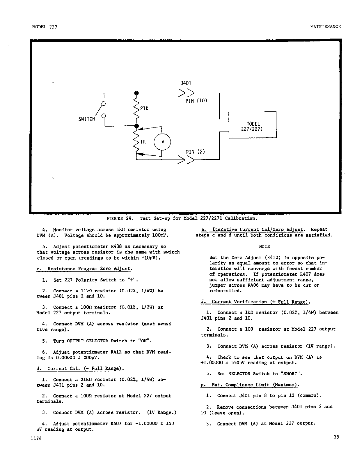
MODEL 227
MAINTENANCE
4.
Monitor voltage across 1kC resistor using
D"M (A). Voltage should be approximately 10&&V.
5. Adjust potentiometer R438 as necessary so
that voltage across resistor is the same with switch
closed or open (readings to be within UOpV).
C. Resistance Pronram Zero Adjust.
1. See
227
Polariry Switch to "+".
2.
Connect a llkn resistor (0.02X, 1/4W) be-
tween 5401 pins 2 and 10.
3.
connect a loon resistor (O.Ol%, 112W) *t
Model 227 output terminals.
4.
Co~ect D"" (A) across resistor (most sensi-
tive range).
5.
Turn OUTPUT SELECTOR Switch to "ON".
6. Adjust potentiometer R412 so that DVM read-
ing is 0.00000 t
ZOOVJ.
d. Current Cal. (- Full Range).
1. Co,,r,e~r a 21kO resistor
(0.022, 114W)
be-
t"een 5401 pins 2 and 10.
2. Connect a 1000 resistor at Model 227 output
terminals.
3.
Connect D"M (A) across resistor. (1V Range.)
4. Adjust potentiometer R407 for -1.00000 C 150
u" reading at output.
1174
e. Iterative Curtent Cal/Zero Adiust. Repeat
steps c and d until both conditions are satisfied.
NOTE
Set the Zero Adjust (R412) in opposite po-
larity an equal amount to error 80 that in-
teration will converge with fewest number
of operations. If potentiometer R407 does
not allow sufficient adjustment range.
jumper across R406 may have to be cut or
reinstalled.
f. Current Verification (+ Fvll Range).
1. Connect a lk0 resistor (O.OZ%, 1/4W) between
5401 pins 2 and 10.
2. Connect a 100 resistor at Model 227 output
terminals.
3.
connect DVM (A) *cros* resistor (1V range).
4.
Check to see that output on DVM (A) is
+l.OOOOO t 55OvV reading at output.
5.
Set SELECTOR Switch to "SHORT".
8. Ext. Compliance Limit (Maximuml.
1. connect 3401 pin 8 to pin 12 (common).
2.
Remove connections between 5401 pins 2 and
10 (leave open).
3.
connect DVM (A) at Model 227 output.
35
MAINTENANCE MODEL 227
4. Cannect.5401 pin 15 to pin 12 (common).
CAUTION
Up to 300 volts is present at various rear
panel cermina1s a* well es internal cir-
cuit points.
5. Connect 5401 pin 1 to pin 9.
6. Connect a 1kR resistor (0.02%) beween 3401
pins 2 and 10.
7. Set OUTPUT SELECTOR Switch to "ON".
8. Record voltage reading at output.
9. Connect a 21kn resistor (0.02%) between
5401 pins 2 and 10. (Remove 1kR resistor).
10. Compare reading of srep 9 to that of step 10.
11. Select resistor value (1kR or 21kn) which
gives the lowest (absolute value) reading.
12. With this resistor installed, adjust po-
tentiometer R405 for a reading of 305V t 1V.
13. Set OUTPUT SELECTOR Switch to "SHORT".
14. Remove connection at 5401, pi" 15.
15. Set
OUTPUT
SELECTOR Switch to "ON".
16. Output voltage should read
55V _C 2V.
17.
Set OUTPUT SELECTOR Switch to "SHORT".
18. Remove connection between 5401 pins 1 and 9.
h. Ext. Com~llance Limit (Minimum).
1. Connect a lkn resistor between J401 pins 2
and 10.
2. Connect 5401 pin 15 to pin 12.
3.
Connect DVM (A) across output.
NOTE
Make certain M connection is made between
5401 pins 1 and 9 (open).
4.
Sef
OUTl’“T
SELECTOR Switch to "ON".
5.
Voltage at output should be lass than 9"
volts (positive).
6.
Connect 21kO resistor between 5401 pins 2
and 10.
7. Voltage et output should be less than 9V
vo1rs (negative).
8. Repeat steps 2 through 7 with 5401 pi" 15 not
connected to pi" 12. "c&age reading should be less
then
k3.5V.
6-6. MODEL 2271 CHECKOUT (Not Installed in Model
227).
a. Power Supply Check.
1. Connect external+12 volt supply (needed only
for check-out purposes) to printed circuit board
PC-342. Connector 5405
pi" F should be +12" with
respect to pin B. Connector
5405
pi" E should be
-12V
with respect to pin B.
2.
CD”“ect exCer”al +5V
supply to connector 5401
pin 4,
(+SV)
end pin 12 (cormon). External supply
should be rated at +5V to t6V et 200 milliamperes.
b. Relay Check. (An ohmmeter is required for this
check to verify open circuit and short circuit condi-
tions . )
NOTE
Connect 5404 pin B fo 12V common (5405,
pi"
B) co energize relay K408. This action con-
neccs the +5V supply co Model 2271 circuitry.
1. Remote Compliance Limit (Relay K407).
Momentarily connect 5401 pi" 8 to pi" 12
(+kmo"~ to energize K407.
b). Check condition of relay confects et 3405
G and D using a" Ohmmeter.
c) . Contacts should open (infinite resistance)
when closure to common is made.
2. 3OOV
Compliance Range (Relay K406).
4. Momentarily connect 5401 pin 15 to pin I.2
(common)
to energize K406.
b).
Check condition of relay contacts et 5405
K end H "sin8 en Ohmmeter (H).
c) . Contacts should close (zero resistance)
when closure to comma,, is made.
d) . Check condition of relay contacts at
K406A
pins 5 and 6 or across R419.
4.
Resistance
should change from 00 to approx-
imately 20kQ when closure to cocaon is made.
f). Leave 5401 pi" 15 to pi" 12 connected for
next test.
3. 1OOOmA Range (Relays K404, K405, end K406).
a).
Momentarily connect 3401 pin 7 and pin 12.
b).
Check condition of relay contacts at 5405
K and H "sin8 an ohonnerer.
4. Contacts should open (infinite resistance)
when closure to common is made.
d) . Check condition of relay contacts at 5404
pin K and pi" C using a" Ohmmeter (B).
36
1174
MODEL 227 MAINTENANCE
f). Remove connections between pins 7, 12, and
15 before proceeding to next step.
4. lOOmA Range (Relay K403).
a). Momentarily mnnecf 5401 pin 14 to pin 12
(common) fo energize relay K403.
b). Check condition of relay contaces at 5404
pi" K and F.
cl. Contacts should close (zero resistance)
when closure to cormnon is made.
5. 1OmA Range (Relay K402).
a). Momenrarily connect 5401 pin 6 to pin 12
(comon) to energize relay K402.
b). Check condition of relay contacts at 5404
pin K and E.
c) . Contacts should close (zero resistance)
when closure to common is made.
6. 1OOOpA Range (Relay K401).
a). Momentarily connect 5401 pin 13 to pin 12
(common) to energize relay K401.
b). Check condition of relay contacts at 5404
pin K and A.
C). Contacts should close (zero resistance)
when closure to common is made.
c. Compliance Monitor Check.
1. Connect a 312Q resisror (5%. 1/2W) between
5401 pin 5 and pin 4 (+5V supply).
NOTE
Current through the 312Q resistor should be
16mA. Set the +5 volt supply to achieve the
C"lTC2*t.
2. Voltage between 5401 pin 5 and pin 12 should
be less than f0.4V. (Leave resistor connected for
next seep.)
3. Connect a 3600 resistor (5X, 1/2W) between
5406 pin A and 5405 pin F (+12V supply).
4. connect a jumper wire between 5406, pin B to
5405, pin B
(12V
common).
5. Voltage at 5401 pin 5 should be greater than
+2.4V.
6.
Disconnect resisrors and jumper.
NOTE
Should it be necessary to remove the Model 2271
Option from the Model 227 chassis, con,,ector
J206A. furnished with each 22712271 (shown on
schematic 262263) must be ins&led at P206.
Connecror J206A is a ten-pin Berg Connector
with jumper wires between pins A and C; D and G.
0975
37
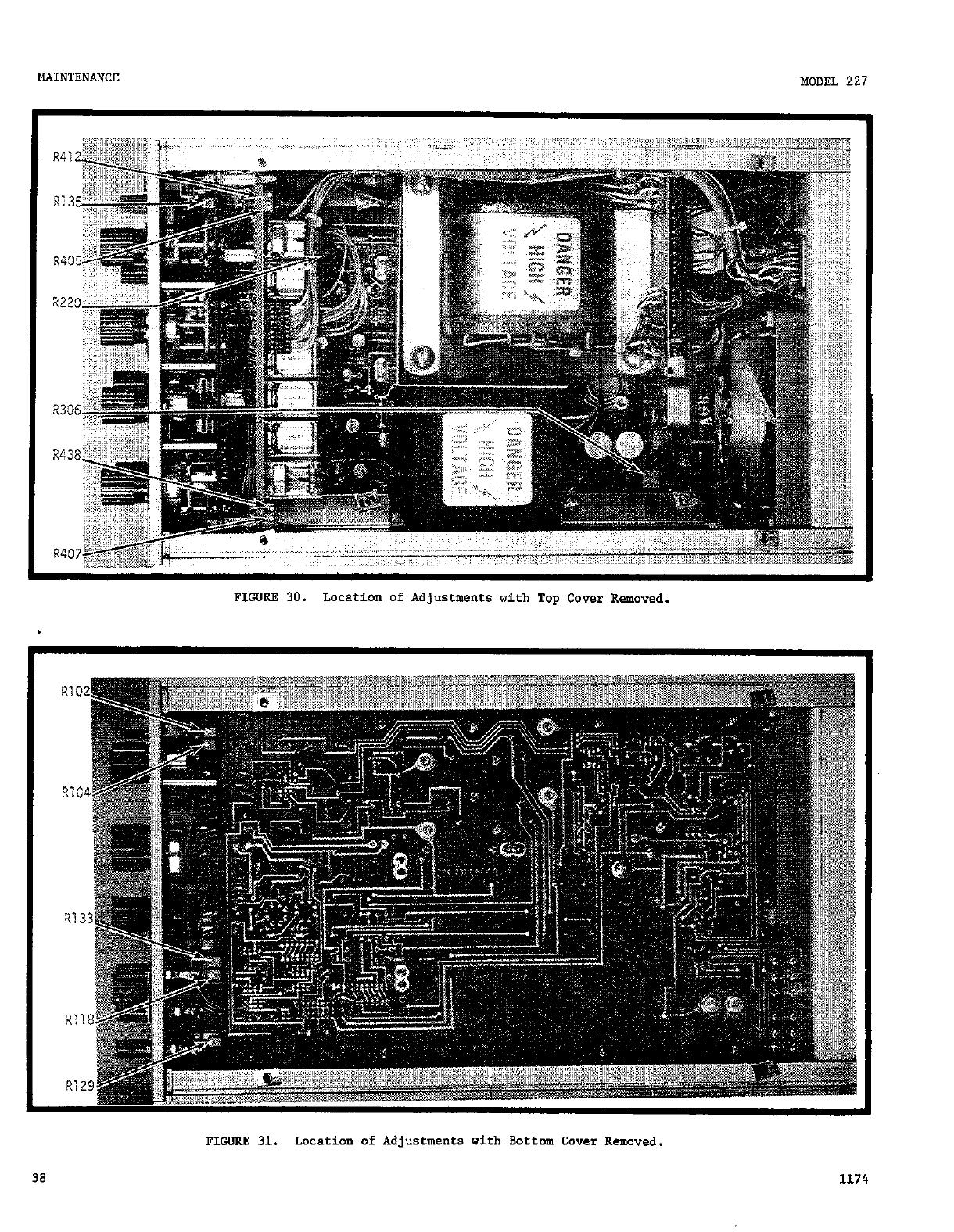
MAINTENANCE MODEL 227
FIGURE 30. Location of Adjustments with Top Cover Removed.
38
F1Gw.E 31. Location of Adjustments with Bottom Cover Removed.
1174
MODEL 227 REPLACEABLE PARTS
SECTION 7. REPLACEABLE PARTS
7-1. GENERAL. This section contains information for
ordering replacement parts. The parts list is arrang-
ed in alphameric order af their Circuit Designations.
7-2. ORDERING INFORMATION. To place an order or to
obtain information concerning replacement parts, con-
tact your Keithley representative or the factory. See
the inside front cover of the manual for addresses.
When ordering, include the following information:
a. Insfrument: Model Number
b. Instrument Serial Number
C. Part Description
d. Circuit Designation (if applicable)
e. Keithley Stock Part Number.
7-3. SCHmTIC IlI*GRAMs.
a, Power Supply (26227D). This schematic des-
cribes the line-operated power supply, including
fuses, fan, and thermal circuit-breaker. Circuit
designation series 1s "300".
b. Current Source (262263). This schematic des-
cribes the range switching, regulating amplifiers,
reference amplifier, and other controls. Circuit
designation series is "100" for Switch Board, PC-330
and "200" far Mother Board, PC-331.
C. Model 2271 Programming Option (266083). This
schematic describes the controls for range, current,
and compliance. Circuit designation series is "400".
1174 39
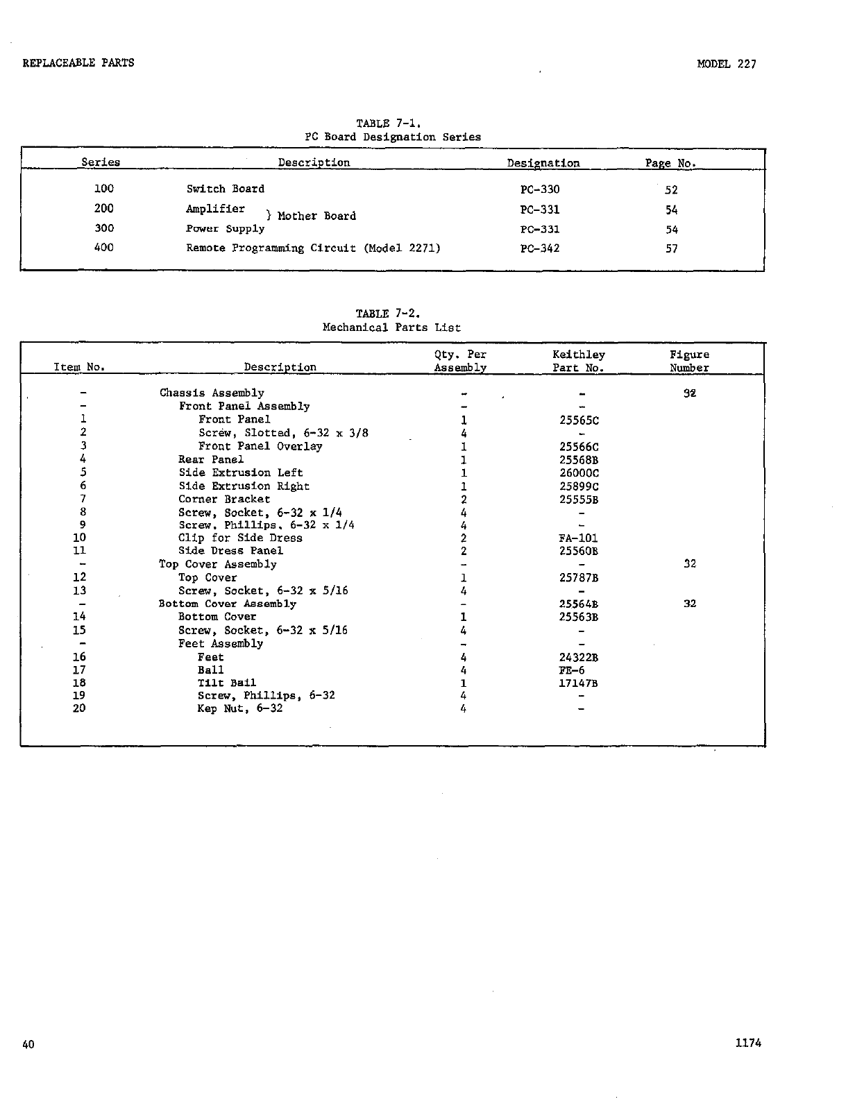
REPLACEABLE PARTS MODEL 227
TABLE 7-1.
PC Board Desiznnatian Series
Series Description
100 Switch Board
200 Amplifier > Mother Board
300 Power Supply
400 Remfe Programming Circuit (Model 2271)
Designation
PC-330
PC-331
PC-331
PC-342
Page No.
52
54
54
57
TABLE 7-2.
Mechanical Parts List
Item No. Description Qty. Per
Assembly Keithley
Part No.
Chassis Assembly - 92
Front
Panel
Assembly
1
Front Panel 1
25565C
2 Scr&, Slotted, 6-32 x 318 4
3
Front
Panel Overlay 1 25566C
4 Rear Panel 1 25568B
5 Side Extrusion Left 1 26000C
6 Side Extrusion Right 1 25899C
7 Corner Bracket 2 25555B
8 Screw, Socket, 6-32 x l/4 4
9 Screw. Phillips, 6-32 x l/4 4
10
Clip for Side Dress 2 FA-101
11 Side Dress Panel 2 255608
Top Cover Assembly 32
12 Top Cover 25787B
13 Screw, Socket, 6-32 x 5116 t
Bottom Cover Assembly 25564B 32
14 Bottom cover 1 25563B
15 Screw, Socket, 6-32 x S/16 4
Feet Assembly
16 Feet 4 24322B
17 Ball 4 FE-6
Tilt Bail
Screw, Phillips, 6-32
Kep Nut, 6-32
1
4
4
17147B
40 1174

MODEL 227 REPLACEABLE PARTS
FIGURE 32. Chassis Assembly.
1174 41
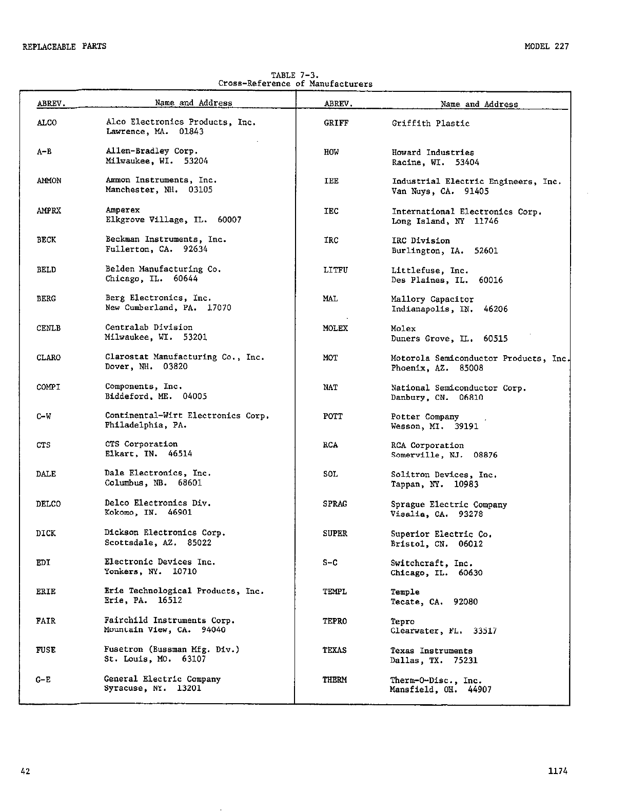
REPLACEABLE PARTS MODEL 227
AWE”. Name and Address
ALCO
A-B
AMMON
AMPRX
BECK
BELD
BERG
CENLB
CLARO
COMPI
c-w
CTS
DALE
DELCO
DICK
ED1
ERIE
FAIR
FUSE
G-E
Alto Electronics Products, Inc.
Lawrence, MA. 01843
Allen-Bradley Corp.
Milwaukee, WI. 53204
Ammo* Instr"me"ts, 1°C.
Manchester, NH. 03105
Amperex
Elkgrove Village, IL. 60007
Beckman Instruments, Inc.
Fullerton, CA. 92634
Belden Manufacturing Co.
Chicago, IL. 60644
Berg Electronics, Inc.
New Cuberland, PA. 17070
Centralab Division
Milwaukee, WI. 53201
Clarostat Manufacturing Co., Inc.
Dover, NH. 03820
Components, Inc.
Biddeford, ME. 04005
Continental-Wirt Electronics Carp.
Philadelphia, PA.
CTS corporation
Elkarc, IN. 46514
Dale Electronics, Inc.
c01umbus, NB. 68601
Delco Electronics Div.
Kokomo, IN. 46901
Dickson Electronics Corp.
Scottsdale, AZ. 85022
Electronic Devices Inc.
Yonkers, NY. 10710
Erie Technological Products, Inc.
Erie, PA. 16512
Fairchild Instruments Corp.
Mountain View, CA. 94040
Fusetran (Bussman Mfg. Div.)
St. Louis, HO. 63107
General Electric Company
Syracuse, NY. 13201
AliRE”. Name and Address
GRIFF
HOW
IEE
IEC
IRC
LITF"
MAL
MOLBX
MOT
NAT
POTT
RCA
SOL
SPRAG
SUPER
s-c
TK!fPL
TEPRO
TEXAS
THERM
TABLE 7-3.
Cross-Reference of Manufacturers
Griffith Plastic
Howard Industries
Racine, "I. 53404
Industrial Electric Engineers, Inc.
"an Nuys, CA. 91405
International Electronics Corp.
Long Island, NY 11746
IRC Division
Burlington, IA. 52601
Littlefuse, Inc.
Des Plaines, IL. 60016
Mallory capacitor
Indianapolis, IN. 46206
Malex
Duners Grave, IL. 60515
Motorola Semiconductor Products, In
Phoenix, AZ. 85008
National Semiconductor Corp.
Danbury, CN. 06810
Potter Company
weeson, MI. 39191
RCA COrpOration
Somerville, NJ. 08876
Solitron Devices, Inc.
Tappan, NY. 10983
Sprague Electric Company
Visalia, CA. 93278
Superior Electric Co.
Bristol, CN. 06012
Switchcraft, IDC.
Chicago, IL. 60630
Temple
Tecate,
CA. 92080
Tepro
Clearwater, FL. 33517
Texas Instruments
Dallas, TX. 75231
Therm-O-Disc., Inc.
Mansfield, OH. 44907
42 1174
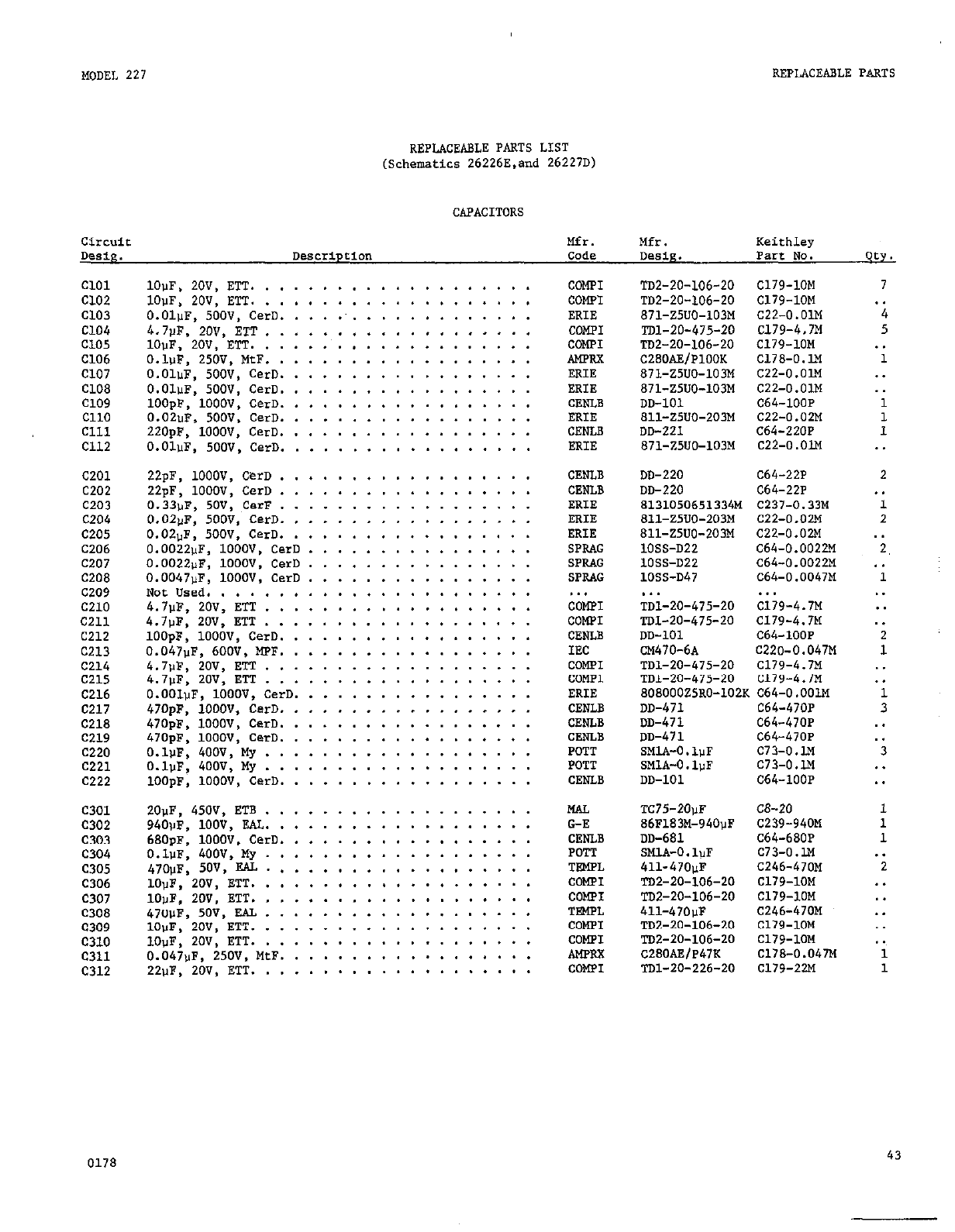
MODEL 227 REPLACEABLE PARTS
REPLACEABLE PARTS LIST
(Schematics 26226E,and 26227D3)
CAPACITORS
Description
Mfr.
Code Mfr.
Deslg. Keithley
Part No. t .
Cl01
Cl02
Cl03
Cl04
Cl05
Cl06
Cl07
Cl08
Cl09
Cl10
Cl11
Cl12
c201
c202
C203
C204
C205
C206
C207
C208
c209
c210
CZll
c212
C213
c214
c215
C216
c217
C218
c219
c220
c221
c222
c301
C302
c303
c304
c305
C306
c307
C308
c309
c310
C311
C312
lOvF, 2OV, ETT. . .
lOuF, 20", ETT. . .
O.OluF, 5OOV, CerD.
4.?uF, ZOV, ETT . .
IOpF, 20". ETT. .
O.lliF, ZSOV, MtF. .
O.OluF, SOOV, CerD.
O.Ol!lF, 5oov. cerIl.
lOOpP, 1000". CerD.
0.02uF. 5OOV. CerD.
220pF, IOOOV, CerD.
O.OW, SOOV, CerD.
22pF, lOOOV, CerD .
22pF, lOOOV, CerD .
0.33uF, 5OV, CerF .
O.OZuF, 50OV, Gem.
0.02~F, 5OOV, CerD.
0.0022uF. lOOOV, Cerll
0.0022uF. 1OOOV. CerD
0.0047uF. 1OOOV. CerD
Not U&d: . . .'. . .
4.?uF, 2OV, ETT . . .
4.?uF, 20", ETT . . .
lOOpF, lOOO", CerD. .
O.O4?,,F, 6OOV, MPF. .
4.7@, ZO", ETT . .
4.7uF. 20". ETT . . .
O.OOl,,F, lbOOV, CerD.
47OPP, lOOOV, cem. .
4?0PF, 1000", CerD. .
470pF. 1000". CerD. .
O.lvF, 4OOV;My . . .
O.lpF, 4OOV, My . . .
100pF, 1000", CerD. .
2OpP, 450". ETB . .
940pF, lOOV, FAL. .
680pF, lOOOV, CerD.
O.luF, BOOV, My . .
4?0uF, 50", FJ& . .
1O,,F, 20", ETT. . .
lO,,F, 20V. ETT. . .
470°F. 50". FAL . .
lO,,F, 20V;ETT. . .
lO,,F, 2OV, ETT. . .
O.O4?vF, 250". MtF.
22,iF, ZOV, ETT. . .
. . .
. . .
. . .
. . .
. . .
. .
. * .
. . .
. . .
. .
. . .
. . .
. . .
. . .
. . .
. . .
. . .
. .
. .
. .
. .
. .
. .
. *
. .
. .
.
.
, ,
. .
. .
.
. .
. .
. .
.
.
. .
. *
. .
. .
. .
. .
. .
. .
* .
. .
. .
. .
. .
. .
. .
.
. .
. .
. .
.
. *
. .
. .
. .
, .
. .
. . .
. . .
. . .
. . .
* . .
. . .
. . .
. . .
. . .
. .
. . .
. . .
. . .
. . .
. . .
. . .
. . .
. . .
. . .
. . .
. . .
. . .
. . .
. . .
. . .
. . .
* . .
. . .
. . .
. . .
. . .
. . .
. . .
. . .
. . .
. . .
. . .
. . .
. .
. . .
. . .
. . .
. . .
. . .
. . .
. . .
. . .
. . .
. . .
. . .
. . .
. .
. . .
. . .
. . .
. .
. . .
, , .
. .
. . .
. . .
. . .
. . .
. . .
. . .
. . .
. . .
. . .
. . .
. . *
. .
. . .
. .
. . .
. . .
. .
. *
. .
. .
. .
. .
. .
.
. .
. .
. .
. .
. .
. .
* .
. ,
. .
. .
. .
. .
. .
. .
.
. .
. .
. .
. .
. .
, .
.
. .
. .
. .
. .
* . .
. . .
. . .
. . .
. . .
. .
. . .
. . .
. . .
. . .
. . .
. * .
COMPI
COMPI
ERIE
CO&PI
COMPI
AMPFS
ERIE
ERIE
CENLB
ERTE
CENLB
ERIE
CENLB
CENLB
ERIE
ERIE
ERIE
SPRAG
SPRAG
*..
COMPI
COMPI
CENLB
IEC
COMPI
COMPI
ERIE
CENLB
CENLB
CENLB
POTT
POTT
CENLB
MAL
G-E
CENLB
POTT
TmL
COMPI
COMPI
TE+PL
COMPI
COMFI
AMPRK
COMPI
TD2-20-106-20
C2SOAE/PlOOK
TD2-20-106-20
8?1-25UO-103M
8?1-Z5UO-103M
871-ZSUO-103M
TDl-20-475-20
TD2-20-106-20
C1?9-10M
C179-10M
C22-O.OlM
C179-4. JM
C179-10M
C178-0.m
DD-101
ml-zwo-203M
DD-221
S?l-25UO-103M
C22-0.02M
C64-220P
c22-o.olM
c22-o.olM
C22-O.OlM
C64-100P
DD-220
DD-220
8131050651334M
811-Z5"0-2O3M
811-ZSUO-203M
loss-D22
lOSS-D22
lOSS-D47
. . .
TDl-20-475-20
TDl-20-475-20
DD-101
C64-22P
C64-22P
C23?-0.33M
c22-0.0%
c22-0.02M
C64-0.0022M
C64-0.0022M
C64-0.0047M
. . .
C179-4.7M
c179-4.7M
C64-1OOP
CM4?0-6A C220-0.047M
TDl-20-475-20 C179-4.7M
TDl-20-475-20 C1?9-4.7M
80800025RO-102K C64-O.OOlM
DD-471
DD-471
DD-471
SMlA-0.1uF
SMlA-O.l"F
DD-101
C280AEIP47K
TDl-20-226-20
TC?S-20@
86F183M-940uF
DD-681
SHIA-O.luF
411-4?0,,F
TD2-20-106-20
TDZ-20-106-20
411-470pF
TD2-20-106-20
TDZ-20-106-20
C64-47OP
C64-470P
C64-47OP
c73-0.l.M
C?3-0.m
C64-1OOP
C178-o.o4?M
C179-22M
CB-20
C239-940M
C64-6SOP
c73-o.lM
C246-47OM
C179-10M
C1?9-10M
C246-470M
C1?9-1OM
C179-1OM
7
. .
4
5
. .
1
. .
. .
1
1
1
. .
2
. .
1
2
.
2,
. .
1
. .
. .
.
2
1
. .
1
3
.
.
3
. .
. .
1
1
1
. .
2
. .
. .
. .
.
. 9
1
1
0178 43
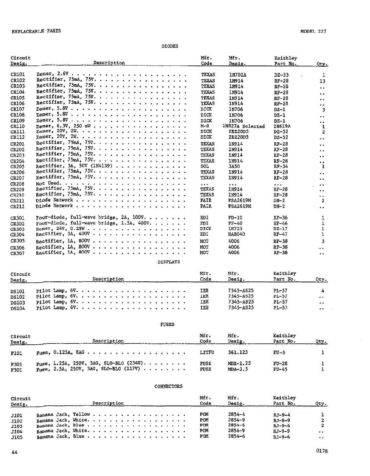
REPLACEABLE PARTS MODEL 22,
DIODES
Mfr. Mfr. Keithley
Code Desig. Part No. t .
CR101
CR102
CR103
ml04
CR105
ml06
ml07
CR108
ml09
ml10
CR111
CR112
CR201
CR202
CR203
CR204
CR205
CR206
CR207
CR208
CR210
CR211
CR212
.~~
Not Used .........................
Rectifier, 75mA, 75V. ................
Rectifier, 75ti, 75V. ................
Diode Network .................
Diode Network .................
CR301
CR302
CR303
CR304
CR305
CR306
CR307
Four-diode, full-wave bridge, ZA, 1OOV. ......
Four-diode, full-wave bridge, l.SA, 400V. .....
zener. 24V, 0.25W .................
Rectifier, 3A, 400V ................
Rectifier, lb., 8oov ................
ReCtifieI, l& 8oov ................
Rectifier, IA, ROOV ................
DISPLAYS
circuit
De+%.
zener, 2.6V ...
Re,Ctifi6&', ?h& 75v.
.................... : : : : : : :
R‘JCtifieI, %& 75',
.................
Rectifier, 7.%& 7%. ................
Rectifier, 75!& 75V. ................
RBCtifier, 75mA. 75V. ................
zener, 5.b . :. . . * . . . . .
zener, 5.8V . . . . . I . . . . .
zener, 5.m . . . . . . . . . . .
zener, 6.3V, 250 m" . . . , . . .
zener, zov, 2w. . . . . . . . . ,
zener, zov, 2w. . . . . . . . . .
Rectifier, 75.d. 75v. . . . . . .
Rectifier, 75x& 75V. . . . . . .
Rectifier, 75mA, 75V. . . . , . .
Rectifier* .75mA. 75v. . . . . . .
..-
Rectifier; 3A, iOV (lN4139)
Rectifier, 75mA, 75v. . . . : : :
Rectifier, 75wA. 75v. . . , , . .
. . .
. . .
. . .
. . .
. . .
. . .
. . .
. * .
. . .
. . .
. . .
. . .
* . .
. . . . .
. . . . .
. . . . .
. . . . .
. . . . .
. . . . .
. . . . .
. . . . .
. . . . .
. . . . .
. . . . .
, . . . .
. . . . *
TEXAS
TEZAS
TEXAS
TEXAS
TEXAS
TEXAS
DICK
DICK
DICK
M-S
DICK
DICK
TEXAS
TEXAS
TEXAS
TEXAS
SOL
TEXAS
TEXAS
lN702A
lN914
lN914
lN914
lN914
lN914
lN706
l&706 DZ-1 . .
lN706 DZ-1 . .
lN827A Selected 286198 1
ZEZZOD5 DZ-52 2
ZEZZOD5
lN914
lN914
lN914
lN914
3A50
lN914
lN914
. . .
TEXAS
TEXAS
FAIR
FAIR
. . .
~lN914
lN914
FSA2619M
FSA2619M
ED1 PD-10
EDI PF-40
DICK lN723
ED1 RABo40
MOT 4006
MOT 4006
MOT 4006
DZ-33 1
RF-28 13
RF-28 . .
RF-28 . .
RF-28 . .
RF-28 . .
DZ-1 3
DZ-52 . .
RF-28 * .
RF-28 . .
RF-28 . .
RF-28 . .
RF-34 1
RF-28 . .
RF-28 . .
. . . . .
RF-28 . .
RF-28 . .
DN-2 2
DN-2 . .
RF-36 1
RF-46 1
DZ-17 1
RF-47 1
RF-38 3
RF-38 . .
w-38 ,.
Description Mfr. Mfr. Keithley
Code Desig. Part No. t .
DSlOl pilot Lamp, 6V. .................. IEE 7345-AS25 PL-57 4
DS102 pilot Lamp, 6V. .................. IEB 7345-AS25 PI.-57 . .
DS103 pilot Lamp, 6V. .................. IEE 7345-AS25 PL-57 . .
DS104 pilot Lamp, 6V. .................. IEE 7345-8825 PL-57 . .
FUSES
Description Mfr. Mfr. Keithley
Code De&. Part NO. t .
FlOl F"BB, 0.125A, SAG . . . . . . . . . . . . . . . . . . LITFD 361.125 Fu-5 1
F301 ~"ee, 1.25A, 25OV,
3AG,
SLO-BLO (234V). ....... FUSE MDX-1.25 FU-28
F301 Fuse, 2.5A, 25OV, 3AG, SLO-BLO (117V) ........ FUSE MDA-Z.5 FU-45
CONNECTORS
Mfr. Mfr. Keithley
Code Desig. Part No. t .
no1 ~*nena Jack, Yellow ................ POM 2854-4 BJ-9-4 1
5102 banana Jack, White. ................ PO" 2854-9 BJ-9-9 2
5103 Banana Jack, Blue ................. POM 2854-6 M-9-6 2
5104 *mana Jack, White. ................ POM 2854-9 BJ-9-9 . .
no5 ~~,,ana Jack, Blue ................. PGM 2854-6 BJ-9-6 . .
44 0178
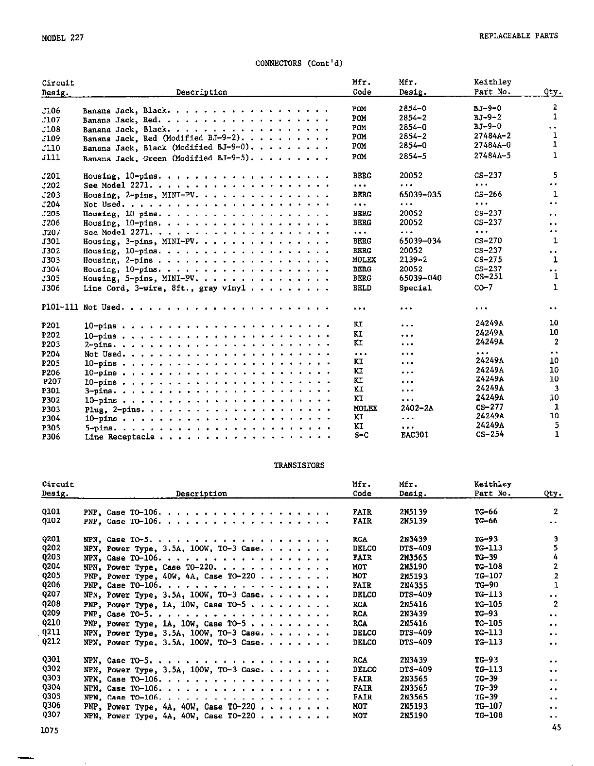
MODEL 227
Circuit
Desig.
REPLACEABLE PARTS
CONNECTORS (Cont'd)
Mfr. Mfr. Keithley
Code Desig. Part No. e .
5106
Banana Jack, Black. .........
5107 Banana Jack, Red. ..........
J108 banana Jack, Black. .........
J109 banana Jack, Red (Modified BJ-9-Z). .
.I110 banana Jack, Black (Modified BJ-9-O).
Jlll Banana Jack, Green (Modified 85-9-S).
5201
musing, lo-pins. ..........
5202 See Model 2271. ...........
5203
'dousing, Z-pins, MINI-PV. ......
3204
Not Used. ..............
5205
Housing, 10 pins. ..........
5206 Housing, lo-pins. ..........
5207 See Model 2271. ...........
5301 Housing, )-pins, MINI-PV. ......
5302 musing, lo-pins. ..........
5303 Housing, z-pins ...........
5304 Housing, lo-pins. ..........
5305
Rousing, S-pins, MINI-PV. ......
5306 Line Cord, 3-wire, Sft., gray vinyl .
PlOl-111 Not Used. ..............
P201
lo-pins ...............
P202
lo-pins ...............
P203 z-pins. ...............
P204 Not Used. ..............
P205 lo-pins ...............
P206
lo-pins ...............
P207
lo-pins ...............
P301 3-pins ................
P302 lo-pins ...............
P303 Plug. z-pins. ............
P304
lo-pins ...............
P305 5-pins ................
P306 Line Receptacle ...........
........
........
........
........
........
........
........
........
........
........
........
........
........
........
........
........
........
........
........
. . . . . . . .
........
........
........
........
........
........
........
........
........
........
........
........
........
POM
2854-O
BJ-9-O
POM
2854-2
BJ-9-2
POM
2854-O
BJ-9-0
POM
2854-2 274848-Z
POM
2854-O
274848-O
POM
2854-5
274848-S
BERG
. . .
BERG
. . .
BERC
BERG
. . .
BERG
BERG
MOLEX
BERG
BERG
BELD
20052
65039-035
. . .
20052
20052
65039-034
20052
2139-2
20052
65039-040
Special
CS-237
I..
CS-266
. . .
CS-237
CS-237
. . .
CS-270
CS-237
CS-275
CS-237
CS-251
co-7
*.. . * .
KI
KI
KI
. . *
. . .
. . .
. . .
. . .
. . .
. . .
. . .
242498
24249A
242498
. . .
KI
KI
KI
KI
KI . . .
2402-2A
I..
24249A
242498
242498
242498
242498
CS-277
2424911
24249A
CS-254
TUNSISTORS
. . .
EAc301
2
1
. .
1
1
1
5
. .
1
. .
. .
. .
. .
1
. .
1
. .
1
1
. .
10
10
2
. .
10
10
10
1;
1
10
5
1
Keirhley
Parr No. t .
Circuit
Desig. Code
Mfr.
Desig .
QlOl
PNp, Case
TO-106.
. . . . . . . . . . .
0102
PNp, Case
TO-106.
. . . . . . . . . . .
Q201
Q202
6203
Q204
9205
Q206
Q207
9208
Q209
9210
.Q211
Q212
9301
6302
Q303
4304
Q305
6306
9307
NPN, Case
TC-5.
. . . . . . . . . . . .
NPN, Power Type,
3.5A,
lOOW, TO-3 Case.
NPN, Case TC-106. . . . . . . . . . . .
NPN, Power Type, Case TO-220. . . . . .
PNP. Power Type, 4OW, 4A, Case
TO-220 .
PNP, Case TO-106. . . . . . . . . . . .
NPN, Power Type, 3.5A, lOOW, TO-3 Case.
PNP, Power Type, lA, lOW, Case TC-5 . .
PNP, Case TO-5.
. . . . . . . . . . . .
PNP, Power Type, lA, lOW, Case
TO-5 . .
NPN, Pcver Type,
3.5A,
lOOW, TC-3
Case.
NPN, Power Type, 3.5A, lOOW, TO-3 Case.
.......
.......
.......
.......
.......
.......
.......
.......
.......
.......
.......
.......
.......
.......
FAIR 2N5139 TG66
FAIR 2N5139 TG-66
RCA
DELCO
FAIR
MOT
MOT
FAIR
DELCO
RCA
RCA
RCA
DELCO
DELCO
2N3439
DTS-409
2113565
2N5190
2N5193
2N4355
DTS-409
285416
283439
285416
DTS-409
DTS-409
NPN, Case TO-5.
. . . . . . . . . . . .
. . * . . . . RCA 2313439
NPN, Power Type, 3.5A, lOOW, TO-3 Case. . . . . . . . DELCO DTS-409
NPN, Case TO-106. . . . . . . . . . . . . . . . . * . FAIR 2~3565
NPN, Case
TO-106.
. . . . . . . . . . .
. . . . . . . FAIR 2N3565
NPN, Case
TO-106.
. . . . . . . . . . .
. . . . . . . FAIR 2~3565
PNP, Power Type, &A, 4OW, Case TO-220 . . . + . . . . MOT 2N5193
NPN, Power Type, 4A, 4OW, Case TO-220 . . . . . . . .
MOT
2N5190
TG-93
To-113
TG-39
TG-108
TG107
TO90
TG113
To105
m-93
TO105
TO113
TC-113
TO93
TG-113
TO39
TG39
TG-39
TG-107
TO108
2
3
5
4
2
2
1
. .
2
. .
. .
. .
. .
. .
. .
. .
. .
. .
. .
. .
45
1075
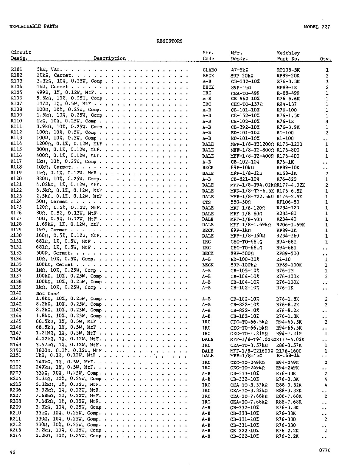
REPLACEABLE PARTS
Circuit
Desis. Description
RESISTORS
Mfr.
Code Mfr.
Desig.
MODEL 227
Keithley
Part No. f .
RlOl
R102
R103
R104
RIO5
RlO6
R107
RlOS
Rlo9
RllO
RJ.11
R112
RI13
R114
Rl15
R116
R117
R118
R119
R120
R121
R122
R123
R124
R125
R126
R127
Rl28
R129
R130
R131
R132
R133
R134
R135
R136
R137
R138
R139
Rl40
R141
P.l42
R143
R144
R145
R146
R147
R148
R149
8150
R151
R201
R202
R203
R204
R205
R206
R207
R208
R209
R210
R211
R212
R213
R214
46
5kC, Var. ...........
ZOkR, Cermet. .........
3.3kn, lo%, 0.25W, Camp . : . .
lkR, Cermer ..........
499il. 1%. 0.12W. MeF. .....
5.6kti, lb%, 0.25W, Cmp . . . .
1370, l%, O.SW, MtF . . . . . .
1000, 10%. 0.25W, Camp. . . . .
l.Skn, lo%, 0.25W, Camp . . , .
lkn, lo%, 0.25W, Cm,, . . . .
3.9kQ, lo%, 0.25W, Camp . . . .
lOOR, lO%, 0.5w, camp .
loon, lO%, o.sw, corn* .
12oot7, 0.1%. O.lZW, MtF
................
...............
...............
...............
...............
...............
...............
...............
...............
...............
...............
...............
...............
...............
...............
...............
...............
...............
...............
...............
...............
...............
...............
...............
...............
...............
...............
...............
...............
...............
...............
...............
...............
...............
...............
...............
...............
................
...............
...............
...............
...............
...............
...............
...............
...............
...............
...............
...............
...............
...............
...............
...............
SOOR, O.l%, O.lZW, MtF.
4000, O.l%, O.lZW, MtF.
lkn, lo%, 0.25W, Camp .
lOkn, Cennet. . . . . .
lkn, 0.1X, O.lZW, MtF .
8200, 10%. O.ZSW, Camp.
4.02k0, l%, O.lZW, MtF.
6.5kQ, O.l%, O.l2w, MtB
2.5k0, O.l%, O.lZW, MtP
500, Cermet . . . . . .
12on. 0.5%. 0.12w. Mm.
.
800, 0.5%, O.lZW, MtF .
4002, 0.5%. O.lZW, MtF .
1.69k0, 1%, O.IZW, MtF.
1kR. Cermet . . . , . .
160& O.S%, O.l2W, MtF.
6813, 1X, 0.5W, MtF . .
681n. 1%. O.SW. MtF . .
SOOn; C&met. : . . . .
100, lO%, 0.5w, camp. .
lOOk0, Cemet . . . . .
lMQ, 10X, O.ZSW, Camp ,
lOOka, lo%, 0.25W, Camp
lOOkR, lo%, 0.25W, Camp
lkn, 10%. 0.25W, Camp .
Not Used
l.Skn, lo%, 0.25W, Camp
S.ZkC, 10X, 0.25W, Camp
8.2k0, lo%, O.ZSW, Camp
l.Skn, lo%, O.ZSW, Camp
66.5kR, l%, O.SW, MtF .
66.5kn, l%, 0.5W, MtF .
l.ZlM& 1%, 0.5W, MtF .
4.02k0, l%, O.l2W, MtF.
3.57kn. 1%. 0.12W. MtF.
16000. 0.1%. 0.12W. MtF
lkn. 0.1%. 0.12W. MtF .
249kn, l%, O.SW, MtF. .
249kn, 1X, 0.5W, MfF. .
33kn, lo%, 0.25W, Camp.
3.3kR, 10%. 0.25W, Camp
3.32kn. 1%. 0.12W. MtF.
,
3.32k0, I%, O.l2W, MtF.
7.68k0, 1X, O.lZW, MtF.
7.68k0, l%, O.l2W, MtF.
3.3kn, 104, 0.25W, Camp
33k0, lo%, 0.25W, Camp.
3300, lo%, 0.25W, Camp.
33On, lo%, O.ZSW, Camp.
Z.Zkn, 10X, 0.25W, Camp
z.zkn, lO%, 0.25w, camp
. .
. *
. *
. .
. .
. .
. .
. .
. .
. .
.
. .
. .
. .
* .
. .
. .
. .
. .
. .
. .
. .
. * . .
. . . .
. . . .
. . . .
. . . .
. . . ,
. * . .
. .
. . . *
. . .
. . . .
CLARO
BECK
A-B
BECK
IRC
A-B
IRC
A-B
A-B
A-B
A-B
A-B
A-B
DALE
DALE
DALE
A-B
BECK
DALE
A-B
DALE
DALE
DALE
CTS
DALE
DALE
DALE
DALE
BECK
DALE
IRC
IRC
BECK
A-B
BECK
A-B
A-B
A-B
A-B
A-B
A-B
A-B
A-B
IRC
IRC
IRC
DALE
IRC
DALE
DALE
IRC
IRC
A-B
A-B
IRC
IRC
IRC
IRC
A-B
A-B
A-B
A-B
A-B
A-B
47-5kn RP105-5K
89P-2OkQ RP89-20K
CB-332-10% R76-3.3K
89P-lkQ RP89-lK
CEA-TO-499 R-88-499
CB-562-10% R76-5.6K
CEC-TO-137Q R94-137
CB-101-10% R76-100
CB-152-10% R76-1.5K
CB-IOZ-10% R76-1K
CB-392-10% R76-3.9K
ED-101-10% Rl-100
ED-101-10% Rl-100
MFF-l/S-T212000 Rl76-1200
MFF-l/8-TZ-8000 R176-800
MFF-l/8-TZ-400n R176-400
CB-lOi-10% R76-1K
89P-10kR RP89-10K
MFF-l/8-lk0 R168-1K
CB-821-10% R76-820
MFF-l/8-T94.02kRR177-4.02K
MFF-l/8-TZ-6.5K R176-6.5K
MPF-l/8-T22.5kO R176-2.5K
550-5on RP106-50
MFF-l/8-120Q R234-120
MFF-l/8-80!? R234-80
MFF-l/8-40n R234-40
MFF-l/8-1.69kR R206-1.69K
89P-lkn RP89-1K
mF-1/8-16on R234-160
CEC-TO-681n R94-681
CEC-TO-681n R94-681
89P-5003 RP89-500
ED-lOO-10% Rl-10
89P-100kR RP89-100K
CB-105-10% R76-1M
CB-104-10% R76-100K
CB-104-10% R76-100K
CB-102-10% R76-1K
CB-182-10%
CB-822-10%
CB-822-105:
CB-182-10%
CEC-TO-66.5kQ
CEC-TO-66.5kn
R76-1.8K
R76-8.2K
R76-8.2K
R76-1.8K
R94-66.5K
R94-66.5K
CEC-TO-1.2l"P R94-1.2l.M
MFF-l/8-T94.02kRRl77-4.02K
CEA-TO-3.57kR R88-3.57K
MFF-l/8-T21600R Rl76-1600
MFF-l/8-1kQ R-168-lk
CEC-TO-249kn R94-249K
CEC-TO-249kn R94-249K
CB-333-10% R76-33K
CB-332-10% R76-3.3K
CEA-TO-3.32kQ R88-3.32K
CFA-TO-3.32kn RSS-3.32K
CRA-TO-7.68kn R88-7.68K
CEA-TO-7.68kR
CB-332-10%
CB-333-105:
CB-331-10%
CB-331-10%
CB-222-10%
CB-222-10%
R88-7.68K
R76-3.3K
R76-33K
R76-330
R76-330
R76-2.2K
R76-2.2K
1
2
1
2
1
1
1
1
1
3
1
2
. .
1
1
1
. .
. .
2
1
2
1
1
1
1
1
1
1
1
1
2
. .
. .
1
1
1
2
. .
. .
2
2
. *
. .
2
. .
1
. .
1
1
. .
2
. .
2
4
4
. .
2
. .
. .
. .
2
. .
2
. .
0776
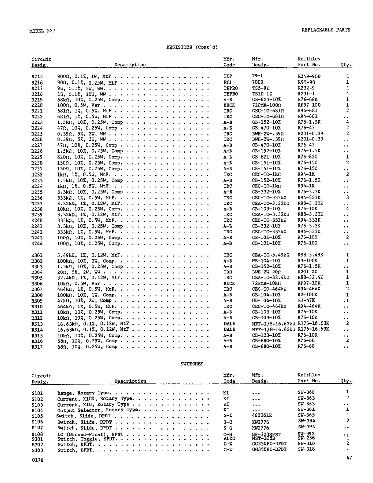
MODEL 227
RESISTORS (Cont'd)
REPLACEABLE PARTS
circuit Mfr. Mfr. Keithley
Desiyz. Description Code Desig. Part NO. -
R215
R216
R217
R218
R219
R220
R221
R222
R223
R224
R225
R226
R227
R228
R229
R230
R231
R232
R233
R234
R235
R236
R237
R238
R239
R240
R241
R242
R243
R244
soon, O.l%, lW, MfF . .
90R, 0.1%. 0.25W. MtF . .
9% O.l%, 5w. ww. . . .
1n, 0.1%. low, WW . . .
68k0, 10%. 0.25W, Cap. .
loon, O.5W, "a= . . . .
6818, l%, 0.5W, MtF . . .
681n, 1X, 0.5W, MtF . . .
1.5k$,, 10%. 0.25W, Camp .
470, 10X, 0.25W, Camp . .
0.39G. 5%, 2w, ww . . . .
0.39n, 54, 2w, ww . . . .
47n, lo%, 0.25W. Camp . .
1.5kn, 10%. 0.25W. Camp .
820~. 10%. 0.25W, Camp. .
15On, lo%, 0.25W, Camp. .
1500, 10%. 0.25W, Camp. .
IkR. 1%. 0.5W, MtF. . . .
1.5!b, iO%, 0;25W, Come .
Ikn, 1%. 0.5W. MtF. . . .
3.3kR, 10X, 0.25W. Come .
333k0, 1%. 0.5W, MtF. .
3.32kn, I%, O.l2W, MtF. .
10kn, IO%, 0.25W, Come. .
3.32kn, 1%. O.lZW, MfF. .
333wl, 14, 0.5W, MtF. . .
3.3kR. 10%. 0.25W. Comu .
333kfi, 1%;0.5W, I&. : .
lOOn, lo%, 0.25W, Camp. .
1000, lo%, 0.25W, Camp.
......
......
......
......
......
......
......
......
......
......
......
......
......
......
......
......
......
......
......
......
......
......
......
......
......
......
......
......
......
. . .
. . .
. . .
. . .
. . .
. . .
. . .
. . *
. . .
. . .
. . .
. . .
. . .
. . .
. . .
. . .
. . .
. . .
. . .
. . .
. . .
. . .
. . .
. . .
. . .
. . .
. . .
. . .
. . .
. . .
. .
. *
. .
. .
. .
. .
. .
. .
. .
. .
. .
. .
. .
. .
. .
9 .
. .
. .
. .
. .
. .
. .
.
. .
. .
. .
. .
. .
. .
. .
TEP
RCL
TEPRO
TEPRO
A-B
BECK
IRC
IRC
A-B
A-B
IRC
IRC
A-B
A-B
A-B
A-B
A-B
IRC
A-B
IRC
A-B
IRC
IRC
A-B
IRC
IRC
A-B
TRC
A-B
A-B
TS-I
7009
TS5-9*
TSlO-10
CB-623-10X
72PMR-1OOQ
CEC-TO-681n
CEC-TO-681n
CB-152-10%
CB-470-101
BWH-ZW-.39Q
IN"-2W-.39s,
CB-470-10%
CB-152-10%
CB-821-10%
c8-151-10%
CB-151-10%
CRC-TO-lk0
CB-152-10%
CEC-TO-lkn
CB-332-10%
CEC-TO-333kn
CEA-TC-3.32kn
CB-103-10%
CF.A-TO-3.32kn
CEC-TO-333kO
CB-332-10%
CRC-TO-333kn
CB-IOl-10%
CB-lOl-10%
R249-900
R95-90
R232-9
R231-1
R76-68K
RP97-100
R94-681
R94-681
R76-1.5K
R76-47
RZOl-0.39
R201-0.39
R76-47
R76-1.5K
R76-820
R76-150
R76-150
R94-1K
R76-1.5K
R94-1K
R76-3.3K
R94-333K
R88-3.32K
R76-10K
R88-3.32K
R94-333K
R76-3.3K
R94-333K
R76-100
R76-100
R301
R302
R303
R304
R305
R306
R307
R308
R309
R310
R311
R312
F.313
R314
P.315
F.316
R317
5.49kn. 1%, O.l2W, MtF.
lOOksI, 10X, ZW, Camp. .
1.5ksI, lo%:, 0.25W, Come
ZOR, 5%. 2w, ww * . 9 .
32.4kn, 1X, O.lZW, MtF.
10kn, 0.5W, "as . . . .
464kn, l%, 0.5W, MtF. .
lOOk0, 10%. lW, Camp. .
47kn, 10%. 2w, camp . *
464kn, 1X, 0.5W, MtF. .
lOkD, 10%. 0.25W. ComP.
10kR. 10%. 0.25W, ComP.
. .
. .
. .
. .
. .
. .
* .
. .
. .
* .
. .
. .
. . .
. . .
. . .
. . .
. . .
. . .
. . .
. . .
. . .
. . .
. . .
. . .
. .
. .
. .
. .
. .
. .
. .
. .
. .
. .
. .
. .
. .
. .
. .
. .
. .
. .
. .
. .
. .
. .
. .
. .
16.63k0, O.L%, O.lZW, MtF ..............
16.63kn, O.l%, O.l2W, MtF ..............
loks, 10X, 0.25W. Camp. ...............
68$,, 10%. 0.25W, Camp
................
68n, 10X, 0.25W, Camp
................
IRC
A-B
A-B
IRC
IRC
BECK
IRC
A-B
A-B
IRC
A-B
A-B
DALE
DALE
.4-B
A-B
A-B
CEA-TO-5.49kn
HB-104-10%
CB-152-10%
BWn-2w-20*
CF.&TO-32.4kn
72PNblOkn
CEC-TO-464kO
GB-104-10X
HB-104-10X
CEC-TO-464kn
CB-103-10%
CB-103-10X
R88-5.49K
R3-100K
R76-1.5K
RZOl-20
R88-32.4K
RP97-10K
R94-464K
R2-100K
R3-47K
R94-464K
R76-10K
R76-10K
MPF-l/8-16.63kn R176-16.63K
HFF-l/8-16.63kn R176-16.63K
CB-103-10X R76-10K
CB-680-10X R76-68
CB-680-10X R76-68
-LEE
1
1
1
1
1
1
2
4
2
2
.
. .
1
2
. .
2
. .
. .
. .
3
. .
4
. .
. .
. .
. .
2
. .
1
1
. *
1
1
1
2
1
.l
. .
. .
. .
2
. .
. .
2
. .
SWITCHES
Mfr. Mfr. Keithley
_ . .
Cir.Xlit
De&?. De*crlpti.On
SlOl Range, Rotary Type. . . . . . .
s102 current, x100, Rotary Type. . .
5103 Current, X10, Rotary Type . . .
s104 Output Selector, Rotary
Type. .
s105 Switch, Slide, DPDT . . . . , .
S106 Switch. Slide. DPDT . . . . . .
BYi
1
2
. .
1
I
2
. .
. .
1
2
. .
“CZSLg.
. . .
. . .
rare NO.
...........
...........
...........
...........
...........
...........
...........
...........
...........
...........
...........
SW-360
SW-363
SW-363
SW-361
SW-365
SW-394
SW-394
SW-392
SW-236
SW-318
SW-318
KI
KI
KI
KI
s-c
s-c
S-C
c-w
ALCO
c-w
c-w
46206LR
XW2776
XW2776
isa%sT
GG350PC-DPDT
GG350PC-DPDT
s107 Switch. Slide. DPDT . . . . . .
% LO (Ground-Flost) SPST
Switch, Toggle, StDT. . : : : :
5302 Switch. :
DPDT. . . . . . . . . .
s303 sviec :h, DPDT. . . . . . . . . .
0178 47
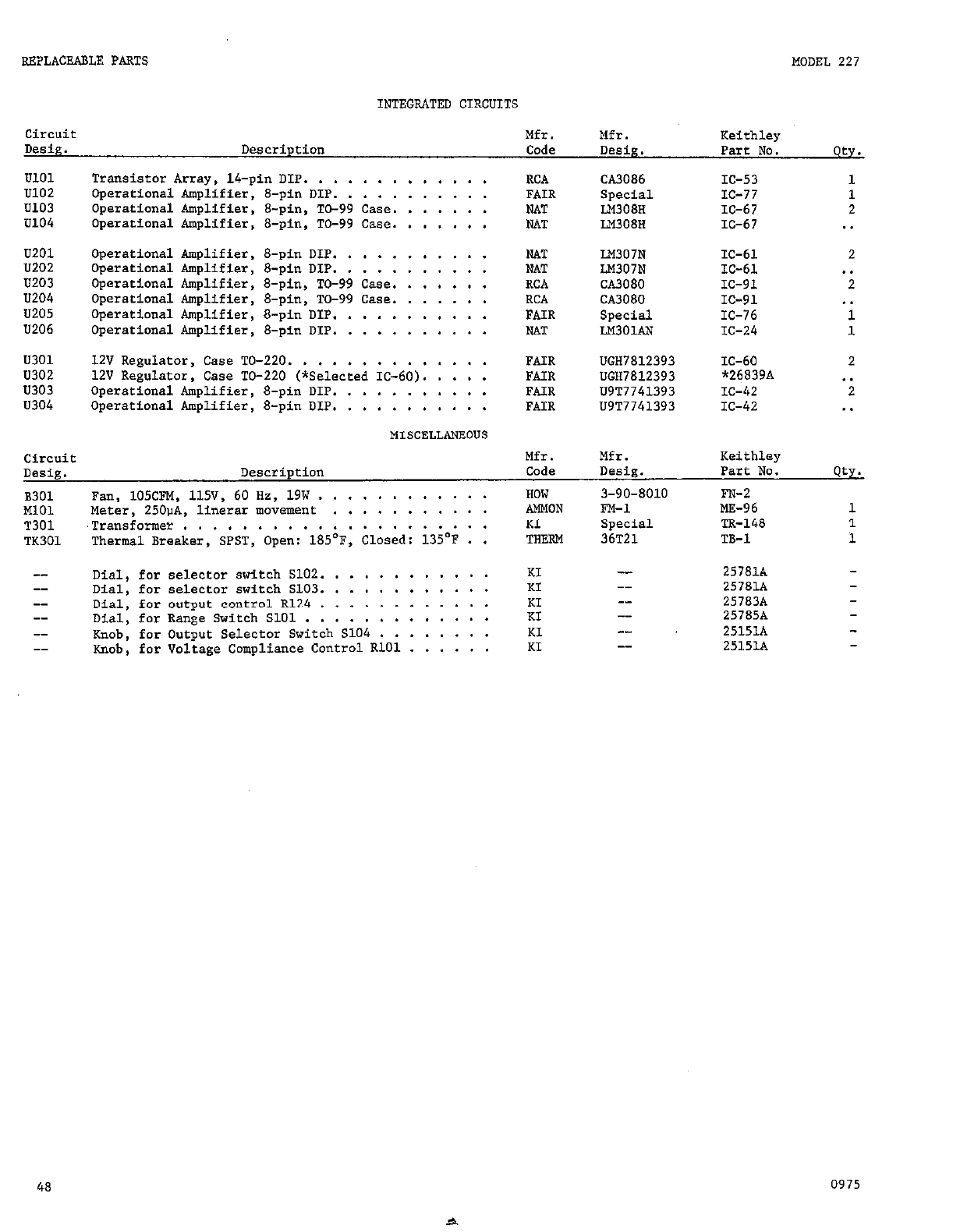
REPLACEABLE PARTS MODEL 227
INTEGRATED CIRCUITS
Circuit Mfr. Mfr. Keithley
Desk. Description Code Desig. Part No. t .
UlOl Transistor Array, 1Cpin DIP. . . . . . . . , . . . . RCA CA3086 IC-53 1
no2 Operational Amplifier, 8-pin DIP. . . . . . . . . . . FAIR Special IC-77 1
U103 Operational Amplifier, 8-pin, TO-99 Case. . . . . . . NAT LM308H X-67 2
U104 Operational Amplifier, 8-pin, TO-99 Case. . . . . . . NAT LM308H X-67 . .
U201 Operational Amplifier, 8-pin DIP. , , . . .
u202 Operational Amplifier, 8-pin DIP. . . . . .
U203 Operational Amplifier, S-pin, TO-99 Case. .
U204 Operational Amplifier, S-pin, TO-99 Case. .
u205 Operational Amplifier, 8-pin DIP. . . . . .
U206 Operational Amplifier, 8-pin DIP. . . . . .
u301 12V
ReRulator, Case TO-220. . . . . . . . .
U302 12V Regulator, Case TO-220 (*Selected IC-60)
u303 Operational Amplifier, S-pin DIP. . . . . .
U304 Operational Amplifier, 8-pin DIP, . . . . .
. .
NAT
LM307N IC-61 2
. . NAT LM307N IX-61 . .
. . RCA CA3080 IC-91 2
. . RCA CA3080 IC-91 . .
. . FAIR Special IC-76 1
. . NAT LM301AN IC-24 1
9 .
. .
9 .
* .
FAIR UGH7812393 IC-60
2
FAIR UGH7812393 *26839A . .
FAIR U9T7741393 IC-42
2
FAIR U9T7741393
IC-42 . .
MISCELLANEOUS
Circuit
D.ZQ. Description
Mfr.
Code Mfr.
De&g. Keithley
Part No. qtr.
B301 Fan, 105CFM, 115V, 60 Hz, 19W ..........
HOW 3-90-8010
FN-2
Ml01 Meter, 250uA, linerar movement ......... AWHON FM-l ME-96 1
T301 .Transfomer ................... KI Special TR-148 1
TK301 Thermal Breaker, SPST, Open: 185'F, Closed: 135'F THERM
36T21 TB-1 1
-- Dial, for selector switch 5102. . . . . . . .
-- Dial, for selector switch 5103. . . . . . . .
-- Dial, for output control R124 . . . . . . . .
-_ Dial, far Range Switch SlOl . . . . . . . . .
_- Knob, far Output Selector Switch 5104 . . . .
_- snob, far Voltage Compliance Control RlOl . *
. . KI -- 257818
. .
KI 25781.A
. . KI _- 257838
. . KI -- 25785A
. .
KI --
2515lA
KI --
. . 251518
48
0975
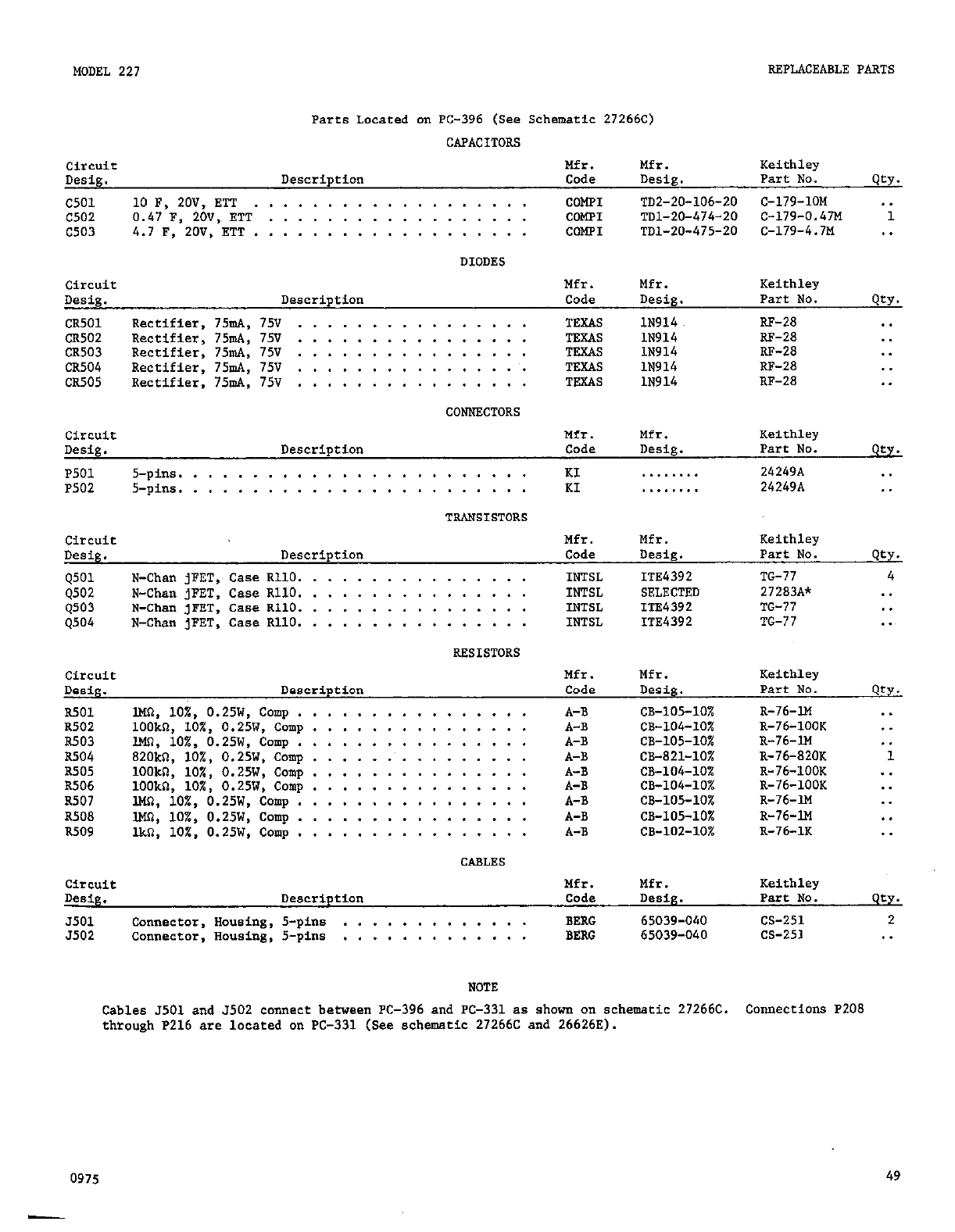
MODEL 22, KEPLACEABLE PARTS
Parts Located on PC-396 (See Schematic 272660
CAPACITORS
CiXT"iE Mfr. Mfr. Keiehley
Desig. Description Code Desig. Part NO. WY.
c501 lOF,20V,ETT . . . . . . . . . . . . . . . . . . . corn1 TD2-20-106-20 C-179-1OM . .
C502 0.47 F, 2ov, ETT . . . . . . . . . . . . . . . . . . CONPI TDl-20-474-20 c-179-0.47M 1
c503 4.7 F, 2OV, ETT . . . . . . . . . . . . . . . . . . . co*1 TDl-20-475-20 C-179-4.7M . .
DIODES
circuit Mfr. Mfr. Keithley
Desig.
DeSCKiptiOU
Code Desig. Part NO. QtY.
CR501 Rectifier, 75mA, 75v . . . . . . . . . . . . . . . . TEXAS lN914, RF-28
. .
CR502 Rectifier,
75m.A. 75V . . . . . . . . . . . . . . . . TEXAS
lN914 RF-28 .
CR503 Rectifier, 75!& 75V . . . . . . . . . . . . . . . . TEXAS lN914 RF-28 . .
CR504 Rectifier, 75luA. 75v . . . . . * . . . . . . . . . . TEXAS lN914 RF-28
. .
CR505
Rectifier, JSmA, 75V . . . . . . . . . . . . . . . .
TEXAS
lN914 RF-28 . .
CONNECTOKS
CirCUit Mfr.
Mfr. Keirhley
De&g. Description Code Desig. Part No. t .
P501 5-pins........................ KI . . . . . . . . 24249A . .
P502 5+ns.............. * . . . . . . . . . KI . . . . . . . . 24249A .
TRANSISTORS
circuit
Desig.
Mfr. Mfr. Keithley
Code Desig. Part NO. QtY.
q501 N-Ghan JPET, Case RllO. ............... INTSL ITE4392
TG77
4
4502
N-Chan JFET, Case RllO. ............... INTSL SELECTED 27283A* ..
Q503 N-Chan JFET, Case RllO. ............... INTSL ITE4392 TG-77 ..
q504 N-Chan JPET, Case P.llO. ............... INTSL IT34392
TG-77 ..
CirC"it
RESISTORS
Mfr. Mfr. Keithley
Desig. Description Code Desig. Part No; Qfy.
R501 lMn, lo%, 0.25W, Camp ................
A-B
CB-105-10X R-76-lM . .
R502 lOOkn, lo%, 0.25W, Camp ............... A-B CB-104-10X R-76-100K . .
R503 lMQ, 10X, 0.25W, Camp ................
A-B
CB-105-10% R-76-l&! . .
R504
820kn, 10X, 0.25W, Camp ................ A-B CB-821-10%
R-J6-820K
1
R505 lOOkn, 10X, 0.25W, Camp ............... A-B CB-104-10% R-76-1OOK . .
R506 lOOk& 10X, 0.25W, Camp ............... A-S CB-104-10% R-J6-100K . .
R507
lMn, 10X, 0.25W, Camp ................ A-B CB-105-10'6
R-J6-lM . .
R508 IMQ, 10X, 0.25W, Cap ................
A-B
CB-105-10X R-76-lM . .
Ii509 lkR, IO%, 0.25W, Cap ................ A-B CB-102-10% R-76-1K . .
CABLES
cbmxtt Mfr. Mfr. Keithley
nesig. Description Code Desig. Part No. t .
J501 connector, musing, 5-pins . . . . . . . . . . 1 . . BERG 65039-040 CS-251 2
5502 Con"ector, Housing, 5-pins . . . . . . . . . . . . . BERG 65039-040 CS-251 . .
NOTE
Cables J501 and 5502 connect between PC-396 and PC-331 as shown on schematic
272&X. Connections P208
through P216 are located on PC-331 (See schematic 27266C and 266263).
0975 49
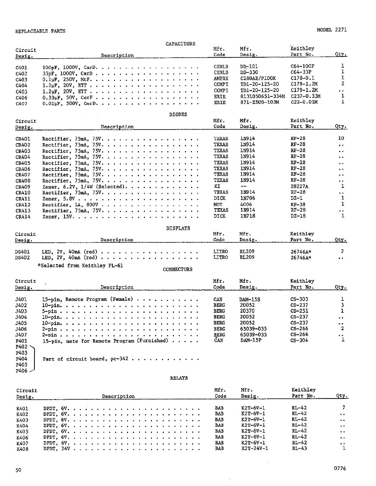
REPLACZABLE PARTS MODEL 2271
Circuit
Desig.
CAPACITORS Mfr. Mfr. Keithley
Code Desig. Part
No.
f .
c401 loom. 1ooov. CerD. . . . . . . . . . . . . . . . . . CENLB DD-101 C64-1OOP 1
)D-330 C64-33P 1
C402
c403
c404
c405
C406
c407
33pk;lOOOV;CerD . . .
O.lvF, 25OV, MtF. . . .
1.2@, 2OV, ETT . . . .
1,2pF, ZOV, ETT . . . .
0.33UF, 5ov, CerF . . .
O.Ol@, 5oov, CerD. . .
. .
* .
. .
. .
. .
. *
. .
. .
. .
. .
.
. .
. .
. .
. *
. .
. .
. .
. .
. .
. .
. .
. .
. .
. .
. .
. .
. .
. .
. .
CENLB
AMPRX
corn1
corn1
ERIE
ERIE
I
C280AEfPlOOK ClJ8-0.1
TDl-20-125-20 c179-1.2M
TDl-20-125-20 c179-1.2M
8131050651-33413 C237-0.33M
871-ZSUO-103M c22-o.om
1
2
. .
1
1
circuit
De&g. Description
DIODES Mfr. Mfr. Keithley
Code De&. Part No. t .
. .
. .
. *
. .
........... TEDS
lN914 RF-28 10
........... TEXAS lN914 RF-28 ..
........... TBXAS 1N914 RF-28 ..
........... TELL3 lN914 RF-28 ..
. . TEXAS lN914 RF-28 . .
. .
TEXAS
lN914 w-28 . .
. . TEKAS lN914 RF-28 . .
CR401 Recrifier~, 75mA, 75V. .
CR402 Rectifier, 75mA, 75V. .
CR403 Rectifier, 75mA, 75V. .
CR404 Rectifier, 75mA, 7%. ,
CR405 Rectifier, 75mA, 75V. . . . . . . . . .
CR406 Rectifier, 75mA, 75V. . . . . * . . . .
CR407 Rectifier, 75mA, 75V. . . . . . . . . .
CR408 Rectifier, 75,& J5V. ................ TECAS lN914 RF-28 ..
CR409 Zeaer, 6.2V, lJ4W (Selected). ............ KI -- 28227A 1
CR410 Rectifier, 75mA, 75V. ................ TEKAS lN914 RF-28 ..
CR411 izener, 5.8V ..................... DICK lNJ06 DZ-1 1
CR412 Rectifier, lA, 800V ................. MOT 4006 RF-38 1
CR413 Rectifier, 75mA, JSV. ................ TEXAS lN914 RF-28 ..
CR414 2ener, 15v. ..................... DICK lNJ18 DZ-18 1
circuit
DeSig. Description
DISPLAYS Mfr. Mfr. Keithley
Code Desig. Part No. t .
DS401 LED, 2V, 4OmA (red) ................. LITRb RL209 26746A* 2
DS402 LED, 2V, 4OmA (r.ed) ................. LITRO RL209 26746A* ..
*Selected from Keithley PL-61 CONNECTORS
Circuit i
Desig. Description
Mfr. Mfr. Keithley
Code DesiR. Part NO. t .
5401 15-pin, Remote Program (Female) ........... CAN DAM-15s cs-303 1
5402 lo-pin ........................ BERG 20052 CS-237 3
5403 5-pin .. ,* ...................... BERG 20370 CS-251 1
5404 lO-pin ........................ BERG 20052 CS-237 ..
5405 lo-pi" ........................ BERG 20052 CS-237 ..
5406 2-pin ........................ BERG 65039-035 CS-266 2
5407 2-lli* ........................ BERG 65039-035 CS-266 ..
P401 15-pin, mate for Remote Program (Furnished) ..... &ii DAM-15P cs-304 1
P402
P403
P404
1
part of circuit board, pc-342 ............
P405
P406
RELAYS
circuit
DeSig. Description
Mfr. Mfr. Keithley
Code Desig. Part No. t .
K401 DPDT.6V ....................... BAB K2T-6V-1 RL-42 7
K402 DPDT.6V ....................... BAB K2T-6V-1 RL-42 ..
K403 DPDT.6V ....................... BAB KZT-6V-1 RL-42 ..
K404 DPDT.6V ....................... BAB Km-6V-1 RL-42 ..
K405 DPDT.6V ....................... BAB KZT-6V-1 RL-42 ..
K406 DPDT,6V ....................... BAR KZT-6V-1 RL-42 ..
K407 DPDT,6V. ...................... BAB K2T-6V-1 RL-42 ..
K408 DPDT.24V ...................... MB K2T-24V-1 RL-43 1
50 0776
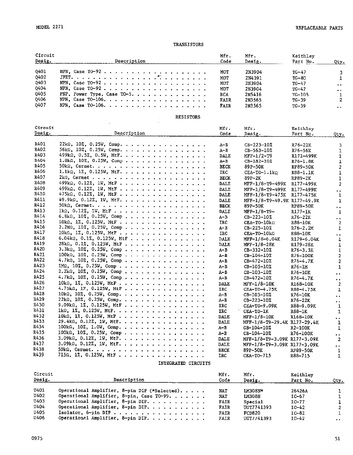
MODEL 2271 REPLACEABLE PARTS
TRANSISTORS
Circuit
Desip. DescriDtion Mfr. Mfr. Keithley
Code Desig. Part No. t .
0401 NPN. Case TO-92 . , . . . . . MOT 283904 TG-47 3
MOT
2N4391 TG-80 1
MOT 2N3904 TG-47 . .
MOT
2N3904 TG-47 . .
RCA 2135416 TG-105
FAIR 2103565 TG-39 :
FAIR 2N3565 TG-39 . .
6402 JFET .............
q403 NPN, Case TO-92 .......
0404 NPN. Case TO-92 .......
6405 PNP; Power Type, Case TO-5. .
Q406 NPN, Case TO-106. . , . . . .
Q407 NPN, Case TO-106. . . . . . .
RESISTORS
Circuit
Desig. Description Mfr. Mfr. Keithley
Code De&z. Part No. t .
R401
R402
R403
It404
R405
R406
R407
R408
R409
R410
R411
R412
R413
R414
R415
R416
R417
R418
R419
R420
R421
R422
R423
R424
R425
R426
R427
R428
R429
R430
R431
R432
R433
R434
R435
R436
R437
R438
R439
22kO~, lo%, 0.25W, Camp. . . . .
56k0, 10%. 0.25W, Camp. . . . .
499kR. 0.5%, 0.5W, MtF. , . . .
1.8k0, lo%, 0.25W, Cmp . . . *
50kn, Cermet. . . . . . . . . .
l.lko, l%, O.lZSW, MtF. . . . .
2kc7, Cemet . . . . . . . . . .
499kR, 0.12%. 1W. MtF . . . .
. .
. .
. .
. .
. .
. *
. .
. .
. .
. .
.
. .
. *
. *
. .
. .
. .
. .
. .
. .
. .
. .
. .
. .
. .
. .
. .
. .
. .
. .
. .
. .
. .
. .
. .
. .
. .
. .
. .
. .
. *
* *
. .
. .
. *
. .
. .
. .
. .
. .
.
. .
. .
. .
A-B
A-B
DALE
A-B
BECK
IRC
BECK
DALE
DALE
DALE
DALE
BECK
DALE
A-B
IRC
A-B
IRC
DALE
DALI?
A-B
A-B
A-B
A-B
A-B
A-B
DALE
IRC
A-B
A-B
IRC
IRC
mF-l/8-1OK
CB-223-10%
CB-563-10%
CEA-TO-II. J5K
MFF-l/2-T9
CB-182-10%
CB-103-10%
89P-50K
CEA-TO-l.lkn
89P-2K
MFF-l/8-T9-499K
MFF-l/8-T9-499K
MFF-l/8-T9-475K
MFF-l/8-T9-49.9K
89P-50K
MFF-l/8-T9-
CB-223-10%
CBA-TO-1Okn
CB-225-10%
CBA-TO-1OkR
MFF-l/8-6.04K
MFF-l/8-28K
CB-332-10%
CB-104-10%
CB-472-10%
CB-105-10%
CB-103-10%
CB-472-10%
R76-22K
Rl68-10K
R76-56K
Rl71-499K
R88-4.75K
RJ6-1.8K
RP89-50K
R88-l.lK
RP89-2K
R177-499K
R177-499K
R177-475K
R177-49.9K
P.P89-50K
R177-1K
R76-22K
R88-10K
R76-2.X
R88-10K
R179-6.04K
R179-28K
R76-3.3K
R76-100K
R76-4.7K
R76-IN
R76-10K
RJ6-4.7K
3
1
1
1
2
1
1
2
* .
1
1
. .
1
. .
2
1
. .
1
1
1
2
2
1
. .
. .
2
1
. .
. .
1
1
. .
1
1
. .
2
. .
1
1
499k0, 0.12%, 1W; MfF . . . . *
475kn. 0.12X, lw, MtF . . . .
49.9k51, O.lZ%, lw, MtF. . . . .
SOkR, Cermet. . . . . . . . .
lkn, 0.12%, lW, MtF . . . , . .
6.8kR. 10%. 0.25W. Cow . . . .
lOkn, l%, O.l25W, MtF . . . . . .
Z.ZMn, 10%. 0.25W, Camp . . . . .
lOkR, l%, O.l25W, MtP . . . . . .
6.04kn, O.l%, O.l25W, MtF . . . .
28kR, O.l%, O.l25W, MtF
3.3kn, lo%, 0.25W, Camp
100kQ. 10%. 0.25W. Corm
4.7kR; 10%; 0.25W; Cm;
lMn, lo%, 0.25W, Camp .
2.2k0, lo%, 0.25W, Cmp
4.7kR, lo%, 0.25W, Camp
lOkn, l%, O.l25W, MtF .
4.75kn, lZ, O.lZSW, MfF
lOkR, 10%. 0.25W, Camp.
22kn, lo%, 0.25W, Camp.
9.09kn. 1%. O.l25W,
MtF
lkn, l%, O.l25W, MtF. .
lOk0, l%, O.l25W, MtF .
29.4kn. 0.12%.
1W. MtF.
_,
lOOkQ, lo%, l.OW, Cap.
lOOkR, lo%, 0.25W, Camp
3.09k*, 0.122, lW, MtF.
3.09k0, 0.12%. lW, MtF.
50k0, Cermet. . . . . .
715fi, 1%. O.l25W, MtF .
. . .
. . .
. . .
. . .
. . .
. . .
. . .
. . .
. . .
. . .
. . .
. . .
. . .
. . .
. . .
. . .
. * .
. . .
. . .
. . .
. * .
. .
. .
. .
. .
. .
. .
. .
. .
* .
. .
. *
. .
. .
. .
. .
. .
. .
. .
. .
. .
* .
.........
.........
.........
.........
.........
.........
.........
.........
.........
.........
.........
.........
.........
.........
.........
.........
.........
.........
.........
.........
.........
INTRGRATED CIRCUITS
CB-223-10%
CRA-TO-9.09K
CBA-TO-1K
R76-10K
R76-22K
R88-9.09K
R88-1K
MFF-l/8-1OK Rl68-10K
MFF-l/8-T9-29.4K R177-29.4K
GB-104-10% R2-100K
DALE
DALE
A-B
A-B
DALE
DALE
CB-104-10% R76-100K
MFF-l/8-T9-3.09K R177-3.09K
MFP-l/8-T9-3.09K Rl77-3.09K
89P-50K
Cm-TO-715 RP89-50K
R88-715 IRC
Mfr.
Code Desig.
Mfr. Keithley
Part No. t .
Circuit
Desig. Description
u401 Operational Amplifier, E-pin DIP (*Selected). . . . NAT LH308N* 264268 1
U402 Operational Amplifier, 8-pin, Case TO-99. . . . . . NAT W308H
K-67
1
"403 Operational Amplifier, 8-pin DIP. . . . . . . . . . FAIR Special IC-77 1
II404 Operational Amplifier, 8-pin DIP. . . . . . . . . . FAIR UGT7741393 IC-42 2
II405
Isoiat~r,
6-pin DIP . . . . . . . . . . . . . . . . FAIR FCD820 IC-82 1
II406 Operariowl Amplifier, 8-pin DIP. . . , . . . . . . FAIR UGT7741393 IC-42 . .
0975 51
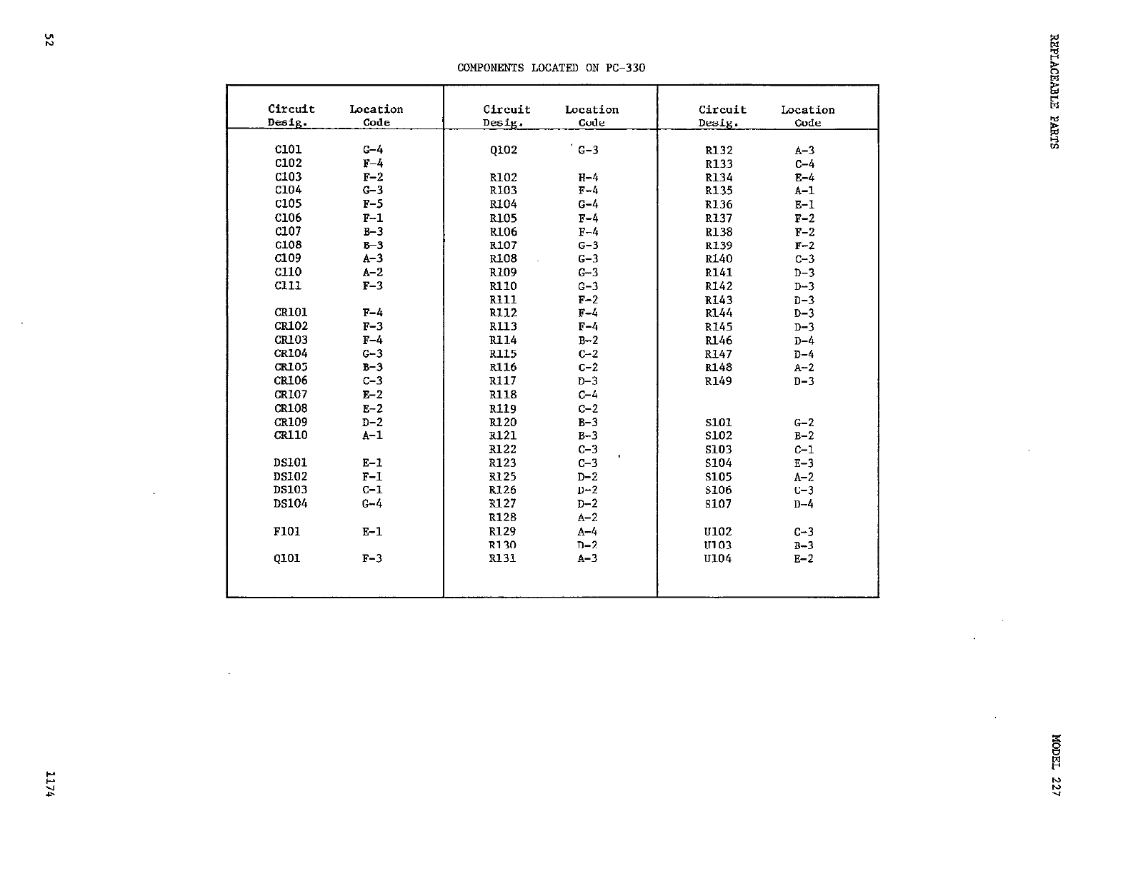
COMPONENTS LOCATED
ON PC-330
circuit
Desig.
Cl01
Cl02
Cl03
Cl05
Cl06
Cl07
Cl08
Cl09
Cl10
Cl11
CR104
ml05
CR106
CR107
CRlO8
CR109
ml10
F-4
F-3
F-4
C-3
B-3
C-3
E-2
B-2
D-2
A-l
DSlOl E-l
us102 F-l
DS103 C-l
DS104 G-4
FlOl
E-l
q101
Location
Code
04
F-4
F-2
03
P-5
F-l
B-3
&3
A-3
A-2
F-3
circuit
Desig.
Rlo2
RI03
Rlo4
R105
RlO6
R107
R108
R109
RllO
RI11
R112
R113
R114
R115
R116
RI17
R118
R119
R120
R121
R122
R123
R125
R126
R127
R128
Rl29
R130
R131
Location
Code
C-3
H-4
F-4
G-4
F-4
F-4
G-3
G-3
63
C-3
F-2
F-4
F-4
B-2
c-2
c-2
D-3
c-4
C-2
B-3
B-3
c-3
c-3 .
D-2
D-2
D-2
A-2
A-4
D-2
A-3
circuit
Desig .
RI32
R133
R134
Location
Code
A-3
c-4
E-4
R135
A-l
R136 E-l
RI37
F-2
R138 F-2
R139
F-2
Rl40 c-3
R141 D-3
R142
D-3
R143 D-3
R144 D-3
R145 D-3
Rl46 D-4
R147 D-4
R148 A-2
R149 D-3
SlOl 62
s102 B-2
5103 C-l
s104 E-3
s105 A-2
S106 c-3
5107 D-4
u102 c-3
u103 B-3
In04 E-2
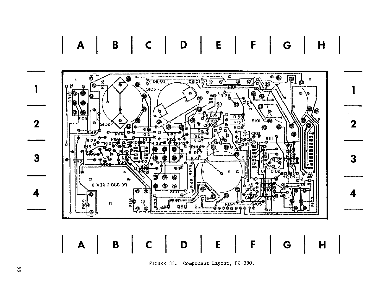
1
2
3
4
A
I I
B C
I DI E I FlG
H
A
I 6
IClDlE FIG
FIGURE 33. component Layout, PC-330.
1
2
3
4
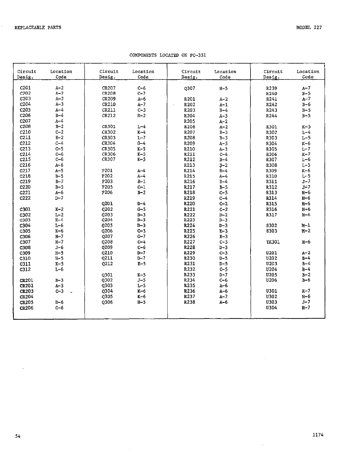
REPLACEABLE PARTS
COMPONENTS LOCATED ON PC-331
MODEL 227
c201
c202
C203
C204
C205
C206
C207
C208
c210
c211
c212
c213
C214
C215
C216
C217
C218
c219
c220
c221
c222
c301
C302
c303
c304
c305
C306
c307
C308
c309
C3LO
c311
C312
CR201
CR202
CR203
CR204
CR205
CR206
A-2
A-2
A-2
A-3
A-4
B-4
A-4
B-2
c-2
B-2
c-4
c-5
C-6
C-6
A-6
A-5
B-5
B-7
B-5
A-6
D-7
K-2
L-2
K-4
L-6
K-6
H-7
H-7
.,-6
H-5
H-5
K-5
L-6
B-3
A-3
c-3
D-6
C-6
CR207
CR208
CR209
CR210
CR211
CR212
CR301
CR302
CR303
CR304
CR305
CR306
CR307
P201
P202
P203
P205
P206
Q201
q202
Q203
Q204
Q205
0206
Q207
Q208
Q209
Q210
9211
9212
Q301
9302
9303
Q304
q305
9306
C-6
c-7
A-6
A-7
c-3
D-2
L-4
K-4
L-7
G-4
K-S
K-5
K-5
A-4
A-4
B-l
C-l
B-2
D-4
G-5
D-3
D-3
D-3
c-3
07
c-4
C-6
D-7
D-7
R-5
K-5
J-5
L-5
K-6
K-6
H-5
Q307
R201
R202
R203
R204
R205
R206
R207
R208
R209
R210
R2.u
R212
R213
R214
a215
R216
R217
R218
R219
R220
R221
R222
R223
R224
R225
R226
R227
R228
R229
R230
R231
R232
R233
R234
R235
R236
R237
R238
H-5
A-2
A-l
B-4
A-3
A-2
A-2
B-3
B-3
A-3
A-3
c-4
B-4
B-2
B-4
A-4
B-4
B-5
c-5
c-4
c-2
c-2
D-2
D-3
D-3
R-3
R-3
c-3
D-3
c-3
D-5
D-5
c-5
D-7
C-6
A-6
A-6
A-7
A-6
circuir
Location
Desip. Code
R239
R240
R241
R242
R243
R244
R301
R302
R303
R304
R305
R306
R307
R308
R309
RX10
R311
R312
R313
R314
R315
R316
R317
5302
S303
TK301
UZOI
u202
U203
U204
u205
U206
u301
U302
u303
II304
A-7
B-5
A-7
B-6
B-5
B-5
K-5
L-4
L-5
K-6
L-7
K-7
~-6
L-5
K-6
L-5
J-7
.F7
H-6
H-6
H-6
x-6
H-6
M-l
M-2
n-6
A-2
R-4
B-4
R-4
B-2
B-6
K-7
H-6
s-7
H-7
54 1174
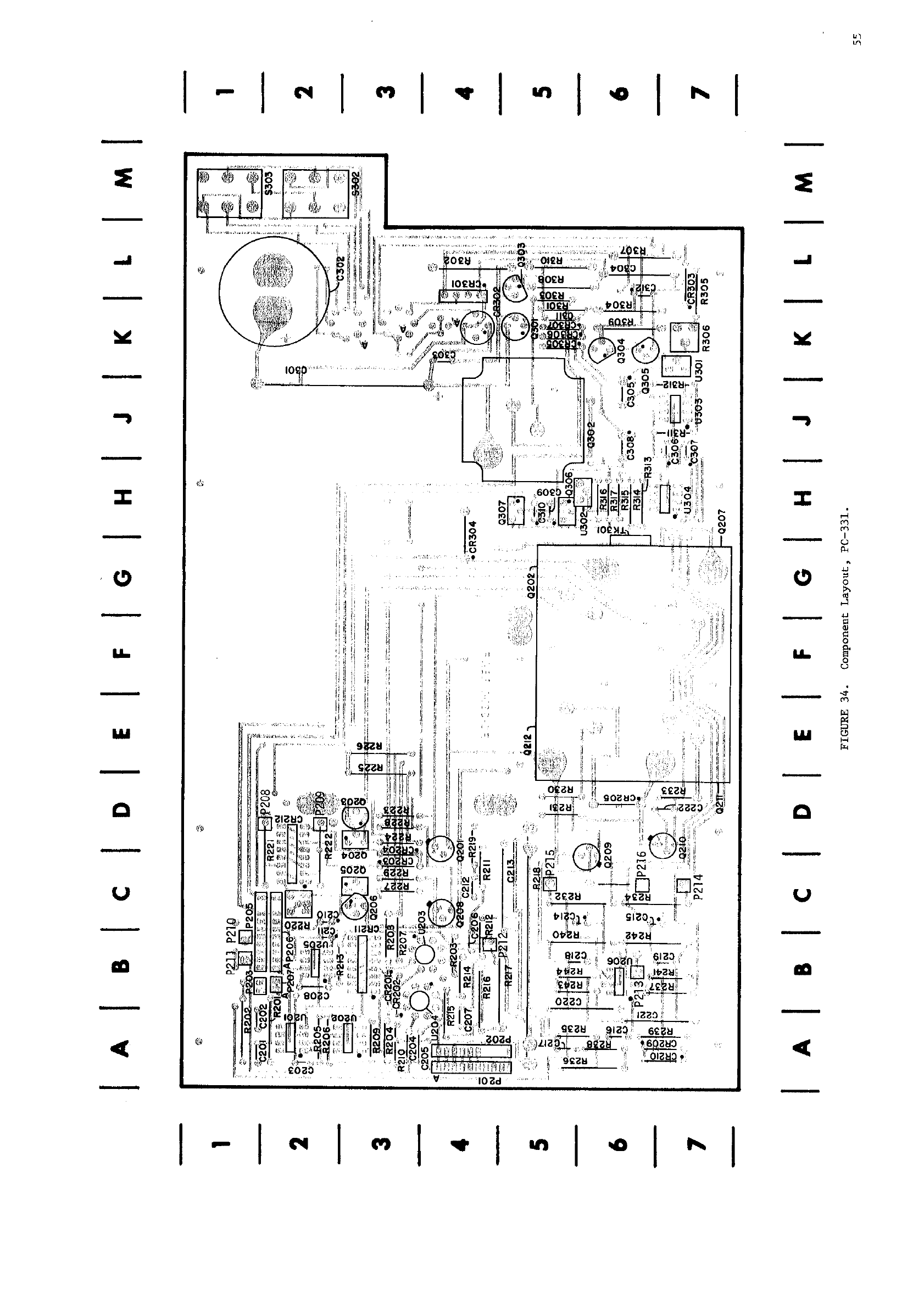
I
L
:I’ ii’
;/ ..:;:’
h I
COMPONENTS LOCATED ON PC-342
1
circuit
LWXti0lI
Desig. Code
c401 c-3
C402 G-3
c403 G-3
c404 E-2
c405 E-2
C406 G-3
c407 F-2
CR401 B-2
CR402 B-2
CR403 c-2
CR404 c-2
CR405 D-1
CR406 E-l
CR407 F-l
CR408 G-2
CR409 A-2
CR410 c-3
CR411 c-3
CR412 B-3
CR413 c-3
CR414 G-3
DS401 03
US402 G-3
circuit
Desig.
5402 D-l
5403 G-2
5404 c-2
5405 E-2
5406 G-l
K401 B-l
K402 R-3
K403 B-3
K404 c-2
K405 "-2
K406 E-2
K407 F-2
K408 G-2
q401
Q402
q403
Q404
q405
Q406
a407
F-3
D-2
D-3
F-l
B-3
G-3
c-3
R401 D-3
R402 B-3
R403 A-3
R404 B-3
8405 G-l
R406 A-3
R407 A-l
R408 A-3
R409 A-3
R41.0 A-2
R411 G-2
R412 G-l
R413 D-3
R414 P-3
R415 G-2
R416 G-2
R417 G-3
R418 G-2
R419 F-3
R420 F-3
R421 G-l
R422 F-l
circuit Locatfo,
Desig. Code
8423 F-l
R424 F-l
R425 F-l
R426 E-3
R427 E-3
R428 D-3
R429 D-3
R430 D-3
R431 D-3
R432 F-3
R433 Ii-3
R434 G-3
R435 F-3
R436 A-2
R437 A-2
R438 A-2
R439 G-2
II401 F-3
U402 B-3
u403 R-3
u404 G-3
u405 G-l
U406 D-3
FIGURE 35. Component Layout, PC-342.
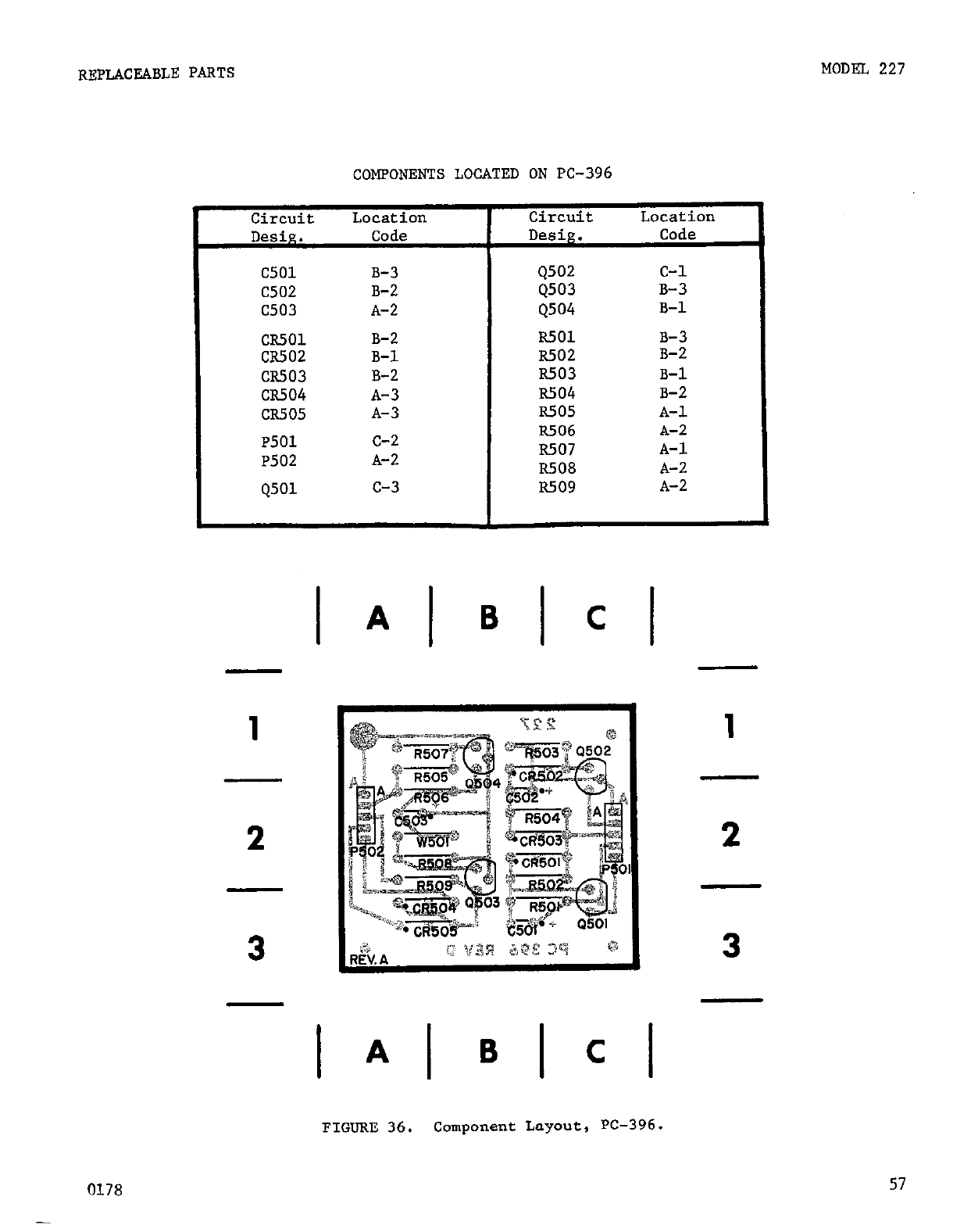
REPLACEABLE PARTS MODEL 227
COMPONENTS LOCATED ON PC-396
Circuit Location I Circuit Location
c501 B-3
C502 B-2
c503 A-2 I
Q502 C-l
4503 B-3
4504 B-l
CR501 B-2
CR502 B-l
CR503 B-2
CR504 A-3
CR505 A-3
P501 c-2
P502 A-2
Q501 c-3
R501
R502
R503
R504
R505
R506
R507
R508
R509
B-3
B-2
B-l
B-2
A-l
A-2
A-l
A-2
A-2
I I
A B
c I
1
2
3
FIGURE 36. component Layout, PC-396.
1
2
3
0178 57
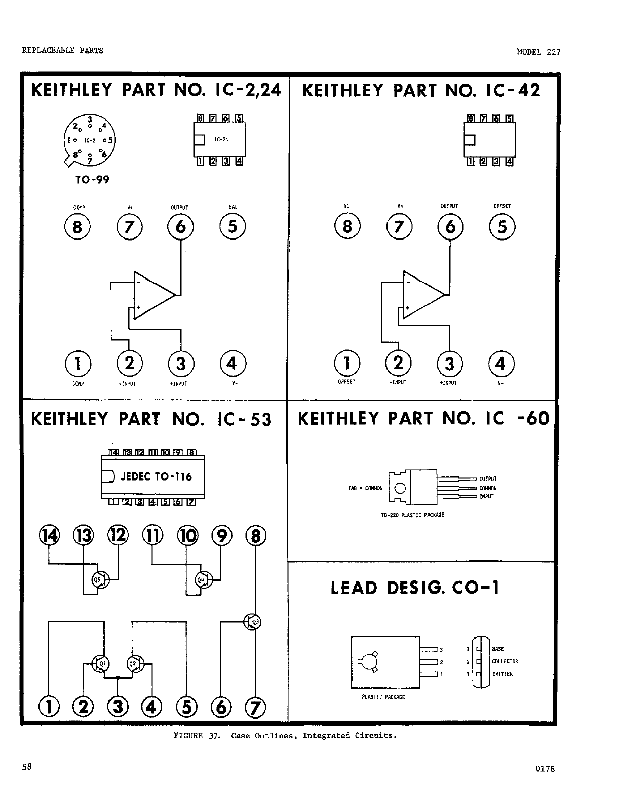
REPLACEABLE PARTS MODEL 227
KEITHLEY PART NO. IC-2,24
TO-99
+
0
1
%I
2 3
0
4
tw -INWT +,NP”I v-
KEITHLEY PART NO. IC - 53
KEITHLEY PART NO. IC-42
0
4
v-
KEITHLEY PART NO. IC -60
LEAD DESIG. CO-l
FIGURE 37. Case Outlines, Integrated Circuits.
58 0178
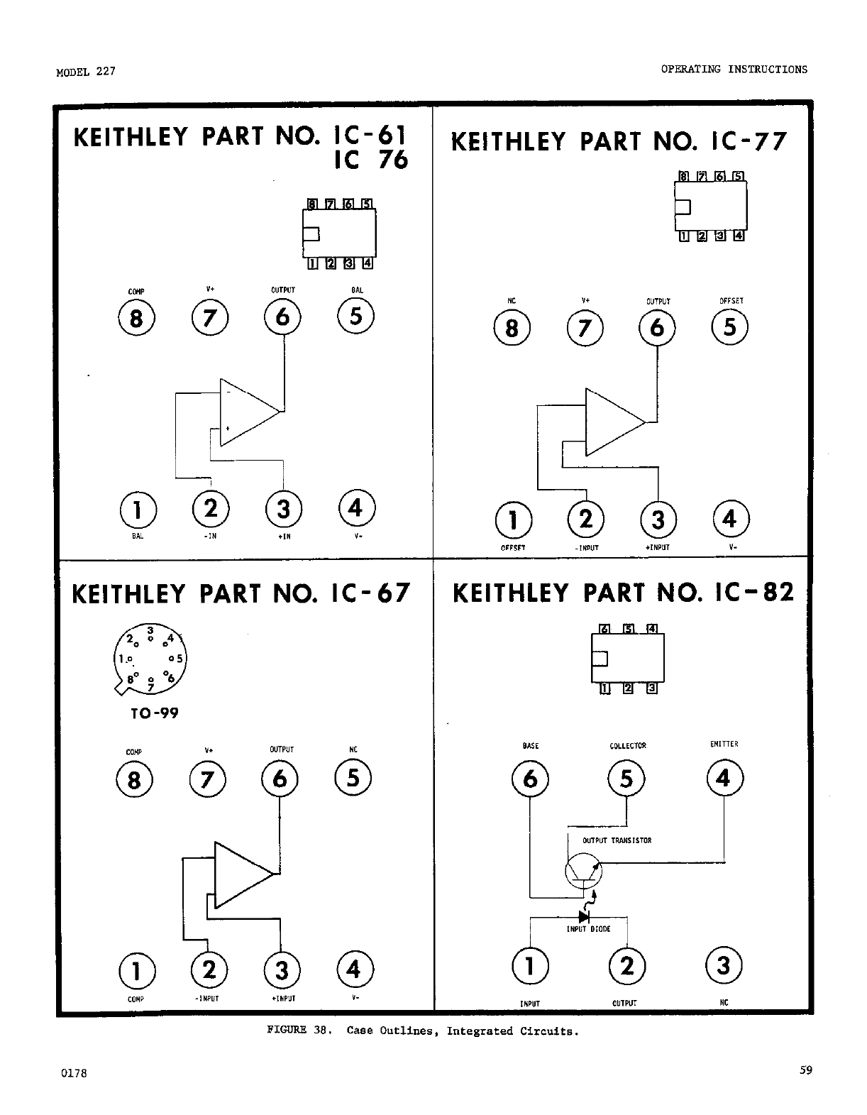
MODEL 227
KEITHLEY PART NO. IC-61
IC 76 KEITHLEY PART NO. IC-77
KEITHLEY PART NO. IC-67 KEITHLEY PART NO. IC- 82
P1lxJP.E 38. Case Outlines, Integrated Circuits.
0178 59
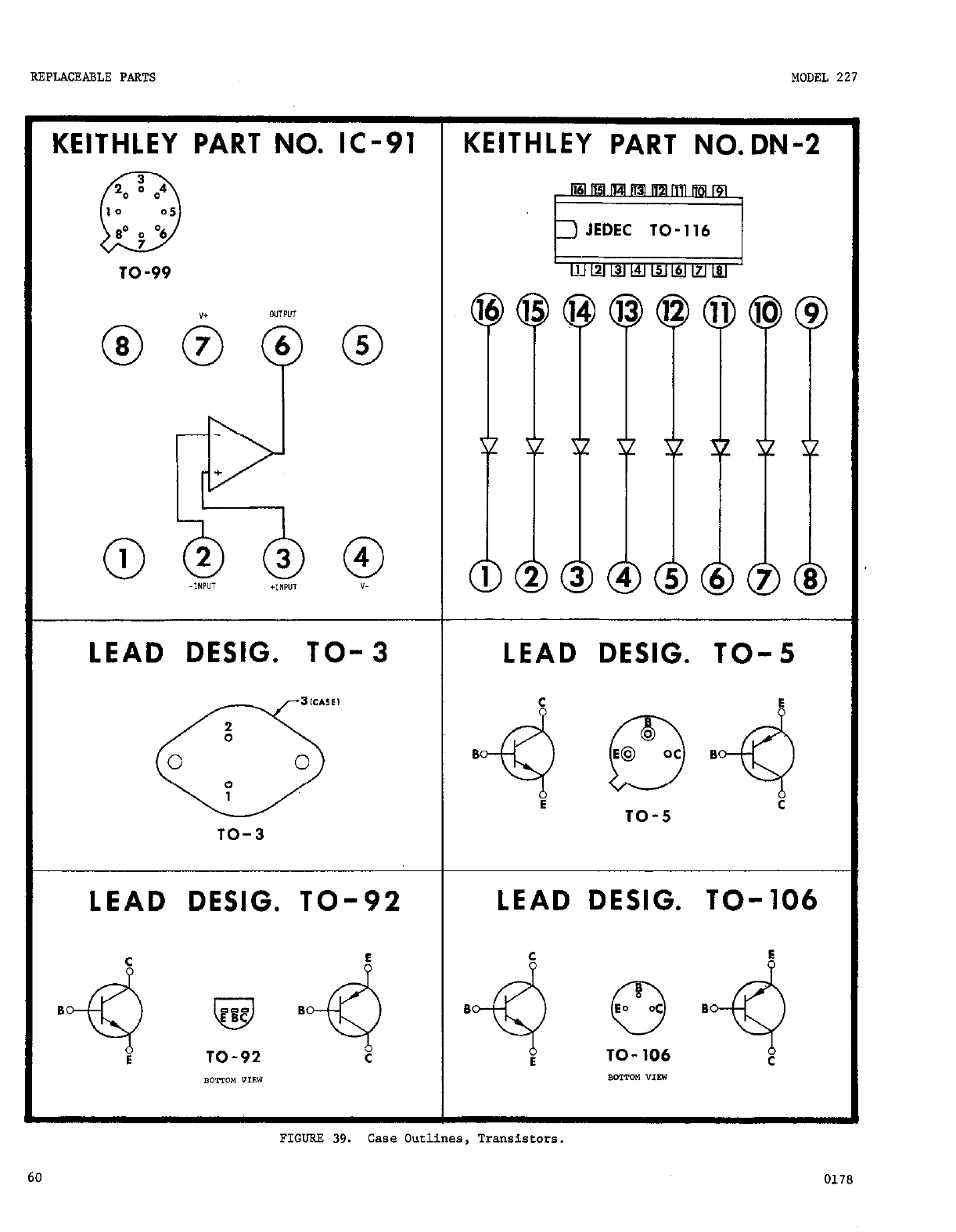
REPLACEABLE PARTS MODEL 227
KEITHLEY PART NO. IC -91 KEITHLEY PART NO. DN-2
JEDEC TO-116
TO-99
LEAD DESIG. TO- 3 LEAD DESIG. TO-5
GE’ +iQJ f?J qJ$
TO-5
TO-3
LEAD DESIG. TO-92 LEAD DESIG. TO-106
-e) z2 +ii) B+$ g6 B%)
E E C
BomoM YIEW Bc.2T.m Ylrn
60 0178
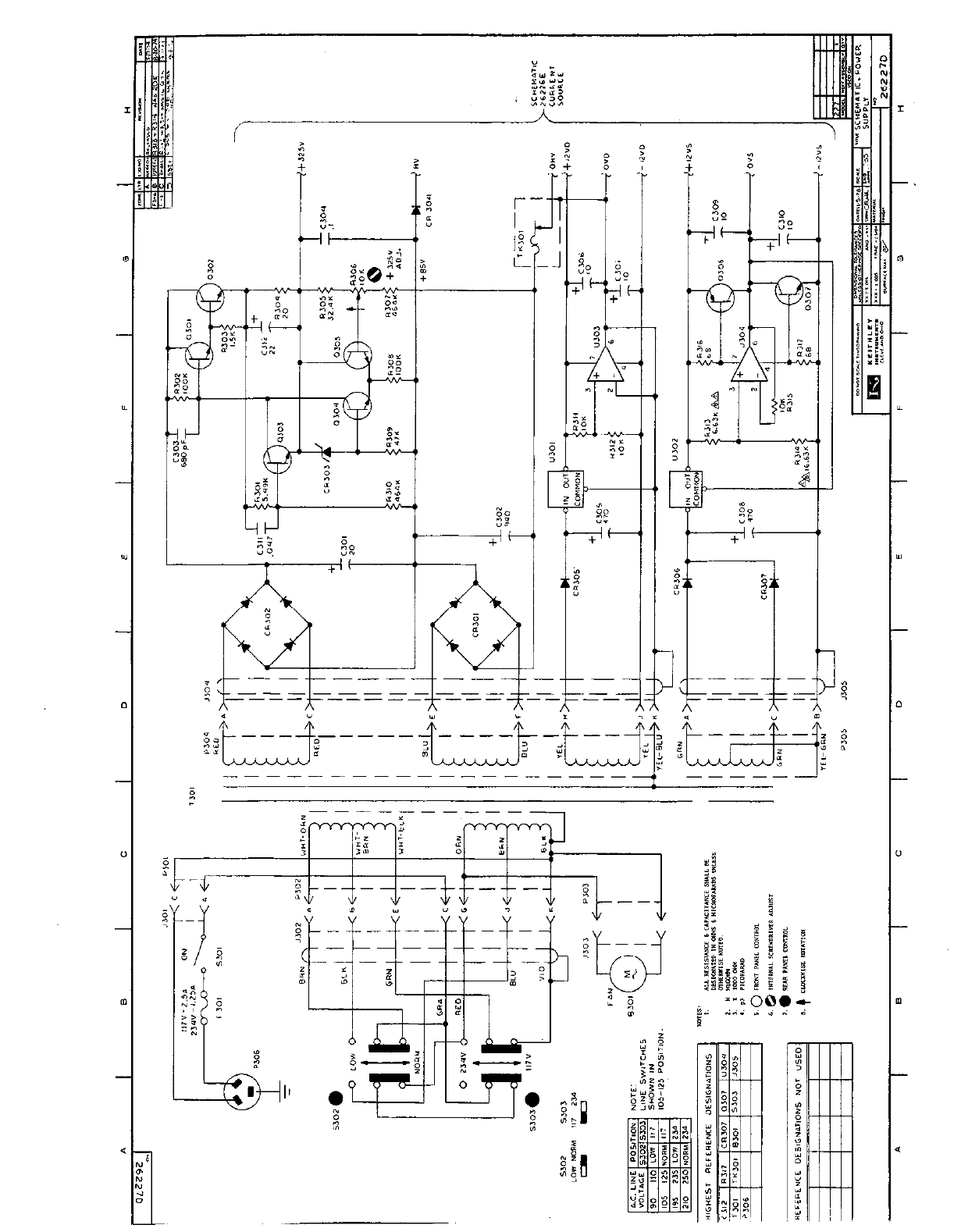
--T-l+
,o
z
---
---.
AAd.A.4
L
I +”
z
:
--:
-- -
--- r
-j-j=+
--------------------
i
:S310N
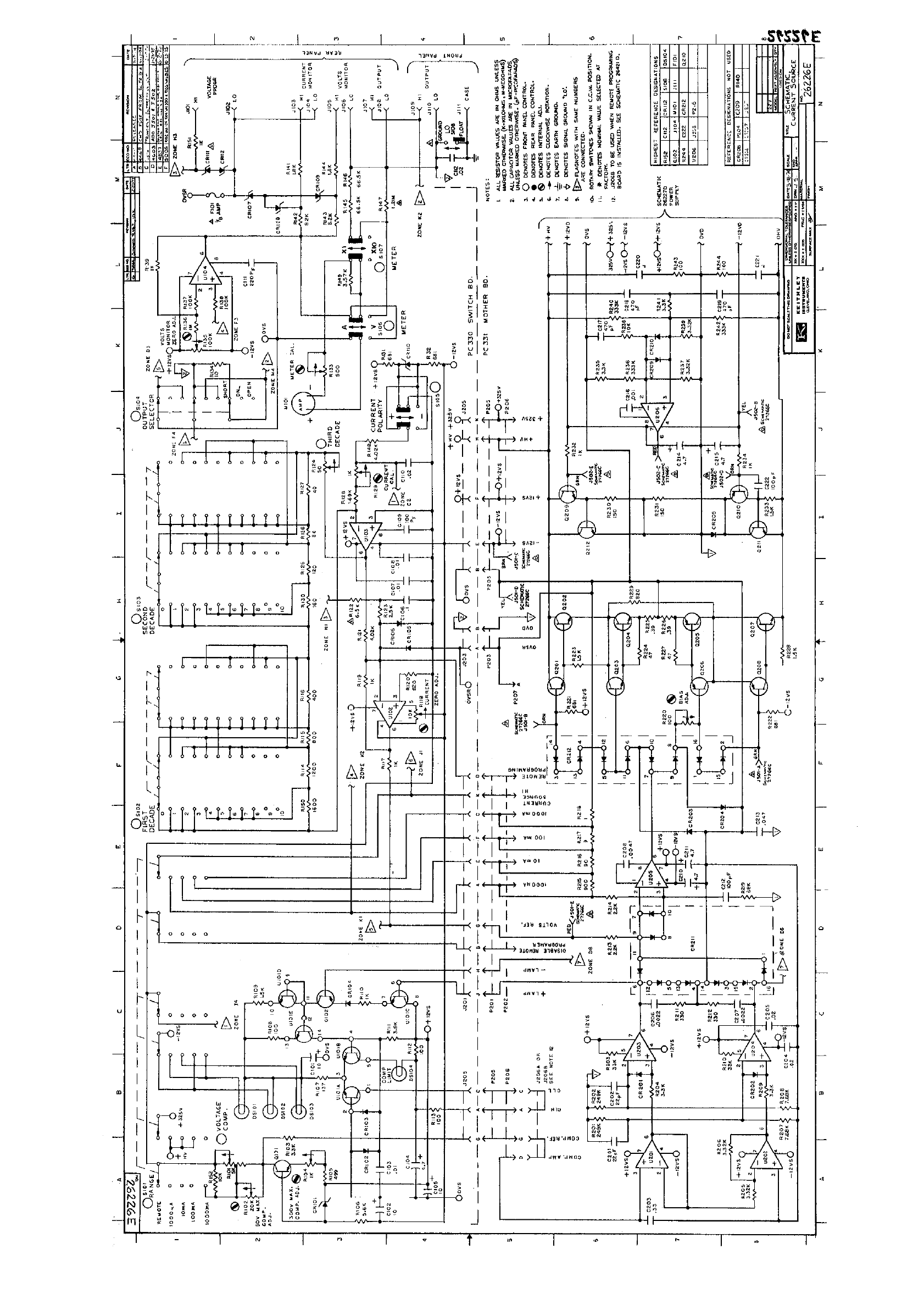
-
%
-
x
-
7
-
h
-
I
u
-
*
-
w
-
c
-
L
-
m
-
,e
-
B I
:
B I
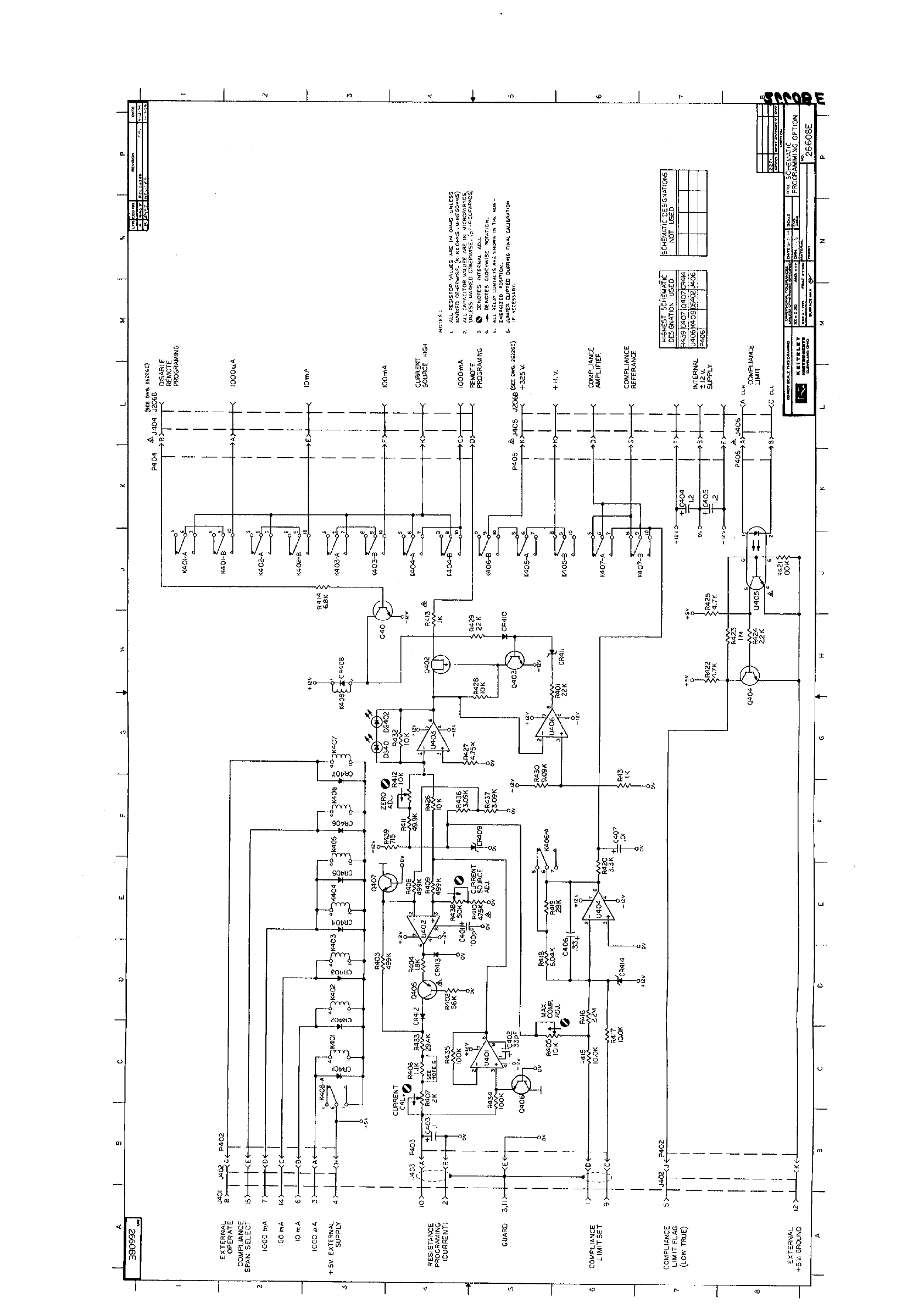
I I “I
-----__
--A____
KEITHLEY INSTRUMENTS, INC.
28775 AURORA ROAD
CLEVELAND, OHIO 44139
SERVICE FORM
MODEL NO.
NAME
COMPANY
SERIAL NO. P.O. NO; DATE R- I
PHONE
ADDRESS
CITY
STATE -ZIP
cl
1. Describe problem and symptoms using quantitative data whenever possible (enclose
readings, chart recordings, etc.)
(Attach additional sheets as necessary).
El Show a block diagram of your measurement system including all instruments connected
(whether power is turned on or not). Also describe signal source.
cl
3. List the positions of fi controls and switches on both front and rear panels of
the instrument.
cl
4. Describe input signal source levels, frequencies. etc.
Cl .
5. List and describe all cables used in the experiment (length, shielding, etc.).
El .
6. i--:t,;:i describe all other equipment used in the experiment. Give control settings
Ll
7 Environment:
Where is the measurement being performed? (Factory, controlled laboratory,
out-of-doors, etc.)
What power line voltage is used? Variation? Frequency?
Ambient temperature? "F. Variation? "F. Rel. Humidity?
Other
El Additional Information. (If special modifications have been made by the user,
please describe below.)
-