L010546 LSI LS7183, LS7184
User Manual: L010546 - LSI-LS7183, LSI-LS7184
Open the PDF directly: View PDF ![]() .
.
Page Count: 4

QUADRATURE CLOCK CONVERTER
FEATURES:
• x1, x2 and x4 resolution
• Programmable output pulse width (200ns to 140µs)
• Excellent regulation of output pulse width
• TTL and low voltage CMOS compatible I/Os
• +3V to +5.5V operation (VDD - VSS)
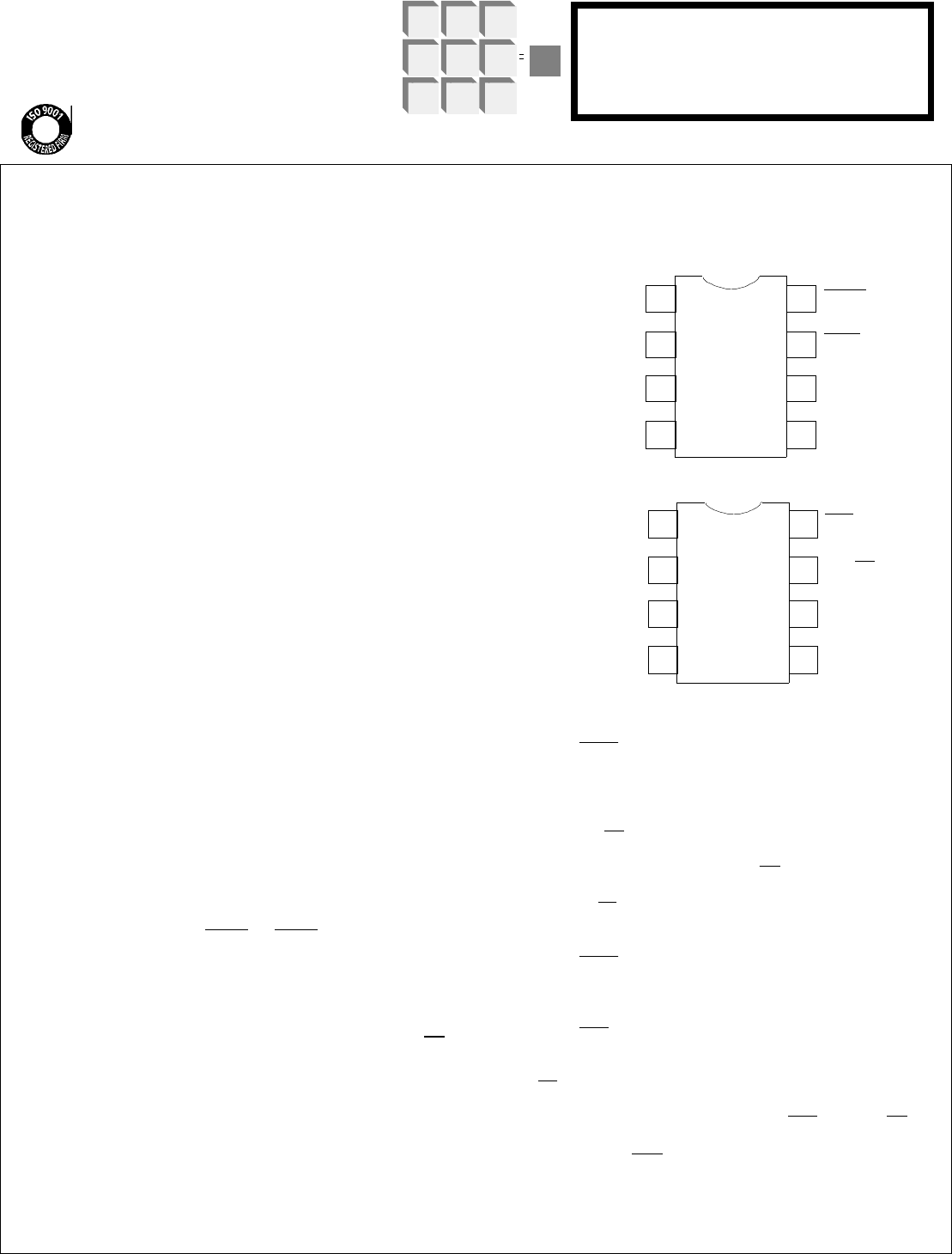
• LS7183, LS7184 (DIP);
LS7183-S, LS7184-S (SOIC) - See Figure 1
INPUT/OUTPUT DESCRIPTION:
RBIAS (Pin 1)
Input for external component connection. A resistor connected be-
tween this input and VSS adjusts the output clock pulse width (Tow).
VDD (Pin 2)
Supply Voltage positive terminal.
VSS (Pin 3)
Supply Voltage negative terminal.
A, B (Pin 4, Pin 5)
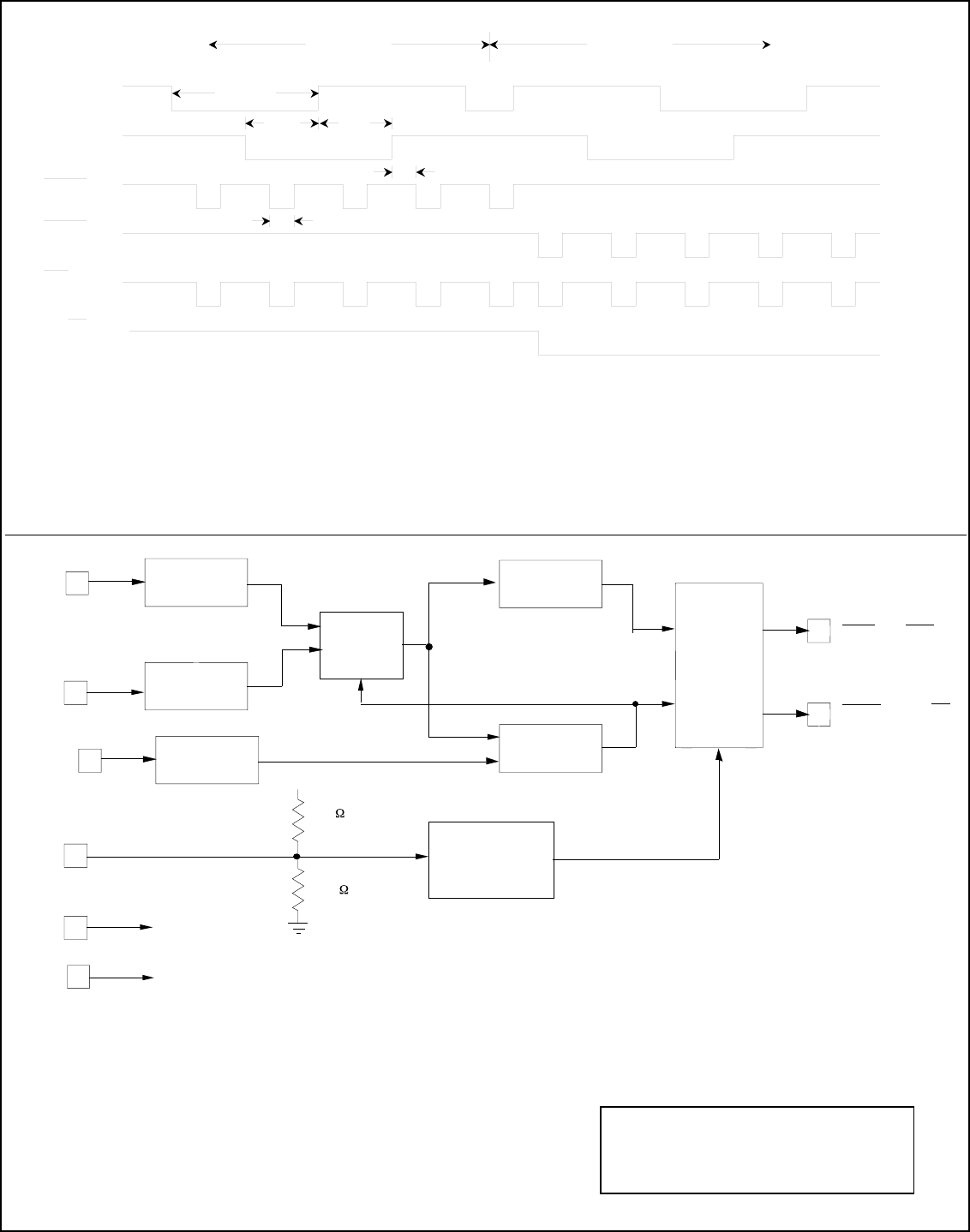
Quadrature Clock inputs A and B. Directional output pulses are gener-
ated from the A and B clocks according to Fig. 2. A and B inputs have
built-in immunity for noise signals less than 50ns duration (Validation
delay, TVD). The A and B inputs are inhibited during the occurrence of
a directional output clock (UPCK or DNCK), so that spurious clocks
resulting from encoder dither are rejected.
MODE (Pin 6)
MODE is a 3-state input to select resolution x1, x2 or x4. The input
quadrature clock rate is multiplied by factors of 1, 2 and 4 in x1, x2
and x4 mode, respectively, in producing the output UP/DN clocks
(See Fig. 2). x1, x2 and x4 modes selected by the MODE input logic
levels are as follows:
Mode = 0 : x1 selected
Mode = 1 : x2 selected
Mode = Float : x4 selected
LS7183 - DNCK (Pin 7)
In LS7183, this is the DOWN Clock Output. This output con-
sists of low-going pulses generated when A input lags the B
input.
LS7184 - UP/DN (Pin 7)
In LS7184, this is the count direction indication output. When
A input leads the B input, the UP/DN output goes high in-
dicating that the count direction is UP. When A input lags the
B input, UP/DN output goes low, indicating that the count di-
rection is DOWN.
LS7183 - UPCK (Pin 8)
In LS7183, this is the UP Clock output. This output consists of
low-going pulses generated when A input leads the B input.
LS7184 - CLK (Pin 8)
In LS7184, this is the combined UP Clock and DOWN Clock
output. The count direction at any instant is indicated by the
UP/DN output (Pin 7).
NOTE: For the LS7184, the timing of CLK and UP/DN re-
quires that the counter interfacing with LS7184 counts on the
rising edge of the CLK pulses.
Applications:
• Interface incremental encoders to Up / Down Counters
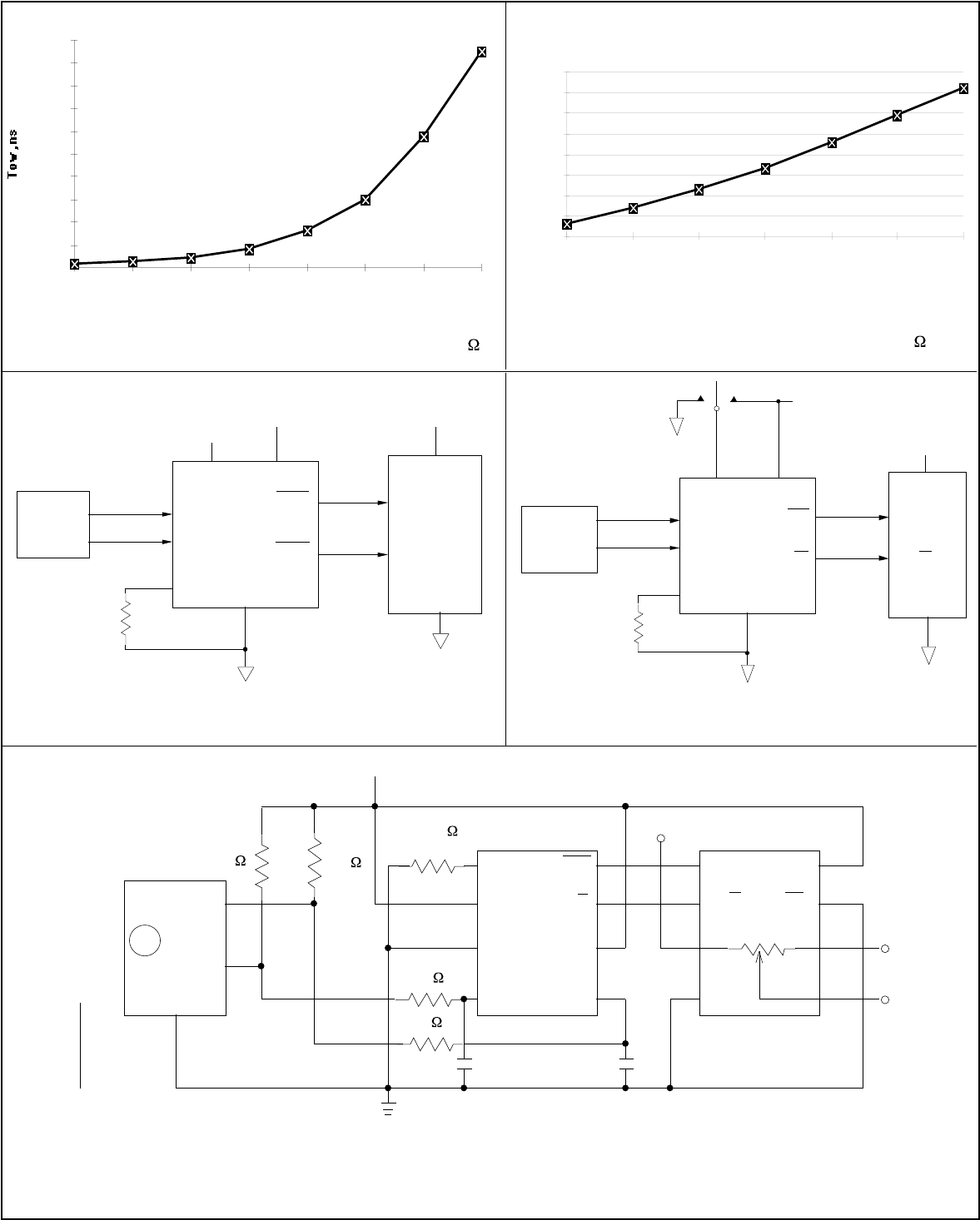
(See Figure 6A and Figure 6B)
• Interface rotary encoders to Digital Potentiometers
(See Figure 7)
DESCRIPTION:
The LS7183 and LS7184 are CMOS quadrature clock converters.
Quadrature clocks derived from optical or magnetic encoders, when
applied to the A and B inputs of the LS7183/LS7184, are converted to
strings of Up Clocks and Down Clocks (LS7183) or to a Clock and an
Up/Down direction control (LS7184). These outputs can be interfaced
directly with standard Up/Down counters for direction and position
January 2009
7183/84-011309-1
LSI/CSI
LSI Computer Systems, Inc. 1235 Walt Whitman Road, Melville, NY 11747 (631) 271-0400 FAX (631) 271-0405
LS7183
LS7184
UL
®
A3800
RBIAS
VDD (+V)
VSS (-V)
A B
MODE
DNCK
UPCK
PIN ASSIGNMENT - TOP VIEW
CLK
UP/DN
FIGURE 1
1
2
3
4
8
7
6
5
LS7184
RBIAS
VDD (+V )
VSS (-V)
A B
MODE
1
2
3
4
8
7
6
5
LS7183
LSI LSI

ABSOLUTE MAXIMUM RATINGS:
PARAMETER SYMBOL VALUE UNITS
DC Supply Voltage VDD - VSS 7.0 V
Voltage at any input VIN VSS - 0.3 to VDD + 0.3 V
Operating temperature TA -20 to +85 °C
Storage temperature TSTG -55 to +150 °C
7183/84-012703-2
DC ELECTRICAL CHARACTERISTICS:
(Unless otherwise specified VDD = 3V to 5V and TA = -20°C to +85°C)
PARAMETER SYMBOL MIN TYPE MAX UNITS CONDITON
Supply Voltage VDD 3.0 - 5.5 V -
Supply current IDD - 30 45 µA VDD = 3V
IDD - 110 150 µA VDD = 5V
MODE input:
Logic 0 Vml - - 0.6 V -
Logic 1 Vmh VDD - 0.6 - - V -
Logic float Vmf (VDD/2) - 0.5 VDD/2 (VDD/2) + 0.5 V -
Logic 0 input current Iml - 3.0 5.0 µA VDD = 3V
Iml - 12.0 16.0 µA VDD = 5V
Logic 1 input current Imh - -3.0 -5.0 µA VDD = 3V
Imh - -12.0 -16.0 µA VDD = 5V
A, B inputs:
Logic 0 VABl - - 0.3VDD V -
Logic 1 VABh 0.7VDD - - V -
Input current IABlk - 0 10 nA -
RBIAS input:
External resistor RB5k - 10M ohm -
All outputs:
Sink current Iol -1.2 -1.8 - mA Vo = 0.5V, VDD = 3V
Iol -2.5 -3.5 - mA Vo = 0.5V, VDD = 5V
Source current Ioh 1.2 1.8 - mA Vo = 2.5V, VDD = 3V
Ioh 2.5 3.5 - mA Vo = 4.5V, VDD = 5V
TRANSIENT CHARACTERISTICS
(TA = -20°C to +85°C)
PARAMETER SYMBOL MIN TYPE MAX UNITS CONDITON
Output Clock Pulse Width TOW 190 - - ns See Fig. 2
A, B inputs:
Validation Delay TVD - 25 50 ns VDD = 5V
TVD - 50 100 ns VDD = 3V
Phase Delay TPS TVD + TOW - Infinite s -
Pulse Width TPW 2TPS - Infinite s -
Frequency fA, B - - 1/(2TPW) Hz -
Inupt to Output Delay TDS - 200 270 ns VDD = 3V
TDS - 110 150 ns VDD = 5V

7183/84-121508-3
NOTE: Output clocks labelled 1, 2 and 4 have the following interpretations.
1: Generated in x1, x2 and x4 modes
2: Generated in x2 and x4 modes only
4: Generated in x4 mode only
FIGURE 2. LS7183, LS7184 INPUT/OUTPUT TIMING
The information included herein is believed to be
accurate and reliable. However, LSI Computer Systems,
Inc. assumes no responsibilities for inaccuracies, nor for
any infringements of patent rights of others which may
result from its use.
FORWARD REVERSE
T
PW
T
OW
T
PS
T
DS
24142
24142
24142
24142
A
B
UPCLK
(7183)
DNCLK
(7183)
CLK
(7184)
UP/DN
(7184)
T
PS
DIRECTION
PULSE
CURRENT
MIRROR
FILTER
FILTERA
B
MODE
V
DD
V
SS
MUX
AND
BUFFER
8
7
UPCK or CLK
DNCK or UP/DN
1
4
5
6
2
3
FIGURE 3. LS7183, LS7184 BLOCK DIAGRAM
RBIAS
INHIBIT
LOGIC
MODE
DECODE
VDD
1M
1M
+V
-V

7183/84-011309-4
Figure 4. Bias resistance vs pulse width. R in k .Figure 5. Bias resistance vs pulse width. R in M .
ENCODER
A CLOCK
B CLOCK
6 2
8
74
5
8
16
CK-UP
CK-DN
40193
3
A
B
RB
4
5
1
+V
Vss
LS7183
VDD
UPCK
DNCK
FIGURE 6A. TYPICAL APPLICATION FOR LS7183 IN x4 MODE
+V
RBIAS Vss
MODE VDD
ENCODER
A CLOCK
B CLOCK
6 2
8
7
8
16
VDD
3
A
B
4
5
1
+V
VDD
+V
CK
UP/DN
Vss
15
10
LS7184
RBIAS
4516
CLK
UP/DN
FIGURE 6B*. TYPICAL APPLICATION FOR LS7184N WITH MODE SELECTION
*See NOTE at bottom right of Page 1.
RB
Vss
MODE
SPDT (On - Off - On)
GND
B
A
B
MODE
CLK
U/D
RBIAS
V DD
VSS
A
2
3
5 4
6
7
8
100k
+5V
B1
W1
CLK
U/D
1
2
A1
A1
3
4
8
7
6
5
VDD
CS
B1
W1
FIGURE 7. Rotary Encoder Control of Digital Potentiometer
AD5220 LS7184
DIGITAL
POTENTIOMETER
ROTARY
ENCODER
GND
10k
10k
10k 10k
0.01uF 0.01uF
Part Number:
RE11CT-V1Y12-EF2CS
1
RBIAS vs Tow
0
1000
2000
3000
4000
5000
6000
7000
8000
9000
10000
5 10 20 51 100 220 430 750
R, kOhm
RBIAS vs Tow
0
20
40
60
80
100
120
140
160
1 2 3 5.1 6.8 8.2 10
R, MOhm
Tow, us