LG KG270 Manual
User Manual: LG-KG270-Manual
Open the PDF directly: View PDF ![]() .
.
Page Count: 125 [warning: Documents this large are best viewed by clicking the View PDF Link!]

Date: April, 2007 / Issue 1.0
Service Manual Model : KG270/MG160
Service Manual
KG270/MG160

- 3 -
1. INTRODUCTION ...............................5
1.1 Purpose .................................................. 5
1.2 Regulatory Information............................ 5
2. PERFORMANCE...............................7
2.1 H/W Features...........................................7
2.2 S/W Features...........................................8
3. TECHNICAL BRIEF ........................14
3.1 Digital Main Processor(PMB7880).........14
3.2 Power Amplifier Module (SKY77318) ....22
3.3 26 MHz Clock (DCXO)...........................24
3.4 RTC(32.768KHz Crystal) .......................25
3.5 LCD Interface(3-wire SPI interface).......26
3.6 SIM Card Interface.................................28
3.7 KEYPAD Interface .................................29
3.8 Battery Charging Block Interface ...........30
3.9 RF Interface ...........................................31
3.10 Audio Interface.....................................33
3.11 Key LED Interface................................37
3.12 Vibrator Interface .................................38
3.13 Memory Interface.................................39
3.14 Power Block Interface..........................40
3.15 FM Radio Interface ..............................42
4. TROUBLE SHOOTING ...................44
4.1 RF Trouble.............................................44
4.2 TX Trouble .............................................50
4.3 Power On Trouble..................................54
4.4 SIM Card Trouble...................................56
4.5 Vibrator Trouble .....................................58
4.6 Keypad Trouble......................................60
4.7 RTC Trouble ..........................................62
4.8. Key backlight Trouble ...........................64
4.9. LCD Trouble..........................................66
4.10. Microphone Trouble............................69
4.11. Receiver Trouble.................................71
4.12 Speaker Trouble ..................................73
4.13 Headphone Trouble .............................75
4.14 Charging Trouble .................................77
4.15 FM Radio Trouble ................................79
5. DOWNLOAD.......................................82
5.1 Download Setup.....................................82
5.2 Download Process.................................83
6. BLOCK DIAGRAM ..........................88
7. Circuit Diagram ..............................89
8. PCB LAYOUT..................................93
9. ENGINEERING MODE ....................95
9.1 About Engineering Mode .......................95
9.2 Access Codes........................................95
9.3 Key Operation........................................95
9.4 Engineering Mode Menu Tree ...............95
10. CALIBRATION ..............................92
10.1 Test Equipment Setup .........................92
10.2 Calibration Steps..................................92
11. STAND ALONE TEST .................109
11.1 Test Program Setting.........................109
11.2 Tx Test...............................................111
11.3 RX Test..............................................112
12. EXPLODED VIEW &
REPLACEMENT PART LIST ..... 113
12.1 Exploded View .................................. 113
12.2 Replacement Parts ............................115
12.3 Accessory ......................................... 124
Table Of Contents

- 4 -

1. INTRODUCTION
- 5 -
1.1 Purpose
This manual provides the information necessary to repair, description and download the features of
this model.
1.2 Regulatory Information
A. Security
Toll fraud, the unauthorized use of telecommunications system by an unauthorized part (for example,
persons other than your company’s employees, agents, subcontractors, or person working on your
company’s behalf) can result in substantial additional charges for your telecommunications services.
System users are responsible for the security of own system. There are may be risks of toll fraud
associated with your telecommunications system. System users are responsible for programming and
configuring the equipment to prevent unauthorized use. The manufacturer does not warrant that this
product is immune from the above case but will prevent unauthorized use of common-carrier
telecommunication service of facilities accessed through or connected to it.
The manufacturer will not be responsible for any charges that result from such unauthorized use.
B. Incidence of Harm
If a telephone company determines that the equipment provided to customer is faulty and possibly
causing harm or interruption in service to the telephone network, it should disconnect telephone
service until repair can be done. A telephone company may temporarily disconnect service as long as
repair is not done.
C. Changes in Service
A local telephone company may make changes in its communications facilities or procedure. If these
changes could reasonably be expected to affect the use of the this phone or compatibility with the
network, the telephone company is required to give advanced written notice to the user, allowing the
user to take appropriate steps to maintain telephone service.
D. Maintenance Limitations
Maintenance limitations on this model must be performed only by the manufacturer or its authorized
agent. The user may not make any changes and/or repairs expect as specifically noted in this manual.
Therefore, note that unauthorized alternations or repair may affect the regulatory status of the system
and may void any remaining warranty.
1. INTRODUCTION

1. INTRODUCTION
- 6 -
E. Notice of Radiated Emissions
This model complies with rules regarding radiation and radio frequency emission as defined by local
regulatory agencies. In accordance with these agencies, you may be required to provide information
such as the following to the end user.
F. Pictures
The pictures in this manual are for illustrative purposes only; your actual hardware may look slightly
different.
G. Interference and Attenuation
Phone may interfere with sensitive laboratory equipment, medical equipment, etc.Interference from
unsuppressed engines or electric motors may cause problems.
H. Electrostatic Sensitive Devices
ATTENTION
Boards, which contain Electrostatic Sensitive Device (ESD), are indicated by the sign.
Following information is ESD handling:
• Service personnel should ground themselves by using a wrist strap when exchange system boards.
• When repairs are made to a system board, they should spread the floor with anti-static mat which is
also grounded.
• Use a suitable, grounded soldering iron.
• Keep sensitive parts in these protective packages until these are used.
• When returning system boards or parts like EEPROM to the factory, use the protective package as
described.

2. PERFORMANCE
- 7 -
2.1 H/W Features
2. PERFORMANCE
Item Specifications
Band GSM DUAL Band(900/1800)
Type Bar type
Dimension 98 * 45 * 12.9mm
Weight 60g
Battery 750mAh Li-ion
Talk Time Over 2hours @EGSM,TX Level : 5
Stand-by Time Over 200 hours @Paging period : 5
RTC Under 4 hours when removed battery.
Antenna Internal Type(Dual-band)
LCD(Main) 1.52"(128x128 pixels), 65K Color STN LCD
Back Light Yes
Back Light color Blue
Vibrator Yes
Speaker&Receiver Yes(11x07 Receiver, 16®™ Speaker)
C-MIC Yes
Earphone Jack Mono or Stereo(Optional)
SIM Yes(Plug in Type) : 3.0V
MIDI 16 poly
I/O Connect 18 Pins (included Earphone Jack)
2.2 S/W Features
Function Detail Item Specification Etc.
Operating System OS O OSE
Data Circuit O
Packet X
Connectivity Infrared (IrDA) X
Bluetooth X
USB X
USB Mass storage X
RS232 O
Voice Function Voice Recording X
Voice Command X
Answering machine X
Memory User Memory O TBD Under 300KB
XMMS
XPictures (Still Image &
Moving Image)
XMP3 (Music Contents)
XJava Contents
OWallpaper 3 bitmap images
ORingtone 10 MIDI Ringtones
Xexternal memory (microSD)
Camera Camera Module X
Audio Voice Codec O FR, HR, EFR, AMR-NB
AMR O
FM Radio O
Integrated handsfree speaker O Speaker phone mode
2. PERFORMANCE
- 8 -
Function Detail Item Specification Etc.
Display RSSI O 6 level
Battery Level O 5 level
RTC O
Multi?Language O Basic:English
Max. 4 language of Latin
2 or 3 language of etc.
Quick Access Mode X
PLMN/Service Indicator O
Dimming Clock X
Dual Clock X
Local Time / Selected Area Time
Normal Features Last Dialed Number O 10
Last Received Number O 10
Last Missed Number O 10
Scratch Pad Memory X
Call Call Waiting O
Manage-ment Call Swap O
Call Retrieve O
Auto Answer X
Automatic Redial O
Calling Line dentification O
Full Call divert O
Speed Dialing O
Last Number Redial O
Multi-party Call (Conference Call)
O
Explicit Call Transfer X
2. PERFORMANCE
- 9 -
2. PERFORMANCE
- 10 -
Function Detail Item Specification Etc.
Network Automatic Network Selection O
Manual Network Selection O
Network Service Status O
DTMF DTMF Signaling O
DTMF Enable & Disable O
Audio Key Tone Volume O 6 Level (Include Mute)
Ring Tone Volume O 6 Level (Include Mute)
Ring Tone Pattern O 10Type(fixed)
Ring Type Silent O Vibrator & Ring (Indicator)
Earpiece Volume O
6 Level (Include Mute)
Mute O
Cell Broadcast Read Cell Broadcast O
Cell Broadcast Categories O
Cell Broadcast Message O
Language
Phone Book Entry O 300
Field O Office,Mobile
Numeric Store and Recall O
Alphabetic Store O
Alphabetic Recall O
Scroll by alphabetic or O
numeric order
Last Number Dialed
O10
Last Number Missed O 10
Last Number Received O 10
Copy & Move O
Fixed Dial Number O
Barred Dial Number X
Service Dial Number O
Email Entry X
Picture ID X
Video Caller ID X
My Name card X
2. PERFORMANCE
- 11 -
Function Detail Item Specification Etc.
Supp. Services Call Forwarding O All Incoming Calls,
ONo Reply
OOn Busy,
ONot reachable
Call Barring O All Outgoing Calls,
OInternational Calls,
OCalls except to Home Country
incoming Calls,
O
All incoming Calls when roaming
Conference Call O up to 3 calls
SIM Plug?In Type O 3 V only
SIM Lock O Service Provider / Network Lock
SIM Toolkit O Class 1, 2, 3
Prepaid SIM Operation O
Mega SIM X
Short Messaging Read Message O
Manage-ment Write and Edit Message O Not Support EMS
Send and Receive Message O
Reply to Message O
Forward Message
Extract Number from Message O
Message Status O
Message Unread Indicator O
Settable Message Center Number,
O
Reply Path and Validity O
Visible and Audible Message O
Receive Alerting
Voice Mail O
Settable Voice Mail Center Number
O
Message Protocol ONormal, Fax, National Paging,
Email, X400, ERMES, Voice
Message Overflow Indicator O
Message Center Number O
Help Menu X
2. PERFORMANCE
- 12 -
Function Detail Item Specification Etc.
Sound contents Ringtones O
Karaoke X
Stutter Sound X
Flip tone X
Button tone O
Others X
Miscellaneous Development & Test Facility O
Function Field Test Facility O
Display Software Version O
IMEI O
Text Input Language O Selectable Auto Language
Predictive word input O T9
Scheduler Schedule O 20 input (20 character)
To Do List X 50 input
Memo O 20 input (40 character)
D-day counter X
Send via Bluetooth X Schedule, Memo, To Do list, Messaging
World Time Setting Local Time O
Display Two Number of Cities Time X
Dual clock
Daylight saving X Summer time calibration function
NITS X Automatic setting as country code in SIM
Unit converter O Currency, Surface, Length, Weight,
Temperature, Volume, Velocity
Stop watch O
Calculator Calculation O + - * /
PC Sync Phone Book Sync X
Message Sync X
Multimedia Contents Sync X
Scheduler Sync X E-MAIL, EMS, Schedule, Phonebook,
Name card etc.
Sync ML DS X
DM X
Game X
Menu Quick Access Mode (Profile) X
External Interface Electrical Man Machine Interface O
Development and Test Facility O

2. PERFORMANCE
- 13 -
Function Detail Item Specification Etc.
Handset Restore Factory Setting O
Read Software Version O
Battery Charging Mode O
Security Emergency Call O
Handset Lock O
Security Code O Delete all
SIM Lock O
Key guard O
Real Time Clock 12/24 hour O
Calendar O
Automatic Leap Year Adjustment
Time Zone O
Daylight saving X
Alarm Manager O Once, Daily, Mon~Fri, Mon~Sat
Dimming Clock X
Power-off Alarm O
On Alarm Event O Display
Accessory Hand strap X
Embedded microSD Card X
microSD Adapter X
Stereo earmic O EarMic Type Provides optionally
only for supporting
FM radio function.
earmic w/music remote controller X
Neck strap X
LCD Cleaner X
Holster X
Data cable O RS232 cable Option
CD X
Holster charger X Standard battery Back-up
and Holster function
additional standard battery X
Extended Battery X
Desktop Charger X
Cigar Lighter Adapter X
Portable Handsfree X
Bluetooth headset X
Bluetooth stereo earset controller X
Car kit X
Leather Pouch X
Stylus Pen X
X
Compass X
3. TECHNICAL BRIEF
- 14 -
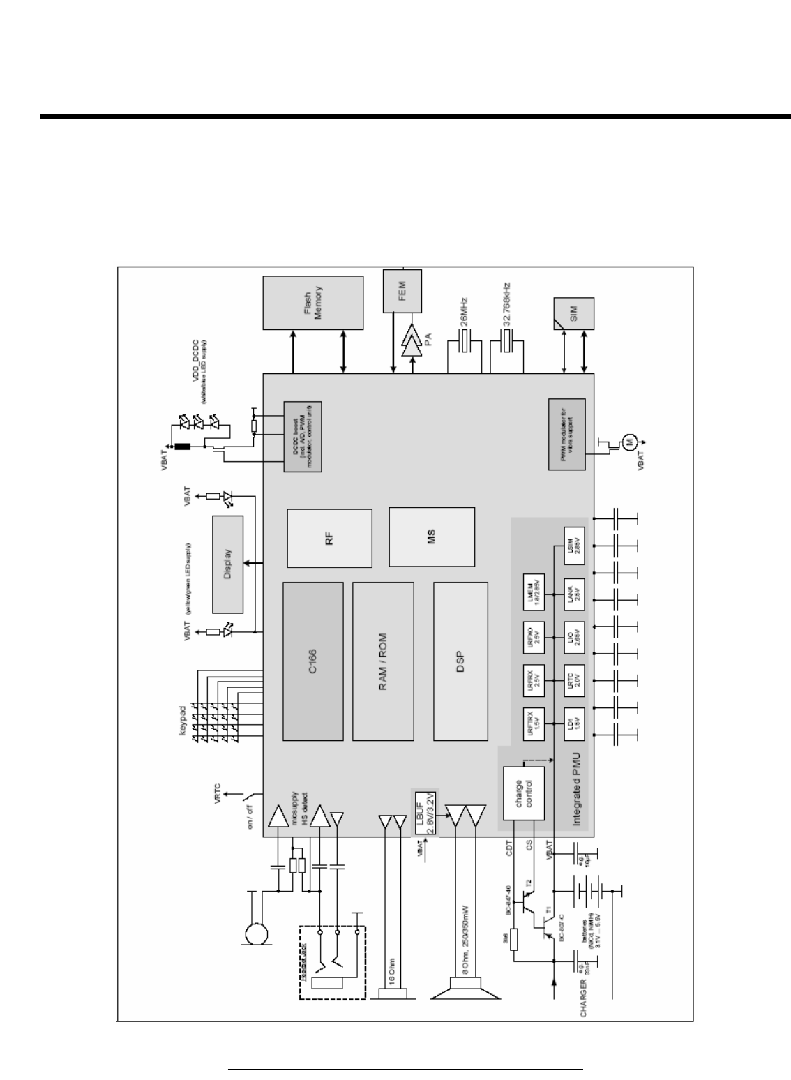
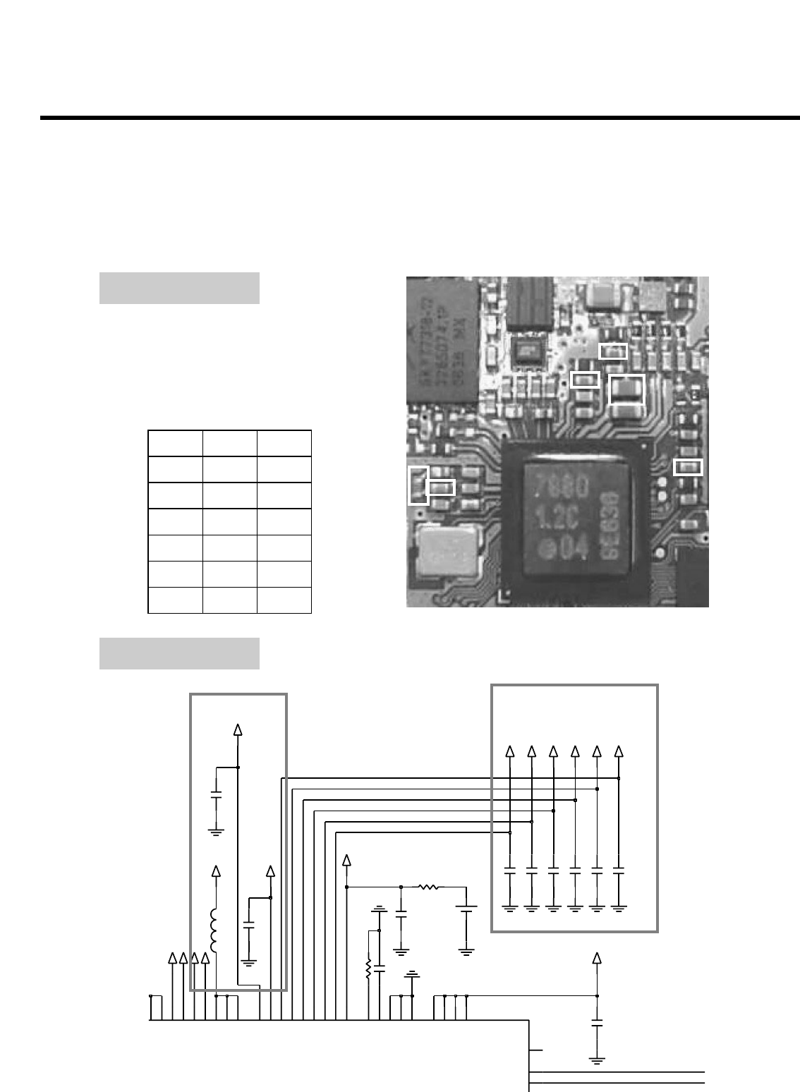
3.1 Digital Main Processor(PMB7880)
3. TECHNICAL BRIEF
Figure. 3-1 PMB7880 FUNCTIONAL BLOCK DIAGRAM

3. TECHNICAL BRIEF
- 15 -
3.1.1 Overview of E-GOLDvoice
The E-GOLDvoice is a GSM baseband modem including RF transceiver covering the low bands
GSM850 /GSM900 and high bands GSM1800 / GSM1900 bands.
E-GOLDvoice is Dual Band, therefore, it supports by default a low / high pair of bands at the same
time:
1. GSM850 / GSM1800
2. GSM850 / GSM1900
3. GSM900 / GSM1800
4. GSM900 / GSM1900
The E-GOLDvoice is optimized for voice-centric Mobile Phone applications.
The E-GOLDvoice is designed as a single chip solution that integrates the digital, mixed-signal, RF
functionality and a direct-to-battery Power Management Unit.
The transceiver consists of:
• Constant gain direct conversion receiver with an analog I/Q baseband interface
• Fully integrated Sigma/Delta-synthesizer capability
• Fully integrated two-band RF oscillator
• Two-band digital GMSK modulator with digital TX interface
• Digitally controlled crystal oscillator generating system clocks.
The E-GOLDvoice supports a direct battery connection, hence eliminating the need for an external
Power Management Unit. The E-GOLDvoice has different power down modes and an integrated
power up sequencer.
The E-GOLDvoice is powered by the C166®S MCU and TEAKLite® DSP cores. The operating
temperature range from -40C to 85C. It is manufactured using the 0.13 •Ïm CMOS process.

3. TECHNICAL BRIEF
- 16 -
3.1.2 Features
] Baseband
• High performance fixed-point TEAKlite DSP
• C166S high performance microcontroller
• There are several Interfaces:
- I2S interface for DAI connections (for Tape Approval)
- High Speed SSC Interface for connection of external peripherals
- SIM Interface
- Keypad Interface (6x4 or 5x5 keys)
- EBU for external RAM/FLASH connection
- Asynchronous serial interface
- JTAG Interface
- Black & white and color displays are supported
- PWM source to drive vibrator
- Keypad and display backlight supported.
] Receiver
• Constant gain, direct conversion receiver with fully integrated blocking filter
• Two integrated LNAs
• No need of interstage and IF filter
• Highly linear RF quadrature demodulator
• Programmable DC output level
• Very low power budget.
] Transmitter
• Digital Sigma-Delta modulator for GMSK modulation, typical -163.5 dBc/Hz@20 MHz
• Single ended outputs to PA, Pout = +3.5 dBm
• Very low power budget.
] RF-Synthesizer
• Σ∆Synthesizer for multi-slot operation
• Fast lock-in times (< 150 •Ïs)
• Integrated loop filter
• RF Oscillator
• Fully integrated RF VCO.
] Crystal Oscillator
• Fully digital controlled crystal oscillator core with a highly linear tuning characteristic.

3. TECHNICAL BRIEF
- 17 -
] Mixed Signal and Power Management Unit
• DC/DC boost for voltages up to 15V for driving White or Blue LEDs
• 8-Ohm loud speaker driver (250/350mW)
• 16-Ohm earpiece driver
• 32-Ohm headset driver
• 4 measurement interfaces (PA temperature, battery voltage, battery temperature,and ambient
temperature)
• Differential microphone input
• System start up circuitry
• Charger circuitry for NiCd, NiMh and LiIon cells
• Integrated regulators for direct connection to battery.

3.1.3 GSM System Description
The E-GOLDvoice is suited for mobile stations operating in the GSM850/900/1800/1900 bands.
In the receiver path the antenna input signal is converted to the baseband, filtered, and then amplified
to target level by the RF transceiver chipset.
Two A-to-D converters generate two 6.5 Mbit/s data streams. The decimation and narrowband channel
filtering is done by a digital baseband filter in each path.
The DSP performs:
1. The GMSK equalization of the received baseband signal (SAIC support available)
2. Viterbi channel decoding supported by an hardware accelerator.
The recovered digital speech data is fed into the speech decoder.
The E-GOLDvoice supports fullrate, halfrate, enhanced fullrate and adaptive multirate speech CODEC
algorithms.
The generated voice signal passes through a digital voiceband filter. The resulting 4 Mbit/s data
stream is D-to-A converted by a multi-bit-oversampling converter, postfiltered, and then amplified by a
programmable gain stage.
The output buffer can drive a handset ear-piece or an external audio amplifier, an additional output
driver for external loud speaker is implemented.
In the transmit direction the differential microphone signal is fed into a programmable gain amplifier.
The prefiltered and A-to-D converted voice signal forms a 2 Mbit/s data stream. The oversampled
voice signal passes a digital decimation filter.
The E-GOLDvoice performs speech and channel encoding (including voice activity detection (VAD)
and discontinuous transmission (DTX)) and digital GMSK modulation.
In the RF transceiver part, the baseband signal modulates the RF carrier at the desired frequency in
the 850 MHz, 900 MHz, 1.8 GHz, and 1.9 GHz bands using an I/Q modulator. The E-GOLDvoice
supports dual band applications.
Finally, an RF power module amplifies the RF transmit signal at the required power level. Using
software, the E-GOLDvoice controls the gain of the power amplifier by predefined ramping curves (16
words, 11 bits).
For baseband operation, the E-GOLDvoice supports:
• Making or receiving a voice call
• Sending or receiving an SMS.
3. TECHNICAL BRIEF
- 18 -

3. TECHNICAL BRIEF
- 19 -
3.1.4 PMU Details
The E-GOLDvoice includes battery charger support (various sensor connections for temperature,
battery technology, voltage, etc.) and a ringer buffer.
E-GOLDvoice avoids the need for an external power management component because its internal
power management unit contains:
• Voltage regulators for the On-chip and Off-chip functional blocks
• Charger circuitry for NiCd, NiMh and LiIon cells.
3.1.5 Bus Concept
The E-GOLDvoice has two cores (a microcontroller and a DSP), each with its own bus.
There is an interconnection between the TEAKlite bus and the C166S X-Bus.
3.1.6 C166S Buses
The C166S is connected to three buses:
1. Local Memory (LM) bus
2. X-Bus
3. PD-Bus.
3.1.7 TEAKLite Bus
The TEAKlite is connected to the TEAKlite bus.
3.1.8 Bus Interconnections
The interconnection between the X-Bus and the TEAKlite Bus uses:
• Multicore Synchronization
• Shared Memory.
3.1.9 Clock Concept
The E-GOLDvoice has a flexible clock control.
3.1.10 Interrupt Concept
The C166 MCU carries out the E-GOLDvoice interrupt system.
3.1.11 Debug Concept
The E-GOLDvoice includes a multi-core debug. The C166 and TEAKlite cores can be debugged in
parallel with:
• A single JTAG port (that is, on a single host)
• Mutual breakpoint control.

3.1.12 C166 Debug Concept
The debugging of the C166 uses the OCDS and the Cerberus.
3.1.13 TEAKLite Debug Concept
TEAKlite debugging uses the OCEM and the SEIB.
3.1.14 Power Management
The E-GOLDvoice provides the power management unit (PMU) for the complete mobile phone
application. The integrated PMU is directly connected to the battery and provides a set of linear
voltage regulators (LDO’s).
These LDO’s generate all required supply voltages and currents needed in a low feature mobile
phone. A charger control circuit charges NiCd, NiMH and LiIon batteries.
The charger control supports hardware controlled pre-charging and software controlled charging. It
offers a wide charger voltage range, making halfwave/full-wave charging with cheap transformers
possible.
White/blue backlight generation is supported with a special driver for very a low external parts count.
Power consumption during operation phases is minimized due to flexible clock switching In the
Standby Mode most parts of the device are switched off, only a small part is running at 32kHz and the
controller RAM is switched to a power saving mode. The TEAKLite ROM can be switched off during
Standby via SW.
3.1.15 On-Chip Security Concept
Secure boot is based on a public/private key approach. Flash images that are not signed with the
private key during phone manufacture cannot be loaded.
Verification of the Flash code is done with the public key. The public key as well as hash and verify
algorithms are stored in the ROM, which ensures a hardware secured boot procedure.
The following security features are supported:
• Prevention of illegal Flash programming
• Flash programming makes use of the E-GOLDvoice ID for personalization checks with IMEI and
SIM-lock protection
3. TECHNICAL BRIEF
- 20 -

3. TECHNICAL BRIEF
- 21 -
The security features use the following mechanism:
• Boot ROM flow:
- Controls the boot transition to external flash
- Controls the flash update
• Flash tied to the individual chip via an ID using e-fuses, that is, each E-GOLDvoice chip has its
own fused ID.
Further details on the E-GOLDvoice security concept are not publicly documented.
3.1.16 Asynchronous Operation Mode Concept
The E-GOLDvoice can operate in either:
• The traditional synchronous mode with the 26MHz system clock synchronized on the base station
• A special asynchronous mode (XO concept).
In the asynchronous mode the 26MHz clock input is not synchronized with the base station; the
residual frequency offset is compensated in the digital signal processing domain. This processing
includes frequency and timing compensation of the baseband and voiceband signals.
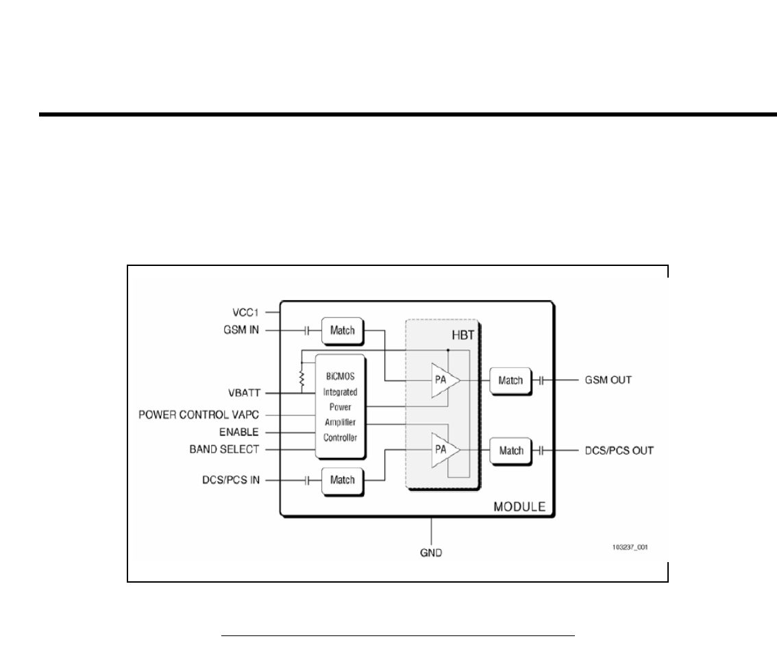
3.2 Power Amplifier Module (SKY77318)
The SKY77318 Power Amplifier Module (PAM) is designed in a low profile (1.2 mm), compact form
factor for quad-band cellular handsets comprising GSM850/900, DCS1800, and PCS1900 operation.
The PAM also supports Class 12 General Packet Radio Service (GPRS) multi-slot operation.
The module consists of separate GSM PA and DCS1800/PCS1900 PA blocks, impedance-matching
circuitry for 50 Ωinput and output impedances and a Power Amplifier Control (PAC) block with an
internal current-sense resistor. The custom BiCMOS integrated circuit provides the internal PAC
function and interface circuitry.
Fabricated onto a single Gallium Arsenide (GaAs) die, one Heterojunction Bipolar Transistor (HBT) PA
block supports the GSM bands and the other supports the DCS1800 and PCS1900 bands. Both PA
blocks share common power supply pins to distribute current.
The GaAs die, the Silicon (Si) die, and the passive components are mounted on a multi-layer laminate
substrate. The assembly is encapsulated with plastic overmold.
3. TECHNICAL BRIEF
- 22 -
Figure. 3-2 SKY77318 FUNCTIONAL BLOCK DIAGRAM

3. TECHNICAL BRIEF
- 23 -
RF input and output ports of the SKY77318 are internally matched to a 50 Ωload to reduce the
number of external components for a quad-band design. Extremely low leakage current (2.5 µA,
typical) of the dual PA module maximizes handset standby time. The SKY77318 also contains
bandselect switching circuitry to select GSM (logic 0) or DCS/PCS (logic 1) as determined from the
Band Select (BS) signal.
In Figure 1 below, the BS pin selects the PA output (DCS/PCS_OUT orGSM_OUT) and the Analog
Power Control (VAPC) controls the level of output power.
The VBATT pin connects to an internal current-sense resistor and interfaces to an integrated power
amplifier control (iPAC) function, which is insensitive to variations in temperature, power supply,
process, and input power.
The ENABLE input allows initial turn-on of PAM circuitry to minimize battery drain.
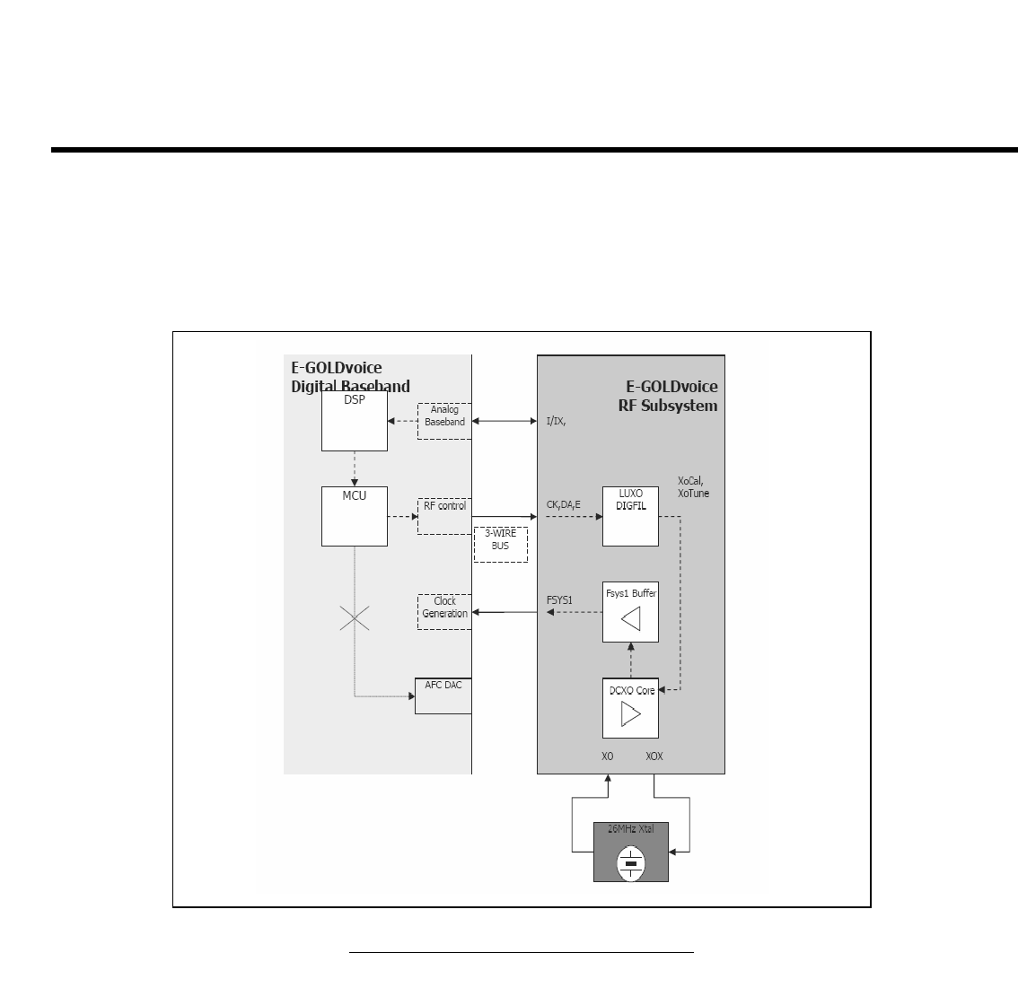
3.3 26 MHz Clock (DCXO)
DCXO (Digitally Controlled Crystal Oscillator) and VCTCXO (Voltage Controlled Temperature
Compensated Crystal Oscillator) are two different techniques used To maintain the mobile’s reference
oscillator’s accuracy over time. The reference oscillator’s accuracy over time will vary due to initial
crystal frequency offset, temperature drift and aging.
These static and dynamic frequency variations have to be compensated, otherwise the mobile would
be in danger of losing connection to the network.
The technique used to perform the frequency compensation is generally termed Automatic Frequency
Control (AFC).
To summarize the operation of DCXO, GSM Baseband processor will calculate the AFC compensation
(which is continuously updated) required based on the measured frequency error. Then the required
AFC compensation is sent to the LUXO (Lineari-Zation Unit of Crystal Oscillator), which in turns
control the DCXO core and generates The 26MHz system clock.
3. TECHNICAL BRIEF
- 24 -
Figure. 3-3 E-GoldVoice DCXO Overview
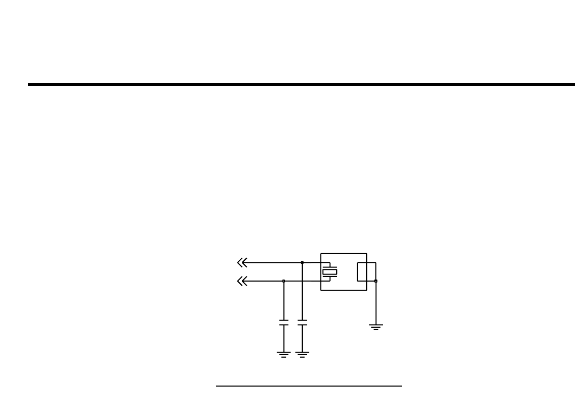
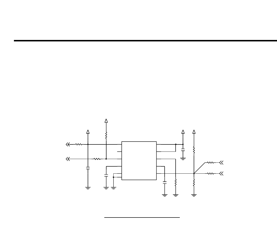
3.4 RTC(32.768KHz Crystal)
The integrated Real Time Clock (RTC) is able to provide programmable alarm functions and external
interrupts. Due to its extreme low power consumption the RTC can be supplied from a small backup
battery. This allows the generation of external interrupts, even when the main PMB7880 supply
voltage is switched off. For this purpose the RTC is powered by own voltage supply pins VDD_RTC
and VSS_RTC.
The RTC shall be driven by a 32.768 kHz (32k) clock which needs to be applied via the PMB7880
F32K and OSC32K pins. The clock can be fed from either an external clock source or use the on chip
32 KHz oscillator module.
The low clock frequency and the optimized low power design give the possibility to run the chip with a
minimum of power dissipation. For example, for this specific application the 26 MHz reference
oscillator can be switched off during system standby and a lowpower time reference can be kept when
the 32k clock is provided to the RTC.
The RTC consists of an PMB7880 specific RTC shell, containing the RTC macro, as well as the 32
kHz oscillator, as described in the following sections. The module RTC Shell solely performs level
translation of the 32KHz clock to the VDD_LD1 power supply domain, and is not functionally
associated with the RTC.
3. TECHNICAL BRIEF
- 25 -
Figure. 3-4 E-Gold Voice RTC Interface
32.768KHZ CRYSTAL
X100
MC-146_12_5PF
12
3
4
32.768KHz
C104 18p
C105 18p
32KIN
32KOUT
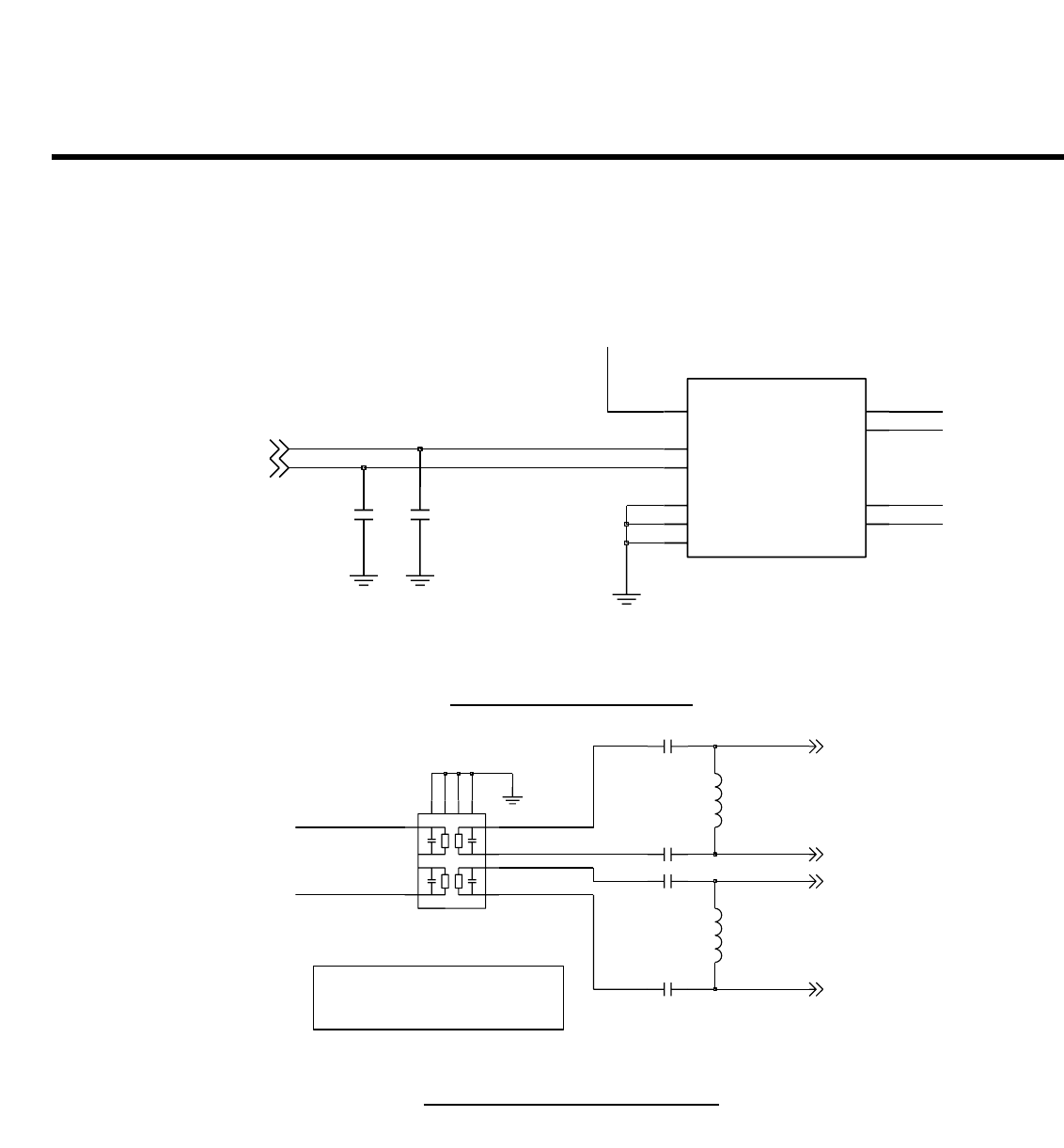
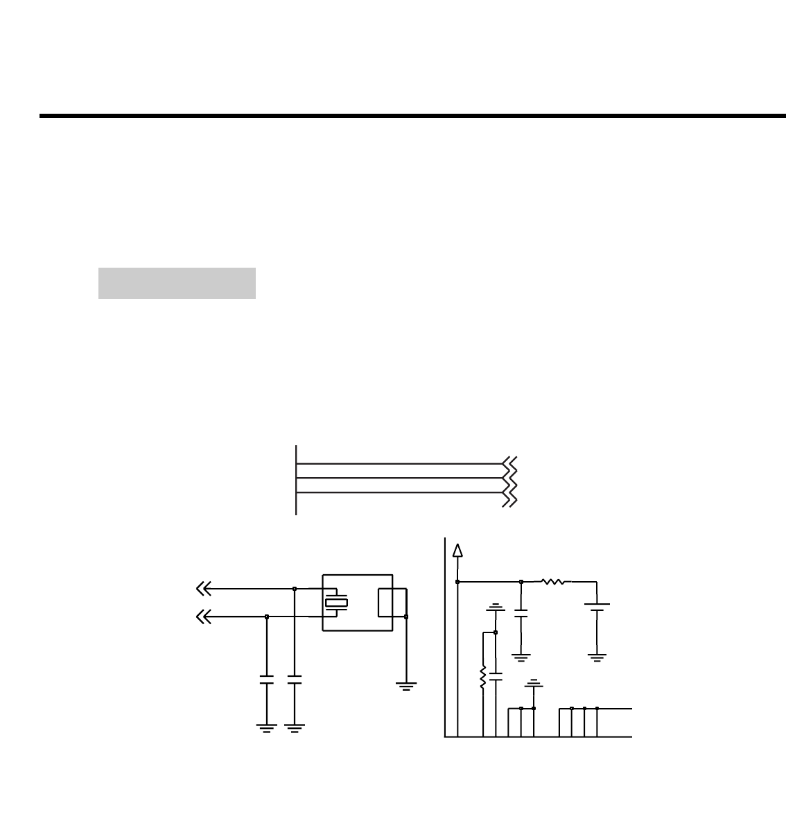
3.5 LCD Interface(3-wire SPI interface)
3. TECHNICAL BRIEF
- 26 -
Figure 3-5-1. LCD Interface
IMSA-9671S-13Y902
(ENQY0013801)
47R208
NA
C213
27p
C210
47R206
C209
27p
1u
C221
27p
C211
R205 47
NA
C214
47R207
2V8_VIO
14
15
1
10
11
12
13
2
3
4
5
6
7
8
9
CN200
NA
C208
MTPG
MTPD
R210
100K
C212
27p
MLED2
MLED1
SSC0_CLK
SSC0_MTSR
CS3
LCD_RESET
MLED
LCD_ID
Figure 3-5-2. Charge pump interface
CHARGE PUMP
C204
27p
4GND
IN
5
12
NC
AAT3157ITP-T1
10
C1+
C1- 9
C2+ 7
C2- 6
8CP
D1 1
2
D2
D3 3
11 EN_SET
U200
C200
1u
R202
100K
27p
C203
1u
C201
C202
27p
VBAT
MLED
W_LED_DRV
MLED1
MLED2
The AAT3157 is a low noise, constant frequency charge pump DC/DC converter that uses a trimode
load switch (1X), fractional (1.5X), and doubling (2X) conversion to maximize efficiency for white LED
applications. The AAT3157 is capable of driving up to three channels of LEDs at 20mA per channel
from a 2.7V to 5.5V input.
The current sinks may be operated individually or in parallel for driving higher current LEDs. A low
external parts count (two 1µF flying capacitors and two small 1µF capacitors at VIN and VOUT) make
this part ideally suited for small, battery-powered applications. AnalogicTech's S2Cwire™ (Simple
Serial Control™) serial digital input is used to enable, disable, and set current for each LED with 16
settings down to 50µA.
The low-current mode supply current can be as low as 50µA to save power.
3. TECHNICAL BRIEF
- 27 -
Figure 3-5-3. Charge pump Output Current
Signals Description
CS3 This signal enable to access to the driver IC of LCD.
SSC0_MTSR This signal transfer serial data to driver IC.
SSC0_CLK This signal transfer serial clock to driver IC.
LCD_RESET This signal makes driver IC to HW default status.
MLED This signal provide power to white LEDs.
MLED1/2 This signal be feed back from white LEDs.
2V8_VIO This signal provides power to LCD modules.(2.8V)
Data Output (mA/Ch) Data Output (mA/Ch)
120.0 9 5.0
217.0 10 4.2
314.0 11 3.4
412.0 12 2.8
510.0 13 1.0
68.6 14 0.5
77.0 15 0.1
86.0 16 0.05
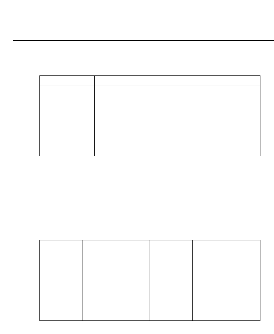
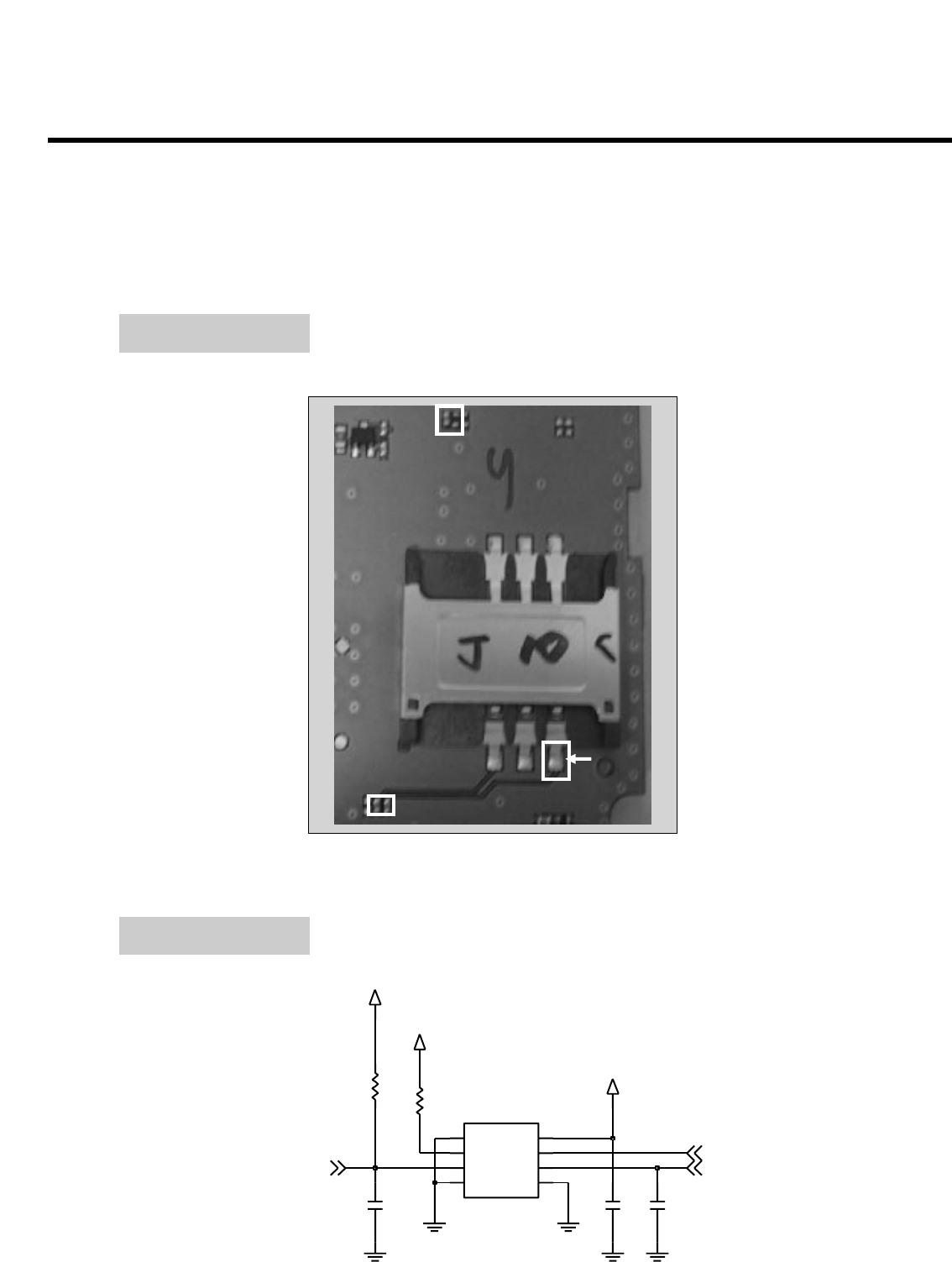
3.6 SIM Card Interface
The EGoldVoice provides SIM Interface Module. The AD6527 checks status Periodically During
established call mode whether SIM card is inserted or not, but it doesn't check during deep sleep
mode. In order to communicate with SIM card, 3 signals SIM_DATA, SIM_CLK, SIM_RST.
3. TECHNICAL BRIEF
- 28 -
Figure 3-6. SIM CARD Interface
C311
0.1u
4.7KR302
C310
22p 22p
C312
2V85_VSIM
2V85_VSIM
0
R303
I_O
6
2
RST
1
VCC
VPP
5
J300
CLK 3
4GND
GND1 78 GND2
2V85_VSIM
SIM_CLK
SIM_RST
SIM_DATA
Signals Description
SIM_RST This signal makes SIM card to HW default status.
SIM_CLK This signal is transferred to SIM card.
SIM_DATA This signal is interface datum.
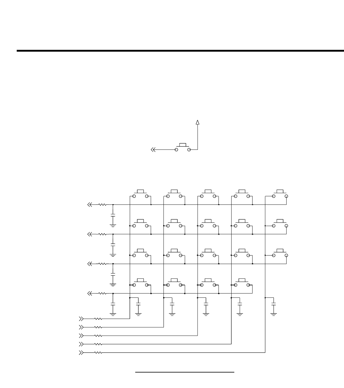
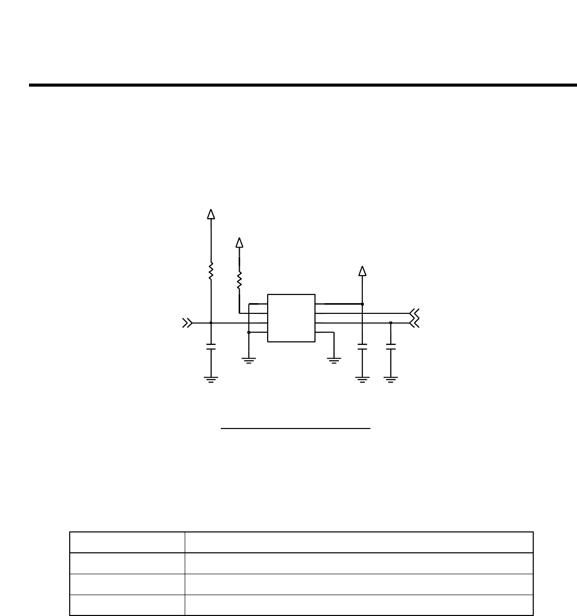
3.7 KEYPAD Interface
The keypad interface is connected to the X-Bus, together with the XBIU and the Shared Memory
Register, using a single Bus Interface.
The keypad supports two scan modes:
• By default, the keypad is a 4x6 scan matrix (4 input and 6 output pins).
• To set the keypad to a 5x5 scan matrix (5 input and 5 output pins)
The scan mode should be determined at the very beginning of the system start because changes are
not allowed later.
3. TECHNICAL BRIEF
- 29 -
Figure 3-7 KEY MAXTRIX Interface
DOWN
23
5
#
MENU
SEND
4UP SEL
KEY MATRIX
1
7
*
LEFT
END
9
0
RIGHT
6
8
SW203
R204
680
SW201
2V0_VRTC
SW216
C215
NA NA
C219
R212 680
SW205
SW212
SW217
SW215
C207
NA
SW210
SW214
NA
C218
SW211
SW200
SW219
R215 680
SW204
NA NA
C216 C220
R209
680
SW208SW207
R201
680
SW202
C206
NA
R211 680
SW209
SW213
NA
C205
680
R203
R214 680
R213 680
SW218
NA
C217
SW206
KEY_OUT2
KEY_OUT3
KEY_OUT4
KEY_IN3
END_KEY
KEY_IN0
KEY_IN2
KEY_IN1
KEY_IN4
KEY_OUT1
3.8 Battery Charging Block Interface
The AAT3681A is a high performance battery charger designed to charge single Cell
lithiumion/polymer batteries with up to 500mA of current from an external power source.
It is a stand-alone charging solution, with just one external component required For complete
functionality. The AAT3681A precisely regulates battery charge voltage and current for 4.2V lithium-
ion/polymer battery cells.
The adapter/USB charge input constant current level can be programmed up to 500mA for rapid
charging applications.
The AAT3681A has four basic modes for the battery charge cycle:
pre-conditioning/trickle charge; constant current/fast charge; constant voltage; and end of charge.
3. TECHNICAL BRIEF
- 30 -
Figure 3-8. Charging IC Interface
(10V,K,X5R)
CHARGING IC
(1%)
(10V,K,X5R)
1u
C126
2V8_VIO
VCHARGE
NA
R120
NA
R118
1.8KR119
0.015u
C127
160K
R124
VBAT
1u
C125
NAR123
R125
100K
R121
NA
2_FAULT
_STATUS
3
6
ENGND
5
8
IREF
11 PGND
TIME
47
V2P8
10
VBATVIN
1
VSEN_TEMP 9
U101
ISL9201IRZ-T
0R122
C128
1u
VCHARGE
CHG_EN_TEST
CHG_STATUS
CHG_EN
CHARGE_DETECT
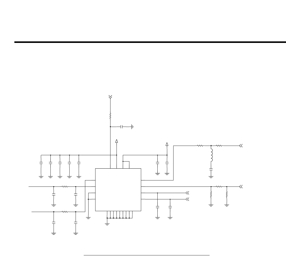
3.9 RF Interface
E-GOLDvoice features a fully integrated constant-gain direct conversion receiver, i.e. there is no
interstage filter needed and the baseband level at the analogue IQinterface follows directly the RF
input level. Depending on the baseband ADC dynamic range, single- or multiple-step gain switching
schemes are possible.
An integrated, selfaligning, low-pass filter ensures the receivers to function under blocking and
reference interference conditions and avoids aliasing by baseband sampling. An automatic DC-offset
compensation is implemented and can be switched depending on the gain setting.
3. TECHNICAL BRIEF
- 31 -
Figure 3-9-1. ASM interface
Figure 3-9-2. SAW Filter interface
C417
27p
C418
27p
FL400
5GND1
GND2
8
GND3
10
GSM1800_1900RX 6
1
GSM1800_1900TX
GSM850_900RX 4
2
GSM850_900TX
9IN
VC_GSM1800_1900TX
7
3VC_GSM850_900TX
LMSP2PAA-575TEMP
VC2
VC1
IN CASE OF GSM850/PCS1900
CHANGE THIS DUAL SAW FILTER
PART_NO SFSB0001401
TO PART_NO SFSB0001301
3pC421
L403
18nH
1
I2
4
9
O1_1
O1_2
8
O2_1
7
6
O2_2
B9308FL401
2
G1
3
G2
5
G3
10
G4
I1
3pC419
3pC422
L404
5.1nH
3pC420
GSM_RXN
DCS_RXN
GSM_RXP
DCS_RXP
The digital transmitter architecture is based on a fractional-N sigma-delta synthesizer for constant
envelope GMSK modulation. This configuration allows a very low power design with a reduced
external component count.
The modulation is transferred between baseband- and RF-part of the PMB7880 via a digital interface
signal into the digital modulator.
The following Gaussian filter shapes the digital data stream for the GMSK modulation. Additionally a
pre-distortion filter compensates the attenuation of the PLL transfer function resulting in a very low
distortion at the transmit output.
The filtered digital data stream is scaled appropriately and added to the channel word. This sum is fed
into the MASH modulator. The output of the MASH modulator is a sequence of integer divider values
representing the high resolution fractional input signal. This sequence controls the MMD (multi
modulus divider) at a sample rate of 26MHz. Thus a tightly controlled frequency modulation of the
VCO is achieved.
3. TECHNICAL BRIEF
- 32 -
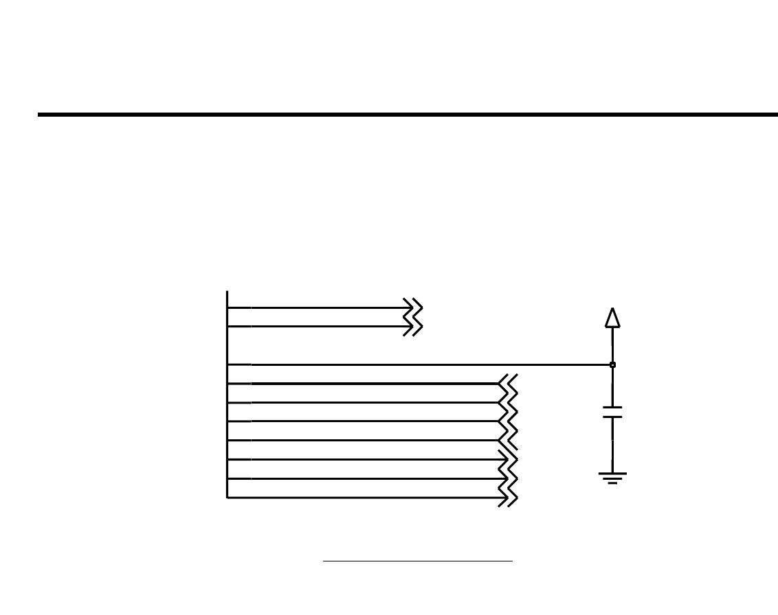
Figure 3-9-3. PAM(Power Amplifier Module) interface
(50V,J,NP0)
(50V,J,NP0)
(2012)
(16V,K,X7R)
(10V,Z,Y5V)
(50V,J,NP0)
(16V,K,X7R)
(50V,J,NP0)
VBAT
C414
27p
VBAT
L402
NA
27p
C407 C408
0.01u
GND7
13
14 GND8
16 GND9
P_GND
21
RSVD_GND
19
20
VAPC
VBATT 17
VCC1A 2
VCC1B 6
1
BS
3
DCS_PCS_INDCS_PCS_OUT
15
EGSM_IN 4
EGSM_OUT
11
18
ENABLE
5GND1
GND2
7
GND3
8
9GND4
GND5
10
12 GND6
NA
U400
SKY77318
C416
C405
R407
0
33p
C412
NA
39p
C415
NA
C401
0
R404
C411
NA
C402
10u
R410
0
R408
NA
C409
NA
C404
0.01u
R402 1K
0
R406
R405
0
27p
C413
R409
NA
12p
C403
18p
C406
DCS_PCS_OUT
TXON_PA
BS
GSM_OUT
TX_RAMP
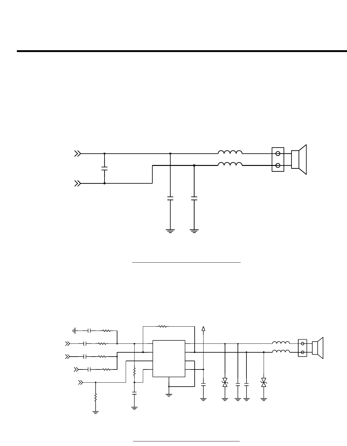
3.10 Audio Interface
The audio front-end of E-GOLDvoice offers the digital and analog circuit blocks for both receive and
transmit audio operation and ringing. It features a high-quality, digital-to-analog path with amplifying
stages for connecting acoustic transducers to the E-GOLDvoice. In the transmit direction the supply
voltage generation for microphones, low-noise amplifier and analog to digital conversion are integrated
on the E-GOLDvoice.
For E-GOLDvoice the EPp1/EPn1 driver are used as differntial Earpiece-Driver, EPPa1 is used as
single-ended Headset-Driver.
The audio front-end itself can be considered to be organized in three sub-blocks:
• Interface to processor cores (TEAKlite and - indirectly - C166S)
• Digital filters
• Analog part.
3. TECHNICAL BRIEF
- 33 -
Figure 3-10-1 Audio interface
C124
1000p
P12
VMIC
L15
LOUD1
LOUD2 K14
R13
MICN1
R12
MICN2
MICP1 P15
MICP2 P11
EPN1 N15
EPP1 M12
EPPA1 M14
VMIC
AUXIP
SPK_N
VINNORN
VINNORP
REC_P
REC_N
EPPA1
SPK_P
AUXIN
The interface to the processor cores consists of a direct physical connection to the TEAKlite DSP bus
and a set of firmware commands to handle communication between the C166S and the audio front-
end which serves as the interface peripheral for audio algorithms running on the DSP or the controller.
The audio front-end Generates interrupts on certain occasions, for example, when exchange of data is
requested. The core interface part of the audio front-end also contains the control and status registers
which are used to set up certain operation modes of the peripheral.
The section next to the core interface contains the digital filters for interpolation and decimation of the
audio signals being received and transmitted. The data path for the receive direction can be set up to
process sampling rates between 8kHz and 48kHz.
The interpolation filters for the respective sampling rates are implemented in a dedi-cated hardware
block and are automatically selected to suite the chosen sampling rate.
Low-pass interpolation filtering, which produces an unsigned 16-bit data stream with a sampling rate of
4 MHz, is performed digitally. D-to-A conversion, postfiltering, and final amplification are performed on
the analog part. The amplifier buffer for voiceband receive does also support ringer functionality. The
ringer functionality is activated by Setting bits RINGSELPN or RINGSELPA in the voiceband part of
the analog control register.
In transmit direction, amplification, prefiltering and A-to-D conversion (analog ∑∆ modulation) are
performed on the analog part. The resulting 2-Mbit/s data stream is filtered by a digital low-pass
decimation filter for further processing by DSP firmware.
Two sampling rates, 8kHz and 16kHz, are supported.
The analog section contains all the necessary analog functional blocks including microphone supply
generation, output and input amplifiers and analog filtering.
3. TECHNICAL BRIEF
- 34 -
Signals Description
EPp1 Main Receiver Positive signal(Differential signal)
EPn1 Main Receiver Negative signal(Differential signal)
EPpa1 Headset signal(Single Ended signal)
Loud1 Speaker Output Positive signal(Differential signal)
Loud2 Speaker Output Negative signal(Differential signal)
MICP1 Main Microphone Positive signal(Differential signal)
MICN1 Main Microphone Negative signal(Differential signal)
MICP2 Headset Microphone Positive signal(Differential signal)
MICN2 Headset Microphone Negative signal(Differential signal)
VMIC Main/Headset Microphone supply power
3. TECHNICAL BRIEF
- 35 -
Figure 3-10-2 Main Receiver interface
(SURY0013001)
RECEIVER
11*07*3T receiver
22nHL100
39p
C103
39p
C102
1
2
CN100
L101 22nH
C100
39p
REC_P
REC_N
Figure 3-10-3 Main Speaker interface
SPEAKER
(SUSY0025801)
(2012)
Gain : Rf/Rin
SPEAKER AMPLIFIER
(10V,K)
16pi 3.4T speaker
C118 0.1u
VBAT
0.1uC119
L103 27nH
R108
82K
R103
NA
C120
1 uF
VP B3
C3 _SD
27nHL104
U100 NCP2890AFCT2G
BYPASS
C1
A1 INM
INP
A3
OUTA A2
C2
OUTB
VM B2
B1 VM_P
C123
0.1u
0.1uC117
diode
D101
R102
82K
20K
R105
20K
R106
20K
R104
D100
diode
R110
100K
C122
0.1u
CN101
1
2
C121 0.22u
NAC116
RADIO_SPK_L
LOUD_SPK_EN
SPK_N
SPK_P
3. TECHNICAL BRIEF
- 36 -
Figure 3-10-4 Main Microphone interface
MAIN_MIC
C313 39p
1K
R300
C306 0.1u
VMIC
MIC300
OB4-15L42-C33L
1
2
0.1u
C307
2.2K
R301
100ohm
R304
10u
C304
C314 39p
R307
100ohm
0.1uC309
2.2K
R309
C303
39p
39p
C308
VINNORP
VINNORN
Figure 3-10-5 Headset interface
FOR RADIO
12,13 : CHG
8 : JACK_D
(50V,C,NP0)
9,10 : BATT
4 : EAR_L
(10V,Z,Y5V)
FOR RADIO
I/O CONNECTOR
11 : R/ON
5 : EAR_R
2 : AUDIO
(50V,J,NP0)
(50V,J,NP0)
(2012)
1608
7 : RXD
(TOL:0.25P)
EAR_MIC
6 : TXD
39pC325
VMIC
NAR322
2V8_VIO
0.1u
C317
100K
R324
2V8_VIO
C336
3p
C326 39p
2V8_VIO 10p
C322
21
22
3
4
5
6
7
8
9
HSEJ-18S04-25R
1
10
11
12
13
14
15
16
17
18
19
2
20
100K
CN301
R323
18p
C337
C324 10u
2V8_VIO VCHARGE
1800FB301
C318
NA 10u
C319
L300
270nH
1
2
3
VBAT
CN302
R316
1.5K
C328
56p
R321
100K
C323 10u
R318
2.2K
39pC321
C327
10u
FB302 1800
R332 0
C320 0.1u
FB300 1800
VBAT
BATT_TEMP
DSR
HS_DET
AUXOP_FML
AUXOP_FMR
RPWRON
RXD
TXD
FM_ANT
AUXIN
AUXIP
3. TECHNICAL BRIEF
- 37 -
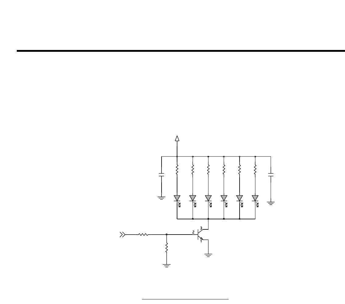
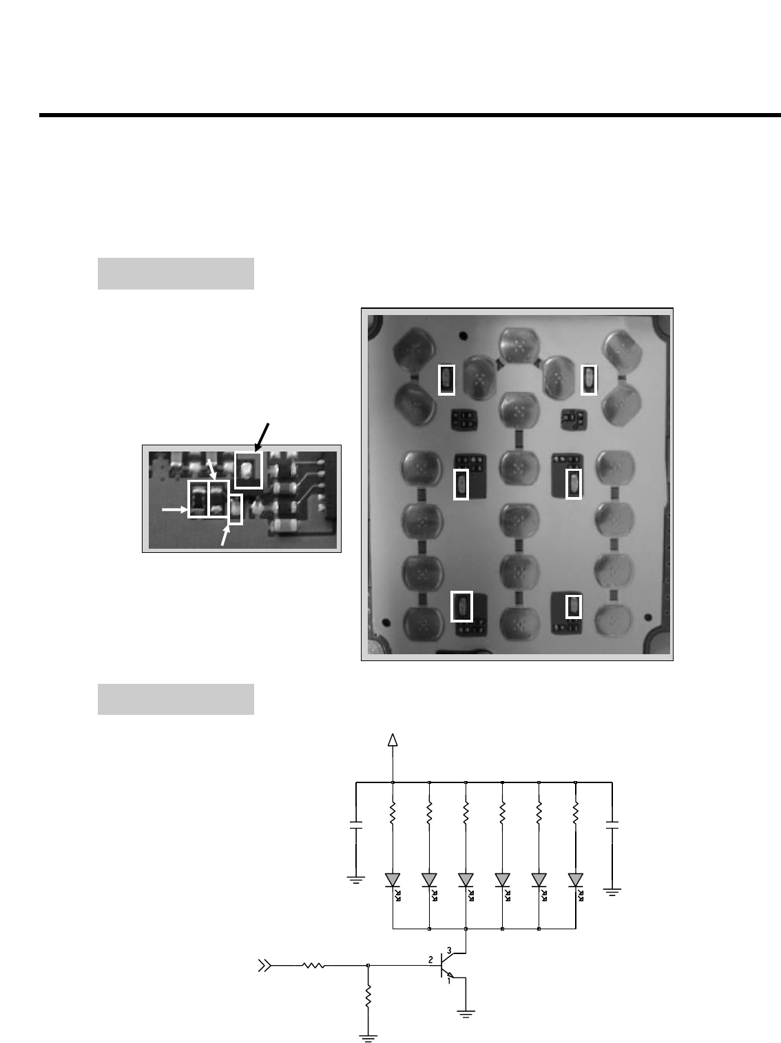
3.11 Key LED Interface
This handset has 6 LEDs that illuminates blue color.
Control signal is controlled by EGold-voice with PWM and handset has 3 methods, ON, OFF and
Dimming.
Figure 3-11 Key LED interface
KEY BACKLIGHT
(10V,K,X5R)(10V,K,X5R)
LD201
VBAT
LEBB-S14H
LEBB-S14H
LD200
2SC5585
Q200
LEBB-S14H
LD204
1u
C223
LD202
LEBB-S14H
100ohm
R220
LD203
LEBB-S14H R219
100ohm
100ohm
R218
R223
10K
100ohm
R216
1KR222
LD205
LEBB-S14H
1uC222
R217
100ohm
R221
100ohm
KEY_BACKLIGHT
3. TECHNICAL BRIEF
- 38 -
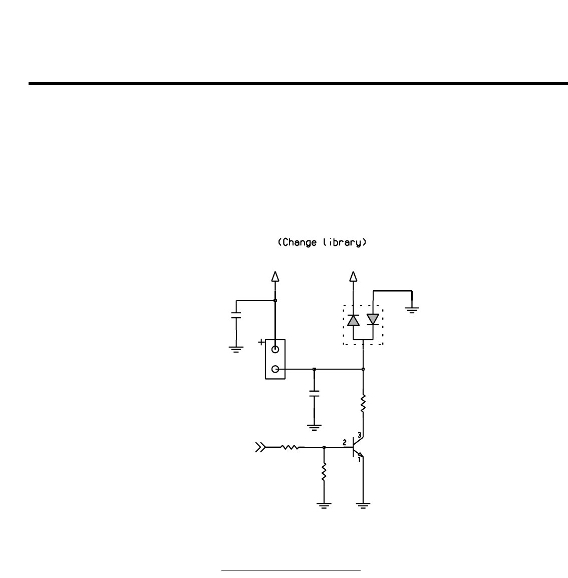
3.12 Vibrator Interface
This handset has vibrator operation. Control signal is controlled by EGold-voice with PWM.
Figure 3-12 Vibrator interface
(1608)
VIBRATOR
(50V,J,NP0)
VBAT
C302
27p
CN300
1
2
R308
100K
Q300
2SC5585
D300
1SS302-T5L_F_H
1K
R306
27p
C305
VBAT
R305
10
VIBRATOR
3. TECHNICAL BRIEF
- 39 -
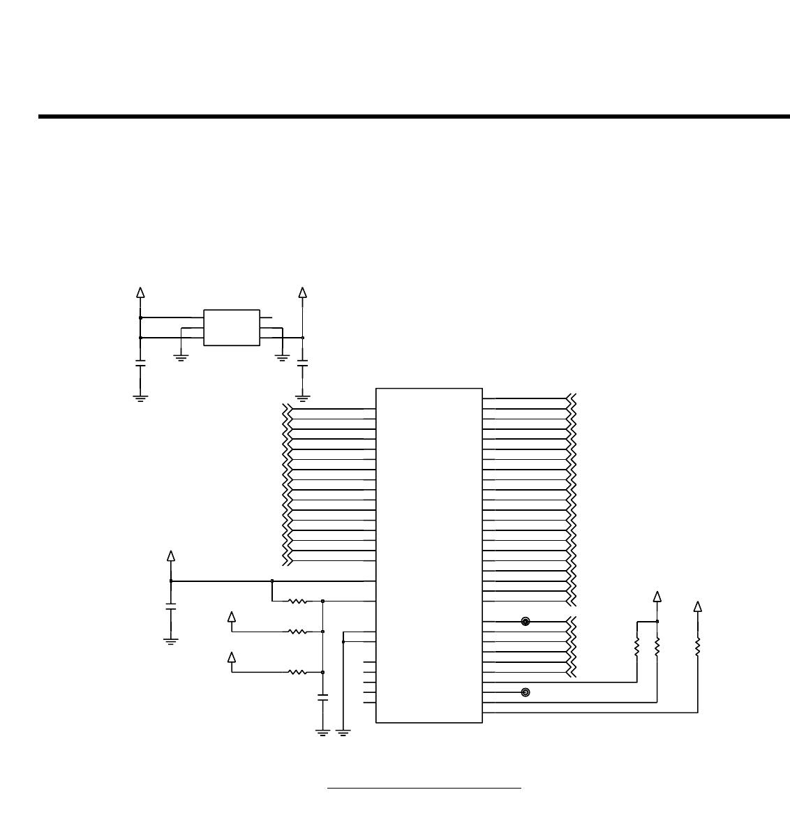
3.13 Memory Interface
In E-GOLDvoice, the 16bits demultiplex X-bus interface is used for memory device support. NOR
Flash memory is supported. (The NAND Flash memory is not supported). The page mode can be
supported for flash memories.
Up to 8MBytes of external RAM and/or ROM can be connected to the MCU via its external bus
interface.
Up to 3 external CS signals can be generated to save external glue logic.
Access to very slow memories is supported via a special ‘Ready’ function.
The system MCU clock is set to run with 26Mhz.
Figure 3-13 Memory interface
MEMORY
(NOT MOUNTED)
100KR312
2V8_VMEM
NAR315
0R310
G8
VSS2
E2
WP_ACC A4
F1
_CE1F G1
_CE1S
A3
_LB
F2
_OE
B4
_RSTF
_UB B3
A5
_WE
DQ2
F4 DQ3
DQ4
F5
DQ5
H6
DQ6
E6
G7 DQ7
DQ8
H2
DQ9
F3
C8 RFU0
RFU1
D8
E7 RFU2
RFU3
F8
H5 RFU4
RY__BY C4
VCCF
G4
G5 VCCS
VSS1
A3
A4 D2
A5 C2
A6 B2
A2
A7
A8 A6
A9 C6
CE2S B5
G2 DQ0
E3 DQ1
DQ10
G3
DQ11
H4
G6 DQ12
DQ13
F6
DQ14
H7
F7 DQ15
H3
S71GL032A40BAW0F
E1
A0 D1
A1
A10 D6
A7
A11
A12 B7
C7
A13
A14 D7
B8
A15 E8
A16 D3
A17 C3
A18 B6
A19
A2 C1
C5
A20
B1
U301
C316
0.1u
R311 NA
2V8_VMEM_S
2V8_VIO
C301
NANA
C300
2V8_VMEM_S
1
3VIN VOUT 4
VBAT
BH28FB1WHFVU300
6
BGND
2GND
NC 5
STBY
R313 100K
2V8_VMEM
TP300
_RY_BY
0.1u
C315 2V8_VMEM
R314 0
ADD21
ADD04
ADD05
ADD06
ADD07
ADD08
ADD09
ADD10
_OE
_WR
DATA11
DATA12
DATA13
DATA14
DATA15
ADD01
ADD02
ADD11
ADD12
ADD13
ADD14
ADD15
ADD16
ADD17
ADD18
ADD19
ADD20
ADD03
CS0n
CS1n
ADD00
BHE_N
DATA00
DATA01
DATA02
DATA03
DATA04
DATA05
DATA06
DATA07
DATA08
DATA09
DATA10
3. TECHNICAL BRIEF
- 40 -
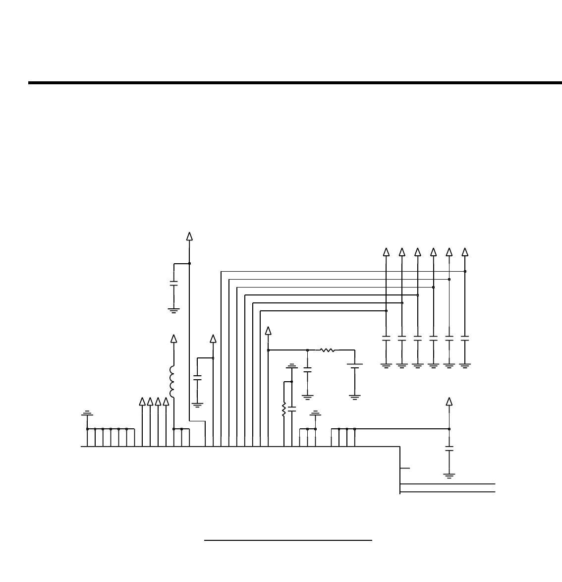
3.14 Power Block Interface
The E-GOLDvoice integrated power management unit (PMU) supports direct connection to battery
(DCB). That means all supply voltages needed are generated on-chip with integrated linear voltage
regulators. The input of these linear voltage regulators is the battery voltage. The external memory and
SIM card supply is provided by the on-chip voltage regulators. Table 144 is an overview of the internal
generated supply voltages.
The integrated power management also provides the control state machine for system start up,
including start up with discharged batteries, trickle charging and system reset control. After system
start up several methods are implemented for active and idle power saving.
Figure 3-14-1 Power Block interface
(1608)
(1608)
(16V,K,X5R)
R101 22K
2V85_VSIM
C115
2.2u
VD1
BAT100
1V5_VRF0
C114
6.8K
R100
220n
3V2_VBUF
1u
1u
C110
C108
VBAT
2V85_VSIM
VRF1
W_LED_FBN J12
W_LED_FBP J14
XO A8
A9
XOX
R6
R7
VDD_SIM
G15
VREFP
VSS1 B8
VSS2 B9
VSS4 J8
K8
VSS5
VSS6 K7
F10
VSS8 M8
VSS9
VDDP_MEM
VDD_LANA K15
VDD_LBUF J13
G12
VDD_LD1
VDD_LIO J10
K10
VDD_LMEM B11
VDD_LRF1V5
VDD_LRF2V5 F15
VDD_LRTC K12
VDD_LSIM M11
VDD_MAIN1 G9
VDD_MAIN2 J7
G10
VDD_PLL
VDD_RTC
H13
VBAT_1
VBAT_2 F12
H15
VBAT_3
VBAT_4 H14
F6
VDDP_IO
L4
D12
REXT
IREF G13
AGND G14
2V8_VIO
C112 1u
C106 1u
2V0_VRTC
2V8_VIO
1u
C113
2V8_VMEM
C111
1u
2V0_VRTC
1uC109
2V5_VANA
2V8_VMEM
2.2u
18nH
L102
C101
1uC107
VD1
3. TECHNICAL BRIEF
- 41 -
LDO output voltage selection
• LD1, LIO, LSIM, LBUF output voltage programmable by software.
• LMEM output voltage is selectable by pin configuration upon startup.
Active and idle power saving options:
• The flexible clock switching options allow minimizing the power consumption during the operation
phases of the E-GOLDvoice.
• Current consumption during the standby mode is minimized by reducing the clock to 32 kHz and
switching it off for most of the device. In addition, the power supply for the TEAKLite ROM is
switched off and the controller RAM is switched to a power saving mode.
Start-up and Reset Control State Machine Features
• Power up upon battery insertion, push button, alarm, charger connection.
• Detection of battery exchange or re-insertion.
• Complete start-up sequence management.
• System turn-on, system turn-off operation management including emergency (under-voltage) and
programmed shutdown functions.
• Internal reset of the baseband, including silent reset.
• Tri-state function of the baseband module.
• Standby mode controlled by VCXO_EN provided by SCCU module.
Figure 3-14-2 EGold Voice PMU
Name Output Voltage(V) Output Current (mA) Comment
LRTC 2.0 4 Used for the real time and digital PMU supply
LD1 1.2/1.5 150 Used for the core supplies (MCU and DSP via switch)
LIO 1.8/2.85 30 Used for the I/O pad supply and, for example, the display
LRFXO 2.5 10 Used for the crystal oscillator supply
LMEM 2.5 100 Used for the external memory supply, voltage can be
configured during startup
LANA 2.5 100 Used for analog (audio and baseband processing) and
headset driver
LSIM 1.8/2.85 30 Used of the SIM card supply
LBUF 2.6/2.8/3.0/3.2 300 Used for the loudspeaker and earpiece driver
LRFRX 2.5 100 Used for the RF RX part
LRFTRX 1.5 120 Used for the RF TX/TX part
- 42 -
3. TECHNICAL BRIEF
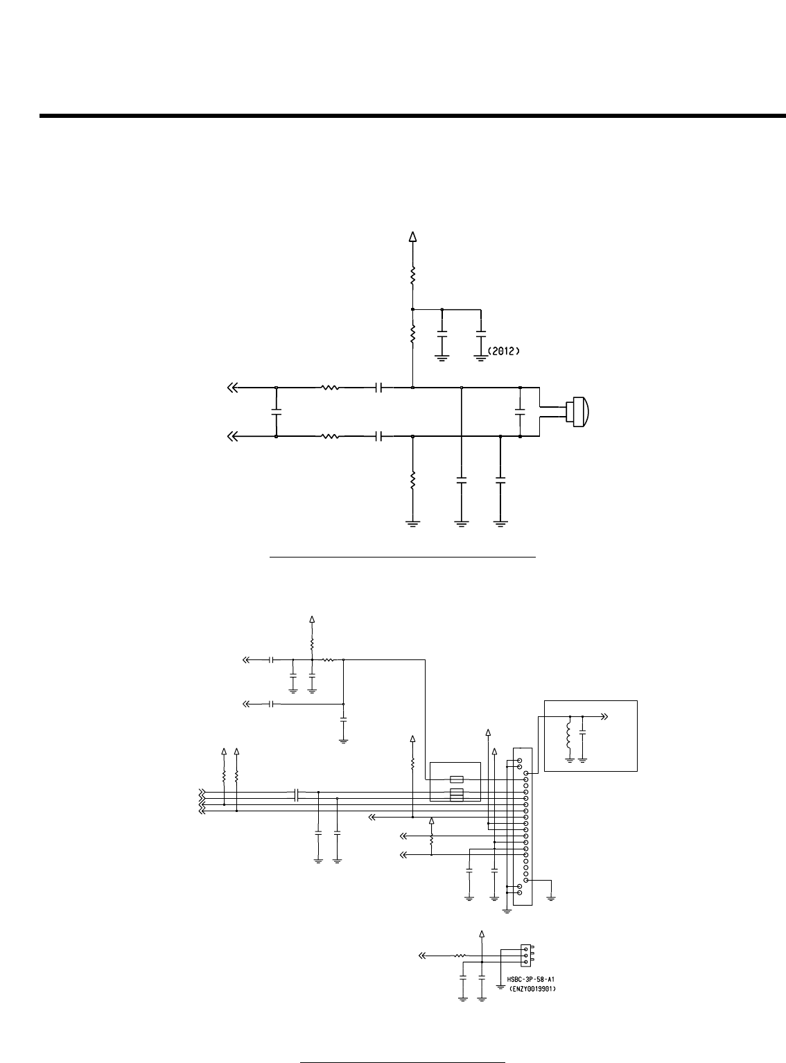
3.15 FM Radio Interface
RADIO
(FOR FM RADIO)
(10V,K,X5R)
NO RADIO
FOR RADIO
2.7K
RADIO
RADIO_DETECT
27K
2V8_VIO
FOR RADIO
C339 0.1u
0R327
VBAT
R342
NA
47
R338
2V8_RADIO
R331 0
0.1uC333
100K
R343
R334
10K
NA
R340
330K
R341
R329 20K
8
16
VA
11
VD
VIO
10
5_RST
6_SEN
2FMIP
4GND1 GND2 12
GND3 15
GPIO1 19
18
GPIO2
GPIO3 17
14
LOUT
NC1
1
20
NC2
PGND 21
9RCLK
3RFGND 13
ROUT
SCLK
7
SDIO
U302
SI4702-B16
R336
4.7K
FM_RST
NLAS5223BMNR2G
U305
COM1
3
COM2
9
GND
6
4
IN1
8
IN2
NC1
5
7
NC2
2
NO1
10
NO2
1
VCC
0R328
20KR330
C330
1u
9
BGND
BYPASS
23
GND
7VDD
VIN1
1
VIN2
5
8
VOUT1
6
VOUT2
_SHDN
4
U303 LM4809LD
R333 39K
R337
4.7K
6
BGND
2GND
NC 5
STBY
1
3VIN VOUT 4
1u
C329
BH28FB1WHFVU304
2V8_RADIO
R344
240K
2V8_RADIO
R335
100K
TP301
RADIO_AMP_SHDN
100pC331
C342
1u
C341
1u
R339
27K
2V8_RADIO
C332 0.1u
FM_INT
0.1u
C338
22n
C335
100K
R345
NAC334
2V8_RADIO
NAR325
2V8_RADIO
2V8_VIO
2V8_VIO
39KR326
0.1u
C340
FM_ANT
FM_32K
EPPA1
FM_INT
RADIO_AMP_SHDN
RADIO_DETECT
RADIO_AMP_SHDN
RADIO_EN
RADIO_SPK_R
RADIO_SPK_L
FM_SCL
FM_SDA
RADIO_SPK_R
RADIO_SPK_L
FM_RST
AUXOP_FMR
AUXOP_FML
HEADSET_RADIO_SEL
EPPA1

3. TECHNICAL BRIEF
- 43 -
3.15.1 FM Tunner
The Si4702 patented digital low-IF architecture reduces external components and eliminates the need
for factory adjustments. The receive (RX) section integrates a low noise amplifier (LNA) supporting the
worldwide FM broadcast band (76 to 108 MHz). An automatic gain control (AGC) circuit controls the
gain of the LNA to optimize sensitivity and rejection of strong interferers.
For two-wire operation, a transfer begins with the START condition. The control word is latched
internally on rising SCLK edges and is eight bits in length, comprised of a seven bit device address
equal to 0010000b and a read/write bit (write = 0 and read = 1). The device acknowledges the address
by setting SDIO low on the next falling SCLK edge. For write operations, the device acknowledge Is
followed by an eight bit data word latched internally on rising edges of SCLK.
The device always acknowledges the data by setting SDIO low on the next falling SCLK edge. An
internal address counter automatically increments to allow continuous data byte writes, starting with
the upper byte of register 02h, followed by the lower byte of register 02h, and onward until the lower
byte of the last register is reached. The internal address counter then automatically wraps around to
the upper byte of register 00h and proceeds from there until continuous writes cease. Data transfer
ceases with the STOP command. After every STOP Command, The internal address counter is reset.
For read operations, the device acknowledge is followed by an eight bit data word shifted out on falling
SCLK edges. An internal address counter automatically increments to allow continuous data byte
reads, starting with the upper byte of register 0Ah, followed by the lower byte of register 0Ah, and
onward until the lower byte of the last register is reached. The internal address counter then
automatically wraps around to the upper byte of register 00h and proceeds from there until continuous
reads cease. After each byte of data is read, the controller IC should return an acknowledge if an
additional byte of data will be requested. Data transfer ceases with the STOP command. After every
STOP command, the internal address counter is reset.
3.15.2 Headphone Amplifier
The MAX4411 fixed-gain, stereo headphone driver features Maxim’s patented DirectDrive architecture,
eliminating the large output-coupling capacitors required By conventional single-supply headphone
drivers. The device consists of two 80mW Class AB headphone drivers, internal feedback network
(fixed -1.5V/V gain), undervoltage lockout (UVLO)/shutdown control, charge pump, and
comprehensive click-and-pop suppression circuitry.
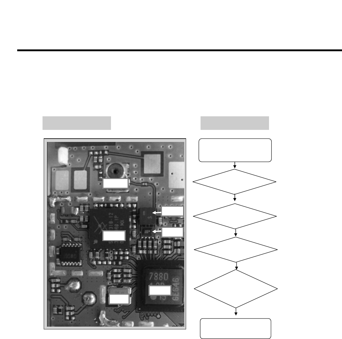
4.1 RF Trouble
4. TROUBLE SHOOTING
- 44 -
4. TROUBLE SHOOTING
U400
SW400
U102
FL400
X101
FL401
REFERENCE PART Description
U400 PAM (Power Amp. Module)
X101 DCXO (26MHz)
FL400 ASM (Antenna Switch Module)
SW400 Mobile Switch
FL401 RX SAW Filter
4. TROUBLE SHOOTING
- 45 -
RF Trouble
Antenna.Contact Point
SW400
Antenna Matching component
TEST POINT
CIRCUIT DIAGRAM
TP403
C410
22p
R403
0
C400 1p
TP401
SW400
RF500
ANT
G1
G2
RF
TP404TP402
2.2nH
L400
TP405
0R401
R400
NA
TP400
22nHL401
Antenna Matching component
Mobile SW
Coupling Capacitor
4. TROUBLE SHOOTING
- 46 -
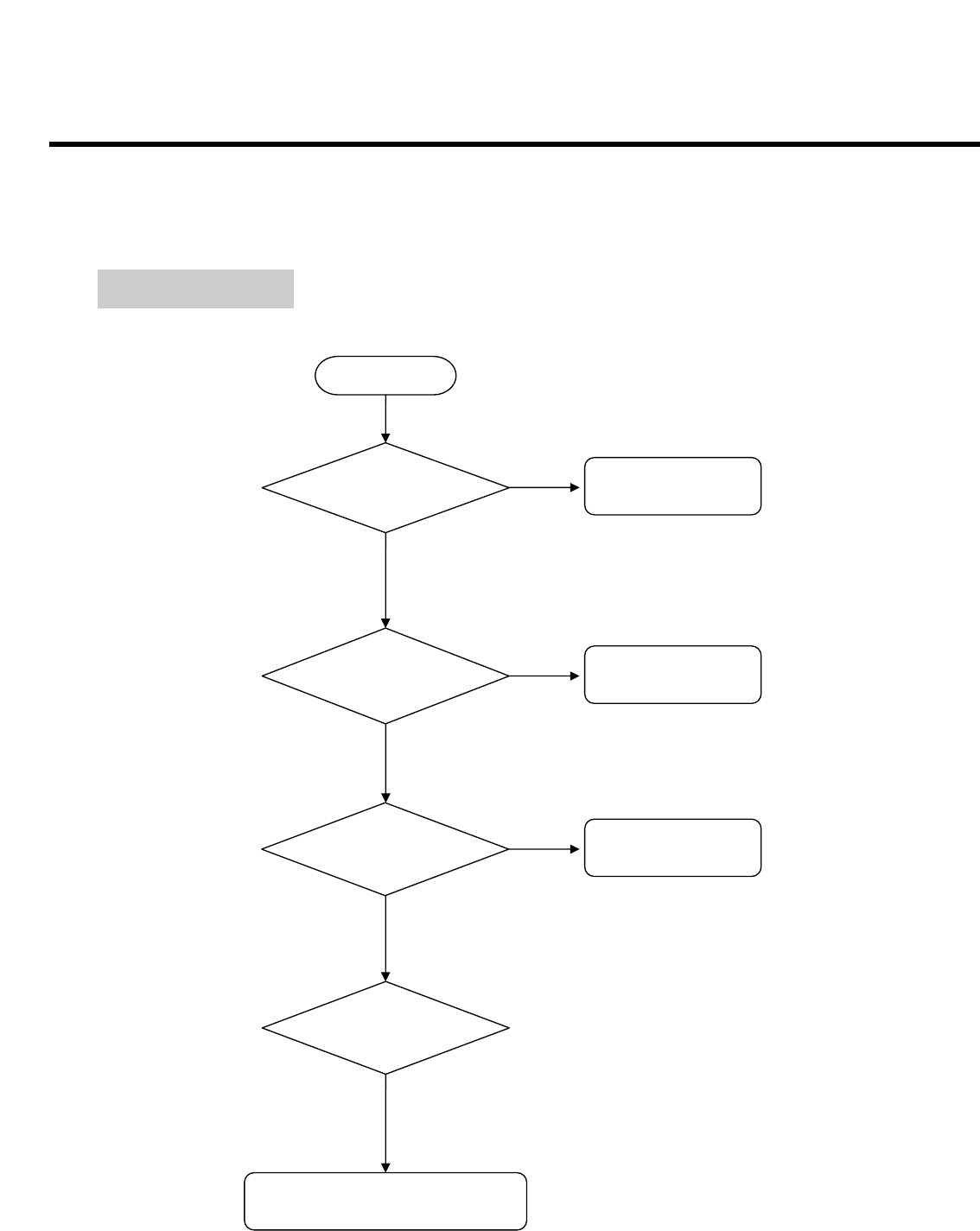
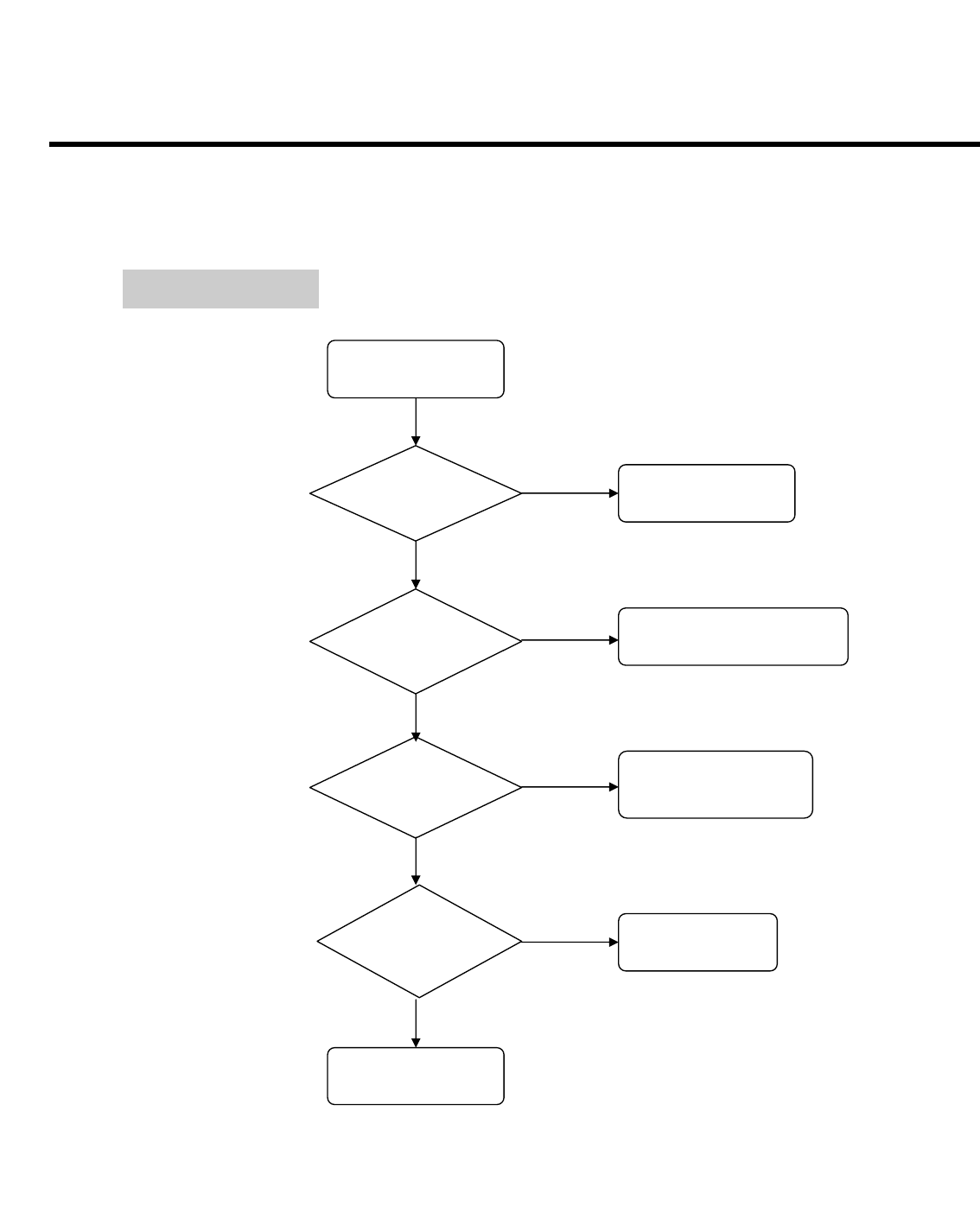
CHECKING FLOW
START
Change PCB
Check
Mobile SW
Download
And
Calibration
Check
Antenna PAD&
Intenna Contact Change Antenna
OK
NG
OK
Change SW400
NG
NG
Check
Matching component Resolder component
NG
4. TROUBLE SHOOTING
- 47 -
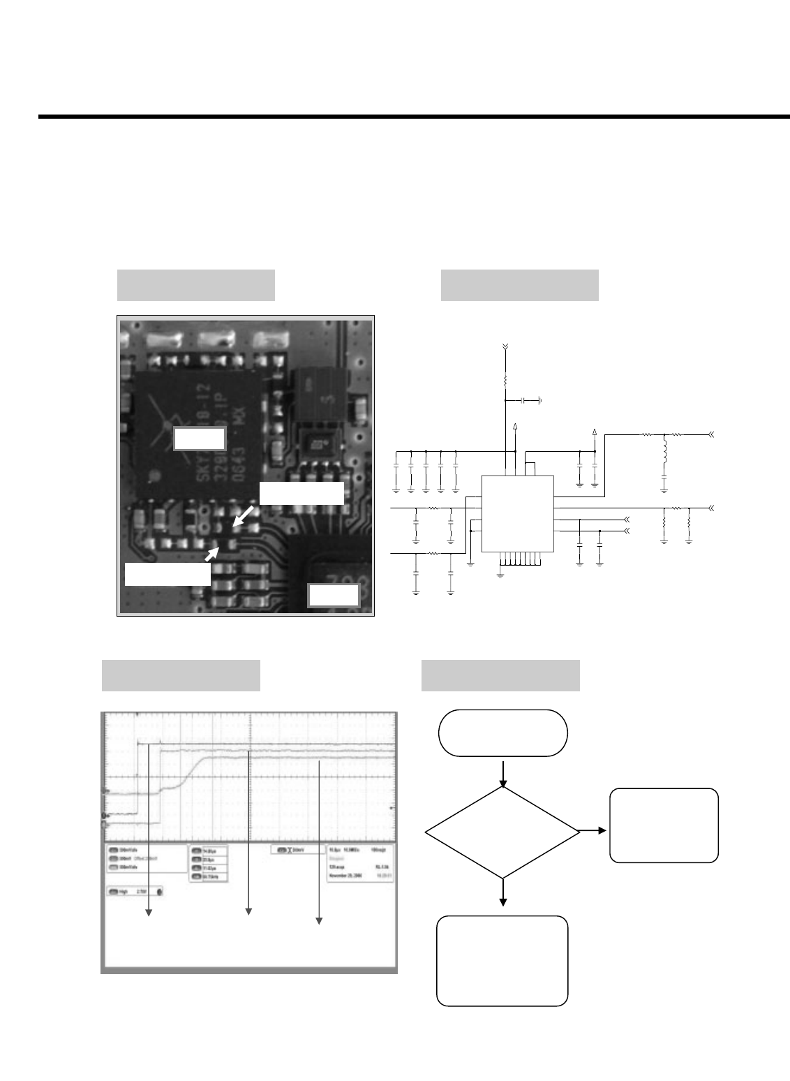
RX Trouble
START
Check point.
DCXO(X101)
Setup Test Equipment
Cell Power :-74d Bm
GSM850 CH190
PCS CH660
Check point
mobile SW &
ASM & SAW
Filter(SW400,F
L400,FL401)
Re-Download S/W &
CAL
U400
SW400
U102
FL400
X101
FL401
TEST POINT CHECKING FLOW
4. TROUBLE SHOOTING
- 48 -
RX Trouble
(1) Checking VCTCXO Circuit
U400
SW400
U102
FL400
X101
FL401
Is the waveform
of Pin3 similar to
DCXO(X101)
Waveform?
Replace
X101
Yes
No
DCXO Circuit is OK.
See next page to check
PLL Circuit.
( NX3225SA(W-188-34-7)
2GND1
GND2 4
1
HOT1
HOT2
3
NX3225SA
X101
26MHz
2V8_VIO
NA
R107
TEST POINT
CIRCUIT
Waveform
Pin 2
Pin 1
Waveform
CHECKING FLOW
4. TROUBLE SHOOTING
- 49 -
RX Trouble
* FL401 6,7 and 8,9 output are
balanced
U400
SW400
U102
FL400
FL401
Pin 6
Pin 4
Check Pin 1, 2 of
SW400
with RF Cable
Signal is
OK ?
Replace
Mobile SW
(SW400)
Yes
N
o
Yes
Mobile SW & ASM is OK.
See next page
Replace ASM
(FL400)
N
o
Yes
Check Pin 4,6 of
FL400 ?
Replace SAW
Filter (FL401)
N
o
Check Pin 6,7 and 8,9 of
FL401 ?
TEST POINT CHECKING FLOW
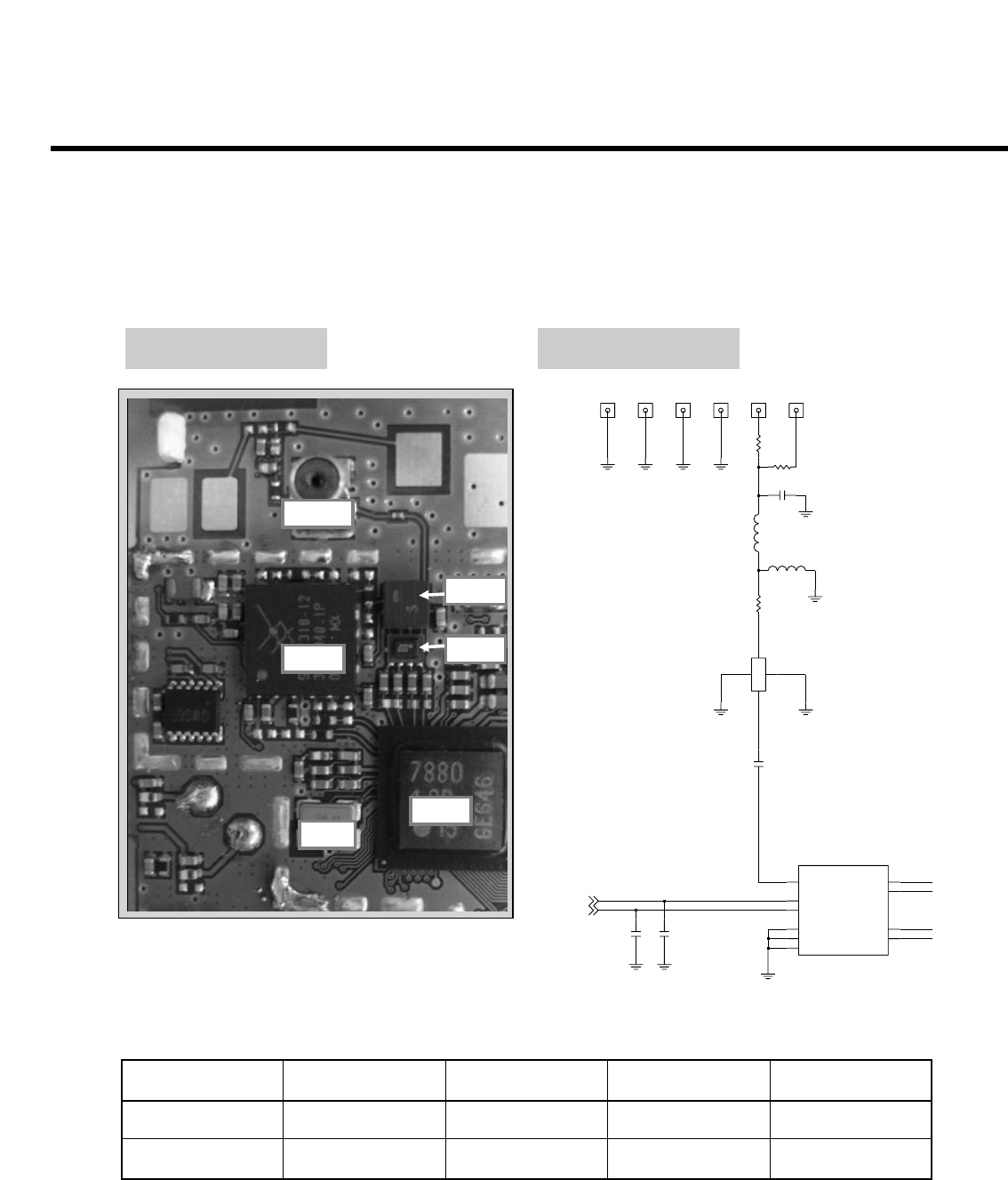
4. TROUBLE SHOOTING
- 50 -
4.2 TX Trouble
U400
SW400
U102
FL400
X101
FL401
Check point
DCXO(X101)
Setup Test Equipment
Cell Power : - 74dBm
GSM850 CH190
PCS CH661
Re-Download S/W & RF
CAL
Check point
ULC2(U102)Outp
ut Signal
Check point
PAM(U400)
Control Signal
Check
ASM & Mobile
S/W & SAW
(FL400,SW400
,FL401)
TEST POINT CHECKING FLOW
4. TROUBLE SHOOTING
- 51 -
TX Trouble
HB RF Input
LB RF Input
U400
U102
TEST POINT
(50V,J,NP0)
(50V,J,NP0)
(2012)
(16V,K,X7R)
(10V,Z,Y5V)
(50V,J,NP0)
(16V,K,X7R)
(50V,J,NP0)
VBAT
C414
27p
VBAT
L402
NA
27p
C407 C408
0.01u
GND7
13
14 GND8
16 GND9
P_GND
21
RSVD_GND
19
20
VAPC
VBATT 17
VCC1A 2
VCC1B 6
1
BS
3
DCS_PCS_INDCS_PCS_OUT
15
EGSM_IN 4
EGSM_OUT
11
18
ENABLE
5GND1
GND2
7
GND3
8
9GND4
GND5
10
12 GND6
NA
U400
SKY77318
C416
C405
R407
0
33p
C412
NA
39p
C415
NA
C401
0
R404
C411
NA
C402
10u
R410
0
R408
NA
C409
NA
C404
0.01u
R402 1K
0
R406
R405
0
27p
C413
R409
NA
12p
C403
18p
C406
DCS_PCS_OUT
TXON_PA
BS
GSM_OUT
TX_RAMP
CIRCUIT
Vapc
ASMPaon & BS
Waveform
Check Control
Signals
Signals are
Normal ?
Check
ULC2(U102)
Yes
N
o
PAM Control
Signal is OK.
See next page to
check
ASM & Mobile SW
Circuit.
CHECKING FLOW
4. TROUBLE SHOOTING
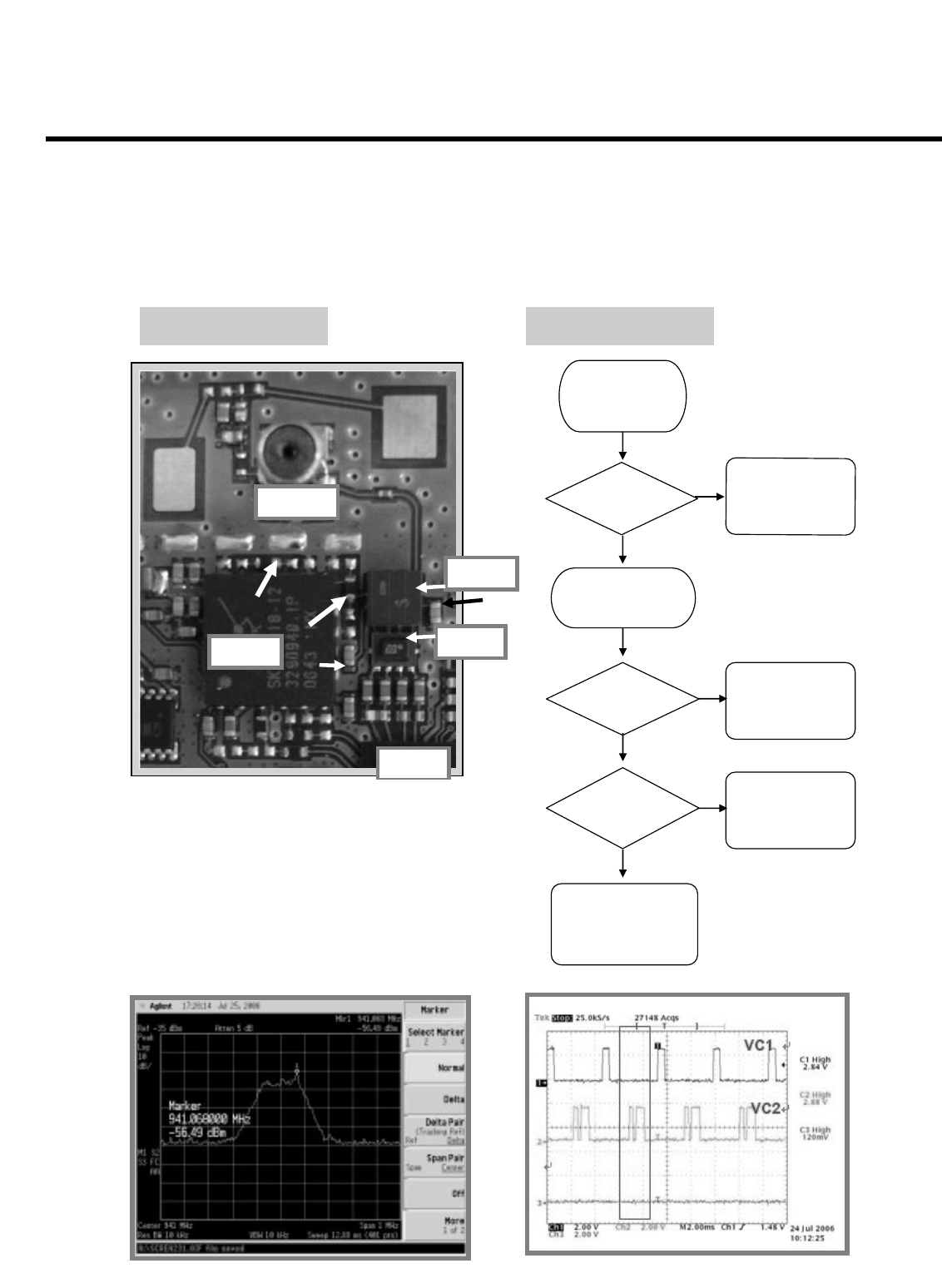
- 52 -
TX Trouble
U400
SW400
U102
FL400
X101
FL401
TEST POINT
TP403
C410
22p
R403
0
C400 1p
TP401
SW400
RF500
ANT
G1
G2
RF
TP404TP402
C417
27p
2.2nH
L400
C418
27p
TP405
0R401
R400
NA
TP400
FL400
5GND1
GND2
8
GND3
10
GSM1800_1900RX 6
1
GSM1800_1900TX
GSM850_900RX 4
2
GSM850_900TX
9IN
VC_GSM1800_1900TX
7
3VC_GSM850_900TX
LMSP2PAA-575TEMP
22nHL401
VC2
VC1
CIRCUIT
Mode GSM900 TX DCS1800 TX GSM800 RX DCS1800 RX
VC1 H(2.7V) L L L
VC2 L H(2.7V) L L
4. TROUBLE SHOOTING
- 53 -
RX Trouble
U400
SW400
U102
FL400
FL401
Pin 2
Pin 1
Pin 3
Pin 7
TEST POINT
Check Pin 1, 2 of
SW400
with RF Cable
Signal is
OK ?
Replace Mobile
SW (SW400)
Yes
No
Yes
Mobile SW & ASM is
OK.
Check Antenna.
Check ULC2
(U102)
Control
Signal is
OK ?
No
Yes
Check Pin 1,2
Replace ASM
(FL400)
Pin 3,7
Signal is
normal ?
No
Yes
CHECKING FLOW
4. TROUBLE SHOOTING
- 54 -
4.3 Power On Trouble
Check Points
-Battery Voltage( Need to over 3.35V)
-Power-On Key detection (PWRON signal)
-Outputs of LDOs from EGV
TEST POINT
CIRCUIT
(1608)
(1608)
(16V,K,X5R)
R101 22K
2V85_VSIM
C115
2.2u
VD1
BAT100
1V5_VRF0
C114
6.8K
R100
220n
3V2_VBUF
1u
1u
C110
C108
VBAT
2V85_VSIM
VRF1
W_LED_FBN J12
W_LED_FBP J14
XO A8
A9
XOX
R6
R7
VDD_SIM
G15
VREFP
VSS1 B8
VSS2 B9
VDDP_MEM
VDD_LANA K15
VDD_LBUF J13
G12
VDD_LD1
VDD_LIO J10
K10
VDD_LMEM B11
VDD_LRF1V5
VDD_LRF2V5 F15
VDD_LRTC K12
VDD_LSIM M11
VDD_MAIN1 G9
VDD_MAIN2 J7
G10
VDD_PLL
VDD_RTC
H13
VBAT_1
VBAT_2 F12
H15
VBAT_3
VBAT_4 H14
F6
VDDP_IO
L4
D12
REXT
IREF G13
AGND G14
2V8_VIO
C112 1u
C106 1u
2V0_VRTC
2V8_VIO
1u
C113
2V8_VMEM
C111
1u
2V0_VRTC
1uC109
2V5_VANA
2V8_VMEM
2.2u
18nH
L102
C101
1uC107
VD1
LDO VOLTAGE PART
V_IO 2.8V C107
V_BUF 3.2V C101
V_MEM 2.8V C109
V_ANA 2.5V C113
V_SIM 2.85V C108
VRF0 1.5V C110
C106
C107
C111
C110
C109
C101
EGV
IC
26Mhz
4. TROUBLE SHOOTING
- 55 -
Power On Trouble
CHECKING FLOW
START
Check Battery Voltage
> 3.35V
Push power-on key
And check the level change
of PWRKEY
Check the voltage of
The LDO outputs at U102
THE PHONE WILL
POWER ON.
Charge or Change Battery
Check the contact of power key
Or dome-switch
Replace U102
YES
YES
YES
NO
NO
LDO VOLTAGE PART
V_IO 2.8V C107
V_BUF 3.2V C101
V_MEM 2.8V C109
V_ANA 2.5V C113
V_SIM 2.85V C108
VRF0 1.5V C110
NO
4. TROUBLE SHOOTING
- 56 -
4.4. SIM Card Trouble
C331/C332
J300.PIN1
R302/C310
TEST POINT
CIRCUIT DIAGRAM
C311
0.1u
4.7KR302
C310
22p 22p
C312
2V85_VSIM
2V85_VSIM
0
R303
I_O
6
2
RST
1
VCC
VPP
5
J300
CLK 3
4GND
GND1 78 GND2
2V85_VSIM
SIM_CLK
SIM_RST
SIM_DATA
4. TROUBLE SHOOTING
- 57 -
START
Does the SIM cards
supports 3V ?
NO Change the SIM Card. Our phone
supports only 3V SIM card.
YES
Check J300.PIN1 NG
OK
J300.PIN1 = 2.85V Change board
Check soldering
status of J300 and
Other component
OK
NG Resolder J300 or
other component
R302/C310/
C311/C312
OK
Check Operation
Change board
Re-download SW
Checking Flow
4. TROUBLE SHOOTING
- 58 -
4.5. Vibrator Trouble
Q300.PIN3
R305
R306
R308
TEST POINT
CIRCUIT DIAGRAM
(1608)
(50V,J,NP0)
VBAT
C302
27p
CN300
1
2
R308
100K
Q300
2SC5585
D300
1SS302-T5L_F_H
1K
R306
27p
C305
VBAT
R305
10
VIBRATOR
4. TROUBLE SHOOTING
- 59 -
Check Voltage Level of
R306/R308
OK
NG
OK
Change PCB
Enter the engineering mode,
and set vibrator on.
R306=2.8V
R308=0.7V
Check Voltage Level of
Q300.PIN3 and R305
Q300.PIN3=0V
R305=0V Change Q300
NG
Replace Vibrator
START
Checking Flow
4. TROUBLE SHOOTING
- 60 -
4.6. Keypad Trouble
R215
R201 R214
R211
R203
R212
R209
R204 R213
TEST POINT
CIRCUIT DIAGRAM
DOWN
23
5
#
MENU
SEND
4UP SEL
KEY MATRIX
1
7
*
LEFT
END
9
0
RIGHT
6
8
SW203
R204
680
SW201
2V0_VRTC
SW216
C215
NA NA
C219
R212 680
SW205
SW212
SW217
SW215
C207
NA
SW210
SW214
NA
C218
SW211
SW200
SW219
R215 680
SW204
NA NA
C216 C220
R209
680
SW208SW207
R201
680
SW202
C206
NA
R211 680
SW209
SW213
NA
C205
680
R203
R214 680
R213 680
SW218
NA
C217
SW206
KEY_OUT2
KEY_OUT3
KEY_OUT4
KEY_IN3
END_KEY
KEY_IN0
KEY_IN2
KEY_IN1
KEY_IN4
KEY_OUT1
4. TROUBLE SHOOTING
- 61 -
Check soldering status
Of component
OK
NG Resolder component
R201/R203/R204
R209/R211/R212
R213/R214/R215
Change PCB
Check Metal Doom NG Change Metal Doom
START
OK
Checking Flow
4. TROUBLE SHOOTING
- 62 -
4.7 RTC Trouble
Check Points
- 32.768KHz is right clock
- The power of RTC is right.
SWITCH_ON N7
OSC32K P6
F32K R5
B4
CLKOUT CHG_STATUS
32KOUT
PWRON
32KIN
X100
MC-146_12_5PF
12
3
4
32.768KHz
C104 18p
C105 18p
32KIN
32KOUT
R101 22K
BAT100
C114
6.8K
R100
220n
W_LED_FBN J12
W_LED_FBP J14
G15
VREFP
G12
VDD
_
LD1
VDD_LRTC K12
H13
VBAT_1
VBAT_2 F12
H15
VBAT_3
VBAT_4 H14
IREF G13
AGND G14 C112 1u
CIRCUIT
4. TROUBLE SHOOTING
- 63 -
CHECKING FLOW
RTC will work properly
Is the frequency
about 32Khz?
START
Replace X100 and try again.
YES
Is VRTC
about 2.0V?
YES
Replace BAT100
4.8. Key backlight Trouble
4. TROUBLE SHOOTING
- 64 -
D203 D200
D204D201
D205 D202
R203
R204
Q200.PIN2
Q200.PIN3
TEST POINT
CIRCUIT DIAGRAM
KEY BACKLIGHT
(10V,K,X5R)(10V,K,X5R)
LD201
VBAT
LEBB-S14H
LEBB-S14H
LD200
2SC5585
Q200
LEBB-S14H
LD204
1u
C223
LD202
LEBB-S14H
100ohm
R220
LD203
LEBB-S14H R219
100ohm
100ohm
R218
R223
10K
100ohm
R216
1KR222
LD205
LEBB-S14H
1uC222
R217
100ohm
R221
100ohm
KEY_BACKLIGHT
4. TROUBLE SHOOTING
- 65 -
START
Check Voltage Level
Of R222
NO
Change PCB
YES
YES
R222=2.8V
Check Voltage Level
Of R222 and Q200.PIN2
R222=0.7V Check component
R222 and Q200
Replace component
NO
NG
Check LED
component
LD200~LD205
R216~R221
NO Replace component
Change PCB
YES
Checking Flow
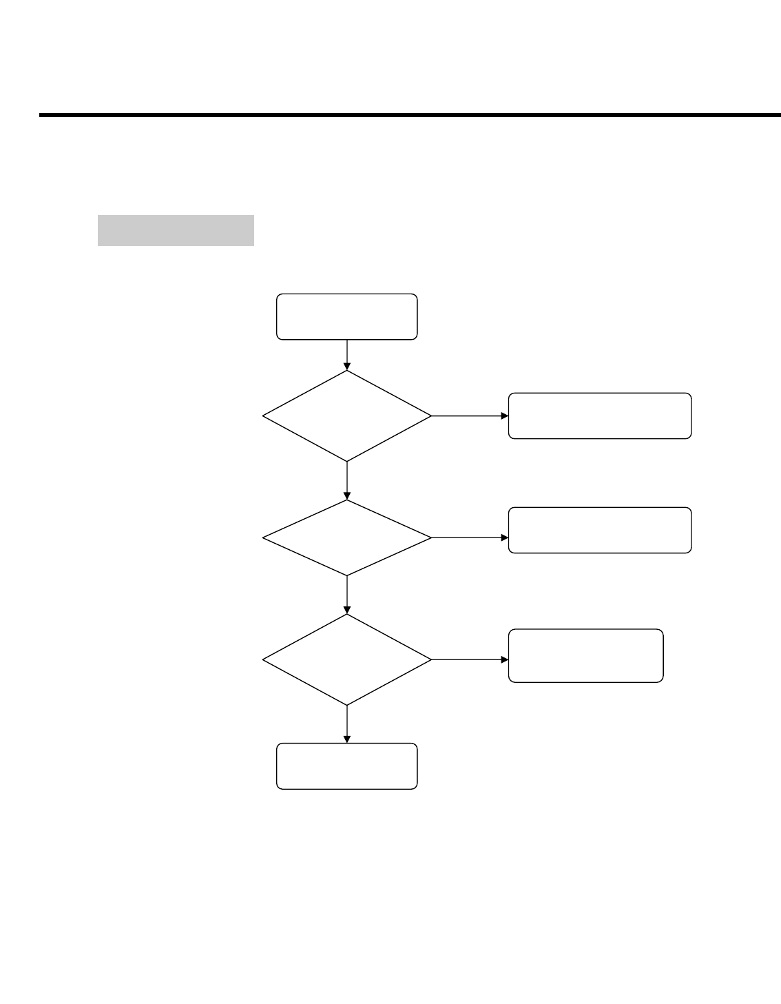
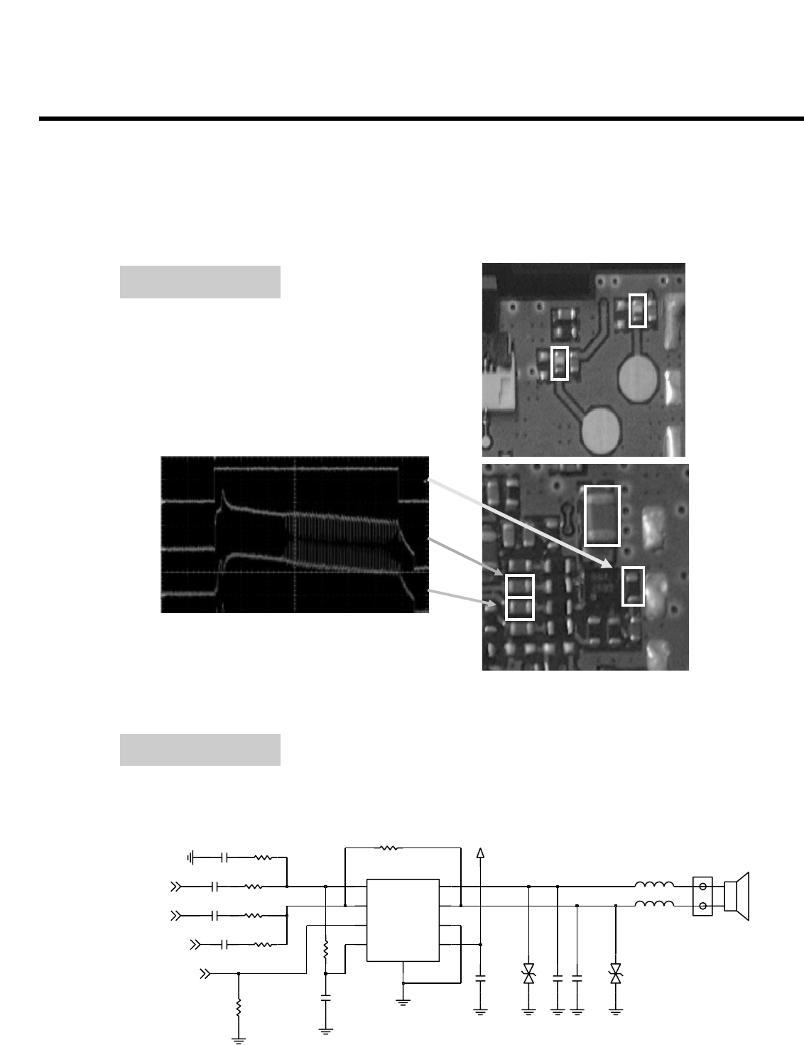
4.9. LCD Trouble
4. TROUBLE SHOOTING
- 66 -
CN200
R207R205 R206R208
C221
TEST POINT
CIRCUIT DIAGRAM
IMSA-9671S-13Y902
(ENQY0013801)
47R208
NA
C213
27p
C210
47R206
C209
27p
1u
C221
27p
C211
R205 47
NA
C214
47R207
2V8_VIO
14
15
1
10
11
12
13
2
3
4
5
6
7
8
9
CN200
NA
C208
MTPG
MTPD
R210
100K
C212
27p
MLED2
MLED1
SSC0_CLK
SSC0_MTSR
CS3
LCD_RESET
MLED
LCD_ID
4. TROUBLE SHOOTING
- 67 -
START
Backlight is OK? Change PCB
YES
NG
Check Operation
After LCD changes
NO
Check Control
Signal and Power
Including soldering status
C221=2.8V
Control Signal=
Refer to next page
NG Replace component
Or change PCB
Change PCB
OK
Check soldering
status of CN200
OK
Change LCD
OK
NG Replace CN200
Checking Flow
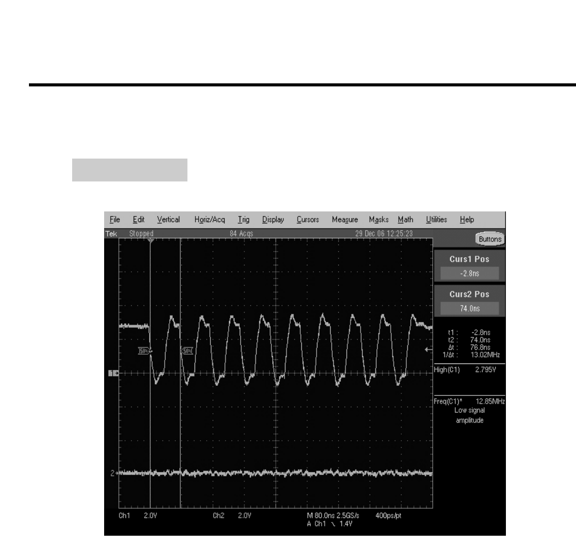
]SS0_MTSR pattern is out randomly when clock is fluctiatied.
, clock frequency is 13MHz and LCD_RESET is High(2.8V).
4. TROUBLE SHOOTING
- 68 -
WAVEFORM
SS0_SCK
LCD_CS
4. TROUBLE SHOOTING
- 69 -
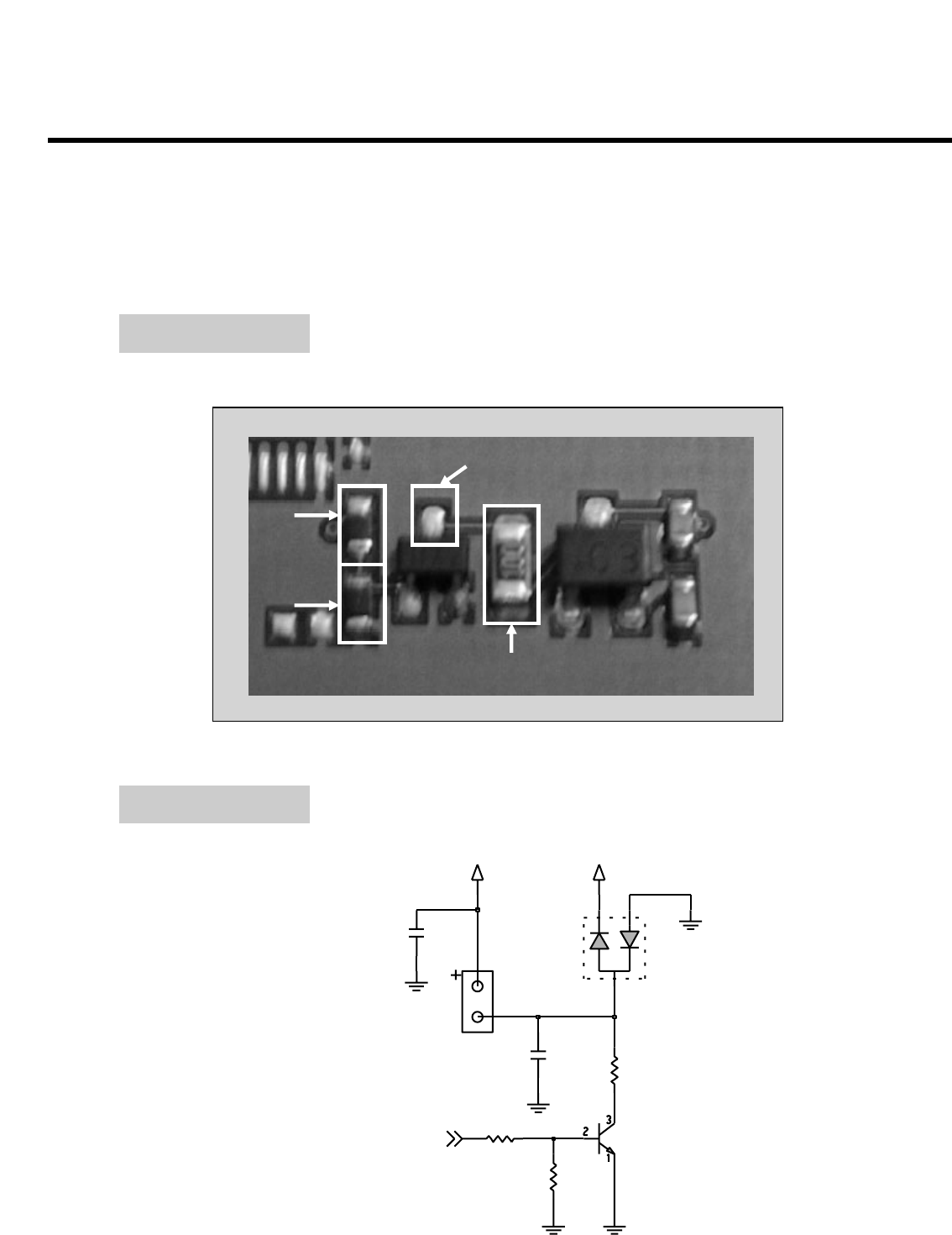
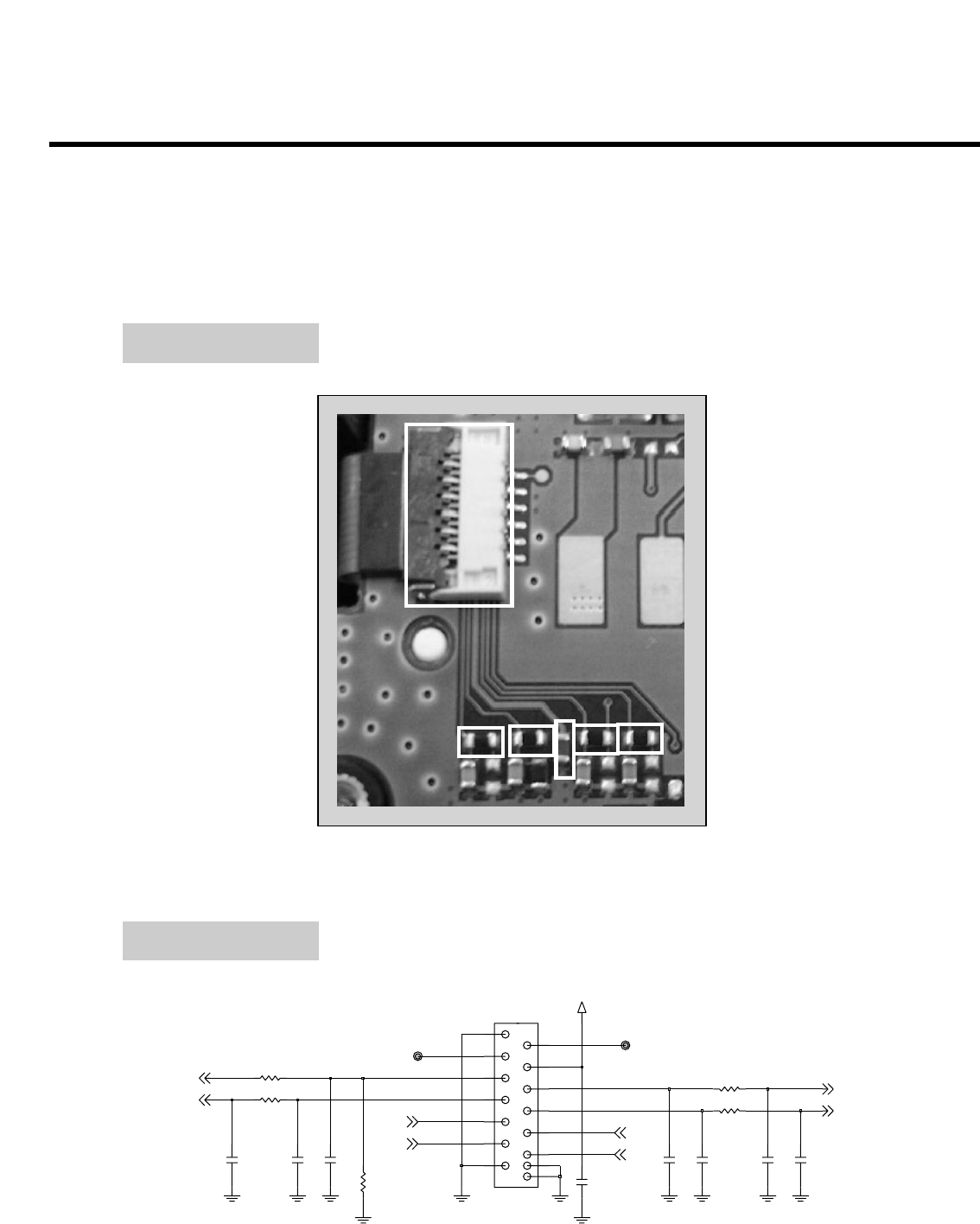
4.10. Microphone Trouble
R300
Microphone component
MIC.P
TEST POINT
CIRCUIT DIAGRAM
MAIN_MIC
C313 39p
1K
R300
C306 0.1u
VMIC
MIC300
OB4-15L42-C33L
1
2
0.1u
C307
2.2K
R301
100ohm
R304
10u
C304
C314 39p
R307
100ohm
0.1uC309
2.2K
R309
C303
39p
39p
C308
VINNORP
VINNORN
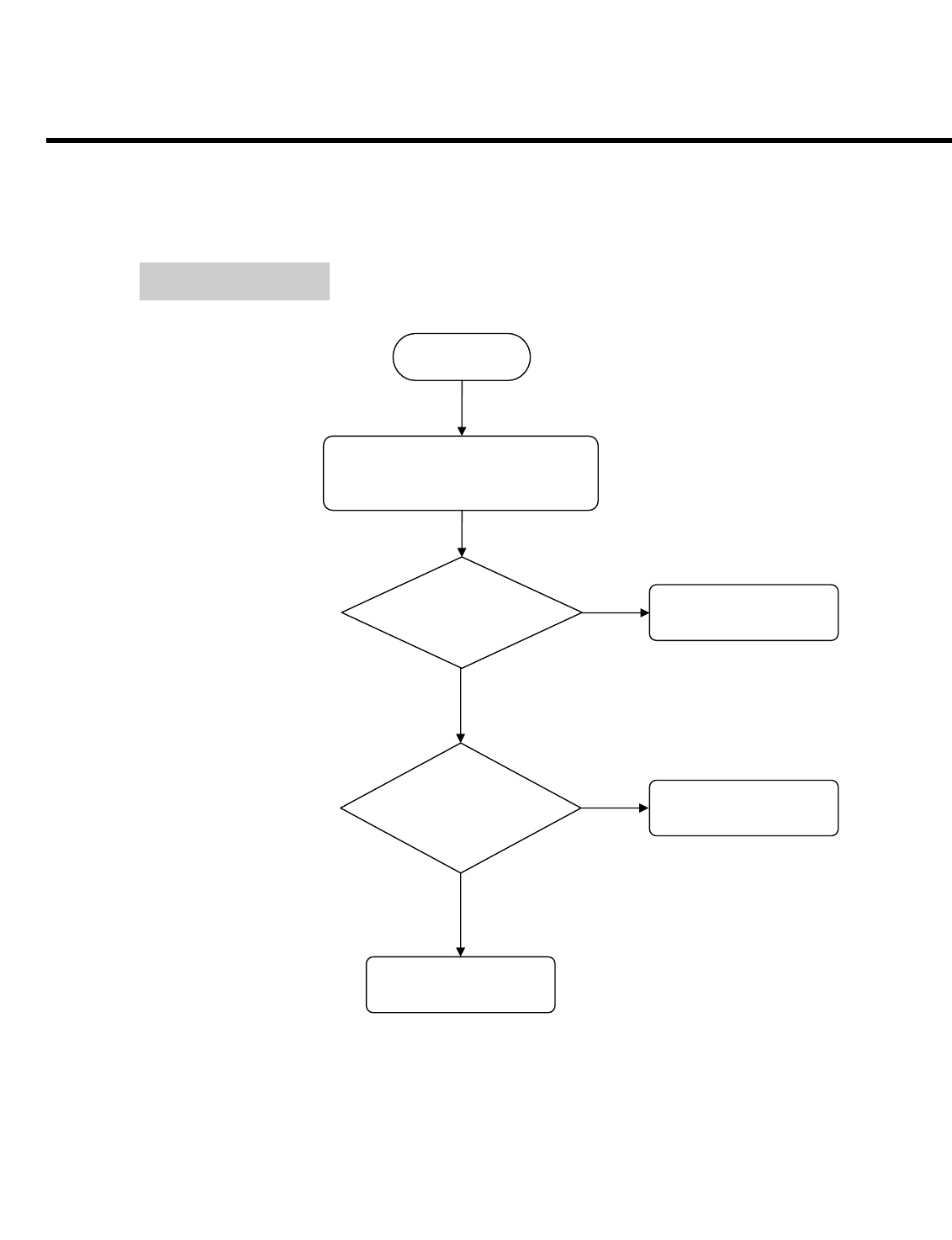
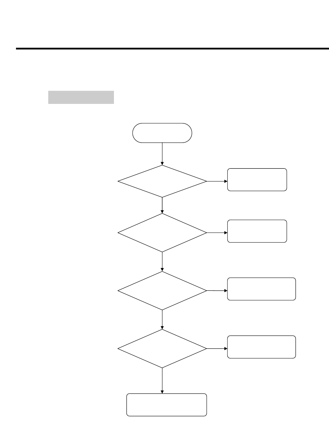
4. TROUBLE SHOOTING
- 70 -
Replace PCB
Check the voltage Level
of MIC_P
Check voltage level
of R300
Change Microphone
Check component
status around MIC
Re-solder or
replace the Component
Check status of MIC Re-solder or
replace Microphone
YES
NO
OK
OK
NG
NG
MIC_P= about 1.2~1.5V DC
with a few tens mV
NG
Replace PCB
OK
R300.VMIC=2.5V
Make a call
Checking Flow
4. TROUBLE SHOOTING
- 71 -
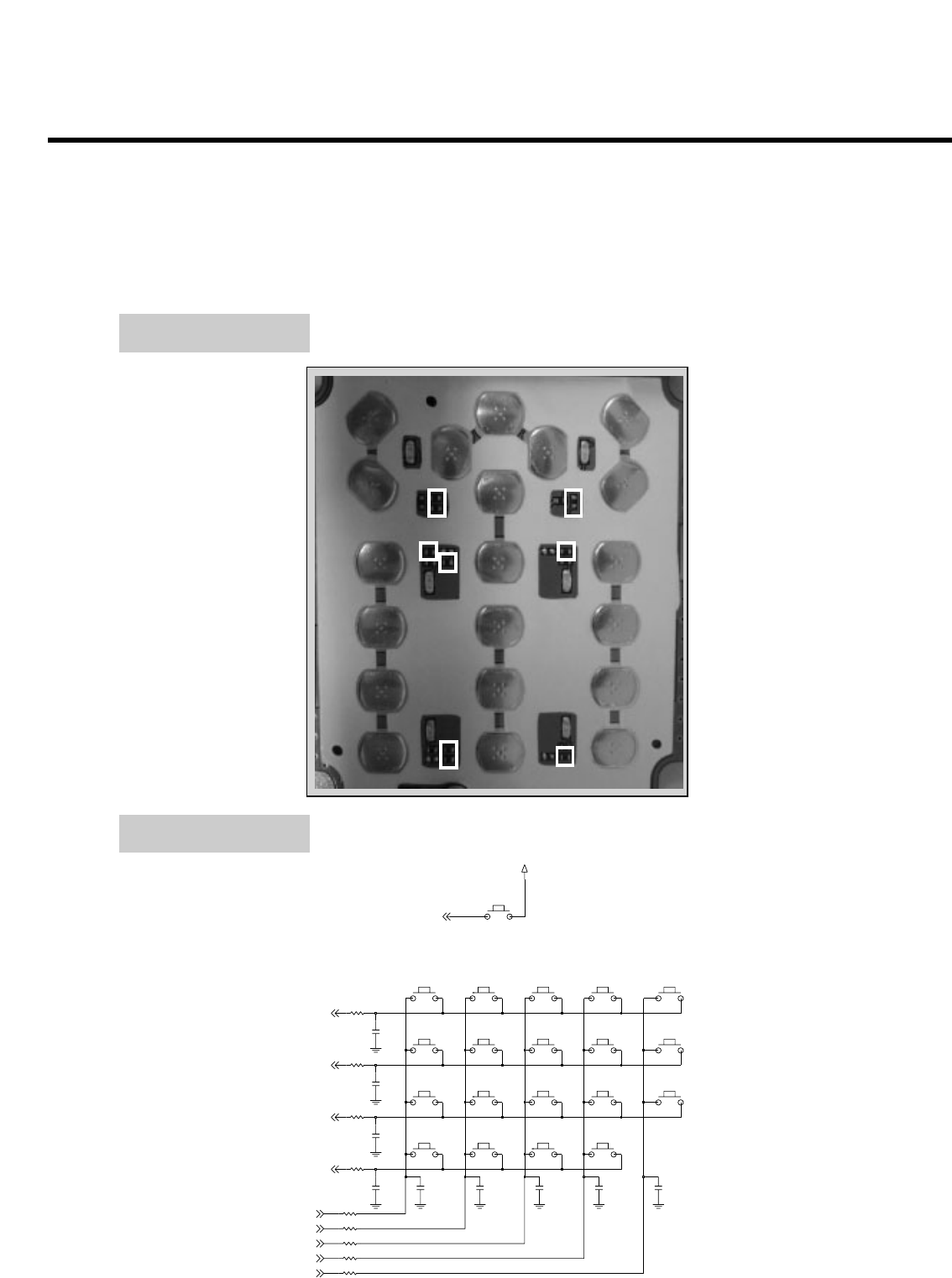
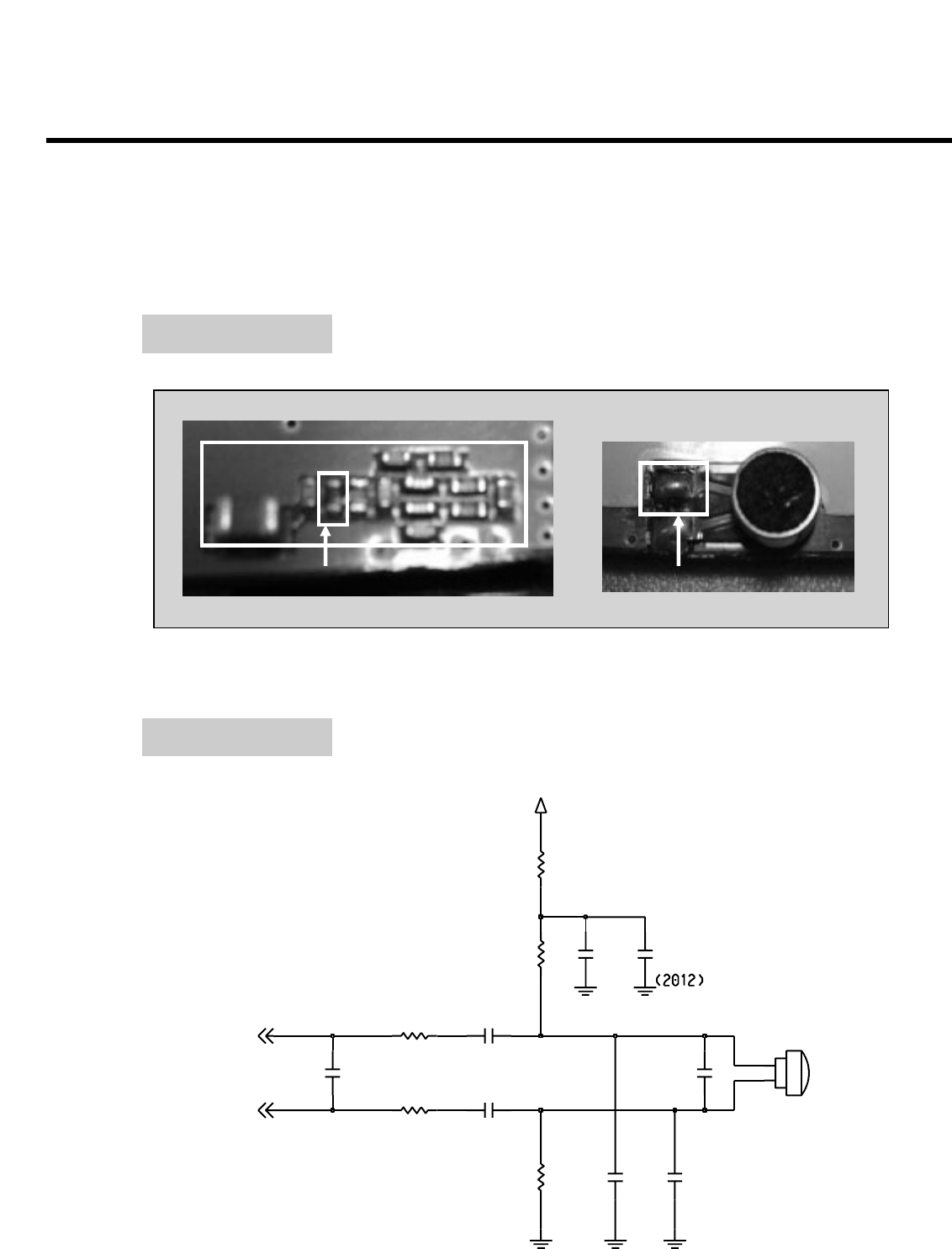
4.11. Receiver Trouble
REC.N REC.P
L100
C102
L101
C103
TEST POINT
CIRCUIT DIAGRAM
(SURY0013001)
RECEIVER
11*07*3T receiver
22nHL100
39p
C103
39p
C102
1
2
CN100
L101 22nH
C100
39p
REC_P
REC_N
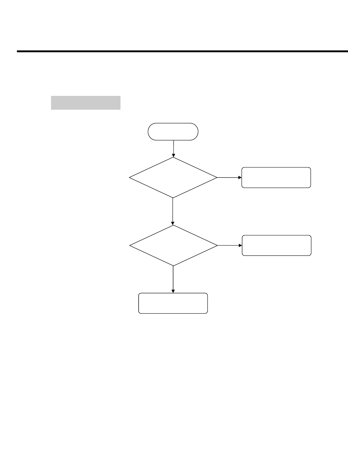
4. TROUBLE SHOOTING
- 72 -
Check L100 &
L101
Check component
status
Re-solder or
replace the Component
Check Receiver replace Receiver
YES
NG
OK
OK
NG
NG
Replace PCB
L100&L101 bias will
Fluctiate signal above
1.2V
Press any Key
Check L100/L101
C102/103 Re-solder or
replace the Component
Checking Flow
4. TROUBLE SHOOTING
- 73 -
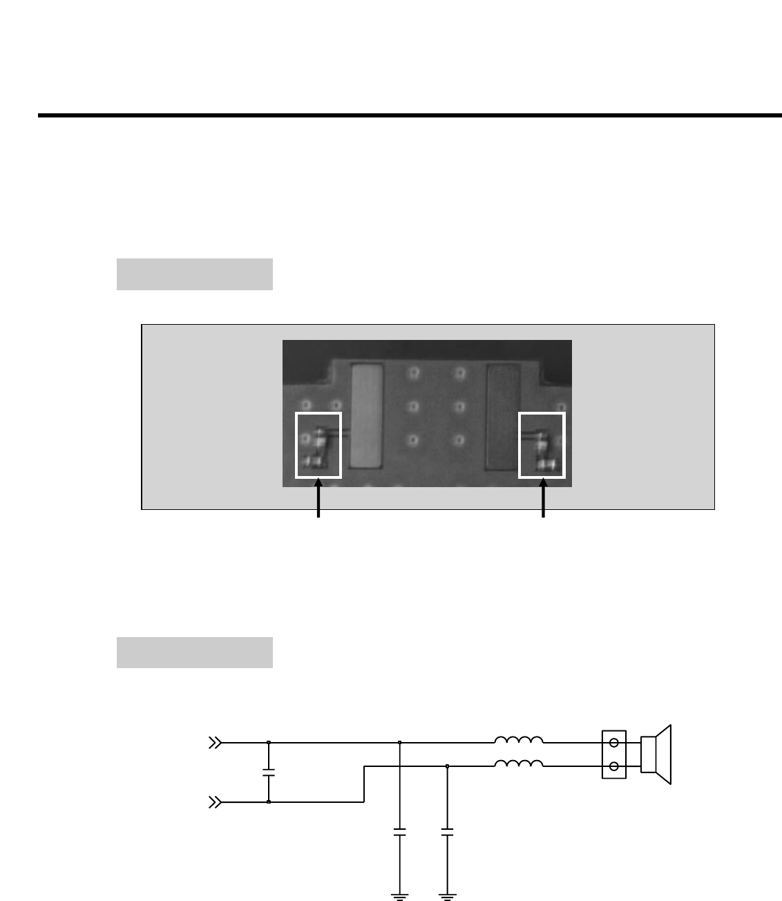
4.12 Speaker Trouble
Check Points
- Speaker spring contact
- Audio amp soldering
TEST POINT
CIRCUIT
SPEAKER
(SUSY0025801)
(2012)
Gain : Rf/Rin
SPEAKER AMPLIFIER
(10V,K)
16pi 3.4T speaker
C118 0.1u
VBAT
0.1uC119
L103 27nH
R108
82K
R103
NA
C120
1 uF
VP B3
C3 _SD
27nHL104
U100 NCP2890AFCT2G
BYPASS
C1
A1 INM
INP
A3
OUTA A2
C2
OUTB
VM B2
B1 VM_P
C123
0.1u
0.1uC117
diode
D101
R102
82K
20K
R105
20K
R106
20K
R104
D100
diode
R110
100K
C122
0.1u
CN101
1
2
C121 0.22u
NAC116
RADIO_SPK_L
LOUD_SPK_EN
SPK_N
SPK_P
CN200
L103
CN101íS 2PIN
CN101íS 1PIN
L104
AMP IC
C120
C117
C118
R111
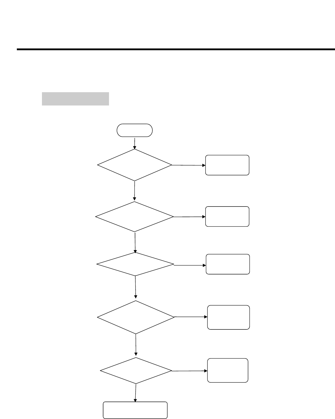
4. TROUBLE SHOOTING
- 74 -
Checking Flow
Start
Check the voltage level
of U100 = Vbat?
No
Check
The battery
Yes
Check the Signal,
C117,C118
Yes
No
Check
U102
Check the Level of
U100.C3 = Low ? No
Check
U102
Check the Contact
Of CN101
Yes
No
Re-Assemble
or Re-place
Speaker
Try again
or Change the Board
Yes
Re-solder
L102,L103
Check the Signal,
L102,L103
Yes
No
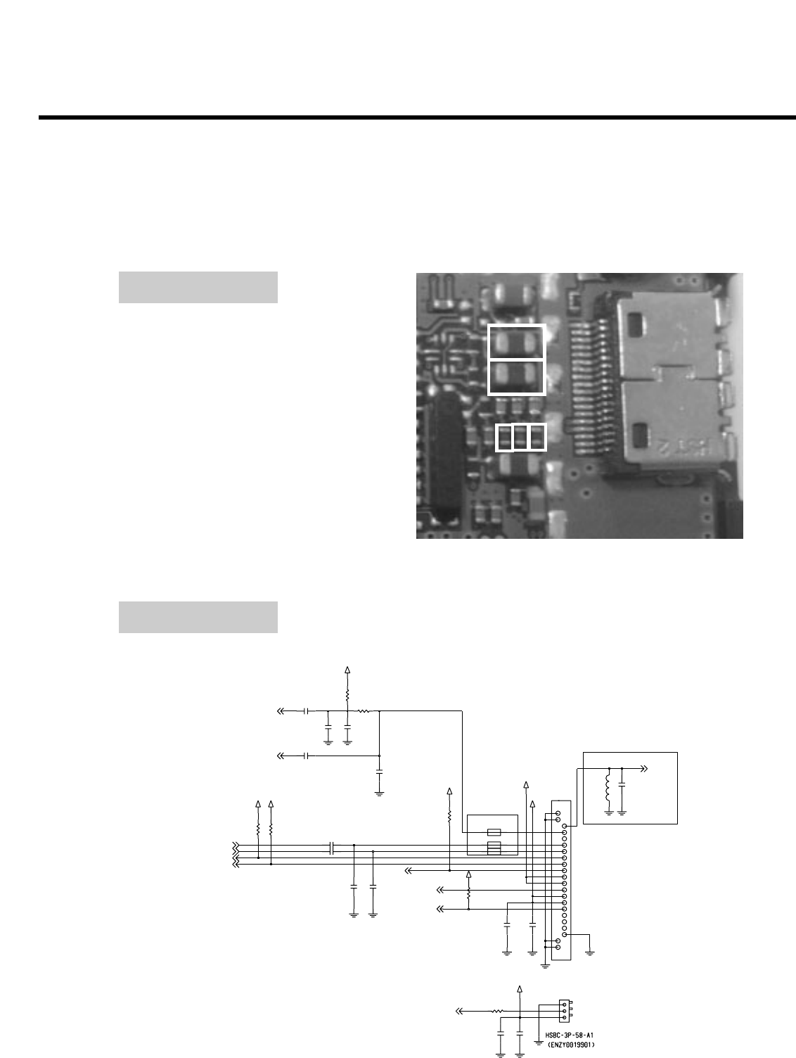
4. TROUBLE SHOOTING
- 75 -
4.13 Headphone Trouble
Check Points
-18pin IO connector
-Passive Parts slodering Status
TEST POINT
CIRCUIT DIAGRAM
FOR RADIO
12,13 : CHG
8 : JACK_D
(50V,C,NP0)
9,10 : BATT
4 : EAR_L
(10V,Z,Y5V)
FOR RADIO
I/O CONNECTOR
11 : R/ON
5 : EAR_R
2 : AUDIO
(50V,J,NP0)
(50V,J,NP0)
(2012)
1608
7 : RXD
(TOL:0.25P)
EAR_MIC
6 : TXD
39pC325
VMIC
NAR322
2V8_VIO
0.1u
C317
100K
R324
2V8_VIO
C336
3p
C326 39p
2V8_VIO 10p
C322
21
22
3
4
5
6
7
8
9
HSEJ-18S04-25R
1
10
11
12
13
14
15
16
17
18
19
2
20
100K
CN301
R323
18p
C337
C324 10u
2V8_VIO VCHARGE
1800FB301
C318
NA 10u
C319
L300
270nH
1
2
3
VBAT
CN302
R316
1.5K
C328
56p
R321
100K
C323 10u
R318
2.2K
39pC321
C327
10u
FB302 1800
R332 0
C320 0.1u
FB300 1800
VBAT
BATT_TEMP
DSR
HS_DET
AUXOP_FML
AUXOP_FMR
RPWRON
RXD
TXD
FM_ANT
AUXIN
AUXIP
CN301
FB301
C321
C322
FB302
FB300
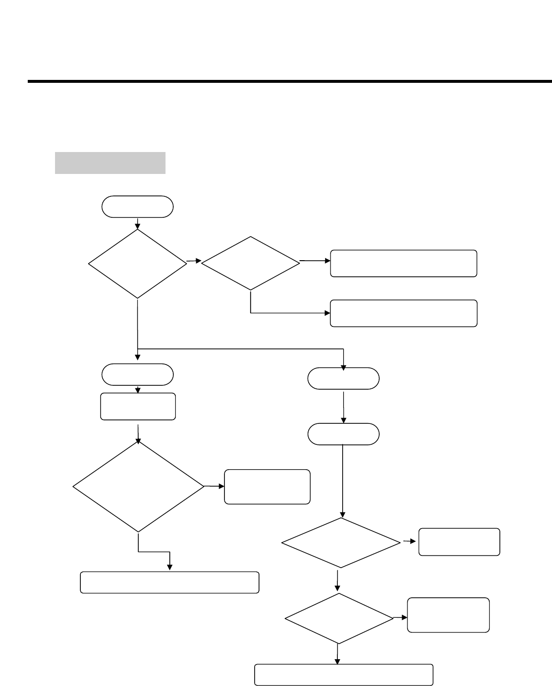
4. TROUBLE SHOOTING
- 76 -
CHECKING FLOW
START
Does the audio
profile of the phone
change to the
earphone mode?
Check the voltage Level
CN301.8 = Low?
Replace U100 or Change Board
Re-solder CN301 or Change
another Ear- Mic set and Try again
Mic Earphone
Go to MIC
Trouble section
Re-solder causal
component
(CN301)
Check the signal Level
at AUX_MIC.
Is it about 1.2~1.5V DC
with a few tens mV AC?
Change another Ear-Mic set and Try again
Acoustic
Does waveform at
U102.EPPA1
fluctuate?
Replace U100 or
Change the board
Does waveform at
CN301.4 and CN301.5
fluctuate?
Re-solder causal
component
(CN302,C322 etc.)
Change another Ear-Mic set and Try again
Yes
Yes
Yes
Yes
No
No
No
No No
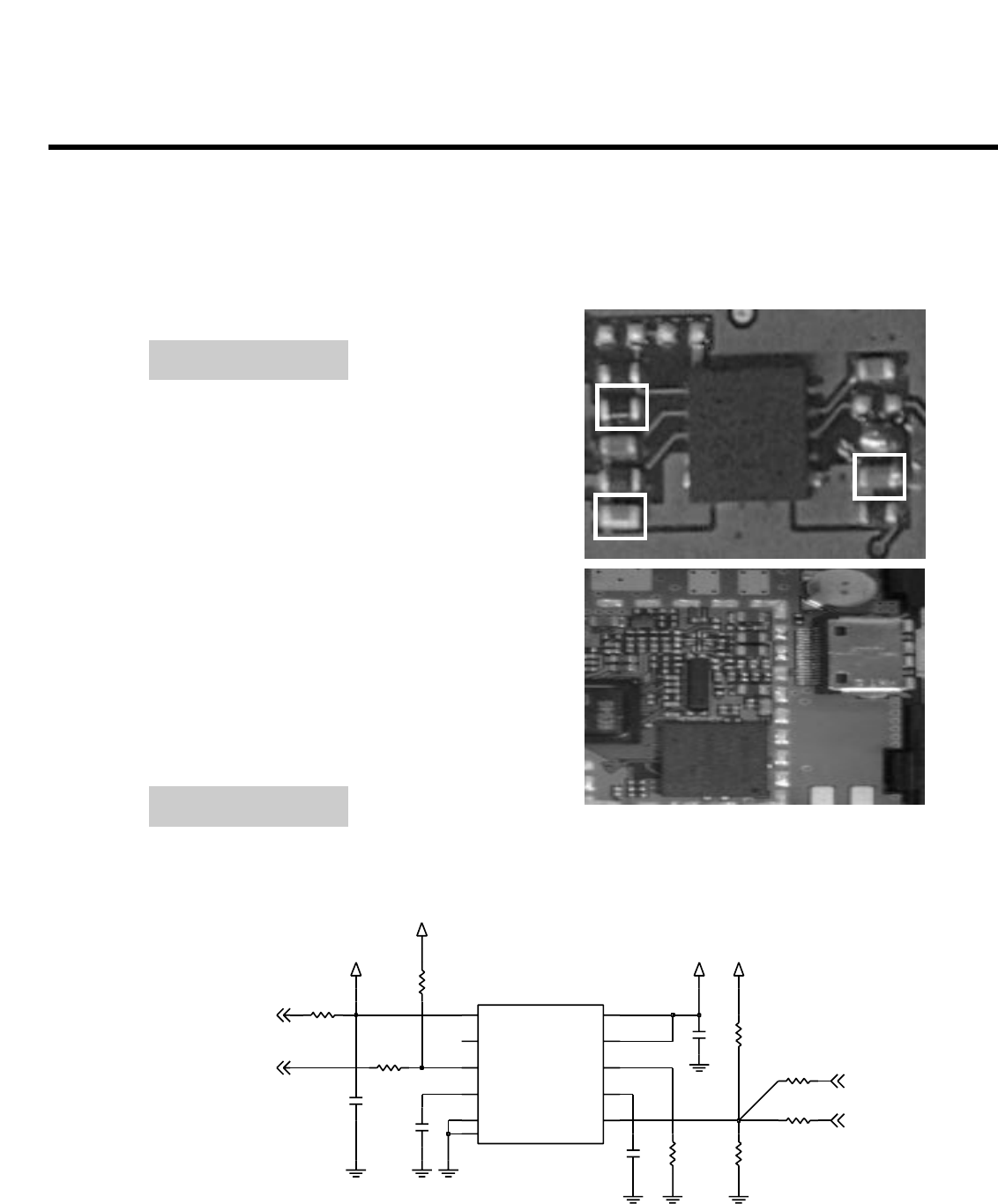
4. TROUBLE SHOOTING
- 77 -
4.14 Charging Trouble
Check Points
-Connection of TA (check TA voltage 5.2V)
-Charging Current Path component voltage
drop
-Battery voltage
-Charging IC
TEST POINT
CIRCUIT
(10V,K,X5R)
CHARGING IC
(1%)
(10V,K,X5R)
1u
C126
2V8_VIO
VCHARGE
NA
R120
NA
R118
1.8KR119
0.015u
C127
160K
R124
VBAT
1u
C125
NAR123
R125
100K
R121
NA
2_FAULT
_STATUS
3
6
ENGND
5
8
IREF
11 PGND
TIME
47
V2P8
10
VBATVIN
1
VSEN_TEMP 9
U101
ISL9201IRZ-T
0R122
C128
1u
VCHARGE
CHG_EN_TEST
CHG_STATUS
CHG_EN
CHARGE_DETECT
Charger
IC
U101
C125
C126
R124
CN301
VCHARGE
=5.2V
VBAT
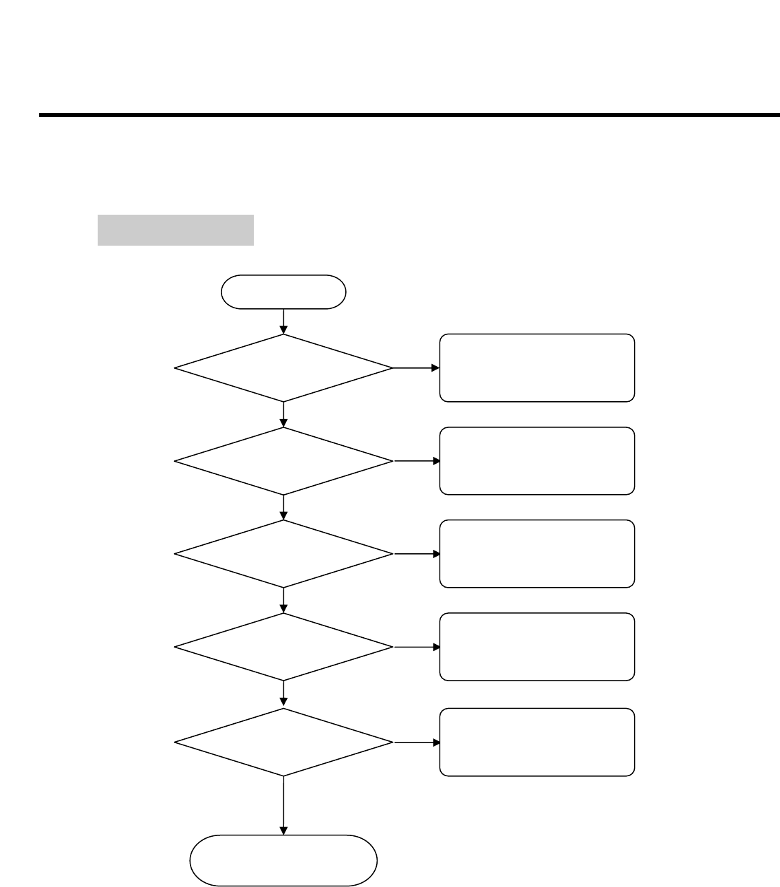
4. TROUBLE SHOOTING
- 78 -
START
I/O Connector(CN301)
Is well-soldered ?
Is The Voltage of C126
5.2V ?
The Voltage of C128
Is 2.8V
YES
YES
YES
Check the voltage of R124
High or Low?
YES
Battery is charged?
YES
Charging is
properly operating
NO
NO
LOW
NO
NO
Resolder the CN300
Pin 12,13 : VCHARGE
The TA is out of order
Change the TA
Replace the
U101
Check the U102
The battery may have
problems.
Change the battery.
Checking Flow
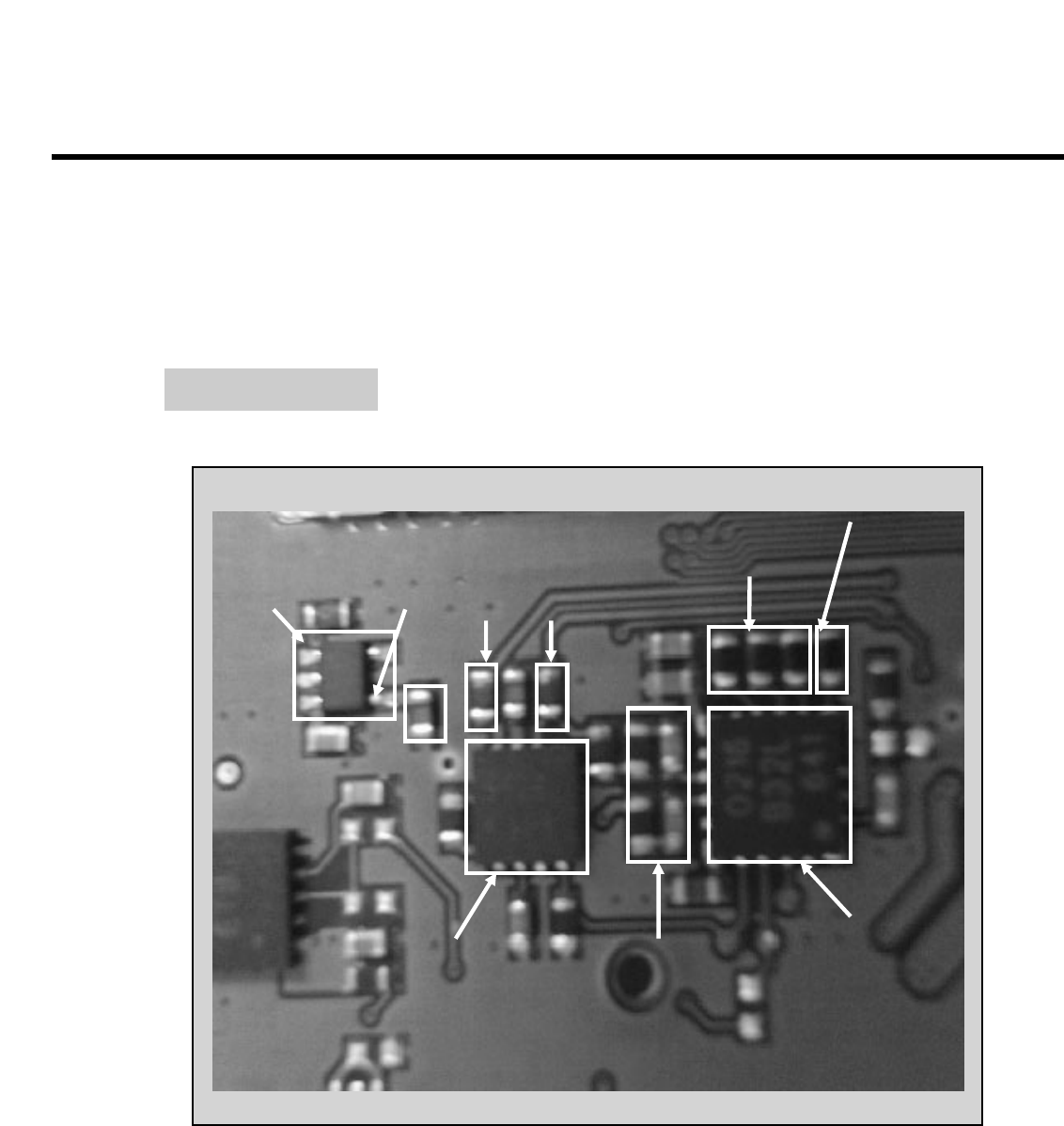
4. TROUBLE SHOOTING
- 79 -
4.15. FM Radio Trouble
R338/R337/R336
R332
U304.P1U304.P4
R329/R330
C332/C333
R327
U302
U303
R331
TEST POINT
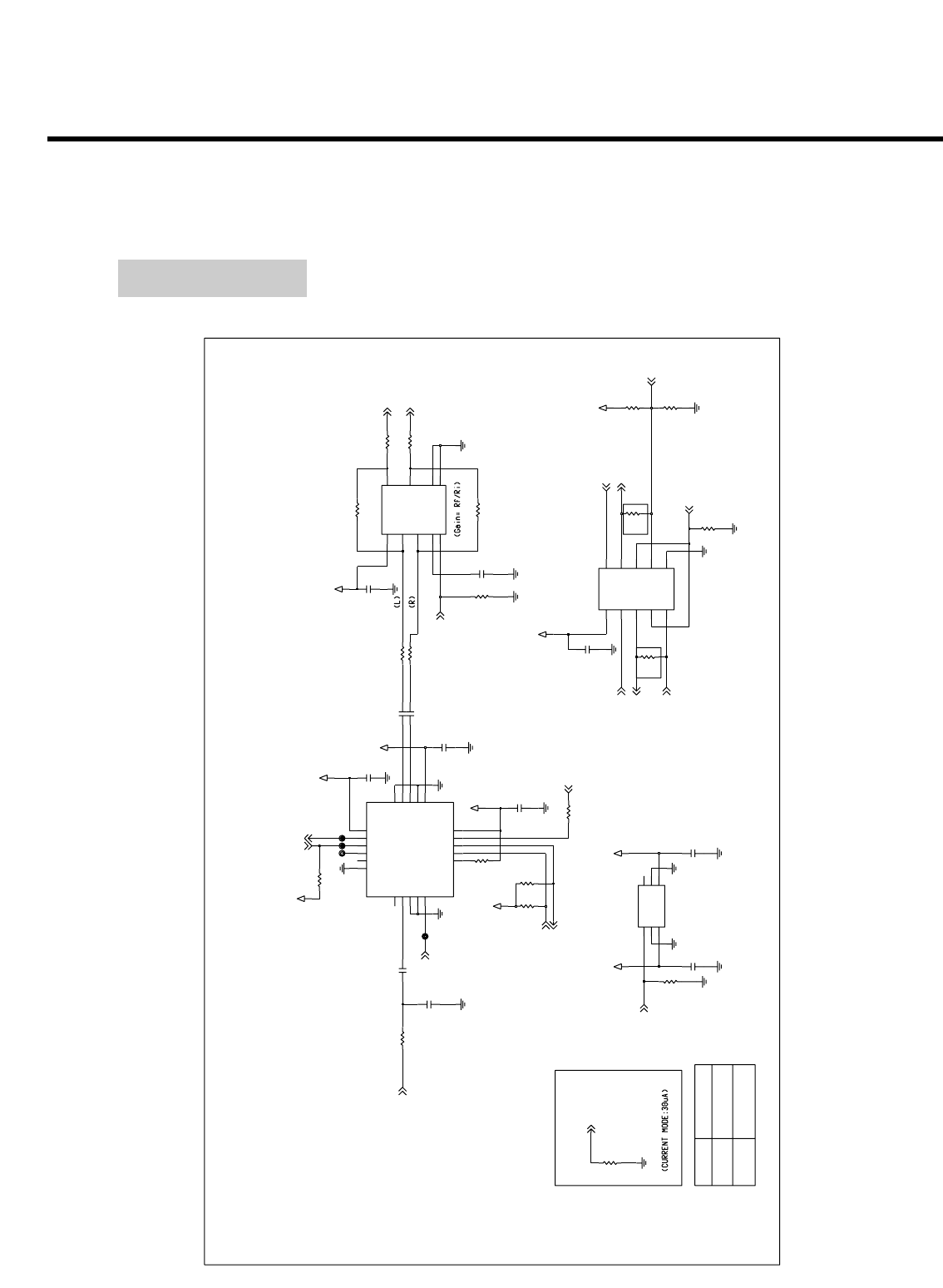
4. TROUBLE SHOOTING
- 80 -
RADIO
(FOR FM RADIO)
(10V,K,X5R)
NO RADIO
FOR RADIO
2.7K
RADIO
RADIO_DETECT
27K
2V8_VIO
FOR RADIO
C339 0.1u
0R327
VBAT
R342
NA
47
R338
2V8_RADIO
R331 0
0.1uC333
100K
R343
R334
10K
NA
R340
330K
R341
R329 20K
8
16
VA
11
VD
VIO
10
5_RST
6_SEN
2FMIP
4GND1 GND2 12
GND3 15
GPIO1 19
18
GPIO2
GPIO3 17
14
LOUT
NC1
1
20
NC2
PGND 21
9RCLK
3RFGND 13
ROUT
SCLK
7
SDIO
U302
SI4702-B16
R336
4.7K
FM_RST
NLAS5223BMNR2G
U305
COM1
3
COM2
9
GND
6
4
IN1
8
IN2
NC1
5
7
NC2
2
NO1
10
NO2
1
VCC
0R328
20KR330
C330
1u
9
BGND
BYPASS
23
GND
7VDD
VIN1
1
VIN2
5
8
VOUT1
6
VOUT2
_SHDN
4
U303 LM4809LD
R333 39K
R337
4.7K
6
BGND
2GND
NC 5
STBY
1
3VIN VOUT 4
1u
C329
BH28FB1WHFVU304
2V8_RADIO
R344
240K
2V8_RADIO
R335
100K
TP301
RADIO_AMP_SHDN
100pC331
C342
1u
C341
1u
R339
27K
2V8_RADIO
C332 0.1u
FM_INT
0.1u
C338
22n
C335
100K
R345
NAC334
2V8_RADIO
NAR325
2V8_RADIO
2V8_VIO
2V8_VIO
39KR326
0.1u
C340
FM_ANT
FM_32K
EPPA1
FM_INT
RADIO_AMP_SHDN
RADIO_DETECT
RADIO_AMP_SHDN
RADIO_EN
RADIO_SPK_R
RADIO_SPK_L
FM_SCL
FM_SDA
RADIO_SPK_R
RADIO_SPK_L
FM_RST
AUXOP_FMR
AUXOP_FML
HEADSET_RADIO_SEL
EPPA1
CIRCUIT DIAGRAM
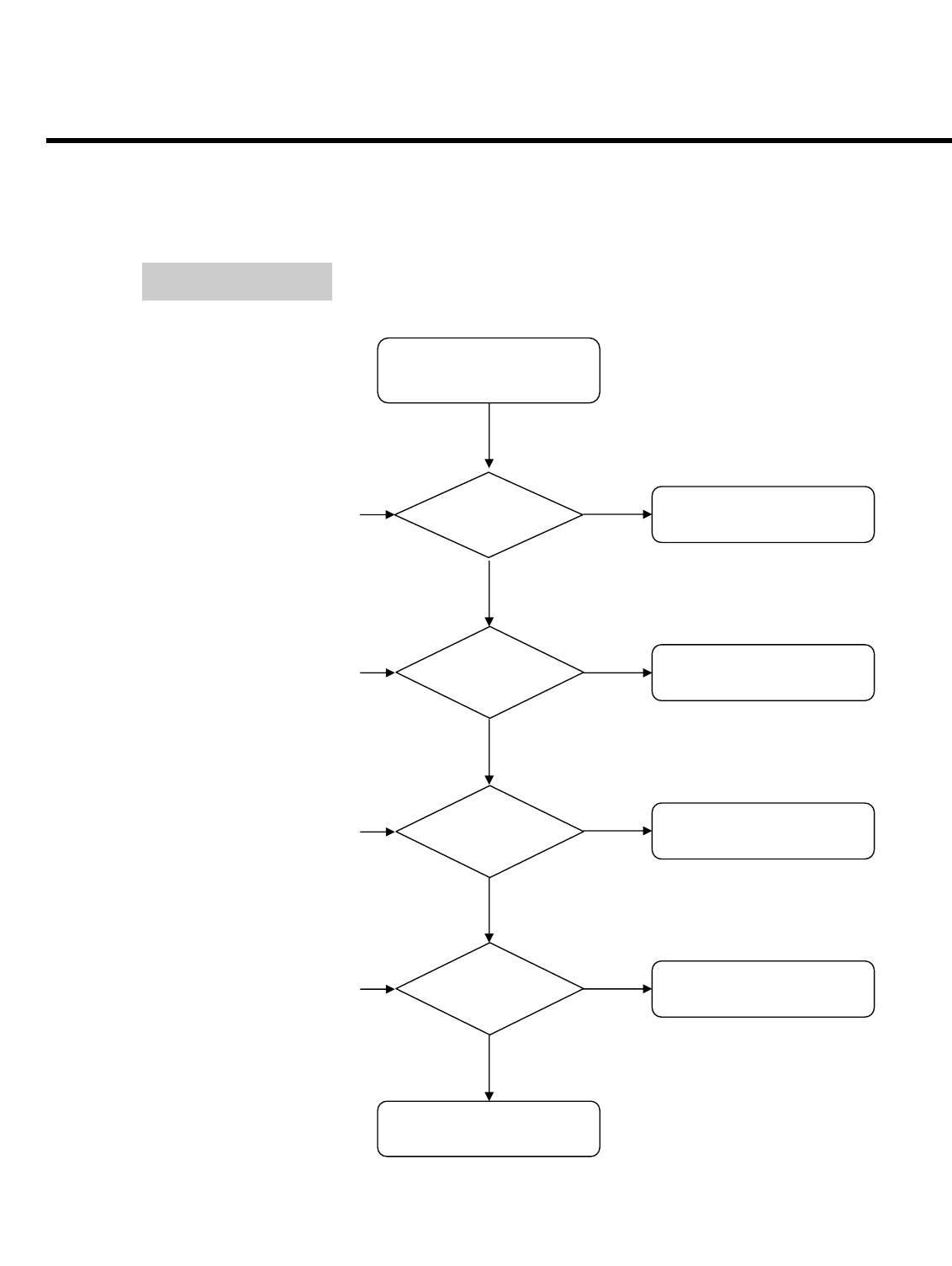
4. TROUBLE SHOOTING
- 81 -
Connector Headset and
Turn on Radio and
tuned channel
Check LDO
Power
U304.PIN1 = High
U304.PIN4=2.8V
Check
Control Signal
R336/R337/338
Check I2C signal and 32K clock
Check
Audio Output
Of Transceiver
R329/R330
C332/C333
Check
Audio Output
Of Amplifier
R327/R331
Change PCB
Change U304
Change PCB
Change U302
Change U303
NO
NG
NG
NG
YES
OK
OK
OK
Checking Flow
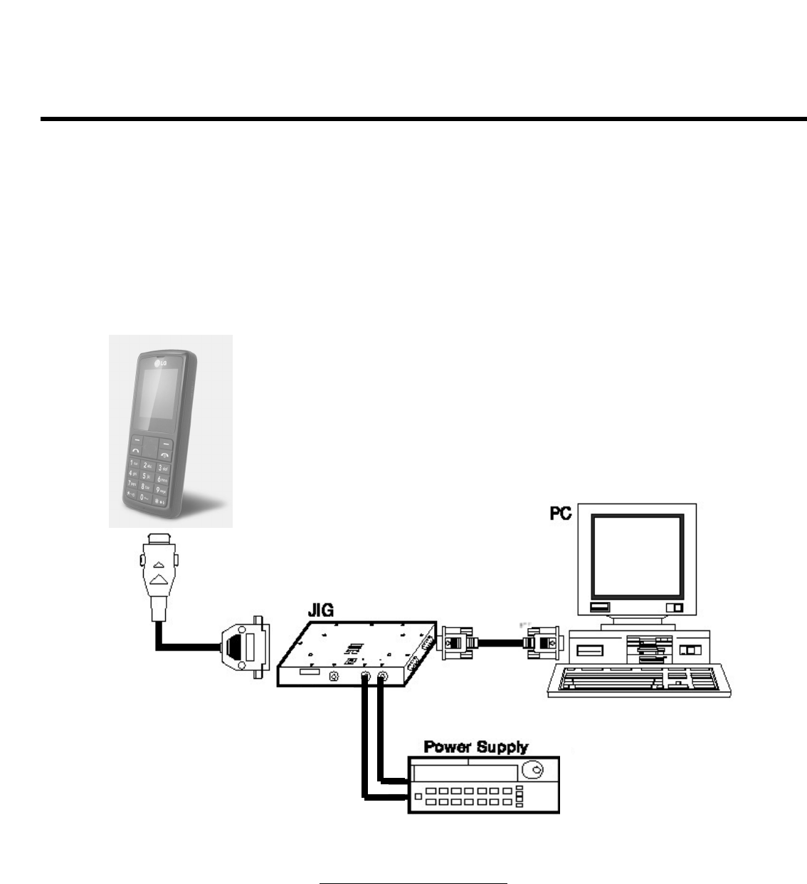
5. DOWNLOAD
- 82 -
5. DOWNLOAD
5.1 Download Setup
Configure system like figure 5-1.
Figure 9-1. Download Setup
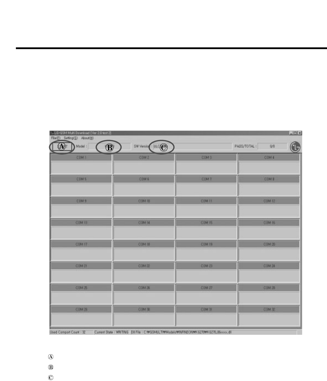
5. DOWNLOAD
- 83 -
5.2 Download Process
5.2.1. Download step[1]
: Start or Stop download
: Selected configuration DLL file
: File name donwloading
File(F) →Exit(X) : End program
Setting(S) →Configuration : configuration download condition DLL, SW files and etc.
About(H) →MultiGSM : Provide version information
First, select Setting Menu.
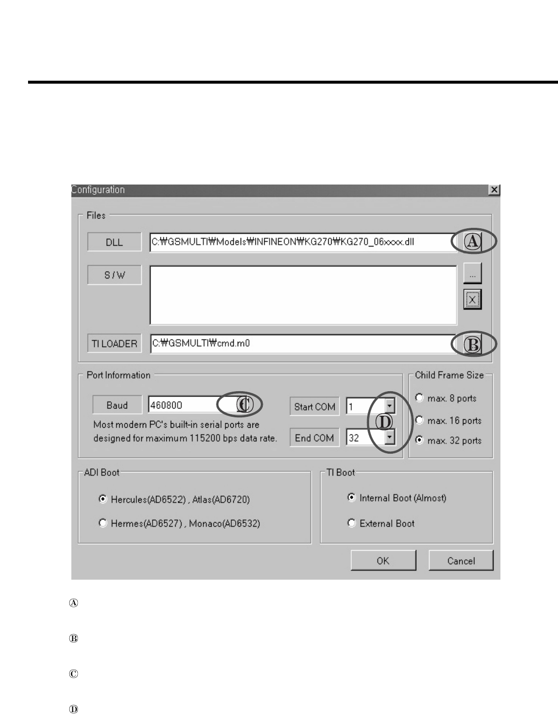
- 84 -
5. DOWNLOAD
5.2.2. Download step[2]
: Select a appropriated DLL file
- You must select KG270_xxxxxx.DLL file.
: Select configuration file
You must select cmd.m0 file
: Select download speed
You must 460800. System supports maximum 460800bps.
: Select port
select start and end port be operated
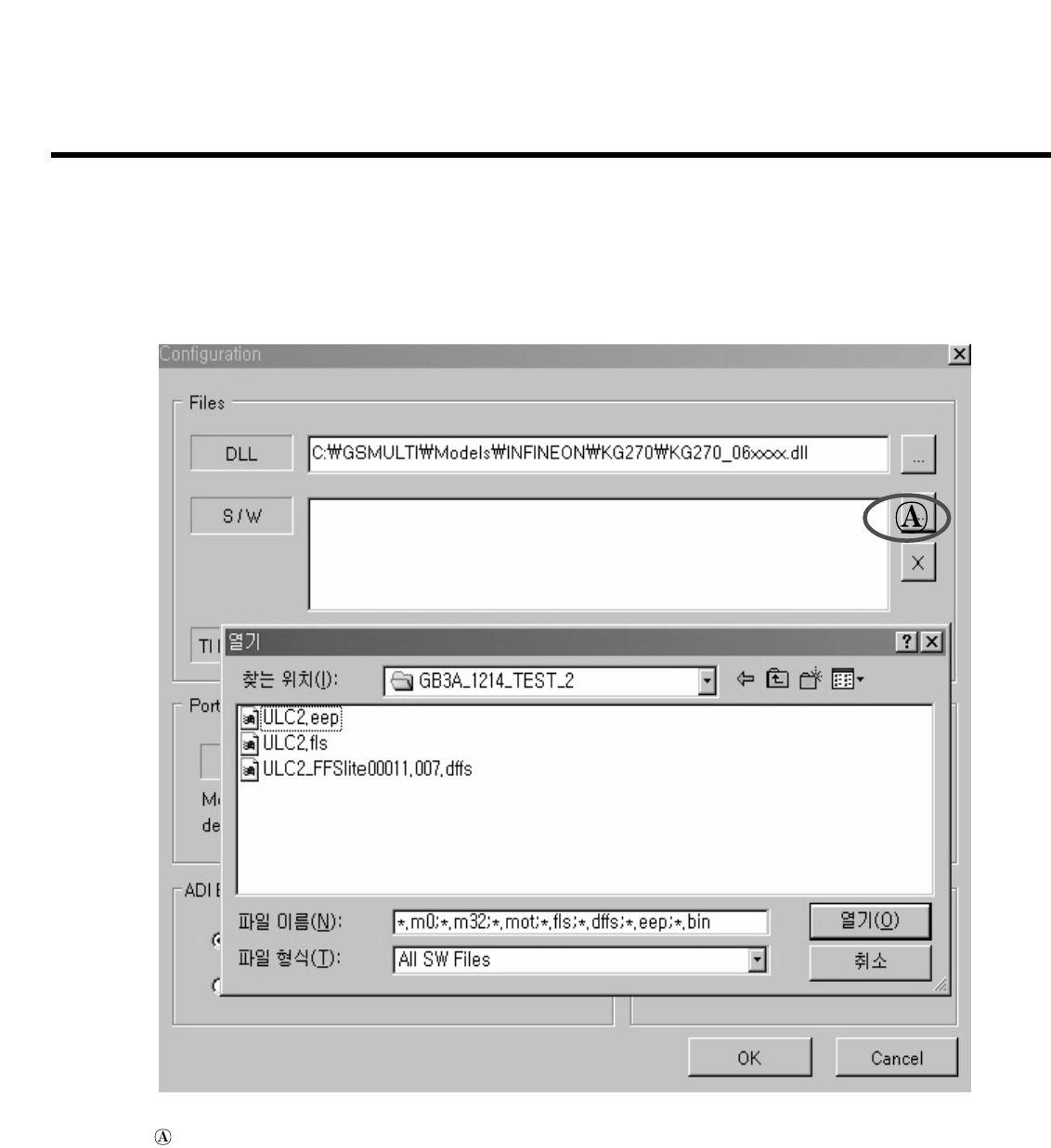
- 85 -
5. DOWNLOAD
5.2.3. Download step[3]
: Select files downloaded
KG270 have 4 files, *.eep, *.fls, *.dffs and *.cust.
But You must not select *.eep file.
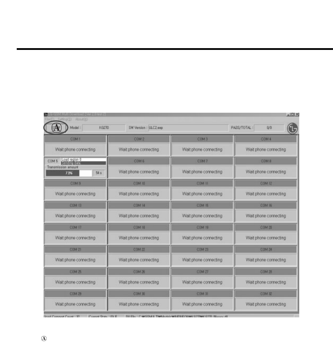
- 86 -
5. DOWNLOAD
5.2.4. Download step[4]
: Start download and stop download next step.
If configuration is finished, then push start button and then button is changed to STOP.
Turn on power of multi download and connector phones.
If download is started, then push start button else program will download repeatedly.
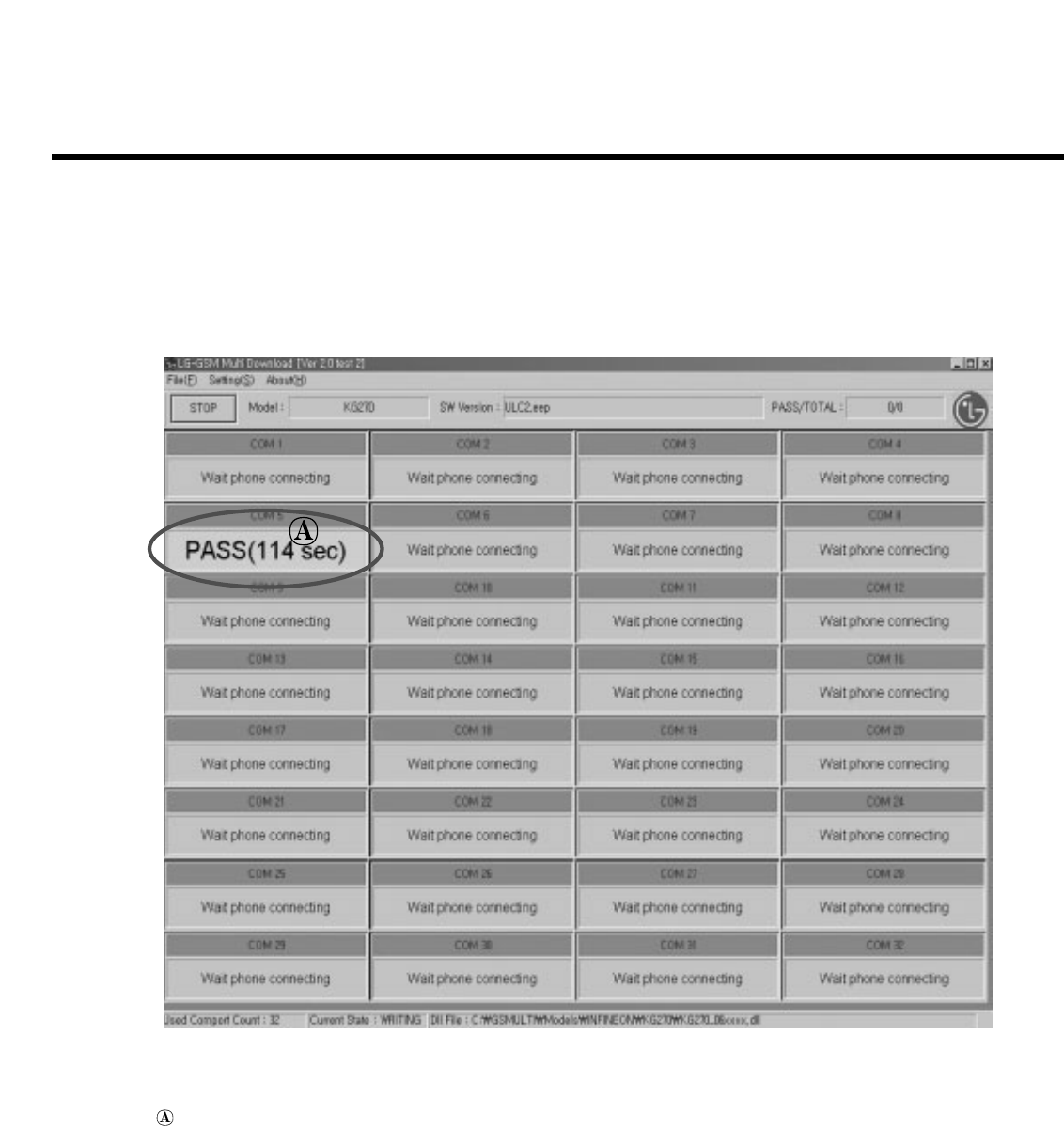
- 87 -
5. DOWNLOAD
5.2.5. Download step[5]
: This region appears donwload status.
If download is finished, PASS or FAIL.message is showed.
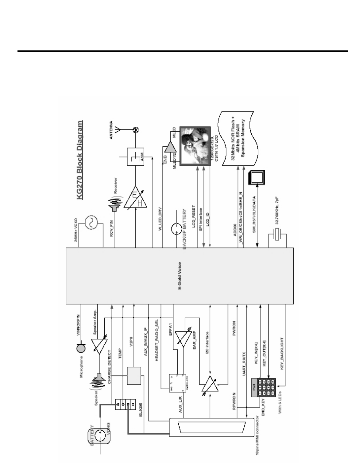
- 88 -
6. BLOCK DIAGRAM
6. BLOCK DIAGRAM
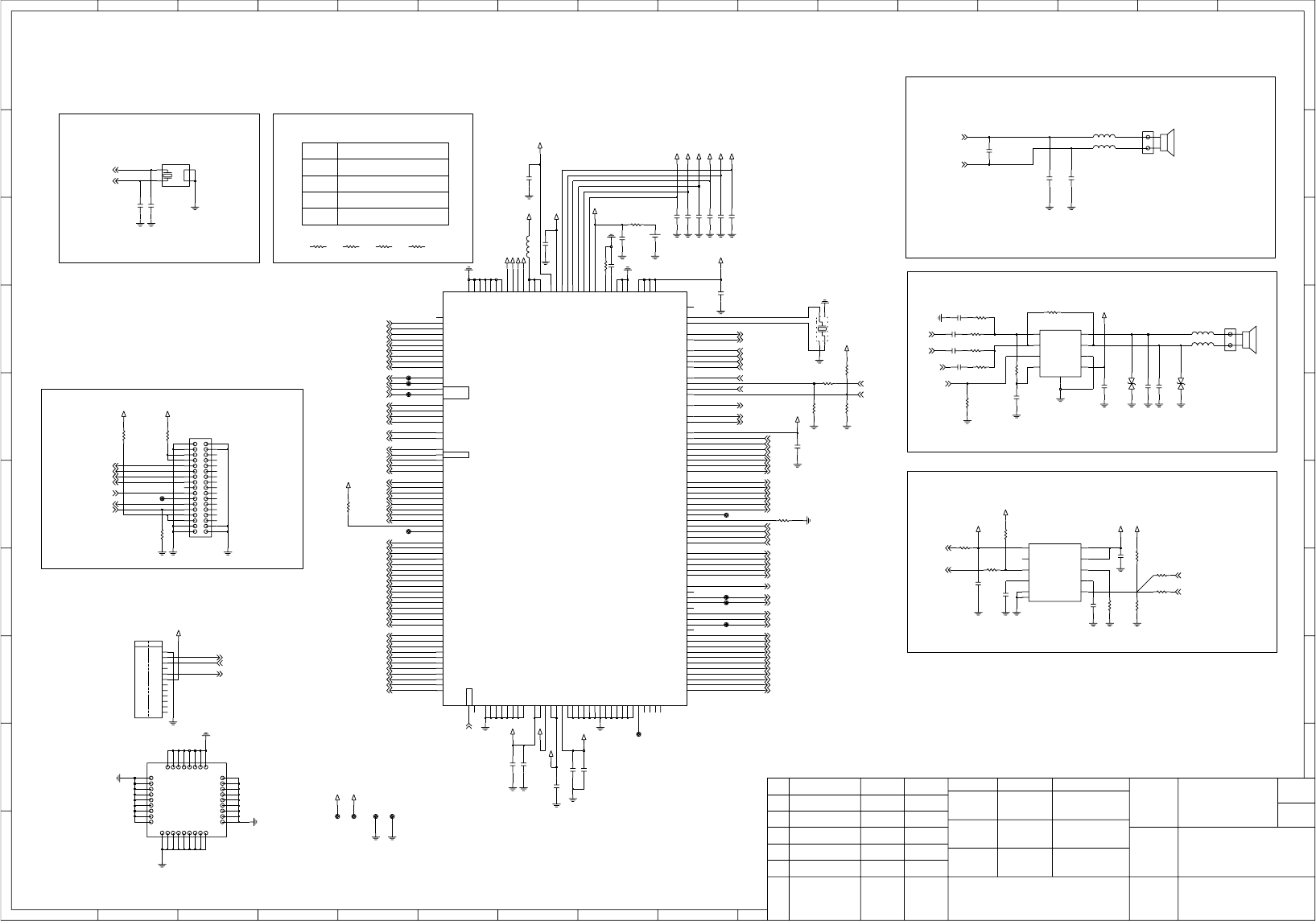
- 89 -
VBAT
PWR
URXD
UTXD
3G 2.5G
GND
RX
TX
UFLS
ON_SW
SPEAKER
(FOR LCD SPI INTERFACE)
Sheet/
C
E
(SUSY0025801)
(FOR CHARGING IC)
D
C
UART PORT
(SURY0013001)
Section
Iss.
(FOR FM RADIO)
(30uA)
E
7
RECEIVER
A
NO.
C
3
6
3
8
(90uA)
Checked
11
M0,2 : ~1.92V
M7,9 : ~0.96V
(VOLTAGE SENSING)
Sheets
16
(2012)
(FOR FM RADIO)
Approved
32.768KHZ CRYSTAL
DRAWING
Notice No.
13
Sign & Name
E
(10V,K,X5R)
123
8
( NX3225SA(W-188-34-7)
F
LG(42)-A-5505-10:01
15
Date
Gain : Rf/Rin
(FOR FM RADIO)
14
2006
SPEAKER AMPLIFIER
LG Electronics Inc.
(1608)
(1608)
Name
B
D
(10V,K)
B
9
E
ON BOARD ARM9 JTAG & ETM INTERFACE
(FOR FM RADIO)
A
(FOR SW DEBUGGING / NOT MOUNTED)
D
R196
D
(FOR FM RADIO)
(16V,K,X5R)
F
11/16
DRAWING
16pi 3.4T speaker
(NOT MOUNTED)
7
(FOR FM RADIO)
2
11*07*3T receiver
5 9
CHARGING IC
(1%)
NAME
KG278, MG160b, KG275
(FOR FM RADIO)
(FOR CHARGING IC)
2
GB3_RADIO
1/4
BB
R197
R198
R199
KG270
MG160a
MODEL
1
(FOR 2.8V VMEM SELECTION)
Designer
4
1
MODEL
LG Electronics Inc.
4
C
SPFY0144601
10
VER-1.1
6
5
Date
F
for mass production)
(30uA)
(10V,K,X5R)
(R110 will be changed to NA
(FOR FM RADIO)
SANG-YOEN.LEE
R101 22K
22nHL100
C118
GND1
0.1u
20
21
22
23
24
G1 G2
G3 G4
4
5
6
7
8
9
16
25
26
27
28
29
30
17
18
19
CN102
1
10
11
12
13
14
15
2
3
VBAT
1u
C126
2V85_VSIM
0.1uC119
C115
2.2u
VD1
0.1uC129
L103 27nH
68K
R109
R108
82K
BAT100
X100
MC-146_12_5PF
12
3
4
32.768KHz
R113
NA
R103
NA
2V8_VIO
1V5_VRF0
VBAT
C104 18p
C114
6.8K
R100
220n
2GND1
GND2 4
1
HOT1
HOT2
3
NX3225SA
X101
26MHz
3V2_VBUF
RXD
R114
NA
1u
1u
C110
VBAT2
C108
C124
1000p
VCHARGE
VBAT
2V85_VSIM
39p
C103
C120
1 uF
47K
R112
NA
R120
C131 1u
NA
R118
39p
VRF1
C102
1.8KR119
VP B3
C3 _SD
27nHL104
U100 NCP2890AFCT2G
BYPASS
C1
A1 INM
INP
A3
OUTA A2
C2
OUTB
VM B2
B1 VM_P
0.015u
C127
VBAT
C123
0.1u
0.1uC117
160K
R124
E_FUSE
VBAT
1u
C125
B10
C14 VSS_RF7
C10 VSS_RF8
D11 VSS_RF9
WR_N E2
W_LED_DRV A2
W_LED_FBN J12
W_LED_FBP J14
XO A8
A9
XOX
MON100
K13
M15 VSS_MS2
L13 VSS_MS3
VSS_MS4
L14
VSS_MS5
N14
P14 VSS_MS6
N11 VSS_MS7
VSS_RF1
A15
VSS_RF10
D14
E12 VSS_RF11
VSS_RF12
E13
E14 VSS_RF13
A12 VSS_RF2
B14 VSS_RF3
B13 VSS_RF4
VSS_RF5
B12
VSS_RF6
R6
VDD_RX
F13
R7
VDD_SIM
C11 VDD_TRX
F14 VDD_VCO
B1
VIB_CONTROL
P12
VMIC
G15
VREFP
VSS1 B8
VSS2 B9
VSS4 J8
K8
VSS5
VSS6 K7
F10
VSS8 M8
VSS9
VSS_EPLS
L12
VSS_MS1
VDDP_MEM
D10 VDD_DIG
VDD_LANA K15
VDD_LBUF J13
G12
VDD_LD1
VDD_LIO J10
K10
VDD_LMEM
VDD_LO
A11
B11
VDD_LRF1V5
VDD_LRF2V5 F15
A10 VDD_LRF_XO
VDD_LRTC K12
VDD_LSIM M11
VDD_MAIN1 G9
VDD_MAIN2 J7
G10
VDD_PLL
VDD_RTC
TRIG_IN
TRIG_OUT
B5 TRST_N
K9
TX1 A14
TX2 A13
H7 TXD
T_OUT0 A7
B6
T_OUT2
A6
T_OUT3
T_OUT4 A5
B7
T_OUT8
H13
VBAT_1
VBAT_2 F12
H15
VBAT_3
VBAT_4 H14
F6
VDDP_IO
L4
RX12X
RX34 E15
RX34X D15
G7 RXD
SAFE_RES M7
H9 SCL
SDA
H10
SSC0_CLK
J6
K6 SSC0_MRST
G6 SSC0_MTSR
SWITCH_ON N7
B2
T2IN
R9 TCK
TDI
M10
P8 TDO
P9 TMS
C5
N6
MON2
N9
R15 NC1
NC2
J15
NC3
A1
R1 NC4
F7 NMI_N
N5
OE_N
OSC32K P6
P13
PAOUT1
RD_N R3
P5
RESET_N
D12
REXT
A3
RSTOUT_N
RTS_N
H8
RX12 C15
B15
KP4
KP5
C6
C9 KP6
KP7
D8
F9 KP8
F8 KP9
L15
LOUD1
LOUD2 K14
R14
M0
P10
M2
R11
M7
N10
M9
R13
MICN1
R12
MICN2
MICP1 P15
MICP2 P11
MON1
M2
D6
K1
J2 D7
D8
P3
D9
R2
DISP_REST
H6
EPN1 N15
EPP1 M12
EPPA1 M14
E_FUSE
G3
F32K R5
IREF G13
KP0
C8
KP1
D6
D7 KP2
C7 KP3
D9
J9
CS0_N P4
K3
CS1_N
M5
CS3_N
G8 CTS_N
D0
R4
D1
P1
M1 D10
N1 D11
L2 D12
K2 D13
D14
J1
D15
M4
P2 D2
D3
N2
L1 D4
D5
A6
H4 A7
A8
C1
A9
F1
M6
ADV_N
AGND G14
BACK_LIGHT B3
E3
BHE_N
CC00IO A4
N8 CCIN
R8 CCIO
P7 CCLK
CCRST
R10
CCVZ_N
M9
H12 CDT
B4
CLKOUT
CS
A11
H2
A12
J3
A13
A14 H3
A15 J4
K4
A16
A17 L3
F3
A18
A19 D1
A2
F4 A20 H1
A21 E1
A22 G1
A3
E4
A4
D4
G4 A5
D2
1
2
U102
PMB7880
C2 A0
D5 A1
F2 A10 G2
2V8_VIO
CN100
C112 1u
NAR123
L101 22nH
47nC130
R125
100K
C105 18p
R121
NA
2_FAULT
_STATUS
3
VRF1
NA
R117
6
ENGND
5
8
IREF
11 PGND
TIME
47
V2P8
10
VBATVIN
1
VSEN_TEMP 9
C100
U101
ISL9201IRZ-T
VMIC
39p
C106 1u
4700p
C133
2V0_VRTC
2V8_VMEM
diode
D101
R102
82K
2V8_VIO
2V8_VIO
20K
R105
EXTRSTn
20K
R106
100K
R111
1u
C113
0R122
2V8_VMEM
VD1
C128
1u
20K
R104
2V8_VIO
D100
diode
C111
1u
VBAT
2V0_VRTC
R110
100K
UA100
12
CTS
10
DSR
1
GND
4
NC1
NC2 7
8
NC3
NC4 9
ON_SW 5
RTS 11
2
RX
TX 3
6
C122
0.1u
BHE_N
1uC109
CS100
C132
TXD
4700p
_WR
GND2
_RESET
CN101
1
2
28
29
3
30
31
32
33
34
35
4
5
6
7
8
9
13
14
15
16
17
18
19
2
20
21
22
23
24
25
26
27
SC100
1
10
11
12
VRF2
VCHARGE
VBAT
VBAT1
C121 0.22u
R116 0
NAC116
R196
0
2V5_VANA
NA
R198R197
NA
R199
NA
DSR
2V8_VMEM
2.2u
2V0_VRTC
18nH
L102
C101
100K
R115
1uC107
NA
R107
VD1
1V5_VRF0
LCD_ID
DSR BATT_TEMP
CHG_EN_TEST
CHG_EN_TEST
CHG_STATUS
REC_P
HS_DET
CHG_EN
DEFAULT_BANDSEL
RADIO_SPK_L
LOUD_SPK_EN
CHARGE_DETECT
CHARGE_DETECT
REC_N
AUXIP
ADD01
SSC0_CLK
SSC0_MTSR
CHG_EN
HEADSET_RADIO_SEL
FM_SCL
FM_SDA
FM_INT
SPK_N
SPK_P
LOUD_SPK_EN
CS3
RADIO_DETECT
32KIN
32KOUT
TXD
CHG_STATUS
TRIG_OUT
TRSTn
TDI
TMS
TCK
TDO
TRIG_IN
VIBRATOR
W_LED_DRV
RPWRON
RXD
TCK
TDI
TDO
TMS
TRIG_IN
TRIG_OUT
TRSTn
GSM_OUT
DCS_PCS_OUT
TXD
TXON_PA
VC1
VC2
FM_32K
BS
SPK_N
VINNORN
VINNORP
_OE
32KOUT
TX_RAMP
FM_RST
GSM_RXP
GSM_RXN
DCS_RXP
DCS_RXN
RXD
PWRON
KEY_OUT3
KEY_OUT4
KEY_IN0
KEY_IN1
KEY_IN2
KEY_IN3
KEY_IN4
REC_P
REC_N
KEY_BACKLIGHT
RADIO_EN
LCD_RESET
EPPA1
32KIN
SPK_P
DATA10
DATA11
DATA12
DATA13
DATA14 CS1n
DATA15 CS0n
_WR
BHE_N
SIM_CLK
SIM_DATA
SIM_RST
KEY_OUT1
KEY_OUT2
ADD15
ADD16
ADD17
ADD18
ADD19
ADD20
DATA00
DATA01
DATA02
DATA03
DATA04
DATA05
DATA06
DATA07
DATA08
DATA09
AUXIN
ADD21ADD00
ADD02
ADD03
ADD04
ADD05
ADD06
ADD07
ADD08
ADD09
ADD10 ADD11
ADD12
ADD13
ADD14
7. CIRCUIT DIAGRAM
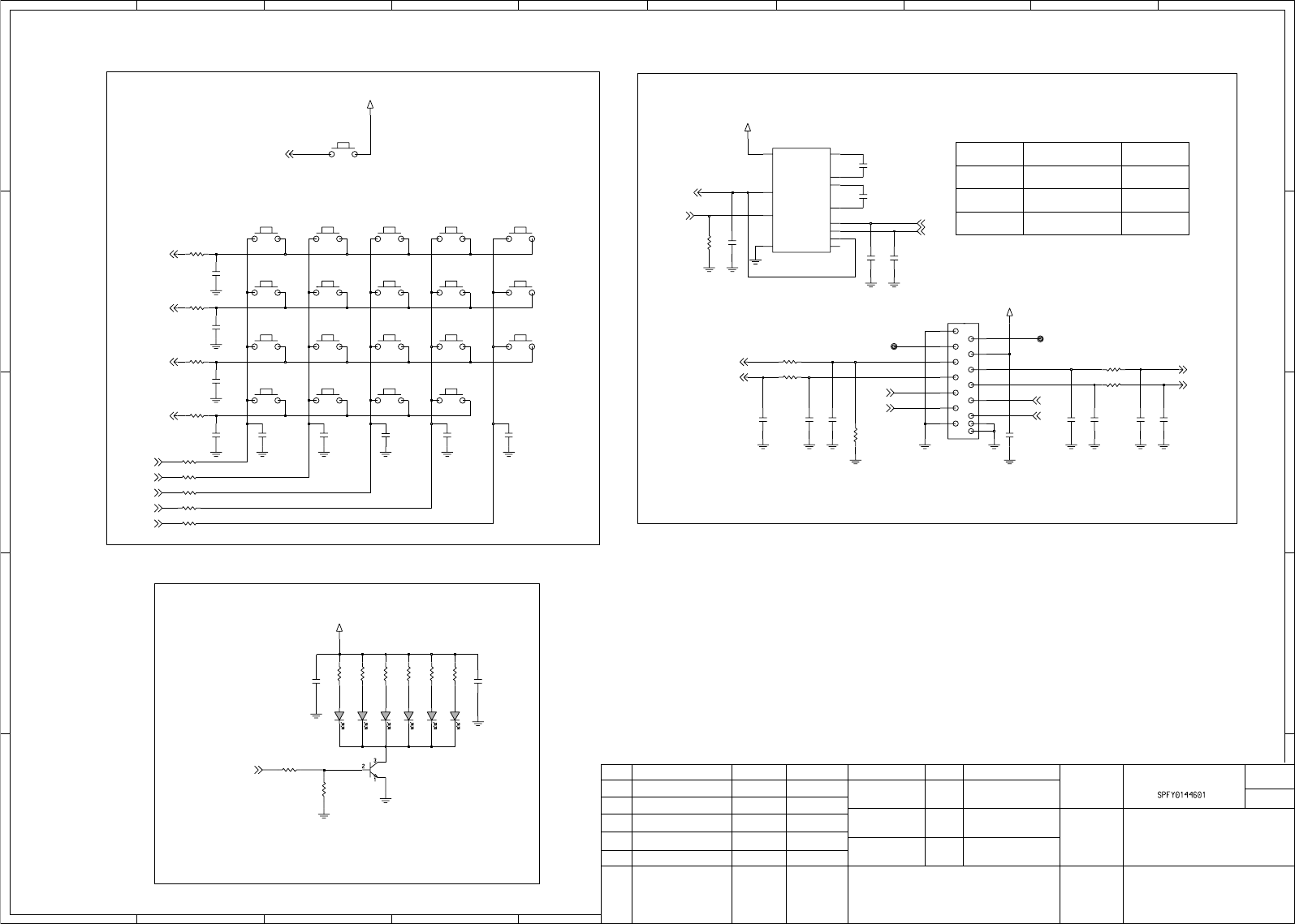
- 90 -
DOWN
23
LG Electronics Inc.
DRAWING
E
7
KEY BACKLIGHT
5
11/16
4
2006
#
4
GB3_RADIO
10
MENU
IMSA-9671S-13Y902
SEND
1
REV-1.1
4
A
Notice No.
SII
(10V,K,X5R)
ID
MODEL
NO.
DRAWING
Date
5
Sheet/
1
UP SEL
NAME
D
6
KEY MATRIX
MAKER
Iss.
LG Electronics Inc.
A
HIGH
(10V,K,X5R)
1
C
2
7
8
2
*
HYUN-OK.LEE
LEFT
B
SHARP
3
3
Sheets
Name
Approved
END
D
LOW
Sign & Name
9
LGIC(42)-A-5505-10:01
0
Designer
CHARGE PUMP
RIGHT
5
6
9
8
SW203
AUDIO,LCD,KEY
2/4
GP 150Kohm pull up
Voltage
1.9V
0V
0.9V
Date
Checked
(ENQY0013801)
Section
47R208
LD201
VBAT
LEBB-S14H
NA
C213
R204
680
27p
SW201
C210
47R206
LEBB-S14H
LD200
C209
27p
2V0_VRTC
SW216
1u
C215 C221
NA
2SC5585
Q200
C204
NA
C219
27p
LEBB-S14H
LD204
R212 680
SW205
SW212
SW217
SW215
C207
NA
SW210
SW214
27p
C211
1u
C223
NA
LD202
LEBB-S14H
C218
SW211
100ohm
R220
SW200
SW219
R215 680
LD203
LEBB-S14H
SW204
NA
R219
100ohm
NA
C216 C220
R205 47
100ohm
R218
R209
680
4GND
IN
5
12
NC
NA
C214
AAT3157ITP-T1
10
C1+
C1- 9
C2+ 7
C2- 6
8CP
D1 1
2
D2
D3 3
11 EN_SET
R223
10K
U200
SW208SW207
47R207
R201
680
100ohm
R216
SW202
2V8_VIO
C200
1u
1KR222
R202
100K
14
15
1
10
11
12
13
2
3
4
5
6
7
8
9
C206 CN200
NA
R211 680
NA
SW209
SW213
C208
LD205
27p
LEBB-S14H
1u
C203
NA
C222
C205
680
R203
R214 680
MTPG
MTPD
1u
C201
R210
100K
C212
27p
R217
100ohm
R213 680
R221
100ohm
C202
27p
SW218
NA
C217
VBAT
SW206
MLED2
MLED1
SSC0_CLK
SSC0_MTSR
CS3
MLED
W_LED_DRV
KEY_OUT2
KEY_OUT3
KEY_OUT4
KEY_IN3
LCD_RESET
MLED1
MLED2
MLED
LCD_ID
END_KEY
KEY_BACKLIGHT
KEY_IN0
KEY_IN2
KEY_IN1
KEY_IN4
KEY_OUT1
7. CIRCUIT DIAGRAM
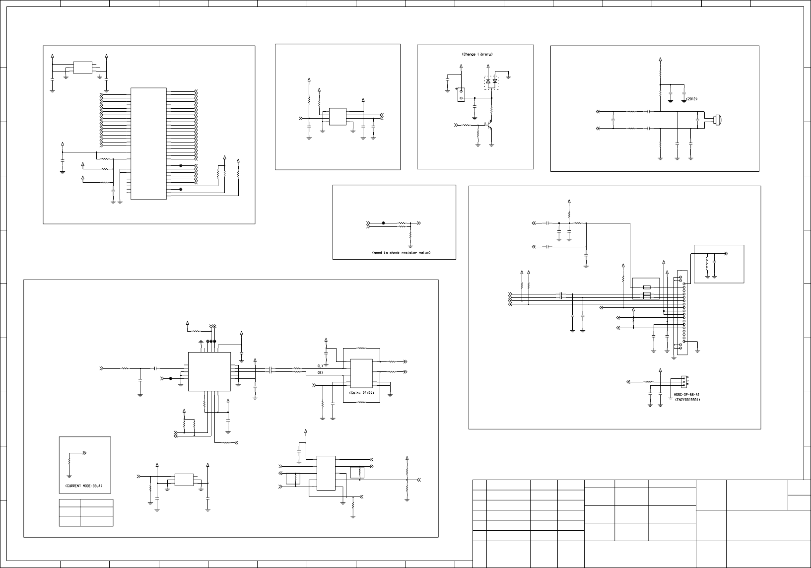
- 91 -
FOR RADIO
Name
1
A
LG Electronics Inc.
SANG-YEON.LEE
SIM_CONNECTOR
(1608)
8
Sheet/
12,13 : CHG
6
8 : JACK_D
(50V,C,NP0)
11
8
9,10 : BATT
2
C
9
RADIO
2
14
E
DRAWING
LG(42)-A-5505-10:01
1
(FOR FM RADIO)
REMOTE POWER ON
4 : EAR_L
(10V,K,X5R)
(10V,Z,Y5V)
Checked
Sheets
2006
12
D
FOR RADIO
15
C
FF
Iss.
E E
NO RADIO
C
I/O CONNECTOR
D
11 : R/ON
Date
3
5 : EAR_R
B
5
D
C
VER-1.1
2006
SPFY0144601
NAME
2 : AUDIO
E
FOR RADIO
NO.
2.7K
3
(50V,J,NP0)
5
MEMORY
LG Electronics Inc.
4
D
VIBRATOR
(50V,J,NP0)
13
(50V,J,NP0)
MAIN_MIC
DRAWING
(2012)
RADIO
16
B
RADIO_DETECT
Approved
6
MODEL
4
27K
1608
7
7 : RXD
Date
2V8_VIO
2006
11/16
GB3_RADIO
3/4
RADIO,MEMORY,AUDIO,I/O
Sign & Name
Designer
9
Section
FOR RADIO
F
(NOT MOUNTED)
(TOL:0.25P)
7
EAR_MIC
10
Notice No.
A
6 : TXD
100KR312
C313
VBAT
39p
C311
C339 0.1u
0.1u
39pC325
2V8_VMEM
VMIC
1K
R300
R317 47
4.7KR302
0R327
NAR315
VBAT
C302
27p
R342
NA
47
R338
C310
2V8_RADIO
22p
C306 0.1u
NAR322
R331
VMIC
2V8_VIO
CN300
1
2
0
0R310
0.1uC333
G8
VSS2
E2
WP_ACC A4
F1
_CE1F G1
_CE1S
A3
_LB
F2
_OE
B4
_RSTF
_UB B3
A5
_WE
DQ2
F4 DQ3
DQ4
F5
DQ5
H6
DQ6
E6
G7 DQ7
DQ8
H2
DQ9
F3
C8 RFU0
RFU1
D8
E7 RFU2
RFU3
F8
H5 RFU4
RY__BY C4
VCCF
G4
G5 VCCS
VSS1
A3
A4 D2
A5 C2
A6 B2
A2
A7
A8 A6
A9 C6
CE2S B5
G2 DQ0
E3 DQ1
DQ10
G3
DQ11
H4
G6 DQ12
DQ13
F6
DQ14
H7
F7 DQ15
H3
S71GL032A40BAW0F
E1
A0 D1
A1
A10 D6
A7
A11
A12 B7
C7
A13
A14 D7
B8
A15 E8
A16 D3
A17 C3
A18 B6
A19
A2 C1
C5
A20
B1
U301
22p
C312
C316
0.1u
R311 NA
2V8_VMEM_S
RPWRON
2V85_VSIM
2V8_VIO
100K
R343
C301
NANA
C300
R308
100K
2V8_VMEM_S
R334
10K
0.1u
1
3VIN VOUT 4
VBAT
C317
BH28FB1WHFVU300
6
BGND
2GND
NC 5
STBY
100K
R324
Q300
2V8_VIO
2SC5585
C336
3p
NA
R340
330K
R341
R329 20K
8
16
VA
11
VD
VIO
10
5_RST
6_SEN
2FMIP
4GND1 GND2 12
GND3 15
GPIO1 19
18
GPIO2
GPIO3 17
14
LOUT
NC1
1
20
NC2
PGND 21
9RCLK
3RFGND 13
ROUT
SCLK
7
SDIO
2V85_VSIM
U302
SI4702-B16
R336
4.7K
R313 100K
MIC300
OB4-15L42-C33L
1
2
FM_RST
D300
1SS302-T5L_F_H
NLAS5223BMNR2G
U305
COM1
3
COM2
9
GND
6
4
IN1
8
IN2
NC1
5
7
NC2
2
NO1
10
NO2
1
VCC
2V8_VMEM
0R328
20KR330
C330
1u
9
BGND
BYPASS
23
GND
7VDD
VIN1
1
VIN2
5
8
VOUT1
6
VOUT2
_SHDN
4
U303 LM4809LD
C326 39p
2V8_VIO
R333 39K
10p
R337
C322
4.7K
6
BGND
2GND
NC 5
STBY
1
3VIN VOUT 4
1u
C329
BH28FB1WHFVU304
21
22
3
4
5
6
7
8
9
HSEJ-18S04-25R
1
10
11
12
13
14
15
16
17
18
19
2
20
100K
2V8_RADIO
CN301
R323
R344
240K
18p
C337
TP300
2V8_RADIO
_RY_BY
R335
100K
C324
0.1u
C307
10u
TP301
RADIO_AMP_SHDN
100pC331
C342
1u
1K
R306
2V8_VIO
C341
1u
VCHARGE
1800FB301
2.2K
R301
100ohm
R304
0
R303
C318
NA
0.1u
C315
R339
27K
I_O
6
2
RST
1
VCC
VPP
5
2V8_RADIO
2V8_VMEM
J300
CLK 3
4GND
GND1 78 GND2
10u
C304
10u
100K
R320
C319
0R319
27p
C305
C314 39p
C332 0.1u
FM_INT
L300
270nH
R307
100ohm
1
2
3
VBAT
CN302
0.1u
C338
22n
C335
100K
R345
VBAT
NAC334
R314
0.1uC309
0
R316
1.5K
2.2K
R309
C328
56p
R305
10
R321
100K
C303
39p
C323 10u
R318
2.2K
39p
2V8_RADIO
C321
C327
10u
39p
NAR325
C308
2V8_RADIO
2V8_VIO
2V8_VIO
FB302 1800
2V85_VSIM
R332 0
C320 0.1u
FB300 1800
39KR326
VBAT
BATT_TEMP
0.1u
C340
FM_ANT
FM_32K
EPPA1
FM_INT
DSR
RADIO_AMP_SHDN
RADIO_DETECT
RADIO_AMP_SHDN
SIM_CLK
SIM_RST
PWRON
HS_DET
VIBRATOR
END_KEY
RPWRON
AUXOP_FML
AUXOP_FMR
RADIO_EN
RADIO_SPK_R
RADIO_SPK_L
RPWRON
RXD
TXD
FM_ANT
FM_SCL
FM_SDA
AUXIN
AUXIP
SIM_DATA
RADIO_SPK_R
RADIO_SPK_L
FM_RST
AUXOP_FMR
AUXOP_FML
HEADSET_RADIO_SEL
EPPA1
ADD21
ADD04
ADD05
ADD06
ADD07
ADD08
ADD09
ADD10
_OE
_WR
VINNORP
VINNORN
DATA11
DATA12
DATA13
DATA14
DATA15
ADD01
ADD02
ADD11
ADD12
ADD13
ADD14
ADD15
ADD16
ADD17
ADD18
ADD19
ADD20
ADD03
CS0n
CS1n
ADD00
BHE_N
DATA00
DATA01
DATA02
DATA03
DATA04
DATA05
DATA06
DATA07
DATA08
DATA09
DATA10
7. CIRCUIT DIAGRAM
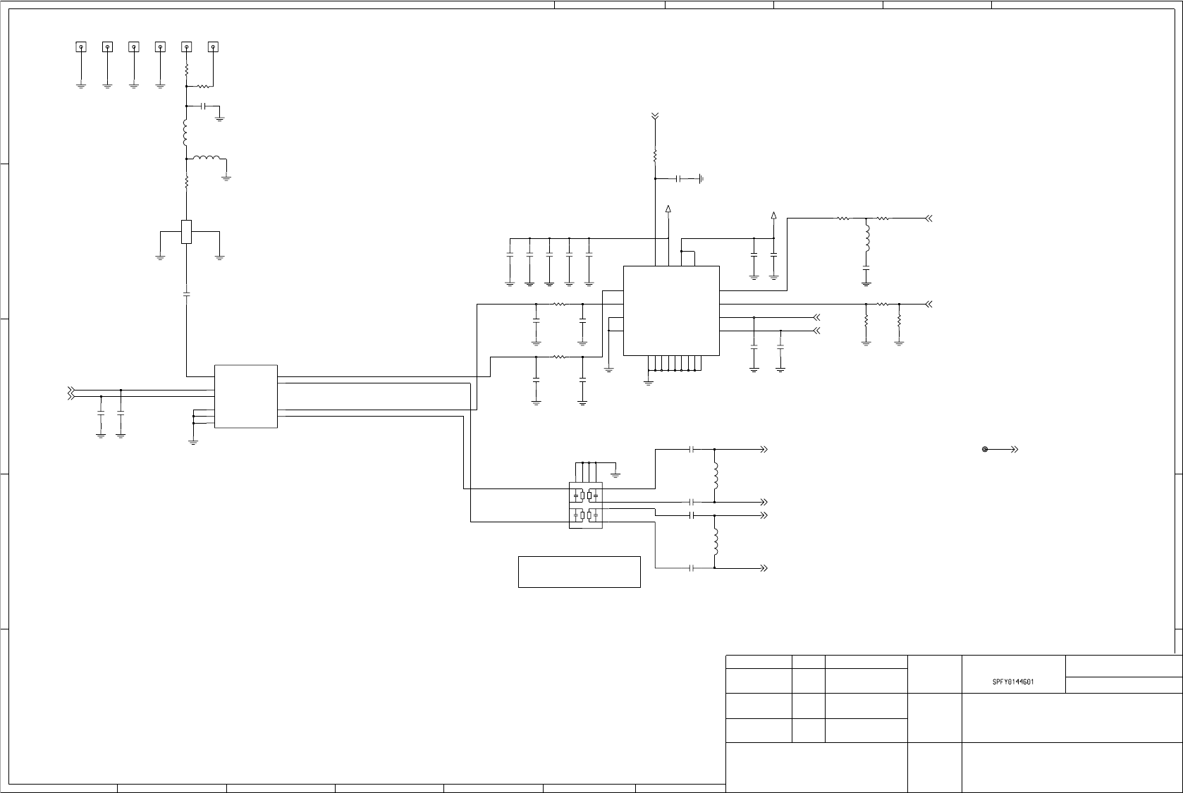
- 92 -
4
A
GB3_RADIO
11/16
4
Checked
7
IN CASE OF GSM850/PCS1900
1
D
CHANGE THIS DUAL SAW FILTER
(50V,J,NP0)
E
PART_NO SFSB0001401
2006
6
NO.
Date
1
LG Electronics Inc.
(50V,J,NP0)
DRAWING
D
Sign & Name
3
A
VER-1.1
LGIC(42)-A-5505-10:01
8
(2012)
LG Electronics Inc.
52
Designer MODEL
Approved
A
6
2006
2
B
5 7 9
Sheet/Sheets
RF
4/4
(16V,K,X7R)
(10V,Z,Y5V)
(50V,J,NP0)
10
KEE-OUN.PARK
C
2006
C
Section
TO PART_NO SFSB0001301
3
DRAWING
(16V,K,X7R)
(50V,J,NP0)
NAME
VBAT
C414
27p
TP403
C410
VBAT
L402
NA
22p
R403
0
C400 1p
TP406
TP401
27p
C407 C408
3pC421
0.01u
GND7
13
14 GND8
16 GND9
P_GND
21
RSVD_GND
19
20
VAPC
VBATT 17
VCC1A 2
VCC1B 6
1
BS
3
DCS_PCS_INDCS_PCS_OUT
15
EGSM_IN 4
EGSM_OUT
11
18
ENABLE
5GND1
GND2
7
GND3
8
9GND4
GND5
10
12 GND6
NA
U400
SKY77318
SW400
RF500
ANT
G1
G2
RF
C416
TP404
L403
18nH
C405
R407
0
33p
1
I2
4
9
O1_1
O1_2
8
O2_1
7
6
O2_2
B9308FL401
2
G1
3
G2
5
G3
10
G4
I1
C412
NA
39p
C415
NA
C401
3pC419
0
R404
C411
NA
3pC422
L404
C402
5.1nH
10u
R410
0
R408
NA
C409
NA
3pC420
TP402
C404
0.01u
R402 1K
C417
27p
0
R406
R405
0
2.2nH
L400
27p
C413
C418
27p
TP405
0R401
R400
NA
R409
TP400
NA
12p
FL400
5GND1
GND2
8
GND3
10
GSM1800_1900RX 6
1
GSM1800_1900TX
GSM850_900RX 4
2
GSM850_900TX
9IN
VC_GSM1800_1900TX
7
3VC_GSM850_900TX
C403
18p
LMSP2PAA-575TEMP
C406
22nHL401
GSM_RXN
DCS_RXN
DCS_PCS_OUT
DEFAULT_BANDSEL
TXON_PA
BS
GSM_RXP
DCS_RXP
VC2
VC1
GSM_OUT
TX_RAMP
7. CIRCUIT DIAGRAM
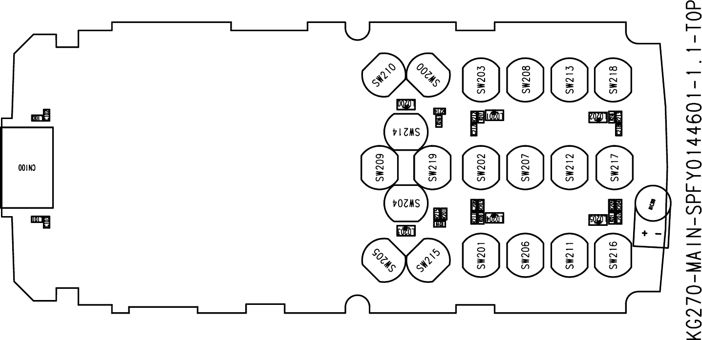
- 93 -
8. PCB LAYOUT
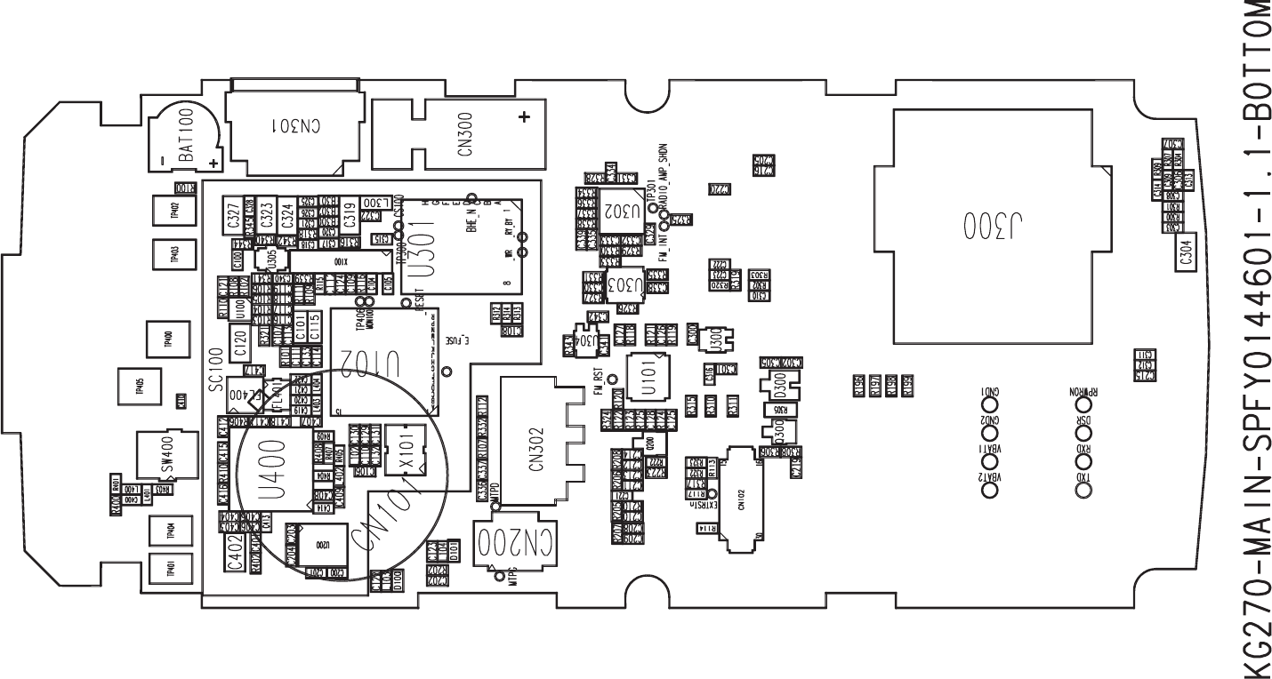
- 94 -
8. PCB LAYOUT
- 95 -
9. ENGINEERING MODE
9.1 About Engineering Mode
Engineering mode is designed to allow a service man/engineer to view and test the basic functions
provided by a handset.
9.2 Access Codes
The key sequence for switching the engineering mode on is 2945#*#. Pressing END will switch
back to non-engineering mode operation.
9.3 Key Operation
Use Up and Down key to select a menu and press ‘select’ key to progress the test. Pressing ‘back’ key
will switch back to the original test menu.
9.4 Engineering Mode Menu Tree
9. ENGINEERING MODE
ENGINEERING MODE 1. BB TEST
2. Model Version
3. Eng Mode
4. Call Timer
5. Factory Reset
6. MF Test
- 96 -
9. ENGINEERING MODE
* FM Radio function is not supported
BB TEST 1. Backlight
2. LCD
3. Battery Info
4. Vibrator
5. Audio
6. FM Radio
1. Backlight On
2. Backlight Off
3. Backlight Value
1. LCD Color
2. Contrast
1. Red
2. Green
3. Blue
4. Black
5. White
6. Auto LCD
1. Vibrator On
2. Vibrator Off
1. Audio Test
2. Close
*

- 97 -
9. ENGINEERING MODE
9.4.1 BB Test
9.4.1.1 Backlight
➀backlight on : LCD backlight is off.
➁backlight off : LCD backlight is on.
➂backlight value : LCD backlight brightness is controlled by 20% from 100 to 0.
9.4.1.2 LCD
➀LCD color : This menu includes 5 color menu and automatic color change.
5 color menu is Red, Green, Blue, Black and White.
➁LCD contrast : This menu displays a contrast value and LCD maker.
9.4.1.3 Battery Info
This menu displays the information of battery, as example battery voltage level and temperature.
In line 2, battery voltage level is displayed with average and instant value.
In line 3. battery temperature value is displayed, but this value is ADC value.
In line 4. Icon number of battery voltage is displayed.
9.4.1.4 Vibrator
This menu can control vibrator on and off operation.
9.4.1.5 Audio
This menu can control MIDI operation
- 98 -
9. ENGINEERING MODE
9.4.2 Model Version
This menu displays the Model software version.
Eng Mode 1. Serving Cell
2. Neighbour Cells
3. Reset Information
Model Version

- 99 -
9. ENGINEERING MODE
9.4.3 Eng Mode
9.4.3.1 Serving Cell
This Menu dispays the the informations of Serving Cell environment.
For example, ARFCN, RF Level etc.
ARFCN : Absolut Radio Frequency Channel Number (Frequency Number) of Serving Cell while Idle
mode
RxLev : RX level of Serving Cell while Idle mode
C1 : C1 Value of Serving Cell, This value will be used to decide cell reselection.
C2 : C2 Value of Serving Cell, This value will be used to decide cell reselection.
BPM : Paging period of Serving Cell
ARFCND : Absolut Radio Frequency Channel Number (Frequency Number) of Serving Cell while
Dedicated mode
RxLf : Full RX level of Serving Cell
RxLs : Sub RX level of Serving Cell
RxQf : Full RX qual of Serving Cell
RxQs : Sub RX qual of Serving Cell
DSC : Downlink Signal Counter
RLL : Radio Link Loss Counter
Chtyp : Channel type of Serving Cell
Chmod : Channel Mode of Serving Cell
DTX : Discontinuous Transmission mode of Serving Cell
MCC : Mobile Country Code of Serving Cell
MNC : Mobile Country Code of Serving Cell
LAC : Location Area Code of Serving Cell
CID : Cell ID of Serving Cell
BSIC : Base Tranceiver Station Identity Code of Serving Cell
TxPwrMax : MS_TXPWR_MAX_CCH value of Serving Cell
RxMin : RXLEV_ACCESS_MIN value of Serving Cell
C2vld : C2_VALID value of Serving Cell
CRoff : CELL_RESELECT_OFFSET value of Serving Cell
TMPoff : TEMPORARY_OFFSET value of Serving Cell
PTime : PENALTY_TIME value of Serving Cell
RF# : Number of frequencies in MA(Mobile Allocation)
T3212 : Periodic Location Update Timer
TxPwrLev : Current Tx power of MS
ACC : Access Control Class
Band : Current Band Information
TA : Current Timing Advance
Cipher : Cipher mode of Serving Cell
CBQ : Cell Bar Quality flag of Serving Cell
CBA : Cell Bar Access flag of Serving Cell

9. ENGINEERING MODE
- 100 -
9.4.3.2 Neighbour Cells
This menu displays the informations of Neighbour Cells.
ARFCN : Absolut Radio Frequency Channel Number (Frequency Number) of Neighbour Cell
RxLev : Rx Level of Neighbour Cell
C1 : C1 Value of Neighbour Cell, This value will be used to decide cell reselection.
C2 : C2 Value of Neighbour Cell, This value will be used to decide cell reselection.
MCC : Mobile Country Code of Neighbour Cell
MNC : Mobile Network Code of Neighbour Cell
LAC : Location Area Code of Neighbour Cell
CID : Cell ID of Neighbour Cell
BSIC : Base Tranceiver Station Identity Code of Neighbour Cell
9.4.3.3 Reset Information
This menu displays the information of reset point in source code, call stack.

9. ENGINEERING MODE
- 101 -
9.4.4 Call Timer
This menu displays the time of all calls, including the received calls.
9.4.5 Factory Reset
This menu is to format data block in the flash memory and this procedure set up the default value in
data block.
Call Timer
Factory Reset
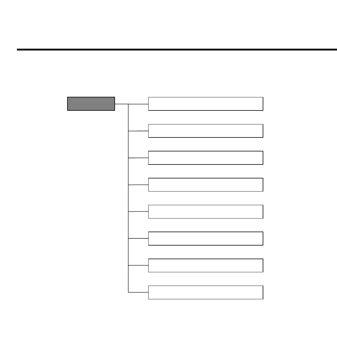
9. ENGINEERING MODE
- 102 -
* function is not supported
MF TEST 1. All auto Test
2. Backlight
3. Audio
4. Vibrator
5. LCD
6. Key Pad
7. Mic Speaker
8. FM radio
*
*

9. ENGINEERING MODE
- 103 -
9.4.6 MF TEST
This manufacturing mode is designed to do the baseband test automatically.
Selecting this menu will process the test automatically, and phone displays the previous menu after
completing the test.
9.4.6.1 All auto Test
LCD, Backlight, Vibrator, Buzzer, Key Pad
9.4.6.2 Backlight
LCD Backlight is on for about 1.5 seconds at the same time, then off.
9.4.6.3 Audio
This menu is to test the volume of Melody. It rings in the following sequence.
Volume 1, Volume 2, Volume 3, Volume 0 (mute), Volume 4, Volume 5.
9.4.6.4 Vibrator
Vibrator is on for about 1.5 seconds.
9.4.6.5 LCD
Main LCD screen resolution tests horizontally and vertically one by one and fills the screen.
9.4.6.6 Key Pad
When a pop-up message shows ‘Press Any Key’, you may press any keys.
If the key is working properly, name of the key is displayed on the screen.
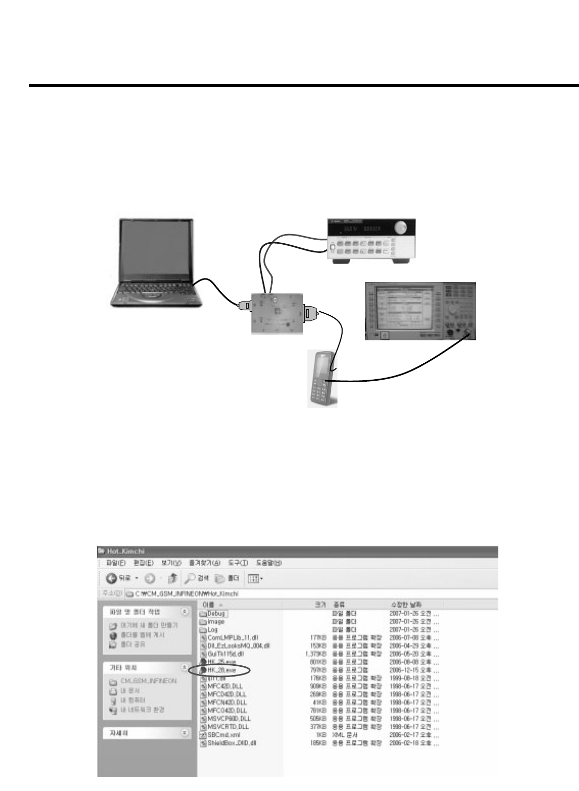
- 104 -
10. CALIBRATION
10.1 Test Equipment Setup
10.2 Calibration Steps
10.2.1 Tune on the phone
10.2.2 Execute “HK_28.exe”
10. CALIBRATION
4.000V 0.0000A
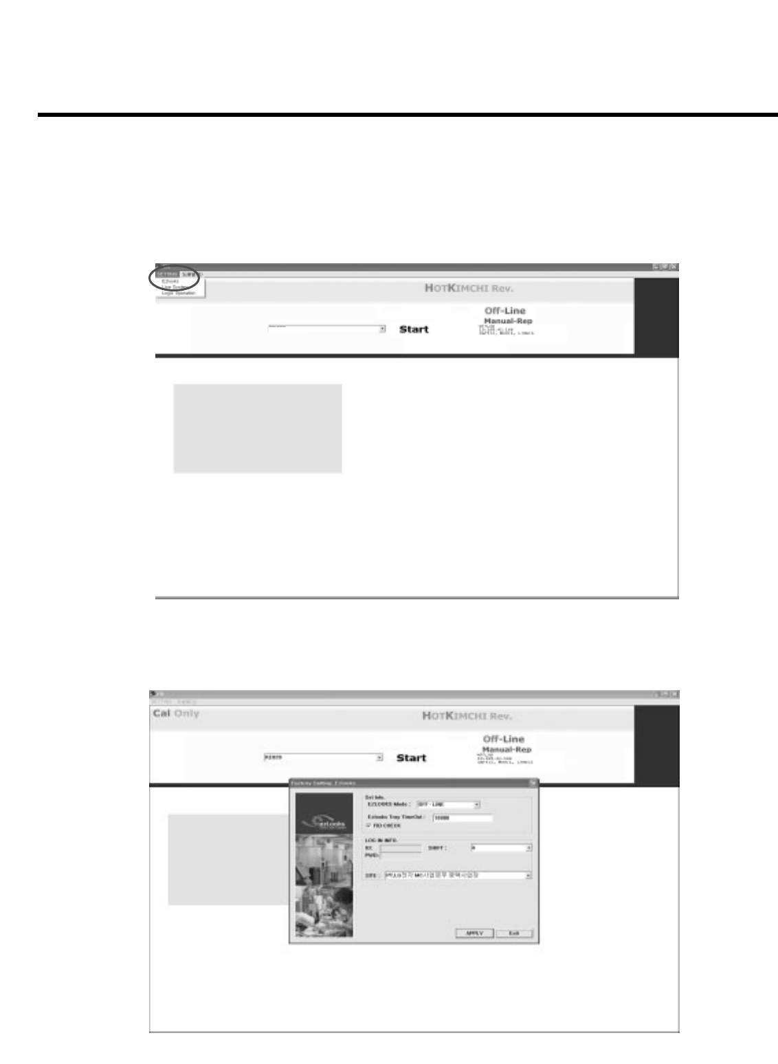
- 105 -
10. CALIBRATION
10.2.3 Click “SETTING” Memu
10.2.4 Setup “Ezlooks” menu such as the following fugure
KG278
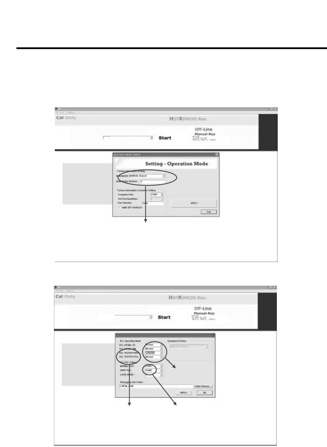
10. CALIBRATION
- 106 -
10.2.5 Setup “Line System” menu such as the following fugure
10.2.6 Setup Logic operation such as the following figure
Adjust the number of times.
KG278
PWR : Power Supply
CELL :Call-Test Equipment
Operation Mode
1. By-Pass: not control by GPIB
2. Normal : control by GPIB
Setup UART Port
KG278
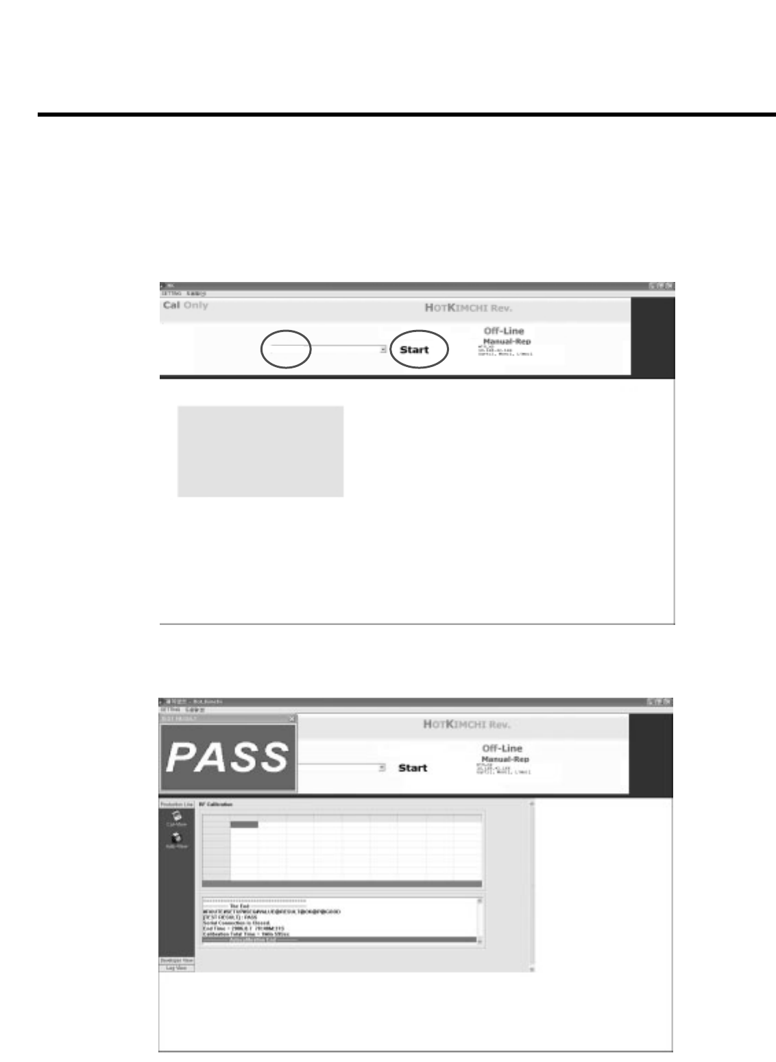
10. CALIBRATION
- 107 -
10.2.7 Select “MODEL”
10.2.8 Click “START” for RF calibration
10.2.9 RF Calibration finish
KG278
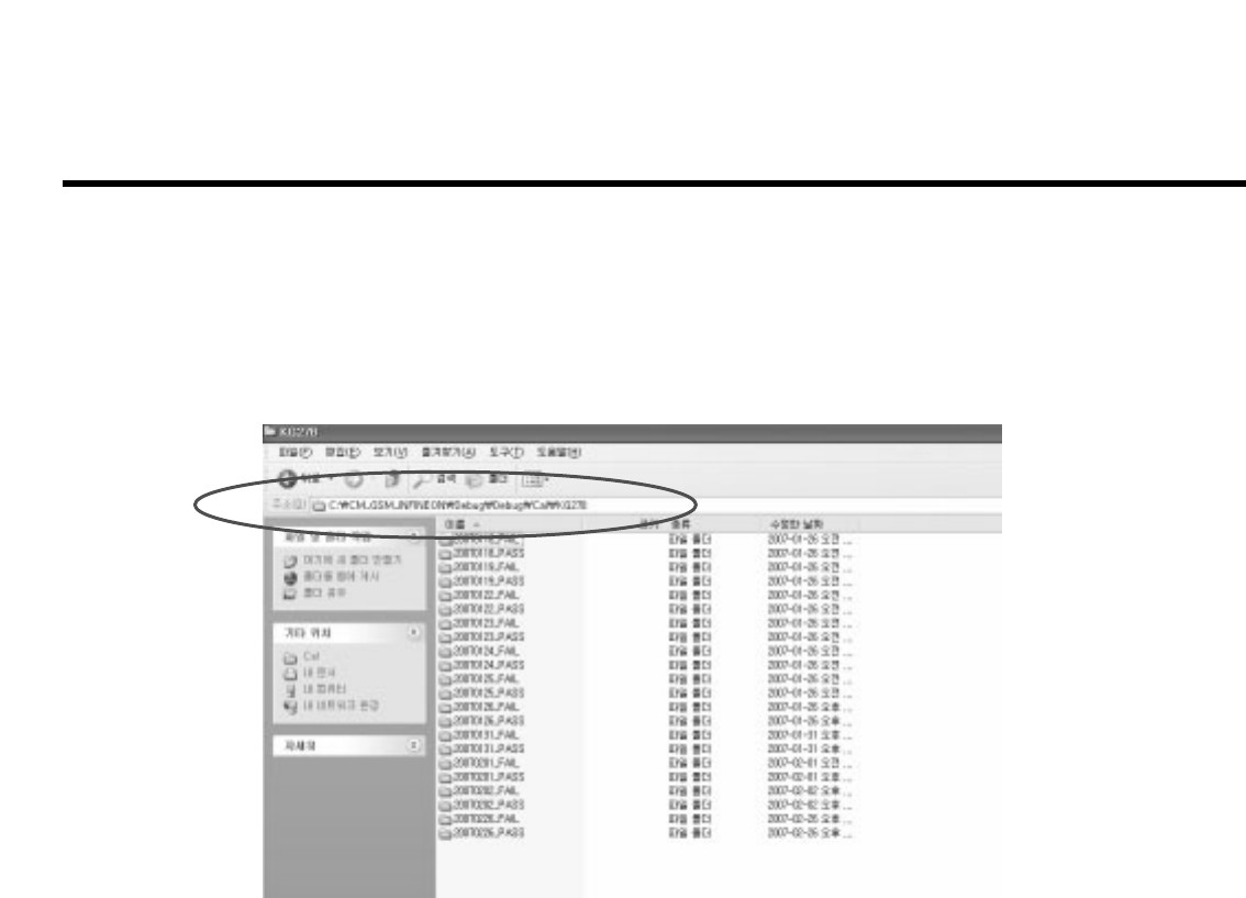
10. CALIBRATION
- 108 -
10.2.10 Calibration data will be saved to the following folder
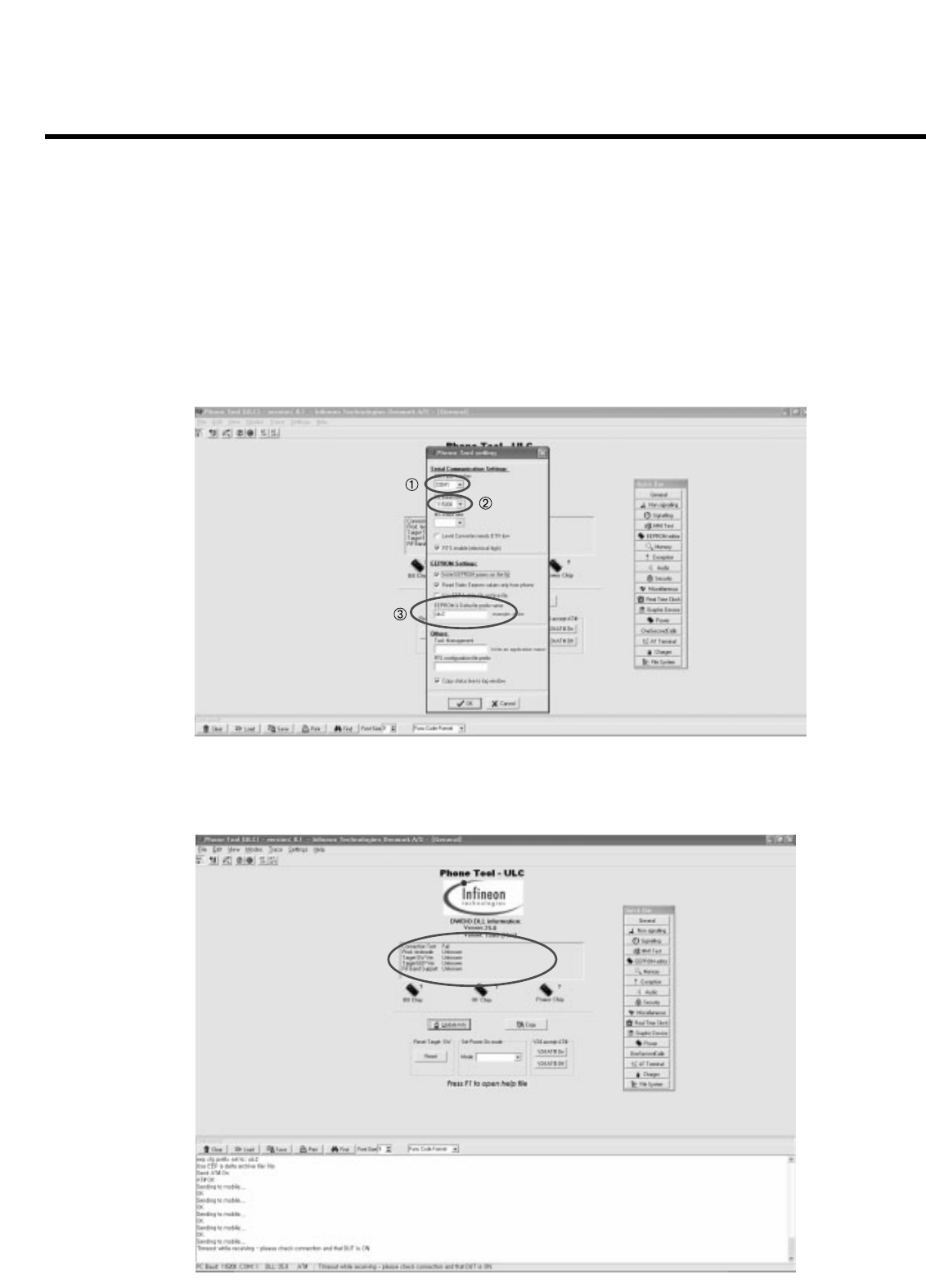
- 109 -
11. STAND ALONE TEST
11.1 Test Program Setting
11.1.1 Set COM Port
11.1.2 Check PC Baud rate(115200)
11.1.3 Confirm EEPROM & Delta file prefix name
11.1.4 Click “V24AT#ON” and then “Update Info” for communicating Phone
and Test Program
11. STAND ALONE TEST
Not Connected
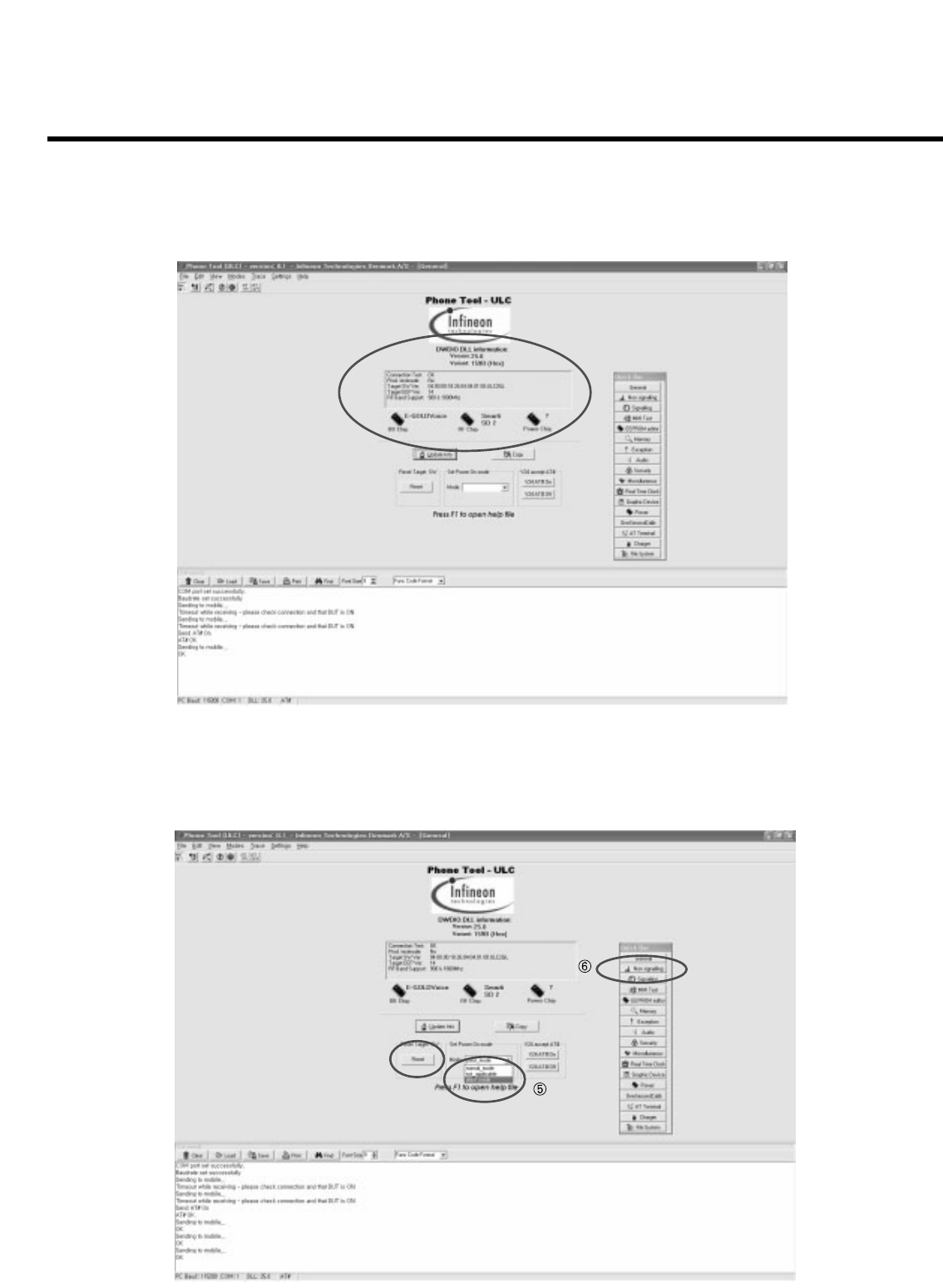
- 110 -
11. STAND ALONE TEST
11.1.5 For the purpose of the Standalone Test, Change the Phone to “ptest
mode” and then Click the “Reset” bar.
11.1.6 Select “Non signaling” in the Quick Bar menu. Then Standalone Test
setup is finished.
Connected
Change "ptest mode"
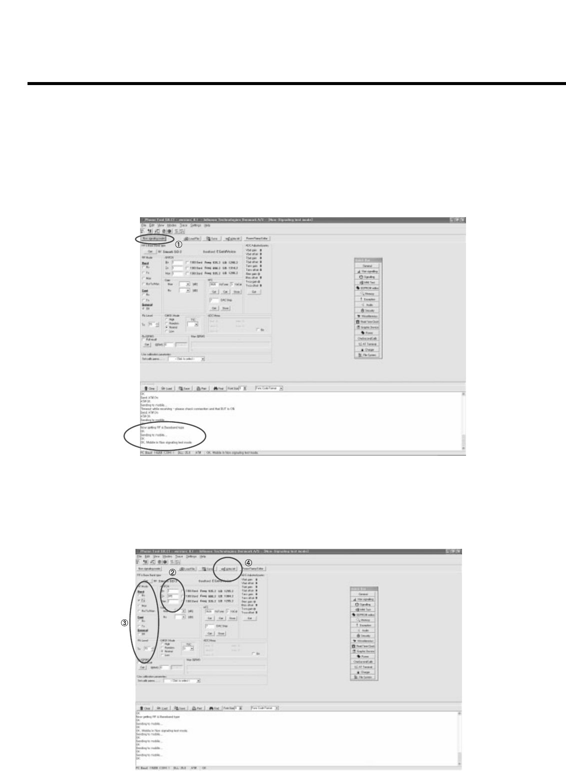
- 111 -
11. STAND ALONE TEST
11.2 Tx Test
11.2.1 Click “Non signaling mode” bar and then confirm “OK” test in the
command line
11.2.2 Put the number of TX Channel in the ARFCN
11.2.3 Select “TX” in the RF mode menu and “PCL” in the PA Level menu
11.2.4 Finally, Click “Write All” bar and try the efficiency test of Phone
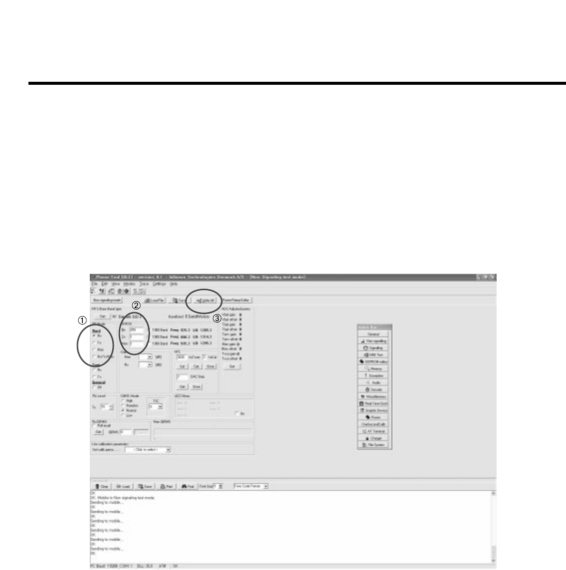
11. STAND ALONE TEST
- 112 -
11.3 RX Test
11.3.1 Put the number of RX Channel in the ARFCN
11.3.2 Select “RX” in the RF mode menu
11.3.3 Finally, Click “Write All” bar and try the efficiency test of Phone
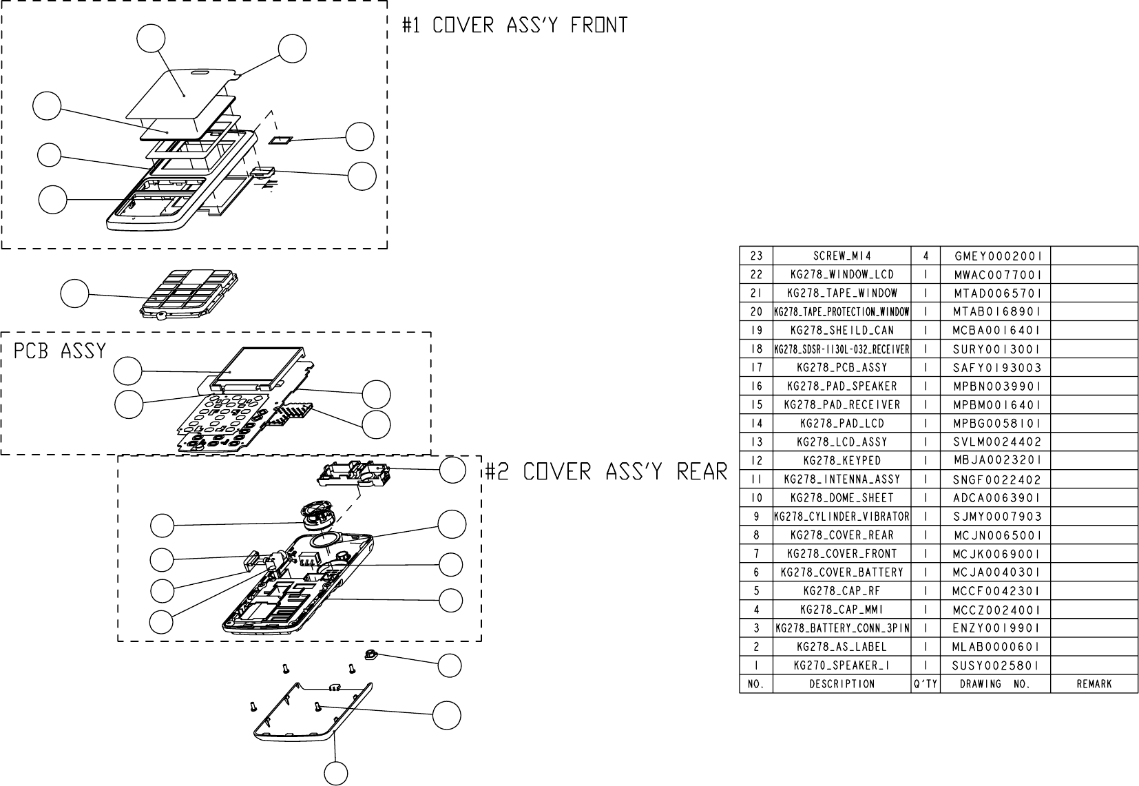
- 113 -
14
12
13
10 17
19
1
9
4
2
11
16
3
8
5
23
6
7
21
22
20
15
18
12. EXPLODED VIEW & REPLACEMENT PART LIST
12.1 EXPLODED VIEW
- 114 -
12. EXPLODED VIEW & REPLACEMENT PART LIST
- 115 -
12.2 Replacement Parts
<Mechanic component>
Level Location
No. Description Part Number Specification Color Remark
1GSM,BAR/FILP TGSM0050103 Black
2AAAY00 ADDITION AAAY0203337 Black
2APEY00 PHONE APEY0429703 Black
3ACGK00 COVER ASSY,FRONT ACGK0085205 Black
4MCJK00 COVER,FRONT MCJK0069001 MOLD, PC LUPOY SC-1004A, , , , , Black 7
4MPBG00 PAD,LCD MPBG0058101 COMPLEX, (empty), , , , , Without
Color 14
4MPBM00 PAD,RECEIVER MPBM0016401 COMPLEX, (empty), , , , , Without
Color 15
4MTAB00 TAPE,PROTECTION MTAB0168901 COMPLEX, (empty), , , , , Without
Color 20
4MTAD00 TAPE,WINDOW MTAD0065701 COMPLEX, (empty), , , , , Without
Color 21
4MWAC00 WINDOW,LCD MWAC0077002 CUTTING, PMMA MR 200, , , , , Black 22
4SURY00 RECEIVER SURY0013001 PIN ,109 dB,32 ohm,11*7 ,3T ,; , , , , , ,CONTACT , 18
3ACGM00 COVER ASSY,REAR ACGM0086801 Black
4ENZY00 CONNECTOR,ETC ENZY0019901 3 PIN,3 mm,STRAIGHT , , 3
4MCCZ00 CAP MCCZ0024001 MOLD, Urethane Rubber S185A, , , , , Black 4
4MCJN00 COVER,REAR MCJN0065001 MOLD, PC LUPOY SC-1004A, , , , , Black 8
4MLAB00 LABEL,A/S MLAB0000601 HUMIDITY STICKER Without
Color 2
4MPBN00 PAD,SPEAKER MPBN0039901 COMPLEX, (empty), , , , , Without
Color 16
3GMEY00 SCREW MACHINE,BIND GMEY0002001 1.4 mm,3 mm,MSWR3(BK) ,B ,+ ,HEAD t=0.6, HEAD d2.7 23
3MBJA00 BUTTON,DIAL MBJA0023209 COMPLEX, (empty), , , , , Black 12
3MCCF00 CAP,MOBILE SWITCH MCCF0042301 MOLD, Urethane Rubber S185A, , , , , Black 5
3MLAK00 LABEL,MODEL MLAK0006901
5ADCA00 DOME ASSY,METAL ADCA0063901 Without
Color 10
5MLAZ00 LABEL MLAZ0038301 PID Label 4 Array Without
Color
6SC100 CAN,SHIELD MCBA0016401 PRESS, NS, 0.2, , , , Without
Color 19
Note: This Chapter is used for reference, Part order
is ordered by SBOM standard on GCSC
12. EXPLODED VIEW & REPLACEMENT PART LIST
- 116 -
Level Location
No. Description Part Number Specification Color Remark
4SJMY00 VIBRATOR,MOTOR SJMY0007903 3 V,0.85 A,4*8 ,Height 5.8T Cylinder ,; ,3V , , ,11000 , , , , 9
VIBRATOR,MOTOR SJMY0007904 3 V,.1 A,4*8 ,height 5.8mm ,; ,3V , , ,11000 , , , ,
4SNGF00 ANTENNA,GSM,FIXED SNGF0022402 3.0 ,-2.0 dBd,, ,internal, GSM900/1800 ,; ,DUAL ,-2.0 ,50
,3.0 11
4SUSY00 SPEAKER SUSY0025801 PIN ,8 ohm,89 dB,16 mm, ,; , , , , , , ,CONTACT 1
3SAFY00 PCB ASSY,MAIN SAFY0193036 17
4SAFB00 PCB ASSY,MAIN,INSERT SAFB0061605
5SUMY00 MICROPHONE SUMY0003802 FPCB ,-42 dB,4*1.5 ,
5SVLM00 LCD MODULE SVLM0024402 MAIN ,128*128 ,35.78*39.7*2.7 ,65k ,CSTN ,TM ,S6B33BG
,1.52" Serial IF Only for CI 13
4SAFF00 PCB ASSY,MAIN,SMT SAFF0114336
5SAFC PCB ASSY,MAIN,SMT
BOTTOM SAFC0086602
6BAT100 BATTERY,CELL,LITHIUM SBCL0001901 3.3 V,0.025 mAh,COIN ,Capacitor type Backup Batt. Pb-Free
,; ,3.3 ,0.025mAh ,COIN
6C100 CAP,CERAMIC,CHIP ECCH0000120 39 pF,50V,J,NP0,TC,1005,R/TP
6C101 CAP,CERAMIC,CHIP ECCH0005602 2.2 uF,16V ,K ,X5R ,HD ,1608 ,R/TP
6C104 CAP,CERAMIC,CHIP ECCH0000113 18 pF,50V,J,NP0,TC,1005,R/TP
6C105 CAP,CERAMIC,CHIP ECCH0000113 18 pF,50V,J,NP0,TC,1005,R/TP
6C106 CAP,CERAMIC,CHIP ECCH0004904 1 uF,6.3V ,K ,X5R ,TC ,1005 ,R/TP
6C107 CAP,CERAMIC,CHIP ECCH0004904 1 uF,6.3V ,K ,X5R ,TC ,1005 ,R/TP
6C108 CAP,CERAMIC,CHIP ECCH0004904 1 uF,6.3V ,K ,X5R ,TC ,1005 ,R/TP
6C109 CAP,CERAMIC,CHIP ECCH0004904 1 uF,6.3V ,K ,X5R ,TC ,1005 ,R/TP
6C110 CAP,CERAMIC,CHIP ECCH0004904 1 uF,6.3V ,K ,X5R ,TC ,1005 ,R/TP
6C111 CAP,CERAMIC,CHIP ECCH0004904 1 uF,6.3V ,K ,X5R ,TC ,1005 ,R/TP
6C112 CAP,CERAMIC,CHIP ECCH0004904 1 uF,6.3V ,K ,X5R ,TC ,1005 ,R/TP
6C113 CAP,CERAMIC,CHIP ECCH0004904 1 uF,6.3V ,K ,X5R ,TC ,1005 ,R/TP
6C114 CAP,CHIP,MAKER ECZH0001216 220 nF,10V ,K ,X5R ,TC ,1005 ,R/TP
6C115 CAP,CERAMIC,CHIP ECCH0005602 2.2 uF,16V ,K ,X5R ,HD ,1608 ,R/TP
6C117 CAP,CERAMIC,CHIP ECCH0000182 0.1 uF,10V ,K ,X5R ,HD ,1005 ,R/TP
6C118 CAP,CERAMIC,CHIP ECCH0000182 0.1 uF,10V ,K ,X5R ,HD ,1005 ,R/TP
6C119 CAP,CERAMIC,CHIP ECCH0000182 0.1 uF,10V ,K ,X5R ,HD ,1005 ,R/TP
6C120 CAP,CERAMIC,CHIP ECCH0002101 1 uF,10V ,K ,B ,TC ,2012 ,R/TP
<Main component>
Note: This Chapter is used for reference, Part order
is ordered by SBOM standard on GCSC

12. EXPLODED VIEW & REPLACEMENT PART LIST
- 117 -
Level Location
No. Description Part Number Specification Color Remark
6C121 CAP,CERAMIC,CHIP ECCH0002004 0.22 uF,10V ,K ,B ,TC ,1005 ,R/TP
6C122 CAP,CERAMIC,CHIP ECCH0000182 0.1 uF,10V ,K ,X5R ,HD ,1005 ,R/TP
6C123 CAP,CERAMIC,CHIP ECCH0000182 0.1 uF,10V ,K ,X5R ,HD ,1005 ,R/TP
6C124 CAP,CERAMIC,CHIP ECCH0000143 1 nF,50V,K,X7R,HD,1005,R/TP
6C125 CAP,CHIP,MAKER ECZH0001215 1 uF,10V ,K ,X5R ,TC ,1005 ,R/TP
6C126 CAP,CHIP,MAKER ECZH0001215 1 uF,10V ,K ,X5R ,TC ,1005 ,R/TP
6C127 CAP,CERAMIC,CHIP ECCH0000157 15 nF,16V,K,X7R,HD,1005,R/TP
6C128 CAP,CERAMIC,CHIP ECCH0004904 1 uF,6.3V ,K ,X5R ,TC ,1005 ,R/TP
6C129 CAP,CERAMIC,CHIP ECCH0000182 0.1 uF,10V ,K ,X5R ,HD ,1005 ,R/TP
6C130 CAP,CERAMIC,CHIP ECCH0002002 47000 pF,10V ,K ,B ,HD ,1005 ,R/TP
6C131 CAP,CERAMIC,CHIP ECCH0004904 1 uF,6.3V ,K ,X5R ,TC ,1005 ,R/TP
6C132 CAP,CHIP,MAKER ECZH0001106 4700 pF,25V ,K ,X7R ,HD ,1005 ,R/TP
6C133 CAP,CHIP,MAKER ECZH0001106 4700 pF,25V ,K ,X7R ,HD ,1005 ,R/TP
6C200 CAP,CERAMIC,CHIP ECCH0004904 1 uF,6.3V ,K ,X5R ,TC ,1005 ,R/TP
6C201 CAP,CERAMIC,CHIP ECCH0004904 1 uF,6.3V ,K ,X5R ,TC ,1005 ,R/TP
6C202 CAP,CHIP,MAKER ECZH0000826 27 pF,50V ,J ,NP0 ,TC ,1005 ,R/TP
6C203 CAP,CHIP,MAKER ECZH0000826 27 pF,50V ,J ,NP0 ,TC ,1005 ,R/TP
6C204 CAP,CHIP,MAKER ECZH0000826 27 pF,50V ,J ,NP0 ,TC ,1005 ,R/TP
6C209 CAP,CHIP,MAKER ECZH0000826 27 pF,50V ,J ,NP0 ,TC ,1005 ,R/TP
6C210 CAP,CHIP,MAKER ECZH0000826 27 pF,50V ,J ,NP0 ,TC ,1005 ,R/TP
6C211 CAP,CHIP,MAKER ECZH0000826 27 pF,50V ,J ,NP0 ,TC ,1005 ,R/TP
6C212 CAP,CHIP,MAKER ECZH0000826 27 pF,50V ,J ,NP0 ,TC ,1005 ,R/TP
6C221 CAP,CERAMIC,CHIP ECCH0004904 1 uF,6.3V ,K ,X5R ,TC ,1005 ,R/TP
6C222 CAP,CHIP,MAKER ECZH0001215 1 uF,10V ,K ,X5R ,TC ,1005 ,R/TP
6C223 CAP,CHIP,MAKER ECZH0001215 1 uF,10V ,K ,X5R ,TC ,1005 ,R/TP
6C302 CAP,CHIP,MAKER ECZH0000826 27 pF,50V ,J ,NP0 ,TC ,1005 ,R/TP
6C303 CAP,CERAMIC,CHIP ECCH0000120 39 pF,50V,J,NP0,TC,1005,R/TP
6C304 CAP,CERAMIC,CHIP ECCH0006501 10 uF,6.3V ,K ,X5R ,TC ,2012 ,R/TP
6C305 CAP,CHIP,MAKER ECZH0000826 27 pF,50V ,J ,NP0 ,TC ,1005 ,R/TP
6C306 CAP,CERAMIC,CHIP ECCH0000161 33 nF,16V,K,X7R,HD,1005,R/TP
6C307 CAP,CERAMIC,CHIP ECCH0000182 0.1 uF,10V ,K ,X5R ,HD ,1005 ,R/TP
6C308 CAP,CERAMIC,CHIP ECCH0000120 39 pF,50V,J,NP0,TC,1005,R/TP
6C309 CAP,CERAMIC,CHIP ECCH0000161 33 nF,16V,K,X7R,HD,1005,R/TP
6C310 CAP,CERAMIC,CHIP ECCH0000115 22 pF,50V,J,NP0,TC,1005,R/TP

12. EXPLODED VIEW & REPLACEMENT PART LIST
- 118 -
Level Location
No. Description Part Number Specification Color Remark
6C311 CAP,CERAMIC,CHIP ECCH0000182 0.1 uF,10V ,K ,X5R ,HD ,1005 ,R/TP
6C312 CAP,CERAMIC,CHIP ECCH0000115 22 pF,50V,J,NP0,TC,1005,R/TP
6C313 CAP,CERAMIC,CHIP ECCH0000120 39 pF,50V,J,NP0,TC,1005,R/TP
6C314 CAP,CERAMIC,CHIP ECCH0000120 39 pF,50V,J,NP0,TC,1005,R/TP
6C315 CAP,CERAMIC,CHIP ECCH0000182 0.1 uF,10V ,K ,X5R ,HD ,1005 ,R/TP
6C316 CAP,CERAMIC,CHIP ECCH0000182 0.1 uF,10V ,K ,X5R ,HD ,1005 ,R/TP
6C317 CAP,CERAMIC,CHIP ECCH0000182 0.1 uF,10V ,K ,X5R ,HD ,1005 ,R/TP
6C319 CAP,CERAMIC,CHIP ECCH0006501 10 uF,6.3V ,K ,X5R ,TC ,2012 ,R/TP
6C320 CAP,CERAMIC,CHIP ECCH0000182 0.1 uF,10V ,K ,X5R ,HD ,1005 ,R/TP
6C321 CAP,CERAMIC,CHIP ECCH0000120 39 pF,50V,J,NP0,TC,1005,R/TP
6C322 CAP,CERAMIC,CHIP ECCH0000110 10 pF,50V,D,NP0,TC,1005,R/TP
6C323 CAP,CERAMIC,CHIP ECCH0006501 10 uF,6.3V ,K ,X5R ,TC ,2012 ,R/TP
6C324 CAP,CERAMIC,CHIP ECCH0006501 10 uF,6.3V ,K ,X5R ,TC ,2012 ,R/TP
6C325 CAP,CERAMIC,CHIP ECCH0000120 39 pF,50V,J,NP0,TC,1005,R/TP
6C326 CAP,CERAMIC,CHIP ECCH0000120 39 pF,50V,J,NP0,TC,1005,R/TP
6C327 CAP,CERAMIC,CHIP ECCH0003002 10 uF,10V ,Z ,Y5V ,HD ,2012 ,R/TP
6C328 CAP,CHIP,MAKER ECZH0000841 56 pF,50V ,J ,NP0 ,TC ,1005 ,R/TP
6C329 CAP,CERAMIC,CHIP ECCH0004904 1 uF,6.3V ,K ,X5R ,TC ,1005 ,R/TP
6C330 CAP,CERAMIC,CHIP ECCH0004904 1 uF,6.3V ,K ,X5R ,TC ,1005 ,R/TP
6C331 CAP,CHIP,MAKER ECZH0000813 100 pF,50V ,J ,NP0 ,TC ,1005 ,R/TP
6C332 CAP,CERAMIC,CHIP ECCH0000182 0.1 uF,10V ,K ,X5R ,HD ,1005 ,R/TP
6C333 CAP,CERAMIC,CHIP ECCH0000182 0.1 uF,10V ,K ,X5R ,HD ,1005 ,R/TP
6C335 CAP,CERAMIC,CHIP ECCH0000179 22 nF,16V ,K ,X5R ,HD ,1005 ,R/TP
6C336 CAP,CERAMIC,CHIP ECCH0000104 3 pF,50V,C,NP0,TC,1005,R/TP
6C337 CAP,CERAMIC,CHIP ECCH0000113 18 pF,50V,J,NP0,TC,1005,R/TP
6C338 CAP,CERAMIC,CHIP ECCH0000182 0.1 uF,10V ,K ,X5R ,HD ,1005 ,R/TP
6C339 CAP,CERAMIC,CHIP ECCH0000182 0.1 uF,10V ,K ,X5R ,HD ,1005 ,R/TP
6C340 CAP,CERAMIC,CHIP ECCH0000182 0.1 uF,10V ,K ,X5R ,HD ,1005 ,R/TP
6C341 CAP,CHIP,MAKER ECZH0001215 1 uF,10V ,K ,X5R ,TC ,1005 ,R/TP
6C342 CAP,CERAMIC,CHIP ECCH0004904 1 uF,6.3V ,K ,X5R ,TC ,1005 ,R/TP
6C400 CAP,CHIP,MAKER ECZH0000802 1 pF,50V ,C ,NP0 ,TC ,1005 ,R/TP
6C401 CAP,CERAMIC,CHIP ECCH0000120 39 pF,50V,J,NP0,TC,1005,R/TP
6C402 CAP,CERAMIC,CHIP ECCH0003002 10 uF,10V ,Z ,Y5V ,HD ,2012 ,R/TP
6C403 CAP,CHIP,MAKER ECZH0000816 12 pF,50V ,J ,NP0 ,TC ,1005 ,R/TP

12. EXPLODED VIEW & REPLACEMENT PART LIST
- 119 -
Level Location
No. Description Part Number Specification Color Remark
6C404 CAP,CERAMIC,CHIP ECCH0000155 10 nF,16V,K,X7R,HD,1005,R/TP
6C405 CAP,CHIP,MAKER ECZH0000830 33 pF,50V ,J ,NP0 ,TC ,1005 ,R/TP
6C406 CAP,CERAMIC,CHIP ECCH0000113 18 pF,50V,J,NP0,TC,1005,R/TP
6C407 CAP,CHIP,MAKER ECZH0000826 27 pF,50V ,J ,NP0 ,TC ,1005 ,R/TP
6C408 CAP,CERAMIC,CHIP ECCH0000155 10 nF,16V,K,X7R,HD,1005,R/TP
6C410 CAP,CERAMIC,CHIP ECCH0009505 22 pF,25V ,J ,NP0 ,TC ,0603 ,R/TP
6C413 CAP,CHIP,MAKER ECZH0000826 27 pF,50V ,J ,NP0 ,TC ,1005 ,R/TP
6C414 CAP,CHIP,MAKER ECZH0000826 27 pF,50V ,J ,NP0 ,TC ,1005 ,R/TP
6C417 CAP,CHIP,MAKER ECZH0000826 27 pF,50V ,J ,NP0 ,TC ,1005 ,R/TP
6C418 CAP,CHIP,MAKER ECZH0000826 27 pF,50V ,J ,NP0 ,TC ,1005 ,R/TP
6C419 CAP,CERAMIC,CHIP ECCH0000104 3 pF,50V,C,NP0,TC,1005,R/TP
6C420 CAP,CERAMIC,CHIP ECCH0000104 3 pF,50V,C,NP0,TC,1005,R/TP
6C421 CAP,CERAMIC,CHIP ECCH0000104 3 pF,50V,C,NP0,TC,1005,R/TP
6C422 CAP,CERAMIC,CHIP ECCH0000104 3 pF,50V,C,NP0,TC,1005,R/TP
6CN200 CONNECTOR,FFC/FPC ENQY0013801 13 PIN,0.3 mm,STRAIGHT , , ,; , ,0.30MM ,FPC ,STRAIGHT
,TOP ,SMD ,R/TP ,[empty] ,
6CN301 CONNECTOR,I/O ENRY0006401 18 PIN,0.4 mm,ANGLE , ,H=2.5, Reverse Type
6D300 DIODE,SWITCHING EDSY0005301 SC-70 ,80 V,0.1 A,R/TP ,
6FB300 FILTER,BEAD,CHIP SFBH0008105 1800 ohm,1005 ,Chip bead ,; ,1800ohm ,; ,[empty] ,R/TP
6FB301 FILTER,BEAD,CHIP SFBH0008105 1800 ohm,1005 ,Chip bead ,; ,1800ohm ,; ,[empty] ,R/TP
6FB302 FILTER,BEAD,CHIP SFBH0008105 1800 ohm,1005 ,Chip bead ,; ,1800ohm ,; ,[empty] ,R/TP
6FL400 FILTER,SEPERATOR SFAY0010101 850.1900 ,900.1800 ,2.0 dB,2.0 dB,2.0 dB,2.0 dB,ETC
,Dual Band ASM, 2.5x2.5x1.2
6FL401 FILTER,SAW,DUAL SFSB0001401
942.5 MHz,35 MHz,2.1 dB,20 dB,1842.5 MHz,75 MHz,2.3
dB,12 dB,2.0*1.6*0.68 ,SMD
,925M~960M,1805M~1880M,10p,B,150_82,150_15,EGSM
+DCS Rx ,; ,942.5, 1842.5 ,2.0*1.6*0.68 ,SMD ,R/TP
6J300 CONN,SOCKET ENSY0018101 6 PIN,ETC , ,2.54 mm,H=1.5
6L102 INDUCTOR,CHIP ELCH0001032 18 nH,J ,1005 ,R/TP ,PBFREE
6L103 INDUCTOR,CHIP ELCH0004715 27 nH,J ,1005 ,R/TP ,
6L104 INDUCTOR,CHIP ELCH0004715 27 nH,J ,1005 ,R/TP ,
6L300 INDUCTOR,CHIP ELCH0001556 270 nH,J ,1608 ,R/TP ,
6L400 INDUCTOR,CHIP ELCH0004721 2.2 nH,S ,1005 ,R/TP ,
6L401 INDUCTOR,CHIP ELCH0001413 22 nH,J ,1005 ,R/TP ,PBFREE
6L403 INDUCTOR,CHIP ELCH0001032 18 nH,J ,1005 ,R/TP ,PBFREE
6L404 INDUCTOR,CHIP ELCH0003814 5.1 nH,S ,1005 ,R/TP ,5.1nH,1005
6Q200 TR,BJT,NPN EQBN0007101 EMT3 ,0.15 W,R/TP ,LOW FREQUENCY

12. EXPLODED VIEW & REPLACEMENT PART LIST
- 120 -
Level Location
No. Description Part Number Specification Color Remark
6Q300 TR,BJT,NPN EQBN0007101 EMT3 ,0.15 W,R/TP ,LOW FREQUENCY
6R100 RES,CHIP,MAKER ERHZ0000506 6800 ohm,1/16W ,J ,1005 ,R/TP
6R101 RES,CHIP,MAKER ERHZ0000244 22 Kohm,1/16W ,F ,1005 ,R/TP
6R102 RES,CHIP ERHY0000278 82K ohm,1/16W,J,1005,R/TP
6R104 RES,CHIP,MAKER ERHZ0000438 20 Kohm,1/16W ,J ,1005 ,R/TP
6R105 RES,CHIP,MAKER ERHZ0000438 20 Kohm,1/16W ,J ,1005 ,R/TP
6R106 RES,CHIP,MAKER ERHZ0000438 20 Kohm,1/16W ,J ,1005 ,R/TP
6R108 RES,CHIP ERHY0000278 82K ohm,1/16W,J,1005,R/TP
6R109 RES,CHIP,MAKER ERHZ0000507 68 Kohm,1/16W ,J ,1005 ,R/TP
6R110 RES,CHIP,MAKER ERHZ0000406 100 Kohm,1/16W ,J ,1005 ,R/TP
6R111 RES,CHIP,MAKER ERHZ0000406 100 Kohm,1/16W ,J ,1005 ,R/TP
6R112 RES,CHIP,MAKER ERHZ0000287 47 Kohm,1/16W ,F ,1005 ,R/TP
6R115 RES,CHIP,MAKER ERHZ0000406 100 Kohm,1/16W ,J ,1005 ,R/TP
6R116 RES,CHIP,MAKER ERHZ0000401 0 ohm,1/16W ,J ,1005 ,R/TP
6R119 RES,CHIP ERHY0003401 1800 ohm,1/16W ,J ,1005 ,R/TP
6R122 RES,CHIP,MAKER ERHZ0000401 0 ohm,1/16W ,J ,1005 ,R/TP
6R124 RES,CHIP ERHY0008402 160 Kohm,1/16W ,F ,1005 ,R/TP
6R125 RES,CHIP,MAKER ERHZ0000406 100 Kohm,1/16W ,J ,1005 ,R/TP
6R197 RES,CHIP,MAKER ERHZ0000401 0 ohm,1/16W ,J ,1005 ,R/TP
6R202 RES,CHIP,MAKER ERHZ0000406 100 Kohm,1/16W ,J ,1005 ,R/TP
6R205 RES,CHIP,MAKER ERHZ0000483 47 ohm,1/16W ,J ,1005 ,R/TP
6R206 RES,CHIP,MAKER ERHZ0000483 47 ohm,1/16W ,J ,1005 ,R/TP
6R207 RES,CHIP,MAKER ERHZ0000483 47 ohm,1/16W ,J ,1005 ,R/TP
6R208 RES,CHIP,MAKER ERHZ0000483 47 ohm,1/16W ,J ,1005 ,R/TP
6R210 RES,CHIP,MAKER ERHZ0000406 100 Kohm,1/16W ,J ,1005 ,R/TP
6R222 RES,CHIP,MAKER ERHZ0000404 1 Kohm,1/16W ,J ,1005 ,R/TP
6R223 RES,CHIP,MAKER ERHZ0000405 10 Kohm,1/16W ,J ,1005 ,R/TP
6R300 RES,CHIP,MAKER ERHZ0000404 1 Kohm,1/16W ,J ,1005 ,R/TP
6R301 RES,CHIP,MAKER ERHZ0000443 2200 ohm,1/16W ,J ,1005 ,R/TP
6R302 RES,CHIP,MAKER ERHZ0000485 4700 ohm,1/16W ,J ,1005 ,R/TP
6R303 RES,CHIP,MAKER ERHZ0000401 0 ohm,1/16W ,J ,1005 ,R/TP
6R304 RES,CHIP ERHY0003301 100 ohm,1/16W ,J ,1005 ,R/TP
6R305 RES,CHIP,MAKER ERHZ0000702 10 ohm,1/10W ,J ,1608 ,R/TP
6R306 RES,CHIP,MAKER ERHZ0000404 1 Kohm,1/16W ,J ,1005 ,R/TP

12. EXPLODED VIEW & REPLACEMENT PART LIST
- 121 -
Level Location
No. Description Part Number Specification Color Remark
6R307 RES,CHIP ERHY0003301 100 ohm,1/16W ,J ,1005 ,R/TP
6R308 RES,CHIP,MAKER ERHZ0000406 100 Kohm,1/16W ,J ,1005 ,R/TP
6R309 RES,CHIP,MAKER ERHZ0000443 2200 ohm,1/16W ,J ,1005 ,R/TP
6R310 RES,CHIP,MAKER ERHZ0000401 0 ohm,1/16W ,J ,1005 ,R/TP
6R312 RES,CHIP,MAKER ERHZ0000406 100 Kohm,1/16W ,J ,1005 ,R/TP
6R313 RES,CHIP,MAKER ERHZ0000406 100 Kohm,1/16W ,J ,1005 ,R/TP
6R314 RES,CHIP,MAKER ERHZ0000401 0 ohm,1/16W ,J ,1005 ,R/TP
6R316 RES,CHIP,MAKER ERHZ0000529 1.5 Kohm,1/16W ,J ,1005 ,R/TP
6R317 RES,CHIP,MAKER ERHZ0000405 10 Kohm,1/16W ,J ,1005 ,R/TP
6R318 RES,CHIP,MAKER ERHZ0000443 2200 ohm,1/16W ,J ,1005 ,R/TP
6R319 RES,CHIP,MAKER ERHZ0000401 0 ohm,1/16W ,J ,1005 ,R/TP
6R320 RES,CHIP,MAKER ERHZ0000406 100 Kohm,1/16W ,J ,1005 ,R/TP
6R321 RES,CHIP,MAKER ERHZ0000406 100 Kohm,1/16W ,J ,1005 ,R/TP
6R323 RES,CHIP,MAKER ERHZ0000406 100 Kohm,1/16W ,J ,1005 ,R/TP
6R324 RES,CHIP,MAKER ERHZ0000406 100 Kohm,1/16W ,J ,1005 ,R/TP
6R326 RES,CHIP,MAKER ERHZ0000476 39 Kohm,1/16W ,J ,1005 ,R/TP
6R327 RES,CHIP,MAKER ERHZ0000401 0 ohm,1/16W ,J ,1005 ,R/TP
6R328 RES,CHIP,MAKER ERHZ0000401 0 ohm,1/16W ,J ,1005 ,R/TP
6R329 RES,CHIP,MAKER ERHZ0000438 20 Kohm,1/16W ,J ,1005 ,R/TP
6R330 RES,CHIP,MAKER ERHZ0000438 20 Kohm,1/16W ,J ,1005 ,R/TP
6R331 RES,CHIP,MAKER ERHZ0000401 0 ohm,1/16W ,J ,1005 ,R/TP
6R332 RES,CHIP,MAKER ERHZ0000401 0 ohm,1/16W ,J ,1005 ,R/TP
6R333 RES,CHIP,MAKER ERHZ0000476 39 Kohm,1/16W ,J ,1005 ,R/TP
6R334 RES,CHIP,MAKER ERHZ0000405 10 Kohm,1/16W ,J ,1005 ,R/TP
6R335 RES,CHIP,MAKER ERHZ0000406 100 Kohm,1/16W ,J ,1005 ,R/TP
6R336 RES,CHIP,MAKER ERHZ0000485 4700 ohm,1/16W ,J ,1005 ,R/TP
6R337 RES,CHIP,MAKER ERHZ0000485 4700 ohm,1/16W ,J ,1005 ,R/TP
6R338 RES,CHIP,MAKER ERHZ0000483 47 ohm,1/16W ,J ,1005 ,R/TP
6R339 RES,CHIP,MAKER ERHZ0000454 27 Kohm,1/16W ,J ,1005 ,R/TP
6R341 RES,CHIP,MAKER ERHZ0000467 330 Kohm,1/16W ,J ,1005 ,R/TP
6R343 RES,CHIP,MAKER ERHZ0000406 100 Kohm,1/16W ,J ,1005 ,R/TP
6R344 RES,CHIP,MAKER ERHZ0000450 240 Kohm,1/16W ,J ,1005 ,R/TP
6R345 RES,CHIP,MAKER ERHZ0000406 100 Kohm,1/16W ,J ,1005 ,R/TP
6R401 RES,CHIP,MAKER ERHZ0000401 0 ohm,1/16W ,J ,1005 ,R/TP

12. EXPLODED VIEW & REPLACEMENT PART LIST
- 122 -
Level Location
No. Description Part Number Specification Color Remark
6R402 RES,CHIP,MAKER ERHZ0000404 1 Kohm,1/16W ,J ,1005 ,R/TP
6R403 RES,CHIP,MAKER ERHZ0000401 0 ohm,1/16W ,J ,1005 ,R/TP
6R404 RES,CHIP,MAKER ERHZ0000401 0 ohm,1/16W ,J ,1005 ,R/TP
6R405 RES,CHIP,MAKER ERHZ0000401 0 ohm,1/16W ,J ,1005 ,R/TP
6R406 RES,CHIP,MAKER ERHZ0000401 0 ohm,1/16W ,J ,1005 ,R/TP
6R407 RES,CHIP,MAKER ERHZ0000401 0 ohm,1/16W ,J ,1005 ,R/TP
6R410 RES,CHIP,MAKER ERHZ0000401 0 ohm,1/16W ,J ,1005 ,R/TP
6SW400 CONN,RF SWITCH ENWY0004501 ,SMD , dB,H=3.6, Straight type
6U100 IC EUSY0176402 Flip-Chip CSP ,9 PIN,R/TP ,Audio Power Amplifier
6U101 IC EUSY0328601 DFN ,10 PIN,R/TP ,Li-ion charger IC, 1A, 10Pin, 3x3, DFN
6U102 IC EUSY0317401 BGA ,189 PIN,R/TP ,E-Gold voice
6U200 IC EUSY0238702 TSOPJW-12 ,12 PIN,R/TP ,3PORT Charge Pump(AAT2154
Low cost version)
6U301 IC EUSY0328001 BGA ,56 PIN,R/TP ,32Mb/4Mb , 200 nm, MirroBit
6U302 IC EUSY0320801 QFN ,20 PIN,R/TP ,FM Tuner Chip, 3*3*0.57, Pb Free
6U303 IC EUSY0142501 LLP ,8 PIN,R/TP ,Dual 105mW Headphone Amplifier
6U304 IC EUSY0223002 HVSOF5 ,5 PIN,R/TP ,150mA CMOS LDO WITH OUTPUT
CONTROL / 2.8V
6U305 IC EUSY0300101 WQFN ,10 PIN,R/TP ,Small package Dual SPDT analog
Switch, PB-Free
6U400 PAM SMPY0014001 35.5 dBm,56 %, A, dBc, dB,6x6x1.15 ,SMD ,Tri Band
6X100 X-TAL EXXY0004602 .032768 MHz,20 PPM,12.5 pF,65000 ohm,SMD
,6.9*1.4*1.3 ,
6X101 X-TAL EXXY0018404
26 MHz,10 PPM,8 pF,40 ohm,SMD ,3.2*2.5*0.6 ,12ppm at -
30'C ~ +85'C, C0 1.0pF, C1 3.6fF ,; ,26 ,10PPM ,8 , , ,SMD
,R/TP
5SAFD PCB ASSY,MAIN,SMT TOP SAFD0085602
6C102 CAP,CERAMIC,CHIP ECCH0000120 39 pF,50V,J,NP0,TC,1005,R/TP
6C103 CAP,CERAMIC,CHIP ECCH0000120 39 pF,50V,J,NP0,TC,1005,R/TP
6L100 INDUCTOR,CHIP ELCH0004711 22 nH,J ,1005 ,R/TP ,
6L101 INDUCTOR,CHIP ELCH0004711 22 nH,J ,1005 ,R/TP ,
6LD200 DIODE,LED,CHIP EDLH0006001 Blue ,1608 ,R/TP ,Blue SMD LED
6LD201 DIODE,LED,CHIP EDLH0006001 Blue ,1608 ,R/TP ,Blue SMD LED
6LD202 DIODE,LED,CHIP EDLH0006001 Blue ,1608 ,R/TP ,Blue SMD LED
6LD203 DIODE,LED,CHIP EDLH0006001 Blue ,1608 ,R/TP ,Blue SMD LED
6LD204 DIODE,LED,CHIP EDLH0006001 Blue ,1608 ,R/TP ,Blue SMD LED
6LD205 DIODE,LED,CHIP EDLH0006001 Blue ,1608 ,R/TP ,Blue SMD LED
6R201 RES,CHIP,MAKER ERHZ0000505 680 ohm,1/16W ,J ,1005 ,R/TP

12. EXPLODED VIEW & REPLACEMENT PART LIST
- 123 -
Level Location
No. Description Part Number Specification Color Remark
6R203 RES,CHIP,MAKER ERHZ0000505 680 ohm,1/16W ,J ,1005 ,R/TP
6R204 RES,CHIP,MAKER ERHZ0000505 680 ohm,1/16W ,J ,1005 ,R/TP
6R209 RES,CHIP,MAKER ERHZ0000505 680 ohm,1/16W ,J ,1005 ,R/TP
6R211 RES,CHIP,MAKER ERHZ0000505 680 ohm,1/16W ,J ,1005 ,R/TP
6R212 RES,CHIP,MAKER ERHZ0000505 680 ohm,1/16W ,J ,1005 ,R/TP
6R213 RES,CHIP,MAKER ERHZ0000505 680 ohm,1/16W ,J ,1005 ,R/TP
6R214 RES,CHIP,MAKER ERHZ0000505 680 ohm,1/16W ,J ,1005 ,R/TP
6R215 RES,CHIP,MAKER ERHZ0000505 680 ohm,1/16W ,J ,1005 ,R/TP
6R216 RES,CHIP ERHY0003301 100 ohm,1/16W ,J ,1005 ,R/TP
6R217 RES,CHIP ERHY0003301 100 ohm,1/16W ,J ,1005 ,R/TP
6R218 RES,CHIP ERHY0003301 100 ohm,1/16W ,J ,1005 ,R/TP
6R219 RES,CHIP ERHY0003301 100 ohm,1/16W ,J ,1005 ,R/TP
6R220 RES,CHIP ERHY0003301 100 ohm,1/16W ,J ,1005 ,R/TP
6R221 RES,CHIP ERHY0003301 100 ohm,1/16W ,J ,1005 ,R/TP
6SPFY00 PCB,MAIN SPFY0144601 FR-4 ,.0.8mm,BUILD-UP 4 ,KG270/KG278 Main PCB

Level Location
No. Description Part Number Specification Color Remark
3MCJA00 COVER,BATTERY MCJA0040301 MOLD, PC LUPOY SC-1004A, , , , , Black 6
3SBPL00 BATTERY PACK,LI-ION SBPL0089503
3.7 V,750 mAh,1 CELL,PRISMATIC ,WLT, BATT, Europe
Label, Pb-Free ,; ,3.7 ,750 ,0.2C ,PRISMATIC ,43x34x46 ,
,ALLTEL SILVER ,Innerpack ,Europe Label
BATTERY PACK,LI-ION SBPL0088203
3.7 V,750 mAh,1 CELL,PRISMATIC ,GB3 BATT(CMW
standard batt), Europe, Pb-Free ,; ,3.7 ,750 ,0.2C
,PRISMATIC ,43x34x46 , ,ALLTEL SILVER ,Innerpack
,Europe Label
3SGEY00 EAR PHONE/EAR MIKE SET SGEY0003209
; ,10mW ,16 OHM ,105dB ,10KHZ ,450HZ ,[empty]
,BLACK,EARPHONE HOUSING:SILVER ,18P MMI
CONNECTOR ,MONO18P(5P)LOW COST
3SSAD00 ADAPTOR,AC-DC SSAD0024901
100-240V ,5060 Hz,5.1 V,.7 A,CB/GOST ,AC-DC
ADAPTOR ,; ,100Vac~350Vac ,5.1V (+0.15, -0.2) ,700mA
,5060 , ,WALL 2P ,I/O CONNECTOR ,
ADAPTOR,AC-DC SSAD0024902
100-240V ,5060 Hz,5.2 V,0.7 A,CB/GOST ,AC-DC
ADAPTOR ,; ,100Vac~350Vac ,5.2±0.3V ,700mA ,5060 ,
,WALL 2P ,I/O CONNECTOR ,
12.3 Accessory
Note: This Chapter is used for reference, Part order
is ordered by SBOM standard on GCSC
12. EXPLODED VIEW & REPLACEMENT PART LIST
- 124 -

Note

Note
