LG KS10 Manual
User Manual: LG-KS10-Manual
Open the PDF directly: View PDF ![]() .
.
Page Count: 247 [warning: Documents this large are best viewed by clicking the View PDF Link!]
Date: July, 2007 / Issue 1.0
Service Manual Model : KS10
Service Manual
KS10

- 3 -
1. INTRODUCTION.................................. 5
1.1 Purpose ...................................................... 5
1.2 Regulatory Information ............................... 5
2. PERFORMANCE ..................................7
2.1 System Overview.........................................7
2.2 Usable environment.....................................8
2.3 Radio Performance......................................8
2.4 Current Consumption.................................14
2.5 RSSI BAR ..................................................14
2.6 Battery BAR ...............................................15
2.7 Sound Pressure Level ...............................16
2.8 Charging ....................................................16
3. TECHNICAL BRIEF............................17
3.1 General Description ...................................17
3.2 GSM Mode.................................................19
3.3 UMTS Mode...............................................23
3.4 LO Phase-locked Loop ..............................26
3.5 Off-chip RF Components ...........................29
3.6 Digital Baseband
(Stn8810 / MSM6275)................................34
3.7. Hardware Architecture ..............................36
3.8. Subsystem of STn8810 ............................39
3.9. Hardware Peripheral system of
Stn8810 ....................................................42
3.10. Subsystem of MSM6275.........................47
3.11. External memory interface......................50
3.12. Hardware sub system of MSM6275........51
3.13. Audio and sound.....................................61
3.14. Camera interface ....................................67
3.15 Bluetooth..................................................76
3.16 Main Features..........................................77
4. TROUBLE SHOOTING.......................83
4.1 RF Component ..........................................83
4.2 SIGNAL PATH ...........................................85
4.3 Checking VCXO Block...............................87
4.4 Checking Ant. Switch Module Block ..........91
4.5 Checking WCDMA Block ...........................93
4.6 Checking GSM Block...............................103
4.7 Power on trouble......................................111
4.8 USB trouble .............................................114
4.9 SIM detect trouble....................................115
4.10 Key sense trouble ..................................116
4.11 Keypad backlight trouble .......................118
4.12 Folder on/off trouble...............................120
4.13 Micro SD trouble ....................................122
4.14 Charging trouble ....................................124
4.15 Audio trouble..........................................127
4.16 Camera trouble ......................................143
4.17 Main LCD trouble...................................149
4.18 Bluetooth trouble....................................152
5. DOWNLOAD.....................................155
5.1 Composition omposition ..........................155
5.2 LGDP2 Program install LGDP2 Program
install........................................................156
5.3 USB Driver setup USB Driver setup ........159
5.4 KS10 LGDP2 run file & DLL file setup .....162
5.5 Execute LGDP2 program.........................163
6. BLOCK DIAGRAM ...........................178
6.1 GSM & WCDMA RF Block.......................178
6.2 Interface Diagram ....................................180
6.3 KS10 Modem & Baseband
Block Diagram .........................................184
6.4 KS10 Application Processor Block
Diagram ...................................................185
6.5 KS10 Audio & BT Block Diagram ............186
Table Of Contents
LGE Internal Use Only
Copyright © 2007 LG Electronics. Inc. All right reserved.
Only for training and service purposes

- 4 -
6.6 KS10 Camera Block Diagram .................187
6.7 KS10 LCD Block Diagram ......................188
6.8 KS10 Power Distribution Diagram ...........189
6.9 KS10 Clock Distribution Diagram ...........190
7. Circuit Diagram................................177
8. PCB LAYOUT ...................................202
9. Usage of Hot-Kimchi .......................209
9.1 Usage of Hot-Kimchi................................195
10. Engineering Mode .........................212
10.1 Version Info............................................213
10.2 Device Test............................................213
10.3 Factory Reset ........................................214
10.4 MTC .......................................................214
10.5 Save Log................................................214
11. EXPLODED VIEW & REPLACEMENT
PART LIST ..................................... 216
10.1 EXPLODED VIEW ................................ 216
10.2 Replacement Parts
<Mechanic component> ....................... 219
<Main component> ............................... 222
10.3 Accessory ............................................. 246
LGE Internal Use Only
Copyright © 2007 LG Electronics. Inc. All right reserved.
Only for training and service purposes

- 5 -
LGE Internal Use Only
Copyright © 2007 LG Electronics. Inc. All right reserved.
Only for training and service purposes
1.1 Purpose
This manual provides the information necessary to repair, calibration, description and download the
features of this model.
1.2 Regulatory Information
A. Security
Toll fraud, the unauthorized use of telecommunications system by an unauthorized part (for example,
persons other than your company’s employees, agents, subcontractors, or person working on your
company’s behalf) can result in substantial additional charges for your telecommunications services.
System users are responsible for the security of own system.
There are may be risks of toll fraud associated with your telecommunications system. System users
are responsible for programming and configuring the equipment to prevent unauthorized use. The
manufacturer does not warrant that this product is immune from the above case but will prevent
unauthorized use of commoncarrier telecommunication service of facilities accessed through or
connected to it. The manufacturer will not be responsible for any charges that result from such
unauthorized use.
B. Incidence of Harm
If a telephone company determines that the equipment provided to customer is faulty and possibly
causing harm or interruption in service to the telephone network, it should disconnect telephone
service until repair can be done. A telephone company may temporarily disconnect service as long as
repair is not done.
C. Changes in Service
A local telephone company may make changes in its communications facilities or procedure. If these
changes could reasonably be expected to affect the use of the phones or compatibility with the net
work, the telephone company is required to give advanced written notice to the user, allowing the user
to take appropriate steps to maintain telephone service.
D. Maintenance Limitations
Maintenance limitations on the phones must be performed only by the manufacturer or its authorized
agent. The user may not make any changes and/or repairs expect as specifically noted in this manual.
Therefore, note that unauthorized alternations or repair may affect the regulatory status of the system
and may void any remaining warranty.
1. INTRODUCTION
1. INTRODUCTION

- 6 -
LGE Internal Use Only
Copyright © 2007 LG Electronics. Inc. All right reserved.
Only for training and service purposes
E. Notice of Radiated Emissions
This model complies with rules regarding radiation and radio frequency emission as defined by local
regulatory agencies. In accordance with these agencies, you may be required to provide information
such as the following to the end user.
F. Pictures
The pictures in this manual are for illustrative purposes only; your actual hardware may look slightly
different.
G. Interference and Attenuation
A phone may interfere with sensitive laboratory equipment, medical equipment, etc. Interference from
unsuppressed engines or electric motors may cause problems.
H. Electrostatic Sensitive Devices
ATTENTION
Boards, which contain Electrostatic Sensitive Device (ESD), are indicated by the sign.
Following information is ESD handling:
• Service personnel should ground themselves by using a wrist strap when exchange system boards.
• When repairs are made to a system board, they should spread the floor with anti-static mat which is
also grounded.
• Use a suitable, grounded soldering iron.
• Keep sensitive parts in these protective packages until these are used.
• When returning system boards or parts like EEPROM to the factory, use the protective package as
described.
1. INTRODUCTION
- 7 -
LGE Internal Use Only
Copyright © 2007 LG Electronics. Inc. All right reserved.
Only for training and service purposes
2. PERFORMANCE
2.1 System Overview
2. PERFORMANCE
Item Specification
Shape GSM900/1800/1900 and WCDMA Slide Handset
Size 104 X 52 X 18.9 mm
Weight 118 g (with 950mAh Battery)
Power 3.7V normal, 950 mAh Li-Polymer
Talk Time Over 150 min (WCDMA, Tx=12 dBm, Voice)
(with 950mAh) Over 175 min (GSM, Tx=Max, Voice)
Standby Time Over 200 Hrs (WCDMA, DRX=1.28)
(with 950mAh) Over 220 Hrs (GSM, Paging period=9)
Antenna Internal type and Antenna
LCD Main 240 X 320 pixel TFT (QVGA LCD Module)
LCD Backlight Blue LED Back Light (main only)
Camera Dual Camera ; 1.3 Mega pixel (CMOS), VGA Camera (CMOS)
Vibrator Yes (Cylinder Type)
LED Indicator No
MIC Yes
Receiver Yes
Earphone Jack Yes
Connectivity Bluetooth, USB
Volume Key Push Type(+, -)
External Memory Micro-SD
I/O Connect 18 Pin
- 8 -
LGE Internal Use Only
Copyright © 2007 LG Electronics. Inc. All right reserved.
Only for training and service purposes
2.2 Usable environment
1) Environment
2) Environment (Accessory)
* CLA : 12 ~ 24 V(DC)
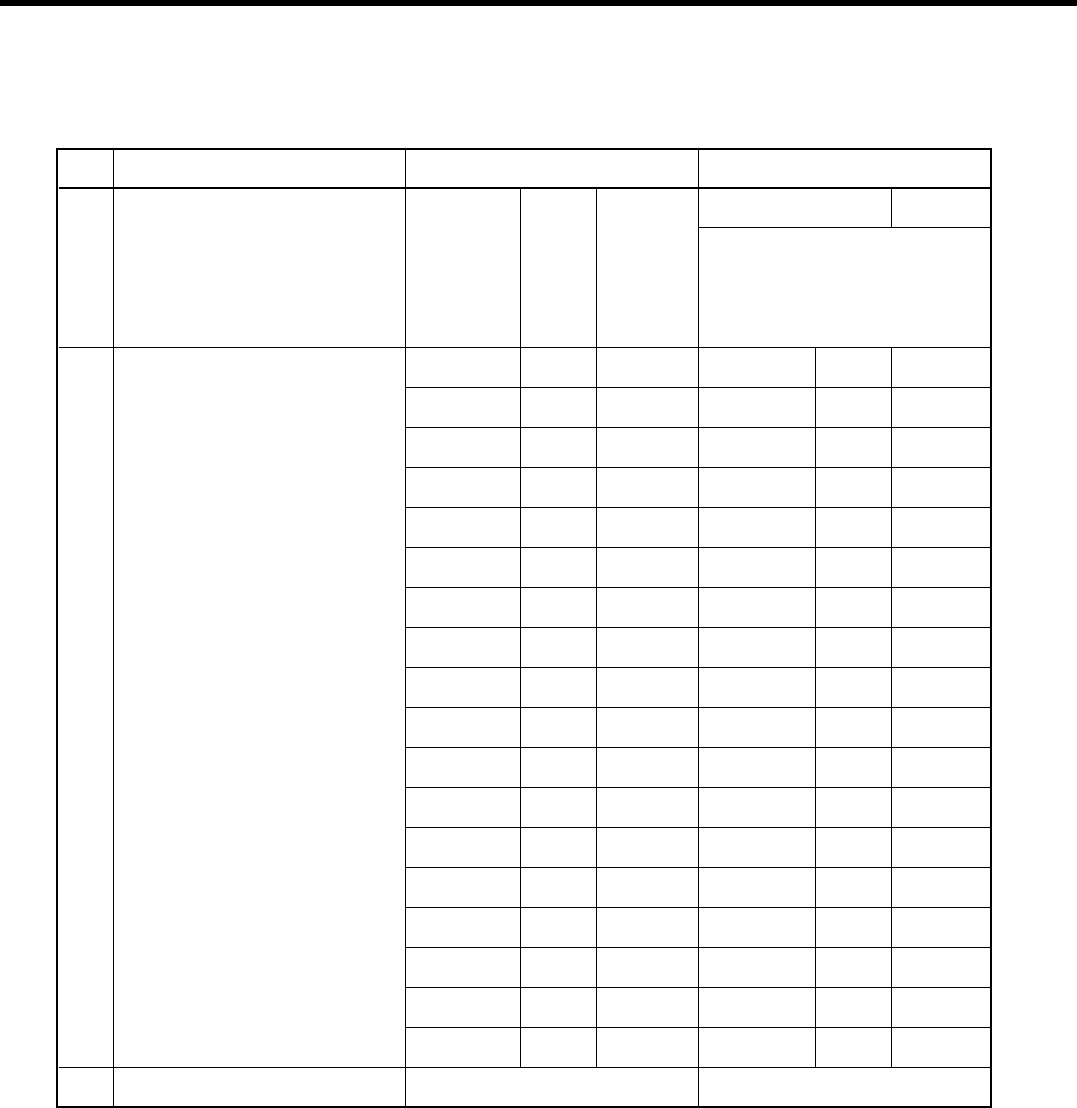
2.3 Radio Performance
1) Transmitter - GSM Mode
* In case of DCS : [A] -> 1710, [B] -> 1785 * In case of PCS : [A] -> 1850, [B] -> 1910
2. PERFORMANCE
Item Specification
Voltage 3.7 V(Typ), [Shut Down : 3.22 V]
Operation Temp -20 ~ +60°C
Storage Temp -20 ~ +70°C
Humidity 85 % (Max)
Reference Spec. Min Typ. Max Unit
TA Power Available power 100 220 240 Vac
No Item GSM DCS & PCS
100k~1GHz -39dBm
9k ~ 1GHz -39dBm
MS allocated 1G~[A]MHz -33dBm
Channel
1G~12.75GHz -33dBm
[A]M~[B]MHz -39dBm
Conducted [B]M~12.75GHz -33dBm
1Spurious 100k~880MHz -60dBm 100k~880MHz -60dBm
Emission 880M~915MHz -62dBm 880M~915MHz -62dBm
Idle Mode
915M~1GHz -60dBm 915M~1GHz -60dBm
1G~[A]MHz -50dBm 1G~[A]MHz -50dBm
[A]M~[B]MHz -56dBm [A]M~[B]MHz -56dBm
[B]M~12.5GHz -50dBm [B]M~12.5GHz -50dBm
- 9 -
LGE Internal Use Only
Copyright © 2007 LG Electronics. Inc. All right reserved.
Only for training and service purposes
2. PERFORMANCE
* In case of DCS : [A] -> 1710, [B] -> 1785 * In case of PCS : [A] -> 1850, [B] -> 1910
No Item GSM DCS & PCS
30M ~ 1GHz -36dBm
30M~1GHz -36dBm
MS allocated 1G~[A]MHz -30dBm
Channel
1G ~ 4GHz -30dBm
[A]M~[B]MHz -36dBm
Radiated [B]M~4GHz -30dBm
2Spurious 30M ~ 880MHz -57dBm 30M~880MHz -57dBm
Emission 880M ~ 915MHz -59dBm 880M~915MHz -59dBm
Idle Mode
915M~1GHz -57dBm 915M~1GHz -57dBm
1G~[A]MHz -47dBm 1G~[A]MHz -47dBm
[A]M~[B]MHz -53dBm [A]M~[B]MHz -53dBm
[B]M~4GHz -47dBm [B]M~4GHz -47dBm
3Frequency Error ±0.1ppm ±0.1ppm
4Phase Error
±5(RMS) ±5(RMS)
±20(PEAK) ±20(PEAK)
3dB below reference sensitivity 3dB below reference sensitivity
Frequency Error RA250 : ±200Hz RA250: ±250Hz
5Under Multipath and HT100 : ±100Hz HT100: ±250Hz
Interference Condition TU50 : ±100Hz TU50: ±150Hz
TU3 : ±150Hz TU1.5: ±200Hz
0 ~ 100kHz +0.5dB 0 ~ 100kHz +0.5dB
200kHz -30dB 200kHz -30dB
250kHz -33dB 250kHz -33dB
Due to 400kHz -60dB 400kHz -60dB
Output RF
modulation 600 ~ 1800kHz -60dB 600 ~ 1800kHz -60dB
61800 ~ 3000kHz -63dB 1800 ~ 6000kHz -65dB
Spectrum
3000 ~ 6000kHz -65dB ≥6000kHz -73dB
≥6000kHz -71dB
Due to
400kHz -19dB 400kHz -22dB
Switching
600kHz -21dB 600kHz -24dB
transient
1200kHz -21dB 1200kHz -24dB
1800kHz -24dB 1800kHz -27dB
- 10 -
LGE Internal Use Only
Copyright © 2007 LG Electronics. Inc. All right reserved.
Only for training and service purposes
2. PERFORMANCE
No Item GSM DCS & PCS
Frequency offset 800kHz
7Intermodulation attenuation –
Intermodulation product should
be Less than 55dB below the
level of Wanted signal
Power control
Power Tolerance
Power control
Power Tolerance
Level (dBm) (dB) Level (dBm) (dB)
533±3 030±3
631±3 128±3
729±3 226±3
827±3 324±3
925±3 422±3
10 23 ±3 5 20 ±3
8Transmitter Output Power 11 21 ±3 6 18 ±3
12 19 ±3 7 16 ±3
13 17 ±3 8 14 ±3
14 15 ±3 9 12 ±4
15 13 ±3 10 10 ±4
16 11 ±5 11 8 ±4
17 9 ±5 12 6 ±4
18 7 ±5 13 4 ±4
19 5 ±5 14 2 ±5
15 0 ±5
9Burst timing Mask IN Mask IN
- 11 -
LGE Internal Use Only
Copyright © 2007 LG Electronics. Inc. All right reserved.
Only for training and service purposes
2. PERFORMANCE
2) Transmitter - WCDMA Mode
No Item Specification
1Maximum Output Power Class 3 : +24dBm(+1/-3dB)
Class 4 : +21dBm(±2dB)
2Frequency Error ±0.1ppm
3Open Loop Power control in uplink ±9dB@normal, ±12dB@extreme
Adjust output(TPC command)
cmd 1dB 2dB 3dB
+1 +0.5/1.5 +1/3 +1.5/4.5
4Inner Loop Power control in uplink 0 -0.5/+0.5 -0.5/+0.5 -0.5/+0.5
-1 -0.5/-1.5 -1/-3 -1.5/-4.5
Group (10 equel command group)
+1 +8/+12 +16/+24
5Minimum Output Power -50dBm(3.84MHz)
Qin/Qout : PCCH quality levels
6Out-of-synchronization handling of output power Toff@DPCCH/Ior : -22 -> -28dB
Ton@DPCCH/Ior : -24 -> -18dB
7Transmit OFF Power -56dBm(3.84MHz)
8Transmit ON/OFF Time Mask
±25us
PRACH,CPCH,uplinlk compressed mode
±25us
9Change of TFC
Power varies according to the data rate
DTX : DPCH off
(minimize interference between UE)
10 Power setting in uplink compressed ±3dB(after 14slots transmission gap)
11 Occupied Bandwidth(OBW) 5MHz(99%)
-35-15*(∆f-2.5)dBc@∆f=2.5~3.5MHz,30k
12 Spectrum emission Mask
-35-1*(∆f-3.5)dBc@∆f=3.5~7.5MHz,1M
-39-10*(∆f-7.5)dBc@∆f=7.5~8.5MHz,1M
-49dBc@∆f=8.5~12.5MHz,1M
- 12 -
LGE Internal Use Only
Copyright © 2007 LG Electronics. Inc. All right reserved.
Only for training and service purposes
3)Receiver - GSM Mode
2. PERFORMANCE
No Item Specification
13 Adjacent Channel Leakage Ratio(ACLR)
33dB@5MHz, ACP>-50dBm
43dB@10MHz, ACP>-50dBm
-36dBm@f=9~150KHz, 1K BW
-36dBm@f=50KHz~30MHz, 10K BW
-36dBm@f=30MHz~1000MHz, 100K BW
14
Spurious Emissions -30dBm@f=1~12.5GHz, 1M BW
(*: additional requirement) (*)-41dBm@f=1893.5~1919.6MHz, 300K
(*)-67dBm@f=925~935MHz, 100K BW
(*)-79dBm@f=935~960MHz, 100K BW
(*)-71dBm@f=1805~1880MHz, 100K BW
15 Transmit Intermodulation
-31dBc@5MHz,Interferer -40dBc
-41dBc@10MHz, Interferer -40dBc
16 Error Vector Magnitude (EVM)
17.5%(>-20dBm)
(@12.2K, 1DPDCH+1DPCCH)
17 Transmit OFF Power
-15dB@SF=4.768Kbps, Multi-code
transmission
No Item GSM DCS & PCS
1
Sensitivity (TCH/FS Class II) -105dBm -105dBm
2
Co-Channel Rejection
C/Ic=7dB Storage -30 ~ +85
(TCH/FS Class II, RBER, TU high/FH)
3Adjacent Channel 200kHz C/Ia1=-12dB C/Ia1=-12dB
Rejection 400kHz C/Ia2=-44dB C/Ia2=-44dB
Wanted Signal :-98dBm Wanted Signal :-96dBm
4
Intermodulation Rejection 1st interferer:-44dBm 1st interferer:-44dBm
2nd interferer:-45dBm 2nd interferer:-44dBm
5
Blocking Response Wanted Signal :-101dBm Wanted Signal :-101dBm
(TCH/FS Class II, RBER)
Unwanted : Depend on Frequency Unwanted : Depend on Frequency
- 13 -
LGE Internal Use Only
Copyright © 2007 LG Electronics. Inc. All right reserved.
Only for training and service purposes
2. PERFORMANCE
4) Receiver - WCDMA Mode
No Item Specification
1Reference Sensitivity Level -106.7 dBm(3.84 MHz)
-25dBm(3.84MHz)
2Maximum Input Level -44dBm/3.84MHz(DPCH_Ec)
UE@+20dBm output power(Class3)
3Adjacent Channel Selectivity (ACS)
33dB
UE@+20dBm output power(Class3)
-56dBm/3.84MHz@10MHz
4In-band Blocking UE@+20dBm output power(Class3)
-44dBm/3.84MHz@15MHz
UE@+20dBm output power(Class3)
-44dBm/3.84MHz@f=2050~2095 and
2185~2230MHz
UE@+20dBm output power(Class3)
-30dBm/3.84MHz@f=2025~2050 and
5Out-band Blocking 2230~2255MHz
UE@+20dBm output power(Class3)
-15dBm/3.84MHz@f=1~2025 and
2255~12500MHz
UE@+20dBm output power(Class3)
6Spurious Response
-44dBm CW
UE@+20dBm output power(Class3)
-46dBm CW@10MHz
7Intermodulation Characteristic -46dBm/3.84MHz@20MHz
UE@+20dBm output power(Class3)
-57dBm@f=9KHz~1GHz, 100K BW
8Spurious Emissions -47dBm@f=1~12.5GHz, 1M BW
-60dBm@f=1920MHz~1980MHz, 3.84M BW
-60dBm@f=2110MHz~2170MHz, 3.84M BW
- 14 -
LGE Internal Use Only
Copyright © 2007 LG Electronics. Inc. All right reserved.
Only for training and service purposes
2. PERFORMANCE
2.4 Current Consumption
(Stand by Test Condition : Bluetooth off, LCD backlight off)
(Call Test Condition : Bluetooth off, LCD backlight dimming mode)
(VT Test Condition : Speaker off, LCD backlight On)
2.5 RSSI BAR
Stand by Voice Call VT
WCDMA
Under 4.32 mA Under 335 mA Under 569mA
(DRX=1.28) (Tx=10dBm -Low power) (Tx=10dBm -Low power)
Under 4.32 mA Under 380 mA
GSM (Paging=5period) (Tx=Max power)
Level Change WCDMA GSM
BAR 7 → 6-86 ±2 dBm -82 ±2dBm
BAR 6 → 5-90 ±2 dBm -86 ±2dBm
BAR 5 → 4-94 ±2 dBm -90 ±2dBm
BAR 4 → 3-98 ±2 dBm -94 ±2dBm
BAR 3 → 2-102 ±2 dBm -98 ±2dBm
BAR 2 → 1-106 ±2 dBm -102 ±2dBm
BAR 1 → 0-110 ±2 dBm -106 ±2dBm
- 15 -
LGE Internal Use Only
Copyright © 2007 LG Electronics. Inc. All right reserved.
Only for training and service purposes
2.6 Battery BAR
2. PERFORMANCE
Indication Standby
Bar 7 3.96 ± 0.05V
Bar 7 →63.95 ± 0.05V
Bar 6 →53.86 ± 0.05V
Bar 5 →43.78 ± 0.05V
Bar 4 →33.74 ± 0.05V
Bar 3 →23.69 ± 0.05V
Bar 2 →13.63 ± 0.05V
Bar 1 →Empty 3.50 ± 0.05V
Low Voltage, 3.63,3.50 ± 0.05V (Stand-by) / 3.63, 3.50 ± 0.05V (Talk)
Warning message + tone Bar 2 → 1 / Bar 1 →Empty
Power Off 3.20 ± 0.05V
- 16 -
LGE Internal Use Only
Copyright © 2007 LG Electronics. Inc. All right reserved.
Only for training and service purposes
2. PERFORMANCE
2.7 Sound Pressure Level
2.8 Charging
- Charging Method : CC & CV (Constant Current & Constant Voltage)
- Maximum Charging Voltage : 4.2V
- Maximum Charging Current : 650mA
- Nominal Battery Capacity : 950 mAh
- Charger Voltage : 4.8V
- Charging time : Max 3 h (Except time trickle charging)
- Full charge indication current (icon stop current) : 60mA
- Low battery POP UP : 3.48V
- Low battery alarm interval : Idle - 3 min, Dedicated - 1min
- Cut-off voltage : 3.22V
No Test Item Specification
1Sending Loudness Rating (SLR) 8 ±3 dB
2Receiving Loudness Rating (RLR) Nor -4 ± 3 dB
Max -15 ± 3 dB
3Side Tone Masking Rating (STMR) Min 17 dB
4Echo Loss (EL) Min 40 dB
5Sending Distortion (SD) Refer to Table 30.3
6Receiving Distortion (RD) Refer to Table 30.4
7Idle Noise-Sending (INS) Max -64 dBm0p
8Idle Noise-Receiving (INR) Nor Under -47 dBPA
Max Under -36 dBPA
9Sending Loudness Rating (SLR) 8±3dB
10 Receiving Loudness Rating (RLR) Nor -1 ±3 dB
Max -12 ±3 dB
11 Side Tone Masking Rating (STMR) Min 25 dB
12 Echo Loss (EL) Min 40 dB
13 Sending Distortion (SD) Refer to Table 30.3
14 Receiving Distortion (RD) Refer to Table 30.4
15 Idle Noise-Sending (INS) Max -55 dBm0p
16 Idle Noise-Receiving (INR) Nor Under -45 dBPA
Max Under -40 dBPA
TDMA Noise
-. GSM : Power Level : 5
DCS/PCS : Power Level : 0
(Cell Power : -90 ~ -105 dBm)
17
-. Acoustic (Max Vol.)
MS/Headset SLR : 8
±
3dB
MS/Headset RLR : -15 ± 3dB/-12dB
(SLR/RLR : Mid-value setting)
MS
Headset
MS and
Headset
Max Under -62 dBm
- 17 -
LGE Internal Use Only
Copyright © 2007 LG Electronics. Inc. All right reserved.
Only for training and service purposes
3. TECHNICAL BRIEF
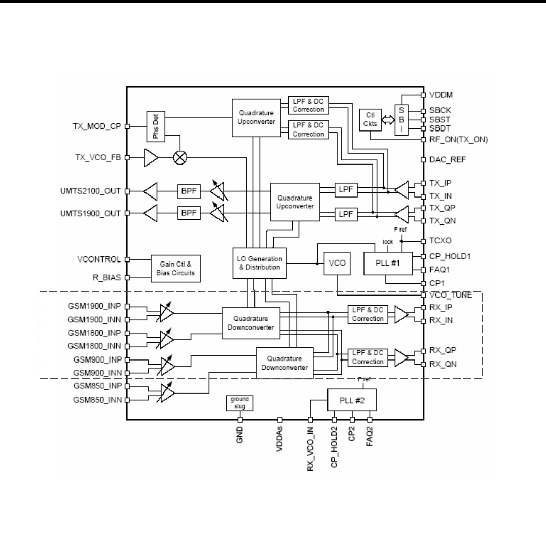
3.1 General Description
The KS10 supports UMTS-2100 DS-WCDMA, EGSM-900, DCS-1800, and PCS-1900. All receivers
and the UMTS transmitter use the radio One1Zero-IF architecture to eliminate intermediate
frequencies, directly converting signals between RF and baseband. The EGSM, DCS1800 and
PCS1900 transmitters use a baseband-to-IF up-conversion followed by an offset phase-locked loop
that translates the GMSK-modulated signal to RF.
1QUALCOMM’s branded chipset that implements a Zero-IF radio architecture.
3. TECHNICAL BRIEF
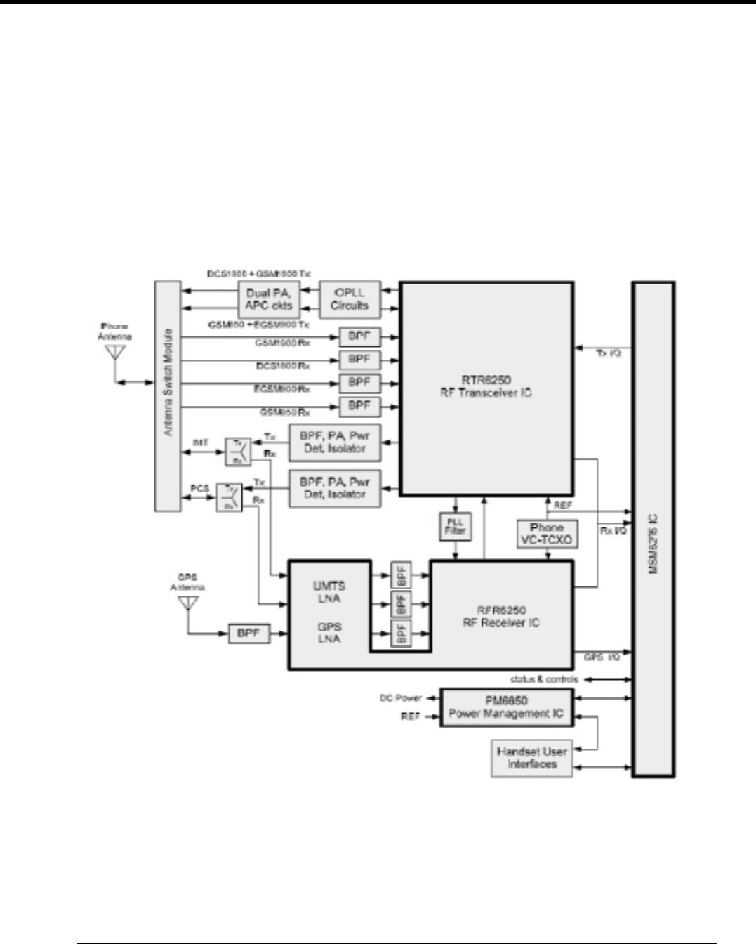
KS10 high-level RF functional block diagram

- 18 -
LGE Internal Use Only
Copyright © 2007 LG Electronics. Inc. All right reserved.
Only for training and service purposes
A generic, high-level functional block diagram of KS10 is shown in Figure 1-1. One antenna collects
base station forward link signals and radiates handset reverse link signals. The antenna connects with
receive and transmit paths through a switch module (plus a duplexer for UMTS-2100 operation).
UMTS band signals at the antenna are switched to the relevant UMTS duplexer. The UMTS receive
band signals are amplified by the front-end LNAs of the RFR6250 IC before passing through a band-
pass filter and being applied to the mixer inputs of the RFR6250 IC. On-chip circuits down-convert the
received signal directly from RF to baseband using radioOne Zero-IF techniques. Generation and
distribution of the UMTS LO, for the down-converter, is performed entirely on-chip (except for the loop
filter). The RFR6250 IC outputs analog baseband signals for processing by the MSM device. This
baseband interface is shared with the RTR6250 GSM receiver outputs, but is separate from the GPS
baseband interface.
EGSM, DCS and PCS receive signals from the antenna switch module pass through their band-pass
filters, then are applied to the RTR6250 IC. In a similar fashion to the UMTS paths, RTR6250 IC
circuits down-convert the received signals directly from RF to baseband. The GSM LO for multiband
down conversion is entirely generated within the RTR6250 IC (PLL and distribution functions) with
exception of the off-chip loop filter. The RTR analog baseband outputs are routed to the MSM6275 IC
for further processing (an interface shared with the RFR UMTS receive paths).
The UMTS transmit path begins with analog baseband signals from the MSM device that drive the
RTR6250 IC. Integrated PLL and VCO circuits generate the Tx LO used in the quadrature upconverter
that translates baseband signals directly to RF. The RTR6250 output driver stages deliver fairly high-
level signals that are filtered and applied to the power amplifiers (PA). The PA output is routed to the
antenna through a duplexer and switch module.
The shared EGSM-900, DCS-1800, and PCS-1900 transmit path begins with the same baseband
interface from the MSM6275 IC that is used for the UMTS band. A single EGSM/DCS/PCS quadrature
upconverter translates the GMSK-modulated signal to a convenient intermediate frequency (IF) that
forms one input to an offset phase-locked loop (OPLL). OPLL functions are split between the
RTR6250 IC and off-chip loop filter and dual Tx VCO circuits, and translate the GMSK-modulated
signal to the desired EGSM-900, DCS-1800 or PCS-1900 channel frequency. This signal is applied to
a dual power amplifier (only one is active at a time). The enabled path continues with the PA, an
automated power control (APC) circuit that samples the transmit power and adjusts its level, the switch
module (which includes a band-appropriate lowpass filter), and the antenna.
KS10 power supply voltages are managed and regulated by the PM6250 Power Management IC. This
versatile device integrates all wireless handset power management, general housekeeping, and user
interface support functions into a single mixed signal IC. It monitors and controls the external power
source and coordinates battery recharging while maintaining the handset supply voltages using low
dropout, programmable regulators.
The device’s general housekeeping functions include an ADC and analog multiplexer circuit for
monitoring on-chip voltage sources, charging status, and current flow, as well as userdefined off-chip
variables such as temperature, RF output power, and battery ID. Various oscillator, clock, and counter
circuits support IC and higher-level handset functions. Key parameters such as under-voltage lockout
and crystal oscillator signal presence are monitored to protect against detrimental conditions.
3. TECHNICAL BRIEF

- 19 -
LGE Internal Use Only
Copyright © 2007 LG Electronics. Inc. All right reserved.
Only for training and service purposes
3. TECHNICAL BRIEF
3.2 GSM Mode
3.2.1 GSM Receiver
The Dual-mode KS10’s receiver functions are split between the two RFICs as follows:
• UMTS-2100 operation uses the RFR6250 Receiver ICs to implement the receive signal path,
accepting an RF input and delivering analog baseband outputs (I and Q).
• EGSM-900, DCS-1800, and PCS-1900 modes both use the RTR6250 IC only. Each mode has
independent front-end circuits and down-converters, but they share common baseband circuits (with
only one mode active at a time). All receiver control functions are beginning with SBI2-controlled
parameters.
The EGSM, DCS, and PCS receiver inputs of RTR6250 are connected directly to the transceiver front-
end circuits(filters and antenna switch module). EGSM, DCS, and PCS receiver inputs are similar to
the RFR6250 UMTS Rx input in that they also use differential configurations to improve common-
mode rejection and second-order non-linearity performance.
The balance between the complementary signals is critical and must be maintained from the RF filter
outputs all the way into the IC pins Since EGSM, DCS, and PCS signals are time-division duplex (the
handset can only receive or transmit at one time), switches are used to separate Rx and Tx signals in
place of frequency duplexers - this is accomplished in the switch module.
The EGSM, DCS, and PCS receive signals are routed to the RTR6250 through band selection filters
and matching networks that transform single-ended 50-Ω sources to differential impedances optimized
for gain and noise figure. Similar to the RFR, the RTR input uses a differential configuration to improve
second-order inter-modulation and common mode rejection performance. The RTR6250 input stages
include MSM-controlled gain adjustments that maximize receiver dynamic range.
The amplifier outputs drive the RF ports of the quadrature RF-to-baseband downconverters.
The downconverted baseband outputs are multiplexed and routed to lowpass filters (one I and one Q)
having passband and stopband characteristics suitable for GMSK processing. These filter circuits
include DC offset corrections. The filter outputs are buffered and passed on to the MSM6275 IC for
further processing (an interface shared with the RFR6250 UMTS receiver outputs).
2The RFIC operating modes and circuit parameters are MSM-controlled through the proprietary 3-line Serial Bus Interface (SBI). The Application
Programming Interface (API) is used to implement SBI commands. The API is documented in AMSS Software - please see applicable AMSS
Software documentation for details.
- 20 -
LGE Internal Use Only
Copyright © 2007 LG Electronics. Inc. All right reserved.
Only for training and service purposes
3. TECHNICAL BRIEF
- 21 -
LGE Internal Use Only
Copyright © 2007 LG Electronics. Inc. All right reserved.
Only for training and service purposes
3. TECHNICAL BRIEF
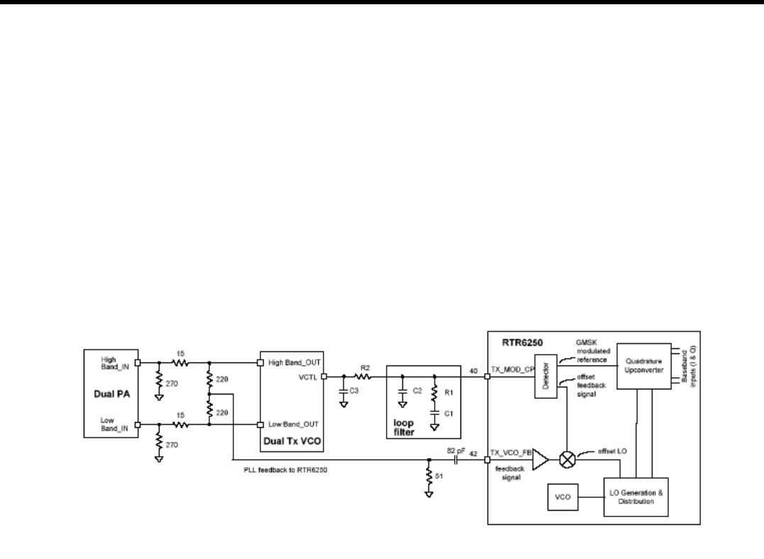
3.2.2 GSM Transmitter
The shared GSM Low-band (EGSM900) and High-band (DCS1800, PCS1900) transmit path begins
with the baseband inputs from the MSM6275 IC. These differential analog input signals are buffered,
lowpass filtered, corrected for DC offsets then applied to the GSM quadrature upconverter. The
upconverter LO signals are generated from the transceiver VCO signal by the LO distribution and
generation circuits within RTR6250. This upconverter translates the GMSK-modulated signal to a
convenient intermediate frequency (IF) that forms one input to a frequency/phase detector circuit. This
IF signal is the reference input to an offset phase-locked loop (OPLL) circuit as shown in Figure 1.2.2-1.
The feedback path of this OPLL circuit includes a downconversion from the RF output frequency range
to the IF range. The two inputs to this downconversion mixer are formed as follows:
1. The dual Tx VCO output (operating in the desired RF output frequency range) is buffered within the
RTR6250 IC then applied to the mixer RF port.
2. The LO Generation and Distribution circuits that deliver the transmit path.s LO for the baseband-to-IF
upconversion also provides the offset LO signal that is applied to the feedback path.s mixer LO port.
Figure 1.2.2-1 Offset phase-locked loop interfaces

- 22 -
LGE Internal Use Only
Copyright © 2007 LG Electronics. Inc. All right reserved.
Only for training and service purposes
The mixer IF port output is the offset feedback signal - the variable input to the frequency/phase
detector circuit. The detector compares its variable input to its reference input and generates an error
signal that is lowpass filtered by the loop filter and applied to the dual Tx VCO tuning port to force the
VCO output in the direction that minimizes errors. As mentioned earlier, the VCO output is connected to
the feedback path thereby creating a closed-loop control system that will force frequency and phase
errors between the variable and reference inputs to zero.
The waveform at the dual Tx VCO output is the GMSK-modulated signal centered at the desired GSM
channel frequency. A phase-locked loop circuit is used to translate the GMSKmodulated signal from IF
to RF primarily for two reasons:
1. Phase-locked loops provide a lowpass filter function from the reference input to the VCO output.
These results in a bandpass function centered at the desired channel frequency that provides steep,
well-controlled rejection of the out-of-band spectrum.
2. The resulting output bandpass function is virtually unchanged as the transmitter is tuned over
channels spanning the GSM operating band.
The PA is a key component in any transmitter chain and must complement the rest of the transmitter
precisely. For GSM band operation, the closed-loop transmit power control functions add even more
requirements relative to the UMTS PA. In addition to gain control and switching requirements, the usual
RF parameters such as gain, output power level, several output spectrum requirements, and power
supply current are critical. The gain must be sufficient and variable to deliver the desired transmitter
output power given the VCO output level, the subsequent passive devices’ losses, and the control set
point. The maximum and minimum transmitter output power levels depend upon the operating band
class and mobile station class per the applicable standard. Transmitter timing requirements and in-band
and out-of-band emissions, all dominated by the PA, are also specified by the applicable standard.
The active dual Tx VCO output is applied to the dual power amplifier to continue the transmit path, and
feedback to the RTR6250 IC to complete the frequency control loop. The PA operating band (EGSM or
DCS/PCS) is selected by the MSM device GPIO control. (GSM_PA_BAND).
3. TECHNICAL BRIEF

- 23 -
LGE Internal Use Only
Copyright © 2007 LG Electronics. Inc. All right reserved.
Only for training and service purposes
3. TECHNICAL BRIEF
3.3 WCDMA Mode
3.3.1 Receiver
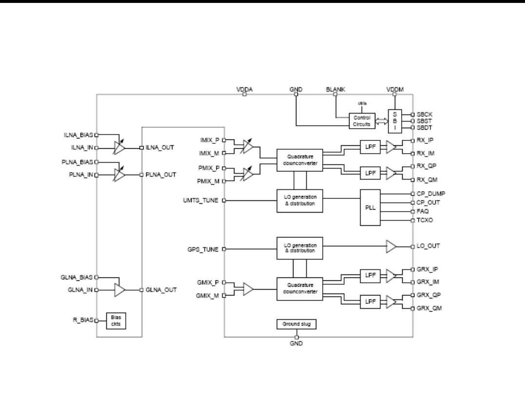
The UMTS duplexer receiver output is routed to LNA circuits within the RFR6250 IC. The LNA gain is
dynamically controlled by the MSM6275 IC to cover full receiver dynamic range and to save current
consumption.
The UMTS LNA output is routed to the down conversion mixer inputs, in the RFR6250 IC, through a
band selection filter that transforms a single-ended 50-Ω source to differential 100-Ω load impedance
that is matched to the RFR6250 IC. The RFR input uses a differential configuration to improve second-
order inter-modulation and common mode rejection performance. The RFR6250 IC input stages include
MSM-controlled gain adjustments that further extend receiver dynamic range.
The amplifier output drives the RF port of the quadrature RF-to-baseband down-converter. The down-
converted baseband outputs are routed to low-pass filters (one I and one Q) having pass-band and
stop-band characteristics suitable for DS-WCDMA processing. The filter outputs are buffered and
passed on to the MSM6275 IC for further processing. This baseband interface is shared with the
RTR6250 GSM receiver outputs.
The RFR6250 IC includes LO generation and distribution circuitry to reduce off-chip component
requirements. The GPS RX LO source is created using the PLL control elements of the RTR6250
PLL2, via a discrete loop filter components, in tandem with the VCO in the RFR6250. Using only this
PLL signal, the RFR6250 LO generation and distribution circuits create the necessary LO signals for
the UMTS quadrature down-converter. By definition, the ZIF down-converter requires FLO equal to FRF,
and the RTR6250/RFR6250 design achieves this without allowing FVCO to equal FRF.
- 24 -
LGE Internal Use Only
Copyright © 2007 LG Electronics. Inc. All right reserved.
Only for training and service purposes
3. TECHNICAL BRIEF
Figure 1.3.1-1 RFR6250 IC functional block diagram

- 25 -
LGE Internal Use Only
Copyright © 2007 LG Electronics. Inc. All right reserved.
Only for training and service purposes
3.3.2 Transmitter
The UMTS transmit path begins with analog baseband signals from the MSM device that drive the
RTR6250 IC. The RTR6250 IC provides all the UMTS transmitter active signalpath circuits except the
power amplifiers. Analog (I and Q) differential signals from the MSM device are buffered, filtered, and
applied to Baseband-to-RF quadrature upconverters. Gain control is implemented on-chip. The RF
outputs include an integrated matching inductor, reducing the off-chip matching network to a single
series capacitor.
The RTR6250 UMTS output is routed to its power amplifier through a bandpass filter, and delivers fairly
high-level signals that are filtered and applied to the PA. The PA device used in KU950 is “Load
Insensitive PA”- no need to use isolator - and routed to the duplexer Tx port directly. Transmit power is
delivered from the duplexer to the antenna through the switch module.
The RTR6250 IC integrates LO generation and distribution circuits on-chip, substantially reducing off-
chip requirements. Various modes and programmable features result in a highly flexible transceiver LO
output that supports not only UMTS transmissions, but all EGSM900 and DCS1800/PCS1900 Rx and
Tx modes as well.
The UMTS Tx LO (PLL1) is generated almost entirely on-chip, requiring only the loop filter off-chip (two
capacitors and two resistors); all UMTS Tx VCO and PLL circuits are on-chip. An internal RTR6250
switch routes the internal VCO signal to the LO generation and distribution circuits to create the
necessary UMTS Tx LO signals.
3. TECHNICAL BRIEF
- 26 -
LGE Internal Use Only
Copyright © 2007 LG Electronics. Inc. All right reserved.
Only for training and service purposes
3.4 LO Phase-locked Loop
Most LO functions are fully integrated on-chip, do not require user adjustment, and need not be
considered by handset designers. QUALCOMM has established and implemented frequency plans
and LO generation schemes that support the radioOne 6250-IIseries chipset while requiring minimal
off-chip design effort. Only one area requires handset designer attention: the loop filters of each
phase-locked loop (PLL).
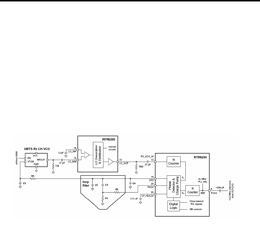
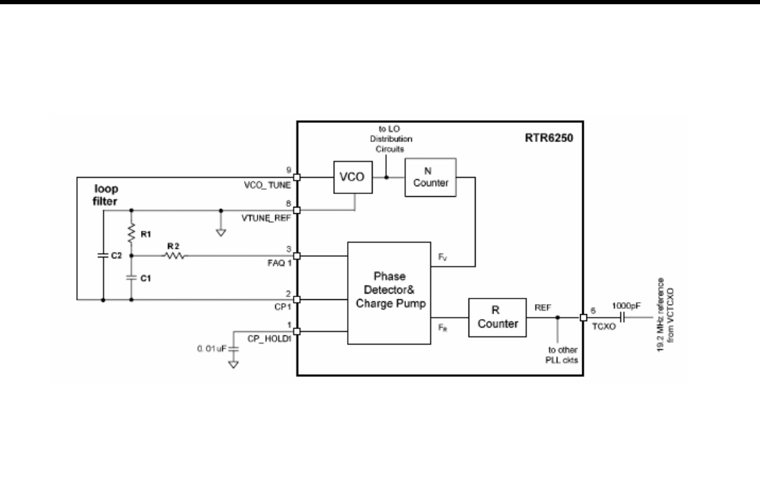
3.4.1 UMTS Rx PLL (PLL2)
UMTS Rx LO functional blocks are distributed between the RFR6250 IC, RTR6250 IC, and external
UMTS_RX_CH_VCO and loop filter components (Figure 1.4.1-1). The external UMTS_RX_CH_VCO
must be enabled for UMTS Rx operation and disabled otherwise; a dedicated MSM6275 IC signal
(UHF_VCO_EN ) enables the VCO.
3. TECHNICAL BRIEF
Figure 1.4.1-1 UMTS Rx PLL functional block diagram

- 27 -
LGE Internal Use Only
Copyright © 2007 LG Electronics. Inc. All right reserved.
Only for training and service purposes
3. TECHNICAL BRIEF
The RFR6250 IC accommodates single-ended or differential LO inputs; if single-ended, either pin can
be active. AC-couple the inactive pin to ground using an appropriately valued capacitor (12 pF is used
in KS10). The 27 pF capacitor should be used to AC-couple the active pin to the VCO signal. Using
only the selected VCO signal, the RFR6250 IC LO generation and distribution circuits create the
necessary LO signals for the active quadrature downconverter.
A sample of the downconverter LO is buffered and routed from RFR6250 IC pin 19 to RTR6250 IC pin
32 (RX_VCO_IN). This signal requires a terminating resistor near the RTR6250 IC input pin and an AC
coupling capacitor that assures the internal RTR6250 IC biasing is not disrupted in the example. Good
microstrip or stripline controlled-impedance techniques must be used.
Most UMTS Rx PLL circuits are included within the RTR6250 IC: reference divider, phase detector,
charge pump, feedback divider, and digital logic that generate LOCK status. The buffered 19.2 MHz
TCXO signal provides the synthesizer input (REF), the frequency reference to which the PLL is phase
and frequency locked. The reference is divided by the RCounter to create a fixed frequency input to
the phase detector, FR. The other phase detector input (FV) varies as the loop acquires lock, and is
generated by dividing the RX_VCO_IN frequency using the feedback path.s N-Counter. The closed
loop will force FV to equal FR when locked. If the loop is not locked the error between FV and FR will
create an error signal at the output of the charge pump. This error signal is filtered by the loop filter
and applied to the VCO, tuning the output frequency such that the error is decreased. Ultimately the
loop forces the error to approach zero and the PLL is phase and frequency locked.
Many key PLL performance characteristics are largely determined by the loop filter design - stability,
transitory response, settling time, and phase noise.
3.4.2 Transceiver PLL (PLL1)
All LO functional blocks for the other handset modes(UMTS Tx, EGSM Tx/Rx, DCS Tx/Rx, PCS
Tx/Rx) are integrated into the RTR6250 IC except the loop filter components (Figure 1.4.2-1). On-chip
circuits include reference divider, phase detector, charge pump, VCO, feedback divider, and digital
logic status. The functional description given in Section 1.4.1 for the UMTS Rx PLL applies to the
Transceiver PLL as well.
- 28 -
LGE Internal Use Only
Copyright © 2007 LG Electronics. Inc. All right reserved.
Only for training and service purposes
The off-chip loop filter allows optimization of key PLL performance characteristics (stability, transitory
response, settling time, and phase noise) for different applications. Guidelines are provided in the next
subsection for proper implementation of this critical circuit.
3. TECHNICAL BRIEF
Figure 1.4.2-1 Transceiver PLL functional block diagram

- 29 -
LGE Internal Use Only
Copyright © 2007 LG Electronics. Inc. All right reserved.
Only for training and service purposes
3. TECHNICAL BRIEF
3.5 Off-chip RF Components
3.5.1 Front End Module(FL500)
Front End module integrates antenna switch module and GSM Rx filter.
The antenna switch module allows multiple operating bands and modes to share the same antenna. In
the KS10 design, a common antenna connects to one of six paths:
1) UMTS-2100 Rx/Tx, 2) EGSM Rx, 3) DCS-1800 Rx, 4) PCS-1900 Rx, 5)EGSM Tx, and 6) DCS-
1800, PCS-1900 Tx. UMTS operation requires simultaneous reception and transmission, so the
UMTS Rx/Tx connection is routed to a duplexer that separates receive and transmit signals. GSM
band of operation is time division duplexed, so only the receiver or transmitter is active at any time
and a frequency duplexer is not required. The module includes lowpass filters for the GSM bands
transmit paths to reduce out-of-band emissions, PA harmonics in particular.
The GSM mode RF filters are located before their LNAs, so their insertion losses are extremely critical
(1.3 dB typical). Other important parameters are:
■Out-of-band rejection or attenuation levels
❏Far out-of-band signals - ranging from DC up to the first band of particular concern and from the
last band of particular concern to beyond three times the highest passband frequency.
❏Frequencies of particular concern . bands known to include other wireless transmitters that may
deliver significant power levels to the receiver input.
❏GSM band receivers operate while the handset transmitters are off so there are no Txband
leakage attenuation requirements.
■Phase and amplitude balance - the UMTS discussion presented above applies for GSM bands as
well. See the data sheet for specific values. Of course, passband ripple and return loss are still
important in all cases for the same reasons explained in the antenna switch module and duplexer
sections.
3.5.2 UMTS duplexer (U506)
A UMTS duplexer splits a single operating band into receive and transmit paths. Important
performance requirements include:
- Insertion loss . this component is also in the receive and transmit paths; In the KS10 typical losses:
UMTS Tx = 1.45 dB, UMTS Rx = 1.86 dB.
- Out-of-band rejection or attenuation . the duplexer provides input selectivity for the receiver, output
filtering for the transmitter, and isolation between the two. Rejection levels for both paths are
specified over a number of frequency ranges. Two Tx-to-Rx isolation levels are critical to receiver
performance:
- Rx-band isolation . the transmitter is specified for out-of-band noise falling into the Rx band. This
noise leaks from the transmit path into the receive path, and must be limited to avoid degrading
receiver sensitivity. The required Rx-band isolation depends on the PA out of-band noise levels and
Rx-band losses between the PA and LNA. Typical duplexer Rx band isolation value is 51 dB.
- 30 -
LGE Internal Use Only
Copyright © 2007 LG Electronics. Inc. All right reserved.
Only for training and service purposes
- Tx-band isolation . the transmit channel power also leaks into the receiver. In this case, the leakage
is outside the receiver passband but at a relatively high level. It combines with Rx band jammers to
create cross-modulation products that fall in-band to desensitize the receiver. The required Tx-band
isolation depends on the PA channel power and Tx-band losses between the PA and LNA. Typical
duplexer Tx-band isolation value is 57 dB.
- Passband ripple . the loss of this fairly narrowband device is not flat across its passband. Passband
ripple increases the receive or transmit insertion loss at specific frequencies, creating performance
variations across the bands channels, and should be controlled.
- Return loss . minimize mismatch losses with typical return losses of 10 dB or more (VSWR <2:1).
- Power handling. high power levels in the transmit path must be accommodated without degraded
performance. The specified level depends on the operating band class and mobile station class (per
the applicable standard), as well as circuit losses and antenna EIRP. Several duplexer characteristics
depend upon its source and load impedances. QUALCOMM strongly recommends an isolator be
used between the UMTS PA and duplexer to assure proper performance.
3.5.3 UMTS Power Amplifier (U505)
The AWT6277 meets the increasing demands for higher output power in UMTS handsets. The PA
module is optimized for VREF = +2.85 V, a requirement for compatibility with the Qualcomm® 6250
chipset. The device is manufactured on an advanced InGaP HBT MMIC technology offering state-of-
the-art reliability, temperature stability, and ruggedness. Selectable bias modes that optimize efficiency
for different output power levels, and a shutdown mode with low leakage current, increase handset talk
and standby time. The self-contained 4 mm x 4 mm x 1.1 mm surface mount package incorporates
matching networks optimized for output power, efficiency, and linearity in a 50 Ω system.
3. TECHNICAL BRIEF
Figure 1.5.3-1 UMTS PA functional block diagram
- 31 -
LGE Internal Use Only
Copyright © 2007 LG Electronics. Inc. All right reserved.
Only for training and service purposes
3. TECHNICAL BRIEF
3.5.4 Thermistor (R527)
This thermistor senses temperature variations around UMTS PA to adjust PA gain deviation for
assure compliance with the applicable transmit power control standards. Negative temperature
compensation thermistor is used in the KS10.
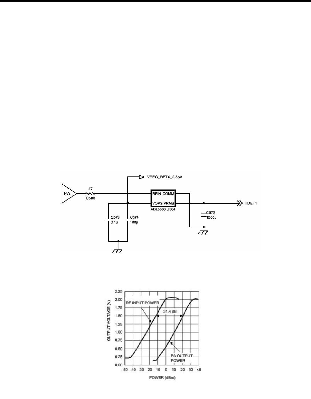
3.5.5. UMTS transmit power detector (U504)
This detector couples PA output power level to calibrate the transmitter characteristic over the channel
variation and temperature. Its detector coupling range and converted voltage is based on diode
sensitivity and transmitter power level.
The KS10 uses National Semiconductor ADL5500 power detector IC. In Figure 1.5.5-1, C580 is set to
47ohm&Coupler resulting in an attenuation of 31.4dB. The output voltage is proportional to the
logarithm of the input power. Figure1.5.5-2 shows the output voltage versus PA output power of the
ADL5500 setup as depicted in Figure1.5.5-1
Figure 1.5.5-1 Block diagram of ADL5500 with resistive tap
Figure 1.5.5-2 Power detector response, Vout vs PA output power
- 32 -
LGE Internal Use Only
Copyright © 2007 LG Electronics. Inc. All right reserved.
Only for training and service purposes
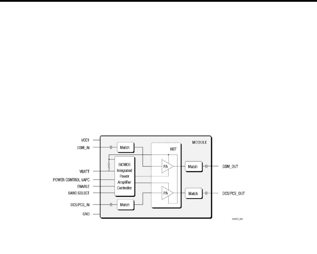
3.5.6 Dual band GSM power amplifier (U501)
The TQM7M5003 is a high-power, high-efficiency power amplifier module with integrated power
control that provides over 50dB of control range. The devices is a self-contained 6mm°ø6mm module
with 50Ω input and output terminals. The device is designed for use as the final RF amplifier in
GSM850, EGSM900, DCS and PCS hand-held digital celluar equipment and other applications in the
824MHz to 849MHz, 880MHz to 915MHz, 1710MHz to 1785MHz and 1850MHz to 1910MHz bands.
The VBATT pin connects to an internal current-sense resistor and interfaces to an integrated power
amplifier control function, which is insensitive to variations in temperature, power supply, process, and
input power. The ENABLE input allows initial turn-on of PAM circuitry to minimize battery drain.
3.5.7 GSM transmit VCO (U502)
The dual Tx VCO is a key component within the GSM OPLL. This VCO performance directly impacts
PLL and transmitter performance. VCO specifications refer to muRata MQW5V0C869M datasheet.
The dual Tx VCO outputs, one for Low-band GSM and one for high band, drive a resistive network
that splits the active signal into two signals: 1) the input to the active PA . this is the low loss path,
and 2) the OPLL feedback signal . this is the high loss path. See Figure 8-1 for recommended
topology and resistor values.
The losses from the VCO outputs to the PA inputs must be factored into the output chain.s power
budget. Each path includes a π-pad that introduces approximately a 3-dB loss. The low band GSM
π-pad is formed by R516 plus R522, R521, and R524; the high band GSM π-pad is formed by R518
plus R523, R520, and R524. One leg of each π-pad is used to couple the VCO output to form the
feedback path as described below.
For a given VCO output drive level, the loss to the RTR6250 input must assure the specified input
level is achieved (-18 to -12 dBm). Large resistors included in the π-pads are used to lightly couple
off the VCO outputs to create the feedback signal. Since the RTR6250 TX_VCO_FB pin presents
fairly high impedance. A series capacitor (82 pF) AC couples the feedback signal into the RTR6250
IC.
3. TECHNICAL BRIEF
Figure 1.5.6-1 GSM PA functional block diagram

- 33 -
LGE Internal Use Only
Copyright © 2007 LG Electronics. Inc. All right reserved.
Only for training and service purposes
3. TECHNICAL BRIEF
3.5.8 UMTS Rx RF filter (FL501)
An RF filter is located between the UMTS LNA and mixer. Insertion loss is important, but not as critical
as losses before the LNA. The most important parameters of this component include:
■Out-of-band rejection or attenuation levels, usually specified to meet these conditions:
❏Far out-of-band signals - ranging from DC up to the first band of particular concern and from the
last band of particular concern to beyond three times the highest passband frequency.
❏Tx-band leakage - the transmitter channel power, although attenuated by the duplexer, still
presents a cross-modulation threat in combination with Rx-band jammers. The RF filter must
provide rejection of this Tx-band leakage.
❏Other frequencies of particular concern . bands known to include other wireless transmitters that
may deliver significant power levels to the receiver input.
■Phase and amplitude balance - the ZIF architecture requires well-balanced differential inputs to the
RFR6250 IC. This is accomplished by the RF filter which takes a single-ended output from the
RFL6250 IC and provides differential outputs having nominal 180 phase separation. Phase and/or
amplitude imbalance causes degraded common-mode rejection and second-order nonlinearity, so
their requirements are specified jointly.
❏±3 degrees and ± 1 dB
❏-12 to + 3 degrees and ± 0.7 dB
Of course, passband ripple and return loss are still important in all cases for the same reasons
explained in the antenna switch module and duplexer sections.
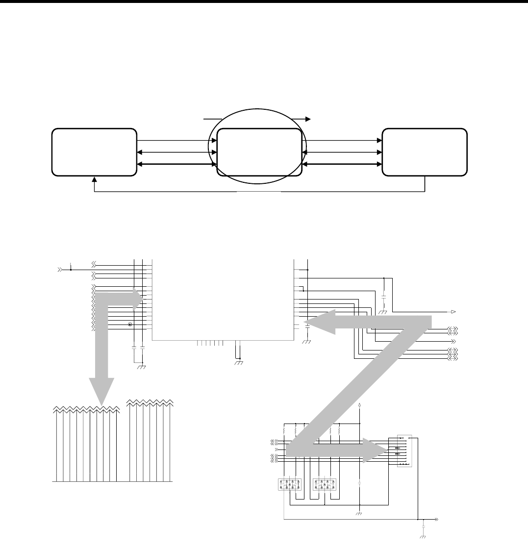
3.5.9 VCTCXO (X500)
The Voltage Controlled Temperature Compensated Crystal Oscillator (VCTCXO) provides the
reference frequency for all RFIC synthesizers as well as clock generation functions within the
MSM6275 IC. The 6275-series chipset requires a 19.2 MHz nominal VCTCXO frequency. The
oscillator frequency is controlled by the MSM6275’s TRK_LO_ADJ pulse density modulated signal in
the same manner as the transmit gain control.
The filtered PDM signal results in an analog control signal into the VCTCXO tuning port whose voltage
is directly proportional to the density of the digital bit stream. The MSM device varies the pulse density
to change the analog control voltage that sets the oscillator frequency - all within a feedback control
loop that minimizes handset frequency drift relative to the network.

- 34 -
LGE Internal Use Only
Copyright © 2007 LG Electronics. Inc. All right reserved.
Only for training and service purposes
3.6 Digital Baseband (Stn8810 / MSM6275)
3.6.1 General features of Stn8810 device
• Support for Peripheral Device & multimedia function
• Support for high-speed downlink packet access (HSDPA) - 1.8 Mbps
• Minimal support for high-level operating system such as Symbian™, Linux and WinCE® operating
systems (OSs).
• 1-Gbit NAND Flash memory, 512-Mbit DDR mobile RAM Stacked in Package
• Two DSP implementation for multimedia function
- Smart video accelerator : Programmable DSP (MMDSP+) for intermediate level processing,
clocked at 66 MHz,
- Smart audio accelerator : High-performance block, flexible sophisticated audio accelerator based
on the MMDSP+ programmable audio DSP, clocked at 133 MHz,
• ARM926EJ 32-bit RISC CPU at 350MHz
32-Kbyte instruction cache, 16-Kbyte data cache
• MultiMedia Card/SD Card/SDIO host controller
• 96 general-purpose I/Os (muxed with peripheral I/Os)
• Camera interfaces
- Supports high-resolution camera modules up to 4 Mpixels
- Serial camera interface up to 416 Mbit/s (MIPI legacy CSI)
- Parallel camera CCIR-656 interface up to 66 MHz (MIPI legacy CPI)
• Color LCD controller for STN or TFT panels or display interface for display module
- 24-bpp true color
- MIPI legacy DBI and DPI
• Host port interface (HPI)
- 16-bit parallel data bus,
- Multiplexed and non-multiplexed address/data bus,
- Indirect host access,
- Direct host access to a segment of STn8810 memory in multiplexed mode.
- Interface to modem for data communication
• I/O peripherals
- 3 autobaud UARTs (one with modem control signals) up to 3.692 Mbit/s
- 1 synchronous serial port (SSP) up to 24 Mbit/s
- 3 multichannel serial ports (MSP) up to 48 Mbit/s
- 2 I©˜C multi-master/slave interfaces
- One 8-channel, full-duplex high-speed serial interface, 108 Mbit/s
- Host port interface
- JTAG
3. TECHNICAL BRIEF
3. BB Technical Description

- 35 -
LGE Internal Use Only
Copyright © 2007 LG Electronics. Inc. All right reserved.
Only for training and service purposes
3. TECHNICAL BRIEF
3.6.2 General features of MSM6275 device
• Support for multimode operation - WCDMA(UMTS), GSM/GPRS, EDGE
• Support for high-speed downlink packet access (HSDPA) - 1.8 Mbps
• Support for WCDMA (UMTS) uplink data rate up to 384 kbps
• High-performance ARM926EJ-S running at up to 225 MHz
• ARM Jazelle Java hardware acceleration for faster Java-based games and other applets
• QDSP4000 high-performance DSP cores
• Integrated gpsOne position location technology functionality
• Integrated Bluetooth 1.2 baseband processor for wireless connectivity to peripherals
• High-speed, serial mobile display digital interface (MDDI) Type I, which optimizes the interconnection
cost between the MSM device and LCD panel
• Direct interface to digital camera module with video front end (VFE) image processing
• Vocoder support (AMR, FR, EFR, HR)
• Advanced 14x14 mm, 0.5 mm pitch, 409-pin lead-free CSP packaging technology
• WCDMA Access
- Maximum of eight simultaneous transport channels
- Four coded composite transport channels (CCTrCH)
- PS data rates supporting 384kbps DL / 64kbps UL
• GSM/GPRS Access
- GSM/GPRS network signaling (from Layer 1 to 3)
- GSM AMR,EFR,FR
• Operation and Services
- USIM Interfaces
- General Purpose I/O (GPIO) Interface
- Dual Memory Buses (EBI1-SDRAM & EBI2-NAND Flash)
- JTAG
- RTC
• Data Communication
- UARTs (ACB, EDB (RS232))
- Slave USB
- 36 -
3. TECHNICAL BRIEF
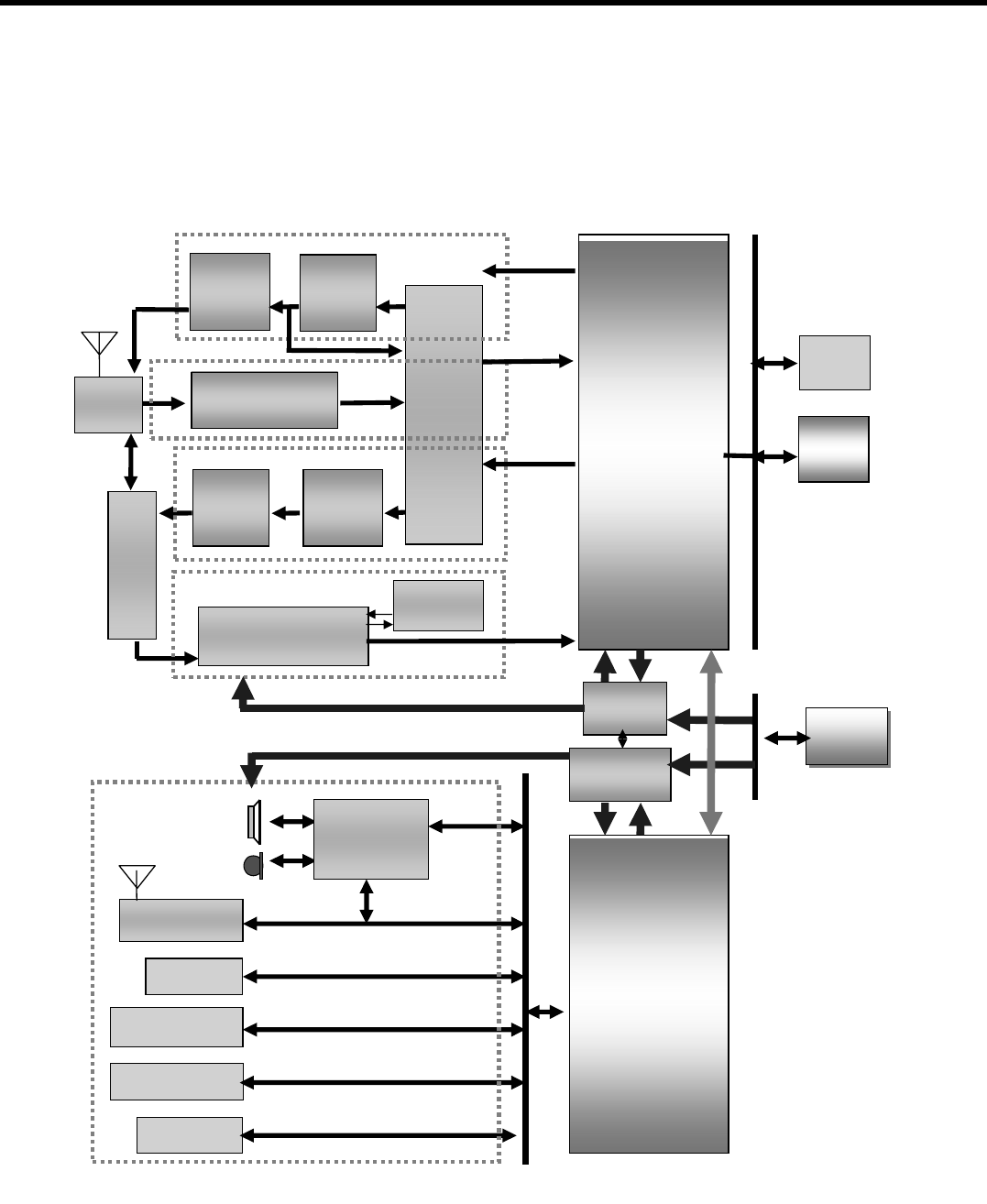
3.7. Hardware Architecture
LGE Internal Use Only
Copyright © 2007 LG Electronics. Inc. All right reserved.
Only for training and service purposes
MSM6275
PM6650
SDRAM
+ NAND
MAIN LCD
GSM
Quadband
PA
BLUETOOTH
18pin MMI
Connector
18pin MMI
Connector
1.3M CAMERA
Receiver
/SPEAKER
MIC
RFR6250
RTR6250
Micro SD
USIM
GSMQua
d
TX VCO
UMTS
(2100)
PA
WCDMA RX
WCDMA TX
GSM
900/1800/1900
RX FILTER
GSM RX
GSM TX
UMTS
TX
FILTER
D
U
P
L
E
X
E
R
UMTS
RX
FILTER
VGA CAMERA
FEM
STn8810
STw4810
Audio Codec.
(WM8753)
HPI I/F
Figure. Simplified Block Diagram
LGE Internal Use Only
Copyright © 2007 LG Electronics. Inc. All right reserved.
Only for training and service purposes
3. TECHNICAL BRIEF
- 37 -
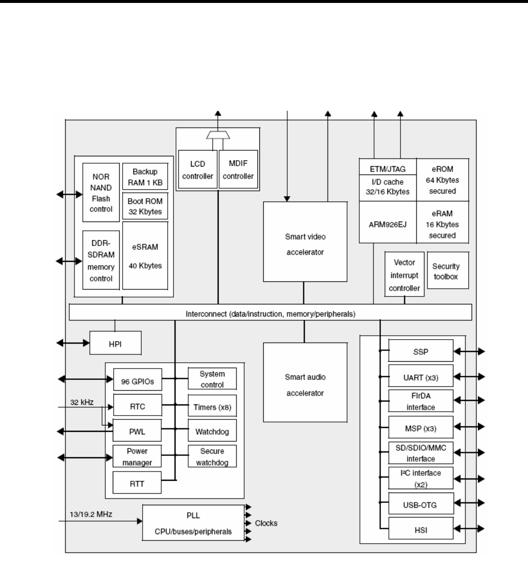
Figure. STn8810 and supported peripherals
3.7.1. STn8810 and supported peripherals
LGE Internal Use Only
Copyright © 2007 LG Electronics. Inc. All right reserved.
Only for training and service purposes
3. TECHNICAL BRIEF
- 38 -
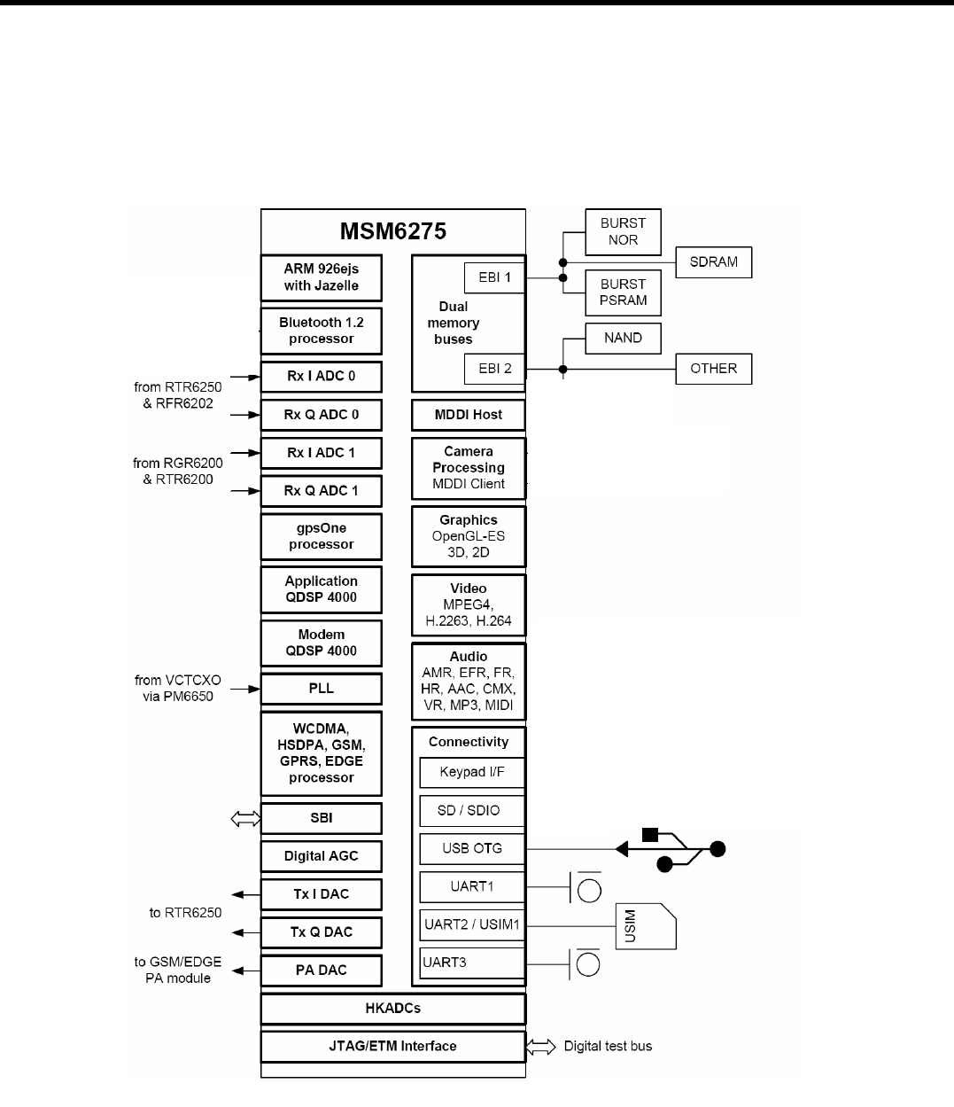
3.7.2. MSM6275 and supported peripherals
Figure. MSM6275 and supported peripherals

LGE Internal Use Only
Copyright © 2007 LG Electronics. Inc. All right reserved.
Only for training and service purposes
3. TECHNICAL BRIEF
- 39 -
3.8. Subsystem of STn8810
3.8.1. ARM926EJ processor
The STn8810 CPU is an ARM926EJ reduced instruction set computer (RISC) processor. This 32-bit
processor core supports 32-bit ARM® and 16-bit Thumb instruction sets, enabling the user to trade off
between high performance and high code density.
The cached ARM CPU features a memory management unit (MMU) and is clocked at 264 MHz.
It has a 32-Kbyte instruction cache and a 16-Kbyte data cache, and supports the Jazelle™ extensions
for Java acceleration. It also includes an embedded trace module (ETM Medium+) for real-time CPU
activity tracing and debugging. It supports 4-bit and 8-bit normal trace mode and 4-bit demultiplexed
trace mode, with normal or half-rate clock.
3.8.2. Smart video accelerator (SVA)
Using leading-edge technology, this block is a low-power, high-performance video accelerator that
supports the following features:
• MPEG-4 simple profile level 3 video encoder and decoder; real time up to VGA 30 fps (encode only
or decode only)
• H.263 profile 3 level 10 video codec; real time subQCIF or QCIF 15 fps for videoconferencing
• H.263 profile 3 level 30 video encoder or decoder; real-time up to CIF 30 fps
• JPEG baseline accelerated encoder or decoder, up to 4080 x 4080 pixels
• Programmable DSP (MMDSP+) for intermediate level processing, clocked at 66 MHz
• Picture pre-/post-processing
• Low-power implementation
3.8.3. Smart audio accelerator (SAA)
This high-performance block is a flexible sophisticated audio accelerator based on the MMDSP+
programmable audio DSP, clocked at 133 MHz, and features:
• 24-bit data path
• Ultra-low power implementation
The audio accelerator features:
• MP3, AAC, AAC+ (SBR) decoding, Midi synthesis, and more
• Speech codecs: AMR (WB, NB), and more
• Audio sample rates of 32 kHz, 44.1 kHz and 48 kHz
• Noise reduction and echo cancelling
• Stereo enhancements and surround effects

LGE Internal Use Only
Copyright © 2007 LG Electronics. Inc. All right reserved.
Only for training and service purposes
3. TECHNICAL BRIEF
- 40 -
3.8.4. Advanced power management unit (PMU)
The dynamic PMU optimizes power consumption of the STn8810. It delivers all the platform clocks,
and handles reset management. It also manages GPIO levels during sleep mode and emergency
self-refresh of SDRAM.
The PMU controls the external voltage regulator, in order to change its settings in different modes.
In deep-sleep mode, only GPIOs, the real-time clock (RTC), system and reset controller (SRC),
PMU and secured RAM remain in operation. The PMU also controls the embedded 1.2 V voltage
switch that switches off the logic supply after the platform has entered sleep mode.
The family of power manager ICs, STw481x companion chips, seamlessly interface with the
Nomadik STn8810 and optimize global system power consumption leveraging on the PMU.
3.8.5. Host port interface (HPI)
The host port interface features:
• 16-bit parallel data bus
• Multiplexed and non-multiplexed address/data bus
• Indirect host access
• Direct host access to a segment of STn8810 memory in multiplexed mode
3.8.6. General purpose inputs/outputs (GPIOs)
The STn8810 provides 96 programmable inputs or outputs that have switchable pull-up and pull-down
resistors and are controllable in two modes:
• Software mode through an APB bus interface
• Hardware mode through a hardware control interface
The GPIO interface provides the following individually programmable functions:
• Any number of pins may be configured as interrupt sources
• Debouncing logic can be enabled for each GPIO to filter out glitches on I/Os
• Any GPIO may be used to wake up the device from sleep mode independent of interrupt
programming, and the input level that triggers wake-up is definable for each enabled GPIO
3.8.7. Universal asynchronous receivers-transmitters (UARTs)
The STn8810 provides three autobaud UARTs, one of which offers all modem control/status signals.
They are enhanced versions of the industry-standard 16C550 UART with a high data rate up to 3.692
Mbit/s.

LGE Internal Use Only
Copyright © 2007 LG Electronics. Inc. All right reserved.
Only for training and service purposes
3. TECHNICAL BRIEF
- 41 -
3.8.8. USB interface
The STn8810 USB interface is USB 2.0 compliant, with On-The-Go standard extension (rev 1.0)
compliance. The USB-OTG features:
• Supports full-speed (12 Mbit/s) and low-speed (1.5 Mbit/s) signaling bit rate
• Supports session request protocol (SRP) and host negotiation protocol (HNP)
• 8 bidirectional endpoints plus control endpoint 0
• Digital interface to external PHY
• Fully compatible with STw4810 power manager companion chip
3.8.9. I2C bus interface
The STn8810 provides two I©˜C bus interfaces that support the following features:
• Slave transmitter/receiver and master transmitter/receiver modes
• Multi-master capability
• 10-bit addressing
• Standard (100 kHz) and fast (400 kHz) speeds
• Compliance with I2C and DDC standards
In addition to receiving and transmitting data, the interface converts data from serial to parallel
format and vice-versa using an interrupt or polled handshake. The interrupts are enabled and
disabled in software.
3.8.10. MultiMediaCard/secure data card interface (MMC/SD/SDIO)
This interface can directly control one SD card (without encryption/decryption logic) or SDIO card, or
one MultiMediaCard. It also supports several of each card type using the GPIOs for card selection.
LGE Internal Use Only
Copyright © 2007 LG Electronics. Inc. All right reserved.
Only for training and service purposes
3. TECHNICAL BRIEF
- 42 -
3.9. Hardware Peripheral system of Stn8810
3.9.1. Keypad
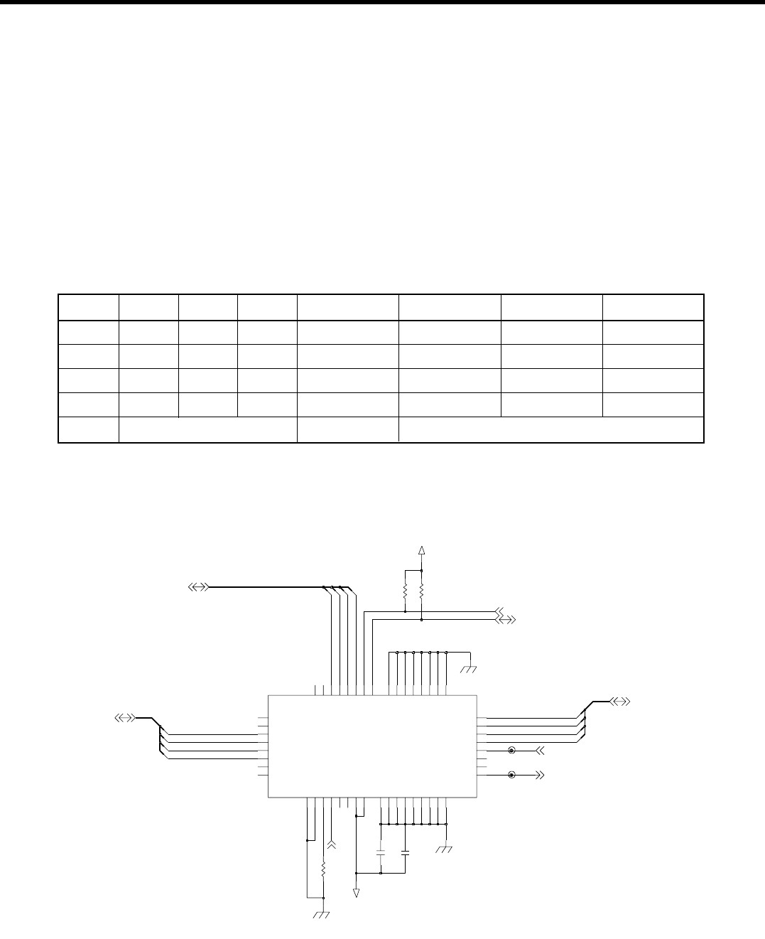
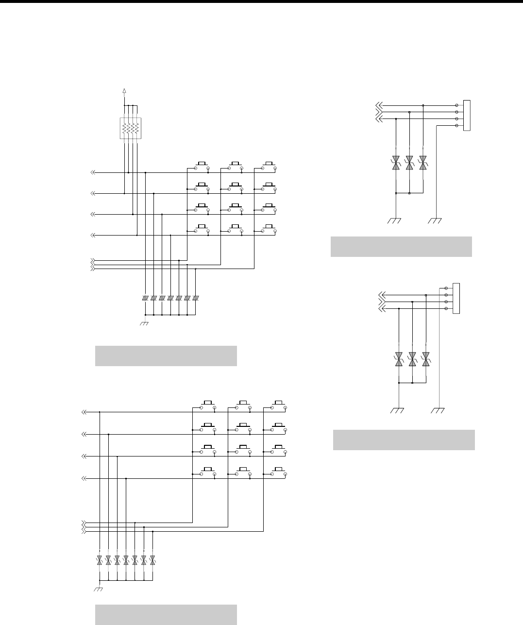
KS10 has 28 buttons, 12 function keys in Sub PCB (Folder), 12 numeric keys in main and 4 side keys.
KS10 use key coder IC because Stn8810 has not enough GPIO. Key coder IC use interrupt and I2C
interface for communication with STn8810. Figure shows the Keypad circuit.
°ÆEND’ Key is connected to PM_ON_SW_N to PM6650
Table. Key Matrix Mapping Table
Figure. Schematic of key coder IC
COL0 COL1 COL2 COL3 COL4 COL5 COL6
ROW0 1 2 3 Vol. UP Left Soft Key UP Right Soft Key
ROW1 4 5 6 Vol. DOWN MENU OK CANCEL
ROW2 7 8 9 SHOT SEND DOWN END
ROW3 * 0 # LEFT EDIT RIGHT
Main Side Key Folder
TP407
0.1u
C418
R415
3.3K
TP406
C419
0.1u
3.3K
R414
Wake_INP2 E7
D6
Wake_INP3
B6
Wake_INP4
Wake_INP5 A7
Wake_INP6
A6
B5 Wake_INP7
F3
_RESET
NC1 F5
G6
NC2
NC3 F6
G7
NC4
C2
NC5
NC6 C1
C6
NC7
NC8 B7
F1 PWM
SCL_AB E6
F7
SDA_AB
VCC1
E1
VCC2
E2
G1
WD_Out
Wake_INP0 D7
C7
Wake_INP1Gen_IO_0
D2
D1 Gen_IO_1
Gen_IO_2
B3
Gen_IO_3
A2
A1 Gen_In0
Gen_In1
B2
Int_Rx G2
Int_Tx F2
G3
K_Out0
K_Out1 F4
G4
K_Out2
K_Out3 G5
K_Out4
A5
B4 K_Out5
K_Out6
A4
A3 K_Out7
LM8333GGR8_NOPB
U404
B1 CLK_In
GND1
C3
C4 GND2
C5 GND3
GND4
D3
D4 GND5
GND6
D5
GND7
E3
E4 GND8
GND9
E5
AP_VDD_IO_2.7V
AP_VDD_IO_2.7V
68KR419
FOLDER_DETECT
I2CSCL1
I2CSDA1
KEY_COL(5)
KEY_COL(6)
KEY_COL(7)
KEY_COL(4:7)
KEYCODER_RSTN
KEYCODER_INT
KEY_ROW(0:3)
KEY_ROW(2)
KEY_ROW(3)
KEY_ROW(0)
KEY_ROW(1)
KEY_COL(3)
KEY_COL(2)
KEY_COL(3:0)
KEY_COL(1)KEY_COL(4)
KEY_COL(0)
LGE Internal Use Only
Copyright © 2007 LG Electronics. Inc. All right reserved.
Only for training and service purposes
3. TECHNICAL BRIEF
- 43 -
Figure. Schematic of keypad
SW400
SW411
SW407
VA403 EVLC14S02050
VA405 EVLC14S02050
EVLC14S02050VA404
SW408
VA401 EVLC14S02050
EVLC14S02050VA406
SW401
EVLC14S02050VA402
SW409 SW410
SW402
VA407 EVLC14S02050
SW406
AP_VDD_IO_2.7V
2
4
6
8
1
3
5
7
SW404
RA400 100K
SW405SW403
KEY_COL(1)
KEY_COL(2)
KEY_ROW(0)
KEY_ROW(1)
KEY_ROW(2)
KEY_ROW(3)
KEY_COL(0)
VA102 RSB6.8CST2R
RSB6.8CST2RVA101
SW106 SW108
VA105
VA104
RSB6.8CST2R
RSB6.8CST2R
SW107
VA103
VA107
RSB6.8CST2R
VA106
RSB6.8CST2R
RSB6.8CST2R
SW104 SW105SW103
SW102SW100
SW111SW109
SW101
SW110
KEY_ROW(0)
KEY_ROW(1)
KEY_COL(6)
KEY_COL(4)
KEY_COL(5)
KEY_ROW(3)
KEY_ROW(2)
D402 RSB6.8CST2R
RSB6.8CST2RD401
D400 RSB6.8CST2R
1
2
3
4
CN400
KEY_ROW(0)
KEY_ROW(1)
KEY_COL(3)
RSB6.8CST2RD405
1
2
3
4
CN401
D404 RSB6.8CST2R
RSB6.8CST2RD403
KEY_COL(3)
KEY_ROW(2)
KEY_ON_SW_N
Side Key (Vol. UP/Down)
Side Key (Power/Shot)
Main PCB
Sub PCB
LGE Internal Use Only
Copyright © 2007 LG Electronics. Inc. All right reserved.
Only for training and service purposes
3. TECHNICAL BRIEF
- 44 -
3.9.2. Folder on/off operation
There is a magnet to detect the folder status, opened or closed. If a magnet is close to the hall-effect
switch, the voltage at pin1 of U402 goes to 0V. Otherwise, 2.7V. This folder signal is delivered to
GPIO0 of the Key coder IC .
AP_VDD_IO_2.7V
0.1u
C414
U402 A3212EEH-T
3GND1
GND2 4
2NC1 5
NC2
1OUTPUT
7
PGND
6
VDD
EUSY0200301
R413
100K
C413
1u
ZD1
RSB6.8CST2R
FOLDER_DETECT
Figure. Schematic of folder on/off detection circuit

LGE Internal Use Only
Copyright © 2007 LG Electronics. Inc. All right reserved.
Only for training and service purposes
3. TECHNICAL BRIEF
- 45 -
3.9.3. Keypad backlight
There are 8 White LEDs on Top side of Main PCB and 9 White LEDs on Top side of sub PCB in board
backlight circuit and, which are driven by KEYBD_BACKLIGHT line form PM6650. Key Pad backlight
controlled by PM6650.
Figure. Schematic of main PCB keypad backlight circuit
100ohmR411
SSC-TWH104-HLS
LD407
SSC-TWH104-HLS
LD406
SSC-TWH104-HLS
LD402
EVL14K02200
VA400
R409 100ohm
100ohmR412
AP_+VPWR
LD400
SSC-TWH104-HLS
100ohmR406
R400
0
R408 100ohm
SSC-TWH104-HLS
LD401
SSC-TWH104-HLS
LD403
R403 100ohm
SSC-TWH104-HLS
LD405
100ohmR405
R402 100ohm
LD404
SSC-TWH104-HLS
KPD_DRV_N
Figure. Schematic of key PCB keypad backlight circuit
100ohmR109
EVL14K02200
VA100
100ohmR111
100ohmR110
LD108
SSC-TWH104-HLSSSC-TWH104-HLS
LD107
LD104
SSC-TWH104-HLS
AP_+VPWR
SSC-TWH104-HLS
LD103
100ohm
100ohmR113
R112
100ohmR114
LD102
SSC-TWH104-HLS
LD100
SSC-TWH104-HLS
100ohmR107 100ohm R108R106 100ohm
SSC-TWH104-HLS
LD101
LD105
SSC-TWH104-HLS SSC-TWH104-HLS
LD106
KPD_DRV_N
LGE Internal Use Only
Copyright © 2007 LG Electronics. Inc. All right reserved.
Only for training and service purposes
3.9.4. Micro SD
3. TECHNICAL BRIEF
- 46 -
CPU
(ST Micro.)
PMIC
(ST Micro.) SD Socket
Clock Clock
Command Command
Data Data
1.8V Signal 2.85V Signal
Level shifting
SD_INT
VMMC_3.1V
VMMC K5
H8 USBINTN
K7 USBRCV
G9 USBSCL
USBSDA
H9
USBVM
VBAT_MMC J4
MCDATA31DIR
MCFBCLK
H5
B1 NC1
NC2
B7
B8 NC3
NC4
C5
NC5
F8
NC6
G8
NC7
K10
D3
J5
GPO1 K6
GPO2
LATCHCLK F3G2 MCCLK
H1 MCCMD
MCCMDDIR
G3
K2 MCDAT0DIR
K9 MCDAT2DIR
MCDATA0
K1
H3 MCDATA1
J1 MCDATA2
MCDATA3
H2
H4
CLKOUT G1
F2
CMDOUT
E1
DATAOUT0
DATAOUT1 E2
E3
DATAOUT2
DATAOUT3 F1
DN
GND1
B9
GND2
TP305
C335
NA
2.2u
C332
C334
NA
1u
C336
NA
USBINTN
SD_CMD
SD_DAT(2)
SD_CLK
SD_DAT(3)
SD_DAT(1)
MCDAT2DIR
MCDAT31DIR
MCDAT1
MCDAT3
MCDAT2
USBSCL
USBSDA
MCCLK
MCCMDDIR
MCCMD
MCFBCLK
MCDAT0DIR
MCDAT0
SD_DAT(0)
USBVM
USBRCV
D15
F24
MSPTXD2_SMPCE2N
D12
MCCLK
C12
MCCMD
MCCMDDIR E13
MCDAT0 D14
C14
MCDAT0DIR
E14
MCDAT1
MCDAT2 C13
MCDAT3 D13
MCDAT31DIR E15
MCFBCLK E17
E16
MSPRXD0
MSPSCK0 F17
H22
MSPTCK2_SMPIORN
MSPTFS0 C15
G24
MSPTFS2_SMPCE1N
MSPTXD0
MCDAT1
MCDAT0DIR
MCDAT0
MCCMDDIR
MCCMD
MCCLK
REMOTE_PWR_ON_AP
MSPTXD0
SW_RESET
MSPTFS0
SD_INT
MCDAT2DIR
MSPRXD0
MCFBCLK
MCDAT31DIR
MCDAT3
MCDAT2
1u
C339
34
5
6
R310 51K
D301
PLR0504F
1
2
51K
R309
R311 51K
51K
R313
1
2
34
5
6
PLR0504F
D300
R314 51K
NA
C343
NA
R312
5
6
7
8
SWASWBGND
GND
1
2
3
4
GCC110-8S-R-E1000
S300
VMMC_3.1V
SD_INT
SD_DAT(1)
SD_DAT(0)
SD_CLK
SD_CMD
SD_DAT(3)
SD_DAT(2)
PMIC
(ST Micro.)
SD Socket
CPU
(ST Micro.)

LGE Internal Use Only
Copyright © 2007 LG Electronics. Inc. All right reserved.
Only for training and service purposes
3. TECHNICAL BRIEF
- 47 -
3.10. Subsystem of MSM6275
3.10.1. ARM Microprocessor Subsystem
The MSM6275 device uses an embedded ARM926EJ-S microprocessor. This microprocessor,
through the system software, controls most of the functionality for the MSM device, including control of
the external peripherals such as the keypad, LCD, RAM, ROM, and EEPROM devices. Through a
generic serial bus interface (SBI) the ARM926EJ-S configures and controls the functionality of the
RFL6202, RFR6202, RTR6250, RTR6200, and PM6650 devices.
3.10.2. UMTS/HSDPA Subsystem
The UMTS/HSDPA subsystem performs the digital release 99 June 2004 of the WCDMA FDD
standard and release 5 specifications of HSDPA signal processing.
The UMTS Subsystem performs the digital UMTS signal processing. Its components include:
•
Searcher engine
•
Demodulating fingers
•
Combining block
•
Frame deinterleaver
•
Viterbi decoder
•
Up-link subsystem
•
Turbo decoder
On the down-link channel the UMTS subsystem searches, demodulates, and decodes incoming
CPICH, CCPCH, SCH, and Traffic Channel information. It extracts packet data from the downlink
traffic channel and prepares the packet data for processing. For the up-link, the WCDMA subsystem
processes the packet data and modulates the up-link traffic channel (DCH).
3.10.3. GSM/GPRS Subsystem
The GSM/GPRS/EGPRS subsystem reuses the MSM6275 GSM core. It performs the digital GSM
signal processing and PA gain controls for GPRS support. The PA output level is controlled by an
analog signal generated on the MSM. In GSM mode, the power profile ramps up before The burst and
ramps down after the burst. In GPRS mode, at the beginning of each burst (up to Four active transmit
slots), PA must be smoothly ramped up to some desired output power level, Held at that level for the
current slot, smoothly ramped down/up during the transition period and Held to the new level for the
next slot until the last slot. Then it must be smoothly ramped down to near-zero level. The MSM6275
support differential GSM PA power control output.

LGE Internal Use Only
Copyright © 2007 LG Electronics. Inc. All right reserved.
Only for training and service purposes
3.10.4. RF Interface
The RF interface communicates with the mobile station external RF circuits. Signals to these Circuits
control signal gain in the Rx and Tx signal path, control DC offset errors, and maintain the system
frequency reference.
3.10.5. Serial Bus Interface (SBI)
The MSM6275 device’s SBI is designed specifically to be a quick, low pin count control Protocol for
QUALCOMM’s RFL6202, RFR6202, RTR6250, RTR6200, and PM6650 ASICs. Using the SBI, the
RTR6250, RFR6200, RFL6200, and PM6650 devices can be configured for different operating modes
and for minimum power consumption, extending battery life in standby mode. The SBI also controls
DC baseband offset errors.
3.10.6. HKADC
The MSM6275 device has an on-chip 8-bit analog-to-digital converter (HKADC) which is Intended to
digitize DC signals corresponding to analog parameters such as battery voltage, temperature, and RF
power levels.
The MSM6275 device has seven analog input pins (HKAIN[5:0]) which are multiplexed to the input of
the internal HKADC.
3.10.7. Stereo Wideband CODEC
The MSM6275 device integrates a wideband voice/audio codec into the MSM. The codec supports two
differential microphone inputs, one differential earphone output, one single-ended earphone output,
and a differential analog auxiliary interface. The codec integrates the microphone and earphone
amplifiers into the MSM6275 device, reducing the external component count to just a few passive
components. The microphone (Tx) audio path consists of a two-stage amplifier with the gain of the
second stage set externally. The Rx/Tx paths are designed to meet the ITU-G.712 requirements for
digital transmission systems.
3.10.8. Vocoder Subsystem
The MSM6275 QDSP4000 supports AMR, FR, EFR, and HR. In addition, the QDSP4000 has modules
to support the following audio functions: DTMF tone generation, DTMF tone detection, Tx/Rx volume
controls, Tx/Rx automatic gain control (AGC), Rx automatic volume control (AVC), ear seal echo
canceller (ESEC), acoustic echo canceller (AEC), noise suppression (NS), and programmable, 13-tap,
Type-I, FIR, Tx/Rx compensation filters. The MSM6275 device’s integrated ARM9TDMI processor
downloads the firmware into the QDSP4000 and configures the QDSP4000 to support the desired
functionality.
3. TECHNICAL BRIEF
- 48 -

LGE Internal Use Only
Copyright © 2007 LG Electronics. Inc. All right reserved.
Only for training and service purposes
3. TECHNICAL BRIEF
- 49 -
3.10.9. General-Purpose Input/Output Interface
The MSM6275 device has general-purpose bidirectional input/output pins. Some of the GPIO pins
have alternate functions supported on them. The alternate functions include USB interface, additional
RAM, ROM, general-purpose chip selects, parallel LCD interface, and a UART interface. The function
of these pins is documented in the various software releases.
3.10.10. UART
There are three UARTs in the MSM6275 ASIC:
•
UART1 for data
•
UART2 (can be used for USIM interface)
•
UART3 (can be used for PM SBI interface)
3.10.11. USB
The MSM6275 device integrates a universal serial bus(USB) controller that supports both
unidirectional and bidirectional transceiver interfaces. The USB controller acts as a USB peripheral
communicating with the USB host. It is also capable of a USB OTG interface to a USB OTG
Transceiver.
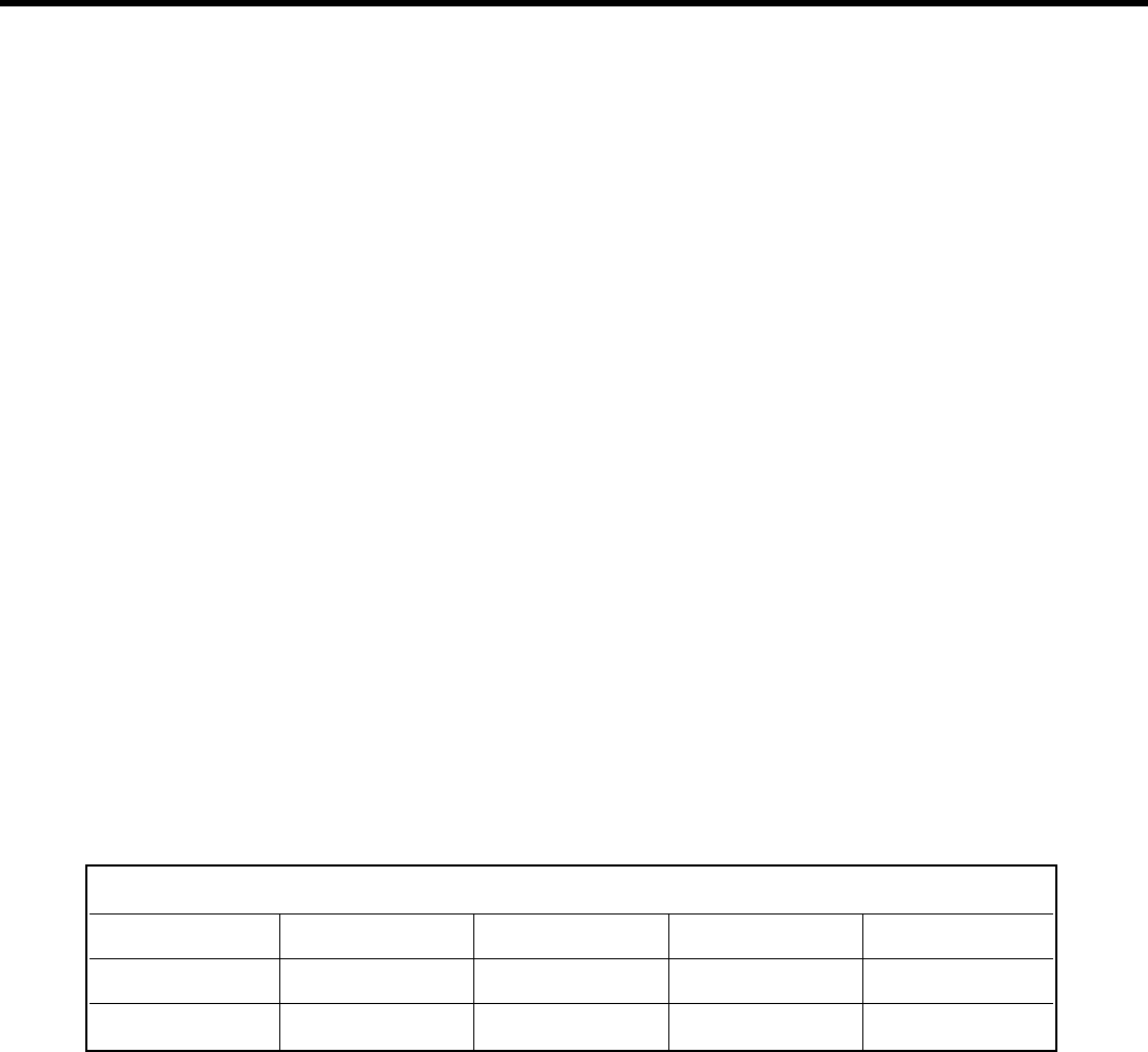
LGE Internal Use Only
Copyright © 2007 LG Electronics. Inc. All right reserved.
Only for training and service purposes
3.11. External memory interface
The MSM6275 have two external memory interfaces with arbitration for the multi-layer AHB system
and memory controllers. The EBI1 bus is a high performance bus that supports a wide variety of
memories. EBI2 bus is targeted to be the interface for slow peripheral devices(i,.e., LCD) as well as
the NAND flash memory.
•
EBI1 Features
- 16 bit static and dynamic memory interface
- 32 bit dynamic memory interface
- 24 bits of address for static memory devices which can support up to 32MBytes on each chip select
- Synchronous burst memories supported (burst NOR, burst PSRAM)
- Synchronous DRAM memories supported
- Byte addressable memory supporting 8 bit, 16 bit and 32 bit accesses
- Pseudo SRAM (PSRAM) memory support
•
EBI2 Features
- Support for asynchronous FLASH and SRAM(16bit & 8bit).
- Interface support for byte addressable 16bit devices(UB_N & LB_N signals).
- 2Mbytes of memory per chip select.
- Support for 8 bit wide NAND flash.
- Support for parallel LCD interfaces, port mapped of memory mapped(16 & 8 bit)
•
512Mb NAND flash memory + 512Mb SDRAM (1die)
3. TECHNICAL BRIEF
- 50 -
Interface Spec
Device Part Name Maker Read Access Time Write Access Time
FLASH TY90009800COGG Toshiba 35 ns/Bytes 50 ns/Bytes
SDRAM TY90009800COGG Toshiba 107 ns/4Double Word 53 ns/4Double Word
Table. External memory interface for KS10

LGE Internal Use Only
Copyright © 2007 LG Electronics. Inc. All right reserved.
Only for training and service purposes
3. TECHNICAL BRIEF
- 51 -
3.12. Hardware sub system of MSM6275
3.12.1. RF Interface
3.12.1.1. RTR6250 (WCDMA_Tx, GSM_Tx/Rx)
MSM6275 controls RF part(RTR6250) using these signals.
•
SBST,SBDT,SBCK : SBI I/F signals for control Sub-chipset
•
PA_ON : Power AMP on RF part
•
RX_I/Q,TX_I/Q : I/Q for Tx/Rx of RF
•
TX_AGC_ADJ : control the gain of the Tx signal prior to the power amplifier
3.12.1.2. RFR6250 (WCDMA_Rx)
•
SBST,SBDT,SBCK : SBI I/F signals for control Sub-chipset
•
RX_I/Q, : I/Q for Rx of RF
3.12.1.3. The others
•
GSM_PA_BAND : DCS/GSM Band Selection of Power Amp
•
TRK_LO_ADJ : TCXO(19.2M) Control
•
PA_ON : WCDMA TX Power Amp Enable
•
ANT_SEL[0-2] : Ant Switch Module Mode Selection (WCDMA,GSM Tx/Rx,DCS Tx/Rx)
•
GSM_PA_RAMP : Power Amp Gain Control of APC_IC
•
GSM_PA_EN : Power Amp Gain Control Enable of APC_IC
•
GSM_TX_VCO_0_EN_N : GSM Band Tx VCO Enable of Dual VCO
•
GSM_TX_VCO_1_EN_N : DCS Band Tx VCO Enable of Dual VCO
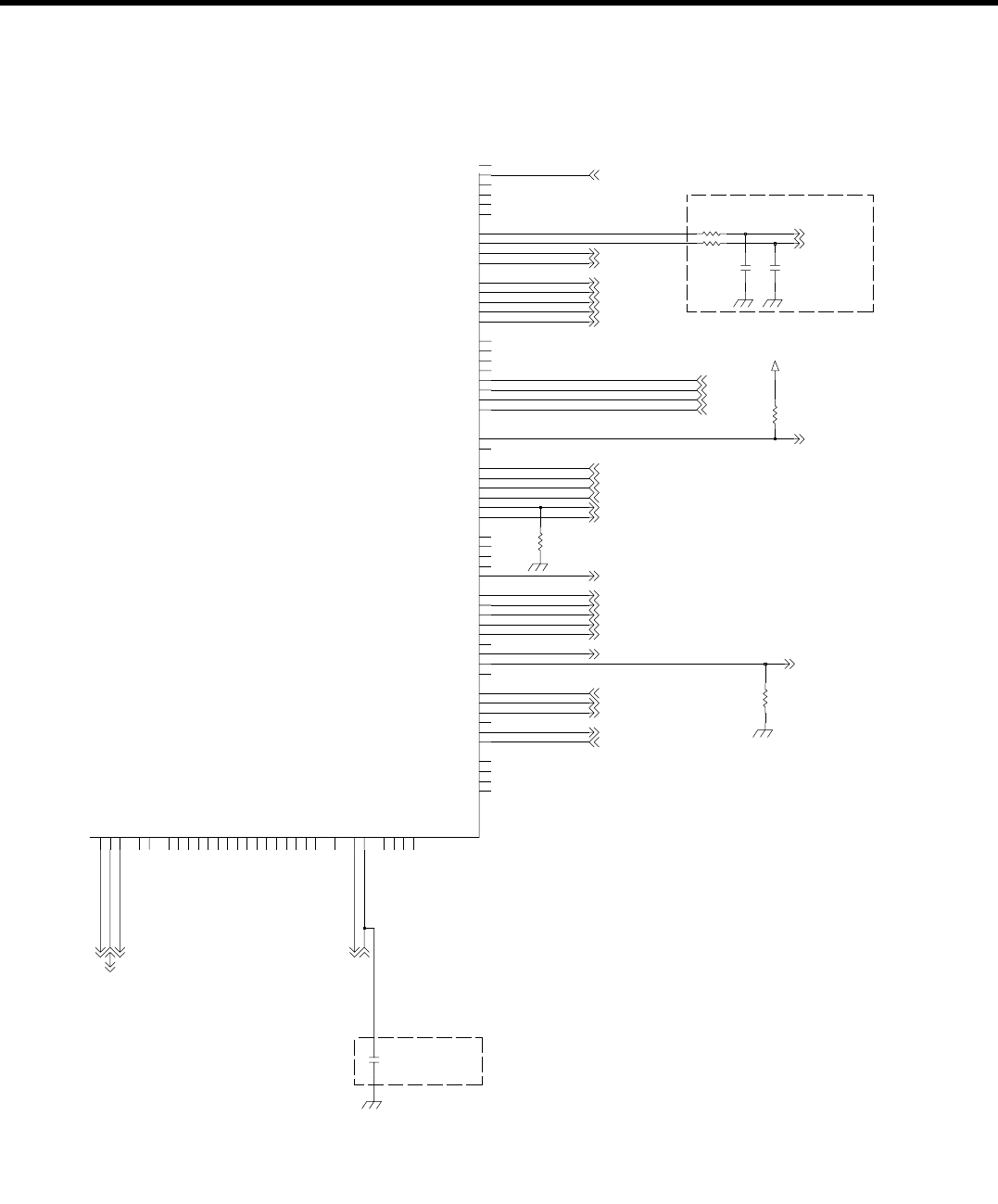
- 52 -
3. TECHNICAL BRIEF
LGE Internal Use Only
Copyright © 2007 LG Electronics. Inc. All right reserved.
Only for training and service purposes
(WCMDA 2100PAM Enable)
(WCMDA PAM MODE)
(Check CAM_DATA PINOUT !!!!)
MSM pin AD26
Place near
10%
Near to MSM
XMEM1_CS_N3_SDRAM1_CS_N1_GPIO77
Y6
L25
UART3_RFR_N_GPIO87
TDI
TDO
A17
TMS
F15
TRK_LO_ADJ
L13
H15
TRST_N
H13
TX_AGC_ADJ
TX_ON_GRFC10
H12
H6
UART2_DP_RX_DATA_GPIO89
F18
SYNTH0_GP_PDM0_GPIO92
H23
SYNTH1_GPIO41
TCK
D16
TCXO_EN_GPIO94
F19
D15
SBDT
H26
SBST
SBST1_GPIO93
H18
P25
PA_POWER_CTL
AA25
Q_IM_CH0
Q_IM_CH1
W23
Y25
Q_IP_CH0
Q_IP_CH1
V23
B12
Q_OUT
A12
Q_OUT_N
RINGER_GPIO18
L19
RTCK
H16
L21
SBCK
J23
PA_ON0
F17
MDDIC_DATN
A23
A22
MDDIC_DATP
MDDIC_STBN
B23
B22
MDDIC_STBP
MDDIH_DATN
B19
B20
MDDIH_DATP
MDDIH_STBN
A19
A20
MDDIH_STBP
I2C_SCL_GPIO27
K21
I2C_SDA_GPIO26
AB25
I_IM_CH0
V25
I_IM_CH1
AC25
I_IP_CH0
W25
I_IP_CH1
I_OUT
B13
I_OUT_N
A13
GRFC3_GPIO6
GRFC4_AUX_SBCK_GPIO7
H10
D11
GRFC5_AUX_SBST_GPIO8
GRFC7_GPIO10
T23
B4
GRFC8_GPIO11
GRFX6_GPIO9
T19
GSM_PA_DAC_REF
AD26
N16
H17
GP_PDM1_PA_RANGE0
D17
GP_PDM2_PA_RANGE1
B8
GRFC0_GPIO3
A8
GRFC1_AUX_SBDT_GPIO4
D9
GRFC2_GPIO5
F10
F12
DAC_REF
GPIO17
K26
GPIO19
G21
L15
CAMIF_DATA7_GPIO59
D20
F16
CAMIF_DATA8_GPIO60
F20
CAMIF_DATA9_GPIO61
E23
CAMIF_HSYNC_GPIO15
CAMIF_PCLK_GPIO82
K23
CAMIF_VSYNC_GPIO16
B3
G23
BT_CLK_GPIO25
BT_DATA_GPIO20
R19
E26
BT_SBCK_GPIO23
BT_SBDT_GPIO22
E25
F23
BT_SBST_GPIO24
BT_TX_RX_N_GPIO21
H21
CAMIF_DATA0_GPIO83
J25
J26
CAMIF_DATA1_GPIO81
D21
CAMIF_DATA2_AUX_TRST_N_GPIO54
CAMIF_DATA3_AUX_TCK_GPIO55
C25
CAMIF_DATA4_AUX_TMS_GPIO56
D22
J19
CAMIF_DATA5_AUX_TDI_GPIO57
CAMIF_DATA6_AUX_TDO_GPIO58
AUX_PCM_CLK_GRFC14_GPIO80
K19
N21
AUX_PCM_DIN_GRFC13_GPIO14
AUX_PCM_DOUT_GRFC12_GPIO103
G4
AUX_PCM_SYNC_GRFC11_GPIO102
J8
600-1
M6275_A
R609100K
0.01u
C644
100K R611
51K
R610
R6071K
C646
0.1u
R6082K
VREG_MSMP_2.7V
C645
33nF
HPIEV_IT_STATE_ETMTRIGIN
RX0_I_P
RX0_I_M
RX0_Q_P
RX0_Q_M
EAR_SENSE_N
MSM_RTCK
MSM_TDO
HPI_IT_APE_ETMPSTA0_XTIDAT
HPI_IT_MOD_ETMSYNCA_XTIDAT
HPI_EME_MOD_ETMPSTA1_XTIDAT
HPI_EME_APE_ETMPSTA2_XTIDAT
MSM_TDI
MSM_TCK
TCXO_EN
MSM_TMS
MSM_TRST_N
TX_ON
TX_I_M
PA_ON
GSM_PA_RAMP
TX_Q_P
TX_Q_M
RF_SBCK
RF_SBDT
RF_SBST
DAC_REF
W_VMODE_N
GSM_PA_EN
GSM_PA_BAND
GSM_TX_VCO_1_EN_N
GSM_TX_VCO_0_EN_N
ANT_SEL1
ANT_SEL2
ANT_SEL0
GSM_PA_DAC_REF
TX_I_P
TX_AGC_ADJ
TRK_LO_ADJ
Figure. Schematic of RF Interface of MSM6275
- 53 -
3. TECHNICAL BRIEF
3.12.2. MSM sub system
3.12.2.1. SIM interface
SIM interface scheme is shown in Figure.
And, there control signals are followed
•
USIM_CLK : USIM Clock
•
USIM_Reset : USIM Reset
•
USIM_Data : USIM Data T/Rx
3.12.2.2. UART interface
UART signals are connected to MSM GPIO through IO connector with 115.2kbps speed.
And, used for RF calibration and Data download.
LGE Internal Use Only
Copyright © 2007 LG Electronics. Inc. All right reserved.
Only for training and service purposes
Figure. SIM Interface
Table. UART interface
MSM6275 PM6650 USIM
USIM CLK
USIM Reset
USIM Data
USIM Data
USIM Reset
USIM CLK
VREG_USIM 2.85V
GPIO_Map Name Note
GPIO_96 UART_RXD Data_Rx
GPIO_95 UART_TXD Data_Tx
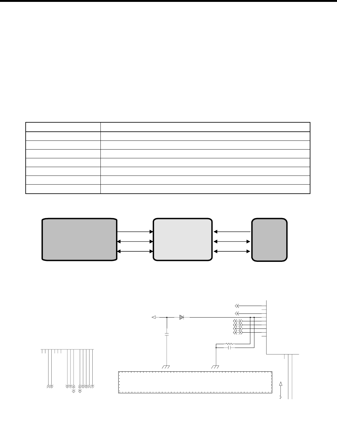
- 54 -
3. TECHNICAL BRIEF
3.12.2.3. USB
The MSM6275 device contains a Universal Serial Bus (USB) interface to provide an efficient
interconnect between the mobile phone and a personal computer (PC). The USB interface of the
MSM6275 was designed to comply with the definition of a peripheral as specified in USB Specification,
Revision 1.1. Therefore, by definition, the USB interface is also compliant as a peripheral with the USB
Specification, Revision 2.0. The USB Specification Revision 1.1 defines two speeds of operation,
namely low-speed (1.5 Mbps) and full-speed (12 Mbps), both of which are supported by the
MSM6275. KS10’s USB interface uses the PM6650 internal logic for USB Transceiver.
LGE Internal Use Only
Copyright © 2007 LG Electronics. Inc. All right reserved.
Only for training and service purposes
Name Note
USB_RCV Rx_Data to MSM
USB_DAT Data to/from MSM
USB_SE0 Data to/from MSM
USB_OE_N Out-Put Enable of Transceiver
USB_VBUS USB_Power From Host(PC)
USB_D+ USB Data+ to Host
USB_D- USB Data- to Host
Table. USB signal interface
Figure. USB Interface
MSM6275_USB Block PM6650_USB Block
Figure. Schematic of USB block (MSM6275 Side & PM6650 Side)
MSM6275 PM6650 MMI
Connector
USB_D-
USB_D+
USB_VBU
S
USB_SE0
USB_DAT
USB_OE_
N
UART3_DP_RX_DATA_GPIO85
UART3_DP_TX_DATA_GPIO84
M19
P16
UART1_CTS_N_GPIO97
UART1_DP_RX_DATA_GPIO96
M23
UART1_DP_TX_DATA_GPIO95
L26
P21
UART1_RFR_N_PA_POWER_CTL_M_GPIO98
G6
UART2_CTS_N_GPIO90
UART2_DP_TX_DATA_GPIO88
E4
UART2_RFR_N_GPIO91
F4
UART3_CTS_N_GPIO86
L23
M21
GPIO42
GPIO44
D8
F14
GPIO64
GPIO39
F7
GPIO40
D6
D7
PM_SBCK
MSM_UART_RXD
MSM_UART_TXD
MSM_USIM_RST_N
MSM_USIM_DATA
MSM_USIM_CLK
PM_SBDT
PM_SBST
PM_INT_N
PS_HOLD
Draw the Artwork_line thickly !!!!!
--->> USB_VBUS , FLASH_DRV_N , KPD_DRV_N , KEY_ON_SW_N , MOT_PWR-
Power Line --> Route carefully!!!!!
4.7u
smd_1608h_9_r
C731
47K R710
C7321u
+VPWR
RB521S-30
D701
GP1_DRV_N(MPP7)
LCD_DRV_N
22
KPD_DRV_N
23
KPDPWR_N
24
VIB_DRV_N
25
VSW_5V
14
USB_CTL_N
15
USB_VBUS
16
USB_DAT
17
USB_D_P
18
USB_SE0
19
USB_D_M
20
21
VREG_5V
USB_OE_N
13
USB_VBUS
100K
USB_CTL_N
USB_OE_N
USB_DAT
MSM_USB_D+
USB_SE0
MSM_USB_D-
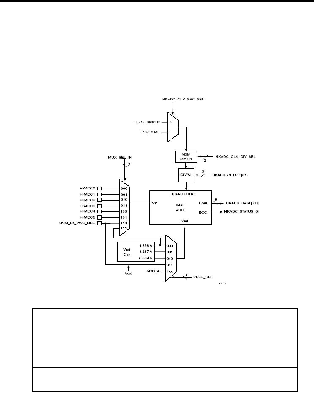
- 55 -
3. TECHNICAL BRIEF
3.12.2.3. HKADC (House Keeping ADC)
The MSM6275 device has an on-chip 8-bit analog-to-digital converter (HKADC) which is tended to
digitize DC signals corresponding to analog parameters such as battery voltage, temperature, and RF
power levels. The MSM6275 device has six analog input pins which are multiplexed to the input of the
internal HKADC.
LGE Internal Use Only
Copyright © 2007 LG Electronics. Inc. All right reserved.
Only for training and service purposes
Figure. MSM6275 HKADC Block diagram
Table. HKADC channel table
ADC Ch# Signal Name Note
HKADC0 AMUX_OUT RF PAM Temperature sensing
HKADC1 VBATT_SENSE Battery voltage level sensing
HKADC2 HDET1 RF WCDMA PAM Power Level sensing
HKADC3 VBAT_TEMP Battery Temperature sensing
HKADC4 - -
HKADC5 - -

LGE Internal Use Only
Copyright © 2007 LG Electronics. Inc. All right reserved.
Only for training and service purposes
3.12.3. Power Block
3.12.3.1. General
MSM6275A, included RF, is fully covered by PM6650-1M(Qualcomm PMIC). PM6650-1M cover the
power of MSM6275A, MSM memory, RF block, USIM and TCXO.
Major power components are :
PM6650-1M (U700) : Phone power supply
NUS5530MN (Q701) : External charger supply switching & Main Battery charging control
3.12.3.2. PM6650-1M
The PM6650-1M device (Figure 1-1) integrates all wireless handset power management. The power
management portion accepts power from all the most common sources - battery, external charger,
adapter, coin cell back-up - and generates all the regulated voltages needed to power the appropriate
handset electronics. It monitors and controls the power sources, detecting which sources are applied,
verifying that they are within acceptable operational limits, and coordinates battery and coin cell
recharging while maintaining the handset electronics supply voltages. Eight programmable output
voltages are generated using low dropout voltage regulators, all derived from a common trimmed
voltage reference.
A dedicated controller manages the TCXO warm-up and signal buffering, and key parameters (under-
voltage lockout and crystal oscillator signal presence) are monitored to protect against detrimental
conditions.
MSM device controls and statuses the PM6650-1M IC using a three-line Serial BusInterface(SBI)
supplemented by an Interrupt Manager for time-critical information. Another dedicated IC Interface
circuit monitors multiple trigger events and controls the power-on sequence.
3. TECHNICAL BRIEF
- 56 -
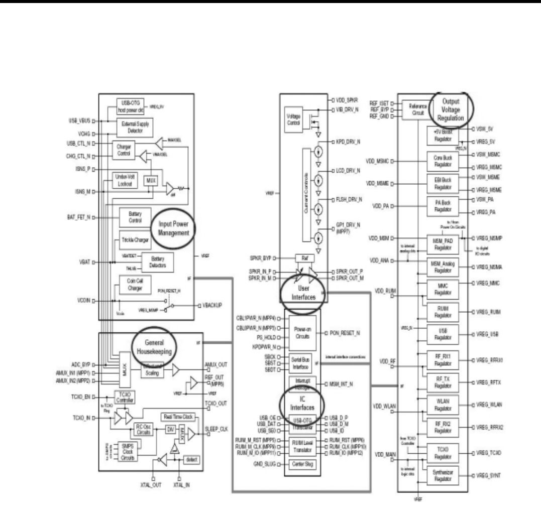
LGE Internal Use Only
Copyright © 2007 LG Electronics. Inc. All right reserved.
Only for training and service purposes
3. TECHNICAL BRIEF
- 57 -
Figure. PM6650-1M Functional Block Diagram
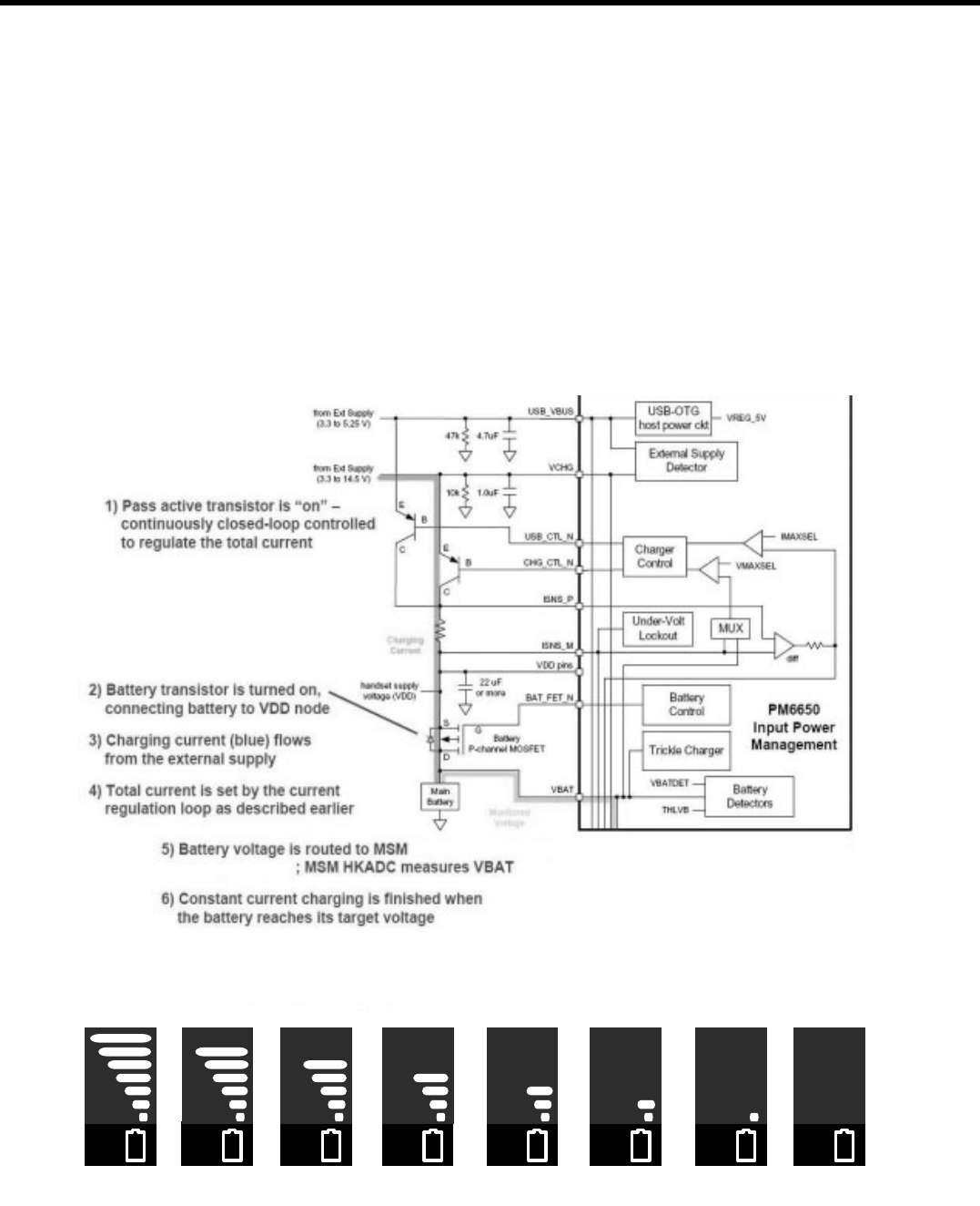
LGE Internal Use Only
Copyright © 2007 LG Electronics. Inc. All right reserved.
Only for training and service purposes
3. TECHNICAL BRIEF
- 58 -
3.12.3.3. Charging control
A programmable charging block in PM6650-1M is used for battery charging. It is possible to set limits
for the charging current. The external supply typically connects directly to pin (VCHG). The voltage on
this pin (VCHG) is monitored by detection circuitry to ascertain whether a valid external supply is
applied or not. For additional accuracy or to capture variations over time, this voltage is routed
internally to the housekeeping ADC via the analog multiplexer. PM6650-1M circuits monitor voltages at
VCHARGER and ICHARGE pins to determine which supply should be used and when to switch
between the two supplies. These pins are connected to the Source (or emitter) and Drain (or collector)
contacts of the pass transistor respectively.
4.2V~3.96V 3.86V~3.79V 3.78V~3.75V
3.95V ~ 3.87V 3.74V~3.70V 3.69V~3.64V 3.63V~3.51V 3.50V~3.20V
KS10 Charging Control block
Figure. KS10 Battery Bar Display (Standby condition)
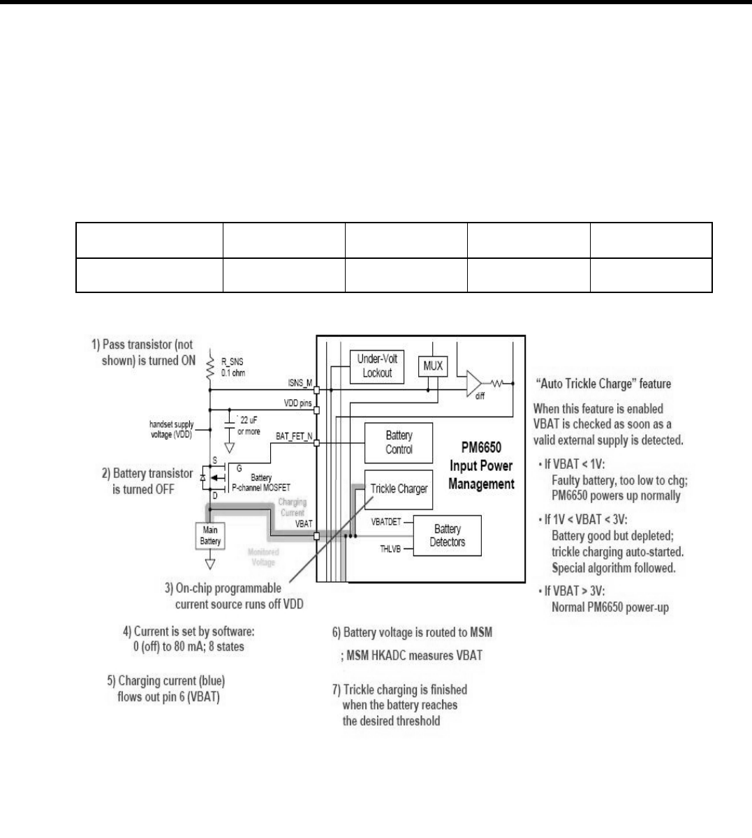
LGE Internal Use Only
Copyright © 2007 LG Electronics. Inc. All right reserved.
Only for training and service purposes
3. TECHNICAL BRIEF
- 59 -
3.12.3.3.1 Trickle charging
Trickle Charging of the main battery, enabled through SBI control and powered from VDD, is provided
by the PM6650-1M IC, The trickle charger is on-chip programmable current source that supplies
current from VDD to pin (VBAT). Trickle charging can be used for lithium-ion and nickelbased batteries,
with its performance specified below (3.2V). The charging current is set to 80mA.
Parameter Min Typ Max Unit
Trickle Current 60 80 100 mA

- 60 -
3. TECHNICAL BRIEF
3.12.3.3.2 Constant current charging
The PM6650-1M IC supports constant current charging of the main battery by controlling the charger
pass transistor and the battery transistor. The constant current charging continues until the battery
reaches its target voltage, 4.2V.
3.12.3.3.3 Constant voltage charging
Constant voltage charging begins when the battery voltage reaches a target voltage, 4.2V. The end of
constant voltage charging is commonly detected 10% of the full charging current (60mA)
•
Charging Method : CC & CV (Constant Current & Constant Voltage)
•
Maximum Charging Voltage : 4.2V
•
Maximum Charging Current : 650mA
•
Nominal Battery Capacity : 950 mAh
•
Charger Voltage : 4.8V
•
Charging time : Max 3 h (Except time trickle charging)
•
Full charge indication current (icon stop current) : 60mA
•
Low battery POP UP : 3.63V , 3.50V
•
Low battery alarm interval : warning tone once only
•
Cut-off voltage : 3.20V
LGE Internal Use Only
Copyright © 2007 LG Electronics. Inc. All right reserved.
Only for training and service purposes
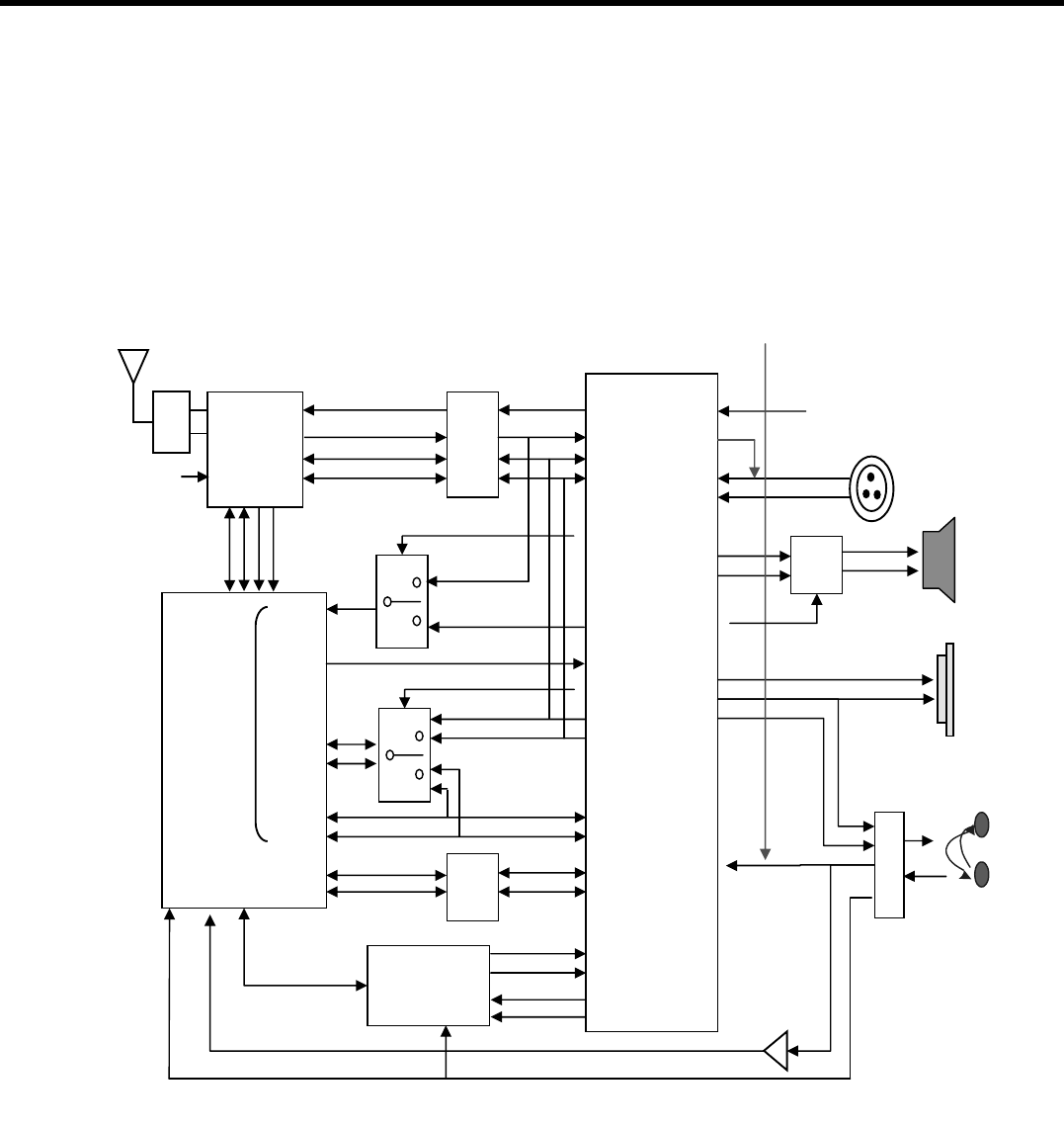
- 61 -
3. TECHNICAL BRIEF
3.13. Audio and sound
3.13.1. Overview of Audio & Sound & BT path
LGE Internal Use Only
Copyright © 2007 LG Electronics. Inc. All right reserved.
Only for training and service purposes
MSM
AMP
Level
Shifter
AU_19.2M
Level
Shifter
I2CSCL0
I2CSDA0
PM_SCL SCL
SDA
UART0
UART
PCM PCM
I2S
WM_BCLK
WM_LRC
WM_MSPTCK0
WM_MSPTFS0
MSPRFS0
MSPRCK0
RXP
RSN
WM_MONO1
WM_MONO2
MIC1
MIC2
MIC_BIAS
SPK_AMP_SD_N
OUT3
LOUT1
Speaker
Receiver
Head Set
MIC
LOUT2
ROUT2
ROUT1
EAR_SENSE_N
HOOK_SENSE_N
GPIO
GPIO
GPIO
Switch
Switch
STN8810
(CPU)
I2S
WM_DACDAT
WM_MSPRXD0
MSPRXD0
GPIO
Filter
BT_19.2M
ANT
WM_8753
(Audio Codec)
STLC2500C
(BT)
VREG_MSMP_2.7V
PM_SDA
Figure. Block diagram ofaAudio &sSound path
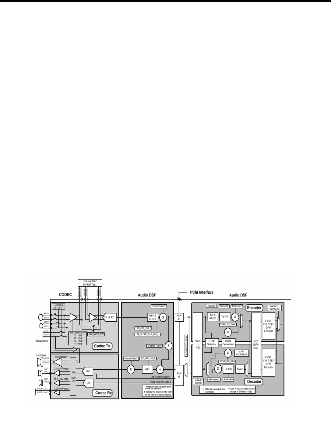
LGE Internal Use Only
Copyright © 2007 LG Electronics. Inc. All right reserved.
Only for training and service purposes
3.13.2. Audio signal processing & interface
3.13.2.1. MSM6275A audio interface
The MSM6275 device integrates a wideband audio CODEC into the mobile station modem. The
wideband codec allows the MSM device to support stereo music/ringer Melody applications in addition
to the 8 kHz voice band applications on the forward link. In the audio transmit path, the device
operates as 13-bit linear converter with software selectable 8 kHz and 16 kHz sampling rate. In the
audio receive path, the device operates as a software selectable 13-bit or 16-bit linear converter with
software selectable 8 kHz, 16 kHz, 22.05 kHz, 24 kHz, 32 kHz, 44.1 kHz, or 48 kHz sampling rate.
Through software, the Rx path can be configured as either a mono or stereo output.
The integrated CODEC contains all of the required conversion and amplification stages for the audio
front end. The CODEC operates as a 13-bit linear CODEC with the transmit (Tx) and receive (Rx)
filters designed to meet ITU-T G.712 requirements. The CODEC includes a programmable sidetone
path for summing a portion of the Tx audio into the Rx path. An on-chip Voltage/Current reference is
provided to generate the precise voltages and currents required by the CODEC.
The interface supports two differential microphone inputs and a differential auxiliary input, each of
which can be configured as single-ended if desired. In addition, the interface supports one differential
earphone output, one single-ended earphone output, and one differential auxiliary output or two single-
ended line outputs.
The CODEC is configured through the QDSP4000 command types and is not directly controlled by the
microprocessor. The CODEC configuration command is sent to the QDSP4000 and then the
QDSP4000 executes the command and configures the CODEC. Data is exchanged between the
codec interface and the QDSP4000 through its DMA interface. The QDSP4000 uses the Ex_DMA_4
channel for reading data from the codec and uses the Ex_DMA_5 channel to transfer data to the
codec. The CODEC interface is shown in more detail in Figure below.
3. TECHNICAL BRIEF
- 62 -
Figure. Detailed diagram of MSM6275 audio interface
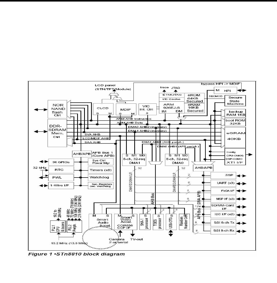
LGE Internal Use Only
Copyright © 2007 LG Electronics. Inc. All right reserved.
Only for training and service purposes
3. TECHNICAL BRIEF
- 63 -
3.13.2.2. STn8810 audio interface
Smart Audio Accelerator (SAA)
This high-performance block performs an audio hardware accelerator based on a programmable audio
DSP with 24-bit data path and ultra low power implementation.
Figure. Detailed diagram of STn8810 audio interface
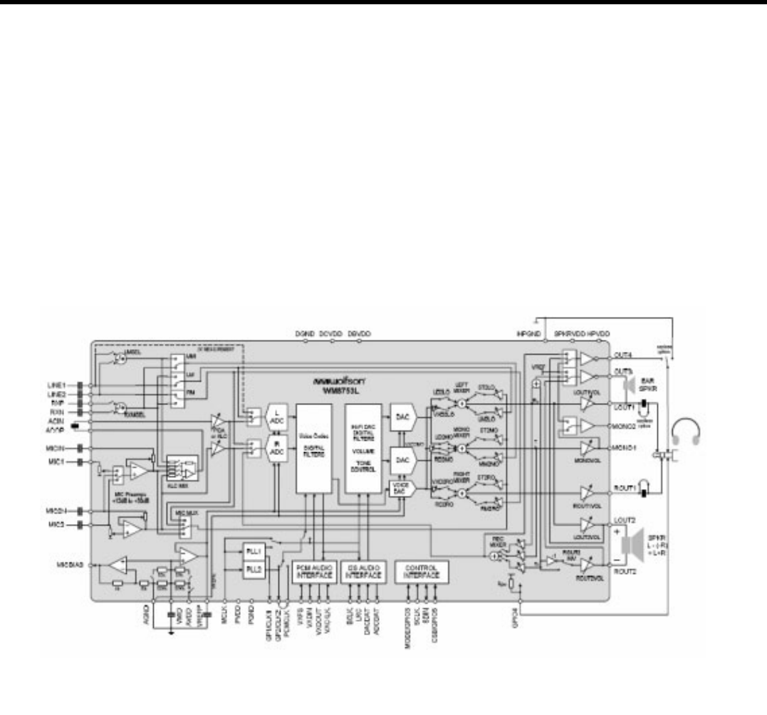
- 64 -
3. TECHNICAL BRIEF
3.13.2.3. WM8753L audio interface
The WM8753L is a low Power, high quality stereo Codec with integrated Voice CODEC designed for
portable digital telephony applications such as mobile phone, or headset with Hi-Fi playback capability.
The device integrates dual interfaces to two differentially connected microphones, and includes
drevers for speakers, headphone and earpiece. External component requirements are reduced as no
separate microphone or headphone amplifiers are required.
Advanced on-chip digital signal processing performs tone control, Bass Boost and automatic level
control for the microphone or line input through the ADC.
LGE Internal Use Only
Copyright © 2007 LG Electronics. Inc. All right reserved.
Only for training and service purposes
Figure. Detailed diagram of WM8753L audio interface
- 65 -
3. TECHNICAL BRIEF
LGE Internal Use Only
Copyright © 2007 LG Electronics. Inc. All right reserved.
Only for training and service purposes
MSM6275A BLK Handset main MIC BLK
Place near
(CODEC VSS)
MSM pin W18
10%
SDCC_DAT1_GPIO99
F25
M25
SDCC_DAT2_GPIO100
SDCC_DAT3_GPIO101
M26
MICFBN
MICFBP
AC21
MICINN
AC19
AC20
MICINP
MICOUTN
AA18
AA19
MICOUTP
MDP_VSYNC_PRIMARY_GPIO105
AD2
AE3
MDP_VSYNC_SECONDA_GPIO104
MIC1N
AF20
MIC1P
AE20
AF21
MIC2N
MIC2P
AF22
MICBIAS
T15
AC22
HPH_L
W17
AA17
HPH_R
EAR1ON
AE18
EAR1OP
AF18
CCOMP
AA20
AF19
AUXIN
AE19
AUXIP
AC18
AUXON_AUXOR
AUXOP_AUXOL
AC17
C611
NANA
C608
NA
C610
0.1u
C607
C609
NA
L600
100nH
C600
10p
WM_HPH_R
WM_HPH_L
MICINP
WM_MONO1
WM_MONO2
MICFBN
MICFBP
MICINN
MICOUTN
MICOUTP
WM_RXN
WM_RXP
C245 1u
EVLC18S02015
VA200
C247
10p
2.2K
R221
C251
39p
2.2K
R227
MIC200
SUMY0009203
1
2
C252
39p
VA201
EVLC18S02015
39p
C246
1uC248
WM_MICBIAS
WM_MIC1P
WM_MIC1N
Head Set Jack BLK
1608
CONNECTOR VBATT_SENSE PIN CHECK!!
1%
Between (VBATT & +5V_PWR) and (Mic signal)
CAD for EMC Noise
1%
C249 47n
R717
NA
VREG_MSMP_2.7V
R716
0
U203
NCS2200SQ2T2G
GND
2
1
OUT
VCC
5
3
VIN+
VIN-
4
AP_VDD_IO_2.7V
5
6
7
8
9
11
12
13
14
15
16
17
18
19
2
20
21
22
3
4
CN202
1
10
C242 33u
FB503 1000
33uC244
10pC258
47pC255
R223 68
R225 NA
C240 1u
RSB6.8CST2RVA211
EVLC14S02050VA205
1
2
3
4
5
EVLC14S02050
VBATT
CN203
VA208
smd_1608h_9_r
1u
C254
2.2K
R217
680K
R226
C259
33p
0.01u
C257
C238
0.1u
C239
10p
USB_VBUS_IN
VA206 EVLC14S02050
4
G2
1IN 2
OUT
NFM21PC105B1A3
U205
G1
3
FB245
10u
C237
100K R219
+5V_PWR
47pC256
EVLC14S02050VA204
PSD12-LFD200
VREG_MSMP_2.7V
INSTPAR
470K
R224
C253
33u
VA203 EVLC18S02003
330K
R218
VA207 EVLC14S02050
C241 1u
AP_VDD_IO_1.8V
EVLC18S02003
VA202
0.1u
C260
68R222
ICVL0505600V150FRVA209
1M
R216
VA210 RSB6.8CST2R
11K
R228
PSD05-LF
D201 INSTPAR
USB_D+
USB_D-
EAR_SENSE_N
HOOK_SENSE
WM_LOUT1
UART_RXD
UART_TXD
VBAT_TEMP
WM_MIC2N
WM_MIC2P
REMOTE_PWR_ON
VBATT_SENSE
WM_ROUT1
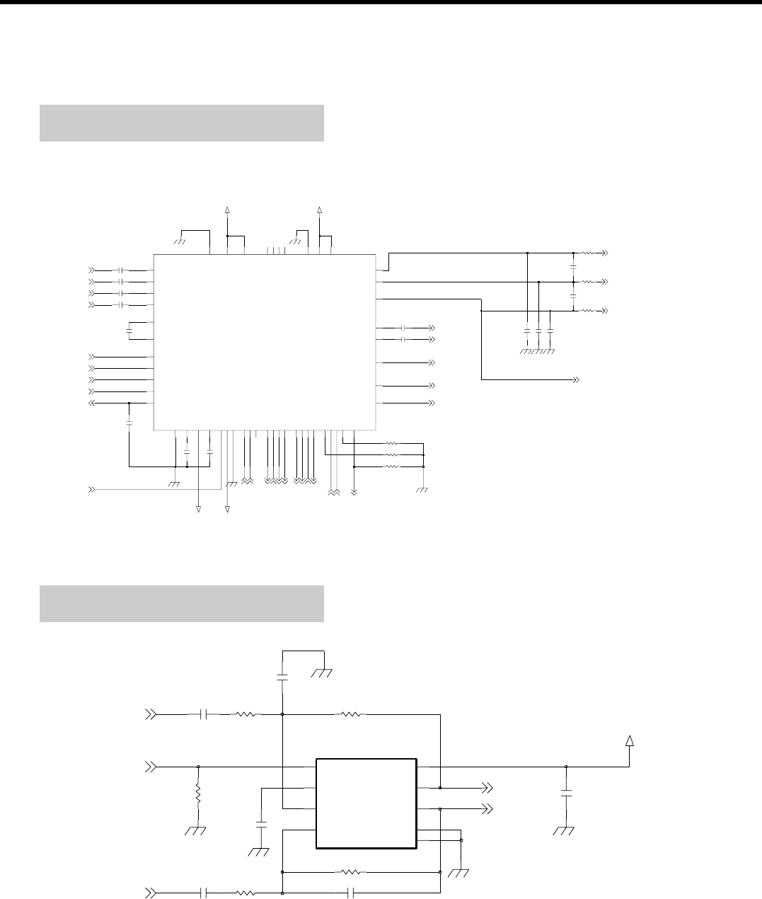
- 66 -
3. TECHNICAL BRIEF
LGE Internal Use Only
Copyright © 2007 LG Electronics. Inc. All right reserved.
Only for training and service purposes
Audio Codec(WM8753) BLK
WM_DVDD
WM_AVDD
WM_AVDD
1u C229
NAC231
C227
10p
1uC224
100K R214
C223
NA
C226 1u
1u C230
C233 39p
C222 1u
AP_VDD_CAM_1.8V
R213100K
NA
R209
C232 39p
R212
0
C235
4.7u
R211
0
A8
VMID
A4
B5 VREF
VXCLK
H3
VXDIN
J1
J2 VXDOUT
VXFS
J3
R215100K
MONO2
A7
NC1 C8
NC2 F8
NC3
NC4 G2
E8
OUT3
OUT4 E9
J8 PCMCLK
H9 PGND
PVDD
G9
ROUT1 D9
ROUT2 B9
RXN
C2
RXP
B1
H1 SCLK
G1 SDIN
SPKRVDD
GPIO4
HPVDD F9
HP_SPKRGND C9
LINE1
A2
A1 LINE2
D8
LOUT1
A9
LOUT2
H4 LRC
J6 MCLK
C1 MIC1
MIC1N
D2
D1 MIC2
MIC2N
E2
MICBIAS
B4
F1 MODE_GPIO3
MONO1 B6
B7
U202
WM8753LEB-RV
A3 ACIN
B3 ACOP
ADCDAT
J5
A5 AGND
AVDD
A6
J4 BCLK
CSB_GPIO5
F2
DACDAT
H5
H6
DBVDD
DCVDD J7
DGND H7
G8 GP1_CLK1
GP2_CLK2
J9
E1
C225 1u
C228 1u
C234
4.7u
WM_DVDD
C236
4.7u
WM_DACDAT
WM_LRC
WM_MSPRXD0
MSPTXD0
MSPTCK0
MSPTFS0
WM_BCLK
WM_ADCDAT
SPK_AMP_EN
WM_HPH_R
WM_HPH_L
RECEIVER--
WM_ROUT2WM_MICBIAS
AU_SW
VT_SW
PM_SDA
PM_SCL
AU_19.2M
WM_RXP
WM_RXN
RECEIVER-
WM_MONO2
WM_MONO1
WM_MIC1N
WM_ROUT1
WM_MIC1P
WM_LOUT1WM_MIC2N
WM_LOUT2
WM_MIC2P
RECEIVER+
Audio Amp for loud Speaker
SPEAKER AMP
C262
0.068u
68KR230
R232 68K
R233
10K
10K
R229
C261
NA
0.068u
C267
AP_+VPWR
R231
100K
2.2u
C263
1_SHUTDOWN
BYPASS
2
7
GND
IN+
3
4IN- 9
PGND
6
VDD
VO+ 5
VO- 8
TPA6205A1DRBRU208
C268 NA
C266
0.22u
SPKL-
SPKL+
SPK_AMP_EN
WM_LOUT2
WM_ROUT2
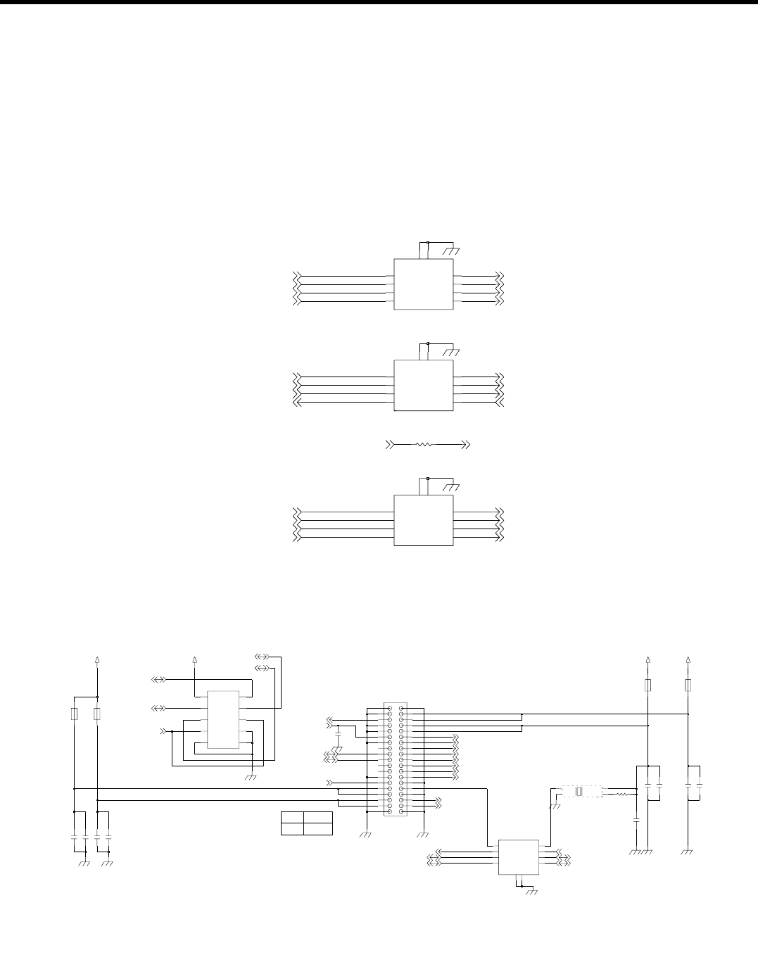
- 67 -
3. TECHNICAL BRIEF
3.14. Camera interface
KS10 has two cameras : 2M Pixel CMOS and VGA Pixel CMOS Camera Below figures shows the
camera board to board connector and camera I/F signal.
3.14.1. Mega Camera Interface
LGE Internal Use Only
Copyright © 2007 LG Electronics. Inc. All right reserved.
Only for training and service purposes
R206 0
EVRC18S03Q015050R
G1 5
G2 10
1INOUT_A1
INOUT_A2
2
3INOUT_A3
INOUT_A4
4
INOUT_B1 9
8
INOUT_B2
INOUT_B3 7
6
INOUT_B4
FL201
5
G2 10
1INOUT_A1
INOUT_A2
2
3INOUT_A3
INOUT_A4
4
INOUT_B1 9
8
INOUT_B2
INOUT_B3 7
6
INOUT_B4
FL202 EVRC18S03Q015050R
G1
G2 10
1INOUT_A1
INOUT_A2
2
3INOUT_A3
INOUT_A4
4
INOUT_B1 9
8
INOUT_B2
INOUT_B3 7
6
INOUT_B4
FL200 EVRC18S03Q015050R
G1 5
CCIRID(0)_CAM
CCIRID(1)_CAM
CCIRID(3)_CAM
CCIRID(2)_CAM
CCIRICLK_CAM
CCIRID(5)_CAM
CCIRID(4)_CAM
CCIRID(3)
CCIRID(2)
CCIRID(1)
CCIRID(0)
CCIRID(7)
CCIRID(6)
CCIRID(5)
CCIRID(4)
CCIRID(6)_CAM
CCIRID(7)_CAM
CCIRIHS_CAM
CCIRIVS_CAM
CAMCLK_27MHZ_CAM CAMCLK_27MHZ
CCIRIHS
CCIRIVS
CCIRICLK
CAMCLK_27MHZ
MCAM_27M
Figure. Schematic of 2 Mega Camera EMI/ESD filter I/F
Hi-Z
AXK7L34227
DrivenLOW
HIGH
2M_CAMERA
C2130.1u
HB-1M1005-601JT
FB207
C21210u
31
32
33
34
4
5
6
7
8
9
17 18
19
2
20
21
22
23
24
25
26
27
28
29
3
30
G1
G2
G3 G4
1
10
11
12
13
14
15
16
CN200
CSC3R270000BEVRS00 X200
27MHz
GND
2
3OUT
TRI_OPEN 1
4
VDD
AP_VDD_IO_2.7V
HB-1M1005-601JT
FB206
R207 100K
AP_VDD_CAM_2.7V
C214
0.01u
C21010u
10
INOUT_A1
1
2INOUT_A2
INOUT_A3
3
4INOUT_A4
9
INOUT_B1
INOUT_B2 8
7
INOUT_B3
INOUT_B4 6
FL203 EVRC18S03Q015050R
G1
5
G2
AP_VDD_CAM_2.7V
0.1u C211
10u C218
C207
1u
COM1
3
COM2
9
6
GND
IN1
4
IN2
8
NC1
5
NC2
7
NO1
2
NO2
101
VCC
SLAS4717EPMTR2G
U200
AP_VDD_CAM_1.8V
C21510u
0.1u C217
HB-1M1005-601JT
FB204
FB205
HB-1M1005-601JT
0.1u C216
I2CSDA0_SW
I2CSCL0_CAM
I2CSDA0_CAM
2M_PWDN
I2CSCL0_CAM
I2CSDA0_CAM
I2CSCL0_SW
I2CSDA0_SW
2M_RSTn
2M_RSTn_CAM
2M_RSTn_CAM
CCIRID(4)_CAM
CCIRID(3)_CAM
I2CSCL0_SW
CCIRID(2)_CAM
CAM_PWR_EN
CCIRID(1)_CAM
CCIRID(0)_CAM
CCIRIVS_CAM
CCIRIHS_CAM
I2CSDA0
I2CSCL0
CCIRICLK_CAM
CCIRID(7)_CAM
CCIRID(6)_CAM
CCIRID(5)_CAM
Figure. Schematic of 2 Mega Camera Board to Board Connector

- 68 -
3. TECHNICAL BRIEF
LGE Internal Use Only
Copyright © 2007 LG Electronics. Inc. All right reserved.
Only for training and service purposes
Table. Interface between 2M Camera Module and Main Board (in camera module)
Image data outputOYUV730
Image data outputOYUV629
Image data outputOYUV528
Image data outputOYUV427
Digital I/O VoltagePIOVDD32
Digital I/O VoltagePIOVDD31
Image data outputOYUV326
Digital Core VoltagePDVDD 1.8V33
GroundGNDGND6
Initializes sensor, Active LowIRESET5
GroundGNDGND4
GroundGNDGND3
Pixel ClockOPCLK2
Non-connectionNCNC11
Non-connectionNCNC10
Clock for two-wire serial interfaceISCK9
Data for two-wire serial interfaceI/OSDA8
Non-connectionNCNC7
Analog VoltagePAVDD 2.8V16
Actuator VoltagePLVDD 2.8V15
Actuator VoltagePLVDD 2.8V14
Power down mode, active HighIPDOWN13
GroundGNDGND12
Master clockICLKIN21
GroundGNDGND20
Vertical Synchronous signalOVSYNC19
Horizontal Synchronous signalOHSYNC18
Analog VoltagePAVDD 2.8V17
GNDGNDGND1
GroundGNDGND22
Image data outputOYUV023
Image data outputOYUV124
Image data outputOYUV225
Digital Core VoltagePDVDD 1.8V34
NotePortNameNo

- 69 -
3. TECHNICAL BRIEF
The 2MCamera module is connected to main board with 34pin Board to Board connector
(AXK8L34125). Its interface is dedicated camera interface port in STN8810. The camera port supply
24MHz master clock to camera module and receive 40.078MHz pixel clock (max.15fps), vertical sync
signal, horizontal sync signal, reset signal and 8bits data from camera module.
The camera module is controlled by I2C port from STN8810.
LGE Internal Use Only
Copyright © 2007 LG Electronics. Inc. All right reserved.
Only for training and service purposes
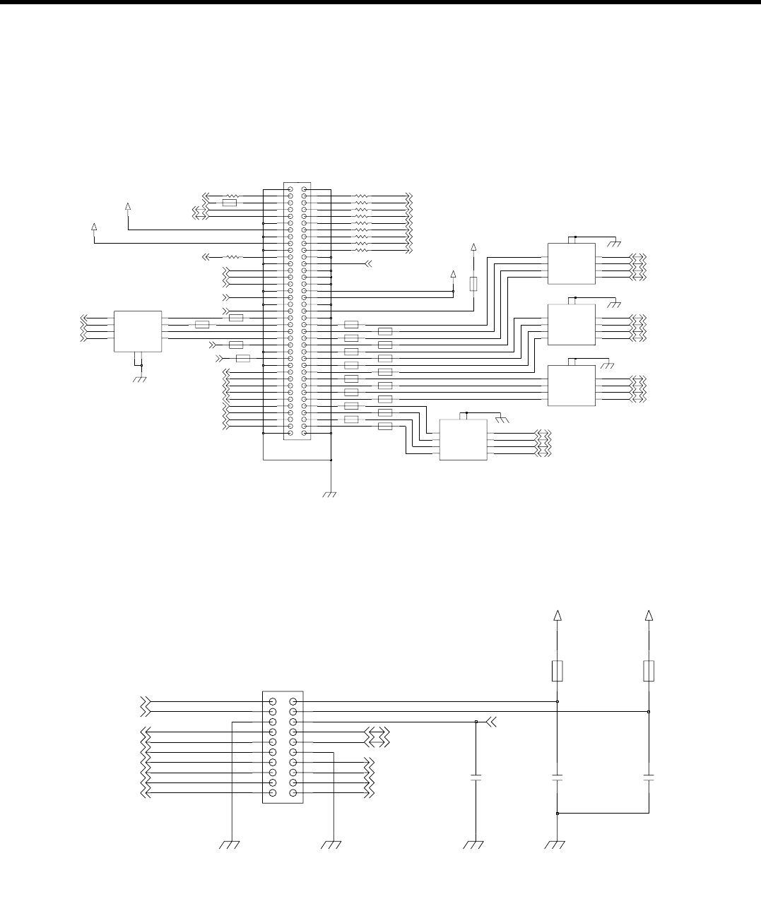
- 70 -
3. TECHNICAL BRIEF
3.14.2. VGA Camera Interface
LGE Internal Use Only
Copyright © 2007 LG Electronics. Inc. All right reserved.
Only for training and service purposes
Figure. Schematic of Main slider FPCB B to B connector (in main BD)
Figure. Schematic of VGA Camera Board to Board Connector (in main slider FPCB)
AXK7L70227
MAIIN-SLIDER CON-HEADER
0R728
0R727
0R726
0R725
0R724
0R723
0R722
0R721
0R720
0R719
0R718
FB239
AP_VDD_CAM_2.7V
FB224
FB235
FB232
FB229
AP_+VPWR
INOUT_B4
5
G1 10
G2
1
INOUT_A1
INOUT_A2 2
3
INOUT_A3
INOUT_A4 4
INOUT_B1
9
8INOUT_B2
INOUT_B3
7
6
EVRC14S03Q030100R FL204
FB222
FB236
FB237
5
G1 10
G2
1
INOUT_A1 2
INOUT_A2 3
INOUT_A3
INOUT_A4 4
INOUT_B1
9
8INOUT_B2
INOUT_B3
7
6INOUT_B4
FB227
EVRC14S03Q030100R FL208
FB233
FB242
FB225
FB243
FB221
AP_VDD_CAM_1.8V
FB244
INOUT_A3
3
4INOUT_A4
9
INOUT_B1
INOUT_B2 8
7
INOUT_B3
INOUT_B4 6
FL206 EVRC18S03Q015050R
G1
5
G2
10
INOUT_A1
1
2INOUT_A2
FB241
G1 5
G2 10
INOUT_A1 1
2
INOUT_A2
INOUT_A3 3
4
INOUT_A4
9INOUT_B1
INOUT_B2
8
7INOUT_B3
INOUT_B4
6
FL205EVRC14S03Q030100R
FB223
AP_VDD_LCD_2.8V
1
INOUT_A1
INOUT_A2 2
3
INOUT_A3
INOUT_A4 4
INOUT_B1
9
8INOUT_B2
INOUT_B3
7
6INOUT_B4
EVRC14S03Q030100R FL207
5
G1 10
G2
FB234
FB231FB230
64
65
66
67
68
69
7
70
8
9
G1 G2
G3 G4
50
51
52
53
54
55
56
57
58
59
6
60
61
62
63
35 36
37
38
39
4
40
41
42
43
44
45
46
47
48
49
5
20
21
22
23
24
25
26
27
28
29
3
30
31
32
33
34
CN201
1
10
11
12
13
14
15
16
17
18
19
2
FB240
FB238
CCIRID(2)
CCIRID(1)
CCIRID(0)
CCIRICLK
CCIRIHS
I2CSCL0_CAM
I2CSDA0_CAM
VGA_RSTn
CCIRIVS
CCIRID(7)
CCIRID(6)
CCIRID(5)
CCIRID(4)
CCIRID(3)
DIS_CSN
LCD_NRESET
DIS_WEN
DIS_RS
CAMCLK_27MHZ_CAM
RECEIVER+
RECEIVER-
RECEIVER--
LCD_VS
LCD_DATA(3)
LCD_DATA(5)
LCD_DATA(7)
LCD_DATA(9)
LCD_DATA(11)
LCD_DATA(13)
LCD_DATA(15)
LCD_DATA(14)
LCD_DATA(12)
LCD_DATA(10)
LCD_DATA(8)
LCD_DATA(0)
LCD_DATA(2)
LCD_DATA(4)
LCD_DATA(6)
MOT_PWR-
WLED_CTL
VGA_STANDBY
KPD_DRV_N
KEY_ROW(0)
KEY_ROW(1)
KEY_ROW(2)
KEY_ROW(3)
KEY_COL(4)
KEY_COL(5)
KEY_COL(6)
KEY_COL(7)
LCD_DATA(1)
VGA_CAMERA
AXK720145G
HB-1M1005-601JT
FB101
FB100
HB-1M1005-601JT
1u
C102
AP_VDD_CAM_2.7V
C101
0.1u
C100
0.1u
192
20
3
4
5
6
7
8
9
1
10 11
12
13
14
15
16
17
18
AP_VDD_CAM_1.8V
CN100
VGA_STANDBY
CAMCLK_27MHZ_CAM
I2CSCL0_CAMCCIRICLK_CAM
I2CSDA0_CAMCCIRID(0)_CAM
CCIRID(1)_CAM
VGA_RSTn
CCIRIHS_CAMCCIRID(2)_CAM
CCIRIVS_CAMCCIRID(3)_CAM
CCIRID(7)_CAMCCIRID(4)_CAM
CCIRID(6)_CAMCCIRID(5)_CAM

- 71 -
3. TECHNICAL BRIEF
The VGA Camera module is connected to main slider FPCB with 20pin Board to Board
connector(AXK820145). The main slider FPCB is connected to main board with 70pin board to board
connector.
Its interface is dedicated camera interface port in STN8810. The camera port supply 24MHz master
clock to camera module and receive 13.5MHz pixel clock (max. 15fps), vertical sync signal, horizontal
sync signal, reset signal and 8bits data from camera module.
The camera module is controlled by I2C port from STN8810.
LGE Internal Use Only
Copyright © 2007 LG Electronics. Inc. All right reserved.
Only for training and service purposes
Table. Interface between Camera Module and Main Board (in camera module)
Image Data[1]OD16
Image Data[0]OD05
Video Output Clock D[0:7]OPCLK4
GroundGNDGND3
Master ClockIMCLK2
Image Data[6]OD611
Image Data[5]OD510
Image Data[4]OD49
Image Data[3]OD38
Image Data[2]OD27
Data for two wire serial interfaceI/OSDA16
GroundGNDGND15
Horizontal SynchronizationOHSYNC14
Vertical SynchronizationOVSYNC13
Image Data[7]OD712
Analog core circuit power supply voltage
& Digital I/O circuit power supply voltage
PAVDD & IOVDD20
Digital core circuit power supply voltagePDVDD19
Reset initializes sensor Active LowIRESET18
Clock for two wire serial interfaceISCL17
Active ëHighíIENABLE1
NotePortNameNo
- 72 -
3. TECHNICAL BRIEF
3.14.3. LCD backlight / Camera LDO
U100(in SUB board, AAT3151) is a charge pump. U301(in main board, BH18LB1WHFB) supply a
1.8V power of mega camera and VGA camera. U303(in main board, MIC5219-2.7YM5) supply a 2.7V
power of mega camera and VGA camera.
These parts are controlled by GPIOs of STN8810.
LGE Internal Use Only
Copyright © 2007 LG Electronics. Inc. All right reserved.
Only for training and service purposes
Figure. Schematic of charge pump
LCD_Backlight driver
ZD101
RSB6.8CST2R
1u
C102
C101
1u
1u
C100
100K
R101
D3
D4 1
EN_SET
2
9GND
13 PGND
8VIN
VOUT
5
AP_+VPWR
AAT3151IWP_T1
3
C1+
C1- 4
C2+ 6
7
C2- 10
D1 11
D2 12
U100
4.7u
C103
WLED_CTL
LED_ANODE
LED4
LED3
LED2
LED1
Figure. Schematic of camera LDO
AP_+VPWR AP_VDD_CAM_2.7V
AP_VDD_CAM_1.8V
1u
C305
2.2u
C309
AP_+VPWR
U301 BH18LB1WHFV
BGND 6
GND
2
5
NC
1STBY
VIN
34
VOUT 4
BYPEN
3GND
2
1IN 5
OUT
U303
MIC5219-2.7YM5
C308
1u
2.2u
C307C306
470p
CAM_PWR_EN
CAM_PWR_EN
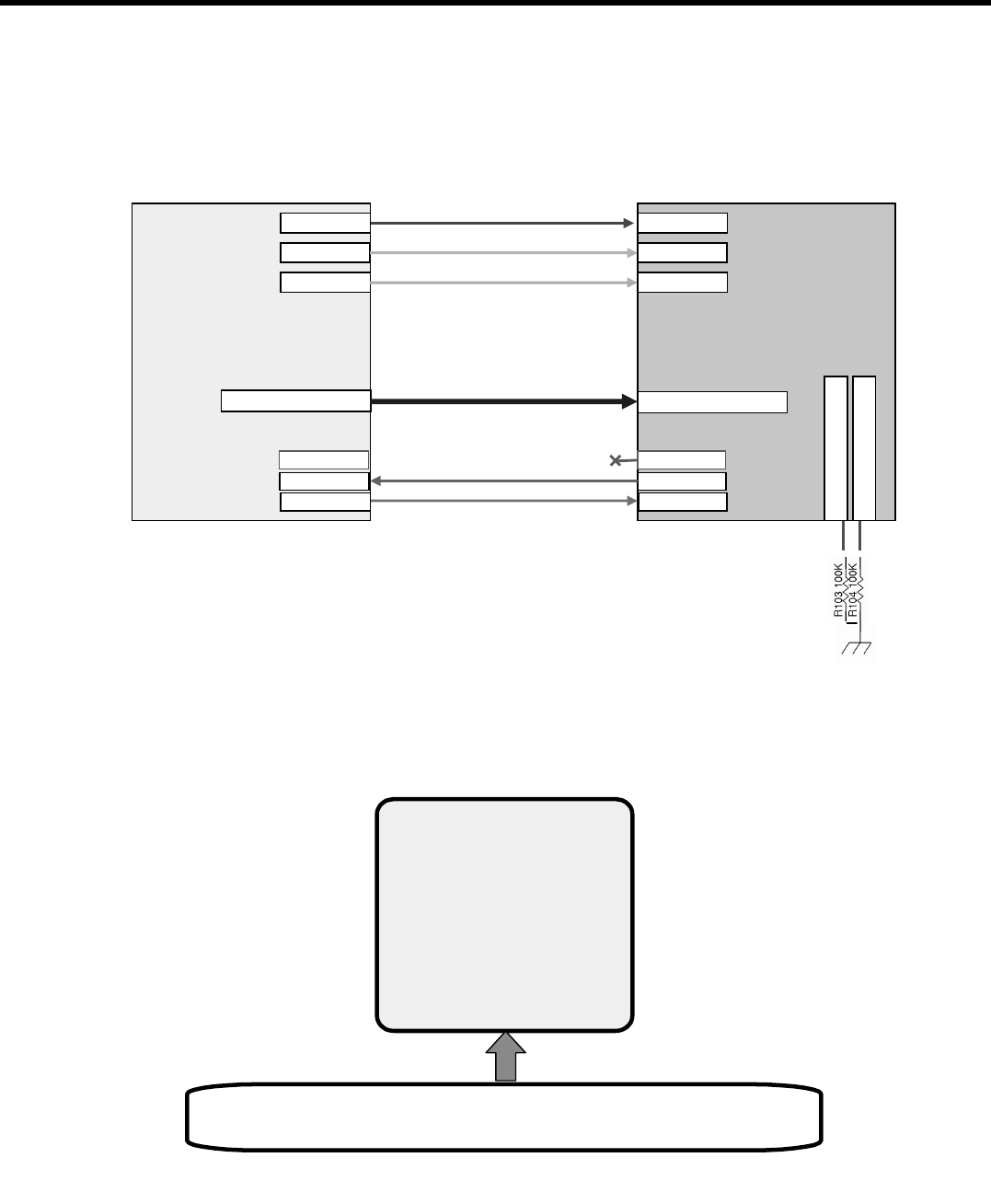
- 73 -
3. TECHNICAL BRIEF
3.14.4. LCD module
LGE Internal Use Only
Copyright © 2007 LG Electronics. Inc. All right reserved.
Only for training and service purposes
Figure. LCD I/F Block Diagram
STN8810 LCD
MM_LCD_DATA[0:15]
MM_LCD_WE_N
MM_LCD_ADS_N
MM_LCD_CS_N
MM_LCD_IF_MODE_1
MM_LCD_IF_MODE_0
MM_LCD_RESET
MM_LCD_VSYNC
MM_LCD_RD_N
MM_LCD_RESET
MM_LCD_VSYNC
MM_LCD_RD_N
MM_LCD_DATA[0:15]
MM_LCD_WE_N
MM_LCD_ADS_N
MM_LCD_CS_N
NC
Figure. LCD Module
MAIN LCD
MODULE
260K Color TFT
240 * 320 Pixel
BD663474(Hitachi) Graphic Controller Driver Main LCD Panel
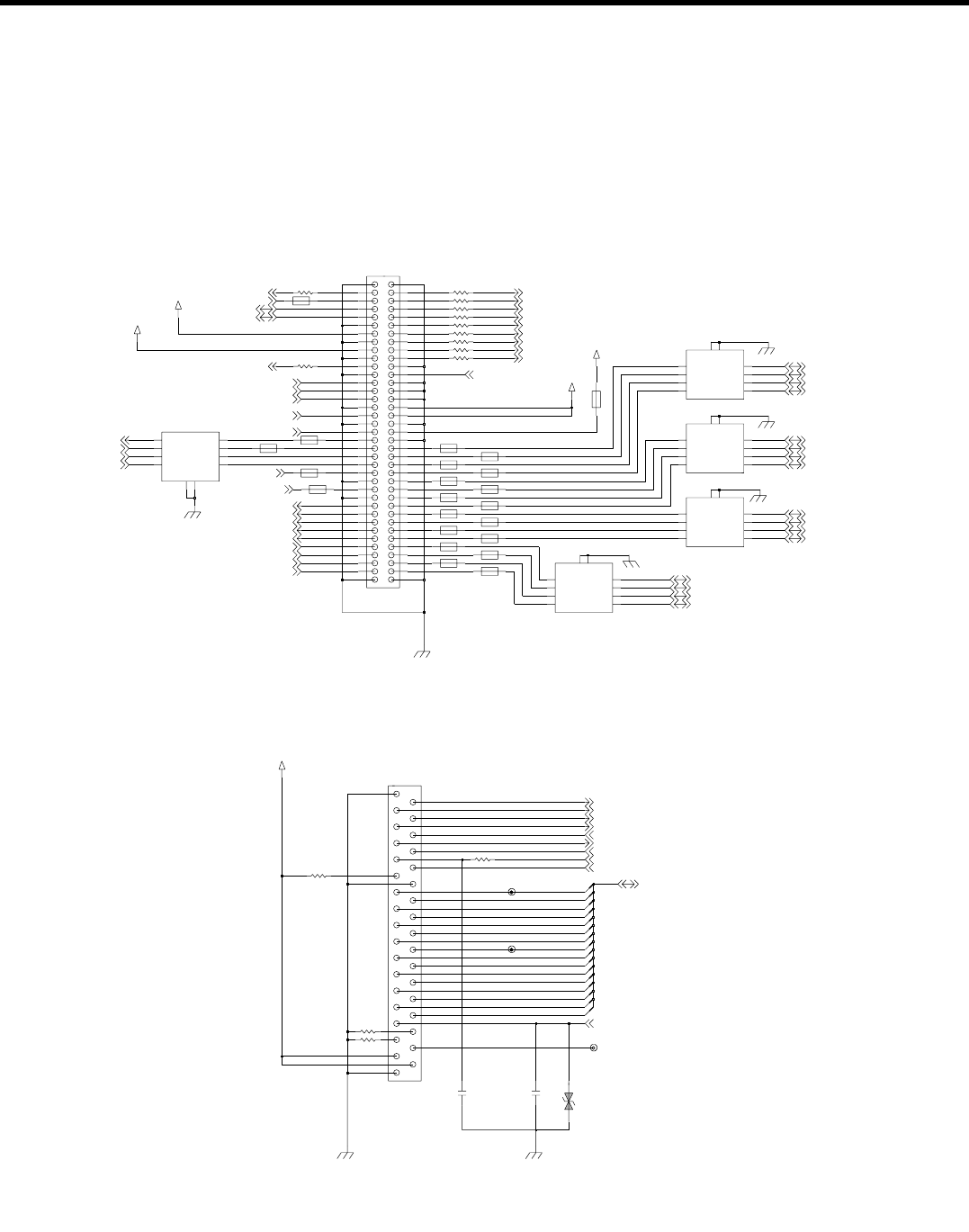
- 74 -
3. TECHNICAL BRIEF
3.14.5. Display
LCD module is connected to SUB board with 35-pin zip connector(XF2B-3545-31A).
The LCD is controlled by 16-bit in STN8810.
LGE Internal Use Only
Copyright © 2007 LG Electronics. Inc. All right reserved.
Only for training and service purposes
Figure. Schematic of Main slider FPCB B to B connector (in main BD)
Figure. Schematic of LCD connector (in SUB board)
AXK7L70227
MAIIN-SLIDER CON-HEADER
0R728
0R727
0R726
0R725
0R724
0R723
0R722
0R721
0R720
0R719
0R718
FB239
AP_VDD_CAM_2.7V
FB224
FB235
FB232
FB229
AP_+VPWR
INOUT_B4
5
G1 10
G2
1
INOUT_A1
INOUT_A2 2
3
INOUT_A3
INOUT_A4 4
INOUT_B1
9
8INOUT_B2
INOUT_B3
7
6
EVRC14S03Q030100R FL204
FB222
FB236
FB237
5
G1 10
G2
1
INOUT_A1 2
INOUT_A2 3
INOUT_A3
INOUT_A4 4
INOUT_B1
9
8INOUT_B2
INOUT_B3
7
6INOUT_B4
FB227
EVRC14S03Q030100R FL208
FB233
FB242
FB225
FB243
FB221
AP_VDD_CAM_1.8V
FB244
INOUT_A3
3
4INOUT_A4
9
INOUT_B1
INOUT_B2 8
7
INOUT_B3
INOUT_B4 6
FL206 EVRC18S03Q015050R
G1
5
G2
10
INOUT_A1
1
2INOUT_A2
FB241
G1 5
G2 10
INOUT_A1 1
2
INOUT_A2
INOUT_A3 3
4
INOUT_A4
9INOUT_B1
INOUT_B2
8
7INOUT_B3
INOUT_B4
6
FL205EVRC14S03Q030100R
FB223
AP_VDD_LCD_2.8V
1
INOUT_A1
INOUT_A2 2
3
INOUT_A3
INOUT_A4 4
INOUT_B1
9
8INOUT_B2
INOUT_B3
7
6INOUT_B4
EVRC14S03Q030100R FL207
5
G1 10
G2
FB234
FB231FB230
64
65
66
67
68
69
7
70
8
9
G1 G2
G3 G4
50
51
52
53
54
55
56
57
58
59
6
60
61
62
63
35 36
37
38
39
4
40
41
42
43
44
45
46
47
48
49
5
20
21
22
23
24
25
26
27
28
29
3
30
31
32
33
34
CN201
1
10
11
12
13
14
15
16
17
18
19
2
FB240
FB238
CCIRID(2)
CCIRID(1)
CCIRID(0)
CCIRICLK
CCIRIHS
I2CSCL0_CAM
I2CSDA0_CAM
VGA_RSTn
CCIRIVS
CCIRID(7)
CCIRID(6)
CCIRID(5)
CCIRID(4)
CCIRID(3)
DIS_CSN
LCD_NRESET
DIS_WEN
DIS_RS
CAMCLK_27MHZ_CAM
RECEIVER+
RECEIVER-
RECEIVER--
LCD_VS
LCD_DATA(3)
LCD_DATA(5)
LCD_DATA(7)
LCD_DATA(9)
LCD_DATA(11)
LCD_DATA(13)
LCD_DATA(15)
LCD_DATA(14)
LCD_DATA(12)
LCD_DATA(10)
LCD_DATA(8)
LCD_DATA(0)
LCD_DATA(2)
LCD_DATA(4)
LCD_DATA(6)
MOT_PWR-
WLED_CTL
VGA_STANDBY
KPD_DRV_N
KEY_ROW(0)
KEY_ROW(1)
KEY_ROW(2)
KEY_ROW(3)
KEY_COL(4)
KEY_COL(5)
KEY_COL(6)
KEY_COL(7)
LCD_DATA(1)
XF2B-3545-31A-P
LCD Connector
(lower contact)
C105
820p
0R115
35
4
5
6
7
8
9
20
21
22
23
24
25
26
27
28
29
3
30
31
32
33
34
1
10
11
12
13
14
15
16
17
18
19
2
CN100
ZD100 RSB6.8CST2R
100K
R102
R103 100K
R104 100K
1uC104
AP_VDD_LCD_2.8V
TP100
TP102
TP101
LCD_NRESET
LCD_DATA(0)
LCD_VS
DIS_CSN
DIS_WEN
DIS_RS
LED_ANODE
LED3
LED2
LED1
LCD_DATA(1)
LCD_DATA(10)
LCD_DATA(11)
LCD_DATA(12)
LCD_DATA(13)
LCD_DATA(14)
LCD_DATA(15)
LCD_DATA(2)
LCD_DATA(3)
LCD_DATA(4)
LCD_DATA(5)
LCD_DATA(6)
LCD_DATA(7)
LCD_DATA(8)
LCD_DATA(9)
LCD_DATA(0:15)
LED4
- 75 -
3. TECHNICAL BRIEF
LGE Internal Use Only
Copyright © 2007 LG Electronics. Inc. All right reserved.
Only for training and service purposes
Table. Interface between 2M Camera Module and Main Board (in camera module
Interface I/O PowerPVCC234
Interface mode selectIIM230
ResetIRESET29
Data Bus (Instruction & Display Data)I/ODB1528
Data Bus (Instruction & Display Data)I/ODB1427
Maker ID (HI : VCC2 level)OMID(HIGH)32
Interface mode selectIIM131
Data Bus (Instruction & Display Data)I/ODB1326
Power Supply for Analog CircuitPVCC133
Power Supply for LED-LED(AN)6
Ground for LED-LED(CA)5
Ground for LED-LED(CA)4
Ground for LED-LED(CA)3
Ground for LED-LED(CA)2
Read StrobeIRD11
Write StrobeIWR10
Register SelectIRS9
Chip SelectICS8
Frame Head Pulse SignalOVSYNC-OUT7
Data Bus (Instruction & Display Data)I/ODB316
Data Bus (Instruction & Display Data)I/ODB215
Data Bus (Instruction & Display Data)I/ODB114
Data Bus (Instruction & Display Data)I/ODB013
GroundGNDGND12
Data Bus (Instruction & Display Data)I/ODB821
Data Bus (Instruction & Display Data)I/ODB720
Data Bus (Instruction & Display Data)I/ODB619
Data Bus (Instruction & Display Data)I/ODB518
Data Bus (Instruction & Display Data)I/ODB417
GroundGNDGND1
Data Bus (Instruction & Display Data)I/ODB922
Data Bus (Instruction & Display Data)I/ODB1023
Data Bus (Instruction & Display Data)I/ODB1124
Data Bus (Instruction & Display Data)I/ODB1225
Ground GNDGND35
NotePortNameNo
- 76 -
3. TECHNICAL BRIEF
3.15 Bluetooth
KS10 supported bluetooth, which is possible to data file transfer, BT headset call.
CPU (STn8810) interfaces with bluetooth one chip module (U401) which includes RF and baseband.
The STLC2500C is a single chip ROM-based Bluetooth solution for applications requiring integration
up to HCI level.
The STLC2500C's main interfaces are UART for HCI transport between CPU (STn8810) and bluetooth
module, PCM for voice between audio codec.(WM8753) and bluetooth module and GPIOs for control
purposes. Voice data is transferred to CPU(STn8810) through audio codec.(WM8753).
The radio has been designed specifically for single chip requirements and for low power consumption.
Radio signal from bluetooth antenna (ANT400) is transferred to bluetooth module through BALUN filter
(FL400). Bluetooth module has its’ own oscillator (X400, 27MHz) for normal operation and use sleep
clock(32.768KHz) from PM6650, PMIC of MSM 6275.
■ Bluetooth™ specification compliance: V1.2
■ Transmit Power : Power Class2
■ Ultra low power architecture with 3 different low power levels:
- Sleep Mode
- Deep Sleep Mode
- Complete Power Down Mode
LGE Internal Use Only
Copyright © 2007 LG Electronics. Inc. All right reserved.
Only for training and service purposes
Figure. Diagram of STLC2500C

LGE Internal Use Only
Copyright © 2007 LG Electronics. Inc. All right reserved.
Only for training and service purposes
3. TECHNICAL BRIEF
- 77 -
3.16 Main Features
3.16.1. Main features of KS10
- Slide Type
- WCDMA(2100) + GSM(900,1800) + PCS(1900) Triple mode
- Main LCD: 320*240, 262K (2.4”)
- 2.0M Pixel CMOS Camera
- VGA CMOS Camera
- φ17 speaker
- Stereo Headset
- Video telephony in WCDMA with camera
- HSDPA up to 1.8Mbps
- Loud Speaker phone(in GSM and WCDMA)
- 64 Poly Sound
- MP3/AAC/WMA decoder and play
- MPEG4 encoder/decoder and play/save
- H.263 decoder
- JPEG en/decoder
- Support Bluetooth, USB
- 104 x 52 x 18.9 mm
- 950mAh hard pack
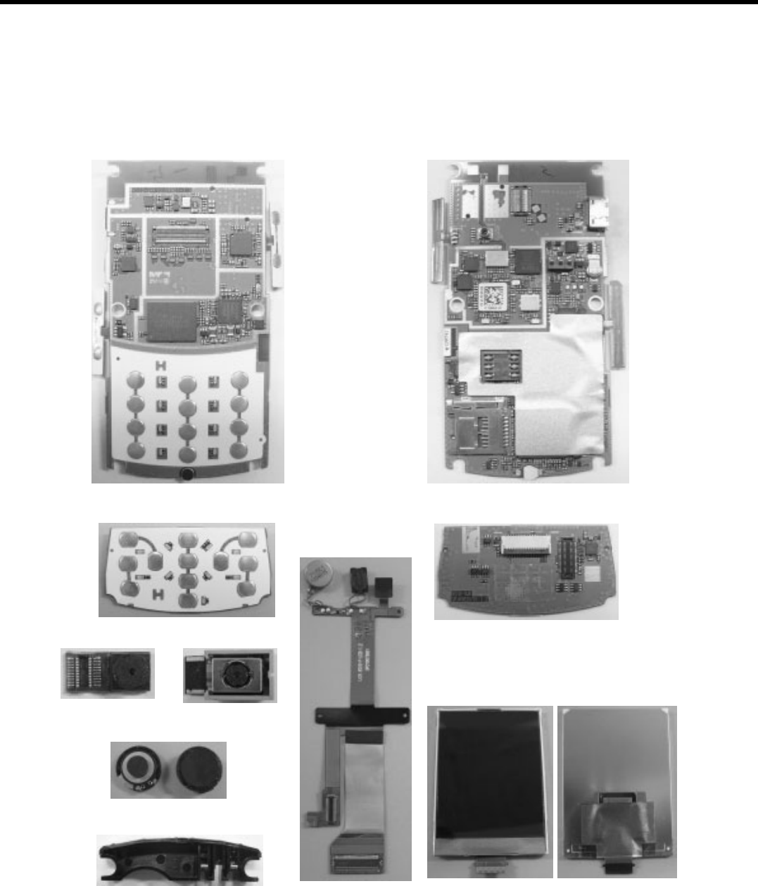
LGE Internal Use Only
Copyright © 2007 LG Electronics. Inc. All right reserved.
Only for training and service purposes
2. Main Components of KS10
3. TECHNICAL BRIEF
- 78 -
LCD
MAIN Bottom SideMAIN Top Side
KEY Top Side KEY Bottom Side
1.3M camera
VGA camera
LCD FPCB
Intenna
Speaker
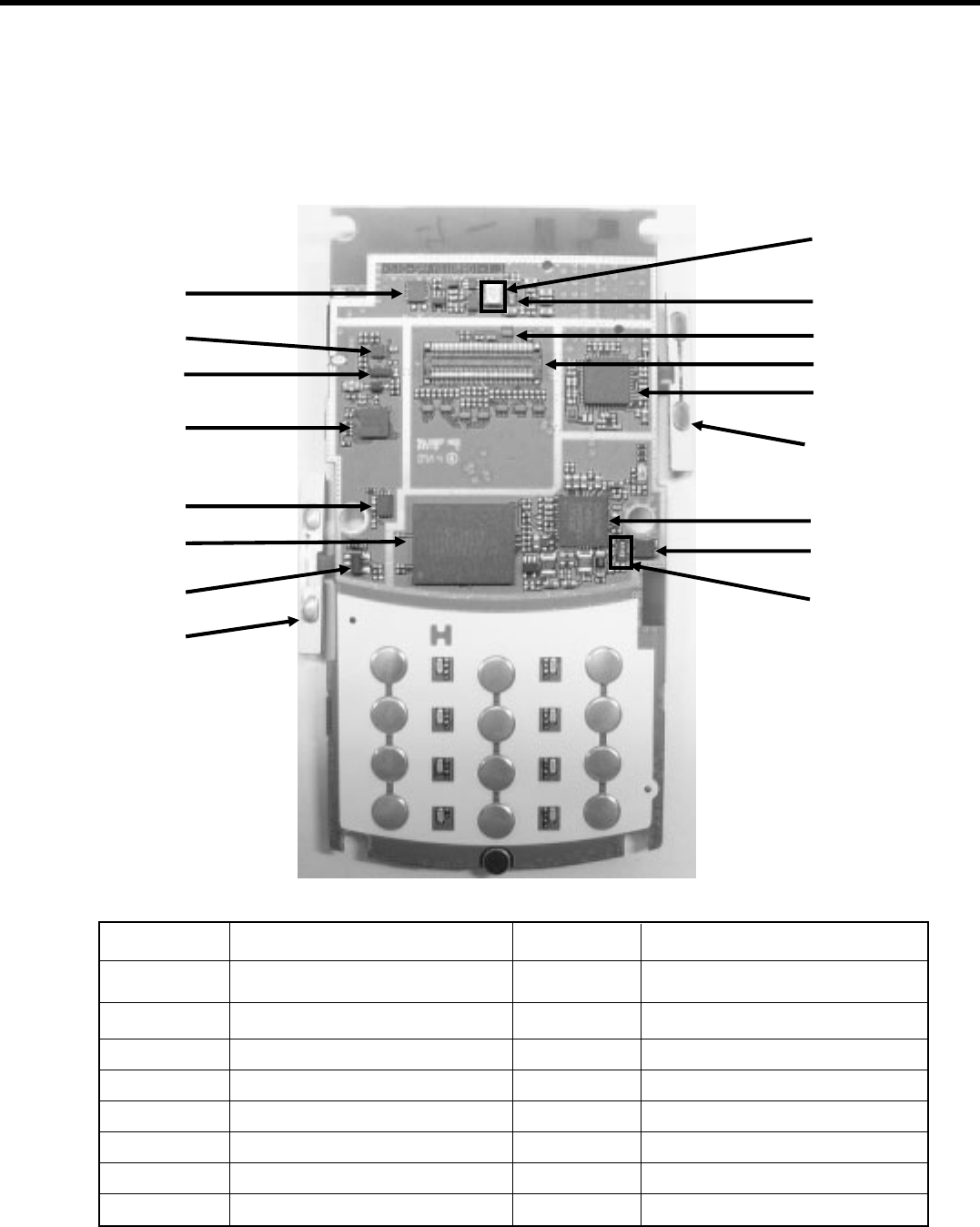
LGE Internal Use Only
Copyright © 2007 LG Electronics. Inc. All right reserved.
Only for training and service purposes
3. TECHNICAL BRIEF
- 79 -
2. 1 Main Top Side
CN201
X500
U508
U701
U700
U402
U404
U406
U403
X200
U207
FL206
U306 X700
FL203
Side Key
Side Key
Reference Description Reference Description
U207 over voltage protection IC X200 27MHz OSCILLATOR
U406 Analog Switch FL203 EMI_ESD FILTER
U403 Analog Switch Multiplexer FL206 EMI_ESD FILTER
U404 Key Coder IC CN201 B To B CONNECTOR
U402 hall-effect switch IC U508 RF Receiver(RFR6250E)
U701 MCP Memory U700 PMIC for MSM
U306 LDO Regulator X500 TCXO 19.2MHz
--X700 TCXO 32.768kHz
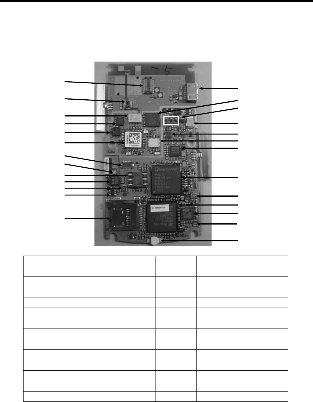
LGE Internal Use Only
Copyright © 2007 LG Electronics. Inc. All right reserved.
Only for training and service purposes
2.2. Main Bottom Side
3. TECHNICAL BRIEF
- 80 -
Reference Description Reference Description
CN200 B To B CONNECTOR CN202 Connector(I/O, Ear jack, Power)
SW500 RF SWITCH CONNECTOR U501 GSM/EDGE Quadband PAM
CN402 JTAG-JIG-FPCB-CON CN203 Battery Connector
FL500 FILTER, SAPERATOR BAT700 Back up Battery
U506 DUPLEXER, GSM U208 AUDIO AMPLIFIER
U505 PAM _power amplifier module U502 Voltage Controlled Oscillator
U500 RF Transceiver (RTR6250D) U202 Audio Codec.
FL400 SAW FILTER _BPF U600 MSM6275 (Modem BB Chip)
J300 USIM Connector X100 19.2MHz Oscillator
U401 Bluetooth Single Chip U100 STN8810S12B2V1 (CPU)
X400 19.2MHz Oscillator U310 PMIC for CPU
U400 LDO Regulator L301 Power Inductor
S300 Micro-SD CONNECTOR MIC200 Microphone
CN202
J300 U600
U100
U310
CN402
U208
CN200
U505
U506
FL500
U500
SW500
S300
U202
BAT700
CN203
X100
U401
X400
U400
MIC200
U501
U502
L301
FL400
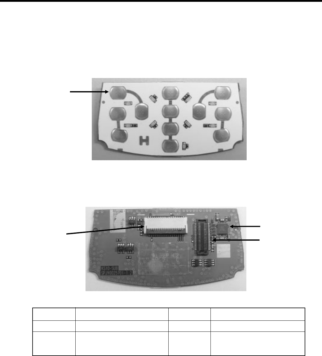
LGE Internal Use Only
Copyright © 2007 LG Electronics. Inc. All right reserved.
Only for training and service purposes
3. TECHNICAL BRIEF
- 81 -
2.3. KEY Top Side
2.4. KEY Bottom Side
SW100
CN101
U100
CN100
Reference Description Reference Description
SW100 Dome Switch U100 LCD Backlight Driver
CN100 LCD Connector CN101 FUNCTION-SLIDER Connector
(FPCB to KEYPCB)
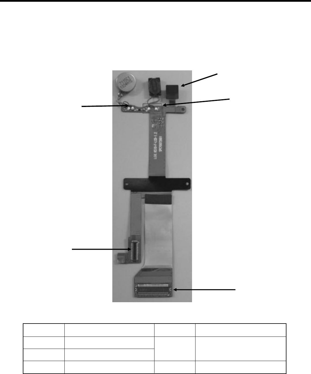
LGE Internal Use Only
Copyright © 2007 LG Electronics. Inc. All right reserved.
Only for training and service purposes
2.5. LCD FPCB
3. TECHNICAL BRIEF
- 82 -
Reference Description Reference Description
Vibrator Vibrator PAD CN101
FUNCTION-SLIDER
Receiver Receiver PAD
Connector (FPCB to KEYPCB)
CN100 VGA_CAMERA Connector CN102
MAIN-SLIDER CON-SOCKET
CN101
CN100
Receiver
CN102
Vibrator PAD
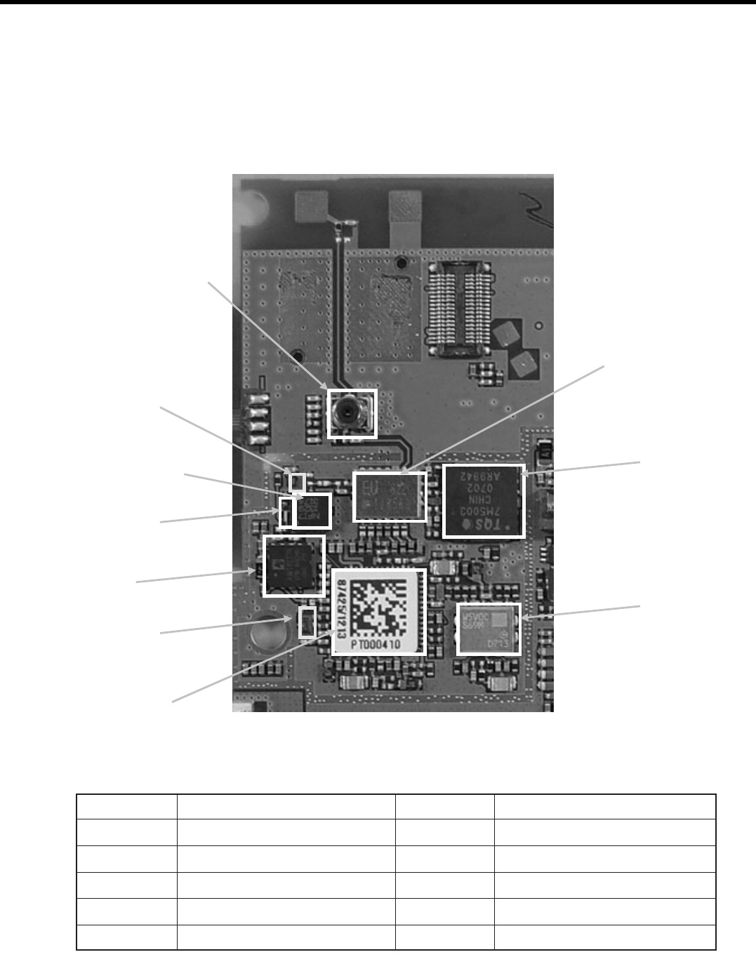
LGE Internal Use Only
Copyright © 2007 LG Electronics. Inc. All right reserved.
Only for training and service purposes
4. TROUBLE SHOOTING
- 83 -
4. TROUBLE SHOOTING
4.1 RF Component
RF component (Bottom)
U502
U503
U505
SW500
U504
U507
U501
U506
U500
FL500
Reference Description Reference Description
U505 WCDMA PAM U507 Coupler
U506 WCDMA Duplexer U501 GSM/D/PCS PAM
U503 WCDMA TX SAW U504 HDET
FL500 Front-End-Module U500 GSM/WCDMA Transceiver (RTR)
U502 GSM TX VCO SW500 RF Antenna Connector
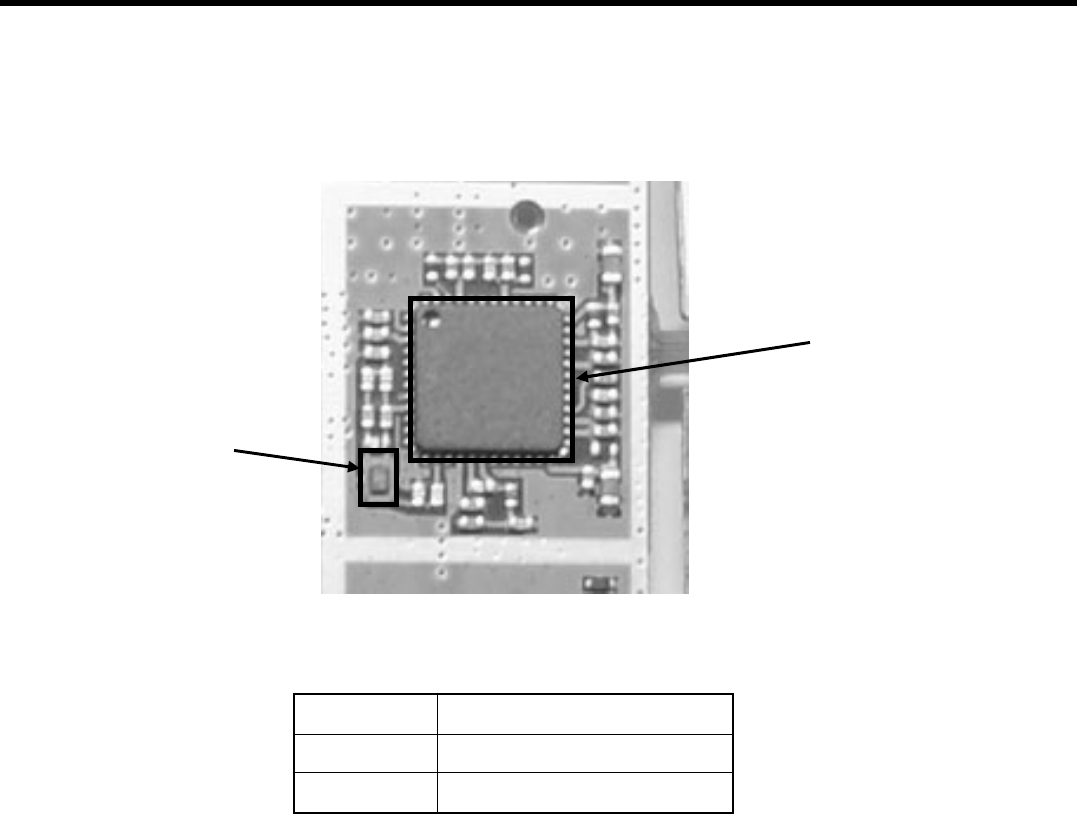
LGE Internal Use Only
Copyright © 2007 LG Electronics. Inc. All right reserved.
Only for training and service purposes
RF component (Top)
4. TROUBLE SHOOTING
- 84 -
FL501
U508
Reference Description
U508 RFR6250(WCDMA RX)
FL501 WCDMA RX SAW
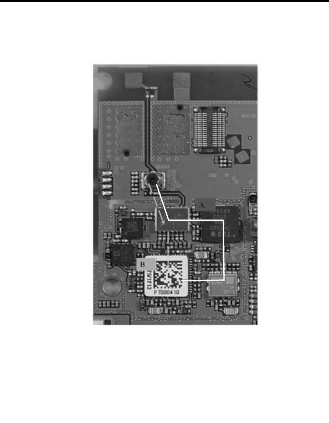
LGE Internal Use Only
Copyright © 2007 LG Electronics. Inc. All right reserved.
Only for training and service purposes
4. TROUBLE SHOOTING
- 85 -
4.2 SIGNAL PATH
GSM/DCS/PCS Rx Tx PATH
A. GSM/DCS/PCS Tx PATH
B. GSM/DCS/PCS Rx PATH
A
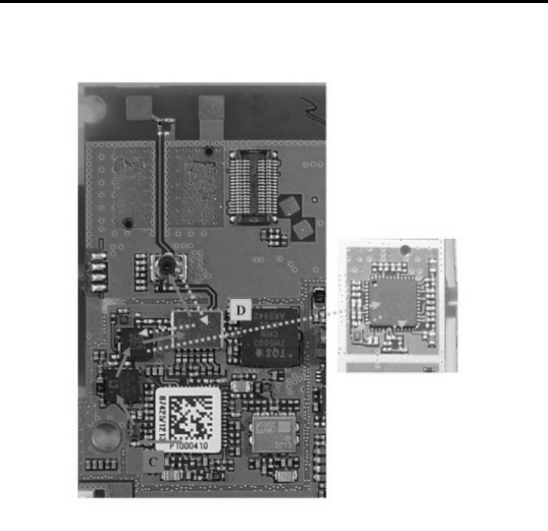
LGE Internal Use Only
Copyright © 2007 LG Electronics. Inc. All right reserved.
Only for training and service purposes
4. TROUBLE SHOOTING
- 86 -
WCDMA RX/ TX PATH
C. WCDMA Tx PATH
D. WCDMA Rx PATH
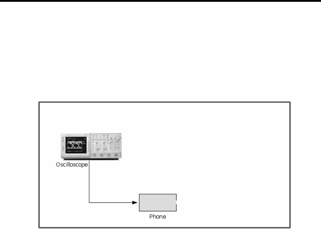
- 87 -
4. TROUBLE SHOOTING
4.3 Checking VCXO Block
The reference frequency (19.2MHz) from X100 (VCXO) is used WCDMA TX
part, GSM part and BB part.
LGE Internal Use Only
Copyright © 2007 LG Electronics. Inc. All right reserved.
Only for training and service purposes
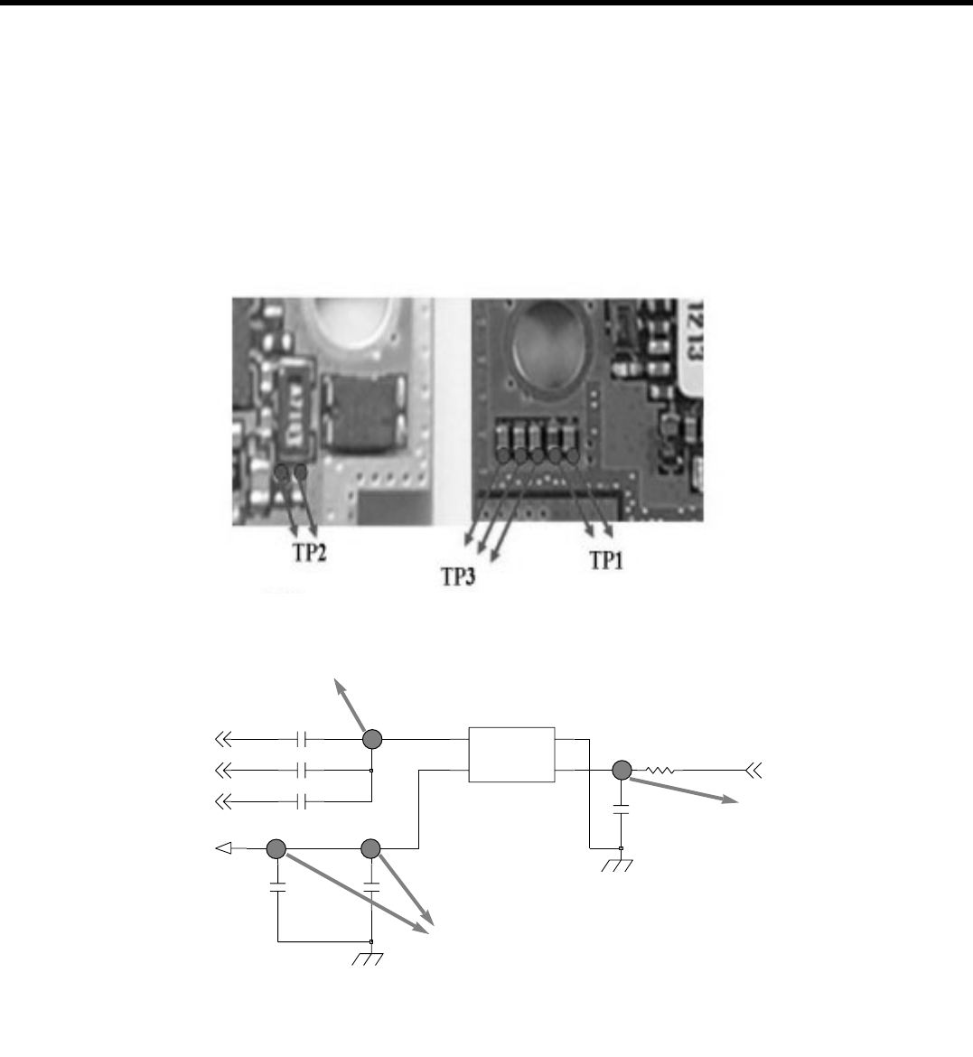
LGE Internal Use Only
Copyright © 2007 LG Electronics. Inc. All right reserved.
Only for training and service purposes
4. TROUBLE SHOOTING
- 88 -
Check 1. Crystal part
If you already check this crystal part, you can skip check 1.
Test Point (Crystal Part)
TCXO
C564
0.01u
C567
1000p
100ohm
R525
C563 1000p
2
GNDOUT
3
VCC
4VCONT 1
19.2MHz
X500
100pC559
C566
0.1uF
VREG_TCXO_2.85V
1000pC562
TCXO_PM
RTR6250_TCXO
RFR6250_TCXO
TRK_LO_ADJ
Schematic of the Crystal Part
TP3
TP2
TP1
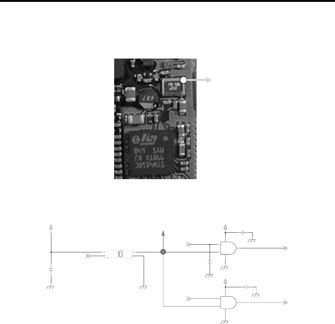
LGE Internal Use Only
Copyright © 2007 LG Electronics. Inc. All right reserved.
Only for training and service purposes
4. TROUBLE SHOOTING
- 89 -
Schematic of the Crystal Part (19.2MHz)
TP1
C153
0.1u
NA
C152
AP_VDD_IO_1.8V
3
1
TRI_OPEN
VDD
4
19.2MHz
X100
CSC3M192000EEVRS00
2
GND
OUT
1
2
4
VCC
5
NL17SZ08XV5T2
U101
3
GND
AP_VDD_IO_1.8V
AP_VDD_IO_1.8V
3
1
2
4
5
VCC U103
NL17SZ08XV5T2
GND
C1540.1u
C1510.1u
AU_CLK_EN
AU_19.2M
REQUEST_MC
PWREN
CPU_19.2M
TP1
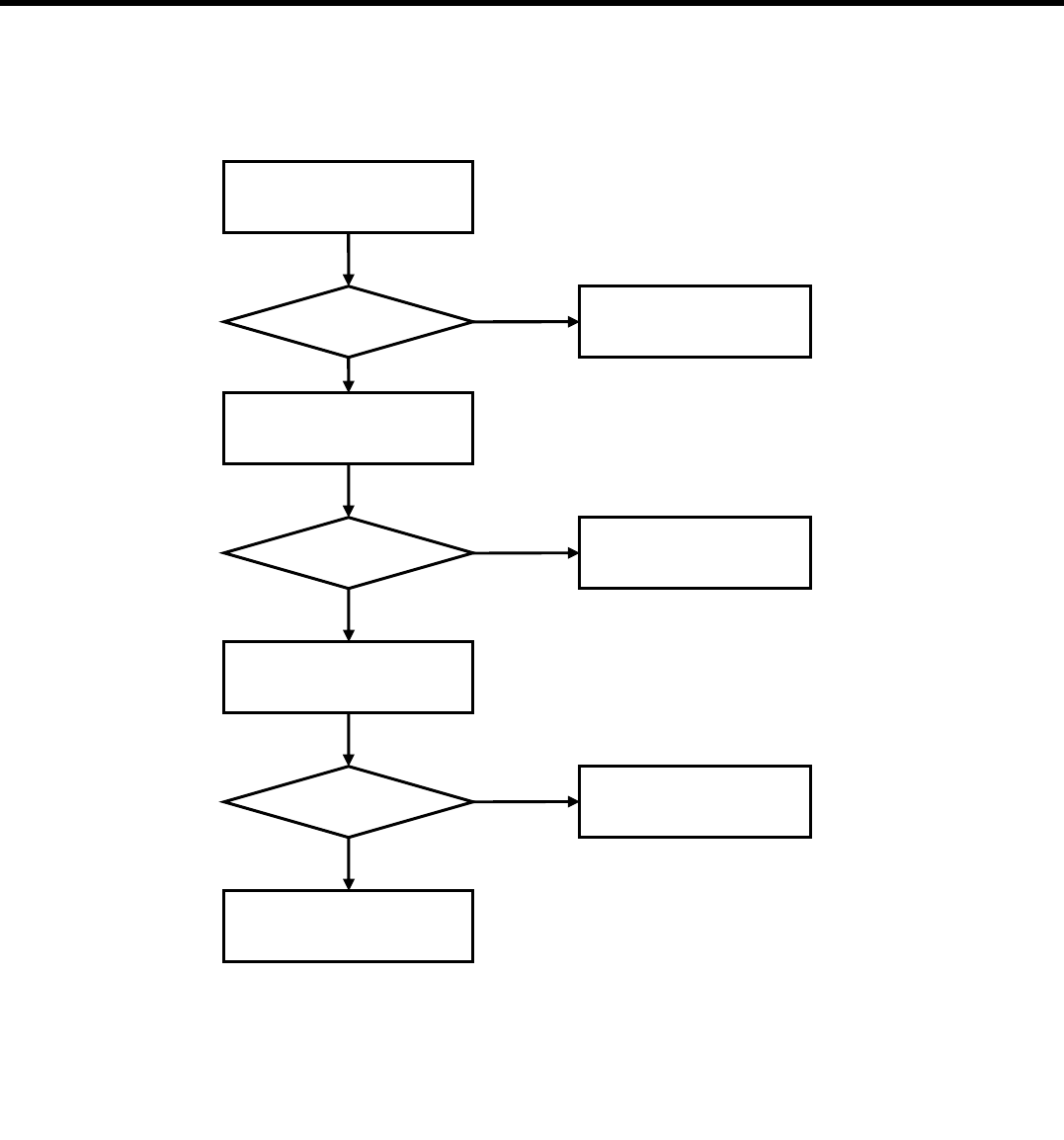
LGE Internal Use Only
Copyright © 2007 LG Electronics. Inc. All right reserved.
Only for training and service purposes
4. TROUBLE SHOOTING
- 90 -
Check TP1
VCC of VCXO
VCC 2.8V
Check TP2
TRK_LO_ADJ
3V Voltage 0V
Check TP3
With Oscilloscope
19.2MHz Signal
VCXO is OK
Check other part
Check PMIC
Check MSM
Check soldering
and components
Yes
Yes
Yes
No
No
No
≥
≥≥
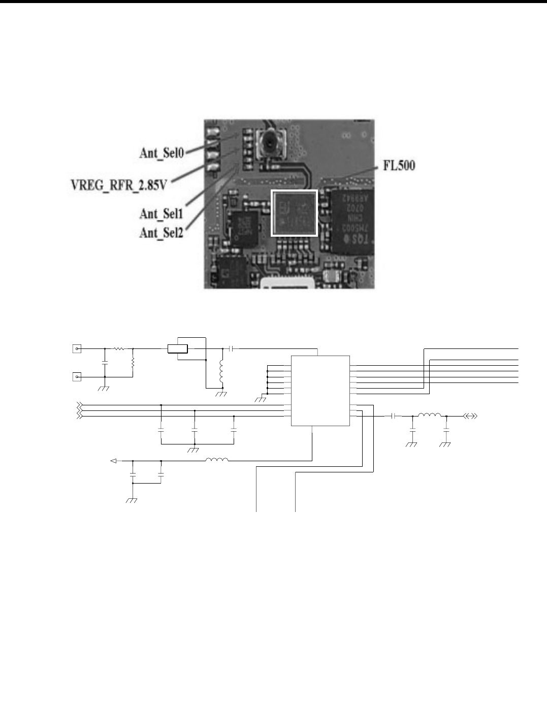
LGE Internal Use Only
Copyright © 2007 LG Electronics. Inc. All right reserved.
Only for training and service purposes
4. TROUBLE SHOOTING
- 91 -
4.4 Checking Ant. Switch Module Block
VREG_RFR_2.85V
C511
47p
C502
NA
56p
ANT500
C506
NA
C512
L514 7.5nH
C520
0.1u
ANT501
47p
C510
L502
1p
UMTS_TX_RX
VC1
17
15
VC2
VC3
14
16
VDD
ANT
12
DCS_PCS_TX
8
3
DCS_RX1
DCS_RX2
4
1
EGSM_RX1
EGSM_RX2
2
EGSM_TX
10
7
GND1
GND2
9
11
GND3
GND4
13
18
GND5
GND6
20
5
PCS_RX1
PCS_RX2
6
19
FL500ESHS-L090UB
0
C500 56pC501
C509
47p
KMS-512
SW500
ANT
G1
G2RF
56nH
L504
C519
47p
C507 1.5nH
C513
NA
WCDMA_2100
ANT_SEL0
ANT_SEL1
ANT_SEL2
Schematic of the Antenna Switch Block
LGE Internal Use Only
Copyright © 2007 LG Electronics. Inc. All right reserved.
Only for training and service purposes
4. TROUBLE SHOOTING
- 92 -
Logic Table of the Antenna Switch
Checking Switch Block power source
Check Soldering of
ANT_SEL0, 1, 2 High Level
2.5V < Voltgae < 3.0V Check VCC
TP1 VREG_RFRX_0_2.85V
Check the Logic
in each mode
YES
NO
Mode ANT_SEL0 ANT_SEL1 ANT_SEL2
EGSM TX High Low Low
EGSM RX Low Low Low
DCS/PCS TX Low High High
DCS RX Low Low High
PCS RX Low High Low
UMTS Low Low Low
LGE Internal Use Only
Copyright © 2007 LG Electronics. Inc. All right reserved.
Only for training and service purposes
4. TROUBLE SHOOTING
- 93 -
4.5 Checking WCDMA Block
START
1. Check VCXO 19.2MHz
2. Check ANT. SW Module
ANT_SEL0, 1, 2
3. Check RF Tx Level
4. Check PAM Block
5. Check RF Rx Level
6. Re-download SW & CAL.
1
5
3.4
2
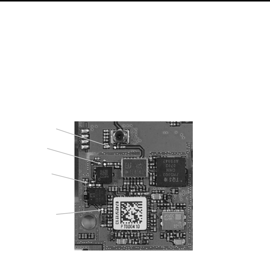
LGE Internal Use Only
Copyright © 2007 LG Electronics. Inc. All right reserved.
Only for training and service purposes
4.5.1 Checking VCXO Block
Refer to 3.3
4.5.2 Checking Ant. SW module
Refer to 3.4
4.5.3 Checking RF TX Level
Test Point (RF TX Level)
4. TROUBLE SHOOTING
- 94 -
TP1
TP2
TP3
TP4
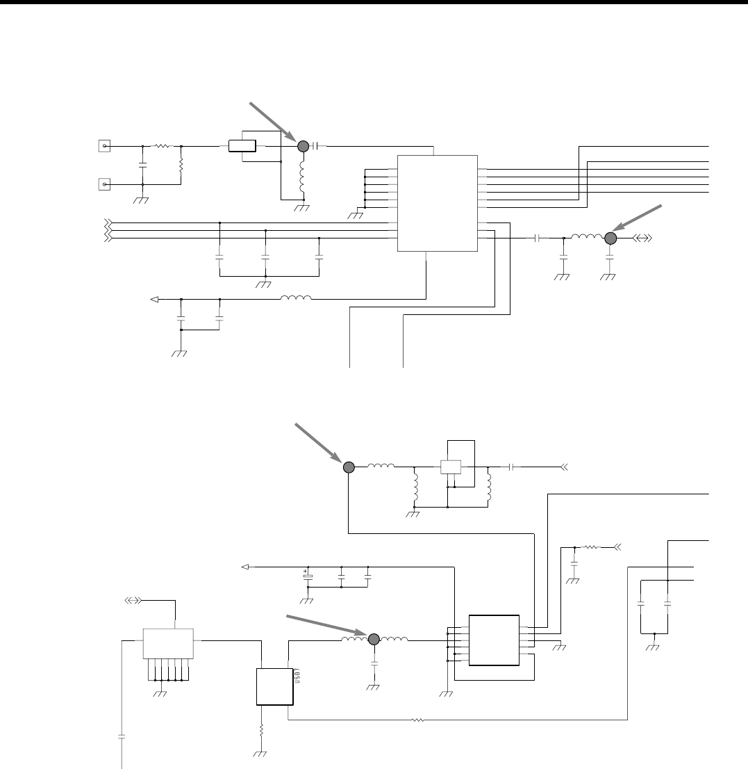
LGE Internal Use Only
Copyright © 2007 LG Electronics. Inc. All right reserved.
Only for training and service purposes
4. TROUBLE SHOOTING
- 95 -
VREG_RFR_2.85V
C511
47p
C502
NA
56p
ANT500
C506
NA
C512
L514 7.5nH
C520
0.1u
ANT501
47p
C510
L502
1p
UMTS_TX_RX
VC1
17
15
VC2
VC3
14
16
VDD
ANT
12
DCS_PCS_TX
8
3
DCS_RX1
DCS_RX2
4
1
EGSM_RX1
EGSM_RX2
2
EGSM_TX
10
7
GND1
GND2
9
11
GND3
GND4
13
18
GND5
GND6
20
5
PCS_RX1
PCS_RX2
6
19
FL500ESHS-L090UB
0
C500 56pC501
C509
47p
KMS-512
SW500
ANT
G1
G2RF
56nH
L504
C519
47p
C507 1.5nH
C513
NA
WCDMA_2100
ANT_SEL0
ANT_SEL1
ANT_SEL2
WCDMA
C570
0.01u
L526
3.9nH
C561
22p
12p
C581
C569
15p
C580
47
L527
1.2p
R531
51
100p
C574
INOUT
4
EFCH1950TDC1
U503
2
G1
5
G2
3
G3 1
+VPWR
C568
22u
U506ACMD-7601
ANT
G1
G2
G3
G4
G5
G6
G7
RX TX
1.8nHC560
C573
0.1u
450OHM
COUP
32
IN
1
OUT
6.2KR529
110 VCC2
4
VMODE
VREF 5
AWT6277R U505
GND1 3
GND2
6
7GND3
9GND4
GND5
11
2
RFIN
RFOUT
8
VCC1
C575
1.8nH
L525
8.2nH
C571
3.9nH
R530
0.01u
WCDMA_2100_TX_OUT
WCDMA_2100
W_VMODE_N
TP1
TP4
TP3
TP2
LGE Internal Use Only
Copyright © 2007 LG Electronics. Inc. All right reserved.
Only for training and service purposes
4. TROUBLE SHOOTING
- 96 -
For testing, Max power output is needed.
Set the Phone Tx is ON
and PDM is 450
Check TP1
Over 21dBm ?
Change the board
RF Tx Level is OK
Check FEM
Check PAM Block
Refer to 3.5.4
NO
YES
Check TP2
Over 19dBm ?
NO
YES
Check TP3
Over 15dBm ?
NO
YES
Check TP4
Over -5dBm ?
NO
YES
Check Duplexer
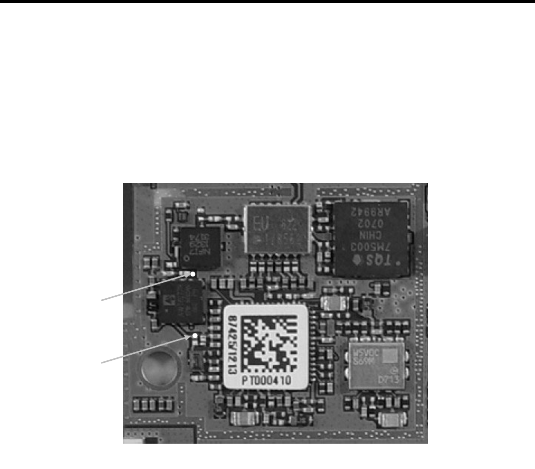
LGE Internal Use Only
Copyright © 2007 LG Electronics. Inc. All right reserved.
Only for training and service purposes
4. TROUBLE SHOOTING
- 97 -
4.5.4 Checking PAM Block
PAM control signal
PA_ON : WCDMA Tx Power Detect IC(HDET) Enable
PA_RO: WCDMA Tx Power Amp Gain Control
PA_ON must be HIGH(over 2.5V)
PA_FET_N must be LOW if the max Tx power is set (lower than 0.5V)
PAM_OUT
PAM_IN
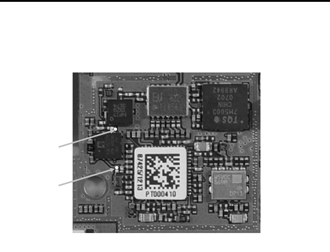
LGE Internal Use Only
Copyright © 2007 LG Electronics. Inc. All right reserved.
Only for training and service purposes
4. TROUBLE SHOOTING
- 98 -
PAM IN/OUT Signal
PAM OUT must be over 15dBm
PAM IN must be over -5dBm
PAM_IN
PAM_OUT
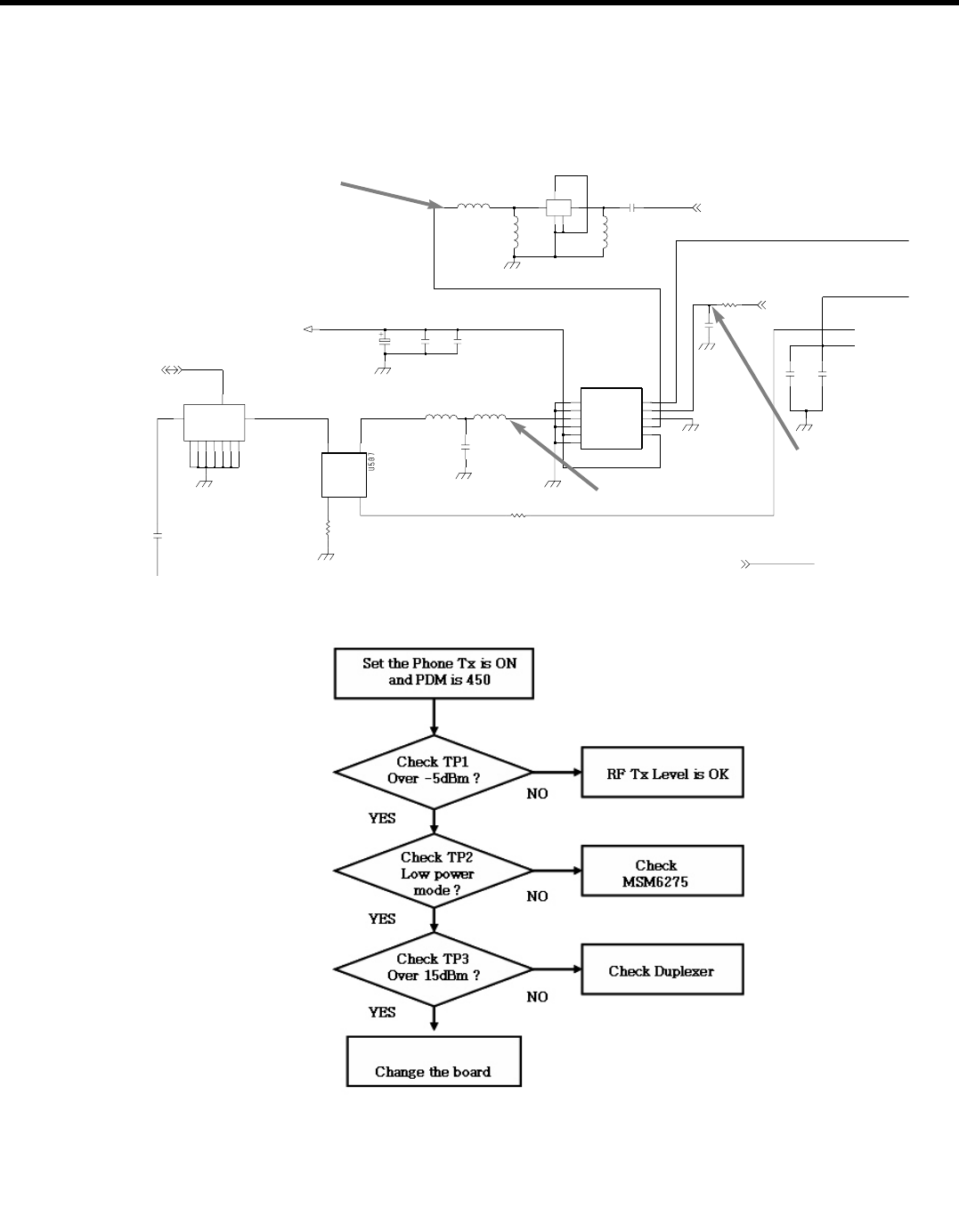
LGE Internal Use Only
Copyright © 2007 LG Electronics. Inc. All right reserved.
Only for training and service purposes
4. TROUBLE SHOOTING
- 99 -
WCDMA
C570
0.01u
L526
3.9nH
C561
22p
12p
C581
C569
15p
C580
47
L527
1.2p
R531
51
100p
C574
INOUT
4
EFCH1950TDC1
U503
2
G1
5
G2
3
G3 1
+VPWR
C568
22u
U506ACMD-7601
ANT
G1
G2
G3
G4
G5
G6
G7
RX TX
1.8nHC560
C573
0.1u
450OHM
COUP
32
IN
1
OUT
6.2KR529
110 VCC2
4
VMODE
VREF 5
AWT6277R U505
GND1 3
GND2
6
7GND3
9GND4
GND5
11
2
RFIN
RFOUT
8
VCC1
C575
1.8nH
L525
8.2nH
C571
3.9nH
R530
0.01u
WCDMA_2100_TX_OUT
WCDMA_2100
W_VMODE_N
ILNA_OUT
TP1
TP3
TP2
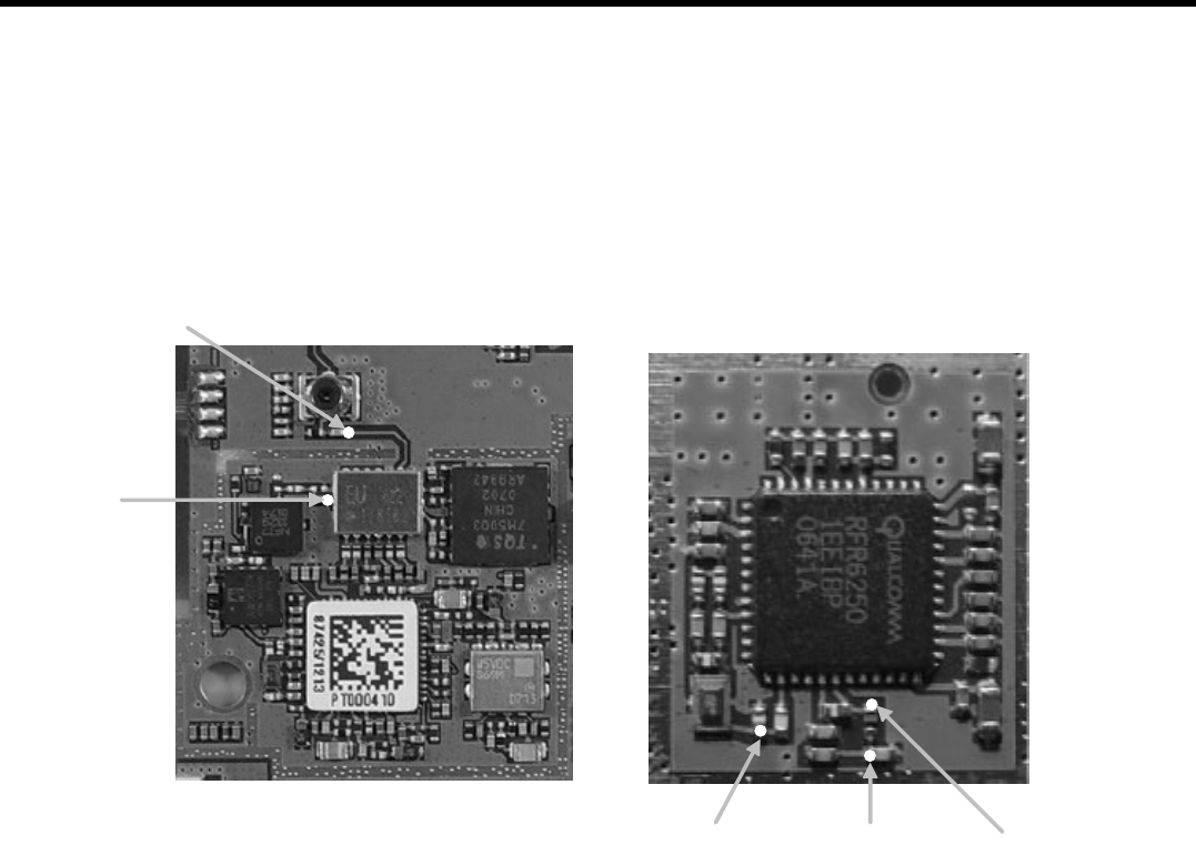
LGE Internal Use Only
Copyright © 2007 LG Electronics. Inc. All right reserved.
Only for training and service purposes
4.5.5 Check RF Rx Level
Test Point (RF Rx Level)
4. TROUBLE SHOOTING
- 100 -
TP1
TP2
TP4 TP3 BIAS
TOP BOTTOM
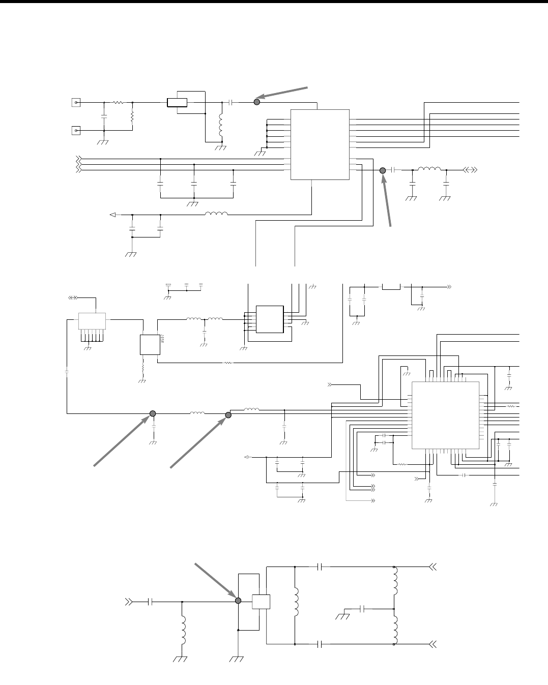
LGE Internal Use Only
Copyright © 2007 LG Electronics. Inc. All right reserved.
Only for training and service purposes
4. TROUBLE SHOOTING
- 101 -
VREG_RFR_2.85V
C511
47p
C502
NA
56p
ANT500
C506
NA
C512
L514 7.5nH
C520
0.1u
ANT501
47p
C510
L502
1p
UMTS_TX_RX
VC1
17
15
VC2
VC3
14
16
VDD
ANT
12
DCS_PCS_TX
8
3
DCS_RX1
DCS_RX2
4
1
EGSM_RX1
EGSM_RX2
2
EGSM_TX
10
7
GND1
GND2
9
11
GND3
GND4
13
18
GND5
GND6
20
5
PCS_RX1
PCS_RX2
6
19
FL500ESHS-L090UB
0
C500 56pC501
C509
47p
KMS-512
SW500
ANT
G1
G2RF
56nH
L504
C519
47p
C507 1.5nH
C513
NA
WCDMA_2100
ANT_SEL0
ANT_SEL1
ANT_SEL2
(1%)
4.7u
C593
VOPS VRMS
ADL5500 U504
C594
0.1u
100p
C592
C570
0.01u
12p
C581
R535
10
R532
11.3K
680p
C587
10p
C595
C599
100p
C580
47
L527
1.2p
C585
100p
R531
51
100p
C574
L532
100nH
L533
2.7nH
100p
C800
VREG_RFR_2.85V
C568
22u
U506ACMD-7601
ANT
G1
G2
G3
G4
G5
G6
G7
RX TX
32 VDDA5
VDDA6
34
36 VDDA7
VDDA8 45
41
VDDM
VDDRF1 3
12
VDDRF2
19 VDDRF3
10
PMIXM
PMIXP 11
RX_IM
21
20 RX_IP
23 RX_QM
RX_QP
22
46
R_BIAS
SBCK 42
SBDT 43
44
SBST
33 TCXO
25 UMTS_TUNE
VDDA1 7
24 VDDA2
26 VDDA3
VDDA4
27
4
GND
GPS_TUNE
35
GRX_IM 39
40
GRX_IP
37
GRX_QM
GRX_QP 38
ILNA_BIAS
17
18 ILNA_IN
ILNA_OUT
14
8
IMIXM
IMIXP 928 LO_OUT
49
PGND
15 PLNA_BIAS
PLNA_IN
16
PLNA_OUT
13
BLANK 2
29 CP_DUMP
CP_OUT
30
31 FAQ
GLNA_BIAS
48
47
GLNA_IN
1
GLNA_OUT
GMIXM 5
6
GMIXP
RFR6250E
U508
C572
1500pC573
0.1u
100p
C588
450OHM
COUP
32
IN
1
OUT
110 VCC2
4
VMODE
VREF 5
AWT6277R U505
GND1 3
GND2
6
7GND3
9GND4
GND5
11
2
RFIN
RFOUT
8
VCC1
C596
4.7p
C575
1.8nH
C586
100p
1.2p
C597
0.1u
C598
C591
4.7u
C571
3.9nH
R530
0.01u
WCDMA_2100
HDET1
CP2_OUT
ILNA_OUT
RX0_I_M
RX0_I_P
RX0_Q_M
RX0_Q_P
0.1u
C579
C578
8.2p
C584
33p
L530
2.2nH
L529
33nH
B7827
2
G1
5
G2
1
IN
3
O1
4
O2
FL501
L528
2.7nH
C577
33p
L531
2.7nH
ILNA_OUT
IMT_RX_M
IMT_RX_P
TP1
TP2
TP3 BIAS
TP4
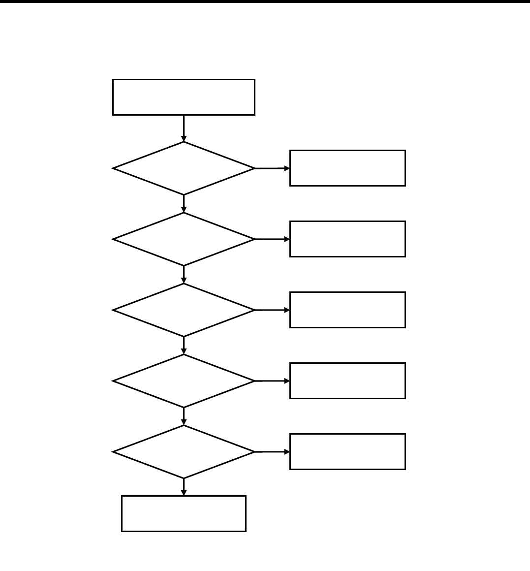
LGE Internal Use Only
Copyright © 2007 LG Electronics. Inc. All right reserved.
Only for training and service purposes
4. TROUBLE SHOOTING
- 102 -
Set the Phone Rx is ON
Check BIAS
Over 2V ?
Change the board
Check bias block
soldering
Check RF s/w
Check Duplexer
YES
NO
Check TP1
Signal exist?
YES
NO
Check TP2
Signal exist?
YES
NO
Check TP3
Signal exist?
YES
NO
Check FEM
Check TP4
Signal exist?
NO
Check RFR6250
YES
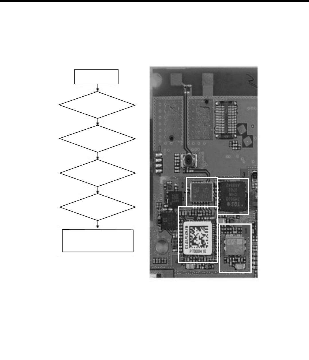
LGE Internal Use Only
Copyright © 2007 LG Electronics. Inc. All right reserved.
Only for training and service purposes
4. TROUBLE SHOOTING
- 103 -
4.6 Checking GSM Block
Start
1. Check TXVCO Block
2. Check ANT.SW
Module
3. Check TX PAM Block
4. Check RF RX Level
4. Re download SW & CAL
1
2
3
4

LGE Internal Use Only
Copyright © 2007 LG Electronics. Inc. All right reserved.
Only for training and service purposes
4. TROUBLE SHOOTING
- 104 -
4.6.1 Checking VCO Block
NO OSCILLATION HIGH
(1%)
(1%)
DCS1800/PCS1900
HIGH
(1%)
TX VCO CONTROL LOGIC
GSM850/900 HIGH
HIGHLOW
TP5
LOW
TP4
C537
120p
15p
C556 15p
C557
R517 100ohm
330p
VBATT
C535
VREG_RFTX_2.85V
R523
FB502
270
100p
C547
R524
51
0.1uF
C555
39 VDDA11
VDDA12
41
43 VDD_M
40 TX_MOD_
TX_VCO_F
42
38 GSM900_I
_
37
VREG_MSMP_2.7V
R521
220
R519 100ohm
C554
33p
0R508
R507 100
VC
10
GND1 2
GND2 4
GND3 6
7
GND4
GND5
8
GND6
12
13 GND7
GND8
14
5OUT_DCSPCS
1OUT_GSM 9
SW1 11
SW2
3
VB
MQW5V0C869M U502
0
R513
C553
tcc_1608h_9_r
4.7u
R510
100
C546
1000p
15R518
15R516
0.01u
C545
220
R520
100ohmR514
C541 82p
270
R522
C539
5.6n
ECHU1C562JX5
22u
C543
GSM_PA_RAMP
GSM_TX_VCO_0_EN_N
GSM_TX_VCO_1_EN_N
TX_ON
TP2 TP1
TP3
TP5
TP4
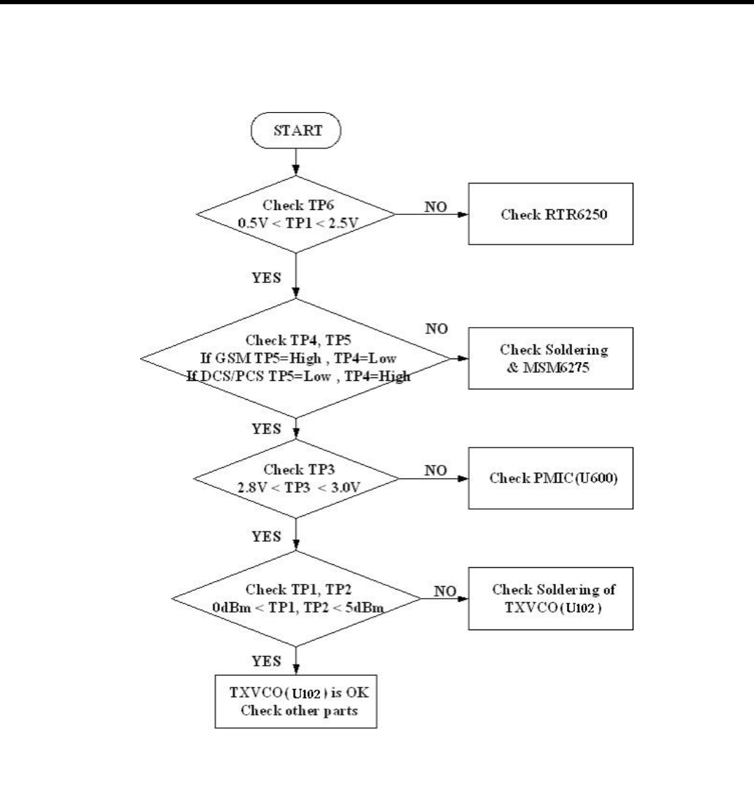
LGE Internal Use Only
Copyright © 2007 LG Electronics. Inc. All right reserved.
Only for training and service purposes
4. TROUBLE SHOOTING
- 105 -
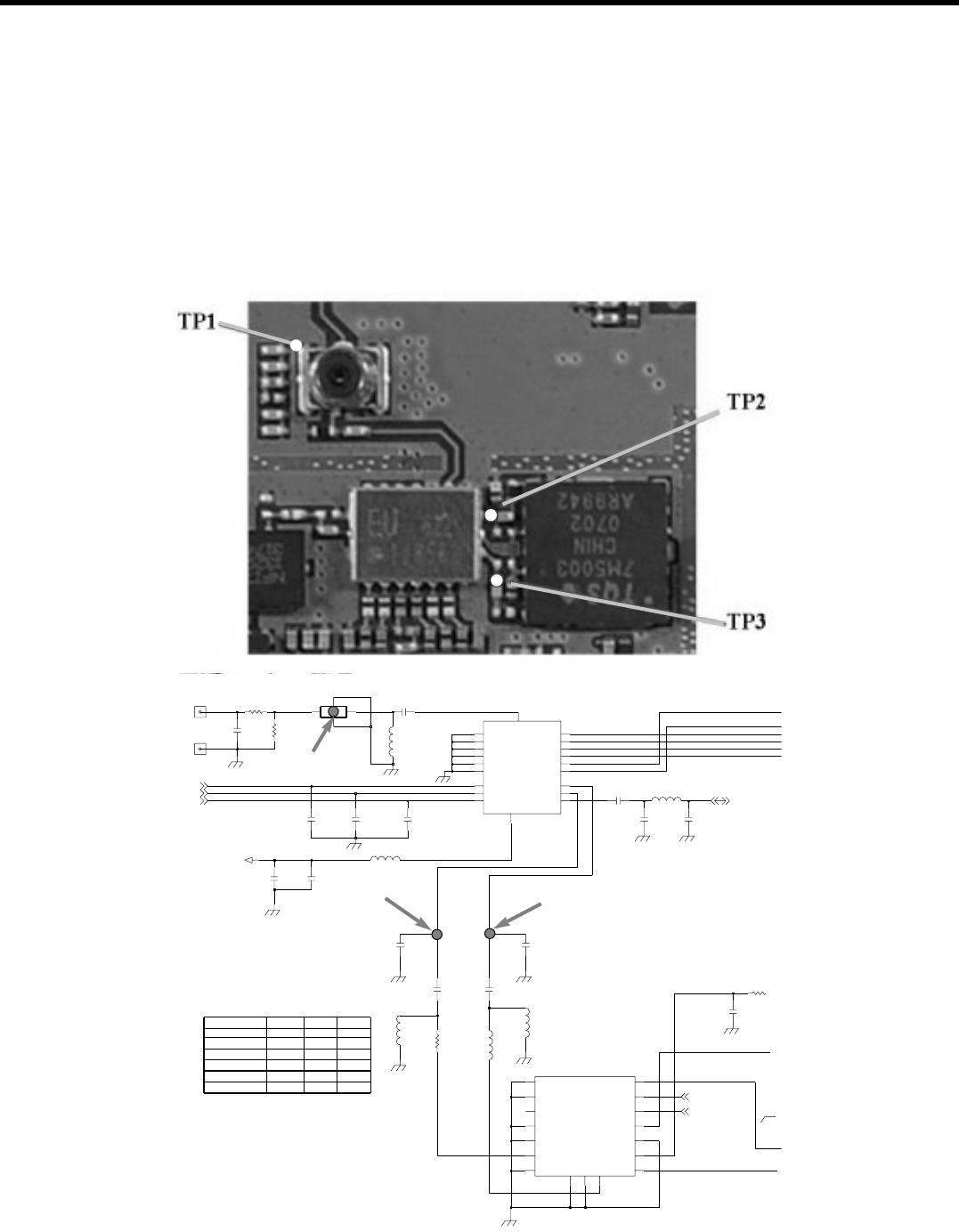
LGE Internal Use Only
Copyright © 2007 LG Electronics. Inc. All right reserved.
Only for training and service purposes
4. TROUBLE SHOOTING
- 106 -
4.6.2 Checking Ant. SW Module
Refer to chapter 3.4
4.6.3 Checking RF Tx level
LOW
LOW
LOW
DCS RX LOW
(1%)
IN_C
LOW
HIGH
LOW
IN_B
LOW
LOW
IN_A
LOWGSM 900 RX
PCS RX
DCS/PCS TX
ANTENNA SWITCH MODULE LOGIC
LOW
HIGH
UMTS 2100
HIGH
HIGH
LOWGSM900 TX
LOWLOW
HIGH
VREG_RFR_2.85V
C531
33p
C511
47p
NA
C528
C502
NA
56p
ANT500
C506
2.2KR506
NA
C512
C529
NA
L514 7.5nH
C536
68p
C530
33p
C520
0.1u
ANT501
47p
C510
L522
18nH
L502
1p
UMTS_TX_RX
VC1
17
15
VC2
VC3
14
16
VDD
ANT
12
DCS_PCS_TX
8
3
DCS_RX1
DCS_RX2
4
1
EGSM_RX1
EGSM_RX2
2
EGSM_TX
10
7
GND1
GND2
9
11
GND3
GND4
13
18
GND5
GND6
20
5
PCS_RX1
PCS_RX2
6
19
FL500ESHS-L090UB
0
C500 56pC501
C509
47p
KMS-512
SW500
ANT
G1
G2RF
56nH
L504
L523
22nH
C519
47p
10
GND3
11
GND4
GND5
13
GND6
14
GND7
16
17 GND8
7
GSM_IN
9GSM_OUT
TX_EN 3
4
VBATT
VCC
12
6
VRAMP
TQM7M5003
U501
2
BS
DCS_PCS_IN 1
DCS_PCS_OUT
15
GND1 5
GND2
8
R511
0
L524
1.5nH
C507 1.5nH
C513
NA
GSM_PA_EN
GSM_PA_BAND
WCDMA_2100
ANT_SEL0
ANT_SEL1
ANT_SEL2
TP3
TP2
TP1
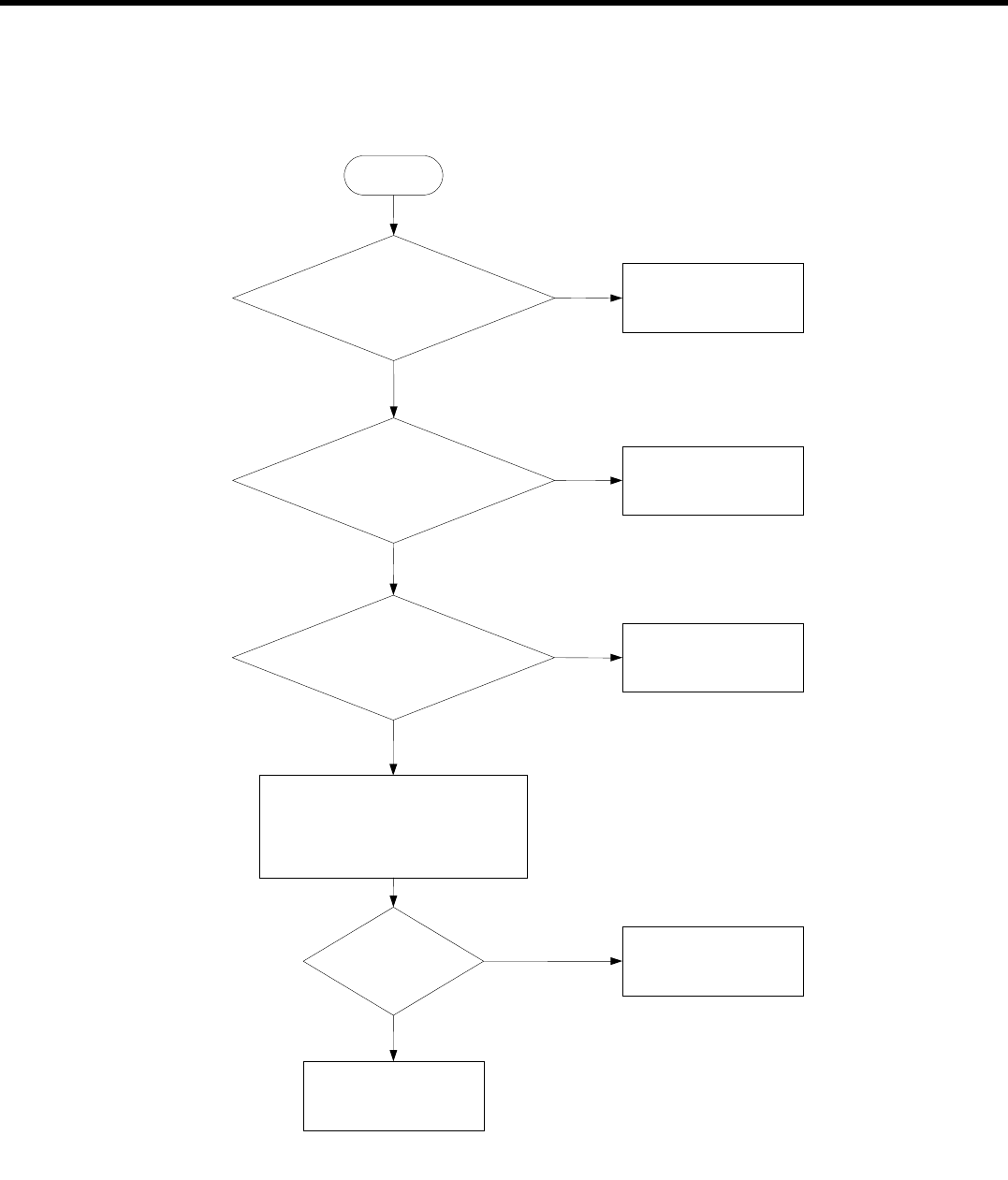
LGE Internal Use Only
Copyright © 2007 LG Electronics. Inc. All right reserved.
Only for training and service purposes
4. TROUBLE SHOOTING
- 107 -
Check TP1
If GSM over 31dBm ?
If DCS/PCS over 28dBm ?
STAR
GSM/DCS/PCS
Tx is Ok
Check other part
Check ANT. SW
Module
Refer to chapter 3.4
Change the Board
Check Soldering of
PAM (U101)
If problems stiil exist, replace
PAM.
YES
YES
NO
NO
NO
NO
Check TP2, TP3
If TP2 over 29dBm ?
If TP3 over 25dBm ?
Check PAM Block
OK ?
Refer to chapter 3.6.4
Check TXVCO
Refer to chapter 3.6.1
YES
Problems resolved?
YES GSM/DCS/PCS
Tx is OK
NO
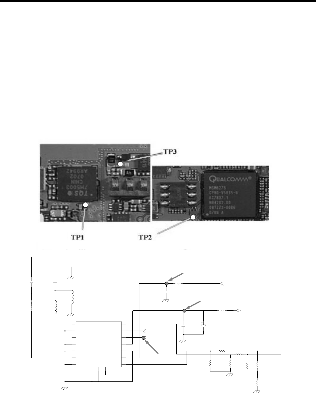
LGE Internal Use Only
Copyright © 2007 LG Electronics. Inc. All right reserved.
Only for training and service purposes
4. TROUBLE SHOOTING
- 108 -
4.6.4 Checking PAM Block
PAM Control Signal
TP1. GSM_PA_RAMP : Power Amp Gain Control. typically, 0.5V < Vapc <
2.6V,
TP2. GSM_PA_EN : Power Amp Enable
(Power ON : higher than 2.5V , Power OFF : lower than 0.7V)
TP3. +VPWR : PAM Supply Voltage Vcc higher than 3.28V
(1%)
C531
33p
VBATT
R523
270
2.2KR506
R524
51
C544
100p
C536
68p
C530
33p
R521
220
L522
18nH
0
R513
15R518
15R516
220
R520
10
GND3
11
GND4
GND5
13
GND6
14
GND7
16
17 GND8
7
GSM_IN
9GSM_OUT
TX_EN 3
4
VBATT
VCC
12
6
VRAMP
TQM7M5003
U501
2
BS
DCS_PCS_IN 1
DCS_PCS_OUT
15
GND1 5
GND2
8
R511
0
L524
1.5nH
270
R522
22u
C543
GSM_PA_EN
GSM_PA_BAND
GSM_PA_RAMP
TP1
TP3
TP2
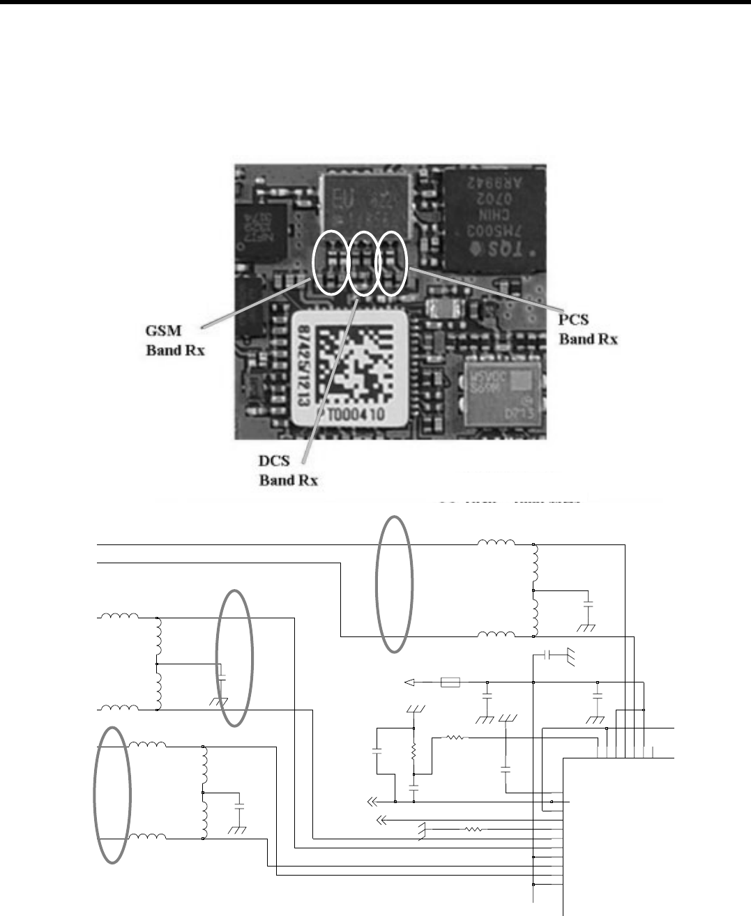
LGE Internal Use Only
Copyright © 2007 LG Electronics. Inc. All right reserved.
Only for training and service purposes
4. TROUBLE SHOOTING
- 109 -
4.6.5 Checking RF Rx Block
(1%)
(1%)
(1%)
(change to 4.53k)
(1%)
C514
1000p
9.1nH
L519
L510
3.3nH
R502
4.7K
3.3nH
L500
L516
10nH
10nH
L520
C504
1000p
R501
4.3K
FB500
39 VDDA11
23
VDDA6
VDDA7 26
VDDA8 27
31 VDDA9
VDDA10
36
34 GSM1800_INN
GSM1800_INP
35
24
GSM1900_INN
GSM1900_INP 25
GSM850_INP 22
38 GSM900_INN
GSM900_INP
37
RX_VCO_IN
32 R_BIAS
33
U500
RTR6250D
CP2
30
CP_HOLD2
29
28
FAQ2
L517
9.1nH
1000p
C527
3.6nH
L505
C515
33p
5.1nH
L513
0R508
R507 100
6.8n
C526
ECHU1C682JX5
C508 33p
L507
5.1nH
VREG_RFTX_2.85V
C521
680p
11.3KR503
C516
33p
L508
7.5nH
C525
0.01u
L501
3.6nH
7.5nH
L511
CP2_OUT
UHF_LO_BUFF
PCS Band Rx
1930-1990 MHz
DCS Band Rx
1805-1880 MHz
GSM Band Rx
925-960 MHz

LGE Internal Use Only
Copyright © 2007 LG Electronics. Inc. All right reserved.
Only for training and service purposes
4. TROUBLE SHOOTING
- 110 -
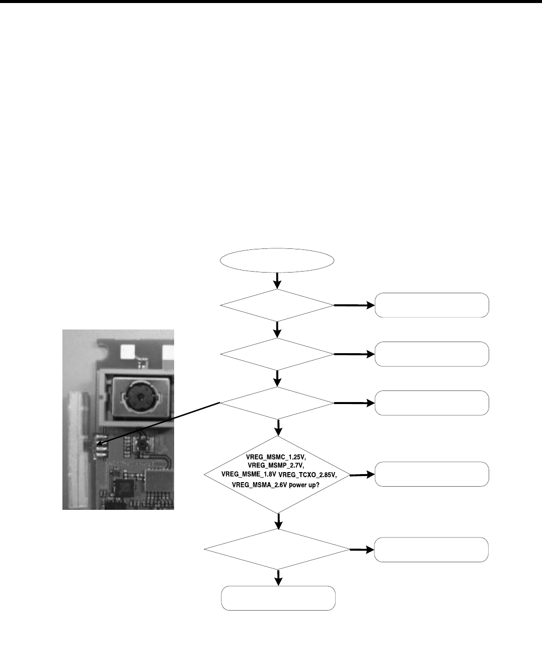
LGE Internal Use Only
Copyright © 2007 LG Electronics. Inc. All right reserved.
Only for training and service purposes
4. TROUBLE SHOOTING
- 111 -
BB Trouble Shooting
4.7 Power on trouble
Power on sequence of KS10 is :
PWR key press →KEY_ON_SW_N go to low (D405, PM6650-1M KPDPWR_N pin#24) →PM6650-
1M Power Up →VREG_MSMC_1.375V(C735), VREG_MSME_1.8V(C736),
VREG_MSMP_2.7V(C730), VREG_MSMA_2.6V(C726), VREG_TCXO_2.85V(C710) power up →
PON_RESET_N assert to MSM and PON assert to STn8810 →VDD_IO_2.7V(C304),
VDD_IO_1.8V(C311),AP_VCORE(C314),AP_VPLL(C328),AP_VFUSE(C329) power up -> CPU and
Phone booting & PS_HOLD(D700) assert High to PMIC(PM6650-1M)
Start
Battery voltg. higher
than 3.22V?
Press PWR key
Keypad LED on?
VA100 high to low
when key press?
Is clock ok?
X100 : 19.2M
X600 : 32.768Khz
Change the Main board
Change or charging the
Battery
Follow the LED trouble
shoot
Check open Pattern
of power button
Change the Main board
Check the TXCO
NO
YES
YES
YES
YES
YES
NO
NO
NO
NO
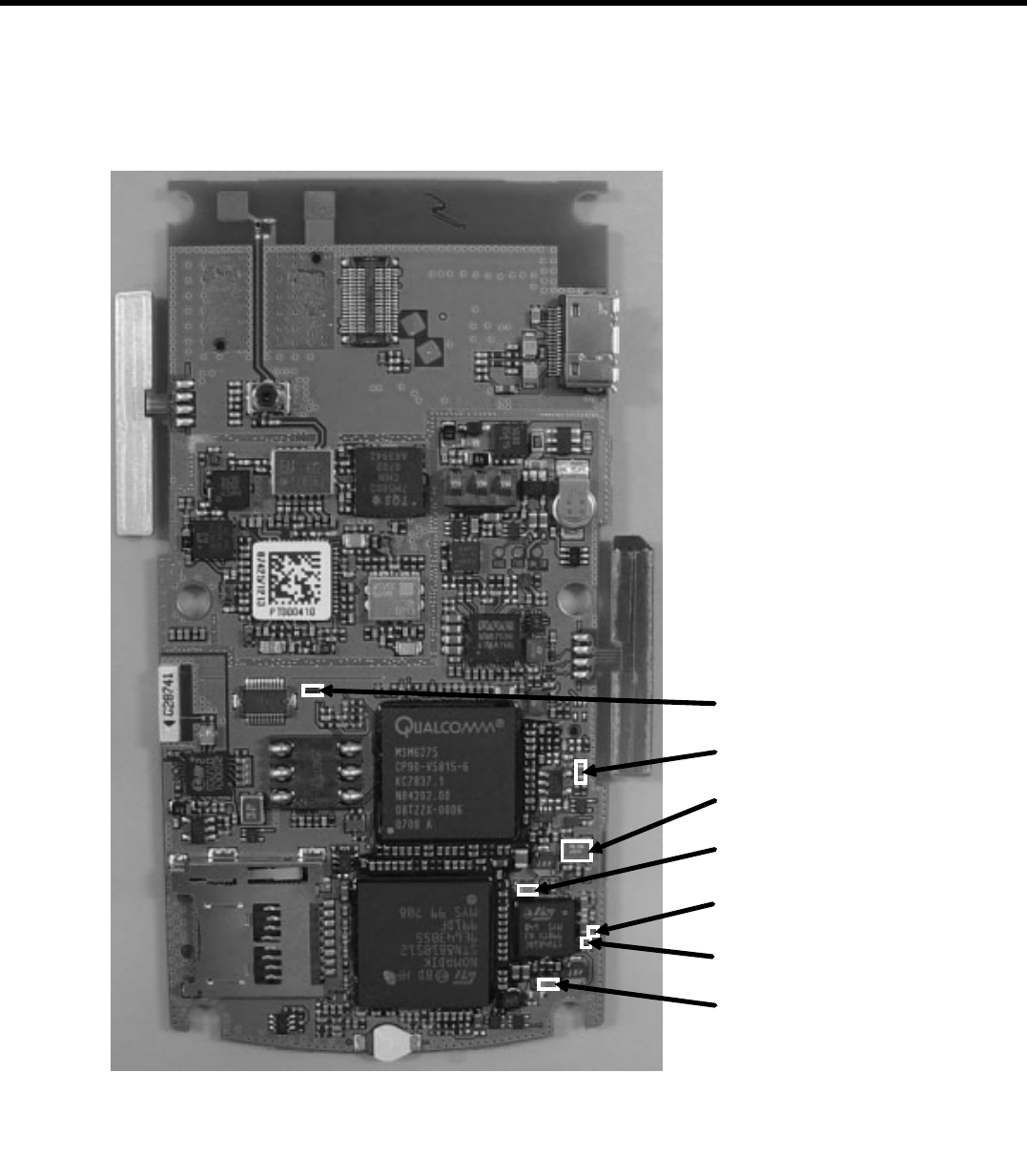
LGE Internal Use Only
Copyright © 2007 LG Electronics. Inc. All right reserved.
Only for training and service purposes
4. TROUBLE SHOOTING
- 112 -
VDD_IO_2.7V(C304)
VDD_IO_1.8V(C311)
AP_VCORE(C314)
AP_VPLL(C328)
AP_VFUSE(C329)
X100
PS_HOLD(D700)
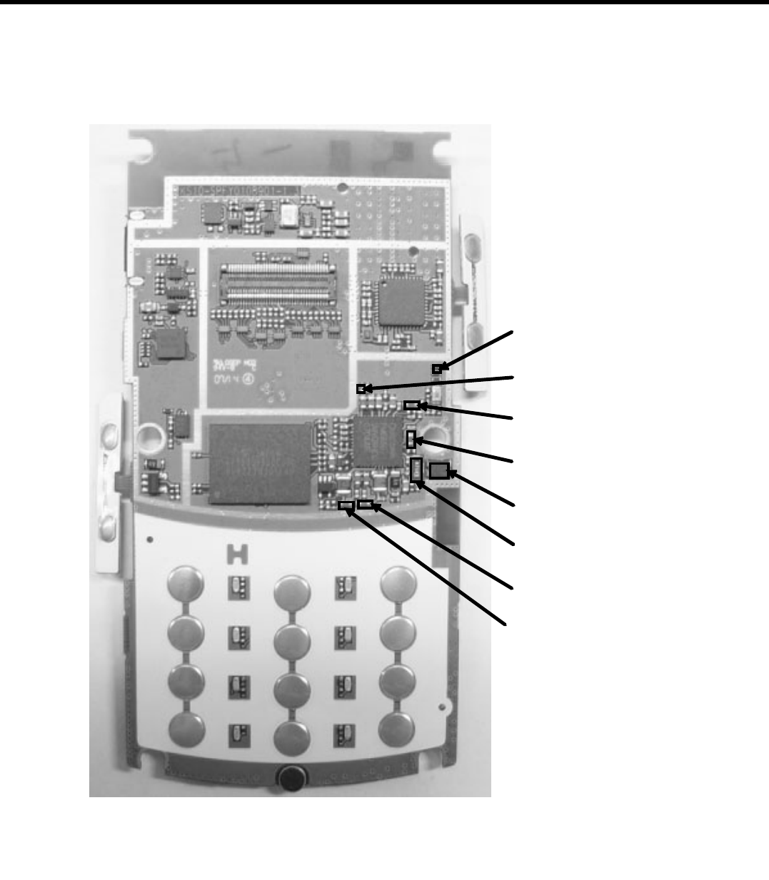
LGE Internal Use Only
Copyright © 2007 LG Electronics. Inc. All right reserved.
Only for training and service purposes
4. TROUBLE SHOOTING
- 113 -
KEY_ON_SW_N (D405)
VREG_MSMC_1.375V(C735)
VREG_MSME_1.8V(C736)
VREG_MSMP_2.7V(C730)
VREG_MSMA_2.6V(C726)
VREG_TCXO_2.85V(C710)
X500
X700
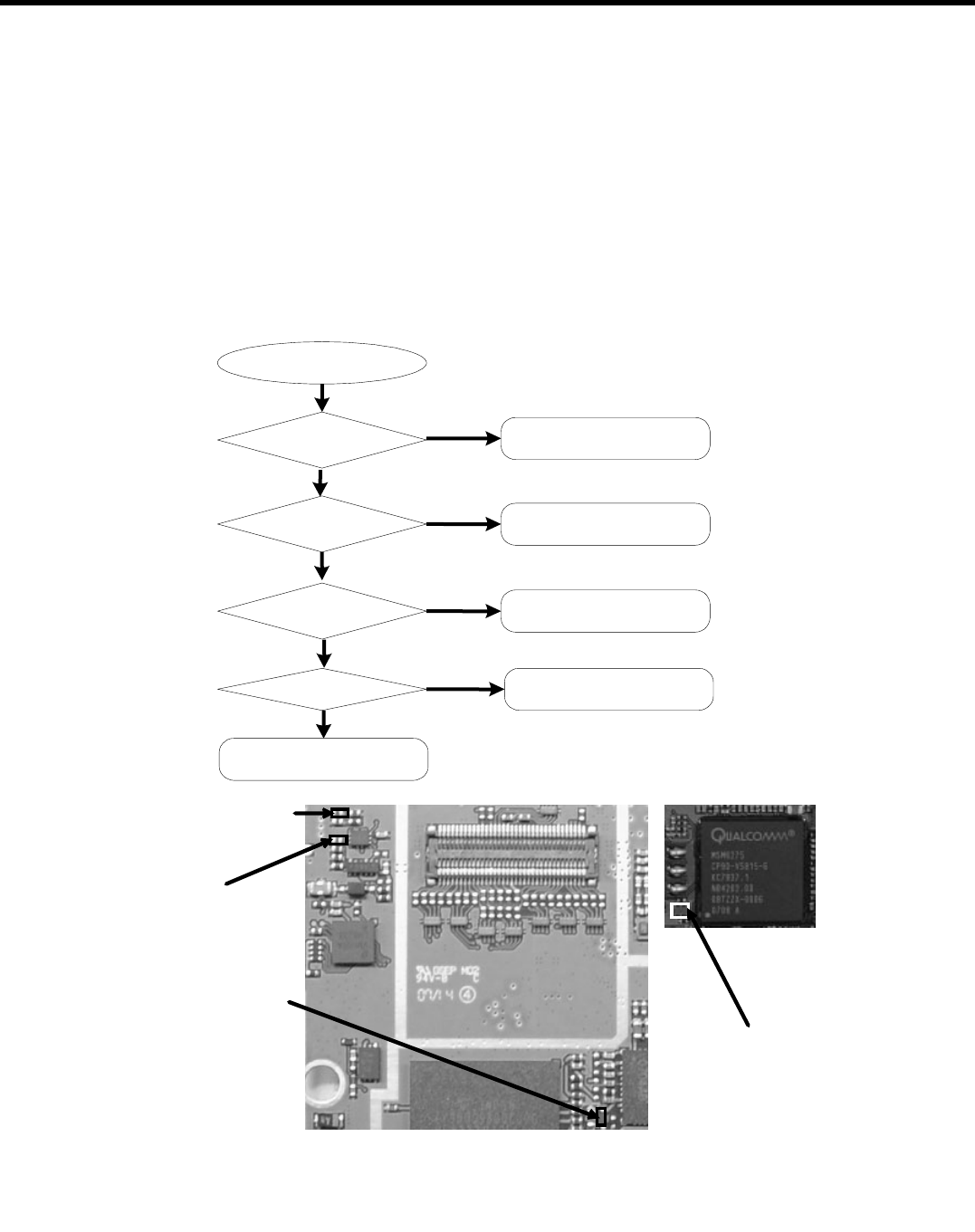
LGE Internal Use Only
Copyright © 2007 LG Electronics. Inc. All right reserved.
Only for training and service purposes
4. TROUBLE SHOOTING
- 114 -
4.8 USB trouble
USB Initial sequence of KS10 is :
USB connected to KS10 →USB_VBUS_IN(VA205) go to 5V
→USB_VBUS_EN go to high (Q702 Pin_2) →USB_VBUS(D701) go to 5V
→USB_D+(VA202) go to 3.3V →48M Crystal on →USB_DATA is triggered →USB work
Start
USB_VBUS is about
to 5V?
USB_D+ is about to 3.3V?
48MHz is run?
Change the Main board
Check Q702, D701
USB cable
Check VA202
Check X600
NO
YES
YES
YES
NO
NO
Cable is insert?
YES
Cable insert
NO
X600(48MHz)
VA202 (USB_D+)
VA205(USB_VBUS_IN)
D701(USB_D+)
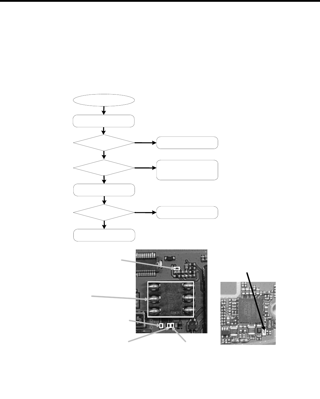
LGE Internal Use Only
Copyright © 2007 LG Electronics. Inc. All right reserved.
Only for training and service purposes
4. TROUBLE SHOOTING
- 115 -
4.9 SIM detect trouble
USB Initial sequence of KS10 is :
VREG_USIM_2.85V(C739 of PM6650) go to 2.85V →USIM clock, reset and data triggered
→USIM IF work (Schematic and place are refer to SIM technical brief)
Start
Work well?
VREG_USIM_2.85V is 3.0V?
USIM_P_CLK is run?
Change the Main board
End
Check J300, C739,
VA300,VA301,
VA302,VA303
Yes
No
YES
NO
Re-insert the SIM card
Change SIM card
Work well? End
Yes
No
VA303 (VREG_USIM_2.85V)
VA302(USIM_P_RST_N)
C739 (VREG_USIM_2.85V)
J300
VA301 (USIM_P_CLK)
VA300 (USIM_P_DATA)
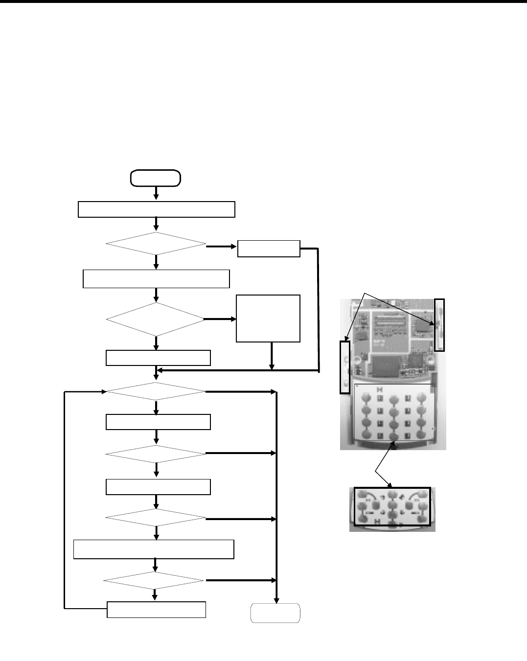
LGE Internal Use Only
Copyright © 2007 LG Electronics. Inc. All right reserved.
Only for training and service purposes
4. TROUBLE SHOOTING
- 116 -
4.10 Key sense trouble
Key Sense sequence of KS10 is :
Default condition ROW(0-3) is 2.7V →Press the key →Corresponding ROW(x) and COL(x) go to
0V →Key sensing by key coder IC (U404) →Key coder IC send the key information to CPU by I2C
interface
Check Metal
DOME SHEET
Sub & Main
board
Check the RA400 with no key press
Change the Main board
Yes
NO
Change the side key
Check the RA400 with key press
ROW(0-4) is 2.7V? Check RA400
NO
Yes
ROW(0-4),
COL(0-4) is 0V?
Work well?
End
NO
START
Check R414, 415, C418,TP407,TP406
NO
YES
NO
Change FPCB
Work well?
NO
Change Sub board
Work well?
Work well?
NO
YES
YES
YES
NO
Dome sheet
Side Key
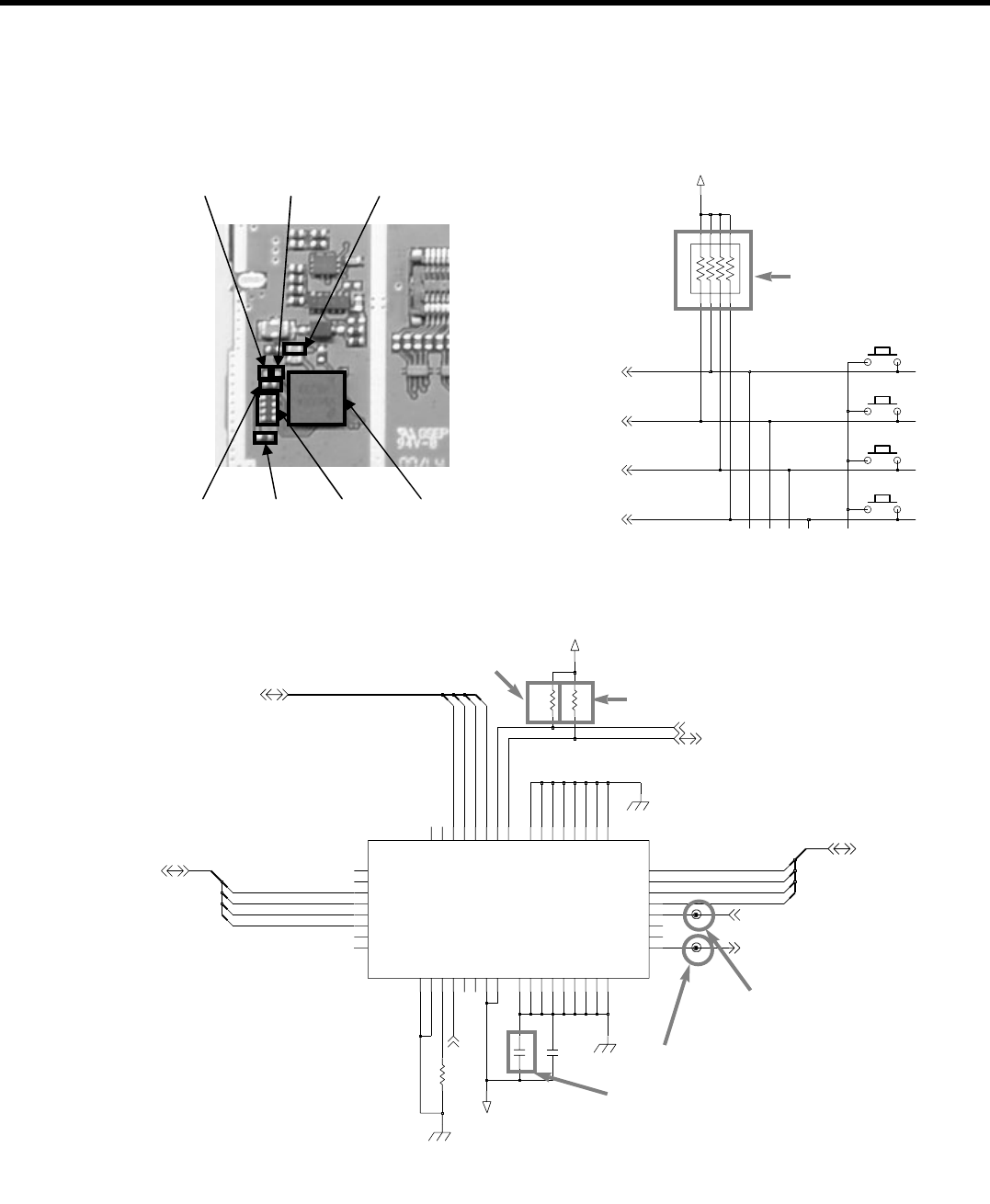
LGE Internal Use Only
Copyright © 2007 LG Electronics. Inc. All right reserved.
Only for training and service purposes
4. TROUBLE SHOOTING
- 117 -
RA400 U404R415R414
C418TP406 TP407
TP407
0.1u
C418
R415
3.3K
TP406
C419
0.1u
3.3K
R414
Wake_INP2 E7
D6
Wake_INP3
B6
Wake_INP4
Wake_INP5 A7
Wake_INP6
A6
B5 Wake_INP7
F3
_RESET
NC1 F5
G6
NC2
NC3 F6
G7
NC4
C2
NC5
NC6 C1
C6
NC7
NC8 B7
F1 PWM
SCL_AB E6
F7
SDA_AB
VCC1
E1
VCC2
E2
G1
WD_Out
Wake_INP0 D7
C7
Wake_INP1Gen_IO_0
D2
D1 Gen_IO_1
Gen_IO_2
B3
Gen_IO_3
A2
A1 Gen_In0
Gen_In1
B2
Int_Rx G2
Int_Tx F2
G3
K_Out0
K_Out1 F4
G4
K_Out2
K_Out3 G5
K_Out4
A5
B4 K_Out5
K_Out6
A4
A3 K_Out7
LM8333GGR8_NOPB
U404
B1 CLK_In
GND1
C3
C4 GND2
C5 GND3
GND4
D3
D4 GND5
GND6
D5
GND7
E3
E4 GND8
GND9
E5
AP_VDD_IO_2.7V
AP_VDD_IO_2.7V
68KR419
FOLDER_DETECT
I2CSCL1
I2CSDA1
KEY_COL(5)
KEY_COL(6)
KEY_COL(7)
KEY_COL(4:7)
KEYCODER_RSTN
KEYCODER_INT
KEY_ROW(0:3)
KEY_ROW(2)
KEY_ROW(3)
KEY_ROW(0)
KEY_ROW(1)
KEY_COL(3)
KEY_COL(2)
KEY_COL(3:0)
KEY_COL(1)KEY_COL(4)
KEY_COL(0)
SW400
SW409
SW406
AP_VDD_IO_2.7V
2
4
6
8
1
3
5
7
RA400 100K
SW403
KEY_ROW(0)
KEY_ROW(1)
KEY_ROW(2)
KEY_ROW(3)
RA400
R415
TP406
TP407
C418
R414
Schematic of key sense part
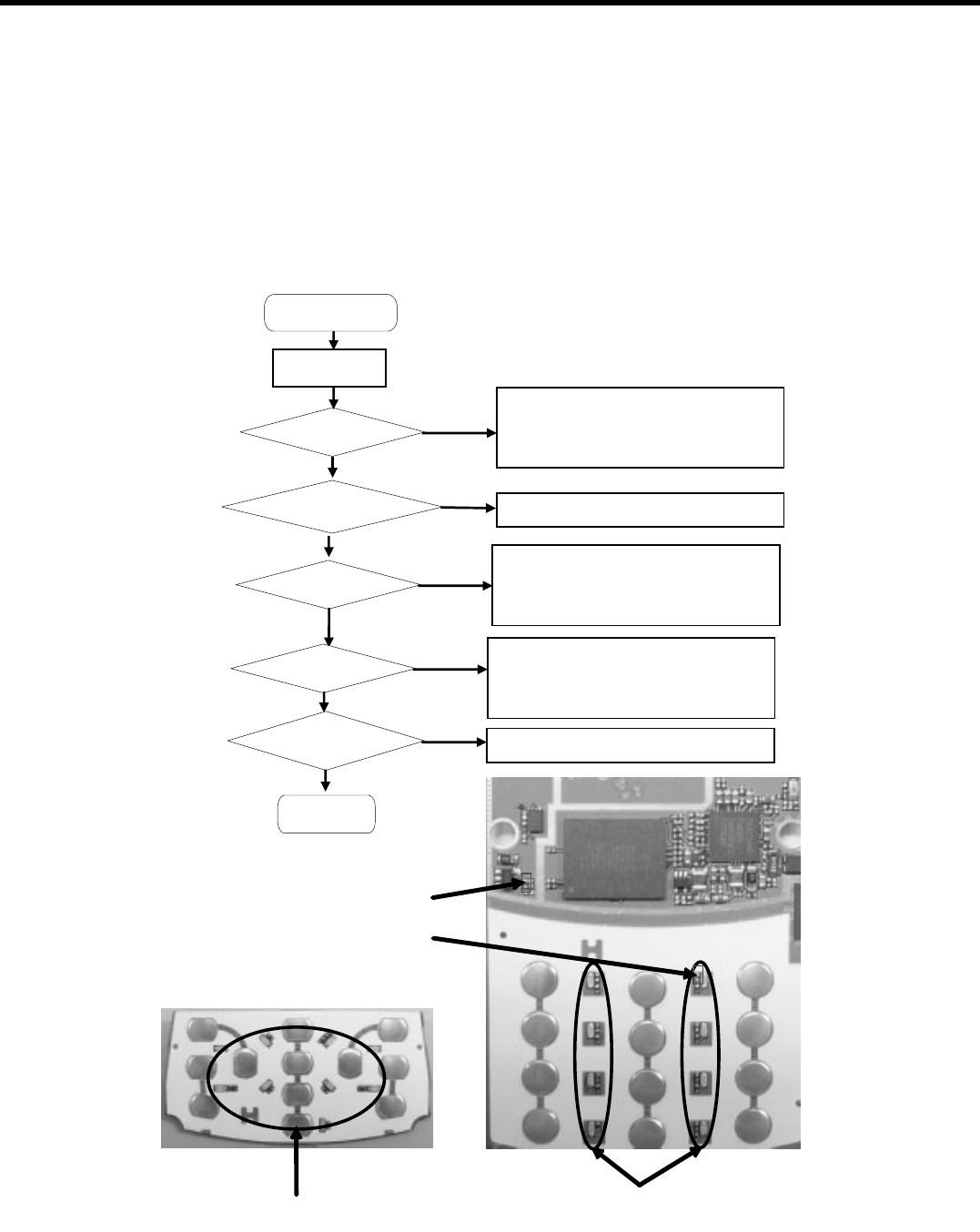
LGE Internal Use Only
Copyright © 2007 LG Electronics. Inc. All right reserved.
Only for training and service purposes
4. TROUBLE SHOOTING
- 118 -
4.11 Keypad backlight trouble
Key Pad Back Light is on as below :
Key pressing →STn8810 commend MSM6275 lighting the Key LED →
MSM 6275 KPD_DRV_N go to Low →LED On (Key Pad LED controlled by PM6650)
Start
Check device short :
LD400~407 and R402~412 (Main)
LD101~108 and R106~114 (Sub)
NO
Yes
Yes
Key press
Signal KPD_DRV_N
is Low?
AP_+VPWR is OK?
Check connection
between Main and FPCB
and between FPCB and Sub
NO
Only Sub board LED
is not work?
Change the main board
NO
Yes
Yes Check device open :
LD400~407 and R402~412 (Main)
LD101~108 and R106~114 (Sub)
NO
Some LED
is not work?
Work well?
Yes
Change the main & Sub board
NO
En d
LD400~407 and R402~412 (Main)
LD101~108 and R106~114 (Sub)
R400 (AP_+VPWR)
VA400 (KPD_DRV_N)
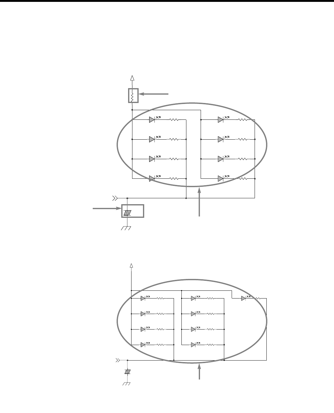
- 119 -
4. TROUBLE SHOOTING
Main
SUB
LGE Internal Use Only
Copyright © 2007 LG Electronics. Inc. All right reserved.
Only for training and service purposes
100ohmR411
SSC-TWH104-HLS
LD407
SSC-TWH104-HLS
LD406
SSC-TWH104-HLS
LD402
EVL14K02200
VA400
R409 100ohm
100ohmR412
AP_+VPWR
LD400
SSC-TWH104-HLS
100ohmR406
R400
0
R408 100ohm
SSC-TWH104-HLS
LD401
SSC-TWH104-HLS
LD403
R403 100ohm
SSC-TWH104-HLS
LD405
100ohmR405
R402 100ohm
LD404
SSC-TWH104-HLS
KPD_DRV_N
100ohmR109
EVL14K02200
VA100
100ohmR111
100ohmR110
LD108
SSC-TWH104-HLSSSC-TWH104-HLS
LD107
LD104
SSC-TWH104-HLS
AP_+VPWR
SSC-TWH104-HLS
LD103
100ohm
100ohmR113
R112
100ohmR114
LD102
SSC-TWH104-HLS
LD100
SSC-TWH104-HLS
100ohmR107 100ohm R108R106 100ohm
SSC-TWH104-HLS
LD101
LD105
SSC-TWH104-HLS SSC-TWH104-HLS
LD106
KPD_DRV_N
LD400~407 and R402~412 (Main)
LD100~108 and R106~114 (Sub)
VA400 (KPD_DRV_N)
R400 (AP_+VPWR)
Schematic of keypad backlight part
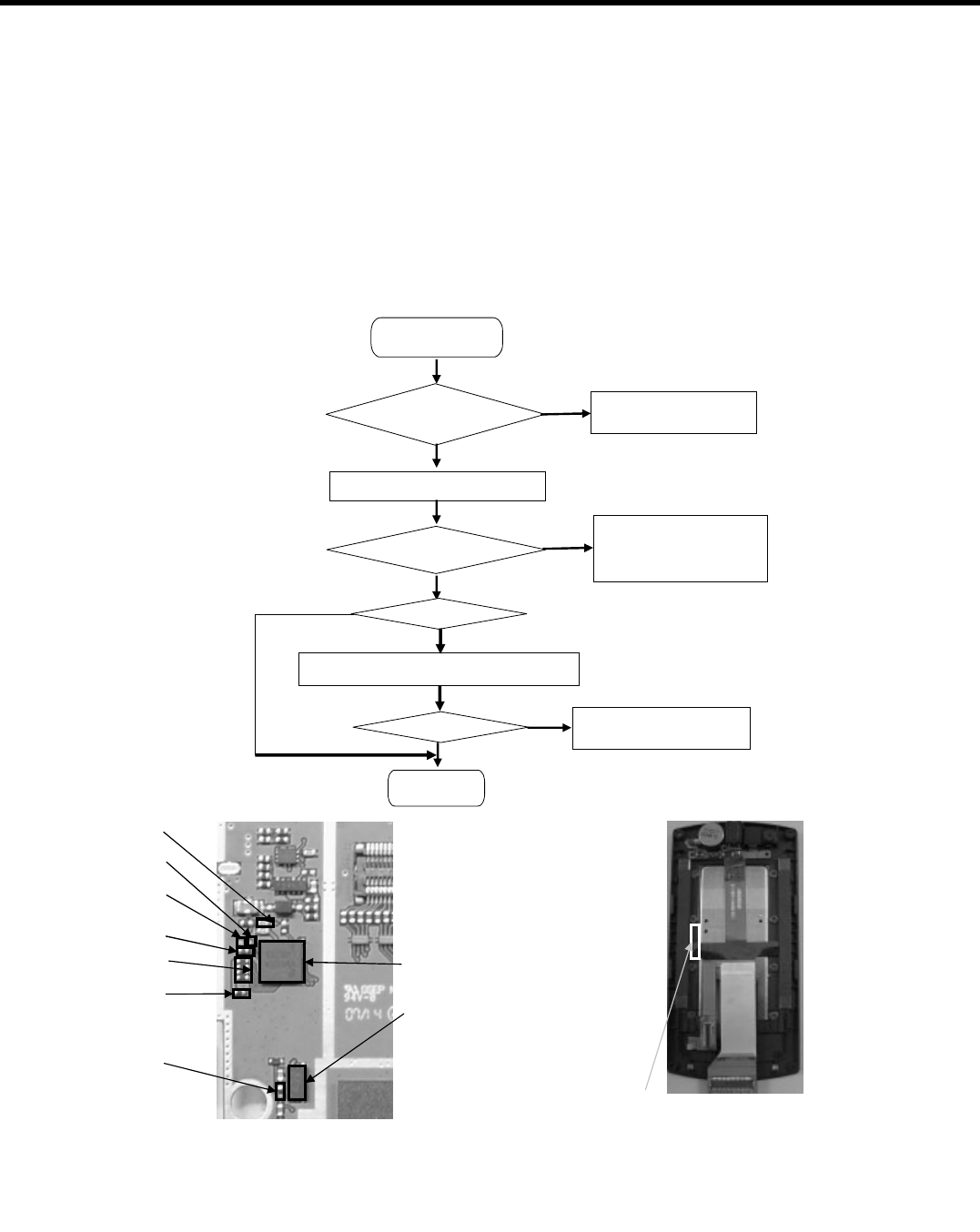
LGE Internal Use Only
Copyright © 2007 LG Electronics. Inc. All right reserved.
Only for training and service purposes
4. TROUBLE SHOOTING
- 120 -
4.12 Folder on/off trouble
Folder On/Off(Close/Open) is worked as below :
Folder On/Off Event →Flip(U402 pin 1,key board) is triggered(Open : about 2.7V, Close : 0V)
→Key coder IC(U404) sense the Folder Flip Event →Key coder IC send the key
information to CPU by I2C interface
Insert the magnet
Check the magnet in
folder Assy
Approach the magnet to U402
FLIP(U402p in 1) is 0V?
Yes
NO
Yes
Check the U402
And check the R413
for AP_VDD_IO_2.7V
Start
End
Yes
NO
Change the Main Board
Check R414, 415, C418,TP407,TP406
Work well?
NO
YES
NO
Work well?
RA400 U404
R415
R414
C418
TP406
TP407
magnet
U402
R413

LGE Internal Use Only
Copyright © 2007 LG Electronics. Inc. All right reserved.
Only for training and service purposes
4. TROUBLE SHOOTING
- 121 -
TP407
0.1u
C418
R415
3.3K
TP406
C419
0.1u
3.3K
R414
Wake_INP2 E7
D6
Wake_INP3
B6
Wake_INP4
Wake_INP5 A7
Wake_INP6
A6
B5 Wake_INP7
F3
_RESET
NC1 F5
G6
NC2
NC3 F6
G7
NC4
C2
NC5
NC6 C1
C6
NC7
NC8 B7
F1 PWM
SCL_AB E6
F7
SDA_AB
VCC1
E1
VCC2
E2
G1
WD_Out
Wake_INP0 D7
C7
Wake_INP1Gen_IO_0
D2
D1 Gen_IO_1
Gen_IO_2
B3
Gen_IO_3
A2
A1 Gen_In0
Gen_In1
B2
Int_Rx G2
Int_Tx F2
G3
K_Out0
K_Out1 F4
G4
K_Out2
K_Out3 G5
K_Out4
A5
B4 K_Out5
K_Out6
A4
A3 K_Out7
LM8333GGR8_NOPB
U404
B1 CLK_In
GND1
C3
C4 GND2
C5 GND3
GND4
D3
D4 GND5
GND6
D5
GND7
E3
E4 GND8
GND9
E5
AP_VDD_IO_2.7V
AP_VDD_IO_2.7V
68KR419
FOLDER_DETECT
I2CSCL1
I2CSDA1
KEY_COL(5)
KEY_COL(6)
KEY_COL(7)
KEY_COL(4:7)
KEYCODER_RSTN
KEYCODER_INT
KEY_ROW(0:3)
KEY_ROW(2)
KEY_ROW(3)
KEY_ROW(0)
KEY_ROW(1)
KEY_COL(3)
KEY_COL(2)
KEY_COL(3:0)
KEY_COL(1)KEY_COL(4)
KEY_COL(0)
SW400
SW409
SW406
AP_VDD_IO_2.7V
2
4
6
8
1
3
5
7
RA400 100K
SW403
KEY_ROW(0)
KEY_ROW(1)
KEY_ROW(2)
KEY_ROW(3) FOLDER_SENSE
AP_VDD_IO_2.7V
0.1u
C414
U402 A3212EEH-T
3GND1
GND2 4
2NC1 5
NC2
1OUTPUT
7
PGND
6
VDD
EUSY0200301
R413
100K
C413
1u
ZD1
RSB6.8CST2R
FOLDER_DETECT
R414 R415
TP406
TP407
C418
RA400
R413
U402
U404
Schematic of Folder on/off part
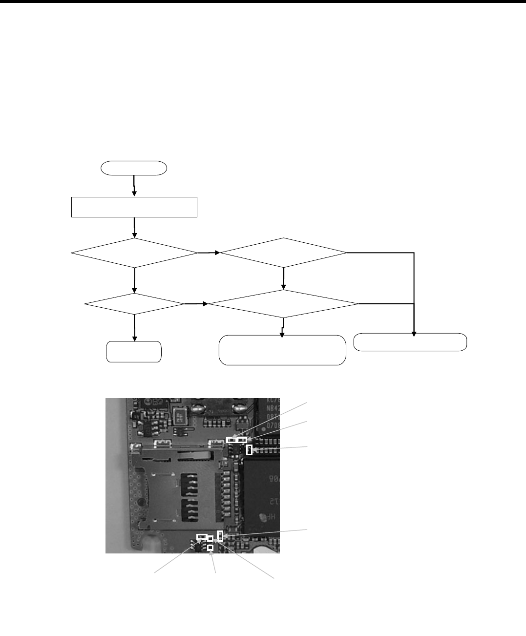
LGE Internal Use Only
Copyright © 2007 LG Electronics. Inc. All right reserved.
Only for training and service purposes
4. TROUBLE SHOOTING
- 122 -
4.13 Micro SD trouble
Micro SD is worked as below :
Micro SD insertion →Card Detect (SD_INT) goes to low →STn8810 detect SD_INT and
assert VMMC_3.1V by STw4810 →go working
Does the micro SD icon
appears ?
SD_INT(C343,NA)
is be low ?
Insert the Micro SD Card
Start
End Check the Pull up resistor
R309, R310,R311,R313,R314
Check VMMC_3.1V
is over 2.85V?
Work well?
YES
YES
NO
C343 (SD_INT)
C339 (VMMC_3.1V)
Change the main board
NO
YES
YES
NO
NO
R309 R310
R311
R313
R314
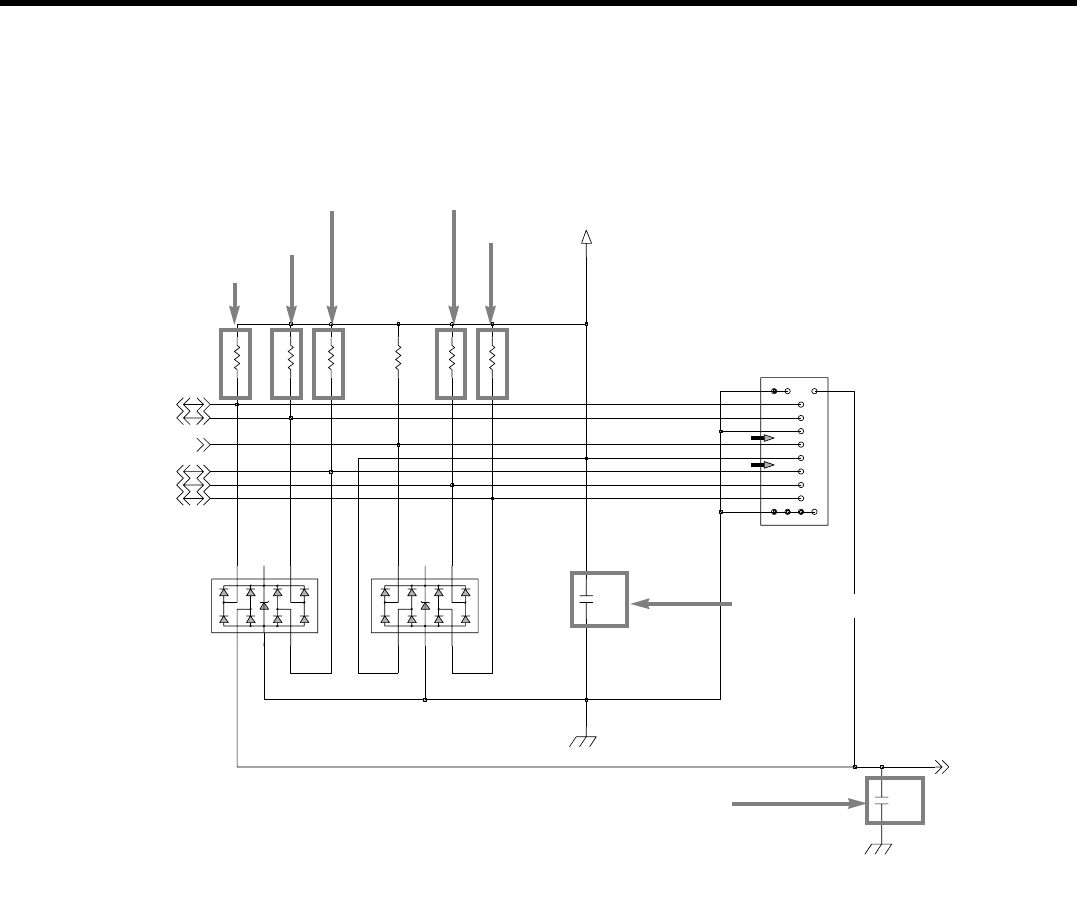
- 123 -
4. TROUBLE SHOOTING
LGE Internal Use Only
Copyright © 2007 LG Electronics. Inc. All right reserved.
Only for training and service purposes
1u
C339
34
5
6
R310 51K
D301
PLR0504F
1
2
51K
R309
R311 51K
51K
R313
1
2
34
5
6
PLR0504F
D300
R314 51K
NA
C343
NA
R312
5
6
7
8
SWASWBGND
GND
1
2
3
4
GCC110-8S-R-E1000
S300
VMMC_3.1V
SD_INT
SD_DAT(1)
SD_DAT(0)
SD_CLK
SD_CMD
SD_DAT(3)
SD_DAT(2)
R309
R310
C343 (SD_INT)
R311 R313
R314
C339 (VMMC_3.1V)
Schematic of Micro SD
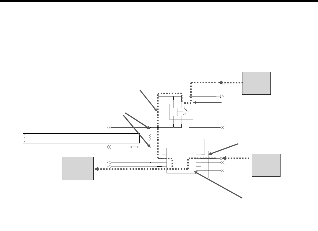
LGE Internal Use Only
Copyright © 2007 LG Electronics. Inc. All right reserved.
Only for training and service purposes
4. TROUBLE SHOOTING
- 124 -
4.14 Charging trouble
• Charging Procedure
- Connecting TA or USB Cable
- Control the charging current by PM6650-1M IC using USB_CNT_N or CHG_CNT_N signal
- Charging Current flows into the battery by control BATT_FET_N
• Check Point
- Connection of TA or USB Cable
- Charging current path
- Battery
• Trouble Shooting Setup
- Connect TA or USB Cable and battery to the phone
• Trouble Shooting Procedure
- Check the charger connector
- Check the charging current path
- Check the battery
Battery charging circuit !!!!!
1%
2012
Route as equal length as possible! -> ICHARGE, ICHARGEOUT
+5V_PWR
+VPWR
10
Drain_B
Emitter 8
5
Gate
NC1
1
NC2 6
Source
3
Q701 NUS5530MN
7
Base
2Collector
Collector_B 9
4Drain
USB_VBUS
0.1R713
64
VBATT
Q700
QST4
312
5
ICHARGE
BATT_FET_N
ICHARGEOUT
USB_CTL_N
CHG_CNT_N
Pass control Tr
(ON)
4.2~4.25V
Main
Battery
TA
(4.6V)
Battery FET
(ON)
Charging Current Flow
Pass control Tr
(ON)
USB Cable
(5.0V)
USB Charging control
TA Charging
control
Charging current
sensing
Battery charging
control
Q700
Q701
Q602
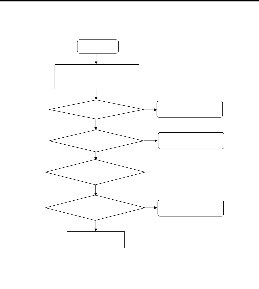
LGE Internal Use Only
Copyright © 2007 LG Electronics. Inc. All right reserved.
Only for training and service purposes
4. TROUBLE SHOOTING
- 125 -
Start
Check the pin and battery
Connect terminals of I/O connector
Connection OK? Change I/O connector
Is the TA voltage 4.8V?
Is the USB voltage 5.0V? Change TA/USB cable
Check the Q700,Q701
END
Change the board
NO
Yes
NO
Yes
NO
Yes
Charging OK?
Yes
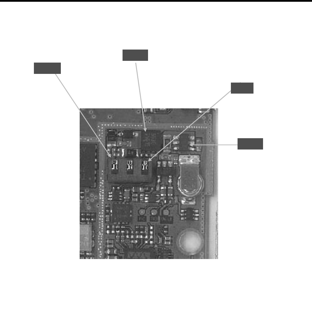
LGE Internal Use Only
Copyright © 2007 LG Electronics. Inc. All right reserved.
Only for training and service purposes
4. TROUBLE SHOOTING
- 126 -
Q701
Q700
VBAT
GND
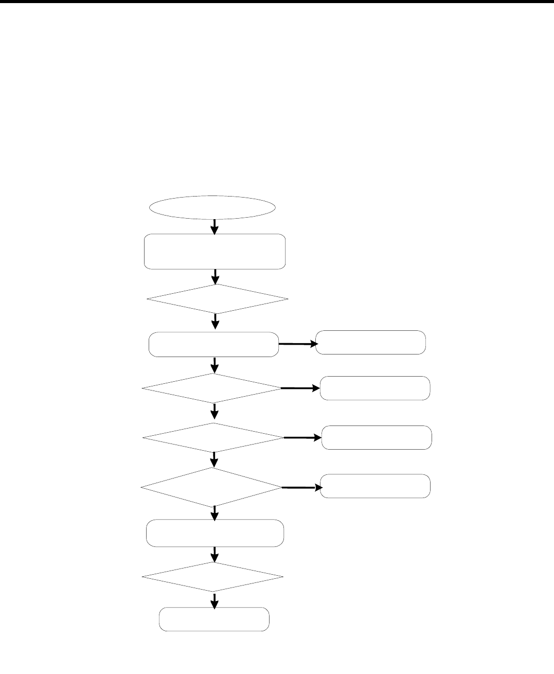
LGE Internal Use Only
Copyright © 2007 LG Electronics. Inc. All right reserved.
Only for training and service purposes
4. TROUBLE SHOOTING
- 127 -
4.15 Audio trouble
4.15.1 Receiver path
Voice Receiver path as below:
MSM6275A Ear1ON/Ear1OP → U202(audio codec) →CN201(b’d to b’d connector for LCD Module)
→CN102(LCD b’d to b’d connector of LCD FPCB) →R100, R101 →Receiver
Start
Change the Main board
NO
Connect the phone to network
Equipment and setup call
Setup 1KHz tone out
YES
The sine wave appear at
R100,R101 of LCD FPCB?
NO
Can you hear the tone?
YES
END
Check connector pin
or change the LCD FPCB
YES
Change the Receiver
Hear the tone to the receiver?
NO
END
The sine wave appear at
C225,C226?
The sine wave appear at
R211,C212?
Check the U202 or
Change the Main board
NO
YES
YES
Check the pads of Receiver

LGE Internal Use Only
Copyright © 2007 LG Electronics. Inc. All right reserved.
Only for training and service purposes
4. TROUBLE SHOOTING
- 128 -
LCD connector
C225, C226
ReceiverR100, R101
Receiver
pads
R211, R212
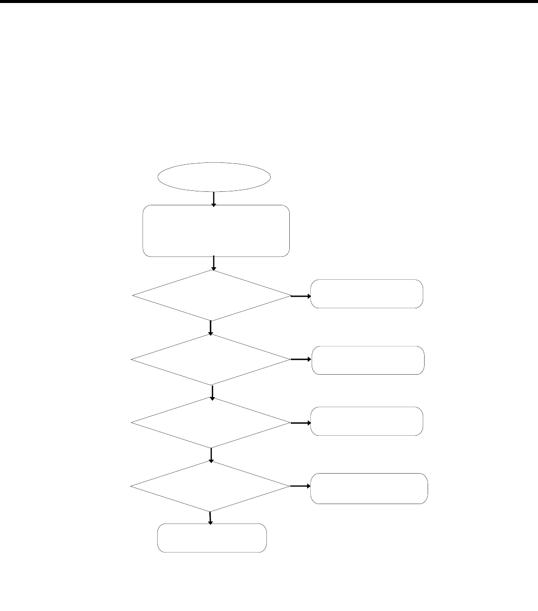
LGE Internal Use Only
Copyright © 2007 LG Electronics. Inc. All right reserved.
Only for training and service purposes
4. TROUBLE SHOOTING
- 129 -
4.15.2 Voice path for headset
Voice path for Head_Set as below:
MSM6275A HPH_R, HPH_L →C222,C224 U202(audio codec) →FB702, FB704 →C242,C244
→ #4, #5 pin of CN202 headset Jack
Start
The sine wave appear at
C222,C224 ? Change the Main board
NO
Connect the phone to network
Equipment and setup call
Setup 1KHz tone out
And insert head_Set
The sine wave appear at
C242,C244 ?
YES
Check the U202
or change the Main b'd
NO
Can you hear the tone?
NO
YES
YES
END
Headset insertion detection
in the Main LCD Display OK?
Check #8 pin of CN202
or change the Main b'd
NO
YES
Check the CN202
or change the Main b'd
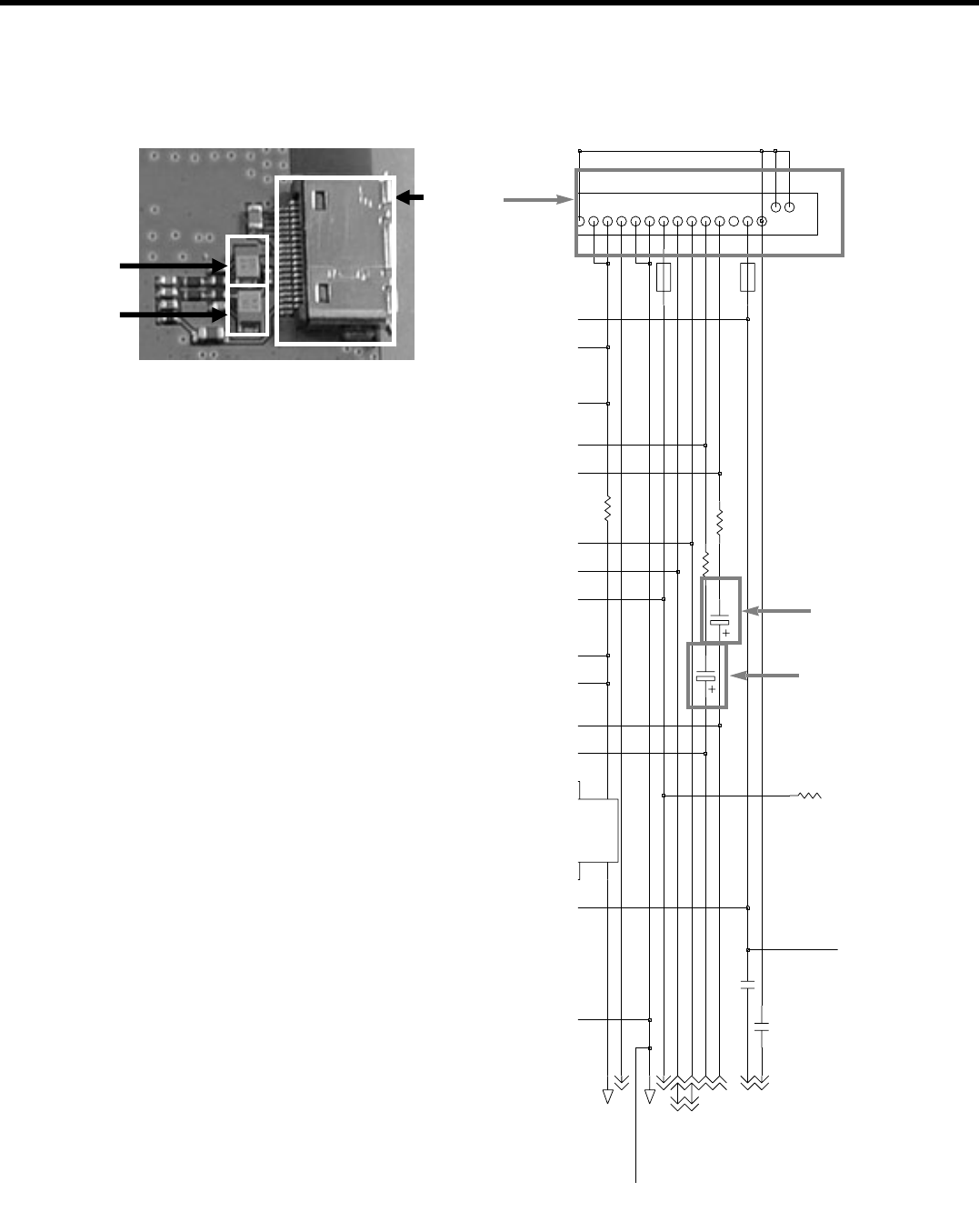
- 130 -
4. TROUBLE SHOOTING
LGE Internal Use Only
Copyright © 2007 LG Electronics. Inc. All right reserved.
Only for training and service purposes
CN202
C242
C244
1608
5
6
7
8
9
11
12
13
14
19
2
21
3
4
CN202
1
10
C242 33u
FB503 1000
33uC244R223 68
R225 NA
C240 1u
VBATT
4
G2
1IN 2
OUT
U205
G1
3
FB245
100K R219
+5V_PWR
C241 1u
68R222
USB_D+
USB_D-
EAR_SENSE_N
WM_LOUT1
WM_MIC2N
WM_MIC2P
REMOTE_PWR_O
WM_ROUT1
Schematic of voice path
C242
C244
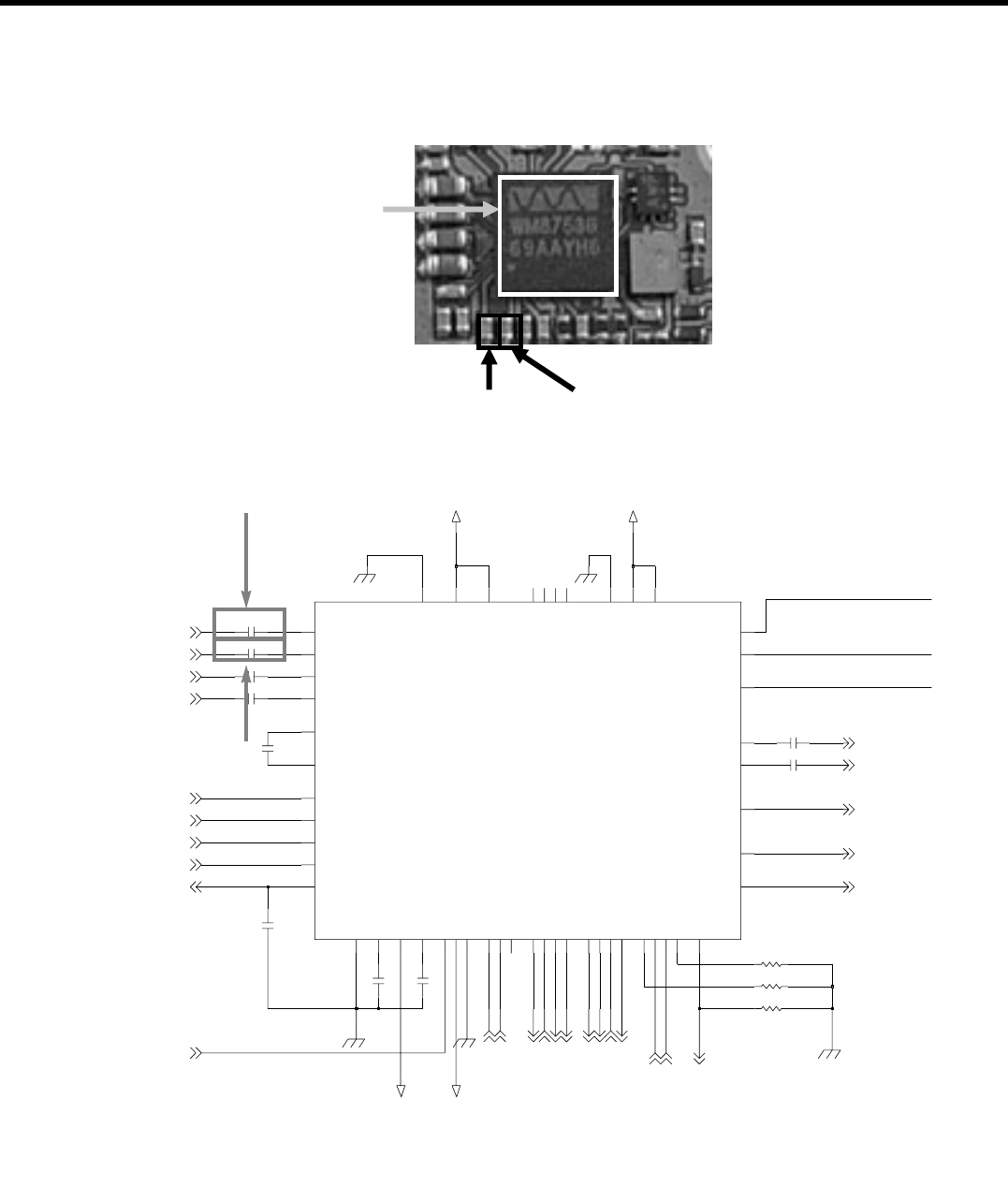
- 131 -
4. TROUBLE SHOOTING
LGE Internal Use Only
Copyright © 2007 LG Electronics. Inc. All right reserved.
Only for training and service purposes
Schematic of voice path
C222 C224
U202
WM_DVDD
WM_AVDD
WM_AVDD
1u C229
1uC224
100K R214
C226 1u
1u C230
C222 1u
R213100K
C235
4.7u
A8
VMID
A4
B5 VREF
VXCLK
H3
VXDIN
J1
J2 VXDOUT
VXFS
J3
R215100K
MONO2
A7
NC1 C8
NC2 F8
NC3
NC4 G2
E8
OUT3
OUT4 E9
J8 PCMCLK
H9 PGND
PVDD
G9
ROUT1 D9
ROUT2 B9
RXN
C2
RXP
B1
H1 SCLK
G1 SDIN
SPKRVDD
GPIO4
HPVDD F9
HP_SPKRGND C9
LINE1
A2
A1 LINE2
D8
LOUT1
A9
LOUT2
H4 LRC
J6 MCLK
C1 MIC1
MIC1N
D2
D1 MIC2
MIC2N
E2
MICBIAS
B4
F1 MODE_GPIO3
MONO1 B6
B7
U202
WM8753LEB-RV
A3 ACIN
B3 ACOP
ADCDAT
J5
A5 AGND
AVDD
A6
J4 BCLK
CSB_GPIO5
F2
DACDAT
H5
H6
DBVDD
DCVDD J7
DGND H7
G8 GP1_CLK1
GP2_CLK2
J9
E1
C225 1u
C228 1u
C234
4.7u
WM_DVDD
C236
4.7u
WM_DACDAT
WM_LRC
WM_MSPRXD0
MSPTXD0
MSPTCK0
MSPTFS0
WM_BCLK
WM_ADCDAT
SPK_AMP_EN
WM_HPH_R
WM_HPH_L
WM_ROUT2WM_MICBIAS
AU_SW
VT_SW
PM_SDA
PM_SCL
AU_19.2M
WM_RXP
WM_RXN
WM_MONO2
WM_MONO1
WM_MIC1N
WM_ROUT1
WM_MIC1P
WM_MIC2N
WM_LOUT2
WM_MIC2P
U202
C222
C224
LGE Internal Use Only
Copyright © 2007 LG Electronics. Inc. All right reserved.
Only for training and service purposes
4. TROUBLE SHOOTING
- 132 -
4.15.3 Sound path for headset
Multimedia Sound path for Head_Set as below:
STN8810(msptxd0) →U202(audio codec) → C242,C244 → #4,#5 pin of CN202 headset Jack
Start
Connect the phone to network
Equipment and setup call
Setup 1KHz tone out
And insert head_Set
The sine wave appear at
C242,C244 ?
Check the U202
or change the Main b'd
Can you hear the tone?
NO
YES
YES
END
Headset insertion detection
in the Main LCD Display OK?
Check #8 pin of CN202
or change the Main b'd
NO
YES
Check the CN202
or change the Main b'd
1608
5
6
7
8
9
11
12
13
19
2
21
3
4
CN202
1
10
C242 33u
FB503 1000
33uC244R223 68
C240 1u
VBATT
1IN 2
OUT
U205
FB245
100K R219
+5V_PWR
C241 1u
68R222
USB_D+
USB_D-
EAR_SENSE_N
WM_LOUT1
WM_MIC2N
WM_MIC2P
REMOTE_PWR_ON
WM_ROUT1
C242, C244
CN202
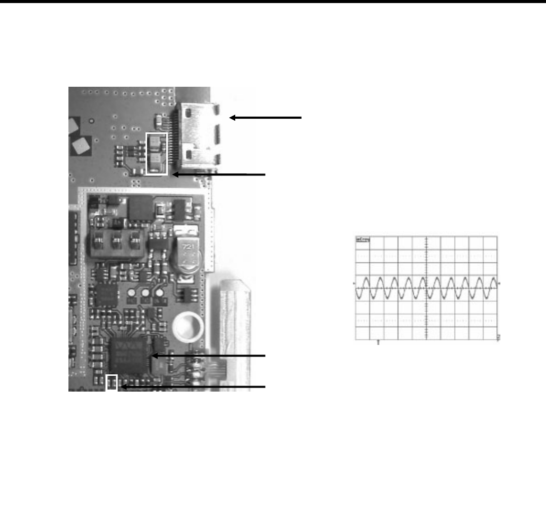
LGE Internal Use Only
Copyright © 2007 LG Electronics. Inc. All right reserved.
Only for training and service purposes
4. TROUBLE SHOOTING
- 133 -
C242, C244
U202
Audio codec
CN202
Headset connector
C222, C224
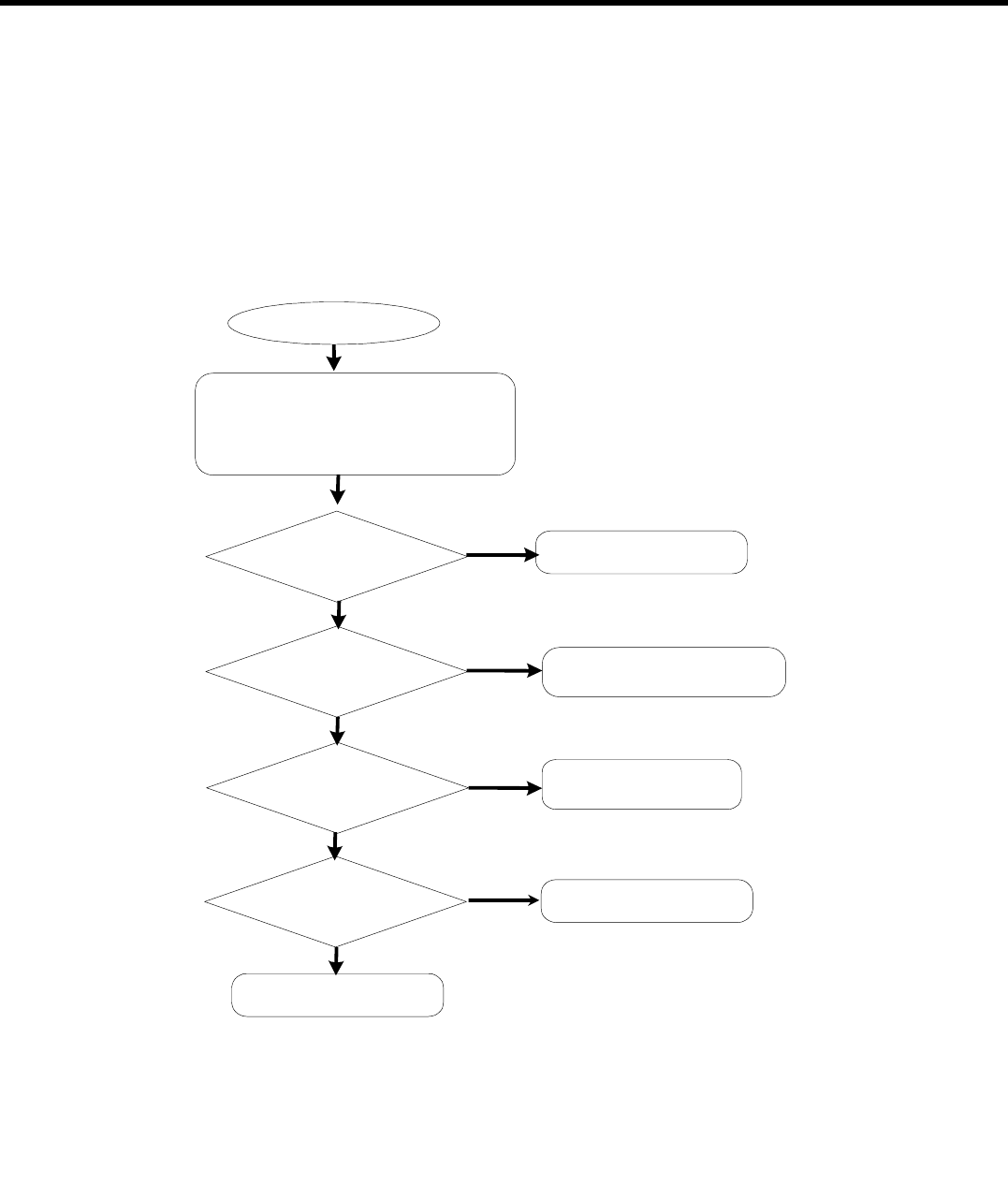
LGE Internal Use Only
Copyright © 2007 LG Electronics. Inc. All right reserved.
Only for training and service purposes
4. TROUBLE SHOOTING
- 134 -
4.15.4 Loud speaker path (voice speaker phone)
Loud speaker path as below:
MSM6275A HPH_R, HPH_L →C222,C224 →U202(audio codec) → C262,C267 → U208
(Speaker AMP) →pads of speaker →Speaker
Start
The sine wave appear at
C222,C224?
Change the Main board
NO
Connect the phone to network
Equipment and setup call
Setup 1KHz tone out
Set phone with speaker phone mode
The sine wave appear at
C262, C267?
YES
Check the U202 or
Change the Main board
NO
Check the U208
and R229, R233
NO
YES
YES
Can you hear the tone? Change the speaker
NO
YES
END
The sine wave appear at
pads of speaker?
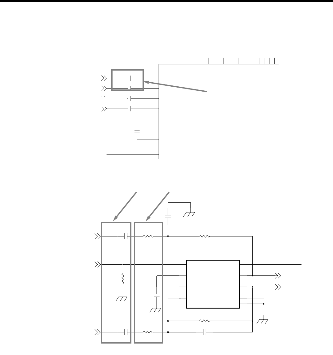
LGE Internal Use Only
Copyright © 2007 LG Electronics. Inc. All right reserved.
Only for training and service purposes
4. TROUBLE SHOOTING
- 135 -
1uC224
C226 1u
C222 1u
A7
NC1 C8
NC2 F8
NC3
NC4 G2
RXN
C2
RXP
B1
LINE1
A2
A1 LINE2
MIC1N
D2
U202
WM8753LEB-RV
A3 ACIN
B3 ACOP
H6
DBVDD
DCVDD J7
DGND H7
C225 1u
C228 1u
WM_HPH_R
WM_HPH_L
WM_RXP
WM_RXN
C222, C224
C262
0.068u
68KR230
R232 68K
R233
10K
10K
R229
C261
NA
0.068u
C267
R231
100K
1_SHUTDOWN
BYPASS
2
7
GND
IN+
3
4IN- 9
PGND
6
VDD
VO+ 5
VO- 8
TPA6205A1DRBRU208
C268 NA
C266
0.22u
SPKL-
SPKL+
SPK_AMP_EN
WM_LOUT2
WM_ROUT2
C222, C224
C262, C267 R229, R233
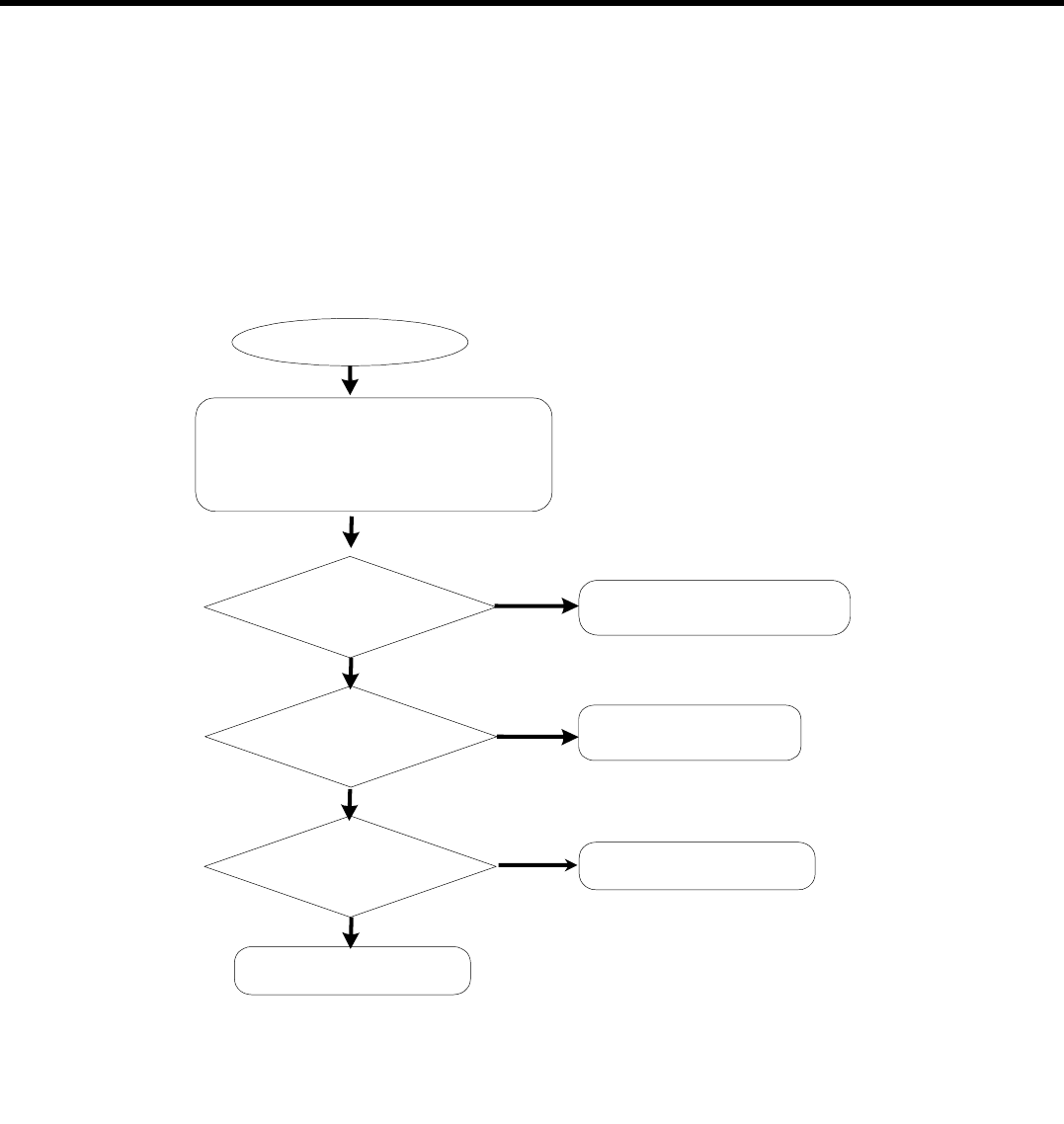
LGE Internal Use Only
Copyright © 2007 LG Electronics. Inc. All right reserved.
Only for training and service purposes
4. TROUBLE SHOOTING
- 136 -
4.15.5 Loud speaker path (VT, multimedia play, etc)
Loud speaker path (VT, multimedia play) as below:
STN8810(msptxd0) →U202(audio codec) → C262,C267 → U208 (Speaker AMP) →
pads of speaker →Speaker
Start
Connect the phone to network
Equipment and setup call
Setup 1KHz tone out
Set phone with speaker phone mode
The sine wave appear at
C262, C267?
Check the U202 or
Change the Main board
NO
Check the U208
and R229, R233
NO
YES
YES
Can you hear the tone? Change the speaker
NO
YES
END
The sine wave appear at
pads of speaker?
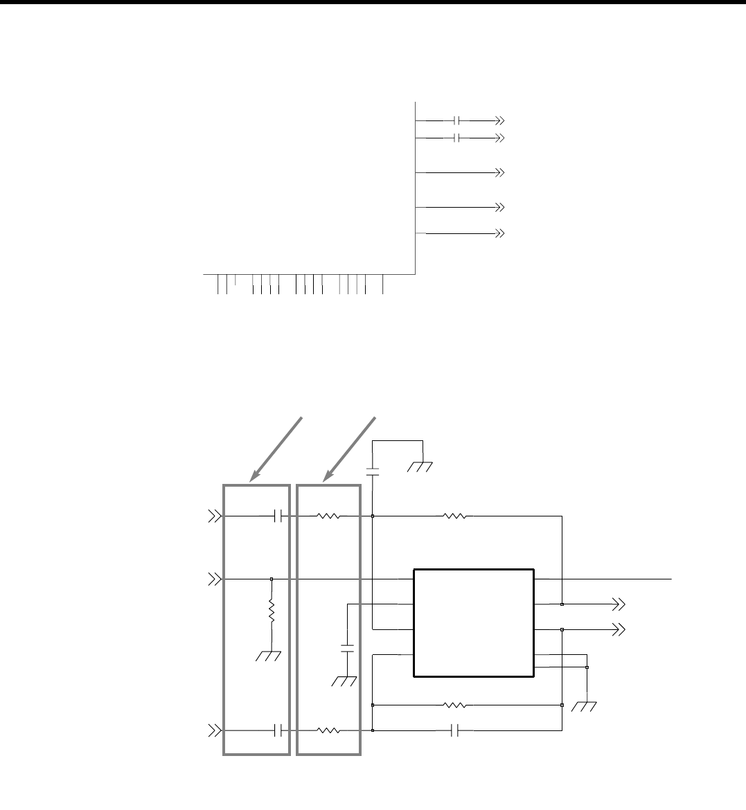
- 137 -
4. TROUBLE SHOOTING
LGE Internal Use Only
Copyright © 2007 LG Electronics. Inc. All right reserved.
Only for training and service purposes
1u C229
1u C230
VXCLK
H3
VXDIN
J1
J2 VXDOUT
VXFS
J3
MONO2
J8 PCMCLK
PGND
ROUT1 D9
ROUT2 B9
H1 SCLK
G1 SDIN
GPIO4
A9
LOUT2
H4 LRC
F1 MODE_GPIO3
MONO1 B6
B7
U202
WM8753LEB-RV
ADCDAT
J5
J4 BCLK
CSB_GPIO5
F2
DACDAT
H5
G8 GP1_CLK1
GP2_CLK2
J9
E1
WM_ROUT2
WM_MONO2
WM_MONO1
WM_ROUT1
WM_LOUT2
Audio Codec
Speaker AMP
C262
0.068u
68KR230
R232 68K
R233
10K
10K
R229
C261
NA
0.068u
C267
R231
100K
1_SHUTDOWN
BYPASS
2
7
GND
IN+
3
4IN- 9
PGND
6
VDD
VO+ 5
VO- 8
TPA6205A1DRBRU208
C268 NA
C266
0.22u
SPKL-
SPKL+
SPK_AMP_EN
WM_LOUT2
WM_ROUT2
C262, C267 R229, R233
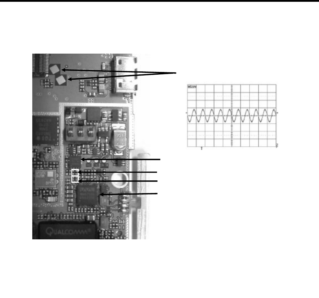
LGE Internal Use Only
Copyright © 2007 LG Electronics. Inc. All right reserved.
Only for training and service purposes
4. TROUBLE SHOOTING
- 138 -
U208 (Speaker Amp)
R711
Pads of Speaker
C722
C723
U202 (audio codec)
R229, R233
C262, C267
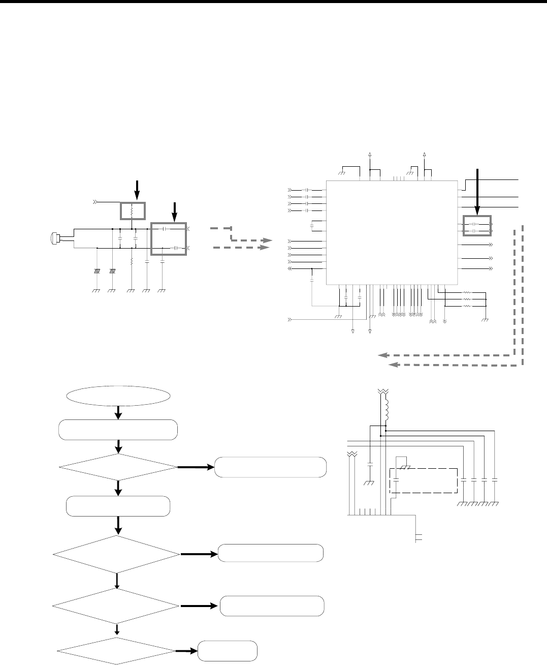
LGE Internal Use Only
Copyright © 2007 LG Electronics. Inc. All right reserved.
Only for training and service purposes
4. TROUBLE SHOOTING
- 139 -
4.15.6 Microphone for main MIC
Main Microphone path as below:
MIC →C245,C248 →U202(audio codec) → C229,C230 →MSM6275A →
MIC feed back gain logic →MSM internal CODEC
C245 1u
EVLC18S02015
VA200
C247
10p
2.2K
R221
C251
39p
2.2K
R227
MIC200
SUMY0009203
1
2
C252
39p
VA201
EVLC18S02015
39p
C246
1uC248
WM_MICBIAS
WM_MIC1P
WM_MIC1N
WM_DVDD
WM_AVDD
WM_AVDD
1u C229
1uC224
100K R214
C226 1u
1u C230
C222 1u
R213100K
C235
4.7u
A8
VMID
A4
B5 VREF
VXCLK
H3
VXDIN
J1
J2 VXDOUT
VXFS
J3
R215100K
MONO2
A7
NC1 C8
NC2 F8
NC3
NC4 G2
E8
OUT3
OUT4 E9
J8 PCMCLK
H9 PGND
PVDD
G9
ROUT1 D9
ROUT2 B9
RXN
C2
RXP
B1
H1 SCLK
G1 SDIN
SPKRVDD
GPIO4
HPVDD F9
HP_SPKRGND C9
LINE1
A2
A1 LINE2
D8
LOUT1
A9
LOUT2
H4 LRC
J6 MCLK
C1 MIC1
MIC1N
D2
D1 MIC2
MIC2N
E2
MICBIAS
B4
F1 MODE_GPIO3
MONO1 B6
B7
U202
WM8753LEB-RV
A3 ACIN
B3 ACOP
ADCDAT
J5
A5 AGND
AVDD
A6
J4 BCLK
CSB_GPIO5
F2
DACDAT
H5
H6
DBVDD
DCVDD J7
DGND H7
G8 GP1_CLK1
GP2_CLK2
J9
E1
C225 1u
C228 1u
C234
4.7u
WM_DVDD
C236
4.7u
WM_DACDAT
WM_LRC
WM_MSPRXD0
MSPTXD0
MSPTCK0
MSPTFS0
WM_BCLK
WM_ADCDAT
SPK_AMP_EN
WM_HPH_R
WM_HPH_L
WM_ROUT2WM_MICBIAS
AU_SW
VT_SW
PM_SDA
PM_SCL
AU_19.2M
WM_RXP
WM_RXN
WM_MONO2
WM_MONO1
WM_MIC1N
WM_ROUT1
WM_MIC1P
WM_MIC2N
WM_LOUT2
WM_MIC2P
Can you scoping some
sound signal at C245,C248?
Change the MIC
NO
YES
YES
make some sound or
voice to MIC
Work well? END
YES
Can you scoping some
sound signal at C229,C230?
Check the U202 or
Change the Main B'd
NO
Start
MIC_BIAS(C102) is 2.7V? Change the Main B'd
NO
Make a call
Place near
(CODEC VSS)
MSM pin W18
10%
SDCC_DAT1_GPIO99
F25
M25
SDCC_DAT2_GPIO100
M26
MICINN
AC19
AC20
MICINP
MIC1N
AF20
MIC1P
AE20
AF21
MIC2N
MIC2P
AF22
CCOMP
AA20
AF19
AUXIN
AE19
AUXIP
C611
NANA
C608
NA
C610
0.1u
C607
C609
NA
L600
100nH
C600
10p
MICINP
WM_MONO1
WM_MONO2
MICINN
R221
C245,C248
[main MIC]
[audio codec]
[MSM6275A]
C229,C230
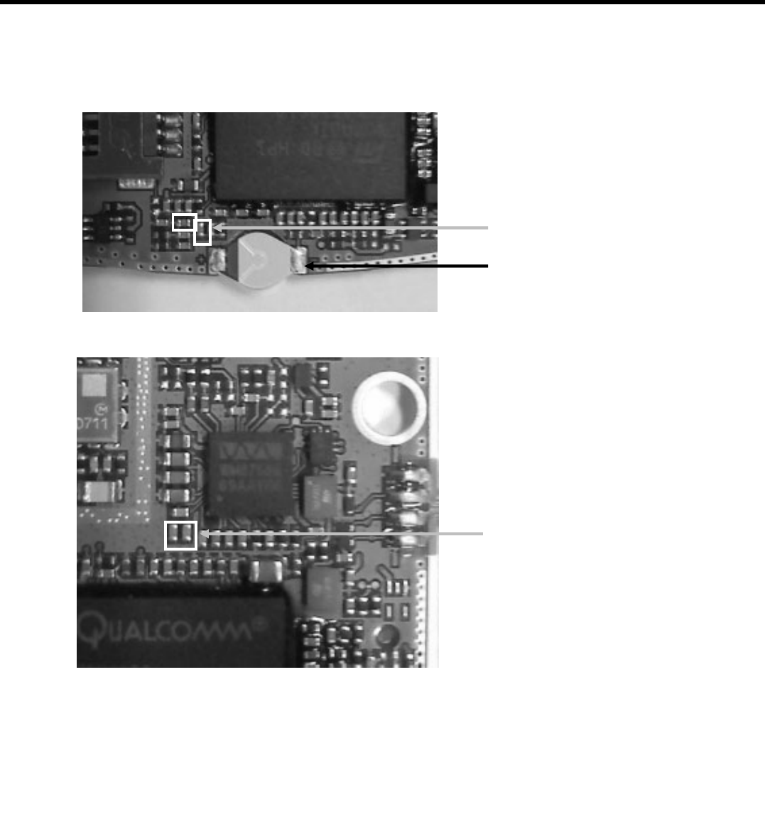
- 140 -
4. TROUBLE SHOOTING
LGE Internal Use Only
Copyright © 2007 LG Electronics. Inc. All right reserved.
Only for training and service purposes
MIC200 (MIC for Handset)
C229, C239
C245, C248
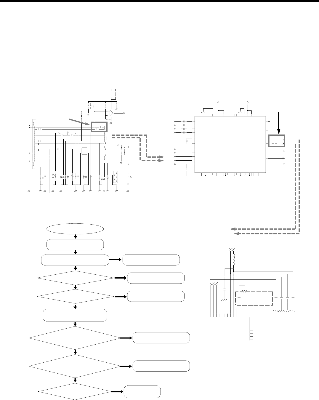
- 141 -
4. TROUBLE SHOOTING
4.15.7 Microphone for headset
MIC for Head_Set path as below:
Insert Headset →EAR_SENSE_N(pin8) go 0V →MSM6275A and STN8810 sense Head_Set
insertion →MIC signal → U202(audio codec) →MSM6275.
[CN202(headset connector)]
[MSM6275A]
LGE Internal Use Only
Copyright © 2007 LG Electronics. Inc. All right reserved.
Only for training and service purposes
1608
CONNECTOR VBATT_SENSE PIN CHECK!!
1%
1%
C249 47n
R717
NA
R716
0
U203
NCS2200SQ2T2G
GND
2
1
OUT
VCC
5
3
VIN+
VIN-
4
5
6
7
8
9
11
12
13
14
15
16
17
18
19
2
20
21
22
3
4
CN202
1
10
C242 33u
FB503 1000
33uC244
10pC258
47pC255
R223 68
R225 NA
C240 1u
RSB6.8CST2RVA211
EVLC14S02050VA205
1
2
3
4
5
EVLC14S02050
VBATT
CN203
VA208
smd_1608h_9_r
1u
C254
2.2K
R217
680K
R226
C259
33p
0.01u
C257
C238
0.1u
C239
10p
USB_VBUS_IN
VA206 EVLC14S02050
4
G2
1IN 2
OUT
NFM21PC105B1A3
U205
G1
3
FB245
10u
C237
100K R219
+5V_PWR
47pC256
EVLC14S02050VA204
PSD12-LFD200
VREG_MSMP_2.7V
INSTPAR
470K
R224
C253
33u
VA203 EVLC18S02003
330K
R218
VA207 EVLC14S02050
C241 1u
AP_VDD_IO_1.8V
EVLC18S02003
VA202
0.1u
C260
68R222
ICVL0505600V150FRVA209
1M
R216
VA210 RSB6.8CST2R
11K
R228
PSD05-LF
D201 INSTPAR
USB_D+
USB_D-
EAR_SENSE_N
HOOK_SENSE
WM_LOUT1
UART_RXD
UART_TXD
VBAT_TEMP
WM_MIC2N
WM_MIC2P
REMOTE_PWR_ON
VBATT_SENSE
WM_ROUT1
WM_AVDD
1u C229
1uC224
C226 1u
1u C230
C222 1u
A8
VMID
A4
B5 VREF
VXCLK
H3
VXDIN
J1
J2 VXDOUT
VXFS
J3
MONO2
A7
NC1 C8
NC2 F8
NC3
NC4 G2
E8
OUT3
OUT4 E9
J8 PCMCLK
H9 PGND
PVDD
G9
ROUT1 D9
ROUT2 B9
RXN
C2
RXP
B1
H1 SCLK
G1 SDIN
SPKRVDD
GPIO4
HPVDD F9
HP_SPKRGND C9
LINE1
A2
A1 LINE2
D8
LOUT1
A9
LOUT2
H4 LRC
J6 MCLK
C1 MIC1
MIC1N
D2
D1 MIC2
MIC2N
E2
MICBIAS
B4
F1 MODE_GPIO3
MONO1 B6
B7
U202
WM8753LEB-RV
A3 ACIN
B3 ACOP
ADCDAT
J5
A5 AGND
AVDD
A6
J4 BCLK
CSB_GPIO5
F2
DACDAT
H5
H6
DBVDD
DCVDD J7
DGND H7
G8 GP1_CLK1
GP2_CLK2
J9
E1
C225 1u
C228 1u
C234
4.7u
WM_DVDD
WM_HPH_R
WM_HPH_L
WM_ROUT2WM_MICBIAS
WM_RXP
WM_RXN
WM_MONO2
WM_MONO1
WM_MIC1N
WM_ROUT1
WM_MIC1P
WM_MIC2N
WM_LOUT2
WM_MIC2P
Start
EAR_SENSE_N is 0V?
END
Make a call
Change the Main b'd
Change the Main b'd
MIC_BIAS is 2.7V ?
YES
YES
NO
NO
NO
Try change the head set
Can you scoping some
sound signal at C240,C241?
Change the MIC
YES
YES
make some sound or
voice to MIC
Work well? END
YES
Can you scoping some
sound signal at C229,C230?
Check the U202 or
Change the Main B'd
NO
NO
YES
Place near
(CODEC VSS)
MSM pin W18
10%
SDCC_DAT1_GPIO99
F25
M25
SDCC_DAT2_GPIO100
SDCC_DAT3_GPIO101
M26
MICFBP
MICINN
AC19
AC20
MICINP
MDP_VSYNC_PRIMARY_GPIO105
AD2
AE3
MDP_VSYNC_SECONDA_GPIO104
MIC1N
AF20
MIC1P
AE20
AF21
MIC2N
MIC2P
AF22
CCOMP
AA20
AF19
AUXIN
AE19
AUXIP
C611
NANA
C608
NA
C610
0.1u
C607
C609
NA
L600
100nH
C600
10p
MICINP
WM_MONO1
WM_MONO2
MICINN
[audio codec]
C240,C241
C229,C230

- 142 -
4. TROUBLE SHOOTING
LGE Internal Use Only
Copyright © 2007 LG Electronics. Inc. All right reserved.
Only for training and service purposes
#8 pin of ear connector
to check EAR_SENSE_N
C237
Capacitor to check MIC bias (2.7V)
C240
C240
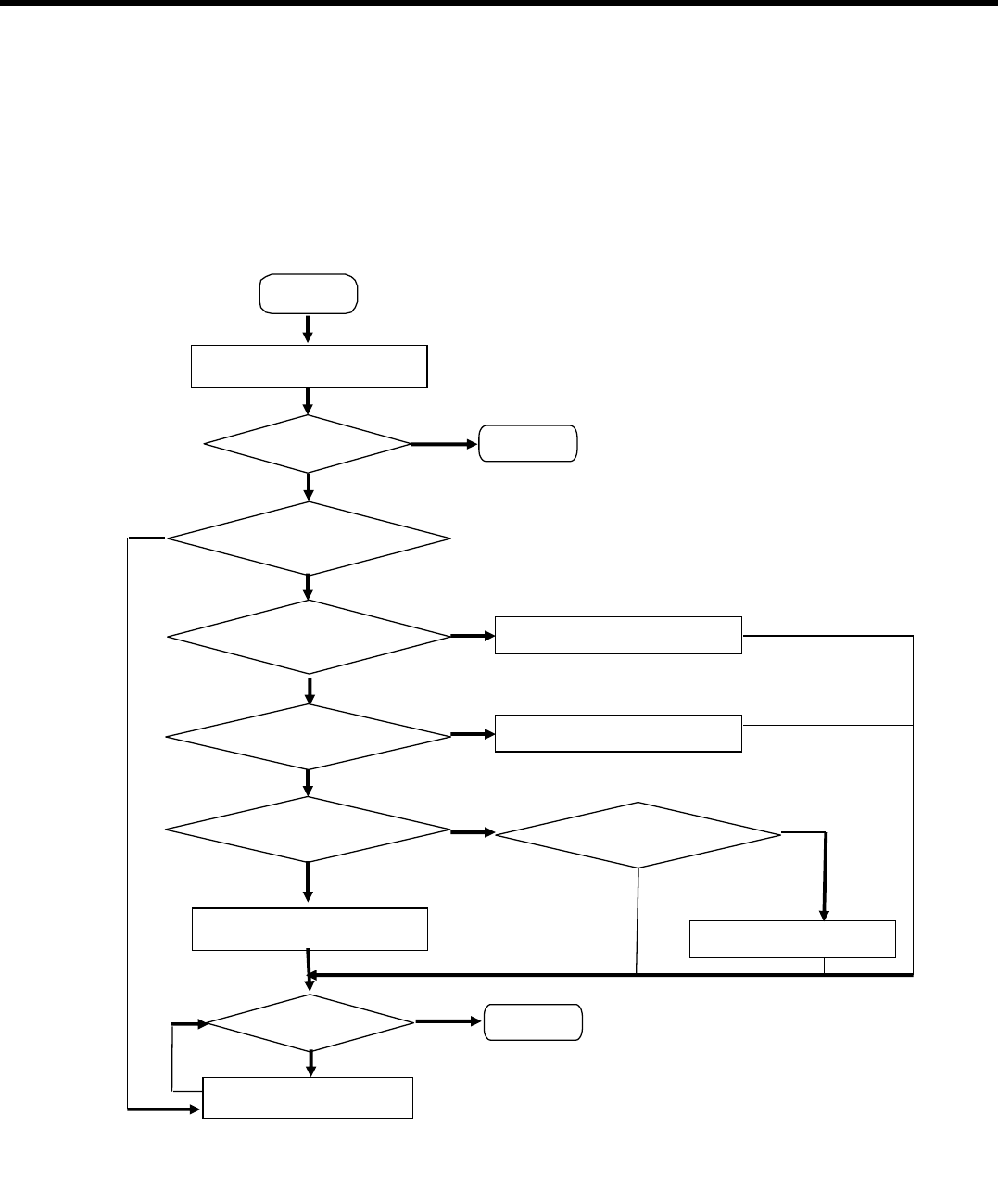
- 143 -
4. TROUBLE SHOOTING
4.16 Camera trouble
Camera control signals are generated by STN8810 and directly connected with STN8810.
KS10 has two cameras. The one is a 2 Mega Camera, the other is VGA camera.
LGE Internal Use Only
Copyright © 2007 LG Electronics. Inc. All right reserved.
Only for training and service purposes
Check AP_VDD_CAM_2.7V,
AP_VDD_CAM_1.8V
No
Camera is OK?
Check the camera conn. and
reconnect the camera
Change the LDO (U301, U303)
Camera is OK
Check the CCIRCLK_CAM
Change the camera
Yes
NO
NO
Yes
(FL201 #2)
Change the Main board
End
Yes
End
NO
2M START
STN8810 output signal check
(2M_RSTn_CAM, CAM_PWR_EN))
Yes
NO
Check master clock
OSC X200 output
Yes
Change the OSC (X200)
NO
Yes
Check the EMI/ESD filter
(FL201 #8)
Yes
No
Change the Filter (FL201)
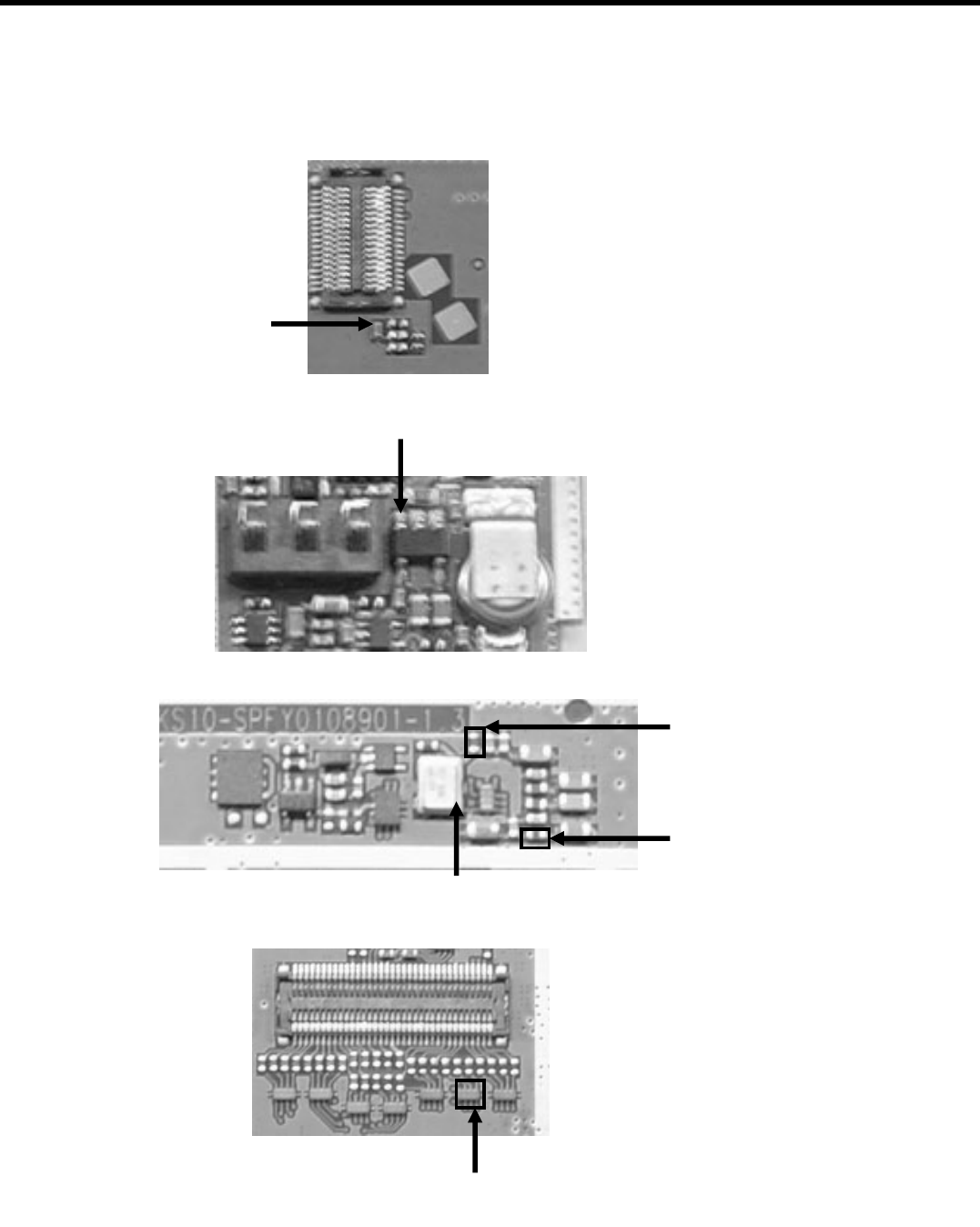
LGE Internal Use Only
Copyright © 2007 LG Electronics. Inc. All right reserved.
Only for training and service purposes
4. TROUBLE SHOOTING
- 144 -
2M_RSTn_CAM
CAM_PWR_EN
AP_VDD_CAM_2.7V
AP_VDD_CAM_1.8V
24MHZ OSC output
FL201
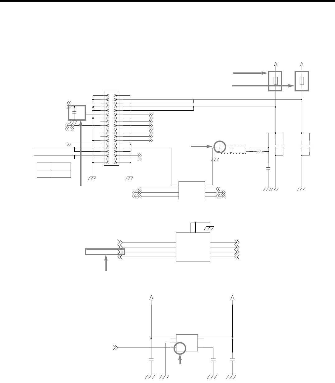
- 145 -
4. TROUBLE SHOOTING
LGE Internal Use Only
Copyright © 2007 LG Electronics. Inc. All right reserved.
Only for training and service purposes
Hi-Z
AXK7L34227
DrivenLOW
HIGH
2M_CAMERA
C2130.1u
C21210u
31
32
33
34
4
5
6
7
8
9
17 18
19
2
20
21
22
23
24
25
26
27
28
29
3
30
G1
G2
G3 G4
1
10
11
12
13
14
15
16
CN200
CSC3R270000BEVRS00 X200
27MHz
GND
2
3
OUT
TRI_OPEN
1
4
VDD
R207 100K
AP_VDD_CAM_2.7V
C214
0.01u
C21010u
INOUT_A1
1
2INOUT_A2
INOUT_A3
3
4INOUT_A4
9
INOUT_B1
INOUT_B2 8
7
INOUT_B3
INOUT_B4 6
FL203 EVRC18S03Q015050R
0.1u C211
C207
1u
AP_VDD_CAM_1.8V
HB-1M1005-601JT
FB204
FB205
HB-1M1005-601JT
I2CSCL0_CAM
I2CSDA0_CAM
2M_PWDN
I2CSCL0_CAM
I2CSDA0_CAM
I2CSCL0_SW
I2CSDA0_SW
2M_RSTn
2M_RSTn_CAM
2M_RSTn_CAM
CCIRID(4)_CAM
CCIRID(3)_CAM
CCIRID(2)_CAM
CCIRID(1)_CAM
CCIRID(0)_CAM
CCIRIVS_CAM
CCIRIHS_CAM
CCIRICLK_CAM
CCIRID(7)_CAM
CCIRID(6)_CAM
CCIRID(5)_CAM
AP_+VPWR AP_VDD_CAM_2.7V
1u
C305
4
BYPEN
3GND
2
1IN 5
OUT
U303
MIC5219-2.7YM5
2.2u
C307C306
470p
CAM_PWR_EN
EVRC18S03Q015050R
G1 5
G2 10
1INOUT_A1
INOUT_A2
2
3INOUT_A3
INOUT_A4
4
INOUT_B1 9
8
INOUT_B2
INOUT_B3 7
6
INOUT_B4
FL201
CCIRICLK_CAM
CCIRIHS_CAM
CCIRIVS_CAM
CAMCLK_27MHZ_CAM CAMCLK_27MHZ
CCIRIHS
CCIRIVS
CCIRICLK
2M_RSTn_CAM
FL201 (#2)
24MHZ OSC output
CAM_PWR_EN
AP_VDD_CAM_2.7V
AP_VDD_CAM_1.8V
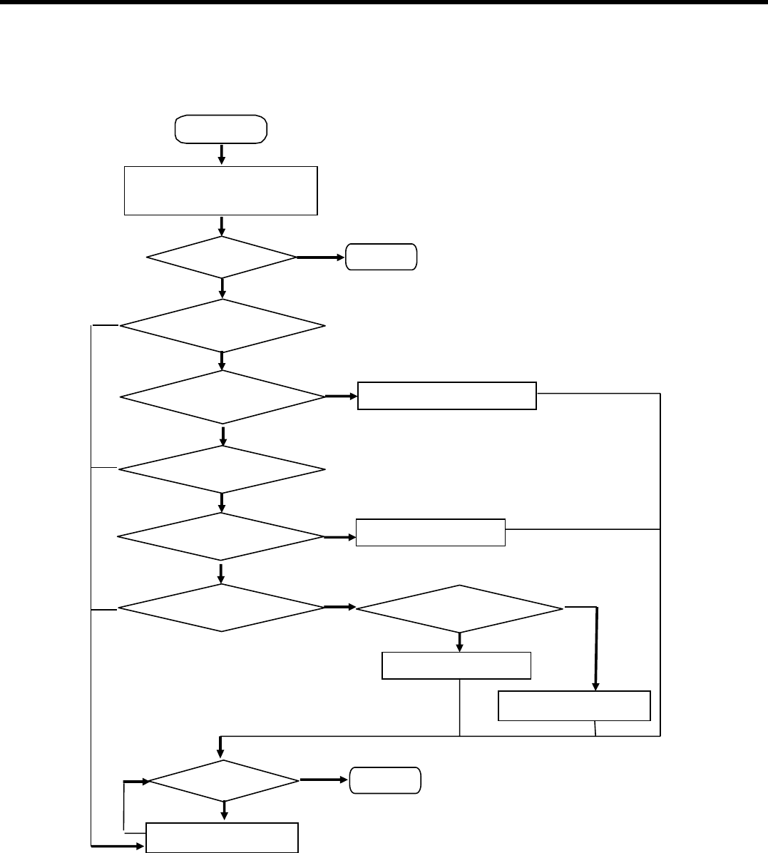
LGE Internal Use Only
Copyright © 2007 LG Electronics. Inc. All right reserved.
Only for training and service purposes
4. TROUBLE SHOOTING
- 146 -
Check AP_VDD_CAM_2.7V,
AP_VDD_CAM_1.8V
Camera is OK?
Check the camera & 70-pin
main conn.
And reconnect these connectors
Change the LDO (U301, U303)
Camera is OK
Check the CCIRCLK
Yes
NO
NO
Yes
(R719)
Change the Main board
End
Yes
End
NO
VGA START
STN8810 output signal check
(VGA_RSTn, VGA_STNADBY)
Yes
NO
Check master clock
(CAMCLK_27MHZ : R206)
Yes
Yes
Check the EMI/ESD filter
(FL201 #1)
Change the Filter (FL201)
NO
NO
Yes
NO
Change the camera
Change the slider FPCB
Check the CCIRCLK (in FPCB)
(R104 in slider FPCB))
Yes
No
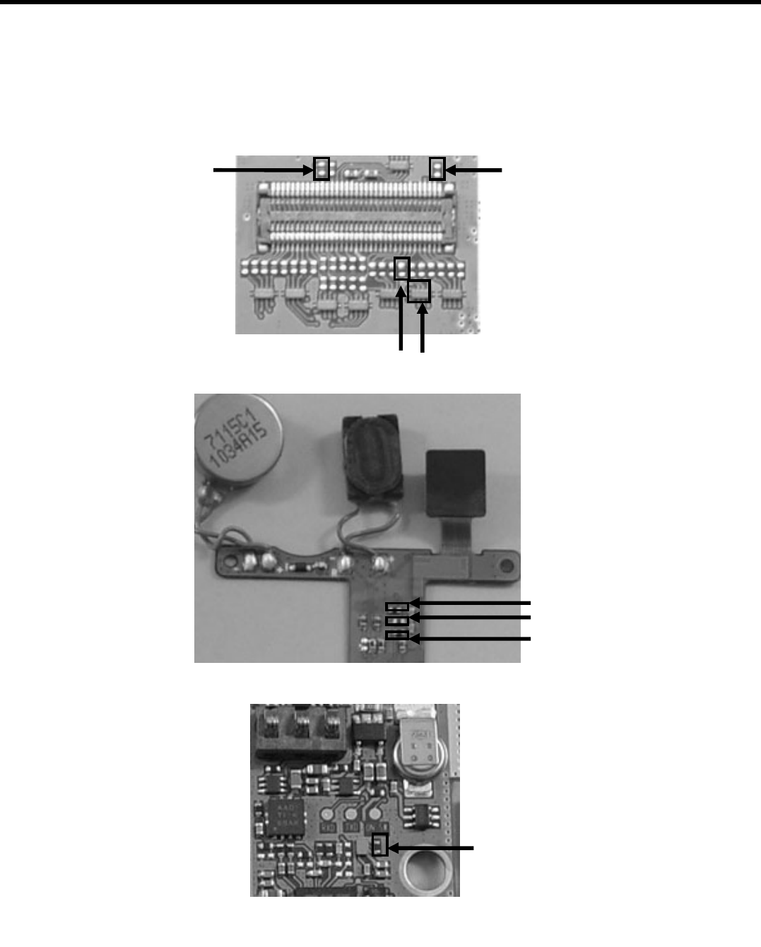
- 147 -
4. TROUBLE SHOOTING
LGE Internal Use Only
Copyright © 2007 LG Electronics. Inc. All right reserved.
Only for training and service purposes
FL201
VGA_RSTnVGA_STANDBY
AP_VDD_CAM_1.8V
AP_VDD_CAM_2.7V
R719 (CCIRICLK)
CAMCLK_27MHZ
R104 (CCIRICLK)
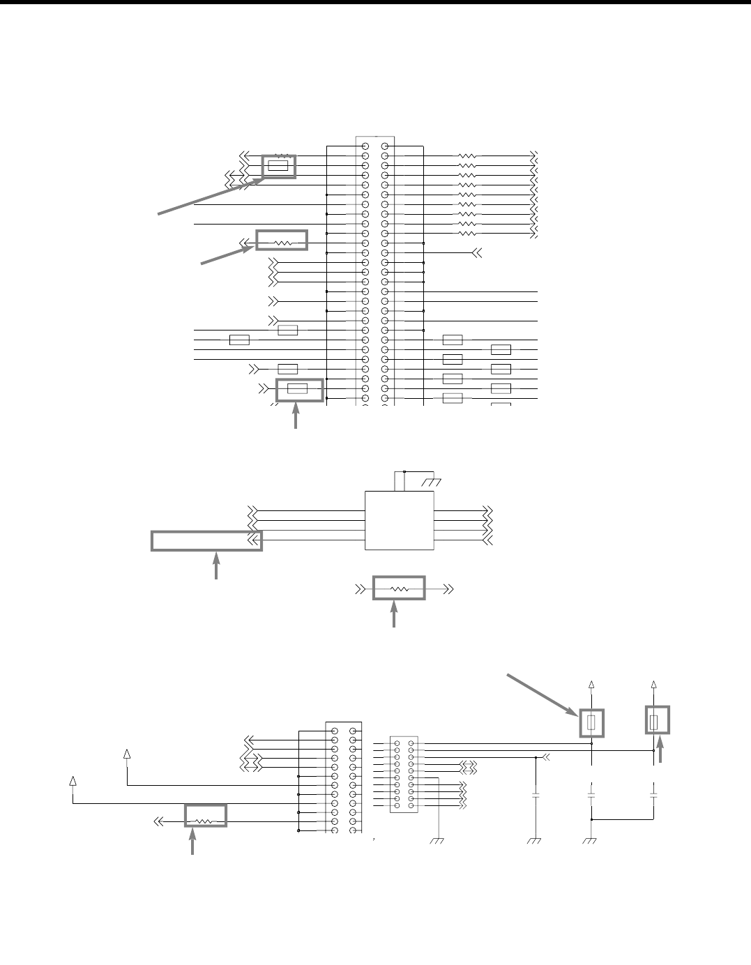
- 148 -
4. TROUBLE SHOOTING
LGE Internal Use Only
Copyright © 2007 LG Electronics. Inc. All right reserved.
Only for training and service purposes
MAIIN-SLIDER CON-HEADER
0R728
0R727
0R726
0R725
0R724
0R723
0R722
0R721
0R720
0R719
0R718
FB224
FB235
FB232
FB229
FB236
FB227
FB233
FB225
FB221
15050R
FB223
FB234
FB231FB230
64
65
66
67
68
69
7
70
8
9
G1 G2
50
51
52
53
54
55
56
57
58
59
6
60
61
62
63
4
44
45
46
47
48
49
5
20
21
22
23
24
25
26
27
3
CN201
1
10
11
12
13
14
15
16
17
18
19
2
CCIRICLK
CCIRIHS
L0_CAM
A0_CAM
VGA_RSTn
LCD_NRESET
CAMCLK_27MH
RECEIVER+
RECEIVER-
RECEIVER--
MOT_PWR-
WLED_CTL
VGA_STANDBY
R206 0
EVRC18S03Q015050R
G1 5
G2 10
1INOUT_A1
INOUT_A2
2
3INOUT_A3
INOUT_A4
4
INOUT_B1 9
8
INOUT_B2
INOUT_B3 7
6
INOUT_B4
FL201
CCIRICLK_CAM
CCIRIHS_CAM
CCIRIVS_CAM
CAMCLK_27MHZ_CAM CAMCLK_27MHZ
CCIRIHS
CCIRIVS
CCIRICLK
CAMCLK_27MHZ
MCAM_27M
7
8
9
G1 G2
6
4
5
3
1
10
11
12
2
CN102
AP_VDD_CAM_2.7V
AP_VDD_CAM_1.8V
R104
0
I2CSCL0_CAM
I2CSDA0_CAM
VGA_RSTn
CCIRICLK_CAM
CCIRIHS_CAM
VGA_CAMERA
AXK720145G
HB-1M1005-601JT
FB101
FB100
HB-1M1005-601JT
1u
C102
AP_VDD_CAM_2.7V
C101
0.1u
C100
0.1u
192
20
3
4
5
6
7
8
9
1
10 11
12
13
14
15
16
17
18
AP_VDD_CAM_1.8V
CN100
I2CSCL0_CAM
I2CSDA0_CAM
VGA_RSTn
CCIRIHS_CAM
CCIRIVS_CAM
CCIRID(7)_CAM
CCIRID(6)_CAM
VGA_RSTn
R719 (CCIRICLK)
VGA_STANDBY
FL201 (#1)
R104 (CCIRICLK)
AP_VDD_CAM_2.7V
AP_VDD_CAM_1.8V
CAMCLK_27MHZ
Schematic of VGA camera part
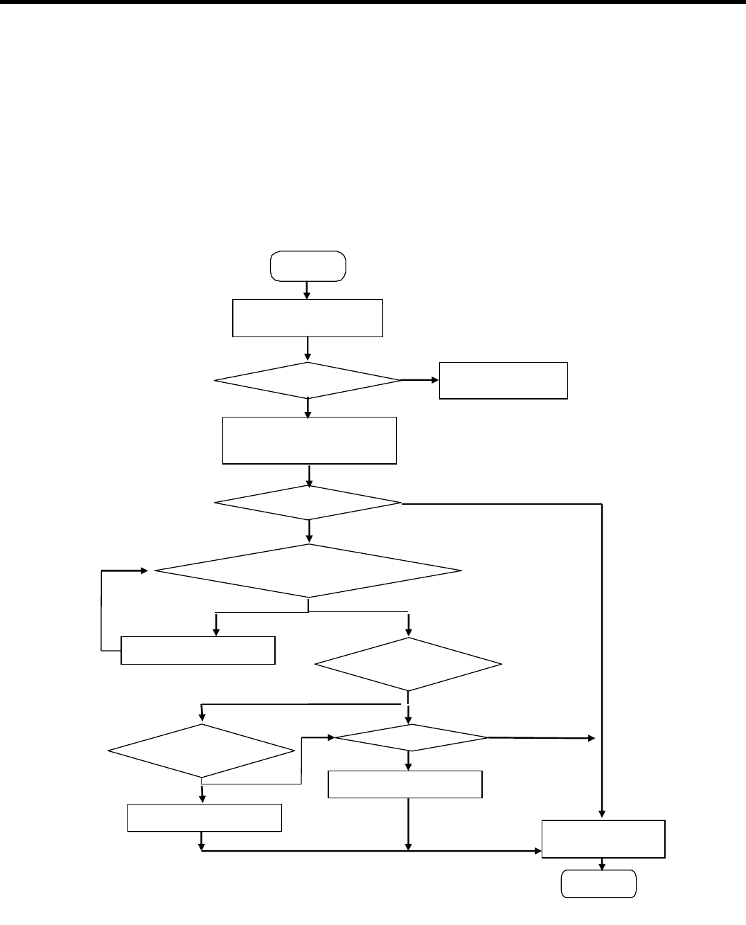
- 149 -
4. TROUBLE SHOOTING
4.17 Main LCD trouble
Main LCD control signals are generated by STN8810. Those signal’s path are :
STN8810 -> 70-pin main connector(CN201 in main PCB) -> 70-pin connector (CN102 in slider FPCB)
-> 40-pin connector (CN101 in slider FPCB) -> 40-pin connector (CN101 in SUB PCB) -> LCD zip
connector (CN100 in SUB PCB) -> LCD Module
LGE Internal Use Only
Copyright © 2007 LG Electronics. Inc. All right reserved.
Only for training and service purposes
The LCD works
START
Press END key
to turn the power on
Is the circuit powered?
Follow the Power ON
trouble shooting
LCD display OK?
Check AP_VDD_LCD_2.8V, LCD_NRESET,
LCD_DATA(0) in Main BD
No
Yes
Yes
No
Disconnect and reconnect
70-pin , 40-pin B to B,
and 35-pin zip connector
Change the Main BD
No
End
Yes
Check the same signal
in SUB BD
No Yes
Change the slider FPCB
& re-check
Display OK?
Yes
Change the LCD module
No
Yes
Change the SUB BD
No
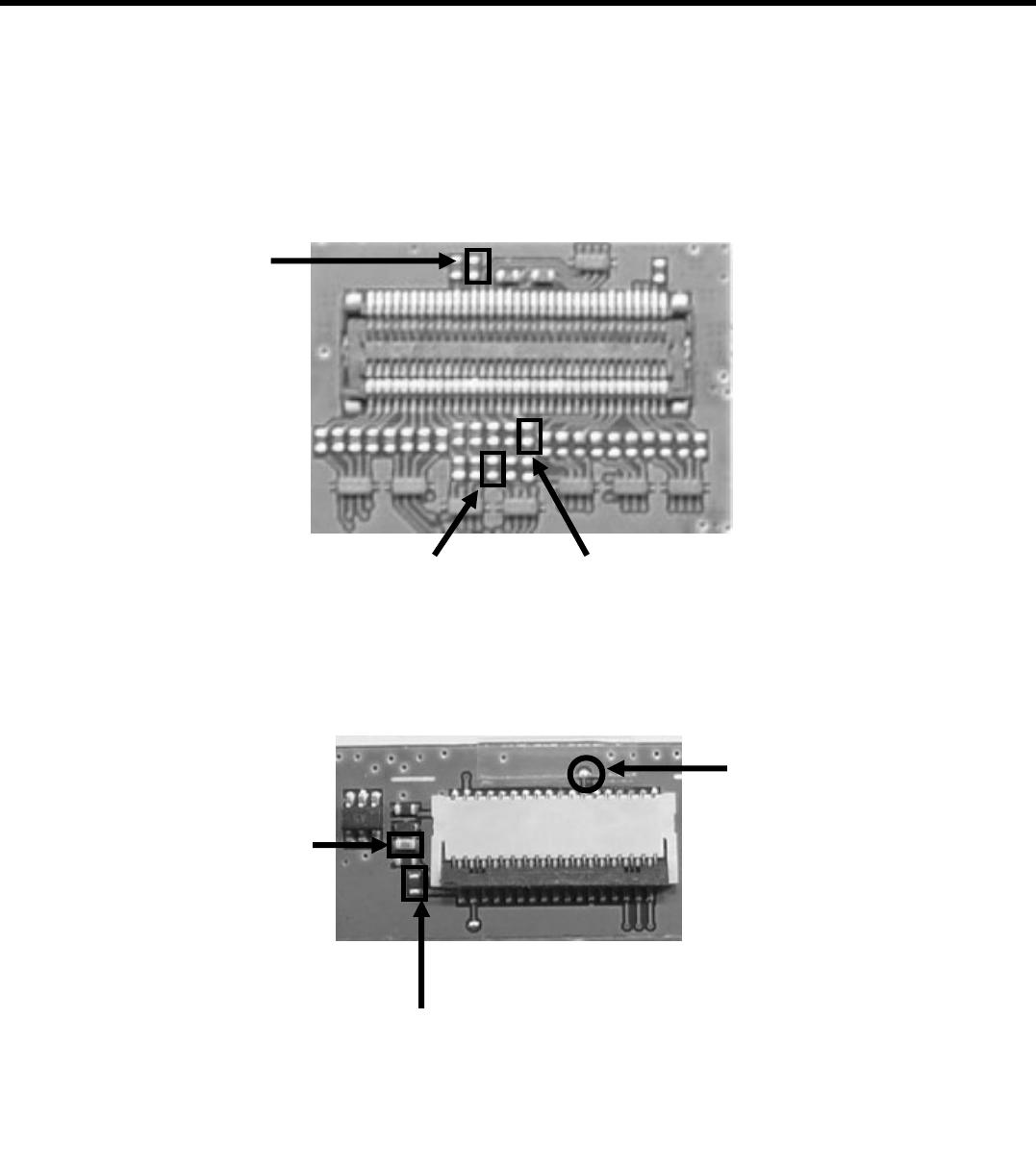
- 150 -
4. TROUBLE SHOOTING
Main BD
SUB BD
LGE Internal Use Only
Copyright © 2007 LG Electronics. Inc. All right reserved.
Only for training and service purposes
AP_VDD_LCD_2.8VLCD_DATA(0)
LCD_NRESET
AP_VDD_LCD_2.8V
LCD_DATA(0)
LCD_NRESET
- 151 -
4. TROUBLE SHOOTING
LGE Internal Use Only
Copyright © 2007 LG Electronics. Inc. All right reserved.
Only for training and service purposes
MAIIN-SLIDER CON-HEADER
0R728
0R727
0R726
0R725
0R724
0R723
0R722
0R721
0R720
0R719
0R718
FB224
FB235
FB232
FB229
AP_+VPWR FB222
FB236
FB227
FB233
FB225
FB221
9
8
7
6
3Q015050R
FB223
AP_VDD_LCD_2.8V
FB234
FB231FB230
64
65
66
67
68
69
7
70
8
9
G1 G2
50
51
52
53
54
55
56
57
58
59
6
60
61
62
63
4
44
45
46
47
48
49
5
20
21
22
23
24
25
26
27
3
CN201
1
10
11
12
13
14
15
16
17
18
19
2
CCIRID(2)
CCIRID(1)
CCIRID(0)
CCIRICLK
CCIRIHS
CSCL0_CAM
SDA0_CAM
VGA_RSTn
CCIRIVS
CCIRID(7)
CCIRID(6)
CCIRID(5)
CCIRID(4)
CCIRID(3)
LCD_NRESET
CAMCLK_27MHZ_CAM
RECEIVER+
RECEIVER-
RECEIVER--
MOT_PWR-
WLED_CTL
VGA_STANDBY
XF2B-3545-31A-P
LCD Connector
(lower contact)
C105
820p
0R115
35
4
5
6
7
8
9
20
21
22
23
24
25
26
27
28
29
3
30
31
32
33
34
1
10
11
12
13
14
15
16
17
18
19
2
CN100
ZD100 RSB6.8CST2R
100K
R102
R103 100K
R104 100K
1uC104
AP_VDD_LCD_2.8V
TP100
TP102
TP101
LCD_NRESET
LCD_DATA(0)
LCD_VS
DIS_CSN
DIS_WEN
DIS_RS
LED_ANODE
LED3
LED2
LED1
LCD_DATA(1)
LCD_DATA(10)
LCD_DATA(11)
LCD_DATA(12)
LCD_DATA(13)
LCD_DATA(14)
LCD_DATA(15)
LCD_DATA(2)
LCD_DATA(3)
LCD_DATA(4)
LCD_DATA(5)
LCD_DATA(6)
LCD_DATA(7)
LCD_DATA(8)
LCD_DATA(9)
LCD_DATA(0:15)
LED4
Schematic of LCD part
AP_VDD_LCD_2.8V
LCD_DATA(0)
LCD_DATA(0)
LCD_NRESET
LCD_NRESET
AP_VDD_LCD_2.8V
LGE Internal Use Only
Copyright © 2007 LG Electronics. Inc. All right reserved.
Only for training and service purposes
4.18 Bluetooth trouble
Bluetooth control signals are generated by STN8810.
Those signal’s path are : STN8810 →AP_VDD_IO_1.8V and AP_VDD_BT_2.7V is asserted →
CLK32K is asserted →Bluetooth ON →BT_RESETN is High CLK_REQ_OUT_1 is High →
REF_CLK_IN is asserted →transmit/receive data/control through UART →transmit/receive voice data
through PCM I/F
Figure. Schematic of Bluetooth Interface
4. TROUBLE SHOOTING
- 152 -
R401
0
6
1
U_BP
C409 0.1u
DEA212450BT-7043C1
FL400
5BP1
4BP2 BP_DC 2
3G1
G2
TP400
0
R715
AP_VDD_BT_2.7V
0.1u
C401
0
R404
E7
G2 VDD_D
VDD_DSM
B7
A7 VDD_HV_A
VDD_HV_D
G1
VDD_IO_A
G5
F3 VDD_IO_B
C7 VDD_N
VDD_RF
A1
B4
VSS_ANA1
VSS_ANA2 B6
C6
VSS_ANA3
VSS_DIG1 E3
E4
VSS_DIG2
A2
VSS_RF1 A5
VSS_RF2
G3
D2 PCM_A
PCM_B
E1
PCM_CLK
D1
PCM_SYNC
C2
REF_CLK_IN
D6
D3 RESET_N
RFN A4
A3
RFP
TOUT_IN_QP
B5
A6 TOUT_IP_QN
G4 UART_CTS UART_RTS F4
F5 UART_RXD UART_TXD F6
D7 VDD_CL
VDD_CLD
E5
C5 BT_WAKEUP
E6 CLK_REQ_IN_1
G6 CLK_REQ_IN_2
CLK_REQ_OUT2
G7
CLK_REQ_OUT_1 C4
E2 CONFIG_1
CONFIG_2
F1
F2 CONFIG_3
GPIO_0
D5
C1 GPIO_10
B2
GPIO_11
B3 GPIO_16
GPIO_8
C3
GPIO_9
B1
HOST_WAKEUP
F7
LP_CLK
STLC2500CU401
AF_PRG
220nC405
220nC408
AP_VDD_BT_2.7V
2
GND
OUT 3
1TRI_OPEN
VDD
4
19.2MHz
X400 CSC3M192000EEVRS00
0.1uC412
C404 0.1u
0.1uC411
C410 220n
C407 220n
R410
0
FEED
NC1
NC2
AP_VDD_IO_1.8V
ANT400
220nC406
BT_RESETN
UCTS0N
URXD0
PCMDATAOUT
PCMDATAIN
PCMCLK
PCMSYNC
UTXD0
URTS0N
CLK32K
X400
R404
FL400 ANT400
33u
C400C402
1u
AP_+VPWR
R714
0
470p
C403
MIC5219-2.7YM5U400
BYP 43 EN
2GND
IN
1OUT 5
AP_VDD_BT_2.7V
PON
U400
LGE Internal Use Only
Copyright © 2007 LG Electronics. Inc. All right reserved.
Only for training and service purposes
4. TROUBLE SHOOTING
- 153 -
Bluetooth RF Test
TC-3000A (Bluetooth Tester)
1. Set phone to bluetooth test-mode:
Enter Test Mode(*#32*36907#) →Module Test Set →BT DUT →BT DUT ON
2. Connect phone to bluetooth tester
3. Set channel to 39
4. Measure output-power
5. Check TP1 : output-power > -6 dBm
LGE Internal Use Only
Copyright © 2007 LG Electronics. Inc. All right reserved.
Only for training and service purposes
4. TROUBLE SHOOTING
- 154 -
Set the bluetooth ON
AP_VDD_BT_2.7V
is asserted?
Check LDO
(U400) Pin#5
REF_CLK_IN
is asserted?
Check Oscillator
(X400)
RF Power (R404)
< -6 dBm?
Check BT Antenna
(ANT400) soldering
Check FL400
soldering
Bluetooth is work well? Change
the main board
END
U400 X400
ANT400 FL400
R404
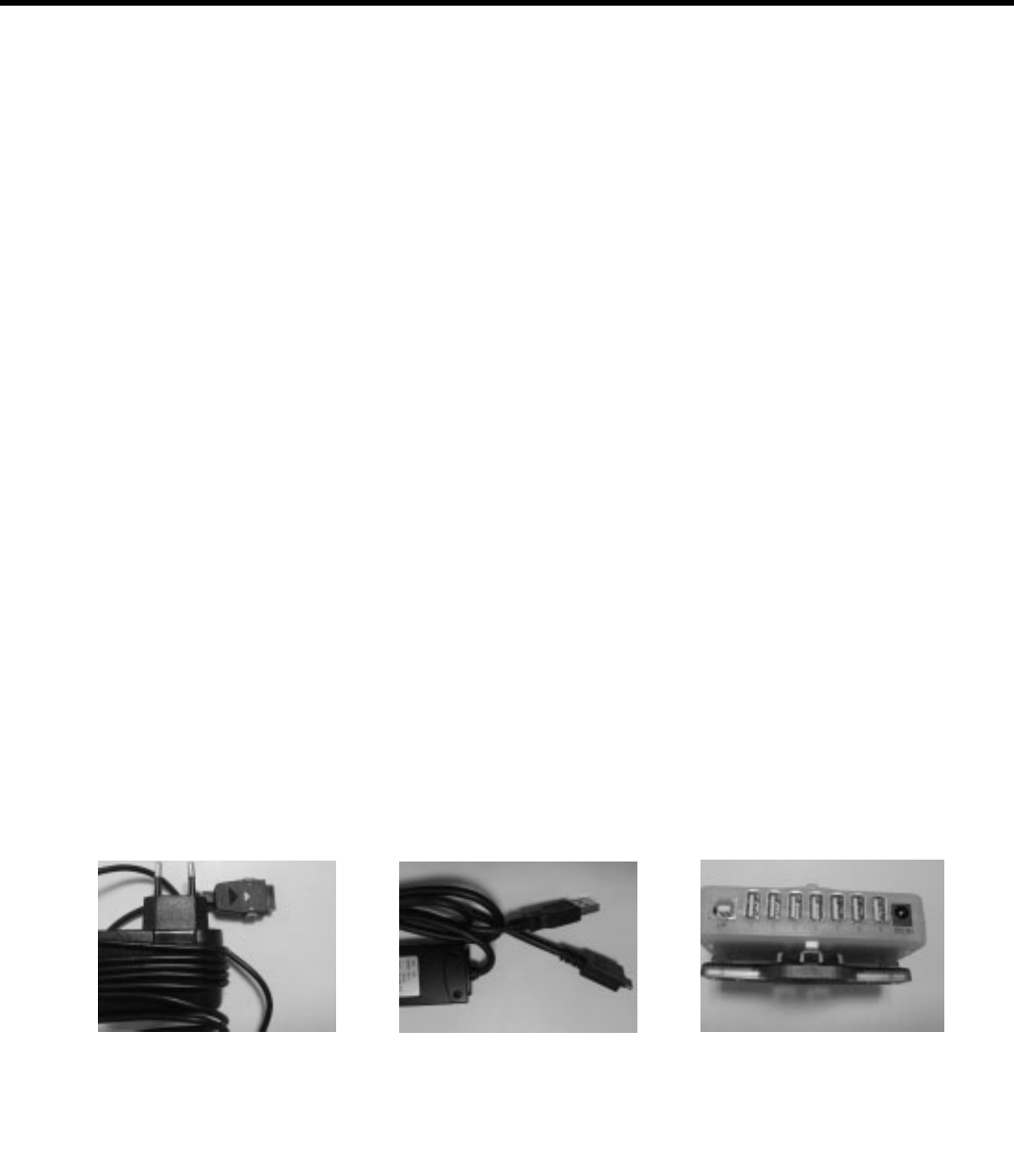
- 155 -
5. DOWNLOAD
5.1 Composition omposition
5.1.1 PC OS
- Windows 2000(SP4) & Windows XP(SP2)
- RAM : 256M
- USB : 1.1 or 2.0
5.1.2 D/L Tool
- TA-25G
- 3G USB DLC
- USB HUB : Support 1.1 with 2.0
4 ~7 ports USB
Using the external power (Adaptor)
5.1.3 Program
- LGDP2 program: V32
5.1.4 Solution for KS10
- AP : Nomadik application processors
- MP : Qualcomm application processors
5. DOWNLOAD
LGE Internal Use Only
Copyright © 2007 LG Electronics. Inc. All right reserved.
Only for training and service purposes
<TA-25G> <3G USB DLC> <USB Hub>
LGE Internal Use Only
Copyright © 2007 LG Electronics. Inc. All right reserved.
Only for training and service purposes
5. DOWNLOAD
- 156 -
5.2 LGDP2 Program install LGDP2 Program install
5.2.1 The "LGDP2_for set-up zip" file is downloaded on CSMG site.
5.2.2 The "LGDP2_for set-up zip" file is unzip as same name in PC.
5.2.3 Select "First LGDP2_set-up" folder.
5.2.4 Open "serial_number" file.
5.2.5 Double click "LGDP2_31_INCLUDE_LGDP1_Setup" file.
LGE Internal Use Only
Copyright © 2007 LG Electronics. Inc. All right reserved.
Only for training and service purposes
5. DOWNLOAD
- 157 -
5.2.6 Click “Next” button.
5.2.7 Writing Serial number and then click “Next” button.
5.2.8 Click “Install” button.
LGE Internal Use Only
Copyright © 2007 LG Electronics. Inc. All right reserved.
Only for training and service purposes
5.2.9 Click “Finish” button.
5. DOWNLOAD
- 158 -
LGE Internal Use Only
Copyright © 2007 LG Electronics. Inc. All right reserved.
Only for training and service purposes
5. DOWNLOAD
- 159 -
5.3 USB Driver setup USB Driver setup
5.3.1 Setup the USB driver for MP.
5.3.1.1 Select "LG USB Modem Driver 4"1".7(WHQL)" in "LGDP2_for set-up" folder.
5.3.1.2 Double click
“LGUSBModemDriver_WHQL_Eng_Ver_4.7”
LGE Internal Use Only
Copyright © 2007 LG Electronics. Inc. All right reserved.
Only for training and service purposes
5.3.1.3 Click “Next” button. 5.3.1.4 Click “OK” button.
5. DOWNLOAD
- 160 -

LGE Internal Use Only
Copyright © 2007 LG Electronics. Inc. All right reserved.
Only for training and service purposes
5. DOWNLOAD
- 161 -
5.3.2 Setup the KS10 USB driver for AP.
5.3.2.1 Copy "KS10_USB_20070426" folder in "LGDP2_for set-up" folder.
5.3.2.2 And then paste this folder on "DOWNLOAD" folder in
C driver as below picture.
LGE Internal Use Only
Copyright © 2007 LG Electronics. Inc. All right reserved.
Only for training and service purposes
5. DOWNLOAD
- 162 -
5.4 KS10 LGDP2 run file & DLL file setup
5.4.1 Setup the KS10 run file & DLL file.
5.4.1.1 Copy "LGDP2_V32" file &
"Model" folder in "LGDP2_for set-
up" folder.
5.4.1.2 And then paste these file & folder
on "DOWNLOAD" folder in C
driver.
LGE Internal Use Only
Copyright © 2007 LG Electronics. Inc. All right reserved.
Only for training and service purposes
5. DOWNLOAD
- 163 -
5.5 Execute LGDP2 program
5.5.1 Double click “LGDP2_V32” file in "DOWNLOAD" folder.
5.5.2 Click “LOGIN” button.
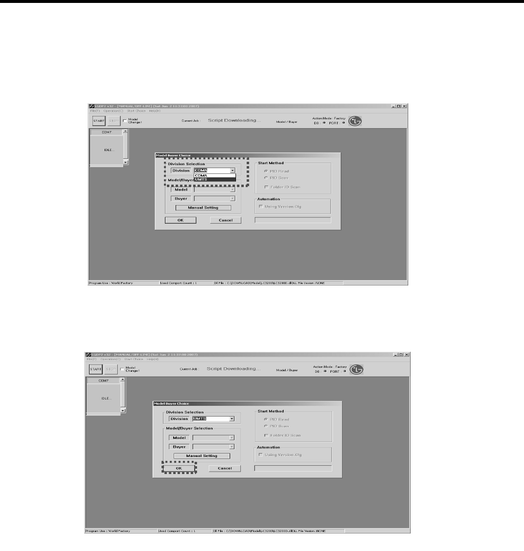
- 164 -
5. DOWNLOAD
5.5.3 You choose the "UMTS" in "Division" Box
5.5.4 Click “OK” button.
LGE Internal Use Only
Copyright © 2007 LG Electronics. Inc. All right reserved.
Only for training and service purposes
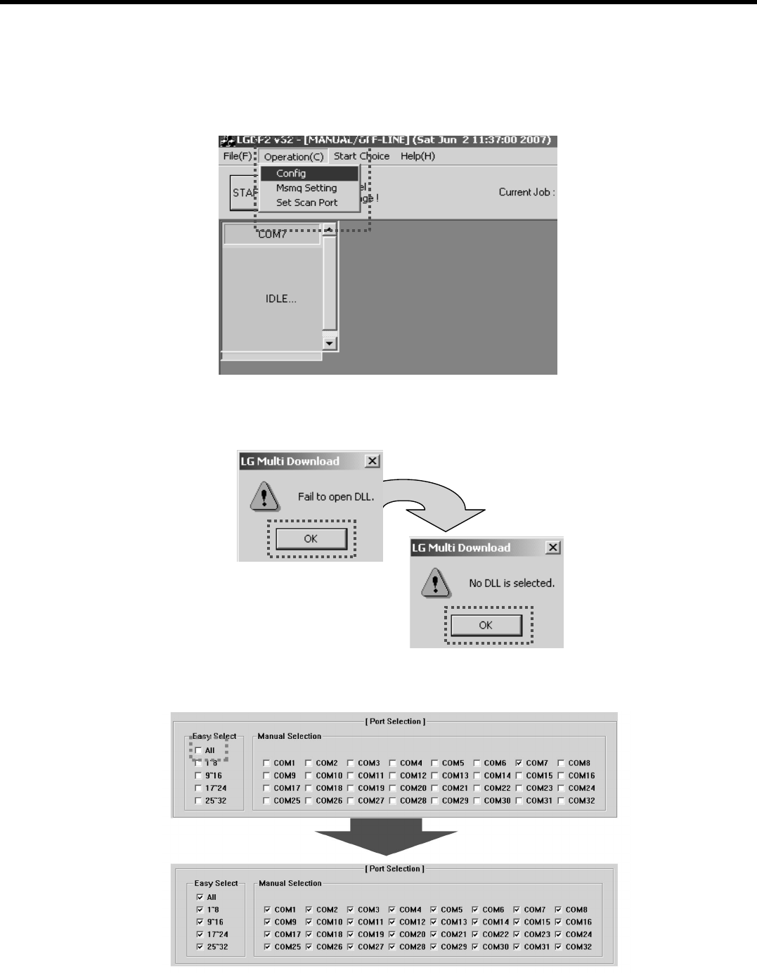
- 165 -
5. DOWNLOAD
5.5.5 Click “Operation(C)” on menu and then select “Config”.
5.5.6 Click “OK” button.
* Ignore these below message
5.5.7 Click “All” icon.
LGE Internal Use Only
Copyright © 2007 LG Electronics. Inc. All right reserved.
Only for training and service purposes
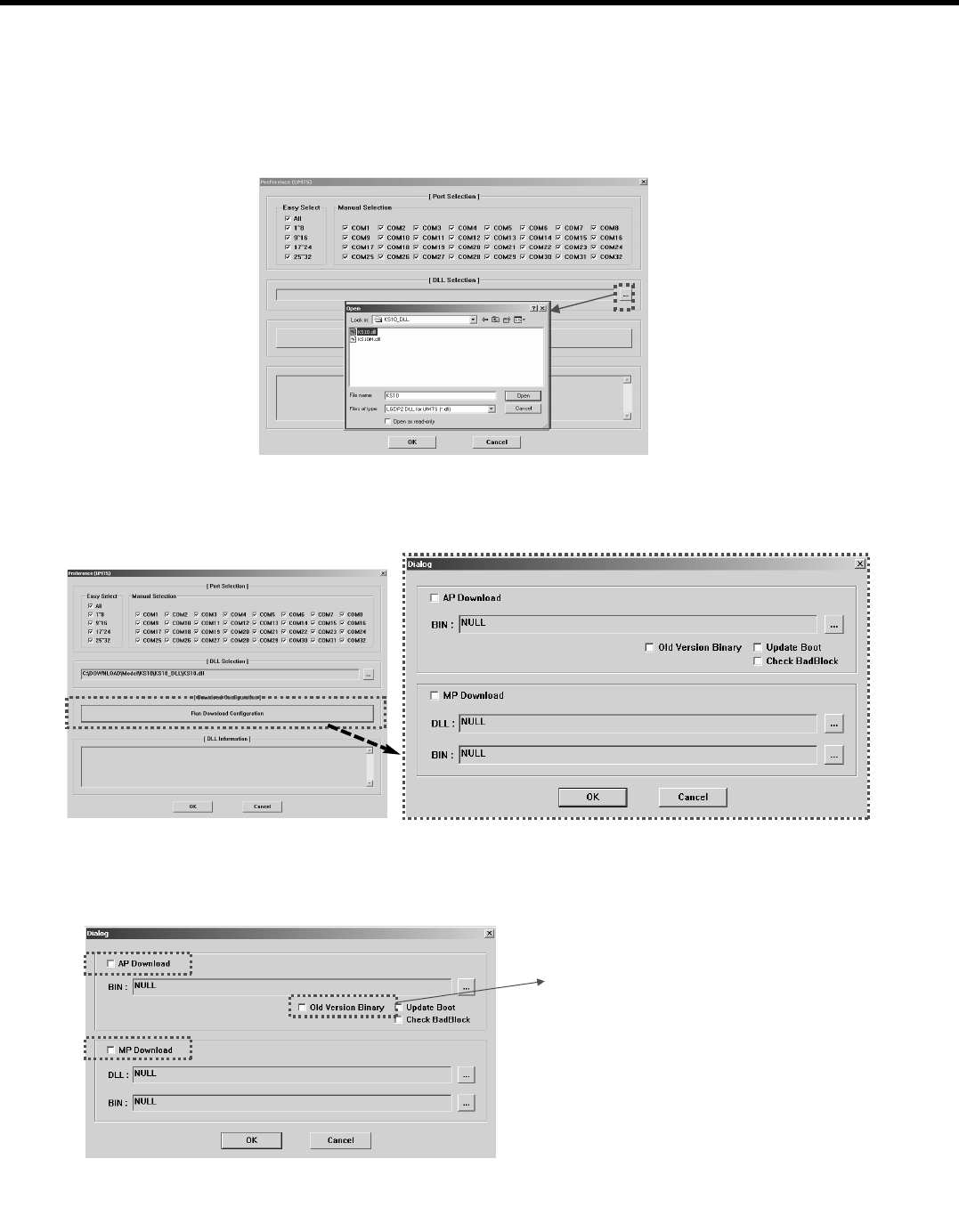
- 166 -
5. DOWNLOAD
5.5.8 Choose the "KS10.DLL" file on "Model" folder in "Download" folder.
5.5.9 Click “Run Download Configuration” button.
5.5.10 Select AP download & Old Version Binary & MP Download icons.
LGE Internal Use Only
Copyright © 2007 LG Electronics. Inc. All right reserved.
Only for training and service purposes
Explain Old Version Binary icon
It is control "Binary" type.
We use old type Binary in now so, you should be
check this category.
But in the future, We will release the new Binary.
So, If the new Binary is released, you don't check
"Old Version Binary" category.
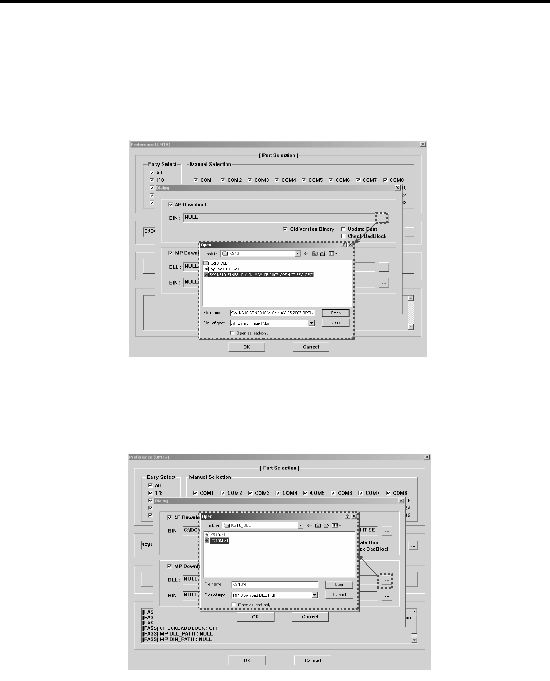
- 167 -
5. DOWNLOAD
5.5.11 Insert “SW-KS10-STN8810-V10a-MAY-05-2007
-OPEN-IT-SEC-OFC” in "KS10" folder on "Model" folder after click
"..." icon on "BIN" Box right side.
5.5.12 Insert “KS10M.Dll” in "KS10_DLL" folder on "Model" folder after
click "..." icon on "DLL" Box right side.
LGE Internal Use Only
Copyright © 2007 LG Electronics. Inc. All right reserved.
Only for training and service purposes
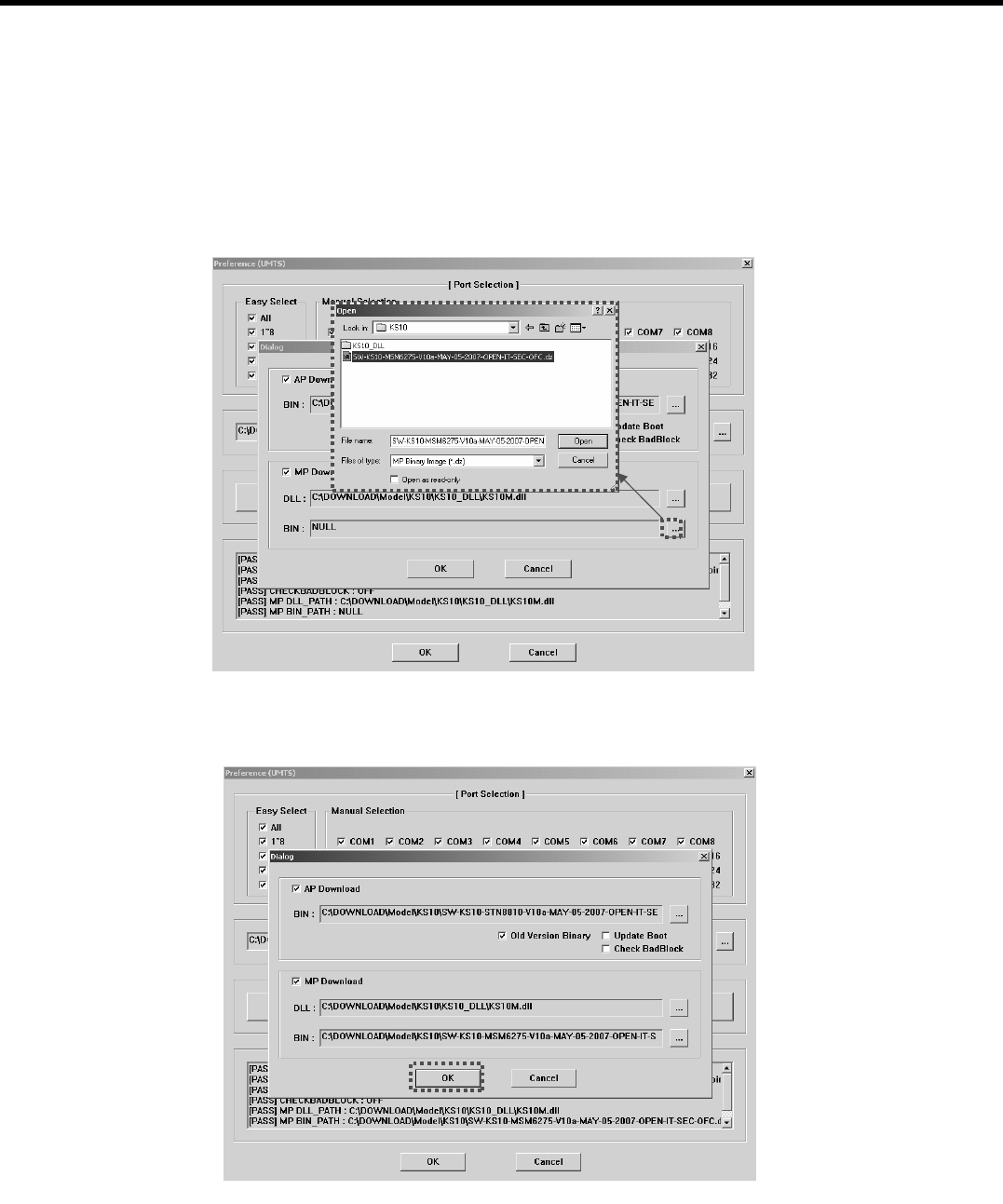
- 168 -
5. DOWNLOAD
5.5.13 Insert “SW-KS10-MSM6275-V10a-MAY-05-2007
-OPEN-IT-SEC-OFC.dz” in "KS10" folder on "Model" folder after
click "..." icon on "BIN" Box right side.
5.5.14 Click “OK” button.
LGE Internal Use Only
Copyright © 2007 LG Electronics. Inc. All right reserved.
Only for training and service purposes
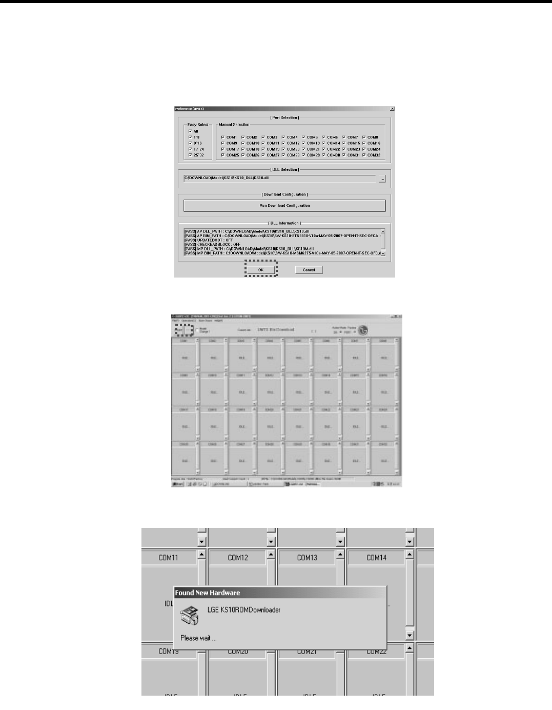
- 169 -
5. DOWNLOAD
5.5.15 Click “OK” button.
5.5.16 Click “START” button and then connect phone.
5.5.17 PC create New hardware driver.
LGE Internal Use Only
Copyright © 2007 LG Electronics. Inc. All right reserved.
Only for training and service purposes
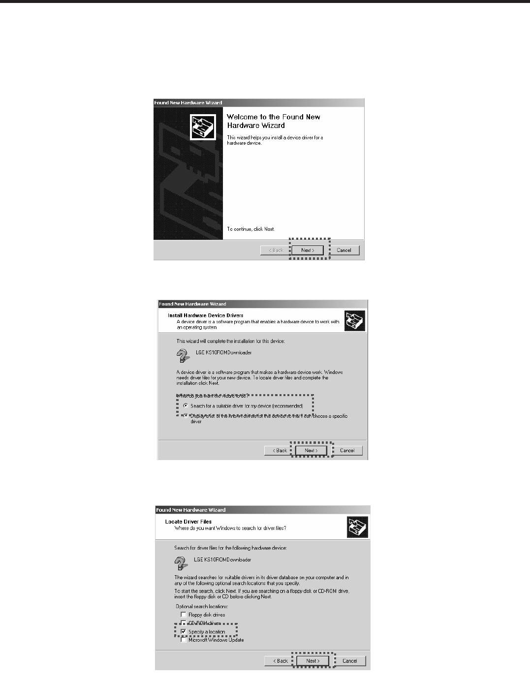
- 170 -
5. DOWNLOAD
5.5.18 Click “Next” button.
5.5.19 Select “11” icon and then click “Next” button.
5.5.20 Select “22” icon and then click “Next” button.
LGE Internal Use Only
Copyright © 2007 LG Electronics. Inc. All right reserved.
Only for training and service purposes
11
22
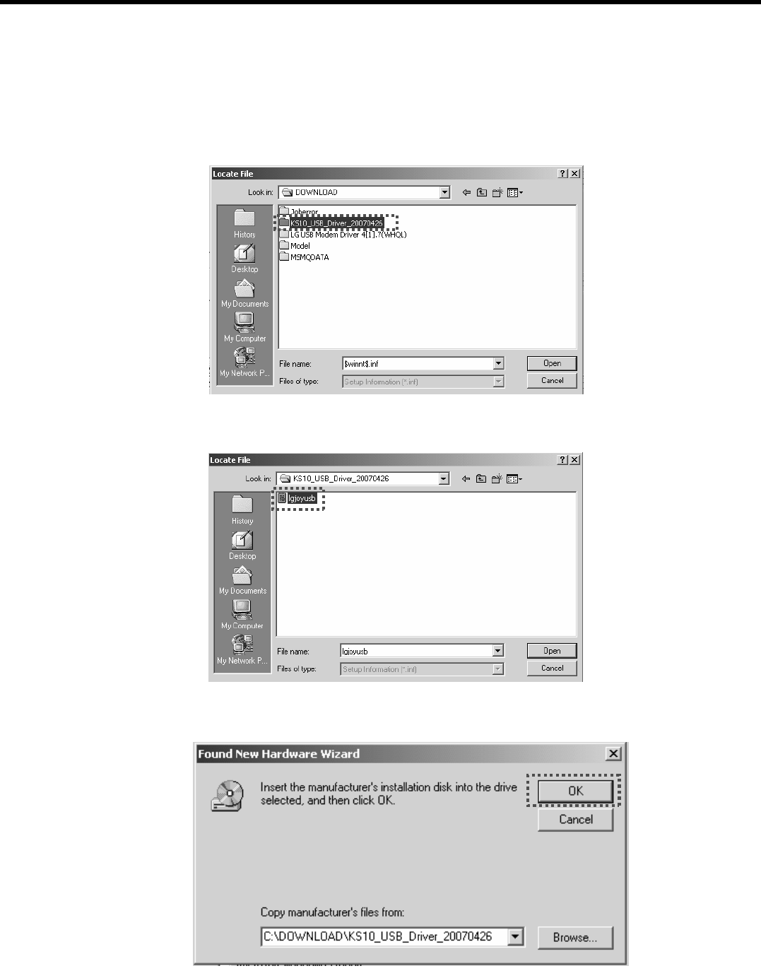
- 171 -
5. DOWNLOAD
5.5.21 Select "KS10_USB_Driver_20070426" folder in "DOWNLOAD"
folder.
5.5.22 Click the "lgjoyusb" file.
5.5.23 Click “OK” button.
LGE Internal Use Only
Copyright © 2007 LG Electronics. Inc. All right reserved.
Only for training and service purposes
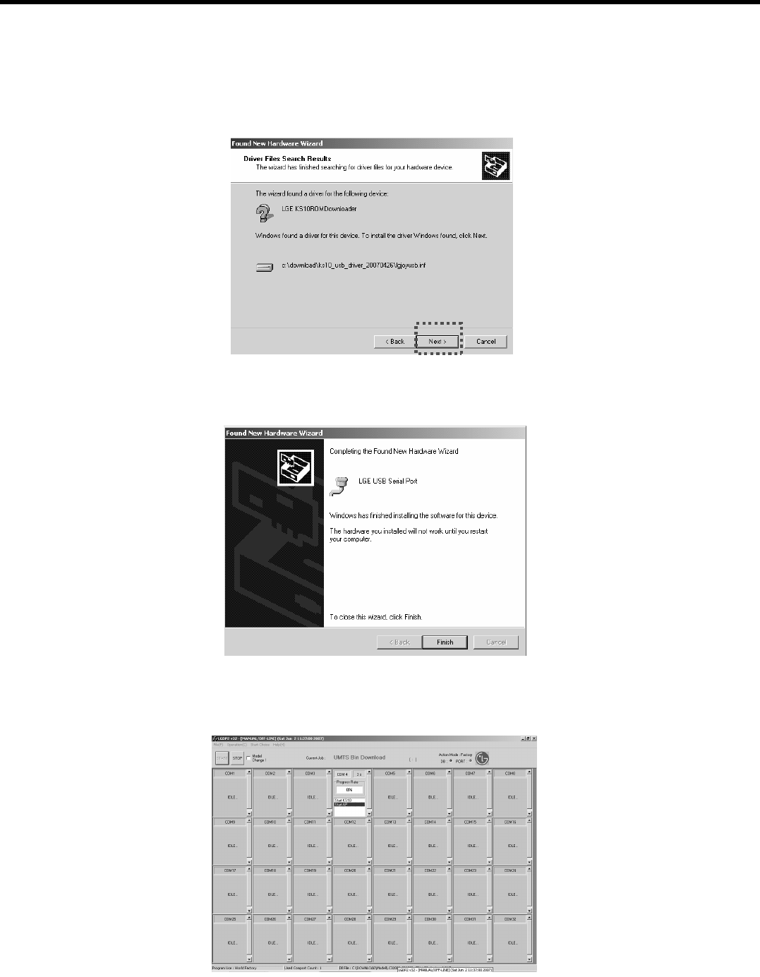
- 172 -
5. DOWNLOAD
5.5.24 Click “OK” button.
5.5.25 Click “Finish” button.
5.5.26 the LGDP2 program is running automatically.
LGE Internal Use Only
Copyright © 2007 LG Electronics. Inc. All right reserved.
Only for training and service purposes
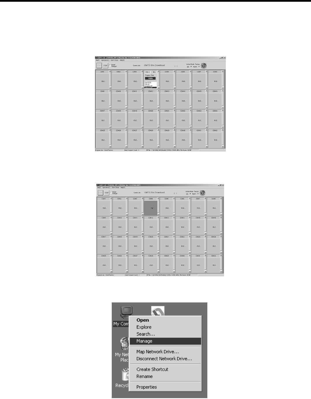
- 173 -
5. DOWNLOAD
5.5.27 Remember a first com ports No..
5.5.28 It is displayed "Fail" message after completing AP downloading.
Don’t disconnection phone.
5.5.29 Click mouse right button on “My computer”. Then select
“Manage”.
LGE Internal Use Only
Copyright © 2007 LG Electronics. Inc. All right reserved.
Only for training and service purposes
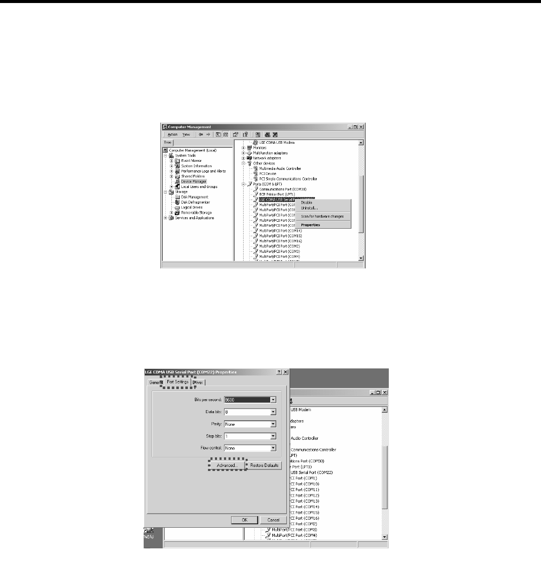
- 174 -
5. DOWNLOAD
5.5.30 Follow up as below step. Device Manager >>LGE CDMA USB Serial port >>
click mouse right button >>select “properties”
5.5.31 Select “Port settings” icon. Then click “Advanced” button.
LGE Internal Use Only
Copyright © 2007 LG Electronics. Inc. All right reserved.
Only for training and service purposes
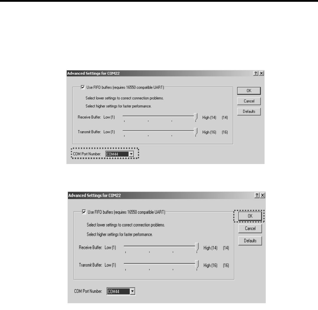
- 175 -
5. DOWNLOAD
5.5.32 You should select com port No. which first com No. plus 40 is for MP.
ex) First com port : com 4 port Select com 44 (= 4+ 40 ) port
5.5.33 Click “OK” button.
LGE Internal Use Only
Copyright © 2007 LG Electronics. Inc. All right reserved.
Only for training and service purposes
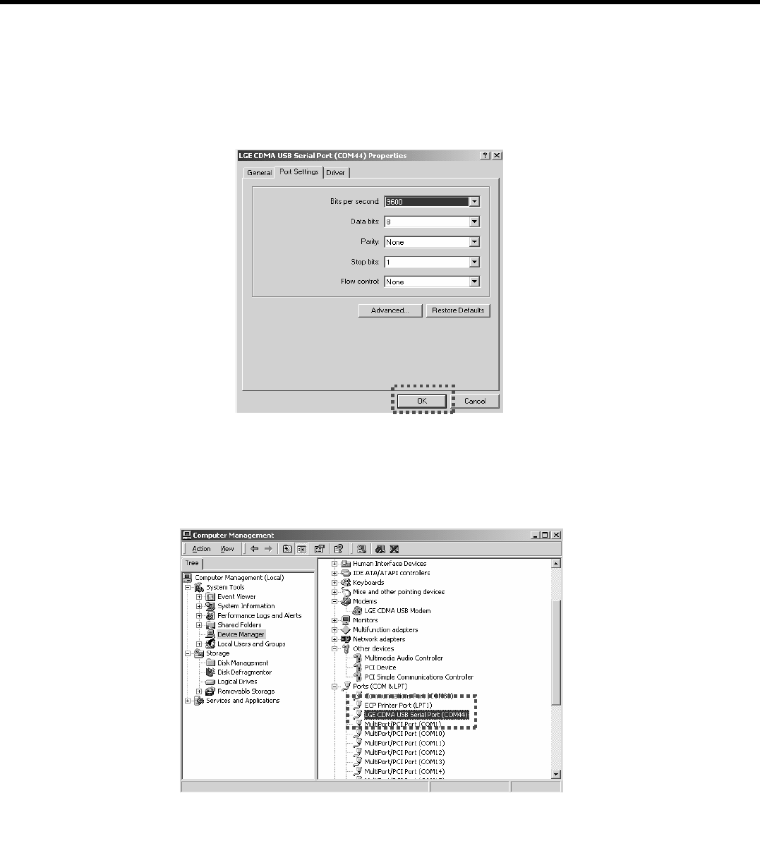
- 176 -
5. DOWNLOAD
5.5.34 Click “OK” button.
5.5.35 Checking com port number.
LGE Internal Use Only
Copyright © 2007 LG Electronics. Inc. All right reserved.
Only for training and service purposes

- 177 -
5. DOWNLOAD
5.5.36 Disconnect and reconnect the phone.
And then the program is running automatically.
5.5.37 Running the LGDP2 program.
❇ If you want to download the other phone, you just do from 5-17 to 5-36
category on this Guide.
LGE Internal Use Only
Copyright © 2007 LG Electronics. Inc. All right reserved.
Only for training and service purposes
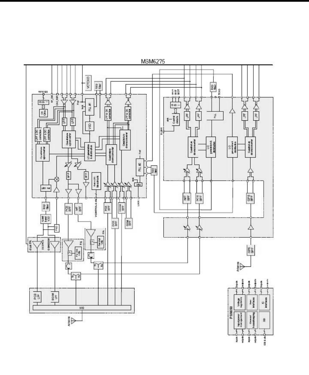
- 178 -
6. BLOCK DIAGRAM
6.1 GSM & WCDMA RF Block
6. BLOCK DIAGRAM
LGE Internal Use Only
Copyright © 2007 LG Electronics. Inc. All right reserved.
Only for training and service purposes
Fig 2.1-1.UMTS-2100 + EGSM-900/DCS-1800/PCS-1900 RF Functional Block Diagram
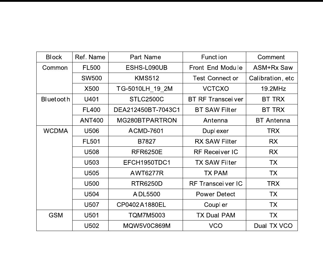
- 179 -
6. BLOCK DIAGRAM
LGE Internal Use Only
Copyright © 2007 LG Electronics. Inc. All right reserved.
Only for training and service purposes
Table 2.1-1. RF Block Component
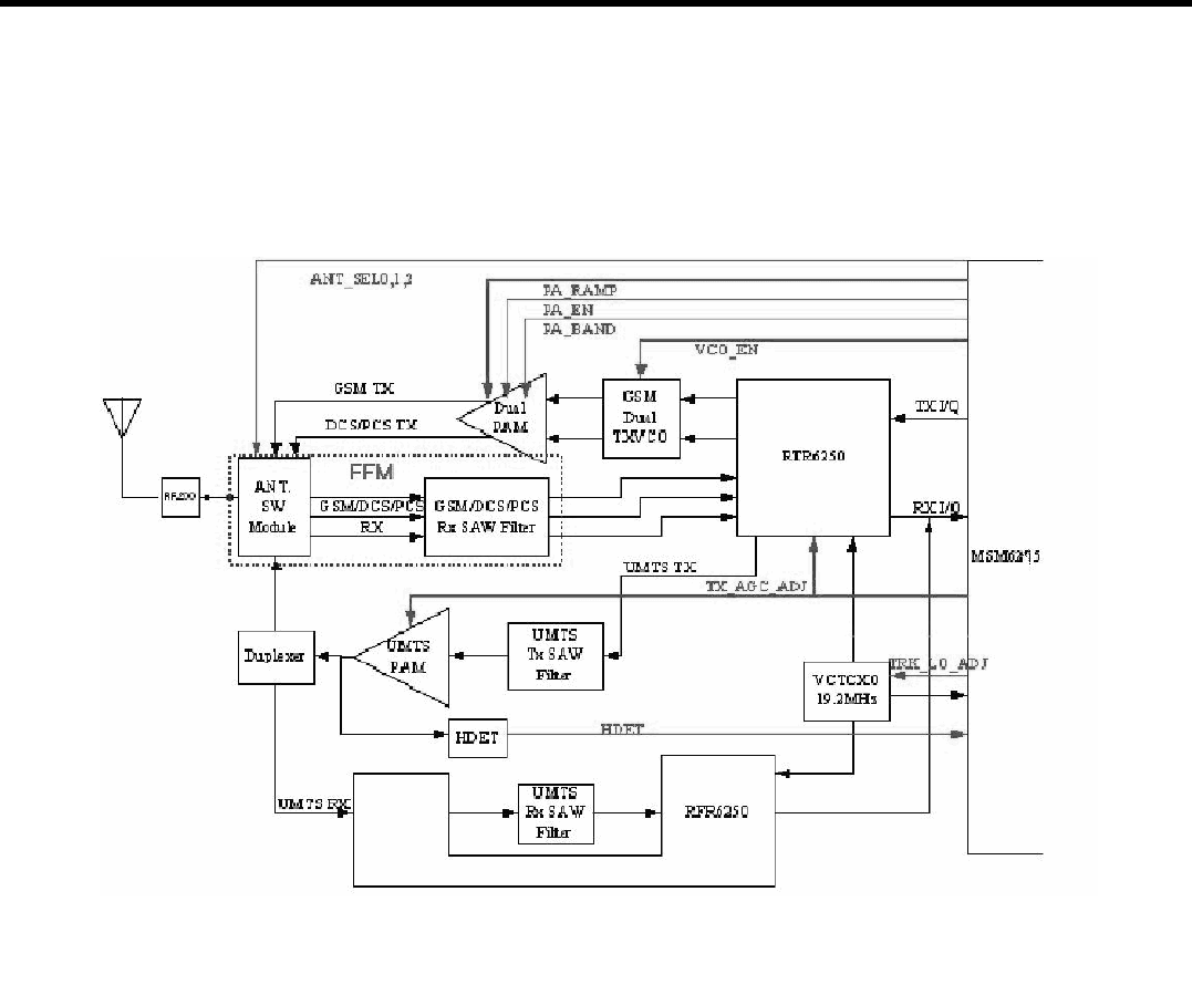
- 180 -
6. BLOCK DIAGRAM
6.2 Interface Diagram
LGE Internal Use Only
Copyright © 2007 LG Electronics. Inc. All right reserved.
Only for training and service purposes
KS10 Interface Diagram

- 181 -
6. BLOCK DIAGRAM
Main RF signal (black)
GSM TX : GSM Tx RF signal
GSM RX : GSM Rx RF signal
DCS TX : DCS Tx RF signal
DCS RX : DCS Rx RF signal
PCS TX : PCS Tx RF signal
PCS RX : PCS Rx RF signal
UMTS TX : UMTS Tx RF signal
UMTS RX : UMTS Rx RF signal
TX_I/Q : I/Q for Tx of RF
RX_I/Q : I/Q for Rx of RF
Control signal(red)
ANT_SEL 0,1,2 : Ant Switch Module Mode Selection
(WCDMA, GSM Tx/Rx, DCS Tx/Rx, PCS Tx/Rx)
GSM PA_CTL Signal
GSM_PA_BAND : DCS or PCS /GSM Mode Selection
GSM_PA_EN : Power Amp Gain Control Enable
GSM_PA_RAMP : Power Amp Gain Control
GSM/DCS/PCS_VCO_EN
GSM_TX_VCO_0_EN_N : GSM band Tx VCO Enable
GSM_TX_VCO_1_EN_N : DCS or PCS band Tx VCO Enable
UMTS PA_CTL Signal
TX_AGC_ADJ : WCDMA Tx Power Level Control
HDET1 : WCDMA Tx High Power Level Control
PA_ON : WCDMA Tx Power Amp Enable
W_VMODE_N : WCDMA Tx Power Amp Gain Control
TRK_LO_ADJ : TCXO(19.2M) Control
LGE Internal Use Only
Copyright © 2007 LG Electronics. Inc. All right reserved.
Only for training and service purposes
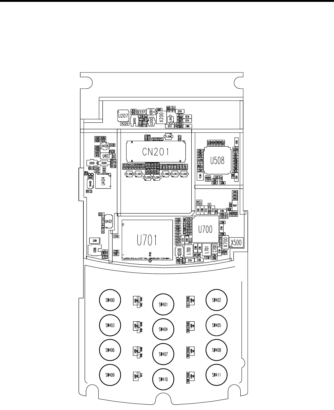
- 182 -
6. BLOCK DIAGRAM
*Top Side
LGE Internal Use Only
Copyright © 2007 LG Electronics. Inc. All right reserved.
Only for training and service purposes
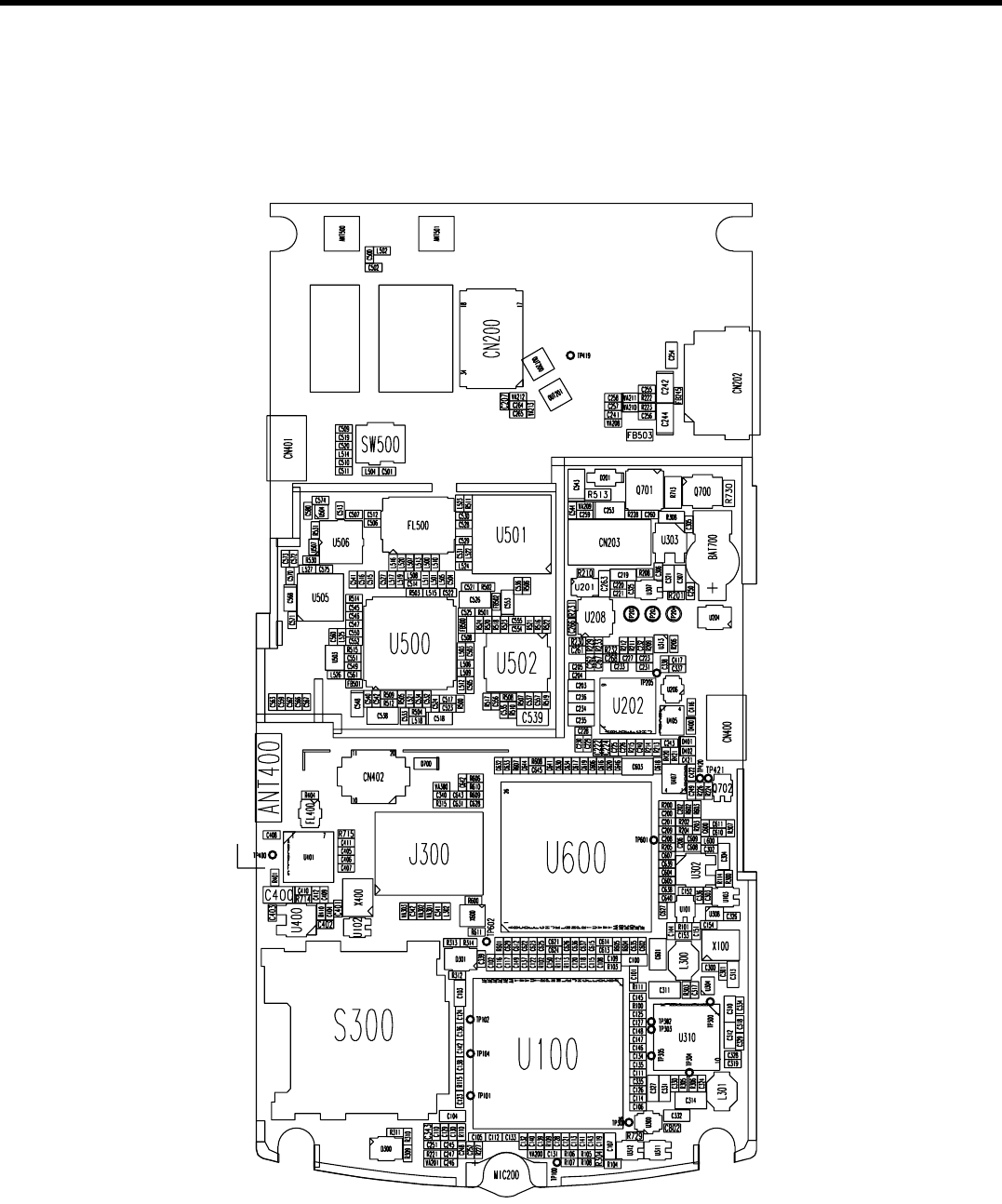
- 183 -
6. BLOCK DIAGRAM
*Bottom Side
LGE Internal Use Only
Copyright © 2007 LG Electronics. Inc. All right reserved.
Only for training and service purposes
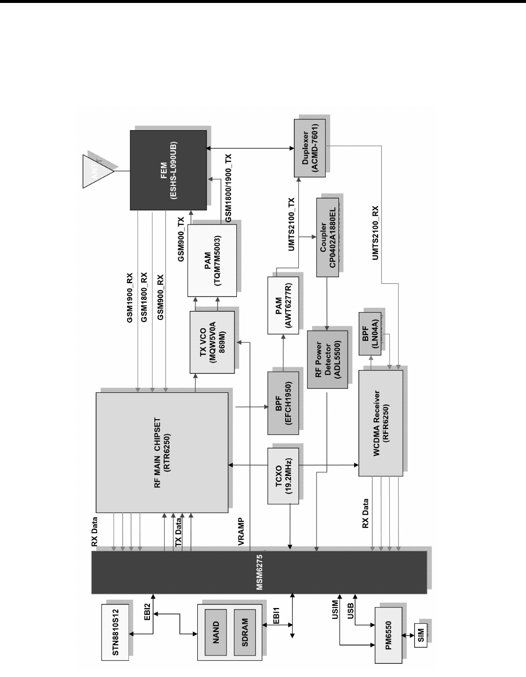
- 184 -
6. BLOCK DIAGRAM
6.3 KS10 Modem & Baseband Block Diagram
LGE Internal Use Only
Copyright © 2007 LG Electronics. Inc. All right reserved.
Only for training and service purposes
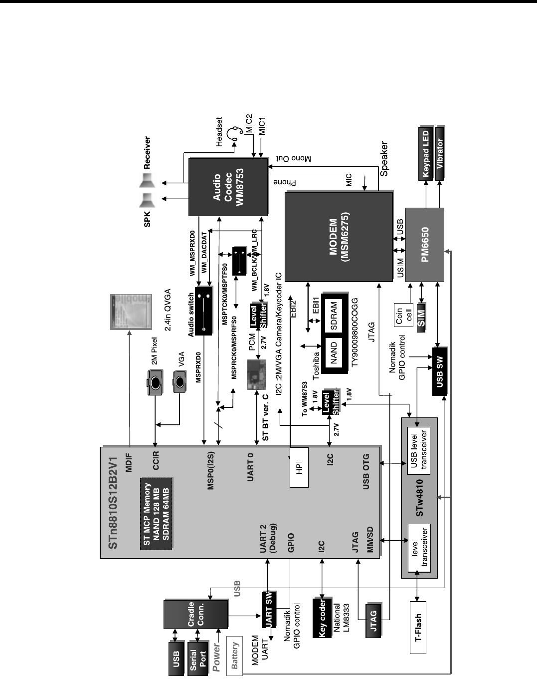
- 185 -
6. BLOCK DIAGRAM
6.4 KS10 Application Processor Block Diagram
LGE Internal Use Only
Copyright © 2007 LG Electronics. Inc. All right reserved.
Only for training and service purposes
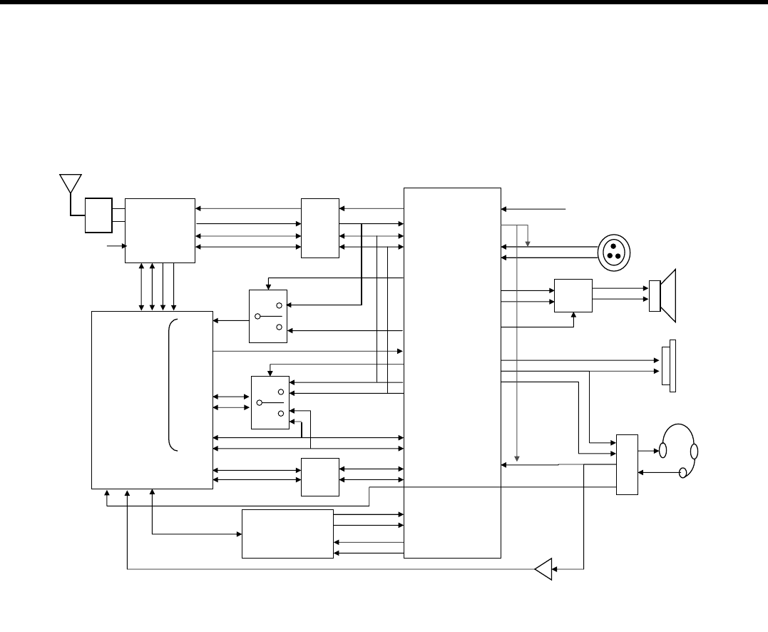
- 186 -
6. BLOCK DIAGRAM
6.5 KS10 Audio & BT Block Diagram
LGE Internal Use Only
Copyright © 2007 LG Electronics. Inc. All right reserved.
Only for training and service purposes
MSM
AMP
Level
Shifter
AU_19.2M
Level
Shifter
I2CSCL0
I2CSDA0
PM_SCL
PM_SDA SCL
SDA
UART0
UART
PCM PCM
I2S
WM_BCLK
WM_LRC
WM_MSPTCK0
WM_MSPTFS0
MSPRFS0
MSPRCK0
RXP
RSN
WM_MONO1
WM_MONO2
MIC1
MIC2
MIC_BIAS
SPK_AMP_SD_N
OUT3
LOUT1
Speaker
Receiver
Head Set
MIC
LOUT2
ROUT2
ROUT1
EAR_SENSE_N
HOOK_SENSE_N
GPIO
GPIO
GPIO
GPIO
Switch
Switch
STN8810
(CPU)
I2S
WM_DACDAT
WM_MSPRXD0MSPRXD0
GPIO
Filter
BT_19.2M
ANT
WM_8753
(Audio Codec.)
STLC2500C
(BT)
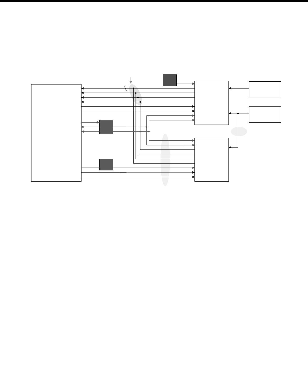
- 187 -
6. BLOCK DIAGRAM
6.6 KS10 Camera Block Diagram
LGE Internal Use Only
Copyright © 2007 LG Electronics. Inc. All right reserved.
Only for training and service purposes
CPU
VGA Camera
module
Data[7:0]
VSYNC
HSYNC
PCLK
2M_nReset
2M_PWDN
CAM_PWR_EN
I2CSDA0
I2CSCL0
MCLK
VGA_nRESET
VGA_STANDBY
8
Slide
2M Camera
module
Each part (2M camera & VGA camera)
supports the Hi-Z state in power down mode.
Level
Shifter
OSC MCLK
SW
ON/OFF
CAM power
1.2V
CAM power
2.7V
Slide
LGE Internal Use Only
Copyright © 2007 LG Electronics. Inc. All right reserved.
Only for training and service purposes
6.7 KS10 LCD Block Diagram
6. BLOCK DIAGRAM
- 188 -
CPU
LCD module
(Hitachi 2.4íí)
Data[15:0]
nCS1
nWE
RS
nRESET
LCD_VSYNC
WLED_EN
16
Slide
LCD power
2.8V
Backlight
Driver
Control
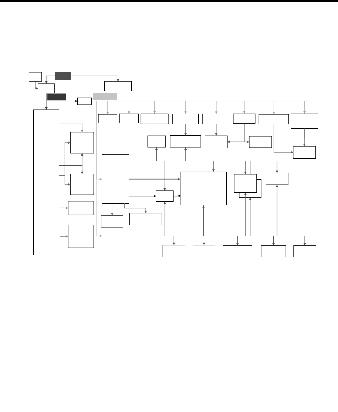
LGE Internal Use Only
Copyright © 2007 LG Electronics. Inc. All right reserved.
Only for training and service purposes
6. BLOCK DIAGRAM
- 189 -
6.8 KS10 Power Distribution Diagram
STw4810
(PMIC)
AP_+VPWR
MIC5219-2.7
(LDO IO)
VBAT
R0
STn8810
(CPU)
WM8753LEB
(Audio Codec.)
TPA6205A1DRBR
(Audio AMP)
Reset
Logic
Power ON/Off
Logic
ST2378
(Level Shifter)
ST2378
(Level Shifter)
STLC2500
(BT)
BH33FB1WHFV
(LDO Audio)
BH18LB1WHFY
(LDO MCAM)
MIC5219-2.7
(LDO CAM)
Key Pad
Array pull up
LM8333
(Key Coder)
SLAS4717EPMTR2G
(USB SW)
NLAS3158MNR2G
(UART SW)
MAX4717
(AU SW)
VDD_IO
2M_CAMERA
(Connector)
R1114N281D-TR-F
(LDO LCD)
Key Pad
Array pull up
(Folder)
VGA_CAM
(Connector)
LCD
(Connector)
TransFlash
(Connector)
RST
AP_VDD_IO_1.8V
AP_VDD_IO_2.7V
VUSB_3.1V
VMMC_3.1V
VCORE/
VPLL/
VFUSE
VDDIOC/D/E
VDDQ/DDR/NAND
VDDIOA/B/F
Vibrator
AU_3.3V CAM_1.8V CAM_2.7V LCD_2.8V
AAT3151IWP_T1
(LCD Backlight
Driver)
Key Pad
LED
A3212EEH-T
(Folder Sense)
Charging
Circuit
PM6650
(PMIC)
MSM6275
+VPWR
TY90009800
COGG
(Memory)
RF Block
VREG_MSMA
_2.6V
VREG_MSMC
_1.375
VREG_MSMP
_2.7V
VREG_MSME
_1.8V
USIM
(Socket)
VREG_USIM
_2.85V
VREG_TCXO
_2.85V
VREG_SYNTH
_2.85V
VREG_RFTX
_2.85V
VREG_RFR
_2.85V
DC
Power
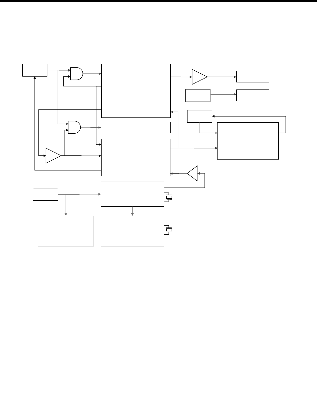
LGE Internal Use Only
Copyright © 2007 LG Electronics. Inc. All right reserved.
Only for training and service purposes
6.9 KS10 Clock Distribution Diagram
6. BLOCK DIAGRAM
- 190 -
WM9712 (Audio Codec.)
Nomadik
STLC2500C (BT)
STw4810
PM6650
19.2MHz
OSC
Request_MC
SLEEP CLK
PWREN
PWREN
TCXO_EN
L/S
AU_PWR_EN
L/S
2M Camera
L/S
CLKOUT0
MXTALI
27MHz
OSC
REF_CLK_IN
LP_CLK
CLK_REQ_OUT_1
SXTALI
CLK_32K_IN
CLK_32K
VGA Camera
19.2MHz
OSC
MSM6275
19.2MHz
TCXO
RF Block
32.768KHz
(X-tal)
USB 48MHz
(X-tal)
TCXO_OUT
TCXO
19.2MHz
19.2MHz
19.2MHz
19.2MHz
27MHz
27MHz
32.768KHz
32.768KHz
32.768KHz
19.2MHz
19.2MHz
RTR6250_TCXO
RFR6250_TCXO
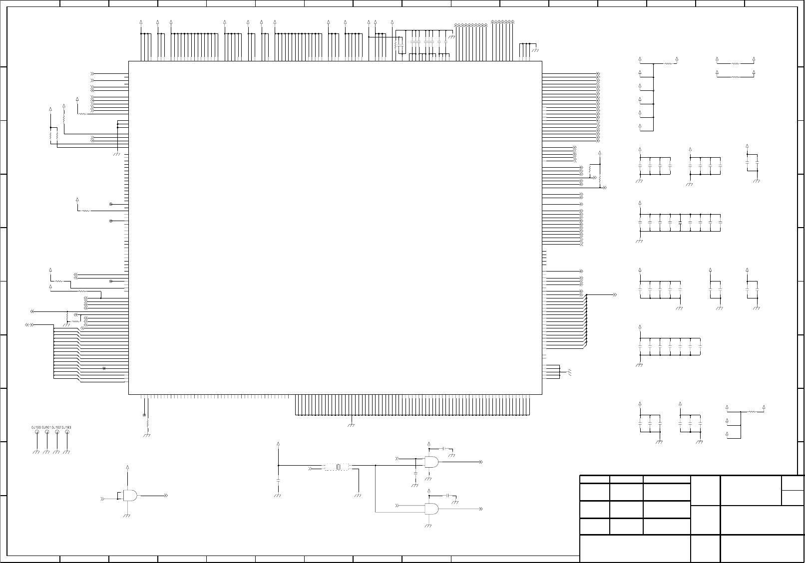
- 191 -
LGE Internal Use Only
Copyright © 2007 LG Electronics. Inc. All right reserved.
Only for training and service purposes
7. CIRCUIT DIAGRAM
12
DRAWING
D
513
Sheets
Approved
5
2 4
E
Sheet/
9
F
C
4
NO.
D
E
4
6
B
10 12
F
2
LG Electronics Inc.
C
1
E
9
F
B
E
13
F
11
A
7
B
7
C
Section
2 75
D
F
77
12
NAME
3
C
2
F
E
F
NAME
F
E
8
16
LG Electronics Inc.
A
31
A
NO.
B
9
5
A
C
Sheet/
LG(42)-A-5505-10:01
6131 87
8
D
3
3
D
E
11
B
3
Approved
E
15158
LG Electronics Inc.
C
1610
C
9
14
34
Sheets
148
5
B
D
C
DRAWING
A
LG Electronics Inc.
106
F
15
Sign & Name
DD
1
Date
C
A
6
MODEL
C
C
Checked
16
Designer
11
LG(42)-A-5505-10:01
6
14
E
5
2
D
8
9
4 6
1
DRAWING
4
D
2006
MAY LGE JOY 1.3
1/7
AP CPU & Memory
9
E
C
2
E
E
1
D
D
47K
R307
AP_VDD_IO_1.8V
0.1u
C138 C139
0.1u
C153
AP_VFUSE
TP104
0.1u
0.1u
C144
120p
R108
3K
C105
C117
0.1u
R104
NA
0.1u
C141
10KR109
C130
0.1u
120p C106
R103 10
VDDIOF
R101
0
VDDQVDDIOF
VDDNAND
NA
C152
VDD12
VDD12
AP_VDD_IO_1.8V
VDDIOC
VDDIOE
0R114
0R102
C123
0.1u
VDDIOE
VDDIOC
VDDIOA
0.1u
C127
0.1u
VDDIOE
VDDNAND
C115
4
5
VCC
0.1u
C146
U102
NL17SZ08XV5T2
3
GND
1
2
C118
VDDIOD
0.1u
C102120p
120p C101
C122
0.1u
VDDIOA
VDDQ
VDDNAND
VDDIOE
C109120p
10KR111
VDDQ
0.1u
C114
C120
0.1u
AP_VDD_IO_1.8V
3
1
TRI_OPEN
VDD
4
VDDIOA
TP102
R112
100K
19.2MHz
X100
CSC3M192000EEVRS00
2
GND
OUT
AP_VCORE
VDDDDR
C112
0.1u
C116
0.1u
C143
VDDIOA
VDD12
0.1u
C129
4.7K
R110
0.1u
3K R107
VDDNAND1 B15
VDDNAND2
VDDNAND3 AE12
AE15
VDDNAND4
VDDOK
D19
VDDQ1 M2
R2
VDDQ2
VDDQ3 W2
H2
VDDQ4
F6
VOTP
AA15
VDDIOC7 AA16
AA18
VDDIOC8
VDDIOC9 AA21
VDDIOD1 H21
VDDIOD2 K21
VDDIOD3 M21
VDDIOD4 T21
U21
VDDIOD5
VDDIOD6 N21
VDDIOE1 F14
F20
VDDIOE2
VDDIOE3 F13
VDDIOF1 F9
F10
VDDIOF2 F12
VDDIOF3
B12
M6
R6
VDDIOA4
VDDIOB1 U6
VDDIOB2 W6
AA9
VDDIOB3
Y21
VDDIOC1
VDDIOC10 AB20
W23
VDDIOC11 AA13
VDDIOC12 AA20
VDDIOC13
VDDIOC14 AB11
AB18
VDDIOC15
Y22
VDDIOC2
VDDIOC3 AA11
AA12
VDDIOC4
VDDIOC5 AA14
VDDIOC6
F18
VDD12_4 G21
J6
VDD12_5 L6
VDD12_6
VDD12_7 L21
VDD12_8 P6
R21
VDD12_9
VDDA F3
G2
VDDDDR1 G25
VDDDDR2
VDDDDR3 L2
T2
VDDDDR4
VDDDDR5 Y2
Y25
VDDDDR6
H6
VDDIOA1 K6
VDDIOA2
VDDIOA3
G22
USBOEN G23
USBRCV F23
USBSCL E23
E22
USBSDA
F22
USBVM
E24
USBVP
D6
UTXD0
VDD12_1 F11
VDD12_10 T6
VDD12_11 V6
V21
VDD12_12
VDD12_13 AA8
AA17
VDD12_14
VDD12_15 AB24
F16
VDD12_2
VDD12_3
L24
SXTALI
C19
C20 SXTALO
H24 TAPSEL
D4 TCK
TDI
D5 TDO
C5
AE7 TMPWNG0
AE8 TMPWNG1
E6 TMS
TRSTN
E5
TSTCLK
L11
UCTS0N E7
D8
URTS0N
URXD0 F7
URXD2 AB6
USBINTN
V24
SMA_DQ5
U24
P23 SMA_DQ6
SMA_DQ7
P22
SMA_DQ8
V22
SMA_DQ9
U23
K22 SMCS0N
J22 SMCS1N
SMFRSTN
Y24
Y23 SMFWPN
P21 SMOEN
E18 SMPIOIS16N
SMPIOWN
H23
SMPS0N
J21
W21 SMPS1N
SMWAITN
P24
SMWEN
SMAD4
N24 SMAD5
SMAD6
J23
SMAD7
L22
J24 SMAD8
SMAD9
M23
SMA_DQ0
W22
V23 SMA_DQ1
SMA_DQ10
U22
SMA_DQ11
W24
R23 SMA_DQ12
SMA_DQ13
R22
SMA_DQ14
T24
SMA_DQ15
R24
T23 SMA_DQ2
SMA_DQ3
T22
SMA_DQ4
SDRDQ6
AB17 SDRDQ7
AC13 SDRDQ8
SDRDQ9
AB12
SDRDQML
AB16 SDRDQMU
AB14
AC17 SDRDQSL
AB13 SDRDQSU
AB15 SDRFBCK
SDRRASN
AB22
AD21 SDRWRN
N23 SMAD0
SMAD1
K23
M24 SMAD10
SMAD2
L23
K24 SMAD3
M22
SDRCKN
AC14 SDRCKP
AA19 SDRCS0N
SDRCS1N
AA10
AB21 SDRDQ0
SDRDQ1
AC20
SDRDQ10
AC12
AB9 SDRDQ11
SDRDQ12
AC10
AC9 SDRDQ13
AC11 SDRDQ14
SDRDQ15
AB10
SDRDQ2
AC22
AC19 SDRDQ3
AC21 SDRDQ4
SDRDQ5
AC18
AB19
AD20
AD14 SDRAD11
AD15 SDRAD12
SDRAD13
AA22
AC23 SDRAD14
AD19 SDRAD2
SDRAD3
AD18
AD9 SDRAD4
AD17 SDRAD5
AD10 SDRAD6
AD13 SDRAD7
SDRAD8
AD16
AD11 SDRAD9
SDRCASN
AD22
SDRCKE0
AD12 SDRCKE1
AC16
AC15
D15
F24
MSPTXD2_SMPCE2N
MXTALI
C21
C22 MXTALO
AE20 NANDWP01
AE19 NANDWP0N
D20 PORN
PWLOUT E21
E20 PWREN
RCOMP C7
REMAP0_SMDIRN
F19 REMAP1_SMPREGN
E19
N22 SCANEN
SCANMOD
D23
AB23 SDRAD0
AA23 SDRAD1
SDRAD10
I2CSDA0
D12
MCCLK
C12
MCCMD
MCCMDDIR E13
MCDAT0 D14
C14
MCDAT0DIR
E14
MCDAT1
MCDAT2 C13
MCDAT3 D13
MCDAT31DIR E15
MCFBCLK E17
E16
MSPRXD0
MSPSCK0 F17
H22
MSPTCK2_SMPIORN
MSPTFS0 C15
G24
MSPTFS2_SMPCE1N
MSPTXD0
D11 HDAT14_MSPSCK1
C11
E12 HDAT15
U5 HDAT2
HDAT3
T3 HDAT4
T4
T5 HDAT5
R3 HDAT6
HDAT7
R4 HDAT8
P4 HDAT9
N3
N4 HPIEV
G4 HRDN_SSPCLK
E4 HRDY_RTCK
G6 HWRN_SSPFRM
I2CSCL0 F5
F4
G3
E8
GPIO6
D22
GPIO76 K4
GPIO91 J3
GPIO92
HADR0
J5 HADR1_UTXD1
H5
H4 HADR2_URXD1
HALEN_SSPRXD
G5
J4 HBHEN
HCSN
H3
U3 HDAT0
HDAT1
U4
D10 HDAT10_MSPTXD1
C10 HDAT11_MSPTFS1
HDAT12
E11 HDAT13
F15
D16
GPIO21 C16
GPIO22
GPIO26 C17
GPIO28 D18
C18
GPIO29
C6
GPIO3
GPIO34 AB8
AB7
GPIO35 AC7
GPIO36 AD7
GPIO37
GPIO38 AD6
GPIO4 D7
F8
GPIO5
N6
GPIO53
GPIO54 N5
GPIO58_SSPTXD
AE16
M12 GND7
B1 GND70
GND71
B7
GND72
B8
GND73
B11
B16 GND74
GND75
B19
GND76
B20
H25
GND77
GND78 M25
GND79 R25
GND8
M13
GND80 W25
M14 GND9
E3
GNDA
GPIO19
AE1
AE2 GND55
GND56
AE3
AF1 GND57
AF2 GND58
AF3 GND59
GND6
M11
GND60
AD25
AD26 GND61
AE24 GND62
AE25
GND63 AE26
GND64
GND65 AF24
GND66 AF25
AF26
GND67
AE11 GND68
GND69
L15
GND40
B25
C2 GND41
C25 GND42
A1 GND43
GND44
A2
A3 GND45
GND46
C1
A24 GND47
GND48
A25
A26 GND49
L16 GND5
GND50
B26
C26 GND51
GND52
AD1
AD2 GND53
GND54
R12
R13 GND26
GND27
R14
R15 GND28
R16 GND29
L14 GND3
T11 GND30
GND31
T12
T13 GND32
GND33
T14
T15 GND34
GND35
T16
GND36
AA24
B2 GND37
GND38
B3
B24 GND39
GND4
M15
M16 GND11
GND12
N11
N12 GND13
N13 GND14
N14 GND15
GND16
N15
N16 GND17
P11 GND18
GND19
P12
GND2
L13
P13 GND20
GND21
P14
P15 GND22
GND23
P16
R11 GND24
GND25
C3
C23
DECOUPLING10
DECOUPLING11 C24
D24
DECOUPLING12
DECOUPLING13 F21
C4
DECOUPLING2
DECOUPLING3 D3
AC3
DECOUPLING4 AD3
DECOUPLING5 AD4
DECOUPLING6
DECOUPLING7 AC24
AD23
DECOUPLING8
DECOUPLING9 AD24
DU1 L25
DU2 T25
L12 GND1
GND10
AD8
CLCD17 AC8
CLCD2 Y6
CLCD3 Y4
AA3
CLCD4
Y5
CLCD5
AB3
CLCD6
CLCD7 AA4
CLCD8 AB4
CLCD9 AC4
AA7
CLFPVS
CLKOUT0
D17
CLLE V4
CLLPHS W4
V5
CLPCK
CLPWR V3
DECOUPLING1
CCIRIHS
P5
CCIRIIVS
E10
CCPCKN
C9
CCPCKP
CCPDAN E9
CCPDAP D9
CCPRSET C8
W3
CLACDE
CLCD0 W5
Y3
CLCD1
AD5
CLCD10
AA5
CLCD11
CLCD12 AA6
AC5
CLCD13
AB5
CLCD14
AC6
CLCD15
CLCD16
U100
BATOK
D21
R5
CCIRICLK_CCIROCLK
CCIRID0_CCIROD0 M3
CCIRID1_CCIROD1 M5
CCIRID2_CCIROD2 M4
CCIRID3_CCIROD3 L3
CCIRID4_CCIROD4 L5
L4
CCIRID5_CCIROD5
CCIRID6_CCIROD6 K3
CCIRID7_CCIROD7 K5
P3
C124
STN8810S12B2V1
1
2
4
VCC
5
0.1u
NL17SZ08XV5T2
U101
3
GND
C149
0.1u
C147
C111
0.1u
0.1u
C1000.33u
0.1u
VDDDDRVDDIOD
VDDIOB
C134
0.33u C104
0.1u
C132
C145
0.1u
AP_VDD_IO_1.8V
VDDIOD
100K
R113
TP103
VDDIOD
15K R106
VDDIOD
C121
0.1u
VDDIOE
0.1u
C142
15K R105
AP_VDD_IO_1.8V
VDDA
0.1u
C125
C136
0.1u
VDDDDR
VDDIOB
AP_VDD_IO_2.7V
100K
R115
VDDA
0.1u
C128
0.1u
C137
0.1u
C133
C1081u
VDDIOF
C110
0.1u
TP100
3
1
2
4
5
VCC
VDDIOB
U103
NL17SZ08XV5T2
GND
C103
C135
0.33u
C154
AP_VDD_IO_1.8V
0.1u
0.1u
0.33u
TP101
C107
C1510.1u
0.1u
C113
C150
0.1u
C148
0.1u
VDDIOC
C126
0.1u
C140
0.1u
VDDIOD
0.1u
C119
0.1u
AP_VPLL
C131
51K R100
AP_TDO
AP_TMS
AP_RTCK
MCAM_CLK_OUT
CPU_19.2M
PORN
CLK32K
REMOTE_PWR_ON
AU_CLK_EN
AU_19.2M
VGA_STANDBY_AP
REQUEST_MC
MSPRFS0
2M_RSTN_AP
2M_PWDN_AP
REMOTE_PWR_ON_AP
AP_TRST_N
UART_SW
HPIEV_IT_STATE_ETMTRIGIN
KEYCODER_RSTN
PWREN
CPU_19.2M
LCD_DATA(12)
LCD_DATA(11)
LCD_DATA(10)
LCD_DATA(1)
LCD_DATA(0)
DIS_WEN
CCIRIVS
CCIRIHS
CCIRID(7)
CCIRID(6)
CCIRID(5)
CCIRID(4)
CCIRID(3)
CCIRID(2)
CCIRID(1)
CCIRID(0)
CCIRICLK
DIS_CSN
DIS_RS
LCD_VS
LCD_DATA(9)
LCD_DATA(8)
LCD_DATA(7)
LCD_DATA(6)
LCD_DATA(5)
LCD_DATA(4)
LCD_DATA(3)
LCD_DATA(2)
VGA_RSTN
LCD_NRESET
LCD_DATA(15)
LCD_DATA(14)
LCD_DATA(13)
HPI_IT_APE_ETMPSTA0_XTIDAT
HPI_IT_MOD_ETMSYNCA_XTIDAT
HOOK_SENSE
BT_RESETN
I2CSDA1
I2CSCL1
PWR_BTN
KEYCODER_INT
UTXD2
USB_SW
CAM_PWR_EN
LCD_PWR_EN
AU_PWR_EN
WLED_CTL
LEVEL_SHIFT_EN
MSPRCK0
MSPTCK0
EBI2_DATA(14)
EBI2_DATA(13)
EBI2_DATA(12)
EBI2_DATA(11)
EBI2_DATA(10)
EBI2_DATA(1)
EBI2_DATA(0)
HPI_EME_APE_ETMPSTA2_XTIDAT
EBI2_ADDR(2)
EBI2_ADDR(1)
HPI_EME_MOD_ETMPSTA1_XTIDAT
MCDAT1
MCDAT0DIR
MCDAT0
MCCMDDIR
MCCMD
MCCLK
EBI2_DATA(9)
EBI2_DATA(8)
EBI2_DATA(7)
EBI2_DATA(6)
EBI2_DATA(5)
EBI2_DATA(4)
EBI2_DATA(3)
EBI2_DATA(2)
EBI2_DATA(15)
URXD0
URTS0N
UCTS0N
EAR_SENSE_N
PWREN
IT_WAKE_UP_AP
REMOTE_PWR_ON_AP
MSPTXD0
SW_RESET
MSPTFS0
SD_INT
MCDAT2DIR
MSPRXD0
MCFBCLK
MCDAT31DIR
MCDAT3
MCDAT2
VDDOK
UTXD0
USBVP
USBVM
USBSDA
USBSCL
USBRCV
USBOEN
USBINTN
URXD2
AP_TDI
AP_TCK
EBI2_WE_N
EBI2_OE_N
EBI2_DATA(0:15)
I2CSCL0
I2CSDA0
HCSN_ETMCLK_XTICLK
LCD_DATA(0:15)
- 192 -
LGE Internal Use Only
Copyright © 2007 LG Electronics. Inc. All right reserved.
Only for training and service purposes
7. CIRCUIT DIAGRAM
VBAT
PWR
URXD
UTXD
3G2.5G
GND
RX
TX
UFLS
ON_SW
1608
Checked
Sign & Name
LG Electronics Inc.
Hi-Z
2
B
SPK PAD size 2 by2
CONNECTOR VBATT_SENSE PIN CHECK!!
06.02.22 spk connect to contact type
Sheet/
E
67
F
85
1%
D
C
8
DRAWING
MODEL
12
2
AXK7L34227
PLACE CLOSE TO MSM
14
SPEAKER AMP
C
3
A
LG(42)-A-5505-10:01
D
E
1
F
A
11
C
4
LG Electronics Inc.
E
Designer
NAME
10
Driven
Section
13
TA OVP Circuit
2/7
AUDIO & 18PIN & CAMERA
C
Sheets
3 9
9
LOW
E
116
AXK7L70227
B
DRAWING
MAIIN-SLIDER CON-HEADER
6
D
HIGH
5
Approved
Between (VBATT & +5V_PWR) and (Mic signal)
Date
15
4
CAD for EMC Noise
D
F
2M_CAMERA
NO.
7
1%
MSM6725 EXT FILTER
WM_AVDD
WM_DVDD
LGE
2006
MAY JOY 1.3
0.1u C200
C249 47n
WM_AVDD
R717
NA
VREG_MSMP_2.7V
R716
0
0R728
0R727
0R726
0R725
0R724
0R723
0R722
0R721
0R720
0R719
0R718
C2130.1u
HB-1M1005-601JT
FB207
U203
NCS2200SQ2T2G
GND
2
1
OUT
VCC
5
3
VIN+
VIN-
4
C262
0.068u
AP_VDD_IO_2.7V
WM_AVDD
1u C229
NAC231
C227
10p
1uC224
5
6
7
8
9
11
12
13
14
15
16
17
18
19
2
20
21
22
3
4
CN202
1
10
100K
R210
C245 1u
100K R214
VREG_MSMP_2.7V
0.1u
C242 33u
C243
68KR230
C21210u
22p C265
31
32
33
34
4
5
6
7
8
9
17 18
19
2
20
21
22
23
24
25
26
27
28
29
3
30
G1
G2
G3 G4
1
10
11
12
13
14
15
16
TP205
CN200
FB239
WM_DVDD
R232 68K
AP_VDD_CAM_2.7V
FB224
CSC3R270000BEVRS00 X200
27MHz
GND
2
3
OUT
TRI_OPEN
1
4
VDD
0.015u
WM_DVDD
FB235
C206
FB232
0.015u C202
C2050.1u
IN1
8
IN2
NC1
5
7
NC2
2
NO1
10
NO2
1
VCC
AP_VDD_IO_2.7V
SLAS4717EPMTR2G
U206
COM1
3
COM2
9
GND
6
4
FB229
FB503 1000
AP_+VPWR
0.1u
R206 0
C201
C2090.1u
R203
470K
U207
NUS3065MUTAG
3
CNTRL
DRAIN 4
9DRAIN_THERMAL
6GATE
2
GND
1
IN
OUT
7
SRC
5
VCC
8
11
RTS
RX
2
3
TX
VBAT
6
EVLC18S02015 VA212
INOUT_B4
UT200
CTS
12
DSR
10
1
GND
NC1
4
7
NC2
NC3
8
9
NC4
5
ON_SW
5
G1 10
G2
1
INOUT_A1
INOUT_A2 2
3
INOUT_A3
INOUT_A4 4
INOUT_B1
9
8INOUT_B2
INOUT_B3
7
6
HB-1M1005-601JT
EVRC14S03Q030100R FL204
TP204
FB206
33uC244
R233
10K
10pC258
R207 100K
6
S
5
VCC
VA213
EVLC18S02015
U204
NLAS4157DFT2G
A4
B0
3
B1
1
GND
2
47pC255
R223 68
C223
FB222
NA
FB236
R225 NA
C240 1u
C226 1u
RSB6.8CST2R
FB237
VA211
EVLC14S02050VA205
10K
R229
C2040.1u
1
2
3
4
5
AP_VDD_CAM_2.7V
EVLC14S02050
VBATT
CN203
EVLC18S02015
VA208
1u
VA200
C230
C247
10p
2.2K
R221
C251
EVRC18S03Q015050R
G1 5
G2 10
1INOUT_A1
INOUT_A2
2
3INOUT_A3
INOUT_A4
4
INOUT_B1 9
8
INOUT_B2
INOUT_B3 7
6
INOUT_B4
39p
FL201
C233 39p
2.2K
R227
smd_1608h_9_r
MIC200
SUMY0009203
1
2
1u
C254
C26422p
2.2K
C214
R217
0.01u
680K
R226
C21010u
5
G1 10
G2
1
INOUT_A1 2
INOUT_A2 3
INOUT_A3
INOUT_A4 4
INOUT_B1
9
8INOUT_B2
INOUT_B3
7
6INOUT_B4
FB227
EVRC14S03Q030100R FL208
C259
33p
0.01u
C257
0.1u
C250
C203
10u
C238
0.1u
5
G2 10
1INOUT_A1
INOUT_A2
2
3INOUT_A3
INOUT_A4
4
INOUT_B1 9
8
INOUT_B2
INOUT_B3 7
6
INOUT_B4
FL202 EVRC18S03Q015050R
G1
FB233
R202
10K
10
INOUT_A1
1
2INOUT_A2
INOUT_A3
3
4INOUT_A4
9
INOUT_B1
INOUT_B2 8
7
INOUT_B3
INOUT_B4 6
FB242
FL203 EVRC18S03Q015050R
G1
5
G2
FB225
C239
10p
FB243
C252
FB221
C222 1u
39p
AP_VDD_CAM_1.8V
R213100K
FB244
USB_VBUS_IN
C261
VA206
NA
0.1u C221
EVLC14S02050
NA
R209
+VPWR
4
G2
1IN 2
OUT
NFM21PC105B1A3
U205
G1
3
C232 39p
FB245
10u
OUT200
AP_VDD_CAM_2.7V
C237
0.068u
C267
0.1u C211
C208
AP_+VPWR
0
0.1u
INOUT_A3
3
4INOUT_A4
9
INOUT_B1
INOUT_B2 8
7
INOUT_B3
INOUT_B4 6
R208
FL206 EVRC18S03Q015050R
G1
5
G2
10
INOUT_A1
1
2INOUT_A2
100K R219
FB241
+5V_PWR
47pC256
EVLC14S02050VA204
PSD12-LFD200
VREG_MSMP_2.7V
INSTPAR
R204
10K
470K
G1 5
G2 10
INOUT_A1 1
2
INOUT_A2
INOUT_A3 3
4
INOUT_A4
9INOUT_B1
INOUT_B2
8
7INOUT_B3
INOUT_B4
6
R224
FL205EVRC14S03Q030100R
R212
0
C253
33u
10u C218
VA203 EVLC18S02003
VA201
EVLC18S02015
330K
R218
C207
FB223
1u
R231
100K
2.2u
C263
39p
VA207
C246
R201
0
EVLC14S02050
AP_VDD_LCD_2.8V
C241 1u
COM1
3
COM2
9
6
GND
IN1
4
IN2
8
NC1
5
NC2
7
NO1
2
NO2
101
VCC
AP_VDD_IO_1.8V
SLAS4717EPMTR2G
U200
1_SHUTDOWN
0.1u C220
BYPASS
2
7
GND
IN+
3
4IN- 9
PGND
6
VDD
VO+ 5
VO- 8
C235
TPA6205A1DRBRU208
1
INOUT_A1
INOUT_A2 2
3
INOUT_A3
INOUT_A4 4
INOUT_B1
9
8INOUT_B2
INOUT_B3
7
6INOUT_B4
4.7u
EVRC14S03Q030100R FL207
5
G1 10
G2
AP_VDD_IO_1.8V
R211
0
EVLC18S02003
VA202
0.1u
C260
AP_AU_3.3V
4
NC
6
NOV+
2
U201DG2011DX-T1-E3
COM 5
GND
3
1IN
68R222
C268
WM_DVDD
NA
R200
180K
A8
VMID
A4
B5 VREF
VXCLK
H3
VXDIN
J1
J2 VXDOUT
VXFS
J3
R215100K
MONO2
A7
NC1 C8
NC2 F8
NC3
NC4 G2
E8
OUT3
OUT4 E9
J8 PCMCLK
H9 PGND
PVDD
G9
ROUT1 D9
ROUT2 B9
RXN
C2
RXP
B1
H1 SCLK
G1 SDIN
SPKRVDD
GPIO4
HPVDD F9
HP_SPKRGND C9
LINE1
A2
A1 LINE2
D8
LOUT1
A9
LOUT2
H4 LRC
J6 MCLK
C1 MIC1
MIC1N
D2
D1 MIC2
MIC2N
E2
MICBIAS
B4
F1 MODE_GPIO3
MONO1 B6
B7
U202
WM8753LEB-RV
A3 ACIN
B3 ACOP
ADCDAT
J5
A5 AGND
AVDD
A6
J4 BCLK
CSB_GPIO5
F2
DACDAT
H5
H6
DBVDD
DCVDD J7
DGND H7
G8 GP1_CLK1
GP2_CLK2
J9
E1
G2 10
1INOUT_A1
INOUT_A2
2
3INOUT_A3
INOUT_A4
4
INOUT_B1 9
8
INOUT_B2
INOUT_B3 7
6
INOUT_B4
FL200 EVRC18S03Q015050R
G1 5
AP_VDD_CAM_1.8V
OUT201
C215
FB234
10u
FB231
ICVL0505600V150FR
FB230
0.1u
VA209
C217
1M
HB-1M1005-601JT
FB204
R216
VA210 RSB6.8CST2R
64
65
66
67
68
69
7
70
8
9
G1 G2
G3 G4
50
51
52
53
54
55
56
57
58
59
6
60
61
62
63
35 36
37
38
39
4
40
41
42
43
44
45
46
47
48
49
5
20
21
22
23
24
25
26
27
28
29
3
30
31
32
33
34
CN201
1
10
11
12
13
14
15
16
17
18
19
2
11K
R228
R205
180K
C225
PSD05-LF
D201
1u
C228
INSTPAR
1u
FB205
HB-1M1005-601JT
C234
4.7u
C219
FB240
10u
FB238
0.1u C216
TP202
TP203
1uC248
WM_DVDD
C266
0.22u
CCIRID(2)
CCIRID(1)
CCIRID(0)
C236
4.7u
USB_D+
USB_D-
CCIRICLK
CCIRID(0)_CAM
CCIRID(1)_CAM
CCIRID(3)_CAM
CCIRID(2)_CAM
CCIRIHS
I2CSCL0_CAM
I2CSDA0_CAM
VGA_RSTn
CCIRIVS
CCIRID(7)
CCIRID(6)
CCIRID(5)
CCIRID(4)
CCIRID(3)
MSM_UART_RXD_IN
MSM_UART_RXD
SPKL-
SPKL+
SPK_AMP_EN
EAR_SENSE_N
WM_DACDAT
WM_LRC
WM_MSPRXD0
MSPTXD0
MSPTCK0
I2CSDA0_SW
I2CSCL0_CAM
I2CSDA0_CAM
CCIRICLK_CAM
CCIRID(5)_CAM
CCIRID(4)_CAM
2M_PWDN
DIS_CSN
MSM_UART_RXD_IN
REMOTE_PWR_ON
LCD_NRESET
DIS_WEN
DIS_RS
MSM_UART_TXD
HOOK_SENSE
I2CSCL0_CAM
I2CSDA0_CAM
I2CSCL0_SW
I2CSDA0_SW
MSPTFS0
WM_BCLK
WM_ADCDAT
WM_LOUT2
WM_ROUT2
SPK_AMP_EN
CAMCLK_27MHZ_CAM
RECEIVER+
RECEIVER-
RECEIVER--
2M_RSTn
2M_RSTn_CAM
2M_RSTn_CAM
LCD_VS
LCD_DATA(3)
LCD_DATA(5)
LCD_DATA(7)
LCD_DATA(9)
LCD_DATA(11)
LCD_DATA(13)
LCD_DATA(15)
LCD_DATA(14)
LCD_DATA(12)
LCD_DATA(10)
LCD_DATA(8)
LCD_DATA(0)
LCD_DATA(2)
LCD_DATA(4)
LCD_DATA(6)
WM_HPH_R
WM_HPH_L
MOT_PWR-
WLED_CTL
VGA_STANDBY
KPD_DRV_N
KEY_ROW(0)
KEY_ROW(1)
KEY_ROW(2)
KEY_ROW(3)
KEY_COL(4)
KEY_COL(5)
KEY_COL(6)
KEY_COL(7)
LCD_DATA(1)
CCIRID(3)
CCIRID(2)
CCIRID(1)
CCIRID(0)
CCIRID(7)
CCIRID(6)
CCIRID(5)
CCIRID(4)
CCIRID(6)_CAM
CCIRID(7)_CAM
CCIRIHS_CAM
CCIRIVS_CAM
CAMCLK_27MHZ_CAM
VT_SW
MSPRXD0
WM_DACDAT
WM_MSPRXD0
MSPRFS0
MSPTCK0
WM_BCLK
AU_SW
MSPRCK0
RECEIVER--
CAMCLK_27MHZ
CCIRIHS
CCIRIVS
CCIRICLK
WM_LOUT1
UART_RXD
UART_TXD
VBAT_TEMP
SPKL-
SPKL+
WM_LRC
MSPTFS0
WM_MIC2N
WM_MICBIAS
WM_MIC2P
WM_MIC1P
REMOTE_PWR_ON
WM_MIC1N
VBATT_SENSE
WM_ROUT1
VBATT
WM_ROUT2
KEY_ON_SW_N
WM_MICBIAS
MSM_UART_TXD
MSM_UART_RXD_IN
AU_SW
VT_SW
PM_SDA
PM_SCL
AU_19.2M
WM_RXP
WM_RXN
RECEIVER-
WM_MONO2
WM_MONO1
WM_MIC1N
WM_ROUT1
WM_MIC1P
WM_LOUT1WM_MIC2N
USB_D+
WM_LOUT2
USB_D-
WM_MIC2P
USB_VBUS
CAMCLK_27MHZ
RECEIVER+
CCIRID(4)_CAM
CCIRID(3)_CAM
I2CSCL0_SW
CCIRID(2)_CAM
CAM_PWR_EN
CCIRID(1)_CAM
CCIRID(0)_CAM
MICOUTP
MICINN
CCIRIVS_CAM
MICFBP
CCIRIHS_CAM
MCAM_27M
I2CSDA0
I2CSCL0
CCIRICLK_CAM
MICOUTN
MICINP
CCIRID(7)_CAM
MICFBN
CCIRID(6)_CAM
CCIRID(5)_CAM
- 193 -
LGE Internal Use Only
Copyright © 2007 LG Electronics. Inc. All right reserved.
Only for training and service purposes
7. CIRCUIT DIAGRAM
5
E
A
Sign & Name
LG Electronics Inc.
DRAWING
B
1
DRAWING
9
F
A
Sheets
114
MODEL
NAME
7
MODEL
8
6
2
D
2
1
C
8
A
146
Sign & Name
E
LG Electronics Inc.
510
Approved
E
7
Designer
6
Checked
9
DRAWING
Approved
2
13
Sheets
NO.
124
D
Sheet/
Date
3 5 16
Designer
C
USIM Connector
3
3/7
LGE
MAY
2006 LGE
AP POWER & T-Flash CON
JOY 1.3
15
DRAWING
Sheet/
8
1
C
Section
1
NAME
D
LG Electronics Inc.
4
Checked
NO.
3
9
Date
5
LG Electronics Inc.
Section
6
3 7
2
4
0
R300
C323
AP_VDD_IO_1.8V
AP_VDD_IO_2.7V
AP_+VPWR
NA
C314
22u
1u
C339
VMMC_3.1V
USB_VBUS
34
5
6
R310 51K
D301
PLR0504F
1
2
CE
3GND
2
NC 4
1VDD 5
VOUT
AP_VDD_LCD_2.8V
U306 R1114N281D-TR-F
C3370.1u
51K
R309
EVLC18S02015
VA302
3
GND
1
2
4
5
VCC
VMINUS_VCORE2
B3
VMINUS_VIO_VMEM1 A2
VMINUS_VIO_VMEM2
VMMC K5
VPLL A8
A9
VREF_18
VUSB F10
NL17SZ32XV5T2U311
A4
B4
VBAT_VIO_VMEM2
VBAT_VPLL_FUSE C7
VBUS G10
VCORE A10
VDDOK
J2
A7
VFUSE
A5
VIO_VMEM
VLX_VCORE1 D8
C10
VLX_VCORE2
C4
VLX_VIO_VMEM1
VLX_VIO_VMEM2 A3
VMINUS_ANA B5
C3 VMINUS_DIG
VMINUS_USB J9
VMINUS_VCORE1 C9
B10
TCXO_EN
H8 USBINTN
USBOEN
K8
K7 USBRCV
G9 USBSCL
USBSDA
H9
J8 USBVM
J7 USBVP
A6
VAUX
VBAT_ANA C6
VBAT_DIG
D1
VBAT_MMC J4
F9
VBAT_USB
VBAT_VAUX B6
D9
VBAT_VCORE1
VBAT_VCORE2 D10
VBAT_VIO_VMEM1
MCDATA31DIR
MCFBCLK
H5
B1 NC1
NC2
B7
B8 NC3
NC4
C5
NC5
F8
NC6
G8
NC7
K10
C8 PON
J3 PORN
PWREN
H6
REQUEST_MC
B2
J6 SCL
SDA
H7
SW_RESET
K4
C1
D3
J5
GPO1 K6
GPO2
E8
ID
IT_WAKE_UP
C2
LATCHCLK F3
D2 MASTER_CLK
G2 MCCLK
H1 MCCMD
MCCMDDIR
G3
K2 MCDAT0DIR
K9 MCDAT2DIR
MCDATA0
K1
H3 MCDATA1
J1 MCDATA2
MCDATA3
H2
H4
CLK32K
K3
CLK32K_IN
A1
CLKOUT G1
F2
CMDOUT
J10
CN
H10
CP
E1
DATAOUT0
DATAOUT1 E2
E3
DATAOUT2
DATAOUT3 F1
E10
DN
DP E9
GND1
B9
GND2
U310
STW4810AHDT_LF
C802
C34012p
AP_+VPWR
0.1u
R303 47K
C322
TP302
1u
22R305
VA301
EVLC18S02015
C320
33u
C328
1u
AP_VDD_CAM_2.7V
C312
AP_VDD_IO_2.7V
4.7u
C3380.1u
U304
ST1G3234BJR
A1 A1C1 B1
GND
B2 VCCA A3
C3
VCCB
C310
4.7u
C321
AP_VDD_CAM_1.8V
+VPWR
R308 0
smd_1608h_5_r
2.2u
R311 51K
AP_VCORE
TP304
TP303
TP301
VUSB_3.1V
AP_+VPWR
0.1u C300
1u
C305
CLK
3
4
GND
I_O 6
RST
2
1VCC 5
VPP
J300
C303
C325
1u
AP_VDD_IO_1.8V
470p
TP305
C335
NA
C317
0.1u
56nH
L302
9
6
GND
4
IN1
8
IN2
NC1
5
7
NC2
2
NO1
10
NO2
1
VCC
VCC
5
NLAS5223BMNR2G
U300
COM1
3
COM2
U312
3
GND
1
2
4
NL17SZ08XV5T2
C3260.1u
R306 22
51K
R313
EVLC18S02015
VA300
1u
C302
0.1u
AP_VDD_IO_1.8V
1
2
34
5
6
AP_VDD_IO_1.8V
C301
PLR0504F
D300
2.2u
C304
1uC319
MIC5219-2.7YM5
U302
BYP 43 EN
2GND
IN
1OUT 5
AP_AU_3.3V
L301
4.7uH
AP_+VPWR
VREG_USIM_2.85V
TP300
R729 100K
2.2u
C309
C329
AP_VPLL
2.2u
1u
U307 BH33FB1WHFV
BGND 6
GND
2
5
NC
1STBY
VIN
34
VOUT
C332
AP_+VPWR
C3270.47u
AP_VFUSE
AP_+VPWR
C311
22u
R314 51K
U301 BH18LB1WHFV
BGND 6
GND
2
5
NC
1STBY
VIN
34
VOUT
4
BYPEN
3GND
2
1IN 5
OUT
AP_VDD_IO_2.7V
AP_VDD_IO_1.8V
U303
MIC5219-2.7YM5
NA
C343
0.1uC318
4.7u
C331
12p
U308
ST1G3234BJR
A1 A1C1 B1
GND
B2 VCCA A3
C3
VCCB
C341
C308
1u
4.7uH
L300
C334
NA
1u
C336
AP_VDD_IO_1.8V
NA
R304
2.2u
NA
R312
C307
1u
C306
C324
470p
C313
AP_+VPWR
AP_+VPWR
A1
A1B1
C1
B2 GND
A3
VCCA
VCCB C3
VREG_MSMP_2.7V
4.7u
4.7K
ST1G3234BJR
U313
5
6
7
8
SWASWB
R315
GND
GND
1
2
3
4
EVL5M02200
VA303
GCC110-8S-R-E1000
S300
VMMC_3.1V
0.1u
C330
C342
SD_INT
PON
IT_WAKE_UP_AP
IT_WAKE_UP
CLK32K
MSM_RESIN_N
1u
SW_RESET
USIM_P_DATA
LCD_PWR_EN
SD_DAT(1)
SD_DAT(0)
SD_CLK
SD_CMD
SD_DAT(3)
SD_DAT(2)
IT_WAKE_UP
MCAM_27MMCAM_CLK_OUT
USIM_P_RST_N
USIM_P_CLK
USBINTN
SLEEP_CLK
PON
REQUEST_MC
AU_CLK_EN
AU_PWR_EN
VDDOK
SD_CMD
SD_DAT(2)
SD_CLK
PORN
SD_DAT(3)
SD_DAT(1)
MCDAT2DIR
AU_PWR_EN
AP_USB_D-
AP_USB_D+
MCDAT31DIR
MCDAT1
MCDAT3
MCDAT2
PWREN
PM_SDA
CAM_PWR_EN
CAM_PWR_EN
USBSCL
USBSDA
MCCLK
MCCMDDIR
MCCMD
MCFBCLK
MCDAT0DIR
MCDAT0
PM_SCL
SD_DAT(0)
USBVP
USBVM
USBRCV
USBOEN
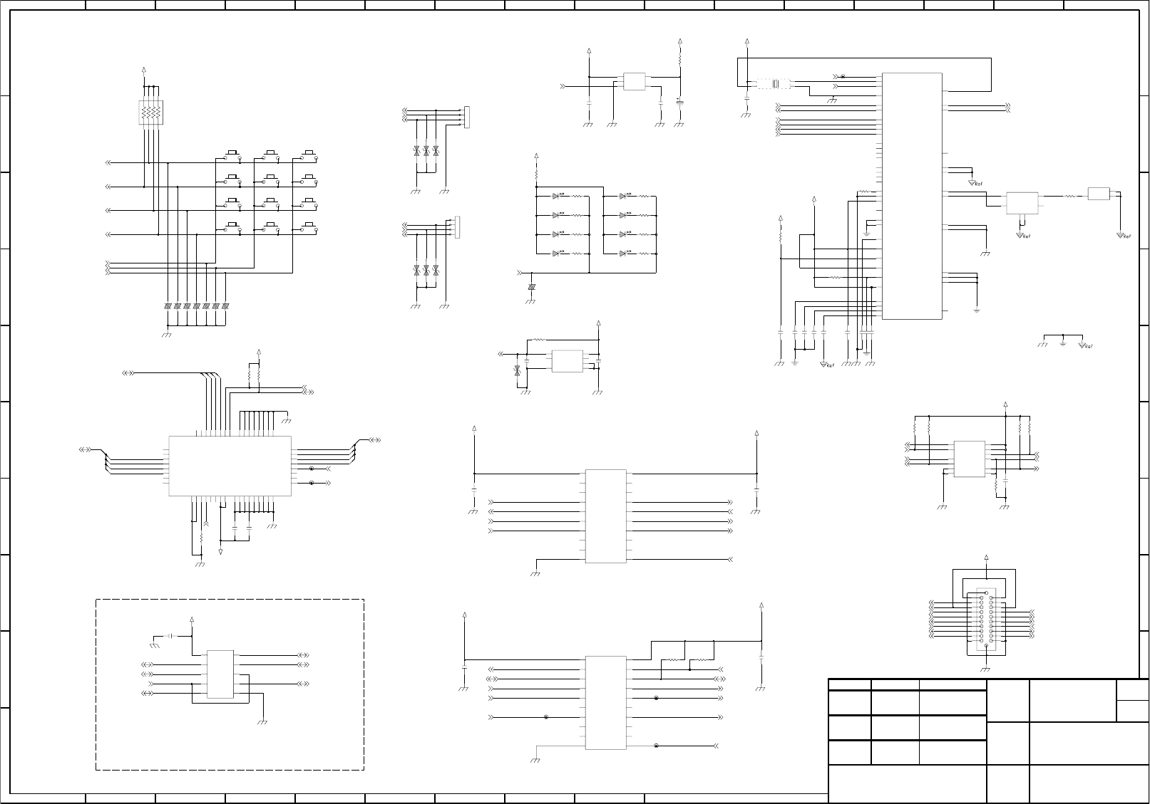
- 194 -
LGE Internal Use Only
Copyright © 2007 LG Electronics. Inc. All right reserved.
Only for training and service purposes
7. CIRCUIT DIAGRAM
A
3
C
NO.
NAME
Approved
MODEL
6
JTAG-JIG-FPCB-CON
6
F
LG Electronics Inc.
9
Sheet/
8
NO.
D
UART SWITCH
64
5
3
B
NAME
Checked
Section
F
Checked
2
B
E
11 12
Designer
Date
2
LG Electronics Inc.
F
14
F
C
15
D
5
Designer
1
DRAWING
D
Sheets
7
LG(42)-A-5505-10:01
DRAWING
4
LG Electronics Inc.
810
Section
LG Electronics Inc.
USB SWITCH
5
C
E
1
7
D
DRAWING
3
D
DRAWING
Date
C
1
E
D
52
C
E
LG(42)-A-5505-10:01
F
16
A
Approved
E
8
FOLDER_SENSE
E
C
Sheet/
6
D
B
Sign & Name
Sheets
E
A
MODEL
742
C
13
Sign & Name
4 93
9
R401
0
2006 LGE JOY 1.3
BT & KEYCODER
LGE
MAY
USB SW & LEVEL SHIFTER
4/7
1
SW400
100ohmR411
AP_VDD_IO_2.7V
SSC-TWH104-HLS
LD407
33u
C400
6
1
U_BP
C409 0.1u
DEA212450BT-7043C1
FL400
5BP1
4BP2 BP_DC 2
3G1
G2
R421 1K
U406
SLAS4717EPMTR2G
3
COM1
9
COM2
6
GND
IN1
4
IN2
8
5
NC1
NC2
7
NO1
2
NO2
10
VCC
1
TP407
SSC-TWH104-HLS
TP400
LD406
C402
1u
SW411
10
7
S1
VCC1 9
12
VCC2
TP421
NLAS3158MNR2G
U403
0B0
2
0B1 11
51B0 8
1B1
A0
1
4A1
3GND1
6GND2
S0
20
3
4
5
6
7
8
9
G1
G2
1
10 11
12
13
14
15
16
17
18
192
CN402
0
R715
0.1u
SW407
AP_VDD_IO_2.7V
C414
VA403 EVLC14S02050
D402 RSB6.8CST2R
C416
0.1u
0.1u
C418
VA405 EVLC14S02050
C421
0.1u
AP_VDD_BT_2.7V
C417
0.1u
RSB6.8CST2RD405
C420
0.1u
0.1u
C401
SSC-TWH104-HLS
R415
3.3K
EVLC14S02050VA404
LD402
1
2
3
4
0
R404
CN401
EVL14K02200
VA400
SW408
R409 100ohm
AP_+VPWR
R714
0
E7
G2 VDD_D
VDD_DSM
B7
A7 VDD_HV_A
VDD_HV_D
G1
VDD_IO_A
G5
F3 VDD_IO_B
C7 VDD_N
VDD_RF
A1
B4
VSS_ANA1
VSS_ANA2 B6
C6
VSS_ANA3
VSS_DIG1 E3
E4
VSS_DIG2
A2
VSS_RF1 A5
VSS_RF2
G3
D2 PCM_A
PCM_B
E1
PCM_CLK
D1
PCM_SYNC
C2
REF_CLK_IN
D6
D3 RESET_N
RFN A4
A3
RFP
TOUT_IN_QP
B5
A6 TOUT_IP_QN
G4 UART_CTS UART_RTS F4
F5 UART_RXD UART_TXD F6
D7 VDD_CL
VDD_CLD
E5
C5 BT_WAKEUP
E6 CLK_REQ_IN_1
G6 CLK_REQ_IN_2
CLK_REQ_OUT2
G7
CLK_REQ_OUT_1 C4
E2 CONFIG_1
CONFIG_2
F1
F2 CONFIG_3
GPIO_0
D5
C1 GPIO_10
B2
GPIO_11
B3 GPIO_16
GPIO_8
C3
GPIO_9
B1
HOST_WAKEUP
F7
LP_CLK
AP_VDD_IO_1.8V
STLC2500CU401
AF_PRG
100ohmR412
VA401 EVLC14S02050
U402 A3212EEH-T
3GND1
GND2 4
2NC1 5
NC2
1OUTPUT
7
PGND
6
VDD
AP_+VPWR
220n
EUSY0200301
TP406
C405
220nC408
AP_VDD_BT_2.7V
EVLC14S02050VA406
0.1u
TP420
C422
2
GND
OUT
3
1
TRI_OPEN
VDD
4
19.2MHz
X400 CSC3M192000EEVRS00
C419
SW401
LD400
0.1u
0.1u
SSC-TWH104-HLS
100ohmR406
C412
3.3K
R414
D404
EVLC14S02050VA402
RSB6.8CST2R
SW409
470p
C403
C404
VUSB_3.1V
0.1u
R413
100K
SW410
0.1uC411
VREG_MSMP_2.7V
RSB6.8CST2RD401
C410 220n
C407 220n
R400
0
R408 100ohm
SSC-TWH104-HLS
SW402
LD401
VA407 EVLC14S02050
D400 RSB6.8CST2R
Wake_INP2 E7
D6
Wake_INP3
B6
Wake_INP4
Wake_INP5 A7
Wake_INP6
A6
B5 Wake_INP7
F3
_RESET
NC1 F5
G6
NC2
NC3 F6
G7
NC4
C2
NC5
NC6 C1
C6
NC7
NC8 B7
F1 PWM
SCL_AB E6
F7
SDA_AB
VCC1
E1
VCC2
E2
G1
WD_Out
Wake_INP0 D7
C7
Wake_INP1Gen_IO_0
D2
D1 Gen_IO_1
Gen_IO_2
B3
Gen_IO_3
A2
A1 Gen_In0
Gen_In1
B2
Int_Rx G2
Int_Tx F2
G3
K_Out0
K_Out1 F4
G4
K_Out2
K_Out3 G5
K_Out4
A5
B4 K_Out5
K_Out6
A4
A3 K_Out7
LM8333GGR8_NOPB
U404
B1 CLK_In
GND1
C3
C4 GND2
C5 GND3
GND4
D3
D4 GND5
GND6
D5
GND7
E3
E4 GND8
GND9
E5
SW406
SSC-TWH104-HLS
LD403
C413
1u
R403 100ohm
R410
0
RSB6.8CST2RD403
SSC-TWH104-HLS
LD405
B3
IOVCC7
IOVCC8 A4
IOVL1
E2
D1 IOVL2
IOVL3
D2
C1 IOVL4
C2 IOVL5
IOVL6
B1
IOVL7
B2
A1 IOVL8
A2
OE
E4
VCC
E1 VL
TP419
ST2378EBJRU407
GND
A3
IOVCC1 E3
D4
IOVCC2
D3
IOVCC3
IOVCC4 C4
C3
IOVCC5
IOVCC6 B4
100ohmR405
NA
R450
AP_VDD_IO_2.7V
AP_VDD_IO_1.8V
R402 100ohm
AP_VDD_IO_2.7V
C415
0.1u
2
4
6
8
1
3
5
7
SW404
RA400 100K
FEED
NC1
NC2
AP_VDD_IO_1.8V
MIC5219-2.7YM5U400
BYP 43 EN
2GND
IN
1OUT 5
ANT400
SW405
AP_VDD_IO_2.7V
ZD1
RSB6.8CST2R
AP_VDD_BT_2.7V
R416
100K
R417
100K
220nC406
1
2
3
4
AP_VDD_IO_2.7V
R451
CN400
NA
B3
A4
IOVCC8
E2 IOVL1
IOVL2
D1
D2 IOVL3
IOVL4
C1
IOVL5
C2
B1 IOVL6
B2 IOVL7
IOVL8
A1
OE A2
VCC E4
VL
E1
U405 ST2378EBJR
A3 GND
E3
IOVCC1
D4
IOVCC2
IOVCC3 D3
C4
IOVCC4
IOVCC5 C3
B4
IOVCC6
IOVCC7
LD404
SSC-TWH104-HLS
R418
100K
SW403
R420 1K
68KR419
KEY_COL(3)
KEY_ROW(2)
URXD2
MSM_UART_RXD
UART_SW
MSM_UART_TXD
UTXD2
FOLDER_DETECT
AP_VDD_IO_2.7V
FOLDER_DETECT
BT_RESETN
MSM_TDI
MSM_TRST_N
MSM_RESIN_N
MSM_TCK
MSM_TMS
MSM_RTCK
MSM_TDO
JTAG_PS_HOLD
AP_TRST_N
AP_TDI
AP_TMS
AP_TCK
AP_TDO
PON
AP_RTCK
KEY_ROW(0)
KEY_ON_SW_N
KEY_COL(1)
KEY_COL(2)
KEY_ROW(0)
UCTS0N
PCMDATAOUT
PCMSYNC
PM_SDA
2M_PWDN_AP
I2CSCL1
I2CSDA1
LEVEL_SHIFT_EN
VGA_STANDBY_AP VGA_STANDBY
KEY_COL(5)
KEY_COL(6)
KEY_COL(7)
KEY_COL(4:7)
KPD_DRV_N
KEY_ROW(1)
KEY_ROW(2)
KEY_ROW(3)
KEY_COL(0)
USB_SW
KEY_ROW(1)
KEY_COL(3)
PM_SCL
2M_RSTN
I2CSDA0
I2CSCL0
2M_PWDN
2M_RSTN_AP
LEVEL_SHIFT_EN
URXD0
PCMDATAOUT
PCMDATAIN
PCMCLK
PCMSYNC
UTXD0
URTS0N
KEYCODER_RSTN
MSM_USB_D+
MSM_USB_D-
AP_USB_D+
AP_USB_D-
USB_D-
USB_D+
PCMCLK
WM_ADCDAT
WM_BCLK
UART_RXD
KEYCODER_INT
KEY_ROW(0:3)
KEY_ROW(2)
KEY_ROW(3)
KEY_ROW(0)
KEY_ROW(1)
KEY_COL(3)
KEY_COL(2)
KEY_COL(3:0)
KEY_COL(1)KEY_COL(4)
KEY_COL(0)
PCMDATAIN
UART_TXD
WM_DACDAT
WM_LRC
CLK32K

- 195 -
LGE Internal Use Only
Copyright © 2007 LG Electronics. Inc. All right reserved.
Only for training and service purposes
7. CIRCUIT DIAGRAM
11 14
NO OSCILLATION
E
LOW
8
7
LOW
TCXO
14
E
942
(1%)
11
1
F
HIGH
C C
(1%)
LOW
16
6
(1%)
E
(1%)
B
D
F
DCS RX LOW
3146
A
13
LG Electronics Inc.
DRAWING
F
E
15
D D
MODEL
(1%)
IN_C
6
LOW
HIGH
LOW
A
DCS1800/PCS1900
B
IN_B
1
Sheets
LG Electronics Inc.
3
B
E
LOW
Designer
Section
Sheets
LG Electronics Inc.
B
LOW
A
D
IN_A
D
3
C
F
51
A
D
C
2
LOW
Thermistor Circuit
9
GSM 900 RX
13
WCDMA
PCS RX
E
9
DCS/PCS TX
A
GSM/EDGE
1 5
(1%)
(1%)
ANTENNA SWITCH MODULE LOGIC
B
4
E
LG(42)-A-5505-10:01
E
HIGH
8
(1%)
(1%)
Sheet/
8
(change to 4.53k)
A
LG Electronics Inc.
3
(1%)
10
C
8
2
2
TX VCO CONTROL LOGIC
10
E
F
GSM850/900 HIGH
C
(1%)
6
16
97
LG(42)-A-5505-10:01
E
LOW
HIGH
F
D
UMTS 2100
D
E
D
C
DD
2
Date
E
7
C
3 94
F
5
HIGH
B
8
HIGH
C
LOW
NO.
10
Approved NAME
64
Sign & Name
C
Approved
11
HIGH
LOW
9
165
2
Sheet/
SW1
6
NAME
15151371
LOW
NO.
12
D
7
F
5
SW2
Checked
1
DRAWING
4
74
3
R515 1K
LGE
2006
MAY JOY 1.3
5/7
RF
GSM900 TX
5
C
DRAWING
12
F
LOWLOW
8
C
HIGH
12
VREG_RFR_2.85V
C537
120p
R509 3.3K
C514
1000p
C564
0.01u
15p
C556 15p
4.7u
C557
C593
C531
33p
R517 100ohm
9.1nH
L519
COMMRFIN
VOPS VRMS
ADL5500 U504
L510
3.3nH
C511
47p
0.068u
330p
C565
VBATT
C535
C594
0.1u
100p
C592
C570
0.01u
R502
4.7K
C534
VREG_RFTX_2.85V
C567
0.1uF
1000p
3.3nH
L500
L526
3.9nH
C558
NA
0.01u
C528
L516
10nH
10nH
L520
C504
1000p
C561
22p
ECHU1C392JX5
C538
3.9n
12p
C581
47nH
L518
R534
10
C502
NA
0.1u
FB501
C579
R523
FB502
270
56p
L521
47nH
ANT500
C506
33p
C549
R501
4.3K
C505
47p
100ohm
R525
2.2KR506
C569
FB500
15p
R535
10
100p
C547
NA
C512
R532
11.3K
R524
51
0.1uF
C532
C555
33p
680p
C587
VTUNE_REF 8
R533
51
39 VDDA11
VDDA12
41
VDDA13
48
50 VDDA14
VDDA15
52
VDDA16
54
56 VDDA17
5
VDDA2
7
VDDA3
VDDA4 10
15
VDDA5
23
VDDA6
VDDA7 26
VDDA8 27
31 VDDA9
43 VDD_M
SBDT
45
46 SBST
TCXO 6
19
TX_IN
18
TX_IP
40 TX_MOD_CP
TX_QN 17
16
TX_QP
TX_VCO_FB
42
53 UMTS1900_OUT
51 UMTS2100_OUT
UMTS800_OUT
55
VCONTROL
49
VCO_TUNE 9
VDDA1 4
VDDA10
36
34 GSM1800_INN
GSM1800_INP
35
24
GSM1900_INN
GSM1900_INP 25
GSM850_INN 21
GSM850_INP 22
38 GSM900_INN
GSM900_INP
37
47 RF_ON_TX_ON
14
RX_IN
RX_IP 13
RX_QN 12
RX_QP 11
RX_VCO_IN
32 R_BIAS
33
SBCK
44
U500
RTR6250D
2
CP1
CP2
30
CP_HOLD1 1
CP_HOLD2
29
DAC_REF 20
3
FAQ1
28
FAQ2
GND_SLUG
57
C529
NA
L514 7.5nH
VREG_RFTX_2.85V
C563 1000p
2.2uH
L503
L517
9.1nH
10p
C544
VREG_MSMP_2.7V
C595
2
GNDOUT
3
VCC
4VCONT 1
100p
19.2MHz
X500
C599
100p
C536
68p
1000p
C527
R505 0
C580
47
VREG_MSMP_2.7V
C530
33p
C578
8.2p
VREG_SYNTH_2.85V
3.6nH
L505
C515
33p
4700p
C550 C552
100p
C520
0.1u
1u
C590
R521
100pC559
220
R500
10
68K
R527
100p
C582
ANT501
47p
C510
5.1nH
L513
VREG_RFTX_2.85V
6.2K
R512
L527
1.2p
R519 100ohm
L522
18nH
2.2uH
L509
UMC4N
2
45
31
Q500
C554
33p
C584
33p
0R508
C585
100p
R531
51
C524
0.1uF
C523
R507 100
100p
L502
1p
VC
10
C583
0.1u
GND1 2
GND2 4
GND3 6
7
GND4
GND5
8
GND6
12
13 GND7
GND8
14
5OUT_DCSPCS
1OUT_GSM 9
SW1 11
SW2
3
VB
MQW5V0C869M U502
UMTS_TX_RX
VC1
17
15
VC2
VC3
14
16
VDD
470K
R528
ANT
12
DCS_PCS_TX
8
3
DCS_RX1
DCS_RX2
4
1
EGSM_RX1
EGSM_RX2
2
EGSM_TX
10
7
GND1
GND2
9
11
GND3
GND4
13
18
GND5
GND6
20
5
PCS_RX1
PCS_RX2
6
19
6.8n
FL500ESHS-L090UB
C526
ECHU1C682JX5
100p
C574
C508 33p
INOUT
4
VREG_RFTX_2.85V
2.2uH
L506
EFCH1950TDC1
U503
2
G1
5
G2
3
G3 1
390p
C542
L532
100nH
0
C500
L533
2.7nH
56pC501
100p
C800
0.1uF
C503
+VPWR
C551
47p
VREG_RFR_2.85V
C566
0.1uF
C568
22u
0
R513
L507
5.1nH
C553
tcc_1608h_9_r
4.7u
L515
47nH
U506ACMD-7601
ANT
G1
G2
G3
G4
G5
G6
G7
RX TX
1.8nH
VREG_TCXO_2.85V
C560
L530
2.2nH
C517
0.1uF
C548
4.7u
32 VDDA5
VDDA6
34
36 VDDA7
VDDA8 45
41
VDDM
VDDRF1 3
12
VDDRF2
19 VDDRF3
L529
33nH
10
PMIXM
PMIXP 11
RX_IM
21
20 RX_IP
23 RX_QM
RX_QP
22
46
R_BIAS
SBCK 42
SBDT 43
44
SBST
33 TCXO
25 UMTS_TUNE
VDDA1 7
24 VDDA2
26 VDDA3
VDDA4
27
4
GND
GPS_TUNE
35
GRX_IM 39
40
GRX_IP
37
GRX_QM
GRX_QP 38
ILNA_BIAS
17
18 ILNA_IN
ILNA_OUT
14
8
IMIXM
IMIXP 928 LO_OUT
49
PGND
15 PLNA_BIAS
PLNA_IN
16
PLNA_OUT
13
BLANK 2
29 CP_DUMP
CP_OUT
30
31 FAQ
GLNA_BIAS
48
47
GLNA_IN
1
GLNA_OUT
GMIXM 5
6
GMIXP
RFR6250E
U508
R510
100
C572
1500pC573
0.1u
C509
47p
B7827
2
G1
5
G2
1
IN
3
O1
4
O2
100p
FL501
KMS-512
SW500
ANT
G1
G2RF
C588
450OHM
COUP
32
IN
1
OUT
2.2uH
L512
C546
1000p
4.7u
VREG_RFTX_2.85V
6.2KR529
110 VCC2
4
VMODE
VREF 5
C518
AWT6277R U505
GND1 3
GND2
6
7GND3
9GND4
GND5
11
2
RFIN
RFOUT
8
VCC1
1000pC562
56nH
L504
15R518
C521
680p
C596
4.7p
11.3KR503
33p
C575
C533
1.8nH
L528
2.7nH
15R516
VREG_TCXO_2.85V
0R504
L523
22nH
0.01u
C545
80.6K
R526
220
C516
R520
C522
33p
VREG_RFTX_2.85V
33p
C519
47p
10
GND3
11
GND4
GND5
13
GND6
14
GND7
16
17 GND8
7
GSM_IN
9GSM_OUT
TX_EN 3
4
VBATT
VCC
12
6
VRAMP
TQM7M5003
U501
2
BS
DCS_PCS_IN 1
DCS_PCS_OUT
15
GND1 5
GND2
8
C586
100p
1.2p
R511
0
C597
C589
10p
L524
1.5nH
L525
8.2nH
0.1u
100ohmR514
C598
L508
7.5nH
C525
0.01u
C507 1.5nH
C591
4.7u
C577
L501
3.6nH
33p
C571
3.9nH
R530
0.01u
C541 82p
C540
0.01u
270
R522
C513
7.5nH
L511
NA
L531
2.7nH
C539
5.6n
ECHU1C562JX5
22u
C543
GSM_PA_EN
GSM_PA_BAND
ILNA_OUT
WCDMA_2100_TX_OUT
WCDMA_2100
WCDMA_2100
TX_Q_M
TX_Q_P
TX_I_P
CP2_OUT
HDET1
IMT_RX_M
IMT_RX_P
W_VMODE_N
CP2_OUT
UHF_LO_BUFF
UHF_LO_BUFF
TX_I_M
ILNA_OUT
IMT_RX_M
IMT_RX_P
RX0_I_M
RX0_I_P
RX0_Q_M
RX0_Q_P
RFR6250_TCXO
RF_SBST
RF_SBDT
RF_SBCK
TCXO_PM
RTR6250_TCXO
GSM_PA_RAMP
PA_ON
GSM_TX_VCO_0_EN_N
GSM_TX_VCO_1_EN_N
ANT_SEL0
ANT_SEL1
ANT_SEL2
TX_ON
TX_AGC_ADJ
RX0_I_M
RX0_I_P
RX0_Q_M
RX0_Q_P
RFR6250_TCXO
TRK_LO_ADJ
PA_THERM
DAC_REF
RF_SBCK
RF_SBDT
RF_SBST
RTR6250_TCXO
WCDMA_2100_TX_OUT
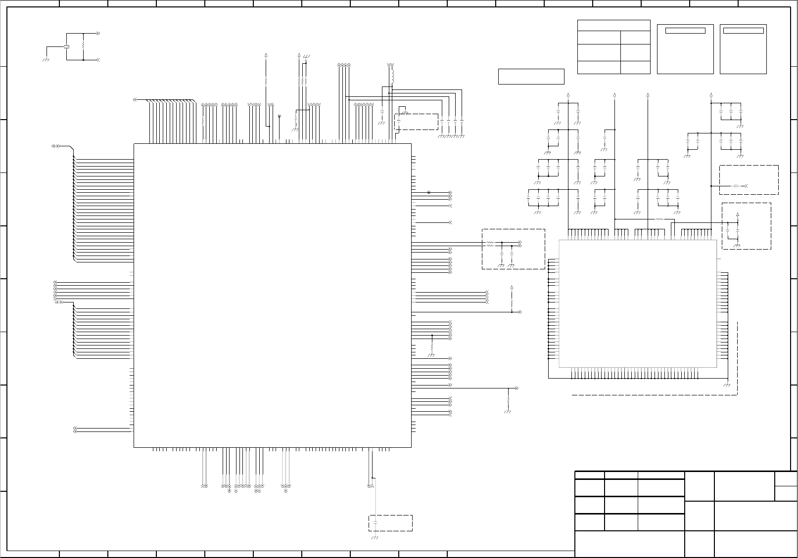
- 196 -
LGE Internal Use Only
Copyright © 2007 LG Electronics. Inc. All right reserved.
Only for training and service purposes
7. CIRCUIT DIAGRAM
DRAWING
HKADC[4] - PCB_Rev_ADC
(WCMDA 2100PAM Enable)
10
D
4
Default Pull-up
14
ADC
E
Place near
( Default Pull-Down)
0 1
NAME
150K : 68K : 0.81V
3
DRAWING
0 1 0
2 12
Sign & Name
D
2
LG(42)-A-5505-10:01
1005 0.1uF 16V +80/-20%
F
Date
F
WDOG_EN (1:Enable , 0:Disable)
for VSS_THERMAL
6
(CODEC VSS)
(WCMDA PAM MODE)
8-bit, NAND boot
HKADC[1] - VBATT_SENSE
E
E
C
Trusted boot
B
LG Electronics Inc.
8 13
Native, ARM JTAG
Sheet/
C
6
MSM pin W18
(VDD_DAC_REF)
1
0 0 0
NOR boot
15
Near to B18 (VDD_PLL)
B
2200p cap => place between
MODE
PMIC_AUXIN[1]
150K : 47K : 0.62V
MODE2 MODE1 MODE0
(2012)
MODEL
9
150K : 100K : 1.04V
16
F
HKADC[0] - AMUX_OUT
10%
(Check CAM_DATA PINOUT !!!!)
PMIC_AUXIN[2] - PA_THERM
MSM pin AD26
C
Checked
D
5
HKADC[2] - HDET1
Place near
8
HKADC[3]
7
Native, MSM JTAG
10%
150K : 680K : 2.13V
Section
11
1
150K : 10K : 0.016V
0
BOOT_MODE2 BOOT_MODE
HKADC(5):PCB_Rev_ADC
150K : 150K : 1.30V
Sheets
A
Designer
A
4
(PLLOUT_TEST)
C
150K : 300K : 1.73V
9
2012 10uF 6.3V +80/-20% Ceramic
BOOT_MODE3
10%
NO.
150K : 470K : 1.97V
5
HKADC[5] - CHARGER_THERM
16-bit, NAND boot
MAY
2006 LGE
MODEM CPU
6/7
JOY 1.3
D12(VDDA1) and F12(DAC_REF)
Approved
LG Electronics Inc.
1 1
7
150K : 750K : 2.17V
3
w18 (Analog VSS guard ring for CODEC)
(CAD : 10uF=>Input MSMA_2.6V)
E
Normal boot
1
Near to MSM
D
USB 48M CLK
X 0
13
2
48MHz
X600
EXRY0002401
XMEM1_CS_N1_GPIO76
Y4
XMEM1_CS_N2_SDRAM1_CS_N0
XMEM1_CS_N3_SDRAM1_CS_N1_GPIO77
Y6
XMEM1_HWAIT_N AA2
XMEM1_LWAIT_N_SDRAM1_CAS_N K8
W14
XMEM2_CS_N0
XMEM2_CS_N1
AC15
XMEM2_CS_N2_GPIO35
W15
AA15
XMEM2_CS_N3_GPIO36
TP601
UART3_DP_RX_DATA_GPIO85
UART3_DP_TX_DATA_GPIO84
M19
L25
UART3_RFR_N_GPIO87
UB1_N_SDRAM1_DQM1 M6
UB2_N
AF10
USB_DAT_VP
N26
N25 USB_OE_TP_N
USB_RX_DATA_GPIO29
N19
USB_SE0_VM
N23
A10
USB_XTAL48_IN B10
USB_XTAL48_OUT
AE17
WDOG_EN
WDOG_STB_SBCK1_GPIO0
H25
U8
WE1_N_SDRAM1_WE_N
WE2_N
AF4
XMEM1_CS_N0 W6
AA1
TDI
TDO
A17
TMS
F15
TRK_LO_ADJ
L13
H15
TRST_N
H13
TX_AGC_ADJ
TX_ON_GRFC10
H12
P16 UART1_CTS_N_GPIO97
UART1_DP_RX_DATA_GPIO96
M23
UART1_DP_TX_DATA_GPIO95
L26
P21 UART1_RFR_N_PA_POWER_CTL_M_GPIO98
G6 UART2_CTS_N_GPIO90
H6
UART2_DP_RX_DATA_GPIO89
UART2_DP_TX_DATA_GPIO88
E4
UART2_RFR_N_GPIO91
F4
UART3_CTS_N_GPIO86
L23
M21
T6
T8
SDRAM1_D31
AB4
SDRAM1_D4
J6
SDRAM1_D5
G2
SDRAM1_D6
SDRAM1_D7
H4
P4
SDRAM1_D8
SDRAM1_D9
J4
A16
SLEEP_XTAL_IN B16
SLEEP_XTAL_OUT
F18
SYNTH0_GP_PDM0_GPIO92
H23 SYNTH1_GPIO41
B6
SYNTH2_GPIO65
TCK
D16
TCXO D18
TCXO_EN_GPIO94
F19
D15
U6
V4
SDRAM1_D17
SDRAM1_D18
R11
SDRAM1_D19
E1
SDRAM1_D2
AB2
Y1
SDRAM1_D20
SDRAM1_D21
Y2
SDRAM1_D22
V6
W4
SDRAM1_D23
R4
SDRAM1_D24
SDRAM1_D25
R6
T1
SDRAM1_D26
SDRAM1_D27
T2
R8
SDRAM1_D28
T4
SDRAM1_D29
SDRAM1_D3
D1
SDRAM1_D30
SBDT
F26
SBDT1_GPIO1
H26 SBST
SBST1_GPIO93
H18
SDCC_DAT1_GPIO99
F25
M25
SDCC_DAT2_GPIO100
SDCC_DAT3_GPIO101
M26
N4
SDRAM1_CLK_EN
E2
SDRAM1_D0
D2
SDRAM1_D1
J2
SDRAM1_D10
K6
SDRAM1_D11
SDRAM1_D12
J1
SDRAM1_D13
K4
L8
SDRAM1_D14
SDRAM1_D15
L6
SDRAM1_D16
PA_ON1_GPIO2
P25 PA_POWER_CTL
AA25
Q_IM_CH0
Q_IM_CH1
W23
Y25
Q_IP_CH0
Q_IP_CH1
V23
B12
Q_OUT
A12
Q_OUT_N
RESIN_N F13
RESOUT_N F11
AA4
RESOUT_N_EBI1
RINGER_GPIO18
L19
ROM1_ADV_N_SDRAM1_RAS_N G1
AB1
ROM1_CLK_SDRAM1_CLK
RTCK
H16
L21 SBCK
J23
MICFBN
MICFBP AC21
MICINN AC19
AC20
MICINP
MICOUTN AA18
AA19
MICOUTP
M16 MMC_CLK_SDCC_CLK_GPIO31
MMC_CMD_GPIO30
H14
L14 MMC_DATA_SDCC_DAT0_GPIO32
MODE0 Y23
MODE1 U23
T21
MODE2
T14
NAND2_FLASH_READY_GPIO33
OE1_N V2
AF7
OE2_N
PA_ON0
F17
H11
LCD_EN_GPIO37
MDDIC_DATN
A23
A22
MDDIC_DATP
MDDIC_STBN
B23
B22
MDDIC_STBP
MDDIH_DATN
B19
B20 MDDIH_DATP
MDDIH_STBN
A19
A20 MDDIH_STBP
MDP_VSYNC_PRIMARY_GPIO105
AD2
AE3
MDP_VSYNC_SECONDA_GPIO104
MIC1N AF20
MIC1P AE20
AF21
MIC2N
MIC2P AF22
MICBIAS T15
AC22
I2C_SCL_GPIO27
K21 I2C_SDA_GPIO26
AB25
I_IM_CH0
V25
I_IM_CH1
AC25
I_IP_CH0
W25
I_IP_CH1
I_OUT
B13
I_OUT_N
A13
R21 KEYSENSE0_N_GPIO62
KEYSENSE1_N_GPIO63
P19 KEYSENSE2_N_GPIO46
D14 KEYSENSE3_N_GPIO47
R23
U21 KEYSENSE4_N_GPIO48
LB1_N_SDRAM1_DQM0 L2
LB2_N_A2_0
AE10
LCD_CS_N_GPIO38
AF14
AE13
GRFC3_GPIO6
GRFC4_AUX_SBCK_GPIO7
H10
D11
GRFC5_AUX_SBST_GPIO8
GRFC7_GPIO10
T23
B4
GRFC8_GPIO11
D5
GRFC9_GPIO12
GRFX6_GPIO9
T19
GSM_PA_DAC_REF
AD26
V21
HKAIN0
HKAIN1 AA23
W21
HKAIN2
HKAIN3 V19
Y21
HKAIN4
HKAIN5 AB23
HPH_L W17
AA17
HPH_R
N16
GPIO42
H9
GPIO43
GPIO44
D8
A4 GPIO45
GPIO49
F9 GPIO50
B7 GPIO51
A7 GPIO52
D10
L12 GPIO53
F14 GPIO64
F8
GPIO66
H17
GP_PDM1_PA_RANGE0
D17
GP_PDM2_PA_RANGE1
B8
GRFC0_GPIO3
A8
GRFC1_AUX_SBDT_GPIO4
D9
GRFC2_GPIO5
F10
AE4
AC6
D2_3
AE5
D2_4
AA7
D2_5
AF5
D2_6
D2_7
AC7
D2_8
AA8
D2_9
W9
F12
DAC_REF
EAR1ON AE18
EAR1OP AF18
GPIO17
K26 GPIO19
G21
A6
GPIO28
GPIO39
F7
GPIO40
D6
D7
L15 CAMIF_DATA7_GPIO59
D20
F16 CAMIF_DATA8_GPIO60
F20 CAMIF_DATA9_GPIO61
E23 CAMIF_HSYNC_GPIO15
CAMIF_PCLK_GPIO82
K23
CAMIF_VSYNC_GPIO16
B3
CCOMP AA20
D2_0
AC5
AF3
D2_1
AC8
D2_10
AE7
D2_11
AA9
D2_12
W10
D2_13
D2_14
AC9
D2_15
AA10
D2_2
BOOT_MODE
BOOT_MODE2 AE22
AD1
BOOT_MODE3
G23
BT_CLK_GPIO25
BT_DATA_GPIO20
R19
E26
BT_SBCK_GPIO23
BT_SBDT_GPIO22
E25
F23
BT_SBST_GPIO24
BT_TX_RX_N_GPIO21
H21
CAMCLK_PO_GP_MN_GPIO13
J21
CAMIF_DATA0_GPIO83
J25
J26 CAMIF_DATA1_GPIO81
D21 CAMIF_DATA2_AUX_TRST_N_GPIO54
CAMIF_DATA3_AUX_TCK_GPIO55
C25 CAMIF_DATA4_AUX_TMS_GPIO56
D22
J19 CAMIF_DATA5_AUX_TDI_GPIO57
CAMIF_DATA6_AUX_TDO_GPIO58
A2_20_GPIO34
A2_3
W11
AC10
A2_4
AA11
A2_5
A2_6
AC11
T12
A2_7
W12
A2_8
A2_9
AA12
AF19
AUXIN AE19
AUXIP
AC18
AUXON_AUXOR
AUXOP_AUXOL AC17
AUX_PCM_CLK_GRFC14_GPIO80
K19
N21
AUX_PCM_DIN_GRFC13_GPIO14
AUX_PCM_DOUT_GRFC12_GPIO103
G4
AUX_PCM_SYNC_GRFC11_GPIO102
J8
AE21
A1_6
A1_7 N6
A1_8 N2
N1
A1_9
AE9
A2_1
AC12
A2_10
A2_11
AE12
A2_12
AF12
AA13
A2_13
A2_14
AC13
A2_15
W13
A2_16
AE14
AC14
A2_17
A2_18
T13
A2_19
AA14
AF9
A2_2
AF13
L1
A1_1
P1
A1_10
A1_11 P2
A1_12 P6
P8
A1_13
A1_14 P11
L4
A1_2
U4
A1_23_SDRAM1_DQM2_GPIO78
V1
A1_24_GPIO79
V8
A1_25_SDRAM1_DQM3_GPIO75
M8
A1_3 M4
A1_4
A1_5 N11
N8
U600-1
MSM6275_A
TP602
R609100K
0.01u
C644
1000p
C623
0.01u
C624
100K R611
10u
smd_2125h1_45_r
C603
0.01u
C627
0.01u
C616
0.01u
C643
51K
R610
1M
R600
R60251K
C640
0.1uF
0.1uF
C628
C642
0.1u
0.1uF
C639
C613
0.01u
VREG_MSMA_2.6V
VREG_MSMP_2.7V
R601100K
0.1uF
C620
C602
0.01u
51 R605
100p
C606
1000p
VREG_MSMP_2.7V
R6071K
VREG_MSME_1.8V
C631
0.1uF
C618
C611
NA
0.01u
VREG_MSMC_1.375V
C635
1000p
C633
C646
0.1u
R6082K
1000p
NA
C638
C608
NA
C610
C615
0.1uF
VREG_MSMP_2.7V
C617
0.01u
R603100K
0.1u
C607
VREG_MSMA_2.6V
1000p
C637
0.01u
C626
100K R604
B17
VSS_PAD3_2
A15
VSS_PAD3_3
A9
VSS_DIG_3
VSS_DIG_4
AF8
VSS_DIG_5
AF16
VSS_DIG_6
T26
G26
VSS_DIG_7
D26
VSS_DIG_8
A24
VSS_DIG_9
VSS_PAD1_0
F1
VSS_PAD1_1
K1
M1
VSS_PAD1_2
R1
VSS_PAD1_3
U1
VSS_PAD1_4
VSS_PAD2_0
AF6
AF11
VSS_PAD2_1
AF15
VSS_PAD2_2
VSS_PAD3_0
R26
VSS_PAD3_1
VSSA15
VSSA16
AF24
VSSA2
A21
D13
VSSA3
D19
VSSA4
VSSA5
P26
VSSA6
U19
VSSA7
V26
W16
VSSA8
W18
VSSA9
VSS_DIG_0
C1
VSS_DIG_1
H1
A14
VSS_DIG_10
VSS_DIG_11
A11
VSS_DIG_12
A5
W1
VSS_DIG_2
AC1
AE26
AF1
VSS48
VSS49
AF2
VSS5
B1
AF25
VSS50
VSS51
AF26
B2 VSS6
VSS7
B25
B26 VSS8
VSS9
D4
A18
VSSA1
VSSA10
W26
VSSA11
AB26
AC16
VSSA12
VSSA13
AC26
AD25
VSSA14
AF23
R13
R14 VSS33
VSS34
R15
R16 VSS35
VSS36
T11
T16 VSS37
W8 VSS38
VSS39
W19
A26 VSS4
VSS40
AA6
AA21
VSS41
AC4
VSS42
VSS43
AC23
AE1
VSS44
VSS45
AE2
AE25
VSS46
VSS47
M11
M12 VSS19
A2 VSS2
VSS20
M13
M14 VSS21
VSS22
M15
N12 VSS23
VSS24
N13
N14 VSS25
VSS26
N15
P12 VSS27
VSS28
P13
P14 VSS29
VSS3
A25
VSS30
P15
R12 VSS31
VSS32
VDD_PAD2_2
R25
VDD_PAD3_0 K25
VDD_PAD3_1
VDD_PAD3_2 B15
VDD_PAD3_3 B9
VDD_PAD4_0 A3
B18
VDD_PLL
VSS1
A1
D23 VSS10
F6 VSS11
VSS12
F21
VSS13
H8
H19 VSS14
K10 VSS15
VSS16
L11
L16 VSS17
VSS18
W2
VDD_DIG_3 AC2
VDD_DIG_4 AE8
VDD_DIG_5 AE16
T25
VDD_DIG_6
VDD_DIG_7 G25
VDD_DIG_8 D25
B24
VDD_DIG_9
VDD_MDDI B21
F2
VDD_PAD1_0 K2
VDD_PAD1_1
VDD_PAD1_2 M2
VDD_PAD1_3 R2
VDD_PAD1_4 U2
VDD_PAD2_0 AE6
AE11
VDD_PAD2_1 AE15
RESERVED
VDDA1 D12
AF17
VDDA10
VDDA2 P23
U25
VDDA3
VDDA4 U26
VDDA5 Y26
VDDA6 AA26
AE23
VDDA7
VDDA8 AE24
VDDA9 AA16
C2
VDD_DIG_0 H2
VDD_DIG_1
B14
VDD_DIG_10
VDD_DIG_11 B11
VDD_DIG_12 B5
VDD_DIG_2
U600-2
MSM6275_B
C26
C612
VREG_MSMP_2.7V
0.01u
0.1uF
C605
C636
1000p
C629
0.1uF
C614
0.01u
smd_2125h1_45_r
C601
C609
10u
NA
C632
1000p
C634 C641
1000p 0.1uF
0
R606
L600
100nH
C619
0.1uF
C621
1000p
C600
0.01u
10p
C625
C645
33nF
0.1uF
C604
C622
1000p
C630
2200p
HPIEV_IT_STATE_ETMTRIGIN
RX0_I_P
RX0_I_M
RX0_Q_P
RX0_Q_M
USB_XTALOUT
USB_XTALIN
WM_HPH_R
WM_HPH_L
EAR_SENSE_N
MSM_RTCK
MSM_TDO
FOLDER_DETECT
HPI_IT_APE_ETMPSTA0_XTIDAT
HPI_IT_MOD_ETMSYNCA_XTIDAT
HPI_EME_MOD_ETMPSTA1_XTIDAT
HPI_EME_APE_ETMPSTA2_XTIDAT
PM_SBCK
SDRAM_DQM(1)
USB_DAT
USB_OE_N
USB_PWR_EN
USB_SE0
USB_XTALIN
USB_XTALOUT
SDRAM_WE_N
SDRAM_CS_N(0)
SDRAM_CAS_N
HCSN_ETMCLK_XTICLK
MSM_TDI
MICINP
WM_MONO1
SLEEP_CLK
MSM_TCK
BUFF_TCXO
TCXO_EN
MSM_TMS
MSM_TRST_N
TX_ON
MSM_UART_RXD
MSM_UART_TXD
MSM_USIM_RST_N
MSM_USIM_DATA
MSM_USIM_CLK
PM_SBDT
PM_SBST
TX_I_M
SDRAM_DQM(0)
WM_MONO2
MICFBN
MICFBP
MICINN
MICOUTN
MICOUTP
PA_ON
GSM_PA_RAMP
TX_Q_P
TX_Q_M
MSM_RESIN_N
RESOUT_EBI2_N
SDRAM_RAS_N
RF_SBCK
RF_SBDT
RF_SBST
SDRAM_CLK_EN
DAC_REF
WM_RXN
WM_RXP
PWR_BTN
PM_INT_N
PS_HOLD
W_VMODE_N
GSM_PA_EN
GSM_PA_BAND
GSM_TX_VCO_1_EN_N
GSM_TX_VCO_0_EN_N
ANT_SEL1
ANT_SEL2
ANT_SEL0
GSM_PA_DAC_REF
AMUX_OUT
VBATT_SENSE
HDET1
VBAT_TEMP
TX_I_P
SDRAM_ADDR(10)
SDRAM_ADDR(11)
SDRAM_ADDR(12)
SDRAM_ADDR(13)
SDRAM_ADDR(14)
SDRAM_ADDR(2)
SDRAM_DQM(2)
SDRAM_ADDR(0)
SDRAM_DQM(3)
SDRAM_ADDR(3)
SDRAM_ADDR(4)
SDRAM_ADDR(5)
SDRAM_ADDR(6)
SDRAM_ADDR(7)
SDRAM_ADDR(8)
SDRAM_ADDR(9)
SDRAM_DATA(4)
SDRAM_DATA(3)
SDRAM_DATA(2)
SDRAM_DATA(1)
EBI2_DATA(15)
EBI2_DATA(14)
EBI2_DATA(13)
EBI2_DATA(12)
EBI2_DATA(11)
EBI2_DATA(10)
EBI2_DATA(9)
EBI2_DATA(8)
EBI2_ADDR(1)
EBI2_ADDR(2)
NAND_ALE
EBI2_WE_N
SDRAM_ADDR(1)
SDRAM_DATA(20)
SDRAM_DATA(19)
SDRAM_DATA(18)
SDRAM_DATA(17)
SDRAM_DATA(16)
SDRAM_DATA(15)
SDRAM_DATA(14)
SDRAM_DATA(13)
SDRAM_DATA(12)
SDRAM_DATA(11)
SDRAM_DATA(10)
SDRAM_DATA(9)
SDRAM_DATA(8)
SDRAM_DATA(7)
SDRAM_DATA(6)
SDRAM_DATA(5) TX_AGC_ADJ
TRK_LO_ADJ
SDRAM_DATA(0)
SDRAM_DATA(0:31)
SDRAM_DATA(31)
SDRAM_DATA(30)
SDRAM_DATA(29)
SDRAM_DATA(28)
SDRAM_DATA(27)
SDRAM_DATA(26)
SDRAM_DATA(25)
SDRAM_DATA(24)
SDRAM_DATA(23)
SDRAM_DATA(22)
SDRAM_DATA(21)
EBI2_DATA(0)
NAND_READY
NAND_CLE
DAC_REF
EBI2_DATA(0:15)
EBI2_DATA(7)
EBI2_DATA(6)
EBI2_DATA(5)
EBI2_DATA(4)
EBI2_DATA(3)
EBI2_DATA(2)
EBI2_DATA(1)
SDRAM_ADDR(0:14)
EBI2_OE_N
NAND_CS_N
SDRAM_CLK
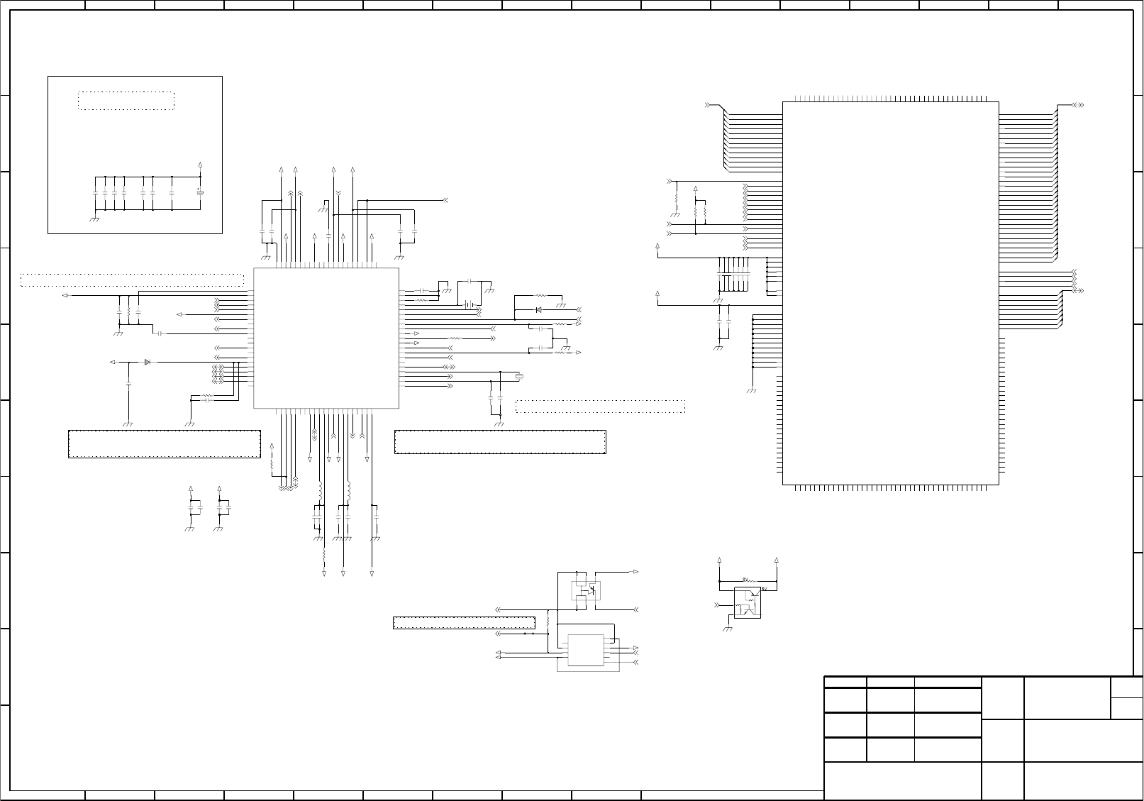
- 197 -
LGE Internal Use Only
Copyright © 2007 LG Electronics. Inc. All right reserved.
Only for training and service purposes
7. CIRCUIT DIAGRAM
VDD_ANA : 0.1uF
7
D
12
4
E
Artwork --> Place crystal and load caps close to PM6650 !!
A
Designer
63
3
B
C
3
DRAWING
1
LG(42)-A-5505-10:01
Sheets
Designer
Checked
B
14
VDD_MSMC : 4.7uF
Section
NO.
Date
A
LG Electronics Inc.
LG Electronics Inc.
VDD_WLAN : 0.1uF
DRAWING
4
DRAWING
Battery charging circuit !!!!!
Approved
VDD_SPKR : NA
2
VDD_MSME : 4.7uF
Draw the Artwork_line thickly !!!!!
1%
C
4
F
15
1
Approved
Date
Checked
C
USB Booting Protection
F
EUSY0297301
LG Electronics Inc.
7
Sheet/
10
VDD_RUIM : 0.1uF
C
PMIC_VPWR_BYPASS
NAME
--->> USB_VBUS , FLASH_DRV_N , KPD_DRV_N , KEY_ON_SW_N , MOT_PWR-
9
Load=12.5p
4
Section
NA
5
D
9
13
F
2 8
B
11
VDD_PA : 4.7uF
DRAWING
E
D
8
VDD_RF : 0.1uF
Sheets
C
96
1
Sheet/
Sign & Name
E
VDD_MSM : 0.1uF
D
NO.
MODEL
5
2012
6
D
E E
Power Line --> Route carefully!!!!!
5
LG(42)-A-5505-10:01
F
E
C
Route carefully to avoid corrupting sensitive analog and RF signals!!!!!
MODEL
C
NAME
2006 LGE
draw_number
7/7
JOY 1.3
MODEM POWER
MAY LGE
draw_number
16
F
D
6
VDD_MAIN : 0.1uF
2
Artwork --> Place resistor and capacitor close to PM6650 !!
LG Electronics Inc.
----->> PM_SBDT , PM_SBCK , PM_SBST , PM_INT_N
2
5
E
1%
D
73
A
1 8
Route as equal length as possible! -> ICHARGE, ICHARGEOUT
Sign & Name
1000p C705
C761
smd_1608h_9_r
4.7u
4.7u
smd_1608h_9_r
VREG_SYNTH_2.85V
+VPWR
VREG_MSMP_2.7V
C731
4.7u
smd_1608h_9_r
C709
R70210K
C706
R704 470K
0.1u
0.01u
NAR730
C727
C719 0.1uF
+5V_PWR
+5V_PWR
C716 0.1uF
X700
32.768KHz
12
2
45
31
USB_VBUS_IN
1u
+VPWR
KRX102E
Q702
C715
0.1uFC722
VREG_MSME_1.8V
47K R710
+VPWR
C739
smd_1608h_9_r
2.2u
0.1u
RB521S-30
D700
C702
C710
4.7u
smd_1608h_9_r
C730
1u
0R707
R709 0
10K R706
C704
0.1u
1u
C729
+VPWR
4.7u
18p
C736
smd_1608h_9_r
C733
C732
+VPWR
1u C711
1u
+VPWR
4.7u
smd_1608h_9_r
C708
VREG_RFR_2.85V
VREG_USIM_2.85V
smd_1608h_9_r
C735
VREG_RFTX_2.85V
4.7u
0.1uF
2.2u
smd_1608h_9_r
C713
C720
0.1uFC728
10
Drain_B
Emitter 8
5
Gate
NC1
1
NC2 6
Source
3
USB_VBUS
VREG_MSMP_2.7V
Q701 NUS5530MN
7
Base
2Collector
Collector_B 9
4Drain
0.1u C701
+VPWR
+VPWR
+VPWR
0.1u C714
+VPWR
VREG_TCXO_2.85V
C723
VREG_MSMC_1.375V
0.1u
0.1u
C725
RB521S-30
D701
VREG_MSMA_2.6V
+VPWR
0.1u C703
4.7uH
L701
8
REF_OUT(MPP8) 80
VREG_SYNT 81
AMUX_OUT 82
VDD_MAIN 83
84
VREG_TCXO
GND_SLUG 85
PON_RESET_N
9
72
VREG_RFTX 73
SPKR_BYP 74
SPKR_OUT_P 75
SPKR_IN_P 76
VDD_SPKR 77
SPKR_IN_M 78
SPKR_OUT_M 79
FLSH_DRV_N
65
CBL1PWR_N(MPP4) 66
VREG_RFRX2 67
CBL0PWR_N(MPP3) 68
VREG_RFRX1 69
BAT_FET_N
7
AMUX_IN1(MPP1) 70
VDD_RF 71
AMUX_IN2(MPP2)
58
MSM_INT_N 59
VBAT
6
VCOIN 60
REF_ISET 61
REF_GND 62
REF_BYP 63
VREG_WLAN 64
VDD_WLAN
50
SBST 51
VDD_MSM 52
TCXO_OUT 53
VDD_ANA 54
TCXO_EN 55
VREG_MSMA 56
PS_HOLD 57
TCXO_IN
43
XTAL_IN 44
SLEEP_CLK 45
XTAL_OUT 46
SBDT 47
VBACKUP 48
SBCK 49
ISNS_M
5
VREG_MSMP
VREG_MSME
VSW_MSME
37
RUIM_CLK(MPP10)
38
VREG_MMC
39
CHG_CTL_N
4
RUIM_M_RST(MPP5)
40
VDD_RUIM
41
VREG_RUIM
42
RUIM_RST(MPP6)
VDD_PA
ISNS_P
3
RUIM_M_IO(MPP11)
30
VSW_MSMC
31
VREG_MSMC
32
VDD_MSMC
33
RUIM_M_CLK(MPP9)
34
VDD_MSME
35
36
GP1_DRV_N(MPP7)
LCD_DRV_N
22
KPD_DRV_N
23
KPDPWR_N
24
VIB_DRV_N
25
RUIM_IO(MPP12)
26
VSW_PA
27
VREG_PA
28
29
VSW_5V
14
USB_CTL_N
15
USB_VBUS
16
USB_DAT
17
USB_D_P
18
USB_SE0
19
VCHG
2
USB_D_M
20
21
ADC_BYP
1
VREG_USB
10
USB_ID
11
VREG_5V
12
USB_OE_N
13
1000p
U700
PM6650-1M
4.7u
C737
C726
smd_1608h_9_r
0.1uFC721
C738
1000p
VREG_MSMP_2.7V
51
R708
USB_VBUS
USB_VBUS
18p
C734
smd_1608h_9_r
2.2u
VREG_MSME_1.8V
+VPWR
C712
R703100K
100K
R711
VSS7
P13
VSS8
R8
VSS9
U2
E6 _CAS
_CE
M9
_CS
E5
D5 _RAS
M10 _RE
D6 _WED
K6 _WEN
_WP
L6
D13 VCCD3
V3 VCCD4
V8 VCCD5
VCCD6
V12
VCCN2
K12
VCCQD1
V4
V9 VCCQD2
C6 VSS1
VSS10
U6
VSS11
U10
U13 VSS12
F7 VSS2
G2 VSS3
G13 VSS4
L13 VSS5
VSS6
P2
NC88
M12
N2 NC89
B1
NC9
NC90 N3
N4
NC91 N5
NC92 N6
NC93
NC94 N9
N10
NC95
NC96 N11
N12
NC97
NC98 N13
NC99 P7
M2 RY__BY
C7 VCCD1
VCCD2
D2
NC73
K9
K10 NC74
NC75
K11
NC76
K13
K14 NC77
L1 NC78
L2 NC79
A14
NC8
NC80
L3
L4 NC81
NC82
L5
NC83
L9
NC84
L11
L14 NC85
M5 NC86
NC87
M6
H13 NC59
NC6 A12
NC60
J2
J3 NC61
NC62
J4
NC63
J5
NC64
J6
NC65
J10
J11 NC66
J13 NC67
NC68
K1
K2 NC69
A13
NC7
NC70
K3
K4 NC71
NC72
K5
NC44
G4
G5 NC45
NC46
G6
G7 NC47
NC48
G8
NC49
G9
A11
NC5
NC50
G10
G11 NC51
NC52
H2
H3 NC53
NC54
H4
H5 NC55
NC56
H6
H9 NC57
H11 NC58
A3
NC3
NC30
E12
E13 NC31
NC32
F2
F3 NC33
F4 NC34
F5 NC35
NC36
F6
NC37
F8
F9 NC38
NC39
F10
A4
NC4
F11 NC40
NC41
F12
F13 NC42
G3 NC43
B13
NC15 B14
NC16
NC17 C1
C2
NC18 C5
NC19
NC2 A2
C13
NC20 C14
NC21 D1
NC22
NC23 D14
E1
NC24 E7
NC25
NC26 E8
E9
NC27
NC28 E10
E11
NC29
B4
NC12
NC120 Y12
Y13
NC121 Y14
NC122 W1
NC123
NC124 W2
W3
NC125
NC126 W4
W11
NC127
NC128 W12
W13
NC129
B11
NC13
NC130 W14
J12 NC131
D7 NC132
B12
NC14
NC105 T3
NC106 T7
NC107 T13
NC108 U1
U3
NC109
B3
NC11
NC110 U14
V1
NC111
NC112 V2
V13
NC113
NC114 V14
Y1
NC115
NC116 Y2
Y3
NC117
NC118 Y4
Y11
NC119
U9
DQM3
M11
IO1
IO2 M13
IO3 L10
L12
IO4 J9
IO5 H12
IO6 H10
IO7
IO8 G12
A1
NC1
B2
NC10
P8
NC100 R2
NC101
NC102 R7
NC103 R9
T2
NC104
DQ26 R10
DQ27 P11
R11
DQ28
DQ29 P12
V5
DQ3
DQ30 R12
R13
DQ31
DQ4 U5
DQ5 T6
V6
DQ6 U7
DQ7
DQ8 T9
T10
DQ9
U8
DQM0 T8
DQM1 V7
DQM2
T11
DQ11
DQ12 U11
DQ13 V11
T12
DQ14 U12
DQ15
DQ16 P3
DQ17 R3
DQ18 P4
R4
DQ19
DQ2 T5
P5
DQ20
DQ21 R5
DQ22 P6
R6
DQ23
DQ24 P9
P10
DQ25
E2 A3
D12 A4
A5
C12
A6
D11
C11 A7
D10 A8
C10 A9
M3 ALE
C4 BA0
D4 BA1
D8 CKE
M4 CLE
C8 CLK
DQ0 U4
T4
DQ1
DQ10 V10
TY90009800COGG
C3 A0
D3 A1
E4 A10
D9 A11
C9 A12
E3 A2
0.1uFC718
U701
C717 0.1uF
C724
1u
R701 100K
0
R712
BAT700
121K
R705 ML414RM_F9CL
VBATT
C760
+VPWR
+VPWR
1000p
4.7u
smd_1608h_9_r
C707
4.7uH
L700
0.1R713
33u
tcc_2125h1_r
C700
64
+VPWR
VBATT
Q700
QST4
312
5
ICHARGE
BATT_FET_N
ICHARGEOUT
USB_CTL_N
NAND_CLE
NAND_ALE
SDRAM_CS_N(0)
CHG_CNT_N
USB_PWR_EN
SDRAM_DQM(3)
EBI2_DATA(0)
EBI2_DATA(1)
EBI2_DATA(2)
EBI2_DATA(3)
EBI2_DATA(4)
EBI2_DATA(5)
EBI2_DATA(6)
EBI2_DATA(7)
KEY_ON_SW_N
ICHARGEOUT
CHG_CNT_N
ICHARGE
SDRAM_DATA(24)
EBI2_OE_N SDRAM_DATA(25)
NAND_READY SDRAM_DATA(26)
SDRAM_CLK_EN SDRAM_DATA(27)
SDRAM_ADDR(13) SDRAM_DATA(28)
SDRAM_ADDR(14) SDRAM_DATA(29)
SDRAM_DATA(30)
SDRAM_DATA(31)
SDRAM_DQM(0)
SDRAM_DQM(1)
SDRAM_DQM(2)
SDRAM_DATA(15)
EBI2_WE_N SDRAM_DATA(16)
SDRAM_RAS_N
RESOUT_EBI2_N
SDRAM_DATA(17)
SDRAM_WE_N SDRAM_DATA(18)
SDRAM_CAS_N SDRAM_DATA(19)
SDRAM_CLK SDRAM_DATA(20)
SDRAM_DATA(21)
SDRAM_DATA(22)
SDRAM_DATA(23)
NAND_CS_N
SDRAM_DATA(6)SDRAM_ADDR(6)
SDRAM_DATA(7)SDRAM_ADDR(7)
SDRAM_DATA(8)SDRAM_ADDR(8)
SDRAM_DATA(9)SDRAM_ADDR(9)
SDRAM_DATA(10)SDRAM_ADDR(10)
SDRAM_DATA(11)SDRAM_ADDR(11)
SDRAM_DATA(12)SDRAM_ADDR(12)
SDRAM_DATA(13)
SDRAM_DATA(14)
REMOTE_PWR_ON
PS_HOLD
JTAG_PS_HOLD
SDRAM_DATA(0)SDRAM_ADDR(0)
SDRAM_DATA(1)SDRAM_ADDR(1)
SDRAM_DATA(2)SDRAM_ADDR(2)
SDRAM_DATA(3)SDRAM_ADDR(3)
SDRAM_DATA(4)SDRAM_ADDR(4)
SDRAM_DATA(5)SDRAM_ADDR(5)
MSM_USIM_RST_N
USIM_P_RST_N
PM_SBCK
BUFF_TCXO
PM_SBST
TCXO_EN
PM_INT_N
GSM_PA_DAC_REF
AMUX_OUT
USB_CTL_N
MSM_RESIN_N
SDRAM_ADDR(0:12)
EBI2_DATA(0:7)
SDRAM_DATA(0:31)
PA_THERM
SLEEP_CLK
PM_SBDT
TCXO_PM
BATT_FET_N
USB_OE_N
USB_DAT
MSM_USB_D+
USB_SE0
MSM_USB_D-
KPD_DRV_N
MOT_PWR-
USIM_P_DATA
MSM_USIM_DATA
MSM_USIM_CLK
USIM_P_CLK
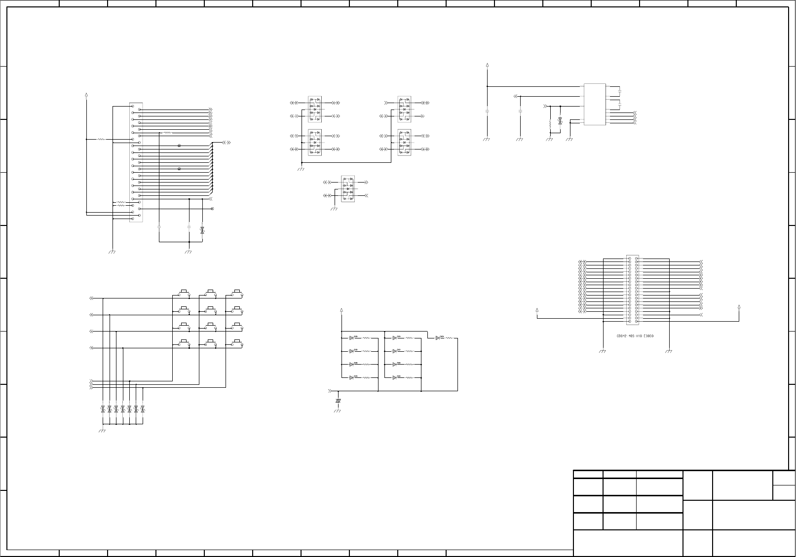
- 198 -
LGE Internal Use Only
Copyright © 2007 LG Electronics. Inc. All right reserved.
Only for training and service purposes
7. CIRCUIT DIAGRAM
13
XF2B-3545-31A-P
LCD Connector
NAME
DRAWING
FUNCTION KEYPAD LED
A
B
C
LG Electronics Inc.
LG Electronics Inc.
Sheet/
314
NO.
Designer
Sheets
7
Section
1
DRAWING
11
5
Checked
C
D
E
3 5
6
65
E
Sheet/
4
DRAWING
Date
4
LCD_Backlight driver
1
(lower contact)
Section
862
Approved
Date
D
9
Approved
Sign & Name
3 8
10
A
F
Designer
Checked
15 16
MODEL
1
1 7
MODEL
FUNCTION-SLIDER CON-HEADER
D
E
4
DRAWING
LG Electronics Inc.
53
NAME
C
A
4
9
Sheets
7
6
Sign & Name
2
2
LG Electronics Inc. NO.
LGE
2006
MAY JOY 1.3
LCD & FUNCTION KEY
LGE
MAY
1/1
82 12
9
100ohm
C105
820p
R109
0R115
VA102 RSB6.8CST2R
RSB6.8CST2RVA101
EVL14K02200
VA100
SW106 SW108
VA105
VA104
RSB6.8CST2R
100ohm
RSB6.8CST2R
35
4
5
6
7
8
9
R111
20
21
22
23
24
25
26
27
28
29
3
30
31
32
33
34
1
10
11
12
13
14
15
16
17
18
19
2
40
23
24
25
26
27
28
29
CN100
5
6
7
8
9
21
30
31
32
33
34
35
36
37
38
39
22
1
10
11
12
13
14
15
16
17
18
19
2
20
3
4
CN101
SW107
100ohmR110
AP_+VPWR
LD108
SSC-TWH104-HLSSSC-TWH104-HLS
LD107
VA103
VA107
RSB6.8CST2R
VA106
RSB6.8CST2R
LD104
SSC-TWH104-HLS
RSB6.8CST2R
SW104 SW105SW103
SW102
ZD101
RSB6.8CST2R
SW100
ZD100 RSB6.8CST2R
AP_+VPWR
SSC-TWH104-HLS
LD103
100ohm
100ohmR113
R112
1u
C102
C101
1u
1u
C100
100ohm
100K
R114
R102
R103 100K
R104 100K
LD102
SSC-TWH104-HLS
LD100
SSC-TWH104-HLS
SW111
PLR0504F
1
2
34
5
6
SW109
4
5
6
D104
PLR0504F
D103
1
2
3
PLR0504F
D101
1
2
34
5
6
PLR0504F
1
2
34
5
6
1
2
34
5
6
D102
D100
PLR0504F
100ohmR107 100ohm R108R106 100ohm
100K
AP_VDD_LCD_2.8V
R101
SW101
D3
D4 1
EN_SET
2
9GND
13 PGND
8VIN
VOUT
5
AP_+VPWR
AAT3151IWP_T1
3
C1+
C1- 4
C2+ 6
7
C2- 10
D1 11
D2 12
1u
U100
4.7u
C104
C103
AP_VDD_LCD_2.8V
SW110
SSC-TWH104-HLS
LD101
TP100
TP102
LD105
SSC-TWH104-HLS
TP101
SSC-TWH104-HLS
LD106
LCD_VS
LCD_DATA(14)
LCD_DATA(12)
LCD_DATA(3)
LCD_DATA(1)
LCD_DATA(0)
LCD_DATA(9)
LCD_DATA(2)
LCD_DATA(11)
LCD_DATA(4)
LCD_DATA(13)
LCD_DATA(7)
LCD_DATA(6)
LCD_DATA(15)
DIS_WEN
WLED_CTL
LCD_DATA(5)
LCD_DATA(3)
LCD_DATA(1)
KEY_ROW(0)
KEY_ROW(1)
KEY_COL(6)
LCD_NRESET
LCD_DATA(0)
LCD_VS
DIS_CSN
DIS_WEN
DIS_RS
LCD_DATA(8)
LCD_DATA(10)
DIS_CSN
LCD_DATA(5)
DIS_RS
LCD_NRESET
DIS_WEN
DIS_RS
DIS_CSN
LCD_VS
WLED_CTL
LCD_DATA(0)
LCD_DATA(2)
LCD_DATA(4)
LCD_DATA(6)
LCD_DATA(8)
LCD_DATA(10)
LCD_DATA(12)
LCD_DATA(14)
LCD_DATA(15)
LCD_DATA(13)
LCD_DATA(11)
LCD_DATA(9)
LCD_DATA(7)
KEY_COL(4)
KEY_COL(5)
KEY_ROW(3)
KEY_ROW(2)
KPD_DRV_N
LED_ANODE
LED4
LED3
LED2
LED1
KEY_COL(7)
KEY_COL(6)
KEY_COL(5)
KEY_COL(4)
KEY_ROW(3)
KEY_ROW(2)
KEY_ROW(1)
KEY_ROW(0)
KPD_DRV_N
LED_ANODE
LED3
LED2
LED1
LCD_DATA(1)
LCD_DATA(10)
LCD_DATA(11)
LCD_DATA(12)
LCD_DATA(13)
LCD_DATA(14)
LCD_DATA(15)
LCD_DATA(2)
LCD_DATA(3)
LCD_DATA(4)
LCD_DATA(5)
LCD_DATA(6)
LCD_DATA(7)
LCD_DATA(8)
LCD_DATA(9)
LCD_DATA(0:15)
LED4
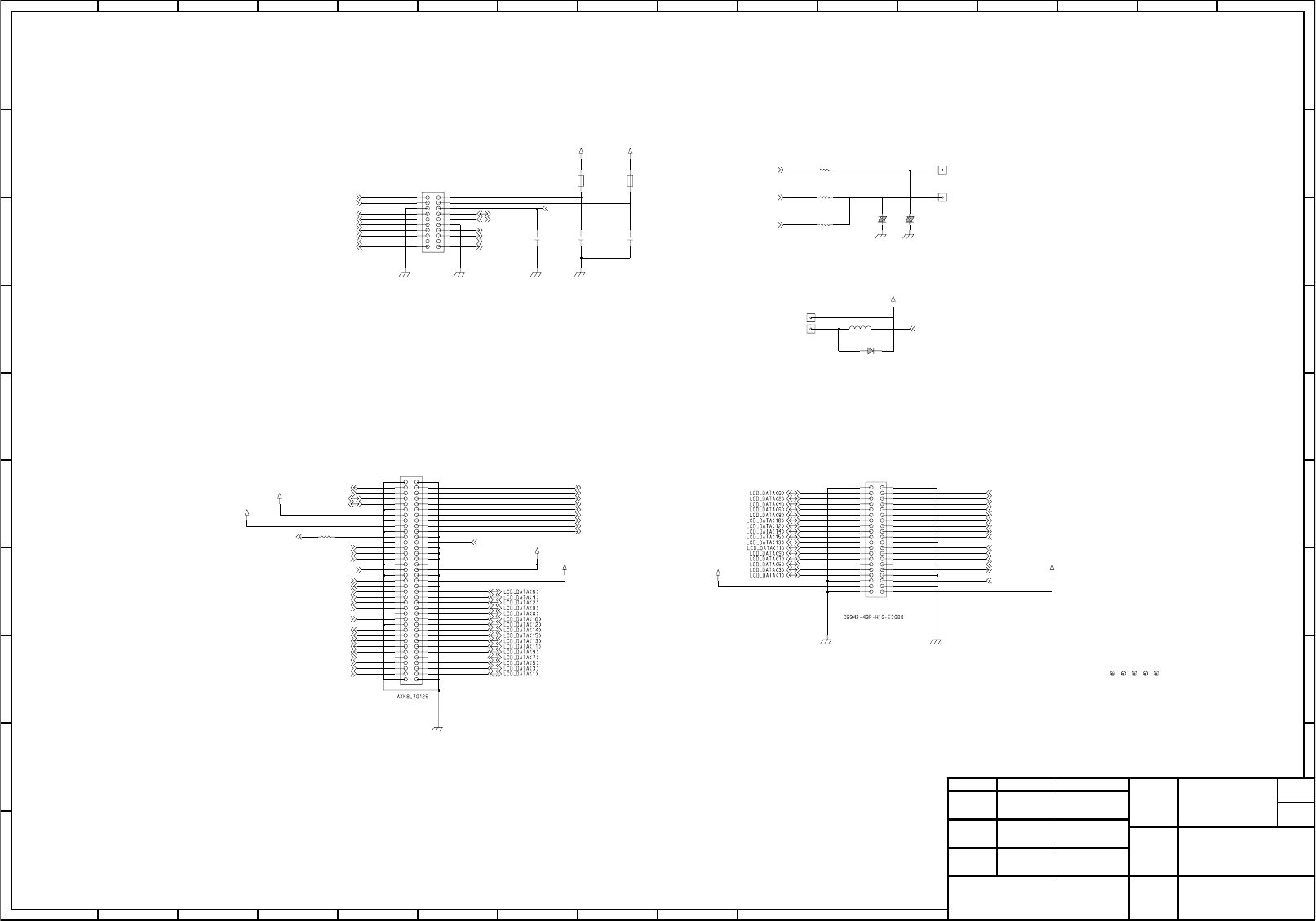
- 199 -
LGE Internal Use Only
Copyright © 2007 LG Electronics. Inc. All right reserved.
Only for training and service purposes
7. CIRCUIT DIAGRAM
5
2
D
7
FUNCTION-SLIDER CON-SOCKET
4
9
C
MODEL
C
9
DRAWING
6
NAME
MODEL
34
5
3 72
A
84
1
NO.
6 8
3
LG Electronics Inc.
MAIIN-SLIDER CON-SOCKET
VGA_CAMERA
Checked
Designer
NO.
613 14
Designer
Sheets
D
12
E
LG Electronics Inc.
E
Checked
SectionSection
10
LG Electronics Inc.
1
1
52
Approved
8
11
Sign & NameSign & Name
4
Approved NAME
5
Sheets
Sheet/
DRAWING
15
Sheet/
9
E
16
Date
DRAWING
B
A
C
D
AP_VDD_LCD_2.8V
2006 LGE
SLIDER FPCB
JOY 1.3
MAY LGE
1/1
AXK720145G
1
LG Electronics Inc.
623
F
Date
DRAWING
7
A
HB-1M1005-601JT
FB101
67
68
69
7
70
8
9
G1 G2
G3 G4
52
53
54
55
56
57
58
59
6
60
61
62
63
64
65
66
38
39
4
40
41
42
43
44
45
46
47
48
49
5
50
51
23
24
25
26
27
28
29
3
30
31
32
33
34
35 36
37
1
10
11
12
13
14
15
16
17
18
19
2
20
21
22
CN102
FB100
HB-1M1005-601JT
R103 NA
TP105
OUT100
TP106
EVLC18S02015
VA101
1u
C102
36
37
38
39
22
40
23
24
25
26
27
28
29
2
20
3
4
5
6
7
8
9
21
30
31
32
33
34
35
1
10
11
12
13
14
15
16
17
18
19
AP_+VPWR
CN101
TP108
0R101
AP_VDD_CAM_2.7V
AP_VDD_CAM_1.8V
OUT101
OUT102
L100
VA100
EVLC18S02015
56nH
AP_+VPWR
AP_VDD_LCD_2.8V
AP_VDD_CAM_2.7V
OUT103
RB521S-30
D100
AP_+VPWR
C101
0.1u
C100
0.1u
192
20
3
4
5
6
7
8
9
1
10 11
12
13
14
15
16
17
18
TP107
AP_VDD_CAM_1.8V
CN100
TP109
R100 0
R104
0
CCIRID(2)_CAM
CCIRID(0)_CAM
CCIRID(1)_CAM
RECEIVER+
RECEIVER-
I2CSCL0_CAM
I2CSDA0_CAM
VGA_RSTn
RECEIVER--
CCIRIVS_CAM
CCIRICLK_CAM
VGA_STANDBY
MOT_PWR-
CAMCLK_27MHZ_CAM
CCIRID(4)_CAM
CCIRID(6)_CAM
CCIRID(7)_CAM
CCIRID(5)_CAM
CCIRIHS_CAM
CCIRID(3)_CAM
KEY_ROW(3)
KEY_COL(4)
KEY_COL(5)
WLED_CTL
LCD_NRESET
DIS_WEN
DIS_RS
DIS_CSN
LCD_VS
KPD_DRV_N
RECEIVER-
RECEIVER--
KEY_COL(6)
KEY_COL(7)
KEY_ROW(0)
KEY_ROW(1)
KEY_ROW(2)
DIS_WEN
DIS_CSN
DIS_RS
LCD_VS
KEY_ROW(3)
KEY_ROW(2)
KEY_ROW(1)
KEY_ROW(0)
KEY_COL(5)
KEY_COL(4)
KPD_DRV_N
KEY_COL(6)
KEY_COL(7)
WLED_CTL
RECEIVER+
VGA_STANDBY
CAMCLK_27MHZ_CAM
I2CSCL0_CAMCCIRICLK_CAM
I2CSDA0_CAMCCIRID(0)_CAM
CCIRID(1)_CAM
VGA_RSTn
CCIRIHS_CAMCCIRID(2)_CAM
CCIRIVS_CAMCCIRID(3)_CAM
CCIRID(7)_CAMCCIRID(4)_CAM
CCIRID(6)_CAMCCIRID(5)_CAM
MOT_PWR-
LCD_NRESET

- 200 -
LGE Internal Use Only
Copyright © 2007 LG Electronics. Inc. All right reserved.
Only for training and service purposes
7. CIRCUIT DIAGRAM
10
Approved
1
A
LGIC(42)-A-5505-10:01
NO.
Sheet/
Sheets
5
Checked
2
B
MODEL
34
D
9
B
Sign & Name
Iss.
VOLUME DOWN
A
Date Name
DRAWING
LG Electronics Inc.
DRAWING
Section Date
8
VOLUME UP
C
NAME
Notice No.
5
VOLUME SIDE KEY
D
VOLUME_SIDEKEY_FPCB
Rev_C
1/1
JOY
Designer
23
B
LG Electronics Inc.
64
E
A
71
AUG
2006
C
1
2
3
4
TP2 TP1
CN?
KB101
KB100

- 201 -
LGE Internal Use Only
Copyright © 2007 LG Electronics. Inc. All right reserved.
Only for training and service purposes
7. CIRCUIT DIAGRAM
TP1 TP2
KB100
KB101
5
POWER KEY
D
B
MODEL
Checked
2
CAMERA KEY
Sheets
AUG
2006
A
5
71
E
A
NAME
Notice No.
B
C
NO.
Sheet/
C
Date
8
LG Electronics Inc.
DRAWING
Designer
23
LGIC(42)-A-5505-10:01 LG Electronics Inc.
64
1
2
3
4
JOY 1/1
LGE
POWER_Camera_BUTTON
Date Name
DRAWING
10
Approved
1
A
9
B
Sign & Name
Iss.
D
Section
34
CN100
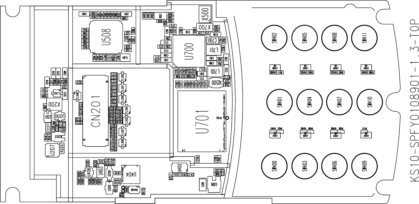
- 202 -
LGE Internal Use Only
Copyright © 2007 LG Electronics. Inc. All right reserved.
Only for training and service purposes
8. PCB LAYOUT
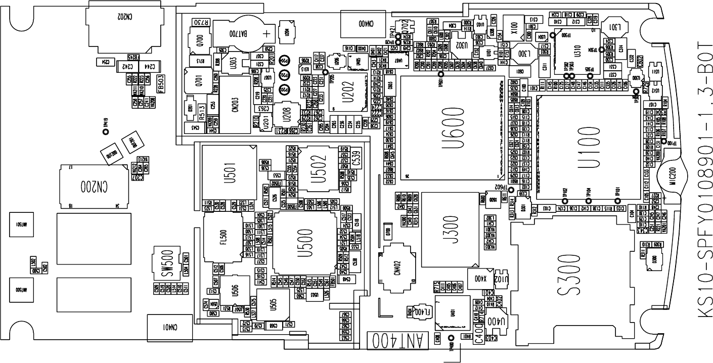
- 203 -
LGE Internal Use Only
Copyright © 2007 LG Electronics. Inc. All right reserved.
Only for training and service purposes
8. PCB LAYOUT
- 204 -
LGE Internal Use Only
Copyright © 2007 LG Electronics. Inc. All right reserved.
Only for training and service purposes
8. PCB LAYOUT
LGMC
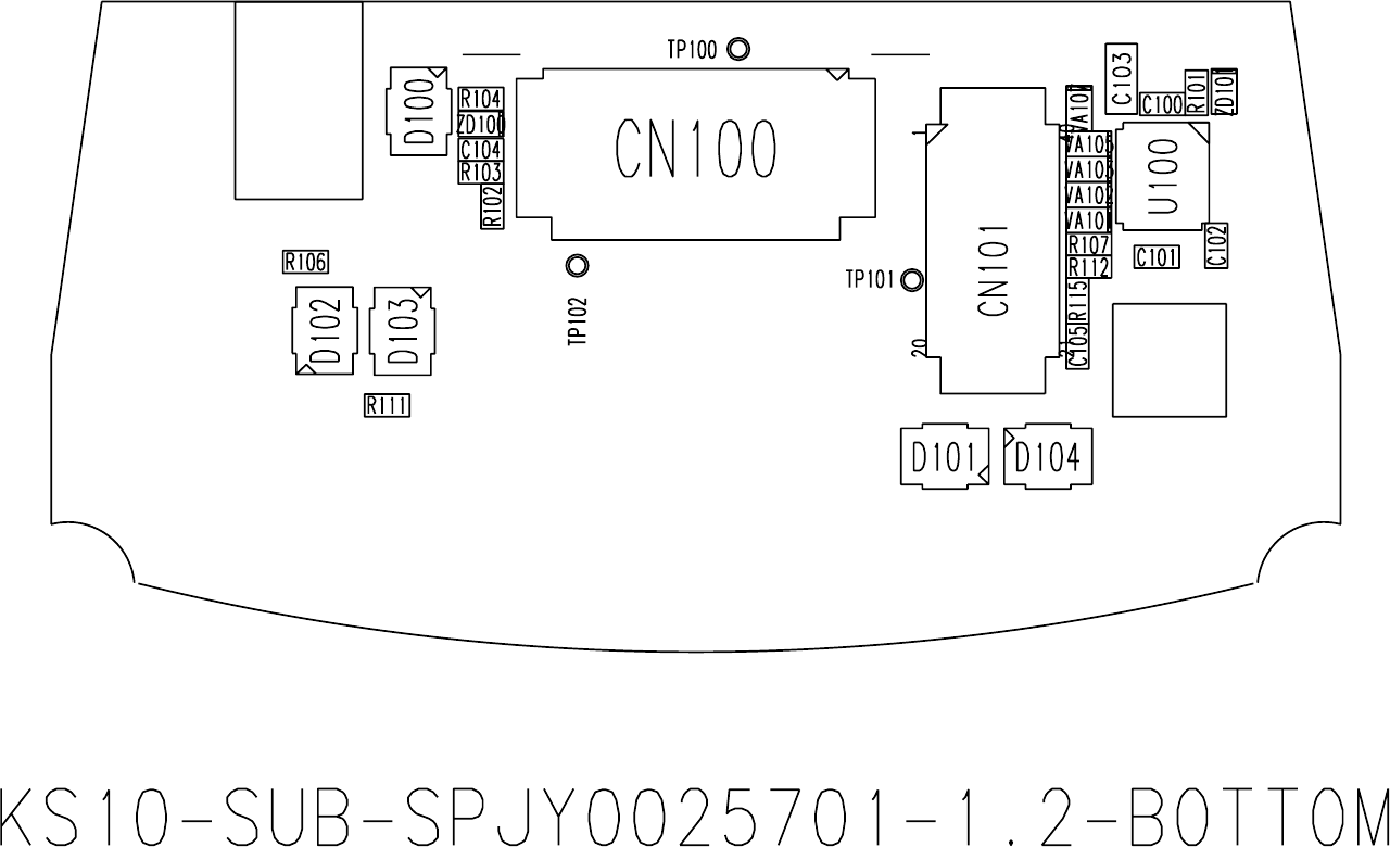
- 205 -
LGE Internal Use Only
Copyright © 2007 LG Electronics. Inc. All right reserved.
Only for training and service purposes
8. PCB LAYOUT
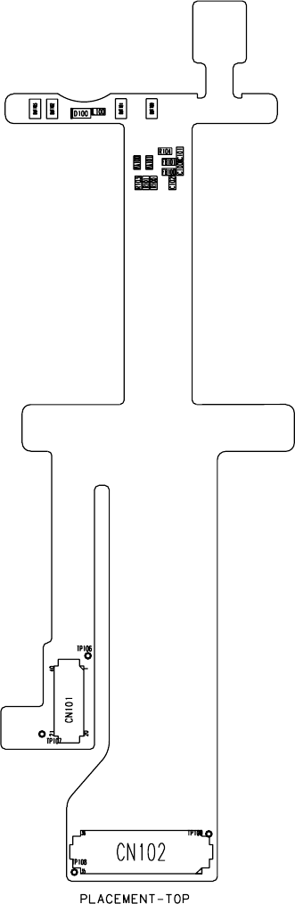
- 206 -
LGE Internal Use Only
Copyright © 2007 LG Electronics. Inc. All right reserved.
Only for training and service purposes
8. PCB LAYOUT
LGMC
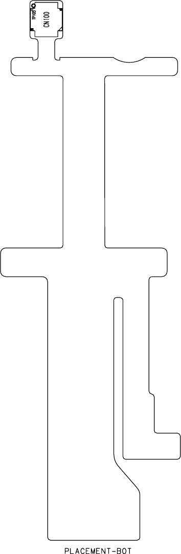
- 207 -
LGE Internal Use Only
Copyright © 2007 LG Electronics. Inc. All right reserved.
Only for training and service purposes
8. PCB LAYOUT
LGMC
- 208 -
LGE Internal Use Only
Copyright © 2007 LG Electronics. Inc. All right reserved.
Only for training and service purposes
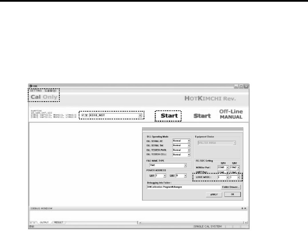
- 209 -
9. Usage of Hot-Kimchi
9.1 Usage of Hot-Kimchi
9.1.1 Calibration
•
Procedure
1. Click SETTING in menu, and logic operation in sub-menu.
Choose “1” in LOGIC MODE (means calibration alone)
2.Select the model name which you want in list box
3.Click Start button to calibrate a phone
9. Usage of Hot-Kimchi
LGE Internal Use Only
Copyright © 2007 LG Electronics. Inc. All right reserved.
Only for training and service purposes
Model Name
Calibration only
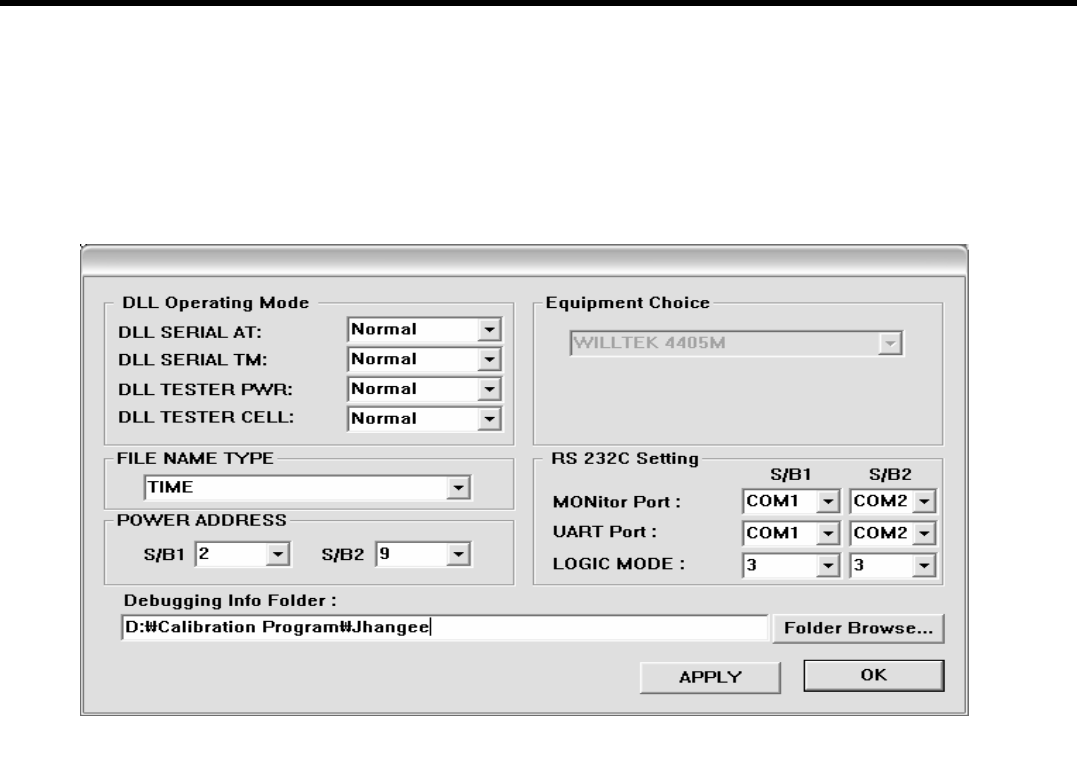
- 210 -
9. Usage of Hot-Kimchi
9.1.2 Basic Setting
•
Contents
✔ Click SETTING in menu, and logic operation in sub-menu.
✔ You can select how to control AT comm, Testset, and Power supply in DLL Operating
Mode.
✔ You can set UART Port and logic mode. (mode 1 : Calibration alone)
✔ You can set Result File’s name type. If you choose “TIME”, the saved files’ name is
saved in a run - time.
✔ You can run the multi mode (S/B1,S/B2 : You can use S/B1 for only one port.)
✔ You can set the path of HOTKIMCHI program.
LGE Internal Use Only
Copyright © 2007 LG Electronics. Inc. All right reserved.
Only for training and service purposes

- 211 -
9. Usage of Hot-Kimchi
9.1.3 Log of Calibration and Test
•
Contents
✔ On Running, Log window is created in center area. It displays logs of command, and
measurements of Calibration or Autotest.
✔ The result files are saved in the directory “~janghee\debug\Cal”, “~janghee\debug\Auto”,
or “~janghee\debug\CalAuto”.
LGE Internal Use Only
Copyright © 2007 LG Electronics. Inc. All right reserved.
Only for training and service purposes

- 212 -
10. Engineering Mode
A. About Engineering Mode
Engineering mode is designed to allow a service man/engineer to view and test the basic
functions provided by a handset.
B. Access Codes
The key sequence for switching the engineering mode on is *#001*2580#. Pressing END will
switch back to non-engineering mode operation.
10. Engineering Mode
LGE Internal Use Only
Copyright © 2007 LG Electronics. Inc. All right reserved.
Only for training and service purposes
5. Save
Log
4. MTC
2. Device
Test
3. F
Engineering Mode
actory
Reset
1. Version
Info
AP/MP/HW
Factory
Options of in Main view :
- Set AP Debugmode On
- Set MP Debugmode On
Auto All Test
LCD
LED
Vibrator
Sound
Camera
Keypad
MP Msg Viewer
RTC Test

- 213 -
10. Engineering Mode
10.1 Version Info
10.1.1 AP/MP/HW Version
10.1.2 Factory Version
10.2 Device Test
10.2.1 Auto All Test
LCD On/Off -> Keypad LED On/Off -> Color Auto Test -> Ringtone Test -> Vibrator Test ->
Keypad Test
10.2.2 LCD
1) Auto Color Test
Red -> Green -> Blue -> Balck -> White To exit test, press the right arrow key.
2) Color Table Test : display the RGB table
10.2.3 LED
1) Backlight Test
This controls brightness of Backlight. When entering into the menu, the present
backlight-value in the phone is displayed. Use Left/Right key to adjust the level of
brightness.
2) Keypad Light Test
This controls brightness of keypad light. When entering into the menu, the present
keypad light-value in the phone is displayed. Use Left/Right key to adjust the level of
brightness of keypad.
3) Blinking Test
Keypad & LCD Backlight blinking test.
10.2.4 Vibrator
This menu is to test the vibration mode.
10.2.5 Sound
1) Ringtone Test
This menu is test ring tone.
2) Audio Calibration
This menu is to test db value of each volume level
3) Vocoder Calibration
This menu is to test db value of each frequency of codec.
LGE Internal Use Only
Copyright © 2007 LG Electronics. Inc. All right reserved.
Only for training and service purposes

- 214 -
10. Engineering Mode
4) Echo Cancelation
This menu is to test echo cancellation parameter of codec.
5) Sound Calibration
This menu is to test volume gain of codec.
6) Loopback Test
This menu is to test the vibration mode.
7) AES/ACS Tunning
This menu is to test acoustic echo cancellation/suppression.
10.2.6 Camera
Camera application will be launched.
10.2.7 Keypad
This menu is to test all keys.
10.2.8 MP Msg Viewer
This menu is to display messages from MP
10.2.9 RTC Test
This menu is to display current time.
10.3 Factory Reset
This menu is to restore factory setting value.
10.4 MTC
Not to use.
10.5 Save Log
To save the latest log messages.
In Main view
Options
Set AP Debugmode On : UART switch is changed to AP / MP side
Set MP Debugmode On : not to use.
LGE Internal Use Only
Copyright © 2007 LG Electronics. Inc. All right reserved.
Only for training and service purposes
- 215 -
LGE Internal Use Only
Copyright © 2007 LG Electronics. Inc. All right reserved.
Only for training and service purposes
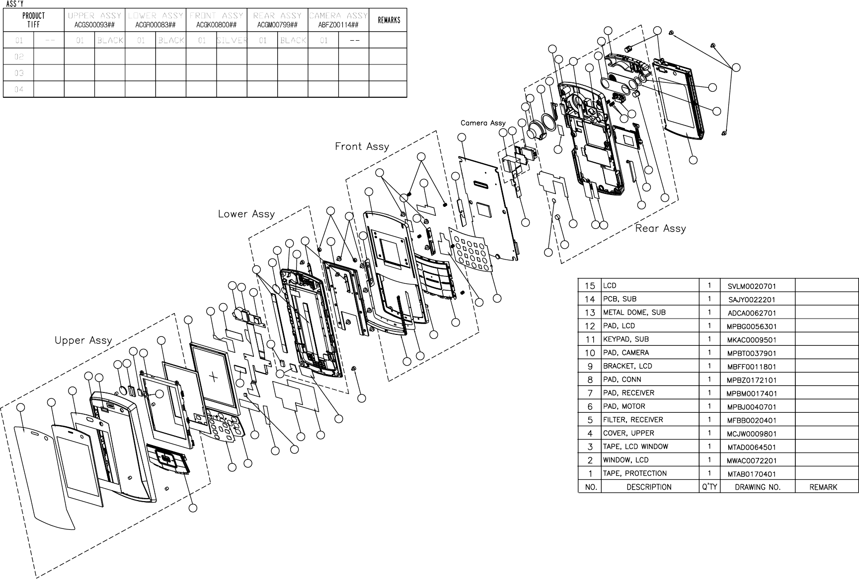
- 216 -
LGE Internal Use Only
Copyright © 2007 LG Electronics. Inc. All right reserved.
Only for training and service purposes
11. EXPLODED VIEW & REPLACEMENT PART LIST
11.1 EXPLODED VIEW
12
3
45
67
89
12
10
15
16 17
22 23 24
30
31
32
33 35
34
36
37 83
38
39
84
43
46
47
44
50
51 53 54
55
58
59
60
61
65
66 67 68
69
70
71 78
79
85
80
81
76
75
74
77
64
6357
56
55
52
49
48
45
42
41
40
73
72
62
25
26
82
29
28
27
21
20
19
14
13
11
18
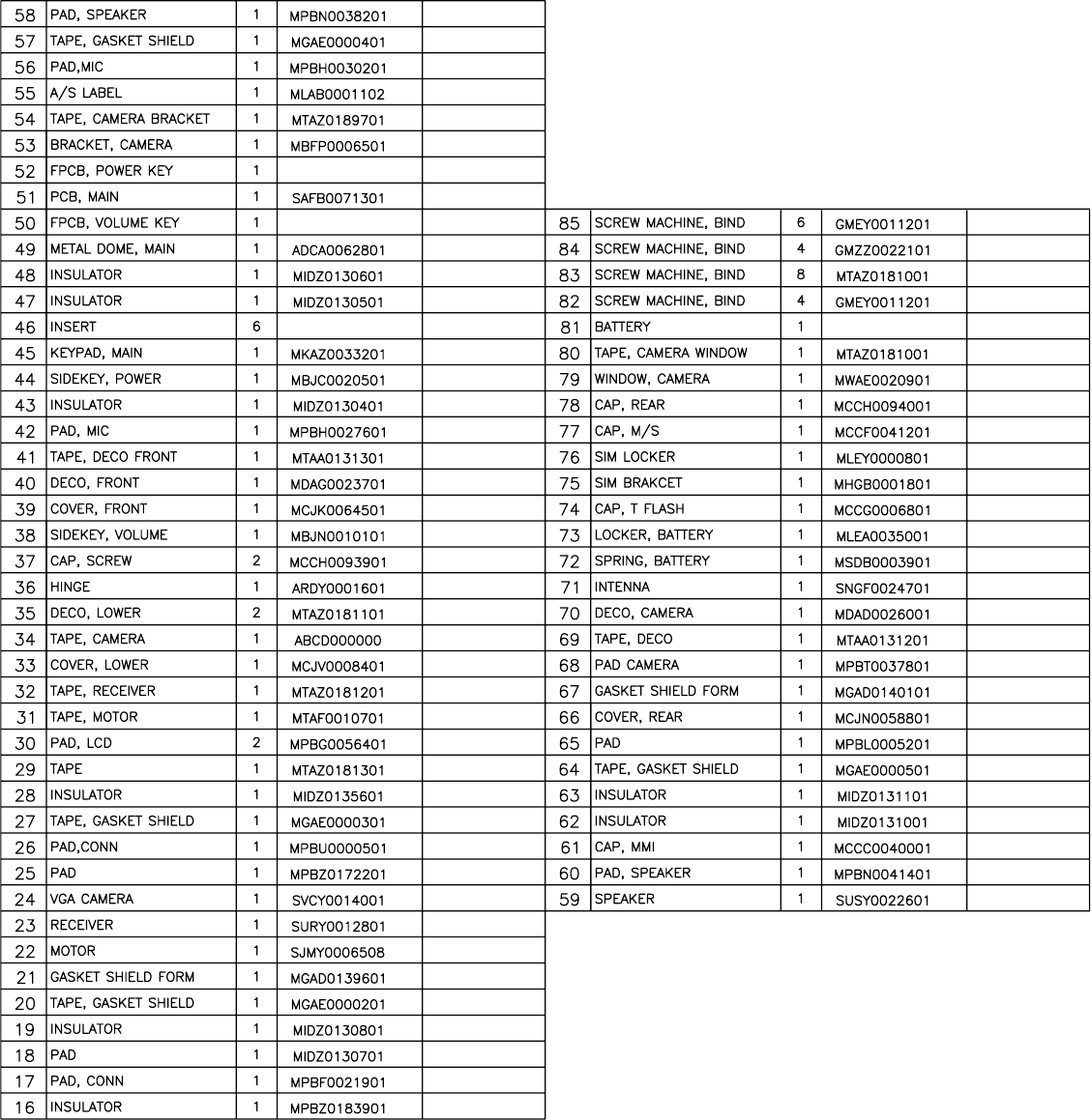
- 217 -
LGE Internal Use Only
Copyright © 2007 LG Electronics. Inc. All right reserved.
Only for training and service purposes
- 218 -
LGE Internal Use Only
Copyright © 2007 LG Electronics. Inc. All right reserved.
Only for training and service purposes
LGE Internal Use Only
Copyright © 2007 LG Electronics. Inc. All right reserved.
Only for training and service purposes
11. EXPLODED VIEW & REPLACEMENT PART LIST
- 219 -
11.2 Replacement Parts
<Mechanic component>
Note: This Chapter is used for reference, Part order
is ordered by SBOM standard on GCSC
Level Location
No Part Name Part Number Spec Color Remark
1 IMT,FOLDER TIFF0011101
2 AAAY00 ADDITION AAAY0123901 Metal Black
3 MCCZ00 CAP MCCZ0021601 BOX, TW, , , , , Without Color
3 MCJZ00 COVER MCJZ0046701 BOX, TW, , , , , Without Color 62
3 MLAC00 LABEL,BARCODE MLAC0004501 Export(105*40) Without Color
3 MLAJ00 LABEL,MASTER BOX MLAJ0004401 LABEL,MASTER BOX(for C1300i NEW_CGR) Without Color
3 MPBZ00 PAD MPBZ0155609 BOX, TW, , , , , Without Color
3 MPCY00 PALLET MPCY0012403 COMPLEX, (empty), , , , , DARK BLUE
2 APEY00 PHONE APEY0241401 Metal Black
3 ACGM00 COVER ASSY,REAR ACGM0079901 Black
4 MCCC00 CAP,EARPHONE JACK MCCC0040001 COMPLEX, (empty), , , , , Black 61
4 MCCF00 CAP,MOBILE SWITCH MCCF0041201 MOLD, Urethane Rubber S190A, , , , , Black 77
4 MCCG00 CAP,MULTIMEDIA CARD MCCG0006801 COMPLEX, (empty), , , , , Black 74
4 MCJN00 COVER,REAR MCJN0058801 MOLD, PC LUPOY SC-1004ML, , , , , Black 66
4 MDAD00 DECO,CAMERA MDAD0026001 ELECTROFORMING, Ni, , , , , Black 70
4 MGAD00 GASKET,SHIELD FORM MGAD0140101 COMPLEX, (empty), , , , , Without Color 67
4 MGAE00 GASKET,DUST MGAE0000401 COMPLEX, (empty), , , , , Without Color 57
4 MGAE01 GASKET,DUST MGAE0000501 COMPLEX, (empty), , , , , Without Color 64
4 MHGB00 HOLDER,CARD MHGB0001801 PRESS, STS, 0.2T, , , , Without Color 75
4 MIDZ00 INSULATOR MIDZ0131001 COMPLEX, (empty), , , , , Without Color
4 MIDZ01 INSULATOR MIDZ0131101 COMPLEX, (empty), , , , , Without Color 63
4 MLAB00 LABEL,A/S MLAB0001102 C2000 USASV DIA 4.0 White 55
4 MLAN00 LABEL,QUALCOMM MLAN0000603 White,95C Transparent
4 MLEA00 LOCKER,BATTERY MLEA0035001 MOLD, PC LUPOY SC-1004ML, , , , , Black 73
4 MLEY00 LOCKER MLEY0000801 SIM LOCKER Silver 76
4 MPBH00 PAD,MIKE MPBH0030201 COMPLEX, (empty), , , , , Without Color 56
4 MPBL00 PAD,MSM MPBL0005201 COMPLEX, (empty), , , , , Without Color 65
4 MPBN00 PAD,SPEAKER MPBN0038201 COMPLEX, (empty), , , , , Without Color 58
4 MPBN01 PAD,SPEAKER MPBN0041401 COMPLEX, (empty), , , , , Without Color 60
4 MPBT00 PAD,CAMERA MPBT0037801 COMPLEX, (empty), , , , , Without Color 68
4 MSDB00 SPRING,COIL MSDB0003901 CUTTING, BeCu, , , , , Silver 72
4 MTAA00 TAPE,DECO MTAA0131201 COMPLEX, (empty), , , , , Without Color 69
4 MTAB00 TAPE,PROTECTION MTAB0170801 COMPLEX, (empty), , , , , Without Color

LGE Internal Use Only
Copyright © 2007 LG Electronics. Inc. All right reserved.
Only for training and service purposes
11. EXPLODED VIEW & REPLACEMENT PART LIST
- 220 -
Level Location
No Part Name Part Number Spec Color Remark
4 MTAZ00 TAPE MTAZ0181001 COMPLEX, (empty), , , , , Without Color 80,83
4 MWAE00 WINDOW,CAMERA MWAE0020901 CUTTING, NS, , , , , Black 79
5 MBJC00 BUTTON,FUNCTION MBJC0020501 COMPLEX, (empty), , 51.9, 104, 12.2, Black 44
5 MBJN00 BUTTON,VOLUME MBJN0010101 COMPLEX, (empty), , 51.9, 104, 12.2, Black 38
5 MCJK00 COVER,FRONT MCJK0064501 MOLD, PC LUPOY SC-1004ML, , 51.9, 104, 12.2, Black 39
6 MICE00 INSERT,NUT MICE0000801 EXTRUSION, LDPE, , , , , Gold
5 MDAG00 DECO,FRONT MDAG0023701 MOLD, POM TX-31, , 51.9, 104, 12.2, Black 40
5 MIDZ00 INSULATOR MIDZ0130401 COMPLEX, (empty), , , , , Without Color 43
5 MIDZ01 INSULATOR MIDZ0130501 COMPLEX, (empty), , , , , Without Color 47
5 MIDZ02 INSULATOR MIDZ0130601 COMPLEX, (empty), , , , , Without Color 48
5 MPBH00 PAD,MIKE MPBH0027601 COMPLEX, (empty), , , , , Without Color 42
5 MTAA00 TAPE,DECO MTAA0131301 COMPLEX, (empty), , , , , Without Color 41
5 MTAB00 TAPE,PROTECTION MTAB0148801 COMPLEX, (empty), , , , , Without Color
5 MTAB01 TAPE,PROTECTION MTAB0170201 COMPLEX, (empty), , , , , Without Color
4 ACGR00 COVER
ASSY,SLIDE(LOWER) ACGR0008301 Black
5 MCJV00 COVER,SLIDE(LOWER) MCJV0008401 MOLD, PC LUPOY SC-1004ML, , 51.9, 104, 7.6, Black 33
5 MDAY00 DECO MDAY0032901 MOLD, POM TX-31, , 51.9, 104, 12.2, Black
5 MMAA00 MAGNET,SWITCH MMAA0000901 G7000 12x2x0.7t Metal Silver
5 MPBG00 PAD,LCD MPBG0056401 COMPLEX, (empty), , , , , Without Color 30
5 MPBU00 PAD,CONNECTOR MPBU0000501 COMPLEX, (empty), , , , , Without Color 26
5 MTAF00 TAPE,MOTOR MTAF0010701 COMPLEX, (empty), , , , , Without Color 31
5 MTAZ00 TAPE MTAZ0181101 COMPLEX, (empty), , , , , Without Color 35
5 MTAZ01 TAPE MTAZ0181201 COMPLEX, (empty), , , , , Without Color 32
5 MTAZ02 TAPE MTAZ0181301 COMPLEX, (empty), , , , , Without Color 29
4 ACGS00 COVER
ASSY,SLIDE(UPPER) ACGS0009301 Black
5 MBFF00 BRACKET,LCD MBFF0011801 CASTING, Al Alloy, , , , , Black 9
5 MCJW00 COVER,SLIDE(UPPER) MCJW0009801 CASTING, Al Alloy, , 51.9, 104, 7.6, Black 4
6 MICC00 INSERT,FRONT(UPPER) MICC0010001 D2.2 L2.0 KURL 45 Gold
5 MFBB00 FILTER,RECEIVER MFBB0020401 COMPLEX, (empty), , , , , Without Color 5
5 MKAC00 KEYPAD,FUNCTION MKAC0009501 MOLD, ABS MP-220, , 51.9, 104, 7.6, Black 11
5 MPBG00 PAD,LCD MPBG0056301 COMPLEX, (empty), , , , , Without Color 12
5 MPBJ00 PAD,MOTOR MPBJ0040701 COMPLEX, (empty), , , , , Without Color 6
5 MPBM00 PAD,RECEIVER MPBM0017401 COMPLEX, (empty), , , , , Without Color 7
5 MPBT00 PAD,CAMERA MPBT0037901 COMPLEX, (empty), , , , , Without Color 10
5 MPBZ00 PAD MPBZ0172101 COMPLEX, (empty), , , , , Without Color 8
5 MTAB00 TAPE,PROTECTION MTAB0153501 COMPLEX, (empty), , , , , Without Color
LGE Internal Use Only
Copyright © 2007 LG Electronics. Inc. All right reserved.
Only for training and service purposes
11. EXPLODED VIEW & REPLACEMENT PART LIST
- 221 -
Level Location
No Part Name Part Number Spec Color Remark
5 MTAD00 TAPE,WINDOW MTAD0064501 COMPLEX, (empty), , , , , Without Color 3
5 MWAC00 WINDOW,LCD MWAC0072201 CUTTING, PMMA MR 200, , 51.9, 104, 12.2, Black 2
4 ARDY00 RAIL ASSY,SLIDE ARDY0001601 Black 36
4 GMEY00 SCREW MACHINE,BIND GMEY0011201 1.4 mm,3 mm,MSWR3(BK) ,N ,+ ,NYLOK Without Color 82,85
4 GMZZ00 SCREW MACHINE GMZZ0022101 1.4 mm,1.7 mm,MSWR3(BK) ,A ,+ ,- , Without Color 84
4 GMZZ01 SCREW MACHINE GMZZ0020501 3.5 mm,1.5 mm,SWCH18A ,A ,+ ,- , Black
4 MCCH00 CAP,SCREW MCCH0093901 MOLD, Urethane Rubber S190A, , , , , Black 37
4 MGAD00 GASKET,SHIELD FORM MGAD0139601 COMPLEX, (empty), , , , , Without Color 21
4 MGAE00 GASKET,DUST MGAE0000101 COMPLEX, (empty), , , , , Without Color
4 MGAE01 GASKET,DUST MGAE0000201 COMPLEX, (empty), , , , , Without Color 20
4 MGAE02 GASKET,DUST MGAE0000301 COMPLEX, (empty), , , , , Without Color 27
4 MIDZ00 INSULATOR MIDZ0130701 COMPLEX, (empty), , , , , Without Color 18
4 MIDZ01 INSULATOR MIDZ0130801 COMPLEX, (empty), , , , , Without Color 19
4 MIDZ02 INSULATOR MIDZ0135601 COMPLEX, (empty), , , , , Without Color 28
4 MIDZ03 INSULATOR MIDZ0143101 COMPLEX, (empty), , , , , Without Color
4 MKAZ00 KEYPAD MKAZ0033201 MOLD, ABS MP-220, , , , , Black 45
4 MLAZ00 LABEL MLAZ0038303 PRINTING, (empty), , , , , White
4 MPBF00 PAD,FLEXIBLE PCB MPBF0021901 COMPLEX, (empty), , , , , Without Color 17
4 MPBZ00 PAD MPBZ0172201 COMPLEX, (empty), , , , , Without Color 25
4 MPBZ01 PAD MPBZ0183901 COMPLEX, (empty), , , , , Without Color 16
4 MTAB00 TAPE,PROTECTION MTAB0170401 COMPLEX, (empty), , , , , Without Color 1
4 MTAB01 TAPE,PROTECTION MTAB0176601 COMPLEX, (empty), , , , , Without Color
7 MBFP00 BRACKET,CAMERA MBFP0006501 MOLD, PC LUPOY SC-1004ML, , , , , Black 53
7 MTAK00 TAPE,CAMERA MTAK0000701 COMPLEX, (empty), , , , , Without Color
7 MTAZ00 TAPE MTAZ0189701 COMPLEX, (empty), , , , , Without Color 54
5 MLAZ00 LABEL MLAZ0038301 PID Label 4 Array Without Color
LGE Internal Use Only
Copyright © 2007 LG Electronics. Inc. All right reserved.
Only for training and service purposes
11. EXPLODED VIEW & REPLACEMENT PART LIST
- 222 -
Level Location
No Part Name Part Number Spec Color Remark
4 SNGF00 ANTENNA,GSM,FIXED SNGF0024701 3.0 ,-2 dBd, ,EGSM+DCS+PCS+W-BAND I, INTERNAL ,;
,QUAD ,-2.0 ,50 ,3.0 71
4 SUSY00 SPEAKER SUSY0022601 PIN ,8 ohm,90 dB,17 mm,Spring Contact Type 59
3 ACGQ00 COVER ASSY,SLIDE ACGQ0013301 Black
4 ACGK00 COVER ASSY,FRONT ACGK0080001 Black
4 SACY00 PCB ASSY,FLEXIBLE SACY0053101 LCD FPCB
5 SACB00 PCB
ASSY,FLEXIBLE,INSERT SACB0035701
5 SACE00 PCB ASSY,FLEXIBLE,SMT SACE0048001
6 SACC00 PCB ASSY,FLEXIBLE,SMT
BOTTOM SACC0028501
7 CN100 CONNECTOR,BOARD TO
BOARD ENBY0019501 20 PIN,.4 mm,ETC , ,H=1.5, Socket
6 SACD00 PCB ASSY,FLEXIBLE,SMT
TOP SACD0039101
7 C100 CAP,CERAMIC,CHIP ECCH0000182 0.1 uF,10V ,K ,X5R ,HD ,1005 ,R/TP
7 C101 CAP,CERAMIC,CHIP ECCH0000182 0.1 uF,10V ,K ,X5R ,HD ,1005 ,R/TP
7 C102 CAP,CERAMIC,CHIP ECCH0004904 1 uF,6.3V ,K ,X5R ,TC ,1005 ,R/TP
7 CN101 CONNECTOR,BOARD TO
BOARD ENBY0035901 40 PIN,0.4 mm,ETC , ,H=1.0, Plug
7 CN102 CONNECTOR,BOARD TO
BOARD ENBY0022901 70 PIN,0.4 mm,ETC , ,H=0.9, Plug
7 D100 DIODE,SWITCHING EDSY0011901 EMD2 ,30 V,1 A,R/TP ,VF=1.5V(IF=200mA) ,
IR=30uA(VR=10V)
7 FB100 FILTER,BEAD,CHIP SFBH0000903 600 ohm,1005 ,
7 FB101 FILTER,BEAD,CHIP SFBH0000903 600 ohm,1005 ,
7 L100 INDUCTOR,CHIP ELCH0005007 56 nH,J ,1005 ,R/TP ,
7 R100 RES,CHIP,MAKER ERHZ0000401 0 ohm,1/16W ,J ,1005 ,R/TP
7 R101 RES,CHIP,MAKER ERHZ0000401 0 ohm,1/16W ,J ,1005 ,R/TP
7 R104 RES,CHIP,MAKER ERHZ0000401 0 ohm,1/16W ,J ,1005 ,R/TP
7 VA100 VARISTOR SEVY0003801 18 V, ,SMD ,
7 VA101 VARISTOR SEVY0003801 18 V, ,SMD ,
6 SPCY00 PCB,FLEXIBLE SPCY0072601 POLYI ,.4 mm,MULTI-4 , SLIDE-FPCB
4 SAJY00 PCB ASSY,SUB SAJY0022201 14
5 SAJB00 PCB ASSY,SUB,INSERT SAJB0010801
6 ADCA00 DOME ASSY,METAL ADCA0062701 Without Color 13
5 SAJE00 PCB ASSY,SUB,SMT SAJE0016601
11.2 Replacement Parts
<Main component>
Note: This Chapter is used for reference, Part order
is ordered by SBOM standard on GCSC

LGE Internal Use Only
Copyright © 2007 LG Electronics. Inc. All right reserved.
Only for training and service purposes
11. EXPLODED VIEW & REPLACEMENT PART LIST
- 223 -
Level Location
No Part Name Part Number Spec Color Remark
6 SAJC00 PCB ASSY,SUB,SMT
BOTTOM SAJC0014901
7 C100 CAP,CERAMIC,CHIP ECCH0004904 1 uF,6.3V ,K ,X5R ,TC ,1005 ,R/TP
7 C101 CAP,CERAMIC,CHIP ECCH0004904 1 uF,6.3V ,K ,X5R ,TC ,1005 ,R/TP
7 C102 CAP,CERAMIC,CHIP ECCH0004904 1 uF,6.3V ,K ,X5R ,TC ,1005 ,R/TP
7 C103 CAP,CERAMIC,CHIP ECCH0006201 4.7 uF,6.3V ,K ,X5R ,TC ,1608 ,R/TP
7 C104 CAP,CERAMIC,CHIP ECCH0004904 1 uF,6.3V ,K ,X5R ,TC ,1005 ,R/TP
7 CN100 CONNECTOR,FFC/FPC ENQY0010901 35 PIN,0.3 mm,ETC , ,H=1.2
7 CN101 CONNECTOR,BOARD TO
BOARD ENBY0036001 40 PIN,0.4 mm,ETC , ,H=1.0, Socket
7 D100 DIODE,TVS EDTY0008607 SC70-6L ,6 V,200 W,R/TP ,PB-FREE
7 D101 DIODE,TVS EDTY0008607 SC70-6L ,6 V,200 W,R/TP ,PB-FREE
7 D102 DIODE,TVS EDTY0008607 SC70-6L ,6 V,200 W,R/TP ,PB-FREE
7 D103 DIODE,TVS EDTY0008607 SC70-6L ,6 V,200 W,R/TP ,PB-FREE
7 D104 DIODE,TVS EDTY0008607 SC70-6L ,6 V,200 W,R/TP ,PB-FREE
7 R101 RES,CHIP,MAKER ERHZ0000406 100 Kohm,1/16W ,J ,1005 ,R/TP
7 R102 RES,CHIP,MAKER ERHZ0000406 100 Kohm,1/16W ,J ,1005 ,R/TP
7 R103 RES,CHIP,MAKER ERHZ0000406 100 Kohm,1/16W ,J ,1005 ,R/TP
7 R104 RES,CHIP,MAKER ERHZ0000406 100 Kohm,1/16W ,J ,1005 ,R/TP
7 R106 RES,CHIP ERHY0003301 100 ohm,1/16W ,J ,1005 ,R/TP
7 R107 RES,CHIP ERHY0003301 100 ohm,1/16W ,J ,1005 ,R/TP
7 R111 RES,CHIP ERHY0003301 100 ohm,1/16W ,J ,1005 ,R/TP
7 R112 RES,CHIP ERHY0003301 100 ohm,1/16W ,J ,1005 ,R/TP
7 R115 RES,CHIP,MAKER ERHZ0000401 0 ohm,1/16W ,J ,1005 ,R/TP
7 U100 IC EUSY0337001 TDFN33 ,12 PIN,R/TP ,3x3x1.0
7 VA101 DIODE,TVS EDTY0009401 VMN2 ,5 V,10 W,R/TP ,1.0*0.6*0.4 ,; , ,7.82V , , ,100mW
,[empty] ,[empty] ,2P ,1
7 VA102 DIODE,TVS EDTY0009401 VMN2 ,5 V,10 W,R/TP ,1.0*0.6*0.4 ,; , ,7.82V , , ,100mW
,[empty] ,[empty] ,2P ,1
7 VA103 DIODE,TVS EDTY0009401 VMN2 ,5 V,10 W,R/TP ,1.0*0.6*0.4 ,; , ,7.82V , , ,100mW
,[empty] ,[empty] ,2P ,1
7 VA105 DIODE,TVS EDTY0009401 VMN2 ,5 V,10 W,R/TP ,1.0*0.6*0.4 ,; , ,7.82V , , ,100mW
,[empty] ,[empty] ,2P ,1
7 VA107 DIODE,TVS EDTY0009401 VMN2 ,5 V,10 W,R/TP ,1.0*0.6*0.4 ,; , ,7.82V , , ,100mW
,[empty] ,[empty] ,2P ,1
7 ZD100 DIODE,TVS EDTY0009401 VMN2 ,5 V,10 W,R/TP ,1.0*0.6*0.4 ,; , ,7.82V , , ,100mW
,[empty] ,[empty] ,2P ,1
7 ZD101 DIODE,TVS EDTY0009401 VMN2 ,5 V,10 W,R/TP ,1.0*0.6*0.4 ,; , ,7.82V , , ,100mW
,[empty] ,[empty] ,2P ,1
6 SAJD00 PCB ASSY,SUB,SMT TOP SAJD0017001
7 LD100 DIODE,LED,CHIP EDLH0012501 Snow White ,1608 ,R/TP ,color concept

LGE Internal Use Only
Copyright © 2007 LG Electronics. Inc. All right reserved.
Only for training and service purposes
11. EXPLODED VIEW & REPLACEMENT PART LIST
- 224 -
Level Location
No Part Name Part Number Spec Color Remark
7 LD101 DIODE,LED,CHIP EDLH0012501 Snow White ,1608 ,R/TP ,color concept
7 LD102 DIODE,LED,CHIP EDLH0012501 Snow White ,1608 ,R/TP ,color concept
7 LD103 DIODE,LED,CHIP EDLH0012501 Snow White ,1608 ,R/TP ,color concept
7 LD104 DIODE,LED,CHIP EDLH0012501 Snow White ,1608 ,R/TP ,color concept
7 LD105 DIODE,LED,CHIP EDLH0012501 Snow White ,1608 ,R/TP ,color concept
7 LD106 DIODE,LED,CHIP EDLH0012501 Snow White ,1608 ,R/TP ,color concept
7 LD107 DIODE,LED,CHIP EDLH0012501 Snow White ,1608 ,R/TP ,color concept
7 LD108 DIODE,LED,CHIP EDLH0012501 Snow White ,1608 ,R/TP ,color concept
7 R108 RES,CHIP ERHY0003301 100 ohm,1/16W ,J ,1005 ,R/TP
7 R109 RES,CHIP ERHY0003301 100 ohm,1/16W ,J ,1005 ,R/TP
7 R110 RES,CHIP ERHY0003301 100 ohm,1/16W ,J ,1005 ,R/TP
7 R113 RES,CHIP ERHY0003301 100 ohm,1/16W ,J ,1005 ,R/TP
7 R114 RES,CHIP ERHY0003301 100 ohm,1/16W ,J ,1005 ,R/TP
7 VA100 VARISTOR SEVY0000702 14 V,10% ,SMD ,
7 VA104 DIODE,TVS EDTY0009401 VMN2 ,5 V,10 W,R/TP ,1.0*0.6*0.4 ,; , ,7.82V , , ,100mW
,[empty] ,[empty] ,2P ,1
7 VA106 DIODE,TVS EDTY0009401 VMN2 ,5 V,10 W,R/TP ,1.0*0.6*0.4 ,; , ,7.82V , , ,100mW
,[empty] ,[empty] ,2P ,1
6 SPJY00 PCB,SUB SPJY0025701 FR-4 ,0.8 mm,SBL 6 ,KS10
4 SJMY00 VIBRATOR,MOTOR SJMY0006508 3 V,.08 A,10*3.45 ,17mm , ,3V , , ,12500 , , , ,38 22
4 SURY00 RECEIVER SURY0012801 23
4 SVCY00 CAMERA SVCY0014001 CMOS ,VGA ,5.5x11.4x3.2t, Magna 1/7.4" 24
4 SVLM00 LCD MODULE SVLM0020701 MAIN ,2.4" 240*320 ,42.88*60.65 ,262k ,TFT ,TM
,BD663474 , 15
3 GMEY00 SCREW MACHINE,BIND GMEY0011201 1.4 mm,3 mm,MSWR3(BK) ,N ,+ ,NYLOK Without Color
3 MCCH00 CAP,SCREW MCCH0094001 COMPLEX, (empty), , , , , Black 78
3 MCCH01 CAP,SCREW MCCH0097701 MOLD, Urethane Rubber S190A, , , , , Black
3 MLAK00 LABEL,MODEL MLAK0006901
3 SAFY00 PCB ASSY,MAIN SAFY0184101
4 SAFB00 PCB ASSY,MAIN,INSERT SAFB0071301 51
5 ACMY00 CAMERA ASSY ACMY0005701 Black
6 ABFZ00 BRACKET ASSY ABFZ0011401 Black
6 SVCY00 CAMERA SVCY0014101 CMOS ,MEGA ,2M AF(FPCB,Micron 1/4" SOC2020,90')
5 ADCA00 DOME ASSY,METAL ADCA0062801 Without Color 49
5 MAAA00 ABSORBER,ELECTROMAG
NETIC WAVE MAAA0000101 COMPLEX, (empty), , , , , Without Color
5 SPKY00 PCB,SIDEKEY SPKY0034201 POLYI ,0.2 mm,DOUBLE ,POWER_SIDE_KEY
5 SPKY01 PCB,SIDEKEY SPKY0034401 POLYI ,0.2 mm,DOUBLE ,SIDE KEY(Volume)
4 SAFF00 PCB ASSY,MAIN,SMT SAFF0105101

LGE Internal Use Only
Copyright © 2007 LG Electronics. Inc. All right reserved.
Only for training and service purposes
11. EXPLODED VIEW & REPLACEMENT PART LIST
- 225 -
Level Location
No Part Name Part Number Spec Color Remark
5 SAFC00 PCB ASSY,MAIN,SMT
BOTTOM SAFC0084601
6 ANT400 ANTENNA,GSM,FIXED SNGF0023801 3.0 ,-2.0 dBd,, ,Chip, bluetooth ,; ,SINGLE ,-2.0 ,50 ,3.0
6 BAT700 BATTERY,CELL,LITHIUM SBCL0001305 3 V,1 mAh,COIN ,SMT Temp.260 degree. PB-Free B/B
6 C100 CAP,CERAMIC,CHIP ECCH0000275 0.33 uF,16V,Z,Y5V,HD,1608,R/TP
6 C101 CAP,CERAMIC,CHIP ECCH0000129 120 pF,50V,J,NP0,TC,1005,R/TP
6 C102 CAP,CERAMIC,CHIP ECCH0000129 120 pF,50V,J,NP0,TC,1005,R/TP
6 C103 CAP,CERAMIC,CHIP ECCH0000275 0.33 uF,16V,Z,Y5V,HD,1608,R/TP
6 C104 CAP,CERAMIC,CHIP ECCH0000275 0.33 uF,16V,Z,Y5V,HD,1608,R/TP
6 C105 CAP,CERAMIC,CHIP ECCH0000129 120 pF,50V,J,NP0,TC,1005,R/TP
6 C106 CAP,CERAMIC,CHIP ECCH0000129 120 pF,50V,J,NP0,TC,1005,R/TP
6 C107 CAP,CERAMIC,CHIP ECCH0000275 0.33 uF,16V,Z,Y5V,HD,1608,R/TP
6 C108 CAP,CERAMIC,CHIP ECCH0004904 1 uF,6.3V ,K ,X5R ,TC ,1005 ,R/TP
6 C109 CAP,CERAMIC,CHIP ECCH0000129 120 pF,50V,J,NP0,TC,1005,R/TP
6 C110 CAP,CERAMIC,CHIP ECCH0000182 0.1 uF,10V ,K ,X5R ,HD ,1005 ,R/TP
6 C111 CAP,CERAMIC,CHIP ECCH0000182 0.1 uF,10V ,K ,X5R ,HD ,1005 ,R/TP
6 C112 CAP,CERAMIC,CHIP ECCH0000182 0.1 uF,10V ,K ,X5R ,HD ,1005 ,R/TP
6 C113 CAP,CERAMIC,CHIP ECCH0000182 0.1 uF,10V ,K ,X5R ,HD ,1005 ,R/TP
6 C114 CAP,CERAMIC,CHIP ECCH0000182 0.1 uF,10V ,K ,X5R ,HD ,1005 ,R/TP
6 C115 CAP,CERAMIC,CHIP ECCH0000182 0.1 uF,10V ,K ,X5R ,HD ,1005 ,R/TP
6 C116 CAP,CERAMIC,CHIP ECCH0000182 0.1 uF,10V ,K ,X5R ,HD ,1005 ,R/TP
6 C117 CAP,CERAMIC,CHIP ECCH0000182 0.1 uF,10V ,K ,X5R ,HD ,1005 ,R/TP
6 C118 CAP,CERAMIC,CHIP ECCH0000182 0.1 uF,10V ,K ,X5R ,HD ,1005 ,R/TP
6 C119 CAP,CERAMIC,CHIP ECCH0000182 0.1 uF,10V ,K ,X5R ,HD ,1005 ,R/TP
6 C120 CAP,CERAMIC,CHIP ECCH0000182 0.1 uF,10V ,K ,X5R ,HD ,1005 ,R/TP
6 C121 CAP,CERAMIC,CHIP ECCH0000182 0.1 uF,10V ,K ,X5R ,HD ,1005 ,R/TP
6 C122 CAP,CERAMIC,CHIP ECCH0000182 0.1 uF,10V ,K ,X5R ,HD ,1005 ,R/TP
6 C123 CAP,CERAMIC,CHIP ECCH0000182 0.1 uF,10V ,K ,X5R ,HD ,1005 ,R/TP
6 C124 CAP,CERAMIC,CHIP ECCH0000182 0.1 uF,10V ,K ,X5R ,HD ,1005 ,R/TP
6 C125 CAP,CERAMIC,CHIP ECCH0000182 0.1 uF,10V ,K ,X5R ,HD ,1005 ,R/TP
6 C126 CAP,CERAMIC,CHIP ECCH0000182 0.1 uF,10V ,K ,X5R ,HD ,1005 ,R/TP
6 C127 CAP,CERAMIC,CHIP ECCH0000182 0.1 uF,10V ,K ,X5R ,HD ,1005 ,R/TP
6 C128 CAP,CERAMIC,CHIP ECCH0000182 0.1 uF,10V ,K ,X5R ,HD ,1005 ,R/TP
6 C129 CAP,CERAMIC,CHIP ECCH0000182 0.1 uF,10V ,K ,X5R ,HD ,1005 ,R/TP
6 C130 CAP,CERAMIC,CHIP ECCH0000182 0.1 uF,10V ,K ,X5R ,HD ,1005 ,R/TP
6 C131 CAP,CERAMIC,CHIP ECCH0000182 0.1 uF,10V ,K ,X5R ,HD ,1005 ,R/TP
6 C132 CAP,CERAMIC,CHIP ECCH0000182 0.1 uF,10V ,K ,X5R ,HD ,1005 ,R/TP

LGE Internal Use Only
Copyright © 2007 LG Electronics. Inc. All right reserved.
Only for training and service purposes
11. EXPLODED VIEW & REPLACEMENT PART LIST
- 226 -
Level Location
No Part Name Part Number Spec Color Remark
6 C133 CAP,CERAMIC,CHIP ECCH0000182 0.1 uF,10V ,K ,X5R ,HD ,1005 ,R/TP
6 C134 CAP,CERAMIC,CHIP ECCH0000182 0.1 uF,10V ,K ,X5R ,HD ,1005 ,R/TP
6 C135 CAP,CERAMIC,CHIP ECCH0000182 0.1 uF,10V ,K ,X5R ,HD ,1005 ,R/TP
6 C136 CAP,CERAMIC,CHIP ECCH0000182 0.1 uF,10V ,K ,X5R ,HD ,1005 ,R/TP
6 C137 CAP,CERAMIC,CHIP ECCH0000182 0.1 uF,10V ,K ,X5R ,HD ,1005 ,R/TP
6 C138 CAP,CERAMIC,CHIP ECCH0000182 0.1 uF,10V ,K ,X5R ,HD ,1005 ,R/TP
6 C139 CAP,CERAMIC,CHIP ECCH0000182 0.1 uF,10V ,K ,X5R ,HD ,1005 ,R/TP
6 C140 CAP,CERAMIC,CHIP ECCH0000182 0.1 uF,10V ,K ,X5R ,HD ,1005 ,R/TP
6 C141 CAP,CERAMIC,CHIP ECCH0000182 0.1 uF,10V ,K ,X5R ,HD ,1005 ,R/TP
6 C142 CAP,CERAMIC,CHIP ECCH0000182 0.1 uF,10V ,K ,X5R ,HD ,1005 ,R/TP
6 C143 CAP,CERAMIC,CHIP ECCH0000182 0.1 uF,10V ,K ,X5R ,HD ,1005 ,R/TP
6 C144 CAP,CERAMIC,CHIP ECCH0000182 0.1 uF,10V ,K ,X5R ,HD ,1005 ,R/TP
6 C145 CAP,CERAMIC,CHIP ECCH0000182 0.1 uF,10V ,K ,X5R ,HD ,1005 ,R/TP
6 C146 CAP,CERAMIC,CHIP ECCH0000182 0.1 uF,10V ,K ,X5R ,HD ,1005 ,R/TP
6 C147 CAP,CERAMIC,CHIP ECCH0000182 0.1 uF,10V ,K ,X5R ,HD ,1005 ,R/TP
6 C148 CAP,CERAMIC,CHIP ECCH0000182 0.1 uF,10V ,K ,X5R ,HD ,1005 ,R/TP
6 C149 CAP,CERAMIC,CHIP ECCH0000182 0.1 uF,10V ,K ,X5R ,HD ,1005 ,R/TP
6 C150 CAP,CERAMIC,CHIP ECCH0000182 0.1 uF,10V ,K ,X5R ,HD ,1005 ,R/TP
6 C151 CAP,CERAMIC,CHIP ECCH0000182 0.1 uF,10V ,K ,X5R ,HD ,1005 ,R/TP
6 C153 CAP,CERAMIC,CHIP ECCH0000182 0.1 uF,10V ,K ,X5R ,HD ,1005 ,R/TP
6 C154 CAP,CERAMIC,CHIP ECCH0000182 0.1 uF,10V ,K ,X5R ,HD ,1005 ,R/TP
6 C200 CAP,CERAMIC,CHIP ECCH0000182 0.1 uF,10V ,K ,X5R ,HD ,1005 ,R/TP
6 C201 CAP,CERAMIC,CHIP ECCH0000182 0.1 uF,10V ,K ,X5R ,HD ,1005 ,R/TP
6 C202 CAP,CERAMIC,CHIP ECCH0000157 15 nF,16V,K,X7R,HD,1005,R/TP
6 C203 CAP,CERAMIC,CHIP ECCH0007901 10 uF,4V ,M ,X5R ,TC ,1608 ,R/TP
6 C204 CAP,CERAMIC,CHIP ECCH0000182 0.1 uF,10V ,K ,X5R ,HD ,1005 ,R/TP
6 C205 CAP,CERAMIC,CHIP ECCH0000182 0.1 uF,10V ,K ,X5R ,HD ,1005 ,R/TP
6 C206 CAP,CERAMIC,CHIP ECCH0000157 15 nF,16V,K,X7R,HD,1005,R/TP
6 C207 CAP,CERAMIC,CHIP ECCH0004904 1 uF,6.3V ,K ,X5R ,TC ,1005 ,R/TP
6 C208 CAP,CERAMIC,CHIP ECCH0000182 0.1 uF,10V ,K ,X5R ,HD ,1005 ,R/TP
6 C209 CAP,CERAMIC,CHIP ECCH0000182 0.1 uF,10V ,K ,X5R ,HD ,1005 ,R/TP
6 C219 CAP,CERAMIC,CHIP ECCH0007901 10 uF,4V ,M ,X5R ,TC ,1608 ,R/TP
6 C220 CAP,CERAMIC,CHIP ECCH0000182 0.1 uF,10V ,K ,X5R ,HD ,1005 ,R/TP
6 C221 CAP,CERAMIC,CHIP ECCH0000182 0.1 uF,10V ,K ,X5R ,HD ,1005 ,R/TP
6 C222 CAP,CHIP,MAKER ECZH0003202 1 uF,6.3V ,Z ,Y5V ,HD ,1005 ,R/TP
6 C224 CAP,CHIP,MAKER ECZH0003202 1 uF,6.3V ,Z ,Y5V ,HD ,1005 ,R/TP
6 C225 CAP,CHIP,MAKER ECZH0003202 1 uF,6.3V ,Z ,Y5V ,HD ,1005 ,R/TP
LGE Internal Use Only
Copyright © 2007 LG Electronics. Inc. All right reserved.
Only for training and service purposes
11. EXPLODED VIEW & REPLACEMENT PART LIST
- 227 -
Level Location
No Part Name Part Number Spec Color Remark
6 C226 CAP,CHIP,MAKER ECZH0003202 1 uF,6.3V ,Z ,Y5V ,HD ,1005 ,R/TP
6 C227 CAP,CERAMIC,CHIP ECCH0000110 10 pF,50V,D,NP0,TC,1005,R/TP
6 C228 CAP,CHIP,MAKER ECZH0003202 1 uF,6.3V ,Z ,Y5V ,HD ,1005 ,R/TP
6 C229 CAP,CHIP,MAKER ECZH0003202 1 uF,6.3V ,Z ,Y5V ,HD ,1005 ,R/TP
6 C230 CAP,CHIP,MAKER ECZH0003202 1 uF,6.3V ,Z ,Y5V ,HD ,1005 ,R/TP
6 C232 CAP,CERAMIC,CHIP ECCH0000120 39 pF,50V,J,NP0,TC,1005,R/TP
6 C233 CAP,CERAMIC,CHIP ECCH0000120 39 pF,50V,J,NP0,TC,1005,R/TP
6 C234 CAP,CHIP,MAKER ECZH0026301 4.7 uF,6.3V ,Z ,Y5V ,HD ,1608 ,R/TP
6 C235 CAP,CHIP,MAKER ECZH0026301 4.7 uF,6.3V ,Z ,Y5V ,HD ,1608 ,R/TP
6 C236 CAP,CHIP,MAKER ECZH0026301 4.7 uF,6.3V ,Z ,Y5V ,HD ,1608 ,R/TP
6 C240 CAP,CHIP,MAKER ECZH0003202 1 uF,6.3V ,Z ,Y5V ,HD ,1005 ,R/TP
6 C241 CAP,CHIP,MAKER ECZH0003202 1 uF,6.3V ,Z ,Y5V ,HD ,1005 ,R/TP
6 C242 CAP,TANTAL,CHIP ECTH0004402 33 uF,6.3V ,M ,L_ESR ,2012 ,R/TP
6 C243 CAP,CERAMIC,CHIP ECCH0000182 0.1 uF,10V ,K ,X5R ,HD ,1005 ,R/TP
6 C244 CAP,TANTAL,CHIP ECTH0004402 33 uF,6.3V ,M ,L_ESR ,2012 ,R/TP
6 C245 CAP,CHIP,MAKER ECZH0003202 1 uF,6.3V ,Z ,Y5V ,HD ,1005 ,R/TP
6 C246 CAP,CERAMIC,CHIP ECCH0000120 39 pF,50V,J,NP0,TC,1005,R/TP
6 C247 CAP,CERAMIC,CHIP ECCH0000110 10 pF,50V,D,NP0,TC,1005,R/TP
6 C248 CAP,CHIP,MAKER ECZH0003202 1 uF,6.3V ,Z ,Y5V ,HD ,1005 ,R/TP
6 C249 CAP,CERAMIC,CHIP ECCH0002002 47000 pF,10V ,K ,B ,HD ,1005 ,R/TP
6 C250 CAP,CERAMIC,CHIP ECCH0000182 0.1 uF,10V ,K ,X5R ,HD ,1005 ,R/TP
6 C251 CAP,CERAMIC,CHIP ECCH0000120 39 pF,50V,J,NP0,TC,1005,R/TP
6 C252 CAP,CERAMIC,CHIP ECCH0000120 39 pF,50V,J,NP0,TC,1005,R/TP
6 C253 CAP,TANTAL,CHIP ECTH0002002
33 uF,10V ,M ,L_ESR ,2012 ,R/TP ,; , ,[empty] ,[empty] ,
,-55TO+125C , ,2.2X1.1X1.1MM ,[empty] ,[empty]
,[empty]
6 C254 CAP,CHIP,MAKER ECZH0003503 1 uF,25V ,K ,X5R ,HD ,1608 ,R/TP
6 C255 CAP,CERAMIC,CHIP ECCH0000122 47 pF,50V,J,NP0,TC,1005,R/TP
6 C256 CAP,CERAMIC,CHIP ECCH0000122 47 pF,50V,J,NP0,TC,1005,R/TP
6 C257 CAP,CHIP,MAKER ECZH0000830 33 pF,50V ,J ,NP0 ,TC ,1005 ,R/TP
6 C258 CAP,CERAMIC,CHIP ECCH0000110 10 pF,50V,D,NP0,TC,1005,R/TP
6 C259 CAP,CERAMIC,CHIP ECCH0000155 10 nF,16V,K,X7R,HD,1005,R/TP
6 C260 CAP,CERAMIC,CHIP ECCH0000182 0.1 uF,10V ,K ,X5R ,HD ,1005 ,R/TP
6 C262 CAP,CERAMIC,CHIP ECCH0000165 68 nF,6.3V,K,X5R,HD,1005,R/TP
6 C263 CAP,CERAMIC,CHIP ECCH0005602 2.2 uF,16V ,K ,X5R ,HD ,1608 ,R/TP
6 C264 CAP,CERAMIC,CHIP ECCH0000115 22 pF,50V,J,NP0,TC,1005,R/TP
6 C265 CAP,CERAMIC,CHIP ECCH0000115 22 pF,50V,J,NP0,TC,1005,R/TP
6 C266 CAP,CERAMIC,CHIP ECCH0002004 0.22 uF,10V ,K ,B ,TC ,1005 ,R/TP

LGE Internal Use Only
Copyright © 2007 LG Electronics. Inc. All right reserved.
Only for training and service purposes
11. EXPLODED VIEW & REPLACEMENT PART LIST
- 228 -
Level Location
No Part Name Part Number Spec Color Remark
6 C267 CAP,CERAMIC,CHIP ECCH0000165 68 nF,6.3V,K,X5R,HD,1005,R/TP
6 C300 CAP,CERAMIC,CHIP ECCH0000182 0.1 uF,10V ,K ,X5R ,HD ,1005 ,R/TP
6 C301 CAP,CERAMIC,CHIP ECCH0000182 0.1 uF,10V ,K ,X5R ,HD ,1005 ,R/TP
6 C302 CAP,CERAMIC,CHIP ECCH0004904 1 uF,6.3V ,K ,X5R ,TC ,1005 ,R/TP
6 C303 CAP,CHIP,MAKER ECZH0001121 470 pF,50V ,K ,X7R ,HD ,1005 ,R/TP
6 C304 CAP,CHIP,MAKER ECZH0001421 2.2 uF,6.3V ,K ,X5R ,HD ,1608 ,R/TP
6 C305 CAP,CERAMIC,CHIP ECCH0004904 1 uF,6.3V ,K ,X5R ,TC ,1005 ,R/TP
6 C306 CAP,CHIP,MAKER ECZH0001121 470 pF,50V ,K ,X7R ,HD ,1005 ,R/TP
6 C307 CAP,CHIP,MAKER ECZH0001421 2.2 uF,6.3V ,K ,X5R ,HD ,1608 ,R/TP
6 C310 CAP,CERAMIC,CHIP ECCH0007801 4.7 uF,10V ,Z ,Y5V ,HD ,1608 ,R/TP
6 C311 CAP,CERAMIC,CHIP ECCH0000393 22 uF,6.3V ,M ,X5R ,HD ,2012 ,R/TP
6 C312 CAP,CERAMIC,CHIP ECCH0007801 4.7 uF,10V ,Z ,Y5V ,HD ,1608 ,R/TP
6 C313 CAP,CERAMIC,CHIP ECCH0007801 4.7 uF,10V ,Z ,Y5V ,HD ,1608 ,R/TP
6 C314 CAP,CERAMIC,CHIP ECCH0000393 22 uF,6.3V ,M ,X5R ,HD ,2012 ,R/TP
6 C317 CAP,CERAMIC,CHIP ECCH0000182 0.1 uF,10V ,K ,X5R ,HD ,1005 ,R/TP
6 C318 CAP,CERAMIC,CHIP ECCH0000182 0.1 uF,10V ,K ,X5R ,HD ,1005 ,R/TP
6 C319 CAP,CERAMIC,CHIP ECCH0004904 1 uF,6.3V ,K ,X5R ,TC ,1005 ,R/TP
6 C321 CAP,CHIP,MAKER ECZH0001421 2.2 uF,6.3V ,K ,X5R ,HD ,1608 ,R/TP
6 C324 CAP,CERAMIC,CHIP ECCH0004904 1 uF,6.3V ,K ,X5R ,TC ,1005 ,R/TP
6 C325 CAP,CERAMIC,CHIP ECCH0004904 1 uF,6.3V ,K ,X5R ,TC ,1005 ,R/TP
6 C326 CAP,CERAMIC,CHIP ECCH0000182 0.1 uF,10V ,K ,X5R ,HD ,1005 ,R/TP
6 C327 CAP,CHIP,MAKER ECZH0001503 0.47 uF,10V ,Z ,Y5V ,HD ,1608 ,R/TP
6 C328 CAP,CERAMIC,CHIP ECCH0004904 1 uF,6.3V ,K ,X5R ,TC ,1005 ,R/TP
6 C329 CAP,CERAMIC,CHIP ECCH0004904 1 uF,6.3V ,K ,X5R ,TC ,1005 ,R/TP
6 C330 CAP,CERAMIC,CHIP ECCH0004904 1 uF,6.3V ,K ,X5R ,TC ,1005 ,R/TP
6 C331 CAP,CHIP,MAKER ECZH0026301 4.7 uF,6.3V ,Z ,Y5V ,HD ,1608 ,R/TP
6 C332 CAP,CHIP,MAKER ECZH0001421 2.2 uF,6.3V ,K ,X5R ,HD ,1608 ,R/TP
6 C334 CAP,CERAMIC,CHIP ECCH0004904 1 uF,6.3V ,K ,X5R ,TC ,1005 ,R/TP
6 C337 CAP,CERAMIC,CHIP ECCH0000182 0.1 uF,10V ,K ,X5R ,HD ,1005 ,R/TP
6 C338 CAP,CERAMIC,CHIP ECCH0000182 0.1 uF,10V ,K ,X5R ,HD ,1005 ,R/TP
6 C339 CAP,CERAMIC,CHIP ECCH0004904 1 uF,6.3V ,K ,X5R ,TC ,1005 ,R/TP
6 C340 CAP,CHIP,MAKER ECZH0000816 12 pF,50V ,J ,NP0 ,TC ,1005 ,R/TP
6 C341 CAP,CHIP,MAKER ECZH0000816 12 pF,50V ,J ,NP0 ,TC ,1005 ,R/TP
6 C342 CAP,CERAMIC,CHIP ECCH0000182 0.1 uF,10V ,K ,X5R ,HD ,1005 ,R/TP
6 C400 CAP,TANTAL,CHIP ECTH0002002
33 uF,10V ,M ,L_ESR ,2012 ,R/TP ,; , ,[empty] ,[empty] ,
,-55TO+125C , ,2.2X1.1X1.1MM ,[empty] ,[empty]
,[empty]
6 C401 CAP,CERAMIC,CHIP ECCH0000182 0.1 uF,10V ,K ,X5R ,HD ,1005 ,R/TP

LGE Internal Use Only
Copyright © 2007 LG Electronics. Inc. All right reserved.
Only for training and service purposes
11. EXPLODED VIEW & REPLACEMENT PART LIST
- 229 -
Level Location
No Part Name Part Number Spec Color Remark
6 C402 CAP,CHIP,MAKER ECZH0001215 1 uF,10V ,K ,X5R ,TC ,1005 ,R/TP
6 C403 CAP,CHIP,MAKER ECZH0001121 470 pF,50V ,K ,X7R ,HD ,1005 ,R/TP
6 C404 CAP,CERAMIC,CHIP ECCH0000182 0.1 uF,10V ,K ,X5R ,HD ,1005 ,R/TP
6 C405 CAP,CHIP,MAKER ECZH0001211 220 nF,10V ,Z ,Y5V ,HD ,1005 ,R/TP
6 C406 CAP,CHIP,MAKER ECZH0001211 220 nF,10V ,Z ,Y5V ,HD ,1005 ,R/TP
6 C407 CAP,CHIP,MAKER ECZH0001211 220 nF,10V ,Z ,Y5V ,HD ,1005 ,R/TP
6 C408 CAP,CHIP,MAKER ECZH0001211 220 nF,10V ,Z ,Y5V ,HD ,1005 ,R/TP
6 C409 CAP,CERAMIC,CHIP ECCH0000182 0.1 uF,10V ,K ,X5R ,HD ,1005 ,R/TP
6 C410 CAP,CHIP,MAKER ECZH0001211 220 nF,10V ,Z ,Y5V ,HD ,1005 ,R/TP
6 C411 CAP,CERAMIC,CHIP ECCH0000182 0.1 uF,10V ,K ,X5R ,HD ,1005 ,R/TP
6 C412 CAP,CERAMIC,CHIP ECCH0000182 0.1 uF,10V ,K ,X5R ,HD ,1005 ,R/TP
6 C416 CAP,CERAMIC,CHIP ECCH0000182 0.1 uF,10V ,K ,X5R ,HD ,1005 ,R/TP
6 C417 CAP,CERAMIC,CHIP ECCH0000182 0.1 uF,10V ,K ,X5R ,HD ,1005 ,R/TP
6 C421 CAP,CERAMIC,CHIP ECCH0000182 0.1 uF,10V ,K ,X5R ,HD ,1005 ,R/TP
6 C422 CAP,CERAMIC,CHIP ECCH0000182 0.1 uF,10V ,K ,X5R ,HD ,1005 ,R/TP
6 C500 RES,CHIP,MAKER ERHZ0000401 0 ohm,1/16W ,J ,1005 ,R/TP
6 C501 CAP,CHIP,MAKER ECZH0000841 56 pF,50V ,J ,NP0 ,TC ,1005 ,R/TP
6 C503 CAP,CERAMIC,CHIP ECCH0000122 47 pF,50V,J,NP0,TC,1005,R/TP
6 C504 CAP,CERAMIC,CHIP ECCH0000143 1 nF,50V,K,X7R,HD,1005,R/TP
6 C505 CAP,CERAMIC,CHIP ECCH0000122 47 pF,50V,J,NP0,TC,1005,R/TP
6 C506 CAP,CHIP,MAKER ECZH0000841 56 pF,50V ,J ,NP0 ,TC ,1005 ,R/TP
6 C507 INDUCTOR,CHIP ELCH0001033 1.5 nH,S ,1005 ,R/TP ,PBFREE
6 C508 CAP,CHIP,MAKER ECZH0000830 33 pF,50V ,J ,NP0 ,TC ,1005 ,R/TP
6 C509 CAP,CERAMIC,CHIP ECCH0000122 47 pF,50V,J,NP0,TC,1005,R/TP
6 C510 CAP,CERAMIC,CHIP ECCH0000122 47 pF,50V,J,NP0,TC,1005,R/TP
6 C511 CAP,CERAMIC,CHIP ECCH0000122 47 pF,50V,J,NP0,TC,1005,R/TP
6 C514 CAP,CERAMIC,CHIP ECCH0000143 1 nF,50V,K,X7R,HD,1005,R/TP
6 C515 CAP,CHIP,MAKER ECZH0000830 33 pF,50V ,J ,NP0 ,TC ,1005 ,R/TP
6 C516 CAP,CHIP,MAKER ECZH0000830 33 pF,50V ,J ,NP0 ,TC ,1005 ,R/TP
6 C517 CAP,CHIP,MAKER ECZH0004402 0.1 uF,16V ,Z ,NP0 ,TC ,1005 ,R/TP
6 C518 CAP,TANTAL,CHIP,MAKER ECTZ0006002 4.7 uF,6.3V ,M ,L_ESR ,1608 ,R/TP
6 C519 CAP,CERAMIC,CHIP ECCH0000122 47 pF,50V,J,NP0,TC,1005,R/TP
6 C520 CAP,CERAMIC,CHIP ECCH0000182 0.1 uF,10V ,K ,X5R ,HD ,1005 ,R/TP
6 C521 CAP,CHIP,MAKER ECZH0001122 680 pF,50V ,K ,X7R ,HD ,1005 ,R/TP
6 C522 CAP,CHIP,MAKER ECZH0000830 33 pF,50V ,J ,NP0 ,TC ,1005 ,R/TP
6 C523 CAP,CHIP,MAKER ECZH0000813 100 pF,50V ,J ,NP0 ,TC ,1005 ,R/TP
6 C524 CAP,CHIP,MAKER ECZH0004402 0.1 uF,16V ,Z ,NP0 ,TC ,1005 ,R/TP

LGE Internal Use Only
Copyright © 2007 LG Electronics. Inc. All right reserved.
Only for training and service purposes
11. EXPLODED VIEW & REPLACEMENT PART LIST
- 230 -
Level Location
No Part Name Part Number Spec Color Remark
6 C525 CAP,CERAMIC,CHIP ECCH0000155 10 nF,16V,K,X7R,HD,1005,R/TP
6 C526 CAP,FILM,MPP ECFD0000604 6.8 nF,16V ,J ,NI ,SMD ,2012 mm,R/TP
6 C527 CAP,CERAMIC,CHIP ECCH0000143 1 nF,50V,K,X7R,HD,1005,R/TP
6 C530 CAP,CHIP,MAKER ECZH0000830 33 pF,50V ,J ,NP0 ,TC ,1005 ,R/TP
6 C531 CAP,CHIP,MAKER ECZH0000830 33 pF,50V ,J ,NP0 ,TC ,1005 ,R/TP
6 C532 CAP,CHIP,MAKER ECZH0000830 33 pF,50V ,J ,NP0 ,TC ,1005 ,R/TP
6 C533 CAP,CHIP,MAKER ECZH0000830 33 pF,50V ,J ,NP0 ,TC ,1005 ,R/TP
6 C534 CAP,CHIP,MAKER ECZH0004402 0.1 uF,16V ,Z ,NP0 ,TC ,1005 ,R/TP
6 C535 CAP,CERAMIC,CHIP ECCH0000137 330 pF,50V ,K ,X7R ,HD ,1005 ,R/TP
6 C536 CAP,CHIP,MAKER ECZH0000844 68 pF,50V ,J ,NP0 ,TC ,1005 ,R/TP
6 C537 CAP,CERAMIC,CHIP ECCH0000129 120 pF,50V,J,NP0,TC,1005,R/TP
6 C538 CAP,FILM,MPP ECFD0000703 3900 pF,16V ,J ,NI ,SMD ,2012 mm,R/TP
6 C539 CAP,FILM,MPP ECFD0000614 5.6 nF,16V ,J ,NI ,SMD ,2012 mm,R/TP
6 C540 CAP,CERAMIC,CHIP ECCH0000155 10 nF,16V,K,X7R,HD,1005,R/TP
6 C541 CAP,CERAMIC,CHIP ECCH0000127 82 pF,50V,J,NP0,TC,1005,R/TP
6 C542 CAP,CERAMIC,CHIP ECCH0000138 390 pF,50V,K,X7R,HD,1005,R/TP
6 C543 CAP,TANTAL,CHIP ECTH0001704 22 uF,10V ,M ,L_ESR ,2012 ,R/TP ,; , ,[empty] ,[empty] ,
,[empty] , ,2.2X1.25X1.2MM ,[empty] ,[empty] ,[empty]
6 C544 CAP,CHIP,MAKER ECZH0000813 100 pF,50V ,J ,NP0 ,TC ,1005 ,R/TP
6 C545 CAP,CERAMIC,CHIP ECCH0000155 10 nF,16V,K,X7R,HD,1005,R/TP
6 C546 CAP,CERAMIC,CHIP ECCH0000143 1 nF,50V,K,X7R,HD,1005,R/TP
6 C547 CAP,CHIP,MAKER ECZH0000813 100 pF,50V ,J ,NP0 ,TC ,1005 ,R/TP
6 C548 CAP,TANTAL,CHIP,MAKER ECTZ0006002 4.7 uF,6.3V ,M ,L_ESR ,1608 ,R/TP
6 C549 CAP,CHIP,MAKER ECZH0000830 33 pF,50V ,J ,NP0 ,TC ,1005 ,R/TP
6 C550 CAP,CHIP,MAKER ECZH0000813 100 pF,50V ,J ,NP0 ,TC ,1005 ,R/TP
6 C551 CAP,CHIP,MAKER ECZH0004402 0.1 uF,16V ,Z ,NP0 ,TC ,1005 ,R/TP
6 C552 CAP,CHIP,MAKER ECZH0001106 4700 pF,25V ,K ,X7R ,HD ,1005 ,R/TP
6 C553 CAP,TANTAL,CHIP,MAKER ECTZ0006002 4.7 uF,6.3V ,M ,L_ESR ,1608 ,R/TP
6 C554 CAP,CHIP,MAKER ECZH0000830 33 pF,50V ,J ,NP0 ,TC ,1005 ,R/TP
6 C555 CAP,CHIP,MAKER ECZH0004402 0.1 uF,16V ,Z ,NP0 ,TC ,1005 ,R/TP
6 C556 CAP,CERAMIC,CHIP ECCH0000112 15 pF,50V,J,NP0,TC,1005,R/TP
6 C557 CAP,CERAMIC,CHIP ECCH0000112 15 pF,50V,J,NP0,TC,1005,R/TP
6 C559 CAP,CHIP,MAKER ECZH0000813 100 pF,50V ,J ,NP0 ,TC ,1005 ,R/TP
6 C560 INDUCTOR,CHIP ELCH0005010 1.8 nH,S ,1005 ,R/TP ,
6 C561 CAP,CERAMIC,CHIP ECCH0000115 22 pF,50V,J,NP0,TC,1005,R/TP
6 C562 CAP,CERAMIC,CHIP ECCH0000143 1 nF,50V,K,X7R,HD,1005,R/TP
6 C563 CAP,CERAMIC,CHIP ECCH0000143 1 nF,50V,K,X7R,HD,1005,R/TP

LGE Internal Use Only
Copyright © 2007 LG Electronics. Inc. All right reserved.
Only for training and service purposes
11. EXPLODED VIEW & REPLACEMENT PART LIST
- 231 -
Level Location
No Part Name Part Number Spec Color Remark
6 C566 CAP,CHIP,MAKER ECZH0004402 0.1 uF,16V ,Z ,NP0 ,TC ,1005 ,R/TP
6 C567 CAP,CERAMIC,CHIP ECCH0000143 1 nF,50V,K,X7R,HD,1005,R/TP
6 C568 CAP,TANTAL,CHIP ECTH0001903 22 uF,6.3V ,M ,L_ESR ,1608 ,R/TP
6 C570 CAP,CERAMIC,CHIP ECCH0000155 10 nF,16V,K,X7R,HD,1005,R/TP
6 C571 CAP,CERAMIC,CHIP ECCH0000155 10 nF,16V,K,X7R,HD,1005,R/TP
6 C572 CAP,CERAMIC,CHIP ECCH0000145 1.5 nF,50V,K,X7R,HD,1005,R/TP
6 C573 CAP,CERAMIC,CHIP ECCH0000182 0.1 uF,10V ,K ,X5R ,HD ,1005 ,R/TP
6 C574 CAP,CHIP,MAKER ECZH0000813 100 pF,50V ,J ,NP0 ,TC ,1005 ,R/TP
6 C575 INDUCTOR,CHIP ELCH0005010 1.8 nH,S ,1005 ,R/TP ,
6 C580 RES,CHIP,MAKER ERHZ0000483 47 ohm,1/16W ,J ,1005 ,R/TP
6 C600 CAP,CERAMIC,CHIP ECCH0000110 10 pF,50V,D,NP0,TC,1005,R/TP
6 C601 CAP,CERAMIC,CHIP ECCH0003401 10 uF,6.3V ,Z ,Y5V ,HD ,2012 ,R/TP
6 C602 CAP,CERAMIC,CHIP ECCH0000155 10 nF,16V,K,X7R,HD,1005,R/TP
6 C603 CAP,CERAMIC,CHIP ECCH0003401 10 uF,6.3V ,Z ,Y5V ,HD ,2012 ,R/TP
6 C604 CAP,CHIP,MAKER ECZH0004402 0.1 uF,16V ,Z ,NP0 ,TC ,1005 ,R/TP
6 C605 CAP,CHIP,MAKER ECZH0004402 0.1 uF,16V ,Z ,NP0 ,TC ,1005 ,R/TP
6 C606 CAP,CHIP,MAKER ECZH0000813 100 pF,50V ,J ,NP0 ,TC ,1005 ,R/TP
6 C607 CAP,CERAMIC,CHIP ECCH0000182 0.1 uF,10V ,K ,X5R ,HD ,1005 ,R/TP
6 C612 CAP,CERAMIC,CHIP ECCH0000155 10 nF,16V,K,X7R,HD,1005,R/TP
6 C613 CAP,CERAMIC,CHIP ECCH0000155 10 nF,16V,K,X7R,HD,1005,R/TP
6 C614 CAP,CERAMIC,CHIP ECCH0000155 10 nF,16V,K,X7R,HD,1005,R/TP
6 C615 CAP,CHIP,MAKER ECZH0004402 0.1 uF,16V ,Z ,NP0 ,TC ,1005 ,R/TP
6 C616 CAP,CERAMIC,CHIP ECCH0000155 10 nF,16V,K,X7R,HD,1005,R/TP
6 C617 CAP,CERAMIC,CHIP ECCH0000155 10 nF,16V,K,X7R,HD,1005,R/TP
6 C618 CAP,CHIP,MAKER ECZH0004402 0.1 uF,16V ,Z ,NP0 ,TC ,1005 ,R/TP
6 C619 CAP,CHIP,MAKER ECZH0004402 0.1 uF,16V ,Z ,NP0 ,TC ,1005 ,R/TP
6 C620 CAP,CHIP,MAKER ECZH0004402 0.1 uF,16V ,Z ,NP0 ,TC ,1005 ,R/TP
6 C621 CAP,CERAMIC,CHIP ECCH0000143 1 nF,50V,K,X7R,HD,1005,R/TP
6 C622 CAP,CERAMIC,CHIP ECCH0000143 1 nF,50V,K,X7R,HD,1005,R/TP
6 C623 CAP,CERAMIC,CHIP ECCH0000143 1 nF,50V,K,X7R,HD,1005,R/TP
6 C624 CAP,CERAMIC,CHIP ECCH0000155 10 nF,16V,K,X7R,HD,1005,R/TP
6 C625 CAP,CERAMIC,CHIP ECCH0000155 10 nF,16V,K,X7R,HD,1005,R/TP
6 C626 CAP,CERAMIC,CHIP ECCH0000155 10 nF,16V,K,X7R,HD,1005,R/TP
6 C627 CAP,CERAMIC,CHIP ECCH0000155 10 nF,16V,K,X7R,HD,1005,R/TP
6 C628 CAP,CHIP,MAKER ECZH0004402 0.1 uF,16V ,Z ,NP0 ,TC ,1005 ,R/TP
6 C629 CAP,CHIP,MAKER ECZH0004402 0.1 uF,16V ,Z ,NP0 ,TC ,1005 ,R/TP
6 C630 CAP,CERAMIC,CHIP ECCH0000147 2.2 nF,50V,K,X7R,HD,1005,R/TP

LGE Internal Use Only
Copyright © 2007 LG Electronics. Inc. All right reserved.
Only for training and service purposes
11. EXPLODED VIEW & REPLACEMENT PART LIST
- 232 -
Level Location
No Part Name Part Number Spec Color Remark
6 C631 CAP,CERAMIC,CHIP ECCH0000143 1 nF,50V,K,X7R,HD,1005,R/TP
6 C632 CAP,CERAMIC,CHIP ECCH0000143 1 nF,50V,K,X7R,HD,1005,R/TP
6 C633 CAP,CERAMIC,CHIP ECCH0000143 1 nF,50V,K,X7R,HD,1005,R/TP
6 C634 CAP,CERAMIC,CHIP ECCH0000143 1 nF,50V,K,X7R,HD,1005,R/TP
6 C635 CAP,CERAMIC,CHIP ECCH0000155 10 nF,16V,K,X7R,HD,1005,R/TP
6 C636 CAP,CERAMIC,CHIP ECCH0000143 1 nF,50V,K,X7R,HD,1005,R/TP
6 C637 CAP,CERAMIC,CHIP ECCH0000143 1 nF,50V,K,X7R,HD,1005,R/TP
6 C638 CAP,CERAMIC,CHIP ECCH0000143 1 nF,50V,K,X7R,HD,1005,R/TP
6 C639 CAP,CHIP,MAKER ECZH0004402 0.1 uF,16V ,Z ,NP0 ,TC ,1005 ,R/TP
6 C640 CAP,CHIP,MAKER ECZH0004402 0.1 uF,16V ,Z ,NP0 ,TC ,1005 ,R/TP
6 C641 CAP,CHIP,MAKER ECZH0004402 0.1 uF,16V ,Z ,NP0 ,TC ,1005 ,R/TP
6 C642 CAP,CERAMIC,CHIP ECCH0000182 0.1 uF,10V ,K ,X5R ,HD ,1005 ,R/TP
6 C643 CAP,CERAMIC,CHIP ECCH0000155 10 nF,16V,K,X7R,HD,1005,R/TP
6 C644 CAP,CERAMIC,CHIP ECCH0000155 10 nF,16V,K,X7R,HD,1005,R/TP
6 C645 CAP,CERAMIC,CHIP ECCH0000161 33 nF,16V,K,X7R,HD,1005,R/TP
6 C646 CAP,CERAMIC,CHIP ECCH0000182 0.1 uF,10V ,K ,X5R ,HD ,1005 ,R/TP
6 C802 CAP,CERAMIC,CHIP ECCH0000182 0.1 uF,10V ,K ,X5R ,HD ,1005 ,R/TP
6 CN200 CONNECTOR,BOARD TO
BOARD ENBY0015601 34 PIN,0.4 mm,STRAIGHT ,AU ,0.9MM HEIGHT
6 CN202 CONNECTOR,I/O ENRY0006801 18 PIN,0.4 mm,ETC , , ,; ,18 ,0.40MM ,ANGLE
,RECEPTACLE ,SMD ,R/TP ,
6 CN203 CONNECTOR,ETC ENZY0017601 3 PIN,2.5 mm,ETC , ,H=2.5
6 CN402 CONNECTOR,BOARD TO
BOARD ENBY0016701 20 PIN,0.4 mm,STRAIGHT ,AU ,0.9 STACKING,MALE
6 D201 DIODE,TVS EDTY0008601 SOD-323 ,6 V,400 W,R/TP ,PB-FREE
6 D300 DIODE,TVS EDTY0008607 SC70-6L ,6 V,200 W,R/TP ,PB-FREE
6 D301 DIODE,TVS EDTY0008607 SC70-6L ,6 V,200 W,R/TP ,PB-FREE
6 D400 DIODE,TVS EDTY0009401 VMN2 ,5 V,10 W,R/TP ,1.0*0.6*0.4 ,; , ,7.82V , , ,100mW
,[empty] ,[empty] ,2P ,1
6 D401 DIODE,TVS EDTY0009401 VMN2 ,5 V,10 W,R/TP ,1.0*0.6*0.4 ,; , ,7.82V , , ,100mW
,[empty] ,[empty] ,2P ,1
6 D402 DIODE,TVS EDTY0009401 VMN2 ,5 V,10 W,R/TP ,1.0*0.6*0.4 ,; , ,7.82V , , ,100mW
,[empty] ,[empty] ,2P ,1
6 D700 DIODE,SWITCHING EDSY0011901 EMD2 ,30 V,1 A,R/TP ,VF=1.5V(IF=200mA) ,
IR=30uA(VR=10V)
6 FB245 FILTER,BEAD,CHIP SFBH0009304 1500 ohm,1005 ,Chip bead ,; ,1500ohm ,1x0. ,[empty]
,R/TP
6 FB500 FILTER,BEAD,CHIP SFBH0000903 600 ohm,1005 ,
6 FB501 FILTER,BEAD,CHIP SFBH0000903 600 ohm,1005 ,
6 FB502 FILTER,BEAD,CHIP SFBH0000903 600 ohm,1005 ,
6 FB503 FILTER,BEAD,CHIP SFBH0002301 1000 ohm,1608 ,CHIP FERRITE BEAD BLM11
LGE Internal Use Only
Copyright © 2007 LG Electronics. Inc. All right reserved.
Only for training and service purposes
11. EXPLODED VIEW & REPLACEMENT PART LIST
- 233 -
Level Location
No Part Name Part Number Spec Color Remark
6 FL400 FILTER,SAW SFSY0027301 2450 MHz,2.0*1.5*1.0 ,SMD ,Pb-free_B/T_SAW
6 FL500 FILTER,SEPERATOR SFAY0007601
900.1800 ,1900.2100 , dB, dB, dB, dB,ETC ,GSM
TRIPLE, WCDMA2100 Quad Band FEM, 6.5X4.8X1.5
Size
6 J300 CONN,SOCKET ENSY0001602 6 PIN,ETC ,5 IRECTIONAL ,2.54 mm,K(GC200)
6 L300 INDUCTOR,SMD,POWER ELCP0009401 4.7 uH,M ,2.8*2.6*1.0 ,R/TP ,
6 L301 INDUCTOR,SMD,POWER ELCP0009401 4.7 uH,M ,2.8*2.6*1.0 ,R/TP ,
6 L302 INDUCTOR,CHIP ELCH0001022 56 nH,J ,1005 ,R/TP ,Pb Free
6 L500 INDUCTOR,CHIP ELCH0001405 3.3 nH,S ,1005 ,R/TP ,PBFREE
6 L501 INDUCTOR,CHIP ELCH0003816 3.6 nH,S ,1005 ,R/TP ,
6 L502 CAP,CHIP,MAKER ECZH0000802 1 pF,50V ,C ,NP0 ,TC ,1005 ,R/TP
6 L503 INDUCTOR,CHIP ELCH0010401 2.2 uH,M ,1005 ,R/TP ,
6 L504 INDUCTOR,CHIP ELCH0001022 56 nH,J ,1005 ,R/TP ,Pb Free
6 L505 INDUCTOR,CHIP ELCH0003816 3.6 nH,S ,1005 ,R/TP ,
6 L506 INDUCTOR,CHIP ELCH0010401 2.2 uH,M ,1005 ,R/TP ,
6 L507 INDUCTOR,CHIP ELCH0003814 5.1 nH,S ,1005 ,R/TP ,5.1nH,1005
6 L508 INDUCTOR,CHIP ELCH0003817 7.5 nH,J ,1005 ,R/TP ,
6 L509 INDUCTOR,CHIP ELCH0010401 2.2 uH,M ,1005 ,R/TP ,
6 L510 INDUCTOR,CHIP ELCH0001405 3.3 nH,S ,1005 ,R/TP ,PBFREE
6 L511 INDUCTOR,CHIP ELCH0003817 7.5 nH,J ,1005 ,R/TP ,
6 L512 INDUCTOR,CHIP ELCH0010401 2.2 uH,M ,1005 ,R/TP ,
6 L513 INDUCTOR,CHIP ELCH0003814 5.1 nH,S ,1005 ,R/TP ,5.1nH,1005
6 L514 INDUCTOR,CHIP ELCH0003817 7.5 nH,J ,1005 ,R/TP ,
6 L515 INDUCTOR,CHIP ELCH0001421 47 nH,J ,1005 ,R/TP ,PBFREE
6 L516 INDUCTOR,CHIP ELCH0001428 10 nH,J ,1005 ,R/TP ,
6 L517 INDUCTOR,CHIP ELCH0003818 9.1 nH,J ,1005 ,R/TP ,
6 L518 INDUCTOR,CHIP ELCH0001421 47 nH,J ,1005 ,R/TP ,PBFREE
6 L519 INDUCTOR,CHIP ELCH0003818 9.1 nH,J ,1005 ,R/TP ,
6 L520 INDUCTOR,CHIP ELCH0001428 10 nH,J ,1005 ,R/TP ,
6 L521 INDUCTOR,CHIP ELCH0001421 47 nH,J ,1005 ,R/TP ,PBFREE
6 L522 INDUCTOR,CHIP ELCH0001402 18 nH,J ,1005 ,R/TP ,Pb Free
6 L523 INDUCTOR,CHIP ELCH0001413 22 nH,J ,1005 ,R/TP ,PBFREE
6 L524 INDUCTOR,CHIP ELCH0001404 1.5 nH,S,1005,R/TP
6 L525 INDUCTOR,CHIP ELCH0005016 8.2 nH,J ,1005 ,R/TP ,
6 L526 INDUCTOR,CHIP ELCH0005012 3.9 nH,S ,1005 ,R/TP ,
6 L527 CAP,CERAMIC,CHIP ECCH0000701 1.2 pF,50V ,C ,NP0 ,TC ,1005 ,R/TP
6 L600 INDUCTOR,CHIP ELCH0005009 100 nH,J ,1005 ,R/TP ,
6 MIC200 MICROPHONE SUMY0009203 UNIT ,42 dB,4*1.5 ,Reverse TYPE
LGE Internal Use Only
Copyright © 2007 LG Electronics. Inc. All right reserved.
Only for training and service purposes
11. EXPLODED VIEW & REPLACEMENT PART LIST
- 234 -
Level Location
No Part Name Part Number Spec Color Remark
6 Q700 TR,BJT,PNP EQBP0009901 TSMT6 ,0.5 W,R/TP ,Vceo=-12V, Ic=-3A, hFE=270~680
6 Q701 TR,FET,P-CHANNEL EQFP0008601 DFN8 ,1.3 W,-20 V,-3.9 A,R/TP ,Intergrated power
MOSFET with PNP Transistor
6 R100 RES,CHIP,MAKER ERHZ0000295 51 Kohm,1/16W ,F ,1005 ,R/TP
6 R101 RES,CHIP,MAKER ERHZ0000401 0 ohm,1/16W ,J ,1005 ,R/TP
6 R102 RES,CHIP,MAKER ERHZ0000401 0 ohm,1/16W ,J ,1005 ,R/TP
6 R103 RES,CHIP,MAKER ERHZ0000402 10 ohm,1/16W ,J ,1005 ,R/TP
6 R105 RES,CHIP,MAKER ERHZ0000422 15 Kohm,1/16W ,J ,1005 ,R/TP
6 R106 RES,CHIP,MAKER ERHZ0000422 15 Kohm,1/16W ,J ,1005 ,R/TP
6 R107 RES,CHIP,MAKER ERHZ0000459 3 Kohm,1/16W ,J ,1005 ,R/TP
6 R108 RES,CHIP,MAKER ERHZ0000459 3 Kohm,1/16W ,J ,1005 ,R/TP
6 R109 RES,CHIP,MAKER ERHZ0000405 10 Kohm,1/16W ,J ,1005 ,R/TP
6 R110 RES,CHIP,MAKER ERHZ0000485 4700 ohm,1/16W ,J ,1005 ,R/TP
6 R111 RES,CHIP,MAKER ERHZ0000405 10 Kohm,1/16W ,J ,1005 ,R/TP
6 R112 RES,CHIP,MAKER ERHZ0000406 100 Kohm,1/16W ,J ,1005 ,R/TP
6 R113 RES,CHIP,MAKER ERHZ0000406 100 Kohm,1/16W ,J ,1005 ,R/TP
6 R114 RES,CHIP,MAKER ERHZ0000401 0 ohm,1/16W ,J ,1005 ,R/TP
6 R115 RES,CHIP,MAKER ERHZ0000406 100 Kohm,1/16W ,J ,1005 ,R/TP
6 R200 RES,CHIP,MAKER ERHZ0000433 180 Kohm,1/16W ,J ,1005 ,R/TP
6 R201 RES,CHIP,MAKER ERHZ0000401 0 ohm,1/16W ,J ,1005 ,R/TP
6 R202 RES,CHIP,MAKER ERHZ0000405 10 Kohm,1/16W ,J ,1005 ,R/TP
6 R203 RES,CHIP,MAKER ERHZ0000487 470 Kohm,1/16W ,J ,1005 ,R/TP
6 R204 RES,CHIP,MAKER ERHZ0000405 10 Kohm,1/16W ,J ,1005 ,R/TP
6 R205 RES,CHIP,MAKER ERHZ0000433 180 Kohm,1/16W ,J ,1005 ,R/TP
6 R206 RES,CHIP,MAKER ERHZ0000401 0 ohm,1/16W ,J ,1005 ,R/TP
6 R208 RES,CHIP,MAKER ERHZ0000401 0 ohm,1/16W ,J ,1005 ,R/TP
6 R210 RES,CHIP,MAKER ERHZ0000406 100 Kohm,1/16W ,J ,1005 ,R/TP
6 R211 RES,CHIP,MAKER ERHZ0000401 0 ohm,1/16W ,J ,1005 ,R/TP
6 R212 RES,CHIP,MAKER ERHZ0000401 0 ohm,1/16W ,J ,1005 ,R/TP
6 R213 RES,CHIP,MAKER ERHZ0000406 100 Kohm,1/16W ,J ,1005 ,R/TP
6 R214 RES,CHIP,MAKER ERHZ0000406 100 Kohm,1/16W ,J ,1005 ,R/TP
6 R215 RES,CHIP,MAKER ERHZ0000406 100 Kohm,1/16W ,J ,1005 ,R/TP
6 R221 RES,CHIP,MAKER ERHZ0000443 2200 ohm,1/16W ,J ,1005 ,R/TP
6 R222 RES,CHIP,MAKER ERHZ0000504 68 ohm,1/16W ,J ,1005 ,R/TP
6 R223 RES,CHIP,MAKER ERHZ0000504 68 ohm,1/16W ,J ,1005 ,R/TP
6 R224 RES,CHIP,MAKER ERHZ0000288 470 Kohm,1/16W ,F ,1005 ,R/TP
6 R226 RES,CHIP,MAKER ERHZ0000537 680000 ohm,1/16W ,F ,1005 ,R/TP

LGE Internal Use Only
Copyright © 2007 LG Electronics. Inc. All right reserved.
Only for training and service purposes
11. EXPLODED VIEW & REPLACEMENT PART LIST
- 235 -
Level Location
No Part Name Part Number Spec Color Remark
6 R227 RES,CHIP,MAKER ERHZ0000443 2200 ohm,1/16W ,J ,1005 ,R/TP
6 R228 RES,CHIP ERHY0011601 11 Kohm,1/16W ,F ,1005 ,R/TP
6 R229 RES,CHIP,MAKER ERHZ0000203 10 Kohm,1/16W ,F ,1005 ,R/TP
6 R230 RES,CHIP,MAKER ERHZ0000507 68 Kohm,1/16W ,J ,1005 ,R/TP
6 R231 RES,CHIP,MAKER ERHZ0000406 100 Kohm,1/16W ,J ,1005 ,R/TP
6 R232 RES,CHIP,MAKER ERHZ0000507 68 Kohm,1/16W ,J ,1005 ,R/TP
6 R233 RES,CHIP,MAKER ERHZ0000203 10 Kohm,1/16W ,F ,1005 ,R/TP
6 R300 RES,CHIP,MAKER ERHZ0000401 0 ohm,1/16W ,J ,1005 ,R/TP
6 R303 RES,CHIP,MAKER ERHZ0000287 47 Kohm,1/16W ,F ,1005 ,R/TP
6 R305 RES,CHIP,MAKER ERHZ0000441 22 ohm,1/16W ,J ,1005 ,R/TP
6 R306 RES,CHIP,MAKER ERHZ0000441 22 ohm,1/16W ,J ,1005 ,R/TP
6 R307 RES,CHIP,MAKER ERHZ0000486 47 Kohm,1/16W ,J ,1005 ,R/TP
6 R308 RES,CHIP,MAKER ERHZ0000701 0 ohm,1/10W ,J ,1608 ,R/TP
6 R309 RES,CHIP,MAKER ERHZ0000493 51 Kohm,1/16W ,J ,1005 ,R/TP
6 R310 RES,CHIP,MAKER ERHZ0000493 51 Kohm,1/16W ,J ,1005 ,R/TP
6 R311 RES,CHIP,MAKER ERHZ0000493 51 Kohm,1/16W ,J ,1005 ,R/TP
6 R313 RES,CHIP,MAKER ERHZ0000493 51 Kohm,1/16W ,J ,1005 ,R/TP
6 R314 RES,CHIP,MAKER ERHZ0000493 51 Kohm,1/16W ,J ,1005 ,R/TP
6 R315 RES,CHIP,MAKER ERHZ0000485 4700 ohm,1/16W ,J ,1005 ,R/TP
6 R401 RES,CHIP,MAKER ERHZ0000401 0 ohm,1/16W ,J ,1005 ,R/TP
6 R404 RES,CHIP ERHY0000101 0 ohm,1/16W,F,1005,R/TP
6 R410 RES,CHIP,MAKER ERHZ0000401 0 ohm,1/16W ,J ,1005 ,R/TP
6 R420 RES,CHIP,MAKER ERHZ0000404 1 Kohm,1/16W ,J ,1005 ,R/TP
6 R421 RES,CHIP,MAKER ERHZ0000404 1 Kohm,1/16W ,J ,1005 ,R/TP
6 R500 RES,CHIP,MAKER ERHZ0000402 10 ohm,1/16W ,J ,1005 ,R/TP
6 R501 RES,CHIP ERHY0000253 4.3K ohm,1/16W,J,1005,R/TP
6 R502 RES,CHIP,MAKER ERHZ0000286 4700 ohm,1/16W ,F ,1005 ,R/TP
6 R503 RES,CHIP,MAKER ERHZ0003203 11.3 Kohm,1/16W ,F ,1005 ,R/TP
6 R504 RES,CHIP,MAKER ERHZ0000401 0 ohm,1/16W ,J ,1005 ,R/TP
6 R505 RES,CHIP,MAKER ERHZ0000401 0 ohm,1/16W ,J ,1005 ,R/TP
6 R506 RES,CHIP ERHY0000186 2.2 Kohm,1/16W ,F ,1005 ,R/TP
6 R507 RES,CHIP,MAKER ERHZ0000201 100 ohm,1/16W ,F ,1005 ,R/TP
6 R508 RES,CHIP ERHY0000101 0 ohm,1/16W,F,1005,R/TP
6 R509 RES,CHIP,MAKER ERHZ0000267 3300 ohm,1/16W ,F ,1005 ,R/TP
6 R510 RES,CHIP,MAKER ERHZ0000201 100 ohm,1/16W ,F ,1005 ,R/TP
6 R511 RES,CHIP,MAKER ERHZ0000401 0 ohm,1/16W ,J ,1005 ,R/TP
6 R512 RES,CHIP,MAKER ERHZ0000307 6200 ohm,1/16W ,F ,1005 ,R/TP
LGE Internal Use Only
Copyright © 2007 LG Electronics. Inc. All right reserved.
Only for training and service purposes
11. EXPLODED VIEW & REPLACEMENT PART LIST
- 236 -
Level Location
No Part Name Part Number Spec Color Remark
6 R513 RES,CHIP,MAKER ERHZ0000701 0 ohm,1/10W ,J ,1608 ,R/TP
6 R514 RES,CHIP ERHY0003301 100 ohm,1/16W ,J ,1005 ,R/TP
6 R515 RES,CHIP,MAKER ERHZ0000404 1 Kohm,1/16W ,J ,1005 ,R/TP
6 R516 RES,CHIP,MAKER ERHZ0000419 15 ohm,1/16W ,J ,1005 ,R/TP
6 R517 RES,CHIP ERHY0003301 100 ohm,1/16W ,J ,1005 ,R/TP
6 R518 RES,CHIP,MAKER ERHZ0000419 15 ohm,1/16W ,J ,1005 ,R/TP
6 R519 RES,CHIP ERHY0003301 100 ohm,1/16W ,J ,1005 ,R/TP
6 R520 RES,CHIP ERHY0003501 220 ohm,1/16W ,J ,1005 ,R/TP
6 R521 RES,CHIP ERHY0003501 220 ohm,1/16W ,J ,1005 ,R/TP
6 R522 RES,CHIP,MAKER ERHZ0000531 270 ohm,1/16W ,J ,1005 ,R/TP
6 R523 RES,CHIP,MAKER ERHZ0000531 270 ohm,1/16W ,J ,1005 ,R/TP
6 R524 RES,CHIP,MAKER ERHZ0000490 51 ohm,1/16W ,J ,1005 ,R/TP
6 R530 INDUCTOR,CHIP ELCH0005012 3.9 nH,S ,1005 ,R/TP ,
6 R531 RES,CHIP,MAKER ERHZ0000490 51 ohm,1/16W ,J ,1005 ,R/TP
6 R600 RES,CHIP,MAKER ERHZ0000407 1000 Kohm,1/16W ,J ,1005 ,R/TP
6 R601 RES,CHIP,MAKER ERHZ0000406 100 Kohm,1/16W ,J ,1005 ,R/TP
6 R602 RES,CHIP,MAKER ERHZ0000493 51 Kohm,1/16W ,J ,1005 ,R/TP
6 R603 RES,CHIP,MAKER ERHZ0000406 100 Kohm,1/16W ,J ,1005 ,R/TP
6 R604 RES,CHIP,MAKER ERHZ0000406 100 Kohm,1/16W ,J ,1005 ,R/TP
6 R605 RES,CHIP ERHY0000105 51 ohm,1/16W,F,1005,R/TP
6 R606 RES,CHIP,MAKER ERHZ0000401 0 ohm,1/16W ,J ,1005 ,R/TP
6 R607 RES,CHIP,MAKER ERHZ0000404 1 Kohm,1/16W ,J ,1005 ,R/TP
6 R608 RES,CHIP,MAKER ERHZ0000437 2 Kohm,1/16W ,J ,1005 ,R/TP
6 R609 RES,CHIP,MAKER ERHZ0000406 100 Kohm,1/16W ,J ,1005 ,R/TP
6 R610 RES,CHIP,MAKER ERHZ0000493 51 Kohm,1/16W ,J ,1005 ,R/TP
6 R611 RES,CHIP,MAKER ERHZ0000406 100 Kohm,1/16W ,J ,1005 ,R/TP
6 R713 RES,CHIP,MAKER ERHZ0003901 .1 ohm,1/4W ,F ,2012 ,R/TP
6 R714 RES,CHIP,MAKER ERHZ0000401 0 ohm,1/16W ,J ,1005 ,R/TP
6 R715 RES,CHIP,MAKER ERHZ0000401 0 ohm,1/16W ,J ,1005 ,R/TP
6 R729 RES,CHIP,MAKER ERHZ0000406 100 Kohm,1/16W ,J ,1005 ,R/TP
6 R730 RES,CHIP,MAKER ERHZ0000701 0 ohm,1/10W ,J ,1608 ,R/TP
6 S300 CONN,SOCKET ENSY0018901 8 PIN,ETC , ,2.54 mm,Micro-SD, Reverse
6 SW500 CONN,RF SWITCH ENWY0002304 STRAIGHT ,SMD ,0.8 dB,MUSE MODEL
6 U100 IC EUSY0269702 BGA(14*14) ,355 PIN,R/TP ,1Gbit NAND+512Mbit DDR
SDRAM, 3G Smart Phone for Open OS MAP
6 U101 IC EUSY0149402 SOT-553 ,5 PIN,R/TP ,Single 2 Input AND Gate
6 U102 IC EUSY0149402 SOT-553 ,5 PIN,R/TP ,Single 2 Input AND Gate
LGE Internal Use Only
Copyright © 2007 LG Electronics. Inc. All right reserved.
Only for training and service purposes
11. EXPLODED VIEW & REPLACEMENT PART LIST
- 237 -
Level Location
No Part Name Part Number Spec Color Remark
6 U103 IC EUSY0149402 SOT-553 ,5 PIN,R/TP ,Single 2 Input AND Gate
6 U201 IC EUSY0198601 SOT-666 ,6 PIN,R/TP ,Single SPDT Analog Switch
6 U202 IC EUSY0269401 I2C Dual Codec ,48 PIN,R/TP ,
6 U204 IC EUSY0263301 SC-88(2.0x2.1) ,6 PIN,R/TP ,Single SPDT Switch, Pb
Free
6 U206 IC EUSY0317101 WQFN ,10 PIN,R/TP ,1.8*1.4*0.75
6 U208 IC EUSY0335701 QFN ,8 PIN,R/TP ,1.2W, Mono, Differencial Audio AMP
6 U300 IC EUSY0300101 WQFN ,10 PIN,R/TP ,Small package Dual SPDT analog
Switch, PB-Free
6 U302 IC EUSY0064501 SOT-23-5 ,5 PIN,R/TP ,2.7V LDO
REGULATOR,PBFREE
6 U303 IC EUSY0064501 SOT-23-5 ,5 PIN,R/TP ,2.7V LDO
REGULATOR,PBFREE
6 U304 IC EUSY0241401 FLIP-CHIP 5 ,5 PIN,R/TP ,1-BIT DUAL SUP. BUS
BUFFER LEVEL TRANS / 26 OHM SERIES ON A
6 U307 IC EUSY0223003 HVSOF5 ,5 PIN,R/TP ,150mA CMOS LDO WITH
OUTPUT CONTROL / 3.3V
6 U308 IC EUSY0241401 FLIP-CHIP 5 ,5 PIN,R/TP ,1-BIT DUAL SUP. BUS
BUFFER LEVEL TRANS / 26 OHM SERIES ON A
6 U310 IC EUSY0269501 TFBGA ,84 PIN,R/TP ,PMIC for Application Processor
Engine of STM, Pb Free
6 U311 IC EUSY0162301 SOT-553 ,5 PIN,R/TP ,Single 2 Input OR Gate
6 U312 IC EUSY0149402 SOT-553 ,5 PIN,R/TP ,Single 2 Input AND Gate
6 U313 IC EUSY0241401 FLIP-CHIP 5 ,5 PIN,R/TP ,1-BIT DUAL SUP. BUS
BUFFER LEVEL TRANS / 26 OHM SERIES ON A
6 U400 IC EUSY0064501 SOT-23-5 ,5 PIN,R/TP ,2.7V LDO
REGULATOR,PBFREE
6 U401 IC EUSY0293401 VFBGA ,48 PIN,R/TP ,Bluetooth Single Chip(V2.0+EDR)
6 U405 IC EUSY0269201 Flip-Chip20 ,20 PIN,R/TP ,8 bit Level Translator, Pb Free
6 U407 IC EUSY0269201 Flip-Chip20 ,20 PIN,R/TP ,8 bit Level Translator, Pb Free
6 U500 IC EUSY0203802 QFN ,56 PIN,R/TP ,GSM/WCDMA TRANSMITTER &
GSM RECEIVER
6 U501 PAM SMPY0013501 35 dBm,51 %, A, dBc, dB,7x7x1.1 ,SMD ,Polar Edge
6 U502 VCO EXSC0009201 MHz, PPM, pF,SMD ,5.5*4.8*1.5 ,824MHz ~ 915MHz,
1710MHz ~ 1910MHz, 14pin
6 U503 FILTER,SAW SFSY0023001 1950 MHz,2.0*1.4*0.8 ,SMD ,5pin, Unbal-Unbal, 50//50
6 U504 IC EUSY0280501 , PIN,R/TP ,
6 U505 PAM SMPY0013301 dBm,43 %, A,-40 dBc,26 dB,4x4x1.1 ,SMD ,2.1GHz,
HSDPA
6 U506 DUPLEXER,GSM SDGY0000701 1950 MHz,2140 MHz,1.6 dB,1 dB,45 dB,51
dB,3.8*3.8*1.4 ,SMD ,WCDMA (FBAR)
6 U507 COUPLER,RF
DIRECTIONAL SCDY0003402 -20 dB,-0.25 dB,-35 dB,1.0*0.58*0.35 ,SMD ,1850M ~
1910M, 4pin, Pb Free
6 U600 IC EUSY0241701 BALL CSP ,409 PIN,R/TP
,WCDMA/GSM/GPRS/EDGE/HSDPA MODEM
6 VA200 VARISTOR SEVY0003801 18 V, ,SMD ,
LGE Internal Use Only
Copyright © 2007 LG Electronics. Inc. All right reserved.
Only for training and service purposes
11. EXPLODED VIEW & REPLACEMENT PART LIST
- 238 -
Level Location
No Part Name Part Number Spec Color Remark
6 VA201 VARISTOR SEVY0003801 18 V, ,SMD ,
6 VA208 VARISTOR SEVY0001001 14 V, ,SMD ,50pF, 1005
6 VA209 VARISTOR SEVY0003602 5.6 V, ,SMD ,1005, 60pF
6 VA210 DIODE,TVS EDTY0009401 VMN2 ,5 V,10 W,R/TP ,1.0*0.6*0.4 ,; , ,7.82V , , ,100mW
,[empty] ,[empty] ,2P ,1
6 VA211 DIODE,TVS EDTY0009401 VMN2 ,5 V,10 W,R/TP ,1.0*0.6*0.4 ,; , ,7.82V , , ,100mW
,[empty] ,[empty] ,2P ,1
6 VA212 VARISTOR SEVY0003801 18 V, ,SMD ,
6 VA213 VARISTOR SEVY0003801 18 V, ,SMD ,
6 VA300 VARISTOR SEVY0003801 18 V, ,SMD ,
6 VA301 VARISTOR SEVY0003801 18 V, ,SMD ,
6 VA302 VARISTOR SEVY0003801 18 V, ,SMD ,
6 VA303 VARISTOR SEVY0003901 5.5 V, ,SMD ,480pF, 1005
6 X100 OSCILLATOR EXSY0022201
19.2 MHz,20 PPM,15 pF,SMD ,3.2*2.5*1.0 ,1.71V ~
1.89V, -20'C ~ +70'C ,; ,19.2MHz ,20PPM ,1.8V ,3.2 ,2.5
,1.0 , ,SMD ,R/TP
6 X400 OSCILLATOR EXSY0022201
19.2 MHz,20 PPM,15 pF,SMD ,3.2*2.5*1.0 ,1.71V ~
1.89V, -20'C ~ +70'C ,; ,19.2MHz ,20PPM ,1.8V ,3.2 ,2.5
,1.0 , ,SMD ,R/TP
6 X600 RESONATOR EXRY0002401 48 MHz,.5 %,14 pF,SMD ,2.0*1.2*0.65 ,Outgoing
Tolerance 0.2%, 0.05% at -40'C ~ +85C, Built-In Cap
5 SAFD00 PCB ASSY,MAIN,SMT TOP SAFD0083601
6 C210 CAP,CERAMIC,CHIP ECCH0007901 10 uF,4V ,M ,X5R ,TC ,1608 ,R/TP
6 C211 CAP,CERAMIC,CHIP ECCH0000182 0.1 uF,10V ,K ,X5R ,HD ,1005 ,R/TP
6 C212 CAP,CERAMIC,CHIP ECCH0007901 10 uF,4V ,M ,X5R ,TC ,1608 ,R/TP
6 C213 CAP,CERAMIC,CHIP ECCH0000182 0.1 uF,10V ,K ,X5R ,HD ,1005 ,R/TP
6 C214 CAP,CERAMIC,CHIP ECCH0000155 10 nF,16V,K,X7R,HD,1005,R/TP
6 C215 CAP,CERAMIC,CHIP ECCH0007901 10 uF,4V ,M ,X5R ,TC ,1608 ,R/TP
6 C216 CAP,CERAMIC,CHIP ECCH0000182 0.1 uF,10V ,K ,X5R ,HD ,1005 ,R/TP
6 C217 CAP,CERAMIC,CHIP ECCH0000182 0.1 uF,10V ,K ,X5R ,HD ,1005 ,R/TP
6 C218 CAP,CERAMIC,CHIP ECCH0007901 10 uF,4V ,M ,X5R ,TC ,1608 ,R/TP
6 C237 CAP,TANTAL,CHIP ECTH0002201 10 uF,6.3V ,M ,STD ,1608 ,R/TP
6 C238 CAP,CERAMIC,CHIP ECCH0000182 0.1 uF,10V ,K ,X5R ,HD ,1005 ,R/TP
6 C239 CAP,CERAMIC,CHIP ECCH0000110 10 pF,50V,D,NP0,TC,1005,R/TP
6 C308 CAP,CERAMIC,CHIP ECCH0004904 1 uF,6.3V ,K ,X5R ,TC ,1005 ,R/TP
6 C309 CAP,CHIP,MAKER ECZH0001421 2.2 uF,6.3V ,K ,X5R ,HD ,1608 ,R/TP
6 C320 CAP,TANTAL,CHIP ECTH0002002
33 uF,10V ,M ,L_ESR ,2012 ,R/TP ,; , ,[empty] ,[empty] ,
,-55TO+125C , ,2.2X1.1X1.1MM ,[empty] ,[empty]
,
[
em
p
t
y]
6 C322 CAP,CERAMIC,CHIP ECCH0004904 1 uF,6.3V ,K ,X5R ,TC ,1005 ,R/TP
6 C413 CAP,CERAMIC,CHIP ECCH0004904 1 uF,6.3V ,K ,X5R ,TC ,1005 ,R/TP
6 C414 CAP,CERAMIC,CHIP ECCH0000182 0.1 uF,10V ,K ,X5R ,HD ,1005 ,R/TP
LGE Internal Use Only
Copyright © 2007 LG Electronics. Inc. All right reserved.
Only for training and service purposes
11. EXPLODED VIEW & REPLACEMENT PART LIST
- 239 -
Level Location
No Part Name Part Number Spec Color Remark
6 C415 CAP,CERAMIC,CHIP ECCH0000182 0.1 uF,10V ,K ,X5R ,HD ,1005 ,R/TP
6 C418 CAP,CERAMIC,CHIP ECCH0000182 0.1 uF,10V ,K ,X5R ,HD ,1005 ,R/TP
6 C419 CAP,CERAMIC,CHIP ECCH0000182 0.1 uF,10V ,K ,X5R ,HD ,1005 ,R/TP
6 C420 CAP,CERAMIC,CHIP ECCH0000182 0.1 uF,10V ,K ,X5R ,HD ,1005 ,R/TP
6 C558 CAP,CERAMIC,CHIP ECCH0000155 10 nF,16V,K,X7R,HD,1005,R/TP
6 C564 CAP,CERAMIC,CHIP ECCH0000155 10 nF,16V,K,X7R,HD,1005,R/TP
6 C565 CAP,CERAMIC,CHIP ECCH0000165 68 nF,6.3V,K,X5R,HD,1005,R/TP
6 C569 CAP,CERAMIC,CHIP ECCH0000112 15 pF,50V,J,NP0,TC,1005,R/TP
6 C577 CAP,CHIP,MAKER ECZH0000830 33 pF,50V ,J ,NP0 ,TC ,1005 ,R/TP
6 C578 CAP,CHIP,MAKER ECZH0000853 8.2 pF,50V ,D ,NP0 ,TC ,1005 ,R/TP
6 C579 CAP,CERAMIC,CHIP ECCH0000182 0.1 uF,10V ,K ,X5R ,HD ,1005 ,R/TP
6 C581 CAP,CHIP,MAKER ECZH0000816 12 pF,50V ,J ,NP0 ,TC ,1005 ,R/TP
6 C582 CAP,CHIP,MAKER ECZH0000813 100 pF,50V ,J ,NP0 ,TC ,1005 ,R/TP
6 C583 CAP,CERAMIC,CHIP ECCH0000182 0.1 uF,10V ,K ,X5R ,HD ,1005 ,R/TP
6 C584 CAP,CHIP,MAKER ECZH0000830 33 pF,50V ,J ,NP0 ,TC ,1005 ,R/TP
6 C585 CAP,CHIP,MAKER ECZH0000813 100 pF,50V ,J ,NP0 ,TC ,1005 ,R/TP
6 C586 CAP,CERAMIC,CHIP ECCH0000173 1.2 pF,16V ,B ,NP0 ,TC ,1005 ,R/TP
6 C587 CAP,CHIP,MAKER ECZH0001122 680 pF,50V ,K ,X7R ,HD ,1005 ,R/TP
6 C588 CAP,CHIP,MAKER ECZH0000813 100 pF,50V ,J ,NP0 ,TC ,1005 ,R/TP
6 C589 CAP,CERAMIC,CHIP ECCH0000110 10 pF,50V,D,NP0,TC,1005,R/TP
6 C590 CAP,CERAMIC,CHIP ECCH0004904 1 uF,6.3V ,K ,X5R ,TC ,1005 ,R/TP
6 C591 CAP,CERAMIC,CHIP ECCH0007801 4.7 uF,10V ,Z ,Y5V ,HD ,1608 ,R/TP
6 C592 CAP,CHIP,MAKER ECZH0000813 100 pF,50V ,J ,NP0 ,TC ,1005 ,R/TP
6 C593 CAP,CERAMIC,CHIP ECCH0007801 4.7 uF,10V ,Z ,Y5V ,HD ,1608 ,R/TP
6 C594 CAP,CERAMIC,CHIP ECCH0000182 0.1 uF,10V ,K ,X5R ,HD ,1005 ,R/TP
6 C595 CAP,CERAMIC,CHIP ECCH0000110 10 pF,50V,D,NP0,TC,1005,R/TP
6 C596 CAP,CHIP,MAKER ECZH0000839 4.7 pF,50V ,C ,NP0 ,TC ,1005 ,R/TP
6 C597 CAP,CHIP,MAKER ECZH0000813 100 pF,50V ,J ,NP0 ,TC ,1005 ,R/TP
6 C598 CAP,CERAMIC,CHIP ECCH0000182 0.1 uF,10V ,K ,X5R ,HD ,1005 ,R/TP
6 C599 CAP,CHIP,MAKER ECZH0000813 100 pF,50V ,J ,NP0 ,TC ,1005 ,R/TP
6 C700 CAP,TANTAL,CHIP ECTH0002002
33 uF,10V ,M ,L_ESR ,2012 ,R/TP ,; , ,[empty] ,[empty] ,
,-55TO+125C , ,2.2X1.1X1.1MM ,[empty] ,[empty]
,
[
em
p
t
y]
6 C701 CAP,CERAMIC,CHIP ECCH0000182 0.1 uF,10V ,K ,X5R ,HD ,1005 ,R/TP
6 C702 CAP,CERAMIC,CHIP ECCH0000182 0.1 uF,10V ,K ,X5R ,HD ,1005 ,R/TP
6 C703 CAP,CERAMIC,CHIP ECCH0000182 0.1 uF,10V ,K ,X5R ,HD ,1005 ,R/TP
6 C704 CAP,CERAMIC,CHIP ECCH0000182 0.1 uF,10V ,K ,X5R ,HD ,1005 ,R/TP
6 C705 CAP,CERAMIC,CHIP ECCH0000143 1 nF,50V,K,X7R,HD,1005,R/TP

LGE Internal Use Only
Copyright © 2007 LG Electronics. Inc. All right reserved.
Only for training and service purposes
11. EXPLODED VIEW & REPLACEMENT PART LIST
- 240 -
Level Location
No Part Name Part Number Spec Color Remark
6 C706 CAP,CERAMIC,CHIP ECCH0000182 0.1 uF,10V ,K ,X5R ,HD ,1005 ,R/TP
6 C707 CAP,CHIP,MAKER ECZH0026301 4.7 uF,6.3V ,Z ,Y5V ,HD ,1608 ,R/TP
6 C708 CAP,CHIP,MAKER ECZH0026301 4.7 uF,6.3V ,Z ,Y5V ,HD ,1608 ,R/TP
6 C709 CAP,CHIP,MAKER ECZH0026301 4.7 uF,6.3V ,Z ,Y5V ,HD ,1608 ,R/TP
6 C710 CAP,CERAMIC,CHIP ECCH0004904 1 uF,6.3V ,K ,X5R ,TC ,1005 ,R/TP
6 C711 CAP,CERAMIC,CHIP ECCH0004904 1 uF,6.3V ,K ,X5R ,TC ,1005 ,R/TP
6 C712 CAP,CHIP,MAKER ECZH0001421 2.2 uF,6.3V ,K ,X5R ,HD ,1608 ,R/TP
6 C713 CAP,CHIP,MAKER ECZH0001421 2.2 uF,6.3V ,K ,X5R ,HD ,1608 ,R/TP
6 C714 CAP,CERAMIC,CHIP ECCH0000182 0.1 uF,10V ,K ,X5R ,HD ,1005 ,R/TP
6 C715 CAP,CERAMIC,CHIP ECCH0004904 1 uF,6.3V ,K ,X5R ,TC ,1005 ,R/TP
6 C716 CAP,CHIP,MAKER ECZH0004402 0.1 uF,16V ,Z ,NP0 ,TC ,1005 ,R/TP
6 C717 CAP,CHIP,MAKER ECZH0004402 0.1 uF,16V ,Z ,NP0 ,TC ,1005 ,R/TP
6 C718 CAP,CHIP,MAKER ECZH0004402 0.1 uF,16V ,Z ,NP0 ,TC ,1005 ,R/TP
6 C719 CAP,CHIP,MAKER ECZH0004402 0.1 uF,16V ,Z ,NP0 ,TC ,1005 ,R/TP
6 C720 CAP,CHIP,MAKER ECZH0004402 0.1 uF,16V ,Z ,NP0 ,TC ,1005 ,R/TP
6 C721 CAP,CHIP,MAKER ECZH0004402 0.1 uF,16V ,Z ,NP0 ,TC ,1005 ,R/TP
6 C722 CAP,CHIP,MAKER ECZH0004402 0.1 uF,16V ,Z ,NP0 ,TC ,1005 ,R/TP
6 C723 CAP,CERAMIC,CHIP ECCH0000182 0.1 uF,10V ,K ,X5R ,HD ,1005 ,R/TP
6 C724 CAP,CERAMIC,CHIP ECCH0004904 1 uF,6.3V ,K ,X5R ,TC ,1005 ,R/TP
6 C725 CAP,CERAMIC,CHIP ECCH0000182 0.1 uF,10V ,K ,X5R ,HD ,1005 ,R/TP
6 C726 CAP,CHIP,MAKER ECZH0026301 4.7 uF,6.3V ,Z ,Y5V ,HD ,1608 ,R/TP
6 C727 CAP,CERAMIC,CHIP ECCH0000155 10 nF,16V,K,X7R,HD,1005,R/TP
6 C728 CAP,CHIP,MAKER ECZH0004402 0.1 uF,16V ,Z ,NP0 ,TC ,1005 ,R/TP
6 C729 CAP,CERAMIC,CHIP ECCH0004904 1 uF,6.3V ,K ,X5R ,TC ,1005 ,R/TP
6 C730 CAP,CHIP,MAKER ECZH0026301 4.7 uF,6.3V ,Z ,Y5V ,HD ,1608 ,R/TP
6 C731 CAP,CHIP,MAKER ECZH0026301 4.7 uF,6.3V ,Z ,Y5V ,HD ,1608 ,R/TP
6 C732 CAP,CERAMIC,CHIP ECCH0004904 1 uF,6.3V ,K ,X5R ,TC ,1005 ,R/TP
6 C733 CAP,CERAMIC,CHIP ECCH0000113 18 pF,50V,J,NP0,TC,1005,R/TP
6 C734 CAP,CERAMIC,CHIP ECCH0000113 18 pF,50V,J,NP0,TC,1005,R/TP
6 C735 CAP,CHIP,MAKER ECZH0026301 4.7 uF,6.3V ,Z ,Y5V ,HD ,1608 ,R/TP
6 C736 CAP,CHIP,MAKER ECZH0026301 4.7 uF,6.3V ,Z ,Y5V ,HD ,1608 ,R/TP
6 C737 CAP,CERAMIC,CHIP ECCH0000143 1 nF,50V,K,X7R,HD,1005,R/TP
6 C738 CAP,CERAMIC,CHIP ECCH0000143 1 nF,50V,K,X7R,HD,1005,R/TP
6 C739 CAP,CHIP,MAKER ECZH0001421 2.2 uF,6.3V ,K ,X5R ,HD ,1608 ,R/TP
6 C760 CAP,CERAMIC,CHIP ECCH0000143 1 nF,50V,K,X7R,HD,1005,R/TP
6 C761 CAP,CHIP,MAKER ECZH0026301 4.7 uF,6.3V ,Z ,Y5V ,HD ,1608 ,R/TP
6 C800 CAP,CHIP,MAKER ECZH0000813 100 pF,50V ,J ,NP0 ,TC ,1005 ,R/TP
LGE Internal Use Only
Copyright © 2007 LG Electronics. Inc. All right reserved.
Only for training and service purposes
11. EXPLODED VIEW & REPLACEMENT PART LIST
- 241 -
Level Location
No Part Name Part Number Spec Color Remark
6 CN201 CONNECTOR,BOARD TO
BOARD ENBY0022801 70 PIN,0.4 mm,ETC , ,H=0.9, Socket
6 D200 DIODE,TVS EDTY0008602 SOD-323 ,13.3 V,400 W,R/TP ,PB-FREE
6 D403 DIODE,TVS EDTY0009401 VMN2 ,5 V,10 W,R/TP ,1.0*0.6*0.4 ,; , ,7.82V , , ,100mW
,[empty] ,[empty] ,2P ,1
6 D404 DIODE,TVS EDTY0009401 VMN2 ,5 V,10 W,R/TP ,1.0*0.6*0.4 ,; , ,7.82V , , ,100mW
,[empty] ,[empty] ,2P ,1
6 D405 DIODE,TVS EDTY0009401 VMN2 ,5 V,10 W,R/TP ,1.0*0.6*0.4 ,; , ,7.82V , , ,100mW
,[empty] ,[empty] ,2P ,1
6 D701 DIODE,SWITCHING EDSY0011901 EMD2 ,30 V,1 A,R/TP ,VF=1.5V(IF=200mA) ,
IR=30uA(VR=10V)
6 FB204 FILTER,BEAD,CHIP SFBH0000903 600 ohm,1005 ,
6 FB205 FILTER,BEAD,CHIP SFBH0000903 600 ohm,1005 ,
6 FB206 FILTER,BEAD,CHIP SFBH0000903 600 ohm,1005 ,
6 FB207 FILTER,BEAD,CHIP SFBH0000903 600 ohm,1005 ,
6 FB221 FILTER,BEAD,CHIP SFBH0009304 1500 ohm,1005 ,Chip bead ,; ,1500ohm ,1x0. ,[empty]
,R/TP
6 FB222 FILTER,BEAD,CHIP SFBH0000903 600 ohm,1005 ,
6 FB223 FILTER,BEAD,CHIP SFBH0009304 1500 ohm,1005 ,Chip bead ,; ,1500ohm ,1x0. ,[empty]
,R/TP
6 FB224 FILTER,BEAD,CHIP SFBH0009304 1500 ohm,1005 ,Chip bead ,; ,1500ohm ,1x0. ,[empty]
,R/TP
6 FB225 FILTER,BEAD,CHIP SFBH0009304 1500 ohm,1005 ,Chip bead ,; ,1500ohm ,1x0. ,[empty]
,R/TP
6 FB227 FILTER,BEAD,CHIP SFBH0009304 1500 ohm,1005 ,Chip bead ,; ,1500ohm ,1x0. ,[empty]
,R/TP
6 FB229 FILTER,BEAD,CHIP SFBH0009304 1500 ohm,1005 ,Chip bead ,; ,1500ohm ,1x0. ,[empty]
,R/TP
6 FB230 FILTER,BEAD,CHIP SFBH0009304 1500 ohm,1005 ,Chip bead ,; ,1500ohm ,1x0. ,[empty]
,R/TP
6 FB231 FILTER,BEAD,CHIP SFBH0009304 1500 ohm,1005 ,Chip bead ,; ,1500ohm ,1x0. ,[empty]
,R/TP
6 FB232 FILTER,BEAD,CHIP SFBH0009304 1500 ohm,1005 ,Chip bead ,; ,1500ohm ,1x0. ,[empty]
,R/TP
6 FB233 FILTER,BEAD,CHIP SFBH0009304 1500 ohm,1005 ,Chip bead ,; ,1500ohm ,1x0. ,[empty]
,R/TP
6 FB234 FILTER,BEAD,CHIP SFBH0009304 1500 ohm,1005 ,Chip bead ,; ,1500ohm ,1x0. ,[empty]
,R/TP
6 FB235 FILTER,BEAD,CHIP SFBH0009304 1500 ohm,1005 ,Chip bead ,; ,1500ohm ,1x0. ,[empty]
,R/TP
6 FB236 FILTER,BEAD,CHIP SFBH0009304 1500 ohm,1005 ,Chip bead ,; ,1500ohm ,1x0. ,[empty]
,R/TP
6 FB237 FILTER,BEAD,CHIP SFBH0009304 1500 ohm,1005 ,Chip bead ,; ,1500ohm ,1x0. ,[empty]
,R/TP
6 FB238 FILTER,BEAD,CHIP SFBH0009304 1500 ohm,1005 ,Chip bead ,; ,1500ohm ,1x0. ,[empty]
,R/TP
6 FB239 FILTER,BEAD,CHIP SFBH0009304 1500 ohm,1005 ,Chip bead ,; ,1500ohm ,1x0. ,[empty]
,R/TP

LGE Internal Use Only
Copyright © 2007 LG Electronics. Inc. All right reserved.
Only for training and service purposes
11. EXPLODED VIEW & REPLACEMENT PART LIST
- 242 -
Level Location
No Part Name Part Number Spec Color Remark
6 FB240 FILTER,BEAD,CHIP SFBH0009304 1500 ohm,1005 ,Chip bead ,; ,1500ohm ,1x0. ,[empty]
,R/TP
6 FB241 FILTER,BEAD,CHIP SFBH0009304 1500 ohm,1005 ,Chip bead ,; ,1500ohm ,1x0. ,[empty]
,R/TP
6 FB242 FILTER,BEAD,CHIP SFBH0009304 1500 ohm,1005 ,Chip bead ,; ,1500ohm ,1x0. ,[empty]
,R/TP
6 FB243 FILTER,BEAD,CHIP SFBH0009304 1500 ohm,1005 ,Chip bead ,; ,1500ohm ,1x0. ,[empty]
,R/TP
6 FB244 FILTER,BEAD,CHIP SFBH0009304 1500 ohm,1005 ,Chip bead ,; ,1500ohm ,1x0. ,[empty]
,R/TP
6 FL200 FILTER,EMI/POWER SFEY0013601 SMD ,18 V,4ch. EMI_ESD Filter (50 Ohm, 7.5pF)
6 FL201 FILTER,EMI/POWER SFEY0013601 SMD ,18 V,4ch. EMI_ESD Filter (50 Ohm, 7.5pF)
6 FL202 FILTER,EMI/POWER SFEY0013601 SMD ,18 V,4ch. EMI_ESD Filter (50 Ohm, 7.5pF)
6 FL203 FILTER,EMI/POWER SFEY0013601 SMD ,18 V,4ch. EMI_ESD Filter (50 Ohm, 7.5pF)
6 FL204 FILTER,EMI/POWER SFEY0013201 SMD ,1608 ,EMI-ESD Filter, 4ch, 14V, 15pF, 100ohm
6 FL205 FILTER,EMI/POWER SFEY0013201 SMD ,1608 ,EMI-ESD Filter, 4ch, 14V, 15pF, 100ohm
6 FL206 FILTER,EMI/POWER SFEY0013601 SMD ,18 V,4ch. EMI_ESD Filter (50 Ohm, 7.5pF)
6 FL207 FILTER,EMI/POWER SFEY0013201 SMD ,1608 ,EMI-ESD Filter, 4ch, 14V, 15pF, 100ohm
6 FL208 FILTER,EMI/POWER SFEY0013201 SMD ,1608 ,EMI-ESD Filter, 4ch, 14V, 15pF, 100ohm
6 FL501 FILTER,SAW SFSY0025601 2140 MHz,2.0*1.4*0.68 ,SMD ,Balanced Output
(100ohm)
6 L528 INDUCTOR,CHIP ELCH0005002 2.7 nH,S ,1005 ,R/TP ,
6 L529 INDUCTOR,CHIP ELCH0005006 33 nH,J ,1005 ,R/TP ,
6 L530 INDUCTOR,CHIP ELCH0005001 2.2 nH,S ,1005 ,R/TP ,
6 L531 INDUCTOR,CHIP ELCH0005002 2.7 nH,S ,1005 ,R/TP ,
6 L532 INDUCTOR,CHIP ELCH0005009 100 nH,J ,1005 ,R/TP ,
6 L533 INDUCTOR,CHIP ELCH0003815 2.7 nH,S ,1005 ,R/TP ,
6 L700 INDUCTOR,SMD,POWER ELCP0008001 4.7 uH,M ,2.5*2.0*1.0 ,R/TP ,
6 L701 INDUCTOR,SMD,POWER ELCP0008001 4.7 uH,M ,2.5*2.0*1.0 ,R/TP ,
6 LD400 DIODE,LED,CHIP EDLH0012501 Snow White ,1608 ,R/TP ,color concept
6 LD401 DIODE,LED,CHIP EDLH0012501 Snow White ,1608 ,R/TP ,color concept
6 LD402 DIODE,LED,CHIP EDLH0012501 Snow White ,1608 ,R/TP ,color concept
6 LD403 DIODE,LED,CHIP EDLH0012501 Snow White ,1608 ,R/TP ,color concept
6 LD404 DIODE,LED,CHIP EDLH0012501 Snow White ,1608 ,R/TP ,color concept
6 LD405 DIODE,LED,CHIP EDLH0012501 Snow White ,1608 ,R/TP ,color concept
6 LD406 DIODE,LED,CHIP EDLH0012501 Snow White ,1608 ,R/TP ,color concept
6 LD407 DIODE,LED,CHIP EDLH0012501 Snow White ,1608 ,R/TP ,color concept
6 Q500 TR,BJT,ARRAY EQBA0000301 SC-88A,0.15W,R/TP,NPN/PNP DUAL
6 R207 RES,CHIP,MAKER ERHZ0000406 100 Kohm,1/16W ,J ,1005 ,R/TP
6 R216 RES,CHIP,MAKER ERHZ0000407 1000 Kohm,1/16W ,J ,1005 ,R/TP
LGE Internal Use Only
Copyright © 2007 LG Electronics. Inc. All right reserved.
Only for training and service purposes
11. EXPLODED VIEW & REPLACEMENT PART LIST
- 243 -
Level Location
No Part Name Part Number Spec Color Remark
6 R217 RES,CHIP,MAKER ERHZ0000443 2200 ohm,1/16W ,J ,1005 ,R/TP
6 R218 RES,CHIP,MAKER ERHZ0000467 330 Kohm,1/16W ,J ,1005 ,R/TP
6 R219 RES,CHIP,MAKER ERHZ0000406 100 Kohm,1/16W ,J ,1005 ,R/TP
6 R400 RES,CHIP,MAKER ERHZ0000401 0 ohm,1/16W ,J ,1005 ,R/TP
6 R402 RES,CHIP ERHY0003301 100 ohm,1/16W ,J ,1005 ,R/TP
6 R403 RES,CHIP ERHY0003301 100 ohm,1/16W ,J ,1005 ,R/TP
6 R405 RES,CHIP ERHY0003301 100 ohm,1/16W ,J ,1005 ,R/TP
6 R406 RES,CHIP ERHY0003301 100 ohm,1/16W ,J ,1005 ,R/TP
6 R408 RES,CHIP ERHY0003301 100 ohm,1/16W ,J ,1005 ,R/TP
6 R409 RES,CHIP ERHY0003301 100 ohm,1/16W ,J ,1005 ,R/TP
6 R411 RES,CHIP ERHY0003301 100 ohm,1/16W ,J ,1005 ,R/TP
6 R412 RES,CHIP ERHY0003301 100 ohm,1/16W ,J ,1005 ,R/TP
6 R413 RES,CHIP,MAKER ERHZ0000406 100 Kohm,1/16W ,J ,1005 ,R/TP
6 R414 RES,CHIP,MAKER ERHZ0000267 3300 ohm,1/16W ,F ,1005 ,R/TP
6 R415 RES,CHIP,MAKER ERHZ0000267 3300 ohm,1/16W ,F ,1005 ,R/TP
6 R416 RES,CHIP,MAKER ERHZ0000406 100 Kohm,1/16W ,J ,1005 ,R/TP
6 R417 RES,CHIP,MAKER ERHZ0000406 100 Kohm,1/16W ,J ,1005 ,R/TP
6 R418 RES,CHIP,MAKER ERHZ0000406 100 Kohm,1/16W ,J ,1005 ,R/TP
6 R419 RES,CHIP,MAKER ERHZ0000507 68 Kohm,1/16W ,J ,1005 ,R/TP
6 R525 RES,CHIP ERHY0003301 100 ohm,1/16W ,J ,1005 ,R/TP
6 R526 RES,CHIP,MAKER ERHZ0000318 80.6 Kohm,1/16W ,F ,1005 ,R/TP
6 R527 THERMISTOR SETY0000903 NTC ,68000 ohm,SMD ,+/- 10% / 2012 SIZE, Pb Free
6 R528 RES,CHIP,MAKER ERHZ0000288 470 Kohm,1/16W ,F ,1005 ,R/TP
6 R529 RES,CHIP,MAKER ERHZ0000502 6200 ohm,1/16W ,J ,1005 ,R/TP
6 R532 RES,CHIP,MAKER ERHZ0003203 11.3 Kohm,1/16W ,F ,1005 ,R/TP
6 R533 RES,CHIP,MAKER ERHZ0000490 51 ohm,1/16W ,J ,1005 ,R/TP
6 R534 RES,CHIP,MAKER ERHZ0000402 10 ohm,1/16W ,J ,1005 ,R/TP
6 R535 RES,CHIP,MAKER ERHZ0000402 10 ohm,1/16W ,J ,1005 ,R/TP
6 R701 RES,CHIP,MAKER ERHZ0000406 100 Kohm,1/16W ,J ,1005 ,R/TP
6 R702 RES,CHIP,MAKER ERHZ0000405 10 Kohm,1/16W ,J ,1005 ,R/TP
6 R703 RES,CHIP,MAKER ERHZ0000406 100 Kohm,1/16W ,J ,1005 ,R/TP
6 R704 RES,CHIP,MAKER ERHZ0000487 470 Kohm,1/16W ,J ,1005 ,R/TP
6 R705 RES,CHIP,MAKER ERHZ0004201 121000 ohm,1/16W ,F ,1005 ,R/TP
6 R706 RES,CHIP,MAKER ERHZ0000405 10 Kohm,1/16W ,J ,1005 ,R/TP
6 R707 RES,CHIP,MAKER ERHZ0000401 0 ohm,1/16W ,J ,1005 ,R/TP
6 R708 RES,CHIP,MAKER ERHZ0000490 51 ohm,1/16W ,J ,1005 ,R/TP
6 R709 RES,CHIP,MAKER ERHZ0000401 0 ohm,1/16W ,J ,1005 ,R/TP

LGE Internal Use Only
Copyright © 2007 LG Electronics. Inc. All right reserved.
Only for training and service purposes
11. EXPLODED VIEW & REPLACEMENT PART LIST
- 244 -
Level Location
No Part Name Part Number Spec Color Remark
6 R710 RES,CHIP,MAKER ERHZ0000486 47 Kohm,1/16W ,J ,1005 ,R/TP
6 R711 RES,CHIP,MAKER ERHZ0000406 100 Kohm,1/16W ,J ,1005 ,R/TP
6 R712 RES,CHIP,MAKER ERHZ0000401 0 ohm,1/16W ,J ,1005 ,R/TP
6 R716 RES,CHIP,MAKER ERHZ0000401 0 ohm,1/16W ,J ,1005 ,R/TP
6 R718 RES,CHIP,MAKER ERHZ0000401 0 ohm,1/16W ,J ,1005 ,R/TP
6 R719 RES,CHIP,MAKER ERHZ0000401 0 ohm,1/16W ,J ,1005 ,R/TP
6 R720 RES,CHIP,MAKER ERHZ0000401 0 ohm,1/16W ,J ,1005 ,R/TP
6 R721 RES,CHIP,MAKER ERHZ0000401 0 ohm,1/16W ,J ,1005 ,R/TP
6 R722 RES,CHIP,MAKER ERHZ0000401 0 ohm,1/16W ,J ,1005 ,R/TP
6 R723 RES,CHIP,MAKER ERHZ0000401 0 ohm,1/16W ,J ,1005 ,R/TP
6 R724 RES,CHIP,MAKER ERHZ0000401 0 ohm,1/16W ,J ,1005 ,R/TP
6 R725 RES,CHIP,MAKER ERHZ0000401 0 ohm,1/16W ,J ,1005 ,R/TP
6 R726 RES,CHIP,MAKER ERHZ0000401 0 ohm,1/16W ,J ,1005 ,R/TP
6 R727 RES,CHIP,MAKER ERHZ0000401 0 ohm,1/16W ,J ,1005 ,R/TP
6 R728 RES,CHIP,MAKER ERHZ0000401 0 ohm,1/16W ,J ,1005 ,R/TP
6 RA400 RES,ARRAY,R ERNR0000404 100 Kohm,100 Kohm,8 PIN,J ,1/16W ,SMD ,R/TP
6 SPFY01 PCB,MAIN SPFY0108901 FR-4 ,1 mm,STAGGERED-10 ,IVH(3-8), JOY
6 U200 IC EUSY0317101 WQFN ,10 PIN,R/TP ,1.8*1.4*0.75
6 U203 IC EUSY0250501 SC70 ,5 PIN,R/TP ,Comparator, pin compatible to
EUSY0077701
6 U205 FILTER,EMI/POWER SFEY0006501 SMD ,3 TERMINAL EMI FILTER
6 U207 IC EUSY0333701 TLLGA ,8 PIN,R/TP ,OVP
6 U301 IC EUSY0223006 HVSOF5 ,5 PIN,R/TP ,1.8V ,150mA LDO
6 U306 IC EUSY0232802 sot 23-5 ,5 PIN,R/TP ,2.8V,150mA LDO
6 U402 IC EUSY0200301 Leadless chip ,6 PIN,R/TP ,Hall S/W, Pb Free
6 U403 IC EUSY0254201 DFN ,12 PIN,R/TP ,Dual SPDT Analog Switch(Pb Free)
6 U404 IC EUSY0270601 Microarray ,49 PIN,R/TP ,Key Scan Controller(up to 72
keys), Pb Free
6 U406 IC EUSY0317101 WQFN ,10 PIN,R/TP ,1.8*1.4*0.75
6 U508 IC EUSY0246002 QFN ,48 PIN,R/TP ,UMTS-1900/-2100 and GPS RF
Receiver IC
6 U700 IC EUSY0306301 BCCS ,84 PIN,R/TP ,PMIC(MSMC 1.375V) (Rev.M), Pb
Free
6 U701 IC EUSY0297301 11*14*1.2 ,225 PIN,R/TP ,NAND(90nm), DRAM(90nm)
6 VA202 VARISTOR SEVY0004001 18 V, ,SMD ,3pF, 1005
6 VA203 VARISTOR SEVY0004001 18 V, ,SMD ,3pF, 1005
6 VA204 VARISTOR SEVY0001001 14 V, ,SMD ,50pF, 1005
6 VA205 VARISTOR SEVY0001001 14 V, ,SMD ,50pF, 1005
6 VA206 VARISTOR SEVY0001001 14 V, ,SMD ,50pF, 1005

LGE Internal Use Only
Copyright © 2007 LG Electronics. Inc. All right reserved.
Only for training and service purposes
11. EXPLODED VIEW & REPLACEMENT PART LIST
- 245 -
Level Location
No Part Name Part Number Spec Color Remark
6 VA207 VARISTOR SEVY0001001 14 V, ,SMD ,50pF, 1005
6 VA400 VARISTOR SEVY0000702 14 V,10% ,SMD ,
6 VA401 VARISTOR SEVY0001001 14 V, ,SMD ,50pF, 1005
6 VA402 VARISTOR SEVY0001001 14 V, ,SMD ,50pF, 1005
6 VA403 VARISTOR SEVY0001001 14 V, ,SMD ,50pF, 1005
6 VA404 VARISTOR SEVY0001001 14 V, ,SMD ,50pF, 1005
6 VA405 VARISTOR SEVY0001001 14 V, ,SMD ,50pF, 1005
6 VA406 VARISTOR SEVY0001001 14 V, ,SMD ,50pF, 1005
6 VA407 VARISTOR SEVY0001001 14 V, ,SMD ,50pF, 1005
6 X200 OSCILLATOR EXSY0022103
27 MHz,50 PPM,15 pF,SMD ,3.2*2.5*1.0 ,2.3V ~ 3.2V, -
20'C ~ +70'C ,; ,27MHz ,50PPM ,2.8V ,3.2 ,2.5 ,1.0 ,
,SMD ,R/TP
6 X500 VCTCXO EXSK0007801
19.2 MHz,2 PPM,10 pF,SMD ,3.3*2.5*1.0 ,2ppm at -
30~+85, AFC 0.4V~2.4V, 2.8V ,; ,19.2MHz ,2PPM ,2.8V
,3.3mm ,2.5mm ,1.0mm , ,SMD ,R/TP
6 X700 X-TAL EXXY0018701 32.768 KHz,20 PPM,12.5 pF,70 Kohm,SMD ,3.2*1.5*0.9
,
6 ZD1 DIODE,TVS EDTY0009401 VMN2 ,5 V,10 W,R/TP ,1.0*0.6*0.4 ,; , ,7.82V , , ,100mW
,[empty] ,[empty] ,2P ,1

LGE Internal Use Only
Copyright © 2007 LG Electronics. Inc. All right reserved.
Only for training and service purposes
11.3 Accessory Note: This Chapter is used for reference, Part order
is ordered by SBOM standard on GCSC
Level Location
No Part Name Part Number Spec Color Remark
3 ADEY00 DATA KIT ADEY0009701 KS10 CD Ass'y for Italy Without Color
4 MCHZ00 COMPACT DISK MCHZ0036101 COMPLEX, (empty), , , , , SILVER
SNOW
4 MEAY00 ENVELOPE MEAY0000401 PRINTING, (empty), , , , , Without Color
3 SBPP00 BATTERY PACK,LI-
POLYMER SBPP0021101
3.7 V,950 mAh,1 CELL,PRISMATIC ,KS10 ITAML Batt,
Europe Label, Pb-Free ,; ,3.7 ,950 ,0.2C ,PRISMATIC
,59x38x37 , ,BLACK ,Hardpack ,Europe Label
Metal Black
3 SDGY00 DATA CABLE SGDY0010901 LG-US03K ,18pin USB DataCable
3 SGEY00 EAR PHONE/EAR MIKE
SET SGEY0005516 GSM FORDER ,KG320(C2EAR PHONE)
3 SSAD00 ADAPTOR,AC-DC SSAD0021002 100-240V ,5060 Hz,4.8 V,0.9 A,CB & CE ,18pin plug
ADAPTOR,AC-DC SSAD0021001 100-240V ,5060 Hz,4.8 V,0.9 A,CB & CE ,18pin plug
ADAPTOR,AC-DC SSAD0021004 100-240V ,5060 Hz,4.8 V,0.9 A,CB & CE ,18pin plug
ADAPTOR,AC-DC SSAD0021005 100-240V ,5060 Hz,4.8 V,0.9 A,CB & CE ,18pin plug
ADAPTOR,AC-DC SSAD0021006 100-240V ,5060 Hz,4.8 V,0.9 A,CB & CE ,18pin plug
ADAPTOR,AC-DC SSAD0021008 100-240V ,5060 Hz,4.8 V,0.9 A,CE&CB ,18pin Plug ,; , , ,
, , ,[empty] ,I/O CONNECTOR ,
11. EXPLODED VIEW & REPLACEMENT PART LIST
- 246 -

Note

Note
