UM10462 LPC11U3x/2x/1x User Manual LPC11U3X
User Manual:
Open the PDF directly: View PDF ![]() .
.
Page Count: 521 [warning: Documents this large are best viewed by clicking the View PDF Link!]
- Chapter 1: LPC11U3x/2x/1x Introductory information
- Chapter 2: LPC11U3x/2x/1x Memory mapping
- Chapter 3: LPC11U3x/2x/1x System control block
- 3.1 How to read this chapter
- 3.2 Introduction
- 3.3 Pin description
- 3.4 Clocking and power control
- 3.5 Register description
- 3.5.1 System memory remap register
- 3.5.2 Peripheral reset control register
- 3.5.3 System PLL control register
- 3.5.4 System PLL status register
- 3.5.5 USB PLL control register
- 3.5.6 USB PLL status register
- 3.5.7 System oscillator control register
- 3.5.8 Watchdog oscillator control register
- 3.5.9 Internal resonant crystal control register
- 3.5.10 System reset status register
- 3.5.11 System PLL clock source select register
- 3.5.12 System PLL clock source update register
- 3.5.13 USB PLL clock source select register
- 3.5.14 USB PLL clock source update enable register
- 3.5.15 Main clock source select register
- 3.5.16 Main clock source update enable register
- 3.5.17 System clock divider register
- 3.5.18 System clock control register
- 3.5.19 SSP0 clock divider register
- 3.5.20 USART clock divider register
- 3.5.21 SSP1 clock divider register
- 3.5.22 USB clock source select register
- 3.5.23 USB clock source update enable register
- 3.5.24 USB clock divider register
- 3.5.25 CLKOUT clock source select register
- 3.5.26 CLKOUT clock source update enable register
- 3.5.27 CLKOUT clock divider register
- 3.5.28 POR captured PIO status register 0
- 3.5.29 POR captured PIO status register 1
- 3.5.30 BOD control register
- 3.5.31 System tick counter calibration register
- 3.5.32 IRQ latency register
- 3.5.33 NMI source selection register
- 3.5.34 Pin interrupt select registers
- 3.5.35 USB clock control register
- 3.5.36 USB clock status register
- 3.5.37 Interrupt wake-up enable register 0
- 3.5.38 Interrupt wake-up enable register 1
- 3.5.39 Deep-sleep mode configuration register
- 3.5.40 Wake-up configuration register
- 3.5.41 Power configuration register
- 3.5.42 Device ID register
- 3.5.43 Flash memory access
- 3.6 Reset
- 3.7 Start-up behavior
- 3.8 Brown-out detection
- 3.9 Power management
- 3.10 System PLL/USB PLL functional description
- Post divider
- Feedback divider
- Changing the divider values
- Chapter 4: LPC11U3x/2x/1x Power Management Unit (PMU)
- Chapter 5: LPC11U3x/2x/1x Power profiles
- 5.1 How to read this chapter
- 5.2 Features
- 5.3 Basic configuration
- 5.4 General description
- 5.5 Definitions
- 5.6 Clocking routine
- 5.6.1 set_pll
- 5.6.1.1 Param0: system PLL input frequency and Param1: expected system clock
- 5.6.1.2 Param2: mode
- 5.6.1.3 Param3: system PLL lock time-out
- 5.6.1.4 Code examples
- 5.6.1.4.1 Invalid frequency (device maximum clock rate exceeded)
- 5.6.1.4.2 Invalid frequency selection (system clock divider restrictions)
- 5.6.1.4.3 Exact solution cannot be found (PLL)
- 5.6.1.4.4 System clock less than or equal to the expected value
- 5.6.1.4.5 System clock greater than or equal to the expected value
- 5.6.1.4.6 System clock approximately equal to the expected value
- 5.6.1 set_pll
- 5.7 Power routine
- Chapter 6: LPC11U3x/2x/1x NVIC
- 6.1 How to read this chapter
- 6.2 Introduction
- 6.3 Features
- 6.4 Interrupt sources
- 6.5 Register description
- 6.5.1 Interrupt Set Enable Register 0 register
- 6.5.2 Interrupt clear enable register 0
- 6.5.3 Interrupt Set Pending Register 0 register
- 6.5.4 Interrupt Clear Pending Register 0 register
- 6.5.5 Interrupt Active Bit Register 0
- 6.5.6 Interrupt Priority Register 0
- 6.5.7 Interrupt Priority Register 1
- 6.5.8 Interrupt Priority Register 2
- 6.5.9 Interrupt Priority Register 3
- 6.5.10 Interrupt Priority Register 4
- 6.5.11 Interrupt Priority Register 5
- 6.5.12 Interrupt Priority Register 6
- 6.5.13 Interrupt Priority Register 7
- Chapter 7: LPC11U3x/2x/1x I/O configuration
- 7.1 How to read this chapter
- 7.2 Introduction
- 7.3 General description
- 7.4 Register description
- 7.4.1 I/O configuration registers
- 7.4.1.1 RESET_PIO0_0 register
- 7.4.1.2 PIO0_1 register
- 7.4.1.3 PIO0_2 register
- 7.4.1.4 PIO0_3 register
- 7.4.1.5 PIO0_4 register
- 7.4.1.6 PIO0_5 register
- 7.4.1.7 PIO0_6 register
- 7.4.1.8 PIO0_7 register
- 7.4.1.9 PIO0_8 register
- 7.4.1.10 PIO0_9 register
- 7.4.1.11 SWCLK_PIO0_10 register
- 7.4.1.12 TDI_PIO0_11 register
- 7.4.1.13 TMS_PIO0_12 register
- 7.4.1.14 PIO0_13 register
- 7.4.1.15 TRST_PIO0_14 register
- 7.4.1.16 SWDIO_PIO0_15 register
- 7.4.1.17 PIO0_16 register
- 7.4.1.18 PIO0_17 register
- 7.4.1.19 PIO0_18 register
- 7.4.1.20 PIO0_19 register
- 7.4.1.21 PIO0_20 register
- 7.4.1.22 PIO0_21 register
- 7.4.1.23 PIO0_22 register
- 7.4.1.24 PIO0_23 register
- 7.4.1.25 PIO1_0 register
- 7.4.1.26 PIO1_1 register
- 7.4.1.27 PIO1_2 register
- 7.4.1.28 PIO1_3 register
- 7.4.1.29 PIO1_4 register
- 7.4.1.30 PIO1_5 register
- 7.4.1.31 PIO1_6 register
- 7.4.1.32 PIO1_7 register
- 7.4.1.33 PIO1_8 register
- 7.4.1.34 PIO1_9 register
- 7.4.1.35 PIO1_10 register
- 7.4.1.36 PIO1_11 register
- 7.4.1.37 PIO1_12 register
- 7.4.1.38 PIO1_13 register
- 7.4.1.39 PIO1_14 register
- 7.4.1.40 PIO1_15 register
- 7.4.1.41 PIO1_16 register
- 7.4.1.42 PIO1_17 register
- 7.4.1.43 PIO1_18 register
- 7.4.1.44 PIO1_19 register
- 7.4.1.45 PIO1_20 register
- 7.4.1.46 PIO1_21 register
- 7.4.1.47 PIO1_22 register
- 7.4.1.48 PIO1_23 register
- 7.4.1.49 PIO1_24 register
- 7.4.1.50 PIO1_25 register
- 7.4.1.51 PIO1_26 register
- 7.4.1.52 PIO1_27 register
- 7.4.1.53 PIO1_28 register
- 7.4.1.54 PIO1_29 register
- 7.4.1.55 PIO1_31 register
- 7.4.1 I/O configuration registers
- Chapter 8: LPC11U3x/2x/1x Pin configuration
- Chapter 9: LPC11U3x/2x/1x GPIO
- 9.1 How to read this chapter
- 9.2 Basic configuration
- 9.3 Features
- 9.4 Introduction
- 9.5 Register description
- 9.5.1 GPIO pin interrupts register description
- 9.5.1.1 Pin interrupt mode register
- 9.5.1.2 Pin interrupt level (rising edge) interrupt enable register
- 9.5.1.3 Pin interrupt level (rising edge) interrupt set register
- 9.5.1.4 Pin interrupt level (rising edge interrupt) clear register
- 9.5.1.5 Pin interrupt active level (falling edge) interrupt enable register
- 9.5.1.6 Pin interrupt active level (falling edge) interrupt set register
- 9.5.1.7 Pin interrupt active level (falling edge interrupt) clear register
- 9.5.1.8 Pin interrupt rising edge register
- 9.5.1.9 Pin interrupt falling edge register
- 9.5.1.10 Pin interrupt status register
- 9.5.2 GPIO GROUP0/GROUP1 interrupt register description
- 9.5.3 GPIO port register description
- 9.5.3.1 GPIO port byte pin registers
- 9.5.3.2 GPIO port word pin registers
- 9.5.3.3 GPIO port direction registers
- 9.5.3.4 GPIO port mask registers
- 9.5.3.5 GPIO port pin registers
- 9.5.3.6 GPIO masked port pin registers
- 9.5.3.7 GPIO port set registers
- 9.5.3.8 GPIO port clear registers
- 9.5.3.9 GPIO port toggle registers
- 9.5.1 GPIO pin interrupts register description
- 9.6 Functional description
- Chapter 10: LPC11U3x/2x/1x USB on-chip drivers
- 10.1 How to read this chapter
- 10.2 Introduction
- 10.3 USB driver functions
- 10.4 Calling the USB device driver
- 10.5 USB API
- 10.5.1 __WORD_BYTE
- 10.5.2 _BM_T
- 10.5.3 _CDC_ABSTRACT_CONTROL_MANAGEMENT_DESCRIPTOR
- 10.5.4 _CDC_CALL_MANAGEMENT_DESCRIPTOR
- 10.5.5 _CDC_HEADER_DESCRIPTOR
- 10.5.6 _CDC_LINE_CODING
- 10.5.7 _CDC_UNION_1SLAVE_DESCRIPTOR
- 10.5.8 _CDC_UNION_DESCRIPTOR
- 10.5.9 _DFU_STATUS
- 10.5.10 _HID_DESCRIPTOR
- 10.5.11 _HID_DESCRIPTOR::_HID_DESCRIPTOR_LIST
- 10.5.12 _HID_REPORT_T
- 10.5.13 _MSC_CBW
- 10.5.14 _MSC_CSW
- 10.5.15 _REQUEST_TYPE
- 10.5.16 _USB_COMMON_DESCRIPTOR
- 10.5.17 _USB_CORE_DESCS_T
- 10.5.18 _USB_DEVICE_QUALIFIER_DESCRIPTOR
- 10.5.19 _USB_DFU_FUNC_DESCRIPTOR
- 10.5.20 _USB_INTERFACE_DESCRIPTOR
- 10.5.21 _USB_OTHER_SPEED_CONFIGURATION
- 10.5.22 _USB_SETUP_PACKET
- 10.5.23 _USB_STRING_DESCRIPTOR
- 10.5.24 _WB_T
- 10.5.25 USBD_API
- 10.5.26 USBD_API_INIT_PARAM
- 10.5.27 USBD_CDC_API
- 10.5.28 USBD_CDC_INIT_PARAM
- 10.5.29 USBD_CORE_API
- 10.5.30 USBD_DFU_API
- 10.5.31 USBD_DFU_INIT_PARAM
- 10.5.32 USBD_HID_API
- 10.5.33 USBD_HID_INIT_PARAM
- 10.5.34 USBD_HW_API
- 10.5.35 USBD_MSC_API
- 10.5.36 USBD_MSC_INIT_PARAM
- Chapter 11: LPC11U3x/2x/1x USB2.0 device controller
- 11.1 How to read this chapter
- 11.2 Basic configuration
- 11.3 Features
- 11.4 General description
- 11.5 Pin description
- 11.6 Register description
- 11.6.1 USB Device Command/Status register (DEVCMDSTAT)
- 11.6.2 USB Info register (INFO)
- 11.6.3 USB EP Command/Status List start address (EPLISTSTART)
- 11.6.4 USB Data buffer start address (DATABUFSTART)
- 11.6.5 USB Link Power Management register (LPM)
- 11.6.6 USB Endpoint skip (EPSKIP)
- 11.6.7 USB Endpoint Buffer in use (EPINUSE)
- 11.6.8 USB Endpoint Buffer Configuration (EPBUFCFG)
- 11.6.9 USB interrupt status register (INTSTAT)
- 11.6.10 USB interrupt enable register (INTEN)
- 11.6.11 USB set interrupt status register (INTSETSTAT)
- 11.6.12 USB interrupt routing register (INTROUTING)
- 11.6.13 USB Endpoint toggle (EPTOGGLE)
- 11.7 Functional description
- Chapter 12: LPC11U3x/2x/1x USART
- 12.1 How to read this chapter
- 12.2 Basic configuration
- 12.3 Features
- 12.4 Pin description
- 12.5 Register description
- 12.5.1 USART Receiver Buffer Register (when DLAB = 0, Read Only)
- 12.5.2 USART Transmitter Holding Register (when DLAB = 0, Write Only)
- 12.5.3 USART Divisor Latch LSB and MSB Registers (when DLAB = 1)
- 12.5.4 USART Interrupt Enable Register (when DLAB = 0)
- 12.5.5 USART Interrupt Identification Register (Read Only)
- 12.5.6 USART FIFO Control Register (Write Only)
- 12.5.7 USART Line Control Register
- 12.5.8 USART Modem Control Register
- 12.5.9 USART Line Status Register (Read-Only)
- 12.5.10 USART Modem Status Register
- 12.5.11 USART Scratch Pad Register
- 12.5.12 USART Auto-baud Control Register
- 12.5.13 IrDA Control Register
- 12.5.14 USART Fractional Divider Register
- 12.5.15 USART Oversampling Register
- 12.5.16 USART Transmit Enable Register
- 12.5.17 UART Half-duplex enable register
- 12.5.18 Smart Card Interface Control register
- 12.5.19 USART RS485 Control register
- 12.5.20 USART RS-485 Address Match register
- 12.5.21 USART RS-485 Delay value register
- 12.5.22 USART Synchronous mode control register
- 12.6 Functional description
- RS-485/EIA-485 Normal Multidrop Mode
- RS-485/EIA-485 Auto Address Detection (AAD) mode
- RS-485/EIA-485 Auto Direction Control
- RS485/EIA-485 driver delay time
- RS485/EIA-485 output inversion
- 12.7 Architecture
- Chapter 13: LPC11U3x/2x/1x SSP/SPI
- 13.1 How to read this chapter
- 13.2 Basic configuration
- 13.3 Features
- 13.4 General description
- 13.5 Pin description
- 13.6 Register description
- 13.6.1 SSP/SPI Control Register 0
- 13.6.2 SSP/SPI Control Register 1
- 13.6.3 SSP/SPI Data Register
- 13.6.4 SSP/SPI Status Register
- 13.6.5 SSP/SPI Clock Prescale Register
- 13.6.6 SSP/SPI Interrupt Mask Set/Clear Register
- 13.6.7 SSP/SPI Raw Interrupt Status Register
- 13.6.8 SSP/SPI Masked Interrupt Status Register
- 13.6.9 SSP/SPI Interrupt Clear Register
- 13.7 Functional description
- Chapter 14: LPC11U3x/2x/1x I2C-bus controller
- 14.1 How to read this chapter
- 14.2 Basic configuration
- 14.3 Features
- 14.4 Applications
- 14.5 General description
- 14.6 Pin description
- 14.7 Register description
- 14.7.1 I2C Control Set register (CONSET)
- 14.7.2 I2C Status register (STAT)
- 14.7.3 I2C Data register (DAT)
- 14.7.4 I2C Slave Address register 0 (ADR0)
- 14.7.5 I2C SCL HIGH and LOW duty cycle registers (SCLH and SCLL)
- 14.7.6 I2C Control Clear register (CONCLR)
- 14.7.7 I2C Monitor mode control register (MMCTRL)
- 14.7.8 I2C Slave Address registers (ADR[1, 2, 3])
- 14.7.9 I2C Data buffer register (DATA_BUFFER)
- 14.7.10 I2C Mask registers (MASK[0, 1, 2, 3])
- 14.8 Functional description
- 14.8.1 Input filters and output stages
- 14.8.2 Address Registers, ADR0 to ADR3
- 14.8.3 Address mask registers, MASK0 to MASK3
- 14.8.4 Comparator
- 14.8.5 Shift register, DAT
- 14.8.6 Arbitration and synchronization logic
- 14.8.7 Serial clock generator
- 14.8.8 Timing and control
- 14.8.9 Control register, CONSET and CONCLR
- 14.8.10 Status decoder and status register
- 14.9 I2C operating modes
- 14.10 Details of I2C operating modes
- 14.10.1 Master Transmitter mode
- 14.10.2 Master Receiver mode
- 14.10.3 Slave Receiver mode
- 14.10.4 Slave Transmitter mode
- 14.10.5 Miscellaneous states
- 14.10.6 Some special cases
- 14.10.7 I2C state service routines
- 14.10.8 Initialization
- 14.10.9 I2C interrupt service
- 14.10.10 The state service routines
- 14.10.11 Adapting state services to an application
- 14.11 Software example
- Chapter 15: LPC11U3x/2x/1x 16-bit counter/timers CT16B0/1
- 15.1 How to read this chapter
- 15.2 Basic configuration
- 15.3 Features
- 15.4 Applications
- 15.5 General description
- 15.6 Pin description
- 15.7 Register description
- 15.7.1 Interrupt Register
- 15.7.2 Timer Control Register
- 15.7.3 Timer Counter
- 15.7.4 Prescale Register
- 15.7.5 Prescale Counter register
- 15.7.6 Match Control Register
- 15.7.7 Match Registers
- 15.7.8 Capture Control Register
- 15.7.9 Capture Registers
- 15.7.10 External Match Register
- 15.7.11 Count Control Register
- 15.7.12 PWM Control register
- 15.7.13 Rules for single edge controlled PWM outputs
- 15.8 Example timer operation
- 15.9 Architecture
- Chapter 16: LPC11U3x/2x/1x 32-bit counter/timers CT32B0/1
- 16.1 How to read this chapter
- 16.2 Basic configuration
- 16.3 Features
- 16.4 Applications
- 16.5 General description
- 16.6 Pin description
- 16.7 Register description
- 16.7.1 Interrupt Register
- 16.7.2 Timer Control Register
- 16.7.3 Timer Counter registers
- 16.7.4 Prescale Register
- 16.7.5 Prescale Counter Register
- 16.7.6 Match Control Register
- 16.7.7 Match Registers
- 16.7.8 Capture Control Register
- 16.7.9 Capture Registers
- 16.7.10 External Match Register
- 16.7.11 Count Control Register
- 16.7.12 PWM Control Register
- 16.7.13 Rules for single edge controlled PWM outputs
- 16.8 Example timer operation
- 16.9 Architecture
- Chapter 17: LPC11U3x/2x/1x Windowed Watchdog Timer (WWDT)
- Chapter 18: LPC11U3x/2x/1x System tick timer
- Chapter 19: LPC11U3x/2x/1x ADC
- Chapter 20: LPC11U3x/2x/1x Flash programming firmware
- 20.1 How to read this chapter
- 20.2 Bootloader
- 20.3 Features
- 20.4 Description
- 20.5 Memory map after any reset
- 20.6 Flash content protection mechanism
- 20.7 Criterion for Valid User Code
- 20.8 ISP/IAP communication protocol
- 20.9 USB communication protocol
- 20.10 Boot process flowchart
- 20.11 Sector numbers
- 20.12 Code Read Protection (CRP)
- 20.13 ISP commands
- 20.13.1 Unlock <Unlock code>
- 20.13.2 Set Baud Rate <Baud Rate> <stop bit>
- 20.13.3 Echo <setting>
- 20.13.4 Write to RAM <start address> <number of bytes>
- 20.13.5 Read Memory <address> <no. of bytes>
- 20.13.6 Prepare sector(s) for write operation <start sector number> <end sector number>
- 20.13.7 Copy RAM to flash <Flash address> <RAM address> <no of bytes>
- 20.13.8 Go <address> <mode>
- 20.13.9 Erase sector(s) <start sector number> <end sector number>
- 20.13.10 Blank check sector(s) <sector number> <end sector number>
- 20.13.11 Read Part Identification number
- 20.13.12 Read Boot code version number
- 20.13.13 Compare <address1> <address2> <no of bytes>
- 20.13.14 ReadUID
- 20.13.15 ISP Return Codes
- 20.14 IAP commands
- 20.14.1 Prepare sector(s) for write operation
- 20.14.2 Copy RAM to flash
- 20.14.3 Erase Sector(s)
- 20.14.4 Blank check sector(s)
- 20.14.5 Read Part Identification number
- 20.14.6 Read Boot code version number
- 20.14.7 Compare <address1> <address2> <no of bytes>
- 20.14.8 Reinvoke ISP
- 20.14.9 ReadUID
- 20.14.10 Erase page
- 20.14.11 Write EEPROM
- 20.14.12 Read EEPROM
- 20.14.13 IAP Status codes
- 20.15 Debug notes
- 20.16 Register description
- 20.16.1 EEPROM BIST start address register
- 20.16.2 EEPROM BIST stop address register
- 20.16.3 EEPROM signature register
- 20.16.4 Flash controller registers
- 20.16.4.1 Flash memory access register
- 20.16.4.2 Flash signature generation
- 20.16.4.3 Signature generation address and control registers
- 20.16.4.4 Signature generation result registers
- 20.16.4.5 Flash module status register
- 20.16.4.6 Flash module status clear register
- 20.16.4.7 Algorithm and procedure for signature generation
- Signature generation
- Content verification
- Chapter 21: LPC11U3x/2x/1x Serial Wire Debugger (SWD)
- Chapter 22: LPC11U3x/2x/1x Integer division routines
- Chapter 23: LPC11U3x/2x/1x I/O Handler
- Chapter 24: LPC11U3x/2x/1x Appendix ARM Cortex-M0
- 24.1 Introduction
- 24.2 About the Cortex-M0 processor and core peripherals
- 24.3 Processor
- 24.4 Instruction set
- 24.4.1 Instruction set summary
- 24.4.2 Intrinsic functions
- 24.4.3 About the instruction descriptions
- 24.4.4 Memory access instructions
- 24.4.5 General data processing instructions
- 24.4.6 Branch and control instructions
- 24.4.7 Miscellaneous instructions
- 24.5 Peripherals
- 24.5.1 About the ARM Cortex-M0
- 24.5.2 Nested Vectored Interrupt Controller
- 24.5.2.1 Accessing the Cortex-M0 NVIC registers using CMSIS
- 24.5.2.2 Interrupt Set-enable Register
- 24.5.2.3 Interrupt Clear-enable Register
- 24.5.2.4 Interrupt Set-pending Register
- 24.5.2.5 Interrupt Clear-pending Register
- 24.5.2.6 Interrupt Priority Registers
- 24.5.2.7 Level-sensitive and pulse interrupts
- 24.5.2.8 NVIC usage hints and tips
- 24.5.3 System Control Block
- 24.5.3.1 The CMSIS mapping of the Cortex-M0 SCB registers
- 24.5.3.2 CPUID Register
- 24.5.3.3 Interrupt Control and State Register
- 24.5.3.4 Application Interrupt and Reset Control Register
- 24.5.3.5 System Control Register
- 24.5.3.6 Configuration and Control Register
- 24.5.3.7 System Handler Priority Registers
- 24.5.3.8 SCB usage hints and tips
- 24.5.4 System timer, SysTick
- 24.6 Cortex-M0 instruction summary
- Chapter 25: Supplementary information

UM10462
LPC11U3x/2x/1x User manual
Rev. 5.3 — 11 June 2014 User manual
Document information
Info Content
Keywords LPC11U3x/2x/1x, ARM Cortex-M0, microcontroller, LPC11U12,
LPC11U14, LPC11U13, USB, LPC11U22, LPC11U23, LPC11U24,
LPC11U34, LPC11U35, LPC11U36, LPC11U37, LPC11U37H, I/O Handler
Abstract LPC11U3x/2x/1x User manual

UM10462 All information provided in this document is subject to legal disclaimers. © NXP B.V. 2014. All rights reserved.
User manual Rev. 5.3 — 11 June 2014 2 of 521
NXP Semiconductors UM10462
LPC11U3x/2x/1x User manual
Revision history
Rev Date Description
5.3 20140611 Modifications:
•I/O Handler interrupt added in Table 59 “Connection of interrupt sources to the Vectored
Interrupt Controller”.
•NVIC register description added. See Section 6.5.
5.2 20140331 Modifications:
•Part LPC11U22FBD48/301 added.
•Use of IAP mode with power profiles clarified. Use power profiles in default mode when
executing IAP commands. See Section 20.14 “IAP commands” and Section 5.3.
•Section 5.3 added to clarify use of power profiles.
•Watchdog interrupt flag polarity corrected: This flag is cleared by writing a 1 to the
WDINT bit in the MOD register (Section 17.8.1 “Watchdog mode register”).
•Figure 69 “Boot process flowchart” corrected.
•Table 15 “Internal resonant crystal control register (IRCCTRL, address 0x4004 8028) bit
description” added.
•Remark added to Section 3.9.4.3 “Wake-up from Deep-sleep mode” and
Section 3.9.5.3 “Wake-up from Power-down mode”: After wake-up, reprogram the clock
source for the main clocks.
•Pin description tables for RESET/PIO0_0 updated: In deep power-down mode, this pin
must be pulled HIGH externally. The RESET pin can be left unconnected or be used as
a GPIO pin if an external RESET function is not needed. See Chapter 8
“LPC11U3x/2x/1x Pin configuration”.
•Pin description notes relating to open-drain I2C-bus pins updated for clarity. Chapter 8
“LPC11U3x/2x/1x Pin configuration”.
•Pin description of the WAKEUP pin updated for clarity. Chapter 8 “LPC11U3x/2x/1x Pin
configuration”.
5.1 20131220 Modifications:
•Reset value of the SYSAHBCLKCTRL register corrected. See Table 5.
•Reserved function added to IOCON pin configuration registers PIO0_8 and PIO0_9.
See Table 69 and Table 70.
•Changed title to “LPC11U3x/2x/1x User manual”.
5 20131120 Modifications:
•Table 121 “GPIO pins available” corrected.
•Table 343 “ISP entry pins for different boot loader versions” added.
•Bit description of the SLEEPDEEP bit corrected in Table 53 “Power control register
(PCON, address 0x4003 8000) bit description”.
•Part LPC11U37HFBD64/401 added.
•API pointer structure updated in Figure 73, Figure 10, and Figure 19.
•Power Profiles API pointer definitions corrected. See Section 5.4.
•Chapter 23 “LPC11U3x/2x/1x I/O Handler” added.

UM10462 All information provided in this document is subject to legal disclaimers. © NXP B.V. 2014. All rights reserved.
User manual Rev. 5.3 — 11 June 2014 3 of 521
NXP Semiconductors UM10462
LPC11U3x/2x/1x User manual
4.1 20130719 Modifications:
•Description of the NMISRC register updated. See Section 3.5.32 “NMI source selection
register”.
•Bootloader description clarified. See Section 20.2.
•Code listings corrected in Chapter 10.
•Table 346 “LPC11U3x flash sectors and pages” corrected for LPC11U35 parts.
•Editorial updates in Section 20.14 “IAP commands”.
•Steps to enter Deep-sleep mode and Power-down mode updated in Section 3.9.4.2
“Programming Deep-sleep mode” and Section 3.9.5.2 “Programming Power-down
mode”: Main clock must be switched to IRC before entering either mode.
•Minimum USB AHB clock changed to 6 MHz. See Section 11.4.7.
•Description of ISP GO command expanded. See Section 20.13.8.
4 20121119 Modifications:
•Removed remark “USB ISP commands are supported for the Windows operating
system only.”. USP ISP commands are supported in Windows, Linux, and Mac OS.
•Remove the following step to execute before entering Deep power-down: Enable the
IRC. This step is not longer required. See Section 3.9.6 “Deep power-down mode”.
•Register offset of the CR1 register corrected in timers CT16B0 and CT32B0. See
Table 293 and Table 314.
•Bit position of the CAP1 interrupt flag corrected in the IR registers of timers CT16B0
and CT32B0. See Table 282 and Table 303.
•Bit positions of the CAP1 edge and interrupt control bits corrected in the CCR registers
of timers CT16B0 and CT32B0. See Table 290 and Table 311.
•Bit values of the CAP1 counter mode and capture input select bits corrected in the
CTCR registers of timers CT16B0 and CT32B0. See Table 297 and Table 319.
•Remove instruction breakpoints from feature list for SWD. See Section 21.2.
•Explained use of interrupts with Power profiles in Section 5.3 “General description”.
•BOD interrupt level 0 removed. See Section 3.5.29 “BOD control register”.
•Polarity of the IOCON glitch filter FILTR bit changed: 0 = glitch filter on, 1 = glitch filter
off. See Table 60.
•Reset value of SYSCON registers updated and reset value after boot added. See
Table 5 “Register overview: system control block (base address 0x4004 8000)”.
3 20120716 Modifications:
•Parts LPC11U3x added.
•Editorial updates to Section 9.4.1 and Section 9.6.4.
•USB on-chip driver support for composite device added in Chapter 10.
Revision history …continued
Rev Date Description

UM10462 All information provided in this document is subject to legal disclaimers. © NXP B.V. 2014. All rights reserved.
User manual Rev. 5.3 — 11 June 2014 4 of 521
Contact information
For more information, please visit: http://www.nxp.com
For sales office addresses, please send an email to: salesaddresses@nxp.com
NXP Semiconductors UM10462
LPC11U3x/2x/1x User manual
•Flash page erase command added for LPC11U3x parts in Chapter 20.
•FREQSEL bit values updated in Table 14 “Watchdog oscillator control register
(WDTOSCCTRL, address 0x4004 8024) bit description”.
•SRAM use by bootloader specified in Section 20.2.
•Description of interrupt use with IAP calls updated (see Section 20.8.7).
•Description of ISP Go command updated (only Thumb mode allowed) in Table 357.
•Update EEPROM write command. The top 64 bytes are reserved for the 4 kB EEPROM
only (see Section 20.14.11).
•Description of the BYPASS bit corrected in Table 13 “System oscillator control register
(SYSOSCCTRL, address 0x4004 8020) bit description”.
•Description of USB CDC device class updated in Table 186 “USBD_CDC_API class
structure” and Table 187 “USBD_CDC_INIT_PARAM class structure”.
•IRC suitable for USB clocking in low-speed mode (see Section 11.4.7 and
Section 3.5.12).
•Figure 8 “Start-up timing” updated (RESET changed to internal reset).
•Figure 66 corrected.
2.1 20120113 Modifications:
•Description of PIOPOR1CAP register updated (see Table 34).
•LPM register added (Table 201).
2 20111214 LPC11U3x/2x/1x User manual
Modifications:
•Parts LPC11U2x added.
•Chapter 22 added.
•Part LPC11U14FHI33/201 added.
Modifications:
•Parts LPC11U2x added.
•Chapter 22 added.
•Part LPC11U14FHI33/201 added.
•Bit 10 (TD) changed to reserved for PIO0_4 and PIO0_5 registers (Table 65, Table 66).
1 20110414 Initial version
Revision history …continued
Rev Date Description

UM10462 All information provided in this document is subject to legal disclaimers. © NXP B.V. 2014. All rights reserved.
User manual Rev. 5.3 — 11 June 2014 5 of 521
1.1 Introduction
The LPC11U3x/2x/1x are an ARM Cortex-M0 based, low-cost 32-bit MCU family,
designed for 8/16-bit microcontroller applications, offering performance, low power, simple
instruction set and memory3 addressing together with reduced code size compared to
existing 8/16-bit architectures.
The LPC11U3x/2x/1x operate at CPU frequencies of up to 50 MHz. Equipped with a
highly flexible and configurable full-speed USB 2.0 device controller, the LPC11U3x/2x/1x
bring unparalleled design flexibility and seamless integration to today's demanding
connectivity solutions.
The peripheral complement of the LPC11U3x/2x/1x includes up to 32 kB of flash memory,
up to 8 kB of SRAM data memory, one Fast-mode Plus I2C-bus interface, one
RS-485/EIA-485 USART with support for synchronous mode and smart card interface,
two SSP interfaces, four general purpose counter/timers, a 10-bit ADC, and up to 54
general purpose I/O pins.
The I/O Handler is a software library-supported hardware engine that can be used to add
performance, connectivity and flexibility to system designs. It is available on the
LPC11U37HFBD64/401. The I/O Handler can emulate serial interfaces such as UART,
I2C, and I2S with no or very low additional CPU load and can off-load the CPU by
performing processing-intensive functions like DMA transfers in hardware. Software
libraries for multiple I/O handler applications are available on http://www.LPCware.com.
See Section 25.2 “References” for additional documentation related to the LPC11Uxx
parts.
1.2 Features
•System:
–ARM Cortex-M0 processor, running at frequencies of up to 50 MHz.
–ARM Cortex-M0 built-in Nested Vectored Interrupt Controller (NVIC).
–Non Maskable Interrupt (NMI) input selectable from several input sources.
–System tick timer.
•Memory:
–Up to 32 kB on-chip flash program memory.
–LPC11U3x only: Up to 128 kB on-chip flash program memory with sector (4 kB)
and page erase (256 byte) access.
–In-System Programming (ISP) and In-Application Programming (IAP) via on-chip
bootloader software.
–Total SRAM
LPC11U1x: up to 6 kB (4 kB main SRAM and 2 kB USB SRAM).
LPC11U2x: up to 10 kB (8 kB main SRAM and 2 kB USB SRAM).
UM10462
Chapter 1: LPC11U3x/2x/1x Introductory information
Rev. 5.3 — 11 June 2014 User manual

UM10462 All information provided in this document is subject to legal disclaimers. © NXP B.V. 2014. All rights reserved.
User manual Rev. 5.3 — 11 June 2014 6 of 521
NXP Semiconductors UM10462
Chapter 1: LPC11U3x/2x/1x Introductory information
LPC11U3x: up to 12 kB (8 kB main SRAM0, 2 kB SRAM1, 2 kB USB SRAM).
–16 kB boot ROM.
–LPC11U2x/3x only: Up to 4 kB on-chip EEPROM data memory; byte erasable and
byte programmable; on-chip API support.
•ROM based drivers:
–Power profiles.
–32-bit integer division routines.
–LPC11U2x/3x only: ROM-based USB drivers. Flash updates via USB supported.
Supports Human-Interface Device (HID) class, Mass Storage Device Class (MSC),
and Communication Device Class (CDC).
–LPC11U2x/3x only: IAP EEPROM drivers.
•Debug options:
–Standard JTAG test interface for BSDL.
– Serial Wire Debug.
•Digital peripherals:
–Up to 54 General Purpose I/O (GPIO) pins with configurable pull-up/pull-down
resistors, repeater mode, and open-drain mode.
–Up to eight GPIO pins can be selected as edge and level sensitive interrupt
sources.
–Two GPIO grouped interrupt modules enables an interrupt based on a
programmable pattern of input states of a group of GPIO pins.
–High-current source output driver (20 mA) on one pin (P0_7).
–High-current sink driver (20 mA) on true open-drain pins (P0_4 and P0_5).
–Four general purpose counter/timers with a total of 8 capture inputs and 13 match
outputs.
–Programmable windowed WatchDog Timer (WDT) with a dedicated, internal
low-power WatchDog Oscillator (WDO).
•Analog peripherals:
–10-bit ADC with input multiplexing among eight pins.
•I/O Handler for hardware emulation of serial interfaces, DMA, and other functionality;
supported through software libraries. (LPC11U37HFBD64/401 only.)
•Serial interfaces:
–USB 2.0 full-speed device controller.
–USART with fractional baud rate generation, internal FIFO, a full modem control
handshake interface, and support for RS-485/9-bit mode and synchronous mode.
USART supports an asynchronous smart card interface (ISO 7816-3).
–Two SSP interfaces with FIFO and multi-protocol capabilities.
–I2C-bus interface supporting the full I2C-bus specification and Fast-mode Plus with
a data rate of up to 1 Mbit/s with multiple address recognition and monitor mode.
•Clock generation:
–Crystal Oscillator with an operating range of 1 MHz to 25 MHz (system oscillator).

UM10462 All information provided in this document is subject to legal disclaimers. © NXP B.V. 2014. All rights reserved.
User manual Rev. 5.3 — 11 June 2014 7 of 521
NXP Semiconductors UM10462
Chapter 1: LPC11U3x/2x/1x Introductory information
–12 MHz Internal high-frequency RC oscillator (IRC) that can optionally be used as
a system clock.
–Internal low-power, low-frequency WatchDog Oscillator (WDO) with programmable
frequency output.
–PLL allows CPU operation up to the maximum CPU rate with the system oscillator
or the IRC as clock sources.
–A second, dedicated PLL is provided for USB.
–Clock output function with divider that can reflect the crystal oscillator, the main
clock, the IRC, or the watchdog oscillator.
•Power control:
–Four reduced power modes: Sleep, Deep-sleep, Power-down, and Deep
power-down.
–Power profiles residing in boot ROM allow optimized performance and minimized
power consumption for any given application through one simple function call.
–Processor wake-up from Deep-sleep and Power-down modes via reset, selectable
GPIO pins, watchdog interrupt, BOD interrupt, or USB port activity.
–Processor wake-up from Deep power-down mode using one special function pin.
–Integrated PMU (Power Management Unit) to minimize power consumption during
Sleep, Deep-sleep, Power-down, and Deep power-down modes.
–Power-On Reset (POR).
–Brownout detect with four separate thresholds for interrupt and forced reset.
•Unique device serial number for identification.
•Single 3.3 V power supply (1.8 V to 3.6 V).
•Temperature range 40 C to +85 C.
•Available as LQFP64, LQFP48, TFBGA48 packages, and as HVQFN33 in two
package sizes: 5 x 5 x 0.85 mm and 7 x 7 x 0.85 mm.
•Pin-compatible to the ARM Cortex-M3 based LPC134x series.
1.3 Ordering information
Table 1. Ordering information
Type number Package
Name Description Version
LPC11U12FHN33/201 HVQFN33 plastic thermal enhanced very thin quad flat package; no leads; 33
terminals; body 7 7 0.85 mm
n/a
LPC11U12FBD48/201 LQFP48 plastic low profile quad flat package; 48 leads; body 7 7 1.4 mm SOT313-2
LPC11U13FBD48/201 LQFP48 plastic low profile quad flat package; 48 leads; body 7 7 1.4 mm SOT313-2
LPC11U14FHN33/201 HVQFN33 plastic thermal enhanced very thin quad flat package; no leads; 33
terminals; body 7 7 0.85 mm
n/a
LPC11U14FHI33/201 HVQFN33 HVQFN: plastic thermal enhanced very thin quad flat package; no
leads; 33 terminals; body 5 5 0.85 mm
n/a
LPC11U14FBD48/201 LQFP48 plastic low profile quad flat package; 48 leads; body 7 7 1.4 mm SOT313-2
LPC11U14FET48/201 TFBGA48 plastic thin fine-pitch ball grid array package; 48 balls; body 4.5 4.5
0.7 mm
SOT1155-2

UM10462 All information provided in this document is subject to legal disclaimers. © NXP B.V. 2014. All rights reserved.
User manual Rev. 5.3 — 11 June 2014 8 of 521
NXP Semiconductors UM10462
Chapter 1: LPC11U3x/2x/1x Introductory information
LPC11U22FBD48/301 LQFP48 plastic low profile quad flat package; 48 leads; body 7 7 1.4 mm SOT313-2
LPC11U23FBD48/301 LQFP48 plastic low profile quad flat package; 48 leads; body 7 7 1.4 mm SOT313-2
LPC11U24FHI33/301 HVQFN33 plastic thermal enhanced very thin quad flat package; no leads; 33
terminals; body 5 5 0.85 mm
n/a
LPC11U24FBD48/301 LQFP48 plastic low profile quad flat package; 48 leads; body 7 7 1.4 mm SOT313-2
LPC11U24FET48/301 LQFP48 plastic low profile quad flat package; 48 leads; body 7 7 1.4 mm SOT313-2
LPC11U24FHN33/401 HVQFN33 plastic thermal enhanced very thin quad flat package; no leads; 33
terminals; body 7 7 0.85 mm
n/a
LPC11U24FBD48/401 LQFP48 plastic low profile quad flat package; 48 leads; body 7 7 1.4 mm SOT313-2
LPC11U24FBD64/401 LQFP64 plastic low profile quad flat package; 64 leads; body 10 10 1.4 mm SOT314-2
LPC11U34FHN33/311 HVQFN33 plastic thermal enhanced very thin quad flat package; no leads; 33
terminals; body 7 7 0.85 mm
n/a
LPC11U34FBD48/311 LQFP48 plastic low profile quad flat package; 48 leads; body 7 7 1.4 mm SOT313-2
LPC11U34FHN33/421 HVQFN33 plastic thermal enhanced very thin quad flat package; no leads; 33
terminals; body 7 7 0.85 mm
n/a
LPC11U34FBD48/421 LQFP48 plastic low profile quad flat package; 48 leads; body 7 7 1.4 mm SOT313-2
LPC11U35FHN33/401 HVQFN33 plastic thermal enhanced very thin quad flat package; no leads; 33
terminals; body 7 7 0.85 mm
n/a
LPC11U35FBD48/401 LQFP48 plastic low profile quad flat package; 48 leads; body 7 7 1.4 mm SOT313-2
LPC11U35FBD64/401 LQFP64 plastic low profile quad flat package; 64 leads; body 10 10 1.4 mm SOT314-2
LPC11U35FHI33/501 HVQFN33 plastic thermal enhanced very thin quad flat package; no leads; 33
terminals; body 5 5 0.85 mm
n/a
LPC11U35FET48/501 TFBGA48 plastic thin fine-pitch ball grid array package; 48 balls; body 4.5 4.5
0.7 mm
SOT1155-2
LPC11U36FBD48/401 LQFP48 plastic low profile quad flat package; 48 leads; body 7 7 1.4 mm SOT313-2
LPC11U36FBD64/401 LQFP64 plastic low profile quad flat package; 64 leads; body 10 10 1.4 mm SOT314-2
LPC11U37FBD48/401 LQFP48 plastic low profile quad flat package; 48 leads; body 7 7 1.4 mm SOT313-2
LPC11U37HFBD64/401 LQFP64 plastic low profile quad flat package; 64 leads; body 10 10 1.4 mm SOT314-2
LPC11U37FBD64/501 LQFP64 plastic low profile quad flat package; 64 leads; body 10 10 1.4 mm SOT314-2
Table 1. Ordering information …continued
Type number Package
Name Description Version
Table 2. Part ordering options
Part Number FLASH
(kB) SRAM
(kB)
(Main
SRAM)
SRAM1
(kB) USB
SRAM
(kB)
Total
genera
purpose
SRAM
EEPROM
(kB) USB I2C/
Fast+ SSP ADC
Chan
nels
GPIO
LPC11U12FHN33/201 16 4 - 2 6 N/A 1 1 2 8 26
LPC11U12FBD48/201 16 4 - 2 6 N/A 1 1 2 8 40
LPC11U13FBD48/201 24 4 - 2 6 N/A 1 1 2 8 40
LPC11U14FHI33/201 32 4 - 2 6 N/A 1 1 2 8 26
LPC11U14FHN33/201 32 4 - 2 6 N/A 1 1 2 8 26
LPC11U14FBD48/201 32 4 - 2 6 N/A 1 1 2 8 40
LPC11U14FET48/201 32 4 - 2 6 N/A 1 1 2 8 40
LPC11U22FBD48/301 16 6 - 2 8 1 1 1 2 8 40

UM10462 All information provided in this document is subject to legal disclaimers. © NXP B.V. 2014. All rights reserved.
User manual Rev. 5.3 — 11 June 2014 9 of 521
NXP Semiconductors UM10462
Chapter 1: LPC11U3x/2x/1x Introductory information
[1] 2 kB of SRAM1 available for I/O Handler library only.
LPC11U23FBD48/301 24 6 - 2 8 1 1 1 2 8 40
LPC11U24FHI33/301 32 6 - 2 8 2 1 1 2 8 26
LPC11U24FBD48/301 32 6 - 2 8 2 1 1 2 8 40
LPC11U24FET48/301 32 6 - 2 8 2 1 1 2 8 40
LPC11U24FHN33/401 32 8 - 2 10 4 1 1 2 8 26
LPC11U24FBD48/401 32 8 - 2 10 4 1 1 2 8 40
LPC11U24FBD64/401 32 8 - 2 10 4 1 1 2 8 54
LPC11U34FHN33/311 40 8 - - 8 4 1 1 2 8 26
LPC11U34FBD48/311 40 8 - - 8 4 1 1 2 8 40
LPC11U34FHN33/421 48 8 - 2 10 4 1 1 2 8 26
LPC11U34FBD48/421 48 8 - 2 10 4 1 1 2 8 40
LPC11U35FHN33/401 64 8 - 2 10 4 1 1 2 8 26
LPC11U35FBD48/401 64 8 - 2 10 4 1 1 2 8 40
LPC11U35FBD64/401 64 8 - 2 10 4 1 1 2 8 54
LPC11U35FHI33/501 64 8 2 2 12 4 1 1 2 8 26
LPC11U35FET48/501 64 8 2 2 12 4 1 1 2 8 40
LPC11U36FBD48/401 96 8 - 2 10 4 1 1 2 8 40
LPC11U36FBD64/401 96 8 - 2 10 4 1 1 2 8 54
LPC11U37FBD48/401 128 8 - 2 10 4 1 1 2 8 40
LPC11U37HFBD64/401 128 8 2[1] 210 4 11 2854
LPC11U37FBD64/501 128 8 2 2 12 4 1 1 2 8 54
Table 2. Part ordering options …continued
Part Number FLASH
(kB) SRAM
(kB)
(Main
SRAM)
SRAM1
(kB) USB
SRAM
(kB)
Total
genera
purpose
SRAM
EEPROM
(kB) USB I2C/
Fast+ SSP ADC
Chan
nels
GPIO
UM10462 All information provided in this document is subject to legal disclaimers. © NXP B.V. 2014. All rights reserved.
User manual Rev. 5.3 — 11 June 2014 10 of 521
NXP Semiconductors UM10462
Chapter 1: LPC11U3x/2x/1x Introductory information
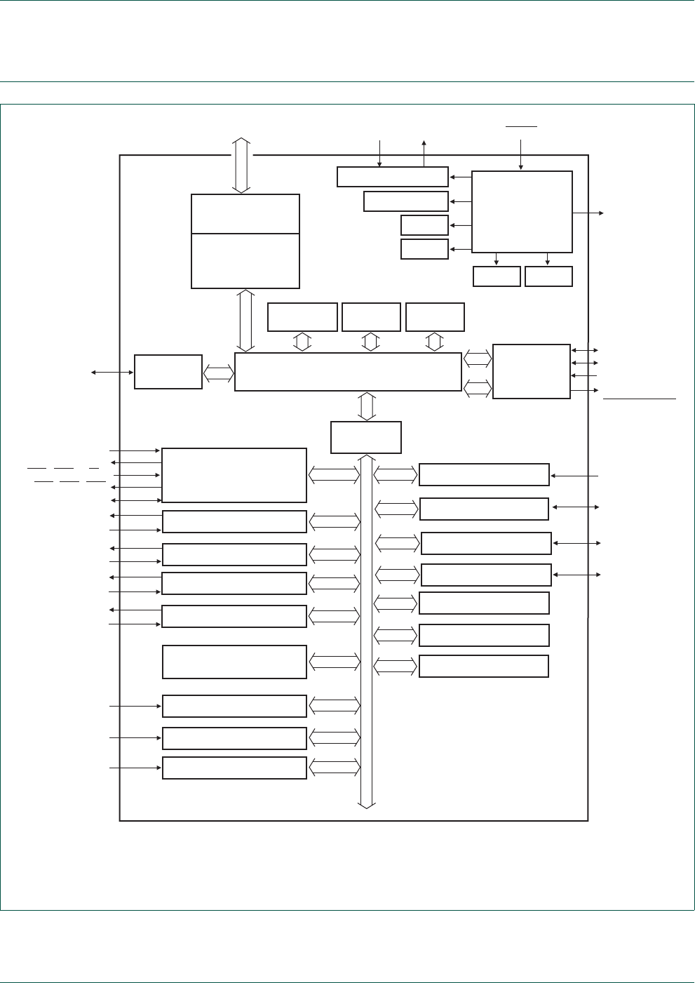
1.4 Block diagram
(1) Function not available on the HVQFN33 package.
(2) CT32B1_CAP1 is only available on the TFBGA48 package.
Fig 1. Block diagram (LPC11U1x)
SRAM
6 kB
ARM
CORTEX-M0
TEST/DEBUG
INTERFACE
FLASH
16/24/32 kB
HIGH-SPEED
GPIO
AHB TO APB
BRIDGE
CLOCK
GENERATION,
POWER CONTROL,
SYSTEM
FUNCTIONS
RESET
SWD, JTAG
LPC11U12/13/14
slave
slave
slave slave
ROM
16 kB
slave
AHB-LITE BUS
GPIO ports 0/1
CLKOUT
IRC, WDO
SYSTEM OSCILLATOR
POR
PLL0 USB PLL
BOD
10-bit ADC
USART/
SMARTCARD INTERFACE AD[7:0]
RXD
TXD
CTS, RTS, DTR
SCLK
GPIO PIN INTERRUPTS
32-bit COUNTER/TIMER 0
CT32B0_MAT[3:0]
CT32B0_CAP[1:0](1)
32-bit COUNTER/TIMER 1
CT32B1_MAT[3:0]
CT32B1_CAP[1:0](2)
DCD, DSR(1), RI(1)
16-bit COUNTER/TIMER 1
WINDOWED WATCHDOG
TIMER
GPIO GROUP0 INTERRUPT
CT16B1_MAT[1:0]
16-bit COUNTER/TIMER 0
CT16B0_MAT[2:0]
CT16B0_CAP0
CT16B1_CAP0
GPIO pins
GPIO pins
GPIO GROUP1 INTERRUPT
GPIO pins
system bus
SSP0 SCK0, SSEL0,
MISO0, MOSI0
SSP1 SCK1, SSEL1,
MISO1, MOSI1
I2C-BUS
IOCON
SYSTEM CONTROL
PMU
SCL, SDA
XTALIN XTALOUT
USB DEVICE
CONTROLLER
USB_DP
USB_DM
USB_VBUS
USB_FTOGGLE,
USB_CONNECT
002aaf885
master
slave
UM10462 All information provided in this document is subject to legal disclaimers. © NXP B.V. 2014. All rights reserved.
User manual Rev. 5.3 — 11 June 2014 11 of 521
NXP Semiconductors UM10462
Chapter 1: LPC11U3x/2x/1x Introductory information
(1) Not available on HVQFN33 packages.
(2) CT32B1_CAP1 available on TFBGA48/LQFP64 packages only. CT16B0_CAP1 and CT16B1_CAP1 available on LQFP64
packages only. CT32B0_CAP1 available on LQFP48/TFBGA48/LQFP64 packages only.
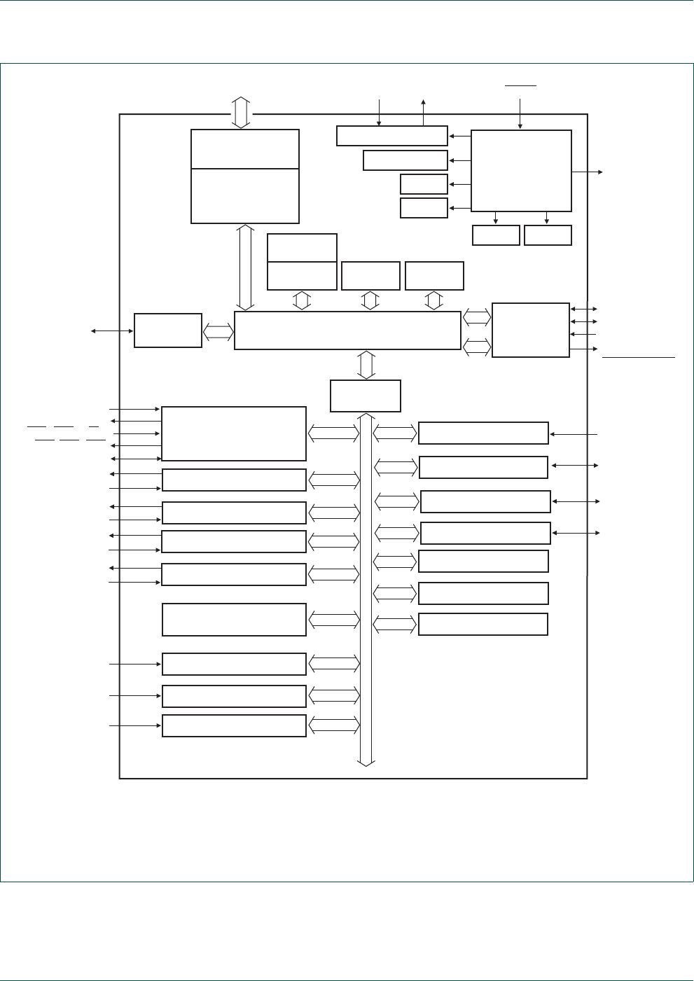
Fig 2. Block diagram (LPC11U2x)
SRAM
8/10 kB
ARM
CORTEX-M0
TEST/DEBUG
INTERFACE
FLASH
16/24/32 kB
HIGH-SPEED
GPIO
AHB TO APB
BRIDGE
CLOCK
GENERATION,
POWER CONTROL,
SYSTEM
FUNCTIONS
RESET
SWD, JTAG
LPC11U2x
slave
slave
slave slave
ROM
16 kB
slave
AHB-LITE BUS
GPIO ports 0/1
CLKOUT
IRC, WDO
SYSTEM OSCILLATOR
POR
PLL0 USB PLL
BOD
10-bit ADC
USART/
SMARTCARD INTERFACE AD[7:0]
RXD
TXD
CTS, RTS, DTR
SCLK
GPIO INTERRUPTS
32-bit COUNTER/TIMER 0
CT32B0_MAT[3:0]
CT32B0_CAP[1:0](2)
32-bit COUNTER/TIMER 1
CT32B1_MAT[3:0]
CT32B1_CAP[1:0](2)
DCD, DSR(1), RI(1)
16-bit COUNTER/TIMER 1
WINDOWED WATCHDOG
TIMER
GPIO GROUP0 INTERRUPTS
CT16B1_MAT[1:0]
16-bit COUNTER/TIMER 0
CT16B0_MAT[2:0]
CT16B0_CAP[1:0](2)
CT16B1_CAP[1:0](2)
GPIO pins
GPIO pins
GPIO GROUP1 INTERRUPTS
GPIO pins
system bus
SSP0 SCK0, SSEL0,
MISO0, MOSI0
SSP1 SCK1, SSEL1,
MISO1, MOSI1
I2C-BUS
IOCON
SYSTEM CONTROL
PMU
SCL, SDA
XTALIN XTALOUT
USB DEVICE
CONTROLLER
USB_DP
USB_DM
USB_VBUS
USB_FTOGGLE,
USB_CONNECT
002aag333
master
slave
EEPROM
1/2/4 kB
UM10462 All information provided in this document is subject to legal disclaimers. © NXP B.V. 2014. All rights reserved.
User manual Rev. 5.3 — 11 June 2014 12 of 521
NXP Semiconductors UM10462
Chapter 1: LPC11U3x/2x/1x Introductory information
(1) Not available on HVQFN33 packages.
(2) CT16B0_CAP1, CT16B1_CAP1 available on LQFP64 packages only; CT32B0_CAP1 available on TFBGA48, LQFP48, and
LQFP64 packages only; CT32B1_CAP1 available in TFBGA48/LQFP64 packages only.
(3) LPC11U37HFBD64/401 only.
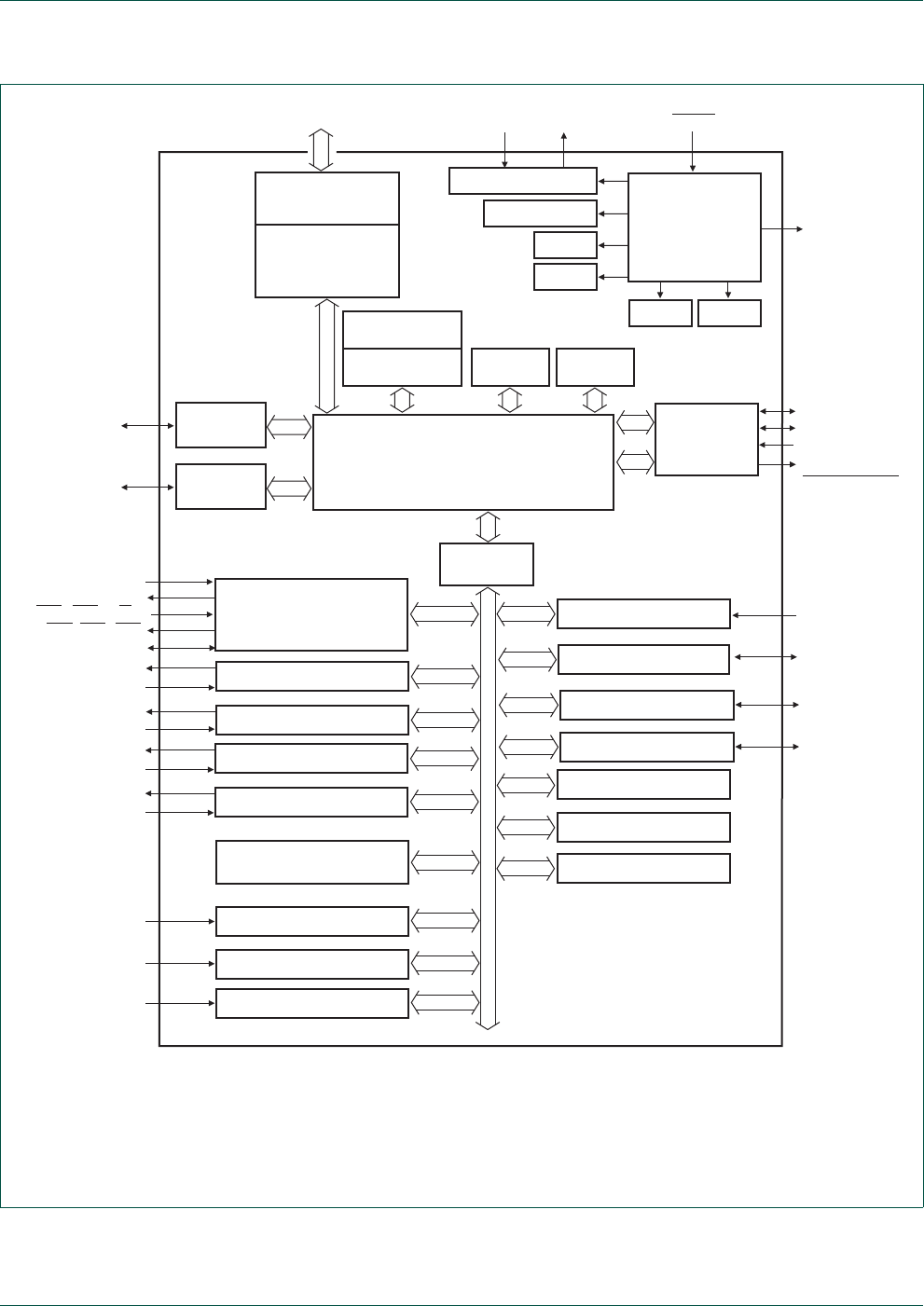
Fig 3. Block diagram (LPC11U3x)
SRAM
8/10/12 kB
ARM
CORTEX-M0
TEST/DEBUG
INTERFACE
FLASH
40/48/64/96/128 kB
HIGH-SPEED
GPIO
AHB TO APB
BRIDGE
CLOCK
GENERATION,
POWER CONTROL,
SYSTEM
FUNCTIONS
RESET
SWD, JTAG
LPC11U3x
slave
slave
master
slave slave
ROM
16 kB
slave
AHB-LITE BUS
GPIO ports 0/1
I/O
HANDLER(3)
IOH_[20:0]
CLKOUT
IRC, WDO
SYSTEM OSCILLATOR
POR
PLL0 USB PLL
BOD
10-bit ADC
USART/
SMARTCARD INTERFACE AD[7:0]
RXD
TXD
CTS, RTS, DTR
SCLK
GPIO INTERRUPTS
32-bit COUNTER/TIMER 0
CT32B0_MAT[3:0]
CT32B0_CAP[1:0](2)
32-bit COUNTER/TIMER 1
CT32B1_MAT[3:0]
CT32B1_CAP[1:0](2)
DCD, DSR(1), RI(1)
16-bit COUNTER/TIMER 1
WINDOWED WATCHDOG
TIMER
GPIO GROUP0 INTERRUPTS
CT16B1_MAT[1:0]
16-bit COUNTER/TIMER 0
CT16B0_MAT[2:0]
CT16B0_CAP[1:0](2)
CT16B1_CAP[1:0](2)
GPIO pins
GPIO pins
GPIO GROUP1 INTERRUPTS
GPIO pins
system bus
SSP0 SCK0, SSEL0,
MISO0, MOSI0
SSP1 SCK1, SSEL1,
MISO1, MOSI1
I2C-BUS
IOCON
SYSTEM CONTROL
PMU
SCL, SDA
XTALIN XTALOUT
USB DEVICE
CONTROLLER
USB_DP
USB_DM
USB_VBUS
USB_FTOGGLE,
USB_CONNECT
002aag345
master
slave
EEPROM
4 kB

UM10462 All information provided in this document is subject to legal disclaimers. © NXP B.V. 2014. All rights reserved.
User manual Rev. 5.3 — 11 June 2014 13 of 521
2.1 How to read this chapter
See Table 3 for the memory configuration of the LPC11U3x/2x/1x parts.
[1] For I/O Handler use only.
UM10462
Chapter 2: LPC11U3x/2x/1x Memory mapping
Rev. 5.3 — 11 June 2014 User manual
Table 3. LPC11U3x/2x/1x memory configuration
Part Flash
in kB Main
SRAM0 at
0x1000
0000
SRAM1 at
0x2000
0000
USB SRAM
at 0x2000
4000
EEPROM Reference
LPC11U12FHN33/201 16 4 - 2 n/a Figure 4
LPC11U12FBD48/201 16 4 - 2 n/a Figure 4
LPC11U13FBD48/201 24 4 - 2 n/a Figure 4
LPC11U14FHN33/201 32 4 - 2 n/a Figure 4
LPC11U14FHI33/201 32 4 - 2 n/a Figure 4
LPC11U14FBD48/201 32 4 - 2 n/a Figure 4
LPC11U14FET48/201 32 4 - 2 n/a Figure 4
LPC11U22FBD48/301 16 6 - 2 1 kB Figure 5
LPC11U23FBD48/301 24 6 - 2 1 kB Figure 5
LPC11U24FHI33/301 32 6 - 2 2 kB Figure 5
LPC11U24FBD48/301 32 6 - 2 2 kB Figure 5
LPC11U24FET48/301 32 6 - 2 2 kB Figure 5
LPC11U24FHN33/401 32 8 - 2 4 kB Figure 5
LPC11U24FBD48/401 32 8 - 2 4 kB Figure 5
LPC11U24FBD64/401 32 8 - 2 4 kB Figure 5
LPC11U34FHN33/311 40 8 - - 4 kB Figure 6
LPC11U34FBD48/311 40 8 - - 4 kB Figure 6
LPC11U34FHN33/421 48 8 - 2 4 kB Figure 6
LPC11U34FBD48/421 48 8 - 2 4 kB Figure 6
LPC11U35FHN33/401 64 8 - 2 4 kB Figure 6
LPC11U35FBD48/401 64 8 - 2 4 kB Figure 6
LPC11U35FBD64/401 64 8 - 2 4 kB Figure 6
LPC11U35FHI33/501 64 8 2 2 4 kB Figure 6
LPC11U35FET48/501 64 8 2 2 4 kB Figure 6
LPC11U36FBD48/401 96 8 - 2 4 kB Figure 6
LPC11U36FBD64/401 96 8 - 2 4 kB Figure 6
LPC11U37FBD48/401 128 8 - 2 4 kB Figure 6
LPC11U37HFBD64/401 128 8 2[1] 24 kBFigure 6
LPC11U37FBD64/501 128 8 2 2 4 kB Figure 6

UM10462 All information provided in this document is subject to legal disclaimers. © NXP B.V. 2014. All rights reserved.
User manual Rev. 5.3 — 11 June 2014 14 of 521
NXP Semiconductors UM10462
Chapter 2: LPC11U3x/2x/1x Memory mapping
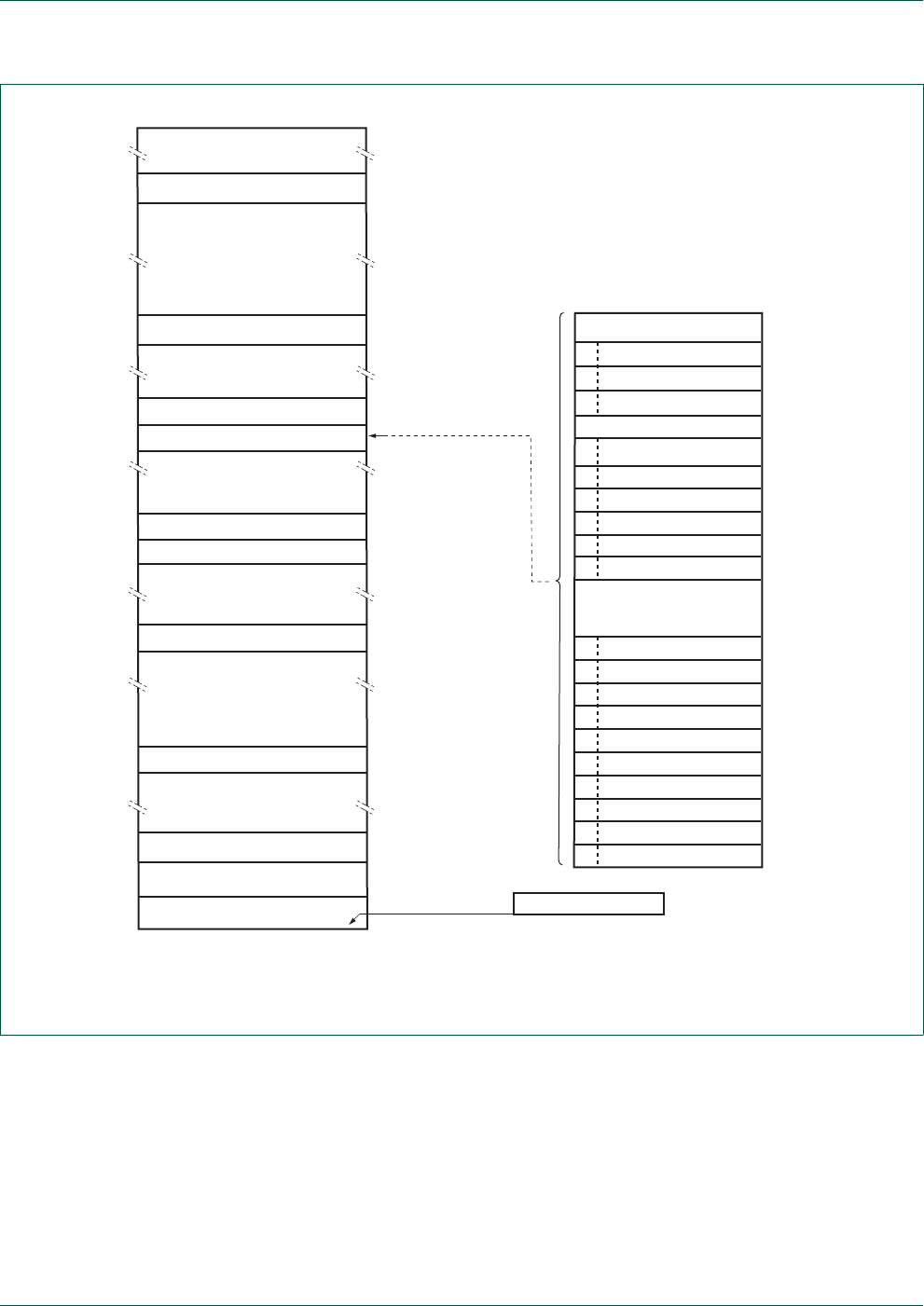
2.2 Memory map
The LPC11U3x/2x/1x incorporates several distinct memory regions, shown in the
following figures. Figure 4 shows the overall map of the entire address space from the
user program viewpoint following reset.
The AHB peripheral area is 2 MB in size and is divided to allow for up to 128 peripherals.
The APB peripheral area is 512 kB in size and is divided to allow for up to 32 peripherals.
Each peripheral of either type is allocated 16 kB of space. This allows simplifying the
address decoding for each peripheral.
UM10462 All information provided in this document is subject to legal disclaimers. © NXP B.V. 2014. All rights reserved.
User manual Rev. 5.3 — 11 June 2014 15 of 521
NXP Semiconductors UM10462
Chapter 2: LPC11U3x/2x/1x Memory mapping
SSP1 available on 48-pin packages only.
Fig 4. LPC11U1x memory map
APB peripherals
0x4000 4000
0x4000 8000
0x4000 C000
0x4001 0000
0x4001 8000
0x4002 0000
0x4002 8000
0x4003 8000
0x4003 C000
0x4004 0000
0x4004 4000
0x4004 8000
0x4004 C000
0x4004 C000
0x4005 8000
0x4005 C000
0x4006 0000
0x4006 4000
0x4008 0000
0x4002 4000
0x4001 C000
0x4001 4000
0x4000 0000
WWDT
32-bit counter/timer 0
32-bit counter/timer 1
ADC
USART/SMART CARD
PMU
I
2
C-bus
20 - 21 reserved
10 - 13 reserved
reserved
reserved
25 - 31 reserved
0
1
2
3
4
5
6
7
8
9
16
15
14
17
18
reserved
reserved
0x0000 0000
0 GB
0.5 GB
4 GB
1 GB
0x1000 1000
0x1FFF 0000
0x1FFF 4000
0x2000 0000
0x5000 0000
0x5000 4000
0xFFFF FFFF
reserved
reserved
reserved
2 kB USB RAM
reserved
0x4000 0000
0x4008 0000
0x4008 4000
APB peripherals
USB
GPIO
0x2000 4000
0x2000 4800
4 kB SRAM 0x1000 0000
LPC11U12/13/14
0x0000 6000
0x0000 4000
24 kB on-chip flash (LPC11U13)
0x0000 8000
32 kB on-chip flash (LPC11U14)
16 kB on-chip flash (LPC11U12)
16 kB boot ROM
0x0000 0000
0x0000 00C0
active interrupt vectors
002aaf891
reserved
reserved
SSP0
SSP1
16-bit counter/timer 1
16-bit counter/timer 0
IOCON
system control
19 GPIO interrupts
22
23 GPIO GROUP0 INT
24 GPIO GROUP1 INT
flash controller
0xE000 0000
0xE010 0000
private peripheral bus
UM10462 All information provided in this document is subject to legal disclaimers. © NXP B.V. 2014. All rights reserved.
User manual Rev. 5.3 — 11 June 2014 16 of 521
NXP Semiconductors UM10462
Chapter 2: LPC11U3x/2x/1x Memory mapping
Fig 5. LPC11U2x memory map
APB peripherals
0x4000 4000
0x4000 8000
0x4000 C000
0x4001 0000
0x4001 8000
0x4002 0000
0x4002 8000
0x4003 8000
0x4003 C000
0x4004 0000
0x4004 4000
0x4004 8000
0x4004 C000
0x4004 C000
0x4005 8000
0x4005 C000
0x4006 0000
0x4006 4000
0x4008 0000
0x4002 4000
0x4001 C000
0x4001 4000
0x4000 0000
WWDT
32-bit counter/timer 0
32-bit counter/timer 1
ADC
USART/SMART CARD
PMU
I
2
C-bus
20 - 21 reserved
10 - 13 reserved
reserved
reserved
25 - 31 reserved
0
1
2
3
4
5
6
7
8
9
16
15
14
17
18
reserved
reserved
0x0000 0000
0 GB
0.5 GB
4 GB
1 GB
0x1000 1800
0x1FFF 0000
0x1FFF 4000
0x2000 0000
0x5000 0000
0x5000 4000
0xFFFF FFFF
reserved
reserved
reserved
2 kB USB RAM
reserved
0x4000 0000
0x4008 0000
0x4008 4000
APB peripherals
USB
GPIO
0x2000 4000
0x2000 4800
6 kB SRAM (LPC11U2x/301)
0x1000 2000
8 kB SRAM (LPC11U2x/401)
0x1000 0000
LPC11U2x
0x0000 6000
0x0000 4000
24 kB on-chip flash (LPC11U23)
16 kB on-chip flash (LPC11U22)
0x0000 8000
32 kB on-chip flash (LPC11U24)
16 kB boot ROM
0x0000 0000
0x0000 00C0
active interrupt vectors
002aag594
reserved
reserved
SSP0
SSP1
16-bit counter/timer 1
16-bit counter/timer 0
IOCON
system control
19 GPIO interrupts
22
23 GPIO GROUP0 INT
24 GPIO GROUP1 INT
flash/EEPROM controller
0xE000 0000
0xE010 0000
private peripheral bus
UM10462 All information provided in this document is subject to legal disclaimers. © NXP B.V. 2014. All rights reserved.
User manual Rev. 5.3 — 11 June 2014 17 of 521
NXP Semiconductors UM10462
Chapter 2: LPC11U3x/2x/1x Memory mapping
Fig 6. LPC11U3x memory map
APB peripherals
0x4000 4000
0x4000 8000
0x4000 C000
0x4001 0000
0x4001 8000
0x4002 0000
0x4002 8000
0x4003 8000
0x4003 C000
0x4004 0000
0x4004 4000
0x4004 8000
0x4004 C000
0x4004 C000
0x4005 8000
0x4005 C000
0x4006 0000
0x4006 4000
0x4008 0000
0x4002 4000
0x4001 C000
0x4001 4000
0x4000 0000
WWDT
32-bit counter/timer 0
32-bit counter/timer 1
ADC
USART/SMART CARD
PMU
I
2
C-bus
20 - 21 reserved
10 - 13 reserved
reserved
reserved
25 - 31 reserved
0
1
2
3
4
5
6
7
8
9
16
15
14
17
18
reserved
reserved
0x0000 0000
0 GB
0.5 GB
4 GB
1 GB
0x1000 0000
0x1FFF 0000
0x1FFF 4000
0x2000 0000
0x5000 0000
0x5000 4000
0xFFFF FFFF
reserved
reserved
reserved
2 kB USB RAM (LPC11U34/421
LPC11U35/401/501
LPC11U36/401/501
LPC11U37/401/501,
LPC11U37H/401)
reserved
0x4000 0000
0x4008 0000
0x4008 4000
APB peripherals
USB
GPIO
0x2000 4000
0x2000 4800
0x1000 2000
8 kB SRAM0 (LPC11U3x)
LPC11U3x
0x0000 A000
40 kB on-chip flash (LPC11U34/311)
0x0000 C000
48 kB on-chip flash (LPC11U34/421)
0x0001 0000
64 kB on-chip flash (LPC11U35)
0x0001 8000
96 kB on-chip flash (LPC11U36)
0x0002 0000
128 kB on-chip flash (LPC11U37/7H)
16 kB boot ROM
0x0000 0000
0x0000 00C0
active interrupt vectors
002aag813
reserved
reserved
SSP0
SSP1
16-bit counter/timer 1
16-bit counter/timer 0
IOCON
system control
19 GPIO interrupts
22
23 GPIO GROUP0 INT
24 GPIO GROUP1 INT
flash/EEPROM controller
0xE000 0000
0xE010 0000
private peripheral bus
2 kB SRAM1 (LPC11U35/501
LPC11U37/501)
I/O Handler code area
for LPC11U37HFBD64/401
0x2000 0800

UM10462 All information provided in this document is subject to legal disclaimers. © NXP B.V. 2014. All rights reserved.
User manual Rev. 5.3 — 11 June 2014 18 of 521
3.1 How to read this chapter
The system control block is identical for all LPC11U3x/2x/1x parts.
The following register bit is available on LPC11U3x/501 and LPC11U37H only and is
reserved otherwise: SYSAHBCLKCTRL register bit RAM1 (bit 26) (Table 24).
Remark: For part LPC11U37H, enable the SRAM1 clock in the SYSAHBCLKCTRL
(Table 24) register for running the I/O Handler software library code.
The DEVICE_ID register contains the device id numbers for the LPC11U1x and
LPC11U2x parts. For LPC11U3x parts, see the ISP/IAP Read Part Id command
(Table 376).
3.2 Introduction
The system configuration block controls oscillators, some aspects of the power
management, and the clock generation of the LPC11U3x/2x/1x. Also included in this block
is a register for remapping flash, SRAM, and ROM memory areas.
3.3 Pin description
Table 4 shows pins that are associated with system control block functions.
3.4 Clocking and power control
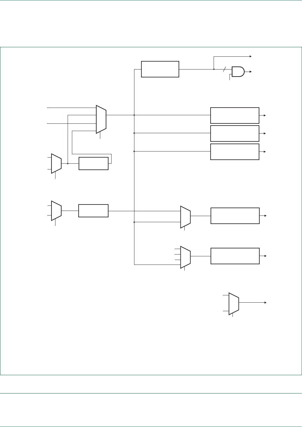
See Figure 7 for an overview of the LPC11U3x/2x/1x Clock Generation Unit (CGU).
The LPC11U3x/2x/1x include three independent oscillators. These are the system
oscillator, the Internal RC oscillator (IRC), and the Watchdog oscillator. Each oscillator can
be used for more than one purpose as required in a particular application.
Following reset, the LPC11U3x/2x/1x will operate from the Internal RC oscillator until
switched by software. This allows systems to operate without an external crystal and the
bootloader code to operate at a known frequency.
The SYSAHBCLKCTRL register gates the system clock to the various peripherals and
memories. USART and SSP have individual clock dividers to derive peripheral clocks
from the main clock.
UM10462
Chapter 3: LPC11U3x/2x/1x System control block
Rev. 5.3 — 11 June 2014 User manual
Table 4. Pin summary
Pin name Pin
direction Pin description
CLKOUT O Clockout pin
PIO0 and PIO1 pins I Eight pins can be selected as external interrupt
pins from all available GPIO pins (see Table 40).
UM10462 All information provided in this document is subject to legal disclaimers. © NXP B.V. 2014. All rights reserved.
User manual Rev. 5.3 — 11 June 2014 19 of 521
NXP Semiconductors UM10462
Chapter 3: LPC11U3x/2x/1x System control block
The main clock, and the clock outputs from the IRC, the system oscillator, and the
watchdog oscillator can be observed directly on the CLKOUT pin.
3.5 Register description
All system control block registers are on word address boundaries. Details of the registers
appear in the description of each function.
Fig 7. LPC11U3x/2x/1x CGU block diagram
system oscillator
watchdog oscillator
IRC oscillator
USB PLL
USBPLLCLKSEL
(USB clock select)
SYSTEM CLOCK
DIVIDER
SYSAHBCLKCTRLn
(AHB clock enable)
CPU, system control,
PMU
memories,
peripheral clocks
SSP0 PERIPHERAL
CLOCK DIVIDER SSP0
SSP1 PERIPHERAL
CLOCK DIVIDER SSP1
USART PERIPHERAL
CLOCK DIVIDER UART
WDT
CLKSEL
(WDT clock select)
USB 48 MHz CLOCK
DIVIDER USB
USBUEN
(USB clock update enable)
watchdog oscillator
IRC oscillator
system oscillator CLKOUT PIN CLOCK
DIVIDER CLKOUT pin
CLKOUTUEN
(CLKOUT update enable)
002aaf892
system clock
SYSTEM PLL
IRC oscillator
system oscillator
IRC oscillator
watchdog oscillator
MAINCLKSEL
(main clock select)
SYSPLLCLKSEL
(system PLL clock select)
main clock
IRC oscillator
n

UM10462 All information provided in this document is subject to legal disclaimers. © NXP B.V. 2014. All rights reserved.
User manual Rev. 5.3 — 11 June 2014 20 of 521
NXP Semiconductors UM10462
Chapter 3: LPC11U3x/2x/1x System control block
In addition to the system control block registers described in Table 5, the flash access
timing register, which can be re-configured as part the system setup, is described in
Table 6. This register is not part of the system configuration block.
All address offsets not shown in Table 5 and Table 6 are reserved and should not be
written.
Table 5. Register overview: system control block (base address 0x4004 8000)
Name Access Offset Description Reset value Reset value
after boot Reference
SYSMEMREMAP R/W 0x000 System memory remap 0x02 0x02 Table 7
PRESETCTRL R/W 0x004 Peripheral reset control 0 0 Table 8
SYSPLLCTRL R/W 0x008 System PLL control 0 0 Table 9
SYSPLLSTAT R 0x00C System PLL status 0 0 Table 10
USBPLLCTRL R/W 0x010 USB PLL control 0 0 Table 11
USBPLLSTAT R 0x014 USB PLL status 0 0 Table 12
SYSOSCCTRL R/W 0x020 System oscillator control 0 0 Table 13
WDTOSCCTRL R/W 0x024 Watchdog oscillator control 0 0 Table 14
IRCCTRL R/W 0x028 IRC control 0x080 - Table 15
- - 0x02C Reserved - - -
SYSRSTSTAT R/W 0x030 System reset status register 0x3 0x3 Table 16
SYSPLLCLKSEL R/W 0x040 System PLL clock source select 0x1 0x1 Table 17
SYSPLLCLKUEN R/W 0x044 System PLL clock source update
enable
0x1 0x1 Table 18
USBPLLCLKSEL R/W 0x048 USB PLL clock source select 0 0 Table 19
USBPLLCLKUEN R/W 0x04C USB PLL clock source update enable 0 0 Table 20
MAINCLKSEL R/W 0x070 Main clock source select 0 0 Table 21
MAINCLKUEN R/W 0x074 Main clock source update enable 0x1 0x1 Table 22
SYSAHBCLKDIV R/W 0x078 System clock divider 0x1 0x1 Table 23
SYSAHBCLKCTRL R/W 0x080 System clock control 0x3F 0x0800485F Table 24
SSP0CLKDIV R/W 0x094 SSP0 clock divider 0 0x1 Table 25
UARTCLKDIV R/W 0x098 UART clock divider 0 0 Table 26
SSP1CLKDIV R/W 0x09C SSP1 clock divider 0 0 Table 27
- - 0x0A0 -
0x0BC
Reserved - - -
USBCLKSEL R/W 0x0C0 USB clock source select 0 0 Table 28
USBCLKUEN R/W 0x0C4 USB clock source update enable 0 0 Table 29
USBCLKDIV R/W 0x0C8 USB clock source divider 0 0x1 Table 30
- - 0x0CC Reserved - -
CLKOUTSEL R/W 0x0E0 CLKOUT clock source select 0 0 Table 31
CLKOUTUEN R/W 0x0E4 CLKOUT clock source update enable 0 0 Table 32
CLKOUTDIV R/W 0x0E8 CLKOUT clock divider 0 0 Table 33
PIOPORCAP0 R 0x100 POR captured PIO status 0 user dependent user
dependent
Table 34
PIOPORCAP1 R 0x104 POR captured PIO status 1 user dependent user
dependent
Table 35

UM10462 All information provided in this document is subject to legal disclaimers. © NXP B.V. 2014. All rights reserved.
User manual Rev. 5.3 — 11 June 2014 21 of 521
NXP Semiconductors UM10462
Chapter 3: LPC11U3x/2x/1x System control block
3.5.1 System memory remap register
The system memory remap register selects whether the exception vectors are read from
boot ROM, flash, or SRAM. By default, the flash memory is mapped to address 0x0000
0000. When the MAP bits in the SYSMEMREMAP register are set to 0x0 or 0x1, the boot
ROM or RAM respectively are mapped to the bottom 512 bytes of the memory map
(addresses 0x0000 0000 to 0x0000 0200).
BODCTRL R/W 0x150 Brown-Out Detect 0 0 Table 36
SYSTCKCAL R/W 0x154 System tick counter calibration 0x0 0x4 Table 37
IRQLATENCY R/W 0x170 IRQ delay. Allows trade-off between
interrupt latency and determinism.
0x10 0x10 Table 38
NMISRC R/W 0x174 NMI Source Control 0 0 Table 39
PINTSEL0 R/W 0x178 GPIO Pin Interrupt Select register 0 0 0 Table 40
PINTSEL1 R/W 0x17C GPIO Pin Interrupt Select register 1 0 0 Table 40
PINTSEL2 R/W 0x180 GPIO Pin Interrupt Select register 2 0 0 Table 40
PINTSEL3 R/W 0x184 GPIO Pin Interrupt Select register 3 0 0 Table 40
PINTSEL4 R/W 0x188 GPIO Pin Interrupt Select register 4 0 0 Table 40
PINTSEL5 R/W 0x18C GPIO Pin Interrupt Select register 5 0 0 Table 40
PINTSEL6 R/W 0x190 GPIO Pin Interrupt Select register 6 0 0 Table 40
PINTSEL7 R/W 0x194 GPIO Pin Interrupt Select register 7 0 0 Table 40
USBCLKCTRL R/W 0x198 USB clock control 0 0 Table 41
USBCLKST R 0x19C USB clock status 0x1 0x1 Table 42
STARTERP0 R/W 0x204 Start logic 0 interrupt wake-up enable
register 0
00Table 43
STARTERP1 R/W 0x214 Start logic 1 interrupt wake-up enable
register 1
00Table 44
PDSLEEPCFG R/W 0x230 Power-down states in deep-sleep
mode
0xFFFF 0xFFFF Table 45
PDAWAKECFG R/W 0x234 Power-down states for wake-up from
deep-sleep
0xEDF0 0xEDF0 Table 46
PDRUNCFG R/W 0x238 Power configuration register 0xEDD0 0xEDF0 Table 47
DEVICE_ID R 0x3F4 Device ID part dependent Table 48
Table 5. Register overview: system control block (base address 0x4004 8000) …continued
Name Access Offset Description Reset value Reset value
after boot Reference
Table 6. Register overview: flash control block (base address 0x4003 C000)
Name Access Offset Description Reset value Reference
FLASHCFG R/W 0x010 Flash read access configuration - Table 49

UM10462 All information provided in this document is subject to legal disclaimers. © NXP B.V. 2014. All rights reserved.
User manual Rev. 5.3 — 11 June 2014 22 of 521
NXP Semiconductors UM10462
Chapter 3: LPC11U3x/2x/1x System control block
3.5.2 Peripheral reset control register
This register allows software to reset specific peripherals. A 0 in an assigned bit in this
register resets the specified peripheral. A 1 negates the reset and allows peripheral
operation.
Remark: Before accessing the SSP and I2C peripherals, write a 1 to this register to
ensure that the reset signals to the SSP and I2C are de-asserted.
3.5.3 System PLL control register
This register connects and enables the system PLL and configures the PLL multiplier and
divider values. The PLL accepts an input frequency from 10 MHz to 25 MHz from various
clock sources. The input frequency is multiplied to a higher frequency and then divided
down to provide the actual clock used by the CPU, peripherals, and memories. The PLL
can produce a clock up to the maximum allowed for the CPU.
Table 7. System memory remap register (SYSMEMREMAP, address 0x4004 8000) bit
description
Bit Symbol Value Description Reset
value
1:0 MAP System memory remap. Value 0x3 is reserved. 0x2
0x0 Boot Loader Mode. Interrupt vectors are re-mapped to Boot
ROM.
0x1 User RAM Mode. Interrupt vectors are re-mapped to Static
RAM.
0x2 User Flash Mode. Interrupt vectors are not re-mapped and
reside in Flash.
31:2 - - Reserved -
Table 8. Peripheral reset control register (PRESETCTRL, address 0x4004 8004) bit
description
Bit Symbol Value Description Reset
value
0 SSP0_RST_N SSP0 reset control 0
0 Resets the SSP0 peripheral.
1 SSP0 reset de-asserted.
1 I2C_RST_N I2C reset control 0
0 Resets the I2C peripheral.
1 I2C reset de-asserted.
2 SSP1_RST_N SSP1 reset control 0
0 Resets the SSP1 peripheral.
1 SSP1 reset de-asserted.
3 - Reserved -
31:4 - - Reserved -

UM10462 All information provided in this document is subject to legal disclaimers. © NXP B.V. 2014. All rights reserved.
User manual Rev. 5.3 — 11 June 2014 23 of 521
NXP Semiconductors UM10462
Chapter 3: LPC11U3x/2x/1x System control block
3.5.4 System PLL status register
This register is a Read-only register and supplies the PLL lock status (see
Section 3.10.1).
3.5.5 USB PLL control register
The USB PLL is identical to the system PLL and is used to provide a dedicated clock to
the USB block if available (see Section 3.1).
This register connects and enables the USB PLL and configures the PLL multiplier and
divider values. The PLL accepts an input frequency from 10 MHz to 25 MHz from various
clock sources. The input frequency is multiplied up to a high frequency, then divided down
to provide the actual clock 48 MHz clock used by the USB subsystem.
Remark: The USB PLL must be connected to the system oscillator for correct USB
operation (see Table 19).
Table 9. System PLL control register (SYSPLLCTRL, address 0x4004 8008) bit description
Bit Symbol Value Description Reset
value
4:0 MSEL Feedback divider value. The division value M is the
programmed MSEL value + 1.
00000: Division ratio M = 1
to
11111: Division ratio M = 32
0
6:5 PSEL Post divider ratio P. The division ratio is 2 P. 0
0x0 P = 1
0x1 P = 2
0x2 P = 4
0x3 P = 8
31:7 - - Reserved. Do not write ones to reserved bits. -
Table 10. System PLL status register (SYSPLLSTAT, address 0x4004 800C) bit description
Bit Symbol Value Description Reset
value
0 LOCK PLL lock status 0
0 PLL not locked
1 PLL locked
31:1 - - Reserved -

UM10462 All information provided in this document is subject to legal disclaimers. © NXP B.V. 2014. All rights reserved.
User manual Rev. 5.3 — 11 June 2014 24 of 521
NXP Semiconductors UM10462
Chapter 3: LPC11U3x/2x/1x System control block
3.5.6 USB PLL status register
This register is a Read-only register and supplies the PLL lock status (see
Section 3.10.1).
3.5.7 System oscillator control register
This register configures the frequency range for the system oscillator.
Table 11. USB PLL control register (USBPLLCTRL, address 0x4004 8010) bit
description
Bit Symbol Value Description Reset
value
4:0 MSEL Feedback divider value. The division value M is the
programmed MSEL value + 1.
00000: Division ratio M = 1
to
11111: Division ratio M = 32
0x000
6:5 PSEL Post divider ratio P. The division ratio is 2 P. 0x00
0x0 P = 1
0x1 P = 2
0x2 P = 4
0x3 P = 8
31:7 - - Reserved. Do not write ones to reserved bits. 0x00
Table 12. USB PLL status register (USBPLLSTAT, address 0x4004 8014) bit description
Bit Symbol Value Description Reset
value
0 LOCK PLL lock status 0x0
0 PLL not locked
1 PLL locked
31:1 - - Reserved 0x00
Table 13. System oscillator control register (SYSOSCCTRL, address 0x4004 8020) bit
description
Bit Symbol Value Description Reset
value
0 BYPASS Bypass system oscillator 0x0
0 Oscillator is not bypassed.
1 Bypass enabled. PLL input (sys_osc_clk) is fed
directly from the XTALIN pin bypassing the
oscillator. Use this mode when using an external
clock source instead of the crystal oscillator.
1 FREQRANGE Determines frequency range for Low-power
oscillator.
0x0
0 1 - 20 MHz frequency range.
1 15 - 25 MHz frequency range
31:2 - - Reserved 0x00

UM10462 All information provided in this document is subject to legal disclaimers. © NXP B.V. 2014. All rights reserved.
User manual Rev. 5.3 — 11 June 2014 25 of 521
NXP Semiconductors UM10462
Chapter 3: LPC11U3x/2x/1x System control block
3.5.8 Watchdog oscillator control register
This register configures the watchdog oscillator. The oscillator consists of an analog and a
digital part. The analog part contains the oscillator function and generates an analog clock
(Fclkana). With the digital part, the analog output clock (Fclkana) can be divided to the
required output clock frequency wdt_osc_clk. The analog output frequency (Fclkana) can
be adjusted with the FREQSEL bits between 600 kHz and 4.6 MHz. With the digital part
Fclkana will be divided (divider ratios = 2, 4,...,64) to wdt_osc_clk using the DIVSEL bits.
The output clock frequency of the watchdog oscillator can be calculated as
wdt_osc_clk = Fclkana/(2 (1 + DIVSEL)) = 9.4 kHz to 2.3 MHz (nominal values).
Remark: Any setting of the FREQSEL bits will yield a Fclkana value within 40% of the
listed frequency value. The watchdog oscillator is the clock source with the lowest power
consumption. If accurate timing is required, use the IRC or system oscillator.
Remark: The frequency of the watchdog oscillator is undefined after reset. The watchdog
oscillator frequency must be programmed by writing to the WDTOSCCTRL register before
using the watchdog oscillator.
Table 14. Watchdog oscillator control register (WDTOSCCTRL, address 0x4004 8024) bit
description
Bit Symbol Value Description Reset
value
4:0 DIVSEL Select divider for Fclkana.
wdt_osc_clk = Fclkana/ (2 (1 + DIVSEL))
00000: 2 (1 + DIVSEL) = 2
00001: 2 (1 + DIVSEL) = 4
to
11111: 2 (1 + DIVSEL) = 64
0
8:5 FREQSEL Select watchdog oscillator analog output frequency
(Fclkana).
0x00
0x1 0.6 MHz
0x2 1.05 MHz
0x3 1.4 MHz
0x4 1.75 MHz
0x5 2.1 MHz
0x6 2.4 MHz
0x7 2.7 MHz
0x8 3.0 MHz
0x9 3.25 MHz
0xA 3.5 MHz
0xB 3.75 MHz
0xC 4.0 MHz
0xD 4.2 MHz
0xE 4.4 MHz
0xF 4.6 MHz
31:9 - - Reserved 0x00

UM10462 All information provided in this document is subject to legal disclaimers. © NXP B.V. 2014. All rights reserved.
User manual Rev. 5.3 — 11 June 2014 26 of 521
NXP Semiconductors UM10462
Chapter 3: LPC11U3x/2x/1x System control block
3.5.9 Internal resonant crystal control register
This register is used to trim the on-chip 12 MHz oscillator. The trim value is factory-preset
and written by the boot code on start-up.
3.5.10 System reset status register
If another reset signal - for example the external RESET pin - remains asserted after the
POR signal is negated, then its bit is set to detected. Write a one to clear the reset.
The reset value given in Table 16 applies to the POR reset.
3.5.11 System PLL clock source select register
This register selects the clock source for the system PLL. The SYSPLLCLKUEN register
(see Section 3.5.12) must be toggled from LOW to HIGH for the update to take effect.
Table 15. Internal resonant crystal control register (IRCCTRL, address 0x4004 8028) bit
description
Bit Symbol Description Reset value
7:0 TRIM Trim value 0x80 then flash will
reprogram
31:8 - Reserved 0x00
Table 16. System reset status register (SYSRSTSTAT, address 0x4004 8030) bit description
Bit Symbol Value Description Reset
value
0 POR POR reset status 1
0 No POR detected
1 POR detected. Writing a one clears this reset.
1 EXTRST External reset status 1
0 No reset event detected.
1 Reset detected. Writing a one clears this reset.
2 WDT Status of the Watchdog reset 0
0 No WDT reset detected
1 WDT reset detected. Writing a one clears this reset.
3 BOD Status of the Brown-out detect reset 0
0 No BOD reset detected
1 BOD reset detected. Writing a one clears this reset.
4 SYSRST Status of the software system reset 0
0 No System reset detected
1 System reset detected. Writing a one clears this reset.
31:5 - - Reserved -

UM10462 All information provided in this document is subject to legal disclaimers. © NXP B.V. 2014. All rights reserved.
User manual Rev. 5.3 — 11 June 2014 27 of 521
NXP Semiconductors UM10462
Chapter 3: LPC11U3x/2x/1x System control block
Table 17. System PLL clock source select register (SYSPLLCLKSEL, address 0x4004 8040)
bit description
Bit Symbol Value Description Reset
value
1:0 SEL System PLL clock source 1
0x0 IRC
0x1 Crystal Oscillator (SYSOSC)
0x2 Reserved
0x3 Reserved
31:2 - - Reserved -

UM10462 All information provided in this document is subject to legal disclaimers. © NXP B.V. 2014. All rights reserved.
User manual Rev. 5.3 — 11 June 2014 28 of 521
NXP Semiconductors UM10462
Chapter 3: LPC11U3x/2x/1x System control block
3.5.12 System PLL clock source update register
This register updates the clock source of the system PLL with the new input clock after the
SYSPLLCLKSEL register has been written to. In order for the update to take effect, first
write a zero to the SYSPLLUEN register and then write a one to SYSPLLUEN.
3.5.13 USB PLL clock source select register
This register selects the clock source for the dedicated USB PLL. The USBPLLCLKUEN
register (see Section 3.5.14) must be toggled from LOW to HIGH for the update to take
effect.
Remark: When switching clock sources, both clocks must be running before the clock
source is updated in the USBPLLCLKUEN register. For USB operation, the clock source
must be switched from IRC to system oscillator with both the IRC and the system
oscillator running. After the switch, the IRC can be turned off.
3.5.14 USB PLL clock source update enable register
This register updates the clock source of the USB PLL with the new input clock after the
USBPLLCLKSEL register has been written to. In order for the update to take effect at the
USB PLL input, first write a zero to the USBPLLUEN register and then write a one to
USBPLLUEN.
Remark: The system oscillator must be selected in the USBPLLCLKSEL register in order
to use the USB PLL, and this register must be toggled to update the USB PLL clock with
the system oscillator.
Remark: When switching clock sources, both clocks must be running before the clock
source is updated.
Table 18. System PLL clock source update enable register (SYSPLLCLKUEN, address
0x4004 8044) bit description
Bit Symbol Value Description Reset value
0 ENA Enable system PLL clock source update 1
0 No change
1 Update clock source
31:1 - - Reserved -
Table 19. USB PLL clock source select register (USBPLLCLKSEL, address 0x4004 8048) bit
description
Bit Symbol Value Description Reset
value
1:0 SEL USB PLL clock source 0x00
0x0 IRC. The USB PLL clock source must be switched to system
oscillator for correct full-speed USB operation. The IRC is
suitable for low-speed USB operation.
0x1 System oscillator
0x2 Reserved
0x3 Reserved
31:2 - - Reserved 0x00

UM10462 All information provided in this document is subject to legal disclaimers. © NXP B.V. 2014. All rights reserved.
User manual Rev. 5.3 — 11 June 2014 29 of 521
NXP Semiconductors UM10462
Chapter 3: LPC11U3x/2x/1x System control block
3.5.15 Main clock source select register
This register selects the main system clock, which can be the system PLL (sys_pllclkout),
or the watchdog oscillator, or the IRC oscillator. The main system clock clocks the core,
the peripherals, and the memories.
Bit 0 of the MAINCLKUEN register (see Section 3.5.16) must be toggled from 0 to 1 for
the update to take effect.
3.5.16 Main clock source update enable register
This register updates the clock source of the main clock with the new input clock after the
MAINCLKSEL register has been written to. In order for the update to take effect, first write
a zero to bit 0 of this register, then write a one.
3.5.17 System clock divider register
This register controls how the main clock is divided to provide the system clock to the
core, memories, and the peripherals. The system clock can be shut down completely by
setting the DIV field to zero.
Table 20. USB PLL clock source update enable register (USBPLLCLKUEN, address 0x4004
804C) bit description
Bit Symbol Value Description Reset value
0 ENA Enable USB PLL clock source update 0x0
0 No change
1 Update clock source
31:1 - - Reserved 0x00
Table 21. Main clock source select register (MAINCLKSEL, address 0x4004 8070) bit
description
Bit Symbol Value Description Reset value
1:0 SEL Clock source for main clock 0
0x0 IRC Oscillator
0x1 PLL input
0x2 Watchdog oscillator
0x3 PLL output
31:2 - - Reserved -
Table 22. Main clock source update enable register (MAINCLKUEN, address 0x4004 8074)
bit description
Bit Symbol Value Description Reset value
0 ENA Enable main clock source update 1
0 No change
1 Update clock source
31:1 - - Reserved -

UM10462 All information provided in this document is subject to legal disclaimers. © NXP B.V. 2014. All rights reserved.
User manual Rev. 5.3 — 11 June 2014 30 of 521
NXP Semiconductors UM10462
Chapter 3: LPC11U3x/2x/1x System control block
3.5.18 System clock control register
The SYSAHBCLKCTRL register enables the clocks to individual system and peripheral
blocks. The system clock (bit 0) provides the clock for the AHB, the APB bridge, the ARM
Cortex-M0, the Syscon block, and the PMU. This clock cannot be disabled.
Table 23. System clock divider register (SYSAHBCLKDIV, address 0x4004 8078) bit
description
Bit Symbol Description Reset
value
7:0 DIV System AHB clock divider values
0: System clock disabled.
1: Divide by 1.
to
255: Divide by 255.
0x1
31:8 - Reserved -
Table 24. System clock control register (SYSAHBCLKCTRL, address 0x4004 8080) bit
description
Bit Symbol Value Description Reset
value
0 SYS Enables the clock for the AHB, the APB bridge, the
Cortex-M0 FCLK and HCLK, SysCon, and the PMU.
This bit is read only and always reads as 1.
1
0 Reserved
1 Enable
1 ROM Enables clock for ROM. 1
0 Disable
1 Enable
2 RAM0 Enables clock for Main SRAM0. 1
0 Disable
1 Enable
3 FLASHREG Enables clock for flash register interface. 1
0 Disable
1 Enable
4 FLASHARRAY Enables clock for flash array access. 1
0 Disable
1 Enable
5 I2C Enables clock for I2C. 1
0 Disable
1 Enable
6 GPIO Enables clock for GPIO port registers. 0
0 Disable
1 Enable
7 CT16B0 Enables clock for 16-bit counter/timer 0. 0
0 Disable
1 Enable

UM10462 All information provided in this document is subject to legal disclaimers. © NXP B.V. 2014. All rights reserved.
User manual Rev. 5.3 — 11 June 2014 31 of 521
NXP Semiconductors UM10462
Chapter 3: LPC11U3x/2x/1x System control block
8 CT16B1 Enables clock for 16-bit counter/timer 1. 0
0 Disable
1 Enable
9 CT32B0 Enables clock for 32-bit counter/timer 0. 0
0 Disable
1 Enable
10 CT32B1 Enables clock for 32-bit counter/timer 1.
0 Disable
1 Enable
11 SSP0 Enables clock for SSP0. 0
0 Disable
1 Enable
12 USART Enables clock for UART.
0 Disable
1 Enable
13 ADC Enables clock for ADC. 0
0 Disable
1 Enable
14 USB Enables clock to the USB register interface. 0
0 Disable
1 Enable
15 WWDT Enables clock for WWDT. 0
0 Disable
1 Enable
16 IOCON Enables clock for I/O configuration block. 0
0 Disable
1 Enable
17 - Reserved 0
18 SSP1 Enables clock for SSP1. 0
0 Disable
1 Enable
19 PINT Enables clock to GPIO Pin interrupts register
interface.
0
0 Disable
1 Enable
22:20 - Reserved -
23 GROUP0INT Enables clock to GPIO GROUP0 interrupt register
interface.
0
0 Disable
1 Enable
Table 24. System clock control register (SYSAHBCLKCTRL, address 0x4004 8080) bit
description …continued
Bit Symbol Value Description Reset
value

UM10462 All information provided in this document is subject to legal disclaimers. © NXP B.V. 2014. All rights reserved.
User manual Rev. 5.3 — 11 June 2014 32 of 521
NXP Semiconductors UM10462
Chapter 3: LPC11U3x/2x/1x System control block
3.5.19 SSP0 clock divider register
This register configures the SSP0 peripheral clock SPI0_PCLK. SPI0_PCLK can be shut
down by setting the DIV field to zero.
3.5.20 USART clock divider register
This register configures the USART peripheral clock UART_PCLK. The UART_PCLK can
be shut down by setting the DIV field to zero.
24 GROUP1INT Enables clock to GPIO GROUP1 interrupt register
interface.
0
0 Disable
1 Enable
25 - - Reserved -
26 RAM1 Enables SRAM1 block at address 0x2000 0000. See
Section 3.1 for availability of this bit.
0
0 Disable
1 Enable
27 USBRAM Enables USB SRAM block at address 0x2000 4000. 0
0 Disable
1 Enable
31:28 - - Reserved -
Table 24. System clock control register (SYSAHBCLKCTRL, address 0x4004 8080) bit
description …continued
Bit Symbol Value Description Reset
value
Table 25. SSP0 clock divider register (SSP0CLKDIV, address 0x4004 8094) bit description
Bit Symbol Description Reset
value
7:0 DIV SPI0_PCLK clock divider values.
0: System clock disabled.
1: Divide by 1.
to
255: Divide by 255.
0
31:8 - Reserved -
Table 26. USART clock divider register (UARTCLKDIV, address 0x4004 8098) bit description
Bit Symbol Description Reset
value
7:0 DIV UART_PCLK clock divider values
0: Disable UART_PCLK.
1: Divide by 1.
to
255: Divide by 255.
0
31:8 - Reserved -

UM10462 All information provided in this document is subject to legal disclaimers. © NXP B.V. 2014. All rights reserved.
User manual Rev. 5.3 — 11 June 2014 33 of 521
NXP Semiconductors UM10462
Chapter 3: LPC11U3x/2x/1x System control block
3.5.21 SSP1 clock divider register
This register configures the SSP1 peripheral clock SSP1_PCLK. The SSP1_PCLK can be
shut down by setting the DIV bits to 0x0.
3.5.22 USB clock source select register
This register selects the clock source for the USB usb_clk. The clock source can be either
the USB PLL output or the main clock, and the clock can be further divided by the
USBCLKDIV register (see Table 30) to obtain a 48 MHz clock.
The USBCLKUEN register (see Section 3.5.23) must be toggled from LOW to HIGH for
the update to take effect.
Remark: When switching clock sources, both clocks must be running before the clock
source is updated. The default clock source for the USB controller is the USB PLL output.
For switching the clock source to the main clock, ensure that the system PLL and the USB
PLL are running to make both clock sources available for switching. The main clock must
be set to 48 MHz and configured with the main PLL and the system oscillator. After the
switch, the USB PLL can be turned off.
3.5.23 USB clock source update enable register
This register updates the clock source of the USB with the new input clock after the
USBCLKSEL register has been written to. In order for the update to take effect, first write
a zero to the USBCLKUEN register and then write a one to USBCLKUEN.
Remark: When switching clock sources, both clocks must be running before the clock
source is updated.
Table 27. SPI1 clock divider register (SSP1CLKDIV, address 0x4004 809C) bit description
Bit Symbol Description Reset
value
7:0 DIV SSP1_PCLK clock divider values
0: Disable SSP1_PCLK.
1: Divide by 1.
to
255: Divide by 255.
0x00
31:8 - Reserved 0x00
Table 28. USB clock source select register (USBCLKSEL, address 0x4004 80C0) bit
description
Bit Symbol Value Description Reset
value
1:0 SEL USB clock source. Values 0x2 and 0x3 are reserved. 0x00
0x0 USB PLL out
0x1 Main clock
31:2 - - Reserved 0x00

UM10462 All information provided in this document is subject to legal disclaimers. © NXP B.V. 2014. All rights reserved.
User manual Rev. 5.3 — 11 June 2014 34 of 521
NXP Semiconductors UM10462
Chapter 3: LPC11U3x/2x/1x System control block
3.5.24 USB clock divider register
This register allows the USB clock usb_clk to be divided to 48 MHz. The usb_clk can be
shut down by setting the DIV bits to 0x0.
3.5.25 CLKOUT clock source select register
This register selects the signal visible on the CLKOUT pin. Any oscillator or the main clock
can be selected.
Bit 0 of the CLKOUTUEN register (see Section 3.5.26) must be toggled from 0 to 1 for the
update to take effect.
3.5.26 CLKOUT clock source update enable register
This register updates the clock source of the CLKOUT pin with the new clock after the
CLKOUTSEL register has been written to. In order for the update to take effect at the input
of the CLKOUT pin, first write a zero to bit 0 of this register, then write a one.
Table 29. USB clock source update enable register (USBCLKUEN, address 0x4004 80C4) bit
description
Bit Symbol Value Description Reset value
0 ENA Enable USB clock source update 0x0
0 No change
1 Update clock source
31:1 - - Reserved 0x00
Table 30. USB clock divider register (USBCLKDIV, address 0x4004 80C8) bit description
Bit Symbol Description Reset value
7:0 DIV USB clock divider values
0: Disable USB clock.
1: Divide by 1.
to
255: Divide by 255.
0x01
31:8 - Reserved 0x00
Table 31. CLKOUT clock source select register (CLKOUTSEL, address 0x4004 80E0) bit
description
Bit Symbol Value Description Reset
value
1:0 SEL CLKOUT clock source 0
0x0 IRC oscillator
0x1 Crystal oscillator (SYSOSC)
0x2 LF oscillator (watchdog oscillator)
0x3 Main clock
31:2 - - Reserved 0

UM10462 All information provided in this document is subject to legal disclaimers. © NXP B.V. 2014. All rights reserved.
User manual Rev. 5.3 — 11 June 2014 35 of 521
NXP Semiconductors UM10462
Chapter 3: LPC11U3x/2x/1x System control block
3.5.27 CLKOUT clock divider register
This register determines the divider value for the signal on the CLKOUT pin.
3.5.28 POR captured PIO status register 0
The PIOPORCAP0 register captures the state of GPIO port 0 at power-on-reset. Each bit
represents the reset state of one GPIO pin. This register is a read-only status register.
3.5.29 POR captured PIO status register 1
The PIOPORCAP1 register captures the state of GPIO port 1 at power-on-reset. Each bit
represents the reset state of one GPIO pin. This register is a read-only status register.
3.5.30 BOD control register
The BOD control register selects up to four separate threshold values for sending a BOD
interrupt to the NVIC and for forced reset. Reset and interrupt threshold values listed in
Table 36 are typical values.
Table 32. CLKOUT clock source update enable register (CLKOUTUEN, address 0x4004
80E4) bit description
Bit Symbol Value Description Reset value
0 ENA Enable CLKOUT clock source update 0
0 No change
1 Update clock source
31:1 - - Reserved -
Table 33. CLKOUT clock divider registers (CLKOUTDIV, address 0x4004 80E8) bit
description
Bit Symbol Description Reset
value
7:0 DIV CLKOUT clock divider values
0: Disable CLKOUT clock divider.
1: Divide by 1.
to
255: Divide by 255.
0
31:8 - Reserved -
Table 34. POR captured PIO status register 0 (PIOPORCAP0, address 0x4004 8100) bit
description
Bit Symbol Description Reset value
23:0 PIOSTAT State of PIO0_23 through PIO0_0 at power-on reset Implementation
dependent
31:24 - Reserved. -
Table 35. POR captured PIO status register 1 (PIOPORCAP1, address 0x4004 8104) bit
description
Bit Symbol Description Reset value
31:0 PIOSTAT State of PIO1_31 through PIO1_0 at power-on reset Implementation
dependent

UM10462 All information provided in this document is subject to legal disclaimers. © NXP B.V. 2014. All rights reserved.
User manual Rev. 5.3 — 11 June 2014 36 of 521
NXP Semiconductors UM10462
Chapter 3: LPC11U3x/2x/1x System control block
Both the BOD interrupt and the BOD reset, depending on the value of bit BODRSTENA in
this register, can wake-up the chip from Sleep, Deep-sleep, and Power-down modes. See
Section 3.9.
3.5.31 System tick counter calibration register
This register determines the value of the SYST_CALIB register (see Table 349).
3.5.32 IRQ latency register
The IRQLATENCY register is an eight-bit register which specifies the minimum number of
cycles (0-255) permitted for the system to respond to an interrupt request. The intent of
this register is to allow the user to select a trade-off between interrupt response time and
determinism.
Table 36. BOD control register (BODCTRL, address 0x4004 8150) bit description
Bit Symbol Value Description Reset
value
1:0 BODRSTLEV BOD reset level 0
0x0 Level 0: The reset assertion threshold voltage is 1.46 V; the
reset de-assertion threshold voltage is 1.63 V.
0x1 Level 1: The reset assertion threshold voltage is 2.06 V; the
reset de-assertion threshold voltage is 2.15 V.
0x2 Level 2: The reset assertion threshold voltage is 2.35 V; the
reset de-assertion threshold voltage is 2.43 V.
0x3 Level 3: The reset assertion threshold voltage is 2.63 V; the
reset de-assertion threshold voltage is 2.71 V.
3:2 BODINTVAL BOD interrupt level 0
0x0 Level 0: Reserved.
0x1 Level 1:The interrupt assertion threshold voltage is 2.22 V;
the interrupt de-assertion threshold voltage is 2.35 V.
0x2 Level 2: The interrupt assertion threshold voltage is 2.52 V;
the interrupt de-assertion threshold voltage is 2.66 V.
0x3 Level 3: The interrupt assertion threshold voltage is 2.80 V;
the interrupt de-assertion threshold voltage is 2.90 V.
4 BODRSTENA BOD reset enable 0
0 Disable reset function.
1 Enable reset function.
31:5 - - Reserved 0x00
Table 37. System tick timer calibration register (SYSTCKCAL, address 0x4004 8154) bit
description
Bit Symbol Description Reset
value
25:0 CAL System tick timer calibration value 0
31:26 - Reserved -

UM10462 All information provided in this document is subject to legal disclaimers. © NXP B.V. 2014. All rights reserved.
User manual Rev. 5.3 — 11 June 2014 37 of 521
NXP Semiconductors UM10462
Chapter 3: LPC11U3x/2x/1x System control block
Setting this parameter to a very low value (e.g. zero) will guarantee the best possible
interrupt performance but will also introduce a significant degree of uncertainty and jitter.
Requiring the system to always take a larger number of cycles (whether it needs it or not)
will reduce the amount of uncertainty but may not necessarily eliminate it.
Theoretically, the ARM Cortex-M0 core should always be able to service an interrupt
request within 15 cycles. System factors external to the cpu, however, bus latencies,
peripheral response times, etc. can increase the time required to complete a previous
instruction before an interrupt can be serviced. Therefore, accurately specifying a
minimum number of cycles that will ensure determinism will depend on the application.
The default setting for this register is 0x010.
3.5.33 NMI source selection register
The NMI source selection register selects a peripheral interrupts as source for the NMI
interrupt of the ARM Cortex-M0 core. For a list of all peripheral interrupts and their IRQ
numbers see Table 59. For a description of the NMI functionality, see Section 24.3.3.2.
Remark: When you want to change the interrupt source for the NMI, you must first disable
the NMI source by setting bit 31 in this register to 0. Then change the source by updating
the IRQN bits and re-enable the NMI source by setting bit 31 to 1.
Note: If the NMISRC register is used to select an interrupt as the source of Non-Maskable
interrupts, and the selected interrupt is enabled, one interrupt request can result in both a
Non-Maskable and a normal interrupt. This can be avoided by disabling the normal
interrupt in the NVIC, as described in Section 24.5.2.
3.5.34 Pin interrupt select registers
Each of these 8 registers selects one GPIO pin from all GPIO pins on both ports as the
source of a pin interrupt. To select a pin for any of the eight pin interrupts, write the pin
number as 0 to 23 for pins PIO0_0 to PIO0_23 and 24 to 55 for pins PIO1_0 to PIO1_31
to the INTPIN bits. For example, setting INTPIN to 0x5 in PINTSEL0 selects pin PIO0_5
for pin interrupt 0. Setting INTPIN in PINTSEL7 to 0x32 (pin 50) selects pin PIO1_26 for
pin interrupt 7.
Table 38. IRQ latency register (IRQLATENCY, address 0x4004 8170) bit description
Bit Symbol Description Reset
value
7:0 LATENCY 8-bit latency value 0x010
31:8 - Reserved -
Table 39. NMI source selection register (NMISRC, address 0x4004 8174) bit description
Bit Symbol Description Reset
value
4:0 IRQN The IRQ number of the interrupt that acts as the Non-Maskable Interrupt
(NMI) if bit 31 is 1. See Table 59 for the list of interrupt sources and their
IRQ numbers.
0
30:5 - Reserved -
31 NMIEN Write a 1 to this bit to enable the Non-Maskable Interrupt (NMI) source
selected by bits 4:0.
0

UM10462 All information provided in this document is subject to legal disclaimers. © NXP B.V. 2014. All rights reserved.
User manual Rev. 5.3 — 11 June 2014 38 of 521
NXP Semiconductors UM10462
Chapter 3: LPC11U3x/2x/1x System control block
Each of the 8 pin interrupts must be enabled in the NVIC using interrupt slots # 0 to 7 (see
Table 59).
To enable each pin interrupt and configure its edge or level sensitivity, use the GPIO pin
interrupt registers (see Section 9.5.1).
3.5.35 USB clock control register
This register controls the use of the USB need_clock signal and the polarity of the
need_clock signal for triggering the USB wake-up interrupt. For details of how to use the
USB need_clock signal for waking up the part from Deep-sleep or Power-down modes,
see Section 11.7.6.
3.5.36 USB clock status register
This register is read-only and returns the status of the USB need_clock signal. For details
of how to use the USB need_clock signal for waking up the part from Deep-sleep or
Power-down modes, see Section 11.7.6.
Table 40. Pin interrupt select registers (PINTSEL0 to 7, address 0x4004 8178 to 0x4004
8194) bit description
Bit Symbol Description Reset
value
5:0 INTPIN Pin number select for pin interrupt. (PIO0_0 to PIO0_23 correspond
to numbers 0 to 23 and PIO1_0 to PIO1_31 correspond to numbers
24 to 55).
0
31:6 - Reserved -
Table 41. USB clock control register (USBCLKCTRL, address 0x4004 8198) bit description
Bit Symbol Value Description Reset
value
0 AP_CLK USB need_clock signal control 0
0 Under hardware control.
1 Forced HIGH.
1 POL_CLK USB need_clock polarity for triggering the USB wake-up
interrupt
0
0 Falling edge of the USB need_clock triggers the USB
wake-up (default).
1 Rising edge of the USB need_clock triggers the USB
wake-up.
31:2 - - Reserved 0x00
Table 42. USB clock status register (USBCLKST, address 0x4004 819C) bit description
Bit Symbol Value Description Reset
value
0 NEED_CLKST USB need_clock signal status 0
0LOW
1 HIGH
31:1 - - Reserved 0x00

UM10462 All information provided in this document is subject to legal disclaimers. © NXP B.V. 2014. All rights reserved.
User manual Rev. 5.3 — 11 June 2014 39 of 521
NXP Semiconductors UM10462
Chapter 3: LPC11U3x/2x/1x System control block
3.5.37 Interrupt wake-up enable register 0
The STARTERP0 register enables the individual GPIO pins selected through the Pin
interrupt select registers (see Table 40) for wake-up. The pin interrupts must also be
enabled in the NVIC (interrupts 0 to 8 in Table 59).
3.5.38 Interrupt wake-up enable register 1
This register selects which interrupts will wake the LPC11U3x/2x/1x from deep-sleep and
power-down modes. Interrupts selected by a one in these registers must be enabled in the
NVIC (Table 59) in order to successfully wake the LPC11U3x/2x/1x from deep-sleep or
power-down mode.
The STARTERP1 register enables the WWDT interrupt, the BOD interrupt, the USB
wake-up interrupt and the two GPIO group interrupts for wake-up.
Table 43. Interrupt wake-up enable register 0 (STARTERP0, address 0x4004 8204) bit
description
Bit Symbol Value Description Reset
value
0 PINT0 Pin interrupt 0 wake-up 0
0 Disabled
1 Enabled
1 PINT1 Pin interrupt 1 wake-up 0
0 Disabled
1 Enabled
2 PINT2 Pin interrupt 2 wake-up 0
0 Disabled
1 Enabled
3 PINT3 Pin interrupt 3 wake-up 0
0 Disabled
1 Enabled
4 PINT4 Pin interrupt 4 wake-up 0
0 Disabled
1 Enabled
5 PINT5 Pin interrupt 5 wake-up 0
0 Disabled
1 Enabled
6 PINT6 Pin interrupt 6 wake-up 0
0 Disabled
1 Enabled
7 PINT7 Pin interrupt 7 wake-up 0
0 Disabled
1 Enabled
31:8 - Reserved -

UM10462 All information provided in this document is subject to legal disclaimers. © NXP B.V. 2014. All rights reserved.
User manual Rev. 5.3 — 11 June 2014 40 of 521
NXP Semiconductors UM10462
Chapter 3: LPC11U3x/2x/1x System control block
3.5.39 Deep-sleep mode configuration register
The bits in this register (BOD_PD and WDTOSC_OD) can be programmed to control
aspects of Deep-sleep and Power-down modes. The bits are loaded into corresponding
bits of the PDRUNCFG register when Deep-sleep mode or Power-down mode is entered.
Remark: Hardware forces the analog blocks to be powered down in Deep-sleep and
Power-down modes according to the power configuration described in Section 3.9.4.1 and
Section 3.9.5.1.An exception are the exception of BOD and watchdog oscillator, which
can be configured to remain running through this register. The WDTOSC_PD value
written to the PDSLEEPCFG register is overwritten if the LOCK bit in the WWDT MOD
register (see Table 337) is set. See Section 17.7 for details.
Table 44. Interrupt wake-up enable register 1 (STARTERP1, address 0x4004 8214) bit
description
Bit Symbol Value Description Reset
value
11:0 Reserved. -
12 WWDTINT WWDT interrupt wake-up 0
0 Disabled
1 Enabled
13 BODINT Brown Out Detect (BOD) interrupt wake-up 0
0 Disabled
1 Enabled
18:14 - Reserved -
19 USB_WAKEUP USB need_clock signal wake-up 0
0 Disabled
1 Enabled
20 GPIOINT0 GPIO GROUP0 interrupt wake-up 0
0 Disabled
1 Enabled
21 GPIOINT1 GPIO GROUP1 interrupt wake-up 0
0 Disabled
1 Enabled
31:22 Reserved. -
Table 45. Deep-sleep configuration register (PDSLEEPCFG, address 0x4004 8230) bit
description
Bit Symbol Value Description Reset
value
2:0 Reserved. 111
3 BOD_PD BOD power-down control for Deep-sleep and Power-down
mode
1
0 Powered
1 Powered down
5:4 Reserved. 11

UM10462 All information provided in this document is subject to legal disclaimers. © NXP B.V. 2014. All rights reserved.
User manual Rev. 5.3 — 11 June 2014 41 of 521
NXP Semiconductors UM10462
Chapter 3: LPC11U3x/2x/1x System control block
3.5.40 Wake-up configuration register
This register controls the power configuration of the device when waking up from
Deep-sleep or Power-down mode.
6 WDTOSC_PD Watchdog oscillator power-down control for Deep-sleep
and Power-down mode
1
0 Powered
1 Powered down
31:7 - - Reserved -
Table 45. Deep-sleep configuration register (PDSLEEPCFG, address 0x4004 8230) bit
description …continued
Bit Symbol Value Description Reset
value
Table 46. Wake-up configuration register (PDAWAKECFG, address 0x4004 8234) bit
description
Bit Symbol Value Description Reset
value
0 IRCOUT_PD IRC oscillator output wake-up configuration 0
0 Powered
1 Powered down
1 IRC_PD IRC oscillator power-down wake-up configuration 0
0 Powered
1 Powered down
2 FLASH_PD Flash wake-up configuration 0
0 Powered
1 Powered down
3 BOD_PD BOD wake-up configuration 0
0 Powered
1 Powered down
4 ADC_PD ADC wake-up configuration 1
0 Powered
1 Powered down
5 SYSOSC_PD Crystal oscillator wake-up configuration 1
0 Powered
1 Powered down
6 WDTOSC_PD Watchdog oscillator wake-up configuration 1
0 Powered
1 Powered down
7 SYSPLL_PD System PLL wake-up configuration 1
0 Powered
1 Powered down
8 USBPLL_PD USB PLL wake-up configuration 1
0 Powered
1 Powered down

UM10462 All information provided in this document is subject to legal disclaimers. © NXP B.V. 2014. All rights reserved.
User manual Rev. 5.3 — 11 June 2014 42 of 521
NXP Semiconductors UM10462
Chapter 3: LPC11U3x/2x/1x System control block
3.5.41 Power configuration register
The PDRUNCFG register controls the power to the various analog blocks. This register
can be written to at any time while the chip is running, and a write will take effect
immediately with the exception of the power-down signal to the IRC.
To avoid glitches when powering down the IRC, the IRC clock is automatically switched off
at a clean point. Therefore, for the IRC a delay is possible before the power-down state
takes effect.
9 - 0 Reserved. 0
10 USBPAD_PD USB transceiver wake-up configuration 1
0 USB transceiver powered
1 USB transceiver powered down
11 - Reserved. Always write this bit as 1. 1
12 - Reserved. Always write this bit as 0. 0
15:13 - Reserved. Always write these bits as 111. 111
31:16 - - Reserved -
Table 46. Wake-up configuration register (PDAWAKECFG, address 0x4004 8234) bit
description …continued
Bit Symbol Value Description Reset
value
Table 47. Power configuration register (PDRUNCFG, address 0x4004 8238) bit
description
Bit Symbol Value Description Reset
value
0 IRCOUT_PD IRC oscillator output power-down 0
0 Powered
1 Powered down
1 IRC_PD IRC oscillator power-down 0
0 Powered
1 Powered down
2 FLASH_PD Flash power-down 0
0 Powered
1 Powered down
3 BOD_PD BOD power-down 0
0 Powered
1 Powered down
4 ADC_PD ADC power-down 1
0 Powered
1 Powered down
5 SYSOSC_PD Crystal oscillator power-down 0
0 Powered
1 Powered down

UM10462 All information provided in this document is subject to legal disclaimers. © NXP B.V. 2014. All rights reserved.
User manual Rev. 5.3 — 11 June 2014 43 of 521
NXP Semiconductors UM10462
Chapter 3: LPC11U3x/2x/1x System control block
3.5.42 Device ID register
This device ID register is a read-only register and contains the part ID for each
LPC11U3x/2x/1x part. This register is also read by the ISP/IAP commands (see
Table 376).
6 WDTOSC_PD Watchdog oscillator power-down 1
0 Powered
1 Powered down
7 SYSPLL_PD System PLL power-down 1
0 Powered
1 Powered down
8 USBPLL_PD USB PLL power-down 1
0 Powered
1 Powered down
9 - 0 Reserved. Always write this bit as 0. 0
10 USBPAD_PD USB transceiver power-down configuration 1
0 USB transceiver powered
1 USB transceiver powered down (suspend mode)
11 - Reserved. Always write this bit as 1. 1
12 - Reserved. Always write this bit as 0. 0
15:13 - Reserved. Always write these bits as 111. 111
31:16 - - Reserved -
Table 47. Power configuration register (PDRUNCFG, address 0x4004 8238) bit
description …continued
Bit Symbol Value Description Reset
value
Table 48. Device ID register (DEVICE_ID, address 0x4004 83F4) bit description
Bit Symbol Description Reset value
31:0 DEVICEID Device ID numbers for LPC11U3x/2x/1x parts
LPC11U12FHN33/201 = 0x095C 802B/0x295C 802B
LPC11U12FBD48/201 = 0x095C 802B/0x295C 802B
LPC11U13FBD48/201 = 0x097A 802B/0x297A 802B
LPC11U14FHN33/201 = 0x0998 802B/0x2998 802B
LPC11U14FHI33/201 = 0x2998 802B
LPC11U14FBD48/201 = 0x0998 802B/0x2998 802B
LPC11U14FET48/201 = 0x0998 802B/0x2998 802B
LPC11U22FBD48/301 = 0x2954 402B
LPC11U23FBD48/301 = 0x2972 402B
LPC11U24FHI33/301 = 0x2988 402B
LPC11U24FBD48/301 = 0x2988 402B
LPC11U24FET48/301 = 0x2988 402B
LPC11U24FHN33/401 = 0x2980 002B
LPC11U24FBD48/401 = 0x2980 002B
LPC11U24FBD64/401 = 0x2980 002B
part-dependent

UM10462 All information provided in this document is subject to legal disclaimers. © NXP B.V. 2014. All rights reserved.
User manual Rev. 5.3 — 11 June 2014 44 of 521
NXP Semiconductors UM10462
Chapter 3: LPC11U3x/2x/1x System control block
3.5.43 Flash memory access
Depending on the system clock frequency, access to the flash memory can be configured
with various access times by writing to the FLASHCFG register at address 0x4003 C010.
This register is part of the flash configuration block (see Figure 4).
Remark: Improper setting of this register may result in incorrect operation of the
LPC11U3x/2x/1x.
3.6 Reset
Reset has the following sources on the LPC11U3x/2x/1x: the RESET pin, Watchdog
Reset, Power-On Reset (POR), and Brown Out Detect (BOD). In addition, there is an
ARM software reset.
The RESET pin is a Schmitt trigger input pin. Assertion of chip Reset by any source, once
the operating voltage attains a usable level, starts the IRC causing reset to remain
asserted until the external Reset is de-asserted, the oscillator is running, and the flash
controller has completed its initialization.
On the assertion of any reset source (Arm software reset, POR, BOD reset, External
reset, and Watchdog reset), the following processes are initiated:
1. The IRC starts up. After the IRC-start-up time (maximum of 6 s on power-up), the
IRC provides a stable clock output.
2. The flash is powered up. This takes approximately 100 s. Then the flash initialization
sequence is started, which takes about 250 cycles.
3. The boot code in the ROM starts. The boot code performs the boot tasks and may
jump to the flash.
When the internal Reset is removed, the processor begins executing at address 0, which
is initially the Reset vector mapped from the boot block. At that point, all of the processor
and peripheral registers have been initialized to predetermined values.
Table 49. Flash configuration register (FLASHCFG, address 0x4003 C010) bit description
Bit Symbol Value Description Reset
value
1:0 FLASHTIM Flash memory access time. FLASHTIM +1 is equal to the
number of system clocks used for flash access.
0x2
0x0 1 system clock flash access time (for system clock
frequencies of up to 20 MHz).
0x1 2 system clocks flash access time (for system clock
frequencies of up to 40 MHz).
0x2 3 system clocks flash access time (for system clock
frequencies of up to 50 MHz).
0x3 Reserved.
31:2 - - Reserved. User software must not change the value of
these bits. Bits 31:2 must be written back exactly as read.
-
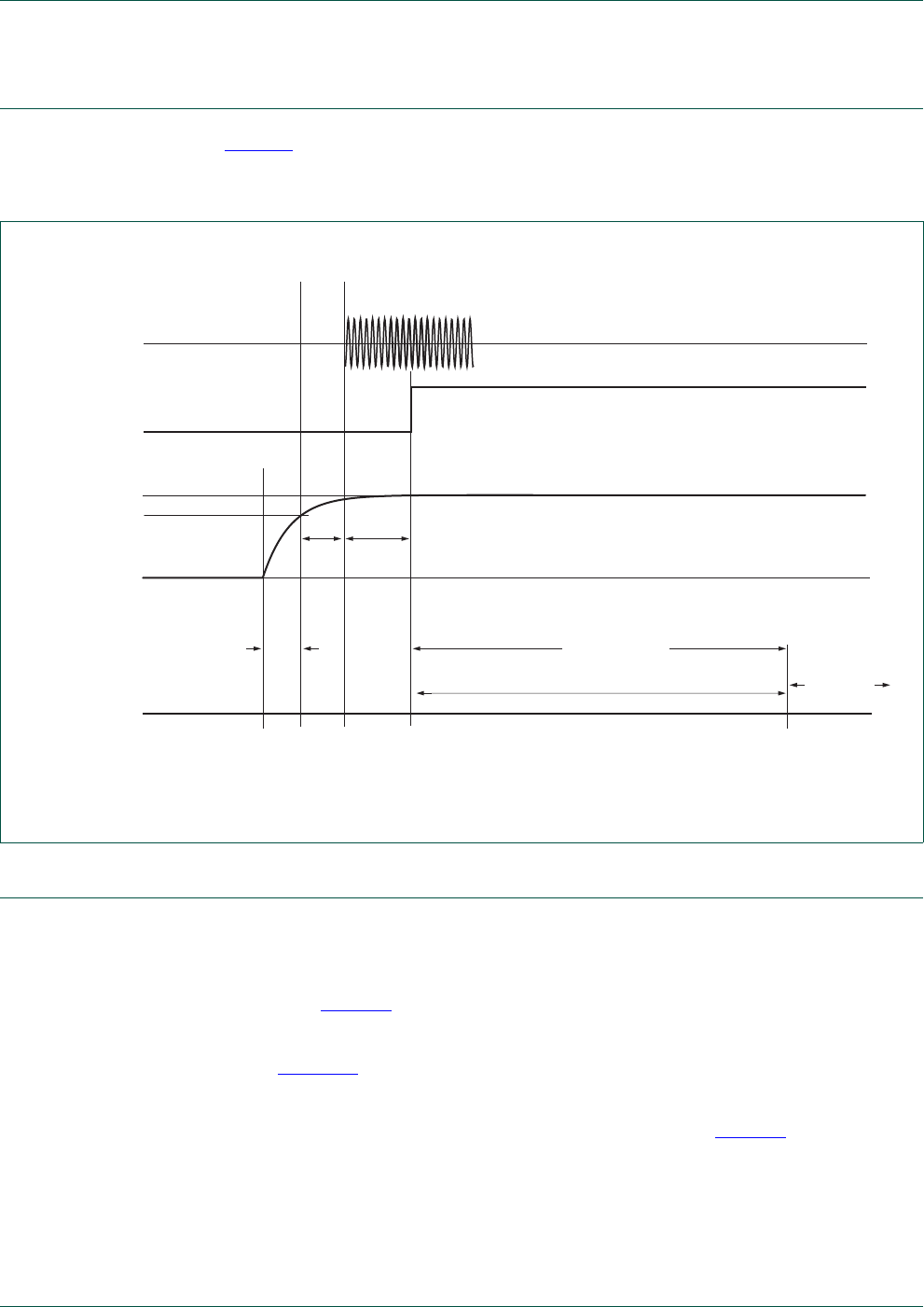
UM10462 All information provided in this document is subject to legal disclaimers. © NXP B.V. 2014. All rights reserved.
User manual Rev. 5.3 — 11 June 2014 45 of 521
NXP Semiconductors UM10462
Chapter 3: LPC11U3x/2x/1x System control block
3.7 Start-up behavior
See Figure 8 for the start-up timing after reset. The IRC is the default clock at Reset and
provides a clean system clock shortly after the supply voltage reaches the threshold value
of 1.8 V.
3.8 Brown-out detection
The LPC11U3x/2x/1x includes up to four levels for monitoring the voltage on the VDD pin.
If this voltage falls below one of the selected levels, the BOD asserts an interrupt signal to
the NVIC or issues a reset, depending on the value of the BODRSTENA bit in the BOD
control register (Table 36).
The interrupt signal can be enabled for interrupt in the Interrupt Enable Register in the
NVIC (see Table 436) in order to cause a CPU interrupt; if not, software can monitor the
signal by reading a dedicated status register.
If the BOD interrupt is enabled in the STARTERP1 register (see Table 44) and in the
NVIC, the BOD interrupt can wake up the chip from Deep-sleep and power-down mode.
If the BOD reset is enabled, the forced BOD reset can wake up the chip from Deep-sleep
or Power-down mode.
Fig 8. Start-up timing
valid threshold
= 1.8V
processor status
VDD
IRC status
internal reset
GND
80 μs 101 μs
boot time
user code
boot code
execution
finishes;
user code starts
IRC
starts
supply ramp-up
time
55 μs

UM10462 All information provided in this document is subject to legal disclaimers. © NXP B.V. 2014. All rights reserved.
User manual Rev. 5.3 — 11 June 2014 46 of 521
NXP Semiconductors UM10462
Chapter 3: LPC11U3x/2x/1x System control block
3.9 Power management
The LPC11U3x/2x/1x support a variety of power control features. In Active mode, when
the chip is running, power and clocks to selected peripherals can be optimized for power
consumption. In addition, there are four special modes of processor power reduction with
different peripherals running: Sleep mode, Deep-sleep mode, Power-down mode, and
Deep power-down mode.
[1] If bit 5, the clock source lock bit, in the WWDT MOD register is set and the IRC is selected as the WWDT
clock source, the IRC and the IRC output are forced on during this mode (Table 342). This increases power
consumption and may cause the part not to enter Power-down mode correctly. For details see Section 17.7.
Remark: The Debug mode is not supported in Sleep, Deep-sleep, Power-down, or Deep
power-down modes.
3.9.1 Reduced power modes and WWDT lock features
The WWDT clock select lock feature influences the power consumption in any of the
power modes because locking the WWDT clock source forces the selected WWDT clock
source to be on independently of the Deep-sleep and Power-down mode software
configuration through the PDSLEEPCFG register. For details see Section 17.7.
If the part uses Deep-sleep mode with the WWDT running, the watchdog oscillator is the
preferred clock source as it minimizes power consumption. If the clock source is not
locked, the watchdog oscillator must be powered by using the PDSLEEPCFG register.
Alternatively, the IRC may be selected and locked in WWDT MOD register, which forces
the IRC on during Deep-sleep mode.
If the part uses Power-down mode with the WWDT running, the watchdog oscillator must
be selected as the clock source. If the clock source is not locked, the watchdog oscillator
must be powered by using the PDSLEEPCFG register. Do not lock the clock source with
the IRC selected.
Table 50. Peripheral configuration in reduced power modes
Peripheral Sleep mode Deep-sleep
mode Power-down
mode Deep power-down
mode
IRC software configurable on off[1] off
IRC output software configurable off[1] off[1] off
Flash software configurable on off off
BOD software configurable software
configurable
software
configurable
off
PLL software configurable off off off
SysOsc software configurable off off off
WDosc/WWDT software configurable software
configurable
software
configurable
off
ADC software configurable off off off
Digital peripherals software configurable off off off
USB software configurable off off off

UM10462 All information provided in this document is subject to legal disclaimers. © NXP B.V. 2014. All rights reserved.
User manual Rev. 5.3 — 11 June 2014 47 of 521
NXP Semiconductors UM10462
Chapter 3: LPC11U3x/2x/1x System control block
3.9.2 Active mode
In Active mode, the ARM Cortex-M0 core and memories are clocked by the system clock,
and peripherals are clocked by the system clock or a dedicated peripheral clock.
The chip is in Active mode after reset and the default power configuration is determined
by the reset values of the PDRUNCFG and SYSAHBCLKCTRL registers. The power
configuration can be changed during run time.
3.9.2.1 Power configuration in Active mode
Power consumption in Active mode is determined by the following configuration choices:
•The SYSAHBCLKCTRL register controls which memories and peripherals are
running (Table 24).
•The power to various analog blocks (PLL, oscillators, the ADC, the BOD circuit, and
the flash block) can be controlled at any time individually through the PDRUNCFG
register (Table 47).
•The clock source for the system clock can be selected from the IRC (default), the
system oscillator, or the watchdog oscillator (see Figure 7 and related registers).
•The system clock frequency can be selected by the SYSPLLCTRL (Table 9) and the
SYSAHBCLKDIV register (Table 23).
•Selected peripherals (USART, SSP0/1, USB, CLKOUT) use individual peripheral
clocks with their own clock dividers. The peripheral clocks can be shut down through
the corresponding clock divider registers (Table 25 to Table 33).
3.9.3 Sleep mode
In Sleep mode, the system clock to the ARM Cortex-M0 core is stopped, and execution of
instructions is suspended until either a reset or an interrupt occurs.
Peripheral functions, if selected to be clocked in the SYSAHBCLKCTRL register, continue
operation during Sleep mode and may generate interrupts to cause the processor to
resume execution. Sleep mode eliminates dynamic power used by the processor itself,
memory systems and related controllers, and internal buses. The processor state and
registers, peripheral registers, and internal SRAM values are maintained, and the logic
levels of the pins remain static.
3.9.3.1 Power configuration in Sleep mode
Power consumption in Sleep mode is configured by the same settings as in Active mode:
•The clock remains running.
•The system clock frequency remains the same as in Active mode, but the processor is
not clocked.
•Analog and digital peripherals are selected as in Active mode.
3.9.3.2 Programming Sleep mode
The following steps must be performed to enter Sleep mode:
1. The PD bits in the PCON register must be set to the default value 0x0.
2. The SLEEPDEEP bit in the ARM Cortex-M0 SCR register must be set to zero.

UM10462 All information provided in this document is subject to legal disclaimers. © NXP B.V. 2014. All rights reserved.
User manual Rev. 5.3 — 11 June 2014 48 of 521
NXP Semiconductors UM10462
Chapter 3: LPC11U3x/2x/1x System control block
3. Use the ARM Cortex-M0 Wait-For-Interrupt (WFI) instruction.
3.9.3.3 Wake-up from Sleep mode
Sleep mode is exited automatically when an interrupt enabled by the NVIC arrives at the
processor or a reset occurs. After wake-up due to an interrupt, the microcontroller returns
to its original power configuration defined by the contents of the PDRUNCFG and the
SYSAHBCLKDIV registers. If a reset occurs, the microcontroller enters the default
configuration in Active mode.
3.9.4 Deep-sleep mode
In Deep-sleep mode, the system clock to the processor is disabled as in Sleep mode. All
analog blocks are powered down, except for the BOD circuit and the watchdog oscillator,
which must be selected or deselected during Deep-sleep mode in the PDSLEEPCFG
register. The main clock, and therefore all peripheral clocks, are disabled except for the
clock to the watchdog timer if the watchdog oscillator is selected. The IRC is running, but
its output is disabled. The flash is in stand-by mode.
Remark: If the LOCK bit is set in the WWDT MOD register (Table 337) and the IRC is
selected as a clock source for the WWDT, the IRC continues to clock the WWDT in
Deep-sleep mode.
Deep-sleep mode eliminates all power used by analog peripherals and all dynamic power
used by the processor itself, memory systems and related controllers, and internal buses.
The processor state and registers, peripheral registers, and internal SRAM values are
maintained, and the logic levels of the pins remain static.
3.9.4.1 Power configuration in Deep-sleep mode
Power consumption in Deep-sleep mode is determined by the Deep-sleep power
configuration setting in the PDSLEEPCFG (Table 45) register:
•The watchdog oscillator can be left running in Deep-sleep mode if required for the
WWDT.
•If the IRC is locked as the WWDT clock source (see Section 17.7), the IRC continues
to run and clock the WWDT in Deep-sleep mode independently of the setting in the
PDSLEEPCFG register.
•The BOD circuit can be left running in Deep-sleep mode if required by the application.
3.9.4.2 Programming Deep-sleep mode
The following steps must be performed to enter Deep-sleep mode:
1. The PD bits in the PCON register must be set to 0x1 (Table 54).
2. Select the power configuration in Deep-sleep mode in the PDSLEEPCFG (Table 45)
register.
3. Determine if the WWDT clock source must be locked to override the power
configuration in case the IRC is selected as clock for the WWDT (see Section 17.7).
4. If the main clock is not the IRC, power up the IRC in the PDRUNCFG register and
switch the clock source to IRC in the MAINCLKSEL register (Table 21). This ensures
that the system clock is shut down glitch-free.

UM10462 All information provided in this document is subject to legal disclaimers. © NXP B.V. 2014. All rights reserved.
User manual Rev. 5.3 — 11 June 2014 49 of 521
NXP Semiconductors UM10462
Chapter 3: LPC11U3x/2x/1x System control block
5. Select the power configuration after wake-up in the PDAWAKECFG (Table 46)
register.
6. If any of the available wake-up interrupts are needed for wake-up, enable the
interrupts in the interrupt wake-up registers (Table 43, Table 44) and in the NVIC.
7. Write one to the SLEEPDEEP bit in the ARM Cortex-M0 SCR register.
8. Use the ARM WFI instruction.
3.9.4.3 Wake-up from Deep-sleep mode
The microcontroller can wake up from Deep-sleep mode in the following ways:
•Signal on one of the eight pin interrupts selected in Table 40. Each pin interrupt must
also be enabled in the STARTERP0 register (Table 43) and in the NVIC.
•BOD signal, if the BOD is enabled in the PDSLEEPCFG register:
–BOD interrupt using the deep-sleep interrupt wake-up register 1 (Table 44). The
BOD interrupt must be enabled in the NVIC. The BOD interrupt must be selected in
the BODCTRL register.
–Reset from the BOD circuit. In this case, the BOD circuit must be enabled in the
PDSLEEPCFG register, and the BOD reset must be enabled in the BODCTRL
register (Table 36).
•WWDT signal, if the watchdog oscillator is enabled in the PDSLEEPCFG register:
–WWDT interrupt using the interrupt wake-up register 1 (Table 44). The WWDT
interrupt must be enabled in the NVIC. The WWDT interrupt must be set in the
WWDT MOD register.
–Reset from the watchdog timer. The WWDT reset must be set in the WWDT MOD
register. In this case, the watchdog oscillator must be running in Deep-sleep mode
(see PDSLEEPCFG register), and the WDT must be enabled in the
SYSAHBCLKCTRL register.
•USB wake-up signal using the interrupt wake-up register 1 (Table 44). For details, see
Section 11.7.6.
•GPIO group interrupt signal (see Table 44).
Remark: If the watchdog oscillator is running in Deep-sleep mode, its frequency
determines the wake-up time.
Remark: If the application in active mode uses a main clock different from the IRC,
reprogram the clock source for the main clock in the MAINCLKSEL register after waking
up.
3.9.5 Power-down mode
In Power-down mode, the system clock to the processor is disabled as in Sleep mode. All
analog blocks are powered down, except for the BOD circuit and the watchdog oscillator,
which must be selected or deselected during Power-down mode in the PDSLEEPCFG
register. The main clock and therefore all peripheral clocks are disabled except for the
clock to the watchdog timer if the watchdog oscillator is selected. The IRC itself and the
flash are powered down, decreasing power consumption compared to Deep-sleep mode.

UM10462 All information provided in this document is subject to legal disclaimers. © NXP B.V. 2014. All rights reserved.
User manual Rev. 5.3 — 11 June 2014 50 of 521
NXP Semiconductors UM10462
Chapter 3: LPC11U3x/2x/1x System control block
Remark: Do not set the LOCK bit in the WWDT MOD register (Table 337) when the IRC is
selected as a clock source for the WWDT. This prevents the part from entering the
Power-down mode correctly.
Power-down mode eliminates all power used by analog peripherals and all dynamic
power used by the processor itself, memory systems and related controllers, and internal
buses. The processor state and registers, peripheral registers, and internal SRAM values
are maintained, and the logic levels of the pins remain static. Wake-up times are longer
compared to the Deep-sleep mode.
3.9.5.1 Power configuration in Power-down mode
Power consumption in Power-down mode can be configured by the power configuration
setting in the PDSLEEPCFG (Table 45) register in the same way as for Deep-sleep mode
(see Section 3.9.4.1):
•The watchdog oscillator can be left running in Deep-sleep mode if required for the
WWDT.
•The BOD circuit can be left running in Deep-sleep mode if required by the application.
3.9.5.2 Programming Power-down mode
The following steps must be performed to enter Power-down mode:
1. The PD bits in the PCON register must be set to 0x2 (Table 54).
2. Select the power configuration in Power-down mode in the PDSLEEPCFG (Table 45)
register.
3. If the lock bit 5 in the WWDT MOD register is set (Table 337) and the IRC is selected
as the WWDT clock source, reset the part to clear the lock bit and then select the
watchdog oscillator as the WWDT clock source.
4. If the main clock is not the IRC, power up the IRC in the PDRUNCFG register and
switch the clock source to IRC in the MAINCLKSEL register (Table 21). This ensures
that the system clock is shut down glitch-free.
5. Select the power configuration after wake-up in the PDAWAKECFG (Table 46)
register.
6. If any of the available wake-up interrupts are used for wake-up, enable the interrupts
in the interrupt wake-up registers (Table 43, Table 44) and in the NVIC.
7. Write one to the SLEEPDEEP bit in the ARM Cortex-M0 SCR register.
8. Use the ARM WFI instruction.
3.9.5.3 Wake-up from Power-down mode
The microcontroller can wake up from Power-down mode in the same way as from
Deep-sleep mode:
•Signal on one of the eight pin interrupts selected in Table 40. Each pin interrupt must
also be enabled in the STARTERP0 register (Table 43) and in the NVIC.
•BOD signal, if the BOD is enabled in the PDSLEEPCFG register:
–BOD interrupt using the interrupt wake-up register 1 (Table 44). The BOD interrupt
must be enabled in the NVIC. The BOD interrupt must be selected in the
BODCTRL register.

UM10462 All information provided in this document is subject to legal disclaimers. © NXP B.V. 2014. All rights reserved.
User manual Rev. 5.3 — 11 June 2014 51 of 521
NXP Semiconductors UM10462
Chapter 3: LPC11U3x/2x/1x System control block
–Reset from the BOD circuit. In this case, the BOD reset must be enabled in the
BODCTRL register (Table 36).
•WWDT signal, if the watchdog oscillator is enabled in the PDSLEEPCFG register:
–WWDT interrupt using the interrupt wake-up register 1 (Table 44). The WWDT
interrupt must be enabled in the NVIC. The WWDT interrupt must be set in the
WWDT MOD register.
–Reset from the watchdog timer.The WWDT reset must be set in the WWDT MOD
register.
•USB wake-up signal interrupt wake-up register 1 (Table 44). For details, see
Section 11.7.6.
•GPIO group interrupt signal (see Table 44).
Remark: If the watchdog oscillator is running in Power-down mode, its frequency
determines the wake-up time.
Remark: If the application in active mode uses a main clock different from the IRC,
reprogram the clock source for the main clock in the MAINCLKSEL register after waking
up.
3.9.6 Deep power-down mode
In Deep power-down mode, power and clocks are shut off to the entire chip with the
exception of the WAKEUP pin. The Deep power-down mode is controlled by the PMU
(see Chapter 4).
During Deep power-down mode, the contents of the SRAM and registers are not retained
except for a small amount of data which can be stored in the general purpose registers of
the PMU block.
All functional pins are tri-stated in Deep power-down mode except for the WAKEUP pin.
Remark: Setting bit 3 in the PCON register (Section 4.3.1) prevents the part from entering
Deep-power down mode.
3.9.6.1 Power configuration in Deep power-down mode
Deep power-down mode has no configuration options. All clocks, the core, and all
peripherals are powered down. Only the WAKEUP pin is powered.
3.9.6.2 Programming Deep power-down mode
The following steps must be performed to enter Deep power-down mode:
1. Pull the WAKEUP pin externally HIGH.
2. Ensure that bit 3 in the PCON register (Table 54) is cleared.
3. Write 0x3 to the PD bits in the PCON register (see Table 54).
4. Store data to be retained in the general purpose registers (Section 4.3.2).
5. Write one to the SLEEPDEEP bit in the ARM Cortex-M0 SCR register.
6. Use the ARM WFI instruction.
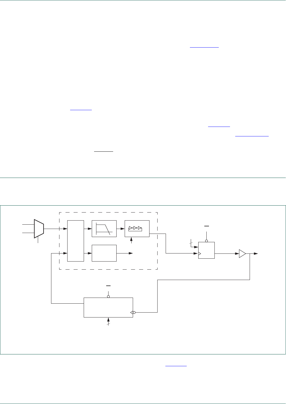
UM10462 All information provided in this document is subject to legal disclaimers. © NXP B.V. 2014. All rights reserved.
User manual Rev. 5.3 — 11 June 2014 52 of 521
NXP Semiconductors UM10462
Chapter 3: LPC11U3x/2x/1x System control block
3.9.6.3 Wake-up from Deep power-down mode
Pulling the WAKEUP pin LOW wakes up the LPC11U3x/2x/1x from Deep power-down,
and the chip goes through the entire reset process (Section 3.6).
1. On the WAKEUP pin, transition from HIGH to LOW.
–The PMU will turn on the on-chip voltage regulator. When the core voltage reaches
the power-on-reset (POR) trip point, a system reset will be triggered and the chip
re-boots.
–All registers except the GPREG0 to GPREG4 will be in their reset state.
2. Once the chip has booted, read the deep power-down flag in the PCON register
(Table 54) to verify that the reset was caused by a wake-up event from Deep
power-down and was not a cold reset.
3. Clear the deep power-down flag in the PCON register (Table 54).
4. (Optional) Read the stored data in the general purpose registers (Section 4.3.2).
5. Set up the PMU for the next Deep power-down cycle.
Remark: The RESET pin has no functionality in Deep power-down mode.
3.10 System PLL/USB PLL functional description
The LPC11U3x/2x/1x uses the system PLL to create the clocks for the core and
peripherals. An identical PLL is available for the USB.
The block diagram of this PLL is shown in Figure 9. The input frequency range is 10 MHz
to 25 MHz. The input clock is fed directly to the Phase-Frequency Detector (PFD). This
block compares the phase and frequency of its inputs, and generates a control signal
when phase and/ or frequency do not match. The loop filter filters these control signals
and drives the current controlled oscillator (CCO), which generates the main clock and
(1) System PLL only.
Fig 9. System PLL block diagram
LOCK
DETECT
PFD
FCLKOUT
pd
analog section
pd
cd
/M
/2P
cd
PSEL<1:0>
pd
2
MSEL<4:0>
5
irc_osc_clk
(1)
sys_osc_clk
SYSPLLCLKSEL/
USBPLLCLKCEL
FCLKIN FCCO
LOCK

UM10462 All information provided in this document is subject to legal disclaimers. © NXP B.V. 2014. All rights reserved.
User manual Rev. 5.3 — 11 June 2014 53 of 521
NXP Semiconductors UM10462
Chapter 3: LPC11U3x/2x/1x System control block
optionally two additional phases. The CCO frequency range is 156 MHz to
320 MHz.These clocks are either divided by 2P by the programmable post divider to
create the output clocks, or are sent directly to the outputs. The main output clock is then
divided by M by the programmable feedback divider to generate the feedback clock. The
output signal of the phase-frequency detector is also monitored by the lock detector, to
signal when the PLL has locked on to the input clock.
3.10.1 Lock detector
The lock detector measures the phase difference between the rising edges of the input
and feedback clocks. Only when this difference is smaller than the so called “lock
criterion” for more than eight consecutive input clock periods, the lock output switches
from low to high. A single too large phase difference immediately resets the counter and
causes the lock signal to drop (if it was high). Requiring eight phase measurements in a
row to be below a certain figure ensures that the lock detector will not indicate lock until
both the phase and frequency of the input and feedback clocks are very well aligned. This
effectively prevents false lock indications, and thus ensures a glitch free lock signal.
3.10.2 Power-down control
To reduce the power consumption when the PLL clock is not needed, a Power-down
mode has been incorporated. This mode is enabled by setting the SYSPLL_PD bit to one
in the Power-down configuration register (Table 47). In this mode, the internal current
reference will be turned off, the oscillator and the phase-frequency detector will be
stopped and the dividers will enter a reset state. While in Power-down mode, the lock
output will be low to indicate that the PLL is not in lock. When the Power-down mode is
terminated by setting the SYSPLL_PD bit to zero, the PLL will resume its normal
operation and will make the lock signal high once it has regained lock on the input clock.
3.10.3 Divider ratio programming
Post divider
The division ratio of the post divider is controlled by the PSEL bits. The division ratio is two
times the value of P selected by PSEL bits as shown in Table 9 and Table 11. This
guarantees an output clock with a 50% duty cycle.
Feedback divider
The feedback divider’s division ratio is controlled by the MSEL bits. The division ratio
between the PLL’s output clock and the input clock is the decimal value on MSEL bits plus
one, as specified in Table 9 and Table 11.
Changing the divider values
Changing the divider ratio while the PLL is running is not recommended. As there is no
way to synchronize the change of the MSEL and PSEL values with the dividers, the risk
exists that the counter will read in an undefined value, which could lead to unwanted
spikes or drops in the frequency of the output clock. The recommended way of changing
between divider settings is to power down the PLL, adjust the divider settings and then let
the PLL start up again.

UM10462 All information provided in this document is subject to legal disclaimers. © NXP B.V. 2014. All rights reserved.
User manual Rev. 5.3 — 11 June 2014 54 of 521
NXP Semiconductors UM10462
Chapter 3: LPC11U3x/2x/1x System control block
3.10.4 Frequency selection
The PLL frequency equations use the following parameters (also see Figure 7):
3.10.4.1 Normal mode
In this mode the post divider is enabled, giving a 50 % duty cycle clock with the following
frequency relations:
(1)
To select the appropriate values for M and P, it is recommended to follow these steps:
1. Specify the input clock frequency Fclkin.
2. Calculate M to obtain the desired output frequency Fclkout with M = Fclkout / Fclkin.
3. Find a value so that FCCO = 2 P Fclkout.
4. Verify that all frequencies and divider values conform to the limits specified in Table 9
and Table 11.
Table 52 shows how to configure the PLL for a 12 MHz crystal oscillator using the
SYSPLLCTRL register (Table 9). The main clock is equivalent to the system clock if the
system clock divider SYSAHBCLKDIV is set to one (see Table 23).
3.10.4.2 Power-down mode
In this mode, the internal current reference will be turned off, the oscillator and the
phase-frequency detector will be stopped and the dividers will enter a reset state. While in
Power-down mode, the lock output will be low, to indicate that the PLL is not in lock. When
the Power-down mode is terminated by SYSPLL_PD bit to zero in the Power-down
configuration register (Table 47), the PLL will resume its normal operation and will make
the lock signal high once it has regained lock on the input clock.
Table 51. PLL frequency parameters
Parameter System PLL
FCLKIN Frequency of sys_pllclkin (input clock to the system PLL) from the
SYSPLLCLKSEL multiplexer (see Section 3.5.11).
FCCO Frequency of the Current Controlled Oscillator (CCO); 156 to 320 MHz.
FCLKOUT Frequency of sys_pllclkout
P System PLL post divider ratio; PSEL bits in SYSPLLCTRL (see
Section 3.5.3).
M System PLL feedback divider register; MSEL bits in SYSPLLCTRL (see
Section 3.5.3).
Table 52. PLL configuration examples
PLL input
clock
sys_pllclkin
(Fclkin)
Main clock
(Fclkout) MSEL bits
Table 9 M divider
value PSEL bits
Table 9 P divider
value FCCO
frequency
12 MHz 48 MHz 00011(binary) 4 01 (binary) 2 192 MHz
12 MHz 36 MHz 00010(binary) 3 10 (binary) 4 288 MHz
12 MHz 24 MHz 00001(binary) 2 10 (binary) 4 192 MHz
Fclkout M FclkinFCCO2P==

UM10462 All information provided in this document is subject to legal disclaimers. © NXP B.V. 2014. All rights reserved.
User manual Rev. 5.3 — 11 June 2014 55 of 521
4.1 How to read this chapter
The PMU is identical on all LPC11U3x/2x/1x parts. Also refer to Chapter 5 for power
control.
4.2 Introduction
The PMU controls the Deep power-down mode. Four general purpose register in the PMU
can be used to retain data during Deep power-down mode.
4.3 Register description
4.3.1 Power control register
The power control register selects whether one of the ARM Cortex-M0 controlled
power-down modes (Sleep mode or Deep-sleep/Power-down mode) or the Deep
power-down mode is entered and provides the flags for Sleep or Deep-sleep/Power-down
modes and Deep power-down modes respectively. See Section 3.9 for details on how to
enter the power-down modes.
UM10462
Chapter 4: LPC11U3x/2x/1x Power Management Unit (PMU)
Rev. 5.3 — 11 June 2014 User manual
Table 53. Register overview: PMU (base address 0x4003 8000)
Name Access Address
offset Description Reset
value Reference
PCON R/W 0x000 Power control register 0x0 Table 54
GPREG0 R/W 0x004 General purpose register 0 0x0 Table 55
GPREG1 R/W 0x008 General purpose register 1 0x0 Table 55
GPREG2 R/W 0x00C General purpose register 2 0x0 Table 55
GPREG3 R/W 0x010 General purpose register 3 0x0 Table 55
GPREG4 R/W 0x014 General purpose register 4 0x0 Table 56
Table 54. Power control register (PCON, address 0x4003 8000) bit description
Bit Symbol Value Description Reset
value
2:0 PM Power mode 000
0x0 Default. The part is in active or sleep mode.
0x1 ARM WFI will enter Deep-sleep mode.
0x2 ARM WFI will enter Power-down mode.
0x3 ARM WFI will enter Deep-power down mode (ARM
Cortex-M0 core powered-down).
3 NODPD A 1 in this bit prevents entry to Deep power-down mode
when 0x3 is written to the PM field above, the
SLEEPDEEP bit is set, and a WFI is executed
This bit is cleared only by power-on reset, so writing a one
to this bit locks the part in a mode in which Deep
power-down mode is blocked.
0

UM10462 All information provided in this document is subject to legal disclaimers. © NXP B.V. 2014. All rights reserved.
User manual Rev. 5.3 — 11 June 2014 56 of 521
NXP Semiconductors UM10462
Chapter 4: LPC11U3x/2x/1x Power Management Unit (PMU)
4.3.2 General purpose registers 0 to 3
The general purpose registers retain data through the Deep power-down mode when
power is still applied to the VDD pin but the chip has entered Deep power-down mode.
Only a “cold” boot when all power has been completely removed from the chip will reset
the general purpose registers.
4.3.3 General purpose register 4
The general purpose register 4 retains data through the Deep power-down mode when
power is still applied to the VDD pin but the chip has entered Deep power-down mode.
Only a “cold” boot, when all power has been completely removed from the chip, will reset
the general purpose registers.
Remark: If there is a possibility that the external voltage applied on pin VDD drops below
2.2 V during Deep power-down, the hysteresis of the WAKEUP input pin has to be
disabled in this register before entering Deep power-down mode in order for the chip to
wake up.
7:4 - - Reserved. Do not write ones to this bit. 0
8 SLEEPFLAG Sleep mode flag 0
0 Read: No power-down mode entered. LPC11U3x/2x/1x is
in Active mode.
Write: No effect.
1 Read: Sleep/Deep-sleep or Power-down mode entered.
Write: Writing a 1 clears the SLEEPFLAG bit to 0.
10:9 - - Reserved. Do not write ones to this bit. 0
11 DPDFLAG Deep power-down flag 0
0 Read: Deep power-down mode not entered.
Write: No effect.
0
1 Read: Deep power-down mode entered.
Write: Clear the Deep power-down flag.
31:12 - - Reserved. Do not write ones to this bit. 0
Table 54. Power control register (PCON, address 0x4003 8000) bit description …continued
Bit Symbol Value Description Reset
value
Table 55. General purpose registers 0 to 3 (GPREG[0:3], address 0x4003 8004 (GPREG0) to
0x4003 8010 (GPREG3)) bit description
Bit Symbol Description Reset
value
31:0 GPDATA Data retained during Deep power-down mode. 0x0
Table 56. General purpose register 4 (GPREG4, address 0x4003 8014) bit
description
Bit Symbol Value Description Reset
value
9:0 - - Reserved. Do not write ones to this bit. 0x0

UM10462 All information provided in this document is subject to legal disclaimers. © NXP B.V. 2014. All rights reserved.
User manual Rev. 5.3 — 11 June 2014 57 of 521
NXP Semiconductors UM10462
Chapter 4: LPC11U3x/2x/1x Power Management Unit (PMU)
4.4 Functional description
For details of entering and exiting reduced power modes, see Section 3.9.
10 WAKEUPHYS WAKEUP pin hysteresis enable 0x0
0 Hysteresis for WAKUP pin disabled.
1 Hysteresis for WAKEUP pin enabled.
31:11 GPDATA Data retained during Deep power-down mode. 0x0
Table 56. General purpose register 4 (GPREG4, address 0x4003 8014) bit
description …continued
Bit Symbol Value Description Reset
value

UM10462 All information provided in this document is subject to legal disclaimers. © NXP B.V. 2014. All rights reserved.
User manual Rev. 5.3 — 11 June 2014 58 of 521
5.1 How to read this chapter
The power profiles are available for all LPC11U3x/2x/1x.
5.2 Features
•Includes ROM-based application services
•Power Management services
•Clocking services
5.3 Basic configuration
Specific power profile settings are required in the following situations:
•When using the USB, configure the power profiles in Default mode.
•When using IAP commands, configure the power profiles in Default mode.
Disable all interrupts before making calls to the power profile API. You can re-enable the
interrupts after the power profile API calls have completed.
5.4 General description
The power consumption in Active and Sleep modes can be optimized for the application
through simple calls to the power profile. The power configuration routine configures the
LPC11U3x/2x/1x for one of the following power modes:
•Default mode corresponding to power configuration after reset.
•CPU performance mode corresponding to optimized processing capability.
•Efficiency mode corresponding to optimized balance of current consumption and CPU
performance.
•Low-current mode corresponding to lowest power consumption.
In addition, the power profile includes routines to select the optimal PLL settings for a
given system clock and PLL input clock.
The API calls to the ROM are performed by executing functions which are pointed by a
pointer within the ROM Driver Table. Figure 10 shows the pointer structure used to call the
Power Profiles API.
UM10462
Chapter 5: LPC11U3x/2x/1x Power profiles
Rev. 5.3 — 11 June 2014 User manual
UM10462 All information provided in this document is subject to legal disclaimers. © NXP B.V. 2014. All rights reserved.
User manual Rev. 5.3 — 11 June 2014 59 of 521
NXP Semiconductors UM10462
Chapter 5: LPC11U3x/2x/1x Power profiles
Fig 10. Power profiles pointer structure
Ptr to ROM Driver table
Ptr to Device Table 2
Ptr to Device Table 1
Ptr to Device Table 0
…
Ptr to Device Table n
set_pll
set_power
Ptr to Function 2
Ptr to Function 0
Ptr to Function 1
…
Ptr to Function n
Power API function table
Device n
ROM Driver Table
0x1FFF 1FF8
+0x0
+0x04
+0x08
+0x0C
Ptr to PowerAPI Table
Fig 11. LPC11U3x/2x/1x clock configuration for power API use
SYS PLL
irc_osc_clk
sys_osc_clk
irc_osc_clk
wdt_osc_clk
MAINCLKSEL
SYSPLLCLKSEL
CLOCK
DIVIDER
SYSAHBCLKCTRL[1]
(ROM enable)
SYSAHBCLKCTRL[27]
(USBRAM enable)
CLOCK
DIVIDER Peripherals
main clock system clock
sys_pllclkin
sys_pllclkout
7
ARM
CORTEX-M0
ROM
USB RAM
SYSAHBCLKDIV

UM10462 All information provided in this document is subject to legal disclaimers. © NXP B.V. 2014. All rights reserved.
User manual Rev. 5.3 — 11 June 2014 60 of 521
NXP Semiconductors UM10462
Chapter 5: LPC11U3x/2x/1x Power profiles
5.5 Definitions
The following elements have to be defined in an application that uses the power profiles:
typedef struct _PWRD {
void (*set_pll)(unsigned int cmd[], unsigned int resp[]);
void (*set_power)(unsigned int cmd[], unsigned int resp[]);
} PWRD;
#define rom_driver_ptr (*(ROM) **) 0x1FFF 1FF8)
pPWRD = (PWRD *)(rom_driver_ptr->pPWRD);
5.6 Clocking routine
5.6.1 set_pll
This routine sets up the system PLL according to the calling arguments. If the expected
clock can be obtained by simply dividing the system PLL input, set_pll bypasses the PLL
to lower system power consumption.
Remark: Before this routine is invoked, the PLL clock source (IRC/system oscillator) must
be selected (Table 17), the main clock source must be set to the input clock to the system
PLL (Table 19) and the system/AHB clock divider must be set to 1 (Table 21).
set_pll attempts to find a PLL setup that matches the calling parameters. Once a
combination of a feedback divider value (SYSPLLCTRL, M), a post divider ratio
(SYSPLLCTRL, P) and the system/AHB clock divider (SYSAHBCLKDIV) is found, set_pll
applies the selected values and switches the main clock source selection to the system
PLL clock out (if necessary).
The routine returns a result code that indicates if the system PLL was successfully set
(PLL_CMD_SUCCESS) or not (in which case the result code identifies what went wrong).
The current system frequency value is also returned. The application should use this
information to adjust other clocks in the device (the SSP, UART, and WDT clocks, and/or
clockout).
The following definitions are needed when making set_pll power routine calls:
/* set_pll mode options */
#define CPU_FREQ_EQU 0
#define CPU_FREQ_LTE 1
Table 57. set_pll routine
Routine set_pll
Input Param0: system PLL input frequency (in kHz)
Param1: expected system clock (in kHz)
Param2: mode (CPU_FREQ_EQU, CPU_FREQ_LTE, CPU_FREQ_GTE,
CPU_FREQ_APPROX)
Param3: system PLL lock time-out
Result Result0: PLL_CMD_SUCCESS | PLL_INVALID_FREQ | PLL_INVALID_MODE |
PLL_FREQ_NOT_FOUND | PLL_NOT_LOCKED
Result1: system clock (in kHz)

UM10462 All information provided in this document is subject to legal disclaimers. © NXP B.V. 2014. All rights reserved.
User manual Rev. 5.3 — 11 June 2014 61 of 521
NXP Semiconductors UM10462
Chapter 5: LPC11U3x/2x/1x Power profiles
#define CPU_FREQ_GTE 2
#define CPU_FREQ_APPROX 3
/* set_pll result0 options */
#define PLL_CMD_SUCCESS 0
#define PLL_INVALID_FREQ 1
#define PLL_INVALID_MODE 2
#define PLL_FREQ_NOT_FOUND 3
#define PLL_NOT_LOCKED 4
For a simplified clock configuration scheme see Figure 11. For more details see Figure 7.
5.6.1.1 Param0: system PLL input frequency and Param1: expected system clock
set_pll looks for a setup in which the system PLL clock does not exceed 50 MHz. It easily
finds a solution when the ratio between the expected system clock and the system PLL
input frequency is an integer value, but it can also find solutions in other cases.
The system PLL input frequency (Param0) must be between 10000 to 25000 kHz (10
MHz to 25 MHz) inclusive. The expected system clock (Param1) must be between 1 and
50000 kHz inclusive. If either of these requirements is not met, set_pll returns
PLL_INVALID_FREQ and returns Param0 as Result1 since the PLL setting is unchanged.
5.6.1.2 Param2: mode
The first priority of set_pll is to find a setup that generates the system clock at exactly the
rate specified in Param1. If it is unlikely that an exact match can be found, input parameter
mode (Param2) should be used to specify if the actual system clock can be less than or
equal, greater than or equal or approximately the value specified as the expected system
clock (Param1).
A call specifying CPU_FREQ_EQU will only succeed if the PLL can output exactly the
frequency requested in Param1.
CPU_FREQ_LTE can be used if the requested frequency should not be exceeded (such
as overall current consumption and/or power budget reasons).
CPU_FREQ_GTE helps applications that need a minimum level of CPU processing
capabilities.
CPU_FREQ_APPROX results in a system clock that is as close as possible to the
requested value (it may be greater than or less than the requested value).
If an illegal mode is specified, set_pll returns PLL_INVALID_MODE. If the expected
system clock is out of the range supported by this routine, set_pll returns
PLL_FREQ_NOT_FOUND. In these cases the current PLL setting is not changed and
Param0 is returned as Result1.
5.6.1.3 Param3: system PLL lock time-out
It should take no more than 100 s for the system PLL to lock if a valid configuration is
selected. If Param3 is zero, set_pll will wait indefinitely for the PLL to lock. A non-zero
value indicates how many times the code will check for a successful PLL lock event
before it returns PLL_NOT_LOCKED. In this case the PLL settings are unchanged and
Param0 is returned as Result1.

UM10462 All information provided in this document is subject to legal disclaimers. © NXP B.V. 2014. All rights reserved.
User manual Rev. 5.3 — 11 June 2014 62 of 521
NXP Semiconductors UM10462
Chapter 5: LPC11U3x/2x/1x Power profiles
Remark: The time it takes the PLL to lock depends on the selected PLL input clock
source (IRC/system oscillator) and its characteristics. The selected source can
experience more or less jitter depending on the operating conditions such as power
supply and/or ambient temperature. This is why it is suggested that when a good known
clock source is used and a PLL_NOT_LOCKED response is received, the set_pll routine
should be invoked several times before declaring the selected PLL clock source invalid.
Hint: setting Param3 equal to the system PLL frequency [Hz] divided by 10000 will
provide more than enough PLL lock-polling cycles.
5.6.1.4 Code examples
The following examples illustrate some of the features of set_pll discussed above.
5.6.1.4.1 Invalid frequency (device maximum clock rate exceeded)
command[0] = 12000;
command[1] = 60000;
command[2] = CPU_FREQ_EQU;
command[3] = 0;
(*rom)->pWRD->set_pll(command, result);
The above code specifies a 12 MHz PLL input clock and a system clock of exactly
60 MHz. The application was ready to infinitely wait for the PLL to lock. But the expected
system clock of 60 MHz exceeds the maximum of 50 MHz. Therefore set_pll returns
PLL_INVALID_FREQ in result[0] and 12000 in result[1] without changing the PLL
settings.
5.6.1.4.2 Invalid frequency selection (system clock divider restrictions)
command[0] = 12000;
command[1] = 40;
command[2] = CPU_FREQ_LTE;
command[3] = 0;
(*rom)->pWRD->set_pll(command, result);
The above code specifies a 12 MHz PLL input clock, a system clock of no more than
40 kHz and no time-out while waiting for the PLL to lock. Since the maximum divider value
for the system clock is 255 and running at 40 kHz would need a divide by value of 300,
set_pll returns PLL_INVALID_FREQ in result[0] and 12000 in result[1] without changing
the PLL settings.
5.6.1.4.3 Exact solution cannot be found (PLL)
command[0] = 12000;
command[1] = 25000;
command[2] = CPU_FREQ_EQU;
command[3] = 0;
(*rom)->pWRD->set_pll(command, result);
The above code specifies a 12 MHz PLL input clock and a system clock of exactly
25 MHz. The application was ready to infinitely wait for the PLL to lock. Since there is no
valid PLL setup within earlier mentioned restrictions, set_pll returns
PLL_FREQ_NOT_FOUND in result[0] and 12000 in result[1] without changing the PLL
settings.

UM10462 All information provided in this document is subject to legal disclaimers. © NXP B.V. 2014. All rights reserved.
User manual Rev. 5.3 — 11 June 2014 63 of 521
NXP Semiconductors UM10462
Chapter 5: LPC11U3x/2x/1x Power profiles
5.6.1.4.4 System clock less than or equal to the expected value
command[0] = 12000;
command[1] = 25000;
command[2] = CPU_FREQ_LTE;
command[3] = 0;
(*rom)->pWRD->set_pll(command, result);
The above code specifies a 12 MHz PLL input clock, a system clock of no more than
25 MHz and no locking time-out. set_pll returns PLL_CMD_SUCCESS in result[0] and
24000 in result[1]. The new system clock is 24 MHz.
5.6.1.4.5 System clock greater than or equal to the expected value
command[0] = 12000;
command[1] = 25000;
command[2] = CPU_FREQ_GTE;
command[3] = 0;
(*rom)->pWRD->set_pll(command, result);
The above code specifies a 12 MHz PLL input clock, a system clock of at least 25 MHz
and no locking time-out. set_pll returns PLL_CMD_SUCCESS in result[0] and 36000 in
result[1]. The new system clock is 36 MHz.
5.6.1.4.6 System clock approximately equal to the expected value
command[0] = 12000;
command[1] = 16500;
command[2] = CPU_FREQ_APPROX;
command[3] = 0;
(*rom)->pWRD->set_pll(command, result);
The above code specifies a 12 MHz PLL input clock, a system clock of approximately
16.5 MHz and no locking time-out. set_pll returns PLL_CMD_SUCCESS in result[0] and
16000 in result[1]. The new system clock is 16 MHz.
5.7 Power routine
5.7.1 set_power
This routine configures the device’s internal power control settings according to the calling
arguments. The goal is to reduce active power consumption while maintaining the feature
of interest to the application close to its optimum.
Remark: The set_power routine was designed for systems employing the configuration of
SYSAHBCLKDIV = 1 (System clock divider register, see Table 23 and Figure 11). Using
this routine in an application with the system clock divider not equal to 1 might not improve
microcontroller’s performance as much as in setups when the main clock and the system
clock are running at the same rate.
set_power returns a result code that reports whether the power setting was successfully
changed or not.
UM10462 All information provided in this document is subject to legal disclaimers. © NXP B.V. 2014. All rights reserved.
User manual Rev. 5.3 — 11 June 2014 64 of 521
NXP Semiconductors UM10462
Chapter 5: LPC11U3x/2x/1x Power profiles
The following definitions are needed for set_power routine calls:
/* set_power mode options */
#define PWR_DEFAULT 0
#define PWR_CPU_PERFORMANCE 1
#define PWR_EFFICIENCY 2
#define PWR_LOW_CURRENT 3
/* set_power result0 options */
#define PWR_CMD_SUCCESS 0
#define PWR_INVALID_FREQ 1
#define PWR_INVALID_MODE 2
Fig 12. Power profiles usage
using power profiles and
changing system clock
current_clock,
new_clock , new_mode
use power routine call
to change mode to
DEFAULT
use either clocking routine call or
custom code to change system clock
from current_clock to new _clock
use power routine call
to change mode to
new_mode
end
Table 58. set_power routine
Routine set_power
Input Param0: main clock (in MHz)
Param1: mode (PWR_DEFAULT, PWR_CPU_PERFORMANCE, PWR_
EFFICIENCY, PWR_LOW_CURRENT)
Param2: system clock (in MHz)
Result Result0: PWR_CMD_SUCCESS | PWR_INVALID_FREQ |
PWR_INVALID_MODE

UM10462 All information provided in this document is subject to legal disclaimers. © NXP B.V. 2014. All rights reserved.
User manual Rev. 5.3 — 11 June 2014 65 of 521
NXP Semiconductors UM10462
Chapter 5: LPC11U3x/2x/1x Power profiles
For a simplified clock configuration scheme see Figure 11. For more details see Figure 7.
5.7.1.1 Param0: main clock
The main clock is the clock rate the microcontroller uses to source the system’s and the
peripherals’ clock. It is configured by either a successful execution of the clocking routine
call or a similar code provided by the user. This operand must be an integer between 1 to
50 MHz inclusive. If a value out of this range is supplied, set_power returns
PWR_INVALID_FREQ and does not change the power control system.
5.7.1.2 Param1: mode
The input parameter mode (Param1) specifies one of four available power settings. If an
illegal selection is provided, set_power returns PWR_INVALID_MODE and does not
change the power control system.
PWR_DEFAULT keeps the device in a baseline power setting similar to its reset state.
PWR_CPU_PERFORMANCE configures the microcontroller so that it can provide more
processing capability to the application. CPU performance is 30% better than the default
option.
PWR_EFFICIENCY setting was designed to find a balance between active current and
the CPU’s ability to execute code and process data. In this mode the device outperforms
the default mode both in terms of providing higher CPU performance and lowering active
current.
PWR_LOW_CURRENT is intended for those solutions that focus on lowering power
consumption rather than CPU performance.
5.7.1.3 Param2: system clock
The system clock is the clock rate at which the microcontroller core is running when
set_power is called. This parameter is an integer between from 1 and 50 MHz inclusive.
5.7.1.4 Code examples
The following examples illustrate some of the set_power features discussed above.
5.7.1.4.1 Invalid frequency (device maximum clock rate exceeded)
command[0] = 60;
command[1] = PWR_CPU_PERFORMANCE;
command[2] = 60;
(*rom)->pWRD->set_power(command, result);
The above setup would be used in a system running at the main and system clock of
60 MHz, with a need for maximum CPU processing power. Since the specified 60 MHz
clock is above the 50 MHz maximum, set_power returns PWR_INVALID_FREQ in
result[0] without changing anything in the existing power setup.
5.7.1.4.2 An applicable power setup
command[0] = 24;
command[1] = PWR_CPU_EFFICIENCY;
command[2] = 24;

UM10462 All information provided in this document is subject to legal disclaimers. © NXP B.V. 2014. All rights reserved.
User manual Rev. 5.3 — 11 June 2014 66 of 521
NXP Semiconductors UM10462
Chapter 5: LPC11U3x/2x/1x Power profiles
(*rom)->pWRD->set_power(command, result);
The above code specifies that an application is running at the main and system clock of
24 MHz with emphasis on efficiency. set_power returns PWR_CMD_SUCCESS in
result[0] after configuring the microcontroller’s internal power control features.

UM10462 All information provided in this document is subject to legal disclaimers. © NXP B.V. 2014. All rights reserved.
User manual Rev. 5.3 — 11 June 2014 67 of 521
6.1 How to read this chapter
The NVIC is identical for all LPC11U3x/2x/1x parts. See Section 24.5.2 for details.
Interrupt 31 (I/O Handler interrupt) is available on part LPC11U37HFBD64/401 only.
6.2 Introduction
The Nested Vectored Interrupt Controller (NVIC) is an integral part of the Cortex-M0. The
tight coupling to the CPU allows for low interrupt latency and efficient processing of late
arriving interrupts.
6.3 Features
•Nested Vectored Interrupt Controller that is an integral part of the ARM Cortex-M0
•Tightly coupled interrupt controller provides low interrupt latency
•Controls system exceptions and peripheral interrupts
•The NVIC supports 32 vectored interrupts
•4 programmable interrupt priority levels with hardware priority level masking
•Software interrupt generation
•Support for NMI
6.4 Interrupt sources
Table 59 lists the interrupt sources for each peripheral function. Each peripheral device
may have one or more interrupt lines to the Vectored Interrupt Controller. Each line may
represent more than one interrupt source. There is no significance or priority about what
line is connected where, except for certain standards from ARM.
See Section 24.5.2 for the NVIC register bit descriptions.
UM10462
Chapter 6: LPC11U3x/2x/1x NVIC
Rev. 5.3 — 11 June 2014 User manual
Table 59. Connection of interrupt sources to the Vectored Interrupt Controller
Interrupt
number Name Description Flags
0 PIN_INT0 GPIO pin interrupt 0 -
1 PIN_INT1 GPIO pin interrupt 1 -
2 PIN_INT2 GPIO pin interrupt 2 -
3 PIN_INT3 GPIO pin interrupt 3 -
4 PIN_INT4 GPIO pin interrupt 4 -
5 PIN_INT5 GPIO pin interrupt 5 -
6 PIN_INT6 GPIO pin interrupt 6 -
7 PIN_INT7 GPIO pin interrupt 7 -

UM10462 All information provided in this document is subject to legal disclaimers. © NXP B.V. 2014. All rights reserved.
User manual Rev. 5.3 — 11 June 2014 68 of 521
NXP Semiconductors UM10462
Chapter 6: LPC11U3x/2x/1x NVIC
8 GINT0 GPIO GROUP0
interrupt
-
9 GINT1 GPIO GROUP1
interrupt
-
13 to 10 - Reserved
14 SSP1 SSP1 interrupt Tx FIFO half empty
Rx FIFO half full
Rx Timeout
Rx Overrun
15 I2C I2C interrupt SI (state change)
16 CT16B0 CT16B0 interrupt Match 0 - 2
Capture 0 -1
17 CT16B1 CT16B1 interrupt Match 0 - 1
Capture 0 -1
18 CT32B0 CT32B0 interrupt Match 0 - 3
Capture 0 - 1
19 CT32B1 CT32B1 interrupt Match 0 - 3
Capture 0 -1
20 SSP0 SSP0 interrupt Tx FIFO half empty
Rx FIFO half full
Rx Timeout
Rx Overrun
21 USART USART interrupt Rx Line Status (RLS)
Transmit Holding Register Empty (THRE)
Rx Data Available (RDA)
Character Time-out Indicator (CTI)
End of Auto-Baud (ABEO)
Auto-Baud Time-Out (ABTO)
Modem control interrupt
22 USB_IRQ USB_IRQ interrupt USB IRQ interrupt
23 USB_FIQ USB_FIQ interrupt USB FIQ interrupt
24 ADC ADC interrupt A/D Converter end of conversion
25 WWDT WWDT interrupt Windowed Watchdog interrupt (WDINT)
26 BOD BOD interrupt Brown-out detect
27 FLASH Flash/EEPROM
interface interrupt
-
28 - - Reserved
29 - - Reserved
30 USB_WAKEUP USB_WAKEUP
interrupt
USB wake-up interrupt
31 IOH IOH interrupt I/O Handler interrupt
Table 59. Connection of interrupt sources to the Vectored Interrupt Controller …continued
Interrupt
number Name Description Flags

UM10462 All information provided in this document is subject to legal disclaimers. © NXP B.V. 2014. All rights reserved.
User manual Rev. 5.3 — 11 June 2014 69 of 521
NXP Semiconductors UM10462
Chapter 6: LPC11U3x/2x/1x NVIC
6.5 Register description
See the ARM Cortex-M0+ technical reference manual.
The NVIC registers are located on the ARM private peripheral bus.
Table 60. Register overview: NVIC (base address 0xE000 E000)
Name Access Address
offset Description Reset
value Reference
ISER0 R/W 0x100 Interrupt Set Enable Register 0. This register allows enabling
interrupts and reading back the interrupt enables for specific
peripheral functions.
0Table 61
- - 0x104 Reserved. - -
ICER0 R/W 0x180 Interrupt Clear Enable Register 0. This register allows disabling
interrupts and reading back the interrupt enables for specific
peripheral functions.
0Table 62
- - 0x184 Reserved. 0 -
ISPR0 R/W 0x200 Interrupt Set Pending Register 0. This register allows changing the
interrupt state to pending and reading back the interrupt pending
state for specific peripheral functions.
0Table 63
- - 0x204 Reserved. 0 -
ICPR0 R/W 0x280 Interrupt Clear Pending Register 0. This register allows changing the
interrupt state to not pending and reading back the interrupt pending
state for specific peripheral functions.
0Table 64
- - 0x284 Reserved. 0 -
IABR0 RO 0x300 Interrupt Active Bit Register 0. This register allows reading the
current interrupt active state for specific peripheral functions.
0Table 65
- - 0x304 Reserved. 0 -
IPR0 R/W 0x400 Interrupt Priority Registers 0. This register allows assigning a priority
to each interrupt. This register contains the 2-bit priority fields for
interrupts 0 to 3.
0Table 66
IPR1 R/W 0x404 Interrupt Priority Registers 1 This register allows assigning a priority
to each interrupt. This register contains the 2-bit priority fields for
interrupts 4 to 7.
0Table 67
IPR2 R/W 0x408 Interrupt Priority Registers 2. This register allows assigning a priority
to each interrupt. This register contains the 2-bit priority fields for
interrupts 8 to 11.
0Table 68
IPR3 R/W 0x40C Interrupt Priority Registers 3. This register allows assigning a priority
to each interrupt. This register contains the 2-bit priority fields for
interrupts 12 to 15.
0Table 69
IPR4 R/W 0x410 Interrupt Priority Registers 4. This register allows assigning a priority
to each interrupt. This register contains the 2-bit priority fields for
interrupts 12 to 15.
0Table 70

UM10462 All information provided in this document is subject to legal disclaimers. © NXP B.V. 2014. All rights reserved.
User manual Rev. 5.3 — 11 June 2014 70 of 521
NXP Semiconductors UM10462
Chapter 6: LPC11U3x/2x/1x NVIC
6.5.1 Interrupt Set Enable Register 0 register
The ISER0 register allows to enable peripheral interrupts or to read the enabled state of
those interrupts. Disable interrupts through the ICER0 (Section 6.5.2).
The bit description is as follows for all bits in this register:
Write — Writing 0 has no effect, writing 1 enables the interrupt.
Read — 0 indicates that the interrupt is disabled, 1 indicates that the interrupt is enabled.
IPR5 R/W 0x414 Interrupt Priority Registers 5. This register allows assigning a priority
to each interrupt. This register contains the 2-bit priority fields for
interrupts 12 to 15.
0Table 71
IPR6 R/W 0x418 Interrupt Priority Registers 6. This register allows assigning a priority
to each interrupt. This register contains the 2-bit priority fields for
interrupts 24 to 27.
0Table 72
IPR7 R/W 0x41C Interrupt Priority Registers 7. This register allows assigning a priority
to each interrupt. This register contains the 2-bit priority fields for
interrupts 28 to 31.
0Table 73
Table 60. Register overview: NVIC (base address 0xE000 E000) …continued
Name Access Address
offset Description Reset
value Reference
Table 61. Interrupt Set Enable Register 0 register (ISER0, address 0xE000 E100) bit
description
Bit Symbol Description Reset value
0 ISE_PININT0 Interrupt enable. 0
1 ISE_PININT1 Interrupt enable. 0
2 ISE_PININT2 Interrupt enable. 0
3 ISE_PININT3 Interrupt enable. 0
4 ISE_PININT4 Interrupt enable. 0
5 ISE_PININT5 Interrupt enable. 0
6 ISE_PININT6 Interrupt enable. 0
7 ISE_PININT7 Interrupt enable. 0
8 ISE_GINT0 Interrupt enable. 0
9 ISE_GINT1 Interrupt enable. 0
10 - Reserved. 0
11 - Reserved. 0
12 - Reserved. 0
13 - Reserved. 0
14 ISE_SSP1 Interrupt enable. 0
15 ISE_I2C0 Interrupt enable. 0
16 ISE_CT16B0 Interrupt enable. 0
17 ISE_CT16B1 Interrupt enable. 0
18 ISE_CT32B0 Interrupt enable. 0
19 ISE_CT32B1 Interrupt enable. 0
20 ISE_SSP0 Interrupt enable. 0
21 ISE_USART0 Interrupt enable. 0

UM10462 All information provided in this document is subject to legal disclaimers. © NXP B.V. 2014. All rights reserved.
User manual Rev. 5.3 — 11 June 2014 71 of 521
NXP Semiconductors UM10462
Chapter 6: LPC11U3x/2x/1x NVIC
6.5.2 Interrupt clear enable register 0
The ICER0 register allows disabling the peripheral interrupts, or for reading the enabled
state of those interrupts. Enable interrupts through the ISER0 registers (Section 6.5.1).
The bit description is as follows for all bits in this register:
Write — Writing 0 has no effect, writing 1 disables the interrupt.
Read — 0 indicates that the interrupt is disabled, 1 indicates that the interrupt is enabled.
22 ISE_USB_IRQ Interrupt enable. 0
23 ISE_USB_FIQ Interrupt enable. 0
24 ISE_ADC Interrupt enable. 0
25 ISE_WWDT Interrupt enable. 0
26 ISE_BOD Interrupt enable. 0
27 ISE_FLASH Interrupt enable. 0
28 - Reserved. 0
29 - Reserved. 0
30 ISE_USB_WAKEKUP Interrupt enable. 0
31 ISE_IOH Interrupt enable. 0
Table 61. Interrupt Set Enable Register 0 register (ISER0, address 0xE000 E100) bit
description …continued
Bit Symbol Description Reset value
Table 62. Interrupt clear enable register 0 (ICER0, address 0xE000 E180)
Bit Symbol Description Reset value
0 ICE_PININT0 Interrupt disable. 0
1 ICE_PININT1 Interrupt disable. 0
2 ICE_PININT2 Interrupt disable. 0
3 ICE_PININT3 Interrupt disable. 0
4 ICE_PININT4 Interrupt disable. 0
5 ICE_PININT5 Interrupt disable. 0
6 ICE_PININT6 Interrupt disable. 0
7 ICE_PININT7 Interrupt disable. 0
8 ICE_GINT0 Interrupt disable. 0
9 ICE_GINT1 Interrupt disable. 0
10 - Reserved. 0
11 - Reserved. 0
12 - Reserved. 0
13 - Reserved. 0
14 ICE_SSP1 Interrupt disable. 0
15 ICE_I2C0 Interrupt disable. 0
16 ICE_CT16B0 Interrupt disable. 0
17 ICE_CT16B1 Interrupt disable. 0
18 ICE_CT32B0 Interrupt disable. 0
19 ICE_CT32B1 Interrupt disable. 0

UM10462 All information provided in this document is subject to legal disclaimers. © NXP B.V. 2014. All rights reserved.
User manual Rev. 5.3 — 11 June 2014 72 of 521
NXP Semiconductors UM10462
Chapter 6: LPC11U3x/2x/1x NVIC
6.5.3 Interrupt Set Pending Register 0 register
The ISPR0 register allows setting the pending state of the peripheral interrupts, or for
reading the pending state of those interrupts. Clear the pending state of interrupts through
the ICPR0 registers (Section 6.5.4).
The bit description is as follows for all bits in this register:
Write — Writing 0 has no effect, writing 1 changes the interrupt state to pending.
Read — 0 indicates that the interrupt is not pending, 1 indicates that the interrupt is
pending.
20 ICE_SSP0 Interrupt disable. 0
21 ICE_USART0 Interrupt disable. 0
22 ICE_USB_IRQ Interrupt disable. 0
23 ICE_USB_FIQ Interrupt disable. 0
24 ICE_ADC0 Interrupt disable. 0
25 ICE_WWDT Interrupt disable. 0
26 ICE_BOD Interrupt disable. 0
27 ICE_FLASH Interrupt disable. 0
28 - Reserved. 0
29 - Reserved. 0
30 ICE_USB_WAKEKUP Interrupt disable. 0
31 ICE_IOH Interrupt disable. 0
Table 62. Interrupt clear enable register 0 (ICER0, address 0xE000 E180) …continued
Bit Symbol Description Reset value
Table 63. Interrupt set pending register 0 register (ISPR0, address 0xE000 E200) bit
description
Bit Symbol Description Reset value
0 ISP_PININT0 Interrupt pending set. 0
1 ISP_PININT1 Interrupt pending set. 0
2 ISP_PININT2 Interrupt pending set. 0
3 ISP_PININT3 Interrupt pending set. 0
4 ISP_PININT4 Interrupt pending set. 0
5 ISP_PININT5 Interrupt pending set. 0
6 ISP_PININT6 Interrupt pending set. 0
7 ISP_PININT7 Interrupt pending set. 0
8 ISP_GINT0 Interrupt pending set. 0
9 ISP_GINT1 Interrupt pending set. 0
10 - Reserved. 0
11 - Reserved. 0
12 - Reserved. 0
13 - Reserved. 0
14 ISP_SSP1 Interrupt pending set. 0
15 ISP_I2C0 Interrupt pending set. 0

UM10462 All information provided in this document is subject to legal disclaimers. © NXP B.V. 2014. All rights reserved.
User manual Rev. 5.3 — 11 June 2014 73 of 521
NXP Semiconductors UM10462
Chapter 6: LPC11U3x/2x/1x NVIC
6.5.4 Interrupt Clear Pending Register 0 register
The ICPR0 register allows clearing the pending state of the peripheral interrupts, or for
reading the pending state of those interrupts. Set the pending state of interrupts through
the ISPR0 register (Section 6.5.3).
The bit description is as follows for all bits in this register:
Write — Writing 0 has no effect, writing 1 changes the interrupt state to not pending.
Read — 0 indicates that the interrupt is not pending, 1 indicates that the interrupt is
pending.
16 ISP_CT16B0 Interrupt pending set. 0
17 ISP_CT16B1 Interrupt pending set. 0
18 ISP_CT32B0 Interrupt pending set. 0
19 ISP_CT32B1 Interrupt pending set. 0
20 ISP_SSP0 Interrupt pending set. 0
21 ISP_USART0 Interrupt pending set. 0
22 ISP_USB_IRQ Interrupt pending set. 0
23 ISP_USB_FIQ Interrupt pending set. 0
24 ISP_ADC Interrupt pending set. 0
25 ISP_WWDT Interrupt pending set. 0
26 ISP_BOD Interrupt pending set. 0
27 ISP_FLASH Interrupt pending set. 0
28 - Reserved. 0
29 - Reserved. 0
30 ISP_USB_WAKEKUP Interrupt pending set. 0
31 ISP_IOH Interrupt pending set. 0
Table 63. Interrupt set pending register 0 register (ISPR0, address 0xE000 E200) bit
description …continued
Bit Symbol Description Reset value
Table 64. Interrupt clear pending register 0 register (ICPR0, address 0xE000 E280) bit
description
Bit Symbol Function Reset value
0 ICP_PININT0 Interrupt pending clear. 0
1 ICP_PININT1 Interrupt pending clear. 0
2 ICP_PININT2 Interrupt pending clear. 0
3 ICP_PININT3 Interrupt pending clear. 0
4 ICP_PININT4 Interrupt pending clear. 0
5 ICP_PININT5 Interrupt pending clear. 0
6 ICP_PININT6 Interrupt pending clear. 0
7 ICP_PININT7 Interrupt pending clear. 0
8 ICP_GINT0 Interrupt pending clear. 0
9 ICP_GINT1 Interrupt pending clear. 0
10 - Reserved. 0

UM10462 All information provided in this document is subject to legal disclaimers. © NXP B.V. 2014. All rights reserved.
User manual Rev. 5.3 — 11 June 2014 74 of 521
NXP Semiconductors UM10462
Chapter 6: LPC11U3x/2x/1x NVIC
6.5.5 Interrupt Active Bit Register 0
The IABR0 register is a read-only register that allows reading the active state of the
peripheral interrupts. Use this register to determine which peripherals are asserting an
interrupt to the NVIC and may also be pending if there are enabled.
The bit description is as follows for all bits in this register:
Write — n/a.
Read — 0 indicates that the interrupt is not active, 1 indicates that the interrupt is active.
11 - Reserved. 0
12 - Reserved. 0
13 - Reserved. 0
14 ICP_SSP1 Interrupt pending clear. 0
15 ICP_I2C0 Interrupt pending clear. 0
16 ICP_CT16B0 Interrupt pending clear. 0
17 ICP_CT16B1 Interrupt pending clear. 0
18 ICP_CT32B0 Interrupt pending clear. 0
19 ICP_CT32B1 Interrupt pending clear. 0
20 ICP_SSP0 Interrupt pending clear. 0
21 ICP_USART0 Interrupt pending clear. 0
22 ICP_USB_IRQ Interrupt pending clear. 0
23 ICP_USB_FIQ Interrupt pending clear. 0
24 ICP_ADC Interrupt pending clear. 0
25 ICP_WWDT Interrupt pending clear. 0
26 ICP_BOD Interrupt pending clear. 0
27 ICP_FLASH Interrupt pending clear. 0
28 - Reserved. 0
29 - Reserved. 0
30 ICP_USB_WAKEKUP Interrupt pending clear. 0
31 ICP_IOH Interrupt pending clear. 0
Table 64. Interrupt clear pending register 0 register (ICPR0, address 0xE000 E280) bit
description …continued
Bit Symbol Function Reset value
Table 65. Interrupt Active Bit Register 0 (IABR0, address 0xE000 E300) bit description
Bit Symbol Function Reset value
0 IAB_PININT0 Interrupt active state. 0
1 IAB_PININT1 Interrupt active state. 0
2 IAB_PININT2 Interrupt active state. 0
3 IAB_PININT3 Interrupt active state. 0
4 IAB_PININT4 Interrupt active state. 0
5 IAB_PININT5 Interrupt active state. 0
6 IAB_PININT6 Interrupt active state. 0
7 IAB_PININT7 Interrupt active state. 0

UM10462 All information provided in this document is subject to legal disclaimers. © NXP B.V. 2014. All rights reserved.
User manual Rev. 5.3 — 11 June 2014 75 of 521
NXP Semiconductors UM10462
Chapter 6: LPC11U3x/2x/1x NVIC
6.5.6 Interrupt Priority Register 0
The IPR0 register controls the priority of four peripheral interrupts. Each interrupt can
have one of 4 priorities, where 0 is the highest priority.
8 IAB_GINT0 Interrupt active state. 0
9 IAB_GINT1 Interrupt active state. 0
10 - Reserved. 0
11 - Reserved. 0
12 - Reserved. 0
13 - Reserved. 0
14 IAB_SSP1 Interrupt active state. 0
15 IAB_I2C0 Interrupt active state. 0
16 IAB_CT16B0 Interrupt active state. 0
17 IAB_CT16B1 Interrupt active state. 0
18 IAB_CT32B0 Interrupt active state. 0
19 IAB_CT32B1 Interrupt active state. 0
20 IAB_SSP0 Interrupt active state. 0
21 IAB_USART0 Interrupt active state. 0
22 IAB_USB_IRQ Interrupt active state. 0
23 IAB_USB_FIQ Interrupt active state. 0
24 IAB_ADC Interrupt active state. 0
25 IAB_WWDT Interrupt active state. 0
26 IAB_BOD Interrupt active state. 0
27 IAB_FLASH Interrupt active state. 0
28 - Reserved. 0
29 - Reserved. 0
30 IAB_USB_WAKEKUP Interrupt active state. 0
31 IAP_IOH Interrupt active state. 0
Table 65. Interrupt Active Bit Register 0 (IABR0, address 0xE000 E300) bit description
Bit Symbol Function Reset value
Table 66. Interrupt Priority Register 0 (IPR0, address 0xE000 E400) bit description
Bit Symbol Description Reset value
5:0 - These bits ignore writes, and read as 0. 0
7:6 IP_PIN_INT0 Interrupt Priority. 0 = highest priority. 3 = lowest priority. 0
13:8 - These bits ignore writes, and read as 0. 0
15:14 IP_PIN_INT1 Interrupt Priority. 0 = highest priority. 3 = lowest priority. 0
21:16 - These bits ignore writes, and read as 0. 0
23:22 IP_PIN_INT2 Interrupt Priority. 0 = highest priority. 3 = lowest priority. 0
29:24 - These bits ignore writes, and read as 0. 0
31:30 IP_PIN_INT3 Interrupt Priority. 0 = highest priority. 3 = lowest priority. 0

UM10462 All information provided in this document is subject to legal disclaimers. © NXP B.V. 2014. All rights reserved.
User manual Rev. 5.3 — 11 June 2014 76 of 521
NXP Semiconductors UM10462
Chapter 6: LPC11U3x/2x/1x NVIC
6.5.7 Interrupt Priority Register 1
The IPR1 register controls the priority of four peripheral interrupts. Each interrupt can
have one of 4 priorities, where 0 is the highest priority.
6.5.8 Interrupt Priority Register 2
The IPR2 register controls the priority of four peripheral interrupts. Each interrupt can
have one of 4 priorities, where 0 is the highest priority.
6.5.9 Interrupt Priority Register 3
The IPR3 register controls the priority of four peripheral interrupts. Each interrupt can
have one of 4 priorities, where 0 is the highest priority.
Table 67. Interrupt Priority Register 1 (IPR1, address 0xE000 E404) bit description
Bit Symbol Description Reset value
5:0 - These bits ignore writes, and read as 0. 0
7:6 IP_PIN_INT4 Interrupt Priority. 0 = highest priority. 3 = lowest priority. 0
13:8 - These bits ignore writes, and read as 0. 0
15:14 IP_PIN_INT5 Interrupt Priority. 0 = highest priority. 3 = lowest priority. 0
21:16 - These bits ignore writes, and read as 0. 0
23:22 IP_PIN_INT6 Interrupt Priority. 0 = highest priority. 3 = lowest priority. 0
29:24 - These bits ignore writes, and read as 0. 0
31:30 IP_PIN_INT7 Interrupt Priority. 0 = highest priority. 3 = lowest priority. 0
Table 68. Interrupt Priority Register 2 (IPR2, address 0xE000 E408) bit description
Bit Symbol Description Reset value
5:0 - These bits ignore writes, and read as 0. 0
7:6 IP_GINT0 Interrupt Priority. 0 = highest priority. 3 = lowest priority. 0
13:8 - These bits ignore writes, and read as 0. 0
15:14 IP_GINT1 Interrupt Priority. 0 = highest priority. 3 = lowest priority. 0
21:16 - These bits ignore writes, and read as 0. 0
23:22 - Reserved. 0
29:24 - These bits ignore writes, and read as 0. 0
31:30 - Reserved. 0
Table 69. Interrupt Priority Register 3 (IPR3, address 0xE000 E40C) bit description
Bit Symbol Description Reset value
5:0 - These bits ignore writes, and read as 0. 0
7:6 - Reserved. 0
13:8 - These bits ignore writes, and read as 0. 0
15:14 - Reserved. 0
21:16 - These bits ignore writes, and read as 0. 0
23:22 IP_SSP1 Interrupt Priority. 0 = highest priority. 3 = lowest priority. 0
29:24 - These bits ignore writes, and read as 0. 0
31:30 IP_I2C0 Interrupt Priority. 0 = highest priority. 3 = lowest priority. 0

UM10462 All information provided in this document is subject to legal disclaimers. © NXP B.V. 2014. All rights reserved.
User manual Rev. 5.3 — 11 June 2014 77 of 521
NXP Semiconductors UM10462
Chapter 6: LPC11U3x/2x/1x NVIC
6.5.10 Interrupt Priority Register 4
The IPR6 register controls the priority of four peripheral interrupts. Each interrupt can
have one of 4 priorities, where 0 is the highest priority.
6.5.11 Interrupt Priority Register 5
The IPR7 register controls the priority of four peripheral interrupts. Each interrupt can
have one of 4 priorities, where 0 is the highest priority.
6.5.12 Interrupt Priority Register 6
The IPR7 register controls the priority of four peripheral interrupts. Each interrupt can
have one of 4 priorities, where 0 is the highest priority.
Table 70. Interrupt Priority Register 4 (IPR4, address 0xE000 E410) bit description
Bit Symbol Description Reset value
5:0 - These bits ignore writes, and read as 0. 0
7:6 IP_CT16B0 Interrupt Priority. 0 = highest priority. 3 = lowest priority. 0
13:8 - These bits ignore writes, and read as 0. 0
15:14 IP_CT16B1 Interrupt Priority. 0 = highest priority. 3 = lowest priority. 0
21:16 - These bits ignore writes, and read as 0. 0
23:22 IP_CT32B0 Interrupt Priority. 0 = highest priority. 3 = lowest priority. 0
29:24 - These bits ignore writes, and read as 0. 0
31:30 IP_CT32B1 Interrupt Priority. 0 = highest priority. 3 = lowest priority. 0
Table 71. Interrupt Priority Register 5 (IPR5, address 0xE000 E414) bit description
Bit Symbol Description Reset value
5:0 - These bits ignore writes, and read as 0. 0
7:6 IP_SSP0 Interrupt Priority. 0 = highest priority. 3 = lowest priority. 0
13:8 - These bits ignore writes, and read as 0. 0
15:14 IP_USART0 Interrupt Priority. 0 = highest priority. 3 = lowest priority. 0
21:16 - These bits ignore writes, and read as 0. 0
23:22 IP_USB_IRQ Interrupt Priority. 0 = highest priority. 3 = lowest priority. 0
29:24 - These bits ignore writes, and read as 0. 0
31:30 IP_USB_FIQ Interrupt Priority. 0 = highest priority. 3 = lowest priority. 0
Table 72. Interrupt Priority Register 6 (IPR6, address 0xE000 E418) bit description
Bit Symbol Description Reset value
5:0 - These bits ignore writes, and read as 0. 0
7:6 IP_ADC Interrupt Priority. 0 = highest priority. 3 = lowest priority. 0
13:8 - These bits ignore writes, and read as 0. 0
15:14 IP_WWDT Interrupt Priority. 0 = highest priority. 3 = lowest priority. 0
21:16 - These bits ignore writes, and read as 0. 0
23:22 IP_BOD Interrupt Priority. 0 = highest priority. 3 = lowest priority. 0
29:24 - These bits ignore writes, and read as 0. 0
31:30 IP_FLASH Interrupt Priority. 0 = highest priority. 3 = lowest priority. 0

UM10462 All information provided in this document is subject to legal disclaimers. © NXP B.V. 2014. All rights reserved.
User manual Rev. 5.3 — 11 June 2014 78 of 521
NXP Semiconductors UM10462
Chapter 6: LPC11U3x/2x/1x NVIC
6.5.13 Interrupt Priority Register 7
The IPR7 register controls the priority of four peripheral interrupts. Each interrupt can
have one of 4 priorities, where 0 is the highest priority.
Table 73. Interrupt Priority Register 7 (IPR7, address 0xE000 E41C) bit description
Bit Symbol Description Reset value
5:0 - These bits ignore writes, and read as 0. 0
7:6 - Reserved. 0
13:8 - These bits ignore writes, and read as 0. 0
15:14 - Reserved. 0
21:16 - These bits ignore writes, and read as 0. 0
23:22 IP_USB_WAKEUP Interrupt Priority. 0 = highest priority. 3 = lowest priority. 0
29:24 - These bits ignore writes, and read as 0. 0
31:30 IP_IOH Interrupt Priority. 0 = highest priority. 3 = lowest priority. 0

UM10462 All information provided in this document is subject to legal disclaimers. © NXP B.V. 2014. All rights reserved.
User manual Rev. 5.3 — 11 June 2014 79 of 521
7.1 How to read this chapter
The IOCON register map depends on the package type (see Table 74). Registers for pins
which are not pinned out are reserved.
Pin functions IOH_n are available only on part LPC11U37H for use with the I/O Handler.
7.2 Introduction
The I/O configuration registers control the electrical characteristics of the pads. The
following features are programmable:
•Pin function
•Internal pull-up/pull-down resistor or bus keeper function (repeater mode)
•Open-drain mode for standard I/O pins
•Hysteresis
•Input inverter
•Glitch filter on selected pins
•Analog input or digital mode for pads hosting the ADC inputs
•I2C mode for pads hosting the I2C-bus function
7.3 General description
The IOCON registers control the function (GPIO or peripheral function) and the electrical
characteristics of the port pins (see Figure 13).
UM10462
Chapter 7: LPC11U3x/2x/1x I/O configuration
Rev. 5.3 — 11 June 2014 User manual
Table 74. IOCON registers available
Package Port 0 Port 1
HVQFN33 PIO0_0 to PIO0_23 PIO1_15; PIO1_19
LQFP48 PIO0_0 to PIO0_23 PIO1_13 to PIO1_16; PIO1_19 to PIO1_29; PIO1_31
TFBGA48 PIO0_0 to PIO0_23 PIO1_5; PIO1_13 to PIO1_16; PIO1_19 to PIO1_29
LQFP64 PIO0_0 to PIO0_23 PIO1_0 to PIO1_29
UM10462 All information provided in this document is subject to legal disclaimers. © NXP B.V. 2014. All rights reserved.
User manual Rev. 5.3 — 11 June 2014 80 of 521
NXP Semiconductors UM10462
Chapter 7: LPC11U3x/2x/1x I/O configuration
7.3.1 Pin function
The FUNC bits in the IOCON registers can be set to GPIO (FUNC = 000) or to a
peripheral function. If the pins are GPIO pins, the DIR registers determine whether the pin
is configured as an input or output (see Section 9.5.3.3). For any peripheral function, the
pin direction is controlled automatically depending on the pin’s functionality. The DIR
registers have no effect for peripheral functions.
7.3.2 Pin mode
The MODE bits in the IOCON register allow the selection of on-chip pull-up or pull-down
resistors for each pin or select the repeater mode.
The possible on-chip resistor configurations are pull-up enabled, pull-down enabled, or no
pull-up/pull-down. The default value is pull-up enabled.
The repeater mode enables the pull-up resistor if the pin is at a logic HIGH and enables
the pull-down resistor if the pin is at a logic LOW. This causes the pin to retain its last
known state if it is configured as an input and is not driven externally. The state retention is
The 10 ns glitch filter is available on selected pins only.
Fig 13. Standard I/O pin configuration
PIN
V
DD
V
DD
ESD
V
SS
ESD
strong
pull-up
strong
pull-down
V
DD
weak
pull-up
weak
pull-down
open-drain enable
output enable
repeater mode
enable
pull-up enable
pull-down enable
select data
inverter
data output
data input
select glitch
filter
analog input
select analog input
002aaf695
pin configured
as digital output
driver
pin configured
as digital input
pin configured
as analog input
10 ns RC
GLITCH FILTER

UM10462 All information provided in this document is subject to legal disclaimers. © NXP B.V. 2014. All rights reserved.
User manual Rev. 5.3 — 11 June 2014 81 of 521
NXP Semiconductors UM10462
Chapter 7: LPC11U3x/2x/1x I/O configuration
not applicable to the Deep power-down mode. Repeater mode may typically be used to
prevent a pin from floating (and potentially using significant power if it floats to an
indeterminate state) if it is temporarily not driven.
7.3.3 Hysteresis
The input buffer for digital functions can be configured with hysteresis or as plain buffer
through the IOCON registers.
If the external pad supply voltage VDD is between 2.5 V and 3.6 V, the hysteresis buffer
can be enabled or disabled. If VDD is below 2.5 V, the hysteresis buffer must be disabled
to use the pin in input mode.
7.3.4 Input inverter
If the input inverter is enabled, a HIGH pin level is inverted to 0 and a LOW pin level is
inverted to 1.
7.3.5 Input glitch filter
Selected pins (pins PIO0_22, PIO0_23, and PIO0_11 to PIO0_16) provide the option of
turning on or off a 10 ns input glitch filter. The glitch filter is turned on by default. The
RESET pin has a 20 ns glitch filter (not configurable).
7.3.6 Open-drain mode
A pseudo open-drain mode can be supported for all digital pins. Note that except for the
I2C-bus pins, this is not a true open-drain mode.
7.3.7 Analog mode
In analog mode, the digital receiver is disconnected to obtain an accurate input voltage for
analog-to-digital conversions. This mode can be selected in those IOCON registers that
control pins with an analog function. If analog mode is selected, hysteresis, pin mode,
inverter, glitch filter, and open-drain settings have no effect.
For pins without analog functions, the analog mode setting has no effect.
7.3.8 I2C mode
If the I2C function is selected by the FUNC bits of registers PIO0_4 (Table 80) and PIO0_5
(Table 81), then the I2C-bus pins can be configured for different I2C-modes:
•Standard mode/Fast-mode I2C with 50 ns input glitch filter. An open-drain output
according to the I2C-bus specification can be configured separately.
•Fast-mode Plus I2C with 50 ns input glitch filter. In this mode, the pins function as
high-current sinks. An open-drain output according to the I2C-bus specification can be
configured separately.
•Standard functionality without input filter.
Remark: Either Standard mode/Fast-mode I2C or Standard I/O functionality should be
selected if the pin is used as GPIO pin.
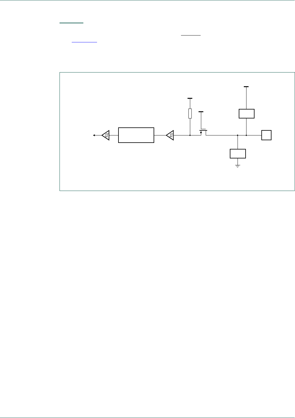
UM10462 All information provided in this document is subject to legal disclaimers. © NXP B.V. 2014. All rights reserved.
User manual Rev. 5.3 — 11 June 2014 82 of 521
NXP Semiconductors UM10462
Chapter 7: LPC11U3x/2x/1x I/O configuration
7.3.9 RESET pin (pin RESET_PIO0_0)
See Figure 14 for the reset pad configuration. RESET functionality is not available in
Deep power-down mode. Use the WAKEUP pin to reset the chip and wake up from Deep
power-down mode. An external pull-up resistor is required on this pin for the Deep
power-down mode. The reset pin includes a fixed 20 ns glitch filter.
7.3.10 WAKEUP pin (pin PIO0_16)
The WAKEUP pin is combined with pin PIO0_16 and includes a 20 ns fixed glitch filter.
This pin must be pulled HIGH externally to enter Deep power-down mode and pulled LOW
to exit Deep power-down mode. A LOW-going pulse as short as 50 ns wakes up the part.
Fig 14. Reset pad configuration
VSS
reset
002aaf274
VDD
VDD
VDD
Rpu ESD
ESD
20 ns RC
GLITCH FILTER PIN
UM10462 All information provided in this document is subject to legal disclaimers. © NXP B.V. 2014. All rights reserved.
User manual Rev. 5.3 — 11 June 2014 83 of 521
NXP Semiconductors UM10462
Chapter 7: LPC11U3x/2x/1x I/O configuration
7.4 Register description
The I/O configuration registers control the PIO port pins, the inputs and outputs of all
peripherals and functional blocks, the I2C-bus pins, and the ADC input pins.
Each port pin PIOn_m has one IOCON register assigned to control the pin’s function and
electrical characteristics.
Table 75. Register overview: I/O configuration (base address 0x4004 4000)
Name Access Address
offset Description Reset value Reference
RESET_PIO0_0 R/W 0x000 I/O configuration for pin RESET/PIO0_0 0x0000 0090 Table 76
PIO0_1 R/W 0x004 I/O configuration for pin
PIO0_1/CLKOUT/CT32B0_MAT2/USB_FTO
GGLE
0x0000 0090 Table 77
PIO0_2 R/W 0x008 I/O configuration for pin
PIO0_2/SSEL0/CT16B0_CAP0/IOH_0
0x0000 0090 Table 78
PIO0_3 R/W 0x00C I/O configuration for pin
PIO0_3/USB_VBUS/IOH_1
0x0000 0090 Table 79
PIO0_4 R/W 0x010 I/O configuration for pin PIO0_4/SCL/IOH_2 0x0000 0080 Table 80
PIO0_5 R/W 0x014 I/O configuration for pin PIO0_5/SDA/IOH_3 0x0000 0080 Table 81
PIO0_6 R/W 0x018 I/O configuration for pin
PIO0_6/USB_CONNECT/SCK0/IOH_4
0x0000 0090 Table 82
PIO0_7 R/W 0x01C I/O configuration for pin PIO0_7/CTS/IOH_5 0x0000 0090 Table 83
PIO0_8 R/W 0x020 I/O configuration for pin
PIO0_8/MISO0/CT16B0_MAT0/R/IOH_6
0x0000 0090 Table 84
PIO0_9 R/W 0x024 I/O configuration for pin
PIO0_9/MOSI0/CT16B0_MAT1/R/IOH_7
0x0000 0090 Table 85
SWCLK_PIO0_10 R/W 0x028 I/O configuration for pin SWCLK/PIO0_10/
SCK0/CT16B0_MAT2
0x0000 0090 Table 86
TDI_PIO0_11 R/W 0x02C I/O configuration for pin
TDI/PIO0_11/AD0/CT32B0_MAT3
0x0000 0090 Table 87
TMS_PIO0_12 R/W 0x030 I/O configuration for pin
TMS/PIO0_12/AD1/CT32B1_CAP0
0x0000 0090 Table 88
TDO_PIO0_13 R/W 0x034 I/O configuration for pin
TDO/PIO0_13/AD2/CT32B1_MAT0
0x0000 0090 Table 89
TRST_PIO0_14 R/W 0x038 I/O configuration for pin
TRST/PIO0_14/AD3/CT32B1_MAT1
0x0000 0090 Table 90
SWDIO_PIO0_15 R/W 0x03C I/O configuration for pin
SWDIO/PIO0_15/AD4/CT32B1_MAT2
0x0000 0090 Table 91
PIO0_16 R/W 0x040 I/O configuration for pin
PIO0_16/AD5/CT32B1_MAT3/IOH_8
WAKEUP
0x0000 0090 Table 92
PIO0_17 R/W 0x044 I/O configuration for pin
PIO0_17/RTS/CT32B0_CAP0/SCLK
0x0000 0090 Table 93
PIO0_18 R/W 0x048 I/O configuration for pin
PIO0_18/RXD/CT32B0_MAT0
0x0000 0090 Table 94
PIO0_19 R/W 0x04C I/O configuration for pin
PIO0_19/TXD/CT32B0_MAT1
0x0000 0090 Table 95
UM10462 All information provided in this document is subject to legal disclaimers. © NXP B.V. 2014. All rights reserved.
User manual Rev. 5.3 — 11 June 2014 84 of 521
NXP Semiconductors UM10462
Chapter 7: LPC11U3x/2x/1x I/O configuration
PIO0_20 R/W 0x050 I/O configuration for pin
PIO0_20/CT16B1_CAP0
0x0000 0090 Table 96
PIO0_21 R/W 0x054 I/O configuration for pin
PIO0_21/CT16B1_MAT0/MOSI1
0x0000 0090 Table 97
PIO0_22 R/W 0x058 I/O configuration for pin
PIO0_22/AD6/CT16B1_MAT1/MISO1
0x0000 0090 Table 98
PIO0_23 R/W 0x05C I/O configuration for pin
PIO0_23/AD7/IOH_9
0x0000 0090 Table 99
PIO1_0 R/W 0x060 I/O configuration for pin
PIO1_0/CT32B1_MAT0/IOH_10
0x0000 0090 Table 100
PIO1_1 R/W 0x064 I/O configuration for pin
PIO1_1/CT32B1_MAT1/IOH_11
0x0000 0090 Table 101
PIO1_2 R/W 0x068 I/O configuration for pin
PIO1_2/CT32B1_MAT2IOH_12
0x0000 0090 Table 102
PIO1_3 R/W 0x06C I/O configuration for pin
PIO1_3/CT32B1_MAT3/IOH_13
0x0000 0090 Table 103
PIO1_4 R/W 0x070 I/O configuration for pin
PIO1_4/CT32B1_CAP0/IOH_14
0x0000 0090 Table 104
PIO1_5 R/W 0x074 I/O configuration for pin
PIO1_5/CT32B1_CAP1/IOH_15
0x0000 0090 Table 105
PIO1_6 R/W 0x078 I/O configuration for pin PIO1_6/IOH_16 0x0000 0090 Table 106
PIO1_7 R/W 0x07C I/O configuration for pin PIO1_7/IOH_17 0x0000 0090 Table 107
PIO1_8 R/W 0x080 I/O configuration for pin PIO1_8/IOH_18 0x0000 0090 Table 108
PIO1_9 R/W 0x084 I/O configuration for pin PIO1_9 0x0000 0090 Table 109
PIO1_10 R/W 0x088 I/O configuration for pin PIO1_10 0x0000 0090 Table 110
PIO1_11 R/W 0x08C I/O configuration for pin PIO1_11 0x0000 0090 Table 111
PIO1_12 R/W 0x090 I/O configuration for pin PIO1_12 0x0000 0090 Table 112
PIO1_13 R/W 0x094 I/O configuration for pin
PIO1_13/DTR/CT16B0_MAT0/TXD
0x0000 0090 Table 113
PIO1_14 R/W 0x098 I/O configuration for pin
PIO1_14/DSR/CT16B0_MAT1/RXD
0x0000 0090 Table 114
PIO1_15 R/W 0x09C I/O configuration for pin PIO1_15/DCD/
CT16B0_MAT2/SCK1
0x0000 0090 Table 115
PIO1_16 R/W 0x0A0 I/O configuration for pin
PIO1_16/RI/CT16B0_CAP0
0x0000 0090 Table 116
PIO1_17 R/W 0x0A4 I/O configuration for
PIO1_17/CT16B0_CAP1/RXD
0x0000 0090 Table 117
PIO1_18 R/W 0x0A8 I/O configuration for
PIO1_18/CT16B1_CAP1/TXD
0x0000 0090 Table 118
PIO1_19 R/W 0x0AC I/O configuration for pin
PIO1_19/DTR/SSEL1
0x0000 0090 Table 119
PIO1_20 R/W 0x0B0 I/O configuration for pin
PIO1_20/DSR/SCK1
0x0000 0090 Table 120
PIO1_21 R/W 0x0B4 I/O configuration for pin
PIO1_21/DCD/MISO1
0x0000 0090 Table 121
Table 75. Register overview: I/O configuration (base address 0x4004 4000) …continued
Name Access Address
offset Description Reset value Reference

UM10462 All information provided in this document is subject to legal disclaimers. © NXP B.V. 2014. All rights reserved.
User manual Rev. 5.3 — 11 June 2014 85 of 521
NXP Semiconductors UM10462
Chapter 7: LPC11U3x/2x/1x I/O configuration
7.4.1 I/O configuration registers
7.4.1.1 RESET_PIO0_0 register
PIO1_22 R/W 0x0B8 I/O configuration for pin PIO1_22/RI/MOSI1 0x0000 0090 Table 122
PIO1_23 R/W 0x0BC I/O configuration for pin
PIO1_23/CT16B1_MAT1/SSEL1
0x0000 0090 Table 123
PIO1_24 R/W 0x0C0 I/O configuration for pin PIO1_24/
CT32B0_MAT0
0x0000 0090 Table 124
PIO1_25 R/W 0x0C4 I/O configuration for pin
PIO1_25/CT32B0_MAT1
0x0000 0090 Table 125
PIO1_26 R/W 0x0C8 I/O configuration for pin
PIO1_26/CT32B0_MAT2/RXD/IOH_19
0x0000 0090 Table 126
PIO1_27 R/W 0x0CC I/O configuration for pin
PIO1_27/CT32B0_MAT3/TXD/IOH_20
0x0000 0090 Table 127
PIO1_28 R/W 0x0D0 I/O configuration for pin
PIO1_28/CT32B0_CAP0/SCLK
0x0000 0090 Table 128
PIO1_29 R/W 0x0D4 I/O configuration for pin PIO1_29/SCK0/
CT32B0_CAP1
0x0000 0090 Table 129
- R/W 0x0D8 Reserved - -
PIO1_31 R/W 0x0DC I/O configuration for pin PIO1_31 0x0000 0090 Table 130
Table 75. Register overview: I/O configuration (base address 0x4004 4000) …continued
Name Access Address
offset Description Reset value Reference
Table 76. RESET_PIO0_0 register (RESET_PIO0_0, address 0x4004 4000) bit
description
Bit Symbol Value Description Reset
value
2:0 FUNC Selects pin function. Values 0x2 to 0x7 are reserved. 000
0x0 RESET.
0x1 PIO0_0.
4:3 MODE Selects function mode (on-chip pull-up/pull-down resistor
control).
10
0x0 Inactive (no pull-down/pull-up resistor enabled).
0x1 Pull-down resistor enabled.
0x2 Pull-up resistor enabled.
0x3 Repeater mode.
5 HYS Hysteresis. 0
0 Disable.
1 Enable.
6 INV Invert input 0
0 Input not inverted (HIGH on pin reads as 1, LOW on pin reads
as 0).
1 Input inverted (HIGH on pin reads as 0, LOW on pin reads as
1).
9:7 - - Reserved. 001

UM10462 All information provided in this document is subject to legal disclaimers. © NXP B.V. 2014. All rights reserved.
User manual Rev. 5.3 — 11 June 2014 86 of 521
NXP Semiconductors UM10462
Chapter 7: LPC11U3x/2x/1x I/O configuration
7.4.1.2 PIO0_1 register
10 OD Open-drain mode. 0
0 Disable.
1 Open-drain mode enabled.
Remark: This is not a true open-drain mode.
31:11 - - Reserved. 0
Table 76. RESET_PIO0_0 register (RESET_PIO0_0, address 0x4004 4000) bit
description …continued
Bit Symbol Value Description Reset
value
Table 77. PIO0_1 register (PIO0_1, address 0x4004 4004) bit description
Bit Symbol Value Description Reset
value
2:0 FUNC Selects pin function. Values 0x4 to 0x7 are reserved. 000
0x0 PIO0_1.
0x1 CLKOUT.
0x2 CT32B0_MAT2.
0x3 USB_FTOGGLE.
4:3 MODE Selects function mode (on-chip pull-up/pull-down resistor
control).
10
0x0 Inactive (no pull-down/pull-up resistor enabled).
0x1 Pull-down resistor enabled.
0x2 Pull-up resistor enabled.
0x3 Repeater mode.
5 HYS Hysteresis. 0
0 Disable.
1 Enable.
6 INV Invert input 0
0 Input not inverted (HIGH on pin reads as 1, LOW on pin reads
as 0).
1 Input inverted (HIGH on pin reads as 0, LOW on pin reads as
1).
9:7 - - Reserved. 001
10 OD Open-drain mode. 0
0 Disable.
1 Open-drain mode enabled.
Remark: This is not a true open-drain mode.
31:11 - - Reserved. 0

UM10462 All information provided in this document is subject to legal disclaimers. © NXP B.V. 2014. All rights reserved.
User manual Rev. 5.3 — 11 June 2014 87 of 521
NXP Semiconductors UM10462
Chapter 7: LPC11U3x/2x/1x I/O configuration
7.4.1.3 PIO0_2 register
7.4.1.4 PIO0_3 register
Table 78. PIO0_2 register (PIO0_2, address 0x4004 4008) bit description
Bit Symbol Value Description Reset
value
2:0 FUNC Selects pin function. Values 0x4 to 0x7 are reserved. 000
0x0 PIO0_2.
0x1 SSEL0.
0x2 CT16B0_CAP0.
0x3 IOH_0.
4:3 MODE Selects function mode (on-chip pull-up/pull-down resistor
control).
10
0x0 Inactive (no pull-down/pull-up resistor enabled).
0x1 Pull-down resistor enabled.
0x2 Pull-up resistor enabled.
0x3 Repeater mode.
5 HYS Hysteresis. 0
0 Disable.
1 Enable.
6 INV Invert input 0
0 Input not inverted (HIGH on pin reads as 1, LOW on pin reads
as 0).
1 Input inverted (HIGH on pin reads as 0, LOW on pin reads as
1).
9:7 - - Reserved. 001
10 OD Open-drain mode. 0
0 Disable.
1 Open-drain mode enabled.
Remark: This is not a true open-drain mode.
31:11 - - Reserved. 0
Table 79. PIO0_3 register (PIO0_3, address 0x4004 400C) bit description
Bit Symbol Value Description Reset
value
2:0 FUNC Selects pin function. Values 0x3 to 0x7 are reserved. 000
0x0 PIO0_3.
0x1 USB_VBUS.
0x2 IOH_1.
4:3 MODE Selects function mode (on-chip pull-up/pull-down resistor
control).
10
0x0 Inactive (no pull-down/pull-up resistor enabled).
0x1 Pull-down resistor enabled.
0x2 Pull-up resistor enabled.
0x3 Repeater mode.

UM10462 All information provided in this document is subject to legal disclaimers. © NXP B.V. 2014. All rights reserved.
User manual Rev. 5.3 — 11 June 2014 88 of 521
NXP Semiconductors UM10462
Chapter 7: LPC11U3x/2x/1x I/O configuration
7.4.1.5 PIO0_4 register
7.4.1.6 PIO0_5 register
5 HYS Hysteresis. 0
0 Disable.
1 Enable.
6 INV Invert input 0
0 Input not inverted (HIGH on pin reads as 1, LOW on pin reads
as 0).
1 Input inverted (HIGH on pin reads as 0, LOW on pin reads as
1).
9:7 - - Reserved. 001
10 OD Open-drain mode. 0
0 Disable.
1 Open-drain mode enabled.
Remark: This is not a true open-drain mode.
31:11 - - Reserved. 0
Table 79. PIO0_3 register (PIO0_3, address 0x4004 400C) bit description …continued
Bit Symbol Value Description Reset
value
Table 80. PIO0_4 register (PIO0_4, address 0x4004 4010) bit description
Bit Symbol Value Description Reset
value
2:0 FUNC Selects pin function. Values 0x3 to 0x7 are reserved. 000
0x0 PIO0_4 (open-drain pin).
0x1 I2C SCL (open-drain pin).
0x2 IOH_2.
7:3 - - Reserved. 10000
9:8 I2CMODE Selects I2C mode (see Section 7.3.8).
Select Standard mode (I2CMODE = 00, default) or
Standard I/O functionality (I2CMODE = 01) if the pin
function is GPIO (FUNC = 000).
00
0x0 Standard mode/ Fast-mode I2C.
0x1 Standard I/O functionality
0x2 Fast-mode Plus I2C
0x3 Reserved.
31:10 - - Reserved. -
Table 81. PIO0_5 register (PIO0_5, address 0x4004 4014) bit description
Bit Symbol Value Description Reset
value
2:0 FUNC Selects pin function. Values 0x3 to 0x7 are reserved. 000
0x0 PIO0_5 (open-drain pin).
0x1 I2C SDA (open-drain pin).
0x2 IOH_3.

UM10462 All information provided in this document is subject to legal disclaimers. © NXP B.V. 2014. All rights reserved.
User manual Rev. 5.3 — 11 June 2014 89 of 521
NXP Semiconductors UM10462
Chapter 7: LPC11U3x/2x/1x I/O configuration
7.4.1.7 PIO0_6 register
7:3 - - Reserved. 10000
9:8 I2CMODE Selects I2C mode (see Section 7.3.8).
Select Standard mode (I2CMODE = 00, default) or Standard
I/O functionality (I2CMODE = 01) if the pin function is GPIO
(FUNC = 000).
00
0x0 Standard mode/ Fast-mode I2C.
0x1 Standard I/O functionality
0x2 Fast-mode Plus I2C
0x3 Reserved.
31:10 - - Reserved. -
Table 81. PIO0_5 register (PIO0_5, address 0x4004 4014) bit description …continued
Bit Symbol Value Description Reset
value
Table 82. PIO0_6 register (PIO0_6, address 0x4004 4018) bit description
Bit Symbol Value Description Reset
value
2:0 FUNC Selects pin function. Values 0x4 to 0x7 are reserved. 000
0x0 PIO0_6.
0x1 USB_CONNECT.
0x2 SCK0.
0x3 SCK0.IOH_4
4:3 MODE Selects function mode (on-chip pull-up/pull-down resistor
control).
10
0x0 Inactive (no pull-down/pull-up resistor enabled).
0x1 Pull-down resistor enabled.
0x2 Pull-up resistor enabled.
0x3 Repeater mode.
5 HYS Hysteresis. 0
0 Disable.
1 Enable.
6 INV Invert input 0
0 Input not inverted (HIGH on pin reads as 1, LOW on pin reads
as 0).
1 Input inverted (HIGH on pin reads as 0, LOW on pin reads as
1).
9:7 - - Reserved. 001
10 OD Open-drain mode. 0
0 Disable.
1 Open-drain mode enabled.
Remark: This is not a true open-drain mode.
31:11 - - Reserved. 0

UM10462 All information provided in this document is subject to legal disclaimers. © NXP B.V. 2014. All rights reserved.
User manual Rev. 5.3 — 11 June 2014 90 of 521
NXP Semiconductors UM10462
Chapter 7: LPC11U3x/2x/1x I/O configuration
7.4.1.8 PIO0_7 register
7.4.1.9 PIO0_8 register
Table 83. PIO0_7 register (PIO0_7, address 0x4004 401C) bit description
Bit Symbol Value Description Reset
value
2:0 FUNC Selects pin function. Values 0x3 to 0x7 are reserved. 000
0x0 PIO0_7.
0x1 CTS.
0x2 IOH_5.
4:3 MODE Selects function mode (on-chip pull-up/pull-down resistor
control).
10
0x0 Inactive (no pull-down/pull-up resistor enabled).
0x1 Pull-down resistor enabled.
0x2 Pull-up resistor enabled.
0x3 Repeater mode.
5 HYS Hysteresis. 0
0 Disable.
1 Enable.
6 INV Invert input 0
0 Input not inverted (HIGH on pin reads as 1, LOW on pin reads
as 0).
1 Input inverted (HIGH on pin reads as 0, LOW on pin reads as
1).
9:7 - - Reserved. 001
10 OD Open-drain mode. 0
0 Disable.
1 Open-drain mode enabled.
Remark: This is not a true open-drain mode.
31:11 - - Reserved. 0
Table 84. PIO0_8 register (PIO0_8, address 0x4004 4020) bit description
Bit Symbol Value Description Reset
value
2:0 FUNC Selects pin function. Values 0x3 and 0x5 to 0x7 are reserved. 000
0x0 PIO0_8.
0x1 MISO0.
0x2 CT16B0_MAT0.
0x4 IOH_6.
4:3 MODE Selects function mode (on-chip pull-up/pull-down resistor
control).
10
0x0 Inactive (no pull-down/pull-up resistor enabled).
0x1 Pull-down resistor enabled.
0x2 Pull-up resistor enabled.
0x3 Repeater mode.

UM10462 All information provided in this document is subject to legal disclaimers. © NXP B.V. 2014. All rights reserved.
User manual Rev. 5.3 — 11 June 2014 91 of 521
NXP Semiconductors UM10462
Chapter 7: LPC11U3x/2x/1x I/O configuration
7.4.1.10 PIO0_9 register
5 HYS Hysteresis. 0
0 Disable.
1 Enable.
6 INV Invert input 0
0 Input not inverted (HIGH on pin reads as 1, LOW on pin reads
as 0).
1 Input inverted (HIGH on pin reads as 0, LOW on pin reads as
1).
9:7 - - Reserved. 001
10 OD Open-drain mode. 0
0 Disable.
1 Open-drain mode enabled.
Remark: This is not a true open-drain mode.
31:11 - - Reserved. 0
Table 84. PIO0_8 register (PIO0_8, address 0x4004 4020) bit description …continued
Bit Symbol Value Description Reset
value
Table 85. PIO0_9 register (PIO0_9, address 0x4004 4024) bit description
Bit Symbol Value Description Reset
value
2:0 FUNC Selects pin function. Values 0x3 and 0x5 to 0x7 are reserved. 000
0x0 PIO0_9.
0x1 MOSI0.
0x2 CT16B0_MAT1.
0x4 IOH_7
4:3 MODE Selects function mode (on-chip pull-up/pull-down resistor
control).
10
0x0 Inactive (no pull-down/pull-up resistor enabled).
0x1 Pull-down resistor enabled.
0x2 Pull-up resistor enabled.
0x3 Repeater mode.
5 HYS Hysteresis. 0
0 Disable.
1 Enable.
6 INV Invert input 0
0 Input not inverted (HIGH on pin reads as 1, LOW on pin reads
as 0).
1 Input inverted (HIGH on pin reads as 0, LOW on pin reads as
1).
9:7 - - Reserved. 001

UM10462 All information provided in this document is subject to legal disclaimers. © NXP B.V. 2014. All rights reserved.
User manual Rev. 5.3 — 11 June 2014 92 of 521
NXP Semiconductors UM10462
Chapter 7: LPC11U3x/2x/1x I/O configuration
7.4.1.11 SWCLK_PIO0_10 register
10 OD Open-drain mode. 0
0 Disable.
1 Open-drain mode enabled.
Remark: This is not a true open-drain mode.
31:11 - - Reserved. 0
Table 85. PIO0_9 register (PIO0_9, address 0x4004 4024) bit description …continued
Bit Symbol Value Description Reset
value
Table 86. SWCLK_PIO0_10 register (SWCLK_PIO0_10, address 0x4004 4028) bit
description
Bit Symbol Value Description Reset
value
2:0 FUNC Selects pin function. Values 0x4 to 0x7 are reserved. 000
0x0 SWCLK.
0x1 PIO0_10.
0x2 SCK0.
0x3 CT16B0_MAT2.
4:3 MODE Selects function mode (on-chip pull-up/pull-down resistor
control).
10
0x0 Inactive (no pull-down/pull-up resistor enabled).
0x1 Pull-down resistor enabled.
0x2 Pull-up resistor enabled.
0x3 Repeater mode.
5HYS Hysteresis. 0
0 Disable.
1 Enable.
6 INV Invert input 0
0 Input not inverted (HIGH on pin reads as 1, LOW on pin reads
as 0).
1 Input inverted (HIGH on pin reads as 0, LOW on pin reads as
1).
9:7 - - Reserved. 001
10 OD Open-drain mode. 0
0 Disable.
1 Open-drain mode enabled.
Remark: This is not a true open-drain mode.
31:11 - - Reserved. 0

UM10462 All information provided in this document is subject to legal disclaimers. © NXP B.V. 2014. All rights reserved.
User manual Rev. 5.3 — 11 June 2014 93 of 521
NXP Semiconductors UM10462
Chapter 7: LPC11U3x/2x/1x I/O configuration
7.4.1.12 TDI_PIO0_11 register
Table 87. TDI_PIO0_11 register (TDI_PIO0_11, address 0x4004 402C) bit description
Bit Symbol Value Description Reset
value
2:0 FUNC Selects pin function. Values 0x4 to 0x7 are reserved. 000
0x0 TDI.
0x1 PIO0_11.
0x2 AD0.
0x3 CT32B0_MAT3.
4:3 MODE Selects function mode (on-chip pull-up/pull-down resistor
control).
10
0x0 Inactive (no pull-down/pull-up resistor enabled).
0x1 Pull-down resistor enabled.
0x2 Pull-up resistor enabled.
0x3 Repeater mode.
5 HYS Hysteresis. 0
0 Disable.
1 Enable.
6 INV Invert input 0
0 Input not inverted (HIGH on pin reads as 1, LOW on pin reads
as 0).
1 Input inverted (HIGH on pin reads as 0, LOW on pin reads as
1).
7 ADMODE Selects Analog/Digital mode. 1
0 Analog input mode.
1 Digital functional mode.
8 FILTR Selects 10 ns input glitch filter. 0
0 Filter enabled.
1 Filter disabled.
9 - - Reserved. 0
10 OD Open-drain mode. 0
0 Disable.
1 Open-drain mode enabled.
Remark: This is not a true open-drain mode.
31:11 - - Reserved. 0

UM10462 All information provided in this document is subject to legal disclaimers. © NXP B.V. 2014. All rights reserved.
User manual Rev. 5.3 — 11 June 2014 94 of 521
NXP Semiconductors UM10462
Chapter 7: LPC11U3x/2x/1x I/O configuration
7.4.1.13 TMS_PIO0_12 register
Table 88. TMS_PIO0_12 register (TMS_PIO0_12, address 0x4004 4030) bit description
Bit Symbol Value Description Reset
value
2:0 FUNC Selects pin function. Values 0x4 to 0x7 are reserved. 000
0x0 TMS.
0x1 PIO0_12.
0x2 AD1.
0x3 CT32B1_CAP0.
4:3 MODE Selects function mode (on-chip pull-up/pull-down resistor
control).
10
0x0 Inactive (no pull-down/pull-up resistor enabled).
0x1 Pull-down resistor enabled.
0x2 Pull-up resistor enabled.
0x3 Repeater mode.
5 HYS Hysteresis. 0
0 Disable.
1 Enable.
6 INV Invert input 0
0 Input not inverted (HIGH on pin reads as 1, LOW on pin reads
as 0).
1 Input inverted (HIGH on pin reads as 0, LOW on pin reads as
1).
7 ADMODE Selects Analog/Digital mode. 1
0 Analog input mode.
1 Digital functional mode.
8 FILTR Selects 10 ns input glitch filter. 0
0 Filter enabled.
1 Filter disabled.
9 - - Reserved. 0
10 OD Open-drain mode. 0
0 Disable.
1 Open-drain mode enabled.
Remark: This is not a true open-drain mode.
31:11 - - Reserved. 0

UM10462 All information provided in this document is subject to legal disclaimers. © NXP B.V. 2014. All rights reserved.
User manual Rev. 5.3 — 11 June 2014 95 of 521
NXP Semiconductors UM10462
Chapter 7: LPC11U3x/2x/1x I/O configuration
7.4.1.14 PIO0_13 register
Table 89. TDO_PIO0_13 register (TDO_PIO0_13, address 0x4004 4034) bit description
Bit Symbol Value Description Reset
value
2:0 FUNC Selects pin function. Values 0x4 to 0x7 are reserved. 000
0x0 TDO.
0x1 PIO0_13.
0x2 AD2.
0x3 CT32B1_MAT0.
4:3 MODE Selects function mode (on-chip pull-up/pull-down resistor
control).
10
0x0 Inactive (no pull-down/pull-up resistor enabled).
0x1 Pull-down resistor enabled.
0x2 Pull-up resistor enabled.
0x3 Repeater mode.
5 HYS Hysteresis. 0
0 Disable.
1 Enable.
6 INV Invert input 0
0 Input not inverted (HIGH on pin reads as 1, LOW on pin reads
as 0).
1 Input inverted (HIGH on pin reads as 0, LOW on pin reads as
1).
7 ADMODE Selects Analog/Digital mode. 1
0 Analog input mode.
1 Digital functional mode.
8 FILTR Selects 10 ns input glitch filter. 0
0 Filter enabled.
1 Filter disabled.
9 - - Reserved. 0
10 OD Open-drain mode. 0
0 Disable.
1 Open-drain mode enabled.
Remark: This is not a true open-drain mode.
31:11 - - Reserved. 0

UM10462 All information provided in this document is subject to legal disclaimers. © NXP B.V. 2014. All rights reserved.
User manual Rev. 5.3 — 11 June 2014 96 of 521
NXP Semiconductors UM10462
Chapter 7: LPC11U3x/2x/1x I/O configuration
7.4.1.15 TRST_PIO0_14 register
Table 90. TRST_PIO0_14 register (TRST_PIO0_14, address 0x4004 4038) bit description
Bit Symbol Value Description Reset
value
2:0 FUNC Selects pin function. Values 0x4 to 0x7 are reserved. 000
0x0 TRST.
0x1 PIO0_14.
0x2 AD3.
0x3 CT32B1_MAT1.
4:3 MODE Selects function mode (on-chip pull-up/pull-down resistor
control).
10
0x0 Inactive (no pull-down/pull-up resistor enabled).
0x1 Pull-down resistor enabled.
0x2 Pull-up resistor enabled.
0x3 Repeater mode.
5 HYS Hysteresis. 0
0 Disable.
1 Enable.
6 INV Invert input 0
0 Input not inverted (HIGH on pin reads as 1, LOW on pin reads
as 0).
1 Input inverted (HIGH on pin reads as 0, LOW on pin reads as
1).
7 ADMODE Selects Analog/Digital mode. 1
0 Analog input mode.
1 Digital functional mode.
8 FILTR Selects 10 ns input glitch filter. 0
0 Filter enabled.
1 Filter disabled.
9 - - Reserved. 0
10 OD Open-drain mode. 0
0 Disable.
1 Open-drain mode enabled.
Remark: This is not a true open-drain mode.
31:11 - - Reserved. 0

UM10462 All information provided in this document is subject to legal disclaimers. © NXP B.V. 2014. All rights reserved.
User manual Rev. 5.3 — 11 June 2014 97 of 521
NXP Semiconductors UM10462
Chapter 7: LPC11U3x/2x/1x I/O configuration
7.4.1.16 SWDIO_PIO0_15 register
Table 91. SWDIO_PIO0_15 register (SWDIO_PIO0_15, address 0x4004 403C) bit description
Bit Symbol Value Description Reset
value
2:0 FUNC Selects pin function. Values 0x4 to 0x7 are reserved. 000
0x0 SWDIO.
0x1 PIO0_15.
0x2 AD4.
0x3 CT32B1_MAT2.
4:3 MODE Selects function mode (on-chip pull-up/pull-down resistor
control).
10
0x0 Inactive (no pull-down/pull-up resistor enabled).
0x1 Pull-down resistor enabled.
0x2 Pull-up resistor enabled.
0x3 Repeater mode.
5 HYS Hysteresis. 0
0 Disable.
1 Enable.
6 INV Invert input 0
0 Input not inverted (HIGH on pin reads as 1, LOW on pin reads
as 0).
1 Input inverted (HIGH on pin reads as 0, LOW on pin reads as
1).
7 ADMODE Selects Analog/Digital mode. 1
0 Analog input mode.
1 Digital functional mode.
8 FILTR Selects 10 ns input glitch filter. 0
0 Filter enabled.
1 Filter disabled.
9 - - Reserved. 0
10 OD Open-drain mode. 0
0 Disable.
1 Open-drain mode enabled.
Remark: This is not a true open-drain mode.
31:11 - - Reserved. 0

UM10462 All information provided in this document is subject to legal disclaimers. © NXP B.V. 2014. All rights reserved.
User manual Rev. 5.3 — 11 June 2014 98 of 521
NXP Semiconductors UM10462
Chapter 7: LPC11U3x/2x/1x I/O configuration
7.4.1.17 PIO0_16 register
Table 92. PIO0_16 register (PIO0_16, address 0x4004 4040) bit description
Bit Symbol Value Description Reset
value
2:0 FUNC Selects pin function. This pin functions as WAKEUP pin if the
LPC11U3x/2x/1x is in Deep power-down mode regardless of
the value of FUNC. Values 0x4 to 0x7 are reserved.
000
0x0 PIO0_16.
0x1 AD5.
0x2 CT32B1_MAT3.
0x3 IOH_8.
4:3 MODE Selects function mode (on-chip pull-up/pull-down resistor
control).
10
0x0 Inactive (no pull-down/pull-up resistor enabled).
0x1 Pull-down resistor enabled.
0x2 Pull-up resistor enabled.
0x3 Repeater mode.
5 HYS Hysteresis. 0
0 Disable.
1 Enable.
6 INV Invert input 0
0 Input not inverted (HIGH on pin reads as 1, LOW on pin reads
as 0).
1 Input inverted (HIGH on pin reads as 0, LOW on pin reads as
1).
7 ADMODE Selects Analog/Digital mode. 1
0 Analog input mode.
1 Digital functional mode.
8 FILTR Selects 10 ns input glitch filter. 0
0 Filter enabled.
1 Filter disabled.
9 - - Reserved. 0
10 OD Open-drain mode. 0
0 Disable.
1 Open-drain mode enabled.
Remark: This is not a true open-drain mode.
31:11 - - Reserved. 0

UM10462 All information provided in this document is subject to legal disclaimers. © NXP B.V. 2014. All rights reserved.
User manual Rev. 5.3 — 11 June 2014 99 of 521
NXP Semiconductors UM10462
Chapter 7: LPC11U3x/2x/1x I/O configuration
7.4.1.18 PIO0_17 register
7.4.1.19 PIO0_18 register
Table 93. PIO0_17 register (PIO0_17, address 0x4004 4044) bit description
Bit Symbol Value Description Reset
value
2:0 FUNC Selects pin function. Values 0x4 to 0x7 are reserved. 000
0x0 PIO0_17.
0x1 RTS.
0x2 CT32B0_CAP0.
0x3 SCLK (UART synchronous clock).
4:3 MODE Selects function mode (on-chip pull-up/pull-down resistor
control).
10
0x0 Inactive (no pull-down/pull-up resistor enabled).
0x1 Pull-down resistor enabled.
0x2 Pull-up resistor enabled.
0x3 Repeater mode.
5 HYS Hysteresis. 0
0 Disable.
1 Enable.
6 INV Invert input 0
0 Input not inverted (HIGH on pin reads as 1, LOW on pin reads
as 0).
1 Input inverted (HIGH on pin reads as 0, LOW on pin reads as
1).
9:7 - - Reserved. 001
10 OD Open-drain mode. 0
0 Disable.
1 Open-drain mode enabled.
Remark: This is not a true open-drain mode.
31:11 - - Reserved. 0
Table 94. PIO0_18 register (PIO0_18, address 0x4004 4048) bit description
Bit Symbol Value Description Reset
value
2:0 FUNC Selects pin function. Values 0x3 to 0x7 are reserved. 000
0x0 PIO0_18.
0x1 RXD.
0x2 CT32B0_MAT0.
4:3 MODE Selects function mode (on-chip pull-up/pull-down resistor
control).
10
0x0 Inactive (no pull-down/pull-up resistor enabled).
0x1 Pull-down resistor enabled.
0x2 Pull-up resistor enabled.
0x3 Repeater mode.

UM10462 All information provided in this document is subject to legal disclaimers. © NXP B.V. 2014. All rights reserved.
User manual Rev. 5.3 — 11 June 2014 100 of 521
NXP Semiconductors UM10462
Chapter 7: LPC11U3x/2x/1x I/O configuration
7.4.1.20 PIO0_19 register
5 HYS Hysteresis. 0
0 Disable.
1 Enable.
6 INV Invert input 0
0 Input not inverted (HIGH on pin reads as 1, LOW on pin reads
as 0).
1 Input inverted (HIGH on pin reads as 0, LOW on pin reads as
1).
9:7 - - Reserved. 001
10 OD Open-drain mode. 0
0 Disable.
1 Open-drain mode enabled.
Remark: This is not a true open-drain mode.
31:11 - - Reserved. 0
Table 94. PIO0_18 register (PIO0_18, address 0x4004 4048) bit description …continued
Bit Symbol Value Description Reset
value
Table 95. PIO0_19 register (PIO0_19, address 0x4004 404C) bit description
Bit Symbol Value Description Reset
value
2:0 FUNC Selects pin function. Values 0x3 to 0x7 are reserved. 000
0x0 PIO0_19.
0x1 TXD.
0x2 CT32B0_MAT1.
4:3 MODE Selects function mode (on-chip pull-up/pull-down resistor
control).
10
0x0 Inactive (no pull-down/pull-up resistor enabled).
0x1 Pull-down resistor enabled.
0x2 Pull-up resistor enabled.
0x3 Repeater mode.
5 HYS Hysteresis. 0
0 Disable.
1 Enable.
6 INV Invert input 0
0 Input not inverted (HIGH on pin reads as 1, LOW on pin reads
as 0).
1 Input inverted (HIGH on pin reads as 0, LOW on pin reads as
1).
9:7 - - Reserved. 001

UM10462 All information provided in this document is subject to legal disclaimers. © NXP B.V. 2014. All rights reserved.
User manual Rev. 5.3 — 11 June 2014 101 of 521
NXP Semiconductors UM10462
Chapter 7: LPC11U3x/2x/1x I/O configuration
7.4.1.21 PIO0_20 register
10 OD Open-drain mode. 0
0 Disable.
1 Open-drain mode enabled.
Remark: This is not a true open-drain mode.
31:11 - - Reserved. 0
Table 95. PIO0_19 register (PIO0_19, address 0x4004 404C) bit description …continued
Bit Symbol Value Description Reset
value
Table 96. PIO0_20 register (PIO0_20, address 0x4004 4050) bit description
Bit Symbol Value Description Reset
value
2:0 FUNC Selects pin function. Values 0x2 to 0x7 are reserved. 000
0x0 PIO0_20.
0x1 CT16B1_CAP0.
4:3 MODE Selects function mode (on-chip pull-up/pull-down resistor
control).
10
0x0 Inactive (no pull-down/pull-up resistor enabled).
0x1 Pull-down resistor enabled.
0x2 Pull-up resistor enabled.
0x3 Repeater mode.
5 HYS Hysteresis. 0
0 Disable.
1 Enable.
6 INV Invert input 0
0 Input not inverted (HIGH on pin reads as 1, LOW on pin reads
as 0).
1 Input inverted (HIGH on pin reads as 0, LOW on pin reads as
1).
9:7 - - Reserved. 001
10 OD Open-drain mode. 0
0 Disable.
1 Open-drain mode enabled.
Remark: This is not a true open-drain mode.
31:11 - - Reserved. 0

UM10462 All information provided in this document is subject to legal disclaimers. © NXP B.V. 2014. All rights reserved.
User manual Rev. 5.3 — 11 June 2014 102 of 521
NXP Semiconductors UM10462
Chapter 7: LPC11U3x/2x/1x I/O configuration
7.4.1.22 PIO0_21 register
7.4.1.23 PIO0_22 register
Table 97. PIO0_21 register (PIO0_21, address 0x4004 4054) bit description
Bit Symbol Value Description Reset
value
2:0 FUNC Selects pin function. Values 0x3 to 0x7 are reserved. 000
0x0 PIO0_21.
0x1 CT16B1_MAT0.
0x2 MOSI1.
4:3 MODE Selects function mode (on-chip pull-up/pull-down resistor
control).
10
0x0 Inactive (no pull-down/pull-up resistor enabled).
0x1 Pull-down resistor enabled.
0x2 Pull-up resistor enabled.
0x3 Repeater mode.
5 HYS Hysteresis. 0
0 Disable.
1 Enable.
6 INV Invert input 0
0 Input not inverted (HIGH on pin reads as 1, LOW on pin reads
as 0).
1 Input inverted (HIGH on pin reads as 0, LOW on pin reads as
1).
9:7 - - Reserved. 001
10 OD Open-drain mode. 0
0 Disable.
1 Open-drain mode enabled.
Remark: This is not a true open-drain mode.
31:11 - - Reserved. 0
Table 98. PIO0_22 register (PIO0_22, address 0x4004 4058) bit description
Bit Symbol Value Description Reset
value
2:0 FUNC Selects pin function. Values 0x4 to 0x7 are reserved. 000
0x0 PIO0_22.
0x1 AD6.
0x2 CT16B1_MAT1.
0x3 MISO1.
4:3 MODE Selects function mode (on-chip pull-up/pull-down resistor
control).
10
0x0 Inactive (no pull-down/pull-up resistor enabled).
0x1 Pull-down resistor enabled.
0x2 Pull-up resistor enabled.
0x3 Repeater mode.

UM10462 All information provided in this document is subject to legal disclaimers. © NXP B.V. 2014. All rights reserved.
User manual Rev. 5.3 — 11 June 2014 103 of 521
NXP Semiconductors UM10462
Chapter 7: LPC11U3x/2x/1x I/O configuration
7.4.1.24 PIO0_23 register
5 HYS Hysteresis. 0
0 Disable.
1 Enable.
6 INV Invert input 0
0 Input not inverted (HIGH on pin reads as 1, LOW on pin reads
as 0).
1 Input inverted (HIGH on pin reads as 0, LOW on pin reads as
1).
7 ADMODE Selects Analog/Digital mode. 1
0 Analog input mode.
1 Digital functional mode.
8 FILTR Selects 10 ns input glitch filter. 0
0 Filter enabled.
1 Filter disabled.
9 - - Reserved. 0
10 OD Open-drain mode. 0
0 Disable.
1 Open-drain mode enabled.
Remark: This is not a true open-drain mode.
31:11 - - Reserved. 0
Table 98. PIO0_22 register (PIO0_22, address 0x4004 4058) bit description …continued
Bit Symbol Value Description Reset
value
Table 99. PIO0_23 register (PIO0_23, address 0x4004 405C) bit description
Bit Symbol Value Description Reset
value
2:0 FUNC Selects pin function. Values 0x3 to 0x7 are reserved. 000
0x0 PIO0_23.
0x1 AD7.
0x2 IOH_9.
4:3 MODE Selects function mode (on-chip pull-up/pull-down resistor
control).
10
0x0 Inactive (no pull-down/pull-up resistor enabled).
0x1 Pull-down resistor enabled.
0x2 Pull-up resistor enabled.
0x3 Repeater mode.
5 HYS Hysteresis. 0
0 Disable.
1 Enable.

UM10462 All information provided in this document is subject to legal disclaimers. © NXP B.V. 2014. All rights reserved.
User manual Rev. 5.3 — 11 June 2014 104 of 521
NXP Semiconductors UM10462
Chapter 7: LPC11U3x/2x/1x I/O configuration
7.4.1.25 PIO1_0 register
6 INV Invert input 0
0 Input not inverted (HIGH on pin reads as 1, LOW on pin reads
as 0).
1 Input inverted (HIGH on pin reads as 0, LOW on pin reads as
1).
7 ADMODE Selects Analog/Digital mode. 1
0 Analog input mode.
1 Digital functional mode.
8 FILTR Selects 10 ns input glitch filter. 0
0 Filter enabled.
1 Filter disabled.
9 - - Reserved. 0
10 OD Open-drain mode. 0
0 Disable.
1 Open-drain mode enabled.
Remark: This is not a true open-drain mode.
31:11 - - Reserved. 0
Table 99. PIO0_23 register (PIO0_23, address 0x4004 405C) bit description …continued
Bit Symbol Value Description Reset
value
Table 100. PIO1_0 register (PIO1_0, address 0x4004 4060) bit description
Bit Symbol Value Description Reset
value
2:0 FUNC Selects pin function. Values 0x3 to 0x7 are reserved. 0
0x0 PIO1_0.
0x1 CT32B1_MAT1.
0x2 IOH_10.
4:3 MODE Selects function mode (on-chip pull-up/pull-down resistor
control).
0x2
0x0 Inactive (no pull-down/pull-up resistor enabled).
0x1 Pull-down resistor enabled.
0x2 Pull-up resistor enabled.
0x3 Repeater mode.
5 HYS Hysteresis. 0
0 Disable.
1 Enable.
6 INV Invert input 0
0 Input not inverted (HIGH on pin reads as 1, LOW on pin
reads as 0).
1 Input inverted (HIGH on pin reads as 0, LOW on pin reads as
1).
9:7 RESERVED Reserved. 0x1

UM10462 All information provided in this document is subject to legal disclaimers. © NXP B.V. 2014. All rights reserved.
User manual Rev. 5.3 — 11 June 2014 105 of 521
NXP Semiconductors UM10462
Chapter 7: LPC11U3x/2x/1x I/O configuration
7.4.1.26 PIO1_1 register
10 OD Open-drain mode. 0
0 Disable.
1 Open-drain mode enabled. This is not a true open-drain
mode. Input cannot be pulled up above VDD.
31:11 RESERVED Reserved. 0
Table 100. PIO1_0 register (PIO1_0, address 0x4004 4060) bit description …continued
Bit Symbol Value Description Reset
value
Table 101. PIO1_1 register (PIO1_1, address 0x4004 4064) bit description
Bit Symbol Value Description Reset
value
2:0 FUNC Selects pin function. Values 0x3 to 0x7 are reserved. 0
0x0 PIO1_1.
0x1 CT32B1_MAT1.
0x2 IOH_11
4:3 MODE Selects function mode (on-chip pull-up/pull-down resistor
control).
0x2
0x0 Inactive (no pull-down/pull-up resistor enabled).
0x1 Pull-down resistor enabled.
0x2 Pull-up resistor enabled.
0x3 Repeater mode.
5 HYS Hysteresis. 0
0 Disable.
1 Enable.
6 INV Invert input 0
0 Input not inverted (HIGH on pin reads as 1, LOW on pin reads
as 0).
1 Input inverted (HIGH on pin reads as 0, LOW on pin reads as
1).
9:7 RESERVED Reserved. 0x1
10 OD Open-drain mode. 0
0 Disable.
1 Open-drain mode enabled. This is not a true open-drain
mode. Input cannot be pulled up above VDD.
31:11 RESERVED Reserved. 0

UM10462 All information provided in this document is subject to legal disclaimers. © NXP B.V. 2014. All rights reserved.
User manual Rev. 5.3 — 11 June 2014 106 of 521
NXP Semiconductors UM10462
Chapter 7: LPC11U3x/2x/1x I/O configuration
7.4.1.27 PIO1_2 register
7.4.1.28 PIO1_3 register
Table 102. PIO1_2 register (PIO1_2, address 0x4004 4068) bit description
Bit Symbol Value Description Reset
value
2:0 FUNC Selects pin function. Values 0x4 to 0x7 are reserved. 0
0x0 PIO1_2.
0x1 CT32B1_MAT2.
0x3 IOH_12.
4:3 MODE Selects function mode (on-chip pull-up/pull-down resistor
control).
0x2
0x0 Inactive (no pull-down/pull-up resistor enabled).
0x1 Pull-down resistor enabled.
0x2 Pull-up resistor enabled.
0x3 Repeater mode.
5 HYS Hysteresis. 0
0 Disable.
1 Enable.
6 INV Invert input 0
0 Input not inverted (HIGH on pin reads as 1, LOW on pin
reads as 0).
1 Input inverted (HIGH on pin reads as 0, LOW on pin reads as
1).
9:7 RESERVED Reserved. 0x1
10 OD Open-drain mode. 0
0 Disable.
1 Open-drain mode enabled. This is not a true open-drain
mode. Input cannot be pulled up above VDD.
31:11 RESERVED Reserved. 0
Table 103. PIO1_3 (PIO1_3, address 0x4004406C) bit description
Bit Symbol Value Description Reset
value
2:0 FUNC Selects pin function. Values 0x3 to 0x7 are reserved. 0
0x0 PIO1_3.
0x1 CT32B1_MAT3.
0x2 IOH_13.
4:3 MODE Selects function mode (on-chip pull-up/pull-down resistor
control).
0x2
0x0 Inactive (no pull-down/pull-up resistor enabled).
0x1 Pull-down resistor enabled.
0x2 Pull-up resistor enabled.
0x3 Repeater mode.

UM10462 All information provided in this document is subject to legal disclaimers. © NXP B.V. 2014. All rights reserved.
User manual Rev. 5.3 — 11 June 2014 107 of 521
NXP Semiconductors UM10462
Chapter 7: LPC11U3x/2x/1x I/O configuration
7.4.1.29 PIO1_4 register
5 HYS Hysteresis. 0
0 Disable.
1 Enable.
6 INV Invert input 0
0 Input not inverted (HIGH on pin reads as 1, LOW on pin
reads as 0).
1 Input inverted (HIGH on pin reads as 0, LOW on pin reads as
1).
9:7 RESERVED Reserved. 0x1
10 OD Open-drain mode. 0
0 Disable.
1 Open-drain mode enabled. This is not a true open-drain
mode. Input cannot be pulled up above VDD.
31:11 RESERVED Reserved. 0
Table 103. PIO1_3 (PIO1_3, address 0x4004406C) bit description …continued
Bit Symbol Value Description Reset
value
Table 104. I/O configuration PIO1_4 (PIO1_4, address 0x4004 4070) bit description
Bit Symbol Value Description Reset
value
2:0 FUNC Selects pin function. Values 0x3 to 0x7 are reserved. 0
0x0 PIO1_4.
0x1 CT32B1_CAP0.
0x2 IOH_14.
4:3 MODE Selects function mode (on-chip pull-up/pull-down resistor
control).
0x2
0x0 Inactive (no pull-down/pull-up resistor enabled).
0x1 Pull-down resistor enabled.
0x2 Pull-up resistor enabled.
0x3 Repeater mode.
5 HYS Hysteresis. 0
0 Disable.
1 Enable.
6 INV Invert input 0
0 Input not inverted (HIGH on pin reads as 1, LOW on pin
reads as 0).
1 Input inverted (HIGH on pin reads as 0, LOW on pin reads as
1).
9:7 RESERVED Reserved. 0x1

UM10462 All information provided in this document is subject to legal disclaimers. © NXP B.V. 2014. All rights reserved.
User manual Rev. 5.3 — 11 June 2014 108 of 521
NXP Semiconductors UM10462
Chapter 7: LPC11U3x/2x/1x I/O configuration
7.4.1.30 PIO1_5 register
7.4.1.31 PIO1_6 register
10 OD Open-drain mode. 0
0 Disable.
1 Open-drain mode enabled. This is not a true open-drain
mode. Input cannot be pulled up above VDD.
31:11 RESERVED Reserved. 0
Table 104. I/O configuration PIO1_4 (PIO1_4, address 0x4004 4070) bit description …continued
Bit Symbol Value Description Reset
value
Table 105. PIO1_5 register (PIO1_5, address 0x4004 4074) bit description
Bit Symbol Value Description Reset
value
2:0 FUNC Selects pin function. Values 0x3 to 0x7 are reserved. 000
0x0 PIO1_5.
0x1 CT32B1_CAP1.
0x2 IOH_15.
4:3 MODE Selects function mode (on-chip pull-up/pull-down resistor
control).
10
0x0 Inactive (no pull-down/pull-up resistor enabled).
0x1 Pull-down resistor enabled.
0x2 Pull-up resistor enabled.
0x3 Repeater mode.
5 HYS Hysteresis. 0
0 Disable.
1 Enable.
6 INV Invert input 0
0 Input not inverted (HIGH on pin reads as 1, LOW on pin reads
as 0).
1 Input inverted (HIGH on pin reads as 0, LOW on pin reads as
1).
9:7 - - Reserved. 001
10 OD Open-drain mode. 0
0 Disable.
1 Open-drain mode enabled.
Remark: This is not a true open-drain mode.
31:11 - - Reserved. 0
Table 106. PIO1_6 register (PIO1_6, address 0x4004 4078) bit description
Bit Symbol Value Description Reset
value
2:0 FUNC Selects pin function. Values 0x2 to 0x7 are reserved. 0
0x0 PIO1_6.
0x1 IOH_16.

UM10462 All information provided in this document is subject to legal disclaimers. © NXP B.V. 2014. All rights reserved.
User manual Rev. 5.3 — 11 June 2014 109 of 521
NXP Semiconductors UM10462
Chapter 7: LPC11U3x/2x/1x I/O configuration
7.4.1.32 PIO1_7 register
4:3 MODE Selects function mode (on-chip pull-up/pull-down resistor
control).
0x2
0x0 Inactive (no pull-down/pull-up resistor enabled).
0x1 Pull-down resistor enabled.
0x2 Pull-up resistor enabled.
0x3 Repeater mode.
5 HYS Hysteresis. 0
0 Disable.
1 Enable.
6 INV Invert input 0
0 Input not inverted (HIGH on pin reads as 1, LOW on pin
reads as 0).
1 Input inverted (HIGH on pin reads as 0, LOW on pin reads as
1).
9:7 RESERVED Reserved. 001
10 OD Open-drain mode. 0
0 Disable.
1 Open-drain mode enabled. This is not a true open-drain
mode. Input cannot be pulled up above VDD.
31:11 RESERVED Reserved. 0
Table 106. PIO1_6 register (PIO1_6, address 0x4004 4078) bit description …continued
Bit Symbol Value Description Reset
value
Table 107. PIO1_7 register (PIO1_7, address 0x4004 407C) bit description
Bit Symbol Value Description Reset
value
2:0 FUNC Selects pin function. Values 0x2 to 0x7 are reserved. 0
0x0 PIO1_7.
0x1 IOH_17.
4:3 MODE Selects function mode (on-chip pull-up/pull-down resistor
control).
0x2
0x0 Inactive (no pull-down/pull-up resistor enabled).
0x1 Pull-down resistor enabled.
0x2 Pull-up resistor enabled.
0x3 Repeater mode.
5 HYS Hysteresis. 0
0 Disable.
1 Enable.
6 INV Invert input 0
0 Input not inverted (HIGH on pin reads as 1, LOW on pin
reads as 0).
1 Input inverted (HIGH on pin reads as 0, LOW on pin reads as
1).

UM10462 All information provided in this document is subject to legal disclaimers. © NXP B.V. 2014. All rights reserved.
User manual Rev. 5.3 — 11 June 2014 110 of 521
NXP Semiconductors UM10462
Chapter 7: LPC11U3x/2x/1x I/O configuration
7.4.1.33 PIO1_8 register
9:7 RESERVED Reserved. 001
10 OD Open-drain mode. 0
0 Disable.
1 Open-drain mode enabled. This is not a true open-drain
mode. Input cannot be pulled up above VDD.
31:11 RESERVED Reserved. 0
Table 107. PIO1_7 register (PIO1_7, address 0x4004 407C) bit description …continued
Bit Symbol Value Description Reset
value
Table 108. PIO1_8 register (PIO1_8, address 0x4004 4080) bit description
Bit Symbol Value Description Reset
value
2:0 FUNC Selects pin function. Values 0x2 to 0x7 are reserved. 0
0x0 PIO1_8.
0x1 IOH_18.
4:3 MODE Selects function mode (on-chip pull-up/pull-down resistor
control).
0x2
0x0 Inactive (no pull-down/pull-up resistor enabled).
0x1 Pull-down resistor enabled.
0x2 Pull-up resistor enabled.
0x3 Repeater mode.
5 HYS Hysteresis. 0
0 Disable.
1 Enable.
6 INV Invert input 0
0 Input not inverted (HIGH on pin reads as 1, LOW on pin reads
as 0).
1 Input inverted (HIGH on pin reads as 0, LOW on pin reads as
1).
9:7 RESERVED Reserved. 001
10 OD Open-drain mode. 0
0 Disable.
1 Open-drain mode enabled. This is not a true open-drain
mode. Input cannot be pulled up above VDD.
31:11 RESERVED Reserved. 0

UM10462 All information provided in this document is subject to legal disclaimers. © NXP B.V. 2014. All rights reserved.
User manual Rev. 5.3 — 11 June 2014 111 of 521
NXP Semiconductors UM10462
Chapter 7: LPC11U3x/2x/1x I/O configuration
7.4.1.34 PIO1_9 register
7.4.1.35 PIO1_10 register
Table 109. PIO1_9 register (PIO1_9, address 0x4004 4084) bit description
Bit Symbol Value Description Reset
value
2:0 FUNC Selects pin function. Values 0x1 to 0x7 are reserved. 0
0x0 PIO1_9.
4:3 MODE Selects function mode (on-chip pull-up/pull-down resistor
control).
0x2
0x0 Inactive (no pull-down/pull-up resistor enabled).
0x1 Pull-down resistor enabled.
0x2 Pull-up resistor enabled.
0x3 Repeater mode.
5 HYS Hysteresis. 0
0 Disable.
1 Enable.
6 INV Invert input 0
0 Input not inverted (HIGH on pin reads as 1, LOW on pin reads
as 0).
1 Input inverted (HIGH on pin reads as 0, LOW on pin reads as
1).
9:7 RESERVED Reserved. 001
10 OD Open-drain mode. 0
0 Disable.
1 Open-drain mode enabled. This is not a true open-drain
mode. Input cannot be pulled up above VDD.
31:11 RESERVED Reserved. 0
Table 110. PIO1_10 register (PIO1_10, address 0x4004 4088) bit description
Bit Symbol Value Description Reset
value
2:0 FUNC Selects pin function. Values 0x1 to 0x7 are reserved. 0
0x0 PIO1_10.
4:3 MODE Selects function mode (on-chip pull-up/pull-down resistor
control).
0x2
0x0 Inactive (no pull-down/pull-up resistor enabled).
0x1 Pull-down resistor enabled.
0x2 Pull-up resistor enabled.
0x3 Repeater mode.
5 HYS Hysteresis. 0
0 Disable.
1 Enable.

UM10462 All information provided in this document is subject to legal disclaimers. © NXP B.V. 2014. All rights reserved.
User manual Rev. 5.3 — 11 June 2014 112 of 521
NXP Semiconductors UM10462
Chapter 7: LPC11U3x/2x/1x I/O configuration
7.4.1.36 PIO1_11 register
6 INV Invert input 0
0 Input not inverted (HIGH on pin reads as 1, LOW on pin
reads as 0).
1 Input inverted (HIGH on pin reads as 0, LOW on pin reads as
1).
9:7 RESERVED Reserved. 001
10 OD Open-drain mode. 0
0 Disable.
1 Open-drain mode enabled. This is not a true open-drain
mode. Input cannot be pulled up above VDD.
31:11 RESERVED Reserved. 0
Table 110. PIO1_10 register (PIO1_10, address 0x4004 4088) bit description …continued
Bit Symbol Value Description Reset
value
Table 111. PIO1_11 register (PIO1_11, address 0x4004 408C) bit description
Bit Symbol Value Description Reset
value
2:0 FUNC Selects pin function. Values 0x1 to 0x7 are reserved. 000
0x0 PIO1_11.
4:3 MODE Selects function mode (on-chip pull-up/pull-down resistor
control).
0x2
0x0 Inactive (no pull-down/pull-up resistor enabled).
0x1 Pull-down resistor enabled.
0x2 Pull-up resistor enabled.
0x3 Repeater mode.
5 HYS Hysteresis. 0
0 Disable.
1 Enable.
6 INV Invert input 0
0 Input not inverted (HIGH on pin reads as 1, LOW on pin
reads as 0).
1 Input inverted (HIGH on pin reads as 0, LOW on pin reads as
1).
9:7 RESERVED Reserved. 001
10 OD Open-drain mode. 0
0 Disable.
1 Open-drain mode enabled. This is not a true open-drain
mode. Input cannot be pulled up above VDD.
31:11 RESERVED Reserved. 0

UM10462 All information provided in this document is subject to legal disclaimers. © NXP B.V. 2014. All rights reserved.
User manual Rev. 5.3 — 11 June 2014 113 of 521
NXP Semiconductors UM10462
Chapter 7: LPC11U3x/2x/1x I/O configuration
7.4.1.37 PIO1_12 register
7.4.1.38 PIO1_13 register
Table 112. PIO1_12 register (PIO1_12, address 0x4004 4090) bit description
Bit Symbol Value Description Reset
value
2:0 FUNC Selects pin function. Values 0x1 to 0x7 are reserved. 000
0x0 PIO1_12.
4:3 MODE Selects function mode (on-chip pull-up/pull-down resistor
control).
0x2
0x0 Inactive (no pull-down/pull-up resistor enabled).
0x1 Pull-down resistor enabled.
0x2 Pull-up resistor enabled.
0x3 Repeater mode.
5 HYS Hysteresis. 0
0 Disable.
1 Enable.
6 INV Invert input 0
0 Input not inverted (HIGH on pin reads as 1, LOW on pin
reads as 0).
1 Input inverted (HIGH on pin reads as 0, LOW on pin reads as
1).
9:7 RESERVED Reserved. 001
10 OD Open-drain mode. 0
0 Disable.
1 Open-drain mode enabled. This is not a true open-drain
mode. Input cannot be pulled up above VDD.
31:11 RESERVED Reserved. 0
Table 113. PIO1_13 register (PIO1_13, address 0x4004 4094) bit description
Bit Symbol Value Description Reset
value
2:0 FUNC Selects pin function. Values 0x4 to 0x7 are reserved. 000
0x0 PIO1_13.
0x1 DTR.
0x2 CT16B0_MAT0.
0x3 TXD.
4:3 MODE Selects function mode (on-chip pull-up/pull-down resistor
control).
10
0x0 Inactive (no pull-down/pull-up resistor enabled).
0x1 Pull-down resistor enabled.
0x2 Pull-up resistor enabled.
0x3 Repeater mode.

UM10462 All information provided in this document is subject to legal disclaimers. © NXP B.V. 2014. All rights reserved.
User manual Rev. 5.3 — 11 June 2014 114 of 521
NXP Semiconductors UM10462
Chapter 7: LPC11U3x/2x/1x I/O configuration
7.4.1.39 PIO1_14 register
5 HYS Hysteresis. 0
0 Disable.
1 Enable.
6 INV Invert input 0
0 Input not inverted (HIGH on pin reads as 1, LOW on pin reads
as 0).
1 Input inverted (HIGH on pin reads as 0, LOW on pin reads as
1).
9:7 - - Reserved. 001
10 OD Open-drain mode. 0
0 Disable.
1 Open-drain mode enabled.
Remark: This is not a true open-drain mode.
31:11 - - Reserved. 0
Table 113. PIO1_13 register (PIO1_13, address 0x4004 4094) bit description …continued
Bit Symbol Value Description Reset
value
Table 114. PIO1_14 register (PIO1_14, address 0x4004 4098) bit description
Bit Symbol Value Description Reset
value
2:0 FUNC Selects pin function. Values 0x4 to 0x7 are reserved. 000
0x0 PIO1_14.
0x1 DSR.
0x2 CT16B0_MAT1.
0x3 RXD.
4:3 MODE Selects function mode (on-chip pull-up/pull-down resistor
control).
10
0x0 Inactive (no pull-down/pull-up resistor enabled).
0x1 Pull-down resistor enabled.
0x2 Pull-up resistor enabled.
0x3 Repeater mode.
5 HYS Hysteresis. 0
0 Disable.
1 Enable.
6 INV Invert input 0
0 Input not inverted (HIGH on pin reads as 1, LOW on pin reads
as 0).
1 Input inverted (HIGH on pin reads as 0, LOW on pin reads as
1).
9:7 - - Reserved. 001

UM10462 All information provided in this document is subject to legal disclaimers. © NXP B.V. 2014. All rights reserved.
User manual Rev. 5.3 — 11 June 2014 115 of 521
NXP Semiconductors UM10462
Chapter 7: LPC11U3x/2x/1x I/O configuration
7.4.1.40 PIO1_15 register
10 OD Open-drain mode. 0
0 Disable.
1 Open-drain mode enabled.
Remark: This is not a true open-drain mode.
31:11 - - Reserved. 0
Table 114. PIO1_14 register (PIO1_14, address 0x4004 4098) bit description …continued
Bit Symbol Value Description Reset
value
Table 115. PIO1_15 register (PIO1_15, address 0x4004 409C) bit description
Bit Symbol Value Description Reset
value
2:0 FUNC Selects pin function. Values 0x4 to 0x7 are reserved. 000
0x0 PIO1_15.
0x1 DCD.
0x2 CT16B0_MAT2.
0x3 SCK1.
4:3 MODE Selects function mode (on-chip pull-up/pull-down resistor
control).
10
0x0 Inactive (no pull-down/pull-up resistor enabled).
0x1 Pull-down resistor enabled.
0x2 Pull-up resistor enabled.
0x3 Repeater mode.
5 HYS Hysteresis. 0
0 Disable.
1 Enable.
6 INV Invert input 0
0 Input not inverted (HIGH on pin reads as 1, LOW on pin reads
as 0).
1 Input inverted (HIGH on pin reads as 0, LOW on pin reads as
1).
9:7 - - Reserved. 001
10 OD Open-drain mode. 0
0 Disable.
1 Open-drain mode enabled.
Remark: This is not a true open-drain mode.
31:11 - - Reserved. 0

UM10462 All information provided in this document is subject to legal disclaimers. © NXP B.V. 2014. All rights reserved.
User manual Rev. 5.3 — 11 June 2014 116 of 521
NXP Semiconductors UM10462
Chapter 7: LPC11U3x/2x/1x I/O configuration
7.4.1.41 PIO1_16 register
7.4.1.42 PIO1_17 register
Table 116. PIO1_16 register (PIO1_16, address 0x4004 40A0) bit description
Bit Symbol Value Description Reset
value
2:0 FUNC Selects pin function. Values 0x3 to 0x7 are reserved. 000
0x0 PIO1_16.
0x1 RI.
0x2 CT16B0_CAP0.
4:3 MODE Selects function mode (on-chip pull-up/pull-down resistor
control).
10
0x0 Inactive (no pull-down/pull-up resistor enabled).
0x1 Pull-down resistor enabled.
0x2 Pull-up resistor enabled.
0x3 Repeater mode.
5 HYS Hysteresis. 0
0 Disable.
1 Enable.
6 INV Invert input 0
0 Input not inverted (HIGH on pin reads as 1, LOW on pin reads
as 0).
1 Input inverted (HIGH on pin reads as 0, LOW on pin reads as
1).
9:7 - - Reserved. 001
10 OD Open-drain mode. 0
0 Disable.
1 Open-drain mode enabled.
Remark: This is not a true open-drain mode.
31:11 - - Reserved. 0
Table 117. PIO1_17 register (PIO1_17, address 0x4004 40A4) bit description
Bit Symbol Value Description Reset
value
2:0 FUNC Selects pin function. Values 0x3 to 0x7 are reserved. 0
0x0 PIO1_17.
0x1 CT16B0_CAP1
0x2 RXD
4:3 MODE Selects function mode (on-chip pull-up/pull-down resistor
control).
0x2
0x0 Inactive (no pull-down/pull-up resistor enabled).
0x1 Pull-down resistor enabled.
0x2 Pull-up resistor enabled.
0x3 Repeater mode.

UM10462 All information provided in this document is subject to legal disclaimers. © NXP B.V. 2014. All rights reserved.
User manual Rev. 5.3 — 11 June 2014 117 of 521
NXP Semiconductors UM10462
Chapter 7: LPC11U3x/2x/1x I/O configuration
7.4.1.43 PIO1_18 register
5 HYS Hysteresis. 0
0 Disable.
1 Enable.
6 INV Invert input 0
0 Input not inverted (HIGH on pin reads as 1, LOW on pin
reads as 0).
1 Input inverted (HIGH on pin reads as 0, LOW on pin reads as
1).
9:7 RESERVED Reserved. 001
10 OD Open-drain mode. 0
0 Disable.
1 Open-drain mode enabled. This is not a true open-drain
mode. Input cannot be pulled up above VDD.
31:11 RESERVED Reserved. 0
Table 117. PIO1_17 register (PIO1_17, address 0x4004 40A4) bit description …continued
Bit Symbol Value Description Reset
value
Table 118. PIO1_18 register (PIO1_18, address 0x4004 40A8) bit description
Bit Symbol Value Description Reset
value
2:0 FUNC Selects pin function. Values 0x3 to 0x7 are reserved. 0
0x0 PIO1_18
0x1 CT16B1_CAP1
0x2 TXD
4:3 MODE Selects function mode (on-chip pull-up/pull-down resistor
control).
0x2
0x0 Inactive (no pull-down/pull-up resistor enabled).
0x1 Pull-down resistor enabled.
0x2 Pull-up resistor enabled.
0x3 Repeater mode.
5 HYS Hysteresis. 0
0 Disable.
1 Enable.
6 INV Invert input 0
0 Input not inverted (HIGH on pin reads as 1, LOW on pin
reads as 0).
1 Input inverted (HIGH on pin reads as 0, LOW on pin reads as
1).
9:7 RESERVED Reserved. 001

UM10462 All information provided in this document is subject to legal disclaimers. © NXP B.V. 2014. All rights reserved.
User manual Rev. 5.3 — 11 June 2014 118 of 521
NXP Semiconductors UM10462
Chapter 7: LPC11U3x/2x/1x I/O configuration
7.4.1.44 PIO1_19 register
10 OD Open-drain mode. 0
0 Disable.
1 Open-drain mode enabled. This is not a true open-drain
mode. Input cannot be pulled up above VDD.
31:11 RESERVED Reserved. 0
Table 118. PIO1_18 register (PIO1_18, address 0x4004 40A8) bit description …continued
Bit Symbol Value Description Reset
value
Table 119. PIO1_19 register (PIO1_19, address 0x4004 40AC) bit description
Bit Symbol Value Description Reset
value
2:0 FUNC Selects pin function. Values 0x3 to 0x7 are reserved. 000
0x0 PIO1_19.
0x1 DTR.
0x2 SSEL1.
4:3 MODE mode (on-chip pull-up/pull-down resistor control). 10
0x0 Inactive (no pull-down/pull-up resistor enabled).
0x1 Pull-down resistor enabled.
0x2 Pull-up resistor enabled.
0x3 Repeater mode.
5 HYS Hysteresis. 0
0 Disable.
1 Enable.
6 INV Invert input 0
0 Input not inverted (HIGH on pin reads as 1, LOW on pin reads
as 0).
1 Input inverted (HIGH on pin reads as 0, LOW on pin reads as
1).
9:7 - - Reserved. 001
10 OD Open-drain mode. 0
0 Disable.
1 Open-drain mode enabled.
Remark: This is not a true open-drain mode.
31:11 - - Reserved. 0

UM10462 All information provided in this document is subject to legal disclaimers. © NXP B.V. 2014. All rights reserved.
User manual Rev. 5.3 — 11 June 2014 119 of 521
NXP Semiconductors UM10462
Chapter 7: LPC11U3x/2x/1x I/O configuration
7.4.1.45 PIO1_20 register
7.4.1.46 PIO1_21 register
Table 120. PIO1_20 register (PIO1_20, address 0x4004 40B0) bit description
Bit Symbol Value Description Reset
value
2:0 FUNC Selects pin function. Values 0x3 to 0x7 are reserved. 000
0x0 PIO1_20.
0x1 DSR.
0x2 SCK1.
4:3 MODE Selects function mode (on-chip pull-up/pull-down resistor
control).
10
0x0 Inactive (no pull-down/pull-up resistor enabled).
0x1 Pull-down resistor enabled.
0x2 Pull-up resistor enabled.
0x3 Repeater mode.
5 HYS Hysteresis. 0
0 Disable.
1 Enable.
6 INV Invert input 0
0 Input not inverted (HIGH on pin reads as 1, LOW on pin reads
as 0).
1 Input inverted (HIGH on pin reads as 0, LOW on pin reads as
1).
9:7 - - Reserved. 001
10 OD Open-drain mode. 0
0 Disable.
1 Open-drain mode enabled.
Remark: This is not a true open-drain mode.
31:11 - - Reserved. 0
Table 121. PIO1_21 register (PIO1_21, address 0x4004 40B4) bit description
Bit Symbol Value Description Reset
value
2:0 FUNC Selects pin function. Values 0x3 to 0x7 are reserved. 000
0x0 PIO1_21.
0x1 DCD.
0x2 MISO1.
4:3 MODE Selects function mode (on-chip pull-up/pull-down resistor
control).
10
0x0 Inactive (no pull-down/pull-up resistor enabled).
0x1 Pull-down resistor enabled.
0x2 Pull-up resistor enabled.
0x3 Repeater mode.

UM10462 All information provided in this document is subject to legal disclaimers. © NXP B.V. 2014. All rights reserved.
User manual Rev. 5.3 — 11 June 2014 120 of 521
NXP Semiconductors UM10462
Chapter 7: LPC11U3x/2x/1x I/O configuration
7.4.1.47 PIO1_22 register
5 HYS Hysteresis. 0
0 Disable.
1 Enable.
6 INV Invert input 0
0 Input not inverted (HIGH on pin reads as 1, LOW on pin reads
as 0).
1 Input inverted (HIGH on pin reads as 0, LOW on pin reads as
1).
9:7 - - Reserved. 001
10 OD Open-drain mode. 0
0 Disable.
1 Open-drain mode enabled.
Remark: This is not a true open-drain mode.
31:11 - - Reserved. 0
Table 121. PIO1_21 register (PIO1_21, address 0x4004 40B4) bit description …continued
Bit Symbol Value Description Reset
value
Table 122. PIO1_22 register (PIO1_22, address 0x4004 40B8) bit description
Bit Symbol Value Description Reset
value
2:0 FUNC Selects pin function. Values 0x3 to 0x7 are reserved. 000
0x0 PIO1_22.
0x1 RI.
0x2 MOSI1.
4:3 MODE Selects function mode (on-chip pull-up/pull-down resistor
control).
10
0x0 Inactive (no pull-down/pull-up resistor enabled).
0x1 Pull-down resistor enabled.
0x2 Pull-up resistor enabled.
0x3 Repeater mode.
5 HYS Hysteresis. 0
0 Disable.
1 Enable.
6 INV Invert input 0
0 Input not inverted (HIGH on pin reads as 1, LOW on pin reads
as 0).
1 Input inverted (HIGH on pin reads as 0, LOW on pin reads as
1).
9:7 - - Reserved. 001

UM10462 All information provided in this document is subject to legal disclaimers. © NXP B.V. 2014. All rights reserved.
User manual Rev. 5.3 — 11 June 2014 121 of 521
NXP Semiconductors UM10462
Chapter 7: LPC11U3x/2x/1x I/O configuration
7.4.1.48 PIO1_23 register
10 OD Open-drain mode. 0
0 Disable.
1 Open-drain mode enabled.
Remark: This is not a true open-drain mode.
31:11 - - Reserved. 0
Table 122. PIO1_22 register (PIO1_22, address 0x4004 40B8) bit description …continued
Bit Symbol Value Description Reset
value
Table 123. PIO1_23 register (PIO1_23, address 0x4004 40BC) bit description
Bit Symbol Value Description Reset
value
2:0 FUNC Selects pin function. Values 0x3 to 0x7 are reserved. 000
0x0 PIO1_23.
0x1 CT16B1_MAT1.
0x2 SSEL1.
4:3 MODE Selects function mode (on-chip pull-up/pull-down resistor
control).
10
0x0 Inactive (no pull-down/pull-up resistor enabled).
0x1 Pull-down resistor enabled.
0x2 Pull-up resistor enabled.
0x3 Repeater mode.
5 HYS Hysteresis. 0
0 Disable.
1 Enable.
6 INV Invert input 0
0 Input not inverted (HIGH on pin reads as 1, LOW on pin reads
as 0).
1 Input inverted (HIGH on pin reads as 0, LOW on pin reads as
1).
9:7 - - Reserved. 001
10 OD Open-drain mode. 0
0 Disable.
1 Open-drain mode enabled.
Remark: This is not a true open-drain mode.
31:11 - - Reserved. 0

UM10462 All information provided in this document is subject to legal disclaimers. © NXP B.V. 2014. All rights reserved.
User manual Rev. 5.3 — 11 June 2014 122 of 521
NXP Semiconductors UM10462
Chapter 7: LPC11U3x/2x/1x I/O configuration
7.4.1.49 PIO1_24 register
7.4.1.50 PIO1_25 register
Table 124. PIO1_24 register (PIO1_24, address 0x4004 40C0) bit description
Bit Symbol Value Description Reset
value
2:0 FUNC Selects pin function. Values 0x2 to 0x7 are reserved. 000
0x0 PIO1_24.
0x1 CT32B0_MAT0.
4:3 MODE Selects function mode (on-chip pull-up/pull-down resistor
control).
10
0x0 Inactive (no pull-down/pull-up resistor enabled).
0x1 Pull-down resistor enabled.
0x2 Pull-up resistor enabled.
0x3 Repeater mode.
5 HYS Hysteresis. 0
0 Disable.
1 Enable.
6 INV Invert input 0
0 Input not inverted (HIGH on pin reads as 1, LOW on pin reads
as 0).
1 Input inverted (HIGH on pin reads as 0, LOW on pin reads as
1).
9:7 - - Reserved. 001
10 OD Open-drain mode. 0
0 Disable.
1 Open-drain mode enabled.
Remark: This is not a true open-drain mode.
31:11 - - Reserved. 0
Table 125. PIO1_25 register (PIO1_25, address 0x4004 40C4) bit description
Bit Symbol Value Description Reset
value
2:0 FUNC Selects pin function. Values 0x2 to 0x7 are reserved. 000
0x0 PIO1_25.
0x1 CT32B0_MAT1.
4:3 MODE Selects function mode (on-chip pull-up/pull-down resistor
control).
10
0x0 Inactive (no pull-down/pull-up resistor enabled).
0x1 Pull-down resistor enabled.
0x2 Pull-up resistor enabled.
0x3 Repeater mode.
5 HYS Hysteresis. 0
0 Disable.
1 Enable.

UM10462 All information provided in this document is subject to legal disclaimers. © NXP B.V. 2014. All rights reserved.
User manual Rev. 5.3 — 11 June 2014 123 of 521
NXP Semiconductors UM10462
Chapter 7: LPC11U3x/2x/1x I/O configuration
7.4.1.51 PIO1_26 register
6 INV Invert input 0
0 Input not inverted (HIGH on pin reads as 1, LOW on pin reads
as 0).
1 Input inverted (HIGH on pin reads as 0, LOW on pin reads as
1).
9:7 - - Reserved. 001
10 OD Open-drain mode. 0
0 Disable.
1 Open-drain mode enabled.
Remark: This is not a true open-drain mode.
31:11 - - Reserved. 0
Table 125. PIO1_25 register (PIO1_25, address 0x4004 40C4) bit description …continued
Bit Symbol Value Description Reset
value
Table 126. PIO1_26 register (PIO1_26, address 0x4004 40C8) bit description
Bit Symbol Value Description Reset
value
2:0 FUNC Selects pin function. Values 0x4 to 0x7 are reserved. 000
0x0 PIO1_26.
0x1 CT32B0_MAT2.
0x2 RXD.
0x3 IOH_19.
4:3 MODE Selects function mode (on-chip pull-up/pull-down resistor
control).
10
0x0 Inactive (no pull-down/pull-up resistor enabled).
0x1 Pull-down resistor enabled.
0x2 Pull-up resistor enabled.
0x3 Repeater mode.
5 HYS Hysteresis. 0
0 Disable.
1 Enable.
6 INV Invert input 0
0 Input not inverted (HIGH on pin reads as 1, LOW on pin reads
as 0).
1 Input inverted (HIGH on pin reads as 0, LOW on pin reads as
1).
9:7 - - Reserved. 001
10 OD Open-drain mode. 0
0 Disable.
1 Open-drain mode enabled.
Remark: This is not a true open-drain mode.
31:11 - - Reserved. 0

UM10462 All information provided in this document is subject to legal disclaimers. © NXP B.V. 2014. All rights reserved.
User manual Rev. 5.3 — 11 June 2014 124 of 521
NXP Semiconductors UM10462
Chapter 7: LPC11U3x/2x/1x I/O configuration
7.4.1.52 PIO1_27 register
7.4.1.53 PIO1_28 register
Table 127. PIO1_27 register (PIO1_27, address 0x4004 40CC) bit description
Bit Symbol Value Description Reset
value
2:0 FUNC Selects pin function. Values 0x4 to 0x7 are reserved. 000
0x0 PIO1_27.
0x1 CT32B0_MAT3.
0x2 TXD.
0x3 IOH_20.
4:3 MODE Selects function mode (on-chip pull-up/pull-down resistor
control).
10
0x0 Inactive (no pull-down/pull-up resistor enabled).
0x1 Pull-down resistor enabled.
0x2 Pull-up resistor enabled.
0x3 Repeater mode.
5 HYS Hysteresis. 0
0 Disable.
1 Enable.
6 INV Invert input 0
0 Input not inverted (HIGH on pin reads as 1, LOW on pin reads
as 0).
1 Input inverted (HIGH on pin reads as 0, LOW on pin reads as
1).
9:7 - - Reserved. 001
10 OD Open-drain mode. 0
0 Disable.
1 Open-drain mode enabled.
Remark: This is not a true open-drain mode.
31:11 - - Reserved. 0
Table 128. PIO1_28 register (PIO1_28, address 0x4004 40D0) bit description
Bit Symbol Value Description Reset
value
2:0 FUNC Selects pin function. Values 0x3 to 0x7 are reserved. 000
0x0 PIO1_28.
0x1 CT32B0_CAP0.
0x2 SCLK.
4:3 MODE Selects function mode (on-chip pull-up/pull-down resistor
control).
10
0x0 Inactive (no pull-down/pull-up resistor enabled).
0x1 Pull-down resistor enabled.
0x2 Pull-up resistor enabled.
0x3 Repeater mode.

UM10462 All information provided in this document is subject to legal disclaimers. © NXP B.V. 2014. All rights reserved.
User manual Rev. 5.3 — 11 June 2014 125 of 521
NXP Semiconductors UM10462
Chapter 7: LPC11U3x/2x/1x I/O configuration
7.4.1.54 PIO1_29 register
5 HYS Hysteresis. 0
0 Disable.
1 Enable.
6 INV Invert input 0
0 Input not inverted (HIGH on pin reads as 1, LOW on pin reads
as 0).
1 Input inverted (HIGH on pin reads as 0, LOW on pin reads as
1).
9:7 - - Reserved. 001
10 OD Open-drain mode. 0
0 Disable.
1 Open-drain mode enabled.
Remark: This is not a true open-drain mode.
31:11 - - Reserved. 0
Table 128. PIO1_28 register (PIO1_28, address 0x4004 40D0) bit description …continued
Bit Symbol Value Description Reset
value
Table 129. PIO1_29 register (PIO1_29, address 0x4004 40D4) bit description
Bit Symbol Value Description Reset
value
2:0 FUNC Selects pin function. Values 0x3 to 0x7 are reserved. 000
0x0 PIO1_29.
0x1 SCK0.
0x2 CT32B0_CAP1.
4:3 MODE Selects function mode (on-chip pull-up/pull-down resistor
control).
10
0x0 Inactive (no pull-down/pull-up resistor enabled).
0x1 Pull-down resistor enabled.
0x2 Pull-up resistor enabled.
0x3 Repeater mode.
5 HYS Hysteresis. 0
0 Disable.
1 Enable.
6 INV Invert input 0
0 Input not inverted (HIGH on pin reads as 1, LOW on pin reads
as 0).
1 Input inverted (HIGH on pin reads as 0, LOW on pin reads as
1).
9:7 - - Reserved. 001

UM10462 All information provided in this document is subject to legal disclaimers. © NXP B.V. 2014. All rights reserved.
User manual Rev. 5.3 — 11 June 2014 126 of 521
NXP Semiconductors UM10462
Chapter 7: LPC11U3x/2x/1x I/O configuration
7.4.1.55 PIO1_31 register
10 OD Open-drain mode. 0
0 Disable.
1 Open-drain mode enabled.
Remark: This is not a true open-drain mode.
31:11 - - Reserved. 0
Table 129. PIO1_29 register (PIO1_29, address 0x4004 40D4) bit description …continued
Bit Symbol Value Description Reset
value
Table 130. PIO1_31 register (PIO1_31, address 0x4004 40DC) bit description
Bit Symbol Value Description Reset
value
2:0 FUNC Selects pin function. Values 0x1 to 0x7 are reserved. 000
0x0 PIO1_31.
4:3 MODE Selects function mode (on-chip pull-up/pull-down resistor
control).
10
0x0 Inactive (no pull-down/pull-up resistor enabled).
0x1 Pull-down resistor enabled.
0x2 Pull-up resistor enabled.
0x3 Repeater mode.
5 HYS Hysteresis. 0
0 Disable.
1 Enable.
6 INV Invert input 0
0 Input not inverted (HIGH on pin reads as 1, LOW on pin reads
as 0).
1 Input inverted (HIGH on pin reads as 0, LOW on pin reads as
1).
9:7 - - Reserved. 001
10 OD Open-drain mode. 0
0 Disable.
1 Open-drain mode enabled.
Remark: This is not a true open-drain mode.
31:11 - - Reserved. 0

UM10462 All information provided in this document is subject to legal disclaimers. © NXP B.V. 2014. All rights reserved.
User manual Rev. 5.3 — 11 June 2014 127 of 521
8.1 How to read this chapter
Table 131 shows the possible pin configuration for the LPC11U3x/2x/1x parts.
UM10462
Chapter 8: LPC11U3x/2x/1x Pin configuration
Rev. 5.3 — 11 June 2014 User manual
Table 131. LPC11U3x/2x/1x pin configurations
Part Package Pin configuration Pin description
LPC11U1x HVQFN33 Figure 15 Table 132
LQFP48 Figure 16 Table 132
TFBGA48 Figure 17 Table 132
LPC11U2x HVQFN33 Figure 15 Table 134
LQFP48 Figure 16 Table 134
LQFP64 Figure 18 Table 134
LPC11U3x HVQFN33 Figure 15 Table 135
LQFP48 Figure 16 Table 135
TFBGA48 Figure 17 Table 135
LQFP64 Figure 18 Table 135
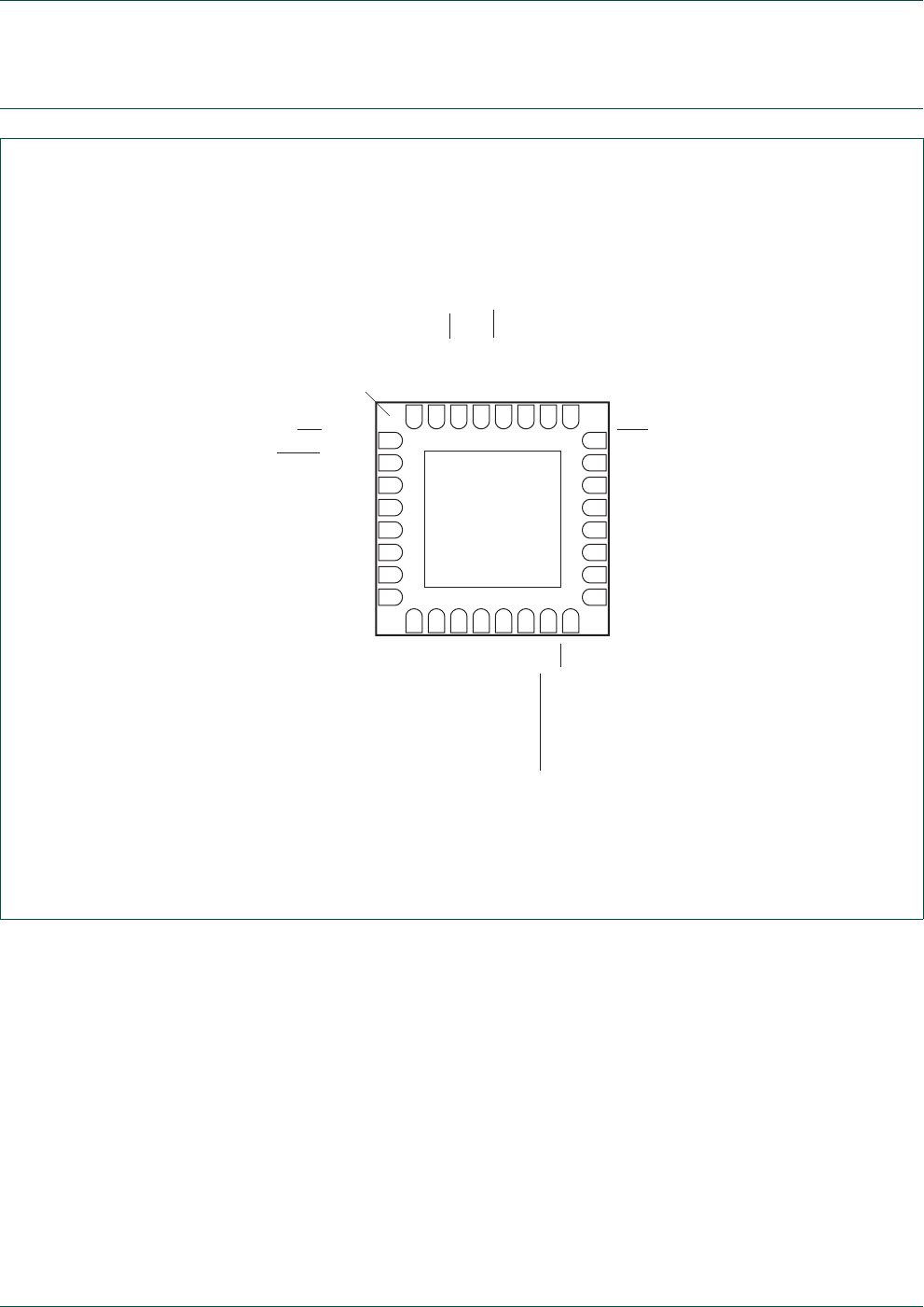
UM10462 All information provided in this document is subject to legal disclaimers. © NXP B.V. 2014. All rights reserved.
User manual Rev. 5.3 — 11 June 2014 128 of 521
NXP Semiconductors UM10462
Chapter 8: LPC11U3x/2x/1x Pin configuration
8.2 Pin configuration
Fig 15. Pin configuration (HVQFN33)
002aaf888_1
Transparent top view
PIO0_8/MISO0/CT16B0_MAT0
PIO0_20/CT16B1_CAP0
PIO0_2/SSEL0/CT16B0_CAP0
PIO0_9/MOSI0/CT16B0_MAT1
VDD SWCLK/PIO0_10/SCK0/CT16B0_MAT2
XTALOUT PIO0_22/AD6/CT16B1_MAT1/MISO1
XTALIN TDI/PIO0_11/AD0/CT32B0_MAT3
PIO0_1/CLKOUT/CT32B0_MAT2/USB_FTOGGLE TMS/PIO0_12/AD1/CT32B1_CAP0
RESET/PIO0_0 TDO/PIO0_13/AD2/CT32B1_MAT0
PIO1_19/DTR/SSEL1 TRST/PIO0_14/AD3/CT32B1_MAT1
PIO0_3/USB_VBUS
PIO0_4/SCL
PIO0_5/SDA
PIO0_21/CT16B1_MAT0/MOSI1
USB_DM
USB_DP
PIO0_6/USB_CONNECT/SCK0
PIO0_7/CTS
PIO0_19/TXD/CT32B0_MAT1
PIO0_18/RXD/CT32B0_MAT0
PIO0_17/RTS/CT32B0_CAP0/SCLK
VDD
PIO1_15/DCD/CT16B0_MAT2/SCK1
PIO0_23/AD7
PIO0_16/AD5/CT32B1_MAT3/WAKEUP
SWDIO/PIO0_15/AD4/CT32B1_MAT2
817
718
619
520
421
322
223
124
9
10
11
12
13
14
15
16
32
31
30
29
28
27
26
25
terminal 1
index area
33 VSS
LPC11U1x
LPC11U2x
LPC11U3x
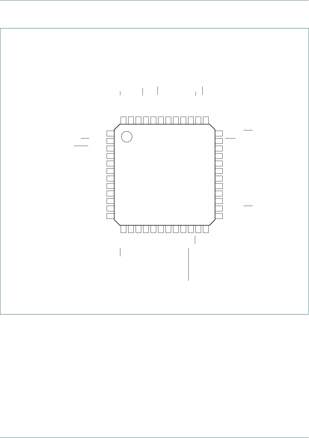
UM10462 All information provided in this document is subject to legal disclaimers. © NXP B.V. 2014. All rights reserved.
User manual Rev. 5.3 — 11 June 2014 129 of 521
NXP Semiconductors UM10462
Chapter 8: LPC11U3x/2x/1x Pin configuration
Fig 16. Pin configuration (LQFP48)
LPC11U1x
LPC11U2x
LPC11U3x
PIO1_25/CT32B0_MAT1 PIO1_13/DTR/CT16B0_MAT0/TXD
PIO1_19/DTR/SSEL1 TRST/PIO0_14/AD3/CT32B1_MAT1
RESET/PIO0_0 TDO/PIO0_13/AD2/CT32B1_MAT0
PIO0_1/CLKOUT/CT32B0_MAT2/USB_FTOGGLE TMS/PIO0_12/AD1/CT32B1_CAP0
V
SS
TDI/PIO0_11/AD0/CT32B0_MAT3
XTALIN PIO1_29/SCK0/CT32B0_CAP1
XTALOUT PIO0_22/AD6/CT16B1_MAT1/MISO1
V
DD
SWCLK/PIO0_10/SCK0/CT16B0_MAT2
PIO0_20/CT16B1_CAP0 PIO0_9/MOSI0/CT16B0_MAT1
PIO0_2/SSEL0/CT16B0_CAP0 PIO0_8/MISO0/CT16B0_MAT0
PIO1_26/CT32B0_MAT2/RXD PIO1_21/DCD/MISO1
PIO1_27/CT32B0_MAT3/TXD PIO1_31
PIO1_20/DSR/SCK1 PIO1_16/RI/CT16B0_CAP0
PIO0_3/USB_VBUS PIO0_19/TXD/CT32B0_MAT1
PIO0_4/SCL PIO0_18/RXD/CT32B0_MAT0
PIO0_5/SDA PIO0_17/RTS/CT32B0_CAP0/SCLK
PIO0_21/CT16B1_MAT0/MOSI1 V
DD
PIO1_23/CT16B1_MAT1/SSEL1 PIO1_15/DCD/CT16B0_MAT2/SCK1
USB_DM PIO0_23/AD7
USB_DP V
SS
PIO1_24/CT32B0_MAT0 PIO0_16/AD5/CT32B1_MAT3/WAKEUP
PIO0_6/USB_CONNECT/SCK0 SWDIO/PIO0_15/AD4/CT32B1_MAT2
PIO0_7/CTS
PIO1_28/CT32B0_CAP0/SCLK
PIO1_22/RI/MOSI1
PIO1_14/DSR/CT16B0_MAT1/RXD
002aaf884_1
1
2
3
4
5
6
7
8
9
10
11
12
36
35
34
33
32
31
30
29
28
27
26
25
13
14
15
16
17
18
19
20
21
22
23
48
47
46
45
44
43
42
41
40
39
38
37
24
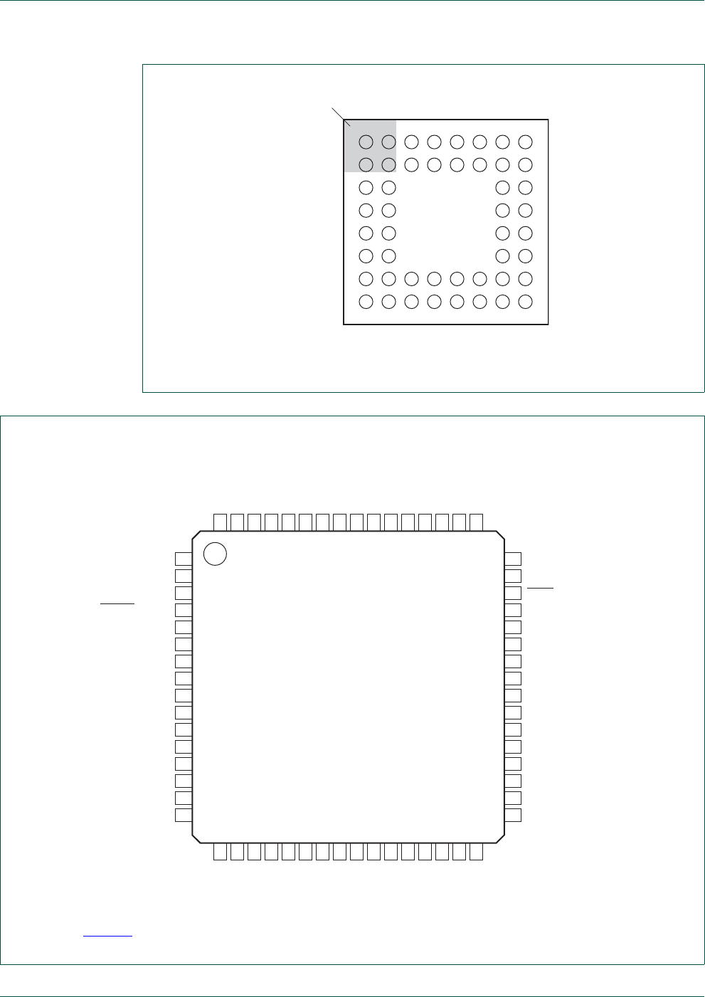
UM10462 All information provided in this document is subject to legal disclaimers. © NXP B.V. 2014. All rights reserved.
User manual Rev. 5.3 — 11 June 2014 130 of 521
NXP Semiconductors UM10462
Chapter 8: LPC11U3x/2x/1x Pin configuration
Fig 17. Pin configuration (TFBGA48)
002aag101_1
LPC11U1x/3x
Transparent top view
H
G
F
D
B
E
C
A
24681357
ball A1
index area
See Table 134 for the full pin name.
Fig 18. Pin configuration (LQFP64)
LPC11U2x
LPC11U3x
PIO1_0 VDD
PIO1_25 PIO1_13
PIO1_19 TRST/PIO0_14
RESET/PIO0_0 TDO/PIO0_13
PIO0_1 TMS/PIO0_12
PIO1_7 PIO1_11
VSS TDI/PIO0_11
XTALIN PIO1_29
XTALOUT PIO0_22
VDD PIO1_8
PIO0_20 SWCLK/PIO0_10
PIO1_10 PIO0_9
PIO0_2 PIO0_8
PIO1_26 PIO1_21
PIO1_27 PIO1_2
PIO1_4 VDD
PIO1_1 PIO1_6
PIO1_20 PIO1_16
PIO0_3 PIO0_19
PIO0_4 PIO0_18
PIO0_5 PIO0_17
PIO0_21 PIO1_12
PIO1_17 VDD
PIO1_23 PIO1_15
USB_DM PIO0_23
USB_DP PIO1_9
PIO1_24 VSS
PIO1_18 PIO0_16
PIO0_6 SWDIO/PIO0_15
PIO0_7 PIO1_22
PIO1_28 PIO1_3
PIO1_5 PIO1_14
002aag624_1
1
2
3
4
5
6
7
8
9
10
11
12
13
14
15
16
48
47
46
45
44
43
42
41
40
39
38
37
36
35
34
33
17
18
19
20
21
22
23
24
25
26
27
28
29
30
31
32
64
63
62
61
60
59
58
57
56
55
54
53
52
51
50
49

UM10462 All information provided in this document is subject to legal disclaimers. © NXP B.V. 2014. All rights reserved.
User manual Rev. 5.3 — 11 June 2014 131 of 521
NXP Semiconductors UM10462
Chapter 8: LPC11U3x/2x/1x Pin configuration
8.2.1 LPC11U1x pin description
Table 132 shows all pins and their assigned digital or analog functions ordered by GPIO
port number. The default function after reset is listed first. All port pins have internal
pull-up resistors enabled after reset with the exception of the true open-drain pins PIO0_4
and PIO0_5.
Every port pin has a corresponding IOCON register for programming the digital or analog
function, the pull-up/pull-down configuration, the repeater, and the open-drain modes.
The USART, counter/timer, and SSP functions are available on more than one port pin.
Table 133 shows how peripheral functions are assigned to port pins.
Table 132. LPC11U1x pin description
Symbol
Pin HVQFN33
Pin LQFP48
Ball TFBGA48
Reset
state
[1]
Type Description
RESET/PIO0_0 2 3 C1 [2] I; PU I RESET — External reset input with 20 ns glitch
filter. A LOW-going pulse as short as 50 ns on
this pin resets the device, causing I/O ports and
peripherals to take on their default states, and
processor execution to begin at address 0. This
pin also serves as the debug select input. LOW
level selects the JTAG boundary scan. HIGH
level selects the ARM SWD debug mode.
In deep power-down mode, this pin must be
pulled HIGH externally. The RESET pin can be
left unconnected or be used as a GPIO pin if an
external RESET function is not needed and
Deep power-down mode is not used.
-I/OPIO0_0 — General purpose digital input/output
pin.
PIO0_1/CLKOUT/
CT32B0_MAT2/
USB_FTOGGLE
34 C2 [3] I; PU I/O PIO0_1 — General purpose digital input/output
pin. A LOW level on this pin during reset starts
the ISP command handler.
-OCLKOUT — Clockout pin.
-OCT32B0_MAT2 — Match output 2 for 32-bit
timer 0.
-OUSB_FTOGGLE — USB 1 ms Start-of-Frame
signal.
PIO0_2/SSEL0/
CT16B0_CAP0
810F1 [3] I; PU I/O PIO0_2 — General purpose digital input/output
pin.
-I/OSSEL0 — Slave select for SSP0.
-ICT16B0_CAP0 — Capture input 0 for 16-bit
timer 0.
PIO0_3/USB_VBUS 9 14 H2 [3] I; PU I/O PIO0_3 — General purpose digital input/output
pin.
-IUSB_VBUS — Monitors the presence of USB
bus power.
UM10462 All information provided in this document is subject to legal disclaimers. © NXP B.V. 2014. All rights reserved.
User manual Rev. 5.3 — 11 June 2014 132 of 521
NXP Semiconductors UM10462
Chapter 8: LPC11U3x/2x/1x Pin configuration
PIO0_4/SCL 10 15 G3 [4] I; IA I/O PIO0_4 — General purpose digital input/output
pin (open-drain).
-I/OSCL — I2C-bus clock input/output (open-drain).
High-current sink only if I2C Fast-mode Plus is
selected in the I/O configuration register.
PIO0_5/SDA 11 16 H3 [4] I; IA I/O PIO0_5 — General purpose digital input/output
pin (open-drain).
-I/OSDA — I2C-bus data input/output (open-drain).
High-current sink only if I2C Fast-mode Plus is
selected in the I/O configuration register.
PIO0_6/USB_CONNECT/
SCK0
15 22 H6 [3] I; PU I/O PIO0_6 — General purpose digital input/output
pin.
-OUSB_CONNECT — Signal used to switch an
external 1.5 k resistor under software control.
Used with the SoftConnect USB feature.
-I/OSCK0 — Serial clock for SSP0.
PIO0_7/CTS 16 23 G7 [5] I; PU I/O PIO0_7 — General purpose digital input/output
pin (high-current output driver).
-ICTS — Clear To Send input for USART.
PIO0_8/MISO0/
CT16B0_MAT0
17 27 F8 [3] I; PU I/O PIO0_8 — General purpose digital input/output
pin.
-I/OMISO0 — Master In Slave Out for SSP0.
-OCT16B0_MAT0 — Match output 0 for 16-bit
timer 0.
PIO0_9/MOSI0/
CT16B0_MAT1
18 28 F7 [3] I; PU I/O PIO0_9 — General purpose digital input/output
pin.
-I/OMOSI0 — Master Out Slave In for SSP0.
-OCT16B0_MAT1 — Match output 1 for 16-bit
timer 0.
SWCLK/PIO0_10/SCK0/
CT16B0_MAT2
19 29 E7 [3] I; PU I SWCLK — Serial wire clock and test clock TCK
for JTAG interface.
-I/OPIO0_10 — General purpose digital
input/output pin.
-OSCK0 — Serial clock for SSP0.
-OCT16B0_MAT2 — Match output 2 for 16-bit
timer 0.
TDI/PIO0_11/AD0/
CT32B0_MAT3
21 32 D8 [6] I; PU I TDI — Test Data In for JTAG interface.
-I/OPIO0_11 — General purpose digital input/output
pin.
-IAD0 — A/D converter, input 0.
-OCT32B0_MAT3 — Match output 3 for 32-bit
timer 0.
Table 132. LPC11U1x pin description …continued
Symbol
Pin HVQFN33
Pin LQFP48
Ball TFBGA48
Reset
state
[1]
Type Description
UM10462 All information provided in this document is subject to legal disclaimers. © NXP B.V. 2014. All rights reserved.
User manual Rev. 5.3 — 11 June 2014 133 of 521
NXP Semiconductors UM10462
Chapter 8: LPC11U3x/2x/1x Pin configuration
TMS/PIO0_12/AD1/
CT32B1_CAP0
22 33 C7 [6] I; PU I TMS — Test Mode Select for JTAG interface.
-I/OPIO_12 — General purpose digital input/output
pin.
-IAD1 — A/D converter, input 1.
-ICT32B1_CAP0 — Capture input 0 for 32-bit
timer 1.
TDO/PIO0_13/AD2/
CT32B1_MAT0
23 34 C8 [6] I; PU O TDO — Test Data Out for JTAG interface.
-I/OPIO0_13 — General purpose digital
input/output pin.
-IAD2 — A/D converter, input 2.
-OCT32B1_MAT0 — Match output 0 for 32-bit
timer 1.
TRST/PIO0_14/AD3/
CT32B1_MAT1
24 35 B7 [6] I; PU I TRST — Test Reset for JTAG interface.
-I/OPIO0_14 — General purpose digital
input/output pin.
-IAD3 — A/D converter, input 3.
-OCT32B1_MAT1 — Match output 1 for 32-bit
timer 1.
SWDIO/PIO0_15/AD4/
CT32B1_MAT2
25 39 B6 [6] I; PU I/O SWDIO — Serial wire debug input/output.
-I/OPIO0_15 — General purpose digital
input/output pin.
-IAD4 — A/D converter, input 4.
-OCT32B1_MAT2 — Match output 2 for 32-bit
timer 1.
PIO0_16/AD5/
CT32B1_MAT3/WAKEUP
26 40 A6 [6] I; PU I/O PIO0_16 — General purpose digital
input/output pin. In Deep power-down mode,
this pin functions as the WAKEUP pin with 20 ns
glitch filter. Pull this pin HIGH externally to enter
Deep power-down mode. Pull this pin LOW to
exit Deep power-down mode. A LOW-going
pulse as short as 50 ns wakes up the part.
-IAD5 — A/D converter, input 5.
-OCT32B1_MAT3 — Match output 3 for 32-bit
timer 1.
PIO0_17/RTS/
CT32B0_CAP0/SCLK
30 45 A3 [3] I; PU I/O PIO0_17 — General purpose digital
input/output pin.
-ORTS — Request To Send output for USART.
-ICT32B0_CAP0 — Capture input 0 for 32-bit
timer 0.
-I/OSCLK — Serial clock input/output for USART in
synchronous mode.
Table 132. LPC11U1x pin description …continued
Symbol
Pin HVQFN33
Pin LQFP48
Ball TFBGA48
Reset
state
[1]
Type Description

UM10462 All information provided in this document is subject to legal disclaimers. © NXP B.V. 2014. All rights reserved.
User manual Rev. 5.3 — 11 June 2014 134 of 521
NXP Semiconductors UM10462
Chapter 8: LPC11U3x/2x/1x Pin configuration
PIO0_18/RXD/
CT32B0_MAT0
31 46 B3 [3] I; PU I/O PIO0_18 — General purpose digital
input/output pin.
-IRXD — Receiver input for USART.Used in
UART ISP mode.
-OCT32B0_MAT0 — Match output 0 for 32-bit
timer 0.
PIO0_19/TXD/
CT32B0_MAT1
32 47 B2 [3] I; PU I/O PIO0_19 — General purpose digital
input/output pin.
-OTXD — Transmitter output for USART. Used in
UART ISP mode.
-OCT32B0_MAT1 — Match output 1 for 32-bit
timer 0.
PIO0_20/CT16B1_CAP0 7 9 F2 [3] I; PU I/O PIO0_20 — General purpose digital
input/output pin.
-ICT16B1_CAP0 — Capture input 0 for 16-bit
timer 1.
PIO0_21/CT16B1_MAT0/
MOSI1
12 17 G4 [3] I; PU I/O PIO0_21 — General purpose digital
input/output pin.
-OCT16B1_MAT0 — Match output 0 for 16-bit
timer 1.
-I/OMOSI1 — Master Out Slave In for SSP1.
PIO0_22/AD6/
CT16B1_MAT1/MISO1
20 30 E8 [6] I; PU I/O PIO0_22 — General purpose digital
input/output pin.
-IAD6 — A/D converter, input 6.
-OCT16B1_MAT1 — Match output 1 for 16-bit
timer 1.
-I/OMISO1 — Master In Slave Out for SSP1.
PIO0_23/AD7 27 42 A5 [6] I; PU I/O PIO0_23 — General purpose digital
input/output pin.
-IAD7 — A/D converter, input 7.
PIO1_5/CT32B1_CAP1 - - H8 [3] I; PU I/O PIO1_5 — General purpose digital input/output
pin.
-ICT32B1_CAP1 — Capture input 1 for 32-bit
timer 1.
PIO1_13/DTR/
CT16B0_MAT0/TXD
-36B8 [3] I; PU I/O PIO1_13 — General purpose digital
input/output pin.
-ODTR — Data Terminal Ready output for
USART.
-OCT16B0_MAT0 — Match output 0 for 16-bit
timer 0.
-OTXD — Transmitter output for USART.
Table 132. LPC11U1x pin description …continued
Symbol
Pin HVQFN33
Pin LQFP48
Ball TFBGA48
Reset
state
[1]
Type Description
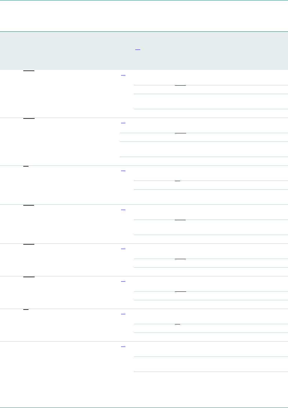
UM10462 All information provided in this document is subject to legal disclaimers. © NXP B.V. 2014. All rights reserved.
User manual Rev. 5.3 — 11 June 2014 135 of 521
NXP Semiconductors UM10462
Chapter 8: LPC11U3x/2x/1x Pin configuration
PIO1_14/DSR/
CT16B0_MAT1/RXD
-37A8 [3] I; PU I/O PIO1_14 — General purpose digital
input/output pin.
-IDSR — Data Set Ready input for USART.
-OCT16B0_MAT1 — Match output 1 for 16-bit
timer 0.
-IRXD — Receiver input for USART.
PIO1_15/DCD/
CT16B0_MAT2/SCK1
28 43 A4 [3] I; PU I/O PIO1_15 — General purpose digital
input/output pin.
IDCD — Data Carrier Detect input for USART.
-OCT16B0_MAT2 — Match output 2 for 16-bit
timer 0.
-I/OSCK1 — Serial clock for SSP1.
PIO1_16/RI/
CT16B0_CAP0
-48A2 [3] I; PU I/O PIO1_16 — General purpose digital
input/output pin.
-IRI — Ring Indicator input for USART.
-ICT16B0_CAP0 — Capture input 0 for 16-bit
timer 0.
PIO1_19/DTR/SSEL1 1 2 B1 [3] I; PU I/O PIO1_19 — General purpose digital
input/output pin.
-ODTR — Data Terminal Ready output for
USART.
-I/OSSEL1 — Slave select for SSP1.
PIO1_20/DSR/SCK1 - 13 H1 [3] I; PU I/O PIO1_20 — General purpose digital
input/output pin.
-IDSR — Data Set Ready input for USART.
-I/OSCK1 — Serial clock for SSP1.
PIO1_21/DCD/MISO1 - 26 G8 [3] I; PU I/O PIO1_21 — General purpose digital
input/output pin.
-IDCD — Data Carrier Detect input for USART.
-I/OMISO1 — Master In Slave Out for SSP1.
PIO1_22/RI/MOSI1 - 38 A7 [3] I; PU I/O PIO1_22 — General purpose digital
input/output pin.
-IRI — Ring Indicator input for USART.
-I/OMOSI1 — Master Out Slave In for SSP1.
PIO1_23/CT16B1_MAT1/
SSEL1
-18H4 [3] I; PU I/O PIO1_23 — General purpose digital
input/output pin.
-OCT16B1_MAT1 — Match output 1 for 16-bit
timer 1.
-I/OSSEL1 — Slave select for SSP1.
Table 132. LPC11U1x pin description …continued
Symbol
Pin HVQFN33
Pin LQFP48
Ball TFBGA48
Reset
state
[1]
Type Description

UM10462 All information provided in this document is subject to legal disclaimers. © NXP B.V. 2014. All rights reserved.
User manual Rev. 5.3 — 11 June 2014 136 of 521
NXP Semiconductors UM10462
Chapter 8: LPC11U3x/2x/1x Pin configuration
PIO1_24/CT32B0_MAT0 - 21 G6 [3] I; PU I/O PIO1_24 — General purpose digital
input/output pin.
-OCT32B0_MAT0 — Match output 0 for 32-bit
timer 0.
PIO1_25/CT32B0_MAT1 - 1 A1 [3] I; PU I/O PIO1_25 — General purpose digital
input/output pin.
-OCT32B0_MAT1 — Match output 1 for 32-bit
timer 0.
PIO1_26/CT32B0_MAT2/
RXD
-11G2 [3] I; PU I/O PIO1_26 — General purpose digital
input/output pin.
-OCT32B0_MAT2 — Match output 2 for 32-bit
timer 0.
-IRXD — Receiver input for USART.
PIO1_27/CT32B0_MAT3/
TXD
-12G1 [3] I; PU I/O PIO1_27 — General purpose digital
input/output pin.
-OCT32B0_MAT3 — Match output 3 for 32-bit
timer 0.
-OTXD — Transmitter output for USART.
PIO1_28/CT32B0_CAP0/
SCLK
-24H7 [3] I; PU I/O PIO1_28 — General purpose digital
input/output pin.
-ICT32B0_CAP0 — Capture input 0 for 32-bit
timer 0.
-I/OSCLK — Serial clock input/output for USART in
synchronous mode.
PIO1_29/SCK0/
CT32B0_CAP1
-31D7 [3] I; PU I/O PIO1_29 — General purpose digital
input/output pin.
-I/OSCK0 — Serial clock for SSP0.
-ICT32B0_CAP1 — Capture input 1 for 32-bit
timer 0.
PIO1_31 - 25 - [3] I; PU I/O PIO1_31 — General purpose digital
input/output pin.
USB_DM 13 19 G5 [7] F- USB_DM — USB bidirectional D line.
USB_DP 14 20 H5 [7] F- USB_DP — USB bidirectional D+ line.
XTALIN 4 6 D1 [8] - - Input to the oscillator circuit and internal clock
generator circuits. Input voltage must not
exceed 1.8 V.
XTALOUT 5 7 E1 [8] - - Output from the oscillator amplifier.
VDD 6;
29
8;
44
B4,
E2
- - Supply voltage to the internal regulator, the
external rail, and the ADC. Also used as the
ADC reference voltage.
VSS 33 5;
41
B5,
D2
- - Ground.
Table 132. LPC11U1x pin description …continued
Symbol
Pin HVQFN33
Pin LQFP48
Ball TFBGA48
Reset
state
[1]
Type Description
UM10462 All information provided in this document is subject to legal disclaimers. © NXP B.V. 2014. All rights reserved.
User manual Rev. 5.3 — 11 June 2014 137 of 521
NXP Semiconductors UM10462
Chapter 8: LPC11U3x/2x/1x Pin configuration
[1] Pin state at reset for default function: I = Input; O = Output; PU = internal pull-up enabled; IA = inactive, no pull-up/down enabled;
F = floating; floating pins, if not used, should be tied to ground or power to minimize power consumption.
[2] RESET functionality is not available in Deep power-down mode. Use the WAKEUP pin to reset the chip and wake up from Deep
power-down mode. An external pull-up resistor is required on this pin for the Deep power-down mode.
[3] 5 V tolerant pad providing digital I/O functions with configurable pull-up/pull-down resistors and configurable hysteresis.
[4] I2C-bus pins compliant with the I2C-bus specification for I2C standard mode, I2C Fast-mode, and I2C Fast-mode Plus. The pin requires
an external pull-up to provide output functionality. When power is switched off, this pin is floating and does not disturb the I2C lines.
Open-drain configuration applies to all functions on this pin.
[5] 5 V tolerant pad providing digital I/O functions with configurable pull-up/pull-down resistors and configurable hysteresis; includes
high-current output driver.
[6] 5 V tolerant pad providing digital I/O functions with configurable pull-up/pull-down resistors, configurable hysteresis, and analog input.
When configured as a ADC input, digital section of the pad is disabled and the pin is not 5 V tolerant; includes digital input glitch filter.
[7] Pad provides USB functions. It is designed in accordance with the USB specification, revision 2.0 (Full-speed and Low-speed mode
only). This pad is not 5 V tolerant.
[8] When the system oscillator is not used, connect XTALIN and XTALOUT as follows: XTALIN can be left floating or can be grounded
(grounding is preferred to reduce susceptibility to noise). XTALOUT should be left floating.
To assign a peripheral function to a port, program the FUNC bits in the port pin’s IOCON
register with this function. The user must ensure that the assignment of a function to a port
pin is unambiguous. Only the debug functions for JTAG and SWD are selected by default
in their corresponding IOCON registers. All other functions must be programmed in the
IOCON block before they can be used. For details see Section 7.3.
Table 133. Multiplexing of peripheral functions
Peripheral Function Type Default Available on ports
HVQFN33/LQFP48/TFBGA48 LQFP48/TFBGA48 TFBGA48
USART RXD I no PIO0_18 - PIO1_14 PIO1_26 -
TXD O no PIO0_19 - PIO1_13 PIO1_27 -
CTS Ino PIO0_7 - - - -
RTS O no PIO0_17 - - - -
DTR O no PIO1_13 PIO1_19 - - -
DSR I no - - PIO1_14 PIO1_20 -
DCD I no PIO1_15 PIO1_21 - -
RI I no PIO1_16 PIO1_22 -
SCLK I/O no PIO0_17 PIO1_28 - -
SSP0 SCK0 I/O no PIO0_6 PIO0_10 PIO1_29 -
SSEL0 I/O no PIO0_2 - - - -
MISO0 I/O no PIO0_8 - - - -
MOSI0 I/O no PIO0_9 - - - -
SSP1 SCK1 I/O no PIO1_15 PIO1_20 - -
SSEL1 I/O no PIO1_19 PIO1_23 - -
MISO1 I/O no PIO0_22 PIO1_21 - -
MOSI1 I/O no PIO0_21 PIO1_22 - -
CT16B0 CT16B0_CAP0 I no PIO0_2 PIO1_16 - -
CT16B0_MAT0 O no PIO0_8 PIO1_13 - -
CT16B0_MAT1 O no PIO0_9 PIO1_14 - -
CT16B0_MAT2 O no PIO0_10 PIO1_15 - - -

UM10462 All information provided in this document is subject to legal disclaimers. © NXP B.V. 2014. All rights reserved.
User manual Rev. 5.3 — 11 June 2014 138 of 521
NXP Semiconductors UM10462
Chapter 8: LPC11U3x/2x/1x Pin configuration
8.2.2 LPC11U2x pin description
Table 134 shows all pins and their assigned digital or analog functions in order of the
GPIO port number. The default function after reset is listed first. All port pins have internal
pull-up resistors enabled after reset except for the true open-drain pins PIO0_4 and
PIO0_5.
CT16B1 CT16B1_CAP0 I no PIO0_20 - - - -
CT16B1_MAT0 O no PIO0_21 - - - -
CT16B1_MAT1 O no PIO0_22 - PIO1_23 - -
CT32B0 CT32B0_CAP0 I no PIO0_17 - PIO1_28 - -
CT32B0_CAP1 I no PIO1_29 - - - -
CT32B0_MAT0 O no PIO0_18 - PIO1_24 - -
CT32B0_MAT1 O no PIO0_19 - PIO1_25 - -
CT32B0_MAT2 O no PIO0_1 - PIO1_26 - -
CT32B0_MAT3 O no PIO0_11 - PIO1_27 - -
CT32B1 CT32B1_CAP0 I no PIO0_12 - - -
CT32B1_CAP1 I no - - - PIO1_5
CT32B1_MAT0 O no PIO0_13 - - - -
CT32B1_MAT1 O no PIO0_14 - - - -
CT32B1_MAT2 O no PIO0_15 - - - -
CT32B1_MAT3 O no PIO0_16 - - - -
ADC AD0 I no PIO0_11 - - - -
AD1 I no PIO0_12 - - - -
AD2 I no PIO0_13 - - - -
AD3 I no PIO0_14 - - - -
AD4 I no PIO0_15 - - - -
AD5 I no PIO0_16 - - - -
AD6 I no PIO0_22 - - - -
AD7 I no PIO0_23 - - - -
USB USB_VBUS I no PIO0_3 - - - -
USB_FTOGGLE O no PIO0_1 - - - -
USB_CONNECT Ono PIO0_6 - - - -
CLKOUT CLKOUT O no PIO0_1 - - - -
JTAG TDI I yes PIO0_11 - - - -
TMS I yes PIO0_12 - - - -
TDO O yes PIO0_13 - - - -
TRST I yes PIO0_14 - - - -
TCK I yes PIO0_10 - - - -
SWD SWCLK I yes PIO0_10 - - - -
SWDIO I/O yes PIO0_15 - - - -
Table 133. Multiplexing of peripheral functions …continued
Peripheral Function Type Default Available on ports
HVQFN33/LQFP48/TFBGA48 LQFP48/TFBGA48 TFBGA48

UM10462 All information provided in this document is subject to legal disclaimers. © NXP B.V. 2014. All rights reserved.
User manual Rev. 5.3 — 11 June 2014 139 of 521
NXP Semiconductors UM10462
Chapter 8: LPC11U3x/2x/1x Pin configuration
Every port pin has a corresponding IOCON register for programming the digital or analog
function, the pull-up/pull-down configuration, the repeater, and the open-drain modes.
The USART, counter/timer, and SSP functions are available on more than one port pin.
Table 134. LPC11U2x pin description
Symbol
Pin HVQFN33
Pin LQFP48
Pin LQFP64
Reset
state
[1]
Type Description
RESET/PIO0_0 2 3 4 [2] I; PU I RESET — External reset input with 20 ns glitch filter. A
LOW-going pulse as short as 50 ns on this pin resets the
device, causing I/O ports and peripherals to take on their
default states, and processor execution to begin at address
0. This pin also serves as the debug select input. LOW
level selects the JTAG boundary scan. HIGH level selects
the ARM SWD debug mode.
In deep power-down mode, this pin must be pulled HIGH
externally. The RESET pin can be left unconnected or be
used as a GPIO pin if an external RESET function is not
needed and Deep power-down mode is not used.
-I/OPIO0_0 — General purpose digital input/output pin.
PIO0_1/CLKOUT/
CT32B0_MAT2/
USB_FTOGGLE
34 5 [3] I; PU I/O PIO0_1 — General purpose digital input/output pin. A LOW
level on this pin during reset starts the ISP command
handler or the USB device enumeration (see pin PIO0_3).
-OCLKOUT — Clockout pin.
-OCT32B0_MAT2 — Match output 2 for 32-bit timer 0.
-OUSB_FTOGGLE — USB 1 ms Start-of-Frame signal.
PIO0_2/SSEL0/
CT16B0_CAP0
81013
[3] I; PU I/O PIO0_2 — General purpose digital input/output pin.
-I/OSSEL0 — Slave select for SSP0.
-ICT16B0_CAP0 — Capture input 0 for 16-bit timer 0.
PIO0_3/USB_VBUS 9 14 19 [3] I; PU I/O PIO0_3 — General purpose digital input/output pin. A LOW
level on this pin during reset starts the ISP command
handler. A HIGH level during reset starts the USB device
enumeration.
-IUSB_VBUS — Monitors the presence of USB bus power.
PIO0_4/SCL 10 15 20 [4] I; IA I/O PIO0_4 — General purpose digital input/output pin
(open-drain).
-I/OSCL — I2C-bus clock input/output (open-drain).
High-current sink only if I2C Fast-mode Plus is selected in
the I/O configuration register.
PIO0_5/SDA 11 16 21 [4] I; IA I/O PIO0_5 — General purpose digital input/output pin
(open-drain).
-I/OSDA — I2C-bus data input/output (open-drain).
High-current sink only if I2C Fast-mode Plus is selected in
the I/O configuration register.
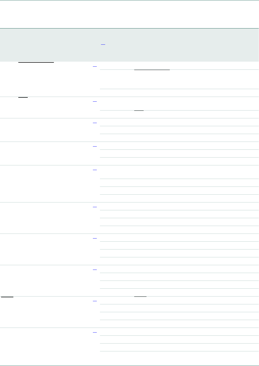
UM10462 All information provided in this document is subject to legal disclaimers. © NXP B.V. 2014. All rights reserved.
User manual Rev. 5.3 — 11 June 2014 140 of 521
NXP Semiconductors UM10462
Chapter 8: LPC11U3x/2x/1x Pin configuration
PIO0_6/USB_CONNECT/
SCK0
15 22 29 [3] I; PU I/O PIO0_6 — General purpose digital input/output pin.
-OUSB_CONNECT — Signal used to switch an external
1.5 k resistor under software control. Used with the
SoftConnect USB feature.
-I/OSCK0 — Serial clock for SSP0.
PIO0_7/CTS 16 23 30 [5] I; PU I/O PIO0_7 — General purpose digital input/output pin
(high-current output driver).
-ICTS — Clear To Send input for USART.
PIO0_8/MISO0/
CT16B0_MAT0
17 27 36 [3] I; PU I/O PIO0_8 — General purpose digital input/output pin.
-I/OMISO0 — Master In Slave Out for SSP0.
-OCT16B0_MAT0 — Match output 0 for 16-bit timer 0.
PIO0_9/MOSI0/
CT16B0_MAT1
18 28 37 [3] I; PU I/O PIO0_9 — General purpose digital input/output pin.
-I/OMOSI0 — Master Out Slave In for SSP0.
-OCT16B0_MAT1 — Match output 1 for 16-bit timer 0.
SWCLK/PIO0_10/SCK0/
CT16B0_MAT2
19 29 38 [3] I; PU I SWCLK — Serial wire clock and test clock TCK for JTAG
interface.
-I/OPIO0_10 — General purpose digital input/output pin.
-OSCK0 — Serial clock for SSP0.
-OCT16B0_MAT2 — Match output 2 for 16-bit timer 0.
TDI/PIO0_11/AD0/
CT32B0_MAT3
21 32 42 [6] I; PU I TDI — Test Data In for JTAG interface.
-I/OPIO0_11 — General purpose digital input/output pin.
-IAD0 — A/D converter, input 0.
-OCT32B0_MAT3 — Match output 3 for 32-bit timer 0.
TMS/PIO0_12/AD1/
CT32B1_CAP0
22 33 44 [6] I; PU I TMS — Test Mode Select for JTAG interface.
-I/OPIO_12 — General purpose digital input/output pin.
-IAD1 — A/D converter, input 1.
-ICT32B1_CAP0 — Capture input 0 for 32-bit timer 1.
TDO/PIO0_13/AD2/
CT32B1_MAT0
23 34 45 [6] I; PU O TDO — Test Data Out for JTAG interface.
-I/OPIO0_13 — General purpose digital input/output pin.
-IAD2 — A/D converter, input 2.
-OCT32B1_MAT0 — Match output 0 for 32-bit timer 1.
TRST/PIO0_14/AD3/
CT32B1_MAT1
24 35 46 [6] I; PU I TRST — Test Reset for JTAG interface.
-I/OPIO0_14 — General purpose digital input/output pin.
-IAD3 — A/D converter, input 3.
-OCT32B1_MAT1 — Match output 1 for 32-bit timer 1.
SWDIO/PIO0_15/AD4/
CT32B1_MAT2
25 39 52 [6] I; PU I/O SWDIO — Serial wire debug input/output.
-I/OPIO0_15 — General purpose digital input/output pin.
-IAD4 — A/D converter, input 4.
-OCT32B1_MAT2 — Match output 2 for 32-bit timer 1.
Table 134. LPC11U2x pin description …continued
Symbol
Pin HVQFN33
Pin LQFP48
Pin LQFP64
Reset
state
[1]
Type Description
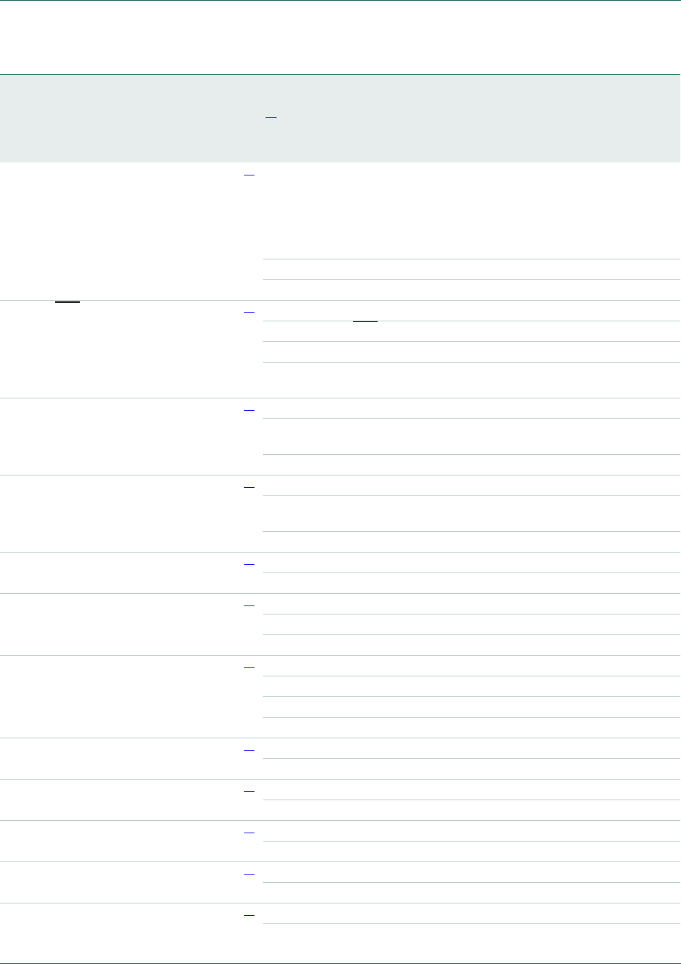
UM10462 All information provided in this document is subject to legal disclaimers. © NXP B.V. 2014. All rights reserved.
User manual Rev. 5.3 — 11 June 2014 141 of 521
NXP Semiconductors UM10462
Chapter 8: LPC11U3x/2x/1x Pin configuration
PIO0_16/AD5/
CT32B1_MAT3/WAKEUP
26 40 53 [6] I; PU I/O PIO0_16 — General purpose digital input/output pin. In
Deep power-down mode, this pin functions as the
WAKEUP pin with 20 ns glitch filter. Pull this pin HIGH
externally to enter Deep power-down mode. Pull this pin
LOW to exit Deep power-down mode. A LOW-going pulse
as short as 50 ns wakes up the part.
-IAD5 — A/D converter, input 5.
-OCT32B1_MAT3 — Match output 3 for 32-bit timer 1.
PIO0_17/RTS/
CT32B0_CAP0/SCLK
30 45 60 [3] I; PU I/O PIO0_17 — General purpose digital input/output pin.
-ORTS — Request To Send output for USART.
-ICT32B0_CAP0 — Capture input 0 for 32-bit timer 0.
-I/OSCLK — Serial clock input/output for USART in
synchronous mode.
PIO0_18/RXD/
CT32B0_MAT0
31 46 61 [3] I; PU I/O PIO0_18 — General purpose digital input/output pin.
-IRXD — Receiver input for USART. Used in UART ISP
mode.
-OCT32B0_MAT0 — Match output 0 for 32-bit timer 0.
PIO0_19/TXD/
CT32B0_MAT1
32 47 62 [3] I; PU I/O PIO0_19 — General purpose digital input/output pin.
-OTXD — Transmitter output for USART. Used in UART ISP
mode.
-OCT32B0_MAT1 — Match output 1 for 32-bit timer 0.
PIO0_20/CT16B1_CAP0 7 9 11 [3] I; PU I/O PIO0_20 — General purpose digital input/output pin.
-ICT16B1_CAP0 — Capture input 0 for 16-bit timer 1.
PIO0_21/CT16B1_MAT0/
MOSI1
12 17 22 [3] I; PU I/O PIO0_21 — General purpose digital input/output pin.
-OCT16B1_MAT0 — Match output 0 for 16-bit timer 1.
-I/OMOSI1 — Master Out Slave In for SSP1.
PIO0_22/AD6/
CT16B1_MAT1/MISO1
20 30 40 [6] I; PU I/O PIO0_22 — General purpose digital input/output pin.
-IAD6 — A/D converter, input 6.
-OCT16B1_MAT1 — Match output 1 for 16-bit timer 1.
-I/OMISO1 — Master In Slave Out for SSP1.
PIO0_23/AD7 27 42 56 [6] I; PU I/O PIO0_23 — General purpose digital input/output pin.
-IAD7 — A/D converter, input 7.
PIO1_0/CT32B1_MAT0 - - 1 [3] I; PU I/O PIO1_0 — General purpose digital input/output pin.
-OCT32B1_MAT0 — Match output 0 for 32-bit timer 1.
PIO1_1/CT32B1_MAT1 - - 17 [3] I; PU I/O PIO1_1 — General purpose digital input/output pin.
-OCT32B1_MAT1 — Match output 1 for 32-bit timer 1.
PIO1_2/CT32B1_MAT2 - - 34 [3] I; PU I/O PIO1_2 — General purpose digital input/output pin.
-OCT32B1_MAT2 — Match output 2 for 32-bit timer 1.
PIO1_3/CT32B1_MAT3 - - 50 [3] I; PU I/O PIO1_3 — General purpose digital input/output pin.
-OCT32B1_MAT3 — Match output 3 for 32-bit timer 1.
Table 134. LPC11U2x pin description …continued
Symbol
Pin HVQFN33
Pin LQFP48
Pin LQFP64
Reset
state
[1]
Type Description

UM10462 All information provided in this document is subject to legal disclaimers. © NXP B.V. 2014. All rights reserved.
User manual Rev. 5.3 — 11 June 2014 142 of 521
NXP Semiconductors UM10462
Chapter 8: LPC11U3x/2x/1x Pin configuration
PIO1_4/CT32B1_CAP0 - - 16 [3] I; PU I/O PIO1_4 — General purpose digital input/output pin.
-ICT32B1_CAP0 — Capture input 0 for 32-bit timer 1.
PIO1_5/CT32B1_CAP1 - - 32 [3] I; PU I/O PIO1_5 — General purpose digital input/output pin.
-ICT32B1_CAP1 — Capture input 1 for 32-bit timer 1.
PIO1_6 - - 64 [3] I; PU I/O PIO1_6 — General purpose digital input/output pin.
PIO1_7 - - 6 [3] I; PU I/O PIO1_7 — General purpose digital input/output pin.
PIO1_8 - - 39 [3] I; PU I/O PIO1_8 — General purpose digital input/output pin.
PIO1_9 - - 55 [3] I; PU I/O PIO1_9 — General purpose digital input/output pin.
PIO1_10 - - 12 [3] I; PU I/O PIO1_10 — General purpose digital input/output pin.
PIO1_11 - - 43 [3] I; PU I/O PIO1_11 — General purpose digital input/output pin.
PIO1_12 - - 59 [3] I; PU I/O PIO1_12 — General purpose digital input/output pin.
PIO1_13/DTR/
CT16B0_MAT0/TXD
-3647
[3] I; PU I/O PIO1_13 — General purpose digital input/output pin.
-ODTR — Data Terminal Ready output for USART.
-OCT16B0_MAT0 — Match output 0 for 16-bit timer 0.
-OTXD — Transmitter output for USART.
PIO1_14/DSR/
CT16B0_MAT1/RXD
-3749
[3] I; PU I/O PIO1_14 — General purpose digital input/output pin.
-IDSR — Data Set Ready input for USART.
-OCT16B0_MAT1 — Match output 1 for 16-bit timer 0.
-IRXD — Receiver input for USART.
PIO1_15/DCD/
CT16B0_MAT2/SCK1
28 43 57 [3] I; PU I/O PIO1_15 — General purpose digital input/output pin.
IDCD — Data Carrier Detect input for USART.
-OCT16B0_MAT2 — Match output 2 for 16-bit timer 0.
-I/OSCK1 — Serial clock for SSP1.
PIO1_16/RI/
CT16B0_CAP0
-4863
[3] I; PU I/O PIO1_16 — General purpose digital input/output pin.
-IRI — Ring Indicator input for USART.
-ICT16B0_CAP0 — Capture input 0 for 16-bit timer 0.
PIO1_17/CT16B0_CAP1/
RXD
-- 23
[3] I; PU I/O PIO1_17 — General purpose digital input/output pin.
-ICT16B0_CAP1 — Capture input 1 for 16-bit timer 0.
-IRXD — Receiver input for USART.
PIO1_18/CT16B1_CAP1/
TXD
-- 28
[3] I; PU I/O PIO1_18 — General purpose digital input/output pin.
-ICT16B1_CAP1 — Capture input 1 for 16-bit timer 1.
-OTXD — Transmitter output for USART.
PIO1_19/DTR/SSEL1 1 2 3 [3] I; PU I/O PIO1_19 — General purpose digital input/output pin.
-ODTR — Data Terminal Ready output for USART.
-I/OSSEL1 — Slave select for SSP1.
PIO1_20/DSR/SCK1 - 13 18 [3] I; PU I/O PIO1_20 — General purpose digital input/output pin.
-IDSR — Data Set Ready input for USART.
-I/OSCK1 — Serial clock for SSP1.
Table 134. LPC11U2x pin description …continued
Symbol
Pin HVQFN33
Pin LQFP48
Pin LQFP64
Reset
state
[1]
Type Description

UM10462 All information provided in this document is subject to legal disclaimers. © NXP B.V. 2014. All rights reserved.
User manual Rev. 5.3 — 11 June 2014 143 of 521
NXP Semiconductors UM10462
Chapter 8: LPC11U3x/2x/1x Pin configuration
PIO1_21/DCD/MISO1 - 26 35 [3] I; PU I/O PIO1_21 — General purpose digital input/output pin.
-IDCD — Data Carrier Detect input for USART.
-I/OMISO1 — Master In Slave Out for SSP1.
PIO1_22/RI/MOSI1 - 38 51 [3] I; PU I/O PIO1_22 — General purpose digital input/output pin.
-IRI — Ring Indicator input for USART.
-I/OMOSI1 — Master Out Slave In for SSP1.
PIO1_23/CT16B1_MAT1/
SSEL1
-1824
[3] I; PU I/O PIO1_23 — General purpose digital input/output pin.
-OCT16B1_MAT1 — Match output 1 for 16-bit timer 1.
-I/OSSEL1 — Slave select for SSP1.
PIO1_24/CT32B0_MAT0 - 21 27 [3] I; PU I/O PIO1_24 — General purpose digital input/output pin.
-OCT32B0_MAT0 — Match output 0 for 32-bit timer 0.
PIO1_25/CT32B0_MAT1 - 1 2 [3] I; PU I/O PIO1_25 — General purpose digital input/output pin.
-OCT32B0_MAT1 — Match output 1 for 32-bit timer 0.
PIO1_26/CT32B0_MAT2/
RXD
-1114
[3] I; PU I/O PIO1_26 — General purpose digital input/output pin.
-OCT32B0_MAT2 — Match output 2 for 32-bit timer 0.
-IRXD — Receiver input for USART.
PIO1_27/CT32B0_MAT3/
TXD
-1215
[3] I; PU I/O PIO1_27 — General purpose digital input/output pin.
-OCT32B0_MAT3 — Match output 3 for 32-bit timer 0.
-OTXD — Transmitter output for USART.
PIO1_28/CT32B0_CAP0/
SCLK
-2431
[3] I; PU I/O PIO1_28 — General purpose digital input/output pin.
-ICT32B0_CAP0 — Capture input 0 for 32-bit timer 0.
-I/OSCLK — Serial clock input/output for USART in
synchronous mode.
PIO1_29/SCK0/
CT32B0_CAP1
-3141
[3] I; PU I/O PIO1_29 — General purpose digital input/output pin.
-I/OSCK0 — Serial clock for SSP0.
-ICT32B0_CAP1 — Capture input 1 for 32-bit timer 0.
PIO1_31 - 25 - [3] I; PU I/O PIO1_31 — General purpose digital input/output pin.
USB_DM 13 19 25 [7] F-USB_DM — USB bidirectional D line.
USB_DP 14 20 26 [7] F-USB_DP — USB bidirectional D+ line.
XTALIN 4 6 8 [8] - - Input to the oscillator circuit and internal clock generator
circuits. Input voltage must not exceed 1.8 V.
XTALOUT 5 7 9 [8] - - Output from the oscillator amplifier.
VDD 6;
29
8;
44
10;
33;
48;
58
- - Supply voltage to the internal regulator, the external rail,
and the ADC. Also used as the ADC reference voltage.
VSS 33 5;
41
7;
54
- - Ground.
Table 134. LPC11U2x pin description …continued
Symbol
Pin HVQFN33
Pin LQFP48
Pin LQFP64
Reset
state
[1]
Type Description

UM10462 All information provided in this document is subject to legal disclaimers. © NXP B.V. 2014. All rights reserved.
User manual Rev. 5.3 — 11 June 2014 144 of 521
NXP Semiconductors UM10462
Chapter 8: LPC11U3x/2x/1x Pin configuration
[1] Pin state at reset for default function: I = Input; O = Output; PU = internal pull-up enabled; IA = inactive, no pull-up/down enabled;
F = floating; If the pins are not used, tie floating pins to ground or power to minimize power consumption.
[2] RESET functionality is not available in Deep power-down mode. Use the WAKEUP pin to reset the chip and wake up from Deep
power-down mode. An external pull-up resistor is required on this pin for the Deep power-down mode.
[3] 5 V tolerant pad providing digital I/O functions with configurable pull-up/pull-down resistors and configurable hysteresis.
[4] I2C-bus pins compliant with the I2C-bus specification for I2C standard mode, I2C Fast-mode, and I2C Fast-mode Plus. The pin requires
an external pull-up to provide output functionality. When power is switched off, this pin is floating and does not disturb the I2C lines.
Open-drain configuration applies to all functions on this pin.
[5] 5 V tolerant pad providing digital I/O functions with configurable pull-up/pull-down resistors and configurable hysteresis; includes
high-current output driver.
[6] 5 V tolerant pad providing digital I/O functions with configurable pull-up/pull-down resistors, configurable hysteresis, and analog input.
When configured as a ADC input, digital section of the pad is disabled and the pin is not 5 V tolerant; includes digital input glitch filter.
[7] Pad provides USB functions. It is designed in accordance with the USB specification, revision 2.0 (Full-speed and Low-speed mode
only). This pad is not 5 V tolerant.
[8] When the system oscillator is not used, connect XTALIN and XTALOUT as follows: XTALIN can be left floating or can be grounded
(grounding is preferred to reduce susceptibility to noise). Leave XTALOUT floating.
8.2.3 LPC11U3x pin description
Table 135. LPC11U3x pin description
Symbol
Pin HVQFN33
Pin TFBGA48
Pin LQFP48
Pin LQFP64
Reset
state
[1]
Type Description
RESET/PIO0_0 2 C1 3 4 [2] I; PU I RESET — External reset input with 20 ns glitch filter.
A LOW-going pulse as short as 50 ns on this pin
resets the device, causing I/O ports and peripherals to
take on their default states and processor execution
to begin at address 0. This pin also serves as the
debug select input. LOW level selects the JTAG
boundary scan. HIGH level selects the ARM SWD
debug mode.
In deep power-down mode, this pin must be pulled
HIGH externally. The RESET pin can be left
unconnected or be used as a GPIO pin if an external
RESET function is not needed and Deep power-down
mode is not used.
- I/O PIO0_0 — General purpose digital input/output pin.
PIO0_1/CLKOUT/
CT32B0_MAT2/
USB_FTOGGLE
3C24 5 [3] I; PU I/O PIO0_1 — General purpose digital input/output pin. A
LOW level on this pin during reset starts the ISP
command handler or the USB device enumeration.
-OCLKOUT — Clockout pin.
-OCT32B0_MAT2 — Match output 2 for 32-bit timer 0.
-OUSB_FTOGGLE — USB 1 ms Start-of-Frame signal.
PIO0_2/SSEL0/
CT16B0_CAP0/IOH_0
8F11013
[3] I; PU I/O PIO0_2 — General purpose digital input/output pin.
- I/O SSEL0 — Slave select for SSP0.
-ICT16B0_CAP0 — Capture input 0 for 16-bit timer 0.
- I/O IOH_0 — I/O Handler input/output 0.
LPC11U37HFBD64/401 only.

UM10462 All information provided in this document is subject to legal disclaimers. © NXP B.V. 2014. All rights reserved.
User manual Rev. 5.3 — 11 June 2014 145 of 521
NXP Semiconductors UM10462
Chapter 8: LPC11U3x/2x/1x Pin configuration
PIO0_3/USB_VBUS/
IOH_1
9H21419
[3] I; PU I/O PIO0_3 — General purpose digital input/output pin. A
LOW level on this pin during reset starts the ISP
command handler. A HIGH level during reset starts
the USB device enumeration.
-IUSB_VBUS — Monitors the presence of USB bus
power.
- I/O IOH_1 — I/O Handler input/output 1.
LPC11U37HFBD64/401 only.
PIO0_4/SCL/IOH_2 10 G3 15 20 [4] I; IA I/O PIO0_4 — General purpose digital input/output pin
(open-drain).
- I/O SCL — I2C-bus clock input/output (open-drain).
High-current sink only if I2C Fast-mode Plus is
selected in the I/O configuration register.
- I/O IOH_2 — I/O Handler input/output 2.
LPC11U37HFBD64/401 only.
PIO0_5/SDA/IOH_3 11 H3 16 21 [4] I; IA I/O PIO0_5 — General purpose digital input/output pin
(open-drain).
- I/O SDA — I2C-bus data input/output (open-drain).
High-current sink only if I2C Fast-mode Plus is
selected in the I/O configuration register.
- I/O IOH_3 — I/O Handler input/output 3.
LPC11U37HFBD64/401 only.
PIO0_6/USB_CONNECT/
SCK0/IOH_4
15 H6 22 29 [3] I; PU I/O PIO0_6 — General purpose digital input/output pin.
-OUSB_CONNECT — Signal used to switch an external
1.5 k resistor under software control. Used with the
SoftConnect USB feature.
- I/O SCK0 — Serial clock for SSP0.
- I/O IOH_4 — I/O Handler input/output 4.
LPC11U37HFBD64/401 only.
PIO0_7/CTS/IOH_5 16 G7 23 30 [5] I; PU I/O PIO0_7 — General purpose digital input/output pin
(high-current output driver).
-ICTS — Clear To Send input for USART.
- I/O IOH_5 — I/O Handler input/output 5.
(LPC11U37HFBD64/401 only.)
PIO0_8/MISO0/
CT16B0_MAT0/R/IOH_6
17 F8 27 36 [3] I; PU I/O PIO0_8 — General purpose digital input/output pin.
- I/O MISO0 — Master In Slave Out for SSP0.
-OCT16B0_MAT0 — Match output 0 for 16-bit timer 0.
- - Reserved.
- I/O IOH_6 — I/O Handler input/output 6.
(LPC11U37HFBD64/401 only.)
Table 135. LPC11U3x pin description …continued
Symbol
Pin HVQFN33
Pin TFBGA48
Pin LQFP48
Pin LQFP64
Reset
state
[1]
Type Description

UM10462 All information provided in this document is subject to legal disclaimers. © NXP B.V. 2014. All rights reserved.
User manual Rev. 5.3 — 11 June 2014 146 of 521
NXP Semiconductors UM10462
Chapter 8: LPC11U3x/2x/1x Pin configuration
PIO0_9/MOSI0/
CT16B0_MAT1/R/IOH_7
18 F7 28 37 [3] I; PU I/O PIO0_9 — General purpose digital input/output pin.
- I/O MOSI0 — Master Out Slave In for SSP0.
-OCT16B0_MAT1 — Match output 1 for 16-bit timer 0.
- - Reserved.
- I/O IOH_7 — I/O Handler input/output 7.
(LPC11U37HFBD64/401 only.)
SWCLK/PIO0_10/SCK0/
CT16B0_MAT2
19 E7 29 38 [3] I; PU I SWCLK — Serial wire clock and test clock TCK for
JTAG interface.
- I/O PIO0_10 — General purpose digital input/output pin.
-OSCK0 — Serial clock for SSP0.
-OCT16B0_MAT2 — Match output 2 for 16-bit timer 0.
TDI/PIO0_11/AD0/
CT32B0_MAT3
21 D8 32 42 [6] I; PU I TDI — Test Data In for JTAG interface.
- I/O PIO0_11 — General purpose digital input/output pin.
-IAD0 — A/D converter, input 0.
-OCT32B0_MAT3 — Match output 3 for 32-bit timer 0.
TMS/PIO0_12/AD1/
CT32B1_CAP0
22 C7 33 44 [6] I; PU I TMS — Test Mode Select for JTAG interface.
- I/O PIO_12 — General purpose digital input/output pin.
-IAD1 — A/D converter, input 1.
-ICT32B1_CAP0 — Capture input 0 for 32-bit timer 1.
TDO/PIO0_13/AD2/
CT32B1_MAT0
23 C8 34 45 [6] I; PU O TDO — Test Data Out for JTAG interface.
- I/O PIO0_13 — General purpose digital input/output pin.
-IAD2 — A/D converter, input 2.
-OCT32B1_MAT0 — Match output 0 for 32-bit timer 1.
TRST/PIO0_14/AD3/
CT32B1_MAT1
24 B7 35 46 [6] I; PU I TRST — Test Reset for JTAG interface.
- I/O PIO0_14 — General purpose digital input/output pin.
-IAD3 — A/D converter, input 3.
-OCT32B1_MAT1 — Match output 1 for 32-bit timer 1.
SWDIO/PIO0_15/AD4/
CT32B1_MAT2
25 B6 39 52 [6] I; PU I/O SWDIO — Serial wire debug input/output.
- I/O PIO0_15 — General purpose digital input/output pin.
-IAD4 — A/D converter, input 4.
-OCT32B1_MAT2 — Match output 2 for 32-bit timer 1.
Table 135. LPC11U3x pin description …continued
Symbol
Pin HVQFN33
Pin TFBGA48
Pin LQFP48
Pin LQFP64
Reset
state
[1]
Type Description

UM10462 All information provided in this document is subject to legal disclaimers. © NXP B.V. 2014. All rights reserved.
User manual Rev. 5.3 — 11 June 2014 147 of 521
NXP Semiconductors UM10462
Chapter 8: LPC11U3x/2x/1x Pin configuration
PIO0_16/AD5/
CT32B1_MAT3/IOH_8/
WAKEUP
26 A6 40 53 [6] I; PU I/O PIO0_16 — General purpose digital input/output pin.
In Deep power-down mode, this pin functions as the
WAKEUP pin with 20 ns glitch filter. Pull this pin HIGH
externally to enter Deep power-down mode. Pull this
pin LOW to exit Deep power-down mode. A
LOW-going pulse as short as 50 ns wakes up the
part.
In deep power-down mode, this pin must be pulled
HIGH externally. The RESET pin can be left
unconnected or be used as a GPIO pin if an external
RESET function is not needed and Deep power-down
mode is not used.
-IAD5 — A/D converter, input 5.
-OCT32B1_MAT3 — Match output 3 for 32-bit timer 1.
- I/O IOH_8 — I/O Handler input/output 8.
(LPC11U37HFBD64/401 only.)
PIO0_17/RTS/
CT32B0_CAP0/SCLK
30 A3 45 60 [3] I; PU I/O PIO0_17 — General purpose digital input/output pin.
-ORTS — Request To Send output for USART.
-ICT32B0_CAP0 — Capture input 0 for 32-bit timer 0.
- I/O SCLK — Serial clock input/output for USART in
synchronous mode.
PIO0_18/RXD/
CT32B0_MAT0
31 B3 46 61 [3] I; PU I/O PIO0_18 — General purpose digital input/output pin.
-IRXD — Receiver input for USART. Used in UART ISP
mode.
-OCT32B0_MAT0 — Match output 0 for 32-bit timer 0.
PIO0_19/TXD/
CT32B0_MAT1
32 B2 47 62 [3] I; PU I/O PIO0_19 — General purpose digital input/output pin.
-OTXD — Transmitter output for USART. Used in UART
ISP mode.
-OCT32B0_MAT1 — Match output 1 for 32-bit timer 0.
PIO0_20/CT16B1_CAP0 7 F2 9 11 [3] I; PU I/O PIO0_20 — General purpose digital input/output pin.
-ICT16B1_CAP0 — Capture input 0 for 16-bit timer 1.
PIO0_21/CT16B1_MAT0/
MOSI1
12 G4 17 22 [3] I; PU I/O PIO0_21 — General purpose digital input/output pin.
-OCT16B1_MAT0 — Match output 0 for 16-bit timer 1.
- I/O MOSI1 — Master Out Slave In for SSP1.
PIO0_22/AD6/
CT16B1_MAT1/MISO1
20 E8 30 40 [6] I; PU I/O PIO0_22 — General purpose digital input/output pin.
-IAD6 — A/D converter, input 6.
-OCT16B1_MAT1 — Match output 1 for 16-bit timer 1.
- I/O MISO1 — Master In Slave Out for SSP1.
PIO0_23/AD7/IOH_9 27 A5 42 56 [6] I; PU I/O PIO0_23 — General purpose digital input/output pin.
-IAD7 — A/D converter, input 7.
- I/O IOH_9 — I/O Handler input/output 9.
(LPC11U37HFBD64/401 only.)
Table 135. LPC11U3x pin description …continued
Symbol
Pin HVQFN33
Pin TFBGA48
Pin LQFP48
Pin LQFP64
Reset
state
[1]
Type Description

UM10462 All information provided in this document is subject to legal disclaimers. © NXP B.V. 2014. All rights reserved.
User manual Rev. 5.3 — 11 June 2014 148 of 521
NXP Semiconductors UM10462
Chapter 8: LPC11U3x/2x/1x Pin configuration
PIO1_0/CT32B1_MAT0/
IOH_10
---1
[3] I; PU I/O PIO1_0 — General purpose digital input/output pin.
-OCT32B1_MAT0 — Match output 0 for 32-bit timer 1.
- I/O IOH_10 — I/O Handler input/output 10.
(LPC11U37HFBD64/401 only.)
PIO1_1/CT32B1_MAT1/
IOH_11
---17
[3] I; PU I/O PIO1_1 — General purpose digital input/output pin.
-OCT32B1_MAT1 — Match output 1 for 32-bit timer 1.
- I/O IOH_11 — I/O Handler input/output 11.
(LPC11U37HFBD64/401 only.)
PIO1_2/CT32B1_MAT2/
IOH_12
---34
[3] I; PU I/O PIO1_2 — General purpose digital input/output pin.
-OCT32B1_MAT2 — Match output 2 for 32-bit timer 1.
- I/O IOH_12 — I/O Handler input/output 12.
(LPC11U37HFBD64/401 only.)
PIO1_3/CT32B1_MAT3/
IOH_13
---50
[3] I; PU I/O PIO1_3 — General purpose digital input/output pin.
-OCT32B1_MAT3 — Match output 3 for 32-bit timer 1.
- I/O IOH_13 — I/O Handler input/output 13.
(LPC11U37HFBD64/401 only.)
PIO1_4/CT32B1_CAP0/
IOH_14
---16
[3] I; PU I/O PIO1_4 — General purpose digital input/output pin.
-ICT32B1_CAP0 — Capture input 0 for 32-bit timer 1.
- I/O IOH_14 — I/O Handler input/output 14.
(LPC11U37HFBD64/401 only.)
PIO1_5/CT32B1_CAP1
/IOH_15
-H8- 32
[3] I; PU I/O PIO1_5 — General purpose digital input/output pin.
-ICT32B1_CAP1 — Capture input 1 for 32-bit timer 1.
- I/O IOH_15 — I/O Handler input/output 15.
(LPC11U37HFBD64/401 only.)
PIO1_6/IOH_16 - - - 64 [3] I; PU I/O PIO1_6 — General purpose digital input/output pin.
- I/O IOH_16 — I/O Handler input/output 16.
(LPC11U37HFBD64/401 only.)
PIO1_7/IOH_17 - - - 6 [3] I; PU I/O PIO1_7 — General purpose digital input/output pin.
- I/O IOH_17 — I/O Handler input/output 17.
(LPC11U37HFBD64/401 only.)
PIO1_8/IOH_18 - - - 39 [3] I; PU I/O PIO1_8 — General purpose digital input/output pin.
- I/O IOH_18 — I/O Handler input/output 18.
(LPC11U37HFBD64/401 only.)
PIO1_9 - - - 55 [3] I; PU I/O PIO1_9 — General purpose digital input/output pin.
PIO1_10 - - - 12 [3] I; PU I/O PIO1_10 — General purpose digital input/output pin.
PIO1_11 - - - 43 [3] I; PU I/O PIO1_11 — General purpose digital input/output pin.
PIO1_12 - - - 59 [3] I; PU I/O PIO1_12 — General purpose digital input/output pin.
Table 135. LPC11U3x pin description …continued
Symbol
Pin HVQFN33
Pin TFBGA48
Pin LQFP48
Pin LQFP64
Reset
state
[1]
Type Description

UM10462 All information provided in this document is subject to legal disclaimers. © NXP B.V. 2014. All rights reserved.
User manual Rev. 5.3 — 11 June 2014 149 of 521
NXP Semiconductors UM10462
Chapter 8: LPC11U3x/2x/1x Pin configuration
PIO1_13/DTR/
CT16B0_MAT0/TXD
-B83647
[3] I; PU I/O PIO1_13 — General purpose digital input/output pin.
-ODTR — Data Terminal Ready output for USART.
-OCT16B0_MAT0 — Match output 0 for 16-bit timer 0.
-OTXD — Transmitter output for USART.
PIO1_14/DSR/
CT16B0_MAT1/RXD
-A83749
[3] I; PU I/O PIO1_14 — General purpose digital input/output pin.
-IDSR — Data Set Ready input for USART.
-OCT16B0_MAT1 — Match output 1 for 16-bit timer 0.
-IRXD — Receiver input for USART.
PIO1_15/DCD/
CT16B0_MAT2/SCK1
28 A4 43 57 [3] I; PU I/O PIO1_15 — General purpose digital input/output pin.
IDCD — Data Carrier Detect input for USART.
-OCT16B0_MAT2 — Match output 2 for 16-bit timer 0.
- I/O SCK1 — Serial clock for SSP1.
PIO1_16/RI/
CT16B0_CAP0
-A24863
[3] I; PU I/O PIO1_16 — General purpose digital input/output pin.
-IRI — Ring Indicator input for USART.
-ICT16B0_CAP0 — Capture input 0 for 16-bit timer 0.
PIO1_17/CT16B0_CAP1/
RXD
---23
[3] I; PU I/O PIO1_17 — General purpose digital input/output pin.
-ICT16B0_CAP1 — Capture input 1 for 16-bit timer 0.
-IRXD — Receiver input for USART.
PIO1_18/CT16B1_CAP1/
TXD
---28
[3] I; PU I/O PIO1_18 — General purpose digital input/output pin.
-ICT16B1_CAP1 — Capture input 1 for 16-bit timer 1.
-OTXD — Transmitter output for USART.
PIO1_19/DTR/SSEL1 1 B1 2 3 [3] I; PU I/O PIO1_19 — General purpose digital input/output pin.
-ODTR — Data Terminal Ready output for USART.
- I/O SSEL1 — Slave select for SSP1.
PIO1_20/DSR/SCK1 - H1 13 18 [3] I; PU I/O PIO1_20 — General purpose digital input/output pin.
-IDSR — Data Set Ready input for USART.
- I/O SCK1 — Serial clock for SSP1.
PIO1_21/DCD/MISO1 - G8 26 35 [3] I; PU I/O PIO1_21 — General purpose digital input/output pin.
-IDCD — Data Carrier Detect input for USART.
- I/O MISO1 — Master In Slave Out for SSP1.
PIO1_22/RI/MOSI1 - A7 38 51 [3] I; PU I/O PIO1_22 — General purpose digital input/output pin.
-IRI — Ring Indicator input for USART.
- I/O MOSI1 — Master Out Slave In for SSP1.
PIO1_23/CT16B1_MAT1/
SSEL1
-H41824
[3] I; PU I/O PIO1_23 — General purpose digital input/output pin.
-OCT16B1_MAT1 — Match output 1 for 16-bit timer 1.
- I/O SSEL1 — Slave select for SSP1.
PIO1_24/CT32B0_MAT0 - G6 21 27 [3] I; PU I/O PIO1_24 — General purpose digital input/output pin.
-OCT32B0_MAT0 — Match output 0 for 32-bit timer 0.
Table 135. LPC11U3x pin description …continued
Symbol
Pin HVQFN33
Pin TFBGA48
Pin LQFP48
Pin LQFP64
Reset
state
[1]
Type Description

UM10462 All information provided in this document is subject to legal disclaimers. © NXP B.V. 2014. All rights reserved.
User manual Rev. 5.3 — 11 June 2014 150 of 521
NXP Semiconductors UM10462
Chapter 8: LPC11U3x/2x/1x Pin configuration
[1] Pin state at reset for default function: I = Input; O = Output; PU = internal pull-up enabled; IA = inactive, no pull-up/down enabled;
F = floating; If the pins are not used, tie floating pins to ground or power to minimize power consumption.
[2] 5 V tolerant pad. RESET functionality is not available in Deep power-down mode. Use the WAKEUP pin to reset the chip and wake up
from Deep power-down mode. An external pull-up resistor is required on this pin for the Deep power-down mode.
[3] 5 V tolerant pad providing digital I/O functions with configurable pull-up/pull-down resistors and configurable hysteresis.
[4] I2C-bus pins compliant with the I2C-bus specification for I2C standard mode, I2C Fast-mode, and I2C Fast-mode Plus. The pin requires
an external pull-up to provide output functionality. When power is switched off, this pin is floating and does not disturb the I2C lines.
Open-drain configuration applies to all functions on this pin.
[5] 5 V tolerant pad providing digital I/O functions with configurable pull-up/pull-down resistors and configurable hysteresis; includes
high-current output driver.
PIO1_25/CT32B0_MAT1 - A1 1 2 [3] I; PU I/O PIO1_25 — General purpose digital input/output pin.
-OCT32B0_MAT1 — Match output 1 for 32-bit timer 0.
PIO1_26/CT32B0_MAT2/
RXD/IOH_19
-G21114
[3] I; PU I/O PIO1_26 — General purpose digital input/output pin.
-OCT32B0_MAT2 — Match output 2 for 32-bit timer 0.
-IRXD — Receiver input for USART.
- I/O IOH_19 — I/O Handler input/output 19.
(LPC11U37HFBD64/401 only.)
PIO1_27/CT32B0_MAT3/
TXD/IOH_20
-G11215
[3] I; PU I/O PIO1_27 — General purpose digital input/output pin.
-OCT32B0_MAT3 — Match output 3 for 32-bit timer 0.
-OTXD — Transmitter output for USART.
- I/O IOH_20 — I/O Handler input/output 20.
(LPC11U37HFBD64/401 only.)
PIO1_28/CT32B0_CAP0/
SCLK
-H72431
[3] I; PU I/O PIO1_28 — General purpose digital input/output pin.
-ICT32B0_CAP0 — Capture input 0 for 32-bit timer 0.
- I/O SCLK — Serial clock input/output for USART in
synchronous mode.
PIO1_29/SCK0/
CT32B0_CAP1
-D73141
[3] I; PU I/O PIO1_29 — General purpose digital input/output pin.
- I/O SCK0 — Serial clock for SSP0.
-ICT32B0_CAP1 — Capture input 1 for 32-bit timer 0.
PIO1_31 - - 25 - [3] I; PU I/O PIO1_31 — General purpose digital input/output pin.
USB_DM 13 G5 19 25 [7] F-USB_DM — USB bidirectional D line.
USB_DP 14 H5 20 26 [7] F-USB_DP — USB bidirectional D+ line.
XTALIN 4 D1 6 8 [8] - - Input to the oscillator circuit and internal clock
generator circuits. Input voltage must not exceed
1.8 V.
XTALOUT 5 E1 7 9 [8] - - Output from the oscillator amplifier.
VDD 6;
29
B4;
E2
8;
44
10;
33;
48;
58
- - Supply voltage to the internal regulator, the external
rail, and the ADC. Also used as the ADC reference
voltage.
VSS 33 B5;
D2
5;
41
7;
54
- - Ground.
Table 135. LPC11U3x pin description …continued
Symbol
Pin HVQFN33
Pin TFBGA48
Pin LQFP48
Pin LQFP64
Reset
state
[1]
Type Description

UM10462 All information provided in this document is subject to legal disclaimers. © NXP B.V. 2014. All rights reserved.
User manual Rev. 5.3 — 11 June 2014 151 of 521
NXP Semiconductors UM10462
Chapter 8: LPC11U3x/2x/1x Pin configuration
[6] 5 V tolerant pad providing digital I/O functions with configurable pull-up/pull-down resistors, configurable hysteresis, and analog input.
When configured as a ADC input, digital section of the pad is disabled and the pin is not 5 V tolerant; includes digital input glitch filter.
[7] Pad provides USB functions. It is designed in accordance with the USB specification, revision 2.0 (Full-speed and Low-speed mode
only). This pad is not 5 V tolerant.
[8] When the system oscillator is not used, connect XTALIN and XTALOUT as follows: XTALIN can be left floating or can be grounded
(grounding is preferred to reduce susceptibility to noise). Leave XTALOUT floating.

UM10462 All information provided in this document is subject to legal disclaimers. © NXP B.V. 2014. All rights reserved.
User manual Rev. 5.3 — 11 June 2014 152 of 521
9.1 How to read this chapter
All GPIO registers refer to 32 pins on each port. Depending on the package type, not all
pins are available, and the corresponding bits in the GPIO registers are reserved (see
Table 136).
9.2 Basic configuration
Various register blocks must be enabled to use the GPIO port and pin interrupt features:
•For the pin interrupts, select up to 8 external interrupt pins from all GPIO port pins in
the SYSCON block (Table 40) and enable the clock to the pin interrupt register block
in the SYSAHBCLKCTRL register (Table 24, bit 19). The pin interrupt wake-up feature
is enabled in the STARTERP0 register (Table 43).
•For the group interrupt feature, enable the clock to the GROUP0 and GROUP1
register interfaces in the SYSAHBCLKCTRL register ((Table 24, bit 19). The group
interrupt wake-up feature is enabled in the STARTERP1 register (Table 44).
•For the GPIO port registers, enable the clock to the GPIO port register in the
SYSAHBCLKCTRL register (Table 24, bit 6).
9.3 Features
9.3.1 GPIO pin interrupt features
•Up to 8 pins can be selected from all GPIO pins as edge- or level-sensitive interrupt
requests. Each request creates a separate interrupt in the NVIC.
•Edge-sensitive interrupt pins can interrupt on rising or falling edges or both.
•Level-sensitive interrupt pins can be HIGH- or LOW-active.
9.3.2 GPIO group interrupt features
•The inputs from any number of GPIO pins can be enabled to contribute to a combined
group interrupt.
•The polarity of each input enabled for the group interrupt can be configured HIGH or
LOW.
•Enabled interrupts can be logically combined through an OR or AND operation.
UM10462
Chapter 9: LPC11U3x/2x/1x GPIO
Rev. 5.3 — 11 June 2014 User manual
Table 136. GPIO pins available
Package GPIO Port 0 GPIO Port 1
HVQFN33 PIO0_0 to PIO0_23 PIO1_15; PIO1_19
LQFPN48 PIO0_0 to PIO0_23 PIO1_13 to PIO1_16; PIO1_19 to PIO1_29; PIO1_31
TFBGA48 PIO0_0 to PIO0_23 PIO1_5; PIO1_13 to PIO1_16; PIO1_19 to PIO1_29
LQFP64 PIO0_0 to PIO0_23 PIO1_0 to PIO1_29

UM10462 All information provided in this document is subject to legal disclaimers. © NXP B.V. 2014. All rights reserved.
User manual Rev. 5.3 — 11 June 2014 153 of 521
NXP Semiconductors UM10462
Chapter 9: LPC11U3x/2x/1x GPIO
•Two group interrupts are supported to reflect two distinct interrupt patterns.
•The GPIO group interrupts can wake up the part from sleep, deep-sleep or
power-down modes.
9.3.3 GPIO port features
•GPIO pins can be configured as input or output by software.
•All GPIO pins default to inputs with interrupt disabled at reset.
•Pin registers allow pins to be sensed and set individually.
9.4 Introduction
The GPIO pins can be used in several ways to set pins as inputs or outputs and use the
inputs as combinations of level and edge sensitive interrupts.
9.4.1 GPIO pin interrupts
From all available GPIO pins, up to eight pins can be selected in the system control block
to serve as external interrupt pins (see Table 40). The external interrupt pins are
connected to eight individual interrupts in the NVIC and are created based on rising or
falling edges or on the input level on the pin.
9.4.2 GPIO group interrupt
For each port/pin connected to one of the two the GPIO Grouped Interrupt blocks
(GROUP0 and GROUP1), the GPIO grouped interrupt registers determine which pins are
enabled to generate interrupts and what the active polarities of each of those inputs are.
The GPIO grouped interrupt registers also select whether the interrupt output will be level
or edge triggered and whether it will be based on the OR or the AND of all of the enabled
inputs.
When the designated pattern is detected on the selected input pins, the GPIO grouped
interrupt block will generate an interrupt. If the part is in a power-savings mode it will first
asynchronously wake the part up prior to asserting the interrupt request. The interrupt
request line can be cleared by writing a one to the interrupt status bit in the control
register.
9.4.3 GPIO port
The GPIO port registers can be used to configure each GPIO pin as input or output and
read the state of each pin if the pin is configured as input or set the state of each pin if the
pin is configured as output.
9.5 Register description
The GPIO consists of the following blocks:
•The GPIO pin interrupts block at address 0x4004 C000. Registers in this block enable
the up to 8 pin interrupts selected in the syscon block PINTSEL registers (see
Table 40) and configure the level and edge sensitivity for each selected pin interrupt.

UM10462 All information provided in this document is subject to legal disclaimers. © NXP B.V. 2014. All rights reserved.
User manual Rev. 5.3 — 11 June 2014 154 of 521
NXP Semiconductors UM10462
Chapter 9: LPC11U3x/2x/1x GPIO
The GPIO interrupt registers are listed in Table 137 and Section 9.5.1
•The GPIO GROUP0 interrupt block at address 0x4005 C000. Registers in this block
allow to configure any pin on port 0 and 1 to contribute to a combined interrupt. The
GPIO GROUP0 registers are listed in Table 138 and Section 9.5.2.
•The GPIO GROUP1 interrupt block at address 0x4006 0000. Registers in this block
allow to configure any pin on port 0 and 1 to contribute to a combined interrupt. The
GPIO GROUP1 registers are listed in Table 139 and Section 9.5.2.
•The GPIO port block at address 0x5000 0000. Registers in this block allow to read
and write to port pins and configure port pins as inputs or outputs.The GPIO port
registers are listed in Table 140 and Section 9.5.3.
Note: In all GPIO registers, bits that are not shown are reserved.
Table 137. Register overview: GPIO pin interrupts (base address: 0x4004 C000)
Name Access Address
offset Description Reset
value Reference
ISEL R/W 0x000 Pin Interrupt Mode register 0 Table 141
IENR R/W 0x004 Pin interrupt level (rising edge) interrupt
enable register
0Table 142
SIENR WO 0x008 Pin interrupt level (rising edge) interrupt set
register
NA Table 143
CIENR WO 0x00C Pin interrupt level (rising edge interrupt) clear
register
NA Table 144
IENF R/W 0x010 Pin interrupt active level (falling edge)
interrupt enable register
0Table 145
SIENF WO 0x014 Pin interrupt active level (falling edge)
interrupt set register
NA Table 146
CIENF WO 0x018 Pin interrupt active level (falling edge)
interrupt clear register
NA Table 147
RISE R/W 0x01C Pin interrupt rising edge register 0 Table 148
FALL R/W 0x020 Pin interrupt falling edge register 0 Table 149
IST R/W 0x024 Pin interrupt status register 0 Table 150
Table 138. Register overview: GPIO GROUP0 interrupt (base address 0x4005 C000)
Name Access Address
offset Description Reset
value Reference
CTRL R/W 0x000 GPIO grouped interrupt control
register
0Table 151
PORT_POL0 R/W 0x020 GPIO grouped interrupt port 0 polarity
register
0xFFFF
FFFF
Table 152
PORT_POL1 R/W 0x024 GPIO grouped interrupt port 1 polarity
register
0xFFFF
FFFF
Table 153
PORT_ENA0 R/W 0x040 GPIO grouped interrupt port 0 enable
register
0Table 154
PORT_ENA1 R/W 0x044 GPIO grouped interrupt port 1 enable
register
0Table 155
UM10462 All information provided in this document is subject to legal disclaimers. © NXP B.V. 2014. All rights reserved.
User manual Rev. 5.3 — 11 June 2014 155 of 521
NXP Semiconductors UM10462
Chapter 9: LPC11U3x/2x/1x GPIO
GPIO port addresses can be read and written as bytes, halfwords, or words.
[1] “ext” in this table and subsequent tables indicates that the data read after reset depends on the state of the pin, which in turn may
depend on an external source.
Table 139. Register overview: GPIO GROUP1 interrupt (base address 0x4006 0000)
Name Access Address
offset Description Reset
value Reference
CTRL R/W 0x000 GPIO grouped interrupt control
register
0Table 151
PORT_POL0 R/W 0x020 GPIO grouped interrupt port 0 polarity
register
0xFFFF
FFFF
Table 152
PORT_POL1 R/W 0x024 GPIO grouped interrupt port 1 polarity
register
0xFFFF
FFFF
Table 153
PORT_ENA0 R/W 0x040 GPIO grouped interrupt port 0 enable
register
0Table 154
PORT_ENA1 R/W 0x044 GPIO grouped interrupt port 1 enable
register
0Table 155
Table 140. Register overview: GPIO port (base address 0x5000 0000)
Name Access Address
offset Description Reset
value Width Reference
B0 to B23 R/W 0x0000 to 0x0018 Byte pin registers port 0; pins
PIO0_0 to PIO0_23
ext[1] byte (8 bit) Table 156
B32 to B63 R/W 0x0020 to 0x002F Byte pin registers port 1 ext[1] byte (8 bit) Table 157
W0 to W23 R/W 0x1000 to 0x1060 Word pin registers port 0 ext[1] word (32 bit) Table 158
W32 to W63 R/W 0x1080 to 0x10FC Word pin registers port 1 ext[1] word (32 bit) Table 159
DIR0 R/W 0x2000 Direction registers port 0 0 word (32 bit) Table 160
DIR1 R/W 0x2004 Direction registers port 1 0 word (32 bit) Table 161
MASK0 R/W 0x2080 Mask register port 0 0 word (32 bit) Table 162
MASK1 R/W 0x2084 Mask register port 1 0 word (32 bit) Table 163
PIN0 R/W 0x2100 Port pin register port 0 ext[1] word (32 bit) Table 164
PIN1 R/W 0x2104 Port pin register port 1 ext[1] word (32 bit) Table 165
MPIN0 R/W 0x2180 Masked port register port 0 ext[1] word (32 bit) Table 166
MPIN1 R/W 0x2184 Masked port register port 1 ext[1] word (32 bit) Table 167
SET0 R/W 0x2200 Write: Set register for port 0
Read: output bits for port 0
0 word (32 bit) Table 168
SET1 R/W 0x2204 Write: Set register for port 1
Read: output bits for port 1
0 word (32 bit) Table 169
CLR0 WO 0x2280 Clear port 0 NA word (32 bit) Table 170
CLR1 WO 0x2284 Clear port 1 NA word (32 bit) Table 171
NOT0 WO 0x2300 Toggle port 0 NA word (32 bit) Table 172
NOT1 WO 0x2304 Toggle port 1 NA word (32 bit) Table 173

UM10462 All information provided in this document is subject to legal disclaimers. © NXP B.V. 2014. All rights reserved.
User manual Rev. 5.3 — 11 June 2014 156 of 521
NXP Semiconductors UM10462
Chapter 9: LPC11U3x/2x/1x GPIO
9.5.1 GPIO pin interrupts register description
9.5.1.1 Pin interrupt mode register
For each of the 8 pin interrupts selected in the PINTSELn registers (see Table 40), one bit
in the ISEL register determines whether the interrupt is edge or level sensitive.
9.5.1.2 Pin interrupt level (rising edge) interrupt enable register
For each of the 8 pin interrupts selected in the PINTSELn registers (see Table 40), one bit
in the IENR register enables the interrupt depending on the pin interrupt mode configured
in the ISEL register:
•If the pin interrupt mode is edge sensitive (PMODE = 0), the rising edge interrupt is
enabled.
•If the pin interrupt mode is level sensitive (PMODE = 1), the level interrupt is enabled.
The IENF register configures the active level (HIGH or LOW) for this interrupt.
9.5.1.3 Pin interrupt level (rising edge) interrupt set register
For each of the 8 pin interrupts selected in the PINTSELn registers (see Table 40), one bit
in the SIENR register sets the corresponding bit in the IENR register depending on the pin
interrupt mode configured in the ISEL register:
•If the pin interrupt mode is edge sensitive (PMODE = 0), the rising edge interrupt is
set.
•If the pin interrupt mode is level sensitive (PMODE = 1), the level interrupt is set.
Table 141. Pin interrupt mode register (ISEL, address 0x4004 C000) bit description
Bit Symbol Description Reset
value Access
7:0 PMODE Selects the interrupt mode for each pin interrupt. Bit n
configures the pin interrupt selected in PINTSELn.
0 = Edge sensitive
1 = Level sensitive
0R/W
31:8 - Reserved. - -
Table 142. Pin interrupt level (rising edge) interrupt enable register (IENR, address 0x4004
C004) bit description
Bit Symbol Description Reset
value Access
7:0 ENRL Enables the rising edge or level interrupt for each pin
interrupt. Bit n configures the pin interrupt selected in
PINTSELn.
0 = Disable rising edge or level interrupt.
1 = Enable rising edge or level interrupt.
0R/W
31:8 - Reserved. - -

UM10462 All information provided in this document is subject to legal disclaimers. © NXP B.V. 2014. All rights reserved.
User manual Rev. 5.3 — 11 June 2014 157 of 521
NXP Semiconductors UM10462
Chapter 9: LPC11U3x/2x/1x GPIO
9.5.1.4 Pin interrupt level (rising edge interrupt) clear register
For each of the 8 pin interrupts selected in the PINTSELn registers (see Table 40), one bit
in the CIENR register clears the corresponding bit in the IENR register depending on the
pin interrupt mode configured in the ISEL register:
•If the pin interrupt mode is edge sensitive (PMODE = 0), the rising edge interrupt is
cleared.
•If the pin interrupt mode is level sensitive (PMODE = 1), the level interrupt is cleared.
9.5.1.5 Pin interrupt active level (falling edge) interrupt enable register
For each of the 8 pin interrupts selected in the PINTSELn registers (see Table 40), one bit
in the IENF register enables the falling edge interrupt or the configures the level sensitivity
depending on the pin interrupt mode configured in the ISEL register:
•If the pin interrupt mode is edge sensitive (PMODE = 0), the falling edge interrupt is
enabled.
•If the pin interrupt mode is level sensitive (PMODE = 1), the active level of the level
interrupt (HIGH or LOW) is configured.
Table 143. Pin interrupt level (rising edge) interrupt set register (SIENR, address 0x4004
C008) bit description
Bit Symbol Description Reset
value Access
7:0 SETENRL Ones written to this address set bits in the IENR, thus
enabling interrupts. Bit n sets bit n in the IENR register.
0 = No operation.
1 = Enable rising edge or level interrupt.
NA WO
31:8 - Reserved. - -
Table 144. Pin interrupt level (rising edge interrupt) clear register (CIENR, address 0x4004
C00C) bit description
Bit Symbol Description Reset
value Access
7:0 CENRL Ones written to this address clear bits in the IENR, thus
disabling the interrupts. Bit n clears bit n in the IENR
register.
0 = No operation.
1 = Disable rising edge or level interrupt.
NA WO
31:8 - Reserved. - -

UM10462 All information provided in this document is subject to legal disclaimers. © NXP B.V. 2014. All rights reserved.
User manual Rev. 5.3 — 11 June 2014 158 of 521
NXP Semiconductors UM10462
Chapter 9: LPC11U3x/2x/1x GPIO
9.5.1.6 Pin interrupt active level (falling edge) interrupt set register
For each of the 8 pin interrupts selected in the PINTSELn registers (see Table 40), one bit
in the SIENF register sets the corresponding bit in the IENF register depending on the pin
interrupt mode configured in the ISEL register:
•If the pin interrupt mode is edge sensitive (PMODE = 0), the falling edge interrupt is
set.
•If the pin interrupt mode is level sensitive (PMODE = 1), the HIGH-active interrupt is
selected.
9.5.1.7 Pin interrupt active level (falling edge interrupt) clear register
For each of the 8 pin interrupts selected in the PINTSELn registers (see Table 40), one bit
in the CIENF register sets the corresponding bit in the IENF register depending on the pin
interrupt mode configured in the ISEL register:
•If the pin interrupt mode is edge sensitive (PMODE = 0), the falling edge interrupt is
cleared.
•If the pin interrupt mode is level sensitive (PMODE = 1), the LOW-active interrupt is
selected.
Table 145. Pin interrupt active level (falling edge) interrupt enable register (IENF, address
0x4004 C010) bit description
Bit Symbol Description Reset
value Access
7:0 ENAF Enables the falling edge or configures the active level interrupt
for each pin interrupt. Bit n configures the pin interrupt selected
in PINTSELn.
0 = Disable falling edge interrupt or set active interrupt level
LOW.
1 = Enable falling edge interrupt enabled or set active interrupt
level HIGH.
0R/W
31:8 - Reserved. - -
Table 146. Pin interrupt active level (falling edge interrupt) set register (SIENF, address
0x4004 C014) bit description
Bit Symbol Description Reset
value Access
7:0 SETENAF Ones written to this address set bits in the IENF, thus
enabling interrupts. Bit n sets bit n in the IENF register.
0 = No operation.
1 = Select HIGH-active interrupt or enable falling edge
interrupt.
NA WO
31:8 - Reserved. - -

UM10462 All information provided in this document is subject to legal disclaimers. © NXP B.V. 2014. All rights reserved.
User manual Rev. 5.3 — 11 June 2014 159 of 521
NXP Semiconductors UM10462
Chapter 9: LPC11U3x/2x/1x GPIO
9.5.1.8 Pin interrupt rising edge register
This register contains ones for pin interrupts selected in the PINTSELn registers (see
Table 40) on which a rising edge has been detected. Writing ones to this register clears
rising edge detection. Ones in this register assert an interrupt request for pins that are
enabled for rising-edge interrupts. All edges are detected for all pins selected by the
PINTSELn registers, regardless of whether they are interrupt-enabled.
9.5.1.9 Pin interrupt falling edge register
This register contains ones for pin interrupts selected in the PINTSELn registers (see
Table 40) on which a falling edge has been detected. Writing ones to this register clears
falling edge detection. Ones in this register assert an interrupt request for pins that are
enabled for falling-edge interrupts. All edges are detected for all pins selected by the
PINTSELn registers, regardless of whether they are interrupt-enabled.
Table 147. Pin interrupt active level (falling edge) interrupt clear register (CIENF, address
0x4004 C018) bit description
Bit Symbol Description Reset
value Access
7:0 CENAF Ones written to this address clears bits in the IENF, thus
disabling interrupts. Bit n clears bit n in the IENF register.
0 = No operation.
1 = LOW-active interrupt selected or falling edge interrupt
disabled.
NA WO
31:8 - Reserved. - -
Table 148. Pin interrupt rising edge register (RISE, address 0x4004 C01C) bit description
Bit Symbol Description Reset
value Access
7:0 RDET Rising edge detect. Bit n detects the rising edge of the pin
selected in PINTSELn.
Read 0: No rising edge has been detected on this pin since
Reset or the last time a one was written to this bit.
Write 0: no operation.
Read 1: a rising edge has been detected since Reset or the
last time a one was written to this bit.
Write 1: clear rising edge detection for this pin.
0R/W
31:8 - Reserved. - -
Table 149. Pin interrupt falling edge register (FALL, address 0x4004 C020) bit description
Bit Symbol Description Reset
value Access
7:0 FDET Falling edge detect. Bit n detects the falling edge of the pin
selected in PINTSELn.
Read 0: No falling edge has been detected on this pin since
Reset or the last time a one was written to this bit.
Write 0: no operation.
Read 1: a falling edge has been detected since Reset or the
last time a one was written to this bit.
Write 1: clear falling edge detection for this pin.
0R/W
31:8 - Reserved. - -

UM10462 All information provided in this document is subject to legal disclaimers. © NXP B.V. 2014. All rights reserved.
User manual Rev. 5.3 — 11 June 2014 160 of 521
NXP Semiconductors UM10462
Chapter 9: LPC11U3x/2x/1x GPIO
9.5.1.10 Pin interrupt status register
Reading this register returns ones for pin interrupts that are currently requesting an
interrupt. For pins identified as edge-sensitive in the Interrupt Select register, writing ones
to this register clears both rising- and falling-edge detection for the pin. For level-sensitive
pins, writing ones inverts the corresponding bit in the Active level register, thus switching
the active level on the pin.
9.5.2 GPIO GROUP0/GROUP1 interrupt register description
9.5.2.1 Grouped interrupt control register
9.5.2.2 GPIO grouped interrupt port polarity registers
The grouped interrupt port polarity registers determine how the polarity of each enabled
pin contributes to the grouped interrupt. Each port is associated with its own port polarity
register, and the values of both registers together determine the grouped interrupt.
Table 150. Pin interrupt status register (IST address 0x4004 C024) bit description
Bit Symbol Description Reset
value Access
7:0 PSTAT Pin interrupt status. Bit n returns the status, clears the edge
interrupt, or inverts the active level of the pin selected in
PINTSELn.
Read 0: interrupt is not being requested for this interrupt pin.
Write 0: no operation.
Read 1: interrupt is being requested for this interrupt pin.
Write 1 (edge-sensitive): clear rising- and falling-edge
detection for this pin.
Write 1 (level-sensitive): switch the active level for this pin (in
the IENF register).
0R/W
31:8 - Reserved. - -
Table 151. GPIO grouped interrupt control register (CTRL, addresses 0x4005 C000 (GROUP0
INT) and 0x4006 0000 (GROUP1 INT)) bit description
Bit Symbol Value Description Reset value
0 INT Group interrupt status. This bit is cleared by writing a
one to it. Writing zero has no effect.
0
0 No interrupt request is pending.
1 Interrupt request is active.
1 COMB Combine enabled inputs for group interrupt 0
0 OR functionality: A grouped interrupt is generated
when any one of the enabled inputs is active (based
on its programmed polarity).
1 AND functionality: An interrupt is generated when all
enabled bits are active (based on their programmed
polarity).
2 TRIG Group interrupt trigger 0
0 Edge-triggered
1 Level-triggered
31:3 - - Reserved 0

UM10462 All information provided in this document is subject to legal disclaimers. © NXP B.V. 2014. All rights reserved.
User manual Rev. 5.3 — 11 June 2014 161 of 521
NXP Semiconductors UM10462
Chapter 9: LPC11U3x/2x/1x GPIO
9.5.2.3 GPIO grouped interrupt port enable registers
The grouped interrupt port enable registers enable the pins which contribute to the
grouped interrupt. Each port is associated with its own port enable register, and the values
of both registers together determine which pins contribute to the grouped interrupt.
Table 152. GPIO grouped interrupt port 0 polarity registers (PORT_POL0, addresses 0x4005
C020 (GROUP0 INT) and 0x4006 0020 (GROUP1 INT)) bit description
Bit Symbol Description Reset
value Access
31:0 POL0 Configure pin polarity of port 0 pins for group interrupt. Bit n
corresponds to pin P0_n of port 0.
0 = the pin is active LOW. If the level on this pin is LOW, the
pin contributes to the group interrupt.
1 = the pin is active HIGH. If the level on this pin is HIGH, the
pin contributes to the group interrupt.
1-
Table 153. GPIO grouped interrupt port 1 polarity registers (PORT_POL1, addresses 0x4005
C024 (GROUP0 INT) and 0x4006 0024 (GROUP1 INT)) bit description
Bit Symbol Description Reset
value Access
31:0 POL1 Configure pin polarity of port 1 pins for group interrupt. Bit n
corresponds to pin P1_n of port 1.
0 = the pin is active LOW. If the level on this pin is LOW, the
pin contributes to the group interrupt.
1 = the pin is active HIGH. If the level on this pin is HIGH, the
pin contributes to the group interrupt.
1-
Table 154. GPIO grouped interrupt port 0 enable registers (PORT_ENA0, addresses 0x4005
C040 (GROUP0 INT) and 0x4006 0040 (GROUP1 INT)) bit description
Bit Symbol Description Reset
value Access
31:0 ENA0 Enable port 0 pin for group interrupt. Bit n corresponds to pin
P0_n of port 0.
0 = the port 0 pin is disabled and does not contribute to the
grouped interrupt.
1 = the port 0 pin is enabled and contributes to the grouped
interrupt.
0-
Table 155. GPIO grouped interrupt port 1 enable registers (PORT_ENA1, addresses 0x4005
C044 (GROUP0 INT) and 0x4006 0044 (GROUP1 INT)) bit description
Bit Symbol Description Reset
value Access
31:0 ENA1 Enable port 1 pin for group interrupt. Bit n corresponds to pin
P1_n of port 0.
0 = the port 1 pin is disabled and does not contribute to the
grouped interrupt.
1 = the port 1 pin is enabled and contributes to the grouped
interrupt.
0-

UM10462 All information provided in this document is subject to legal disclaimers. © NXP B.V. 2014. All rights reserved.
User manual Rev. 5.3 — 11 June 2014 162 of 521
NXP Semiconductors UM10462
Chapter 9: LPC11U3x/2x/1x GPIO
9.5.3 GPIO port register description
9.5.3.1 GPIO port byte pin registers
Each GPIO pin has a byte register in this address range. Software typically reads and
writes bytes to access individual pins, but can read or write halfwords to sense or set the
state of two pins, and read or write words to sense or set the state of four pins.
9.5.3.2 GPIO port word pin registers
Each GPIO pin has a word register in this address range. Any byte, halfword, or word read
in this range will be all zeros if the pin is low or all ones if the pin is high, regardless of
direction, masking, or alternate function, except that pins configured as analog I/O always
read as zeros. Any write will clear the pin’s output bit if the value written is all zeros, else it
will set the pin’s output bit.
Table 156. GPIO port 0 byte pin registers (B0 to B23, addresses 0x5000 0000 to 0x5000 0018)
bit description
Bit Symbol Description Reset
value Access
0 PBYTE Read: state of the pin P0_n, regardless of direction, masking,
or alternate function, except that pins configured as analog
I/O always read as 0.
Write: loads the pin’s output bit.
ext R/W
7:1 Reserved (0 on read, ignored on write) 0 -
Table 157. GPIO port 1 byte pin registers (B32 to B63, addresses 0x5000 0020 to 0x5000
002F) bit description
Bit Symbol Description Reset
value Access
0 PBYTE Read: state of the pin P1_n, regardless of direction, masking,
or alternate function, except that pins configured as analog
I/O always read as 0.
Write: loads the pin’s output bit.
ext R/W
7:1 Reserved (0 on read, ignored on write) 0 -
Table 158. GPIO port 0 word pin registers (W0 to W23, addresses 0x5000 1000 to 0x5000
1060) bit description
Bit Symbol Description Reset
value Access
31:0 PWORD Read 0: pin is LOW.
Write 0: clear output bit.
Read 0xFFFF FFFF: pin is HIGH.
Write any value 0x0000 0001 to 0xFFFF FFFF: set output
bit.
Remark: Only 0 or 0xFFFF FFFF can be read. Writing any
value other than 0 will set the output bit.
ext R/W

UM10462 All information provided in this document is subject to legal disclaimers. © NXP B.V. 2014. All rights reserved.
User manual Rev. 5.3 — 11 June 2014 163 of 521
NXP Semiconductors UM10462
Chapter 9: LPC11U3x/2x/1x GPIO
9.5.3.3 GPIO port direction registers
Each GPIO port has one direction register for configuring the port pins as inputs or
outputs.
9.5.3.4 GPIO port mask registers
These registers affect writing and reading the MPORT registers. Zeroes in these registers
enable reading and writing; ones disable writing and result in zeros in corresponding
positions when reading.
Table 159. GPIO port 1 word pin registers (W32 to W63, addresses 0x5000 1080 to 0x5000
10FC) bit description
Bit Symbol Description Reset
value Access
31:0 PWORD Read 0: pin is LOW.
Write 0: clear output bit.
Read 0xFFFF FFFF: pin is HIGH.
Write any value 0x0000 0001 to 0xFFFF FFFF: set output
bit.
Remark: Only 0 or 0xFFFF FFFF can be read. Writing any
value other than 0 will set the output bit.
ext R/W
Table 160. GPIO direction port 0 register (DIR0, address 0x5000 2000) bit description
Bit Symbol Description Reset
value Access
31:0 DIRP0 Selects pin direction for pin P0_n (bit 0 = P0_0, bit 1 = P0_1,
..., bit 31 = P0_31).
0 = input.
1 = output.
0R/W
Table 161. GPIO direction port 1 register (DIR1, address 0x5000 2004) bit description
Bit Symbol Description Reset
value Access
31:0 DIRP1 Selects pin direction for pin P1_n (bit 0 = P1_0, bit 1 = P1_1,
..., bit 31 = P1_31).
0 = input.
1 = output.
0R/W
Table 162. GPIO mask port 0 register (MASK0, address 0x5000 2080) bit description
Bit Symbol Description Reset
value Access
31:0 MASKP0 Controls which bits corresponding to P0_n are active in the
P0MPORT register (bit 0 = P0_0, bit 1 = P0_1, ..., bit 31 =
P0_31).
0 = Read MPORT: pin state; write MPORT: load output bit.
1 = Read MPORT: 0; write MPORT: output bit not affected.
0R/W

UM10462 All information provided in this document is subject to legal disclaimers. © NXP B.V. 2014. All rights reserved.
User manual Rev. 5.3 — 11 June 2014 164 of 521
NXP Semiconductors UM10462
Chapter 9: LPC11U3x/2x/1x GPIO
9.5.3.5 GPIO port pin registers
Reading these registers returns the current state of the pins read, regardless of direction,
masking, or alternate functions, except that pins configured as analog I/O always read as
0s. Writing these registers loads the output bits of the pins written to, regardless of the
Mask register.
9.5.3.6 GPIO masked port pin registers
These registers are similar to the PORT registers, except that the value read is masked by
ANDing with the inverted contents of the corresponding MASK register, and writing to one
of these registers only affects output register bits that are enabled by zeros in the
corresponding MASK register
Table 163. GPIO mask port 1 register (MASK1, address 0x5000 2084) bit description
Bit Symbol Description Reset
value Access
31:0 MASKP1 Controls which bits corresponding to P1_n are active in the
P1MPORT register (bit 0 = P1_0, bit 1 = P1_1, ..., bit 31 =
P1_31).
0 = Read MPORT: pin state; write MPORT: load output bit.
1 = Read MPORT: 0; write MPORT: output bit not affected.
0R/W
Table 164. GPIO port 0 pin register (PIN0, address 0x5000 2100) bit description
Bit Symbol Description Reset
value Access
31:0 PORT0 Reads pin states or loads output bits (bit 0 = P0_0, bit 1 =
P0_1, ..., bit 31 = P0_31).
0 = Read: pin is low; write: clear output bit.
1 = Read: pin is high; write: set output bit.
ext R/W
Table 165. GPIO port 1 pin register (PIN1, address 0x5000 2104) bit description
Bit Symbol Description Reset
value Access
31:0 PORT1 Reads pin states or loads output bits (bit 0 = P1_0, bit 1 =
P1_1, ..., bit 31 = P1_31).
0 = Read: pin is low; write: clear output bit.
1 = Read: pin is high; write: set output bit.
ext R/W
Table 166. GPIO masked port 0 pin register (MPIN0, address 0x5000 2180) bit description
Bit Symbol Description Reset
value Access
31:0 MPORTP0 Masked port register (bit 0 = P0_0, bit 1 = P0_1, ..., bit 31
= P0_31).
0 = Read: pin is LOW and/or the corresponding bit in the
MASK register is 1; write: clear output bit if the
corresponding bit in the MASK register is 0.
1 = Read: pin is HIGH and the corresponding bit in the
MASK register is 0; write: set output bit if the
corresponding bit in the MASK register is 0.
ext R/W

UM10462 All information provided in this document is subject to legal disclaimers. © NXP B.V. 2014. All rights reserved.
User manual Rev. 5.3 — 11 June 2014 165 of 521
NXP Semiconductors UM10462
Chapter 9: LPC11U3x/2x/1x GPIO
9.5.3.7 GPIO port set registers
Output bits can be set by writing ones to these registers, regardless of MASK registers.
Reading from these register returns the port’s output bits, regardless of pin directions.
9.5.3.8 GPIO port clear registers
Output bits can be cleared by writing ones to these write-only registers, regardless of
MASK registers.
9.5.3.9 GPIO port toggle registers
Output bits can be toggled/inverted/complemented by writing ones to these write-only
registers, regardless of MASK registers.
Table 167. GPIO masked port 1 pin register (MPIN1, address 0x5000 2184) bit description
Bit Symbol Description Reset
value Access
31:0 MPORTP1 Masked port register (bit 0 = P1_0, bit 1 = P1_1, ..., bit 31
= P1_31).
0 = Read: pin is LOW and/or the corresponding bit in the
MASK register is 1; write: clear output bit if the
corresponding bit in the MASK register is 0.
1 = Read: pin is HIGH and the corresponding bit in the
MASK register is 0; write: set output bit if the
corresponding bit in the MASK register is 0.
ext R/W
Table 168. GPIO set port 0 register (SET0, address 0x5000 2200) bit description
Bit Symbol Description Reset
value Access
31:0 SETP0 Read or set output bits.
0 = Read: output bit: write: no operation.
1 = Read: output bit; write: set output bit.
0R/W
Table 169. GPIO set port 1 register (SET1, address 0x5000 2204) bit description
Bit Symbol Description Reset
value Access
31:0 SETP1 Read or set output bits.
0 = Read: output bit: write: no operation.
1 = Read: output bit; write: set output bit.
0R/W
Table 170. GPIO clear port 0 register (CLR0, address 0x5000 2280) bit description
Bit Symbol Description Reset
value Access
31:0 CLRP0 Clear output bits:
0 = No operation.
1 = Clear output bit.
NA WO
Table 171. GPIO clear port 1 register (CLR1, address 0x5000 2284) bit description
Bit Symbol Description Reset
value Access
31:0 CLRP1 Clear output bits:
0 = No operation.
1 = Clear output bit.
NA WO

UM10462 All information provided in this document is subject to legal disclaimers. © NXP B.V. 2014. All rights reserved.
User manual Rev. 5.3 — 11 June 2014 166 of 521
NXP Semiconductors UM10462
Chapter 9: LPC11U3x/2x/1x GPIO
9.6 Functional description
9.6.1 Reading pin state
Software can read the state of all GPIO pins except those selected for analog input or
output in the “I/O Configuration” logic. A pin does not have to be selected for GPIO in “I/O
Configuration” in order to read its state. There are four ways to read pin state:
•The state of a single pin can be read with 7 high-order zeros from a Byte Pin register.
•The state of a single pin can be read in all bits of a byte, halfword, or word from a
Word Pin register.
•The state of multiple pins in a port can be read as a byte, halfword, or word from a
PORT register.
•The state of a selected subset of the pins in a port can be read from a Masked Port
(MPORT) register. Pins having a 1 in the port’s Mask register will read as 0 from its
MPORT register.
9.6.2 GPIO output
Each GPIO pin has an output bit in the GPIO block. These output bits are the targets of
write operations “to the pins”. Two conditions must be met in order for a pin’s output bit to
be driven onto the pin:
1. The pin must be selected for GPIO operation in the “I/O Configuration” block, and
2. the pin must be selected for output by a 1 in its port’s DIR register.
If either or both of these conditions is (are) not met, “writing to the pin” has no effect.
There are seven ways to change GPIO output bits:
•Writing to a Byte Pin register loads the output bit from the least significant bit.
•Writing to a Word Pin register loads the output bit with the OR of all of the bits written.
(This feature follows the definition of “truth” of a multi-bit value in programming
languages.)
•Writing to a port’s PORT register loads the output bits of all the pins written to.
Table 172. GPIO toggle port 0 register (NOT0, address 0x5000 2300) bit description
Bit Symbol Description Reset
value Access
31:0 NOTP0 Toggle output bits:
0 = no operation.
1 = Toggle output bit.
NA WO
Table 173. GPIO toggle port 1 register (NOT1, address 0x5000 2304) bit description
Bit Symbol Description Reset
value Access
31:0 NOTP1 Toggle output bits:
0 = no operation.
1 = Toggle output bit.
NA WO

UM10462 All information provided in this document is subject to legal disclaimers. © NXP B.V. 2014. All rights reserved.
User manual Rev. 5.3 — 11 June 2014 167 of 521
NXP Semiconductors UM10462
Chapter 9: LPC11U3x/2x/1x GPIO
•Writing to a port’s MPORT register loads the output bits of pins identified by zeros in
corresponding positions of the port’s MASK register.
•Writing ones to a port’s SET register sets output bits.
•Writing ones to a port’s CLR register clears output bits.
•Writing ones to a port’s NOT register toggles/complements/inverts output bits.
The state of a port’s output bits can be read from its SET register. Reading any of the
registers described in 9.6.1 returns the state of pins, regardless of their direction or
alternate functions.
9.6.3 Masked I/O
A port’s MASK register defines which of its pins should be accessible in its MPORT
register. Zeroes in MASK enable the corresponding pins to be read from and written to
MPORT. Ones in MASK force a pin to read as 0 and its output bit to be unaffected by
writes to MPORT. When a port’s MASK register contains all zeros, its PORT and MPORT
registers operate identically for reading and writing.
Applications in which interrupts can result in Masked GPIO operation, or in task switching
among tasks that do Masked GPIO operation, must treat code that uses the Mask register
as a protected/restricted region. This can be done by interrupt disabling or by using a
semaphore.
The simpler way to protect a block of code that uses a MASK register is to disable
interrupts before setting the MASK register, and re-enable them after the last operation
that uses the MPORT or MASK register.
More efficiently, software can dedicate a semaphore to the MASK registers, and
set/capture the semaphore controlling exclusive use of the MASK registers before setting
the MASK registers, and release the semaphore after the last operation that uses the
MPORT or MASK registers.
9.6.4 GPIO Interrupts
Two separate GPIO interrupt facilities are provided. With pin interrupts, up to eight GPIO
pins can each have separately-vectored, edge- or level-sensitive interrupts.
With group interrupts, any subset of the pins in each port can be selected to contribute to
a common interrupt. Any of the pin and port interrupts can be enabled to wake the part
from Deep-sleep mode or Power-down mode.
9.6.4.1 Pin interrupts
In this interrupt facility, up to 8 pins are identified as interrupt sources by the Pin Interrupt
Select registers (PINTSEL0-7). All registers in the pin interrupt block contain 8 bits,
corresponding to the pins called out by the PINTSEL0-7 registers. The ISEL register
defines whether each interrupt pin is edge- or level-sensitive. The RISE and FALL
registers detect edges on each interrupt pin, and can be written to clear (and set) edge
detection. The IST register indicates whether each interrupt pin is currently requesting an
interrupt, and this register can also be written to clear interrupts.
The other pin interrupt registers play different roles for edge-sensitive and level-sensitive
pins, as described in Table 174.

UM10462 All information provided in this document is subject to legal disclaimers. © NXP B.V. 2014. All rights reserved.
User manual Rev. 5.3 — 11 June 2014 168 of 521
NXP Semiconductors UM10462
Chapter 9: LPC11U3x/2x/1x GPIO
9.6.4.2 Group interrupts
In this interrupt facility, an interrupt can be requested for each port, based on any selected
subset of pins within each port. The pins that contribute to each port interrupt are selected
by 1s in the port’s Enable register, and an interrupt polarity can be selected for each pin in
the port’s Polarity register. The level on each pin is exclusive-ORed with its polarity bit and
the result is ANDed with its enable bit, and these results are then inclusive-ORed among
all the pins in the port, to create the port’s raw interrupt request.
The raw interrupt request from each of the two group interrupts is sent to the NVIC, which
can be programmed to treat it as level- or edge-sensitive (see Section 6.4), or it can be
edge-detected by the wake-up interrupt logic (see Section 3.5.37).
9.6.5 Recommended practices
The following lists some recommended uses for using the GPIO port registers:
•For initial setup after Reset or re-initialization, write the PORT register(s).
•To change the state of one pin, write a Byte Pin or Word Pin register.
•To change the state of multiple pins at a time, write the SET and/or CLR registers.
•To change the state of multiple pins in a tightly controlled environment like a software
state machine, consider using the NOT register. This can require less write operations
than SET and CLR.
•To read the state of one pin, read a Byte Pin or Word Pin register.
•To make a decision based on multiple pins, read and mask a PORT register.
Table 174. Pin interrupt registers for edge- and level-sensitive pins
Name Edge-sensitive function Level-sensitive function
IENR Enables rising-edge interrupts. Enables level interrupts.
SIENR Write to enable rising-edge interrupts. Write to enable level interrupts.
CIENR Write to disable rising-edge interrupts. Write to disable level interrupts.
IENF Enables falling-edge interrupts. Selects active level.
SIENF Write to enable falling-edge interrupts. Write to select high-active.
CIENF Write to disable falling-edge interrupts. Write to select low-active.

UM10462 All information provided in this document is subject to legal disclaimers. © NXP B.V. 2014. All rights reserved.
User manual Rev. 5.3 — 11 June 2014 169 of 521
10.1 How to read this chapter
The USB on-chip drivers are available on parts LPC11U2x and LPC11U3x only.
10.2 Introduction
The boot ROM contains a USB driver to simplify the USB application development. The
USB driver implements the Communication Device Class (CDC), the Human Interface
Device (HID), and the Mass Storage Device (MSC) device class. The USB on-chip drivers
support composite device.
10.3 USB driver functions
The USB device driver ROM API consists of the following modules:
•Communication Device Class (CDC) function driver. This module contains an internal
implementation of the USB CDC Class. User applications can use this class driver
instead of implementing the CDC-ACM class manually via the low-level USBD_HW
and USBD_Core APIs. This module is designed to simplify the user code by exposing
only the required interface needed to interface with Devices using the USB CDC-ACM
Class.
–Communication Device Class function driver initialization parameter data structure
(Table 202 “USBD_CDC_INIT_PARAM class structure”).
–CDC class API functions structure. This module exposes functions which interact
directly with USB device controller hardware (Table 201 “USBD_CDC_API class
structure”).
•USB core layer
–struct (Table 198 “_WB_T class structure”)
–union (Table 175 “__WORD_BYTE class structure”)
–struct (Table 176 “_BM_T class structure”)
–struct (Table 189 “_REQUEST_TYPE class structure”)
–struct (Table 196 “_USB_SETUP_PACKET class structure”)
–struct (Table 192 “_USB_DEVICE_QUALIFIER_DESCRIPTOR class structure”)
–struct USB device descriptor
–struct (Table 192 “_USB_DEVICE_QUALIFIER_DESCRIPTOR class structure”)
–struct USB configuration descriptor
–struct (Table 194 “_USB_INTERFACE_DESCRIPTOR class structure”)
–struct USB endpoint descriptor
–struct (Table 197 “_USB_STRING_DESCRIPTOR class structure”)
–struct (Table 190 “_USB_COMMON_DESCRIPTOR class structure”)
–struct (Table 195 “_USB_OTHER_SPEED_CONFIGURATION class structure”)
UM10462
Chapter 10: LPC11U3x/2x/1x USB on-chip drivers
Rev. 5.3 — 11 June 2014 User manual

UM10462 All information provided in this document is subject to legal disclaimers. © NXP B.V. 2014. All rights reserved.
User manual Rev. 5.3 — 11 June 2014 170 of 521
NXP Semiconductors UM10462
Chapter 10: LPC11U3x/2x/1x USB on-chip drivers
–USB descriptors data structure (Table 191 “_USB_CORE_DESCS_T class
structure”)
–USB device stack initialization parameter data structure (Table 200
“USBD_API_INIT_PARAM class structure”).
–USB device stack core API functions structure (Table 203 “USBD_CORE_API
class structure”).
•Device Firmware Upgrade (DFU) class function driver
–DFU descriptors data structure (Table 205 “USBD_DFU_INIT_PARAM class
structure”).
–DFU class API functions structure. This module exposes functions which interact
directly with the USB device controller hardware (Table 204 “USBD_DFU_API
class structure”).
•HID class function driver
–struct (Table 184 “_HID_DESCRIPTOR class structure”).
–struct (Table 186 “_HID_REPORT_T class structure”).
–USB descriptors data structure (Table 207 “USBD_HID_INIT_PARAM class
structure”).
–HID class API functions structure. This structure contains pointers to all the
functions exposed by the HID function driver module (Table 208 “USBD_HW_API
class structure”).
•USB device controller driver
–Hardware API functions structure. This module exposes functions which interact
directly with the USB device controller hardware (Table 208 “USBD_HW_API class
structure”).
•Mass Storage Class (MSC) function driver
–Mass Storage Class function driver initialization parameter data structure
(Table 210).
–MSC class API functions structure. This module exposes functions which interact
directly with the USB device controller hardware (Table 209).
10.4 Calling the USB device driver
A fixed location in ROM contains a pointer to the ROM driver table i.e. 0x1FFF 1FF8. The
ROM driver table contains a pointer to the USB driver table. Pointers to the various USB
driver functions are stored in this table. USB driver functions can be called by using a C
structure. Figure 19 illustrates the pointer mechanism used to access the on-chip USB
driver.
typedef struct USBD_API
{
const USBD_HW_API_T* hw;
const USBD_CORE_API_T* core;
const USBD_MSC_API_T* msc;
UM10462 All information provided in this document is subject to legal disclaimers. © NXP B.V. 2014. All rights reserved.
User manual Rev. 5.3 — 11 June 2014 171 of 521
NXP Semiconductors UM10462
Chapter 10: LPC11U3x/2x/1x USB on-chip drivers
const USBD_DFU_API_T* dfu;
const USBD_HID_API_T* hid;
const USBD_CDC_API_T* cdc;
const uint32_t* reserved6;
const uint32_t version;
} USBD_API_T;
10.5 USB API
10.5.1 __WORD_BYTE
10.5.2 _BM_T
Fig 19. USB device driver pointer structure
Ptr to USB ROM Driver table
Ptr to Device Table 2
Ptr to USB Driver Table
Ptr to Device Table 1
…
Ptr to Device Table n
hw
core
dfu
Ptr to Function 3
Ptr to Function 1
Ptr to Function 2
…
Ptr to Function n
USB API
Device 1
ROM Driver Table
0x1FFF 1FF8
+0x0
+0x04
+0x08
+0x0C
msc
hid
cdc
USB hardware function table
USB core function table
USB MSC function table
USB DFU function table
USB HID function table
USB CDC function table
Table 175. __WORD_BYTE class structure
Member Description
W
uint16_t __WORD_BYTE::W
data member to do 16 bit access
WB
WB_TWB_T __WORD_BYTE::WB
data member to do 8 bit access

UM10462 All information provided in this document is subject to legal disclaimers. © NXP B.V. 2014. All rights reserved.
User manual Rev. 5.3 — 11 June 2014 172 of 521
NXP Semiconductors UM10462
Chapter 10: LPC11U3x/2x/1x USB on-chip drivers
10.5.3 _CDC_ABSTRACT_CONTROL_MANAGEMENT_DESCRIPTOR
10.5.4 _CDC_CALL_MANAGEMENT_DESCRIPTOR
10.5.5 _CDC_HEADER_DESCRIPTOR
10.5.6 _CDC_LINE_CODING
Table 176. _BM_T class structure
Member Description
Recipient
uint8_t _BM_T::Recipient
Recipient type.
Type
uint8_t _BM_T::Type
Request type.
Dir
uint8_t _BM_T::Dir
Direction type.
Table 177. _CDC_ABSTRACT_CONTROL_MANAGEMENT_DESCRIPTOR class structure
Member Description
bFunctionLength
uint8_t _CDC_ABSTRACT_CONTROL_MANAGEMENT_DESCRIPTOR::bFunctionLength
bDescriptorType
uint8_t _CDC_ABSTRACT_CONTROL_MANAGEMENT_DESCRIPTOR::bDescriptorType
bDescriptorSubtype
uint8_t _CDC_ABSTRACT_CONTROL_MANAGEMENT_DESCRIPTOR::bDescriptorSubtype
bmCapabilities
uint8_t _CDC_ABSTRACT_CONTROL_MANAGEMENT_DESCRIPTOR::bmCapabilities
Table 178. _CDC_CALL_MANAGEMENT_DESCRIPTOR class structure
Member Description
bFunctionLength
uint8_t _CDC_CALL_MANAGEMENT_DESCRIPTOR::bFunctionLength
bDescriptorType
uint8_t _CDC_CALL_MANAGEMENT_DESCRIPTOR::bDescriptorType
bDescriptorSubtype
uint8_t _CDC_CALL_MANAGEMENT_DESCRIPTOR::bDescriptorSubtype
bmCapabilities
uint8_t _CDC_CALL_MANAGEMENT_DESCRIPTOR::bmCapabilities
bDataInterface
uint8_t _CDC_CALL_MANAGEMENT_DESCRIPTOR::bDataInterface
Table 179. _CDC_HEADER_DESCRIPTOR class structure
Member Description
bFunctionLength
uint8_t _CDC_HEADER_DESCRIPTOR::bFunctionLength
bDescriptorType
uint8_t _CDC_HEADER_DESCRIPTOR::bDescriptorType
bDescriptorSubtype
uint8_t _CDC_HEADER_DESCRIPTOR::bDescriptorSubtype
bcdCDC
uint16_t _CDC_HEADER_DESCRIPTOR::bcdCDC

UM10462 All information provided in this document is subject to legal disclaimers. © NXP B.V. 2014. All rights reserved.
User manual Rev. 5.3 — 11 June 2014 173 of 521
NXP Semiconductors UM10462
Chapter 10: LPC11U3x/2x/1x USB on-chip drivers
10.5.7 _CDC_UNION_1SLAVE_DESCRIPTOR
10.5.8 _CDC_UNION_DESCRIPTOR
10.5.9 _DFU_STATUS
10.5.10 _HID_DESCRIPTOR
HID class-specific HID Descriptor.
Table 180. _CDC_LINE_CODING class structure
Member Description
dwDTERate
uint32_t _CDC_LINE_CODING::dwDTERate
bCharFormat
uint8_t _CDC_LINE_CODING::bCharFormat
bParityType
uint8_t _CDC_LINE_CODING::bParityType
bDataBits
uint8_t _CDC_LINE_CODING::bDataBits
Table 181. _CDC_UNION_1SLAVE_DESCRIPTOR class structure
Member Description
sUnion
CDC_UNION_DESCRIPTORCDC_UNION_DESCRIPTOR _CDC_UNION_1SLAVE_DESCRIPTOR::sUnion
bSlaveInterfaces
uint8_t _CDC_UNION_1SLAVE_DESCRIPTOR::bSlaveInterfaces[1][1]
Table 182. _CDC_UNION_DESCRIPTOR class structure
Member Description
bFunctionLength
uint8_t _CDC_UNION_DESCRIPTOR::bFunctionLength
bDescriptorType
uint8_t _CDC_UNION_DESCRIPTOR::bDescriptorType
bDescriptorSubtype
uint8_t _CDC_UNION_DESCRIPTOR::bDescriptorSubtype
bMasterInterface
uint8_t _CDC_UNION_DESCRIPTOR::bMasterInterface
Table 183. _DFU_STATUS class structure
Member Description
bStatus
uint8_t _DFU_STATUS::bStatus
bwPollTimeout
uint8_t _DFU_STATUS::bwPollTimeout[3][3]
bState
uint8_t _DFU_STATUS::bState
iString
uint8_t _DFU_STATUS::iString

UM10462 All information provided in this document is subject to legal disclaimers. © NXP B.V. 2014. All rights reserved.
User manual Rev. 5.3 — 11 June 2014 174 of 521
NXP Semiconductors UM10462
Chapter 10: LPC11U3x/2x/1x USB on-chip drivers
10.5.11 _HID_DESCRIPTOR::_HID_DESCRIPTOR_LIST
10.5.12 _HID_REPORT_T
HID report descriptor data structure.
Table 184. _HID_DESCRIPTOR class structure
Member Description
bLength
uint8_t _HID_DESCRIPTOR::bLength
Size of the descriptor, in bytes.
bDescriptorType
uint8_t _HID_DESCRIPTOR::bDescriptorType
Type of HID descriptor.
bcdHID
uint16_t _HID_DESCRIPTOR::bcdHID
BCD encoded version that the HID descriptor and device complies to.
bCountryCode
uint8_t _HID_DESCRIPTOR::bCountryCode
Country code of the localized device, or zero if universal.
bNumDescriptors
uint8_t _HID_DESCRIPTOR::bNumDescriptors
Total number of HID report descriptors for the interface.
DescriptorList
PRE_PACK struct POST_PACK _HID_DESCRIPTOR::_HID_DESCRIPTOR_LISTPRE_PACK struct
POST_PACK _HID_DESCRIPTOR::_HID_DESCRIPTOR_LIST
_HID_DESCRIPTOR::DescriptorList[1][1]
Array of one or more descriptors
Table 185. _HID_DESCRIPTOR::_HID_DESCRIPTOR_LIST class structure
Member Description
bDescriptorType
uint8_t _HID_DESCRIPTOR::_HID_DESCRIPTOR_LIST::bDescriptorType
Type of HID report.
wDescriptorLength
uint16_t _HID_DESCRIPTOR::_HID_DESCRIPTOR_LIST::wDescriptorLength
Length of the associated HID report descriptor, in bytes.
Table 186. _HID_REPORT_T class structure
Member Description
len
uint16_t _HID_REPORT_T::len
Size of the report descriptor in bytes.
idle_time
uint8_t _HID_REPORT_T::idle_time
This value is used by stack to respond to Set_Idle & GET_Idle requests for the specified
report ID. The value of this field specified the rate at which duplicate reports are generated for
the specified Report ID. For example, a device with two input reports could specify an idle
rate of 20 milliseconds for report ID 1 and 500 milliseconds for report ID 2.
__pad
uint8_t _HID_REPORT_T::__pad
Padding space.
desc
uint8_t * _HID_REPORT_T::desc
Report descriptor.

UM10462 All information provided in this document is subject to legal disclaimers. © NXP B.V. 2014. All rights reserved.
User manual Rev. 5.3 — 11 June 2014 175 of 521
NXP Semiconductors UM10462
Chapter 10: LPC11U3x/2x/1x USB on-chip drivers
10.5.13 _MSC_CBW
10.5.14 _MSC_CSW
10.5.15 _REQUEST_TYPE
10.5.16 _USB_COMMON_DESCRIPTOR
Table 187. _MSC_CBW class structure
Member Description
dSignature
uint32_t _MSC_CBW::dSignature
dTag
uint32_t _MSC_CBW::dTag
dDataLength
uint32_t _MSC_CBW::dDataLength
bmFlags
uint8_t _MSC_CBW::bmFlags
bLUN
uint8_t _MSC_CBW::bLUN
bCBLength
uint8_t _MSC_CBW::bCBLength
CB
uint8_t _MSC_CBW::CB[16][16]
Table 188. _MSC_CSW class structure
Member Description
dSignature
uint32_t _MSC_CSW::dSignature
dTag
uint32_t _MSC_CSW::dTag
dDataResidue
uint32_t _MSC_CSW::dDataResidue
bStatus
uint8_t _MSC_CSW::bStatus
Table 189. _REQUEST_TYPE class structure
Member Description
B
uint8_t _REQUEST_TYPE::B
byte wide access member
BM
BM_TBM_T _REQUEST_TYPE::BM
bitfield structure access member
Table 190. _USB_COMMON_DESCRIPTOR class structure
Member Description
bLength
uint8_t _USB_COMMON_DESCRIPTOR::bLength
Size of this descriptor in bytes
bDescriptorType
uint8_t _USB_COMMON_DESCRIPTOR::bDescriptorType
Descriptor Type

UM10462 All information provided in this document is subject to legal disclaimers. © NXP B.V. 2014. All rights reserved.
User manual Rev. 5.3 — 11 June 2014 176 of 521
NXP Semiconductors UM10462
Chapter 10: LPC11U3x/2x/1x USB on-chip drivers
10.5.17 _USB_CORE_DESCS_T
USB descriptors data structure.
10.5.18 _USB_DEVICE_QUALIFIER_DESCRIPTOR
10.5.19 _USB_DFU_FUNC_DESCRIPTOR
Table 191. _USB_CORE_DESCS_T class structure
Member Description
device_desc
uint8_t * _USB_CORE_DESCS_T::device_desc
Pointer to USB device descriptor
string_desc
uint8_t * _USB_CORE_DESCS_T::string_desc
Pointer to array of USB string descriptors
full_speed_desc
uint8_t * _USB_CORE_DESCS_T::full_speed_desc
Pointer to USB device configuration descriptor when device is operating in full speed mode.
high_speed_desc
uint8_t * _USB_CORE_DESCS_T::high_speed_desc
Pointer to USB device configuration descriptor when device is operating in high speed mode.
For full-speed only implementation this pointer should be same as full_speed_desc.
device_qualifier
uint8_t * _USB_CORE_DESCS_T::device_qualifier
Pointer to USB device qualifier descriptor. For full-speed only implementation this pointer
should be set to null (0).
Table 192. _USB_DEVICE_QUALIFIER_DESCRIPTOR class structure
Member Description
bLength
uint8_t _USB_DEVICE_QUALIFIER_DESCRIPTOR::bLength
Size of descriptor
bDescriptorType
uint8_t _USB_DEVICE_QUALIFIER_DESCRIPTOR::bDescriptorType
Device Qualifier Type
bcdUSB
uint16_t _USB_DEVICE_QUALIFIER_DESCRIPTOR::bcdUSB
USB specification version number (e.g., 0200H for V2.00)
bDeviceClass
uint8_t _USB_DEVICE_QUALIFIER_DESCRIPTOR::bDeviceClass
Class Code
bDeviceSubClass
uint8_t _USB_DEVICE_QUALIFIER_DESCRIPTOR::bDeviceSubClass
SubClass Code
bDeviceProtocol
uint8_t _USB_DEVICE_QUALIFIER_DESCRIPTOR::bDeviceProtocol
Protocol Code
bMaxPacketSize0
uint8_t _USB_DEVICE_QUALIFIER_DESCRIPTOR::bMaxPacketSize0
Maximum packet size for other speed
bNumConfigurations
uint8_t _USB_DEVICE_QUALIFIER_DESCRIPTOR::bNumConfigurations
Number of Other-speed Configurations
bReserved
uint8_t _USB_DEVICE_QUALIFIER_DESCRIPTOR::bReserved
Reserved for future use, must be zero

UM10462 All information provided in this document is subject to legal disclaimers. © NXP B.V. 2014. All rights reserved.
User manual Rev. 5.3 — 11 June 2014 177 of 521
NXP Semiconductors UM10462
Chapter 10: LPC11U3x/2x/1x USB on-chip drivers
10.5.20 _USB_INTERFACE_DESCRIPTOR
10.5.21 _USB_OTHER_SPEED_CONFIGURATION
Table 193. _USB_DFU_FUNC_DESCRIPTOR class structure
Member Description
bLength
uint8_t _USB_DFU_FUNC_DESCRIPTOR::bLength
bDescriptorType
uint8_t _USB_DFU_FUNC_DESCRIPTOR::bDescriptorType
bmAttributes
uint8_t _USB_DFU_FUNC_DESCRIPTOR::bmAttributes
wDetachTimeOut
uint16_t _USB_DFU_FUNC_DESCRIPTOR::wDetachTimeOut
wTransferSize
uint16_t _USB_DFU_FUNC_DESCRIPTOR::wTransferSize
bcdDFUVersion
uint16_t _USB_DFU_FUNC_DESCRIPTOR::bcdDFUVersion
Table 194. _USB_INTERFACE_DESCRIPTOR class structure
Member Description
bLength
uint8_t _USB_INTERFACE_DESCRIPTOR::bLength
Size of this descriptor in bytes
bDescriptorType
uint8_t _USB_INTERFACE_DESCRIPTOR::bDescriptorType
INTERFACE Descriptor Type
bInterfaceNumber
uint8_t _USB_INTERFACE_DESCRIPTOR::bInterfaceNumber
Number of this interface. Zero-based value identifying the index in the array of concurrent
interfaces supported by this configuration.
bAlternateSetting
uint8_t _USB_INTERFACE_DESCRIPTOR::bAlternateSetting
Value used to select this alternate setting for the interface identified in the prior field
bNumEndpoints
uint8_t _USB_INTERFACE_DESCRIPTOR::bNumEndpoints
Number of endpoints used by this interface (excluding endpoint zero). If this value is zero, this
interface only uses the Default Control Pipe.
bInterfaceClass
uint8_t _USB_INTERFACE_DESCRIPTOR::bInterfaceClass
Class code (assigned by the USB-IF).
bInterfaceSubClass
uint8_t _USB_INTERFACE_DESCRIPTOR::bInterfaceSubClass
Subclass code (assigned by the USB-IF).
bInterfaceProtocol
uint8_t _USB_INTERFACE_DESCRIPTOR::bInterfaceProtocol
Protocol code (assigned by the USB).
iInterface
uint8_t _USB_INTERFACE_DESCRIPTOR::iInterface
Index of string descriptor describing this interface

UM10462 All information provided in this document is subject to legal disclaimers. © NXP B.V. 2014. All rights reserved.
User manual Rev. 5.3 — 11 June 2014 178 of 521
NXP Semiconductors UM10462
Chapter 10: LPC11U3x/2x/1x USB on-chip drivers
10.5.22 _USB_SETUP_PACKET
10.5.23 _USB_STRING_DESCRIPTOR
Table 195. _USB_OTHER_SPEED_CONFIGURATION class structure
Member Description
bLength
uint8_t _USB_OTHER_SPEED_CONFIGURATION::bLength
Size of descriptor
bDescriptorType
uint8_t _USB_OTHER_SPEED_CONFIGURATION::bDescriptorType
Other_speed_Configuration Type
wTotalLength
uint16_t _USB_OTHER_SPEED_CONFIGURATION::wTotalLength
Total length of data returned
bNumInterfaces
uint8_t _USB_OTHER_SPEED_CONFIGURATION::bNumInterfaces
Number of interfaces supported by this speed configuration
bConfigurationValue
uint8_t _USB_OTHER_SPEED_CONFIGURATION::bConfigurationValue
Value to use to select configuration
IConfiguration
uint8_t _USB_OTHER_SPEED_CONFIGURATION::IConfiguration
Index of string descriptor
bmAttributes
uint8_t _USB_OTHER_SPEED_CONFIGURATION::bmAttributes
Same as Configuration descriptor
bMaxPower
uint8_t _USB_OTHER_SPEED_CONFIGURATION::bMaxPower
Same as Configuration descriptor
Table 196. _USB_SETUP_PACKET class structure
Member Description
bmRequestType
REQUEST_TYPE _USB_SETUP_PACKET::bmRequestType
This bit-mapped field identifies the characteristics of the specific request.
_BM_T.
bRequest
uint8_t _USB_SETUP_PACKET::bRequest
This field specifies the particular request. The Type bits in the bmRequestType field modify
the meaning of this field.
USBD_REQUEST.
wValue
WORD_BYTE _USB_SETUP_PACKET::wValue
Used to pass a parameter to the device, specific to the request.
wIndex
WORD_BYTE _USB_SETUP_PACKET::wIndex
Used to pass a parameter to the device, specific to the request. The wIndex field is often used
in requests to specify an endpoint or an interface.
wLength
uint16_t _USB_SETUP_PACKET::wLength
This field specifies the length of the data transferred during the second phase of the control
transfer.

UM10462 All information provided in this document is subject to legal disclaimers. © NXP B.V. 2014. All rights reserved.
User manual Rev. 5.3 — 11 June 2014 179 of 521
NXP Semiconductors UM10462
Chapter 10: LPC11U3x/2x/1x USB on-chip drivers
10.5.24 _WB_T
10.5.25 USBD_API
Main USBD API functions structure.This structure contains pointer to various USB Device
stack's sub-module function tables. This structure is used as main entry point to access
various methods (grouped in sub-modules) exposed by ROM based USB device stack.
Table 197. _USB_STRING_DESCRIPTOR class structure
Member Description
bLength
uint8_t _USB_STRING_DESCRIPTOR::bLength
Size of this descriptor in bytes
bDescriptorType
uint8_t _USB_STRING_DESCRIPTOR::bDescriptorType
STRING Descriptor Type
bString
uint16_t _USB_STRING_DESCRIPTOR::bString
UNICODE encoded string
Table 198. _WB_T class structure
Member Description
L
uint8_t _WB_T::L
lower byte
H
uint8_t _WB_T::H
upper byte
Table 199. USBD_API class structure
Member Description
hw
const USBD_HW_API_T* USBD_API::hw
Pointer to function table which exposes functions which interact directly with USB device stack's core
layer.
core
const USBD_CORE_API_T* USBD_API::core
Pointer to function table which exposes functions which interact directly with USB device controller
hardware.
msc
const USBD_MSC_API_T* USBD_API::msc
Pointer to function table which exposes functions provided by MSC function driver module.
dfu
const USBD_DFU_API_T* USBD_API::dfu
Pointer to function table which exposes functions provided by DFU function driver module.
hid
const USBD_HID_API_T* USBD_API::hid
Pointer to function table which exposes functions provided by HID function driver module.

UM10462 All information provided in this document is subject to legal disclaimers. © NXP B.V. 2014. All rights reserved.
User manual Rev. 5.3 — 11 June 2014 180 of 521
NXP Semiconductors UM10462
Chapter 10: LPC11U3x/2x/1x USB on-chip drivers
10.5.26 USBD_API_INIT_PARAM
USB device stack initialization parameter data structure.
cdc
const USBD_CDC_API_T* USBD_API::cdc
Pointer to function table which exposes functions provided by CDC-ACM function driver module.
reserved6
const uint32_t* USBD_API::reserved6
Reserved for future function driver module.
version
const uint32_t USBD_API::version
Version identifier of USB ROM stack. The version is defined as 0x0CHDMhCC where each nibble
represents version number of the corresponding component. CC - 7:0 - 8bit core version number h - 11:8
- 4bit hardware interface version number M - 15:12 - 4bit MSC class module version number D - 19:16 -
4bit DFU class module version number H - 23:20 - 4bit HID class module version number C - 27:24 - 4bit
CDC class module version number H - 31:28 - 4bit reserved
Table 199. USBD_API class structure
Member Description
Table 200. USBD_API_INIT_PARAM class structure
Member Description
usb_reg_base
uint32_t USBD_API_INIT_PARAM::usb_reg_base
USB device controller's base register address.
mem_base
uint32_t USBD_API_INIT_PARAM::mem_base
Base memory location from where the stack can allocate data and buffers.
Remark: The memory address set in this field should be accessible by USB DMA controller. Also
this value should be aligned on 2048 byte boundary.
mem_size
uint32_t USBD_API_INIT_PARAM::mem_size
The size of memory buffer which stack can use.
Remark: The mem_size should be greater than the size returned by
USBD_HW_API::GetMemSize() routine.
max_num_ep
uint8_t USBD_API_INIT_PARAM::max_num_ep
max number of endpoints supported by the USB device controller instance (specified by
pad0
uint8_t USBD_API_INIT_PARAM::pad0[3][3]
USB_Reset_Event
USB_CB_T USBD_API_INIT_PARAM::USB_Reset_Event
Event for USB interface reset. This event fires when the USB host requests that the device reset
its interface. This event fires after the control endpoint has been automatically configured by the
library.
Remark: This event is called from USB_ISR context and hence is time-critical. Having delays in
this callback will prevent the device from enumerating correctly or operate properly.
USB_Suspend_Event
USB_CB_T USBD_API_INIT_PARAM::USB_Suspend_Event
Event for USB suspend. This event fires when the USB host suspends the device by halting its
transmission of Start Of Frame pulses to the device. This is generally hooked in order to move the
device over to a low power state until the host wakes up the device.
Remark: This event is called from USB_ISR context and hence is time-critical. Having delays in
this callback will cause other system issues.

UM10462 All information provided in this document is subject to legal disclaimers. © NXP B.V. 2014. All rights reserved.
User manual Rev. 5.3 — 11 June 2014 181 of 521
NXP Semiconductors UM10462
Chapter 10: LPC11U3x/2x/1x USB on-chip drivers
USB_Resume_Event
USB_CB_T USBD_API_INIT_PARAM::USB_Resume_Event
Event for USB wake up or resume. This event fires when a the USB device interface is suspended
and the host wakes up the device by supplying Start Of Frame pulses. This is generally hooked to
pull the user application out of a low power state and back into normal operating mode.
Remark: This event is called from USB_ISR context and hence is time-critical. Having delays in
this callback will cause other system issues.
reserved_sbz
USB_CB_T USBD_API_INIT_PARAM::reserved_sbz
Reserved parameter should be set to zero.
USB_SOF_Event
USB_CB_T USBD_API_INIT_PARAM::USB_SOF_Event
Event for USB Start Of Frame detection, when enabled. This event fires at the start of each USB
frame, once per millisecond in full-speed mode or once per 125 microseconds in high-speed
mode, and is synchronized to the USB bus.
This event is time-critical; it is run once per millisecond (full-speed mode) and thus long handlers
will significantly degrade device performance. This event should only be enabled when needed to
reduce device wake-ups.
This event is not normally active - it must be manually enabled and disabled via the USB interrupt
register.
Remark: This event is not normally active - it must be manually enabled and disabled via the USB
interrupt register.
USB_WakeUpCfg
USB_PARAM_CB_T USBD_API_INIT_PARAM::USB_WakeUpCfg
Event for remote wake-up configuration, when enabled. This event fires when the USB host
request the device to configure itself for remote wake-up capability. The USB host sends this
request to device which report remote wake-up capable in their device descriptors, before going to
low-power state. The application layer should implement this callback if they have any special on
board circuit to triger remote wake up event. Also application can use this callback to differentiate
the following SUSPEND event is caused by cable plug-out or host SUSPEND request. The device
can wake-up host only after receiving this callback and remote wake-up feature is enabled by
host. To signal remote wake-up the device has to generate resume signaling on bus by calling
usapi.hw->WakeUp() routine.
Parameters:
1. hUsb = Handle to the USB device stack.
2. param1 = When 0 - Clear the wake-up configuration, 1 - Enable the wake-up configuration.
Returns:
The call back should return ErrorCode_t type to indicate success or error condition.
USB_Power_Event
USB_PARAM_CB_T USBD_API_INIT_PARAM::USB_Power_Event
Reserved parameter should be set to zero.
USB_Error_Event
USB_PARAM_CB_T USBD_API_INIT_PARAM:USB_Error_Event
Event for error condition. This event fires when USB device controller detect an error condition in
the system.
Parameters:
1. hUsb = Handle to the USB device stack.
2. param1 = USB device interrupt status register.
Returns:
The call back should return ErrorCode_t type to indicate success or error condition.
Table 200. USBD_API_INIT_PARAM class structure
Member Description

UM10462 All information provided in this document is subject to legal disclaimers. © NXP B.V. 2014. All rights reserved.
User manual Rev. 5.3 — 11 June 2014 182 of 521
NXP Semiconductors UM10462
Chapter 10: LPC11U3x/2x/1x USB on-chip drivers
10.5.27 USBD_CDC_API
CDC class API functions structure.This module exposes functions which interact directly
with USB device controller hardware.
USB_Configure_Event
USB_CB_T USBD_API_INIT_PARAM::USB_Configure_Event
Event for USB configuration number changed. This event fires when a the USB host changes the
selected configuration number. On receiving configuration change request from host, the stack
enables/configures the endpoints needed by the new configuration before calling this callback
function.
Remark: This event is called from USB_ISR context and hence is time-critical. Having delays in
this callback will prevent the device from enumerating correctly or operate properly.
USB_Interface_Event
USB_CB_T USBD_API_INIT_PARAM::USB_Interface_Event
Event for USB interface setting changed. This event fires when a the USB host changes the
interface setting to one of alternate interface settings. On receiving interface change request from
host, the stack enables/configures the endpoints needed by the new alternate interface setting
before calling this callback function.
Remark: This event is called from USB_ISR context and hence is time-critical. Having delays in
this callback will prevent the device from enumerating correctly or operate properly.
USB_Feature_Event
USB_CB_T USBD_API_INIT_PARAM::USB_Feature_Event
Event for USB feature changed. This event fires when a the USB host send set/clear feature
request. The stack handles this request for USB_FEATURE_REMOTE_WAKEUP,
USB_FEATURE_TEST_MODE and USB_FEATURE_ENDPOINT_STALL features only. On
receiving feature request from host, the stack handle the request appropriately and then calls this
callback function.
Remark: This event is called from USB_ISR context and hence is time-critical. Having delays in
this callback will prevent the device from enumerating correctly or operate properly.
virt_to_phys
uint32_t(* USBD_API_INIT_PARAM::virt_to_phys)(void *vaddr)
Reserved parameter for future use. should be set to zero.
cache_flush
void(* USBD_API_INIT_PARAM::cache_flush)(uint32_t *start_adr, uint32_t *end_adr)
Reserved parameter for future use. should be set to zero.
Table 200. USBD_API_INIT_PARAM class structure
Member Description
Table 201. USBD_CDC_API class structure
Member Description
GetMemSize
uint32_t(*uint32_t USBD_CDC_API::GetMemSize)(USBD_CDC_INIT_PARAM_T *param)
Function to determine the memory required by the CDC function driver module.
This function is called by application layer before calling pUsbApi->CDC->Init(), to allocate memory
used by CDC function driver module. The application should allocate the memory which is accessible
by USB controller/DMA controller.
Remark: Some memory areas are not accessible by all bus masters.
Parameters:
1. param = Structure containing CDC function driver module initialization parameters.
Returns:
Returns the required memory size in bytes.

UM10462 All information provided in this document is subject to legal disclaimers. © NXP B.V. 2014. All rights reserved.
User manual Rev. 5.3 — 11 June 2014 183 of 521
NXP Semiconductors UM10462
Chapter 10: LPC11U3x/2x/1x USB on-chip drivers
10.5.28 USBD_CDC_INIT_PARAM
Communication Device Class function driver initialization parameter data structure.
init
ErrorCode_t(*ErrorCode_t USBD_CDC_API::init)(USBD_HANDLE_T hUsb, USBD_CDC_INIT_PARAM_T *param,
USBD_HANDLE_T *phCDC)
Function to initialize CDC function driver module.
This function is called by application layer to initialize CDC function driver module.
hUsbHandle to the USB device stack. paramStructure containing CDC function driver module
initialization parameters.
Parameters:
1. hUsb = Handle to the USB device stack.
2. param = Structure containing CDC function driver module initialization parameters.
Returns:
Returns ErrorCode_t type to indicate success or error condition.
Return values:
1. LPC_OK = On success
2. ERR_USBD_BAD_MEM_BUF = Memory buffer passed is not 4-byte aligned or smaller than
required.
3. ERR_API_INVALID_PARAM2 = Either CDC_Write() or CDC_Read() or CDC_Verify() callbacks
are not defined.
4. ERR_USBD_BAD_INTF_DESC = Wrong interface descriptor is passed.
5. ERR_USBD_BAD_EP_DESC = Wrong endpoint descriptor is passed.
SendNotification
ErrorCode_t(*ErrorCode_t USBD_CDC_API::SendNotification)(USBD_HANDLE_T hCdc, uint8_t bNotification, uint16_t
data)
Function to send CDC class notifications to host.
This function is called by application layer to send CDC class notifications to host. See usbcdc11.pdf,
section 6.3, Table 67 for various notification types the CDC device can send.
Remark: The current version of the driver only supports following notifications allowed by ACM
subclass: CDC_NOTIFICATION_NETWORK_CONNECTION, CDC_RESPONSE_AVAILABLE,
CDC_NOTIFICATION_SERIAL_STATE. For all other notifications application should construct the
notification buffer appropriately and call hw->USB_WriteEP() for interrupt endpoint associated with the
interface.
Parameters:
1. hCdc = Handle to CDC function driver.
2. bNotification = Notification type allowed by ACM subclass. Should be
CDC_NOTIFICATION_NETWORK_CONNECTION, CDC_RESPONSE_AVAILABLE or
CDC_NOTIFICATION_SERIAL_STATE. For all other types ERR_API_INVALID_PARAM2 is
returned. See usbcdc11.pdf, section 3.6.2.1, table 5.
3. data = Data associated with notification. For CDC_NOTIFICATION_NETWORK_CONNECTION
a non-zero data value is interpreted as connected state. For CDC_RESPONSE_AVAILABLE
this parameter is ignored. For CDC_NOTIFICATION_SERIAL_STATE the data should use
bitmap values defined in usbcdc11.pdf, section 6.3.5, Table 69.
Returns:
Returns ErrorCode_t type to indicate success or error condition.
Return values:
1. LPC_OK = On success
2. ERR_API_INVALID_PARAM2 = If unsupported notification type is passed.
Table 201. USBD_CDC_API class structure
Member Description

UM10462 All information provided in this document is subject to legal disclaimers. © NXP B.V. 2014. All rights reserved.
User manual Rev. 5.3 — 11 June 2014 184 of 521
NXP Semiconductors UM10462
Chapter 10: LPC11U3x/2x/1x USB on-chip drivers
Table 202. USBD_CDC_INIT_PARAM class structure
Member Description
mem_base
uint32_t USBD_CDC_INIT_PARAM::mem_base
Base memory location from where the stack can allocate data and buffers.
Remark: The memory address set in this field should be accessible by USB DMA controller.
Also this value should be aligned on 4 byte boundary.
mem_size
uint32_t USBD_CDC_INIT_PARAM::mem_size
The size of memory buffer which stack can use.
Remark: The mem_size should be greater than the size returned by
USBD_CDC_API::GetMemSize() routine.
cif_intf_desc
uint8_t * USBD_CDC_INIT_PARAM::cif_intf_desc
Pointer to the control interface descriptor within the descriptor array
dif_intf_desc
uint8_t * USBD_CDC_INIT_PARAM::dif_intf_desc
Pointer to the data interface descriptor within the descriptor array
CIC_GetRequest
ErrorCode_t(* USBD_CDC_INIT_PARAM::CIC_GetRequest)(USBD_HANDLE_T hHid, USB_SETUP_PACKET
*pSetup, uint8_t **pBuffer, uint16_t *length)
Communication Interface Class specific get request call-back function.
This function is provided by the application software. This function gets called when host
sends CIC management element get requests.
Remark: Applications implementing Abstract Control Model subclass can set this param to
NULL. As the default driver parses ACM requests and calls the individual ACM call-back
routines defined in this structure. For all other subclasses this routine should be provided by
the application. The setup packet data (pSetup) is passed to the call-back so that application
can extract the CIC request type and other associated data. By default the stack will assign
pBuffer pointer to EP0Buff allocated at init. The application code can directly write data into
this buffer as long as data is less than 64 byte. If more data has to be sent then application
code should update pBuffer pointer and length accordingly.
Parameters:
1. hCdc = Handle to CDC function driver.
2. pSetup = Pointer to setup packet received from host.
3. pBuffer = Pointer to a pointer of data buffer containing request data. Pointer-to-pointer is
used to implement zero-copy buffers. See USBD_ZeroCopy for more details on
zero-copy concept.
4. length = Amount of data to be sent back to host.
Returns:
The call back should returns ErrorCode_t type to indicate success or error condition.
Return values:
1. LPC_OK = On success.
2. ERR_USBD_UNHANDLED = Event is not handled hence pass the event to next in line.
3. ERR_USBD_xxx = For other error conditions.

UM10462 All information provided in this document is subject to legal disclaimers. © NXP B.V. 2014. All rights reserved.
User manual Rev. 5.3 — 11 June 2014 185 of 521
NXP Semiconductors UM10462
Chapter 10: LPC11U3x/2x/1x USB on-chip drivers
CIC_SetRequest
ErrorCode_t(* USBD_CDC_INIT_PARAM::CIC_SetRequest)(USBD_HANDLE_T hCdc, USB_SETUP_PACKET
*pSetup, uint8_t **pBuffer, uint16_t length)
Communication Interface Class specific set request call-back function.
This function is provided by the application software. This function gets called when host
sends a CIC management element requests.
Remark: Applications implementing Abstract Control Model subclass can set this param to
NULL. As the default driver parses ACM requests and calls the individual ACM call-back
routines defined in this structure. For all other subclasses this routine should be provided by
the application. The setup packet data (pSetup) is passed to the call-back so that application
can extract the CIC request type and other associated data. If a set request has data
associated, then this call-back is called twice. (1) First when setup request is received, at this
time application code could update pBuffer pointer to point to the intended destination. The
length param is set to 0 so that application code knows this is first time. By default the stack
will assign pBuffer pointer to EP0Buff allocated at init. Note, if data length is greater than 64
bytes and application code doesn't update pBuffer pointer the stack will send STALL
condition to host. (2) Second when the data is received from the host. This time the length
param is set with number of data bytes received.
Parameters:
1. hCdc = Handle to CDC function driver.
2. pSetup = Pointer to setup packet received from host.
3. pBuffer = Pointer to a pointer of data buffer containing request data. Pointer-to-pointer is
used to implement zero-copy buffers. See USBD_ZeroCopy for more details on
zero-copy concept.
4. length = Amount of data copied to destination buffer.
Returns:
The call back should returns ErrorCode_t type to indicate success or error condition.
Return values:
1. LPC_OK = On success.
2. ERR_USBD_UNHANDLED = Event is not handled hence pass the event to next in line.
3. ERR_USBD_xxx = For other error conditions.
CDC_BulkIN_Hdlr
ErrorCode_t(* USBD_CDC_INIT_PARAM::CDC_BulkIN_Hdlr)(USBD_HANDLE_T hUsb, void *data, uint32_t
event)
Communication Device Class specific BULK IN endpoint handler.
The application software should provide the BULK IN endpoint handler. Applications should
transfer data depending on the communication protocol type set in descriptors.
Remark:
Parameters:
1. hUsb = Handle to the USB device stack.
2. data = Pointer to the data which will be passed when callback function is called by the
stack.
3. event = Type of endpoint event. See USBD_EVENT_T for more details.
Returns:
The call back should returns ErrorCode_t type to indicate success or error condition.
Return values:
1. LPC_OK = On success.
2. ERR_USBD_UNHANDLED = Event is not handled hence pass the event to next in line.
3. ERR_USBD_xxx = For other error conditions.
Table 202. USBD_CDC_INIT_PARAM class structure
Member Description

UM10462 All information provided in this document is subject to legal disclaimers. © NXP B.V. 2014. All rights reserved.
User manual Rev. 5.3 — 11 June 2014 186 of 521
NXP Semiconductors UM10462
Chapter 10: LPC11U3x/2x/1x USB on-chip drivers
CDC_BulkOUT_Hdlr
ErrorCode_t(* USBD_CDC_INIT_PARAM::CDC_BulkOUT_Hdlr)(USBD_HANDLE_T hUsb, void *data,
uint32_t event))(USBD_HANDLE_T hUsb, void *data, uint32_t event)
Communication Device Class specific BULK OUT endpoint handler.
The application software should provide the BULK OUT endpoint handler. Applications
should transfer data depending on the communication protocol type set in descriptors.
Remark:
Parameters:
1. hUsb = Handle to the USB device stack.
2. data = Pointer to the data which will be passed when callback function is called by the
stack.
3. event = Type of endpoint event. See USBD_EVENT_T for more details.
Returns:
The call back should returns ErrorCode_t type to indicate success or error condition.
Return values:
1. LPC_OK = On success.
2. ERR_USBD_UNHANDLED = Event is not handled hence pass the event to next in line.
3. ERR_USBD_xxx = For other error conditions.
SendEncpsCmd
ErrorCode_t(* USBD_CDC_INIT_PARAM::SendEncpsCmd)(USBD_HANDLE_T hCDC, uint8_t *buffer, uint16_t
len)
Abstract control model(ACM) subclass specific SEND_ENCAPSULATED_COMMAND
request call-back function.
This function is provided by the application software. This function gets called when host
sends a SEND_ENCAPSULATED_COMMAND set request.
Parameters:
1. hCdc = Handle to CDC function driver.
2. buffer = Pointer to the command buffer.
3. len = Length of the command buffer.
Returns:
The call back should returns ErrorCode_t type to indicate success or error condition.
Return values:
1. LPC_OK = On success.
2. ERR_USBD_UNHANDLED = Event is not handled hence pass the event to next in line.
3. ERR_USBD_xxx = For other error conditions.
Table 202. USBD_CDC_INIT_PARAM class structure
Member Description

UM10462 All information provided in this document is subject to legal disclaimers. © NXP B.V. 2014. All rights reserved.
User manual Rev. 5.3 — 11 June 2014 187 of 521
NXP Semiconductors UM10462
Chapter 10: LPC11U3x/2x/1x USB on-chip drivers
GetEncpsResp
ErrorCode_t(* USBD_CDC_INIT_PARAM::GetEncpsResp)(USBD_HANDLE_T hCDC, uint8_t **buffer,
uint16_t *len)
Abstract control model(ACM) subclass specific GET_ENCAPSULATED_RESPONSE request
call-back function.
This function is provided by the application software. This function gets called when host
sends a GET_ENCAPSULATED_RESPONSE request.
Parameters:
1. hCdc = Handle to CDC function driver.
2. buffer = Pointer to a pointer of data buffer containing response data. Pointer-to-pointer is
used to implement zero-copy buffers. See USBD_ZeroCopy for more details on
zero-copy concept.
3. len = Amount of data to be sent back to host.
Returns:
The call back should returns ErrorCode_t type to indicate success or error condition.
Return values:
1. LPC_OK = On success.
2. ERR_USBD_UNHANDLED = Event is not handled hence pass the event to next in line.
3. ERR_USBD_xxx = For other error conditions.
SetCommFeature
ErrorCode_t(* USBD_CDC_INIT_PARAM::SetCommFeature)(USBD_HANDLE_T hCDC, uint16_t feature,
uint8_t *buffer, uint16_t len)
Abstract control model(ACM) subclass specific SET_COMM_FEATURE request call-back
function.
This function is provided by the application software. This function gets called when host
sends a SET_COMM_FEATURE set request.
Parameters:
1. hCdc = Handle to CDC function driver.
2. feature = Communication feature type.
3. buffer = Pointer to the settings buffer for the specified communication feature.
4. len = Length of the request buffer.
Returns:
The call back should returns ErrorCode_t type to indicate success or error condition.
Return values:
1. LPC_OK = On success.
2. ERR_USBD_UNHANDLED = Event is not handled hence pass the event to next in line.
3. ERR_USBD_xxx = For other error conditions.
Table 202. USBD_CDC_INIT_PARAM class structure
Member Description

UM10462 All information provided in this document is subject to legal disclaimers. © NXP B.V. 2014. All rights reserved.
User manual Rev. 5.3 — 11 June 2014 188 of 521
NXP Semiconductors UM10462
Chapter 10: LPC11U3x/2x/1x USB on-chip drivers
GetCommFeature
ErrorCode_t(* USBD_CDC_INIT_PARAM::GetCommFeature)(USBD_HANDLE_T hCDC, uint16_t feature,
uint8_t **pBuffer, uint16_t *len)
Abstract control model(ACM) subclass specific GET_COMM_FEATURE request call-back
function.
This function is provided by the application software. This function gets called when host
sends a GET_ENCAPSULATED_RESPONSE request.
Parameters:
1. hCdc = Handle to CDC function driver.
2. feature = Communication feature type.
3. buffer = Pointer to a pointer of data buffer containing current settings for the
communication feature. Pointer-to-pointer is used to implement zero-copy buffers.
4. len = Amount of data to be sent back to host.
Returns:
The call back should returns ErrorCode_t type to indicate success or error condition.
Return values:
1. LPC_OK = On success.
2. ERR_USBD_UNHANDLED = Event is not handled hence pass the event to next in line.
3. ERR_USBD_xxx = For other error conditions.
Table 202. USBD_CDC_INIT_PARAM class structure
Member Description

UM10462 All information provided in this document is subject to legal disclaimers. © NXP B.V. 2014. All rights reserved.
User manual Rev. 5.3 — 11 June 2014 189 of 521
NXP Semiconductors UM10462
Chapter 10: LPC11U3x/2x/1x USB on-chip drivers
ClrCommFeature
ErrorCode_t(* USBD_CDC_INIT_PARAM::ClrCommFeature)(USBD_HANDLE_T hCDC, uint16_t feature)
Abstract control model(ACM) subclass specific CLEAR_COMM_FEATURE request call-back
function.
This function is provided by the application software. This function gets called when host
sends a CLEAR_COMM_FEATURE request. In the call-back the application should Clears
the settings for a particular communication feature.
Parameters:
1. hCdc = Handle to CDC function driver.
2. feature = Communication feature type. See usbcdc11.pdf, section 6.2.4, Table 47.
Returns:
The call back should returns ErrorCode_t type to indicate success or error condition.
Return values:
1. LPC_OK = On success.
2. ERR_USBD_UNHANDLED = Event is not handled hence pass the event to next in line.
3. ERR_USBD_xxx = For other error conditions.
Table 202. USBD_CDC_INIT_PARAM class structure
Member Description

UM10462 All information provided in this document is subject to legal disclaimers. © NXP B.V. 2014. All rights reserved.
User manual Rev. 5.3 — 11 June 2014 190 of 521
NXP Semiconductors UM10462
Chapter 10: LPC11U3x/2x/1x USB on-chip drivers
SetCtrlLineState
ErrorCode_t(* USBD_CDC_INIT_PARAM::SetCtrlLineState)(USBD_HANDLE_T hCDC, uint16_t state)
Abstract control model(ACM) subclass specific SET_CONTROL_LINE_STATE request
call-back function.
This function is provided by the application software. This function gets called when host
sends a SET_CONTROL_LINE_STATE request. RS-232 signal used to tell the DCE device
the DTE device is now present
Parameters:
1. hCdc = Handle to CDC function driver.
2. state = The state value uses bitmap values defined the USB CDC class specification
document published by usb.org.
Returns:
The call back should returns ErrorCode_t type to indicate success or error condition.
Return values:
1. LPC_OK = On success.
2. ERR_USBD_UNHANDLED = Event is not handled hence pass the event to next in line.
3. ERR_USBD_xxx = For other error conditions.
SendBreak
ErrorCode_t(* USBD_CDC_INIT_PARAM::SendBreak)(USBD_HANDLE_T hCDC, uint16_t mstime)
Abstract control model(ACM) subclass specific SEND_BREAK request call-back function.
This function is provided by the application software. This function gets called when host
sends a SEND_BREAK request.
Parameters:
1. hCdc = Handle to CDC function driver.
2. mstime = Duration of Break signal in milliseconds. If mstime is FFFFh, then the
application should send break until another SendBreak request is received with the
wValue of 0000h.
Returns:
The call back should returns ErrorCode_t type to indicate success or error condition.
Return values:
1. LPC_OK = On success.
2. ERR_USBD_UNHANDLED = Event is not handled hence pass the event to next in line.
3. ERR_USBD_xxx = For other error conditions.
Table 202. USBD_CDC_INIT_PARAM class structure
Member Description

UM10462 All information provided in this document is subject to legal disclaimers. © NXP B.V. 2014. All rights reserved.
User manual Rev. 5.3 — 11 June 2014 191 of 521
NXP Semiconductors UM10462
Chapter 10: LPC11U3x/2x/1x USB on-chip drivers
SetLineCode
ErrorCode_t(* USBD_CDC_INIT_PARAM::SetLineCode)(USBD_HANDLE_T hCDC, CDC_LINE_CODING
*line_coding)
Abstract control model(ACM) subclass specific SET_LINE_CODING request call-back
function.
This function is provided by the application software. This function gets called when host
sends a SET_LINE_CODING request. The application should configure the device per DTE
rate, stop-bits, parity, and number-of-character bits settings provided in command buffer.
Parameters:
1. hCdc = Handle to CDC function driver.
2. line_coding = Pointer to the CDC_LINE_CODING command buffer.
Returns:
The call back should returns ErrorCode_t type to indicate success or error condition.
Return values:
1. LPC_OK = On success.
2. ERR_USBD_UNHANDLED = Event is not handled hence pass the event to next in line.
3. ERR_USBD_xxx = For other error conditions.
CDC_InterruptEP_Hdlr
ErrorCode_t(* USBD_CDC_INIT_PARAM::CDC_InterruptEP_Hdlr)(USBD_HANDLE_T hUsb, void *data,
uint32_t event)
Optional Communication Device Class specific INTERRUPT IN endpoint handler.
The application software should provide the INT IN endpoint handler. Applications should
transfer data depending on the communication protocol type set in descriptors.
Parameters:
1. hUsb = Handle to the USB device stack.
2. data = Pointer to the data which will be passed when callback function is called by the
stack.
3. event = Type of endpoint event. See USBD_EVENT_T for more details.
Returns:
The call back should returns ErrorCode_t type to indicate success or error condition.
Return values:
1. LPC_OK = On success.
2. ERR_USBD_UNHANDLED = Event is not handled hence pass the event to next in line.
3. ERR_USBD_xxx = For other error conditions.
Table 202. USBD_CDC_INIT_PARAM class structure
Member Description

UM10462 All information provided in this document is subject to legal disclaimers. © NXP B.V. 2014. All rights reserved.
User manual Rev. 5.3 — 11 June 2014 192 of 521
NXP Semiconductors UM10462
Chapter 10: LPC11U3x/2x/1x USB on-chip drivers
10.5.29 USBD_CORE_API
USBD stack Core API functions structure.
CDC_Ep0_Hdlr
ErrorCode_t(* USBD_CDC_INIT_PARAM::CDC_Ep0_Hdlr)(USBD_HANDLE_T hUsb, void *data, uint32_t
event)
Optional user override-able function to replace the default CDC class handler.
The application software could override the default EP0 class handler with their own by
providing the handler function address as this data member of the parameter structure.
Application which like the default handler should set this data member to zero before calling
the USBD_CDC_API::Init().
Parameters:
1. hUsb = Handle to the USB device stack.
2. data = Pointer to the data which will be passed when callback function is called by the
stack.
3. event = Type of endpoint event. See USBD_EVENT_T for more details.
Returns:
The call back should returns ErrorCode_t type to indicate success or error condition.
Return values:
1. LPC_OK = On success.
2. ERR_USBD_UNHANDLED = Event is not handled hence pass the event to next in line.
3. ERR_USBD_xxx = For other error conditions.
Table 202. USBD_CDC_INIT_PARAM class structure
Member Description
Table 203. USBD_CORE_API class structure
Member Description
RegisterClassHandler
ErrorCode_t(*ErrorCode_t USBD_CORE_API::RegisterClassHandler)(USBD_HANDLE_T hUsb,
USB_EP_HANDLER_T pfn, void *data)
Function to register class specific EP0 event handler with USB device stack.
The application layer uses this function when it has to register the custom class's EP0 handler. The
stack calls all the registered class handlers on any EP0 event before going through default
handling of the event. This gives the class handlers to implement class specific request handlers
and also to override the default stack handling for a particular event targeted to the interface.
Check USB_EP_HANDLER_T for more details on how the callback function should be
implemented. Also application layer could use this function to register EP0 handler which responds
to vendor specific requests.
Parameters:
1. hUsb = Handle to the USB device stack.
2. pfn = Class specific EP0 handler function.
3. data = Pointer to the data which will be passed when callback function is called by the stack.
Returns:
Returns ErrorCode_t type to indicate success or error condition.
Return values:
1. LPC_OK = On success
2. ERR_USBD_TOO_MANY_CLASS_HDLR(0x0004000c) = The number of class handlers
registered is greater than the number of handlers allowed by the stack.

UM10462 All information provided in this document is subject to legal disclaimers. © NXP B.V. 2014. All rights reserved.
User manual Rev. 5.3 — 11 June 2014 193 of 521
NXP Semiconductors UM10462
Chapter 10: LPC11U3x/2x/1x USB on-chip drivers
RegisterEpHandler
ErrorCode_t(*ErrorCode_t USBD_CORE_API::RegisterEpHandler)(USBD_HANDLE_T hUsb, uint32_t ep_index,
USB_EP_HANDLER_T pfn, void *data)
Function to register interrupt/event handler for the requested endpoint with USB device stack.
The application layer uses this function to register the custom class's EP0 handler. The stack calls
all the registered class handlers on any EP0 event before going through default handling of the
event. This gives the class handlers to implement class specific request handlers and also to
override the default stack handling for a particular event targeted to the interface. Check
USB_EP_HANDLER_T for more details on how the callback function should be implemented.
Parameters:
1. hUsb = Handle to the USB device stack.
2. ep_index = Class specific EP0 handler function.
3. pfn = Class specific EP0 handler function.
4. data = Pointer to the data which will be passed when callback function is called by the stack.
Returns:
Returns ErrorCode_t type to indicate success or error condition.
Return values:
1. LPC_OK = On success
2. ERR_USBD_TOO_MANY_CLASS_HDLR(0x0004000c) = Too many endpoint handlers.
SetupStage
void(*void USBD_CORE_API::SetupStage)(USBD_HANDLE_T hUsb)
Function to set EP0 state machine in setup state.
This function is called by USB stack and the application layer to set the EP0 state machine in setup
state. This function will read the setup packet received from USB host into stack's buffer.
Remark: This interface is provided to users to invoke this function in other scenarios which are not
handle by current stack. In most user applications this function is not called directly.Also this
function can be used by users who are selectively modifying the USB device stack's standard
handlers through callback interface exposed by the stack.
Parameters:
1. hUsb = Handle to the USB device stack.
Returns:
Nothing.
DataInStage
void(*void USBD_CORE_API::DataInStage)(USBD_HANDLE_T hUsb)
Function to set EP0 state machine in data_in state.
This function is called by USB stack and the application layer to set the EP0 state machine in
data_in state. This function will write the data present in EP0Data buffer to EP0 FIFO for
transmission to host.
Remark: This interface is provided to users to invoke this function in other scenarios which are not
handle by current stack. In most user applications this function is not called directly.Also this
function can be used by users who are selectively modifying the USB device stack's standard
handlers through callback interface exposed by the stack.
Parameters:
1. hUsb = Handle to the USB device stack.
Returns:
Nothing.
Table 203. USBD_CORE_API class structure
Member Description

UM10462 All information provided in this document is subject to legal disclaimers. © NXP B.V. 2014. All rights reserved.
User manual Rev. 5.3 — 11 June 2014 194 of 521
NXP Semiconductors UM10462
Chapter 10: LPC11U3x/2x/1x USB on-chip drivers
DataOutStage
void(*void USBD_CORE_API::DataOutStage)(USBD_HANDLE_T hUsb)
Function to set EP0 state machine in data_out state.
This function is called by USB stack and the application layer to set the EP0 state machine in
data_out state. This function will read the control data (EP0 out packets) received from USB host
into EP0Data buffer.
Remark: This interface is provided to users to invoke this function in other scenarios which are not
handle by current stack. In most user applications this function is not called directly.Also this
function can be used by users who are selectively modifying the USB device stack's standard
handlers through callback interface exposed by the stack.
Parameters:
1. hUsb = Handle to the USB device stack.
Returns:
Nothing.
StatusInStage
void(*void USBD_CORE_API::StatusInStage)(USBD_HANDLE_T hUsb)
Function to set EP0 state machine in status_in state.
This function is called by USB stack and the application layer to set the EP0 state machine in
status_in state. This function will send zero length IN packet on EP0 to host, indicating positive
status.
Remark: This interface is provided to users to invoke this function in other scenarios which are not
handle by current stack. In most user applications this function is not called directly.Also this
function can be used by users who are selectively modifying the USB device stack's standard
handlers through callback interface exposed by the stack.
Parameters:
1. hUsb = Handle to the USB device stack.
Returns:
Nothing.
StatusOutStage
void(*void USBD_CORE_API::StatusOutStage)(USBD_HANDLE_T hUsb)
Function to set EP0 state machine in status_out state.
This function is called by USB stack and the application layer to set the EP0 state machine in
status_out state. This function will read the zero length OUT packet received from USB host on
EP0.
Remark: This interface is provided to users to invoke this function in other scenarios which are not
handle by current stack. In most user applications this function is not called directly.Also this
function can be used by users who are selectively modifying the USB device stack's standard
handlers through callback interface exposed by the stack.
Parameters:
1. hUsb = Handle to the USB device stack.
Returns:
Nothing.
Table 203. USBD_CORE_API class structure
Member Description

UM10462 All information provided in this document is subject to legal disclaimers. © NXP B.V. 2014. All rights reserved.
User manual Rev. 5.3 — 11 June 2014 195 of 521
NXP Semiconductors UM10462
Chapter 10: LPC11U3x/2x/1x USB on-chip drivers
10.5.30 USBD_DFU_API
DFU class API functions structure.This module exposes functions which interact directly
with USB device controller hardware.
StallEp0
void(*void USBD_CORE_API::StallEp0)(USBD_HANDLE_T hUsb)
Function to set EP0 state machine in stall state.
This function is called by USB stack and the application layer to generate STALL signalling on EP0
endpoint. This function will also reset the EP0Data buffer.
Remark: This interface is provided to users to invoke this function in other scenarios which are not
handle by current stack. In most user applications this function is not called directly.Also this
function can be used by users who are selectively modifying the USB device stack's standard
handlers through callback interface exposed by the stack.
Parameters:
1. hUsb = Handle to the USB device stack.
Returns:
Nothing.
Table 203. USBD_CORE_API class structure
Member Description

UM10462 All information provided in this document is subject to legal disclaimers. © NXP B.V. 2014. All rights reserved.
User manual Rev. 5.3 — 11 June 2014 196 of 521
NXP Semiconductors UM10462
Chapter 10: LPC11U3x/2x/1x USB on-chip drivers
10.5.31 USBD_DFU_INIT_PARAM
USB descriptors data structure.
Table 204. USBD_DFU_API class structure
Member Description
GetMemSize
uint32_t(*uint32_t USBD_DFU_API::GetMemSize)(USBD_DFU_INIT_PARAM_T *param)
Function to determine the memory required by the DFU function driver module.
This function is called by application layer before calling pUsbApi->dfu->Init(), to allocate memory used by
DFU function driver module. The application should allocate the memory which is accessible by USB
controller/DMA controller.
Remark: Some memory areas are not accessible by all bus masters.
Parameters:
1. param = Structure containing DFU function driver module initialization parameters.
Returns:
Returns the required memory size in bytes.
init
ErrorCode_t(*ErrorCode_t USBD_DFU_API::init)(USBD_HANDLE_T hUsb, USBD_DFU_INIT_PARAM_T *param, uint32_t
init_state)
Function to initialize DFU function driver module.
This function is called by application layer to initialize DFU function driver module.
Parameters:
1. hUsb = Handle to the USB device stack.
2. param = Structure containing DFU function driver module initialization parameters.
Returns:
Returns ErrorCode_t type to indicate success or error condition.
Return values:
1. LPC_OK = On success
2. ERR_USBD_BAD_MEM_BUF = Memory buffer passed is not 4-byte aligned or smaller than
required.
3. ERR_API_INVALID_PARAM2 = Either DFU_Write() or DFU_Done() or DFU_Read() callbacks are
not defined.
4. ERR_USBD_BAD_DESC = USB_DFU_DESCRIPTOR_TYPE is not defined immediately after
interface descriptor.wTransferSize in descriptor doesn't match the value passed in
param->wTransferSize.DFU_Detach() is not defined while USB_DFU_WILL_DETACH is set in DFU
descriptor.
5. ERR_USBD_BAD_INTF_DESC = Wrong interface descriptor is passed.
Table 205. USBD_DFU_INIT_PARAM class structure
Member Description
mem_base
uint32_t USBD_DFU_INIT_PARAM::mem_base
Base memory location from where the stack can allocate data and buffers.
Remark: The memory address set in this field should be accessible by USB DMA controller. Also this
value should be aligned on 4 byte boundary.
mem_size
uint32_t USBD_DFU_INIT_PARAM::mem_size
The size of memory buffer which stack can use.
Remark: The mem_size should be greater than the size returned by USBD_DFU_API::GetMemSize()
routine.

UM10462 All information provided in this document is subject to legal disclaimers. © NXP B.V. 2014. All rights reserved.
User manual Rev. 5.3 — 11 June 2014 197 of 521
NXP Semiconductors UM10462
Chapter 10: LPC11U3x/2x/1x USB on-chip drivers
wTransferSize
uint16_t USBD_DFU_INIT_PARAM::wTransferSize
DFU transfer block size in number of bytes. This value should match the value set in DFU descriptor
provided as part of the descriptor array (
pad
uint16_t USBD_DFU_INIT_PARAM::pad
intf_desc
uint8_t * USBD_DFU_INIT_PARAM::intf_desc
Pointer to the DFU interface descriptor within the descriptor array (
DFU_Write
uint8_t(*uint8_t(* USBD_DFU_INIT_PARAM::DFU_Write)(uint32_t block_num, uint8_t **src, uint32_t length, uint8_t
*bwPollTimeout))(uint32_t block_num, uint8_t **src, uint32_t length, uint8_t *bwPollTimeout)
DFU Write callback function.
This function is provided by the application software. This function gets called when host sends a write
command. For application using zero-copy buffer scheme this function is called for the first time with
Parameters:
1. block_num = Destination start address.
2. src = Pointer to a pointer to the source of data. Pointer-to-pointer is used to implement zero-copy
buffers. See Zero-Copy Data Transfer model for more details on zero-copy concept.
3. bwPollTimeout = Pointer to a 3 byte buffer which the callback implementer should fill with the
amount of minimum time, in milliseconds, that the host should wait before sending a subsequent
DFU_GETSTATUS request.
4. length = Number of bytes to be written.
Returns:
Returns DFU_STATUS_ values defined in mw_usbd_dfu.h.
DFU_Read
uint32_t(*uint32_t(* USBD_DFU_INIT_PARAM::DFU_Read)(uint32_t block_num, uint8_t **dst, uint32_t length))(uint32_t
block_num, uint8_t **dst, uint32_t length)
DFU Read callback function.
This function is provided by the application software. This function gets called when host sends a read
command.
Parameters:
1. block_num = Destination start address.
2. dst = Pointer to a pointer to the source of data. Pointer-to-pointer is used to implement zero-copy
buffers. See Zero-Copy Data Transfer model for more details on zero-copy concept.
3. length = Amount of data copied to destination buffer.
Returns:
Returns DFU_STATUS_ values defined in mw_usbd_dfu.h.
DFU_Done
void(*USBD_DFU_INIT_PARAM::DFU_Done)(void)
DFU done callback function.
This function is provided by the application software. This function gets called after download is
finished.
Nothing.
Returns:
Nothing.
Table 205. USBD_DFU_INIT_PARAM class structure
Member Description

UM10462 All information provided in this document is subject to legal disclaimers. © NXP B.V. 2014. All rights reserved.
User manual Rev. 5.3 — 11 June 2014 198 of 521
NXP Semiconductors UM10462
Chapter 10: LPC11U3x/2x/1x USB on-chip drivers
10.5.32 USBD_HID_API
HID class API functions structure.This structure contains pointers to all the function
exposed by HID function driver module.
DFU_Detach
void(* USBD_DFU_INIT_PARAM::DFU_Detach)(USBD_HANDLE_T hUsb)
DFU detach callback function.
This function is provided by the application software. This function gets called after
USB_REQ_DFU_DETACH is received. Applications which set USB_DFU_WILL_DETACH bit in DFU
descriptor should define this function. As part of this function application can call Connect() routine to
disconnect and then connect back with host. For application which rely on WinUSB based host
application should use this feature since USB reset can be invoked only by kernel drivers on Windows
host. By implementing this feature host doesn't have to issue reset instead the device has to do it
automatically by disconnect and connect procedure.
hUsbHandle DFU control structure.
Parameters:
1. hUsb = Handle DFU control structure.
Returns:
Nothing.
DFU_Ep0_Hdlr
ErrorCode_t(* USBD_DFU_INIT_PARAM::DFU_Ep0_Hdlr)(USBD_HANDLE_T hUsb, void *data, uint32_t event)
Optional user overridable function to replace the default DFU class handler.
The application software could override the default EP0 class handler with their own by providing the
handler function address as this data member of the parameter structure. Application which like the
default handler should set this data member to zero before calling the USBD_DFU_API::Init().
Remark:
Parameters:
1. hUsb = Handle to the USB device stack.
2. data = Pointer to the data which will be passed when callback function is called by the stack.
3. event = Type of endpoint event. See USBD_EVENT_T for more details.
Returns:
The call back should returns ErrorCode_t type to indicate success or error condition.
Return values:
1. LPC_OK = On success.
2. ERR_USBD_UNHANDLED = Event is not handled hence pass the event to next in line.
3. ERR_USBD_xxx = For other error conditions.
Table 205. USBD_DFU_INIT_PARAM class structure
Member Description

UM10462 All information provided in this document is subject to legal disclaimers. © NXP B.V. 2014. All rights reserved.
User manual Rev. 5.3 — 11 June 2014 199 of 521
NXP Semiconductors UM10462
Chapter 10: LPC11U3x/2x/1x USB on-chip drivers
10.5.33 USBD_HID_INIT_PARAM
USB descriptors data structure.
Table 206. USBD_HID_API class structure
Member Description
GetMemSize
uint32_t(*uint32_t USBD_HID_API::GetMemSize)(USBD_HID_INIT_PARAM_T *param)
Function to determine the memory required by the HID function driver module.
This function is called by application layer before calling pUsbApi->hid->Init(), to allocate memory used by
HID function driver module. The application should allocate the memory which is accessible by USB
controller/DMA controller.
Remark: Some memory areas are not accessible by all bus masters.
Parameters:
1. param = Structure containing HID function driver module initialization parameters.
Returns:
Returns the required memory size in bytes.
init
ErrorCode_t(*ErrorCode_t USBD_HID_API::init)(USBD_HANDLE_T hUsb, USBD_HID_INIT_PARAM_T *param)
Function to initialize HID function driver module.
This function is called by application layer to initialize HID function driver module. On successful
initialization the function returns a handle to HID function driver module in passed param structure.
Parameters:
1. hUsb = Handle to the USB device stack.
2. param = Structure containing HID function driver module initialization parameters.
Returns:
Returns ErrorCode_t type to indicate success or error condition.
Return values:
1. LPC_OK = On success
2. ERR_USBD_BAD_MEM_BUF = Memory buffer passed is not 4-byte aligned or smaller than
required.
3. ERR_API_INVALID_PARAM2 = Either HID_GetReport() or HID_SetReport() callback are not
defined.
4. ERR_USBD_BAD_DESC = HID_HID_DESCRIPTOR_TYPE is not defined immediately after
interface descriptor.
5. ERR_USBD_BAD_INTF_DESC = Wrong interface descriptor is passed.
6. ERR_USBD_BAD_EP_DESC = Wrong endpoint descriptor is passed.

UM10462 All information provided in this document is subject to legal disclaimers. © NXP B.V. 2014. All rights reserved.
User manual Rev. 5.3 — 11 June 2014 200 of 521
NXP Semiconductors UM10462
Chapter 10: LPC11U3x/2x/1x USB on-chip drivers
Table 207. USBD_HID_INIT_PARAM class structure
Member Description
mem_base
uint32_t USBD_HID_INIT_PARAM::mem_base
Base memory location from where the stack can allocate data and buffers.
Remark: The memory address set in this field should be accessible by USB DMA controller. Also
this value should be aligned on 4 byte boundary.
mem_size
uint32_t USBD_HID_INIT_PARAM::mem_size
The size of memory buffer which stack can use.
Remark: The mem_size should be greater than the size returned by
USBD_HID_API::GetMemSize() routine.
max_reports
uint8_t USBD_HID_INIT_PARAM::max_reports
Number of HID reports supported by this instance of HID class driver.
pad
uint8_t USBD_HID_INIT_PARAM::pad[3][3]
intf_desc
uint8_t * USBD_HID_INIT_PARAM::intf_desc
Pointer to the HID interface descriptor within the descriptor array (
report_data
USB_HID_REPORT_T *USB_HID_REPORT_T* USBD_HID_INIT_PARAM::report_data
Pointer to an array of HID report descriptor data structure (
Remark: This array should be of global scope.
HID_GetReport
ErrorCode_t(* USBD_HID_INIT_PARAM::HID_GetReport)(USBD_HANDLE_T hHid, USB_SETUP_PACKET *pSetup,
uint8_t **pBuffer, uint16_t *length)
HID get report callback function.
This function is provided by the application software. This function gets called when host sends a
HID_REQUEST_GET_REPORT request. The setup packet data (
Remark: HID reports are sent via interrupt IN endpoint also. This function is called only when report
request is received on control endpoint. Application should implement HID_EpIn_Hdlr to send
reports to host via interrupt IN endpoint.
Parameters:
1. hHid = Handle to HID function driver.
2. pSetup = Pointer to setup packet received from host.
3. pBuffer = Pointer to a pointer of data buffer containing report data. Pointer-to-pointer is used to
implement zero-copy buffers. See Zero-Copy Data Transfer model for more details on
zero-copy concept.
4. length = Amount of data copied to destination buffer.
Returns:
The call back should returns ErrorCode_t type to indicate success or error condition.
Return values:
1. LPC_OK = On success.
2. ERR_USBD_UNHANDLED = Event is not handled hence pass the event to next in line.
3. ERR_USBD_xxx = For other error conditions.

UM10462 All information provided in this document is subject to legal disclaimers. © NXP B.V. 2014. All rights reserved.
User manual Rev. 5.3 — 11 June 2014 201 of 521
NXP Semiconductors UM10462
Chapter 10: LPC11U3x/2x/1x USB on-chip drivers
HID_SetReport
ErrorCode_t(* USBD_HID_INIT_PARAM::HID_SetReport)(USBD_HANDLE_T hHid, USB_SETUP_PACKET *pSetup,
uint8_t **pBuffer, uint16_t length)
HID set report callback function.
This function is provided by the application software. This function gets called when host sends a
HID_REQUEST_SET_REPORT request. The setup packet data (
Parameters:
1. hHid = Handle to HID function driver.
2. pSetup = Pointer to setup packet received from host.
3. pBuffer = Pointer to a pointer of data buffer containing report data. Pointer-to-pointer is used to
implement zero-copy buffers. See Zero-Copy Data Transfer model for more details on
zero-copy concept.
4. length = Amount of data copied to destination buffer.
Returns:
The call back should returns ErrorCode_t type to indicate success or error condition.
Return values:
1. LPC_OK = On success.
2. ERR_USBD_UNHANDLED = Event is not handled hence pass the event to next in line.
3. ERR_USBD_xxx = For other error conditions.
HID_GetPhysDesc
ErrorCode_t(* USBD_HID_INIT_PARAM::HID_GetPhysDesc)(USBD_HANDLE_T hHid, USB_SETUP_PACKET
*pSetup, uint8_t **pBuf, uint16_t *length)
Optional callback function to handle HID_GetPhysDesc request.
The application software could provide this callback HID_GetPhysDesc handler to handle get
physical descriptor requests sent by the host. When host requests Physical Descriptor set 0,
application should return a special descriptor identifying the number of descriptor sets and their
sizes. A Get_Descriptor request with the Physical Index equal to 1 should return the first Physical
Descriptor set. A device could possibly have alternate uses for its items. These can be enumerated
by issuing subsequent Get_Descriptor requests while incrementing the Descriptor Index. A device
should return the last descriptor set to requests with an index greater than the last number defined in
the HID descriptor.
Remark: Applications which don't have physical descriptor should set this data member to zero
before calling the USBD_HID_API::Init().
Parameters:
1. hHid = Handle to HID function driver.
2. pSetup = Pointer to setup packet received from host.
3. pBuf = Pointer to a pointer of data buffer containing physical descriptor data. If the physical
descriptor is in USB accessible memory area application could just update the pointer or else it
should copy the descriptor to the address pointed by this pointer.
4. length = Amount of data copied to destination buffer or descriptor length.
Returns:
The call back should returns ErrorCode_t type to indicate success or error condition.
Return values:
1. LPC_OK = On success.
2. ERR_USBD_UNHANDLED = Event is not handled hence pass the event to next in line.
3. ERR_USBD_xxx = For other error conditions.
Table 207. USBD_HID_INIT_PARAM class structure
Member Description

UM10462 All information provided in this document is subject to legal disclaimers. © NXP B.V. 2014. All rights reserved.
User manual Rev. 5.3 — 11 June 2014 202 of 521
NXP Semiconductors UM10462
Chapter 10: LPC11U3x/2x/1x USB on-chip drivers
HID_SetIdle
ErrorCode_t(* USBD_HID_INIT_PARAM::HID_SetIdle)(USBD_HANDLE_T hHid, USB_SETUP_PACKET *pSetup,
uint8_t idleTime)
Optional callback function to handle HID_REQUEST_SET_IDLE request.
The application software could provide this callback to handle HID_REQUEST_SET_IDLE requests
sent by the host. This callback is provided to applications to adjust timers associated with various
reports, which are sent to host over interrupt endpoint. The setup packet data (
Remark: Applications which don't send reports on Interrupt endpoint or don't have idle time between
reports should set this data member to zero before calling the USBD_HID_API::Init().
Parameters:
1. hHid = Handle to HID function driver.
2. pSetup = Pointer to setup packet recived from host.
3. idleTime = Idle time to be set for the specified report.
Returns:
The call back should returns ErrorCode_t type to indicate success or error condition.
Return values:
1. LPC_OK = On success.
2. ERR_USBD_UNHANDLED = Event is not handled hence pass the event to next in line.
3. ERR_USBD_xxx = For other error conditions.
HID_SetProtocol
ErrorCode_t(* USBD_HID_INIT_PARAM::HID_SetProtocol)(USBD_HANDLE_T hHid, USB_SETUP_PACKET *pSetup,
uint8_t protocol)
Optional callback function to handle HID_REQUEST_SET_PROTOCOL request.
The application software could provide this callback to handle HID_REQUEST_SET_PROTOCOL
requests sent by the host. This callback is provided to applications to adjust modes of their code
between boot mode and report mode.
Remark: Applications which don't support protocol modes should set this data member to zero
before calling the USBD_HID_API::Init().
Parameters:
1. hHid = Handle to HID function driver.
2. pSetup = Pointer to setup packet recived from host.
3. protocol = Protocol mode. 0 = Boot Protocol 1 = Report Protocol
Returns:
The call back should returns ErrorCode_t type to indicate success or error condition.
Return values:
1. LPC_OK = On success.
2. ERR_USBD_UNHANDLED = Event is not handled hence pass the event to next in line.
3. ERR_USBD_xxx = For other error conditions.
Table 207. USBD_HID_INIT_PARAM class structure
Member Description

UM10462 All information provided in this document is subject to legal disclaimers. © NXP B.V. 2014. All rights reserved.
User manual Rev. 5.3 — 11 June 2014 203 of 521
NXP Semiconductors UM10462
Chapter 10: LPC11U3x/2x/1x USB on-chip drivers
HID_EpIn_Hdlr
ErrorCode_t(* USBD_HID_INIT_PARAM::HID_EpIn_Hdlr)(USBD_HANDLE_T hUsb, void *data, uint32_t event)
Optional Interrupt IN endpoint event handler.
The application software could provide Interrupt IN endpoint event handler. Application which send
reports to host on interrupt endpoint should provide an endpoint event handler through this data
member. This data member is ignored if the interface descriptor
Parameters:
1. hUsb = Handle to the USB device stack.
2. data = Handle to HID function driver.
3. event = Type of endpoint event. See USBD_EVENT_T for more details.
Returns:
The call back should return ErrorCode_t type to indicate success or error condition.
Return values:
1. LPC_OK = On success.
2. ERR_USBD_UNHANDLED = Event is not handled hence pass the event to next in line.
3. ERR_USBD_xxx = For other error conditions.
Table 207. USBD_HID_INIT_PARAM class structure
Member Description

UM10462 All information provided in this document is subject to legal disclaimers. © NXP B.V. 2014. All rights reserved.
User manual Rev. 5.3 — 11 June 2014 204 of 521
NXP Semiconductors UM10462
Chapter 10: LPC11U3x/2x/1x USB on-chip drivers
HID_EpOut_Hdlr
ErrorCode_t(* USBD_HID_INIT_PARAM::HID_EpOut_Hdlr)(USBD_HANDLE_T hUsb, void *data, uint32_t event)
Optional Interrupt OUT endpoint event handler.
The application software could provide Interrupt OUT endpoint event handler. Application which
receives reports from host on interrupt endpoint should provide an endpoint event handler through
this data member. This data member is ignored if the interface descriptor
Parameters:
1. hUsb = Handle to the USB device stack.
2. data = Handle to HID function driver.
3. event = Type of endpoint event. See USBD_EVENT_T for more details.
Returns:
The call back should return ErrorCode_t type to indicate success or error condition.
Return values:
1. LPC_OK = On success.
2. ERR_USBD_UNHANDLED = Event is not handled hence pass the event to next in line.
3. ERR_USBD_xxx = For other error conditions.
HID_GetReportDesc
ErrorCode_t(* USBD_HID_INIT_PARAM::HID_GetReportDesc)(USBD_HANDLE_T hHid, USB_SETUP_PACKET
*pSetup, uint8_t **pBuf, uint16_t *length)
Optional user overridable function to replace the default HID_GetReportDesc handler.
The application software could override the default HID_GetReportDesc handler with their own by
providing the handler function address as this data member of the parameter structure. Application
which like the default handler should set this data member to zero before calling the
USBD_HID_API::Init() and also provide report data array
Remark:
Parameters:
1. hUsb = Handle to the USB device stack.
2. data = Pointer to the data which will be passed when callback function is called by the stack.
3. event = Type of endpoint event. See USBD_EVENT_T for more details.
Returns:
The call back should returns ErrorCode_t type to indicate success or error condition.
Return values:
1. LPC_OK = On success.
2. ERR_USBD_UNHANDLED = Event is not handled hence pass the event to next in line.
3. ERR_USBD_xxx = For other error conditions.
Table 207. USBD_HID_INIT_PARAM class structure
Member Description

UM10462 All information provided in this document is subject to legal disclaimers. © NXP B.V. 2014. All rights reserved.
User manual Rev. 5.3 — 11 June 2014 205 of 521
NXP Semiconductors UM10462
Chapter 10: LPC11U3x/2x/1x USB on-chip drivers
10.5.34 USBD_HW_API
Hardware API functions structure.This module exposes functions which interact directly
with USB device controller hardware.
HID_Ep0_Hdlr
ErrorCode_t(* USBD_HID_INIT_PARAM::HID_Ep0_Hdlr)(USBD_HANDLE_T hUsb, void *data, uint32_t event)
Optional user overridable function to replace the default HID class handler.
The application software could override the default EP0 class handler with their own by providing
the handler function address as this data member of the parameter structure. Application which like
the default handler should set this data member to zero before calling the USBD_HID_API::Init().
Remark:
Parameters:
1. hUsb = Handle to the USB device stack.
2. data = Pointer to the data which will be passed when callback function is called by the stack.
3. event = Type of endpoint event. See USBD_EVENT_T for more details.
Returns:
The call back should returns ErrorCode_t type to indicate success or error condition.
Return values:
1. LPC_OK = On success.
2. ERR_USBD_UNHANDLED = Event is not handled hence pass the event to next in line.
3. ERR_USBD_xxx = For other error conditions.
Table 207. USBD_HID_INIT_PARAM class structure
Member Description

UM10462 All information provided in this document is subject to legal disclaimers. © NXP B.V. 2014. All rights reserved.
User manual Rev. 5.3 — 11 June 2014 206 of 521
NXP Semiconductors UM10462
Chapter 10: LPC11U3x/2x/1x USB on-chip drivers
Table 208. USBD_HW_API class structure
Member Description
GetMemSize
uint32_t(*uint32_t USBD_HW_API::GetMemSize)(USBD_API_INIT_PARAM_T *param)
Function to determine the memory required by the USB device stack's DCD and core layers.
This function is called by application layer before calling pUsbApi->hw->
Remark: Some memory areas are not accessible by all bus masters.
Parameters:
1. param = Structure containing USB device stack initialization parameters.
Returns:
Returns the required memory size in bytes.
Init
ErrorCode_t(*ErrorCode_t USBD_HW_API::Init)(USBD_HANDLE_T *phUsb, USB_CORE_DESCS_T *pDesc,
USBD_API_INIT_PARAM_T *param)
Function to initialize USB device stack's DCD and core layers.
This function is called by application layer to initialize USB hardware and core layers. On successful
initialization the function returns a handle to USB device stack which should be passed to the rest of
the functions.
Parameters:
1. phUsb = Pointer to the USB device stack handle of type USBD_HANDLE_T.
2. param = Structure containing USB device stack initialization parameters.
Returns:
Returns ErrorCode_t type to indicate success or error condition.
Return values:
1. LPC_OK(0) = On success
2. ERR_USBD_BAD_MEM_BUF(0x0004000b) = When insufficient memory buffer is passed or
memory is not aligned on 2048 boundary.
Connect
void(*void USBD_HW_API::Connect)(USBD_HANDLE_T hUsb, uint32_t con)
Function to make USB device visible/invisible on the USB bus.
This function is called after the USB initialization. This function uses the soft connect feature to make
the device visible on the USB bus. This function is called only after the application is ready to handle
the USB data. The enumeration process is started by the host after the device detection. The driver
handles the enumeration process according to the USB descriptors passed in the USB initialization
function.
Parameters:
1. hUsb = Handle to the USB device stack.
2. con = States whether to connect (1) or to disconnect (0).
Returns:
Nothing.

UM10462 All information provided in this document is subject to legal disclaimers. © NXP B.V. 2014. All rights reserved.
User manual Rev. 5.3 — 11 June 2014 207 of 521
NXP Semiconductors UM10462
Chapter 10: LPC11U3x/2x/1x USB on-chip drivers
ISR
void(*void USBD_HW_API::ISR)(USBD_HANDLE_T hUsb)
Function to USB device controller interrupt events.
When the user application is active the interrupt handlers are mapped in the user flash space. The user
application must provide an interrupt handler for the USB interrupt and call this function in the interrupt
handler routine. The driver interrupt handler takes appropriate action according to the data received on
the USB bus.
Parameters:
1. hUsb = Handle to the USB device stack.
Returns:
Nothing.
Reset
void(*void USBD_HW_API::Reset)(USBD_HANDLE_T hUsb)
Function to Reset USB device stack and hardware controller.
Reset USB device stack and hardware controller. Disables all endpoints except EP0. Clears all
pending interrupts and resets endpoint transfer queues. This function is called internally by
pUsbApi->hw->init() and from reset event.
Parameters:
1. hUsb = Handle to the USB device stack.
Returns:
Nothing.
ForceFullSpeed
void(*void USBD_HW_API::ForceFullSpeed)(USBD_HANDLE_T hUsb, uint32_t cfg)
Function to force high speed USB device to operate in full speed mode.
This function is useful for testing the behavior of current device when connected to a full speed only
hosts.
Parameters:
1. hUsb = Handle to the USB device stack.
2. cfg = When 1 - set force full-speed or 0 - clear force full-speed.
Returns:
Nothing.
Table 208. USBD_HW_API class structure
Member Description

UM10462 All information provided in this document is subject to legal disclaimers. © NXP B.V. 2014. All rights reserved.
User manual Rev. 5.3 — 11 June 2014 208 of 521
NXP Semiconductors UM10462
Chapter 10: LPC11U3x/2x/1x USB on-chip drivers
WakeUpCfg
void(*void USBD_HW_API::WakeUpCfg)(USBD_HANDLE_T hUsb, uint32_t cfg)
Function to configure USB device controller to walk-up host on remote events.
This function is called by application layer to configure the USB device controller to wake up on remote
events. It is recommended to call this function from users's USB_WakeUpCfg() callback routine
registered with stack.
Remark: User's USB_WakeUpCfg() is registered with stack by setting the USB_WakeUpCfg member
of USBD_API_INIT_PARAM_T structure before calling pUsbApi->hw->Init() routine. Certain USB
device controllers needed to keep some clocks always on to generate resume signaling through
pUsbApi->hw->WakeUp(). This hook is provided to support such controllers. In most controllers cases
this is an empty routine.
Parameters:
1. hUsb = Handle to the USB device stack.
2. cfg = When 1 - Configure controller to wake on remote events or 0 - Configure controller not to
wake on remote events.
Returns:
Nothing.
SetAddress
void(*void USBD_HW_API::SetAddress)(USBD_HANDLE_T hUsb, uint32_t adr)
Function to set USB address assigned by host in device controller hardware.
This function is called automatically when USB_REQUEST_SET_ADDRESS request is received by
the stack from USB host. This interface is provided to users to invoke this function in other scenarios
which are not handle by current stack. In most user applications this function is not called directly. Also
this function can be used by users who are selectively modifying the USB device stack's standard
handlers through callback interface exposed by the stack.
Parameters:
1. hUsb = Handle to the USB device stack.
2. adr = USB bus Address to which the device controller should respond. Usually assigned by the
USB host.
Returns:
Nothing.
Configure
void(*void USBD_HW_API::Configure)(USBD_HANDLE_T hUsb, uint32_t cfg)
Function to configure device controller hardware with selected configuration.
This function is called automatically when USB_REQUEST_SET_CONFIGURATION request is
received by the stack from USB host. This interface is provided to users to invoke this function in other
scenarios which are not handle by current stack. In most user applications this function is not called
directly. Also this function can be used by users who are selectively modifying the USB device stack's
standard handlers through callback interface exposed by the stack.
Parameters:
1. hUsb = Handle to the USB device stack.
2. cfg = Configuration index.
Returns:
Nothing.
Table 208. USBD_HW_API class structure
Member Description

UM10462 All information provided in this document is subject to legal disclaimers. © NXP B.V. 2014. All rights reserved.
User manual Rev. 5.3 — 11 June 2014 209 of 521
NXP Semiconductors UM10462
Chapter 10: LPC11U3x/2x/1x USB on-chip drivers
ConfigEP
void(*void USBD_HW_API::ConfigEP)(USBD_HANDLE_T hUsb, USB_ENDPOINT_DESCRIPTOR *pEPD)
Function to configure USB Endpoint according to descriptor.
This function is called automatically when USB_REQUEST_SET_CONFIGURATION request is
received by the stack from USB host. All the endpoints associated with the selected configuration are
configured. This interface is provided to users to invoke this function in other scenarios which are not
handle by current stack. In most user applications this function is not called directly. Also this function
can be used by users who are selectively modifying the USB device stack's standard handlers through
callback interface exposed by the stack.
Parameters:
1. hUsb = Handle to the USB device stack.
2. pEPD = Endpoint descriptor structure defined in USB 2.0 specification.
Returns:
Nothing.
DirCtrlEP
void(*void USBD_HW_API::DirCtrlEP)(USBD_HANDLE_T hUsb, uint32_t dir)
Function to set direction for USB control endpoint EP0.
This function is called automatically by the stack on need basis. This interface is provided to users to
invoke this function in other scenarios which are not handle by current stack. In most user applications
this function is not called directly. Also this function can be used by users who are selectively modifying
the USB device stack's standard handlers through callback interface exposed by the stack.
Parameters:
1. hUsb = Handle to the USB device stack.
2. cfg = When 1 - Set EP0 in IN transfer mode 0 - Set EP0 in OUT transfer mode
Returns:
Nothing.
Table 208. USBD_HW_API class structure
Member Description

UM10462 All information provided in this document is subject to legal disclaimers. © NXP B.V. 2014. All rights reserved.
User manual Rev. 5.3 — 11 June 2014 210 of 521
NXP Semiconductors UM10462
Chapter 10: LPC11U3x/2x/1x USB on-chip drivers
EnableEP
void(*void USBD_HW_API::EnableEP)(USBD_HANDLE_T hUsb, uint32_t EPNum)
Function to enable selected USB endpoint.
This function enables interrupts on selected endpoint.
Parameters:
1. hUsb = Handle to the USB device stack.
2. EPNum = Endpoint number as per USB specification. ie. An EP1_IN is represented by 0x81
number.
Returns:
Nothing.
This function enables interrupts on selected endpoint.
Parameters:
1. hUsb = Handle to the USB device stack.
2. EPNum = Endpoint number corresponding to the event as per USB specification. ie. An EP1_IN is
represented by 0x81 number. For device events set this param to 0x0.
3. event = Type of endpoint event. See USBD_EVENT_T for more details.
4. enable = 1 - enable event, 0 - disable event.
Returns:
Returns ErrorCode_t type to indicate success or error condition.
Return values:
1. LPC_OK(0) = - On success
2. ERR_USBD_INVALID_REQ(0x00040001) = - Invalid event type.
DisableEP
void(*void USBD_HW_API::DisableEP)(USBD_HANDLE_T hUsb, uint32_t EPNum)
Function to disable selected USB endpoint.
This function disables interrupts on selected endpoint.
Parameters:
1. hUsb = Handle to the USB device stack.
2. EPNum = Endpoint number as per USB specification. ie. An EP1_IN is represented by 0x81
number.
Returns:
Nothing.
ResetEP
void(*void USBD_HW_API::ResetEP)(USBD_HANDLE_T hUsb, uint32_t EPNum)
Function to reset selected USB endpoint.
This function flushes the endpoint buffers and resets data toggle logic.
Parameters:
1. hUsb = Handle to the USB device stack.
2. EPNum = Endpoint number as per USB specification. ie. An EP1_IN is represented by 0x81
number.
Returns:
Nothing.
Table 208. USBD_HW_API class structure
Member Description

UM10462 All information provided in this document is subject to legal disclaimers. © NXP B.V. 2014. All rights reserved.
User manual Rev. 5.3 — 11 June 2014 211 of 521
NXP Semiconductors UM10462
Chapter 10: LPC11U3x/2x/1x USB on-chip drivers
SetStallEP
void(*void USBD_HW_API::SetStallEP)(USBD_HANDLE_T hUsb, uint32_t EPNum)
Function to STALL selected USB endpoint.
Generates STALL signalling for requested endpoint.
Parameters:
1. hUsb = Handle to the USB device stack.
2. EPNum = Endpoint number as per USB specification. ie. An EP1_IN is represented by 0x81
number.
Returns:
Nothing.
ClrStallEP
void(*void USBD_HW_API::ClrStallEP)(USBD_HANDLE_T hUsb, uint32_t EPNum)
Function to clear STALL state for the requested endpoint.
This function clears STALL state for the requested endpoint.
Parameters:
1. hUsb = Handle to the USB device stack.
2. EPNum = Endpoint number as per USB specification. ie. An EP1_IN is represented by 0x81
number.
Returns:
Nothing.
SetTestMode
ErrorCode_t(*ErrorCode_t USBD_HW_API::SetTestMode)(USBD_HANDLE_T hUsb, uint8_t mode)
Function to set high speed USB device controller in requested test mode.
USB-IF requires the high speed device to be put in various test modes for electrical testing. This USB
device stack calls this function whenever it receives USB_REQUEST_CLEAR_FEATURE request for
USB_FEATURE_TEST_MODE. Users can put the device in test mode by directly calling this function.
Returns ERR_USBD_INVALID_REQ when device controller is full-speed only.
Parameters:
1. hUsb = Handle to the USB device stack.
2. mode = Test mode defined in USB 2.0 electrical testing specification.
Returns:
Returns ErrorCode_t type to indicate success or error condition.
Return values:
1. LPC_OK(0) = - On success
2. ERR_USBD_INVALID_REQ(0x00040001) = - Invalid test mode or Device controller is full-speed
only.
Table 208. USBD_HW_API class structure
Member Description

UM10462 All information provided in this document is subject to legal disclaimers. © NXP B.V. 2014. All rights reserved.
User manual Rev. 5.3 — 11 June 2014 212 of 521
NXP Semiconductors UM10462
Chapter 10: LPC11U3x/2x/1x USB on-chip drivers
ReadEP
uint32_t(*uint32_t USBD_HW_API::ReadEP)(USBD_HANDLE_T hUsb, uint32_t EPNum, uint8_t *pData)
Function to read data received on the requested endpoint.
This function is called by USB stack and the application layer to read the data received on the
requested endpoint.
Parameters:
1. hUsb = Handle to the USB device stack.
2. EPNum = Endpoint number as per USB specification. ie. An EP1_IN is represented by 0x81
number.
3. pData = Pointer to the data buffer where data is to be copied.
Returns:
Returns the number of bytes copied to the buffer.
ReadReqEP
uint32_t(*uint32_t USBD_HW_API::ReadReqEP)(USBD_HANDLE_T hUsb, uint32_t EPNum, uint8_t *pData, uint32_t len)
Function to queue read request on the specified endpoint.
This function is called by USB stack and the application layer to queue a read request on the specified
endpoint.
Parameters:
1. hUsb = Handle to the USB device stack.
2. EPNum = Endpoint number as per USB specification. ie. An EP1_IN is represented by 0x81
number.
3. pData = Pointer to the data buffer where data is to be copied. This buffer address should be
accessible by USB DMA master.
4. len = Length of the buffer passed.
Returns:
Returns the length of the requested buffer.
ReadSetupPkt
uint32_t(*uint32_t USBD_HW_API::ReadSetupPkt)(USBD_HANDLE_T hUsb, uint32_t EPNum, uint32_t *pData)
Function to read setup packet data received on the requested endpoint.
This function is called by USB stack and the application layer to read setup packet data received on the
requested endpoint.
Parameters:
1. hUsb = Handle to the USB device stack.
2. EPNum = Endpoint number as per USB specification. ie. An EP0_IN is represented by 0x80
number.
3. pData = Pointer to the data buffer where data is to be copied.
Returns:
Returns the number of bytes copied to the buffer.
Table 208. USBD_HW_API class structure
Member Description

UM10462 All information provided in this document is subject to legal disclaimers. © NXP B.V. 2014. All rights reserved.
User manual Rev. 5.3 — 11 June 2014 213 of 521
NXP Semiconductors UM10462
Chapter 10: LPC11U3x/2x/1x USB on-chip drivers
10.5.35 USBD_MSC_API
MSC class API functions structure.This module exposes functions which interact directly
with USB device controller hardware.
WriteEP
uint32_t(*uint32_t USBD_HW_API::WriteEP)(USBD_HANDLE_T hUsb, uint32_t EPNum, uint8_t *pData, uint32_t cnt)
Function to write data to be sent on the requested endpoint.
This function is called by USB stack and the application layer to send data on the requested endpoint.
Parameters:
1. hUsb = Handle to the USB device stack.
2. EPNum = Endpoint number as per USB specification. ie. An EP1_IN is represented by 0x81
number.
3. pData = Pointer to the data buffer from where data is to be copied.
4. cnt = Number of bytes to write.
Returns:
Returns the number of bytes written.
WakeUp
void(*void USBD_HW_API::WakeUp)(USBD_HANDLE_T hUsb)
Function to generate resume signaling on bus for remote host wake-up.
This function is called by application layer to remotely wake up host controller when system is in
suspend state. Application should indicate this remote wake up capability by setting
USB_CONFIG_REMOTE_WAKEUP in bmAttributes of Configuration Descriptor. Also this routine will
generate resume signalling only if host enables USB_FEATURE_REMOTE_WAKEUP by sending
SET_FEATURE request before suspending the bus.
Parameters:
1. hUsb = Handle to the USB device stack.
Returns:
Nothing.
EnableEvent
ErrorCode_t(* USBD_HW_API::EnableEvent)(USBD_HANDLE_T hUsb, uint32_t EPNum, uint32_t event_type, uint32_t
enable)
Table 208. USBD_HW_API class structure
Member Description

UM10462 All information provided in this document is subject to legal disclaimers. © NXP B.V. 2014. All rights reserved.
User manual Rev. 5.3 — 11 June 2014 214 of 521
NXP Semiconductors UM10462
Chapter 10: LPC11U3x/2x/1x USB on-chip drivers
10.5.36 USBD_MSC_INIT_PARAM
Mass Storage class function driver initialization parameter data structure.
Table 209. USBD_MSC_API class structure
Member Description
GetMemSize
uint32_t(*uint32_t USBD_MSC_API::GetMemSize)(USBD_MSC_INIT_PARAM_T *param)
Function to determine the memory required by the MSC function driver module.
This function is called by application layer before calling pUsbApi->msc->Init(), to allocate
memory used by MSC function driver module. The application should allocate the memory
which is accessible by USB controller/DMA controller.
Remark: Some memory areas are not accessible by all bus masters.
Parameters:
1. param = Structure containing MSC function driver module initialization parameters.
Returns:
Returns the required memory size in bytes.
init
ErrorCode_t(*ErrorCode_t USBD_MSC_API::init)(USBD_HANDLE_T hUsb, USBD_MSC_INIT_PARAM_T
*param)
Function to initialize MSC function driver module.
This function is called by application layer to initialize MSC function driver module.
Parameters:
1. hUsb = Handle to the USB device stack.
2. param = Structure containing MSC function driver module initialization parameters.
Returns:
Returns ErrorCode_t type to indicate success or error condition.
Return values:
1. LPC_OK = On success
2. ERR_USBD_BAD_MEM_BUF = Memory buffer passed is not 4-byte aligned or smaller
than required.
3. ERR_API_INVALID_PARAM2 = Either MSC_Write() or MSC_Read() or MSC_Verify()
callbacks are not defined.
4. ERR_USBD_BAD_INTF_DESC = Wrong interface descriptor is passed.
5. ERR_USBD_BAD_EP_DESC = Wrong endpoint descriptor is passed.

UM10462 All information provided in this document is subject to legal disclaimers. © NXP B.V. 2014. All rights reserved.
User manual Rev. 5.3 — 11 June 2014 215 of 521
NXP Semiconductors UM10462
Chapter 10: LPC11U3x/2x/1x USB on-chip drivers
Table 210. USBD_MSC_INIT_PARAM class structure
Member Description
mem_base
uint32_t USBD_MSC_INIT_PARAM::mem_base
Base memory location from where the stack can allocate data and buffers.
Remark: The memory address set in this field should be accessible by USB DMA controller.
Also this value should be aligned on 4 byte boundary.
mem_size
uint32_t USBD_MSC_INIT_PARAM::mem_size
The size of memory buffer which stack can use.
Remark: The mem_size should be greater than the size returned by
USBD_MSC_API::GetMemSize() routine.
InquiryStr
uint8_t * USBD_MSC_INIT_PARAM::InquiryStr
Pointer to the 28 character string. This string is sent in response to the SCSI Inquiry
command.
Remark: The data pointed by the pointer should be of global scope.
BlockCount
uint32_t USBD_MSC_INIT_PARAM::BlockCount
Number of blocks present in the mass storage device
BlockSize
uint32_t USBD_MSC_INIT_PARAM::BlockSize
Block size in number of bytes
MemorySize
uint32_t USBD_MSC_INIT_PARAM::MemorySize
Memory size in number of bytes
intf_desc
uint8_t * USBD_MSC_INIT_PARAM::intf_desc
Pointer to the interface descriptor within the descriptor array (
MSC_Write
void(*void(* USBD_MSC_INIT_PARAM::MSC_Write)(uint32_t offset, uint8_t **src, uint32_t length))(uint32_t
offset, uint8_t **src, uint32_t length)
MSC Write callback function.
This function is provided by the application software. This function gets called when host
sends a write command.
Parameters:
1. offset = Destination start address.
2. src = Pointer to a pointer to the source of data. Pointer-to-pointer is used to implement
zero-copy buffers. See Zero-Copy Data Transfer model for more details on zero-copy
concept.
3. length = Number of bytes to be written.
Returns:
Nothing.

UM10462 All information provided in this document is subject to legal disclaimers. © NXP B.V. 2014. All rights reserved.
User manual Rev. 5.3 — 11 June 2014 216 of 521
NXP Semiconductors UM10462
Chapter 10: LPC11U3x/2x/1x USB on-chip drivers
MSC_Read
void(*void(* USBD_MSC_INIT_PARAM::MSC_Read)(uint32_t offset, uint8_t **dst, uint32_t length))(uint32_t
offset, uint8_t **dst, uint32_t length)
MSC Read callback function.
This function is provided by the application software. This function gets called when host
sends a read command.
Parameters:
1. offset = Source start address.
2. dst = Pointer to a pointer to the source of data. The MSC function drivers implemented in
stack are written with zero-copy model. Meaning the stack doesn't make an extra copy of
buffer before writing/reading data from USB hardware FIFO. Hence the parameter is
pointer to a pointer containing address buffer (uint8_t** dst). So that the user application
can update the buffer pointer instead of copying data to address pointed by the
parameter. /note The updated buffer address should be access able by USB DMA
master. If user doesn't want to use zero-copy model, then the user should copy data to
the address pointed by the passed buffer pointer parameter and shouldn't change the
address value. See Zero-Copy Data Transfer model for more details on zero-copy
concept.
3. length = Number of bytes to be read.
Returns:
Nothing.
Table 210. USBD_MSC_INIT_PARAM class structure
Member Description

UM10462 All information provided in this document is subject to legal disclaimers. © NXP B.V. 2014. All rights reserved.
User manual Rev. 5.3 — 11 June 2014 217 of 521
NXP Semiconductors UM10462
Chapter 10: LPC11U3x/2x/1x USB on-chip drivers
MSC_Verify
ErrorCode_t(* USBD_MSC_INIT_PARAM::MSC_Verify)(uint32_t offset, uint8_t buf[], uint32_t length)
MSC Verify callback function.
This function is provided by the application software. This function gets called when host
sends a verify command. The callback function should compare the buffer with the
destination memory at the requested offset and
Parameters:
1. offset = Destination start address.
2. buf = Buffer containing the data sent by the host.
3. length = Number of bytes to verify.
Returns:
Returns ErrorCode_t type to indicate success or error condition.
Return values:
1. LPC_OK = If data in the buffer matches the data at destination
2. ERR_FAILED = At least one byte is different.
MSC_GetWriteBuf
void(*void(* USBD_MSC_INIT_PARAM::MSC_GetWriteBuf)(uint32_t offset, uint8_t **buff_adr, uint32_t
length))(uint32_t offset, uint8_t **buff_adr, uint32_t length)
Optional callback function to optimize MSC_Write buffer transfer.
This function is provided by the application software. This function gets called when host
sends SCSI_WRITE10/SCSI_WRITE12 command. The callback function should update the
Parameters:
1. offset = Destination start address.
2. buf = Buffer containing the data sent by the host.
3. length = Number of bytes to write.
Returns:
Nothing.
Table 210. USBD_MSC_INIT_PARAM class structure
Member Description

UM10462 All information provided in this document is subject to legal disclaimers. © NXP B.V. 2014. All rights reserved.
User manual Rev. 5.3 — 11 June 2014 218 of 521
NXP Semiconductors UM10462
Chapter 10: LPC11U3x/2x/1x USB on-chip drivers
MSC_Ep0_Hdlr
ErrorCode_t(* USBD_MSC_INIT_PARAM::MSC_Ep0_Hdlr)(USBD_HANDLE_T hUsb, void *data, uint32_t
event)
Optional user overridable function to replace the default MSC class handler.
The application software could override the default EP0 class handler with their own by
providing the handler function address as this data member of the parameter structure.
Application which like the default handler should set this data member to zero before calling
the USBD_MSC_API::Init().
Remark:
Parameters:
1. hUsb = Handle to the USB device stack.
2. data = Pointer to the data which will be passed when callback function is called by the
stack.
3. event = Type of endpoint event. See USBD_EVENT_T for more details.
Returns:
The call back should returns ErrorCode_t type to indicate success or error condition.
Return values:
1. LPC_OK = On success.
2. ERR_USBD_UNHANDLED = Event is not handled hence pass the event to next in line.
3. ERR_USBD_xxx = For other error conditions.
Table 210. USBD_MSC_INIT_PARAM class structure
Member Description

UM10462 All information provided in this document is subject to legal disclaimers. © NXP B.V. 2014. All rights reserved.
User manual Rev. 5.3 — 11 June 2014 219 of 521
11.1 How to read this chapter
The USB block is available on all LPC11U3x/2x/1x parts.
11.2 Basic configuration
•Pins: Configure the USB pins in the IOCON register block.
•In the SYSAHBCLKCTRL register, enable the clock to the USB controller register
interface by setting bit 14 and to the USB RAM by setting bit 27 (see Table 24).
•Power: Enable the power to the USB PHY and to the USB PLL, if used, in the
PDRUNCFG register (Table 47).
•Configure the USB main clock (see Table 29).
•Configure the USB wake-up signal (see Section 11.7.6) if needed.
11.3 Features
•USB2.0 full-speed device controller.
•Supports 10 physical (5 logical) endpoints including one control endpoint.
•Single and double-buffering supported.
•Each non-control endpoint supports bulk, interrupt, or isochronous endpoint types.
•Supports wake-up from Deep-sleep mode on USB activity and remote wake-up.
•Supports SoftConnect.
•Link Power Management (LPM) supported.
11.4 General description
The Universal Serial Bus (USB) is a four-wire bus that supports communication between a
host and one or more (up to 127) peripherals. The host controller allocates the USB
bandwidth to attached devices through a token-based protocol. The bus supports hot
plugging and dynamic configuration of the devices. All transactions are initiated by the
host controller.
The host schedules transactions in 1 ms frames. Each frame contains a Start-Of-Frame
(SOF) marker and transactions that transfer data to or from device endpoints. Each device
can have a maximum of 16 logical or 32 physical endpoints. The LPC11U3x/2x/1x device
controller supports up to 10 physical endpoints. There are four types of transfers defined
for the endpoints. Control transfers are used to configure the device.
Interrupt transfers are used for periodic data transfer. Bulk transfers are used when the
latency of transfer is not critical. Isochronous transfers have guaranteed delivery time but
no error correction.
UM10462
Chapter 11: LPC11U3x/2x/1x USB2.0 device controller
Rev. 5.3 — 11 June 2014 User manual
UM10462 All information provided in this document is subject to legal disclaimers. © NXP B.V. 2014. All rights reserved.
User manual Rev. 5.3 — 11 June 2014 220 of 521
NXP Semiconductors UM10462
Chapter 11: LPC11U3x/2x/1x USB2.0 device controller
For more information on the Universal Serial Bus, see the USB Implementers Forum
website.
The USB device controller on the LPC11U3x/2x/1x enables full-speed (12 Mb/s) data
exchange with a USB host controller.
Figure 20 shows the block diagram of the USB device controller.
The USB Device Controller has a built-in analog transceiver (ATX). The USB ATX
sends/receives the bi-directional USB_DP and USB_DM signals of the USB bus.
The SIE implements the full USB protocol layer. It is completely hardwired for speed and
needs no software intervention. It handles transfer of data between the endpoint buffers in
USB RAM and the USB bus. The functions of this block include: synchronization pattern
recognition, parallel/serial conversion, bit stuffing/de-stuffing, CRC checking/generation,
PID verification/generation, address recognition, and handshake evaluation/generation.
Fig 20. USB block diagram
CLKREC
AHB_SLAVE
AHB_MASTER
USB SYNC
HRONIZER
REGISTER
INTERFACE
DMA ENGINE
SERIAL INTERFACE
ENGINE (SIE)
USB ATX
USB_DP USB_DM
SIE INTERFACE
USB_CONNECT,
USB_FTOGGLE USB_VBUS
SRAM
UM10462 All information provided in this document is subject to legal disclaimers. © NXP B.V. 2014. All rights reserved.
User manual Rev. 5.3 — 11 June 2014 221 of 521
NXP Semiconductors UM10462
Chapter 11: LPC11U3x/2x/1x USB2.0 device controller
11.4.1 USB software interface
11.4.2 Fixed endpoint configuration
Table 211 shows the supported endpoint configurations. The packet size is configurable
up to the maximum value shown in Table 211 for each type of end point.
11.4.3 SoftConnect
The connection to the USB is accomplished by bringing USB_DP (for a full-speed device)
HIGH through a 1.5 kOhm pull-up resistor. The SoftConnect feature can be used to allow
software to finish its initialization sequence before deciding to establish connection to the
USB. Re-initialization of the USB bus connection can also be performed without having to
unplug the cable.
Fig 21. USB software interface
0x00
70
USB EP List Start Address
8
EP_LIST
...
ADDR OFFSET 1
0
15
NBytesCS
CS = Endpoint Control /Status bits
31 25
ADDR OFFSET 1 0x00
062231
DA_BUF
Data for endpoint 1 OUT
0x000000
0
USB Data Buffer Start Address
22
31
USB Registers System Memory
ADDR OFFSET 2 0x00
062231
Data for endpoint 1 IN
ADDR OFFSET 2NBytesCS
SRAM
SRAM
31
Table 211. Fixed endpoint configuration
Logical
endpoint Physical
endpoint Endpoint type Direction Max packet
size (byte) Double
buffer
0 0 Control Out 64 No
01Control In 64 No
1 2 Interrupt/Bulk/Isochronous Out 64/64/1023 Yes
1 3 Interrupt/Bulk/Isochronous In 64/64/1023 Yes
2 4 Interrupt/Bulk/Isochronous Out 64/64/1023 Yes
2 5 Interrupt/Bulk/Isochronous In 64/64/1023 Yes
3 6 Interrupt/Bulk/Isochronous Out 64/64/1023 Yes
3 7 Interrupt/Bulk/Isochronous In 64/64/1023 Yes
4 8 Interrupt/Bulk/Isochronous Out 64/64/1023 Yes
4 9 Interrupt/Bulk/Isochronous In 64/64/1023 Yes

UM10462 All information provided in this document is subject to legal disclaimers. © NXP B.V. 2014. All rights reserved.
User manual Rev. 5.3 — 11 June 2014 222 of 521
NXP Semiconductors UM10462
Chapter 11: LPC11U3x/2x/1x USB2.0 device controller
To use the SoftConnect feature, the CONNECT signal should control an external switch
that connects the 1.5 kOhm resistor between USB_DP and VDD (+3.3 V). Software can
then control the CONNECT signal by writing to the DCON bit in the DEVCMDSTAT
register.
11.4.4 Interrupts
The USB controller has two interrupt lines USB_Int_Req_IRQ and USB_Int_Req_FIQ.
Software can program the corresponding bit in the USB interrupt routing register to route
the interrupt condition to one of these entries in the NVIC table Table 59. An interrupt is
generated by the hardware if both the interrupt status bit and the corresponding interrupt
enable bit are set. The interrupt status bit is set by hardware if the interrupt condition
occurs (irrespective of the interrupt enable bit setting).
11.4.5 Suspend and resume
The USB protocol insists on power management by the USB device. This becomes even
more important if the device draws power from the bus (bus-powered device). The
following constraints should be met by the bus-powered device.
•A device in the non-configured state should draw a maximum of 100mA from the
USB bus.
•A configured device can draw only up to what is specified in the Max Power field of
the configuration descriptor. The maximum value is 500 mA.
•A suspended device should draw a maximum of 500 A.
A device will go into the L2 suspend state if there is no activity on the USB bus for more
than 3 ms. A suspended device wakes up, if there is transmission from the host
(host-initiated wake up). The USB controller on the LPC11U3x/2x/1x also supports
software initiated remote wake-up. To initiate remote wake-up, software on the device
must enable all clocks and clear the suspend bit. This will cause the hardware to generate
a remote wake-up signal upstream.
The USB controller on the LPC11U3x/2x/1x supports Link Power Management (LPM).
Link Power Management defines an additional link power management state L1 that
supplements the existing L2 state by utilizing most of the existing suspend/resume
infrastructure but provides much faster transitional latencies between L1 and L0 (On).
The assertion of USB suspend signal indicates that there was no activity on the USB bus
for the last 3 ms. At this time an interrupt is sent to the processor on which the software
can start preparing the device for suspend.
If there is no activity for the next 2 ms, the USB need_clock signal will go low. This
indicates that the USB main clock can be switched off.
When activity is detected on the USB bus, the USB suspend signal is deactivated and
USB need_clock signal is activated. This process is fully combinatorial and hence no USB
main clock is required to activate the US B need_clock signal.
11.4.6 Frame toggle output
The USB_FTOGGLE output pin reflects the 1 kHz clock derived from the incoming Start of
Frame tokens sent by the USB host.

UM10462 All information provided in this document is subject to legal disclaimers. © NXP B.V. 2014. All rights reserved.
User manual Rev. 5.3 — 11 June 2014 223 of 521
NXP Semiconductors UM10462
Chapter 11: LPC11U3x/2x/1x USB2.0 device controller
11.4.7 Clocking
The LPC11U3x/2x/1x USB device controller has the following clock connections:
•USB main clock: The USB main clock is the 48 MHz +/- 500 ppm clock from the
dedicated USB PLL or the main clock (see Table 28). If the main clock is used, the
system PLL output must be 48 MHz. The clock source for the USB PLL or the system
PLL must be derived from the system oscillator if the USB is operated in full-speed
mode. For low-speed mode, the IRC is suitable as the clock source.
The USB main clock is used to recover the 12 MHz clock from the USB bus.
•AHB clock: This is the AHB system bus clock. The minimum frequency of the AHB
clock is 6 MHz when the USB device controller is receiving or transmitting USB
packets.
11.5 Pin description
The device controller can access one USB port.
11.6 Register description
Table 212. USB device pin description
Name Direction Description
VBUS IV
BUS status input. When this function is not enabled
via its corresponding IOCON register, it is driven
HIGH internally.
USB_CONNECT O SoftConnect control signal.
USB_FTOGGLE O USB 1 ms SoF signal.
USB_DP I/O Positive differential data.
USB_DM I/O Negative differential data.
Table 213. Register overview: USB (base address: 0x4008 0000)
Name Access Address
offset Description Reset
value Reference
DEVCMDSTAT R/W 0x000 USB Device Command/Status
register
0x00000
800
Table 214
INFO R/W 0x004 USB Info register 0 Table 215
EPLISTSTART R/W 0x008 USB EP Command/Status List
start address
0Table 216
DATABUFSTART R/W 0x00C USB Data buffer start address 0 Table 217
LPM R/W 0x010 USB Link Power Management
register
0Table 218
EPSKIP R/W 0x014 USB Endpoint skip 0 Table 219
EPINUSE R/W 0x018 USB Endpoint Buffer in use 0 Table 220
EPBUFCFG R/W 0x01C USB Endpoint Buffer
Configuration register
0Table 221
INTSTAT R/W 0x020 USB interrupt status register 0 Table 222
INTEN R/W 0x024 USB interrupt enable register 0 Table 223

UM10462 All information provided in this document is subject to legal disclaimers. © NXP B.V. 2014. All rights reserved.
User manual Rev. 5.3 — 11 June 2014 224 of 521
NXP Semiconductors UM10462
Chapter 11: LPC11U3x/2x/1x USB2.0 device controller
11.6.1 USB Device Command/Status register (DEVCMDSTAT)
INTSETSTAT R/W 0x028 USB set interrupt status register 0 Table 224
INTROUTING R/W 0x02C USB interrupt routing register 0 Table 225
EPTOGGLE R 0x034 USB Endpoint toggle register 0 Table 226
Table 213. Register overview: USB (base address: 0x4008 0000)
Name Access Address
offset Description Reset
value Reference
Table 214. USB Device Command/Status register (DEVCMDSTAT, address 0x4008 0000) bit description
Bit Symbol Value Description Reset
value Access
6:0 DEV_ADDR USB device address. After bus reset, the address is reset to
0x00. If the enable bit is set, the device will respond on packets
for function address DEV_ADDR. When receiving a SetAddress
Control Request from the USB host, software must program the
new address before completing the status phase of the
SetAddress Control Request.
0RW
7 DEV_EN USB device enable. If this bit is set, the HW will start responding
on packets for function address DEV_ADDR.
0RW
8 SETUP SETUP token received. If a SETUP token is received and
acknowledged by the device, this bit is set. As long as this bit is
set all received IN and OUT tokens will be NAKed by HW. SW
must clear this bit by writing a one. If this bit is zero, HW will
handle the tokens to the CTRL EP0 as indicated by the CTRL
EP0 IN and OUT data information programmed by SW.
0RWC
9 PLL_ON Always PLL Clock on: 0 RW
0 USB_NeedClk functional
1 USB_NeedClk always 1. Clock will not be stopped in case of
suspend.
10 - Reserved. 0 RO
11 LPM_SUP LPM Supported: 1 RW
0 LPM not supported.
1 LPM supported.
12 INTONNAK_AO Interrupt on NAK for interrupt and bulk OUT EP 0 RW
0 Only acknowledged packets generate an interrupt
1 Both acknowledged and NAKed packets generate interrupts.
13 INTONNAK_AI Interrupt on NAK for interrupt and bulk IN EP 0 RW
0 Only acknowledged packets generate an interrupt
1 Both acknowledged and NAKed packets generate interrupts.
14 INTONNAK_CO Interrupt on NAK for control OUT EP 0 RW
0 Only acknowledged packets generate an interrupt
1 Both acknowledged and NAKed packets generate interrupts.
15 INTONNAK_CI Interrupt on NAK for control IN EP 0 RW
0 Only acknowledged packets generate an interrupt
1 Both acknowledged and NAKed packets generate interrupts.

UM10462 All information provided in this document is subject to legal disclaimers. © NXP B.V. 2014. All rights reserved.
User manual Rev. 5.3 — 11 June 2014 225 of 521
NXP Semiconductors UM10462
Chapter 11: LPC11U3x/2x/1x USB2.0 device controller
16 DCON Device status - connect.
The connect bit must be set by SW to indicate that the device
must signal a connect. The pull-up resistor on USB_DP will be
enabled when this bit is set and the VbusDebounced bit is one.
0RW
17 DSUS Device status - suspend.
The suspend bit indicates the current suspend state. It is set to
1 when the device hasn’t seen any activity on its upstream port
for more than 3 milliseconds. It is reset to 0 on any activity.
When the device is suspended (Suspend bit DSUS = 1) and the
software writes a 0 to it, the device will generate a remote
wake-up. This will only happen when the device is connected
(Connect bit = 1). When the device is not connected or not
suspended, a writing a 0 has no effect. Writing a 1 never has an
effect.
0RW
18 - Reserved. 0 RO
19 LPM_SUS Device status - LPM Suspend.
This bit represents the current LPM suspend state. It is set to 1
by HW when the device has acknowledged the LPM request
from the USB host and the Token Retry Time of 10 s has
elapsed. When the device is in the LPM suspended state (LPM
suspend bit = 1) and the software writes a zero to this bit, the
device will generate a remote walk-up. Software can only write
a zero to this bit when the LPM_REWP bit is set to 1. HW resets
this bit when it receives a host initiated resume. HW only
updates the LPM_SUS bit when the LPM_SUPP bit is equal to
one.
0RW
20 LPM_REWP LPM Remote Wake-up Enabled by USB host.
HW sets this bit to one when the bRemoteWake bit in the LPM
extended token is set to 1. HW will reset this bit to 0 when it
receives the host initiated LPM resume, when a remote
wake-up is sent by the device or when a USB bus reset is
received. Software can use this bit to check if the remote
wake-up feature is enabled by the host for the LPM transaction.
0RO
23:20 - Reserved. 0 RO
24 DCON_C Device status - connect change.
The Connect Change bit is set when the device’s pull-up
resistor is disconnected because VBus disappeared. The bit is
reset by writing a one to it.
0RWC
25 DSUS_C Device status - suspend change.
The suspend change bit is set to 1 when the suspend bit
toggles. The suspend bit can toggle because:
- The device goes in the suspended state
- The device is disconnected
- The device receives resume signaling on its upstream port.
The bit is reset by writing a one to it.
0RWC
26 DRES_C Device status - reset change.
This bit is set when the device received a bus reset. On a bus
reset the device will automatically go to the default state
(unconfigured and responding to address 0). The bit is reset by
writing a one to it.
0RWC
Table 214. USB Device Command/Status register (DEVCMDSTAT, address 0x4008 0000) bit description
Bit Symbol Value Description Reset
value Access

UM10462 All information provided in this document is subject to legal disclaimers. © NXP B.V. 2014. All rights reserved.
User manual Rev. 5.3 — 11 June 2014 226 of 521
NXP Semiconductors UM10462
Chapter 11: LPC11U3x/2x/1x USB2.0 device controller
11.6.2 USB Info register (INFO)
11.6.3 USB EP Command/Status List start address (EPLISTSTART)
This 32-bit register indicates the start address of the USB EP Command/Status List.
Only a subset of these bits is programmable by software. The 8 least-significant bits are
hardcoded to zero because the list must start on a 256 byte boundary. Bits 31 to 8 can be
programmed by software.
27 - Reserved. 0 RO
28 VBUSDEBOUNCED This bit indicates if Vbus is detected or not. The bit raises
immediately when Vbus becomes high. It drops to zero if Vbus
is low for at least 3 ms. If this bit is high and the DCon bit is set,
the HW will enable the pull-up resistor to signal a connect.
0RO
31:29 - Reserved. 0 RO
Table 214. USB Device Command/Status register (DEVCMDSTAT, address 0x4008 0000) bit description
Bit Symbol Value Description Reset
value Access
Table 215. USB Info register (INFO, address 0x4008 0004) bit description
Bit Symbol Value Description Reset
value Access
10:0 FRAME_NR Frame number. This contains the frame number of the last
successfully received SOF. In case no SOF was received by the
device at the beginning of a frame, the frame number returned is
that of the last successfully received SOF. In case the SOF frame
number contained a CRC error, the frame number returned will be
the corrupted frame number as received by the device.
0RO
14:11 ERR_CODE The error code which last occurred: 0 RW
0x0 No error
0x1 PID encoding error
0x2 PID unknown
0x3 Packet unexpected
0x4 Token CRC error
0x5 Data CRC error
0x6 Time out
0x7 Babble
0x8 Truncated EOP
0x9 Sent/Received NAK
0xA Sent Stall
0xB Overrun
0xC Sent empty packet
0xD Bitstuff error
0xE Sync error
0xF Wrong data toggle
15 - Reserved. 0 RO
31:16 - - Reserved - RO

UM10462 All information provided in this document is subject to legal disclaimers. © NXP B.V. 2014. All rights reserved.
User manual Rev. 5.3 — 11 June 2014 227 of 521
NXP Semiconductors UM10462
Chapter 11: LPC11U3x/2x/1x USB2.0 device controller
11.6.4 USB Data buffer start address (DATABUFSTART)
This register indicates the page of the AHB address where the endpoint data can be
located.
11.6.5 USB Link Power Management register (LPM)
Table 216. USB EP Command/Status List start address (EPLISTSTART, address 0x4008
0008) bit description
Bit Symbol Description Reset
value Access
7:0 - Reserved 0 RO
31:8 EP_LIST Start address of the USB EP Command/Status List. 0 R/W
Table 217. USB Data buffer start address (DATABUFSTART, address 0x4008 000C) bit
description
Bit Symbol Description Reset
value Access
21:0 - Reserved 0 R
31:22 DA_BUF Start address of the buffer pointer page where all
endpoint data buffers are located.
0R/W
Table 218. Link Power Management register (LPM, address 0x4008 0010) bit description
Bit Symbol Description Reset
value Access
3:0 HIRD_HW Host Initiated Resume Duration - HW. This is
the HIRD value from the last received LPM
token
0RO
7:4 HIRD_SW Host Initiated Resume Duration - SW. This is
the time duration required by the USB device
system to come out of LPM initiated suspend
after receiving the host initiated LPM resume.
0R/W
8 DATA_PENDING As long as this bit is set to one and LPM
supported bit is set to one, HW will return a
NYET handshake on every LPM token it
receives.
If LPM supported bit is set to one and this bit is
zero, HW will return an ACK handshake on
every LPM token it receives.
If SW has still data pending and LPM is
supported, it must set this bit to 1.
0R/W
31:9 RESERVED Reserved 0 RO

UM10462 All information provided in this document is subject to legal disclaimers. © NXP B.V. 2014. All rights reserved.
User manual Rev. 5.3 — 11 June 2014 228 of 521
NXP Semiconductors UM10462
Chapter 11: LPC11U3x/2x/1x USB2.0 device controller
11.6.6 USB Endpoint skip (EPSKIP)
11.6.7 USB Endpoint Buffer in use (EPINUSE)
11.6.8 USB Endpoint Buffer Configuration (EPBUFCFG)
Table 219. USB Endpoint skip (EPSKIP, address 0x4008 0014) bit description
Bit Symbol Description Reset
value Access
29:0 SKIP Endpoint skip: Writing 1 to one of these bits, will indicate
to HW that it must deactivate the buffer assigned to this
endpoint and return control back to software. When HW
has deactivated the endpoint, it will clear this bit, but it
will not modify the EPINUSE bit.
An interrupt will be generated when the Active bit goes
from 1 to 0.
Note: In case of double-buffering, HW will only clear the
Active bit of the buffer indicated by the EPINUSE bit.
0R/W
31:30 - Reserved 0 R
Table 220. USB Endpoint Buffer in use (EPINUSE, address 0x4008 0018) bit description
Bit Symbol Description Reset
value Access
1:0 - Reserved. Fixed to zero because the control endpoint
zero is fixed to single-buffering for each physical
endpoint.
0R
9:2 BUF Buffer in use: This register has one bit per physical
endpoint.
0: HW is accessing buffer 0.
1: HW is accessing buffer 1.
0R/W
31:10 - Reserved 0 R
Table 221. USB Endpoint Buffer Configuration (EPBUFCFG, address 0x4008 001C) bit
description
Bit Symbol Description Reset
value Access
1:0 - Reserved. Fixed to zero because the control endpoint
zero is fixed to single-buffering for each physical
endpoint.
0R
9:2 BUF_SB Buffer usage: This register has one bit per physical
endpoint.
0: Single-buffer.
1: Double-buffer.
If the bit is set to single-buffer (0), it will not toggle the
corresponding EPINUSE bit when it clears the active bit.
If the bit is set to double-buffer (1), HW will toggle the
EPINUSE bit when it clears the Active bit for the buffer.
0R/W
31:10 - Reserved 0 R

UM10462 All information provided in this document is subject to legal disclaimers. © NXP B.V. 2014. All rights reserved.
User manual Rev. 5.3 — 11 June 2014 229 of 521
NXP Semiconductors UM10462
Chapter 11: LPC11U3x/2x/1x USB2.0 device controller
11.6.9 USB interrupt status register (INTSTAT)
Table 222. USB interrupt status register (INTSTAT, address 0x4008 0020) bit description
Bit Symbol Description Reset
value Access
0 EP0OUT Interrupt status register bit for the Control EP0 OUT direction.
This bit will be set if NBytes transitions to zero or the skip bit is set by software
or a SETUP packet is successfully received for the control EP0.
If the IntOnNAK_CO is set, this bit will also be set when a NAK is transmitted
for the Control EP0 OUT direction.
Software can clear this bit by writing a one to it.
0R/WC
1 EP0IN Interrupt status register bit for the Control EP0 IN direction.
This bit will be set if NBytes transitions to zero or the skip bit is set by
software.
If the IntOnNAK_CI is set, this bit will also be set when a NAK is transmitted
for the Control EP0 IN direction.
Software can clear this bit by writing a one to it.
0R/WC
2 EP1OUT Interrupt status register bit for the EP1 OUT direction.
This bit will be set if the corresponding Active bit is cleared by HW. This is
done in case the programmed NBytes transitions to zero or the skip bit is set
by software.
If the IntOnNAK_AO is set, this bit will also be set when a NAK is transmitted
for the EP1 OUT direction.
Software can clear this bit by writing a one to it.
0R/WC
3 EP1IN Interrupt status register bit for the EP1 IN direction.
This bit will be set if the corresponding Active bit is cleared by HW. This is
done in case the programmed NBytes transitions to zero or the skip bit is set
by software.
If the IntOnNAK_AI is set, this bit will also be set when a NAK is transmitted
for the EP1 IN direction.
Software can clear this bit by writing a one to it.
0R/WC
4 EP2OUT Interrupt status register bit for the EP2 OUT direction.
This bit will be set if the corresponding Active bit is cleared by HW. This is
done in case the programmed NBytes transitions to zero or the skip bit is set
by software.
If the IntOnNAK_AO is set, this bit will also be set when a NAK is transmitted
for the EP2 OUT direction.
Software can clear this bit by writing a one to it.
0R/WC
5 EP2IN Interrupt status register bit for the EP2 IN direction.
This bit will be set if the corresponding Active bit is cleared by HW. This is
done in case the programmed NBytes transitions to zero or the skip bit is set
by software.
If the IntOnNAK_AI is set, this bit will also be set when a NAK is transmitted
for the EP2 IN direction.
Software can clear this bit by writing a one to it.
0R/WC
6 EP3OUT Interrupt status register bit for the EP3 OUT direction.
This bit will be set if the corresponding Active bit is cleared by HW. This is
done in case the programmed NBytes transitions to zero or the skip bit is set
by software.
If the IntOnNAK_AO is set, this bit will also be set when a NAK is transmitted
for the EP3 OUT direction.
Software can clear this bit by writing a one to it.
0R/WC

UM10462 All information provided in this document is subject to legal disclaimers. © NXP B.V. 2014. All rights reserved.
User manual Rev. 5.3 — 11 June 2014 230 of 521
NXP Semiconductors UM10462
Chapter 11: LPC11U3x/2x/1x USB2.0 device controller
11.6.10 USB interrupt enable register (INTEN)
7 EP3IN Interrupt status register bit for the EP3 IN direction.
This bit will be set if the corresponding Active bit is cleared by HW. This is
done in case the programmed NBytes transitions to zero or the skip bit is set
by software.
If the IntOnNAK_AI is set, this bit will also be set when a NAK is transmitted
for the EP3 IN direction.
Software can clear this bit by writing a one to it.
0R/WC
8 EP4OUT Interrupt status register bit for the EP4 OUT direction.
This bit will be set if the corresponding Active bit is cleared by HW. This is
done in case the programmed NBytes transitions to zero or the skip bit is set
by software.
If the IntOnNAK_AO is set, this bit will also be set when a NAK is transmitted
for the EP4 OUT direction.
Software can clear this bit by writing a one to it.
0R/WC
9 EP4IN Interrupt status register bit for the EP4 IN direction.
This bit will be set if the corresponding Active bit is cleared by HW. This is
done in case the programmed NBytes transitions to zero or the skip bit is set
by software.
If the IntOnNAK_AI is set, this bit will also be set when a NAK is transmitted
for the EP4 IN direction.
Software can clear this bit by writing a one to it.
0R/WC
29:10 - Reserved 0 RO
30 FRAME_INT Frame interrupt.
This bit is set to one every millisecond when the VbusDebounced bit and the
DCON bit are set. This bit can be used by software when handling
isochronous endpoints.
Software can clear this bit by writing a one to it.
0R/WC
31 DEV_INT Device status interrupt. This bit is set by HW when one of the bits in the
Device Status Change register are set. Software can clear this bit by writing a
one to it.
0R/WC
Table 222. USB interrupt status register (INTSTAT, address 0x4008 0020) bit description
Bit Symbol Description Reset
value Access
Table 223. USB interrupt enable register (INTEN, address 0x4008 0024) bit description
Bit Symbol Description Reset
value Access
9:0 EP_INT_EN If this bit is set and the corresponding USB
interrupt status bit is set, a HW interrupt is
generated on the interrupt line indicated by the
corresponding USB interrupt routing bit.
0R/W
29:10 - Reserved 0 RO
30 FRAME_INT_EN If this bit is set and the corresponding USB
interrupt status bit is set, a HW interrupt is
generated on the interrupt line indicated by the
corresponding USB interrupt routing bit.
0R/W
31 DEV_INT_EN If this bit is set and the corresponding USB
interrupt status bit is set, a HW interrupt is
generated on the interrupt line indicated by the
corresponding USB interrupt routing bit.
0R/W

UM10462 All information provided in this document is subject to legal disclaimers. © NXP B.V. 2014. All rights reserved.
User manual Rev. 5.3 — 11 June 2014 231 of 521
NXP Semiconductors UM10462
Chapter 11: LPC11U3x/2x/1x USB2.0 device controller
11.6.11 USB set interrupt status register (INTSETSTAT)
11.6.12 USB interrupt routing register (INTROUTING)
11.6.13 USB Endpoint toggle (EPTOGGLE)
Table 224. USB set interrupt status register (INTSETSTAT, address 0x4008 0028) bit
description
Bit Symbol Description Reset
value Access
9:0 EP_SET_INT If software writes a one to one of these bits, the
corresponding USB interrupt status bit is set.
When this register is read, the same value as the
USB interrupt status register is returned.
0R/W
29:10 - Reserved 0 RO
30 FRAME_SET_INT If software writes a one to one of these bits, the
corresponding USB interrupt status bit is set.
When this register is read, the same value as the
USB interrupt status register is returned.
0R/W
31 DEV_SET_INT If software writes a one to one of these bits, the
corresponding USB interrupt status bit is set.
When this register is read, the same value as the
USB interrupt status register is returned.
0R/W
Table 225. USB interrupt routing register (INTROUTING, address 0x4008 002C) bit
description
Bit Symbol Description Reset
value Access
9:0 ROUTE_INT9_0 This bit can control on which hardware interrupt line
the interrupt will be generated:
0: IRQ interrupt line is selected for this interrupt bit
1: FIQ interrupt line is selected for this interrupt bit
0R/W
29:10 - Reserved 0 RO
30 ROUTE_INT30 This bit can control on which hardware interrupt line
the interrupt will be generated:
0: IRQ interrupt line is selected for this interrupt bit
1: FIQ interrupt line is selected for this interrupt bit
0R/W
31 ROUTE_INT31 This bit can control on which hardware interrupt line
the interrupt will be generated:
0: IRQ interrupt line is selected for this interrupt bit
1: FIQ interrupt line is selected for this interrupt bit
0R/W
Table 226. USB Endpoint toggle (EPTOGGLE, address 0x4008 0034) bit description
Bit Symbol Description Reset
value Access
9:0 TOGGLE Endpoint data toggle: This field indicates the current
value of the data toggle for the corresponding
endpoint.
0R
31:10 - Reserved 0 R
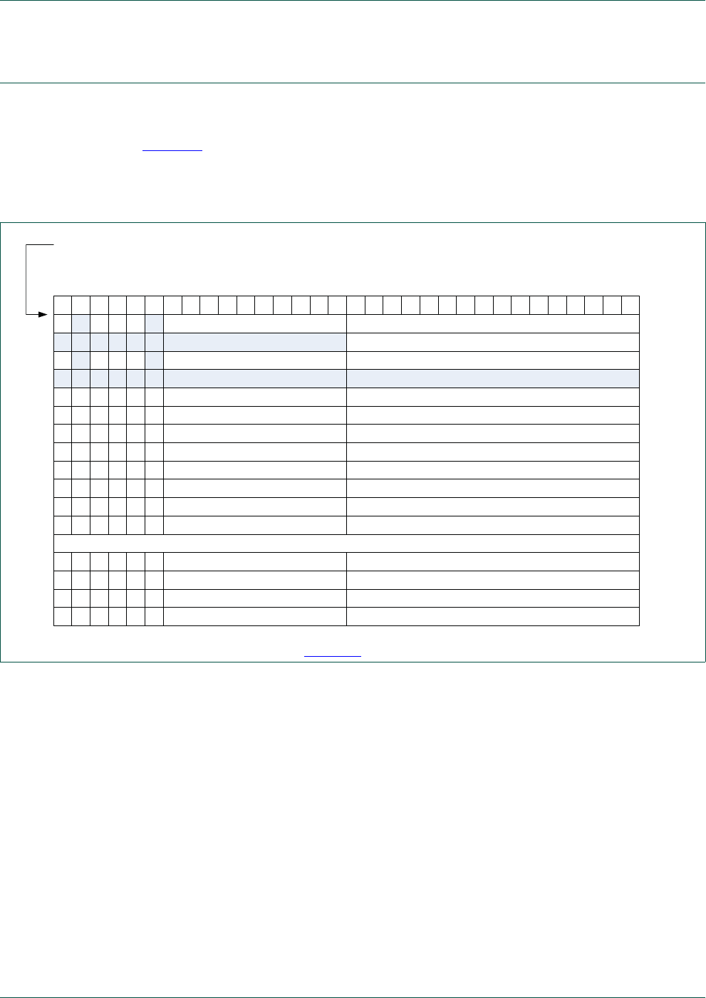
UM10462 All information provided in this document is subject to legal disclaimers. © NXP B.V. 2014. All rights reserved.
User manual Rev. 5.3 — 11 June 2014 232 of 521
NXP Semiconductors UM10462
Chapter 11: LPC11U3x/2x/1x USB2.0 device controller
11.7 Functional description
11.7.1 Endpoint command/status list
Figure 22 gives an overview on how the Endpoint List is organized in memory. The USB
EP Command/Status List start register points to the start of the list that contains all the
endpoint information in memory. The order of the endpoints is fixed as shown in the
picture.
Fig 22. Endpoint command/status list (see also Table 227)
31 30 29 28 27 26 25 24 23 22 21 20 19 18 17 16 15 14 13 12 11 10 9 8 7 6 5 4 3 2 1 0
SETUP bytes Buffer Address OffsetReservedR R R
EP0 OUT Buffer Address OffsetEP0 OUT Buffer NBytesA R S TR TV
R RR
EP0 IN Buffer Address OffsetEP0 IN Buffer NBytesA R S TR TV
Reserved ReservedR R RR RR
EP1 OUT Buffer 0 Address OffsetEP1 OUT Buffer 0 NBytesA D S TR RF
TV
EP1 OUT Buffer 1 Address OffsetEP1 OUT Buffer 1 NBytes
T
EP1 IN Buffer 0 Address OffsetEP1 IN Buffer 0 NBytesA D S TR RF
TV
EP1 IN Buffer 1 Address OffsetEP1 IN Buffer 1 NBytes
T
Offset
0x00
0x04
0x08
0x0C
0x10
0x14
0x18
0x1C
EP2 OUT Buffer 0 Address OffsetEP2 OUT Buffer 0 NBytesA D S TR RF
TV
EP2 OUT Buffer 1 Address OffsetEP2 OUT Buffer 1 NBytes
T
EP2 IN Buffer 0 Address OffsetEP2 IN Buffer 0 NBytesA D S TR RF
TV
EP2 IN Buffer 1 Address OffsetEP2 IN Buffer 1 NBytes
T
0x20
0x24
0x28
0x2C
...
EP4 OUT Buffer 0 Address OffsetEP4 OUT Buffer 0 NBytesA D S TR RF
TV
EP4 OUT Buffer 1 Address OffsetEP4 OUT Buffer 1 NBytes
T
EP4 IN Buffer 0 Address OffsetEP4 IN Buffer 0 NBytesA D S TR RF
TV
EP4 IN Buffer 1 Address OffsetEP4 IN Buffer 1 NBytes
T
0
x4
0
0x44
0x48
0x4C
USB EP Command/Status FIFO start
A D S TR RF
TV T
A D S TR RF
TV T
A D S TR RF
TV T
A D S TR RF
TV T
A D S TR RF
TV T
A D S TR RF
TV T
R
R

UM10462 All information provided in this document is subject to legal disclaimers. © NXP B.V. 2014. All rights reserved.
User manual Rev. 5.3 — 11 June 2014 233 of 521
NXP Semiconductors UM10462
Chapter 11: LPC11U3x/2x/1x USB2.0 device controller
Table 227. Endpoint commands
Symbol Access Description
A RW Active
The buffer is enabled. HW can use the buffer to store received OUT data or
to transmit data on the IN endpoint.
Software can only set this bit to ‘1’. As long as this bit is set to one,
software is not allowed to update any of the values in this 32-bit word. In
case software wants to deactivate the buffer, it must write a one to the
corresponding “skip” bit in the USB Endpoint skip register. Hardware can
only write this bit to zero. It will do this when it receives a short packet or
when the NBytes field transitions to zero or when software has written a
one to the “skip” bit.
D RW Disabled
0: The selected endpoint is enabled.
1: The selected endpoint is disabled.
If a USB token is received for an endpoint that has the disabled bit set,
hardware will ignore the token and not return any data or handshake.
When a bus reset is received, software must set the disable bit of all
endpoints to 1.
Software can only modify this bit when the active bit is zero.
SRWStall
0: The selected endpoint is not stalled
1: The selected endpoint is stalled
The Active bit has always higher priority than the Stall bit. This means that
a Stall handshake is only sent when the active bit is zero and the stall bit is
one.
Software can only modify this bit when the active bit is zero.
TR RW Toggle Reset
When software sets this bit to one, the HW will set the toggle value equal to
the value indicated in the “toggle value” (TV) bit.
For the control endpoint zero, this is not needed to be used because the
hardware resets the endpoint toggle to one for both directions when a
setup token is received.
For the other endpoints, the toggle can only be reset to zero when the
endpoint is reset.
RF / TV RW Rate Feedback mode / Toggle value
For bulk endpoints and isochronous endpoints this bit is reserved and must
be set to zero.
For the control endpoint zero this bit is used as the toggle value. When the
toggle reset bit is set, the data toggle is updated with the value
programmed in this bit.
When the endpoint is used as an interrupt endpoint, it can be set to the
following values.
0: Interrupt endpoint in ‘toggle mode’
1: Interrupt endpoint in ‘rate feedback mode’. This means that the data
toggle is fixed to zero for all data packets.
When the interrupt endpoint is in ‘rate feedback mode’, the TR bit must
always be set to zero.

UM10462 All information provided in this document is subject to legal disclaimers. © NXP B.V. 2014. All rights reserved.
User manual Rev. 5.3 — 11 June 2014 234 of 521
NXP Semiconductors UM10462
Chapter 11: LPC11U3x/2x/1x USB2.0 device controller
Remark: When receiving a SETUP token for endpoint zero, the HW will only read the
SETUP bytes Buffer Address offset to know where it has to store the received SETUP
bytes. The hardware will ignore all other fields. In case the SETUP stage contains more
than 8 bytes, it will only write the first 8 bytes to memory. A USB compliant host must
never send more than 8 bytes during the SETUP stage.
T RW Endpoint Type
0: Generic endpoint. The endpoint is configured as a bulk or interrupt
endpoint
1: Isochronous endpoint
NBytes RW For OUT endpoints this is the number of bytes that can be received in this
buffer.
For IN endpoints this is the number of bytes that must be transmitted.
HW decrements this value with the packet size every time when a packet is
successfully transferred.
Note: If a short packet is received on an OUT endpoint, the active bit will be
cleared and the NBytes value indicates the remaining buffer space that is
not used. Software calculates the received number of bytes by subtracting
the remaining NBytes from the programmed value.
Address
Offset
RW Bits 21 to 6 of the buffer start address.
The address offset is updated by hardware after each successful
reception/transmission of a packet. Hardware increments the original value
with the integer value when the packet size is divided by 64.
Examples:
•If an isochronous packet of 200 bytes is successfully received, the
address offset is incremented by 3.
•If a packet of 64 bytes is successfully received, the address offset is
incremented by 1.
•If a packet of less than 64 bytes is received, the address offset is not
incremented.
Table 227. Endpoint commands
Symbol Access Description
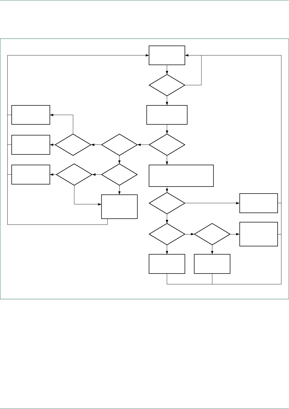
UM10462 All information provided in this document is subject to legal disclaimers. © NXP B.V. 2014. All rights reserved.
User manual Rev. 5.3 — 11 June 2014 235 of 521
NXP Semiconductors UM10462
Chapter 11: LPC11U3x/2x/1x USB2.0 device controller
11.7.2 Control endpoint 0
Fig 23. Flowchart of control endpoint 0 - OUT direction
Wait on EP 0Setup /Out
interrupt
EP0Setup / Out
Interrupt = ‘1’ ?
- Clear EP 0 Setup /Out interrupt
- Read DevStatus (Setup ) bit
Yes
No
DevStatus(Setup ) = ‘1’ ?
Yes
- Clear EP0OUT(Active)
- Clear EP0OUT(Stall)
- Clear EP0IN(Active)
- Clear EP0IN(Stall )
- Clear EP 0IN interrupt
- Clear DevStatus (Setup | IntonNak _CO | IntonNak _CI)
- Read SETUP bytes
CtrlRead ?
Yes
- Write EP0IN( Active = ‘1’
Stall = ‘1’*
NBytes)
- Write DevStatus (
IntOnNak _CO = ‘1’
IntOnNak _CI = ‘0’)
CtrlWriteNoDataStage ?
Yes
-Write EP0OUT(
Active = ‘0’
Stall = ‘1’)
- Write EP0IN( Active = ‘1’
Stall = ‘1
0 Bytes )
No
-Write EP0OUT(
Active = ‘1’
Stall = ‘1’*
NBytes)
- Write DevStatus (
IntOnNak _CO = ‘0’
IntOnNak _CI = ‘1’)
No
All OUT data received ?
- Write EP0OUT(Active = ‘1’
Stall = ‘1’*
NBytes)
No
No
Yes
- Write EP0IN( Active = ‘1’
Stall = ‘1’
0 Bytes )
- Write EP0Out (
Active = ‘0’
Stall = ‘1’)
-Clear EP0IN interrupt
SETUP request
supported ?
Yes
- Write EP0IN( Active = ‘0’
Stall = ‘1’)
-Write EP0OUT(
Active = ‘0’
Stall = ‘1’)
OUT Data phase
on-going ?
Yes
- Write EP0OUT(Active = ‘0’
Stall = ‘1’)
No
No
Note : It is very important that the
DevStatus(Setup) is only cleared after
setting EP0OUT(Active), EP0OUT(Stall),
EP0IN(Active) and EP0IN(Stall) bits are set
to zero
IN Data phase
on-going ?
EP0In Interrupt ?
No
No
Host aborts Control Write
Yes
- Write EP0OUT(Active = ‘1’
Stall = ‘1’
0 Bytes )
- Write EP0IN( Active = ‘0’
Stall = ‘1’)
- Clear EP0IN interrupt
Yes
If not all IN data transferred , the
host aborts Control Read .
Otherwise it is a normal completion
by the host
* : STALL bit must only be set when it is the last packet during the data phase for this Control Transfer
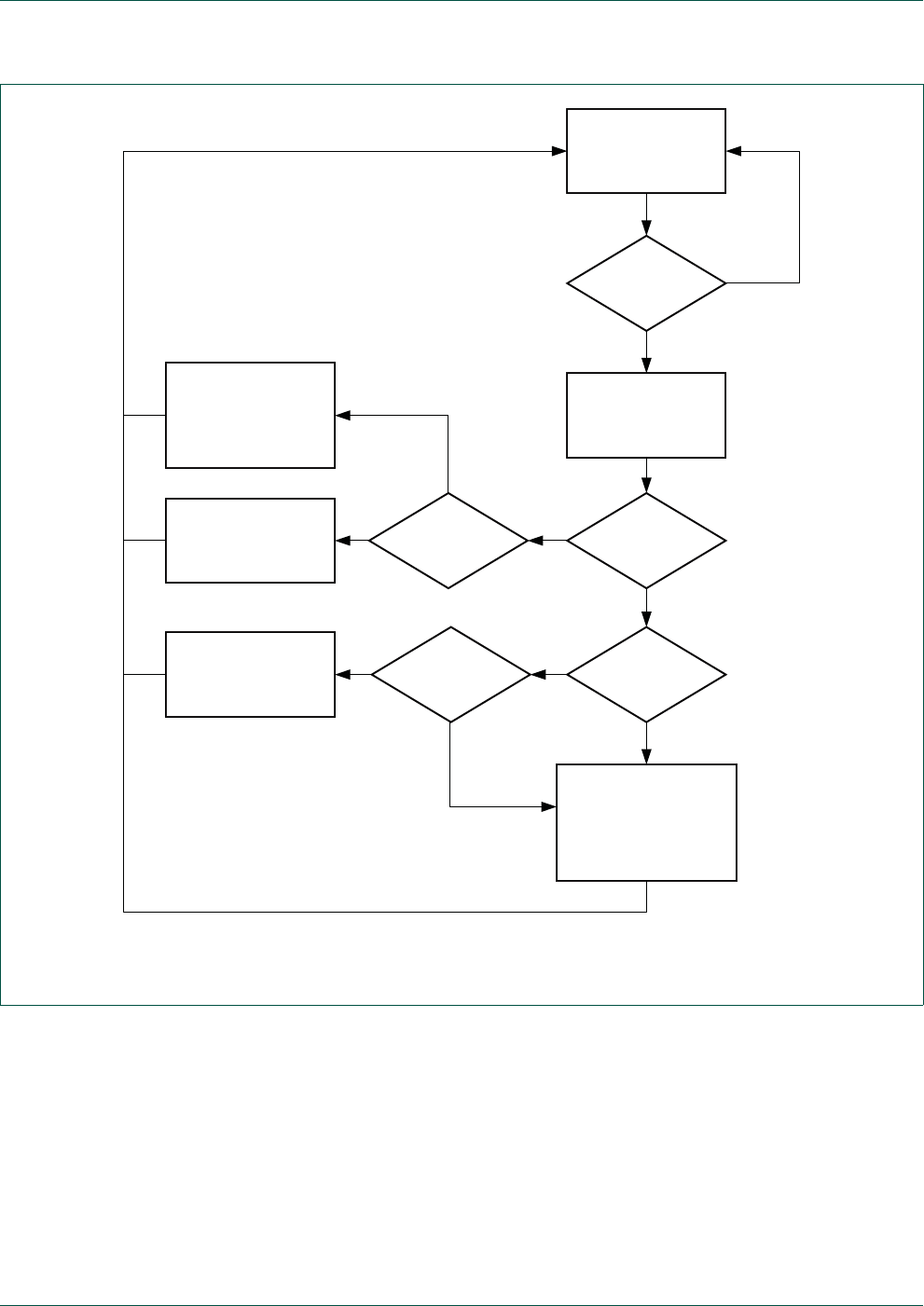
UM10462 All information provided in this document is subject to legal disclaimers. © NXP B.V. 2014. All rights reserved.
User manual Rev. 5.3 — 11 June 2014 236 of 521
NXP Semiconductors UM10462
Chapter 11: LPC11U3x/2x/1x USB2.0 device controller
11.7.3 Generic endpoint: single-buffering
To enable single-buffering, software must set the corresponding "USB EP Buffer Config"
bit to zero. In the "USB EP Buffer in use" register, software can indicate which buffer is
used in this case.
When software wants to transfer data, it programs the different bits in the Endpoint
command/status entry and sets the active bits. The hardware will transmit/receive multiple
packets for this endpoint until the NBytes value is equal to zero. When NBytes goes to
zero, hardware clears the active bit and sets the corresponding interrupt status bit.
Fig 24. Flowchart of control endpoint 0 - IN direction
Wait on EP 0In interrupt
EP0In
Interrupt = ‘1 ’ ?
- Clear EP0In interrupt
Yes
No
All IN data transmitted ?
- Write EP0IN( Active = ‘1’
Stall = ‘1’*
NBytes)
No
Yes
IN data phase
on-going ?
Yes
No
- Write EP0IN( Active = ‘0’
Stall = ‘1’)
OUT data phase
on-going ?
No
- Write EP0IN( Active = ‘1’
Stall = ‘1’
0 Bytes )
- Write EP0OUT(
Active = ‘0’
Stall = ‘1’)
- Clear EP0OUT interrupt
Yes
* : STALL bit must only be set when it is the last packet during the data phase for this Control Transfer
EP0Out Interrupt ?
No
Host aborts Control Read
Yes
- Write EP0OUT(
Active = ‘1’
Stall = ‘1’
0 Bytes )
- Write EP0IN (
Active = ‘0’
Stall = ‘1’)
- Clear EP 0Out interrupt
If not all OUT data transferred , the
host aborts Control Write .
Otherwise it is a normal completion
by the host

UM10462 All information provided in this document is subject to legal disclaimers. © NXP B.V. 2014. All rights reserved.
User manual Rev. 5.3 — 11 June 2014 237 of 521
NXP Semiconductors UM10462
Chapter 11: LPC11U3x/2x/1x USB2.0 device controller
Software must wait until hardware has cleared the Active bit to change some of the
command/status bits. This prevents hardware from overwriting a new value programmed
by software with some old values that were still cached.
If software wants to disable the active bit before the hardware has finished handling the
complete buffer, it can do this by setting the corresponding endpoint skip bit in USB
endpoint skip register.
11.7.4 Generic endpoint: double-buffering
To enable double-buffering, software must set the corresponding "USB EP Buffer Config"
bit to one. The "USB EP Buffer in use" register indicates which buffer will be used by HW
when the next token is received.
When HW clears the active bit of the current buffer in use, it will switch the buffer in use.
Software can also force HW to use a certain buffer by writing to the "USB EP Buffer in
use" bit.
11.7.5 Special cases
11.7.5.1 Use of the Active bit
The use of the Active bit is a bit different between OUT and IN endpoints.
When data must be received for the OUT endpoint, the software will set the Active bit to
one and program the NBytes field to the maximum number of bytes it can receive.
When data must be transmitted for an IN endpoint, the software sets the Active bit to one
and programs the NBytes field to the number of bytes that must be transmitted.
11.7.5.2 Generation of a STALL handshake
Special care must be taken when programming the endpoint to send a STALL handshake.
A STALL handshake is only sent in the following situations:
•The endpoint is enabled (Disabled bit = 0)
•The active bit of the endpoint is set to 0. (No packet needs to be received/transmitted
for that endpoint).
•The stall bit of the endpoint is set to one.
11.7.5.3 Clear Feature (endpoint halt)
When a non-control endpoint has returned a STALL handshake, the host will send a Clear
Feature (Endpoint Halt) for that endpoint. When the device receives this request, the
endpoint must be unstalled and the toggle bit for that endpoint must be reset back to zero.
In order to do that the software must program the following items for the endpoint that is
indicated.
If the endpoint is used in single-buffer mode, program the following:
•Set STALL bit (S) to 0.
•Set toggle reset bit (TR) to 1 and set toggle value bit (TV) to 0.
If the endpoint is used in double-buffer mode, program the following:

UM10462 All information provided in this document is subject to legal disclaimers. © NXP B.V. 2014. All rights reserved.
User manual Rev. 5.3 — 11 June 2014 238 of 521
NXP Semiconductors UM10462
Chapter 11: LPC11U3x/2x/1x USB2.0 device controller
•Set the STALL bit of both buffer 0 and buffer 1 to 0.
•Read the buffer in use bit for this endpoint.
•Set the toggle reset bit (TR) to 1 and set the toggle value bit (TV) to 0 for the buffer
indicated by the buffer in use bit.
11.7.5.4 Set configuration
When a SetConfiguration request is received with a configuration value different from
zero, the device software must enable all endpoints that will be used in this configuration
and reset all the toggle values. To do so, it must generate the procedure explained in
Section 11.7.5.3 for every endpoint that will be used in this configuration.
For all endpoints that are not used in this configuration, it must set the Disabled bit (D) to
one.
11.7.6 USB wake-up
11.7.6.1 Waking up from Deep-sleep and Power-down modes on USB activity
To allow the LPC11U3x/2x/1x to wake up from Deep-sleep or Power-down mode on USB
activity, complete the following steps:
1. Set bit AP_CLK in the USBCLKCTRL register (Table 41) to 0 (default) to enable
automatic control of the USB need_clock signal.
2. Wait until USB activity is suspended by polling the DSUS bit in the DSVCMD_STAT
register (DSUS = 1).
3. The USB need_clock signal will be deasserted after another 2 ms. Poll the
USBCLKST register until the USB need_clock status bit is 0 (Table 42).
4. Once the USBCLKST register returns 0, enable the USB activity wake-up interrupt in
the NVIC (# 30) and clear it.
5. Set bit 1 in the USBCLKCTRL register to 1 to trigger the USB activity wake-up
interrupt on the rising edge of the USB need_clock signal.
6. Enable the wake-up from Deep-sleep or Power-down modes on this interrupt by
enabling the USB need_clock signal in the STARTERP1 register (Table 44, bit 19).
7. Enter Deep-sleep or Power-down modes by writing to the PCON register.
8. Execute a WFI instruction.
The LPC11U3x/2x/1x will automatically wake up and resume execution on USB activity.
11.7.6.2 Remote wake-up
To issue a remote wake-up when the USB activity is suspended, complete the following
steps:
1. Set bit AP_CLK in the USBCLKCTRL register to 0 (Table 41, default) to enable
automatic control of the USB need_clock signal.
2. When it is time to issue a remote wake-up, turn on the USB clock and enable the USB
clock source.
3. Force the USB clock on by writing a 1 to bit AP_CLK (Table 41, bit 0) in the
USBCLKCTRL register.
4. Write a 0 to the DSUS bit in the DSVCMD_STAT register.

UM10462 All information provided in this document is subject to legal disclaimers. © NXP B.V. 2014. All rights reserved.
User manual Rev. 5.3 — 11 June 2014 239 of 521
NXP Semiconductors UM10462
Chapter 11: LPC11U3x/2x/1x USB2.0 device controller
5. Wait until the USB leaves the suspend state by polling the DSUS bit in the
DSVCMD_STAT register (DSUS =0).
6. Clear the AP_CLK bit (Table 41, bit 0) in the USBCLKCTRL to enable automatic USB
clock control.

UM10462 All information provided in this document is subject to legal disclaimers. © NXP B.V. 2014. All rights reserved.
User manual Rev. 5.3 — 11 June 2014 240 of 521
12.1 How to read this chapter
The USART controller is available on all LPC11U3x/2x/1x parts.
12.2 Basic configuration
The USART is configured as follows:
•Pins: The USART pins must be configured in the corresponding IOCON registers (see
Section 7.4).
•The USART block is enabled through the SYSAHBCLKCTRL register (see Table 24).
•The peripheral USART clock (PCLK), which is used by the USART baud rate
generator, is controlled by the UARTCLKDIV register (see Table 26).
12.3 Features
•16-byte receive and transmit FIFOs.
•Register locations conform to ‘550 industry standard.
•Receiver FIFO trigger points at 1, 4, 8, and 14 bytes.
•Built-in baud rate generator.
•Software or hardware flow control.
•RS-485/EIA-485 9-bit mode support with output enable.
•RTS/CTS flow control and other modem control signals.
•1X-clock send or receive.
•ISO 7816-3 compliant smart card interface.
•IrDA interface.
12.4 Pin description
UM10462
Chapter 12: LPC11U3x/2x/1x USART
Rev. 5.3 — 11 June 2014 User manual
Table 228. USART pin description
Pin Type Description
RXD Input Serial Input. Serial receive data.
TXD Output Serial Output. Serial transmit data (input/output in smart card mode).
RTS Output Request To Send. RS-485 direction control pin.
CTS Input Clear To Send.
DTR Output Data Terminal Ready.
DSR Input Data Set Ready. (Not available on HVQFN33-pin packages).
DCD Input Data Carrier Detect.
RI Input Ring Indicator. (Not available on HVQFN33-pin packages).
SCLK I/O Serial Clock.

UM10462 All information provided in this document is subject to legal disclaimers. © NXP B.V. 2014. All rights reserved.
User manual Rev. 5.3 — 11 June 2014 241 of 521
NXP Semiconductors UM10462
Chapter 12: LPC11U3x/2x/1x USART
12.5 Register description
The USART contains registers organized as shown in Table 229. The Divisor Latch
Access Bit (DLAB) is contained in the LCR register bit 7 and enables access to the Divisor
Latches.
Offsets/addresses not shown in Table 229 are reserved.
Table 229. Register overview: USART (base address: 0x4000 8000)
Name Access Address
offset Description Reset
value[1] Reference
RBR RO 0x000 Receiver Buffer Register. Contains the next received
character to be read. (DLAB=0)
NA Table 230
THR WO 0x000 Transmit Holding Register. The next character to be
transmitted is written here. (DLAB=0)
NA Table 231
DLL R/W 0x000 Divisor Latch LSB. Least significant byte of the baud
rate divisor value. The full divisor is used to generate
a baud rate from the fractional rate divider. (DLAB=1)
0x01 Table 232
DLM R/W 0x004 Divisor Latch MSB. Most significant byte of the baud
rate divisor value. The full divisor is used to generate
a baud rate from the fractional rate divider. (DLAB=1)
0Table 233
IER R/W 0x004 Interrupt Enable Register. Contains individual
interrupt enable bits for the 7 potential USART
interrupts. (DLAB=0)
0Table 234
IIR RO 0x008 Interrupt ID Register. Identifies which interrupt(s) are
pending.
0x01 Table 235
FCR WO 0x008 FIFO Control Register. Controls USART FIFO usage
and modes.
0Table 236
LCR R/W 0x00C Line Control Register. Contains controls for frame
formatting and break generation.
0Table 238
MCR R/W 0x010 Modem Control Register. 0 Table 239
LSR RO 0x014 Line Status Register. Contains flags for transmit and
receive status, including line errors.
0x60 Table 241
MSR RO 0x018 Modem Status Register. 0 Table 242
SCR R/W 0x01C Scratch Pad Register. Eight-bit temporary storage for
software.
0Table 243
ACR R/W 0x020 Auto-baud Control Register. Contains controls for the
auto-baud feature.
0Table 244
ICR R/W 0x024 IrDA Control Register. Enables and configures the
IrDA (remote control) mode.
0Table 245
FDR R/W 0x028 Fractional Divider Register. Generates a clock input
for the baud rate divider.
0x10 Table 247
OSR R/W 0x02C Oversampling Register. Controls the degree of
oversampling during each bit time.
0xF0 Table 249
TER R/W 0x030 Transmit Enable Register. Turns off USART
transmitter for use with software flow control.
0x80 Table 250
HDEN R/W 0x040 Half duplex enable register. 0 Table 251
SCICTRL R/W 0x048 Smart Card Interface Control register. Enables and
configures the Smart Card Interface feature.
0Table 252

UM10462 All information provided in this document is subject to legal disclaimers. © NXP B.V. 2014. All rights reserved.
User manual Rev. 5.3 — 11 June 2014 242 of 521
NXP Semiconductors UM10462
Chapter 12: LPC11U3x/2x/1x USART
[1] Reset Value reflects the data stored in used bits only. It does not include reserved bits content.
12.5.1 USART Receiver Buffer Register (when DLAB = 0, Read Only)
The RBR is the top byte of the USART RX FIFO. The top byte of the RX FIFO contains the
oldest character received and can be read via the bus interface. The LSB (bit 0) contains
the first-received data bit. If the character received is less than 8 bits, the unused MSBs
are padded with zeros.
The Divisor Latch Access Bit (DLAB) in the LCR must be zero in order to access the RBR.
The RBR is always Read Only.
Since PE, FE and BI bits (see Table 241) correspond to the byte on the top of the RBR
FIFO (i.e. the one that will be read in the next read from the RBR), the right approach for
fetching the valid pair of received byte and its status bits is first to read the content of the
LSR register, and then to read a byte from the RBR.
12.5.2 USART Transmitter Holding Register (when DLAB = 0, Write Only)
The THR is the top byte of the USART TX FIFO. The top byte is the newest character in
the TX FIFO and can be written via the bus interface. The LSB represents the first bit to
transmit.
The Divisor Latch Access Bit (DLAB) in the LCR must be zero in order to access the THR.
The THR is always Write Only.
RS485CTRL R/W 0x04C RS-485/EIA-485 Control. Contains controls to
configure various aspects of RS-485/EIA-485 modes.
0Table 253
RS485ADRMATCH R/W 0x050 RS-485/EIA-485 address match. Contains the
address match value for RS-485/EIA-485 mode.
0Table 254
RS485DLY R/W 0x054 RS-485/EIA-485 direction control delay. 0 Table 255
SYNCCTRL R/W 0x058 Synchronous mode control register. 0 Table 256
Table 229. Register overview: USART (base address: 0x4000 8000)
Name Access Address
offset Description Reset
value[1] Reference
Table 230. USART Receiver Buffer Register when DLAB = 0, Read Only (RBR - address
0x4000 8000) bit description
Bit Symbol Description Reset Value
7:0 RBR The USART Receiver Buffer Register contains the oldest
received byte in the USART RX FIFO.
undefined
31:8 - Reserved -
Table 231. USART Transmitter Holding Register when DLAB = 0, Write Only (THR - address
0x4000 8000) bit description
Bit Symbol Description Reset Value
7:0 THR Writing to the USART Transmit Holding Register causes the
data to be stored in the USART transmit FIFO. The byte will be
sent when it is the oldest byte in the FIFO and the transmitter is
available.
NA
31:8 - Reserved -

UM10462 All information provided in this document is subject to legal disclaimers. © NXP B.V. 2014. All rights reserved.
User manual Rev. 5.3 — 11 June 2014 243 of 521
NXP Semiconductors UM10462
Chapter 12: LPC11U3x/2x/1x USART
12.5.3 USART Divisor Latch LSB and MSB Registers (when DLAB = 1)
The USART Divisor Latch is part of the USART Baud Rate Generator and holds the value
used (optionally with the Fractional Divider) to divide the UART_PCLK clock in order to
produce the baud rate clock, which must be the multiple of the desired baud rate that is
specified by the Oversampling Register (typically 16X). The DLL and DLM registers
together form a 16-bit divisor. DLL contains the lower 8 bits of the divisor and DLM
contains the higher 8 bits. A zero value is treated like 0x0001. The Divisor Latch Access
Bit (DLAB) in the LCR must be one in order to access the USART Divisor Latches. Details
on how to select the right value for DLL and DLM can be found in Section 12.5.14.
12.5.4 USART Interrupt Enable Register (when DLAB = 0)
The IER is used to enable the various USART interrupt sources.
Table 232. USART Divisor Latch LSB Register when DLAB = 1 (DLL - address 0x4000 8000)
bit description
Bit Symbol Description Reset value
7:0 DLLSB The USART Divisor Latch LSB Register, along with the DLM
register, determines the baud rate of the USART.
0x01
31:8 - Reserved -
Table 233. USART Divisor Latch MSB Register when DLAB = 1 (DLM - address 0x4000 8004)
bit description
Bit Symbol Description Reset value
7:0 DLMSB The USART Divisor Latch MSB Register, along with the DLL
register, determines the baud rate of the USART.
0x00
31:8 - Reserved -
Table 234. USART Interrupt Enable Register when DLAB = 0 (IER - address 0x4000 8004) bit
description
Bit Symbol Value Description Reset
value
0 RBRINTEN RBR Interrupt Enable. Enables the Receive Data Available
interrupt. It also controls the Character Receive Time-out
interrupt.
0
0 Disable the RDA interrupt.
1 Enable the RDA interrupt.
1 THREINTEN THRE Interrupt Enable. Enables the THRE interrupt. The
status of this interrupt can be read from LSR[5].
0
0 Disable the THRE interrupt.
1 Enable the THRE interrupt.
2 RLSINTEN Enables the Receive Line Status interrupt. The status of
this interrupt can be read from LSR[4:1].
-
0 Disable the RLS interrupt.
1 Enable the RLS interrupt.
3 MSINTEN Enables the Modem Status interrupt. The components of
this interrupt can be read from the MSR.
0 Disable the MS interrupt.
1 Enable the MS interrupt.

UM10462 All information provided in this document is subject to legal disclaimers. © NXP B.V. 2014. All rights reserved.
User manual Rev. 5.3 — 11 June 2014 244 of 521
NXP Semiconductors UM10462
Chapter 12: LPC11U3x/2x/1x USART
12.5.5 USART Interrupt Identification Register (Read Only)
IIR provides a status code that denotes the priority and source of a pending interrupt. The
interrupts are frozen during a IIR access. If an interrupt occurs during a IIR access, the
interrupt is recorded for the next IIR access.
7:4 - Reserved, user software should not write ones to reserved
bits. The value read from a reserved bit is not defined.
NA
8 ABEOINTEN Enables the end of auto-baud interrupt. 0
0 Disable end of auto-baud Interrupt.
1 Enable end of auto-baud Interrupt.
9 ABTOINTEN Enables the auto-baud time-out interrupt. 0
0 Disable auto-baud time-out Interrupt.
1 Enable auto-baud time-out Interrupt.
31:10 - Reserved, user software should not write ones to reserved
bits. The value read from a reserved bit is not defined.
NA
Table 234. USART Interrupt Enable Register when DLAB = 0 (IER - address 0x4000 8004) bit
description …continued
Bit Symbol Value Description Reset
value
Table 235. USART Interrupt Identification Register Read only (IIR - address 0x4004 8008) bit
description
Bit Symbol Value Description Reset
value
0 INTSTATUS Interrupt status. Note that IIR[0] is active low. The pending
interrupt can be determined by evaluating IIR[3:1].
1
0 At least one interrupt is pending.
1 No interrupt is pending.
3:1 INTID Interrupt identification. IER[3:1] identifies an interrupt
corresponding to the USART Rx FIFO. All other values of
IER[3:1] not listed below are reserved.
0
0x3 1 - Receive Line Status (RLS).
0x2 2a - Receive Data Available (RDA).
0x6 2b - Character Time-out Indicator (CTI).
0x1 3 - THRE Interrupt.
0x0 4 - Modem status
5:4 - Reserved, user software should not write ones to reserved
bits. The value read from a reserved bit is not defined.
NA
7:6 FIFOEN These bits are equivalent to FCR[0]. 0
8 ABEOINT End of auto-baud interrupt. True if auto-baud has finished
successfully and interrupt is enabled.
0
9 ABTOINT Auto-baud time-out interrupt. True if auto-baud has timed
out and interrupt is enabled.
0
31:10 - Reserved, user software should not write ones to reserved
bits. The value read from a reserved bit is not defined.
NA

UM10462 All information provided in this document is subject to legal disclaimers. © NXP B.V. 2014. All rights reserved.
User manual Rev. 5.3 — 11 June 2014 245 of 521
NXP Semiconductors UM10462
Chapter 12: LPC11U3x/2x/1x USART
Bits IIR[9:8] are set by the auto-baud function and signal a time-out or end of auto-baud
condition. The auto-baud interrupt conditions are cleared by setting the corresponding
Clear bits in the Auto-baud Control Register.
If the IntStatus bit is one and no interrupt is pending and the IntId bits will be zero. If the
IntStatus is 0, a non auto-baud interrupt is pending in which case the IntId bits identify the
type of interrupt and handling as described in Table 236. Given the status of IIR[3:0], an
interrupt handler routine can determine the cause of the interrupt and how to clear the
active interrupt. The IIR must be read in order to clear the interrupt prior to exiting the
Interrupt Service Routine.
The USART RLS interrupt (IIR[3:1] = 011) is the highest priority interrupt and is set
whenever any one of four error conditions occur on the USART RX input: overrun error
(OE), parity error (PE), framing error (FE) and break interrupt (BI). The USART Rx error
condition that set the interrupt can be observed via LSR[4:1]. The interrupt is cleared upon
a LSR read.
The USART RDA interrupt (IIR[3:1] = 010) shares the second level priority with the CTI
interrupt (IIR[3:1] = 110). The RDA is activated when the USART Rx FIFO reaches the
trigger level defined in FCR7:6 and is reset when the USART Rx FIFO depth falls below
the trigger level. When the RDA interrupt goes active, the CPU can read a block of data
defined by the trigger level.
The CTI interrupt (IIR[3:1] = 110) is a second level interrupt and is set when the USART
Rx FIFO contains at least one character and no USART Rx FIFO activity has occurred in
3.5 to 4.5 character times. Any USART Rx FIFO activity (read or write of USART RSR) will
clear the interrupt. This interrupt is intended to flush the USART RBR after a message has
been received that is not a multiple of the trigger level size. For example, if a 105
character message was to be sent and the trigger level was 10 characters, the CPU would
receive 10 RDA interrupts resulting in the transfer of 100 characters and 1 to 5 CTI
interrupts (depending on the service routine) resulting in the transfer of the remaining 5
characters.
Table 236. USART Interrupt Handling
IIR[3:0]
value[1] Priority Interrupt
type Interrupt source Interrupt
reset
0001 - None None -
0110 Highest RX Line
Status /
Error
OE[2] or PE[2] or FE[2] or BI[2] LSR Read[2]
0100 Second RX Data
Available
Rx data available or trigger level reached in FIFO
(FCR0=1)
RBR
Read[3] or
USART
FIFO drops
below
trigger level

UM10462 All information provided in this document is subject to legal disclaimers. © NXP B.V. 2014. All rights reserved.
User manual Rev. 5.3 — 11 June 2014 246 of 521
NXP Semiconductors UM10462
Chapter 12: LPC11U3x/2x/1x USART
[1] Values "0000", “0011”, “0101”, “0111”, “1000”, “1001”, “1010”, “1011”,”1101”,”1110”,”1111” are reserved.
[2] For details see Section 12.5.9 “USART Line Status Register (Read-Only)”
[3] For details see Section 12.5.1 “USART Receiver Buffer Register (when DLAB = 0, Read Only)”
[4] For details see Section 12.5.5 “USART Interrupt Identification Register (Read Only)” and Section 12.5.2
“USART Transmitter Holding Register (when DLAB = 0, Write Only)”
The USART THRE interrupt (IIR[3:1] = 001) is a third level interrupt and is activated when
the USART THR FIFO is empty provided certain initialization conditions have been met.
These initialization conditions are intended to give the USART THR FIFO a chance to fill
up with data to eliminate many THRE interrupts from occurring at system start-up. The
initialization conditions implement a one character delay minus the stop bit whenever
THRE = 1 and there have not been at least two characters in the THR at one time since
the last THRE = 1 event. This delay is provided to give the CPU time to write data to THR
without a THRE interrupt to decode and service. A THRE interrupt is set immediately if the
USART THR FIFO has held two or more characters at one time and currently, the THR is
empty. The THRE interrupt is reset when a THR write occurs or a read of the IIR occurs
and the THRE is the highest interrupt (IIR[3:1] = 001).
The modem status interrupt (IIR3:1 = 000) is the lowest priority USART interrupt and is
activated whenever there is a state change on the CTS, DCD, or DSR or a trailing edge
on the RI pin. The source of the modem interrupt can be read in MSR3:0. Reading the
MSR clears the modem interrupt.
12.5.6 USART FIFO Control Register (Write Only)
The FCR controls the operation of the USART RX and TX FIFOs.
1100 Second Character
Time-out
indication
Minimum of one character in the RX FIFO and no
character input or removed during a time period
depending on how many characters are in FIFO
and what the trigger level is set at (3.5 to 4.5
character times).
The exact time will be:
[(word length) 7 - 2] 8 + [(trigger level - number
of characters) 8 + 1] RCLKs
RBR
Read[3]
0010 Third THRE THRE[2] IIR Read[4]
(if source of
interrupt) or
THR write
0000 Fourth Modem
Status
CTS, DSR, RI, or DCD. MSR Read
Table 236. USART Interrupt Handling
IIR[3:0]
value[1] Priority Interrupt
type Interrupt source Interrupt
reset

UM10462 All information provided in this document is subject to legal disclaimers. © NXP B.V. 2014. All rights reserved.
User manual Rev. 5.3 — 11 June 2014 247 of 521
NXP Semiconductors UM10462
Chapter 12: LPC11U3x/2x/1x USART
12.5.7 USART Line Control Register
The LCR determines the format of the data character that is to be transmitted or received.
Table 237. USART FIFO Control Register Write only (FCR - address 0x4000 8008) bit
description
Bit Symbol Value Description Reset
value
0 FIFOEN FIFO enable 0
0 USART FIFOs are disabled. Must not be used in the application.
1 Active high enable for both USART Rx and TX FIFOs and
FCR[7:1] access. This bit must be set for proper USART
operation. Any transition on this bit will automatically clear the
USART FIFOs.
1RXFIFO
RES
RX FIFO Reset 0
0 No impact on either of USART FIFOs.
1 Writing a logic 1 to FCR[1] will clear all bytes in USART Rx FIFO,
reset the pointer logic. This bit is self-clearing.
2TXFIFO
RES
TX FIFO Reset 0
0 No impact on either of USART FIFOs.
1 Writing a logic 1 to FCR[2] will clear all bytes in USART TX FIFO,
reset the pointer logic. This bit is self-clearing.
3 - - Reserved 0
5:4 - Reserved, user software should not write ones to reserved bits.
The value read from a reserved bit is not defined.
NA
7:6 RXTL RX Trigger Level. These two bits determine how many USART
FIFO characters must be received by the FIFO before an
interrupt is activated.
0
0x0 Trigger level 0 (1 character or 0x01).
0x1 Trigger level 1 (4 characters or 0x04).
0x2 Trigger level 2 (8 characters or 0x08).
0x3 Trigger level 3 (14 characters or 0x0E).
31:8 - - Reserved -
Table 238. USART Line Control Register (LCR - address 0x4000 800C) bit description
Bit Symbol Value Description Reset
Value
1:0 WLS Word Length Select 0
0x0 5-bit character length.
0x1 6-bit character length.
0x2 7-bit character length.
0x3 8-bit character length.
2 SBS Stop Bit Select 0
0 1 stop bit.
1 2 stop bits (1.5 if LCR[1:0]=00).

UM10462 All information provided in this document is subject to legal disclaimers. © NXP B.V. 2014. All rights reserved.
User manual Rev. 5.3 — 11 June 2014 248 of 521
NXP Semiconductors UM10462
Chapter 12: LPC11U3x/2x/1x USART
12.5.8 USART Modem Control Register
The MCR enables the modem loopback mode and controls the modem output signals.
3 PE Parity Enable 0
0 Disable parity generation and checking.
1 Enable parity generation and checking.
5:4 PS Parity Select 0
0x0 Odd parity. Number of 1s in the transmitted character and the
attached parity bit will be odd.
0x1 Even Parity. Number of 1s in the transmitted character and the
attached parity bit will be even.
0x2 Forced 1 stick parity.
0x3 Forced 0 stick parity.
6 BC Break Control 0
0 Disable break transmission.
1 Enable break transmission. Output pin USART TXD is forced to
logic 0 when LCR[6] is active high.
7 DLAB Divisor Latch Access Bit 0
0 Disable access to Divisor Latches.
1 Enable access to Divisor Latches.
31:8 - - Reserved -
Table 238. USART Line Control Register (LCR - address 0x4000 800C) bit description
Bit Symbol Value Description Reset
Value
Table 239. USART Modem Control Register (MCR - address 0x4000 8010) bit description
Bit Symbol Value Description Reset
value
0 DTRCTRL Source for modem output pin DTR. This bit reads as 0 when
modem loopback mode is active.
0
1 RTSCTRL Source for modem output pin RTS. This bit reads as 0 when
modem loopback mode is active.
0
3:2 - Reserved, user software should not write ones to reserved bits.
The value read from a reserved bit is not defined.
0
4 LMS Loopback Mode Select. The modem loopback mode provides a
mechanism to perform diagnostic loopback testing. Serial data
from the transmitter is connected internally to serial input of the
receiver. Input pin, RXD, has no effect on loopback and output
pin, TXD is held in marking state. The DSR, CTS, DCD, and RI
pins are ignored. Externally, DTR and RTS are set inactive.
Internally, the upper four bits of the MSR are driven by the
lower four bits of the MCR. This permits modem status
interrupts to be generated in loopback mode by writing the
lower four bits of MCR.
0
0 Disable modem loopback mode.
1 Enable modem loopback mode.
5 - Reserved, user software should not write ones to reserved bits.
The value read from a reserved bit is not defined.
0

UM10462 All information provided in this document is subject to legal disclaimers. © NXP B.V. 2014. All rights reserved.
User manual Rev. 5.3 — 11 June 2014 249 of 521
NXP Semiconductors UM10462
Chapter 12: LPC11U3x/2x/1x USART
12.5.8.1 Auto-flow control
If auto-RTS mode is enabled, the USART‘s receiver FIFO hardware controls the RTS
output of the USART. If the auto-CTS mode is enabled, the USART‘s transmitter will only
start sending if the CTS pin is low.
12.5.8.1.1 Auto-RTS
The auto-RTS function is enabled by setting the RTSen bit. Auto-RTS data flow control
originates in the RBR module and is linked to the programmed receiver FIFO trigger level.
If auto-RTS is enabled, the data-flow is controlled as follows:
When the receiver FIFO level reaches the programmed trigger level, RTS is deasserted
(to a high value). It is possible that the sending USART sends an additional byte after the
trigger level is reached (assuming the sending USART has another byte to send) because
it might not recognize the deassertion of RTS until after it has begun sending the
additional byte. RTS is automatically reasserted (to a low value) once the receiver FIFO
has reached the previous trigger level. The reassertion of RTS signals the sending
USART to continue transmitting data.
If Auto-RTS mode is disabled, the RTSen bit controls the RTS output of the USART. If
Auto-RTS mode is enabled, hardware controls the RTS output, and the actual value of
RTS will be copied in the RTS Control bit of the USART. As long as Auto-RTS is enabled,
the value of the RTS Control bit is read-only for software.
Example: Suppose the USART operating in type ‘550 mode has the trigger level in FCR
set to 0x2, then, if Auto-RTS is enabled, the USART will deassert the RTS output as soon
as the receive FIFO contains 8 bytes (Table 237 on page 247). The RTS output will be
reasserted as soon as the receive FIFO hits the previous trigger level: 4 bytes.
6 RTSEN RTS enable 0
0 Disable auto-rts flow control.
1 Enable auto-rts flow control.
7 CTSEN CTS enable 0
0 Disable auto-cts flow control.
1 Enable auto-cts flow control.
31:8 - - Reserved -
Table 239. USART Modem Control Register (MCR - address 0x4000 8010) bit description
Bit Symbol Value Description Reset
value
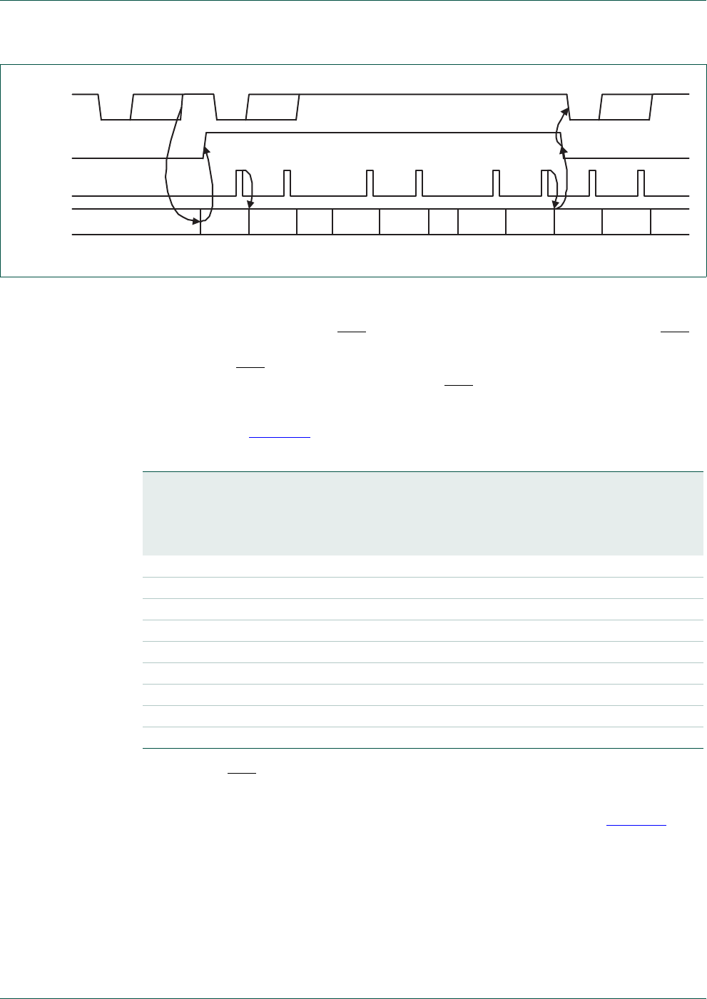
UM10462 All information provided in this document is subject to legal disclaimers. © NXP B.V. 2014. All rights reserved.
User manual Rev. 5.3 — 11 June 2014 250 of 521
NXP Semiconductors UM10462
Chapter 12: LPC11U3x/2x/1x USART
12.5.8.1.2 Auto-CTS
The Auto-CTS function is enabled by setting the CTSen bit. If Auto-CTS is enabled, the
transmitter circuitry checks the CTS input before sending the next data byte. When CTS is
active (low), the transmitter sends the next byte. To stop the transmitter from sending the
following byte, CTS must be released before the middle of the last stop bit that is currently
being sent. In Auto-CTS mode, a change of the CTS signal does not trigger a modem
status interrupt unless the CTS Interrupt Enable bit is set, but the Delta CTS bit in the
MSR will be set. Table 240 lists the conditions for generating a Modem Status interrupt.
The auto-CTS function typically eliminates the need for CTS interrupts. When flow control
is enabled, a CTS state change does not trigger host interrupts because the device
automatically controls its own transmitter. Without Auto-CTS, the transmitter sends any
data present in the transmit FIFO and a receiver overrun error can result. Figure 26
illustrates the Auto-CTS functional timing.
Fig 25. Auto-RTS Functional Timing
start byte N stop start bits0..7 stop start bits0..7 stop
N-1 NN-1 N-1N-2 N-2 M+2 M+1 M M-1
UART1 Rx
RTS1 pin
UART1 Rx
FIFO level
UART1 Rx
FIFO read
~
~~
~
~
~~
~~
~
Table 240. Modem status interrupt generation
Enable
modem
status
interrupt
(IER[3])
CTSen
(MCR[7]) CTS
interrupt
enable
(IER[7])
Delta CTS
(MSR[0]) Delta DCD or trailing edge
RI or
Delta DSR (MSR[3:1])
Modem
status
interrupt
0x x x x No
10 x 0 0 No
10 x 1 x Yes
10 x x 1 Yes
11 0 x 0 No
11 0 x 1 Yes
11 1 0 0 No
11 1 1 x Yes
11 1 x 1 Yes

UM10462 All information provided in this document is subject to legal disclaimers. © NXP B.V. 2014. All rights reserved.
User manual Rev. 5.3 — 11 June 2014 251 of 521
NXP Semiconductors UM10462
Chapter 12: LPC11U3x/2x/1x USART
During transmission of the second character the CTS signal is negated. The third
character is not sent thereafter. The USART maintains 1 on TXD as long as CTS is
negated (high). As soon as CTS is asserted, transmission resumes and a start bit is sent
followed by the data bits of the next character.
12.5.9 USART Line Status Register (Read-Only)
The LSR is a read-only register that provides status information on the USART TX and RX
blocks.
Fig 26. Auto-CTS Functional Timing
start bits0..7 start bits0..7 stop start bits0..7 stop
UART1 TX
CTS1 pin
~
~
~
~
~
~
~
~
stop
Table 241. USART Line Status Register Read only (LSR - address 0x4000 8014) bit
description
Bit Symbol Value Description Reset
Value
0 RDR Receiver Data Ready:LSR[0] is set when the RBR holds an
unread character and is cleared when the USART RBR FIFO
is empty.
0
0 RBR is empty.
1 RBR contains valid data.
1 OE Overrun Error. The overrun error condition is set as soon as it
occurs. A LSR read clears LSR[1]. LSR[1] is set when USART
RSR has a new character assembled and the USART RBR
FIFO is full. In this case, the USART RBR FIFO will not be
overwritten and the character in the USART RSR will be lost.
0
0 Overrun error status is inactive.
1 Overrun error status is active.
2 PE Parity Error. When the parity bit of a received character is in
the wrong state, a parity error occurs. A LSR read clears
LSR[2]. Time of parity error detection is dependent on FCR[0].
Note: A parity error is associated with the character at the top
of the USART RBR FIFO.
0
0 Parity error status is inactive.
1 Parity error status is active.

UM10462 All information provided in this document is subject to legal disclaimers. © NXP B.V. 2014. All rights reserved.
User manual Rev. 5.3 — 11 June 2014 252 of 521
NXP Semiconductors UM10462
Chapter 12: LPC11U3x/2x/1x USART
3 FE Framing Error. When the stop bit of a received character is a
logic 0, a framing error occurs. A LSR read clears LSR[3]. The
time of the framing error detection is dependent on FCR0.
Upon detection of a framing error, the RX will attempt to
re-synchronize to the data and assume that the bad stop bit is
actually an early start bit. However, it cannot be assumed that
the next received byte will be correct even if there is no
Framing Error.
Note: A framing error is associated with the character at the
top of the USART RBR FIFO.
0
0 Framing error status is inactive.
1 Framing error status is active.
4 BI Break Interrupt. When RXD1 is held in the spacing state (all
zeros) for one full character transmission (start, data, parity,
stop), a break interrupt occurs. Once the break condition has
been detected, the receiver goes idle until RXD1 goes to
marking state (all ones). A LSR read clears this status bit. The
time of break detection is dependent on FCR[0].
Note: The break interrupt is associated with the character at
the top of the USART RBR FIFO.
0
0 Break interrupt status is inactive.
1 Break interrupt status is active.
5 THRE Transmitter Holding Register Empty. THRE is set immediately
upon detection of an empty USART THR and is cleared on a
THR write.
1
0 THR contains valid data.
1 THR is empty.
6 TEMT Transmitter Empty. TEMT is set when both THR and TSR are
empty; TEMT is cleared when either the TSR or the THR
contain valid data.
1
0 THR and/or the TSR contains valid data.
1 THR and the TSR are empty.
7 RXFE Error in RX FIFO. LSR[7] is set when a character with a RX
error such as framing error, parity error or break interrupt, is
loaded into the RBR. This bit is cleared when the LSR register
is read and there are no subsequent errors in the USART
FIFO.
0
0 RBR contains no USART RX errors or FCR[0]=0.
1 USART RBR contains at least one USART RX error.
8 TXERR Tx Error. In smart card T=0 operation, this bit is set when the
smart card has NACKed a transmitted character, one more
than the number of times indicated by the TXRETRY field.
0
31:9 - - Reserved -
Table 241. USART Line Status Register Read only (LSR - address 0x4000 8014) bit
description …continued
Bit Symbol Value Description Reset
Value

UM10462 All information provided in this document is subject to legal disclaimers. © NXP B.V. 2014. All rights reserved.
User manual Rev. 5.3 — 11 June 2014 253 of 521
NXP Semiconductors UM10462
Chapter 12: LPC11U3x/2x/1x USART
12.5.10 USART Modem Status Register
The MSR is a read-only register that provides status information on USART input signals.
Bit 0 is cleared when (after) this register is read.
12.5.11 USART Scratch Pad Register
The SCR has no effect on the USART operation. This register can be written and/or read
at user’s discretion. There is no provision in the interrupt interface that would indicate to
the host that a read or write of the SCR has occurred.
Table 242: USART Modem Status Register (MSR - address 0x4000 8018) bit description
Bit Symbol Value Description Reset
value
0 DCTS Delta CTS.
Set upon state change of input CTS. Cleared on an MSR
read.
0
0 No change detected on modem input, CTS.
1 State change detected on modem input, CTS.
1 DDSR Delta DSR.
Set upon state change of input DSR. Cleared on an MSR
read.
0
0 No change detected on modem input, DSR.
1 State change detected on modem input, DSR.
2 TERI Trailing Edge RI.
Set upon low to high transition of input RI. Cleared on an
MSR read.
0
0 No change detected on modem input, RI.
1 Low-to-high transition detected on RI.
3 DDCD Delta DCD. Set upon state change of input DCD. Cleared on
an MSR read.
0
0 No change detected on modem input, DCD.
1 State change detected on modem input, DCD.
4 CTS - Clear To Send State. Complement of input signal CTS. This
bit is connected to MCR[1] in modem loopback mode.
0
5 DSR - Data Set Ready State. Complement of input signal DSR.
This bit is connected to MCR[0] in modem loopback mode.
0
6 RI - Ring Indicator State. Complement of input RI. This bit is
connected to MCR[2] in modem loopback mode.
0
7 DCD - Data Carrier Detect State. Complement of input DCD. This
bit is connected to MCR[3] in modem loopback mode.
0
31:8 - - Reserved, the value read from a reserved bit is not defined. NA
Table 243. USART Scratch Pad Register (SCR - address 0x4000 801C) bit description
Bit Symbol Description Reset
Value
7:0 PAD A readable, writable byte. 0x00
31:8 - Reserved -

UM10462 All information provided in this document is subject to legal disclaimers. © NXP B.V. 2014. All rights reserved.
User manual Rev. 5.3 — 11 June 2014 254 of 521
NXP Semiconductors UM10462
Chapter 12: LPC11U3x/2x/1x USART
12.5.12 USART Auto-baud Control Register
The USART Auto-baud Control Register (ACR) controls the process of measuring the
incoming clock/data rate for baud rate generation, and can be read and written at the
user’s discretion.
12.5.12.1 Auto-baud
The USART auto-baud function can be used to measure the incoming baud rate based on
the “AT” protocol (Hayes command). If enabled the auto-baud feature will measure the bit
time of the receive data stream and set the divisor latch registers DLM and DLL
accordingly.
Auto-baud is started by setting the ACR Start bit. Auto-baud can be stopped by clearing
the ACR Start bit. The Start bit will clear once auto-baud has finished and reading the bit
will return the status of auto-baud (pending/finished).
Table 244. Auto-baud Control Register (ACR - address 0x4000 8020) bit description
Bit Symbol Value Description Reset
value
0 START This bit is automatically cleared after auto-baud
completion.
0
0 Auto-baud stop (auto-baud is not running).
1 Auto-baud start (auto-baud is running). Auto-baud run
bit. This bit is automatically cleared after auto-baud
completion.
1 MODE Auto-baud mode select bit. 0
0 Mode 0.
1 Mode 1.
2AUTORESTART Start mode 0
0 No restart
1 Restart in case of time-out (counter restarts at next
USART Rx falling edge)
7:3 - Reserved, user software should not write ones to
reserved bits. The value read from a reserved bit is not
defined.
0
8 ABEOINTCLR End of auto-baud interrupt clear bit (write only
accessible).
0
0 Writing a 0 has no impact.
1 Writing a 1 will clear the corresponding interrupt in the
IIR.
9 ABTOINTCLR Auto-baud time-out interrupt clear bit (write only
accessible).
0
0 Writing a 0 has no impact.
1 Writing a 1 will clear the corresponding interrupt in the
IIR.
31:10 - Reserved, user software should not write ones to
reserved bits. The value read from a reserved bit is not
defined.
0

UM10462 All information provided in this document is subject to legal disclaimers. © NXP B.V. 2014. All rights reserved.
User manual Rev. 5.3 — 11 June 2014 255 of 521
NXP Semiconductors UM10462
Chapter 12: LPC11U3x/2x/1x USART
Two auto-baud measuring modes are available which can be selected by the ACR Mode
bit. In Mode 0 the baud rate is measured on two subsequent falling edges of the USART
Rx pin (the falling edge of the start bit and the falling edge of the least significant bit). In
Mode 1 the baud rate is measured between the falling edge and the subsequent rising
edge of the USART Rx pin (the length of the start bit).
The ACR AutoRestart bit can be used to automatically restart baud rate measurement if a
time-out occurs (the rate measurement counter overflows). If this bit is set, the rate
measurement will restart at the next falling edge of the USART Rx pin.
The auto-baud function can generate two interrupts.
•The IIR ABTOInt interrupt will get set if the interrupt is enabled (IER ABToIntEn is set
and the auto-baud rate measurement counter overflows).
•The IIR ABEOInt interrupt will get set if the interrupt is enabled (IER ABEOIntEn is set
and the auto-baud has completed successfully).
The auto-baud interrupts have to be cleared by setting the corresponding ACR
ABTOIntClr and ABEOIntEn bits.
The fractional baud rate generator must be disabled (DIVADDVAL = 0) during auto-baud.
Also, when auto-baud is used, any write to DLM and DLL registers should be done before
ACR register write. The minimum and the maximum baud rates supported by USART are
a function of USART_PCLK and the number of data bits, stop bits and parity bits.
(2)
12.5.12.2 Auto-baud modes
When the software is expecting an “AT” command, it configures the USART with the
expected character format and sets the ACR Start bit. The initial values in the divisor
latches DLM and DLM don‘t care. Because of the “A” or “a” ASCII coding (“A” = 0x41,
“a” = 0x61), the USART Rx pin sensed start bit and the LSB of the expected character are
delimited by two falling edges. When the ACR Start bit is set, the auto-baud protocol will
execute the following phases:
1. On ACR Start bit setting, the baud rate measurement counter is reset and the USART
RSR is reset. The RSR baud rate is switched to the highest rate.
2. A falling edge on USART Rx pin triggers the beginning of the start bit. The rate
measuring counter will start counting UART_PCLK cycles.
3. During the receipt of the start bit, 16 pulses are generated on the RSR baud input with
the frequency of the USART input clock, guaranteeing the start bit is stored in the
RSR.
4. During the receipt of the start bit (and the character LSB for Mode = 0), the rate
counter will continue incrementing with the pre-scaled USART input clock
(UART_PCLK).
5. If Mode = 0, the rate counter will stop on next falling edge of the USART Rx pin. If
Mode = 1, the rate counter will stop on the next rising edge of the USART Rx pin.
ratemin 2PCLK
16 215
-------------------------UARTbaudrate PCLK
16 2 databits paritybits stopbits++ +
------------------------------------------------------------------------------------------------------------
ratemax
==
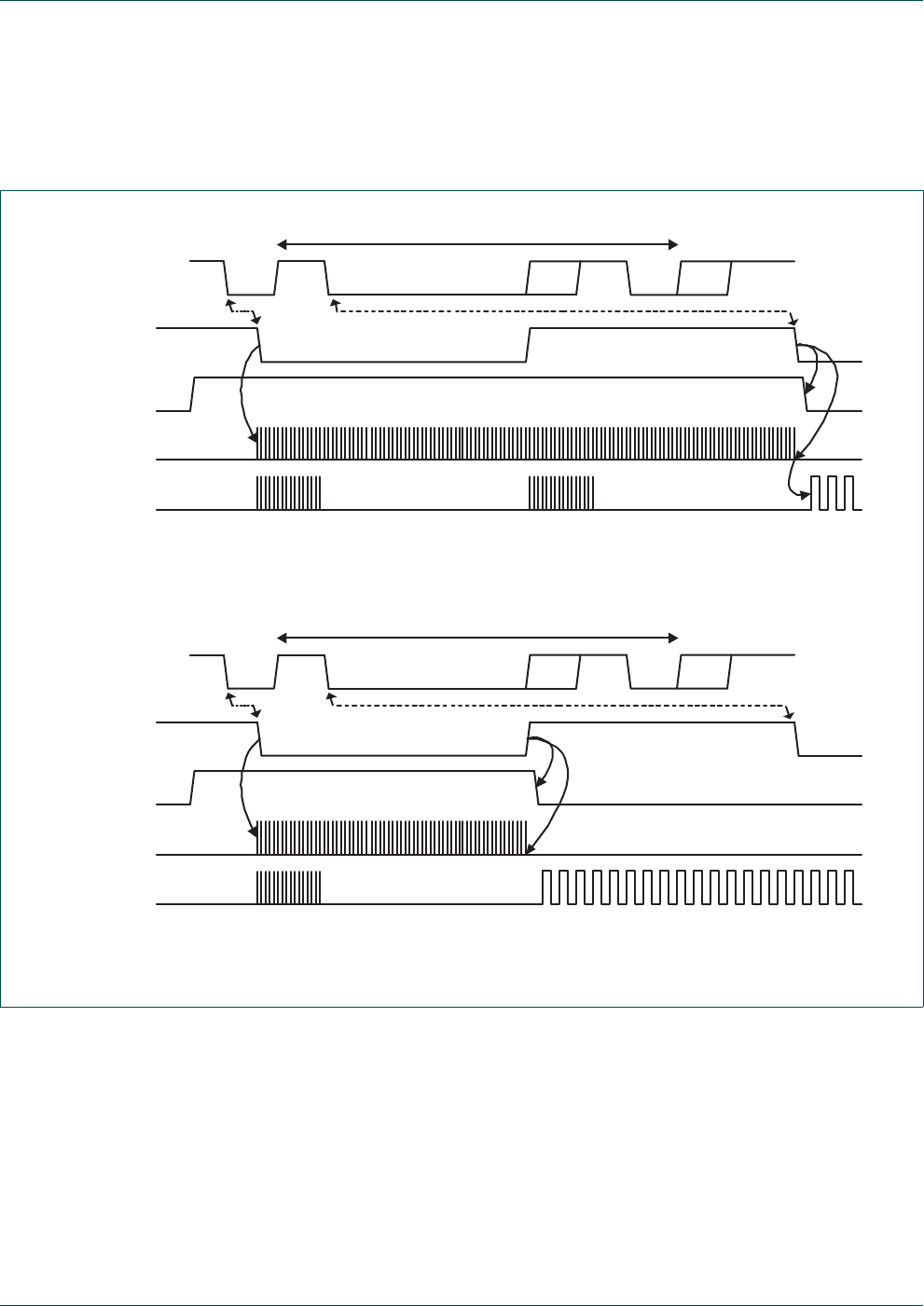
UM10462 All information provided in this document is subject to legal disclaimers. © NXP B.V. 2014. All rights reserved.
User manual Rev. 5.3 — 11 June 2014 256 of 521
NXP Semiconductors UM10462
Chapter 12: LPC11U3x/2x/1x USART
6. The rate counter is loaded into DLM/DLL and the baud rate will be switched to normal
operation. After setting the DLM/DLL, the end of auto-baud interrupt IIR ABEOInt will
be set, if enabled. The RSR will now continue receiving the remaining bits of the
character.
12.5.13 IrDA Control Register
The IrDA Control Register enables and configures the IrDA mode. The value of the ICR
should not be changed while transmitting or receiving data, or data loss or corruption may
occur.
a. Mode 0 (start bit and LSB are used for auto-baud)
b. Mode 1 (only start bit is used for auto-baud)
Fig 27. Auto-baud a) mode 0 and b) mode 1 waveform
UARTn RX start bit LSB of 'A' or 'a'
U0ACR start
rate counter
start bit0 bit1 bit2 bit3 bit4 bit5 bit6 bit7 parity stop
'A' (0x41) or 'a' (0x61)
16 cycles 16 cycles
16xbaud_rate
UARTn RX start bit LSB of 'A' or 'a'
rate counter
'A' (0x41) or 'a' (0x61)
start bit0 bit1 bit2 bit3 bit4 bit5 bit6 bit7 parity stop
U1ACR start
16 cycles
16xbaud_rate

UM10462 All information provided in this document is subject to legal disclaimers. © NXP B.V. 2014. All rights reserved.
User manual Rev. 5.3 — 11 June 2014 257 of 521
NXP Semiconductors UM10462
Chapter 12: LPC11U3x/2x/1x USART
The PulseDiv bits in the ICR are used to select the pulse width when the fixed pulse width
mode is used in IrDA mode (IrDAEn = 1 and FixPulseEn = 1). The value of these bits
should be set so that the resulting pulse width is at least 1.63 µs. Table 246 shows the
possible pulse widths.
Table 245: IrDA Control Register (ICR - 0x4000 8024) bit description
Bit Symbol Value Description Reset
value
0 IRDAEN IrDA mode enable 0
0 IrDA mode is disabled.
1 IrDA mode is enabled.
1 IRDAINV Serial input inverter 0
0 The serial input is not inverted.
1 The serial input is inverted. This has no effect on the
serial output.
2 FIXPULSEEN IrDA fixed pulse width mode. 0
0 IrDA fixed pulse width mode disabled.
1 IrDA fixed pulse width mode enabled.
5:3 PULSEDIV Configures the pulse width when FixPulseEn = 1. 0
0x0 3 / (16 baud rate)
0x1 2 TPCLK
0x2 4 TPCLK
0x3 8 TPCLK
0x4 16 TPCLK
0x5 32 TPCLK
0x6 64 TPCLK
0x7 128 TPCLK
31:6 - Reserved, user software should not write ones to
reserved bits. The value read from a reserved bit is not
defined.
0
Table 246: IrDA Pulse Width
FixPulseEn PulseDiv IrDA Transmitter Pulse width (µs)
0x3 / (16 baud rate)
102 TPCLK
114 TPCLK
128 TPCLK
1316 TPCLK
1432 TPCLK
1564 TPCLK
1 6 128 TPCLK
1 7 256 TPCLK

UM10462 All information provided in this document is subject to legal disclaimers. © NXP B.V. 2014. All rights reserved.
User manual Rev. 5.3 — 11 June 2014 258 of 521
NXP Semiconductors UM10462
Chapter 12: LPC11U3x/2x/1x USART
12.5.14 USART Fractional Divider Register
The USART Fractional Divider Register (FDR) controls the clock pre-scaler for the baud
rate generation and can be read and written at the user’s discretion. This pre-scaler takes
the APB clock and generates an output clock according to the specified fractional
requirements.
Important: If the fractional divider is active (DIVADDVAL > 0) and DLM = 0, the value of
the DLL register must be 3 or greater.
This register controls the clock pre-scaler for the baud rate generation. The reset value of
the register keeps the fractional capabilities of USART disabled making sure that USART
is fully software and hardware compatible with USARTs not equipped with this feature.
The USART baud rate can be calculated as:
(3)
Where UART_PCLK is the peripheral clock, DLM and DLL are the standard USART baud
rate divider registers, and DIVADDVAL and MULVAL are USART fractional baud rate
generator specific parameters.
The value of MULVAL and DIVADDVAL should comply to the following conditions:
1. 1 MULVAL 15
2. 0 DIVADDVAL 14
3. DIVADDVAL< MULVAL
The value of the FDR should not be modified while transmitting/receiving data or data may
be lost or corrupted.
If the FDR register value does not comply to these two requests, then the fractional divider
output is undefined. If DIVADDVAL is zero then the fractional divider is disabled, and the
clock will not be divided.
Table 247. USART Fractional Divider Register (FDR - address 0x4000 8028) bit description
Bit Function Description Reset
value
3:0 DIVADDVAL Baud rate generation pre-scaler divisor value. If this field is 0,
fractional baud rate generator will not impact the USART baud
rate.
0
7:4 MULVAL Baud rate pre-scaler multiplier value. This field must be greater
or equal 1 for USART to operate properly, regardless of whether
the fractional baud rate generator is used or not.
1
31:8 - Reserved, user software should not write ones to reserved bits.
The value read from a reserved bit is not defined.
0
UARTbaudrate PCLK
16 256 U0DLMU0DLL+1DivAddVal
MulVal
-----------------------------
+
----------------------------------------------------------------------------------------------------------------------------------
=

UM10462 All information provided in this document is subject to legal disclaimers. © NXP B.V. 2014. All rights reserved.
User manual Rev. 5.3 — 11 June 2014 259 of 521
NXP Semiconductors UM10462
Chapter 12: LPC11U3x/2x/1x USART
12.5.14.1 Baud rate calculation
The USART can operate with or without using the Fractional Divider. In real-life
applications it is likely that the desired baud rate can be achieved using several different
Fractional Divider settings. The following algorithm illustrates one way of finding a set of
DLM, DLL, MULVAL, and DIVADDVAL values. Such a set of parameters yields a baud
rate with a relative error of less than 1.1% from the desired one.
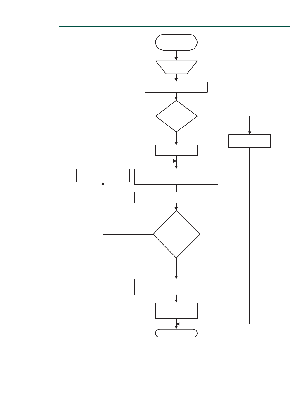
UM10462 All information provided in this document is subject to legal disclaimers. © NXP B.V. 2014. All rights reserved.
User manual Rev. 5.3 — 11 June 2014 260 of 521
NXP Semiconductors UM10462
Chapter 12: LPC11U3x/2x/1x USART
Fig 28. Algorithm for setting USART dividers
PCLK,
BR
Calculating UART
baudrate (BR)
DL est = PCLK/(16 x BR)
DLest is an
integer?
DIVADDVAL = 0
MULVAL = 1
True
FR est
= 1.5
DL est = Int(PCLK/(16 x BR x FR est))
1.1 < FR est < 1.9?
Pick another FRest from
the range [1.1, 1.9]
FRest = PCLK/(16 x BR x DL est)
DIVADDVAL = table(FR est )
MULVAL = table(FR est )
DLM = DLest [15:8]
DLL = DLest [7:0]
End
False
True
False

UM10462 All information provided in this document is subject to legal disclaimers. © NXP B.V. 2014. All rights reserved.
User manual Rev. 5.3 — 11 June 2014 261 of 521
NXP Semiconductors UM10462
Chapter 12: LPC11U3x/2x/1x USART
12.5.14.1.1 Example 1: UART_PCLK = 14.7456 MHz, BR = 9600
According to the provided algorithm DLest = PCLK/(16 x BR) = 14.7456 MHz / (16 x 9600)
= 96. Since this DLest is an integer number, DIVADDVAL = 0, MULVAL = 1, DLM = 0, and
DLL = 96.
12.5.14.1.2 Example 2: UART_PCLK = 12.0 MHz, BR = 115200
According to the provided algorithm DLest = PCLK/(16 x BR) = 12 MHz / (16 x 115200) =
6.51. This DLest is not an integer number and the next step is to estimate the FR
parameter. Using an initial estimate of FRest = 1.5 a new DLest = 4 is calculated and FRest
is recalculated as FRest = 1.628. Since FRest = 1.628 is within the specified range of 1.1
and 1.9, DIVADDVAL and MULVAL values can be obtained from the attached look-up
table.
The closest value for FRest = 1.628 in the look-up Table 248 is FR = 1.625. It is
equivalent to DIVADDVAL = 5 and MULVAL = 8.
Based on these findings, the suggested USART setup would be: DLM = 0, DLL = 4,
DIVADDVAL = 5, and MULVAL = 8. According to Equation 3, the USART’s baud rate is
115384. This rate has a relative error of 0.16% from the originally specified 115200.
12.5.15 USART Oversampling Register
In most applications, the USART samples received data 16 times in each nominal bit time,
and sends bits that are 16 input clocks wide. This register allows software to control the
ratio between the input clock and bit clock. This is required for smart card mode, and
provides an alternative to fractional division for other modes.
Table 248. Fractional Divider setting look-up table
FR DivAddVal/
MulVal FR DivAddVal/
MulVal FR DivAddVal/
MulVal FR DivAddVal/
MulVal
1.000 0/1 1.250 1/4 1.500 1/2 1.750 3/4
1.067 1/15 1.267 4/15 1.533 8/15 1.769 10/13
1.071 1/14 1.273 3/11 1.538 7/13 1.778 7/9
1.077 1/13 1.286 2/7 1.545 6/11 1.786 11/14
1.083 1/12 1.300 3/10 1.556 5/9 1.800 4/5
1.091 1/11 1.308 4/13 1.571 4/7 1.818 9/11
1.100 1/10 1.333 1/3 1.583 7/12 1.833 5/6
1.111 1/9 1.357 5/14 1.600 3/5 1.846 11/13
1.125 1/8 1.364 4/11 1.615 8/13 1.857 6/7
1.133 2/15 1.375 3/8 1.625 5/8 1.867 13/15
1.143 1/7 1.385 5/13 1.636 7/11 1.875 7/8
1.154 2/13 1.400 2/5 1.643 9/14 1.889 8/9
1.167 1/6 1.417 5/12 1.667 2/3 1.900 9/10
1.182 2/11 1.429 3/7 1.692 9/13 1.909 10/11
1.200 1/5 1.444 4/9 1.700 7/10 1.917 11/12
1.214 3/14 1.455 5/11 1.714 5/7 1.923 12/13
1.222 2/9 1.462 6/13 1.727 8/11 1.929 13/14
1.231 3/13 1.467 7/15 1.733 11/15 1.933 14/15

UM10462 All information provided in this document is subject to legal disclaimers. © NXP B.V. 2014. All rights reserved.
User manual Rev. 5.3 — 11 June 2014 262 of 521
NXP Semiconductors UM10462
Chapter 12: LPC11U3x/2x/1x USART
Example: For a baud rate of 3.25 Mbps with a 24 MHz USART clock frequency, the ideal
oversampling ratio is 24/3.25 or 7.3846. Setting OSINT to 0110 for 7 clocks/bit and
OSFrac to 011 for 0.375 clocks/bit, results in an oversampling ratio of 7.375.
In Smart card mode, OSInt is extended by FDINT. This extends the possible oversampling
to 2048, as required to support ISO 7816-3. Note that this value can be exceeded when
D<0, but this is not supported by the USART. When Smart card mode is enabled, the
initial value of OSINT and FDINT should be programmed as “00101110011” (372 minus
one).
12.5.16 USART Transmit Enable Register
In addition to being equipped with full hardware flow control (auto-cts and auto-rts
mechanisms described above), TER enables implementation of software flow control.
When TxEn = 1, the USART transmitter will keep sending data as long as they are
available. As soon as TxEn becomes 0, USART transmission will stop.
Although Table 250 describes how to use TxEn bit in order to achieve hardware flow
control, it is strongly suggested to let the USART hardware implemented auto flow control
features take care of this and limit the scope of TxEn to software flow control.
Table 250 describes how to use TXEn bit in order to achieve software flow control.
Table 249. USART Oversampling Register (OSR - address 0x4000 802C) bit description
Bit Symbol Description Reset
value
0 - Reserved, user software should not write ones to reserved bits.
The value read from a reserved bit is not defined.
NA
3:1 OSFRAC Fractional part of the oversampling ratio, in units of 1/8th of an
input clock period. (001 = 0.125, ..., 111 = 0.875)
0
7:4 OSINT Integer part of the oversampling ratio, minus 1. The reset values
equate to the normal operating mode of 16 input clocks per bit
time.
0xF
14:8 FDINT In Smart Card mode, these bits act as a more-significant extension
of the OSint field, allowing an oversampling ratio up to 2048 as
required by ISO7816-3. In Smart Card mode, bits 14:4 should
initially be set to 371, yielding an oversampling ratio of 372.
0
31:15 - Reserved, user software should not write ones to reserved bits.
The value read from a reserved bit is not defined.
NA

UM10462 All information provided in this document is subject to legal disclaimers. © NXP B.V. 2014. All rights reserved.
User manual Rev. 5.3 — 11 June 2014 263 of 521
NXP Semiconductors UM10462
Chapter 12: LPC11U3x/2x/1x USART
12.5.17 UART Half-duplex enable register
Remark: The HDEN register should be disabled when in smart card mode or IrDA mode
(smart card and IrDA by default run in half-duplex mode).
After reset the USART will be in full-duplex mode, meaning that both TX and RX work
independently. After setting the HDEN bit, the USART will be in half-duplex mode. In this
mode, the USART ensures that the receiver is locked when idle, or will enter a locked
state after having received a complete ongoing character reception. Line conflicts must be
handled in software. The behavior of the USART is unpredictable when data is presented
for reception while data is being transmitted.
For this reason, the value of the HDEN register should not be modified while sending or
receiving data, or data may be lost or corrupted.
12.5.18 Smart Card Interface Control register
This register allows the USART to be used in asynchronous smart card applications.
Table 250. USART Transmit Enable Register (TER - address 0x4000 8030) bit description
Bit Symbol Description Reset Value
6:0 - Reserved, user software should not write ones to reserved bits.
The value read from a reserved bit is not defined.
NA
7 TXEN When this bit is 1, as it is after a Reset, data written to the THR
is output on the TXD pin as soon as any preceding data has
been sent. If this bit cleared to 0 while a character is being sent,
the transmission of that character is completed, but no further
characters are sent until this bit is set again. In other words, a 0
in this bit blocks the transfer of characters from the THR or TX
FIFO into the transmit shift register. Software can clear this bit
when it detects that the a hardware-handshaking TX-permit
signal (CTS) has gone false, or with software handshaking,
when it receives an XOFF character (DC3). Software can set
this bit again when it detects that the TX-permit signal has gone
true, or when it receives an XON (DC1) character.
1
31:8 - Reserved -
Table 251. USART Half duplex enable register (HDEN - addresses 0x4000 8040) bit
description
Bit Symbol Value Description Reset
value
0 HDEN Half-duplex mode enable 0
0 Disable half-duplex mode.
1 Enable half-duplex mode.
31:1 - Reserved, user software should not write ones to
reserved bits. The value read from a reserved bit is not
defined.
-

UM10462 All information provided in this document is subject to legal disclaimers. © NXP B.V. 2014. All rights reserved.
User manual Rev. 5.3 — 11 June 2014 264 of 521
NXP Semiconductors UM10462
Chapter 12: LPC11U3x/2x/1x USART
12.5.19 USART RS485 Control register
The RS485CTRL register controls the configuration of the USART in RS-485/EIA-485
mode.
Table 252. Smart Card Interface Control register (SCICTRL - address 0x4000 8048) bit
description
Bit Symbol Value Description Reset
value
0 SCIEN Smart Card Interface Enable. 0
0 Smart card interface disabled.
1 Asynchronous half duplex smart card interface is
enabled.
1 NACKDIS NACK response disable. Only applicable in T=0. 0
0 A NACK response is enabled.
1 A NACK response is inhibited.
2 PROTSEL Protocol selection as defined in the ISO7816-3 standard. 0
0T = 0
1T = 1
4:3 - - Reserved. -
7:5 TXRETRY - When the protocol selection T bit (above) is 0, the field
controls the maximum number of retransmissions that
the USART will attempt if the remote device signals
NACK. When NACK has occurred this number of times
plus one, the Tx Error bit in the LSR is set, an interrupt is
requested if enabled, and the USART is locked until the
FIFO is cleared.
-
15:8 XTRAGUARD - When the protocol selection T bit (above) is 0, this field
indicates the number of bit times (ETUs) by which the
guard time after a character transmitted by the USART
should exceed the nominal 2 bit times. 0xFF in this field
may indicate that there is just a single bit after a
character and 11 bit times/character
31:16 - - Reserved, user software should not write ones to
reserved bits. The value read from a reserved bit is not
defined.
NA
Table 253. USART RS485 Control register (RS485CTRL - address 0x4000 804C) bit
description
Bit Symbol Value Description Reset
value
0 NMMEN NMM enable. 0
0 RS-485/EIA-485 Normal Multidrop Mode (NMM)
is disabled.
1 RS-485/EIA-485 Normal Multidrop Mode (NMM)
is enabled. In this mode, an address is detected
when a received byte causes the USART to set
the parity error and generate an interrupt.

UM10462 All information provided in this document is subject to legal disclaimers. © NXP B.V. 2014. All rights reserved.
User manual Rev. 5.3 — 11 June 2014 265 of 521
NXP Semiconductors UM10462
Chapter 12: LPC11U3x/2x/1x USART
12.5.20 USART RS-485 Address Match register
The RS485ADRMATCH register contains the address match value for RS-485/EIA-485
mode.
12.5.21 USART RS-485 Delay value register
The user may program the 8-bit RS485DLY register with a delay between the last stop bit
leaving the TXFIFO and the de-assertion of RTS (or DTR). This delay time is in periods of
the baud clock. Any delay time from 0 to 255 bit times may be programmed.
1 RXDIS Receiver enable. 0
0 The receiver is enabled.
1 The receiver is disabled.
2 AADEN AAD enable. 0
0 Auto Address Detect (AAD) is disabled.
1 Auto Address Detect (AAD) is enabled.
3 SEL Select direction control pin 0
0 If direction control is enabled (bit DCTRL = 1), pin
RTS is used for direction control.
1 If direction control is enabled (bit DCTRL = 1), pin
DTR is used for direction control.
4 DCTRL Auto direction control enable. 0
0 Disable Auto Direction Control.
1 Enable Auto Direction Control.
5 OINV Polarity control. This bit reverses the polarity of
the direction control signal on the RTS (or DTR)
pin.
0
0 The direction control pin will be driven to logic 0
when the transmitter has data to be sent. It will be
driven to logic 1 after the last bit of data has been
transmitted.
1 The direction control pin will be driven to logic 1
when the transmitter has data to be sent. It will be
driven to logic 0 after the last bit of data has been
transmitted.
31:6 - - Reserved, user software should not write ones to
reserved bits. The value read from a reserved bit
is not defined.
NA
Table 253. USART RS485 Control register (RS485CTRL - address 0x4000 804C) bit
description …continued
Bit Symbol Value Description Reset
value
Table 254. USART RS-485 Address Match register (RS485ADRMATCH - address
0x4000 8050) bit description
Bit Symbol Description Reset value
7:0 ADRMATCH Contains the address match value. 0x00
31:8 - Reserved -

UM10462 All information provided in this document is subject to legal disclaimers. © NXP B.V. 2014. All rights reserved.
User manual Rev. 5.3 — 11 June 2014 266 of 521
NXP Semiconductors UM10462
Chapter 12: LPC11U3x/2x/1x USART
12.5.22 USART Synchronous mode control register
SYNCCTRL register controls the synchronous mode. When this mode is in effect, the
USART generates or receives a bit clock on the SCLK pin and applies it to the transmit
and receive shift registers. Synchronous mode should not be used with smart card mode.
Table 255. USART RS-485 Delay value register (RS485DLY - address 0x4000 8054) bit
description
Bit Symbol Description Reset value
7:0 DLY Contains the direction control (RTS or DTR) delay value. This
register works in conjunction with an 8-bit counter.
0x00
31:8 - Reserved, user software should not write ones to reserved bits.
The value read from a reserved bit is not defined.
NA
Table 256. USART Synchronous mode control register (SYNCCTRL - address 0x4000 8058)
bit description
Bit Symbol Value Description Reset
value
0 SYNC Enables synchronous mode. 0
0 Disabled
1 Enabled
1 CSRC Clock source select. 0
0 Synchronous slave mode (SCLK in)
1 Synchronous master mode (SCLK out)
2 FES Falling edge sampling. 0
0 RxD is sampled on the rising edge of SCLK
1 RxD is sampled on the falling edge of SCLK
3 TSBYPASS Transmit synchronization bypass in synchronous slave
mode.
0
0 The input clock is synchronized prior to being used in
clock edge detection logic.
1 The input clock is not synchronized prior to being used
in clock edge detection logic. This allows for a high er
input clock rate at the expense of potential
metastability.
4 CSCEN Continuous master clock enable (used only when
CSRC is 1)
0
0 SCLK cycles only when characters are being sent on
TxD
1 SCLK runs continuously (characters can be received
on RxD independently from transmission on TxD)
5 SSDIS Start/stop bits 0
0 Send start and stop bits as in other modes.
1 Do not send start/stop bits.

UM10462 All information provided in this document is subject to legal disclaimers. © NXP B.V. 2014. All rights reserved.
User manual Rev. 5.3 — 11 June 2014 267 of 521
NXP Semiconductors UM10462
Chapter 12: LPC11U3x/2x/1x USART
After reset, synchronous mode is disabled. Synchronous mode is enabled by setting the
SYNC bit. When SYNC is 1, the USART operates as follows:
1. The CSRC bit controls whether the USART sends (master mode) or receives (slave
mode) a serial bit clock on the SCLK pin.
2. When CSRC is 1 selecting master mode, the CSCEN bit selects whether the USART
produces clocks on SCLK continuously (CSCEN=1) or only when transmit data is
being sent on TxD (CSCEN=0).
3. The SSDIS bit controls whether start and stop bits are used. When SSDIS is 0, the
USART sends and samples for start and stop bits as in other modes. When SSDIS is
1, the USART neither sends nor samples for start or stop bits, and each falling edge
on SCLK samples a data bit on RxD into the receive shift register, as well as shifting
the transmit shift register.
The rest of this section provides further details of operation when SYNC is 1.
Data changes on TxD from falling edges on SCLK. When SSDIS is 0, the FES bit controls
whether the USART samples serial data on RxD on rising edges or falling edges on
SCLK. When SSDIS is 1, the USART ignores FES and always samples RxD on falling
edges on SCLK.
The combination SYNC=1, CSRC=1, CSCEN=1, and SSDIS=1 is a difficult operating
mode, because SCLK applies to both directions of data flow and there is no defined
mechanism to signal the receivers when valid data is present on TxD or RxD.
Lacking such a mechanism, SSDIS=1 can be used with CSCEN=0 or CSRC=0 in a mode
similar to the SPI protocol, in which characters are (at least conceptually) “exchanged”
between the USART and remote device for each set of 8 clock cycles on SCLK. Such
operation can be called full-duplex, but the same hardware mode can be used in a
half-duplex way under control of a higher-layer protocol, in which the source of SCLK
toggles it in groups of N cycles whenever data is to be sent in either direction. (N being the
number of bits/character.)
When the LPC11U3x/2x/1x USART is the clock source (CSRC=1), such half-duplex
operation can lead to the rather artificial-seeming requirement of writing a dummy
character to the Transmitter Holding Register in order to generate 8 clocks so that a
character can be received. The CCCLR bit provides a more natural way of programming
half-duplex reception. When the higher-layer protocol dictates that the LPC11U3x/2x/1x
USART should receive a character, software should write the SYNCCTRL register with
6 CCCLR Continuous clock clear 0
0 CSCEN is under software control.
1 Hardware clears CSCEN after each character is
received.
31:7 - Reserved. The value read from a reserved bit is not
defined.
NA
Table 256. USART Synchronous mode control register (SYNCCTRL - address 0x4000 8058)
bit description
Bit Symbol Value Description Reset
value

UM10462 All information provided in this document is subject to legal disclaimers. © NXP B.V. 2014. All rights reserved.
User manual Rev. 5.3 — 11 June 2014 268 of 521
NXP Semiconductors UM10462
Chapter 12: LPC11U3x/2x/1x USART
CSCEN=1 and CCCLR=1. After the USART has sent N clock cycles and thus received a
character, it clears the CSCEN bit. If more characters need to be received thereafter,
software can repeat setting CSCEN and CCCLR.
Aside from such half-duplex operation, the primary use of CSCEN=1 is with SSDIS=0, so
that start bits indicate the transmission of each character in each direction.
12.6 Functional description
12.6.1 RS-485/EIA-485 modes of operation
The RS-485/EIA-485 feature allows the USART to be configured as an addressable slave.
The addressable slave is one of multiple slaves controlled by a single master.
The USART master transmitter will identify an address character by setting the parity (9th)
bit to ‘1’. For data characters, the parity bit is set to ‘0’.
Each USART slave receiver can be assigned a unique address. The slave can be
programmed to either manually or automatically reject data following an address which is
not theirs.
RS-485/EIA-485 Normal Multidrop Mode
Setting the RS485CTRL bit 0 enables this mode. In this mode, an address is detected
when a received byte causes the USART to set the parity error and generate an interrupt.
If the receiver is disabled (RS485CTRL bit 1 = ‘1’), any received data bytes will be ignored
and will not be stored in the RXFIFO. When an address byte is detected (parity bit = ‘1’) it
will be placed into the RXFIFO and an Rx Data Ready Interrupt will be generated. The
processor can then read the address byte and decide whether or not to enable the
receiver to accept the following data.
While the receiver is enabled (RS485CTRL bit 1 =’0’), all received bytes will be accepted
and stored in the RXFIFO regardless of whether they are data or address. When an
address character is received a parity error interrupt will be generated and the processor
can decide whether or not to disable the receiver.
RS-485/EIA-485 Auto Address Detection (AAD) mode
When both RS485CTRL register bits 0 (9-bit mode enable) and 2 (AAD mode enable) are
set, the USART is in auto address detect mode.
In this mode, the receiver will compare any address byte received (parity = ‘1’) to the 8-bit
value programmed into the RS485ADRMATCH register.
If the receiver is disabled (RS485CTRL bit 1 = ‘1’), any received byte will be discarded if it
is either a data byte OR an address byte which fails to match the RS485ADRMATCH
value.
When a matching address character is detected it will be pushed onto the RXFIFO along
with the parity bit, and the receiver will be automatically enabled (RS485CTRL bit 1 will be
cleared by hardware). The receiver will also generate an Rx Data Ready Interrupt.

UM10462 All information provided in this document is subject to legal disclaimers. © NXP B.V. 2014. All rights reserved.
User manual Rev. 5.3 — 11 June 2014 269 of 521
NXP Semiconductors UM10462
Chapter 12: LPC11U3x/2x/1x USART
While the receiver is enabled (RS485CTRL bit 1 = ‘0’), all bytes received will be accepted
and stored in the RXFIFO until an address byte which does not match the
RS485ADRMATCH value is received. When this occurs, the receiver will be automatically
disabled in hardware (RS485CTRL bit 1 will be set), The received non-matching address
character will not be stored in the RXFIFO.
RS-485/EIA-485 Auto Direction Control
RS485/EIA-485 mode includes the option of allowing the transmitter to automatically
control the state of the DIR pin as a direction control output signal.
Setting RS485CTRL bit 4 = ‘1’ enables this feature.
Keep RS485CTRL bit 3 zero so that direction control, if enabled, will use the RTS pin.
When Auto Direction Control is enabled, the selected pin will be asserted (driven LOW)
when the CPU writes data into the TXFIFO. The pin will be de-asserted (driven HIGH)
once the last bit of data has been transmitted. See bits 4 and 5 in the RS485CTRL
register.
The RS485CTRL bit 4 takes precedence over all other mechanisms controlling the
direction control pin with the exception of loopback mode.
RS485/EIA-485 driver delay time
The driver delay time is the delay between the last stop bit leaving the TXFIFO and the
de-assertion of RTS. This delay time can be programmed in the 8-bit RS485DLY register.
The delay time is in periods of the baud clock. Any delay time from 0 to 255 bit times may
be used.
RS485/EIA-485 output inversion
The polarity of the direction control signal on the RTS (or DTR) pins can be reversed by
programming bit 5 in the RS485CTRL register. When this bit is set, the direction control
pin will be driven to logic 1 when the transmitter has data waiting to be sent. The direction
control pin will be driven to logic 0 after the last bit of data has been transmitted.
12.6.2 Smart card mode
Figure 29 shows a typical asynchronous smart card application.
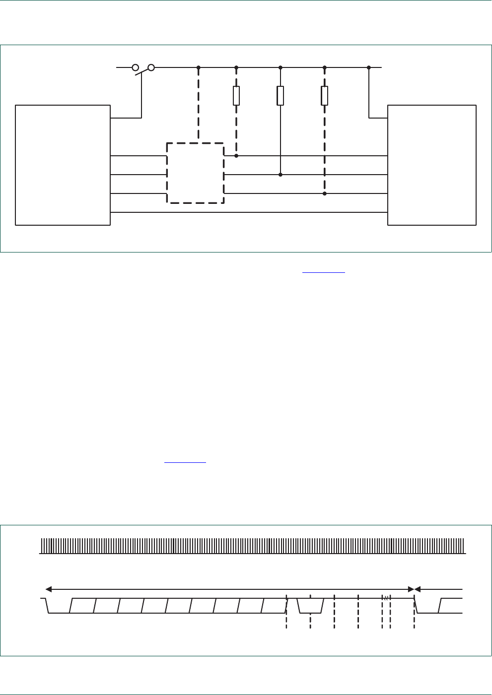
UM10462 All information provided in this document is subject to legal disclaimers. © NXP B.V. 2014. All rights reserved.
User manual Rev. 5.3 — 11 June 2014 270 of 521
NXP Semiconductors UM10462
Chapter 12: LPC11U3x/2x/1x USART
When the SCIEN bit in the SCICTRL register (Table 252) is set as described, the USART
provides bidirectional serial data on the open-drain TXD pin. No RXD pin is used when
SCIEN is 1. The USART SCLK pin will output synchronously with the data at the data bit
rate. Software must use timers to implement character and block waiting times (no
hardware support via trigger signals is provided on the LPC11U3x/2x/1x). GPIO pins can
be used to control the smart card reset and power pins. Any power supplied to the card
must be externally switched as card power supply requirements often exceed source
currents possible on the LPC11U3x/2x/1x. As the specific application may accommodate
any of the available ISO 7816 class A, B, or C power requirements, be aware of the logic
level tolerances and requirements when communicating or powering cards that use
different power rails than the LPC11U3x/2x/1x.
12.6.2.1 Smart card set-up procedure
A T = 0 protocol transfer consists of 8-bits of data, an even parity bit, and two guard bits
that allow for the receiver of the particular transfer to flag parity errors through the NACK
response (see Figure 30). Extra guard bits may be added according to card requirements.
If no NACK is sent (provided the interface accepts them in SCICTRL), the next byte may
be transmitted immediately after the last guard bit. If the NACK is sent, the transmitter will
retry sending the byte until successfully received or until the SCICTRL retry limit has been
met.
The smart card must be set up with the following considerations:
Fig 29. Typical smart card application
LPC11Uxx ISO 7816
Smart Card
pull-up
resistor
selectable
power rail
VCC
CLK
I/O
RST
Insertion Switch
Optional
Logic Level
Translation
pull-up
resistor pull-up
resistor
GPIO
SCLK
GPIO
GPIO
TXD
Fig 30. Smart card T = 0 waveform
start bit0 bit1 bit2 bit3 bit4 bit5 bit6 bit7 parity NACK
guard1 guard2 extra
guard1 extra
guard2 extra
guardn
start bit0
Asynchronous transfer Next transfer or
First retry
TXD
Clock

UM10462 All information provided in this document is subject to legal disclaimers. © NXP B.V. 2014. All rights reserved.
User manual Rev. 5.3 — 11 June 2014 271 of 521
NXP Semiconductors UM10462
Chapter 12: LPC11U3x/2x/1x USART
•If necessary, program PRESETCTRL (Table 8) so that the USART is not continuously
reset.
•Program one IOCON register to enable a USART TXD function.
•If the smart card requires a clock, program one IOCON register to select the USART
SCLK function. The USART will use it as an output.
•Program UARTCLKDIV (Table 26) for an initial USART frequency of 3.58 MHz.
•Program the OSR (Section 12.5.15) for 372x oversampling.
•If necessary, program the DLM and DLL (Section 12.5.3) to 00 and 01 respectively, to
pass the USART clock through without division.
•Program the LCR (Section 12.5.7) for 8-bit characters, parity enabled, even parity.
•Program the GPIO signals associated with the smart card so that (in this order):
a. Reset is low.
b. VCC is provided to the card (GPIO pins do not have the required 200 mA drive).
c. VPP (if provided to the card) is at “idle” state.
•Program SCICTRL (Section 12.5.18) to enable the smart card feature with the desired
options.
•Set up one or more timer(s) to provide timing as needed for ISO 7816 startup.
•Program SYSAHBCLKCTRL (Table 24) to enable the USART clock.
Thereafter, software should monitor card insertion, handle activation, wait for answer to
reset as described in ISO7816-3.
12.7 Architecture
The architecture of the USART is shown below in the block diagram.
The APB interface provides a communications link between the CPU or host and the
USART.
The USART receiver block, RX, monitors the serial input line, RXD, for valid input. The
USART RX Shift Register (RSR) accepts valid characters via RXD. After a valid character
is assembled in the RSR, it is passed to the USART RX Buffer Register FIFO to await
access by the CPU or host via the generic host interface.
The USART transmitter block, TX, accepts data written by the CPU or host and buffers the
data in the USART TX Holding Register FIFO (THR). The USART TX Shift Register (TSR)
reads the data stored in the THR and assembles the data to transmit via the serial output
pin, TXD1.
The USART Baud Rate Generator block, BRG, generates the timing enables used by the
USART TX block. The BRG clock input source is USART_PCLK. The main clock is
divided down per the divisor specified in the DLL and DLM registers. This divided down
clock is a 16x oversample clock, NBAUDOUT.
The interrupt interface contains registers IER and IIR. The interrupt interface receives
several one clock wide enables from the TX and RX blocks.
Status information from the TX and RX is stored in the LSR. Control information for the TX
and RX is stored in the LCR.
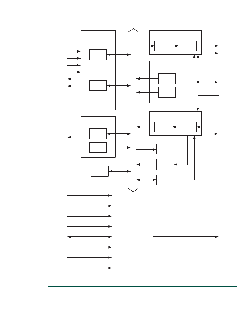
UM10462 All information provided in this document is subject to legal disclaimers. © NXP B.V. 2014. All rights reserved.
User manual Rev. 5.3 — 11 June 2014 272 of 521
NXP Semiconductors UM10462
Chapter 12: LPC11U3x/2x/1x USART
Fig 31. USART block diagram
APB
INTERFACE
LCR
RX
DDIS
LSR
FCR
BRG
TX
INTERRUPT
PA[2:0]
PSEL
PSTB
PWRITE
PD[7:0]
AR
MR
PCLK
U1INTR
SCR
NTXRDY
TXD1
NBAUDOUT
RCLK
NRXRDY
RXD1
RBR RSR
DLM
DLL
THR TSR
IIR
IER
MODEM
RTS/DIR MCR
MSR
DTR/DIR
DCD
RI
DSR
CTS

UM10462 All information provided in this document is subject to legal disclaimers. © NXP B.V. 2014. All rights reserved.
User manual Rev. 5.3 — 11 June 2014 273 of 521
13.1 How to read this chapter
Two SSP/SPI interfaces are available on all LPC11U3x/2x/1x parts.
13.2 Basic configuration
The SSP0/1 are configured using the following registers:
1. Pins: The SSP/SPI pins must be configured in the IOCON register block.
2. Power: In the SYSAHBCLKCTRL register, set bit 11 for SSP0 and bit 18 for SSP1
(Table 24).
3. Peripheral clock: Enable the SSP0/SSP1 peripheral clocks by writing to the
SSP0/1CLKDIV registers (Table 25/Table 27).
4. Reset: Before accessing the SSP/SPI block, ensure that the SSP0/1_RST_N bits (bit
0 and bit 2) in the PRESETCTRL register (Table 8) are set to 1. This de-asserts the
reset signal to the SSP/SPI block.
13.3 Features
•Compatible with Motorola SPI, 4-wire TI SSI, and National Semiconductor Microwire
buses.
•Synchronous Serial Communication.
•Supports master or slave operation.
•Eight-frame FIFOs for both transmit and receive.
•4-bit to 16-bit frame.
13.4 General description
The SSP/SPI is a Synchronous Serial Port (SSP) controller capable of operation on a SPI,
4-wire SSI, or Microwire bus. It can interact with multiple masters and slaves on the bus.
Only a single master and a single slave can communicate on the bus during a given data
transfer. Data transfers are in principle full duplex, with frames of 4 bits to 16 bits of data
flowing from the master to the slave and from the slave to the master. In practice it is often
the case that only one of these data flows carries meaningful data.
UM10462
Chapter 13: LPC11U3x/2x/1x SSP/SPI
Rev. 5.3 — 11 June 2014 User manual

UM10462 All information provided in this document is subject to legal disclaimers. © NXP B.V. 2014. All rights reserved.
User manual Rev. 5.3 — 11 June 2014 274 of 521
NXP Semiconductors UM10462
Chapter 13: LPC11U3x/2x/1x SSP/SPI
13.5 Pin description
13.6 Register description
The register addresses of the SPI controllers are shown in Table 258.
The reset value reflects the data stored in used bits only. It does not include the content of
reserved bits.
Table 257. SSP/SPI pin descriptions
Pin
name Type
Interface pin
name/function Pin description
SPI SSI Microwire
SCK0/1 I/O SCK CLK SK Serial Clock. SCK/CLK/SK is a clock signal used
to synchronize the transfer of data. It is driven by
the master and received by the slave. When
SSP/SPI interface is used, the clock is
programmable to be active-high or active-low,
otherwise it is always active-high. SCK only
switches during a data transfer. Any other time, the
SSP/SPI interface either holds it in its inactive state
or does not drive it (leaves it in high-impedance
state).
SSEL0/1 I/O SSEL FS CS Frame Sync/Slave Select. When the SSP/SPI
interface is a bus master, it drives this signal to an
active state before the start of serial data and then
releases it to an inactive state after the data has
been sent.The active state of this signal can be
high or low depending upon the selected bus and
mode. When the SSP/SPI interface is a bus slave,
this signal qualifies the presence of data from the
Master according to the protocol in use.
When there is just one bus master and one bus
slave, the Frame Sync or Slave Select signal from
the Master can be connected directly to the slave’s
corresponding input. When there is more than one
slave on the bus, further qualification of their Frame
Select/Slave Select inputs will typically be
necessary to prevent more than one slave from
responding to a transfer.
MISO0/1 I/O MISO DR(M)
DX(S)
SI(M)
SO(S)
Master In Slave Out. The MISO signal transfers
serial data from the slave to the master. When the
SSP/SPI is a slave, serial data is output on this
signal. When the SSP/SPI is a master, it clocks in
serial data from this signal. When the SSP/SPI is a
slave and is not selected by FS/SSEL, it does not
drive this signal (leaves it in high-impedance state).
MOSI0/1 I/O MOSI DX(M)
DR(S)
SO(M)
SI(S)
Master Out Slave In. The MOSI signal transfers
serial data from the master to the slave. When the
SSP/SPI is a master, it outputs serial data on this
signal. When the SSP/SPI is a slave, it clocks in
serial data from this signal.

UM10462 All information provided in this document is subject to legal disclaimers. © NXP B.V. 2014. All rights reserved.
User manual Rev. 5.3 — 11 June 2014 275 of 521
NXP Semiconductors UM10462
Chapter 13: LPC11U3x/2x/1x SSP/SPI
Remark: Register names use the SSP prefix to indicate that the SPI controllers have full
SSP capabilities.
13.6.1 SSP/SPI Control Register 0
This register controls the basic operation of the SSP/SPI controller.
Table 258. Register overview: SSP/SPI0 (base address 0x4004 0000)
Name Access Address
offset Description Reset
value Reference
CR0 R/W 0x000 Control Register 0. Selects the serial clock rate, bus type,
and data size.
0Table 260
CR1 R/W 0x004 Control Register 1. Selects master/slave and other
modes.
0Table 261
DR R/W 0x008 Data Register. Writes fill the transmit FIFO, and reads
empty the receive FIFO.
0Table 262
SR RO 0x00C Status Register 0x0000
0003
Table 263
CPSR R/W 0x010 Clock Prescale Register 0 Table 264
IMSC R/W 0x014 Interrupt Mask Set and Clear Register 0 Table 265
RIS RO 0x018 Raw Interrupt Status Register 0x0000
0008
Table 266
MIS RO 0x01C Masked Interrupt Status Register 0 Table 267
ICR WO 0x020 SSPICR Interrupt Clear Register NA Table 268
Table 259. Register overview: SSP/SPI1 (base address 0x4005 8000)
Name Access Address
offset Description Reset
value Reference
CR0 R/W 0x000 Control Register 0. Selects the serial clock rate, bus type,
and data size.
0Table 260
CR1 R/W 0x004 Control Register 1. Selects master/slave and other
modes.
0Table 261
DR R/W 0x008 Data Register. Writes fill the transmit FIFO, and reads
empty the receive FIFO.
0Table 262
SR RO 0x00C Status Register 0x0000
0003
Table 263
CPSR R/W 0x010 Clock Prescale Register 0 Table 264
IMSC R/W 0x014 Interrupt Mask Set and Clear Register 0 Table 265
RIS RO 0x018 Raw Interrupt Status Register 0x0000
0008
Table 266
MIS RO 0x01C Masked Interrupt Status Register 0 Table 267
ICR WO 0x020 SSPICR Interrupt Clear Register NA Table 268

UM10462 All information provided in this document is subject to legal disclaimers. © NXP B.V. 2014. All rights reserved.
User manual Rev. 5.3 — 11 June 2014 276 of 521
NXP Semiconductors UM10462
Chapter 13: LPC11U3x/2x/1x SSP/SPI
13.6.2 SSP/SPI Control Register 1
This register controls certain aspects of the operation of the SSP/SPI controller.
Table 260. SSP/SPI Control Register 0 (CR0 - address 0x4004 0000 (SSP0) and 0x4005 8000
(SSP1)) bit description
Bit Symbol Value Description Reset
Value
3:0 DSS Data Size Select. This field controls the number of bits
transferred in each frame. Values 0000-0010 are not
supported and should not be used.
0000
0x3 4-bit transfer
0x4 5-bit transfer
0x5 6-bit transfer
0x6 7-bit transfer
0x7 8-bit transfer
0x8 9-bit transfer
0x9 10-bit transfer
0xA 11-bit transfer
0xB 12-bit transfer
0xC 13-bit transfer
0xD 14-bit transfer
0xE 15-bit transfer
0xF 16-bit transfer
5:4 FRF Frame Format. 00
0x0 SPI
0x1 TI
0x2 Microwire
0x3 This combination is not supported and should not be used.
6 CPOL Clock Out Polarity. This bit is only used in SPI mode. 0
0 SPI controller maintains the bus clock low between frames.
1 SPI controller maintains the bus clock high between frames.
7 CPHA Clock Out Phase. This bit is only used in SPI mode. 0
0 SPI controller captures serial data on the first clock transition
of the frame, that is, the transition away from the inter-frame
state of the clock line.
1 SPI controller captures serial data on the second clock
transition of the frame, that is, the transition back to the
inter-frame state of the clock line.
15:8 SCR Serial Clock Rate. The number of prescaler output clocks per
bit on the bus, minus one. Given that CPSDVSR is the
prescale divider, and the APB clock PCLK clocks the
prescaler, the bit frequency is PCLK / (CPSDVSR [SCR+1]).
0x00
31:16 - - Reserved -

UM10462 All information provided in this document is subject to legal disclaimers. © NXP B.V. 2014. All rights reserved.
User manual Rev. 5.3 — 11 June 2014 277 of 521
NXP Semiconductors UM10462
Chapter 13: LPC11U3x/2x/1x SSP/SPI
13.6.3 SSP/SPI Data Register
Software can write data to be transmitted to this register and read data that has been
received.
Table 261. SSP/SPI Control Register 1 (CR1 - address 0x4004 0004 (SSP0) and 0x4005 8004
(SSP1)) bit description
Bit Symbol Value Description Reset
Value
0 LBM Loop Back Mode. 0
0 During normal operation.
1 Serial input is taken from the serial output (MOSI or MISO)
rather than the serial input pin (MISO or MOSI
respectively).
1 SSE SPI Enable. 0
0 The SPI controller is disabled.
1 The SPI controller will interact with other devices on the
serial bus. Software should write the appropriate control
information to the other SSP/SPI registers and interrupt
controller registers, before setting this bit.
2 MS Master/Slave Mode.This bit can only be written when the
SSE bit is 0.
0
0 The SPI controller acts as a master on the bus, driving the
SCLK, MOSI, and SSEL lines and receiving the MISO line.
1 The SPI controller acts as a slave on the bus, driving MISO
line and receiving SCLK, MOSI, and SSEL lines.
3 SOD Slave Output Disable. This bit is relevant only in slave
mode (MS = 1). If it is 1, this blocks this SPI controller from
driving the transmit data line (MISO).
0
31:4 - Reserved, user software should not write ones to reserved
bits. The value read from a reserved bit is not defined.
NA
Table 262. SSP/SPI Data Register (DR - address 0x4004 0008 (SSP0) and 0x4005 8008
(SSP1)) bit description
Bit Symbol Description Reset Value
15:0 DATA Write: software can write data to be sent in a future frame to this
register whenever the TNF bit in the Status register is 1,
indicating that the Tx FIFO is not full. If the Tx FIFO was
previously empty and the SPI controller is not busy on the bus,
transmission of the data will begin immediately. Otherwise the
data written to this register will be sent as soon as all previous
data has been sent (and received). If the data length is less than
16 bit, software must right-justify the data written to this register.
Read: software can read data from this register whenever the
RNE bit in the Status register is 1, indicating that the Rx FIFO is
not empty. When software reads this register, the SPI controller
returns data from the least recent frame in the Rx FIFO. If the
data length is less than 16 bit, the data is right-justified in this
field with higher order bits filled with 0s.
0x0000
31:16 - Reserved. -

UM10462 All information provided in this document is subject to legal disclaimers. © NXP B.V. 2014. All rights reserved.
User manual Rev. 5.3 — 11 June 2014 278 of 521
NXP Semiconductors UM10462
Chapter 13: LPC11U3x/2x/1x SSP/SPI
13.6.4 SSP/SPI Status Register
This read-only register reflects the current status of the SPI controller.
13.6.5 SSP/SPI Clock Prescale Register
This register controls the factor by which the Prescaler divides the SPI peripheral clock
SPI_PCLK to yield the prescaler clock that is, in turn, divided by the SCR factor in the
SSPCR0 registers, to determine the bit clock.
Important: the SSPnCPSR value must be properly initialized, or the SPI controller will not
be able to transmit data correctly.
In Slave mode, the SPI clock rate provided by the master must not exceed 1/12 of the SPI
peripheral clock selected in Table 25. The content of the SSPnCPSR register is not
relevant.
In master mode, CPSDVSRmin = 2 or larger (even numbers only).
13.6.6 SSP/SPI Interrupt Mask Set/Clear Register
This register controls whether each of the four possible interrupt conditions in the SPI
controller are enabled.
Table 263. SSP/SPI Status Register (SR - address 0x4004 000C (SSP0) and 0x4005 800C
(SSP1)) bit description
Bit Symbol Description Reset Value
0 TFE Transmit FIFO Empty. This bit is 1 is the Transmit FIFO is
empty, 0 if not.
1
1 TNF Transmit FIFO Not Full. This bit is 0 if the Tx FIFO is full, 1 if not. 1
2 RNE Receive FIFO Not Empty. This bit is 0 if the Receive FIFO is
empty, 1 if not.
0
3 RFF Receive FIFO Full. This bit is 1 if the Receive FIFO is full, 0 if
not.
0
4 BSY Busy. This bit is 0 if the SPI controller is idle, 1 if it is currently
sending/receiving a frame and/or the Tx FIFO is not empty.
0
31:5 - Reserved, user software should not write ones to reserved bits.
The value read from a reserved bit is not defined.
NA
Table 264. SSP/SPI Clock Prescale Register (CPSR - address 0x4004 0010 (SSP0) and
0x4005 8010 (SSP1)) bit description
Bit Symbol Description Reset Value
7:0 CPSDVSR This even value between 2 and 254, by which SPI_PCLK is
divided to yield the prescaler output clock. Bit 0 always reads
as 0.
0
31:8 - Reserved. -

UM10462 All information provided in this document is subject to legal disclaimers. © NXP B.V. 2014. All rights reserved.
User manual Rev. 5.3 — 11 June 2014 279 of 521
NXP Semiconductors UM10462
Chapter 13: LPC11U3x/2x/1x SSP/SPI
13.6.7 SSP/SPI Raw Interrupt Status Register
This read-only register contains a 1 for each interrupt condition that is asserted,
regardless of whether or not the interrupt is enabled in the IMSC registers.
13.6.8 SSP/SPI Masked Interrupt Status Register
This read-only register contains a 1 for each interrupt condition that is asserted and
enabled in the IMSC registers. When an SSP/SPI interrupt occurs, the interrupt service
routine should read this register to determine the causes of the interrupt.
Table 265. SSP/SPI Interrupt Mask Set/Clear register (IMSC - address 0x4004 0014 (SSP0)
and 0x4005 8014 (SSP1)) bit description
Bit Symbol Description Reset
Value
0 RORIM Software should set this bit to enable interrupt when a Receive
Overrun occurs, that is, when the Rx FIFO is full and another frame is
completely received. The ARM spec implies that the preceding frame
data is overwritten by the new frame data when this occurs.
0
1 RTIM Software should set this bit to enable interrupt when a Receive
Time-out condition occurs. A Receive Time-out occurs when the Rx
FIFO is not empty, and no has not been read for a time-out period.
The time-out period is the same for master and slave modes and is
determined by the SSP bit rate: 32 bits at PCLK / (CPSDVSR
[SCR+1]).
0
2 RXIM Software should set this bit to enable interrupt when the Rx FIFO is at
least half full.
0
3 TXIM Software should set this bit to enable interrupt when the Tx FIFO is at
least half empty.
0
31:4 - Reserved, user software should not write ones to reserved bits. The
value read from a reserved bit is not defined.
NA
Table 266. SSP/SPI Raw Interrupt Status register (RIS - address 0x4004 0018 (SSP0) and
0x4005 8018 (SSP1)) bit description
Symbol Description Reset
value
0 RORRIS This bit is 1 if another frame was completely received while the
RxFIFO was full. The ARM spec implies that the preceding frame
data is overwritten by the new frame data when this occurs.
0
1 RTRIS This bit is 1 if the Rx FIFO is not empty, and has not been read for a
time-out period. The time-out period is the same for master and slave
modes and is determined by the SSP bit rate: 32 bits at PCLK /
(CPSDVSR [SCR+1]).
0
2 RXRIS This bit is 1 if the Rx FIFO is at least half full. 0
3 TXRIS This bit is 1 if the Tx FIFO is at least half empty. 1
31:4 - Reserved, user software should not write ones to reserved bits. The
value read from a reserved bit is not defined.
NA

UM10462 All information provided in this document is subject to legal disclaimers. © NXP B.V. 2014. All rights reserved.
User manual Rev. 5.3 — 11 June 2014 280 of 521
NXP Semiconductors UM10462
Chapter 13: LPC11U3x/2x/1x SSP/SPI
13.6.9 SSP/SPI Interrupt Clear Register
Software can write one or more ones to this write-only register, to clear the corresponding
interrupt conditions in the SPI controller. Note that the other two interrupt conditions can
be cleared by writing or reading the appropriate FIFO or disabled by clearing the
corresponding bit in SSPIMSC registers.
13.7 Functional description
13.7.1 Texas Instruments synchronous serial frame format
Figure 32 shows the 4-wire Texas Instruments synchronous serial frame format supported
by the SPI module.
Table 267. SSP/SPI Masked Interrupt Status register (MIS - address 0x4004 001C (SSP0) and
0x4005 801C (SSP1)) bit description
Bit Symbol Description Reset
value
0 RORMIS This bit is 1 if another frame was completely received while the
RxFIFO was full, and this interrupt is enabled.
0
1 RTMIS This bit is 1 if the Rx FIFO is not empty, has not been read for a
time-out period, and this interrupt is enabled. The time-out period is
the same for master and slave modes and is determined by the SSP
bit rate: 32 bits at PCLK / (CPSDVSR [SCR+1]).
0
2 RXMIS This bit is 1 if the Rx FIFO is at least half full, and this interrupt is
enabled.
0
3 TXMIS This bit is 1 if the Tx FIFO is at least half empty, and this interrupt is
enabled.
0
31:4 - Reserved, user software should not write ones to reserved bits. The
value read from a reserved bit is not defined.
NA
Table 268. SSP/SPI interrupt Clear Register (ICR - address 0x4004 0020 (SSP0) and
0x4005 8020 (SSP1)) bit description
Bit Symbol Description Reset Value
0 RORIC Writing a 1 to this bit clears the “frame was received when
RxFIFO was full” interrupt.
NA
1 RTIC Writing a 1 to this bit clears the Rx FIFO was not empty and
has not been read for a timeout period interrupt. The timeout
period is the same for master and slave modes and is
determined by the SSP bit rate: 32 bits at PCLK / (CPSDVSR
[SCR+1]).
NA
31:2 - Reserved, user software should not write ones to reserved
bits. The value read from a reserved bit is not defined.
NA
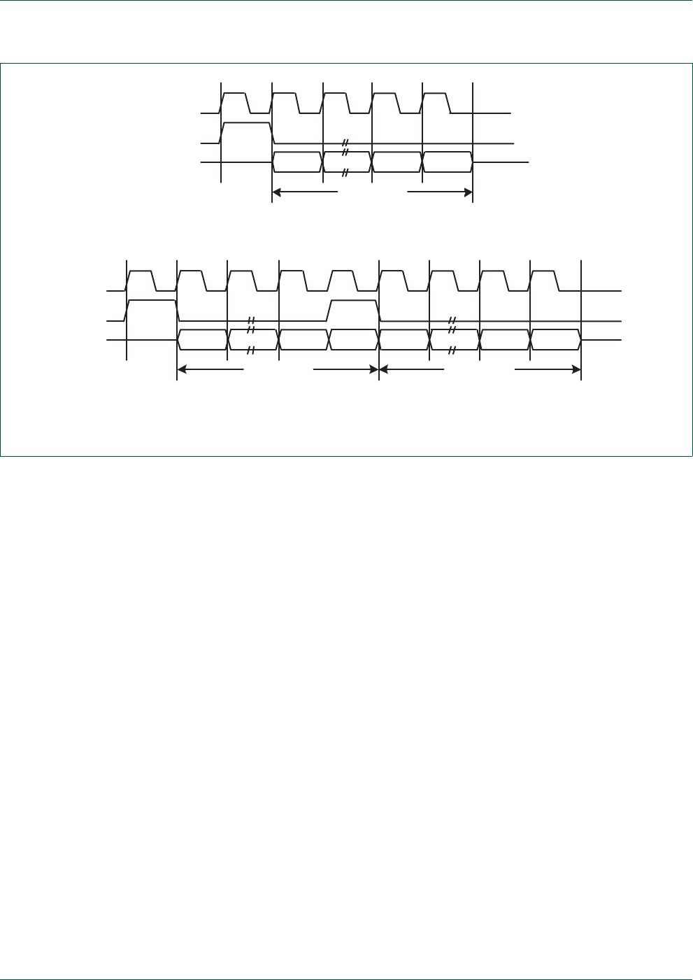
UM10462 All information provided in this document is subject to legal disclaimers. © NXP B.V. 2014. All rights reserved.
User manual Rev. 5.3 — 11 June 2014 281 of 521
NXP Semiconductors UM10462
Chapter 13: LPC11U3x/2x/1x SSP/SPI
For device configured as a master in this mode, CLK and FS are forced LOW, and the
transmit data line DX is in 3-state mode whenever the SSP is idle. Once the bottom entry
of the transmit FIFO contains data, FS is pulsed HIGH for one CLK period. The value to
be transmitted is also transferred from the transmit FIFO to the serial shift register of the
transmit logic. On the next rising edge of CLK, the MSB of the 4-bit to 16-bit data frame is
shifted out on the DX pin. Likewise, the MSB of the received data is shifted onto the DR
pin by the off-chip serial slave device.
Both the SSP and the off-chip serial slave device then clock each data bit into their serial
shifter on the falling edge of each CLK. The received data is transferred from the serial
shifter to the receive FIFO on the first rising edge of CLK after the LSB has been latched.
13.7.2 SPI frame format
The SPI interface is a four-wire interface where the SSEL signal behaves as a slave
select. The main feature of the SPI format is that the inactive state and phase of the SCK
signal are programmable through the CPOL and CPHA bits within the SSPCR0 control
register.
13.7.2.1 Clock Polarity (CPOL) and Phase (CPHA) control
When the CPOL clock polarity control bit is LOW, it produces a steady state low value on
the SCK pin. If the CPOL clock polarity control bit is HIGH, a steady state high value is
placed on the CLK pin when data is not being transferred.
a. Single frame transfer
b. Continuous/back-to-back frames transfer
Fig 32. Texas Instruments Synchronous Serial Frame Format: a) Single and b) Continuous/back-to-back Two
Frames Transfer
CLK
FS
DX/DR
4 to 16 bits
MSB LSB
CLK
FS
DX/DR LSBMSB LSBMSB
4 to 16 bits 4 to 16 bits
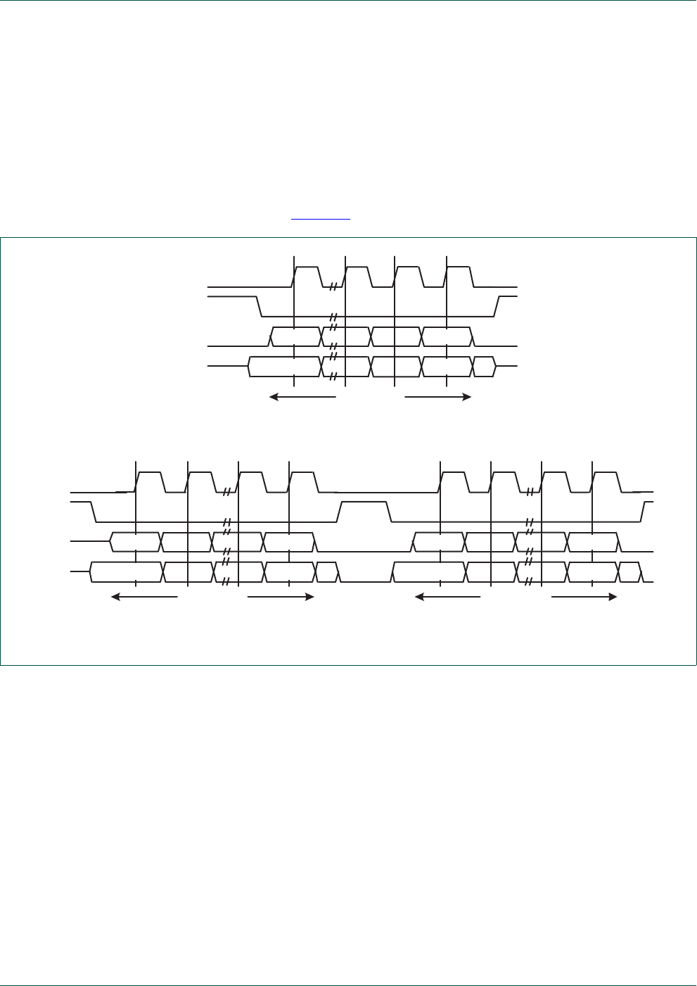
UM10462 All information provided in this document is subject to legal disclaimers. © NXP B.V. 2014. All rights reserved.
User manual Rev. 5.3 — 11 June 2014 282 of 521
NXP Semiconductors UM10462
Chapter 13: LPC11U3x/2x/1x SSP/SPI
The CPHA control bit selects the clock edge that captures data and allows it to change
state. It has the most impact on the first bit transmitted by either allowing or not allowing a
clock transition before the first data capture edge. When the CPHA phase control bit is
LOW, data is captured on the first clock edge transition. If the CPHA clock phase control
bit is HIGH, data is captured on the second clock edge transition.
13.7.2.2 SPI format with CPOL=0,CPHA=0
Single and continuous transmission signal sequences for SPI format with CPOL = 0,
CPHA = 0 are shown in Figure 33.
In this configuration, during idle periods:
•The CLK signal is forced LOW.
•SSEL is forced HIGH.
•The transmit MOSI/MISO pad is in high impedance.
If the SSP/SPI is enabled and there is valid data within the transmit FIFO, the start of
transmission is signified by the SSEL master signal being driven LOW. This causes slave
data to be enabled onto the MISO input line of the master. Master’s MOSI is enabled.
One half SCK period later, valid master data is transferred to the MOSI pin. Now that both
the master and slave data have been set, the SCK master clock pin goes HIGH after one
further half SCK period.
The data is captured on the rising and propagated on the falling edges of the SCK signal.
a. Single transfer with CPOL=0 and CPHA=0
b. Continuous transfer with CPOL=0 and CPHA=0
Fig 33. SPI frame format with CPOL=0 and CPHA=0 (a) Single and b) Continuous Transfer)
SCK
SSEL
MOSI MSB LSB
QMSB LSB
4 to 16 bits
MISO
SCK
SSEL
MOSI
MISO
4 to 16 bits 4 to 16 bits
MSB LSBMSB LSB
QMSB LSB QMSB LSB

UM10462 All information provided in this document is subject to legal disclaimers. © NXP B.V. 2014. All rights reserved.
User manual Rev. 5.3 — 11 June 2014 283 of 521
NXP Semiconductors UM10462
Chapter 13: LPC11U3x/2x/1x SSP/SPI
In the case of a single word transmission, after all bits of the data word have been
transferred, the SSEL line is returned to its idle HIGH state one SCK period after the last
bit has been captured.
However, in the case of continuous back-to-back transmissions, the SSEL signal must be
pulsed HIGH between each data word transfer. This is because the slave select pin
freezes the data in its serial peripheral register and does not allow it to be altered if the
CPHA bit is logic zero. Therefore the master device must raise the SSEL pin of the slave
device between each data transfer to enable the serial peripheral data write. On
completion of the continuous transfer, the SSEL pin is returned to its idle state one SCK
period after the last bit has been captured.
13.7.2.3 SPI format with CPOL=0,CPHA=1
The transfer signal sequence for SPI format with CPOL = 0, CPHA = 1 is shown in
Figure 34, which covers both single and continuous transfers.
In this configuration, during idle periods:
•The CLK signal is forced LOW.
•SSEL is forced HIGH.
•The transmit MOSI/MISO pad is in high impedance.
If the SSP/SPI is enabled and there is valid data within the transmit FIFO, the start of
transmission is signified by the SSEL master signal being driven LOW. Master’s MOSI pin
is enabled. After a further one half SCK period, both master and slave valid data is
enabled onto their respective transmission lines. At the same time, the SCK is enabled
with a rising edge transition.
Data is then captured on the falling edges and propagated on the rising edges of the SCK
signal.
In the case of a single word transfer, after all bits have been transferred, the SSEL line is
returned to its idle HIGH state one SCK period after the last bit has been captured.
For continuous back-to-back transfers, the SSEL pin is held LOW between successive
data words and termination is the same as that of the single word transfer.
13.7.2.4 SPI format with CPOL = 1,CPHA = 0
Single and continuous transmission signal sequences for SPI format with CPOL=1,
CPHA=0 are shown in Figure 35.
Fig 34. SPI frame format with CPOL=0 and CPHA=1
SCK
SSEL
MOSI
Q
4 to 16 bits
MISO Q MSB
MSB LSB
LSB
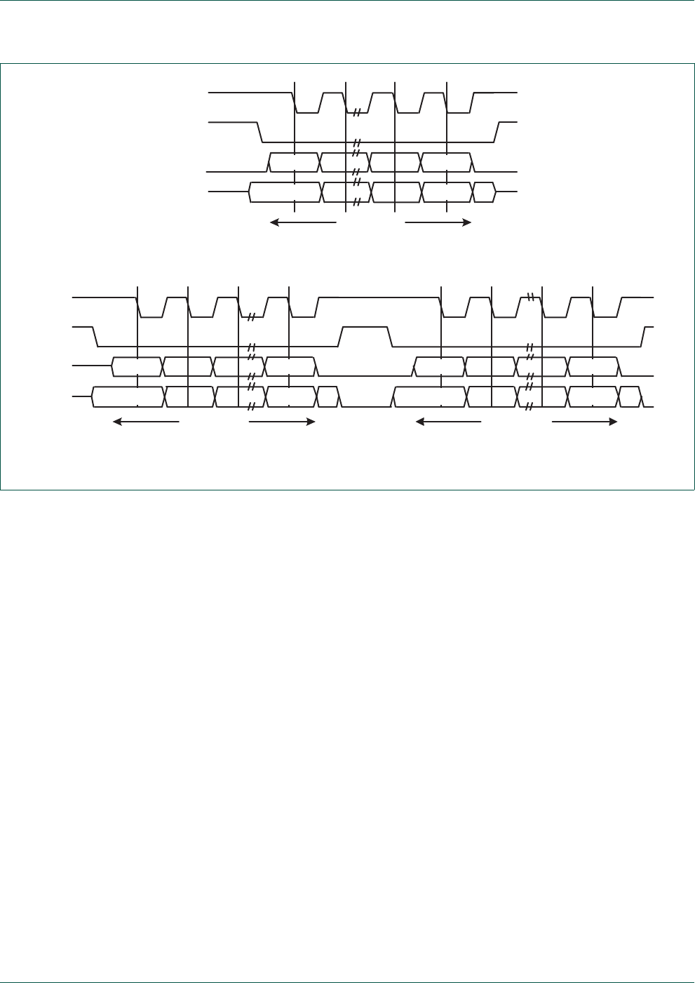
UM10462 All information provided in this document is subject to legal disclaimers. © NXP B.V. 2014. All rights reserved.
User manual Rev. 5.3 — 11 June 2014 284 of 521
NXP Semiconductors UM10462
Chapter 13: LPC11U3x/2x/1x SSP/SPI
In this configuration, during idle periods:
•The CLK signal is forced HIGH.
•SSEL is forced HIGH.
•The transmit MOSI/MISO pad is in high impedance.
If the SSP/SPI is enabled and there is valid data within the transmit FIFO, the start of
transmission is signified by the SSEL master signal being driven LOW, which causes
slave data to be immediately transferred onto the MISO line of the master. Master’s MOSI
pin is enabled.
One half period later, valid master data is transferred to the MOSI line. Now that both the
master and slave data have been set, the SCK master clock pin becomes LOW after one
further half SCK period. This means that data is captured on the falling edges and be
propagated on the rising edges of the SCK signal.
In the case of a single word transmission, after all bits of the data word are transferred, the
SSEL line is returned to its idle HIGH state one SCK period after the last bit has been
captured.
However, in the case of continuous back-to-back transmissions, the SSEL signal must be
pulsed HIGH between each data word transfer. This is because the slave select pin
freezes the data in its serial peripheral register and does not allow it to be altered if the
CPHA bit is logic zero. Therefore the master device must raise the SSEL pin of the slave
device between each data transfer to enable the serial peripheral data write. On
completion of the continuous transfer, the SSEL pin is returned to its idle state one SCK
period after the last bit has been captured.
a. Single transfer with CPOL=1 and CPHA=0
b. Continuous transfer with CPOL=1 and CPHA=0
Fig 35. SPI frame format with CPOL = 1 and CPHA = 0 (a) Single and b) Continuous Transfer)
SCK
SSEL
QMSB LSB
4 to 16 bits
MISO
MOSI MSB LSB
SCK
SSEL
MOSI
MISO
4 to 16 bits 4 to 16 bits
MSB LSBMSB LSB
QMSB LSB QMSB LSB
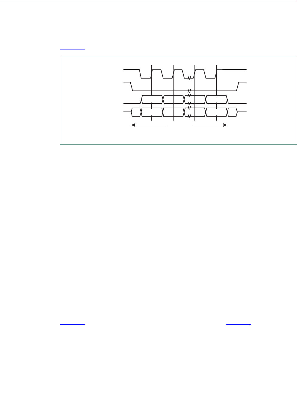
UM10462 All information provided in this document is subject to legal disclaimers. © NXP B.V. 2014. All rights reserved.
User manual Rev. 5.3 — 11 June 2014 285 of 521
NXP Semiconductors UM10462
Chapter 13: LPC11U3x/2x/1x SSP/SPI
13.7.2.5 SPI format with CPOL = 1,CPHA = 1
The transfer signal sequence for SPI format with CPOL = 1, CPHA = 1 is shown in
Figure 36, which covers both single and continuous transfers.
In this configuration, during idle periods:
•The CLK signal is forced HIGH.
•SSEL is forced HIGH.
•The transmit MOSI/MISO pad is in high impedance.
If the SSP/SPI is enabled and there is valid data within the transmit FIFO, the start of
transmission is signified by the SSEL master signal being driven LOW. Master’s MOSI is
enabled. After a further one half SCK period, both master and slave data are enabled onto
their respective transmission lines. At the same time, the SCK is enabled with a falling
edge transition. Data is then captured on the rising edges and propagated on the falling
edges of the SCK signal.
After all bits have been transferred, in the case of a single word transmission, the SSEL
line is returned to its idle HIGH state one SCK period after the last bit has been captured.
For continuous back-to-back transmissions, the SSEL pins remains in its active LOW
state, until the final bit of the last word has been captured, and then returns to its idle state
as described above. In general, for continuous back-to-back transfers the SSEL pin is
held LOW between successive data words and termination is the same as that of the
single word transfer.
13.7.3 Semiconductor Microwire frame format
Figure 37 shows the Microwire frame format for a single frame. Figure 38 shows the same
format when back-to-back frames are transmitted.
Fig 36. SPI Frame Format with CPOL = 1 and CPHA = 1
SCK
SSEL
MOSI
Q
4 to 16 bits
MISO Q MSB
MSB LSB
LSB
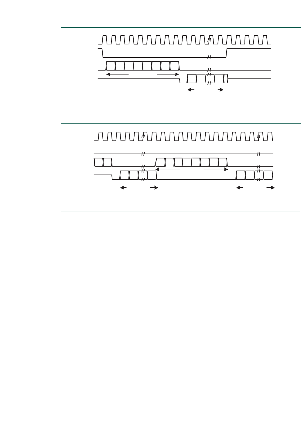
UM10462 All information provided in this document is subject to legal disclaimers. © NXP B.V. 2014. All rights reserved.
User manual Rev. 5.3 — 11 June 2014 286 of 521
NXP Semiconductors UM10462
Chapter 13: LPC11U3x/2x/1x SSP/SPI
Microwire format is very similar to SPI format, except that transmission is half-duplex
instead of full-duplex, using a master-slave message passing technique. Each serial
transmission begins with an 8-bit control word that is transmitted from the SSP/SPI to the
off-chip slave device. During this transmission, no incoming data is received by the
SSP/SPI. After the message has been sent, the off-chip slave decodes it and, after
waiting one serial clock after the last bit of the 8-bit control message has been sent,
responds with the required data. The returned data is 4 to 16 bit in length, making the total
frame length anywhere from 13 to 25 bits.
In this configuration, during idle periods:
•The SK signal is forced LOW.
•CS is forced HIGH.
•The transmit data line SO is arbitrarily forced LOW.
A transmission is triggered by writing a control byte to the transmit FIFO.The falling edge
of CS causes the value contained in the bottom entry of the transmit FIFO to be
transferred to the serial shift register of the transmit logic, and the MSB of the 8-bit control
frame to be shifted out onto the SO pin. CS remains LOW for the duration of the frame
transmission. The SI pin remains tri-stated during this transmission.
The off-chip serial slave device latches each control bit into its serial shifter on the rising
edge of each SK. After the last bit is latched by the slave device, the control byte is
decoded during a one clock wait-state, and the slave responds by transmitting data back
to the SSP/SPI. Each bit is driven onto SI line on the falling edge of SK. The SSP/SPI in
Fig 37. Microwire frame format (single transfer)
Fig 38. Microwire frame format (continuous transfers)
SK
CS
SO
4 to 16 bits
of output data
SI 8-bit control
MSB LSB
0MSB LSB
SK
CS
SO
SI
MSB LSB
4 to 16 bits
of output data
8-bit control
4 to 16 bits
of output data
MSB LSB
0
MSB LSB
LSB
UM10462 All information provided in this document is subject to legal disclaimers. © NXP B.V. 2014. All rights reserved.
User manual Rev. 5.3 — 11 June 2014 287 of 521
NXP Semiconductors UM10462
Chapter 13: LPC11U3x/2x/1x SSP/SPI
turn latches each bit on the rising edge of SK. At the end of the frame, for single transfers,
the CS signal is pulled HIGH one clock period after the last bit has been latched in the
receive serial shifter, that causes the data to be transferred to the receive FIFO.
Note: The off-chip slave device can tri-state the receive line either on the falling edge of
SK after the LSB has been latched by the receive shiftier, or when the CS pin goes HIGH.
For continuous transfers, data transmission begins and ends in the same manner as a
single transfer. However, the CS line is continuously asserted (held LOW) and
transmission of data occurs back to back. The control byte of the next frame follows
directly after the LSB of the received data from the current frame. Each of the received
values is transferred from the receive shifter on the falling edge SK, after the LSB of the
frame has been latched into the SSP/SPI.
13.7.3.1 Setup and hold time requirements on CS with respect to SK in Microwire
mode
In the Microwire mode, the SSP/SPI slave samples the first bit of receive data on the
rising edge of SK after CS has gone LOW. Masters that drive a free-running SK must
ensure that the CS signal has sufficient setup and hold margins with respect to the rising
edge of SK.
Figure 39 illustrates these setup and hold time requirements. With respect to the SK rising
edge on which the first bit of receive data is to be sampled by the SSP/SPI slave, CS must
have a setup of at least two times the period of SK on which the SSP/SPI operates. With
respect to the SK rising edge previous to this edge, CS must have a hold of at least one
SK period.
Fig 39. Microwire frame format setup and hold details
SK
CS
SI
tHOLD
= tSK
tSETUP=2*tSK

UM10462 All information provided in this document is subject to legal disclaimers. © NXP B.V. 2014. All rights reserved.
User manual Rev. 5.3 — 11 June 2014 288 of 521
14.1 How to read this chapter
The I2C-bus block is identical for all LPC11U3x/2x/1x parts.
14.2 Basic configuration
The I2C-bus interface is configured using the following registers:
1. Pins: The I2C pin functions and the I2C mode are configured in the IOCON register
block (Table 80 and Table 81).
2. Power and peripheral clock: In the SYSAHBCLKCTRL register, set bit 5 (Table 24).
3. Reset: Before accessing the I2C block, ensure that the I2C_RST_N bit (bit 1) in the
PRESETCTRL register (Table 8) is set to 1. This de-asserts the reset signal to the I2C
block.
14.3 Features
•Standard I2C-compliant bus interfaces may be configured as Master, Slave, or
Master/Slave.
•Arbitration is handled between simultaneously transmitting masters without corruption
of serial data on the bus.
•Programmable clock allows adjustment of I2C transfer rates.
•Data transfer is bidirectional between masters and slaves.
•Serial clock synchronization allows devices with different bit rates to communicate via
one serial bus.
•Serial clock synchronization is used as a handshake mechanism to suspend and
resume serial transfer.
•Supports Fast-mode Plus.
•Optional recognition of up to four distinct slave addresses.
•Monitor mode allows observing all I2C-bus traffic, regardless of slave address.
•I2C-bus can be used for test and diagnostic purposes.
•The I2C-bus contains a standard I2C-compliant bus interface with two pins.
14.4 Applications
Interfaces to external I2C standard parts, such as serial RAMs, LCDs, tone generators,
other microcontrollers, etc.
14.5 General description
A typical I2C-bus configuration is shown in Figure 40. Depending on the state of the
direction bit (R/W), two types of data transfers are possible on the I2C-bus:
UM10462
Chapter 14: LPC11U3x/2x/1x I2C-bus controller
Rev. 5.3 — 11 June 2014 User manual
UM10462 All information provided in this document is subject to legal disclaimers. © NXP B.V. 2014. All rights reserved.
User manual Rev. 5.3 — 11 June 2014 289 of 521
NXP Semiconductors UM10462
Chapter 14: LPC11U3x/2x/1x I2C-bus controller
•Data transfer from a master transmitter to a slave receiver. The first byte transmitted
by the master is the slave address. Next follows a number of data bytes. The slave
returns an acknowledge bit after each received byte.
•Data transfer from a slave transmitter to a master receiver. The first byte (the slave
address) is transmitted by the master. The slave then returns an acknowledge bit.
Next follows the data bytes transmitted by the slave to the master. The master returns
an acknowledge bit after all received bytes other than the last byte. At the end of the
last received byte, a “not acknowledge” is returned. The master device generates all
of the serial clock pulses and the START and STOP conditions. A transfer is ended
with a STOP condition or with a Repeated START condition. Since a Repeated
START condition is also the beginning of the next serial transfer, the I2C bus will not
be released.
The I2C interface is byte oriented and has four operating modes: master transmitter mode,
master receiver mode, slave transmitter mode and slave receiver mode.
The I2C interface complies with the entire I2C specification, supporting the ability to turn
power off to the ARM Cortex-M0 without interfering with other devices on the same
I2C-bus.
14.5.1 I2C Fast-mode Plus
Fast-Mode Plus supports a 1 Mbit/sec transfer rate to communicate with the I2C-bus
products which NXP Semiconductors is now providing.
Fig 40. I2C-bus configuration
OTHER DEVICE WITH
I
2
C INTERFACE
pull-up
resistor
OTHER DEVICE WITH
I
2
C INTERFACE
LPC11xx
SDA SCL
I
2
C bus
SCL
SDA
pull-up
resistor

UM10462 All information provided in this document is subject to legal disclaimers. © NXP B.V. 2014. All rights reserved.
User manual Rev. 5.3 — 11 June 2014 290 of 521
NXP Semiconductors UM10462
Chapter 14: LPC11U3x/2x/1x I2C-bus controller
14.6 Pin description
The I2C-bus pins must be configured through the IOCON_PIO0_4 (Table 80) and
IOCON_PIO0_5 (Table 81) registers for Standard/ Fast-mode or Fast-mode Plus. In
Fast-mode Plus, rates above 400 kHz and up to 1 MHz may be selected. The I2C-bus pins
are open-drain outputs and fully compatible with the I2C-bus specification.
14.7 Register description
Table 269. I2C-bus pin description
Pin Type Description
SDA Input/Output I2C Serial Data
SCL Input/Output I2C Serial Clock
Table 270. Register overview: I2C (base address 0x4000 0000)
Name Access Address
offset Description Reset
value[1] Reference
CONSET R/W 0x000 I2C Control Set Register. When a one is written to a bit of
this register, the corresponding bit in the I2C control
register is set. Writing a zero has no effect on the
corresponding bit in the I2C control register.
0x00 Table 271
STAT RO 0x004 I2C Status Register. During I2C operation, this register
provides detailed status codes that allow software to
determine the next action needed.
0xF8 Table 272
DAT R/W 0x008 I2C Data Register. During master or slave transmit mode,
data to be transmitted is written to this register. During
master or slave receive mode, data that has been received
may be read from this register.
0x00 Table 273
ADR0 R/W 0x00C I2C Slave Address Register 0. Contains the 7-bit slave
address for operation of the I2C interface in slave mode,
and is not used in master mode. The least significant bit
determines whether a slave responds to the General Call
address.
0x00 Table 274
SCLH R/W 0x010 SCH Duty Cycle Register High Half Word. Determines
the high time of the I2C clock.
0x04 Table 275
SCLL R/W 0x014 SCL Duty Cycle Register Low Half Word. Determines
the low time of the I2C clock. I2nSCLL and I2nSCLH
together determine the clock frequency generated by an
I2C master and certain times used in slave mode.
0x04 Table 276
CONCLR WO 0x018 I2C Control Clear Register. When a one is written to a bit
of this register, the corresponding bit in the I2C control
register is cleared. Writing a zero has no effect on the
corresponding bit in the I2C control register.
NA Table 278
MMCTRL R/W 0x01C Monitor mode control register. 0x00 Table 279
ADR1 R/W 0x020 I2C Slave Address Register 1. Contains the 7-bit slave
address for operation of the I2C interface in slave mode,
and is not used in master mode. The least significant bit
determines whether a slave responds to the General Call
address.
0x00 Table 280

UM10462 All information provided in this document is subject to legal disclaimers. © NXP B.V. 2014. All rights reserved.
User manual Rev. 5.3 — 11 June 2014 291 of 521
NXP Semiconductors UM10462
Chapter 14: LPC11U3x/2x/1x I2C-bus controller
[1] Reset value reflects the data stored in used bits only. It does not include reserved bits content.
14.7.1 I2C Control Set register (CONSET)
The CONSET registers control setting of bits in the CON register that controls operation of
the I2C interface. Writing a one to a bit of this register causes the corresponding bit in the
I2C control register to be set. Writing a zero has no effect.
ADR2 R/W 0x024 I2C Slave Address Register 2. Contains the 7-bit slave
address for operation of the I2C interface in slave mode,
and is not used in master mode. The least significant bit
determines whether a slave responds to the General Call
address.
0x00 Table 280
ADR3 R/W 0x028 I2C Slave Address Register 3. Contains the 7-bit slave
address for operation of the I2C interface in slave mode,
and is not used in master mode. The least significant bit
determines whether a slave responds to the General Call
address.
0x00 Table 280
DATA_BUFFER RO 0x02C Data buffer register. The contents of the 8 MSBs of the
I2DAT shift register will be transferred to the
DATA_BUFFER automatically after every nine bits (8 bits
of data plus ACK or NACK) has been received on the bus.
0x00 Table 281
MASK0 R/W 0x030 I2C Slave address mask register 0. This mask register is
associated with I2ADR0 to determine an address match.
The mask register has no effect when comparing to the
General Call address (‘0000000’).
0x00 Table 282
MASK1 R/W 0x034 I2C Slave address mask register 1. This mask register is
associated with I2ADR0 to determine an address match.
The mask register has no effect when comparing to the
General Call address (‘0000000’).
0x00 Table 282
MASK2 R/W 0x038 I2C Slave address mask register 2. This mask register is
associated with I2ADR0 to determine an address match.
The mask register has no effect when comparing to the
General Call address (‘0000000’).
0x00 Table 282
MASK3 R/W 0x03C I2C Slave address mask register 3. This mask register is
associated with I2ADR0 to determine an address match.
The mask register has no effect when comparing to the
General Call address (‘0000000’).
0x00 Table 282
Table 270. Register overview: I2C (base address 0x4000 0000) …continued
Name Access Address
offset Description Reset
value[1] Reference
Table 271. I2C Control Set register (CONSET - address 0x4000 0000) bit description
Bit Symbol Description Reset
value
1:0 - Reserved. User software should not write ones to reserved bits. The
value read from a reserved bit is not defined.
NA
2 AA Assert acknowledge flag.
3SI I
2C interrupt flag. 0
4 STO STOP flag. 0

UM10462 All information provided in this document is subject to legal disclaimers. © NXP B.V. 2014. All rights reserved.
User manual Rev. 5.3 — 11 June 2014 292 of 521
NXP Semiconductors UM10462
Chapter 14: LPC11U3x/2x/1x I2C-bus controller
I2EN I2C Interface Enable. When I2EN is 1, the I2C interface is enabled. I2EN can be
cleared by writing 1 to the I2ENC bit in the CONCLR register. When I2EN is 0, the I2C
interface is disabled.
When I2EN is “0”, the SDA and SCL input signals are ignored, the I2C block is in the “not
addressed” slave state, and the STO bit is forced to “0”.
I2EN should not be used to temporarily release the I2C-bus since, when I2EN is reset, the
I2C-bus status is lost. The AA flag should be used instead.
STA is the START flag. Setting this bit causes the I2C interface to enter master mode and
transmit a START condition or transmit a Repeated START condition if it is already in
master mode.
When STA is 1 and the I2C interface is not already in master mode, it enters master mode,
checks the bus and generates a START condition if the bus is free. If the bus is not free, it
waits for a STOP condition (which will free the bus) and generates a START condition
after a delay of a half clock period of the internal clock generator. If the I2C interface is
already in master mode and data has been transmitted or received, it transmits a
Repeated START condition. STA may be set at any time, including when the I2C interface
is in an addressed slave mode.
STA can be cleared by writing 1 to the STAC bit in the CONCLR register. When STA is 0,
no START condition or Repeated START condition will be generated.
If STA and STO are both set, then a STOP condition is transmitted on the I2C-bus if it the
interface is in master mode, and transmits a START condition thereafter. If the I2C
interface is in slave mode, an internal STOP condition is generated, but is not transmitted
on the bus.
STO is the STOP flag. Setting this bit causes the I2C interface to transmit a STOP
condition in master mode, or recover from an error condition in slave mode. When STO is
1 in master mode, a STOP condition is transmitted on the I2C-bus. When the bus detects
the STOP condition, STO is cleared automatically.
In slave mode, setting this bit can recover from an error condition. In this case, no STOP
condition is transmitted to the bus. The hardware behaves as if a STOP condition has
been received and it switches to “not addressed” slave receiver mode. The STO flag is
cleared by hardware automatically.
SI is the I2C Interrupt Flag. This bit is set when the I2C state changes. However, entering
state F8 does not set SI since there is nothing for an interrupt service routine to do in that
case.
While SI is set, the low period of the serial clock on the SCL line is stretched, and the
serial transfer is suspended. When SCL is HIGH, it is unaffected by the state of the SI flag.
SI must be reset by software, by writing a 1 to the SIC bit in the CONCLR register.
5 STA START flag. 0
6I2EN I
2C interface enable. 0
31:7 - Reserved. The value read from a reserved bit is not defined. -
Table 271. I2C Control Set register (CONSET - address 0x4000 0000) bit description
Bit Symbol Description Reset
value

UM10462 All information provided in this document is subject to legal disclaimers. © NXP B.V. 2014. All rights reserved.
User manual Rev. 5.3 — 11 June 2014 293 of 521
NXP Semiconductors UM10462
Chapter 14: LPC11U3x/2x/1x I2C-bus controller
AA is the Assert Acknowledge Flag. When set to 1, an acknowledge (low level to SDA)
will be returned during the acknowledge clock pulse on the SCL line on the following
situations:
1. The address in the Slave Address Register has been received.
2. The General Call address has been received while the General Call bit (GC) in the
ADR register is set.
3. A data byte has been received while the I2C is in the master receiver mode.
4. A data byte has been received while the I2C is in the addressed slave receiver mode
The AA bit can be cleared by writing 1 to the AAC bit in the CONCLR register. When AA is
0, a not acknowledge (HIGH level to SDA) will be returned during the acknowledge clock
pulse on the SCL line on the following situations:
1. A data byte has been received while the I2C is in the master receiver mode.
2. A data byte has been received while the I2C is in the addressed slave receiver mode.
14.7.2 I2C Status register (STAT)
Each I2C Status register reflects the condition of the corresponding I2C interface. The I2C
Status register is Read-Only.
The three least significant bits are always 0. Taken as a byte, the status register contents
represent a status code. There are 26 possible status codes. When the status code is
0xF8, there is no relevant information available and the SI bit is not set. All other 25 status
codes correspond to defined I2C states. When any of these states entered, the SI bit will
be set. For a complete list of status codes, refer to tables from Table 287 to Table 292.
14.7.3 I2C Data register (DAT)
This register contains the data to be transmitted or the data just received. The CPU can
read and write to this register only while it is not in the process of shifting a byte, when the
SI bit is set. Data in DAT register remains stable as long as the SI bit is set. Data in DAT
register is always shifted from right to left: the first bit to be transmitted is the MSB (bit 7),
and after a byte has been received, the first bit of received data is located at the MSB of
the DAT register.
Table 272. I2C Status register (STAT - 0x4000 0004) bit description
Bit Symbol Description Reset value
2:0 - These bits are unused and are always 0. 0
7:3 Status These bits give the actual status information about the I2C
interface.
0x1F
31:8 - Reserved. The value read from a reserved bit is not defined. -
Table 273. I2C Data register (DAT - 0x4000 0008) bit description
Bit Symbol Description Reset value
7:0 Data This register holds data values that have been received or are to
be transmitted.
0
31:8 - Reserved. The value read from a reserved bit is not defined. -

UM10462 All information provided in this document is subject to legal disclaimers. © NXP B.V. 2014. All rights reserved.
User manual Rev. 5.3 — 11 June 2014 294 of 521
NXP Semiconductors UM10462
Chapter 14: LPC11U3x/2x/1x I2C-bus controller
14.7.4 I2C Slave Address register 0 (ADR0)
This register is readable and writable and are only used when an I2C interface is set to
slave mode. In master mode, this register has no effect. The LSB of the ADR register is
the General Call bit. When this bit is set, the General Call address (0x00) is recognized.
If this register contains 0x00, the I2C will not acknowledge any address on the bus. All four
registers (ADR0 to ADR3) will be cleared to this disabled state on reset. See also
Table 280.
14.7.5 I2C SCL HIGH and LOW duty cycle registers (SCLH and SCLL)
14.7.5.1 Selecting the appropriate I2C data rate and duty cycle
Software must set values for the registers SCLH and SCLL to select the appropriate data
rate and duty cycle. SCLH defines the number of I2C_PCLK cycles for the SCL HIGH
time, SCLL defines the number of I2C_PCLK cycles for the SCL low time. The frequency
is determined by the following formula (I2C_PCLK is the frequency of the peripheral I2C
clock):
(4)
The values for SCLL and SCLH must ensure that the data rate is in the appropriate I2C
data rate range. Each register value must be greater than or equal to 4. Table 277 gives
some examples of I2C-bus rates based on I2C_PCLK frequency and SCLL and SCLH
values.
Table 274. I2C Slave Address register 0 (ADR0- 0x4000 000C) bit description
Bit Symbol Description Reset value
0 GC General Call enable bit. 0
7:1 Address The I2C device address for slave mode. 0x00
31:8 - Reserved. The value read from a reserved bit is not defined. -
Table 275. I2C SCL HIGH Duty Cycle register (SCLH - address 0x4000 0010) bit description
Bit Symbol Description Reset value
15:0 SCLH Count for SCL HIGH time period selection. 0x0004
31:16 - Reserved. The value read from a reserved bit is not defined. -
Table 276. I2C SCL Low duty cycle register (SCLL - 0x4000 0014) bit description
Bit Symbol Description Reset value
15:0 SCLL Count for SCL low time period selection. 0x0004
31:16 - Reserved. The value read from a reserved bit is not defined. -
I2Cbitfrequency I2CPCLK
SCLH SCLL+
------------------------------------
=

UM10462 All information provided in this document is subject to legal disclaimers. © NXP B.V. 2014. All rights reserved.
User manual Rev. 5.3 — 11 June 2014 295 of 521
NXP Semiconductors UM10462
Chapter 14: LPC11U3x/2x/1x I2C-bus controller
SCLL and SCLH values should not necessarily be the same. Software can set different
duty cycles on SCL by setting these two registers. For example, the I2C-bus specification
defines the SCL low time and high time at different values for a Fast-mode and Fast-mode
Plus I2C.
14.7.6 I2C Control Clear register (CONCLR)
The CONCLR register control clearing of bits in the CON register that controls operation
of the I2C interface. Writing a one to a bit of this register causes the corresponding bit in
the I2C control register to be cleared. Writing a zero has no effect.
AAC is the Assert Acknowledge Clear bit. Writing a 1 to this bit clears the AA bit in the
CONSET register. Writing 0 has no effect.
SIC is the I2C Interrupt Clear bit. Writing a 1 to this bit clears the SI bit in the CONSET
register. Writing 0 has no effect.
STAC is the START flag Clear bit. Writing a 1 to this bit clears the STA bit in the CONSET
register. Writing 0 has no effect.
I2ENC is the I2C Interface Disable bit. Writing a 1 to this bit clears the I2EN bit in the
CONSET register. Writing 0 has no effect.
14.7.7 I2C Monitor mode control register (MMCTRL)
This register controls the Monitor mode which allows the I2C module to monitor traffic on
the I2C bus without actually participating in traffic or interfering with the I2C bus.
Table 277. SCLL + SCLH values for selected I2C clock values
I2C mode I2C bit
frequency I2C_PCLK (MHz)
6 8 10 12 16 20 30 40 50
SCLH + SCLL
Standard mode 100 kHz 60 80 100 120 160 200 300 400 500
Fast-mode 400 kHz 15 20 25 30 40 50 75 100 125
Fast-mode Plus 1 MHz - 8 10 12 16 20 30 40 50
Table 278. I2C Control Clear register (CONCLR - 0x4000 0018) bit description
Bit Symbol Description Reset
value
1:0 - Reserved. User software should not write ones to reserved bits. The
value read from a reserved bit is not defined.
NA
2 AAC Assert acknowledge Clear bit.
3SIC I
2C interrupt Clear bit. 0
4 - Reserved. User software should not write ones to reserved bits. The
value read from a reserved bit is not defined.
NA
5 STAC START flag Clear bit. 0
6I2ENCI
2C interface Disable bit. 0
7 - Reserved. User software should not write ones to reserved bits. The
value read from a reserved bit is not defined.
NA
31:8 - Reserved. The value read from a reserved bit is not defined. -

UM10462 All information provided in this document is subject to legal disclaimers. © NXP B.V. 2014. All rights reserved.
User manual Rev. 5.3 — 11 June 2014 296 of 521
NXP Semiconductors UM10462
Chapter 14: LPC11U3x/2x/1x I2C-bus controller
[1] When the ENA_SCL bit is cleared and the I2C no longer has the ability to stall the bus, interrupt response
time becomes important. To give the part more time to respond to an I2C interrupt under these conditions, a
DATA _BUFFER register is used (Section 14.7.9) to hold received data for a full 9-bit word transmission
time.
Remark: The ENA_SCL and MATCH_ALL bits have no effect if the MM_ENA is ‘0’ (i.e. if
the module is NOT in monitor mode).
14.7.7.1 Interrupt in Monitor mode
All interrupts will occur as normal when the module is in monitor mode. This means that
the first interrupt will occur when an address-match is detected (any address received if
the MATCH_ALL bit is set, otherwise an address matching one of the four address
registers).
Subsequent to an address-match detection, interrupts will be generated after each data
byte is received for a slave-write transfer, or after each byte that the module “thinks” it has
transmitted for a slave-read transfer. In this second case, the data register will actually
contain data transmitted by some other slave on the bus which was actually addressed by
the master.
Table 279. I2C Monitor mode control register (MMCTRL - 0x4000 001C) bit description
Bit Symbol Value Description Reset
value
0 MM_ENA Monitor mode enable. 0
0 Monitor mode disabled.
1The I
2C module will enter monitor mode. In this mode the
SDA output will be forced high. This will prevent the I2C
module from outputting data of any kind (including ACK)
onto the I2C data bus.
Depending on the state of the ENA_SCL bit, the output may
be also forced high, preventing the module from having
control over the I2C clock line.
1 ENA_SCL SCL output enable. 0
0 When this bit is cleared to ‘0’, the SCL output will be forced
high when the module is in monitor mode. As described
above, this will prevent the module from having any control
over the I2C clock line.
1 When this bit is set, the I2C module may exercise the same
control over the clock line that it would in normal operation.
This means that, acting as a slave peripheral, the I2C
module can “stretch” the clock line (hold it low) until it has
had time to respond to an I2C interrupt.[1]
2 MATCH_ALL Select interrupt register match. 0
0 When this bit is cleared, an interrupt will only be generated
when a match occurs to one of the (up-to) four address
registers described above. That is, the module will respond
as a normal slave as far as address-recognition is
concerned.
1 When this bit is set to ‘1’ and the I2C is in monitor mode, an
interrupt will be generated on ANY address received. This
will enable the part to monitor all traffic on the bus.
31:3 - - Reserved. The value read from reserved bits is not defined.

UM10462 All information provided in this document is subject to legal disclaimers. © NXP B.V. 2014. All rights reserved.
User manual Rev. 5.3 — 11 June 2014 297 of 521
NXP Semiconductors UM10462
Chapter 14: LPC11U3x/2x/1x I2C-bus controller
Following all of these interrupts, the processor may read the data register to see what was
actually transmitted on the bus.
14.7.7.2 Loss of arbitration in Monitor mode
In monitor mode, the I2C module will not be able to respond to a request for information by
the bus master or issue an ACK). Some other slave on the bus will respond instead. This
will most probably result in a lost-arbitration state as far as our module is concerned.
Software should be aware of the fact that the module is in monitor mode and should not
respond to any loss of arbitration state that is detected. In addition, hardware may be
designed into the module to block some/all loss of arbitration states from occurring if those
state would either prevent a desired interrupt from occurring or cause an unwanted
interrupt to occur. Whether any such hardware will be added is still to be determined.
14.7.8 I2C Slave Address registers (ADR[1, 2, 3])
These registers are readable and writable and are only used when an I2C interface is set
to slave mode. In master mode, this register has no effect. The LSB of the ADR register is
the General Call bit. When this bit is set, the General Call address (0x00) is recognized.
If these registers contain 0x00, the I2C will not acknowledge any address on the bus. All
four registers will be cleared to this disabled state on reset (also see Table 274).
14.7.9 I2C Data buffer register (DATA_BUFFER)
In monitor mode, the I2C module may lose the ability to stretch the clock (stall the bus) if
the ENA_SCL bit is not set. This means that the processor will have a limited amount of
time to read the contents of the data received on the bus. If the processor reads the DAT
shift register, as it ordinarily would, it could have only one bit-time to respond to the
interrupt before the received data is overwritten by new data.
To give the processor more time to respond, a new 8-bit, read-only DATA_BUFFER
register will be added. The contents of the 8 MSBs of the DAT shift register will be
transferred to the DATA_BUFFER automatically after every nine bits (8 bits of data plus
ACK or NACK) has been received on the bus. This means that the processor will have
nine bit transmission times to respond to the interrupt and read the data before it is
overwritten.
The processor will still have the ability to read the DAT register directly, as usual, and the
behavior of DAT will not be altered in any way.
Although the DATA_BUFFER register is primarily intended for use in monitor mode with
the ENA_SCL bit = ‘0’, it will be available for reading at any time under any mode of
operation.
Table 280. I2C Slave Address registers (ADR[1, 2, 3]- 0x4000 00[20, 24, 28]) bit description
Bit Symbol Description Reset value
0 GC General Call enable bit. 0
7:1 Address The I2C device address for slave mode. 0x00
31:8 - Reserved. The value read from a reserved bit is not defined. 0

UM10462 All information provided in this document is subject to legal disclaimers. © NXP B.V. 2014. All rights reserved.
User manual Rev. 5.3 — 11 June 2014 298 of 521
NXP Semiconductors UM10462
Chapter 14: LPC11U3x/2x/1x I2C-bus controller
14.7.10 I2C Mask registers (MASK[0, 1, 2, 3])
The four mask registers each contain seven active bits (7:1). Any bit in these registers
which is set to ‘1’ will cause an automatic compare on the corresponding bit of the
received address when it is compared to the ADRn register associated with that mask
register. In other words, bits in an ADRn register which are masked are not taken into
account in determining an address match.
On reset, all mask register bits are cleared to ‘0’.
The mask register has no effect on comparison to the General Call address (“0000000”).
Bits(31:8) and bit(0) of the mask registers are unused and should not be written to. These
bits will always read back as zeros.
When an address-match interrupt occurs, the processor will have to read the data register
(DAT) to determine what the received address was that actually caused the match.
14.8 Functional description
Figure 41 shows how the on-chip I2C-bus interface is implemented, and the following text
describes the individual blocks.
Table 281. I2C Data buffer register (DATA_BUFFER - 0x4000 002C) bit description
Bit Symbol Description Reset value
7:0 Data This register holds contents of the 8 MSBs of the DAT shift
register.
0
31:8 - Reserved. The value read from a reserved bit is not defined. 0
Table 282. I2C Mask registers (MASK[0, 1, 2, 3] - 0x4000 00[30, 34, 38, 3C]) bit description
Bit Symbol Description Reset value
0 - Reserved. User software should not write ones to reserved
bits. This bit reads always back as 0.
0
7:1 MASK Mask bits. 0x00
31:8 - Reserved. The value read from reserved bits is undefined. 0
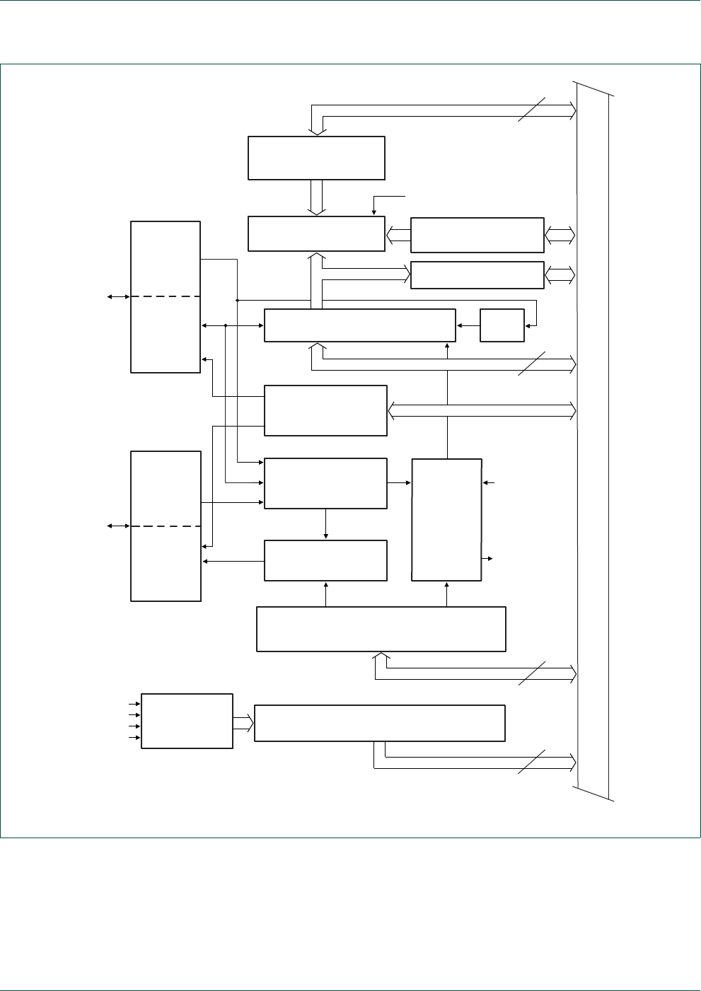
UM10462 All information provided in this document is subject to legal disclaimers. © NXP B.V. 2014. All rights reserved.
User manual Rev. 5.3 — 11 June 2014 299 of 521
NXP Semiconductors UM10462
Chapter 14: LPC11U3x/2x/1x I2C-bus controller
14.8.1 Input filters and output stages
Input signals are synchronized with the internal clock, and spikes shorter than three
clocks are filtered out.
The output for I2C is a special pad designed to conform to the I2C specification.
Fig 41. I2C serial interface block diagram
APB BUS
STATUS REGISTER
I2CnSTAT
CONTROL REGISTER and
SCL DUTY CYLE REGISTERS
I2CnCONSET, I2CnCONCLR, I2CnSCLH, I2CnSCLL
ADDRESS REGISTERS
MASK and COMPARE
SHIFT REGISTER
I2CnDAT ACK
BIT COUNTER/
ARBITRATION and
MONITOR MODE
REGISTER
I2CnMMCTRL
SYNC LOGIC
SERIAL CLOCK
GENERATOR
TIMING and
CONTROL
LOGIC
STATUS
DECODER
status
bus
interrupt
PCLK
INPUT
FILTER
OUTPUT
STAGE
SCL
INPUT
FILTER
OUTPUT
STAGE
SDA
I2CnADDR0 to I2CnADDR3
MASK REGISTERS
I2CnMASK0 to I2CnMASK3
I2CnDATABUFFER
MATCHALL
I2CnMMCTRL[3]
8
8
8
16

UM10462 All information provided in this document is subject to legal disclaimers. © NXP B.V. 2014. All rights reserved.
User manual Rev. 5.3 — 11 June 2014 300 of 521
NXP Semiconductors UM10462
Chapter 14: LPC11U3x/2x/1x I2C-bus controller
14.8.2 Address Registers, ADR0 to ADR3
These registers may be loaded with the 7-bit slave address (7 most significant bits) to
which the I2C block will respond when programmed as a slave transmitter or receiver. The
LSB (GC) is used to enable General Call address (0x00) recognition. When multiple slave
addresses are enabled, the actual address received may be read from the DAT register at
the state where the own slave address has been received.
14.8.3 Address mask registers, MASK0 to MASK3
The four mask registers each contain seven active bits (7:1). Any bit in these registers
which is set to ‘1’ will cause an automatic compare on the corresponding bit of the
received address when it is compared to the ADRn register associated with that mask
register. In other words, bits in an ADRn register which are masked are not taken into
account in determining an address match.
When an address-match interrupt occurs, the processor will have to read the data register
(DAT) to determine what the received address was that actually caused the match.
14.8.4 Comparator
The comparator compares the received 7-bit slave address with its own slave address (7
most significant bits in ADR). It also compares the first received 8-bit byte with the General
Call address (0x00). If an equality is found, the appropriate status bits are set and an
interrupt is requested.
14.8.5 Shift register, DAT
This 8-bit register contains a byte of serial data to be transmitted or a byte which has just
been received. Data in DAT is always shifted from right to left; the first bit to be transmitted
is the MSB (bit 7) and, after a byte has been received, the first bit of received data is
located at the MSB of DAT. While data is being shifted out, data on the bus is
simultaneously being shifted in; DAT always contains the last byte present on the bus.
Thus, in the event of lost arbitration, the transition from master transmitter to slave
receiver is made with the correct data in DAT.
14.8.6 Arbitration and synchronization logic
In the master transmitter mode, the arbitration logic checks that every transmitted logic 1
actually appears as a logic 1 on the I2C-bus. If another device on the bus overrules a logic
1 and pulls the SDA line low, arbitration is lost, and the I2C block immediately changes
from master transmitter to slave receiver. The I2C block will continue to output clock
pulses (on SCL) until transmission of the current serial byte is complete.
Arbitration may also be lost in the master receiver mode. Loss of arbitration in this mode
can only occur while the I2C block is returning a “not acknowledge: (logic 1) to the bus.
Arbitration is lost when another device on the bus pulls this signal low. Since this can
occur only at the end of a serial byte, the I2C block generates no further clock pulses.
Figure 42 shows the arbitration procedure.
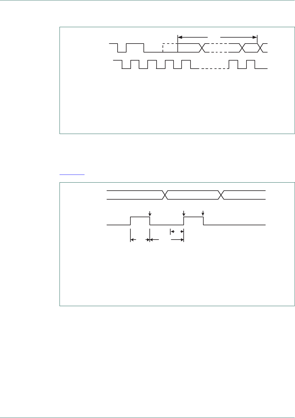
UM10462 All information provided in this document is subject to legal disclaimers. © NXP B.V. 2014. All rights reserved.
User manual Rev. 5.3 — 11 June 2014 301 of 521
NXP Semiconductors UM10462
Chapter 14: LPC11U3x/2x/1x I2C-bus controller
The synchronization logic will synchronize the serial clock generator with the clock pulses
on the SCL line from another device. If two or more master devices generate clock pulses,
the “mark” duration is determined by the device that generates the shortest “marks,” and
the “space” duration is determined by the device that generates the longest “spaces”.
Figure 43 shows the synchronization procedure.
A slave may stretch the space duration to slow down the bus master. The space duration
may also be stretched for handshaking purposes. This can be done after each bit or after
a complete byte transfer. the I2C block will stretch the SCL space duration after a byte has
been transmitted or received and the acknowledge bit has been transferred. The serial
interrupt flag (SI) is set, and the stretching continues until the serial interrupt flag is
cleared.
14.8.7 Serial clock generator
This programmable clock pulse generator provides the SCL clock pulses when the I2C
block is in the master transmitter or master receiver mode. It is switched off when the I2C
block is in slave mode. The I2C output clock frequency and duty cycle is programmable
(1) Another device transmits serial data.
(2) Another device overrules a logic (dotted line) transmitted this I2C master by pulling the SDA line
low. Arbitration is lost, and this I2C enters Slave Receiver mode.
(3) This I2C is in Slave Receiver mode but still generates clock pulses until the current byte has been
transmitted. This I2C will not generate clock pulses for the next byte. Data on SDA originates from
the new master once it has won arbitration.
Fig 42. Arbitration procedure
(1) Another device pulls the SCL line low before this I2C has timed a complete high time. The other
device effectively determines the (shorter) HIGH period.
(2) Another device continues to pull the SCL line low after this I2C has timed a complete low time and
released SCL. The I2C clock generator is forced to wait until SCL goes HIGH. The other device
effectively determines the (longer) LOW period.
(3) The SCL line is released , and the clock generator begins timing the HIGH time.
Fig 43. Serial clock synchronization
SDA line
SCL line 1234 89
ACK
(1) (2)(1) (3)
SDA line
SCL line
(2)
(1)(3)
high
period
low
period
(1)

UM10462 All information provided in this document is subject to legal disclaimers. © NXP B.V. 2014. All rights reserved.
User manual Rev. 5.3 — 11 June 2014 302 of 521
NXP Semiconductors UM10462
Chapter 14: LPC11U3x/2x/1x I2C-bus controller
via the I2C Clock Control Registers. See the description of the I2CSCLL and I2CSCLH
registers for details. The output clock pulses have a duty cycle as programmed unless the
bus is synchronizing with other SCL clock sources as described above.
14.8.8 Timing and control
The timing and control logic generates the timing and control signals for serial byte
handling. This logic block provides the shift pulses for DAT, enables the comparator,
generates and detects START and STOP conditions, receives and transmits acknowledge
bits, controls the master and slave modes, contains interrupt request logic, and monitors
the I2C-bus status.
14.8.9 Control register, CONSET and CONCLR
The I2C control register contains bits used to control the following I2C block functions: start
and restart of a serial transfer, termination of a serial transfer, bit rate, address recognition,
and acknowledgment.
The contents of the I2C control register may be read as CONSET. Writing to CONSET will
set bits in the I2C control register that correspond to ones in the value written. Conversely,
writing to CONCLR will clear bits in the I2C control register that correspond to ones in the
value written.
14.8.10 Status decoder and status register
The status decoder takes all of the internal status bits and compresses them into a 5-bit
code. This code is unique for each I2C-bus status. The 5-bit code may be used to
generate vector addresses for fast processing of the various service routines. Each
service routine processes a particular bus status. There are 26 possible bus states if all
four modes of the I2C block are used. The 5-bit status code is latched into the five most
significant bits of the status register when the serial interrupt flag is set (by hardware) and
remains stable until the interrupt flag is cleared by software. The three least significant bits
of the status register are always zero. If the status code is used as a vector to service
routines, then the routines are displaced by eight address locations. Eight bytes of code is
sufficient for most of the service routines (see the software example in this section).
14.9 I2C operating modes
In a given application, the I2C block may operate as a master, a slave, or both. In the slave
mode, the I2C hardware looks for any one of its four slave addresses and the General Call
address. If one of these addresses is detected, an interrupt is requested. If the processor
wishes to become the bus master, the hardware waits until the bus is free before the
master mode is entered so that a possible slave operation is not interrupted. If bus
arbitration is lost in the master mode, the I2C block switches to the slave mode
immediately and can detect its own slave address in the same serial transfer.
14.9.1 Master Transmitter mode
In this mode data is transmitted from master to slave. Before the master transmitter mode
can be entered, the CONSET register must be initialized as shown in Table 283. I2EN
must be set to 1 to enable the I2C function. If the AA bit is 0, the I2C interface will not
acknowledge any address when another device is master of the bus, so it can not enter
UM10462 All information provided in this document is subject to legal disclaimers. © NXP B.V. 2014. All rights reserved.
User manual Rev. 5.3 — 11 June 2014 303 of 521
NXP Semiconductors UM10462
Chapter 14: LPC11U3x/2x/1x I2C-bus controller
slave mode. The STA, STO and SI bits must be 0. The SI Bit is cleared by writing 1 to the
SIC bit in the CONCLR register. THe STA bit should be cleared after writing the slave
address.
The first byte transmitted contains the slave address of the receiving device (7 bits) and
the data direction bit. In this mode the data direction bit (R/W) should be 0 which means
Write. The first byte transmitted contains the slave address and Write bit. Data is
transmitted 8 bits at a time. After each byte is transmitted, an acknowledge bit is received.
START and STOP conditions are output to indicate the beginning and the end of a serial
transfer.
The I2C interface will enter master transmitter mode when software sets the STA bit. The
I2C logic will send the START condition as soon as the bus is free. After the START
condition is transmitted, the SI bit is set, and the status code in the STAT register is 0x08.
This status code is used to vector to a state service routine which will load the slave
address and Write bit to the DAT register, and then clear the SI bit. SI is cleared by writing
a 1 to the SIC bit in the CONCLR register.
When the slave address and R/W bit have been transmitted and an acknowledgment bit
has been received, the SI bit is set again, and the possible status codes now are 0x18,
0x20, or 0x38 for the master mode, or 0x68, 0x78, or 0xB0 if the slave mode was enabled
(by setting AA to 1). The appropriate actions to be taken for each of these status codes
are shown in Table 287 to Table 292.
14.9.2 Master Receiver mode
In the master receiver mode, data is received from a slave transmitter. The transfer is
initiated in the same way as in the master transmitter mode. When the START condition
has been transmitted, the interrupt service routine must load the slave address and the
data direction bit to the I2C Data register (DAT), and then clear the SI bit. In this case, the
data direction bit (R/W) should be 1 to indicate a read.
Table 283. CONSET used to configure Master mode
Bit 7 6 5 4 3 2 1 0
Symbol - I2EN STA STO SI AA - -
Value- 10000- -
Fig 44. Format in the Master Transmitter mode
A = Acknowledge (SDA low)
A = Not acknowledge (SDA high)
S = START condition
P = STOP condition
S SLAVE ADDRESS RW=0 A DATA AA/A P
from Master to Slave
from Slave to Master
DATA
n bytes data transmitted
UM10462 All information provided in this document is subject to legal disclaimers. © NXP B.V. 2014. All rights reserved.
User manual Rev. 5.3 — 11 June 2014 304 of 521
NXP Semiconductors UM10462
Chapter 14: LPC11U3x/2x/1x I2C-bus controller
When the slave address and data direction bit have been transmitted and an
acknowledge bit has been received, the SI bit is set, and the Status Register will show the
status code. For master mode, the possible status codes are 0x40, 0x48, or 0x38. For
slave mode, the possible status codes are 0x68, 0x78, or 0xB0. For details, refer to
Table 288.
After a Repeated START condition, I2C may switch to the master transmitter mode.
14.9.3 Slave Receiver mode
In the slave receiver mode, data bytes are received from a master transmitter. To initialize
the slave receiver mode, write any of the Slave Address registers (ADR0-3) and write the
I2C Control Set register (CONSET) as shown in Table 284.
I2EN must be set to 1 to enable the I2C function. AA bit must be set to 1 to acknowledge
its own slave address or the General Call address. The STA, STO and SI bits are set to 0.
After ADR and CONSET are initialized, the I2C interface waits until it is addressed by its
own address or general address followed by the data direction bit. If the direction bit is 0
(W), it enters slave receiver mode. If the direction bit is 1 (R), it enters slave transmitter
Fig 45. Format of Master Receiver mode
Fig 46. A Master Receiver switches to Master Transmitter after sending Repeated START
DATA
A = Acknowledge (SDA low)
A = Not acknowledge (SDA high)
S = START condition
P = STOP condition
S SLAVE ADDRESS RW=1 A DATA P
n bytes data received
from Master to Slave
from Slave to Master
AA
A = Acknowledge (SDA low)
A = Not acknowledge (SDA high)
S = START condition
P = STOP condition
SLA = Slave Address
Sr = Repeated START condition
DATA
n bytes data transmitted
From master to slave
From slave to master
ADATA A ASLA R Sr W PS SLA DATAAA
Table 284. CONSET used to configure Slave mode
Bit 7 6 5 4 3 2 1 0
Symbol - I2EN STA STO SI AA - -
Value- 10001- -
UM10462 All information provided in this document is subject to legal disclaimers. © NXP B.V. 2014. All rights reserved.
User manual Rev. 5.3 — 11 June 2014 305 of 521
NXP Semiconductors UM10462
Chapter 14: LPC11U3x/2x/1x I2C-bus controller
mode. After the address and direction bit have been received, the SI bit is set and a valid
status code can be read from the Status register (STAT). Refer to Table 291 for the status
codes and actions.
14.9.4 Slave Transmitter mode
The first byte is received and handled as in the slave receiver mode. However, in this
mode, the direction bit will be 1, indicating a read operation. Serial data is transmitted via
SDA while the serial clock is input through SCL. START and STOP conditions are
recognized as the beginning and end of a serial transfer. In a given application, I2C may
operate as a master and as a slave. In the slave mode, the I2C hardware looks for its own
slave address and the General Call address. If one of these addresses is detected, an
interrupt is requested. When the microcontrollers wishes to become the bus master, the
hardware waits until the bus is free before the master mode is entered so that a possible
slave action is not interrupted. If bus arbitration is lost in the master mode, the I2C
interface switches to the slave mode immediately and can detect its own slave address in
the same serial transfer.
14.10 Details of I2C operating modes
The four operating modes are:
•Master Transmitter
Fig 47. Format of Slave Receiver mode
A
A = Acknowledge (SDA low)
A = Not acknowledge (SDA high)
S = START condition
P = STOP condition
Sr = Repeated START condition
AA/A
n bytes data received
from Master to Slave
from Slave to Master
S SLAVE ADDRESS RW=0 DATA P/SrDATA
Fig 48. Format of Slave Transmitter mode
DATA
A = Acknowledge (SDA low)
A = Not acknowledge (SDA high)
S = START condition
P = STOP condition
ADATA
n bytes data transmitted
from Master to Slave
from Slave to Master
S SLAVE ADDRESS RW=1 A P
A

UM10462 All information provided in this document is subject to legal disclaimers. © NXP B.V. 2014. All rights reserved.
User manual Rev. 5.3 — 11 June 2014 306 of 521
NXP Semiconductors UM10462
Chapter 14: LPC11U3x/2x/1x I2C-bus controller
•Master Receiver
•Slave Receiver
•Slave Transmitter
Data transfers in each mode of operation are shown in Figure 49, Figure 50, Figure 51,
Figure 52, and Figure 53. Table 285 lists abbreviations used in these figures when
describing the I2C operating modes.
In Figure 49 to Figure 53, circles are used to indicate when the serial interrupt flag is set.
The numbers in the circles show the status code held in the STAT register. At these points,
a service routine must be executed to continue or complete the serial transfer. These
service routines are not critical since the serial transfer is suspended until the serial
interrupt flag is cleared by software.
When a serial interrupt routine is entered, the status code in STAT is used to branch to the
appropriate service routine. For each status code, the required software action and details
of the following serial transfer are given in tables from Table 287 to Table 293.
14.10.1 Master Transmitter mode
In the master transmitter mode, a number of data bytes are transmitted to a slave receiver
(see Figure 49). Before the master transmitter mode can be entered, I2CON must be
initialized as follows:
The I2C rate must also be configured in the SCLL and SCLH registers. I2EN must be set
to logic 1 to enable the I2C block. If the AA bit is reset, the I2C block will not acknowledge
its own slave address or the General Call address in the event of another device
becoming master of the bus. In other words, if AA is reset, the I2C interface cannot enter
slave mode. STA, STO, and SI must be reset.
Table 285. Abbreviations used to describe an I2C operation
Abbreviation Explanation
S START Condition
SLA 7-bit slave address
R Read bit (HIGH level at SDA)
W Write bit (LOW level at SDA)
A Acknowledge bit (LOW level at SDA)
ANot acknowledge bit (HIGH level at SDA)
Data 8-bit data byte
P STOP condition
Table 286. CONSET used to initialize Master Transmitter mode
Bit 7 6 5 4 3 2 1 0
Symbol - I2EN STA STO SI AA - -
Value- 1000x- -

UM10462 All information provided in this document is subject to legal disclaimers. © NXP B.V. 2014. All rights reserved.
User manual Rev. 5.3 — 11 June 2014 307 of 521
NXP Semiconductors UM10462
Chapter 14: LPC11U3x/2x/1x I2C-bus controller
The master transmitter mode may now be entered by setting the STA bit. The I2C logic will
now test the I2C-bus and generate a START condition as soon as the bus becomes free.
When a START condition is transmitted, the serial interrupt flag (SI) is set, and the status
code in the status register (STAT) will be 0x08. This status code is used by the interrupt
service routine to enter the appropriate state service routine that loads DAT with the slave
address and the data direction bit (SLA+W). The SI bit in CON must then be reset before
the serial transfer can continue.
When the slave address and the direction bit have been transmitted and an
acknowledgment bit has been received, the serial interrupt flag (SI) is set again, and a
number of status codes in STAT are possible. There are 0x18, 0x20, or 0x38 for the
master mode and also 0x68, 0x78, or 0xB0 if the slave mode was enabled (AA = logic 1).
The appropriate action to be taken for each of these status codes is detailed in Table 287.
After a Repeated START condition (state 0x10). The I2C block may switch to the master
receiver mode by loading DAT with SLA+R).

UM10462 All information provided in this document is subject to legal disclaimers. © NXP B.V. 2014. All rights reserved.
User manual Rev. 5.3 — 11 June 2014 308 of 521
NXP Semiconductors UM10462
Chapter 14: LPC11U3x/2x/1x I2C-bus controller
Table 287. Master Transmitter mode
Status
Code
(I2CSTAT
)
Status of the I2C-bus
and hardware Application software response Next action taken by I2C hardware
To/From DAT To CON
STA STO SI AA
0x08 A START condition
has been transmitted.
Load SLA+W;
clear STA
X 0 0 X SLA+W will be transmitted; ACK bit will
be received.
0x10 A Repeated START
condition has been
transmitted.
Load SLA+W or X 0 0 X As above.
Load SLA+R;
Clear STA
X 0 0 X SLA+R will be transmitted; the I2C block
will be switched to MST/REC mode.
0x18 SLA+W has been
transmitted; ACK has
been received.
Load data byte or 0 0 0 X Data byte will be transmitted; ACK bit will
be received.
No DAT action or 1 0 0 X Repeated START will be transmitted.
No DAT action or 0 1 0 X STOP condition will be transmitted; STO
flag will be reset.
No DAT action 1 1 0 X STOP condition followed by a START
condition will be transmitted; STO flag will
be reset.
0x20 SLA+W has been
transmitted; NOT ACK
has been received.
Load data byte or 0 0 0 X Data byte will be transmitted; ACK bit will
be received.
No DAT action or 1 0 0 X Repeated START will be transmitted.
No DAT action or 0 1 0 X STOP condition will be transmitted; STO
flag will be reset.
No DAT action 1 1 0 X STOP condition followed by a START
condition will be transmitted; STO flag will
be reset.
0x28 Data byte in DAT has
been transmitted;
ACK has been
received.
Load data byte or 0 0 0 X Data byte will be transmitted; ACK bit will
be received.
No DAT action or 1 0 0 X Repeated START will be transmitted.
No DAT action or 0 1 0 X STOP condition will be transmitted; STO
flag will be reset.
No DAT action 1 1 0 X STOP condition followed by a START
condition will be transmitted; STO flag will
be reset.
0x30 Data byte in DAT has
been transmitted;
NOT ACK has been
received.
Load data byte or 0 0 0 X Data byte will be transmitted; ACK bit will
be received.
No DAT action or 1 0 0 X Repeated START will be transmitted.
No DAT action or 0 1 0 X STOP condition will be transmitted; STO
flag will be reset.
No DAT action 1 1 0 X STOP condition followed by a START
condition will be transmitted; STO flag will
be reset.
0x38 Arbitration lost in
SLA+R/W or Data
bytes.
No DAT action or 0 0 0 X I2C-bus will be released; not addressed
slave will be entered.
No DAT action 1 0 0 X A START condition will be transmitted
when the bus becomes free.
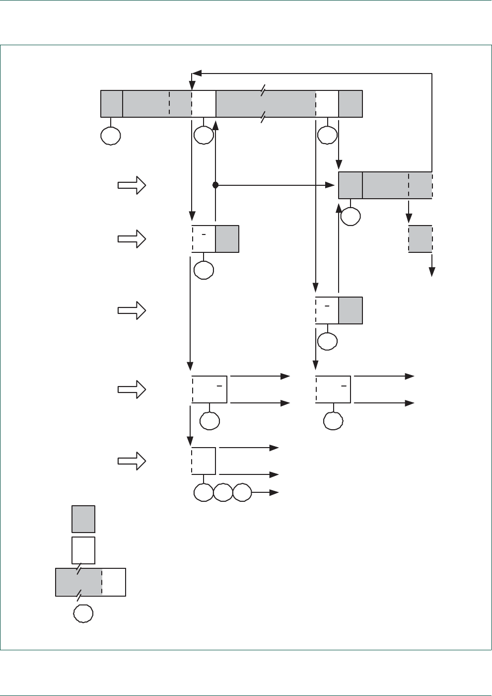
UM10462 All information provided in this document is subject to legal disclaimers. © NXP B.V. 2014. All rights reserved.
User manual Rev. 5.3 — 11 June 2014 309 of 521
NXP Semiconductors UM10462
Chapter 14: LPC11U3x/2x/1x I2C-bus controller
Fig 49. Format and states in the Master Transmitter mode
DATA
A
R
WSLAS
DATAAW
SLA
to Master
receive
mode,
entry
= MR
MT
to corresponding
states in Slave mode
A OR AA OR A
A
other Master
continues
other Master
continues
Aother Master
continues
20H
08H 18H 28H
30H
10H
68H 78H B0H
38H 38H
arbitration lost
in Slave
address or
Data byte
Not
Acknowledge
received after a
Data byte
Not
Acknowledge
received after
the Slave
address
next transfer
started with a
Repeated Start
condition
arbitration lost
and
addressed as
Slave
successful
transmission
to a Slave
Receiver
from Master to Slave
from Slave to Master
any number of data bytes and their associated Acknowledge bits
nthis number (contained in I2STA) corresponds to a defined state of the
I2C bus
A P
P
S P

UM10462 All information provided in this document is subject to legal disclaimers. © NXP B.V. 2014. All rights reserved.
User manual Rev. 5.3 — 11 June 2014 310 of 521
NXP Semiconductors UM10462
Chapter 14: LPC11U3x/2x/1x I2C-bus controller
14.10.2 Master Receiver mode
In the master receiver mode, a number of data bytes are received from a slave transmitter
(see Figure 50). The transfer is initialized as in the master transmitter mode. When the
START condition has been transmitted, the interrupt service routine must load DAT with
the 7-bit slave address and the data direction bit (SLA+R). The SI bit in CON must then be
cleared before the serial transfer can continue.
When the slave address and the data direction bit have been transmitted and an
acknowledgment bit has been received, the serial interrupt flag (SI) is set again, and a
number of status codes in STAT are possible. These are 0x40, 0x48, or 0x38 for the
master mode and also 0x68, 0x78, or 0xB0 if the slave mode was enabled (AA = 1). The
appropriate action to be taken for each of these status codes is detailed in Table 288. After
a Repeated START condition (state 0x10), the I2C block may switch to the master
transmitter mode by loading DAT with SLA+W.

UM10462 All information provided in this document is subject to legal disclaimers. © NXP B.V. 2014. All rights reserved.
User manual Rev. 5.3 — 11 June 2014 311 of 521
NXP Semiconductors UM10462
Chapter 14: LPC11U3x/2x/1x I2C-bus controller
Table 288. Master Receiver mode
Status
Code
(STAT)
Status of the I2C-bus
and hardware Application software response Next action taken by I2C hardware
To/From DAT To CON
STA STO SI AA
0x08 A START condition
has been transmitted.
Load SLA+R X 0 0 X SLA+R will be transmitted; ACK bit will be
received.
0x10 A Repeated START
condition has been
transmitted.
Load SLA+R or X 0 0 X As above.
Load SLA+W X 0 0 X SLA+W will be transmitted; the I2C block
will be switched to MST/TRX mode.
0x38 Arbitration lost in NOT
ACK bit.
No DAT action or 0 0 0 X I2C-bus will be released; the I2C block will
enter slave mode.
No DAT action 1 0 0 X A START condition will be transmitted
when the bus becomes free.
0x40 SLA+R has been
transmitted; ACK has
been received.
No DAT action or 0 0 0 0 Data byte will be received; NOT ACK bit
will be returned.
No DAT action 0 0 0 1 Data byte will be received; ACK bit will be
returned.
0x48 SLA+R has been
transmitted; NOT ACK
has been received.
No DAT action or 1 0 0 X Repeated START condition will be
transmitted.
No DAT action or 0 1 0 X STOP condition will be transmitted; STO
flag will be reset.
No DAT action 1 1 0 X STOP condition followed by a START
condition will be transmitted; STO flag will
be reset.
0x50 Data byte has been
received; ACK has
been returned.
Read data byte or 0 0 0 0 Data byte will be received; NOT ACK bit
will be returned.
Read data byte 0 0 0 1 Data byte will be received; ACK bit will be
returned.
0x58 Data byte has been
received; NOT ACK
has been returned.
Read data byte or 1 0 0 X Repeated START condition will be
transmitted.
Read data byte or 0 1 0 X STOP condition will be transmitted; STO
flag will be reset.
Read data byte 1 1 0 X STOP condition followed by a START
condition will be transmitted; STO flag will
be reset.
UM10462 All information provided in this document is subject to legal disclaimers. © NXP B.V. 2014. All rights reserved.
User manual Rev. 5.3 — 11 June 2014 312 of 521
NXP Semiconductors UM10462
Chapter 14: LPC11U3x/2x/1x I2C-bus controller
Fig 50. Format and states in the Master Receiver mode
A
to Master
transmit
mode, entry
= MT
MR
to corresponding
states in Slave
mode
ARSLAS
RSLAS
W
AA OR A
AP
other Master
continues
other Master
continues
Aother Master
continues
48H
40H 58H
10H
68H 78H B0H
38H 38H
arbitration lost in
Slave address or
Acknowledge bit
Not Acknowledge
received after the
Slave address
next transfer
started with a
Repeated Start
condition
arbitration lost
and addressed
as Slave
successful
transmission to
a Slave
transmitter
from Master to Slave
from Slave to Master
any number of data bytes and their associated
Acknowledge bits
nthis number (contained in I2STA) corresponds to a defined state of
the I2C bus
DATAADATA
50H
ADATA
P
08H

UM10462 All information provided in this document is subject to legal disclaimers. © NXP B.V. 2014. All rights reserved.
User manual Rev. 5.3 — 11 June 2014 313 of 521
NXP Semiconductors UM10462
Chapter 14: LPC11U3x/2x/1x I2C-bus controller
14.10.3 Slave Receiver mode
In the slave receiver mode, a number of data bytes are received from a master transmitter
(see Figure 51). To initiate the slave receiver mode, ADR and CON must be loaded as
follows:
The upper 7 bits are the address to which the I2C block will respond when addressed by a
master. If the LSB (GC) is set, the I2C block will respond to the General Call address
(0x00); otherwise it ignores the General Call address.
The I2C-bus rate settings do not affect the I2C block in the slave mode. I2EN must be set
to logic 1 to enable the I2C block. The AA bit must be set to enable the I2C block to
acknowledge its own slave address or the General Call address. STA, STO, and SI must
be reset.
When ADR and CON have been initialized, the I2C block waits until it is addressed by its
own slave address followed by the data direction bit which must be “0” (W) for the I2C
block to operate in the slave receiver mode. After its own slave address and the W bit
have been received, the serial interrupt flag (SI) is set and a valid status code can be read
from STAT. This status code is used to vector to a state service routine. The appropriate
action to be taken for each of these status codes is detailed in Table 291. The slave
receiver mode may also be entered if arbitration is lost while the I2C block is in the master
mode (see status 0x68 and 0x78).
If the AA bit is reset during a transfer, the I2C block will return a not acknowledge (logic 1)
to SDA after the next received data byte. While AA is reset, the I2C block does not
respond to its own slave address or a General Call address. However, the I2C-bus is still
monitored and address recognition may be resumed at any time by setting AA. This
means that the AA bit may be used to temporarily isolate the I2C block from the I2C-bus.
Table 289. ADR usage in Slave Receiver mode
Bit 7 6 5 4 3 2 1 0
Symbol own slave 7-bit address GC
Table 290. CONSET used to initialize Slave Receiver mode
Bit 7 6 5 4 3 2 1 0
Symbol - I2EN STA STO SI AA - -
Value- 10001- -

UM10462 All information provided in this document is subject to legal disclaimers. © NXP B.V. 2014. All rights reserved.
User manual Rev. 5.3 — 11 June 2014 314 of 521
NXP Semiconductors UM10462
Chapter 14: LPC11U3x/2x/1x I2C-bus controller
Table 291. Slave Receiver mode
Status
Code
(STAT)
Status of the I2C-bus
and hardware Application software response Next action taken by I2C hardware
To/From DAT To CON
STA STO SI AA
0x60 Own SLA+W has
been received; ACK
has been returned.
No DAT action or X 0 0 0 Data byte will be received and NOT ACK
will be returned.
No DAT action X 0 0 1 Data byte will be received and ACK will
be returned.
0x68 Arbitration lost in
SLA+R/W as master;
Own SLA+W has
been received, ACK
returned.
No DAT action or X 0 0 0 Data byte will be received and NOT ACK
will be returned.
No DAT action X 0 0 1 Data byte will be received and ACK will
be returned.
0x70 General call address
(0x00) has been
received; ACK has
been returned.
No DAT action or X 0 0 0 Data byte will be received and NOT ACK
will be returned.
No DAT action X 0 0 1 Data byte will be received and ACK will
be returned.
0x78 Arbitration lost in
SLA+R/W as master;
General call address
has been received,
ACK has been
returned.
No DAT action or X 0 0 0 Data byte will be received and NOT ACK
will be returned.
No DAT action X 0 0 1 Data byte will be received and ACK will
be returned.
0x80 Previously addressed
with own SLV
address; DATA has
been received; ACK
has been returned.
Read data byte or X 0 0 0 Data byte will be received and NOT ACK
will be returned.
Read data byte X 0 0 1 Data byte will be received and ACK will
be returned.
0x88 Previously addressed
with own SLA; DATA
byte has been
received; NOT ACK
has been returned.
Read data byte or 0 0 0 0 Switched to not addressed SLV mode; no
recognition of own SLA or General call
address.
Read data byte or 0 0 0 1 Switched to not addressed SLV mode;
Own SLA will be recognized; General call
address will be recognized if
ADR[0] = logic 1.
Read data byte or 1 0 0 0 Switched to not addressed SLV mode; no
recognition of own SLA or General call
address. A START condition will be
transmitted when the bus becomes free.
Read data byte 1 0 0 1 Switched to not addressed SLV mode;
Own SLA will be recognized; General call
address will be recognized if
ADR[0] = logic 1. A START condition will
be transmitted when the bus becomes
free.
0x90 Previously addressed
with General Call;
DATA byte has been
received; ACK has
been returned.
Read data byte or X 0 0 0 Data byte will be received and NOT ACK
will be returned.
Read data byte X 0 0 1 Data byte will be received and ACK will
be returned.

UM10462 All information provided in this document is subject to legal disclaimers. © NXP B.V. 2014. All rights reserved.
User manual Rev. 5.3 — 11 June 2014 315 of 521
NXP Semiconductors UM10462
Chapter 14: LPC11U3x/2x/1x I2C-bus controller
0x98 Previously addressed
with General Call;
DATA byte has been
received; NOT ACK
has been returned.
Read data byte or 0 0 0 0 Switched to not addressed SLV mode; no
recognition of own SLA or General call
address.
Read data byte or 0 0 0 1 Switched to not addressed SLV mode;
Own SLA will be recognized; General call
address will be recognized if
ADR[0] = logic 1.
Read data byte or 1 0 0 0 Switched to not addressed SLV mode; no
recognition of own SLA or General call
address. A START condition will be
transmitted when the bus becomes free.
Read data byte 1 0 0 1 Switched to not addressed SLV mode;
Own SLA will be recognized; General call
address will be recognized if
ADR[0] = logic 1. A START condition will
be transmitted when the bus becomes
free.
0xA0 A STOP condition or
Repeated START
condition has been
received while still
addressed as
SLV/REC or
SLV/TRX.
No STDAT action
or
0 0 0 0 Switched to not addressed SLV mode; no
recognition of own SLA or General call
address.
No STDAT action
or
0 0 0 1 Switched to not addressed SLV mode;
Own SLA will be recognized; General call
address will be recognized if
ADR[0] = logic 1.
No STDAT action
or
1 0 0 0 Switched to not addressed SLV mode; no
recognition of own SLA or General call
address. A START condition will be
transmitted when the bus becomes free.
No STDAT action 1 0 0 1 Switched to not addressed SLV mode;
Own SLA will be recognized; General call
address will be recognized if
ADR[0] = logic 1. A START condition will
be transmitted when the bus becomes
free.
Table 291. Slave Receiver mode …continued
Status
Code
(STAT)
Status of the I2C-bus
and hardware Application software response Next action taken by I2C hardware
To/From DAT To CON
STA STO SI AA
UM10462 All information provided in this document is subject to legal disclaimers. © NXP B.V. 2014. All rights reserved.
User manual Rev. 5.3 — 11 June 2014 316 of 521
NXP Semiconductors UM10462
Chapter 14: LPC11U3x/2x/1x I2C-bus controller
Fig 51. Format and states in the Slave Receiver mode
A
A P OR SAWSLAS
P OR S
A
A
68H
60H 80H
88H
reception of the
General Call address
and one or more Data
bytes
arbitration lost as
Master and addressed
as Slave
last data byte
received is Not
acknowledged
arbitration lost as
Master and addressed
as Slave by General
Call
reception of the own
Slave address and one
or more Data bytes all
are acknowledged
from Master to Slave
from Slave to Master
any number of data bytes and their associated Acknowledge bits
nthis number (contained in I2STA) corresponds to a defined state of the I
2C
bus
DATAADATA
80H A0H
last data byte is Not
acknowledged
AP OR SA
70h 90h
DATAADATA
90h A0H
GENERAL CALL
A
98h
P OR S
A
78h
DATA

UM10462 All information provided in this document is subject to legal disclaimers. © NXP B.V. 2014. All rights reserved.
User manual Rev. 5.3 — 11 June 2014 317 of 521
NXP Semiconductors UM10462
Chapter 14: LPC11U3x/2x/1x I2C-bus controller
14.10.4 Slave Transmitter mode
In the slave transmitter mode, a number of data bytes are transmitted to a master receiver
(see Figure 52). Data transfer is initialized as in the slave receiver mode. When ADR and
CON have been initialized, the I2C block waits until it is addressed by its own slave
address followed by the data direction bit which must be “1” (R) for the I2C block to
operate in the slave transmitter mode. After its own slave address and the R bit have been
received, the serial interrupt flag (SI) is set and a valid status code can be read from STAT.
This status code is used to vector to a state service routine, and the appropriate action to
be taken for each of these status codes is detailed in Table 292. The slave transmitter
mode may also be entered if arbitration is lost while the I2C block is in the master mode
(see state 0xB0).
If the AA bit is reset during a transfer, the I2C block will transmit the last byte of the transfer
and enter state 0xC0 or 0xC8. The I2C block is switched to the not addressed slave mode
and will ignore the master receiver if it continues the transfer. Thus the master receiver
receives all 1s as serial data. While AA is reset, the I2C block does not respond to its own
slave address or a General Call address. However, the I2C-bus is still monitored, and
address recognition may be resumed at any time by setting AA. This means that the AA
bit may be used to temporarily isolate the I2C block from the I2C-bus.

UM10462 All information provided in this document is subject to legal disclaimers. © NXP B.V. 2014. All rights reserved.
User manual Rev. 5.3 — 11 June 2014 318 of 521
NXP Semiconductors UM10462
Chapter 14: LPC11U3x/2x/1x I2C-bus controller
Table 292. Slave Transmitter mode
Status
Code
(STAT)
Status of the I2C-bus
and hardware Application software response Next action taken by I2C hardware
To/From DAT To CON
STA STO SI AA
0xA8 Own SLA+R has been
received; ACK has
been returned.
Load data byte or X 0 0 0 Last data byte will be transmitted and
ACK bit will be received.
Load data byte X 0 0 1 Data byte will be transmitted; ACK will be
received.
0xB0 Arbitration lost in
SLA+R/W as master;
Own SLA+R has been
received, ACK has
been returned.
Load data byte or X 0 0 0 Last data byte will be transmitted and
ACK bit will be received.
Load data byte X 0 0 1 Data byte will be transmitted; ACK bit will
be received.
0xB8 Data byte in DAT has
been transmitted;
ACK has been
received.
Load data byte or X 0 0 0 Last data byte will be transmitted and
ACK bit will be received.
Load data byte X 0 0 1 Data byte will be transmitted; ACK bit will
be received.
0xC0 Data byte in DAT has
been transmitted;
NOT ACK has been
received.
No DAT action or 0 0 0 0 Switched to not addressed SLV mode; no
recognition of own SLA or General call
address.
No DAT action or 0 0 0 1 Switched to not addressed SLV mode;
Own SLA will be recognized; General call
address will be recognized if
ADR[0] = logic 1.
No DAT action or 1 0 0 0 Switched to not addressed SLV mode; no
recognition of own SLA or General call
address. A START condition will be
transmitted when the bus becomes free.
No DAT action 1 0 0 1 Switched to not addressed SLV mode;
Own SLA will be recognized; General call
address will be recognized if
ADR[0] = logic 1. A START condition will
be transmitted when the bus becomes
free.
0xC8 Last data byte in DAT
has been transmitted
(AA = 0); ACK has
been received.
No DAT action or 0 0 0 0 Switched to not addressed SLV mode; no
recognition of own SLA or General call
address.
No DAT action or 0 0 0 1 Switched to not addressed SLV mode;
Own SLA will be recognized; General call
address will be recognized if
ADR[0] = logic 1.
No DAT action or 1 0 0 0 Switched to not addressed SLV mode; no
recognition of own SLA or General call
address. A START condition will be
transmitted when the bus becomes free.
No DAT action 1 0 0 01 Switched to not addressed SLV mode;
Own SLA will be recognized; General call
address will be recognized if
ADR.0 = logic 1. A START condition will
be transmitted when the bus becomes
free.
UM10462 All information provided in this document is subject to legal disclaimers. © NXP B.V. 2014. All rights reserved.
User manual Rev. 5.3 — 11 June 2014 319 of 521
NXP Semiconductors UM10462
Chapter 14: LPC11U3x/2x/1x I2C-bus controller
14.10.5 Miscellaneous states
There are two STAT codes that do not correspond to a defined I2C hardware state (see
Table 293). These are discussed below.
14.10.5.1 STAT = 0xF8
This status code indicates that no relevant information is available because the serial
interrupt flag, SI, is not yet set. This occurs between other states and when the I2C block
is not involved in a serial transfer.
14.10.5.2 STAT = 0x00
This status code indicates that a bus error has occurred during an I2C serial transfer. A
bus error is caused when a START or STOP condition occurs at an illegal position in the
format frame. Examples of such illegal positions are during the serial transfer of an
address byte, a data byte, or an acknowledge bit. A bus error may also be caused when
external interference disturbs the internal I2C block signals. When a bus error occurs, SI is
set. To recover from a bus error, the STO flag must be set and SI must be cleared. This
Fig 52. Format and states in the Slave Transmitter mode
DATA A
ARSLAS
P OR SA
A
B0H
A8H C0H
C8H
last data byte
transmitted. Switched
to Not Addressed
Slave (AA bit in
I2CON = “0”)
arbitration lost as
Master and
addressed as Slave
reception of the own
Slave address and
one or more Data
bytes all are
acknowledged
from Master to Slave
from Slave to Master
any number of data bytes and their associated
Acknowledge bits
nthis number (contained in I2STA) corresponds to a defined state of
the I2C bus
ADATA
B8H
ALL ONES
ADATA
P OR S

UM10462 All information provided in this document is subject to legal disclaimers. © NXP B.V. 2014. All rights reserved.
User manual Rev. 5.3 — 11 June 2014 320 of 521
NXP Semiconductors UM10462
Chapter 14: LPC11U3x/2x/1x I2C-bus controller
causes the I2C block to enter the “not addressed” slave mode (a defined state) and to
clear the STO flag (no other bits in CON are affected). The SDA and SCL lines are
released (a STOP condition is not transmitted).
14.10.6 Some special cases
The I2C hardware has facilities to handle the following special cases that may occur
during a serial transfer:
•Simultaneous Repeated START conditions from two masters
•Data transfer after loss of arbitration
•Forced access to the I2C-bus
•I2C-bus obstructed by a LOW level on SCL or SDA
•Bus error
14.10.6.1 Simultaneous Repeated START conditions from two masters
A Repeated START condition may be generated in the master transmitter or master
receiver modes. A special case occurs if another master simultaneously generates a
Repeated START condition (see Figure 53). Until this occurs, arbitration is not lost by
either master since they were both transmitting the same data.
If the I2C hardware detects a Repeated START condition on the I2C-bus before generating
a Repeated START condition itself, it will release the bus, and no interrupt request is
generated. If another master frees the bus by generating a STOP condition, the I2C block
will transmit a normal START condition (state 0x08), and a retry of the total serial data
transfer can commence.
Table 293. Miscellaneous States
Status
Code
(STAT)
Status of the I2C-bus
and hardware Application software response Next action taken by I2C hardware
To/From DAT To CON
STA STO SI AA
0xF8 No relevant state
information available;
SI = 0.
No DAT action No CON action Wait or proceed current transfer.
0x00 Bus error during MST
or selected slave
modes, due to an
illegal START or
STOP condition. State
0x00 can also occur
when interference
causes the I2C block
to enter an undefined
state.
No DAT action 0 1 0 X Only the internal hardware is affected in
the MST or addressed SLV modes. In all
cases, the bus is released and the I2C
block is switched to the not addressed
SLV mode. STO is reset.
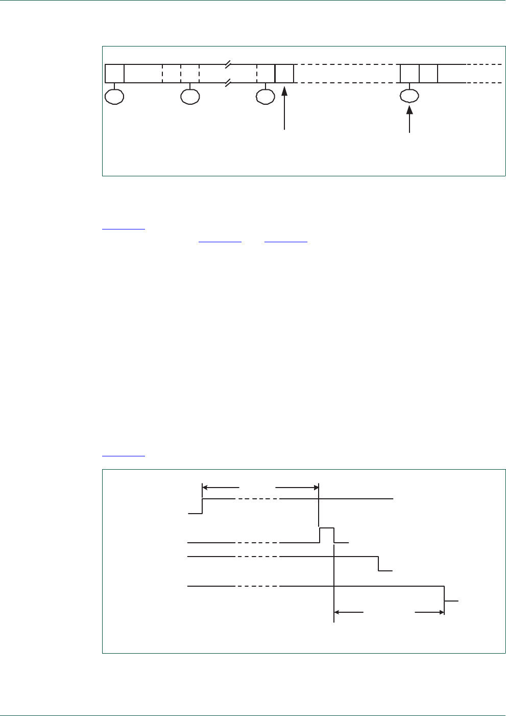
UM10462 All information provided in this document is subject to legal disclaimers. © NXP B.V. 2014. All rights reserved.
User manual Rev. 5.3 — 11 June 2014 321 of 521
NXP Semiconductors UM10462
Chapter 14: LPC11U3x/2x/1x I2C-bus controller
14.10.6.2 Data transfer after loss of arbitration
Arbitration may be lost in the master transmitter and master receiver modes (see
Figure 42). Loss of arbitration is indicated by the following states in STAT; 0x38, 0x68,
0x78, and 0xB0 (see Figure 49 and Figure 50).
If the STA flag in CON is set by the routines which service these states, then, if the bus is
free again, a START condition (state 0x08) is transmitted without intervention by the CPU,
and a retry of the total serial transfer can commence.
14.10.6.3 Forced access to the I2C-bus
In some applications, it may be possible for an uncontrolled source to cause a bus
hang-up. In such situations, the problem may be caused by interference, temporary
interruption of the bus or a temporary short-circuit between SDA and SCL.
If an uncontrolled source generates a superfluous START or masks a STOP condition,
then the I2C-bus stays busy indefinitely. If the STA flag is set and bus access is not
obtained within a reasonable amount of time, then a forced access to the I2C-bus is
possible. This is achieved by setting the STO flag while the STA flag is still set. No STOP
condition is transmitted. The I2C hardware behaves as if a STOP condition was received
and is able to transmit a START condition. The STO flag is cleared by hardware (see
Figure 54).
Fig 53. Simultaneous Repeated START conditions from two masters
SLAAWSLAS
18H 08H
ADATA
28H08H
OTHER MASTER
CONTINUES
other Master sends
repeated START earlier
S
retry
S P
Fig 54. Forced access to a busy I2C-bus
SDA line
SCL line
STA flag
STO flag
time limit
start
condition
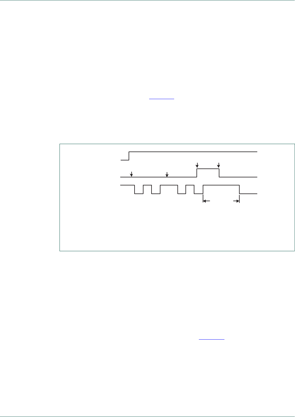
UM10462 All information provided in this document is subject to legal disclaimers. © NXP B.V. 2014. All rights reserved.
User manual Rev. 5.3 — 11 June 2014 322 of 521
NXP Semiconductors UM10462
Chapter 14: LPC11U3x/2x/1x I2C-bus controller
14.10.6.4 I2C-bus obstructed by a LOW level on SCL or SDA
An I2C-bus hang-up can occur if either the SDA or SCL line is held LOW by any device on
the bus. If the SCL line is obstructed (pulled LOW) by a device on the bus, no further serial
transfer is possible, and the problem must be resolved by the device that is pulling the
SCL bus line LOW.
Typically, the SDA line may be obstructed by another device on the bus that has become
out of synchronization with the current bus master by either missing a clock, or by sensing
a noise pulse as a clock. In this case, the problem can be solved by transmitting additional
clock pulses on the SCL line (see Figure 55). The I2C interface does not include a
dedicated time-out timer to detect an obstructed bus, but this can be implemented using
another timer in the system. When detected, software can force clocks (up to 9 may be
required) on SCL until SDA is released by the offending device. At that point, the slave
may still be out of synchronization, so a START should be generated to insure that all I2C
peripherals are synchronized.
14.10.6.5 Bus error
A bus error occurs when a START or STOP condition is detected at an illegal position in
the format frame. Examples of illegal positions are during the serial transfer of an address
byte, a data bit, or an acknowledge bit.
The I2C hardware only reacts to a bus error when it is involved in a serial transfer either as
a master or an addressed slave. When a bus error is detected, the I2C block immediately
switches to the not addressed slave mode, releases the SDA and SCL lines, sets the
interrupt flag, and loads the status register with 0x00. This status code may be used to
vector to a state service routine which either attempts the aborted serial transfer again or
simply recovers from the error condition as shown in Table 293.
14.10.7 I2C state service routines
This section provides examples of operations that must be performed by various I2C state
service routines. This includes:
•Initialization of the I2C block after a Reset.
•I2C Interrupt Service
•The 26 state service routines providing support for all four I2C operating modes.
(1) Unsuccessful attempt to send a START condition.
(2) SDA line is released.
(3) Successful attempt to send a START condition. State 08H is entered.
Fig 55. Recovering from a bus obstruction caused by a LOW level on SDA
SDA line
SCL line
(1)
(2)
(1)
(3)
STA flag
start
condition

UM10462 All information provided in this document is subject to legal disclaimers. © NXP B.V. 2014. All rights reserved.
User manual Rev. 5.3 — 11 June 2014 323 of 521
NXP Semiconductors UM10462
Chapter 14: LPC11U3x/2x/1x I2C-bus controller
14.10.8 Initialization
In the initialization example, the I2C block is enabled for both master and slave modes.
For each mode, a buffer is used for transmission and reception. The initialization routine
performs the following functions:
•ADR is loaded with the part’s own slave address and the General Call bit (GC)
•The I2C interrupt enable and interrupt priority bits are set
•The slave mode is enabled by simultaneously setting the I2EN and AA bits in CON
and the serial clock frequency (for master modes) is defined by is defined by loading
the SCLH and SCLL registers. The master routines must be started in the main program.
The I2C hardware now begins checking the I2C-bus for its own slave address and General
Call. If the General Call or the own slave address is detected, an interrupt is requested
and STAT is loaded with the appropriate state information.
14.10.9 I2C interrupt service
When the I2C interrupt is entered, STAT contains a status code which identifies one of the
26 state services to be executed.
14.10.10 The state service routines
Each state routine is part of the I2C interrupt routine and handles one of the 26 states.
14.10.11 Adapting state services to an application
The state service examples show the typical actions that must be performed in response
to the 26 I2C state codes. If one or more of the four I2C operating modes are not used, the
associated state services can be omitted, as long as care is taken that the those states
can never occur.
In an application, it may be desirable to implement some kind of time-out during I2C
operations, in order to trap an inoperative bus or a lost service routine.
14.11 Software example
14.11.1 Initialization routine
Example to initialize I2C Interface as a Slave and/or Master.
1. Load ADR with own Slave Address, enable General Call recognition if needed.
2. Enable I2C interrupt.
3. Write 0x44 to CONSET to set the I2EN and AA bits, enabling Slave functions. For
Master only functions, write 0x40 to CONSET.
14.11.2 Start Master Transmit function
Begin a Master Transmit operation by setting up the buffer, pointer, and data count, then
initiating a START.
1. Initialize Master data counter.

UM10462 All information provided in this document is subject to legal disclaimers. © NXP B.V. 2014. All rights reserved.
User manual Rev. 5.3 — 11 June 2014 324 of 521
NXP Semiconductors UM10462
Chapter 14: LPC11U3x/2x/1x I2C-bus controller
2. Set up the Slave Address to which data will be transmitted, and add the Write bit.
3. Write 0x20 to CONSET to set the STA bit.
4. Set up data to be transmitted in Master Transmit buffer.
5. Initialize the Master data counter to match the length of the message being sent.
6. Exit
14.11.3 Start Master Receive function
Begin a Master Receive operation by setting up the buffer, pointer, and data count, then
initiating a START.
1. Initialize Master data counter.
2. Set up the Slave Address to which data will be transmitted, and add the Read bit.
3. Write 0x20 to CONSET to set the STA bit.
4. Set up the Master Receive buffer.
5. Initialize the Master data counter to match the length of the message to be received.
6. Exit
14.11.4 I2C interrupt routine
Determine the I2C state and which state routine will be used to handle it.
1. Read the I2C status from STA.
2. Use the status value to branch to one of 26 possible state routines.
14.11.5 Non mode specific states
14.11.5.1 State: 0x00
Bus Error. Enter not addressed Slave mode and release bus.
1. Write 0x14 to CONSET to set the STO and AA bits.
2. Write 0x08 to CONCLR to clear the SI flag.
3. Exit
14.11.5.2 Master States
State 08 and State 10 are for both Master Transmit and Master Receive modes. The R/W
bit decides whether the next state is within Master Transmit mode or Master Receive
mode.
14.11.5.3 State: 0x08
A START condition has been transmitted. The Slave Address + R/W bit will be
transmitted, an ACK bit will be received.
1. Write Slave Address with R/W bit to DAT.
2. Write 0x04 to CONSET to set the AA bit.
3. Write 0x08 to CONCLR to clear the SI flag.
4. Set up Master Transmit mode data buffer.

UM10462 All information provided in this document is subject to legal disclaimers. © NXP B.V. 2014. All rights reserved.
User manual Rev. 5.3 — 11 June 2014 325 of 521
NXP Semiconductors UM10462
Chapter 14: LPC11U3x/2x/1x I2C-bus controller
5. Set up Master Receive mode data buffer.
6. Initialize Master data counter.
7. Exit
14.11.5.4 State: 0x10
A Repeated START condition has been transmitted. The Slave Address + R/W bit will be
transmitted, an ACK bit will be received.
1. Write Slave Address with R/W bit to DAT.
2. Write 0x04 to CONSET to set the AA bit.
3. Write 0x08 to CONCLR to clear the SI flag.
4. Set up Master Transmit mode data buffer.
5. Set up Master Receive mode data buffer.
6. Initialize Master data counter.
7. Exit
14.11.6 Master Transmitter states
14.11.6.1 State: 0x18
Previous state was State 8 or State 10, Slave Address + Write has been transmitted, ACK
has been received. The first data byte will be transmitted, an ACK bit will be received.
1. Load DAT with first data byte from Master Transmit buffer.
2. Write 0x04 to CONSET to set the AA bit.
3. Write 0x08 to CONCLR to clear the SI flag.
4. Increment Master Transmit buffer pointer.
5. Exit
14.11.6.2 State: 0x20
Slave Address + Write has been transmitted, NOT ACK has been received. A STOP
condition will be transmitted.
1. Write 0x14 to CONSET to set the STO and AA bits.
2. Write 0x08 to CONCLR to clear the SI flag.
3. Exit
14.11.6.3 State: 0x28
Data has been transmitted, ACK has been received. If the transmitted data was the last
data byte then transmit a STOP condition, otherwise transmit the next data byte.
1. Decrement the Master data counter, skip to step 5 if not the last data byte.
2. Write 0x14 to CONSET to set the STO and AA bits.
3. Write 0x08 to CONCLR to clear the SI flag.
4. Exit
5. Load DAT with next data byte from Master Transmit buffer.

UM10462 All information provided in this document is subject to legal disclaimers. © NXP B.V. 2014. All rights reserved.
User manual Rev. 5.3 — 11 June 2014 326 of 521
NXP Semiconductors UM10462
Chapter 14: LPC11U3x/2x/1x I2C-bus controller
6. Write 0x04 to CONSET to set the AA bit.
7. Write 0x08 to CONCLR to clear the SI flag.
8. Increment Master Transmit buffer pointer
9. Exit
14.11.6.4 State: 0x30
Data has been transmitted, NOT ACK received. A STOP condition will be transmitted.
1. Write 0x14 to CONSET to set the STO and AA bits.
2. Write 0x08 to CONCLR to clear the SI flag.
3. Exit
14.11.6.5 State: 0x38
Arbitration has been lost during Slave Address + Write or data. The bus has been
released and not addressed Slave mode is entered. A new START condition will be
transmitted when the bus is free again.
1. Write 0x24 to CONSET to set the STA and AA bits.
2. Write 0x08 to CONCLR to clear the SI flag.
3. Exit
14.11.7 Master Receive states
14.11.7.1 State: 0x40
Previous state was State 08 or State 10. Slave Address + Read has been transmitted,
ACK has been received. Data will be received and ACK returned.
1. Write 0x04 to CONSET to set the AA bit.
2. Write 0x08 to CONCLR to clear the SI flag.
3. Exit
14.11.7.2 State: 0x48
Slave Address + Read has been transmitted, NOT ACK has been received. A STOP
condition will be transmitted.
1. Write 0x14 to CONSET to set the STO and AA bits.
2. Write 0x08 to CONCLR to clear the SI flag.
3. Exit
14.11.7.3 State: 0x50
Data has been received, ACK has been returned. Data will be read from DAT. Additional
data will be received. If this is the last data byte then NOT ACK will be returned, otherwise
ACK will be returned.
1. Read data byte from DAT into Master Receive buffer.
2. Decrement the Master data counter, skip to step 5 if not the last data byte.
3. Write 0x0C to CONCLR to clear the SI flag and the AA bit.

UM10462 All information provided in this document is subject to legal disclaimers. © NXP B.V. 2014. All rights reserved.
User manual Rev. 5.3 — 11 June 2014 327 of 521
NXP Semiconductors UM10462
Chapter 14: LPC11U3x/2x/1x I2C-bus controller
4. Exit
5. Write 0x04 to CONSET to set the AA bit.
6. Write 0x08 to CONCLR to clear the SI flag.
7. Increment Master Receive buffer pointer
8. Exit
14.11.7.4 State: 0x58
Data has been received, NOT ACK has been returned. Data will be read from DAT. A
STOP condition will be transmitted.
1. Read data byte from DAT into Master Receive buffer.
2. Write 0x14 to CONSET to set the STO and AA bits.
3. Write 0x08 to CONCLR to clear the SI flag.
4. Exit
14.11.8 Slave Receiver states
14.11.8.1 State: 0x60
Own Slave Address + Write has been received, ACK has been returned. Data will be
received and ACK returned.
1. Write 0x04 to CONSET to set the AA bit.
2. Write 0x08 to CONCLR to clear the SI flag.
3. Set up Slave Receive mode data buffer.
4. Initialize Slave data counter.
5. Exit
14.11.8.2 State: 0x68
Arbitration has been lost in Slave Address and R/W bit as bus Master. Own Slave Address
+ Write has been received, ACK has been returned. Data will be received and ACK will be
returned. STA is set to restart Master mode after the bus is free again.
1. Write 0x24 to CONSET to set the STA and AA bits.
2. Write 0x08 to CONCLR to clear the SI flag.
3. Set up Slave Receive mode data buffer.
4. Initialize Slave data counter.
5. Exit.
14.11.8.3 State: 0x70
General call has been received, ACK has been returned. Data will be received and ACK
returned.
1. Write 0x04 to CONSET to set the AA bit.
2. Write 0x08 to CONCLR to clear the SI flag.
3. Set up Slave Receive mode data buffer.

UM10462 All information provided in this document is subject to legal disclaimers. © NXP B.V. 2014. All rights reserved.
User manual Rev. 5.3 — 11 June 2014 328 of 521
NXP Semiconductors UM10462
Chapter 14: LPC11U3x/2x/1x I2C-bus controller
4. Initialize Slave data counter.
5. Exit
14.11.8.4 State: 0x78
Arbitration has been lost in Slave Address + R/W bit as bus Master. General call has been
received and ACK has been returned. Data will be received and ACK returned. STA is set
to restart Master mode after the bus is free again.
1. Write 0x24 to CONSET to set the STA and AA bits.
2. Write 0x08 to CONCLR to clear the SI flag.
3. Set up Slave Receive mode data buffer.
4. Initialize Slave data counter.
5. Exit
14.11.8.5 State: 0x80
Previously addressed with own Slave Address. Data has been received and ACK has
been returned. Additional data will be read.
1. Read data byte from DAT into the Slave Receive buffer.
2. Decrement the Slave data counter, skip to step 5 if not the last data byte.
3. Write 0x0C to CONCLR to clear the SI flag and the AA bit.
4. Exit.
5. Write 0x04 to CONSET to set the AA bit.
6. Write 0x08 to CONCLR to clear the SI flag.
7. Increment Slave Receive buffer pointer.
8. Exit
14.11.8.6 State: 0x88
Previously addressed with own Slave Address. Data has been received and NOT ACK
has been returned. Received data will not be saved. Not addressed Slave mode is
entered.
1. Write 0x04 to CONSET to set the AA bit.
2. Write 0x08 to CONCLR to clear the SI flag.
3. Exit
14.11.8.7 State: 0x90
Previously addressed with General Call. Data has been received, ACK has been returned.
Received data will be saved. Only the first data byte will be received with ACK. Additional
data will be received with NOT ACK.
1. Read data byte from DAT into the Slave Receive buffer.
2. Write 0x0C to CONCLR to clear the SI flag and the AA bit.
3. Exit

UM10462 All information provided in this document is subject to legal disclaimers. © NXP B.V. 2014. All rights reserved.
User manual Rev. 5.3 — 11 June 2014 329 of 521
NXP Semiconductors UM10462
Chapter 14: LPC11U3x/2x/1x I2C-bus controller
14.11.8.8 State: 0x98
Previously addressed with General Call. Data has been received, NOT ACK has been
returned. Received data will not be saved. Not addressed Slave mode is entered.
1. Write 0x04 to CONSET to set the AA bit.
2. Write 0x08 to CONCLR to clear the SI flag.
3. Exit
14.11.8.9 State: 0xA0
A STOP condition or Repeated START has been received, while still addressed as a
Slave. Data will not be saved. Not addressed Slave mode is entered.
1. Write 0x04 to CONSET to set the AA bit.
2. Write 0x08 to CONCLR to clear the SI flag.
3. Exit
14.11.9 Slave Transmitter states
14.11.9.1 State: 0xA8
Own Slave Address + Read has been received, ACK has been returned. Data will be
transmitted, ACK bit will be received.
1. Load DAT from Slave Transmit buffer with first data byte.
2. Write 0x04 to CONSET to set the AA bit.
3. Write 0x08 to CONCLR to clear the SI flag.
4. Set up Slave Transmit mode data buffer.
5. Increment Slave Transmit buffer pointer.
6. Exit
14.11.9.2 State: 0xB0
Arbitration lost in Slave Address and R/W bit as bus Master. Own Slave Address + Read
has been received, ACK has been returned. Data will be transmitted, ACK bit will be
received. STA is set to restart Master mode after the bus is free again.
1. Load DAT from Slave Transmit buffer with first data byte.
2. Write 0x24 to CONSET to set the STA and AA bits.
3. Write 0x08 to CONCLR to clear the SI flag.
4. Set up Slave Transmit mode data buffer.
5. Increment Slave Transmit buffer pointer.
6. Exit
14.11.9.3 State: 0xB8
Data has been transmitted, ACK has been received. Data will be transmitted, ACK bit will
be received.
1. Load DAT from Slave Transmit buffer with data byte.

UM10462 All information provided in this document is subject to legal disclaimers. © NXP B.V. 2014. All rights reserved.
User manual Rev. 5.3 — 11 June 2014 330 of 521
NXP Semiconductors UM10462
Chapter 14: LPC11U3x/2x/1x I2C-bus controller
2. Write 0x04 to CONSET to set the AA bit.
3. Write 0x08 to CONCLR to clear the SI flag.
4. Increment Slave Transmit buffer pointer.
5. Exit
14.11.9.4 State: 0xC0
Data has been transmitted, NOT ACK has been received. Not addressed Slave mode is
entered.
1. Write 0x04 to CONSET to set the AA bit.
2. Write 0x08 to CONCLR to clear the SI flag.
3. Exit.
14.11.9.5 State: 0xC8
The last data byte has been transmitted, ACK has been received. Not addressed Slave
mode is entered.
1. Write 0x04 to CONSET to set the AA bit.
2. Write 0x08 to CONCLR to clear the SI flag.
3. Exit

UM10462 All information provided in this document is subject to legal disclaimers. © NXP B.V. 2014. All rights reserved.
User manual Rev. 5.3 — 11 June 2014 331 of 521
15.1 How to read this chapter
CT16B0/1 are available on all LPC11U3x/2x/1x parts. The number of capture inputs
depends on package size. See Chapter 8.
15.2 Basic configuration
The CT16B0/1 counter/timers are configured through the following registers:
•Pins: The CT16B0/1 pins must be configured in the IOCON register block.
•Power: In the SYSAHBCLKCTRL register, set bit 7 and 8 in Table 24.
•The peripheral clock is determined by the system clock (see Table 23).
Remark: The register offsets and bit offsets for capture channel 1 are different on timers
CT16B0 and CT16B1. The affected registers are:
•Section 15.7.1 “Interrupt Register”
•Section 15.7.8 “Capture Control Register”
•Section 15.7.9 “Capture Registers”
•Section 15.7.11 “Count Control Register”
15.3 Features
•Two 16-bit counter/timers with a programmable 16-bit prescaler.
•Counter or timer operation
•Two 16-bit capture channels that can take a snapshot of the timer value when an input
signal transitions. A capture event may also optionally generate an interrupt.
•The timer and prescaler may be configured to be cleared on a designated capture
event. This feature permits easy pulse-width measurement by clearing the timer on
the leading edge of an input pulse and capturing the timer value on the trailing edge.
•Four 16-bit match registers that allow:
–Continuous operation with optional interrupt generation on match.
–Stop timer on match with optional interrupt generation.
–Reset timer on match with optional interrupt generation.
•Two external outputs corresponding to match registers with the following capabilities:
–Set LOW on match.
–Set HIGH on match.
–Toggle on match.
–Do nothing on match.
•For each timer, up to four match registers can be configured as PWM allowing to use
up to two match outputs as single edge controlled PWM outputs.
UM10462
Chapter 15: LPC11U3x/2x/1x 16-bit counter/timers CT16B0/1
Rev. 5.3 — 11 June 2014 User manual

UM10462 All information provided in this document is subject to legal disclaimers. © NXP B.V. 2014. All rights reserved.
User manual Rev. 5.3 — 11 June 2014 332 of 521
NXP Semiconductors UM10462
Chapter 15: LPC11U3x/2x/1x 16-bit counter/timers CT16B0/1
15.4 Applications
•Interval timer for counting internal events
•Pulse Width Demodulator via capture input
•Free running timer
•Pulse Width Modulator via match outputs
15.5 General description
Each Counter/timer is designed to count cycles of the peripheral clock (PCLK) or an
externally supplied clock and can optionally generate interrupts or perform other actions at
specified timer values based on four match registers. Each counter/timer also includes
one capture input to trap the timer value when an input signal transitions, optionally
generating an interrupt.
In PWM mode, two match registers can be used to provide a single-edge controlled PWM
output on the match output pins. It is recommended to use the match registers that are not
pinned out to control the PWM cycle length.
15.6 Pin description
Table 294 gives a brief summary of each of the counter/timer related pins.
15.7 Register description
The 16-bit counter/timer0 contains the registers shown in Table 295 and the 16-bit
counter/timer1 contains the registers shown in Table 296. More detailed descriptions
follow.
Table 294. Counter/timer pin description
Pin Type Description
CT16B0_CAP[1:0]
CT16B1_CAP[1:0]
Input Capture Signal:
A transition on a capture pin can be configured to load the
Capture Register with the value in the counter/timer and
optionally generate an interrupt.
The Counter/Timer block can select a capture signal as a clock
source instead of the PCLK derived clock. For more details see
Section 15.7.11.
CT16B0_MAT[2:0]
CT16B1_MAT[1:0]
Output External Match Outputs of CT16B0/1:
When a match register of CT16B0/1 (MR1:0) equals the timer
counter (TC), this output can either toggle, go LOW, go HIGH, or
do nothing. The External Match Register (EMR) and the PWM
Control Register (PWMCON) control the functionality of this
output.

UM10462 All information provided in this document is subject to legal disclaimers. © NXP B.V. 2014. All rights reserved.
User manual Rev. 5.3 — 11 June 2014 333 of 521
NXP Semiconductors UM10462
Chapter 15: LPC11U3x/2x/1x 16-bit counter/timers CT16B0/1
[1] Reset value reflects the data stored in used bits only. It does not include reserved bits content.
Table 295. Register overview: 16-bit counter/timer 0 CT16B0 (base address 0x4000 C000)
Name Access Address
offset Description Reset
value[1] Reference
IR R/W 0x000 Interrupt Register. The IR can be written to clear interrupts. The IR can
be read to identify which of eight possible interrupt sources are
pending.
0Table 297
TCR R/W 0x004 Timer Control Register. The TCR is used to control the Timer Counter
functions. The Timer Counter can be disabled or reset through the
TCR.
0Table 299
TC R/W 0x008 Timer Counter. The 16-bit TC is incremented every PR+1 cycles of
PCLK. The TC is controlled through the TCR.
0Table 300
PR R/W 0x00C Prescale Register. When the Prescale Counter (below) is equal to this
value, the next clock increments the TC and clears the PC.
0Table 301
PC R/W 0x010 Prescale Counter. The 16-bit PC is a counter which is incremented to
the value stored in PR. When the value in PR is reached, the TC is
incremented and the PC is cleared. The PC is observable and
controllable through the bus interface.
0Table 302
MCR R/W 0x014 Match Control Register. The MCR is used to control if an interrupt is
generated and if the TC is reset when a Match occurs.
0Table 303
MR0 R/W 0x018 Match Register 0. MR0 can be enabled through the MCR to reset the
TC, stop both the TC and PC, and/or generate an interrupt every time
MR0 matches the TC.
0Table 304
MR1 R/W 0x01C Match Register 1. See MR0 description. 0 Table 304
MR2 R/W 0x020 Match Register 2. See MR0 description. 0 Table 304
MR3 R/W 0x024 Match Register 3. See MR0 description. 0 Table 304
CCR R/W 0x028 Capture Control Register. The CCR controls which edges of the
capture inputs are used to load the Capture Registers and whether or
not an interrupt is generated when a capture takes place.
0Table 305
CR0 RO 0x02C Capture Register 0. CR0 is loaded with the value of TC when there is
an event on the CT16B0_CAP0 input.
0Table 307
- - 0x030 Reserved. - -
CR1 RO 0x034 Capture Register 1. CR1 is loaded with the value of TC when there is
an event on the CT16B0_CAP1 input.
-Table 308
- - 0x038 Reserved. - -
EMR R/W 0x03C External Match Register. The EMR controls the match function and
the external match pins CT16B0_MAT[1:0] and CT16B1_MAT[1:0].
0Table 310
- - 0x040 -
0x06C
Reserved. - -
CTCR R/W 0x070 Count Control Register. The CTCR selects between Timer and
Counter mode, and in Counter mode selects the signal and edge(s)
for counting.
0Table 313
PWMC R/W 0x074 PWM Control Register. The PWMCON enables PWM mode for the
external match pins CT16B0_MAT[1:0] and CT16B1_MAT[1:0].
0Table 314

UM10462 All information provided in this document is subject to legal disclaimers. © NXP B.V. 2014. All rights reserved.
User manual Rev. 5.3 — 11 June 2014 334 of 521
NXP Semiconductors UM10462
Chapter 15: LPC11U3x/2x/1x 16-bit counter/timers CT16B0/1
Table 296. Register overview: 16-bit counter/timer 1 CT16B1 (base address 0x4001 0000)
Name Access Address Description Reset
value[1] Reference
IR R/W 0x000 Interrupt Register. The IR can be written to clear interrupts. The IR
can be read to identify which of eight possible interrupt sources
are pending.
0Table 297
TCR R/W 0x004 Timer Control Register. The TCR is used to control the Timer
Counter functions. The Timer Counter can be disabled or reset
through the TCR.
0Table 299
TC R/W 0x008 Timer Counter. The 16-bit TC is incremented every PR+1 cycles of
PCLK. The TC is controlled through the TCR.
0Table 300
PR R/W 0x00C Prescale Register. When the Prescale Counter (below) is equal to
this value, the next clock increments the TC and clears the PC.
0Table 301
PC R/W 0x010 Prescale Counter. The 16-bit PC is a counter which is incremented
to the value stored in PR. When the value in PR is reached, the TC
is incremented and the PC is cleared. The PC is observable and
controllable through the bus interface.
0Table 302
MCR R/W 0x014 Match Control Register. The MCR is used to control if an interrupt
is generated and if the TC is reset when a Match occurs.
0Table 303
MR0 R/W 0x018 Match Register 0. MR0 can be enabled through the MCR to reset
the TC, stop both the TC and PC, and/or generate an interrupt
every time MR0 matches the TC.
0Table 304
MR1 R/W 0x01C Match Register 1. See MR0 description. 0 Table 304
MR2 R/W 0x020 Match Register 2. See MR0 description. 0 Table 304
MR3 R/W 0x024 Match Register 3. See MR0 description. 0 Table 304
CCR R/W 0x028 Capture Control Register. The CCR controls which edges of the
capture inputs are used to load the Capture Registers and whether
or not an interrupt is generated when a capture takes place.
0Table 305
CR0 RO 0x02C Capture Register 0. CR0 is loaded with the value of TC when there
is an event on the CT16B1_CAP0 input.
0Table 307
CR1 RO 0x030 Capture Register 1. CR1 is loaded with the value of TC when there
is an event on the CT16B1_CAP1 input.
0Table 309
- - 0x034 Reserved. - -
- - 0x038 Reserved. - -
EMR R/W 0x03C External Match Register. The EMR controls the match function
and the external match pins CT16B0_MAT[2:0] and
CT16B1_MAT[1:0].
0Table 310
- - 0x040 -
0x06C
Reserved. - -
CTCR R/W 0x070 Count Control Register. The CTCR selects between Timer and
Counter mode, and in Counter mode selects the signal and
edge(s) for counting.
0Table 312
PWMC R/W 0x074 PWM Control Register. The PWMCON enables PWM mode for
the external match pins CT16B0_MAT[1:0] and
CT16B1_MAT[1:0].
0Table 314

UM10462 All information provided in this document is subject to legal disclaimers. © NXP B.V. 2014. All rights reserved.
User manual Rev. 5.3 — 11 June 2014 335 of 521
NXP Semiconductors UM10462
Chapter 15: LPC11U3x/2x/1x 16-bit counter/timers CT16B0/1
[1] Reset value reflects the data stored in used bits only. It does not include reserved bits content.
15.7.1 Interrupt Register
The Interrupt Register consists of four bits for the match interrupts and two bits for the
capture interrupts. If an interrupt is generated then the corresponding bit in the IR will be
HIGH. Otherwise, the bit will be LOW. Writing a logic one to the corresponding IR bit will
reset the interrupt. Writing a zero has no effect.
Remark: The bit positions for the CAP1 interrupts are different for counter/timer CT16B0
(CAP1 interrupt on bit 6, Table 297) and counter/timer CT16B1 (CAP1 interrupt on bit 5,
Table 298).
15.7.2 Timer Control Register
The Timer Control Register (TCR) is used to control the operation of the counter/timer.
Table 297. Interrupt Register (IR, address 0x4000 C000 (CT16B0)) bit description
Bit Symbol Description Reset value
0 MR0INT Interrupt flag for match channel 0. 0
1 MR1INT Interrupt flag for match channel 1. 0
2 MR2INT Interrupt flag for match channel 2. 0
3 MR3INT Interrupt flag for match channel 3. 0
4 CR0INT Interrupt flag for capture channel 0 event. 0
5 - Reserved. -
6 CR1INT Interrupt flag for capture channel 1 event. 0
31:7 - Reserved -
Table 298. Interrupt Register (IR, address 0x4001 0000 (CT16B1)) bit description
Bit Symbol Description Reset value
0 MR0INT Interrupt flag for match channel 0. 0
1 MR1INT Interrupt flag for match channel 1. 0
2 MR2INT Interrupt flag for match channel 2. 0
3 MR3INT Interrupt flag for match channel 3. 0
4 CR0INT Interrupt flag for capture channel 0 event. 0
5 CR1INT Interrupt flag for capture channel 1 event. 0
6 - Reserved. -
31:7 - Reserved -
Table 299. Timer Control Register (TCR, address 0x4000 C004 (CT16B0) and 0x4001 0004
(CT16B1)) bit description
Bit Symbol Value Description Reset
value
0 CEN Counter enable. 0
0 The counters are disabled.
1 The Timer Counter and Prescale Counter are enabled for
counting.

UM10462 All information provided in this document is subject to legal disclaimers. © NXP B.V. 2014. All rights reserved.
User manual Rev. 5.3 — 11 June 2014 336 of 521
NXP Semiconductors UM10462
Chapter 15: LPC11U3x/2x/1x 16-bit counter/timers CT16B0/1
15.7.3 Timer Counter
The 16-bit Timer Counter is incremented when the Prescale Counter reaches its terminal
count. Unless it is reset before reaching its upper limit, the TC will count up to the value
0x0000 FFFF and then wrap back to the value 0x0000 0000. This event does not cause
an interrupt, but a Match register can be used to detect an overflow if needed.
15.7.4 Prescale Register
The 16-bit Prescale Register specifies the maximum value for the Prescale Counter.
15.7.5 Prescale Counter register
The 16-bit Prescale Counter controls division of PCLK by some constant value before it is
applied to the Timer Counter. This allows control of the relationship between the resolution
of the timer and the maximum time before the timer overflows. The Prescale Counter is
incremented on every PCLK. When it reaches the value stored in the Prescale Register,
the Timer Counter is incremented, and the Prescale Counter is reset on the next PCLK.
This causes the TC to increment on every PCLK when PR = 0, every 2 PCLKs when
PR = 1, ...
1 CRST Counter reset. 0
0 Do nothing.
1 The Timer Counter and the Prescale Counter are
synchronously reset on the next positive edge of PCLK. The
counters remain reset until TCR[1] is returned to zero.
31:
2
- Reserved, user software should not write ones to reserved bits.
The value read from a reserved bit is not defined.
NA
Table 299. Timer Control Register (TCR, address 0x4000 C004 (CT16B0) and 0x4001 0004
(CT16B1)) bit description
Bit Symbol Value Description Reset
value
Table 300: Timer counter registers (TC, address 0x4000 C008 (CT16B0) and 0x4001 0008
(CT16B1)) bit description
Bit Symbol Description Reset
value
15:0 TC Timer counter value. 0
31:16 - Reserved. -
Table 301: Prescale registers (PR, address 0x4000 C00C (CT16B0) and 0x4001 000C
(CT16B1)) bit description
Bit Symbol Description Reset
value
15:0 PCVAL Prescale value. 0
31:16 - Reserved. -

UM10462 All information provided in this document is subject to legal disclaimers. © NXP B.V. 2014. All rights reserved.
User manual Rev. 5.3 — 11 June 2014 337 of 521
NXP Semiconductors UM10462
Chapter 15: LPC11U3x/2x/1x 16-bit counter/timers CT16B0/1
15.7.6 Match Control Register
The Match Control Register is used to control what operations are performed when one of
the Match Registers matches the Timer Counter. The function of each of the bits is shown
in Table 303.
Table 302: Prescale counter registers (PC, address 0x4000 C010 (CT16B0) and 0x4001 0010
(CT16B1)) bit description
Bit Symbol Description Reset
value
15:0 PC Prescale counter value. 0
31:16 - Reserved. -
Table 303. Match Control Register (MCR, address 0x4000 C014 (CT16B0) and 0x4001 0014 (CT16B1)) bit description
Bit Symbol Value Description Reset
value
0 MR0I Interrupt on MR0: an interrupt is generated when MR0 matches the value in the TC. 0
1 Enabled
0 Disabled
1 MR0R Reset on MR0: the TC will be reset if MR0 matches it. 0
1 Enabled
0 Disabled
2 MR0S Stop on MR0: the TC and PC will be stopped and TCR[0] will be set to 0 if MR0 matches
the TC.
0
1 Enabled
0 Disabled
3 MR1I Interrupt on MR1: an interrupt is generated when MR1 matches the value in the TC. 0
1 Enabled
0 Disabled
4 MR1R Reset on MR1: the TC will be reset if MR1 matches it. 0
1 Enabled
0 Disabled
5 MR1S Stop on MR1: the TC and PC will be stopped and TCR[0] will be set to 0 if MR1 matches
the TC.
0
1 Enabled
0 Disabled
6 MR2I Interrupt on MR2: an interrupt is generated when MR2 matches the value in the TC. 0
1 Enabled
0 Disabled
7 MR2R Reset on MR2: the TC will be reset if MR2 matches it. 0
1 Enabled
0 Disabled

UM10462 All information provided in this document is subject to legal disclaimers. © NXP B.V. 2014. All rights reserved.
User manual Rev. 5.3 — 11 June 2014 338 of 521
NXP Semiconductors UM10462
Chapter 15: LPC11U3x/2x/1x 16-bit counter/timers CT16B0/1
15.7.7 Match Registers
The Match register values are continuously compared to the Timer Counter value. When
the two values are equal, actions can be triggered automatically. The action possibilities
are to generate an interrupt, reset the Timer Counter, or stop the timer. Actions are
controlled by the settings in the MCR register.
15.7.8 Capture Control Register
The Capture Control Register is used to control whether the Capture Register is loaded
with the value in the Counter/timer when the capture event occurs, and whether an
interrupt is generated by the capture event. Setting both the rising and falling bits at the
same time is a valid configuration, resulting in a capture event for both edges. In the
description below, n represents the Timer number, 0 or 1.
Remark: The bit positions for the CAP1 channel control bits are different for
counter/timers CT16B0 (bits 8:6, Table 305) and CT16B1 (bits 5:3, Table 306).
8 MR2S Stop on MR2: the TC and PC will be stopped and TCR[0] will be set to 0 if MR2 matches
the TC.
0
1 Enabled
0 Disabled
9 MR3I Interrupt on MR3: an interrupt is generated when MR3 matches the value in the TC. 0
1 Enabled
0 Disabled
10 MR3R Reset on MR3: the TC will be reset if MR3 matches it. 0
1 Enabled
0 Disabled
11 MR3S Stop on MR3: the TC and PC will be stopped and TCR[0] will be set to 0 if MR3 matches
the TC.
0
1 Enabled
0 Disabled
31:12 - Reserved, user software should not write ones to reserved bits. The value read from a
reserved bit is not defined.
NA
Table 303. Match Control Register (MCR, address 0x4000 C014 (CT16B0) and 0x4001 0014 (CT16B1)) bit description
…continued
Bit Symbol Value Description Reset
value
Table 304: Match registers (MR[0:3], addresses 0x4000 C018 (MR0) to 0x4000 C024 (MR3)
(CT16B0) and 0x4001 0018 (MR0) to 0x4001 0024 (MR3) (CT16B1)) bit description
Bit Symbol Description Reset
value
15:0 MATCH Timer counter match value. 0
31:16 - Reserved. -

UM10462 All information provided in this document is subject to legal disclaimers. © NXP B.V. 2014. All rights reserved.
User manual Rev. 5.3 — 11 June 2014 339 of 521
NXP Semiconductors UM10462
Chapter 15: LPC11U3x/2x/1x 16-bit counter/timers CT16B0/1
Table 305. Capture Control Register (CCR, address 0x4000 C028 (CT16B0)) bit description
Bit Symbol Value Description Reset
value
0 CAP0RE Capture on CT16B0_CAP0 rising edge: a sequence of 0 then 1 on CT16B0_CAP0 will
cause CR0 to be loaded with the contents of TC.
0
1 Enabled.
0 Disabled.
1 CAP0FE Capture on CT16B0_CAP0 falling edge: a sequence of 1 then 0 on CT16B0_CAP0 will
cause CR0 to be loaded with the contents of TC.
0
1 Enabled.
0 Disabled.
2 CAP0I Interrupt on CT16B0_CAP0 event: a CR0 load due to a CT16B0_CAP0 event will
generate an interrupt.
0
1 Enabled.
0 Disabled.
3- Reserved. -
4- Reserved. -
5- Reserved. -
6 CAP1RE Capture on CT16B0_CAP1 rising edge: a sequence of 0 then 1 on CT16B0_CAP1 will
cause CR1 to be loaded with the contents of TC. This bit is reserved for 16-bit timer1
CT16B1.
0
1 Enabled.
0 Disabled.
7 CAP1FE Capture on CT16B0_CAP1 falling edge: a sequence of 1 then 0 on CT16B0_CAP1 will
cause CR1 to be loaded with the contents of TC. This bit is reserved for 16-bit timer1
CT16B1.
0
1 Enabled.
0 Disabled.
8 CAP1I Interrupt on CT16B0_CAP1 event: a CR1 load due to a CT16B0_CAP1 event will
generate an interrupt. This bit is reserved for 16-bit timer1 CT16B1.
0
1 Enabled.
0 Disabled.
31:9 - - Reserved, user software should not write ones to reserved bits. The value read from a
reserved bit is not defined.
NA
Table 306. Capture Control Register (CCR, address 0x4001 0028 (CT16B1)) bit description
Bit Symbol Value Description Reset
value
0 CAP0RE Capture on CT16B1_CAP0 rising edge: a sequence of 0 then 1 on CT16B1_CAP0 will
cause CR0 to be loaded with the contents of TC.
0
1 Enabled.
0 Disabled.
1 CAP0FE Capture on CT16B11_CAP0 falling edge: a sequence of 1 then 0 on CT16B1_CAP0 will
cause CR0 to be loaded with the contents of TC.
0
1 Enabled.
0 Disabled.

UM10462 All information provided in this document is subject to legal disclaimers. © NXP B.V. 2014. All rights reserved.
User manual Rev. 5.3 — 11 June 2014 340 of 521
NXP Semiconductors UM10462
Chapter 15: LPC11U3x/2x/1x 16-bit counter/timers CT16B0/1
15.7.9 Capture Registers
Each Capture register is associated with a device pin and may be loaded with the
counter/timer value when a specified event occurs on that pin. The settings in the Capture
Control Register register determine whether the capture function is enabled, and whether
a capture event happens on the rising edge of the associated pin, the falling edge, or on
both edges.
Remark: The location of the CR1 register relative to the timer base address is different for
CT16B0 (CR1 at +0x034, Table 308) and CT16B1 (CR1 at +0x030, Table 309).
2 CAP0I Interrupt on CT16B1_CAP0 event: a CR0 load due to a CT16B1_CAP0 event will
generate an interrupt.
0
1 Enabled.
0 Disabled.
3 CAP1RE Capture on CT16B1_CAP1 rising edge: a sequence of 0 then 1 on CT16B1_CAP1 will
cause CR1 to be loaded with the contents of TC.
0
1 Enabled.
0 Disabled.
4 CAP1FE Capture on CT16B1_CAP1 falling edge: a sequence of 1 then 0 on CT16B1_CAP1 will
cause CR1 to be loaded with the contents of TC.
0
1 Enabled.
0 Disabled.
5 CAP1I Interrupt on CT16B1_CAP1 event: a CR1 load due to a CT16B0_CAP1 event will
generate an interrupt.
0
1 Enabled.
0 Disabled.
31:6 - - Reserved, user software should not write ones to reserved bits. The value read from a
reserved bit is not defined.
NA
Table 306. Capture Control Register (CCR, address 0x4001 0028 (CT16B1)) bit description
Bit Symbol Value Description Reset
value
Table 307: Capture register 0 (CR0, address 0x4000 C02C (CT16B0) and address 0x4001
002C (CT16B1)) bit description
Bit Symbol Description Reset
value
15:0 CAP Timer counter capture value. 0
31:16 - Reserved. -
Table 308: Capture register 1 (CR1, address 0x4000 C034 (CT16B0)) bit description
Bit Symbol Description Reset
value
15:0 CAP Timer counter capture value. 0
31:16 - Reserved. -

UM10462 All information provided in this document is subject to legal disclaimers. © NXP B.V. 2014. All rights reserved.
User manual Rev. 5.3 — 11 June 2014 341 of 521
NXP Semiconductors UM10462
Chapter 15: LPC11U3x/2x/1x 16-bit counter/timers CT16B0/1
15.7.10 External Match Register
The External Match Register provides both control and status of the external match pins
CT16Bn_MAT[1:0].
If the match outputs are configured as PWM output, the function of the external match
registers is determined by the PWM rules (Section 15.7.13 “Rules for single edge
controlled PWM outputs” on page 346).
Table 309: Capture register 1 (CR1, address 0x4001 0030 (CT16B1)) bit description
Bit Symbol Description Reset
value
15:0 CAP Timer counter capture value. 0
31:16 - Reserved. -
Table 310. External Match Register (EMR, address 0x4000 C03C (CT16B0) and 0x4001 003C (CT16B1)) bit
description
Bit Symbol Value Description Reset
value
0 EM0 External Match 0. This bit reflects the state of output CT16B0_MAT0/CT16B1_MAT0,
whether or not this output is connected to its pin. When a match occurs between the TC
and MR0, this bit can either toggle, go LOW, go HIGH, or do nothing. Bits EMR[5:4]
control the functionality of this output. This bit is driven to the
CT16B0_MAT0/CT16B1_MAT0 pins if the match function is selected in the IOCON
registers (0 = LOW, 1 = HIGH).
0
1 EM1 External Match 1. This bit reflects the state of output CT16B0_MAT1/CT16B1_MAT1,
whether or not this output is connected to its pin. When a match occurs between the TC
and MR1, this bit can either toggle, go LOW, go HIGH, or do nothing. Bits EMR[7:6]
control the functionality of this output. This bit is driven to the
CT16B0_MAT0/CT16B1_MAT0 pins if the match function is selected in the IOCON
registers (0 = LOW, 1 = HIGH).
0
2 EM2 External Match 2. This bit reflects the state of match channel 2. When a match occurs
between the TC and MR2, this bit can either toggle, go LOW, go HIGH, or do nothing.
Bits EMR[9:8] control the functionality of this output.
0
3 EM3 External Match 3. This bit reflects the state of output of match channel 3. When a match
occurs between the TC and MR3, this bit can either toggle, go LOW, go HIGH, or do
nothing. Bits EMR[11:10] control the functionality of this output.
0
5:4 EMC0 External Match Control 0. Determines the functionality of External Match 0. Table 311
shows the encoding of these bits.
00
0x0 Do Nothing.
0x1 Clear the corresponding External Match bit/output to 0 (CT16Bn_MAT0 pin is LOW if
pinned out).
0x2 Set the corresponding External Match bit/output to 1 (CT16Bn_MAT0 pin is HIGH if
pinned out).
0x3 Toggle the corresponding External Match bit/output.

UM10462 All information provided in this document is subject to legal disclaimers. © NXP B.V. 2014. All rights reserved.
User manual Rev. 5.3 — 11 June 2014 342 of 521
NXP Semiconductors UM10462
Chapter 15: LPC11U3x/2x/1x 16-bit counter/timers CT16B0/1
15.7.11 Count Control Register
The Count Control Register (CTCR) is used to select between Timer and Counter mode,
and in Counter mode to select the pin and edges for counting.
When Counter Mode is chosen as a mode of operation, the CAP input (selected by the
CTCR bits 3:2) is sampled on every rising edge of the PCLK clock. After comparing two
consecutive samples of this CAP input, one of the following four events is recognized:
rising edge, falling edge, either of edges or no changes in the level of the selected CAP
input. Only if the identified event occurs, and the event corresponds to the one selected by
bits 1:0 in the CTCR register, will the Timer Counter register be incremented.
7:6 EMC1 External Match Control 1. Determines the functionality of External Match 1. 00
0x0 Do Nothing.
0x1 Clear the corresponding External Match bit/output to 0 (CT16Bn_MAT1 pin is LOW if
pinned out).
0x2 Set the corresponding External Match bit/output to 1 (CT16Bn_MAT1 pin is HIGH if
pinned out).
0x3 Toggle the corresponding External Match bit/output.
9:8 EMC2 External Match Control 2. Determines the functionality of External Match 2. 00
0x0 Do Nothing.
0x1 Clear the corresponding External Match bit/output to 0 (CT16Bn_MAT2 pin is LOW if
pinned out).
0x2 Set the corresponding External Match bit/output to 1 (CT16Bn_MAT2 pin is HIGH if
pinned out).
0x3 Toggle the corresponding External Match bit/output.
11:
10
EMC3 External Match Control 3. Determines the functionality of External Match 3. 00
0x0 Do Nothing.
0x1 Clear the corresponding External Match bit/output to 0 (CT16Bn_MAT3 pin is LOW if
pinned out).
0x2 Set the corresponding External Match bit/output to 1 (CT16Bn_MAT3 pin is HIGH if
pinned out).
0x3 Toggle the corresponding External Match bit/output.
31:
12
- Reserved, user software should not write ones to reserved bits. The value read from a
reserved bit is not defined.
-
Table 310. External Match Register (EMR, address 0x4000 C03C (CT16B0) and 0x4001 003C (CT16B1)) bit
description
Bit Symbol Value Description Reset
value
Table 311. External match control
EMR[11:10], EMR[9:8],
EMR[7:6], or EMR[5:4] Function
00 Do Nothing.
01 Clear the corresponding External Match bit/output to 0 (CT16Bn_MATm pin is LOW if
pinned out).
10 Set the corresponding External Match bit/output to 1 (CT16Bn_MATm pin is HIGH if
pinned out).
11 Toggle the corresponding External Match bit/output.

UM10462 All information provided in this document is subject to legal disclaimers. © NXP B.V. 2014. All rights reserved.
User manual Rev. 5.3 — 11 June 2014 343 of 521
NXP Semiconductors UM10462
Chapter 15: LPC11U3x/2x/1x 16-bit counter/timers CT16B0/1
Effective processing of the externally supplied clock to the counter has some limitations.
Since two successive rising edges of the PCLK clock are used to identify only one edge
on the CAP selected input, the frequency of the CAP input cannot exceed one half of the
PCLK clock. Consequently, the duration of the HIGH/LOW levels on the same CAP input
in this case can not be shorter than 1/PCLK.
Bits 7:4 of this register are also used to enable and configure the capture-clears-timer
feature. This feature allows for a designated edge on a particular CAP input to reset the
timer to all zeros. Using this mechanism to clear the timer on the leading edge of an input
pulse and performing a capture on the trailing edge, permits direct pulse-width
measurement using a single capture input without the need to perform a subtraction
operation in software.
Remark: The bit positions for the CAP1 channel count input select (CIS) and edge select
bits (SELCC) are different for counter/timers CT16B0 (Table 312) and CT16B1
(Table 313).
Table 312. Count Control Register (CTCR, address 0x4000 C070 (CT16B0)) bit description
Bit Symbol Value Description Reset
value
1:0 CTM Counter/Timer Mode. This field selects which rising PCLK
edges can increment Timer’s Prescale Counter (PC), or
clear PC and increment Timer Counter (TC).
Remark: If Counter mode is selected in the CTCR, bits 2:0
in the Capture Control Register (CCR) must be programmed
as 000.
0
0x0 Timer Mode: every rising PCLK edge
0x1 Counter Mode: TC is incremented on rising edges on the
CAP input selected by bits 3:2.
0x2 Counter Mode: TC is incremented on falling edges on the
CAP input selected by bits 3:2.
0x3 Counter Mode: TC is incremented on both edges on the
CAP input selected by bits 3:2.
3:2 CIS Count Input Select. In counter mode (when bits 1:0 in this
register are not 00), these bits select which CAP pin is
sampled for clocking. Values 0x1 and 0x3 are reserved.
0
0x0 CT16B0_CAP0.
0x1 Reserved.
0x2 CT16B0_CAP1.
4 ENCC Setting this bit to 1 enables clearing of the timer and the
prescaler when the capture-edge event specified in bits 7:5
occurs.
0

UM10462 All information provided in this document is subject to legal disclaimers. © NXP B.V. 2014. All rights reserved.
User manual Rev. 5.3 — 11 June 2014 344 of 521
NXP Semiconductors UM10462
Chapter 15: LPC11U3x/2x/1x 16-bit counter/timers CT16B0/1
7:5 SELCC Edge select. When bit 4 is 1, these bits select which capture
input edge will cause the timer and prescaler to be cleared.
These bits have no effect when bit 4 is low. Values 0x2 to
0x3 and 0x6 to 0x7 are reserved.
0
0x0 Rising Edge of CT16B0_CAP0 clears the timer (if bit 4 is
set).
0x1 Falling Edge of CT16B0_CCAP0 clears the timer (if bit 4 is
set).
0x2 Reserved.
0x3 Reserved.
0x4 Rising Edge of CT16B0_CAP1 clears the timer (if bit 4 is
set).
0x5 Falling Edge of CT16B0_CAP1 clears the timer (if bit 4 is
set).
31:8 - - Reserved, user software should not write ones to reserved
bits. The value read from a reserved bit is not defined.
-
Table 313. Count Control Register (CTCR, address 0x4001 0070 (CT16B1)) bit description
Bit Symbol Value Description Reset
value
1:0 CTM Counter/Timer Mode. This field selects which rising PCLK
edges can increment Timer’s Prescale Counter (PC), or
clear PC and increment Timer Counter (TC).
Remark: If Counter mode is selected in the CTCR, bits 2:0 in
the Capture Control Register (CCR) must be programmed as
000.
0
0x0 Timer Mode: every rising PCLK edge
0x1 Counter Mode: TC is incremented on rising edges on the
CAP input selected by bits 3:2.
0x2 Counter Mode: TC is incremented on falling edges on the
CAP input selected by bits 3:2.
0x3 Counter Mode: TC is incremented on both edges on the CAP
input selected by bits 3:2.
3:2 CIS Count Input Select. In counter mode (when bits 1:0 in this
register are not 00), these bits select which CAP pin is
sampled for clocking. Values 0x2 to 0x3 are reserved.
0
0x0 CT16B1_CAP0.
0x1 CT16B1_CAP1.
4 ENCC Setting this bit to 1 enables clearing of the timer and the
prescaler when the capture-edge event specified in bits 7:5
occurs.
0
Table 312. Count Control Register (CTCR, address 0x4000 C070 (CT16B0)) bit description
Bit Symbol Value Description Reset
value

UM10462 All information provided in this document is subject to legal disclaimers. © NXP B.V. 2014. All rights reserved.
User manual Rev. 5.3 — 11 June 2014 345 of 521
NXP Semiconductors UM10462
Chapter 15: LPC11U3x/2x/1x 16-bit counter/timers CT16B0/1
15.7.12 PWM Control register
The PWM Control Register is used to configure the match outputs as PWM outputs. Each
match output can be independently set to perform either as PWM output or as match
output whose function is controlled by the External Match Register (EMR).
For each timer, a maximum of three single edge controlled PWM outputs can be selected
on the CT16Bn_MAT[1:0] outputs. One additional match register determines the PWM
cycle length. When a match occurs in any of the other match registers, the PWM output is
set to HIGH. The timer is reset by the match register that is configured to set the PWM
cycle length. When the timer is reset to zero, all currently HIGH match outputs configured
as PWM outputs are cleared.
7:5 SELCC When bit 4 is a 1, these bits select which capture input edge
will cause the timer and prescaler to be cleared. These bits
have no effect when bit 4 is low. Values 0x6 to 0x7 are
reserved.
0
0x0 Rising Edge of CT16B1_CAP0 clears the timer (if bit 4 is
set).
0x1 Falling Edge of CT16B1_CAP0 clears the timer (if bit 4 is
set).
0x2 Rising Edge of CT16B1_CAP1 clears the timer (if bit 4 is
set).
0x3 Falling Edge of CT16B1_CAP1 clears the timer (if bit 4 is
set).
0x4 Reserved.
0x5 Reserved.
31:8 - - Reserved, user software should not write ones to reserved
bits. The value read from a reserved bit is not defined.
-
Table 313. Count Control Register (CTCR, address 0x4001 0070 (CT16B1)) bit description
Bit Symbol Value Description Reset
value
Table 314. PWM Control Register (PWMC, address 0x4000 C074 (CT16B0) and 0x4001 0074
(CT16B1)) bit description
Bit Symbol Value Description Reset
value
0 PWMEN0 PWM mode enable for channel0. 0
0 CT16Bn_MAT0 is controlled by EM0.
1 PWM mode is enabled for CT16Bn_MAT0.
1 PWMEN1 PWM mode enable for channel1. 0
0 CT16Bn_MAT01 is controlled by EM1.
1 PWM mode is enabled for CT16Bn_MAT1.
2 PWMEN2 PWM mode enable for channel2. 0
0 CT16Bn_MAT2 is controlled by EM2.
1 PWM mode is enabled for CT16Bn_MAT2.
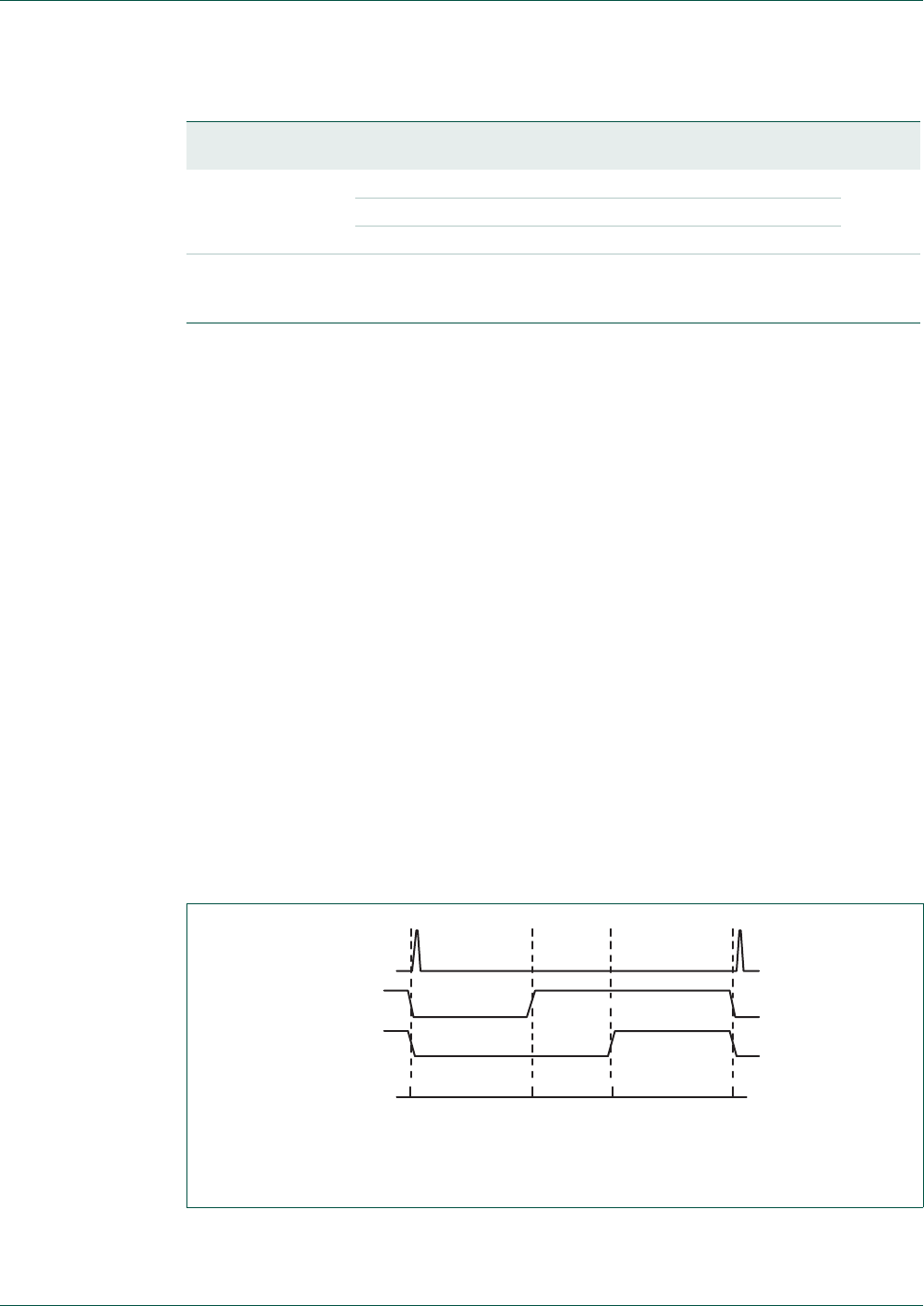
UM10462 All information provided in this document is subject to legal disclaimers. © NXP B.V. 2014. All rights reserved.
User manual Rev. 5.3 — 11 June 2014 346 of 521
NXP Semiconductors UM10462
Chapter 15: LPC11U3x/2x/1x 16-bit counter/timers CT16B0/1
15.7.13 Rules for single edge controlled PWM outputs
1. All single edge controlled PWM outputs go LOW at the beginning of each PWM cycle
(timer is set to zero) unless their match value is equal to zero.
2. Each PWM output will go HIGH when its match value is reached. If no match occurs
(i.e. the match value is greater than the PWM cycle length), the PWM output remains
continuously LOW.
3. If a match value larger than the PWM cycle length is written to the match register, and
the PWM signal is HIGH already, then the PWM signal will be cleared on the next start
of the next PWM cycle.
4. If a match register contains the same value as the timer reset value (the PWM cycle
length), then the PWM output will be reset to LOW on the next clock tick. Therefore,
the PWM output will always consist of a one clock tick wide positive pulse with a
period determined by the PWM cycle length (i.e. the timer reload value).
5. If a match register is set to zero, then the PWM output will go to HIGH the first time the
timer goes back to zero and will stay HIGH continuously.
Note: When the match outputs are selected to perform as PWM outputs, the timer reset
(MRnR) and timer stop (MRnS) bits in the Match Control Register MCR must be set to
zero except for the match register setting the PWM cycle length. For this register, set the
MRnR bit to one to enable the timer reset when the timer value matches the value of the
corresponding match register.
3 PWMEN3 PWM mode enable for channel3. 0
0 CT16Bn_MAT3 is controlled by EM3.
1 PWM mode is enabled for CT16Bn_MAT3.
31:4 - Reserved, user software should not write ones to
reserved bits. The value read from a reserved bit is
not defined.
-
Table 314. PWM Control Register (PWMC, address 0x4000 C074 (CT16B0) and 0x4001 0074
(CT16B1)) bit description
Bit Symbol Value Description Reset
value
Fig 56. Sample PWM waveforms with a PWM cycle length of 100 (selected by MR2) and
MAT2:0 enabled as PWM outputs by the PWMC register.
100
(counter is reset)
04165
PWM0/MAT0
PWM1/MAT1
PWM2/MAT2 MR2 = 100
MR1 = 41
MR0 = 65
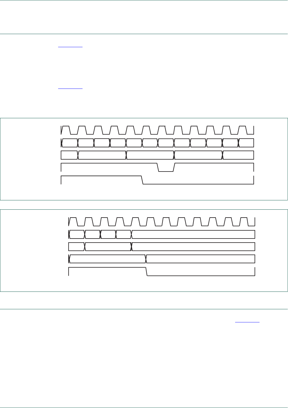
UM10462 All information provided in this document is subject to legal disclaimers. © NXP B.V. 2014. All rights reserved.
User manual Rev. 5.3 — 11 June 2014 347 of 521
NXP Semiconductors UM10462
Chapter 15: LPC11U3x/2x/1x 16-bit counter/timers CT16B0/1
15.8 Example timer operation
Figure 57 shows a timer configured to reset the count and generate an interrupt on match.
The prescaler is set to 2 and the match register set to 6. At the end of the timer cycle
where the match occurs, the timer count is reset. This gives a full length cycle to the
match value. The interrupt indicating that a match occurred is generated in the next clock
after the timer reached the match value.
Figure 58 shows a timer configured to stop and generate an interrupt on match. The
prescaler is again set to 2 and the match register set to 6. In the next clock after the timer
reaches the match value, the timer enable bit in TCR is cleared, and the interrupt
indicating that a match occurred is generated.
15.9 Architecture
The block diagram for counter/timer0 and counter/timer1 is shown in Figure 59.
Fig 57. A timer cycle in which PR=2, MRx=6, and both interrupt and reset on match are enabled
PCLK
prescale
counter
interrupt
timer
counter
timer counter
reset
222200001111
45 6 0 1
Fig 58. A timer cycle in which PR=2, MRx=6, and both interrupt and stop on match are enabled
PCLK
prescale counter
interrupt
timer counter
TCR[0]
(counter enable)
220 01
45 6
1 0
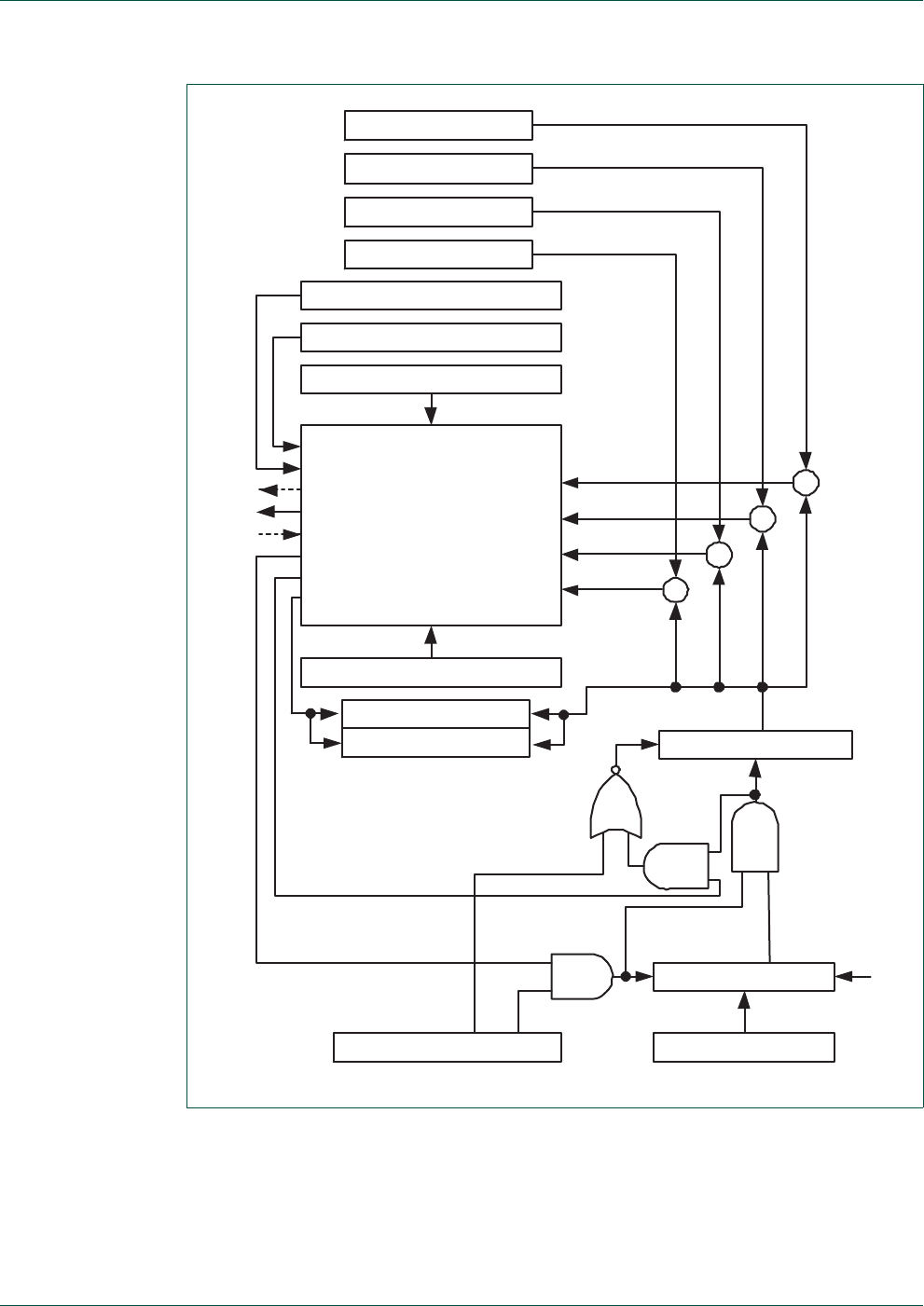
UM10462 All information provided in this document is subject to legal disclaimers. © NXP B.V. 2014. All rights reserved.
User manual Rev. 5.3 — 11 June 2014 348 of 521
NXP Semiconductors UM10462
Chapter 15: LPC11U3x/2x/1x 16-bit counter/timers CT16B0/1
Fig 59. 16-bit counter/timer block diagram
reset MAXVAL
TIMER CONTROL REGISTER PRESCALE REGISTER
PRESCALE COUNTER PCLK
enable
CAPTURE REGISTER 0
MATCH REGISTER 3
MATCH REGISTER 2
MATCH REGISTER 1
MATCH REGISTER 0
CAPTURE CONTROL REGISTER
CONTROL
TIMER COUNTER
CSN
TCI
CE
=
=
=
=
INTERRUPT REGISTER
EXTERNAL MATCH REGISTER
MATCH CONTROL REGISTER
MAT[2:0]
INTERRUPT
CAP[1:0]
STOP ON MATCH
RESET ON MATCH
LOAD[0]
CAPTURE REGISTER 1

UM10462 All information provided in this document is subject to legal disclaimers. © NXP B.V. 2014. All rights reserved.
User manual Rev. 5.3 — 11 June 2014 349 of 521
16.1 How to read this chapter
CT32B0/1 are available on all LPC11U3x/2x/1x parts. The CT32B1_CAP1 input is only
available on the TFBGA48 and LQFP64 packages. The CT32B0_CAP1 input is only
available on LQFP48, TFBGA48, and LQFP64 packages. For all other packages, the
registers controlling the CT32B1_CAP1 and CT32B0_CAP1 inputs are reserved.
16.2 Basic configuration
The CT32B0/1 counter/timers are configured through the following registers:
•Pins: The CT32B0/1 pins must be configured in the IOCON register block.
•Power: In the SYSAHBCLKCTRL register, set bit 9 and 10 in Table 24.
•The peripheral clock is determined by the system clock (see Table 23).
Remark: The register offsets and bit offsets for capture channel 1 are different on timers
CT32B0 and CT32B1. The affected registers are:
•Section 16.7.1 “Interrupt Register”
•Section 16.7.8 “Capture Control Register”
•Section 16.7.9 “Capture Registers”
•Section 16.7.11 “Count Control Register”
16.3 Features
•Two 32-bit counter/timers with a programmable 32-bit prescaler.
•Counter or timer operation.
•Four 32-bit capture channels that can take a snapshot of the timer value when an
input signal transitions. A capture event may also optionally generate an interrupt.
•The timer and prescaler may be configured to be cleared on a designated capture
event. This feature permits easy pulse-width measurement by clearing the timer on
the leading edge of an input pulse and capturing the timer value on the trailing edge.
•Four 32-bit match registers that allow:
–Continuous operation with optional interrupt generation on match.
–Stop timer on match with optional interrupt generation.
–Reset timer on match with optional interrupt generation.
•Four external outputs corresponding to match registers with the following capabilities:
–Set LOW on match.
–Set HIGH on match.
–Toggle on match.
–Do nothing on match.
UM10462
Chapter 16: LPC11U3x/2x/1x 32-bit counter/timers CT32B0/1
Rev. 5.3 — 11 June 2014 User manual

UM10462 All information provided in this document is subject to legal disclaimers. © NXP B.V. 2014. All rights reserved.
User manual Rev. 5.3 — 11 June 2014 350 of 521
NXP Semiconductors UM10462
Chapter 16: LPC11U3x/2x/1x 32-bit counter/timers CT32B0/1
•For each timer, up to four match registers can be configured as PWM allowing to use
up to three match outputs as single edge controlled PWM outputs.
16.4 Applications
•Interval timer for counting internal events
•Pulse Width Demodulator via capture input
•Free running timer
•Pulse Width Modulator via match outputs
16.5 General description
Each Counter/timer is designed to count cycles of the peripheral clock (PCLK) or an
externally supplied clock and can optionally generate interrupts or perform other actions at
specified timer values based on four match registers. Each counter/timer also includes
one capture input to trap the timer value when an input signal transitions, optionally
generating an interrupt.
In PWM mode, three match registers can be used to provide a single-edge controlled
PWM output on the match output pins. One match register is used to control the PWM
cycle length.
16.6 Pin description
Table 315 gives a brief summary of each of the counter/timer related pins.
16.7 Register description
32-bit counter/timer0 contains the registers shown in Table 316 and 32-bit counter/timer1
contains the registers shown in Table 317. More detailed descriptions follow.
Table 315. Counter/timer pin description
Pin Type Description
CT32B0_CAP[1:0]
CT32B1_CAP[1:0]
Input Capture Signals:
A transition on a capture pin can be configured to load one of the
Capture Registers with the value in the Timer Counter and
optionally generate an interrupt.
The counter/timer block can select a capture signal as a clock
source instead of the PCLK derived clock. For more details see
Section 16.7.11 “Count Control Register” on page 360.
CT32B0_MAT[3:0]
CT32B1_MAT[3:0]
Output External Match Output of CT32B0/1:
When a match register MR3:0 equals the timer counter (TC), this
output can either toggle, go LOW, go HIGH, or do nothing. The
External Match Register (EMR) and the PWM Control register
(PWMCON) control the functionality of this output.

UM10462 All information provided in this document is subject to legal disclaimers. © NXP B.V. 2014. All rights reserved.
User manual Rev. 5.3 — 11 June 2014 351 of 521
NXP Semiconductors UM10462
Chapter 16: LPC11U3x/2x/1x 32-bit counter/timers CT32B0/1
[1] Reset value reflects the data stored in used bits only. It does not include reserved bits content.
Table 316. Register overview: 32-bit counter/timer 0 CT32B0 (base address 0x4001 4000)
Name Access Address
offset Description Reset
value[1] Reference
IR R/W 0x000 Interrupt Register. The IR can be written to clear interrupts. The IR
can be read to identify which of eight possible interrupt sources are
pending.
0Table 318
TCR R/W 0x004 Timer Control Register. The TCR is used to control the Timer
Counter functions. The Timer Counter can be disabled or reset
through the TCR.
0Table 320
TC R/W 0x008 Timer Counter. The 32-bit TC is incremented every PR+1 cycles of
PCLK. The TC is controlled through the TCR.
0Table 321
PR R/W 0x00C Prescale Register. When the Prescale Counter (below) is equal to
this value, the next clock increments the TC and clears the PC.
0Table 322
PC R/W 0x010 Prescale Counter. The 32-bit PC is a counter which is incremented
to the value stored in PR. When the value in PR is reached, the TC is
incremented and the PC is cleared. The PC is observable and
controllable through the bus interface.
0Table 323
MCR R/W 0x014 Match Control Register. The MCR is used to control if an interrupt is
generated and if the TC is reset when a Match occurs.
0Table 324
MR0 R/W 0x018 Match Register 0. MR0 can be enabled through the MCR to reset the
TC, stop both the TC and PC, and/or generate an interrupt every
time MR0 matches the TC.
0Table 325
MR1 R/W 0x01C Match Register 1. See MR0 description. 0 Table 325
MR2 R/W 0x020 Match Register 2. See MR0 description. 0 Table 325
MR3 R/W 0x024 Match Register 3. See MR0 description. 0 Table 325
CCR R/W 0x028 Capture Control Register. The CCR controls which edges of the
capture inputs are used to load the Capture Registers and whether
or not an interrupt is generated when a capture takes place.
0Table 326
CR0 RO 0x02C Capture Register 0. CR0 is loaded with the value of TC when there is
an event on the CT32B0_CAP0 input.
0Table 328
- 0x030 Reserved - -
CR1 - 0x034 Capture Register 1. CR1 is loaded with the value of TC when there is
an event on the CT32B0_CAP1 input.
-Table 329
- - 0x038 Reserved. - -
EMR R/W 0x03C External Match Register. The EMR controls the match function and
the external match pins CT32Bn_MAT[3:0].
0Table 331
- - 0x040 -
0x06C
Reserved. - -
CTCR R/W 0x070 Count Control Register. The CTCR selects between Timer and
Counter mode, and in Counter mode selects the signal and edge(s)
for counting.
0Table 333
PWMC R/W 0x074 PWM Control Register. The PWMCON enables PWM mode for the
external match pins CT32Bn_MAT[3:0].
0Table 335

UM10462 All information provided in this document is subject to legal disclaimers. © NXP B.V. 2014. All rights reserved.
User manual Rev. 5.3 — 11 June 2014 352 of 521
NXP Semiconductors UM10462
Chapter 16: LPC11U3x/2x/1x 32-bit counter/timers CT32B0/1
[1] Reset value reflects the data stored in used bits only. It does not include reserved bits content.
Table 317. Register overview: 32-bit counter/timer 1 CT32B1 (base address 0x4001 8000)
Name Access Address
offset Description Reset
value[1] Reference
IR R/W 0x000 Interrupt Register. The IR can be written to clear interrupts. The IR
can be read to identify which of eight possible interrupt sources are
pending.
0Table 319
TCR R/W 0x004 Timer Control Register. The TCR is used to control the Timer
Counter functions. The Timer Counter can be disabled or reset
through the TCR.
0Table 320
TC R/W 0x008 Timer Counter. The 32-bit TC is incremented every PR+1 cycles of
PCLK. The TC is controlled through the TCR.
0Table 321
PR R/W 0x00C Prescale Register. When the Prescale Counter (below) is equal to
this value, the next clock increments the TC and clears the PC.
0Table 322
PC R/W 0x010 Prescale Counter. The 32-bit PC is a counter which is incremented
to the value stored in PR. When the value in PR is reached, the TC
is incremented and the PC is cleared. The PC is observable and
controllable through the bus interface.
0Table 323
MCR R/W 0x014 Match Control Register. The MCR is used to control if an interrupt is
generated and if the TC is reset when a Match occurs.
0Table 324
MR0 R/W 0x018 Match Register 0. MR0 can be enabled through the MCR to reset
the TC, stop both the TC and PC, and/or generate an interrupt every
time MR0 matches the TC.
0Table 325
MR1 R/W 0x01C Match Register 1. See MR0 description. 0 Table 325
MR2 R/W 0x020 Match Register 2. See MR0 description. 0 Table 325
MR3 R/W 0x024 Match Register 3. See MR0 description. 0 Table 325
CCR R/W 0x028 Capture Control Register. The CCR controls which edges of the
capture inputs are used to load the Capture Registers and whether
or not an interrupt is generated when a capture takes place.
0Table 327
CR0 RO 0x02C Capture Register 0. CR0 is loaded with the value of TC when there
is an event on the CT32B1_CAP0 input.
0Table 328
CR1 RO 0x030 Capture Register 1. CR1 is loaded with the value of TC when there
is an event on the CT32B1_CAP1 input.
0Table 330
- - 0x034 Reserved. - -
- - 0x038 Reserved. - -
EMR R/W 0x03C External Match Register. The EMR controls the match function and
the external match pins CT32Bn_MAT[3:0].
0Table 331
- - 0x040 -
0x06C
Reserved. - -
CTCR R/W 0x070 Count Control Register. The CTCR selects between Timer and
Counter mode, and in Counter mode selects the signal and edge(s)
for counting.
0Table 334
PWMC R/W 0x074 PWM Control Register. The PWMCON enables PWM mode for the
external match pins CT32Bn_MAT[3:0].
0Table 335

UM10462 All information provided in this document is subject to legal disclaimers. © NXP B.V. 2014. All rights reserved.
User manual Rev. 5.3 — 11 June 2014 353 of 521
NXP Semiconductors UM10462
Chapter 16: LPC11U3x/2x/1x 32-bit counter/timers CT32B0/1
16.7.1 Interrupt Register
The Interrupt Register consists of four bits for the match interrupts and four bits for the
capture interrupts. If an interrupt is generated then the corresponding bit in the IR will be
HIGH. Otherwise, the bit will be LOW. Writing a logic one to the corresponding IR bit will
reset the interrupt. Writing a zero has no effect.
Remark: The bit positions for the CAP1 interrupts are different for counter/timer CT32B0
(CAP1 interrupt on bit 6, Table 318) and counter/timer CT32B1 (CAP1 interrupt on bit 5,
Table 319).
16.7.2 Timer Control Register
The Timer Control Register (TCR) is used to control the operation of the counter/timer.
Table 318: Interrupt Register (IR, address 0x4001 4000 (CT32B0)) bit description
Bit Symbol Description Reset value
0 MR0INT Interrupt flag for match channel 0. 0
1 MR1INT Interrupt flag for match channel 1. 0
2 MR2INT Interrupt flag for match channel 2. 0
3 MR3INT Interrupt flag for match channel 3. 0
4 CR0INT Interrupt flag for capture channel 0 event. 0
5- Reserved, -
6 CR1INT Interrupt flag for capture channel 1 event. 0
31:7 - Reserved -
Table 319: Interrupt Register (IR, address 0x4001 8000 (CT32B1)) bit description
Bit Symbol Description Reset value
0 MR0INT Interrupt flag for match channel 0. 0
1 MR1INT Interrupt flag for match channel 1. 0
2 MR2INT Interrupt flag for match channel 2. 0
3 MR3INT Interrupt flag for match channel 3. 0
4 CR0INT Interrupt flag for capture channel 0 event. 0
5 CR1INT Interrupt flag for capture channel 1 event. 0
31:6 - Reserved -
Table 320: Timer Control Register (TCR, address 0x4001 4004 (CT32B0) and 0x4001 8004
(CT32B1)) bit description
Bit Symbol Value Description Reset
value
0 CEN Counter enable. 0
0 The counters are disabled.
1 The Timer Counter and Prescale Counter are enabled
for counting.

UM10462 All information provided in this document is subject to legal disclaimers. © NXP B.V. 2014. All rights reserved.
User manual Rev. 5.3 — 11 June 2014 354 of 521
NXP Semiconductors UM10462
Chapter 16: LPC11U3x/2x/1x 32-bit counter/timers CT32B0/1
16.7.3 Timer Counter registers
The 32-bit Timer Counter is incremented when the Prescale Counter reaches its terminal
count. Unless it is reset before reaching its upper limit, the TC will count up through the
value 0xFFFF FFFF and then wrap back to the value 0x0000 0000. This event does not
cause an interrupt, but a Match register can be used to detect an overflow if needed.
16.7.4 Prescale Register
The 32-bit Prescale Register specifies the maximum value for the Prescale Counter.
16.7.5 Prescale Counter Register
The 32-bit Prescale Counter controls division of PCLK by some constant value before it is
applied to the Timer Counter. This allows control of the relationship between the resolution
of the timer and the maximum time before the timer overflows. The Prescale Counter is
incremented on every PCLK. When it reaches the value stored in the Prescale Register,
the Timer Counter is incremented, and the Prescale Counter is reset on the next PCLK.
This causes the TC to increment on every PCLK when PR = 0, every 2 PCLKs when
PR = 1, etc.
1 CRST Counter reset. 0
0 Do nothing.
1 The Timer Counter and the Prescale Counter are
synchronously reset on the next positive edge of PCLK.
The counters remain reset until TCR[1] is returned to
zero.
31:2 - Reserved, user software should not write ones to
reserved bits. The value read from a reserved bit is not
defined.
NA
Table 320: Timer Control Register (TCR, address 0x4001 4004 (CT32B0) and 0x4001 8004
(CT32B1)) bit description
Bit Symbol Value Description Reset
value
Table 321: Timer counter registers (TC, address 0x4001 4008 (CT32B0) and 0x4001 8008
(CT32B1)) bit description
Bit Symbol Description Reset
value
31:0 TC Timer counter value. 0
Table 322: Prescale registers (PR, address 0x4001 400C (CT32B0) and 0x4001 800C
(CT32B1)) bit description
Bit Symbol Description Reset
value
31:0 PCVAL Prescaler value. 0
Table 323: Prescale registers (PC, address 0x4001 4010 (CT32B0) and 0x4001 8010
(CT32B1)) bit description
Bit Symbol Description Reset
value
31:0 PC Prescale counter value. 0

UM10462 All information provided in this document is subject to legal disclaimers. © NXP B.V. 2014. All rights reserved.
User manual Rev. 5.3 — 11 June 2014 355 of 521
NXP Semiconductors UM10462
Chapter 16: LPC11U3x/2x/1x 32-bit counter/timers CT32B0/1
16.7.6 Match Control Register
The Match Control Register is used to control what operations are performed when one of
the Match Registers matches the Timer Counter. The function of each of the bits is shown
in Table 324.
Table 324: Match Control Register (MCR, address 0x4001 4014 (CT32B0) and 0x4001 8014 (CT32B1)) bit description
Bit Symbol Value Description Reset
value
0 MR0I Interrupt on MR0: an interrupt is generated when MR0 matches the value in the TC. 0
1 Enabled
0 Disabled
1 MR0R Reset on MR0: the TC will be reset if MR0 matches it. 0
1 Enabled
0 Disabled
2 MR0S Stop on MR0: the TC and PC will be stopped and TCR[0] will be set to 0 if MR0 matches
the TC.
0
1 Enabled
0 Disabled
3 MR1I Interrupt on MR1: an interrupt is generated when MR1 matches the value in the TC. 0
1 Enabled
0 Disabled
4 MR1R Reset on MR1: the TC will be reset if MR1 matches it. 0
1 Enabled
0 Disabled
5 MR1S Stop on MR1: the TC and PC will be stopped and TCR[0] will be set to 0 if MR1 matches
the TC.
0
1 Enabled
0 Disabled
6 MR2I Interrupt on MR2: an interrupt is generated when MR2 matches the value in the TC. 0
1 Enabled
0 Disabled
7 MR2R Reset on MR2: the TC will be reset if MR2 matches it. 0
1 Enabled
0 Disabled
8 MR2S Stop on MR2: the TC and PC will be stopped and TCR[0] will be set to 0 if MR2 matches
the TC.
0
1 Enabled
0 Disabled
9 MR3I Interrupt on MR3: an interrupt is generated when MR3 matches the value in the TC. 0
1 Enabled
0 Disabled
10 MR3R Reset on MR3: the TC will be reset if MR3 matches it. 0
1 Enabled
0 Disabled

UM10462 All information provided in this document is subject to legal disclaimers. © NXP B.V. 2014. All rights reserved.
User manual Rev. 5.3 — 11 June 2014 356 of 521
NXP Semiconductors UM10462
Chapter 16: LPC11U3x/2x/1x 32-bit counter/timers CT32B0/1
16.7.7 Match Registers
The Match register values are continuously compared to the Timer Counter value. When
the two values are equal, actions can be triggered automatically. The action possibilities
are to generate an interrupt, reset the Timer Counter, or stop the timer. Actions are
controlled by the settings in the MCR register.
16.7.8 Capture Control Register
The Capture Control Register is used to control whether one of the four Capture Registers
is loaded with the value in the Timer Counter when the capture event occurs, and whether
an interrupt is generated by the capture event. Setting both the rising and falling bits at the
same time is a valid configuration, resulting in a capture event for both edges. In the
description below, “n” represents the Timer number, 0 or 1.
Remark: The bit positions for the CAP1 channel control bits are different for
counter/timers CT32B0 (bits 8:6, Table 326) and CT32B1 (bits 5:3, Table 327).
11 MR3S Stop on MR3: the TC and PC will be stopped and TCR[0] will be set to 0 if MR3 matches
the TC.
0
1 Enabled
0 Disabled
31:12 - Reserved, user software should not write ones to reserved bits. The value read from a
reserved bit is not defined.
NA
Table 324: Match Control Register (MCR, address 0x4001 4014 (CT32B0) and 0x4001 8014 (CT32B1)) bit description
Bit Symbol Value Description Reset
value
Table 325: Match registers (MR[0:3], addresses 0x4001 4018 (MR0) to 0x4001 4024 (MR3)
(CT32B0) and 0x4001 8018(MR0) to 0x40018024 (MR3) (CT32B1)) bit description
Bit Symbol Description Reset
value
31:0 MATCH Timer counter match value. 0
Table 326: Capture Control Register (CCR, address 0x4001 4028 (CT32B0) ) bit description
Bit Symbol Value Description Reset
value
0 CAP0RE Capture on CT32B0_CAP0 rising edge: a sequence of 0 then 1 on CT32B0_CAP0 will
cause CR0 to be loaded with the contents of TC.
0
1 Enabled.
0 Disabled.
1 CAP0FE Capture on CT32B0_CAP0 falling edge: a sequence of 1 then 0 on CT32B0_CAP0 will
cause CR0 to be loaded with the contents of TC.
0
1 Enabled.
0 Disabled.
2 CAP0I Interrupt on CT32B0_CAP0 event: a CR0 load due to a CT32B0_CAP0 event will
generate an interrupt.
0
1 Enabled.
0 Disabled.
5:3 - Reserved. -

UM10462 All information provided in this document is subject to legal disclaimers. © NXP B.V. 2014. All rights reserved.
User manual Rev. 5.3 — 11 June 2014 357 of 521
NXP Semiconductors UM10462
Chapter 16: LPC11U3x/2x/1x 32-bit counter/timers CT32B0/1
6 CAP1RE Capture on CT32B0_CAP1 rising edge: a sequence of 0 then 1 on CT32B0_CAP1 will
cause CR1 to be loaded with the contents of TC.
0
1 Enabled.
0 Disabled.
7 CAP1FE Capture on CT32B0_CAP1 falling edge: a sequence of 1 then 0 on CT32B0_CAP1 will
cause CR1 to be loaded with the contents of TC.
0
1 Enabled.
0 Disabled.
8 CAP1I Interrupt on CT32B0_CAP1 event: a CR1 load due to a CT32B0_CAP1 event will
generate an interrupt.
0
1 Enabled.
0 Disabled.
31:9 - Reserved, user software should not write ones to reserved bits. The value read from a
reserved bit is not defined.
NA
Table 326: Capture Control Register (CCR, address 0x4001 4028 (CT32B0) ) bit description
Bit Symbol Value Description Reset
value
Table 327: Capture Control Register (CCR, address 0x4001 8028 (CT32B1)) bit description
Bit Symbol Value Description Reset
value
0 CAP0RE Capture on CT32B1_CAP0 rising edge: a sequence of 0 then 1 on CT32B1_CAP0 will
cause CR0 to be loaded with the contents of TC.
0
1 Enabled.
0 Disabled.
1 CAP0FE Capture on CT32B1_CAP0 falling edge: a sequence of 1 then 0 on CT32B1_CAP0 will
cause CR0 to be loaded with the contents of TC.
0
1 Enabled.
0 Disabled.
2 CAP0I Interrupt on CT32B1_CAP0 event: a CR0 load due to a CT32B1_CAP0 event will
generate an interrupt.
0
1 Enabled.
0 Disabled.
3 CAP1RE Capture on CT32B1_CAP1 rising edge: a sequence of 0 then 1 on CT32B1_CAP1 will
cause CR1 to be loaded with the contents of TC.
0
1 Enabled.
0 Disabled.
4 CAP1FE Capture on CT32B1_CAP1 falling edge: a sequence of 1 then 0 on CT32B1_CAP1 will
cause CR1 to be loaded with the contents of TC.
0
1 Enabled.
0 Disabled.

UM10462 All information provided in this document is subject to legal disclaimers. © NXP B.V. 2014. All rights reserved.
User manual Rev. 5.3 — 11 June 2014 358 of 521
NXP Semiconductors UM10462
Chapter 16: LPC11U3x/2x/1x 32-bit counter/timers CT32B0/1
16.7.9 Capture Registers
Each Capture register is associated with a device pin and may be loaded with the Timer
Counter value when a specified event occurs on that pin. The settings in the Capture
Control Register register determine whether the capture function is enabled, and whether
a capture event happens on the rising edge of the associated pin, the falling edge, or on
both edges.
Remark: The location of the CR1 register relative to the timer base address is different for
CT32B0 (CR1 at +0x034, Table 329) and CT32B1 (CR1 at +0x030, Table 319).
16.7.10 External Match Register
The External Match Register provides both control and status of the external match pins
CAP32Bn_MAT[3:0].
If the match outputs are configured as PWM output, the function of the external match
registers is determined by the PWM rules (Section 16.7.13 “Rules for single edge
controlled PWM outputs” on page 363).
5 CAP1I Interrupt on CT32B1_CAP1 event: a CR1 load due to a CT32B1_CAP1 event will
generate an interrupt.
0
1 Enabled.
0 Disabled.
31:6 - Reserved, user software should not write ones to reserved bits. The value read from a
reserved bit is not defined.
NA
Table 327: Capture Control Register (CCR, address 0x4001 8028 (CT32B1)) bit description
Bit Symbol Value Description Reset
value
Table 328: Capture registers (CR0, addresses 0x4001 402C(CT32B0) and 0x4001 802C
(CT32B1)) bit description
Bit Symbol Description Reset
value
31:0 CAP Timer counter capture value. 0
Table 329: Capture register (CR1, address 0x4001 4034 (CT32B0)) bit description
Bit Symbol Description Reset
value
31:0 CAP Timer counter capture value. 0
Table 330: Capture register (CR1, address 0x4001 8030 (CT32B1)) bit description
Bit Symbol Description Reset
value
31:0 CAP Timer counter capture value. 0

UM10462 All information provided in this document is subject to legal disclaimers. © NXP B.V. 2014. All rights reserved.
User manual Rev. 5.3 — 11 June 2014 359 of 521
NXP Semiconductors UM10462
Chapter 16: LPC11U3x/2x/1x 32-bit counter/timers CT32B0/1
Table 331: External Match Register (EMR, address 0x4001 403C (CT32B0) and 0x4001 803C (CT32B1)) bit
description
Bit Symbol Value Description Reset
value
0 EM0 External Match 0. This bit reflects the state of output CT32Bn_MAT0, whether or not this
output is connected to its pin. When a match occurs between the TC and MR0, this bit
can either toggle, go LOW, go HIGH, or do nothing. Bits EMR[5:4] control the
functionality of this output. This bit is driven to the CT32B0_MAT0/CT32B1_MAT0 pins if
the match function is selected in the IOCON registers (0 = LOW, 1 = HIGH).
0
1 EM1 External Match 1. This bit reflects the state of output CT32Bn_MAT1, whether or not this
output is connected to its pin. When a match occurs between the TC and MR1, this bit
can either toggle, go LOW, go HIGH, or do nothing. Bits EMR[7:6] control the
functionality of this output. This bit is driven to the CT32B0_MAT1/CT32B1_MAT1 pins if
the match function is selected in the IOCON registers (0 = LOW, 1 = HIGH).
0
2 EM2 External Match 2. This bit reflects the state of output CT32Bn_MAT2, whether or not this
output is connected to its pin. When a match occurs between the TC and MR2, this bit
can either toggle, go LOW, go HIGH, or do nothing. Bits EMR[9:8] control the
functionality of this output. This bit is driven to the CT32B0_MAT2/CT32B1_MAT2 pins if
the match function is selected in the IOCON registers (0 = LOW, 1 = HIGH).
0
3 EM3 External Match 3. This bit reflects the state of output CT32Bn_MAT3, whether or not this
output is connected to its pin. When a match occurs between the TC and MR3, this bit
can either toggle, go LOW, go HIGH, or do nothing. Bits EMR[11:10] control the
functionality of this output. This bit is driven to the CT32B0_MAT0/CT32B1_MAT3 pins if
the match function is selected in the IOCON registers (0 = LOW, 1 = HIGH).
0
5:4 EMC0 External Match Control 0. Determines the functionality of External Match 0. 00
0x0 Do Nothing.
0x1 Clear the corresponding External Match bit/output to 0 (CT32Bi_MAT0 pin is LOW if
pinned out).
0x2 Set the corresponding External Match bit/output to 1 (CT32Bi_MAT0 pin is HIGH if
pinned out).
0x3 Toggle the corresponding External Match bit/output.
7:6 EMC1 External Match Control 1. Determines the functionality of External Match 1. 00
0x0 Do Nothing.
0x1 Clear the corresponding External Match bit/output to 0 (CT32Bi_MAT1 pin is LOW if
pinned out).
0x2 Set the corresponding External Match bit/output to 1 (CT32Bi_MAT1 pin is HIGH if
pinned out).
0x3 Toggle the corresponding External Match bit/output.
9:8 EMC2 External Match Control 2. Determines the functionality of External Match 2. 00
0x0 Do Nothing.
0x1 Clear the corresponding External Match bit/output to 0 (CT32Bi_MAT2 pin is LOW if
pinned out).
0x2 Set the corresponding External Match bit/output to 1 (CT32Bi_MAT2 pin is HIGH if
pinned out).
0x3 Toggle the corresponding External Match bit/output.
UM10462 All information provided in this document is subject to legal disclaimers. © NXP B.V. 2014. All rights reserved.
User manual Rev. 5.3 — 11 June 2014 360 of 521
NXP Semiconductors UM10462
Chapter 16: LPC11U3x/2x/1x 32-bit counter/timers CT32B0/1
16.7.11 Count Control Register
The Count Control Register (CTCR) is used to select between Timer and Counter mode,
and in Counter mode to select the pin and edges for counting.
When Counter Mode is chosen as a mode of operation, the CAP input (selected by the
CTCR bits 3:2) is sampled on every rising edge of the PCLK clock. After comparing two
consecutive samples of this CAP input, one of the following four events is recognized:
rising edge, falling edge, either of edges or no changes in the level of the selected CAP
input. Only if the identified event occurs, and the event corresponds to the one selected by
bits 1:0 in the CTCR register, will the Timer Counter register be incremented.
Effective processing of the externally supplied clock to the counter has some limitations.
Since two successive rising edges of the PCLK clock are used to identify only one edge
on the CAP selected input, the frequency of the CAP input cannot exceed one half of the
PCLK clock. Consequently, duration of the HIGH/LOWLOW levels on the same CAP input
in this case cannot be shorter than 1/PCLK.
Bits 7:4 of this register are also used to enable and configure the capture-clears-timer
feature. This feature allows for a designated edge on a particular CAP input to reset the
timer to all zeros. Using this mechanism to clear the timer on the leading edge of an input
pulse and performing a capture on the trailing edge, permits direct pulse-width
measurement using a single capture input without the need to perform a subtraction
operation in software.
11:10 EMC3 External Match Control 3. Determines the functionality of External Match 3. 00
0x0 Do Nothing.
0x1 Clear the corresponding External Match bit/output to 0 (CT32Bi_MAT3 pin is LOW if
pinned out).
0x2 Set the corresponding External Match bit/output to 1 (CT32Bi_MAT3 pin is HIGH if
pinned out).
0x3 Toggle the corresponding External Match bit/output.
31:12 - Reserved, user software should not write ones to reserved bits. The value read from a
reserved bit is not defined.
NA
Table 331: External Match Register (EMR, address 0x4001 403C (CT32B0) and 0x4001 803C (CT32B1)) bit
description
Bit Symbol Value Description Reset
value
Table 332. External match control
EMR[11:10], EMR[9:8],
EMR[7:6], or EMR[5:4] Function
00 Do Nothing.
01 Clear the corresponding External Match bit/output to 0 (CT32Bn_MATm pin is LOW if
pinned out).
10 Set the corresponding External Match bit/output to 1 (CT32Bn_MATm pin is HIGH if
pinned out).
11 Toggle the corresponding External Match bit/output.

UM10462 All information provided in this document is subject to legal disclaimers. © NXP B.V. 2014. All rights reserved.
User manual Rev. 5.3 — 11 June 2014 361 of 521
NXP Semiconductors UM10462
Chapter 16: LPC11U3x/2x/1x 32-bit counter/timers CT32B0/1
Remark: The bit positions for the CAP1 channel count input select (CIS) and edge select
bits (SELCC) are different for counter/timers CT16B0 (Table 333) and CT16B1
(Table 334).
Table 333: Count Control Register (CTCR, address 0x4001 4070 (CT32B0)) bit description
Bit Symbol Value Description Reset
value
1:0 CTM Counter/Timer Mode. This field selects which rising PCLK
edges can increment Timer’s Prescale Counter (PC), or
clear PC and increment Timer Counter (TC).
Remark: If Counter mode is selected in the CTCR, bits 2:0 in
the Capture Control Register (CCR) must be programmed as
000.
00
0x0 Timer Mode: every rising PCLK edge
0x1 Counter Mode: TC is incremented on rising edges on the
CAP input selected by bits 3:2.
0x2 Counter Mode: TC is incremented on falling edges on the
CAP input selected by bits 3:2.
0x3 Counter Mode: TC is incremented on both edges on the CAP
input selected by bits 3:2.
3:2 CIS Count Input Select. In counter mode (when bits 1:0 in this
register are not 00), these bits select which CAP pin is
sampled for clocking.
Remark: If Counter mode is selected in the CTCR, the 3 bits
for that input in the Capture Control Register (CCR) must be
programmed as 000. Values 0x1 and 0x3 are reserved.
00
0x0 CT32B0_CAP0
0x1 Reserved.
0x2 CT32B0_CAP1
4 ENCC Setting this bit to 1 enables clearing of the timer and the
prescaler when the capture-edge event specified in bits 7:5
occurs.
0
7:5 SElCC When bit 4 is a 1, these bits select which capture input edge
will cause the timer and prescaler to be cleared. These bits
have no effect when bit 4 is low. Values 0x2 to 0x3 and 0x6
to 0x7 are reserved.
0x0 Rising Edge of CT32B0_CAP0 clears the timer (if bit 4 is set)
0x1 Falling Edge of CT32B0_CAP0 clears the timer (if bit 4 is set)
0x2 Reserved,
0x3 Reserved.
0x4 Rising Edge of CT32B0_CAP1 clears the timer (if bit 4 is set)
0x5 Falling Edge of CT32B0_CAP1 clears the timer (if bit 4 is set)
31:8 - - Reserved, user software should not write ones to reserved
bits. The value read from a reserved bit is not defined.
-

UM10462 All information provided in this document is subject to legal disclaimers. © NXP B.V. 2014. All rights reserved.
User manual Rev. 5.3 — 11 June 2014 362 of 521
NXP Semiconductors UM10462
Chapter 16: LPC11U3x/2x/1x 32-bit counter/timers CT32B0/1
16.7.12 PWM Control Register
The PWM Control Register is used to configure the match outputs as PWM outputs. Each
match output can be independently set to perform either as PWM output or as match
output whose function is controlled by the External Match Register (EMR).
For each timer, a maximum of three single edge controlled PWM outputs can be selected
on the MATn.2:0 outputs. One additional match register determines the PWM cycle
length. When a match occurs in any of the other match registers, the PWM output is set to
Table 334: Count Control Register (CTCR, address 0x4001 8070 (CT32B1)) bit description
Bit Symbol Value Description Reset
value
1:0 CTM Counter/Timer Mode. This field selects which rising PCLK
edges can increment Timer’s Prescale Counter (PC), or
clear PC and increment Timer Counter (TC).
Remark: If Counter mode is selected in the CTCR, bits 2:0 in
the Capture Control Register (CCR) must be programmed as
000.
00
0x0 Timer Mode: every rising PCLK edge
0x1 Counter Mode: TC is incremented on rising edges on the
CAP input selected by bits 3:2.
0x2 Counter Mode: TC is incremented on falling edges on the
CAP input selected by bits 3:2.
0x3 Counter Mode: TC is incremented on both edges on the CAP
input selected by bits 3:2.
3:2 CIS Count Input Select. In counter mode (when bits 1:0 in this
register are not 00), these bits select which CAP pin is
sampled for clocking.
Remark: If Counter mode is selected in the CTCR, the 3 bits
for that input in the Capture Control Register (CCR) must be
programmed as 000. Values 0x2 to 0x3 are reserved.
00
0x0 CT32B1_CAP0
0x1 CT32B1_CAP1
4 ENCC Setting this bit to 1 enables clearing of the timer and the
prescaler when the capture-edge event specified in bits 7:5
occurs.
0
7:5 SElCC When bit 4 is a 1, these bits select which capture input edge
will cause the timer and prescaler to be cleared. These bits
have no effect when bit 4 is low. Values 0x3 to 0x7 are
reserved.
0x0 Rising Edge of CT32B1_CAP0 clears the timer (if bit 4 is set)
0x1 Falling Edge of CT32B1_CAP0 clears the timer (if bit 4 is set)
0x2 Rising Edge of CT32B1_CAP1 clears the timer (if bit 4 is set)
0x3 Falling Edge of CT32B1_CAP1 clears the timer (if bit 4 is set)
31:8 - - Reserved, user software should not write ones to reserved
bits. The value read from a reserved bit is not defined.
-

UM10462 All information provided in this document is subject to legal disclaimers. © NXP B.V. 2014. All rights reserved.
User manual Rev. 5.3 — 11 June 2014 363 of 521
NXP Semiconductors UM10462
Chapter 16: LPC11U3x/2x/1x 32-bit counter/timers CT32B0/1
HIGH. The timer is reset by the match register that is configured to set the PWM cycle
length. When the timer is reset to zero, all currently HIGH match outputs configured as
PWM outputs are cleared.
16.7.13 Rules for single edge controlled PWM outputs
1. All single edge controlled PWM outputs go LOW at the beginning of each PWM cycle
(timer is set to zero) unless their match value is equal to zero.
2. Each PWM output will go HIGH when its match value is reached. If no match occurs
(i.e. the match value is greater than the PWM cycle length), the PWM output remains
continuously LOW.
3. If a match value larger than the PWM cycle length is written to the match register, and
the PWM signal is HIGH already, then the PWM signal will be cleared with the start of
the next PWM cycle.
4. If a match register contains the same value as the timer reset value (the PWM cycle
length), then the PWM output will be reset to LOW on the next clock tick after the
timer reaches the match value. Therefore, the PWM output will always consist of a
one clock tick wide positive pulse with a period determined by the PWM cycle length
(i.e. the timer reload value).
5. If a match register is set to zero, then the PWM output will go to HIGH the first time the
timer goes back to zero and will stay HIGH continuously.
Table 335: PWM Control Register (PWMC, 0x4001 4074 (CT32B0) and 0x4001 8074 (CT32B1))
bit description
Bit Symbol Value Description Reset
value
0 PWMEN0 PWM mode enable for channel0. 0
0 CT32Bn_MAT0 is controlled by EM0.
1 PWM mode is enabled for CT32Bn_MAT0.
1 PWMEN1 PWM mode enable for channel1. 0
0 CT32Bn_MAT01 is controlled by EM1.
1 PWM mode is enabled for CT32Bn_MAT1.
2 PWMEN2 PWM mode enable for channel2. 0
0 CT32Bn_MAT2 is controlled by EM2.
1 PWM mode is enabled for CT32Bn_MAT2.
3 PWMEN3 PWM mode enable for channel3. Note: It is
recommended to use match channel 3 to set the PWM
cycle.
0
0 CT32Bn_MAT3 is controlled by EM3.
1 PWM mode is enabled for CT132Bn_MAT3.
31:4 - Reserved, user software should not write ones to
reserved bits. The value read from a reserved bit is not
defined.
NA
UM10462 All information provided in this document is subject to legal disclaimers. © NXP B.V. 2014. All rights reserved.
User manual Rev. 5.3 — 11 June 2014 364 of 521
NXP Semiconductors UM10462
Chapter 16: LPC11U3x/2x/1x 32-bit counter/timers CT32B0/1
Note: When the match outputs are selected to perform as PWM outputs, the timer reset
(MRnR) and timer stop (MRnS) bits in the Match Control Register MCR must be set to
zero except for the match register setting the PWM cycle length. For this register, set the
MRnR bit to one to enable the timer reset when the timer value matches the value of the
corresponding match register.
16.8 Example timer operation
Figure 61 shows a timer configured to reset the count and generate an interrupt on match.
The prescaler is set to 2 and the match register set to 6. At the end of the timer cycle
where the match occurs, the timer count is reset. This gives a full length cycle to the
match value. The interrupt indicating that a match occurred is generated in the next clock
after the timer reached the match value.
Figure 62 shows a timer configured to stop and generate an interrupt on match. The
prescaler is again set to 2 and the match register set to 6. In the next clock after the timer
reaches the match value, the timer enable bit in TCR is cleared, and the interrupt
indicating that a match occurred is generated.
Fig 60. Sample PWM waveforms with a PWM cycle length of 100 (selected by MR2) and
MAT2:0 enabled as PWM outputs by the PWMC register.
100
(counter is reset)
04165
PWM0/MAT0
PWM1/MAT1
PWM2/MAT2 MR2 = 100
MR1 = 41
MR0 = 65
Fig 61. A timer cycle in which PR=2, MRx=6, and both interrupt and reset on match are enabled
PCLK
prescale
counter
interrupt
timer
counter
timer counter
reset
222200001111
45 6 0 1

UM10462 All information provided in this document is subject to legal disclaimers. © NXP B.V. 2014. All rights reserved.
User manual Rev. 5.3 — 11 June 2014 365 of 521
NXP Semiconductors UM10462
Chapter 16: LPC11U3x/2x/1x 32-bit counter/timers CT32B0/1
16.9 Architecture
The block diagram for 32-bit counter/timer0 and 32-bit counter/timer1 is shown in
Figure 63.
Fig 62. A timer cycle in which PR=2, MRx=6, and both interrupt and stop on match are enabled
PCLK
prescale counter
interrupt
timer counter
TCR[0]
(counter enable)
220 01
45 6
1 0
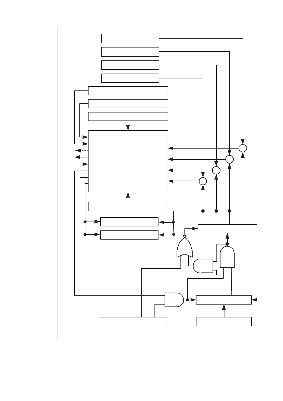
UM10462 All information provided in this document is subject to legal disclaimers. © NXP B.V. 2014. All rights reserved.
User manual Rev. 5.3 — 11 June 2014 366 of 521
NXP Semiconductors UM10462
Chapter 16: LPC11U3x/2x/1x 32-bit counter/timers CT32B0/1
Fig 63. 32-bit counter/timer block diagram
reset MAXVAL
TIMER CONTROL REGISTER PRESCALE REGISTER
PRESCALE COUNTER PCLK
enable
CAPTURE REGISTER 1
CAPTURE REGISTER 0
MATCH REGISTER 3
MATCH REGISTER 2
MATCH REGISTER 1
MATCH REGISTER 0
CAPTURE CONTROL REGISTER
CONTROL
TIMER COUNTER
CSN
TCI
CE
=
=
=
=
INTERRUPT REGISTER
EXTERNAL MATCH REGISTER
MATCH CONTROL REGISTER
MAT[3:0]
INTERRUPT
CAP[1:0]
STOP ON MATCH
RESET ON MATCH
LOAD[3:0]

UM10462 All information provided in this document is subject to legal disclaimers. © NXP B.V. 2014. All rights reserved.
User manual Rev. 5.3 — 11 June 2014 367 of 521
17.1 How to read this chapter
The WWDT is identical on all LPC11U3x/2x/1x parts.
17.2 Basic configuration
The WWDT is configured through the following registers:
•Power to the register interface (WWDT PCLK clock): In the SYSAHBCLKCTRL
register, set bit 15 in Table 24.
•Enable the WWDT clock source (the watchdog oscillator or the IRC) in the
PDRUNCFG register (Table 47).
•For waking up from a WWDT interrupt, enable the watchdog interrupt for wake-up in
the STARTERP1 register (Table 44).
17.3 Features
•Internally resets chip if not reloaded during the programmable time-out period.
•Optional windowed operation requires reload to occur between a minimum and
maximum time-out period, both programmable.
•Optional warning interrupt can be generated at a programmable time prior to
watchdog time-out.
•Programmable 24-bit timer with internal fixed pre-scaler.
•Selectable time period from 1,024 watchdog clocks (TWDCLK 256 4) to over 67
million watchdog clocks (TWDCLK 224 4) in increments of 4 watchdog clocks.
•“Safe” watchdog operation. Once enabled, requires a hardware reset or a Watchdog
reset to be disabled.
•Incorrect feed sequence causes immediate watchdog event if enabled.
•The watchdog reload value can optionally be protected such that it can only be
changed after the “warning interrupt” time is reached.
•Flag to indicate Watchdog reset.
•The Watchdog clock (WDCLK) source can be selected as the Internal High frequency
oscillator (IRC) or the WatchDog oscillator.
•The Watchdog timer can be configured to run in Deep-sleep or Power-down mode
when using the watchdog oscillator as the clock source.
•Debug mode.
UM10462
Chapter 17: LPC11U3x/2x/1x Windowed Watchdog Timer
(WWDT)
Rev. 5.3 — 11 June 2014 User manual

UM10462 All information provided in this document is subject to legal disclaimers. © NXP B.V. 2014. All rights reserved.
User manual Rev. 5.3 — 11 June 2014 368 of 521
NXP Semiconductors UM10462
Chapter 17: LPC11U3x/2x/1x Windowed Watchdog Timer (WWDT)
17.4 Applications
The purpose of the Watchdog Timer is to reset or interrupt the microcontroller within a
programmable time if it enters an erroneous state. When enabled, a watchdog reset
and/or will be generated if the user program fails to “feed” (reload) the Watchdog within a
predetermined amount of time.
When a watchdog window is programmed, an early watchdog feed is also treated as a
watchdog event. This allows preventing situations where a system failure may still feed
the watchdog. For example, application code could be stuck in an interrupt service that
contains a watchdog feed. Setting the window such that this would result in an early feed
will generate a watchdog event, allowing for system recovery.
17.5 Description
The Watchdog consists of a fixed (divide by 4) pre-scaler and a 24 bit counter which
decrements when clocked. The minimum value from which the counter decrements is
0xFF. Setting a value lower than 0xFF causes 0xFF to be loaded in the counter. Hence the
minimum Watchdog interval is (TWDCLK 256 4) and the maximum Watchdog interval is
(TWDCLK 224 4) in multiples of (TWDCLK 4). The Watchdog should be used in the
following manner:
•Set the Watchdog timer constant reload value in the TC register.
•Set the Watchdog timer operating mode in the MOD register.
•Set a value for the watchdog window time in the WINDOW register if windowed
operation is desired.
•Set a value for the watchdog warning interrupt in the WARNINT register if a warning
interrupt is desired.
•Enable the Watchdog by writing 0xAA followed by 0x55 to the FEED register.
•The Watchdog must be fed again before the Watchdog counter reaches zero in order
to prevent a watchdog event. If a window value is programmed, the feed must also
occur after the watchdog counter passes that value.
When the Watchdog Timer is configured so that a watchdog event will cause a reset and
the counter reaches zero, the CPU will be reset, loading the stack pointer and program
counter from the vector table as for an external reset. The Watchdog time-out flag
(WDTOF) can be examined to determine if the Watchdog has caused the reset condition.
The WDTOF flag must be cleared by software.
When the Watchdog Timer is configured to generate a warning interrupt, the interrupt will
occur when the counter matches the value defined by the WARNINT register.
17.5.1 Block diagram
The block diagram of the Watchdog is shown below in the Figure 64. The synchronization
logic (PCLK - WDCLK) is not shown in the block diagram.
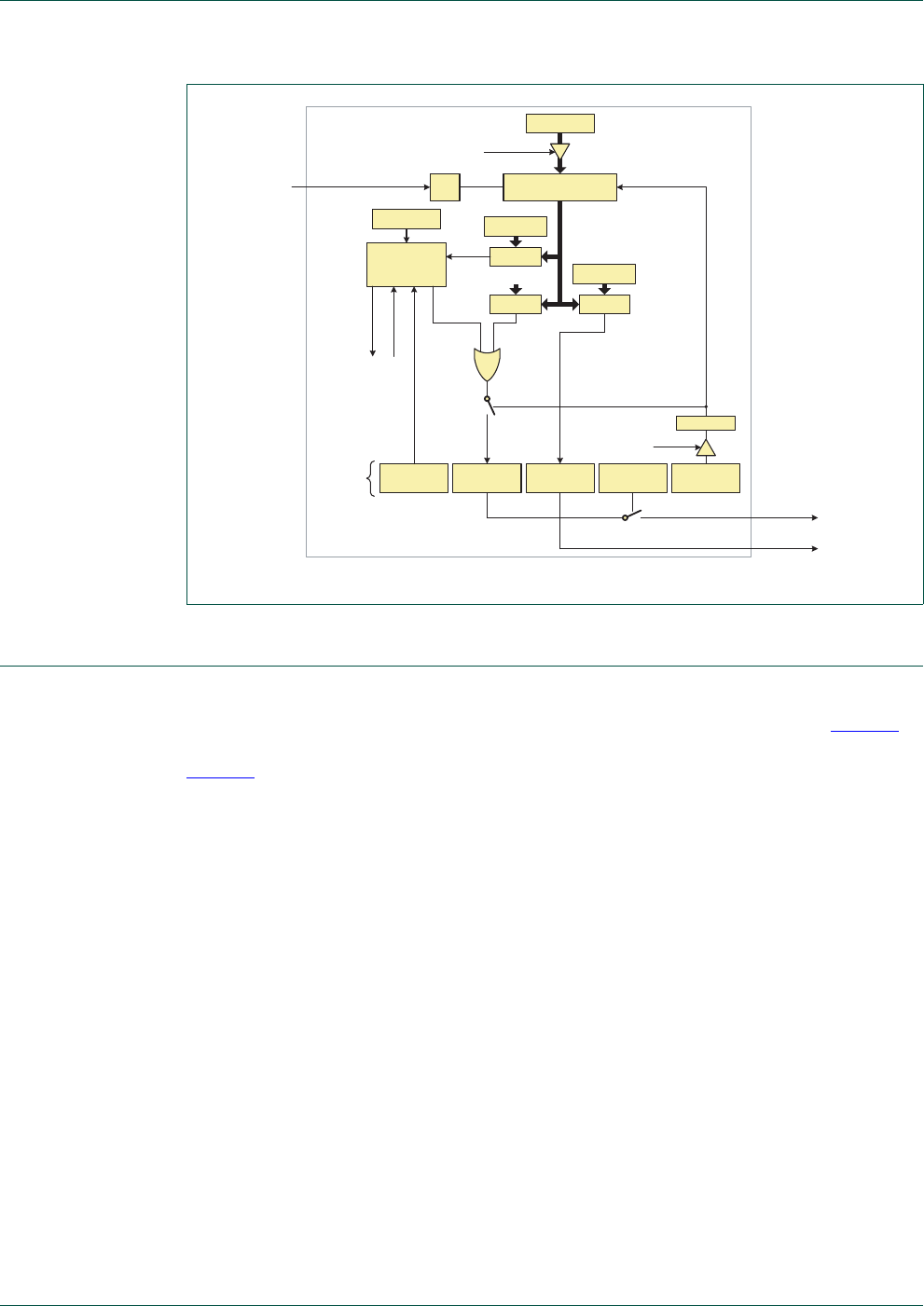
UM10462 All information provided in this document is subject to legal disclaimers. © NXP B.V. 2014. All rights reserved.
User manual Rev. 5.3 — 11 June 2014 369 of 521
NXP Semiconductors UM10462
Chapter 17: LPC11U3x/2x/1x Windowed Watchdog Timer (WWDT)
17.6 Clocking and power control
The watchdog timer block uses two clocks: PCLK and WDCLK. PCLK is used for the APB
accesses to the watchdog registers and is derived from the system clock (see Figure 7).
The WDCLK is used for the watchdog timer counting and is derived from the wdt_clk in
Figure 7. Either the IRC or the watchdog oscillator can be used as wdt_clk in Active mode,
Sleep mode, and Deep-sleep modes. In Power-down mode only the watchdog oscillator is
available.
The synchronization logic between the two clock domains works as follows: When the
MOD and TC registers are updated by APB operations, the new value will take effect in 3
WDCLK cycles on the logic in the WDCLK clock domain.
When the watchdog timer is counting on WDCLK, the synchronization logic will first lock
the value of the counter on WDCLK and then synchronize it with PCLK, so that the CPU
can read the WDTV register.
Remark: Because of the synchronization step, software must add a delay of three
WDCLK clock cycles between the feed sequence and the time the WDPROTECT bit is
enabled in the MOD register. The length of the delay depends on the selected watchdog
clock WDCLK.
Fig 64. Watchdog block diagram
watchdog
interrupt
WDRESET
(MOD [1])
WDTOF
(MOD [2])
WDINT
(MOD [3])
WDEN
(MOD [0])
chip reset
÷4
feed error
feed ok
wd_clk enable count
MOD
register
compare
WDTV
compare
in
range
underflow
feed sequence
detect and
protection
FEED
feed ok
feed ok
compare
0
interrupt
compare
24-bit down counter
WDINTVAL
WINDOW
TC
shadow bit
WDPROTECT
(MOD [4])
TC write

UM10462 All information provided in this document is subject to legal disclaimers. © NXP B.V. 2014. All rights reserved.
User manual Rev. 5.3 — 11 June 2014 370 of 521
NXP Semiconductors UM10462
Chapter 17: LPC11U3x/2x/1x Windowed Watchdog Timer (WWDT)
17.7 Using the WWDT lock features
The WWDT supports several lock features which can be enabled to ensure that the
WWDT is running at all times:
•Accidental overwrite of the WWDT clock source
•Changing the WWDT clock source
•Changing the WWDT reload value
17.7.1 Accidental overwrite of the WWDT clock
If bit 31 of the WWDT CLKSEL register (Table 342) is set, writes to bit 0 of the CLKSEL
register, the clock source select bit, will be ignored and the clock source will not change.
17.7.2 Changing the WWDT clock source
If bit 5 in the WWDT MOD register is set, the current clock source as selected in the
CLKSEL register is locked and can not be changed either by software or by hardware
when Sleep, Deep-sleep or Power-down modes are entered. Therefore, the user must
ensure that the appropriate WWDT clock source for each power mode is selected before
setting bit 5 in the MOD register:
•Active or Sleep modes: Both the IRC or the watchdog oscillator are allowed.
•Deep-sleep mode: Both the IRC and the watchdog oscillator are allowed. However,
using the IRC during Deep-sleep mode will increase the power consumption. To
minimize power consumption, use the watchdog oscillator as clock source.
•Power-down mode: Only the watchdog oscillator is allowed as clock source for the
WWDT. Therefore, before setting bit 5 and locking the clock source, the WWDT clock
source must be set to the watchdog oscillator. Otherwise, the part may not be able to
enter Power-down mode.
•Deep power-down mode: No clock locking mechanisms are in effect as neither the
WWDT nor any of the clocks are running. However, an additional lock bit in the PMU
can be set to prevent the part from even entering Deep power-down mode (see
Table 54).
The clock source lock mechanism can only be disabled by a reset of any type.
17.7.3 Changing the WWDT reload value
If bit 4 is set in the WWDT MOD register, the watchdog time-out value (TC) can be
changed only after the counter is below the value of WDWARNINT and WDWINDOW.
The reload overwrite lock mechanism can only be disabled by a reset of any type.

UM10462 All information provided in this document is subject to legal disclaimers. © NXP B.V. 2014. All rights reserved.
User manual Rev. 5.3 — 11 June 2014 371 of 521
NXP Semiconductors UM10462
Chapter 17: LPC11U3x/2x/1x Windowed Watchdog Timer (WWDT)
17.8 Register description
The Watchdog Timer contains the registers shown in Table 336.
[1] Reset Value reflects the data stored in used bits only. It does not include reserved bits content.
17.8.1 Watchdog mode register
The WDMOD register controls the operation of the Watchdog. Note that a watchdog feed
must be performed before any changes to the WDMOD register take effect.
Table 336. Register overview: Watchdog timer (base address 0x4000 4000)
Name Access Address
offset Description Reset
Value[1] Reference
MOD R/W 0x000 Watchdog mode register. This
register contains the basic mode and
status of the Watchdog Timer.
0Table 337
TC R/W 0x004 Watchdog timer constant register.
This 24-bit register determines the
time-out value.
0xFF Table 339
FEED WO 0x008 Watchdog feed sequence register.
Writing 0xAA followed by 0x55 to this
register reloads the Watchdog timer
with the value contained in WDTC.
NA Table 340
TV RO 0x00C Watchdog timer value register. This
24-bit register reads out the current
value of the Watchdog timer.
0xFF Table 341
CLKSEL R/W 0x010 Watchdog clock select register. 0 Table 342
WARNINT R/W 0x014 Watchdog Warning Interrupt compare
value.
0Table 343
WINDOW R/W 0x018 Watchdog Window compare value. 0xFF FFFF Table 344
Table 337. Watchdog mode register (MOD - 0x4000 4000) bit description
Bit Symbol Value Description Reset
value
0 WDEN Watchdog enable bit. Once this bit has been written with
a 1, it cannot be rewritten with a 0.
0
0 The watchdog timer is stopped.
1 The watchdog timer is running.
1 WDRESET Watchdog reset enable bit. Once this bit has been
written with a 1 it cannot be rewritten with a 0.
0
0 A watchdog timeout will not cause a chip reset.
1 A watchdog timeout will cause a chip reset.
2 WDTOF Watchdog time-out flag. Set when the watchdog timer
times out, by a feed error, or by events associated with
WDPROTECT. Cleared by software. Causes a chip
reset if WDRESET = 1.
0 (only
after
external
reset)
3 WDINT Warning interrupt flag. Set when the timer reaches the
value in WDWARNINT. Cleared by software.
0

UM10462 All information provided in this document is subject to legal disclaimers. © NXP B.V. 2014. All rights reserved.
User manual Rev. 5.3 — 11 June 2014 372 of 521
NXP Semiconductors UM10462
Chapter 17: LPC11U3x/2x/1x Windowed Watchdog Timer (WWDT)
Once the WDEN, WDPROTECT, or WDRESET bits are set they can not be cleared by
software. Both flags are cleared by an external reset or a Watchdog timer reset.
WDTOF The Watchdog time-out flag is set when the Watchdog times out, when a feed
error occurs, or when PROTECT =1 and an attempt is made to write to the TC register.
This flag is cleared by software writing a 0 to this bit.
WDINT The Watchdog interrupt flag is set when the Watchdog counter reaches the value
specified by WARNINT. This flag is cleared when any reset occurs, and is cleared by
software by writing a 1 to this bit.
In all power modes except Deep power-down mode, a Watchdog reset or interrupt can
occur when the watchdog is running and has an operating clock source. The watchdog
oscillator or the IRC can be selected to keep running in Sleep and Deep-sleep modes. In
Power-down mode, only the watchdog oscillator is allowed. If a watchdog interrupt occurs
in Sleep, Deep-sleep mode, or Power-down mode and the WWDT interrupt is enabled in
the NVIC, the device will wake up. Note that in Deep-sleep and Power-down modes, the
WWDT interrupt must be enabled in the STARTERP1 register in addition to the NVIC.
4 WDPROTECT Watchdog update mode. This bit can be set once by
software and is only cleared by a reset.
0
0 The watchdog time-out value (TC) can be changed at
any time.
1 The watchdog time-out value (TC) can be changed only
after the counter is below the value of WDWARNINT
and WDWINDOW.
5 LOCK A 1 in this bit prevents disabling or powering down the
clock source selected by bit 0 of the WDCLKSRC
register and also prevents switching to a clock source
that is disabled or powered down. This bit can be set
once by software and is only cleared by any reset.
Remark: If this bit is one and the WWDT clock source is
the IRC when Deep-sleep or Power-down modes are
entered, the IRC remains running thereby increasing
power consumption in Deep-sleep mode and potentially
preventing the part from entering Power-down mode
correctly (see Section 17.7).
0
31:6 - Reserved, user software should not write ones to
reserved bits. The value read from a reserved bit is not
defined.
NA
Table 337. Watchdog mode register (MOD - 0x4000 4000) bit description
Bit Symbol Value Description Reset
value

UM10462 All information provided in this document is subject to legal disclaimers. © NXP B.V. 2014. All rights reserved.
User manual Rev. 5.3 — 11 June 2014 373 of 521
NXP Semiconductors UM10462
Chapter 17: LPC11U3x/2x/1x Windowed Watchdog Timer (WWDT)
17.8.2 Watchdog Timer Constant register
The TC register determines the time-out value. Every time a feed sequence occurs the
value in the TC is loaded into the Watchdog timer. The TC resets to 0x00 00FF. Writing a
value below 0xFF will cause 0x00 00FF to be loaded into the TC. Thus the minimum
time-out interval is TWDCLK 256 4.
If the WDPROTECT bit in WDMOD = 1, an attempt to change the value of TC before the
watchdog counter is below the values of WDWARNINT and WDWINDOW will cause a
watchdog reset and set the WDTOF flag.
17.8.3 Watchdog Feed register
Writing 0xAA followed by 0x55 to this register will reload the Watchdog timer with the
WDTC value. This operation will also start the Watchdog if it is enabled via the WDMOD
register. Setting the WDEN bit in the WDMOD register is not sufficient to enable the
Watchdog. A valid feed sequence must be completed after setting WDEN before the
Watchdog is capable of generating a reset. Until then, the Watchdog will ignore feed
errors.
After writing 0xAA to WDFEED, access to any Watchdog register other than writing 0x55
to WDFEED causes an immediate reset/interrupt when the Watchdog is enabled, and sets
the WDTOF flag. The reset will be generated during the second PCLK following an
incorrect access to a Watchdog register during a feed sequence.
It is good practise to disable interrupts around a feed sequence, if the application is such
that some/any interrupt might result in rescheduling processor control away from the
current task in the middle of the feed, and then lead to some other access to the WDT
before control is returned to the interrupted task.
Table 338. Watchdog operating modes selection
WDEN WDRESET Mode of Operation
0 X (0 or 1) Debug/Operate without the Watchdog running.
1 0 Watchdog interrupt mode: the watchdog warning interrupt will be generated
but watchdog reset will not.
When this mode is selected, the watchdog counter reaching the value
specified by WDWARNINT will set the WDINT flag and the Watchdog
interrupt request will be generated.
1 1 Watchdog reset mode: both the watchdog interrupt and watchdog reset are
enabled.
When this mode is selected, the watchdog counter reaching the value
specified by WDWARNINT will set the WDINT flag and the Watchdog
interrupt request will be generated, and the watchdog counter reaching zero
will reset the microcontroller. A watchdog feed prior to reaching the value of
WDWINDOW will also cause a watchdog reset.
Table 339. Watchdog Timer Constant register (TC - 0x4000 4004) bit description
Bit Symbol Description Reset
Value
23:0 COUNT Watchdog time-out value. 0x00 00FF
31:24 - Reserved, user software should not write ones to reserved bits. The
value read from a reserved bit is not defined.
NA

UM10462 All information provided in this document is subject to legal disclaimers. © NXP B.V. 2014. All rights reserved.
User manual Rev. 5.3 — 11 June 2014 374 of 521
NXP Semiconductors UM10462
Chapter 17: LPC11U3x/2x/1x Windowed Watchdog Timer (WWDT)
17.8.4 Watchdog Timer Value register
The WDTV register is used to read the current value of Watchdog timer counter.
When reading the value of the 24 bit counter, the lock and synchronization procedure
takes up to 6 WDCLK cycles plus 6 PCLK cycles, so the value of WDTV is older than the
actual value of the timer when it's being read by the CPU.
17.8.5 Watchdog Clock Select register
The LOCK bit in this register prevents software from changing the clock source
inadvertently. Once the LOCK bit is set, software cannot change the clock source until this
register has been reset from any reset source.
17.8.6 Watchdog Timer Warning Interrupt register
The WDWARNINT register determines the watchdog timer counter value that will
generate a watchdog interrupt. When the watchdog timer counter matches the value
defined by WDWARNINT, an interrupt will be generated after the subsequent WDCLK.
A match of the watchdog timer counter to WDWARNINT occurs when the bottom 10 bits
of the counter have the same value as the 10 bits of WARNINT, and the remaining upper
bits of the counter are all 0. This gives a maximum time of 1,023 watchdog timer counts
(4,096 watchdog clocks) for the interrupt to occur prior to a watchdog event. If WARNINT
is 0, the interrupt will occur at the same time as the watchdog event.
Table 340. Watchdog Feed register (FEED - 0x4000 4008) bit description
Bit Symbol Description Reset Value
7:0 FEED Feed value should be 0xAA followed by 0x55. NA
31:8 - Reserved, user software should not write ones to reserved bits.
The value read from a reserved bit is not defined.
NA
Table 341. Watchdog Timer Value register (TV - 0x4000 400C) bit description
Bit Symbol Description Reset
Value
23:0 COUNT Counter timer value. 0x00 00FF
31:24 - Reserved, user software should not write ones to reserved bits. The
value read from a reserved bit is not defined.
NA
Table 342. Watchdog Clock Select register (CLKSEL - 0x4000 4010) bit description
Bit Symbol Value Description Reset
Value
0 CLKSEL Selects source of WDT clock 0
0IRC
1 Watchdog oscillator (WDOSC)
30:1 - Reserved, user software should not write ones to reserved
bits. The value read from a reserved bit is not defined.
NA
31 LOCK If this bit is set to one, writing to this register does not affect bit
0 (that is the clock source cannot be changed). The clock
source can only by changed after a reset from any source.
0
UM10462 All information provided in this document is subject to legal disclaimers. © NXP B.V. 2014. All rights reserved.
User manual Rev. 5.3 — 11 June 2014 375 of 521
NXP Semiconductors UM10462
Chapter 17: LPC11U3x/2x/1x Windowed Watchdog Timer (WWDT)
17.8.7 Watchdog Timer Window register
The WDWINDOW register determines the highest WDTV value allowed when a watchdog
feed is performed. If a feed sequence occurs when WDTV is greater than the value in
WDWINDOW, a watchdog event will occur.
WDWINDOW resets to the maximum possible WDTV value, so windowing is not in effect.
17.9 Watchdog timing examples
The following figures illustrate several aspects of Watchdog Timer operation.
Table 343. Watchdog Timer Warning Interrupt register (WARNINT - 0x4000 4014) bit
description
Bit Symbol Description Reset
Value
9:0 WARNINT Watchdog warning interrupt compare value. 0
31:10 - Reserved, user software should not write ones to reserved bits. The
value read from a reserved bit is not defined.
NA
Table 344. Watchdog Timer Window register (WINDOW - 0x4000 4018) bit description
Bit Symbol Description Reset
Value
23:0 WINDOW Watchdog window value. 0xFF FFFF
31:24 - Reserved, user software should not write ones to reserved bits.
The value read from a reserved bit is not defined.
NA
Fig 65. Early Watchdog Feed with Windowed Mode Enabled
125A 12581259 1257
WDCLK / 4
Watchdog
Counter
Early Feed
Event
Watchdog
Reset
Conditions:
WINDOW = 0x1200
WARNINT = 0x3FF
TC = 0x2000
UM10462 All information provided in this document is subject to legal disclaimers. © NXP B.V. 2014. All rights reserved.
User manual Rev. 5.3 — 11 June 2014 376 of 521
NXP Semiconductors UM10462
Chapter 17: LPC11U3x/2x/1x Windowed Watchdog Timer (WWDT)
Fig 66. Correct Watchdog Feed with Windowed Mode Enabled
Correct Feed
Event
1201 11FF1200
WDCLK / 4
Watchdog
Counter
Watchdog
Reset
11FC11FD 2000 1FFE1FFF11FE 1FFD 1FFC
Conditions:
WDWINDOW = 0x1200
WDWARNINT = 0x3FF
WDTC = 0x2000
Fig 67. Watchdog Warning Interrupt
Watchdog
Interrupt
0403 04010402
WDCLK / 4
Watchdog
Counter 03FE03FF 03FD 03FB03FC0400 03FA 03F9
Conditions:
WINDOW = 0x1200
WARNINT = 0x3FF
TC = 0x2000
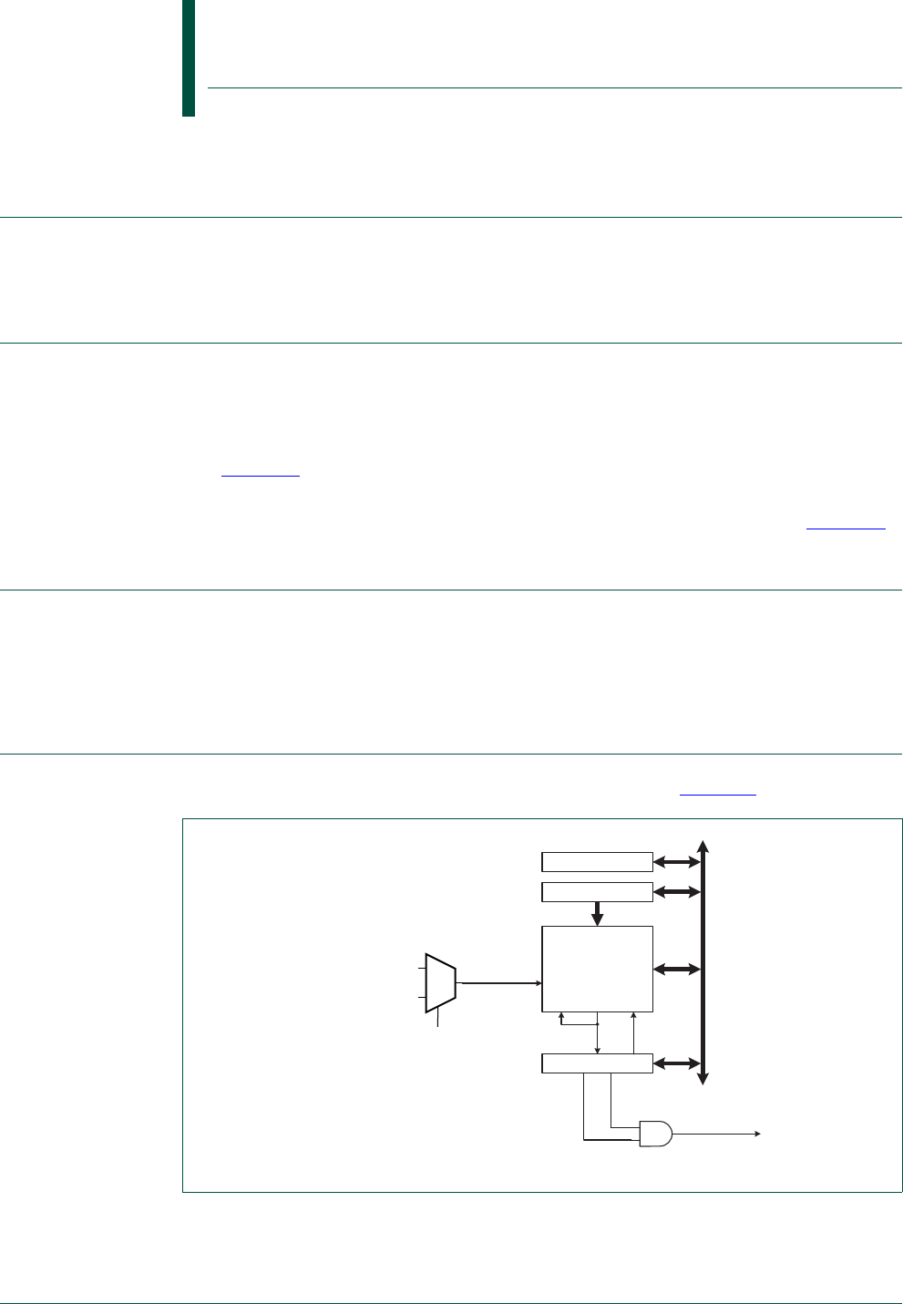
UM10462 All information provided in this document is subject to legal disclaimers. © NXP B.V. 2014. All rights reserved.
User manual Rev. 5.3 — 11 June 2014 377 of 521
18.1 How to read this chapter
The system tick timer (SysTick timer) is part of the ARM Cortex-M0 core and is identical
for all LPC11U3x/2x/1x.
18.2 Basic configuration
The system tick timer is configured using the following registers:
1. Pins: The system tick timer uses no external pins.
2. Power: The system tick timer is enabled through the SysTick control register
(Table 452). The system tick timer clock is fixed to half the frequency of the system
clock.
3. Enable the clock source for the SysTick timer in the SYST_CSR register (Table 452).
18.3 Features
•Simple 24-bit timer.
•Uses dedicated exception vector.
•Clocked internally by the system clock or the system clock/2.
18.4 General description
The block diagram of the SysTick timer is shown below in the Figure 68.
The SysTick timer is an integral part of the Cortex-M0. The SysTick timer is intended to
generate a fixed 10 millisecond interrupt for use by an operating system or other system
management software.
UM10462
Chapter 18: LPC11U3x/2x/1x System tick timer
Rev. 5.3 — 11 June 2014 User manual
Fig 68. System tick timer block diagram
system clock
reference clock
= system clock/2
SYST_CALIB
SYST_RVR
SYST_CVR
24-bit down counter
ENABLE
SYST_CSR
private
peripheral
bus
System Tick
interrupt
TICKINTCOUNTFLAG
load
under-
flow count
enable
clock
load data
1
0
SYST_CSR
bit CLKSOURCE
UM10462 All information provided in this document is subject to legal disclaimers. © NXP B.V. 2014. All rights reserved.
User manual Rev. 5.3 — 11 June 2014 378 of 521
NXP Semiconductors UM10462
Chapter 18: LPC11U3x/2x/1x System tick timer
Since the SysTick timer is a part of the Cortex-M0, it facilitates porting of software by
providing a standard timer that is available on Cortex-M0 based devices. The SysTick
timer can be used for:
•An RTOS tick timer which fires at a programmable rate (for example 100 Hz) and
invokes a SysTick routine.
•A high-speed alarm timer using the core clock.
•A simple counter. Software can use this to measure time to completion and time used.
•An internal clock source control based on missing/meeting durations. The
COUNTFLAG bit-field in the control and status register can be used to determine if an
action completed within a set duration, as part of a dynamic clock management
control loop.
Refer to the Cortex-M0 User Guide for details.
18.5 Register description
The systick timer registers are located on the ARM Cortex-M0 private peripheral bus (see
Figure 4), and are part of the ARM Cortex-M0 core peripherals. For details, see
Section 24.5.4.
[1] Reset Value reflects the data stored in used bits only. It does not include content of reserved bits.
18.5.1 System Timer Control and status register
The SYST_CSR register contains control information for the SysTick timer and provides a
status flag. This register is part of the ARM Cortex-M0 core system timer register block.
For a bit description of this register, see Section 24.5.4.
This register determines the clock source for the system tick timer.
Table 345. Register overview: SysTick timer (base address 0xE000 E000)
Name Access Address
offset Description Reset value[1] Reference
SYST_CSR R/W 0x010 System Timer Control and status register 0x000 0000 Table 346
SYST_RVR R/W 0x014 System Timer Reload value register 0 Table 347
SYST_CVR R/W 0x018 System Timer Current value register 0 Table 348
SYST_CALIB R/W 0x01C System Timer Calibration value register 0x4 Table 349

UM10462 All information provided in this document is subject to legal disclaimers. © NXP B.V. 2014. All rights reserved.
User manual Rev. 5.3 — 11 June 2014 379 of 521
NXP Semiconductors UM10462
Chapter 18: LPC11U3x/2x/1x System tick timer
18.5.2 System Timer Reload value register
The SYST_RVR register is set to the value that will be loaded into the SysTick timer
whenever it counts down to zero. This register is loaded by software as part of timer
initialization. The SYST_CALIB register may be read and used as the value for
SYST_RVR register if the CPU is running at the frequency intended for use with the
SYST_CALIB value.
18.5.3 System Timer Current value register
The SYST_CVR register returns the current count from the System Tick counter when it is
read by software.
Table 346. SysTick Timer Control and status register (SYST_CSR - 0xE000 E010) bit
description
Bit Symbol Description Reset
value
0 ENABLE System Tick counter enable. When 1, the counter is enabled.
When 0, the counter is disabled.
0
1 TICKINT System Tick interrupt enable. When 1, the System Tick interrupt
is enabled. When 0, the System Tick interrupt is disabled. When
enabled, the interrupt is generated when the System Tick counter
counts down to 0.
0
2 CLKSOURCE System Tick clock source selection. When 1, the system clock
(CPU) clock is selected. When 0, the system clock/2 is selected
as the reference clock.
0
15:3 - Reserved, user software should not write ones to reserved bits.
The value read from a reserved bit is not defined.
NA
16 COUNTFLAG Returns 1 if the SysTick timer counted to 0 since the last read of
this register.
0
31:17 - Reserved, user software should not write ones to reserved bits.
The value read from a reserved bit is not defined.
NA
Table 347. System Timer Reload value register (SYST_RVR - 0xE000 E014) bit description
Bit Symbol Description Reset
value
23:0 RELOAD This is the value that is loaded into the System Tick counter when it
counts down to 0.
0
31:24 - Reserved, user software should not write ones to reserved bits.
The value read from a reserved bit is not defined.
NA
Table 348. System Timer Current value register (SYST_CVR - 0xE000 E018) bit description
Bit Symbol Description Reset
value
23:0 CURRENT Reading this register returns the current value of the System Tick
counter. Writing any value clears the System Tick counter and the
COUNTFLAG bit in STCTRL.
0
31:24 - Reserved, user software should not write ones to reserved bits. The
value read from a reserved bit is not defined.
NA

UM10462 All information provided in this document is subject to legal disclaimers. © NXP B.V. 2014. All rights reserved.
User manual Rev. 5.3 — 11 June 2014 380 of 521
NXP Semiconductors UM10462
Chapter 18: LPC11U3x/2x/1x System tick timer
18.5.4 System Timer Calibration value register (SYST_CALIB - 0xE000 E01C)
The value of the SYST_CALIB register is driven by the value of the SYSTCKCAL register
in the system configuration block (see Table 37).
18.6 Functional description
The SysTick timer is a 24-bit timer that counts down to zero and generates an interrupt.
The intent is to provide a fixed 10 millisecond time interval between interrupts. The
SysTick timer is clocked from the CPU clock (the system clock, see Figure 4) or from the
reference clock, which is fixed to half the frequency of the CPU clock. In order to generate
recurring interrupts at a specific interval, the SYST_RVR register must be initialized with
the correct value for the desired interval. A default value is provided in the SYST_CALIB
register and may be changed by software. The default value gives a 10 millisecond
interrupt rate if the CPU clock is set to 50 MHz.
18.7 Example timer calculations
To use the system tick timer, do the following:
1. Program the SYST_RVR register with the reload value RELOAD to obtain the desired
time interval.
2. Clear the SYST_CVR register by writing to it. This ensures that the timer will count
from the SYST_RVR value rather than an arbitrary value when the timer is enabled.
3. Program the SYST_SCR register with the value 0x7 which enables the SysTick timer
and the SysTick timer interrupt.
The following example illustrates selecting the SysTick timer reload value to obtain a
10 ms time interval with the LPC11U3x/2x/1x system clock set to 50 MHz.
Example (system clock = 50 MHz)
The system tick clock = system clock = 50 MHz. Bit CLKSOURCE in the SYST_CSR
register set to 1 (system clock).
RELOAD = (system tick clock frequency 10 ms) 1 = (50 MHz 10 ms) 1 = 5000001
= 499999 = 0x0007A11F.
Table 349. System Timer Calibration value register (SYST_CALIB - 0xE000 E01C) bit
description
Bit Symbol Value Description Reset
value
23:0 TENMS See Table 455.0x4
29:24 - Reserved, user software should not write ones to
reserved bits. The value read from a reserved bit is not
defined.
NA
30 SKEW See Table 455.0
31 NOREF See Table 455.0

UM10462 All information provided in this document is subject to legal disclaimers. © NXP B.V. 2014. All rights reserved.
User manual Rev. 5.3 — 11 June 2014 381 of 521
19.1 How to read this chapter
The ADC block is identical for all LPC11U3x/2x/1x parts.
19.2 Basic configuration
The ADC is configured using the following registers:
1. Pins: The ADC pin functions are configured in the IOCON register block (Section 7.4).
2. Power and peripheral clock: In the SYSAHBCLKCTRL register, set bit 13 (Table 24).
Power to the ADC is controlled through the PDRUNCFG register (Table 47).
Remark: Basic clocking for the A/D converters is determined by the APB clock (PCLK). A
programmable divider is included in the A/D converter to scale this clock to the 4.5 MHz
(max) clock needed by the successive approximation process. An accurate conversion
requires 11 clock cycles.
19.3 Features
•10-bit successive approximation Analog-to-Digital Converter (ADC).
•Input multiplexing among 8 pins.
•Power-down mode.
•Measurement range 0 to 3.6 V. Do not exceed the VDD voltage level.
•10-bit conversion time 2.44 s.
•Burst conversion mode for single or multiple inputs.
•Optional conversion on transition on input pin or Timer Match signal.
•Individual result registers for each A/D channel to reduce interrupt overhead.
19.4 Pin description
Table 350 gives a brief summary of the ADC related pins.
UM10462
Chapter 19: LPC11U3x/2x/1x ADC
Rev. 5.3 — 11 June 2014 User manual
Table 350. ADC pin description
Pin Type Description
AD[7:0] Input Analog Inputs. The A/D converter cell can measure the voltage on any
of these input signals.
Remark: While the pins are 5 V tolerant in digital mode, the maximum
input voltage must not exceed VDD when the pins are configured as
analog inputs.
VDD Input VREF; Reference voltage.

UM10462 All information provided in this document is subject to legal disclaimers. © NXP B.V. 2014. All rights reserved.
User manual Rev. 5.3 — 11 June 2014 382 of 521
NXP Semiconductors UM10462
Chapter 19: LPC11U3x/2x/1x ADC
The ADC function must be selected via the IOCON registers in order to get accurate
voltage readings on the monitored pin. For a pin hosting an ADC input, it is not possible to
have a have a digital function selected and yet get valid ADC readings. An inside circuit
disconnects ADC hardware from the associated pin whenever a digital function is selected
on that pin.
19.5 Register description
The ADC contains registers organized as shown in Table 351.
[1] Reset Value reflects the data stored in used bits only. It does not include reserved bits content.
Table 351. Register overview: ADC (base address 0x4001 C000)
Name Access Address
offset Description Reset
Value[1] Reference
CR R/W 0x000 A/D Control Register. The CR register must be written to
select the operating mode before A/D conversion can occur.
0x0000 0000 Table 352
GDR R/W 0x004 A/D Global Data Register. Contains the result of the most
recent A/D conversion.
NA Table 353
- - 0x008 Reserved. - -
INTEN R/W 0x00C A/D Interrupt Enable Register. This register contains enable
bits that allow the DONE flag of each A/D channel to be
included or excluded from contributing to the generation of
an A/D interrupt.
0x0000 0100 Table 354
DR0 R/W 0x010 A/D Channel 0 Data Register. This register contains the
result of the most recent conversion completed on channel
0
NA Table 355
DR1 R/W 0x014 A/D Channel 1 Data Register. This register contains the
result of the most recent conversion completed on channel
1.
NA Table 355
DR2 R/W 0x018 A/D Channel 2 Data Register. This register contains the
result of the most recent conversion completed on channel
2.
NA Table 355
DR3 R/W 0x01C A/D Channel 3 Data Register. This register contains the
result of the most recent conversion completed on channel
3.
NA Table 355
DR4 R/W 0x020 A/D Channel 4 Data Register. This register contains the
result of the most recent conversion completed on channel
4.
NA Table 355
DR5 R/W 0x024 A/D Channel 5 Data Register. This register contains the
result of the most recent conversion completed on channel
5.
NA Table 355
DR6 R/W 0x028 A/D Channel 6 Data Register. This register contains the
result of the most recent conversion completed on channel
6.
NA Table 355
DR7 R/W 0x02C A/D Channel 7 Data Register. This register contains the
result of the most recent conversion completed on channel
7.
NA Table 355
STAT RO 0x030 A/D Status Register. This register contains DONE and
OVERRUN flags for all of the A/D channels, as well as the
A/D interrupt flag.
0Table 356

UM10462 All information provided in this document is subject to legal disclaimers. © NXP B.V. 2014. All rights reserved.
User manual Rev. 5.3 — 11 June 2014 383 of 521
NXP Semiconductors UM10462
Chapter 19: LPC11U3x/2x/1x ADC
19.5.1 A/D Control Register (CR - 0x4001 C000)
The A/D Control Register provides bits to select A/D channels to be converted, A/D timing,
A/D modes, and the A/D start trigger.
Table 352. A/D Control Register (CR - address 0x4001 C000) bit description
Bit Symbol Value Description Reset
Value
7:0 SEL Selects which of the AD7:0 pins is (are) to be sampled and converted. Bit 0 selects Pin
AD0, bit 1 selects pin AD1,..., and bit 7 selects pin AD7.
In software-controlled mode (BURST = 0), only one channel can be selected, i.e. only one
of these bits should be 1.
In hardware scan mode (BURST = 1), any numbers of channels can be selected, i.e any
or all bits can be set to 1. If all bits are set to 0, channel 0 is selected automatically (SEL =
0x01).
0x00
15:8 CLKDIV The APB clock (PCLK) is divided by CLKDIV +1 to produce the clock for the ADC, which
should be less than or equal to 4.5 MHz. Typically, software should program the smallest
value in this field that yields a clock of 4.5 MHz or slightly less, but in certain cases (such
as a high-impedance analog source) a slower clock may be desirable.
0
16 BURST Burst mode
Remark: If BURST is set to 1, the ADGINTEN bit in the INTEN register (Table 354) must
be set to 0.
0
0 Software-controlled mode: Conversions are software-controlled and require 11 clocks.
1 Hardware scan mode: The AD converter does repeated conversions at the rate selected
by the CLKS field, scanning (if necessary) through the pins selected by 1s in the SEL
field. The first conversion after the start corresponds to the least-significant bit set to 1 in
the SEL field, then the next higher bits (pins) set to 1 are scanned if applicable. Repeated
conversions can be terminated by clearing this bit, but the conversion in progress when
this bit is cleared will be completed.
Important: START bits must be 000 when BURST = 1 or conversions will not start.
19:17 CLKS This field selects the number of clocks used for each conversion in Burst mode, and the
number of bits of accuracy of the result in the LS bits of ADDR, between 11 clocks
(10 bits) and 4 clocks (3 bits).
000
0x0 11 clocks / 10 bits
0x1 10 clocks / 9 bits
0x2 9 clocks / 8 bits
0x3 8 clocks / 7 bits
0x4 7 clocks / 6 bits
0x5 6 clocks / 5 bits
0x6 5 clocks / 4 bits
0x7 4 clocks / 3 bits
23:20 - Reserved, user software should not write ones to reserved bits. The value read from a
reserved bit is not defined.
NA

UM10462 All information provided in this document is subject to legal disclaimers. © NXP B.V. 2014. All rights reserved.
User manual Rev. 5.3 — 11 June 2014 384 of 521
NXP Semiconductors UM10462
Chapter 19: LPC11U3x/2x/1x ADC
[1] Note that this does not require that the timer match function appear on a device pin.
19.5.2 A/D Global Data Register (GDR - 0x4001 C004)
The A/D Global Data Register contains the result of the most recent A/D conversion. This
includes the data, DONE, and Overrun flags, and the number of the A/D channel to which
the data relates.
26:24 START When the BURST bit is 0, these bits control whether and when an A/D conversion is
started:
0
0x0 No start (this value should be used when clearing PDN to 0).
0x1 Start conversion now.
0x2 Start conversion when the edge selected by bit 27 occurs on a trigger signal on
CT16B0_CAP0 (independently of the pinout).
0x3 Start conversion when the edge selected by bit 27 occurs on a trigger input on
CT32B0_CAP0 (independently of the pinout).
0x4 Start conversion when the edge selected by bit 27 occurs on CT32B0_MAT0[1].
0x5 Start conversion when the edge selected by bit 27 occurs on CT32B0_MAT1[1].
0x6 Start conversion when the edge selected by bit 27 occurs on CT16B0_MAT0[1].
0x7 Start conversion when the edge selected by bit 27 occurs on CT16B0_MAT1[1].
27 EDGE This bit is significant only when the START field contains 010-111. In these cases: 0
0 Start conversion on a rising edge on the selected CAP/MAT signal.
1 Start conversion on a falling edge on the selected CAP/MAT signal.
31:28 - Reserved, user software should not write ones to reserved bits. The value read from a
reserved bit is not defined.
NA
Table 352. A/D Control Register (CR - address 0x4001 C000) bit description
Bit Symbol Value Description Reset
Value
Table 353. A/D Global Data Register (GDR - address 0x4001 C004) bit description
Bit Symbol Description Reset
Value
5:0 - Reserved. These bits always read as zeros. 0
15:6 V_VREF When DONE is 1, this field contains a binary fraction representing
the voltage on the ADn pin selected by the SEL field, divided by
the voltage on the VDD pin. Zero in the field indicates that the
voltage on the ADn pin was less than, equal to, or close to that on
VSS, while 0x3FF indicates that the voltage on ADn was close to,
equal to, or greater than that on VREF.
X
23:16 - Reserved. These bits always read as zeros. 0
26:24 CHN These bits contain the channel from which the result bits V_VREF
were converted.
X
29:27 - Reserved. These bits always read as zeros. 0
30 OVERRUN This bit is 1 in burst mode if the results of one or more conversions
was (were) lost and overwritten before the conversion that
produced the result in the V_VREF bits.
0
31 DONE This bit is set to 1 when an A/D conversion completes. It is cleared
when this register is read and when the ADCR is written. If the
ADCR is written while a conversion is still in progress, this bit is
set and a new conversion is started.
0

UM10462 All information provided in this document is subject to legal disclaimers. © NXP B.V. 2014. All rights reserved.
User manual Rev. 5.3 — 11 June 2014 385 of 521
NXP Semiconductors UM10462
Chapter 19: LPC11U3x/2x/1x ADC
19.5.3 A/D Interrupt Enable Register (INTEN - 0x4001 C00C)
This register allows control over which A/D channels generate an interrupt when a
conversion is complete. For example, it may be desirable to use some A/D channels to
monitor sensors by continuously performing conversions on them. The most recent
results are read by the application program whenever they are needed. In this case, an
interrupt is not desirable at the end of each conversion for some A/D channels.
19.5.4 A/D Data Registers (DR0 to DR7 - 0x4001 C010 to 0x4001 C02C)
The A/D Data Register hold the result when an A/D conversion is complete, and also
include the flags that indicate when a conversion has been completed and when a
conversion overrun has occurred.
19.5.5 A/D Status Register (STAT - 0x4001 C030)
The A/D Status register allows checking the status of all A/D channels simultaneously.
The DONE and OVERRUN flags appearing in the DRn register for each A/D channel are
mirrored in ADSTAT. The interrupt flag (the logical OR of all DONE flags) is also found in
ADSTAT.
Table 354. A/D Interrupt Enable Register (INTEN - address 0x4001 C00C) bit description
Bit Symbol Description Reset
Value
7:0 ADINTEN These bits allow control over which A/D channels generate
interrupts for conversion completion. When bit 0 is one, completion
of a conversion on A/D channel 0 will generate an interrupt, when bit
1 is one, completion of a conversion on A/D channel 1 will generate
an interrupt, etc.
0x00
8 ADGINTEN When 1, enables the global DONE flag in ADDR to generate an
interrupt. When 0, only the individual A/D channels enabled by
ADINTEN 7:0 will generate interrupts.
Remark: This bit must be set to 0 in burst mode (BURST = 1 in the
CR register).
1
31:9 - Reserved. Unused, always 0. 0
Table 355. A/D Data Registers (DR0 to DR7 - addresses 0x4001 C010 to 0x4001 C02C) bit
description
Bit Symbol Description Reset
Value
5:0 - Reserved. 0
15:6 V_VREF When DONE is 1, this field contains a binary fraction representing the
voltage on the ADn pin, divided by the voltage on the VREF pin. Zero in
the field indicates that the voltage on the ADn pin was less than, equal
to, or close to that on VREF, while 0x3FF indicates that the voltage on
AD input was close to, equal to, or greater than that on VREF.
NA
29:16 - Reserved. 0
30 OVERRUN This bit is 1 in burst mode if the results of one or more conversions
was (were) lost and overwritten before the conversion that produced
the result in the V_VREF bits.This bit is cleared by reading this
register.
0
31 DONE This bit is set to 1 when an A/D conversion completes. It is cleared
when this register is read.
0

UM10462 All information provided in this document is subject to legal disclaimers. © NXP B.V. 2014. All rights reserved.
User manual Rev. 5.3 — 11 June 2014 386 of 521
NXP Semiconductors UM10462
Chapter 19: LPC11U3x/2x/1x ADC
19.6 Operation
19.6.1 Hardware-triggered conversion
If the BURST bit in the ADCR0 is 0 and the START field contains 010-111, the A/D
converter will start a conversion when a transition occurs on a selected pin or timer match
signal.
19.6.2 Interrupts
An interrupt is requested to the interrupt controller when the ADINT bit in the ADSTAT
register is 1. The ADINT bit is one when any of the DONE bits of A/D channels that are
enabled for interrupts (via the ADINTEN register) are one. Software can use the Interrupt
Enable bit in the interrupt controller that corresponds to the ADC to control whether this
results in an interrupt. The result register for an A/D channel that is generating an interrupt
must be read in order to clear the corresponding DONE flag.
19.6.3 Accuracy vs. digital receiver
While the A/D converter can be used to measure the voltage on any ADC input pin,
regardless of the pin’s setting in the IOCON block, selecting the ADC in the IOCON
registers function improves the conversion accuracy by disabling the pin’s digital receiver
(see also Section 7.3.7).
Table 356. A/D Status Register (STAT - address 0x4001 C030) bit description
Bit Symbol Description Reset
Value
7:0 DONE These bits mirror the DONE status flags that appear in the result
register for each A/D channel n.
0
15:8 OVERRUN These bits mirror the OVERRRUN status flags that appear in the
result register for each A/D channel n. Reading ADSTAT allows
checking the status of all A/D channels simultaneously.
0
16 ADINT This bit is the A/D interrupt flag. It is one when any of the
individual A/D channel Done flags is asserted and enabled to
contribute to the A/D interrupt via the ADINTEN register.
0
31:17 - Reserved. Unused, always 0. 0

UM10462 All information provided in this document is subject to legal disclaimers. © NXP B.V. 2014. All rights reserved.
User manual Rev. 5.3 — 11 June 2014 387 of 521
20.1 How to read this chapter
See Table 357 for different flash configurations and functionality.
Remark: In addition to the ISP and IAP commands, a register can be accessed in the
flash controller block to configure flash memory access times, see Section 20.16.4.1.
UM10462
Chapter 20: LPC11U3x/2x/1x Flash programming firmware
Rev. 5.3 — 11 June 2014 User manual
Table 357. LPC11U3x/2x/1x flash configurations
Type number Flash in kB Configuration Page erase IAP
command
supported
EEPROM
in kB ISP via UART ISP via USB
MSC
LPC11U12FBD48/201 16 Table 360 no no yes no
LPC11U12FHN33/201 16 Table 360 no no yes no
LPC11U13FBD48/201 24 Table 360 no no yes no
LPC11U14FBD48/201 32 Table 360 no no yes no
LPC11U14FHN33/201 32 Table 360 no no yes no
LPC11U14FHI33/201 32 Table 360 no no yes no
LPC11U14FET48/201 32 Table 360 no no yes no
LPC11U22FBD48/301 16 Table 360 no 1 yes yes
LPC11U23FBD48/301 24 Table 360 no 1 yes yes
LPC11U24FHI33/301 32 Table 360 no 2 yes yes
LPC11U24FBD48/301 32 Table 360 no 2 yes yes
LPC11U24FET48/301 32 Table 360 no 2 yes yes
LPC11U24FHN33/401 32 Table 360 no 4 yes yes
LPC11U24FBD48/401 32 Table 360 no 4 yes yes
LPC11U24FBD64/401 32 Table 360 no 4 yes yes
LPC11U34FHN33/311 40 Table 361 yes 4 yes yes
LPC11U34FBD48/311 40 Table 361 yes 4 yes yes
LPC11U34FHN33/421 48 Table 361 yes 4 yes yes
LPC11U34FBD48/421 48 Table 361 yes 4 yes yes
LPC11U35FHN33/401 64 Table 361 yes 4 yes yes
LPC11U35FBD48/401 64 Table 361 yes 4 yes yes
LPC11U35FBD64/401 64 Table 361 yes 4 yes yes
LPC11U35FHI33/501 64 Table 361 yes 4 yes yes
LPC11U35FET48/501 64 Table 361 yes 4 yes yes
LPC11U36FBD48/401 96 Table 361 yes 4 yes yes
LPC11U36FBD64/401 96 Table 361 yes 4 yes yes
LPC11U37FBD48/401 128 Table 361 yes 4 yes yes
LPC11U37HFBD64/401 128 Table 361 yes 4 yes yes
LPC11U37FBD64/501 128 Table 361 yes 4 yes yes

UM10462 All information provided in this document is subject to legal disclaimers. © NXP B.V. 2014. All rights reserved.
User manual Rev. 5.3 — 11 June 2014 388 of 521
NXP Semiconductors UM10462
Chapter 20: LPC11U3x/2x/1x Flash programming firmware
20.2 Bootloader
The bootloader controls initial operation after reset and also provides the means to
program the flash memory. This could be initial programming of a blank device, erasure
and re-programming of a previously programmed device, or programming of the flash
memory by the application program in a running system.
The bootloader version can be read by ISP/IAP calls (see Section 20.13.12 or
Section 20.14.6).
Remark: SRAM location 0x1000 0000 to 0x1000 0050 is not used by the bootloader and
the memory content in this area is retained during reset. SRAM memory is not retained
when the part powers down or enters Deep power-down mode.
20.3 Features
•In-System Programming: In-System programming (ISP) is programming or
reprogramming the on-chip flash memory, using the bootloader software and the
UART serial port. This can be done when the part resides in the end-user board.
•In Application Programming: In-Application (IAP) programming is performing erase
and write operation on the on-chip flash memory, as directed by the end-user
application code.
•Flash access times can be configured through a register in the flash controller block.
•Erase time for one sector is 100 ms 5%. Programming time for one block of
256 bytes is 1 ms 5%.
•Support for ISP via the USB port through enumeration as a Mass Storage Class
(MSC) Device when connected to a USB host interface. See Section 20.1 for
supported parts.
20.4 Description
The bootloader code is executed every time the part is powered on or reset (see
Figure 69). The loader can execute the ISP command handler or the user application
code. A LOW level during reset at the PIO0_1 pin is considered an external hardware
request to start the ISP command handler (or the USB device handler - see Section 20.1)
without checking for a valid user code first.
Assuming that power supply pins are at their nominal levels when the rising edge on
RESET pin is generated, it may take up to 3 ms before the ISP entry pin is sampled and
the decision whether to continue with user code or ISP handler is made. The boot loader
performs the following steps (see Figure 69):
1. If the watchdog overflow flag is set, the boot loader checks whether a valid user code
is present. If the watchdog overflow flag is not set, the ISP entry pin is checked.
2. If there is no request for the ISP command handler execution (ISP entry pin is
sampled HIGH after reset), a search is made for a valid user program.
3. If a valid user program is found then the execution control is transferred to it. If a valid
user program is not found, the boot loader checks the USB boot pin to load a user
code either via USB or UART.

UM10462 All information provided in this document is subject to legal disclaimers. © NXP B.V. 2014. All rights reserved.
User manual Rev. 5.3 — 11 June 2014 389 of 521
NXP Semiconductors UM10462
Chapter 20: LPC11U3x/2x/1x Flash programming firmware
For the LPC11U3x/2x/1x parts, the state of PIO0_3 determines whether the UART or USB
interface will be used (see Section 20.1):
•If PIO0_3 is sampled HIGH, the bootloader connects the LPC1Uxx as a MSC USB
device to a PC host. The LPC11U3x/2x/1x flash memory space is represented as a
drive in the host’s operating system.
•If PIO0_3 is sampled LOW, the bootloader configures the UART serial port using pins
PIO0_18 and PIO0_19 for RXD and TXD and calls the ISP command handler.
Remark: The sampling of pin PIO0_1 can be disabled through programming flash
location 0x0000 02FC (see Section 20.12.1).
The use of the ISP entry pins depends on the boot loader version. See Table 358. The
boot loader version can be obtained using the ISP or IAP commands. Also refer to the
LPC11U1x errata.
20.5 Memory map after any reset
The boot block is 16 kB in size and is located in the memory region starting from the
address 0x1FFF 0000. The bootloader is designed to run from this memory area, but both
the ISP and IAP software use parts of the on-chip RAM. The RAM usage is described
later in this chapter. The interrupt vectors residing in the boot block of the on-chip flash
memory also become active after reset, i.e., the bottom 512 bytes of the boot block are
also visible in the memory region starting from the address 0x0000 0000.
20.6 Flash content protection mechanism
The LPC11U3x/2x/1x is equipped with the Error Correction Code (ECC) capable Flash
memory. The purpose of an error correction module is twofold. Firstly, it decodes data
words read from the memory into output data words. Secondly, it encodes data words to
be written to the memory. The error correction capability consists of single bit error
correction with Hamming code.
The operation of ECC is transparent to the running application. The ECC content itself is
stored in a flash memory not accessible by user’s code to either read from it or write into it
on its own. A byte of ECC corresponds to every consecutive 128 bits of the user
accessible Flash. Consequently, Flash bytes from 0x0000 0000 to 0x0000 000F are
protected by the first ECC byte, Flash bytes from 0x0000 0010 to 0x0000 001F are
protected by the second ECC byte, etc.
Table 358. ISP entry pins for different boot loader versions
Boot loader
version ISP entry pins Boot modes
7.0 Pins PIO0_1 and PIO0_3 must be pulled LOW to enter
UART ISP mode.
UART only
7.1 Only pin PIO0_1 must be pulled LOW to enter UART ISP
mode. Pin PIO0_3 is don’t care.
UART only
7.4 and higher Pins PIO0_1 and PIO0_3 must be pulled LOW to enter
UART ISP mode.
UART and USB

UM10462 All information provided in this document is subject to legal disclaimers. © NXP B.V. 2014. All rights reserved.
User manual Rev. 5.3 — 11 June 2014 390 of 521
NXP Semiconductors UM10462
Chapter 20: LPC11U3x/2x/1x Flash programming firmware
Whenever the CPU requests a read from user’s Flash, both 128 bits of raw data
containing the specified memory location and the matching ECC byte are evaluated. If the
ECC mechanism detects a single error in the fetched data, a correction will be applied
before data are provided to the CPU. When a write request into the user’s Flash is made,
write of user specified content is accompanied by a matching ECC value calculated and
stored in the ECC memory.
When a sector of Flash memory is erased, the corresponding ECC bytes are also erased.
Once an ECC byte is written, it can not be updated unless it is erased first. Therefore, for
the implemented ECC mechanism to perform properly, data must be written into the flash
memory in groups of 16 bytes (or multiples of 16), aligned as described above.
20.7 Criterion for Valid User Code
The reserved ARM Cortex-M0 exception vector location 7 (offset 0x0000 001C in the
vector table) should contain the 2’s complement of the check-sum of table entries 0
through 6. This causes the checksum of the first 8 table entries to be 0. The bootloader
code checksums the first 8 locations in sector 0 of the flash. If the result is 0, then
execution control is transferred to the user code.
If the signature is not valid, the auto-baud routine synchronizes with the host via the serial
port (UART).
If the UART is selected, the host should send a ’?’ (0x3F) as a synchronization character
and wait for a response. The host side serial port settings should be 8 data bits, 1 stop bit
and no parity. The auto-baud routine measures the bit time of the received
synchronization character in terms of its own frequency and programs the baud rate
generator of the serial port. It also sends an ASCII string ("Synchronized<CR><LF>") to
the host. In response to this host should send the same string
("Synchronized<CR><LF>"). The auto-baud routine looks at the received characters to
verify synchronization. If synchronization is verified then "OK<CR><LF>" string is sent to
the host. Host should respond by sending the crystal frequency (in kHz) at which the part
is running. For example, if the part is running at 10 MHz, the response from the host
should be "10000<CR><LF>". "OK<CR><LF>" string is sent to the host after receiving the
crystal frequency. If synchronization is not verified then the auto-baud routine waits again
for a synchronization character. For auto-baud to work correctly in case of user invoked
ISP, the CCLK frequency should be greater than or equal to 10 MHz. In USART ISP
mode, the LPC11U3x/2x/1x is clocked by the IRC and the crystal frequency is ignored.
Once the crystal frequency is received the part is initialized and the ISP command handler
is invoked. For safety reasons an "Unlock" command is required before executing the
commands resulting in flash erase/write operations and the "Go" command. The rest of
the commands can be executed without the unlock command. The Unlock command is
required to be executed once per ISP session. The Unlock command is explained in
Section 20.13 “ISP commands” on page 399.

UM10462 All information provided in this document is subject to legal disclaimers. © NXP B.V. 2014. All rights reserved.
User manual Rev. 5.3 — 11 June 2014 391 of 521
NXP Semiconductors UM10462
Chapter 20: LPC11U3x/2x/1x Flash programming firmware
20.8 ISP/IAP communication protocol
All ISP commands should be sent as single ASCII strings. Strings should be terminated
with Carriage Return (CR) and/or Line Feed (LF) control characters. Extra <CR> and
<LF> characters are ignored. All ISP responses are sent as <CR><LF> terminated ASCII
strings. Data is sent and received in UU-encoded format.
20.8.1 ISP command format
"Command Parameter_0 Parameter_1 ... Parameter_n<CR><LF>" "Data" (Data only for
Write commands).
20.8.2 ISP response format
"Return_Code<CR><LF>Response_0<CR><LF>Response_1<CR><LF> ...
Response_n<CR><LF>" "Data" (Data only for Read commands).
20.8.3 ISP data format
The data stream is in UU-encoded format. The UU-encode algorithm converts 3 bytes of
binary data in to 4 bytes of printable ASCII character set. It is more efficient than Hex
format which converts 1 byte of binary data in to 2 bytes of ASCII hex. The sender should
send the check-sum after transmitting 20 UU-encoded lines. The length of any
UU-encoded line should not exceed 61 characters (bytes) i.e. it can hold 45 data bytes.
The receiver should compare it with the check-sum of the received bytes. If the
check-sum matches then the receiver should respond with "OK<CR><LF>" to continue
further transmission. If the check-sum does not match the receiver should respond with
"RESEND<CR><LF>". In response the sender should retransmit the bytes.
20.8.4 ISP flow control
A software XON/XOFF flow control scheme is used to prevent data loss due to buffer
overrun. When the data arrives rapidly, the ASCII control character DC3 (stop) is sent to
stop the flow of data. Data flow is resumed by sending the ASCII control character DC1
(start). The host should also support the same flow control scheme.
20.8.5 ISP command abort
Commands can be aborted by sending the ASCII control character "ESC". This feature is
not documented as a command under "ISP Commands" section. Once the escape code is
received the ISP command handler waits for a new command.
20.8.6 Interrupts during ISP
The boot block interrupt vectors located in the boot block of the flash are active after any
reset.

UM10462 All information provided in this document is subject to legal disclaimers. © NXP B.V. 2014. All rights reserved.
User manual Rev. 5.3 — 11 June 2014 392 of 521
NXP Semiconductors UM10462
Chapter 20: LPC11U3x/2x/1x Flash programming firmware
20.8.7 Interrupts during IAP
The on-chip flash memory and EEPROM are not accessible during erase/write
operations. When the user application code starts executing, the interrupt vectors from the
user flash area are active. Before making any IAP call, either disable the interrupts or
ensure that the user interrupt vectors are active in RAM and that the interrupt handlers
reside in RAM. The IAP code does not use or disable interrupts.
20.8.8 RAM used by ISP command handler
ISP commands use on-chip RAM from 0x1000 017C to 0x1000 025B. The user could use
this area, but the contents may be lost upon reset. Flash programming commands use the
top 32 bytes of on-chip RAM. The stack is located at RAM top 32 bytes. The maximum
stack usage is 256 bytes and grows downwards.
20.8.9 RAM used by IAP command handler
Flash programming commands use the top 32 bytes of on-chip RAM. The maximum stack
usage in the user allocated stack space is 128 bytes and grows downwards.
20.9 USB communication protocol
Remark: See Section 20.1 for supported parts.
The LPC11U3x/2x/1x is enumerated as a Mass Storage Class (MSC) device to a PC or
another embedded system. In order to connect via the USB interface, the
LPC11U3x/2x/1x must use the external crystal at a frequency of 12 MHz. The MSC device
presents an easy integration with the PC’s operating system. The LPC11U3x/2x/1x flash
memory space is represented as a drive in the host file system. The entire available user
flash is mapped to a file of the size of the LPC11U3x/2x/1x flash in the host’s folder with
the default name ‘firmware.bin’. The ‘firmware.bin’ file can be deleted and a new file can
be copied into the directory, thereby updating the user code in flash. Note that the
filename of the new flash image file is not important. After a reset or a power cycle, the
new file is visible in the host’s file system under it’s default name ‘firmware.bin’.
The code read protection (CRP, see Table 359) level determines how the flash is
reprogrammed:
If CRP1 or CRP2 is enabled, the user flash is erased when the file is deleted.
If CRP1 is enabled or no CRP is selected, the user flash is erased and reprogrammed
when the new file is copied. However, only the area occupied by the new file is erased
and reprogrammed.
Remark: The only commands supported for the LPC11U3x/2x/1x flash image folder are
copy and delete.
Three Code Read Protection (CRP) levels can be enabled for flash images updated
through USB (see Section 20.12 for details). The volume label on the MSCD indicates the
CRP status.

UM10462 All information provided in this document is subject to legal disclaimers. © NXP B.V. 2014. All rights reserved.
User manual Rev. 5.3 — 11 June 2014 393 of 521
NXP Semiconductors UM10462
Chapter 20: LPC11U3x/2x/1x Flash programming firmware
20.9.1 Usage note
When programming flash images via Flash Magic or Serial Wire Debugger (SWD), the
user code valid signature is automatically inserted by the programming utility. When using
USB ISP, the user code valid signature must be either part of the vector table, or the axf or
binary file must be post-processed to insert the checksum.
Table 359. CRP levels for USB boot images
CRP status Volume label Description
No CRP CRP DISABLD The user flash can be read or written.
CRP1 CRP1 ENABLD The user flash content cannot be read but can be updated. The
flash memory sectors are updated depending on the new
firmware image.
CRP2 CRP2 ENABLD The user flash content cannot be read but can be updated. The
entire user flash memory is erased before writing the new
firmware image.
CRP3 CRP3 ENABLD The user flash content cannot be read or updated. The
bootloader always executes the user application if valid.
UM10462 All information provided in this document is subject to legal disclaimers. © NXP B.V. 2014. All rights reserved.
User manual Rev. 5.3 — 11 June 2014 394 of 521
NXP Semiconductors UM10462
Chapter 20: LPC11U3x/2x/1x Flash programming firmware
20.10 Boot process flowchart
(1) For details on handling the crystal frequency, see Section 20.14.8.
(2) For details on available ISP commands based on the CRP settings, see Section 20.12.
Fig 69. Boot process flowchart
RESET
INITIALIZE
RECEIVE CRYSTAL FREQUENCY
RUN ISP COMMAND HANDLER
RUN AUTO-BAUD
CRP1/2/3
ENABLED?
WATCHDOG
FLAG SET?
CRP3/NO_ISP
ENABLED?
ENTER ISP
MODE?
(PIN PIO0_1)
USB ISP?
(PIN PIO0_3)
USER CODE
VALID?
USER CODE
VALID?
AUTO-BAUD
SUCCESSFUL?
EXECUTE INTERNAL
USER CODE
ENABLE DEBUG
yes
yes
yes
yes
yes
yes
(HIGH)
yes (LOW)
yes
no
no
no
no
no (LOW)
no
no (HIGH)
no
ENUMERATE AS MSC
DEVICE TO PC
A
A
UART
ISP
LPC11U2x/3x
only
USB ISP

UM10462 All information provided in this document is subject to legal disclaimers. © NXP B.V. 2014. All rights reserved.
User manual Rev. 5.3 — 11 June 2014 395 of 521
NXP Semiconductors UM10462
Chapter 20: LPC11U3x/2x/1x Flash programming firmware
20.11 Sector numbers
20.11.1 LPC11U1x/2x
Some IAP and ISP commands operate on sectors and specify sector numbers. The
following table shows the correspondence between sector numbers and memory
addresses for LPC11U2x/1x devices.
20.11.2 LPC11U3x
The LPC11U3x support a page erase command. The following table shows the
correspondence between page numbers, sector numbers, and memory addresses.
The size of a sector is 4 kB, the size of a page is 256 Byte. One sector contains 16 pages.
Table 360. LPC11U1x/2x flash sectors
Sector
number Sector
size [kB] Address range LPC11U12/
LPC11U22 LPC11U13/
LPC11U23 LPC11U14/
LPC11U24
0 4 0x0000 0000 - 0x0000 0FFF yes yes yes
1 4 0x0000 1000 - 0x0000 1FFF yes yes yes
2 4 0x0000 2000 - 0x0000 2FFF yes yes yes
3 4 0x0000 3000 - 0x0000 3FFF yes yes yes
4 4 0x0000 4000 - 0x0000 4FFF - yes yes
5 4 0x0000 5000 - 0x0000 5FFF - yes yes
6 4 0x0000 6000 - 0x0000 6FFF - - yes
7 4 0x0000 7000 - 0x0000 7FFF - - yes
Table 361. LPC11U3x flash sectors and pages
Sector
number Sector
size [kB] Page
number Address range
LPC11U34/3xx
LPC11U34/4xx
LPC11U35
LPC11U36
LPC11U37
/LPC11U37H
0 4 0 -15 0x0000 0000 - 0x0000 0FFF yes yes yes yes yes
1 4 16 - 31 0x0000 1000 - 0x0000 1FFF yes yes yes yes yes
2 4 32 - 47 0x0000 2000 - 0x0000 2FFF yes yes yes yes yes
3 4 48 - 63 0x0000 3000 - 0x0000 3FFF yes yes yes yes yes
4 4 64 - 79 0x0000 4000 - 0x0000 4FFF yes yes yes yes yes
5 4 80 - 95 0x0000 5000 - 0x0000 5FFF yes yes yes yes yes
6 4 96 - 111 0x0000 6000 - 0x0000 6FFF yes yes yes yes yes
7 4 112 - 127 0x0000 7000 - 0x0000 7FFF yes yes yes yes yes
8 4 128 - 143 0x0000 8000 - 0x0000 8FFF yes yes yes yes yes
9 4 144 - 159 0x0000 9000 - 0x0000 9FFF yes yes yes yes yes
10 4 160 - 175 0x0000 A000 - 0x0000 AFFF no yes yes yes yes
11 4 176 - 191 0x0000 B000 - 0x0000 BFFF no yes yes yes yes
12 4 192 - 207 0x0000 C000 - 0x0000 CFFF no no yes yes yes
13 4 208 - 223 0x0000 D000 - 0x0000 DFFF no no yes yes yes

UM10462 All information provided in this document is subject to legal disclaimers. © NXP B.V. 2014. All rights reserved.
User manual Rev. 5.3 — 11 June 2014 396 of 521
NXP Semiconductors UM10462
Chapter 20: LPC11U3x/2x/1x Flash programming firmware
20.12 Code Read Protection (CRP)
Code Read Protection is a mechanism that allows the user to enable different levels of
security in the system so that access to the on-chip flash and use of the ISP can be
restricted. When needed, CRP is invoked by programming a specific pattern in flash
location at 0x0000 02FC. IAP commands are not affected by the code read protection.
Important: any CRP change becomes effective only after the device has gone
through a power cycle.
14 4 224 - 239 0x0000 E000 - 0x0000 EFFF no no yes yes yes
15 4 240 - 255 0x0000 F000 - 0x0000 FFFF no no yes yes yes
16 4 256-271 0x0001 0000 - 0x0001 0FFF no no no yes yes
17 4 272-287 0x0001 1000 - 0x0001 1FFF no no no yes yes
18 4 288-303 0x0001 2000 - 0x0001 2FFF no no no yes yes
19 4 304-319 0x0001 3000 - 0x0001 3FFF no no no yes yes
20 4 320-335 0x0001 4000 - 0x0001 4FFF no no no yes yes
21 4 336-351 0x0001 5000 - 0x0001 5FFF no no no yes yes
22 4 352-367 0x0001 6000 - 0x0001 6FFF no no no yes yes
23 4 368-383 0x0001 7000 - 0x0001 7FFF no no no yes yes
24 4 384-399 0x0001 8000 - 0x0001 8FFF no no no no yes
25 4 400-415 0x0001 9000 - 0x0001 9FFF no no no no yes
26 4 416-431 0x0001 A000 - 0x0001 AFFF no no no no yes
27 4 432-447 0x0001 B000 - 0x0001 BFFF no no no no yes
28 4 448-463 0x0001 C000 - 0x0001 CFFF no no no no yes
29 4 464-479 0x0001 D000 - 0x0001 DFFF no no no no yes
30 4 480-495 0x0001 E000 - 0x0001 EFFF no no no no yes
31 4 496-511 0x0001 F000 - 0x0001 FFFF no no no no yes
Table 361. LPC11U3x flash sectors and pages …continued
Sector
number Sector
size [kB] Page
number Address range
LPC11U34/3xx
LPC11U34/4xx
LPC11U35
LPC11U36
LPC11U37
/LPC11U37H

UM10462 All information provided in this document is subject to legal disclaimers. © NXP B.V. 2014. All rights reserved.
User manual Rev. 5.3 — 11 June 2014 397 of 521
NXP Semiconductors UM10462
Chapter 20: LPC11U3x/2x/1x Flash programming firmware
Table 362. Code Read Protection (CRP) options
Name Pattern
programmed in
0x0000 02FC
Description
NO_ISP 0x4E69 7370 Prevents sampling of pin PIO0_1 for entering ISP mode. PIO0_1 is
available for other uses.
CRP1 0x12345678 Access to chip via the SWD pins is disabled. This mode allows
partial flash update using the following ISP commands and
restrictions:
•Write to RAM command should not access RAM below 0x1000
0300. Access to addresses below 0x1000 0200 is disabled.
•Copy RAM to flash command can not write to Sector 0.
•Erase command can erase Sector 0 only when all sectors are
selected for erase.
•Compare command is disabled.
•Read Memory command is disabled.
This mode is useful when CRP is required and flash field updates
are needed but all sectors can not be erased. Since compare
command is disabled in case of partial updates the secondary
loader should implement checksum mechanism to verify the integrity
of the flash.
CRP2 0x87654321 Access to chip via the SWD pins is disabled. The following ISP
commands are disabled:
•Read Memory
•Write to RAM
•Go
•Copy RAM to flash
•Compare
When CRP2 is enabled the ISP erase command only allows erasure
of all user sectors.
CRP3 0x43218765 Access to chip via the SWD pins is disabled. ISP entry by pulling
PIO0_1 LOW is disabled if a valid user code is present in flash
sector 0.
This mode effectively disables ISP override using PIO0_1 pin. It is
up to the user’s application to provide a flash update mechanism
using IAP calls or call reinvoke ISP command to enable flash update
via UART0.
Caution: If CRP3 is selected, no future factory testing can be
performed on the device.
Table 363. Code Read Protection hardware/software interaction
CRP option User Code
Valid PIO0_1 pin at
reset SWD enabled LPC11Uxx
enters USB or
UART ISP
mode
partial flash
update in ISP
mode
None No x Yes Yes Yes
None Yes High Yes No NA
None Yes Low Yes Yes Yes
CRP1 Yes High No No NA
CRP1 Yes Low No Yes Yes

UM10462 All information provided in this document is subject to legal disclaimers. © NXP B.V. 2014. All rights reserved.
User manual Rev. 5.3 — 11 June 2014 398 of 521
NXP Semiconductors UM10462
Chapter 20: LPC11U3x/2x/1x Flash programming firmware
In case a CRP mode is enabled and access to the chip is allowed via the ISP, an
unsupported or restricted ISP command will be terminated with return code
CODE_READ_PROTECTION_ENABLED.
20.12.1 ISP entry protection
In addition to the three CRP modes, the user can prevent the sampling of pin PIO0_1 for
entering ISP mode and thereby release pin PIO0_1 for other uses. This is called the
NO_ISP mode. The NO_ISP mode can be entered by programming the pattern
0x4E69 7370 at location 0x0000 02FC.
The NO_ISP mode is identical to the CRP3 mode except for SWD access, which is
allowed in NO_ISP mode but disabled in CRP3 mode. The NO_ISP mode does not offer
any code protection.
CRP2 Yes High No No NA
CRP2 Yes Low No Yes No
CRP3Yesx NoNoNA
CRP1 No x No Yes Yes
CRP2 No x No Yes No
CRP3 No x No Yes No
Table 364. ISP commands allowed for different CRP levels
ISP command CRP1 CRP2 CRP3 (no entry in ISP
mode allowed)
Unlock yes yes n/a
Set Baud Rate yes yes n/a
Echo yes yes n/a
Write to RAM yes; above 0x1000 0300
only
no n/a
Read Memory no no n/a
Prepare sector(s) for
write operation
yes yes n/a
Copy RAM to flash yes; not to sector 0 no n/a
Go no no n/a
Erase sector(s) yes; sector 0 can only be
erased when all sectors are
erased.
yes; all sectors
only
n/a
Blank check sector(s) no no n/a
Read Part ID yes yes n/a
Read Boot code version yes yes n/a
Compare no no n/a
ReadUID yes yes n/a
Table 363. Code Read Protection hardware/software interaction …continued
CRP option User Code
Valid PIO0_1 pin at
reset SWD enabled LPC11Uxx
enters USB or
UART ISP
mode
partial flash
update in ISP
mode

UM10462 All information provided in this document is subject to legal disclaimers. © NXP B.V. 2014. All rights reserved.
User manual Rev. 5.3 — 11 June 2014 399 of 521
NXP Semiconductors UM10462
Chapter 20: LPC11U3x/2x/1x Flash programming firmware
20.13 ISP commands
The following commands are accepted by the ISP command handler. Detailed status
codes are supported for each command. The command handler sends the return code
INVALID_COMMAND when an undefined command is received. Commands and return
codes are in ASCII format.
CMD_SUCCESS is sent by ISP command handler only when received ISP command has
been completely executed and the new ISP command can be given by the host.
Exceptions from this rule are "Set Baud Rate", "Write to RAM", "Read Memory", and "Go"
commands.
20.13.1 Unlock <Unlock code>
Table 365. ISP command summary
ISP Command Usage Described in
Unlock U <Unlock Code> Table 366
Set Baud Rate B <Baud Rate> <stop bit> Table 367
Echo A <setting> Table 368
Write to RAM W <start address> <number of bytes> Table 369
Read Memory R <address> <number of bytes> Table 370
Prepare sector(s) for
write operation
P <start sector number> <end sector number> Table 371
Copy RAM to flash C <Flash address> <RAM address> <number of bytes> Table 372
Go G <address> <Mode> Table 373
Erase sector(s) E <start sector number> <end sector number> Table 374
Blank check sector(s) I <start sector number> <end sector number> Table 375
Read Part ID J Table 376
Read Boot code version K Table 378
Compare M <address1> <address2> <number of bytes> Table 379
ReadUID N Table 380
Table 366. ISP Unlock command
Command U
Input Unlock code: 2313010
Return Code CMD_SUCCESS |
INVALID_CODE |
PARAM_ERROR
Description This command is used to unlock Flash Write, Erase, and Go commands.
Example "U 23130<CR><LF>" unlocks the Flash Write/Erase & Go commands.

UM10462 All information provided in this document is subject to legal disclaimers. © NXP B.V. 2014. All rights reserved.
User manual Rev. 5.3 — 11 June 2014 400 of 521
NXP Semiconductors UM10462
Chapter 20: LPC11U3x/2x/1x Flash programming firmware
20.13.2 Set Baud Rate <Baud Rate> <stop bit>
20.13.3 Echo <setting>
20.13.4 Write to RAM <start address> <number of bytes>
The host should send the data only after receiving the CMD_SUCCESS return code. The
host should send the check-sum after transmitting 20 UU-encoded lines. The checksum is
generated by adding raw data (before UU-encoding) bytes and is reset after transmitting
20 UU-encoded lines. The length of any UU-encoded line should not exceed
61 characters (bytes) i.e. it can hold 45 data bytes. When the data fits in less than
20 UU-encoded lines then the check-sum should be of the actual number of bytes sent.
The ISP command handler compares it with the check-sum of the received bytes. If the
check-sum matches, the ISP command handler responds with "OK<CR><LF>" to
continue further transmission. If the check-sum does not match, the ISP command
handler responds with "RESEND<CR><LF>". In response the host should retransmit the
bytes.
Table 367. ISP Set Baud Rate command
Command B
Input Baud Rate: 9600 | 19200 | 38400 | 57600 | 115200
Stop bit: 1 | 2
Return Code CMD_SUCCESS |
INVALID_BAUD_RATE |
INVALID_STOP_BIT |
PARAM_ERROR
Description This command is used to change the baud rate. The new baud rate is effective
after the command handler sends the CMD_SUCCESS return code.
Example "B 57600 1<CR><LF>" sets the serial port to baud rate 57600 bps and 1 stop bit.
Table 368. ISP Echo command
Command A
Input Setting: ON = 1 | OFF = 0
Return Code CMD_SUCCESS |
PARAM_ERROR
Description The default setting for echo command is ON. When ON the ISP command handler
sends the received serial data back to the host.
Example "A 0<CR><LF>" turns echo off.

UM10462 All information provided in this document is subject to legal disclaimers. © NXP B.V. 2014. All rights reserved.
User manual Rev. 5.3 — 11 June 2014 401 of 521
NXP Semiconductors UM10462
Chapter 20: LPC11U3x/2x/1x Flash programming firmware
20.13.5 Read Memory <address> <no. of bytes>
The data stream is followed by the command success return code. The check-sum is sent
after transmitting 20 UU-encoded lines. The checksum is generated by adding raw data
(before UU-encoding) bytes and is reset after transmitting 20 UU-encoded lines. The
length of any UU-encoded line should not exceed 61 characters (bytes) i.e. it can hold
45 data bytes. When the data fits in less than 20 UU-encoded lines then the check-sum is
of actual number of bytes sent. The host should compare it with the checksum of the
received bytes. If the check-sum matches then the host should respond with
"OK<CR><LF>" to continue further transmission. If the check-sum does not match then
the host should respond with "RESEND<CR><LF>". In response the ISP command
handler sends the data again.
20.13.6 Prepare sector(s) for write operation <start sector number> <end
sector number>
This command makes flash write/erase operation a two step process.
Table 369. ISP Write to RAM command
Command W
Input Start Address: RAM address where data bytes are to be written. This address
should be a word boundary.
Number of Bytes: Number of bytes to be written. Count should be a multiple of 4
Return Code CMD_SUCCESS |
ADDR_ERROR (Address not on word boundary) |
ADDR_NOT_MAPPED |
COUNT_ERROR (Byte count is not multiple of 4) |
PARAM_ERROR |
CODE_READ_PROTECTION_ENABLED
Description This command is used to download data to RAM. Data should be in UU-encoded
format. This command is blocked when code read protection is enabled.
Example "W 268436224 4<CR><LF>" writes 4 bytes of data to address 0x1000 0300.
Table 370. ISP Read Memory command
Command R
Input Start Address: Address from where data bytes are to be read. This address
should be a word boundary.
Number of Bytes: Number of bytes to be read. Count should be a multiple of 4.
Return Code CMD_SUCCESS followed by <actual data (UU-encoded)> |
ADDR_ERROR (Address not on word boundary) |
ADDR_NOT_MAPPED |
COUNT_ERROR (Byte count is not a multiple of 4) |
PARAM_ERROR |
CODE_READ_PROTECTION_ENABLED
Description This command is used to read data from RAM or flash memory. This command is
blocked when code read protection is enabled.
Example "R 268435456 4<CR><LF>" reads 4 bytes of data from address 0x1000 0000.

UM10462 All information provided in this document is subject to legal disclaimers. © NXP B.V. 2014. All rights reserved.
User manual Rev. 5.3 — 11 June 2014 402 of 521
NXP Semiconductors UM10462
Chapter 20: LPC11U3x/2x/1x Flash programming firmware
20.13.7 Copy RAM to flash <Flash address> <RAM address> <no of bytes>
When writing to the flash, the following limitations apply:
1. The smallest amount of data that can be written to flash by the copy RAM to flash
command is 256 byte (equal to one page).
2. One page consists of 16 flash words (lines), and the smallest amount that can be
modified per flash write is one flash word (one line). This limitation is due to the
application of ECC to the flash write operation, see Section 20.6.
3. To avoid write disturbance (a mechanism intrinsic to flash memories), an erase should
be performed after following 16 consecutive writes inside the same page. Note that
the erase operation then erases the entire sector.
Remark: Once a page has been written to 16 times, it is still possible to write to other
pages within the same sector without performing a sector erase (assuming that those
pages have been erased previously).
Table 371. ISP Prepare sector(s) for write operation command
Command P
Input Start Sector Number
End Sector Number: Should be greater than or equal to start sector number.
Return Code CMD_SUCCESS |
BUSY |
INVALID_SECTOR |
PARAM_ERROR
Description This command must be executed before executing "Copy RAM to flash" or "Erase
Sector(s)" command. Successful execution of the "Copy RAM to flash" or "Erase
Sector(s)" command causes relevant sectors to be protected again. The boot
block can not be prepared by this command. To prepare a single sector use the
same "Start" and "End" sector numbers.
Example "P 0 0<CR><LF>" prepares the flash sector 0.

UM10462 All information provided in this document is subject to legal disclaimers. © NXP B.V. 2014. All rights reserved.
User manual Rev. 5.3 — 11 June 2014 403 of 521
NXP Semiconductors UM10462
Chapter 20: LPC11U3x/2x/1x Flash programming firmware
20.13.8 Go <address> <mode>
The GO command is usually used after the flash image has been updated. After the
update a reset is required. Therefore, the GO command should point to the RESET
handler. Since the device is still in ISP mode, the RESET handler should do the following:
•Re-initialize the SP pointer to the application default.
•Set the SYSMEMREMAP to either 0x01 or 0x02.
While in ISP mode, the SYSMEMREMAP is set to 0x00.
Alternatively, the following snippet can be loaded into the RAM for execution:
SCB->AIRCR = 0x05FA0004; //issue system reset
while(1); //should never come here
This snippet will issue a system reset request to the core.
Table 372. ISP Copy command
Command C
Input Flash Address (DST): Destination flash address where data bytes are to be
written. The destination address should be a 256 byte boundary.
RAM Address (SRC): Source RAM address from where data bytes are to be read.
Number of Bytes: Number of bytes to be written. Should be 256 | 512 | 1024 |
4096.
Return Code CMD_SUCCESS |
SRC_ADDR_ERROR (Address not on word boundary) |
DST_ADDR_ERROR (Address not on correct boundary) |
SRC_ADDR_NOT_MAPPED |
DST_ADDR_NOT_MAPPED |
COUNT_ERROR (Byte count is not 256 | 512 | 1024 | 4096) |
SECTOR_NOT_PREPARED_FOR WRITE_OPERATION |
BUSY |
CMD_LOCKED |
PARAM_ERROR |
CODE_READ_PROTECTION_ENABLED
Description This command is used to program the flash memory. The "Prepare Sector(s) for
Write Operation" command should precede this command. The affected sectors are
automatically protected again once the copy command is successfully executed.
The boot block cannot be written by this command. This command is blocked when
code read protection is enabled. Also see Section 20.6 for the number of bytes that
can be written.
Example "C 0 268467504 512<CR><LF>" copies 512 bytes from the RAM address
0x1000 0800 to the flash address 0.

UM10462 All information provided in this document is subject to legal disclaimers. © NXP B.V. 2014. All rights reserved.
User manual Rev. 5.3 — 11 June 2014 404 of 521
NXP Semiconductors UM10462
Chapter 20: LPC11U3x/2x/1x Flash programming firmware
The following ISP commands will send the system reset code loaded into 0x1000 000.
U 23130
W 268435456 16
0`4@"20%@_N<,[0#@!`#Z!0``
1462
G 268435456 T
20.13.9 Erase sector(s) <start sector number> <end sector number>
Table 373. ISP Go command
Command G
Input Address: Flash or RAM address from which the code execution is to be started.
This address should be on a word boundary.
Mode: T (Execute program in Thumb Mode) | A (not allowed).
Return Code CMD_SUCCESS |
ADDR_ERROR |
ADDR_NOT_MAPPED |
CMD_LOCKED |
PARAM_ERROR |
CODE_READ_PROTECTION_ENABLED
Description This command is used to execute a program residing in RAM or flash memory. It
may not be possible to return to the ISP command handler once this command is
successfully executed. This command is blocked when code read protection is
enabled. The command must be used with an address of 0x0000 0200 or greater.
Example "G 512 T<CR><LF>" branches to address 0x0000 0200 in Thumb mode.
Table 374. ISP Erase sector command
Command E
Input Start Sector Number
End Sector Number: Should be greater than or equal to start sector number.
Return Code CMD_SUCCESS |
BUSY |
INVALID_SECTOR |
SECTOR_NOT_PREPARED_FOR_WRITE_OPERATION |
CMD_LOCKED |
PARAM_ERROR |
CODE_READ_PROTECTION_ENABLED
Description This command is used to erase one or more sector(s) of on-chip flash memory. The
boot block can not be erased using this command. This command only allows
erasure of all user sectors when the code read protection is enabled.
Example "E 2 3<CR><LF>" erases the flash sectors 2 and 3.

UM10462 All information provided in this document is subject to legal disclaimers. © NXP B.V. 2014. All rights reserved.
User manual Rev. 5.3 — 11 June 2014 405 of 521
NXP Semiconductors UM10462
Chapter 20: LPC11U3x/2x/1x Flash programming firmware
20.13.10 Blank check sector(s) <sector number> <end sector number>
20.13.11 Read Part Identification number
Table 375. ISP Blank check sector command
Command I
Input Start Sector Number:
End Sector Number: Should be greater than or equal to start sector number.
Return Code CMD_SUCCESS |
SECTOR_NOT_BLANK (followed by <Offset of the first non blank word location>
<Contents of non blank word location>) |
INVALID_SECTOR |
PARAM_ERROR
Description This command is used to blank check one or more sectors of on-chip flash memory.
Blank check on sector 0 always fails as first 64 bytes are re-mapped to flash
boot block.
When CRP is enabled, the blank check command returns 0 for the offset and value
of sectors which are not blank. Blank sectors are correctly reported irrespective of
the CRP setting.
Example "I 2 3<CR><LF>" blank checks the flash sectors 2 and 3.
Table 376. ISP Read Part Identification command
Command J
Input None.
Return Code CMD_SUCCESS followed by part identification number in ASCII (see Table 377
“LPC11U3x/2x/1x device identification numbers”).
Description This command is used to read the part identification number.
Table 377. LPC11U3x/2x/1x device identification numbers
Device Hex coding
LPC11U12FHN33/201 0x095C 802B/0x295C 802B
LPC11U12FBD48/201 0x095C 802B/0x295C 802B
LPC11U13FBD48/201 0x097A 802B/0x297A 802B
LPC11U14FHN33/201 0x0998 802B/0x2998 802B
LPC11U14FHI33/201 0x2998 802B
LPC11U14FBD48/201 0x0998 802B/0x2998 802B
LPC11U14FET48/201 0x0998 802B/0x2998 802B
LPC11U22FBD48/301 0x2954 402B
LPC11U23FBD48/301 0x2972 402B
LPC11U24FHI33/301 0x2988 402B
LPC11U24FBD48/301 0x2988 402B
LPC11U24FET48/301 0x2988 402B
LPC11U24FHN33/401 0x2980 002B
LPC11U24FBD48/401 0x2980 002B
LPC11U24FBD64/401 0x2980 002B
LPC11U34FHN33/311 0x0003 D440

UM10462 All information provided in this document is subject to legal disclaimers. © NXP B.V. 2014. All rights reserved.
User manual Rev. 5.3 — 11 June 2014 406 of 521
NXP Semiconductors UM10462
Chapter 20: LPC11U3x/2x/1x Flash programming firmware
20.13.12 Read Boot code version number
20.13.13 Compare <address1> <address2> <no of bytes>
LPC11U34FBD48/311 0x0003 D440
LPC11U34FHN33/421 0x0001 CC40
LPC11U34FBD48/421 0x0001 CC40
LPC11U35FHN33/401 0x0001 BC40
LPC11U35FBD48/401 0x0001 BC40
LPC11U35FBD64/401 0x0001 BC40
LPC11U35FHI33/501 0x0000 BC40
LPC11U35FET48/501 0x0000 BC40
LPC11U36FBD48/401 0x0001 9C40
LPC11U36FBD64/401 0x0001 9C40
LPC11U37FBD48/401 0x0001 7C40
LPC11U37HFBD64/401 0x0000 7C44
LPC11U37FBD64/501 0x0000 7C40
Table 377. LPC11U3x/2x/1x device identification numbers …continued
Device Hex coding
Table 378. ISP Read Boot Code version number command
Command K
Input None
Return Code CMD_SUCCESS followed by 2 bytes of boot code version number in ASCII format.
It is to be interpreted as <byte1(Major)>.<byte0(Minor)>.
Description This command is used to read the boot code version number.
Table 379. ISP Compare command
Command M
Input Address1 (DST): Starting flash or RAM address of data bytes to be compared.
This address should be a word boundary.
Address2 (SRC): Starting flash or RAM address of data bytes to be compared.
This address should be a word boundary.
Number of Bytes: Number of bytes to be compared; should be a multiple of 4.
Return Code CMD_SUCCESS | (Source and destination data are equal)
COMPARE_ERROR | (Followed by the offset of first mismatch)
COUNT_ERROR (Byte count is not a multiple of 4) |
ADDR_ERROR |
ADDR_NOT_MAPPED |
PARAM_ERROR |
Description This command is used to compare the memory contents at two locations.
Compare result may not be correct when source or destination address
contains any of the first 512 bytes starting from address zero. First 512 bytes
are re-mapped to boot ROM
Example "M 8192 268468224 4<CR><LF>" compares 4 bytes from the RAM address
0x1000 8000 to the 4 bytes from the flash address 0x2000.

UM10462 All information provided in this document is subject to legal disclaimers. © NXP B.V. 2014. All rights reserved.
User manual Rev. 5.3 — 11 June 2014 407 of 521
NXP Semiconductors UM10462
Chapter 20: LPC11U3x/2x/1x Flash programming firmware
20.13.14 ReadUID
20.13.15 ISP Return Codes
Table 380. ReadUID command
Command N
Input None
Return Code CMD_SUCCESS followed by four 32-bit words of a unique serial number in ASCII
format. The word sent at the lowest address is sent first.
Description This command is used to read the unique ID.
Table 381. ISP Return Codes Summary
Return
Code Mnemonic Description
0 CMD_SUCCESS Command is executed successfully. Sent by ISP
handler only when command given by the host has
been completely and successfully executed.
1 INVALID_COMMAND Invalid command.
2 SRC_ADDR_ERROR Source address is not on word boundary.
3 DST_ADDR_ERROR Destination address is not on a correct boundary.
4 SRC_ADDR_NOT_MAPPED Source address is not mapped in the memory map.
Count value is taken in to consideration where
applicable.
5 DST_ADDR_NOT_MAPPED Destination address is not mapped in the memory
map. Count value is taken in to consideration
where applicable.
6 COUNT_ERROR Byte count is not multiple of 4 or is not a permitted
value.
7 INVALID_SECTOR Sector number is invalid or end sector number is
greater than start sector number.
8 SECTOR_NOT_BLANK Sector is not blank.
9 SECTOR_NOT_PREPARED_FOR_
WRITE_OPERATION
Command to prepare sector for write operation
was not executed.
10 COMPARE_ERROR Source and destination data not equal.
11 BUSY Flash programming hardware interface is busy.
12 PARAM_ERROR Insufficient number of parameters or invalid
parameter.
13 ADDR_ERROR Address is not on word boundary.
14 ADDR_NOT_MAPPED Address is not mapped in the memory map. Count
value is taken in to consideration where applicable.
15 CMD_LOCKED Command is locked.
16 INVALID_CODE Unlock code is invalid.
17 INVALID_BAUD_RATE Invalid baud rate setting.
18 INVALID_STOP_BIT Invalid stop bit setting.
19 CODE_READ_PROTECTION_
ENABLED
Code read protection enabled.

UM10462 All information provided in this document is subject to legal disclaimers. © NXP B.V. 2014. All rights reserved.
User manual Rev. 5.3 — 11 June 2014 408 of 521
NXP Semiconductors UM10462
Chapter 20: LPC11U3x/2x/1x Flash programming firmware
20.14 IAP commands
Remark: When using the IAP commands, configure the power profiles in Default mode.
See Section 5.7.1 “set_power”.
For in application programming the IAP routine should be called with a word pointer in
register r0 pointing to memory (RAM) containing command code and parameters. The
result of the IAP command is returned in the result table pointed to by register r1. The user
can reuse the command table for result by passing the same pointer in registers r0 and r1.
The parameter table should be big enough to hold all the results in case the number of
results are more than number of parameters. Parameter passing is illustrated in the
Figure 70.
The number of parameters and results vary according to the IAP command. The
maximum number of parameters is 5, passed to the "Copy RAM to FLASH" command.
The maximum number of results is 4, returned by the "ReadUID" command. The
command handler sends the status code INVALID_COMMAND when an undefined
command is received. The IAP routine resides at 0x1FFF 1FF0 location and it is thumb
code.
The IAP function could be called in the following way using C:
Define the IAP location entry point. Since the 0th bit of the IAP location is set there will be
a change to Thumb instruction set when the program counter branches to this address.
#define IAP_LOCATION 0x1fff1ff1
Define data structure or pointers to pass IAP command table and result table to the IAP
function:
unsigned int command_param[5];
unsigned int status_result[4];
or
unsigned int * command_param;
unsigned int * status_result;
command_param = (unsigned int *) 0x...
status_result =(unsigned int *) 0x...
Define pointer to function type, which takes two parameters and returns void. Note the IAP
returns the result with the base address of the table residing in R1.
typedef void (*IAP)(unsigned int [],unsigned int[]);
IAP iap_entry;
Setting the function pointer:
iap_entry=(IAP) IAP_LOCATION;
To call the IAP, use the following statement.
iap_entry (command_param,status_result);

UM10462 All information provided in this document is subject to legal disclaimers. © NXP B.V. 2014. All rights reserved.
User manual Rev. 5.3 — 11 June 2014 409 of 521
NXP Semiconductors UM10462
Chapter 20: LPC11U3x/2x/1x Flash programming firmware
Up to 4 parameters can be passed in the r0, r1, r2 and r3 registers respectively (see the
ARM Thumb Procedure Call Standard SWS ESPC 0002 A-05). Additional parameters are
passed on the stack. Up to 4 parameters can be returned in the r0, r1, r2 and r3 registers
respectively. Additional parameters are returned indirectly via memory. Some of the IAP
calls require more than 4 parameters. If the ARM suggested scheme is used for the
parameter passing/returning then it might create problems due to difference in the C
compiler implementation from different vendors. The suggested parameter passing
scheme reduces such risk.
The flash memory is not accessible during a write or erase operation. IAP commands,
which results in a flash write/erase operation, use 32 bytes of space in the top portion of
the on-chip RAM for execution. The user program should not be using this space if IAP
flash programming is permitted in the application.
Table 382. IAP Command Summary
IAP Command Command code Reference
Prepare sector(s) for write operation 50 (decimal) Table 383
Copy RAM to flash 51 (decimal) Table 384
Erase sector(s) 52 (decimal) Table 385
Blank check sector(s) 53 (decimal) Table 386
Read Part ID 54 (decimal) Table 387
Read Boot code version 55 (decimal) Table 388
Compare 56 (decimal) Table 389
Reinvoke ISP 57 (decimal) Table 390
Read UID 58 (decimal) Table 391
Erase page 59 (decimal) Table 392
EEPROM Write 61(decimal) Table 393
EEPROM Read 62(decimal) Table 394
UM10462 All information provided in this document is subject to legal disclaimers. © NXP B.V. 2014. All rights reserved.
User manual Rev. 5.3 — 11 June 2014 410 of 521
NXP Semiconductors UM10462
Chapter 20: LPC11U3x/2x/1x Flash programming firmware
20.14.1 Prepare sector(s) for write operation
This command makes flash write/erase operation a two step process.
20.14.2 Copy RAM to flash
See Section 20.13.7 for limitations on the write-to-flash process.
Fig 70. IAP parameter passing
Command code
Param 0
Param 1
Param n
status_result[0]
status_result[1]
Status code
Result 0
Result 1
Result n
Command Parameter Array
Status Result Array
ARM REGISTER r0
ARM REGISTER r1
command_param[0]
command_param[1]
command_param[2]
command_param[n]
status_result[2]
status_result[n]
Table 383. IAP Prepare sector(s) for write operation command
Command Prepare sector(s) for write operation
Input Command code: 50 (decimal)
Param0: Start Sector Number
Param1: End Sector Number (should be greater than or equal to start sector
number).
Status Code CMD_SUCCESS |
BUSY |
INVALID_SECTOR
Result None
Description This command must be executed before executing "Copy RAM to flash" or "Erase
Sector(s)" command. Successful execution of the "Copy RAM to flash" or "Erase
Sector(s)" command causes relevant sectors to be protected again. The boot
sector can not be prepared by this command. To prepare a single sector use the
same "Start" and "End" sector numbers.

UM10462 All information provided in this document is subject to legal disclaimers. © NXP B.V. 2014. All rights reserved.
User manual Rev. 5.3 — 11 June 2014 411 of 521
NXP Semiconductors UM10462
Chapter 20: LPC11U3x/2x/1x Flash programming firmware
20.14.3 Erase Sector(s)
Table 384. IAP Copy RAM to flash command
Command Copy RAM to flash
Input Command code: 51 (decimal)
Param0(DST): Destination flash address where data bytes are to be written. This
address should be a 256 byte boundary.
Param1(SRC): Source RAM address from which data bytes are to be read. This
address should be a word boundary.
Param2: Number of bytes to be written. Should be 256 | 512 | 1024 | 4096.
Param3: System Clock Frequency (CCLK) in kHz.
Status Code CMD_SUCCESS |
SRC_ADDR_ERROR (Address not a word boundary) |
DST_ADDR_ERROR (Address not on correct boundary) |
SRC_ADDR_NOT_MAPPED |
DST_ADDR_NOT_MAPPED |
COUNT_ERROR (Byte count is not 256 | 512 | 1024 | 4096) |
SECTOR_NOT_PREPARED_FOR_WRITE_OPERATION |
BUSY
Result None
Description This command is used to program the flash memory. The affected sectors should
be prepared first by calling "Prepare Sector for Write Operation" command. The
affected sectors are automatically protected again once the copy command is
successfully executed. The boot sector can not be written by this command. Also
see Section 20.6 for the number of bytes that can be written.
Table 385. IAP Erase Sector(s) command
Command Erase Sector(s)
Input Command code: 52 (decimal)
Param0: Start Sector Number
Param1: End Sector Number (should be greater than or equal to start sector
number).
Param2: System Clock Frequency (CCLK) in kHz.
Status Code CMD_SUCCESS |
BUSY |
SECTOR_NOT_PREPARED_FOR_WRITE_OPERATION |
INVALID_SECTOR
Result None
Description This command is used to erase a sector or multiple sectors of on-chip flash
memory. The boot sector can not be erased by this command. To erase a single
sector use the same "Start" and "End" sector numbers.

UM10462 All information provided in this document is subject to legal disclaimers. © NXP B.V. 2014. All rights reserved.
User manual Rev. 5.3 — 11 June 2014 412 of 521
NXP Semiconductors UM10462
Chapter 20: LPC11U3x/2x/1x Flash programming firmware
20.14.4 Blank check sector(s)
20.14.5 Read Part Identification number
20.14.6 Read Boot code version number
Table 386. IAP Blank check sector(s) command
Command Blank check sector(s)
Input Command code: 53 (decimal)
Param0: Start Sector Number
Param1: End Sector Number (should be greater than or equal to start sector
number).
Status code CMD_SUCCESS |
BUSY |
SECTOR_NOT_BLANK |
INVALID_SECTOR
Result Result0: Offset of the first non blank word location if the status code is
SECTOR_NOT_BLANK.
Result1: Contents of non blank word location.
Description This command is used to blank check a sector or multiple sectors of on-chip flash
memory. To blank check a single sector use the same "Start" and "End" sector
numbers.
Table 387. IAP Read Part Identification command
Command Read part identification number
Input Command code: 54 (decimal)
Parameters: None
Status code CMD_SUCCESS
Result Result0: Part Identification Number.
Description This command is used to read the part identification number.
Table 388. IAP Read Boot Code version number command
Command Read boot code version number
Input Command code: 55 (decimal)
Parameters: None
Status code CMD_SUCCESS
Result Result0: Boot code version number. Read as <byte1(Major)>.<byte0(Minor)>
Description This command is used to read the boot code version number.

UM10462 All information provided in this document is subject to legal disclaimers. © NXP B.V. 2014. All rights reserved.
User manual Rev. 5.3 — 11 June 2014 413 of 521
NXP Semiconductors UM10462
Chapter 20: LPC11U3x/2x/1x Flash programming firmware
20.14.7 Compare <address1> <address2> <no of bytes>
20.14.8 Reinvoke ISP
20.14.9 ReadUID
Table 389. IAP Compare command
Command Compare
Input Command code: 56 (decimal)
Param0(DST): Starting flash or RAM address of data bytes to be compared. This
address should be a word boundary.
Param1(SRC): Starting flash or RAM address of data bytes to be compared. This
address should be a word boundary.
Param2: Number of bytes to be compared; should be a multiple of 4.
Status code CMD_SUCCESS |
COMPARE_ERROR |
COUNT_ERROR (Byte count is not a multiple of 4) |
ADDR_ERROR |
ADDR_NOT_MAPPED
Result Result0: Offset of the first mismatch if the status code is COMPARE_ERROR.
Description This command is used to compare the memory contents at two locations.
The result may not be correct when the source or destination includes any
of the first 512 bytes starting from address zero. The first 512 bytes can be
re-mapped to RAM.
Table 390. Reinvoke ISP
Command Compare
Input Command code: 57 (decimal)
Status code None
Result None.
Description This command is used to invoke the bootloader in ISP mode. It maps boot
vectors, sets PCLK = CCLK, configures UART pins RXD and TXD, resets
counter/timer CT32B1 and resets the U0FDR (see Table 247). This command
may be used when a valid user program is present in the internal flash memory
and the PIO0_1 pin is not accessible to force the ISP mode.
Table 391. IAP ReadUID command
Command Compare
Input Command code: 58 (decimal)
Status code CMD_SUCCESS
Result Result0: The first 32-bit word (at the lowest address).
Result1: The second 32-bit word.
Result2: The third 32-bit word.
Result3: The fourth 32-bit word.
Description This command is used to read the unique ID.

UM10462 All information provided in this document is subject to legal disclaimers. © NXP B.V. 2014. All rights reserved.
User manual Rev. 5.3 — 11 June 2014 414 of 521
NXP Semiconductors UM10462
Chapter 20: LPC11U3x/2x/1x Flash programming firmware
20.14.10 Erase page
Remark: See Table 357 for list of parts that implement this command.
20.14.11 Write EEPROM
20.14.12 Read EEPROM
Table 392. IAP Erase page command
Command Erase page
Input Command code: 59 (decimal)
Param0: Start page number.
Param1: End page number (should be greater than or equal to start page)
Param2: System Clock Frequency (CCLK) in kHz.
Status code CMD_SUCCESS |
BUSY |
SECTOR_NOT_PREPARED_FOR_WRITE_OPERATION |
INVALID_SECTOR
Result None
Description This command is used to erase a page or multiple pages of on-chip flash memory.
To erase a single page use the same "start" and "end" page numbers. See
Table 357 for list of parts that implement this command.
Table 393. IAP Write EEPROM command
Command Compare
Input Command code: 61 (decimal)
Param0: EEPROM address.
Param1: RAM address.
Param2: Number of bytes to be written.
Param3: System Clock Frequency (CCLK) in kHz. The minimum CCLK frequency
supported is CCLK = 200 kHz.
Status code CMD_SUCCESS | SRC_ADDR_NOT_MAPPED | DST_ADDR_NOT_MAPPED
Result None
Description Data is copied from the RAM address to the EEPROM address.
Remark: The top 64 bytes of the 4 kB EEPROM memory are reserved and
cannot be written to. The entire EEPROM is writable for smaller EEPROM sizes.
Table 394. IAP Read EEPROM command
Command Compare
Input Command code: 62 (decimal)
Param0: EEPROM address.
Param1: RAM address.
Param2: Number of bytes to be read.
Param3: System Clock Frequency (CCLK) in kHz. The minimum CCLK frequency
supported is CCLK = 200 kHz.
Status code CMD_SUCCESS | SRC_ADDR_NOT_MAPPED | DST_ADDR_NOT_MAPPED
Result None
Description Data is copied from the EEPROM address to the RAM address.

UM10462 All information provided in this document is subject to legal disclaimers. © NXP B.V. 2014. All rights reserved.
User manual Rev. 5.3 — 11 June 2014 415 of 521
NXP Semiconductors UM10462
Chapter 20: LPC11U3x/2x/1x Flash programming firmware
20.14.13 IAP Status codes
20.15 Debug notes
20.15.1 Comparing flash images
Depending on the debugger used and the IDE debug settings, the memory that is visible
when the debugger connects might be the boot ROM, the internal SRAM, or the flash. To
help determine which memory is present in the current debug environment, check the
value contained at flash address 0x0000 0004. This address contains the entry point to
the code in the ARM Cortex-M0 vector table, which is the bottom of the boot ROM, the
internal SRAM, or the flash memory respectively.
20.15.2 Serial Wire Debug (SWD) flash programming interface
Debug tools can write parts of the flash image to RAM and then execute the IAP call
"Copy RAM to flash" repeatedly with proper offset.
Table 395. IAP Status codes summary
Status
code Mnemonic Description
0 CMD_SUCCESS Command is executed successfully.
1 INVALID_COMMAND Invalid command.
2 SRC_ADDR_ERROR Source address is not on a word boundary.
3 DST_ADDR_ERROR Destination address is not on a correct boundary.
4 SRC_ADDR_NOT_MAPPED Source address is not mapped in the memory map.
Count value is taken in to consideration where
applicable.
5 DST_ADDR_NOT_MAPPED Destination address is not mapped in the memory
map. Count value is taken in to consideration where
applicable.
6 COUNT_ERROR Byte count is not multiple of 4 or is not a permitted
value.
7 INVALID_SECTOR Sector number is invalid.
8 SECTOR_NOT_BLANK Sector is not blank.
9 SECTOR_NOT_PREPARED_
FOR_WRITE_OPERATION
Command to prepare sector for write operation was
not executed.
10 COMPARE_ERROR Source and destination data is not same.
11 BUSY flash programming hardware interface is busy.
Table 396. Memory mapping in debug mode
Memory mapping mode Memory start address visible at 0x0000 0004
Bootloader mode 0x1FFF 0000
User flash mode 0x0000 0000
User SRAM mode 0x1000 0000
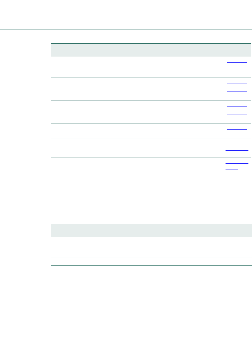
UM10462 All information provided in this document is subject to legal disclaimers. © NXP B.V. 2014. All rights reserved.
User manual Rev. 5.3 — 11 June 2014 416 of 521
NXP Semiconductors UM10462
Chapter 20: LPC11U3x/2x/1x Flash programming firmware
20.16 Register description
20.16.1 EEPROM BIST start address register
The EEPROM BIST start address register is used to program the start address for the
BIST. During BIST the EEPROM devices are accessed with 16-bit read operations so the
LSB of the address is fixed zero.
20.16.2 EEPROM BIST stop address register
The EEPROM BIST stop address register is used to program the stop address for the
BIST and also to start the BIST. During BIST the EEPROM devices are accessed with
16-bit read operations so the LSB of the address is fixed zero.
Table 397. Register overview: FMC (base address 0x4003 C000)
Name Access Address
offset Description Reset
value Reference
FLASHCFG R/W 0x010 Flash memory access time
configuration register
- Table 401
FMSSTART R/W 0x020 Signature start address register 0 Table 402
FMSSTOP R/W 0x024 Signature stop-address register 0 Table 403
FMSW0 R 0x02C Word 0 [31:0] - Table 404
FMSW1 R 0x030 Word 1 [63:32] - Table 405
FMSW2 R 0x034 Word 2 [95:64] - Table 406
FMSW3 R 0x038 Word 3 [127:96] - Table 407
EEMSSTART R/W 0x09C EEPROM BIST start address register 0x0 Table 398
EEMSSTOP R/W 0x0A0 EEPROM BIST stop address register 0x0 Table 399
EEMSSIG R 0x0A4 EEPROM 24-bit BIST signature register 0x0 Table 400
FMSTAT R 0xFE0 Signature generation status register 0
Section 20.
16.4.5
FMSTATCLR W 0xFE8 Signature generation status clear
register
-Section 20.
16.4.6
Table 398. EEPROM BIST start address register (EEMSSTART - address 0x4003 C09C) bit
description
Bit Symbol Description Reset
value Access
13:0 STARTA BIST start address:
Bit 0 is fixed zero since only even addresses are
allowed.
0x0 R/W
31:14 - Reserved 0x0 -

UM10462 All information provided in this document is subject to legal disclaimers. © NXP B.V. 2014. All rights reserved.
User manual Rev. 5.3 — 11 June 2014 417 of 521
NXP Semiconductors UM10462
Chapter 20: LPC11U3x/2x/1x Flash programming firmware
20.16.3 EEPROM signature register
The EEPROM BIST signature register returns the signatures as produced by the
embedded signature generators.
20.16.4 Flash controller registers
20.16.4.1 Flash memory access register
Depending on the system clock frequency, access to the flash memory can be configured
with various access times by writing to the FLASHCFG register.
Remark: Improper setting of this register may result in incorrect operation of the
LPC11U3x/2x/1x flash memory.
Table 399. EEPROM BIST stop address register (EEMSSTOP - address 0x4003 C0A0) bit
description
Bit Symbol Description Reset
value Access
13:0 STOPA BIST stop address:
Bit 0 is fixed zero since only even addresses are
allowed.
0x0 R/W
29:14 - Reserved 0x0 -
30 DEVSEL BIST device select bit
0: the BIST signature is generated over the total
memory space. Singe pages are interleaved over the
EEPROM devices when multiple devices are used, the
signature is generated over memory of multiple
devices.
1: the BIST signature is generated only over a memory
range located on a single EEPROM device. Therefore
the internal address generation is done such that the
address’ CS bits are kept stable to select only the same
device. The address’ MSB and LSB bits are used to
step through the memory range specified by the start
and stop address fields.
Note: if this bit is set the start and stop address fields
must be programmed such that they both address the
same EEPROM device. Therefore the address’ CS bits
in both the start and stop address must be the same.
0x0 R/W
31 STRTBIST BIST start bit
Setting this bit will start the BIST. This bit is
self-clearing.
0x0 R/W
Table 400. EEPROM BIST signature register (EEMSSIG - address 0x4003 C0A4) bit
description
Bits Field name Description Reset
value Access
15:0 DATA_SIG BIST 16-bit signature calculated from only the data
bytes
0x0 R
31:16 PARITY_SIG BIST 16-bit signature calculated from only the parity bits
of the data bytes
0x0 R

UM10462 All information provided in this document is subject to legal disclaimers. © NXP B.V. 2014. All rights reserved.
User manual Rev. 5.3 — 11 June 2014 418 of 521
NXP Semiconductors UM10462
Chapter 20: LPC11U3x/2x/1x Flash programming firmware
20.16.4.2 Flash signature generation
The flash module contains a built-in signature generator. This generator can produce a
128-bit signature from a range of flash memory. A typical usage is to verify the flashed
contents against a calculated signature (e.g. during programming).
The address range for generating a signature must be aligned on flash-word boundaries,
i.e. 128-bit boundaries. Once started, signature generation completes independently.
While signature generation is in progress, the flash memory cannot be accessed for other
purposes, and an attempted read will cause a wait state to be asserted until signature
generation is complete. Code outside of the flash (e.g. internal RAM) can be executed
during signature generation. This can include interrupt services, if the interrupt vector
table is re-mapped to memory other than the flash memory. The code that initiates
signature generation should also be placed outside of the flash memory.
20.16.4.3 Signature generation address and control registers
These registers control automatic signature generation. A signature can be generated for
any part of the flash memory contents. The address range to be used for generation is
defined by writing the start address to the signature start address register (FMSSTART)
and the stop address to the signature stop address register (FMSSTOP). The start and
stop addresses must be aligned to 128-bit boundaries and can be derived by dividing the
byte address by 16.
Signature generation is started by setting the SIG_START bit in the FMSSTOP register.
Setting the SIG_START bit is typically combined with the signature stop address in a
single write.
Table 402 and Table 403 show the bit assignments in the FMSSTART and FMSSTOP
registers respectively.
Table 401. Flash configuration register (FLASHCFG, address 0x4003 C010) bit description
Bit Symbol Value Description Reset
value
1:0 FLASHTIM Flash memory access time. FLASHTIM +1 is equal to the
number of system clocks used for flash access.
0x2
0x0 1 system clock flash access time (for system clock
frequencies of up to 20 MHz).
0x1 2 system clocks flash access time (for system clock
frequencies of up to 40 MHz).
0x2 3 system clocks flash access time (for system clock
frequencies of up to 50 MHz).
0x3 Reserved
31:2 - - Reserved. User software must not change the value of
these bits. Bits 31:2 must be written back exactly as read.
-
Table 402. Flash module signature start register (FMSSTART - 0x4003 C020) bit description
Bit Symbol Description Reset
value
16:0 START Signature generation start address (corresponds to AHB byte
address bits[20:4]).
0
31:17 - Reserved, user software should not write ones to reserved bits.
The value read from a reserved bit is not defined.
NA

UM10462 All information provided in this document is subject to legal disclaimers. © NXP B.V. 2014. All rights reserved.
User manual Rev. 5.3 — 11 June 2014 419 of 521
NXP Semiconductors UM10462
Chapter 20: LPC11U3x/2x/1x Flash programming firmware
20.16.4.4 Signature generation result registers
The signature generation result registers return the flash signature produced by the
embedded signature generator. The 128-bit signature is reflected by the four registers
FMSW0, FMSW1, FMSW2 and FMSW3.
The generated flash signature can be used to verify the flash memory contents. The
generated signature can be compared with an expected signature and thus makes saves
time and code space. The method for generating the signature is described in
Section 20.16.4.7.
Table 407 show bit assignment of the FMSW0 and FMSW1, FMSW2, FMSW3 registers
respectively.
20.16.4.5 Flash module status register
The read-only FMSTAT register provides a means of determining when signature
generation has completed. Completion of signature generation can be checked by polling
the SIG_DONE bit in FMSTAT register. SIG_DONE should be cleared via the
FMSTATCLR register before starting a signature generation operation, otherwise the
status might indicate completion of a previous operation.
Table 403. Flash module signature stop register (FMSSTOP - 0x4003 C024) bit description
Bit Symbol Value Description Reset
value
16:0 STOP BIST stop address divided by 16 (corresponds to AHB
byte address [20:4]).
0
17 SIG_START Start control bit for signature generation. 0
0 Signature generation is stopped
1 Initiate signature generation
31:18 - Reserved, user software should not write ones to
reserved bits. The value read from a reserved bit is not
defined.
NA
Table 404. FMSW0 register (FMSW0, address: 0x4003 C02C) bit description
Bit Symbol Description Reset value
31:0 SW0[31:0] Word 0 of 128-bit signature (bits 31 to 0). -
Table 405. FMSW1 register (FMSW1, address: 0x4003 C030) bit description
Bit Symbol Description Reset value
31:0 SW1[63:32] Word 1 of 128-bit signature (bits 63 to 32). -
Table 406. FMSW2 register (FMSW2, address: 0x4003 C034) bit description
Bit Symbol Description Reset value
31:0 SW2[95:64] Word 2 of 128-bit signature (bits 95 to 64). -
Table 407. FMSW3 register (FMSW3, address: 0x4003 40C8) bit description
Bit Symbol Description Reset value
31:0 SW3[127:96] Word 3 of 128-bit signature (bits 127 to 96). -

UM10462 All information provided in this document is subject to legal disclaimers. © NXP B.V. 2014. All rights reserved.
User manual Rev. 5.3 — 11 June 2014 420 of 521
NXP Semiconductors UM10462
Chapter 20: LPC11U3x/2x/1x Flash programming firmware
20.16.4.6 Flash module status clear register
The FMSTATCLR register is used to clear the signature generation completion flag.
20.16.4.7 Algorithm and procedure for signature generation
Signature generation
A signature can be generated for any part of the flash contents. The address range to be
used for signature generation is defined by writing the start address to the FMSSTART
register, and the stop address to the FMSSTOP register.
The signature generation is started by writing a ‘1’ to the SIG_START bit in the FMSSTOP
register. Starting the signature generation is typically combined with defining the stop
address, which is done in the STOP bits of the same register.
The time that the signature generation takes is proportional to the address range for which
the signature is generated. Reading of the flash memory for signature generation uses a
self-timed read mechanism and does not depend on any configurable timing settings for
the flash. A safe estimation for the duration of the signature generation is:
Duration = int((60 / tcy) + 3) x (FMSSTOP - FMSSTART + 1)
When signature generation is triggered via software, the duration is in AHB clock cycles,
and tcy is the time in ns for one AHB clock. The SIG_DONE bit in FMSTAT can be polled
by software to determine when signature generation is complete.
After signature generation, a 128-bit signature can be read from the FMSW0 to FMSW3
registers. The 128-bit signature reflects the corrected data read from the flash. The 128-bit
signature reflects flash parity bits and check bit values.
Content verification
Table 408. Flash module status register (FMSTAT - 0x4003 CFE0) bit description
Bit Symbol Description Reset
value
1:0 - Reserved, user software should not write ones to reserved bits.
The value read from a reserved bit is not defined.
NA
2 SIG_DONE When 1, a previously started signature generation has
completed. See FMSTATCLR register description for clearing this
flag.
0
31:3 - Reserved, user software should not write ones to reserved bits.
The value read from a reserved bit is not defined.
NA
Table 409. Flash module status clear register (FMSTATCLR - 0x0x4003 CFE8) bit description
Bit Symbol Description Reset
value
1:0 - Reserved, user software should not write ones to reserved
bits. The value read from a reserved bit is not defined.
NA
2 SIG_DONE_CLR Writing a 1 to this bits clears the signature generation
completion flag (SIG_DONE) in the FMSTAT register.
0
31:3 - Reserved, user software should not write ones to reserved
bits. The value read from a reserved bit is not defined.
NA

UM10462 All information provided in this document is subject to legal disclaimers. © NXP B.V. 2014. All rights reserved.
User manual Rev. 5.3 — 11 June 2014 421 of 521
NXP Semiconductors UM10462
Chapter 20: LPC11U3x/2x/1x Flash programming firmware
The signature as it is read from the FMSW0 to FMSW3 registers must be equal to the
reference signature. The algorithms to derive the reference signature is given in
Figure 71.
Fig 71. Algorithm for generating a 128-bit signature
int128 signature = 0
int128 nextSignature
FOR address = flashpage 0 TO address = flashpage max
{
FOR i = 0 TO 126 {
nextSignature[i] = flashword[i] XOR signature[i+1]}
nextSignature[127] = flashword[127] XOR signature[0] XOR signature[2]
XOR signature[27] XOR signature[29]
signature = nextSignature
}
return signature

UM10462 All information provided in this document is subject to legal disclaimers. © NXP B.V. 2014. All rights reserved.
User manual Rev. 5.3 — 11 June 2014 422 of 521
21.1 How to read this chapter
The debug functionality is identical for all LPC11U3x/2x/1x parts.
21.2 Features
•Supports ARM Serial Wire Debug mode.
•Direct debug access to all memories, registers, and peripherals.
•No target resources are required for the debugging session.
•Four breakpoints.
•Two data watchpoints that can also be used as triggers.
•Supports JTAG boundary scan.
21.3 Introduction
Debug functions are integrated into the ARM Cortex-M0. Serial wire debug functions are
supported. The ARM Cortex-M0 is configured to support up to four breakpoints and two
watchpoints.
21.4 Description
Debugging with the LPC11U3x/2x/1x uses the Serial Wire Debug mode. Support for
boundary scan is available.
21.5 Pin description
The tables below indicate the various pin functions related to debug. Some of these
functions share pins with other functions which therefore may not be used at the same
time.
UM10462
Chapter 21: LPC11U3x/2x/1x Serial Wire Debugger (SWD)
Rev. 5.3 — 11 June 2014 User manual
Table 410. Serial Wire Debug pin description
Pin Name Type Description
SWCLK Input Serial Wire Clock. This pin is the clock for SWD debug logic when in
the Serial Wire Debug mode (SWD). This pin is pulled up internally.
SWDIO Input /
Output
Serial wire debug data input/output. The SWDIO pin is used by an
external debug tool to communicate with and control the
LPC11U3x/2x/1x. This pin is pulled up internally.

UM10462 All information provided in this document is subject to legal disclaimers. © NXP B.V. 2014. All rights reserved.
User manual Rev. 5.3 — 11 June 2014 423 of 521
NXP Semiconductors UM10462
Chapter 21: LPC11U3x/2x/1x Serial Wire Debugger (SWD)
21.6 Functional description
21.6.1 Debug limitations
Important: Due to limitations of the ARM Cortex-M0 integration, the LPC11U3x/2x/1x
cannot wake up in the usual manner from Deep-sleep mode. It is recommended not to
use this mode during debug.
Another issue is that debug mode changes the way in which reduced power modes work
internal to the ARM Cortex-M0 CPU, and this ripples through the entire system. These
differences mean that power measurements should not be made while debugging, the
results will be higher than during normal operation in an application.
During a debugging session, the System Tick Timer is automatically stopped whenever
the CPU is stopped. Other peripherals are not affected.
21.6.2 Debug connections for SWD
For debugging purposes, it is useful to provide access to the ISP entry pin PIO0_1. This
pin can be used to recover the part from configurations which would disable the SWD port
such as improper PLL configuration, reconfiguration of SWD pins as ADC inputs, entry
into Deep power-down mode out of reset, etc. This pin can be used for other functions
such as GPIO, but it should not be held LOW on power-up or reset.
Table 411. JTAG boundary scan pin description
Pin Name Type Description
TCK Input JTAG Test Clock. This pin is the clock for JTAG boundary scan
when the RESET pin is LOW.
TMS Input JTAG Test Mode Select. The TMS pin selects the next state in the
TAP state machine. This pin includes an internal pull-up and is used
for JTAG boundary scan when the RESET pin is LOW.
TDI Input JTAG Test Data In. This is the serial data input for the shift register.
This pin includes an internal pull-up and is used for JTAG boundary
scan when the RESET pin is LOW.
TDO Output JTAG Test Data Output. This is the serial data output from the shift
register. Data is shifted out of the device on the negative edge of the
TCK signal. This pin is used for JTAG boundary scan when the
RESET pin is LOW.
TRST Input JTAG Test Reset. The TRST pin can be used to reset the test logic
within the debug logic. This pin includes an internal pull-up and is
used for JTAG boundary scan when the RESET pin is LOW.
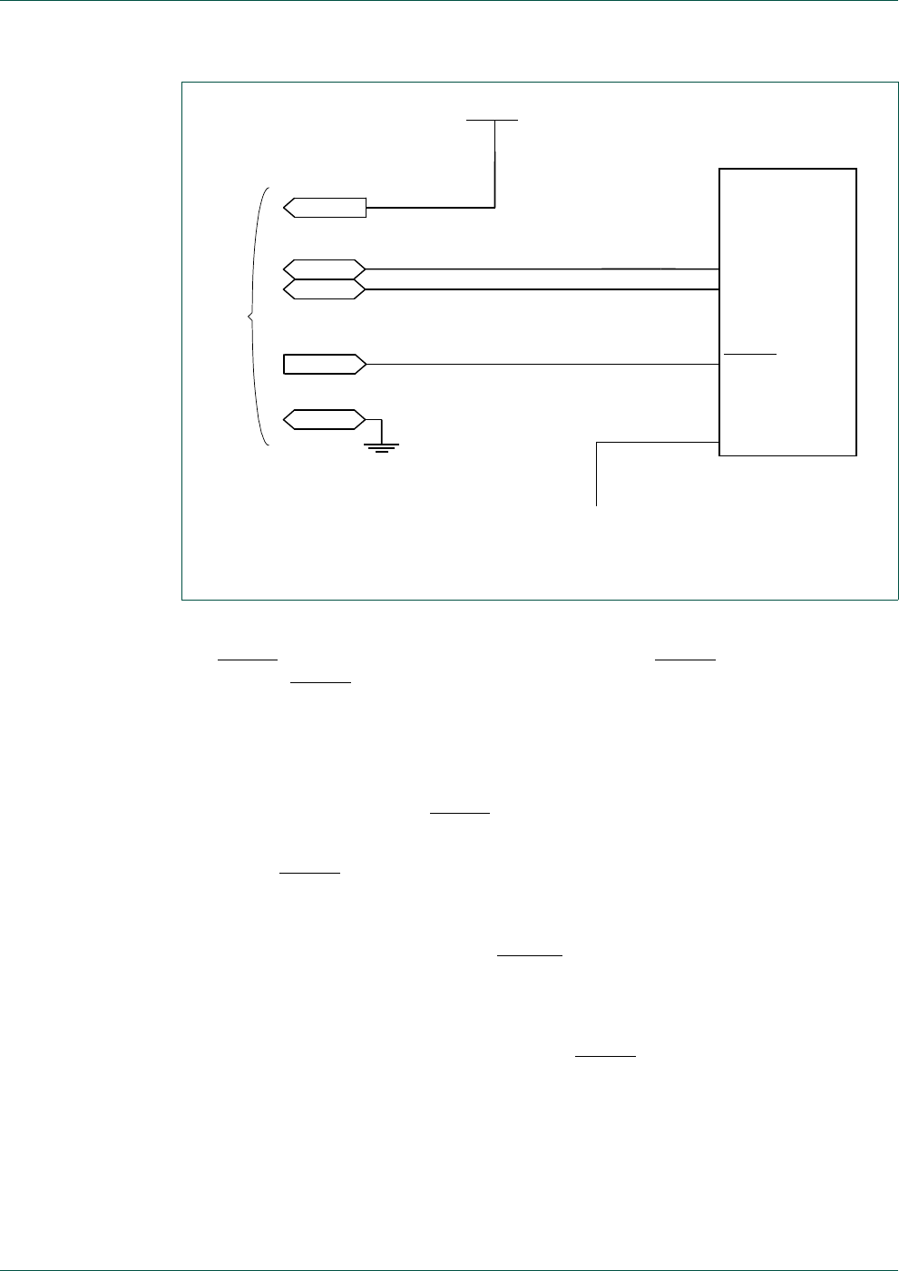
UM10462 All information provided in this document is subject to legal disclaimers. © NXP B.V. 2014. All rights reserved.
User manual Rev. 5.3 — 11 June 2014 424 of 521
NXP Semiconductors UM10462
Chapter 21: LPC11U3x/2x/1x Serial Wire Debugger (SWD)
21.6.3 Boundary scan
The RESET pin selects between the JTAG boundary scan (RESET = LOW) and the ARM
SWD debug (RESET = HIGH). The ARM SWD debug port is disabled while the
LPC11U3x/2x/1x is in reset.
To perform boundary scan testing, follow these steps:
1. Erase any user code residing in flash.
2. Power up the part with the RESET pin pulled HIGH externally.
3. Wait for at least 250 s.
4. Pull the RESET pin LOW externally.
5. Perform boundary scan operations.
6. Once the boundary scan operations are completed, assert the TRST pin to enable the
SWD debug mode and release the RESET pin (pull HIGH).
Remark: The JTAG interface cannot be used for debug purposes.
Remark: POR, BOD reset, or a LOW on the TRST pin puts the test TAP controller in the
Test-Logic Reset state. The first TCK clock while RESET = HIGH places the test TAP in
Run-Test Idle mode.
The VTREF pin on the SWD connector enables the debug connector to match the target voltage.
Fig 72. Connecting the SWD pins to a standard SWD connector
RESET
Signals from SWD connector
SWDIO
SWCLK
VDD
Gnd
VTREF
SWDIO
SWCLK
nSRST
GND
LPC11Uxx
ISP entry
PIO0_1
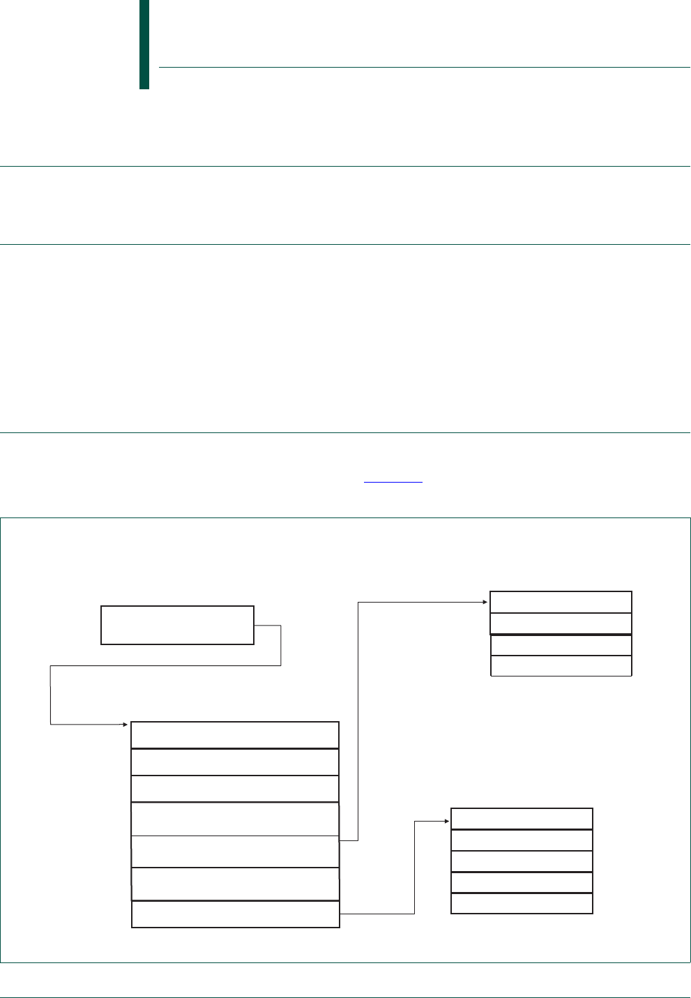
UM10462 All information provided in this document is subject to legal disclaimers. © NXP B.V. 2014. All rights reserved.
User manual Rev. 5.3 — 11 June 2014 425 of 521
22.1 How to read this chapter
The ROM-based 32-bit integer division routines are available on LPC11U2x/LPC11U3x.
22.2 Features
•Performance-optimized signed/unsigned integer division.
•Performance-optimized signed/unsigned integer division with remainder.
•ROM-based routines to reduce code size.
•Support for integers up to 32 bit.
•ROM calls can easily be added to EABI-compliant functions to overload “/” and “%”
operators in C.
22.3 Description
The API calls to the ROM are performed by executing functions which are pointed by a
pointer within the ROM Driver Table. Figure 73 shows the pointer structure used to call the
Integer divider API.
UM10462
Chapter 22: LPC11U3x/2x/1x Integer division routines
Rev. 5.3 — 11 June 2014 User manual
Fig 73. ROM pointer structure
Ptr to ROM Driver table
Ptr to Device Table 2
Ptr to Device Table 1
Ptr to Device Table 0
…
Ptr to Device Table n
sidiv
uidiv
sidivmod
uidivmod
Ptr to Function 2
Ptr to Function 0
Ptr to Function 1
…
Ptr to Function n
Integer division routines function table
Device n
ROM Driver Table
0x1FFF 1FF8
+0x0
+0x4
+0x8
+0x10
+0xC
Ptr to Device Table 3
Ptr to Integer Division routines Table
sidivmod
uidivmod

UM10462 All information provided in this document is subject to legal disclaimers. © NXP B.V. 2014. All rights reserved.
User manual Rev. 5.3 — 11 June 2014 426 of 521
NXP Semiconductors UM10462
Chapter 22: LPC11U3x/2x/1x Integer division routines
The integer division routines perform arithmetic integer division operations and can be
called in the application code through simple API calls.
The following function prototypes are used:
typedef struct { int quot; int rem; } idiv_return;
typedef struct { unsigned quot; unsigned rem; } uidiv_return;
typedef struct {
/* Signed integer division */
int(*sidiv)(int numerator, int denominator);
/* Unsigned integer division */
unsigned(*uidiv) (unsigned numerator, unsigned denominator);
/* Signed integer division with remainder */
idiv_return(*sidivmod)(int numerator, int denominator);
/* Unsigned integer division with remainder */
uidiv_return (*uidivmod)(unsigned numerator, unsigned denominator);
} LPC_ROM_DIV_STRUCT;
22.4 Examples
22.4.1 Initialization
The example C-code listing below shows how to initialize the API’s ROM table pointer.
typedef struct _ROM {
const unsigned p_dev1;
const unsigned p_dev2;
const unsigned p_dev3;
const PWRD *pPWRD;
const LPC_ROM_DIV_STUCT * pROMDiv;
const unsigned p_dev4;
const unsigned p_dev5;
const unsigned p_dev6;
} ROM;
ROM ** rom = (ROM **) 0x1FFF1FF8;
pDivROM = (*rom)->pROMDiv;
22.4.2 Signed division
The example C-code listing below shows how to perform a signed integer division via the
ROM API.
/* Divide (-99) by (+6) */
int32_t result;

UM10462 All information provided in this document is subject to legal disclaimers. © NXP B.V. 2014. All rights reserved.
User manual Rev. 5.3 — 11 June 2014 427 of 521
NXP Semiconductors UM10462
Chapter 22: LPC11U3x/2x/1x Integer division routines
result = pDivROM->sidiv(-99, 6);
/* result now contains (-16) */
22.4.3 Unsigned division with remainder
The example C-code listing below shows how to perform an unsigned integer division with
remainder via the ROM API.
/* Modulus Divide (+99) by (+4) */
uidiv_return result;
result = pDivROM-> uidivmod (+99, 4);
/* result.quot contains (+24) */
/* result.rem contains (+3) */

UM10462 All information provided in this document is subject to legal disclaimers. © NXP B.V. 2014. All rights reserved.
User manual Rev. 5.3 — 11 June 2014 428 of 521
23.1 How to read this chapter
The I/O Handler is only available on part LPC11U37HFBD64/401.
23.2 Features
•I/O Handler for hardware emulation of serial interfaces and DMA.
•Software library support and documentation for each library are available on
http://www.LPCware.com.
•Software libraries for UART, I2C, I2S, DALI, DMA, and more.
23.3 Basic configuration
•I/O Handler library code must be executed from the memory area 0x2000 0000 to
0x2000 07FF. This memory is not available for other use.
•Enable the clock to the SRAM1 memory location in the SYSAHBCLKCTRL register.
See Table 24.
•In the IOCON block, enable the IOH_n pin functions as needed by the software library
application. The documentation provided with each software library on
http://www.LPCware.com lists the IOH_n pin functions (and other pin functions if
necessary) that must be selected in the IOCON block.
23.4 Description
The I/O Handler is a software-library supported hardware engine for emulating serial
interfaces and DMA functionality. The I/O Handler can emulate serial interfaces such as
UART, I2C, or I2S with no or very low additional CPU load and can off-load the CPU by
performing processing-intensive functions like DMA transfers in hardware. Software
libraries for multiple applications are available with supporting application notes from NXP.
(See http://www.LPCware.com.)
23.5 Register description
The I/O Handler has no user-programmable register interface.
23.6 Examples
23.6.1 I/O Handler software library applications
The following sections provide application examples for the I/O Handler software library.
All library examples make use of the I/O Handler hardware to extend the functionality of
the part through software library calls.
UM10462
Chapter 23: LPC11U3x/2x/1x I/O Handler
Rev. 5.3 — 11 June 2014 User manual

UM10462 All information provided in this document is subject to legal disclaimers. © NXP B.V. 2014. All rights reserved.
User manual Rev. 5.3 — 11 June 2014 429 of 521
NXP Semiconductors UM10462
Chapter 23: LPC11U3x/2x/1x I/O Handler
23.6.1.1 I/O Handler I2S
The I/O Handler software library provides functions to emulate an I2S master transmit
interface using the I/O Handler hardware block.
The emulated I2S interface loops over a 1 kB buffer, transmitting the datawords according
to the I2S protocol. Interrupts are generated every time when the first 512 bytes have been
transmitted and when the last 512 bytes have been transmitted. This allows the ARM core
to load the free portion of the buffer with new data, thereby enabling streaming audio.
Two channels with 16-bit per channel are supported. The code size of the software library
is 1 kB and code must be executed from the SRAM1 memory area reserved for the I/O
Handler code.
23.6.1.2 I/O Handler UART
The I/O Handler UART library emulates one additional full-duplex UART. The emulated
UART can be configured for 7 or 8 data bits, no parity and 1 or 2 stop bits. The baud rate
is configurable up to 115200 baud. The RXD signal is available on three I/O Handler pins
(IOH_6, IOH_16, IOH_20), while TXD and CTS are available on all 21 I/O Handler pins.
The code size of the software library is about 1.2 kB and code must be executed from the
SRAM1 memory area reserved for the I/O Handler code.
23.6.1.3 I/O Handler I2C
The I/O Handler I2C library allows to have an additional I2C-bus master. I2C read, I2C write
and combined I2C read/write are supported. Data is automatically read from and written to
user-defined buffers.
The I/O Handler I2C library combined with the on-chip I2C module allows to have two
distinct I2C buses, allowing to separate low-speed from high-speed devices or bridging
two I2C buses.
23.6.1.4 I/O Handler DMA
The I/O Handler DMA library offers DMA-like functionality. Four types of transfer are
supported: memory to memory, memory to peripheral, peripheral to memory and
peripheral to peripheral. Supported peripherals are USART, SSP0/1, ADC and GPIO.
DMA transfers can be triggered by the source/target peripheral, software, counter/timer
module CT16B1, or I/O Handler pin PIO1_6/IOH_16.
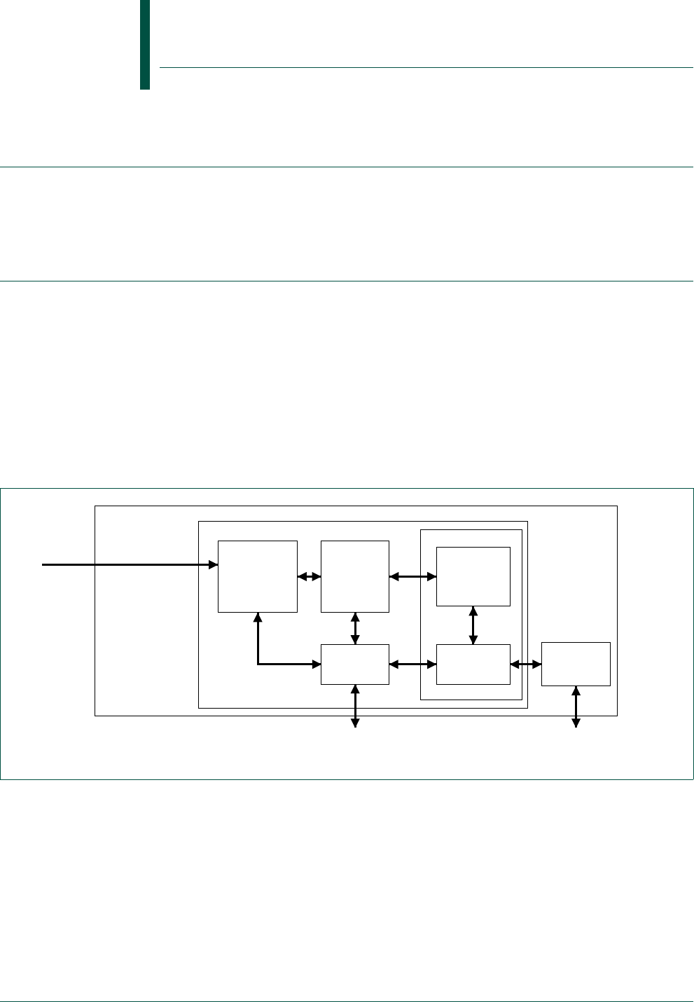
UM10462 All information provided in this document is subject to legal disclaimers. © NXP B.V. 2014. All rights reserved.
User manual Rev. 5.3 — 11 June 2014 430 of 521
24.1 Introduction
The following material is using the ARM Cortex-M0 User Guide. Minor changes have
been made regarding the specific implementation of the Cortex-M0 for the
LPC11U3x/2x/1x.
24.2 About the Cortex-M0 processor and core peripherals
The Cortex-M0 processor is an entry-level 32-bit ARM Cortex processor designed for a
broad range of embedded applications. It offers significant benefits to developers,
including:
•a simple architecture that is easy to learn and program
•ultra-low power, energy efficient operation
•excellent code density
•deterministic, high-performance interrupt handling
•upward compatibility with Cortex-M processor family.
The Cortex-M0 processor is built on a highly area and power optimized 32-bit processor
core, with a 3-stage pipeline von Neumann architecture. The processor delivers
exceptional energy efficiency through a small but powerful instruction set and extensively
optimized design, providing high-end processing hardware including a single-cycle
multiplier.
The Cortex-M0 processor implements the ARMv6-M architecture, which is based on the
16-bit Thumb instruction set and includes Thumb-2 technology. This provides the
exceptional performance expected of a modern 32-bit architecture, with a higher code
density than other 8-bit and 16-bit microcontrollers.
UM10462
Chapter 24: LPC11U3x/2x/1x Appendix ARM Cortex-M0
Rev. 5.3 — 11 June 2014 User manual
Fig 74. Cortex-M0 implementation
&RUWH[0SURFHVVRU
&RUWH[0
SURFHVVRU
FRUH
%XVPDWUL[
1HVWHG
9HFWRUHG
,QWHUUXSW
&RQWUROOHU
19,&
,QWHUUXSWV
'HEXJ
$FFHVV3RUW
'$3
$+%/LWHLQWHUIDFHWRV\VWHP 6HULDO:LUHGHEXJSRUW
'HEXJ
'HEXJJHU
LQWHUIDFH
%UHDNSRLQW
DQG
ZDWFKSRLQW
XQLW
&RUWH[0FRPSRQHQWV

UM10462 All information provided in this document is subject to legal disclaimers. © NXP B.V. 2014. All rights reserved.
User manual Rev. 5.3 — 11 June 2014 431 of 521
NXP Semiconductors UM10462
Chapter 24: LPC11U3x/2x/1x Appendix ARM Cortex-M0
The Cortex-M0 processor closely integrates a configurable Nested Vectored Interrupt
Controller (NVIC), to deliver industry-leading interrupt performance. The NVIC:
•includes a non-maskable interrupt (NMI).
•provides zero jitter interrupt option.
•provides four interrupt priority levels.
The tight integration of the processor core and NVIC provides fast execution of interrupt
service routines (ISRs), dramatically reducing the interrupt latency. This is achieved
through the hardware stacking of registers, and the ability to abandon and restart
load-multiple and store-multiple operations. Interrupt handlers do not require any
assembler wrapper code, removing any code overhead from the ISRs. Tail-chaining
optimization also significantly reduces the overhead when switching from one ISR to
another.
To optimize low-power designs, the NVIC integrates with the sleep modes, that include a
Deep-sleep function that enables the entire device to be rapidly powered down.
24.2.1 System-level interface
The Cortex-M0 processor provides a single system-level interface using AMBA
technology to provide high speed, low latency memory accesses.
24.2.2 Integrated configurable debug
The Cortex-M0 processor implements a complete hardware debug solution, with
extensive hardware breakpoint and watchpoint options. This provides high system
visibility of the processor, memory and peripherals through a 2-pin Serial Wire Debug
(SWD) port that is ideal for microcontrollers and other small package devices.
24.2.3 Cortex-M0 processor features summary
•high code density with 32-bit performance
•tools and binary upwards compatible with Cortex-M processor family
•integrated ultra low-power sleep modes
•efficient code execution permits slower processor clock or increases sleep mode time
•single-cycle 32-bit hardware multiplier
•zero jitter interrupt handling
•extensive debug capabilities.
24.2.4 Cortex-M0 core peripherals
These are:
NVIC — The NVIC is an embedded interrupt controller that supports low latency interrupt
processing.
System Control Block — The System Control Block (SCB) is the programmers model
interface to the processor. It provides system implementation information and system
control, including configuration, control, and reporting of system exceptions.

UM10462 All information provided in this document is subject to legal disclaimers. © NXP B.V. 2014. All rights reserved.
User manual Rev. 5.3 — 11 June 2014 432 of 521
NXP Semiconductors UM10462
Chapter 24: LPC11U3x/2x/1x Appendix ARM Cortex-M0
System timer — The system timer, SysTick, is a 24-bit count-down timer. Use this as a
Real Time Operating System (RTOS) tick timer or as a simple counter.
24.3 Processor
24.3.1 Programmers model
This section describes the Cortex-M0 programmers model. In addition to the individual
core register descriptions, it contains information about the processor modes and stacks.
24.3.1.1 Processor modes
The processor modes are:
Thread mode — Used to execute application software. The processor enters Thread
mode when it comes out of reset.
Handler mode — Used to handle exceptions. The processor returns to Thread mode
when it has finished all exception processing.
24.3.1.2 Stacks
The processor uses a full descending stack. This means the stack pointer indicates the
last stacked item on the stack memory. When the processor pushes a new item onto the
stack, it decrements the stack pointer and then writes the item to the new memory
location. The processor implements two stacks, the main stack and the process stack,
with independent copies of the stack pointer, see Section 24.3.1.3.2.
In Thread mode, the CONTROL register controls whether the processor uses the main
stack or the process stack, see Section 24–24.3.1.3.7. In Handler mode, the processor
always uses the main stack. The options for processor operations are:
24.3.1.3 Core registers
The processor core registers are:
Table 412. Summary of processor mode and stack use options
Processor
mode Used to
execute Stack used
Thread Applications Main stack or process stack
See Section 24–24.3.1.3.7
Handler Exception
handlers
Main stack
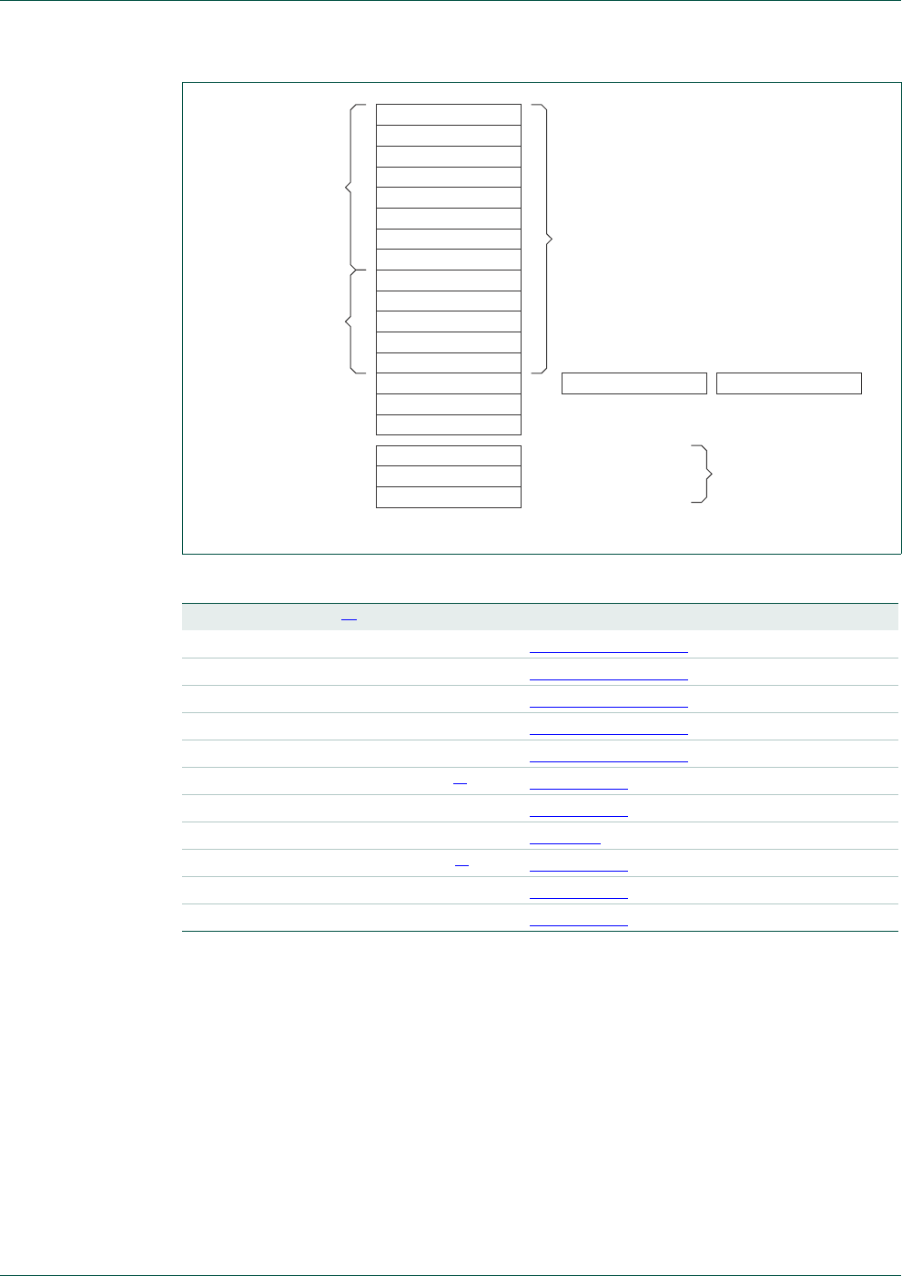
UM10462 All information provided in this document is subject to legal disclaimers. © NXP B.V. 2014. All rights reserved.
User manual Rev. 5.3 — 11 June 2014 433 of 521
NXP Semiconductors UM10462
Chapter 24: LPC11U3x/2x/1x Appendix ARM Cortex-M0
[1] Describes access type during program execution in thread mode and Handler mode. Debug access can
differ.
[2] Bit[24] is the T-bit and is loaded from bit[0] of the reset vector.
24.3.1.3.1 General-purpose registers
R0-R12 are 32-bit general-purpose registers for data operations.
24.3.1.3.2 Stack Pointer
The Stack Pointer (SP) is register R13. In Thread mode, bit[1] of the CONTROL register
indicates the stack pointer to use:
•0 = Main Stack Pointer (MSP). This is the reset value.
•1 = Process Stack Pointer (PSP).
Fig 75. Processor core register set
Table 413. Core register set summary
Name Type [1] Reset value Description
R0-R12 RW Unknown Section 24–24.3.1.3.1
MSP RW See description Section 24–24.3.1.3.2
PSP RW Unknown Section 24–24.3.1.3.2
LR RW Unknown Section 24–24.3.1.3.3
PC RW See description Section 24–24.3.1.3.4
PSR RW Unknown[2] Table 24–414
APSR RW Unknown Table 24–415
IPSR RO
0x00000000
Table 416
EPSR RO Unknown[2] Table 24–417
PRIMASK RW
0x00000000
Table 24–418
CONTROL RW
0x00000000
Table 24–419
3URJUDP&RXQWHU
635
/55
3&5
5
5
5
5
5
5
5
5
5
5
5
5
5
/RZUHJLVWHUV
+LJKUHJLVWHUV
063363
&21752/
365
/LQN5HJLVWHU
6WDFN3RLQWHU
*HQHUDOSXUSRVHUHJLVWHUV
3URJUDP6WDWXV5HJLVWHU
&RQWURO5HJLVWHU
6SHFLDOUHJLVWHUV
35,0$6. ,QWHUUXSWPDVNUHJLVWHU
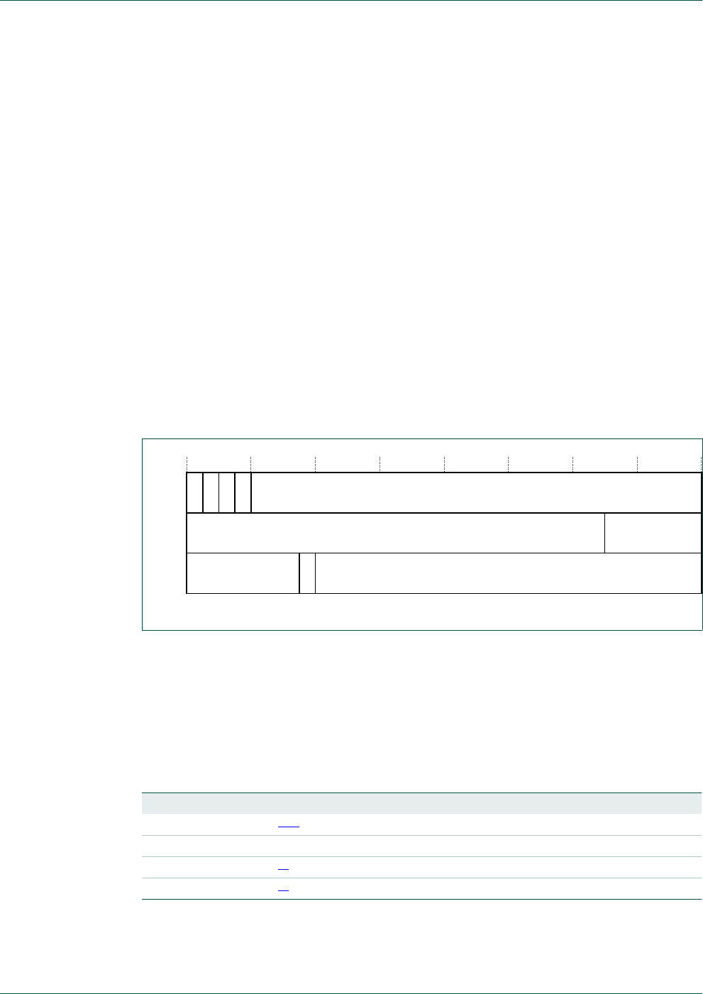
UM10462 All information provided in this document is subject to legal disclaimers. © NXP B.V. 2014. All rights reserved.
User manual Rev. 5.3 — 11 June 2014 434 of 521
NXP Semiconductors UM10462
Chapter 24: LPC11U3x/2x/1x Appendix ARM Cortex-M0
On reset, the processor loads the MSP with the value from address
0x00000000
.
24.3.1.3.3 Link Register
The Link Register (LR) is register R14. It stores the return information for subroutines,
function calls, and exceptions. On reset, the LR value is Unknown.
24.3.1.3.4 Program Counter
The Program Counter (PC) is register R15. It contains the current program address. On
reset, the processor loads the PC with the value of the reset vector, which is at address
0x00000004
. Bit[0] of the value is loaded into the EPSR T-bit at reset and must be 1.
24.3.1.3.5 Program Status Register
The Program Status Register (PSR) combines:
•Application Program Status Register (APSR)
•Interrupt Program Status Register (IPSR)
•Execution Program Status Register (EPSR).
These registers are mutually exclusive bitfields in the 32-bit PSR. The PSR bit
assignments are:
Access these registers individually or as a combination of any two or all three registers,
using the register name as an argument to the
MSR
or
MRS
instructions. For example:
•read all of the registers using
PSR
with the
MRS
instruction
•write to the APSR using
APSR
with the
MSR
instruction.
The PSR combinations and attributes are:
[1] The processor ignores writes to the IPSR bits.
[2] Reads of the EPSR bits return zero, and the processor ignores writes to the these bits
Fig 76. APSR, IPSR, EPSR register bit assignments
Table 414. PSR register combinations
Register Type Combination
PSR RW[1][2] APSR, EPSR, and IPSR
IEPSR RO EPSR and IPSR
IAPSR RW[1] APSR and IPSR
EAPSR RW[2] APSR and EPSR
5HVHUYHG ([FHSWLRQQXPEHU
1=&9
5HVHUYHG
$365
,365
(365 5HVHUYHG 5HVHUYHG7

UM10462 All information provided in this document is subject to legal disclaimers. © NXP B.V. 2014. All rights reserved.
User manual Rev. 5.3 — 11 June 2014 435 of 521
NXP Semiconductors UM10462
Chapter 24: LPC11U3x/2x/1x Appendix ARM Cortex-M0
See the instruction descriptions Section 24–24.4.7.6 and Section 24–24.4.7.7 for more
information about how to access the program status registers.
Application Program Status Register: The APSR contains the current state of the
condition flags, from previous instruction executions. See the register summary in
Table 24–413 for its attributes. The bit assignments are:
See Section 24.4.4.1.4 for more information about the APSR negative, zero, carry or
borrow, and overflow flags.
Interrupt Program Status Register: The IPSR contains the exception number of the
current Interrupt Service Routine (ISR). See the register summary in Table 24–413 for
its attributes. The bit assignments are:
Execution Program Status Register: The EPSR contains the Thumb state bit.
See the register summary in Table 24–413 for the EPSR attributes. The bit assignments
are:
Table 415. APSR bit assignments
Bits Name Function
[31] N Negative flag
[30] Z Zero flag
[29] C Carry or borrow flag
[28] V Overflow flag
[27:0] - Reserved
Table 416. IPSR bit assignments
Bits Name Function
[31:6] - Reserved
[5:0] Exception number This is the number of the current exception:
0 = Thread mode
1 = Reserved
2 = NMI
3 = HardFault
4-10 = Reserved
11 = SVCall
12, 13 = Reserved
14 = PendSV
15 = SysTick
16 = IRQ0
.
.
.
47 = IRQ31
48-63 = Reserved.
see Section 24–24.3.3.2 for more information.

UM10462 All information provided in this document is subject to legal disclaimers. © NXP B.V. 2014. All rights reserved.
User manual Rev. 5.3 — 11 June 2014 436 of 521
NXP Semiconductors UM10462
Chapter 24: LPC11U3x/2x/1x Appendix ARM Cortex-M0
Attempts by application software to read the EPSR directly using the
MRS
instruction
always return zero. Attempts to write the EPSR using the
MSR
instruction are ignored.
Fault handlers can examine the EPSR value in the stacked PSR to determine the cause
of the fault. See Section 24–24.3.3.6. The following can clear the T bit to 0:
•instructions
BLX
,
BX
and
POP{PC}
•restoration from the stacked xPSR value on an exception return
•bit[0] of the vector value on an exception entry.
Attempting to execute instructions when the T bit is 0 results in a HardFault or lockup. See
Section 24–24.3.4.1 for more information.
Interruptible-restartable instructions: The interruptible-restartable instructions are
LDM
and
STM
. When an interrupt occurs during the execution of one of these instructions, the
processor abandons execution of the instruction.
After servicing the interrupt, the processor restarts execution of the instruction from the
beginning.
24.3.1.3.6 Exception mask register
The exception mask register disables the handling of exceptions by the processor.
Disable exceptions where they might impact on timing critical tasks or code sequences
requiring atomicity.
To disable or re-enable exceptions, use the
MSR
and
MRS
instructions, or the
CPS
instruction, to change the value of PRIMASK. See Section 24–24.4.7.6,
Section 24–24.4.7.7, and Section 24–24.4.7.2 for more information.
Priority Mask Register: The PRIMASK register prevents activation of all exceptions with
configurable priority. See the register summary in Table 24–413 for its attributes. The bit
assignments are:
24.3.1.3.7 CONTROL register
The CONTROL register controls the stack used when the processor is in Thread mode.
See the register summary in Table 24–413 for its attributes. The bit assignments are:
Table 417. EPSR bit assignments
Bits Name Function
[31:25] - Reserved
[24] T Thumb state bit
[23:0] - Reserved
Table 418. PRIMASK register bit assignments
Bits Name Function
[31:1] - Reserved
[0] PRIMASK 0 = no effect
1 = prevents the activation of all exceptions with
configurable priority.

UM10462 All information provided in this document is subject to legal disclaimers. © NXP B.V. 2014. All rights reserved.
User manual Rev. 5.3 — 11 June 2014 437 of 521
NXP Semiconductors UM10462
Chapter 24: LPC11U3x/2x/1x Appendix ARM Cortex-M0
Handler mode always uses the MSP, so the processor ignores explicit writes to the active
stack pointer bit of the CONTROL register when in Handler mode. The exception entry
and return mechanisms update the CONTROL register.
In an OS environment, it is recommended that threads running in Thread mode use the
process stack and the kernel and exception handlers use the main stack.
By default, Thread mode uses the MSP. To switch the stack pointer used in Thread mode
to the PSP, use the
MSR
instruction to set the Active stack pointer bit to 1, see
Section 24–24.4.7.6.
Remark: When changing the stack pointer, software must use an
ISB
instruction
immediately after the
MSR
instruction. This ensures that instructions after the ISB execute
using the new stack pointer. See Section 24–24.4.7.5.
24.3.1.4 Exceptions and interrupts
The Cortex-M0 processor supports interrupts and system exceptions. The processor and
the Nested Vectored Interrupt Controller (NVIC) prioritize and handle all exceptions. An
interrupt or exception changes the normal flow of software control. The processor uses
handler mode to handle all exceptions except for reset. See Section 24–24.3.3.6.1 and
Section 24–24.3.3.6.2 for more information.
The NVIC registers control interrupt handling. See Section 24–24.5.2 for more
information.
24.3.1.5 Data types
The processor:
•supports the following data types:
–32-bit words
–16-bit halfwords
–8-bit bytes
•manages all data memory accesses as little-endian. Instruction memory and Private
Peripheral Bus (PPB) accesses are always little-endian. See Section 24–24.3.2.1 for
more information.
24.3.1.6 The Cortex Microcontroller Software Interface Standard
ARM provides the Cortex Microcontroller Software Interface Standard (CMSIS) for
programming Cortex-M0 microcontrollers. The CMSIS is an integrated part of the device
driver library.
Table 419. CONTROL register bit assignments
Bits Name Function
[31:2] - Reserved
[1] Active stack
pointer
Defines the current stack:
0 = MSP is the current stack pointer
1 = PSP is the current stack pointer.
In Handler mode this bit reads as zero and ignores writes.
[0] - Reserved.

UM10462 All information provided in this document is subject to legal disclaimers. © NXP B.V. 2014. All rights reserved.
User manual Rev. 5.3 — 11 June 2014 438 of 521
NXP Semiconductors UM10462
Chapter 24: LPC11U3x/2x/1x Appendix ARM Cortex-M0
For a Cortex-M0 microcontroller system, CMSIS defines:
•a common way to:
–access peripheral registers
–define exception vectors
•the names of:
–the registers of the core peripherals
–the core exception vectors
•a device-independent interface for RTOS kernels.
The CMSIS includes address definitions and data structures for the core peripherals in the
Cortex-M0 processor. It also includes optional interfaces for middleware components
comprising a TCP/IP stack and a Flash file system.
The CMSIS simplifies software development by enabling the reuse of template code, and
the combination of CMSIS-compliant software components from various middleware
vendors. Software vendors can expand the CMSIS to include their peripheral definitions
and access functions for those peripherals.
This document includes the register names defined by the CMSIS, and gives short
descriptions of the CMSIS functions that address the processor core and the core
peripherals.
Remark: This document uses the register short names defined by the CMSIS. In a few
cases these differ from the architectural short names that might be used in other
documents.
The following sections give more information about the CMSIS:
•Section 24.3.5.3 “Power management programming hints”
•Section 24.4.2 “Intrinsic functions”
•Section 24.5.2.1 “Accessing the Cortex-M0 NVIC registers using CMSIS”
•Section 24.5.2.8.1 “NVIC programming hints”.
24.3.2 Memory model
This section describes the processor memory map and the behavior of memory accesses.
The processor has a fixed memory map that provides up to 4GB of addressable memory.
The memory map is:

UM10462 All information provided in this document is subject to legal disclaimers. © NXP B.V. 2014. All rights reserved.
User manual Rev. 5.3 — 11 June 2014 439 of 521
NXP Semiconductors UM10462
Chapter 24: LPC11U3x/2x/1x Appendix ARM Cortex-M0
The processor reserves regions of the Private peripheral bus (PPB) address range for
core peripheral registers, see Section 24–24.2.
24.3.2.1 Memory regions, types and attributes
The memory map is split into regions. Each region has a defined memory type, and some
regions have additional memory attributes. The memory type and attributes determine the
behavior of accesses to the region.
The memory types are:
Normal — The processor can re-order transactions for efficiency, or perform speculative
reads.
Device — The processor preserves transaction order relative to other transactions to
Device or Strongly-ordered memory.
For the LPC11U3x/2x/1x specific implementation of the memory map, see Figure 4.
Fig 77. Cortex-M0 memory map
([WHUQDOGHYLFH
([WHUQDO5$0
3HULSKHUDO
65$0
&RGH
[))))))))
3ULYDWHSHULSKHUDOEXV
[(
[()))))
[)))))))
[$
[)))))))
[
[)))))))
[
[)))))))
[
[
*%
*%
*%
*%
*%
[')))))))
[(
0%
0%
'HYLFH

UM10462 All information provided in this document is subject to legal disclaimers. © NXP B.V. 2014. All rights reserved.
User manual Rev. 5.3 — 11 June 2014 440 of 521
NXP Semiconductors UM10462
Chapter 24: LPC11U3x/2x/1x Appendix ARM Cortex-M0
Strongly-ordered — The processor preserves transaction order relative to all other
transactions.
The different ordering requirements for Device and Strongly-ordered memory mean that
the memory system can buffer a write to Device memory, but must not buffer a write to
Strongly-ordered memory.
The additional memory attributes include.
Execute Never (XN) — Means the processor prevents instruction accesses. A HardFault
exception is generated on executing an instruction fetched from an XN region of memory.
24.3.2.2 Memory system ordering of memory accesses
For most memory accesses caused by explicit memory access instructions, the memory
system does not guarantee that the order in which the accesses complete matches the
program order of the instructions, providing any re-ordering does not affect the behavior of
the instruction sequence. Normally, if correct program execution depends on two memory
accesses completing in program order, software must insert a memory barrier instruction
between the memory access instructions, see Section 24–24.3.2.4.
However, the memory system does guarantee some ordering of accesses to Device and
Strongly-ordered memory. For two memory access instructions A1 and A2, if A1 occurs
before A2 in program order, the ordering of the memory accesses caused by two
instructions is:
Where:
- — Means that the memory system does not guarantee the ordering of the accesses.
< — Means that accesses are observed in program order, that is, A1 is always observed
before A2.
24.3.2.3 Behavior of memory accesses
The behavior of accesses to each region in the memory map is:
Fig 78. Memory ordering restrictions
1RUPDODFFHVV
'HYLFHDFFHVVQRQVKDUHDEOH
'HYLFHDFFHVVVKDUHDEOH
6WURQJO\RUGHUHGDFFHVV
1RUPDO
DFFHVV 1RQVKDUHDEOH 6KDUHDEOH
6WURQJO\
RUGHUHG
DFFHVV
'HYLFHDFFHVV
$
$

UM10462 All information provided in this document is subject to legal disclaimers. © NXP B.V. 2014. All rights reserved.
User manual Rev. 5.3 — 11 June 2014 441 of 521
NXP Semiconductors UM10462
Chapter 24: LPC11U3x/2x/1x Appendix ARM Cortex-M0
[1] See Section 24–24.3.2.1 for more information.
The Code, SRAM, and external RAM regions can hold programs.
24.3.2.4 Software ordering of memory accesses
The order of instructions in the program flow does not always guarantee the order of the
corresponding memory transactions. This is because:
•the processor can reorder some memory accesses to improve efficiency, providing
this does not affect the behavior of the instruction sequence
•memory or devices in the memory map might have different wait states
•some memory accesses are buffered or speculative.
Section 24–24.3.2.2 describes the cases where the memory system guarantees the order
of memory accesses. Otherwise, if the order of memory accesses is critical, software
must include memory barrier instructions to force that ordering. The processor provides
the following memory barrier instructions:
DMB — The Data Memory Barrier (DMB) instruction ensures that outstanding memory
transactions complete before subsequent memory transactions. See Section 24–24.4.7.3.
DSB — The Data Synchronization Barrier (DSB) instruction ensures that outstanding
memory transactions complete before subsequent instructions execute. See
Section 24–24.4.7.4.
ISB — The Instruction Synchronization Barrier (ISB) ensures that the effect of all
completed memory transactions is recognizable by subsequent instructions. See
Section 24–24.4.7.5.
The following are examples of using memory barrier instructions:
Table 420. Memory access behavior
Address
range Memory
region Memory
type[1] XN[1] Description
0x00000000
-
0x1FFFFFFF
Code Normal - Executable region for program
code. You can also put data here.
0x20000000
-
0x3FFFFFFF
SRAM Normal - Executable region for data. You
can also put code here.
0x40000000
-
0x5FFFFFFF
Peripheral Device XN External device memory.
0x60000000
-
0x9FFFFFFF
External
RAM
Normal - Executable region for data.
0xA0000000
-
0xDFFFFFFF
External
device
Device XN External device memory.
0xE0000000
-
0xE00FFFFF
Private Peripheral
Bus
Strongly-ordered XN This region includes the NVIC,
System timer, and System Control
Block. Only word accesses can be
used in this region.
0xE0100000
-
0xFFFFFFFF
Device Device XN Vendor specific.

UM10462 All information provided in this document is subject to legal disclaimers. © NXP B.V. 2014. All rights reserved.
User manual Rev. 5.3 — 11 June 2014 442 of 521
NXP Semiconductors UM10462
Chapter 24: LPC11U3x/2x/1x Appendix ARM Cortex-M0
Vector table — If the program changes an entry in the vector table, and then enables the
corresponding exception, use a
DMB
instruction between the operations. This ensures that
if the exception is taken immediately after being enabled the processor uses the new
exception vector.
Self-modifying code — If a program contains self-modifying code, use an
ISB
instruction
immediately after the code modification in the program. This ensures subsequent
instruction execution uses the updated program.
Memory map switching — If the system contains a memory map switching mechanism,
use a
DSB
instruction after switching the memory map. This ensures subsequent
instruction execution uses the updated memory map.
Memory accesses to Strongly-ordered memory, such as the System Control Block, do not
require the use of
DMB
instructions.
The processor preserves transaction order relative to all other transactions.
24.3.2.5 Memory endianness
The processor views memory as a linear collection of bytes numbered in ascending order
from zero. For example, bytes 0-3 hold the first stored word, and bytes 4-7 hold the
second stored word. Section 24–24.3.2.5.1 describes how words of data are stored in
memory.
24.3.2.5.1 Little-endian format
In little-endian format, the processor stores the least significant byte (lsbyte) of a word at
the lowest-numbered byte, and the most significant byte (msbyte) at the
highest-numbered byte. For example:
24.3.3 Exception model
This section describes the exception model.
24.3.3.1 Exception states
Each exception is in one of the following states:
Inactive — The exception is not active and not pending.
Pending — The exception is waiting to be serviced by the processor.
Fig 79. Little-endian format
5HJLVWHU
$
OVE\WH
PVE\WH
$
$
%%% %
%
%
%
%
0HPRU\
$$GGUHVV

UM10462 All information provided in this document is subject to legal disclaimers. © NXP B.V. 2014. All rights reserved.
User manual Rev. 5.3 — 11 June 2014 443 of 521
NXP Semiconductors UM10462
Chapter 24: LPC11U3x/2x/1x Appendix ARM Cortex-M0
An interrupt request from a peripheral or from software can change the state of the
corresponding interrupt to pending.
Active — An exception that is being serviced by the processor but has not completed.
An exception handler can interrupt the execution of another exception handler. In this
case both exceptions are in the active state.
Active and pending — The exception is being serviced by the processor and there is a
pending exception from the same source.
24.3.3.2 Exception types
The exception types are:
Reset — Reset is invoked on power up or a warm reset. The exception model treats reset
as a special form of exception. When reset is asserted, the operation of the processor
stops, potentially at any point in an instruction. When reset is deasserted, execution
restarts from the address provided by the reset entry in the vector table. Execution restarts
in Thread mode.
NMI — A NonMaskable Interrupt (NMI) can be signalled by a peripheral or triggered by
software. This is the highest priority exception other than reset. It is permanently enabled
and has a fixed priority of 2. NMIs cannot be:
•masked or prevented from activation by any other exception
•preempted by any exception other than Reset.
HardFault — A HardFault is an exception that occurs because of an error during normal
or exception processing. HardFaults have a fixed priority of -1, meaning they have higher
priority than any exception with configurable priority.
SVCall — A supervisor call (SVC) is an exception that is triggered by the
SVC
instruction.
In an OS environment, applications can use
SVC
instructions to access OS kernel
functions and device drivers.
PendSV — PendSV is an interrupt-driven request for system-level service. In an OS
environment, use PendSV for context switching when no other exception is active.
SysTick — A SysTick exception is an exception the system timer generates when it
reaches zero. Software can also generate a SysTick exception. In an OS environment, the
processor can use this exception as system tick.
Interrupt (IRQ) — An interrupt, or IRQ, is an exception signalled by a peripheral, or
generated by a software request. All interrupts are asynchronous to instruction execution.
In the system, peripherals use interrupts to communicate with the processor.
Table 421. Properties of different exception types
Exception
number[1] IRQ
number[1] Exception
type Priority Vector
address[2]
1 - Reset -3, the highest
0x00000004
2-14NMI-2
0x00000008
3 -13 HardFault -1
0x0000000C
4-10 - Reserved - -
11 -5 SVCall Configurable[3]
0x0000002C
12-13 - Reserved - -

UM10462 All information provided in this document is subject to legal disclaimers. © NXP B.V. 2014. All rights reserved.
User manual Rev. 5.3 — 11 June 2014 444 of 521
NXP Semiconductors UM10462
Chapter 24: LPC11U3x/2x/1x Appendix ARM Cortex-M0
[1] To simplify the software layer, the CMSIS only uses IRQ numbers and therefore uses negative values for
exceptions other than interrupts. The IPSR returns the Exception number, see Table 24–416.
[2] See Section 24.3.3.4 for more information.
[3] See Section 24–24.5.2.6.
[4] Increasing in steps of 4.
For an asynchronous exception, other than reset, the processor can execute additional
instructions between when the exception is triggered and when the processor enters the
exception handler.
Privileged software can disable the exceptions that Table 24–421 shows as having
configurable priority, see Section 24–24.5.2.3.
For more information about HardFaults, see Section 24–24.3.4.
24.3.3.3 Exception handlers
The processor handles exceptions using:
Interrupt Service Routines (ISRs) — Interrupts IRQ0 to IRQ31 are the exceptions
handled by ISRs.
Fault handler — HardFault is the only exception handled by the fault handler.
System handlers — NMI, PendSV, SVCall SysTick, and HardFault are all system
exceptions handled by system handlers.
24.3.3.4 Vector table
The vector table contains the reset value of the stack pointer, and the start addresses,
also called exception vectors, for all exception handlers. Figure 24–80 shows the order of
the exception vectors in the vector table. The least-significant bit of each vector must be 1,
indicating that the exception handler is written in Thumb code.
14 -2 PendSV Configurable[3]
0x00000038
15 -1 SysTick Configurable[3]
0x0000003C
16 and above 0 and above Interrupt (IRQ) Configurable[3]
0x00000040
and
above[4]
Table 421. Properties of different exception types
Exception
number[1] IRQ
number[1] Exception
type Priority Vector
address[2]

UM10462 All information provided in this document is subject to legal disclaimers. © NXP B.V. 2014. All rights reserved.
User manual Rev. 5.3 — 11 June 2014 445 of 521
NXP Semiconductors UM10462
Chapter 24: LPC11U3x/2x/1x Appendix ARM Cortex-M0
The vector table is fixed at address
0x00000000
.
24.3.3.5 Exception priorities
As Table 24–421 shows, all exceptions have an associated priority, with:
•a lower priority value indicating a higher priority
•configurable priorities for all exceptions except Reset, HardFault, and NMI.
If software does not configure any priorities, then all exceptions with a configurable priority
have a priority of 0. For information about configuring exception priorities see
•Section 24–24.5.3.7
•Section 24–24.5.2.6.
Configurable priority values are in the range 0-192, in steps of 64. The Reset, HardFault,
and NMI exceptions, with fixed negative priority values, always have higher priority than
any other exception.
Fig 80. Vector table
,QLWLDO63YDOXH
5HVHW
+DUG)DXOW
10,
[
[
[
[&
[
5HVHUYHG
69&DOO
3HQG69
6\V7LFN
,54
5HVHUYHG
[&
[
[&
[
2IIVHW([FHSWLRQQXPEHU
9HFWRU
,54
,54
[
,54
[
[%&
,54QXPEHU

UM10462 All information provided in this document is subject to legal disclaimers. © NXP B.V. 2014. All rights reserved.
User manual Rev. 5.3 — 11 June 2014 446 of 521
NXP Semiconductors UM10462
Chapter 24: LPC11U3x/2x/1x Appendix ARM Cortex-M0
Assigning a higher priority value to IRQ[0] and a lower priority value to IRQ[1] means that
IRQ[1] has higher priority than IRQ[0]. If both IRQ[1] and IRQ[0] are asserted, IRQ[1] is
processed before IRQ[0].
If multiple pending exceptions have the same priority, the pending exception with the
lowest exception number takes precedence. For example, if both IRQ[0] and IRQ[1] are
pending and have the same priority, then IRQ[0] is processed before IRQ[1].
When the processor is executing an exception handler, the exception handler is
preempted if a higher priority exception occurs. If an exception occurs with the same
priority as the exception being handled, the handler is not preempted, irrespective of the
exception number. However, the status of the new interrupt changes to pending.
24.3.3.6 Exception entry and return
Descriptions of exception handling use the following terms:
Preemption — When the processor is executing an exception handler, an exception can
preempt the exception handler if its priority is higher than the priority of the exception
being handled.
When one exception preempts another, the exceptions are called nested exceptions. See
Section 24–24.3.3.6.1 for more information.
Return — This occurs when the exception handler is completed, and:
•there is no pending exception with sufficient priority to be serviced
•the completed exception handler was not handling a late-arriving exception.
The processor pops the stack and restores the processor state to the state it had before
the interrupt occurred. See Section 24–24.3.3.6.2 for more information.
Tail-chaining — This mechanism speeds up exception servicing. On completion of an
exception handler, if there is a pending exception that meets the requirements for
exception entry, the stack pop is skipped and control transfers to the new exception
handler.
Late-arriving — This mechanism speeds up preemption. If a higher priority exception
occurs during state saving for a previous exception, the processor switches to handle the
higher priority exception and initiates the vector fetch for that exception. State saving is
not affected by late arrival because the state saved would be the same for both
exceptions. On return from the exception handler of the late-arriving exception, the normal
tail-chaining rules apply.
24.3.3.6.1 Exception entry
Exception entry occurs when there is a pending exception with sufficient priority and
either:
•the processor is in Thread mode
•the new exception is of higher priority than the exception being handled, in which case
the new exception preempts the exception being handled.
When one exception preempts another, the exceptions are nested.
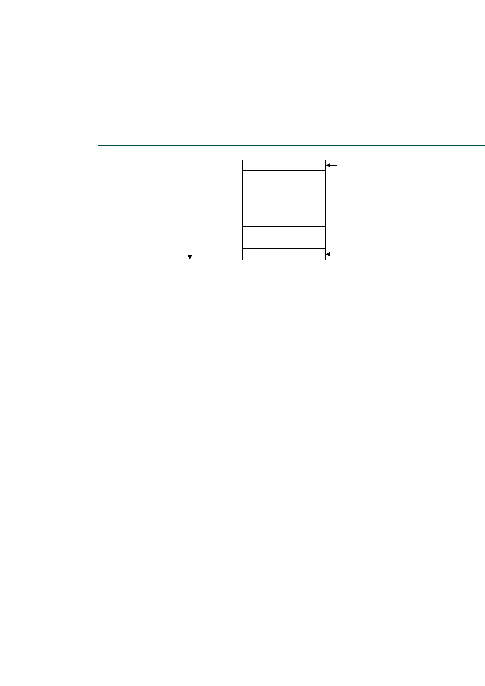
UM10462 All information provided in this document is subject to legal disclaimers. © NXP B.V. 2014. All rights reserved.
User manual Rev. 5.3 — 11 June 2014 447 of 521
NXP Semiconductors UM10462
Chapter 24: LPC11U3x/2x/1x Appendix ARM Cortex-M0
Sufficient priority means the exception has greater priority than any limit set by the mask
register, see Section 24–24.3.1.3.6. An exception with less priority than this is pending but
is not handled by the processor.
When the processor takes an exception, unless the exception is a tail-chained or a
late-arriving exception, the processor pushes information onto the current stack. This
operation is referred to as stacking and the structure of eight data words is referred as a
stack frame. The stack frame contains the following information:
Immediately after stacking, the stack pointer indicates the lowest address in the stack
frame. The stack frame is aligned to a double-word address.
The stack frame includes the return address. This is the address of the next instruction in
the interrupted program. This value is restored to the PC at exception return so that the
interrupted program resumes.
The processor performs a vector fetch that reads the exception handler start address from
the vector table. When stacking is complete, the processor starts executing the exception
handler. At the same time, the processor writes an EXC_RETURN value to the LR. This
indicates which stack pointer corresponds to the stack frame and what operation mode
the processor was in before the entry occurred.
If no higher priority exception occurs during exception entry, the processor starts
executing the exception handler and automatically changes the status of the
corresponding pending interrupt to active.
If another higher priority exception occurs during exception entry, the processor starts
executing the exception handler for this exception and does not change the pending
status of the earlier exception. This is the late arrival case.
24.3.3.6.2 Exception return
Exception return occurs when the processor is in Handler mode and execution of one of
the following instructions attempts to set the PC to an EXC_RETURN value:
•a
POP
instruction that loads the PC
•a
BX
instruction using any register.
The processor saves an EXC_RETURN value to the LR on exception entry. The
exception mechanism relies on this value to detect when the processor has completed an
exception handler. Bits[31:4] of an EXC_RETURN value are
0xFFFFFFF
. When the
processor loads a value matching this pattern to the PC it detects that the operation is a
Fig 81. Exception entry stack contents
63SRLQWVKHUHEHIRUHLQWHUUXSW
[365
3&
/5
5
5
5
5
5
SUHYLRXV!
63SRLQWVKHUHDIWHULQWHUUXSW
63[&
63[
63[
63[
63[&
63[
63[
63[
'HFUHDVLQJ
PHPRU\
DGGUHVV

UM10462 All information provided in this document is subject to legal disclaimers. © NXP B.V. 2014. All rights reserved.
User manual Rev. 5.3 — 11 June 2014 448 of 521
NXP Semiconductors UM10462
Chapter 24: LPC11U3x/2x/1x Appendix ARM Cortex-M0
not a normal branch operation and, instead, that the exception is complete. Therefore, it
starts the exception return sequence. Bits[3:0] of the EXC_RETURN value indicate the
required return stack and processor mode, as Table 24–422 shows.
24.3.4 Fault handling
Faults are a subset of exceptions, see Section 24–24.3.3. All faults result in the HardFault
exception being taken or cause lockup if they occur in the NMI or HardFault handler. The
faults are:
•execution of an
SVC
instruction at a priority equal or higher than SVCall
•execution of a
BKPT
instruction without a debugger attached
•a system-generated bus error on a load or store
•execution of an instruction from an XN memory address
•execution of an instruction from a location for which the system generates a bus fault
•a system-generated bus error on a vector fetch
•execution of an Undefined instruction
•execution of an instruction when not in Thumb-State as a result of the T-bit being
previously cleared to 0
•an attempted load or store to an unaligned address.
Only Reset and NMI can preempt the fixed priority HardFault handler. A HardFault can
preempt any exception other than Reset, NMI, or another hard fault.
24.3.4.1 Lockup
The processor enters a lockup state if a fault occurs when executing the NMI or HardFault
handlers, or if the system generates a bus error when unstacking the PSR on an
exception return using the MSP. When the processor is in lockup state it does not execute
any instructions. The processor remains in lockup state until one of the following occurs:
•it is reset
•a debugger halts it
•an NMI occurs and the current lockup is in the HardFault handler.
Table 422. Exception return behavior
EXC_RETURN Description
0xFFFFFFF1
Return to Handler mode.
Exception return gets state from the main stack.
Execution uses MSP after return.
0xFFFFFFF9
Return to Thread mode.
Exception return gets state from MSP.
Execution uses MSP after return.
0xFFFFFFFD
Return to Thread mode.
Exception return gets state from PSP.
Execution uses PSP after return.
All other values Reserved.

UM10462 All information provided in this document is subject to legal disclaimers. © NXP B.V. 2014. All rights reserved.
User manual Rev. 5.3 — 11 June 2014 449 of 521
NXP Semiconductors UM10462
Chapter 24: LPC11U3x/2x/1x Appendix ARM Cortex-M0
If lockup state occurs in the NMI handler a subsequent NMI does not cause the processor
to leave lockup state.
24.3.5 Power management
The Cortex-M0 processor sleep modes reduce power consumption:
•a sleep mode, that stops the processor clock
•a Deep-sleep and Power-down modes, for details see Section 3.9.
The SLEEPDEEP bit of the SCR selects which sleep mode is used, see
Section 24–24.5.3.5.
This section describes the mechanisms for entering sleep mode, and the conditions for
waking up from sleep mode.
24.3.5.1 Entering sleep mode
This section describes the mechanisms software can use to put the processor into sleep
mode.
The system can generate spurious wake-up events, for example a debug operation wakes
up the processor. Therefore software must be able to put the processor back into sleep
mode after such an event. A program might have an idle loop to put the processor back in
to sleep mode.
24.3.5.1.1 Wait for interrupt
The Wait For Interrupt instruction,
WFI
, causes immediate entry to sleep mode. When the
processor executes a
WFI
instruction it stops executing instructions and enters sleep
mode. See Section 24–24.4.7.12 for more information.
24.3.5.1.2 Wait for event
Remark: The WFE instruction is not implemented on the LPC11U3x/2x/1x.
The Wait For Event instruction,
WFE
, causes entry to sleep mode conditional on the value
of a one-bit event register. When the processor executes a
WFE
instruction, it checks the
value of the event register:
0 — The processor stops executing instructions and enters sleep mode
1 — The processor sets the register to zero and continues executing instructions without
entering sleep mode.
See Section 24–24.4.7.11 for more information.
If the event register is 1, this indicates that the processor must not enter sleep mode on
execution of a
WFE
instruction. Typically, this is because of the assertion of an external
event, or because another processor in the system has executed a
SEV
instruction, see
Section 24–24.4.7.9. Software cannot access this register directly.

UM10462 All information provided in this document is subject to legal disclaimers. © NXP B.V. 2014. All rights reserved.
User manual Rev. 5.3 — 11 June 2014 450 of 521
NXP Semiconductors UM10462
Chapter 24: LPC11U3x/2x/1x Appendix ARM Cortex-M0
24.3.5.1.3 Sleep-on-exit
If the SLEEPONEXIT bit of the SCR is set to 1, when the processor completes the
execution of an exception handler and returns to Thread mode it immediately enters sleep
mode. Use this mechanism in applications that only require the processor to run when an
interrupt occurs.
24.3.5.2 Wake-up from sleep mode
The conditions for the processor to wake-up depend on the mechanism that caused it to
enter sleep mode.
24.3.5.2.1 Wake-up from WFI or sleep-on-exit
Normally, the processor wakes up only when it detects an exception with sufficient priority
to cause exception entry.
Some embedded systems might have to execute system restore tasks after the processor
wakes up, and before it executes an interrupt handler. To achieve this set the PRIMASK
bit to 1. If an interrupt arrives that is enabled and has a higher priority than current
exception priority, the processor wakes up but does not execute the interrupt handler until
the processor sets PRIMASK to zero. For more information about PRIMASK, see
Section 24–24.3.1.3.6.
24.3.5.2.2 Wake-up from WFE
The processor wakes up if:
•it detects an exception with sufficient priority to cause exception entry
•in a multiprocessor system, another processor in the system executes a
SEV
instruction.
In addition, if the SEVONPEND bit in the SCR is set to 1, any new pending interrupt
triggers an event and wakes up the processor, even if the interrupt is disabled or has
insufficient priority to cause exception entry. For more information about the SCR see
Section 24–24.5.3.5.
24.3.5.3 Power management programming hints
ISO/IEC C cannot directly generate the
WFI
,
WFE
, and
SEV
instructions. The CMSIS
provides the following intrinsic functions for these instructions:
void __WFE(void) // Wait for Event
void __WFI(void) // Wait for Interrupt
void __SEV(void) // Send Event
24.4 Instruction set
24.4.1 Instruction set summary
The processor implements a version of the Thumb instruction set. Table 423 lists the
supported instructions.
Remark: In Table 423

UM10462 All information provided in this document is subject to legal disclaimers. © NXP B.V. 2014. All rights reserved.
User manual Rev. 5.3 — 11 June 2014 451 of 521
NXP Semiconductors UM10462
Chapter 24: LPC11U3x/2x/1x Appendix ARM Cortex-M0
•angle brackets, <>, enclose alternative forms of the operand
•braces, {}, enclose optional operands and mnemonic parts
•the Operands column is not exhaustive.
For more information on the instructions and operands, see the instruction descriptions.
Table 423. Cortex-M0 instructions
Mnemonic Operands Brief description Flags Reference
ADCS {Rd,} Rn, Rm Add with Carry N,Z,C,V Section 24–24.4.5
.1
ADD{S} {Rd,} Rn,
<Rm|#imm> Add N,Z,C,V Section 24–24.4.5
.1
ADR Rd, label PC-relative Address to Register - Section 24–24.4.4
.1
ANDS {Rd,} Rn, Rm Bitwise AND N,Z Section 24–24.4.5
.1
ASRS {Rd,} Rm, <Rs|#imm> Arithmetic Shift Right N,Z,C Section 24–24.4.5
.3
B{cc} label Branch {conditionally} - Section 24–24.4.6
.1
BICS {Rd,} Rn, Rm Bit Clear N,Z Section 24–24.4.5
.2
BKPT #imm Breakpoint - Section 24–24.4.7
.1
BL label Branch with Link - Section 24–24.4.6
.1
BLX Rm Branch indirect with Link - Section 24–24.4.6
.1
BX Rm Branch indirect - Section 24–24.4.6
.1
CMN Rn, Rm Compare Negative N,Z,C,V Section 24–24.4.5
.4
CMP Rn, <Rm|#imm> Compare N,Z,C,V Section 24–24.4.5
.4
CPSID iChange Processor State,
Disable Interrupts
-Section 24–24.4.7
.2
CPSIE iChange Processor State,
Enable Interrupts
-Section 24–24.4.7
.2
DMB -Data Memory Barrier - Section 24–24.4.7
.3
DSB -Data Synchronization Barrier - Section 24–24.4.7
.4
EORS {Rd,} Rn, Rm Exclusive OR N,Z Section 24–24.4.5
.2
ISB -Instruction Synchronization
Barrier
-Section 24–24.4.7
.5
LDM Rn{!}, reglist Load Multiple registers,
increment after
-Section 24–24.4.4
.5

UM10462 All information provided in this document is subject to legal disclaimers. © NXP B.V. 2014. All rights reserved.
User manual Rev. 5.3 — 11 June 2014 452 of 521
NXP Semiconductors UM10462
Chapter 24: LPC11U3x/2x/1x Appendix ARM Cortex-M0
LDR Rt, label Load Register from PC-relative
address
-Section 24–24.4.4
LDR Rt, [Rn, <Rm|#imm>] Load Register with word - Section 24–24.4.4
LDRB Rt, [Rn, <Rm|#imm>] Load Register with byte - Section 24–24.4.4
LDRH Rt, [Rn, <Rm|#imm>] Load Register with halfword - Section 24–24.4.4
LDRSB Rt, [Rn, <Rm|#imm>] Load Register with signed byte - Section 24–24.4.4
LDRSH Rt, [Rn, <Rm|#imm>] Load Register with signed
halfword
-Section 24–24.4.4
LSLS {Rd,} Rn, <Rs|#imm> Logical Shift Left N,Z,C Section 24–24.4.5
.3
U{Rd,} Rn, <Rs|#imm> Logical Shift Right N,Z,C Section 24–24.4.5
.3
MOV{S} Rd, Rm Move N,Z Section 24–24.4.5
.5
MRS Rd, spec_reg Move to general register from
special register
-Section 24–24.4.7
.6
MSR spec_reg, Rm Move to special register from
general register
N,Z,C,V Section 24–24.4.7
.7
MULS Rd, Rn, Rm Multiply, 32-bit result N,Z Section 24–24.4.5
.6
MVNS Rd, Rm Bitwise NOT N,Z Section 24–24.4.5
.5
NOP - No Operation - Section 24–24.4.7
.8
ORRS {Rd,} Rn, Rm Logical OR N,Z Section 24–24.4.5
.2
POP reglist Pop registers from stack - Section 24–24.4.4
.6
PUSH reglist Push registers onto stack - Section 24–24.4.4
.6
REV Rd, Rm Byte-Reverse word - Section 24–24.4.5
.7
REV16 Rd, Rm Byte-Reverse packed halfwords - Section 24–24.4.5
.7
REVSH Rd, Rm Byte-Reverse signed halfword - Section 24–24.4.5
.7
RORS {Rd,} Rn, Rs Rotate Right N,Z,C Section 24–24.4.5
.3
RSBS {Rd,} Rn, #0 Reverse Subtract N,Z,C,V Section 24–24.4.5
.1
SBCS {Rd,} Rn, Rm Subtract with Carry N,Z,C,V Section 24–24.4.5
.1
SEV - Send Event - Section 24–24.4.7
.9
STM Rn!, reglist Store Multiple registers,
increment after
-Section 24–24.4.4
.5
Table 423. Cortex-M0 instructions
Mnemonic Operands Brief description Flags Reference

UM10462 All information provided in this document is subject to legal disclaimers. © NXP B.V. 2014. All rights reserved.
User manual Rev. 5.3 — 11 June 2014 453 of 521
NXP Semiconductors UM10462
Chapter 24: LPC11U3x/2x/1x Appendix ARM Cortex-M0
24.4.2 Intrinsic functions
ISO/IEC C code cannot directly access some Cortex-M0 instructions. This section
describes intrinsic functions that can generate these instructions, provided by the CMSIS
and that might be provided by a C compiler. If a C compiler does not support an
appropriate intrinsic function, you might have to use inline assembler to access the
relevant instruction.
The CMSIS provides the following intrinsic functions to generate instructions that ISO/IEC
C code cannot directly access:
STR Rt, [Rn, <Rm|#imm>] Store Register as word - Section 24–24.4.4
STRB Rt, [Rn, <Rm|#imm>] Store Register as byte - Section 24–24.4.4
STRH Rt, [Rn, <Rm|#imm>] Store Register as halfword - Section 24–24.4.4
SUB{S} {Rd,} Rn,
<Rm|#imm> Subtract N,Z,C,V Section 24–24.4.5
.1
SVC #imm Supervisor Call - Section 24–24.4.7
.10
SXTB Rd, Rm Sign extend byte - Section 24–24.4.5
.8
SXTH Rd, Rm Sign extend halfword - Section 24–24.4.5
.8
TST Rn, Rm Logical AND based test N,Z Section 24–24.4.5
.9
UXTB Rd, Rm Zero extend a byte - Section 24–24.4.5
.8
UXTH Rd, Rm Zero extend a halfword - Section 24–24.4.5
.8
WFE - Wait For Event - Section 24–24.4.7
.11
WFI - Wait For Interrupt - Section 24–24.4.7
.12
Table 423. Cortex-M0 instructions
Mnemonic Operands Brief description Flags Reference
Table 424. CMSIS intrinsic functions to generate some Cortex-M0 instructions
Instruction CMSIS intrinsic function
CPSIE i void __enable_irq(void)
CPSID i void __disable_irq(void)
ISB void __ISB(void)
DSB void __DSB(void)
DMB void __DMB(void)
NOP void __NOP(void)
REV uint32_t __REV(uint32_t int value)
REV16 uint32_t __REV16(uint32_t int value)
REVSH uint32_t __REVSH(uint32_t int value)

UM10462 All information provided in this document is subject to legal disclaimers. © NXP B.V. 2014. All rights reserved.
User manual Rev. 5.3 — 11 June 2014 454 of 521
NXP Semiconductors UM10462
Chapter 24: LPC11U3x/2x/1x Appendix ARM Cortex-M0
The CMSIS also provides a number of functions for accessing the special registers using
MRS and MSR instructions:
24.4.3 About the instruction descriptions
The following sections give more information about using the instructions:
•Section 24.4.3.1 “Operands”
•Section 24.4.3.2 “Restrictions when using PC or SP”
•Section 24.4.3.3 “Shift Operations”
•Section 24.4.3.4 “Address alignment”
•Section 24.4.3.5 “PC-relative expressions”
•Section 24.4.3.6 “Conditional execution”.
24.4.3.1 Operands
An instruction operand can be an ARM register, a constant, or another instruction-specific
parameter. Instructions act on the operands and often store the result in a destination
register. When there is a destination register in the instruction, it is usually specified before
the other operands.
24.4.3.2 Restrictions when using PC or SP
Many instructions are unable to use, or have restrictions on whether you can use, the
Program Counter (PC) or Stack Pointer (SP) for the operands or destination register.
See instruction descriptions for more information.
Remark: When you update the PC with a BX, BLX, or POP instruction, bit[0] of any
address must be 1 for correct execution. This is because this bit indicates the destination
instruction set, and the Cortex-M0 processor only supports Thumb instructions. When a
BL or BLX instruction writes the value of bit[0] into the LR it is automatically assigned the
value 1.
SEV void __SEV(void)
WFE void __WFE(void)
WFI void __WFI(void)
Table 425. insic functions to access the special registers
Special register Access CMSIS function
PRIMASK Read uint32_t __get_PRIMASK (void)
Write void __set_PRIMASK (uint32_t value)
CONTROL Read uint32_t __get_CONTROL (void)
Write void __set_CONTROL (uint32_t value)
MSP Read uint32_t __get_MSP (void)
Write void __set_MSP (uint32_t TopOfMainStack)
PSP Read uint32_t __get_PSP (void)
Write void __set_PSP (uint32_t TopOfProcStack)
Table 424. CMSIS intrinsic functions to generate some Cortex-M0 instructions
Instruction CMSIS intrinsic function
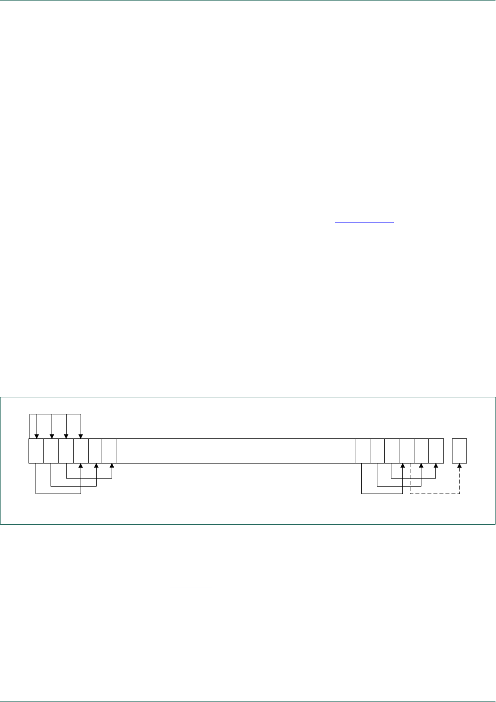
UM10462 All information provided in this document is subject to legal disclaimers. © NXP B.V. 2014. All rights reserved.
User manual Rev. 5.3 — 11 June 2014 455 of 521
NXP Semiconductors UM10462
Chapter 24: LPC11U3x/2x/1x Appendix ARM Cortex-M0
24.4.3.3 Shift Operations
Register shift operations move the bits in a register left or right by a specified number of
bits, the shift length. Register shift can be performed directly by the instructions ASR,
LSR, LSL, and ROR and the result is written to a destination register.The permitted shift
lengths depend on the shift type and the instruction, see the individual instruction
description. If the shift length is 0, no shift occurs. Register shift operations update the
carry flag except when the specified shift length is 0. The following sub-sections describe
the various shift operations and how they affect the carry flag. In these descriptions, Rm is
the register containing the value to be shifted, and n is the shift length.
24.4.3.3.1 ASR
Arithmetic shift right by n bits moves the left-hand 32 -n bits of the register Rm, to the right
by n places, into the right-hand 32 -n bits of the result, and it copies the original bit[31] of
the register into the left-hand n bits of the result. See Figure 24–82.
You can use the ASR operation to divide the signed value in the register Rm by 2n, with
the result being rounded towards negative-infinity.
When the instruction is ASRS the carry flag is updated to the last bit shifted out, bit[n-1], of
the register Rm.
Remark:
•If n is 32 or more, then all the bits in the result are set to the value of bit[31] of Rm.
•If n is 32 or more and the carry flag is updated, it is updated to the value of bit[31] of
Rm.
24.4.3.3.2 LSR
Logical shift right by n bits moves the left-hand 32-n bits of the register Rm, to the right by
n places, into the right-hand 32 -n bits of the result, and it sets the left-hand n bits of the
result to 0. See Figure 83.
You can use the LSR operation to divide the value in the register Rm by 2n, if the value is
regarded as an unsigned integer.
When the instruction is LSRS, the carry flag is updated to the last bit shifted out, bit[n-1],
of the register Rm.
Remark:
Fig 82. ASR #3
&DUU\
)ODJ
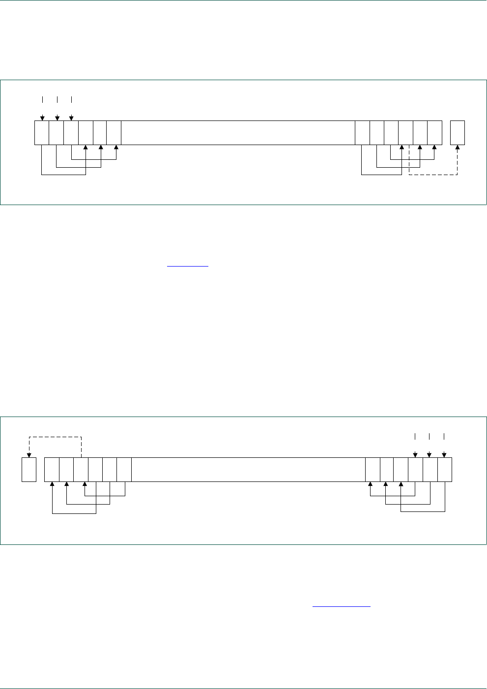
UM10462 All information provided in this document is subject to legal disclaimers. © NXP B.V. 2014. All rights reserved.
User manual Rev. 5.3 — 11 June 2014 456 of 521
NXP Semiconductors UM10462
Chapter 24: LPC11U3x/2x/1x Appendix ARM Cortex-M0
•If n is 32 or more, then all the bits in the result are cleared to 0.
•If n is 33 or more and the carry flag is updated, it is updated to 0.
24.4.3.3.3 LSL
Logical shift left by n bits moves the right-hand 32-n bits of the register Rm, to the left by n
places, into the left-hand 32-n bits of the result, and it sets the right-hand n bits of the
result to 0. See Figure 84.
You can use the LSL operation to multiply the value in the register Rm by 2n, if the value is
regarded as an unsigned integer or a two’s complement signed integer. Overflow can
occur without warning.
When the instruction is LSLS the carry flag is updated to the last bit shifted out, bit[32-n],
of the register Rm. These instructions do not affect the carry flag when used with LSL #0.
Remark:
•If n is 32 or more, then all the bits in the result are cleared to 0.
•If n is 33 or more and the carry flag is updated, it is updated to 0.
24.4.3.3.4 ROR
Rotate right by n bits moves the left-hand 32-n bits of the register Rm, to the right by n
places, into the right-hand 32-n bits of the result, and it moves the right-hand n bits of the
register into the left-hand n bits of the result. See Figure 24–85.
When the instruction is RORS the carry flag is updated to the last bit rotation, bit[n-1], of
the register Rm.
Remark:
Fig 83. LSR #3
&DUU\
)ODJ
Fig 84. LSL #3
&DUU\
)ODJ
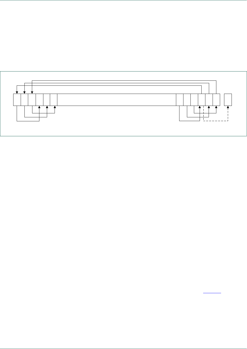
UM10462 All information provided in this document is subject to legal disclaimers. © NXP B.V. 2014. All rights reserved.
User manual Rev. 5.3 — 11 June 2014 457 of 521
NXP Semiconductors UM10462
Chapter 24: LPC11U3x/2x/1x Appendix ARM Cortex-M0
•If n is 32, then the value of the result is same as the value in Rm, and if the carry flag
is updated, it is updated to bit[31] of Rm.
•ROR
with shift length, n, greater than 32 is the same as
ROR
with shift length n-32.
24.4.3.4 Address alignment
An aligned access is an operation where a word-aligned address is used for a word, or
multiple word access, or where a halfword-aligned address is used for a halfword access.
Byte accesses are always aligned.
There is no support for unaligned accesses on the Cortex-M0 processor. Any attempt to
perform an unaligned memory access operation results in a HardFault exception.
24.4.3.5 PC-relative expressions
A PC-relative expression or label is a symbol that represents the address of an instruction
or literal data. It is represented in the instruction as the PC value plus or minus a numeric
offset. The assembler calculates the required offset from the label and the address of the
current instruction. If the offset is too big, the assembler produces an error.
Remark:
•For most instructions, the value of the PC is the address of the current instruction plus
4 bytes.
•Your assembler might permit other syntaxes for PC-relative expressions, such as a
label plus or minus a number, or an expression of the form [PC, #imm].
24.4.3.6 Conditional execution
Most data processing instructions update the condition flags in the Application Program
Status Register (APSR) according to the result of the operation, see Section . Some
instructions update all flags, and some only update a subset. If a flag is not updated, the
original value is preserved. See the instruction descriptions for the flags they affect.
You can execute a conditional branch instruction, based on the condition flags set in
another instruction, either:
•immediately after the instruction that updated the flags
•after any number of intervening instructions that have not updated the flags.
Fig 85. ROR #3
&DUU\
)ODJ

UM10462 All information provided in this document is subject to legal disclaimers. © NXP B.V. 2014. All rights reserved.
User manual Rev. 5.3 — 11 June 2014 458 of 521
NXP Semiconductors UM10462
Chapter 24: LPC11U3x/2x/1x Appendix ARM Cortex-M0
On the Cortex-M0 processor, conditional execution is available by using conditional
branches.
This section describes:
•Section 24.4.3.6.1 “The condition flags”
•Section 24.4.3.6.2 “Condition code suffixes”.
24.4.3.6.1 The condition flags
The APSR contains the following condition flags:
N — Set to 1 when the result of the operation was negative, cleared to 0 otherwise.
Z — Set to 1 when the result of the operation was zero, cleared to 0 otherwise.
C — Set to 1 when the operation resulted in a carry, cleared to 0 otherwise.
V — Set to 1 when the operation caused overflow, cleared to 0 otherwise.
For more information about the APSR see Section 24–24.3.1.3.5.
A carry occurs:
•if the result of an addition is greater than or equal to 232
•if the result of a subtraction is positive or zero
•as the result of a shift or rotate instruction.
Overflow occurs when the sign of the result, in bit[31], does not match the sign of the
result had the operation been performed at infinite precision, for example:
•if adding two negative values results in a positive value
•if adding two positive values results in a negative value
•if subtracting a positive value from a negative value generates a positive value
•if subtracting a negative value from a positive value generates a negative value.
The Compare operations are identical to subtracting, for CMP, or adding, for CMN, except
that the result is discarded. See the instruction descriptions for more information.
24.4.3.6.2 Condition code suffixes
Conditional branch is shown in syntax descriptions as B{cond}. A branch instruction with a
condition code is only taken if the condition code flags in the APSR meet the specified
condition, otherwise the branch instruction is ignored. shows the condition codes to use.
Table 426 also shows the relationship between condition code suffixes and the N, Z, C,
and V flags.
Table 426. Condition code suffixes
Suffix Flags Meaning
EQ Z = 1 Equal, last flag setting result was zero
NE Z = 0 Not equal, last flag setting result was non-zero
CS or HS C = 1 Higher or same, unsigned
CC or LO C = 0 Lower, unsigned
MI N = 1 Negative

UM10462 All information provided in this document is subject to legal disclaimers. © NXP B.V. 2014. All rights reserved.
User manual Rev. 5.3 — 11 June 2014 459 of 521
NXP Semiconductors UM10462
Chapter 24: LPC11U3x/2x/1x Appendix ARM Cortex-M0
24.4.4 Memory access instructions
Table 427 shows the memory access instructions:
24.4.4.1 ADR
Generates a PC-relative address.
24.4.4.1.1 Syntax
ADR Rd, label
where:
Rd is the destination register.
label is a PC-relative expression. See Section 24–24.4.3.5.
24.4.4.1.2 Operation
ADR generates an address by adding an immediate value to the PC, and writes the result
to the destination register.
PL N = 0 Positive or zero
VS V = 1 Overflow
VC V = 0 No overflow
HI C = 1 and Z = 0 Higher, unsigned
LS C = 0 or Z = 1 Lower or same, unsigned
GE N = V Greater than or equal, signed
LT N = V Less than, signed
GT Z = 0 and N = V Greater than, signed
LE Z = 1 and N = V Less than or equal, signed
AL Can have any value Always. This is the default when no suffix is specified.
Table 426. Condition code suffixes
Suffix Flags Meaning
Table 427. Access instructions
Mnemonic Brief description See
LDR{type} Load Register using register offset Section 24–24.4.4.
3
LDR Load Register from PC-relative address Section 24–24.4.4.
4
POP Pop registers from stack Section 24–24.4.4.
6
PUSH Push registers onto stack Section 24–24.4.4.
6
STM Store Multiple registers Section 24–24.4.4.
5
STR{type} Store Register using immediate offset Section 24–24.4.4.
2
STR{type} Store Register using register offset Section 24–24.4.4.
3

UM10462 All information provided in this document is subject to legal disclaimers. © NXP B.V. 2014. All rights reserved.
User manual Rev. 5.3 — 11 June 2014 460 of 521
NXP Semiconductors UM10462
Chapter 24: LPC11U3x/2x/1x Appendix ARM Cortex-M0
ADR facilitates the generation of position-independent code, because the address is
PC-relative.
If you use ADR to generate a target address for a BX or BLX instruction, you must ensure
that bit[0] of the address you generate is set to 1 for correct execution.
24.4.4.1.3 Restrictions
In this instruction Rd must specify R0-R7. The data-value addressed must be word
aligned and within 1020 bytes of the current PC.
24.4.4.1.4 Condition flags
This instruction does not change the flags.
24.4.4.1.5 Examples
ADR R1, TextMessage ; Write address value of a location labelled as
; TextMessage to R1
ADR R3, [PC,#996] ; Set R3 to value of PC + 996.
24.4.4.2 LDR and STR, immediate offset
Load and Store with immediate offset.
24.4.4.2.1 Syntax
LDR Rt, [<Rn | SP> {, #imm}]
LDR<B|H> Rt, [Rn {, #imm}]
STR Rt, [<Rn | SP>, {,#imm}]
STR<B|H> Rt, [Rn {,#imm}]
where:
Rt is the register to load or store.
Rn is the register on which the memory address is based.
imm is an offset from Rn. If imm is omitted, it is assumed to be zero.
24.4.4.2.2 Operation
LDR, LDRB and LDRH instructions load the register specified by Rt with either a word,
byte or halfword data value from memory. Sizes less than word are zero extended to
32-bits before being written to the register specified by Rt.
STR, STRB and STRH instructions store the word, least-significant byte or lower halfword
contained in the single register specified by Rt in to memory. The memory address to load
from or store to is the sum of the value in the register specified by either Rn or SP and the
immediate value imm.
24.4.4.2.3 Restrictions
In these instructions:
•Rt and Rn must only specify R0-R7.

UM10462 All information provided in this document is subject to legal disclaimers. © NXP B.V. 2014. All rights reserved.
User manual Rev. 5.3 — 11 June 2014 461 of 521
NXP Semiconductors UM10462
Chapter 24: LPC11U3x/2x/1x Appendix ARM Cortex-M0
•imm must be between:
–0 and 1020 and an integer multiple of four for LDR and STR
using SP as the base register
–0 and 124 and an integer multiple of four for LDR and STR
using R0-R7 as the base register
–0 and 62 and an integer multiple of two for LDRH and STRH
–0 and 31 for LDRB and STRB.
•The computed address must be divisible by the number of bytes in the transaction,
see Section 24–24.4.3.4.
24.4.4.2.4 Condition flags
These instructions do not change the flags.
24.4.4.2.5 Examples
LDR R4, [R7 ; Loads R4 from the address in R7.
STR R2, [R0,#const-struc] ; const-struc is an expression evaluating
; to a constant in the range 0-1020.
24.4.4.3 LDR and STR, register offset
Load and Store with register offset.
24.4.4.3.1 Syntax
LDR Rt, [Rn, Rm]
LDR<B|H> Rt, [Rn, Rm]
LDR<SB|SH> Rt, [Rn, Rm]
STR Rt, [Rn, Rm]
STR<B|H> Rt, [Rn, Rm]
where:
Rt is the register to load or store.
Rn is the register on which the memory address is based.
Rm is a register containing a value to be used as the offset.
24.4.4.3.2 Operation
LDR, LDRB, U, LDRSB and LDRSH load the register specified by Rt with either a word,
zero extended byte, zero extended halfword, sign extended byte or sign extended
halfword value from memory.
STR, STRB and STRH store the word, least-significant byte or lower halfword contained
in the single register specified by Rt into memory.
The memory address to load from or store to is the sum of the values in the registers
specified by Rn and Rm.

UM10462 All information provided in this document is subject to legal disclaimers. © NXP B.V. 2014. All rights reserved.
User manual Rev. 5.3 — 11 June 2014 462 of 521
NXP Semiconductors UM10462
Chapter 24: LPC11U3x/2x/1x Appendix ARM Cortex-M0
24.4.4.3.3 Restrictions
In these instructions:
•Rt, Rn, and Rm must only specify R0-R7.
•the computed memory address must be divisible by the number of bytes in the load or
store, see Section 24–24.4.3.4.
24.4.4.3.4 Condition flags
These instructions do not change the flags.
24.4.4.3.5 Examples
STR R0, [R5, R1] ; Store value of R0 into an address equal to
; sum of R5 and R1
LDRSH R1, [R2, R3] ; Load a halfword from the memory address
; specified by (R2 + R3), sign extend to 32-bits
; and write to R1.
24.4.4.4 LDR, PC-relative
Load register (literal) from memory.
24.4.4.4.1 Syntax
LDR Rt, label
where:
Rt is the register to load.
label is a PC-relative expression. See Section 24–24.4.3.5.
24.4.4.4.2 Operation
Loads the register specified by Rt from the word in memory specified by label.
24.4.4.4.3 Restrictions
In these instructions, label must be within 1020 bytes of the current PC and word aligned.
24.4.4.4.4 Condition flags
These instructions do not change the flags.
24.4.4.4.5 Examples
LDR R0, LookUpTable ; Load R0 with a word of data from an address
; labelled as LookUpTable.
LDR R3, [PC, #100] ; Load R3 with memory word at (PC + 100).
24.4.4.5 LDM and STM
Load and Store Multiple registers.

UM10462 All information provided in this document is subject to legal disclaimers. © NXP B.V. 2014. All rights reserved.
User manual Rev. 5.3 — 11 June 2014 463 of 521
NXP Semiconductors UM10462
Chapter 24: LPC11U3x/2x/1x Appendix ARM Cortex-M0
24.4.4.5.1 Syntax
LDM Rn{!}, reglist
STM Rn!, reglist
where:
Rn is the register on which the memory addresses are based.
! writeback suffix.
reglist is a list of one or more registers to be loaded or stored, enclosed in braces. It can
contain register ranges. It must be comma separated if it contains more than one
register or register range, see Section 24–24.4.4.5.5.
LDMIA and LDMFD are synonyms for LDM. LDMIA refers to the base register being
Incremented After each access. LDMFD refers to its use for popping data from Full
Descending stacks.
STMIA and STMEA are synonyms for STM. STMIA refers to the base register being
Incremented After each access. STMEA refers to its use for pushing data onto Empty
Ascending stacks.
24.4.4.5.2 Operation
LDM instructions load the registers in reglist with word values from memory addresses
based on Rn.
STM instructions store the word values in the registers in reglist to memory addresses
based on Rn.
The memory addresses used for the accesses are at 4-byte intervals ranging from the
value in the register specified by Rn to the value in the register specified by Rn + 4 * (n-1),
where n is the number of registers in reglist. The accesses happens in order of increasing
register numbers, with the lowest numbered register using the lowest memory address
and the highest number register using the highest memory address. If the writeback suffix
is specified, the value in the register specified by Rn + 4 *n is written back to the register
specified by Rn.
24.4.4.5.3 Restrictions
In these instructions:
•reglist and Rn are limited to R0-R7.
•the writeback suffix must always be used unless the instruction is an LDM where
reglist also contains Rn, in which case the writeback suffix must not be used.
•the value in the register specified by Rn must be word aligned. See
Section 24–24.4.3.4 for more information.
•for STM, if Rn appears in reglist, then it must be the first register in the list.
24.4.4.5.4 Condition flags
These instructions do not change the flags.

UM10462 All information provided in this document is subject to legal disclaimers. © NXP B.V. 2014. All rights reserved.
User manual Rev. 5.3 — 11 June 2014 464 of 521
NXP Semiconductors UM10462
Chapter 24: LPC11U3x/2x/1x Appendix ARM Cortex-M0
24.4.4.5.5 Examples
LDM R0,{R0,R3,R4} ; LDMIA is a synonym for LDM
STMIA R1!,{R2-R4,R6}
24.4.4.5.6 Incorrect examples
STM R5!,{R4,R5,R6} ; Value stored for R5 is unpredictable
LDM R2,{} ; There must be at least one register in the list
24.4.4.6 PUSH and POP
Push registers onto, and pop registers off a full-descending stack.
24.4.4.6.1 Syntax
PUSH reglist
POP reglist
where:
reglist is a non-empty list of registers, enclosed in braces. It can contain register ranges.
It must be comma separated if it contains more than one register or register range.
24.4.4.6.2 Operation
PUSH stores registers on the stack, with the lowest numbered register using the lowest
memory address and the highest numbered register using the highest memory address.
POP loads registers from the stack, with the lowest numbered register using the lowest
memory address and the highest numbered register using the highest memory address.
PUSH uses the value in the SP register minus four as the highest memory address,
POP uses the value in the SP register as the lowest memory address, implementing a
full-descending stack. On completion,
PUSH updates the SP register to point to the location of the lowest store value,
POP updates the SP register to point to the location above the highest location loaded.
If a POP instruction includes PC in its reglist, a branch to this location is performed when
the POP instruction has completed. Bit[0] of the value read for the PC is used to update
the APSR T-bit. This bit must be 1 to ensure correct operation.
24.4.4.6.3 Restrictions
In these instructions:
•reglist must use only R0-R7.
•The exception is LR for a PUSH and PC for a POP.
24.4.4.6.4 Condition flags
These instructions do not change the flags.

UM10462 All information provided in this document is subject to legal disclaimers. © NXP B.V. 2014. All rights reserved.
User manual Rev. 5.3 — 11 June 2014 465 of 521
NXP Semiconductors UM10462
Chapter 24: LPC11U3x/2x/1x Appendix ARM Cortex-M0
24.4.4.6.5 Examples
PUSH {R0,R4-R7} ; Push R0,R4,R5,R6,R7 onto the stack
PUSH {R2,LR} ; Push R2 and the link-register onto the stack
POP {R0,R6,PC} ; Pop r0,r6 and PC from the stack, then branch to
; the new PC.
24.4.5 General data processing instructions
Table 428 shows the data processing instructions:
24.4.5.1 ADC, ADD, RSB, SBC, and SUB
Add with carry, Add, Reverse Subtract, Subtract with carry, and Subtract.
24.4.5.1.1 Syntax
ADCS {Rd,} Rn, Rm
Table 428. Data processing instructions
Mnemonic Brief description See
ADCS Add with Carry Section 24–24.4.5.1
ADD{S} Add Section 24–24.4.5.1
ANDS Logical AND Section 24–24.4.5.2
ASRS Arithmetic Shift Right Section 24–24.4.5.3
BICS Bit Clear Section 24–24.4.5.2
CMN Compare Negative Section 24–24.4.5.4
CMP Compare Section 24–24.4.5.4
EORS Exclusive OR Section 24–24.4.5.2
LSLS Logical Shift Left Section 24–24.4.5.3
LSRS Logical Shift Right Section 24–24.4.5.3
MOV{S} Move Section 24–24.4.5.5
MULS Multiply Section 24–24.4.5.6
MVNS Move NOT Section 24–24.4.5.5
ORRS Logical OR Section 24–24.4.5.2
REV Reverse byte order in a word Section 24–24.4.5.7
REV16 Reverse byte order in each halfword Section 24–24.4.5.7
REVSH Reverse byte order in bottom halfword
and sign extend
Section 24–24.4.5.7
RORS Rotate Right Section 24–24.4.5.3
RSBS Reverse Subtract Section 24–24.4.5.1
SBCS Subtract with Carry Section 24–24.4.5.1
SUBS Subtract Section 24–24.4.5.1
SXTB Sign extend a byte Section 24–24.4.5.8
SXTH Sign extend a halfword Section 24–24.4.5.8
UXTB Zero extend a byte Section 24–24.4.5.8
UXTH Zero extend a halfword Section 24–24.4.5.8
TST Test Section 24–24.4.5.9

UM10462 All information provided in this document is subject to legal disclaimers. © NXP B.V. 2014. All rights reserved.
User manual Rev. 5.3 — 11 June 2014 466 of 521
NXP Semiconductors UM10462
Chapter 24: LPC11U3x/2x/1x Appendix ARM Cortex-M0
ADD{S} {Rd,} Rn, <Rm|#imm>
RSBS {Rd,} Rn, Rm, #0
SBCS {Rd,} Rn, Rm
SUB{S} {Rd,} Rn,
<Rm|#imm>
Where:
S causes an ADD or SUB instruction to update flags
Rd specifies the result register
Rn specifies the first source register
Rm specifies the second source register
imm specifies a constant immediate value.
When the optional Rd register specifier is omitted, it is assumed to take the same value as
Rn, for example ADDS R1,R2 is identical to ADDS R1,R1,R2.
24.4.5.1.2 Operation
The ADCS instruction adds the value in Rn to the value in Rm, adding a further one if the
carry flag is set, places the result in the register specified by Rd and updates the N, Z, C,
and V flags.
The ADD instruction adds the value in Rn to the value in Rm or an immediate value
specified by imm and places the result in the register specified by Rd.
The ADDS instruction performs the same operation as ADD and also updates the N, Z, C
and V flags.
The RSBS instruction subtracts the value in Rn from zero, producing the arithmetic
negative of the value, and places the result in the register specified by Rd and updates the
N, Z, C and V flags.
The SBCS instruction subtracts the value of Rm from the value in Rn, deducts a further
one if the carry flag is set. It places the result in the register specified by Rd and updates
the N, Z, C and V flags.
The SUB instruction subtracts the value in Rm or the immediate specified by imm. It
places the result in the register specified by Rd.
The SUBS instruction performs the same operation as SUB and also updates the N, Z, C
and V flags.
Use ADC and SBC to synthesize multiword arithmetic, see Section 24.4.5.1.4.
See also Section 24–24.4.4.1.
24.4.5.1.3 Restrictions
Table 429 lists the legal combinations of register specifiers and immediate values that can
be used with each instruction.

UM10462 All information provided in this document is subject to legal disclaimers. © NXP B.V. 2014. All rights reserved.
User manual Rev. 5.3 — 11 June 2014 467 of 521
NXP Semiconductors UM10462
Chapter 24: LPC11U3x/2x/1x Appendix ARM Cortex-M0
24.4.5.1.4 Examples
The following shows two instructions that add a 64-bit integer contained in R0 and R1 to
another 64-bit integer contained in R2 and R3, and place the result in R0 and R1.
64-bit addition:
ADDS R0, R0, R2 ; add the least significant words
ADCS R1, R1, R3 ; add the most significant words with carry
Multiword values do not have to use consecutive registers. The following shows
instructions that subtract a 96-bit integer contained in R1, R2, and R3 from another
contained in R4, R5, and R6. The example stores the result in R4, R5, and R6.
96-bit subtraction:
SUBS R4, R4, R1 ; subtract the least significant words
SBCS R5, R5, R2 ; subtract the middle words with carry
SBCS R6, R6, R3 ; subtract the most significant words with carry
The following shows the RSBS instruction used to perform a 1's complement of a single
register.
Arithmetic negation:
RSBS R7, R7, #0 ; subtract R7 from zero
24.4.5.2 AND, ORR, EOR, and BIC
Logical AND, OR, Exclusive OR, and Bit Clear.
24.4.5.2.1 Syntax
ANDS {Rd,} Rn, Rm
ORRS {Rd,} Rn, Rm
EORS {Rd,} Rn, Rm
Table 429. ADC, ADD, RSB, SBC and SUB operand restrictions
Instruction Rd Rn Rm imm Restrictions
ADCS R0-R7 R0-R7 R0-R7 - Rd and Rn must specify the same register.
ADD R0-R15 R0-R15 R0-PC - Rd and Rn must specify the same register.
Rn and Rm must not both specify PC.
R0-R7 SP or PC - 0-1020 Immediate value must be an integer multiple of four.
SP SP - 0-508 Immediate value must be an integer multiple of four.
ADDS R0-R7 R0-R7 - 0-7 -
R0-R7 R0-R7 - 0-255 Rd and Rn must specify the same register.
R0-R7 R0-R7 R0-R7 - -
RSBS R0-R7 R0-R7 - - -
SBCS R0-R7 R0-R7 R0-R7 - Rd and Rn must specify the same register.
SUB SP SP - 0-508 Immediate value must be an integer multiple of four.
SUBS R0-R7 R0-R7 - 0-7 -
R0-R7 R0-R7 - 0-255 Rd and Rn must specify the same register.
R0-R7 R0-R7 R0-R7 - -

UM10462 All information provided in this document is subject to legal disclaimers. © NXP B.V. 2014. All rights reserved.
User manual Rev. 5.3 — 11 June 2014 468 of 521
NXP Semiconductors UM10462
Chapter 24: LPC11U3x/2x/1x Appendix ARM Cortex-M0
BICS {Rd,} Rn, Rm
where:
Rd is the destination register.
Rn is the register holding the first operand and is the same as the destination register.
Rm second register.
24.4.5.2.2 Operation
The AND, EOR, and ORR instructions perform bitwise AND, exclusive OR, and inclusive
OR operations on the values in Rn and Rm.
The BIC instruction performs an AND operation on the bits in Rn with the logical negation
of the corresponding bits in the value of Rm.
The condition code flags are updated on the result of the operation, see
Section 24.4.3.6.1.
24.4.5.2.3 Restrictions
In these instructions, Rd, Rn, and Rm must only specify R0-R7.
24.4.5.2.4 Condition flags
These instructions:
•update the N and Z flags according to the result
•do not affect the C or V flag.
24.4.5.2.5 Examples
ANDS R2, R2, R1
ORRS R2, R2, R5
ANDS R5, R5, R8
EORS R7, R7, R6
BICS R0, R0, R1
24.4.5.3 ASR, LSL, LSR, and ROR
Arithmetic Shift Right, Logical Shift Left, Logical Shift Right, and Rotate Right.
24.4.5.3.1 Syntax
ASRS {Rd,} Rm, Rs
ASRS {Rd,} Rm, #imm
LSLS {Rd,} Rm, Rs
LSLS {Rd,} Rm, #imm
LSRS {Rd,} Rm, Rs
LSRS {Rd,} Rm, #imm
RORS {Rd,} Rm, Rs

UM10462 All information provided in this document is subject to legal disclaimers. © NXP B.V. 2014. All rights reserved.
User manual Rev. 5.3 — 11 June 2014 469 of 521
NXP Semiconductors UM10462
Chapter 24: LPC11U3x/2x/1x Appendix ARM Cortex-M0
where:
Rd is the destination register. If Rd is omitted, it is assumed to take the same value as
Rm.
Rm is the register holding the value to be shifted.
Rs is the register holding the shift length to apply to the value in Rm.
imm is the shift length.
The range of shift length depends on the instruction:
ASR — shift length from 1 to 32
LSL — shift length from 0 to 31
LSR — shift length from 1 to 32.
Remark: MOVS Rd, Rm is a pseudonym for LSLS Rd, Rm, #0.
24.4.5.3.2 Operation
ASR, LSL, LSR, and ROR perform an arithmetic-shift-left, logical-shift-left,
logical-shift-right or a right-rotation of the bits in the register Rm by the number of places
specified by the immediate imm or the value in the least-significant byte of the register
specified by Rs.
For details on what result is generated by the different instructions, see
Section 24–24.4.3.3.
24.4.5.3.3 Restrictions
In these instructions, Rd, Rm, and Rs must only specify R0-R7. For non-immediate
instructions, Rd and Rm must specify the same register.
24.4.5.3.4 Condition flags
These instructions update the N and Z flags according to the result.
The C flag is updated to the last bit shifted out, except when the shift length is 0, see
Section 24–24.4.3.3. The V flag is left unmodified.
24.4.5.3.5 Examples
ASRS R7, R5, #9 ; Arithmetic shift right by 9 bits
LSLS R1, R2, #3 ; Logical shift left by 3 bits with flag update
LSRS R4, R5, #6 ; Logical shift right by 6 bits
RORS R4, R4, R6 ; Rotate right by the value in the bottom byte of R6.
24.4.5.4 CMP and CMN
Compare and Compare Negative.
24.4.5.4.1 Syntax
CMN Rn, Rm
CMP Rn, #imm
CMP Rn, Rm

UM10462 All information provided in this document is subject to legal disclaimers. © NXP B.V. 2014. All rights reserved.
User manual Rev. 5.3 — 11 June 2014 470 of 521
NXP Semiconductors UM10462
Chapter 24: LPC11U3x/2x/1x Appendix ARM Cortex-M0
where:
Rn is the register holding the first operand.
Rm is the register to compare with.
imm is the immediate value to compare with.
24.4.5.4.2 Operation
These instructions compare the value in a register with either the value in another register
or an immediate value. They update the condition flags on the result, but do not write the
result to a register.
The CMP instruction subtracts either the value in the register specified by Rm, or the
immediate imm from the value in Rn and updates the flags. This is the same as a SUBS
instruction, except that the result is discarded.
The CMN instruction adds the value of Rm to the value in Rn and updates the flags. This
is the same as an ADDS instruction, except that the result is discarded.
24.4.5.4.3 Restrictions
For the:
•CMN
instruction Rn, and Rm must only specify R0-R7.
•CMP instruction:
–Rn and Rm can specify R0-R14
–immediate must be in the range 0-255.
24.4.5.4.4 Condition flags
These instructions update the N, Z, C and V flags according to the result.
24.4.5.4.5 Examples
CMP R2, R9
CMN R0, R2
24.4.5.5 MOV and MVN
Move and Move NOT.
24.4.5.5.1 Syntax
MOV{S} Rd, Rm
MOVS Rd, #imm
MVNS Rd, Rm
where:
S is an optional suffix. If S is specified, the condition code flags are updated on the
result of the operation, see Section 24–24.4.3.6.
Rd is the destination register.

UM10462 All information provided in this document is subject to legal disclaimers. © NXP B.V. 2014. All rights reserved.
User manual Rev. 5.3 — 11 June 2014 471 of 521
NXP Semiconductors UM10462
Chapter 24: LPC11U3x/2x/1x Appendix ARM Cortex-M0
Rm is a register.
imm is any value in the range 0-255.
24.4.5.5.2 Operation
The MOV instruction copies the value of Rm into Rd.
The MOVS instruction performs the same operation as the MOV instruction, but also
updates the N and Z flags.
The MVNS instruction takes the value of Rm, performs a bitwise logical negate operation
on the value, and places the result into Rd.
24.4.5.5.3 Restrictions
In these instructions, Rd, and Rm must only specify R0-R7.
When Rd is the PC in a MOV instruction:
•Bit[0] of the result is discarded.
•A branch occurs to the address created by forcing bit[0] of the result to 0. The T-bit
remains unmodified.
Remark: Though it is possible to use MOV as a branch instruction, ARM strongly
recommends the use of a BX or BLX instruction to branch for software portability.
24.4.5.5.4 Condition flags
If S is specified, these instructions:
•update the N and Z flags according to the result
•do not affect the C or V flags.
24.4.5.5.5 Example
MOVS R0, #0x000B ; Write value of 0x000B to R0, flags get updated
MOVS R1, #0x0 ; Write value of zero to R1, flags are updated
MOV R10, R12 ; Write value in R12 to R10, flags are not updated
MOVS R3, #23 ; Write value of 23 to R3
MOV R8, SP ; Write value of stack pointer to R8
MVNS R2, R0 ; Write inverse of R0 to the R2 and update flags
24.4.5.6 MULS
Multiply using 32-bit operands, and producing a 32-bit result.
24.4.5.6.1 Syntax
MULS Rd, Rn, Rm
where:
Rd is the destination register.
Rn, Rm are registers holding the values to be multiplied.

UM10462 All information provided in this document is subject to legal disclaimers. © NXP B.V. 2014. All rights reserved.
User manual Rev. 5.3 — 11 June 2014 472 of 521
NXP Semiconductors UM10462
Chapter 24: LPC11U3x/2x/1x Appendix ARM Cortex-M0
24.4.5.6.2 Operation
The MUL instruction multiplies the values in the registers specified by Rn and Rm, and
places the least significant 32 bits of the result in Rd. The condition code flags are
updated on the result of the operation, see Section 24–24.4.3.6.
The results of this instruction does not depend on whether the operands are signed or
unsigned.
24.4.5.6.3 Restrictions
In this instruction:
•Rd, Rn, and Rm must only specify R0-R7
•Rd must be the same as Rm.
24.4.5.6.4 Condition flags
This instruction:
•updates the N and Z flags according to the result
•does not affect the C or V flags.
24.4.5.6.5 Examples
MULS R0, R2, R0 ; Multiply with flag update, R0 = R0 x R2
24.4.5.7 REV, REV16, and REVSH
Reverse bytes.
24.4.5.7.1 Syntax
REV Rd, Rn
REV16 Rd, Rn
REVSH Rd, Rn
where:
Rd is the destination register.
Rn is the source register.
24.4.5.7.2 Operation
Use these instructions to change endianness of data:
REV — converts 32-bit big-endian data into little-endian data or 32-bit little-endian data
into big-endian data.
REV16 — converts two packed 16-bit big-endian data into little-endian data or two packed
16-bit little-endian data into big-endian data.
REVSH — converts 16-bit signed big-endian data into 32-bit signed little-endian data or
16-bit signed little-endian data into 32-bit signed big-endian data.
24.4.5.7.3 Restrictions
In these instructions, Rd, and Rn must only specify R0-R7.

UM10462 All information provided in this document is subject to legal disclaimers. © NXP B.V. 2014. All rights reserved.
User manual Rev. 5.3 — 11 June 2014 473 of 521
NXP Semiconductors UM10462
Chapter 24: LPC11U3x/2x/1x Appendix ARM Cortex-M0
24.4.5.7.4 Condition flags
These instructions do not change the flags.
24.4.5.7.5 Examples
REV R3, R7 ; Reverse byte order of value in R7 and write it to R3
REV16 R0, R0 ; Reverse byte order of each 16-bit halfword in R0
REVSH R0, R5 ; Reverse signed halfword
24.4.5.8 SXT and UXT
Sign extend and Zero extend.
24.4.5.8.1 Syntax
SXTB Rd, Rm
SXTH Rd, Rm
UXTB Rd, Rm
UXTH Rd, Rm
where:
Rd is the destination register.
Rm is the register holding the value to be extended.
24.4.5.8.2 Operation
These instructions extract bits from the resulting value:
•SXTB extracts bits[7:0] and sign extends to 32 bits
•UXTB extracts bits[7:0] and zero extends to 32 bits
•SXTH extracts bits[15:0] and sign extends to 32 bits
•UXTH extracts bits[15:0] and zero extends to 32 bits.
24.4.5.8.3 Restrictions
In these instructions, Rd and Rm must only specify R0-R7.
24.4.5.8.4 Condition flags
These instructions do not affect the flags.
24.4.5.8.5 Examples
SXTH R4, R6 ; Obtain the lower halfword of the
; value in R6 and then sign extend to
; 32 bits and write the result to R4.
UXTB R3, R1 ; Extract lowest byte of the value in R10 and zero
; extend it, and write the result to R3
24.4.5.9 TST
Test bits.

UM10462 All information provided in this document is subject to legal disclaimers. © NXP B.V. 2014. All rights reserved.
User manual Rev. 5.3 — 11 June 2014 474 of 521
NXP Semiconductors UM10462
Chapter 24: LPC11U3x/2x/1x Appendix ARM Cortex-M0
24.4.5.9.1 Syntax
TST Rn, Rm
where:
Rn is the register holding the first operand.
Rm the register to test against.
24.4.5.9.2 Operation
This instruction tests the value in a register against another register. It updates the
condition flags based on the result, but does not write the result to a register.
The TST instruction performs a bitwise AND operation on the value in Rn and the value in
Rm. This is the same as the ANDS instruction, except that it discards the result.
To test whether a bit of Rn is 0 or 1, use the TST instruction with a register that has that bit
set to 1 and all other bits cleared to 0.
24.4.5.9.3 Restrictions
In these instructions, Rn and Rm must only specify R0-R7.
24.4.5.9.4 Condition flags
This instruction:
•updates the N and Z flags according to the result
•does not affect the C or V flags.
24.4.5.9.5 Examples
TST R0, R1 ; Perform bitwise AND of R0 value and R1 value,
; condition code flags are updated but result is discarded
24.4.6 Branch and control instructions
Table 430 shows the branch and control instructions:
24.4.6.1 B, BL, BX, and BLX
Branch instructions.
24.4.6.1.1 Syntax
B{cond} label
BL label
Table 430. Branch and control instructions
Mnemonic Brief description See
B{cc} Branch {conditionally} Section 24–24.4.6.1
BL Branch with Link Section 24–24.4.6.1
BLX Branch indirect with Link Section 24–24.4.6.1
BX Branch indirect Section 24–24.4.6.1

UM10462 All information provided in this document is subject to legal disclaimers. © NXP B.V. 2014. All rights reserved.
User manual Rev. 5.3 — 11 June 2014 475 of 521
NXP Semiconductors UM10462
Chapter 24: LPC11U3x/2x/1x Appendix ARM Cortex-M0
BX Rm
BLX Rm
where:
cond is an optional condition code, see Section 24–24.4.3.6.
label is a PC-relative expression. See Section 24–24.4.3.5.
Rm is a register providing the address to branch to.
24.4.6.1.2 Operation
All these instructions cause a branch to the address indicated by label or contained in the
register specified by Rm. In addition:
•The BL and BLX instructions write the address of the next instruction to LR, the link
register R14.
•The BX and BLX instructions result in a HardFault exception if bit[0] of Rm is 0.
BL and BLX instructions also set bit[0] of the LR to 1. This ensures that the value is
suitable for use by a subsequent POP {PC} or BX instruction to perform a successful
return branch.
Table 431 shows the ranges for the various branch instructions.
24.4.6.1.3 Restrictions
In these instructions:
•Do not use SP or PC in the BX or BLX instruction.
•For BX and BLX, bit[0] of Rm must be 1 for correct execution. Bit[0] is used to update
the EPSR T-bit and is discarded from the target address.
Remark: Bcond is the only conditional instruction on the Cortex-M0 processor.
24.4.6.1.4 Condition flags
These instructions do not change the flags.
24.4.6.1.5 Examples
B loopA ; Branch to loopA
BL funC ; Branch with link (Call) to function funC, return address
; stored in LR
Table 431. Branch ranges
Instruction Branch range
B label 2 KB to +2 KB
Bcond label 256 bytes to +254 bytes
BL label 16 MB to +16 MB
BX Rm Any value in register
BLX Rm Any value in register

UM10462 All information provided in this document is subject to legal disclaimers. © NXP B.V. 2014. All rights reserved.
User manual Rev. 5.3 — 11 June 2014 476 of 521
NXP Semiconductors UM10462
Chapter 24: LPC11U3x/2x/1x Appendix ARM Cortex-M0
BX LR ; Return from function call
BLX R0 ; Branch with link and exchange (Call) to a address stored
; in R0
BEQ labelD ; Conditionally branch to labelD if last flag setting
; instruction set the Z flag, else do not branch.
24.4.7 Miscellaneous instructions
Table 432 shows the remaining Cortex-M0 instructions:
24.4.7.1 BKPT
Breakpoint.
24.4.7.1.1 Syntax
BKPT #imm
where:
imm is an integer in the range 0-255.
Table 432. Miscellaneous instructions
Mnemonic Brief description See
BKPT Breakpoint Section 24–24.4.7.
1
CPSID Change Processor State, Disable Interrupts Section 24–24.4.7.
2
CPSIE Change Processor State, Enable Interrupts Section 24–24.4.7.
2
DMB Data Memory Barrier Section 24–24.4.7.
3
DSB Data Synchronization Barrier Section 24–24.4.7.
4
ISB Instruction Synchronization Barrier Section 24–24.4.7.
5
MRS Move from special register to register Section 24–24.4.7.
6
MSR Move from register to special register Section 24–24.4.7.
7
NOP No Operation Section 24–24.4.7.
8
SEV Send Event Section 24–24.4.7.
9
SVC Supervisor Call Section 24–24.4.7.
10
WFE Wait For Event Section 24–24.4.7.
11
WFI Wait For Interrupt Section 24–24.4.7.
12

UM10462 All information provided in this document is subject to legal disclaimers. © NXP B.V. 2014. All rights reserved.
User manual Rev. 5.3 — 11 June 2014 477 of 521
NXP Semiconductors UM10462
Chapter 24: LPC11U3x/2x/1x Appendix ARM Cortex-M0
24.4.7.1.2 Operation
The BKPT instruction causes the processor to enter Debug state. Debug tools can use
this to investigate system state when the instruction at a particular address is reached.
imm is ignored by the processor. If required, a debugger can use it to store additional
information about the breakpoint.
The processor might also produce a HardFault or go in to lockup if a debugger is not
attached when a BKPT instruction is executed. See Section 24–24.3.4.1 for more
information.
24.4.7.1.3 Restrictions
There are no restrictions.
24.4.7.1.4 Condition flags
This instruction does not change the flags.
24.4.7.1.5 Examples
BKPT #0 ; Breakpoint with immediate value set to 0x0.
24.4.7.2 CPS
Change Processor State.
24.4.7.2.1 Syntax
CPSID i
CPSIE i
24.4.7.2.2 Operation
CPS changes the PRIMASK special register values. CPSID causes interrupts to be
disabled by setting PRIMASK. CPSIE cause interrupts to be enabled by clearing
PRIMASK.See Section 24–24.3.1.3.6 for more information about these registers.
24.4.7.2.3 Restrictions
There are no restrictions.
24.4.7.2.4 Condition flags
This instruction does not change the condition flags.
24.4.7.2.5 Examples
CPSID i ; Disable all interrupts except NMI (set PRIMASK)
CPSIE i ; Enable interrupts (clear PRIMASK)
24.4.7.3 DMB
Data Memory Barrier.
24.4.7.3.1 Syntax
DMB

UM10462 All information provided in this document is subject to legal disclaimers. © NXP B.V. 2014. All rights reserved.
User manual Rev. 5.3 — 11 June 2014 478 of 521
NXP Semiconductors UM10462
Chapter 24: LPC11U3x/2x/1x Appendix ARM Cortex-M0
24.4.7.3.2 Operation
DMB acts as a data memory barrier. It ensures that all explicit memory accesses that
appear in program order before the DMB instruction are observed before any explicit
memory accesses that appear in program order after the DMB instruction. DMB does not
affect the ordering of instructions that do not access memory.
24.4.7.3.3 Restrictions
There are no restrictions.
24.4.7.3.4 Condition flags
This instruction does not change the flags.
24.4.7.3.5 Examples
DMB ; Data Memory Barrier
24.4.7.4 DSB
Data Synchronization Barrier.
24.4.7.4.1 Syntax
DSB
24.4.7.4.2 Operation
DSB acts as a special data synchronization memory barrier. Instructions that come after
the DSB, in program order, do not execute until the DSB instruction completes. The DSB
instruction completes when all explicit memory accesses before it complete.
24.4.7.4.3 Restrictions
There are no restrictions.
24.4.7.4.4 Condition flags
This instruction does not change the flags.
24.4.7.4.5 Examples
DSB ; Data Synchronisation Barrier
24.4.7.5 ISB
Instruction Synchronization Barrier.
24.4.7.5.1 Syntax
ISB
24.4.7.5.2 Operation
ISB acts as an instruction synchronization barrier. It flushes the pipeline of the processor,
so that all instructions following the ISB are fetched from cache or memory again, after the
ISB instruction has been completed.

UM10462 All information provided in this document is subject to legal disclaimers. © NXP B.V. 2014. All rights reserved.
User manual Rev. 5.3 — 11 June 2014 479 of 521
NXP Semiconductors UM10462
Chapter 24: LPC11U3x/2x/1x Appendix ARM Cortex-M0
24.4.7.5.3 Restrictions
There are no restrictions.
24.4.7.5.4 Condition flags
This instruction does not change the flags.
24.4.7.5.5 Examples
ISB ; Instruction Synchronisation Barrier
24.4.7.6 MRS
Move the contents of a special register to a general-purpose register.
24.4.7.6.1 Syntax
MRS Rd, spec_reg
where:
Rd is the general-purpose destination register.
spec_reg is one of the special-purpose registers: APSR, IPSR, EPSR, IEPSR, IAPSR,
EAPSR, PSR, MSP, PSP, PRIMASK, or CONTROL.
24.4.7.6.2 Operation
MRS stores the contents of a special-purpose register to a general-purpose register. The
MRS instruction can be combined with the MR instruction to produce read-modify-write
sequences, which are suitable for modifying a specific flag in the PSR.
See Section 24–24.4.7.7.
24.4.7.6.3 Restrictions
In this instruction, Rd must not be SP or PC.
24.4.7.6.4 Condition flags
This instruction does not change the flags.
24.4.7.6.5 Examples
MRS R0, PRIMASK ; Read PRIMASK value and write it to R0
24.4.7.7 MSR
Move the contents of a general-purpose register into the specified special register.
24.4.7.7.1 Syntax
MSR spec_reg, Rn
where:
Rn is the general-purpose source register.

UM10462 All information provided in this document is subject to legal disclaimers. © NXP B.V. 2014. All rights reserved.
User manual Rev. 5.3 — 11 June 2014 480 of 521
NXP Semiconductors UM10462
Chapter 24: LPC11U3x/2x/1x Appendix ARM Cortex-M0
spec_reg is the special-purpose destination register: APSR, IPSR, EPSR, IEPSR,
IAPSR, EAPSR, PSR, MSP, PSP, PRIMASK, or CONTROL.
24.4.7.7.2 Operation
MSR updates one of the special registers with the value from the register specified by Rn.
See Section 24–24.4.7.6.
24.4.7.7.3 Restrictions
In this instruction, Rn must not be SP and must not be PC.
24.4.7.7.4 Condition flags
This instruction updates the flags explicitly based on the value in Rn.
24.4.7.7.5 Examples
MSR CONTROL, R1 ; Read R1 value and write it to the CONTROL register
24.4.7.8 NOP
No Operation.
24.4.7.8.1 Syntax
NOP
24.4.7.8.2 Operation
NOP performs no operation and is not guaranteed to be time consuming. The processor
might remove it from the pipeline before it reaches the execution stage.
Use NOP for padding, for example to place the subsequent instructions on a 64-bit
boundary.
24.4.7.8.3 Restrictions
There are no restrictions.
24.4.7.8.4 Condition flags
This instruction does not change the flags.
24.4.7.8.5 Examples
NOP ; No operation
24.4.7.9 SEV
Send Event.
24.4.7.9.1 Syntax
SEV
24.4.7.9.2 Operation
SEV causes an event to be signaled to all processors within a multiprocessor system. It
also sets the local event register, see Section 24–24.3.5.

UM10462 All information provided in this document is subject to legal disclaimers. © NXP B.V. 2014. All rights reserved.
User manual Rev. 5.3 — 11 June 2014 481 of 521
NXP Semiconductors UM10462
Chapter 24: LPC11U3x/2x/1x Appendix ARM Cortex-M0
See also Section 24–24.4.7.11.
24.4.7.9.3 Restrictions
There are no restrictions.
24.4.7.9.4 Condition flags
This instruction does not change the flags.
24.4.7.9.5 Examples
SEV ; Send Event
24.4.7.10 SVC
Supervisor Call.
24.4.7.10.1 Syntax
SVC #imm
where:
imm is an integer in the range 0-255.
24.4.7.10.2 Operation
The SVC instruction causes the SVC exception.
imm is ignored by the processor. If required, it can be retrieved by the exception handler to
determine what service is being requested.
24.4.7.10.3 Restrictions
There are no restrictions.
24.4.7.10.4 Condition flags
This instruction does not change the flags.
24.4.7.10.5 Examples
SVC #0x32 ; Supervisor Call (SVC handler can extract the immediate value
; by locating it via the stacked PC)
24.4.7.11 WFE
Wait For Event.
Remark: The WFE instruction is not implemented on the LPC11U3x/2x/1x.
24.4.7.11.1 Syntax
WFE
24.4.7.11.2 Operation
If the event register is 0, WFE suspends execution until one of the following events
occurs:

UM10462 All information provided in this document is subject to legal disclaimers. © NXP B.V. 2014. All rights reserved.
User manual Rev. 5.3 — 11 June 2014 482 of 521
NXP Semiconductors UM10462
Chapter 24: LPC11U3x/2x/1x Appendix ARM Cortex-M0
•an exception, unless masked by the exception mask registers or the current priority
level
•an exception enters the Pending state, if SEVONPEND in the System Control
Register is set
•a Debug Entry request, if debug is enabled
•an event signaled by a peripheral or another processor in a multiprocessor system
using the SEV instruction.
If the event register is 1, WFE clears it to 0 and completes immediately.
For more information see Section 24–24.3.5.
Remark: WFE is intended for power saving only. When writing software assume that WFE
might behave as NOP.
24.4.7.11.3 Restrictions
There are no restrictions.
24.4.7.11.4 Condition flags
This instruction does not change the flags.
24.4.7.11.5 Examples
WFE ; Wait for event
24.4.7.12 WFI
Wait for Interrupt.
24.4.7.12.1 Syntax
WFI
24.4.7.12.2 Operation
WFI
suspends execution until one of the following events occurs:
•an exception
•an interrupt becomes pending which would preempt if PRIMASK was clear
•a Debug Entry request, regardless of whether debug is enabled.
Remark: WFI is intended for power saving only. When writing software assume that WFI
might behave as a NOP operation.
24.4.7.12.3 Restrictions
There are no restrictions.
24.4.7.12.4 Condition flags
This instruction does not change the flags.

UM10462 All information provided in this document is subject to legal disclaimers. © NXP B.V. 2014. All rights reserved.
User manual Rev. 5.3 — 11 June 2014 483 of 521
NXP Semiconductors UM10462
Chapter 24: LPC11U3x/2x/1x Appendix ARM Cortex-M0
24.4.7.12.5 Examples
WFI ; Wait for interrupt
24.5 Peripherals
24.5.1 About the ARM Cortex-M0
The address map of the Private peripheral bus (PPB) is:
In register descriptions, the register type is described as follows:
RW — Read and write.
RO — Read-only.
WO — Write-only.
24.5.2 Nested Vectored Interrupt Controller
This section describes the Nested Vectored Interrupt Controller (NVIC) and the
registers it uses. The NVIC supports:
•32 interrupts.
•A programmable priority level of 0-3 for each interrupt. A higher level corresponds to a
lower priority, so level 0 is the highest interrupt priority.
•Level and pulse detection of interrupt signals.
•Interrupt tail-chaining.
•An external Non-maskable interrupt (NMI).
The processor automatically stacks its state on exception entry and unstacks this state on
exception exit, with no instruction overhead. This provides low latency exception handling.
The hardware implementation of the NVIC registers is:
Table 433. Core peripheral register regions
Address Core peripheral Description
0xE000E008
-
0xE000E00F
System Control Block Table 24–442
0xE000E010
-
0xE000E01F
System timer Table 24–451
0xE000E100
-
0xE000E4EF
Nested Vectored Interrupt Controller Table 24–434
0xE000ED00
-
0xE000ED3F
System Control Block Table 24–442
0xE000EF00
-
0xE000EF03
Nested Vectored Interrupt Controller Table 24–434
Table 434. NVIC register summary
Address Name Type Reset value Description
0xE000E100
ISER RW
0x00000000
Section 24–24.5.2.2
0xE000E180
ICER RW
0x00000000
Section 24–24.5.2.3
0xE000E200
ISPR RW
0x00000000
Section 24–24.5.2.4
0xE000E280
ICPR RW
0x00000000
Section 24–24.5.2.5
0xE000E400
-
0xE
000E41C
IPR0-7 RW
0x00000000
Section 24–24.5.2.6

UM10462 All information provided in this document is subject to legal disclaimers. © NXP B.V. 2014. All rights reserved.
User manual Rev. 5.3 — 11 June 2014 484 of 521
NXP Semiconductors UM10462
Chapter 24: LPC11U3x/2x/1x Appendix ARM Cortex-M0
24.5.2.1 Accessing the Cortex-M0 NVIC registers using CMSIS
CMSIS functions enable software portability between different Cortex-M profile
processors.
To access the NVIC registers when using CMSIS, use the following functions:
[1] The input parameter IRQn is the IRQ number, see Table 421 for more information.
24.5.2.2 Interrupt Set-enable Register
The ISER enables interrupts, and shows which interrupts are enabled. See the register
summary in Table 434 for the register attributes.
The bit assignments are:
If a pending interrupt is enabled, the NVIC activates the interrupt based on its priority. If an
interrupt is not enabled, asserting its interrupt signal changes the interrupt state to
pending, but the NVIC never activates the interrupt, regardless of its priority.
24.5.2.3 Interrupt Clear-enable Register
The ICER disables interrupts, and show which interrupts are enabled. See the register
summary in Table 24–434 for the register attributes.
The bit assignments are:
Table 435. CMISIS acess NVIC functions
CMSIS function Description
void NVIC_EnableIRQ(IRQn_Type IRQn)[1] Enables an interrupt or exception.
void NVIC_DisableIRQ(IRQn_Type IRQn)[1] Disables an interrupt or exception.
void NVIC_SetPendingIRQ(IRQn_Type IRQn)[1] Sets the pending status of interrupt or exception to 1.
void NVIC_ClearPendingIRQ(IRQn_Type IRQn)[1] Clears the pending status of interrupt or exception to 0.
uint32_t NVIC_GetPendingIRQ(IRQn_Type IRQn)[1] Reads the pending status of interrupt or exception.
This function returns non-zero value if the pending status is set
to 1.
void NVIC_SetPriority(IRQn_Type IRQn, uint32_t priority)[1] Sets the priority of an interrupt or exception with configurable
priority level to 1.
uint32_t NVIC_GetPriority(IRQn_Type IRQn)[1] Reads the priority of an interrupt or exception with configurable
priority level. This function returns the current priority level.
Table 436. ISER bit assignments
Bits Name Function
[31:0] SETENA Interrupt set-enable bits.
Write:
0 = no effect
1 = enable interrupt.
Read:
0 = interrupt disabled
1 = interrupt enabled.

UM10462 All information provided in this document is subject to legal disclaimers. © NXP B.V. 2014. All rights reserved.
User manual Rev. 5.3 — 11 June 2014 485 of 521
NXP Semiconductors UM10462
Chapter 24: LPC11U3x/2x/1x Appendix ARM Cortex-M0
24.5.2.4 Interrupt Set-pending Register
The ISPR forces interrupts into the pending state, and shows which interrupts are
pending. See the register summary in Table 24–434 for the register attributes.
The bit assignments are:
Remark: Writing 1 to the ISPR bit corresponding to:
•an interrupt that is pending has no effect
•a disabled interrupt sets the state of that interrupt to pending.
24.5.2.5 Interrupt Clear-pending Register
The ICPR removes the pending state from interrupts, and shows which interrupts are
pending. See the register summary in Table 24–434 for the register attributes.
The bit assignments are:
Remark: Writing 1 to an ICPR bit does not affect the active state of the corresponding
interrupt.
Table 437. ICER bit assignments
Bits Name Function
[31:0] CLRENA Interrupt clear-enable bits.
Write:
0 = no effect
1 = disable interrupt.
Read:
0 = interrupt disabled
1 = interrupt enabled.
Table 438. ISPR bit assignments
Bits Name Function
[31:0] SETPEND Interrupt set-pending bits.
Write:
0 = no effect
1 = changes interrupt state to pending.
Read:
0 = interrupt is not pending
1 = interrupt is pending.
Table 439. ICPR bit assignments
Bits Name Function
[31:0] CLRPEND Interrupt clear-pending bits.
Write:
0 = no effect
1 = removes pending state an interrupt.
Read:
0 = interrupt is not pending
1 = interrupt is pending.

UM10462 All information provided in this document is subject to legal disclaimers. © NXP B.V. 2014. All rights reserved.
User manual Rev. 5.3 — 11 June 2014 486 of 521
NXP Semiconductors UM10462
Chapter 24: LPC11U3x/2x/1x Appendix ARM Cortex-M0
24.5.2.6 Interrupt Priority Registers
The IPR0-IPR7 registers provide an 2-bit priority field for each interrupt. These registers
are only word-accessible. See the register summary in Table 24–434 for their attributes.
Each register holds four priority fields as shown:
See Section 24–24.5.2.1 for more information about the access to the interrupt priority
array, which provides the software view of the interrupt priorities.
Find the IPR number and byte offset for interrupt M as follows:
•the corresponding IPR number, N, is given by N = N DIV 4
•the byte offset of the required Priority field in this register is M MOD 4, where:
–byte offset 0 refers to register bits[7:0]
–byte offset 1 refers to register bits[15:8]
–byte offset 2 refers to register bits[23:16]
–byte offset 3 refers to register bits[31:24].
24.5.2.7 Level-sensitive and pulse interrupts
The processor supports both level-sensitive and pulse interrupts. Pulse interrupts are also
described as edge-triggered interrupts.
A level-sensitive interrupt is held asserted until the peripheral deasserts the interrupt
signal. Typically this happens because the ISR accesses the peripheral, causing it to clear
the interrupt request. A pulse interrupt is an interrupt signal sampled synchronously on the
Fig 86. IPR register
35,B
35,B 35,B 35,B
,35
35,BQ 35,BQ 35,BQ 35,BQ
,35Q
35,B 35,B 35,B 35,B
,35
Table 440. IPR bit assignments
Bits Name Function
[31:24] Priority, byte offset 3 Each priority field holds a priority value, 0-3. The lower the
value, the greater the priority of the corresponding interrupt.
The processor implements only bits[7:6] of each field, bits
[5:0] read as zero and ignore writes.
[23:16] Priority, byte offset 2
[15:8] Priority, byte offset 1
[7:0] Priority, byte offset 0

UM10462 All information provided in this document is subject to legal disclaimers. © NXP B.V. 2014. All rights reserved.
User manual Rev. 5.3 — 11 June 2014 487 of 521
NXP Semiconductors UM10462
Chapter 24: LPC11U3x/2x/1x Appendix ARM Cortex-M0
rising edge of the processor clock. To ensure the NVIC detects the interrupt, the
peripheral must assert the interrupt signal for at least one clock cycle, during which the
NVIC detects the pulse and latches the interrupt.
When the processor enters the ISR, it automatically removes the pending state from the
interrupt, see Section 24.5.2.7.1. For a level-sensitive interrupt, if the signal is not
deasserted before the processor returns from the ISR, the interrupt becomes pending
again, and the processor must execute its ISR again. This means that the peripheral can
hold the interrupt signal asserted until it no longer needs servicing.
24.5.2.7.1 Hardware and software control of interrupts
The Cortex-M0 latches all interrupts. A peripheral interrupt becomes pending for one of
the following reasons:
•the NVIC detects that the interrupt signal is active and the corresponding interrupt is
not active
•the NVIC detects a rising edge on the interrupt signal
•software writes to the corresponding interrupt set-pending register bit, see
Section 24–24.5.2.4.
A pending interrupt remains pending until one of the following:
•The processor enters the ISR for the interrupt. This changes the state of the interrupt
from pending to active. Then:
–For a level-sensitive interrupt, when the processor returns from the ISR, the NVIC
samples the interrupt signal. If the signal is asserted, the state of the interrupt
changes to pending, which might cause the processor to immediately re-enter the
ISR. Otherwise, the state of the interrupt changes to inactive.
–For a pulse interrupt, the NVIC continues to monitor the interrupt signal, and if this
is pulsed the state of the interrupt changes to pending and active. In this case,
when the processor returns from the ISR the state of the interrupt changes to
pending, which might cause the processor to immediately re-enter the ISR.
If the interrupt signal is not pulsed while the processor is in the ISR, when the
processor returns from the ISR the state of the interrupt changes to inactive.
•Software writes to the corresponding interrupt clear-pending register bit.
For a level-sensitive interrupt, if the interrupt signal is still asserted, the state of the
interrupt does not change. Otherwise, the state of the interrupt changes to inactive.
For a pulse interrupt, state of the interrupt changes to:
–inactive, if the state was pending
–active, if the state was active and pending.
24.5.2.8 NVIC usage hints and tips
Ensure software uses correctly aligned register accesses. The processor does not
support unaligned accesses to NVIC registers.
An interrupt can enter pending state even if it is disabled. Disabling an interrupt only
prevents the processor from taking that interrupt.

UM10462 All information provided in this document is subject to legal disclaimers. © NXP B.V. 2014. All rights reserved.
User manual Rev. 5.3 — 11 June 2014 488 of 521
NXP Semiconductors UM10462
Chapter 24: LPC11U3x/2x/1x Appendix ARM Cortex-M0
24.5.2.8.1 NVIC programming hints
Software uses the
CPSIE i
and instructions to enable and disable interrupts. The CMSIS
provides the following intrinsic functions for these instructions:
void __disable_irq(void) // Disable Interrupts
void __enable_irq(void) // Enable Interrupts
In addition, the CMSIS provides a number of functions for NVIC control, including:
The input parameter IRQn is the IRQ number, see Table 24–421 for more information. For
more information about these functions, see the CMSIS documentation.
24.5.3 System Control Block
The System Control Block (SCB) provides system implementation information, and
system control. This includes configuration, control, and reporting of the system
exceptions. The SCB registers are:
[1] See the register description for more information.
24.5.3.1 The CMSIS mapping of the Cortex-M0 SCB registers
To improve software efficiency, the CMSIS simplifies the SCB register presentation. In the
CMSIS, the array
SHP[1]
corresponds to the registers SHPR2-SHPR3.
24.5.3.2 CPUID Register
The CPUID register contains the processor part number, version, and implementation
information. See the register summary in for its attributes. The bit assignments are:
Table 441. CMSIS functions for NVIC control
CMSIS interrupt control function Description
void NVIC_EnableIRQ(IRQn_t IRQn)
Enable IRQn
void NVIC_DisableIRQ(IRQn_t IRQn)
Disable IRQn
uint32_t NVIC_GetPendingIRQ (IRQn_t IRQn)
Return true (1) if IRQn is pending
void NVIC_SetPendingIRQ (IRQn_t IRQn)
Set IRQn pending
void NVIC_ClearPendingIRQ (IRQn_t IRQn)
Clear IRQn pending status
void NVIC_SetPriority (IRQn_t IRQn, uint32_t priority)
Set priority for IRQn
uint32_t NVIC_GetPriority (IRQn_t IRQn)
Read priority of IRQn
void NVIC_SystemReset (void)
Reset the system
Table 442. Summary of the SCB registers
Address Name Type Reset value Description
0xE000ED00
CPUID RO
0x410CC200
Section 24.5.3.2
0xE000ED04
ICSR RW[1]
0x00000000
Section 24–24.5.3.3
0xE000ED0C
AIRCR RW[1]
0xFA050000
Section 24–24.5.3.4
0xE000ED10
SCR RW
0x00000000
Section 24–24.5.3.5
0xE000ED14
CCR RO
0x00000204
Section 24–24.5.3.6
0xE000ED1C
SHPR2 RW
0x00000000
Section 24–24.5.3.7.1
0xE000ED20
SHPR3 RW
0x00000000
Section 24–24.5.3.7.2

UM10462 All information provided in this document is subject to legal disclaimers. © NXP B.V. 2014. All rights reserved.
User manual Rev. 5.3 — 11 June 2014 489 of 521
NXP Semiconductors UM10462
Chapter 24: LPC11U3x/2x/1x Appendix ARM Cortex-M0
24.5.3.3 Interrupt Control and State Register
The ICSR:
•provides:
–a set-pending bit for the Non-Maskable Interrupt (NMI) exception
–set-pending and clear-pending bits for the PendSV and SysTick exceptions
•indicates:
–the exception number of the exception being processed
–whether there are preempted active exceptions
–the exception number of the highest priority pending exception
–whether any interrupts are pending.
See the register summary in Table 24–442 for the ICSR attributes. The bit assignments
are:
Table 443. CPUID register bit assignments
Bits Name Function
[31:24] Implementer Implementer code:
0x41
= ARM
[23:20] Variant Variant number, the r value in the rnpn product revision
identifier
[19:16] Constant Constant that defines the architecture of the processor:, reads
as
0xC
= ARMv6-M architecture
[15:4] Partno Part number of the processor:
0xC20
= Cortex-M0
[3:0] Revision Revision number, the p value in the rnpn product revision
identifier

UM10462 All information provided in this document is subject to legal disclaimers. © NXP B.V. 2014. All rights reserved.
User manual Rev. 5.3 — 11 June 2014 490 of 521
NXP Semiconductors UM10462
Chapter 24: LPC11U3x/2x/1x Appendix ARM Cortex-M0
Table 444. ICSR bit assignments
Bits Name Type Function
[31] NMIPENDSET RW NMI set-pending bit.
Write:
0 = no effect
1 = changes NMI exception state to pending.
Read:
0 = NMI exception is not pending
1 = NMI exception is pending.
Because NMI is the highest-priority exception, normally
the processor enters the NMI exception handler as soon
as it detects a write of 1 to this bit. Entering the handler
then clears this bit to 0. This means a read of this bit by
the NMI exception handler returns 1 only if the NMI
signal is reasserted while the processor is executing that
handler.
[30:29] - - Reserved.
[28] PENDSVSET RW PendSV set-pending bit.
Write:
0 = no effect
1 = changes PendSV exception state to pending.
Read:
0 = PendSV exception is not pending
1 = PendSV exception is pending.
Writing 1 to this bit is the only way to set the PendSV
exception state to pending.
[27] PENDSVCLR WO PendSV clear-pending bit.
Write:
0 = no effect
1 = removes the pending state from the PendSV
exception.
[26] PENDSTSET RW SysTick exception set-pending bit.
Write:
0 = no effect
1 = changes SysTick exception state to pending.
Read:
0 = SysTick exception is not pending
1 = SysTick exception is pending.
[25] PENDSTCLR WO SysTick exception clear-pending bit.
Write:
0 = no effect
1 = removes the pending state from the SysTick
exception.
This bit is WO. On a register read its value is Unknown.
[24:23] - - Reserved.

UM10462 All information provided in this document is subject to legal disclaimers. © NXP B.V. 2014. All rights reserved.
User manual Rev. 5.3 — 11 June 2014 491 of 521
NXP Semiconductors UM10462
Chapter 24: LPC11U3x/2x/1x Appendix ARM Cortex-M0
[1] This is the same value as IPSR bits[5:0], see Table 24–416.
When you write to the ICSR, the effect is Unpredictable if you:
•write 1 to the PENDSVSET bit and write 1 to the PENDSVCLR bit
•write 1 to the PENDSTSET bit and write 1 to the PENDSTCLR bit.
24.5.3.4 Application Interrupt and Reset Control Register
The AIRCR provides endian status for data accesses and reset control of the system. See
the register summary in Table 24–442 and Table 24–445 for its attributes.
To write to this register, you must write
0x05FA
to the VECTKEY field, otherwise the
processor ignores the write.
The bit assignments are:
[22] ISRPENDING RO Interrupt pending flag, excluding NMI and Faults:
0 = interrupt not pending
1 = interrupt pending.
[21:18] - - Reserved.
[17:12] VECTPENDING RO Indicates the exception number of the highest priority
pending enabled exception:
0 = no pending exceptions
Nonzero = the exception number of the highest priority
pending enabled exception.
[11:6] - - Reserved.
[5:0] VECTACTIVE[1] RO Contains the active exception number:
0 = Thread mode
Nonzero = The exception number[1] of the currently
active exception.
Remark: Subtract 16 from this value to obtain the
CMSIS IRQ number that identifies the corresponding bit
in the Interrupt Clear-Enable, Set-Enable,
Clear-Pending, Set-pending, and Priority Register, see
Table 24–416.
Table 444. ICSR bit assignments
Bits Name Type Function
Table 445. AIRCR bit assignments
Bits Name Type Function
[31:16] Read: Reserved
Write: VECTKEY
RW Register key:
Reads as Unknown
On writes, write
0x05FA
to VECTKEY, otherwise the
write is ignored.
[15] ENDIANESS RO Data endianness implemented:
0 = Little-endian
1 = Big-endian.
[14:3] - - Reserved

UM10462 All information provided in this document is subject to legal disclaimers. © NXP B.V. 2014. All rights reserved.
User manual Rev. 5.3 — 11 June 2014 492 of 521
NXP Semiconductors UM10462
Chapter 24: LPC11U3x/2x/1x Appendix ARM Cortex-M0
24.5.3.5 System Control Register
The SCR controls features of entry to and exit from low power state. See the register
summary in Table 24–442 for its attributes. The bit assignments are:
24.5.3.6 Configuration and Control Register
The CCR is a read-only register and indicates some aspects of the behavior of the
Cortex-M0 processor. See the register summary in Table 24–442 for the CCR attributes.
The bit assignments are:
[2] SYSRESETREQ WO System reset request:
0 = no effect
1 = requests a system level reset.
This bit reads as 0.
[1] VECTCLRACTIVE WO Reserved for debug use. This bit reads as 0. When
writing to the register you must write 0 to this bit,
otherwise behavior is Unpredictable.
[0] - - Reserved.
Table 445. AIRCR bit assignments
Bits Name Type Function
Table 446. SCR bit assignments
Bits Name Function
[31:5] - Reserved.
[4] SEVONPEND Send Event on Pending bit:
0 = only enabled interrupts or events can wakeup the processor,
disabled interrupts are excluded
1 = enabled events and all interrupts, including disabled interrupts,
can wakeup the processor.
When an event or interrupt enters pending state, the event signal
wakes up the processor from WFE. If the processor is not waiting for
an event, the event is registered and affects the next WFE.
The processor also wakes up on execution of an
SEV
instruction.
[3] - Reserved.
[2] SLEEPDEEP Controls whether the processor uses sleep or deep sleep as its low
power mode:
0 = sleep
1 = deep sleep.
[1] SLEEPONEXIT Indicates sleep-on-exit when returning from Handler mode to Thread
mode:
0 = do not sleep when returning to Thread mode.
1 = enter sleep, or deep sleep, on return from an ISR to Thread
mode.
Setting this bit to 1 enables an interrupt driven application to avoid
returning to an empty main application.
[0] - Reserved.

UM10462 All information provided in this document is subject to legal disclaimers. © NXP B.V. 2014. All rights reserved.
User manual Rev. 5.3 — 11 June 2014 493 of 521
NXP Semiconductors UM10462
Chapter 24: LPC11U3x/2x/1x Appendix ARM Cortex-M0
24.5.3.7 System Handler Priority Registers
The SHPR2-SHPR3 registers set the priority level, 0 to 3, of the exception handlers that
have configurable priority.
SHPR2-SHPR3 are word accessible. See the register summary in Table 24–442 for their
attributes.
To access to the system exception priority level using CMSIS, use the following CMSIS
functions:
•
uint32_t NVIC_GetPriority(IRQn_Type IRQn)
•
void NVIC_SetPriority(IRQn_Type IRQn, uint32_t priority)
The input parameter
IRQn
is the IRQ number, see Table 24–421 for more information.
The system fault handlers, and the priority field and register for each handler are:
Each PRI_N field is 8 bits wide, but the processor implements only bits[7:6] of each field,
and bits[5:0] read as zero and ignore writes.
24.5.3.7.1 System Handler Priority Register 2
The bit assignments are:
24.5.3.7.2 System Handler Priority Register 3
The bit assignments are:
Table 447. CCR bit assignments
Bits Name Function
[31:10] - Reserved.
[9] STKALIGN Always reads as one, indicates 8-byte stack alignment on
exception entry.
On exception entry, the processor uses bit[9] of the stacked PSR
to indicate the stack alignment. On return from the exception it
uses this stacked bit to restore the correct stack alignment.
[8:4] - Reserved.
[3] UNALIGN_TRP Always reads as one, indicates that all unaligned accesses
generate a HardFault.
[2:0] - Reserved.
Table 448. System fault handler priority fields
Handler Field Register description
SVCall PRI_11 Section 24–24.5.3.7.1
PendSV PRI_14 Section 24–24.5.3.7.2
SysTick PRI_15
Table 449. SHPR2 register bit assignments
Bits Name Function
[31:24] PRI_11 Priority of system handler 11, SVCall
[23:0] - Reserved

UM10462 All information provided in this document is subject to legal disclaimers. © NXP B.V. 2014. All rights reserved.
User manual Rev. 5.3 — 11 June 2014 494 of 521
NXP Semiconductors UM10462
Chapter 24: LPC11U3x/2x/1x Appendix ARM Cortex-M0
24.5.3.8 SCB usage hints and tips
Ensure software uses aligned 32-bit word size transactions to access all the SCB
registers.
24.5.4 System timer, SysTick
When enabled, the timer counts down from the reload value to zero, reloads (wraps to)
the value in the SYST_RVR on the next clock cycle, then decrements on subsequent
clock cycles. Writing a value of zero to the SYST_RVR disables the counter on the next
wrap. When the counter transitions to zero, the COUNTFLAG status bit is set to 1.
Reading SYST_CSR clears the COUNTFLAG bit to 0.
Writing to the SYST_CVR clears the register and the COUNTFLAG status bit to 0. The
write does not trigger the SysTick exception logic. Reading the register returns its value at
the time it is accessed.
Remark: When the processor is halted for debugging the counter does not decrement.
The system timer registers are:
[1] SysTick calibration value.
24.5.4.1 SysTick Control and Status Register
The SYST_CSR enables the SysTick features. See the register summary in for its
attributes. The bit assignments are:
Table 450. SHPR3 register bit assignments
Bits Name Function
[31:24] PRI_15 Priority of system handler 15, SysTick exception
[23:16] PRI_14 Priority of system handler 14, PendSV
[15:0] - Reserved
Table 451. System timer registers summary
Address Name Type Reset
value Description
0xE000E010
SYST_CSR RW
0x00000000
Section 24.5.4.1
0xE000E014
SYST_RVR RW Unknown Section 24–24.5.4.2
0xE000E018
SYST_CVR RW Unknown Section 24–24.5.4.3
0xE000E01C
SYST_CALIB RO
0xC0000000
[1] Section 24–24.5.4.4
Table 452. SYST_CSR bit assignments
Bits Name Function
[31:17] - Reserved.
[16] COUNTFLAG Returns 1 if timer counted to 0 since the last read of this register.
[15:3] - Reserved.

UM10462 All information provided in this document is subject to legal disclaimers. © NXP B.V. 2014. All rights reserved.
User manual Rev. 5.3 — 11 June 2014 495 of 521
NXP Semiconductors UM10462
Chapter 24: LPC11U3x/2x/1x Appendix ARM Cortex-M0
24.5.4.2 SysTick Reload Value Register
The SYST_RVR specifies the start value to load into the SYST_CVR. See the register
summary in Table 24–451 for its attributes. The bit assignments are:
24.5.4.2.1 Calculating the RELOAD value
The RELOAD value can be any value in the range
0x00000001
-
0x00FFFFFF
. You can program a
value of 0, but this has no effect because the SysTick exception request and
COUNTFLAG are activated when counting from 1 to 0.
To generate a multi-shot timer with a period of N processor clock cycles, use a RELOAD
value of N-1. For example, if the SysTick interrupt is required every 100 clock pulses, set
RELOAD to 99.
24.5.4.3 SysTick Current Value Register
The SYST_CVR contains the current value of the SysTick counter. See the register
summary in Table 24–451 for its attributes. The bit assignments are:
24.5.4.4 SysTick Calibration Value Register
The SYST_CALIB register indicates the SysTick calibration properties. See the register
summary in Table 24–451 for its attributes. The bit assignments are:
[2] CLKSOURCE Selects the SysTick timer clock source:
0 = external reference clock
1 = processor clock.
[1] TICKINT Enables SysTick exception request:
0 = counting down to zero does not assert the SysTick exception
request
1 = counting down to zero to asserts the SysTick exception request.
[0] ENABLE Enables the counter:
0 = counter disabled
1 = counter enabled.
Table 452. SYST_CSR bit assignments
Bits Name Function
Table 453. SYST_RVR bit assignments
Bits Name Function
[31:24] - Reserved.
[23:0] RELOAD Value to load into the SYST_CVR when the counter is enabled and
when it reaches 0, see Section 24.5.4.2.1.
Table 454. SYST_CVR bit assignments
Bits Name Function
[31:24] - Reserved.
[23:0] CURRENT Reads return the current value of the SysTick counter.
A write of any value clears the field to 0, and also clears the
SYST_CSR.COUNTFLAG bit to 0.

UM10462 All information provided in this document is subject to legal disclaimers. © NXP B.V. 2014. All rights reserved.
User manual Rev. 5.3 — 11 June 2014 496 of 521
NXP Semiconductors UM10462
Chapter 24: LPC11U3x/2x/1x Appendix ARM Cortex-M0
If calibration information is not known, calculate the calibration value required from the
frequency of the processor clock or external clock.
24.5.4.5 SysTick usage hints and tips
The interrupt controller clock updates the SysTick counter.
Ensure software uses word accesses to access the SysTick registers.
If the SysTick counter reload and current value are undefined at reset, the correct
initialization sequence for the SysTick counter is:
1. Program reload value.
2. Clear current value.
3. Program Control and Status register.
24.6 Cortex-M0 instruction summary
Table 455. SYST_CALIB register bit assignments
Bits Name Function
[31] NOREF Reads as one. Indicates that no separate reference clock is provided.
[30] SKEW Reads as one. Calibration value for the 10ms inexact timing is not known
because TENMS is not known. This can affect the suitability of SysTick
as a software real time clock.
[29:24] - Reserved.
[23:0] TENMS Reads as zero. Indicates calibration value is not known.
Table 456. Cortex M0- instruction summary
Operation Description Assembler Cycles
Move 8-bit immediate MOVS Rd, #<imm> 1
Lo to Lo MOVS Rd, Rm 1
Any to Any MOV Rd, Rm 1
Any to PC MOV PC, Rm 3
Add 3-bit immediate ADDS Rd, Rn, #<imm> 1
All registers Lo ADDS Rd, Rn, Rm 1
Any to Any ADD Rd, Rd, Rm 1
Any to PC ADD PC, PC, Rm 3
Add 8-bit immediate ADDS Rd, Rd, #<imm> 1
With carry ADCS Rd, Rd, Rm 1
Immediate to SP ADD SP, SP, #<imm> 1
Form address from SP ADD Rd, SP, #<imm> 1
Form address from PC ADR Rd, <label> 1

UM10462 All information provided in this document is subject to legal disclaimers. © NXP B.V. 2014. All rights reserved.
User manual Rev. 5.3 — 11 June 2014 497 of 521
NXP Semiconductors UM10462
Chapter 24: LPC11U3x/2x/1x Appendix ARM Cortex-M0
Subtract Lo and Lo SUBS Rd, Rn, Rm 1
3-bit immediate SUBS Rd, Rn, #<imm> 1
8-bit immediate SUBS Rd, Rd, #<imm> 1
With carry SBCS Rd, Rd, Rm 1
Immediate from SP SUB SP, SP, #<imm> 1
Negate RSBS Rd, Rn, #0 1
Multiply Multiply MULS Rd, Rm, Rd 1
Compare Compare CMP Rn, Rm 1
Negative CMN Rn, Rm 1
Immediate CMP Rn, #<imm> 1
Logical AND ANDS Rd, Rd, Rm 1
Exclusive OR EORS Rd, Rd, Rm 1
OR ORRS Rd, Rd, Rm 1
Bit clear BICS Rd, Rd, Rm 1
Move NOT MVNS Rd, Rm 1
AND test TST Rn, Rm 1
Shift Logical shift left by immediate LSLS Rd, Rm, #<shift> 1
Logical shift left by register LSLS Rd, Rd, Rs 1
Logical shift right by immediate LSRS Rd, Rm, #<shift> 1
Logical shift right by register LSRS Rd, Rd, Rs 1
Arithmetic shift right ASRS Rd, Rm, #<shift> 1
Arithmetic shift right by regist ASRS Rd, Rd, Rs 1
Rotate Rotate right by register RORS Rd, Rd, Rs 1
Load Word, immediate offset LDR Rd, [Rn, #<imm>] 2
Halfword, immediate offset LDRH Rd, [Rn, #<imm>] 2
Byte, immediate offset LDRB Rd, [Rn, #<imm>] 2
Word, register offset LDR Rd, [Rn, Rm] 2
Halfword, register offset LDRH Rd, [Rn, Rm] 2
Signed halfword, register offset LDRSH Rd, [Rn, Rm] 2
Byte, register offset LDRB Rd, [Rn, Rm] 2
Signed byte, register offset LDRSB Rd, [Rn, Rm] 2
PC-relative LDR Rd, <label> 2
SP-relative LDR Rd, [SP, #<imm>] 2
Multiple, excluding base LDM Rn!, {<loreglist>} 1 + N[1]
Multiple, including base LDM Rn, {<loreglist>} 1 + N[1]
Store Word, immediate offset STR Rd, [Rn, #<imm>] 2
Table 456. Cortex M0- instruction summary
Operation Description Assembler Cycles

UM10462 All information provided in this document is subject to legal disclaimers. © NXP B.V. 2014. All rights reserved.
User manual Rev. 5.3 — 11 June 2014 498 of 521
NXP Semiconductors UM10462
Chapter 24: LPC11U3x/2x/1x Appendix ARM Cortex-M0
[1] N is the number of elements.
[2] N is the number of elements in the stack-pop list including PC and assumes load or store
does not generate a HardFault exception.
[3] 3 if taken, 1 if not taken.
[4] Cycle count depends on core and debug configuration.
[5] Excludes time spend waiting for an interrupt or event.
Store Halfword, immediate offset STRH Rd, [Rn, #<imm>] 2
Byte, immediate offset STRB Rd, [Rn, #<imm>] 2
Word, register offset STR Rd, [Rn, Rm] 2
Halfword, register offset STRH Rd, [Rn, Rm] 2
Byte, register offset STRB Rd, [Rn, Rm] 2
SP-relative STR Rd, [SP, #<imm>] 2
Multiple STM Rn!, {<loreglist>} 1 + N[1]
Push Push PUSH {<loreglist>} 1 + N[1]
Push with link register PUSH {<loreglist>, LR} 1 + N[1]
Pop Pop POP {<loreglist>} 1 + N[1]
Pop and return POP {<loreglist>, PC} 4 + N[2]
Branch Conditional B<cc> <label> 1 or 3[3]
Unconditional B <label> 3
With link BL <label> 4
With exchange BX Rm 3
With link and exchange BLX Rm 3
Extend Signed halfword to word SXTH Rd, Rm 1
Signed byte to word SXTB Rd, Rm 1
Unsigned halfword UXTH Rd, Rm 1
Unsigned byte UXTB Rd, Rm 1
Reverse Bytes in word REV Rd, Rm 1
Bytes in both halfwords REV16 Rd, Rm 1
Signed bottom half word REVSH Rd, Rm 1
State change Supervisor Call SVC <imm> -[4]
Disable interrupts CPSID i 1
Enable interrupts CPSIE i 1
Read special register MRS Rd, <specreg> 4
Write special register MSR <specreg>, Rn 4
Hint Send event SEV 1
Wait for interrupt WFI 2[5]
Yield YIELD[6] 1
No operation NOP 1
Barriers Instruction synchronization ISB 4
Data memory DMB 4
Data synchronization DSB 4
Table 456. Cortex M0- instruction summary
Operation Description Assembler Cycles


UM10462 All information provided in this document is subject to legal disclaimers. © NXP B.V. 2014. All rights reserved.
User manual Rev. 5.3 — 11 June 2014 500 of 521
25.1 Abbreviations
25.2 References
[1] LPC11U1x data sheet:
http://www.nxp.com/documents/data_sheet/LPC11U1X.pdf
[2] LPC11U2x data sheet:
http://www.nxp.com/documents/data_sheet/LPC11U2X.pdf
[3] LPC11U3x data sheet:
http://www.nxp.com/documents/data_sheet/LPC11U3X.pdf
[4] LPC11U1x Errata sheet:
http://www.nxp.com/documents/errata_sheet/ES_LPC11U1X.pdf
[5] LPC11U2x Errata sheet:
http://www.nxp.com/documents/errata_sheet/ES_LPC11U2X.pdf
[6] LPC11U3x Errata sheet:
http://www.nxp.com/documents/errata_sheet/ES_LPC11U3X.pdf
UM10462
Chapter 25: Supplementary information
Rev. 5.3 — 11 June 2014 User manual
Table 457. Abbreviations
Acronym Description
A/D Analog-to-Digital
ADC Analog-to-Digital Converter
AHB Advanced High-performance Bus
APB Advanced Peripheral Bus
BOD BrownOut Detection
GPIO General Purpose Input/Output
JTAG Joint Action Test Group
PLL Phase-Locked Loop
RC Resistor-Capacitor
SPI Serial Peripheral Interface
SSI Serial Synchronous Interface
SSP Synchronous Serial Port
TAP Test Access Port
UART Universal Asynchronous Receiver/Transmitter
USART Universal Synchronous Asynchronous Receiver/Transmitter

UM10462 All information provided in this document is subject to legal disclaimers. © NXP B.V. 2014. All rights reserved.
User manual Rev. 5.3 — 11 June 2014 501 of 521
NXP Semiconductors UM10462
Chapter 25: Supplementary information
25.3 Legal information
25.3.1 Definitions
Draft — The document is a draft version only. The content is still under
internal review and subject to formal approval, which may result in
modifications or additions. NXP Semiconductors does not give any
representations or warranties as to the accuracy or completeness of
information included herein and shall have no liability for the consequences of
use of such information.
25.3.2 Disclaimers
Limited warranty and liability — Information in this document is believed to
be accurate and reliable. However, NXP Semiconductors does not give any
representations or warranties, expressed or implied, as to the accuracy or
completeness of such information and shall have no liability for the
consequences of use of such information. NXP Semiconductors takes no
responsibility for the content in this document if provided by an information
source outside of NXP Semiconductors.
In no event shall NXP Semiconductors be liable for any indirect, incidental,
punitive, special or consequential damages (including - without limitation - lost
profits, lost savings, business interruption, costs related to the removal or
replacement of any products or rework charges) whether or not such
damages are based on tort (including negligence), warranty, breach of
contract or any other legal theory.
Notwithstanding any damages that customer might incur for any reason
whatsoever, NXP Semiconductors’ aggregate and cumulative liability towards
customer for the products described herein shall be limited in accordance
with the Terms and conditions of commercial sale of NXP Semiconductors.
Right to make changes — NXP Semiconductors reserves the right to make
changes to information published in this document, including without
limitation specifications and product descriptions, at any time and without
notice. This document supersedes and replaces all information supplied prior
to the publication hereof.
Suitability for use — NXP Semiconductors products are not designed,
authorized or warranted to be suitable for use in life support, life-critical or
safety-critical systems or equipment, nor in applications where failure or
malfunction of an NXP Semiconductors product can reasonably be expected
to result in personal injury, death or severe property or environmental
damage. NXP Semiconductors and its suppliers accept no liability for
inclusion and/or use of NXP Semiconductors products in such equipment or
applications and therefore such inclusion and/or use is at the customer’s own
risk.
Applications — Applications that are described herein for any of these
products are for illustrative purposes only. NXP Semiconductors makes no
representation or warranty that such applications will be suitable for the
specified use without further testing or modification.
Customers are responsible for the design and operation of their applications
and products using NXP Semiconductors products, and NXP Semiconductors
accepts no liability for any assistance with applications or customer product
design. It is customer’s sole responsibility to determine whether the NXP
Semiconductors product is suitable and fit for the customer’s applications and
products planned, as well as for the planned application and use of
customer’s third party customer(s). Customers should provide appropriate
design and operating safeguards to minimize the risks associated with their
applications and products.
NXP Semiconductors does not accept any liability related to any default,
damage, costs or problem which is based on any weakness or default in the
customer’s applications or products, or the application or use by customer’s
third party customer(s). Customer is responsible for doing all necessary
testing for the customer’s applications and products using NXP
Semiconductors products in order to avoid a default of the applications and
the products or of the application or use by customer’s third party
customer(s). NXP does not accept any liability in this respect.
Export control — This document as well as the item(s) described herein
may be subject to export control regulations. Export might require a prior
authorization from competent authorities.
25.3.3 Trademarks
Notice: All referenced brands, product names, service names and trademarks
are the property of their respective owners.
I2C-bus — logo is a trademark of NXP B.V.

UM10462 All information provided in this document is subject to legal disclaimers. © NXP B.V. 2014. All rights reserved.
User manual Rev. 5.3 — 11 June 2014 502 of 521
NXP Semiconductors UM10462
Chapter 25: Supplementary information
25.4 Tables
Table 1. Ordering information . . . . . . . . . . . . . . . . . . . . .7
Table 2. Part ordering options . . . . . . . . . . . . . . . . . . . . .8
Table 3. LPC11U3x/2x/1x memory configuration . . . . . .13
Table 4. Pin summary. . . . . . . . . . . . . . . . . . . . . . . . . . .18
Table 5. Register overview: system control block (base
address 0x4004 8000) . . . . . . . . . . . . . . . . . .20
Table 6. Register overview: flash control block (base
address 0x4003 C000) . . . . . . . . . . . . . . . . . .21
Table 7. System memory remap register
(SYSMEMREMAP, address 0x4004 8000) bit
description . . . . . . . . . . . . . . . . . . . . . . . . . . . .22
Table 8. Peripheral reset control register (PRESETCTRL,
address 0x4004 8004) bit description. . . . . . . .22
Table 9. System PLL control register (SYSPLLCTRL,
address 0x4004 8008) bit description . . . . . . .23
Table 10. System PLL status register (SYSPLLSTAT,
address 0x4004 800C) bit description . . . . . . .23
Table 11. USB PLL control register (USBPLLCTRL, address
0x4004 8010) bit
description . . . . . . . . . . . . . . . . . . . . . . . . . . . .24
Table 12. USB PLL status register (USBPLLSTAT, address
0x4004 8014) bit description . . . . . . . . . . . . . .24
Table 13. System oscillator control register (SYSOSCCTRL,
address 0x4004 8020) bit description. . . . . . . .24
Table 14. Watchdog oscillator control register
(WDTOSCCTRL, address 0x4004 8024) bit
description . . . . . . . . . . . . . . . . . . . . . . . . . . . .25
Table 15. Internal resonant crystal control register
(IRCCTRL, address 0x4004 8028) bit
description . . . . . . . . . . . . . . . . . . . . . . . . . . . .26
Table 16. System reset status register (SYSRSTSTAT,
address 0x4004 8030) bit description. . . . . . . .26
Table 17. System PLL clock source select register
(SYSPLLCLKSEL, address 0x4004 8040) bit
description . . . . . . . . . . . . . . . . . . . . . . . . . . . .27
Table 18. System PLL clock source update enable register
(SYSPLLCLKUEN, address 0x4004 8044) bit
description . . . . . . . . . . . . . . . . . . . . . . . . . . . .28
Table 19. USB PLL clock source select register
(USBPLLCLKSEL, address 0x4004 8048) bit
description . . . . . . . . . . . . . . . . . . . . . . . . . . . .28
Table 20. USB PLL clock source update enable register
(USBPLLCLKUEN, address 0x4004 804C) bit
description . . . . . . . . . . . . . . . . . . . . . . . . . . . .29
Table 21. Main clock source select register (MAINCLKSEL,
address 0x4004 8070) bit description. . . . . . . .29
Table 22. Main clock source update enable register
(MAINCLKUEN, address 0x4004 8074) bit
description . . . . . . . . . . . . . . . . . . . . . . . . . . . .29
Table 23. System clock divider register (SYSAHBCLKDIV,
address 0x4004 8078) bit description. . . . . . . .30
Table 24. System clock control register
(SYSAHBCLKCTRL, address 0x4004 8080) bit
description . . . . . . . . . . . . . . . . . . . . . . . . . . .30
Table 25. SSP0 clock divider register (SSP0CLKDIV,
address 0x4004 8094) bit description. . . . . . . .32
Table 26. USART clock divider register (UARTCLKDIV,
address 0x4004 8098) bit description . . . . . . . 32
Table 27. SPI1 clock divider register (SSP1CLKDIV,
address 0x4004 809C) bit description . . . . . . . 33
Table 28. USB clock source select register (USBCLKSEL,
address 0x4004 80C0) bit description . . . . . . . 33
Table 29. USB clock source update enable register
(USBCLKUEN, address 0x4004 80C4) bit
description . . . . . . . . . . . . . . . . . . . . . . . . . . . . 34
Table 30. USB clock divider register (USBCLKDIV, address
0x4004 80C8) bit description . . . . . . . . . . . . . . 34
Table 31. CLKOUT clock source select register
(CLKOUTSEL, address 0x4004 80E0) bit
description . . . . . . . . . . . . . . . . . . . . . . . . . . . . 34
Table 32. CLKOUT clock source update enable register
(CLKOUTUEN, address 0x4004 80E4) bit
description . . . . . . . . . . . . . . . . . . . . . . . . . . . . 35
Table 33. CLKOUT clock divider registers (CLKOUTDIV,
address 0x4004 80E8) bit description . . . . . . . 35
Table 34. POR captured PIO status register 0
(PIOPORCAP0, address 0x4004 8100) bit
description . . . . . . . . . . . . . . . . . . . . . . . . . . . . 35
Table 35. POR captured PIO status register 1
(PIOPORCAP1, address 0x4004 8104) bit
description . . . . . . . . . . . . . . . . . . . . . . . . . . . . 35
Table 36. BOD control register (BODCTRL, address 0x4004
8150) bit description. . . . . . . . . . . . . . . . . . . . . 36
Table 37. System tick timer calibration register
(SYSTCKCAL, address 0x4004 8154) bit
description . . . . . . . . . . . . . . . . . . . . . . . . . . . . 36
Table 38. IRQ latency register (IRQLATENCY, address
0x4004 8170) bit description . . . . . . . . . . . . . . 37
Table 39. NMI source selection register (NMISRC, address
0x4004 8174) bit description . . . . . . . . . . . . . . 37
Table 40. Pin interrupt select registers (PINTSEL0 to 7,
address 0x4004 8178 to 0x4004 8194) bit
description . . . . . . . . . . . . . . . . . . . . . . . . . . . . 38
Table 41. USB clock control register (USBCLKCTRL,
address 0x4004 8198) bit description . . . . . . . 38
Table 42. USB clock status register (USBCLKST, address
0x4004 819C) bit description . . . . . . . . . . . . . . 38
Table 43. Interrupt wake-up enable register 0 (STARTERP0,
address 0x4004 8204) bit description . . . . . . 39
Table 44. Interrupt wake-up enable register 1 (STARTERP1,
address 0x4004 8214) bit description . . . . . . 40
Table 45. Deep-sleep configuration register
(PDSLEEPCFG, address 0x4004 8230) bit
description . . . . . . . . . . . . . . . . . . . . . . . . . . . 40
Table 46. Wake-up configuration register (PDAWAKECFG,
address 0x4004 8234) bit description . . . . . . 41
Table 47. Power configuration register (PDRUNCFG,
address 0x4004 8238) bit
description . . . . . . . . . . . . . . . . . . . . . . . . . . . . 42
Table 48. Device ID register (DEVICE_ID, address 0x4004
83F4) bit description . . . . . . . . . . . . . . . . . . . . 43
Table 49. Flash configuration register (FLASHCFG, address

UM10462 All information provided in this document is subject to legal disclaimers. © NXP B.V. 2014. All rights reserved.
User manual Rev. 5.3 — 11 June 2014 503 of 521
NXP Semiconductors UM10462
Chapter 25: Supplementary information
0x4003 C010) bit description . . . . . . . . . . . . . .44
Table 50. Peripheral configuration in reduced power
modes. . . . . . . . . . . . . . . . . . . . . . . . . . . . . . . .46
Table 51. PLL frequency parameters . . . . . . . . . . . . . . . .54
Table 52. PLL configuration examples . . . . . . . . . . . . . . .54
Table 53. Register overview: PMU (base address 0x4003
8000) . . . . . . . . . . . . . . . . . . . . . . . . . . . . . . .55
Table 54. Power control register (PCON, address 0x4003
8000) bit description . . . . . . . . . . . . . . . . . . . .55
Table 55. General purpose registers 0 to 3 (GPREG[0:3],
address 0x4003 8004 (GPREG0) to 0x4003 8010
(GPREG3)) bit description . . . . . . . . . . . . . . .56
Table 56. General purpose register 4 (GPREG4, address
0x4003 8014) bit
description . . . . . . . . . . . . . . . . . . . . . . . . . . .56
Table 57. set_pll routine . . . . . . . . . . . . . . . . . . . . . . . . .60
Table 58. set_power routine . . . . . . . . . . . . . . . . . . . . . .64
Table 59. Connection of interrupt sources to the Vectored
Interrupt Controller . . . . . . . . . . . . . . . . . . . . . .67
Table 60. Register overview: NVIC (base address 0xE000
E000) . . . . . . . . . . . . . . . . . . . . . . . . . . . . . . . .69
Table 61. Interrupt Set Enable Register 0 register (ISER0,
address 0xE000 E100) bit description . . . . . .70
Table 62. Interrupt clear enable register 0 (ICER0, address
0xE000 E180) . . . . . . . . . . . . . . . . . . . . . . . . .71
Table 63. Interrupt set pending register 0 register (ISPR0,
address 0xE000 E200) bit description . . . . . . .72
Table 64. Interrupt clear pending register 0 register (ICPR0,
address 0xE000 E280) bit description . . . . . . .73
Table 65. Interrupt Active Bit Register 0 (IABR0, address
0xE000 E300) bit description . . . . . . . . . . . . .74
Table 66. Interrupt Priority Register 0 (IPR0, address
0xE000 E400) bit description . . . . . . . . . . . . . .75
Table 67. Interrupt Priority Register 1 (IPR1, address
0xE000 E404) bit description . . . . . . . . . . . . .76
Table 68. Interrupt Priority Register 2 (IPR2, address
0xE000 E408) bit description . . . . . . . . . . . . . .76
Table 69. Interrupt Priority Register 3 (IPR3, address
0xE000 E40C) bit description. . . . . . . . . . . . . .76
Table 70. Interrupt Priority Register 4 (IPR4, address
0xE000 E410) bit description . . . . . . . . . . . . . .77
Table 71. Interrupt Priority Register 5 (IPR5, address
0xE000 E414) bit description . . . . . . . . . . . . . .77
Table 72. Interrupt Priority Register 6 (IPR6, address
0xE000 E418) bit description . . . . . . . . . . . . . .77
Table 73. Interrupt Priority Register 7 (IPR7, address
0xE000 E41C) bit description. . . . . . . . . . . . . .78
Table 74. IOCON registers available . . . . . . . . . . . . . . . .79
Table 75. Register overview: I/O configuration (base
address 0x4004 4000) . . . . . . . . . . . . . . . . . . .83
Table 76. RESET_PIO0_0 register (RESET_PIO0_0,
address 0x4004 4000) bit
description . . . . . . . . . . . . . . . . . . . . . . . . . . . .85
Table 77. PIO0_1 register (PIO0_1, address 0x4004 4004)
bit description . . . . . . . . . . . . . . . . . . . . . . . . .86
Table 78. PIO0_2 register (PIO0_2, address 0x4004 4008)
bit description . . . . . . . . . . . . . . . . . . . . . . . . .87
Table 79. PIO0_3 register (PIO0_3, address 0x4004 400C)
bit description . . . . . . . . . . . . . . . . . . . . . . . . . 87
Table 80. PIO0_4 register (PIO0_4, address 0x4004 4010)
bit description . . . . . . . . . . . . . . . . . . . . . . . . . 88
Table 81. PIO0_5 register (PIO0_5, address 0x4004 4014)
bit description . . . . . . . . . . . . . . . . . . . . . . . . . 88
Table 82. PIO0_6 register (PIO0_6, address 0x4004 4018)
bit description . . . . . . . . . . . . . . . . . . . . . . . . . 89
Table 83. PIO0_7 register (PIO0_7, address 0x4004 401C)
bit description. . . . . . . . . . . . . . . . . . . . . . . . . . 90
Table 84. PIO0_8 register (PIO0_8, address 0x4004 4020)
bit description . . . . . . . . . . . . . . . . . . . . . . . . . 90
Table 85. PIO0_9 register (PIO0_9, address 0x4004 4024)
bit description . . . . . . . . . . . . . . . . . . . . . . . . . 91
Table 86. SWCLK_PIO0_10 register (SWCLK_PIO0_10,
address 0x4004 4028) bit description . . . . . . . 92
Table 87. TDI_PIO0_11 register (TDI_PIO0_11, address
0x4004 402C) bit description . . . . . . . . . . . . . 93
Table 88. TMS_PIO0_12 register (TMS_PIO0_12, address
0x4004 4030) bit description . . . . . . . . . . . . . . 94
Table 89. TDO_PIO0_13 register (TDO_PIO0_13, address
0x4004 4034) bit description . . . . . . . . . . . . . . 95
Table 90. TRST_PIO0_14 register (TRST_PIO0_14,
address 0x4004 4038) bit description . . . . . . 96
Table 91. SWDIO_PIO0_15 register (SWDIO_PIO0_15,
address 0x4004 403C) bit description . . . . . . 97
Table 92. PIO0_16 register (PIO0_16, address 0x4004
4040) bit description . . . . . . . . . . . . . . . . . . . . 98
Table 93. PIO0_17 register (PIO0_17, address 0x4004
4044) bit description . . . . . . . . . . . . . . . . . . . . 99
Table 94. PIO0_18 register (PIO0_18, address 0x4004
4048) bit description . . . . . . . . . . . . . . . . . . . . 99
Table 95. PIO0_19 register (PIO0_19, address 0x4004
404C) bit description . . . . . . . . . . . . . . . . . . . 100
Table 96. PIO0_20 register (PIO0_20, address 0x4004
4050) bit description . . . . . . . . . . . . . . . . . . . 101
Table 97. PIO0_21 register (PIO0_21, address 0x4004
4054) bit description . . . . . . . . . . . . . . . . . . . 102
Table 98. PIO0_22 register (PIO0_22, address 0x4004
4058) bit description . . . . . . . . . . . . . . . . . . . 102
Table 99. PIO0_23 register (PIO0_23, address 0x4004
405C) bit description . . . . . . . . . . . . . . . . . . 103
Table 100. PIO1_0 register (PIO1_0, address 0x4004 4060)
bit description . . . . . . . . . . . . . . . . . . . . . . . . 104
Table 101. PIO1_1 register (PIO1_1, address 0x4004 4064)
bit description. . . . . . . . . . . . . . . . . . . . . . . . . 105
Table 102. PIO1_2 register (PIO1_2, address 0x4004 4068)
bit description. . . . . . . . . . . . . . . . . . . . . . . . . 106
Table 103. PIO1_3 (PIO1_3, address 0x4004406C) bit
description . . . . . . . . . . . . . . . . . . . . . . . . . . . 106
Table 104. I/O configuration PIO1_4 (PIO1_4, address
0x4004 4070) bit description . . . . . . . . . . . . . 107
Table 105. PIO1_5 register (PIO1_5, address 0x4004 4074)
bit description . . . . . . . . . . . . . . . . . . . . . . . . 108
Table 106. PIO1_6 register (PIO1_6, address 0x4004 4078)
bit description . . . . . . . . . . . . . . . . . . . . . . . . 108
Table 107. PIO1_7 register (PIO1_7, address 0x4004 407C)
bit description . . . . . . . . . . . . . . . . . . . . . . . . 109
Table 108. PIO1_8 register (PIO1_8, address 0x4004 4080)

UM10462 All information provided in this document is subject to legal disclaimers. © NXP B.V. 2014. All rights reserved.
User manual Rev. 5.3 — 11 June 2014 504 of 521
NXP Semiconductors UM10462
Chapter 25: Supplementary information
bit description . . . . . . . . . . . . . . . . . . . . . . . . .110
Table 109. PIO1_9 register (PIO1_9, address 0x4004 4084)
bit description . . . . . . . . . . . . . . . . . . . . . . . . . 111
Table 110. PIO1_10 register (PIO1_10, address 0x4004
4088) bit description . . . . . . . . . . . . . . . . . . . 111
Table 111. PIO1_11 register (PIO1_11, address 0x4004
408C) bit description. . . . . . . . . . . . . . . . . . . .112
Table 112. PIO1_12 register (PIO1_12, address 0x4004
4090) bit description . . . . . . . . . . . . . . . . . . . .113
Table 113. PIO1_13 register (PIO1_13, address 0x4004
4094) bit description . . . . . . . . . . . . . . . . . . .113
Table 114. PIO1_14 register (PIO1_14, address 0x4004
4098) bit description . . . . . . . . . . . . . . . . . . .114
Table 115. PIO1_15 register (PIO1_15, address 0x4004
409C) bit description . . . . . . . . . . . . . . . . . . .115
Table 116. PIO1_16 register (PIO1_16, address 0x4004
40A0) bit description . . . . . . . . . . . . . . . . . . .116
Table 117. PIO1_17 register (PIO1_17, address 0x4004
40A4) bit description . . . . . . . . . . . . . . . . . . .116
Table 118. PIO1_18 register (PIO1_18, address 0x4004
40A8) bit description . . . . . . . . . . . . . . . . . . .117
Table 119. PIO1_19 register (PIO1_19, address 0x4004
40AC) bit description . . . . . . . . . . . . . . . . . . .118
Table 120. PIO1_20 register (PIO1_20, address 0x4004
40B0) bit description . . . . . . . . . . . . . . . . . . .119
Table 121. PIO1_21 register (PIO1_21, address 0x4004
40B4) bit description . . . . . . . . . . . . . . . . . . .119
Table 122. PIO1_22 register (PIO1_22, address 0x4004
40B8) bit description . . . . . . . . . . . . . . . . . . .120
Table 123. PIO1_23 register (PIO1_23, address 0x4004
40BC) bit description . . . . . . . . . . . . . . . . . . .121
Table 124. PIO1_24 register (PIO1_24, address 0x4004
40C0) bit description . . . . . . . . . . . . . . . . . . .122
Table 125. PIO1_25 register (PIO1_25, address 0x4004
40C4) bit description . . . . . . . . . . . . . . . . . . .122
Table 126. PIO1_26 register (PIO1_26, address 0x4004
40C8) bit description . . . . . . . . . . . . . . . . . . .123
Table 127. PIO1_27 register (PIO1_27, address 0x4004
40CC) bit description . . . . . . . . . . . . . . . . . . .124
Table 128. PIO1_28 register (PIO1_28, address 0x4004
40D0) bit description . . . . . . . . . . . . . . . . . . .124
Table 129. PIO1_29 register (PIO1_29, address 0x4004
40D4) bit description . . . . . . . . . . . . . . . . . . .125
Table 130. PIO1_31 register (PIO1_31, address 0x4004
40DC) bit description . . . . . . . . . . . . . . . . . . .126
Table 131. LPC11U3x/2x/1x pin configurations. . . . . . . .127
Table 132. LPC11U1x pin description . . . . . . . . . . . . . . .131
Table 133. Multiplexing of peripheral functions . . . . . . . .137
Table 134. LPC11U2x pin description . . . . . . . . . . . . . . .139
Table 135. LPC11U3x pin description . . . . . . . . . . . . . . .144
Table 136. GPIO pins available . . . . . . . . . . . . . . . . . . . .152
Table 137. Register overview: GPIO pin interrupts (base
address: 0x4004 C000) . . . . . . . . . . . . . . . . .154
Table 138. Register overview: GPIO GROUP0 interrupt
(base address 0x4005 C000) . . . . . . . . . . . .154
Table 139. Register overview: GPIO GROUP1 interrupt
(base address 0x4006 0000) . . . . . . . . . . . . .155
Table 140. Register overview: GPIO port (base address
0x5000 0000) . . . . . . . . . . . . . . . . . . . . . . . . . 155
Table 141. Pin interrupt mode register (ISEL, address
0x4004 C000) bit description . . . . . . . . . . . . 156
Table 142. Pin interrupt level (rising edge) interrupt enable
register (IENR, address 0x4004 C004) bit
description . . . . . . . . . . . . . . . . . . . . . . . . . . . 156
Table 143. Pin interrupt level (rising edge) interrupt set
register (SIENR, address 0x4004 C008) bit
description . . . . . . . . . . . . . . . . . . . . . . . . . . . 157
Table 144. Pin interrupt level (rising edge interrupt) clear
register (CIENR, address 0x4004 C00C) bit
description . . . . . . . . . . . . . . . . . . . . . . . . . . . 157
Table 145. Pin interrupt active level (falling edge) interrupt
enable register (IENF, address 0x4004 C010) bit
description . . . . . . . . . . . . . . . . . . . . . . . . . . . 158
Table 146. Pin interrupt active level (falling edge interrupt)
set register (SIENF, address 0x4004 C014) bit
description . . . . . . . . . . . . . . . . . . . . . . . . . . . 158
Table 147. Pin interrupt active level (falling edge) interrupt
clear register (CIENF, address 0x4004 C018) bit
description . . . . . . . . . . . . . . . . . . . . . . . . . . . 159
Table 148. Pin interrupt rising edge register (RISE, address
0x4004 C01C) bit description . . . . . . . . . . . . 159
Table 149. Pin interrupt falling edge register (FALL, address
0x4004 C020) bit description . . . . . . . . . . . . 159
Table 150. Pin interrupt status register (IST address 0x4004
C024) bit description . . . . . . . . . . . . . . . . . . . 160
Table 151. GPIO grouped interrupt control register (CTRL,
addresses 0x4005 C000 (GROUP0 INT) and
0x4006 0000 (GROUP1 INT)) bit description 160
Table 152. GPIO grouped interrupt port 0 polarity registers
(PORT_POL0, addresses 0x4005 C020
(GROUP0 INT) and 0x4006 0020 (GROUP1 INT))
bit description. . . . . . . . . . . . . . . . . . . . . . . . . 161
Table 153. GPIO grouped interrupt port 1 polarity registers
(PORT_POL1, addresses 0x4005 C024
(GROUP0 INT) and 0x4006 0024 (GROUP1 INT))
bit description. . . . . . . . . . . . . . . . . . . . . . . . . 161
Table 154. GPIO grouped interrupt port 0 enable registers
(PORT_ENA0, addresses 0x4005 C040
(GROUP0 INT) and 0x4006 0040 (GROUP1 INT))
bit description. . . . . . . . . . . . . . . . . . . . . . . . . 161
Table 155. GPIO grouped interrupt port 1 enable registers
(PORT_ENA1, addresses 0x4005 C044
(GROUP0 INT) and 0x4006 0044 (GROUP1 INT))
bit description. . . . . . . . . . . . . . . . . . . . . . . . . 161
Table 156. GPIO port 0 byte pin registers (B0 to B23,
addresses 0x5000 0000 to 0x5000 0018) bit
description . . . . . . . . . . . . . . . . . . . . . . . . . . . 162
Table 157. GPIO port 1 byte pin registers (B32 to B63,
addresses 0x5000 0020 to 0x5000 002F) bit
description . . . . . . . . . . . . . . . . . . . . . . . . . . . 162
Table 158. GPIO port 0 word pin registers (W0 to W23,
addresses 0x5000 1000 to 0x5000 1060) bit
description . . . . . . . . . . . . . . . . . . . . . . . . . . . 162
Table 159. GPIO port 1 word pin registers (W32 to W63,
addresses 0x5000 1080 to 0x5000 10FC) bit
description . . . . . . . . . . . . . . . . . . . . . . . . . . . 163

UM10462 All information provided in this document is subject to legal disclaimers. © NXP B.V. 2014. All rights reserved.
User manual Rev. 5.3 — 11 June 2014 505 of 521
NXP Semiconductors UM10462
Chapter 25: Supplementary information
Table 160. GPIO direction port 0 register (DIR0, address
0x5000 2000) bit description . . . . . . . . . . . . .163
Table 161. GPIO direction port 1 register (DIR1, address
0x5000 2004) bit description . . . . . . . . . . . . .163
Table 162. GPIO mask port 0 register (MASK0, address
0x5000 2080) bit description . . . . . . . . . . . . .163
Table 163. GPIO mask port 1 register (MASK1, address
0x5000 2084) bit description . . . . . . . . . . . . .164
Table 164. GPIO port 0 pin register (PIN0, address 0x5000
2100) bit description . . . . . . . . . . . . . . . . . . . .164
Table 165. GPIO port 1 pin register (PIN1, address 0x5000
2104) bit description . . . . . . . . . . . . . . . . . . . .164
Table 166. GPIO masked port 0 pin register (MPIN0, address
0x5000 2180) bit description . . . . . . . . . . . . .164
Table 167. GPIO masked port 1 pin register (MPIN1, address
0x5000 2184) bit description . . . . . . . . . . . . .165
Table 168. GPIO set port 0 register (SET0, address 0x5000
2200) bit description . . . . . . . . . . . . . . . . . . . .165
Table 169. GPIO set port 1 register (SET1, address 0x5000
2204) bit description . . . . . . . . . . . . . . . . . . . .165
Table 170. GPIO clear port 0 register (CLR0, address
0x5000 2280) bit description . . . . . . . . . . . . .165
Table 171. GPIO clear port 1 register (CLR1, address
0x5000 2284) bit description . . . . . . . . . . . . .165
Table 172. GPIO toggle port 0 register (NOT0, address
0x5000 2300) bit description . . . . . . . . . . . . .166
Table 173. GPIO toggle port 1 register (NOT1, address
0x5000 2304) bit description . . . . . . . . . . . . .166
Table 174. Pin interrupt registers for edge- and
level-sensitive pins . . . . . . . . . . . . . . . . . . . .168
Table 175. __WORD_BYTE class structure . . . . . . . . . .171
Table 176. _BM_T class structure . . . . . . . . . . . . . . . . . .172
Table 177.
_CDC_ABSTRACT_CONTROL_MANAGEMENT
_DESCRIPTOR class structure . . . . . . . . . . .172
Table 178. _CDC_CALL_MANAGEMENT_DESCRIPTOR
class structure . . . . . . . . . . . . . . . . . . . . . . . .172
Table 179. _CDC_HEADER_DESCRIPTOR class
structure . . . . . . . . . . . . . . . . . . . . . . . . . . . . .172
Table 180. _CDC_LINE_CODING class structure. . . . . .173
Table 181. _CDC_UNION_1SLAVE_DESCRIPTOR class
structure . . . . . . . . . . . . . . . . . . . . . . . . . . . . .173
Table 182. _CDC_UNION_DESCRIPTOR class
structure . . . . . . . . . . . . . . . . . . . . . . . . . . . . .173
Table 183. _DFU_STATUS class structure . . . . . . . . . . .173
Table 184. _HID_DESCRIPTOR class structure. . . . . . .174
Table 185.
_HID_DESCRIPTOR::_HID_DESCRIPTOR_LIS
T class structure . . . . . . . . . . . . . . . . . . . . . . .174
Table 186. _HID_REPORT_T class structure . . . . . . . . .174
Table 187. _MSC_CBW class structure . . . . . . . . . . . . .175
Table 188. _MSC_CSW class structure . . . . . . . . . . . . .175
Table 189. _REQUEST_TYPE class structure . . . . . . . .175
Table 190. _USB_COMMON_DESCRIPTOR class
structure . . . . . . . . . . . . . . . . . . . . . . . . . . . . .175
Table 191. _USB_CORE_DESCS_T class structure . . .176
Table 192. _USB_DEVICE_QUALIFIER_DESCRIPTOR
class structure . . . . . . . . . . . . . . . . . . . . . . . .176
Table 193. _USB_DFU_FUNC_DESCRIPTOR class
structure. . . . . . . . . . . . . . . . . . . . . . . . . . . . . 177
Table 194. _USB_INTERFACE_DESCRIPTOR class
structure. . . . . . . . . . . . . . . . . . . . . . . . . . . . . 177
Table 195. _USB_OTHER_SPEED_CONFIGURATION
class structure . . . . . . . . . . . . . . . . . . . . . . . . 178
Table 196. _USB_SETUP_PACKET class structure. . . . 178
Table 197. _USB_STRING_DESCRIPTOR class
structure. . . . . . . . . . . . . . . . . . . . . . . . . . . . . 179
Table 198. _WB_T class structure . . . . . . . . . . . . . . . . . 179
Table 199. USBD_API class structure . . . . . . . . . . . . . . 179
Table 200. USBD_API_INIT_PARAM class structure. . . 180
Table 201. USBD_CDC_API class structure . . . . . . . . . 182
Table 202. USBD_CDC_INIT_PARAM class structure. . 184
Table 203. USBD_CORE_API class structure . . . . . . . . 192
Table 204. USBD_DFU_API class structure. . . . . . . . . . 196
Table 205. USBD_DFU_INIT_PARAM class structure . . 196
Table 206. USBD_HID_API class structure . . . . . . . . . . 199
Table 207. USBD_HID_INIT_PARAM class structure. . . 200
Table 208. USBD_HW_API class structure . . . . . . . . . . 206
Table 209. USBD_MSC_API class structure . . . . . . . . . 214
Table 210. USBD_MSC_INIT_PARAM class structure. . 215
Table 211. Fixed endpoint configuration . . . . . . . . . . . . . 221
Table 212. USB device pin description . . . . . . . . . . . . . . 223
Table 213. Register overview: USB (base address: 0x4008
0000) . . . . . . . . . . . . . . . . . . . . . . . . . . . . . . . 223
Table 214. USB Device Command/Status register
(DEVCMDSTAT, address 0x4008 0000) bit
description . . . . . . . . . . . . . . . . . . . . . . . . . . . 224
Table 215. USB Info register (INFO, address 0x4008 0004)
bit description. . . . . . . . . . . . . . . . . . . . . . . . . 226
Table 216. USB EP Command/Status List start address
(EPLISTSTART, address 0x4008 0008) bit
description . . . . . . . . . . . . . . . . . . . . . . . . . . . 227
Table 217. USB Data buffer start address (DATABUFSTART,
address 0x4008 000C) bit description . . . . . . 227
Table 218. Link Power Management register (LPM, address
0x4008 0010) bit description . . . . . . . . . . . . . 227
Table 219. USB Endpoint skip (EPSKIP, address 0x4008
0014) bit description. . . . . . . . . . . . . . . . . . . . 228
Table 220. USB Endpoint Buffer in use (EPINUSE, address
0x4008 0018) bit description . . . . . . . . . . . . . 228
Table 221. USB Endpoint Buffer Configuration (EPBUFCFG,
address 0x4008 001C) bit description . . . . . . 228
Table 222. USB interrupt status register (INTSTAT, address
0x4008 0020) bit description . . . . . . . . . . . . . 229
Table 223. USB interrupt enable register (INTEN, address
0x4008 0024) bit description . . . . . . . . . . . . . 230
Table 224. USB set interrupt status register (INTSETSTAT,
address 0x4008 0028) bit description . . . . . . 231
Table 225. USB interrupt routing register (INTROUTING,
address 0x4008 002C) bit description . . . . . . 231
Table 226. USB Endpoint toggle (EPTOGGLE, address
0x4008 0034) bit description . . . . . . . . . . . . . 231
Table 227. Endpoint commands . . . . . . . . . . . . . . . . . . . 233
Table 228. USART pin description . . . . . . . . . . . . . . . . . 240
Table 229. Register overview: USART (base address:
0x4000 8000) . . . . . . . . . . . . . . . . . . . . . . . . . 241

UM10462 All information provided in this document is subject to legal disclaimers. © NXP B.V. 2014. All rights reserved.
User manual Rev. 5.3 — 11 June 2014 506 of 521
NXP Semiconductors UM10462
Chapter 25: Supplementary information
Table 230. USART Receiver Buffer Register when
DLAB = 0, Read Only (RBR - address
0x4000 8000) bit description . . . . . . . . . . . . .242
Table 231. USART Transmitter Holding Register when
DLAB = 0, Write Only (THR - address
0x4000 8000) bit description . . . . . . . . . . . . .242
Table 232. USART Divisor Latch LSB Register when
DLAB = 1 (DLL - address 0x4000 8000) bit
description . . . . . . . . . . . . . . . . . . . . . . . . . . .243
Table 233. USART Divisor Latch MSB Register when
DLAB = 1 (DLM - address 0x4000 8004) bit
description . . . . . . . . . . . . . . . . . . . . . . . . . . .243
Table 234. USART Interrupt Enable Register when
DLAB = 0 (IER - address 0x4000 8004) bit
description . . . . . . . . . . . . . . . . . . . . . . . . . .243
Table 235. USART Interrupt Identification Register Read
only (IIR - address 0x4004 8008) bit
description . . . . . . . . . . . . . . . . . . . . . . . . . .244
Table 236. USART Interrupt Handling . . . . . . . . . . . . . . .245
Table 237. USART FIFO Control Register Write only (FCR -
address 0x4000 8008) bit description. . . . . . .247
Table 238. USART Line Control Register (LCR - address
0x4000 800C) bit description . . . . . . . . . . . .247
Table 239. USART Modem Control Register (MCR - address
0x4000 8010) bit description . . . . . . . . . . . . .248
Table 240. Modem status interrupt generation . . . . . . . .250
Table 241. USART Line Status Register Read only (LSR -
address 0x4000 8014) bit description . . . . . .251
Table 242: USART Modem Status Register (MSR - address
0x4000 8018) bit description . . . . . . . . . . . . .253
Table 243. USART Scratch Pad Register (SCR - address
0x4000 801C) bit description . . . . . . . . . . . . .253
Table 244. Auto-baud Control Register (ACR - address
0x4000 8020) bit description . . . . . . . . . . . . .254
Table 245: IrDA Control Register (ICR - 0x4000 8024) bit
description . . . . . . . . . . . . . . . . . . . . . . . . . . .257
Table 246: IrDA Pulse Width . . . . . . . . . . . . . . . . . . . . . .257
Table 247. USART Fractional Divider Register (FDR -
address 0x4000 8028) bit description. . . . . . .258
Table 248. Fractional Divider setting look-up table . . . . .261
Table 249. USART Oversampling Register (OSR - address
0x4000 802C) bit description . . . . . . . . . . . . .262
Table 250. USART Transmit Enable Register (TER - address
0x4000 8030) bit description . . . . . . . . . . . . .263
Table 251. USART Half duplex enable register (HDEN -
addresses 0x4000 8040) bit description . . . .263
Table 252. Smart Card Interface Control register (SCICTRL -
address 0x4000 8048) bit description . . . . . .264
Table 253. USART RS485 Control register (RS485CTRL -
address 0x4000 804C) bit description . . . . .264
Table 254. USART RS-485 Address Match register
(RS485ADRMATCH - address 0x4000 8050) bit
description . . . . . . . . . . . . . . . . . . . . . . . . . . .265
Table 255. USART RS-485 Delay value register (RS485DLY
- address 0x4000 8054) bit description . . . . .266
Table 256. USART Synchronous mode control register
(SYNCCTRL - address 0x4000 8058) bit
description . . . . . . . . . . . . . . . . . . . . . . . . . . .266
Table 257. SSP/SPI pin descriptions . . . . . . . . . . . . . . . 274
Table 258. Register overview: SSP/SPI0 (base address
0x4004 0000) . . . . . . . . . . . . . . . . . . . . . . . . . 275
Table 259. Register overview: SSP/SPI1 (base address
0x4005 8000) . . . . . . . . . . . . . . . . . . . . . . . . . 275
Table 260. SSP/SPI Control Register 0 (CR0 - address
0x4004 0000 (SSP0) and 0x4005 8000 (SSP1))
bit description. . . . . . . . . . . . . . . . . . . . . . . . . 276
Table 261. SSP/SPI Control Register 1 (CR1 - address
0x4004 0004 (SSP0) and 0x4005 8004 (SSP1))
bit description. . . . . . . . . . . . . . . . . . . . . . . . . 277
Table 262. SSP/SPI Data Register (DR - address
0x4004 0008 (SSP0) and 0x4005 8008 (SSP1))
bit description. . . . . . . . . . . . . . . . . . . . . . . . . 277
Table 263. SSP/SPI Status Register (SR - address
0x4004 000C (SSP0) and 0x4005 800C (SSP1))
bit description. . . . . . . . . . . . . . . . . . . . . . . . . 278
Table 264. SSP/SPI Clock Prescale Register (CPSR -
address 0x4004 0010 (SSP0) and 0x4005 8010
(SSP1)) bit description. . . . . . . . . . . . . . . . . . 278
Table 265. SSP/SPI Interrupt Mask Set/Clear register (IMSC
- address 0x4004 0014 (SSP0) and 0x4005 8014
(SSP1)) bit description. . . . . . . . . . . . . . . . . . 279
Table 266. SSP/SPI Raw Interrupt Status register (RIS -
address 0x4004 0018 (SSP0) and 0x4005 8018
(SSP1)) bit description. . . . . . . . . . . . . . . . . . 279
Table 267. SSP/SPI Masked Interrupt Status register (MIS -
address 0x4004 001C (SSP0) and 0x4005 801C
(SSP1)) bit description. . . . . . . . . . . . . . . . . . 280
Table 268. SSP/SPI interrupt Clear Register (ICR - address
0x4004 0020 (SSP0) and 0x4005 8020 (SSP1))
bit description. . . . . . . . . . . . . . . . . . . . . . . . . 280
Table 269. I2C-bus pin description . . . . . . . . . . . . . . . . . 290
Table 270. Register overview: I2C (base address 0x4000
0000) . . . . . . . . . . . . . . . . . . . . . . . . . . . . . . 290
Table 271. I2C Control Set register (CONSET - address
0x4000 0000) bit description . . . . . . . . . . . . . 291
Table 272. I2C Status register (STAT - 0x4000 0004) bit
description . . . . . . . . . . . . . . . . . . . . . . . . . . . 293
Table 273. I2C Data register (DAT - 0x4000 0008) bit
description . . . . . . . . . . . . . . . . . . . . . . . . . . . 293
Table 274. I2C Slave Address register 0 (ADR0-
0x4000 000C) bit description . . . . . . . . . . . . . 294
Table 275. I2C SCL HIGH Duty Cycle register (SCLH -
address 0x4000 0010) bit description . . . . . . 294
Table 276. I2C SCL Low duty cycle register (SCLL -
0x4000 0014) bit description . . . . . . . . . . . . . 294
Table 277. SCLL + SCLH values for selected I2C clock
values. . . . . . . . . . . . . . . . . . . . . . . . . . . . . . . 295
Table 278. I2C Control Clear register (CONCLR -
0x4000 0018) bit description . . . . . . . . . . . . . 295
Table 279. I2C Monitor mode control register (MMCTRL -
0x4000 001C) bit description . . . . . . . . . . . . . 296
Table 280. I2C Slave Address registers (ADR[1, 2, 3]-
0x4000 00[20, 24, 28]) bit description . . . . . . 297
Table 281. I2C Data buffer register (DATA_BUFFER -
0x4000 002C) bit description . . . . . . . . . . . . . 298
Table 282. I2C Mask registers (MASK[0, 1, 2, 3] -

UM10462 All information provided in this document is subject to legal disclaimers. © NXP B.V. 2014. All rights reserved.
User manual Rev. 5.3 — 11 June 2014 507 of 521
NXP Semiconductors UM10462
Chapter 25: Supplementary information
0x4000 00[30, 34, 38, 3C]) bit description . . .298
Table 283. CONSET used to configure Master mode . . .303
Table 284. CONSET used to configure Slave mode . . . .304
Table 285. Abbreviations used to describe an I2C
operation. . . . . . . . . . . . . . . . . . . . . . . . . . . . .306
Table 286. CONSET used to initialize Master Transmitter
mode. . . . . . . . . . . . . . . . . . . . . . . . . . . . . . . .306
Table 287. Master Transmitter mode. . . . . . . . . . . . . . . .308
Table 288. Master Receiver mode. . . . . . . . . . . . . . . . . .311
Table 289. ADR usage in Slave Receiver mode . . . . . . .313
Table 290. CONSET used to initialize Slave Receiver
mode. . . . . . . . . . . . . . . . . . . . . . . . . . . . . . . .313
Table 291. Slave Receiver mode . . . . . . . . . . . . . . . . . .314
Table 292. Slave Transmitter mode. . . . . . . . . . . . . . . . .318
Table 293. Miscellaneous States. . . . . . . . . . . . . . . . . . .320
Table 294. Counter/timer pin description. . . . . . . . . . . . .332
Table 295. Register overview: 16-bit counter/timer 0 CT16B0
(base address 0x4000 C000) . . . . . . . . . . . .333
Table 296. Register overview: 16-bit counter/timer 1 CT16B1
(base address 0x4001 0000) . . . . . . . . . . . .334
Table 297. Interrupt Register (IR, address 0x4000 C000
(CT16B0)) bit description . . . . . . . . . . . . . . . .335
Table 298. Interrupt Register (IR, address 0x4001 0000
(CT16B1)) bit description . . . . . . . . . . . . . . . .335
Table 299. Timer Control Register (TCR, address 0x4000
C004 (CT16B0) and 0x4001 0004 (CT16B1)) bit
description . . . . . . . . . . . . . . . . . . . . . . . . . . .335
Table 300: Timer counter registers (TC, address
0x4000 C008 (CT16B0) and 0x4001 0008
(CT16B1)) bit description . . . . . . . . . . . . . . . .336
Table 301: Prescale registers (PR, address 0x4000 C00C
(CT16B0) and 0x4001 000C (CT16B1)) bit
description . . . . . . . . . . . . . . . . . . . . . . . . . . .336
Table 302: Prescale counter registers (PC, address
0x4000 C010 (CT16B0) and 0x4001 0010
(CT16B1)) bit description . . . . . . . . . . . . . . . .337
Table 303. Match Control Register (MCR, address 0x4000
C014 (CT16B0) and 0x4001 0014 (CT16B1)) bit
description . . . . . . . . . . . . . . . . . . . . . . . . . .337
Table 304: Match registers (MR[0:3], addresses
0x4000 C018 (MR0) to 0x4000 C024 (MR3)
(CT16B0) and 0x4001 0018 (MR0) to
0x4001 0024 (MR3) (CT16B1)) bit
description . . . . . . . . . . . . . . . . . . . . . . . . . . .338
Table 305. Capture Control Register (CCR, address 0x4000
C028 (CT16B0)) bit description . . . . . . . . . . .339
Table 306. Capture Control Register (CCR, address
0x4001 0028 (CT16B1)) bit description . . . . .339
Table 307: Capture register 0 (CR0, address 0x4000 C02C
(CT16B0) and address 0x4001 002C (CT16B1))
bit description . . . . . . . . . . . . . . . . . . . . . . . . .340
Table 308: Capture register 1 (CR1, address 0x4000 C034
(CT16B0)) bit description . . . . . . . . . . . . . . . .340
Table 309: Capture register 1 (CR1, address 0x4001 0030
(CT16B1)) bit description . . . . . . . . . . . . . . . .341
Table 310. External Match Register (EMR, address 0x4000
C03C (CT16B0) and 0x4001 003C (CT16B1)) bit
description . . . . . . . . . . . . . . . . . . . . . . . . . . .341
Table 311. External match control. . . . . . . . . . . . . . . . . . 342
Table 312. Count Control Register (CTCR, address 0x4000
C070 (CT16B0)) bit description . . . . . . . . . . 343
Table 313. Count Control Register (CTCR, address
0x4001 0070 (CT16B1)) bit description . . . . . 344
Table 314. PWM Control Register (PWMC, address 0x4000
C074 (CT16B0) and 0x4001 0074 (CT16B1)) bit
description . . . . . . . . . . . . . . . . . . . . . . . . . . . 345
Table 315. Counter/timer pin description . . . . . . . . . . . . 350
Table 316. Register overview: 32-bit counter/timer 0 CT32B0
(base address 0x4001 4000) . . . . . . . . . . . . 351
Table 317. Register overview: 32-bit counter/timer 1 CT32B1
(base address 0x4001 8000) . . . . . . . . . . . . 352
Table 318: Interrupt Register (IR, address 0x4001 4000
(CT32B0)) bit description. . . . . . . . . . . . . . . . 353
Table 319: Interrupt Register (IR, address 0x4001 8000
(CT32B1)) bit description. . . . . . . . . . . . . . . . 353
Table 320: Timer Control Register (TCR, address
0x4001 4004 (CT32B0) and 0x4001 8004
(CT32B1)) bit description. . . . . . . . . . . . . . . . 353
Table 321: Timer counter registers (TC, address
0x4001 4008 (CT32B0) and 0x4001 8008
(CT32B1)) bit description. . . . . . . . . . . . . . . . 354
Table 322: Prescale registers (PR, address 0x4001 400C
(CT32B0) and 0x4001 800C (CT32B1)) bit
description . . . . . . . . . . . . . . . . . . . . . . . . . . . 354
Table 323: Prescale registers (PC, address 0x4001 4010
(CT32B0) and 0x4001 8010 (CT32B1)) bit
description . . . . . . . . . . . . . . . . . . . . . . . . . . . 354
Table 324: Match Control Register (MCR, address
0x4001 4014 (CT32B0) and 0x4001 8014
(CT32B1)) bit description. . . . . . . . . . . . . . . . 355
Table 325: Match registers (MR[0:3], addresses
0x4001 4018 (MR0) to 0x4001 4024 (MR3)
(CT32B0) and 0x4001 8018(MR0) to 0x40018024
(MR3) (CT32B1)) bit description . . . . . . . . . . 356
Table 326: Capture Control Register (CCR, address
0x4001 4028 (CT32B0) ) bit description . . . . 356
Table 327: Capture Control Register (CCR, address
0x4001 8028 (CT32B1)) bit description . . . . . 357
Table 328: Capture registers (CR0, addresses
0x4001 402C(CT32B0) and 0x4001 802C
(CT32B1)) bit description. . . . . . . . . . . . . . . . 358
Table 329: Capture register (CR1, address 0x4001 4034
(CT32B0)) bit description. . . . . . . . . . . . . . . . 358
Table 330: Capture register (CR1, address 0x4001 8030
(CT32B1)) bit description. . . . . . . . . . . . . . . . 358
Table 331: External Match Register (EMR, address
0x4001 403C (CT32B0) and 0x4001 803C
(CT32B1)) bit description. . . . . . . . . . . . . . . . 359
Table 332. External match control . . . . . . . . . . . . . . . . . 360
Table 333: Count Control Register (CTCR, address
0x4001 4070 (CT32B0)) bit description . . . . 361
Table 334: Count Control Register (CTCR, address
0x4001 8070 (CT32B1)) bit description . . . . 362
Table 335: PWM Control Register (PWMC, 0x4001 4074
(CT32B0) and 0x4001 8074 (CT32B1)) bit
description . . . . . . . . . . . . . . . . . . . . . . . . . . . 363

UM10462 All information provided in this document is subject to legal disclaimers. © NXP B.V. 2014. All rights reserved.
User manual Rev. 5.3 — 11 June 2014 508 of 521
NXP Semiconductors UM10462
Chapter 25: Supplementary information
Table 336. Register overview: Watchdog timer (base
address 0x4000 4000) . . . . . . . . . . . . . . . . . .371
Table 337. Watchdog mode register (MOD - 0x4000 4000)
bit description . . . . . . . . . . . . . . . . . . . . . . . . .371
Table 338. Watchdog operating modes selection . . . . . .373
Table 339. Watchdog Timer Constant register (TC - 0x4000
4004) bit description . . . . . . . . . . . . . . . . . . . .373
Table 340. Watchdog Feed register (FEED - 0x4000 4008)
bit description . . . . . . . . . . . . . . . . . . . . . . . . .374
Table 341. Watchdog Timer Value register (TV - 0x4000
400C) bit description. . . . . . . . . . . . . . . . . . . .374
Table 342. Watchdog Clock Select register (CLKSEL -
0x4000 4010) bit description . . . . . . . . . . . . .374
Table 343. Watchdog Timer Warning Interrupt register
(WARNINT - 0x4000 4014) bit description . . .375
Table 344. Watchdog Timer Window register (WINDOW -
0x4000 4018) bit description . . . . . . . . . . . . .375
Table 345. Register overview: SysTick timer (base address
0xE000 E000). . . . . . . . . . . . . . . . . . . . . . . . .378
Table 346. SysTick Timer Control and status register
(SYST_CSR - 0xE000 E010) bit description .379
Table 347. System Timer Reload value register (SYST_RVR
- 0xE000 E014) bit description . . . . . . . . . . . .379
Table 348. System Timer Current value register (SYST_CVR
- 0xE000 E018) bit description . . . . . . . . . . . .379
Table 349. System Timer Calibration value register
(SYST_CALIB - 0xE000 E01C) bit
description . . . . . . . . . . . . . . . . . . . . . . . . . . .380
Table 350. ADC pin description . . . . . . . . . . . . . . . . . . . .381
Table 351. Register overview: ADC (base address 0x4001
C000) . . . . . . . . . . . . . . . . . . . . . . . . . . . . . . .382
Table 352. A/D Control Register (CR - address
0x4001 C000) bit description . . . . . . . . . . . . .383
Table 353. A/D Global Data Register (GDR - address
0x4001 C004) bit description . . . . . . . . . . . . .384
Table 354. A/D Interrupt Enable Register (INTEN - address
0x4001 C00C) bit description . . . . . . . . . . . . .385
Table 355. A/D Data Registers (DR0 to DR7 - addresses
0x4001 C010 to 0x4001 C02C) bit
description . . . . . . . . . . . . . . . . . . . . . . . . . . .385
Table 356. A/D Status Register (STAT - address
0x4001 C030) bit description . . . . . . . . . . . . .386
Table 357. LPC11U3x/2x/1x flash configurations . . . . . .387
Table 358. ISP entry pins for different boot loader
versions . . . . . . . . . . . . . . . . . . . . . . . . . . . . .389
Table 359. CRP levels for USB boot images. . . . . . . . . .393
Table 360. LPC11U1x/2x flash sectors . . . . . . . . . . . . . .395
Table 361. LPC11U3x flash sectors and pages . . . . . . .395
Table 362. Code Read Protection (CRP) options . . . . . .397
Table 363. Code Read Protection hardware/software
interaction . . . . . . . . . . . . . . . . . . . . . . . . . . .397
Table 364. ISP commands allowed for different CRP
levels . . . . . . . . . . . . . . . . . . . . . . . . . . . . . . .398
Table 365. ISP command summary. . . . . . . . . . . . . . . . .399
Table 366. ISP Unlock command . . . . . . . . . . . . . . . . . .399
Table 367. ISP Set Baud Rate command . . . . . . . . . . . .400
Table 368. ISP Echo command . . . . . . . . . . . . . . . . . . . .400
Table 369. ISP Write to RAM command . . . . . . . . . . . . .401
Table 370. ISP Read Memory command . . . . . . . . . . . . 401
Table 371. ISP Prepare sector(s) for write operation
command . . . . . . . . . . . . . . . . . . . . . . . . . . . . 402
Table 372. ISP Copy command . . . . . . . . . . . . . . . . . . . 403
Table 373. ISP Go command . . . . . . . . . . . . . . . . . . . . . 404
Table 374. ISP Erase sector command . . . . . . . . . . . . . 404
Table 375. ISP Blank check sector command . . . . . . . . 405
Table 376. ISP Read Part Identification command . . . . . 405
Table 377. LPC11U3x/2x/1x device identification
numbers . . . . . . . . . . . . . . . . . . . . . . . . . . . . 405
Table 378. ISP Read Boot Code version number
command . . . . . . . . . . . . . . . . . . . . . . . . . . . . 406
Table 379. ISP Compare command . . . . . . . . . . . . . . . . 406
Table 380. ReadUID command. . . . . . . . . . . . . . . . . . . . 407
Table 381. ISP Return Codes Summary. . . . . . . . . . . . . 407
Table 382. IAP Command Summary . . . . . . . . . . . . . . . 409
Table 383. IAP Prepare sector(s) for write operation
command . . . . . . . . . . . . . . . . . . . . . . . . . . . . 410
Table 384. IAP Copy RAM to flash command. . . . . . . . . 411
Table 385. IAP Erase Sector(s) command . . . . . . . . . . . 411
Table 386. IAP Blank check sector(s) command . . . . . . 412
Table 387. IAP Read Part Identification command . . . . . 412
Table 388. IAP Read Boot Code version number
command . . . . . . . . . . . . . . . . . . . . . . . . . . . . 412
Table 389. IAP Compare command . . . . . . . . . . . . . . . . 413
Table 390. Reinvoke ISP . . . . . . . . . . . . . . . . . . . . . . . . 413
Table 391. IAP ReadUID command . . . . . . . . . . . . . . . . 413
Table 392. IAP Erase page command . . . . . . . . . . . . . . 414
Table 393. IAP Write EEPROM command . . . . . . . . . . . 414
Table 394. IAP Read EEPROM command . . . . . . . . . . . 414
Table 395. IAP Status codes summary . . . . . . . . . . . . . . 415
Table 396. Memory mapping in debug mode . . . . . . . . . 415
Table 397. Register overview: FMC (base address 0x4003
C000) . . . . . . . . . . . . . . . . . . . . . . . . . . . . . . 416
Table 398. EEPROM BIST start address register
(EEMSSTART - address 0x4003 C09C) bit
description . . . . . . . . . . . . . . . . . . . . . . . . . . . 416
Table 399. EEPROM BIST stop address register
(EEMSSTOP - address 0x4003 C0A0) bit
description . . . . . . . . . . . . . . . . . . . . . . . . . . . 417
Table 400. EEPROM BIST signature register (EEMSSIG -
address 0x4003 C0A4) bit description . . . . . . 417
Table 401. Flash configuration register (FLASHCFG,
address 0x4003 C010) bit description . . . . . . 418
Table 402. Flash module signature start register
(FMSSTART - 0x4003 C020) bit description . 418
Table 403. Flash module signature stop register (FMSSTOP
- 0x4003 C024) bit description. . . . . . . . . . . . 419
Table 404. FMSW0 register (FMSW0, address: 0x4003
C02C) bit description . . . . . . . . . . . . . . . . . . 419
Table 405. FMSW1 register (FMSW1, address: 0x4003
C030) bit description . . . . . . . . . . . . . . . . . . . 419
Table 406. FMSW2 register (FMSW2, address: 0x4003
C034) bit description. . . . . . . . . . . . . . . . . . . 419
Table 407. FMSW3 register (FMSW3, address: 0x4003
40C8) bit description. . . . . . . . . . . . . . . . . . . 419
Table 408. Flash module status register (FMSTAT - 0x4003
CFE0) bit description . . . . . . . . . . . . . . . . . . . 420

UM10462 All information provided in this document is subject to legal disclaimers. © NXP B.V. 2014. All rights reserved.
User manual Rev. 5.3 — 11 June 2014 509 of 521
NXP Semiconductors UM10462
Chapter 25: Supplementary information
Table 409. Flash module status clear register (FMSTATCLR
- 0x0x4003 CFE8) bit description . . . . . . . . . .420
Table 410. Serial Wire Debug pin description . . . . . . . . .422
Table 411. JTAG boundary scan pin description . . . . . . .423
Table 412. Summary of processor mode and stack use
options . . . . . . . . . . . . . . . . . . . . . . . . . . . . . .432
Table 413. Core register set summary. . . . . . . . . . . . . . .433
Table 414. PSR register combinations . . . . . . . . . . . . . .434
Table 415. APSR bit assignments . . . . . . . . . . . . . . . . . .435
Table 416. IPSR bit assignments. . . . . . . . . . . . . . . . . . .435
Table 417. EPSR bit assignments . . . . . . . . . . . . . . . . . .436
Table 418. PRIMASK register bit assignments . . . . . . . .436
Table 419. CONTROL register bit assignments . . . . . . .437
Table 420. Memory access behavior. . . . . . . . . . . . . . . .441
Table 421. Properties of different exception types. . . . . .443
Table 422. Exception return behavior . . . . . . . . . . . . . . .448
Table 423. Cortex-M0 instructions. . . . . . . . . . . . . . . . . .451
Table 424. CMSIS intrinsic functions to generate some
Cortex-M0 instructions . . . . . . . . . . . . . . . . . .453
Table 425. insic functions to access the special
registers . . . . . . . . . . . . . . . . . . . . . . . . . . . . .454
Table 426. Condition code suffixes . . . . . . . . . . . . . . . . .458
Table 427. Access instructions . . . . . . . . . . . . . . . . . . . .459
Table 428. Data processing instructions . . . . . . . . . . . . .465
Table 429. ADC, ADD, RSB, SBC and SUB operand
restrictions . . . . . . . . . . . . . . . . . . . . . . . . . . .467
Table 430. Branch and control instructions . . . . . . . . . . .474
Table 431. Branch ranges . . . . . . . . . . . . . . . . . . . . . . . .475
Table 432. Miscellaneous instructions. . . . . . . . . . . . . . .476
Table 433. Core peripheral register regions . . . . . . . . . .483
Table 434. NVIC register summary . . . . . . . . . . . . . . . . .483
Table 435. CMISIS acess NVIC functions . . . . . . . . . . .484
Table 436. ISER bit assignments. . . . . . . . . . . . . . . . . . .484
Table 437. ICER bit assignments . . . . . . . . . . . . . . . . . .485
Table 438. ISPR bit assignments. . . . . . . . . . . . . . . . . . .485
Table 439. ICPR bit assignments . . . . . . . . . . . . . . . . . .485
Table 440. IPR bit assignments. . . . . . . . . . . . . . . . . . . .486
Table 441. CMSIS functions for NVIC control . . . . . . . . .488
Table 442. Summary of the SCB registers . . . . . . . . . . .488
Table 443. CPUID register bit assignments. . . . . . . . . . .489
Table 444. ICSR bit assignments . . . . . . . . . . . . . . . . . .490
Table 445. AIRCR bit assignments . . . . . . . . . . . . . . . . .491
Table 446. SCR bit assignments . . . . . . . . . . . . . . . . . . .492
Table 447. CCR bit assignments . . . . . . . . . . . . . . . . . . .493
Table 448. System fault handler priority fields. . . . . . . . .493
Table 449. SHPR2 register bit assignments . . . . . . . . . .493
Table 450. SHPR3 register bit assignments . . . . . . . . . .494
Table 451. System timer registers summary . . . . . . . . . .494
Table 452. SYST_CSR bit assignments . . . . . . . . . . . . .494
Table 453. SYST_RVR bit assignments . . . . . . . . . . . . .495
Table 454. SYST_CVR bit assignments . . . . . . . . . . . . .495
Table 455. SYST_CALIB register bit assignments . . . . .496
Table 456. Cortex M0- instruction summary . . . . . . . . . .496
Table 457. Abbreviations . . . . . . . . . . . . . . . . . . . . . . . .500

UM10462 All information provided in this document is subject to legal disclaimers. © NXP B.V. 2014. All rights reserved.
User manual Rev. 5.3 — 11 June 2014 510 of 521
NXP Semiconductors UM10462
Chapter 25: Supplementary information
25.5 Figures
Fig 1. Block diagram (LPC11U1x) . . . . . . . . . . . . . . . . .10
Fig 2. Block diagram (LPC11U2x) . . . . . . . . . . . . . . . . .11
Fig 3. Block diagram (LPC11U3x) . . . . . . . . . . . . . . . . .12
Fig 4. LPC11U1x memory map . . . . . . . . . . . . . . . . . . .15
Fig 5. LPC11U2x memory map . . . . . . . . . . . . . . . . . . .16
Fig 6. LPC11U3x memory map . . . . . . . . . . . . . . . . . . .17
Fig 7. LPC11U3x/2x/1x CGU block diagram . . . . . . . . .19
Fig 8. Start-up timing . . . . . . . . . . . . . . . . . . . . . . . . . . .45
Fig 9. System PLL block diagram . . . . . . . . . . . . . . . . .52
Fig 10. Power profiles pointer structure . . . . . . . . . . . . . .59
Fig 11. LPC11U3x/2x/1x clock configuration for power API
use . . . . . . . . . . . . . . . . . . . . . . . . . . . . . . . . . . . .59
Fig 12. Power profiles usage . . . . . . . . . . . . . . . . . . . . . .64
Fig 13. Standard I/O pin configuration . . . . . . . . . . . . . . .80
Fig 14. Reset pad configuration. . . . . . . . . . . . . . . . . . . .82
Fig 15. Pin configuration (HVQFN33) . . . . . . . . . . . . . .128
Fig 16. Pin configuration (LQFP48) . . . . . . . . . . . . . . . .129
Fig 17. Pin configuration (TFBGA48) . . . . . . . . . . . . . .130
Fig 18. Pin configuration (LQFP64) . . . . . . . . . . . . . . . .130
Fig 19. USB device driver pointer structure . . . . . . . . . .171
Fig 20. USB block diagram . . . . . . . . . . . . . . . . . . . . . .220
Fig 21. USB software interface . . . . . . . . . . . . . . . . . . .221
Fig 22. Endpoint command/status list (see also
Table 227) . . . . . . . . . . . . . . . . . . . . . . . . . . . . .232
Fig 23. Flowchart of control endpoint 0 - OUT direction 235
Fig 24. Flowchart of control endpoint 0 - IN direction . .236
Fig 25. Auto-RTS Functional Timing . . . . . . . . . . . . . . .250
Fig 26. Auto-CTS Functional Timing . . . . . . . . . . . . . . .251
Fig 27. Auto-baud a) mode 0 and b) mode 1 waveform 256
Fig 28. Algorithm for setting USART dividers . . . . . . . .260
Fig 29. Typical smart card application . . . . . . . . . . . . . .270
Fig 30. Smart card T = 0 waveform . . . . . . . . . . . . . . . .270
Fig 31. USART block diagram . . . . . . . . . . . . . . . . . . . .272
Fig 32. Texas Instruments Synchronous Serial Frame
Format: a) Single and b) Continuous/back-to-back
Two Frames Transfer. . . . . . . . . . . . . . . . . . . . .281
Fig 33. SPI frame format with CPOL=0 and CPHA=0 (a)
Single and b) Continuous Transfer). . . . . . . . . .282
Fig 34. SPI frame format with CPOL=0 and CPHA=1 . .283
Fig 35. SPI frame format with CPOL = 1 and CPHA = 0 (a)
Single and b) Continuous Transfer). . . . . . . . . .284
Fig 36. SPI Frame Format with CPOL = 1 and
CPHA = 1. . . . . . . . . . . . . . . . . . . . . . . . . . . . . .285
Fig 37. Microwire frame format (single transfer) . . . . . .286
Fig 38. Microwire frame format (continuous transfers) .286
Fig 39. Microwire frame format setup and hold details .287
Fig 40. I2C-bus configuration . . . . . . . . . . . . . . . . . . . . .289
Fig 41. I2C serial interface block diagram . . . . . . . . . . .299
Fig 42. Arbitration procedure . . . . . . . . . . . . . . . . . . . . .301
Fig 43. Serial clock synchronization. . . . . . . . . . . . . . . .301
Fig 44. Format in the Master Transmitter mode. . . . . . .303
Fig 45. Format of Master Receiver mode . . . . . . . . . . .304
Fig 46. A Master Receiver switches to Master Transmitter
after sending Repeated START . . . . . . . . . . . . .304
Fig 47. Format of Slave Receiver mode . . . . . . . . . . . .305
Fig 48. Format of Slave Transmitter mode . . . . . . . . . .305
Fig 49. Format and states in the Master Transmitter
mode . . . . . . . . . . . . . . . . . . . . . . . . . . . . . . . . . 309
Fig 50. Format and states in the Master Receiver
mode . . . . . . . . . . . . . . . . . . . . . . . . . . . . . . . . . 312
Fig 51. Format and states in the Slave Receiver mode 316
Fig 52. Format and states in the Slave Transmitter
mode . . . . . . . . . . . . . . . . . . . . . . . . . . . . . . . . . 319
Fig 53. Simultaneous Repeated START conditions from two
masters . . . . . . . . . . . . . . . . . . . . . . . . . . . . . . . 321
Fig 54. Forced access to a busy I2C-bus . . . . . . . . . . . 321
Fig 55. Recovering from a bus obstruction caused by a
LOW level on SDA . . . . . . . . . . . . . . . . . . . . . . 322
Fig 56. Sample PWM waveforms with a PWM cycle length
of 100 (selected by MR2) and MAT2:0 enabled as
PWM outputs by the PWMC register. . . . . . . . . 346
Fig 57. A timer cycle in which PR=2, MRx=6, and both
interrupt and reset on match are enabled . . . . . 347
Fig 58. A timer cycle in which PR=2, MRx=6, and both
interrupt and stop on match are enabled . . . . . 347
Fig 59. 16-bit counter/timer block diagram . . . . . . . . . . 348
Fig 60. Sample PWM waveforms with a PWM cycle length
of 100 (selected by MR2) and MAT2:0 enabled as
PWM outputs by the PWMC register. . . . . . . . . 364
Fig 61. A timer cycle in which PR=2, MRx=6, and both
interrupt and reset on match are enabled . . . . . 364
Fig 62. A timer cycle in which PR=2, MRx=6, and both
interrupt and stop on match are enabled . . . . . 365
Fig 63. 32-bit counter/timer block diagram . . . . . . . . . . 366
Fig 64. Watchdog block diagram. . . . . . . . . . . . . . . . . . 369
Fig 65. Early Watchdog Feed with Windowed Mode
Enabled. . . . . . . . . . . . . . . . . . . . . . . . . . . . . . . 375
Fig 66. Correct Watchdog Feed with Windowed Mode
Enabled. . . . . . . . . . . . . . . . . . . . . . . . . . . . . . . 376
Fig 67. Watchdog Warning Interrupt . . . . . . . . . . . . . . . 376
Fig 68. System tick timer block diagram . . . . . . . . . . . . 377
Fig 69. Boot process flowchart . . . . . . . . . . . . . . . . . . . 394
Fig 70. IAP parameter passing . . . . . . . . . . . . . . . . . . . 410
Fig 71. Algorithm for generating a 128-bit signature . . . 421
Fig 72. Connecting the SWD pins to a standard SWD
connector . . . . . . . . . . . . . . . . . . . . . . . . . . . . . 424
Fig 73. ROM pointer structure. . . . . . . . . . . . . . . . . . . . 425
Fig 74. Cortex-M0 implementation . . . . . . . . . . . . . . . . 430
Fig 75. Processor core register set . . . . . . . . . . . . . . . . 433
Fig 76. APSR, IPSR, EPSR register bit assignments . 434
Fig 77. Cortex-M0 memory map . . . . . . . . . . . . . . . . . . 439
Fig 78. Memory ordering restrictions. . . . . . . . . . . . . . . 440
Fig 79. Little-endian format . . . . . . . . . . . . . . . . . . . . . . 442
Fig 80. Vector table . . . . . . . . . . . . . . . . . . . . . . . . . . . . 445
Fig 81. Exception entry stack contents . . . . . . . . . . . . . 447
Fig 82. ASR #3 . . . . . . . . . . . . . . . . . . . . . . . . . . . . . . . 455
Fig 83. LSR #3 . . . . . . . . . . . . . . . . . . . . . . . . . . . . . . . 456
Fig 84. LSL #3. . . . . . . . . . . . . . . . . . . . . . . . . . . . . . . . 456
Fig 85. ROR #3 . . . . . . . . . . . . . . . . . . . . . . . . . . . . . . . 457
Fig 86. IPR register . . . . . . . . . . . . . . . . . . . . . . . . . . . . 486

UM10462 All information provided in this document is subject to legal disclaimers. © NXP B.V. 2014. All rights reserved.
User manual Rev. 5.3 — 11 June 2014 511 of 521
NXP Semiconductors UM10462
Chapter 25: Supplementary information
25.6 Contents
Chapter 1: LPC11U3x/2x/1x Introductory information
1.1 Introduction . . . . . . . . . . . . . . . . . . . . . . . . . . . . 5
1.2 Features . . . . . . . . . . . . . . . . . . . . . . . . . . . . . . . 5
1.3 Ordering information . . . . . . . . . . . . . . . . . . . . 7
1.4 Block diagram . . . . . . . . . . . . . . . . . . . . . . . . . 10
Chapter 2: LPC11U3x/2x/1x Memory mapping
2.1 How to read this chapter. . . . . . . . . . . . . . . . . 13 2.2 Memory map . . . . . . . . . . . . . . . . . . . . . . . . . . 14
Chapter 3: LPC11U3x/2x/1x System control block
3.1 How to read this chapter. . . . . . . . . . . . . . . . . 18
3.2 Introduction . . . . . . . . . . . . . . . . . . . . . . . . . . . 18
3.3 Pin description. . . . . . . . . . . . . . . . . . . . . . . . . 18
3.4 Clocking and power control . . . . . . . . . . . . . . 18
3.5 Register description . . . . . . . . . . . . . . . . . . . . 19
3.5.1 System memory remap register . . . . . . . . . . . 21
3.5.2 Peripheral reset control register . . . . . . . . . . . 22
3.5.3 System PLL control register . . . . . . . . . . . . . . 22
3.5.4 System PLL status register. . . . . . . . . . . . . . . 23
3.5.5 USB PLL control register . . . . . . . . . . . . . . . . 23
3.5.6 USB PLL status register . . . . . . . . . . . . . . . . . 24
3.5.7 System oscillator control register . . . . . . . . . . 24
3.5.8 Watchdog oscillator control register . . . . . . . . 25
3.5.9 Internal resonant crystal control register. . . . . 26
3.5.10 System reset status register . . . . . . . . . . . . . . 26
3.5.11 System PLL clock source select register . . . . 26
3.5.12 System PLL clock source update register . . . 28
3.5.13 USB PLL clock source select register. . . . . . . 28
3.5.14 USB PLL clock source update enable register 28
3.5.15 Main clock source select register . . . . . . . . . . 29
3.5.16 Main clock source update enable register . . . 29
3.5.17 System clock divider register . . . . . . . . . . . . . 29
3.5.18 System clock control register . . . . . . . . . . . . . 30
3.5.19 SSP0 clock divider register. . . . . . . . . . . . . . . 32
3.5.20 USART clock divider register . . . . . . . . . . . . . 32
3.5.21 SSP1 clock divider register. . . . . . . . . . . . . . . 33
3.5.22 USB clock source select register . . . . . . . . . . 33
3.5.23 USB clock source update enable register. . . . 33
3.5.24 USB clock divider register. . . . . . . . . . . . . . . . 34
3.5.25 CLKOUT clock source select register. . . . . . . 34
3.5.26 CLKOUT clock source update enable register 34
3.5.27 CLKOUT clock divider register . . . . . . . . . . . . 35
3.5.28 POR captured PIO status register 0 . . . . . . . . 35
3.5.29 POR captured PIO status register 1 . . . . . . . . 35
3.5.30 BOD control register . . . . . . . . . . . . . . . . . . . . 35
3.5.31 System tick counter calibration register . . . . . 36
3.5.32 IRQ latency register . . . . . . . . . . . . . . . . . . . . 36
3.5.33 NMI source selection register . . . . . . . . . . . . . 37
3.5.34 Pin interrupt select registers . . . . . . . . . . . . . . 37
3.5.35 USB clock control register . . . . . . . . . . . . . . . 38
3.5.36 USB clock status register . . . . . . . . . . . . . . . . 38
3.5.37 Interrupt wake-up enable register 0 . . . . . . . . 39
3.5.38 Interrupt wake-up enable register 1 . . . . . . . . 39
3.5.39 Deep-sleep mode configuration register. . . . . 40
3.5.40 Wake-up configuration register . . . . . . . . . . . 41
3.5.41 Power configuration register . . . . . . . . . . . . . 42
3.5.42 Device ID register . . . . . . . . . . . . . . . . . . . . . 43
3.5.43 Flash memory access . . . . . . . . . . . . . . . . . . 44
3.6 Reset . . . . . . . . . . . . . . . . . . . . . . . . . . . . . . . . 44
3.7 Start-up behavior. . . . . . . . . . . . . . . . . . . . . . . 45
3.8 Brown-out detection . . . . . . . . . . . . . . . . . . . . 45
3.9 Power management . . . . . . . . . . . . . . . . . . . . 46
3.9.1 Reduced power modes and WWDT lock
features . . . . . . . . . . . . . . . . . . . . . . . . . . . . . 46
3.9.2 Active mode . . . . . . . . . . . . . . . . . . . . . . . . . . 47
3.9.2.1 Power configuration in Active mode. . . . . . . . 47
3.9.3 Sleep mode . . . . . . . . . . . . . . . . . . . . . . . . . . 47
3.9.3.1 Power configuration in Sleep mode . . . . . . . . 47
3.9.3.2 Programming Sleep mode . . . . . . . . . . . . . . . 47
3.9.3.3 Wake-up from Sleep mode . . . . . . . . . . . . . . 48
3.9.4 Deep-sleep mode. . . . . . . . . . . . . . . . . . . . . . 48
3.9.4.1 Power configuration in Deep-sleep mode . . . 48
3.9.4.2 Programming Deep-sleep mode . . . . . . . . . . 48
3.9.4.3 Wake-up from Deep-sleep mode . . . . . . . . . . 49
3.9.5 Power-down mode. . . . . . . . . . . . . . . . . . . . . 49
3.9.5.1 Power configuration in Power-down mode . . 50
3.9.5.2 Programming Power-down mode . . . . . . . . . 50
3.9.5.3 Wake-up from Power-down mode . . . . . . . . . 50
3.9.6 Deep power-down mode . . . . . . . . . . . . . . . . 51
3.9.6.1 Power configuration in Deep power-down
mode . . . . . . . . . . . . . . . . . . . . . . . . . . . . . . . 51
3.9.6.2 Programming Deep power-down mode . . . . . 51
3.9.6.3 Wake-up from Deep power-down mode . . . . 52
3.10 System PLL/USB PLL functional description 52
3.10.1 Lock detector . . . . . . . . . . . . . . . . . . . . . . . . . 53
3.10.2 Power-down control . . . . . . . . . . . . . . . . . . . . 53
3.10.3 Divider ratio programming . . . . . . . . . . . . . . . 53
Post divider . . . . . . . . . . . . . . . . . . . . . . . . . . . 53
Feedback divider . . . . . . . . . . . . . . . . . . . . . . . 53
Changing the divider values. . . . . . . . . . . . . . . 53
3.10.4 Frequency selection. . . . . . . . . . . . . . . . . . . . 54
3.10.4.1 Normal mode . . . . . . . . . . . . . . . . . . . . . . . . . 54
3.10.4.2 Power-down mode . . . . . . . . . . . . . . . . . . . . . 54

UM10462 All information provided in this document is subject to legal disclaimers. © NXP B.V. 2014. All rights reserved.
User manual Rev. 5.3 — 11 June 2014 512 of 521
NXP Semiconductors UM10462
Chapter 25: Supplementary information
Chapter 4: LPC11U3x/2x/1x Power Management Unit (PMU)
4.1 How to read this chapter. . . . . . . . . . . . . . . . . 55
4.2 Introduction . . . . . . . . . . . . . . . . . . . . . . . . . . . 55
4.3 Register description . . . . . . . . . . . . . . . . . . . . 55
4.3.1 Power control register . . . . . . . . . . . . . . . . . . 55
4.3.2 General purpose registers 0 to 3 . . . . . . . . . 56
4.3.3 General purpose register 4 . . . . . . . . . . . . . . 56
4.4 Functional description . . . . . . . . . . . . . . . . . . 57
Chapter 5: LPC11U3x/2x/1x Power profiles
5.1 How to read this chapter. . . . . . . . . . . . . . . . . 58
5.2 Features . . . . . . . . . . . . . . . . . . . . . . . . . . . . . . 58
5.3 Basic configuration . . . . . . . . . . . . . . . . . . . . . 58
5.4 General description. . . . . . . . . . . . . . . . . . . . . 58
5.5 Definitions . . . . . . . . . . . . . . . . . . . . . . . . . . . . 60
5.6 Clocking routine . . . . . . . . . . . . . . . . . . . . . . . 60
5.6.1 set_pll . . . . . . . . . . . . . . . . . . . . . . . . . . . . . . . 60
5.6.1.1 Param0: system PLL input frequency and
Param1: expected system clock. . . . . . . . . . . 61
5.6.1.2 Param2: mode . . . . . . . . . . . . . . . . . . . . . . . . 61
5.6.1.3 Param3: system PLL lock time-out. . . . . . . . . 61
5.6.1.4 Code examples. . . . . . . . . . . . . . . . . . . . . . . . 62
5.6.1.4.1 Invalid frequency (device maximum clock rate
exceeded). . . . . . . . . . . . . . . . . . . . . . . . . . . . 62
5.6.1.4.2 Invalid frequency selection (system clock divider
restrictions) . . . . . . . . . . . . . . . . . . . . . . . . . . . 62
5.6.1.4.3 Exact solution cannot be found (PLL) . . . . . . 62
5.6.1.4.4 System clock less than or equal to the expected
value . . . . . . . . . . . . . . . . . . . . . . . . . . . . . . . 63
5.6.1.4.5 System clock greater than or equal to the
expected value. . . . . . . . . . . . . . . . . . . . . . . . 63
5.6.1.4.6 System clock approximately equal to the expected
value . . . . . . . . . . . . . . . . . . . . . . . . . . . . . . . 63
5.7 Power routine . . . . . . . . . . . . . . . . . . . . . . . . . 63
5.7.1 set_power . . . . . . . . . . . . . . . . . . . . . . . . . . . 63
5.7.1.1 Param0: main clock . . . . . . . . . . . . . . . . . . . . 65
5.7.1.2 Param1: mode . . . . . . . . . . . . . . . . . . . . . . . . 65
5.7.1.3 Param2: system clock . . . . . . . . . . . . . . . . . . 65
5.7.1.4 Code examples . . . . . . . . . . . . . . . . . . . . . . . 65
5.7.1.4.1 Invalid frequency (device maximum clock rate
exceeded) . . . . . . . . . . . . . . . . . . . . . . . . . . . 65
5.7.1.4.2 An applicable power setup. . . . . . . . . . . . . . . 65
Chapter 6: LPC11U3x/2x/1x NVIC
6.1 How to read this chapter. . . . . . . . . . . . . . . . . 67
6.2 Introduction . . . . . . . . . . . . . . . . . . . . . . . . . . . 67
6.3 Features . . . . . . . . . . . . . . . . . . . . . . . . . . . . . . 67
6.4 Interrupt sources . . . . . . . . . . . . . . . . . . . . . . . 67
6.5 Register description . . . . . . . . . . . . . . . . . . . . 69
6.5.1 . . . . Interrupt Set Enable Register 0 register 70
6.5.2 Interrupt clear enable register 0 . . . . . . . . . . . 71
6.5.3 . . . . Interrupt Set Pending Register 0 register 72
6.5.4 . . Interrupt Clear Pending Register 0 register 73
6.5.5 Interrupt Active Bit Register 0 . . . . . . . . . . . . 74
6.5.6 Interrupt Priority Register 0 . . . . . . . . . . . . . . 75
6.5.7 Interrupt Priority Register 1 . . . . . . . . . . . . . . 76
6.5.8 Interrupt Priority Register 2 . . . . . . . . . . . . . . 76
6.5.9 Interrupt Priority Register 3 . . . . . . . . . . . . . . 76
6.5.10 Interrupt Priority Register 4 . . . . . . . . . . . . . . 77
6.5.11 Interrupt Priority Register 5 . . . . . . . . . . . . . . 77
6.5.12 Interrupt Priority Register 6 . . . . . . . . . . . . . . 77
6.5.13 Interrupt Priority Register 7 . . . . . . . . . . . . . . 78
Chapter 7: LPC11U3x/2x/1x I/O configuration
7.1 How to read this chapter. . . . . . . . . . . . . . . . . 79
7.2 Introduction . . . . . . . . . . . . . . . . . . . . . . . . . . . 79
7.3 General description. . . . . . . . . . . . . . . . . . . . . 79
7.3.1 Pin function. . . . . . . . . . . . . . . . . . . . . . . . . . . 80
7.3.2 Pin mode . . . . . . . . . . . . . . . . . . . . . . . . . . . . 80
7.3.3 Hysteresis. . . . . . . . . . . . . . . . . . . . . . . . . . . . 81
7.3.4 Input inverter. . . . . . . . . . . . . . . . . . . . . . . . . . 81
7.3.5 Input glitch filter . . . . . . . . . . . . . . . . . . . . . . . 81
7.3.6 Open-drain mode . . . . . . . . . . . . . . . . . . . . . . 81
7.3.7 Analog mode . . . . . . . . . . . . . . . . . . . . . . . . . 81
7.3.8 I2C mode. . . . . . . . . . . . . . . . . . . . . . . . . . . . . 81
7.3.9 RESET pin (pin RESET_PIO0_0). . . . . . . . . . 82
7.3.10 WAKEUP pin (pin PIO0_16) . . . . . . . . . . . . . . 82
7.4 Register description . . . . . . . . . . . . . . . . . . . . 83
7.4.1 I/O configuration registers . . . . . . . . . . . . . . . 85
7.4.1.1 RESET_PIO0_0 register . . . . . . . . . . . . . . . . 85
7.4.1.2 PIO0_1 register . . . . . . . . . . . . . . . . . . . . . . . 86
7.4.1.3 PIO0_2 register . . . . . . . . . . . . . . . . . . . . . . . 87
7.4.1.4 PIO0_3 register . . . . . . . . . . . . . . . . . . . . . . . 87
7.4.1.5 PIO0_4 register . . . . . . . . . . . . . . . . . . . . . . . 88
7.4.1.6 PIO0_5 register . . . . . . . . . . . . . . . . . . . . . . . 88
7.4.1.7 PIO0_6 register . . . . . . . . . . . . . . . . . . . . . . . 89
7.4.1.8 PIO0_7 register . . . . . . . . . . . . . . . . . . . . . . . 90
7.4.1.9 PIO0_8 register . . . . . . . . . . . . . . . . . . . . . . . 90
7.4.1.10 PIO0_9 register . . . . . . . . . . . . . . . . . . . . . . . 91
7.4.1.11 SWCLK_PIO0_10 register. . . . . . . . . . . . . . . 92
7.4.1.12 TDI_PIO0_11 register . . . . . . . . . . . . . . . . . . 93
7.4.1.13 TMS_PIO0_12 register . . . . . . . . . . . . . . . . . 94
7.4.1.14 PIO0_13 register . . . . . . . . . . . . . . . . . . . . . . 95
7.4.1.15 TRST_PIO0_14 register . . . . . . . . . . . . . . . . 96
7.4.1.16 SWDIO_PIO0_15 register . . . . . . . . . . . . . . . 97
7.4.1.17 PIO0_16 register . . . . . . . . . . . . . . . . . . . . . . 98
7.4.1.18 PIO0_17 register . . . . . . . . . . . . . . . . . . . . . . 99
7.4.1.19 PIO0_18 register . . . . . . . . . . . . . . . . . . . . . . 99

UM10462 All information provided in this document is subject to legal disclaimers. © NXP B.V. 2014. All rights reserved.
User manual Rev. 5.3 — 11 June 2014 513 of 521
NXP Semiconductors UM10462
Chapter 25: Supplementary information
7.4.1.20 PIO0_19 register . . . . . . . . . . . . . . . . . . . . . 100
7.4.1.21 PIO0_20 register . . . . . . . . . . . . . . . . . . . . . 101
7.4.1.22 PIO0_21 register . . . . . . . . . . . . . . . . . . . . . 102
7.4.1.23 PIO0_22 register . . . . . . . . . . . . . . . . . . . . . 102
7.4.1.24 PIO0_23 register . . . . . . . . . . . . . . . . . . . . . 103
7.4.1.25 PIO1_0 register . . . . . . . . . . . . . . . . . . . . . . 104
7.4.1.26 PIO1_1 register . . . . . . . . . . . . . . . . . . . . . . 105
7.4.1.27 PIO1_2 register . . . . . . . . . . . . . . . . . . . . . . 106
7.4.1.28 PIO1_3 register . . . . . . . . . . . . . . . . . . . . . . 106
7.4.1.29 PIO1_4 register . . . . . . . . . . . . . . . . . . . . . . 107
7.4.1.30 PIO1_5 register . . . . . . . . . . . . . . . . . . . . . . 108
7.4.1.31 PIO1_6 register . . . . . . . . . . . . . . . . . . . . . . 108
7.4.1.32 PIO1_7 register . . . . . . . . . . . . . . . . . . . . . . 109
7.4.1.33 PIO1_8 register . . . . . . . . . . . . . . . . . . . . . . 110
7.4.1.34 PIO1_9 register . . . . . . . . . . . . . . . . . . . . . . 111
7.4.1.35 PIO1_10 register . . . . . . . . . . . . . . . . . . . . . 111
7.4.1.36 PIO1_11 register. . . . . . . . . . . . . . . . . . . . . . 112
7.4.1.37 PIO1_12 register . . . . . . . . . . . . . . . . . . . . . 113
7.4.1.38 PIO1_13 register . . . . . . . . . . . . . . . . . . . . . . 113
7.4.1.39 PIO1_14 register . . . . . . . . . . . . . . . . . . . . . . 114
7.4.1.40 PIO1_15 register . . . . . . . . . . . . . . . . . . . . . . 115
7.4.1.41 PIO1_16 register . . . . . . . . . . . . . . . . . . . . . . 116
7.4.1.42 PIO1_17 register . . . . . . . . . . . . . . . . . . . . . . 116
7.4.1.43 PIO1_18 register . . . . . . . . . . . . . . . . . . . . . . 117
7.4.1.44 PIO1_19 register . . . . . . . . . . . . . . . . . . . . . . 118
7.4.1.45 PIO1_20 register . . . . . . . . . . . . . . . . . . . . . . 119
7.4.1.46 PIO1_21 register . . . . . . . . . . . . . . . . . . . . . . 119
7.4.1.47 PIO1_22 register . . . . . . . . . . . . . . . . . . . . . 120
7.4.1.48 PIO1_23 register . . . . . . . . . . . . . . . . . . . . . 121
7.4.1.49 PIO1_24 register . . . . . . . . . . . . . . . . . . . . . 122
7.4.1.50 PIO1_25 register . . . . . . . . . . . . . . . . . . . . . 122
7.4.1.51 PIO1_26 register . . . . . . . . . . . . . . . . . . . . . 123
7.4.1.52 PIO1_27 register . . . . . . . . . . . . . . . . . . . . . 124
7.4.1.53 PIO1_28 register . . . . . . . . . . . . . . . . . . . . . 124
7.4.1.54 PIO1_29 register . . . . . . . . . . . . . . . . . . . . . 125
7.4.1.55 PIO1_31 register . . . . . . . . . . . . . . . . . . . . . 126
Chapter 8: LPC11U3x/2x/1x Pin configuration
8.1 How to read this chapter. . . . . . . . . . . . . . . . 127
8.2 Pin configuration . . . . . . . . . . . . . . . . . . . . . . 128
8.2.1 LPC11U1x pin description . . . . . . . . . . . . . . 131
8.2.2 LPC11U2x pin description . . . . . . . . . . . . . . 138
8.2.3 LPC11U3x pin description . . . . . . . . . . . . . . 144
Chapter 9: LPC11U3x/2x/1x GPIO
9.1 How to read this chapter. . . . . . . . . . . . . . . . 152
9.2 Basic configuration . . . . . . . . . . . . . . . . . . . . 152
9.3 Features . . . . . . . . . . . . . . . . . . . . . . . . . . . . . 152
9.3.1 GPIO pin interrupt features. . . . . . . . . . . . . . 152
9.3.2 GPIO group interrupt features . . . . . . . . . . . 152
9.3.3 GPIO port features . . . . . . . . . . . . . . . . . . . . 153
9.4 Introduction . . . . . . . . . . . . . . . . . . . . . . . . . . 153
9.4.1 GPIO pin interrupts. . . . . . . . . . . . . . . . . . . . 153
9.4.2 GPIO group interrupt . . . . . . . . . . . . . . . . . . 153
9.4.3 GPIO port . . . . . . . . . . . . . . . . . . . . . . . . . . . 153
9.5 Register description . . . . . . . . . . . . . . . . . . . 153
9.5.1 GPIO pin interrupts register description . . . . 156
9.5.1.1 Pin interrupt mode register . . . . . . . . . . . . . . 156
9.5.1.2 Pin interrupt level (rising edge) interrupt enable
register . . . . . . . . . . . . . . . . . . . . . . . . . . . . . 156
9.5.1.3 Pin interrupt level (rising edge) interrupt set
register . . . . . . . . . . . . . . . . . . . . . . . . . . . . . 156
9.5.1.4 Pin interrupt level (rising edge interrupt) clear
register . . . . . . . . . . . . . . . . . . . . . . . . . . . . . 157
9.5.1.5 Pin interrupt active level (falling edge) interrupt
enable register . . . . . . . . . . . . . . . . . . . . . . . 157
9.5.1.6 Pin interrupt active level (falling edge) interrupt set
register . . . . . . . . . . . . . . . . . . . . . . . . . . . . . 158
9.5.1.7 Pin interrupt active level (falling edge interrupt)
clear register. . . . . . . . . . . . . . . . . . . . . . . . . 158
9.5.1.8 Pin interrupt rising edge register. . . . . . . . . . 159
9.5.1.9 Pin interrupt falling edge register . . . . . . . . . 159
9.5.1.10 Pin interrupt status register . . . . . . . . . . . . . 160
9.5.2 GPIO GROUP0/GROUP1 interrupt register
description . . . . . . . . . . . . . . . . . . . . . . . . . . 160
9.5.2.1 Grouped interrupt control register . . . . . . . . 160
9.5.2.2 GPIO grouped interrupt port polarity
registers . . . . . . . . . . . . . . . . . . . . . . . . . . . . 160
9.5.2.3 GPIO grouped interrupt port enable registers 161
9.5.3 GPIO port register description . . . . . . . . . . . 162
9.5.3.1 GPIO port byte pin registers . . . . . . . . . . . . 162
9.5.3.2 GPIO port word pin registers . . . . . . . . . . . . 162
9.5.3.3 GPIO port direction registers . . . . . . . . . . . . 163
9.5.3.4 GPIO port mask registers . . . . . . . . . . . . . . 163
9.5.3.5 GPIO port pin registers . . . . . . . . . . . . . . . . 164
9.5.3.6 GPIO masked port pin registers. . . . . . . . . . 164
9.5.3.7 GPIO port set registers . . . . . . . . . . . . . . . . 165
9.5.3.8 GPIO port clear registers . . . . . . . . . . . . . . . 165
9.5.3.9 GPIO port toggle registers . . . . . . . . . . . . . . 165
9.6 Functional description . . . . . . . . . . . . . . . . . 166
9.6.1 Reading pin state . . . . . . . . . . . . . . . . . . . . . 166
9.6.2 GPIO output . . . . . . . . . . . . . . . . . . . . . . . . . 166
9.6.3 Masked I/O. . . . . . . . . . . . . . . . . . . . . . . . . . 167
9.6.4 GPIO Interrupts . . . . . . . . . . . . . . . . . . . . . . 167
9.6.4.1 Pin interrupts . . . . . . . . . . . . . . . . . . . . . . . . 167
9.6.4.2 Group interrupts. . . . . . . . . . . . . . . . . . . . . . 168
9.6.5 Recommended practices . . . . . . . . . . . . . . . 168
Chapter 10: LPC11U3x/2x/1x USB on-chip drivers
10.1 How to read this chapter. . . . . . . . . . . . . . . . 169
10.2 Introduction . . . . . . . . . . . . . . . . . . . . . . . . . . 169
10.3 USB driver functions . . . . . . . . . . . . . . . . . . 169
10.4 Calling the USB device driver . . . . . . . . . . . 170

UM10462 All information provided in this document is subject to legal disclaimers. © NXP B.V. 2014. All rights reserved.
User manual Rev. 5.3 — 11 June 2014 514 of 521
NXP Semiconductors UM10462
Chapter 25: Supplementary information
10.5 USB API . . . . . . . . . . . . . . . . . . . . . . . . . . . . . 171
10.5.1 __WORD_BYTE. . . . . . . . . . . . . . . . . . . . . . 171
10.5.2 _BM_T . . . . . . . . . . . . . . . . . . . . . . . . . . . . . 171
10.5.3
_CDC_ABSTRACT_CONTROL_MANAGEMENT
_DESCRIPTOR . . . . . . . . . . . . . . . . . . . . . . 172
10.5.4 _CDC_CALL_MANAGEMENT_
DESCRIPTOR . . . . . . . . . . . . . . . . . . . . . . . 172
10.5.5 _CDC_HEADER_DESCRIPTOR . . . . . . . . . 172
10.5.6 _CDC_LINE_CODING . . . . . . . . . . . . . . . . . 172
10.5.7 _CDC_UNION_1SLAVE_DESCRIPTOR . . . 173
10.5.8 _CDC_UNION_DESCRIPTOR. . . . . . . . . . . 173
10.5.9 _DFU_STATUS. . . . . . . . . . . . . . . . . . . . . . . 173
10.5.10 _HID_DESCRIPTOR . . . . . . . . . . . . . . . . . . 173
10.5.11
_HID_DESCRIPTOR::_HID_DESCRIPTOR_LIS
T . . . . . . . . . . . . . . . . . . . . . . . . . . . . . . . . . . 174
10.5.12 _HID_REPORT_T . . . . . . . . . . . . . . . . . . . . 174
10.5.13 _MSC_CBW . . . . . . . . . . . . . . . . . . . . . . . . . 175
10.5.14 _MSC_CSW . . . . . . . . . . . . . . . . . . . . . . . . . 175
10.5.15 _REQUEST_TYPE. . . . . . . . . . . . . . . . . . . . 175
10.5.16 _USB_COMMON_DESCRIPTOR . . . . . . . . 175
10.5.17 _USB_CORE_DESCS_T. . . . . . . . . . . . . . . 176
10.5.18 _USB_DEVICE_QUALIFIER_DESCRIPTOR 176
10.5.19 _USB_DFU_FUNC_DESCRIPTOR. . . . . . . 176
10.5.20 _USB_INTERFACE_DESCRIPTOR . . . . . . 177
10.5.21 _USB_OTHER_SPEED_CONFIGURATION 177
10.5.22 _USB_SETUP_PACKET . . . . . . . . . . . . . . . 178
10.5.23 _USB_STRING_DESCRIPTOR. . . . . . . . . . 178
10.5.24 _WB_T. . . . . . . . . . . . . . . . . . . . . . . . . . . . . 179
10.5.25 USBD_API . . . . . . . . . . . . . . . . . . . . . . . . . . 179
10.5.26 USBD_API_INIT_PARAM . . . . . . . . . . . . . . 180
10.5.27 USBD_CDC_API . . . . . . . . . . . . . . . . . . . . . 182
10.5.28 USBD_CDC_INIT_PARAM . . . . . . . . . . . . . 183
10.5.29 USBD_CORE_API. . . . . . . . . . . . . . . . . . . . 192
10.5.30 USBD_DFU_API . . . . . . . . . . . . . . . . . . . . . 195
10.5.31 USBD_DFU_INIT_PARAM . . . . . . . . . . . . . 196
10.5.32 USBD_HID_API . . . . . . . . . . . . . . . . . . . . . . 198
10.5.33 USBD_HID_INIT_PARAM . . . . . . . . . . . . . . 199
10.5.34 USBD_HW_API . . . . . . . . . . . . . . . . . . . . . . 205
10.5.35 USBD_MSC_API . . . . . . . . . . . . . . . . . . . . . 213
10.5.36 USBD_MSC_INIT_PARAM . . . . . . . . . . . . . 214
Chapter 11: LPC11U3x/2x/1x USB2.0 device controller
11.1 How to read this chapter. . . . . . . . . . . . . . . . 219
11.2 Basic configuration . . . . . . . . . . . . . . . . . . . 219
11.3 Features . . . . . . . . . . . . . . . . . . . . . . . . . . . . . 219
11.4 General description. . . . . . . . . . . . . . . . . . . . 219
11.4.1 USB software interface. . . . . . . . . . . . . . . . . 221
11.4.2 Fixed endpoint configuration. . . . . . . . . . . . . 221
11.4.3 SoftConnect . . . . . . . . . . . . . . . . . . . . . . . . . 221
11.4.4 Interrupts. . . . . . . . . . . . . . . . . . . . . . . . . . . . 222
11.4.5 Suspend and resume . . . . . . . . . . . . . . . . . . 222
11.4.6 Frame toggle output . . . . . . . . . . . . . . . . . . . 222
11.4.7 Clocking . . . . . . . . . . . . . . . . . . . . . . . . . . . . 223
11.5 Pin description. . . . . . . . . . . . . . . . . . . . . . . . 223
11.6 Register description . . . . . . . . . . . . . . . . . . . 223
11.6.1 USB Device Command/Status register
(DEVCMDSTAT) . . . . . . . . . . . . . . . . . . . . . . 224
11.6.2 USB Info register (INFO) . . . . . . . . . . . . . . . 226
11.6.3 USB EP Command/Status List start address
(EPLISTSTART) . . . . . . . . . . . . . . . . . . . . . . 226
11.6.4 USB Data buffer start address
(DATABUFSTART) . . . . . . . . . . . . . . . . . . . . 227
11.6.5 USB Link Power Management register
(LPM) . . . . . . . . . . . . . . . . . . . . . . . . . . . . . . 227
11.6.6 USB Endpoint skip (EPSKIP) . . . . . . . . . . . . 228
11.6.7 USB Endpoint Buffer in use (EPINUSE) . . . 228
11.6.8 USB Endpoint Buffer Configuration
(EPBUFCFG). . . . . . . . . . . . . . . . . . . . . . . . 228
11.6.9 USB interrupt status register (INTSTAT) . . . 229
11.6.10 USB interrupt enable register (INTEN) . . . . 230
11.6.11 USB set interrupt status register
(INTSETSTAT) . . . . . . . . . . . . . . . . . . . . . . . 231
11.6.12 USB interrupt routing register
(INTROUTING) . . . . . . . . . . . . . . . . . . . . . . 231
11.6.13 USB Endpoint toggle (EPTOGGLE). . . . . . . 231
11.7 Functional description . . . . . . . . . . . . . . . . . 232
11.7.1 Endpoint command/status list . . . . . . . . . . . 232
11.7.2 Control endpoint 0 . . . . . . . . . . . . . . . . . . . . 235
11.7.3 Generic endpoint: single-buffering . . . . . . . . 236
11.7.4 Generic endpoint: double-buffering . . . . . . . 237
11.7.5 Special cases. . . . . . . . . . . . . . . . . . . . . . . . 237
11.7.5.1 Use of the Active bit. . . . . . . . . . . . . . . . . . . 237
11.7.5.2 Generation of a STALL handshake . . . . . . . 237
11.7.5.3 Clear Feature (endpoint halt) . . . . . . . . . . . . 237
11.7.5.4 Set configuration . . . . . . . . . . . . . . . . . . . . . 238
11.7.6 USB wake-up . . . . . . . . . . . . . . . . . . . . . . . . 238
11.7.6.1 Waking up from Deep-sleep and Power-down
modes on USB activity. . . . . . . . . . . . . . . . . 238
11.7.6.2 Remote wake-up . . . . . . . . . . . . . . . . . . . . . 238
Chapter 12: LPC11U3x/2x/1x USART
12.1 How to read this chapter. . . . . . . . . . . . . . . . 240
12.2 Basic configuration . . . . . . . . . . . . . . . . . . . 240
12.3 Features . . . . . . . . . . . . . . . . . . . . . . . . . . . . . 240
12.4 Pin description. . . . . . . . . . . . . . . . . . . . . . . . 240
12.5 Register description . . . . . . . . . . . . . . . . . . . 241
12.5.1 USART Receiver Buffer Register (when
DLAB = 0, Read Only) . . . . . . . . . . . . . . . . . 242
12.5.2 USART Transmitter Holding Register (when
DLAB = 0, Write Only) . . . . . . . . . . . . . . . . . 242
12.5.3 USART Divisor Latch LSB and MSB Registers
(when DLAB = 1) . . . . . . . . . . . . . . . . . . . . . 243
12.5.4 USART Interrupt Enable Register (when
DLAB = 0) . . . . . . . . . . . . . . . . . . . . . . . . . . 243
12.5.5 USART Interrupt Identification Register (Read
Only) . . . . . . . . . . . . . . . . . . . . . . . . . . . . . . 244

UM10462 All information provided in this document is subject to legal disclaimers. © NXP B.V. 2014. All rights reserved.
User manual Rev. 5.3 — 11 June 2014 515 of 521
NXP Semiconductors UM10462
Chapter 25: Supplementary information
12.5.6 USART FIFO Control Register (Write Only) . 246
12.5.7 USART Line Control Register. . . . . . . . . . . . 247
12.5.8 USART Modem Control Register . . . . . . . . . 248
12.5.8.1 Auto-flow control. . . . . . . . . . . . . . . . . . . . . . 249
12.5.8.1.1 Auto-RTS . . . . . . . . . . . . . . . . . . . . . . . . . . . 249
12.5.8.1.2 Auto-CTS . . . . . . . . . . . . . . . . . . . . . . . . . . . 250
12.5.9 USART Line Status Register (Read-Only) . . 251
12.5.10 USART Modem Status Register . . . . . . . . . 253
12.5.11 USART Scratch Pad Register . . . . . . . . . . . 253
12.5.12 USART Auto-baud Control Register . . . . . . 254
12.5.12.1 Auto-baud . . . . . . . . . . . . . . . . . . . . . . . . . . . 254
12.5.12.2 Auto-baud modes . . . . . . . . . . . . . . . . . . . . . 255
12.5.13 IrDA Control Register . . . . . . . . . . . . . . . . . 256
12.5.14 USART Fractional Divider Register . . . . . . . 258
12.5.14.1 Baud rate calculation . . . . . . . . . . . . . . . . . . 259
12.5.14.1.1 Example 1: UART_PCLK = 14.7456 MHz,
BR = 9600. . . . . . . . . . . . . . . . . . . . . . . . . . . 261
12.5.14.1.2 Example 2: UART_PCLK = 12.0 MHz, BR =
115200 . . . . . . . . . . . . . . . . . . . . . . . . . . . . . 261
12.5.15 USART Oversampling Register . . . . . . . . . . 261
12.5.16 USART Transmit Enable Register . . . . . . . 262
12.5.17 UART Half-duplex enable register . . . . . . . . 263
12.5.18 Smart Card Interface Control register . . . . . 263
12.5.19 USART RS485 Control register . . . . . . . . . 264
12.5.20 USART RS-485 Address Match register . . . 265
12.5.21 USART RS-485 Delay value register. . . . . . 265
12.5.22 USART Synchronous mode control register 266
12.6 Functional description . . . . . . . . . . . . . . . . . 268
12.6.1 RS-485/EIA-485 modes of operation . . . . . . 268
RS-485/EIA-485 Normal Multidrop Mode . . . 268
RS-485/EIA-485 Auto Address Detection (AAD)
mode . . . . . . . . . . . . . . . . . . . . . . . . . . . . . . . 268
RS-485/EIA-485 Auto Direction Control. . . . . 269
RS485/EIA-485 driver delay time. . . . . . . . . . 269
RS485/EIA-485 output inversion . . . . . . . . . . 269
12.6.2 Smart card mode . . . . . . . . . . . . . . . . . . . . . 269
12.6.2.1 Smart card set-up procedure . . . . . . . . . . . . 270
12.7 Architecture. . . . . . . . . . . . . . . . . . . . . . . . . . 271
Chapter 13: LPC11U3x/2x/1x SSP/SPI
13.1 How to read this chapter. . . . . . . . . . . . . . . . 273
13.2 Basic configuration . . . . . . . . . . . . . . . . . . . 273
13.3 Features . . . . . . . . . . . . . . . . . . . . . . . . . . . . . 273
13.4 General description. . . . . . . . . . . . . . . . . . . . 273
13.5 Pin description. . . . . . . . . . . . . . . . . . . . . . . . 274
13.6 Register description . . . . . . . . . . . . . . . . . . . 274
13.6.1 SSP/SPI Control Register 0 . . . . . . . . . . . . . 275
13.6.2 SSP/SPI Control Register 1 . . . . . . . . . . . . . 276
13.6.3 SSP/SPI Data Register . . . . . . . . . . . . . . . . 277
13.6.4 SSP/SPI Status Register . . . . . . . . . . . . . . . 278
13.6.5 SSP/SPI Clock Prescale Register . . . . . . . . 278
13.6.6 SSP/SPI Interrupt Mask Set/Clear Register 278
13.6.7 SSP/SPI Raw Interrupt Status Register . . . . 279
13.6.8 SSP/SPI Masked Interrupt Status Register . 279
13.6.9 SSP/SPI Interrupt Clear Register . . . . . . . . 280
13.7 Functional description . . . . . . . . . . . . . . . . . 280
13.7.1 Texas Instruments synchronous serial frame
format. . . . . . . . . . . . . . . . . . . . . . . . . . . . . . 280
13.7.2 SPI frame format . . . . . . . . . . . . . . . . . . . . . 281
13.7.2.1 Clock Polarity (CPOL) and Phase (CPHA)
control . . . . . . . . . . . . . . . . . . . . . . . . . . . . . 281
13.7.2.2 SPI format with CPOL=0,CPHA=0. . . . . . . . 282
13.7.2.3 SPI format with CPOL=0,CPHA=1. . . . . . . . 283
13.7.2.4 SPI format with CPOL = 1,CPHA = 0. . . . . . 283
13.7.2.5 SPI format with CPOL = 1,CPHA = 1. . . . . . 285
13.7.3 Semiconductor Microwire frame format . . . . 285
13.7.3.1 Setup and hold time requirements on CS with
respect to SK in Microwire mode . . . . . . . . . 287
Chapter 14: LPC11U3x/2x/1x I2C-bus controller
14.1 How to read this chapter. . . . . . . . . . . . . . . . 288
14.2 Basic configuration . . . . . . . . . . . . . . . . . . . 288
14.3 Features . . . . . . . . . . . . . . . . . . . . . . . . . . . . . 288
14.4 Applications . . . . . . . . . . . . . . . . . . . . . . . . . . 288
14.5 General description. . . . . . . . . . . . . . . . . . . . 288
14.5.1 I2C Fast-mode Plus . . . . . . . . . . . . . . . . . . . 289
14.6 Pin description. . . . . . . . . . . . . . . . . . . . . . . . 290
14.7 Register description . . . . . . . . . . . . . . . . . . . 290
14.7.1 I2C Control Set register (CONSET) . . . . . . . 291
14.7.2 I2C Status register (STAT). . . . . . . . . . . . . . . 293
14.7.3 I2C Data register (DAT). . . . . . . . . . . . . . . . . 293
14.7.4 I2C Slave Address register 0 (ADR0) . . . . . . 294
14.7.5 I2C SCL HIGH and LOW duty cycle registers
(SCLH and SCLL). . . . . . . . . . . . . . . . . . . . . 294
14.7.5.1 Selecting the appropriate I2C data rate and duty
cycle . . . . . . . . . . . . . . . . . . . . . . . . . . . . . . . 294
14.7.6 I2C Control Clear register (CONCLR). . . . . . 295
14.7.7 I2C Monitor mode control register (MMCTRL) 295
14.7.7.1 Interrupt in Monitor mode. . . . . . . . . . . . . . . 296
14.7.7.2 Loss of arbitration in Monitor mode . . . . . . . 297
14.7.8 I2C Slave Address registers (ADR[1, 2, 3]) . 297
14.7.9 I2C Data buffer register (DATA_BUFFER) . . 297
14.7.10 I2C Mask registers (MASK[0, 1, 2, 3]) . . . . . 298
14.8 Functional description . . . . . . . . . . . . . . . . . 298
14.8.1 Input filters and output stages . . . . . . . . . . . 299
14.8.2 Address Registers, ADR0 to ADR3 . . . . . . . 300
14.8.3 Address mask registers, MASK0 to MASK3 300
14.8.4 Comparator . . . . . . . . . . . . . . . . . . . . . . . . . 300
14.8.5 Shift register, DAT . . . . . . . . . . . . . . . . . . . . 300
14.8.6 Arbitration and synchronization logic . . . . . . 300
14.8.7 Serial clock generator . . . . . . . . . . . . . . . . . 301
14.8.8 Timing and control . . . . . . . . . . . . . . . . . . . . 302
14.8.9 Control register, CONSET and CONCLR . . 302
14.8.10 Status decoder and status register. . . . . . . . 302
14.9 I2C operating modes. . . . . . . . . . . . . . . . . . . 302

UM10462 All information provided in this document is subject to legal disclaimers. © NXP B.V. 2014. All rights reserved.
User manual Rev. 5.3 — 11 June 2014 516 of 521
NXP Semiconductors UM10462
Chapter 25: Supplementary information
14.9.1 Master Transmitter mode . . . . . . . . . . . . . . . 302
14.9.2 Master Receiver mode . . . . . . . . . . . . . . . . . 303
14.9.3 Slave Receiver mode . . . . . . . . . . . . . . . . . . 304
14.9.4 Slave Transmitter mode . . . . . . . . . . . . . . . . 305
14.10 Details of I2C operating modes. . . . . . . . . . . 305
14.10.1 Master Transmitter mode . . . . . . . . . . . . . . . 306
14.10.2 Master Receiver mode . . . . . . . . . . . . . . . . . 310
14.10.3 Slave Receiver mode . . . . . . . . . . . . . . . . . . 313
14.10.4 Slave Transmitter mode . . . . . . . . . . . . . . . . 317
14.10.5 Miscellaneous states . . . . . . . . . . . . . . . . . . 319
14.10.5.1 STAT = 0xF8. . . . . . . . . . . . . . . . . . . . . . . . . 319
14.10.5.2 STAT = 0x00 . . . . . . . . . . . . . . . . . . . . . . . . . 319
14.10.6 Some special cases . . . . . . . . . . . . . . . . . . . 320
14.10.6.1 Simultaneous Repeated START conditions from
two masters . . . . . . . . . . . . . . . . . . . . . . . . . 320
14.10.6.2 Data transfer after loss of arbitration . . . . . . 321
14.10.6.3 Forced access to the I2C-bus . . . . . . . . . . . . 321
14.10.6.4 I2C-bus obstructed by a LOW level on SCL or
SDA . . . . . . . . . . . . . . . . . . . . . . . . . . . . . . . 322
14.10.6.5 Bus error. . . . . . . . . . . . . . . . . . . . . . . . . . . . 322
14.10.7 I2C state service routines . . . . . . . . . . . . . . . 322
14.10.8 Initialization. . . . . . . . . . . . . . . . . . . . . . . . . . 323
14.10.9 I2C interrupt service . . . . . . . . . . . . . . . . . . . 323
14.10.10 The state service routines. . . . . . . . . . . . . . . 323
14.10.11 Adapting state services to an application . . . 323
14.11 Software example . . . . . . . . . . . . . . . . . . . . . 323
14.11.1 Initialization routine. . . . . . . . . . . . . . . . . . . . 323
14.11.2 Start Master Transmit function . . . . . . . . . . . 323
14.11.3 Start Master Receive function. . . . . . . . . . . . 324
14.11.4 I2C interrupt routine . . . . . . . . . . . . . . . . . . . 324
14.11.5 Non mode specific states . . . . . . . . . . . . . . . 324
14.11.5.1 State: 0x00. . . . . . . . . . . . . . . . . . . . . . . . . . 324
14.11.5.2 Master States. . . . . . . . . . . . . . . . . . . . . . . . 324
14.11.5.3 State: 0x08. . . . . . . . . . . . . . . . . . . . . . . . . . 324
14.11.5.4 State: 0x10. . . . . . . . . . . . . . . . . . . . . . . . . . 325
14.11.6 Master Transmitter states . . . . . . . . . . . . . . 325
14.11.6.1 State: 0x18. . . . . . . . . . . . . . . . . . . . . . . . . . 325
14.11.6.2 State: 0x20. . . . . . . . . . . . . . . . . . . . . . . . . . 325
14.11.6.3 State: 0x28. . . . . . . . . . . . . . . . . . . . . . . . . . 325
14.11.6.4 State: 0x30. . . . . . . . . . . . . . . . . . . . . . . . . . 326
14.11.6.5 State: 0x38. . . . . . . . . . . . . . . . . . . . . . . . . . 326
14.11.7 Master Receive states . . . . . . . . . . . . . . . . . 326
14.11.7.1 State: 0x40. . . . . . . . . . . . . . . . . . . . . . . . . . 326
14.11.7.2 State: 0x48. . . . . . . . . . . . . . . . . . . . . . . . . . 326
14.11.7.3 State: 0x50. . . . . . . . . . . . . . . . . . . . . . . . . . 326
14.11.7.4 State: 0x58. . . . . . . . . . . . . . . . . . . . . . . . . . 327
14.11.8 Slave Receiver states . . . . . . . . . . . . . . . . . 327
14.11.8.1 State: 0x60. . . . . . . . . . . . . . . . . . . . . . . . . . 327
14.11.8.2 State: 0x68. . . . . . . . . . . . . . . . . . . . . . . . . . 327
14.11.8.3 State: 0x70. . . . . . . . . . . . . . . . . . . . . . . . . . 327
14.11.8.4 State: 0x78. . . . . . . . . . . . . . . . . . . . . . . . . . 328
14.11.8.5 State: 0x80. . . . . . . . . . . . . . . . . . . . . . . . . . 328
14.11.8.6 State: 0x88. . . . . . . . . . . . . . . . . . . . . . . . . . 328
14.11.8.7 State: 0x90. . . . . . . . . . . . . . . . . . . . . . . . . . 328
14.11.8.8 State: 0x98. . . . . . . . . . . . . . . . . . . . . . . . . . 329
14.11.8.9 State: 0xA0. . . . . . . . . . . . . . . . . . . . . . . . . . 329
14.11.9 Slave Transmitter states . . . . . . . . . . . . . . . 329
14.11.9.1 State: 0xA8. . . . . . . . . . . . . . . . . . . . . . . . . . 329
14.11.9.2 State: 0xB0. . . . . . . . . . . . . . . . . . . . . . . . . . 329
14.11.9.3 State: 0xB8. . . . . . . . . . . . . . . . . . . . . . . . . . 329
14.11.9.4 State: 0xC0 . . . . . . . . . . . . . . . . . . . . . . . . . 330
14.11.9.5 State: 0xC8 . . . . . . . . . . . . . . . . . . . . . . . . . 330
Chapter 15: LPC11U3x/2x/1x 16-bit counter/timers CT16B0/1
15.1 How to read this chapter. . . . . . . . . . . . . . . . 331
15.2 Basic configuration . . . . . . . . . . . . . . . . . . . . 331
15.3 Features . . . . . . . . . . . . . . . . . . . . . . . . . . . . . 331
15.4 Applications . . . . . . . . . . . . . . . . . . . . . . . . . . 332
15.5 General description. . . . . . . . . . . . . . . . . . . . 332
15.6 Pin description. . . . . . . . . . . . . . . . . . . . . . . . 332
15.7 Register description . . . . . . . . . . . . . . . . . . . 332
15.7.1 Interrupt Register . . . . . . . . . . . . . . . . . . . . . 335
15.7.2 Timer Control Register . . . . . . . . . . . . . . . . . 335
15.7.3 Timer Counter . . . . . . . . . . . . . . . . . . . . . . . 336
15.7.4 Prescale Register . . . . . . . . . . . . . . . . . . . . 336
15.7.5 Prescale Counter register . . . . . . . . . . . . . . 336
15.7.6 Match Control Register . . . . . . . . . . . . . . . . 337
15.7.7 Match Registers . . . . . . . . . . . . . . . . . . . . . 338
15.7.8 Capture Control Register . . . . . . . . . . . . . . 338
15.7.9 Capture Registers . . . . . . . . . . . . . . . . . . . . 340
15.7.10 External Match Register . . . . . . . . . . . . . . . 341
15.7.11 Count Control Register . . . . . . . . . . . . . . . . 342
15.7.12 PWM Control register . . . . . . . . . . . . . . . . . 345
15.7.13 Rules for single edge controlled PWM
outputs . . . . . . . . . . . . . . . . . . . . . . . . . . . . . 346
15.8 Example timer operation . . . . . . . . . . . . . . . 347
15.9 Architecture. . . . . . . . . . . . . . . . . . . . . . . . . . 347
Chapter 16: LPC11U3x/2x/1x 32-bit counter/timers CT32B0/1
16.1 How to read this chapter. . . . . . . . . . . . . . . . 349
16.2 Basic configuration . . . . . . . . . . . . . . . . . . . . 349
16.3 Features . . . . . . . . . . . . . . . . . . . . . . . . . . . . . 349
16.4 Applications . . . . . . . . . . . . . . . . . . . . . . . . . . 350
16.5 General description. . . . . . . . . . . . . . . . . . . . 350
16.6 Pin description. . . . . . . . . . . . . . . . . . . . . . . . 350
16.7 Register description . . . . . . . . . . . . . . . . . . . 350
16.7.1 Interrupt Register . . . . . . . . . . . . . . . . . . . . . 353
16.7.2 Timer Control Register . . . . . . . . . . . . . . . . 353
16.7.3 Timer Counter registers . . . . . . . . . . . . . . . 354
16.7.4 Prescale Register. . . . . . . . . . . . . . . . . . . . . 354
16.7.5 Prescale Counter Register . . . . . . . . . . . . . 354
16.7.6 Match Control Register . . . . . . . . . . . . . . . . 355
16.7.7 Match Registers. . . . . . . . . . . . . . . . . . . . . . 356
16.7.8 Capture Control Register . . . . . . . . . . . . . . . 356
16.7.9 Capture Registers . . . . . . . . . . . . . . . . . . . . 358
16.7.10 External Match Register . . . . . . . . . . . . . . . 358

UM10462 All information provided in this document is subject to legal disclaimers. © NXP B.V. 2014. All rights reserved.
User manual Rev. 5.3 — 11 June 2014 517 of 521
NXP Semiconductors UM10462
Chapter 25: Supplementary information
16.7.11 Count Control Register . . . . . . . . . . . . . . . . 360
16.7.12 PWM Control Register . . . . . . . . . . . . . . . . . 362
16.7.13 Rules for single edge controlled PWM
outputs . . . . . . . . . . . . . . . . . . . . . . . . . . . . . 363
16.8 Example timer operation . . . . . . . . . . . . . . . 364
16.9 Architecture. . . . . . . . . . . . . . . . . . . . . . . . . . 365
Chapter 17: LPC11U3x/2x/1x Windowed Watchdog Timer (WWDT)
17.1 How to read this chapter. . . . . . . . . . . . . . . . 367
17.2 Basic configuration . . . . . . . . . . . . . . . . . . . . 367
17.3 Features . . . . . . . . . . . . . . . . . . . . . . . . . . . . . 367
17.4 Applications . . . . . . . . . . . . . . . . . . . . . . . . . . 368
17.5 Description. . . . . . . . . . . . . . . . . . . . . . . . . . . 368
17.5.1 Block diagram. . . . . . . . . . . . . . . . . . . . . . . . 368
17.6 Clocking and power control . . . . . . . . . . . . . 369
17.7 Using the WWDT lock features. . . . . . . . . . . 370
17.7.1 Accidental overwrite of the WWDT clock . . . 370
17.7.2 Changing the WWDT clock source. . . . . . . . 370
17.7.3 Changing the WWDT reload value . . . . . . . 370
17.8 Register description . . . . . . . . . . . . . . . . . . . 371
17.8.1 Watchdog mode register . . . . . . . . . . . . . . . 371
17.8.2 Watchdog Timer Constant register. . . . . . . . 373
17.8.3 Watchdog Feed register. . . . . . . . . . . . . . . . 373
17.8.4 Watchdog Timer Value register . . . . . . . . . . 374
17.8.5 Watchdog Clock Select register. . . . . . . . . . 374
17.8.6 Watchdog Timer Warning Interrupt register . 374
17.8.7 Watchdog Timer Window register . . . . . . . . 375
17.9 Watchdog timing examples . . . . . . . . . . . . . 375
Chapter 18: LPC11U3x/2x/1x System tick timer
18.1 How to read this chapter. . . . . . . . . . . . . . . . 377
18.2 Basic configuration . . . . . . . . . . . . . . . . . . . . 377
18.3 Features . . . . . . . . . . . . . . . . . . . . . . . . . . . . . 377
18.4 General description. . . . . . . . . . . . . . . . . . . . 377
18.5 Register description . . . . . . . . . . . . . . . . . . . 378
18.5.1 System Timer Control and status register . . 378
18.5.2 System Timer Reload value register . . . . . . 379
18.5.3 System Timer Current value register . . . . . 379
18.5.4 System Timer Calibration value register
(SYST_CALIB - 0xE000 E01C) . . . . . . . . . . 380
18.6 Functional description . . . . . . . . . . . . . . . . . 380
18.7 Example timer calculations . . . . . . . . . . . . . 380
Example (system clock = 50 MHz). . . . . . . . . 380
Chapter 19: LPC11U3x/2x/1x ADC
19.1 How to read this chapter. . . . . . . . . . . . . . . . 381
19.2 Basic configuration . . . . . . . . . . . . . . . . . . . . 381
19.3 Features . . . . . . . . . . . . . . . . . . . . . . . . . . . . . 381
19.4 Pin description. . . . . . . . . . . . . . . . . . . . . . . . 381
19.5 Register description . . . . . . . . . . . . . . . . . . . 382
19.5.1 A/D Control Register (CR - 0x4001 C000) . . 383
19.5.2 A/D Global Data Register (GDR - 0x4001
C004) . . . . . . . . . . . . . . . . . . . . . . . . . . . . . . 384
19.5.3 A/D Interrupt Enable Register (INTEN -
0x4001 C00C) . . . . . . . . . . . . . . . . . . . . . . . 385
19.5.4 A/D Data Registers (DR0 to DR7 - 0x4001 C010
to 0x4001 C02C) . . . . . . . . . . . . . . . . . . . . . 385
19.5.5 A/D Status Register (STAT - 0x4001 C030) . 385
19.6 Operation . . . . . . . . . . . . . . . . . . . . . . . . . . . . 386
19.6.1 Hardware-triggered conversion . . . . . . . . . . 386
19.6.2 Interrupts . . . . . . . . . . . . . . . . . . . . . . . . . . . 386
19.6.3 Accuracy vs. digital receiver . . . . . . . . . . . . 386
Chapter 20: LPC11U3x/2x/1x Flash programming firmware
20.1 How to read this chapter. . . . . . . . . . . . . . . . 387
20.2 Bootloader . . . . . . . . . . . . . . . . . . . . . . . . . . . 388
20.3 Features . . . . . . . . . . . . . . . . . . . . . . . . . . . . . 388
20.4 Description. . . . . . . . . . . . . . . . . . . . . . . . . . . 388
20.5 Memory map after any reset . . . . . . . . . . . . . 389
20.6 Flash content protection mechanism . . . . . 389
20.7 Criterion for Valid User Code . . . . . . . . . . . . 390
20.8 ISP/IAP communication protocol . . . . . . . . . 391
20.8.1 ISP command format . . . . . . . . . . . . . . . . . . 391
20.8.2 ISP response format. . . . . . . . . . . . . . . . . . . 391
20.8.3 ISP data format. . . . . . . . . . . . . . . . . . . . . . . 391
20.8.4 ISP flow control. . . . . . . . . . . . . . . . . . . . . . . 391
20.8.5 ISP command abort . . . . . . . . . . . . . . . . . . . 391
20.8.6 Interrupts during ISP. . . . . . . . . . . . . . . . . . . 391
20.8.7 Interrupts during IAP . . . . . . . . . . . . . . . . . . 392
20.8.8 RAM used by ISP command handler. . . . . . 392
20.8.9 RAM used by IAP command handler. . . . . . 392
20.9 USB communication protocol . . . . . . . . . . . 392
20.9.1 Usage note. . . . . . . . . . . . . . . . . . . . . . . . . . 393
20.10 Boot process flowchart . . . . . . . . . . . . . . . . 394
20.11 Sector numbers. . . . . . . . . . . . . . . . . . . . . . . 395
20.11.1 LPC11U1x/2x . . . . . . . . . . . . . . . . . . . . . . . . 395
20.11.2 LPC11U3x . . . . . . . . . . . . . . . . . . . . . . . . . . 395
20.12 Code Read Protection (CRP) . . . . . . . . . . . . 396
20.12.1 ISP entry protection . . . . . . . . . . . . . . . . . . . 398
20.13 ISP commands . . . . . . . . . . . . . . . . . . . . . . . 399
20.13.1 Unlock <Unlock code> . . . . . . . . . . . . . . . . . 399
20.13.2 Set Baud Rate <Baud Rate> <stop bit>. . . . 400

UM10462 All information provided in this document is subject to legal disclaimers. © NXP B.V. 2014. All rights reserved.
User manual Rev. 5.3 — 11 June 2014 518 of 521
NXP Semiconductors UM10462
Chapter 25: Supplementary information
20.13.3 Echo <setting> . . . . . . . . . . . . . . . . . . . . . . . 400
20.13.4 Write to RAM <start address> <number of
bytes>. . . . . . . . . . . . . . . . . . . . . . . . . . . . . . 400
20.13.5 Read Memory <address> <no. of bytes> . . . 401
20.13.6 Prepare sector(s) for write operation <start sector
number> <end sector number> . . . . . . . . . . 401
20.13.7 Copy RAM to flash <Flash address> <RAM
address> <no of bytes> . . . . . . . . . . . . . . . . 402
20.13.8 Go <address> <mode>. . . . . . . . . . . . . . . . . 403
20.13.9 Erase sector(s) <start sector number> <end
sector number>. . . . . . . . . . . . . . . . . . . . . . . 404
20.13.10 Blank check sector(s) <sector number> <end
sector number>. . . . . . . . . . . . . . . . . . . . . . . 405
20.13.11 Read Part Identification number . . . . . . . . . . 405
20.13.12 Read Boot code version number . . . . . . . . . 406
20.13.13 Compare <address1> <address2> <no of
bytes>. . . . . . . . . . . . . . . . . . . . . . . . . . . . . . 406
20.13.14 ReadUID. . . . . . . . . . . . . . . . . . . . . . . . . . . . 407
20.13.15 ISP Return Codes. . . . . . . . . . . . . . . . . . . . . 407
20.14 IAP commands. . . . . . . . . . . . . . . . . . . . . . . . 408
20.14.1 Prepare sector(s) for write operation . . . . . . 410
20.14.2 Copy RAM to flash . . . . . . . . . . . . . . . . . . . . 410
20.14.3 Erase Sector(s). . . . . . . . . . . . . . . . . . . . . . . 411
20.14.4 Blank check sector(s) . . . . . . . . . . . . . . . . . . 412
20.14.5 Read Part Identification number . . . . . . . . . . 412
20.14.6 Read Boot code version number . . . . . . . . . 412
20.14.7 Compare <address1> <address2> <no of
bytes>. . . . . . . . . . . . . . . . . . . . . . . . . . . . . . 413
20.14.8 Reinvoke ISP . . . . . . . . . . . . . . . . . . . . . . . . 413
20.14.9 ReadUID . . . . . . . . . . . . . . . . . . . . . . . . . . . 413
20.14.10 Erase page. . . . . . . . . . . . . . . . . . . . . . . . . . 414
20.14.11 Write EEPROM . . . . . . . . . . . . . . . . . . . . . . 414
20.14.12 Read EEPROM . . . . . . . . . . . . . . . . . . . . . . 414
20.14.13 IAP Status codes . . . . . . . . . . . . . . . . . . . . . 415
20.15 Debug notes . . . . . . . . . . . . . . . . . . . . . . . . . 415
20.15.1 Comparing flash images . . . . . . . . . . . . . . . 415
20.15.2 Serial Wire Debug (SWD) flash programming
interface . . . . . . . . . . . . . . . . . . . . . . . . . . . . 415
20.16 Register description . . . . . . . . . . . . . . . . . . . 416
20.16.1 EEPROM BIST start address register . . . . . 416
20.16.2 EEPROM BIST stop address register . . . . . 416
20.16.3 EEPROM signature register . . . . . . . . . . . . 417
20.16.4 Flash controller registers . . . . . . . . . . . . . . . 417
20.16.4.1 Flash memory access register. . . . . . . . . . . 417
20.16.4.2 Flash signature generation . . . . . . . . . . . . . 418
20.16.4.3 Signature generation address and control
registers . . . . . . . . . . . . . . . . . . . . . . . . . . . . 418
20.16.4.4 Signature generation result registers . . . . . . 419
20.16.4.5 Flash module status register . . . . . . . . . . . . 419
20.16.4.6 Flash module status clear register . . . . . . . 420
20.16.4.7 Algorithm and procedure for signature
generation . . . . . . . . . . . . . . . . . . . . . . . . . . 420
Signature generation . . . . . . . . . . . . . . . . . . . 420
Content verification . . . . . . . . . . . . . . . . . . . . 420
Chapter 21: LPC11U3x/2x/1x Serial Wire Debugger (SWD)
21.1 How to read this chapter. . . . . . . . . . . . . . . . 422
21.2 Features . . . . . . . . . . . . . . . . . . . . . . . . . . . . . 422
21.3 Introduction . . . . . . . . . . . . . . . . . . . . . . . . . . 422
21.4 Description. . . . . . . . . . . . . . . . . . . . . . . . . . . 422
21.5 Pin description . . . . . . . . . . . . . . . . . . . . . . . 422
21.6 Functional description . . . . . . . . . . . . . . . . . 423
21.6.1 Debug limitations . . . . . . . . . . . . . . . . . . . . . 423
21.6.2 Debug connections for SWD . . . . . . . . . . . . 423
21.6.3 Boundary scan. . . . . . . . . . . . . . . . . . . . . . . 424
Chapter 22: LPC11U3x/2x/1x Integer division routines
22.1 How to read this chapter. . . . . . . . . . . . . . . . 425
22.2 Features . . . . . . . . . . . . . . . . . . . . . . . . . . . . . 425
22.3 Description. . . . . . . . . . . . . . . . . . . . . . . . . . . 425
22.4 Examples . . . . . . . . . . . . . . . . . . . . . . . . . . . . 426
22.4.1 Initialization . . . . . . . . . . . . . . . . . . . . . . . . . 426
22.4.2 Signed division. . . . . . . . . . . . . . . . . . . . . . . 426
22.4.3 Unsigned division with remainder . . . . . . . . 427
Chapter 23: LPC11U3x/2x/1x I/O Handler
23.1 How to read this chapter. . . . . . . . . . . . . . . . 428
23.2 Features . . . . . . . . . . . . . . . . . . . . . . . . . . . . . 428
23.3 Basic configuration . . . . . . . . . . . . . . . . . . . . 428
23.4 Description. . . . . . . . . . . . . . . . . . . . . . . . . . . 428
23.5 Register description . . . . . . . . . . . . . . . . . . . 428
23.6 Examples . . . . . . . . . . . . . . . . . . . . . . . . . . . . 428
23.6.1 I/O Handler software library applications . . . 428
23.6.1.1 I/O Handler I2S. . . . . . . . . . . . . . . . . . . . . . . 429
23.6.1.2 I/O Handler UART . . . . . . . . . . . . . . . . . . . . 429
23.6.1.3 I/O Handler I2C. . . . . . . . . . . . . . . . . . . . . . . 429
23.6.1.4 I/O Handler DMA . . . . . . . . . . . . . . . . . . . . . 429
Chapter 24: LPC11U3x/2x/1x Appendix ARM Cortex-M0
24.1 Introduction . . . . . . . . . . . . . . . . . . . . . . . . . . 430
24.2 About the Cortex-M0 processor and core
peripherals . . . . . . . . . . . . . . . . . . . . . . . . . . . 430
24.2.1 System-level interface . . . . . . . . . . . . . . . . . 431
24.2.2 Integrated configurable debug . . . . . . . . . . . 431
24.2.3 Cortex-M0 processor features summary . . . 431
24.2.4 Cortex-M0 core peripherals . . . . . . . . . . . . . 431
24.3 Processor. . . . . . . . . . . . . . . . . . . . . . . . . . . . 432

UM10462 All information provided in this document is subject to legal disclaimers. © NXP B.V. 2014. All rights reserved.
User manual Rev. 5.3 — 11 June 2014 519 of 521
continued >>
NXP Semiconductors UM10462
Chapter 25: Supplementary information
24.3.1 Programmers model. . . . . . . . . . . . . . . . . . . 432
24.3.1.1 Processor modes . . . . . . . . . . . . . . . . . . . . . 432
24.3.1.2 Stacks. . . . . . . . . . . . . . . . . . . . . . . . . . . . . . 432
24.3.1.3 Core registers . . . . . . . . . . . . . . . . . . . . . . . 432
24.3.1.3.1 General-purpose registers . . . . . . . . . . . . . . 433
24.3.1.3.2 Stack Pointer . . . . . . . . . . . . . . . . . . . . . . . . 433
24.3.1.3.3 Link Register . . . . . . . . . . . . . . . . . . . . . . . . 434
24.3.1.3.4 Program Counter . . . . . . . . . . . . . . . . . . . . . 434
24.3.1.3.5 Program Status Register . . . . . . . . . . . . . . . 434
24.3.1.3.6 Exception mask register . . . . . . . . . . . . . . . . 436
24.3.1.3.7 CONTROL register. . . . . . . . . . . . . . . . . . . . 436
24.3.1.4 Exceptions and interrupts . . . . . . . . . . . . . . . 437
24.3.1.5 Data types. . . . . . . . . . . . . . . . . . . . . . . . . . . 437
24.3.1.6 The Cortex Microcontroller Software Interface
Standard . . . . . . . . . . . . . . . . . . . . . . . . . . . . 437
24.3.2 Memory model . . . . . . . . . . . . . . . . . . . . . . . 438
24.3.2.1 Memory regions, types and attributes. . . . . . 439
24.3.2.2 Memory system ordering of memory
accesses. . . . . . . . . . . . . . . . . . . . . . . . . . . . 440
24.3.2.3 Behavior of memory accesses . . . . . . . . . . . 440
24.3.2.4 Software ordering of memory accesses . . . . 441
24.3.2.5 Memory endianness . . . . . . . . . . . . . . . . . . . 442
24.3.2.5.1 Little-endian format. . . . . . . . . . . . . . . . . . . . 442
24.3.3 Exception model . . . . . . . . . . . . . . . . . . . . . . 442
24.3.3.1 Exception states . . . . . . . . . . . . . . . . . . . . . . 442
24.3.3.2 Exception types . . . . . . . . . . . . . . . . . . . . . . 443
24.3.3.3 Exception handlers . . . . . . . . . . . . . . . . . . . . 444
24.3.3.4 Vector table. . . . . . . . . . . . . . . . . . . . . . . . . . 444
24.3.3.5 Exception priorities . . . . . . . . . . . . . . . . . . . . 445
24.3.3.6 Exception entry and return . . . . . . . . . . . . . . 446
24.3.3.6.1 Exception entry. . . . . . . . . . . . . . . . . . . . . . . 446
24.3.3.6.2 Exception return . . . . . . . . . . . . . . . . . . . . . . 447
24.3.4 Fault handling . . . . . . . . . . . . . . . . . . . . . . . . 448
24.3.4.1 Lockup . . . . . . . . . . . . . . . . . . . . . . . . . . . . . 448
24.3.5 Power management . . . . . . . . . . . . . . . . . . . 449
24.3.5.1 Entering sleep mode. . . . . . . . . . . . . . . . . . . 449
24.3.5.1.1 Wait for interrupt . . . . . . . . . . . . . . . . . . . . . . 449
24.3.5.1.2 Wait for event . . . . . . . . . . . . . . . . . . . . . . . . 449
24.3.5.1.3 Sleep-on-exit . . . . . . . . . . . . . . . . . . . . . . . . 450
24.3.5.2 Wake-up from sleep mode . . . . . . . . . . . . . . 450
24.3.5.2.1 Wake-up from WFI or sleep-on-exit . . . . . . . 450
24.3.5.2.2 Wake-up from WFE . . . . . . . . . . . . . . . . . . . 450
24.3.5.3 Power management programming hints. . . . 450
24.4 Instruction set . . . . . . . . . . . . . . . . . . . . . . . . 450
24.4.1 Instruction set summary . . . . . . . . . . . . . . . . 450
24.4.2 Intrinsic functions . . . . . . . . . . . . . . . . . . . . . 453
24.4.3 About the instruction descriptions. . . . . . . . . 454
24.4.3.1 Operands . . . . . . . . . . . . . . . . . . . . . . . . . . . 454
24.4.3.2 Restrictions when using PC or SP . . . . . . . . 454
24.4.3.3 Shift Operations . . . . . . . . . . . . . . . . . . . . . . 455
24.4.3.3.1 ASR . . . . . . . . . . . . . . . . . . . . . . . . . . . . . . . 455
24.4.3.3.2 LSR . . . . . . . . . . . . . . . . . . . . . . . . . . . . . . . 455
24.4.3.3.3 LSL . . . . . . . . . . . . . . . . . . . . . . . . . . . . . . . 456
24.4.3.3.4 ROR. . . . . . . . . . . . . . . . . . . . . . . . . . . . . . . 456
24.4.3.4 Address alignment . . . . . . . . . . . . . . . . . . . . 457
24.4.3.5 PC-relative expressions. . . . . . . . . . . . . . . . 457
24.4.3.6 Conditional execution. . . . . . . . . . . . . . . . . . 457
24.4.3.6.1 The condition flags. . . . . . . . . . . . . . . . . . . . 458
24.4.3.6.2 Condition code suffixes . . . . . . . . . . . . . . . . 458
24.4.4 Memory access instructions. . . . . . . . . . . . . 459
24.4.4.1 ADR . . . . . . . . . . . . . . . . . . . . . . . . . . . . . . . 459
24.4.4.1.1 Syntax . . . . . . . . . . . . . . . . . . . . . . . . . . . . . 459
24.4.4.1.2 Operation. . . . . . . . . . . . . . . . . . . . . . . . . . . 459
24.4.4.1.3 Restrictions . . . . . . . . . . . . . . . . . . . . . . . . . 460
24.4.4.1.4 Condition flags. . . . . . . . . . . . . . . . . . . . . . . 460
24.4.4.1.5 Examples. . . . . . . . . . . . . . . . . . . . . . . . . . . 460
24.4.4.2 LDR and STR, immediate offset . . . . . . . . . 460
24.4.4.2.1 Syntax . . . . . . . . . . . . . . . . . . . . . . . . . . . . . 460
24.4.4.2.2 Operation. . . . . . . . . . . . . . . . . . . . . . . . . . . 460
24.4.4.2.3 Restrictions . . . . . . . . . . . . . . . . . . . . . . . . . 460
24.4.4.2.4 Condition flags. . . . . . . . . . . . . . . . . . . . . . . 461
24.4.4.2.5 Examples . . . . . . . . . . . . . . . . . . . . . . . . . . 461
24.4.4.3 LDR and STR, register offset. . . . . . . . . . . . 461
24.4.4.3.1 Syntax . . . . . . . . . . . . . . . . . . . . . . . . . . . . . 461
24.4.4.3.2 Operation. . . . . . . . . . . . . . . . . . . . . . . . . . . 461
24.4.4.3.3 Restrictions . . . . . . . . . . . . . . . . . . . . . . . . . 462
24.4.4.3.4 Condition flags. . . . . . . . . . . . . . . . . . . . . . . 462
24.4.4.3.5 Examples. . . . . . . . . . . . . . . . . . . . . . . . . . . 462
24.4.4.4 LDR, PC-relative . . . . . . . . . . . . . . . . . . . . . 462
24.4.4.4.1 Syntax . . . . . . . . . . . . . . . . . . . . . . . . . . . . . 462
24.4.4.4.2 Operation. . . . . . . . . . . . . . . . . . . . . . . . . . . 462
24.4.4.4.3 Restrictions . . . . . . . . . . . . . . . . . . . . . . . . . 462
24.4.4.4.4 Condition flags. . . . . . . . . . . . . . . . . . . . . . . 462
24.4.4.4.5 Examples. . . . . . . . . . . . . . . . . . . . . . . . . . . 462
24.4.4.5 LDM and STM . . . . . . . . . . . . . . . . . . . . . . . 462
24.4.4.5.1 Syntax . . . . . . . . . . . . . . . . . . . . . . . . . . . . . 463
24.4.4.5.2 Operation. . . . . . . . . . . . . . . . . . . . . . . . . . . 463
24.4.4.5.3 Restrictions . . . . . . . . . . . . . . . . . . . . . . . . . 463
24.4.4.5.4 Condition flags. . . . . . . . . . . . . . . . . . . . . . . 463
24.4.4.5.5 Examples. . . . . . . . . . . . . . . . . . . . . . . . . . . 464
24.4.4.5.6 Incorrect examples . . . . . . . . . . . . . . . . . . . 464
24.4.4.6 PUSH and POP . . . . . . . . . . . . . . . . . . . . . . 464
24.4.4.6.1 Syntax . . . . . . . . . . . . . . . . . . . . . . . . . . . . . 464
24.4.4.6.2 Operation. . . . . . . . . . . . . . . . . . . . . . . . . . . 464
24.4.4.6.3 Restrictions . . . . . . . . . . . . . . . . . . . . . . . . . 464
24.4.4.6.4 Condition flags. . . . . . . . . . . . . . . . . . . . . . . 464
24.4.4.6.5 Examples. . . . . . . . . . . . . . . . . . . . . . . . . . . 465
24.4.5 General data processing instructions. . . . . . 465
24.4.5.1 ADC, ADD, RSB, SBC, and SUB. . . . . . . . . 465
24.4.5.1.1 Syntax . . . . . . . . . . . . . . . . . . . . . . . . . . . . . 465
24.4.5.1.2 Operation. . . . . . . . . . . . . . . . . . . . . . . . . . . 466

UM10462 All information provided in this document is subject to legal disclaimers. © NXP B.V. 2014. All rights reserved.
User manual Rev. 5.3 — 11 June 2014 520 of 521
NXP Semiconductors UM10462
Chapter 25: Supplementary information
24.4.5.1.3 Restrictions. . . . . . . . . . . . . . . . . . . . . . . . . . 466
24.4.5.1.4 Examples . . . . . . . . . . . . . . . . . . . . . . . . . . . 467
24.4.5.2 AND, ORR, EOR, and BIC . . . . . . . . . . . . . . 467
24.4.5.2.1 Syntax. . . . . . . . . . . . . . . . . . . . . . . . . . . . . . 467
24.4.5.2.2 Operation . . . . . . . . . . . . . . . . . . . . . . . . . . . 468
24.4.5.2.3 Restrictions. . . . . . . . . . . . . . . . . . . . . . . . . . 468
24.4.5.2.4 Condition flags . . . . . . . . . . . . . . . . . . . . . . . 468
24.4.5.2.5 Examples . . . . . . . . . . . . . . . . . . . . . . . . . . . 468
24.4.5.3 ASR, LSL, LSR, and ROR . . . . . . . . . . . . . . 468
24.4.5.3.1 Syntax. . . . . . . . . . . . . . . . . . . . . . . . . . . . . . 468
24.4.5.3.2 Operation . . . . . . . . . . . . . . . . . . . . . . . . . . . 469
24.4.5.3.3 Restrictions. . . . . . . . . . . . . . . . . . . . . . . . . . 469
24.4.5.3.4 Condition flags . . . . . . . . . . . . . . . . . . . . . . . 469
24.4.5.3.5 Examples . . . . . . . . . . . . . . . . . . . . . . . . . . . 469
24.4.5.4 CMP and CMN . . . . . . . . . . . . . . . . . . . . . . . 469
24.4.5.4.1 Syntax. . . . . . . . . . . . . . . . . . . . . . . . . . . . . . 469
24.4.5.4.2 Operation . . . . . . . . . . . . . . . . . . . . . . . . . . . 470
24.4.5.4.3 Restrictions. . . . . . . . . . . . . . . . . . . . . . . . . . 470
24.4.5.4.4 Condition flags . . . . . . . . . . . . . . . . . . . . . . . 470
24.4.5.4.5 Examples . . . . . . . . . . . . . . . . . . . . . . . . . . . 470
24.4.5.5 MOV and MVN . . . . . . . . . . . . . . . . . . . . . . . 470
24.4.5.5.1 Syntax. . . . . . . . . . . . . . . . . . . . . . . . . . . . . . 470
24.4.5.5.2 Operation . . . . . . . . . . . . . . . . . . . . . . . . . . . 471
24.4.5.5.3 Restrictions. . . . . . . . . . . . . . . . . . . . . . . . . . 471
24.4.5.5.4 Condition flags . . . . . . . . . . . . . . . . . . . . . . . 471
24.4.5.5.5 Example . . . . . . . . . . . . . . . . . . . . . . . . . . . . 471
24.4.5.6 MULS . . . . . . . . . . . . . . . . . . . . . . . . . . . . . . 471
24.4.5.6.1 Syntax. . . . . . . . . . . . . . . . . . . . . . . . . . . . . . 471
24.4.5.6.2 Operation . . . . . . . . . . . . . . . . . . . . . . . . . . . 472
24.4.5.6.3 Restrictions. . . . . . . . . . . . . . . . . . . . . . . . . . 472
24.4.5.6.4 Condition flags . . . . . . . . . . . . . . . . . . . . . . . 472
24.4.5.6.5 Examples . . . . . . . . . . . . . . . . . . . . . . . . . . . 472
24.4.5.7 REV, REV16, and REVSH . . . . . . . . . . . . . . 472
24.4.5.7.1 Syntax. . . . . . . . . . . . . . . . . . . . . . . . . . . . . . 472
24.4.5.7.2 Operation . . . . . . . . . . . . . . . . . . . . . . . . . . . 472
24.4.5.7.3 Restrictions. . . . . . . . . . . . . . . . . . . . . . . . . . 472
24.4.5.7.4 Condition flags . . . . . . . . . . . . . . . . . . . . . . . 473
24.4.5.7.5 Examples . . . . . . . . . . . . . . . . . . . . . . . . . . . 473
24.4.5.8 SXT and UXT . . . . . . . . . . . . . . . . . . . . . . . . 473
24.4.5.8.1 Syntax. . . . . . . . . . . . . . . . . . . . . . . . . . . . . . 473
24.4.5.8.2 Operation . . . . . . . . . . . . . . . . . . . . . . . . . . . 473
24.4.5.8.3 Restrictions. . . . . . . . . . . . . . . . . . . . . . . . . . 473
24.4.5.8.4 Condition flags . . . . . . . . . . . . . . . . . . . . . . . 473
24.4.5.8.5 Examples . . . . . . . . . . . . . . . . . . . . . . . . . . . 473
24.4.5.9 TST. . . . . . . . . . . . . . . . . . . . . . . . . . . . . . . . 473
24.4.5.9.1 Syntax. . . . . . . . . . . . . . . . . . . . . . . . . . . . . . 474
24.4.5.9.2 Operation . . . . . . . . . . . . . . . . . . . . . . . . . . . 474
24.4.5.9.3 Restrictions. . . . . . . . . . . . . . . . . . . . . . . . . . 474
24.4.5.9.4 Condition flags . . . . . . . . . . . . . . . . . . . . . . . 474
24.4.5.9.5 Examples . . . . . . . . . . . . . . . . . . . . . . . . . . . 474
24.4.6 Branch and control instructions . . . . . . . . . . 474
24.4.6.1 B, BL, BX, and BLX . . . . . . . . . . . . . . . . . . . 474
24.4.6.1.1 Syntax. . . . . . . . . . . . . . . . . . . . . . . . . . . . . . 474
24.4.6.1.2 Operation . . . . . . . . . . . . . . . . . . . . . . . . . . . 475
24.4.6.1.3 Restrictions. . . . . . . . . . . . . . . . . . . . . . . . . . 475
24.4.6.1.4 Condition flags . . . . . . . . . . . . . . . . . . . . . . . 475
24.4.6.1.5 Examples . . . . . . . . . . . . . . . . . . . . . . . . . . . 475
24.4.7 Miscellaneous instructions . . . . . . . . . . . . . . 476
24.4.7.1 BKPT . . . . . . . . . . . . . . . . . . . . . . . . . . . . . . 476
24.4.7.1.1 Syntax . . . . . . . . . . . . . . . . . . . . . . . . . . . . . 476
24.4.7.1.2 Operation. . . . . . . . . . . . . . . . . . . . . . . . . . . 477
24.4.7.1.3 Restrictions . . . . . . . . . . . . . . . . . . . . . . . . . 477
24.4.7.1.4 Condition flags. . . . . . . . . . . . . . . . . . . . . . . 477
24.4.7.1.5 Examples. . . . . . . . . . . . . . . . . . . . . . . . . . . 477
24.4.7.2 CPS . . . . . . . . . . . . . . . . . . . . . . . . . . . . . . . 477
24.4.7.2.1 Syntax . . . . . . . . . . . . . . . . . . . . . . . . . . . . . 477
24.4.7.2.2 Operation. . . . . . . . . . . . . . . . . . . . . . . . . . . 477
24.4.7.2.3 Restrictions . . . . . . . . . . . . . . . . . . . . . . . . . 477
24.4.7.2.4 Condition flags. . . . . . . . . . . . . . . . . . . . . . . 477
24.4.7.2.5 Examples. . . . . . . . . . . . . . . . . . . . . . . . . . . 477
24.4.7.3 DMB . . . . . . . . . . . . . . . . . . . . . . . . . . . . . . . 477
24.4.7.3.1 Syntax . . . . . . . . . . . . . . . . . . . . . . . . . . . . . 477
24.4.7.3.2 Operation. . . . . . . . . . . . . . . . . . . . . . . . . . . 478
24.4.7.3.3 Restrictions . . . . . . . . . . . . . . . . . . . . . . . . . 478
24.4.7.3.4 Condition flags. . . . . . . . . . . . . . . . . . . . . . . 478
24.4.7.3.5 Examples. . . . . . . . . . . . . . . . . . . . . . . . . . . 478
24.4.7.4 DSB . . . . . . . . . . . . . . . . . . . . . . . . . . . . . . . 478
24.4.7.4.1 Syntax . . . . . . . . . . . . . . . . . . . . . . . . . . . . . 478
24.4.7.4.2 Operation. . . . . . . . . . . . . . . . . . . . . . . . . . . 478
24.4.7.4.3 Restrictions . . . . . . . . . . . . . . . . . . . . . . . . . 478
24.4.7.4.4 Condition flags. . . . . . . . . . . . . . . . . . . . . . . 478
24.4.7.4.5 Examples. . . . . . . . . . . . . . . . . . . . . . . . . . . 478
24.4.7.5 ISB . . . . . . . . . . . . . . . . . . . . . . . . . . . . . . . . 478
24.4.7.5.1 Syntax . . . . . . . . . . . . . . . . . . . . . . . . . . . . . 478
24.4.7.5.2 Operation. . . . . . . . . . . . . . . . . . . . . . . . . . . 478
24.4.7.5.3 Restrictions . . . . . . . . . . . . . . . . . . . . . . . . . 479
24.4.7.5.4 Condition flags. . . . . . . . . . . . . . . . . . . . . . . 479
24.4.7.5.5 Examples. . . . . . . . . . . . . . . . . . . . . . . . . . . 479
24.4.7.6 MRS . . . . . . . . . . . . . . . . . . . . . . . . . . . . . . . 479
24.4.7.6.1 Syntax . . . . . . . . . . . . . . . . . . . . . . . . . . . . . 479
24.4.7.6.2 Operation. . . . . . . . . . . . . . . . . . . . . . . . . . . 479
24.4.7.6.3 Restrictions . . . . . . . . . . . . . . . . . . . . . . . . . 479
24.4.7.6.4 Condition flags. . . . . . . . . . . . . . . . . . . . . . . 479
24.4.7.6.5 Examples. . . . . . . . . . . . . . . . . . . . . . . . . . . 479
24.4.7.7 MSR . . . . . . . . . . . . . . . . . . . . . . . . . . . . . . . 479
24.4.7.7.1 Syntax . . . . . . . . . . . . . . . . . . . . . . . . . . . . . 479
24.4.7.7.2 Operation. . . . . . . . . . . . . . . . . . . . . . . . . . . 480
24.4.7.7.3 Restrictions . . . . . . . . . . . . . . . . . . . . . . . . . 480
24.4.7.7.4 Condition flags. . . . . . . . . . . . . . . . . . . . . . . 480
24.4.7.7.5 Examples. . . . . . . . . . . . . . . . . . . . . . . . . . . 480
24.4.7.8 NOP . . . . . . . . . . . . . . . . . . . . . . . . . . . . . . . 480
24.4.7.8.1 Syntax . . . . . . . . . . . . . . . . . . . . . . . . . . . . . 480
24.4.7.8.2 Operation. . . . . . . . . . . . . . . . . . . . . . . . . . . 480
24.4.7.8.3 Restrictions . . . . . . . . . . . . . . . . . . . . . . . . . 480
24.4.7.8.4 Condition flags. . . . . . . . . . . . . . . . . . . . . . . 480
24.4.7.8.5 Examples. . . . . . . . . . . . . . . . . . . . . . . . . . . 480
24.4.7.9 SEV . . . . . . . . . . . . . . . . . . . . . . . . . . . . . . . 480
24.4.7.9.1 Syntax . . . . . . . . . . . . . . . . . . . . . . . . . . . . . 480
24.4.7.9.2 Operation. . . . . . . . . . . . . . . . . . . . . . . . . . . 480
24.4.7.9.3 Restrictions . . . . . . . . . . . . . . . . . . . . . . . . . 481
24.4.7.9.4 Condition flags. . . . . . . . . . . . . . . . . . . . . . . 481
24.4.7.9.5 Examples. . . . . . . . . . . . . . . . . . . . . . . . . . . 481
24.4.7.10 SVC . . . . . . . . . . . . . . . . . . . . . . . . . . . . . . . 481
24.4.7.10.1 Syntax . . . . . . . . . . . . . . . . . . . . . . . . . . . . 481
24.4.7.10.2 Operation. . . . . . . . . . . . . . . . . . . . . . . . . . 481
24.4.7.10.3 Restrictions . . . . . . . . . . . . . . . . . . . . . . . . 481

NXP Semiconductors UM10462
Chapter 25: Supplementary information
© NXP B.V. 2014. All rights reserved.
For more information, please visit: http://www.nxp.com
For sales office addresses, please send an email to: salesaddresses@nxp.com
Date of release: 11 June 2014
Document identifier: UM10462
Please be aware that important notices concerning this document and the product(s)
described herein, have been included in section ‘Legal information’.
521
24.4.7.10.4 Condition flags . . . . . . . . . . . . . . . . . . . . . . 481
24.4.7.10.5 Examples . . . . . . . . . . . . . . . . . . . . . . . . . . 481
24.4.7.11 WFE . . . . . . . . . . . . . . . . . . . . . . . . . . . . . . . 481
24.4.7.11.1 Syntax. . . . . . . . . . . . . . . . . . . . . . . . . . . . . 481
24.4.7.11.2 Operation . . . . . . . . . . . . . . . . . . . . . . . . . . 481
24.4.7.11.3 Restrictions. . . . . . . . . . . . . . . . . . . . . . . . . 482
24.4.7.11.4 Condition flags . . . . . . . . . . . . . . . . . . . . . . 482
24.4.7.11.5 Examples . . . . . . . . . . . . . . . . . . . . . . . . . . 482
24.4.7.12 WFI . . . . . . . . . . . . . . . . . . . . . . . . . . . . . . . . 482
24.4.7.12.1 Syntax. . . . . . . . . . . . . . . . . . . . . . . . . . . . . 482
24.4.7.12.2 Operation . . . . . . . . . . . . . . . . . . . . . . . . . . 482
24.4.7.12.3 Restrictions. . . . . . . . . . . . . . . . . . . . . . . . . 482
24.4.7.12.4 Condition flags . . . . . . . . . . . . . . . . . . . . . . 482
24.4.7.12.5 Examples . . . . . . . . . . . . . . . . . . . . . . . . . . 483
24.5 Peripherals . . . . . . . . . . . . . . . . . . . . . . . . . . . 483
24.5.1 About the ARM Cortex-M0 . . . . . . . . . . . . . . 483
24.5.2 Nested Vectored Interrupt Controller . . . . . . 483
24.5.2.1 Accessing the Cortex-M0 NVIC registers using
CMSIS . . . . . . . . . . . . . . . . . . . . . . . . . . . . . 484
24.5.2.2 Interrupt Set-enable Register . . . . . . . . . . . . 484
24.5.2.3 Interrupt Clear-enable Register . . . . . . . . . . 484
24.5.2.4 Interrupt Set-pending Register . . . . . . . . . . . 485
24.5.2.5 Interrupt Clear-pending Register . . . . . . . . . 485
24.5.2.6 Interrupt Priority Registers . . . . . . . . . . . . . . 486
24.5.2.7 Level-sensitive and pulse interrupts . . . . . . . 486
24.5.2.7.1 Hardware and software control of interrupts 487
24.5.2.8 NVIC usage hints and tips . . . . . . . . . . . . . . 487
24.5.2.8.1 NVIC programming hints . . . . . . . . . . . . . . . 488
24.5.3 System Control Block. . . . . . . . . . . . . . . . . . 488
24.5.3.1 The CMSIS mapping of the Cortex-M0 SCB
registers . . . . . . . . . . . . . . . . . . . . . . . . . . . . 488
24.5.3.2 CPUID Register . . . . . . . . . . . . . . . . . . . . . . 488
24.5.3.3 Interrupt Control and State Register . . . . . . 489
24.5.3.4 Application Interrupt and Reset Control
Register . . . . . . . . . . . . . . . . . . . . . . . . . . . . 491
24.5.3.5 System Control Register . . . . . . . . . . . . . . . 492
24.5.3.6 Configuration and Control Register . . . . . . . 492
24.5.3.7 System Handler Priority Registers . . . . . . . . 493
24.5.3.7.1 System Handler Priority Register 2 . . . . . . . 493
24.5.3.7.2 System Handler Priority Register 3 . . . . . . . 493
24.5.3.8 SCB usage hints and tips. . . . . . . . . . . . . . . 494
24.5.4 System timer, SysTick . . . . . . . . . . . . . . . . . 494
24.5.4.1 SysTick Control and Status Register . . . . . . 494
24.5.4.2 SysTick Reload Value Register . . . . . . . . . . 495
24.5.4.2.1 Calculating the RELOAD value . . . . . . . . . . 495
24.5.4.3 SysTick Current Value Register . . . . . . . . . . 495
24.5.4.4 SysTick Calibration Value Register . . . . . . . 495
24.5.4.5 SysTick usage hints and tips . . . . . . . . . . . . 496
24.6 Cortex-M0 instruction summary . . . . . . . . . 496
Chapter 25: Supplementary information
25.1 Abbreviations. . . . . . . . . . . . . . . . . . . . . . . . . 500
25.2 References . . . . . . . . . . . . . . . . . . . . . . . . . . . 500
25.3 Legal information. . . . . . . . . . . . . . . . . . . . . . 501
25.3.1 Definitions. . . . . . . . . . . . . . . . . . . . . . . . . . . 501
25.3.2 Disclaimers . . . . . . . . . . . . . . . . . . . . . . . . . . 501
25.3.3 Trademarks . . . . . . . . . . . . . . . . . . . . . . . . . 501
25.4 Tables. . . . . . . . . . . . . . . . . . . . . . . . . . . . . . . 502
25.5 Figures . . . . . . . . . . . . . . . . . . . . . . . . . . . . . . 510
25.6 Contents. . . . . . . . . . . . . . . . . . . . . . . . . . . . . . 511
