Layout And Cuircit Design XOR2 Instructions
User Manual:
Open the PDF directly: View PDF ![]() .
.
Page Count: 23

Technion - IIT
Faculty of Electrical Engineering Computer Exercise 1
Introduction to VLSI
046237
Israel Institute of Technology - Technion
Andrew and Erna Viterbi Faculty of Electrical Engineering
Introduction to VLSI
Computer Exercise 1
Circuit simulations - Custom Design
Last update: November 7, 2018
Submission in pairs only until 11/12/2018
If you have questions please contact
Nicol´as Wainstein - nicolasw@campus.technion.ac.il
1

Technion - IIT
Faculty of Electrical Engineering Computer Exercise 1
Introduction to VLSI
046237
Contents
1 Introduction 3
1.1 Submission .......................................... 3
1.2 An Overview of VLSI CAD Tools . . . . . . . . . . . . . . . . . . . . . . . . . . . . . . 3
1.3 DesignFlow.......................................... 3
1.4 Getting Started with Cadence Virtuoso . . . . . . . . . . . . . . . . . . . . . . . . . . 4
2 Schematic of an XOR2 5
2.1 Createsymbol ........................................ 7
2.2 CreateTestCircuit...................................... 8
3 Schematic Simulation 8
3.1 Plottheoutput........................................ 10
3.1.1 Usingthecalculator ................................. 11
3.1.2 Using the Output Editor . . . . . . . . . . . . . . . . . . . . . . . . . . . . . . . 11
3.2 Parametricsweep....................................... 12
3.3 Cornersimulations ...................................... 12
3.3.1 TTSSCorner..................................... 13
3.3.2 TTFFCorner..................................... 14
3.4 Higherload(FO4) ...................................... 14
3.5 PowerEstimation....................................... 14
3.5.1 Staticdissipation................................... 15
3.5.2 Dynamic ....................................... 15
3.5.3 ShortCircuit ..................................... 15
3.6 Sizing ............................................. 16
3.7 Bufferinsertion........................................ 16
4 Layout 17
4.1 Placement........................................... 19
4.2 DRC.............................................. 19
4.3 Routing ............................................ 20
4.4 LayoutvsSechamtic(LVS) ................................. 21
5 Hierarchical Design 21
5.1 Routing ............................................ 22
5.2 RCExtraction ........................................ 22
5.3 Extracted Layout Simulation . . . . . . . . . . . . . . . . . . . . . . . . . . . . . . . . 23
2

Technion - IIT
Faculty of Electrical Engineering Computer Exercise 1
Introduction to VLSI
046237
1 Introduction
This is the first of two design labs. The labs are intended to teach you the practicalities of chip
design using industry-standard CAD tools from Cadence.
This lab teaches you the basics of how to use the computer-aided design (CAD) tool to design,
simulate, and verify schematics and layout of logic gates. It also serves as a stand-along tutorial to
quickly get up to speed with the Cadence tools. The first step is to draw a schematic indicating the
connection of transistors to build cells such as NAND gates, NOR gates, and NOT gates.
These cells are simulated by applying digital inputs and checking that the outputs match
expectation, while varying some parameters and working conditions. You will also estimate time
delays and power dissipation. A symbol for the cell is also created. Then, you will draw a layout
indicating how the transistors and wires are physically arranged on the chip. The layout is checked
to ensure it satisfies the design rules and that the transistors match the schematic. Finally, you will
perform a hierarchical design, both in the schematic level and in the layout level. The design will be
simulated and characterized.
1.1 Submission
You are intended to submit electronically (Moodle) a report that includes all the figures/simula-
tions/questions that are asked under the title Submission (it may be convenient that you take a look
at this subsection before you start to work). There’s no need to extend in your answers, be precise
and concise. Try to include waveforms (graphs) that clearly explain the issue, for example zoom-in
to the relevant section.
Please, in the first page write down your names, IDs, your lab account and the amount
of hours you invested in this work
1.2 An Overview of VLSI CAD Tools
VLSI designers have a wide variety of CAD tools to choose from, each with their own strengths
and weaknesses. The leading Electronic Design Automation (EDA) companies include Cadence and
Synopsys. Exist some open-source CAD tools such as Electric.
There are two general strategies for chip design. Custom design involves specifying how every
transistor is connected and physically arranged on the chip. Synthesized design involves describing
the function of a digital chip in a hardware description language such as Verilog or VHDL, then using
a computer-aided design tool to automatically generate a set of gates that perform this function, place
the gates on the chip, and route the wires to connect the gates. The majority of commercial designs are
synthesized today because synthesis takes less engineering time. However, custom design gives more
insight into how chips are built and into what to do when things go wrong. Custom design also offers
higher performance, lower power, and smaller chip size. The first lab emphasize the fundamentals of
custom design, while the next two use logic synthesis and automatic placement to save time.
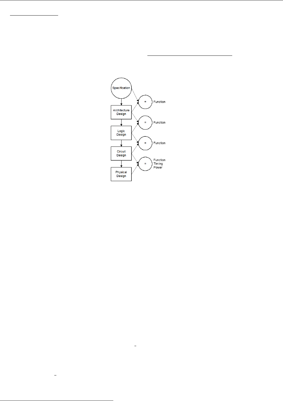
1.3 Design Flow
Cells are commonly described at three levels of abstraction. The register-transfer level (RTL)
description is a Verilog or VHDL file specifying the behaviour of the cell in terms of registers and
combinational logic. It often serves as the specification of what the chip should do. The schematic
illustrates how the cell is composed from transistors or other cells. The layout shows how the transistors
or cells are physically arranged.
3
Technion - IIT
Faculty of Electrical Engineering Computer Exercise 1
Introduction to VLSI
046237
Logic verification involves proving that the cells perform the correct function. One way to do this
is to simulate the cell and apply a set of 1’s and 0’s called test vectors to the inputs, then check that
the outputs match expectation. Typically, logic verification is done first on the RTL to check that the
specification is correct. A test-bench written in Verilog or VHDL automates the process of applying
and checking all of the vectors. The same test vectors are then applied to the schematic to check that
the schematic matches the RTL. Later, we will use a layout-versus schematic (LVS) tool to check that
the layout matches the schematic (and, by inference, the RTL).
Figure 1: VLSI Design Flow
1.4 Getting Started with Cadence Virtuoso
To initiate Cadence Virtuoso follow these steps:
1. Login to a lab machine (instructions posted separately)
2. In the console type:
(a) cd cadence
(b) source KIT.cshrc
(c) cdsprj lab
(d) virtuoso & (The ampersand isn’t necessary but it makes the terminal window available
for further use. Otherwise it is fully dedicated to the process and cannot be used or closed.)
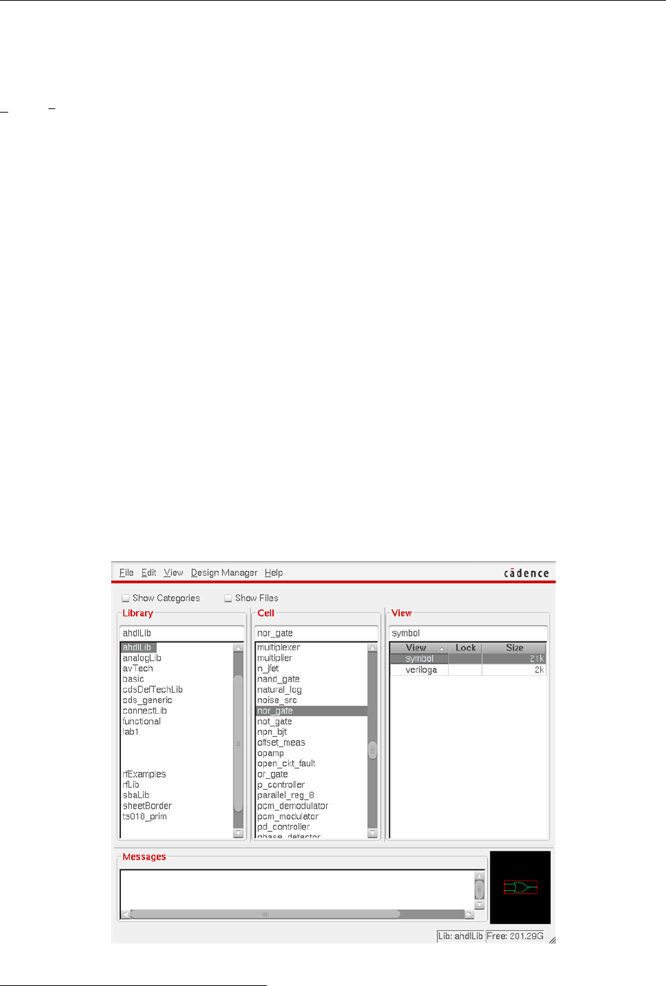
3. The main window will open at the bottom of the screen. Select ‘T ools →Library M anager’.
The library manager window will open. 1
4. Create (don’t use the existing one) a library by invoking F ile →New →Library... in the
Library Manager. Name the library lab1 xxxx, where xxxx is your group lab account. Click
‘OK’.
5. In the window that opens, select ‘Attach to an existing techfile’, click ‘OK’ and then
select ts018 prim as the Technology Library. Click ‘OK’ and you should see your
new library appear in the library manager.
6. SUGGESTION: save your work periodically.
1Don’t try to move libraries around or rename them directly in Linux; there is some unexpected behavior and you
are likely to break them.
4
Technion - IIT
Faculty of Electrical Engineering Computer Exercise 1
Introduction to VLSI
046237
2 Schematic of an XOR2
In this part you will design and simulate an XOR2 gate in the schematic level. The first sections
explain how to design your schematic and Section 3 will teach you how to simulate your circuit. We
will work with TowerJazz 0.18 µm process with λ= 90 nm2.Note: To ease the design, consider
aand b,aand bcomplements, respectively, as different inputs. Remember to take this
into account in your simulations. This means your gate will have 4 inputs.
Each gate or larger component is called a cell. Cells have multiple views, called ‘cellviews’. A
cellview is an aspect of the cell, such as its schematic, its layout, its simulation model, etc. Common
cellviews include:
•Schematic: A circuit schematic consisting of ‘symbol’ views of other cells.
•Layout: The physical layout of a particular schematic cellview, with objects in the layout
typically linked to their schematic counterparts. Layout consists of various layers such as:
polysilicon, M1, M2, Nwell, N+, P+, etc.
•Symbol: A visual representation of the cell, which is used for inserting the cell into other
schematics.
•Various Spectre/HSpice simulation models, usually only for discrete components like passives or
transistors (we won’t use this tool).
•Simulation states (see Section 3).
•Power and timing data.
For example, your library will, eventually, contain several cells (at least one XOR2 schematics and
one for its layout).
Figure 2: Library Manager
2Remember λis half of the channel’s width
5
Technion - IIT
Faculty of Electrical Engineering Computer Exercise 1
Introduction to VLSI
046237
In the library manager, select your library. Go to ‘F ile →New →Cell V iew’. In the window
that opens give the cellview the name xor2. Make sure that the View Name is set to ‘schematic’ and
that the Library Name is set to your library. Click ‘OK’ and a new schematic window will open.
To add a component, e.g., an NMOS transistor, with the schematic window selected, go to
‘Create →Instance’ on the menu bar (or click ‘i’ on the keyboard) and an ‘Add Instance’ window
will open. Click ‘Browse’ and a window similar to the library manager will open. Navigate to the
Tower library, ‘ts018 prim’, find the ‘nmos 18 ’ cell, click it and click the ‘symbol’ view. Then click
inside the schematic window to place it. For now, disregard the values that got filled in the ‘Add
Instance’ window. Press ‘ESC’ on the keyboard to stop placement.
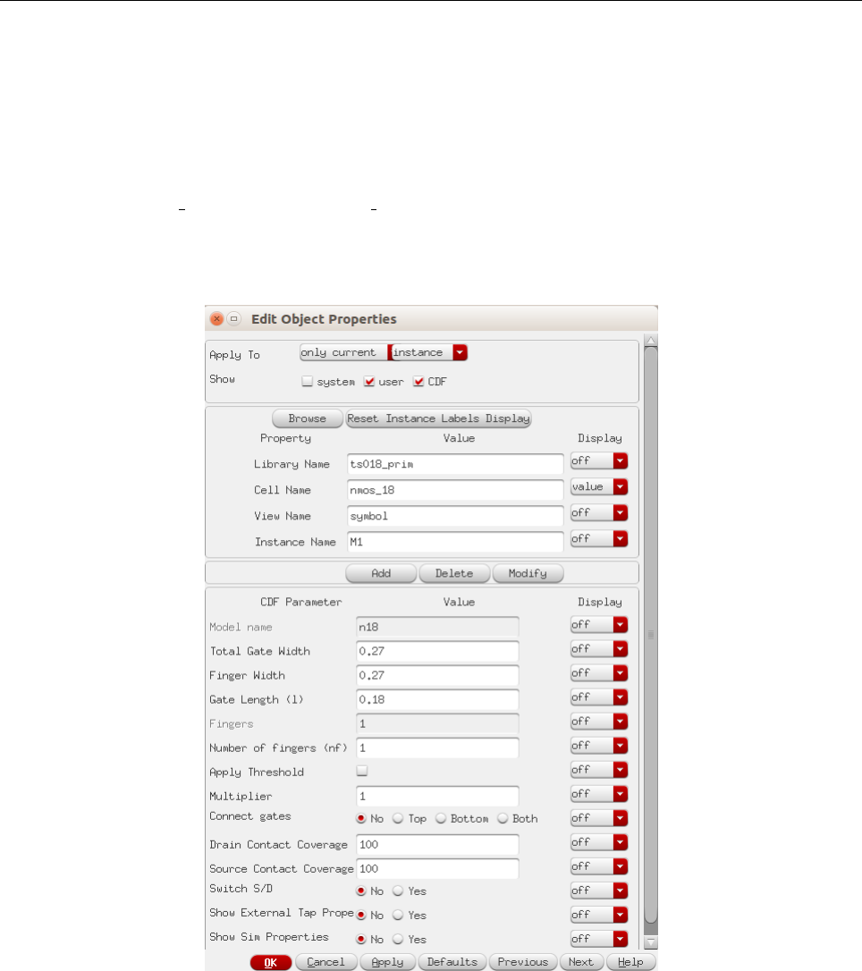
Figure 3: Edit properties
Click on the NMOS and type ‘q’. This will open the properties window (Fig. 3). Note ‘Finger
Width’, ‘Gate Length’ and ‘Fingers’. Width and length should be obvious. ‘Fingers’ refers to the
practice of using multiple parallel transistors instead of a single wide one. Let’s make WNand WP
(NMOS and PMOS width respectively) parametric. For NMOS, in Finger Width write pPar("WN")
and for PMOS pPar("WP"). This will allow us to change parameters in higher hierarchies of the design.
Leave the length at its default (and smallest) 0.18µm value. Click ‘OK’. Remember - everything in
Linux is case sensitive, so note how you wrote everything. Note that sizes are in microns, rather
than meters or λunits.
Place all the transistors needed for an static CMOS XOR2 gate (components can be copied by
pressing ‘c’, clicking, dragging and clicking; for moving components, simply drag them) and connect
them using wires by going to ‘Create →W ire’ or clicking ‘w’ in the keyboard. Note that components
6
Technion - IIT
Faculty of Electrical Engineering Computer Exercise 1
Introduction to VLSI
046237
can also be connected by placing their red box terminals together. Then, place VDD and ground, they
are both in the analogLib library (‘vdd’ and ‘gnd’ respectively). You can use ‘Ctrl+r’ to rotate the
instances. Take care in connecting the bulk of each transistor to either gnd or vdd.
Next, create input and output pins (name them, e.g., a and b for inputs and y for output), go to
‘Create →P in’ or click ‘p’, and then connect them with wires to the gates or output node. Make
sure the direction is properly set for inputs and outputs. Save and check your schematic, choose
‘F ile →Check and Save’ or press ‘Shift+x’. 3
You can zoom in and out with the scroll-wheel and fit the whole schematic by pressing ‘f’ in the
keyboard. Also you can zoom in to a desired place by selecting the area with the right click pressed.
Submit:
1. Print screen of the XOR2 schematic and test circuit (FO1).
2.1 Create symbol
Each schematic can have a corresponding symbol to represent the cell in a higher-level schematic.
You will need to create a symbol for your XOR2 gate. When creating your symbol, it is a good idea
to keep everything aligned to the grid, this will make connecting symbols simpler and cleaner when
you need it for another cell. While looking at your XOR2 schematic, choose Create →Cellview →
F rom Cellview.... In the window that opens, make sure Cell name is xor2, ‘From View Name’ is
schematic, and ‘To View Name’ is symbol, and click OK. Cadence will create a generic symbol based
on your pin names. Check that everything is as expected in the Symbol Generation Options window
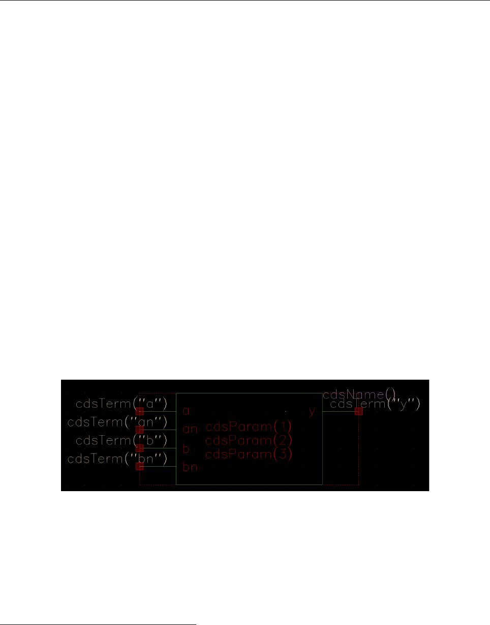
which opens up, and click OK. The Symbol L Editing window that opens up may look like Fig. 4.
Figure 4: Symbol
A schematic is easier to read when familiar symbols are used instead of generic boxes. Modify
the symbol to look like a standard XOR2. Pay attention to the dimensions of the symbol; the overall
design will look more readable if symbols are of consistent sizes. Experiment with the arc drawing
tool. Finally, choose Create →Selection Box... and choose ‘Automatic’. This creates a red box
around the symbol that will define where to click to select the symbol when it appears in another
schematic. Our art work is shown in Fig. 5.
3If you see an error message in the parameter display of the transistors, do not worry, it is just because the tool does
not know how to calculate W(yet).
7

Technion - IIT
Faculty of Electrical Engineering Computer Exercise 1
Introduction to VLSI
046237
Figure 5: XOR2 Symbol example
2.2 Create Test Circuit
Now let’s create a test circuit to simulate the XOR2. Create a new schematic and name it test xor2.
Place the XOR2 symbol you created in the last step (it should be on your library lab1 xxxx; use ‘i’ or
Create →instance), and change its properties (click on it and type ‘q’). They should appear as ‘W n’
and ‘W p’). Select ‘W n’ to be minimum (the technology spec says the minimum width is 0.22 µm)
and ‘W p’ to be ‘r*0.22’. With this last definition we will define the width of the PMOS as a multiple
(r) of the minimum width of 0.22 µm. At the output of this XOR2 gate connect one of the inputs of
a second same gate as a load. This results in Fan Out of 1 (FO1).
Add four voltage sources (use vpulse from analogLib) to control the inputs of the first XOR2
gate. Think of how you could generate the 4 input possibilities. Remember that there are two
complementary pairs. All possibilities should occur in one 20 ns4lapse. Set properties of the
voltage sources (by pressing ‘q’) as follows: voltages 1 and 2 to be 0 Vand 1.8V, respectively, or vice
versa. Rise and fall times to be 100 ps. Play with period, pulse width and delay to generate the input
sequence. You may also use other types of voltage sources.
Now add a voltage source as the main power supply (vdc in analogLib) and set the voltage to 1.8V.
Connect the ground and connect a small floating wire to the positive voltage node (‘PLUS’). Go to
Create →W ire Name... (or press ‘L’), name it vdd! (including the exclamation mark, meaning that
this is a constant global net rather than a parameter) and select the wire. This action will match vdd
terminal in our XOR2 with this voltage source. Complete the schematic by selecting a proper voltage
for the undriven inputs.
Submit:
2. Explain how you implemented the input sources and include the output waveform that shows
the 4 cases.
3. What’s the worst case scenario you should simulate for tprd and tpf d (propagation fall and rise
delay respectively)?
3 Schematic Simulation
In this section you will simulate the XOR2 schematic. In the test xor2 Schematic Cellview go to
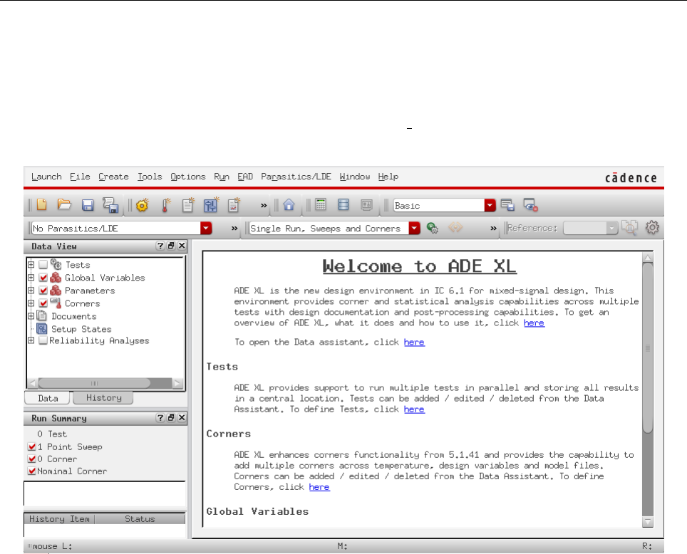
Launch →ADE GXL and select Create N ew V iew. This will open the Virtuoso Analog Design
Environment window (from now on, ‘simulation window’). A window like Fig. 6 will pop-up. In
this window you will manage design variables and parameters, select simulations that will run and
4The tool understands mas mili, uas micro, nas nano, pas pico, etc.
8
Technion - IIT
Faculty of Electrical Engineering Computer Exercise 1
Introduction to VLSI
046237
setup outputs to be plotted automatically. When properly set up this is a very powerful tool and this
exercise will try to show you how to automate things as much as possible.
The left side shows the useful Data View bar. To create a new test, expand the ‘Tests’ item and
select ‘Click to add test’. A new window will open (Fig. 7) and a small pop-up window will ask you
to select the cellview you want to simulate. Choose the test xor2 schematic.
Figure 6: ADE XL Main Window
A brief description of the window in Fig. 7:
•Left side: Design Variables lists all defined parameters and variables. This is now empty but we
can quickly import them from the schematic.
•Upper right sub-window: Analyses lists the defined simulations, some of their parameters and
whether they are active or not.
•Lower right sub-window: Outputs shows the outputs you define for automatic calculation. These
can display values, like DC bias points and results of formulas. It can also list output plots that
are automatically plotted after each simulation run.
9
Technion - IIT
Faculty of Electrical Engineering Computer Exercise 1
Introduction to VLSI
046237
Figure 7: ADE XL Test Editor
Let’s go ahead and save the simulation state now, even though it’s currently empty. Go to
Session →Save State... Under Save State Option select Cellview. This will save this simulation
state and all its settings and results as another cellview in your cell. You may change the name in
‘State’ to something meaningful, like ‘trise’ or ‘tf all’ which is what we’ll first do in the exercise itself.
Click ‘OK’ to save. From now on, it will appear in the library manager as a cellview, and you may
even open it without going through the schematic. Make sure to save your simulation state regularly
and you won’t have to redefine variables and outputs from session to session.
On the right there’s a column of buttons. Click the topmost, ‘Choose Analyses’. The Analyses
window opens. It shows all possible simulations you can run. Let’s start with a transient (‘tran’)
simulation. Select it, set ‘Stop Time’ to 20 ns and make sure to check the ‘Enabled’ button at the
bottom. It’s here that you can later turn it off, although this is a fast simulation that doesn’t take
much time. Click ‘OK’ and you will see it appear in the Analyses List.
Click on the second button from the top, ‘Edit Variables’. In the window that opens click ‘Copy
From’ near ‘Cellview Variables’ and watch all the parametric values you wrote in the schematic
magically appear in the list (in our case, only rappears). Choose 1 for now (we will perform a
Parametric Sweep later). After writing each value click ‘Change’ to save it, or it won’t be saved!
Go back to the ADE GXL window. The new test should appear beneath the Tests tag on the
Data View bar. To run the simulation go to Run →Single Run, Sweeps and Corners... or click the
Green-Play button. If you have errors at this point, carefully repeat this part to make sure you got
all the setup right, and if there are still any errors seek help from the course or lab staff. Remember
to save your state periodically.
3.1 Plot the output
After the simulation finishes successfully, we need to define an output to display the curve. There
are different ways to do this. We’ll explore two.
In both cases below, we explain selecting the output node of the first XOR2 gate. To compute
propagation delay, you will also need to add waveforms of the two inputs of that gate.
10
Technion - IIT
Faculty of Electrical Engineering Computer Exercise 1
Introduction to VLSI
046237
3.1.1 Using the calculator
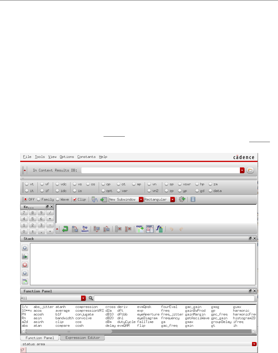
Click the ‘Setup Outputs’ button (third from the top) in the simulation window. Name the output
‘out’. Click ‘Open’ next to ‘Calculator’. This is the very powerful and very complicated calculator
tool. Fig. 8 shows its window. The second bar from the top allows you to select different types of
signals (e.g. vt and it for transient voltage and current respectively, etc.). Select ‘vt’. The schematic
window pops up so that you can select the voltage signal of your preference. Select the output of the
first XOR2 gate. You are taken back to the calculator window and it should show VT(”/netX”) (or
another net name) in the buffer.
Go to T ools →P lot to plot the buffered signal (alternatively, click the calculator-wave symbol in
the third bar from the top). You should immediately see the voltage waveform. Observe that you can
change where the other signals are plotted by changing the option next to the calculator-wave symbol
in the calculator window (options include ‘New subwindow’, ‘Append’ and ‘New window’).
The calculator allow us to perform different calculations with the results. It is extremely helpful in
more complicated simulations. Hint: Explore functions delay,riseT ime,f allT ime, they can be useful
in the following simulations. Using function delay you can define tpdr,tpdf , and then td=tpdr +tpdf
2.
Figure 8: ADE XL Calculator
3.1.2 Using the Output Editor
In this case, instead of opening the calculator, in the ADEXL window, either go to Outputs →
Setup... or click the Setup Output buttons (3rd from above on the right bar). Name the output as you
wish, click the button ‘From schematic’. The schematic pops up. Select the signal of your preference.
By selecting wires in the schematic, voltages will be plotted; by selecting pins, currents will be plotted.
Observe the ‘Type’ field of each output to make sure it’s what you intend.
11

Technion - IIT
Faculty of Electrical Engineering Computer Exercise 1
Introduction to VLSI
046237
3.2 Parametric sweep
Now that we’ve experimented with the simulations, let’s perform a parametric sweep. This powerful
tool allows us to observe how the signals change by changing one or more parameters. In our case we
observe the effect of PMOS width on propagation delay. You are required to simulate the worst
case scenario from the logic point of view. For this part you may use DC (constant)
voltage sources for some inputs and reduce the simulation time.
In the Data View bar of ADEXL, expand the ’Global Variable’ tag. Your design variables should
appear. Next to the variable name, click in the value field. A button with ... will appear. Click it,
and in the new window (where the initial value 1 is shown) write your desired list of values such as
{1,1.5,2,2.5,3,3.5,4}and click ‘OK’. Run the simulation as above (e.g., use the green Play
button).
The plots are observable in the ADEXL window, Results tab. Click the chart button to see the
waveforms. Zoom in (right click and drag) to one of the transitions. Observe how tpdf and tpdr
(propagation fall delay and propagation rise delay respectively)5are affected by r, namely by PMOS
width. Add horizontal and vertical markers to help you find the relevant points by pressing ‘h’ and
‘v’ respectively on the ’Visualization & Analysis’ window. Double clicking a marker helps select exact
level. Select 50% levels and read out times. Another method is to use the delay function as mentioned
before.
Look for the rvalue that yields a symmetric gate, namely where tpdf and tpdr are
roughly equal and for the rvalue that yields to minimum delay. You will need to use
those rvalues in subsequent sections.
Submit:
4. Simulation waveforms of the parametric sweep of r(submit at least 3 cases).
5. Make a table showing tpdf and tpdr for every r.
6. Based on the simulations, what is WPopt (WPthat results in an optimal/minimum delay)?
7. Based on the simulations, what is WPsym (WPthat results in a symmetric gate i.e., equal tpdf
and tpdr)?
8. How are tpdf and tpdr changed/influenced by the input-order-of-arrival i.e., when the inputs do
not arrive simultaneously?
9. Calculate, theoretically and using the technology parameters,6WPopt for minimum propagation
delay.
3.3 Corner simulations
You will now perform simulations to observe how environmental changes affect circuit performance.
The desired environmental corners for the 0.18 µm process are summarized in Table 1.
Corner Voltage Temperature
F 1.98 0 ◦C
T 1.8 70 ◦C
S 1.62 125 ◦C
Table 1: Environmental Corners
5Remember: propagation delay accounts for maximum time from the input crossing 50% to the output crossing 50%
6You may use: µn= 291 cm2/V s,µp= 71 cm2/V s,Vtn = 0.5V,Vtp =−0.42 V,tox = 50˚
A,εox = 3.85,
Cja = 1.1×10⁻³pF/µm2
12
Technion - IIT
Faculty of Electrical Engineering Computer Exercise 1
Introduction to VLSI
046237
We create a new test to study corners. We will vary only supply voltage and temperature, but
leave transistor models in the ‘typical’ mode (if needed, designers can try slow and fast transistors
as well, to investigate On Chip Variation, OCV). Under the Tests item on the Data View bar in
ADEXL, select Click to add test, select same test xor2 schematic, Copy from Cellview and choose the
symmetric rvalue found above.
In the schematic window, go to W indow →Assistants →Variables and Parameters7. The
Variables and Parameters bar should be open on the left. Select the voltage source vdd and select the
‘Parameter’ tab in the aforementioned bar. On the filter menu select ‘CDF Parameters’. A list with
all the vdc parameters appears. Right click on ‘DC voltage’ and select ’Create Parameter’. Go back
to the ADE XL window and observe that this parameter appears under ‘Parameters’ tag.
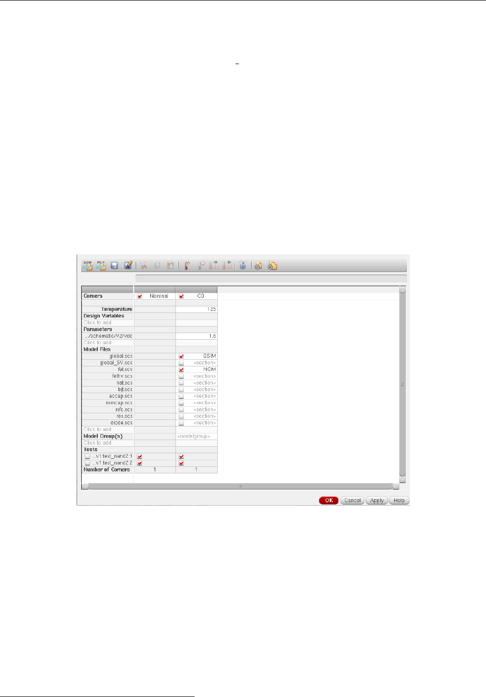
Now we will create a new corner. In ‘Data View’ expand ‘Corners’ tag and click to add a new
corner. A window like Fig 9 will open. First we will import the model files. Click on ‘Click to add’
below the ‘Model Files’ title. In the window that pops up click the button ‘Import from Tests’, a list
of models will appear in the window and press OK.
Figure 9: Corners Setup Window
Create a new corner by clicking the thermometer icon. Under the ‘Parameters’ title select ‘Click
to add’ and add vdc. In ‘Model Files’ under the created corner column, select global.scs to be BSIM
and fet.scs to be NOM (e.g, nominal). Then, change the temperature and vdc values as desired for
the specific corner. Repeat the procedure to create corners (TTSS, TTFF, TTTT)8and press OK.
Run your simulation as described before.
3.3.1 TTSS Corner
Based on the parameters shown in Table 1 create the corner for TTSS. Simulate the Test Circuit
and compare the results with the Typical (TTTT) case.
7Sometimes this option is not available in the schematic window. If that is the case, close the schematic and open it
from the ADE XL window. Go to F ile →Open and select ‘Open in new tab’.
8We mark the corner using four letters (which can be T, F or S): [nMOS speed][pMOS speed][Voltage][Temperature].
13
Technion - IIT
Faculty of Electrical Engineering Computer Exercise 1
Introduction to VLSI
046237
3.3.2 TTFF Corner
Based on the parameters shown in Table 1 create the corner for TTFF. Simulate the Test Circuit
and compare the results with the Typical (TTTT) case.
Submit:
10. Table with results of Corners Simulations.
11. Explain why and how tpd changes in every case.
3.4 Higher load (FO4)
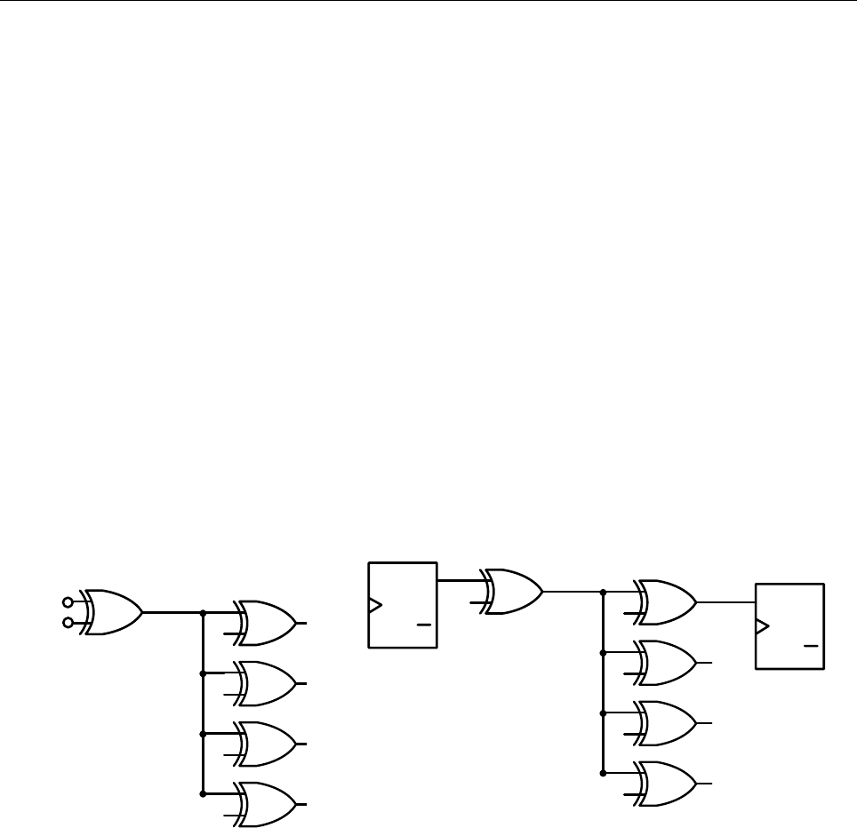
Now create a new schematic to simulate the FO4 case, name it FO4. Insert the XOR2 and load it
with 4 copies of itself. The circuit should look like Fig. 10(a). Perform the simulations for a typical
environment, and observe the changes with respect to the FO1.
Assuming a simple sequential path consisting of one zero-delay flip-flop (as in Fig. 10(b)), one
FO4 XOR2 gate driving four (4) FO1 XOR2 gates and a second zero-delay flip-flop, determine the
maximum frequency in which we can operate the circuit. Note that you do not need to draw a
new schematic including the FF, nor do you need to simulate it. The requested frequency
bound can be computed from the basic combinational logic simulation of Fig. 10(a).
A
B
(a) Test circuit
Q
Q
SET
CLR
D
Q
Q
SET
CLR
D
Zero delay FF
Zero delay FF
(b) Circuit for completeness of definition
of frequency (do not add the FF to your
simulations.)
Figure 10: FO4 circuit
Submit:
12. Simulation results of FO4.
13. Explain why and how tpd changes. Relate to the linear delay model (logical effort).
14. What is the maximum frequency that can be achieved in a synchronous circuit as Fig. 10(b) if
tsetup = 0 and tclk−out = 0?
3.5 Power Estimation
Static CMOS gates are very power-efficient because they dissipate only leakage power while idle.
For a long time power was a secondary consideration behind speed and area. As the transistor has
shrunk following Moore’s law, the transistor counts and frequencies have increased, power consumption
has increased significantly and is now a major design constraint (this is discussed further when we
14

Technion - IIT
Faculty of Electrical Engineering Computer Exercise 1
Introduction to VLSI
046237
study scaling later on).
Power dissipation in CMOS circuits consists of two components:
•Static dissipation:
–subthreshold conduction through OFF transistors (typically, this is the largest contributor)
–tunneling current through the gate
–leakage through reverse-biased diodes
•Dynamic dissipation:
–charge and discharge of load capacitances
–short circuit current while both PMOS and NMOS are turned weakly ON, typically during
a transition.
You will perform simulations to estimate the power. Use the FO4 test circuit.
Hint: To perform the simulations of section 3.5.1 and 3.5.3 you will need to select inside nets of
the XOR2 instances. This can be done by double-clicking the respective instance and by selecting to
open the instance’s schematic in the pop-up window.
3.5.1 Static dissipation
Ideally no power is dissipated in an OFF transistor. However, there are several secondary effects
that lead to small currents flowing through the OFF transistor. Assuming the leakage current is
constant, the static power is:
Pstatic =IstaticVDD (1)
Perform a simulation to determine the static power dissipation of the FO4 gate. You can use the
calculator to implement Eq. 1.
3.5.2 Dynamic
The dynamic power is determined by the well-known equation:
Pdynamic =αCLV2
DD f(2)
Considering α=1
2, the technology parameters (to assess CLand the frequency calculated in the
section 3.4 determine Pdynamic of the FO4 gate.
3.5.3 Short Circuit
For the purpose of this lab we will determine the short circuit power as the average current supplied
by the source (VDD ) when the output changes from 20% to 80%, multiplied by the supply voltage
VDD .
Submit:
15. Simulation results for short circuit and static dissipation.
16. Calculations of the 3 power estimation cases.
17. What is the best strategy to reduce the dynamic power? Relate to the parameters CL,V2
DD and
f, and to scaling. What are the pros and cons of each strategy?
18. How can you reduce the short circuit power dissipation?
15
Technion - IIT
Faculty of Electrical Engineering Computer Exercise 1
Introduction to VLSI
046237
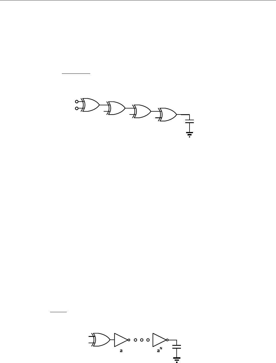
3.6 Sizing
Let us play with cell sizing. In most multistage logical paths the last gate must drive a ‘big’
capacitance, therefore the different gates can be sized to reduce the total delay of the path. Consider
the circuit in Fig. 11, where a logical path of four XOR2 gates drive a capacitance of 100 f F . Starting
from left, each stage is atimes bigger than the previous stage.
Create a new schematic, call it sizing and implement the circuit. In the first XOR2 gate, use
WN=WMIN and a symmetric WP(WPsym ) as determined in Section 3.2 for a symmetric gate.
Simulate and perform a parametric sweep of ato find the optimal value that achieves the shortest
delay. Hint: To perform anyou should write a**n in the respective property field.
1aa2
a3
A
B
100 fF
Figure 11: Sizing circuit
Submit:
19. What’s the optimal a(aopt) for minimum delay?
20. Simulation results (include just 3 cases, including aopt). Explain what happens when a= 1.
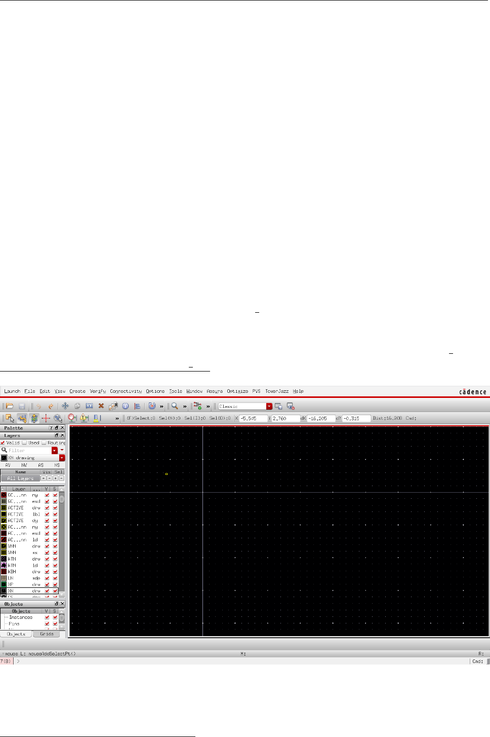
3.7 Buffer insertion
Buffer insertion is used for driving large capacitance that could result from bigger gates, long wires
or I/O. As the name suggests, the idea is to insert buffers in the path between our gate and the big
load. Each inverter will be atimes bigger than the previous one. In this case we choose a= 2.6
(indeed, theoretical optimization would yield the factor e). You will simulate the circuit to find the
optimal number of inverters for minimum delay (Nopt).
Begin by creating the inverter schematic. Proceed as in Section 2, name the transistor width
pPar("Wn") and pPar("Wp") for the NMOS and PMOS respectively. Create the inverter symbol.
Then, create a new schematic, call it buffering. The circuit should be as Fig. 12. Select WN=WMIN ,
and WPfor a symmetric XOR2. The first inverter must have the following dimensions: WN=aWM IN
and WP= 4aWMIN (we assume that this ratio produces an almost symmetric inverter). Calculate
the delay as td=tpr +tpf
2.Note: the original logical value can be inverted (i.e., you can place an odd
number of inverters).
1100 fF
A
B
Figure 12: Buffering insertion circuit
Sumbit:
21. What is the optimal Nopt?
22. Simulation results (include just 3 cases).
16
Technion - IIT
Faculty of Electrical Engineering Computer Exercise 1
Introduction to VLSI
046237
4 Layout
In this section we will create the layout of the 2-input XOR gate using the Layout GXL tool of
Virtuoso. This tool is very useful and comfortable as it saves time and mistakes compared to manual
design of the layout. Among other benefits, it helps to maintain the correlation between the schematic
and layout and to prevent DRC mistakes.
We wish to create a layout subject to the following constraints:
1. Minimum area
2. Maximum height of the cell: 8µm
3. Use metal M1 only.
4. Height of GND and VDD rails: 0.72µm.
5. Inlcude NTAP and PTAP in the cell (Ohmic connections to the substrate and n-Well).
6. Input and output pins must be M1.
7. For each input interconnect (if possible) both MOSFET gates with poly.
IMPORTANT: Before you start with the layout, go to the ‘Library Manager’ and copy
the schematic into a new cell. Call it xor2 fix. In this version we will replace the
parametric widths by fixed values. Open the schematic and change the finger width of
the PMOS to the numerical value of roptWN(as found in Section 3.2). It is important
that you work from the transistor schematic view of xor2 and NOT form xor2 test.9
Create a new symbol for the xor2 fix.
Figure 13: Layout GXL
To start the layout, in the schematic window, go to Launch→Layout GXL, choose the options
‘Layout: Create New’ and ‘Configuration: Automatic’. After a short while, a clean layout window
9Copying cell schematics: In Library Manager window, Edit →Copy... , and select From and To names.
17

Technion - IIT
Faculty of Electrical Engineering Computer Exercise 1
Introduction to VLSI
046237
will open aside the schematic as in Fig. 13. At the left side of the layout window we see the ‘Palette’,
where the layers are displayed.
The used layers in TowerJazz 0.18µm for this design will be:
•Contact (CS). Has an exact dimension of 0.22 ×0.22
•Poly (CG). Polysilicon can only be connected to M1.
•Active (ACTIVE). Can only be connected to M1.
•n+Select (XN) and p+Select (XP).
•n-Well (WN).
•Metal 1 (M1).
Other important things to consider:
•Use only layers with purpose of type drawing (drw). Other types may be used for labeling, drc,
dummy, etc.
•Obviously, if two polygons of the same layer overlap or touch each other, there’s a short circuit
between them.
•If two polygons of different layers overlap or touch, there’s no electrical connection between
them. One exception is the critical overlap of poly and active, that creates a transistor.
Most used actions in layout design:
•Create rectangle: First you need to choose the layer to which the rectangle will belong. Then
go to Create →Shape →Rectangle or press ‘r’. Select the first vertex and then the opposite
vertex. You can update the dimensions afterwards, so don’t worry if it doesn’t match the desired
dimensions at first.
•Modify dimensions: Select the rectangle you want to modify, and press ‘q’. The shape’s
properties will open. There you can change the height and width.
•Stretch shape: Deselect all by clicking on the black background and go to Edit →Stretch or
press ‘s’. Select the side of the shape you intend to stretch and click in the desired new place.
No dragging.
•Copy: Go to Edit →Copy or press ‘c’. Select the shape you want to copy an then select
where you want to place the new copy. Important: before you paste the shape you can press F3,
enabling you to rotate, mirror and change other properties of the copy.
•Move: Select the shape you intend to move, either drag or go to Edit →M ove or press ‘m’ and
move.
•Delete: Select the shape and press the Delete button of your keyboard.
•Measure dimensions: Go to T ools →Create Ruler or press ‘k’. Select the point first and
last point. Afterwards, erase all rulers by going to T ools →Clear All Rulers or by pressing
‘Shift+k’.
18
Technion - IIT
Faculty of Electrical Engineering Computer Exercise 1
Introduction to VLSI
046237
4.1 Placement
In the first stage we’ll import the transistors and the terminals (namely ports or pins) present in
the schematic. The terminals are defined on M1 in our case. Go to the schematic and select all the
NMOS transistors. In the layout window, go to Connectivity →Generate →Selected F rom Source.
You can now see the two NMOS transistors in the layout. Place them by clicking the desired position.
Press ‘Shift+f’ to observe the NMOS layers (‘Shift+f’ display all layers in a hierarchic design as if it
were a flat design).
Go to the schematic window and select one of the NMOS transistors in the schematic. Observe
that the selected transistor is highlighted also in the layout window. Select any net (wire) in the
schematic, and observe what happens in the layout (connected items are selected, and lines appear
that indicate connectivity). Repeat the same step to insert the PMOS and the terminals. Observe
that the connectivity is highlighted and preserved in the layout. Note also that the tool attempts to
preserve relative transistor positions.
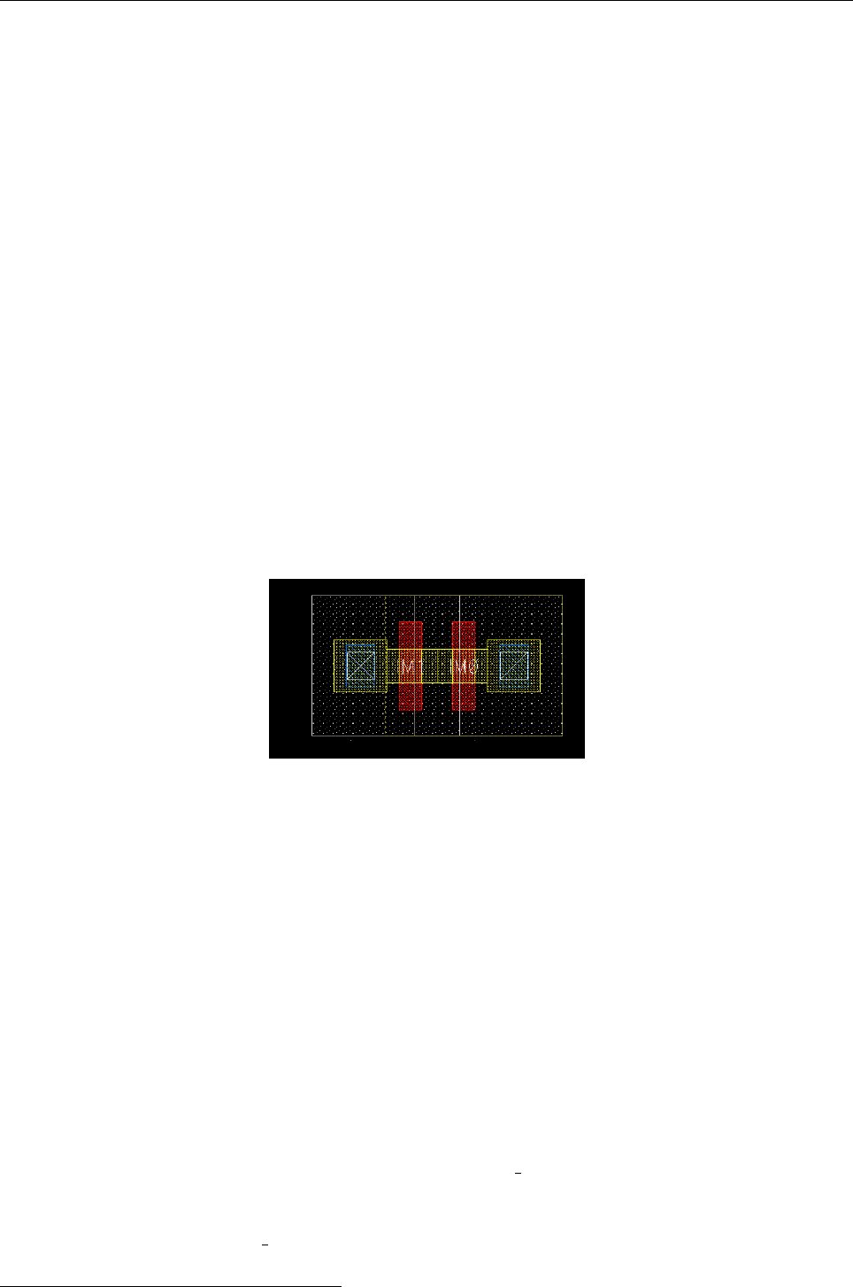
Each pair of NMOS is connected in series, and their shared node (source in one, drain in the other)
is not connected to anywhere else. But when importing the transistors, they came equipped with a
contact on each end. We wish to remove the unnecessary contacts where the NMOS transistors are
interconnected. This can be done by the tool, as follows. Place one of the NMOS transistors so that
its drain node overlaps the source node of the other NMOS transistor. The tools graciously removes
the redundant two contacts, as in Fig. 14.
Figure 14: Combine transistors
Do the same with the NMOS transistors. The result should be different, because their
interconnecting node is also connected elsewhere. Select the terminals and check that all pins are
defined as M1 (drw). If not, change the apropriate property to M1 (drw) (remember purpose
‘drawing’ ). Now check connectivity, go to Connectivity →Check →Against Source. Verify that all
the connections exist besides ground and vdd.
4.2 DRC
Design Rule Check (DRC), as the name implies, checks that the layout complies with the design
rules of a given IC technology. As we have learned in class, these rules prevent potential fabrication
problems.
Before you perform DRC, open a terminal and ”mkdir /tmp/usernamedrc” (where username is
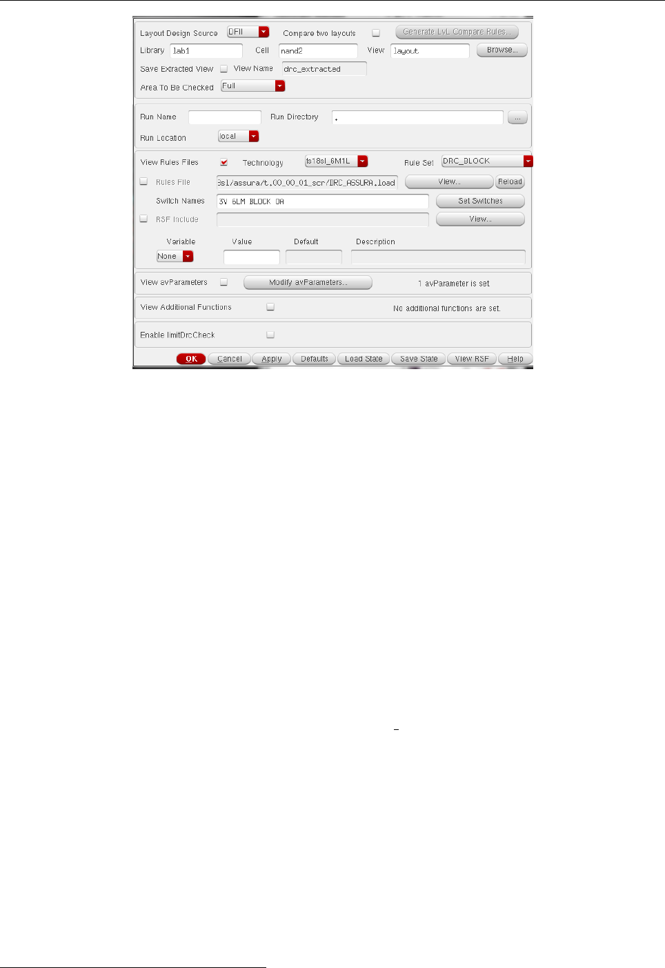
your user name account) in a terminal 10. In the layout window, go to Assura →Run DRC. A
window as in Fig. 15 will open. In ‘Technology’, select ts18sl 6M1L (maximum 6 layers of metal, one
top thin layer), in ‘Switch Names’ write “3V 6LM BLOCK OA” (technology file allows 3.3V I/O cells,
maximum 6 layers of metal, DRC is applied to the entire block and ‘open access’ format is employed)
and select ‘Rule Set’ as “DRC BLOCK ”. Click OK. In the progress window that opens, also click
OK. When the tool finishes (after a while), it will ask if you want to see the results; press ‘Yes’.
10Check in every new session that this folder exists before you perform DRC or LVS.
19
Technion - IIT
Faculty of Electrical Engineering Computer Exercise 1
Introduction to VLSI
046237
Figure 15: DRC window
A window that describes the errors will open. Each type of error includes also error count. You
can click the arrows to observe the mistakes in the layout, one by one. Correct all mistakes, except
those of types LUO, GC.A.1–poly island area, AA.C.1–coverage and M1.A.1–metal island area. At
the end of DRC, select Assura →Close Run.
4.3 Routing
Now you are going to wire the different elements in your layout. Let’s start by using poly to
connect a PMOS and an NMOS to the input ‘a’. To create a wire go to Create →W iring →W ire
or press ‘p’. Select the layer to which the wire will belong, click on the first edge to start drawing,
move the cursor to draw, click once to change direction and double click to finish. Observe that the
tool automatically changes the layer if you directly click on an existing ‘routing’ layer such as poly or
metal 1.
A contact is necessary to connect poly and M1. You can create the contact stack (consisting
of the contact and, if needed, extensions of poly and/or M1 to abide by design rules) by going to
Create →V ia or pressing ‘o’. In ‘Via Definition’ select ‘M1 PO’. It will bring up the complete stack.
Complete all wires and contacts. Make use of the schematic to highlight connections.
Next, create power and ground rails and the ohmic contacts to the P-sub and N-Well (PTAP and
NTAP). The TAP stack is composed by ACTIVE, XN or XP, CS and M1. Both rails must have a
height of 0.72µm and equal width (and must cover the cell from side to side, so that we can place cells
next to each other without adding extra power rails between them). Finally, you have to indicate that
those rails correspond to vdd and gnd. Go to Create →P in. In ‘Terminal Name’ fill the name as it
appears in the schematic (vdd! or gnd!) and select the respective wire.
After finishing routing (or any time during) run DRC again. By the end of this part, your
work should be free of DRC mistakes apart from errors of type AA.C 11.Run another
connectivity check by the end of this stage (see 4.1).
11This error indicates that the total area of the active layer is below the expected for a certain section in the chip. This
problem is usually solved by dummy placement i.e., adding polygons of that layer which doesn’t have any functional or
electrical purpose.
20
Technion - IIT
Faculty of Electrical Engineering Computer Exercise 1
Introduction to VLSI
046237
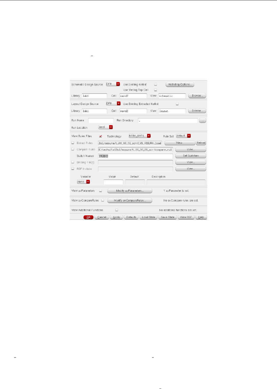
4.4 Layout vs Sechamtic (LVS)
The next step is to prove that the layout matches the schematic. This is done by extracting the
transistors and their connections from the layout, followed by running a layout versus schematic tool.
In the layout window, go to Assura →Run LV S. A window similar to Fig. 16 will open.
In ‘Technology’ choose ts18sl 6M1L. Click ‘OK’ and ‘OK’ again in the process window. Once
finished, another window pops up asking if you want to see the report. Click ‘Yes’. Correct any
mistake in the LVS and repeat checking LVS until the design is error free.
Figure 16: LVS window
Submission from Section 4
23. Layout print-screen with a rule on each axis showing the cell’s dimensions.
24. What is the total area of your cell?
25. Explain how does the placement of one NMOS (PMOS) above and aside the other affects the
gate performance. Which parameters are changed?
26. Print screen of the DRC and LVS reports.
5 Hierarchical Design
In this section we create a hierarchical layout design. Let’s use the FO4 circuit for these purpose
(no flip-flops are needed, only one FO4 and four FO1 gates). Create a new schematic called
FO4 fix . Insert the five fixed-width XOR2 gates (xor2 fix) as in Fig. 10 and connect them properly.
Once done, Check & Save.
Go to Launch →Layout GXL and choose the options ‘Layout: Create New’ and ‘Configuration:
Automatic’. A clean layout will open. Import your xor2 fix layout by going to Create →Instance
or pressing ‘i’. Go to your library (Lab1 ) and select your XOR2 layout. Insert all five XOR2 one aside
the other horizontally. Note that in practice, we would have created a stronger gate for FO4, but for
the purpose of this lab we simply use same layout for all five gates.
21
Technion - IIT
Faculty of Electrical Engineering Computer Exercise 1
Introduction to VLSI
046237
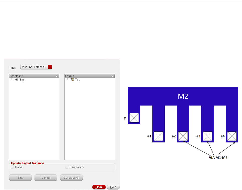
Next, match all gates in the layout with each XOR2 in the schematic, as follows. It is important
to maintain a proper order. In the layout window, go to Connectivity →Define Device
Correspondence... A window like Fig. 17(a) opens up. The left column indicates unbounded instances
in the schematic and the right one indicates the unbounded instances in the layout. Make the
correspondences by selecting one on each column and then click ‘Bind’. If you make a mistake
you can select Filter: All instances and ‘Unbind’ the wrong correspondence.
(a)
(b)
Figure 17: (a) Define Device Correspondence, (b) Routing in hierarchical design.
5.1 Routing
First, perform a Connectivity Check (as in section 4.1). Observe the output: only the routing
should be missing. Prior to adding wires, perform a DRC check and correct all mistakes (if any)
except for errors of type AA.C.
Now let’s route all wires. Begin by vdd and gnd. As they are pins proceed as in section 4.3. They
must use metal 1 and have the same height as all XOR2 cells. These will be our power rails. Then
proceed to route all other wires. The central wire (output of first XOR2 and input to the other four
XOR gates) can be laid out using metal 2 and can go on top of the vdd rail (this is not ideal, but easy
to do). From the top M2 line, draw stubs of M2 to reach the ‘y’ output of the first gate and all four ‘a’
inputs of the following four gates. Connect the M2 stubs by means of M1-to-M2 vias. This structure
is demonstrated in Fig. 17(b). Check the correspondence by clicking in the schematic. When you
have finished the routing, perform DRC and LVS again and repeat fixing until there are no more errors.
5.2 RC Extraction
You will now perform the RC extraction (RCX) of your hierarchical layout. The parasitic extraction
tool calculates both the parasitic RC of the devices and the interconnect. The major purpose of
parasitic extraction is to create an accurate analog model of the circuit, so that detailed simulations
can emulate actual digital and analog circuit responses.
22

Technion - IIT
Faculty of Electrical Engineering Computer Exercise 1
Introduction to VLSI
046237
To run the RCX you must have previously run the LVS and corrected all errors. In the layout
window go to Assura →Run Quantus QRC. In the menu that opens, go to the Setup tab and
in the T echnology field select ts18sl 6M1L. In the field RuleSet select default. In the Output field
select Extracted V iew, do not change other parameters in this tab. Now go to the Extraction tab,
select Extraction T ype to be RC, and fill the Ref N ode field with your ground pin (e.g., gnd!). Click
OK, the extraction will start, and an extracted view (av extracted) will be created.
5.3 Extracted Layout Simulation
We are ready to simulate the extracted layout and compare it to the previous simulations. Open
your F O4fix schematic, and create a new simulation window. Simulate again this circuit as in the
first part of the lab. Calculate (extract) the delay (tpd) of this circuit.
Now, we will simulate the extracted circuit. In ADE L, go to Setup →Environment.... In the
Switch V iew List add the word av extracted before the word schematic. Then, proceed to simulate
as always. Calculate (extract) the delay (tpd) of this circuit.
Submission from Section 5
27. Layout print-screen with a rule on each axis showing the cell’s dimensions.
28. What is the total area?
29. Print-screen of the DRC and LVS results.
30. Explain (shortly) how Place & Route influence the chip’s performance. In your answer refer to:
area, speed and power.
31. Indicate pros and cons of hierarchical design using ‘Standard Cells’. Is it the best layout we
could do? In your answer refer to: area, speed and power.
32. Why do we use constant-height cells?
33. Submit the waveforms of the delay simulations with and without the RCX for the fixed FO4
circuit. Include a table with the results.
34. What’s the increment in the tpdr,tpdf , and tpd considering the parasitics?
35. How could you reduce the parasitics in your layout to reduce the delay?
23
