MC141000 Series Programming Manual 1978
MC141000_Series_Programming_Manual_1978 MC141000_Series_Programming_Manual_1978
User Manual: manual pdf -FilePursuit
Open the PDF directly: View PDF ![]() .
.
Page Count: 41
MC141000
Series
PROGRAMMING
REFERENCE MANUAL
The information
in
this document has been carefully checked and is
believed to be entirely reliable. However, no responsibility is assumed for
inaccuracies. Furthermore, such information does not convey to the pur-
chaser of the product described any license under the patent rights of
Motorola Inc. or others.
Motorola reserves the right to change specifications without notice.
© MOTOROLA INC., 1978
2
TABLE
OF
CONTENTS
INTRODUCTION
.....................................................................
6
MC141 000/1200/1 099 Microcomputers
Microprogramming
MC141000 Family Support Products
MC141000 Microcomputer Resources
...............
. . . . . . . . . . . . . . . . . . . . . . . . . . . . . . . .
..
8
Functional Blocks
Status and Status Latch
Power
Up
and Initialize
Assembly Format . . . . . . . . . . . . . . . . . . . . . . . . . . . . . . . . . . . . . . . . . . . . . . . . . . . . . . . . . . . . . . . . .
..
10
Coding Format
Input Format
Comments
Labels
Operands
Assembler Directives
Additional Documentation
Instruction Tables
..................................................................
11
Functional Listing
Alphabetical Listing
Machine Operation
.................................................................
13
ROM Array
Branch, Call and Return Operations
Random Access Memory (RAM)
Output Ports
Inputs
Arithmetic Logical Unit (ALU)
Instruction Decode
Instruction Details
..................................................................
18
Applications and Software Examples
................................................
34
BCD Addition
BCD Subtraction
LCD Display
LCD Display plus Keyboard
Expanding Number of R-Outputs
External RAM Storage
ILLUSTRATIONS
Figure 1 The MC141000
.............................................................
6
Figure 2 EXORciser-Based Software Development System
............................
7
Figure 3 MC141099-Based Software Development and Debug System . . . . . . . . . . . . . . .
..
7
Figure 4 Motorola Custom Software and Debug Development System
.....................
7
Figure 5 Functional Block Diagram -MC141000/1200/1099
............................
8
Figure 6 Internal BR, CALL and RETN Operations
.....................................
13
Figure 7 BR, CALL and RETN Summary
.............................................
14
Figure 8 RAM Addressing and BIT Selection . . . . . . . . . . . . . . . . . . . . . . . . . . . . . . . . . . . . . . . .
..
15
Figure 9 Output PLA Configured for Seven-Segment Display. . . . . . . . . . . . . . . . . . . . . . . . . .
..
16
3
Table 1 Power
Up
and Initialize . . . . . . . . . . . . . . . . . . . . . . . . . . . . . . . . . . . . . . . . . . . . . . . . . . . . .
..
9
Table 2
MC141
000/1200 Standard Instruction Set, Functional Listing
......................
11
Table 3 MC141000/1200 Standard Instruction Set, Alphabetical Listing
....................
12
Applications
and Software Examples
BCD Addition and Subtraction Flowchart
........................................
35
LCD Display Hardware and Software
...........................................
36
LCD Display Plus Keyboard Hardware
..........................................
37
Software
....................................................................
38
Expanding the number of R-Outputs, Hardware
and Software
................................................................
39
External
RAM
Storage Hardware and Software
.................................
.40
LIST OF ABBREVIATIONS
A Accumulator
ALU Arithmetic Logic Unit
CKI Constant and K-Input Logic
CL Call Latch
I(B) Bit Field of Instruction
I(C) Constant Field of Instruction
I(W) Branch Address of Instruction
Ki K inputs
LSB Least Significant Bit
LSD Least Significant Digit
MSB Most Significant Bit
MSD Most Significant Digit
M(X,V)
RAM
Memory Location = X Address
(0
to 7), Y Address
(0
to
15)
M(X,V,B)
RAM
Memory Bit Location
(B
=
0,
1,2,
or
3)
a
PA
PB
PC
PLA
PLAIR
R
R(V)
RAM
ROM
S
SL
SRR
x
v
Output Register
ROM
Page Address Register
ROM
Page Buffer Register
Program Counter
Programmable Logic Array
PLA Input Register
R-Output Register
R-Output Latch Y
Random Access Memory (Read/Write)
Read Only Memory
Status
Status Latch
Subroutine Return Register
RAM
X Address Register
RAM
Y Address Register
4

5
INTRODUCTION
MC141000/1200/1099 Microcomputers
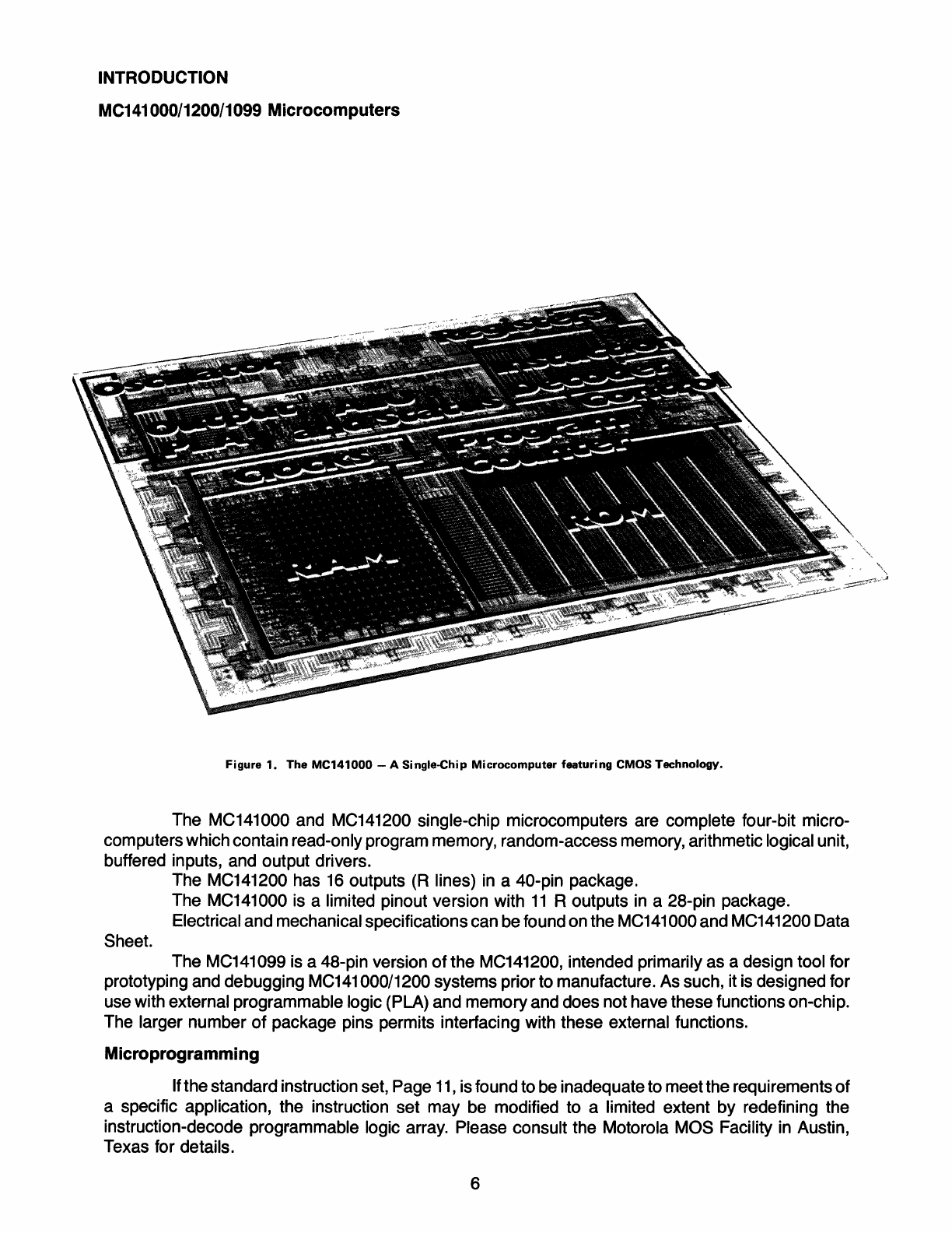
Figure
1.
The
MC141000
- A Single-Chip
Microcomputer
featuring
CMOS Technology.
The MC141000 and MC141200 single-chip microcomputers are complete four-bit micro-
computers which contain read-only program memory, random-access memory, arithmetic logical unit,
buffered inputs, and output drivers.
Sheet.
The MC141200 has
16
outputs (R lines) in a 40-pin package.
The MC141000 is a limited pinout version with
11
R outputs in a 28-pin package.
Electrical and mechanical specifications can be found on the
MC141
000 and MC141200 Data
The MC141099 is a 48-pin version
of
the MC141200, intended primarily as a design tool for
prototyping and debugging
MC141
000/1200 systems prior to manufacture. As such, it is designed for
use with external programmable logic (PLA) and memory and does not have these functions on-chip.
The larger number
of
package pins permits interfacing with these external functions.
Microprogramming
If the standard instruction set, Page
11,
is found to be inadequate to meet the requirements
of
a specific application, the instruction set may be modified to a limited extent by redefining the
instruction-decode programmable logic array. Please consult the Motorola MOS Facility in Austin,
Texas for details.
6
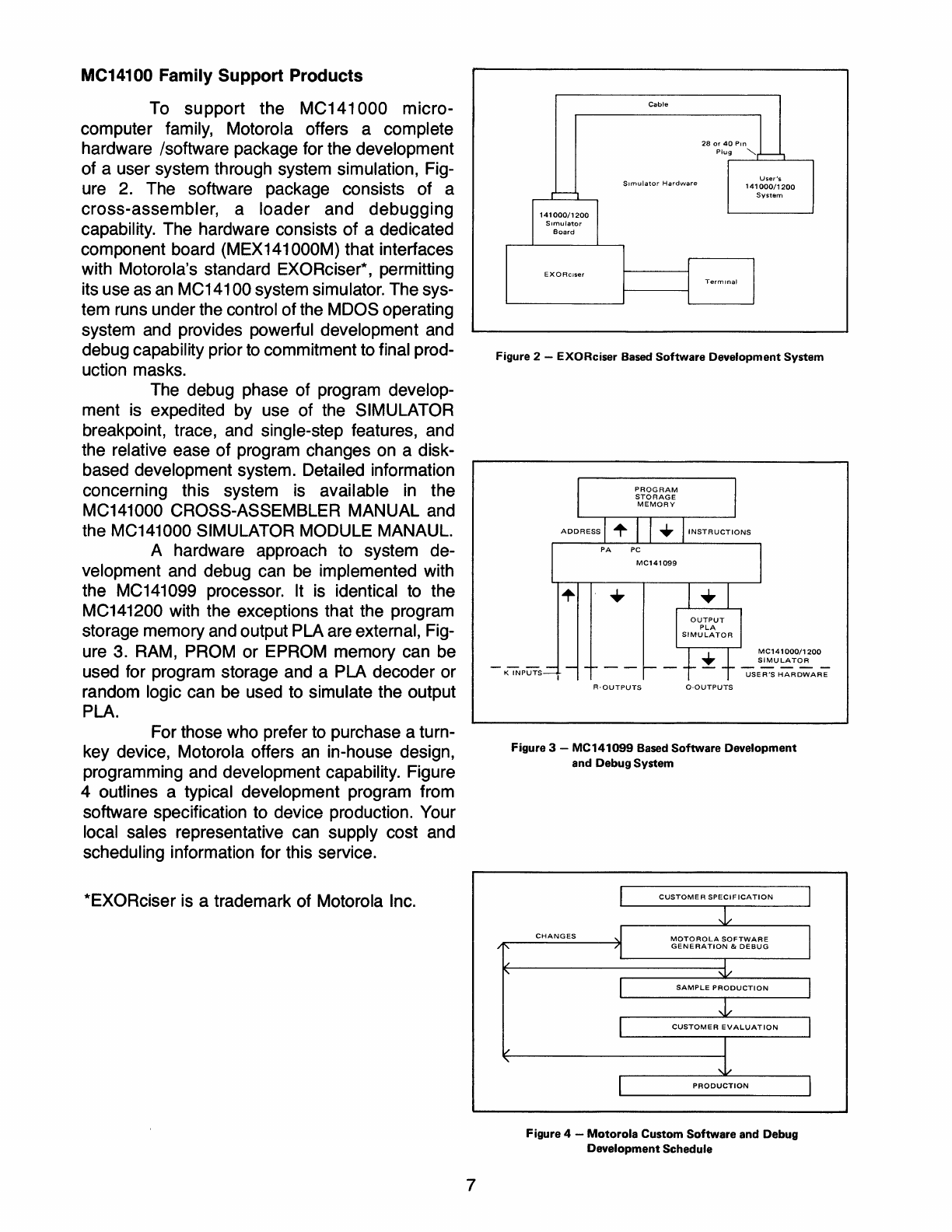
MC14100 Family Support Products
To support the MC141000 micro-
computer family, Motorola offers a complete
hardware /software package for the development
of a user system through system simulation, Fig-
ure
2.
The software package consists of a
cross-assembler, a loader and debugging
capability. The hardware consists of a dedicated
component board (MEX141000M) that interfaces
with Motorola's standard EXORciser*, permitting
its use
as
an
MC141
00 system simulator. The sys-
tem runs under the control of the MOOS operating
system and provides powerful development and
debug capability prior
to
commitment to final prod-
uction masks.
The debug phase of program develop-
ment
is
expedited by use of the SIMULATOR
breakpoint, trace, and single-step features, and
the relative ease of program changes on a disk-
based development system. Detailed information
concerning this system
is
available
in
the
MC141000 CROSS-ASSEMBLER MANUAL and
the MC141000 SIMULATOR MODULE MANAUL.
A hardware approach to system de-
velopment and debug
can
be
implemented with
the MC141099 processor.
It
is
identical
to
the
MC141200 with the exceptions that the program
storage memory and output PLA are external, Fig-
ure 3. RAM, PROM or EPROM memory can be
used for program storage and a PLA decoder or
random logic can
be
used to simulate the output
PLA. For those who prefer to purchase a turn-
key device, Motorola offers
an
in-house design,
programming and development capability. Figure
4 outlines a typical development program from
software specification to device production. Your
local sales representative can supply cost and
scheduling information for this service.
*EXORciser is a trademark of Motorola Inc.
7
Cable
Simulator
Hardware
141000/1200
Simulator
Board
EXORciser
28
or
40
Pm
Plug
""'r--1
Terminal
User's
141000/1200
System
Figure 2 - EXORciser Based
Software
Development System
K
INPUTS
R-OUTPUTS
O-OUTPUTS
MC141000/1200
SIMULATOR
USER'S
HARDWARE
Figure 3 -
MC141099
Based
Software
Development
and Debug System
CHANGES
Figure 4 -
Motorola
Custom
Software
and Debug
Development
Schedule
_6
CONSTANT
&
K-INPUT
MULTIPLEXER
EXTERNAL
WITH
MC141099
r-----'
I I
I
I
I
OUTPUT
PLA
I I
L
_____
.J
A
Outputs
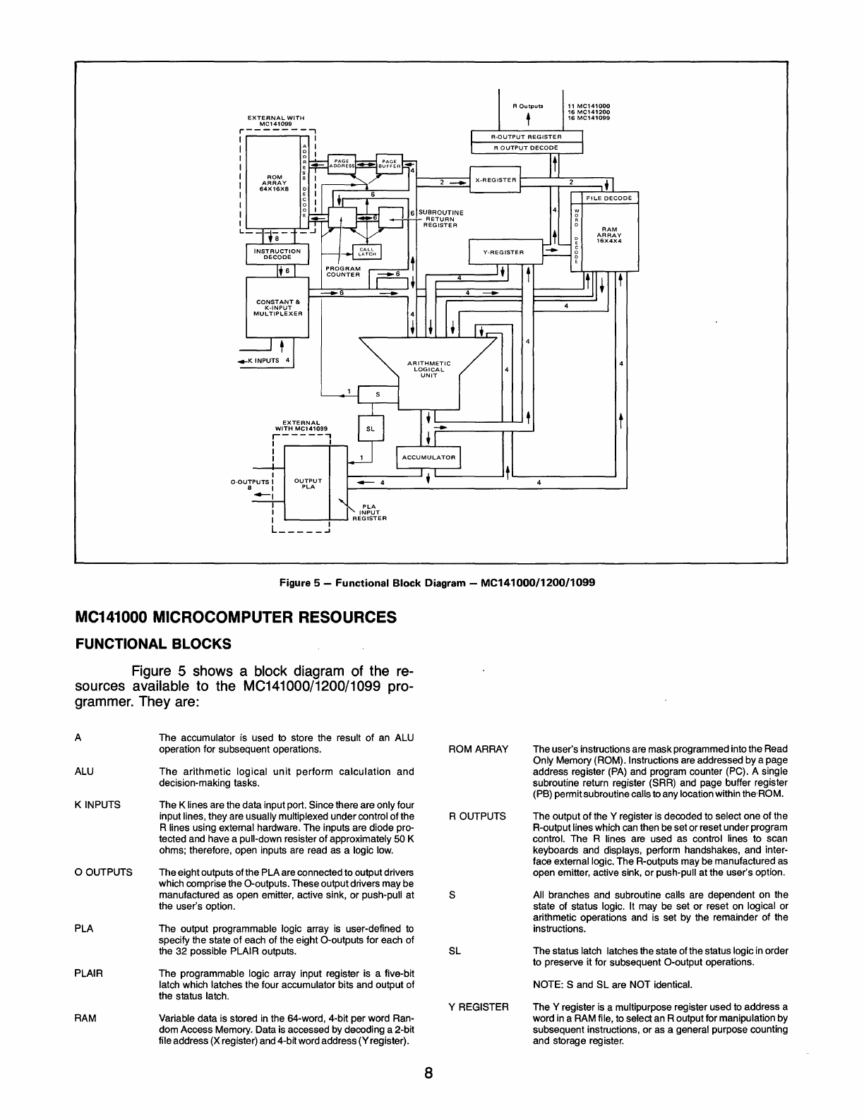
Figure 5 - Functional Block Diagram -MC141
000/1200/1099
MC141000 MICROCOMPUTER RESOURCES
FUNCTIONAL BLOCKS
Figure 5
shows
a
block
diagram
of
the re-
sources available
to
the MC141000/1200/1099 pro-
grammer. They are:
A
ALU
KINPUTS
a OUTPUTS
PLA
PLAIR
RAM
The accumulator is used to store the result of an ALU
operation for subsequent operations.
The
arithmetic
logical
unit
perform
calculation
and
decision-making tasks.
The K lines are the data input port. Since there are only four
input lines, they are usually multiplexed under control
of
the
R lines using external hardware. The inputs are diode pro-
tected and have a pull-down resister
of
approximately 50 K
ohms; therefore, open inputs are read as a logic
low.
The eight outputs of the PLA are connected to output drivers
which comprise the a-outputs. These output drivers may be
manufactured as open emitter, active sink, or push-pull at
the user's option.
The output programmable logic array
is
user-defined
to
specify the state of each of the eight a-outputs for each of
the 32 possible PLAIR outputs.
The programmable logic array input register is a five-bit
latch which latches the four accumulator bits and output of
the status latch.
Variable data is stored
in
the 64-word, 4-bit per word Ran-
dom Access Memory. Data is accessed by decoding a 2-bit
file address (X register) and 4-bit word address
(Y
register).
ROM ARRAY
R OUTPUTS
S
SL
Y REGISTER
8
The user's instructions are mask programmed into the Read
Only Memory (ROM). Instructions are addressed by a page
address register
(PA)
and program counter (PC). A single
subroutine return register (SRR) and page buffer register
(PB) permit subroutine calls to any location within theHOM.
The output
of
the Y register
is
decoded to select one of the
R-output lines which can then be set or reset under program
control. The R lines are used as control lines to scan
keyboards and displays, perform handshakes, and inter-
face external logic. The R-outputs may be manufactured as
open emitter, active sink,
or
push-pull at the user's option.
All branches and subroutine calls are dependent on the
state of status logic. It may
be
set or reset on logical or
arithmetic operations and is set by the remainder of the
instructions.
The status latch latches the state
ofthe
status logic
in
order
to preserve it for subsequent a-output operations.
NOTE:
Sand
SL
are NOT identical.
The Y register
is
a multipurpose register used to address a
word
in
a RAM file, to select an R output for manipulation by
subsequent instructions,
or
as a general purpose counting
and storage register.
Status and Status Latch
All program-modifying instructions (BRanch
or
CALL) are conditional on the state
of
the
status logic. If status is set, the BRanch
or
CALL is executed by jumping to the ROM address specified
by the operand field of the BRanch
or
CALL instruction and the contents
of
the page buffer register
(PB).
If
status is reset, the BRanch or CALL is not to be taken, and the instruction following the BRanch
or CALL is the next to execute. The BRanch
or
CALL takes six clock cycles (one instruction cycle) to
execute whether the status is set or reset.
The status logic is normally set. Whenever it is reset, the reset condition only lasts for one
instruction cycle and then returns to the set state. The only means to keep it reset for more than one
instruction cycle is to execute more than one instruction in series which causes it to reset in series.
The status latch takes the state
of
the status logic and saves it during the execution of a
YNEA instruction. Power on reset and INIT have no effect on the status latch. Therefore, a YNEA
instruction must be executed before a TDO instruction to ensure that the desired state of status latch is
placed into the PLA input register.
Power Up and Initialize
TABLE
1.
Power Up and Initialize
PC
PA
PB CL PLAIR R OUTPUTS
Power Up 0 15 15 0 0 0
Initialize 0 K K 0 0 0
When power is applied, the registers shown
in
Table 1 are loaded as shown for power up. All
other internal registers and RAM come up in an arbitrary state.
After power is applied, the initialize (INIT) input may be used to reinitialize the processor.
Internally, INIT has a 50 K ohm pull-down resistor which holds the INIT line low. It must be held high for
a minimum of 6 full clock cycles and then returned to the low state. If a mechanical switch
or
other
mechanical device is used to control INIT, it may be necessary to include a method of contact
debounce to ensure a valid INIT pulse.
A valid INIT pulse will cause the registers to be loaded as shown in the table. The contents of
registers other than those shown will remain unchanged during initialize. Note that the
PA
and PB are
loaded with the 1 's complement of the K-input lines
(Ka
=MSB). This feature allows the MC141000 to
be initialized to the first instruction on any page by controlling the K-inputs during initialization. This is
useful where the same circuit may be used for several applications. Since the K-inputs have 50 K
pull-down resistors, they will be a 0 (unless driven from another device) and the 1 's complement (F) will
be loaded into PA and PB.
9
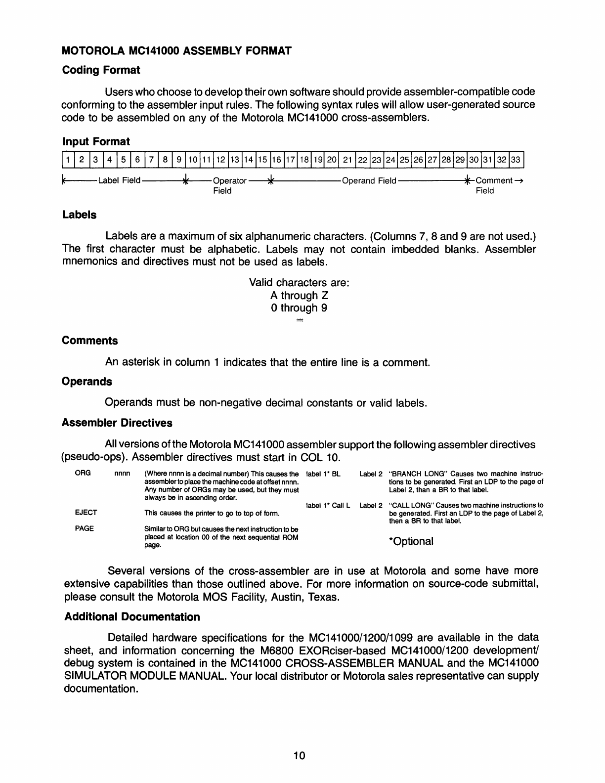
MOTOROLA MC141000 ASSEMBLY FORMAT
Coding Format
Users who choose to develop their own software should provide assembler-compatible code
conforming to the assembler input rules. The following syntax rules will allow user-generated source
code to
be
assembled on any of the Motorola MC141000 cross-assemblers.
Input Format
11
I 2 1
3
14
15
I 6
17
I 8 I
91
10
111
11211-31141151161171181191201
21
122123124125126127128129130
1
31
1
32
1
33
1
k Label Field * Operator
*'
Operand Field * Comment
~
Field Field
Labels
Labels are a maximum of six alphanumeric characters. (Columns
7,
Band
9 are not used.)
The first character must
be
alphabetic. Labels may not contain imbedded blanks. Assembler
mnemonics and directives must not be used as labels.
Valid characters are:
A through Z
o through 9
=
Comments
An asterisk
in
column 1 indicates that the entire line
is
a comment.
Operands
Operands must
be
non-negative decimal constants or valid labels.
Assembler Directives
All versions ofthe Motorola MC141000 assembler support the following assembler directives
(pseudo-ops). Assembler directives must start in COL
10.
ORG
EJECT
PAGE
nnnn (Where nnnn is a decimal number) This causes the label 1* BL
assembler to place the machine code at offset nnnn. Label 2 "BRANCH LONG" Causes two machine instruc-
tions to be generated. First an
LOP
to the page of
Label
2,
than a BR to that label. Any number of ORGs may
be
used, but they must
always
be
in
ascending order.
This causes the printer to go to top
of
form.
Similar to ORG but causes the next instruction to be
placed at location 00 of the next sequential ROM
page.
label 1* Call L Label 2 "CALL LONG" Causes two machine instructions to
be generated. First
an
LOP to the page of Label
2,
then a BR to that label.
*Optional
Several versions of the cross-assembler are
in
use at Motorola and some have more
extensive capabilities than those outlined above. For more information on source-code submittal,
please consult the Motorola MOS Facility, Austin, Texas.
Additional Documentation
Detailed hardware specifications for the
MC141
000/1200/1 099 are available
in
the data
sheet, and information concerning the
M6BOO
EXORciser-based MC141000/1200 development!
debug system is contained
in
the MC141000 CROSS-ASSEMBLER MANUAL and the MC141000
SIMULATOR MODULE MANUAL. Your local distributor or Motorola sales representative can supply
documentation.
10
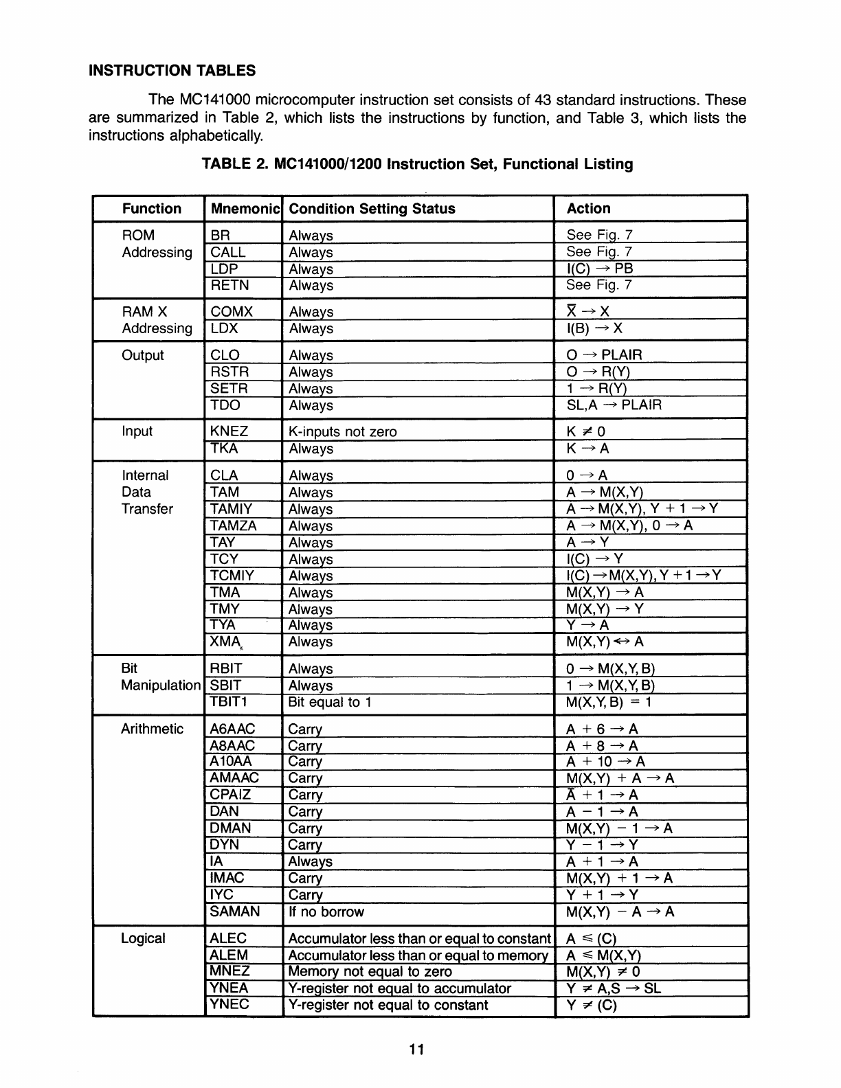
INSTRUCTION TABLES
The
MC141000 microcomputer instruction
set
consists
of
43
standard instructions.
These
are
summarized
in Table 2, which lists
the
instructions
by
function, and Table 3, which lists the
instructions alphabetically.
TABLE
2.
MC141000/1200
Instruction
Set, Functional
Listing
Function Mnemonic Condition Setting Status Action
ROM
BR
Always See Fiq. 7
Addressing CALL Always See Fig. 7
LOP
Always I(C)
~
PB
RETN Always See Fig. 7
RAM X COM X Always
X~X
Addressing LOX Always I(B)
~
X
Output CLO Always o
~
PLAIR
RSTR Always o
~
R(Y)
SETR Always 1
~
R(Y)
TOO Always SL,A
~
PLAIR
Input KNEZ K-inputs not zero K
~
0
TKA Always
K~A
Internal CLA Always
O~A
Oata TAM Always A
~
M(X,Y)
Transfer TAMIY Always A
~
M(X,Y), Y + 1
~
Y
TAMZA Always A
~
M(X,Y), 0
~
A
TAY
Always
A~Y
TCY Always I(C)
~
Y
TCMIY Always I(C)
~M(X,Yt,
Y + 1
~Y
TMA Always M(X,Y)
~
A
TMY Always M(X,Y)
~
Y
TYA
Always
Y~A
XMA
~,
Always
M(X,Y)~A
Bit RBIT Always o
~
M(X,Y,
B)
Manipulation SBIT Always 1
~
M(X,Y,
B)
TBIT1 Bit equal to 1 M(X,Y,
B)
= 1
Arithmetic A6AAC Carry
A+6~A
A8AAC Carry
A+8~A
A10AA Carry A +
10
~A
AMAAC Carry M(X,Y) + A
~
A
CPAIZ Carry
A+1~A
OAN
Carry
A-1~A
OMAN Carry M(X,Y) - 1
~A
OYN
Carry
Y-1~Y
IA Always
A+1~A
IMAC Carry M(X,Y) + 1
~
A
IYC Carry
Y+1~Y
SAMAN
If
no borrow M(X,Y) - A
~
A
Logical ALEC Accumulator less than or equal to constant A ~ (C)
ALEM Accumulator less than or equal to memory A
~
M(X,Y)
MNEZ Memory not equal to zero M(X,Y)
~
0
YNEA V-register not
e~ual
to accumulator Y
~
A,S
~SL
YNEC V-register not equal to constant Y
~
(C)
11
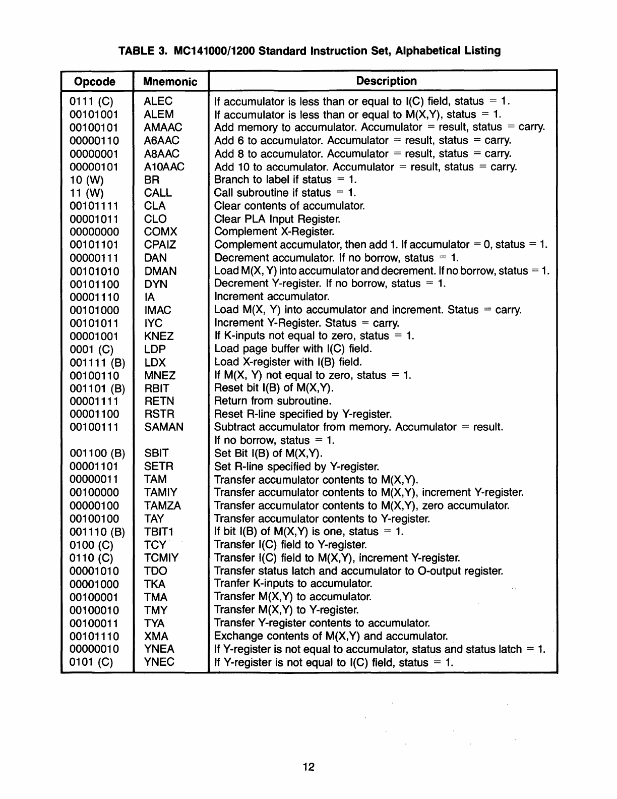
TABLE
3.
MC141000/1200 Standard Instruction Set, Alphabetical Listing
Opcode Mnemonic Description
0111
(C) ALEC If accumulator is less than or equal to I(C) field, status = 1.
00101001 ALEM
If
accumulator is less than or equal to M(X,V), status =
1.
00100101 AMAAC Add memory to accumulator. Accumulator = result, status = carry.
00000110 A6AAC Add 6 to accumulator. Accumulator = result, status = carry.
00000001 A8AAC Add 8 to accumulator. Accumulator = result, status = carry.
00000101 A10AAC Add
10
to accumulator. Accumulator = result, status = carry.
10 (W) BR Branch to label if status =
1.
11
(W) CALL Call subroutine if status =
1.
00101111 CLA Clear contents
of
accumulator.
00001011 CLO Clear PLA Input Register.
00000000 COMX Complement X-Register.
00101101 CPAIZ Complement accumulator, then add
1.
If accumulator =
0,
status =
1.
00000111
DAN
Decrement accumulator. If no borrow, status =
1.
00101010 OMAN Load M(X, V) into accumulator and decrement.
If
no borrow, status =
1.
00101100 DVN Decrement V-register. If no borrow, status =
1.
00001110 IA Increment accumulator.
00101000 IMAC Load M(X, V) into accumulator and increment. Status = carry.
00101011 IVC Increment V-Register. Status = carry.
00001001 KNEZ If K-inputs not equal to zero, status =
1.
0001
(C) LOP Load page buffer with I(C) field.
001111 (B) LOX Load X-register with I(B) field.
00100110 MNEZ If M(X,
V)
not equal to zero, status =
1.
001101 (B) RBIT Reset bit I(B) of M(X,Y).
00001111 RETN Return from subroutine.
00001100 RSTR Reset R-line specified by V-register.
00100111 SAMAN Subtract accumulator from memory. Accumulator = result.
If no borrow, status =
1.
001100 (B) SBIT Set Bit I(B) of M(X,V).
00001101 SETR Set R-line specified by V-register.
00000011 TAM Transfer accumulator contents to M(X,V).
00100000 TAMIV Transfer accumulator contents to M(X,V), increment V-register.
00000100 TAMZA Transfer accumulator contents to M(X,V), zero accumulator.
00100100
TAV
Transfer accumulator contents to V-register.
001110 (B) TBIT1 If bit I(B)
of
M(X,V) is one, status =
1.
0100 (C)
TCV'
Transfer I(C) field to V-register.
0110 (C) TCMIV Transfer I(C) field to M(X,V), increment V-register.
00001010 TOO Transfer status latch and accumulator to O-output' register.
00001000 TKA Tranfer K-inputs to accumulator.
00100001 TMA Transfer M(X,
V)
to accumulator.
00100010 TMV Transfer M(X,
V)
to V-register.
00100011 TVA Transfer V-register contents to accumulator.
00101110 XMA Exchange contents
of
M(X, V) and accumulator. .
00000010 VNEA If V-register is not equal to accumulator, status and status latch =
1.
0101
(C) VNEC If V-register is not equal to I(C) field, status =
1.
12
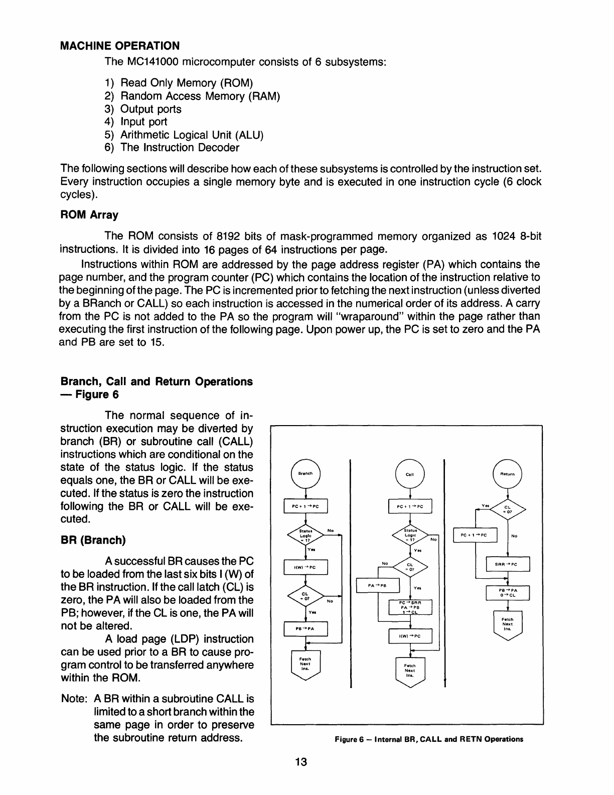
MACHINE OPERATION
The MC141000 microcomputer consists of 6 subsystems:
1)
Read Only Memory (ROM)
2) Random Access Memory (RAM)
3) Output ports
4) Input port
5) Arithmetic Logical Unit (ALU)
6) The Instruction Decoder
The following sections will describe how each of these subsystems
is
controlled by the instruction set.
Every instruction occupies a single memory byte and is executed
in
one instruction cycle (6 clock
cycles).
ROM Array
The ROM consists
of
8192 bits of mask-programmed memory organized as 1024 8-bit
instructions. It is divided into
16
pages of 64 instructions per page.
Instructions within ROM are addressed by the page address register (PA) which contains the
page number, and the program counter (PC) which contains the location
of
the instruction relative to
the beginning
ofthe
page. The
PC
is
incremented prior to fetching the next instruction (unless diverted
by a BRanch or CALL) so each instruction
is
accessed
in
the numerical order of its address. A carry
from the PC
is
not added to the PA so the program will "wraparound" within the page rather than
executing the first instruction of the following page. Upon power up, the PC
is
set to zero and the PA
and PB are set to
15.
Branch, Call and Return Operations
-Figure 6
The normal sequence of in-
struction execution may be diverted by
branch (BR) or subroutine call (CALL)
instructions which are conditional on the
state of the status logic. If the status
equals one, the BR or CALL will be exe-
cuted. If the status is zero the instruction
following the
BR
or CALL will be exe-
cuted.
BR (Branch)
A successful BR causes the
PC
to be loaded from the last six bits I (W) of
the BR instruction. If the call latch (CL) is
zero, the PA will also be loaded from the
PB; however, if the CL is one, the PAwili
not be altered.
A load page (LOP) instruction
can be used prior to a BR to cause pro-
gram control to be transferred anywhere
within the ROM.
Note: A BR within a subrolltine CALL is
limited to a short branch within the
same page in order to preserve
the subroutine return address. Figure 6 - Internal
BR,
CALL
and
RETN
Operations
13
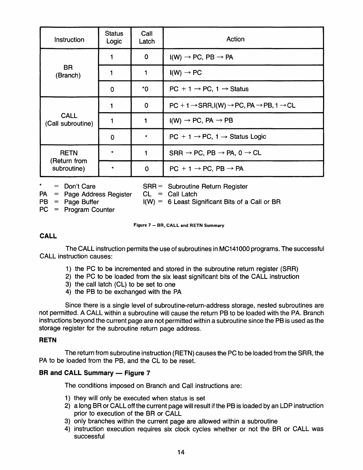
Status Call
Instruction Logic Latch Action
1 0 I(W)
~
PC, PB
~
PA
BR
(Branch) 1 1 I(W)
~
PC
0 *0 PC + 1
~
PC, 1
~
Status
1 0 PC + 1
~SRR,I(W)~PC,
PA~PB,
1
~CL
CALL
(Call subroutine) 1 1 I(W)
~
PC,
PA
~
PB
0 * PC + 1
~
PC, 1
~
Status Logic
RETN * 1
SRR
~
PC, PB
~
PA,
0
~
CL
(Return from
subroutine) * 0 PC + 1
~
PC, PB
~
PA
*
PA
PB
PC
CALL
Don't Care
Page Address Register
Page Buffer
Program Counter
SRR
= Subroutine Return Register
CL
= Call Latch
I(W) = 6 Least Significant Bits
of
a Call
or
BR
Figure 7 -
BR,
CALL
and
RETN
Summary
The
CALL
instruction permits the use
of
subroutines in MC141000 programs.
The
successful
CALL
instruction causes:
1) the PC to be incremented and stored in the subroutine return register (SRR)
2) the PC to be loaded from the six least significant bits
of
the
CALL
instruction
3) the call latch (CL) to be set
to
one
4) the PB
to
be exchanged with the PA
Since there is a single level
of
subroutine-return-address storage, nested subroutines are
not permitted. A
CALL
within a subroutine will cause the return PB to be loaded with the PA. Branch
instructions beyond the current page are not permitted within a subroutine since the PB is used as the
storage register for the subroutine return page address.
RETN
The return from subroutine instruction (RETN) causes the PC to be loaded from the SRR, the
PA to be loaded from the PB, and the
CL
to be reset.
BR
and CALL Summary -Figure 7
The conditions imposed on Branch and Call instructions are:
1) they will only be executed when status is set
2) a long BR or
CALL
off
the current page will result if the PB is loaded by an LDP instruction
prior to execution
of
the BR or
CALL
3) only branches within the current page are allowed within a subroutine
4) instruction execution requires six clock cycles whether
or
not the BR
or
CALL
was
successful
14
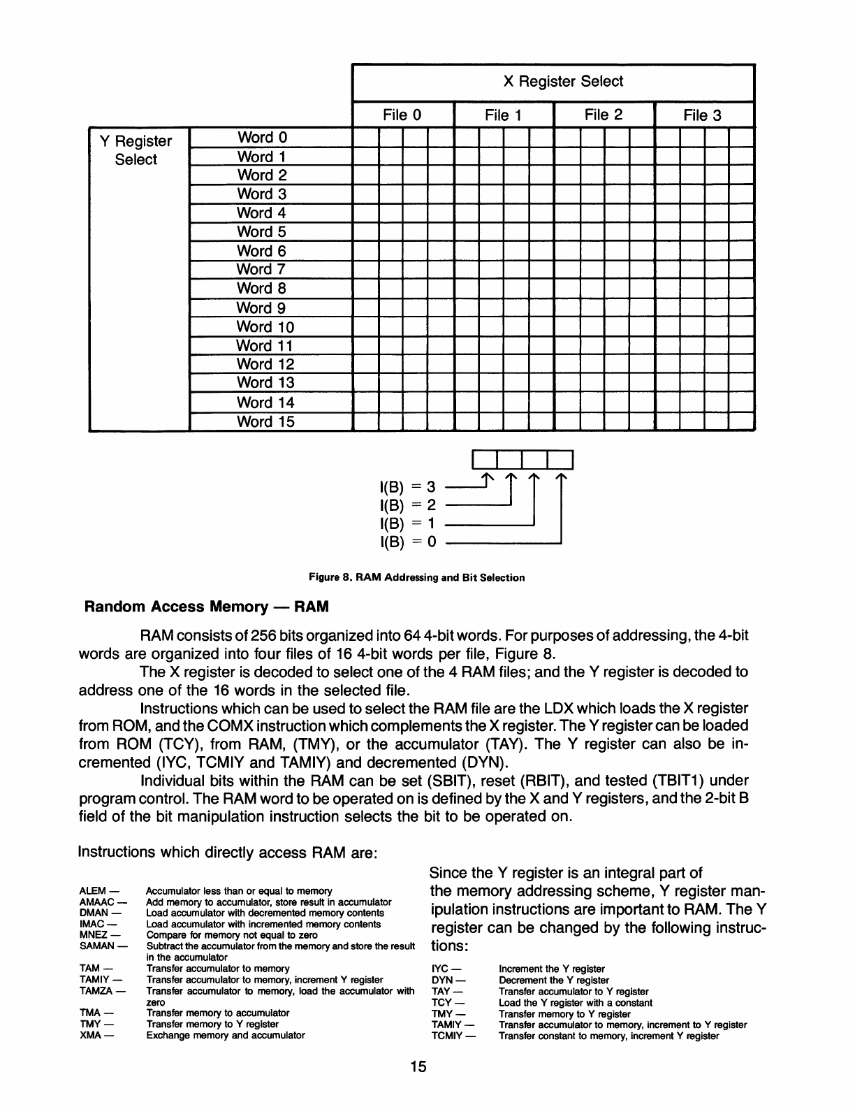
X Register Select
File 0 File 1 File 2 File 3
Y Register Word 0
Select Word 1
Word 2
Word 3
Word 4
Word 5
Word 6
Word 7
Word 8
Word 9
Word 10
Word
11
Word 12
Word 13
Word
14
Word 15
1(8) = 3
l'
J J
1(8)
= 2
1(8)
= 1
1(8)
= 0
Figure
8.
RAM Addressing and Bit Selection
Random Access Memory -RAM
RAM consists
of
256
bits organized into
64
4-bit words. For purposes
of
addressing, the 4-bit
words are organized into four files
of
16 4-bit words
per
file, Figure 8.
The X register is decoded to select
one
of
the 4 RAM files; and the Y register is decoded to
address one
of
the 16 words in the selected file.
Instructions which can be used
to
select the
RAM
file are the LOX which loads the X register
from ROM, and the
COMX
instruction which
complements
the X register.
The
Y register can be loaded
from ROM (TCY) , from RAM, (TMY) ,
or
the accumulator (TAY).
The
Y register can also be in-
cremented (IYC,
TCMIY
and TAMIY) and decremented (OYN).
Individual bits within the RAM can be set
(S8IT),
reset
(R8IT),
and
tested
(T8IT1)
under
program control.
The
RAM word to be operated on is defined
by
the X and Y registers, and the 2-bit 8
field
of
the bit manipulation instruction selects the bit to be operated on.
Instructions which directly access RAM are:
ALEM-
AMAAC-
DMAN-
IMAC-
MNEZ-
SAMAN-
TAM-
TAMIY-
TAMZA-
TMA-
TMY-
XMA-
Accumulator less than or equal to memory
Add memory to accumulator, store result
in
accumulator
Load accumulator with decremented memory contents
Load accumulator with incremented memory contents
Compare for memory not equal to zero
Subtract the accumulator from the memory and store the result
in the accumulator
Transfer accumulator to memory
Transfer accumulator to memory, increment Y register
Transfer accumulator to memory, load the accumulator with
zero
Transfer memory to accumulator
Transfer memory to Y register
Exchange memory and accumulator
15
Since the Y register is an integral part
of
the
memory
addressing scheme, Y register man-
ipulation instructions are important to RAM.
The
Y
register can be changed
by
the following instruc-
tions:
IYC-
DYN-
TAY-
TCY-
TMY-
TAMIY-
TCMIY-
Increment the Y register
Decrement the Y register
Transfer accumulator to Y register
Load the Y register with a constant
Transfer memory to Y register
Transfer accumulator to memory, increment to Y register
Transfer constant to memory, increment Y register
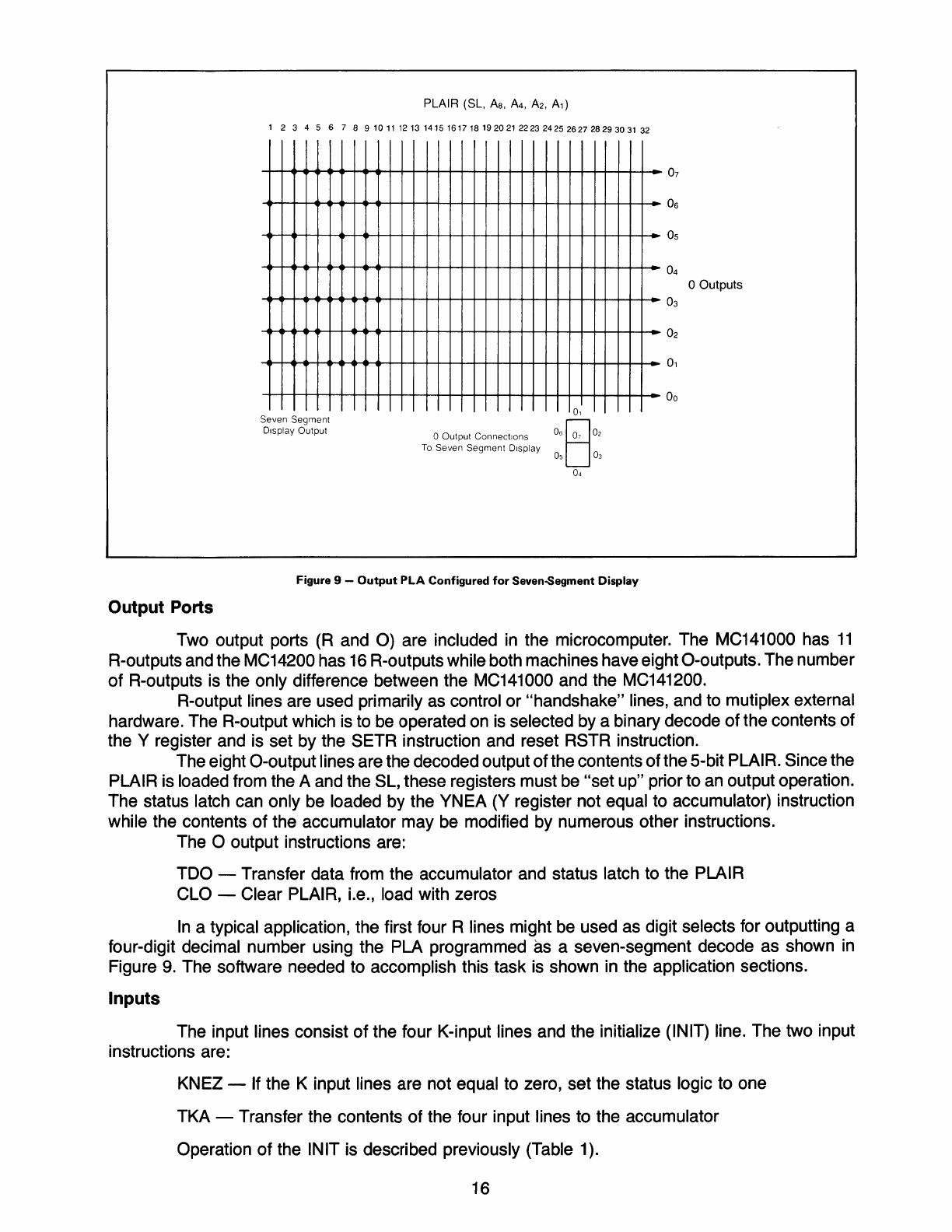
1234567
8
91011121314151617181920212223242526272829303132
Seven Segment
Display Output o Output Connections
To
Seven Segment Display
0,
Figure 9 -
Output
PLA Configured
for
Seven-Segment Display
07
06
05
04
a Outputs
03
02
01
00
Output Ports
Two output ports (R and
0)
are included
in
the microcomputer. The MC141000 has
11
R-outputs and the MC14200 has
16
R-outputs while both machines have eight O-outputs. The number
of
R-outputs is the only difference between the MC141000 and the MC141200.
R-output lines are used primarily as control or "handshake" lines, and to mutiplex external
hardware. The R-output which is to be operated on
is
selected by a binary decode
of
the contents of
the Y register and is set by the SETR instruction and reset RSTR instruction.
The eight O-output lines are the decoded output of the contents of the 5-bit PLAIR. Since the
PLAIR is loaded from the A and the SL, these registers must be "set up" prior to an output operation.
The status latch can only be loaded by the YNEA (Y register not equal to accumulator) instruction
while the contents
of
the accumulator may be modified by numerous other instructions.
The 0 output instructions are:
TOO -Transfer data from the accumulator and status latch to the PLAIR
CLO -Clear PLAIR, i.e., load with zeros
In
a typical application, the first four R lines might be used as digit selects for outputting a
four-digit decimal number using the PLA programmed as a seven-segment decode as shown
in
Figure
9.
The software needed to accomplish this task is shown in the application sections.
Inputs
The input lines consist
of
the four K-input lines and the initialize (IN IT) line. The two input
instructions are:
KNEZ -If the K input lines are not equal to zero, set the status logic to one
TKA -Transfer the contents of the four input lines to the accumulator
Operation
of
the INIT is described previously (Table 1).
16
Arithmetic Logical Unit (ALU)
The ALU is the calculating and decision-making portion
of
the MC141000 hardware and
consists
of
a 4-bit adder/comparator and the status logic.
The status logic will be selectively set or reset by add, subtract, increment, decrement,
compare and bit-test operations. Other instructions always set the status logic to a one.
The adder/comparator can add, subtract, compare two numbers, add +1,
-1,
6,
8,
and
10.
The arithmetic instructions are:
AMAAC-
Add memory to accumulator, results
to accumulator. Carry to status
SAMAN-
Subtract accumulator from memory,
results to accumulator. If no borrow,
one to status
IMAC-
Load memory into accumulator, in-
crement accumulator. Carry to status
DMAN-
Load memory into accumulator, dec-
rement accumulator. If no borrow,
one to status
IA-
Increment accumulator, no status
effect
IYC-
Increment Y register. Carry to status
DAN-
Decrement accumulator. If no bor-
row,
one to status
DYN -Decrement Y register. If no borrow,
one to status
A8AAC -Add 8 to accumulator, results to
accumulator. Carry to status
A 1
OAAC
-Add
10
to accumulator, results to
accumulator. Carry to status
A6AAC -Add 6
to
accumulator, results to
accumulator. Carry to status
CPAIZ -
Complement
accumulator
incre-
ment. If zero, one to status
Instruction Decode
The instruction decode logic latches
every instruction fetched from ROM and config-
ures the internal logic to correctly execute the cur-
the current instruction. The MC141000 includes
within the instruction decode logic the capability
of
modifying the standard instruction set. Typical
examples of useful nonstandard instructions are:
SRDY-
TDOIY-
TKM-
ANEM-
Set R-Output and decrement Y
Transfer A and SL to PLAIR and
increment Y
Transfer K inputs to memory and
increment the Y Register
A not equal to M(X, Y)
The factory should be consulted for fea-
sibility of specific instruction-set modifications.
17
The logical instructions are:
ALEM-
If accumulator less than or equal to
memory, one to status
ALEC-
If
accumulator less than or equal to a
constant, one to status
KNEZ-
If K-inputs not all zero, one to status
MNEZ-
If memory not equal to zero, one to
status
TBIT1 -If the selected bit is one, one to status
YNEA-
If
Y register not equal to accumulator,
one to status and status latch
YNEC-
If Y register not equal to a constant,
one to status
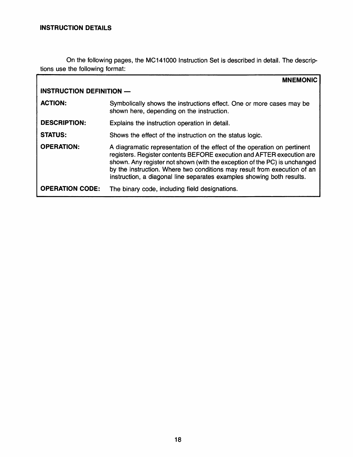
INSTRUCTION DETAILS
On the following pages, the MC141000 Instruction Set is described
in
detail. The descrip-
tions use the following format:
MNEMONIC
INSTRUCTION DEFINITION -
ACTION: Symbolically shows the instructions effect. One or more cases may be
shown here, depending on the instruction.
DESCRIPTION: Explains the instruction operation
in
detail.
STATUS: Shows the effect of the instruction on the status logic.
OPERATION: A diagramatic representation of the effect of the operation on pertinent
registers. Register contents BEFORE execution and AFTER execution are
shown. Any register not shown (with the exception of the
PC)
is unchanged
by the instruction. Where two conditions may result from execution of
an
instruction, a diagonal line separates examples showing both results.
OPERATION CODE: The binary code, including field designations.
18
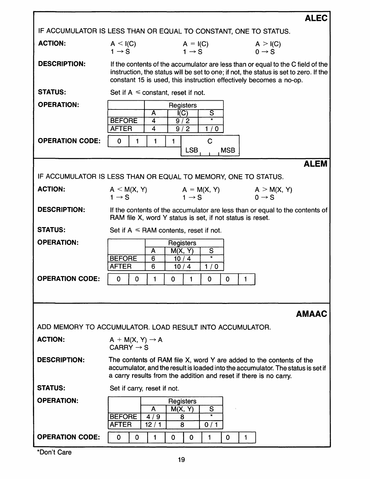
ALEC
IF ACCUMULATOR IS LESS THAN OR EQUAL TO CONSTANT, ONE TO STATUS.
ACTION: A < I(C) A = I(C) A > I(C)
DESCRIPTION:
STATUS:
OPERATION:
1~S
1~S
O~S
If the contents of the accumulator are less than or equal to the C field of the
instruction, the status will
be
set to one; if not, the status
is
set to zero. If the
constant
15
is
used, this instruction effectively becomes a no-op.
Set if A
:::::;
constant, reset if not.
Registers
A I(C) S
BEFORE 4
9/2
*
AFTER 4
9/2
1/0
OPERATION CODE: I ° I 1 I 1 I 1 I c I
L-----L_-.L.-_...L-----I
~SB
I I I MSB
ALEM
IF ACCUMULATOR IS LESS THAN OR EQUAL TO MEMORY, ONE TO STATUS.
ACTION: A < M(X,
Y)
A = M(X,
Y)
A > M(X,
Y)
DESCRIPTION:
STATUS:
OPERATION:
1~S 1~S
O~S
If the contents of the accumulator are less than or equal to the contents of
RAM file
X,
word Y status is set, if not status
is
reset.
Set if A
:::::;
RAM contents, reset if not.
Registers
A M(X,
Y)
S
BEFORE 6
10/4
*
AFTER 6
10/4
1 / °
I 1 I ° I 1 I ° I ° I 1 I
OPERATION CODE:
L-I
_0-----JII...--
0
---'-_....1.------JI...---.L-_--L..-_'---~
AMAAC
ADD MEMORY TO ACCUMULATOR. LOAD RESULT INTO ACCUMULATOR.
ACTION:
DESCRIPTION:
STATUS:
OPERATION:
OPERATION CODE: I
*Don't Care
A + M(X,
Y)
~A
CARRY
~S
The contents of RAM file
X,
word
Yare
added to the contents of the
accumulator, and the result is loaded into the accumulator. The status is set if
a carry results from the addition and reset if there is no carry.
Set if carry, reset if not.
Registers
A M(X,
Y)
S
BEFORE
4/9
8 *
AFTER
12/1
8
0/1
° I ° 1 1 1 ° 1 ° 1 1
10
I 1 I
19
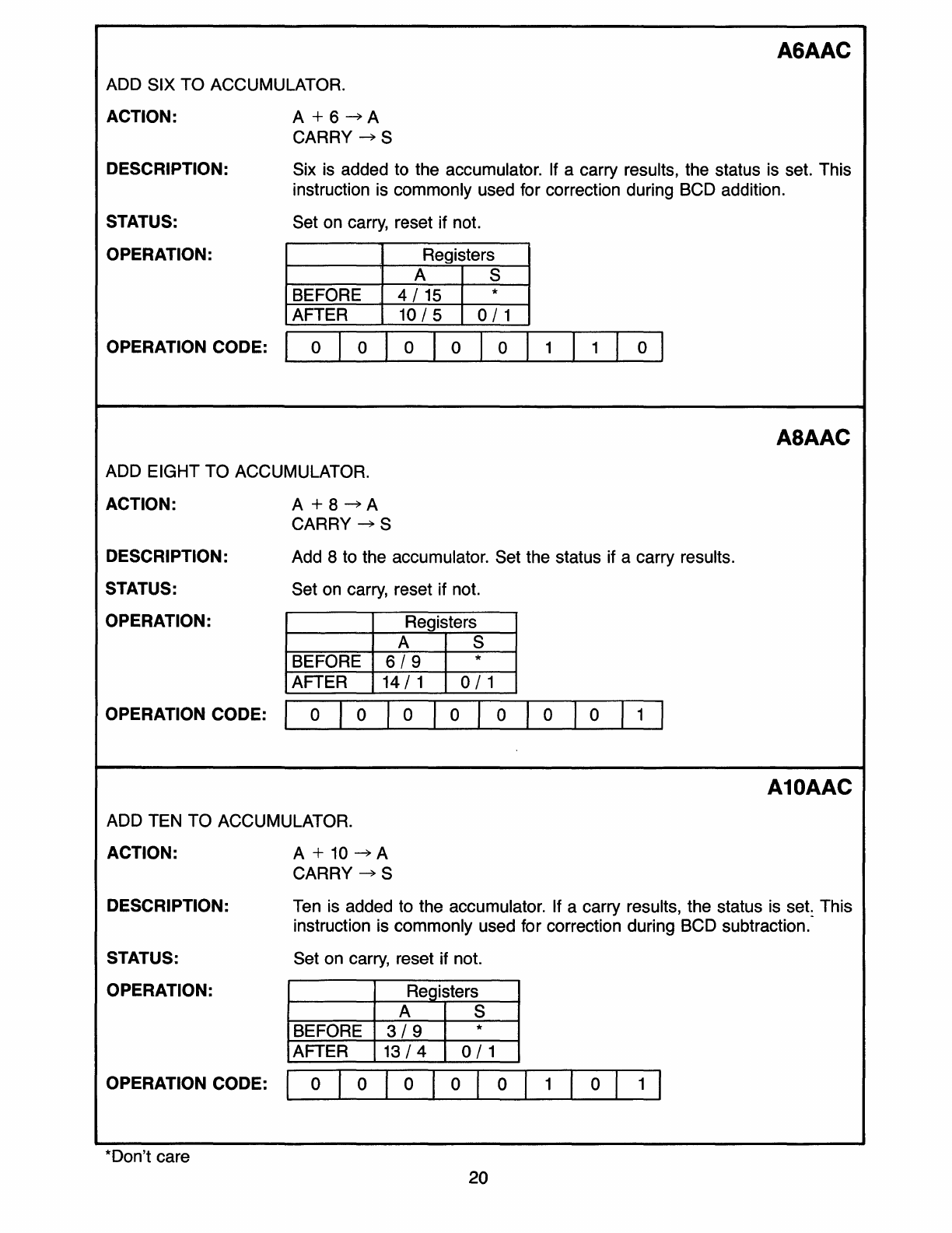
ADD SIX TO ACCUMULATOR.
ACTION:
A+6~A
CARRY
~S
A6AAC
DESCRIPTION: Six
is
added to the accumulator.
If
a carry results, the status is set. This
instruction is commonly used for correction during BCD addition.
STATUS: Set on carry, reset if not.
OPERATION: Registers
A S
BEFORE
4/15
*
AFTER
10/5
0/1
I 0 I 0 I 0 I 1 I 1 I 0 I
OPERATION CODE:
1-1
_o----JI'---0-.l-_.....L....._L...______L..._-'------L_~
ADD EIGHT TO ACCUMULATOR.
ACTION:
DESCRIPTION:
STATUS:
OPERATION:
A+8~A
CARRY
~S
Add 8 to the accumulator. Set the status if a carry results.
Set on carry, reset if not.
Registers
A S
BEFORE
6/9
*
AFTER
14/
1 0 / 1
OPERATION CODE: I 0 I 0 I 0 I 0 I 0 I 0 I 0 I 1 I
ADD TEN TO ACCUMULATOR.
ACTION: A +
10
~A
CARRY
~S
A8AAC
A10AAC
DESCRIPTION: Ten is added to the accumulator. If a carry results, the status is set. This
instruction is commonly used for correction during BCD subtraction.-
STATUS: Set on carry, reset if not.
OPERATION: Registers
A S
BEFORE
3/9
*
AFTER
13/4
0/1
I 0 I 0 I 0 I 1 I 0 I 1 I
OPERATION
CODE:l
L-
_0----JI~0____L..._--'-_L...__---'-
_
__'__'----___J
*Don't care 20
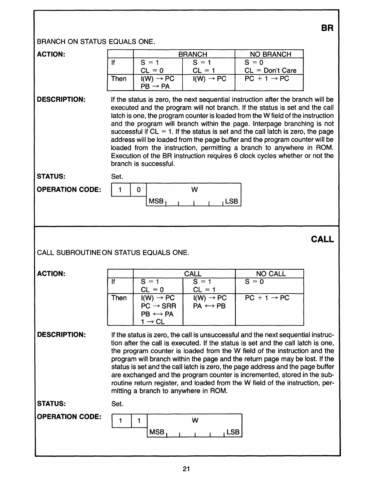
BR
BRANCH
ON
STATUS EQUALS ONE.
ACTION:
BRANCH
NO
BRANCH
DESCRIPTION:
STATUS:
OPERATION
CODE:
If
Then
S = 1
CL
= 0
I(W)
~
PC
PB~PA
S = 1
CL
= 1
I(W)
~
PC
S = 0
CL
= Don't Care
PC+1~PC
If the status is zero,
the
next sequential instruction after the branch will be
executed and the program will not branch. If the status is set and the call
latch is one,
the
program counter is loaded from the W field
of
the instruction
and the program will branch within the page. Interpage branching is not
successful if
CL
=
1.
If the status is set and the call latch is zero, the page
address will be loaded from the page buffer and the program counter will be
loaded from the instruction, permitting a branch to anywhere in ROM.
Execution
of
the BR instruction requires 6 clock cycles whether
or
not the
branch is successful.
Set.
1 I 0
1--1
M_S_B...a-'
_____
W""----"....&.....-_I'--L_SB---'I
CALL
CALL
SUBROUTINE
ON STATUS
EQUALS
ONE.
ACTION:
DESCRIPTION:
STATUS:
.OPERATION
CODE:
If
Then
S = 1
CL
= 0
I(W)
~
PC
PC
~SRR
PB
~PA
1
~CL
CALL
S = 1
CL
= 1
I(W)
~
PC
PA~PB
NO
CALL
S = 0
PC+1~PC
If the status is zero, the call is unsuccessful and the next sequential instruc-
tion after the call is executed. If the status is set and the call latch is one,
the program counter is loaded from the W field
of
the instruction and the
program will branch within the page and the return page
may
be lost. If the
status is set
and
the call latch is zero, the page address and the page buffer
are exchanged and the program counter is incremented, stored in the sub-
routine return register, and loaded from the W field
of
the instruction, per-
mitting a branch to anywhere in ROM.
Set.
'----1
_____
1
--41
MSB
I W
ILSBI
21
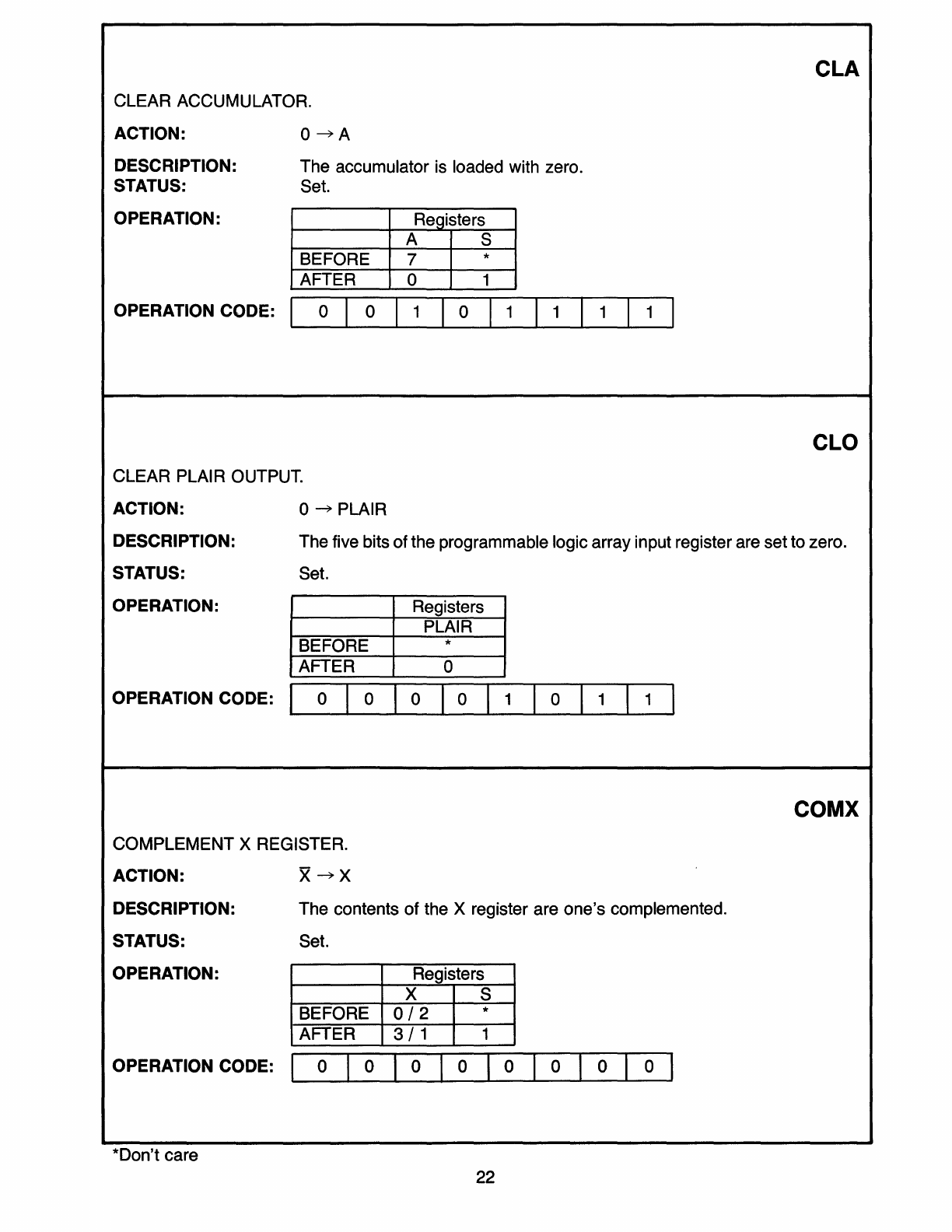
CLEAR ACCUMULATOR.
ACTION:
DESCRIPTION:
STATUS:
OPERATION:
O~A
The accumulator
is
loaded with zero.
Set.
Registers
A S
BEFORE 7 *
AFTER ° 1
1 1 1 ° 1 1 1 1 1 1 1 1 1
OPERATION CODE:
L-I
_0
---1....1 _0----1._---'--_...1...-.-----1._--'-_"------'
CLEAR PLAIR OUTPUT.
ACTION: °
~
PLAIR
CLA
CLO
DESCRIPTION:
STATUS:
The five bits of the programmable logic array input register are set to zero.
Set.
OPERATION: Registers
PLAIR
BEFORE *
AFTER °
OPERATION CODE: I ° 1 ° 1 ° 1 ° 1 1 1 ° 1 1 1 1 I
COMPLEMENT X REGISTER.
ACTION:
DESCRIPTION:
STATUS:
OPERATION:
X~X
The contents of the X register are one's complemented.
Set.
Registers
X S
BEFORE
0/2
*
AFTER
3/1
1
1 ° 1 ° 1 ° I ° I ° 1 ° I
OPERATION CODE:
L...I
_0_1-1
_0----L._-L-_L-----L._--L..---JL.-----I
*Oon't care
22
COMX
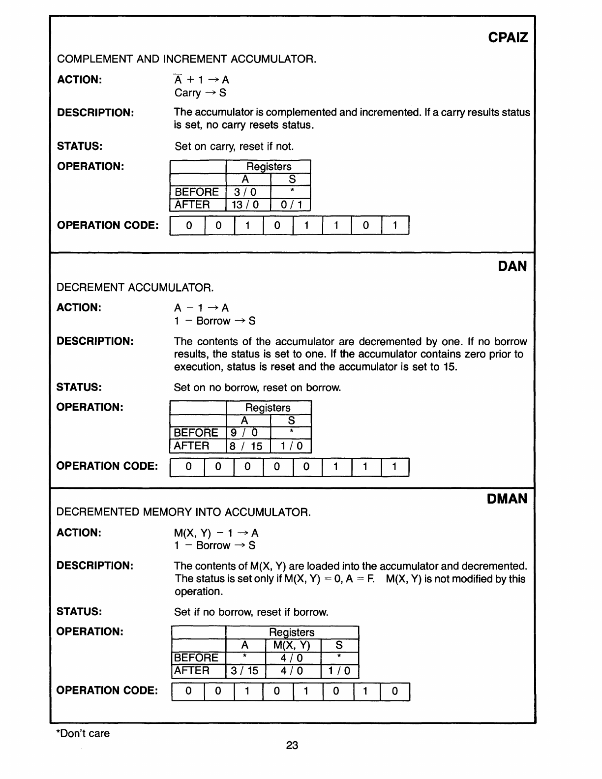
CPAIZ
COMPLEMENT AND INCREMENT ACCUMULATOR.
ACTION:
DESCRIPTION:
STATUS:
OPERATION:
A+1~A
Carry
~
S
The accumulator is complemented and incremented. If a carry results status
is set, no carry resets status.
Set on carry, reset if not.
Registers
A S
BEFORE
3/0
*
AFTER
13/0
0/1
I 1 I 0 I 1 I 1 I 0 I 1 I
OPERATION CODE:
L-I
_O_L......I
_0---'-_-1------IL......----L-_-L.----I1......-----I
DAN
DECREMENT ACCUMULATOR.
ACTION: A - 1
~A
DESCRIPTION:
STATUS:
OPERATION:
1 - Borrow
~
S
The contents
of
the accumulator are decremented by one. If no borrow
results, the status is set to one. If the accumulator contains zero prior to
execution, status is reset and the accumulator is set to 15.
Set on no borrow, reset on borrow.
Registers
A S
BEFORE 9 / 0 *
AFTER 8 / 15 1 / 0
OPERATION CODE: I 0 I 0 I 0 I 0 I 0 I 1 I 1 I 1 I
OMAN
DECREMENTED
MEMORY
INTO ACCUMULATOR.
ACTION:
DESCRIPTION:
STATUS:
OPERATION:
OPERATION CODE: I
*Don't care
M(X, Y) - 1
~
A
1 - Borrow
~
S
The contents
of
M(X, Y) are loaded into the accumulator and decremented.
The status is set only if M(X, Y) = 0, A =
F.
M(X, Y) is not modified by this
operation.
Set if no borrow, reset if borrow.
Registers
A M(X, Y) S
BEFORE *
4/0
*
AFTER
3/15
4/0
1
/0
0 I 0 I 1 I 0 I 1 I 0 I 1 I 0 I
23
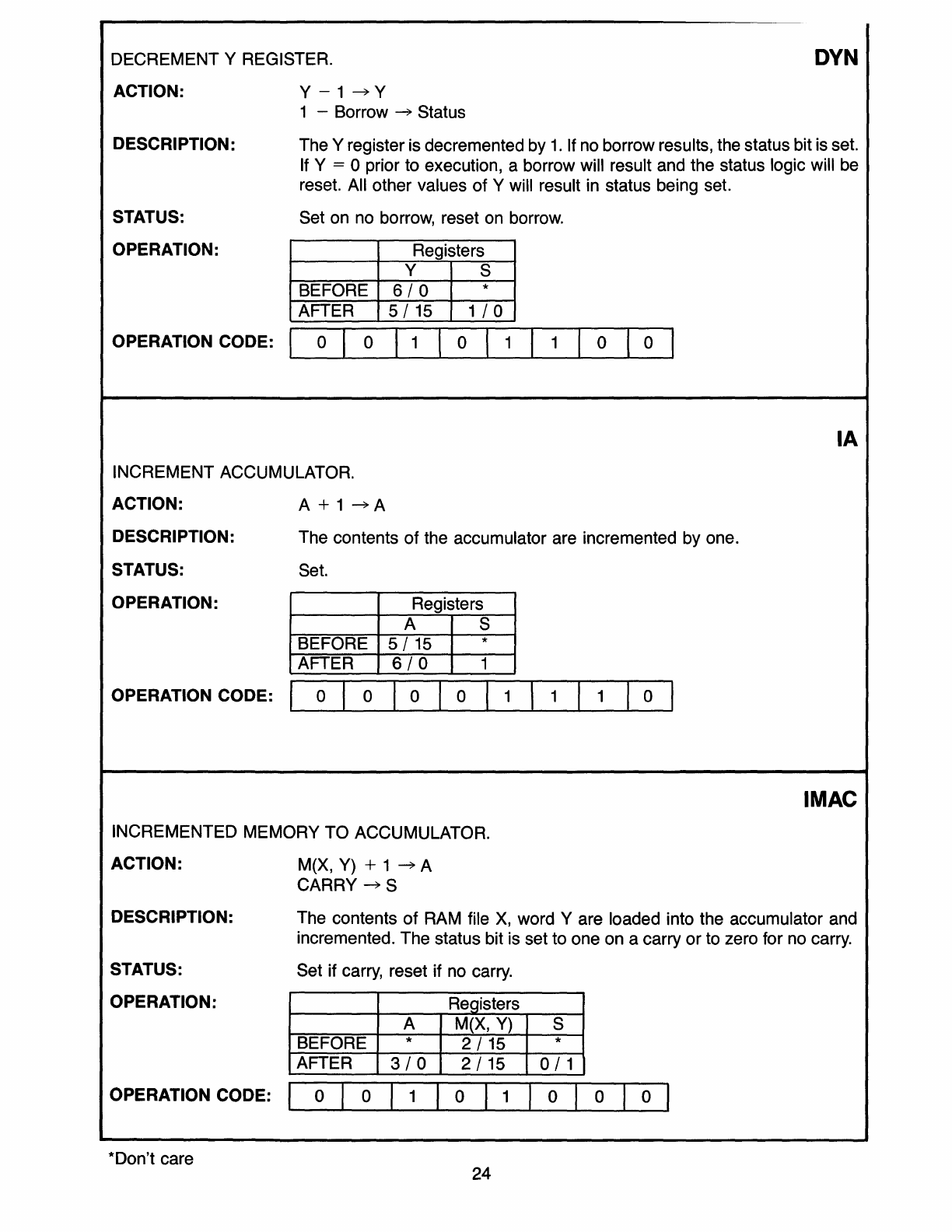
DECREMENT Y REGISTER.
DYN
ACTION:
DESCRIPTION:
STATUS:
OPERATION:
OPERATION CODE:
Y-1~Y
1 - Borrow
~
Status
The Y register is decremented by
1.
If no borrow results, the status bit is set.
If Y = 0 prior to execution, a borrow will result and the status logic will be
reset. All other values of Y will result in status being set.
Set on no borrow, reset on borrow.
Registers
Y S
BEFORE
6/0
*
AFTER 5 /
15
1 / 0
o o 1 o 1 1 o o
IA
INCREMENT ACCUMULATOR.
ACTION: A + 1
~A
DESCRIPTION:
STATUS:
OPERATION:
OPERATION CODE:
The contents of the accumulator are incremented by one.
Set.
Registers
A S
BEFORE 5 /
15
*
AFTER
6/0
1
o o o o 1 1 1 o
IMAC
INCREMENTED MEMORY TO ACCUMULATOR.
ACTION:
DESCRIPTION:
STATUS:
OPERATION:
OPERATION CODE:
*Don't care
M(X, Y) + 1
~
A
CARRY
~
S
The contents
of
RAM file
X,
word
Yare
loaded into the accumulator and
incremented. The status bit is set to one on a carry
or
to zero for no carry.
Set if carry, reset if no carry.
Registers
A M(X,
Y)
S
BEFORE *
2/15
*
AFTER
3/0
2/15
0/1
o o 1 o 1 o o o
24
INCREMENT Y REGISTER.
ACTION: Y + 1
~
Y
CARRY
~S
lye
DESCRIPTION: The contents
of
the Y register are incremented by one. If a carry results, the
status bit is set to one.
STATUS: Set on carry, reset if no carry.
OPERATION: Registers
Y S
BEFORE
4/15
*
AFTER
5/0
0/1
I 1 I ° I 1 I ° I 1 I 1 I
OPERATION CODE
:1
I..-
_0----ll_0--...L-_-'--_"---"-_-'-----..I~___I
KNEZ
IF K INPUTS ARE
NOT
EQUAL TO ZERO,
SET
STATUS.
ACTION: K = ° K
f-
°
1~S
DESCRIPTION: Compare the data on the four K input lines with zero. If the input data is not
zero, set the status bit.
STATUS: Set if K
~
0, reset otherwise.
OPERATION: Registers
K S
BEFORE
7/0
*
AFTER
7/0
1 / °
I ° I ° ! 1 I ° ! ° I 1 I
OPERATION CODE:
1..-1
_0
-.J!L...---
0
-"-_-'--_"-----'-_.....&.--_'-----'
LOAD THE
PAGE
BUFFER.
ACTION:
DESCRIPTION:
STATUS:
I(C)
~
PB
The C field of the instruction is loaded into the
page buffer register.
Set
OPERATION: Registers
I(C) PB
BEFORE 4 *
AFTER * 4
OPERATION CODE: 1 0 I 0 I 0
11
I C I
.
LSB,
,
,MSB
*Don't care 25
LOP
LOAD X REGISTER WITH A CONSTANT.
ACTION: I(B)
~
X
DESCRIPTION:
STATUS:
The B field of the instruction is loaded into the X register.
Set.
OPERATION: Registers
X I(B) S
BEFORE * 2 *
AFTER 2 * 1
1 1 1 1 1 1 I
OPERATION
COD
E
:\
L..-
_0
______
1"'--0
______
1"'---1
----'--_""'-----'------I
LSB~MSB
I
IF MEMORY
NOT
EQUAL TO ZERO, ONE
TO
STATUS.
ACTION: M(X,Y) = ° M(X,Y)
~
°
O~S
1~S
LOX
MNEZ
DESCRIPTION: If the contents
of
memory file X, word
Yare
equal to zero, the status logic is
reset. If the contents
of
that memory location are not zero, the status is set.
STATUS: Reset if M(X, Y) = 0, set if M(X, Y)
~
0.
OPERATION: Registers
M(X,Y) S
BEFORE
0/7
*
AFTER
0/7
0/1
OPERATION
CODE:
I ° I ° I 1 I ° I ° I 1 I 1 I ° I
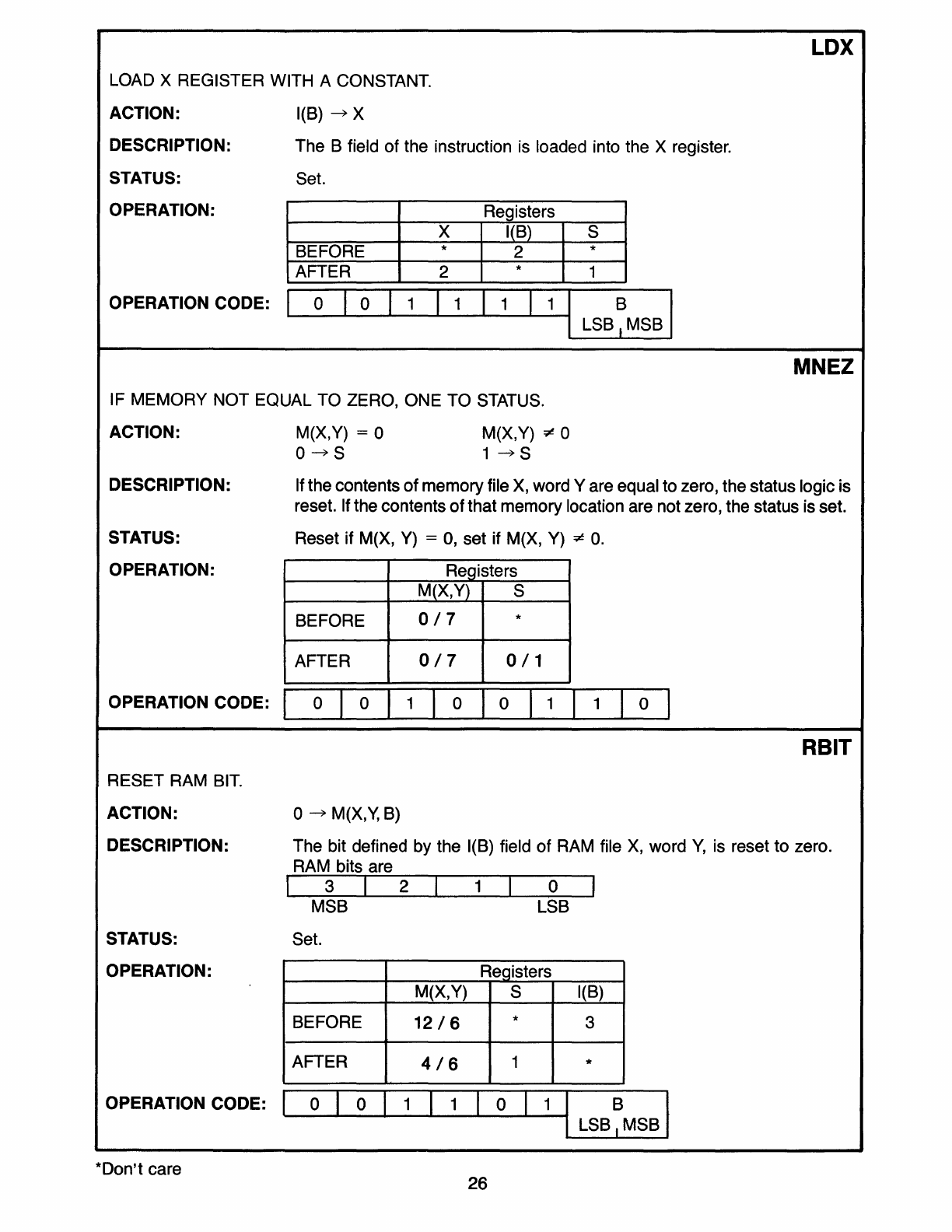
RESET RAM BIT.
ACTION:
DESCRIPTION:
STATUS:
OPERATION:
OPERATION
CODE:
*Oon't care
I
RBIT
°
~
M(X,Y, B)
The bit defined by the I(B) field
of
RAM file X, word
Y,
is reset to zero.
RAM bits are
I 3 I 2 I 1 I ° I
MSB LSB
Set.
Registers
M(X,Y) S I(B)
BEFORE
12/6
* 3
AFTER
4/6
1 *
° I ° I 1 I 1 I ° I 1 I
LSB~MSB
I
26
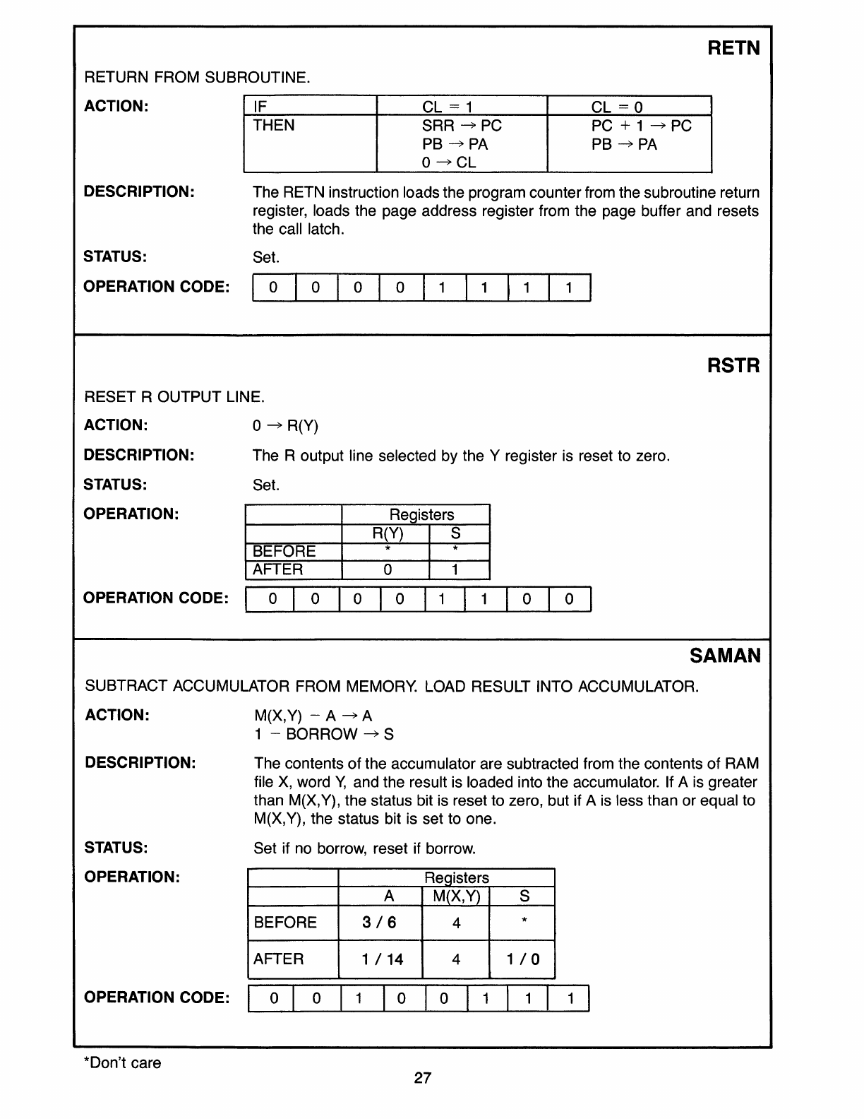
RETN
RETURN FROM SUBROUTINE.
ACTION:
DESCRIPTION:
STATUS:
IF
THEN
CL
= 1
SRR
~
PC
PB
~PA
O~CL
CL
= 0
PC+1~PC
PB
~PA
The RETN instruction loads the program counter from the subroutine return
register, loads the page address register from the page buffer and resets
the call latch.
Set.
OPERATION CODE: I 0 I 0 I 0 I 0 I 1 I 1 I 1 I 1 I
RSTR
RESET
R
OUTPUT
LINE.
ACTION: 0
~
R(Y)
DESCRIPTION:
STATUS:
OPERATION:
The R output line selected by the Y register is reset to zero.
Set.
Registers
R(Y) S
BEFORE * *
AFTER o 1
OPERATION CODE: I 0 I 0 I 0 I 0 I 1 I 1 I 0 I 0 I
SAM
AN
SUBTRACT ACCUMULATOR FROM MEMORY. LOAD RESULT INTO ACCUMULATOR.
ACTION:
DESCRIPTION:
STATUS:
OPERATION:
OPERATION CODE: I
*Don't care
M(X,Y) - A
~A
1 -
BORROW
~
S
The contents
of
the accumulator are subtracted from the contents
of
RAM
file
X,
word
Y,
and the result is loaded into the accumulator. If A is greater
than M(X,Y), the status bit is reset to zero, but if A is less than or equal to
M(X,Y), the status bit is set to one.
Set if no borrow, reset if borrow.
Registers
A M(X,Y) S
BEFORE
3/6
4 *
AFTER
1/14
4
1/0
0 I 0 I 1 I 0 I 0 I 1 I 1 I 1 I
27
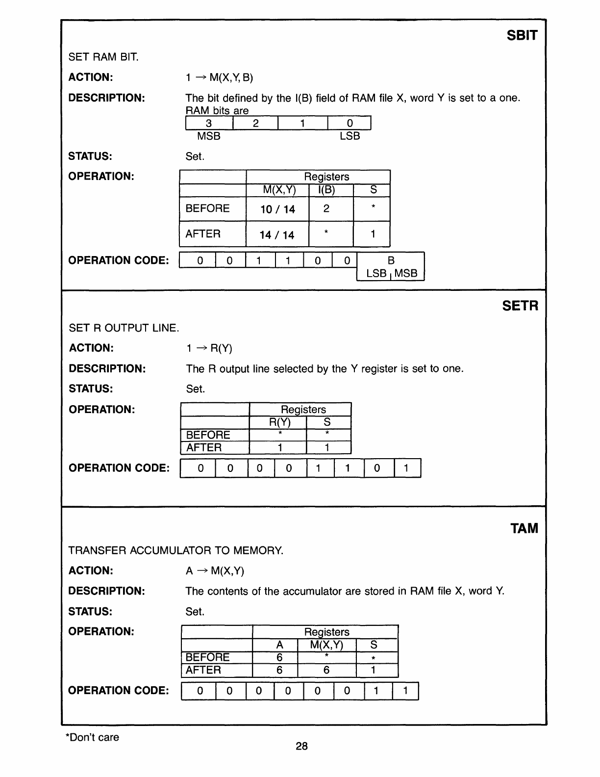
SET
RAM
BIT.
ACTION:
DESCRIPTION:
STATUS:
OPERATION:
OPERATION
CODE:
SET
R OUTPUT LINE.
ACTION:
DESCRIPTION:
STATUS:
OPERATION:
I
SBIT
1
~
M(X,Y, B)
The bit defined by the I(B) field
of
RAM file
X,
word Y is set to a one.
RAM bits are
I 3 I 2 I 1 I 0 I
MSB LSB
Set.
Registers
M(X,Y) I(B) S
BEFORE
10/14
2 *
AFTER
14/14
* 1
0 I 0 I 1 I 1 I 0 I
°1
LSB~MSB
1
1
~
R(Y)
The R output line selected by the Y register is set to one.
Set.
Registers
R(Y) S
BEFORE * *
AFTER 1 1
SETR
OPERATION
CODE:
I 0 I 0 I 0 I 0 I 1 I 1 I ° I 1 I
TRANSFER ACCUMULATOR
TO
MEMORY.
ACTION:
DESCRIPTION:
STATUS:
OPERATION:
A
~
M(X,Y)
The contents of the accumulator are stored in RAM file X, word
Y.
Set.
Registers
A M(X,Y) S
BEFORE 6 * *
AFTER 6 6 1
I 0 I 0 I 0 I 0 1 1 I 1 I
OPERATION
CODE:
1,--_0
____
1 ___ 0
-I..._....a...-~_---'-_--i.-
____
'"_---J
*Don't care
28
TAM
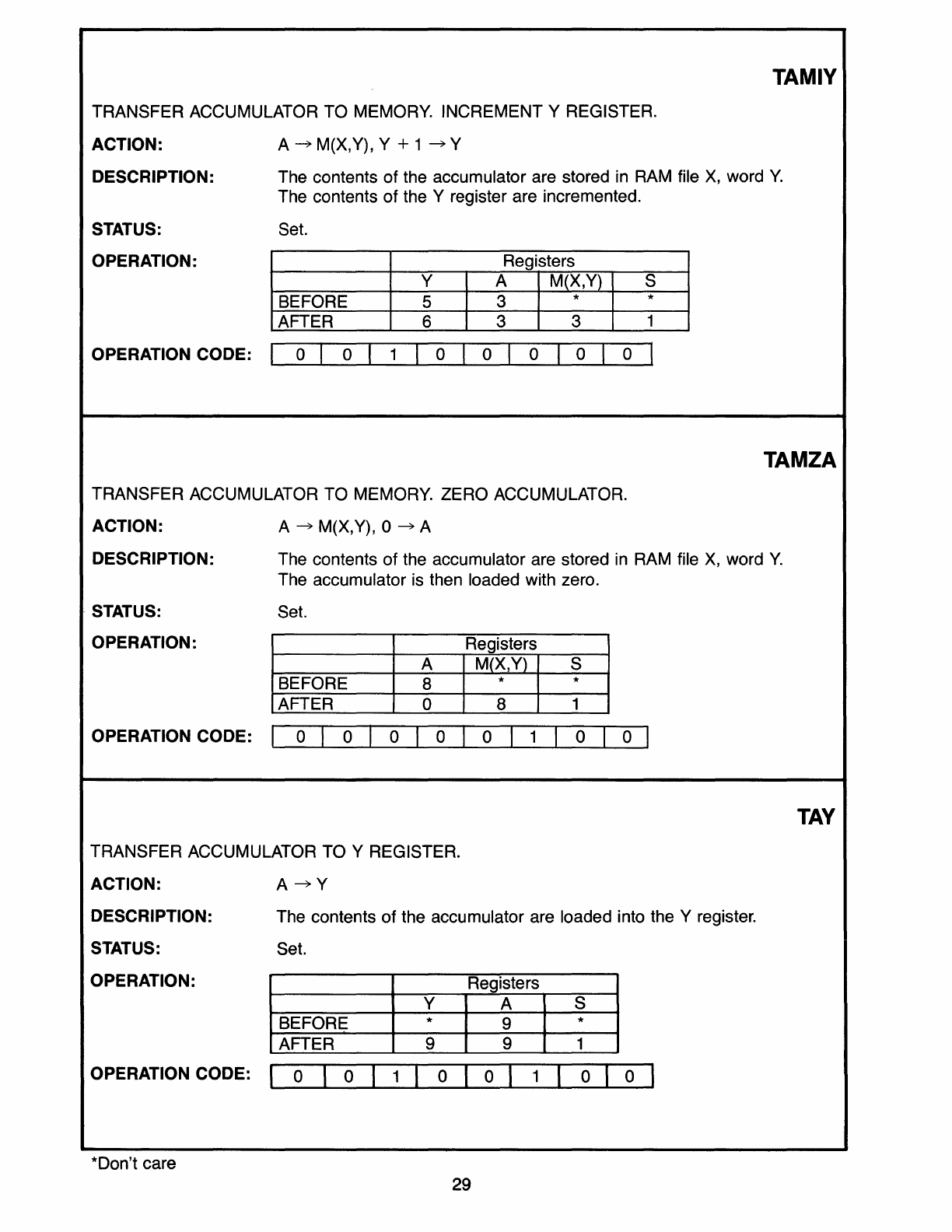
TAMIY
TRANSFER ACCUMULATOR
TO
MEMORY. INCREMENT Y REGISTER.
ACTION:
DESCRIPTION:
STATUS:
OPERATION:
A
~M(X,Y),
Y + 1
~Y
The contents of the accumulator are stored in RAM file
X,
word
Y.
The contents
of
the Y register are incremented.
Set.
Registers
Y A M(X,Y) S
BEFORE 5 3 * *
AFTER 6 3 3 1
I ° I ° I ° 1 ° 1 ° I
OPERATION CODE
:1
L-
_O----l.I_0----L1_1
--L...._.....L.-_.L..------I._----L.._---'
TAMZA
TRANSFER ACCUMULATOR
TO
MEMORY. ZERO ACCUMULATOR.
ACTION:
DESCRIPTION:
STATUS:
OPERATION:
A
~
M(X,Y), °
~A
The contents
of
the accumulator are stored in RAM file
X,
word
Y.
The accumulator is then loaded with zero.
Set.
Registers
A M(X,Y) S
BEFORE 8 * *
AFTER ° 8 1
OPERATION
CODE:
1 ° I ° I ° I ° I ° I 1 I 0 I ° I
TRANSFER ACCUMULATOR
TO
Y REGISTER.
ACTION:
DESCRIPTION:
STATUS:
OPERATION:
A~Y
The contents
of
the accumulator are loaded into the Y register.
Set.
Registers
Y A S
BEFORE * 9 *
AFTER 9 9 1
OPERATION
CODE:
I ° I ° I 1 I ° I 0 I 1 I ° I 0 I
*Oon't care
29
TAY
TBIT1
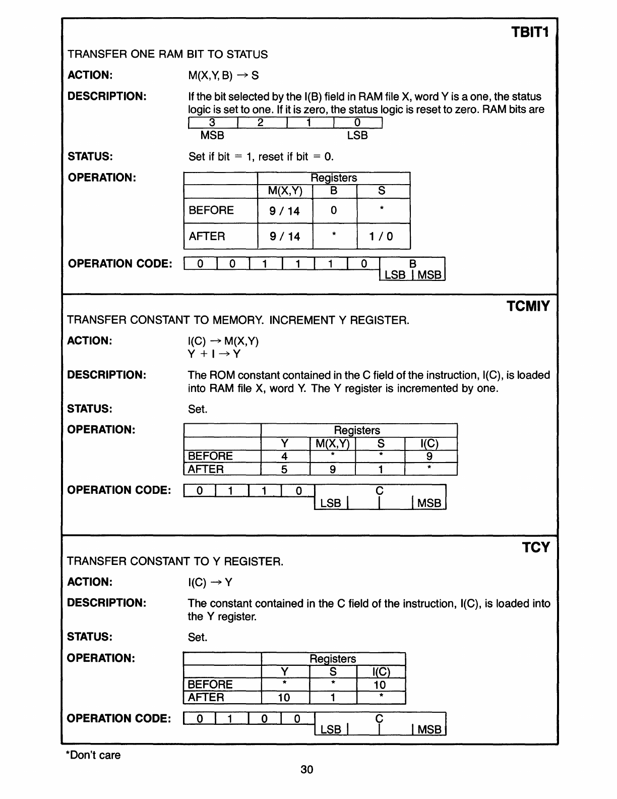
TRANSFER ONE RAM BIT
TO
STATUS
ACTION: M(X,Y,
B)
~
S
DESCRIPTION: If the bit selected by the I(B) field in RAM file
X,
word Y is a one, the status
logic is set to one. If it is zero, the status logic is reset to zero. RAM bits are
I 3 I 2 I 1 I 0 I
MSB LSB
STATUS: Set if bit =
1,
reset if bit =
O.
OPERATION: Registers
M(X,Y) B S
BEFORE
9/14
0 *
AFTER
9/14
*
1/0
OPERATION CODE: I 0 I 0 I 1 I 1 I 1 I 0 I B I
LSB I MSB
TRANSFER CONSTANT TO MEMORY. INCREMENT Y REGISTER.
ACTION: I(C)
~
M(X,Y)
Y +
I~Y
TCMIY
DESCRIPTION: The ROM constant contained
in
the C field
of
the instruction, I(C), is loaded
into RAM file
X,
word
Y.
The Y register is incremented
byone.
STATUS: Set.
OPERATION: Registers
Y M(X,Y) S ITCl
BEFORE 4 * * 9
AFTER 5 9 1 *
I
LSB
I C
IMSBI
I
OPERATION CODE: I 0 I 1 I 1 I 0
TCY
TRANSFER CONSTANT TO Y REGISTER.
ACTION: I(C)
~
Y
DESCRIPTION: The constant contained in the C field
of
the instruction, I(C), is loaded into
the Y register.
STATUS: Set.
OPERATION: Registers
Y S
lie)
BEFORE * * 10
AFTER 10 1 *
OPERATION
CODE:
I 0 I 1 I 0 I 0 I
LSB
I C
IMSBI
I
*Oon't care
30
TRANSFER
DATA
TO OUTPUTS
ACTION: SL,A
~
PLAIR
DESCRIPTION:
STATUS:
OPERATION:
OPERATION CODE:
The status latch and accumulator contents are loaded into the
programmable logic array input register. The 5-bit word selecting
one of the 32 possible output terms is:
I SL I
As
I
A4
I
A2
I
A1
I
MSB LSB
Set.
Registers
SL A PLAIR S
BEFORE
1/0
4/7
*/* *
AFTER
1/0
4/7
36/7
1
I 0 I ° I ° I 0 I 1 I 0 I 1 I 0 I
TRANSFER K INPUTS INTO ACCUMULATOR.
ACTION:
K~A
DESCRIPTION: Data from the four K inputs is loaded into the accumulator.
STATUS: Set.
OPERATION: Registers
A S K
BEFORE * * 6
AFTER 6 1 *
OPERATION CODE: I ° I ° I 0 I 0 I 1 I ° I ° I 0 I
TRANSFER MEMORY TO ACCUMULATOR.
ACTION: M(X,Y)
~
A
TOO
TKA
TMA
DESCRIPTION:
STATUS:
The contents of RAM file
X,
word
Y,
are loaded into the accum'ulator.
Set.
OPERATION: Registers
A M(X,Y) S
BEFORE * 4 *
AFTER 4 4 1
I ° I 0 I 0 1 ° I 1 I
OPERATION CODE: ,-I
_o--...&-I
_0--1...1
_1----L_---L-._.L...-.---L-_--L-----I
*Don't care
31
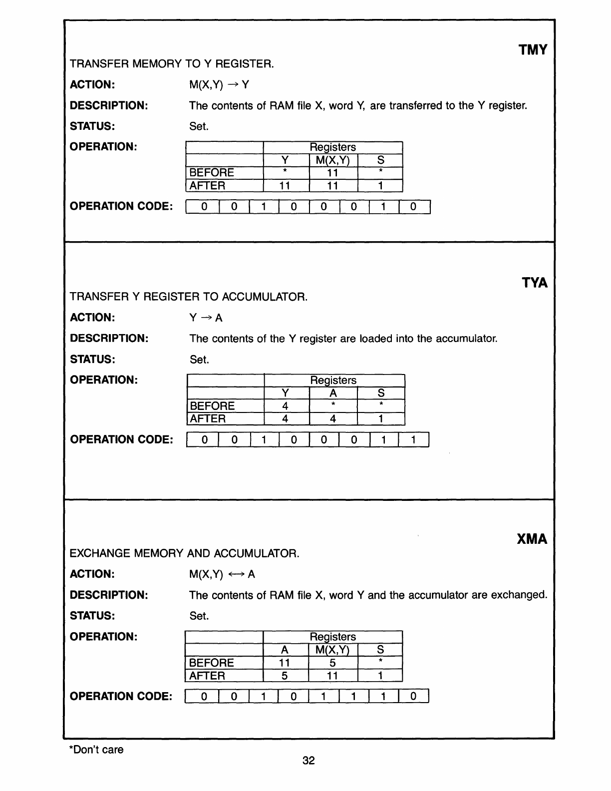
TMV
TRANSFER MEMORY TO Y REGISTER.
ACTION: M(X,Y)
~
Y
DESCRIPTION:
STATUS:
The contents of RAM file
X,
word
Y,
are transferred to the Y register.
Set.
OPERATION: Registers
Y M(X,Y) S
BEFORE *
11
*
AFTER
11 11
1
I ° , ° I ° I 1 I ° I
OPERATION CODE:
1'--_0_''---0----'-,_1
---'--_......1..-_-'-----'-_---'-_---'
TVA
TRANSFER Y REGISTER TO ACCUMULATOR.
ACTION:
Y~A
DESCRIPTION: The contents of the Y register are loaded into the accumulator.
STATUS: Set.
OPERATION: Registers
Y A S
BEFORE 4 * *
AFTER 4 4 1
OPERATION CODE: I ° I ° I 1 I ° I ° I ° I 1 I 1 I
XMA
EXCHANGE MEMORY AND ACCUMULATOR.
ACTION: M(X,Y)
~A
DESCRIPTION:
STATUS:
The contents of RAM file
X,
word Y and the accumulator are exchanged.
Set.
OPERATION: Registers
A M(X,Y) S
BEFORE
11
5 *
AFTER 5
11
1
OPERATION CODE: I ° I ° I 1 I ° I 1 I 1 I 1 I ° ,
*Don't care 32
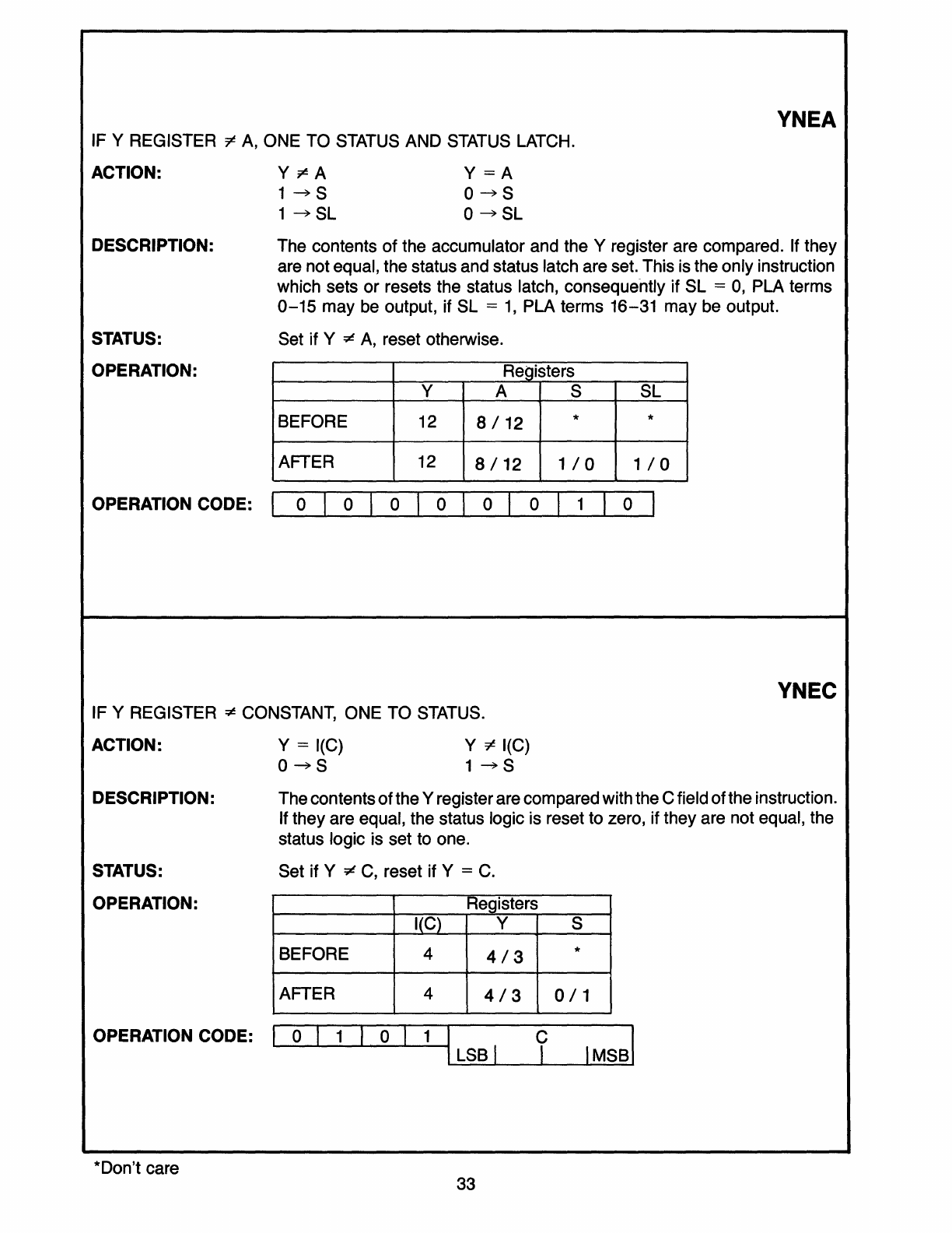
YNEA
IF Y REGISTER
=F-
A,
ONE TO STATUS AND
STATUS
LATCH.
ACTION:
DESCRIPTION:
STATUS:
OPERATION:
OPERATION CODE:
Y~A
1~S
1
~SL
Y=A
O~S
o
~SL
The contents of the accumulator and the Y register are compared. If they
are not equal, the status and status latch are set. This is the only instruction
which sets or resets the status latch, consequently if SL =
0,
PLA terms
0-15
may be output, if SL =
1,
PLA terms 16-31 may be output.
Set if Y
~
A,
reset otherwise.
Registers
Y A S SL
BEFORE 12
8/12
* *
AFTER 12
8/12
1/0 1/0
0 0 0 0 0 0 1 0
YNEC
IF Y REGISTER #- CONSTANT, ONE TO STATUS.
ACTION: Y = I(C) Y
~
I(C)
DESCRIPTION:
STATUS:
OPERATION:
OPERATION CODE:
*Don't care
O~S
1~S
The contents
ofthe
Y register are compared with the C field ofthe instruction.
If they are equal, the status logic is reset to zero, if they are not equal, the
status logic is set to one.
Set if Y ¢
C,
reset if Y =
C.
Registers
I(C) Y S
BEFORE 4
4/3
*
AFTER 4
4/3
0/1
0 1
ILSBI
C
IMSBI
I
o 1
33
APPLICATIONS AND SOFTWARE EXAMPLES
The following hardware
and
software examples illustrate
how
the
MC141000
is
used
in
typical applications. The examples include
BCD
addition
and
subtraction, controlling a display,
monitoring a keypad, interfacing
an
external CMOS memory, and expanding the number of
R-Outputs.
34
BCD Addition and Subtraction Flowchart
ADD
INITIALIZE
Y
(LSD)
= 5
A
(CARRY)
= 0
A +
6~A
A~M
(X,
Y)
1~A
* * ** * * *
*****
** **** * * * * * ** * ** ** ** * * * * * * * ** * ** * * * * * * * * * * * * * * * * * * * * * * * * * * * * ** ** *
BCD
ADDITION
SUBROUTINE
SUMS
TWO
6-DlGIT
BASE
TEN
NUMBERS
LOCATED
IN
Y=O(MSD)
THRU
Y=5(LSD)
OF
COMPLEMENTARY
X
FILES.
THE
AUGEND
IN
X
IS
REPLACED
BY
THE
SUM
AND
THE
ADDEND
IN
X-COMPLEMENT
IS
UNCHANGED.
AN
OVERFLOW
CONDITION
IS
INDICATED
BY
A
CARRY=1
IN
THE
ACCUMULATOR
ON
RETURN.
*****************************************************************************
ADD
CLA
CLEAR
CARRY
TCY
5
ADDRESS
LSD
ADD1
COMX
COMPLEMENT
X
(ADDRESS
ADDEND)
AMAAC
ADDEND
DIGIT
+
CARRY
COMX
ADDRESS
AUGEND
AMAAC
ADD
AUGEND
TO
ACCUMULATOR
BR
CARRY
BRANCH
IF
SUM
CAUSES
CARRY
ALEC
9
VALID
NUMBER?
BR
ADDOK
YES,
BRANCH
CARRY
A6AAC
SUM
GREATER
THAN
10,
ADD
CORRECTION
TAMZA
UNITS
TO
MEMORY,
ZERO
ACCUMULATOR
IA
CARRY
= 1
TO
ACCUMULATOR
ADD2
DYN
DECREMENT
Y
UNTIL
BORROW
BR
ADD1
BRANCH
ON
NO
BORROW
RETN
RETURN
ON
BORROW
ADDOK
TA,MZA
SUM
TO
MEMORY,
ZERO
CARRY
BR
ADD2
BRANCH
TO
ADDRESS
NEXT
DIGIT
35
SUBTRACT
IN
ITIALIZE
Y
(LSD)
= 5
A
(BORROW)
= 0
A+10~A
A~M
(X,
Y)
1
~A
A~M
(X,
Y)
O~A
* * * * ** * * *** * ** * ** ** * ** * * * * * * * * * * * * ** * * * **
****
* * ** ** * * * * * * * * * ** * * * * * * * * * * * * * **
BCD
SUBTRACTION
SUBROUTINE
SUBTRACTS
TWO
6-DIGIT
BASE
TEN
NUMBERS
LOCATED
IN
Y=O
(MSD)
THRU
Y=5
(LSD)
OF
COMPLEMENTARY
X
FILES.
THE
MINUEND
IN
X
IS
REPLACED
BY
THE
DIFFERENCE
AND
THE
SUBTRAHEND
IN
X-COMPLEMENT
IS
UNCHANGED.
AN
UNDERFLOW
CONDITION
IS
INDICATED
BY
A
BORROW
IN
THE
ACCUMULATOR
ON
RETURN.
* * ** ** ** ** * *** ** ** * * * * * * * * * * ** * * * * ** ** ** * * *** * ** ** ** * * ** ** * * * * * * * * * * ** * * * * ** *
SUBT
TCY
5
ADDRESS
LSD
AT
Y=5
CLA
CLEAR
BORROW
SUBT1
COMX
COMPLEMENT
X
REGISTER
AMAAC
ADD
SUBTRAHEND
DIGIT
TO
ACCUMULATOR
COMX
COMPLEMENT
X
SAMAN
SUBTRACT
SUBTRAHEND
FROM
MINUEND
BR
SUBOK
BRANCH
IF
NO
BORROW
A10AAC
ADD
CORRECTION
FACTOR
IF
BORROW
TAMZA
UNITS
TO
MEMORY,
ACCUMULATOR
= 0
IA
SET
BORROW
= 1
SUBT2
DYN
DECREMENT
Y
TO
ADDRESS
NEXT
DIGIT
BR
SUBT1
BRANCH
IF
NO
BORROW
RETN
RETURN
TO
CALLING
ADDRESS
SUBOK
TAMZA
DIFFERENCE
TO
MEMORY,
BORROW
= 0
BR
SUBT2
BRANCH
TO
ADDRESS
NEXT
DIGIT
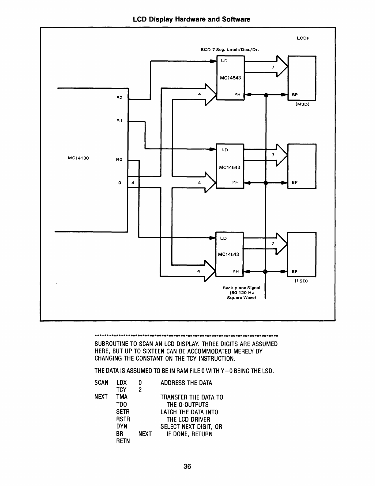
MC14100
LCD Display Hardware and Software
BCD-7
Seg.
Latch/Dec./Dr.
-
LD
7)
-
MC14543
4~
PH --
A2
--
A1
7;
LD
-
AO
~
MC14543
4)
0 4 PH -
--
7J
-
LD
-
MC14543
4)
PH
--
Back
plane
Signal
(50-120
Hz
S
uare
Wave
q
*****************************************************************************
SUBROUTINE
TO
SCAN
AN
LCD
DISPLAY.
THREE
DIGITS
ARE
ASSUMED
HERE,
BUT
UP
TO
SIXTEEN
CAN
BE
ACCOMMODATED
MERELY
BY
CHANGING
THE
CONSTANT
ON
THE
TCY
INSTRUCTION.
THE
DATA
IS
ASSUMED
TO
BE
IN
RAM
FILE
0
WITH
Y=O
BEING
THE
LSD.
SCAN
LOX
0
TCY
2
NEXT
TMA
TOO
SETR
RSTR
DYN
BR
NEXT
RETN
ADDRESS
THE
DATA
TRANSFER
THE
DATA
TO
THE
O-OUTPUTS
LATCH
THE
DATA
INTO
THE
LCD
DRIVER
SELECT
NEXT
DIGIT,
OR
IF
DONE,
RETURN
36
LCDs
BP
(MSD)
BP
BP
(LSD)
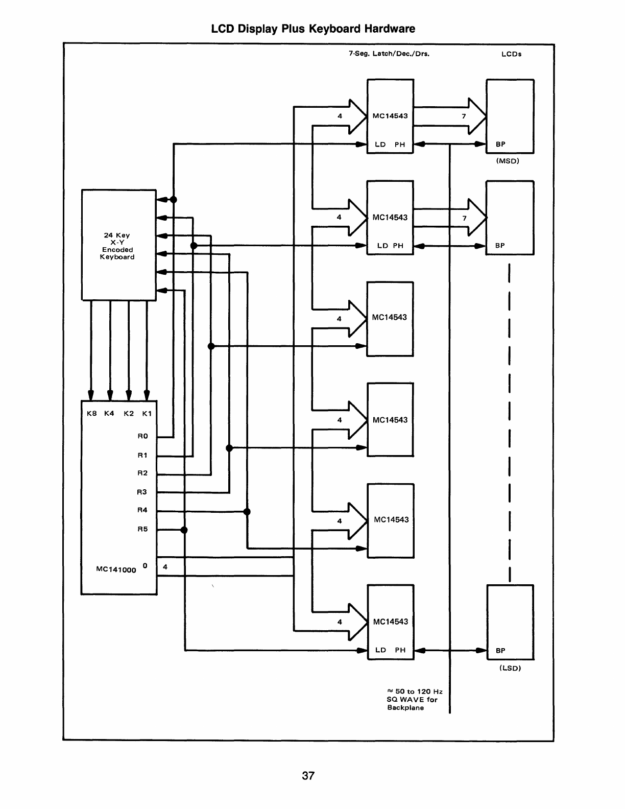
LCD Display Plus Keyboard Hardware
7-Seg.
Latch/Dec./Drs.
LCDs
<>
MC14543
7)
LD
PH
--BP
-- -
(MSD)
~t
4~
7~
MC14543
-
vi
yI
24
Key
-
X-V
-
LD
PH
--
-BP
Encoded
--
Keyboard
-
-
-
-
-
4~
yI
MC14543
-
, I , I ,
It
4~
K8
K4
K2
K1
vi
MC14543
RO I"""- -
R1
R2
R3
R4
4)
MC14543
R5
-
MC141000
0 4
\
4)
MC14543
LD
PH
-BP
- - -
(LSD)
~
50
to
120
Hz
sa
WAVE
for
Backplane
37
Software
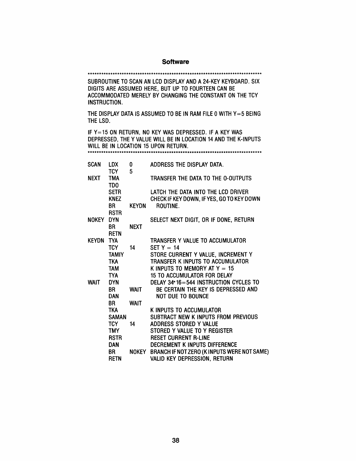
*****************************************************************************
SUBROUTINE
TO
SCAN
AN
LCD
DISPLAY
AND
A
24-KEY
KEYBOARD.
SIX
DIGITS
ARE
ASSUMED
HERE,
BUT
UP
TO
FOURTEEN
CAN
BE
ACCOMMODATED
MERELY
BY
CHANGING
THE
CONSTANT
ON
THE
TCY
INSTRUCTION.
THE
DISPLAY
DATA
IS
ASSUMED
TO
BE
IN
RAM
FILE
0
WITH
Y=5
BEING
THE
LSD.
IF
Y=15
ON
RETURN,
NO
KEY
WAS
DEPRESSED.
IF
A
KEY
WAS
DEPRESSED,
THE
Y
VALUE
WILL
BE
IN
LOCATION
14
AND
THE
K-INPUTS
WILL
BE
IN
LOCATION
15
UPON
RETURN.
*****************************************************************************
SCAN
LOX
0
ADDRESS
THE
DISPLAY
DATA.
TCY
5
NEXT
TMA
TRANSFER
THE
DATA
TO
THE
O-OUTPUTS
TDO
SETR
LATCH
THE
DATA
INTO
THE
LCD
DRIVER
KNEZ
CHECK
IF
KEY
DOWN,
IFYES,
GO
TO
KEY
DOWN
BR
KEYDN
ROUTINE.
RSTR
NOKEY
DYN
SELECT
NEXT
DIGIT,
OR
IF
DONE,
RETURN
BR
NEXT
RETN
KEYDN
TVA
TRANSFER
Y
VALUE
TO
ACCUMULATOR
TCY
14
SET
Y =
14
TAMIY
STORE
CURRENT
Y
VALUE,
INCREMENT
Y
TKA
TRANSFER
K
INPUTS
TO
ACCUMULATOR
TAM
K
INPUTS
TO
MEMORY
AT
Y =
15
TVA
15
TO
ACCUMULATOR
FOR
DELAY
WAIT
DYN
DELAY
34*16=544
INSTRUCTION
CYCLES
TO
BR
WAIT
BE
CERTAIN
THE
KEY
IS
DEPRESSED
AND
DAN
NOT
DUE
TO
BOUNCE
BR
WAIT
TKA
K
INPUTS
TO
ACCUMULATOR
SAMAN
SUBTRACT
NEW
K
INPUTS
FROM
PREVIOUS
TCY
14
ADDRESS
STORED
Y
VALUE
TMY
STORED
Y
VALUE
TO
Y
REGISTER
RSTR
RESET
CURRENT
R-LiNE
DAN
DECREMENT
K
INPUTS
DIFFERENCE
BR
NOKEY
BRANCH
IF
NOTZERO
(K
INPUTS
WERE
NOT
SAME)
RETN
VALID
KEY
DEPRESSION,
RETURN
38
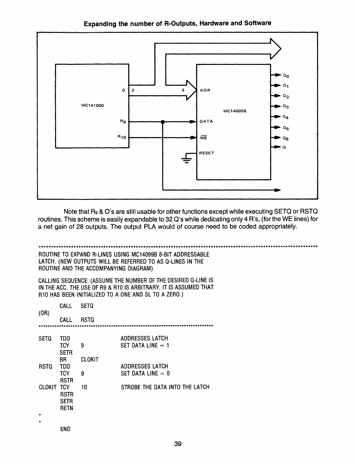
Expanding the number of R-Outputs, Hardware and Software
QO
Q1
0 3 3
ADR
Q2
MC141000
Q3
MC14099B
Q4
R9 DATA
Q5
R10
We
Q6
Q
RESET
-
Note that
R9
&
D's
are still usable for
other
functions
except
while executing
SETQ
or
RSTQ
routines. This scheme is easily expandable to
32
Q's
while dedicating only 4 R's, (for the
WE
lines) for
a net gain
of
28
outputs.
The
output
PLA
would
of
course need to be coded appropriately.
*********************************************w******************************************************************
ROUTINE
TO
EXPAND
R-LiNES
USING
MC14099B
8-BIT
ADDRESSABLE
LATCH.
(NEW
OUTPUTS
WILL
BE
REFERRED
TO
AS
a-LINES
IN
THE
ROUTINE
AND
THE
ACCOMPANYING
DIAGRAM)
CALLING
SEaUENCE:
(ASSUME
THE
NUMBER
OF
THE
DESIRED
a-LINE
IS
IN
THE
ACC.
THE
USE
OF
R9
&
R10
IS
ARBITRARY.
IT
IS
ASSUMED
THAT
R10
HAS
BEEN
INITIALIZED
TO
A
ONE
AND
SL
TO
A
ZERO.)
CALL
SETa
(OR)
CALL
RSTa
*****************************************************************************
SETa
TDO
ADDRESSES
LATCH
TCY
9
SET
DATA
LINE
= 1
SETR
BR
CLOKIT
RSTa
TDO
ADDRESSES
LATCH
TCY
9
SET
DATA
LINE
= 0
RSTR
CLOKIT
TCY
10
STROBE
THE
DATA
INTO
THE
LATCH
RSTR
SETR
RETN
*
*
END
39
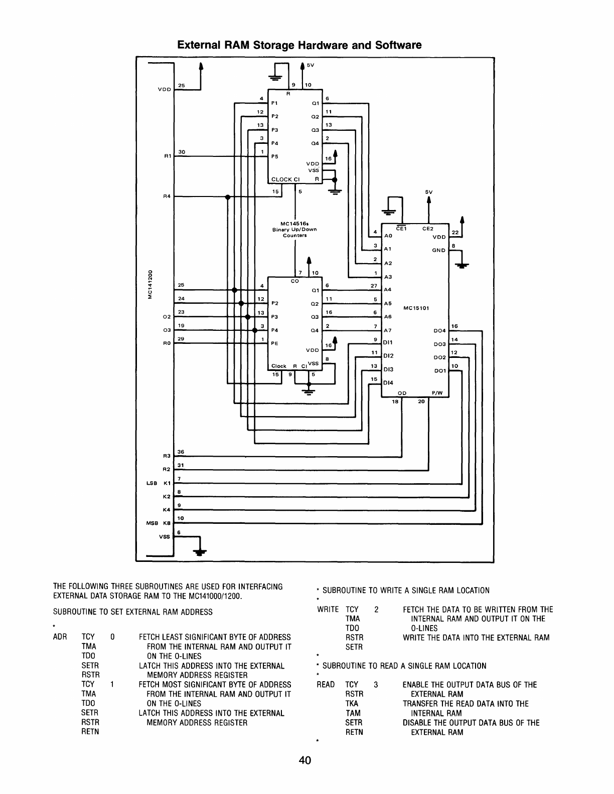
External RAM Storage Hardware and Software
-U
J:l,
["
VDD
R
4 6
P1
Q1
12
11
r---
P2
Q2
13 13
,....-
P3
Q3
3 2
,..-
P4
Q4
f---
30
1
R1
P5
W
VDD
CLOCK
CI
v~~
151
5
5V
R4
Ll
f
MC14516s
Binary
Up/Down
4
CE1
m
lJ
22
Counters
I...-
AO
VDD
3
A1
Il
i-o..-
GND
7
1,0
~
A2
1
A3
CO
25
4 6
27
Q1
A4
24
12
11
5
P2
Q2
A5
23
13 16
MC15101
6
02
P3
Q3
A6
19
3 2 7
16
03
P4
Q4
A7
D04
29
1 W 9
011
~
RO
PE
D03
VDD
11
12
8
...--
012
D02
~
Clock
R
CI
VSS
1
.......!!..
013
~
15
1 9
15
D01
15
014
~
,..-
OD
P/W
18
20
36
R3
31
R2
7
LSB
K1
8
K2
9
K4
10
MSB
K8
VSS
h
-
THE
FOLLOWING
THREE
SUBROUTINES
ARE
USED
FOR
INTERFACING
EXTERNAL
DATA
STORAGE
RAM
TO
THE
MC141000/1200.
•
SUBROUTINE
TO
WRITE
A
SINGLE
RAM
LOCATION
SUBROUTINE
TO
SET
EXTERNAL
RAM
ADDRESS
ADR
TCY
0
TMA
TDO
SETR
RSTR
TCY
TMA
TDO
SETR
RSTR
RETN
FETCH
LEAST
SIGNIFICANT
BYTE
OF
ADDRESS
FROM
THE
INTERNAL
RAM
AND
OUTPUT
IT
ON
THE
O-LiNES
LATCH
THIS
ADDRESS
INTO
THE
EXTERNAL
MEMORY
ADDRESS
REGISTER
FETCH
MOST
SIGNIFICANT
BYTE
OF
ADDRESS
FROM
THE
INTERNAL
RAM
AND
OUTPUT
IT
ON
THE
O-LiNES
LATCH
THIS
ADDRESS
INTO
THE
EXTERNAL
MEMORY
ADDRESS
REGISTER
40
WRITE
TCY
2
TMA
TDO
RSTR
SETA
FETCH
THE
DATA
TO
BE
WRIDEN
FROM
THE
INTERNAL
RAM
AND
OUTPUT
IT
ON
THE
O-LiNES
WRITE
THE
DATA
INTO
THE
EXTERNAL
RAM
*
SUBROUTINE
TO
READ
A
SINGLE
RAM
LOCATION
READ
TCY
3
RSTR
TKA
TAM
SETR
RETN
ENABLE
THE
OUTPUT
DATA
BUS
OF
THE
EXTERNAL
RAM
TRANSFER
THE
READ
DATA
INTO
THE
INTERNAL
RAM
DISABLE
THE
OUTPUT
DATA
BUS
OF
THE
EXTERNAL
RAM