MC68HC08AZ60, MC68HC08AZ48 Data Sheet MC68HC08AZ60
User Manual: MC68HC08AZ60
Open the PDF directly: View PDF ![]() .
.
Page Count: 472 [warning: Documents this large are best viewed by clicking the View PDF Link!]
- List of Paragraphs
- Table of Contents
- List of Figures
- List of Tables
- Section 1. General Description
- 1.1 Contents
- 1.2 Introduction
- 1.3 Features
- 1.4 MCU Block Diagram
- 1.5 Pin Assignments
- 1.5.1 Power Supply Pins (VDD and VSS)
- 1.5.2 Oscillator Pins (OSC1 and OSC2)
- 1.5.3 External Reset Pin (RST)
- 1.5.4 External Interrupt Pin (IRQ)
- 1.5.5 Analog Power Supply Pin (VDDA)
- 1.5.6 Analog Ground Pin (VSSA)
- 1.5.7 External Filter Capacitor Pin (CGMXFC)
- 1.5.8 Port A Input/Output (I/O) Pins (PTA7-PTA0)
- 1.5.9 Port B I/O Pins (PTB7/ATD7-PTB0/ATD0)
- 1.5.10 Port C I/O Pins (PTC5-PTC0)
- 1.5.11 Port D I/O Pins (PTD7-PTD0/ATD8)
- 1.5.12 Port E I/O Pins (PTE7/SPSCK-PTE0/TxD)
- 1.5.13 Port F I/O Pins (PTF6-PTF0/TACH2)
- 1.5.14 Port G I/O Pins (PTG2/KBD2-PTG0/KBD0)
- 1.5.15 Port H I/O Pins (PTH1/KBD4-PTH0/KBD3)
- 1.5.16 CAN Transmit Pin (CANTx)
- 1.5.17 CAN Receive Pin (CANRx)
- 1.6 Ordering Information
- Section 2. Memory Map
- Section 3. RAM
- Section 4. ROM-1 Memory
- Section 5. ROM-2 Memory
- Section 6. EEPROM-1
- Section 7. EEPROM-2
- Section 8. Central Processing Unit (CPU)
- Section 9. System Integration Module (SIM)
- Section 10. Clock Generation Module (CGM)
- 10.1 Contents
- 10.2 Introduction
- 10.3 Features
- 10.4 Functional Description
- 10.5 I/O Signals
- 10.5.1 Crystal Amplifier Input Pin (OSC1)
- 10.5.2 Crystal Amplifier Output Pin (OSC2)
- 10.5.3 External Filter Capacitor Pin (CGMXFC)
- 10.5.4 Analog Power Pin (VDDA)
- 10.5.5 Oscillator Enable Signal (SIMOSCEN)
- 10.5.6 Crystal Output Frequency Signal (CGMXCLK)
- 10.5.7 CGM Base Clock Output (CGMOUT)
- 10.5.8 CGM CPU Interrupt (CGMINT)
- 10.6 CGM Registers
- 10.7 Interrupts
- 10.8 Low-Power Modes
- 10.9 CGM During Break Interrupts
- 10.10 Acquisition/Lock Time Specifications
- Section 11. Mask Options
- Section 12. Break Module (BRK)
- Section 13. Monitor ROM (MON)
- Section 14. Computer Operating Properly (COP)
- Section 15. Low Voltage Inhibit (LVI)
- Section 16. External Interrupt (IRQ)
- Section 17. Serial Communications Interface (SCI)
- Section 18. Serial Peripheral Interface (SPI)
- 18.1 Contents
- 18.2 Introduction
- 18.3 Features
- 18.4 Pin Name Conventions and I/O Register Addresses
- 18.5 Functional Description
- 18.6 Transmission Formats
- 18.7 Interrupts
- 18.8 Queuing Transmission Data
- 18.9 Resetting the SPI
- 18.10 Low-Power Modes
- 18.11 SPI During Break Interrupts
- 18.12 I/O Signals
- 18.13 I/O Registers
- Section 19. Timer Interface Module B (TIMB)
- Section 20. Programmable Interrupt Timer (PIT)
- Section 21. Input/Output Ports
- Section 22. MSCAN Controller (MSCAN08)
- 22.1 Contents
- 22.2 Introduction
- 22.3 Features
- 22.4 External Pins
- 22.5 Message Storage
- 22.6 Identifier Acceptance Filter
- 22.7 Interrupts
- 22.8 Protocol Violation Protection
- 22.9 Low Power Modes
- 22.10 Timer Link
- 22.11 Clock System
- 22.12 Memory Map
- 22.13 Programmer’s Model of Message Storage
- 22.14 Programmer’s Model of Control Registers
- 22.14.1 MSCAN08 Module Control Register 0
- 22.14.2 MSCAN08 Module Control Register 1
- 22.14.3 MSCAN08 Bus Timing Register 0
- 22.14.4 MSCAN08 Bus Timing Register 1
- 22.14.5 MSCAN08 Receiver Flag Register (CRFLG)
- 22.14.6 MSCAN08 Receiver Interrupt Enable Register
- 22.14.7 MSCAN08 Transmitter Flag Register
- 22.14.8 MSCAN08 Transmitter Control Register
- 22.14.9 MSCAN08 Identifier Acceptance Control Register
- 22.14.10 MSCAN08 Receive Error Counter
- 22.14.11 MSCAN08 Transmit Error Counter
- 22.14.12 MSCAN08 Identifier Acceptance Registers
- 22.14.13 MSCAN08 Identifier Mask Registers (CIDMR0-3)
- Section 23. Keyboard Module (KBD)
- Section 24. Timer Interface Module A (TIMA)
- Section 25. Analog-to-Digital Converter (ADC-15)
- Section 26. Electrical Specifications
- 26.1 Contents
- 26.2 Electrical Specifications
- 26.2.1 Maximum Ratings
- 26.2.2 Functional Operating Range
- 26.2.3 Thermal Characteristics
- 26.2.4 5.0 Volt DC Electrical Characteristics
- 26.2.5 Control Timing
- 26.2.6 ADC Characteristics
- 26.2.7 5.0 Vdc ± 0.5 V Serial Peripheral Interface (SPI) Timing
- 26.2.8 CGM Operating Conditions
- 26.2.9 CGM Component Information
- 26.2.10 CGM Acquisition/Lock Time Information
- 26.2.11 Timer Module Characteristics
- 26.2.12 Memory Characteristics
- 26.3 Mechanical Specifications
- Section 27. Appendix: Future EEPROM Registers
- Section 28. Appendix: HC08AZ48 Memory Map
- Glossary
- Revision History

M68HC08
Microcontrollers
freescale.com
MC68HC08AZ60
Data Sheet
Rev. 1.1
MC68HC08AZ60/D
July 14, 2005

MC68HC08AZ60 — Rev 1.1 Technical Data
Freescale Semiconductor 3
MC68HC08AZ60
MC68HC08AZ48
Technical Data — Rev 1.1
Freescale reserves the right to make changes without further notice to any products
herein. Freescale makes no warranty, representation or guarantee regarding the
suitability of its products for any particular purpose, nor does Freescale assume any
liability arising out of the application or use of any product or circuit, and specifically
disclaims any and all liability, including without limitation consequential or incidental
damages. "Typical" parameters which may be provided in Freescale data sheets
and/or specifications can and do vary in different applications and actual performance
may vary over time. All operating parameters, including "Typicals" must be validated
for each customer application by customer's technical experts. Freescale does not
convey any license under its patent rights nor the rights of others. Freescale products
are not designed, intended, or authorized for use as components in systems intended
for surgical implant into the body, or other applications intended to support or sustain
life, or for any other application in which the failure of the Freescale product could
create a situation where personal injury or death may occur. Should Buyer purchase or
use Freescale products for any such unintended or unauthorized application, Buyer
shall indemnify and hold Freescale and its officers, employees, subsidiaries, affiliates,
and distributors harmless against all claims, costs, damages, and expenses, and
reasonable attorney fees arising out of, directly or indirectly, any claim of personal
injury or death associated with such unintended or unauthorized use, even if such claim
alleges that Freescale was negligent regarding the design or manufacture of the part.
Freescale, Inc. is an Equal Opportunity/Affirmative Action Employer.
.© Freescale, Inc., 2005

Technical Data MC68HC08AZ60 — Rev 1.1
4Freescale Semiconductor

MC68HC08AZ60 — Rev 1.1 Technical Data
Freescale Semiconductor List of Paragraphs 5
Technical Data — MC68HC08AZ60
List of Paragraphs
List of Paragraphs. . . . . . . . . . . . . . . . . . . . . . . . . . . . . . . .3
Table of Contents . . . . . . . . . . . . . . . . . . . . . . . . . . . . . . . .5
List of Figures . . . . . . . . . . . . . . . . . . . . . . . . . . . . . . . . . .15
List of Tables. . . . . . . . . . . . . . . . . . . . . . . . . . . . . . . . . . .21
Section 1. General Description . . . . . . . . . . . . . . . . . . . .25
Section 2. Memory Map . . . . . . . . . . . . . . . . . . . . . . . . . .37
Section 3. RAM . . . . . . . . . . . . . . . . . . . . . . . . . . . . . . . . .49
Section 4. ROM-1 Memory . . . . . . . . . . . . . . . . . . . . . . . .51
Section 5. ROM-2 Memory . . . . . . . . . . . . . . . . . . . . . . . .53
Section 6. EEPROM-1 . . . . . . . . . . . . . . . . . . . . . . . . . . . .55
Section 7. EEPROM-2 . . . . . . . . . . . . . . . . . . . . . . . . . . . .67
Section 8. Central Processing Unit (CPU) . . . . . . . . . . .79
Section 9. System Integration Module (SIM) . . . . . . . . .97
Section 10. Clock Generation Module (CGM). . . . . . . .121
Section 11. Mask Options. . . . . . . . . . . . . . . . . . . . . . . .149
Section 12. Break Module (BRK) . . . . . . . . . . . . . . . . . .153
Section 13. Monitor ROM (MON) . . . . . . . . . . . . . . . . . .159
Section 14. Computer Operating Properly (COP) . . . .171
Section 15. Low Voltage Inhibit (LVI) . . . . . . . . . . . . . .177
Section 16. External Interrupt (IRQ) . . . . . . . . . . . . . . .183

List of Paragraphs
Technical Data MC68HC08AZ60 — Rev 1.1
6 List of Paragraphs Freescale Semiconductor
Section 17. Serial Communications Interface (SCI). . .191
Section 18. Serial Peripheral Interface (SPI). . . . . . . . .231
Section 19. Timer Interface Module B (TIMB). . . . . . . .263
Section 20. Modulo Timer (TIM). . . . . . . . . . . . . . . . . . .289
Section 21. Input/Output Ports . . . . . . . . . . . . . . . . . . .299
Section 22. MSCAN Controller (MSCAN08) . . . . . . . . .325
Section 23. Keyboard Module (KBD). . . . . . . . . . . . . . .375
Section 24. Timer Interface Module A (TIMA). . . . . . . .385
Section 25. Analog-to-Digital Converter (ADC-15). . . .417
Section 26. Electrical Specifications. . . . . . . . . . . . . . .429
Section 27. Appendix: Future EEPROM Registers . . .443
Section 28. Appendix: HC08AZ48 Memory Map. . . . . .447
Glossary. . . . . . . . . . . . . . . . . . . . . . . . . . . . . . . . . . . . . .461
Revision History . . . . . . . . . . . . . . . . . . . . . . . . . . . . . . .471

MC68HC08AZ60 — Rev 1.1 Technical Data
Freescale Semiconductor Table of Contents 7
Technical Data — MC68HC08AZ60
Table of Contents
List of Paragraphs
Table of Contents
List of Figures
List of Tables
Section 1. General Description
1.1 Contents . . . . . . . . . . . . . . . . . . . . . . . . . . . . . . . . . . . . . . . . . .25
1.2 Introduction. . . . . . . . . . . . . . . . . . . . . . . . . . . . . . . . . . . . . . . .26
1.3 Features . . . . . . . . . . . . . . . . . . . . . . . . . . . . . . . . . . . . . . . . . .26
1.4 MCU Block Diagram . . . . . . . . . . . . . . . . . . . . . . . . . . . . . . . . .27
1.5 Pin Assignments. . . . . . . . . . . . . . . . . . . . . . . . . . . . . . . . . . . .29
1.6 Ordering Information. . . . . . . . . . . . . . . . . . . . . . . . . . . . . . . . .36
Section 2. Memory Map
2.1 Contents . . . . . . . . . . . . . . . . . . . . . . . . . . . . . . . . . . . . . . . . . .37
2.2 Introduction. . . . . . . . . . . . . . . . . . . . . . . . . . . . . . . . . . . . . . . .37
2.3 I/O Section . . . . . . . . . . . . . . . . . . . . . . . . . . . . . . . . . . . . . . . .40
Section 3. RAM
3.1 Contents . . . . . . . . . . . . . . . . . . . . . . . . . . . . . . . . . . . . . . . . . .49
3.2 Introduction. . . . . . . . . . . . . . . . . . . . . . . . . . . . . . . . . . . . . . . .49
3.3 Functional Description . . . . . . . . . . . . . . . . . . . . . . . . . . . . . . .49

Table of Contents
Technical Data MC68HC08AZ60 — Rev 1.1
8 Table of Contents Freescale Semiconductor
Section 4. ROM-1 Memory
4.1 Contents . . . . . . . . . . . . . . . . . . . . . . . . . . . . . . . . . . . . . . . . . .51
4.2 Introduction. . . . . . . . . . . . . . . . . . . . . . . . . . . . . . . . . . . . . . . .51
4.3 Functional Description . . . . . . . . . . . . . . . . . . . . . . . . . . . . . . .51
4.4 Low-Power Modes . . . . . . . . . . . . . . . . . . . . . . . . . . . . . . . . . .52
Section 5. ROM-2 Memory
5.1 Contents . . . . . . . . . . . . . . . . . . . . . . . . . . . . . . . . . . . . . . . . . .53
5.2 Introduction. . . . . . . . . . . . . . . . . . . . . . . . . . . . . . . . . . . . . . . .53
5.3 Functional Description . . . . . . . . . . . . . . . . . . . . . . . . . . . . . . .53
5.4 Low-Power Modes . . . . . . . . . . . . . . . . . . . . . . . . . . . . . . . . . .54
Section 6. EEPROM-1
6.1 Contents . . . . . . . . . . . . . . . . . . . . . . . . . . . . . . . . . . . . . . . . . .55
6.2 Introduction. . . . . . . . . . . . . . . . . . . . . . . . . . . . . . . . . . . . . . . .55
6.3 Future EEPROM Memory. . . . . . . . . . . . . . . . . . . . . . . . . . . . .56
6.4 Features . . . . . . . . . . . . . . . . . . . . . . . . . . . . . . . . . . . . . . . . . .56
6.5 Functional Description . . . . . . . . . . . . . . . . . . . . . . . . . . . . . . .56
6.6 Low-Power Modes . . . . . . . . . . . . . . . . . . . . . . . . . . . . . . . . . .66
Section 7. EEPROM-2
7.1 Contents . . . . . . . . . . . . . . . . . . . . . . . . . . . . . . . . . . . . . . . . . .67
7.2 Introduction. . . . . . . . . . . . . . . . . . . . . . . . . . . . . . . . . . . . . . . .67
7.3 Future EEPROM Memory. . . . . . . . . . . . . . . . . . . . . . . . . . . . .68
7.4 Features . . . . . . . . . . . . . . . . . . . . . . . . . . . . . . . . . . . . . . . . . .68
7.5 Functional Description . . . . . . . . . . . . . . . . . . . . . . . . . . . . . . .68
7.6 Low-Power Modes . . . . . . . . . . . . . . . . . . . . . . . . . . . . . . . . . .78

Table of Contents
MC68HC08AZ60 — Rev 1.1 Technical Data
Freescale Semiconductor Table of Contents 9
Section 8. Central Processing Unit (CPU)
8.1 Contents . . . . . . . . . . . . . . . . . . . . . . . . . . . . . . . . . . . . . . . . . .79
8.2 Introduction. . . . . . . . . . . . . . . . . . . . . . . . . . . . . . . . . . . . . . . .79
8.3 Features . . . . . . . . . . . . . . . . . . . . . . . . . . . . . . . . . . . . . . . . . .80
8.4 CPU registers . . . . . . . . . . . . . . . . . . . . . . . . . . . . . . . . . . . . . .80
8.5 Arithmetic/logic unit (ALU) . . . . . . . . . . . . . . . . . . . . . . . . . . . .86
8.6 Low-power modes . . . . . . . . . . . . . . . . . . . . . . . . . . . . . . . . . .86
8.7 CPU during break interrupts . . . . . . . . . . . . . . . . . . . . . . . . . . .87
8.8 Instruction Set Summary . . . . . . . . . . . . . . . . . . . . . . . . . . . . .87
8.9 Opcode Map . . . . . . . . . . . . . . . . . . . . . . . . . . . . . . . . . . . . . . .95
Section 9. System Integration Module (SIM)
9.1 Contents . . . . . . . . . . . . . . . . . . . . . . . . . . . . . . . . . . . . . . . . . .97
9.2 Introduction. . . . . . . . . . . . . . . . . . . . . . . . . . . . . . . . . . . . . . . .98
9.3 SIM Bus Clock Control and Generation . . . . . . . . . . . . . . . . .100
9.4 Reset and System Initialization. . . . . . . . . . . . . . . . . . . . . . . .102
9.5 SIM Counter . . . . . . . . . . . . . . . . . . . . . . . . . . . . . . . . . . . . . .106
9.6 Program Exception Control. . . . . . . . . . . . . . . . . . . . . . . . . . .107
9.7 Low-Power Modes . . . . . . . . . . . . . . . . . . . . . . . . . . . . . . . . .112
9.8 SIM Registers . . . . . . . . . . . . . . . . . . . . . . . . . . . . . . . . . . . . .116
Section 10. Clock Generation Module (CGM)
10.1 Contents . . . . . . . . . . . . . . . . . . . . . . . . . . . . . . . . . . . . . . . . .121
10.2 Introduction. . . . . . . . . . . . . . . . . . . . . . . . . . . . . . . . . . . . . . .122
10.3 Features . . . . . . . . . . . . . . . . . . . . . . . . . . . . . . . . . . . . . . . . .122
10.4 Functional Description . . . . . . . . . . . . . . . . . . . . . . . . . . . . . .123
10.5 I/O Signals . . . . . . . . . . . . . . . . . . . . . . . . . . . . . . . . . . . . . . .134

Table of Contents
Technical Data MC68HC08AZ60 — Rev 1.1
10 Table of Contents Freescale Semiconductor
10.6 CGM Registers . . . . . . . . . . . . . . . . . . . . . . . . . . . . . . . . . . . .136
10.7 Interrupts . . . . . . . . . . . . . . . . . . . . . . . . . . . . . . . . . . . . . . . .142
10.8 Low-Power Modes . . . . . . . . . . . . . . . . . . . . . . . . . . . . . . . . .142
10.9 CGM During Break Interrupts . . . . . . . . . . . . . . . . . . . . . . . . .143
10.10 Acquisition/Lock Time Specifications . . . . . . . . . . . . . . . . . . .143
Section 11. Mask Options
11.1 Contents . . . . . . . . . . . . . . . . . . . . . . . . . . . . . . . . . . . . . . . . .149
11.2 Introduction. . . . . . . . . . . . . . . . . . . . . . . . . . . . . . . . . . . . . . .149
11.3 Functional Description . . . . . . . . . . . . . . . . . . . . . . . . . . . . . .149
11.4 Mask Option Register . . . . . . . . . . . . . . . . . . . . . . . . . . . . . .150
Section 12. Break Module (BRK)
12.1 Contents . . . . . . . . . . . . . . . . . . . . . . . . . . . . . . . . . . . . . . . . .153
12.2 Introduction. . . . . . . . . . . . . . . . . . . . . . . . . . . . . . . . . . . . . . .153
12.3 Features . . . . . . . . . . . . . . . . . . . . . . . . . . . . . . . . . . . . . . . . .153
12.4 Functional Description . . . . . . . . . . . . . . . . . . . . . . . . . . . . . .154
12.5 Low-Power Modes . . . . . . . . . . . . . . . . . . . . . . . . . . . . . . . . .156
12.6 Break Module Registers . . . . . . . . . . . . . . . . . . . . . . . . . . . . .157
Section 13. Monitor ROM (MON)
13.1 Contents . . . . . . . . . . . . . . . . . . . . . . . . . . . . . . . . . . . . . . . . .159
13.2 Introduction. . . . . . . . . . . . . . . . . . . . . . . . . . . . . . . . . . . . . . .159
13.3 Features . . . . . . . . . . . . . . . . . . . . . . . . . . . . . . . . . . . . . . . . .160
13.4 Functional Description . . . . . . . . . . . . . . . . . . . . . . . . . . . . . .160

Table of Contents
MC68HC08AZ60 — Rev 1.1 Technical Data
Freescale Semiconductor Table of Contents 11
Section 14. Computer Operating Properly (COP)
14.1 Contents . . . . . . . . . . . . . . . . . . . . . . . . . . . . . . . . . . . . . . . . .171
14.2 Introduction. . . . . . . . . . . . . . . . . . . . . . . . . . . . . . . . . . . . . . .171
14.3 Functional Description . . . . . . . . . . . . . . . . . . . . . . . . . . . . . .172
14.4 I/O Signals . . . . . . . . . . . . . . . . . . . . . . . . . . . . . . . . . . . . . . .173
14.5 COP Control Register. . . . . . . . . . . . . . . . . . . . . . . . . . . . . . .175
14.6 Interrupts. . . . . . . . . . . . . . . . . . . . . . . . . . . . . . . . . . . . . . . . .175
14.7 Monitor Mode . . . . . . . . . . . . . . . . . . . . . . . . . . . . . . . . . . . . .175
14.8 Low-Power Modes . . . . . . . . . . . . . . . . . . . . . . . . . . . . . . . . .175
14.9 COP Module During Break Interrupts. . . . . . . . . . . . . . . . . . .176
Section 15. Low Voltage Inhibit (LVI)
15.1 Contents . . . . . . . . . . . . . . . . . . . . . . . . . . . . . . . . . . . . . . . . .177
15.2 Introduction. . . . . . . . . . . . . . . . . . . . . . . . . . . . . . . . . . . . . . .177
15.3 Features . . . . . . . . . . . . . . . . . . . . . . . . . . . . . . . . . . . . . . . . .177
15.4 Functional Description . . . . . . . . . . . . . . . . . . . . . . . . . . . . . .178
15.5 LVI Status Register. . . . . . . . . . . . . . . . . . . . . . . . . . . . . . . . .181
15.6 LVI Interrupts . . . . . . . . . . . . . . . . . . . . . . . . . . . . . . . . . . . . .182
15.7 Low-Power Modes . . . . . . . . . . . . . . . . . . . . . . . . . . . . . . . . .182
Section 16. External Interrupt (IRQ)
16.1 Contents . . . . . . . . . . . . . . . . . . . . . . . . . . . . . . . . . . . . . . . . .183
16.2 Introduction. . . . . . . . . . . . . . . . . . . . . . . . . . . . . . . . . . . . . . .183
16.3 Features . . . . . . . . . . . . . . . . . . . . . . . . . . . . . . . . . . . . . . . . .183
16.4 Functional Description . . . . . . . . . . . . . . . . . . . . . . . . . . . . . .184
16.5 IRQ Pin . . . . . . . . . . . . . . . . . . . . . . . . . . . . . . . . . . . . . . . . . .187
16.6 IRQ Module During Break Interrupts . . . . . . . . . . . . . . . . . . .188
16.7 IRQ Status and Control Register . . . . . . . . . . . . . . . . . . . . . .189

Table of Contents
Technical Data MC68HC08AZ60 — Rev 1.1
12 Table of Contents Freescale Semiconductor
Section 17. Serial Communications Interface (SCI)
17.1 Contents . . . . . . . . . . . . . . . . . . . . . . . . . . . . . . . . . . . . . . . . .191
17.2 Introduction. . . . . . . . . . . . . . . . . . . . . . . . . . . . . . . . . . . . . . .192
17.3 Features . . . . . . . . . . . . . . . . . . . . . . . . . . . . . . . . . . . . . . . . .192
17.4 Pin Name Conventions. . . . . . . . . . . . . . . . . . . . . . . . . . . . . .193
17.5 Functional Description . . . . . . . . . . . . . . . . . . . . . . . . . . . . . .193
17.6 Low-Power Modes . . . . . . . . . . . . . . . . . . . . . . . . . . . . . . . . .211
17.7 SCI During Break Module Interrupts. . . . . . . . . . . . . . . . . . . .212
17.8 I/O Signals . . . . . . . . . . . . . . . . . . . . . . . . . . . . . . . . . . . . . . .212
17.9 I/O Registers. . . . . . . . . . . . . . . . . . . . . . . . . . . . . . . . . . . . . .213
Section 18. Serial Peripheral Interface (SPI)
18.1 Contents . . . . . . . . . . . . . . . . . . . . . . . . . . . . . . . . . . . . . . . . .231
18.2 Introduction. . . . . . . . . . . . . . . . . . . . . . . . . . . . . . . . . . . . . . .232
18.3 Features . . . . . . . . . . . . . . . . . . . . . . . . . . . . . . . . . . . . . . . . .232
18.4 Pin Name and Register Name Conventions. . . . . . . . . . . . . .233
18.5 Functional Description . . . . . . . . . . . . . . . . . . . . . . . . . . . . . .234
18.6 Transmission Formats . . . . . . . . . . . . . . . . . . . . . . . . . . . . . .238
18.7 Error Conditions . . . . . . . . . . . . . . . . . . . . . . . . . . . . . . . . . . .243
18.8 Interrupts. . . . . . . . . . . . . . . . . . . . . . . . . . . . . . . . . . . . . . . . .247
18.9 Queuing Transmission Data . . . . . . . . . . . . . . . . . . . . . . . . . .248
18.10 Resetting the SPI . . . . . . . . . . . . . . . . . . . . . . . . . . . . . . . . . .249
18.11 Low-Power Modes . . . . . . . . . . . . . . . . . . . . . . . . . . . . . . . . .250
18.12 SPI During Break Interrupts . . . . . . . . . . . . . . . . . . . . . . . . . .251
18.13 I/O Signals . . . . . . . . . . . . . . . . . . . . . . . . . . . . . . . . . . . . . . .252
18.14 I/O Registers. . . . . . . . . . . . . . . . . . . . . . . . . . . . . . . . . . . . . .255

Table of Contents
MC68HC08AZ60 — Rev 1.1 Technical Data
Freescale Semiconductor Table of Contents 13
Section 19. Timer Interface Module B (TIMB)
19.1 Contents . . . . . . . . . . . . . . . . . . . . . . . . . . . . . . . . . . . . . . . . .263
19.2 Introduction. . . . . . . . . . . . . . . . . . . . . . . . . . . . . . . . . . . . . . .264
19.3 Features . . . . . . . . . . . . . . . . . . . . . . . . . . . . . . . . . . . . . . . . .264
19.4 Functional Description . . . . . . . . . . . . . . . . . . . . . . . . . . . . . .267
19.5 Interrupts. . . . . . . . . . . . . . . . . . . . . . . . . . . . . . . . . . . . . . . . .275
19.6 Low-Power Modes . . . . . . . . . . . . . . . . . . . . . . . . . . . . . . . . .275
19.7 TIMB During Break Interrupts. . . . . . . . . . . . . . . . . . . . . . . . .276
19.8 I/O Signals . . . . . . . . . . . . . . . . . . . . . . . . . . . . . . . . . . . . . . .276
19.9 I/O Registers. . . . . . . . . . . . . . . . . . . . . . . . . . . . . . . . . . . . . .278
Section 20. Modulo Timer (TIM)
20.1 Contents . . . . . . . . . . . . . . . . . . . . . . . . . . . . . . . . . . . . . . . . .289
20.2 Introduction. . . . . . . . . . . . . . . . . . . . . . . . . . . . . . . . . . . . . . .289
20.3 Features . . . . . . . . . . . . . . . . . . . . . . . . . . . . . . . . . . . . . . . . .290
20.4 Functional Description . . . . . . . . . . . . . . . . . . . . . . . . . . . . . .290
20.5 TIM Counter Prescaler . . . . . . . . . . . . . . . . . . . . . . . . . . . . . .292
20.6 Low-Power Modes . . . . . . . . . . . . . . . . . . . . . . . . . . . . . . . . .292
20.7 TIM During Break Interrupts . . . . . . . . . . . . . . . . . . . . . . . . . .293
20.8 I/O Registers. . . . . . . . . . . . . . . . . . . . . . . . . . . . . . . . . . . . . .294
Section 21. Input/Output Ports
21.1 Contents . . . . . . . . . . . . . . . . . . . . . . . . . . . . . . . . . . . . . . . . .299
21.2 Introduction. . . . . . . . . . . . . . . . . . . . . . . . . . . . . . . . . . . . . . .300
21.3 Port A . . . . . . . . . . . . . . . . . . . . . . . . . . . . . . . . . . . . . . . . . . .301
21.4 Port B . . . . . . . . . . . . . . . . . . . . . . . . . . . . . . . . . . . . . . . . . . .303
21.5 Port C . . . . . . . . . . . . . . . . . . . . . . . . . . . . . . . . . . . . . . . . . . .306

Table of Contents
Technical Data MC68HC08AZ60 — Rev 1.1
14 Table of Contents Freescale Semiconductor
21.6 Port D . . . . . . . . . . . . . . . . . . . . . . . . . . . . . . . . . . . . . . . . . . .309
21.7 Port E . . . . . . . . . . . . . . . . . . . . . . . . . . . . . . . . . . . . . . . . . . .312
21.8 Port F . . . . . . . . . . . . . . . . . . . . . . . . . . . . . . . . . . . . . . . . . . .316
21.9 Port G . . . . . . . . . . . . . . . . . . . . . . . . . . . . . . . . . . . . . . . . . . .319
21.10 Port H . . . . . . . . . . . . . . . . . . . . . . . . . . . . . . . . . . . . . . . . . . .321
Section 22. MSCAN Controller (MSCAN08)
22.1 Contents . . . . . . . . . . . . . . . . . . . . . . . . . . . . . . . . . . . . . . . . .325
22.2 Introduction. . . . . . . . . . . . . . . . . . . . . . . . . . . . . . . . . . . . . . .326
22.3 Features . . . . . . . . . . . . . . . . . . . . . . . . . . . . . . . . . . . . . . . . .327
22.4 External Pins. . . . . . . . . . . . . . . . . . . . . . . . . . . . . . . . . . . . . .328
22.5 Message Storage . . . . . . . . . . . . . . . . . . . . . . . . . . . . . . . . . .329
22.6 Identifier Acceptance Filter . . . . . . . . . . . . . . . . . . . . . . . . . . .334
22.7 Interrupts. . . . . . . . . . . . . . . . . . . . . . . . . . . . . . . . . . . . . . . . .338
22.8 Protocol Violation Protection. . . . . . . . . . . . . . . . . . . . . . . . . .339
22.9 Low Power Modes . . . . . . . . . . . . . . . . . . . . . . . . . . . . . . . . .340
22.10 Timer Link. . . . . . . . . . . . . . . . . . . . . . . . . . . . . . . . . . . . . . . .344
22.11 Clock System . . . . . . . . . . . . . . . . . . . . . . . . . . . . . . . . . . . . .345
22.12 Memory Map. . . . . . . . . . . . . . . . . . . . . . . . . . . . . . . . . . . . . .349
22.13 Programmer’s Model of Message Storage . . . . . . . . . . . . . . .349
22.14 Programmer’s Model of Control Registers . . . . . . . . . . . . . . .355
Section 23. Keyboard Module (KBD)
23.1 Contents . . . . . . . . . . . . . . . . . . . . . . . . . . . . . . . . . . . . . . . . .375
23.2 Introduction. . . . . . . . . . . . . . . . . . . . . . . . . . . . . . . . . . . . . . .375
23.3 Features . . . . . . . . . . . . . . . . . . . . . . . . . . . . . . . . . . . . . . . . .375
23.4 Functional Description . . . . . . . . . . . . . . . . . . . . . . . . . . . . . .376

Table of Contents
MC68HC08AZ60 — Rev 1.1 Technical Data
Freescale Semiconductor Table of Contents 15
23.5 Keyboard Initialization. . . . . . . . . . . . . . . . . . . . . . . . . . . . . . .379
23.6 Low-Power Modes . . . . . . . . . . . . . . . . . . . . . . . . . . . . . . . . .380
23.7 Keyboard Module During Break Interrupts . . . . . . . . . . . . . . .380
23.8 I/O Registers. . . . . . . . . . . . . . . . . . . . . . . . . . . . . . . . . . . . . .380
Section 24. Timer Interface Module A (TIMA)
24.1 Contents . . . . . . . . . . . . . . . . . . . . . . . . . . . . . . . . . . . . . . . . .385
24.2 Introduction. . . . . . . . . . . . . . . . . . . . . . . . . . . . . . . . . . . . . . .386
24.3 Features . . . . . . . . . . . . . . . . . . . . . . . . . . . . . . . . . . . . . . . . .386
24.4 Functional Description . . . . . . . . . . . . . . . . . . . . . . . . . . . . . .389
24.5 Interrupts. . . . . . . . . . . . . . . . . . . . . . . . . . . . . . . . . . . . . . . . .398
24.6 Low-Power Modes . . . . . . . . . . . . . . . . . . . . . . . . . . . . . . . . .399
24.7 TIMA During Break Interrupts. . . . . . . . . . . . . . . . . . . . . . . . .399
24.8 I/O Signals . . . . . . . . . . . . . . . . . . . . . . . . . . . . . . . . . . . . . . .400
24.9 I/O Registers. . . . . . . . . . . . . . . . . . . . . . . . . . . . . . . . . . . . . .401
Section 25. Analog-to-Digital Converter (ADC-15)
25.1 Contents . . . . . . . . . . . . . . . . . . . . . . . . . . . . . . . . . . . . . . . . .417
25.2 Introduction. . . . . . . . . . . . . . . . . . . . . . . . . . . . . . . . . . . . . . .418
25.3 Features . . . . . . . . . . . . . . . . . . . . . . . . . . . . . . . . . . . . . . . . .418
25.4 Functional Description . . . . . . . . . . . . . . . . . . . . . . . . . . . . . .418
25.5 Interrupts. . . . . . . . . . . . . . . . . . . . . . . . . . . . . . . . . . . . . . . . .421
25.6 Low-Power Modes . . . . . . . . . . . . . . . . . . . . . . . . . . . . . . . . .421
25.7 I/O Signals . . . . . . . . . . . . . . . . . . . . . . . . . . . . . . . . . . . . . . .422
25.8 I/O Registers. . . . . . . . . . . . . . . . . . . . . . . . . . . . . . . . . . . . . .423

Table of Contents
Technical Data MC68HC08AZ60 — Rev 1.1
16 Table of Contents Freescale Semiconductor
Section 26. Electrical Specifications
26.1 Contents . . . . . . . . . . . . . . . . . . . . . . . . . . . . . . . . . . . . . . . . .429
26.2 Electrical Specifications . . . . . . . . . . . . . . . . . . . . . . . . . . . . .430
26.3 Mechanical Specifications . . . . . . . . . . . . . . . . . . . . . . . . . . .441
Section 27. Appendix: Future EEPROM Registers
27.1 EEPROM Timebase Divider Control Registers . . . . . . . . . . .443
27.2 EEDIVH and EEDIVL Registers . . . . . . . . . . . . . . . . . . . . . . .444
27.3 EEDIV Non-volatile Registers. . . . . . . . . . . . . . . . . . . . . . . . .445
Section 28. Appendix: HC08AZ48 Memory Map
28.1 Contents . . . . . . . . . . . . . . . . . . . . . . . . . . . . . . . . . . . . . . . . .447
28.2 Introduction. . . . . . . . . . . . . . . . . . . . . . . . . . . . . . . . . . . . . . .447
28.3 I/O Section . . . . . . . . . . . . . . . . . . . . . . . . . . . . . . . . . . . . . . .450
Glossary
Revision History

MC68HC08AZ60 — Rev 1.1 Technical Data
Freescale Semiconductor List of Figures 15
Technical Data — MC68HC08AZ60
List of Figures
Figure Title Page
1-1 MCU Block Diagram for the MC68HC08AZ60 (64-Pin QFP) . .28
1-2 MC68HC08AZ60 (64-Pin QFP) . . . . . . . . . . . . . . . . . . . . . . . .29
1-3 Power supply bypassing. . . . . . . . . . . . . . . . . . . . . . . . . . . . . .30
2-1 Memory Map. . . . . . . . . . . . . . . . . . . . . . . . . . . . . . . . . . . . . . .38
2-2 Control, Status, and Data Registers . . . . . . . . . . . . . . . . . . . . .41
6-1 EEPROM-1 Control Register (EECR1). . . . . . . . . . . . . . . . . . .62
6-2 EEPROM-1 Nonvolatile Register (EENVR1) . . . . . . . . . . . . . .64
6-3 EEPROM-1 Array Control Register (EEACR1). . . . . . . . . . . . .65
7-1 EEPROM-2 Control Register (EECR2). . . . . . . . . . . . . . . . . . .74
7-2 EEPROM-2 Nonvolatile Register (EENVR2) . . . . . . . . . . . . . .76
7-3 EEPROM-2 Array Control Register (EEACR2). . . . . . . . . . . . .77
8-1 CPU registers . . . . . . . . . . . . . . . . . . . . . . . . . . . . . . . . . . . . . .81
8-2 Accumulator (A) . . . . . . . . . . . . . . . . . . . . . . . . . . . . . . . . . . . .81
8-3 Index register (H:X). . . . . . . . . . . . . . . . . . . . . . . . . . . . . . . . . .82
8-4 Stack pointer (SP). . . . . . . . . . . . . . . . . . . . . . . . . . . . . . . . . . .83
8-5 Program counter (PC). . . . . . . . . . . . . . . . . . . . . . . . . . . . . . . .83
8-6 Condition code register (CCR) . . . . . . . . . . . . . . . . . . . . . . . . .84
9-1 SIM Block Diagram. . . . . . . . . . . . . . . . . . . . . . . . . . . . . . . . . .99
9-2 SIM I/O Register Summary. . . . . . . . . . . . . . . . . . . . . . . . . . . .99
9-3 CGM Clock Signals. . . . . . . . . . . . . . . . . . . . . . . . . . . . . . . . .101
9-4 External Reset Timing . . . . . . . . . . . . . . . . . . . . . . . . . . . . . .103
9-5 Internal Reset Timing . . . . . . . . . . . . . . . . . . . . . . . . . . . . . . .103
9-6 Sources of Internal Reset . . . . . . . . . . . . . . . . . . . . . . . . . . . .104
9-7 POR Recovery . . . . . . . . . . . . . . . . . . . . . . . . . . . . . . . . . . . .105
9-8 Interrupt Entry. . . . . . . . . . . . . . . . . . . . . . . . . . . . . . . . . . . . .108
9-9 Interrupt Processing . . . . . . . . . . . . . . . . . . . . . . . . . . . . . . . .109
9-10 Interrupt Recovery . . . . . . . . . . . . . . . . . . . . . . . . . . . . . . . . .110
9-11 Interrupt Recognition Example . . . . . . . . . . . . . . . . . . . . . . . .111
9-12 Wait Mode Entry Timing . . . . . . . . . . . . . . . . . . . . . . . . . . . . .113

List of Figures
Technical Data MC68HC08AZ60 — Rev 1.1
16 List of Figures Freescale Semiconductor
9-13 Wait Recovery from Interrupt or Break . . . . . . . . . . . . . . . . . .113
9-14 Wait Recovery from Internal Reset. . . . . . . . . . . . . . . . . . . . .114
9-15 Stop Mode Entry Timing . . . . . . . . . . . . . . . . . . . . . . . . . . . . .115
9-16 Stop Mode Recovery from Interrupt or Break. . . . . . . . . . . . .115
9-17 SIM Break Status Register (SBSR) . . . . . . . . . . . . . . . . . . . .116
9-18 SIM Reset Status Register (SRSR) . . . . . . . . . . . . . . . . . . . .118
9-19 SIM Break Flag Control Register (SBFCR) . . . . . . . . . . . . . .119
10-1 CGM Block Diagram . . . . . . . . . . . . . . . . . . . . . . . . . . . . . .124
10-2 I/O Register Summary . . . . . . . . . . . . . . . . . . . . . . . . . . . . . .125
10-3 CGM External Connections . . . . . . . . . . . . . . . . . . . . . . . . . .134
10-4 PLL Control Register (PCTL) . . . . . . . . . . . . . . . . . . . . . . . . .136
10-5 PLL Bandwidth Control Register (PBWC) . . . . . . . . . . . . . . .138
10-6 PLL Programming Register (PPG) . . . . . . . . . . . . . . . . . . . . .140
11-1 Configuration Register (CONFIG-1) . . . . . . . . . . . . . . . . . . . .150
12-1 Break Module Block Diagram . . . . . . . . . . . . . . . . . . . . . . . . .154
12-2 I/O Register Summary . . . . . . . . . . . . . . . . . . . . . . . . . . . . . .155
12-3 Break Status and Control Register (BSCR) . . . . . . . . . . . . . .157
12-4 Break Address Registers (BRKH and BRKL) . . . . . . . . . . . . .158
13-1 Monitor Mode Circuit. . . . . . . . . . . . . . . . . . . . . . . . . . . . . . . .161
13-2 Monitor Data Format. . . . . . . . . . . . . . . . . . . . . . . . . . . . . . . .163
13-3 Sample Monitor Waveforms . . . . . . . . . . . . . . . . . . . . . . . . . .163
13-4 Read Transaction . . . . . . . . . . . . . . . . . . . . . . . . . . . . . . . . . .164
13-5 Break Transaction. . . . . . . . . . . . . . . . . . . . . . . . . . . . . . . . . .164
13-6 Monitor Mode Entry Timing. . . . . . . . . . . . . . . . . . . . . . . . . . .169
14-1 COP Block Diagram . . . . . . . . . . . . . . . . . . . . . . . . . . . . . . . .173
14-2 COP Control Register (COPCTL). . . . . . . . . . . . . . . . . . . . . .175
15-1 LVI Module Block Diagram . . . . . . . . . . . . . . . . . . . . . . . . . . .179
15-2 LVI I/O Register Summary . . . . . . . . . . . . . . . . . . . . . . . . . . .180
15-3 LVI Status Register (LVISR). . . . . . . . . . . . . . . . . . . . . . . . . .181
16-1 IRQ Block Diagram. . . . . . . . . . . . . . . . . . . . . . . . . . . . . . . . .184
16-2 IRQ Interrupt Flowchart . . . . . . . . . . . . . . . . . . . . . . . . . . . . .186
16-3 IRQ Status and Control Register (ISCR) . . . . . . . . . . . . . . . .189
17-1 SCI Module Block Diagram . . . . . . . . . . . . . . . . . . . . . . . .194
17-2 SCI I/O Register Summary . . . . . . . . . . . . . . . . . . . . . . . . . . .195
17-3 SCI Data Formats. . . . . . . . . . . . . . . . . . . . . . . . . . . . . . . . . .196
17-4 SCI Transmitter . . . . . . . . . . . . . . . . . . . . . . . . . . . . . . . . .198
17-5 SCI Transmitter I/O Register Summary . . . . . . . . . . . . . . . . .199
17-6 SCI Receiver Block Diagram . . . . . . . . . . . . . . . . . . . . . .202

List of Figures
MC68HC08AZ60 — Rev 1.1 Technical Data
Freescale Semiconductor List of Figures 17
17-7 SCI I/O Receiver Register Summary . . . . . . . . . . . . . . . . . . .203
17-8 Receiver Data Sampling. . . . . . . . . . . . . . . . . . . . . . . . . . . . .205
17-9 Slow Data . . . . . . . . . . . . . . . . . . . . . . . . . . . . . . . . . . . . . . . .207
17-10 Fast Data . . . . . . . . . . . . . . . . . . . . . . . . . . . . . . . . . . . . . . . .208
17-11 SCI Control Register 1 (SCC1). . . . . . . . . . . . . . . . . . . . . . . .214
17-12 SCI Control Register 2 (SCC2). . . . . . . . . . . . . . . . . . . . . . . .217
17-13 SCI Control Register 3 (SCC3). . . . . . . . . . . . . . . . . . . . . . . .220
17-14 SCI Status Register 1 (SCS1) . . . . . . . . . . . . . . . . . . . . . . . .222
17-15 Flag Clearing Sequence . . . . . . . . . . . . . . . . . . . . . . . . . . . . .225
17-16 SCI Status Register 2 (SCS2) . . . . . . . . . . . . . . . . . . . . . . . .226
17-17 SCI Data Register (SCDR) . . . . . . . . . . . . . . . . . . . . . . . . . . .227
17-18 SCI Baud Rate Register (SCBR) . . . . . . . . . . . . . . . . . . . . . .228
18-1 SPI Module Block Diagram. . . . . . . . . . . . . . . . . . . . . . . . . . .235
18-2 Full-Duplex Master-Slave Connections . . . . . . . . . . . . . . . . .236
18-3 Transmission Format (CPHA = 0) . . . . . . . . . . . . . . . . . . . . .239
18-4 Transmission Format (CPHA = 1) . . . . . . . . . . . . . . . . . . . . .240
18-5 Transmission Start Delay (Master) . . . . . . . . . . . . . . . . . . . . .242
18-6 Missed Read of Overflow Condition . . . . . . . . . . . . . . . . . . . .244
18-7 Clearing SPRF When OVRF Interrupt Is Not Enabled . . . . . .245
18-8 SPI Interrupt Request Generation . . . . . . . . . . . . . . . . . . . . .248
18-9 SPRF/SPTE CPU Interrupt Timing. . . . . . . . . . . . . . . . . . . . .249
18-10 CPHA/SS Timing . . . . . . . . . . . . . . . . . . . . . . . . . . . . . . . . . .254
18-11 SPI Control Register (SPCR) . . . . . . . . . . . . . . . . . . . . . . . . .256
18-12 SPI Status and Control Register (SPSCR). . . . . . . . . . . . . . .259
18-13 SPI Data Register (SPDR) . . . . . . . . . . . . . . . . . . . . . . . . . . .262
19-1 TIMB Block Diagram. . . . . . . . . . . . . . . . . . . . . . . . . . . . . . . .265
19-2 TIMB I/O Register Summary. . . . . . . . . . . . . . . . . . . . . . . . . .266
19-3 PWM Period and Pulse Width . . . . . . . . . . . . . . . . . . . . . . . .271
19-4 TIMB Status and Control Register (TBSC). . . . . . . . . . . . . . .278
19-5 TIMB Counter Registers (TBCNTH and TBCNTL) . . . . . . . . .281
19-6 TIMB Counter Modulo Registers (TMODH and TMODL) . . . .282
19-7 TIMB Channel Status and Control Registers (TBSC0–TBSC1)
. . . . . . . . . . . . . . . . . . . . . . . . . . . . . . . . . . . . . . . . . . . . . . . .283
19-8 CHxMAX Latency . . . . . . . . . . . . . . . . . . . . . . . . . . . . . . . . . .287
19-9 TIMB Channel Registers (TBCH0H/L–TBCH1H/L) . . . . . . . .288
1 TIM Block Diagram . . . . . . . . . . . . . . . . . . . . . . . . . . . . . . . . .290
20-1 TIM I/O Register Summary. . . . . . . . . . . . . . . . . . . . . . . . . . .291
20-2 TIM Status and Control Register (TSC) . . . . . . . . . . . . . . . . .294

List of Figures
Technical Data MC68HC08AZ60 — Rev 1.1
18 List of Figures Freescale Semiconductor
20-3 TIM Counter Registers (TCNTH–TCNTL) . . . . . . . . . . . . . . .297
20-4 TIM Counter Modulo Registers (TMODH–TMODL) . . . . . . . .298
1 CAN Protocol I/O Port Register Summary . . . . . . . . . . . . . . .300
21-1 Port A Data Register (PTA) . . . . . . . . . . . . . . . . . . . . . . . . . .301
21-2 Data Direction Register A (DDRA) . . . . . . . . . . . . . . . . . . . . .301
21-3 Port A I/O Circuit. . . . . . . . . . . . . . . . . . . . . . . . . . . . . . . . . . .302
21-4 Port B Data Register (PTB) . . . . . . . . . . . . . . . . . . . . . . . . . .303
21-5 Data Direction Register B (DDRB) . . . . . . . . . . . . . . . . . . . . .304
21-6 Port B I/O Circuit. . . . . . . . . . . . . . . . . . . . . . . . . . . . . . . . . . .305
21-7 Port C Data Register (PTC) . . . . . . . . . . . . . . . . . . . . . . . . . .306
21-8 Data Direction Register C (DDRC) . . . . . . . . . . . . . . . . . . . . .307
21-9 Port C I/O Circuit. . . . . . . . . . . . . . . . . . . . . . . . . . . . . . . . . . .308
21-10 Port D Data Register (PTD) . . . . . . . . . . . . . . . . . . . . . . . . . .309
21-11 Data Direction Register D (DDRD) . . . . . . . . . . . . . . . . . . . . .310
21-12 Port D I/O Circuit. . . . . . . . . . . . . . . . . . . . . . . . . . . . . . . . . . .311
21-13 Port E Data Register (PTE) . . . . . . . . . . . . . . . . . . . . . . . . . .312
21-14 Data Direction Register E (DDRE) . . . . . . . . . . . . . . . . . . . . .314
21-15 Port E I/O Circuit. . . . . . . . . . . . . . . . . . . . . . . . . . . . . . . . . . .315
21-16 Port F Data Register (PTF). . . . . . . . . . . . . . . . . . . . . . . . . . .316
21-17 Data Direction Register F (DDRF) . . . . . . . . . . . . . . . . . . . . .317
21-18 Port F I/O Circuit. . . . . . . . . . . . . . . . . . . . . . . . . . . . . . . . . . .318
21-19 Port G Data Register (PTG) . . . . . . . . . . . . . . . . . . . . . . . . . .319
21-20 Data Direction Register G (DDRG). . . . . . . . . . . . . . . . . . . . .320
21-21 Port G I/O Circuit . . . . . . . . . . . . . . . . . . . . . . . . . . . . . . . . . .320
21-22 Port H Data Register (PTH) . . . . . . . . . . . . . . . . . . . . . . . . . .321
21-23 Data Direction Register H (DDRH) . . . . . . . . . . . . . . . . . . . . .322
21-24 Port H I/O Circuit. . . . . . . . . . . . . . . . . . . . . . . . . . . . . . . . . . .323
22-1 The CAN System . . . . . . . . . . . . . . . . . . . . . . . . . . . . . . . . . .328
22-2 User Model for Message Buffer Organization. . . . . . . . . . . . .332
22-3 Single 32-Bit Maskable Identifier Acceptance Filter . . . . . . . .335
22-4 Dual 16-Bit Maskable Acceptance Filters. . . . . . . . . . . . . . . .336
22-5 Quadruple 8-Bit Maskable Acceptance Filters . . . . . . . . . . . .337
22-6 Sleep Request/Acknowledge Cycle . . . . . . . . . . . . . . . . . . . .342
22-7 Clocking Scheme . . . . . . . . . . . . . . . . . . . . . . . . . . . . . . . . . .345
22-8 Segments within the Bit Time . . . . . . . . . . . . . . . . . . . . . . . . .347
22-9 MSCAN08 Memory Map. . . . . . . . . . . . . . . . . . . . . . . . . . . . .349
22-10 Message Buffer Organization . . . . . . . . . . . . . . . . . . . . . . . . .350
22-11 Receive/Transmit Message Buffer Extended Identifier (IDRn)

List of Figures
MC68HC08AZ60 — Rev 1.1 Technical Data
Freescale Semiconductor List of Figures 19
. . . . . . . . . . . . . . . . . . . . . . . . . . . . . . . . . . . . . . . . . . . . . . . .351
22-12 Standard Identifier Mapping . . . . . . . . . . . . . . . . . . . . . . . . . .352
22-13 Transmit Buffer Priority Register (TBPR) . . . . . . . . . . . . . . . .354
22-14 MSCAN08 Control Register Structure . . . . . . . . . . . . . . . . . .355
22-15 Module Control Register 0 (CMCR0) . . . . . . . . . . . . . . . . . . .357
22-16 Module Control Register (CMCR1). . . . . . . . . . . . . . . . . . . . .359
22-17 Bus Timing Register 0 (CBTR0) . . . . . . . . . . . . . . . . . . . . . . .360
22-18 Bus Timing Register 1 (CBTR1) . . . . . . . . . . . . . . . . . . . . . . .361
22-19 Receiver Flag Register (CRFLG) . . . . . . . . . . . . . . . . . . . . . .363
22-20 Receiver Interrupt Enable Register (CRIER) . . . . . . . . . . . . .365
22-21 Transmitter Flag Register (CTFLG) . . . . . . . . . . . . . . . . . . . .367
22-22 Transmitter Control Register (CTCR) . . . . . . . . . . . . . . . . . . .368
22-23 Identifier Acceptance Control Register (CIDAC). . . . . . . . . . .369
22-24 Receiver Error Counter (CRXERR) . . . . . . . . . . . . . . . . . . . .371
22-25 Transmit Error Counter (CTXERR). . . . . . . . . . . . . . . . . . . . .371
22-26 Identifier Acceptance Registers (CIDAR0–CIDAR3) . . . . . . .372
22-27 Identifier Mask Registers (CIDMR0–CIDMR3) . . . . . . . . . . . .373
23-1 Keyboard Module Block Diagram . . . . . . . . . . . . . . . . . . . .377
23-2 I/O Register Summary . . . . . . . . . . . . . . . . . . . . . . . . . . . . . .377
23-3 Keyboard Status and Control Register (KBSCR) . . . . . . . . . .381
23-4 Keyboard Interrupt Enable Register (KBIER) . . . . . . . . . . . . .382
24-1 TIMA Block Diagram. . . . . . . . . . . . . . . . . . . . . . . . . . . . . . . .388
24-2 TIMA I/O Register Summary. . . . . . . . . . . . . . . . . . . . . . . . . .388
24-3 PWM Period and Pulse Width . . . . . . . . . . . . . . . . . . . . . . . .394
24-4 TIMA Status and Control Register (TASC). . . . . . . . . . . . . . .401
24-5 TIMA Counter Registers (TCNTH and TCNTL) . . . . . . . . . . .405
24-6 TIMA Counter Modulo Registers
(TAMODH and TAMODL). . . . . . . . . . . . . . . . . . . . . . . . . . . .406
24-7 TIMA Channel Status
and Control Registers (TACC0–TASC5) . . . . . . . . . . . . . . . .407
24-8 CHxMAX Latency . . . . . . . . . . . . . . . . . . . . . . . . . . . . . . . . . .412
24-9 TIMA Channel Registers
(TACH0H/L–TACH3H/L). . . . . . . . . . . . . . . . . . . . . . . . . . . . .413
25-1 ADC Block Diagram . . . . . . . . . . . . . . . . . . . . . . . . . . . . . . . .419
25-2 ADC Status and Control Register (ADSCR). . . . . . . . . . . . . .423
25-3 ADC Data Register (ADR) . . . . . . . . . . . . . . . . . . . . . . . . . . .427
25-4 ADC Input Clock Register (ADICLK) . . . . . . . . . . . . . . . . . . .427
26-1 SPI Master Timing Diagram . . . . . . . . . . . . . . . . . . . . . . . . . .436

List of Figures
Technical Data MC68HC08AZ60 — Rev 1.1
20 List of Figures Freescale Semiconductor
26-2 SPI Slave Timing Diagram . . . . . . . . . . . . . . . . . . . . . . . . . . .437
27-1 EEPROM-2 Divider High Register (EEDIVH) . . . . . . . . . . . . .444
27-2 EEPROM-2 Divider Low Register (EEDIVL). . . . . . . . . . . . . .444
27-3 EEPROM-2 Divider High Non-volatile Register (EEDIVHNVR)
. . . . . . . . . . . . . . . . . . . . . . . . . . . . . . . . . . . . . . . . . . . . . . . .445
27-4 EEPROM-2 Divider Low Non-volatile Register (EEDIVLNVR)
. . . . . . . . . . . . . . . . . . . . . . . . . . . . . . . . . . . . . . . . . . . . . . . .445
28-1 Memory Map. . . . . . . . . . . . . . . . . . . . . . . . . . . . . . . . . . . . . .448
28-2 Control, Status, and Data Registers . . . . . . . . . . . . . . . . . . . .452

MC68HC08AZ60 — Rev 1.1 Technical Data
Freescale Semiconductor List of Tables 21
Technical Data — MC68HC08AZ60
List of Tables
Table Title Page
1-1 External Pins Summary . . . . . . . . . . . . . . . . . . . . . . . . . . . . . .34
1-2 Clock Source Summary . . . . . . . . . . . . . . . . . . . . . . . . . . . . . .36
1-3 MC Order Numbers . . . . . . . . . . . . . . . . . . . . . . . . . . . . . . . . .36
2-1 Vector Addresses . . . . . . . . . . . . . . . . . . . . . . . . . . . . . . . . . . .46
6-1 EEPROM Array Address Blocks. . . . . . . . . . . . . . . . . . . . . . . .60
6-2 EEPROM Program/Erase Mode Select . . . . . . . . . . . . . . . . . .63
7-1 EEPROM Array Address Blocks. . . . . . . . . . . . . . . . . . . . . . . .72
7-2 EEPROM Program/Erase Mode Select . . . . . . . . . . . . . . . . . .75
8-1 Instruction Set Summary . . . . . . . . . . . . . . . . . . . . . . . . . . . . .87
8-2 Opcode Map . . . . . . . . . . . . . . . . . . . . . . . . . . . . . . . . . . . . . . .96
9-1 I/O Register Address Summary . . . . . . . . . . . . . . . . . . . . . . .100
9-2 Signal Name Conventions . . . . . . . . . . . . . . . . . . . . . . . . . . .100
9-3 PIN Bit Set Timing . . . . . . . . . . . . . . . . . . . . . . . . . . . . . . . . .102
10-1 I/O Register Address Summary . . . . . . . . . . . . . . . . . . . . . . .125
10-2 Variable Definitions. . . . . . . . . . . . . . . . . . . . . . . . . . . . . . . . .130
10-3 VCO Frequency Multiplier (N) Selection. . . . . . . . . . . . . . . . .141
12-1 I/O Register Address Summary . . . . . . . . . . . . . . . . . . . . . . .155
13-1 Mode Selection. . . . . . . . . . . . . . . . . . . . . . . . . . . . . . . . . . . .162
13-2 Mode Differences . . . . . . . . . . . . . . . . . . . . . . . . . . . . . . . . . .163
13-3 READ (Read Memory) Command . . . . . . . . . . . . . . . . . . . . .165
13-4 WRITE (Write Memory) Command. . . . . . . . . . . . . . . . . . . . .166
13-5 IREAD (Indexed Read) Command . . . . . . . . . . . . . . . . . . . . .166
13-6 IWRITE (Indexed Write) Command . . . . . . . . . . . . . . . . . . . .167
13-7 READSP (Read Stack Pointer) Command. . . . . . . . . . . . . . .167
13-8 RUN (Run User Program) Command. . . . . . . . . . . . . . . . . . .168
15-1 LVIOUT Bit Indication . . . . . . . . . . . . . . . . . . . . . . . . . . . . . . .181
16-1 IRQ I/O Register Summary. . . . . . . . . . . . . . . . . . . . . . . . . . .185
17-1 Pin Name Conventions. . . . . . . . . . . . . . . . . . . . . . . . . . . . . .193
17-2 SCI I/O Register Address Summary. . . . . . . . . . . . . . . . . . . .195

List of Tables
Technical Data MC68HC08AZ60 — Rev 1.1
22 List of Tables Freescale Semiconductor
17-3 SCI Transmitter I/O Address Summary . . . . . . . . . . . . . . . . .199
17-4 SCI Receiver I/O Address Summary . . . . . . . . . . . . . . . . . . .203
17-5 Start Bit Verification . . . . . . . . . . . . . . . . . . . . . . . . . . . . . . . .205
17-6 Data Bit Recovery. . . . . . . . . . . . . . . . . . . . . . . . . . . . . . . . . .206
17-7 Stop Bit Recovery. . . . . . . . . . . . . . . . . . . . . . . . . . . . . . . . . .206
17-8 Character Format Selection . . . . . . . . . . . . . . . . . . . . . . . . . .216
17-9 SCI Baud Rate Prescaling . . . . . . . . . . . . . . . . . . . . . . . . . . .228
17-10 SCI Baud Rate Selection . . . . . . . . . . . . . . . . . . . . . . . . . . . .229
17-11 SCI Baud Rate Selection Examples . . . . . . . . . . . . . . . . . . . .230
18-1 Pin Name Conventions. . . . . . . . . . . . . . . . . . . . . . . . . . . . . .233
18-2 I/O Register Addresses. . . . . . . . . . . . . . . . . . . . . . . . . . . . . .233
18-3 SPI I/O Register Summary . . . . . . . . . . . . . . . . . . . . . . . . . . .234
18-4 SPI Interrupts . . . . . . . . . . . . . . . . . . . . . . . . . . . . . . . . . . . . .247
18-5 SPI Configuration . . . . . . . . . . . . . . . . . . . . . . . . . . . . . . . . . .255
18-6 SPI Master Baud Rate Selection . . . . . . . . . . . . . . . . . . . . . .261
19-1 Prescaler Selection. . . . . . . . . . . . . . . . . . . . . . . . . . . . . . . . .280
19-2 Mode, Edge, and Level Selection. . . . . . . . . . . . . . . . . . . . . .286
20-1 TIM I/O Register Address Summary. . . . . . . . . . . . . . . . . . . .291
20-2 Prescaler Selection. . . . . . . . . . . . . . . . . . . . . . . . . . . . . . . . .296
21-1 Port A Pin Functions. . . . . . . . . . . . . . . . . . . . . . . . . . . . . . . .303
21-2 Port B Pin Functions. . . . . . . . . . . . . . . . . . . . . . . . . . . . . . . .305
21-3 Port C Pin Functions. . . . . . . . . . . . . . . . . . . . . . . . . . . . . . . .308
21-4 Port D Pin Functions. . . . . . . . . . . . . . . . . . . . . . . . . . . . . . . .311
21-5 Port E Pin Functions. . . . . . . . . . . . . . . . . . . . . . . . . . . . . . . .315
21-6 Port F Pin Functions . . . . . . . . . . . . . . . . . . . . . . . . . . . . . . . .318
21-7 Port G Pin Functions. . . . . . . . . . . . . . . . . . . . . . . . . . . . . . . .321
21-8 Port H Pin Functions. . . . . . . . . . . . . . . . . . . . . . . . . . . . . . . .323
22-1 MSCAN08 Interrupt Vector Addresses. . . . . . . . . . . . . . . . . .339
22-2 MSCAN08 vs CPU operating modes . . . . . . . . . . . . . . . . . . .341
22-3 Time segment syntax . . . . . . . . . . . . . . . . . . . . . . . . . . . . . . .348
22-4 CAN Standard Compliant Bit Time Segment Settings . . . . . .348
22-5 Data Length Codes. . . . . . . . . . . . . . . . . . . . . . . . . . . . . . . . .354
22-6 Synchronization Jump Width . . . . . . . . . . . . . . . . . . . . . . . . .360
22-7 Baud Rate Prescaler. . . . . . . . . . . . . . . . . . . . . . . . . . . . . . . .361
22-8 Time Segment Values . . . . . . . . . . . . . . . . . . . . . . . . . . . . . .362
22-9 Identifier Acceptance Mode Settings . . . . . . . . . . . . . . . . . . .370
22-10 Identifier Acceptance Hit Indication . . . . . . . . . . . . . . . . . . . .370
23-1 I/O Register Address Summary . . . . . . . . . . . . . . . . . . . . . . .377

List of Tables
MC68HC08AZ60 — Rev 1.1 Technical Data
Freescale Semiconductor List of Tables 23
24-1 Prescaler Selection. . . . . . . . . . . . . . . . . . . . . . . . . . . . . . . . .404
24-2 Mode, Edge, and Level Selection. . . . . . . . . . . . . . . . . . . . . .411
25-1 Mux Channel Select . . . . . . . . . . . . . . . . . . . . . . . . . . . . . . . .425
25-2 ADC Clock Divide Ratio . . . . . . . . . . . . . . . . . . . . . . . . . . . . .428
28-1 Vector Addresses . . . . . . . . . . . . . . . . . . . . . . . . . . . . . . . . . .457

List of Tables
Technical Data MC68HC08AZ60 — Rev 1.1
24 List of Tables Freescale Semiconductor

MC68HC08AZ60 — Rev 1.1 Technical Data
Freescale Semiconductor General Description 25
Technical Data — MC68HC08AZ60
Section 1. General Description
1.1 Contents
1.2 Introduction. . . . . . . . . . . . . . . . . . . . . . . . . . . . . . . . . . . . 1.226
1.3 Features. . . . . . . . . . . . . . . . . . . . . . . . . . . . . . . . . . . . . . . . . .26
1.4 MCU Block Diagram . . . . . . . . . . . . . . . . . . . . . . . . . . . . . . . .27
1.5 Pin Assignments. . . . . . . . . . . . . . . . . . . . . . . . . . . . . . . . . . .29
1.5.1 Power Supply Pins (VDD and VSS) . . . . . . . . . . . . . . . . . .30
1.5.2 Oscillator Pins (OSC1 and OSC2). . . . . . . . . . . . . . . . . . .30
1.5.3 External Reset Pin (RST) . . . . . . . . . . . . . . . . . . . . . . . . . .31
1.5.4 External Interrupt Pin (IRQ). . . . . . . . . . . . . . . . . . . . . . . .31
1.5.5 Analog Power Supply Pin (VDDA) . . . . . . . . . . . . . . . . . . .31
1.5.6 Analog Ground Pin (VSSA). . . . . . . . . . . . . . . . . . . . . . . . .31
1.5.7 External Filter Capacitor Pin (CGMXFC) . . . . . . . . . . . . .31
1.5.8 Port A Input/Output (I/O) Pins (PTA7–PTA0) . . . . . . . . . .31
1.5.9 Port B I/O Pins (PTB7/ATD7–PTB0/ATD0) . . . . . . . . . . . .32
1.5.10 Port C I/O Pins (PTC5–PTC0) . . . . . . . . . . . . . . . . . . . . . .32
1.5.11 Port D I/O Pins (PTD7–PTD0/ATD8) . . . . . . . . . . . . . . . . .32
1.5.12 Port E I/O Pins (PTE7/SPSCK–PTE0/TxD) . . . . . . . . . . . .32
1.5.13 Port F I/O Pins (PTF6–PTF0/TACH2). . . . . . . . . . . . . . . . .33
1.5.14 Port G I/O Pins (PTG2/KBD2–PTG0/KBD0) . . . . . . . . . . .33
1.5.15 Port H I/O Pins (PTH1/KBD4–PTH0/KBD3). . . . . . . . . . . .33
1.5.16 CAN Transmit Pin (CANTx) . . . . . . . . . . . . . . . . . . . . . . . .33
1.5.17 CAN Receive Pin (CANRx). . . . . . . . . . . . . . . . . . . . . . . . .33
1.6 Ordering Information . . . . . . . . . . . . . . . . . . . . . . . . . . . . . . .36
1.6.1 MC Order Numbers . . . . . . . . . . . . . . . . . . . . . . . . . . . . . .36

General Description
Technical Data MC68HC08AZ60 — Rev 1.1
26 General Description Freescale Semiconductor
1.2 Introduction
The MC68HC08AZ60 is a member of the low-cost, high-performance
M68HC08 Family of 8-bit microcontroller units (MCUs). The M68HC08
Family is based on the customer-specified integrated circuit (CSIC)
design strategy. All MCUs in the family use the enhanced M68HC08
central processor unit (CPU08) and are available with a variety of
modules, memory sizes and types, and package types.
1.3 Features
Features of the MC68HC08AZ60 include:
• High-Performance M68HC08 Architecture
• Fully Upward-Compatible Object Code with M6805, M146805,
and M68HC05 Families
• 8.4 MHz Internal Bus Frequency
• 60 Kbytes of Read-Only Memory (ROM)
• 1 Kbyte of On-Chip Electrically Erasable Programmable Read-
Only Memory with Security Option (EEPROM)
• 2 Kbyte of On-Chip RAM
• Clock Generator Module (CGM)
• Serial Peripheral Interface Module (SPI)
• Serial Communications Interface Module (SCI)
• 8-Bit, 15-Channel Analog-to-Digital Converter (ADC-15)
• 16-Bit, 6-Channel Timer Interface Module (TIMA-6)
• Periodic Interrupt Timer (TIM)
• System Protection Features
– Computer Operating Properly (COP) with Optional Reset
– Low-Voltage Detection with Optional Reset
– Illegal Opcode Detection with Optional Reset
– Illegal Address Detection with Optional Reset

General Description
MCU Block Diagram
MC68HC08AZ60 — Rev 1.1 Technical Data
Freescale Semiconductor General Description 27
• Low-Power Design (Fully Static with Stop and Wait Modes)
• Master Reset Pin and Power-On Reset
Features of the CPU08 include:
• Enhanced HC05 Programming Model
• Extensive Loop Control Functions
• 16 Addressing Modes (Eight More Than the HC05)
• 16-Bit Index Register and Stack Pointer
• Memory-to-Memory Data Transfers
• Fast 8 × 8 Multiply Instruction
• Fast 16/8 Divide Instruction
• Binary-Coded Decimal (BCD) Instructions
• Optimization for Controller Applications
• C Language Support
• 16-Bit, 2-Channel Timer Interface Module (TIMB)
• 5-Bit Keyboard Interrupt Module
• MSCAN Controller (Scalable CAN) implements CAN 2.0b
Protocol as Defined in BOSCH Specification September 1991
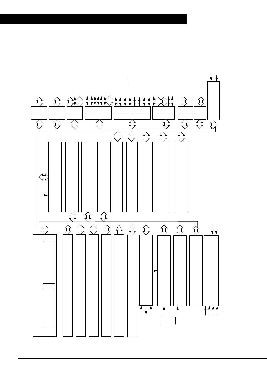
1.4 MCU Block Diagram
Figure 1-1 shows the structure of the MC68HC08AZ60.
General Description
Technical Data MC68HC08AZ60 — Rev 1.1
28 General Description Freescale Semiconductor
BREAK MODULE
CLOCK GENERATOR
MODULE
SYSTEM INTEGRATION
MODULE
ANALOG-TO-DIGITAL
MODULE
SERIAL COMMUNICATIONS
INTERFACE MODULE
SERIAL PERIPHERAL
INTERFACE MODULE
TIMER A 6 CHANNEL
INTERFACE MODULE
LOW-VOLTAGE INHIBIT
MODULE
POWER-ON RESET
MODULE
COMPUTER OPERATING
PROPERLY MODULE
ARITHMETIC/LOGIC
UNIT (ALU)
CPU
REGISTERS
M68HC08 CPU
CONTROL AND STATUS REGISTERS — 62 BYTES
USER ROM — 60 kBYTES
USER RAM — 2048BYTES
USER EEPROM — 1024 BYTES
MONITOR ROM — 224 BYTES
IRQ MODULE
DDRD
PTD
DDRE
PTE
PTG
DDRG
OSC1
OSC2
CGMXFC
RST
IRQ
VDD
VDDA
VSSA
PTE7/SPSCK
PTE6/MOSI
PTE5/MISO
PTE4/SS
PTE3/TACH1
PTE2/TACH0
PTE1/RxD
PTE0/TxD
PTF5/TBCH1–PTF4/TBCH0
PTF3/TACH5-PTF2/TACH4
PTF
DDRF
PTG2/KBD2–PTG0/KBD0
POWER
PTF1/TACH3
PTF0/TACH2
PTA
DDRA
DDRB
PTB
DDRC
PTC
PTA7–PTA0
PTB7/ATD7–PTB0/ATD0
PTC5–PTC3
PTC2/MCLK
PTC1–PTC0
VREFH
MSCAN MODULE
TIMER B INTERFACE
MODULE
CANRx
CANTx
PTH
DDRH
PTH1/KBD4–PTH0/KBD3
KEYBOARD INTERRUPT
MODULE
VSS
USER ROM VECTOR SPACE — 52 BYTES
PTF6
VDDAREF
AVSS/VREFL
Figure 1-1. MCU Block Diagram for the MC68HC08AZ60 (64-Pin QFP)
PTD1/ATD9–PTD0/ATD8
PTD2/ATD10
PTD6/ATD14/TACLK
PTD5/ATD13
PTD3/ATD11
PTD4/ATD12/TBCLK
PTD7

General Description
Pin Assignments
MC68HC08AZ60 — Rev 1.1 Technical Data
Freescale Semiconductor General Description 29
1.5 Pin Assignments
Figure 1-2 shows the MC68HC08AZ60 pin assignments.
Figure 1-2. MC68HC08AZ60 (64-Pin QFP)
NOTE: The following pin descriptions are just a quick reference. For a more
detailed representation, see Input/Output Ports on page 299.
PTF4/TBCH0
CGMXFC
PTB7/ATD7
PTF3/TACH5
PTF2/TACH4
PTF1/TACH3
PTF0/TACH2
RST
IRQ
PTC4
CANRx
CANTx
PTF5/TBCH1
PTE0/TxD
PTE1/RxD
PTE2/TACH0
PTE3/TACH1
PTH0/KBD3
PTD3/ATD11
PTD2/ATD10
AVSS /VREFL
VDDAREF
PTD1/ATD9
PTD0/ATD8
PTB6/ATD6
PTB5/ATD5
PTB4/ATD4
PTB3/ATD3
PTB2/ATD2
PTB1/ATD1
PTB0/ATD0
PTA7
VSSA
VDDA
VREFH
PTD7
PTD6/ATD14/TACLK
PTD5/ATD13
PTD4/ATD12/TBCLK
PTH1/KBD4
PTC5
PTC3
PTC2/MCLK
PTC1
PTC0
OSC1
OSC2
PTE6/MOSI
PTE4/SS
PTE5/MISO
PTE7/SPSCK
VSS
VDD
PTG0/KBD0
PTG1/KBD1
PTG2/KBD2
PTA0
PTA1
PTA2
PTA3
PTA4
PTA5
PTA6
1
2
3
4
5
6
7
8
9
10
11
12
13
14
15
16
17
18
19
20
21
22
23
24
25
26
27
28
29
30
31
32
47
46
45
44
43
42
41
40
39
38
37
36
35
34
33
64
63
62
61
60
59
58
57
56
55
54
53
52
51
50
PTF6
48
49
General Description
Technical Data MC68HC08AZ60 — Rev 1.1
30 General Description Freescale Semiconductor
1.5.1 Power Supply Pins (VDD and VSS)
VDD and VSS are the power supply and ground pins. The MCU operates
from a single power supply.
Fast signal transitions on MCU pins place high, short-duration current
demands on the power supply. To prevent noise problems, take special
care to provide power supply bypassing at the MCU as shown in Figure
1-3. Place the C1 bypass capacitor as close to the MCU as possible. Use
a high-frequency response ceramic capacitor for C1. C2 is an optional
bulk current bypass capacitor for use in applications that require the port
pins to source high current levels.
VSS is also the ground for the port output buffers and the ground return
for the serial clock in the serial peripheral interface module (SPI). See
Serial Peripheral Interface (SPI) on page 231.
NOTE: VSS must be grounded for proper MCU operation.
1.5.2 Oscillator Pins (OSC1 and OSC2)
The OSC1 and OSC2 pins are the connections for the on-chip oscillator
circuit. See Clock Generation Module (CGM) on page 121.
Figure 1-3. Power supply bypassing
MCU
VDD
C2
C1
0.1 µF
VSS
VDD
+
NOTE: Component values shown represent typical applications.

General Description
Pin Assignments
MC68HC08AZ60 — Rev 1.1 Technical Data
Freescale Semiconductor General Description 31
1.5.3 External Reset Pin (RST)
A logic 0 on the RST pin forces the MCU to a known startup state. RST
is bidirectional, allowing a reset of the entire system. It is driven low when
any internal reset source is asserted. See System Integration Module
(SIM) on page 97 for more information.
1.5.4 External Interrupt Pin (IRQ)
IRQ is an asynchronous external interrupt pin. See External Interrupt
(IRQ) on page 183.
1.5.5 Analog Power Supply Pin (VDDA)
VDDA is the power supply pin for the analog portion of the chip. This pin
will supply the clock generator module (CGM). See Clock Generation
Module (CGM) on page 121.
1.5.6 Analog Ground Pin (VSSA)
The VSSA analog ground pin is used only for the ground connections for
the analog sections of the circuit and should be decoupled as per the
VSS digital ground pin. The analog sections consist of a clock generator
module (CGM). See Clock Generation Module (CGM) on page 121.
1.5.7 External Filter Capacitor Pin (CGMXFC)
CGMXFC is an external filter capacitor connection for the CGM. See
Clock Generation Module (CGM) on page 121
1.5.8 Port A Input/Output (I/O) Pins (PTA7–PTA0)
PTA7–PTA0 are general-purpose bidirectional I/O port pins. See
Input/Output Ports on page 299.

General Description
Technical Data MC68HC08AZ60 — Rev 1.1
32 General Description Freescale Semiconductor
1.5.9 Port B I/O Pins (PTB7/ATD7–PTB0/ATD0)
Port B is an 8-bit special function port that shares all eight pins with the
analog-to-digital converter (ADC). See Analog-to-Digital Converter
(ADC-15) on page 417 and Input/Output Ports on page 299.
1.5.10 Port C I/O Pins (PTC5–PTC0)
PTC5–PTC3 and PTC1–PTC0 are general-purpose bidirectional I/O
port pins. PTC2/MCLK is a special function port that shares its pin with
the system clock which has a frequency equivalent to the system clock.
See Input/Output Ports on page 299.
1.5.11 Port D I/O Pins (PTD7–PTD0/ATD8)
Port D is an 8-bit special-function port that shares seven of its pins with
the analog-to-digital converter module (ADC-15), one of its pins with the
timer interface module (TIMA), and one more of its pins with the timer
interface module (TIMB). See Timer Interface Module A (TIMA) on
page 385, Analog-to-Digital Converter (ADC-15) on page 417 and
Input/Output Ports on page 299.
1.5.12 Port E I/O Pins (PTE7/SPSCK–PTE0/TxD)
Port E is an 8-bit special function port that shares two of its pins with the
timer interface module (TIMA), four of its pins with the serial peripheral
interface module (SPI), and two of its pins with the serial communication
interface module (SCI). See Serial Communications Interface (SCI)
on page 191, Serial Peripheral Interface (SPI) on page 231, Timer
Interface Module A (TIMA) on page 385, and Input/Output Ports on
page 299.

General Description
Pin Assignments
MC68HC08AZ60 — Rev 1.1 Technical Data
Freescale Semiconductor General Description 33
1.5.13 Port F I/O Pins (PTF6–PTF0/TACH2)
Port F is a 7-bit special function port that shares its pins with the timer
interface module (TIMB). Six of its pins are shared with the timer
interface module (TIMA-6). See Timer Interface Module A (TIMA) on
page 385, Modulo Timer (TIM) on page 289, and Input/Output Ports
on page 299.
1.5.14 Port G I/O Pins (PTG2/KBD2–PTG0/KBD0)
Port G is a 3-bit special function port that shares all of its pins with the
keyboard interrupt module (KBD). See Keyboard Module (KBD) on
page 375 and Input/Output Ports on page 299.
1.5.15 Port H I/O Pins (PTH1/KBD4–PTH0/KBD3)
Port H is a 2-bit special-function port that shares all of its pins with the
keyboard interrupt module (KBD). See Keyboard Module (KBD) on
page 375 and Input/Output Ports on page 299.
1.5.16 CAN Transmit Pin (CANTx)
This pin is the digital output from the CAN module (CANTx). See
MSCAN Controller (MSCAN08) on page 325.
1.5.17 CAN Receive Pin (CANRx)
This pin is the digital input to the CAN module (CANRx). See MSCAN
Controller (MSCAN08) on page 325.

General Description
Technical Data MC68HC08AZ60 — Rev 1.1
34 General Description Freescale Semiconductor
Table 1-1. External Pins Summary
Pin Name Function Driver
Type Hysteresis Reset State
PTA7–PTA0 General-Purpose I/O Dual State No Input Hi-Z
PTB7/ATD7–PTB0/ATD0 General-Purpose I/O
ADC Channel Dual State No Input Hi-Z
PTC5–PTC0 General-Purpose I/O Dual State No Input Hi-Z
PTD7 General Purpose I/O/ Dual State No Input Hi-Z
PTD6/ATD14/TACLK ** ADC Channel General-Purpose I/O
ADC Channel/Timer
External Input Clock Dual State No Input Hi-Z
PTD5/ATD13 ** ADC Channel General-Purpose I/O
ADC Channel Dual State No Input Hi-Z
PTD4/ATD12/TBCLK ** ADC Channel General-Purpose I/O
ADC Channel/Timer
External Input Clock Dual State No Input Hi-Z
PTD3/ATD11–PTD0/ATD8 **ADC
Channels General-Purpose I/O
ADC Channel Dual State No Input Hi-Z
PTE7/SPSCK General-Purpose I/O
SPI Clock Dual State
Open Drain Yes Input Hi-Z
PTE6/MOSI General-Purpose I/O
SPI Data Path Dual State
Open Drain Yes Input Hi-Z
PTE5/MISO General-Purpose I/O
SPI Data Path Dual State
Open Drain Yes Input Hi-Z
PTE4/SS General-Purpose I/O
SPI Slave Select Dual State Yes Input Hi-Z
PTE3/TACH1 General-Purpose I/O
Timer Channel 1 Dual State Yes Input Hi-Z
PTE2/TACH0 General-Purpose I/O
Timer Channel 0 Dual State Yes Input Hi-Z
PTE1/RxD General-Purpose I/O
SCI Receive Data Dual State Yes Input Hi-Z
PTE0/TxD General-Purpose I/O
SCI Transmit Data Dual State No Input Hi-Z
PTF6 General-Purpose I/O Dual State No Input Hi-Z
PTF5/TBCH1–PTF4/TBCH0 General-Purpose
I/O/Timer B Channel Dual State Yes Input Hi-Z

General Description
Pin Assignments
MC68HC08AZ60 — Rev 1.1 Technical Data
Freescale Semiconductor General Description 35
PTF3/TACH5 General-Purpose I/O
Timer A Channel 5 Dual State Yes Input Hi-Z
PTF2/TACH4 General-Purpose I/O
Timer A Channel 4 Dual State Yes Input Hi-Z
PTF1/TACH3 General-Purpose I/O
Timer A Channel 3 Dual State Yes Input Hi-Z
PTF0/TACH2 General-Purpose I/O
Timer A Channel 2 Dual State Yes Input Hi-Z
PTG2/KBD2–PTG0/KBD0 General-Purpose I/O/
Keyboard Wakeup Pin Dual State Yes Input Hi-Z
PTH1/KBD4 –PTH0/KBD3 General-Purpose I/O/
Keyboard Wakeup Pin Dual State Yes Input Hi-Z
VDD Chip Power Supply N/A N/A N/A
VSS Chip Ground N/A N/A N/A
AVDD/VDDAREF
ADC Power Supply/
ADC Reference
Voltage N/A N/A N/A
AVSS/VREFL ADC Ground/ADC
Reference Voltage N/A N/A N/A
VREFH A/D Reference
Voltage N/A N/A N/A
OSC1 External Clock In N/A N/A Input Hi-Z
OSC2 External Clock Out N/A N/A Output
CGMXFC PLL Loop Filter Cap N/A N/A N/A
IRQ External Interrupt
Request N/A N/A Input Hi-Z
RST Reset N/A N/A Output Low
CANRx CAN Serial Input N/A Yes Input Hi-Z
CANTx CAN Serial Output Output No Output
Table 1-1. External Pins Summary (Continued)
Pin Name Function Driver
Type Hysteresis Reset State

General Description
Technical Data MC68HC08AZ60 — Rev 1.1
36 General Description Freescale Semiconductor
1.6 Ordering Information
This section contains instructions for ordering the MC68HC08AZ60.
1.6.1 MC Order Numbers
Table 1-2. Clock Source Summary
Module Clock Source
ADC CGMXCLK or Bus Clock
CAN CGMXCLK or CGMOUT
COP CGMXCLK
CPU Bus Clock
EEPROM RC OSC or Bus Clock
SPI Bus Clock/SPSCK
SCI CGMXCLK
TIMA-6 Bus Clock or PTD6/ATD14/TACLK
TIMB Bus Clock or PTD4/TBCLK
TIM Bus Clock
SIM CGMOUT and CGMXCLK
IRQ Bus Clock
BRK Bus Clock
LVI Bus Clock
CGM OSC1 and OSC2
Table 1-3. MC Order Numbers
MC Order Number Operating
Temperature Range
MC68HC08AZ60CFU –40 °C to + 85°C
MC68HC08AZ60VFU –40 °C to + 105 °C
MC68HC08AZ60MFU –40 °C to + 125 °C

MC68HC08AZ60 — Rev 1.1 Technical Data
Freescale Semiconductor Memory Map 37
Technical Data — MC68HC08AZ60
Section 2. Memory Map
2.1 Contents
2.2 Introduction. . . . . . . . . . . . . . . . . . . . . . . . . . . . . . . . . . . . . . .37
2.3 I/O Section. . . . . . . . . . . . . . . . . . . . . . . . . . . . . . . . . . . . . . . .40
2.2 Introduction
The CPU08 can address 64 Kbytes of memory space. The memory
map, shown in Figure 2-1, includes:
• 60 Kbytes of ROM
• 2048 Bytes of RAM
• 1024 Bytes of EEPROM with Protect Option
• 52 Bytes of User-Defined Vectors
• 224 Bytes of Monitor ROM
The following definitions apply to the memory map representation of
reserved and unimplemented locations.
•Reserved — Accessing a reserved location can have
unpredictable effects on MCU operation.
•Unimplemented — Accessing an unimplemented location
causes an illegal address reset if illegal address resets are
enabled.

Memory Map
Technical Data MC68HC08AZ60 — Rev 1.1
38 Memory Map Freescale Semiconductor
Figure 2-1. Memory Map
$0000
I/O REGISTERS (64 BYTES)
$0000
↓↓
$003F $003F
$0040
I/O REGISTERS, 16 BYTES
$0040
↓↓
$004F $004F
$0050
RAM-1, 1024 BYTES
$0050
↓↓
$044F $044F
$0450
ROM-2, 176 BYTES
$0450
↓↓
$04FF $04FF
$0500 CAN CONTROL AND MESSAGE
BUFFERS, 128 BYTES
$0500
↓↓
$057F $057F
$0580
ROM-2, 128 BYTES
$0580
↓↓
$05FF $05FF
$0600
EEPROM-2, 512 BYTES
$0600
↓↓
$07FF $07FF
$0800
EEPROM-1, 512 BYTES
$0800
↓↓
$09FF $09FF
$0A00
RAM-2 , 1024 BYTES
$0A00
↓↓
$0DFF $0DFF
$0E00
ROM-2, 29,184 BYTES
$0E00
↓↓
$7FFF $7FFF
$8000
ROM-1, 32,256BYTES
$8000
↓↓
$FDFF $FDFF
$FE00 SIM BREAK STATUS REGISTER (SBSR) $FE00
$FE01 SIM RESET STATUS REGISTER (SRSR) $FE01
$FE02 RESERVED $FE02
$FE03 SIM BREAK FLAG CONTROL REGISTER (SBFCR) $FE03
$FE04 RESERVED $FE04

Memory Map
Introduction
MC68HC08AZ60 — Rev 1.1 Technical Data
Freescale Semiconductor Memory Map 39
$FE05 RESERVED $FE05
$FE06 UNIMPLEMENTED $FE06
$FE07 RESERVED $FE07
$FE08 RESERVED $FE08
$FE09 RESERVED $FE09
$FE0A RESERVED $FE0A
$FE0B RESERVED) $FE0B
$FE0C BREAK ADDRESS REGISTER HIGH (BRKH) $FE0C
$FE0D BREAK ADDRESS REGISTER LOW (BRKL) $FE0D
$FE0E BREAK STATUS AND CONTROL REGISTER (BSCR) $FE0E
$FE0F LVI STATUS REGISTER (LVISR) $FE0F
$FE10 RESERVED $FE10
$FE11 RESERVED $FE11
$FE12
UNIMPLEMENTED (5BYTES)
$FE12
↓↓
$FE17 $FE17
$FE18 EEPROM NON-VOLATILE REGISTER (EENVR2) $FE18
$FE19 EEPROM CONTROL REGISTER (EECR2) $FE19
$FE1A RESERVED $FE1A
$FE1B EEPROM ARRAY CONFIGURATION (EEACR2) $FE1B
$FE1C EEPROM NON-VOLATILE REGISTER (EENVR1) $FE1C
$FE1D EEPROM CONTROL REGISTER (EECR1) $FE1D
$FE1E RESERVED $FE1E
$FE1F EEPROM ARRAY CONFIGURATION (EEACR1) $FE1F
$FE20
MONITOR ROM (224 BYTES)
$FE20
↓↓
$FEFF $FEFF
$FF00
↓
$FF7F
UNIMPLEMENTED (128 BYTES)
$FF00
↓
$FF7F
$FF80 RESERVED $FF80
$FF81 RESERVED $FF81
$FF82
RESERVED (75 BYTES)
$FF82
↓↓
$FFCB $FFCB
$FFCC
VECTORS (52BYTES)
$FFCC
↓↓
$FFFF $FFFF
Figure 2-1. Memory Map (Continued)

Memory Map
Technical Data MC68HC08AZ60 — Rev 1.1
40 Memory Map Freescale Semiconductor
2.3 I/O Section
Addresses $0000–$003F, shown in Figure 2-2, contain most of the
control, status, and data registers. Additional I/O registers have these
addresses:
• $FE00 (SIM break status register, SBSR)
• $FE01 (SIM reset status register, SRSR)
• $FE03 (SIM break flag control register, SBFCR)
• $FE09 (configuration write-once register, CONFIG-2)
• $FE0C and $FE0D (break address registers, BRKH and BRKL)
• $FE0E (break status and control register, BRKSCR)
• $FE0F (LVI status register, LVISR)
• $FE18 (EEPROM non-volatile register, EENVR2)
• $FE19 (EEPROM control register, EECR2)
• $FE1B (EEPROM array configuration register, EEACR2)
• $FE1C (EEPROM non-volatile register, EENVR1)
• $FE1D (EEPROM control register, EECR1)
• $FE1F (EEPROM array configuration register, EEACR1)
• $FFFF (COP control register, COPCTL)
Table 2-1 is a list of vector locations.

Memory Map
I/O Section
MC68HC08AZ60 — Rev 1.1 Technical Data
Freescale Semiconductor Memory Map 41
Addr. Register Name Bit 7 6 5 4 3 2 1 Bit 0
$0000 Port A Data Register (PTA) Read: PTA7 PTA6 PTA5 PTA4 PTA3 PTA2 PTA1 PTA0
Write:
$0001 Port B Data Register (PTB) Read: PTB7 PTB6 PTB5 PTB4 PTB3 PTB2 PTB1 PTB0
Write:
$0002 Port C Data Register (PTC) Read: 0 0 PTC5 PTC4 PTC3 PTC2 PTC1 PTC0
Write:
$0003 Port D Data Register (PTD) Read: PTD7 PTD6 PTD5 PTD4 PTD3 PTD2 PTD1 PTD0
Write:
$0004 Data Direction Register A
(DDRA)
Read: DDRA7 DDRA6 DDRA5 DDRA4 DDRA3 DDRA2 DDRA1 DDRA0
Write:
$0005 Data Direction Register B
(DDRB)
Read: DDRB7 DDRB6 DDRB5 DDRB4 DDRB3 DDRB2 DDRB1 DDRB0
Write:
$0006 Data Direction Register C
(DDRC)
Read: MCLKEN 0DDRC5 DDRC4 DDRC3 DDRC2 DDRC1 DDRC0
Write:
$0007 Data Direction Register D
(DDRD)
Read: DDRD7 DDRD6 DDRD5 DDRD4 DDRD3 DDR2 DDRD1 DDRD0
Write:
$0008 Port E Data Register (PTE) Read: PTE7 PTE6 PTE5 PTE4 PTE3 PTE2 PTE1 PTE0
Write:
$0009 Port F Data Register (PTF) Read: 0 PTF6 PTF5 PTF4 PTF3 PTF2 PTF1 PTF0
Write:
$000A Port G Data Register (PTG) Read: 0 0 0 0 0 PTG2 PTG1 PTG0
Write:
$000B Port H Data Register (PTH) Read: 0 0 0 0 0 0 PTH1 PTH0
Write:
$000C Data Direction Register E
(DDRE)
Read: DDRE7 DDRE6 DDRE5 DDRE4 DDRE3 DDRE2 DDRE1 DDRE0
Write:
$000D Data Direction Register F
(DDRF)
Read: 0 DDRF6 DDRF5 DDRF4 DDRF3 DDRF2 DDRF1 DDRF0
Write:
$000E Data Direction Register G
(DDRG)
Read: 0 0 0 0 0 DDRG2 DDRG1 DDRG0
Write:
$000F Data Direction Register H
(DDRH)
Read: 0 0 0 0 0 0 DDRH1 DDRH0
Write:
$0010 SPI Control Register (SPCR) Read: SPRIE R SPMSTR CPOL CPHA SPWOM SPE SPTIE
Write:
= Unimplemented R = Reserved
Figure 2-2. Control, Status, and Data Registers (Sheet 1 of 6)

Memory Map
Technical Data MC68HC08AZ60 — Rev 1.1
42 Memory Map Freescale Semiconductor
$0011 SPI Status and Control
Register (SPSCR)
Read: SPRF ERRIE OVRF MODF SPTE MODFE
NSPR1 SPR0
Write:
$0012 SPI Data Register (SPDR) Read: R7 R6 R5 R4 R3 R2 R1 R0
Write: T7 T6 T5 T4 T3 T2 T1 T0
$0013 SCI Control Register 1 (SCC1) Read: LOOPS ENSCI TXINV M WAKE ILTY PEN PTY
Write:
$0014 SCI Control Register 2 (SCC2) Read: SCTIE TCIE SCRIE ILIE TE RE RWU SBK
Write:
$0015 SCI Control Register 3 (SCC3) Read: R8 T8 R R ORIE NEIE FEIE PEIE
Write:
$0016 SCI Status Register 1 (SCS1) Read: SCTE TC SCRF IDLE OR NF FE PE
Write:
$0017 SCI Status Register 2 (SCS2) Read: 0 0 0 0 0 0 BKF RPF
Write:
$0018 SCI Data Register (SCDR) Read: R7 R6 R5 R4 R3 R2 R1 R0
Write: T7 T6 T5 T4 T3 T2 T1 T0
$0019 SCI Baud Rate Register (SCBR) Read: 0 0 SCP1 SCP0 SCR2 SCR1 SCR0
Write:
$001A IRQ Status and Control
Register (ISCR)
Read: 0 0 0 0 IRQF 0 IMASK1 MODE1
Write: ACK1
$001B Keyboard Status and Control
Register (KBSCR)
Read: 0 0 0 0 KEYF 0 IMASKK MODEK
Write: ACKK
$001C PLL Control Register (PCTL) Read: PLLIE PLLF PLLON BCS 1111
Write:
$001D PLL Bandwidth Control
Register (PBWC)
Read: AUTO LOCK ACQ XLD 0000
Write:
$001E PLL Programming Register
(PPG)
Read: MUL7 MUL6 MUL5 MUL4 VRS7 VRS6 VRS5 VRS4
Write:
$001F Mask Option Register
(MOR)
Read: LVISTOP ROMSEC LVIRST LVIPWR SSREC COPRS STOP COPD
Write:RRRRRRRR
$0020 Timer A Status and Control
Register (TASC)
Read: TOF TOIE TSTOP 00
PS2 PS1 PS0
Write: 0 TRST
$0021 Keyboard Interrupt Enable
Register (KBIE)
Read: 0 0 0 KBIE4 KBIE3 KBIE2 KBIE1 KBIE0
Write:
$0022 Timer A Counter Register
High (TACNTH)
Read: Bit 15 14 13 12 11 10 9 Bit 8
Write:
Addr. Register Name Bit 7 6 5 4 3 2 1 Bit 0
Figure 2-2. Control, Status, and Data Registers (Sheet 2 of 6)

Memory Map
I/O Section
MC68HC08AZ60 — Rev 1.1 Technical Data
Freescale Semiconductor Memory Map 43
$0023 Timer A Counter Register
Low (TACNTL)
Read: Bit 7 6 5 4 3 2 1 Bit 0
Write:
$0024 Timer A Modulo Register
High (TAMODH)
Read: Bit 15 14 13 12 11 10 9 Bit 8
Write:
$0025 Timer A Modulo Register
Low (TAMODL)
Read: Bit 7 6 5 4 3 2 1 Bit 0
Write:
$0026 Timer A Channel 0 Status and
Control Register (TASC0)
Read: CH0F CH0IE MS0B MS0A ELS0B ELS0A TOV0 CH0MAX
Write: 0
$0027 Timer A Channel 0 Register
High (TACH0H)
Read: Bit 15 14 13 12 11 10 9 Bit 8
Write:
$0028 Timer A Channel 0 Register
Low (TACH0L)
Read: Bit 7 6 5 4 3 2 1 Bit 0
Write:
$0029 Timer A Channel 1 Status and
Control Register (TASC1)
Read: CH1F CH1IE 0MS1A ELS1B ELS1A TOV1 CH1MAX
Write: 0
$002A Timer A Channel 1 Register
High (TACH1H)
Read: Bit 15 14 13 12 11 10 9 Bit 8
Write:
$002B Timer A Channel 1 Register
Low (TACH1L)
Read: Bit 7 6 5 4 3 2 1 Bit 0
Write:
$002C Timer A Channel 2 Status and
Control Register (TASC2)
Read: CH2F CH2IE MS2B MS2A ELS2B ELS2A TOV2 CH2MAX
Write: 0
$002D Timer A Channel 2 Register
High (TACH2H)
Read: Bit 15 14 13 12 11 10 9 Bit 8
Write:
$002E Timer A Channel 2 Register
Low (TACH2L)
Read: Bit 7 6 5 4 3 2 1 Bit 0
Write:
$002F Timer A Channel 3 Status and
Control Register (TASC3)
Read: CH3F CH3IE 0MS3A ELS3B ELS3A TOV3 CH3MAX
Write: 0
$0030 Timer A Channel 3 Register
High (TACH3H)
Read: Bit 15 14 13 12 11 10 9 Bit 8
Write:
$0031 Timer A Channel 3 Register
Low (TACH3L)
Read: Bit 7 6 5 4 3 2 1 Bit 0
Write:
$0032 Timer A Channel 4 Status and
Control Register (TASC4)
Read: CH4F CH4IE MS4B MS4A ELS4B ELS4A TOV4 CH4MAX
Write: 0
$0033 Timer A Channel 4 Register High
(TACH4H)
Read: Bit 15 14 13 12 11 10 9 Bit 8
Write:
$0034 Timer A Channel 4 Register Low
(TACH4L)
Read: Bit 7 6 5 4 3 2 1 Bit 0
Write:
Addr. Register Name Bit 7 6 5 4 3 2 1 Bit 0
Figure 2-2. Control, Status, and Data Registers (Sheet 3 of 6)

Memory Map
Technical Data MC68HC08AZ60 — Rev 1.1
44 Memory Map Freescale Semiconductor
$0035 Timer A Channel 5 Status and
Control Register (TASC5)
Read: CH5F CH5IE 0MS5A ELS5B ELS5A TOV5 CH5MAX
Write: 0
$0036 Timer A Channel 5 Register
High (TACH5H)
Read: Bit 15 14 13 12 11 10 9 Bit 8
Write:
$0037 Timer A Channel 5 Register
Low (TACH5L)
Read: Bit 7 6 5 4 3 2 1 Bit 0
Write:
$0038 Analog-to-Digital Status and
Control Register (ADSCR)
Read: COCO AIEN ADCO ADCH4 ADCH3 ADCH2 ADCH1 ADCH0
Write: R
$0039 Analog-to-Digital Data Register
(ADR)
Read: AD7 AD6 AD5 AD4 AD3 AD2 AD1 AD0
Write:
$003A Analog-to-Digital Input Clock
Register (ADICLK)
Read: ADIV2 ADIV1 ADIV0 ADICLK 0000
Write:
$0040 Timer B Status and Control
Register (TBSCR)
Read: TOF TOIE TSTOP 00
PS2 PS1 PS0
Write: TRST
$0041 Timer B Counter Register High
(TBCNTH)
Read: Bit 15 14 13 12 11 10 9 Bit 8
Write:
$0042 Timer B Counter Register Low
(TBCNTL)
Read: Bit 7 6 5 4 3 2 1 Bit 0
Write:
$0043 Timer B Modulo Register High
(TBMODH)
Read: Bit 15 14 13 12 11 10 9 Bit 8
Write:
$0044 Timer B Modulo Register Low
(TBMODL)
Read: Bit 7 6 5 4 3 2 1 Bit 0
Write:
$0045 Timer B CH0 Status and Control
Register (TBSC0)
Read: CH0F CH0IE MS0B MS0A ELS0B ELS0A TOV0 CH0MAX
Write: 0
$0046 Timer B CH0 Register High
(TBCH0H)
Read: Bit 15 14 13 12 11 10 9 Bit 8
Write:
$0047 Timer B CH0 Register Low
(TBCH0L)
Read: Bit 7 6 5 4 3 2 1 Bit 0
Write:
Timer B CH1 Status and Control
Register (TBSC1)
Read: CH1F CH1IE 0MS1A ELS1B ELS1A TOV1 CH1MAX
$0048 Write: 0
$0049 Timer B CH1 Register High
(TBCH1H)
Read: Bit 15 14 13 12 11 10 9 Bit 8
Write:
$004A Timer B CH1 Register Low
(TBCH1L)
Read: Bit 7 6 5 4 3 2 1 Bit 0
Write:
$004B TIM Status and Control Register
(TSC)
Read: TOF TOIE TSTOP 00
PS2 PS1 PS0
Write: TRST
Addr. Register Name Bit 7 6 5 4 3 2 1 Bit 0
Figure 2-2. Control, Status, and Data Registers (Sheet 4 of 6)

Memory Map
I/O Section
MC68HC08AZ60 — Rev 1.1 Technical Data
Freescale Semiconductor Memory Map 45
$004C TIM Counter Register High
(TCNTH)
Read: Bit 15 14 13 12 11 10 9 Bit 8
Write:
$004D TIM Counter Register Low
(TCNTL)
Read: Bit 7 6 5 4 3 2 1 Bit 0
Write:
$004E TIM Modulo Register High
(TMODH)
Read: Bit 15 14 13 12 11 10 9 Bit 8
Write:
$004F TIM Modulo Register Low
(TMODL)
Read: Bit 7 6 5 4 3 2 1 Bit 0
Write:
$FE00 SIM Break Status Register
(SBSR)
Read: R R R R R R SBSW R
Write:
$FE01 SIM Reset Status Register (SRSR) Read: POR PIN COP ILOP ILAD 0 LVI 0
Write:
$FE03 SIM Break Flag Control Register
(SBFCR)
Read: BCFERR R RRRR
Write:
$FE09 RESERVED Read: RRRRRRRR
Write:
$FE0B RESERVED Read: RRRRRRRR
Write:
$FE0C Break Address Register High
(BRKH)
Read: Bit 15 14 13 12 11 10 9 Bit 8
Write:
$FE0D Break Address Register Low
(BRKL)
Read: Bit 7 6 5 4 3 2 1 Bit 0
Write:
$FE0E Break Status and Control
Register (BRKSCR)
Read: BRKE BRKA 0 0 0000
Write:
$FE0F LVI Status Register (LVISR) Read: LVIOUT 0 0 0 0 0 0 0
Write:
$FE11 RESERVED Read: RRRRRRRR
Write:
$FE18 EEPROM Nonvolatile Register
(EENVR2)
Read: EERA CON2 CON1 EEPRTC
TEEBP3 EEBP2 EEBP1 EEBP0
Write:
$FE19 EEPROM Control
Register (EECR2)
Read: EEBCLK 0EEOFF EERAS1 EERAS0 EELAT 0EEPGM
Write:
$FE1A Reserved Read: RRRRRRRR
Write:
Addr. Register Name Bit 7 6 5 4 3 2 1 Bit 0
Figure 2-2. Control, Status, and Data Registers (Sheet 5 of 6)
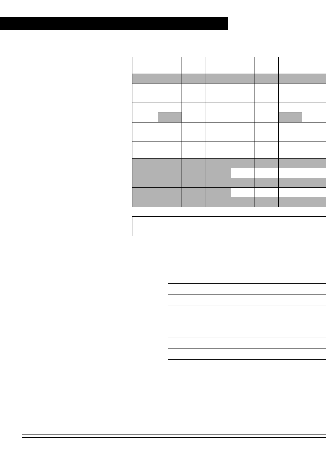
Memory Map
Technical Data MC68HC08AZ60 — Rev 1.1
46 Memory Map Freescale Semiconductor
$FE1B EEPROM Array Control Register
(EEACR2)
Read: EERA CON2 CON1 EEPRTC
TEEBP3 EEBP2 EEBP1 EEBP0
Write:
$FE1C EEPROM Nonvolatile Register
(EENVR1)
Read: EERA CON2 CON1 EEPRTC
TEEBP3 EEBP2 EEBP1 EEBP0
Write:
$FE1D EEPROM Control
Register (EECR1)
Read: EEBCLK 0EEOFF EERAS1 EERAS0 EELAT 0EEPGM
Write:
$FE1E Reserved Read: RRRRRRRR
Write:
$FE1F EEPROM Array Control Register
(EEACR1)
Read: EERA CON2 CON1 EEPRTC
TEEBP3 EEBP2 EEBP1 EEBP0
Write:
$FF80 RESERVED Read: RRRR
Write:
$FF81 RESERVED Read: RRRR
Write:
$FFFF COP Control Register (COPCTL) Read: LOW BYTE OF RESET VECTOR
Write: WRITING TO $FFFF CLEARS COP COUNTER
Addr. Register Name Bit 7 6 5 4 3 2 1 Bit 0
Figure 2-2. Control, Status, and Data Registers (Sheet 6 of 6)
Table 2-1. Vector Addresses
Address Vector
Low
$FFCC TIMA Channel 5 Vector (High)
$FFCD TIMA Channel 5 Vector (Low)
$FFCE TIMA Channel 4 Vector (High)
$FFCF TIMA Channel 4 Vector (Low)
$FFD0 ADC Vector (High)
$FFD1 ADC Vector (Low)

Memory Map
I/O Section
MC68HC08AZ60 — Rev 1.1 Technical Data
Freescale Semiconductor Memory Map 47
$FFD2 Keyboard Vector (High)
$FFD3 Keyboard Vector (Low)
$FFD4 SCI Transmit Vector (High)
$FFD5 SCI Transmit Vector (Low)
$FFD6 SCI Receive Vector (High)
$FFD7 SCI Receive Vector (Low)
$FFD8 SCI Error Vector (High)
$FFD9 SCI Error Vector (Low)
$FFDA CAN Transmit Vector (High)
$FFDB CAN Transmit Vector (Low)
$FFDC CAN Receive Vector (High)
$FFDD CAN Receive Vector (Low)
$FFDE CAN Error Vector (High)
$FFDF CAN Error Vector (Low)
$FFE0 CAN Wakeup Vector (High)
$FFE1 CAN Wakeup Vector (Low)
$FFE2 SPI Transmit Vector (High)
$FFE3 SPI Transmit Vector (Low)
$FFE4 SPI Receive Vector (High)
$FFE5 SPI Receive Vector (Low)
$FFE6 TIMB Overflow Vector (High)
$FFE7 TIMB Overflow Vector (Low)
$FFE8 TIMB CH1 Vector (High)
$FFE9 TIMB CH1 Vector (Low)
$FFEA TIMB CH0 Vector (High)
$FFEB TIMB CH0 Vector (Low)
$FFEC TIMA Overflow Vector (High)
$FFED TIMA Overflow Vector (Low)
$FFEE TIMA CH3 Vector (High)
$FFEF TIMA CH3 Vector (Low)
$FFF0 TIMA CH2 Vector (High)
$FFF1 TIMA CH2 Vector (Low)
Table 2-1. Vector Addresses (Continued)
Address Vector
Priority

Memory Map
Technical Data MC68HC08AZ60 — Rev 1.1
48 Memory Map Freescale Semiconductor
Note that all available ROM locations not defined by the user will, by
default, be filled with the software interrupt instruction (SWI, opcode 83)
– see Central Processing Unit (CPU). Please take this into account
when defining vector addresses. It is recommended that all vector
addresses are defined.
$FFF2 TIMA CH1 Vector (High)
$FFF3 TIMA CH1 Vector (Low)
$FFF4 TIMA CH0 Vector (High)
$FFF5 TIMA CH0 Vector (Low)
$FFF6 TIM Vector (High)
$FFF7 TIM Vector (Low)
$FFF8 PLL Vector (High)
$FFF9 PLL Vector (Low)
$FFFA IRQ Vector (High)
$FFFB IRQ Vector (Low)
$FFFC SWI Vector (High)
$FFFD SWI Vector (Low)
High
$FFFE Reset Vector (High)
$FFFF Reset Vector (Low)
Table 2-1. Vector Addresses (Continued)
Address Vector
Priority

MC68HC08AZ60 — Rev 1.1 Technical Data
Freescale Semiconductor RAM 49
Technical Data — MC68HC08AZ60
Section 3. RAM
3.1 Contents
3.2 Introduction. . . . . . . . . . . . . . . . . . . . . . . . . . . . . . . . . . . . . . .49
3.3 Functional Description. . . . . . . . . . . . . . . . . . . . . . . . . . . . . .49
3.2 Introduction
This section describes the 2048 bytes of random-access memory
(RAM).
3.3 Functional Description
Addresses $0050 through $044F and $0A00 through $0DFF are RAM
locations. The location of the stack RAM is programmable with the reset
stack pointer instruction (RSP). The 16-bit stack pointer allows the stack
RAM to be anywhere in the 64K-byte memory space.
NOTE: For correct operation, the stack pointer must point only to RAM
locations.
Within page zero are 176 bytes of RAM. Because the location of the
stack RAM is programmable, all page zero RAM locations can be used
for input/output (I/O) control and user data or code. When the stack
pointer is moved from its reset location at $00FF, direct addressing
mode instructions can access all page zero RAM locations efficiently.
Page zero RAM, therefore, provides ideal locations for frequently
accessed global variables.
Before processing an interrupt, the CPU uses five bytes of the stack to
save the contents of the CPU registers.

RAM
Technical Data MC68HC08AZ60 — Rev 1.1
50 RAM Freescale Semiconductor
NOTE: For M68HC05, M6805, and M146805 compatibility, the H register is not
stacked.
During a subroutine call, the CPU uses two bytes of the stack to store
the return address. The stack pointer decrements during pushes and
increments during pulls.
NOTE: Be careful when using nested subroutines. The CPU could overwrite
data in the RAM during a subroutine or during the interrupt stacking
operation.

MC68HC08AZ60 — Rev 1.1 Technical Data
Freescale Semiconductor ROM-1 Memory 51
Technical Data — MC68HC08AZ60
Section 4. ROM-1 Memory
4.1 Contents
4.2 Introduction. . . . . . . . . . . . . . . . . . . . . . . . . . . . . . . . . . . . . . .51
4.3 Functional Description. . . . . . . . . . . . . . . . . . . . . . . . . . . . . .51
4.4 Low-Power Modes . . . . . . . . . . . . . . . . . . . . . . . . . . . . . . . . .52
4.4.1 WAIT Mode . . . . . . . . . . . . . . . . . . . . . . . . . . . . . . . . . . . . .52
4.4.2 STOP Mode . . . . . . . . . . . . . . . . . . . . . . . . . . . . . . . . . . . . .52
4.2 Introduction
This section describes the operation of the embedded ROM-1 memory.
4.3 Functional Description
The ROM memory physically consists of two independent arrays of 32K
bytes with an additional 52 bytes of user vectors and two bytes of block
protection. The address ranges for the user memory and vectors are:
• $8000–$FDFF
• $FFCC–$FFFF (These locations are reserved for user-defined
interrupt and reset vectors.)
NOTE: A security feature prevents viewing of the ROM contents.(1)
1. No security feature is absolutely secure. However, Freescale’s strategy is to make reading or
copying the ROM difficult for unauthorized users.

ROM-1 Memory
Technical Data MC68HC08AZ60 — Rev 1.1
52 ROM-1 Memory Freescale Semiconductor
4.4 Low-Power Modes
The WAIT and STOP instructions put the MCU in low power
consumption standby modes.
4.4.1 WAIT Mode
Putting the MCU into wait mode while the ROM is in read mode does not
affect the operation of the ROM memory directly, but there will not be any
memory activity since the CPU is inactive.
4.4.2 STOP Mode
When the MCU is put into stop mode, if the ROM is in read mode, it will
be put into low power standby.

MC68HC08AZ60 — Rev 1.1 Technical Data
Freescale Semiconductor ROM-2 Memory 53
Technical Data — MC68HC08AZ60
Section 5. ROM-2 Memory
5.1 Contents
5.2 Introduction. . . . . . . . . . . . . . . . . . . . . . . . . . . . . . . . . . . . . . .53
5.3 Functional Description. . . . . . . . . . . . . . . . . . . . . . . . . . . . . .53
5.4 Low-Power Modes . . . . . . . . . . . . . . . . . . . . . . . . . . . . . . . . .54
5.4.1 WAIT Mode . . . . . . . . . . . . . . . . . . . . . . . . . . . . . . . . . . . . .54
5.4.2 STOP Mode . . . . . . . . . . . . . . . . . . . . . . . . . . . . . . . . . . . . .54
5.2 Introduction
This section describes the operation of the embedded ROM-2 memory.
5.3 Functional Description
The ROM-2 memory is an array of up to 29,488 bytes. The address
ranges for the user memory and the control register are:
• $0450–$04FF
• $0580–$05FF
• $0E00–$7FFF
NOTE: A security feature prevents viewing of the ROM contents.(1)
1. No security feature is absolutely secure. However, Freescale’s strategy is to make reading or
copying the ROM difficult for unauthorized users.

ROM-2 Memory
Technical Data MC68HC08AZ60 — Rev 1.1
54 ROM-2 Memory Freescale Semiconductor
5.4 Low-Power Modes
The WAIT and STOP instructions put the MCU in low power
consumption standby modes.
5.4.1 WAIT Mode
Putting the MCU into wait mode while the ROM is in read mode does not
affect the operation of the ROM memory directly, but there will not be any
memory activity since the CPU is inactive.
5.4.2 STOP Mode
When the MCU is put into stop mode, if the ROM is in read mode, it will
be put into low power standby.

MC68HC08AZ60 — Rev 1.1 Technical Data
Freescale Semiconductor EEPROM-1 55
Technical Data — MC68HC08AZ60
Section 6. EEPROM-1
6.1 Contents
6.2 Introduction. . . . . . . . . . . . . . . . . . . . . . . . . . . . . . . . . . . . . . .55
6.3 Future EEPROM Memory . . . . . . . . . . . . . . . . . . . . . . . . . . . .56
6.4 Features. . . . . . . . . . . . . . . . . . . . . . . . . . . . . . . . . . . . . . . . . .56
6.5 Functional Description. . . . . . . . . . . . . . . . . . . . . . . . . . . . . .56
6.5.1 EEPROM Programming . . . . . . . . . . . . . . . . . . . . . . . . . . .57
6.5.2 EEPROM Erasing . . . . . . . . . . . . . . . . . . . . . . . . . . . . . . . .58
6.5.3 EEPROM Block Protection . . . . . . . . . . . . . . . . . . . . . . . .60
6.5.4 MCU Configuration. . . . . . . . . . . . . . . . . . . . . . . . . . . . . . .60
6.5.5 MC68HC08AZ60 EEPROM Protection . . . . . . . . . . . . . . .61
6.5.6 EEPROM Control Register. . . . . . . . . . . . . . . . . . . . . . . . .62
6.5.7 EEPROM Nonvolatile Register . . . . . . . . . . . . . . . . . . . . .64
6.5.8 EEPROM Array Configuration Register . . . . . . . . . . . . . .65
6.6 Low-Power Modes . . . . . . . . . . . . . . . . . . . . . . . . . . . . . . . . .66
6.6.1 Wait Mode . . . . . . . . . . . . . . . . . . . . . . . . . . . . . . . . . . . . . .66
6.6.2 Stop Mode. . . . . . . . . . . . . . . . . . . . . . . . . . . . . . . . . . . . . .66
6.2 Introduction
This section describes the electrically erasable programmable read-only
memory (EEPROM). The 1024 bytes available on the MC68HC08AZ60
are physically located in two 512byte arrays. This chapter details the
array covering the address range $0800 to $09FF. For information
relating to the array covering address range $0600 to $07FF see
EEPROM-2 on page 67.

EEPROM-1
Technical Data MC68HC08AZ60 — Rev 1.1
56 EEPROM-1 Freescale Semiconductor
6.3 Future EEPROM Memory
Design is underway to introduce an improved EEPROM module, which
will simplify programming and erase. Current read, write and erase
algorithms are fully compatible with the new EEPROM design. The new
EEPROM module requires a constant timebase through the set up of
new timebase control registers. If more information is required for code
compatibility please contact the factory. The silicon differences will be
identified by mask set. Please read Appendix: Future EEPROM
Registers on page 443 for preliminary details.
NOTE: This new silicon will not allow multiple writes before erase. EEPROM
bytes must be erased before reprogramming.
6.4 Features
EEPROM features include:
• Byte, Block, or Bulk Erasable
• Nonvolatile Block Protection Option
• Nonvolatile MCU Configuration Bits
• On-Chip Charge Pump for Programming/Erasing
• Security Option
6.5 Functional Description
The 512 bytes of EEPROM-1 can be programmed or erased without an
external voltage supply. The EEPROM has a lifetime of 10,000 write-
erase cycles. EEPROM cells are protected with a nonvolatile block
protection option. These options are stored in the EEPROM nonvolatile
register (EENVR1) and are loaded into the EEPROM array configuration
register after reset (EEACR1) or a read of EENVR1. Hardware interlocks
are provided to protect stored data corruption from accidental
programming/erasing.

EEPROM-1
Functional Description
MC68HC08AZ60 — Rev 1.1 Technical Data
Freescale Semiconductor EEPROM-1 57
6.5.1 EEPROM Programming
The EEPROM-1 array will leave the factory in the erased state: all
addresses logic ‘1’ and bit 4 of the EENVR1 register programmed to ‘1’
such that the full array is available and unprotected.
The unprogrammed state is a logic 1. Programming changes the state to
a logic 0. Only valid EEPROM bytes in the non-protected blocks and
EENVR1 can be programmed. It is recommended that all bits should
be erased before being programmed.
Follow this procedure to program a byte of EEPROM after first ensuring
the block protect feature is not set on the address block of the byte to be
programmed:
1. Clear EERAS1 and EERAS0 and set EELAT in the EECR1. (See
note A and B.)
2. Write the desired data to any user EEPROM address.
3. Set the EEPGM bit. (See note C.)
4. Wait for a time, tEEPGM, to program the byte.
5. Clear EEPGM bit.
6. Wait for a time, tEEFPV, for the programming voltage to fall.
7. Clear EELAT bits. (See note D.)
8. Repeat steps 1 to 7 for more EEPROM programming.

EEPROM-1
Technical Data MC68HC08AZ60 — Rev 1.1
58 EEPROM-1 Freescale Semiconductor
NOTES:
a.EERAS1 and EERAS0 must be cleared for programming. Otherwise,
the part will be in erase mode.
b. Setting EELAT bit configures the address and data buses to
latch data for programming the array. Only data with valid
EEPROM address will be latched. If another consecutive
valid EEPROM write occurs, this address and data will
override the previous address and data. Any attempts to read
other EEPROM data will read the latched data. If EELAT is
set, other writes to the EECR1 will only be allowed after a
valid EEPROM write.
c. To ensure proper programming sequence, the EEPGM bit
cannot be set if the EELAT bit is cleared and a non-EEPROM
write has occurred. When EEPGM is set, the onboard charge
pump generates the program voltage and applies it to the
user EEPROM array. When the EEPGM bit is cleared, the
program voltage is removed from the array and the internal
charge pump is turned off.
d. Any attempt to clear both EEPGM and EELAT bits with a
single instruction will only clear EEPGM. This is to allow time
for removal of high voltage from the EEPROM array.
6.5.2 EEPROM Erasing
The unprogrammed state is a logic 1. Only the valid EEPROM bytes in
the nonprotected blocks and EENVR1 can be erased.
Use this procedure to erase EEPROM after first ensuring the block
protect feature is not set on the address block of the byte to be erased:
1. Clear/set EERAS1 and EERAS0 to select byte/block/bulk erase,
and set EELAT in EECR1. (See note A.)
2. Write any data to the desired address for byte erase, to any
address in the desired block for block erase, or to any array
address for bulk erase.
3. Set the EEPGM bit. (See note B.)

EEPROM-1
Functional Description
MC68HC08AZ60 — Rev 1.1 Technical Data
Freescale Semiconductor EEPROM-1 59
4. Wait for a time, tEEPGM,/tEEBLOCK/tEEBULK..
5. Clear EEPGM bit.
6. Wait for a time, tEEFPV, for the erasing voltage to fall.
7. Clear EELAT bits. (See note C.)
8. Repeat steps 1 to 7 for more EEPROM byte/block erasing.
EEBPx bit must be cleared to erase EEPROM data in the corresponding
block. If any EEBPx is set, the corresponding block can not be erased
and bulk erase mode does not apply.
NOTES:
a.Setting EELAT bit configures the address and data buses to latch data
for erasing the array. Only valid EEPROM addresses with
their data will be latched. If another consecutive valid
EEPROM write occurs, this address and data will override the
previous address and data. In block erase mode, any
EEPROM address in the block may be used in step 2. All
locations within this block will be erased. In bulk erase mode,
any EEPROM address may be used to erase the whole
EEPROM. EENVR1 is not affected with block or bulk erase.
Any attempts to read other EEPROM data will read the
latched data. If EELAT is set, other writes to the EECR1 will
only be allowed after a valid EEPROM write.
b. The EEPGM bit cannot be set if the EELAT bit is cleared and
a non-EEPROM write has occurred. This is to ensure proper
erasing sequence. Once EEPGM is set, the type of erase
mode cannot be modified. If EEPGM is set, the onboard
charge pump generates the erase voltage and applies it to
the user EEPROM array. When the EEPGM bit is cleared, the
erase voltage is removed from the array and the internal
charge pump is turned off.
c. Any attempt to clear both EEPGM and EELAT bits with a
single instruction will only clear EEPGM. This is to allow time
for removal of high voltage from the EEPROM array.
All bits should be erased before being programmed.

EEPROM-1
Technical Data MC68HC08AZ60 — Rev 1.1
60 EEPROM-1 Freescale Semiconductor
6.5.3 EEPROM Block Protection
The 512 bytes of EEPROM are divided into four 128-byte blocks. Each
of these blocks can be separately protected by EEBPx bit. Any attempt
to program or erase memory locations within the protected block will not
allow the program/erase voltage to be applied to the array. Table 6-1
shows the address ranges within the blocks.
If EEBPx bit is set, that corresponding address block is protected. These
bits are effective after a reset or a read to EENVR1 register. The block
protect configuration can be modified by erasing/programming the
corresponding bits in the EENVR1 register and then reading the
EENVR1 register.
6.5.4 MCU Configuration
The EEPROM nonvolatile register (EENVR1) also contains general-
purpose bits which can be used to enable/disable functions within the
MCU which, for safety reasons, need to be controlled from nonvolatile
memory. On reset, this special register loads the MCU configuration into
the volatile EEPROM array configuration register (EEACR1). Thereafter,
all reads to the EENVR1 will reload EEACR1.
The MCU configuration can be changed by programming/erasing the
EENVR1 like a normal EEPROM byte. Please note that it is the user’s
responsibility to erase and program the EENVR1 register to the
correct system requirements and verify it prior to use. The new
array configuration will take affect after a system reset or a read of the
EENVR1.
Table 6-1. EEPROM Array Address Blocks
Block Number (EEBPx) Address Range
EEBP0 $0800–$087F
EEBP1 $0880–$08FF
EEBP2 $0900–$097F
EEBP3 $0980–$09FF

EEPROM-1
Functional Description
MC68HC08AZ60 — Rev 1.1 Technical Data
Freescale Semiconductor EEPROM-1 61
6.5.5 MC68HC08AZ60 EEPROM Protection
The MC68HC08AZ60 has a special protection option which prevents
program/erase access to memory locations $08F0 to $08FF. This
protect function is enabled by programming the EEPRTCT bit in the
EENVR to 0.
In addition to the disabling of the program and erase operations on
memory locations $08F0 to $08FF the enabling of the protect option has
the following effects.
• Bulk and block erase modes are disabled.
• Programming and erasing of the EENVR is disabled.
• Unsecure locations ($0800–$08EF) can be erased using the
single byte erase function as normal.
• Secured locations can be read as normal.
• Writing to a secure location no longer qualifies as a “valid
EEPROM write” as detailed in (see EEPROM Programming)
Note B and (see EEPROM Erasing) Note A.
NOTE: Once armed, the protect option is permanently enabled. As a
consequence, all functions in the EENVR will remain in the state they
were in immediately before the security was enabled.

EEPROM-1
Technical Data MC68HC08AZ60 — Rev 1.1
62 EEPROM-1 Freescale Semiconductor
6.5.6 EEPROM Control Register
This read/write register controls programming/erasing of the array.
EEBCLK — EEPROM Bus Clock Enable
This read/write bit determines which clock will be used to drive the
internal charge pump for programming/erasing. Reset clears this bit.
1 = Bus clock drives charge pump
0 = Internal RC oscillator drives charge pump
NOTE: It is recommended that the internal RC oscillator is used to drive the
internal charge pump for applications that have a bus frequency of less
than 8 MHz.
EEOFF — EEPROM Power Down
This read/write bit disables the EEPROM module for lower power
consumption. Any attempts to access the array will give unpredictable
results. Reset clears this bit.
1 = Disable EEPROM array
0 = Enable EEPROM array
NOTE: The EEPROM requires a recovery time, tEEOFF, to stabilize after clearing
the EEOFF bit.
Address: $FE1D
Bit 7654321Bit 0
Read:
EEBCLK
0
EEOFF EERAS1 EERAS0 EELAT
0
EEPGM
Write:
Reset:00000000
= Unimplemented
Figure 6-1. EEPROM-1 Control Register (EECR1)

EEPROM-1
Functional Description
MC68HC08AZ60 — Rev 1.1 Technical Data
Freescale Semiconductor EEPROM-1 63
EERAS1 and EERAS0 — Erase Bits
These read/write bits set the erase modes. Reset clears these bits.
EELAT — EEPROM Latch Control
This read/write bit latches the address and data buses for
programming the EEPROM array. EELAT cannot be cleared if
EEPGM is still set. Reset clears this bit.
1 = Buses configured for EEPROM programming
0 = Buses configured for normal read operation
EEPGM — EEPROM Program/Erase Enable
This read/write bit enables the internal charge pump and applies the
programming/erasing voltage to the EEPROM array if the EELAT bit
is set and a write to a valid EEPROM location has occurred. Reset
clears the EEPGM bit.
1 = EEPROM programming/erasing power switched on
0 = EEPROM programming/erasing power switched off
NOTE: Writing logic 0s to both the EELAT and EEPGM bits with a single
instruction will clear EEPGM only to allow time for the removal of high
voltage.
Table 6-2. EEPROM Program/Erase Mode Select
EEBPx EERAS1 EERAS0 MODE
000Byte Program
001Byte Erase
0 1 0 Block Erase
011Bulk Erase
1 X X No Erase/Program
X = don’t care

EEPROM-1
Technical Data MC68HC08AZ60 — Rev 1.1
64 EEPROM-1 Freescale Semiconductor
6.5.7 EEPROM Nonvolatile Register
The EEPROM nonvolatile register (EENVR1) is shown in Figure 6-2.
EERA — EEPROM Redundant Array
This bit is reserved for future use and should always be equal to 0.
CONx — MCU Configuration Bits
These read/write bits can be used to enable/disable functions within
the MCU. Reset loads CONx from EENVR1 to EEACR1.
CON2 — Unused
CON1— Unused
NOTE: This feature is a write-once feature. Once the protection is enabled it
may not be disabled.
EEPRTCT — EEPROM Protection
This one-time programmable bit can be used to protect 16 bytes
($8F0–$8FF) from being erased or programmed.
1 = EEPROM protection disabled
0 = EEPROM protection enabled
EEBP3–EEBP0 — EEPROM Block Protection Bits
These read/write bits select blocks of EEPROM array from being
programmed or erased. Reset loads EEBP[3:0] from EENVR1 to
EEACR1.
1 = EEPROM array block is protected
0 = EEPROM array block is unprotected
Address: $FE1C
Bit 7 6 5 4 3 2 1 Bit 0
Read:
EERA CON2 CON1 EEPRTCT EEBP3 EEBP2 EEBP1 EEBP0
Write:
Reset: PV
= Unimplemented PV = Programmed value or 1 in the erased state.
Figure 6-2. EEPROM-1 Nonvolatile Register (EENVR1)

EEPROM-1
Functional Description
MC68HC08AZ60 — Rev 1.1 Technical Data
Freescale Semiconductor EEPROM-1 65
6.5.8 EEPROM Array Configuration Register
The EEPROM array configration register (EEACR1) is shown in Figure
6-3.
EERA — EEPROM Redundant Array
This bit is reserved for future use and should always be equal to 0.
CONx — MCU Configuration Bits
These read/write bits can be used to enable/disable functions within
the MCU. Reset loads CONx from EENVR1 to EEACR1.
CON2 — Unused
CON1— Unused
NOTE: This feature is a write-once feature. Once the protection is enabled it
may not be disabled.
EEPRTCT — EEPROM Protection
This one-time programmable bit can be used to protect 16 bytes
($8F0–$8FF) from being erased or programmed.
1 = EEPROM protection disabled
0 = EEPROM protection enabled
EEBP3–EEBP0 — EEPROM Block Protection Bits
These read/write bits select blocks of EEPROM array from being
programmed or erased. Reset loads EEBP[3:0] from EENVR1 to
EEACR1.
1 = EEPROM array block is protected
0 = EEPROM array block is unprotected
Address: $FE1F
Bit 7 6 5 4 3 2 1 Bit 0
Read: EERA CON2 CON1 EEPRTCT EEBP3 EEBP2 EEBP1 EEBP0
Write:
Reset: EENVR
= Unimplemented
Figure 6-3. EEPROM-1 Array Control Register (EEACR1)

EEPROM-1
Technical Data MC68HC08AZ60 — Rev 1.1
66 EEPROM-1 Freescale Semiconductor
6.6 Low-Power Modes
The WAIT and STOP instructions can put the MCU in low power-
consumption standby modes.
6.6.1 Wait Mode
The WAIT instruction does not affect the EEPROM. It is possible to
program the EEPROM and put the MCU in wait mode. However, if the
EEPROM is inactive, power can be reduced by setting the EEOFF bit
before executing the WAIT instruction.
6.6.2 Stop Mode
The STOP instruction reduces the EEPROM power consumption to a
minimum. The STOP instruction should not be executed while the high
voltage is turned on (EEPGM = 1).
If stop mode is entered while program/erase is in progress, high voltage
will be automatically turned off. However, the EEPGM bit will remain set.
When stop mode is terminated, and if EEPGM is still set, the high voltage
will be automatically turned back on. Program/erase time will need to be
extended if program/erase is interrupted by entering stop mode.
The module requires a recovery time, tEESTOP, to stabilize after leaving
stop mode. Attempts to access the array during the recovery time will
result in unpredictable behavior.

MC68HC08AZ60 — Rev 1.1 Technical Data
Freescale Semiconductor EEPROM-2 67
Technical Data — MC68HC08AZ60
Section 7. EEPROM-2
7.1 Contents
7.2 Introduction. . . . . . . . . . . . . . . . . . . . . . . . . . . . . . . . . . . . . . .67
7.3 Future EEPROM Memory . . . . . . . . . . . . . . . . . . . . . . . . . . . .68
7.4 Features. . . . . . . . . . . . . . . . . . . . . . . . . . . . . . . . . . . . . . . . . .68
7.5 Functional Description. . . . . . . . . . . . . . . . . . . . . . . . . . . . . .68
7.5.1 EEPROM Programming . . . . . . . . . . . . . . . . . . . . . . . . . . .69
7.5.2 EEPROM Erasing . . . . . . . . . . . . . . . . . . . . . . . . . . . . . . . .70
7.5.3 EEPROM Block Protection . . . . . . . . . . . . . . . . . . . . . . . .72
7.5.4 MCU Configuration. . . . . . . . . . . . . . . . . . . . . . . . . . . . . . .72
7.5.5 MC68HC08AZ60 EEPROM Protection . . . . . . . . . . . . . . .73
7.5.6 EEPROM Control Register. . . . . . . . . . . . . . . . . . . . . . . . .74
7.5.7 EEPROM Nonvolatile Register . . . . . . . . . . . . . . . . . . . . .76
7.5.8 EEPROM Array Configuration Register . . . . . . . . . . . . . .77
7.6 Low-Power Modes . . . . . . . . . . . . . . . . . . . . . . . . . . . . . . . . .78
7.6.1 Wait Mode . . . . . . . . . . . . . . . . . . . . . . . . . . . . . . . . . . . . . .78
7.6.2 Stop Mode. . . . . . . . . . . . . . . . . . . . . . . . . . . . . . . . . . . . . .78
7.2 Introduction
This section describes the electrically erasable programmable read-only
memory (EEPROM). The 1024 bytes available on the MC68HC08AZ60
are physically located in two 512byte arrays. This chapter details the
array covering the address range $0600 to $07FF. For information
relating to the array covering address range $0800 to $09FF see
EEPROM-1 on page 55.

EEPROM-2
Technical Data MC68HC08AZ60 — Rev 1.1
68 EEPROM-2 Freescale Semiconductor
7.3 Future EEPROM Memory
Design is underway to introduce an improved EEPROM module, which
will simplify programming and erase. Current read, write and erase
algorithms are fully compatible with the new EEPROM design. The new
EEPROM module requires a constant timebase through the set up of
new timebase control registers. If more information is required for code
compatibility please contact the factory. The silicon differences will be
identified by mask set. Please read Appendix: Future EEPROM
Registers for preliminary details.
NOTE: This new silicon will not allow multiple writes before erase. EEPROM
bytes must be erased before reprogramming.
7.4 Features
EEPROM features include:
• Byte, Block, or Bulk Erasable
• Nonvolatile Block Protection Option
• Nonvolatile MCU Configuration Bits
• On-Chip Charge Pump for Programming/Erasing
• Security Option
7.5 Functional Description
The 512 bytes of EEPROM-2 can be programmed or erased without an
external voltage supply. The EEPROM has a lifetime of 10,000 write-
erase cycles. EEPROM cells are protected with a nonvolatile block
protection option. These options are stored in the EEPROM nonvolatile
register (EENVR2) and are loaded into the EEPROM array configuration
register after reset (EEACR2) or a read of EENVR2. Hardware interlocks
are provided to protect stored data corruption from accidental
programming/erasing.

EEPROM-2
Functional Description
MC68HC08AZ60 — Rev 1.1 Technical Data
Freescale Semiconductor EEPROM-2 69
7.5.1 EEPROM Programming
The EEPROM-2 array will leave the factory in the erased state: all
addresses logic ‘1’ and bit 4 of the EENVR2 register programmed to ‘1’
such that the full array is available and unprotected.
The unprogrammed state is a logic 1. Programming changes the state to
a logic 0. Only valid EEPROM bytes in the non-protected blocks and
EENVR2 can be programmed. It is recommended that all bits should
be erased before being programmed.
Follow this procedure to program a byte of EEPROM after first ensuring
the block protect feature is not set on the address block of the byte to be
programmed:
1. Clear EERAS1 and EERAS0 and set EELAT in the EECR2. (See
note A and B.)
2. Write the desired data to any user EEPROM address.
3. Set the EEPGM bit. (See note C.)
4. Wait for a time, tEEPGM, to program the byte.
5. Clear EEPGM bit.
6. Wait for a time, tEEFPV, for the programming voltage to fall.
7. Clear EELAT bits. (See note D.)
8. Repeat steps 1 to 7 for more EEPROM programming.

EEPROM-2
Technical Data MC68HC08AZ60 — Rev 1.1
70 EEPROM-2 Freescale Semiconductor
NOTES:
a.EERAS1 and EERAS0 must be cleared for programming. Otherwise,
the part will be in erase mode.
b. Setting EELAT bit configures the address and data buses to
latch data for programming the array. Only data with valid
EEPROM address will be latched. If another consecutive
valid EEPROM write occurs, this address and data will
override the previous address and data. Any attempts to read
other EEPROM data will read the latched data. If EELAT is
set, other writes to the EECR2 will only be allowed after a
valid EEPROM write.
c. To ensure proper programming sequence, the EEPGM bit
cannot be set if the EELAT bit is cleared and a non-EEPROM
write has occurred. When EEPGM is set, the onboard charge
pump generates the program voltage and applies it to the
user EEPROM array. When the EEPGM bit is cleared, the
program voltage is removed from the array and the internal
charge pump is turned off.
d. Any attempt to clear both EEPGM and EELAT bits with a
single instruction will only clear EEPGM. This is to allow time
for removal of high voltage from the EEPROM array.
7.5.2 EEPROM Erasing
The unprogrammed state is a logic 1. Only the valid EEPROM bytes in
the nonprotected blocks and EENVR2 can be erased.
Use this procedure to erase EEPROM after first ensuring the block
protect feature is not set on the address block of the byte to be erased:
1. Clear/set EERAS1 and EERAS0 to select byte/block/bulk erase,
and set EELAT in EECR2. (See note A.)
2. Write any data to the desired address for byte erase, to any
address in the desired block for block erase, or to any array
address for bulk erase.
3. Set the EEPGM bit. (See note B.)

EEPROM-2
Functional Description
MC68HC08AZ60 — Rev 1.1 Technical Data
Freescale Semiconductor EEPROM-2 71
4. Wait for a time, tEEPGM,/tEEBLOCK/tEEBULK..
5. Clear EEPGM bit.
6. Wait for a time, tEEFPV, for the erasing voltage to fall.
7. Clear EELAT bits. (See note C.)
8. Repeat steps 1 to 7 for more EEPROM byte/block erasing.
EEBPx bit must be cleared to erase EEPROM data in the corresponding
block. If any EEBPx is set, the corresponding block can not be erased
and bulk erase mode does not apply.
NOTES:
a.Setting EELAT bit configures the address and data buses to latch data
for erasing the array. Only valid EEPROM addresses with
their data will be latched. If another consecutive valid
EEPROM write occurs, this address and data will override the
previous address and data. In block erase mode, any
EEPROM address in the block may be used in step 2. All
locations within this block will be erased. In bulk erase mode,
any EEPROM address may be used to erase the whole
EEPROM. EENVR2 is not affected with block or bulk erase.
Any attempts to read other EEPROM data will read the
latched data. If EELAT is set, other writes to the EECR2 will
only be allowed after a valid EEPROM write.
b. The EEPGM bit cannot be set if the EELAT bit is cleared and
a non-EEPROM write has occurred. This is to ensure proper
erasing sequence. Once EEPGM is set, the type of erase
mode cannot be modified. If EEPGM is set, the onboard
charge pump generates the erase voltage and applies it to
the user EEPROM array. When the EEPGM bit is cleared, the
erase voltage is removed from the array and the internal
charge pump is turned off.
c. Any attempt to clear both EEPGM and EELAT bits with a
single instruction will only clear EEPGM. This is to allow time
for removal of high voltage from the EEPROM array.
All bits should be erased before being programmed.

EEPROM-2
Technical Data MC68HC08AZ60 — Rev 1.1
72 EEPROM-2 Freescale Semiconductor
7.5.3 EEPROM Block Protection
The 512 bytes of EEPROM are divided into four 128-byte blocks. Each
of these blocks can be separately protected by EEBPx bit. Any attempt
to program or erase memory locations within the protected block will not
allow the program/erase voltage to be applied to the array. Table 7-1
shows the address ranges within the blocks.
If EEBPx bit is set, that corresponding address block is protected. These
bits are effective after a reset or a read to EENVR2 register. The block
protect configuration can be modified by erasing/programming the
corresponding bits in the EENVR2 register and then reading the
EENVR2 register.
7.5.4 MCU Configuration
The EEPROM nonvolatile register (EENVR2) also contains general-
purpose bits which can be used to enable/disable functions within the
MCU which, for safety reasons, need to be controlled from nonvolatile
memory. On reset, this special register loads the MCU configuration into
the volatile EEPROM array configuration register (EEACR2). Thereafter,
all reads to the EENVR2 will reload EEACR2.
The MCU configuration can be changed by programming/erasing the
EENVR2 like a normal EEPROM byte. Please note that it is the user’s
responsibility to erase and program the EENVR2 register to the
correct system requirements and verify it prior to use. The new
array configuration will take affect after a system reset or a read of the
EENVR2.
Table 7-1. EEPROM Array Address Blocks
Block Number (EEBPx) Address Range
EEBP0 $0600–$067F
EEBP1 $0680–$06FF
EEBP2 $0700–$077F
EEBP3 $0780–$07FF

EEPROM-2
Functional Description
MC68HC08AZ60 — Rev 1.1 Technical Data
Freescale Semiconductor EEPROM-2 73
7.5.5 MC68HC08AZ60 EEPROM Protection
The MC68HC08AZ60 has a special protection option which prevents
program/erase access to memory locations $08F0 to $08FF. This
protect function is enabled by programming the EEPRTCT bit in the
EENVR to 0.
In addition to the disabling of the program and erase operations on
memory locations $08F0 to $08FF the enabling of the protect option has
the following effects.
• Bulk and block erase modes are disabled.
• Programming and erasing of the EENVR is disabled.
• Unsecure locations ($0800–$08EF) can be erased using the
single byte erase function as normal.
• Secured locations can be read as normal.
• Writing to a secure location no longer qualifies as a “valid
EEPROM write” as detailed in (see EEPROM Programming)
Note B and (see EEPROM Erasing) Note A.
NOTE: Once armed, the protect option is permanently enabled. As a
consequence, all functions in the EENVR will remain in the state they
were in immediately before the security was enabled.

EEPROM-2
Technical Data MC68HC08AZ60 — Rev 1.1
74 EEPROM-2 Freescale Semiconductor
7.5.6 EEPROM Control Register
This read/write register controls programming/erasing of the array.
EEBCLK — EEPROM Bus Clock Enable
This read/write bit determines which clock will be used to drive the
internal charge pump for programming/erasing. Reset clears this bit.
1 = Bus clock drives charge pump
0 = Internal RC oscillator drives charge pump
NOTE: It is recommended that the internal RC oscillator is used to drive the
internal charge pump for applications that have a bus frequency of less
than 8 MHz.
EEOFF — EEPROM Power Down
This read/write bit disables the EEPROM module for lower power
consumption. Any attempts to access the array will give unpredictable
results. Reset clears this bit.
1 = Disable EEPROM array
0 = Enable EEPROM array
NOTE: The EEPROM requires a recovery time, tEEOFF, to stabilize after clearing
the EEOFF bit.
Address: $FE19
Bit 7654321Bit 0
Read:
EEBCLK
0
EEOFF EERAS1 EERAS0 EELAT
0
EEPGM
Write:
Reset:00000000
= Unimplemented
Figure 7-1. EEPROM-2 Control Register (EECR2)

EEPROM-2
Functional Description
MC68HC08AZ60 — Rev 1.1 Technical Data
Freescale Semiconductor EEPROM-2 75
EERAS1 and EERAS0 — Erase Bits
These read/write bits set the erase modes. Reset clears these bits.
EELAT — EEPROM Latch Control
This read/write bit latches the address and data buses for
programming the EEPROM array. EELAT cannot be cleared if
EEPGM is still set. Reset clears this bit.
1 = Buses configured for EEPROM programming
0 = Buses configured for normal read operation
EEPGM — EEPROM Program/Erase Enable
This read/write bit enables the internal charge pump and applies the
programming/erasing voltage to the EEPROM array if the EELAT bit
is set and a write to a valid EEPROM location has occurred. Reset
clears the EEPGM bit.
1 = EEPROM programming/erasing power switched on
0 = EEPROM programming/erasing power switched off
NOTE: Writing logic 0s to both the EELAT and EEPGM bits with a single
instruction will clear EEPGM only to allow time for the removal of high
voltage.
Table 7-2. EEPROM Program/Erase Mode Select
EEBPx EERAS1 EERAS0 MODE
000Byte Program
001Byte Erase
0 1 0 Block Erase
011Bulk Erase
1 X X No Erase/Program
X = don’t care

EEPROM-2
Technical Data MC68HC08AZ60 — Rev 1.1
76 EEPROM-2 Freescale Semiconductor
7.5.7 EEPROM Nonvolatile Register
The EEPROM nonvolatile register (EENVR2) is shown in Figure 7-2.
EERA — EEPROM Redundant Array
This bit is reserved for future use and should always be equal to 0.
CONx — MCU Configuration Bits
These read/write bits can be used to enable/disable functions within
the MCU. Reset loads CONx from EENVR2 to EEACR2.
CON2 — Unused
CON1— Unused
NOTE: This feature is a write-once feature. Once the protection is enabled it
may not be disabled.
EEPRTCT — EEPROM Protection
This one-time programmable bit can be used to protect 16 bytes
($8F0–$8FF) from being erased or programmed.
1 = EEPROM protection disabled
0 = EEPROM protection enabled
EEBP3–EEBP0 — EEPROM Block Protection Bits
These read/write bits select blocks of EEPROM array from being
programmed or erased. Reset loads EEBP[3:0] from EENVR2 to
EEACR2.
1 = EEPROM array block is protected
0 = EEPROM array block is unprotected
Address: $FE18
Bit 7 6 5 4 3 2 1 Bit 0
Read:
EERA CON2 CON1 EEPRTCT EEBP3 EEBP2 EEBP1 EEBP0
Write:
Reset: PV
= Unimplemented PV = Programmed value or 1 in the erased state.
Figure 7-2. EEPROM-2 Nonvolatile Register (EENVR2)

EEPROM-2
Functional Description
MC68HC08AZ60 — Rev 1.1 Technical Data
Freescale Semiconductor EEPROM-2 77
7.5.8 EEPROM Array Configuration Register
The EEPROM array configration register (EEACR2) is shown in Figure
7-3.
EERA — EEPROM Redundant Array
This bit is reserved for future use and should always be equal to 0.
CONx — MCU Configuration Bits
These read/write bits can be used to enable/disable functions within
the MCU. Reset loads CONx from EENVR2 to EEACR2.
CON2 — Unused
CON1— Unused
NOTE: This feature is a write-once feature. Once the protection is enabled it
may not be disabled.
EEPRTCT — EEPROM Protection
This one-time programmable bit can be used to protect 16 bytes
($8F0–$8FF) from being erased or programmed.
1 = EEPROM protection disabled
0 = EEPROM protection enabled
EEBP3–EEBP0 — EEPROM Block Protection Bits
These read/write bits select blocks of EEPROM array from being
programmed or erased. Reset loads EEBP[3:0] from EENVR2 to
EEACR2.
1 = EEPROM array block is protected
0 = EEPROM array block is unprotected
Address: $FE1B
Bit 7 6 5 4 3 2 1 Bit 0
Read: EERA CON2 CON1 EEPRTCT EEBP3 EEBP2 EEBP1 EEBP0
Write:
Reset: EENVR
= Unimplemented
Figure 7-3. EEPROM-2 Array Control Register (EEACR2)

EEPROM-2
Technical Data MC68HC08AZ60 — Rev 1.1
78 EEPROM-2 Freescale Semiconductor
7.6 Low-Power Modes
The WAIT and STOP instructions can put the MCU in low power-
consumption standby modes.
7.6.1 Wait Mode
The WAIT instruction does not affect the EEPROM. It is possible to
program the EEPROM and put the MCU in wait mode. However, if the
EEPROM is inactive, power can be reduced by setting the EEOFF bit
before executing the WAIT instruction.
7.6.2 Stop Mode
The STOP instruction reduces the EEPROM power consumption to a
minimum. The STOP instruction should not be executed while the high
voltage is turned on (EEPGM = 1).
If stop mode is entered while program/erase is in progress, high voltage
will be automatically turned off. However, the EEPGM bit will remain set.
When stop mode is terminated, and if EEPGM is still set, the high voltage
will be automatically turned back on. Program/erase time will need to be
extended if program/erase is interrupted by entering stop mode.
The module requires a recovery time, tEESTOP, to stabilize after leaving
stop mode. Attempts to access the array during the recovery time will
result in unpredictable behavior.

Central Processing Unit (CPU)
Contents
MC68HC08AZ60 — Rev 1.1 Technical Data
Freescale Semiconductor Central Processing Unit (CPU) 79
8.1 Contents
8.2 Introduction. . . . . . . . . . . . . . . . . . . . . . . . . . . . . . . . . . . . . . .79
8.3 Features. . . . . . . . . . . . . . . . . . . . . . . . . . . . . . . . . . . . . . . . . .80
8.4 CPU registers . . . . . . . . . . . . . . . . . . . . . . . . . . . . . . . . . . . . .80
8.4.1 Accumulator (A) . . . . . . . . . . . . . . . . . . . . . . . . . . . . . . . . .81
8.4.2 Index register (H:X) . . . . . . . . . . . . . . . . . . . . . . . . . . . . . .82
8.4.3 Stack pointer (SP) . . . . . . . . . . . . . . . . . . . . . . . . . . . . . . .82
8.4.4 Program counter (PC) . . . . . . . . . . . . . . . . . . . . . . . . . . . .83
8.4.5 Condition code register (CCR) . . . . . . . . . . . . . . . . . . . . .84
8.5 Arithmetic/logic unit (ALU) . . . . . . . . . . . . . . . . . . . . . . . . . .86
8.6 Low-power modes . . . . . . . . . . . . . . . . . . . . . . . . . . . . . . . . .86
8.6.1 WAIT mode . . . . . . . . . . . . . . . . . . . . . . . . . . . . . . . . . . . . .86
8.6.2 STOP mode. . . . . . . . . . . . . . . . . . . . . . . . . . . . . . . . . . . . .86
8.7 CPU during break interrupts . . . . . . . . . . . . . . . . . . . . . . . . .87
8.8 Instruction Set Summary . . . . . . . . . . . . . . . . . . . . . . . . . . . .87
8.9 Opcode Map . . . . . . . . . . . . . . . . . . . . . . . . . . . . . . . . . . . . . .95
8.2 Introduction
This section describes the central processor unit (CPU8). The M68HC08
CPU is an enhanced and fully object-code-compatible version of the
M68HC05 CPU. The CPU08 Reference Manual (Freescale document
number CPU08RM/AD) contains a description of the CPU instruction
set, addressing modes, and architecture.
Technical Data — MC68HC08AZ60
Section 8. Central Processing Unit (CPU)

Central Processing Unit (CPU)
Technical Data MC68HC08AZ60 — Rev 1.1
80 Central Processing Unit (CPU) Freescale Semiconductor
8.3 Features
Features of the CPU include the following:
• Full upward, object-code compatibility with M68HC05 family
• 16-bit stack pointer with stack manipulation instructions
• 16-bit index register with X-register manipulation instructions
• 8.4MHz CPU internal bus frequency
• 64K byte program/data memory space
• 16 addressing modes
• Memory-to-memory data moves without using accumulator
• Fast 8-bit by 8-bit multiply and 16-bit by 8-bit divide instructions
• Enhanced binary-coded decimal (BCD) data handling
• Low-power STOP and WAIT Modes
8.4 CPU registers
Figure 8-1 shows the five CPU registers. CPU registers are not part of
the memory map.
Central Processing Unit (CPU)
CPU registers
MC68HC08AZ60 — Rev 1.1 Technical Data
Freescale Semiconductor Central Processing Unit (CPU) 81
Figure 8-1. CPU registers
8.4.1 Accumulator (A)
The accumulator is a general-purpose 8-bit register. The CPU uses the
accumulator to hold operands and the results of arithmetic/logic
operations.
ACCUMULATOR (A)
INDEX REGISTER (H:X)
STACK POINTER (SP)
PROGRAM COUNTER (PC)
CONDITION CODE REGISTER (CCR)
CARRY/BORROW FLAG
ZERO FLAG
NEGATIVE FLAG
INTERRUPT MASK
HALF-CARRY FLAG
TWO’S COMPLEMENT OVERFLOW FLAG
V11HINZC
H X
0
0
0
0
7
15
15
15
70
Bit 7654321Bit 0
ARead:
Write:
Reset: Unaffected by reset
Figure 8-2. Accumulator (A)

Central Processing Unit (CPU)
Technical Data MC68HC08AZ60 — Rev 1.1
82 Central Processing Unit (CPU) Freescale Semiconductor
8.4.2 Index register (H:X)
The 16-bit index register allows indexed addressing of a 64K byte
memory space. H is the upper byte of the index register and X is the
lower byte. H:X is the concatenated 16-bit index register.
In the indexed addressing modes, the CPU uses the contents of the
index register to determine the conditional address of the operand.
The index register can also be used as a temporary data storage
location.
8.4.3 Stack pointer (SP)
The stack pointer is a 16-bit register that contains the address of the next
location on the stack. During a reset, the stack pointer is preset to
$00FF. The reset stack pointer (RSP) instruction sets the least
significant byte to $FF and does not affect the most significant byte. The
stack pointer decrements as data is pushed onto the stack and
increments as data is pulled from the stack.
In the stack pointer 8-bit offset and 16-bit offset addressing modes, the
stack pointer can function as an index register to access data on the
stack. The CPU uses the contents of the stack pointer to determine the
conditional address of the operand.
Bit
151413121110987654321
Bit
0
H:X Read:
Write:
Reset:00000000XXXXXXXX
X = Indeterminate
Figure 8-3. Index register (H:X)

Central Processing Unit (CPU)
CPU registers
MC68HC08AZ60 — Rev 1.1 Technical Data
Freescale Semiconductor Central Processing Unit (CPU) 83
NOTE: The location of the stack is arbitrary and may be relocated anywhere in
RAM. Moving the SP out of page zero ($0000 to $00FF) frees direct
address (page zero) space. For correct operation, the stack pointer must
point only to RAM locations.
8.4.4 Program counter (PC)
The program counter is a 16-bit register that contains the address of the
next instruction or operand to be fetched.
Normally, the program counter automatically increments to the next
sequential memory location every time an instruction or operand is
fetched. Jump, branch, and interrupt operations load the program
counter with an address other than that of the next sequential location.
During reset, the program counter is loaded with the reset vector
address located at $FFFE and $FFFF. The vector address is the
address of the first instruction to be executed after exiting the reset state.
Bit
151413121110987654321
Bit
0
SP Read:
Write:
Reset:0000000011111111
Figure 8-4. Stack pointer (SP)
Bit
151413121110987654321
Bit
0
PC Read:
Write:
Reset: Loaded with vector from $FFFE and $FFFF
Figure 8-5. Program counter (PC)

Central Processing Unit (CPU)
Technical Data MC68HC08AZ60 — Rev 1.1
84 Central Processing Unit (CPU) Freescale Semiconductor
8.4.5 Condition code register (CCR)
The 8-bit condition code register contains the interrupt mask and five
flags that indicate the results of the instruction just executed. Bits 6 and
5 are set permanently to ‘1’. The following paragraphs describe the
functions of the condition code register.
V — Overflow flag
The CPU sets the overflow flag when a two's complement overflow
occurs. The signed branch instructions BGT, BGE, BLE, and BLT use
the overflow flag.
1 = Overflow
0 = No overflow
H — Half-carry flag
The CPU sets the half-carry flag when a carry occurs between
accumulator bits 3 and 4 during an ADD or ADC operation. The half-
carry flag is required for binary-coded decimal (BCD) arithmetic
operations. The DAA instruction uses the states of the H and C flags
to determine the appropriate correction factor.
1 = Carry between bits 3 and 4
0 = No carry between bits 3 and 4
I — Interrupt mask
When the interrupt mask is set, all maskable CPU interrupts are
disabled. CPU interrupts are enabled when the interrupt mask is
cleared. When a CPU interrupt occurs, the interrupt mask is set
automatically after the CPU registers are saved on the stack, but
before the interrupt vector is fetched.
1 = Interrupts disabled
0 = Interrupts enabled
Bit 7654321Bit 0
CCR Read: V11HINZC
Write:
Reset:X11X1XXX
X = Indeterminate
Figure 8-6. Condition code register (CCR)

Central Processing Unit (CPU)
CPU registers
MC68HC08AZ60 — Rev 1.1 Technical Data
Freescale Semiconductor Central Processing Unit (CPU) 85
NOTE: To maintain M6805 compatibility, the upper byte of the index register (H)
is not stacked automatically. If the interrupt service routine modifies H,
then the user must stack and unstack H using the PSHH and PULH
instructions.
After the I bit is cleared, the highest-priority interrupt request is
serviced first.
A return from interrupt (RTI) instruction pulls the CPU registers from the
stack and restores the interrupt mask from the stack. After any reset, the
interrupt mask is set and can only be cleared by the clear interrupt mask
software instruction (CLI).
N — Negative flag
The CPU sets the negative flag when an arithmetic operation, logic
operation, or data manipulation produces a negative result, setting bit
7 of the result.
1 = Negative result
0 = Non-negative result
Z — Zero flag
The CPU sets the zero flag when an arithmetic operation, logic
operation, or data manipulation produces a result of $00.
1 = Zero result
0 = Non-zero result
C — Carry/borrow flag
The CPU sets the carry/borrow flag when an addition operation
produces a carry out of bit 7 of the accumulator or when a subtraction
operation requires a borrow. Some instructions - such as bit test and
branch, shift, and rotate - also clear or set the carry/borrow flag.
1 = Carry out of bit 7
0 = No carry out of bit 7

Central Processing Unit (CPU)
Technical Data MC68HC08AZ60 — Rev 1.1
86 Central Processing Unit (CPU) Freescale Semiconductor
8.5 Arithmetic/logic unit (ALU)
The ALU performs the arithmetic and logic operations defined by the
instruction set.
Refer to the CPU08 Reference Manual (Freescale document number
CPU08RM/AD) for a description of the instructions and addressing
modes and more detail about CPU architecture.
8.6 Low-power modes
The WAIT and STOP instructions put the MCU in low--power
consumption standby modes.
8.6.1 WAIT mode
The WAIT instruction:
• clears the interrupt mask (I bit) in the condition code register,
enabling interrupts. After exit from WAIT mode by interrupt, the I
bit remains clear. After exit by reset, the I bit is set.
• Disables the CPU clock
8.6.2 STOP mode
The STOP instruction:
• clears the interrupt mask (I bit) in the condition code register,
enabling external interrupts. After exit from STOP mode by
external interrupt, the I bit remains clear. After exit by reset, the I
bit is set.
• Disables the CPU clock
After exiting STOP mode, the CPU clock begins running after the
oscillator stabilization delay.

Central Processing Unit (CPU)
CPU during break interrupts
MC68HC08AZ60 — Rev 1.1 Technical Data
Freescale Semiconductor Central Processing Unit (CPU) 87
8.7 CPU during break interrupts
If the break module is enabled, a break interrupt causes the CPU to
execute the software interrupt instruction (SWI) at the completion of the
current CPU instruction. See Break Module (BRK) on page 153. The
program counter vectors to $FFFC–$FFFD ($FEFC–$FEFD in monitor
mode).
A return-from-interrupt instruction (RTI) in the break routine ends the
break interrupt and returns the MCU to normal operation if the break
interrupt has been deasserted.
8.8 Instruction Set Summary
Table 8-1 provides a summary of the M68HC08 instruction set.
Table 8-1. Instruction Set Summary
Source
Form Operation Description
Effect on
CCR
Address
Mode
Opcode
Operand
Cycles
VHI NZC
ADC #opr
ADC opr
ADC opr
ADC opr,X
ADC opr,X
ADC ,X
ADC opr,SP
ADC opr,SP
Add with Carry A ← (A) + (M) + (C) ↕↕–↕↕↕
IMM
DIR
EXT
IX2
IX1
IX
SP1
SP2
A9
B9
C9
D9
E9
F9
9E
E9
9E
D9
ii
dd
hh
ll
ee
ff
ff
ff
ee
ff
2
3
4
4
3
2
4
5
ADD #opr
ADD opr
ADD opr
ADD opr,X
ADD opr,X
ADD ,X
ADD opr,SP
ADD opr,SP
Add without Carry A ← (A) + (M) ↕↕–↕↕↕
IMM
DIR
EXT
IX2
IX1
IX
SP1
SP2
AB
BB
CB
DB
EB
FB
9E
EB
9E
DB
ii
dd
hh
ll
ee
ff
ff
ff
ee
ff
2
3
4
4
3
2
4
5
AIS #opr Add Immediate Value (Signed) to
SP SP ← (SP) + (16 « M) ––––––IMM A7 ii 2
AIX #opr Add Immediate Value (Signed) to
H:X H:X ← (H:X) + (16 « M) ––––––IMM AF ii 2
Central Processing Unit (CPU)
Technical Data MC68HC08AZ60 — Rev 1.1
88 Central Processing Unit (CPU) Freescale Semiconductor
AND #opr
AND opr
AND opr
AND opr,X
AND opr,X
AND ,X
AND opr,SP
AND opr,SP
Logical AND A ← (A) & (M) 0 – – ↕↕–
IMM
DIR
EXT
IX2
IX1
IX
SP1
SP2
A4
B4
C4
D4
E4
F4
9E
E4
9E
D4
ii
dd
hh
ll
ee
ff
ff
ff
ee
ff
2
3
4
4
3
2
4
5
ASL opr
ASLA
ASLX
ASL opr,X
ASL ,X
ASL opr,SP
Arithmetic Shift Left
(Same as LSL) ↕––↕↕↕
DIR
INH
INH
IX1
IX
SP1
38
48
58
68
78
9E
68
dd
ff
ff
4
1
1
4
3
5
ASR opr
ASRA
ASRX
ASR opr,X
ASR opr,X
ASR opr,SP
Arithmetic Shift Right ↕––↕↕↕
DIR
INH
INH
IX1
IX
SP1
37
47
57
67
77
9E
67
dd
ff
ff
4
1
1
4
3
5
BCC rel Branch if Carry Bit Clear PC ← (PC) + 2 + rel ? (C) = 0 ––––––REL 24 rr 3
BCLR n, opr Clear Bit n in M Mn ← 0 ––––––
DIR
(b0)
DIR
(b1)
DIR
(b2)
DIR
(b3)
DIR
(b4)
DIR
(b5)
DIR
(b6)
DIR
(b7)
11
13
15
17
19
1B
1D
1F
dd
dd
dd
dd
dd
dd
dd
dd
4
4
4
4
4
4
4
4
BCS rel Branch if Carry Bit Set (Same as
BLO) PC ← (PC) + 2 + rel ? (C) = 1 ––––––REL 25 rr 3
BEQ rel Branch if Equal PC ← (PC) + 2 + rel ? (Z) = 1 ––––––REL 27 rr 3
BGE opr Branch if Greater Than or Equal
To (Signed Operands) PC ← (PC) + 2 + rel ? (N ⊕ V) = 0 ––––––REL 90 rr 3
BGT opr Branch if Greater Than (Signed
Operands) PC ← (PC) + 2 + rel ? (Z) | (N ⊕ V) =
0––––––REL 92 rr 3
BHCC rel Branch if Half Carry Bit Clear PC ← (PC) + 2 + rel ? (H) = 0 ––––––REL 28 rr 3
BHCS rel Branch if Half Carry Bit Set PC ← (PC) + 2 + rel ? (H) = 1 ––––––REL 29 rr 3
BHI rel Branch if Higher PC ← (PC) + 2 + rel ? (C) | (Z) = 0 ––––––REL 22 rr 3
BHS rel Branch if Higher or Same
(Same as BCC) PC ← (PC) + 2 + rel ? (C) = 0 ––––––REL 24 rr 3
BIH rel Branch if IRQ Pin High PC ← (PC) + 2 + rel ? IRQ = 1 ––––––REL 2F rr 3
BIL rel Branch if IRQ Pin Low PC ← (PC) + 2 + rel ? IRQ = 0 ––––––REL 2E rr 3
Table 8-1. Instruction Set Summary (Continued)
Source
Form Operation Description
Effect on
CCR
Address
Mode
Opcode
Operand
Cycles
VHI NZC
C
b0
b7
0
b0
b7
C

Central Processing Unit (CPU)
Instruction Set Summary
MC68HC08AZ60 — Rev 1.1 Technical Data
Freescale Semiconductor Central Processing Unit (CPU) 89
BIT #opr
BIT opr
BIT opr
BIT opr,X
BIT opr,X
BIT ,X
BIT opr,SP
BIT opr,SP
Bit Test (A) & (M) 0 – – ↕↕–
IMM
DIR
EXT
IX2
IX1
IX
SP1
SP2
A5
B5
C5
D5
E5
F5
9E
E5
9E
D5
ii
dd
hh
ll
ee
ff
ff
ff
ee
ff
2
3
4
4
3
2
4
5
BLE opr Branch if Less Than or Equal To
(Signed Operands) PC ← (PC) + 2 + rel ? (Z) | (N ⊕ V) =
1––––––REL 93 rr 3
BLO rel Branch if Lower (Same as BCS) PC ← (PC) + 2 + rel ? (C) = 1 ––––––REL 25 rr 3
BLS rel Branch if Lower or Same PC ← (PC) + 2 + rel ? (C) | (Z) = 1 ––––––REL 23 rr 3
BLT opr Branch if Less Than (Signed
Operands) PC ← (PC) + 2 + rel ? (N ⊕ V) =1––––––REL 91 rr 3
BMC rel Branch if Interrupt Mask Clear PC ← (PC) + 2 + rel ? (I) = 0 ––––––REL 2C rr 3
BMI rel Branch if Minus PC ← (PC) + 2 + rel ? (N) = 1 ––––––REL 2B rr 3
BMS rel Branch if Interrupt Mask Set PC ← (PC) + 2 + rel ? (I) = 1 ––––––REL 2D rr 3
BNE rel Branch if Not Equal PC ← (PC) + 2 + rel ? (Z) = 0 ––––––REL 26 rr 3
BPL rel Branch if Plus PC ← (PC) + 2 + rel ? (N) = 0 ––––––REL 2A rr 3
BRA rel Branch Always PC ← (PC) + 2 + rel ––––––REL 20 rr 3
BRCLR
n,opr,rel Branch if Bit n in M Clear PC ← (PC) + 3 + rel ? (Mn) = 0 – – – – – ↕
DIR
(b0)
DIR
(b1)
DIR
(b2)
DIR
(b3)
DIR
(b4)
DIR
(b5)
DIR
(b6)
DIR
(b7)
01
03
05
07
09
0B
0D
0F
dd
rr
dd
rr
dd
rr
dd
rr
dd
rr
dd
rr
dd
rr
dd
rr
5
5
5
5
5
5
5
5
BRN rel Branch Never PC ← (PC) + 2 ––––––REL 21 rr 3
BRSET
n,opr,rel Branch if Bit n in M Set PC ← (PC) + 3 + rel ? (Mn) = 1 – – – – – ↕
DIR
(b0)
DIR
(b1)
DIR
(b2)
DIR
(b3)
DIR
(b4)
DIR
(b5)
DIR
(b6)
DIR
(b7)
00
02
04
06
08
0A
0C
0E
dd
rr
dd
rr
dd
rr
dd
rr
dd
rr
dd
rr
dd
rr
dd
rr
5
5
5
5
5
5
5
5
Table 8-1. Instruction Set Summary (Continued)
Source
Form Operation Description
Effect on
CCR
Address
Mode
Opcode
Operand
Cycles
VHI NZC

Central Processing Unit (CPU)
Technical Data MC68HC08AZ60 — Rev 1.1
90 Central Processing Unit (CPU) Freescale Semiconductor
BSET n,opr Set Bit n in M Mn ← 1 ––––––
DIR
(b0)
DIR
(b1)
DIR
(b2)
DIR
(b3)
DIR
(b4)
DIR
(b5)
DIR
(b6)
DIR
(b7)
10
12
14
16
18
1A
1C
1E
dd
dd
dd
dd
dd
dd
dd
dd
4
4
4
4
4
4
4
4
BSR rel Branch to Subroutine
PC ← (PC) + 2; push (PCL)
SP ← (SP) – 1; push (PCH)
SP ← (SP) – 1
PC ← (PC) + rel
––––––REL AD rr 4
CBEQ opr,rel
CBEQA
#opr,rel
CBEQX
#opr,rel
CBEQ
opr,X+,rel
CBEQ X+,rel
CBEQ
opr,SP,rel
Compare and Branch if Equal
PC ← (PC) + 3 + rel ? (A) – (M) = $00
PC ← (PC) + 3 + rel ? (A) – (M) = $00
PC ← (PC) + 3 + rel ? (X) – (M) = $00
PC ← (PC) + 3 + rel ? (A) – (M) = $00
PC ← (PC) + 2 + rel ? (A) – (M) = $00
PC ← (PC) + 4 + rel ? (A) – (M) = $00
––––––
DIR
IMM
IMM
IX1+
IX+
SP1
31
41
51
61
71
9E
61
dd
rr
ii rr
ii rr
ff rr
rr
ff rr
5
4
4
5
4
6
CLC Clear Carry Bit C ← 0 –––––0INH 98 1
CLI Clear Interrupt Mask I ← 0 ––0–––INH 9A 2
CLR opr
CLRA
CLRX
CLRH
CLR opr,X
CLR ,X
CLR opr,SP
Clear
M ← $00
A ← $00
X ← $00
H ← $00
M ← $00
M ← $00
M ← $00
0––01–
DIR
INH
INH
INH
IX1
IX
SP1
3F
4F
5F
8C
6F
7F
9E
6F
dd
ff
ff
3
1
1
1
3
2
4
CMP #opr
CMP opr
CMP opr
CMP opr,X
CMP opr,X
CMP ,X
CMP opr,SP
CMP opr,SP
Compare A with M (A) – (M) ↕––↕↕↕
IMM
DIR
EXT
IX2
IX1
IX
SP1
SP2
A1
B1
C1
D1
E1
F1
9E
E1
9E
D1
ii
dd
hh
ll
ee
ff
ff
ff
ee
ff
2
3
4
4
3
2
4
5
COM opr
COMA
COMX
COM opr,X
COM ,X
COM opr,SP
Complement (One’s
Complement)
M ← (M) = $FF – (M)
A ← (A) = $FF – (M)
X ← (X) = $FF – (M)
M ← (M) = $FF – (M)
M ← (M) = $FF – (M)
M ← (M) = $FF – (M)
0––↕↕1
DIR
INH
INH
IX1
IX
SP1
33
43
53
63
73
9E
63
dd
ff
ff
4
1
1
4
3
5
CPHX #opr
CPHX opr Compare H:X with M (H:X) – (M:M + 1) ↕––↕↕↕IMM
DIR 65
75
ii
ii+1
dd
3
4
Table 8-1. Instruction Set Summary (Continued)
Source
Form Operation Description
Effect on
CCR
Address
Mode
Opcode
Operand
Cycles
VHI NZC

Central Processing Unit (CPU)
Instruction Set Summary
MC68HC08AZ60 — Rev 1.1 Technical Data
Freescale Semiconductor Central Processing Unit (CPU) 91
CPX #opr
CPX opr
CPX opr
CPX ,X
CPX opr,X
CPX opr,X
CPX opr,SP
CPX opr,SP
Compare X with M (X) – (M) ↕––↕↕↕
IMM
DIR
EXT
IX2
IX1
IX
SP1
SP2
A3
B3
C3
D3
E3
F3
9E
E3
9E
D3
ii
dd
hh
ll
ee
ff
ff
ff
ee
ff
2
3
4
4
3
2
4
5
DAA Decimal Adjust A (A)10 U– – ↕↕↕INH 72 2
DBNZ opr,rel
DBNZA rel
DBNZX rel
DBNZ
opr,X,rel
DBNZ X,rel
DBNZ
opr,SP,rel
Decrement and Branch if Not
Zero
A ← (A) – 1 or M ← (M) – 1 or X ← (X) –
1
PC ← (PC) + 3 + rel ? (result) ≠ 0
PC ← (PC) + 2 + rel ? (result) ≠ 0
PC ← (PC) + 2 + rel ? (result) ≠ 0
PC ← (PC) + 3 + rel ? (result) ≠ 0
PC ← (PC) + 2 + rel ? (result) ≠ 0
PC ← (PC) + 4 + rel ? (result) ≠ 0
––––––
DIR
INH
INH
IX1
IX
SP1
3B
4B
5B
6B
7B
9E
6B
dd
rr
rr
rr
ff rr
rr
ff rr
5
3
3
5
4
6
DEC opr
DECA
DECX
DEC opr,X
DEC ,X
DEC opr,SP
Decrement
M ← (M) – 1
A ← (A) – 1
X ← (X) – 1
M ← (M) – 1
M ← (M) – 1
M ← (M) – 1
↕––↕↕–
DIR
INH
INH
IX1
IX
SP1
3A
4A
5A
6A
7A
9E
6A
dd
ff
ff
4
1
1
4
3
5
DIV Divide A ← (H:A)/(X)
H ← Remainder ––––↕↕INH 52 7
EOR #opr
EOR opr
EOR opr
EOR opr,X
EOR opr,X
EOR ,X
EOR opr,SP
EOR opr,SP
Exclusive OR M with A A ← (A ⊕ M) 0––↕↕–
IMM
DIR
EXT
IX2
IX1
IX
SP1
SP2
A8
B8
C8
D8
E8
F8
9E
E8
9E
D8
ii
dd
hh
ll
ee
ff
ff
ff
ee
ff
2
3
4
4
3
2
4
5
INC opr
INCA
INCX
INC opr,X
INC ,X
INC opr,SP
Increment
M ← (M) + 1
A ← (A) + 1
X ← (X) + 1
M ← (M) + 1
M ← (M) + 1
M ← (M) + 1
↕––↕↕–
DIR
INH
INH
IX1
IX
SP1
3C
4C
5C
6C
7C
9E
6C
dd
ff
ff
4
1
1
4
3
5
JMP opr
JMP opr
JMP opr,X
JMP opr,X
JMP ,X
Jump PC ← Jump Address ––––––
DIR
EXT
IX2
IX1
IX
BC
CC
DC
EC
FC
dd
hh
ll
ee
ff
ff
2
3
4
3
2
JSR opr
JSR opr
JSR opr,X
JSR opr,X
JSR ,X
Jump to Subroutine
PC ← (PC) + n (n = 1, 2, or 3)
Push (PCL); SP ← (SP) – 1
Push (PCH); SP ← (SP) – 1
PC ← Unconditional Address
––––––
DIR
EXT
IX2
IX1
IX
BD
CD
DD
ED
FD
dd
hh
ll
ee
ff
ff
4
5
6
5
4
Table 8-1. Instruction Set Summary (Continued)
Source
Form Operation Description
Effect on
CCR
Address
Mode
Opcode
Operand
Cycles
VHI NZC
Central Processing Unit (CPU)
Technical Data MC68HC08AZ60 — Rev 1.1
92 Central Processing Unit (CPU) Freescale Semiconductor
LDA #opr
LDA opr
LDA opr
LDA opr,X
LDA opr,X
LDA ,X
LDA opr,SP
LDA opr,SP
Load A from M A ← (M) 0 – – ↕↕–
IMM
DIR
EXT
IX2
IX1
IX
SP1
SP2
A6
B6
C6
D6
E6
F6
9E
E6
9E
D6
ii
dd
hh
ll
ee
ff
ff
ff
ee
ff
2
3
4
4
3
2
4
5
LDHX #opr
LDHX opr Load H:X from M H:X ← (M:M + 1)0––↕↕–IMM
DIR 45
55 ii jj
dd 3
4
LDX #opr
LDX opr
LDX opr
LDX opr,X
LDX opr,X
LDX ,X
LDX opr,SP
LDX opr,SP
Load X from M X ← (M) 0 – – ↕↕–
IMM
DIR
EXT
IX2
IX1
IX
SP1
SP2
AE
BE
CE
DE
EE
FE
9E
EE
9E
DE
ii
dd
hh
ll
ee
ff
ff
ff
ee
ff
2
3
4
4
3
2
4
5
LSL opr
LSLA
LSLX
LSL opr,X
LSL ,X
LSL opr,SP
Logical Shift Left
(Same as ASL) ↕––↕↕↕
DIR
INH
INH
IX1
IX
SP1
38
48
58
68
78
9E
68
dd
ff
ff
4
1
1
4
3
5
LSR opr
LSRA
LSRX
LSR opr,X
LSR ,X
LSR opr,SP
Logical Shift Right ↕––0↕↕
DIR
INH
INH
IX1
IX
SP1
34
44
54
64
74
9E
64
dd
ff
ff
4
1
1
4
3
5
MOV opr,opr
MOV opr,X+
MOV #opr,opr
MOV X+,opr
Move (M)Destination ← (M)Source
H:X ← (H:X) + 1 (IX+D, DIX+) 0––↕↕–
DD
DIX+
IMD
IX+D
4E
5E
6E
7E
dd
dd
dd
ii
dd
dd
5
4
4
4
MUL Unsigned multiply X:A ← (X) × (A) –0–––0INH 42 5
NEG opr
NEGA
NEGX
NEG opr,X
NEG ,X
NEG opr,SP
Negate (Two’s Complement)
M ← –(M) = $00 – (M)
A ← –(A) = $00 – (A)
X ← –(X) = $00 – (X)
M ← –(M) = $00 – (M)
M ← –(M) = $00 – (M)
↕––↕↕↕
DIR
INH
INH
IX1
IX
SP1
30
40
50
60
70
9E
60
dd
ff
ff
4
1
1
4
3
5
NOP No Operation None ––––––INH 9D 1
NSA Nibble Swap A A ← (A[3:0]:A[7:4]) ––––––INH 62 3
Table 8-1. Instruction Set Summary (Continued)
Source
Form Operation Description
Effect on
CCR
Address
Mode
Opcode
Operand
Cycles
VHI NZC
C
b0
b7
0
b0
b7
C0
Central Processing Unit (CPU)
Instruction Set Summary
MC68HC08AZ60 — Rev 1.1 Technical Data
Freescale Semiconductor Central Processing Unit (CPU) 93
ORA #opr
ORA opr
ORA opr
ORA opr,X
ORA opr,X
ORA ,X
ORA opr,SP
ORA opr,SP
Inclusive OR A and M A ← (A) | (M) 0 – – ↕↕–
IMM
DIR
EXT
IX2
IX1
IX
SP1
SP2
AA
BA
CA
DA
EA
FA
9E
EA
9E
DA
ii
dd
hh
ll
ee
ff
ff
ff
ee
ff
2
3
4
4
3
2
4
5
PSHA Push A onto Stack Push (A); SP ← (SP) – 1 ––––––INH 87 2
PSHH Push H onto Stack Push (H); SP ← (SP) – 1 ––––––INH 8B 2
PSHX Push X onto Stack Push (X); SP ← (SP) – 1 ––––––INH 89 2
PULA Pull A from Stack SP ← (SP + 1); Pull (A)––––––INH 86 2
PULH Pull H from Stack SP ← (SP + 1); Pull (H)––––––INH 8A 2
PULX Pull X from Stack SP ← (SP + 1); Pull (X)––––––INH 88 2
ROL opr
ROLA
ROLX
ROL opr,X
ROL ,X
ROL opr,SP
Rotate Left through Carry ↕––↕↕↕
DIR
INH
INH
IX1
IX
SP1
39
49
59
69
79
9E
69
dd
ff
ff
4
1
1
4
3
5
ROR opr
RORA
RORX
ROR opr,X
ROR ,X
ROR opr,SP
Rotate Right through Carry ↕––↕↕↕
DIR
INH
INH
IX1
IX
SP1
36
46
56
66
76
9E
66
dd
ff
ff
4
1
1
4
3
5
RSP Reset Stack Pointer SP ← $FF ––––––INH 9C 1
RTI Return from Interrupt
SP ← (SP) + 1; Pull (CCR)
SP ← (SP) + 1; Pull (A)
SP ← (SP) + 1; Pull (X)
SP ← (SP) + 1; Pull (PCH)
SP ← (SP) + 1; Pull (PCL)
↕↕↕↕↕↕INH 80 7
RTS Return from Subroutine SP ← SP + 1; Pull (PCH)
SP ← SP + 1; Pull (PCL) ––––––INH 81 4
SBC #opr
SBC opr
SBC opr
SBC opr,X
SBC opr,X
SBC ,X
SBC opr,SP
SBC opr,SP
Subtract with Carry A ← (A) – (M) – (C) ↕––↕↕↕
IMM
DIR
EXT
IX2
IX1
IX
SP1
SP2
A2
B2
C2
D2
E2
F2
9E
E2
9E
D2
ii
dd
hh
ll
ee
ff
ff
ff
ee
ff
2
3
4
4
3
2
4
5
SEC Set Carry Bit C ← 1 –––––1INH 99 1
SEI Set Interrupt Mask I ← 1 ––1–––INH 9B 2
Table 8-1. Instruction Set Summary (Continued)
Source
Form Operation Description
Effect on
CCR
Address
Mode
Opcode
Operand
Cycles
VHI NZC
C
b0
b7
b0
b7
C

Central Processing Unit (CPU)
Technical Data MC68HC08AZ60 — Rev 1.1
94 Central Processing Unit (CPU) Freescale Semiconductor
STA opr
STA opr
STA opr,X
STA opr,X
STA ,X
STA opr,SP
STA opr,SP
Store A in M M ← (A) 0 – – ↕↕–
DIR
EXT
IX2
IX1
IX
SP1
SP2
B7
C7
D7
E7
F7
9E
E7
9E
D7
dd
hh
ll
ee
ff
ff
ff
ee
ff
3
4
4
3
2
4
5
STHX opr Store H:X in M (M:M + 1) ← (H:X) 0 – – ↕↕– DIR 35 dd 4
STOP Enable IRQ Pin; Stop Oscillator I ← 0; Stop Oscillator ––0–––INH 8E 1
STX opr
STX opr
STX opr,X
STX opr,X
STX ,X
STX opr,SP
STX opr,SP
Store X in M M ← (X) 0 – – ↕↕–
DIR
EXT
IX2
IX1
IX
SP1
SP2
BF
CF
DF
EF
FF
9E
EF
9E
DF
dd
hh
ll
ee
ff
ff
ff
ee
ff
3
4
4
3
2
4
5
SUB #opr
SUB opr
SUB opr
SUB opr,X
SUB opr,X
SUB ,X
SUB opr,SP
SUB opr,SP
Subtract A ← (A) – (M) ↕––↕↕↕
IMM
DIR
EXT
IX2
IX1
IX
SP1
SP2
A0
B0
C0
D0
E0
F0
9E
E0
9E
D0
ii
dd
hh
ll
ee
ff
ff
ff
ee
ff
2
3
4
4
3
2
4
5
SWI Software Interrupt
PC ← (PC) + 1; Push (PCL)
SP ← (SP) – 1; Push (PCH)
SP ← (SP) – 1; Push (X)
SP ← (SP) – 1; Push (A)
SP ← (SP) – 1; Push (CCR)
SP ← (SP) – 1; I ← 1
PCH ← Interrupt Vector High Byte
PCL ← Interrupt Vector Low Byte
––1–––INH 83 9
TAP Transfer A to CCR CCR ← (A) ↕↕↕↕↕↕INH 84 2
TAX Transfer A to X X ← (A) ––––––INH 97 1
TPA Transfer CCR to A A ← (CCR) ––––––INH 85 1
TST opr
TSTA
TSTX
TST opr,X
TST ,X
TST opr,SP
Test for Negative or Zero (A) – $00 or (X) – $00 or (M) – $00 0 – – ↕↕–
DIR
INH
INH
IX1
IX
SP1
3D
4D
5D
6D
7D
9E
6D
dd
ff
ff
3
1
1
3
2
4
TSX Transfer SP to H:X H:X ← (SP) + 1 ––––––INH 95 2
TXA Transfer X to A A ← (X) ––––––INH 9F 1
TXS Transfer H:X to SP (SP) ← (H:X) – 1 ––––––INH 94 2
Table 8-1. Instruction Set Summary (Continued)
Source
Form Operation Description
Effect on
CCR
Address
Mode
Opcode
Operand
Cycles
VHI NZC

Central Processing Unit (CPU)
Opcode Map
MC68HC08AZ60 — Rev 1.1 Technical Data
Freescale Semiconductor Central Processing Unit (CPU) 95
8.9 Opcode Map
A AccumulatornAny bit
C Carry/borrow bitopr Operand (one or two bytes)
CCRCondition code registerPC Program counter
ddDirect address of operandPCH Program counter high byte
dd rrDirect address of operand and relative offset of branch instructionPCL Program counter low byte
DDDirect to direct addressing modeREL Relative addressing mode
DIRDirect addressing moderel Relative program counter offset byte
DIX+Direct to indexed with post increment addressing moderr Relative program counter offset byte
ee ffHigh and low bytes of offset in indexed, 16-bit offset addressingSP1 Stack pointer, 8-bit offset addressing mode
EXTExtended addressing modeSP2 Stack pointer 16-bit offset addressing mode
ff Offset byte in indexed, 8-bit offset addressingSP Stack pointer
H Half-carry bitU Undefined
H Index register high byteV Overflow bit
hh llHigh and low bytes of operand address in extended addressingX Index register low byte
I Interrupt maskZ Zero bit
ii Immediate operand byte& Logical AND
IMDImmediate source to direct destination addressing mode| Logical OR
IMMImmediate addressing mode⊕Logical EXCLUSIVE OR
INHInherent addressing mode( ) Contents of
IXIndexed, no offset addressing mode–( ) Negation (two’s complement)
IX+Indexed, no offset, post increment addressing mode# Immediate value
IX+DIndexed with post increment to direct addressing mode«Sign extend
IX1Indexed, 8-bit offset addressing mode←Loaded with
IX1+Indexed, 8-bit offset, post increment addressing mode? If
IX2Indexed, 16-bit offset addressing mode: Concatenated with
MMemory location↕Set or cleared
N Negative bit— Not affected
Table 8-1. Instruction Set Summary (Continued)
Source
Form Operation Description
Effect on
CCR
Address
Mode
Opcode
Operand
Cycles
VHI NZC

Technical Data MC68HC08AZ60 — Rev 1.1
96 Central Processing Unit (CPU) Freescale Semiconductor
Central Processing Unit (CPU)
Bit Manipulation Branch Read-Modify-Write Control Register/Memory
DIR DIR REL DIR INH INH IX1 SP1 IX INH INH IMM DIR EXT IX2 SP2 IX1 SP1 IX
0 1 2 3 4 5 6 9E6 7 8 9 A B C D 9ED E 9EE F
05
BRSET0
3DIR
4
BSET0
2DIR
3
BRA
2REL
4
NEG
2DIR
1
NEGA
1INH
1
NEGX
1INH
4
NEG
2IX1
5
NEG
3 SP1
3
NEG
1IX
7
RTI
1INH
3
BGE
2REL
2
SUB
2IMM
3
SUB
2DIR
4
SUB
3EXT
4
SUB
3IX2
5
SUB
4SP2
3
SUB
2IX1
4
SUB
3 SP1
2
SUB
1IX
15
BRCLR0
3DIR
4
BCLR0
2DIR
3
BRN
2REL
5
CBEQ
3DIR
4
CBEQA
3IMM
4
CBEQX
3IMM
5
CBEQ
3IX1+
6
CBEQ
4 SP1
4
CBEQ
2IX+
4
RTS
1INH
3
BLT
2REL
2
CMP
2IMM
3
CMP
2DIR
4
CMP
3EXT
4
CMP
3IX2
5
CMP
4SP2
3
CMP
2IX1
4
CMP
3 SP1
2
CMP
1IX
25
BRSET1
3DIR
4
BSET1
2DIR
3
BHI
2REL
5
MUL
1INH
7
DIV
1INH
3
NSA
1INH
2
DAA
1INH
3
BGT
2REL
2
SBC
2IMM
3
SBC
2DIR
4
SBC
3EXT
4
SBC
3IX2
5
SBC
4SP2
3
SBC
2IX1
4
SBC
3 SP1
2
SBC
1IX
35
BRCLR1
3DIR
4
BCLR1
2DIR
3
BLS
2REL
4
COM
2DIR
1
COMA
1INH
1
COMX
1INH
4
COM
2IX1
5
COM
3 SP1
3
COM
1IX
9
SWI
1INH
3
BLE
2REL
2
CPX
2IMM
3
CPX
2DIR
4
CPX
3EXT
4
CPX
3IX2
5
CPX
4SP2
3
CPX
2IX1
4
CPX
3 SP1
2
CPX
1IX
45
BRSET2
3DIR
4
BSET2
2DIR
3
BCC
2REL
4
LSR
2DIR
1
LSRA
1INH
1
LSRX
1INH
4
LSR
2IX1
5
LSR
3 SP1
3
LSR
1IX
2
TAP
1INH
2
TXS
1INH
2
AND
2IMM
3
AND
2DIR
4
AND
3EXT
4
AND
3IX2
5
AND
4SP2
3
AND
2IX1
4
AND
3 SP1
2
AND
1IX
55
BRCLR2
3DIR
4
BCLR2
2DIR
3
BCS
2REL
4
STHX
2DIR
3
LDHX
3IMM
4
LDHX
2DIR
3
CPHX
3IMM
4
CPHX
2DIR
1
TPA
1INH
2
TSX
1INH
2
BIT
2IMM
3
BIT
2DIR
4
BIT
3EXT
4
BIT
3IX2
5
BIT
4SP2
3
BIT
2IX1
4
BIT
3 SP1
2
BIT
1IX
65
BRSET3
3DIR
4
BSET3
2DIR
3
BNE
2REL
4
ROR
2DIR
1
RORA
1INH
1
RORX
1INH
4
ROR
2IX1
5
ROR
3 SP1
3
ROR
1IX
2
PULA
1INH
2
LDA
2IMM
3
LDA
2DIR
4
LDA
3EXT
4
LDA
3IX2
5
LDA
4SP2
3
LDA
2IX1
4
LDA
3 SP1
2
LDA
1IX
75
BRCLR3
3DIR
4
BCLR3
2DIR
3
BEQ
2REL
4
ASR
2DIR
1
ASRA
1INH
1
ASRX
1INH
4
ASR
2IX1
5
ASR
3 SP1
3
ASR
1IX
2
PSHA
1INH
1
TAX
1INH
2
AIS
2IMM
3
STA
2DIR
4
STA
3EXT
4
STA
3IX2
5
STA
4SP2
3
STA
2IX1
4
STA
3 SP1
2
STA
1IX
85
BRSET4
3DIR
4
BSET4
2DIR
3
BHCC
2REL
4
LSL
2DIR
1
LSLA
1INH
1
LSLX
1INH
4
LSL
2IX1
5
LSL
3 SP1
3
LSL
1IX
2
PULX
1INH
1
CLC
1INH
2
EOR
2IMM
3
EOR
2DIR
4
EOR
3EXT
4
EOR
3IX2
5
EOR
4SP2
3
EOR
2IX1
4
EOR
3 SP1
2
EOR
1IX
95
BRCLR4
3DIR
4
BCLR4
2DIR
3
BHCS
2REL
4
ROL
2DIR
1
ROLA
1INH
1
ROLX
1INH
4
ROL
2IX1
5
ROL
3 SP1
3
ROL
1IX
2
PSHX
1INH
1
SEC
1INH
2
ADC
2IMM
3
ADC
2DIR
4
ADC
3EXT
4
ADC
3IX2
5
ADC
4SP2
3
ADC
2IX1
4
ADC
3 SP1
2
ADC
1IX
A5
BRSET5
3DIR
4
BSET5
2DIR
3
BPL
2REL
4
DEC
2DIR
1
DECA
1INH
1
DECX
1INH
4
DEC
2IX1
5
DEC
3 SP1
3
DEC
1IX
2
PULH
1INH
2
CLI
1INH
2
ORA
2IMM
3
ORA
2DIR
4
ORA
3EXT
4
ORA
3IX2
5
ORA
4SP2
3
ORA
2IX1
4
ORA
3 SP1
2
ORA
1IX
B5
BRCLR5
3DIR
4
BCLR5
2DIR
3
BMI
2REL
5
DBNZ
3DIR
3
DBNZA
2INH
3
DBNZX
2INH
5
DBNZ
3IX1
6
DBNZ
4 SP1
4
DBNZ
2IX
2
PSHH
1INH
2
SEI
1INH
2
ADD
2IMM
3
ADD
2DIR
4
ADD
3EXT
4
ADD
3IX2
5
ADD
4SP2
3
ADD
2IX1
4
ADD
3 SP1
2
ADD
1IX
C5
BRSET6
3DIR
4
BSET6
2DIR
3
BMC
2REL
4
INC
2DIR
1
INCA
1INH
1
INCX
1INH
4
INC
2IX1
5
INC
3 SP1
3
INC
1IX
1
CLRH
1INH
1
RSP
1INH
2
JMP
2DIR
3
JMP
3EXT
4
JMP
3IX2
3
JMP
2IX1
2
JMP
1IX
D5
BRCLR6
3DIR
4
BCLR6
2DIR
3
BMS
2REL
3
TST
2DIR
1
TSTA
1INH
1
TSTX
1INH
3
TST
2IX1
4
TST
3 SP1
2
TST
1IX
1
NOP
1INH
4
BSR
2REL
4
JSR
2DIR
5
JSR
3EXT
6
JSR
3IX2
5
JSR
2IX1
4
JSR
1IX
E5
BRSET7
3DIR
4
BSET7
2DIR
3
BIL
2REL
5
MOV
3DD
4
MOV
2DIX+
4
MOV
3IMD
4
MOV
2IX+D
1
STOP
1INH *2
LDX
2IMM
3
LDX
2DIR
4
LDX
3EXT
4
LDX
3IX2
5
LDX
4SP2
3
LDX
2IX1
4
LDX
3 SP1
2
LDX
1IX
F5
BRCLR7
3DIR
4
BCLR7
2DIR
3
BIH
2REL
3
CLR
2DIR
1
CLRA
1INH
1
CLRX
1INH
3
CLR
2IX1
4
CLR
3 SP1
2
CLR
1IX
1
WAIT
1INH
1
TXA
1INH
2
AIX
2IMM
3
STX
2DIR
4
STX
3EXT
4
STX
3IX2
5
STX
4SP2
3
STX
2IX1
4
STX
3 SP1
2
STX
1IX
INH Inherent REL Relative SP1 Stack Pointer, 8-Bit Offset
IMM Immediate IX Indexed, No Offset SP2 Stack Pointer, 16-Bit Offset
DIR Direct IX1 Indexed, 8-Bit Offset IX+ Indexed, No Offset with
EXT Extended IX2 Indexed, 16-Bit Offset Post Increment
DD Direct-Direct IMD Immediate-Direct IX1+ Indexed, 1-Byte Offset with
IX+D Indexed-Direct DIX+ Direct-Indexed Post Increment
*Pre-byte for stack pointer indexed instructions
0 High Byte of Opcode in Hexadecimal
Low Byte of Opcode in Hexadecimal 0 5
BRSET0
3DIR
Cycles
Opcode Mnemonic
Number of Bytes / Addressing Mode
Table 8-2. Opcode Map
MSB
LSB
MSB
LSB

MC68HC08AZ60 — Rev 1.1 Technical Data
Freescale Semiconductor System Integration Module (SIM) 97
Technical Data — MC68HC08AZ60
Section 9. System Integration Module (SIM)
9.1 Contents
9.2 Introduction. . . . . . . . . . . . . . . . . . . . . . . . . . . . . . . . . . . . . . .98
9.3 SIM Bus Clock Control and Generation . . . . . . . . . . . . . . .100
9.3.1 Bus Timing . . . . . . . . . . . . . . . . . . . . . . . . . . . . . . . . . . . .100
9.3.2 Clock Startup from POR or LVI Reset . . . . . . . . . . . . . .101
9.3.3 Clocks in Stop Mode and Wait Mode . . . . . . . . . . . . . . .101
9.4 Reset and System Initialization. . . . . . . . . . . . . . . . . . . . . .102
9.4.1 External Pin Reset . . . . . . . . . . . . . . . . . . . . . . . . . . . . . .102
9.4.2 Active Resets from Internal Sources . . . . . . . . . . . . . . .103
9.4.2.1 Power-On Reset . . . . . . . . . . . . . . . . . . . . . . . . . . . . . .104
9.4.2.2 Computer Operating Properly (COP) Reset. . . . . . . .105
9.4.2.3 Illegal Opcode Reset . . . . . . . . . . . . . . . . . . . . . . . . . .105
9.4.2.4 Illegal Address Reset. . . . . . . . . . . . . . . . . . . . . . . . . .105
9.4.2.5 Low-Voltage Inhibit (LVI) Reset . . . . . . . . . . . . . . . . .106
9.5 SIM Counter. . . . . . . . . . . . . . . . . . . . . . . . . . . . . . . . . . . . . .106
9.5.1 SIM Counter During Power-On Reset. . . . . . . . . . . . . . .106
9.5.2 SIM Counter During Stop Mode Recovery. . . . . . . . . . .107
9.5.3 SIM Counter and Reset States . . . . . . . . . . . . . . . . . . . .107
9.6 Program Exception Control. . . . . . . . . . . . . . . . . . . . . . . . .107
9.6.1 Interrupts. . . . . . . . . . . . . . . . . . . . . . . . . . . . . . . . . . . . . .108
9.6.2 Reset . . . . . . . . . . . . . . . . . . . . . . . . . . . . . . . . . . . . . . . . .111
9.6.3 Break Interrupts . . . . . . . . . . . . . . . . . . . . . . . . . . . . . . . .111
9.6.4 Status Flag Protection in Break Mode . . . . . . . . . . . . . .112
9.7 Low-Power Modes . . . . . . . . . . . . . . . . . . . . . . . . . . . . . . . .112
9.7.1 Wait Mode . . . . . . . . . . . . . . . . . . . . . . . . . . . . . . . . . . . . .112
9.7.2 Stop Mode. . . . . . . . . . . . . . . . . . . . . . . . . . . . . . . . . . . . .114
9.8 SIM Registers . . . . . . . . . . . . . . . . . . . . . . . . . . . . . . . . . . . .116
9.8.1 SIM Break Status Register. . . . . . . . . . . . . . . . . . . . . . . .116

System Integration Module (SIM)
Technical Data MC68HC08AZ60 — Rev 1.1
98 System Integration Module (SIM) Freescale Semiconductor
9.8.2 SIM Reset Status Register. . . . . . . . . . . . . . . . . . . . . . . .118
9.8.3 SIM Break Flag Control Register . . . . . . . . . . . . . . . . . .119
9.2 Introduction
This section describes the system integration module (SIM), which
supports up to 32 external and/or internal interrupts. Together with the
central processor unit (CPU), the SIM controls all MCU activities. A block
diagram of the SIM is shown in Figure 9-1. Figure 9-2 is a summary of
the SIM input/output (I/O) registers. The SIM is a system state controller
that coordinates CPU and exception timing. The SIM is responsible for:
• Bus clock generation and control for CPU and peripherals
– Stop/wait/reset/break entry and recovery
– Internal clock control
• Master reset control, including power-on reset (POR) and
computer operating properly (COP) timeout
• Interrupt control:
– Acknowledge timing
– Arbitration control timing
– Vector address generation
• CPU enable/disable timing
• Modular architecture expandable to 128 interrupt sources
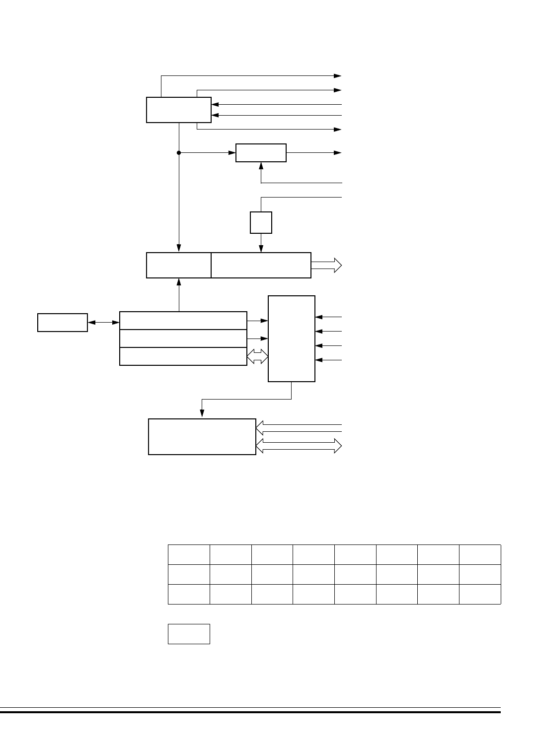
System Integration Module (SIM)
Introduction
MC68HC08AZ60 — Rev 1.1 Technical Data
Freescale Semiconductor System Integration Module (SIM) 99
Figure 9-1. SIM Block Diagram
Register Name Bit 7 6 5 4 3 2 1 Bit 0
SIM Break Status Register (SBSR) RRRRRRSBSWR
SIM Reset Status Register (SRSR) POR PIN COP ILOP ILAD 0 LVI 0
SIM Break Flag Control Register (SBFCR)BCFERRRRRRR
R=Reserved
Figure 9-2. SIM I/O Register Summary
STOP/WAIT
CLOCK
CONTROL CLOCK GENERATORS
POR CONTROL
RESET PIN CONTROL
SIM RESET STATUS REGISTER
INTERRUPT CONTROL
AND PRIORITY DECODE
MODULE STOP
MODULE WAIT
CPU STOP (FROM CPU)
CPU WAIT (FROM CPU)
SIMOSCEN (TO CGM)
CGMOUT (FROM CGM)
INTERNAL CLOCKS
MASTER
RESET
CONTROL
RESET
PIN LOGIC
LVI (FROM LVI MODULE)
ILLEGAL OPCODE (FROM CPU)
ILLEGAL ADDRESS (FROM ADDRESS
MAP DECODERS)
COP (FROM COP MODULE)
INTERRUPT SOURCES
CPU INTERFACE
RESET
CONTROL
SIM
COUNTER COP CLOCK
CGMXCLK (FROM CGM)
÷ 2

System Integration Module (SIM)
Technical Data MC68HC08AZ60 — Rev 1.1
100 System Integration Module (SIM) Freescale Semiconductor
Table 9-2 shows the internal signal names used in this section.
9.3 SIM Bus Clock Control and Generation
The bus clock generator provides system clock signals for the CPU and
peripherals on the MCU. The system clocks are generated from an
incoming clock, CGMOUT, as shown in Figure 9-3. This clock can come
from either an external oscillator or from the on-chip PLL. (See Clock
Generation Module (CGM) on page 121).
9.3.1 Bus Timing
In user mode, the internal bus frequency is either the crystal oscillator
output (CGMXCLK) divided by four or the PLL output (CGMVCLK)
divided by four. (See Clock Generation Module (CGM) on page 121).
Table 9-1. I/O Register Address Summary
Register SBSR SRSR SBFCR
Address $FE00 $FE01 $FE03
Table 9-2. Signal Name Conventions
Signal Name Description
CGMXCLK Buffered Version of OSC1 from Clock Generator Module
(CGM)
CGMVCLK PLL Output
CGMOUT PLL-Based or OSC1-Based Clock Output from CGM Module
(Bus Clock = CGMOUT Divided by Two)
IAB Internal Address Bus
IDB Internal Data Bus
PORRST Signal from the Power-On Reset Module to the SIM
IRST Internal Reset Signal
R/W Read/Write Signal
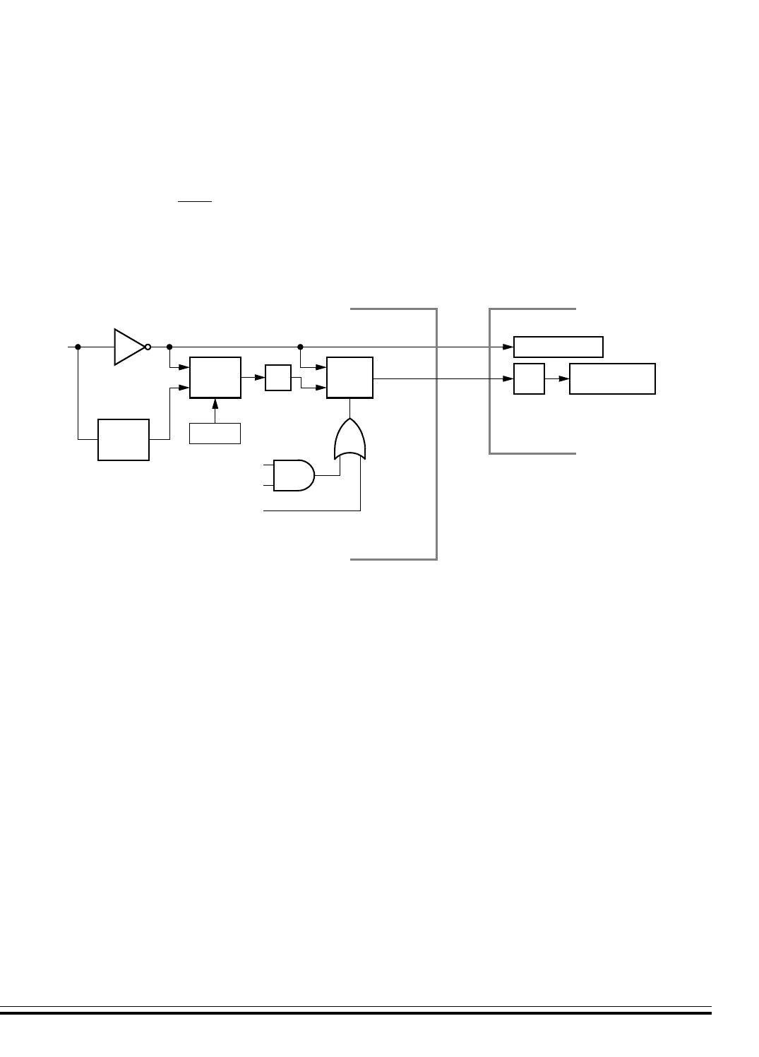
System Integration Module (SIM)
SIM Bus Clock Control and Generation
MC68HC08AZ60 — Rev 1.1 Technical Data
Freescale Semiconductor System Integration Module (SIM) 101
9.3.2 Clock Startup from POR or LVI Reset
When the power-on reset module or the low-voltage inhibit module
generates a reset, the clocks to the CPU and peripherals are inactive
and held in an inactive phase until after 4096 CGMXCLK cycles. The
RST pin is driven low by the SIM during this entire period. The bus clocks
start upon completion of the timeout.
Figure 9-3. CGM Clock Signals
9.3.3 Clocks in Stop Mode and Wait Mode
Upon exit from stop mode by an interrupt, break, or reset, the SIM allows
CGMXCLK to clock the SIM counter. The CPU and peripheral clocks do
not become active until after the stop delay timeout. This timeout is
selectable as 4096 or 32 CGMXCLK cycles. See Stop Mode on page
114.
In wait mode, the CPU clocks are inactive. Refer to the wait mode
subsection of each module to see if the module is active or inactive in
wait mode. Some modules can be programmed to be active in wait
mode.
PLL
OSC1 CGMXCLK
÷ 2BUS CLOCK
GENERATORS
SIM
CGM
SIM COUNTER
PTC3
MONITOR MODE
CLOCK
SELECT
CIRCUIT
CGMVCLK
BCS
÷ 2A
BS*
CGMOUT
*When S = 1,
CGMOUT = B
USER MODE

System Integration Module (SIM)
Technical Data MC68HC08AZ60 — Rev 1.1
102 System Integration Module (SIM) Freescale Semiconductor
9.4 Reset and System Initialization
The MCU has these reset sources:
• Power-on reset module (POR)
• External reset pin (RST)
• Computer operating properly module (COP)
• Low-voltage inhibit module (LVI)
• Illegal opcode
• Illegal address
All of these resets produce the vector $FFFE–FFFF ($FEFE–FEFF in
monitor mode) and assert the internal reset signal (IRST). IRST causes
all registers to be returned to their default values and all modules to be
returned to their reset states.
An internal reset clears the SIM counter (see SIM Counter on page
106), but an external reset does not. Each of the resets sets a
corresponding bit in the SIM reset status register (SRSR) (see SIM
Registers on page 116).
9.4.1 External Pin Reset
Pulling the asynchronous RST pin low halts all processing. The PIN bit
of the SIM reset status register (SRSR) is set as long as RST is held low
for a minimum of 67 CGMXCLK cycles, assuming that neither the POR
nor the LVI was the source of the reset. See Table 9-3 for details. Figure
9-4 shows the relative timing.
Table 9-3. PIN Bit Set Timing
Reset Type Number of Cycles Required to Set PIN
POR/LVI 4163 (4096 + 64 + 3)
All others 67 (64 + 3)
System Integration Module (SIM)
Reset and System Initialization
MC68HC08AZ60 — Rev 1.1 Technical Data
Freescale Semiconductor System Integration Module (SIM) 103
Figure 9-4. External Reset Timing
9.4.2 Active Resets from Internal Sources
All internal reset sources actively pull the RST pin low for 32 CGMXCLK
cycles to allow resetting of external peripherals. The internal reset signal
IRST continues to be asserted for an additional 32 cycles (see Figure 9-
5). An internal reset can be caused by an illegal address, illegal opcode,
COP timeout, LVI, or POR (see Figure 9-6). Note that for LVI or POR
resets, the SIM cycles through 4096 CGMXCLK cycles during which the
SIM forces the RST pin low. The internal reset signal then follows the
sequence from the falling edge of RST shown in Figure 9-5.
The COP reset is asynchronous to the bus clock.
The active reset feature allows the part to issue a reset to peripherals
and other chips within a system built around the MCU.
Figure 9-5. Internal Reset Timing
RST
IAB PC VECT H VECT L
CGMOUT
IRST
RST RST PULLED LOW BY MCU
IAB
32 CYCLES 32 CYCLES
VECTOR HIGH
CGMXCLK

System Integration Module (SIM)
Technical Data MC68HC08AZ60 — Rev 1.1
104 System Integration Module (SIM) Freescale Semiconductor
Figure 9-6. Sources of Internal Reset
9.4.2.1 Power-On Reset
When power is first applied to the MCU, the power-on reset module
(POR) generates a pulse to indicate that power-on has occurred. The
external reset pin (RST) is held low while the SIM counter counts out
4096 CGMXCLK cycles. Another sixty-four CGMXCLK cycles later, the
CPU and memories are released from reset to allow the reset vector
sequence to occur.
At power-on, the following events occur:
• A POR pulse is generated.
• The internal reset signal is asserted.
• The SIM enables CGMOUT.
• Internal clocks to the CPU and modules are held inactive for 4096
CGMXCLK cycles to allow stabilization of the oscillator.
• The RST pin is driven low during the oscillator stabilization time.
• The POR bit of the SIM reset status register (SRSR) is set and all
other bits in the register are cleared.
ILLEGAL ADDRESS RST
ILLEGAL OPCODE RST
COPRST
LVI
POR
INTERNAL RESET
System Integration Module (SIM)
Reset and System Initialization
MC68HC08AZ60 — Rev 1.1 Technical Data
Freescale Semiconductor System Integration Module (SIM) 105
Figure 9-7. POR Recovery
9.4.2.2 Computer Operating Properly (COP) Reset
The overflow of the COP counter causes an internal reset and sets the
COP bit in the SIM reset status register (SRSR) if the COPD bit in the
CONFIG-1 register is at logic zero.
See Computer Operating Properly (COP) on page 171.
9.4.2.3 Illegal Opcode Reset
The SIM decodes signals from the CPU to detect illegal instructions. An
illegal instruction sets the ILOP bit in the SIM reset status register
(SRSR) and causes a reset.
If the stop enable bit, STOP, in the MOR register is logic zero, the SIM
treats the STOP instruction as an illegal opcode and causes an illegal
opcode reset.
9.4.2.4 Illegal Address Reset
An opcode fetch from an unmapped address generates an illegal
address reset. The SIM verifies that the CPU is fetching an opcode prior
to asserting the ILAD bit in the SIM reset status register (SRSR) and
PORRST
OSC1
CGMXCLK
CGMOUT
RST
IAB
4096
CYCLES
32
CYCLES
32
CYCLES
$FFFE $FFFF

System Integration Module (SIM)
Technical Data MC68HC08AZ60 — Rev 1.1
106 System Integration Module (SIM) Freescale Semiconductor
resetting the MCU. A data fetch from an unmapped address does not
generate a reset.
Extra care should be exercised if code running in these parts is
eventually shrunk into a smaller ROM size. Code errors may result
in illegal addresses being accessed. Devices with smaller ROM
sizes may behave in a different manner in this instance. Is is the
user’s responsibility to check their code for illegal addresses.
Also note that some HC08 devices generate illegal address resets
with data fetches under certain circumstances. User’s should
always check relevant data books and always check their code for
illegal addresses.
9.4.2.5 Low-Voltage Inhibit (LVI) Reset
The low-voltage inhibit module (LVI) asserts its output to the SIM when
the VDD voltage falls to the VLVII voltage. The LVI bit in the SIM reset
status register (SRSR) is set and a chip reset is asserted if the LVIPWRD
and LVIRSTD bits in the CONFIG-1 register are at logic zero. The RST
pin will be held low until the SIM counts 4096 CGMXCLK cycles after
VDD rises above VLVIR. Another sixty-four CGMXCLK cycles later, the
CPU is released from reset to allow the reset vector sequence to occur.
See Low Voltage Inhibit (LVI) on page 177.
9.5 SIM Counter
The SIM counter is used by the power-on reset module (POR) and in
stop mode recovery to allow the oscillator time to stabilize before
enabling the internal bus (IBUS) clocks. The SIM counter also serves as
a prescaler for the computer operating properly module (COP). The SIM
counter overflow supplies the clock for the COP module. The SIM
counter is 12 bits long and is clocked by the falling edge of CGMXCLK.
9.5.1 SIM Counter During Power-On Reset
The power-on reset module (POR) detects power applied to the MCU.
At power-on, the POR circuit asserts the signal PORRST. Once the SIM

System Integration Module (SIM)
Program Exception Control
MC68HC08AZ60 — Rev 1.1 Technical Data
Freescale Semiconductor System Integration Module (SIM) 107
is initialized, it enables the clock generation module (CGM) to drive the
bus clock state machine.
9.5.2 SIM Counter During Stop Mode Recovery
The SIM counter also is used for stop mode recovery. The STOP
instruction clears the SIM counter. After an interrupt, break, or reset, the
SIM senses the state of the short stop recovery bit, SSREC, in the mask
option register. If the SSREC bit is a logic one, then the stop recovery is
reduced from the normal delay of 4096 CGMXCLK cycles down to 32
CGMXCLK cycles. This is ideal for applications using canned oscillators
that do not require long start-up times from stop mode. External crystal
applications should use the full stop recovery time, that is, with SSREC
cleared.
9.5.3 SIM Counter and Reset States
External reset has no effect on the SIM counter. See Stop Mode on
page 114 for details. The SIM counter is free-running after all reset
states. See Active Resets from Internal Sources on page 103 for
counter control and internal reset recovery sequences.
9.6 Program Exception Control
Normal, sequential program execution can be changed in three different
ways:
• Interrupts
– Maskable hardware CPU interrupts
– Non-maskable software interrupt instruction (SWI)
• Reset
• Break interrupts

System Integration Module (SIM)
Technical Data MC68HC08AZ60 — Rev 1.1
108 System Integration Module (SIM) Freescale Semiconductor
9.6.1 Interrupts
At the beginning of an interrupt, the CPU saves the CPU register
contents on the stack and sets the interrupt mask (I bit) to prevent
additional interrupts. At the end of an interrupt, the RTI instruction
recovers the CPU register contents from the stack so that normal
processing can resume. Figure 9-8 shows interrupt entry timing. Figure
9-10 shows interrupt recovery timing.
Interrupts are latched, and arbitration is performed in the SIM at the start
of interrupt processing. The arbitration result is a constant that the CPU
uses to determine which vector to fetch. Once an interrupt is latched by
the SIM, no other interrupt can take precedence, regardless of priority,
until the latched interrupt is serviced (or the I bit is cleared), see Figure
9-9.
Figure 9-8. Interrupt Entry
MODULE
IDB
R/W
INTERRUPT
DUMMY SP SP – 1 SP – 2 SP – 3 SP – 4 VECT H VECT L START ADDR
IAB
DUMMY PC – 1[7:0] PC – 1[15:8] X A CCR V DATA H V DATA L OPCODE
I BIT
System Integration Module (SIM)
Program Exception Control
MC68HC08AZ60 — Rev 1.1 Technical Data
Freescale Semiconductor System Integration Module (SIM) 109
Figure 9-9. Interrupt Processing
NO
NO
NO
YES
NO
NO
YES
YES
(AS MANY INTERRUPTS
I BIT SET?
FROM RESET
BREAK INTERRUPT?
I BIT SET?
IRQ
INTERRUPT?
SWI
INSTRUCTION?
RTI
INSTRUCTION?
FETCH NEXT
INSTRUCTION.
UNSTACK CPU REGISTERS.
STACK CPU REGISTERS.
SET I BIT.
LOAD PC WITH INTERRUPT VECTOR.
EXECUTE INSTRUCTION.
YES
YES
AS EXIST ON CHIP)

System Integration Module (SIM)
Technical Data MC68HC08AZ60 — Rev 1.1
110 System Integration Module (SIM) Freescale Semiconductor
Figure 9-10. Interrupt Recovery
Hardware Interrupts
A hardware interrupt does not stop the current instruction. Processing
of a hardware interrupt begins after completion of the current
instruction. When the current instruction is complete, the SIM checks
all pending hardware interrupts. If interrupts are not masked (I bit
clear in the condition code register), and if the corresponding interrupt
enable bit is set, the SIM proceeds with interrupt processing;
otherwise, the next instruction is fetched and executed.
If more than one interrupt is pending at the end of an instruction
execution, the highest priority interrupt is serviced first. Figure 9-11
demonstrates what happens when two interrupts are pending. If an
interrupt is pending upon exit from the original interrupt service
routine, the pending interrupt is serviced before the LDA instruction is
executed.
The LDA opcode is prefetched by both the INT1 and INT2 RTI
instructions. However, in the case of the INT1 RTI prefetch, this is a
redundant operation.
NOTE: To maintain compatibility with the M68HC05, M6805 and M146805
Families the H register is not pushed on the stack during interrupt entry.
If the interrupt service routine modifies the H register or uses the indexed
addressing mode, software should save the H register and then restore
it prior to exiting the routine.
MODULE
IDB
R/W
INTERRUPT
SP – 4 SP – 3 SP – 2 SP – 1 SP PC PC + 1
IAB
CCR A X PC – 1 [7:0] PC – 1 [15:8] OPCODE OPERAND
I BIT
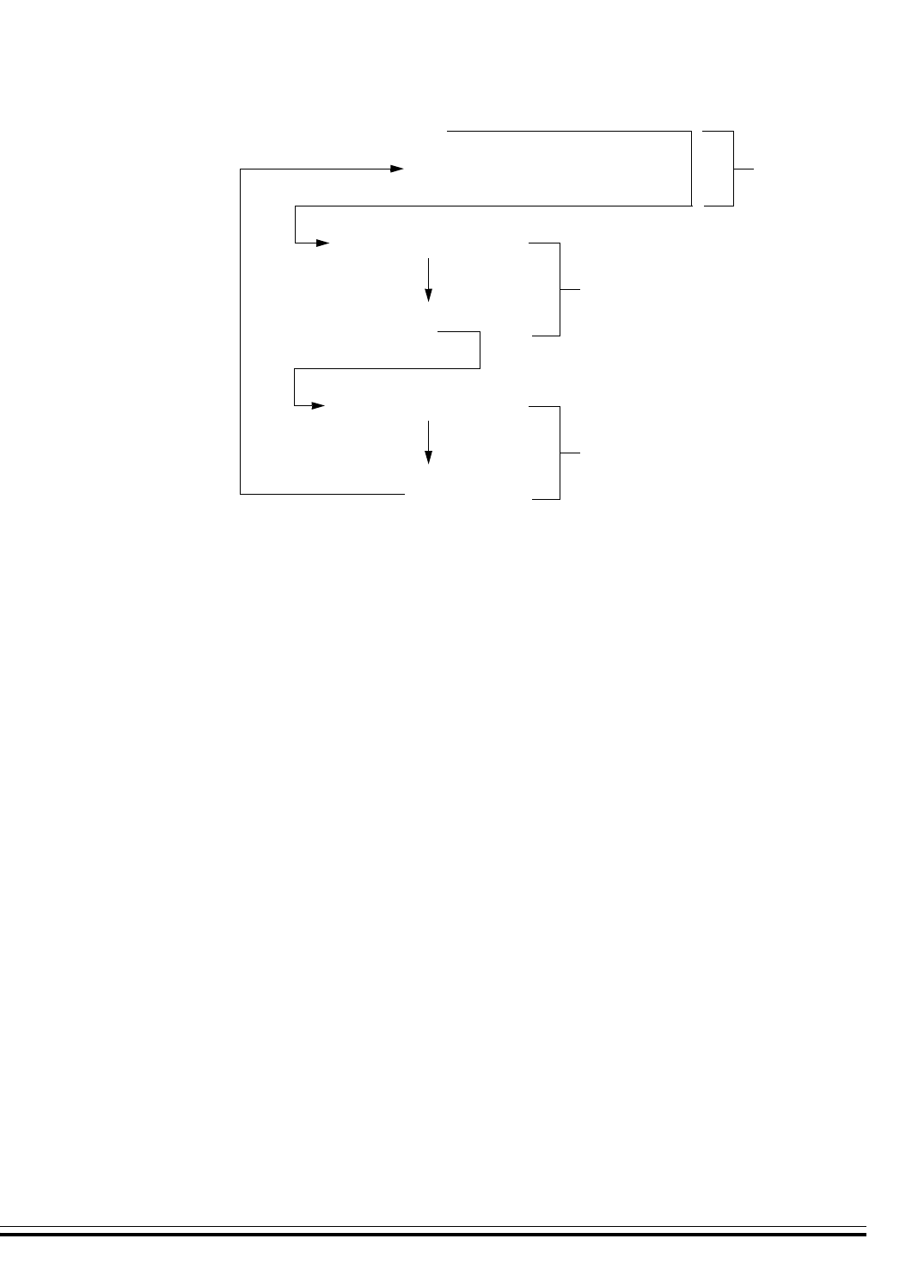
System Integration Module (SIM)
Program Exception Control
MC68HC08AZ60 — Rev 1.1 Technical Data
Freescale Semiconductor System Integration Module (SIM) 111
Figure 9-11. Interrupt Recognition Example
SWI Instruction
The SWI instruction is a non-maskable instruction that causes an
interrupt regardless of the state of the interrupt mask (I bit) in the
condition code register.
NOTE: A software interrupt pushes PC onto the stack. A software interrupt does
not push PC – 1, as a hardware interrupt does.
9.6.2 Reset
All reset sources always have higher priority than interrupts and cannot
be arbitrated.
9.6.3 Break Interrupts
The break module can stop normal program flow at a software-
programmable break point by asserting its break interrupt output. See
Break Module (BRK) on page 153. The SIM puts the CPU into the break
state by forcing it to the SWI vector location. Refer to the break interrupt
CLI
LDA
INT1
PULH
RTI
INT2
BACKGROUND
#$FF
PSHH
INT1 INTERRUPT SERVICE ROUTINE
PULH
RTI
PSHH
INT2 INTERRUPT SERVICE ROUTINE
ROUTINE

System Integration Module (SIM)
Technical Data MC68HC08AZ60 — Rev 1.1
112 System Integration Module (SIM) Freescale Semiconductor
subsection of each module to see how each module is affected by the
break state.
9.6.4 Status Flag Protection in Break Mode
The SIM controls whether status flags contained in other modules can
be cleared during break mode. The user can select whether flags are
protected from being cleared by properly initializing the break clear flag
enable bit (BCFE) in the SIM break flag control register (SBFCR).
Protecting flags in break mode ensures that set flags will not be cleared
while in break mode. This protection allows registers to be freely read
and written during break mode without losing status flag information.
Setting the BCFE bit enables the clearing mechanisms. Once cleared in
break mode, a flag remains cleared even when break mode is exited.
Status flags with a two-step clearing mechanism — for example, a read
of one register followed by the read or write of another — are protected,
even when the first step is accomplished prior to entering break mode.
Upon leaving break mode, execution of the second step will clear the flag
as normal.
9.7 Low-Power Modes
Executing the WAIT or STOP instruction puts the MCU in a low power-
consumption mode for standby situations. The SIM holds the CPU in a
non-clocked state. The operation of each of these modes is described
below. Both STOP and WAIT clear the interrupt mask (I) in the condition
code register, allowing interrupts to occur.
9.7.1 Wait Mode
In wait mode, the CPU clocks are inactive while one set of peripheral
clocks continue to run. Figure 9-12 shows the timing for wait mode entry.
A module that is active during wait mode can wake up the CPU with an
interrupt if the interrupt is enabled. Stacking for the interrupt begins one
cycle after the WAIT instruction during which the interrupt occurred.

System Integration Module (SIM)
Low-Power Modes
MC68HC08AZ60 — Rev 1.1 Technical Data
Freescale Semiconductor System Integration Module (SIM) 113
Refer to the wait mode subsection of each module to see if the module
is active or inactive in wait mode. Some modules can be programmed to
be active in wait mode.
Wait mode can also be exited by a reset or break. A break interrupt
during wait mode sets the SIM break stop/wait bit, SBSW, in the SIM
break status register (SBSR). If the COP disable bit, COPD, in the
configuration register is logic 0, then the computer operating properly
module (COP) is enabled and remains active in wait mode.
Figure 9-12. Wait Mode Entry Timing
Figure 9-13. Wait Recovery from Interrupt or Break
WAIT ADDR + 1 SAME SAMEIAB
IDB PREVIOUS DATA NEXT OPCODE SAME
WAIT ADDR
SAME
R/W
NOTE: Previous data can be operand data or the WAIT opcode, depending on the last instruction.
$6E0C$6E0B $00FF $00FE $00FD $00FC
$A6 $A6 $01 $0B $6E$A6
IAB
IDB
EXITSTOPWAIT
NOTE: EXITSTOPWAIT = RST pin OR CPU interrupt OR break interrupt
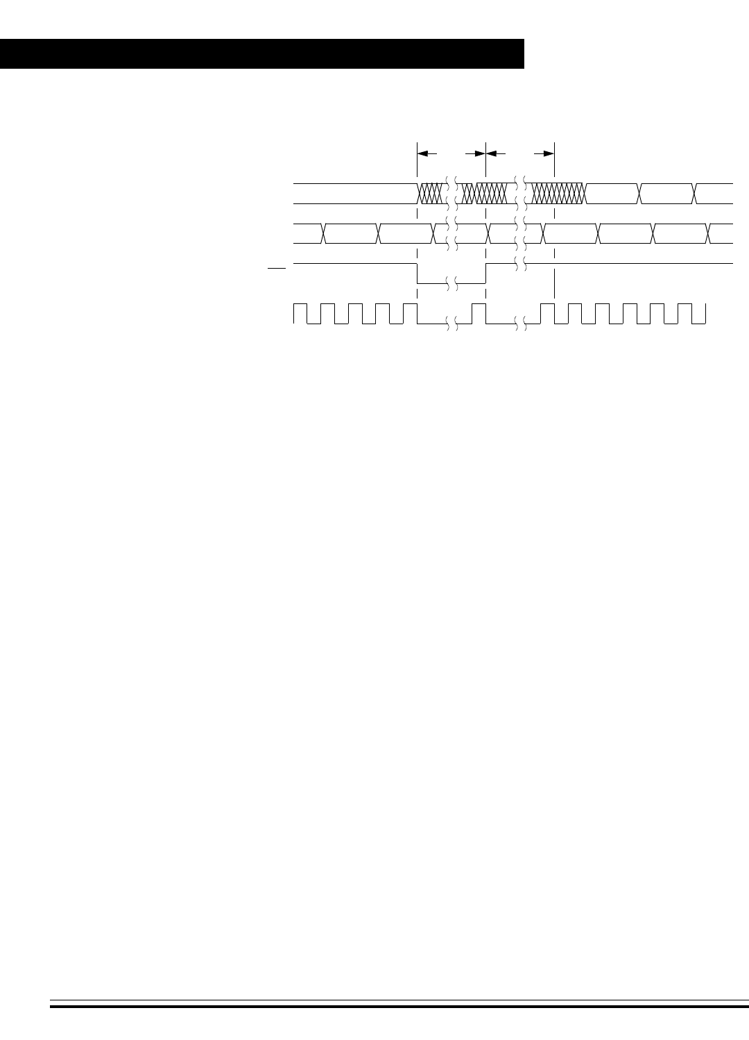
System Integration Module (SIM)
Technical Data MC68HC08AZ60 — Rev 1.1
114 System Integration Module (SIM) Freescale Semiconductor
Figure 9-14. Wait Recovery from Internal Reset
9.7.2 Stop Mode
In stop mode, the SIM counter is reset and the system clocks are
disabled. An interrupt request from a module can cause an exit from stop
mode. Stacking for interrupts begins after the selected stop recovery
time has elapsed. Reset or break also causes an exit from stop mode.
The SIM disables the clock generator module outputs (CGMOUT and
CGMXCLK) in stop mode, stopping the CPU and peripherals. Stop
recovery time is selectable using the SSREC bit in the mask option
register (MOR). If SSREC is set, stop recovery is reduced from the
normal delay of 4096 CGMXCLK cycles down to 32. This is ideal for
applications using canned oscillators that do not require long startup
times from stop mode.
NOTE: External crystal applications should use the full stop recovery time by
clearing the SSREC bit.
A break interrupt during stop mode sets the SIM break stop/wait bit
(SBSW) in the SIM break status register (SBSR).
The SIM counter is held in reset from the execution of the STOP
instruction until the beginning of stop recovery. It is then used to time the
recovery period. Figure 9-15 shows stop mode entry timing.
IAB
IDB
RST
$A6 $A6
$6E0B RST VCT H RST VCT L
$A6
CGMXCLK
32
Cycles
32
Cycles
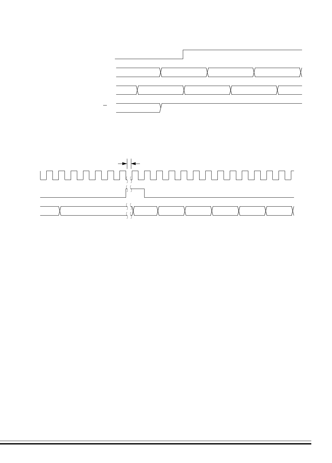
System Integration Module (SIM)
Low-Power Modes
MC68HC08AZ60 — Rev 1.1 Technical Data
Freescale Semiconductor System Integration Module (SIM) 115
Figure 9-15. Stop Mode Entry Timing
Figure 9-16. Stop Mode Recovery from Interrupt or Break
STOP ADDR + 1 SAME SAMEIAB
IDB PREVIOUS DATA NEXT OPCODE SAME
STOP ADDR
SAME
R/W
CPUSTOP
NOTE: Previous data can be operand data or the STOP opcode, depending on the last
instruction.
CGMXCLK
INT/BREAK
IAB STOP + 2 STOP + 2 SP SP – 1 SP – 2 SP – 3
STOP +1
STOP RECOVERY PERIOD

System Integration Module (SIM)
Technical Data MC68HC08AZ60 — Rev 1.1
116 System Integration Module (SIM) Freescale Semiconductor
9.8 SIM Registers
The SIM has three memory mapped registers.
9.8.1 SIM Break Status Register
The SIM break status register contains a flag to indicate that a break
caused an exit from stop or wait mode.
SBSW — SIM Break Stop/Wait
This status bit is useful in applications requiring a return to wait or stop
mode after exiting from a break interrupt. Clear SBSW by writing a
logic 0 to it. Reset clears SBSW.
1 = Stop mode or wait mode was exited by break interrupt
0 = Stop mode or wait mode was not exited by break interrupt
SBSW can be read within the break state SWI routine. The user can
modify the return address on the stack by subtracting one from it. The
following code is an example of this. Writing zero to the SBSW bit
clears it.
Address: $FE00
Bit 7654321Bit 0
Read:
RRRRRR
SBSW
R
Write: See Note
Reset: 0
R = Reserved NOTE: Writing a logic 0 clears SBSW
Figure 9-17. SIM Break Status Register (SBSR)

System Integration Module (SIM)
SIM Registers
MC68HC08AZ60 — Rev 1.1 Technical Data
Freescale Semiconductor System Integration Module (SIM) 117
;
;
;
This code works if the H register has been pushed onto the stack in the break
service routine software. This code should be executed at the end of the
break service routine software.
HIBYTE EQU 5
LOBYTE EQU 6
; If not SBSW, do RTI
BRCLR SBSW,SBSR, RETURN ;
;
See if wait mode or stop mode was exited
by break.
TST LOBYTE,SP ; If RETURNLO is not zero,
BNE DOLO ; then just decrement low byte.
DEC HIBYTE,SP ; Else deal with high byte, too.
DOLO DEC LOBYTE,SP ; Point to WAIT/STOP opcode.
RETURN PULH
RTI
; Restore H register.

System Integration Module (SIM)
Technical Data MC68HC08AZ60 — Rev 1.1
118 System Integration Module (SIM) Freescale Semiconductor
9.8.2 SIM Reset Status Register
This register contains six flags that show the source of the last reset. The
status register will automatically clear after reading it. A power-on reset
sets the POR bit and clears all other bits in the register.
POR — Power-On Reset Bit
1 = Last reset caused by POR circuit
0 = Read of SRSR
PIN — External Reset Bit
1 = Last reset caused by external reset pin (RST)
0 = POR or read of SRSR
COP — Computer Operating Properly Reset Bit
1 = Last reset caused by COP counter
0 = POR or read of SRSR
ILOP — Illegal Opcode Reset Bit
1 = Last reset caused by an illegal opcode
0 = POR or read of SRSR
ILAD — Illegal Address Reset Bit (opcode fetches only)
1 = Last reset caused by an opcode fetch from an illegal address
0 = POR or read of SRSR
LVI — Low-Voltage Inhibit Reset Bit
1 = Last reset was caused by the LVI circuit
0 = POR or read of SRSR
Address: $FE01
Bit 7654321Bit 0
Read: POR PIN COP ILOP ILAD 0 LVI 0
Write:
POR:10000000
= Unimplemented
Figure 9-18. SIM Reset Status Register (SRSR)

System Integration Module (SIM)
SIM Registers
MC68HC08AZ60 — Rev 1.1 Technical Data
Freescale Semiconductor System Integration Module (SIM) 119
9.8.3 SIM Break Flag Control Register
The SIM break control register contains a bit that enables software to
clear status bits while the MCU is in a break state.
BCFE — Break Clear Flag Enable Bit
This read/write bit enables software to clear status bits by accessing
status registers while the MCU is in a break state. To clear status bits
during the break state, the BCFE bit must be set.
1 = Status bits clearable during break
0 = Status bits not clearable during break
Address: $FE03
Bit 7654321Bit 0
Read: BCFERRRRRRR
Write:
Reset: 0 0
R= Reserved
Figure 9-19. SIM Break Flag Control Register (SBFCR)

System Integration Module (SIM)
Technical Data MC68HC08AZ60 — Rev 1.1
120 System Integration Module (SIM) Freescale Semiconductor

MC68HC08AZ60 — Rev 1.1 Technical Data
Freescale Semiconductor Clock Generation Module (CGM) 121
Technical Data — MC68HC08AZ60
Section 10. Clock Generation Module (CGM)
10.1 Contents
10.2 Introduction. . . . . . . . . . . . . . . . . . . . . . . . . . . . . . . . . . . . . .122
10.3 Features. . . . . . . . . . . . . . . . . . . . . . . . . . . . . . . . . . . . . . . . .122
10.4 Functional Description. . . . . . . . . . . . . . . . . . . . . . . . . . . . .123
10.4.1 Crystal Oscillator Circuit . . . . . . . . . . . . . . . . . . . . . . . . .123
10.4.2 Phase-Locked Loop Circuit (PLL). . . . . . . . . . . . . . . . . .126
10.4.2.1 Circuits . . . . . . . . . . . . . . . . . . . . . . . . . . . . . . . . . . . . .126
10.4.2.2 Acquisition and Tracking Modes . . . . . . . . . . . . . . . .127
10.4.2.3 Manual and Automatic PLL Bandwidth Modes . . . . .128
10.4.2.4 Programming the PLL . . . . . . . . . . . . . . . . . . . . . . . . .130
10.4.2.5 Special Programming Exceptions . . . . . . . . . . . . . . .132
10.4.3 Base Clock Selector Circuit . . . . . . . . . . . . . . . . . . . . . .132
10.4.4 CGM External Connections. . . . . . . . . . . . . . . . . . . . . . .133
10.5 I/O Signals . . . . . . . . . . . . . . . . . . . . . . . . . . . . . . . . . . . . . . .134
10.5.1 Crystal Amplifier Input Pin (OSC1). . . . . . . . . . . . . . . . .134
10.5.2 Crystal Amplifier Output Pin (OSC2) . . . . . . . . . . . . . . .134
10.5.3 External Filter Capacitor Pin (CGMXFC) . . . . . . . . . . . .134
10.5.4 Analog Power Pin (VDDA). . . . . . . . . . . . . . . . . . . . . . . . .135
10.5.5 Oscillator Enable Signal (SIMOSCEN) . . . . . . . . . . . . . .135
10.5.6 Crystal Output Frequency Signal (CGMXCLK) . . . . . . .135
10.5.7 CGM Base Clock Output (CGMOUT) . . . . . . . . . . . . . . .135
10.5.8 CGM CPU Interrupt (CGMINT) . . . . . . . . . . . . . . . . . . . . .135
10.6 CGM Registers . . . . . . . . . . . . . . . . . . . . . . . . . . . . . . . . . . .136
10.6.1 PLL Control Register . . . . . . . . . . . . . . . . . . . . . . . . . . . .136
10.6.2 PLL Bandwidth Control Register . . . . . . . . . . . . . . . . . .138
10.6.3 PLL Programming Register. . . . . . . . . . . . . . . . . . . . . . .140
10.7 Interrupts. . . . . . . . . . . . . . . . . . . . . . . . . . . . . . . . . . . . . . . .142
10.8 Low-Power Modes . . . . . . . . . . . . . . . . . . . . . . . . . . . . . . . .142

Clock Generation Module (CGM)
Technical Data MC68HC08AZ60 — Rev 1.1
122 Clock Generation Module (CGM) Freescale Semiconductor
10.8.1 Wait Mode . . . . . . . . . . . . . . . . . . . . . . . . . . . . . . . . . . . . .142
10.8.2 Stop Mode. . . . . . . . . . . . . . . . . . . . . . . . . . . . . . . . . . . . .143
10.9 CGM During Break Interrupts . . . . . . . . . . . . . . . . . . . . . . .143
10.10 Acquisition/Lock Time Specifications . . . . . . . . . . . . . . . .143
10.10.1 Acquisition/Lock Time Definitions . . . . . . . . . . . . . . . . .143
10.10.2 Parametric Influences on Reaction Time. . . . . . . . . . . .145
10.10.3 Choosing a Filter Capacitor . . . . . . . . . . . . . . . . . . . . . .146
10.10.4 Reaction Time Calculation . . . . . . . . . . . . . . . . . . . . . . .147
10.2 Introduction
The CGM generates the crystal clock signal, CGMXCLK, which operates
at the frequency of the crystal. The CGM also generates the base clock
signal, CGMOUT, from which the system clocks are derived. CGMOUT
is based on either the crystal clock divided by two or the phase-locked
loop (PLL) clock, CGMVCLK, divided by two. The PLL is a frequency
generator designed for use with 1-MHz to 8-MHz crystals or ceramic
resonators. The PLL can generate an 8-MHz bus frequency without
using a 32-MHz crystal.
10.3 Features
Features of the CGM include:
• Phase-Locked Loop with Output Frequency in Integer Multiples of
the Crystal Reference
• Programmable Hardware Voltage-Controlled Oscillator (VCO) for
Low-Jitter Operation
• Automatic Bandwidth Control Mode for Low-Jitter Operation
• Automatic Frequency Lock Detector
• CPU Interrupt on Entry or Exit from Locked Condition

Clock Generation Module (CGM)
Functional Description
MC68HC08AZ60 — Rev 1.1 Technical Data
Freescale Semiconductor Clock Generation Module (CGM) 123
10.4 Functional Description
The CGM consists of three major submodules:
• Crystal oscillator circuit — The crystal oscillator circuit generates
the constant crystal frequency clock, CGMXCLK.
• Phase-locked loop (PLL) — The PLL generates the
programmable VCO frequency clock CGMVCLK.
• Base clock selector circuit — This software-controlled circuit
selects either CGMXCLK divided by two or the VCO clock,
CGMVCLK, divided by two as the base clock, CGMOUT. The
system clocks are derived from CGMOUT.
Figure 10-1 shows the structure of the CGM.
10.4.1 Crystal Oscillator Circuit
The crystal oscillator circuit consists of an inverting amplifier and an
external crystal. The OSC1 pin is the input to the amplifier and the OSC2
pin is the output. The SIMOSCEN signal enables the crystal oscillator
circuit.
The CGMXCLK signal is the output of the crystal oscillator circuit and
runs at a rate equal to the crystal frequency. CGMXCLK is then buffered
to produce CGMRCLK, the PLL reference clock.
CGMXCLK can be used by other modules which require precise timing
for operation. The duty cycle of CGMXCLK is not guaranteed to be 50%
and depends on external factors, including the crystal and related
external components.
An externally generated clock also can feed the OSC1 pin of the crystal
oscillator circuit. Connect the external clock to the OSC1 pin and let the
OSC2 pin float.
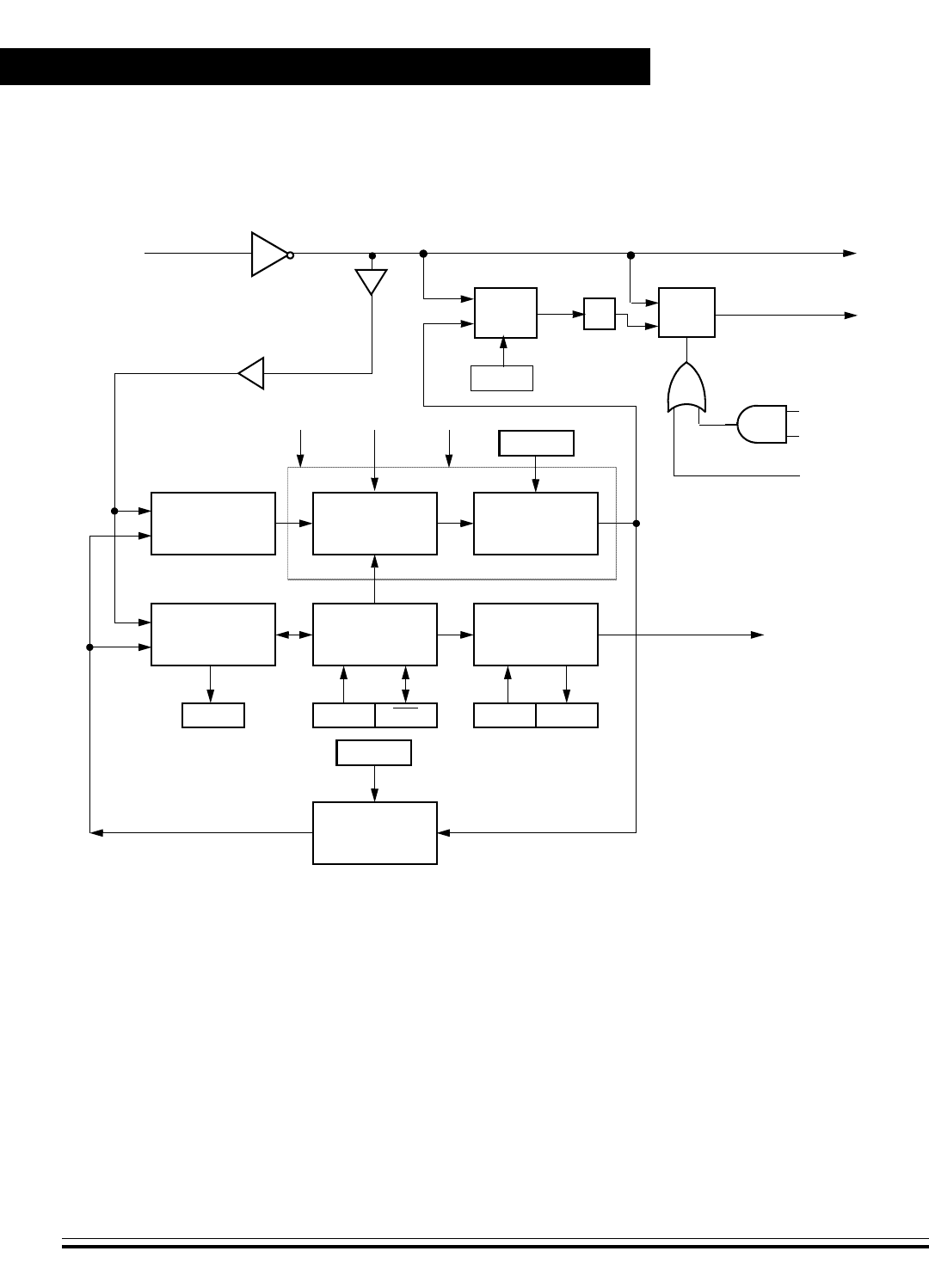
Clock Generation Module (CGM)
Technical Data MC68HC08AZ60 — Rev 1.1
124 Clock Generation Module (CGM) Freescale Semiconductor
Figure 10-1. CGM Block Diagram
PHASE
DETECTOR LOOP
FILTER
FREQUENCY
DIVIDER
VOLTAGE
CONTROLLED
OSCILLATOR
BANDWIDTH
CONTROL
LOCK
DETECTOR
CLOCK
CGMVDV CGMVCLK
INTERRUPT
CONTROL
CGMINT
CGMRDV
PLL ANALOG
CGMRCLK
SELECT
CIRCUIT
LOCK AUTO ACQ
VRS7–VRS4
PLLIE PLLF
MUL7–MUL4
VDDA CGMXFC VSS
OSC1 CGMXCLK
PTC3
MONITOR MODE
BCS
÷ 2A
BS*
CGMOUT
*When S = 1,
CGMOUT = B
USER MODE

Clock Generation Module (CGM)
Functional Description
MC68HC08AZ60 — Rev 1.1 Technical Data
Freescale Semiconductor Clock Generation Module (CGM) 125
Register Name Bit 7654321Bit 0
PLL Control Register (PCTL)
Read: PLLIE PLLF PLLON BCS 1111
Write:
Reset:00101111
PLL Bandwidth Control Register
(PBWC)
Read: AUTO LOCK ACQ XLD 0000
Write:
Reset:00000000
PLL Programming Register (PPG)
Read: MUL7 MUL6 MUL5 MUL4 VRS7 VRS6 VRS5 VRS4
Write:
Reset:01100110
= Unimplemented
Figure 10-2. I/O Register Summary
Table 10-1. I/O Register Address Summary
Register PCTL PBWC PPG
Address $001C $001D $001E

Clock Generation Module (CGM)
Technical Data MC68HC08AZ60 — Rev 1.1
126 Clock Generation Module (CGM) Freescale Semiconductor
10.4.2 Phase-Locked Loop Circuit (PLL)
The PLL is a frequency generator that can operate in either acquisition
mode or tracking mode, depending on the accuracy of the output
frequency. The PLL can change between acquisition and tracking
modes either automatically or manually.
10.4.2.1 Circuits
The PLL consists of these circuits:
• Voltage-controlled oscillator (VCO)
• Modulo VCO frequency divider
• Phase detector
• Loop filter
• Lock detector
The operating range of the VCO is programmable for a wide range of
frequencies and for maximum immunity to external noise, including
supply and CGMXFC noise. The VCO frequency is bound to a range
from roughly one-half to twice the center-of-range frequency, fVRS.
Modulating the voltage on the CGMXFC pin changes the frequency
within this range. By design, fVRS is equal to the nominal center-of-range
frequency, fNOM, (4.9152 MHz) times a linear factor L or (L)fNOM.
CGMRCLK is the PLL reference clock, a buffered version of CGMXCLK.
CGMRCLK runs at a frequency, fRCLK, and is fed to the PLL through a
buffer. The buffer output is the final reference clock, CGMRDV, running
at a frequency fRDV =f
RCLK.
The VCO’s output clock, CGMVCLK, running at a frequency fVCLK, is fed
back through a programmable modulo divider. The modulo divider
reduces the VCO clock by a factor, N. The divider’s output is the VCO
feedback clock, CGMVDV, running at a frequency fVDV =f
VCLK/N. See
Programming the PLL on page 130 for more information.
The phase detector then compares the VCO feedback clock, CGMVDV,
with the final reference clock, CGMRDV. A correction pulse is generated
based on the phase difference between the two signals. The loop filter

Clock Generation Module (CGM)
Functional Description
MC68HC08AZ60 — Rev 1.1 Technical Data
Freescale Semiconductor Clock Generation Module (CGM) 127
then slightly alters the dc voltage on the external capacitor connected to
CGMXFC based on the width and direction of the correction pulse. The
filter can make fast or slow corrections depending on its mode, as
described in Acquisition and Tracking Modes on page 127. The value
of the external capacitor and the reference frequency determines the
speed of the corrections and the stability of the PLL.
The lock detector compares the frequencies of the VCO feedback clock,
CGMVDV, and the final reference clock, CGMRDV. Therefore, the
speed of the lock detector is directly proportional to the final reference
frequency, fRDV. The circuit determines the mode of the PLL and the lock
condition based on this comparison.
10.4.2.2 Acquisition and Tracking Modes
The PLL filter is manually or automatically configurable into one of two
operating modes:
• Acquisition mode — In acquisition mode, the filter can make large
frequency corrections to the VCO. This mode is used at PLL
startup or when the PLL has suffered a severe noise hit and the
VCO frequency is far off the desired frequency. When in
acquisition mode, the ACQ bit is clear in the PLL bandwidth control
register. See PLL Bandwidth Control Register on page 138.
• Tracking mode — In tracking mode, the filter makes only small
corrections to the frequency of the VCO. PLL jitter is much lower
in tracking mode, but the response to noise is also slower. The
PLL enters tracking mode when the VCO frequency is nearly
correct, such as when the PLL is selected as the base clock
source. See Base Clock Selector Circuit on page 132. The PLL
is automatically in tracking mode when it’s not in acquisition mode
or when the ACQ bit is set.

Clock Generation Module (CGM)
Technical Data MC68HC08AZ60 — Rev 1.1
128 Clock Generation Module (CGM) Freescale Semiconductor
10.4.2.3 Manual and Automatic PLL Bandwidth Modes
The PLL can change the bandwidth or operational mode of the loop filter
manually or automatically.
In automatic bandwidth control mode (AUTO = 1), the lock detector
automatically switches between acquisition and tracking modes.
Automatic bandwidth control mode also is used to determine when the
VCO clock, CGMVCLK, is safe to use as the source for the base clock,
CGMOUT. See PLL Bandwidth Control Register on page 138. If PLL
CPU interrupt requests are enabled, the software can wait for a PLL
CPU interrupt request and then check the LOCK bit. If CPU interrupts
are disabled, software can poll the LOCK bit continuously (during PLL
startup, usually) or at periodic intervals. In either case, when the LOCK
bit is set, the VCO clock is safe to use as the source for the base clock.
See Base Clock Selector Circuit on page 132. If the VCO is selected
as the source for the base clock and the LOCK bit is clear, the PLL has
suffered a severe noise hit and the software must take appropriate
action, depending on the application. See Interrupts on page 142.
These conditions apply when the PLL is in automatic bandwidth control
mode:
• The ACQ bit (See 10.6.2 PLL Bandwidth Control Register.) is a
read-only indicator of the mode of the filter. See Acquisition and
Tracking Modes on page 127.
• The ACQ bit is set when the VCO frequency is within a certain
tolerance, ∆trk, and is cleared when the VCO frequency is out of a
certain tolerance, ∆unt. See Electrical Specifications on page
430.
• The LOCK bit is a read-only indicator of the locked state of the
PLL.
• The LOCK bit is set when the VCO frequency is within a certain
tolerance, ∆Lock, and is cleared when the VCO frequency is out of
a certain tolerance, ∆unl. See Electrical Specifications on page
430.

Clock Generation Module (CGM)
Functional Description
MC68HC08AZ60 — Rev 1.1 Technical Data
Freescale Semiconductor Clock Generation Module (CGM) 129
• CPU interrupts can occur if enabled (PLLIE = 1) when the PLL’s
lock condition changes, toggling the LOCK bit. See PLL Control
Register on page 136.
The PLL also can operate in manual mode (AUTO = 0). Manual mode is
used by systems that do not require an indicator of the lock condition for
proper operation. Such systems typically operate well below fbusmax and
require fast startup. The following conditions apply when in manual
mode:
•ACQ is a writable control bit that controls the mode of the filter.
Before turning on the PLL in manual mode, the ACQ bit must be
clear.
• Before entering tracking mode (ACQ = 1), software must wait a
given time, tacq (see Electrical Specifications on page 430), after
turning on the PLL by setting PLLON in the PLL control register
(PCTL).
• Software must wait a given time, tal, after entering tracking mode
before selecting the PLL as the clock source to CGMOUT
(BCS = 1).
• The LOCK bit is disabled.
• CPU interrupts from the CGM are disabled.

Clock Generation Module (CGM)
Technical Data MC68HC08AZ60 — Rev 1.1
130 Clock Generation Module (CGM) Freescale Semiconductor
10.4.2.4 Programming the PLL
Use this 9-step procedure to program the PLL. The table below lists the
variables used and their meaning.
1. Choose the desired bus frequency, fBUSDES.
Example: fBUSDES = 8 MHz
2. Calculate the desired VCO frequency, fVCLKDES.
fVCLKDES = 4 × fBUSDES
Example: fVCLKDES = 4 × 8 MHz = 32 MHz
3. Using a reference frequency, fRCLK, equal to the crystal frequency,
calculate the VCO frequency multiplier, N. Round the result to the
nearest integer.
Example:
4. Calculate the VCO frequency, fVCLK.
Example: fVCLK = 8 × 4 MHz = 32 MHz
Table 10-2. Variable Definitions
Variable Definition
fBUSDES Desired Bus Clock Frequency
fVCLKDES Desired VCO Clock Frequency
fRCLK Chosen Reference Crystal Frequency
fVCLK Calculated VCO Clock Frequency
fBUS Calculated Bus Clock Frequency
fNOM Nominal VCO Center Frequency
fVRS Shifted VCO Center Frequency
NfVCLKDES
fRCLK
----------------------=
N 32 MHz
4 MHz
--------------------=8=
fVCLK Nf
RCLK
×=

Clock Generation Module (CGM)
Functional Description
MC68HC08AZ60 — Rev 1.1 Technical Data
Freescale Semiconductor Clock Generation Module (CGM) 131
5. Calculate the bus frequency, fBUS, and compare fBUS with
fBUSDES.
Example:
6. If the calculated fbus is not within the tolerance limits of your
application, select another fBUSDES or another fRCLK.
7. Using the value 4.9152 MHz for fNOM, calculate the VCO linear
range multiplier, L. The linear range multiplier controls the
frequency range of the PLL.
Example:
8. Calculate the VCO center-of-range frequency, fVRS. The center-
of-range frequency is the midpoint between the minimum and
maximum frequencies attainable by the PLL.
fVRS = L × fNOM
Example: fVRS = 7 × 4.9152 MHz = 34.4 MHz
NOTE: For proper operation, .
Exceeding the recommended maximum bus frequency or VCO
frequency can crash the MCU.
9. Program the PLL registers accordingly:
a. In the upper four bits of the PLL programming register (PPG),
program the binary equivalent of N.
b. In the lower four bits of the PLL programming register (PPG),
program the binary equivalent of L.
fBUS fVCLK
4
-------------=
fBUS 32 MHz
4
--------------------=8 MHz=
L round fVCLK
fNOM
-------------
=
L 32 MHz
4.9152 MHz
--------------------------------
=7=
fVRS fVCLK
–fNOM
2
----------------
≤

Clock Generation Module (CGM)
Technical Data MC68HC08AZ60 — Rev 1.1
132 Clock Generation Module (CGM) Freescale Semiconductor
10.4.2.5 Special Programming Exceptions
The programming method described in Programming the PLL on page
130, does not account for two possible exceptions. A value of 0 for N or
L is meaningless when used in the equations given. To account for these
exceptions:
• A 0 value for N is interpreted the same as a value of 1.
• A 0 value for L disables the PLL and prevents its selection as the
source for the base clock. See Base Clock Selector Circuit on
page 132.
10.4.3 Base Clock Selector Circuit
This circuit is used to select either the crystal clock, CGMXCLK, or the
VCO clock, CGMVCLK, as the source of the base clock, CGMOUT. The
two input clocks go through a transition control circuit that waits up to
three CGMXCLK cycles and three CGMVCLK cycles to change from
one clock source to the other. During this time, CGMOUT is held in
stasis. The output of the transition control circuit is then divided by two
to correct the duty cycle. Therefore, the bus clock frequency, which is
one-half of the base clock frequency, is one-fourth the frequency of the
selected clock (CGMXCLK or CGMVCLK).
The BCS bit in the PLL control register (PCTL) selects which clock drives
CGMOUT. The VCO clock cannot be selected as the base clock source
if the PLL is not turned on. The PLL cannot be turned off if the VCO clock
is selected. The PLL cannot be turned on or off simultaneously with the
selection or deselection of the VCO clock. The VCO clock also cannot
be selected as the base clock source if the factor L is programmed to a
0. This value would set up a condition inconsistent with the operation of
the PLL, so that the PLL would be disabled and the crystal clock would
be forced as the source of the base clock.

Clock Generation Module (CGM)
Functional Description
MC68HC08AZ60 — Rev 1.1 Technical Data
Freescale Semiconductor Clock Generation Module (CGM) 133
10.4.4 CGM External Connections
In its typical configuration, the CGM requires seven external
components. Five of these are for the crystal oscillator and two are for
the PLL.
The crystal oscillator is normally connected in a Pierce oscillator
configuration, as shown in Figure 10-3. Figure 10-3 shows only the
logical representation of the internal components and may not represent
actual circuitry. The oscillator configuration uses five components:
• Crystal, X1
• Fixed capacitor, C1
• Tuning capacitor, C2 (can also be a fixed capacitor)
• Feedback resistor, RB
• Series resistor, RS (optional)
The series resistor (RS) may not be required for all ranges of operation,
especially with high-frequency crystals. Refer to the crystal
manufacturer’s data for more information.
Figure 10-3 also shows the external components for the PLL:
• Bypass capacitor, CBYP
• Filter capacitor, CF
Routing should be done with great care to minimize signal cross talk and
noise. (See Acquisition/Lock Time Specifications on page 143 for
routing information and more information on the filter capacitor’s value
and its effects on PLL performance).
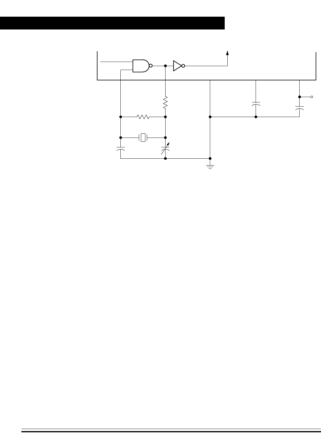
Clock Generation Module (CGM)
Technical Data MC68HC08AZ60 — Rev 1.1
134 Clock Generation Module (CGM) Freescale Semiconductor
Figure 10-3. CGM External Connections
10.5 I/O Signals
The following paragraphs describe the CGM input/output (I/O) signals.
10.5.1 Crystal Amplifier Input Pin (OSC1)
The OSC1 pin is an input to the crystal oscillator amplifier.
10.5.2 Crystal Amplifier Output Pin (OSC2)
The OSC2 pin is the output of the crystal oscillator inverting amplifier.
10.5.3 External Filter Capacitor Pin (CGMXFC)
The CGMXFC pin is required by the loop filter to filter out phase
corrections. A small external capacitor is connected to this pin.
NOTE: To prevent noise problems, CF should be placed as close to the
CGMXFC pin as possible with minimum routing distances and no routing
of other signals across the CF connection.
C1C2
CF
SIMOSCEN CGMXCLK
RB
X1
RS*
CBYP
*RS can be 0 (shorted) when used with higher-frequency crystals. Refer to manufacturer’s data.
OSC1
OSC2
VSS
CGMXFC
VDD
VDDA

Clock Generation Module (CGM)
I/O Signals
MC68HC08AZ60 — Rev 1.1 Technical Data
Freescale Semiconductor Clock Generation Module (CGM) 135
10.5.4 Analog Power Pin (VDDA)
VDDA is a power pin used by the analog portions of the PLL. Connect the
VDDA pin to the same voltage potential as the VDD pin.
NOTE: Route VDDA carefully for maximum noise immunity and place bypass
capacitors as close as possible to the package.
10.5.5 Oscillator Enable Signal (SIMOSCEN)
The SIMOSCEN signal enables the oscillator and PLL.
10.5.6 Crystal Output Frequency Signal (CGMXCLK)
CGMXCLK is the crystal oscillator output signal. It runs at the full speed
of the crystal (fxclk) and comes directly from the crystal oscillator circuit.
Figure 10-3 shows only the logical relation of CGMXCLK to OSC1 and
OSC2 and may not represent the actual circuitry. The duty cycle of
CGMXCLK is unknown and may depend on the crystal and other
external factors. Also, the frequency and amplitude of CGMXCLK can be
unstable at startup.
10.5.7 CGM Base Clock Output (CGMOUT)
CGMOUT is the clock output of the CGM. This signal is used to generate
the MCU clocks. CGMOUT is a 50% duty cycle clock running at twice the
bus frequency. CGMOUT is software programmable to be either the
oscillator output, CGMXCLK, divided by two or the VCO clock,
CGMVCLK, divided by two.
10.5.8 CGM CPU Interrupt (CGMINT)
CGMINT is the CPU interrupt signal generated by the PLL lock detector.

Clock Generation Module (CGM)
Technical Data MC68HC08AZ60 — Rev 1.1
136 Clock Generation Module (CGM) Freescale Semiconductor
10.6 CGM Registers
Three registers control and monitor operation of the CGM:
• PLL control register (PCTL)
• PLL bandwidth control register (PBWC)
• PLL programming register (PPG)
10.6.1 PLL Control Register
The PLL control register contains the interrupt enable and flag bits, the
on/off switch, and the base clock selector bit.
PLLIE — PLL Interrupt Enable Bit
This read/write bit enables the PLL to generate a CPU interrupt
request when the LOCK bit toggles, setting the PLL flag, PLLF. When
the AUTO bit in the PLL bandwidth control register (PBWC) is clear,
PLLIE cannot be written and reads as logic 0. Reset clears the PLLIE
bit.
1 = PLL CPU interrupt requests enabled
0 = PLL CPU interrupt requests disabled
Address: $001C
Bit 7654321Bit 0
Read:
PLLIE
PLLF
PLLON BCS
1111
Write:
Reset:00101111
= Unimplemented
Figure 10-4. PLL Control Register (PCTL)

Clock Generation Module (CGM)
CGM Registers
MC68HC08AZ60 — Rev 1.1 Technical Data
Freescale Semiconductor Clock Generation Module (CGM) 137
PLLF — PLL Flag Bit
This read-only bit is set whenever the LOCK bit toggles. PLLF
generates a CPU interrupt request if the PLLIE bit also is set. PLLF
always reads as logic 0 when the AUTO bit in the PLL bandwidth
control register (PBWC) is clear. Clear the PLLF bit by reading the
PLL control register. Reset clears the PLLF bit.
1 = Change in lock condition
0 = No change in lock condition
NOTE: Do not inadvertently clear the PLLF bit. Be aware that any read or read-
modify-write operation on the PLL control register clears the PLLF bit.
PLLON — PLL On Bit
This read/write bit activates the PLL and enables the VCO clock,
CGMVCLK. PLLON cannot be cleared if the VCO clock is driving the
base clock, CGMOUT (BCS = 1). See Base Clock Selector Circuit
on page 132. Reset sets this bit so that the loop can stabilize as the
MCU is powering up.
1 = PLL on
0 = PLL off
BCS — Base Clock Select Bit
This read/write bit selects either the crystal oscillator output,
CGMXCLK, or the VCO clock, CGMVCLK, as the source of the CGM
output, CGMOUT. CGMOUT frequency is one-half the frequency of
the selected clock. BCS cannot be set while the PLLON bit is clear.
After toggling BCS, it may take up to three CGMXCLK and three
CGMVCLK cycles to complete the transition from one source clock to
the other. During the transition, CGMOUT is held in stasis. See Base
Clock Selector Circuit on page 132. Reset and the STOP instruction
clear the BCS bit.
1 = CGMVCLK divided by two drives CGMOUT
0 = CGMXCLK divided by two drives CGMOUT
NOTE: PLLON and BCS have built-in protection that prevents the base clock
selector circuit from selecting the VCO clock as the source of the base
clock if the PLL is off. Therefore, PLLON cannot be cleared when BCS
is set, and BCS cannot be set when PLLON is clear. If the PLL is off

Clock Generation Module (CGM)
Technical Data MC68HC08AZ60 — Rev 1.1
138 Clock Generation Module (CGM) Freescale Semiconductor
(PLLON = 0), selecting CGMVCLK requires two writes to the PLL control
register. See Base Clock Selector Circuit on page 132.
PCTL3–PCTL0 — Unimplemented
These bits provide no function and always read as logic 1s.
10.6.2 PLL Bandwidth Control Register
The PLL bandwidth control register:
• Selects automatic or manual (software-controlled) bandwidth
control mode
• Indicates when the PLL is locked
• In automatic bandwidth control mode, indicates when the PLL is in
acquisition or tracking mode
• In manual operation, forces the PLL into acquisition or tracking
mode
Address: $001D
Bit 7654321Bit 0
Read:
AUTO
LOCK
ACQ XLD
0000
Write:
Reset:00000000
= Unimplemented
Figure 10-5. PLL Bandwidth Control Register (PBWC)

Clock Generation Module (CGM)
CGM Registers
MC68HC08AZ60 — Rev 1.1 Technical Data
Freescale Semiconductor Clock Generation Module (CGM) 139
AUTO — Automatic Bandwidth Control Bit
This read/write bit selects automatic or manual bandwidth control.
When initializing the PLL for manual operation (AUTO = 0), clear the
ACQ bit before turning on the PLL. Reset clears the AUTO bit.
1 = Automatic bandwidth control
0 = Manual bandwidth control
LOCK — Lock Indicator Bit
When the AUTO bit is set, LOCK is a read-only bit that becomes set
when the VCO clock, CGMVCLK, is locked (running at the
programmed frequency). When the AUTO bit is clear, LOCK reads as
logic 0 and has no meaning. Reset clears the LOCK bit.
1 = VCO frequency correct or locked
0 = VCO frequency incorrect or unlocked
ACQ — Acquisition Mode Bit
When the AUTO bit is set, ACQ is a read-only bit that indicates
whether the PLL is in acquisition mode or tracking mode. When the
AUTO bit is clear, ACQ is a read/write bit that controls whether the
PLL is in acquisition or tracking mode.
In automatic bandwidth control mode (AUTO = 1), the last-written
value from manual operation is stored in a temporary location and is
recovered when manual operation resumes. Reset clears this bit,
enabling acquisition mode.
1 = Tracking mode
0 = Acquisition mode
XLD — Crystal Loss Detect Bit
When the VCO output, CGMVCLK, is driving CGMOUT, this
read/write bit can indicate whether the crystal reference frequency is
active or not.
1 = Crystal reference not active
0 = Crystal reference active

Clock Generation Module (CGM)
Technical Data MC68HC08AZ60 — Rev 1.1
140 Clock Generation Module (CGM) Freescale Semiconductor
To check the status of the crystal reference, do the following:
1. Write a logic 1 to XLD.
2. Wait N × 4 cycles. N is the VCO frequency multiplier.
3. Read XLD.
The crystal loss detect function works only when the BCS bit is set,
selecting CGMVCLK to drive CGMOUT. When BCS is clear, XLD
always reads as logic 0.
Bits 3–0 — Reserved for Test
These bits enable test functions not available in user mode. To ensure
software portability from development systems to user applications,
software should write 0s to bits 3–0 when writing to PBWC.
10.6.3 PLL Programming Register
The PLL programming register contains the programming information for
the modulo feedback divider and the programming information for the
hardware configuration of the VCO.
MUL7–MUL4 — Multiplier Select Bits
These read/write bits control the modulo feedback divider that selects
the VCO frequency multiplier, N. (See Circuits on page 126 and
Programming the PLL on page 130). A value of $0 in the multiplier
select bits configures the modulo feedback divider the same as a
value of $1. Reset initializes these bits to $6 to give a default multiply
value of 6.
Address: $001E
Bit 7654321Bit 0
Read:
MUL7 MUL6 MUL5 MUL4 VRS7 VRS6 VRS5 VRS4
Write:
Reset:01100110
Figure 10-6. PLL Programming Register (PPG)
Clock Generation Module (CGM)
CGM Registers
MC68HC08AZ60 — Rev 1.1 Technical Data
Freescale Semiconductor Clock Generation Module (CGM) 141
NOTE: The multiplier select bits have built-in protection that prevents them from
being written when the PLL is on (PLLON = 1).
VRS7–VRS4 — VCO Range Select Bits
These read/write bits control the hardware center-of-range linear
multiplier L, which controls the hardware center-of-range frequency,
fVRS. (See Circuits on page 126, Programming the PLL on page
130, and PLL Control Register on page 136.) VRS7–VRS4 cannot
be written when the PLLON bit in the PLL control register (PCTL) is
set. See Special Programming Exceptions on page 132. A value of
$0 in the VCO range select bits disables the PLL and clears the BCS
bit in the PCTL. (See Base Clock Selector Circuit on page 132 and
Special Programming Exceptions on page 132 for more
information.) Reset initializes the bits to $6 to give a default range
multiply value of 6.
NOTE: The VCO range select bits have built-in protection that prevents them
from being written when the PLL is on (PLLON = 1) and prevents
selection of the VCO clock as the source of the base clock (BCS = 1) if
the VCO range select bits are all clear.
The VCO range select bits must be programmed correctly. Incorrect
programming can result in failure of the PLL to achieve lock.
Table 10-3. VCO Frequency Multiplier (N) Selection
MUL7:MUL6:MUL5:MUL4 VCO Frequency Multiplier (N)
0000 1
0001 1
0010 2
0011 3
1101 13
1110 14
1111 15

Clock Generation Module (CGM)
Technical Data MC68HC08AZ60 — Rev 1.1
142 Clock Generation Module (CGM) Freescale Semiconductor
10.7 Interrupts
When the AUTO bit is set in the PLL bandwidth control register (PBWC),
the PLL can generate a CPU interrupt request every time the LOCK bit
changes state. The PLLIE bit in the PLL control register (PCTL) enables
CPU interrupt requests from the PLL. PLLF, the interrupt flag in the
PCTL, becomes set whether CPU interrupt requests are enabled or not.
When the AUTO bit is clear, CPU interrupt requests from the PLL are
disabled and PLLF reads as logic 0.
Software should read the LOCK bit after a PLL CPU interrupt request to
see if the request was due to an entry into lock or an exit from lock. When
the PLL enters lock, the VCO clock, CGMVCLK, divided by two can be
selected as the CGMOUT source by setting BCS in the PCTL. When the
PLL exits lock, the VCO clock frequency is corrupt, and appropriate
precautions should be taken. If the application is not frequency sensitive,
CPU interrupt requests should be disabled to prevent PLL interrupt
service routines from impeding software performance or from exceeding
stack limitations.
NOTE: Software can select the CGMVCLK divided by two as the CGMOUT
source even if the PLL is not locked (LOCK = 0). Therefore, software
should make sure the PLL is locked before setting the BCS bit.
10.8 Low-Power Modes
The WAIT and STOP instructions put the MCU in low power-
consumption standby modes.
10.8.1 Wait Mode
The CGM remains active in wait mode. Before entering wait mode,
software can disengage and turn off the PLL by clearing the BCS and
PLLON bits in the PLL control register (PCTL). Less power-sensitive
applications can disengage the PLL without turning it off. Applications
that require the PLL to wake the MCU from wait mode also can deselect
the PLL output without turning off the PLL.

Clock Generation Module (CGM)
CGM During Break Interrupts
MC68HC08AZ60 — Rev 1.1 Technical Data
Freescale Semiconductor Clock Generation Module (CGM) 143
10.8.2 Stop Mode
The STOP instruction disables the CGM and holds low all CGM outputs
(CGMXCLK, CGMOUT, and CGMINT).
If CGMOUT is being driven by CGMVCLK and a STOP instruction is
executed; the PLL will clear the BCS bit in the PLL control register,
causing CGMOUT to be driven by CGMXCLK. When the MCU recovers
from STOP, the crystal clock divided by two drives CGMOUT and BCS
remains clear.
10.9 CGM During Break Interrupts
The BCFE bit in the break flag control register (BFCR) enables software
to clear status bits during the break state. See Break Module (BRK) on
page 153.
To allow software to clear status bits during a break interrupt, write a
logic 1 to the BCFE bit. If a status bit is cleared during the break state, it
remains cleared when the MCU exits the break state.
To protect the PLLF bit during the break state, write a logic 0 to the BCFE
bit. With BCFE at logic 0 (its default state), software can read and write
the PLL control register during the break state without affecting the PLLF
bit.
10.10 Acquisition/Lock Time Specifications
The acquisition and lock times of the PLL are, in many applications, the
most critical PLL design parameters. Proper design and use of the PLL
ensures the highest stability and lowest acquisition/lock times.
10.10.1 Acquisition/Lock Time Definitions
Typical control systems refer to the acquisition time or lock time as the
reaction time, within specified tolerances, of the system to a step input.
In a PLL, the step input occurs when the PLL is turned on or when it
suffers a noise hit. The tolerance is usually specified as a percent of the

Clock Generation Module (CGM)
Technical Data MC68HC08AZ60 — Rev 1.1
144 Clock Generation Module (CGM) Freescale Semiconductor
step input or when the output settles to the desired value plus or minus
a percent of the frequency change. Therefore, the reaction time is
constant in this definition, regardless of the size of the step input. For
example, consider a system with a 5% acquisition time tolerance. If a
command instructs the system to change from 0 Hz to 1 MHz, the
acquisition time is the time taken for the frequency to reach
1MHz±50 kHz. Fifty kHz = 5% of the 1-MHz step input. If the system is
operating at 1 MHz and suffers a –100 kHz noise hit, the acquisition time
is the time taken to return from 900 kHz to 1 MHz ±5 kHz. Five kHz = 5%
of the 100-kHz step input.
Other systems refer to acquisition and lock times as the time the system
takes to reduce the error between the actual output and the desired
output to within specified tolerances. Therefore, the acquisition or lock
time varies according to the original error in the output. Minor errors may
not even be registered. Typical PLL applications prefer to use this
definition because the system requires the output frequency to be within
a certain tolerance of the desired frequency regardless of the size of the
initial error.
The discrepancy in these definitions makes it difficult to specify an
acquisition or lock time for a typical PLL. Therefore, the definitions for
acquisition and lock times for this module are:
• Acquisition time, tacq, is the time the PLL takes to reduce the error
between the actual output frequency and the desired output
frequency to less than the tracking mode entry tolerance, ∆trk.
Acquisition time is based on an initial frequency error,
(fdes –f
orig)/fdes, of not more than ±100%. In automatic bandwidth
control mode (see Manual and Automatic PLL Bandwidth
Modes on page 128), acquisition time expires when the ACQ bit
becomes set in the PLL bandwidth control register (PBWC).
• Lock time, tLock, is the time the PLL takes to reduce the error
between the actual output frequency and the desired output
frequency to less than the lock mode entry tolerance, ∆Lock. Lock
time is based on an initial frequency error, (fdes – forig)/fdes, of not
more than ±100%. In automatic bandwidth control mode, lock time

Clock Generation Module (CGM)
Acquisition/Lock Time Specifications
MC68HC08AZ60 — Rev 1.1 Technical Data
Freescale Semiconductor Clock Generation Module (CGM) 145
expires when the LOCK bit becomes set in the PLL bandwidth
control register (PBWC). (See Manual and Automatic PLL
Bandwidth Modes on page 128).
Obviously, the acquisition and lock times can vary according to how
large the frequency error is and may be shorter or longer in many cases.
10.10.2 Parametric Influences on Reaction Time
Acquisition and lock times are designed to be as short as possible while
still providing the highest possible stability. These reaction times are not
constant, however. Many factors directly and indirectly affect the
acquisition time.
The most critical parameter which affects the reaction times of the PLL
is the reference frequency, fRDV. This frequency is the input to the phase
detector and controls how often the PLL makes corrections. For stability,
the corrections must be small compared to the desired frequency, so
several corrections are required to reduce the frequency error.
Therefore, the slower the reference the longer it takes to make these
corrections. This parameter is also under user control via the choice of
crystal frequency fXCLK.
Another critical parameter is the external filter capacitor. The PLL
modifies the voltage on the VCO by adding or subtracting charge from
this capacitor. Therefore, the rate at which the voltage changes for a
given frequency error (thus a change in charge) is proportional to the
capacitor size. The size of the capacitor also is related to the stability of
the PLL. If the capacitor is too small, the PLL cannot make small enough
adjustments to the voltage and the system cannot lock. If the capacitor
is too large, the PLL may not be able to adjust the voltage in a
reasonable time. See Choosing a Filter Capacitor on page 146.
Also important is the operating voltage potential applied to VDDA. The
power supply potential alters the characteristics of the PLL. A fixed value
is best. Variable supplies, such as batteries, are acceptable if they vary
within a known range at very slow speeds. Noise on the power supply is
not acceptable, because it causes small frequency errors which
continually change the acquisition time of the PLL.

Clock Generation Module (CGM)
Technical Data MC68HC08AZ60 — Rev 1.1
146 Clock Generation Module (CGM) Freescale Semiconductor
Temperature and processing also can affect acquisition time because
the electrical characteristics of the PLL change. The part operates as
specified as long as these influences stay within the specified limits.
External factors, however, can cause drastic changes in the operation of
the PLL. These factors include noise injected into the PLL through the
filter capacitor, filter capacitor leakage, stray impedances on the circuit
board, and even humidity or circuit board contamination.
10.10.3 Choosing a Filter Capacitor
As described in Parametric Influences on Reaction Time on page
145, the external filter capacitor, CF, is critical to the stability and reaction
time of the PLL. The PLL is also dependent on reference frequency and
supply voltage. The value of the capacitor must, therefore, be chosen
with supply potential and reference frequency in mind. For proper
operation, the external filter capacitor must be chosen according to this
equation:
For acceptable values of Cfact, (see Electrical Specifications on page
430). For the value of VDDA, choose the voltage potential at which the
MCU is operating. If the power supply is variable, choose a value near
the middle of the range of possible supply values.
This equation does not always yield a commonly available capacitor
size, so round to the nearest available size. If the value is between two
different sizes, choose the higher value for better stability. Choosing the
lower size may seem attractive for acquisition time improvement, but the
PLL may become unstable. Also, always choose a capacitor with a tight
tolerance (±20% or better) and low dissipation.
CFCfact
VDDA
frdv
-------------
=

Clock Generation Module (CGM)
Acquisition/Lock Time Specifications
MC68HC08AZ60 — Rev 1.1 Technical Data
Freescale Semiconductor Clock Generation Module (CGM) 147
10.10.4 Reaction Time Calculation
The actual acquisition and lock times can be calculated using the
equations below. These equations yield nominal values under the
following conditions:
• Correct selection of filter capacitor, CF (see Choosing a Filter
Capacitor on page 146).
• Room temperature operation
• Negligible external leakage on CGMXFC
• Negligible noise
The K factor in the equations is derived from internal PLL parameters.
Kacq is the K factor when the PLL is configured in acquisition mode, and
Ktrk is the K factor when the PLL is configured in tracking mode. (See
Acquisition and Tracking Modes on page 127).
Note the inverse proportionality between the lock time and the reference
frequency.
In automatic bandwidth control mode, the acquisition and lock times are
quantized into units based on the reference frequency. (See Manual
and Automatic PLL Bandwidth Modes on page 128). A certain
number of clock cycles, nACQ, is required to ascertain that the PLL is
within the tracking mode entry tolerance, ∆TRK, before exiting acquisition
mode. A certain number of clock cycles, nTRK, is required to ascertain
that the PLL is within the lock mode entry tolerance, ∆Lock. Therefore, the
tacq VDDA
fRDV
------------
8
KACQ
-------------
=
tal VDDA
fRDV
------------
4
KTRK
------------
=
tLock tACQ tAL
+=

Clock Generation Module (CGM)
Technical Data MC68HC08AZ60 — Rev 1.1
148 Clock Generation Module (CGM) Freescale Semiconductor
acquisition time, tACQ, is an integer multiple of nACQ/fRDV, and the
acquisition to lock time, tAL, is an integer multiple of nTRK/fRDV. Also,
since the average frequency over the entire measurement period must
be within the specified tolerance, the total time usually is longer than
tLock as calculated above.
In manual mode, it is usually necessary to wait considerably longer than
tLock before selecting the PLL clock (see Base Clock Selector Circuit
on page 132), because the factors described in Parametric Influences
on Reaction Time on page 145, may slow the lock time considerably.

MC68HC08AZ60 — Rev 1.1 Technical Data
Freescale Semiconductor Mask Options 149
Technical Data — MC68HC08AZ60
Section 11. Mask Options
11.1 Contents
11.2 Introduction. . . . . . . . . . . . . . . . . . . . . . . . . . . . . . . . . . . . . .149
11.3 Functional Description. . . . . . . . . . . . . . . . . . . . . . . . . . . . .149
11.4 Mask Option Register. . . . . . . . . . . . . . . . . . . . . . . . . . . . . .150
11.2 Introduction
This section describes use of mask options by custom-masked ROMs
and the mask option register in the MC68HC08AZ60.
11.3 Functional Description
The mask options are hard-wired connections, specified at the same
time as the ROM code, which allow the user to customise the MCU. The
options control the enable or disable ability of the following functions:
• ROM security(1)
• Resets caused by the LVI module
• Power to the LVI module
• Stop mode recovery time (32 CGMXCLK cycles or 4096
CGMXCLK cycles)
• COP timeout period (218 – 24 CGMXCLK cycles or 213 – 24
CGMXCLK cycles)
• Stop instruction
1. No security feature is absolutely secure. However, Motoroola’s strategy is to make reading or
copying the ROM data dificult for unauthorized users.

Mask Options
Technical Data MC68HC08AZ60 — Rev 1.1
150 Mask Options Freescale Semiconductor
• Computer operating properly module (COP)
The mask option register ($001F) is used in the initialization of various
options. For free compatibility with the emulator OTP
(MC68HC908AZ60), a write to $001F in the MC68HC08AZ60 has no
effect on MCU operation.
11.4 Mask Option Register
LVISTOP — LVI Stop Mode Enable Bit
LVISTOP enables the LVI module in stop mode. (See Low Voltage
Inhibit (LVI) on page 177).
1 = LVI enabled during stop mode
0 = LVI disabled during stop mode
ROMSEC — ROM Security Bit
ROMSEC enables the RM security feature. Setting the ROMSEC bit
prevents reading of the ROM contents Acccess to the ROM is denied
to unauthorized users of customer-specified software.
1 = ROM security enabled
0 = ROM security disabled
LVIRST — LVI Reset Enable Bit
LVIRST enables the reset signal from the LVI module. (See Low
Voltage Inhibit (LVI) on page 177).
1 = LVI module resets enabled
0 = LVI module resets disabled
Bit 7654321Bit 0
Read: LVISTOP ROMSEC LVIRST LVIPWR SSREC COPRS STOP COPD
Write:RRRRRRRR
Reset: Unaffected by Reset
R=Reserved
Figure 11-1. Configuration Register (CONFIG-1)

Mask Options
Mask Option Register
MC68HC08AZ60 — Rev 1.1 Technical Data
Freescale Semiconductor Mask Options 151
LVIPWR — LVI Power Enable Bit
LVIPWR enables the LVI module. (See Low Voltage Inhibit (LVI) on
page 177).
1 = LVI module power enabled
0 = LVI module power disabled
SSREC — Short Stop Recovery Bit
SSREC enables the CPU to exit stop mode with a delay of 32
CGMXCLK cycles instead of a 4096-CGMXCLK cycle delay. (See
Stop Mode on page 143).
1 = Stop mode recovery after 32 CGMXCLK cycles
0 = Stop mode recovery after 4096 CGMXCLK cycles
NOTE: If using an external crystal oscillator, do not set the SSREC bit.
COPL — COP Long Timeout
COPL enables the shorter COP timeout period. (See Computer
Operating Properly (COP) on page 171).
1 = COP timeout period is 213 – 24 CGMXCLK cycles
0 = COP timeout period is 218 – 24 CGMXCLK cycles
STOP — STOP Instruction Enable Bit
STOP enables the STOP instruction.
1 = STOP instruction enabled
0 = STOP instruction treated as illegal opcode
COPD — COP Disable Bit
COPD disables the COP module. (See Computer Operating
Properly (COP) on page 171).
1 = COP module disabled
0 = COP module enabled
Extra care should be exercised when selecting mask option
registers since other HC08 family parts may have different register
options. If in doubt, check with your local field applications
representative.

Mask Options
Technical Data MC68HC08AZ60 — Rev 1.1
152 Mask Options Freescale Semiconductor

MC68HC08AZ60 — Rev 1.1 Technical Data
Freescale Semiconductor Break Module (BRK) 153
Technical Data — MC68HC08AZ60
Section 12. Break Module (BRK)
12.1 Contents
12.2 Introduction. . . . . . . . . . . . . . . . . . . . . . . . . . . . . . . . . . . . . .153
12.3 Features. . . . . . . . . . . . . . . . . . . . . . . . . . . . . . . . . . . . . . . . .153
12.4 Functional Description. . . . . . . . . . . . . . . . . . . . . . . . . . . . .154
12.4.1 Flag Protection During Break Interrupts . . . . . . . . . . . .155
12.4.2 CPU During Break Interrupts . . . . . . . . . . . . . . . . . . . . .156
12.4.3 TIM During Break Interrupts . . . . . . . . . . . . . . . . . . . . . .156
12.4.4 COP During Break Interrupts . . . . . . . . . . . . . . . . . . . . .156
12.5 Low-Power Modes . . . . . . . . . . . . . . . . . . . . . . . . . . . . . . . .156
12.5.1 Wait Mode . . . . . . . . . . . . . . . . . . . . . . . . . . . . . . . . . . . . .156
12.5.2 Stop Mode. . . . . . . . . . . . . . . . . . . . . . . . . . . . . . . . . . . . .157
12.6 Break Module Registers. . . . . . . . . . . . . . . . . . . . . . . . . . . .157
12.6.1 Break Status and Control Register. . . . . . . . . . . . . . . . .157
12.6.2 Break Address Registers. . . . . . . . . . . . . . . . . . . . . . . . .158
12.2 Introduction
The break module can generate a break interrupt that stops normal
program flow at a defined address to enter a background program.
12.3 Features
• Accessible I/O Registers during Break Interrupts
• CPU-Generated Break Interrupts
• Software-Generated Break Interrupts
• COP Disabling during Break Interrupts
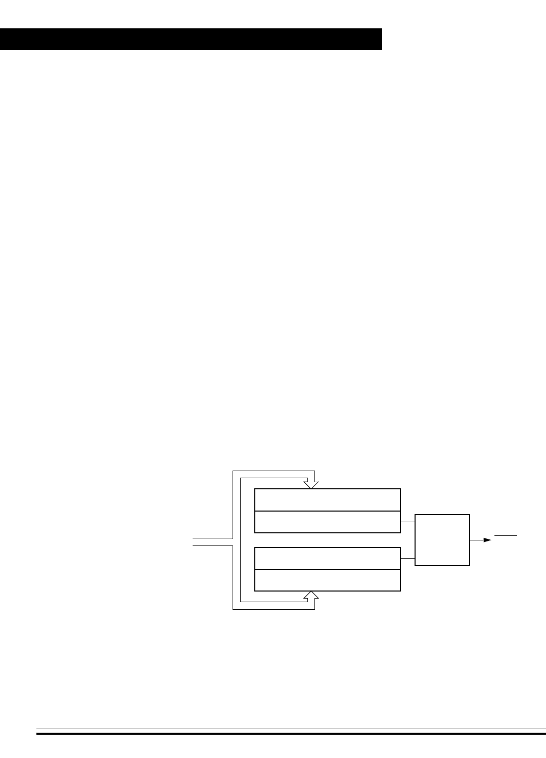
Break Module (BRK)
Technical Data MC68HC08AZ60 — Rev 1.1
154 Break Module (BRK) Freescale Semiconductor
12.4 Functional Description
When the internal address bus matches the value written in the break
address registers, the break module issues a breakpoint signal to the
CPU. The CPU then loads the instruction register with a software
interrupt instruction (SWI) after completion of the current CPU
instruction. The program counter vectors to $FFFC and $FFFD ($FEFC
and $FEFD in monitor mode).
The following events can cause a break interrupt to occur:
• A CPU-generated address (the address in the program counter)
matches the contents of the break address registers.
• Software writes a logic 1 to the BRKA bit in the break status and
control register.
When a CPU-generated address matches the contents of the break
address registers, the break interrupt begins after the CPU completes its
current instruction. A return-from-interrupt instruction (RTI) in the break
routine ends the break interrupt and returns the MCU to normal
operation. Figure 12-1 shows the structure of the break module.
Figure 12-1. Break Module Block Diagram
IAB[15:8]
IAB[7:0]
8-BIT COMPARATOR
8-BIT COMPARATOR
CONTROL
BREAK ADDRESS REGISTER LOW
BREAK ADDRESS REGISTER HIGH
IAB[15:0]
BREAK
Break Module (BRK)
Functional Description
MC68HC08AZ60 — Rev 1.1 Technical Data
Freescale Semiconductor Break Module (BRK) 155
12.4.1 Flag Protection During Break Interrupts
The BCFE bit in the break flag control register (BFCR) enables software
to clear status bits during the break state.
Register Name Bit 7654321Bit 0
Break Address Register High
(BRKH)
Read: Bit 15 14 13 12 11 10 9 Bit 8
Write:
Reset:00000000
Break Address Register Low
(BRKL)
Read: Bit 7654321Bit 0
Write:
Reset:00000000
Break Status and Control Register
(BSCR)
Read: BRKE BRKA 000000
Write:
Reset:00000000
= Unimplemented R = Reserved
Figure 12-2. I/O Register Summary
Table 12-1. I/O Register Address Summary
Register BRKH BRKL BSCR
Address $FE0C $FE0D $FE0E

Break Module (BRK)
Technical Data MC68HC08AZ60 — Rev 1.1
156 Break Module (BRK) Freescale Semiconductor
12.4.2 CPU During Break Interrupts
The CPU starts a break interrupt by:
• Loading the instruction register with the SWI instruction
• Loading the program counter with $FFFC:$FFFD ($FEFC:$FEFD
in monitor mode)
The break interrupt begins after completion of the CPU instruction in
progress. If the break address register match occurs on the last cycle of
a CPU instruction, the break interrupt begins immediately.
12.4.3 TIM During Break Interrupts
A break interrupt stops the timer counter.
12.4.4 COP During Break Interrupts
The COP is disabled during a break interrupt when VHi is present on the
RST pin.
12.5 Low-Power Modes
The WAIT and STOP instructions put the MCU in low power-consump-
tion standby modes.
12.5.1 Wait Mode
If enabled, the break module is active in wait mode. The SIM break
stop/wait bit (SBSW) in the SIM break status register indicates whether
wait was exited by a break interrupt. If so, the user can modify the return
address on the stack by subtracting one from it. (See System
Integration Module (SIM) on page 97).

Break Module (BRK)
Break Module Registers
MC68HC08AZ60 — Rev 1.1 Technical Data
Freescale Semiconductor Break Module (BRK) 157
12.5.2 Stop Mode
The break module is inactive in stop mode. The STOP instruction does
not affect break module register states. A break interrupt will cause an
exit from stop mode and sets the SBSW bit in the SIM break status
register.
12.6 Break Module Registers
These registers control and monitor operation of the break module:
• Break address register high (BRKH)
• Break address register low (BRKL)
• Break status and control register (BSCR)
12.6.1 Break Status and Control Register
The break status and control register contains break module enable and
status bits.
BRKE — Break Enable Bit
This read/write bit enables breaks on break address register matches.
Clear BRKE by writing a logic 0 to bit 7. Reset clears the BRKE bit.
1 = Breaks enabled on 16-bit address match
0 = Breaks disabled on 16-bit address match
Address: $FE0E
Bit 7654321Bit 0
Read:
BRKE BRKA
000000
Write:
Reset:00000000
= Unimplemented
Figure 12-3. Break Status and Control Register (BSCR)

Break Module (BRK)
Technical Data MC68HC08AZ60 — Rev 1.1
158 Break Module (BRK) Freescale Semiconductor
BRKA — Break Active Bit
This read/write status and control bit is set when a break address
match occurs. Writing a logic 1 to BRKA generates a break interrupt.
Clear BRKA by writing a logic 0 to it before exiting the break routine.
Reset clears the BRKA bit.
1 = (When read) Break address match
0 = (When read) No break address match
12.6.2 Break Address Registers
The break address registers contain the high and low bytes of the
desired breakpoint address. Reset clears the break address registers.
Register: BRKH BRKL
Address: $FE0C $FE0D
Bit 7654321Bit 0
Read:
Bit 15 14 13 12 11 10 9 Bit 8
Write:
Reset:00000000
Read:
Bit 7654321Bit 0
Write:
Reset:00000000
Figure 12-4. Break Address Registers (BRKH and BRKL)

MC68HC08AZ60 — Rev 1.1 Technical Data
Freescale Semiconductor Monitor ROM (MON) 159
Technical Data — MC68HC08AZ60
Section 13. Monitor ROM (MON)
13.1 Contents
13.2 Introduction. . . . . . . . . . . . . . . . . . . . . . . . . . . . . . . . . . . . . .159
13.3 Features. . . . . . . . . . . . . . . . . . . . . . . . . . . . . . . . . . . . . . . . .160
13.4 Functional Description. . . . . . . . . . . . . . . . . . . . . . . . . . . . .160
13.4.1 Entering Monitor Mode . . . . . . . . . . . . . . . . . . . . . . . . . .162
13.4.2 Data Format . . . . . . . . . . . . . . . . . . . . . . . . . . . . . . . . . . .163
13.4.3 Echoing . . . . . . . . . . . . . . . . . . . . . . . . . . . . . . . . . . . . . . .164
13.4.4 Break Signal . . . . . . . . . . . . . . . . . . . . . . . . . . . . . . . . . . .164
13.4.5 Commands . . . . . . . . . . . . . . . . . . . . . . . . . . . . . . . . . . . .165
13.4.6 Baud Rate . . . . . . . . . . . . . . . . . . . . . . . . . . . . . . . . . . . . .168
13.4.7 Security . . . . . . . . . . . . . . . . . . . . . . . . . . . . . . . . . . . . . . .169
13.2 Introduction
This section describes the monitor ROM (MON). The monitor ROM
allows complete testing of the MCU through a single-wire interface with
a host computer.

Monitor ROM (MON)
Technical Data MC68HC08AZ60 — Rev 1.1
160 Monitor ROM (MON) Freescale Semiconductor
13.3 Features
Features of the monitor ROM include:
• Normal User-Mode Pin Functionality
• One Pin Dedicated to Serial Communication between Monitor
ROM and Host Computer
• Standard Mark/Space Non-Return-to-Zero (NRZ) Communication
with Host Computer
• Up to 28.8 kBaud Communication with Host Computer
• Execution of Code in RAM.
13.4 Functional Description
Monitor ROM receives and executes commands from a host computer.
Figure 13-1 shows a sample circuit used to enter monitor mode and
communicate with a host computer via a standard RS-232 interface.
While simple monitor commands can access any memory address, the
MC68HC08AZ60 has a ROM security feature to prevent external
viewing of the contents of ROM. Proper procedures must be followed to
verify ROM content. Access to the ROM is denied to unauthorized users
of customer specified software (see Security on page 169).
In monitor mode, the MCU can execute host-computer code in RAM
while all MCU pins except PTA0 retain normal operating mode functions.
All communication between the host computer and the MCU is through
the PTA0 pin. A level-shifting and multiplexing interface is required
between PTA0 and the host computer. PTA0 is used in a wired-OR
configuration and requires a pullup resistor.
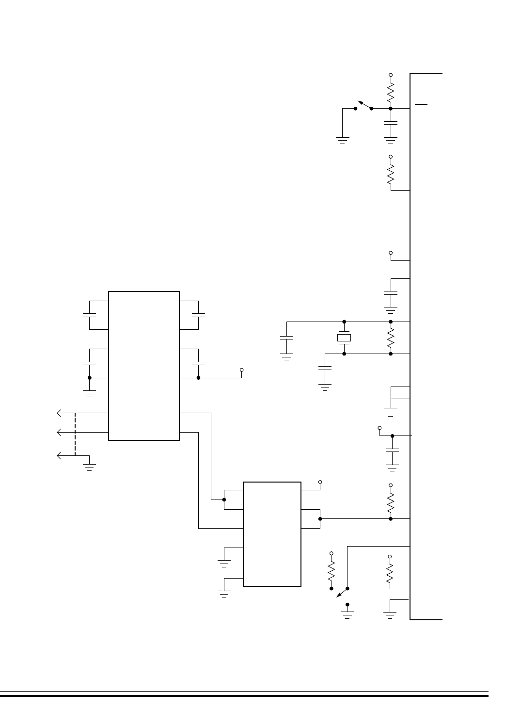
Monitor ROM (MON)
Functional Description
MC68HC08AZ60 — Rev 1.1 Technical Data
Freescale Semiconductor Monitor ROM (MON) 161
Figure 13-1. Monitor Mode Circuit
+
+
+
10 MΩ
X1
VDD
VDDA
VHI
MC145407
MC74HC125
68HC08
RST
IRQ
VDDA/VDDAREF
CGMXFC
OSC1
OSC2
VSS
VDD
PTA0
VDD
10 kΩ
0.1 µF
0.1 µF
10 Ω
6
5
2
4
3
1
DB-25
2
3
7
20
18
17
19
16
15 VDD
VDD
VDD
20 pF
20 pF
10 µF
10 µF10 µF
10 µF
1
2
4
7
14
3
0.1 µF
4.9152 MHz
10 kΩ
PTC3
VDD
10 kΩ
B
A
NOTE: Position A — Bus clock = CGMXCLK ÷ 4 or CGMVCLK ÷ 4
Position B — Bus clock = CGMXCLK ÷ 2
(SEE
NOTE.)
56
+
PTC0
PTC1
VDD
10 kΩ
VSSA

Monitor ROM (MON)
Technical Data MC68HC08AZ60 — Rev 1.1
162 Monitor ROM (MON) Freescale Semiconductor
13.4.1 Entering Monitor Mode
Table 13-1 shows the pin conditions for entering monitor mode.
Enter monitor mode by either
• Executing a software interrupt instruction (SWI) or
• Applying a logic 0 and then a logic 1 to the RST pin.
Once out of reset, the MCU waits for the host to send eight security bytes
(see Security on page 169). After the security bytes, the MCU sends a
break signal (10 consecutive logic 0s) to the host computer, indicating
that it is ready to receive a command.
Monitor mode uses alternate vectors for reset, SWI, and break interrupt.
The alternate vectors are in the $FE page instead of the $FF page and
allow code execution from the internal monitor firmware instead of user
code. The COP module is disabled in monitor mode as long as VHI (see
5.0 Volt DC Electrical Characteristics on page 432), is applied to
either the IRQ pin or the RESET pin. (See System Integration Module
(SIM) on page 97 for more information on modes of operation).
NOTE: Holding the PTC3 pin low when entering monitor mode causes a bypass
of a divide-by-two stage at the oscillator. The CGMOUT frequency is
equal to the CGMXCLK frequency, and the OSC1 input directly
generates internal bus clocks. In this case, the OSC1 signal must have
a 50% duty cycle at maximum bus frequency.
Table 13-1. Mode Selection
IRQ Pin
PTC0 Pin
PTC1 Pin
PTA0 Pin
PTC3 Pin
Mode CGMOUT Bus
Frequency
VHI(1) 1011Monitor or
VHI(1) 1010Monitor CGMXCLK
1. For VHI, 5.0 Volt DC Electrical Characteristics on page 432, and Maximum Ratings on
page 430.
CGMXCLK
2
----------------------------- CGMVCLK
2
----------------------------- CGMOUT
2
--------------------------
CGMOUT
2
--------------------------
Monitor ROM (MON)
Functional Description
MC68HC08AZ60 — Rev 1.1 Technical Data
Freescale Semiconductor Monitor ROM (MON) 163
Table 13-2 is a summary of the differences between user mode and
monitor mode.
13.4.2 Data Format
Communication with the monitor ROM is in standard non-return-to-zero
(NRZ) mark/space data format. (See Figure 13-2 and Figure 13-3.)
The data transmit and receive rate can be anywhere from 4800 baud to
28.8 kBaud. Transmit and receive baud rates must be identical.
Figure 13-2. Monitor Data Format
Figure 13-3. Sample Monitor Waveforms
Table 13-2. Mode Differences
Modes
Functions
COP Reset
Vector
High
Reset
Vector
Low
Break
Vector
High
Break
Vector
Low
SWI
Vector
High
SWI
Vector
Low
User Enabled $FFFE $FFFF $FFFC $FFFD $FFFC $FFFD
Monitor Disabled(1)
1. If the high voltage (VHI) is removed from the IRQ/VPP pin while in monitor mode, the SIM
asserts its COP enable output. The COP is a mask option enabled or disabled by the
COPD bit in the configuration register. See 5.0 Volt DC Electrical Characteristics on
page 432.
$FEFE $FEFF $FEFC $FEFD $FEFC $FEFD
BIT 5
START
BIT BIT 0 BIT 1
NEXT
STOP
BIT
START
BIT
BIT 2 BIT 3 BIT 4 BIT 6 BIT 7
BIT 5
START
BIT BIT 0 BIT 1
NEXT
STOP
BIT
START
BIT
BIT 2 BIT 3 BIT 4 BIT 6 BIT 7
START
BIT BIT 0 BIT 1 NEXT
STOP
BIT START
BIT
BIT 2
$A5
BREAK BIT 3 BIT 4 BIT 5 BIT 6 BIT 7
Monitor ROM (MON)
Technical Data MC68HC08AZ60 — Rev 1.1
164 Monitor ROM (MON) Freescale Semiconductor
13.4.3 Echoing
As shown in Figure 13-4, the monitor ROM immediately echoes each
received byte back to the PTA0 pin for error checking.
Any result of a command appears after the echo of the last byte of the
command.
Figure 13-4. Read Transaction
13.4.4 Break Signal
A start bit followed by nine low bits is a break signal. (See Figure 13-5).
When the monitor receives a break signal, it drives the PTA0 pin high for
the duration of two bits before echoing the break signal.
Figure 13-5. Break Transaction
ADDR. HIGHREADREAD ADDR. HIGH ADDR. LOW ADDR. LOW DATA
ECHO
SENT TO
MONITOR
RESULT
01234567 01234567
MISSING STOP BIT
TWO-STOP-BIT DELAY BEFORE ZERO ECHO
Monitor ROM (MON)
Functional Description
MC68HC08AZ60 — Rev 1.1 Technical Data
Freescale Semiconductor Monitor ROM (MON) 165
13.4.5 Commands
The monitor ROM uses these commands:
• READ, read memory
• WRITE, write memory
• IREAD, indexed read
• IWRITE, indexed write
• READSP, read stack pointer
• RUN, run user program
A sequence of IREAD or IWRITE commands can access a block of
memory sequentially over the full 64-Kbyte memory map.
Table 13-3. READ (Read Memory) Command
Description Read byte from memory
Operand Specifies 2-byte address in high byte:low byte order
Data Returned Returns contents of specified address
Opcode $4A
Command Sequence
ADDR. HIGHREADREAD ADDR. HIGH ADDR. LOW ADDR. LOW DATA
ECHO
SENT TO
MONITOR
RESULT
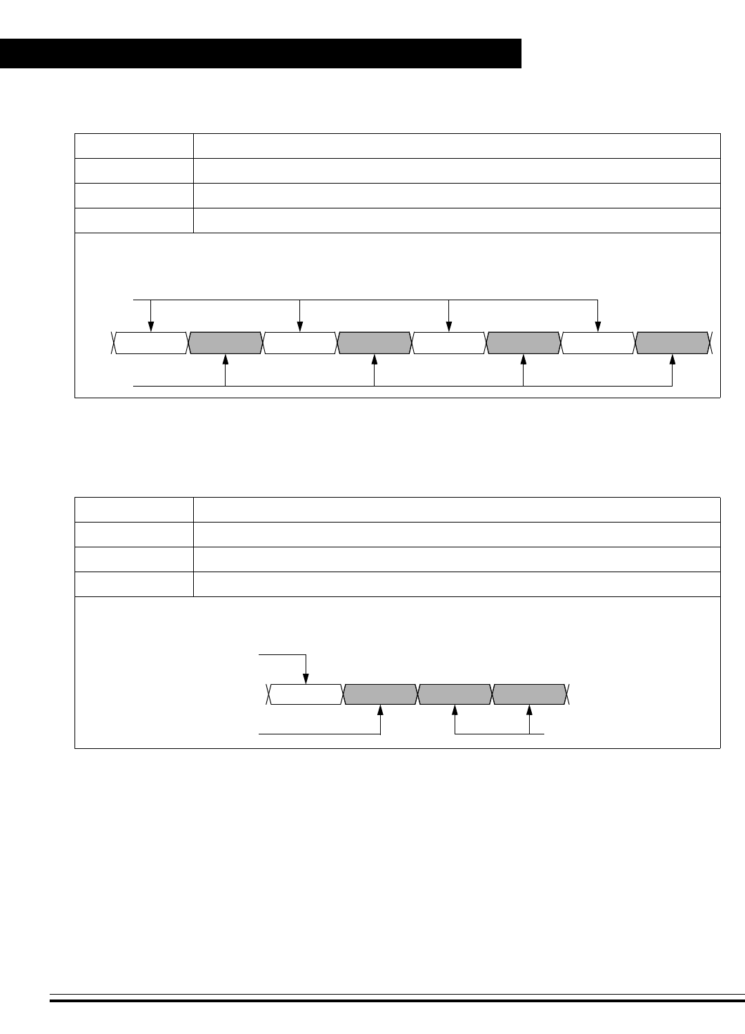
Monitor ROM (MON)
Technical Data MC68HC08AZ60 — Rev 1.1
166 Monitor ROM (MON) Freescale Semiconductor
Table 13-4. WRITE (Write Memory) Command
Description Write byte to memory
Operand Specifies 2-byte address in high byte:low byte order; low byte followed by data byte
Data Returned None
Opcode $49
Command Sequence
ADDR. HIGHWRITEWRITE ADDR. HIGH ADDR. LOW ADDR. LOW DATA
ECHO
SENT TO
MONITOR
DATA
Table 13-5. IREAD (Indexed Read) Command
Description Read next 2 bytes in memory from last address accessed
Operand Specifies 2-byte address in high byte:low byte order
Data Returned Returns contents of next two addresses
Opcode $1A
Command Sequence
DATAIREADIREAD DATA
ECHO
SENT TO
MONITOR
RESULT
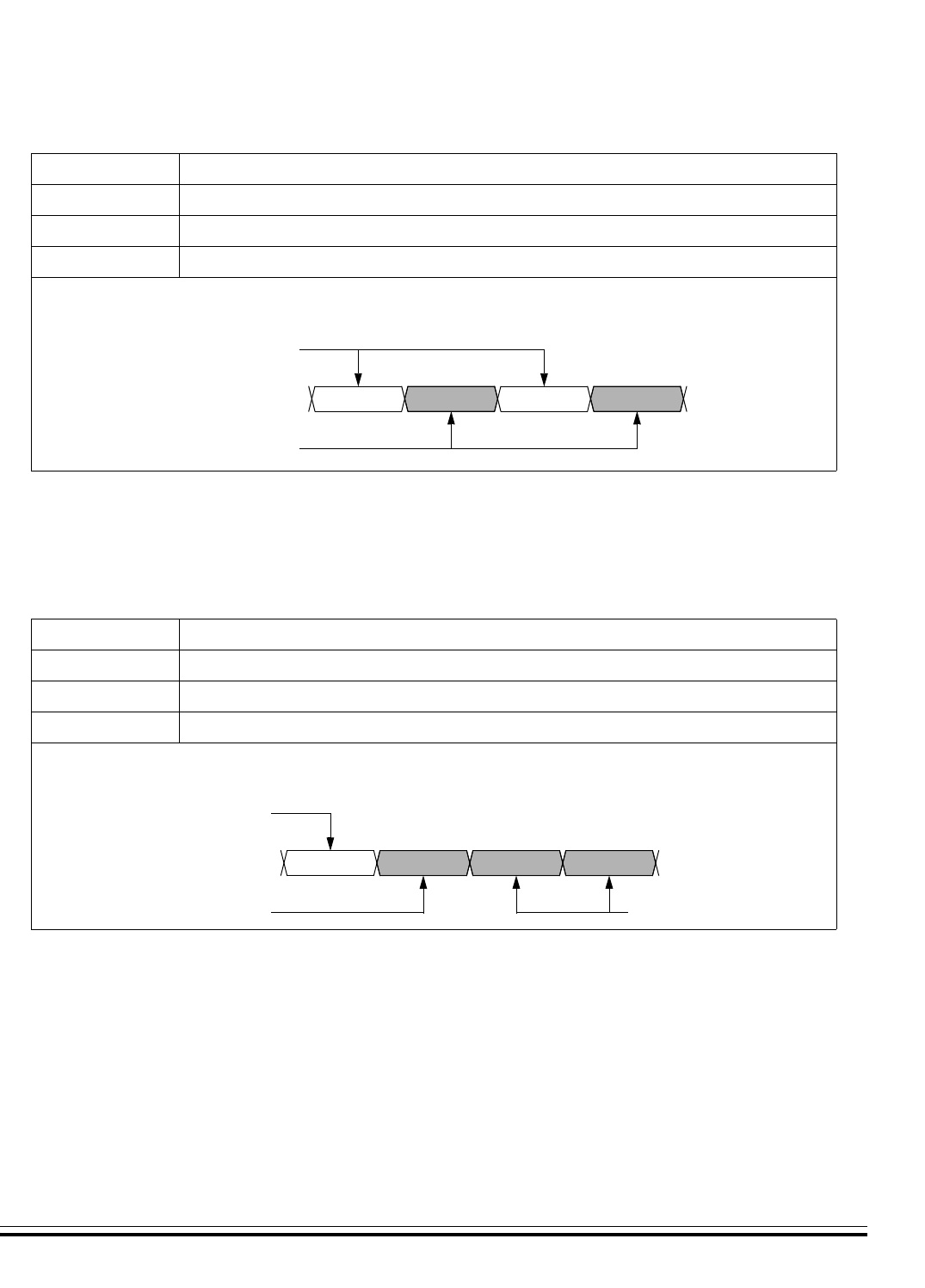
Monitor ROM (MON)
Functional Description
MC68HC08AZ60 — Rev 1.1 Technical Data
Freescale Semiconductor Monitor ROM (MON) 167
Table 13-6. IWRITE (Indexed Write) Command
Description Write to last address accessed + 1
Operand Specifies single data byte
Data Returned None
Opcode $19
Command Sequence
DATAIWRITEIWRITE DATA
ECHO
SENT TO
MONITOR
Table 13-7. READSP (Read Stack Pointer) Command
Description Reads stack pointer
Operand None
Data Returned Returns stack pointer in high byte:low byte order
Opcode $0C
Command Sequence
SP HIGHREADSPREADSP SP LOW
ECHO
SENT TO
MONITOR
RESULT
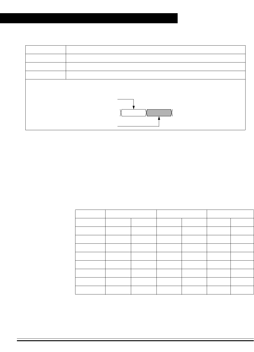
Monitor ROM (MON)
Technical Data MC68HC08AZ60 — Rev 1.1
168 Monitor ROM (MON) Freescale Semiconductor
13.4.6 Baud Rate
The part features a monitor mode which is optimised to operate with
either a 4.1952MHz crystal clock source (or multiples of 4.1952MHz) or
a 4MHz crystal (or multiples of 4MHz). This supports designs which use
the MSCAN module, which is generally clocked from a 4MHz, 8MHz or
16MHz crystal. The table below outlines the available baud rates for a
range of crystals and how they can match to a PC baud rate.
Care should be taken when setting the baud rate since incorrect
baud rate setting can result in communications failure.
Table 13-8. RUN (Run User Program) Command
Description Executes RTI instruction
Operand None
Data Returned None
Opcode $28
Command Sequence
RUNRUN
ECHO
SENT TO
MONITOR
Baud rate Closest PC baud PC Error %
Clock freq PTC3=0 PTC3=1 PTC3=0 PTC3=1 PTC3=0 PTC3=1
32kHz 57.97 28.98 57.6 28.8 0.64 0.63
1MHz 1811.59 905.80 1800 900 0.64 0.64
2MHz 3623.19 1811.59 3600 1800 0.64 0.64
4MHz 7246.37 3623.19 7200 3600 0.64 0.64
4.194MHz 7597.83 3798.91 7680 3840 1.08 1.08
4.9152MHz 8904.35 4452.17 8861 4430 0.49 0.50
8MHz 14492.72 7246.37 14400 7200 0.64 0.64
16MHz 28985.51 14492.75 28800 14400 0.64 0.64
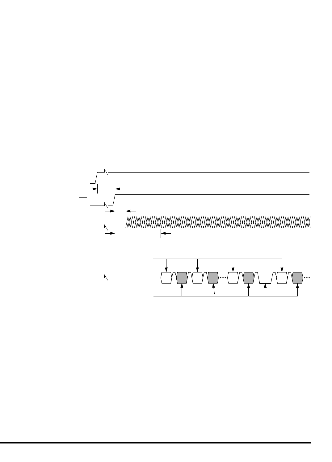
Monitor ROM (MON)
Functional Description
MC68HC08AZ60 — Rev 1.1 Technical Data
Freescale Semiconductor Monitor ROM (MON) 169
13.4.7 Security
A security feature discourages unauthorized reading of ROM locations
while in monitor mode. The host can bypass the security feature at
monitor mode entry by sending eight security bytes that match the bytes
at locations $FFF6–$FFFD. Locations $FFF6–$FFFD contain user-
defined data.
NOTE: Do not leave locations $FFF6–$FFFD blank. For security reasons, enter
data at locations $FFF6–$FFFD even if they are not used for vectors.
During monitor mode entry, the MCU waits after the power-on reset for
the host to send the eight security bytes on pin PA0.
Figure 13-6. Monitor Mode Entry Timing
If the received bytes match those at locations $FFF6–$FFFD, the host
bypasses the security feature and can read all ROM locations and
execute code from ROM. Security remains bypassed until a power-on
reset occurs. After the host bypasses security, any reset other than a
power-on reset requires the host to send another eight bytes. If the reset
Byte 1
Byte 1 Echo
Byte 2
Byte 2 Echo
Byte 8
Byte 8 Echo
Command
Command Echo
PA0
PA7
RST
VDD
4096 + 32 CGMXCLK CYCLES
24 CGMXCLK CYCLES
256 CGMXCLK CYCLES (ONE BIT TIME)
141121
Break
NOTE: 1 = Echo delay (2 bit times)
2 = Data return delay (2 bit times)
4 = Wait 1 bit time before sending next byte.
4
FROM HOST
FROM MCU

Monitor ROM (MON)
Technical Data MC68HC08AZ60 — Rev 1.1
170 Monitor ROM (MON) Freescale Semiconductor
was not a power-on reset, the security remains bypassed regardless of
the data that the host sends.
If the received bytes do not match the data at locations $FFF6–$FFFD,
the host fails to bypass the security feature. The MCU remains in monitor
mode, but reading ROM locations returns undefined data, and trying to
execute code from ROM causes an illegal address reset. After the host
fails to bypass security, any reset other than a power-on reset causes an
endless loop of illegal address resets.
After receiving the eight security bytes from the host, the MCU transmits
a break character signalling that it is ready to receive a command.
NOTE: The MCU does not transmit a break character until after the host sends
the eight security bytes.

MC68HC08AZ60 — Rev 1.1 Technical Data
Freescale Semiconductor Computer Operating Properly (COP) 171
Technical Data — MC68HC08AZ60
Section 14. Computer Operating Properly (COP)
14.1 Contents
14.2 Introduction. . . . . . . . . . . . . . . . . . . . . . . . . . . . . . . . . . . . . .171
14.3 Functional Description. . . . . . . . . . . . . . . . . . . . . . . . . . . . .172
14.4 I/O Signals . . . . . . . . . . . . . . . . . . . . . . . . . . . . . . . . . . . . . . .173
14.4.1 CGMXCLK . . . . . . . . . . . . . . . . . . . . . . . . . . . . . . . . . . . . .173
14.4.2 STOP Instruction . . . . . . . . . . . . . . . . . . . . . . . . . . . . . . .173
14.4.3 COPCTL Write. . . . . . . . . . . . . . . . . . . . . . . . . . . . . . . . . .174
14.4.4 Power-On Reset . . . . . . . . . . . . . . . . . . . . . . . . . . . . . . . .174
14.4.5 Internal Reset . . . . . . . . . . . . . . . . . . . . . . . . . . . . . . . . . .174
14.4.6 Reset Vector Fetch. . . . . . . . . . . . . . . . . . . . . . . . . . . . . .174
14.4.7 COPD. . . . . . . . . . . . . . . . . . . . . . . . . . . . . . . . . . . . . . . . .174
14.4.8 COPL . . . . . . . . . . . . . . . . . . . . . . . . . . . . . . . . . . . . . . . . .174
14.5 COP Control Register. . . . . . . . . . . . . . . . . . . . . . . . . . . . . .175
14.6 Interrupts. . . . . . . . . . . . . . . . . . . . . . . . . . . . . . . . . . . . . . . .175
14.7 Monitor Mode . . . . . . . . . . . . . . . . . . . . . . . . . . . . . . . . . . . .175
14.8 Low-Power Modes . . . . . . . . . . . . . . . . . . . . . . . . . . . . . . . .175
14.8.1 Wait Mode . . . . . . . . . . . . . . . . . . . . . . . . . . . . . . . . . . . . .175
14.8.2 Stop Mode. . . . . . . . . . . . . . . . . . . . . . . . . . . . . . . . . . . . .176
14.9 COP Module During Break Interrupts. . . . . . . . . . . . . . . . .176
14.2 Introduction
The COP module contains a free-running counter that generates a reset
if allowed to overflow. The COP module helps software recover from
runaway code. Prevent a COP reset by periodically clearing the COP
counter.

Computer Operating Properly (COP)
Technical Data MC68HC08AZ60 — Rev 1.1
172 Computer Operating Properly (COP) Freescale Semiconductor
14.3 Functional Description
The COP counter is a free-running 6-bit counter preceded by a 12-bit
prescaler. If not cleared by software, the COP counter overflows and
generates an asynchronous reset after 213 –2
4 or 218 –2
4 CGMXCLK
cycles, depending on the state of the COP long timeout bit, COPL, in the
CONFIG-1. When COPL = 1, a 4.9152-MHz crystal gives a COP timeout
period of 53.3 ms. Writing any value to location $FFFF before an
overflow occurs prevents a COP reset by clearing the COP counter and
stages 4–12 of the SIM counter.
NOTE: Service the COP immediately after reset and before entering or after
exiting stop mode to guarantee the maximum time before the first COP
counter overflow.
A COP reset pulls the RST pin low for 32 CGMXCLK cycles and sets the
COP bit in the reset status register (RSR).
In monitor mode, the COP is disabled if the RST pin or the IRQ pin is held
at VHi. During the break state, VHi on the RST pin disables the COP.
NOTE: Place COP clearing instructions in the main program and not in an
interrupt subroutine. Such an interrupt subroutine could keep the COP
from generating a reset even while the main program is not working
properly.
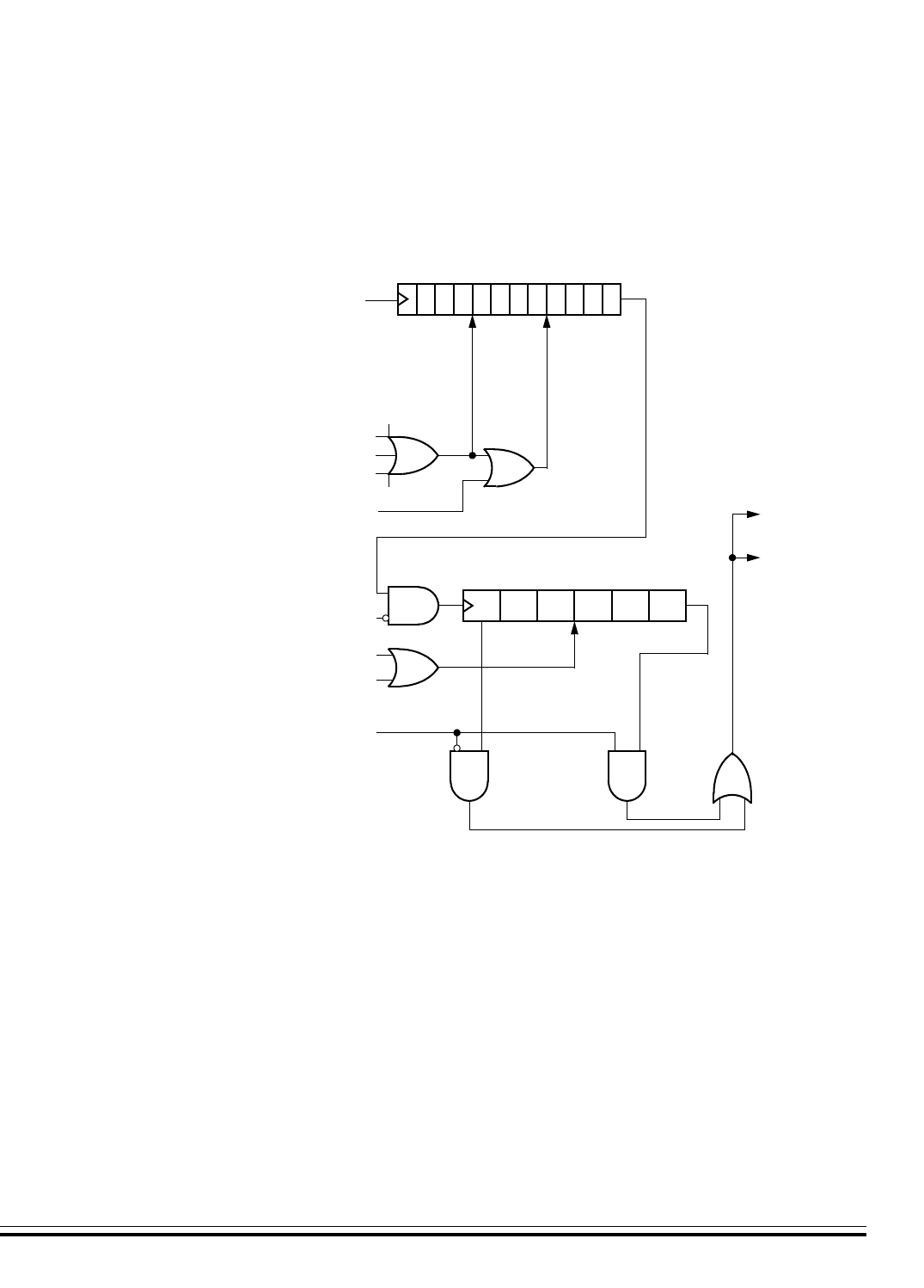
Computer Operating Properly (COP)
I/O Signals
MC68HC08AZ60 — Rev 1.1 Technical Data
Freescale Semiconductor Computer Operating Properly (COP) 173
14.4 I/O Signals
The following paragraphs describe the signals shown in Figure 14-1.
14.4.1 CGMXCLK
CGMXCLK is the crystal oscillator output signal. CGMXCLK frequency
is equal to the crystal frequency.
14.4.2 STOP Instruction
The STOP instruction clears the COP prescaler.
Figure 14-1. COP Block Diagram
COPCTL WRITE
CGMXCLK
RESET VECTOR FETCH
RESET
RESET STATUS
INTERNAL RESET SOURCES
STOP INSTRUCTION
CLEAR STAGES 4–12
CLEAR ALL STAGES
6-BIT COP COUNTER
COPD FROM MOR
RESET
COPCTL WRITE
CLEAR COP
COUNTER
COPRS FROM MOR
12-BIT COP PRESCALER
REGISTER

Computer Operating Properly (COP)
Technical Data MC68HC08AZ60 — Rev 1.1
174 Computer Operating Properly (COP) Freescale Semiconductor
14.4.3 COPCTL Write
Writing any value to the COP control register (COPCTL) (see COP
Control Register on page 175), clears the COP counter and clears
stages 12 through 4 of the COP prescaler. Reading the COP control
register returns the reset vector.
14.4.4 Power-On Reset
The power-on reset (POR) circuit clears the COP prescaler 4096
CGMXCLK cycles after power-up.
14.4.5 Internal Reset
An internal reset clears the COP prescaler and the COP counter.
14.4.6 Reset Vector Fetch
A reset vector fetch occurs when the vector address appears on the data
bus. A reset vector fetch clears the COP prescaler.
14.4.7 COPD
The COPD signal reflects the state of the COP disable bit (COPD) in the
MOR register. (See Mask Options on page 149).
14.4.8 COPL
The COPL signal reflects the state of the COP rate select bit. COPRS in
the mask option register. (See Mask Options on page 149).

Computer Operating Properly (COP)
COP Control Register
MC68HC08AZ60 — Rev 1.1 Technical Data
Freescale Semiconductor Computer Operating Properly (COP) 175
14.5 COP Control Register
The COP control register is located at address $FFFF and overlaps the
reset vector. Writing any value to $FFFF clears the COP counter and
starts a new timeout period. Reading location $FFFF returns the low
byte of the reset vector.
14.6 Interrupts
The COP does not generate CPU interrupt requests.
14.7 Monitor Mode
The COP is disabled in monitor mode when VHi is present on the IRQ
pin or on the RST pin.
14.8 Low-Power Modes
The WAIT and STOP instructions put the MCU in low power-consump-
tion standby modes.
14.8.1 Wait Mode
The COP remains active in wait mode. To prevent a COP reset during
wait mode, periodically clear the COP counter in a CPU interrupt routine.
Address: $FFFF
Bit 7654321Bit 0
Read: Low Byte of Reset Vector
Write: Clear COP Counter
Reset: Unaffected by Reset
Figure 14-2. COP Control Register (COPCTL)

Computer Operating Properly (COP)
Technical Data MC68HC08AZ60 — Rev 1.1
176 Computer Operating Properly (COP) Freescale Semiconductor
14.8.2 Stop Mode
Stop mode turns off the CGMXCLK input to the COP and clears the COP
prescaler. Service the COP immediately before entering or after exiting
stop mode to ensure a full COP timeout period after entering or exiting
stop mode.
The STOP bit in the mask option register (MOR) enables the STOP
instruction. To prevent inadvertently turning off the COP with a STOP
instruction, disable the STOP instruction by clearing the STOP bit.
14.9 COP Module During Break Interrupts
The COP is disabled during a break interrupt when VHi is present on the
RST pin.

MC68HC08AZ60 — Rev 1.1 Technical Data
Freescale Semiconductor Low Voltage Inhibit (LVI) 177
Technical Data — MC68HC08AZ60
Section 15. Low Voltage Inhibit (LVI)
15.1 Contents
15.2 Introduction. . . . . . . . . . . . . . . . . . . . . . . . . . . . . . . . . . . . . .177
15.3 Features. . . . . . . . . . . . . . . . . . . . . . . . . . . . . . . . . . . . . . . . .177
15.4 Functional Description. . . . . . . . . . . . . . . . . . . . . . . . . . . . .178
15.4.1 Polled LVI Operation . . . . . . . . . . . . . . . . . . . . . . . . . . . .180
15.4.2 Forced Reset Operation. . . . . . . . . . . . . . . . . . . . . . . . . .180
15.4.3 False Reset Protection. . . . . . . . . . . . . . . . . . . . . . . . . . .180
15.5 LVI Status Register. . . . . . . . . . . . . . . . . . . . . . . . . . . . . . . .181
15.6 LVI Interrupts . . . . . . . . . . . . . . . . . . . . . . . . . . . . . . . . . . . .181
15.7 Low-Power Modes . . . . . . . . . . . . . . . . . . . . . . . . . . . . . . . .182
15.7.1 Wait Mode . . . . . . . . . . . . . . . . . . . . . . . . . . . . . . . . . . . . .182
15.7.2 Stop Mode. . . . . . . . . . . . . . . . . . . . . . . . . . . . . . . . . . . . .182
15.2 Introduction
This section describes the low-voltage inhibit module, which monitors
the voltage on the VDD pin and can force a reset when the VDD voltage
falls to the LVI trip voltage.
15.3 Features
Features of the LVI module include:
• Programmable LVI Reset
• Programmable Power Consumption
• Digital Filtering of VDD Pin Level

Low Voltage Inhibit (LVI)
Technical Data MC68HC08AZ60 — Rev 1.1
178 Low Voltage Inhibit (LVI) Freescale Semiconductor
NOTE: If a low voltage interrupt (LVI) occurs during programming of EEPROM
memory, then adequate programming time may may not have been
allowed to ensure the integrity and retention of the data. It is the
responsibility of the user to ensure that in the event of an LVI any
addresses being programmed receive specification programming
conditions.
15.4 Functional Description
Figure 15-1 shows the structure of the LVI module. The LVI is enabled
out of reset. The LVI module contains a bandgap reference circuit and
comparator. The LVI power bit, LVIPWR, enables the LVI to monitor VDD
voltage. The LVI reset bit, LVIRST, enables the LVI module to generate
a reset when VDD falls below a voltage, LVITRIPF, and remains at or
below that level for nine or more consecutive CPU cycles.
Note that short VDD spikes may not trip the LVI. It is the user’s
responsibility to ensure a clean VDD signal within the specified
operating voltage range if normal microcontroller operation is to be
guaranteed.
LVISTOP, enables the LVI module during stop mode. This will ensure
when the STOP instruction is implemented, the LVI will continue to
monitor the voltage level on VDD. LVIPWR, LVISTOP, and LVIRST are
in the MOR register. (See Mask Options on page 149).
Once an LVI reset occurs, the MCU remains in reset until VDD rises
above a voltage, LVITRIPR. VDD must be above LVITRIPR for only one
CPU cycle to bring the MCU out of reset. (See Forced Reset Operation
on page 180). The output of the comparator controls the state of the
LVIOUT flag in the LVI status register (LVISR).
An LVI reset also drives the RST pin low to provide low-voltage
protection to external peripheral devices.
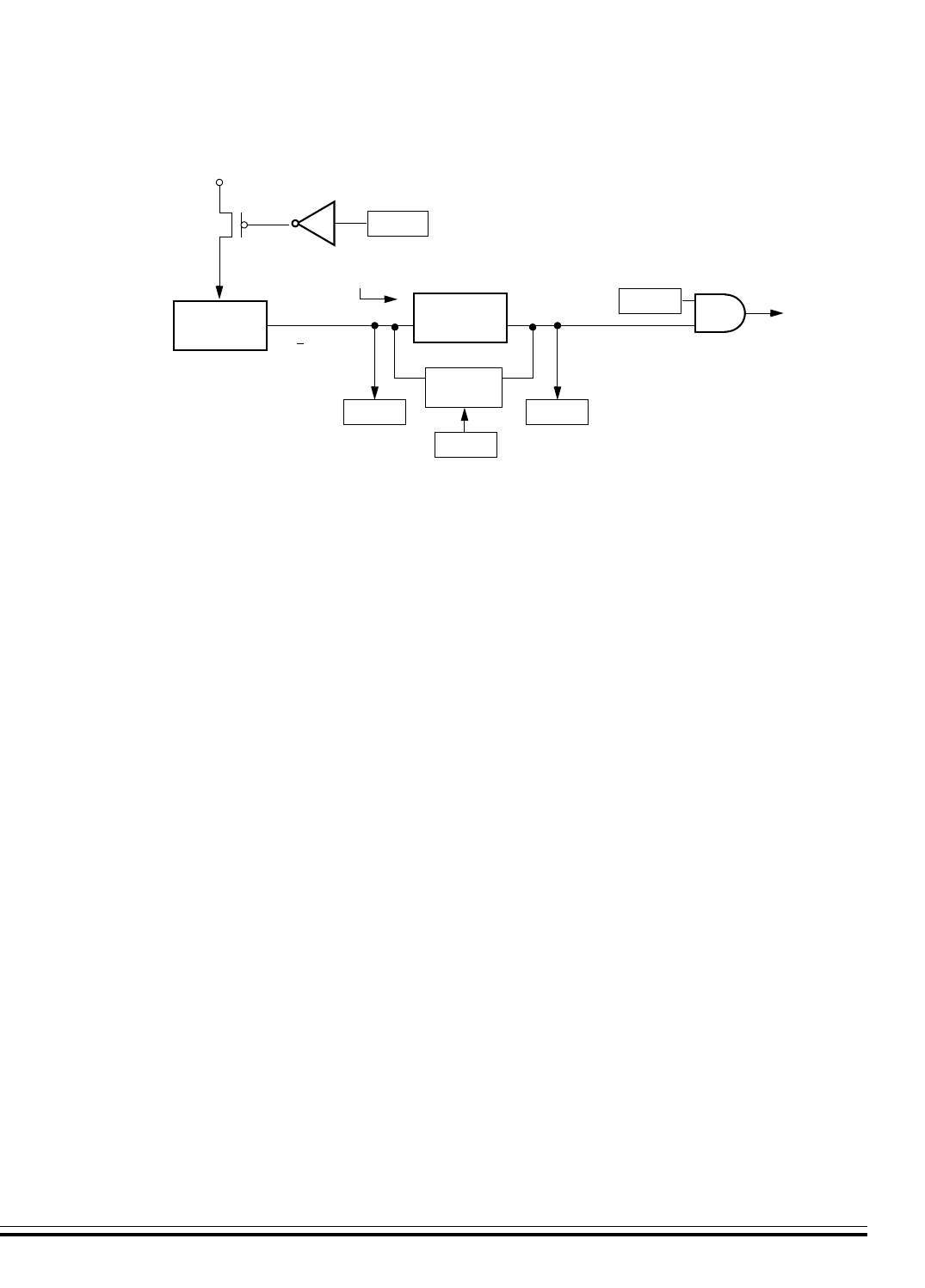
Low Voltage Inhibit (LVI)
Functional Description
MC68HC08AZ60 — Rev 1.1 Technical Data
Freescale Semiconductor Low Voltage Inhibit (LVI) 179
Figure 15-1. LVI Module Block Diagram
LOW VDD
LVIRST
VDD > LVITRIP = 0
VDD < LVITRIP = 1
LVIOUT
LVIPWR
DETECTOR
VDD
LVI RESET
FROM MOR
FROM MOR
VDD
DIGITAL FILTER
CPU CLOCK
ANLGTRIP
Stop Mode
Filter Bypass
LVISTOP
FROM MOR

Low Voltage Inhibit (LVI)
Technical Data MC68HC08AZ60 — Rev 1.1
180 Low Voltage Inhibit (LVI) Freescale Semiconductor
15.4.1 Polled LVI Operation
In applications that can operate at VDD levels below the LVITRIPF level,
software can monitor VDD by polling the LVIOUT bit. In the mask option
register, the LVIPWR bit must be at logic 1 to enable the LVI module, and
the LVIRST bit must be at logic 0 to disable LVI resets.
15.4.2 Forced Reset Operation
In applications that require VDD to remain above the LVITRIPF level,
enabling LVI resets allows the LVI module to reset the MCU when VDD
falls to the LVITRIPF level and remains at or below that level for nine or
more consecutive CPU cycles. In the mask option register, the LVIPWR
and LVIRST bits must be at logic 1 to enable the LVI module and to
enable LVI resets.
15.4.3 False Reset Protection
The VDD pin level is digitally filtered to reduce false resets due to power
supply noise. In order for the LVI module to reset the MCU,VDD must
remain at or below the LVITRIPF level for nine or more consecutive CPU
cycles. VDD must be above LVITRIPR for only one CPU cycle to bring the
MCU out of reset.
Figure 15-2. LVI I/O Register Summary
Addr. Register Name Bit 7654321Bit 0
$FE0F LVI Status Register (LVISR) LVIOUT
= Unimplemented

Low Voltage Inhibit (LVI)
LVI Status Register
MC68HC08AZ60 — Rev 1.1 Technical Data
Freescale Semiconductor Low Voltage Inhibit (LVI) 181
15.5 LVI Status Register
The LVI status register flags VDD voltages below the LVITRIPF level.
LVIOUT — LVI Output Bit
This read-only flag becomes set when the VDD voltage falls below the
LVITRIPF voltage for 32 to 40 CGMXCLK cycles. (See Table 15-1).
Reset clears the LVIOUT bit.
Address: $FE0F
Bit 7654321Bit 0
Read: LVIOUT 0000000
Write:
Reset:00000000
= Unimplemented
Figure 15-3. LVI Status Register (LVISR)
Table 15-1. LVIOUT Bit Indication
VDD
LVIOUT
At Level: For Number of
CGMXCLK Cycles:
VDD > LVITRIPR Any 0
VDD < LVITRIPF < 32 CGMXCLK Cycles 0
VDD < LVITRIPF Between 32 and 40
CGMXCLK Cycles 0 or 1
VDD < LVITRIPF > 40 CGMXCLK Cycles 1
LVITRIPF < VDD < LVITRIPR Any Previous Value

Low Voltage Inhibit (LVI)
Technical Data MC68HC08AZ60 — Rev 1.1
182 Low Voltage Inhibit (LVI) Freescale Semiconductor
15.6 LVI Interrupts
The LVI module does not generate interrupt requests.
15.7 Low-Power Modes
The WAIT and STOP instructions put the MCU in low power-
consumption standby modes.
15.7.1 Wait Mode
With the LVIPWR bit in the mask option register programmed to logic 1,
the LVI module is active after a WAIT instruction.
With the LVIRST bit in the mask option register programmed to logic 1,
the LVI module can generate a reset and bring the MCU out of wait
mode.
15.7.2 Stop Mode
With the LVISTOP and LVIPWR bits in the mask option register
programmed to a logic 1, the LVI module will be active after a STOP
instruction. Because CPU clocks are disabled during stop mode, the LVI
trip must bypass the digital filter to generate a reset and bring the MCU
out of stop.
With the LVIPWR bit in the mask option register programmed to logic 1
and the LVISTOP bit at a logic 0, the LVI module will be inactive after a
STOP instruction.
Note that the LVI feature is intended to provide the safe shutdown
of the microcontroller and thus protection of related circuitry prior
to any application VDD voltage collapsing completely to an unsafe
level. Is is not intended that users operate the microcontroller at
lower than the specified operating voltage, VDD

MC68HC08AZ60 — Rev 1.1 Technical Data
Freescale Semiconductor External Interrupt (IRQ) 183
Technical Data — MC68HC08AZ60
Section 16. External Interrupt (IRQ)
16.1 Contents
16.2 Introduction. . . . . . . . . . . . . . . . . . . . . . . . . . . . . . . . . . . . . .183
16.3 Features. . . . . . . . . . . . . . . . . . . . . . . . . . . . . . . . . . . . . . . . .183
16.4 Functional Description. . . . . . . . . . . . . . . . . . . . . . . . . . . . .184
16.5 IRQ Pin. . . . . . . . . . . . . . . . . . . . . . . . . . . . . . . . . . . . . . . . . .187
16.6 IRQ Module During Break Interrupts . . . . . . . . . . . . . . . . .188
16.7 IRQ Status and Control Register. . . . . . . . . . . . . . . . . . . . .189
16.2 Introduction
This section describes the nonmaskable external interrupt (IRQ) input.
16.3 Features
Features include:
• Dedicated External Interrupt Pin (IRQ)
• Hysteresis Buffer
• Programmable Edge-Only or Edge- and Level-Interrupt Sensitivity
• Automatic Interrupt Acknowledge
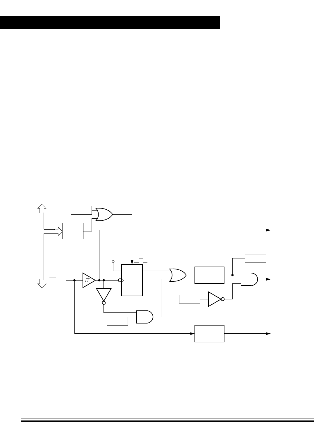
External Interrupt (IRQ)
Technical Data MC68HC08AZ60 — Rev 1.1
184 External Interrupt (IRQ) Freescale Semiconductor
16.4 Functional Description
A logic 0 applied to the external interrupt pin can latch a CPU interrupt
request. Figure 16-1 shows the structure of the IRQ module.
Interrupt signals on the IRQ pin are latched into the IRQ latch. An
interrupt latch remains set until one of the following actions occurs:
• Vector fetch — A vector fetch automatically generates an interrupt
acknowledge signal that clears the latch that caused the vector
fetch.
• Software clear — Software can clear an interrupt latch by writing
to the appropriate acknowledge bit in the interrupt status and
control register (ISCR). Writing a logic 1 to the ACK1 bit clears the
IRQ latch.
• Reset — A reset automatically clears both interrupt latches.
Figure 16-1. IRQ Block Diagram
ACK1
IMASK1
DQ
CK
CLR
IRQ
HIGH
INTERRUPT
TO MODE
SELECT
LOGIC
IRQ
LATCH
REQUEST
IRQ
VDD
MODE1
VOLTAGE
DETECT
SYNCHRO-
NIZER
IRQF
TO CPU FOR
BIL/BIH
INSTRUCTIONS
VECTOR
FETCH
DECODER
INTERNAL ADDRESS BUS

External Interrupt (IRQ)
Functional Description
MC68HC08AZ60 — Rev 1.1 Technical Data
Freescale Semiconductor External Interrupt (IRQ) 185
The external interrupt pin is falling-edge triggered and is software-
configurable to be both falling-edge and low-level triggered. The MODE1
bit in the ISCR controls the triggering sensitivity of the IRQ pin.
When an interrupt pin is edge-triggered only, the interrupt latch remains
set until a vector fetch, software clear, or reset occurs.
When an interrupt pin is both falling-edge and low-level-triggered, the
interrupt latch remains set until both of the following occur:
• Vector fetch or software clear
• Return of the interrupt pin to logic 1
The vector fetch or software clear may occur before or after the interrupt
pin returns to logic 1. As long as the pin is low, the interrupt request
remains pending. A reset will clear the latch and the MODE1 control bit,
thereby clearing the interrupt even if the pin stays low.
When set, the IMASK1 bit in the ISCR masks all external interrupt
requests. A latched interrupt request is not presented to the interrupt
priority logic unless the corresponding IMASK bit is clear.
NOTE: The interrupt mask (I) in the condition code register (CCR) masks all
interrupt requests, including external interrupt requests.
(See Figure 16-2).
Table 16-1. IRQ I/O Register Summary
Addr. Register Name Bit 7654321Bit 0
$001A IRQ Status/Control Register (ISCR)
Read: 0000IRQF0
IMASK1 MODE1
Write:RRRRRACK1
R= Reserved
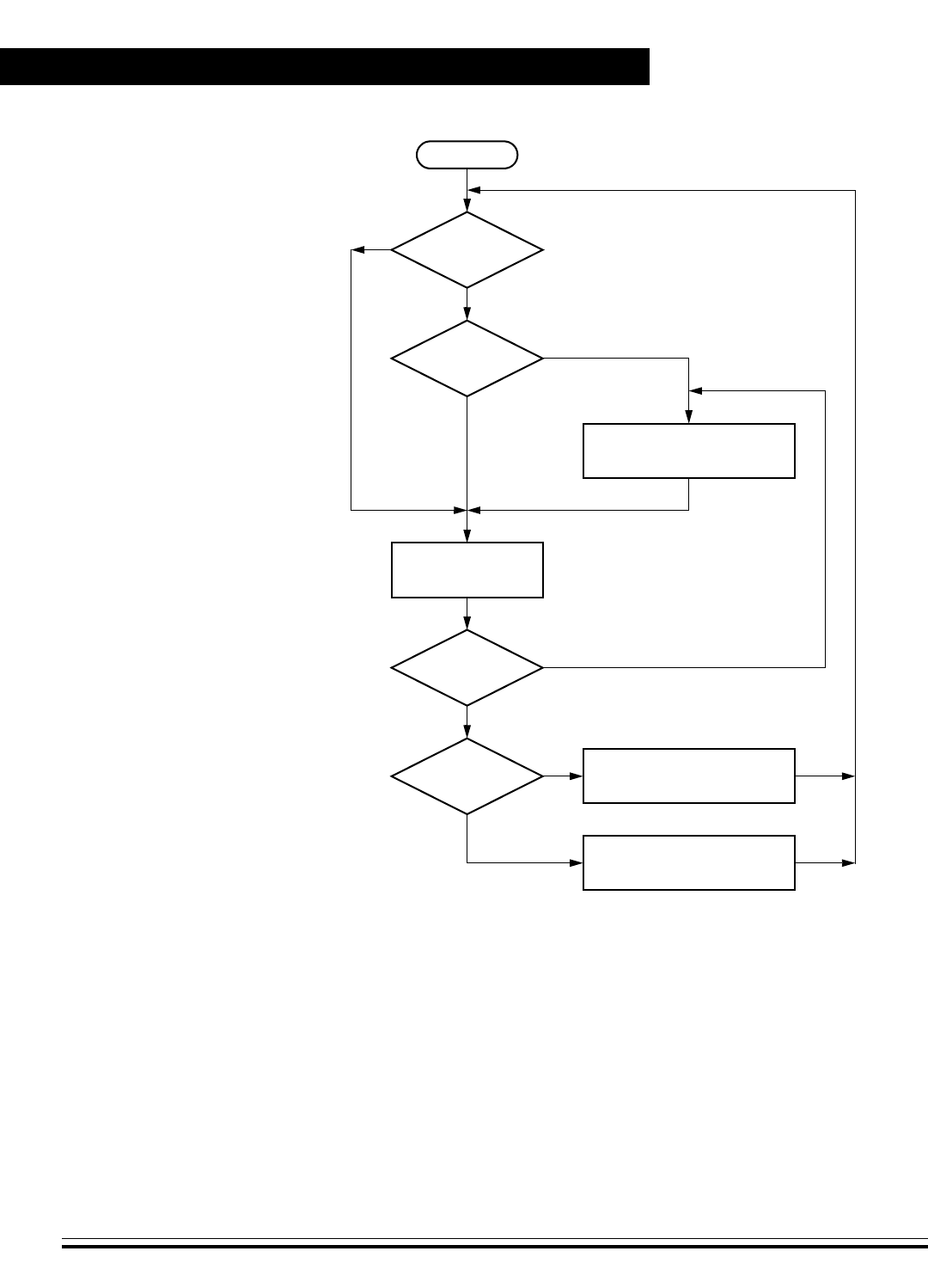
External Interrupt (IRQ)
Technical Data MC68HC08AZ60 — Rev 1.1
186 External Interrupt (IRQ) Freescale Semiconductor
Figure 16-2. IRQ Interrupt Flowchart
FROM RESET
I BIT SET?
FETCH NEXT
YES
NO
INTERRUPT?
INSTRUCTION.
SWI
INSTRUCTION?
RTI
INSTRUCTION?
NO
STACK CPU REGISTERS.
NO
SET I BIT.
LOAD PC WITH INTERRUPT VECTOR.
NO
YES UNSTACK CPU REGISTERS.
EXECUTE INSTRUCTION.
YES
YES

External Interrupt (IRQ)
IRQ Pin
MC68HC08AZ60 — Rev 1.1 Technical Data
Freescale Semiconductor External Interrupt (IRQ) 187
16.5 IRQ Pin
A logic 0 on the IRQ pin can latch an interrupt request into the IRQ latch.
A vector fetch, software clear, or reset clears the IRQ latch.
If the MODE1 bit is set, the IRQ pin is both falling-edge sensitive and
low-level sensitive. With MODE1 set, both of the following actions must
occur to clear the IRQ latch:
• Vector fetch or software clear — A vector fetch generates an
interrupt acknowledge signal to clear the latch. Software may
generate the interrupt acknowledge signal by writing a logic 1 to
the ACK1 bit in the interrupt status and control register (ISCR).
The ACK1 bit is useful in applications that poll the IRQ pin and
require software to clear the IRQ latch. Writing to the ACK1 bit can
also prevent spurious interrupts due to noise. Setting ACK1 does
not affect subsequent transitions on the IRQ pin. A falling edge on
IRQ/VPP that occurs after writing to the ACK1 bit latches another
interrupt request. If the IRQ mask bit, IMASK1, is clear, the CPU
loads the program counter with the vector address at locations
$FFFA and $FFFB.
• Return of the IRQ pin to logic 1 — As long as the IRQ pin is at logic
0, the IRQ latch remains set.
The vector fetch or software clear and the return of the IRQ pin to logic 1
can occur in any order. The interrupt request remains pending as long
as the IRQ pin is at logic 0. A reset will clear the latch and the MODE1
control bit, thereby clearing the interrupt even if the pin stays low.
If the MODE1 bit is clear, the IRQ pin is falling-edge sensitive only. With
MODE1 clear, a vector fetch or software clear immediately clears the
IRQ latch.

External Interrupt (IRQ)
Technical Data MC68HC08AZ60 — Rev 1.1
188 External Interrupt (IRQ) Freescale Semiconductor
The IRQF bit in the ISCR register can be used to check for pending
interrupts. The IRQF bit is not affected by the IMASK1 bit, which makes
it useful in applications where polling is preferred.
Use the BIH or BIL instruction to read the logic level on the IRQ pin.
NOTE: When using the level-sensitive interrupt trigger, avoid false interrupts by
masking interrupt requests in the interrupt routine.
16.6 IRQ Module During Break Interrupts
The system integration module (SIM) controls whether the IRQ interrupt
latch can be cleared during the break state. The BCFE bit in the SIM
break flag control register (SBFCR) enables software to clear the latches
during the break state. (See SIM Break Flag Control Register on page
119
To allow software to clear the IRQ latch during a break interrupt, write a
logic 1 to the BCFE bit. If a latch is cleared during the break state, it
remains cleared when the MCU exits the break state.
To protect the latch during the break state, write a logic 0 to the BCFE
bit. With BCFE at logic 0 (its default state), writing to the ACK1 bit in the
IRQ status and control register during the break state has no effect on
the IRQ latch.

External Interrupt (IRQ)
IRQ Status and Control Register
MC68HC08AZ60 — Rev 1.1 Technical Data
Freescale Semiconductor External Interrupt (IRQ) 189
16.7 IRQ Status and Control Register
The IRQ status and control register (ISCR) controls and monitors
operation of the IRQ module. The ISCR has these functions:
• Shows the state of the IRQ interrupt flag
• Clears the IRQ interrupt latch
• Masks IRQ interrupt request
• Controls triggering sensitivity of the IRQ interrupt pin
IRQF — IRQ Flag Bit
This read-only status bit is high when the IRQ interrupt is pending.
1 = IRQ interrupt pending
0 = IRQ interrupt not pending
ACK1 — IRQ Interrupt Request Acknowledge Bit
Writing a logic 1 to this write-only bit clears the IRQ latch. ACK1
always reads as logic 0. Reset clears ACK1.
IMASK1 — IRQ Interrupt Mask Bit
Writing a logic 1 to this read/write bit disables IRQ interrupt requests.
Reset clears IMASK1.
1 = IRQ interrupt requests disabled
0 = IRQ interrupt requests enabled
Address: $001A
Bit 7654321Bit 0
Read: 0000IRQF0
IMASK1 MODE1
Write:RRRRRACK1
Reset:00000000
R= Reserved
Figure 16-3. IRQ Status and Control Register (ISCR)

External Interrupt (IRQ)
Technical Data MC68HC08AZ60 — Rev 1.1
190 External Interrupt (IRQ) Freescale Semiconductor
MODE1 — IRQ Edge/Level Select Bit
This read/write bit controls the triggering sensitivity of the IRQ pin.
Reset clears MODE1.
1 = IRQ interrupt requests on falling edges and low levels
0 = IRQ interrupt requests on falling edges only

MC68HC08AZ60 — Rev 1.1 Technical Data
Freescale Semiconductor Serial Communications Interface (SCI) 191
Technical Data — MC68HC08AZ60
Section 17. Serial Communications Interface (SCI)
17.1 Contents
17.2 Introduction. . . . . . . . . . . . . . . . . . . . . . . . . . . . . . . . . . . . . .192
17.3 Features. . . . . . . . . . . . . . . . . . . . . . . . . . . . . . . . . . . . . . . . .192
17.4 Pin Name Conventions. . . . . . . . . . . . . . . . . . . . . . . . . . . . .193
17.5 Functional Description. . . . . . . . . . . . . . . . . . . . . . . . . . . . .193
17.5.1 Data Format . . . . . . . . . . . . . . . . . . . . . . . . . . . . . . . . . . .196
17.5.2 Transmitter . . . . . . . . . . . . . . . . . . . . . . . . . . . . . . . . . . . .196
17.5.2.1 Character Length . . . . . . . . . . . . . . . . . . . . . . . . . . . . .196
17.5.2.2 Character Transmission . . . . . . . . . . . . . . . . . . . . . . .196
17.5.2.3 Break Characters . . . . . . . . . . . . . . . . . . . . . . . . . . . . .200
17.5.2.4 Idle Characters . . . . . . . . . . . . . . . . . . . . . . . . . . . . . . .200
17.5.2.5 Inversion of Transmitted Output . . . . . . . . . . . . . . . .201
17.5.2.6 Transmitter Interrupts . . . . . . . . . . . . . . . . . . . . . . . . .201
17.5.3 Receiver . . . . . . . . . . . . . . . . . . . . . . . . . . . . . . . . . . . . . .202
17.5.3.1 Character Length . . . . . . . . . . . . . . . . . . . . . . . . . . . . .204
17.5.3.2 Character Reception . . . . . . . . . . . . . . . . . . . . . . . . . .204
17.5.3.3 Data Sampling . . . . . . . . . . . . . . . . . . . . . . . . . . . . . . .204
17.5.3.4 Framing Errors . . . . . . . . . . . . . . . . . . . . . . . . . . . . . . .207
17.5.3.5 Baud Rate Tolerance . . . . . . . . . . . . . . . . . . . . . . . . . .207
17.5.3.6 Receiver Wakeup . . . . . . . . . . . . . . . . . . . . . . . . . . . . .209
17.5.3.7 Receiver Interrupts . . . . . . . . . . . . . . . . . . . . . . . . . . .210
17.5.3.8 Error Interrupts . . . . . . . . . . . . . . . . . . . . . . . . . . . . . .210
17.6 Low-Power Modes . . . . . . . . . . . . . . . . . . . . . . . . . . . . . . . .211
17.6.1 Wait Mode . . . . . . . . . . . . . . . . . . . . . . . . . . . . . . . . . . . . .211
17.6.2 Stop Mode. . . . . . . . . . . . . . . . . . . . . . . . . . . . . . . . . . . . .211
17.7 SCI During Break Module Interrupts. . . . . . . . . . . . . . . . . .212
17.8 I/O Signals . . . . . . . . . . . . . . . . . . . . . . . . . . . . . . . . . . . . . . .212
17.8.1 PTE0/SCTxD (Transmit Data) . . . . . . . . . . . . . . . . . . . . .212
17.8.2 PTE1/SCRxD (Receive Data) . . . . . . . . . . . . . . . . . . . . . .213

Serial Communications Interface (SCI)
Technical Data MC68HC08AZ60 — Rev 1.1
192 Serial Communications Interface (SCI) Freescale Semiconductor
17.9 I/O Registers . . . . . . . . . . . . . . . . . . . . . . . . . . . . . . . . . . . . .213
17.9.1 SCI Control Register 1. . . . . . . . . . . . . . . . . . . . . . . . .213
17.9.2 SCI Control Register 2. . . . . . . . . . . . . . . . . . . . . . . . .216
17.9.3 SCI Control Register 3. . . . . . . . . . . . . . . . . . . . . . . . .220
17.9.4 SCI Status Register 1 . . . . . . . . . . . . . . . . . . . . . . . . . . .222
17.9.5 SCI Status Register 2 . . . . . . . . . . . . . . . . . . . . . . . . . . .226
17.9.6 SCI Data Register. . . . . . . . . . . . . . . . . . . . . . . . . . . . .227
17.9.7 SCI Baud Rate Register. . . . . . . . . . . . . . . . . . . . . . . .228
17.2 Introduction
The SCI allows asynchronous communications with peripheral devices
and other MCUs.
17.3 Features
The SCI module’s features include:
• Full Duplex Operation
• Standard Mark/Space Non-Return-to-Zero (NRZ) Format
• 32 Programmable Baud Rates
• Programmable 8-Bit or 9-Bit Character Length
• Separately Enabled Transmitter and Receiver
• Separate Receiver and Transmitter CPU Interrupt Requests
• Programmable Transmitter Output Polarity
• Two Receiver Wakeup Methods:
– Idle Line Wakeup
– Address Mark Wakeup
• Interrupt-Driven Operation with Eight Interrupt Flags:
– Transmitter Empty
– Transmission Complete
– Receiver Full
– Idle Receiver Input

Serial Communications Interface (SCI)
Pin Name Conventions
MC68HC08AZ60 — Rev 1.1 Technical Data
Freescale Semiconductor Serial Communications Interface (SCI) 193
– Receiver Overrun
– Noise Error
– Framing Error
– Parity Error
• Receiver Framing Error Detection
• Hardware Parity Checking
• 1/16 Bit-Time Noise Detection
17.4 Pin Name Conventions
The generic names of the SCI input/output (I/O) pins are:
• RxD (receive data)
• TxD (transmit data)
SCI I/O lines are implemented by sharing parallel I/O port pins. The full
name of an SCI input or output reflects the name of the shared port pin.
Table 17-1 shows the full names and the generic names of the SCI I/O
pins.The generic pin names appear in the text of this section.
17.5 Functional Description
Figure 17-1 shows the structure of the SCI module. The SCI allows full-
duplex, asynchronous, NRZ serial communication between the MCU
and remote devices, including other MCUs. The transmitter and receiver
of the SCI operate independently, although they use the same baud rate
generator. During normal operation, the CPU monitors the status of the
SCI, writes the data to be transmitted, and processes received data.
Table 17-1. Pin Name Conventions
Generic Pin Names RxD TxD
Full Pin Names PTE1/SCRxD PTE0/SCTxD
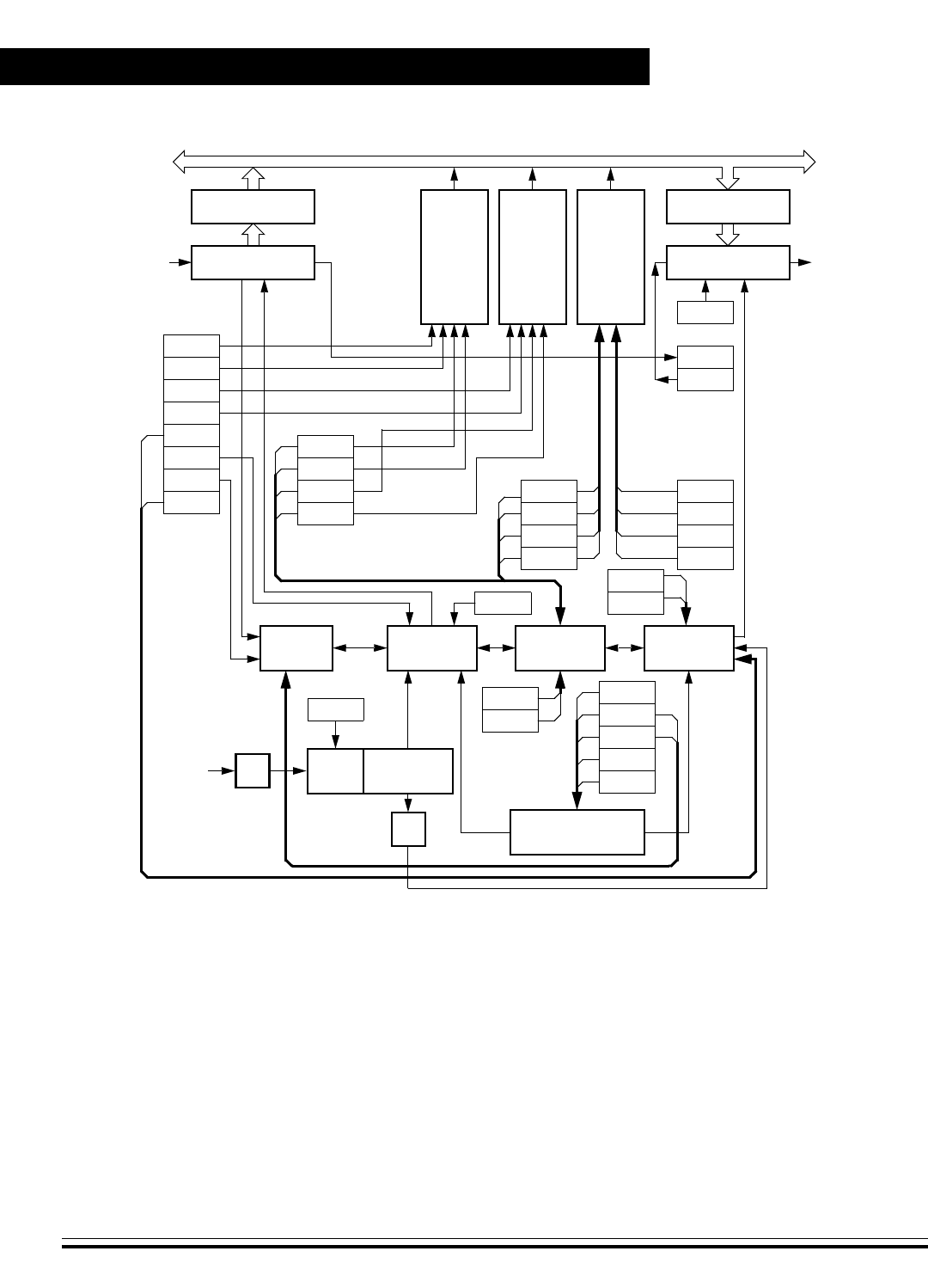
Serial Communications Interface (SCI)
Technical Data MC68HC08AZ60 — Rev 1.1
194 Serial Communications Interface (SCI) Freescale Semiconductor
Figure 17-1. SCI Module Block Diagram
SCTE
TC
SCRF
IDLE
OR
NF
FE
PE
SCTIE
TCIE
SCRIE
ILIE
TE
RE
RWU
SBK
R8
T8
ORIE
FEIE
PEIE
BKF
RPF
SCI DATA
RECEIVE
SHIFT REGISTER
SCI DATA
REGISTER
TRANSMIT
SHIFT REGISTER
NEIE
M
WAKE
ILTY
FLAG
CONTROL
TRANSMIT
CONTROL
RECEIVE
CONTROL
DATA SELECTION
CONTROL
WAKEUP
PTY
PEN
REGISTER
TRANSMITTER
INTERRUPT
CONTROL
RECEIVER
INTERRUPT
CONTROL
ERROR
INTERRUPT
CONTROL
CONTROL
ENSCI
LOOPS
ENSCI
INTERNAL BUS
TXINV
LOOPS
÷ 4
÷ 16
PRE-
SCALER BAUD RATE
GENERATOR
CGMXCLK
RxD TxD
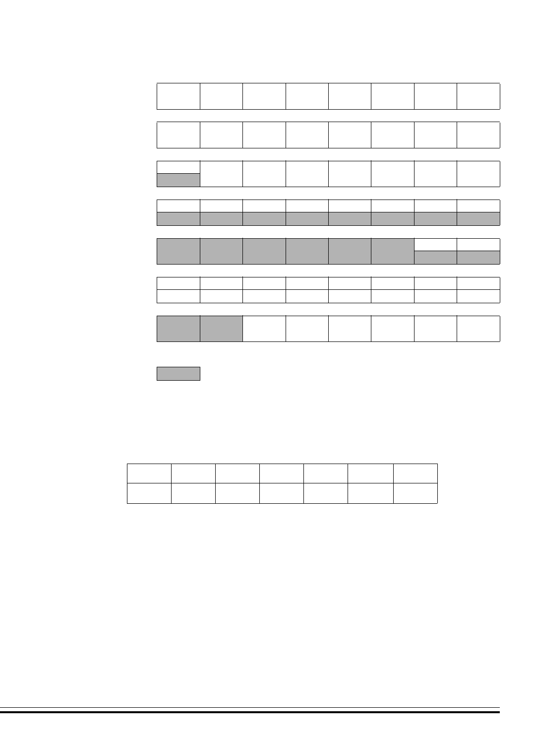
Serial Communications Interface (SCI)
Functional Description
MC68HC08AZ60 — Rev 1.1 Technical Data
Freescale Semiconductor Serial Communications Interface (SCI) 195
Register Name Bit 7654321Bit 0
SCI Control Register 1 (SCC1)
Read: LOOPS ENSCI TXINV M WAKE ILTY PEN PTY
Write:
Reset:00000000
SCI Control Register 2 (SCC2)
Read: SCTIE TCIE SCRIE ILIE TE RE RWU SBK
Write:
Reset:00000000
SCI Control Register 3 (SCC3)
Read: R8 T8 R R ORIE NEIE FEIE PEIE
Write:
Reset:UU000000
SCI Status Register 1 (SCS1)
Read: SCTE TC SCRF IDLE OR NF FE PE
Write:
Reset:11000000
SCI Status Register 2 (SCS2)
Read: BKF RPF
Write:
Reset:00000000
SCI Data Register (SCDR)
Read: R7 R6 R5 R4 R3 R2 R1 R0
Write: T7 T6 T5 T4 T3 T2 T1 T0
Reset: Unaffected by Reset
SCI Baud Rate Register (SCBR)
Read: SCP1 SCP0 R SCR2 SCR1 SCR0
Write:
Reset:00000000
= Unimplemented U = Unaffected R = Reserved
Figure 17-2. SCI I/O Register Summary
Table 17-2. SCI I/O Register Address Summary
Register SCC1 SCC2 SCC3 SCS1 SCS2 SCDR SCBR
Address $0013 $0014 $0015 $0016 $0017 $0018 $0019
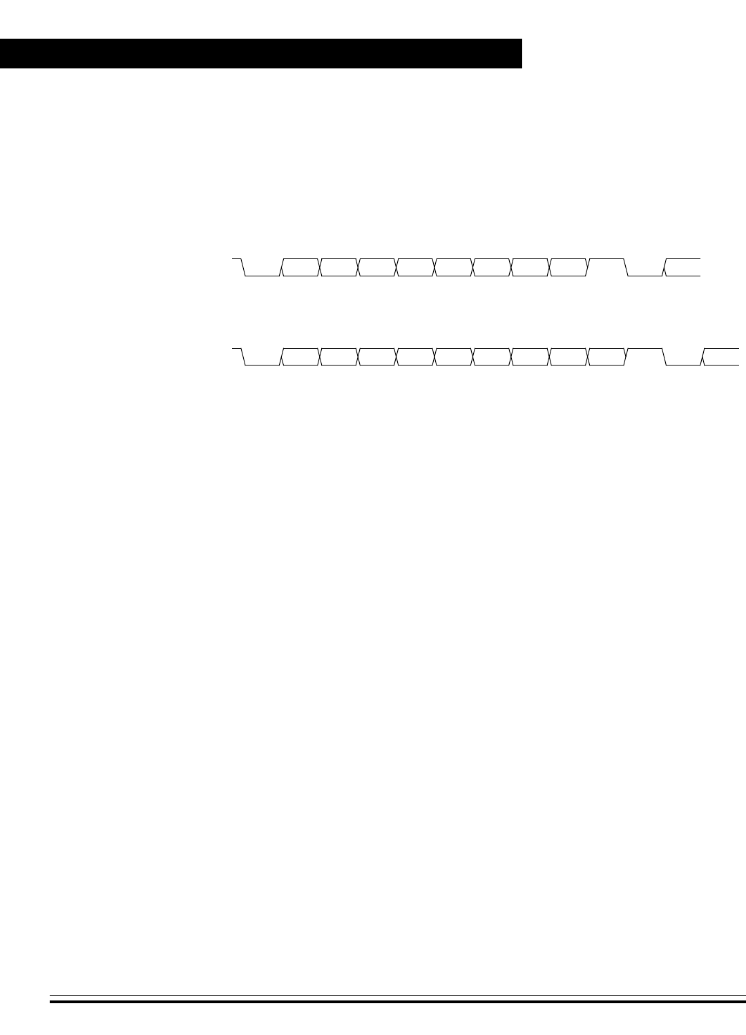
Serial Communications Interface (SCI)
Technical Data MC68HC08AZ60 — Rev 1.1
196 Serial Communications Interface (SCI) Freescale Semiconductor
17.5.1 Data Format
The SCI uses the standard non-return-to-zero mark/space data format
illustrated in Figure 17-3.
Figure 17-3. SCI Data Formats
17.5.2 Transmitter
Figure 17-4 shows the structure of the SCI transmitter.
17.5.2.1 Character Length
The transmitter can accommodate either 8-bit or 9-bit data. The state of
the M bit in SCI control register 1 (SCC1) determines character length.
When transmitting 9-bit data, bit T8 in SCI control register 3 (SCC3) is
the ninth bit (bit 8).
17.5.2.2 Character Transmission
During an SCI transmission, the transmit shift register shifts a character
out to the TxD pin. The SCI data register (SCDR) is the write-only buffer
between the internal data bus and the transmit shift register. To initiate
an SCI transmission:
1. Enable the SCI by writing a logic 1 to the enable SCI bit (ENSCI)
in SCI control register 1 (SCC1).
2. Enable the transmitter by writing a logic 1 to the transmitter enable
bit (TE) in SCI control register 2 (SCC2).
3. Clear the SCI transmitter empty bit (SCTE) by first reading SCI
BIT 5
START
BIT BIT 0 BIT 1
NEXT
STOP
BIT
START
BIT
8-BIT DATA FORMAT
(BIT M IN SCC1 CLEAR)
START
BIT BIT 0
NEXT
STOP
BIT
START
BIT
9-BIT DATA FORMAT
(BIT M IN SCC1 SET)
BIT 1 BIT 2 BIT 3 BIT 4 BIT 5 BIT 6 BIT 7 BIT 8
BIT 2 BIT 3 BIT 4 BIT 6 BIT 7
PARITY
OR DATA
BIT
PARITY
OR DATA
BIT

Serial Communications Interface (SCI)
Functional Description
MC68HC08AZ60 — Rev 1.1 Technical Data
Freescale Semiconductor Serial Communications Interface (SCI) 197
status register 1 (SCS1) and then writing to the SCDR.
4. Repeat step 3 for each subsequent transmission.
At the start of a transmission, transmitter control logic automatically
loads the transmit shift register with a preamble of logic 1s. After the
preamble shifts out, control logic transfers the SCDR data into the
transmit shift register. A logic 0 start bit automatically goes into the least
significant bit position of the transmit shift register. A logic 1 stop bit goes
into the most significant bit position.
The SCI transmitter empty bit, SCTE, in SCS1 becomes set when the
SCDR transfers a byte to the transmit shift register. The SCTE bit
indicates that the SCDR can accept new data from the internal data bus.
If the SCI transmit interrupt enable bit, SCTIE, in SCC2 is also set, the
SCTE bit generates a transmitter CPU interrupt request.
When the transmit shift register is not transmitting a character, the TxD
pin goes to the idle condition, logic 1. If at any time software clears the
ENSCI bit in SCI control register 1 (SCC1), the transmitter and receiver
relinquish control of the port E pins.
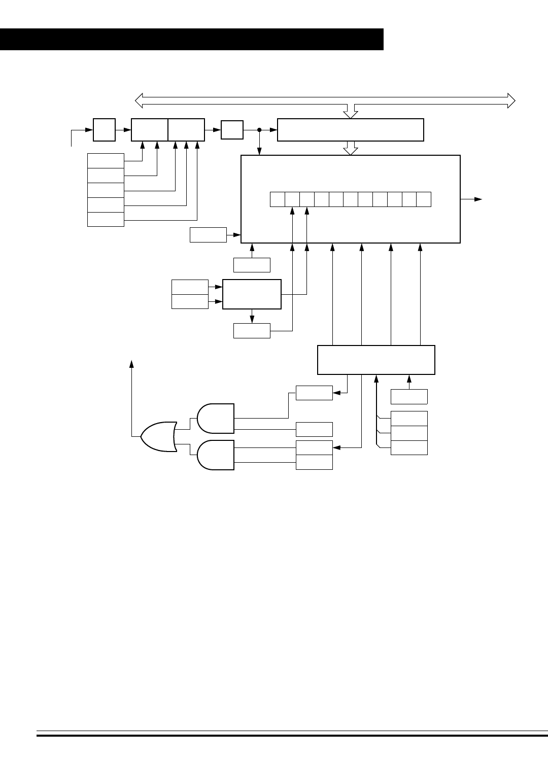
Serial Communications Interface (SCI)
Technical Data MC68HC08AZ60 — Rev 1.1
198 Serial Communications Interface (SCI) Freescale Semiconductor
Figure 17-4. SCI Transmitter
PEN
PTY
H876543210L
11-BIT
TRANSMIT
STOP
START
T8
SCTE
SCTIE
TCIE
SBK
TC
CGMXCLK
PARITY
GENERATION
MSB
SCI DATA REGISTER
LOAD FROM SCDR
SHIFT ENABLE
PREAMBLE
(ALL ONES)
BREAK
(ALL ZEROS)
TRANSMITTER
CONTROL LOGIC
SHIFT REGISTER
TC
SCTIE
TCIE
SCTE
TRANSMITTER CPU INTERRUPT REQUEST
M
ENSCI
LOOPS
TE
TXINV
INTERNAL BUS
÷ 4PRE-
SCALER
SCP1
SCP0
SCR2
SCR1
SCR0
BAUD
DIVIDER ÷ 16
TxD
Serial Communications Interface (SCI)
Functional Description
MC68HC08AZ60 — Rev 1.1 Technical Data
Freescale Semiconductor Serial Communications Interface (SCI) 199
Register Name Bit 7654321Bit 0
SCI Control Register 1 (SCC1)
Read: LOOPS ENSCI TXINV M WAKE ILTY PEN PTY
Write:
Reset:00000000
SCI Control Register 2 (SCC2)
Read: SCTIE TCIE SCRIE ILIE TE RE RWU SBK
Write:
Reset:00000000
SCI Control Register 3 (SCC3)
Read: R8 T8 R R ORIE NEIE FEIE PEIE
Write:
Reset:UU000000
SCI Status Register 1 (SCS1)
Read: SCTE TC SCRF IDLE OR NF FE PE
Write:
Reset:11000000
SCI Data Register (SCDR)
Read: R7 R6 R5 R4 R3 R2 R1 R0
Write: T7 T6 T5 T4 T3 T2 T1 T0
Reset: Unaffected by Reset
SCI Baud Rate Register (SCBR)
Read: SCP1 SCP0 R SCR2 SCR1 SCR0
Write:
Reset:00000000
= Unimplemented U = Unaffected R = Reserved
Figure 17-5. SCI Transmitter I/O Register Summary
Table 17-3. SCI Transmitter I/O Address Summary
Register SCC1 SCC2 SCC3 SCS1 SCDR SCBR
Address $0013 $0014 $0015 $0016 $0018 $0019

Serial Communications Interface (SCI)
Technical Data MC68HC08AZ60 — Rev 1.1
200 Serial Communications Interface (SCI) Freescale Semiconductor
17.5.2.3 Break Characters
Writing a logic 1 to the send break bit, SBK, in SCC2 loads the transmit
shift register with a break character. A break character contains all logic
0s and has no start, stop, or parity bit. Break character length depends
on the M bit in SCC1. As long as SBK is at logic 1, transmitter logic
continuously loads break characters into the transmit shift register. After
software clears the SBK bit, the shift register finishes transmitting the
last break character and then transmits at least one logic 1. The
automatic logic 1 at the end of a break character guarantees the
recognition of the start bit of the next character.
The SCI recognizes a break character when a start bit is followed by
eight or nine logic 0 data bits and a logic 0 where the stop bit should be.
Receiving a break character has the following effects on SCI registers:
• Sets the framing error bit (FE) in SCS1
• Sets the SCI receiver full bit (SCRF) in SCS1
• Clears the SCI data register (SCDR)
• Clears the R8 bit in SCC3
• Sets the break flag bit (BKF) in SCS2
• May set the overrun (OR), noise flag (NF), parity error (PE), or
reception in progress flag (RPF) bits
17.5.2.4 Idle Characters
An idle character contains all logic 1s and has no start, stop, or parity bit.
Idle character length depends on the M bit in SCC1. The preamble is a
synchronizing idle character that begins every transmission.
If the TE bit is cleared during a transmission, the TxD pin becomes idle
after completion of the transmission in progress. Clearing and then
setting the TE bit during a transmission queues an idle character to be
sent after the character currently being transmitted.

Serial Communications Interface (SCI)
Functional Description
MC68HC08AZ60 — Rev 1.1 Technical Data
Freescale Semiconductor Serial Communications Interface (SCI) 201
NOTE: When queueing an idle character, return the TE bit to logic 1 before the
stop bit of the current character shifts out to the TxD pin. Setting TE after
the stop bit appears on TxD causes data previously written to the SCDR
to be lost.
A good time to toggle the TE bit for a queued idle character is when the
SCTE bit becomes set and just before writing the next byte to the SCDR.
17.5.2.5 Inversion of Transmitted Output
The transmit inversion bit (TXINV) in SCI control register 1 (SCC1)
reverses the polarity of transmitted data. All transmitted values, including
idle, break, start, and stop bits, are inverted when TXINV is at logic 1.
(See SCI Control Register 1.)
17.5.2.6 Transmitter Interrupts
The following conditions can generate CPU interrupt requests from the
SCI transmitter:
• SCI transmitter empty (SCTE) — The SCTE bit in SCS1 indicates
that the SCDR has transferred a character to the transmit shift
register. SCTE can generate a transmitter CPU interrupt request.
Setting the SCI transmit interrupt enable bit, SCTIE, in SCC2
enables the SCTE bit to generate transmitter CPU interrupt
requests.
• Transmission complete (TC) — The TC bit in SCS1 indicates that
the transmit shift register and the SCDR are empty and that no
break or idle character has been generated. The transmission
complete interrupt enable bit, TCIE, in SCC2 enables the TC bit to
generate transmitter CPU interrupt requests.
Serial Communications Interface (SCI)
Technical Data MC68HC08AZ60 — Rev 1.1
202 Serial Communications Interface (SCI) Freescale Semiconductor
17.5.3 Receiver
Figure 17-6 shows the structure of the SCI receiver.
Figure 17-6. SCI Receiver Block Diagram
ALL ONES
ALL ZEROS
M
WAKE
ILTY
PEN
PTY
BKF
RPF
H876543210L
11-BIT
RECEIVE SHIFT REGISTER
STOP
START
DATA
RECOVERY
OR
ORIE
NF
NEIE
FE
FEIE
PE
PEIE
SCRIE
SCRF
ILIE
IDLE
WAKEUP
LOGIC
PARITY
CHECKING
MSB
ERROR CPU INTERRUPT REQUEST
CPU INTERRUPT REQUEST
SCI DATA REGISTER
R8
ORIE
NEIE
FEIE
PEIE
SCRIE
ILIE
RWU
SCRF
IDLE
OR
NF
FE
PE
INTERNAL BUS
PRE-
SCALER
BAUD
DIVIDER
÷ 4÷ 16
SCP1
SCP0
SCR2
SCR1
SCR0
CGMXCLK
RxD
Serial Communications Interface (SCI)
Functional Description
MC68HC08AZ60 — Rev 1.1 Technical Data
Freescale Semiconductor Serial Communications Interface (SCI) 203
Register Name Bit 7654321Bit 0
SCI Control Register 1 (SCC1) Read: LOOPS ENSCI TXINV M WAKE ILTY PEN PTY
Write:
Reset:00000000
SCI Control Register 2 (SCC2) Read: SCTIE TCIE SCRIE ILIE TE RE RWU SBK
Write:
Reset:00000000
SCI Control Register 3 (SCC3) Read: R8 T8 R R ORIE NEIE FEIE PEIE
Write:
Reset:UU000000
SCI Status Register 1 (SCS1) Read: SCTE TC SCRF IDLE OR NF FE PE
Write:
Reset:11000000
SCI Status Register 2 (SCS2) Read: BKF RPF
Write:
Reset:00000000
SCI Data Register (SCDR) Read: R7 R6 R5 R4 R3 R2 R1 R0
Write: T7 T6 T5 T4 T3 T2 T1 T0
Reset: Unaffected by Reset
SCI Baud Rate Register (SCBR) Read: SCP1 SCP0 R SCR2 SCR1 SCR0
Write:
Reset:00000000
= Unimplemented U = Unaffected R = Reserved
Figure 17-7. SCI I/O Receiver Register Summary
Table 17-4. SCI Receiver I/O Address Summary
Register SCC1 SCC2 SCC3 SCS1 SCS2 SCDR SCBR
Address $0013 $0014 $0015 $0016 $0017 $0018 $0019

Serial Communications Interface (SCI)
Technical Data MC68HC08AZ60 — Rev 1.1
204 Serial Communications Interface (SCI) Freescale Semiconductor
17.5.3.1 Character Length
The receiver can accommodate either 8-bit or 9-bit data. The state of the
M bit in SCI control register 1 (SCC1) determines character length.
When receiving 9-bit data, bit R8 in SCI control register 2 (SCC2) is the
ninth bit (bit 8). When receiving 8-bit data, bit R8 is a copy of the eighth
bit (bit 7).
17.5.3.2 Character Reception
During an SCI reception, the receive shift register shifts characters in
from the RxD pin. The SCI data register (SCDR) is the read-only buffer
between the internal data bus and the receive shift register.
After a complete character shifts into the receive shift register, the data
portion of the character transfers to the SCDR. The SCI receiver full bit,
SCRF, in SCI status register 1 (SCS1) becomes set, indicating that the
received byte can be read. If the SCI receive interrupt enable bit, SCRIE,
in SCC2 is also set, the SCRF bit generates a receiver CPU interrupt
request.
17.5.3.3 Data Sampling
The receiver samples the RxD pin at the RT clock rate. The RT clock is
an internal signal with a frequency 16 times the baud rate. To adjust for
baud rate mismatch, the RT clock is resynchronized at the following
times (see Figure 17-8):
• After every start bit
• After the receiver detects a data bit change from logic 1 to logic 0
(after the majority of data bit samples at RT8, RT9, and RT10
returns a valid logic 1 and the majority of the next RT8, RT9, and
RT10 samples returns a valid logic 0)
To locate the start bit, data recovery logic does an asynchronous search
for a logic 0 preceded by three logic 1s. When the falling edge of a
possible start bit occurs, the RT clock begins to count to 16.
Serial Communications Interface (SCI)
Functional Description
MC68HC08AZ60 — Rev 1.1 Technical Data
Freescale Semiconductor Serial Communications Interface (SCI) 205
Figure 17-8. Receiver Data Sampling
To verify the start bit and to detect noise, data recovery logic takes
samples at RT3, RT5, and RT7. Table 17-5 summarizes the results of
the start bit verification samples.
If start bit verification is not successful, the RT clock is reset and a new
search for a start bit begins.
Table 17-5. Start Bit Verification
RT3, RT5, and RT7 Samples Start Bit Verification Noise Flag
000 Yes 0
001 Yes 1
010 Yes 1
011 No 0
100 Yes 1
101 No 0
110 No 0
111 No 0
RT CLOCK
RESET
RT1
RT1
RT1
RT1
RT1
RT1
RT1
RT1
RT1
RT2
RT3
RT4
RT5
RT8
RT7
RT6
RT11
RT10
RT9
RT15
RT14
RT13
RT12
RT16
RT1
RT2
RT3
RT4
START BIT
QUALIFICATION START BIT
VERIFICATION DATA
SAMPLING
SAMPLES
RT
CLOCK
RT CLOCK
STATE
START BIT LSB
RxD

Serial Communications Interface (SCI)
Technical Data MC68HC08AZ60 — Rev 1.1
206 Serial Communications Interface (SCI) Freescale Semiconductor
To determine the value of a data bit and to detect noise, recovery logic
takes samples at RT8, RT9, and RT10. Table 17-6 summarizes the
results of the data bit samples.
NOTE: The RT8, RT9, and RT10 samples do not affect start bit verification. If
any or all of the RT8, RT9, and RT10 start bit samples are logic 1s
following a successful start bit verification, the noise flag (NF) is set and
the receiver assumes that the bit is a start bit.
To verify a stop bit and to detect noise, recovery logic takes samples at
RT8, RT9, and RT10. Table 17-7 summarizes the results of the stop bit
samples.
Table 17-6. Data Bit Recovery
RT8, RT9, and RT10 Samples Data Bit Determination Noise Flag
000 0 0
001 0 1
010 0 1
011 1 1
100 0 1
101 1 1
110 1 1
111 1 0
Table 17-7. Stop Bit Recovery
RT8, RT9, and RT10 Samples Framing Error Flag Noise Flag
000 1 0
001 1 1
010 1 1
011 0 1
100 1 1
101 0 1
110 0 1
111 0 0

Serial Communications Interface (SCI)
Functional Description
MC68HC08AZ60 — Rev 1.1 Technical Data
Freescale Semiconductor Serial Communications Interface (SCI) 207
17.5.3.4 Framing Errors
If the data recovery logic does not detect a logic 1 where the stop bit
should be in an incoming character, it sets the framing error bit, FE, in
SCS1. A break character also sets the FE bit because a break character
has no stop bit. The FE bit is set at the same time that the SCRF bit is
set.
17.5.3.5 Baud Rate Tolerance
A transmitting device may be operating at a baud rate below or above
the receiver baud rate. Accumulated bit time misalignment can cause
one of the three stop bit data samples to fall outside the actual stop bit.
Then a noise error occurs. If more than one of the samples is outside the
stop bit, a framing error occurs. In most applications, the baud rate
tolerance is much more than the degree of misalignment that is likely to
occur.
As the receiver samples an incoming character, it resynchronizes the RT
clock on any valid falling edge within the character. Resynchronization
within characters corrects misalignments between transmitter bit times
and receiver bit times.
Slow Data Tolerance
Figure 17-9 shows how much a slow received character can be
misaligned without causing a noise error or a framing error. The slow
stop bit begins at RT8 instead of RT1 but arrives in time for the stop
bit data samples at RT8, RT9, and RT10.
Figure 17-9. Slow Data
MSB STOP
RT1
RT2
RT3
RT4
RT5
RT6
RT7
RT8
RT9
RT10
RT11
RT12
RT13
RT14
RT15
RT16
DATA
SAMPLES
RECEIVER
RT CLOCK

Serial Communications Interface (SCI)
Technical Data MC68HC08AZ60 — Rev 1.1
208 Serial Communications Interface (SCI) Freescale Semiconductor
For an 8-bit character, data sampling of the stop bit takes the receiver
9 bit times ×16 RT cycles + 10 RT cycles = 154 RT cycles.
With the misaligned character shown in Figure 17-9, the receiver
counts 154 RT cycles at the point when the count of the transmitting
device is 9 bit times ×16 RT cycles + 3 RT cycles = 147 RT cycles.
The maximum percent difference between the receiver count and the
transmitter count of a slow 8-bit character with no errors is
For a 9-bit character, data sampling of the stop bit takes the receiver
10 bit times ×16 RT cycles + 10 RT cycles = 170 RT cycles.
With the misaligned character shown in Figure 17-9, the receiver
counts 170 RT cycles at the point when the count of the transmitting
device is 10 bit times ×16 RT cycles + 3 RT cycles = 163 RT cycles.
The maximum percent difference between the receiver count and the
transmitter count of a slow 9-bit character with no errors is
Fast Data Tolerance
Figure 17-10 shows how much a fast received character can be
misaligned without causing a noise error or a framing error. The fast
stop bit ends at RT10 instead of RT16 but is still there for the stop bit
data samples at RT8, RT9, and RT10.
Figure 17-10. Fast Data
154 147–
154
--------------------------100×4.54%=
170 163–
170
--------------------------100×4.12%=
IDLE OR NEXT CHARACTERSTOP
RT1
RT2
RT3
RT4
RT5
RT6
RT7
RT8
RT9
RT10
RT11
RT12
RT13
RT14
RT15
RT16
DATA
SAMPLES
RECEIVER
RT CLOCK

Serial Communications Interface (SCI)
Functional Description
MC68HC08AZ60 — Rev 1.1 Technical Data
Freescale Semiconductor Serial Communications Interface (SCI) 209
For an 8-bit character, data sampling of the stop bit takes the receiver
9 bit times ×16 RT cycles + 10 RT cycles = 154 RT cycles.
With the misaligned character shown in Figure 17-10, the receiver
counts 154 RT cycles at the point when the count of the transmitting
device is 10 bit times ×16 RT cycles = 160 RT cycles.
The maximum percent difference between the receiver count and the
transmitter count of a fast 8-bit character with no errors is
For a 9-bit character, data sampling of the stop bit takes the receiver
10 bit times ×16 RT cycles + 10 RT cycles = 170 RT cycles.
With the misaligned character shown in Figure 17-10, the receiver
counts 170 RT cycles at the point when the count of the transmitting
device is 11 bit times ×16 RT cycles = 176 RT cycles.
The maximum percent difference between the receiver count and the
transmitter count of a fast 9-bit character with no errors is
17.5.3.6 Receiver Wakeup
So that the MCU can ignore transmissions intended only for other
receivers in multiple-receiver systems, the receiver can be put into a
standby state. Setting the receiver wakeup bit, RWU, in SCC2 puts the
receiver into a standby state during which receiver interrupts are
disabled.
Depending on the state of the WAKE bit in SCC1, either of two
conditions on the RxD pin can bring the receiver out of the standby state:
• Address mark — An address mark is a logic 1 in the most
significant bit position of a received character. When the WAKE bit
is set, an address mark wakes the receiver from the standby state
by clearing the RWU bit. The address mark also sets the SCI
receiver full bit, SCRF. Software can then compare the character
containing the address mark to the user-defined address of the
receiver. If they are the same, the receiver remains awake and
154 160–
154
--------------------------100×3.90%.=
170 176–
170
--------------------------100×3.53%.=

Serial Communications Interface (SCI)
Technical Data MC68HC08AZ60 — Rev 1.1
210 Serial Communications Interface (SCI) Freescale Semiconductor
processes the characters that follow. If they are not the same,
software can set the RWU bit and put the receiver back into the
standby state.
• Idle input line condition — When the WAKE bit is clear, an idle
character on the RxD pin wakes the receiver from the standby
state by clearing the RWU bit. The idle character that wakes the
receiver does not set the receiver idle bit, IDLE, or the SCI receiver
full bit, SCRF. The idle line type bit, ILTY, determines whether the
receiver begins counting logic 1s as idle character bits after the
start bit or after the stop bit.
NOTE: With the WAKE bit clear, setting the RWU bit after the RxD pin has been
idle may cause the receiver to wake up immediately.
17.5.3.7 Receiver Interrupts
The following sources can generate CPU interrupt requests from the SCI
receiver:
• SCI receiver full (SCRF) — The SCRF bit in SCS1 indicates that
the receive shift register has transferred a character to the SCDR.
SCRF can generate a receiver CPU interrupt request. Setting the
SCI receive interrupt enable bit, SCRIE, in SCC2 enables the
SCRF bit to generate receiver CPU interrupts.
• Idle input (IDLE) — The IDLE bit in SCS1 indicates that 10 or 11
consecutive logic 1s shifted in from the RxD pin. The idle line
interrupt enable bit, ILIE, in SCC2 enables the IDLE bit to generate
CPU interrupt requests.
17.5.3.8 Error Interrupts
The following receiver error flags in SCS1 can generate CPU interrupt
requests:
• Receiver overrun (OR) — The OR bit indicates that the receive
shift register shifted in a new character before the previous
character was read from the SCDR. The previous character

Serial Communications Interface (SCI)
Low-Power Modes
MC68HC08AZ60 — Rev 1.1 Technical Data
Freescale Semiconductor Serial Communications Interface (SCI) 211
remains in the SCDR, and the new character is lost. The overrun
interrupt enable bit, ORIE, in SCC3 enables OR to generate SCI
error CPU interrupt requests.
• Noise flag (NF) — The NF bit is set when the SCI detects noise on
incoming data or break characters, including start, data, and stop
bits. The noise error interrupt enable bit, NEIE, in SCC3 enables
NF to generate SCI error CPU interrupt requests.
• Framing error (FE) — The FE bit in SCS1 is set when a logic 0
occurs where the receiver expects a stop bit. The framing error
interrupt enable bit, FEIE, in SCC3 enables FE to generate SCI
error CPU interrupt requests.
• Parity error (PE) — The PE bit in SCS1 is set when the SCI
detects a parity error in incoming data. The parity error interrupt
enable bit, PEIE, in SCC3 enables PE to generate SCI error CPU
interrupt requests.
17.6 Low-Power Modes
The WAIT and STOP instructions put the MCU in low power-
consumption standby modes.
17.6.1 Wait Mode
The SCI module remains active in wait mode. Any enabled CPU
interrupt request from the SCI module can bring the MCU out of wait
mode.
If SCI module functions are not required during wait mode, reduce power
consumption by disabling the module before executing the WAIT
instruction.
17.6.2 Stop Mode
The SCI module is inactive in stop mode. The STOP instruction does not
affect SCI register states. SCI module operation resumes after the MCU
exits stop mode.

Serial Communications Interface (SCI)
Technical Data MC68HC08AZ60 — Rev 1.1
212 Serial Communications Interface (SCI) Freescale Semiconductor
Because the internal clock is inactive during stop mode, entering stop
mode during an SCI transmission or reception results in invalid data.
17.7 SCI During Break Module Interrupts
The BCFE bit in the break flag control register (BFCR) enables software
to clear status bits during the break state. (See Break Module (BRK) on
page 153).
To allow software to clear status bits during a break interrupt, write a
logic 1 to the BCFE bit. If a status bit is cleared during the break state, it
remains cleared when the MCU exits the break state.
To protect status bits during the break state, write a logic 0 to the BCFE
bit. With BCFE at logic 0 (its default state), software can read and write
I/O registers during the break state without affecting status bits. Some
status bits have a two-step read/write clearing procedure. If software
does the first step on such a bit before the break, the bit cannot change
during the break state as long as BCFE is at logic 0. After the break,
doing the second step clears the status bit.
17.8 I/O Signals
Port E shares two of its pins with the SCI module. The two SCI I/O pins
are:
• PTE0/SCTxD — Transmit data
• PTE1/SCRxD — Receive data
17.8.1 PTE0/SCTxD (Transmit Data)
The PTE0/SCTxD pin is the serial data output from the SCI transmitter.
The SCI shares the PTE0/SCTxD pin with port E. When the SCI is
enabled, the PTE0/SCTxD pin is an output regardless of the state of the
DDRE2 bit in data direction register E (DDRE).

Serial Communications Interface (SCI)
I/O Registers
MC68HC08AZ60 — Rev 1.1 Technical Data
Freescale Semiconductor Serial Communications Interface (SCI) 213
17.8.2 PTE1/SCRxD (Receive Data)
The PTE1/SCRxD pin is the serial data input to the SCI receiver. The
SCI shares the PTE1/SCRxD pin with port E. When the SCI is enabled,
the PTE1/SCRxD pin is an input regardless of the state of the DDRE1 bit
in data direction register E (DDRE).
17.9 I/O Registers
The following I/O registers control and monitor SCI operation:
• SCI control register 1 (SCC1)
• SCI control register 2 (SCC2)
• SCI control register 3 (SCC3)
• SCI status register 1 (SCS1)
• SCI status register 2 (SCS2)
• SCI data register (SCDR)
• SCI baud rate register (SCBR)
17.9.1 SCI Control Register 1
SCI control register 1:
• Enables loop mode operation
• Enables the SCI
• Controls output polarity
• Controls character length
• Controls SCI wakeup method
• Controls idle character detection
• Enables parity function
• Controls parity type

Serial Communications Interface (SCI)
Technical Data MC68HC08AZ60 — Rev 1.1
214 Serial Communications Interface (SCI) Freescale Semiconductor
LOOPS — Loop Mode Select Bit
This read/write bit enables loop mode operation. In loop mode the
RxD pin is disconnected from the SCI, and the transmitter output goes
into the receiver input. Both the transmitter and the receiver must be
enabled to use loop mode. Reset clears the LOOPS bit.
1 = Loop mode enabled
0 = Normal operation enabled
ENSCI — Enable SCI Bit
This read/write bit enables the SCI and the SCI baud rate generator.
Clearing ENSCI sets the SCTE and TC bits in SCI status register 1
and disables transmitter interrupts. Reset clears the ENSCI bit.
1 = SCI enabled
0 = SCI disabled
TXINV — Transmit Inversion Bit
This read/write bit reverses the polarity of transmitted data. Reset
clears the TXINV bit.
1 = Transmitter output inverted
0 = Transmitter output not inverted
NOTE: Setting the TXINV bit inverts all transmitted values, including idle, break,
start, and stop bits.
Address: $0013
Bit 7654321Bit 0
Read:
LOOPS ENSCI TXINV M WAKE ILLTY PEN PTY
Write:
Reset:00000000
Figure 17-11. SCI Control Register 1 (SCC1)

Serial Communications Interface (SCI)
I/O Registers
MC68HC08AZ60 — Rev 1.1 Technical Data
Freescale Semiconductor Serial Communications Interface (SCI) 215
M — Mode (Character Length) Bit
This read/write bit determines whether SCI characters are eight or
nine bits long. (See Table 17-8).The ninth bit can serve as an extra
stop bit, as a receiver wakeup signal, or as a parity bit. Reset clears
the M bit.
1 = 9-bit SCI characters
0 = 8-bit SCI characters
WAKE — Wakeup Condition Bit
This read/write bit determines which condition wakes up the SCI: a
logic 1 (address mark) in the most significant bit position of a received
character or an idle condition on the RxD pin. Reset clears the WAKE
bit.
1 = Address mark wakeup
0 = Idle line wakeup
ILTY — Idle Line Type Bit
This read/write bit determines when the SCI starts counting logic 1s
as idle character bits. The counting begins either after the start bit or
after the stop bit. If the count begins after the start bit, then a string of
logic 1s preceding the stop bit may cause false recognition of an idle
character. Beginning the count after the stop bit avoids false idle
character recognition, but requires properly synchronized
transmissions. Reset clears the ILTY bit.
1 = Idle character bit count begins after stop bit
0 = Idle character bit count begins after start bit
PEN — Parity Enable Bit
This read/write bit enables the SCI parity function. (See Table 17-8).
When enabled, the parity function inserts a parity bit in the most
significant bit position. (See Table 17-7). Reset clears the PEN bit.
1 = Parity function enabled
0 = Parity function disabled

Serial Communications Interface (SCI)
Technical Data MC68HC08AZ60 — Rev 1.1
216 Serial Communications Interface (SCI) Freescale Semiconductor
PTY — Parity Bit
This read/write bit determines whether the SCI generates and checks
for odd parity or even parity. (See Table 17-8). Reset clears the PTY
bit.
1 = Odd parity
0 = Even parity
NOTE: Changing the PTY bit in the middle of a transmission or reception can
generate a parity error.
17.9.2 SCI Control Register 2
SCI control register 2:
• Enables the following CPU interrupt requests:
– Enables the SCTE bit to generate transmitter CPU interrupt
requests
– Enables the TC bit to generate transmitter CPU interrupt
requests
– Enables the SCRF bit to generate receiver CPU interrupt
requests
– Enables the IDLE bit to generate receiver CPU interrupt
requests
Table 17-8. Character Format Selection
Control Bits Character Format
M PEN:PTY Start
Bits Data
Bits Parity Stop
Bits Character
Length
0 0X 1 8 None 1 10 Bits
1 0X 1 9 None 1 11 Bits
0 10 1 7 Even 1 10 Bits
0 11 1 7 Odd 1 10 Bits
1 10 1 8 Even 1 11 Bits
1 11 1 8 Odd 1 11 Bits

Serial Communications Interface (SCI)
I/O Registers
MC68HC08AZ60 — Rev 1.1 Technical Data
Freescale Semiconductor Serial Communications Interface (SCI) 217
• Enables the transmitter
• Enables the receiver
• Enables SCI wakeup
• Transmits SCI break characters
SCTIE — SCI Transmit Interrupt Enable Bit
This read/write bit enables the SCTE bit to generate SCI transmitter
CPU interrupt requests. Setting the SCTIE bit in SCC3 enables the
SCTE bit to generate CPU interrupt requests. Reset clears the SCTIE
bit.
1 = SCTE enabled to generate CPU interrupt
0 = SCTE not enabled to generate CPU interrupt
TCIE — Transmission Complete Interrupt Enable Bit
This read/write bit enables the TC bit to generate SCI transmitter CPU
interrupt requests. Reset clears the TCIE bit.
1 = TC enabled to generate CPU interrupt requests
0 = TC not enabled to generate CPU interrupt requests
Address: $0014
Bit 7654321Bit 0
Read:
SCTIE TCIE SCRIE ILIE TE RE RWU SBK
Write:
Reset:00000000
Figure 17-12. SCI Control Register 2 (SCC2)

Serial Communications Interface (SCI)
Technical Data MC68HC08AZ60 — Rev 1.1
218 Serial Communications Interface (SCI) Freescale Semiconductor
SCRIE — SCI Receive Interrupt Enable Bit
This read/write bit enables the SCRF bit to generate SCI receiver
CPU interrupt requests. Setting the SCRIE bit in SCC3 enables the
SCRF bit to generate CPU interrupt requests. Reset clears the SCRIE
bit.
1 = SCRF enabled to generate CPU interrupt
0 = SCRF not enabled to generate CPU interrupt
ILIE — Idle Line Interrupt Enable Bit
This read/write bit enables the IDLE bit to generate SCI receiver CPU
interrupt requests. Reset clears the ILIE bit.
1 = IDLE enabled to generate CPU interrupt requests
0 = IDLE not enabled to generate CPU interrupt requests
TE — Transmitter Enable Bit
Setting this read/write bit begins the transmission by sending a
preamble of 10 or 11 logic 1s from the transmit shift register to the
TxD pin. If software clears the TE bit, the transmitter completes any
transmission in progress before the TxD returns to the idle condition
(logic 1). Clearing and then setting TE during a transmission queues
an idle character to be sent after the character currently being
transmitted. Reset clears the TE bit.
1 = Transmitter enabled
0 = Transmitter disabled
NOTE: Writing to the TE bit is not allowed when the enable SCI bit (ENSCI) is
clear. ENSCI is in SCI control register 1.

Serial Communications Interface (SCI)
I/O Registers
MC68HC08AZ60 — Rev 1.1 Technical Data
Freescale Semiconductor Serial Communications Interface (SCI) 219
RE — Receiver Enable Bit
Setting this read/write bit enables the receiver. Clearing the RE bit
disables the receiver but does not affect receiver interrupt flag bits.
Reset clears the RE bit.
1 = Receiver enabled
0 = Receiver disabled
NOTE: Writing to the RE bit is not allowed when the enable SCI bit (ENSCI) is
clear. ENSCI is in SCI control register 1.
RWU — Receiver Wakeup Bit
This read/write bit puts the receiver in a standby state during which
receiver interrupts are disabled. The WAKE bit in SCC1 determines
whether an idle input or an address mark brings the receiver out of the
standby state and clears the RWU bit. Reset clears the RWU bit.
1 = Standby state
0 = Normal operation
SBK — Send Break Bit
Setting and then clearing this read/write bit transmits a break
character followed by a logic 1. The logic 1 after the break character
guarantees recognition of a valid start bit. If SBK remains set, the
transmitter continuously transmits break characters with no logic 1s
between them. Reset clears the SBK bit.
1 = Transmit break characters
0 = No break characters being transmitted
NOTE: Do not toggle the SBK bit immediately after setting the SCTE bit.
Toggling SBK before the preamble begins causes the SCI to send a
break character instead of a preamble.

Serial Communications Interface (SCI)
Technical Data MC68HC08AZ60 — Rev 1.1
220 Serial Communications Interface (SCI) Freescale Semiconductor
17.9.3 SCI Control Register 3
SCI control register 3:
• Stores the ninth SCI data bit received and the ninth SCI data bit to
be transmitted.
• Enables the following interrupts:
– Receiver overrun interrupts
– Noise error interrupts
– Framing error interrupts
– Parity error interrupts
R8 — Received Bit 8
When the SCI is receiving 9-bit characters, R8 is the read-only ninth
bit (bit 8) of the received character. R8 is received at the same time
that the SCDR receives the other 8 bits.
When the SCI is receiving 8-bit characters, R8 is a copy of the eighth
bit (bit 7). Reset has no effect on the R8 bit.
T8 — Transmitted Bit 8
When the SCI is transmitting 9-bit characters, T8 is the read/write
ninth bit (bit 8) of the transmitted character. T8 is loaded into the
transmit shift register at the same time that the SCDR is loaded into
the transmit shift register. Reset has no effect on the T8 bit.
Address: $0015
Bit 7654321Bit 0
Read: R8
T8 R R ORIE NEIE FEIE PEIE
Write:
Reset:UU000000
= Unimplemented R = Reserved U = Unaffected
Figure 17-13. SCI Control Register 3 (SCC3)

Serial Communications Interface (SCI)
I/O Registers
MC68HC08AZ60 — Rev 1.1 Technical Data
Freescale Semiconductor Serial Communications Interface (SCI) 221
ORIE — Receiver Overrun Interrupt Enable Bit
This read/write bit enables SCI error CPU interrupt requests
generated by the receiver overrun bit, OR.
1 = SCI error CPU interrupt requests from OR bit enabled
0 = SCI error CPU interrupt requests from OR bit disabled
NEIE — Receiver Noise Error Interrupt Enable Bit
This read/write bit enables SCI error CPU interrupt requests
generated by the noise error bit, NE. Reset clears NEIE.
1 = SCI error CPU interrupt requests from NE bit enabled
0 = SCI error CPU interrupt requests from NE bit disabled
FEIE — Receiver Framing Error Interrupt Enable Bit
This read/write bit enables SCI error CPU interrupt requests
generated by the framing error bit, FE. Reset clears FEIE.
1 = SCI error CPU interrupt requests from FE bit enabled
0 = SCI error CPU interrupt requests from FE bit disabled
PEIE — Receiver Parity Error Interrupt Enable Bit
This read/write bit enables SCI receiver CPU interrupt requests
generated by the parity error bit, PE. Reset clears PEIE.
1 = SCI error CPU interrupt requests from PE bit enabled
0 = SCI error CPU interrupt requests from PE bit disabled

Serial Communications Interface (SCI)
Technical Data MC68HC08AZ60 — Rev 1.1
222 Serial Communications Interface (SCI) Freescale Semiconductor
17.9.4 SCI Status Register 1
SCI status register 1 contains flags to signal the following conditions:
• Transfer of SCDR data to transmit shift register complete
• Transmission complete
• Transfer of receive shift register data to SCDR complete
• Receiver input idle
• Receiver overrun
• Noisy data
• Framing error
• Parity error
SCTE — SCI Transmitter Empty Bit
This clearable, read-only bit is set when the SCDR transfers a
character to the transmit shift register. SCTE can generate an SCI
transmitter CPU interrupt request. When the SCTIE bit in SCC2 is set,
SCTE generates an SCI transmitter CPU interrupt request. In normal
operation, clear the SCTE bit by reading SCS1 with SCTE set and
then writing to SCDR. Reset sets the SCTE bit.
1 = SCDR data transferred to transmit shift register
0 = SCDR data not transferred to transmit shift register
Address: $0016
Bit 7654321Bit 0
Read: SCTE TC SCRF IDLE OR NF FE PE
Write:
Reset:11000000
= Unimplemented
Figure 17-14. SCI Status Register 1 (SCS1)

Serial Communications Interface (SCI)
I/O Registers
MC68HC08AZ60 — Rev 1.1 Technical Data
Freescale Semiconductor Serial Communications Interface (SCI) 223
TC — Transmission Complete Bit
This read-only bit is set when the SCTE bit is set, and no data,
preamble, or break character is being transmitted. TC generates an
SCI transmitter CPU interrupt request if the TCIE bit in SCC2 is also
set. TC is cleared automatically when data, preamble, or break is
queued and ready to be sent. There may be up to 1.5 transmitter
clocks of latency between queueing data, preamble, and break and
the transmission actually starting. Reset sets the TC bit.
1 = No transmission in progress
0 = Transmission in progress
SCRF — SCI Receiver Full Bit
This clearable, read-only bit is set when the data in the receive shift
register transfers to the SCI data register. SCRF can generate an SCI
receiver CPU interrupt request. When the SCRIE bit in SCC2 is set
the SCRF generates a CPU interrupt request. In normal operation,
clear the SCRF bit by reading SCS1 with SCRF set and then reading
the SCDR. Reset clears SCRF.
1 = Received data available in SCDR
0 = Data not available in SCDR
IDLE — Receiver Idle Bit
This clearable, read-only bit is set when 10 or 11 consecutive logic 1s
appear on the receiver input. IDLE generates an SCI error CPU
interrupt request if the ILIE bit in SCC2 is also set. Clear the IDLE bit
by reading SCS1 with IDLE set and then reading the SCDR. After the
receiver is enabled, it must receive a valid character that sets the
SCRF bit before an idle condition can set the IDLE bit. Also, after the
IDLE bit has been cleared, a valid character must again set the SCRF
bit before an idle condition can set the IDLE bit. Reset clears the IDLE
bit.
1 = Receiver input idle
0 = Receiver input active (or idle since the IDLE bit was cleared)

Serial Communications Interface (SCI)
Technical Data MC68HC08AZ60 — Rev 1.1
224 Serial Communications Interface (SCI) Freescale Semiconductor
OR — Receiver Overrun Bit
This clearable, read-only bit is set when software fails to read the
SCDR before the receive shift register receives the next character.
The OR bit generates an SCI error CPU interrupt request if the ORIE
bit in SCC3 is also set. The data in the shift register is lost, but the data
already in the SCDR is not affected. Clear the OR bit by reading SCS1
with OR set and then reading the SCDR. Reset clears the OR bit.
1 = Receive shift register full and SCRF = 1
0 = No receiver overrun
Software latency may allow an overrun to occur between reads of SCS1
and SCDR in the flag-clearing sequence. Figure 17-15 shows the
normal flag-clearing sequence and an example of an overrun caused by
a delayed flag-clearing sequence. The delayed read of SCDR does not
clear the OR bit because OR was not set when SCS1 was read. Byte 2
caused the overrun and is lost. The next flag-clearing sequence reads
byte 3 in the SCDR instead of byte 2.
In applications that are subject to software latency or in which it is
important to know which byte is lost due to an overrun, the flag-clearing
routine can check the OR bit in a second read of SCS1 after reading the
data register.
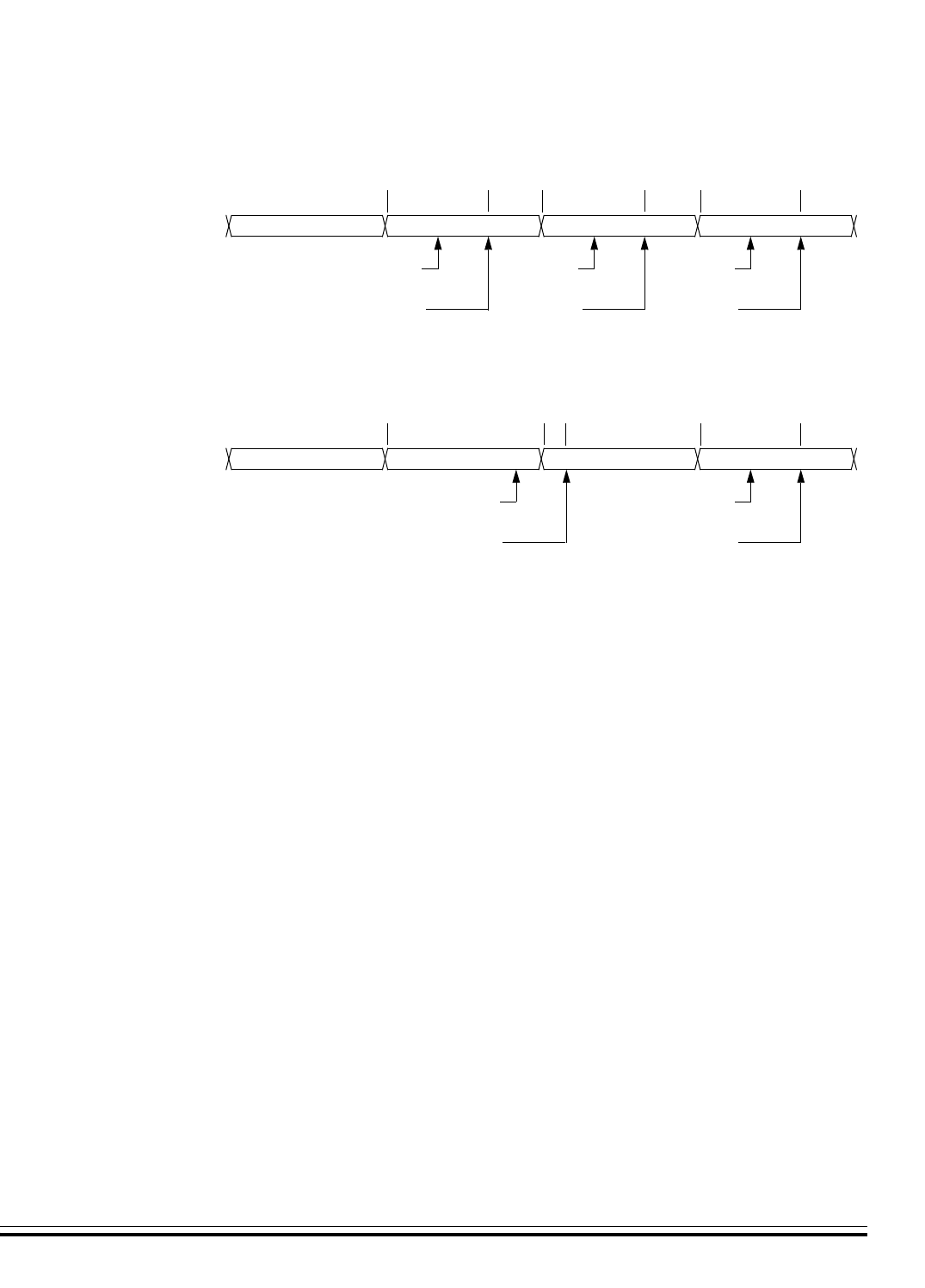
Serial Communications Interface (SCI)
I/O Registers
MC68HC08AZ60 — Rev 1.1 Technical Data
Freescale Semiconductor Serial Communications Interface (SCI) 225
Figure 17-15. Flag Clearing Sequence
NF — Receiver Noise Flag Bit
This clearable, read-only bit is set when the SCI detects noise on the
RxD pin. NF generates an NF CPU interrupt request if the NEIE bit in
SCC3 is also set. Clear the NF bit by reading SCS1 and then reading
the SCDR. Reset clears the NF bit.
1 = Noise detected
0 = No noise detected
FE — Receiver Framing Error Bit
This clearable, read-only bit is set when a logic 0 is accepted as the
stop bit. FE generates an SCI error CPU interrupt request if the FEIE
bit in SCC3 also is set. Clear the FE bit by reading SCS1 with FE set
and then reading the SCDR. Reset clears the FE bit.
1 = Framing error detected
0 = No framing error detected
BYTE 1
NORMAL FLAG CLEARING SEQUENCE
READ SCS1
SCRF = 1
READ SCDR
BYTE 1
SCRF = 1
SCRF = 1
BYTE 2 BYTE 3 BYTE 4
OR = 0
READ SCS1
SCRF = 1
OR = 0
READ SCDR
BYTE 2
SCRF = 0
READ SCS1
SCRF = 1
OR = 0
SCRF = 1
SCRF = 0
READ SCDR
BYTE 3
SCRF = 0
BYTE 1
READ SCS1
SCRF = 1
READ SCDR
BYTE 1
SCRF = 1
SCRF = 1
BYTE 2 BYTE 3 BYTE 4
OR = 0
READ SCS1
SCRF = 1
OR = 1
READ SCDR
BYTE 3
DELAYED FLAG CLEARING SEQUENCE
OR = 1
SCRF = 1
OR = 1
SCRF = 0
OR = 1
SCRF = 0
OR = 0

Serial Communications Interface (SCI)
Technical Data MC68HC08AZ60 — Rev 1.1
226 Serial Communications Interface (SCI) Freescale Semiconductor
PE — Receiver Parity Error Bit
This clearable, read-only bit is set when the SCI detects a parity error
in incoming data. PE generates a PE CPU interrupt request if the
PEIE bit in SCC3 is also set. Clear the PE bit by reading SCS1 with
PE set and then reading the SCDR. Reset clears the PE bit.
1 = Parity error detected
0 = No parity error detected
17.9.5 SCI Status Register 2
SCI status register 2 contains flags to signal the following conditions:
• Break character detected
• Incoming data
BKF — Break Flag Bit
This clearable, read-only bit is set when the SCI detects a break
character on the RxD pin. In SCS1, the FE and SCRF bits are also
set. In 9-bit character transmissions, the R8 bit in SCC3 is cleared.
BKF does not generate a CPU interrupt request. Clear BKF by
reading SCS2 with BKF set and then reading the SCDR. Once
cleared, BKF can become set again only after logic 1s again appear
on the RxD pin followed by another break character. Reset clears the
BKF bit.
1 = Break character detected
0 = No break character detected
Address: $0017
Bit 7654321Bit 0
Read: BKF RPF
Write:
Reset:00000000
= Unimplemented
Figure 17-16. SCI Status Register 2 (SCS2)

Serial Communications Interface (SCI)
I/O Registers
MC68HC08AZ60 — Rev 1.1 Technical Data
Freescale Semiconductor Serial Communications Interface (SCI) 227
RPF — Reception in Progress Flag Bit
This read-only bit is set when the receiver detects a logic 0 during the
RT1 time period of the start bit search. RPF does not generate an
interrupt request. RPF is reset after the receiver detects false start bits
(usually from noise or a baud rate mismatch), or when the receiver
detects an idle character. Polling RPF before disabling the SCI
module or entering stop mode can show whether a reception is in
progress.
1 = Reception in progress
0 = No reception in progress
17.9.6 SCI Data Register
The SCI data register is the buffer between the internal data bus and the
receive and transmit shift registers. Reset has no effect on data in the
SCI data register.
R7/T7:R0/T0 — Receive/Transmit Data Bits
Reading address $0018 accesses the read-only received data bits,
R7:R0. Writing to address $0018 writes the data to be transmitted,
T7:T0. Reset has no effect on the SCI data register.
NOTE: Do not use read-modify-write instructions on the SCI data register.
Address: $0018
Bit 7654321Bit 0
Read: R7 R6 R5 R4 R3 R2 R1 R0
Write: T7 T6 T5 T4 T3 T2 T1 T0
Reset: Unaffected by Reset
Figure 17-17. SCI Data Register (SCDR)
Serial Communications Interface (SCI)
Technical Data MC68HC08AZ60 — Rev 1.1
228 Serial Communications Interface (SCI) Freescale Semiconductor
17.9.7 SCI Baud Rate Register
The baud rate register selects the baud rate for both the receiver and the
transmitter.
SCP1 and SCP0 — SCI Baud Rate Prescaler Bits
These read/write bits select the baud rate prescaler divisor as shown
in Table 17-9. Reset clears SCP1 and SCP0.
Address: $0019
Bit 7654321Bit 0
Read:
SCP1 SCP0 R SCR2 SCR1 SCR0
Write:
Reset:00000000
= Unimplemented R = Reserved
Figure 17-18. SCI Baud Rate Register (SCBR)
Table 17-9. SCI Baud Rate Prescaling
SCP[1:0] Prescaler Divisor (PD)
00 1
01 3
10 4
11 13

Serial Communications Interface (SCI)
I/O Registers
MC68HC08AZ60 — Rev 1.1 Technical Data
Freescale Semiconductor Serial Communications Interface (SCI) 229
SCR2 – SCR0 — SCI Baud Rate Select Bits
These read/write bits select the SCI baud rate divisor as shown in
Table 17-10. Reset clears SCR2–SCR0.
Use the following formula to calculate the SCI baud rate:
where:
fCrystal = crystal frequency
PD = prescaler divisor
BD = baud rate divisor
Table 17-11 shows the SCI baud rates that can be generated with a
4.9152-MHz crystal.
Table 17-10. SCI Baud Rate Selection
SCR[2:1:0] Baud Rate Divisor (BD)
000 1
001 2
010 4
011 8
100 16
101 32
110 64
111 128
Baud rate fCrystal
64 PD BD××
------------------------------------=

Serial Communications Interface (SCI)
Technical Data MC68HC08AZ60 — Rev 1.1
230 Serial Communications Interface (SCI) Freescale Semiconductor
Table 17-11. SCI Baud Rate Selection Examples
SCP[1:0] Prescaler
Divisor
(PD) SCR[2:1:0] Baud Rate
Divisor
(BD)
Baud Rate
(fCrystal = 4.9152 MHz)
00 1 000 1 76,800
00 1 001 2 38,400
00 1 010 4 19,200
00 1 011 8 9600
00 1 100 16 4800
00 1 101 32 2400
00 1 110 64 1200
00 1 111 128 600
01 3 000 1 25,600
01 3 001 2 12,800
01 3 010 4 6400
01 3 011 8 3200
01 3 100 16 1600
01 3 101 32 800
01 3 110 64 400
01 3 111 128 200
10 4 000 1 19,200
10 4 001 2 9600
10 4 010 4 4800
10 4 011 8 2400
10 4 100 16 1200
10 4 101 32 600
10 4 110 64 300
10 4 111 128 150
11 13 000 1 5908
11 13 001 2 2954
11 13 010 4 1477
11 13 011 8 739
11 13 100 16 369
11 13 101 32 185
11 13 110 64 92
11 13 111 128 46

MC68HC08AZ60 — Rev 1.1 Technical Data
Freescale Semiconductor Serial Peripheral Interface (SPI) 231
Technical Data — MC68HC08AZ60
Section 18. Serial Peripheral Interface (SPI)
18.1 Contents
18.2 Introduction. . . . . . . . . . . . . . . . . . . . . . . . . . . . . . . . . . . . . .232
18.3 Features. . . . . . . . . . . . . . . . . . . . . . . . . . . . . . . . . . . . . . . . .232
18.4 Pin Name Conventions and I/O Register Addresses. . . . .233
18.5 Functional Description. . . . . . . . . . . . . . . . . . . . . . . . . . . . .234
18.5.1 Master Mode . . . . . . . . . . . . . . . . . . . . . . . . . . . . . . . . . . .236
18.5.2 Slave Mode . . . . . . . . . . . . . . . . . . . . . . . . . . . . . . . . . . . .237
18.6 Transmission Formats . . . . . . . . . . . . . . . . . . . . . . . . . . . . .238
18.6.1 Clock Phase and Polarity Controls. . . . . . . . . . . . . . . . .238
18.6.2 Transmission Format When CPHA = ‘0’. . . . . . . . . . . . .239
18.6.3 Transmission Format When CPHA = ‘1’. . . . . . . . . . . . .240
18.6.4 Transmission Initiation Latency . . . . . . . . . . . . . . . . . . .241
18.6.5 Error Conditions . . . . . . . . . . . . . . . . . . . . . . . . . . . . . . . . . .243
18.6.6 Overflow Error . . . . . . . . . . . . . . . . . . . . . . . . . . . . . . . . .243
18.6.7 Mode Fault Error. . . . . . . . . . . . . . . . . . . . . . . . . . . . . . . .245
18.7 Interrupts. . . . . . . . . . . . . . . . . . . . . . . . . . . . . . . . . . . . . . . .247
18.8 Queuing Transmission Data . . . . . . . . . . . . . . . . . . . . . . . .248
18.9 Resetting the SPI . . . . . . . . . . . . . . . . . . . . . . . . . . . . . . . . .250
18.10 Low-Power Modes . . . . . . . . . . . . . . . . . . . . . . . . . . . . . . . .251
18.10.1 WAIT Mode . . . . . . . . . . . . . . . . . . . . . . . . . . . . . . . . . . . .251
18.10.2 STOP Mode . . . . . . . . . . . . . . . . . . . . . . . . . . . . . . . . . . . .251
18.11 SPI During Break Interrupts. . . . . . . . . . . . . . . . . . . . . . . . .251
18.12 I/O Signals . . . . . . . . . . . . . . . . . . . . . . . . . . . . . . . . . . . . . . .252
18.12.1 MISO (MasterIn/Slave Out) . . . . . . . . . . . . . . . . . . . . . . .253
18.12.2 MOSI (Master Out/Slave In) . . . . . . . . . . . . . . . . . . . . . . .253

Serial Peripheral Interface (SPI)
Technical Data MC68HC08AZ60 — Rev 1.1
232 Serial Peripheral Interface (SPI) Freescale Semiconductor
18.12.3 SPSCK (Serial Clock). . . . . . . . . . . . . . . . . . . . . . . . . . . .253
18.12.4 SS (Slave Select) . . . . . . . . . . . . . . . . . . . . . . . . . . . . . . .254
18.12.5 VSS (Clock Ground). . . . . . . . . . . . . . . . . . . . . . . . . . . . .255
18.13 I/O Registers . . . . . . . . . . . . . . . . . . . . . . . . . . . . . . . . . . . . .255
18.13.1 SPI Control Register (SPCR). . . . . . . . . . . . . . . . . . . . . .256
18.13.2 SPI Status and Control Register (SPSCR) . . . . . . . . . . .258
18.13.3 SPI Data Register (SPDR) . . . . . . . . . . . . . . . . . . . . . . . .262
18.2 Introduction
This section describes the serial peripheral interface module (SPI),
which allows full-duplex, synchronous, serial communications with
peripheral devices.
18.3 Features
Features of the SPI module include the following:
• Full-duplex operation
• Master and slave modes
• Double-buffered operation with separate transmit and receive
registers
• Four master mode frequencies (maximum = bus frequency ÷2)
• Maximum slave mode frequency = bus frequency
• Serial clock with programmable polarity and phase
• Two separately enabled interrupts with CPU service:
– SPRF (SPI receiver full)
– SPTE (SPI transmitter empty)
• Mode fault error flag with CPU interrupt capability
• Overflow error flag with CPU interrupt capability
• Programmable wired-OR mode
•I
2C (inter-integrated circuit) compatibility
Serial Peripheral Interface (SPI)
Pin Name Conventions and I/O Register Addresses
MC68HC08AZ60 — Rev 1.1 Technical Data
Freescale Semiconductor Serial Peripheral Interface (SPI) 233
18.4 Pin Name Conventions and I/O Register Addresses
The generic names of the SPI input/output (I/O) pins are:
•SS (slave select)
• SPSCK (SPI serial clock)
• MOSI (master out slave in)
• MISO (master in slave out)
The SPI shares four I/O pins with a parallel I/O port. The full name of an
SPI pin reflects the name of the shared port pin. Table 18-1 shows the
full names of the SPI I/O pins. The generic pin names appear in the text
that follows.:
The generic pins names appear in the text that follows.
Table 18-1. Pin Name Conventions
SPI Generic Pin Names: MISO MOSI SS SCK VSS
Full SPI Pin Names: SPI PTE5/MISO PTE6/MOSI PTE4/SS PTE7/SPSCK CGND
Table 18-2. I/O Register Addresses
Register name Register address
SPI Control Register (SPICR) $0010
SPI Status and Control Register (SPISCR) $0011
SPI Data Register (SPIDR) $0012

Serial Peripheral Interface (SPI)
Technical Data MC68HC08AZ60 — Rev 1.1
234 Serial Peripheral Interface (SPI) Freescale Semiconductor
18.5 Functional Description
Figure 18-1 summarizes the SPI I/O registers and Figure 18-2 show the
structure of the SPI module.
Register name R/W Bit 7 6 5 4 3 2 1 Bit 0
SPI Control Register (SPCR) Read: SPRIE R SPMSTR CPOL CPHA SPWOM SPE SPTIE
Write:
Reset:00101000
SPI Status and Control Register
(SPSCR)
Read: SPRF ERRIE OVRF MODF SPTE MODFEN SPR1 SPR0
Write:
Reset:00001000
SPI Data Register (SPDR) Read:R7R6R5R4R3R2R1R0
Write: T7 T6 T5 T4 T3 T2 T1 T0
Reset: Unaffected by reset
R=Reserved = Unimplemented
Figure 18-1. SPI I/O Register Summary
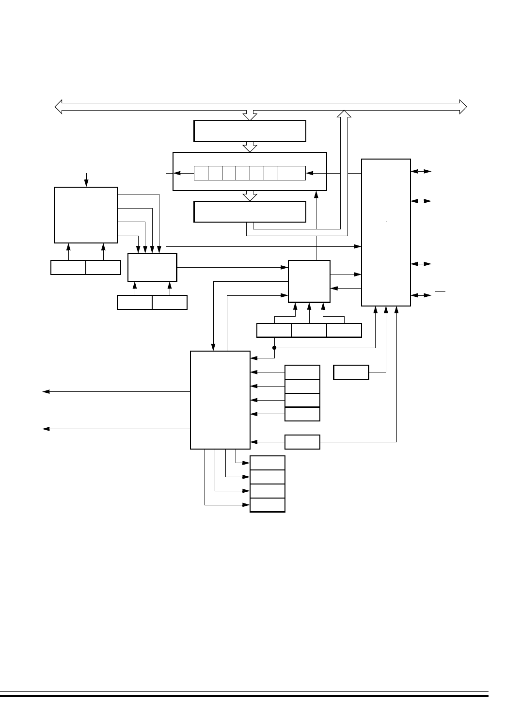
Serial Peripheral Interface (SPI)
Functional Description
MC68HC08AZ60 — Rev 1.1 Technical Data
Freescale Semiconductor Serial Peripheral Interface (SPI) 235
Figure 18-2. SPI Module Block Diagram
The SPI module allows full-duplex, synchronous, serial communication
between the MCU and peripheral devices, including other MCUs.
Software can poll the SPI status flags or SPI operation can be interrupt-
driven. All SPI interrupts can be serviced by the CPU.
The following paragraphs describe the operation of the SPI module.
TRANSMITTER CPU INTERRUPT REQUEST
RECEIVER/ERROR CPU INTERRUPT REQUEST
76543210
SPR1
SPMSTR
TRANSMIT DATA REGISTER
SHIFT REGISTER
SPR0
BUS CLOCK
CLOCK
SELECT
÷ 2
CLOCK
DIVIDER
÷ 8
÷ 32
÷ 128
CLOCK
LOGIC
CPHA CPOL
SPI
SPRIE
SPE
SPWOM
SPRF
SPTE
OVRF
M
S
PIN
CONTROL
LOGIC
RECEIVE DATA REGISTER
SPTIE
SPE
INTERNAL BUS
MODFEN
ERRIE
CONTROL
MODF
SPMSTR
MOSI
MISO
SPSCK
SS

Serial Peripheral Interface (SPI)
Technical Data MC68HC08AZ60 — Rev 1.1
236 Serial Peripheral Interface (SPI) Freescale Semiconductor
18.5.1 Master Mode
The SPI operates in master mode when the SPI master bit, SPMSTR, is
set.
NOTE: Configure the SPI modules as master and slave before enabling them.
Enable the master SPI before enabling the slave SPI. Disable the slave
SPI before disabling the master SPI. See SPI Control Register (SPCR)
on page 256.
Only a master SPI module can initiate transmissions. Software begins
the transmission from a master SPI module by writing to the SPI data
register. If the shift register is empty, the byte immediately transfers to
the shift register, setting the SPI transmitter empty bit, SPTE. The byte
begins shifting out on the MOSI pin under the control of the serial clock.
See Figure 18-3.
The SPR1 and SPR0 bits control the baud rate generator and determine
the speed of the shift register. See SPI Status and Control Register
(SPSCR) on page 258. Through the SPSCK pin, the baud rate generator
of the master also controls the shift register of the slave peripheral.
As the byte shifts out on the MOSI pin of the master, another byte shifts
in from the slave on the master’s MISO pin. The transmission ends when
the receiver full bit, SPRF, becomes set. At the same time that SPRF
becomes set, the byte from the slave transfers to the receive data
register. In normal operation, SPRF signals the end of a transmission.
Software clears SPRF by reading the SPI status and control register with
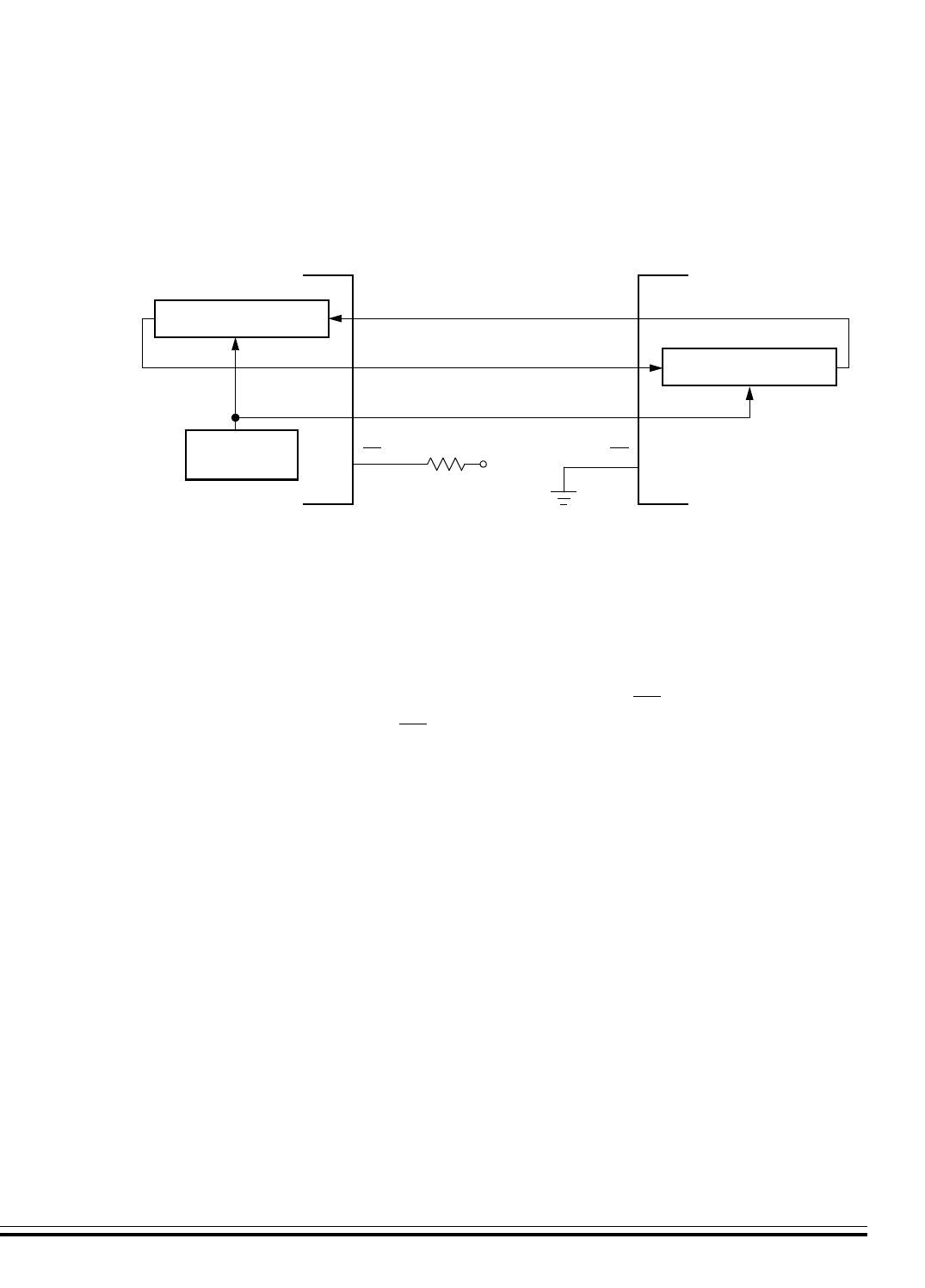
Serial Peripheral Interface (SPI)
Functional Description
MC68HC08AZ60 — Rev 1.1 Technical Data
Freescale Semiconductor Serial Peripheral Interface (SPI) 237
SPRF set and then reading the SPI data register. Writing to the SPI data
register clears the SPTIE bit.
18.5.2 Slave Mode
The SPI operates in slave mode when the SPMSTR bit is clear. In slave
mode the SPSCK pin is the input for the serial clock from the master
MCU. Before a data transmission occurs, the SS pin of the slave MCU
must be at logic ‘0’. SS must remain low until the transmission is
complete. See Mode Fault Error on page 245.
In a slave SPI module, data enters the shift register under the control of
the serial clock from the master SPI module. After a byte enters the shift
register of a slave SPI, it transfers to the receive data register, and the
SPRF bit is set. To prevent an overflow condition, slave software must
then read the SPI data register before another byte enters the shift
register.
The maximum frequency of the SPSCK for an SPI configured as a slave
is the bus clock speed (which is twice as fast as the fastest master
SPSCK clock that can be generated). The frequency of the SPSCK for
an SPI configured as a slave does not have to correspond to any
particular SPI baud rate. The baud rate only controls the speed of the
SPSCK generated by an SPI configured as a master. Therefore, the
Figure 18-3. Full-duplex Master-Slave Connections
SHIFT REGISTER
SHIFT REGISTER
BAUD RATE
GENERATOR
MASTER MCU SLAVE MCU
VDD
MOSI MOSI
MISO MISO
SPSCK SPSCK
SS SS

Serial Peripheral Interface (SPI)
Technical Data MC68HC08AZ60 — Rev 1.1
238 Serial Peripheral Interface (SPI) Freescale Semiconductor
frequency of the SPSCK for an SPI configured as a slave can be any
frequency less than or equal to the bus speed.
When the master SPI starts a transmission, the data in the slave shift
register begins shifting out on the MISO pin. The slave can load its shift
register with a new byte for the next transmission by writing to its transmit
data register. The slave must write to its transmit data register at least
one bus cycle before the master starts the next transmission. Otherwise
the byte already in the slave shift register shifts out on the MISO pin.
Data written to the slave shift register during a a transmission remains in
a buffer until the end of the transmission.
When the clock phase bit (CPHA) is set, the first edge of SPSCK starts
a transmission. When CPHA is clear, the falling edge of SS starts a
transmission. See Transmission Formats on page 238.
If the write to the data register is late, the SPI transmits the data already
in the shift register from the previous transmission.
NOTE: SPSCK must be in the proper idle state before the slave is enabled to
prevent SPSCK from appearing as a clock edge.
18.6 Transmission Formats
During an SPI transmission, data is simultaneously transmitted (shifted
out serially) and received (shifted in serially). A serial clock line
synchronizes shifting and sampling on the two serial data lines. A slave
select line allows individual selection of a slave SPI device; slave
devices that are not selected do not interfere with SPI bus activities. On
a master SPI device, the slave select line can optionally be used to
indicate a multiple-master bus contention.
18.6.1 Clock Phase and Polarity Controls
Software can select any of four combinations of serial clock (SCK) phase
and polarity using two bits in the SPI control register (SPCR). The clock
polarity is specified by the CPOL control bit, which selects an active high
or low clock and has no significant effect on the transmission format.

Serial Peripheral Interface (SPI)
Transmission Formats
MC68HC08AZ60 — Rev 1.1 Technical Data
Freescale Semiconductor Serial Peripheral Interface (SPI) 239
The clock phase (CPHA) control bit selects one of two fundamentally
different transmission formats. The clock phase and polarity should be
identical for the master SPI device and the communicating slave device.
In some cases, the phase and polarity are changed between
transmissions to allow a master device to communicate with peripheral
slaves having different requirements.
NOTE: Before writing to the CPOL bit or the CPHA bit, the SPI should be
disabled by clearing the SPI enable bit (SPE).
18.6.2 Transmission Format When CPHA = ‘0’
Figure 18-4 shows an SPI transmission in which CPHA is ‘0’. The figure
should not be used as a replacement for data sheet parametric
information.Two waveforms are shown for SCK: one for CPOL = ‘0’ and
another for CPOL = ‘1’. The diagram may be interpreted as a master or
slave timing diagram since the serial clock (SCK), master in/slave out
(MISO), and master out/slave in (MOSI) pins are directly connected
between the master and the slave. The MISO signal is the output from
the slave, and the MOSI signal is the output from the master. The SS line
is the slave select input to the slave. The slave SPI drives its MISO
output only when its slave select input (SS) is at logic ‘0’, so that only the
selected slave drives to the master. The SS pin of the master is not
shown but is assumed to be inactive. The SS pin of the master must be
high or must be reconfigured as general purpose I/O not affecting the
SPI. See Mode Fault Error on page 245. When CPHA = ‘0’, the first
SPSCK edge is the MSB capture strobe. Therefore the slave must begin
driving its data before the first SPSCK edge, and a falling edge on the
SS pin is used to start the transmission. The SS pin must be toggled high
and then low again between each byte transmitted.
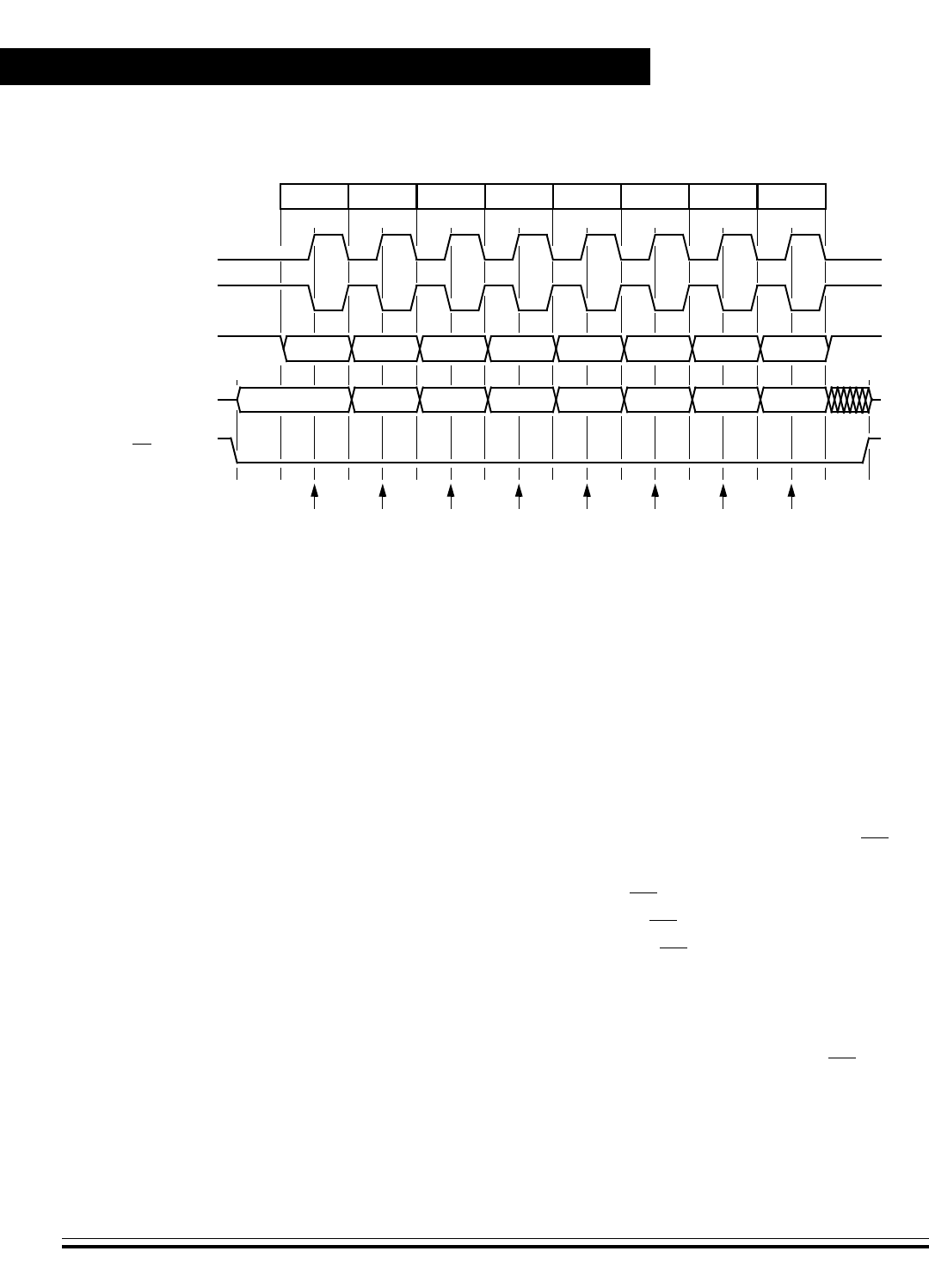
Serial Peripheral Interface (SPI)
Technical Data MC68HC08AZ60 — Rev 1.1
240 Serial Peripheral Interface (SPI) Freescale Semiconductor
Figure 18-4. Transmission Format (CPHA = ‘0’)
18.6.3 Transmission Format When CPHA = ‘1’
Figure 18-5 shows an SPI transmission in which CPHA is ‘1’. The figure
should not be used as a replacement for data sheet parametric
information. Two waveforms are shown for SCK: one for CPOL = ‘0’ and
another for CPOL = ‘1’. The diagram may be interpreted as a master or
slave timing diagram since the serial clock (SCK), master in/slave out
(MISO), and master out/slave in (MOSI) pins are directly connected
between the master and the slave. The MISO signal is the output from
the slave, and the MOSI signal is the output from the master. The SS line
is the slave select input to the slave. The slave SPI drives its MISO
output only when its slave select input (SS) is at logic ‘0’, so that only the
selected slave drives to the master. The SS pin of the master is not
shown but is assumed to be inactive. The SS pin of the master must be
high or must be reconfigured as general-purpose I/O not affecting the
SPI. See Mode Fault Error on page 245. When CPHA = ‘1’, the master
begins driving its MOSI pin on the first SPSCK edge. Therefore the slave
uses the first SPSCK edge as a start transmission signal. The SS pin can
remain low between transmissions. This format may be preferable in
BIT 6 BIT 5 BIT 4 BIT 3 BIT 2 BIT 1 LSB
MSB
BIT 6 BIT 5 BIT 4 BIT 3 BIT 2 BIT 1 LSB
MSB
12345678
SCK CYCLE #
(FOR REFERENCE)
SCK (CPOL =’0’)
SCK (CPOL =1)
MOSI
(FROM MASTER)
MISO
(FROM SLAVE)
SS (TO SLAVE)
CAPTURE STROBE
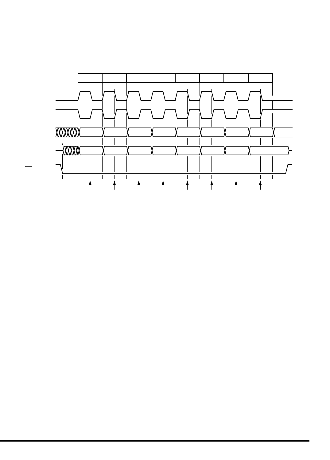
Serial Peripheral Interface (SPI)
Transmission Formats
MC68HC08AZ60 — Rev 1.1 Technical Data
Freescale Semiconductor Serial Peripheral Interface (SPI) 241
systems having only one master and only one slave driving the MISO
data line.
Figure 18-5. Transmission Format (CPHA = ‘1’)
18.6.4 Transmission Initiation Latency
When the SPI is configured as a master (SPMSTR = ‘1’), transmissions
are started by a software write to the SPDR. CPHA has no effect on the
delay to the start of the transmission, but it does affect the initial state of
the SCK signal. When CPHA = ‘0’, the SCK signal remains inactive for
the first half of the first SCK cycle. When CPHA = ‘1’, the first SCK cycle
begins with an edge on the SCK line from its inactive to its active level.
The SPI clock rate (selected by SPR1:SPR0) affects the delay from the
write to SPDR and the start of the SPI transmission. See Figure 18-6.
The internal SPI clock in the master is a free-running derivative of the
internal MCU clock. It is only enabled when both the SPE and SPMSTR
bits are set to conserve power. SCK edges occur halfway through the
low time of the internal MCU clock. Since the SPI clock is free-running,
it is uncertain where the write to the SPDR will occur relative to the
slower SCK. This uncertainty causes the variation in the initiation delay
shown in Figure 18-6. This delay will be no longer than a single SPI bit
time. That is, the maximum delay is two MCU bus cycles for DIV2, eight
MCU bus cycles for DIV8, 32 MCU bus cycles for DIV32, and 128 MCU
bus cycles for DIV128.
BIT 6 BIT 5 BIT 4 BIT 3 BIT 2 BIT 1 LSB
MSB
BIT 6 BIT 5 BIT 4 BIT 3 BIT 2 BIT 1 LSB
MSB
12345678
SCK CYCLE #
(FOR REFERENCE)
SCK (CPOL =’0’)
SCK (CPOL =1)
MOSI
(FROM MASTER)
MISO
(FROM SLAVE)
SS (TO SLAVE)
CAPTURE STROBE
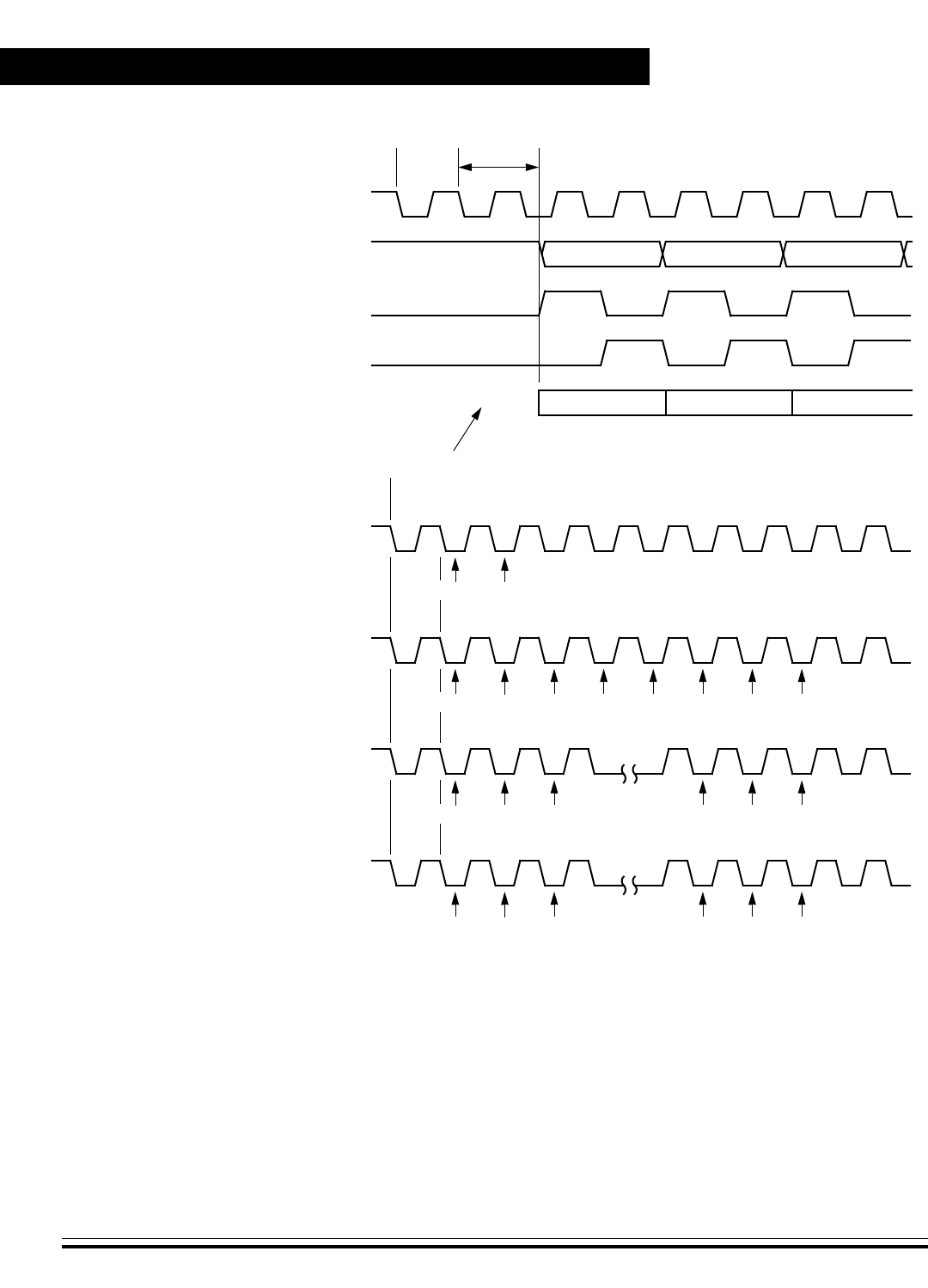
Serial Peripheral Interface (SPI)
Technical Data MC68HC08AZ60 — Rev 1.1
242 Serial Peripheral Interface (SPI) Freescale Semiconductor
Figure 18-6. Transmission Start Delay (Master)
WRITE
TO SPDR INITIATION DELAY
BUS
MOSI
SCK
(CPHA = ‘1’)
SCK
(CPHA =’0’)
SCK CYCLE
NUMBER
MSB BIT 6
12
CLOCK
WRITE
TO SPDR
EARLIEST LATEST (SCK = INTERNAL CLOCK ÷ 2;
EARLIEST LATEST
2 POSSIBLE START POINTS)
(SCK = INTERNAL CLOCK ÷ 8;
8 POSSIBLE START POINTS)
EARLIEST LATEST(SCK = INTERNAL CLOCK ÷ 32;
32 POSSIBLE START POINTS)
EARLIEST LATEST(SCK = INTERNAL CLOCK ÷ 128;
128 POSSIBLE START POINTS)
WRITE
TO SPDR
WRITE
TO SPDR
WRITE
TO SPDR
BUS
CLOCK
BIT 5
3
BUS
CLOCK
BUS
CLOCK
BUS
CLOCK
INITIATION DELAY FROM WRITE SPDR TO TRANSFER BEGIN

Serial Peripheral Interface (SPI)
Transmission Formats
MC68HC08AZ60 — Rev 1.1 Technical Data
Freescale Semiconductor Serial Peripheral Interface (SPI) 243
18.6.5 Error Conditions
The following flags signal SPI error conditions:
• Overflow (OVRF) — failing to read the SPI data register before the
next byte enters the shift register results in the OVRF bit becoming
set. The new byte does not transfer to the receive data register,
and the unread byte still can be read by accessing the SPI data
register. OVRF is in the SPI status and control register.
• Mode fault error (MODF) — the MODF bit indicates that the
voltage on the slave select pin (SS) is inconsistent with the mode
of the SPI. MODF is in the SPI status and control register.
18.6.6 Overflow Error
The overflow flag (OVRF) becomes set if the SPI receive data register
still has unread data from a previous transmission when the capture
strobe of bit 1 of the next transmission occurs. See Figure 18-4 and
Figure 18-5. If an overflow occurs, the data being received is not
transferred to the receive data register so that the unread data can still
be read. Therefore, an overflow error always indicates the loss of data.
OVRF generates a receiver/error CPU interrupt request if the error
interrupt enable bit (ERRIE) is also set. MODF and OVRF can generate
a receiver/error CPU interrupt request. See Figure 18-9. It is not
possible to enable only MODF or OVRF to generate a receiver/error
CPU interrupt request. However, leaving MODFEN low prevents MODF
from being set.
If an end-of-block transmission interrupt was meant to pull the MCU out
of wait, having an overflow condition without overflow interrupts enabled
causes the MCU to hang in wait mode. If the OVRF is enabled to
generate an interrupt, it can pull the MCU out of wait mode instead.
If the CPU SPRF interrupt is enabled and the OVRF interrupt is not,
watch for an overflow condition. Figure 18-7 shows how it is possible to
miss an overflow.
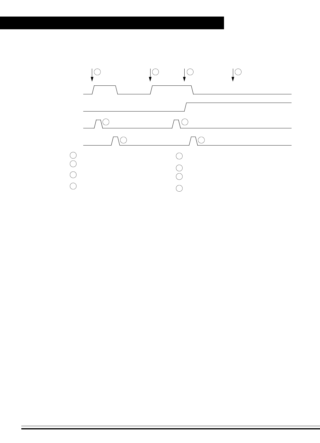
Serial Peripheral Interface (SPI)
Technical Data MC68HC08AZ60 — Rev 1.1
244 Serial Peripheral Interface (SPI) Freescale Semiconductor
Figure 18-7. Missed Read of Overflow Condition
The first part of Figure 18-7 shows how to read the SPSCR and SPDR
to clear the SPRF without problems. However, as illustrated by the
second transmission example, the OVRF flag can be set in the interval
between SPSCR and SPDR being read.
In this case, an overflow can easily be missed. Since no more SPRF
interrupts can be generated until this OVRF is serviced, it will not be
obvious that bytes are being lost as more transmissions are completed.
To prevent this, the OVRF interrupt should be enabled, or alternatively
another read of the SPSCR should be carried out following the read of
the SPDR. This ensures that the OVRF was not set before the SPRF
was cleared and that future transmissions will terminate with an SPRF
interrupt. Figure 18-8 illustrates this process. Generally, to avoid this
second SPSCR read, enable the OVRF to the CPU by setting the ERRIE
bit.
READ SPDR
READ SPSCR
OVRF
SPRF
BYTE 1 BYTE 2 BYTE 3 BYTE 4
BYTE 1 SETS SPRF BIT.
CPU READS SPSCR WITH SPRF BIT SET
CPU READS BYTE 1 IN SPDR,
BYTE 2 SETS SPRF BIT.
CPU READS SPSCRW WITH SPRF BIT SET
BYTE 3 SETS OVRF BIT. BYTE 3 IS LOST.
CPU READS BYTE 2 IN SPDR, CLEARING SPRF
BYTE 4 FAILS TO SET SPRF BIT BECAUSE
1
1
2
3
4
5
6
7
8
2
3
4
5
6
7
8
CLEARING SPRF BIT. BUT NOT OVRF BIT.
OVRF BIT IS SET. BYTE 4 IS LOST.
AND OVRF BIT CLEAR.
AND OVRF BIT CLEAR.
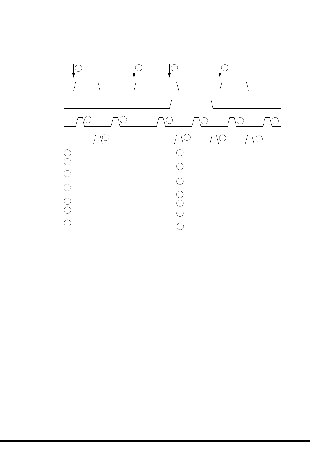
Serial Peripheral Interface (SPI)
Transmission Formats
MC68HC08AZ60 — Rev 1.1 Technical Data
Freescale Semiconductor Serial Peripheral Interface (SPI) 245
Figure 18-8. Clearing SPRF When OVRF Interrupt is Not Enabled
18.6.7 Mode Fault Error
For the MODF flag to be set, the mode fault error enable bit (MODFEN)
must be set. Clearing the MODFEN bit does not clear the MODF flag but
does prevent MODF from being set again after MODF is cleared.
MODF generates a receiver/error CPU interrupt request if the error
interrupt enable bit (ERRIE) is also set. The SPRF, MODF, and OVRF
interrupts share the same CPU interrupt vector. MODF and OVRF can
generate a receiver/error CPU interrupt request. See Figure 18-9. It is
not possible to enable only MODF or OVRF to generate a receiver/error
CPU interrupt request. However, leaving MODFEN low prevents MODF
from being set.
READ SPDR
READ SPSCR
OVRF
SPRF
BYTE 1 BYTE 2 BYTE 3 BYTE 4
1
BYTE 1 SETS SPRF BIT.
CPU READS SPSCR WITH SPRF BIT SET
CPU READS BYTE 1 IN SPDR,
CPU READS SPSCR AGAIN
BYTE 2 SETS SPRF BIT.
CPU READS SPSCR WITH SPRF BIT SET
BYTE 3 SETS OVRF BIT. BYTE 3 IS LOST.
CPU READS BYTE 2 IN SPDR,
CPU READS SPSCR AGAIN
CPU READS BYTE 2 SPDR,
BYTE 4 SETS SPRF BIT.
CPU READS SPSCR.
CPU READS BYTE 4 IN SPDR,
CPU READS SPSCR AGAIN
1
2
3CLEARING SPRF BIT.
4TO CHECK OVRF BIT.
5
6
7
8
9
CLEARING SPRF BIT.
TO CHECK OVRF BIT.
CLEARING OVRF BIT.
2
3
4
5
6
7
8
9
10
11
12
13
14
CLEARING SPRF BIT.
TO CHECK OVRF BIT.
SPI RECEIVE
COMPLETE
AND OVRF BIT CLEAR.
AND OVRF BIT CLEAR.
10
11
12
13
14

Serial Peripheral Interface (SPI)
Technical Data MC68HC08AZ60 — Rev 1.1
246 Serial Peripheral Interface (SPI) Freescale Semiconductor
In a master SPI with the mode fault enable bit (MODFEN) set, the mode
fault flag (MODF) is set if SS goes to logic ‘0’. A mode fault in a master
SPI causes the following events to occur:
• If ERRIE = ‘1’, the SPI generates an SPI receiver/error CPU
interrupt request.
• The SPE bit is cleared.
• The SPTE bit is set.
• The SPI state counter is cleared.
• The data direction register of the shared I/O port regains control of
port drivers.
NOTE: To prevent bus contention with another master SPI after a mode fault
error, clear all data direction register (DDR) bits associated with the SPI
shared port pins.
NOTE: Setting the MODF flag (SPSCR) does not clear the SPMSTR bit.
Reading SPMSTR when MODF = 1 will indicate a MODE fault error
occurred in either master mode or slave mode.
When configured as a slave (SPMSTR = ‘0’), the MODF flag is set if SS
goes high during a transmission. When CPHA = ‘0’, a transmission
begins when SS goes low and ends once the incoming SPSCK goes
back to its idle level following the shift of the eighth data bit. When CPHA
= ‘1’, the transmission begins when the SPSCK leaves its idle level and
SS is already low. The transmission continues until the SPSCK returns
to its IDLE level following the shift of the last data bit. See Transmission
Formats on page 238.
NOTE: When CPHA = ‘0’, a MODF occurs if a slave is selected (SS is at logic
‘0’) and later deselected (SS is at logic ‘1’) even if no SPSCK is sent to
that slave. This happens because SS at logic ‘0’ indicates the start of the
transmission (MISO driven out with the value of MSB) for CPHA = ‘0’.
When CPHA = ‘1’, a slave can be selected and then later deselected with
no transmission occurring. Therefore, MODF does not occur since a
transmission was never begun.
In a slave SPI (MSTR = ‘0’), the MODF bit generates an SPI
receiver/error CPU interrupt request if the ERRIE bit is set. The MODF

Serial Peripheral Interface (SPI)
Interrupts
MC68HC08AZ60 — Rev 1.1 Technical Data
Freescale Semiconductor Serial Peripheral Interface (SPI) 247
bit does not clear the SPE bit or reset the SPI in any way. Software can
abort the SPI transmission by toggling the SPE bit of the slave.
NOTE: A logic ‘1’ on the SS pin of a slave SPI puts the MISO pin in a high
impedance state. Also, the slave SPI ignores all incoming SPSCK
clocks, even if a transmission has begun.
To clear the MODF flag, read the SPSCR and then write to the SPCR
register. This entire clearing procedure must occur with no MODF
condition existing or else the flag will not be cleared.
18.7 Interrupts
Four SPI status flags can be enabled to generate CPU interrupt
requests:
The SPI transmitter interrupt enable bit (SPTIE) enables the SPTE flag
to generate transmitter CPU interrupt requests.
The SPI receiver interrupt enable bit (SPRIE) enables the SPRF bit to
generate receiver CPU interrupt requests, provided that the SPI is
enabled (SPE = 1).
The error interrupt enable bit (ERRIE) enables both the MODF and
OVRF flags to generate a receiver/error CPU interrupt request.
The mode fault enable bit (MODFEN) can prevent the MODF flag from
being set so that only the OVRF flag is enabled to generate
receiver/error CPU interrupt requests.
Table 18-3. SPI Interrupts
Flag Request
SPTE (Transmitter Empty) SPI Transmitter CPU Interrupt Request (SPTIE = 1)
SPRF (Receiver Full) SPI Receiver CPU Interrupt Request (SPRIE = 1)
OVRF (Overflow) SPI Receiver/Error Interrupt Request (SPRIE = 1, ERRIE = 1)
MODF (Mode Fault) SPI Receiver/Error Interrupt Request (SPRIE = 1, ERRIE = 1, MODFEN = ‘1’)
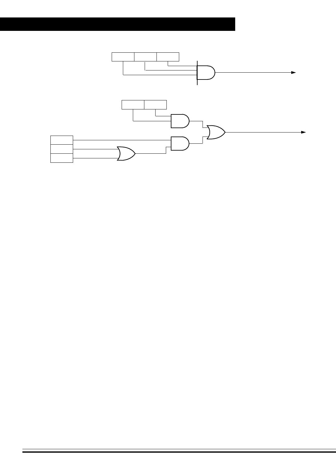
Serial Peripheral Interface (SPI)
Technical Data MC68HC08AZ60 — Rev 1.1
248 Serial Peripheral Interface (SPI) Freescale Semiconductor
Figure 18-9. SPI Interrupt Request Generation
Two sources in the SPI status and control register can generate CPU
interrupt requests:
• SPI receiver full bit (SPRF) — the SPRF bit becomes set every
time a byte transfers from the shift register to the receive data
register. If the SPI receiver interrupt enable bit, SPRIE, is also set,
SPRF can generate an SPI receiver/error CPU interrupt request.
• SPI transmitter empty (SPTE) — the SPTE bit becomes set every
time a byte transfers from the transmit data register to the shift
register. If the SPI transmit interrupt enable bit, SPTIE, is also set,
SPTE can generate an SPTE CPU interrupt request.
18.8 Queuing Transmission Data
The double-buffered transmit data register allows a data byte to be
queued and transmitted. For an SPI configured as a master, a queued
data byte is transmitted immediately after the previous transmission has
completed. The SPI transmitter empty flag (SPTE) indicates when the
transmit data buffer is ready to accept new data. Write to the SPI data
register only when the SPTE bit is high. Figure 18-10 shows the timing
associated with doing back-to-back transmissions with the SPI (SPSCK
has CPHA: CPOL = 1:0).
SPTE SPTIE
SPRFSPRIE
ERRIE
MODF
OVRF
SPE
SPI TRANSMITTER
CPU INTERRUPT REQUEST
SPI RECEIVER/ERROR
CPU INTERRUPT REQUEST

Serial Peripheral Interface (SPI)
Queuing Transmission Data
MC68HC08AZ60 — Rev 1.1 Technical Data
Freescale Semiconductor Serial Peripheral Interface (SPI) 249
For a slave, the transmit data buffer allows back-to-back transmissions
to occur without the slave having to time the write of its data between the
transmissions. Also, if no new data is written to the data buffer, the last
value contained in the shift register will be the next data word
transmitted.
Figure 18-10. SPRF/SPTE CPU Interrupt Timing
BIT
3
MOSI
P
SCK (CPHA:CPOL =‘1’:0)
SPTE
WRITE TO SPDR 1
CPU WRITES BYTE 2 TO SPDR, QUEUEING
CPU WRITES BYTE 1 TO SPDR, CLEARING
BYTE 1 TRANSFERS FROM TRANSMIT DATA
3
1
2
2
3
5
SPTE BIT.
REGISTER TO SHIFT REGISTER, SETTING SPTE BIT.
SPRF
READ SPSCR
MSB BIT
6BIT
5BIT
4BIT
2BIT
1LSB MSB BIT
6BIT
5BIT
4BIT
3BIT
2BIT
1LSB MSB BIT
6
BYTE 2 TRANSFERS FROM TRANSMIT DATA
CPU WRITES BYTE 3 TO SPDR, QUEUEING
BYTE 3 TRANSFERS FROM TRANSMIT DATA
5
8
10
8
10
4FIRST INCOMING BYTE TRANSFERS FROM SHIFT
6CPU READS SPSCR WITH SPRF BIT SET.
4
6
9
SECOND INCOMING BYTE TRANSFERS FROM SHIFT
9
11
BYTE 2 AND CLEARING SPTE BIT.
REGISTER TO SHIFT REGISTER, SETTING SPTE BIT.
REGISTER TO RECEIVE DATA REGISTER, SETTING
SPRF BIT.
BYTE 3 AND CLEARING SPTE BIT.
REGISTER TO SHIFT REGISTER, SETTING SPTE BIT.
REGISTER TO RECEIVE DATA REGISTER, SETTING
SPRF BIT.
12 CPU READS SPDR, CLEARING SPRF BIT.
BIT
5BIT
4
BYTE 1 BYTE 2 BYTE 3
712
READ SPDR
7CPU READS SPDR, CLEARING SPRF BIT.
11 CPU READS SPSCR WITH SPRF BIT SET.

Serial Peripheral Interface (SPI)
Technical Data MC68HC08AZ60 — Rev 1.1
250 Serial Peripheral Interface (SPI) Freescale Semiconductor
18.9 Resetting the SPI
Any system reset completely resets the SPI. Partial resets occur
whenever the SPI enable bit (SPE) is low. Whenever SPE is low, the
following occurs:
• The SPTE flag is set
• Any transmission currently in progress is aborted
• The shift register is cleared
• The SPI state counter is cleared, making it ready for a new
complete transmission
• All the SPI port logic is defaulted back to being general purpose
I/O.
The following items are reset only by a system reset:
• All control bits in the SPCR register
• All control bits in the SPSCR register (MODFEN, ERRIE, SPR1,
and SPR0)
• The status flags SPRF, OVRF, and MODF
By not resetting the control bits when SPE is low, the user can clear SPE
between transmissions without having to set all control bits again when
SPE is set back high for the next transmission.
By not resetting the SPRF, OVRF, and MODF flags, the user can still
service these interrupts after the SPI has been disabled. The user can
disable the SPI by writing ‘0’ to the SPE bit. The SPI can also be disabled
by a mode fault occurring in an SPI that was configured as a master with
the MODFEN bit set.

Serial Peripheral Interface (SPI)
Low-Power Modes
MC68HC08AZ60 — Rev 1.1 Technical Data
Freescale Semiconductor Serial Peripheral Interface (SPI) 251
18.10 Low-Power Modes
The WAIT and STOP instructions put the MCU in low power-
consumption standby modes.
18.10.1 WAIT Mode
The SPI module remains active after the execution of a WAIT instruction.
In WAIT mode the SPI module registers are not accessible by the CPU.
Any enabled CPU interrupt request from the SPI module can bring the
MCU out of WAIT mode.
If SPI module functions are not required during WAIT mode, power
consumption can be reduced by disabling the SPI module before
executing the WAIT instruction.
To exit WAIT mode when an overflow condition occurs, the OVRF bit
should be enabled to generate CPU interrupt requests by setting the
error interrupt enable bit (ERRIE). See Interrupts on page 247.
18.10.2 STOP Mode
The SPI module is inactive after the execution of a STOP instruction.
The STOP instruction does not affect register conditions. SPI operation
resumes after an external interrupt. If STOP mode is exited by reset, any
transfer in progress is aborted, and the SPI is reset.
18.11 SPI During Break Interrupts
The system integration module (SIM) controls whether status bits in
other modules can be cleared during the break state. The BCFE bit in
the SIM break flag control register (SBFCR) enables software to clear
status bits during the break state. See SIM Break Flag Control
Register on page 119.
To allow software to clear status bits during a break interrupt, a ‘1’ should
be written to the BCFE bit. If a status bit is cleared during the break state,
it remains cleared when the MCU exits the break state.

Serial Peripheral Interface (SPI)
Technical Data MC68HC08AZ60 — Rev 1.1
252 Serial Peripheral Interface (SPI) Freescale Semiconductor
To protect status bits during the break state, a ‘0’ should be written to the
BCFE bit. With BCFE at ‘0’ (its default state), software can read and write
I/O registers during the break state without affecting status bits. Some
status bits have a two-step read/write clearing procedure. If software
does the first step on such a bit before the break, the bit cannot change
during the break state as long as BCFE is a ‘0’. After the break, the
second step clears the status bit.
Since the SPTE bit cannot be cleared during a break with the BCFE bit
cleared, a write to the data register in break mode will not initiate a
transmission, nor will this data be transferred into the shift register.
Therefore, a write to the SPDR in break mode with the BCFE bit cleared
has no effect.
18.12 I/O Signals
The SPI module has five I/O pins and shares four of them with a parallel
I/O port.
• MISO — data received
• MOSI — data transmitted
• SPSCK — serial clock
•SS — slave select
•V
SS — clock ground
The SPI has limited inter-integrated circuit (I2C) capability (requiring
software support) as a master in a single-master environment. To
communicate with I2C peripherals, MOSI becomes an open-drain output
when the SPWOM bit in the SPI control register is set. In I2C
communication, the MOSI and MISO pins are connected to a
bidirectional pin from the I2C peripheral and through a pullup resistor to
VDD.

Serial Peripheral Interface (SPI)
I/O Signals
MC68HC08AZ60 — Rev 1.1 Technical Data
Freescale Semiconductor Serial Peripheral Interface (SPI) 253
18.12.1 MISO (MasterIn/Slave Out)
MISO is one of the two SPI module pins that transmits serial data. In full
duplex operation, the MISO pin of the master SPI module is connected
to the MISO pin of the slave SPI module. The master SPI simultaneously
receives data on its MISO pin and transmits data from its MOSI pin.
Slave output data on the MISO pin is enabled only when the SPI is
configured as a slave. The SPI is configured as a slave when its
SPMSTR bit is logic ‘0’ and its SS pin is at locic ‘0’. To support a multiple-
slave system, a logic ‘1’ on the SS pin puts the MISO pin in a high-
impedance state.
When enabled, the SPI controls data direction of the MISO pin
regardless of the state of the data direction register of the shared I/O
port.
18.12.2 MOSI (Master Out/Slave In)
MOSI is one of the two SPI module pins that transmits serial data. In full
duplex operation, the MOSI pin of the master SPI module is connected
to the MOSI pin of the slave SPI module. The master SPI simultaneously
transmits data from its MOSI pin and receives data on its MISO pin.
When enabled, the SPI controls data direction of the MOSI pin
regardless of the state of the data direction register of the shared I/O
port.
18.12.3 SPSCK (Serial Clock)
The serial clock synchronizes data transmission between master and
slave devices. In a master MCU, the SPSCK pin is the clock output. In a
slave MCU, the SPSCK pin is the clock input. In full duplex operation, the
master and slave MCUs exchange a byte of data in eight serial clock
cycles.
When enabled, the SPI controls data direction of the SPSCK pin
regardless of the state of the data direction register of the shared I/O
port.

Serial Peripheral Interface (SPI)
Technical Data MC68HC08AZ60 — Rev 1.1
254 Serial Peripheral Interface (SPI) Freescale Semiconductor
18.12.4 SS (Slave Select)
The SS pin has various functions depending on the current state of the
SPI. For an SPI configured as a slave, the SS is used to select a slave.
For CPHA = ‘0’, the SS is used to define the start of a transmission. See
Transmission Formats on page 238. Since it is used to indicate the
start of a transmission, the SS must be toggled high and low between
each byte transmitted for the CPHA = ‘0’ format. However, it can remain
low throughout the transmission for the CPHA = ‘1’ format. See Figure
18-11.
Figure 18-11. CPHA/SS Timing
When an SPI is configured as a slave, the SS pin is always configured
as an input. It cannot be used as a general purpose I/O regardless of the
state of the MODFEN control bit. However, the MODFEN bit can still
prevent the state of the SS from creating a MODF error. See SPI Status
and Control Register (SPSCR) on page 258.
NOTE: A logic ‘1’ on the SS pin of a slave SPI puts the MISO pin in a high-
impedance state. The slave SPI ignores all incoming SPSCK clocks,
even if transmission has already begun.
When an SPI is configured as a master, the SS input can be used in
conjunction with the MODF flag to prevent multiple masters from driving
MOSI and SPSCK. See Mode Fault Error on page 245. For the state of
the SS pin to set the MODF flag, the MODFEN bit in the SPSCK register
must be set. If the MODFEN bit is low for an SPI master, the SS pin can
be used as a general purpose I/O under the control of the data direction
register of the shared I/O port. With MODFEN high, it is an input-only pin
BYTE 1 BYTE 3
MISO/MOSI BYTE 2
MASTER SS
SLAVE SS
(CPHA =’0’)
SLAVE SS
(CPHA = ‘1’)

Serial Peripheral Interface (SPI)
I/O Registers
MC68HC08AZ60 — Rev 1.1 Technical Data
Freescale Semiconductor Serial Peripheral Interface (SPI) 255
to the SPI regardless of the state of the data direction register of the
shared I/O port.
The CPU can always read the state of the SS pin by configuring the
appropriate pin as an input and reading the data register. See Table 18-
4.
18.12.5 VSS
(Clock Ground)
VSS is the ground return for the serial clock pin, SPSCK, and the ground
for the port output buffers. To reduce the ground return path loop and
minimize radio frequency (RF) emissions, connect the ground pin of the
slave to the VSS pin.
18.13 I/O Registers
Three registers control and monitor SPI operation:
• SPI control register (SPCR)
• SPI status and control register (SPSCR)
• SPI data register (SPDR)
Table 18-4. SPI Configuration
SPE SPMSTR MODFEN SPI CONFIGURATION STATE OF SS LOGIC
0 X X Not Enabled General-purpose I/O; SS
ignored by SPI
1 0 X Slave Input-only to SPI
1 1 0 Master without MODF General-purpose I/O; SS
ignored by SPI
1 1 1 Master with MODF Input-only to SPI
X = don’t care

Serial Peripheral Interface (SPI)
Technical Data MC68HC08AZ60 — Rev 1.1
256 Serial Peripheral Interface (SPI) Freescale Semiconductor
18.13.1 SPI Control Register (SPCR)
The SPI control register does the following:
• Enables SPI module interrupt requests
• Selects CPU interrupt requests
• Configures the SPI module as master or slave
• Selects serial clock polarity and phase
• Configures the SPSCK, MOSI, and MISO pins as open-drain
outputs
• Enables the SPI module
SPRIE — SPI Receiver Interrupt Enable
This read/write bit enables CPU interrupt requests generated by the
SPRF bit. The SPRF bit is set when a byte transfers from the shift
register to the receive data register. Reset clears the SPRIE bit.
1 = SPRF CPU interrupt requests enabled
0 = SPRF CPU interrupt requests disabled
SPMSTR — SPI Master
This read/write bit selects master mode operation or slave mode
operation. Reset sets the SPMSTR bit.
1 = Master mode
0 = Slave mode
Bit 7 6 5 4 3 2 1 Bit 0
SPCR Read: SPRIE R SPMSTR CPOL CPHA SPWOM SPE SPTIE
Write:
Reset:00101000
R= Reserved
Figure 18-12. SPI Control Register (SPCR)

Serial Peripheral Interface (SPI)
I/O Registers
MC68HC08AZ60 — Rev 1.1 Technical Data
Freescale Semiconductor Serial Peripheral Interface (SPI) 257
CPOL — Clock Polarity
This read/write bit determines the logic state of the SPSCK pin
between transmissions. See Figure 18-4 and Figure 18-5. To
transmit data between SPI modules, the SPI modules must have
identical CPOL bits. Reset clears the CPOL bit.
CPHA — Clock Phase
This read/write bit controls the timing relationship between the serial
clock and SPI data. See Figure 18-4 and Figure 18-5. To transmit
data between SPI modules, the SPI modules must have identical
CPHA bits. When CPHA = ‘0’, the SS pin of the slave SPI module
must be set to logic one between bytes. See Figure 18-11. Reset sets
the CPHA bit.
When CPHA =’0’ for a slave, the falling edge of SS indicates the
beginning of the transmission. This causes the SPI to leave its idle
state and begin driving the MISO pin with the MSB of its data. Once
the transmission begins, no new data is allowed into the shift register
from the data register. Therefore, the slave data register must be
loaded with the desired transmit data before the falling edge of SS.
Any data written after the falling edge is stored in the data register and
transferred to the shift register at the current transmission.
When CPHA = ‘1’ for a slave, the first edge of the SPSCK indicates
the beginning of the transmission. The same applies when SS is high
for a slave. The MISO pin is held in a high-impedance state, and the
incoming SPSCK is ignored. In certain cases, it may also cause the
MODF flag to be set. See Mode Fault Error on page 245. A logic ‘1’
on the SS pin does not affect the state of the SPI state machine in any
way.
SPWOM — SPI Wired-OR Mode
This read/write bit disables the pull-up devices on pins SPSCK,
MOSI, and MISO so that those pins become open-drain outputs.
1 = Wired-OR SPSCK, MOSI, and MISO pins
0 = Normal push-pull SPSCK, MOSI, and MISO pins

Serial Peripheral Interface (SPI)
Technical Data MC68HC08AZ60 — Rev 1.1
258 Serial Peripheral Interface (SPI) Freescale Semiconductor
SPE — SPI Enable
This read/write bit enables the SPI module. Clearing SPE causes a
partial reset of the SPI. See Resetting the SPI on page 250. Reset
clears the SPE bit.
1 = SPI module enabled
0 = SPI module disabled
SPTIE— SPI Transmit Interrupt Enable
This read/write bit enables CPU interrupt requests generated by the
SPTE bit. SPTE is set when a byte transfers from the transmit data
register to the shift register. Reset clears the SPTIE bit.
1 = SPTE CPU interrupt requests enabled
0 = SPTE CPU interrupt requests disabled
18.13.2 SPI Status and Control Register (SPSCR)
The SPI status and control register contains flags to signal the following
conditions:
• Receive data register full
• Failure to clear SPRF bit before next byte is received (overflow
error)
• Inconsistent logic level on SS pin (mode fault error)
• Transmit data register empty

Serial Peripheral Interface (SPI)
I/O Registers
MC68HC08AZ60 — Rev 1.1 Technical Data
Freescale Semiconductor Serial Peripheral Interface (SPI) 259
The SPI status and control register also contains bits that perform the
following functions:
• Enable error interrupts
• Enable mode fault error detection
• Select master SPI baud rate
SPRF — SPI Receiver Full
This clearable, read-only flag is set each time a byte transfers from
the shift register to the receive data register. SPRF generates a CPU
interrupt request if the SPRIE bit in the SPI control register is set also.
During an SPRF CPU interrupt, the CPU clears SPRF by reading the
SPI status and control register with SPRF set and then reading the
SPI data register. Any read of the SPI data register clears the SPRF
bit.
Reset clears the SPRF bit.
1 = Receive data register full
0 = Receive data register not full
ERRIE — Error Interrupt Enable
This read-only bit enables the MODF and OVRF flags to generate
CPU interrupt requests. Reset clears the ERRIE bit.
1 = MODF and OVRF can generate CPU interrupt requests
0 = MODF and OVRF cannot generate CPU interrupt requests
OVRF — Overflow Flag
This clearable, read-only flag is set if software does not read the byte
in the receive data register before the next byte enters the shift
register. In an overflow condition, the byte already in the receive data
Bit 7654321Bit 0
SPSCR Read: SPRF ERRIE OVRF MODF SPTE MODFE
NSPR1 SPR0
Write:
Reset:00001000
R= Reserved = Unimplemented
Figure 18-13. SPI Status and Control Register (SPSCR)

Serial Peripheral Interface (SPI)
Technical Data MC68HC08AZ60 — Rev 1.1
260 Serial Peripheral Interface (SPI) Freescale Semiconductor
register is unaffected, and the byte that shifted in last is lost. Clear the
OVRF bit by reading the SPI status and control register with OVRF set
and then reading the SPI data register. Reset clears the OVRF flag.
1 = Overflow
0 = No overflow
MODF — Mode Fault
This clearable, ready-only flag is set in a slave SPI if the SS pin goes
high during a transmission. In a master SPI, the MODF flag is set if
the SS pin goes low at any time. Clear the MODF bit by reading the
SPI status and control register with MODF set and then writing to the
SPI data register. Reset clears the MODF bit.
1 = SS pin at inappropriate logic level
0 = SS pin at appropriate logic level
SPTE — SPI Transmitter Empty
This clearable, read-only flag is set each time the transmit data
register transfers a byte into the shift register. SPTE generates an
SPTE CPU interrupt request if the SPTIE bit in the SPI control register
is set also.
NOTE: The SPI data register should not be written to unless the SPTE bit is
high.
For an idle master or idle slave that has no data loaded into its
transmit buffer, the SPTE will be set again within two bus cycles since
the transmit buffer empties into the shift register. This allows the user
to queue up a 16-bit value to send. For an already active slave, the
load of the shift register cannot occur until the transmission is
completed. This implies that a back-to-back write to the transmit data
register is not possible. The SPTE indicates when the next write can
occur.
Reset sets the SPTE bit.
1 = Transmit data register empty
0 = Transmit data register not empty

Serial Peripheral Interface (SPI)
I/O Registers
MC68HC08AZ60 — Rev 1.1 Technical Data
Freescale Semiconductor Serial Peripheral Interface (SPI) 261
MODFEN — Mode Fault Enable
This read/write bit, when set to ‘1’, allows the MODF flag to be set. If
the MODF flag is set, clearing the MODFEN does not clear the MODF
flag. If the SPI is enabled as a master and the MODFEN bit is low,
then the SS pin is available as a general purpose I/O.
If the MODFEN bit is set, then this pin is not available as a general
purpose I/O. When the SPI is enabled as a slave, the SS pin is not
available as a general purpose I/O regardless of the value of
MODFEN. See SS (Slave Select) on page 254.
If the MODFEN bit is low, the level of the SS pin does not affect the
operation of an enabled SPI configured as a master. For an enabled
SPI configured as a slave, having MODFEN low only prevents the
MODF flag from being set. It does not affect any other part of SPI
operation. See Mode Fault Error on page 245.
SPR1 and SPR0 — SPI Baud Rate Select
In master mode, these read/write bits select one of four baud rates as
shown in Table 18-5. SPR1 and SPR0 have no effect in slave mode.
Reset clears SPR1 and SPR0.
The following formula is used to calculate the SPI baud rate:
where:
CGMOUT = base clock output of the clock generator module (CGM)
BD = baud rate divisor
Table 18-5. SPI Master Baud Rate Selection
SPR1:SPR0 Baud rate divisor (BD)
00 2
01 8
10 32
11 128
Baud rate CGMOUT
2BD×
---------------------------=

Serial Peripheral Interface (SPI)
Technical Data MC68HC08AZ60 — Rev 1.1
262 Serial Peripheral Interface (SPI) Freescale Semiconductor
18.13.3 SPI Data Register (SPDR)
The SPI data register is the read/write buffer for the receive data register
and the transmit data register. Writing to the SPI data register writes data
into the transmit data register. Reading the SPI data register reads data
from the receive data register. The transmit data and receive data
registers are separate buffers that can contain different values. See
Figure 18-2.
R7:R0/T7:T0 — Receive/Transmit Data Bits
NOTE: Do not use Read-modify-write instructions on the SPI data register since
the buffer read is not the same as the buffer written.
Bit 7654321Bit 0
SPDR Read: R7 R6 R5 R4 R3 R2 R1 R0
Write: T7 T6 T5 T4 T3 T2 T1 T0
Reset: Indeterminate after reset
Figure 18-14. SPI Data Register (SPDR)

MC68HC08AZ60 — Rev 1.1 Technical Data
Freescale Semiconductor Timer Interface Module B (TIMB) 263
Technical Data — MC68HC08AZ60
Section 19. Timer Interface Module B (TIMB)
19.1 Contents
19.2 Introduction. . . . . . . . . . . . . . . . . . . . . . . . . . . . . . . . . . . . . .264
19.3 Features. . . . . . . . . . . . . . . . . . . . . . . . . . . . . . . . . . . . . . . . .264
19.4 Functional Description. . . . . . . . . . . . . . . . . . . . . . . . . . . . .266
19.4.1 TIMB Counter Prescaler. . . . . . . . . . . . . . . . . . . . . . . . . .266
19.4.2 Input Capture . . . . . . . . . . . . . . . . . . . . . . . . . . . . . . . . . .267
19.4.3 Output Compare. . . . . . . . . . . . . . . . . . . . . . . . . . . . . . . .268
19.4.3.1 Unbuffered Output Compare. . . . . . . . . . . . . . . . . . . .268
19.4.3.2 Buffered Output Compare. . . . . . . . . . . . . . . . . . . . . .269
19.4.4 Pulse Width Modulation (PWM) . . . . . . . . . . . . . . . . . . .270
19.4.4.1 Unbuffered PWM Signal Generation . . . . . . . . . . . . .271
19.4.4.2 Buffered PWM Signal Generation. . . . . . . . . . . . . . . .272
19.4.4.3 PWM Initialization . . . . . . . . . . . . . . . . . . . . . . . . . . . .272
19.5 Interrupts. . . . . . . . . . . . . . . . . . . . . . . . . . . . . . . . . . . . . . . .274
19.6 Low-Power Modes . . . . . . . . . . . . . . . . . . . . . . . . . . . . . . . .274
19.6.1 Wait Mode . . . . . . . . . . . . . . . . . . . . . . . . . . . . . . . . . . . . .274
19.6.2 Stop Mode. . . . . . . . . . . . . . . . . . . . . . . . . . . . . . . . . . . . .274
19.7 TIMB During Break Interrupts . . . . . . . . . . . . . . . . . . . . . . .275
19.8 I/O Signals . . . . . . . . . . . . . . . . . . . . . . . . . . . . . . . . . . . . . . .275
19.8.1 TIMB Clock Pin (PTD4/ATD12/TBLCK). . . . . . . . . . . . . .275
19.8.2 TIMB Channel I/O Pins (PTF5/TBCH1–PTF4/TBCH0) . .276
19.9 I/O Registers . . . . . . . . . . . . . . . . . . . . . . . . . . . . . . . . . . . . .276
19.9.1 TIMB Status and Control Register . . . . . . . . . . . . . . . . .277
19.9.2 TIMB Counter Registers . . . . . . . . . . . . . . . . . . . . . . . . .279
19.9.3 TIMB Counter Modulo Registers. . . . . . . . . . . . . . . . . . .280
19.9.4 TIMB Channel Status and Control Registers. . . . . . . . .281
19.9.5 TIMB Channel Registers . . . . . . . . . . . . . . . . . . . . . . . . .285

Timer Interface Module B (TIMB)
Technical Data MC68HC08AZ60 — Rev 1.1
264 Timer Interface Module B (TIMB) Freescale Semiconductor
19.2 Introduction
This section describes the timer interface module (TIMB). The TIMB is a
2-channel timer that provides a timing reference with input capture,
output compare and pulse width modulation functions. Figure 19-1 is a
block diagram of the TIMB.
For further information regarding timers on M68HC08 family devices,
please consult the HC08 Timer Reference Manual, TIM08RM/AD.
19.3 Features
Features of the TIMB include:
• Two Input Capture/Output Compare Channels
– Rising-Edge, Falling-Edge or Any-Edge Input Capture Trigger
– Set, Clear or Toggle Output Compare Action
• Buffered and Unbuffered Pulse Width Modulation (PWM) Signal
Generation
• Programmable TIMB Clock Input
– 7 Frequency Internal Bus Clock Prescaler Selection
– External TIMB Clock Input (4 MHz Maximum Frequency)
• Free-Running or Modulo Up-Count Operation
• Toggle Any Channel Pin on Overflow
• TIMB Counter Stop and Reset Bits
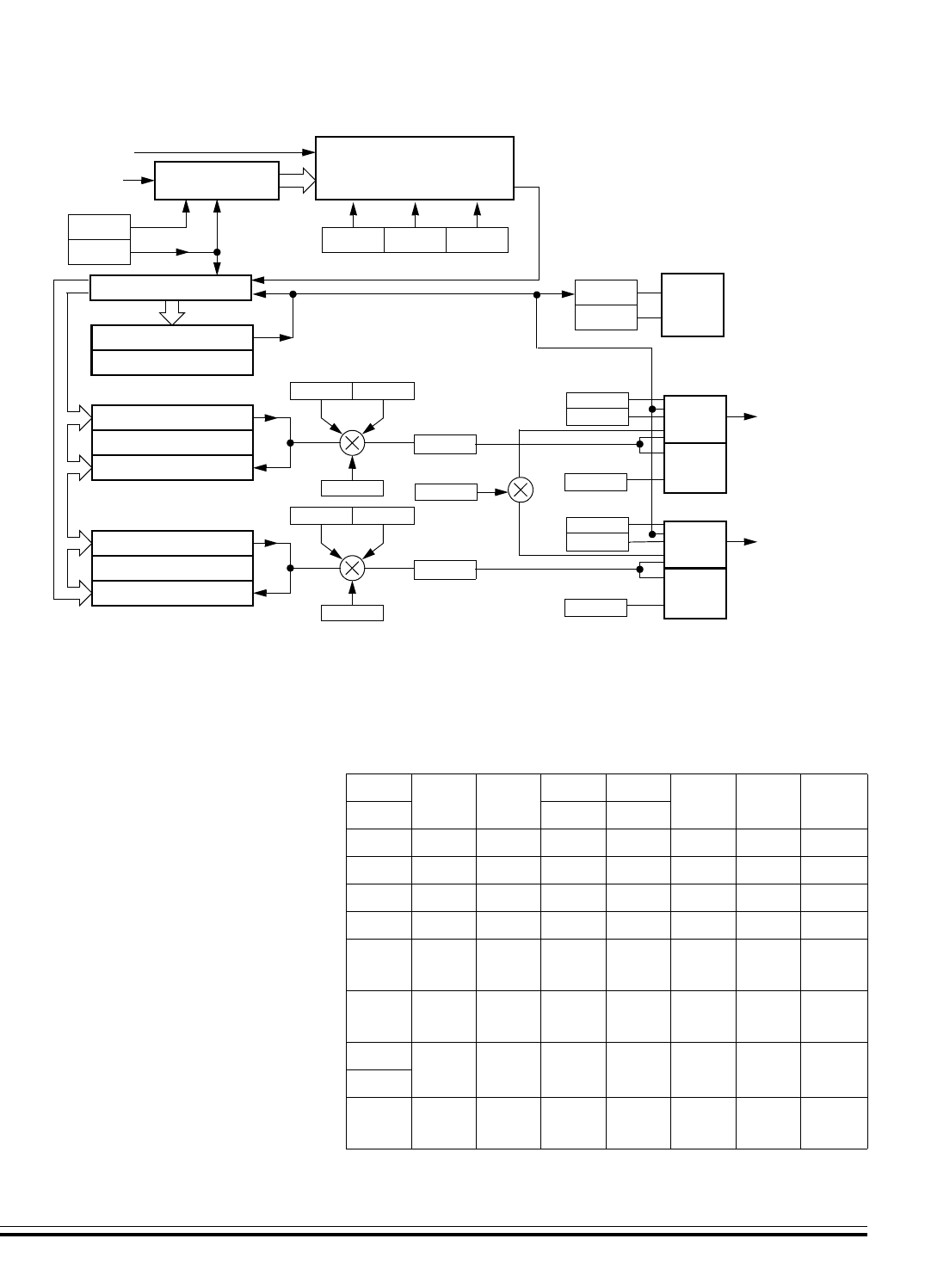
Timer Interface Module B (TIMB)
Features
MC68HC08AZ60 — Rev 1.1 Technical Data
Freescale Semiconductor Timer Interface Module B (TIMB) 265
Figure 19-1. TIMB Block Diagram
Figure 19-2. TIMB I/O Register Summary
Addr. Register Name Bit 7654321Bit 0
$0040 TIMB Status/Control Register (TBSC) R: TOF TOIE TSTOP 00
PS2 PS1 PS0
W: 0TRSTR
$0041 TIMB Counter Register High (TBCNTH) R: Bit 15 14 13 12 11 10 9 Bit 8
W: RRRRRRRR
$0042 TIMB Counter Register Low (TBCNTL) R: Bit 7654321Bit 0
W: RRRRRRRR
$0043 TIMB Counter Modulo Reg. High
(TBMODH)
R: Bit 15 14 13 12 11 10 9 Bit 8
W:
$0044 TIMB Counter Modulo Reg. Low
(TBMODL)
R: Bit 7654321Bit 0
W:
$0045 TIMB Ch. 0 Status/Control Register
(TBSC0)
R: CH0F CH0IE MS0B MS0A ELS0B ELS0A TOV0 CH0MAX
W: 0
$0046 TIMB Ch. 0 Register High (TBCH0H) R: Bit 15 14 13 12 11 10 9 Bit 8
W:
PRESCALER
PRESCALER SELECT
TCLK
INTERNAL
16-BIT COMPARATOR
PS2 PS1 PS0
16-BIT COMPARATOR
16-BIT LATCH
TCH0H:TCH0L
MS0A
ELS0B ELS0A
PTF4
TOF
TOIE
INTER-
CHANNEL 0
TMODH:TMODL
TRST
TSTOP
TOV0
CH0IE
CH0F
CH0MAX
MS0B
16-BIT COUNTER
BUS CLOCK
PTD4/ATD12/TBLCK
PTF4/TBCH0
PTF5/TBCH1
LOGIC
RUPT
LOGIC
INTER-
RUPT
LOGIC
16-BIT COMPARATOR
16-BIT LATCH
TCH1H:TCH1L
MS1A
ELS1B ELS1A
PTF5
CHANNEL 1 TOV1
CH1IE
CH1F
CH1MAX LOGIC
INTER-
RUPT
LOGIC

Timer Interface Module B (TIMB)
Technical Data MC68HC08AZ60 — Rev 1.1
266 Timer Interface Module B (TIMB) Freescale Semiconductor
19.4 Functional Description
Figure 19-1 shows the TIMB structure. The central component of the
TIMB is the 16-bit TIMB counter that can operate as a free-running
counter or a modulo up-counter. The TIMB counter provides the timing
reference for the input capture and output compare functions. The TIMB
counter modulo registers, TBMODH–TBMODL, control the modulo
value of the TIMB counter. Software can read the TIMB counter value at
any time without affecting the counting sequence.
The two TIMB channels are programmable independently as input
capture or output compare channels.
19.4.1 TIMB Counter Prescaler
The TIMB clock source can be one of the seven prescaler outputs or the
TIMB clock pin, PTD4/ATD12/TBLCK. The prescaler generates seven
clock rates from the internal bus clock. The prescaler select bits, PS[2:0],
in the TIMB status and control register select the TIMB clock source.
$0047 TIMB Ch. 0 Register Low (TBCH0L) R: Bit 7654321Bit 0
W:
$0048 TIMB Ch. 1 Status/Control Register
(TBSC1)
R: CH1F CH1IE 0MS1A ELS1B ELS1A TOV1 CH1MAX
W: 0R
$0049 TIMB Ch. 1 Register High (TBCH1H) R: Bit 15 14 13 12 11 10 9 Bit 8
W:
$004A TIMB Ch. 1 Register Low (TBCH1L) R: Bit 7654321Bit 0
W:
R= Reserved
Figure 19-2. TIMB I/O Register Summary
Addr. Register Name Bit 7654321Bit 0

Timer Interface Module B (TIMB)
Functional Description
MC68HC08AZ60 — Rev 1.1 Technical Data
Freescale Semiconductor Timer Interface Module B (TIMB) 267
19.4.2 Input Capture
An input capture function has three basic parts: edge select logic, an
input capture latch and a 16-bit counter. Two 8-bit registers, which make
up the 16-bit input capture register, are used to latch the value of the
free-running counter after the corresponding input capture edge detector
senses a defined transition. The polarity of the active edge is
programmable. The level transition which triggers the counter transfer is
defined by the corresponding input edge bits (ELSxB and ELSxA in
TBSC0 through TBSC1 control registers with x referring to the active
channel number). When an active edge occurs on the pin of an input
capture channel, the TIMB latches the contents of the TIMB counter into
the TIMB channel registers, TBCHxH–TBCHxL. Input captures can
generate TIMB CPU interrupt requests. Software can determine that an
input capture event has occurred by enabling input capture interrupts or
by polling the status flag bit.
The free-running counter contents are transferred to the TIMB channel
register (TBCHxH–TBCHxL, see TIMB Channel Registers on page
285) on each proper signal transition regardless of whether the TIMB
channel flag (CH0F–CH1F in TBSC0–TBSC1 registers) is set or clear.
When the status flag is set, a CPU interrupt is generated if enabled. The
value of the count latched or “captured” is the time of the event. Because
this value is stored in the input capture register 2 bus cycles after the
actual event occurs, user software can respond to this event at a later
time and determine the actual time of the event. However, this must be
done prior to another input capture on the same pin; otherwise, the
previous time value will be lost.
By recording the times for successive edges on an incoming signal,
software can determine the period and/or pulse width of the signal. To
measure a period, two successive edges of the same polarity are
captured. To measure a pulse width, two alternate polarity edges are
captured. Software should track the overflows at the 16-bit module
counter to extend its range.
Another use for the input capture function is to establish a time
reference. In this case, an input capture function is used in conjunction
with an output compare function. For example, to activate an output
signal a specified number of clock cycles after detecting an input event

Timer Interface Module B (TIMB)
Technical Data MC68HC08AZ60 — Rev 1.1
268 Timer Interface Module B (TIMB) Freescale Semiconductor
(edge), use the input capture function to record the time at which the
edge occurred. A number corresponding to the desired delay is added to
this captured value and stored to an output compare register (see TIMB
Channel Registers on page 285). Because both input captures and
output compares are referenced to the same 16-bit modulo counter, the
delay can be controlled to the resolution of the counter independent of
software latencies.
Reset does not affect the contents of the input capture channel register
(TBCHxH–TBCHxL).
19.4.3 Output Compare
With the output compare function, the TIMB can generate a periodic
pulse with a programmable polarity, duration and frequency. When the
counter reaches the value in the registers of an output compare channel,
the TIMB can set, clear or toggle the channel pin. Output compares can
generate TIMB CPU interrupt requests.
19.4.3.1 Unbuffered Output Compare
Any output compare channel can generate unbuffered output compare
pulses as described in Output Compare on page 268. The pulses are
unbuffered because changing the output compare value requires writing
the new value over the old value currently in the TIMB channel registers.
An unsynchronized write to the TIMB channel registers to change an
output compare value could cause incorrect operation for up to two
counter overflow periods. For example, writing a new value before the
counter reaches the old value but after the counter reaches the new
value prevents any compare during that counter overflow period. Also,
using a TIMB overflow interrupt routine to write a new, smaller output
compare value may cause the compare to be missed. The TIMB may
pass the new value before it is written.
Use the following methods to synchronize unbuffered changes in the
output compare value on channel x:

Timer Interface Module B (TIMB)
Functional Description
MC68HC08AZ60 — Rev 1.1 Technical Data
Freescale Semiconductor Timer Interface Module B (TIMB) 269
• When changing to a smaller value, enable channel x output
compare interrupts and write the new value in the output compare
interrupt routine. The output compare interrupt occurs at the end
of the current output compare pulse. The interrupt routine has until
the end of the counter overflow period to write the new value.
• When changing to a larger output compare value, enable TIMB
overflow interrupts and write the new value in the TIMB overflow
interrupt routine. The TIMB overflow interrupt occurs at the end of
the current counter overflow period. Writing a larger value in an
output compare interrupt routine (at the end of the current pulse)
could cause two output compares to occur in the same counter
overflow period.
19.4.3.2 Buffered Output Compare
Channels 0 and 1 can be linked to form a buffered output compare
channel whose output appears on the PTF4/TBCH0 pin. The TIMB
channel registers of the linked pair alternately control the output.
Setting the MS0B bit in TIMB channel 0 status and control register
(TBSC0) links channel 0 and channel 1. The output compare value in the
TIMB channel 0 registers initially controls the output on the
PTF4/TBCH0 pin. Writing to the TIMB channel 1 registers enables the
TIMB channel 1 registers to synchronously control the output after the
TIMB overflows. At each subsequent overflow, the TIMB channel
registers (0 or 1) that control the output are the ones written to last.
TBSC0 controls and monitors the buffered output compare function and
TIMB channel 1 status and control register (TBSC1) is unused. While the
MS0B bit is set, the channel 1 pin, PTF5/TBCH1, is available as a
general-purpose I/O pin.
NOTE: In buffered output compare operation, do not write new output compare
values to the currently active channel registers. User software should
track the currently active channel to prevent writing a new value to the
active channel. Writing to the active channel registers is the same as
generating unbuffered output compares.
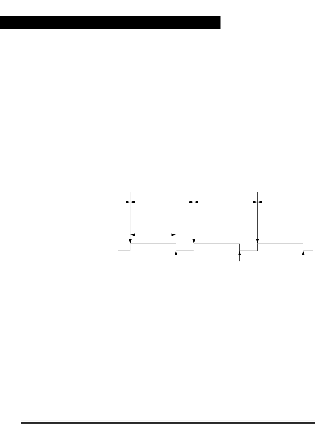
Timer Interface Module B (TIMB)
Technical Data MC68HC08AZ60 — Rev 1.1
270 Timer Interface Module B (TIMB) Freescale Semiconductor
19.4.4 Pulse Width Modulation (PWM)
By using the toggle-on-overflow feature with an output compare channel,
the TIMB can generate a PWM signal. The value in the TIMB counter
modulo registers determines the period of the PWM signal. The channel
pin toggles when the counter reaches the value in the TIMB counter
modulo registers. The time between overflows is the period of the PWM
signal.
As Figure 19-3 shows, the output compare value in the TIMB channel
registers determines the pulse width of the PWM signal. The time
between overflow and output compare is the pulse width. Program the
TIMB to clear the channel pin on output compare if the state of the PWM
pulse is logic 1. Program the TIMB to set the pin if the state of the PWM
pulse is logic 0.
Figure 19-3. PWM Period and Pulse Width
The value in the TIMB counter modulo registers and the selected
prescaler output determines the frequency of the PWM output. The
frequency of an 8-bit PWM signal is variable in 256 increments. Writing
$00FF (255) to the TIMB counter modulo registers produces a PWM
period of 256 times the internal bus clock period if the prescaler select
value is $000 (see TIMB Status and Control Register).
The value in the TIMB channel registers determines the pulse width of
the PWM output. The pulse width of an 8-bit PWM signal is variable in
256 increments. Writing $0080 (128) to the TIMB channel registers
produces a duty cycle of 128/256 or 50%.
PTEx/TCHx
PERIOD
PULSE
WIDTH
OVERFLOW OVERFLOW OVERFLOW
OUTPUT
COMPARE OUTPUT
COMPARE
OUTPUT
COMPARE

Timer Interface Module B (TIMB)
Functional Description
MC68HC08AZ60 — Rev 1.1 Technical Data
Freescale Semiconductor Timer Interface Module B (TIMB) 271
19.4.4.1 Unbuffered PWM Signal Generation
Any output compare channel can generate unbuffered PWM pulses as
described in Pulse Width Modulation (PWM) on page 270. The pulses
are unbuffered because changing the pulse width requires writing the
new pulse width value over the value currently in the TIMB channel
registers.
An unsynchronized write to the TIMB channel registers to change a
pulse width value could cause incorrect operation for up to two PWM
periods. For example, writing a new value before the counter reaches
the old value but after the counter reaches the new value prevents any
compare during that PWM period. Also, using a TIMB overflow interrupt
routine to write a new, smaller pulse width value may cause the compare
to be missed. The TIMB may pass the new value before it is written to
the TIMB channel registers.
Use the following methods to synchronize unbuffered changes in the
PWM pulse width on channel x:
• When changing to a shorter pulse width, enable channel x output
compare interrupts and write the new value in the output compare
interrupt routine. The output compare interrupt occurs at the end
of the current pulse. The interrupt routine has until the end of the
PWM period to write the new value.
• When changing to a longer pulse width, enable TIMB overflow
interrupts and write the new value in the TIMB overflow interrupt
routine. The TIMB overflow interrupt occurs at the end of the
current PWM period. Writing a larger value in an output compare
interrupt routine (at the end of the current pulse) could cause two
output compares to occur in the same PWM period.
NOTE: In PWM signal generation, do not program the PWM channel to toggle
on output compare. Toggling on output compare prevents reliable 0%
duty cycle generation and removes the ability of the channel to self-
correct in the event of software error or noise. Toggling on output
compare also can cause incorrect PWM signal generation when
changing the PWM pulse width to a new, much larger value.

Timer Interface Module B (TIMB)
Technical Data MC68HC08AZ60 — Rev 1.1
272 Timer Interface Module B (TIMB) Freescale Semiconductor
19.4.4.2 Buffered PWM Signal Generation
Channels 0 and 1 can be linked to form a buffered PWM channel whose
output appears on the PTF4/TBCH0 pin. The TIMB channel registers of
the linked pair alternately control the pulse width of the output.
Setting the MS0B bit in TIMB channel 0 status and control register
(TBSC0) links channel 0 and channel 1. The TIMB channel 0 registers
initially control the pulse width on the PTF4/TBCH0 pin. Writing to the
TIMB channel 1 registers enables the TIMB channel 1 registers to
synchronously control the pulse width at the beginning of the next PWM
period. At each subsequent overflow, the TIMB channel registers (0 or
1) that control the pulse width are the ones written to last. TBSC0
controls and monitors the buffered PWM function, and TIMB channel 1
status and control register (TBSC1) is unused. While the MS0B bit is set,
the channel 1 pin, PTF5/TBCH1, is available as a general-purpose I/O
pin.
NOTE: In buffered PWM signal generation, do not write new pulse width values
to the currently active channel registers. User software should track the
currently active channel to prevent writing a new value to the active
channel. Writing to the active channel registers is the same as
generating unbuffered PWM signals.
19.4.4.3 PWM Initialization
To ensure correct operation when generating unbuffered or buffered
PWM signals, use the following initialization procedure:
1. In the TIMB status and control register (TBSC):
a. Stop the TIMB counter by setting the TIMB stop bit, TSTOP.
b. Reset the TIMB counter and prescaler by setting the TIMB
reset bit, TRST.
2. In the TIMB counter modulo registers (TBMODH–TBMODL) write
the value for the required PWM period.
3. In the TIMB channel x registers (TBCHxH–TBCHxL) write the
value for the required pulse width.

Timer Interface Module B (TIMB)
Functional Description
MC68HC08AZ60 — Rev 1.1 Technical Data
Freescale Semiconductor Timer Interface Module B (TIMB) 273
4. In TIMB channel x status and control register (TBSCx):
a. Write 0:1 (for unbuffered output compare or PWM signals) or
1:0 (for buffered output compare or PWM signals) to the
mode select bits, MSxB–MSxA (see Table 19-2).
b. Write 1 to the toggle-on-overflow bit, TOVx.
c. Write 1:0 (to clear output on compare) or 1:1 (to set output on
compare) to the edge/level select bits, ELSxB–ELSxA. The
output action on compare must force the output to the
complement of the pulse width level (see Table 19-2).
NOTE: In PWM signal generation, do not program the PWM channel to toggle
on output compare. Toggling on output compare prevents reliable 0%
duty cycle generation and removes the ability of the channel to self-
correct in the event of software error or noise. Toggling on output
compare can also cause incorrect PWM signal generation when
changing the PWM pulse width to a new, much larger value.
5. In the TIMB status control register (TBSC) clear the TIMB stop bit,
TSTOP.
Setting MS0B links channels 0 and 1 and configures them for buffered
PWM operation. The TIMB channel 0 registers (TBCH0H–TBCH0L)
initially control the buffered PWM output. TIMB status control register 0
(TBSC0) controls and monitors the PWM signal from the linked
channels. MS0B takes priority over MS0A.
Clearing the toggle-on-overflow bit, TOVx, inhibits output toggles on
TIMB overflows. Subsequent output compares try to force the output to
a state it is already in and have no effect. The result is a 0% duty cycle
output.
Setting the channel x maximum duty cycle bit (CHxMAX) and setting the
TOVx bit generates a 100% duty cycle output (see TIMB Channel
Status and Control Registers on page 281).

Timer Interface Module B (TIMB)
Technical Data MC68HC08AZ60 — Rev 1.1
274 Timer Interface Module B (TIMB) Freescale Semiconductor
19.5 Interrupts
The following TIMB sources can generate interrupt requests:
• TIMB overflow flag (TOF) — The TOF bit is set when the TIMB
counter value reaches the value in the TIMB counter modulo
registers. The TIMB overflow interrupt enable bit, TOIE, enables
TIMB overflow CPU interrupt requests. TOF and TOIE are in the
TIMB status and control register.
• TIMB channel flags (CH1F–CH0F) — The CHxF bit is set when an
input capture or output compare occurs on channel x. Channel x
TIMB CPU interrupt requests are controlled by the channel x
interrupt enable bit, CHxIE.
19.6 Low-Power Modes
The WAIT and STOP instructions put the MCU in low power-
consumption standby modes.
19.6.1 Wait Mode
The TIMB remains active after the execution of a WAIT instruction. In
wait mode, the TIMB registers are not accessible by the CPU. Any
enabled CPU interrupt request from the TIMB can bring the MCU out of
wait mode.
If TIMB functions are not required during wait mode, reduce power
consumption by stopping the TIMB before executing the WAIT
instruction.
19.6.2 Stop Mode
The TIMB is inactive after the execution of a STOP instruction. The
STOP instruction does not affect register conditions or the state of the
TIMB counter. TIMB operation resumes when the MCU exits stop mode.

Timer Interface Module B (TIMB)
TIMB During Break Interrupts
MC68HC08AZ60 — Rev 1.1 Technical Data
Freescale Semiconductor Timer Interface Module B (TIMB) 275
19.7 TIMB During Break Interrupts
A break interrupt stops the TIMB counter and inhibits input captures.
The system integration module (SIM) controls whether status bits in
other modules can be cleared during the break state. The BCFE bit in
the SIM break flag control register (SBFCR) enables software to clear
status bits during the break state (see SIM Break Flag Control Register
on page 119).
To allow software to clear status bits during a break interrupt, write a
logic 1 to the BCFE bit. If a status bit is cleared during the break state, it
remains cleared when the MCU exits the break state.
To protect status bits during the break state, write a logic 0 to the BCFE
bit. With BCFE at logic 0 (its default state), software can read and write
I/O registers during the break state without affecting status bits. Some
status bits have a 2-step read/write clearing procedure. If software does
the first step on such a bit before the break, the bit cannot change during
the break state as long as BCFE is at logic 0. After the break, doing the
second step clears the status bit.
19.8 I/O Signals
Port D shares one of its pins with the TIMB. Port F shares two of its pins
with the TIMB. PTD4/ATD12/TBLCK is an external clock input to the
TIMB prescaler. The two TIMB channel I/O pins are PTF4/TBCH0 and
PTF5/TBCH1.
19.8.1 TIMB Clock Pin (PTD4/ATD12/TBLCK)
PTD4/ATD12/TBLCK is an external clock input that can be the clock
source for the TIMB counter instead of the prescaled internal bus clock.
Select the PTD4/ATD12/TBLCK input by writing logic 1s to the three
prescaler select bits, PS[2:0] (see TIMB Status and Control Register).
The minimum TCLK pulse width, TCLKLMIN or TCLKHMIN, is:
1
bus frequency
------------------------------------- t SU
+

Timer Interface Module B (TIMB)
Technical Data MC68HC08AZ60 — Rev 1.1
276 Timer Interface Module B (TIMB) Freescale Semiconductor
The maximum TCLK frequency is the least: 4 MHz or bus frequency ÷ 2.
PTD4/ATD12/TBLCK is available as a general-purpose I/O pin or ADC
channel when not used as the TIMB clock input. When the
PTD4/ATD12/TBLCK pin is the TIMB clock input, it is an input regardless
of the state of the DDRD4 bit in data direction register D.
19.8.2 TIMB Channel I/O Pins (PTF5/TBCH1–PTF4/TBCH0)
Each channel I/O pin is programmable independently as an input
capture pin or an output compare pin. PTF4/TBCH0 and PTF5/TBCH1
can be configured as buffered output compare or buffered PWM pins.
19.9 I/O Registers
These I/O registers control and monitor TIMB operation:
• TIMB status and control register (TBSC)
• TIMB control registers (TBCNTH–TBCNTL)
• TIMB counter modulo registers (TBMODH–TBMODL)
• TIMB channel status and control registers (TBSC0 and TBSC1)
• TIMB channel registers (TBCH0H–TBCH0L, TBCH1H–TBCH1L)

Timer Interface Module B (TIMB)
I/O Registers
MC68HC08AZ60 — Rev 1.1 Technical Data
Freescale Semiconductor Timer Interface Module B (TIMB) 277
19.9.1 TIMB Status and Control Register
The TIMB status and control register:
• Enables TIMB overflow interrupts
• Flags TIMB overflows
• Stops the TIMB counter
• Resets the TIMB counter
• Prescales the TIMB counter clock
TOF — TIMB Overflow Flag Bit
This read/write flag is set when the TIMB counter reaches the modulo
value programmed in the TIMB counter modulo registers. Clear TOF
by reading the TIMB status and control register when TOF is set and
then writing a logic 0 to TOF. If another TIMB overflow occurs before
the clearing sequence is complete, then writing logic 0 to TOF has no
effect. Therefore, a TOF interrupt request cannot be lost due to
inadvertent clearing of TOF. Reset clears the TOF bit. Writing a logic
1 to TOF has no effect.
1 = TIMB counter has reached modulo value
0 = TIMB counter has not reached modulo value
TOIE — TIMB Overflow Interrupt Enable Bit
This read/write bit enables TIMB overflow interrupts when the TOF bit
becomes set. Reset clears the TOIE bit.
1 = TIMB overflow interrupts enabled
0 = TIMB overflow interrupts disabled
Address: $0040
Bit 7654321Bit 0
Read: TOF TOIE TSTOP 00
PS2 PS1 PS0
Write: 0 TRST R
Reset:00100000
R= Reserved
Figure 19-4. TIMB Status and Control Register (TBSC)

Timer Interface Module B (TIMB)
Technical Data MC68HC08AZ60 — Rev 1.1
278 Timer Interface Module B (TIMB) Freescale Semiconductor
TSTOP — TIMB Stop Bit
This read/write bit stops the TIMB counter. Counting resumes when
TSTOP is cleared. Reset sets the TSTOP bit, stopping the TIMB
counter until software clears the TSTOP bit.
1 = TIMB counter stopped
0 = TIMB counter active
NOTE: Do not set the TSTOP bit before entering wait mode if the TIMB is
required to exit wait mode. Also, when the TSTOP bit is set and the timer
is configured for input capture operation, input captures are inhibited
until TSTOP is cleared.
TRST — TIMB Reset Bit
Setting this write-only bit resets the TIMB counter and the TIMB
prescaler. Setting TRST has no effect on any other registers. Counting
resumes from $0000. TRST is cleared automatically after the TIMB
counter is reset and always reads as logic 0. Reset clears the TRST bit.
1 = Prescaler and TIMB counter cleared
0 = No effect
NOTE: Setting the TSTOP and TRST bits simultaneously stops the TIMB
counter at a value of $0000.
PS[2:0] — Prescaler Select Bits
These read/write bits select either the PTD4/ATD12/TBLCK pin or
one of the seven prescaler outputs as the input to the TIMB counter
as Table 19-1 shows. Reset clears the PS[2:0] bits.
Table 19-1. Prescaler Selection
PS[2:0] TIMB Clock Source
000 Internal Bus Clock ÷1
001 Internal Bus Clock ÷ 2
010 Internal Bus Clock ÷ 4
011 Internal Bus Clock ÷ 8
100 Internal Bus Clock ÷ 16
101 Internal Bus Clock ÷ 32
110 Internal Bus Clock ÷ 64
111 PTD4/ATD12/TBLCK

Timer Interface Module B (TIMB)
I/O Registers
MC68HC08AZ60 — Rev 1.1 Technical Data
Freescale Semiconductor Timer Interface Module B (TIMB) 279
19.9.2 TIMB Counter Registers
The two read-only TIMB counter registers contain the high and low bytes
of the value in the TIMB counter. Reading the high byte (TBCNTH)
latches the contents of the low byte (TBCNTL) into a buffer. Subsequent
reads of TBCNTH do not affect the latched TBCNTL value until TBCNTL
is read. Reset clears the TIMB counter registers. Setting the TIMB reset
bit (TRST) also clears the TIMB counter registers.
NOTE: If TBCNTH is read during a break interrupt, be sure to unlatch TBCNTL
by reading TBCNTL before exiting the break interrupt. Otherwise,
TBCNTL retains the value latched during the break.
Register Name and Address TBCNTH — $0041
Bit 7654321Bit 0
Read: BIT 15 BIT 14 BIT 13 BIT 12 BIT 11 BIT 10 BIT 9 BIT 8
Write:RRRRRRRR
Reset:00000000
Register Name and Address TBCNTL — $0042
Bit 7654321Bit 0
Read: BIT 7 BIT 6 BIT 5 BIT 4 BIT 3 BIT 2 BIT 1 BIT 0
Write:RRRRRRRR
Reset:00000000
RR = Reserved
Figure 19-5. TIMB Counter Registers (TBCNTH and TBCNTL)

Timer Interface Module B (TIMB)
Technical Data MC68HC08AZ60 — Rev 1.1
280 Timer Interface Module B (TIMB) Freescale Semiconductor
19.9.3 TIMB Counter Modulo Registers
The read/write TIMB modulo registers contain the modulo value for the
TIMB counter. When the TIMB counter reaches the modulo value, the
overflow flag (TOF) becomes set and the TIMB counter resumes
counting from $0000 at the next timer clock. Writing to the high byte
(TBMODH) inhibits the TOF bit and overflow interrupts until the low byte
(TBMODL) is written. Reset sets the TIMB counter modulo registers.
NOTE: Reset the TIMB counter before writing to the TIMB counter modulo
registers.
Register Name and Address TBMODH — $0043
Bit 7654321Bit 0
Read:
BIT 15 BIT 14 BIT 13 BIT 12 BIT 11 BIT 10 BIT 9 BIT 8
Write:
Reset:11111111
Register Name and Address TBMODL — $0044
Bit 7654321Bit 0
Read:
BIT 7 BIT 6 BIT 5 BIT 4 BIT 3 BIT 2 BIT 1 BIT 0
Write:
Reset:11111111
Figure 19-6. TIMB Counter Modulo Registers (TBMODH and
TBMODL)

Timer Interface Module B (TIMB)
I/O Registers
MC68HC08AZ60 — Rev 1.1 Technical Data
Freescale Semiconductor Timer Interface Module B (TIMB) 281
19.9.4 TIMB Channel Status and Control Registers
Each of the TIMB channel status and control registers:
• Flags input captures and output compares
• Enables input capture and output compare interrupts
• Selects input capture, output compare or PWM operation
• Selects high, low or toggling output on output compare
• Selects rising edge, falling edge or any edge as the active input
capture trigger
• Selects output toggling on TIMB overflow
• Selects 0% and 100% PWM duty cycle
• Selects buffered or unbuffered output compare/PWM operation
Register Name and Address TBSC0 — $0045
Bit 7654321Bit 0
Read: CH0F
CH0IE MS0B MS0A ELS0B ELS0A TOV0 CH0MAX
Write: 0
Reset:00000000
Register Name and Address TBSC1 — $0048
Bit 7654321Bit 0
Read: CH1F
CH1IE
0
MS1A ELS1B ELS1A TOV1 CH1MAX
Write: 0 R
Reset:00000000
RR = Reserved
Figure 19-7. TIMB Channel Status and Control Registers
(TBSC0–TBSC1)

Timer Interface Module B (TIMB)
Technical Data MC68HC08AZ60 — Rev 1.1
282 Timer Interface Module B (TIMB) Freescale Semiconductor
CHxF — Channel x Flag Bit
When channel x is an input capture channel, this read/write bit is set
when an active edge occurs on the channel x pin. When channel x is
an output compare channel, CHxF is set when the value in the TIMB
counter registers matches the value in the TIMB channel x registers.
When CHxIE = 1, clear CHxF by reading TIMB channel x status and
control register with CHxF set, and then writing a logic 0 to CHxF. If
another interrupt request occurs before the clearing sequence is
complete, then writing logic 0 to CHxF has no effect. Therefore, an
interrupt request cannot be lost due to inadvertent clearing of CHxF.
Reset clears the CHxF bit. Writing a logic 1 to CHxF has no effect.
1 = Input capture or output compare on channel x
0 = No input capture or output compare on channel x
CHxIE — Channel x Interrupt Enable Bit
This read/write bit enables TIMB CPU interrupts on channel x.
Reset clears the CHxIE bit.
1 = Channel x CPU interrupt requests enabled
0 = Channel x CPU interrupt requests disabled
MSxB — Mode Select Bit B
This read/write bit selects buffered output compare/PWM operation.
MSxB exists only in the TIMB channel 0.
Setting MS0B disables the channel 1 status and control register and
reverts TBCH1 to general-purpose I/O.
Reset clears the MSxB bit.
1 = Buffered output compare/PWM operation enabled
0 = Buffered output compare/PWM operation disabled

Timer Interface Module B (TIMB)
I/O Registers
MC68HC08AZ60 — Rev 1.1 Technical Data
Freescale Semiconductor Timer Interface Module B (TIMB) 283
MSxA — Mode Select Bit A
When ELSxB:A ≠ 00, this read/write bit selects either input capture
operation or unbuffered output compare/PWM operation (see Table
19-2).
1 = Unbuffered output compare/PWM operation
0 = Input capture operation
When ELSxB:A = 00, this read/write bit selects the initial output level
of the TBCHx pin once PWM, input capture or output compare
operation is enabled (see Table 19-2). Reset clears the MSxA bit.
1 = Initial output level low
0 = Initial output level high
NOTE: Before changing a channel function by writing to the MSxB or MSxA bit,
set the TSTOP and TRST bits in the TIMB status and control register
(TBSC).
ELSxB and ELSxA — Edge/Level Select Bits
When channel x is an input capture channel, these read/write bits
control the active edge-sensing logic on channel x.
When channel x is an output compare channel, ELSxB and ELSxA
control the channel x output behavior when an output compare
occurs.
When ELSxB and ELSxA are both clear, channel x is not connected
to port F and pin PTFx/TBCHx is available as a general-purpose I/O
pin. However, channel x is at a state determined by these bits and
becomes transparent to the respective pin when PWM, input capture,
or output compare mode is enabled. Table 19-2 shows how ELSxB
and ELSxA work. Reset clears the ELSxB and ELSxA bits.

Timer Interface Module B (TIMB)
Technical Data MC68HC08AZ60 — Rev 1.1
284 Timer Interface Module B (TIMB) Freescale Semiconductor
NOTE: Before enabling a TIMB channel register for input capture operation,
make sure that the PTFx/TBCHx pin is stable for at least two bus clocks.
TOVx — Toggle-On-Overflow Bit
When channel x is an output compare channel, this read/write bit
controls the behavior of the channel x output when the TIMB counter
overflows. When channel x is an input capture channel, TOVx has no
effect. Reset clears the TOVx bit.
1 = Channel x pin toggles on TIMB counter overflow.
0 = Channel x pin does not toggle on TIMB counter overflow.
NOTE: When TOVx is set, a TIMB counter overflow takes precedence over a
channel x output compare if both occur at the same time.
Table 19-2. Mode, Edge, and Level Selection
MSxB:MSxA ELSxB:ELSxA Mode Configuration
X0 00
Output
Preset
Pin under Port Control;
Initialize Timer
Output Level High
X1 00 Pin under Port Control;
Initialize Timer
Output Level Low
00 01
Input
Capture
Capture on Rising Edge Only
00 10 Capture on Falling Edge Only
00 11 Capture on Rising or Falling Edge
01 01 Output
Compare
or PWM
Toggle Output on Compare
01 10 Clear Output on Compare
01 11 Set Output on Compare
1X 01 Buffered
Output
Compare
or Buffered
PWM
Toggle Output on Compare
1X 10 Clear Output on Compare
1X 11 Set Output on Compare
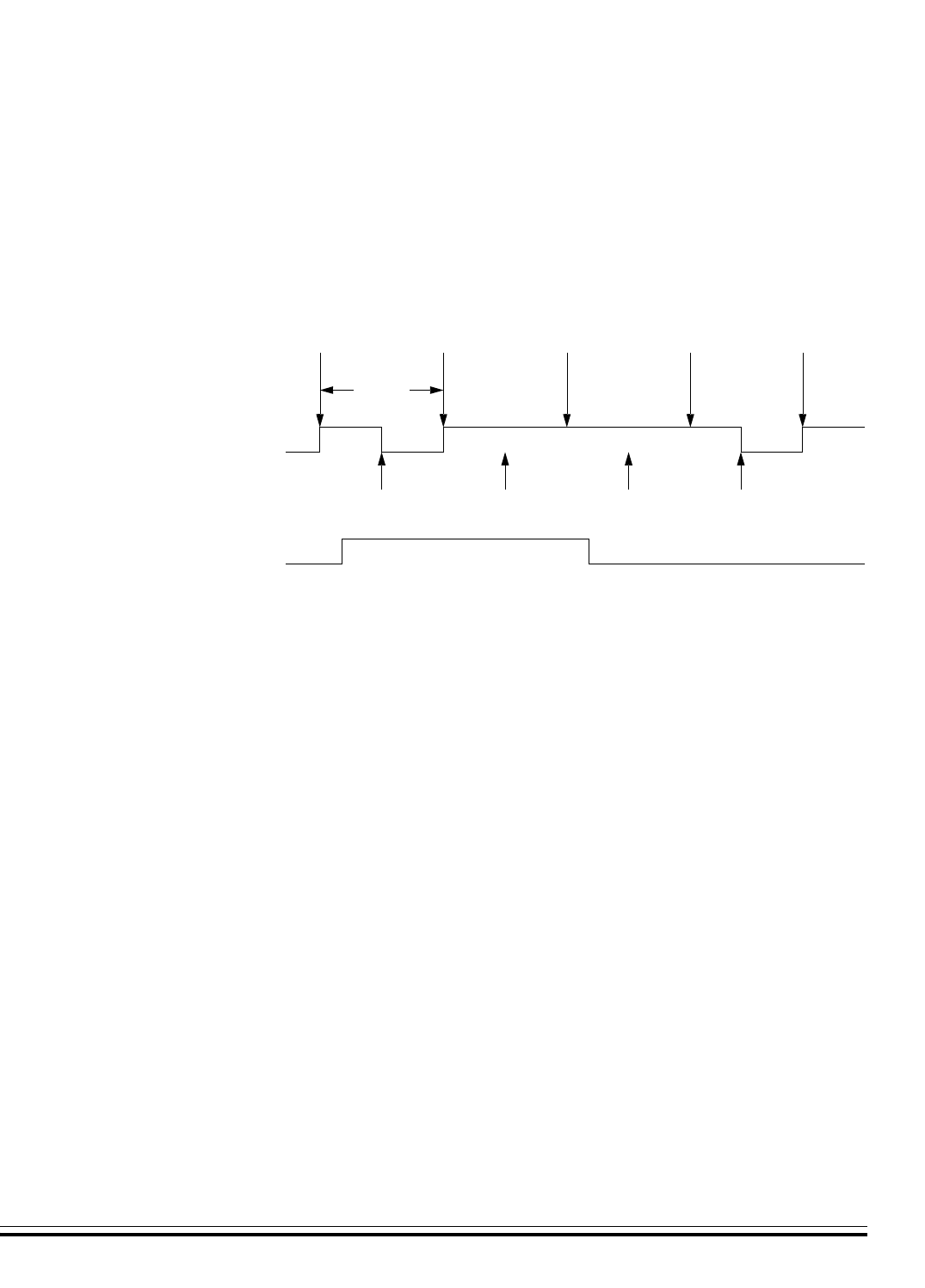
Timer Interface Module B (TIMB)
I/O Registers
MC68HC08AZ60 — Rev 1.1 Technical Data
Freescale Semiconductor Timer Interface Module B (TIMB) 285
CHxMAX — Channel x Maximum Duty Cycle Bit
When the TOVx bit is at logic 1, setting the CHxMAX bit forces the
duty cycle of buffered and unbuffered PWM signals to 100%. As
Figure 19-8 shows, the CHxMAX bit takes effect in the cycle after it
is set or cleared. The output stays at the 100% duty cycle level until
the cycle after CHxMAX is cleared.
Figure 19-8. CHxMAX Latency
19.9.5 TIMB Channel Registers
These read/write registers contain the captured TIMB counter value of
the input capture function or the output compare value of the output
compare function. The state of the TIMB channel registers after reset is
unknown.
In input capture mode (MSxB–MSxA = 0:0) reading the high byte of the
TIMB channel x registers (TBCHxH) inhibits input captures until the low
byte (TBCHxL) is read.
In output compare mode (MSxB–MSxA ≠ 0:0) writing to the high byte of
the TIMB channel x registers (TBCHxH) inhibits output compares and
the CHxF bit until the low byte (TBCHxL) is written.
OUTPUT
OVERFLOW
PTEx/TCHx
PERIOD
CHxMAX
OVERFLOW OVERFLOW OVERFLOW OVERFLOW
COMPARE
OUTPUT
COMPARE
OUTPUT
COMPARE
OUTPUT
COMPARE

Timer Interface Module B (TIMB)
Technical Data MC68HC08AZ60 — Rev 1.1
286 Timer Interface Module B (TIMB) Freescale Semiconductor
Register Name and Address TBCH0H — $0046
Bit 7654321Bit 0
Read:
Bit 15 Bit 14 Bit 13 Bit 12 Bit 11 Bit 10 Bit 9 Bit 8
Write:
Reset: Indeterminate after Reset
Register Name and Address TBCH0L — $0047
Bit 7654321Bit 0
Read:
Bit 7Bit 6Bit 5Bit 4Bit 3Bit 2Bit 1Bit 0
Write:
Reset: Indeterminate after Reset
Register Name and Address TBCH1H — $0049
Bit 7654321Bit 0
Read:
Bit 15 Bit 14 Bit 13 Bit 12 Bit 11 Bit 10 Bit 9 Bit 8
Write:
Reset: Indeterminate after Reset
Register Name and Address TBCH1L — $004A
Bit 7654321Bit 0
Read:
Bit 7Bit 6Bit 5Bit 4Bit 3Bit 2Bit 1Bit 0
Write:
Reset: Indeterminate after Reset
Figure 19-9. TIMB Channel Registers
(TBCH0H/L–TBCH1H/L)

MC68HC08AZ60 — Rev 1.1 Technical Data
Freescale Semiconductor Programmable Interrupt Timer (PIT) 289
Technical Data — MC68HC08AZ60
Section 20. Programmable Interrupt Timer (PIT)
20.1 Contents
20.2 Introduction. . . . . . . . . . . . . . . . . . . . . . . . . . . . . . . . . . . . . .289
20.3 Features. . . . . . . . . . . . . . . . . . . . . . . . . . . . . . . . . . . . . . . . .290
20.4 Functional Description. . . . . . . . . . . . . . . . . . . . . . . . . . . . .290
20.5 PIT Counter Prescaler . . . . . . . . . . . . . . . . . . . . . . . . . . . . .291
20.6 Low-Power Modes . . . . . . . . . . . . . . . . . . . . . . . . . . . . . . . .292
20.6.1 Wait Mode . . . . . . . . . . . . . . . . . . . . . . . . . . . . . . . . . . . . .292
20.6.2 Stop Mode. . . . . . . . . . . . . . . . . . . . . . . . . . . . . . . . . . . . .292
20.7 PIT During Break Interrupts. . . . . . . . . . . . . . . . . . . . . . . . .292
20.8 I/O Registers . . . . . . . . . . . . . . . . . . . . . . . . . . . . . . . . . . . . .293
20.8.1 PIT Status and Control Register . . . . . . . . . . . . . . . . . . .293
20.8.2 PIT Counter Registers . . . . . . . . . . . . . . . . . . . . . . . . . . .296
20.8.3 PIT Counter Modulo Registers . . . . . . . . . . . . . . . . . . . .297
20.2 Introduction
This section describes the Programmable Interrupt Timer (PIT) which is
a periodic interrupt timer whose counter is clocked internally via software
programmable options. Figure 20-1 is a block diagram of the PIT.
For further information regarding timers on M68HC08 family devices,
please consult the HC08 Timer Reference Manual, TIM08RM/AD.
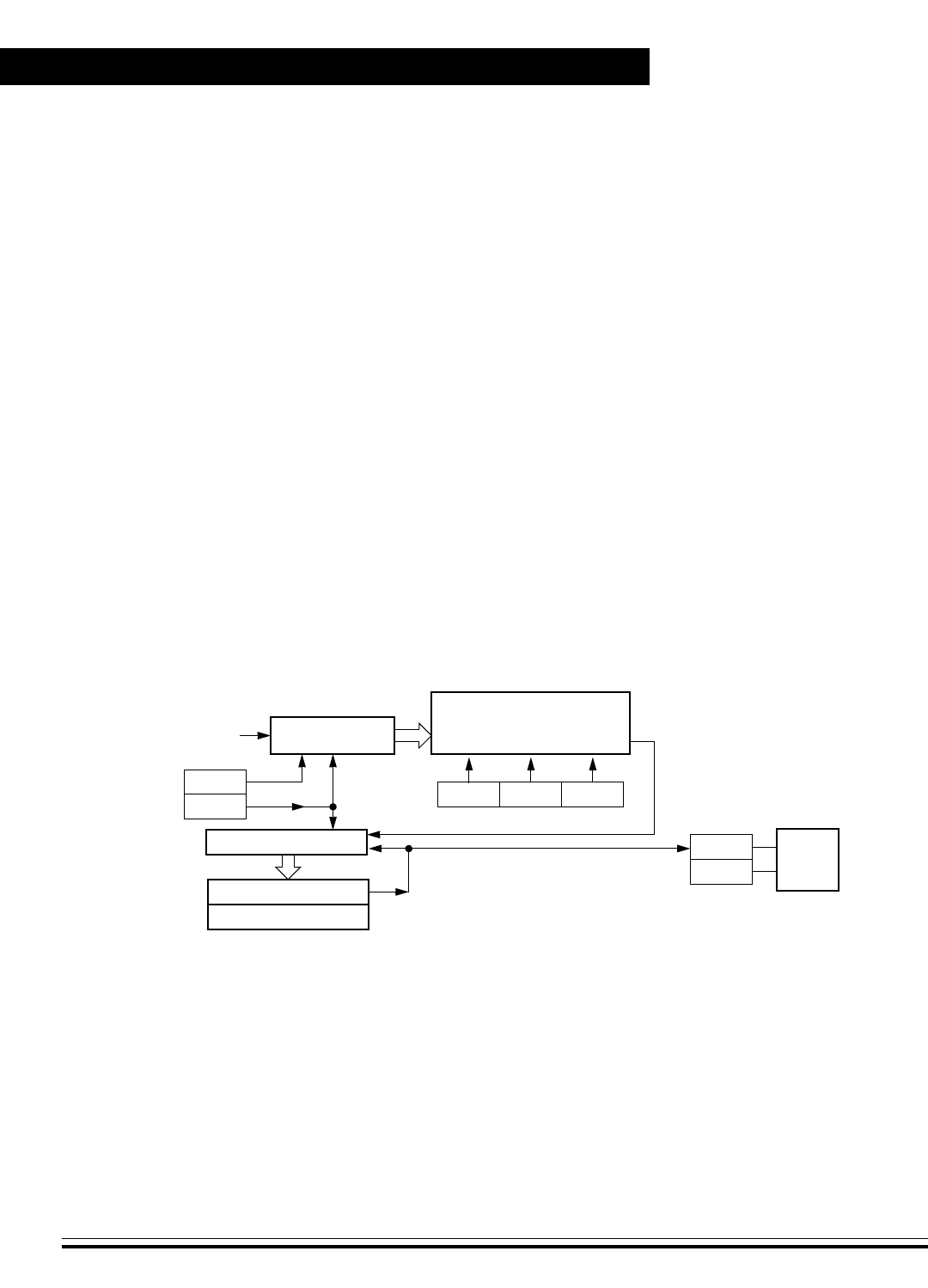
Programmable Interrupt Timer (PIT)
Technical Data MC68HC08AZ60 — Rev 1.1
290 Programmable Interrupt Timer (PIT) Freescale Semiconductor
20.3 Features
Features of the PIT include:
• Programmable PIT Clock Input
• Free-Running or Modulo Up-Count Operation
• PIT Counter Stop and Reset Bits
20.4 Functional Description
Figure 20-1 shows the structure of the PIT. The central component of
the PIT is the 16-bit PIT counter that can operate as a free-running
counter or a modulo up-counter. The counter provides the timing
reference for the interrupt. The PIT counter modulo registers,
PMODH–PMODL, control the modulo value of the counter. Software can
read the counter value at any time without affecting the counting
sequence.
Figure 20-1. PIT Block Diagram
PRESCALER PRESCALER SELECT
INTERNAL
16-BIT COMPARATOR
PPS2 PPS1 PPS0
POF
POIE
INTER-
PMODH:PMODL
CRST
CSTOP
16-BIT COUNTER
BUS CLOCK
RUPT
LOGIC
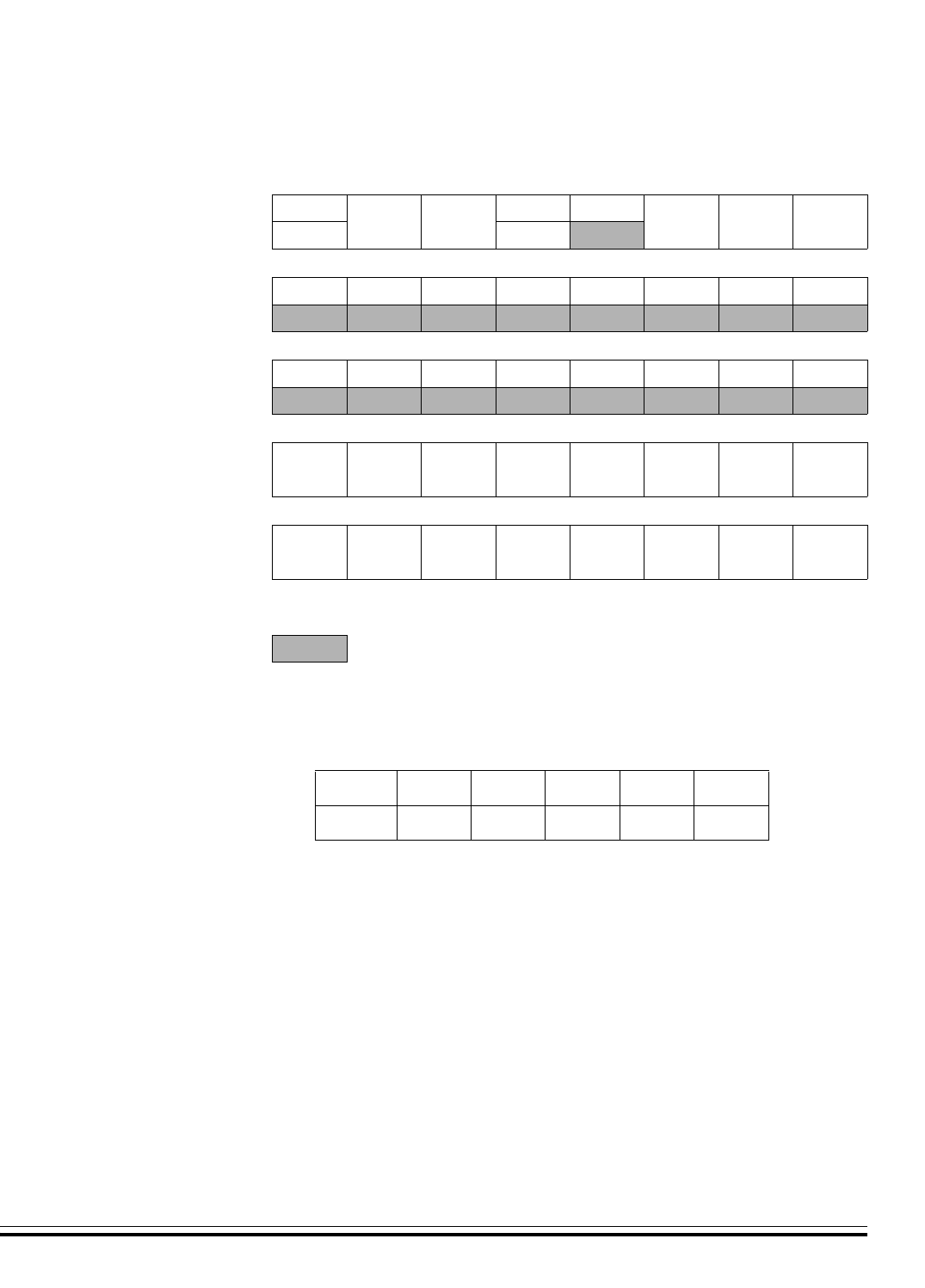
Programmable Interrupt Timer (PIT)
PIT Counter Prescaler
MC68HC08AZ60 — Rev 1.1 Technical Data
Freescale Semiconductor Programmable Interrupt Timer (PIT) 291
20.5 PIT Counter Prescaler
The clock source can be one of the seven prescaler outputs. The
prescaler generates seven clock rates from the internal bus clock. The
prescaler select bits, PPS[2:0], in the status and control register select
the PIT clock source.
The value in the PIT counter modulo registers and the selected prescaler
output determines the frequency of the periodic interrupt. The PIT
overflow flag (POF) is set when the PIT counter value reaches the
Register Name Bit 7654321Bit 0
PIT Status and Control Register
(PSC)
Read: POF POIE PSTOP 00
PPS2 PPS1 PPS0
Write: 0 PRST
Reset:00100000
PIT Counter Register High
(PCNTH)
Read: Bit 15 14 13 12 11 10 9 Bit 8
Write:
Reset:00000000
PIT Counter Register Low
(PCNTL)
Read: Bit 7 654321Bit 0
Write:
Reset:00000000
PIT Counter Modulo Register High
(PMODH)
Read: Bit 15 14 13 12 11 10 9 Bit 8
Write:
Reset:11111111
PIT Counter Modulo Register Low
(PMODL)
Read: Bit 7654321Bit 0
Write:
Reset:11111111
=Unimplemented
Figure 20-2. PIT I/O Register Summary
Table 20-1. PIT I/O Register Address Summary
Register PSC PCNTH PCNTL PMODH PMODL
Address $004B $004C $004D $004E $004F

Programmable Interrupt Timer (PIT)
Technical Data MC68HC08AZ60 — Rev 1.1
292 Programmable Interrupt Timer (PIT) Freescale Semiconductor
modulo value programmed in the PIT counter modulo registers. The PIT
interrupt enable bit, POIE, enables PIT overflow CPU interrupt requests.
POF and POIE are in the PIT status and control register.
20.6 Low-Power Modes
The WAIT and STOP instructions put the MCU in low power-consump-
tion standby modes.
20.6.1 Wait Mode
The PIT remains active after the execution of a WAIT instruction. In wait
mode the PIT registers are not accessible by the CPU. Any enabled CPU
interrupt request from the PIT can bring the MCU out of wait mode.
If PIT functions are not required during wait mode, reduce power
consumption by stopping the PIT before executing the WAIT instruction.
20.6.2 Stop Mode
The PIT is inactive after the execution of a STOP instruction. The STOP
instruction does not affect register conditions or the state of the PIT
counter. PIT operation resumes when the MCU exits stop mode after an
external interrupt.
20.7 PIT During Break Interrupts
A break interrupt stops the PIT counter.
The system integration module (SIM) controls whether status bits in
other modules can be cleared during the break state. The BCFE bit in
the SIM break flag control register (SBFCR) enables software to clear
status bits during the break state (see SIM Break Flag Control Register
on page 119).

Programmable Interrupt Timer (PIT)
I/O Registers
MC68HC08AZ60 — Rev 1.1 Technical Data
Freescale Semiconductor Programmable Interrupt Timer (PIT) 293
To allow software to clear status bits during a break interrupt, write a
logic 1 to the BCFE bit. If a status bit is cleared during the break state, it
remains cleared when the MCU exits the break state.
To protect status bits during the break state, write a logic 0 to the BCFE
bit. With BCFE at logic 0 (its default state), software can read and write
I/O registers during the break state without affecting status bits. Some
status bits have a 2-step read/write clearing procedure. If software does
the first step on such a bit before the break, the bit cannot change during
the break state as long as BCFE is at logic 0. After the break, doing the
second step clears the status bit.
20.8 I/O Registers
The following I/O registers control and monitor operation of the PIT:
• PIT status and control register (PSC)
• PIT counter registers (PCNTH–PCNTL)
• PIT counter modulo registers (PMODH–PMODL)
20.8.1 PIT Status and Control Register
The PIT status and control register:
• Enables PIT interrupt
• Flags PIT overflows
• Stops the PIT counter
• Resets the PIT counter
• Prescales the PIT counter clock

Programmable Interrupt Timer (PIT)
Technical Data MC68HC08AZ60 — Rev 1.1
294 Programmable Interrupt Timer (PIT) Freescale Semiconductor
POF — PIT Overflow Flag Bit
This read/write flag is set when the PIT counter reaches the modulo
value programmed in the PIT counter modulo registers. Clear POF by
reading the PIT status and control register when POF is set and then
writing a logic 0 to POF. If another PIT overflow occurs before the
clearing sequence is complete, then writing logic 0 to POF has no
effect. Therefore, a POF interrupt request cannot be lost due to
inadvertent clearing of POF. Reset clears the POF bit. Writing a logic
1 to POF has no effect.
1 = PIT counter has reached modulo value
0 = PIT counter has not reached modulo value
POIE — PIT Overflow Interrupt Enable Bit
This read/write bit enables PIT overflow interrupts when the POF bit
becomes set. Reset clears the POIE bit.
1 = PIT overflow interrupts enabled
0 = PIT overflow interrupts disabled
PSTOP — PIT Stop Bit
This read/write bit stops the PIT counter. Counting resumes when
PSTOP is cleared. Reset sets the PSTOP bit, stopping the PIT
counter until software clears the PSTOP bit.
1 = PIT counter stopped
0 = PIT counter active
Address: $004B
Bit 7654321Bit 0
Read: POF
POIE PSTOP
00
PPS2 PPS1 PPS0
Write: 0 PRST
Reset:00100000
= Unimplemented
Figure 20-3. PIT Status and Control Register (PSC)

Programmable Interrupt Timer (PIT)
I/O Registers
MC68HC08AZ60 — Rev 1.1 Technical Data
Freescale Semiconductor Programmable Interrupt Timer (PIT) 295
NOTE: Do not set the PSTOP bit before entering wait mode if the PIT is required
to exit wait mode.
PRST — PIT Reset Bit
Setting this write-only bit resets the PIT counter and the PIT prescaler.
Setting PRST has no effect on any other registers. Counting resumes
from $0000. PRST is cleared automatically after the PIT counter is
reset and always reads as logic zero. Reset clears the PRST bit.
1 = Prescaler and PIT counter cleared
0 = No effect
NOTE: Setting the PSTOP and PRST bits simultaneously stops the PIT counter
at a value of $0000.
PPS[2:0] — Prescaler Select Bits
These read/write bits select one of the seven prescaler outputs as the
input to the PIT counter as Table 20-2 shows. Reset clears the
PPS[2:0] bits.
Table 20-2. Prescaler Selection
PPS[2:0] PIT Clock Source
000 Internal Bus Clock ÷1
001 Internal Bus Clock ÷ 2
010 Internal Bus Clock ÷ 4
011 Internal Bus Clock ÷ 8
100 Internal Bus Clock ÷ 16
101 Internal Bus Clock ÷ 32
110 Internal Bus Clock ÷ 64
111 Internal Bus Clock ÷ 64
Programmable Interrupt Timer (PIT)
Technical Data MC68HC08AZ60 — Rev 1.1
296 Programmable Interrupt Timer (PIT) Freescale Semiconductor
20.8.2 PIT Counter Registers
The two read-only PIT counter registers contain the high and low bytes
of the value in the PIT counter. Reading the high byte (PCNTH) latches
the contents of the low byte (PCNTL) into a buffer. Subsequent reads of
PCNTH do not affect the latched PCNTL value until PCNTL is read.
Reset clears the PIT counter registers. Setting the PIT reset bit (PRST)
also clears the PIT counter registers.
NOTE: If you read PCNTH during a break interrupt, be sure to unlatch PCNTL
by reading PCNTL before exiting the break interrupt. Otherwise, PCNTL
retains the value latched during the break.
Address: $004C
Bit 7654321Bit 0
Read: Bit 15 14 13 12 11 10 9 Bit 8
Write:
Reset:00000000
Address: $004D
Bit 7654321Bit 0
Read: Bit 15 14 13 12 11 10 9 Bit 8
Write:
Reset:00000000
= Unimplemented
Figure 20-4. PIT Counter Registers (PCNTH–PCNTL)

Programmable Interrupt Timer (PIT)
I/O Registers
MC68HC08AZ60 — Rev 1.1 Technical Data
Freescale Semiconductor Programmable Interrupt Timer (PIT) 297
20.8.3 PIT Counter Modulo Registers
The read/write PIT modulo registers contain the modulo value for the PIT
counter. When the PIT counter reaches the modulo value the overflow
flag (POF) becomes set and the PIT counter resumes counting from
$0000 at the next timer clock. Writing to the high byte (PMODH) inhibits
the POF bit and overflow interrupts until the low byte (PMODL) is written.
Reset sets the PIT counter modulo registers.
NOTE: Reset the PIT counter before writing to the PIT counter modulo registers.
Address: $004E:$004F
Bit 7654321Bit 0
Read:
Bit 15 14 13 12 11 10 9 Bit 8
Write:
Reset:11111111
Address: $004E:$004F
Bit 7654321Bit 0
Read:
Bit 7654321Bit 0
Write:
Reset:11111111
Figure 20-5. PIT Counter Modulo Registers (PMODH–PMODL)

Programmable Interrupt Timer (PIT)
Technical Data MC68HC08AZ60 — Rev 1.1
298 Programmable Interrupt Timer (PIT) Freescale Semiconductor

MC68HC08AZ60 — Rev 1.1 Technical Data
Freescale Semiconductor Input/Output Ports 299
Technical Data — MC68HC08AZ60
Section 21. Input/Output Ports
21.1 Contents
21.2 Introduction. . . . . . . . . . . . . . . . . . . . . . . . . . . . . . . . . . . . . .300
21.3 Port A. . . . . . . . . . . . . . . . . . . . . . . . . . . . . . . . . . . . . . . . . . .301
21.3.1 Port A Data Register . . . . . . . . . . . . . . . . . . . . . . . . . . . .301
21.3.2 Data Direction Register A . . . . . . . . . . . . . . . . . . . . . . . .301
21.4 Port B. . . . . . . . . . . . . . . . . . . . . . . . . . . . . . . . . . . . . . . . . . .303
21.4.1 Port B Data Register . . . . . . . . . . . . . . . . . . . . . . . . . . . .303
21.4.2 Data Direction Register B . . . . . . . . . . . . . . . . . . . . . . . .304
21.5 Port C. . . . . . . . . . . . . . . . . . . . . . . . . . . . . . . . . . . . . . . . . . .306
21.5.1 Port C Data Register . . . . . . . . . . . . . . . . . . . . . . . . . . . .306
21.5.2 Data Direction Register C . . . . . . . . . . . . . . . . . . . . . . . .307
21.6 Port D. . . . . . . . . . . . . . . . . . . . . . . . . . . . . . . . . . . . . . . . . . .309
21.6.1 Port D Data Register . . . . . . . . . . . . . . . . . . . . . . . . . . . .309
21.6.2 Data Direction Register D . . . . . . . . . . . . . . . . . . . . . . . .310
21.7 Port E . . . . . . . . . . . . . . . . . . . . . . . . . . . . . . . . . . . . . . . . . . .312
21.7.1 Port E Data Register. . . . . . . . . . . . . . . . . . . . . . . . . . . . .312
21.7.2 Data Direction Register E . . . . . . . . . . . . . . . . . . . . . . . .314
21.8 Port F . . . . . . . . . . . . . . . . . . . . . . . . . . . . . . . . . . . . . . . . . . .316
21.8.1 Port F Data Register. . . . . . . . . . . . . . . . . . . . . . . . . . . . .316
21.8.2 Data Direction Register F . . . . . . . . . . . . . . . . . . . . . . . .317
21.9 Port G. . . . . . . . . . . . . . . . . . . . . . . . . . . . . . . . . . . . . . . . . . .319
21.9.1 Port G Data Register . . . . . . . . . . . . . . . . . . . . . . . . . . . .319
21.9.2 Data Direction Register G . . . . . . . . . . . . . . . . . . . . . . . .320
21.10 Port H. . . . . . . . . . . . . . . . . . . . . . . . . . . . . . . . . . . . . . . . . . .321
21.10.1 Port H Data Register . . . . . . . . . . . . . . . . . . . . . . . . . . . .321
21.10.2 Data Direction Register H . . . . . . . . . . . . . . . . . . . . . . . .322

Input/Output Ports
Technical Data MC68HC08AZ60 — Rev 1.1
300 Input/Output Ports Freescale Semiconductor
21.2 Introduction
Fifty bidirectional input/output (I/O) form seven parallel ports. All I/O pins
are programmable as inputs or outputs.
NOTE: Connect any unused I/O pins to an appropriate logic level, either VDD or
VSS. Although the I/O ports do not require termination for proper
operation, termination reduces excess current consumption and the
possibility of electrostatic damage.
Figure 1. CAN Protocol I/O Port Register Summary
Addr. Register Name Bit 7 6 5 4 3 2 1 Bit 0
$0000 Port A Data Register (PTA) PTA7 PTA6 PTA5 PTA4 PTA3 PTA2 PTA1 PTA0
$0001 Port B Data Register (PTB) PTB7 PTB6 PTB5 PTB4 PTB3 PTB2 PTB1 PTB0
$0002 Port C Data Register (PTC) 0 0 PTC5 PTC4 PTC3 PTC2 PTC1 PTC0
$0003 Port D Data Register (PTD) PTD7 PTD6 PTD5 PTD4 PTD3 PTD2 PTD1 PTD0
$0004 Data Direction Register A (DDRA) DDRA7 DDRA6 DDRA5 DDRA4 DDRA3 DDRA2 DDRA1 DDRA0
$0005 Data Direction Register B (DDRB) DDRB7 DDRB6 DDRB5 DDRB4 DDRB3 DDRB2 DDRB1 DDRB0
$0006 Data Direction Register C (DDRC) MCLKEN 0 DDRC5 DDRC4 DDRC3 DDRC2 DDRC1 DDRC0
$0007 Data Direction Register D (DDRD) DDRD7 DDRD6 DDRD5 DDRD4 DDRD3 DDRD2 DDRD1 DDRD0
$0008 Port E Data Register (PTE) PTE7 PTE6 PTE5 PTE4 PTE3 PTE2 PTE1 PTE0
$0009 Port F Data Register (PTF) 0 PTF6 PTF5 PTF4 PTF3 PTF2 PTF1 PTF0
$000A Port G Data Register (PTG) 0 0 0 0 0 PTG2 PTG1 PTG0
$000B Port H Data Register (PTH) 0 0 0 0 0 0 PTH1 PTH0
$000C Data Direction Register E (DDRE) DDRE7 DDRE6 DDRE5 DDRE4 DDRE3 DDRE2 DDRE1 DDRE0
$000D Data Direction Register F (DDRF) 0 DDRF6 DDRF5 DDRF4 DDRF3 DDRF2 DDRF1 DDRF0
$000E Data Direction Register G (DDRG) 0 0 0 0 0 DDRG2 DDRG1 DDRG0
$000F Data Direction Register H (DDRH) 0 0 0 0 0 0 DDRH1‘ DDRH0

Input/Output Ports
Port A
MC68HC08AZ60 — Rev 1.1 Technical Data
Freescale Semiconductor Input/Output Ports 301
21.3 Port A
Port A is an 8-bit general-purpose bidirectional I/O port.
21.3.1 Port A Data Register
The port A data register contains a data latch for each of the eight
port A pins.
PTA[7:0] — Port A Data Bits
These read/write bits are software programmable. Data direction of
each port A pin is under the control of the corresponding bit in data
direction register A. Reset has no effect on port A data.
21.3.2 Data Direction Register A
Data direction register A determines whether each port A pin is an input
or an output. Writing a logic 1 to a DDRA bit enables the output buffer for
the corresponding port A pin; a logic 0 disables the output buffer.
Address: $0000
Bit 7654321Bit 0
Read:
PTA7 PTA6 PTA5 PTA4 PTA3 PTA2 PTA1 PTA0
Write:
Reset: Unaffected by Reset
Figure 21-1. Port A Data Register (PTA)
Address: $0004
Bit 7654321Bit 0
Read:
DDRA7 DDRA6 DDRA5 DDRA4 DDRA3 DDRA2 DDRA1 DDRA0
Write:
Reset:00000000
Figure 21-2. Data Direction Register A (DDRA)
Input/Output Ports
Technical Data MC68HC08AZ60 — Rev 1.1
302 Input/Output Ports Freescale Semiconductor
DDRA[7:0] — Data Direction Register A Bits
These read/write bits control port A data direction. Reset clears
DDRA[7:0], configuring all port A pins as inputs.
1 = Corresponding port A pin configured as output
0 = Corresponding port A pin configured as input
NOTE: Avoid glitches on port A pins by writing to the port A data register before
changing data direction register A bits from 0 to 1.
Figure 21-3 shows the port A I/O logic.
Figure 21-3. Port A I/O Circuit
When bit DDRAx is a logic 1, reading address $0000 reads the PTAx
data latch. When bit DDRAx is a logic 0, reading address $0000 reads
the voltage level on the pin. The data latch can always be written,
regardless of the state of its data direction bit. Table 21-1 summarizes
the operation of the port A pins.
READ DDRA ($0004)
WRITE DDRA ($0004)
RESET
WRITE PTA ($0000)
READ PTA ($0000)
PTAx
DDRAx
PTAx
INTERNAL DATA BUS

Input/Output Ports
Port B
MC68HC08AZ60 — Rev 1.1 Technical Data
Freescale Semiconductor Input/Output Ports 303
21.4 Port B
Port B is an 8-bit special function port that shares all of its pins with the
analog-to-digital converter.
21.4.1 Port B Data Register
The port B data register contains a data latch for each of the eight port
B pins.
PTB[7:0] — Port B Data Bits
These read/write bits are software programmable. Data direction of
each port B pin is under the control of the corresponding bit in data
direction register B. Reset has no effect on port B data.
Table 21-1. Port A Pin Functions
DDRA
Bit PTA
Bit I/O Pin
Mode
Accesses
to DDRA Accesses to PTA
Read/Write Read Write
0 X Input, Hi-Z DDRA[7:0] Pin PTA[7:0](1)
1 X Output DDRA[7:0] PTA[7:0] PTA[7:0]
X = don’t care
Hi-Z = high impedance
1. Writing affects data register, but does not affect input.
Address: $0001
Bit 7654321Bit 0
Read:
PTB7 PTB6 PTB5 PTB4 PTB3 PTB2 PTB1 PTB0
Write:
Reset: Unaffected by Reset
Alternate
Functions: ATD7 ATD6 ATD5 ATD4 ATD3 ATD2 ATD1 ATD0
Figure 21-4. Port B Data Register (PTB)

Input/Output Ports
Technical Data MC68HC08AZ60 — Rev 1.1
304 Input/Output Ports Freescale Semiconductor
ATD[7:0] — ADC Channels
PTB7/ATD7–PTB0/ATD0 are eight of the analog-to-digital converter
channels. The ADC channel select bits, CH[4:0], determine whether
the PTB7/ATD7–PTB0/ATD0 pins are ADC channels or general-
purpose I/O pins. If an ADC channel is selected and a read of this
corresponding bit in the port B data register occurs, the data will be 0
if the data direction for this bit is programmed as an input. Otherwise,
the data will reflect the value in the data latch. (See Analog-to-Digital
Converter (ADC-15) on page 417). Data direction register B (DDRB)
does not affect the data direction of port B pins that are being used by
the ADC. However, the DDRB bits always determine whether reading
port B returns to the states of the latches or logic 0.
21.4.2 Data Direction Register B
Data direction register B determines whether each port B pin is an input
or an output. Writing a logic 1 to a DDRB bit enables the output buffer for
the corresponding port B pin; a logic 0 disables the output buffer.
DDRB[7:0] — Data Direction Register B Bits
These read/write bits control port B data direction. Reset clears
DDRB[7:0], configuring all port B pins as inputs.
1 = Corresponding port B pin configured as output
0 = Corresponding port B pin configured as input
NOTE: Avoid glitches on port B pins by writing to the port B data register before
changing data direction register B bits from 0 to 1.
Figure 21-6 shows the port B I/O logic.
Address: $0005
Bit 7654321Bit 0
Read:
DDRB7 DDRB6 DDRB5 DDRB4 DDRB3 DDRB2 DDRB1 DDRB0
Write:
Reset:00000000
Figure 21-5. Data Direction Register B (DDRB)

Input/Output Ports
Port B
MC68HC08AZ60 — Rev 1.1 Technical Data
Freescale Semiconductor Input/Output Ports 305
Figure 21-6. Port B I/O Circuit
When bit DDRBx is a logic 1, reading address $0001 reads the PTBx
data latch. When bit DDRBx is a logic 0, reading address $0001 reads
the voltage level on the pin. The data latch can always be written,
regardless of the state of its data direction bit. Table 21-2 summarizes
the operation of the port B pins.
Table 21-2. Port B Pin Functions
DDRB
Bit PTB
Bit I/O Pin
Mode
Accesses
to DDRB Accesses to PTB
Read/Write Read Write
0 X Input, Hi-Z DDRB[7:0] Pin PTB[7:0](1)
1 X Output DDRB[7:0] PTB[7:0] PTB[7:0]
X = don’t care
Hi-Z = high impedance
1. Writing affects data register, but does not affect input.
READ DDRB ($0005)
WRITE DDRB ($0005)
RESET
WRITE PTB ($0001)
READ PTB ($0001)
PTBx
DDRBx
PTBx
INTERNAL DATA BUS

Input/Output Ports
Technical Data MC68HC08AZ60 — Rev 1.1
306 Input/Output Ports Freescale Semiconductor
21.5 Port C
Port C is an 6-bit general-purpose bidirectional I/O port.
21.5.1 Port C Data Register
The port C data register contains a data latch for each of the six port C
pins.
PTC[5:0] — Port C Data Bits
These read/write bits are software-programmable. Data direction of
each port C pin is under the control of the corresponding bit in data
direction register C. Reset has no effect on port C data (5:0).
MCLK — T12 System Clock Bit
The system clock is driven out of PTC2 when enabled by MCLKEN bit
in PTCDDR7.
Address: $0002
Bit 7654321Bit 0
Read: 0 0
PTC5 PTC4 PTC3 PTC2 PTC1 PTC0
Write: R R
Reset: Unaffected by Reset
R= Reserved
Alternate
Functions: MCLK
Figure 21-7. Port C Data Register (PTC)

Input/Output Ports
Port C
MC68HC08AZ60 — Rev 1.1 Technical Data
Freescale Semiconductor Input/Output Ports 307
21.5.2 Data Direction Register C
Data direction register C determines whether each port C pin is an input
or an output. Writing a logic 1 to a DDRC bit enables the output buffer for
the corresponding port C pin; a logic 0 disables the output buffer.
MCLKEN — MCLK Enable Bit
This read/write bit enables MCLK to be an output signal on PTC2. If
MCLK is enabled, DDRC2 has no effect. Reset clears this bit.
1 = MCLK output enabled
0 = MCLK output disabled
DDRC[5:0] — Data Direction Register C Bits
These read/write bits control port C data direction. Reset clears
DDRC[7:0], configuring all port C pins as inputs.
1 = Corresponding port C pin configured as output
0 = Corresponding port C pin configured as input
NOTE: Avoid glitches on port C pins by writing to the port C data register before
changing data direction register C bits from 0 to 1.
Figure 21-9 shows the port C I/O logic.
Address: $0006
Bit 7654321Bit 0
Read:
MCLKEN
0
DDRC5 DDRC4 DDRC3 DDRC2 DDRC1 DDRC0
Write: R
Reset:00000000
R= Reserved
Figure 21-8. Data Direction Register C (DDRC)

Input/Output Ports
Technical Data MC68HC08AZ60 — Rev 1.1
308 Input/Output Ports Freescale Semiconductor
Figure 21-9. Port C I/O Circuit
When bit DDRCx is a logic 1, reading address $0002 reads the PTCx
data latch. When bit DDRCx is a logic 0, reading address $0002 reads
the voltage level on the pin. The data latch can always be written,
regardless of the state of its data direction bit. Table 21-3 summarizes
the operation of the port C pins.
Table 21-3. Port C Pin Functions
Bit
Value PTC
Bit I/O Pin
Mode
Accesses
to DDRC Accesses to PTC
Read/Write Read Write
0 2 Input, Hi-Z DDRC[2] Pin PTC2
1 2 Output DDRC[2] 0 —
0 X Input, Hi-Z DDRC[5:0] Pin PTC[5:0](1)
1 X Output DDRC[5:0] PTC[5:0] PTC[5:0]
X = don’t care
Hi-Z = high impedance
1. Writing affects data register, but does not affect input.
READ DDRC ($0006)
WRITE DDRC ($0006)
RESET
WRITE PTC ($0002)
READ PTC ($0002)
PTCx
DDRCx
PTCx
INTERNAL DATA BUS

Input/Output Ports
Port D
MC68HC08AZ60 — Rev 1.1 Technical Data
Freescale Semiconductor Input/Output Ports 309
21.6 Port D
Port D is an 8-bit general-purpose I/O port.
21.6.1 Port D Data Register
Port D is a 8-bit special function port that shares seven of its pins with
the analog to digital converter and two with the timer interface
modules.
PTD[7:0] — Port D Data Bits
PTD[7:0] are read/write, software programmable bits. Data direction
of PTD[7:0] pins are under the control of the corresponding bit in data
direction register D.
ATD[14:8] — ADC Channel Status Bits
PTD6/ATD14/TACLK–PTD0/ATD8 are seven of the 15 analog-to-
digital converter channels. The ADC channel select bits, CH[4:0],
determine whether the PTD6/ATD14/TACLK–PTD0/ATD8 pins are
ADC channels or general-purpose I/O pins. If an ADC channel is
selected and a read of this corresponding bit in the port B data register
occurs, the data will be 0 if the data direction for this bit is
programmed as an input. Otherwise, the data will reflect the value in
the data latch. (See Analog-to-Digital Converter (ADC-15) on page
417).
Data direction register D (DDRD) does not affect the data direction of
port D pins that are being used by the TIMA or TIMB. However, the
Address: $0003
Bit 7654321Bit 0
Read:
PTD7 PTD6 PTD5 PTD4 PTD3 PTD2 PTD1 PTD0
Write:
Reset: Unaffected by Reset
Alternate
Functions: RATD14/
TACLK ATD13 ATD12/
TBCLK ATD11 ATD10 ATD9 ATD8
Figure 21-10. Port D Data Register (PTD)

Input/Output Ports
Technical Data MC68HC08AZ60 — Rev 1.1
310 Input/Output Ports Freescale Semiconductor
DDRD bits always determine whether reading port D returns the states
of the latches or logic 0.
TACLK/TBCLK — Timer Clock Input Bit
The PTD6/ATD14/TACLK pin is the external clock input for the TIMA.
The PTD4/ATD12/TBLCK pin is the external clock input for the TIMB.
The prescaler select bits, PS[2:0], select PTD6/ATD14/TACLK or
PTD4/ATD12/TBLCK as the TIM clock input. (See TIMA Channel
Status and Control Registers on page 406 and TIMB Channel
Status and Control Registers on page 281). When not selected as
the TIM clock, PTD6/ATD14/TACLK and PTD4/ATD12/TBLCK are
available for general-purpose I/O. While TACLK/TBCLK are selected
corresponding DDRD bits have no effect.
21.6.2 Data Direction Register D
Data direction register D determines whether each port D pin is an input
or an output. Writing a logic 1 to a DDRD bit enables the output buffer for
the corresponding port D pin; a logic 0 disables the output buffer.
DDRD[7:0] — Data Direction Register D Bits
These read/write bits control port D data direction. Reset clears
DDRD[7:0], configuring all port D pins as inputs.
1 = Corresponding port D pin configured as output
0 = Corresponding port D pin configured as input
NOTE: Avoid glitches on port D pins by writing to the port D data register before
changing data direction register D bits from 0 to 1.
Figure 21-12 shows the port D I/O logic.
Address: $0007
Bit 7654321Bit 0
Read:
DDRD7 DDRD6 DDRD5 DDRD4 DDRD3 DDRD2 DDRD1 DDRD0
Write:
Reset:00000000
Figure 21-11. Data Direction Register D (DDRD)
Input/Output Ports
Port D
MC68HC08AZ60 — Rev 1.1 Technical Data
Freescale Semiconductor Input/Output Ports 311
Figure 21-12. Port D I/O Circuit
When bit DDRDx is a logic 1, reading address $0003 reads the PTDx
data latch. When bit DDRDx is a logic 0, reading address $0003 reads
the voltage level on the pin. The data latch can always be written,
regardless of the state of its data direction bit. Table 21-4 summarizes
the operation of the port D pins.
Table 21-4. Port D Pin Functions
DDRD
Bit PTD
Bit I/O Pin
Mode
Accesses to
DDRD Accesses to PTD
Read/Write Read Write
0 X Input, Hi-Z DDRD[7:0] Pin PTD[7:0](1)
1 X Output DDRD[7:0] PTD[7:0] PTD[7:0]
X = don’t care
Hi-Z = high impedance
1. Writing affects data register, but does not affect input.
READ DDRD ($0007)
WRITE DDRD ($0007)
RESET
WRITE PTD ($0003)
READ PTD ($0003)
PTDx
DDRDx
PTDx
INTERNAL DATA BUS

Input/Output Ports
Technical Data MC68HC08AZ60 — Rev 1.1
312 Input/Output Ports Freescale Semiconductor
21.7 Port E
Port E is an 8-bit special function port that shares two of its pins with the
timer interface module (TIMA), two of its pins with the serial
communications interface module (SCI), and four of its pins with the
serial peripheral interface module (SPI).
21.7.1 Port E Data Register
The port E data register contains a data latch for each of the eight port
E pins.
PTE[7:0] — Port E Data Bits
PTE[7:0] are read/write, software programmable bits. Data direction
of each port E pin is under the control of the corresponding bit in data
direction register E.
SPSCK — SPI Serial Clock Bit
The PTE7/SPSCK pin is the serial clock input of an SPI slave module
and serial clock output of an SPI master module. When the SPE bit is
clear, the PTE7/SPSCK pin is available for general-purpose I/O. (See
SPI Control Register (SPCR) on page 256).
MOSI — Master Out/Slave In Bit
The PTE6/MOSI pin is the master out/slave in terminal of the SPI
module. When the SPE bit is clear, the PTE6/MOSI pin is available for
general-purpose I/O.
Address: $0008
Bit 7654321Bit 0
Read:
PTE7 PTE6 PTE5 PTE4 PTE3 PTE2 PTE1 PTE0
Write:
Reset: Unaffected by Reset
Alternate
Function: SPSCK MOSI MISO SS TACH1 TACH0 RxD TxD
Figure 21-13. Port E Data Register (PTE)

Input/Output Ports
Port E
MC68HC08AZ60 — Rev 1.1 Technical Data
Freescale Semiconductor Input/Output Ports 313
MISO — Master In/Slave Out Bit
The PTE5/MISO pin is the master in/slave out terminal of the SPI
module. When the SPI enable bit, SPE, is clear, the SPI module is
disabled, and the PTE5/MISO pin is available for general-purpose
I/O. (See SPI Control Register (SPCR) on page 256).
SS — Slave Select Bit
The PTE4/SS pin is the slave select input of the SPI module. When
the SPE bit is clear, or when the SPI master bit, SPMSTR, is set and
MODFEN bit is low, the PTE4/SS pin is available for general-purpose
I/O. (See SS (Slave Select) on page 254). When the SPI is enabled
as a slave, the DDRF0 bit in data direction register E (DDRE) has no
effect on the PTE4/SS pin.
NOTE: Data direction register E (DDRE) does not affect the data direction of
port E pins that are being used by the SPI module. However, the DDRE
bits always determine whether reading port E returns the states of the
latches or the states of the pins. (See Table 21-5).
TACH[1:0] — Timer Channel I/O Bits
The PTE3/TACH1–PTE2/TACH0 pins are the TIM input
capture/output compare pins. The edge/level select bits,
ELSxB:ELSxA, determine whether the PTE3/TACH1–PTE2/TACH0
pins are timer channel I/O pins or general-purpose I/O pins. (See
TIMA Channel Status and Control Registers on page 406).
NOTE: Data direction register E (DDRE) does not affect the data direction of
port E pins that are being used by the TIM. However, the DDRE bits
always determine whether reading port E returns the states of the
latches or the states of the pins. (See Table 21-5).
RxD — SCI Receive Data Input Bit
The PTE1/RxD pin is the receive data input for the SCI module. When
the enable SCI bit, ENSCI, is clear, the SCI module is disabled, and
the PTE1/RxD pin is available for general-purpose I/O. (See SCI
Control Register 1 on page 213).

Input/Output Ports
Technical Data MC68HC08AZ60 — Rev 1.1
314 Input/Output Ports Freescale Semiconductor
TxD — SCI Transmit Data Output
The PTE0/TxD pin is the transmit data output for the SCI module.
When the enable SCI bit, ENSCI, is clear, the SCI module is disabled,
and the PTE0/TxD pin is available for general-purpose I/O. (See SCI
Control Register 1 on page 213).
NOTE: Data direction register E (DDRE) does not affect the data direction of
port E pins that are being used by the SCI module. However, the DDRE
bits always determine whether reading port E returns the states of the
latches or the states of the pins. (See Table 21-5).
21.7.2 Data Direction Register E
Data direction register E determines whether each port E pin is an input
or an output. Writing a logic 1 to a DDRE bit enables the output buffer for
the corresponding port E pin; a logic 0 disables the output buffer.
DDRE[7:0] — Data Direction Register E Bits
These read/write bits control port E data direction. Reset clears
DDRE[7:0], configuring all port E pins as inputs.
1 = Corresponding port E pin configured as output
0 = Corresponding port E pin configured as input
NOTE: Avoid glitches on port E pins by writing to the port E data register before
changing data direction register E bits from 0 to 1.
Figure 21-15 shows the port E I/O logic.
Address: $000C
Bit 7654321Bit 0
Read:
DDRE7 DDRE6 DDRE5 DDRE4 DDRE3 DDRE2 DDRE1 DDRE0
Write:
Reset:00000000
Figure 21-14. Data Direction Register E (DDRE)

Input/Output Ports
Port E
MC68HC08AZ60 — Rev 1.1 Technical Data
Freescale Semiconductor Input/Output Ports 315
Figure 21-15. Port E I/O Circuit
When bit DDREx is a logic 1, reading address $0008 reads the PTEx
data latch. When bit DDREx is a logic 0, reading address $0008 reads
the voltage level on the pin. The data latch can always be written,
regardless of the state of its data direction bit. Table 21-5 summarizes
the operation of the port E pins.
Table 21-5. Port E Pin Functions
DDRE
Bit PTE
Bit I/O Pin
Mode
Accesses
to DDRE Accesses to PTE
Read/Write Read Write
0 X Input, Hi-Z DDRE[7:0] Pin PTE[7:0](1)
1 X Output DDRE[7:0] PTE[7:0] PTE[7:0]
X = don’t care
Hi-Z = high impedance
1. Writing affects data register, but does not affect input.
READ DDRE ($000C)
WRITE DDRE ($000C)
RESET
WRITE PTE ($0008)
READ PTE ($0008)
PTEx
DDREx
PTEx
INTERNAL DATA BUS

Input/Output Ports
Technical Data MC68HC08AZ60 — Rev 1.1
316 Input/Output Ports Freescale Semiconductor
21.8 Port F
Port F is a 7-bit special function port that shares four of its pins with the
timer interface module (TIMA-6) and two of its pins with the timer
interface module (TIMB).
21.8.1 Port F Data Register
The port F data register contains a data latch for each of the seven port
F pins.
PTF[6:0] — Port F Data Bits
These read/write bits are software programmable. Data direction of
each port F pin is under the control of the corresponding bit in data
direction register F. Reset has no effect on PTF[6:0].
TACH[5:2] — Timer A Channel I/O Bits
The PTF3–PTF0/TACH2 pins are the TIM input capture/output
compare pins. The edge/level select bits, ELSxB:ELSxA, determine
whether the PTF3–PTF0/TACH2 pins are timer channel I/O pins or
general-purpose I/O pins. (See TIMA Status and Control Register
on page 401).
Address: $0009
Bit 7654321Bit 0
Read: 0
PTF6 PTF5 PTF4 PTF3 PTF2 PTF1 PTF0
Write: R
Reset: Unaffected by Reset
Alternate
Function: TBCH1 TBCH0 TACH5 TACH4 TACH3 TACH2
R= Reserved
Figure 21-16. Port F Data Register (PTF)

Input/Output Ports
Port F
MC68HC08AZ60 — Rev 1.1 Technical Data
Freescale Semiconductor Input/Output Ports 317
TBCH[1:0] — Timer B Channel I/O Bits
The PTF5/TBCH1–PTF4/TBCH0 pins are the TIMB input
capture/output compare pins. The edge/level select bits,
ELSxB:ELSxA, determine whether the PTF5/TBCH1–PTF4/TBCH0
pins are timer channel I/O pins or general-purpose I/O pins. (See PIT
Status and Control Register on page 293).
NOTE: Data direction register F (DDRF) does not affect the data direction of port
F pins that are being used by the TIM. However, the DDRF bits always
determine whether reading port F returns the states of the latches or the
states of the pins. (See Table 21-6).
21.8.2 Data Direction Register F
Data direction register F determines whether each port F pin is an input
or an output. Writing a logic 1 to a DDRF bit enables the output buffer for
the corresponding port F pin; a logic 0 disables the output buffer.
DDRF[6:0] — Data Direction Register F Bits
These read/write bits control port F data direction. Reset clears
DDRF[6:0], configuring all port F pins as inputs.
1 = Corresponding port F pin configured as output
0 = Corresponding port F pin configured as input
NOTE: Avoid glitches on port F pins by writing to the port F data register before
changing data direction register F bits from 0 to 1.
Figure 21-18 shows the port F I/O logic.
Address: $000D
Bit 7654321Bit 0
Read: 0
DDRF6 DDRF5 DDRF4 DDRF3 DDRF2 DDRF1 DDRF0
Write: R
Reset:00000000
R= Reserved
Figure 21-17. Data Direction Register F (DDRF)
Input/Output Ports
Technical Data MC68HC08AZ60 — Rev 1.1
318 Input/Output Ports Freescale Semiconductor
Figure 21-18. Port F I/O Circuit
When bit DDRFx is a logic 1, reading address $0009 reads the PTFx
data latch. When bit DDRFx is a logic 0, reading address $0009 reads
the voltage level on the pin. The data latch can always be written,
regardless of the state of its data direction bit. Table 21-6 summarizes
the operation of the port F pins.
Table 21-6. Port F Pin Functions
DDRF
Bit PTF
Bit I/O Pin
Mode
Accesses
to DDRF Accesses to PTF
Read/Write Read Write
0 X Input, Hi-Z DDRF[6:0] Pin PTF[6:0](1)
1 X Output DDRF[6:0] PTF[6:0] PTF[6:0]
X = don’t care
Hi-Z = high impedance
1. Writing affects data register, but does not affect input.
READ DDRF ($000D)
WRITE DDRF ($000D)
RESET
WRITE PTF ($0009)
READ PTF ($0009)
PTFx
DDRFx
PTFx
INTERNAL DATA BUS

Input/Output Ports
Port G
MC68HC08AZ60 — Rev 1.1 Technical Data
Freescale Semiconductor Input/Output Ports 319
21.9 Port G
Port G is a 3-bit special function port that shares all of its pins with the
keyboard interrupt module (KBD).
21.9.1 Port G Data Register
The port G data register contains a data latch for each of the three port
G pins.
PTG[2:0] — Port G Data Bits
These read/write bits are software programmable. Data direction of
each port G pin is under the control of the corresponding bit in data
direction register G. Reset has no effect on PTG[2:0].
KBD[2:0] — Keyboard Wakeup pins
The keyboard interrupt enable bits, KBIE[2:0], in the keyboard
interrupt control register, enable the port G pins as external interrupt
pins (See Keyboard Module (KBD) on page 375). Enabling an
external interrupt pin will override the corresponding DDRGx.
Address: $000A
Bit 7654321Bit 0
Read: 00000
PTG2 PTG1 PTG0
Write:RRRRR
Reset: Unaffected by Reset
Alternate
Function: KBD2 KBD1 KBD0
R= Reserved
Figure 21-19. Port G Data Register (PTG)
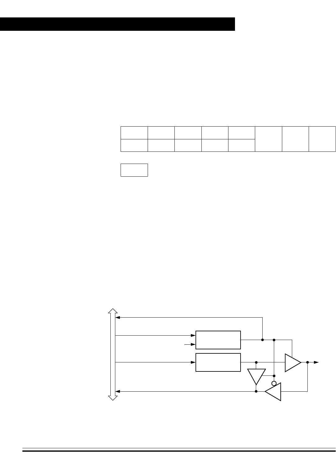
Input/Output Ports
Technical Data MC68HC08AZ60 — Rev 1.1
320 Input/Output Ports Freescale Semiconductor
21.9.2 Data Direction Register G
Data direction register G determines whether each port G pin is an input
or an output. Writing a logic 1 to a DDRG bit enables the output buffer
for the corresponding port G pin; a logic 0 disables the output buffer.
DDRG[2:0] — Data Direction Register G Bits
These read/write bits control port G data direction. Reset clears
DDRG[2:0], configuring all port G pins as inputs.
1 = Corresponding port G pin configured as output
0 = Corresponding port G pin configured as input
NOTE: Avoid glitches on port G pins by writing to the port G data register before
changing data direction register G bits from 0 to 1.
Figure 21-21 shows the port G I/O logic.
Figure 21-21. Port G I/O Circuit
Address: $000E
Bit 7654321Bit 0
Read: 00000
DDRG2 DDRG1 DDRG0
Write:RRRRR
Reset:00000000
R= Reserved
Figure 21-20. Data Direction Register G (DDRG)
READ DDRG ($000E)
WRITE DDRG ($000E)
RESET
WRITE PTG ($000A)
READ PTG ($000A)
PTGx
DDRGx
PTGx
INTERNAL DATA BUS

Input/Output Ports
Port H
MC68HC08AZ60 — Rev 1.1 Technical Data
Freescale Semiconductor Input/Output Ports 321
When bit DDRGx is a logic 1, reading address $000A reads the PTGx
data latch. When bit DDRGx is a logic 0, reading address $000A reads
the voltage level on the pin. The data latch can always be written,
regardless of the state of its data direction bit. Table 21-7 summarizes
the operation of the port G pins.
21.10 Port H
Port H is a 2-bit special function port that shares all of its pins with the
keyboard interrupt module (KBD).
21.10.1 Port H Data Register
The port H data register contains a data latch for each of the two port H
pins.
Table 21-7. Port G Pin Functions
DDRG
Bit PTG
Bit I/O Pin
Mode
Accesses
to DDRG Accesses to PTG
Read/Write Read Write
0 X Input, Hi-Z DDRG[2:0] Pin PTG[2:0](1)
1 X Output DDRG[2:0] PTG[2:0] PTG[2:0]
X = don’t care
Hi-Z = high impedance
1. Writing affects data register, but does not affect input.
Address: $000B
Bit 7654321Bit 0
Read: 000000
PTH1 PTH0
Write:RRRRRR
Reset: Unaffected by Reset
Alternate
Function: KBD4 KBD3
Figure 21-22. Port H Data Register (PTH)

Input/Output Ports
Technical Data MC68HC08AZ60 — Rev 1.1
322 Input/Output Ports Freescale Semiconductor
PTH[1:0] — Port H Data Bits
These read/write bits are software programmable. Data direction of
each port H pin is under the control of the corresponding bit in data
direction register H. Reset has no effect on PTH[1:0].
KBD[4:3] — Keyboard Wake-up pins
The keyboard interrupt enable bits, KBIE[4:3], in the keyboard
interrupt control register, enable the port H pins as external interrupt
pins (See Keyboard Module (KBD) on page 375).
21.10.2 Data Direction Register H
Data direction register H determines whether each port H pin is an input
or an output. Writing a logic 1 to a DDRH bit enables the output buffer for
the corresponding port H pin; a logic 0 disables the output buffer.
DDRH[1:0] — Data Direction Register H Bits
These read/write bits control port H data direction. Reset clears
DDRG[1:0], configuring all port H pins as inputs.
1 = Corresponding port H pin configured as output
0 = Corresponding port H pin configured as input
NOTE: Avoid glitches on port H pins by writing to the port H data register before
changing data direction register H bits from 0 to 1.
R= Reserved
Figure 21-22. Port H Data Register (PTH)
Address: $000F
Bit 7654321Bit 0
Read: 000000
DDRH1 DDRH0
Write:RRRRRR
Reset:00000000
R= Reserved
Figure 21-23. Data Direction Register H (DDRH)
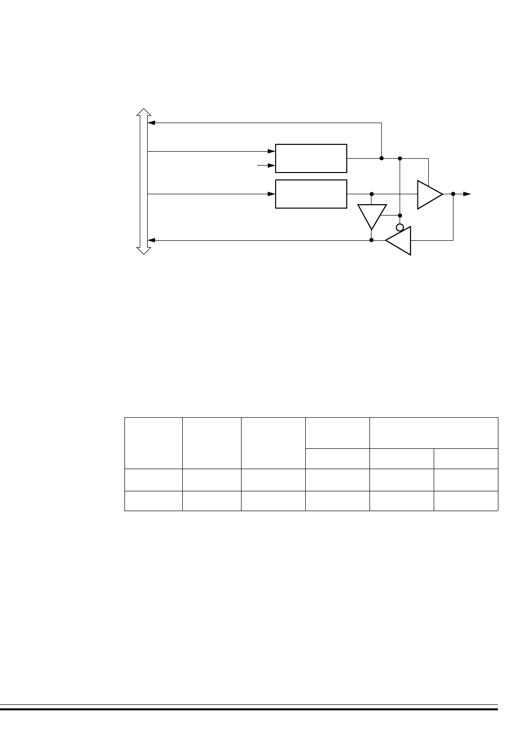
Input/Output Ports
Port H
MC68HC08AZ60 — Rev 1.1 Technical Data
Freescale Semiconductor Input/Output Ports 323
Figure 21-24 shows the port H I/O logic.
Figure 21-24. Port H I/O Circuit
When bit DDRHx is a logic 1, reading address $000B reads the PTHx
data latch. When bit DDRHx is a logic 0, reading address $000B reads
the voltage level on the pin. The data latch can always be written,
regardless of the state of its data direction bit. Table 21-8 summarizes
the operation of the port H pins.
Table 21-8. Port H Pin Functions
DDRH
Bit PTH
Bit I/O Pin
Mode
Accesses
to DDRH Accesses to PTH
Read/Write Read Write
0 X Input, Hi-Z DDRH[1:0] Pin PTH[1:0](1)
1 X Output DDRH[1:0] PTH[1:0] PTH[1:0]
X = don’t care
Hi-Z = high impedance
1. Writing affects data register, but does not affect input.
READ DDRH ($000F)
WRITE DDRH ($000F)
RESET
WRITE PTH ($000B)
READ PTH ($000B)
PTHx
DDRHx
PTHx
INTERNAL DATA BUS

Input/Output Ports
Technical Data MC68HC08AZ60 — Rev 1.1
324 Input/Output Ports Freescale Semiconductor

MC68HC08AZ60 — Rev 1.1 Technical Data
Freescale Semiconductor MSCAN Controller (MSCAN08) 325
Technical Data — MC68HC08AZ60
Section 22. MSCAN Controller (MSCAN08)
22.1 Contents
22.2 Introduction. . . . . . . . . . . . . . . . . . . . . . . . . . . . . . . . . . . . . .326
22.3 Features. . . . . . . . . . . . . . . . . . . . . . . . . . . . . . . . . . . . . . . . .327
22.4 External Pins. . . . . . . . . . . . . . . . . . . . . . . . . . . . . . . . . . . . .328
22.5 Message Storage . . . . . . . . . . . . . . . . . . . . . . . . . . . . . . . . .329
22.5.1 Background . . . . . . . . . . . . . . . . . . . . . . . . . . . . . . . . . . .329
22.5.2 Receive Structures. . . . . . . . . . . . . . . . . . . . . . . . . . . . . .330
22.5.3 Transmit Structures . . . . . . . . . . . . . . . . . . . . . . . . . . . . .333
22.6 Identifier Acceptance Filter . . . . . . . . . . . . . . . . . . . . . . . . .334
22.7 Interrupts. . . . . . . . . . . . . . . . . . . . . . . . . . . . . . . . . . . . . . . .339
22.7.1 Interrupt Acknowledge . . . . . . . . . . . . . . . . . . . . . . . . . .340
22.7.2 Interrupt Vectors . . . . . . . . . . . . . . . . . . . . . . . . . . . . . . .341
22.8 Protocol Violation Protection . . . . . . . . . . . . . . . . . . . . . . .341
22.9 Low Power Modes . . . . . . . . . . . . . . . . . . . . . . . . . . . . . . . .342
22.9.1 MSCAN08 Sleep Mode . . . . . . . . . . . . . . . . . . . . . . . . . . .343
22.9.2 MSCAN08 Soft Reset Mode. . . . . . . . . . . . . . . . . . . . . . .344
22.9.3 MSCAN08 Power Down Mode . . . . . . . . . . . . . . . . . . . . .345
22.9.4 CPU Wait Mode. . . . . . . . . . . . . . . . . . . . . . . . . . . . . . . . .345
22.9.5 Programmable Wakeup Function . . . . . . . . . . . . . . . . . .346
22.10 Timer Link . . . . . . . . . . . . . . . . . . . . . . . . . . . . . . . . . . . . . . .346
22.11 Clock System . . . . . . . . . . . . . . . . . . . . . . . . . . . . . . . . . . . .346
22.12 Memory Map . . . . . . . . . . . . . . . . . . . . . . . . . . . . . . . . . . . . .350
22.13 Programmer’s Model of Message Storage. . . . . . . . . . . . .350
22.13.1 Message Buffer Outline . . . . . . . . . . . . . . . . . . . . . . . . . .351
22.13.2 Identifier Registers. . . . . . . . . . . . . . . . . . . . . . . . . . . . . .351

MSCAN Controller (MSCAN08)
Technical Data MC68HC08AZ60 — Rev 1.1
326 MSCAN Controller (MSCAN08) Freescale Semiconductor
22.13.3 Data Length Register (DLR) . . . . . . . . . . . . . . . . . . . . . .355
22.13.4 Data Segment Registers (DSRn). . . . . . . . . . . . . . . . . . .355
22.13.5 Transmit Buffer Priority Registers . . . . . . . . . . . . . . . . .356
22.14 Programmer’s Model of Control Registers . . . . . . . . . . . .356
22.14.1 MSCAN08 Module Control Register 0 . . . . . . . . . . . . . .359
22.14.2 MSCAN08 Module Control Register 1 . . . . . . . . . . . . . .361
22.14.3 MSCAN08 Bus Timing Register 0 . . . . . . . . . . . . . . . . . .362
22.14.4 MSCAN08 Bus Timing Register 1 . . . . . . . . . . . . . . . . . .363
22.14.5 MSCAN08 Receiver Flag Register (CRFLG). . . . . . . . . .365
22.14.6 MSCAN08 Receiver Interrupt Enable Register . . . . . . .367
22.14.7 MSCAN08 Transmitter Flag Register . . . . . . . . . . . . . . .369
22.14.8 MSCAN08 Transmitter Control Register . . . . . . . . . . . .370
22.14.9 MSCAN08 Identifier Acceptance Control Register . . . .371
22.14.10 MSCAN08 Receive Error Counter. . . . . . . . . . . . . . . . . .373
22.14.11 MSCAN08 Transmit Error Counter . . . . . . . . . . . . . . . . .373
22.14.12 MSCAN08 Identifier Acceptance Registers . . . . . . . . . .374
22.14.13 MSCAN08 Identifier Mask Registers (CIDMR0-3) . . . . .375
22.2 Introduction
The MSCAN08 is the specific implementation of the scalable controller
area network (MSCAN) concept targeted for the Freescale M68HC08
Microcontroller Family.
The module is a communication controller implementing the CAN 2.0
A/B protocol as defined in the BOSCH specification dated September
1991.
The CAN protocol was primarily, but not exclusively, designed to be
used as a vehicle serial data bus, meeting the specific requirements of
this field: real-time processing, reliable operation in the electromagnetic
interference (EMI) environment of a vehicle, cost-effectiveness and
required bandwidth.
MSCAN08 utilizes an advanced buffer arrangement, resulting in a
predictable real-time behavior, and simplifies the application software.

MSCAN Controller (MSCAN08)
Features
MC68HC08AZ60 — Rev 1.1 Technical Data
Freescale Semiconductor MSCAN Controller (MSCAN08) 327
22.3 Features
Basic features of the MSCAN08 are:
• Modular Architecture
• Implementation of the CAN Protocol — Version 2.0A/B
– Standard and Extended Data Frames.
– 0–8 Bytes Data Length.
– Programmable Bit Rate up to 1 Mbps Depending on the Actual
Bit Timing and the Clock Jitter of the PLL
• Support for Remote Frames
• Double-Buffered Receive Storage Scheme
• Triple-Buffered Transmit Storage Scheme with Internal
Prioritisation Using a “Local Priority” Concept
• Flexible Maskable Identifier Filter Supports Alternatively One Full
Size Extended Identifier Filter or Two 16-Bit Filters or Four 8-Bit
Filters
• Programmable Wakeup Functionality with Integrated Low-Pass
Filter
• Programmable Loop-Back Mode Supports Self-Test Operation
• Separate Signalling and Interrupt Capabilities for All CAN
Receiver and Transmitter Error States (Warning, Error Passive,
Bus Off)
• Programmable MSCAN08 Clock Source Either CPU Bus Clock or
Crystal Oscillator Output
• Programmable Link to On-Chip Timer Interface Module (TIMB) for
Time-Stamping and Network Synchronization
• Low-Power Sleep Mode
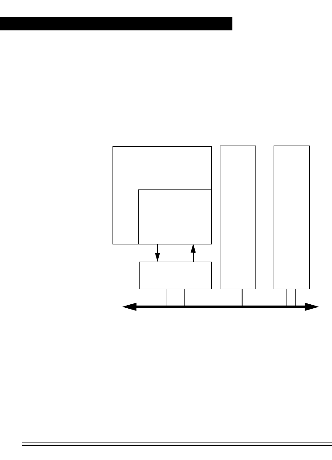
MSCAN Controller (MSCAN08)
Technical Data MC68HC08AZ60 — Rev 1.1
328 MSCAN Controller (MSCAN08) Freescale Semiconductor
22.4 External Pins
The MSCAN08 uses two external pins, one input (RxCAN) and one
output (TxCAN). The TxCAN output pin represents the logic level on the
CAN: 0 is for a dominant state, and 1 is for a recessive state.
A typical CAN system with MSCAN08 is shown in Figure 22-1.
Figure 22-1. The CAN System
Each CAN station is connected physically to the CAN bus lines through
a transceiver chip. The transceiver is capable of driving the large current
needed for the CAN and has current protection against defective CAN or
defective stations.
C A N BUS
CAN CONTROLLER
(MSCAN08)
TRANSCEIVER
CAN NODE 1
CAN STATION 1
CAN NODE 2 CAN NODE N
CAN_L
CAN_H
TXCAN RXCAN
MCU

MSCAN Controller (MSCAN08)
Message Storage
MC68HC08AZ60 — Rev 1.1 Technical Data
Freescale Semiconductor MSCAN Controller (MSCAN08) 329
22.5 Message Storage
MSCAN08 facilitates a sophisticated message storage system which
addresses the requirements of a broad range of network applications.
22.5.1 Background
Modern application layer software is built under two fundamental
assumptions:
1. Any CAN node is able to send out a stream of scheduled
messages without releasing the bus between two messages.
Such nodes will arbitrate for the bus right after sending the
previous message and will only release the bus in case of lost
arbitration.
2. The internal message queue within any CAN node is organized as
such that the highest priority message will be sent out first if more
than one message is ready to be sent.
Above behaviour cannot be achieved with a single transmit buffer. That
buffer must be reloaded right after the previous message has been sent.
This loading process lasts a definite amount of time and has to be
completed within the inter-frame sequence (IFS) to be able to send an
uninterrupted stream of messages. Even if this is feasible for limited
CAN bus speeds, it requires that the CPU reacts with short latencies to
the transmit interrupt.
A double buffer scheme would de-couple the re-loading of the transmit
buffers from the actual message being sent and as such reduces the
reactiveness requirements on the CPU. Problems may arise if the
sending of a message would be finished just while the CPU re-loads the
second buffer. In that case, no buffer would then be ready for
transmission and the bus would be released.
At least three transmit buffers are required to meet the first of the above
requirements under all circumstances. The MSCAN08 has three
transmit buffers.

MSCAN Controller (MSCAN08)
Technical Data MC68HC08AZ60 — Rev 1.1
330 MSCAN Controller (MSCAN08) Freescale Semiconductor
The second requirement calls for some sort of internal prioritisation
which the MSCAN08 implements with the “local priority” concept
described in Receive Structures on page 330.
22.5.2 Receive Structures
The received messages are stored in a 2-stage input first in first out
(FIFO). The two message buffers are mapped using a Ping Pong
arrangement into a single memory area (see Figure 22-2). While the
background receive buffer (RxBG) is exclusively associated to the
MSCAN08, the foreground receive buffer (RxFG) is addressable by the
CPU08. This scheme simplifies the handler software, because only one
address area is applicable for the receive process.
Both buffers have a size of 13 bytes to store the CAN control bits, the
identifier (standard or extended), and the data content (for details, see
Programmer’s Model of Message Storage on page 350).
The receiver full flag (RXF) in the MSCAN08 receiver flag register
(CRFLG) (see MSCAN08 Receiver Flag Register (CRFLG) on page
365), signals the status of the foreground receive buffer. When the buffer
contains a correctly received message with matching identifier, this flag
is set.
On reception, each message is checked to see if it passes the filter (for
details see Identifier Acceptance Filter on page 334) and in parallel is
written into RxBG. The MSCAN08 copies the content of RxBG into
RxFG(1), sets the RXF flag, and generates a receive interrupt to the
CPU(2). The user’s receive handler has to read the received message
from RxFG and to reset the RXF flag to acknowledge the interrupt and
to release the foreground buffer. A new message which can follow
immediately after the IFS field of the CAN frame, is received into RxBG.
The overwriting of the background buffer is independent of the identifier
filter function.
1. Only if the RXF flag is not set.
2. The receive interrupt will occur only if not masked. A polling scheme can be applied on RXF
also.

MSCAN Controller (MSCAN08)
Message Storage
MC68HC08AZ60 — Rev 1.1 Technical Data
Freescale Semiconductor MSCAN Controller (MSCAN08) 331
When the MSCAN08 module is transmitting, the MSCAN08 receives its
own messages into the background receive buffer, RxBG. It does NOT
overwrite RxFG, generate a receive interrupt or acknowledge its own
messages on the CAN bus. The exception to this rule is in loop-back
mode (see MSCAN08 Module Control Register 1 on page 361), where
the MSCAN08 treats its own messages exactly like all other incoming
messages. The MSCAN08 receives its own transmitted messages in the
event that it loses arbitration. If arbitration is lost, the MSCAN08 must be
prepared to become receiver.
An overrun condition occurs when both the foreground and the
background receive message buffers are filled with correctly received
messages with accepted identifiers and another message is correctly
received from the bus with an accepted identifier. The latter message will
be discarded and an error interrupt with overrun indication will be
generated if enabled. The MSCAN08 is still able to transmit messages
with both receive message buffers filled, but all incoming messages are
discarded.
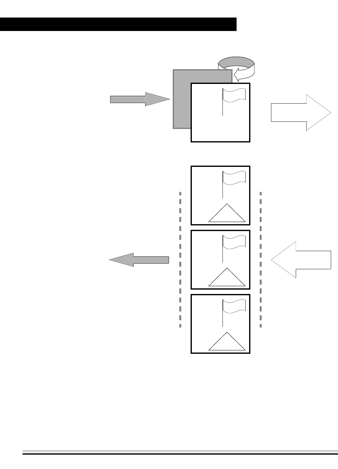
MSCAN Controller (MSCAN08)
Technical Data MC68HC08AZ60 — Rev 1.1
332 MSCAN Controller (MSCAN08) Freescale Semiconductor
Figure 22-2. User Model for Message Buffer Organization
RxFG
RxBG
Tx0
RXF
TXE
PRIO
Tx1 TXE
PRIO
Tx2 TXE
PRIO
MSCAN08 CPU08 Ibus

MSCAN Controller (MSCAN08)
Message Storage
MC68HC08AZ60 — Rev 1.1 Technical Data
Freescale Semiconductor MSCAN Controller (MSCAN08) 333
22.5.3 Transmit Structures
The MSCAN08 has a triple transmit buffer scheme to allow multiple
messages to be set up in advance and to achieve an optimized real-time
performance. The three buffers are arranged as shown in Figure 22-2.
All three buffers have a 13-byte data structure similar to the outline of the
receive buffers (see Programmer’s Model of Message Storage on
page 350). An additional transmit buffer priority register (TBPR) contains
an 8-bit “local priority” field (PRIO) (see Transmit Buffer Priority
Registers on page 356).
To transmit a message, the CPU08 has to identify an available transmit
buffer which is indicated by a set transmit buffer empty (TXE) flag in the
MSCAN08 transmitter flag register (CTFLG) (see MSCAN08
Transmitter Flag Register on page 369).
The CPU08 then stores the identifier, the control bits and the data
content into one of the transmit buffers. Finally, the buffer has to be
flagged ready for transmission by clearing the TXE flag.
The MSCAN08 then will schedule the message for transmission and will
signal the successful transmission of the buffer by setting the TXE flag.
A transmit interrupt is generated(1) when TXE is set and can be used to
drive the application software to re-load the buffer.
In case more than one buffer is scheduled for transmission when the
CAN bus becomes available for arbitration, the MSCAN08 uses the local
priority setting of the three buffers for prioritisation. For this purpose,
every transmit buffer has an 8-bit local priority field (PRIO). The
application software sets this field when the message is set up. The local
priority reflects the priority of this particular message relative to the set
of messages being emitted from this node. The lowest binary value of
the PRIO field is defined as the highest priority.
1. The transmit interrupt will occur only if not masked. A polling scheme can be applied on TXE
also.

MSCAN Controller (MSCAN08)
Technical Data MC68HC08AZ60 — Rev 1.1
334 MSCAN Controller (MSCAN08) Freescale Semiconductor
The internal scheduling process takes place whenever the MSCAN08
arbitrates for the bus. This is also the case after the occurrence of a
transmission error.
When a high priority message is scheduled by the application software,
it may become necessary to abort a lower priority message being set up
in one of the three transmit buffers. As messages that are already under
transmission cannot be aborted, the user has to request the abort by
setting the corresponding abort request flag (ABTRQ) in the
transmission control register (CTCR). The MSCAN08 will then grant the
request, if possible, by setting the corresponding abort request
acknowledge (ABTAK) and the TXE flag in order to release the buffer
and by generating a transmit interrupt. The transmit interrupt handler
software can tell from the setting of the ABTAK flag whether the
message was actually aborted (ABTAK = 1) or sent (ABTAK = 0).
22.6 Identifier Acceptance Filter
The Identifier Acceptance Registers (CIDAR0-3) define the acceptance
patterns of the standard or extended identifier (ID10-ID0 or ID28-ID0).
Any of these bits can be marked ‘don’t care’ in the Identifier Mask
Registers (CIDMR0-3).
A filter hit is indicated to the application on software by a set RXF
(Receive Buffer Full Flag, see MSCAN08 Receiver Flag Register
(CRFLG) on page 365) and two bits in the Identifier Acceptance Control
Register (see MSCAN08 Identifier Acceptance Control Register on
page 371). These Identifier Hit Flags (IDHIT1-0) clearly identify the filter
section that caused the acceptance. They simplify the application
software’s task to identify the cause of the receiver interrupt. In case that
more than one hit occurs (two or more filters match) the lower hit has
priority.
A very flexible programmable generic identifier acceptance filter has
been introduced to reduce the CPU interrupt loading. The filter is
programmable to operate in four different modes:
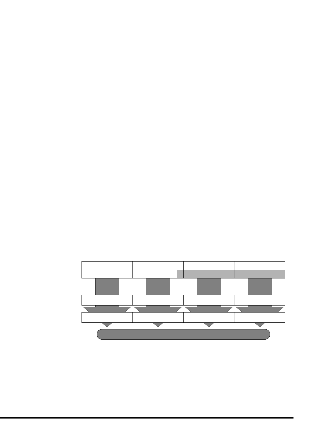
MSCAN Controller (MSCAN08)
Identifier Acceptance Filter
MC68HC08AZ60 — Rev 1.1 Technical Data
Freescale Semiconductor MSCAN Controller (MSCAN08) 335
• Single identifier acceptance filter, each to be applied to a) the full
29 bits of the extended identifier and to the following bits of the
CAN frame: RTR, IDE, SRR or b) the 11 bits of the standard
identifier plus the RTR and IDE bits of CAN 2.0A/B messages.
This mode implements a single filter for a full length CAN 2.0B
compliant extended identifier. Figure 22-3 shows how the 32-bit
filter bank (CIDAR0-3, CIDMR0-3) produces a filter 0 hit.
• Two identifier acceptance filters, each to be applied to a) the 14
most significant bits of the extended identifier plus the SRR and
the IDE bits of CAN2.0B messages, or b) the 11 bits of the
identifier plus the RTR and IDE bits of CAN 2.0A/B messages.
Figure 22-4 shows how the 32-bit filter bank (CIDAR0-3,
CIDMR0-3) produces filter 0 and 1 hits.
• Four identifier acceptance filters, each to be applied to the first
eight bits of the identifier. This mode implements four independent
filters for the first eight bits of a CAN 2.0A/B compliant standard
identifier. Figure 22-5 shows how the 32-bit filter bank (CIDAR0-
3, CIDMR0-3) produces filter 0 to 3 hits.
• Closed filter. No CAN message will be copied into the foreground
buffer RxFG, and the RXF flag will never be set.
Figure 22-3. Single 32-Bit Maskable Identifier Acceptance Filter
ID28 ID21IDR0
ID10 ID3IDR0
ID20 ID15IDR1
ID2 IDEIDR1
ID14 ID7IDR2
ID10 ID3IDR2
ID6 RTRIDR3
ID10 ID3IDR3
AC7 AC0CIDAR0
AM7 AM0CIDMR0
AC7 AC0CIDAR1
AM7 AM0CIDMR1
AC7 AC0CIDAR2
AM7 AM0CIDMR2
AC7 AC0CIDAR3
AM7 AM0CIDMR3
ID Accepted (Filter 0 Hit)
MSCAN Controller (MSCAN08)
Technical Data MC68HC08AZ60 — Rev 1.1
336 MSCAN Controller (MSCAN08) Freescale Semiconductor
Figure 22-4. Dual 16-Bit Maskable Acceptance Filters
ID28 ID21IDR0
ID10 ID3IDR0
ID20 ID15IDR1
ID2 IDEIDR1
ID14 ID7IDR2
ID10 ID3IDR2
ID6 RTRIDR3
ID10 ID3IDR3
AC7 AC0CIDAR0
AM7 AM0CIDMR0
AC7 AC0CIDAR1
AM7 AM0CIDMR1
ID ACCEPTED (FILTER 0 HIT)
AC7 AC0CIDAR2
AM7 AM0CIDMR2
AC7 AC0CIDAR3
AM7 AM0CIDMR3
ID ACCEPTED (FILTER 1 HIT)
MSCAN Controller (MSCAN08)
Identifier Acceptance Filter
MC68HC08AZ60 — Rev 1.1 Technical Data
Freescale Semiconductor MSCAN Controller (MSCAN08) 337
.
Figure 22-5. Quadruple 8-Bit Maskable Acceptance Filters
AC7 AC0CIDAR3
AM7 AM0CIDMR3
ID ACCEPTED (FILTER 3 HIT)
AC7 AC0CIDAR2
AM7 AM0CIDMR2
ID ACCEPTED (FILTER 2 HIT)
AC7 AC0CIDAR1
AM7 AM0CIDMR1
ID ACCEPTED (FILTER 1 HIT)
ID28 ID21IDR0
ID10 ID3IDR0
ID20 ID15IDR1
ID2 IDEIDR1
ID14 ID7IDR2
ID10 ID3IDR2
ID6 RTRIDR3
ID10 ID3IDR3
AC7 AC0CIDAR0
AM7 AM0CIDMR0
ID ACCEPTED (FILTER 0 HIT)

MSCAN Controller (MSCAN08)
Technical Data MC68HC08AZ60 — Rev 1.1
338 MSCAN Controller (MSCAN08) Freescale Semiconductor
22.6.1 MSCAN Extended ID Rejected if Stuff Bit Between ID16 and ID15
For 32-bit and 16-bit identifier acceptance modes, an extended ID CAN
frame with a stuff bit between ID16 and ID15 can be erroneously
rejected, depending on IDAR0, IDAR1, and IDMR1.
Extended IDs (ID28-ID0) which generate a stuff bit between ID16 and
ID15:
where x = 0 or 1 (don't care)
* = pattern for ID28 to ID18 (see following).
Affected extended IDs (ID28 - ID18) patterns:
a) xxxxxxxxx01 exceptions: 00000000001
01111100001
xxxx1000001 except
11111000001
b) xxxxx100000 exception: 01111100000
c) xxxx0111111 exception: 00000111111
d) x0111110000
e) 10000000000
f) 11111111111
g) 10000011111
When an affected ID is received, an incorrect value is compared to the
2nd byte of the filter (IDAR1 and IDAR5, plus IDAR3 and IDAR7 in 16-
bit mode). This incorrect value is the shift register contents before ID15
is shifted in (i.e. right shifted by 1).
22.6.1.1 Work- around
If the problematic IDs cannot be avoided, the workaround is to mask
certain bits with IDMR1 (and IDMR5, plus IDMR3 and IDMR7 in 16-bit
mode).
IDAR0 IDAR1 IDAR2 IDAR3
******** ***1111x xxxxxxxx xxxxxxxx

MSCAN Controller (MSCAN08)
Interrupts
MC68HC08AZ60 — Rev 1.1 Technical Data
Freescale Semiconductor MSCAN Controller (MSCAN08) 339
Example 1: to receive the message IDs
xxxx xxxx x011 111x xxxx xxxx xxxx xxxx
IDMR1 etc. must be 111x xxx1, i.e. ID20,19,18,15 must be masked.
Example 2: to receive the message IDs
xxxx 0111 1111 111x xxxx xxxx xxxx xxxx
IDMR1 etc. must be 1xxx xxx1, i.e. ID20 and ID15 must be masked.
In general, using IDMR1 etc. 1111 xxx1, i.e. masking
ID20,19,18,SRR,15, hides the problem.
22.7 Interrupts
The MSCAN08 supports four interrupt vectors mapped onto eleven
different interrupt sources, any of which can be individually masked (for
details see MSCAN08 Receiver Flag Register (CRFLG) on page 365,
to MSCAN08 Transmitter Control Register on page 370).
•Transmit Interrupt: At least one of the three transmit buffers is
empty (not scheduled) and can be loaded to schedule a message
for transmission. The TXE flags of the empty message buffers are
set.
•Receive Interrupt: A message has been received successfully and
loaded into the foreground receive buffer. This interrupt will be
emitted immediately after receiving the EOF symbol. The RXF flag
is set.
•Wakeup Interrupt: An activity on the CAN bus occurred during
MSCAN08 internal sleep mode or power-down mode (provided
SLPAK = WUPIE = 1).
•Error Interrupt: An overrun, error, or warning condition occurred.
The receiver flag register (CRFLG) will indicate one of the
following conditions:
–Overrun: An overrun condition as described in Receive
Structures on page 330, has occurred.
–Receiver Warning: The receive error counter has reached the
CPU Warning limit of 96.

MSCAN Controller (MSCAN08)
Technical Data MC68HC08AZ60 — Rev 1.1
340 MSCAN Controller (MSCAN08) Freescale Semiconductor
–Transmitter Warning: The transmit error counter has reached
the CPU Warning limit of 96.
–Receiver Error Passive: The receive error counter has
exceeded the error passive limit of 127 and MSCAN08 has
gone to error passive state.
–Transmitter Error Passive: The transmit error counter has
exceeded the error passive limit of 127 and MSCAN08 has
gone to error passive state.
–Bus Off: The transmit error counter has exceeded 255 and
MSCAN08 has gone to bus off state.
22.7.1 Interrupt Acknowledge
Interrupts are directly associated with one or more status flags in either
the MSCAN08 receiver flag register (CRFLG) or the MSCAN08
transmitter flag register (CTFLG). Interrupts are pending as long as one
of the corresponding flags is set. The flags in the above registers must
be reset within the interrupt handler in order to handshake the interrupt.
The flags are reset through writing a ‘1’ to the corresponding bit position.
A flag cannot be cleared if the respective condition still prevails.
NOTE: Bit manipulation instructions (BSET) shall not be used to clear interrupt
flags.

MSCAN Controller (MSCAN08)
Protocol Violation Protection
MC68HC08AZ60 — Rev 1.1 Technical Data
Freescale Semiconductor MSCAN Controller (MSCAN08) 341
22.7.2 Interrupt Vectors
The MSCAN08 supports four interrupt vectors as shown in Table 22-1.
The vector addresses and the relative interrupt priority are defined in
Table 2-1.
22.8 Protocol Violation Protection
The MSCAN08 will protect the user from accidentally violating the CAN
protocol through programming errors. The protection logic implements
the following features:
• The receive and transmit error counters cannot be written or
otherwise manipulated.
• All registers which control the configuration of the MSCAN08 can
not be modified while the MSCAN08 is on-line. The SFTRES bit in
the MSCAN08 module control register (see MSCAN08 Module
Control Register 0 on page 359) serves as a lock to protect the
following registers:
– MSCAN08 module control register 1 (CMCR1)
– MSCAN08 bus timing register 0 and 1 (CBTR0 and CBTR1)
– MSCAN08 identifier acceptance control register (CIDAC)
– MSCAN08 identifier acceptance registers (CIDAR0–3)
Table 22-1. MSCAN08 Interrupt Vector Addresses
Function Source Local
Mask Global
Mask
Wakeup WUPIF WUPIE
I Bit
Error
Interrupts
RWRNIF RWRNIE
TWRNIF TWRNIE
RERRIF RERRIE
TERRIF TERRIE
BOFFIF BOFFIE
OVRIF OVRIE
Receive RXF RXFIE
Transmit
TXE0 TXEIE0
TXE1 TXEIE1
TXE2 TXEIE2

MSCAN Controller (MSCAN08)
Technical Data MC68HC08AZ60 — Rev 1.1
342 MSCAN Controller (MSCAN08) Freescale Semiconductor
– MSCAN08 identifier mask registers (CIDMR0–3)
• The TxCAN pin is forced to recessive when the MSCAN08 is in
any of the Low Power Modes.
22.9 Low Power Modes
In addition to normal mode, the MSCAN08 has three modes with
reduced power consumption: Sleep, Soft Reset and Power Down
modes. In Sleep and Soft Reset mode, power consumption is reduced
by stopping all clocks except those to access the registers. In Power
Down mode, all clocks are stopped and no power is consumed.
The WAIT and STOP instructions put the MCU in low power
consumption stand-by modes. summarizes the combinations of
MSCAN08 and CPU modes. A particular combination of modes is
entered for the given settings of the bits SLPAK and SFTRES. For all
modes, an MSCAN wake-up interrupt can occur only if
SLPAK=WUPIE=1.
.
Table 22-2 MSCAN08 vs CPU Operating Modes
MSCAN Mode CPU Mode
STOP WAIT or RUN
Power Down SLPAK = X(1)
SFTRES = X
1. ‘X’ means don’t care.
Sleep SLPAK = 1
SFTRES = 0
Soft Reset SLPAK = 0
SFTRES = 1
Normal SLPAK = 0
SFTRES = 0

MSCAN Controller (MSCAN08)
Low Power Modes
MC68HC08AZ60 — Rev 1.1 Technical Data
Freescale Semiconductor MSCAN Controller (MSCAN08) 343
22.9.1 MSCAN08 Sleep Mode
The CPU can request the MSCAN08 to enter the low-power mode by
asserting the SLPRQ bit in the module configuration register (see Figure
22-6). The time when the MSCAN08 enters Sleep mode depends on its
activity:
• if it is transmitting, it continues to transmit until there is no more
message to be transmitted, and then goes into Sleep mode
• if it is receiving, it waits for the end of this message and then goes
into Sleep mode
• if it is neither transmitting or receiving, it will immediately go into
Sleep mode
NOTE: The application software must avoid setting up a transmission (by
clearing or more TXE flags) and immediately request Sleep mode (by
setting SLPRQ). It then depends on the exact sequence of operations
whether MSCAN08 starts transmitting or goes into Sleep mode directly.
During Sleep mode, the SLPAK flag is set. The application software
should use SLPAK as a handshake indication for the request (SLPRQ)
to go into Sleep mode. When in Sleep mode, the MSCAN08 stops its
internal clocks. However, clocks to allow register accesses still run. If the
MSCAN08 is in buss-off state, it stops counting the 128*11 consecutive
recessive bits due to the stopped clocks. The TxCAN pin stays in
recessive state. If RXF=1, the message can be read and RXF can be
cleared. Copying of RxGB into RxFG doesn’t take place while in Sleep
mode. It is possible to access the transmit buffers and to clear the TXE
flags. No message abort takes place while in Sleep mode.
The MSCAN08 leaves Sleep mode (wake-up) when:
• bus activity occurs or
• the MCU clears the SLPRQ bit or
• the MCU sets the SFTRES bit
MSCAN Controller (MSCAN08)
Technical Data MC68HC08AZ60 — Rev 1.1
344 MSCAN Controller (MSCAN08) Freescale Semiconductor
Figure 22-6. Sleep Request/Acknowledge Cycle
NOTE: The MCU cannot clear the SLPRQ bit before the MSCAN08 is in Sleep
mode (SLPAK=1).
After wake-up, the MSCAN08 waits for 11 consecutive recessive bits to
synchronize to the bus. As a consequence, if the MSCAN08 is woken-
up by a CAN frame, this frame is not received. The receive message
buffers (RxFG and RxBG) contain messages if they were received
before Sleep mode was entered. All pending actions are executed upon
wake-up: copying of RxBG into RxFG, message aborts and message
transmissions. If the MSCAN08 is still in bus-off state after Sleep mode
was left, it continues counting the 128*11 consecutive recessive bits.
22.9.2 MSCAN08 Soft Reset Mode
In Soft Reset mode, the MSCAN08 is stopped. Registers can still be
accessed. This mode is used to initialize the module configuration, bit
timing and the CAN message filter. See MSCAN08 Module Control
Register 0 on page 359 for a complete description of the Soft Reset
mode.
MSCAN08 Running
SLPRQ = 0
SLPAK = 0
Sleep Request
SLPRQ = 1
SLPAK = 0
MSCAN08 Sleeping
SLPRQ = 1
SLPAK = 1
MCU
MSCAN08
MCU
or MSCAN08

MSCAN Controller (MSCAN08)
Low Power Modes
MC68HC08AZ60 — Rev 1.1 Technical Data
Freescale Semiconductor MSCAN Controller (MSCAN08) 345
When setting the SFTRES bit, the MSCAN08 immediately stops all
ongoing transmissions and receptions, potentially causing CAN protocol
violations.
NOTE: The user is responsible to take care that the MSCAN08 is not active
when Soft Reset mode is entered. The recommended procedure is to
bring the MSCAN08 into Sleep mode before the SFTRES bit is set.
22.9.3 MSCAN08 Power Down Mode
The MSCAN08 is in Power Down mode when the CPU is in Stop mode.
When entering the Power Down mode, the MSCAN08 immediately stops
all ongoing transmissions and receptions, potentially causing CAN
protocol violations.
NOTE: The user is responsible to take care that the MSCAN08 is not active
when Power Down mode is entered. The recommended procedure is to
bring the MSCAN08 into Sleep mode before the STOP instruction is
executed.
To protect the CAN bus system from fatal consequences of violations to
the above rule, the MSCAN08 drives the TxCAN pin into recessive state.
In Power Down mode, no registers can be accessed.
MSCAN08 bus activity can wake the MCU from CPU Stop/MSCAN08
power-down mode. However, until the oscillator starts up and
synchronisation is achieved the MSCAN08 will not respond to incoming
data.
22.9.4 CPU Wait Mode
The MSCAN08 module remains active during CPU wait mode. The
MSCAN08 will stay synchronized to the CAN bus and generates
transmit, receive, and error interrupts to the CPU, if enabled. Any such
interrupt will bring the MCU out of wait mode.

MSCAN Controller (MSCAN08)
Technical Data MC68HC08AZ60 — Rev 1.1
346 MSCAN Controller (MSCAN08) Freescale Semiconductor
22.9.5 Programmable Wakeup Function
The MSCAN08 can be programmed to apply a low-pass filter function to
the RxCAN input line while in internal sleep mode (see information on
control bit WUPM in MSCAN08 Module Control Register 1 on page
361). This feature can be used to protect the MSCAN08 from wake-up
due to short glitches on the CAN bus lines. Such glitches can result from
electromagnetic inference within noisy environments.
22.10 Timer Link
The MSCAN08 will generate a timer signal whenever a valid frame has
been received. Because the CAN specification defines a frame to be
valid if no errors occurred before the EOF field has been transmitted
successfully, the timer signal will be generated right after the EOF. A
pulse of one bit time is generated. As the MSCAN08 receiver engine also
receives the frames being sent by itself, a timer signal also will be
generated after a successful transmission.
The previously described timer signal can be routed into the on-chip
Timer Interface Module B (TIMB).This signal is connected to the
Channel 0 input under the control of the timer link enable (TLNKEN) bit
in the CMCR0.
After the TIMB module has been programmed to capture rising edge
events, it can be used under software control to generate 16-bit time
stamps which can be stored with the received message.
22.11 Clock System
Figure 22-7 shows the structure of the MSCAN08 clock generation
circuitry and its interaction with the clock generation module (CGM).
With this flexible clocking scheme the MSCAN08 is able to handle CAN
bus rates ranging from 10 kbps up to 1 Mbps.
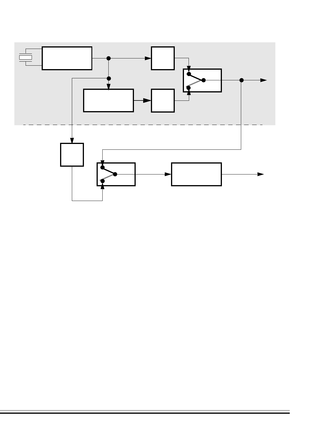
MSCAN Controller (MSCAN08)
Clock System
MC68HC08AZ60 — Rev 1.1 Technical Data
Freescale Semiconductor MSCAN Controller (MSCAN08) 347
Figure 22-7. Clocking Scheme
The clock source bit (CLKSRC) in the MSCAN08 module control register
(CMCR1) (see MSCAN08 Module Control Register 0 on page 359)
defines whether the MSCAN08 is connected to the output of the crystal
oscillator or to the PLL output.
The clock source has to be chosen such that the tight oscillator tolerance
requirements (up to 0.4%) of the CAN protocol are met.
NOTE: If the system clock is generated from a PLL, it is recommended to select
the crystal clock source rather than the system clock source due to jitter
considerations, especially at faster CAN bus rates.
A programmable prescaler is used to generate out of the MSCAN08
clock the time quanta (Tq) clock. A time quantum is the atomic unit of
time handled by the MSCAN08.
PLL
÷ 2
MSCAN08
PRESCALER
(1 .. 64)
OSC
CGMXCLK
÷ 2
CGMOUT
(TO SIM)
CGM
÷ 2
CLKSRC
MSCANCLK
(2 * BUS FREQ.)
BCS

MSCAN Controller (MSCAN08)
Technical Data MC68HC08AZ60 — Rev 1.1
348 MSCAN Controller (MSCAN08) Freescale Semiconductor
A bit time is subdivided into three segments(1)(see Figure 22-8).
• SYNC_SEG: This segment has a fixed length of one time
quantum. Signal edges are expected to happen within this section.
• Time segment 1: This segment includes the PROP_SEG and the
PHASE_SEG1 of the CAN standard. It can be programmed by
setting the parameter TSEG1 to consist of 4 to 16 time quanta.
• Time segment 2: This segment represents PHASE_SEG2 of the
CAN standard. It can be programmed by setting the TSEG2
parameter to be 2 to 8 time quanta long.
The synchronization jump width (SJW) can be programmed in a range
of 1 to 4 time quanta by setting the SJW parameter.
The above parameters can be set by programming the bus timing
registers, CBTR0–CBTR1, see MSCAN08 Bus Timing Register 0 on
page 362 and MSCAN08 Bus Timing Register 1 on page 363).
NOTE: It is the user’s responsibility to make sure that the bit timing settings are
in compliance with the CAN standard,
Table 22-8 gives an overview on the CAN conforming segment settings
and the related parameter values.
1. For further explanation of the underlying concepts please refer to ISO/DIS 11 519-1, Section
10.3.
fTq = fMSCANCLK
Presc value
Bit rate= No. of time quanta
fTq
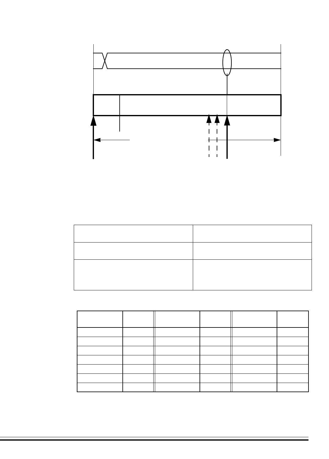
MSCAN Controller (MSCAN08)
Clock System
MC68HC08AZ60 — Rev 1.1 Technical Data
Freescale Semiconductor MSCAN Controller (MSCAN08) 349
Figure 22-8. Segments Within the Bit Time
Table 22-3. Time segment syntax
SYNC_SEG System expects transitions to occur on the bus
during this period.
Transmit point A node in transmit mode will transfer a new
value to the CAN bus at this point.
Sample point
A node in receive mode will sample the bus at
this point. If the three samples per bit option is
selected then this point marks the position of
the third sample.
Time
Segment 1 TSEG1 Time
Segment 2 TSEG2 Synchron.
Jump Width SJW
5 .. 10 4 .. 9 2 1 1 .. 2 0 .. 1
4 .. 11 3 .. 10 3 2 1 .. 3 0 .. 2
5 .. 12 4 .. 11 4 3 1 .. 4 0 .. 3
6 .. 13 5 .. 12 5 4 1 .. 4 0 .. 3
7 .. 14 6 .. 13 6 5 1 .. 4 0 .. 3
8 .. 15 7 .. 14 7 6 1 .. 4 0 .. 3
9 .. 16 8 .. 15 8 7 1 .. 4 0 .. 3
Table 22-4. CAN Standard Compliant Bit Time Segment Settings
SYNC
_SEG TIME SEGMENT 1 TIME SEG. 2
1 4 ... 16 2 ... 8
8... 25 TIME QUANTA
= 1 BIT TIME
NRZ SIGNAL
SAMPLE POINT
(SINGLE OR TRIPLE SAMPLING)
(PROP_SEG + PHASE_SEG1) (PHASE_SEG2)

MSCAN Controller (MSCAN08)
Technical Data MC68HC08AZ60 — Rev 1.1
350 MSCAN Controller (MSCAN08) Freescale Semiconductor
22.12 Memory Map
The MSCAN08 occupies 128 bytes in the CPU08 memory space, as
shown in Figure 22-9.
Figure 22-9. MSCAN08 Memory Map
22.13 Programmer’s Model of Message Storage
This section details the organization of the receive and transmit
message buffers and the associated control registers. For reasons of
programmer interface simplification, the receive and transmit message
buffers have the same outline. Each message buffer allocates 16 bytes
in the memory map containing a 13-byte data structure. An additional
transmit buffer priority register (TBPR) is defined for the transmit buffers.
$0500 CONTROL REGISTERS
9 BYTES
$0508
$0509 RESERVED
5 BYTES
$050D
$050E ERROR COUNTERS
2 BYTES
$050F
$0510 IDENTIFIER FILTER
8 BYTES
$0517
$0518 RESERVED
40 BYTES
$053F
$0540 RECEIVE BUFFER
$054F
$0550 TRANSMIT BUFFER 0
$055F
$0560 TRANSMIT BUFFER 1
$056F
$0570 TRANSMIT BUFFER 2
$057F

MSCAN Controller (MSCAN08)
Programmer’s Model of Message Storage
MC68HC08AZ60 — Rev 1.1 Technical Data
Freescale Semiconductor MSCAN Controller (MSCAN08) 351
22.13.1 Message Buffer Outline
Figure 22-11 shows the common 13-byte data structure of receive and
transmit buffers for extended identifiers. The mapping of standard
identifiers into the IDR registers is shown in Figure 22-12. All bits of the
13-byte data structure are undefined out of reset.
NOTE: The foreground receive buffer can be read anytime but cannot be
written. The transmit buffers can be read or written anytime.
Addr(1) Register Name
$05b0 IDENTIFIER REGISTER 0
$05b1 IDENTIFIER REGISTER 1
$05b2 IDENTIFIER REGISTER 2
$05b3 IDENTIFIER REGISTER 3
$05b4 DATA SEGMENT REGISTER 0
$05b5 DATA SEGMENT REGISTER 1
$05b6 DATA SEGMENT REGISTER 2
$05b7 DATA SEGMENT REGISTER 3
$05b8 DATA SEGMENT REGISTER 4
$05b9 DATA SEGMENT REGISTER 5
$05bA DATA SEGMENT REGISTER 6
$05bB DATA SEGMENT REGISTER 7
$05bC DATA LENGTH REGISTER
$05bD TRANSMIT BUFFER PRIORITY
REGISTER(2)
$05bE UNUSED
$05bF UNUSED
1. Where b equals the following:
b=4 for Receive Buffer
b=5 for Transmit Buffer 0
b=6 for Transmit Buffer 1
b=7 for Transmit Buffer 2
2. Not applicable for receive buffers
Figure 22-10. Message Buffer Organization

MSCAN Controller (MSCAN08)
Technical Data MC68HC08AZ60 — Rev 1.1
352 MSCAN Controller (MSCAN08) Freescale Semiconductor
22.13.2 Identifier Registers
The identifiers consist of either 11 bits (ID10–ID0) for the standard, or 29
bits (ID28–ID0) for the extended format. ID10/28 is the most significant
bit and is transmitted first on the bus during the arbitration procedure.
The priority of an identifier is defined to be highest for the smallest binary
number.
SRR — Substitute Remote Request
This fixed recessive bit is used only in extended format. It must be set
to 1 by the user for transmission buffers and will be stored as received
on the CAN bus for receive buffers.
Addr Register Bit 7 6 5 4 3 2 1 Bit 0
$05b0IDR0Read: ID28 ID27 ID26 ID25 ID24 ID23 ID22 ID21
Write:
$05b1IDR1Read: ID20 ID19 ID18 SRR (=1) IDE (=1) ID17 ID16 ID15
Write:
$05b2IDR2Read: ID14 ID13 ID12 ID11 ID10 ID9 ID8 ID7
Write:
$05b3IDR3Read: ID6 ID5 ID4 ID3 ID2 ID1 ID0 RTR
Write:
$05b4DSR0Read: DB7 DB6 DB5 DB4 DB3 DB2 DB1 DB0
Write:
$05b5DSR1Read: DB7 DB6 DB5 DB4 DB3 DB2 DB1 DB0
Write:
Figure 22-11. Receive/Transmit Message Buffer Extended Identifier (IDRn) (Sheet 1 of 2)

MSCAN Controller (MSCAN08)
Programmer’s Model of Message Storage
MC68HC08AZ60 — Rev 1.1 Technical Data
Freescale Semiconductor MSCAN Controller (MSCAN08) 353
$05b6DSR2Read: DB7 DB6 DB5 DB4 DB3 DB2 DB1 DB0
Write:
$05b7DSR3Read: DB7 DB6 DB5 DB4 DB3 DB2 DB1 DB0
Write:
$05b8DSR4Read: DB7 DB6 DB5 DB4 DB3 DB2 DB1 DB0
Write:
$05b9DSR5Read: DB7 DB6 DB5 DB4 DB3 DB2 DB1 DB0
Write:
$05bADSR6Read: DB7 DB6 DB5 DB4 DB3 DB2 DB1 DB0
Write:
$05bBDSR7Read: DB7 DB6 DB5 DB4 DB3 DB2 DB1 DB0
Write:
$05bCDLRRead: DLC3 DLC2 DLC1 DLC0
Write:
= Unimplemented
Addr Register Bit 7 6 5 4 3 2 1 Bit 0
Figure 22-11. Receive/Transmit Message Buffer Extended Identifier (IDRn) (Sheet 2 of 2)

MSCAN Controller (MSCAN08)
Technical Data MC68HC08AZ60 — Rev 1.1
354 MSCAN Controller (MSCAN08) Freescale Semiconductor
IDE — ID Extended
This flag indicates whether the extended or standard identifier format
is applied in this buffer. In case of a receive buffer, the flag is set as
being received and indicates to the CPU how to process the buffer
identifier registers. In case of a transmit buffer, the flag indicates to the
MSCAN08 what type of identifier to send.
1 = Extended format, 29 bits
0 = Standard format, 11 bits
RTR — Remote Transmission Request
This flag reflects the status of the remote transmission request bit in
the CAN frame. In case of a receive buffer, it indicates the status of
the received frame and supports the transmission of an answering
frame in software. In case of a transmit buffer, this flag defines the
setting of the RTR bit to be sent.
1 = Remote frame
0 = Data frame
AddrRegister Bit 7654321Bit 0
$05b0IDR0Read: ID10 ID9 ID8 ID7 ID6 ID5 ID4 ID3
Write:
$05b1IDR1Read: ID2 ID1 ID0 RTR IDE(=0)
Write:
$05b2IDR2Read:
Write:
$05b3IDR3Read:
Write:
= Unimplemented
Figure 22-12. Standard Identifier Mapping

MSCAN Controller (MSCAN08)
Programmer’s Model of Message Storage
MC68HC08AZ60 — Rev 1.1 Technical Data
Freescale Semiconductor MSCAN Controller (MSCAN08) 355
22.13.3 Data Length Register (DLR)
This register keeps the data length field of the CAN frame.
DLC3–DLC0 — Data Length Code Bits
The data length code contains the number of bytes (data byte count)
of the respective message. At transmission of a remote frame, the
data length code is transmitted as programmed while the number of
transmitted bytes is always 0. The data byte count ranges from 0 to 8
for a data frame. Table 22-5 shows the effect of setting the DLC bits.
22.13.4 Data Segment Registers (DSRn)
The eight data segment registers contain the data to be transmitted or
received. The number of bytes to be transmitted or being received is
determined by the data length code in the corresponding DLR.
Table 22-5. Data Length Codes
Data Length Code Data
Byte
Count
DLC3 DLC2 DLC1 DLC0
00000
00011
00102
00113
01004
01015
01106
01117
10008

MSCAN Controller (MSCAN08)
Technical Data MC68HC08AZ60 — Rev 1.1
356 MSCAN Controller (MSCAN08) Freescale Semiconductor
22.13.5 Transmit Buffer Priority Registers
PRIO7–PRIO0 — Local Priority
This field defines the local priority of the associated message buffer.
The local priority is used for the internal prioritisation process of the
MSCAN08 and is defined to be highest for the smallest binary
number. The MSCAN08 implements the following internal
prioritisation mechanism:
• All transmission buffers with a cleared TXE flag participate in the
prioritisation right before the SOF is sent.
• The transmission buffer with the lowest local priority field wins the
prioritisation.
• In case more than one buffer has the same lowest priority, the
message buffer with the lower index number wins.
22.14 Programmer’s Model of Control Registers
The programmer’s model has been laid out for maximum simplicity and
efficiency. Figure 22-14 gives an overview on the control register block
of the MSCAN08.
Address: $05bD
Bit 7654321Bit 0
Read:
PRIO7 PRIO6 PRIO5 PRIO4 PRIO3 PRIO2 PRIO1 PRIO0
Write:
Reset:uuuuuuuu
Figure 22-13. Transmit Buffer Priority Register (TBPR)

MSCAN Controller (MSCAN08)
Programmer’s Model of Control Registers
MC68HC08AZ60 — Rev 1.1 Technical Data
Freescale Semiconductor MSCAN Controller (MSCAN08) 357
Addr Register Bit 7 6 5 4 3 2 1 Bit 0
$0500 CMCR0
Read: 0 0 0 SYNCH
TLNKEN
SLPAK
SLPRQ SFTRES
Write:
$0501 CMCR1
Read: 0 0 0 0 0
LOOPB WUPM CLKSRC
Write:
$0502 CBTR0
Read:
SJW1 SJW0 BRP5 BRP4 BRP3 BRP2 BRP1 BRP0
Write:
$0503 CBTR1
Read:
SAMP TSEG22 TSEG21 TSEG20 TSEG13 TSEG12 TSEG11 TSEG10
Write:
$0504 CRFLG
Read:
WUPIF RWRNIF TWRNIF RERRIF TERRIF BOFFIF OVRIF RXF
Write:
$0505 CRIER
Read:
WUPIE RWRNIE TWRNIE RERRIE TERRIE BOFFIE OVRIE RXFIE
Write:
$0506 CTFLG
Read: 0 ABTAK2 ABTAK1 ABTAK0 0
TXE2 TXE1 TXE0
Write:
$0507 CTCR
Read: 0
ABTRQ2 ABTRQ1 ABTRQ0
0
TXEIE2 TXEIE1 TXEIE0
Write:
$0508 CIDAC
Read: 0 0
IDAM1 IDAM0
0 0 IDHIT1 IDHIT0
Write:
$0509 Reserved
Read:
RRRRRRRR
Write:
= Unimplemented R = Reserved
Figure 22-14. MSCAN08 Control Register Structure

MSCAN Controller (MSCAN08)
Technical Data MC68HC08AZ60 — Rev 1.1
358 MSCAN Controller (MSCAN08) Freescale Semiconductor
$050E CRXERR
Read:
RXERR7 RXERR6 RXERR5 RXERR4 RXERR3 RXERR2 RXERR1 RXERR0
Write:
$050F CTXERR
Read:
TXERR7 TXERR6 TXERR5 TXERR4 TXERR3 TXERR2 TXERR1 TXERR0
Write:
$0510 CIDAR0
Read:
AC7 AC6 AC5 AC4 AC3 AC2 AC1 AC0
Write:
$0511 CIDAR1
Read:
AC7 AC6 AC5 AC4 AC3 AC2 AC1 AC0
Write:
$0512 CIDAR2
Read:
AC7 AC6 AC5 AC4 AC3 AC2 AC1 AC0
Write:
$0513 CIDAR3
Read:
AC7 AC6 AC5 AC4 AC3 AC2 AC1 AC0
Write:
$0514 CIDMR0
Read:
AM7AM6AM5AM4AM3AM2AM1AM0
Write:
$0515 CIDMR1
Read:
AM7AM6AM5AM4AM3AM2AM1AM0
Write:
$0516 CIDMR2
Read:
AM7AM6AM5AM4AM3AM2AM1AM0
Write:
$0517 CIDMR3
Read:
AM7AM6AM5AM4AM3AM2AM1AM0
Write:
Addr Register Bit 7 6 5 4 3 2 1 Bit 0
Figure 22-14. MSCAN08 Control Register Structure (Continued)

MSCAN Controller (MSCAN08)
Programmer’s Model of Control Registers
MC68HC08AZ60 — Rev 1.1 Technical Data
Freescale Semiconductor MSCAN Controller (MSCAN08) 359
22.14.1 MSCAN08 Module Control Register 0
SYNCH — Synchronized Status
This bit indicates whether the MSCAN08 is synchronized to the CAN
bus and as such can participate in the communication process.
1 = MSCAN08 synchronized to the CAN bus
0 = MSCAN08 not synchronized to the CAN bus
TLNKEN — Timer Enable
This flag is used to establish a link between the MSCAN08 and the
on-chip timer (see Timer Link on page 346).
1 = The MSCAN08 timer signal output is connected to the Timer
Interface Module B Channel 0.
0 = The port is connected to the timer input.
SLPAK — Sleep Mode Acknowledge
This flag indicates whether the MSCAN08 is in module internal sleep
mode. It shall be used as a handshake for the sleep mode request
(see MSCAN08 Sleep Mode on page 343). If the MSCAN08 detects
bus activity while in Sleep mode, it clears the flag.
1 = Sleep – MSCAN08 in internal sleep mode
0 = Wakeup – MSCAN08 is not in Sleep mode
Address: $0500
Bit 7654321Bit 0
Read: 0 0 0 SYNCH
TLNKEN
SLPAK
SLPRQ SFTRES
Write:
Reset:00000001
= Unimplemented
Figure 22-15. Module Control Register 0 (CMCR0)

MSCAN Controller (MSCAN08)
Technical Data MC68HC08AZ60 — Rev 1.1
360 MSCAN Controller (MSCAN08) Freescale Semiconductor
SLPRQ — Sleep Request, Go to Internal Sleep Mode
This flag requests the MSCAN08 to go into an internal power-saving
mode (see MSCAN08 Sleep Mode on page 343).
1 = Sleep — The MSCAN08 will go into internal sleep mode.
0 = Wakeup — The MSCAN08 will function normally.
SFTRES — Soft Reset
When this bit is set by the CPU, the MSCAN08 immediately enters the
soft reset state. Any ongoing transmission or reception is aborted and
synchronization to the bus is lost.
The following registers enter and stay in their hard reset state:
CMCR0, CRFLG, CRIER, CTFLG, and CTCR.
The registers CMCR1, CBTR0, CBTR1, CIDAC, CIDAR0–3, and
CIDMR0–3 can only be written by the CPU when the MSCAN08 is in
soft reset state. The values of the error counters are not affected by
soft reset.
When this bit is cleared by the CPU, the MSCAN08 tries to
synchronize to the CAN bus. If the MSCAN08 is not in bus-off state,
it will be synchronized after 11 recessive bits on the bus; if the
MSCAN08 is in bus-off state, it continues to wait for 128 occurrences
of 11 recessive bits.
Clearing SFTRES and writing to other bits in CMCR0 must be in
separate instructions.
1 = MSCAN08 in soft reset state
0 = Normal operation

MSCAN Controller (MSCAN08)
Programmer’s Model of Control Registers
MC68HC08AZ60 — Rev 1.1 Technical Data
Freescale Semiconductor MSCAN Controller (MSCAN08) 361
22.14.2 MSCAN08 Module Control Register 1
LOOPB — Loop Back Self-Test Mode
When this bit is set, the MSCAN08 performs an internal loop back
which can be used for self-test operation: the bit stream output of the
transmitter is fed back to the receiver internally. The RxCAN input pin
is ignored and the TxCAN output goes to the recessive state (logic
‘1’). The MSCAN08 behaves as it does normally when transmitting
and treats its own transmitted message as a message received from
a remote node. In this state the MSCAN08 ignores the bit sent during
the ACK slot of the CAN frame Acknowledge field to insure proper
reception of its own message. Both transmit and receive interrupt are
generated.
1 = Activate loop back self-test mode
0 = Normal operation
WUPM — Wakeup Mode
This flag defines whether the integrated low-pass filter is applied to
protect the MSCAN08 from spurious wakeups (see Programmable
Wakeup Function on page 346).
1 = MSCAN08 will wake up the CPU only in cases of a dominant
pulse on the bus which has a length of at least twup.
0 = MSCAN08 will wake up the CPU after any recessive to
dominant edge on the CAN bus.
Address: $0501
Bit 7654321Bit 0
Read: 00000
LOOPB WUPM CLKSRC
Write:
Reset:00000000
= Unimplemented
Figure 22-16. Module Control Register (CMCR1)

MSCAN Controller (MSCAN08)
Technical Data MC68HC08AZ60 — Rev 1.1
362 MSCAN Controller (MSCAN08) Freescale Semiconductor
CLKSRC — Clock Source
This flag defines which clock source the MSCAN08 module is driven
from (see Clock System on page 346).
1 = The MSCAN08 clock source is CGMOUT (see Figure 22-7).
0 = The MSCAN08 clock source is CGMXCLK/2 (see Figure 22-7).
NOTE: The CMCR1 register can be written only if the SFTRES bit in the
MSCAN08 module control register is set
22.14.3 MSCAN08 Bus Timing Register 0
SJW1 and SJW0 — Synchronization Jump Width
The synchronization jump width (SJW) defines the maximum number
of time quanta (Tq) clock cycles by which a bit may be shortened, or
lengthened, to achieve resynchronization on data transitions on the
bus (see Table 22-6).
Address: $0502
Bit 7654321Bit 0
Read: SJW1 SJW0 BRP5 BRP4 BRP3 BRP2 BRP1 BRP0
Write:
Reset:00000000
Figure 22-17. Bus Timing Register 0 (CBTR0)
Table 22-6. Synchronization Jump Width
SJW1 SJW0 Synchronization Jump Width
00 1 Tq cycle
01 2 Tq cycle
10 3 Tq cycle
11 4 Tq cycle

MSCAN Controller (MSCAN08)
Programmer’s Model of Control Registers
MC68HC08AZ60 — Rev 1.1 Technical Data
Freescale Semiconductor MSCAN Controller (MSCAN08) 363
BRP5–BRP0 — Baud Rate Prescaler
These bits determine the time quanta (Tq) clock, which is used to build
up the individual bit timing, according toTable 22-7.
NOTE: The CBTR0 register can be written only if the SFTRES bit in the
MSCAN08 module control register is set.
22.14.4 MSCAN08 Bus Timing Register 1
SAMP — Sampling
This bit determines the number of serial bus samples to be taken per
bit time. If set, three samples per bit are taken, the regular one
(sample point) and two preceding samples, using a majority rule. For
higher bit rates, SAMP should be cleared, which means that only one
sample will be taken per bit.
1 = Three samples per bit(1)
0 = One sample per bit
Table 22-7. Baud Rate Prescaler
BRP5 BRP4 BRP3 BRP2 BRP1 BRP0 Prescaler Value (P)
000000 1
000001 2
000010 3
000011 4
:::::: :
:::::: :
111111 64
Address: $0503
Bit 7654321Bit 0
Read:
SAMP TSEG22 TSEG21 TSEG20 TSEG13 TSEG12 TSEG11 TSEG10
Write:
Reset:00000000
Figure 22-18. Bus Timing Register 1 (CBTR1)
1. In this case PHASE_SEG1 must be at least 2 time quanta.

MSCAN Controller (MSCAN08)
Technical Data MC68HC08AZ60 — Rev 1.1
364 MSCAN Controller (MSCAN08) Freescale Semiconductor
TSEG22–TSEG10 — Time Segment
Time segments within the bit time fix the number of clock cycles per
bit time and the location of the sample point.
Time segment 1 (TSEG1) and time segment 2 (TSEG2) are
programmable as shown in Table 22-9.
The bit time is determined by the oscillator frequency, the baud rate
prescaler, and the number of time quanta (Tq) clock cycles per bit as
shown in Table 22-9).
NOTE: The CBTR1 register can only be written if the SFTRES bit in the
MSCAN08 module control register is set.
Table 22-8. Time Segment Values
TSEG13 TSEG12 TSEG11 TSEG10 Time
Segment 1 TSEG22 TSEG21 TSEG20 Time
Segment 2
0000
1 Tq Cycle(1) 000
1 Tq Cycle(1)
0001
2 Tq Cycles(1) 001
2 Tq Cycles
0010
3Tq Cycles(1) ... .
0011
4 Tq Cycles ... .
.... . 111
8Tq Cycles
.... .
1111
16 Tq Cycles
1. This setting is not valid. Please refer to Table 22-4 for valid settings.
Bit time= Pres value
fMSCANCLK • number of Time Quanta

MSCAN Controller (MSCAN08)
Programmer’s Model of Control Registers
MC68HC08AZ60 — Rev 1.1 Technical Data
Freescale Semiconductor MSCAN Controller (MSCAN08) 365
22.14.5 MSCAN08 Receiver Flag Register (CRFLG)
All bits of this register are read and clear only. A flag can be cleared by
writing a 1 to the corresponding bit position. A flag can be cleared only
when the condition which caused the setting is valid no more. Writing a
0 has no effect on the flag setting. Every flag has an associated interrupt
enable flag in the CRIER register. A hard or soft reset will clear the
register.
WUPIF — Wakeup Interrupt Flag
If the MSCAN08 detects bus activity while in Sleep mode, it sets the
WUPIF flag. If not masked, a wake-up interrupt is pending while this
flag is set.
1 = MSCAN08 has detected activity on the bus and requested
wake-up.
0 = No wake-up interrupt has occurred.
RWRNIF — Receiver Warning Interrupt Flag
This flag is set when the MSCAN08 goes into warning status due to
the receive error counter (REC) exceeding 96 and neither one of the
Error Interrupt flags or the Bus-off Interrupt flag is set(1). If not
masked, an error interrupt is pending while this flag is set.
1 = MSCAN08 has gone into receiver warning status.
0 = No receiver warning status has been reached.
Address: $0504
Bit 7654321Bit 0
Read:
WUPIF RWRNIF TWRNIF RERRIF TERRIF BOFFIF OVRIF RXF
Write:
Reset:00000000
Figure 22-19. Receiver Flag Register (CRFLG)
1. Condition to set the flag: RWRNIF = (96 ð REC) & RERRIF & TERRIF & BOFFIF

MSCAN Controller (MSCAN08)
Technical Data MC68HC08AZ60 — Rev 1.1
366 MSCAN Controller (MSCAN08) Freescale Semiconductor
TWRNIF — Transmitter Warning Interrupt Flag
This flag is set when the MSCAN08 goes into warning status due to
the transmit error counter (TEC) exceeding 96 and neither one of the
error interrupt flags or the bus-off interrupt flag is set(1). If not masked,
an error interrupt is pending while this flag is set.
1 = MSCAN08 has gone into transmitter warning status.
0 = No transmitter warning status has been reached.
RERRIF — Receiver Error Passive Interrupt Flag
This flag is set when the MSCAN08 goes into error passive status due
to the receive error counter exceeding 127 and the bus-off interrupt
flag is not set(2). If not masked, an Error interrupt is pending while this
flag is set.
1 = MSCAN08 has gone into receiver error passive status.
0 = No receiver error passive status has been reached.
TERRIF — Transmitter Error Passive Interrupt Flag
This flag is set when the MSCAN08 goes into error passive status due
to the Transmit Error counter exceeding 127 and the Bus-off interrupt
flag is not set(3). If not masked, an Error interrupt is pending while this
flag is set.
1 = MSCAN08 went into transmit error passive status.
0 = No transmit error passive status has been reached.
BOFFIF — Bus-Off Interrupt Flag
This flag is set when the MSCAN08 goes into bus-off status, due to
the transmit error counter exceeding 255. It cannot be cleared before
the MSCAN08 has monitored 128 times 11 consecutive ‘recessive’
bits on the bus. If not masked, an Error interrupt is pending while this
flag is set.
1 = MSCAN08has gone into bus-off status.
0 = No bus-off status has bee reached.
1. Condition to set the flag: TWRNIF = (96 ð TEC) & RERRIF & TERRIF & BOFFIF
2. Condition to set the flag: RERRIF = (127 ð REC ð 255) & BOFFIF
3. Condition to set the flag: TERRIF = (128 ð TEC ð 255) & BOFFIF

MSCAN Controller (MSCAN08)
Programmer’s Model of Control Registers
MC68HC08AZ60 — Rev 1.1 Technical Data
Freescale Semiconductor MSCAN Controller (MSCAN08) 367
OVRIF — Overrun Interrupt Flag
This flag is set when a data overrun condition occurs. If not masked,
an error interrupt is pending while this flag is set.
1 = A data overrun has been detected since last clearing the flag.
0 = No data overrun has occurred.
RXF — Receive Buffer Full
The RXF flag is set by the MSCAN08 when a new message is
available in the foreground receive buffer. This flag indicates whether
the buffer is loaded with a correctly received message. After the CPU
has read that message from the receive buffer the RXF flag must be
cleared to release the buffer. A set RXF flag prohibits the exchange
of the background receive buffer into the foreground buffer. If not
masked, a receive interrupt is pending while this flag is set.
1 = The receive buffer is full. A new message is available.
0 = The receive buffer is released (not full).
NOTE: To ensure data integrity, no registers of the receive buffer shall be read
while the RXF flag is cleared.
NOTE: The CRFLG register is held in the reset state when the SFTRES bit in
CMCR0 is set.
22.14.6 MSCAN08 Receiver Interrupt Enable Register
WUPIE — Wakeup Interrupt Enable
1 = A wakeup event will result in a wakeup interrupt.
0 = No interrupt will be generated from this event.
Address: $0505
Bit 7654321Bit 0
Read:
WUPIE RWRNIE TWRNIE RERRIE TERRIE BOFFIE OVRIE RXFIE
Write:
Reset:00000000
Figure 22-20. Receiver Interrupt Enable Register (CRIER)

MSCAN Controller (MSCAN08)
Technical Data MC68HC08AZ60 — Rev 1.1
368 MSCAN Controller (MSCAN08) Freescale Semiconductor
RWRNIE — Receiver Warning Interrupt Enable
1 = A receiver warning status event will result in an error interrupt.
0 = No interrupt is generated from this event.
TWRNIE — Transmitter Warning Interrupt Enable
1 = A transmitter warning status event will result in an error
interrupt.
0 = No interrupt is generated from this event.
RERRIE — Receiver Error Passive Interrupt Enable
1 = A receiver error passive status event will result in an error
interrupt.
0 = No interrupt is generated from this event.
TERRIE — Transmitter Error Passive Interrupt Enable
1 = A transmitter error passive status event will result in an error
interrupt.
0 = No interrupt is generated from this event.
BOFFIE — Bus-Off Interrupt Enable
1 = A bus-off event will result in an error interrupt.
0 = No interrupt is generated from this event.
OVRIE — Overrun Interrupt Enable
1 = An overrun event will result in an error interrupt.
0 = No interrupt is generated from this event.
RXFIE — Receiver Full Interrupt Enable
1 = A receive buffer full (successful message reception) event will
result in a receive interrupt.
0 = No interrupt will be generated from this event.
NOTE: The CRIER register is held in the reset state when the SFTRES bit in
CMCR0 is set.

MSCAN Controller (MSCAN08)
Programmer’s Model of Control Registers
MC68HC08AZ60 — Rev 1.1 Technical Data
Freescale Semiconductor MSCAN Controller (MSCAN08) 369
22.14.7 MSCAN08 Transmitter Flag Register
The Abort Acknowledge flags are read only. The Transmitter Buffer
Empty flags are read and clear only. A flag can be cleared by writing a 1
to the corresponding bit position. Writing a 0 has no effect on the flag
setting. The Transmitter Buffer Empty flags each have an associated
interrupt enable bit in the CTCR register. A hard or soft reset will resets
the register.
ABTAK2–ABTAK0 — Abort Acknowledge
This flag acknowledges that a message has been aborted due to a
pending abort request from the CPU. After a particular message
buffer has been flagged empty, this flag can be used by the
application software to identify whether the message has been
aborted successfully or has been sent. The ABTAKx flag is cleared
implicitly whenever the corresponding TXE flag is cleared.
1 = The message has been aborted.
0 = The message has not been aborted, thus has been sent out.
TXE2–TXE0 — Transmitter Empty
This flag indicates that the associated transmit message buffer is
empty, thus not scheduled for transmission. The CPU must
handshake (clear) the flag after a message has been set up in the
transmit buffer and is due for transmission. The MSCAN08 sets the
flag after the message has been sent successfully. The flag is also set
by the MSCAN08 when the transmission request was successfully
Address: $0506 5
Bit 7654321Bit 0
Read: 0 ABTAK2 ABTAK1 ABTAK0 0
TXE2 TXE1 TXE0
Write:
Reset:00000111
= Unimplemented
Figure 22-21. Transmitter Flag Register (CTFLG)

MSCAN Controller (MSCAN08)
Technical Data MC68HC08AZ60 — Rev 1.1
370 MSCAN Controller (MSCAN08) Freescale Semiconductor
aborted due to a pending abort request (see Transmit Buffer
Priority Registers on page 356). If not masked, a receive interrupt is
pending while this flag is set.
Clearing a TXEx flag also clears the corresponding ABTAKx flag
(ABTAK, see above). When a TXEx flag is set, the corresponding
ABTRQx bit (ABTRQ, see MSCAN08 Transmitter Control Register)
is cleared.
1 = The associated message buffer is empty (not scheduled).
0 = The associated message buffer is full (loaded with a message
due for transmission).
NOTE: To ensure data integrity, no registers of the transmit buffers should be
written to while the associated TXE flag is cleared.
NOTE: The CTFLG register is held in the reset state when the SFTRES bit in
CMCR0 is set.
22.14.8 MSCAN08 Transmitter Control Register
ABTRQ2–ABTRQ0 — Abort Request
The CPU sets an ABTRQx bit to request that an already scheduled
message buffer (TXE = 0) be aborted. The MSCAN08 will grant the
request if the message has not already started transmission, or if the
transmission is not successful (lost arbitration or error). When a
message is aborted the associated TXE and the abort acknowledge
flag (ABTAK) (see MSCAN08 Transmitter Flag Register on page
Address: $0507
Bit 7654321Bit 0
Read: 0
ABTRQ2 ABTRQ1 ABTRQ0
0
TXEIE2 TXEIE1 TXEIE0
Write:
Reset:00000000
= Unimplemented
Figure 22-22. Transmitter Control Register (CTCR)

MSCAN Controller (MSCAN08)
Programmer’s Model of Control Registers
MC68HC08AZ60 — Rev 1.1 Technical Data
Freescale Semiconductor MSCAN Controller (MSCAN08) 371
369) will be set and an TXE interrupt is generated if enabled. The
CPU cannot reset ABTRQx. ABTRQx is cleared implicitly whenever
the associated TXE flag is set.
1 = Abort request pending
0 = No abort request
NOTE: The software must not clear one or more of the TXE flags in CTFLG and
simultaneously set the respective ABTRQ bit(s).
TXEIE2–TXEIE0 — Transmitter Empty Interrupt Enable
1 = A transmitter empty (transmit buffer available for transmission)
event results in a transmitter empty interrupt.
0 = No interrupt is generated from this event.
NOTE: The CTCR register is held in the reset state when the SFTRES bit in
CMCR0 is set.
22.14.9 MSCAN08 Identifier Acceptance Control Register
IDAM1–IDAM0— Identifier Acceptance Mode
The CPU sets these flags to define the identifier acceptance filter
organization (see
Identifier Acceptance Filter
on page 334).
Table
22-9
summarizes the different settings. In “filter closed” mode no
messages will be accepted so that the foreground buffer will never be
reloaded.
Address: $0508
Bit 7654321Bit 0
Read: 0 0
IDAM1 IDAM0
0 0 IDHIT1 IDHIT0
Write:
Reset:00000000
= Unimplemented
Figure 22-23. Identifier Acceptance Control Register (CIDAC)

MSCAN Controller (MSCAN08)
Technical Data MC68HC08AZ60 — Rev 1.1
372 MSCAN Controller (MSCAN08) Freescale Semiconductor
IDHIT1–IDHIT0— Identifier Acceptance Hit Indicator
The MSCAN08 sets these flags to indicate an identifier acceptance hit
(see Identifier Acceptance Filter on page 334). Table 22-9
summarizes the different settings.
The IDHIT indicators are always related to the message in the
foreground buffer. When a message gets copied from the background to
the foreground buffer, the indicators are updated as well.
NOTE: The CIDAC register can be written only if the SFTRES bit in the CMCR0
is set.
Table 22-9. Identifier Acceptance Mode Settings
IDAM1 IDAM0 Identifier Acceptance Mode
0 0 Single 32-Bit Acceptance Filter
0 1 Two 16-Bit Acceptance Filter
1 0 Four 8-Bit Acceptance Filters
1 1 Filter Closed
Table 22-10. Identifier Acceptance Hit Indication
IDHIT1 IDHIT0 Identifier Acceptance Hit
0 0 Filter 0 Hit
0 1 Filter 1 Hit
1 0 Filter 2 Hit
1 1 Filter 3 Hit

MSCAN Controller (MSCAN08)
Programmer’s Model of Control Registers
MC68HC08AZ60 — Rev 1.1 Technical Data
Freescale Semiconductor MSCAN Controller (MSCAN08) 373
22.14.10 MSCAN08 Receive Error Counter
This register reflects the status of the MSCAN08 receive error counter.
The register is read only.
22.14.11 MSCAN08 Transmit Error Counter
This register reflects the status of the MSCAN08 transmit error counter.
The register is read only.
NOTE: Both error counters may only be read when in Sleep or Soft Reset mode.
Address: $050E
Bit 7654321Bit 0
Read: RXERR7 RXERR6 RXERR5 RXERR4 RXERR3 RXERR2 RXERR1 RXERR0
Write:
Reset:00000000
= Unimplemented
Figure 22-24. Receiver Error Counter (CRXERR)
Address: $050F
Bit 7654321Bit 0
Read: TXERR7 TXERR6 TXERR5 TXERR4 TXERR3 TXERR2 TXERR1 TXERR0
Write:
Reset:00000000
= Unimplemented
Figure 22-25. Transmit Error Counter (CTXERR)

MSCAN Controller (MSCAN08)
Technical Data MC68HC08AZ60 — Rev 1.1
374 MSCAN Controller (MSCAN08) Freescale Semiconductor
22.14.12 MSCAN08 Identifier Acceptance Registers
On reception each message is written into the background receive
buffer. The CPU is only signalled to read the message, however, if it
passes the criteria in the identifier acceptance and identifier mask
registers (accepted); otherwise, the message will be overwritten by the
next message (dropped).
The acceptance registers of the MSCAN08 are applied on the IDR0 to
IDR3 registers of incoming messages in a bit by bit manner.
For extended identifiers, all four acceptance and mask registers are
applied. For standard identifiers only the first two (CIDMR0/1 and
CIDAR0/1) are applied.
CIDAR0 Address: $0510
Bit 7654321Bit 0
Read: AC7 AC6 AC5 AC4 AC3 AC2 AC1 AC0
Write:
Reset: Unaffected by Reset
CIDAR1 Address: $0511
Bit 7654321Bit 0
Read: AC7 AC6 AC5 AC4 AC3 AC2 AC1 AC0
Write:
Reset: Unaffected by Reset
CIDAR2 Address: $0512
Bit 7654321Bit 0
Read: AC7 AC6 AC5 AC4 AC3 AC2 AC1 AC0
Write:
Reset: Unaffected by Reset
CIDAR3 Address: $0513
Bit 7654321Bit 0
Read: AC7 AC6 AC5 AC4 AC3 AC2 AC1 AC0
Write:
Reset: Unaffected by Reset
Figure 22-26. Identifier Acceptance Registers (CIDAR0–CIDAR3)

MSCAN Controller (MSCAN08)
Programmer’s Model of Control Registers
MC68HC08AZ60 — Rev 1.1 Technical Data
Freescale Semiconductor MSCAN Controller (MSCAN08) 375
AC7–AC0 — Acceptance Code Bits
AC7–AC0 comprise a user-defined sequence of bits with which the
corresponding bits of the related identifier register (IDRn) of the
receive message buffer are compared. The result of this comparison
is then masked with the corresponding identifier mask register.
NOTE: The CIDAR0–3 registers can be written only if the SFTRES bit in
CMCR0 is set
22.14.13 MSCAN08 Identifier Mask Registers (CIDMR0-3)
The identifier mask registers specify which of the corresponding bits in
the identifier acceptance register are relevant for acceptance filtering.
For standard identifiers it is required to program the last three bits (AM2-
AM0) in the mask register CIDMR1 to ‘don’t care’.
CIDMRO Address: $0514
Bit 7654321Bit 0
Read: AM7 AM6 AM5 AM4 AM3 AM2 AM1 AM0
Write:
Reset: Unaffected by Reset
CIDMR1 Address: $0515
Bit 7654321Bit 0
Read: AM7 AM6 AM5 AM4 AM3 AM2 AM1 AM0
Write:
Reset: Unaffected by Reset
CIDMR2 Address: $0516
Bit 7654321Bit 0
Read: AM7 AM6 AM5 AM4 AM3 AM2 AM1 AM0
Write:
Reset: Unaffected by Reset
CIDMR3 Address: $0517
Bit 7654321Bit 0
Read: AM7 AM6 AM5 AM4 AM3 AM2 AM1 AM0
Write:
Reset: Unaffected by Reset
Figure 22-27. Identifier Mask Registers (CIDMR0–CIDMR3)

MSCAN Controller (MSCAN08)
Technical Data MC68HC08AZ60 — Rev 1.1
376 MSCAN Controller (MSCAN08) Freescale Semiconductor
AM7–AM0 — Acceptance Mask Bits
If a particular bit in this register is cleared, this indicates that the
corresponding bit in the identifier acceptance register must be the
same as its identifier bit before a match will be detected. The
message will be accepted if all such bits match. If a bit is set, it
indicates that the state of the corresponding bit in the identifier
acceptance register will not affect whether or not the message is
accepted.
1 = Ignore corresponding acceptance code register bit.
0 = Match corresponding acceptance code register and identifier
bits.
NOTE: The CIDMR0-3 registers can be written only if the SFTRES bit in the
CMCR0 is set

MC68HC08AZ60 — Rev 1.1 Technical Data
Freescale Semiconductor Keyboard Module (KBD) 375
Technical Data — MC68HC08AZ60
Section 23. Keyboard Module (KBD)
23.1 Contents
23.2 Introduction. . . . . . . . . . . . . . . . . . . . . . . . . . . . . . . . . . . . . .375
23.3 Features. . . . . . . . . . . . . . . . . . . . . . . . . . . . . . . . . . . . . . . . .376
23.4 Functional Description. . . . . . . . . . . . . . . . . . . . . . . . . . . . .376
23.5 Keyboard Initialization . . . . . . . . . . . . . . . . . . . . . . . . . . . . .379
23.6 Low-Power Modes . . . . . . . . . . . . . . . . . . . . . . . . . . . . . . . .380
23.6.1 Wait Mode . . . . . . . . . . . . . . . . . . . . . . . . . . . . . . . . . . . . .380
23.6.2 Stop Mode. . . . . . . . . . . . . . . . . . . . . . . . . . . . . . . . . . . . .380
23.7 Keyboard Module During Break Interrupts . . . . . . . . . . . .380
23.8 I/O Registers . . . . . . . . . . . . . . . . . . . . . . . . . . . . . . . . . . . . .381
23.8.1 Keyboard Status and Control Register . . . . . . . . . . . . .381
23.8.2 Keyboard Interrupt Enable Register. . . . . . . . . . . . . . . .382
23.2 Introduction
The keyboard interrupt module (KBD) provides five independently
maskable external interrupt pins.

Keyboard Module (KBD)
Technical Data MC68HC08AZ60 — Rev 1.1
376 Keyboard Module (KBD) Freescale Semiconductor
23.3 Features
KBD features include:
• Five Keyboard Interrupt Pins with Separate Keyboard Interrupt
Enable Bits and One Keyboard Interrupt Mask
• Hysteresis Buffers
• Programmable Edge-Only or Edge- and Level- Interrupt Sensitivity
• Automatic Interrupt Acknowledge
• Exit from Low-Power Modes
23.4 Functional Description
Writing to the KBIE4–KBIE0 bits in the keyboard interrupt enable register
independently enables or disables each port G or port H pin as a
keyboard interrupt pin. Enabling a keyboard interrupt pin also enables its
internal pullup device. A logic 0 applied to an enabled keyboard interrupt
pin latches a keyboard interrupt request.
A keyboard interrupt is latched when one or more keyboard pins goes
low after all were high. The MODEK bit in the keyboard status and
control register controls the triggering mode of the keyboard interrupt.
• If the keyboard interrupt is edge-sensitive only, a falling edge on a
keyboard pin does not latch an interrupt request if another
keyboard pin is already low. To prevent losing an interrupt request
on one pin because another pin is still low, software can disable
the latter pin while it is low.
• If the keyboard interrupt is falling edge- and low level-sensitive, an
interrupt request is present as long as any keyboard pin is low.
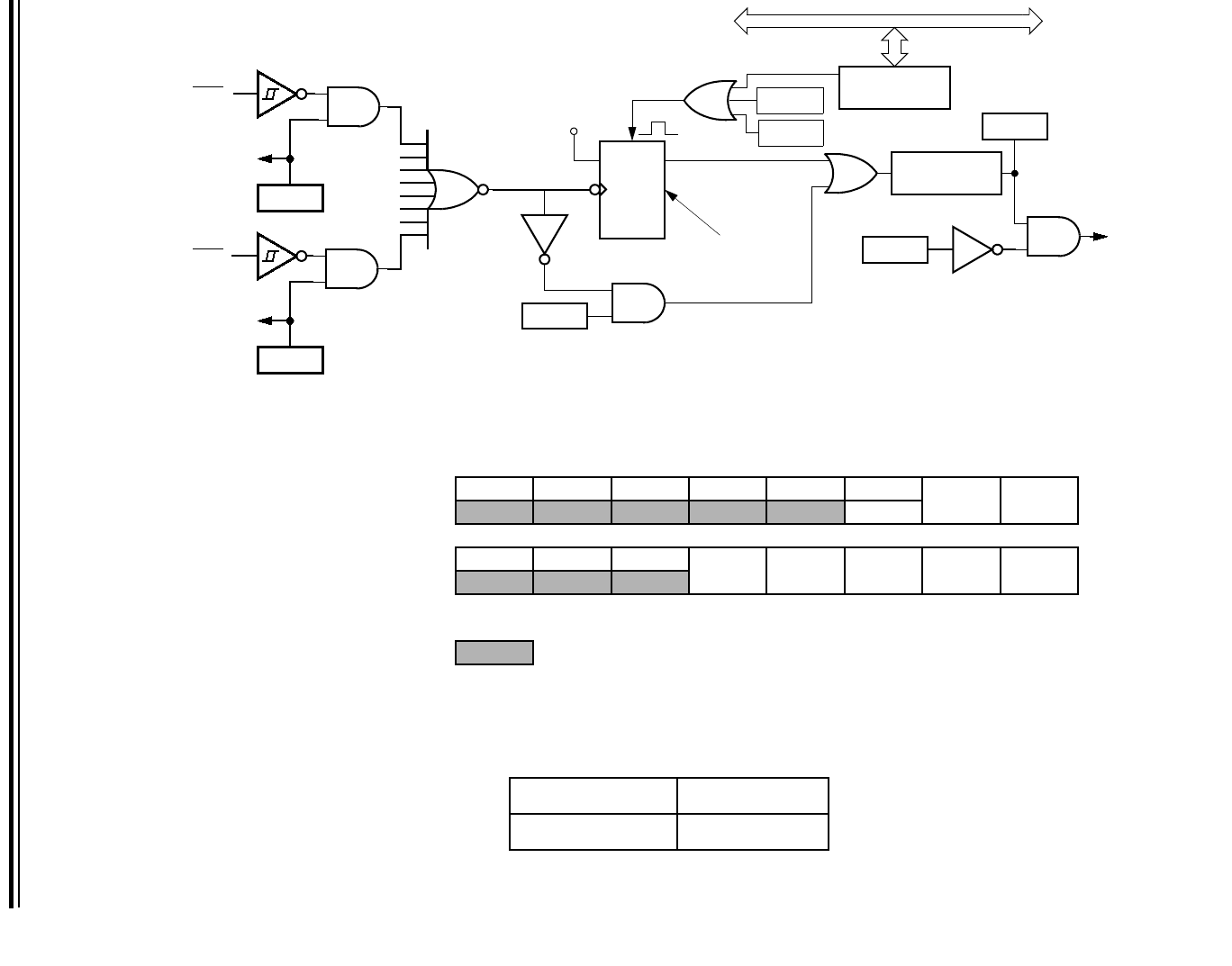
MC68HC08AZ60 — Rev 1.1 Technical Data
Freescale Semiconductor Keyboard Module (KBD) 377
Keyboard Module (KBD)
Functional Description
Figure 23-1. Keyboard Module Block Diagram
Register Name Bit 7654321Bit 0
Keyboard Status and Control Reg-
ister (KBSCR)
Read: 0000KEYF 0 IMASKK MODEK
Write: ACKK
Reset:00000000
Keyboard Interrupt Enable Regis-
ter (KBIER)
Read: 0 0 0 KBIE4 KBIE3 KBIE2 KBIE1 KBIE0
Write:
Reset:00000000
= Unimplemented
Figure 23-2. I/O Register Summary
Table 23-1. I/O Register Address Summary
Register KBSCR KBIER
Address $001A $001B
KB0IE
KB4IE
.
.
.KEYBOARD
INTERRUPT
DQ
CK
CLR
VDD
MODEK
IMASKK
KEYBOARD
INTERRUPT FF REQUEST
VECTOR FETCH
DECODER
ACKK
INTERNAL BUS
RESET
TO PULLUP ENABLE
KBD4
KBD0
TO PULLUP ENABLE
SYNCHRONIZER
KEYF

Keyboard Module (KBD)
Technical Data MC68HC08AZ60 — Rev 1.1
378 Keyboard Module (KBD) Freescale Semiconductor
If the MODEK bit is set, the keyboard interrupt pins are both falling edge-
and low level-sensitive, and both of the following actions must occur to
clear a keyboard interrupt request:
• Vector fetch or software clear — A vector fetch generates an
interrupt acknowledge signal to clear the interrupt request.
Software may generate the interrupt acknowledge signal by
writing a logic 1 to the ACKK bit in the keyboard status and control
register (KBSCR). The ACKK bit is useful in applications that poll
the keyboard interrupt pins and require software to clear the
keyboard interrupt request. Writing to the ACKK bit prior to leaving
an interrupt service routine also can prevent spurious interrupts
due to noise. Setting ACKK does not affect subsequent transitions
on the keyboard interrupt pins. A falling edge that occurs after
writing to the ACKK bit latches another interrupt request. If the
keyboard interrupt mask bit, IMASKK, is clear, the CPU loads the
program counter with the vector address at locations $FFDE and
$FFDF.
• Return of all enabled keyboard interrupt pins to logic 1. As long as
any enabled keyboard interrupt pin is at logic 0, the keyboard
interrupt remains set.
The vector fetch or software clear and the return of all enabled keyboard
interrupt pins to logic 1 may occur in any order.
If the MODEK bit is clear, the keyboard interrupt pin is falling edge-
sensitive only. With MODEK clear, a vector fetch or software clear
immediately clears the keyboard interrupt request.
Reset clears the keyboard interrupt request and the MODEK bit, clearing
the interrupt request even if a keyboard interrupt pin stays at logic 0.
The keyboard flag bit (KEYF) in the keyboard status and control register
can be used to see if a pending interrupt exists. The KEYF bit is not
affected by the keyboard interrupt mask bit (IMASKK) which makes it
useful in applications where polling is preferred.
To determine the logic level on a keyboard interrupt pin, use the data
direction register to configure the pin as an input and read the data
register.

Keyboard Module (KBD)
Keyboard Initialization
MC68HC08AZ60 — Rev 1.1 Technical Data
Freescale Semiconductor Keyboard Module (KBD) 379
NOTE: Setting a keyboard interrupt enable bit (KBIEx) forces the corresponding
keyboard interrupt pin to be an input, overriding the data direction
register. However, the data direction register bit must be a logic 0 for
software to read the pin.
23.5 Keyboard Initialization
When a keyboard interrupt pin is enabled, it takes time for the internal
pullup to reach a logic 1. Therefore, a false interrupt can occur as soon
as the pin is enabled.
To prevent a false interrupt on keyboard initialization:
1. Mask keyboard interrupts by setting the IMASKK bit in the
keyboard status and control register
2. Enable the KBI pins by setting the appropriate KBIEx bits in the
keyboard interrupt enable register
3. Write to the ACKK bit in the keyboard status and control register
to clear any false interrupts
4. Clear the IMASKK bit.
An interrupt signal on an edge-triggered pin can be acknowledged
immediately after enabling the pin. An interrupt signal on an edge- and
level-triggered interrupt pin must be acknowledged after a delay that
depends on the external load.
Another way to avoid a false interrupt:
1. Configure the keyboard pins as outputs by setting the appropriate
DDRG bits in data direction register G.
2. Configure the keyboard pins as outputs by setting the appropriate
DDRH bits in data direction register H.
3. Write logic 1s to the appropriate port G and port H data register
bits.
4. Enable the KBI pins by setting the appropriate KBIEx bits in the
keyboard interrupt enable register.

Keyboard Module (KBD)
Technical Data MC68HC08AZ60 — Rev 1.1
380 Keyboard Module (KBD) Freescale Semiconductor
23.6 Low-Power Modes
The WAIT and STOP instructions put the MCU in low-power-
consumption standby modes.
23.6.1 Wait Mode
The keyboard module remains active in wait mode. Clearing the
IMASKK bit in the keyboard status and control register enables keyboard
interrupt requests to bring the MCU out of wait mode.
23.6.2 Stop Mode
The keyboard module remains active in stop mode. Clearing the
IMASKK bit in the keyboard status and control register enables keyboard
interrupt requests to bring the MCU out of stop mode.
23.7 Keyboard Module During Break Interrupts
The BCFE bit in the break flag control register (BFCR) enables software
to clear status bits during the break state. See Break Module on page
149.
To allow software to clear the KEYF bit during a break interrupt, write a
logic 1 to the BCFE bit. If KEYF is cleared during the break state, it
remains cleared when the MCU exits the break state.
To protect the KEYF bit during the break state, write a logic 0 to the
BCFE bit. With BCFE at logic 0, writing to the keyboard acknowledge bit
(ACKK) in the keyboard status and control register during the break state
has no effect. See Keyboard Status and Control Register on page
381.

Keyboard Module (KBD)
I/O Registers
MC68HC08AZ60 — Rev 1.1 Technical Data
Freescale Semiconductor Keyboard Module (KBD) 381
23.8 I/O Registers
The following registers control and monitor operation of the keyboard
module:
• Keyboard status and control register (KBSCR)
• Keyboard interrupt enable register (KBIER)
23.8.1 Keyboard Status and Control Register
The keyboard status and control register:
• Flags keyboard interrupt requests
• Acknowledges keyboard interrupt requests
• Masks keyboard interrupt requests
• Controls keyboard interrupt triggering sensitivity
Bits 7–4 — Not used
These read-only bits always read as logic 0s.
KEYF — Keyboard Flag Bit
This read-only bit is set when a keyboard interrupt is pending. Reset
clears the KEYF bit.
1 = Keyboard interrupt pending
0 = No keyboard interrupt pending
Address: $001A
Bit 7654321Bit 0
Read: 0000KEYF 0
IMASKK MODEK
Write: ACKK
Reset:00000000
= Unimplemented
Figure 23-3. Keyboard Status and Control Register (KBSCR)

Keyboard Module (KBD)
Technical Data MC68HC08AZ60 — Rev 1.1
382 Keyboard Module (KBD) Freescale Semiconductor
ACKK — Keyboard Acknowledge Bit
Writing a logic 1 to this write-only bit clears the keyboard interrupt
request. ACKK always reads as logic 0. Reset clears ACKK.
IMASKK — Keyboard Interrupt Mask Bit
Writing a logic 1 to this read/write bit prevents the output of the
keyboard interrupt mask from generating interrupt requests. Reset
clears the IMASKK bit.
1 = Keyboard interrupt requests masked
0 = Keyboard interrupt requests not masked
MODEK — Keyboard Triggering Sensitivity Bit
This read/write bit controls the triggering sensitivity of the keyboard
interrupt pins. Reset clears MODEK.
1 = Keyboard interrupt requests on falling edges and low levels
0 = Keyboard interrupt requests on falling edges only
23.8.2 Keyboard Interrupt Enable Register
The keyboard interrupt enable register enables or disables each port G
and each port H pin to operate as a keyboard interrupt pin.
KBIE4–KBIE0 — Keyboard Interrupt Enable Bits
Each of these read/write bits enables the corresponding keyboard
interrupt pin to latch interrupt requests. Reset clears the keyboard
interrupt enable register.
1 = Port pin enabled as keyboard interrupt pin
0 = Port pin not enabled as keyboard interrupt pin
Address: $001B
Bit 7654321Bit 0
Read: 0 0 0
KBIE4 KBIE3 KBIE2 KBIE1 KBIE0
Write:
Reset:00000000
= Unimplemented
Figure 23-4. Keyboard Interrupt Enable Register (KBIER)

MC68HC08AZ60 — Rev 1.1 Technical Data
Freescale Semiconductor Timer Interface Module A (TIMA) 385
Technical Data — MC68HC08AZ60
Section 24. Timer Interface Module A (TIMA)
24.1 Contents
24.2 Introduction. . . . . . . . . . . . . . . . . . . . . . . . . . . . . . . . . . . . . .386
24.3 Features. . . . . . . . . . . . . . . . . . . . . . . . . . . . . . . . . . . . . . . . .386
24.4 Functional Description. . . . . . . . . . . . . . . . . . . . . . . . . . . . .389
24.4.1 TIMA Counter Prescaler. . . . . . . . . . . . . . . . . . . . . . . . . .389
24.4.2 Input Capture . . . . . . . . . . . . . . . . . . . . . . . . . . . . . . . . . .389
24.4.3 Output Compare. . . . . . . . . . . . . . . . . . . . . . . . . . . . . . . .390
24.4.3.1 Unbuffered Output Compare. . . . . . . . . . . . . . . . . . . .391
24.4.3.2 Buffered Output Compare. . . . . . . . . . . . . . . . . . . . . .392
24.4.4 Pulse Width Modulation (PWM) . . . . . . . . . . . . . . . . . . .393
24.4.4.1 Unbuffered PWM Signal Generation . . . . . . . . . . . . .394
24.4.4.2 Buffered PWM Signal Generation. . . . . . . . . . . . . . . .395
24.4.4.3 PWM Initialization . . . . . . . . . . . . . . . . . . . . . . . . . . . .397
24.5 Interrupts. . . . . . . . . . . . . . . . . . . . . . . . . . . . . . . . . . . . . . . .398
24.6 Low-Power Modes . . . . . . . . . . . . . . . . . . . . . . . . . . . . . . . .399
24.6.1 Wait Mode . . . . . . . . . . . . . . . . . . . . . . . . . . . . . . . . . . . . .399
24.6.2 Stop Mode. . . . . . . . . . . . . . . . . . . . . . . . . . . . . . . . . . . . .399
24.7 TIMA During Break Interrupts . . . . . . . . . . . . . . . . . . . . . . .399
24.8 I/O Signals . . . . . . . . . . . . . . . . . . . . . . . . . . . . . . . . . . . . . . .400
24.8.1 TIMA Clock Pin (PTD6/ATD14/ TCLK). . . . . . . . . . . . . . .400
24.8.2 TIMA Channel I/O Pins (PTF3–PTF0/TACH2 and
PTE3/TACH1–PTE2/TACH0)400
24.9 I/O Registers . . . . . . . . . . . . . . . . . . . . . . . . . . . . . . . . . . . . .401
24.9.1 TIMA Status and Control Register . . . . . . . . . . . . . . . . .401
24.9.2 TIMA Counter Registers . . . . . . . . . . . . . . . . . . . . . . . . .403
24.9.3 TIMA Counter Modulo Registers. . . . . . . . . . . . . . . . . . .404
24.9.4 TIMA Channel Status and Control Registers. . . . . . . . .405
24.9.5 TIMA Channel Registers . . . . . . . . . . . . . . . . . . . . . . . . .411

Timer Interface Module A (TIMA)
Technical Data MC68HC08AZ60 — Rev 1.1
386 Timer Interface Module A (TIMA) Freescale Semiconductor
24.2 Introduction
This section describes the timer interface module (TIMA). The TIMA is a
6-channel timer that provides a timing reference with input capture,
output compare, and pulse-width-modulation functions. Figure 24-1 is a
block diagram of the TIMA.
For further information regarding timers on M68HC08 family devices,
please consult the HC08 Timer Reference Manual, TIM08RM/AD.
24.3 Features
Features of the TIMA include:
• Six Input Capture/Output Compare Channels
– Rising-Edge, Falling-Edge, or Any-Edge Input Capture Trigger
– Set, Clear, or Toggle Output Compare Action
• Buffered and Unbuffered Pulse Width Modulation (PWM) Signal
Generation
• Programmable TIMA Clock Input
– 7-Frequency Internal Bus Clock Prescaler Selection
– External TIMA Clock Input (4-MHz Maximum Frequency)
• Free-Running or Modulo Up-Count Operation
• Toggle Any Channel Pin on Overflow
• TIMA Counter Stop and Reset Bits
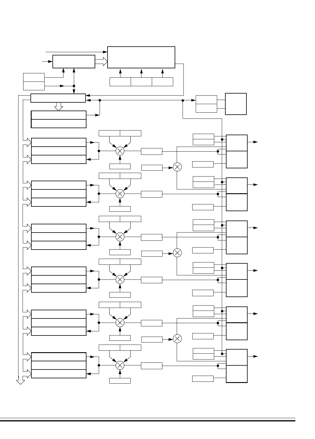
Timer Interface Module A (TIMA)
Features
MC68HC08AZ60 — Rev 1.1 Technical Data
Freescale Semiconductor Timer Interface Module A (TIMA) 387
Figure 24-1. TIMA Block Diagram
PRESCALER
PRESCALER SELECT
TCLK
INTERNAL
16-BIT COMPARATOR
PS2 PS1 PS0
16-BIT COMPARATOR
16-BIT LATCH
TCH0H:TCH0L
MS0A
ELS0B ELS0A
PTE2
TOF
TOIE
INTER-
CHANNEL 0
TMODH:TMODL
TRST
TSTOP
TOV0
CH0IE
CH0F
CH0MAX
MS0B
16-BIT COUNTER
BUS CLOCK
PTD6/ATD14/TACLK
PTE2/TACH0
PTE3/TACH1
PTF0/TACH2
PTF1/TACH3
LOGIC
RUPT
LOGIC
INTER-
RUPT
LOGIC
16-BIT COMPARATOR
16-BIT LATCH
TCH1H:TCH1L
MS1A
ELS1B ELS1A
PTE3
CHANNEL 1 TOV1
CH1IE
CH1F
CH1MAX LOGIC
INTER-
RUPT
LOGIC
16-BIT COMPARATOR
16-BIT LATCH
TCH2H:TCH2L
MS2A
ELS2B ELS2A
PTF0
CHANNEL 2 TOV2
CH2IE
CH2F
CH2MAX
MS2B
LOGIC
INTER-
RUPT
LOGIC
16-BIT COMPARATOR
16-BIT LATCH
TCH3H:TCH3L
MS3A
ELS3B ELS3A
PTF1
CHANNEL 3 TOV3
CH3IE
CH3F
CH3MAX LOGIC
INTER-
RUPT
LOGIC
16-BIT COMPARATOR
16-BIT LATCH
TCH4H:TCH4L
MS4A
ELS4B ELS4A
PTF2
CHANNEL 4 TOV4
CH4IE
CH4F
CH5MAX
MS4B
LOGIC
INTER-
RUPT
LOGIC
16-BIT COMPARATOR
16-BIT LATCH
TCH5H:TCH5L
MS5A
ELS5B ELS5A
PTF3
CHANNEL 5 TOV5
CH5IE
CH5F
CH5MAX LOGIC
INTER-
RUPT
LOGIC
PTF2
PTF3

Timer Interface Module A (TIMA)
Technical Data MC68HC08AZ60 — Rev 1.1
388 Timer Interface Module A (TIMA) Freescale Semiconductor
Figure 24-2. TIMA I/O Register Summary
Addr. Register Name Bit 7654321Bit 0
$0020 TIMA Status/Control Register (TASC) TOF TOIE TSTOP TRST 0 PS2 PS1 PS0
$0021 Reserved R R RRRRRR
$0022 TIMA Counter Register High (TACNTH) Bit 15 14 13 12 11 10 9 Bit 8
$0023 TIMA Counter Register Low (TACNTL) Bit 7 654321Bit 0
$0024 TIMA Counter Modulo Reg. High (TAMODH) Bit 15 14 13 12 11 10 9 Bit 8
$0025 TIMA Counter Modulo Reg. Low (TAMODL) Bit 7 654321Bit 0
$0026 TIMA Ch. 0 Status/Control Register (TASC0) CH0F CH0IE MS0B MS0A ELS0B ELS0A TOV0 CH0MAX
$0027 TIMA Ch. 0 Register High (TACH0H) Bit 15 14 13 12 11 10 9 Bit 8
$0028 TIMA Ch. 0 Register Low (TACH0L) Bit 7 654321Bit 0
$0029 TIMA Ch. 1 Status/Control Register (TASC1) CH1F CH1IE 0 MS1A ELS1B ELS1A TOV1 CH1MAX
$002A TIMA Ch. 1 Register High (TACH1H) Bit 15 14 13 12 11 10 9 Bit 8
$002B TIMA Ch. 1 Register Low (TACH1L) Bit 7 654321Bit 0
$002C TIMA Ch. 2 Status/Control Register (TASC2) CH2F CH2IE MS2B MS2A ELS2B ELS2A TOV2 CH2MAX
$002D TIMA Ch. 2 Register High (TACH2H) Bit 15 14 13 12 11 10 9 Bit 8
$002E TIMA Ch. 2 Register Low (TACH2L) Bit 7 654321Bit 0
$002F TIMA Ch. 3 Status/Control Register (TASC3) CH3F CH3IE 0 MS3A ELS3B ELS3A TOV3 CH3MAX
$0030 TIMA Ch. 3 Register High (TACH3H) Bit 15 14 13 12 11 10 9 Bit 8
$0031 TIMA Ch. 3 Register Low (TACH3L) Bit 7 654321Bit 0
$0032 TIMA Ch. 4 Status/Control Register (TASC4) CH4F CH4IE MS4B MS4A ELS4B ELS4A TOV4 CH4MAX
$0033 TIMA Ch. 4 Register High (TACH4H) Bit 15 14 13 12 11 10 9 Bit 8
$0034 TIMA Ch. 4 Register Low (TACH4L) Bit 7 654321Bit 0
$0035 TIMA Ch. 5 Status/Control Register (TASC5) CH5F CH5IE 0 MS5A ELS5B ELS5A TOV5 CH5MAX
$0036 TIMA Ch. 5 Register High (TACH5H) Bit 15 14 13 12 11 10 9 Bit 8
$0037 TIMA Ch. 5 Register Low (TACH5L) Bit 7 654321Bit 0
R= Reserved

Timer Interface Module A (TIMA)
Functional Description
MC68HC08AZ60 — Rev 1.1 Technical Data
Freescale Semiconductor Timer Interface Module A (TIMA) 389
24.4 Functional Description
Figure 24-1 shows the TIMA structure. The central component of the
TIMA is the 16-bit TIMA counter that can operate as a free-running
counter or a modulo up-counter. The TIMA counter provides the timing
reference for the input capture and output compare functions. The TIMA
counter modulo registers, TAMODH–TAMODL, control the modulo
value of the TIMA counter. Software can read the TIMA counter value at
any time without affecting the counting sequence.
The six TIMA channels are programmable independently as input
capture or output compare channels.
24.4.1 TIMA Counter Prescaler
The TIMA clock source can be one of the seven prescaler outputs or the
TIMA clock pin, PTD6/ATD14/TACLK. The prescaler generates seven
clock rates from the internal bus clock. The prescaler select bits, PS[2:0],
in the TIMA status and control register select the TIMA clock source.
24.4.2 Input Capture
An input capture function has three basic parts: edge select logic, an
input capture latch, and a 16-bit counter. Two 8-bit registers, which make
up the 16-bit input capture register, are used to latch the value of the
free-running counter after the corresponding input capture edge detector
senses a defined transition. The polarity of the active edge is
programmable. The level transition which triggers the counter transfer is
defined by the corresponding input edge bits (ELSxB and ELSxA in
TASC0 through TASC5 control registers with x referring to the active
channel number). When an active edge occurs on the pin of an input
capture channel, the TIMA latches the contents of the TIMA counter into
the TIMA channel registers, TACHxH–TACHxL. Input captures can
generate TIMA CPU interrupt requests. Software can determine that an
input capture event has occurred by enabling input capture interrupts or
by polling the status flag bit.

Timer Interface Module A (TIMA)
Technical Data MC68HC08AZ60 — Rev 1.1
390 Timer Interface Module A (TIMA) Freescale Semiconductor
The free-running counter contents are transferred to the TIMA channel
status and control register (TACHxH–TACHxL, see TIMA Channel
Registers on page 411), on each proper signal transition regardless of
whether the TIMA channel flag (CH0F–CH5F in TASC0–TASC5
registers) is set or clear. When the status flag is set, a CPU interrupt is
generated if enabled. The value of the count latched or “captured” is the
time of the event. Because this value is stored in the input capture
register 2 bus cycles after the actual event occurs, user software can
respond to this event at a later time and determine the actual time of the
event. However, this must be done prior to another input capture on the
same pin; otherwise, the previous time value will be lost.
By recording the times for successive edges on an incoming signal,
software can determine the period and/or pulse width of the signal. To
measure a period, two successive edges of the same polarity are
captured. To measure a pulse width, two alternate polarity edges are
captured. Software should track the overflows at the 16-bit module
counter to extend its range.
Another use for the input capture function is to establish a time
reference. In this case, an input capture function is used in conjunction
with an output compare function. For example, to activate an output
signal a specified number of clock cycles after detecting an input event
(edge), use the input capture function to record the time at which the
edge occurred. A number corresponding to the desired delay is added to
this captured value and stored to an output compare register (see TIMA
Channel Registers on page 411). Because both input captures and
output compares are referenced to the same 16-bit modulo counter, the
delay can be controlled to the resolution of the counter independent of
software latencies.
Reset does not affect the contents of the input capture channel register
(TACHxH–TACHxL).
24.4.3 Output Compare
With the output compare function, the TIMA can generate a periodic
pulse with a programmable polarity, duration, and frequency. When the
counter reaches the value in the registers of an output compare channel,

Timer Interface Module A (TIMA)
Functional Description
MC68HC08AZ60 — Rev 1.1 Technical Data
Freescale Semiconductor Timer Interface Module A (TIMA) 391
the TIMA can set, clear, or toggle the channel pin. Output compares can
generate TIMA CPU interrupt requests.
24.4.3.1 Unbuffered Output Compare
Any output compare channel can generate unbuffered output compare
pulses as described in Output Compare on page 390. The pulses are
unbuffered because changing the output compare value requires writing
the new value over the old value currently in the TIMA channel registers.
An unsynchronized write to the TIMA channel registers to change an
output compare value could cause incorrect operation for up to two
counter overflow periods. For example, writing a new value before the
counter reaches the old value but after the counter reaches the new
value prevents any compare during that counter overflow period. Also,
using a TIMA overflow interrupt routine to write a new, smaller output
compare value may cause the compare to be missed. The TIMA may
pass the new value before it is written.
Use the following methods to synchronize unbuffered changes in the
output compare value on channel x:
• When changing to a smaller value, enable channel x output
compare interrupts and write the new value in the output compare
interrupt routine. The output compare interrupt occurs at the end
of the current output compare pulse. The interrupt routine has until
the end of the counter overflow period to write the new value.
• When changing to a larger output compare value, enable TIMA
overflow interrupts and write the new value in the TIMA overflow
interrupt routine. The TIMA overflow interrupt occurs at the end of
the current counter overflow period. Writing a larger value in an
output compare interrupt routine (at the end of the current pulse)
could cause two output compares to occur in the same counter
overflow period.

Timer Interface Module A (TIMA)
Technical Data MC68HC08AZ60 — Rev 1.1
392 Timer Interface Module A (TIMA) Freescale Semiconductor
24.4.3.2 Buffered Output Compare
Channels 0 and 1 can be linked to form a buffered output compare
channel whose output appears on the PTE2/TACH0 pin. The TIMA
channel registers of the linked pair alternately control the output.
Setting the MS0B bit in TIMA channel 0 status and control register
(TASC0) links channel 0 and channel 1. The output compare value in the
TIMA channel 0 registers initially controls the output on the
PTE2/TACH0 pin. Writing to the TIMA channel 1 registers enables the
TIMA channel 1 registers to synchronously control the output after the
TIMA overflows. At each subsequent overflow, the TIMA channel
registers (0 or 1) that control the output are the ones written to last.
TASC0 controls and monitors the buffered output compare function, and
TIMA channel 1 status and control register (TASC1) is unused. While the
MS0B bit is set, the channel 1 pin, PTE3/TACH1, is available as a
general-purpose I/O pin.
Channels 2 and 3 can be linked to form a buffered output compare
channel whose output appears on the PTF0/TACH2 pin. The TIMA
channel registers of the linked pair alternately control the output.
Setting the MS2B bit in TIMA channel 2 status and control register
(TASC2) links channel 2 and channel 3. The output compare value in the
TIMA channel 2 registers initially controls the output on the
PTF0/TACH2 pin. Writing to the TIMA channel 3 registers enables the
TIMA channel 3 registers to synchronously control the output after the
TIMA overflows. At each subsequent overflow, the TIMA channel
registers (2 or 3) that control the output are the ones written to last.
TASC2 controls and monitors the buffered output compare function, and
TIMA channel 3 status and control register (TASC3) is unused. While the
MS2B bit is set, the channel 3 pin, PTF1/TACH3, is available as a
general-purpose I/O pin.
Channels 4 and 5 can be linked to form a buffered output compare
channel whose output appears on the PTF2 pin. The TIMA channel
registers of the linked pair alternately control the output.
Setting the MS4B bit in TIMA channel 4 status and control register
(TSC4) links channel 4 and channel 5. The output compare value in the

Timer Interface Module A (TIMA)
Functional Description
MC68HC08AZ60 — Rev 1.1 Technical Data
Freescale Semiconductor Timer Interface Module A (TIMA) 393
TIMA channel 4 registers initially controls the output on the PTF2 pin.
Writing to the TIMA channel 5 registers enables the TIMA channel 5
registers to synchronously control the output after the TIMA overflows.
At each subsequent overflow, the TIMA channel registers (4 or 5) that
control the output are the ones written to last. TASC4 controls and
monitors the buffered output compare function, and TIMA channel 5
status and control register (TASC5) is unused. While the MS4B bit is set,
the channel 5 pin, PTF3, is available as a general-purpose I/O pin.
NOTE: In buffered output compare operation, do not write new output compare
values to the currently active channel registers. User software should
track the currently active channel to prevent writing a new value to the
active channel. Writing to the active channel registers is the same as
generating unbuffered output compares.
24.4.4 Pulse Width Modulation (PWM)
By using the toggle-on-overflow feature with an output compare channel,
the TIMA can generate a PWM signal. The value in the TIMA counter
modulo registers determines the period of the PWM signal. The channel
pin toggles when the counter reaches the value in the TIMA counter
modulo registers. The time between overflows is the period of the PWM
signal.
As Figure 24-3 shows, the output compare value in the TIMA channel
registers determines the pulse width of the PWM signal. The time
between overflow and output compare is the pulse width. Program the
TIMA to clear the channel pin on output compare if the state of the PWM
pulse is logic 1. Program the TIMA to set the pin if the state of the PWM
pulse is logic 0.

Timer Interface Module A (TIMA)
Technical Data MC68HC08AZ60 — Rev 1.1
394 Timer Interface Module A (TIMA) Freescale Semiconductor
Figure 24-3. PWM Period and Pulse Width
The value in the TIMA counter modulo registers and the selected
prescaler output determines the frequency of the PWM output. The
frequency of an 8-bit PWM signal is variable in 256 increments. Writing
$00FF (255) to the TIMA counter modulo registers produces a PWM
period of 256 times the internal bus clock period if the prescaler select
value is $000 (see TIMA Status and Control Register on page 401).
The value in the TIMA channel registers determines the pulse width of
the PWM output. The pulse width of an 8-bit PWM signal is variable in
256 increments. Writing $0080 (128) to the TIMA channel registers
produces a duty cycle of 128/256 or 50%.
24.4.4.1 Unbuffered PWM Signal Generation
Any output compare channel can generate unbuffered PWM pulses as
described in Pulse Width Modulation (PWM) on page 393. The pulses
are unbuffered because changing the pulse width requires writing the
new pulse width value over the value currently in the TIMA channel
registers.
An unsynchronized write to the TIMA channel registers to change a
pulse width value could cause incorrect operation for up to two PWM
periods. For example, writing a new value before the counter reaches
the old value but after the counter reaches the new value prevents any
compare during that PWM period. Also, using a TIMA overflow interrupt
routine to write a new, smaller pulse width value may cause the compare
PTEx/TCHx
PERIOD
PULSE
WIDTH
OVERFLOW OVERFLOW OVERFLOW
OUTPUT
COMPARE OUTPUT
COMPARE
OUTPUT
COMPARE

Timer Interface Module A (TIMA)
Functional Description
MC68HC08AZ60 — Rev 1.1 Technical Data
Freescale Semiconductor Timer Interface Module A (TIMA) 395
to be missed. The TIMA may pass the new value before it is written to
the TIMA channel registers.
Use the following methods to synchronize unbuffered changes in the
PWM pulse width on channel x:
• When changing to a shorter pulse width, enable channel x output
compare interrupts and write the new value in the output compare
interrupt routine. The output compare interrupt occurs at the end
of the current pulse. The interrupt routine has until the end of the
PWM period to write the new value.
• When changing to a longer pulse width, enable TIMA overflow
interrupts and write the new value in the TIMA overflow interrupt
routine. The TIMA overflow interrupt occurs at the end of the
current PWM period. Writing a larger value in an output compare
interrupt routine (at the end of the current pulse) could cause two
output compares to occur in the same PWM period.
NOTE: In PWM signal generation, do not program the PWM channel to toggle
on output compare. Toggling on output compare prevents reliable 0%
duty cycle generation and removes the ability of the channel to self-
correct in the event of software error or noise. Toggling on output
compare also can cause incorrect PWM signal generation when
changing the PWM pulse width to a new, much larger value.
24.4.4.2 Buffered PWM Signal Generation
Channels 0 and 1 can be linked to form a buffered PWM channel whose
output appears on the PTE2/TACH0 pin. The TIMA channel registers of
the linked pair alternately control the pulse width of the output.
Setting the MS0B bit in TIMA channel 0 status and control register
(TASC0) links channel 0 and channel 1. The TIMA channel 0 registers
initially control the pulse width on the PTE2/TACH0 pin. Writing to the
TIMA channel 1 registers enables the TIMA channel 1 registers to
synchronously control the pulse width at the beginning of the next PWM
period. At each subsequent overflow, the TIMA channel registers (0 or
1) that control the pulse width are the ones written to last. TASC0
controls and monitors the buffered PWM function, and TIMA channel 1

Timer Interface Module A (TIMA)
Technical Data MC68HC08AZ60 — Rev 1.1
396 Timer Interface Module A (TIMA) Freescale Semiconductor
status and control register (TASC1) is unused. While the MS0B bit is set,
the channel 1 pin, PTE3/TACH1, is available as a general-purpose I/O
pin.
Channels 2 and 3 can be linked to form a buffered PWM channel whose
output appears on the PTF0/TACH2 pin. The TIMA channel registers of
the linked pair alternately control the pulse width of the output.
Setting the MS2B bit in TIMA channel 2 status and control register
(TASC2) links channel 2 and channel 3. The TIMA channel 2 registers
initially control the pulse width on the PTF0/TACH2 pin. Writing to the
TIMA channel 3 registers enables the TIMA channel 3 registers to
synchronously control the pulse width at the beginning of the next PWM
period. At each subsequent overflow, the TIMA channel registers (2 or
3) that control the pulse width are the ones written to last. TASC2
controls and monitors the buffered PWM function, and TIMA channel 3
status and control register (TASC3) is unused. While the MS2B bit is set,
the channel 3 pin, PTF1/TACH3, is available as a general-purpose I/O
pin.
Channels 4 and 5 can be linked to form a buffered PWM channel whose
output appears on the PTF2 pin. The TIMA channel registers of the
linked pair alternately control the pulse width of the output.
Setting the MS4B bit in TIMA channel 4 status and control register
(TASC4) links channel 4 and channel 5. The TIMA channel 4 registers
initially control the pulse width on the PTF2 pin. Writing to the TIMA
channel 5 registers enables the TIMA channel 5 registers to
synchronously control the pulse width at the beginning of the next PWM
period. At each subsequent overflow, the TIMA channel registers (4 or
5) that control the pulse width are the ones written to last. TASC4
controls and monitors the buffered PWM function, and TIMA channel 5
status and control register (TASC5) is unused. While the MS4B bit is set,
the channel 5 pin, PTF3, is available as a general-purpose I/O pin.
NOTE: In buffered PWM signal generation, do not write new pulse width values
to the currently active channel registers. User software should track the
currently active channel to prevent writing a new value to the active
channel. Writing to the active channel registers is the same as
generating unbuffered PWM signals.

Timer Interface Module A (TIMA)
Functional Description
MC68HC08AZ60 — Rev 1.1 Technical Data
Freescale Semiconductor Timer Interface Module A (TIMA) 397
24.4.4.3 PWM Initialization
To ensure correct operation when generating unbuffered or buffered
PWM signals, use the following initialization procedure:
1. In the TIMA status and control register (TASC):
a. Stop the TIMA counter by setting the TIMA stop bit, TSTOP.
b. Reset the TIMA counter and prescaler by setting the TIMA
reset bit, TRST.
2. In the TIMA counter modulo registers (TAMODH–TAMODL), write
the value for the required PWM period.
3. In the TIMA channel x registers (TACHxH–TACHxL), write the
value for the required pulse width.
4. In TIMA channel x status and control register (TSCx):
a. Write 0:1 (for unbuffered output compare or PWM signals) or
1:0 (for buffered output compare or PWM signals) to the
mode select bits, MSxB–MSxA. (See Table 24-2).
b. Write 1 to the toggle-on-overflow bit, TOVx.
c. Write 1:0 (to clear output on compare) or 1:1 (to set output on
compare) to the edge/level select bits, ELSxB–ELSxA. The
output action on compare must force the output to the
complement of the pulse width level. (See Table 24-2.)
NOTE: In PWM signal generation, do not program the PWM channel to toggle
on output compare. Toggling on output compare prevents reliable 0%
duty cycle generation and removes the ability of the channel to self-
correct in the event of software error or noise. Toggling on output
compare can also cause incorrect PWM signal generation when
changing the PWM pulse width to a new, much larger value.
5. In the TIMA status control register (TASC), clear the TIMA stop bit,
TSTOP.
Setting MS0B links channels 0 and 1 and configures them for buffered
PWM operation. The TIMA channel 0 registers (TACH0H–TACH0L)
initially control the buffered PWM output. TIMA status control register 0

Timer Interface Module A (TIMA)
Technical Data MC68HC08AZ60 — Rev 1.1
398 Timer Interface Module A (TIMA) Freescale Semiconductor
(TASC0) controls and monitors the PWM signal from the linked
channels. MS0B takes priority over MS0A.
Setting MS2B links channels 2 and 3 and configures them for buffered
PWM operation. The TIMA channel 2 registers (TACH2H–TACH2L)
initially control the buffered PWM output. TIMA status control register 2
(TASC2) controls and monitors the PWM signal from the linked
channels. MS2B takes priority over MS2A.
Setting MS4B links channels 4 and 5 and configures them for buffered
PWM operation. The TIMA channel 4 registers (TACH4H–TACH4L)
initially control the buffered PWM output. TIMA status control register 4
(TASC4) controls and monitors the PWM signal from the linked
channels. MS4B takes priority over MS4A.
Clearing the toggle-on-overflow bit, TOVx, inhibits output toggles on
TIMA overflows. Subsequent output compares try to force the output to
a state it is already in and have no effect. The result is a 0% duty cycle
output.
Setting the channel x maximum duty cycle bit (CHxMAX) and setting the
TOVx bit generates a 100% duty cycle output. (See TIMA Channel
Status and Control Registers on page 405).
24.5 Interrupts
The following TIMA sources can generate interrupt requests:
• TIMA overflow flag (TOF) — The TOF bit is set when the TIMA
counter value reaches the modulo value programmed in the TIMA
counter modulo registers. The TIMA overflow interrupt enable bit,
TOIE, enables TIMA overflow CPU interrupt requests. TOF and
TOIE are in the TIMA status and control register.
• TIMA channel flags (CH5F–CH0F) — The CHxF bit is set when an
input capture or output compare occurs on channel x. Channel x
TIMA CPU interrupt requests are controlled by the channel x
interrupt enable bit, CHxIE.

Timer Interface Module A (TIMA)
Low-Power Modes
MC68HC08AZ60 — Rev 1.1 Technical Data
Freescale Semiconductor Timer Interface Module A (TIMA) 399
24.6 Low-Power Modes
The WAIT and STOP instructions put the MCU in low power-
consumption standby modes.
24.6.1 Wait Mode
The TIMA remains active after the execution of a WAIT instruction. In
wait mode, the TIMA registers are not accessible by the CPU. Any
enabled CPU interrupt request from the TIMA can bring the MCU out of
wait mode.
If TIMA functions are not required during wait mode, reduce power
consumption by stopping the TIMA before executing the WAIT
instruction.
24.6.2 Stop Mode
The TIMA is inactive after the execution of a STOP instruction. The
STOP instruction does not affect register conditions or the state of the
TIMA counter. TIMA operation resumes when the MCU exits stop mode.
24.7 TIMA During Break Interrupts
A break interrupt stops the TIMA counter and inhibits input captures.
The system integration module (SIM) controls whether status bits in
other modules can be cleared during the break state. The BCFE bit in
the SIM break flag control register (SBFCR) enables software to clear
status bits during the break state. (See SIM Break Flag Control
Register on page 119).
To allow software to clear status bits during a break interrupt, write a
logic 1 to the BCFE bit. If a status bit is cleared during the break state, it
remains cleared when the MCU exits the break state.
To protect status bits during the break state, write a logic 0 to the BCFE
bit. With BCFE at logic 0 (its default state), software can read and write

Timer Interface Module A (TIMA)
Technical Data MC68HC08AZ60 — Rev 1.1
400 Timer Interface Module A (TIMA) Freescale Semiconductor
I/O registers during the break state without affecting status bits. Some
status bits have a 2-step read/write clearing procedure. If software does
the first step on such a bit before the break, the bit cannot change during
the break state as long as BCFE is at logic 0. After the break, doing the
second step clears the status bit.
24.8 I/O Signals
Port D shares one of its pins with the TIMA. Port E shares two of its pins
with the TIMA and port F shares four of its pins with the TIMA.
PTD6/ATD14/TACLK is an external clock input to the TIMA prescaler.
The six TIMA channel I/O pins are PTE2/TACH0, PTE3/TACH1,
PTF0/TACH2, PTF1/TACH3, PTF2, and PTF3.
24.8.1 TIMA Clock Pin (PTD6/ATD14/
TCLK)
PTD6/ATD14/TACLK is an external clock input that can be the clock
source for the TIMA counter instead of the prescaled internal bus clock.
Select the PTD6/ATD14/TACLK input by writing logic 1s to the three
prescaler select bits, PS[2:0]. (See TIMA Status and Control
Register.) The minimum TCLK pulse width, TCLKLMIN or TCLKHMIN, is:
The maximum TCLK frequency is the least: 4 MHz or bus frequency ÷ 2.
PTD6/ATD14/TACLK is available as a general-purpose I/O pin or ADC
channel when not used as the TIMA clock input. When the
PTD6/ATD14/TACLK pin is the TIMA clock input, it is an input regardless
of the state of the DDRD6 bit in data direction register D.
24.8.2 TIMA Channel I/O Pins (PTF3–PTF0/TACH2 and PTE3/TACH1–PTE2/TACH0)
Each channel I/O pin is programmable independently as an input
capture pin or an output compare pin. PTE2/TACH0, PTE6/TACH2, and
1
bus frequency
------------------------------------- t SU
+

Timer Interface Module A (TIMA)
I/O Registers
MC68HC08AZ60 — Rev 1.1 Technical Data
Freescale Semiconductor Timer Interface Module A (TIMA) 401
PTF2 can be configured as buffered output compare or buffered PWM
pins.
24.9 I/O Registers
These I/O registers control and monitor TIMA operation:
• TIMA status and control register (TASC)
• TIMA control registers (TACNTH–TACNTL)
• TIMA counter modulo registers (TAMODH–TAMODL)
• TIMA channel status and control registers (TASC0, TASC1,
TASC2, TASC3, TASC4, and TSAC5)
• TIMA channel registers (TACH0H–TACH0L, TACH1H–TACH1L,
TACH2H–TACH2L, TACH3H–TACH3L, TACH4H–TACH4L, and
TACH5H–TACH5L)
24.9.1 TIMA Status and Control Register
The TIMA status and control register:
• Enables TIMA overflow interrupts
• Flags TIMA overflows
• Stops the TIMA counter
• Resets the TIMA counter
• Prescales the TIMA counter clock
Address: $0020
Bit 7654321Bit 0
Read: TOF TOIE TSTOP 00
PS2 PS1 PS0
Write: 0 TRST R
Reset:00100000
R= Reserved
Figure 24-4. TIMA Status and Control Register (TASC)

Timer Interface Module A (TIMA)
Technical Data MC68HC08AZ60 — Rev 1.1
402 Timer Interface Module A (TIMA) Freescale Semiconductor
TOF — TIMA Overflow Flag Bit
This read/write flag is set when the TIMA counter reaches the modulo
value programmed in the TIMA counter modulo registers. Clear TOF
by reading the TIMA status and control register when TOF is set and
then writing a logic 0 to TOF. If another TIMA overflow occurs before
the clearing sequence is complete, then writing logic 0 to TOF has no
effect. Therefore, a TOF interrupt request cannot be lost due to
inadvertent clearing of TOF. Reset clears the TOF bit. Writing a logic
1 to TOF has no effect.
1 = TIMA counter has reached modulo value.
0 = TIMA counter has not reached modulo value.
TOIE — TIMA Overflow Interrupt Enable Bit
This read/write bit enables TIMA overflow interrupts when the TOF bit
becomes set. Reset clears the TOIE bit.
1 = TIMA overflow interrupts enabled
0 = TIMA overflow interrupts disabled
TSTOP — TIMA Stop Bit
This read/write bit stops the TIMA counter. Counting resumes when
TSTOP is cleared. Reset sets the TSTOP bit, stopping the TIMA
counter until software clears the TSTOP bit.
1 = TIMA counter stopped
0 = TIMA counter active
NOTE: Do not set the TSTOP bit before entering wait mode if the TIMA is
required to exit wait mode. Also, when the TSTOP bit is set and input
capture mode is enabled, input captures are inhibited until TSTOP is
cleared.
TRST — TIMA Reset Bit
Setting this write-only bit resets the TIMA counter and the TIMA
prescaler. Setting TRST has no effect on any other registers.
Counting resumes from $0000. TRST is cleared automatically after
the TIMA counter is reset and always reads as logic 0. Reset clears
the TRST bit.
1 = Prescaler and TIMA counter cleared
0 = No effect

Timer Interface Module A (TIMA)
I/O Registers
MC68HC08AZ60 — Rev 1.1 Technical Data
Freescale Semiconductor Timer Interface Module A (TIMA) 403
NOTE: Setting the TSTOP and TRST bits simultaneously stops the TIMA
counter at a value of $0000.
PS[2:0] — Prescaler Select Bits
These read/write bits select either the PTD6/ATD14/TACLK pin or
one of the seven prescaler outputs as the input to the TIMA counter
as Table 24-1 shows. Reset clears the PS[2:0] bits.
24.9.2 TIMA Counter Registers
The two read-only TIMA counter registers contain the high and low bytes
of the value in the TIMA counter. Reading the high byte (TACNTH)
latches the contents of the low byte (TACNTL) into a buffer. Subsequent
reads of TACNTH do not affect the latched TACNTL value until TACNTL
is read. Reset clears the TIMA counter registers. Setting the TIMA reset
bit (TRST) also clears the TIMA counter registers.
NOTE: If TACNTH is read during a break interrupt, be sure to unlatch TACNTL
by reading TACNTL before exiting the break interrupt. Otherwise,
TACNTL retains the value latched during the break.
Table 24-1. Prescaler Selection
PS[2:0] TIMA Clock Source
000 Internal Bus Clock ÷1
001 Internal Bus Clock ÷ 2
010 Internal Bus Clock ÷ 4
011 Internal Bus Clock ÷ 8
100 Internal Bus Clock ÷ 16
101 Internal Bus Clock ÷ 32
110 Internal Bus Clock ÷ 64
111 PTD6/ATD14/TACLK

Timer Interface Module A (TIMA)
Technical Data MC68HC08AZ60 — Rev 1.1
404 Timer Interface Module A (TIMA) Freescale Semiconductor
24.9.3 TIMA Counter Modulo Registers
The read/write TIMA modulo registers contain the modulo value for the
TIMA counter. When the TIMA counter reaches the modulo value, the
overflow flag (TOF) becomes set, and the TIMA counter resumes
counting from $0000 at the next timer clock. Writing to the high byte
(TAMODH) inhibits the TOF bit and overflow interrupts until the low byte
(TAMODL) is written. Reset sets the TIMA counter modulo registers.
Register Name and Address TCNTH — $0022
Bit 7654321Bit 0
Read: BIT 15 BIT 14 BIT 13 BIT 12 BIT 11 BIT 10 BIT 9 BIT 8
Write:RRRRRRRR
Reset:00000000
Register Name and Address TCNTL — $0023
Bit 7654321Bit 0
Read: BIT 7 BIT 6 BIT 5 BIT 4 BIT 3 BIT 2 BIT 1 BIT 0
Write:RRRRRRRR
Reset:00000000
R = Reserved
Figure 24-5. TIMA Counter Registers (TCNTH and TCNTL)

Timer Interface Module A (TIMA)
I/O Registers
MC68HC08AZ60 — Rev 1.1 Technical Data
Freescale Semiconductor Timer Interface Module A (TIMA) 405
NOTE: Reset the TIMA counter before writing to the TIMA counter modulo
registers.
24.9.4 TIMA Channel Status and Control Registers
Each of the TIMA channel status and control registers:
• Flags input captures and output compares
• Enables input capture and output compare interrupts
• Selects input capture, output compare, or PWM operation
• Selects high, low, or toggling output on output compare
• Selects rising edge, falling edge, or any edge as the active input
capture trigger
• Selects output toggling on TIMA overflow
• Selects 0% and 100% PWM duty cycle
• Selects buffered or unbuffered output compare/PWM operation
Register Name and Address TAMODH — $0024
Bit 7654321Bit 0
Read:
BIT 15 BIT 14 BIT 13 BIT 12 BIT 11 BIT 10 BIT 9 BIT 8
Write:
Reset:11111111
Register Name and Address TAMODL — $0025
Bit 7654321Bit 0
Read:
BIT 7 BIT 6 BIT 5 BIT 4 BIT 3 BIT 2 BIT 1 BIT 0
Write:
Reset:11111111
Figure 24-6. TIMA Counter Modulo Registers
(TAMODH and TAMODL)

Timer Interface Module A (TIMA)
Technical Data MC68HC08AZ60 — Rev 1.1
406 Timer Interface Module A (TIMA) Freescale Semiconductor
Register Name and Address TASC0 — $0026
Bit 7654321Bit 0
Read: CH0F
CH0IE MS0B MS0A ELS0B ELS0A TOV0 CH0MAX
Write: 0
Reset:00000000
Register Name and Address TASC1 — $0029
Bit 7654321Bit 0
Read: CH1F
CH1IE
0
MS1A ELS1B ELS1A TOV1 CH1MAX
Write: 0 R
Reset:00000000
R= Reserved
Figure 24-7. TIMA Channel Status
and Control Registers (TACC0–TASC5)

Timer Interface Module A (TIMA)
I/O Registers
MC68HC08AZ60 — Rev 1.1 Technical Data
Freescale Semiconductor Timer Interface Module A (TIMA) 407
Register Name and Address TASC2 — $002C
Bit 7654321Bit 0
Read: CH2F
CH2IE MS2B MS2A ELS2B ELS2A TOV2 CH2MAX
Write: 0
Reset:00000000
Register Name and Address TASC3 — $002F
Bit 7654321Bit 0
Read: CH3F
CH3IE
0
MS3A ELS3B ELS3A TOV3 CH3MAX
Write: 0 R
Reset:00000000
Register Name and Address TASC4 — $0032
Bit 7654321Bit 0
Read: CH4F
CH4IE MS4B MS4A ELS4B ELS4A TOV4 CH4MAX
Write: 0
Reset:00000000
Register Name and Address TASC5 — $0035
Bit 7654321Bit 0
Read: CH5F
CH5IE
0
MS5A ELS5B ELS5A TOV5 CH5MAX
Write: 0 R
Reset:00000000
R = Reserved
Figure 24-7. TIMA Channel Status
and Control Registers (TACC0–TASC5) (Continued)

Timer Interface Module A (TIMA)
Technical Data MC68HC08AZ60 — Rev 1.1
408 Timer Interface Module A (TIMA) Freescale Semiconductor
CHxF — Channel x Flag Bit
When channel x is an input capture channel, this read/write bit is set
when an active edge occurs on the channel x pin. When channel x is
an output compare channel, CHxF is set when the value in the TIMA
counter registers matches the value in the TIMA channel x registers.
When CHxIE = 1, clear CHxF by reading TIMA channel x status and
control register with CHxF set, and then writing a logic 0 to CHxF. If
another interrupt request occurs before the clearing sequence is
complete, then writing logic 0 to CHxF has no effect. Therefore, an
interrupt request cannot be lost due to inadvertent clearing of CHxF.
Reset clears the CHxF bit. Writing a logic 1 to CHxF has no effect.
1 = Input capture or output compare on channel x
0 = No input capture or output compare on channel x
CHxIE — Channel x Interrupt Enable Bit
This read/write bit enables TIMA CPU interrupts on channel x.
Reset clears the CHxIE bit.
1 = Channel x CPU interrupt requests enabled
0 = Channel x CPU interrupt requests disabled
MSxB — Mode Select Bit B
This read/write bit selects buffered output compare/PWM operation.
MSxB exists only in the TIMA channel 0, TIMA channel 2, and TIMA
channel 4 status and control registers.
Setting MS0B disables the channel 1 status and control register and
reverts TACH1 pin to general-purpose I/O.
Setting MS2B disables the channel 3 status and control register and
reverts TACH3 pin to general-purpose I/O.
Setting MS4B disables the channel 5 status and control register and
reverts TACH5 pin to general-purpose I/O.
Reset clears the MSxB bit.
1 = Buffered output compare/PWM operation enabled
0 = Buffered output compare/PWM operation disabled

Timer Interface Module A (TIMA)
I/O Registers
MC68HC08AZ60 — Rev 1.1 Technical Data
Freescale Semiconductor Timer Interface Module A (TIMA) 409
MSxA — Mode Select Bit A
When ELSxB:A ≠ 00, this read/write bit selects either input capture
operation or unbuffered output compare/PWM operation. See Table
24-2.
1 = Unbuffered output compare/PWM operation
0 = Input capture operation
When ELSxB:A = 00, this read/write bit selects the initial output level
of the TCHx pin once PWM, output compare mode, or input capture
mode is enabled. See Table 24-2. Reset clears the MSxA bit.
1 = Initial output level low
0 = Initial output level high
NOTE: Before changing a channel function by writing to the MSxB or MSxA bit,
set the TSTOP and TRST bits in the TIMA status and control register
(TSC).
ELSxB and ELSxA — Edge/Level Select Bits
When channel x is an input capture channel, these read/write bits
control the active edge-sensing logic on channel x.
When channel x is an output compare channel, ELSxB and ELSxA
control the channel x output behavior when an output compare
occurs.
When ELSxB and ELSxA are both clear, channel x is not connected
to port E or port F, and pin PTEx/TACHx or pin PTFx/TACHx is
available as a general-purpose I/O pin. However, channel x is at a
state determined by these bits and becomes transparent to the
respective pin when PWM, input capture mode, or output compare
operation mode is enabled. Table 24-2 shows how ELSxB and
ELSxA work. Reset clears the ELSxB and ELSxA bits.

Timer Interface Module A (TIMA)
Technical Data MC68HC08AZ60 — Rev 1.1
410 Timer Interface Module A (TIMA) Freescale Semiconductor
NOTE: Before enabling a TIMA channel register for input capture operation,
make sure that the PTEx/TACHx pin or PTFx/TACHx pin is stable for at
least two bus clocks.
TOVx — Toggle-On-Overflow Bit
When channel x is an output compare channel, this read/write bit
controls the behavior of the channel x output when the TIMA counter
overflows. When channel x is an input capture channel, TOVx has no
effect. Reset clears the TOVx bit.
1 = Channel x pin toggles on TIMA counter overflow.
0 = Channel x pin does not toggle on TIMA counter overflow.
NOTE: When TOVx is set, a TIMA counter overflow takes precedence over a
channel x output compare if both occur at the same time.
Table 24-2. Mode, Edge, and Level Selection
MSxB:MSxA ELSxB:ELSxA Mode Configuration
X0 00
Output
Preset
Pin under Port Control;
Initialize Timer
Output Level High
X1 00 Pin under Port Control;
Initialize Timer
Output Level Low
00 01
Input
Capture
Capture on Rising Edge Only
00 10 Capture on Falling Edge Only
00 11 Capture on Rising or Falling Edge
01 01 Output
Compare
or PWM
Toggle Output on Compare
01 10 Clear Output on Compare
01 11 Set Output on Compare
1X 01 Buffered
Output
Compare
or Buffered
PWM
Toggle Output on Compare
1X 10 Clear Output on Compare
1X 11 Set Output on Compare

Timer Interface Module A (TIMA)
I/O Registers
MC68HC08AZ60 — Rev 1.1 Technical Data
Freescale Semiconductor Timer Interface Module A (TIMA) 411
CHxMAX — Channel x Maximum Duty Cycle Bit
When the TOVx bit is at logic 1, setting the CHxMAX bit forces the
duty cycle of buffered and unbuffered PWM signals to 100%. As
Figure 24-8 shows, the CHxMAX bit takes effect in the cycle after it
is set or cleared. The output stays at the 100% duty cycle level until
the cycle after CHxMAX is cleared.
Figure 24-8. CHxMAX Latency
24.9.5 TIMA Channel Registers
These read/write registers contain the captured TIMA counter value of
the input capture function or the output compare value of the output
compare function. The state of the TIMA channel registers after reset is
unknown.
In input capture mode (MSxB–MSxA = 0:0), reading the high byte of the
TIMA channel x registers (TCHxH) inhibits input captures until the low
byte (TCHxL) is read.
In output compare mode (MSxB–MSxA ≠ 0:0), writing to the high byte of
the TIMA channel x registers (TCHxH) inhibits output compares and the
CHxF bit until the low byte (TCHxL) is written.
OUTPUT
OVERFLOW
PTEx/TCHx
PERIOD
CHxMAX
OVERFLOW OVERFLOW OVERFLOW OVERFLOW
COMPARE
OUTPUT
COMPARE
OUTPUT
COMPARE
OUTPUT
COMPARE

Timer Interface Module A (TIMA)
Technical Data MC68HC08AZ60 — Rev 1.1
412 Timer Interface Module A (TIMA) Freescale Semiconductor
Register Name and Address TACH0H — $0027
Bit 7654321Bit 0
Read:
Bit 15 Bit 14 Bit 13 Bit 12 Bit 11 Bit 10 Bit 9 Bit 8
Write:
Reset: Indeterminate after Reset
Register Name and Address TACH0L — $0028
Bit 7654321Bit 0
Read:
Bit 7Bit 6Bit 5Bit 4Bit 3Bit 2Bit 1Bit 0
Write:
Reset: Indeterminate after Reset
Register Name and Address TACH1H — $002A
Bit 7654321Bit 0
Read:
Bit 15 Bit 14 Bit 13 Bit 12 Bit 11 Bit 10 Bit 9 Bit 8
Write:
Reset: Indeterminate after Reset
Register Name and Address TACH1L — $002B
Bit 7654321Bit 0
Read:
Bit 7Bit 6Bit 5Bit 4Bit 3Bit 2Bit 1Bit 0
Write:
Reset: Indeterminate after Reset
Register Name and Address TACH2H — $002D
Bit 7654321Bit 0
Read:
Bit 15 Bit 14 Bit 13 Bit 12 Bit 11 Bit 10 Bit 9 Bit 8
Write:
Reset: Indeterminate after Reset
Figure 24-9. TIMA Channel Registers
(TACH0H/L–TACH3H/L) (Sheet 1 of 3)

Timer Interface Module A (TIMA)
I/O Registers
MC68HC08AZ60 — Rev 1.1 Technical Data
Freescale Semiconductor Timer Interface Module A (TIMA) 413
Register Name and Address TACH2L — $002E
Bit 7654321Bit 0
Read:
Bit 7Bit 6Bit 5Bit 4Bit 3Bit 2Bit 1Bit 0
Write:
Reset: Indeterminate after Reset
Register Name and Address TACH3H — $0030
Bit 7654321Bit 0
Read:
Bit 15 Bit 14 Bit 13 Bit 12 Bit 11 Bit 10 Bit 9 Bit 8
Write:
Reset: Indeterminate after Reset
Register Name and Address TACH3L — $0031
Bit 7654321Bit 0
Read:
Bit 7Bit 6Bit 5Bit 4Bit 3Bit 2Bit 1Bit 0
Write:
Reset: Indeterminate after Reset
Register Name and Address TACH4H — $0033
Bit 7654321Bit 0
Read:
Bit 15 Bit 14 Bit 13 Bit 12 Bit 11 Bit 10 Bit 9 Bit 8
Write:
Reset: Indeterminate after Reset
Register Name and Address TACH4L — $0034
Bit 7654321Bit 0
Read:
Bit 7Bit 6Bit 5Bit 4Bit 3Bit 2Bit 1Bit 0
Write:
Reset: Indeterminate after Reset
Figure 24-9. TIMA Channel Registers
(TACH0H/L–TACH3H/L) (Sheet 2 of 3)

Timer Interface Module A (TIMA)
Technical Data MC68HC08AZ60 — Rev 1.1
414 Timer Interface Module A (TIMA) Freescale Semiconductor
Register Name and Address TACH5H — $0036
Bit 7654321Bit 0
Read:
Bit 15 Bit 14 Bit 13 Bit 12 Bit 11 Bit 10 Bit 9 Bit 8
Write:
Reset: Indeterminate after Reset
Register Name and Address TACH5L — $0037
Bit 7654321Bit 0
Read:
Bit 7Bit 6Bit 5Bit 4Bit 3Bit 2Bit 1Bit 0
Write:
Reset: Indeterminate after Reset
Figure 24-9. TIMA Channel Registers
(TACH0H/L–TACH3H/L) (Sheet 3 of 3)

MC68HC08AZ60 — Rev 1.1 Technical Data
Freescale Semiconductor Analog-to-Digital Converter (ADC-15) 417
Technical Data — MC68HC08AZ60
Section 25. Analog-to-Digital Converter (ADC-15)
25.1 Contents
25.2 Introduction. . . . . . . . . . . . . . . . . . . . . . . . . . . . . . . . . . . . . .418
25.3 Features. . . . . . . . . . . . . . . . . . . . . . . . . . . . . . . . . . . . . . . . .418
25.4 Functional Description. . . . . . . . . . . . . . . . . . . . . . . . . . . . .418
25.4.1 ADC Port I/O Pins. . . . . . . . . . . . . . . . . . . . . . . . . . . . . . .419
25.4.2 Voltage Conversion . . . . . . . . . . . . . . . . . . . . . . . . . . . . .420
25.4.3 Conversion Time . . . . . . . . . . . . . . . . . . . . . . . . . . . . . . .420
25.4.4 Continuous Conversion. . . . . . . . . . . . . . . . . . . . . . . . . .421
25.4.5 Accuracy and Precision. . . . . . . . . . . . . . . . . . . . . . . . . .421
25.5 Interrupts. . . . . . . . . . . . . . . . . . . . . . . . . . . . . . . . . . . . . . . .421
25.6 Low-Power Modes . . . . . . . . . . . . . . . . . . . . . . . . . . . . . . . .421
25.6.1 Wait Mode . . . . . . . . . . . . . . . . . . . . . . . . . . . . . . . . . . . . .421
25.6.2 Stop Mode. . . . . . . . . . . . . . . . . . . . . . . . . . . . . . . . . . . . .422
25.7 I/O Signals . . . . . . . . . . . . . . . . . . . . . . . . . . . . . . . . . . . . . . .422
25.7.1 ADC Analog Power Pin (VDDAREF) . . . . . . . . . . . . . . . .422
25.7.2 ADC Analog Ground/ADC Voltage Reference Low Pin
(AVSS/VREFL) . . . . . . . . . . . . . . . . . . . . . . . . . . . . . . . . . .422
25.7.4 ADC Voltage In (ADCVIN) . . . . . . . . . . . . . . . . . . . . . . . .423
25.8 I/O Registers . . . . . . . . . . . . . . . . . . . . . . . . . . . . . . . . . . . . .423
25.8.1 ADC Status and Control Register. . . . . . . . . . . . . . . . . .423
25.8.2 ADC Data Register . . . . . . . . . . . . . . . . . . . . . . . . . . . . . .426
25.8.3 ADC Input Clock Register . . . . . . . . . . . . . . . . . . . . . . . .426

Analog-to-Digital Converter (ADC-15)
Technical Data MC68HC08AZ60 — Rev 1.1
418 Analog-to-Digital Converter (ADC-15) Freescale Semiconductor
25.2 Introduction
This section describes the analog-to-digital converter. The ADC is an 8-
bit analog-to-digital converter.
For further information regarding analog-to-digital converters on
Freescale microcontrollers, please consult the HC08 ADC Reference
Manual, ADCRM/AD.
25.3 Features
Features of the ADC module include:
• 15 Channels with Multiplexed Input
• Linear Successive Approximation
• 8-Bit Resolution
• Single or Continuous Conversion
• Conversion Complete Flag or Conversion Complete Interrupt
• Selectable ADC Clock
25.4 Functional Description
Fifteen ADC channels are available for sampling external sources at
pins PTD6/ATD14/TACLK–PTD0/ATD8 and PTB7/ATD7–PTB0/ATD0.
An analog multiplexer allows the single ADC converter to select one of
15 ADC channels as ADC voltage in (ADCVIN). ADCVIN is converted by
the successive approximation register-based counters. When the
conversion is completed, ADC places the result in the ADC data register
and sets a flag or generates an interrupt. See Figure 25-1.
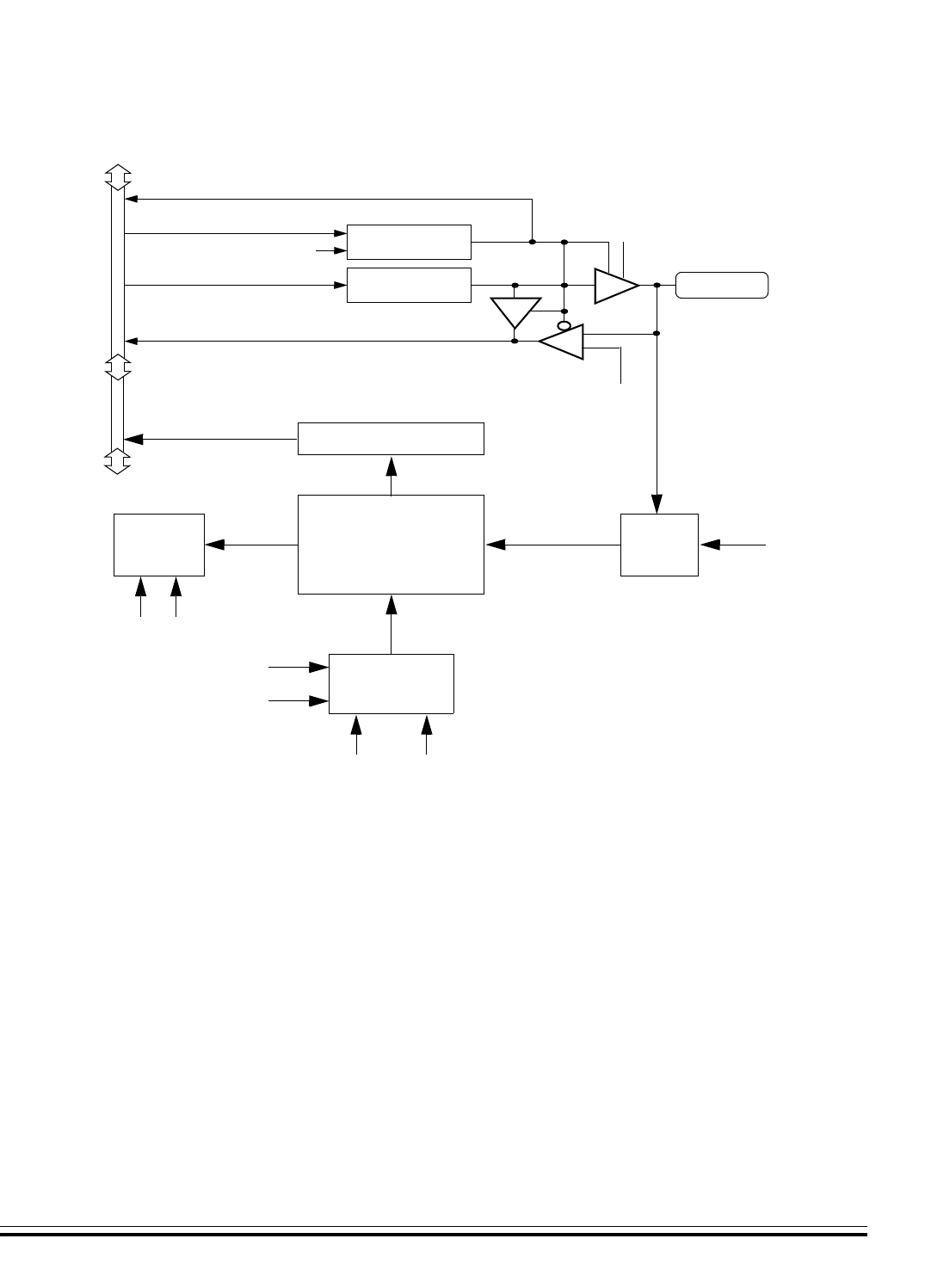
Analog-to-Digital Converter (ADC-15)
Functional Description
MC68HC08AZ60 — Rev 1.1 Technical Data
Freescale Semiconductor Analog-to-Digital Converter (ADC-15) 419
Figure 25-1. ADC Block Diagram
25.4.1 ADC Port I/O Pins
PTD6/ATD14/TACLK–PTD0/ATD8 and PTB7/ATD7–PTB0/ATD0 are
general-purpose I/O pins that share with the ADC channels.
The channel select bits define which ADC channel/port pin will be used
as the input signal. The ADC overrides the port I/O logic by forcing that
pin as input to the ADC. The remaining ADC channels/port pins are
controlled by the port I/O logic and can be used as general-purpose I/O.
Writes to the port register or DDR will not have any affect on the port pin
that is selected by the ADC. Read of a port pin which is in use by the
INTERNAL
DATA BUS
READ DDRB/DDRB
WRITE DDRB/DDRD
RESET
WRITE PTB/PTD
READ PTB/PTD
PTBx/PTDx
DDRBx/DDRDx
PTBx/PTDx
INTERRUPT
LOGIC
CHANNEL
SELECT
ADC
CLOCK
GENERATOR
CONVERSION
COMPLETE
ADC VOLTAGE IN
ADCVIN
ADC CLOCK
CGMXCLK
BUS CLOCK
ADCH[4:0]
ADC DATA REGISTER
ADIV[2:0] ADICLK
AIEN COCO
DISABLE
DISABLE
ADC CHANNEL x

Analog-to-Digital Converter (ADC-15)
Technical Data MC68HC08AZ60 — Rev 1.1
420 Analog-to-Digital Converter (ADC-15) Freescale Semiconductor
ADC will return a logic 0 if the corresponding DDR bit is at logic 0. If the
DDR bit is at logic 1, the value in the port data latch is read.
NOTE: Do not use ADC channels ATD14 or ATD12 when using the
PTD6/ATD14/TACLK or PTD4/ATD12/TBLCK pins as the clock inputs
for the 16-bit Timers.
25.4.2 Voltage Conversion
When the input voltage to the ADC equals VREFH (see Electrical
Specifications on page 423), the ADC converts the signal to $FF (full
scale). If the input voltage equals AVSS/VREFL, the ADC converts it to
$00. Input voltages between VREFH and AVSS/VREFL are a straight-line
linear conversion. Conversion accuracy of all other input voltages is not
guaranteed. Avoid current injection on unused ADC inputs to prevent
potential conversion error.
NOTE: Input voltage should not exceed the analog supply voltages.
25.4.3 Conversion Time
Conversion starts after a write to the ADSCR (ADC status control
register, $0038), and requires between 16 and 17 ADC clock cycles to
complete. Conversion time in terms of the number of bus cycles is a
function of ADICLK select, CGMXCLK frequency, bus frequency, and
ADIV prescaler bits. For example, with a CGMXCLK frequency of 4
MHz, bus frequency of 8 MHz, and fixed ADC clock frequency of 1 MHz,
one conversion will take between 16 and 17 µs and there will be between
128 bus cycles between each conversion. Sample rate is approximately
60 kHz.
Refer to Electrical Specifications on page 423.
16 to 17 ADC Clock Cycles
Conversion Time =
ADC Clock Frequency
Number of Bus Cycles = Conversion Time x Bus Frequency

Analog-to-Digital Converter (ADC-15)
Interrupts
MC68HC08AZ60 — Rev 1.1 Technical Data
Freescale Semiconductor Analog-to-Digital Converter (ADC-15) 421
25.4.4 Continuous Conversion
In the continuous conversion mode, the ADC data register will be filled
with new data after each conversion. Data from the previous conversion
will be overwritten whether that data has been read or not. Conversions
will continue until the ADCO bit (ADC status control register, $0038) is
cleared. The COCO bit is set after the first conversion and will stay set
for the next several conversions until the next write of the ADC status
and control register or the next read of the ADC data register.
25.4.5 Accuracy and Precision
The conversion process is monotonic and has no missing codes. See
Electrical Specifications on page 423 for accuracy information.
25.5 Interrupts
When the AIEN bit is set, the ADC module is capable of generating a
CPU interrupt after each ADC conversion. A CPU interrupt is generated
if the COCO bit (ADC status control register, $0038) is at logic 0. If the
COCO bit is set, an interrupt is generated. The COCO bit is not used as
a conversion complete flag when interrupts are enabled.
25.6 Low-Power Modes
The following subsections describe the low-power modes.
25.6.1 Wait Mode
The ADC continues normal operation during wait mode. Any enabled
CPU interrupt request from the ADC can bring the MCU out of wait
mode. If the ADC is not required to bring the MCU out of wait mode,
power down the ADC by setting the ADCH[4:0] bits in the ADC status
and control register before executing the WAIT instruction.

Analog-to-Digital Converter (ADC-15)
Technical Data MC68HC08AZ60 — Rev 1.1
422 Analog-to-Digital Converter (ADC-15) Freescale Semiconductor
25.6.2 Stop Mode
The ADC module is inactive after the execution of a STOP instruction.
Any pending conversion is aborted. ADC conversions resume when the
MCU exits stop mode. Allow one conversion cycle to stabilize the analog
circuitry before attempting a new ADC conversion after exiting stop
mode.
25.7 I/O Signals
The ADC module has 15 channels that are shared with I/O ports B and
D. Refer to Electrical Specifications on page 423 for voltages
referenced below.
25.7.1 ADC Analog Power Pin (VDDAREF)
The ADC analog portion uses VDDAREF as its power pin. Connect the
VDDAREF pin to the same voltage potential as VDD. External filtering may
be necessary to ensure clean VDDAREF for good results.
NOTE: Route VDDAREF carefully for maximum noise immunity and place bypass
capacitors as close as possible to the package. VDDAREF must be
present for operation of the ADC.
25.7.2 ADC Analog Ground/ADC Voltage Reference Low Pin (AVSS/VREFL)
The ADC analog portion uses AVSS/VREFL as its ground pin. Connect
the AVSS/VREFL pin to the same voltage potential as VSS.
VREFL is the lower reference supply for the ADC.
25.7.3 ADC Voltage Reference Pin (VREFH)
VREFH is the high reference voltage for all analog-to-digital conversions.

Analog-to-Digital Converter (ADC-15)
I/O Registers
MC68HC08AZ60 — Rev 1.1 Technical Data
Freescale Semiconductor Analog-to-Digital Converter (ADC-15) 423
25.7.4 ADC Voltage In (ADCVIN)
ADCVIN is the input voltage signal from one of the 15 ADC channels to
the ADC module.
25.8 I/O Registers
These I/O registers control and monitor ADC operation:
• ADC status and control register (ADSCR)
• ADC data register (ADR)
• ADC clock register (ADICLK)
25.8.1 ADC Status and Control Register
The following paragraphs describe the function of the ADC status and
control register.
COCO — Conversions Complete Bit
When the AIEN bit is a logic 0, the COCO is a read-only bit which is
set each time a conversion is completed. This bit is cleared whenever
the ADC status and control register is written or whenever the ADC
data register is read.
Address: $0038
Bit 7654321Bit 0
Read: COCO
AIEN ADCO ADCH4 ADCH3 ADCH2 ADCH1 ADCH0
Write: R
Reset:00011111
R= Reserved
Figure 25-2. ADC Status and Control Register (ADSCR)

Analog-to-Digital Converter (ADC-15)
Technical Data MC68HC08AZ60 — Rev 1.1
424 Analog-to-Digital Converter (ADC-15) Freescale Semiconductor
If the AIEN bit is a logic 1, the COCO is a read/write bit which selects
the CPU to service the ADC interrupt request. Reset clears this bit.
1 = conversion completed (AIEN = 0)
0 = conversion not completed (AIEN = 0)
or
CPU interrupt enabled (AIEN = 1)
AIEN — ADC Interrupt Enable Bit
When this bit is set, an interrupt is generated at the end of an ADC
conversion. The interrupt signal is cleared when the data register is
read or the status/control register is written. Reset clears the AIEN bit.
1 = ADC interrupt enabled
0 = ADC interrupt disabled
ADCO — ADC Continuous Conversion Bit
When set, the ADC will convert samples continuously and update the
ADR register at the end of each conversion. Only one conversion is
allowed when this bit is cleared. Reset clears the ADCO bit.
1 = Continuous ADC conversion
0 = One ADC conversion
ADCH[4:0] — ADC Channel Select Bits
ADCH4, ADCH3, ADCH2, ADCH1, and ADCH0 form a 5-bit field
which is used to select one of 15 ADC channels. Channel selection is
detailed in the following table. Care should be taken when using a port
pin as both an analog and a digital input simultaneously to prevent
switching noise from corrupting the analog signal. See Table 25-1.
The ADC subsystem is turned off when the channel select bits are all
set to one. This feature allows for reduced power consumption for the
MCU when the ADC is not used. Reset sets these bits.
NOTE: Recovery from the disabled state requires one conversion cycle to
stabilize.

Analog-to-Digital Converter (ADC-15)
I/O Registers
MC68HC08AZ60 — Rev 1.1 Technical Data
Freescale Semiconductor Analog-to-Digital Converter (ADC-15) 425
Table 25-1. Mux Channel Select
ADCH4 ADCH3 ADCH2 ADCH1 ADCH0 Input Select
00000 PTB0/ATD0
00001 PTB1/ATD1
00010 PTB2/ATD2
00011 PTB3/ATD3
00100 PTB4/ATD4
00101 PTB5/ATD5
00110 PTB6/ATD6
00111 PTB7/ATD7
01000 PTD0/ATD8
01001 PTD1/ATD9
01010PTD2/ATD10
01011PTD3/ATD11
01100PTD4/ATD12/TBLCK
01101PTD5/ATD13
01110PTD6/ATD14/TACLK
Range 01111 ($0F) to 11010 ($1A)
Unused (see Note 1)
Unused (see Note 1)
11011 Reserved
11 1 0 0 Unused (see Note 1)
11 1 0 1 VREFH
(see Note 2)
11 1 1 0 AVSS/VREFL (see Note 2)
11 1 1 1 [ADC power off]
NOTES:
1. If any unused channels are selected, the resulting ADC conversion will be
unknown.
2. The voltage levels supplied from internal reference nodes as specified in the
table are used to verify the operation of the ADC converter both in production
test and for user applications.

Analog-to-Digital Converter (ADC-15)
Technical Data MC68HC08AZ60 — Rev 1.1
426 Analog-to-Digital Converter (ADC-15) Freescale Semiconductor
25.8.2 ADC Data Register
One 8-bit result register is provided. This register is updated each time
an ADC conversion completes.
25.8.3 ADC Input Clock Register
This register selects the clock frequency for the ADC.
ADIV2–ADIV0 — ADC Clock Prescaler Bits
ADIV2, ADIV1, and ADIV0 form a 3-bit field which selects the divide
ratio used by the ADC to generate the internal ADC clock. Table 25-
2 shows the available clock configurations. The ADC clock should be
set to approximately 1 MHz.
Address: $0039
Bit 7654321Bit 0
Read: AD7 AD6 AD5 AD4 AD3 AD2 AD1 AD0
Write:RRRRRRRR
Reset: Indeterminate after Reset
R= Reserved
Figure 25-3. ADC Data Register (ADR)
Address: $003A
Bit 7654321Bit 0
Read:
ADIV2 ADIV1 ADIV0 ADICLK
0000
Write: RRRR
Reset: 00000000
R= Reserved
Figure 25-4. ADC Input Clock Register (ADICLK)

Analog-to-Digital Converter (ADC-15)
I/O Registers
MC68HC08AZ60 — Rev 1.1 Technical Data
Freescale Semiconductor Analog-to-Digital Converter (ADC-15) 427
ADICLK — ADC Input Clock Register Bit
ADICLK selects either bus clock or CGMXCLK as the input clock
source to generate the internal ADC clock. Reset selects CGMXCLK
as the ADC clock source.
If the external clock (CGMXCLK) is equal to or greater than 1 MHz,
CGMXCLK can be used as the clock source for the ADC. If
CGMXCLK is less than 1 MHz, use the PLL-generated bus clock as
the clock source. As long as the internal ADC clock is at
approximately 1 MHz, correct operation can be guaranteed. See
Electrical Specifications on page 423.
1 = Internal bus clock
0 = External clock (CGMXCLK)
NOTE: During the conversion process, changing the ADC clock will result in an
incorrect conversion.
Table 25-2. ADC Clock Divide Ratio
ADIV2 ADIV1 ADIV0 ADC Clock Rate
0 0 0 ADC Input Clock /1
0 0 1 ADC Input Clock / 2
0 1 0 ADC Input Clock / 4
0 1 1 ADC Input Clock / 8
1 X X ADC Input Clock / 16
X = don’t care
fXCLK or Bus Frequency
1 MHz =
ADIV[2:0]

Analog-to-Digital Converter (ADC-15)
Technical Data MC68HC08AZ60 — Rev 1.1
428 Analog-to-Digital Converter (ADC-15) Freescale Semiconductor

MC68HC08AZ60 — Rev 1.1 Technical Data
Freescale Semiconductor Electrical Specifications 429
Technical Data — MC68HC08AZ60
Section 26. Electrical Specifications
26.1 Contents
26.2 Electrical Specifications . . . . . . . . . . . . . . . . . . . . . . . . . . . 430
26.2.1 Maximum Ratings . . . . . . . . . . . . . . . . . . . . . . . . . . . . . . 430
26.2.3 Functional Operating Range. . . . . . . . . . . . . . . . . . . . . . 431
26.2.4 Thermal Characteristics . . . . . . . . . . . . . . . . . . . . . . . . . 431
26.2.5 5.0 Volt DC Electrical Characteristics . . . . . . . . . . . . . . 432
26.2.6 ADC Characteristics . . . . . . . . . . . . . . . . . . . . . . . . . . . . 434
26.2.7 5.0 Vdc ± 0.5 V Serial Peripheral Interface (SPI) Timing435
26.2.8 CGM Operating Conditions. . . . . . . . . . . . . . . . . . . . . . . 438
26.2.9 CGM Component Information. . . . . . . . . . . . . . . . . . . . . 438
26.2.10 CGM Acquisition/Lock Time Information. . . . . . . . . . . . 439
26.2.11 Timer Module Characteristics. . . . . . . . . . . . . . . . . . . . . 440
26.2.12 Memory Characteristics . . . . . . . . . . . . . . . . . . . . . . . . . 440
26.2 Mechanical Specifications. . . . . . . . . . . . . . . . . . . . . . . . . . 441
26.3.1 64-Pin Quad Flat Pack (QFP). . . . . . . . . . . . . . . . . . . . . . 441

Electrical Specifications
Technical Data MC68HC08AZ60 — Rev 1.1
430 Electrical Specifications Freescale Semiconductor
26.2 Electrical Specifications
26.2.1 Maximum Ratings
Maximum ratings are the extreme limits to which the MCU can be
exposed without permanently damaging it.
NOTE: This device is not guaranteed to operate properly at the maximum
ratings. Refer to 5.0 Volt DC Electrical Characteristics on page 432 for
guaranteed operating conditions.
NOTE: This device contains circuitry to protect the inputs against damage due
to high static voltages or electric fields; however, it is advised that normal
precautions be taken to avoid application of any voltage higher than
maximum-rated voltages to this high-impedance circuit. For proper
operation, it is recommended that VIN and VOUT be constrained to the
range VSS ≤ (VIN or VOUT) ≤ VDD. Reliability of operation is enhanced if
unused inputs are connected to an appropriate logic voltage level (for
example, either VSS or VDD).
Rating Symbol Value Unit
Supply Voltage VDD –0.3 to +6.0 V
Input Voltage VIN VSS –0.3 to VDD +0.3 V
Maximum Current Per Pin
Excluding VDD and VSS I± 25 mA
Storage Temperature TSTG –55 to +150 °C
Maximum Current out of VSS IMVSS 100 mA
Maximum Current into VDD IMVDD 100 mA
Reset IRQ Input Voltage VHI VDD+2 to VDD + 4 V
NOTE: Voltages are referenced to VSS.

Electrical Specifications
Electrical Specifications
MC68HC08AZ60 — Rev 1.1 Technical Data
Freescale Semiconductor Electrical Specifications 431
26.2.2 Functional Operating Range
NOTE: For applications which use the LVI, Freescale guarantee the
functionality of the device down to the LVI trip point (VLVI).
26.2.3 Thermal Characteristics
Rating Symbol Value Unit
Operating Temperature Range(1)
1. TA(MAX) = 125°C for part suffix MFU
105°C for part suffix VFU
85°C for part suffix CFU
TA–40 to TA(MAX)°C
Operating Voltage Range VDD 5.0 ± 0.5v V
Characteristic Symbol Value Unit
Thermal Resistance
QFP (64 Pins) θJA 70 °C/W
I/O Pin Power Dissipation PI/O User Determined W
Power Dissipation (see Note 1) PDPD = (IDD x VDD) +
PI/O = K/(TJ + 273 °CW
Constant (see Note 2) K PD x (TA + 273 °C)
+ (PD2 x θJA)W/°C
Average Junction Temperature TJTA = PD x θJA °C
NOTES:
1.Power dissipation is a function of temperature.
2.K is a constant unique to the device. K can be determined from a known TA and
measured PD. With this value of K, PD and TJ can be determined for any value of TA.

Electrical Specifications
Technical Data MC68HC08AZ60 — Rev 1.1
432 Electrical Specifications Freescale Semiconductor
26.2.4 5.0 Volt DC Electrical Characteristics
Characteristic Symbol Min Max Unit
Output High Voltage
(ILOAD = –2.0 mA) All Ports VOH
VDD –0.8 —V
(ILOAD = –5.0 mA) All Ports VDD –1.5 —V
Total source current IOHtot —10mA
Output Low Voltage
(ILOAD = 1.6 mA) All Ports VOL
—0.4V
(ILOAD = 10.0 mA) All Ports —1.5V
Total sink current IOLtot —15mA
Input High Voltage
All Ports, IRQs, RESET, OSC1 VIH 0.7 x VDD VDD V
Input Low Voltage
All Ports, IRQs, RESET, OSC1 VIL VSS 0.3 x VDD V
VDD Supply Current
Run (see Notes 2 and 9)
Wait (see Notes 3 and 9)
Stop (see Note 4)
LVI enabled, TA=25 °C
LVI disabled, TA=25 °C
LVI enabled, –40 °C to +125 °C
LVI disabled, –40 °C to +125 °C
IDD
—
—
—
—
—
—
35
20
400
50
500
100
mA
mA
µA
µA
µA
µA
I/O Ports Hi-Z Leakage Current IL—± 1µA
Input Current IIN —± 1µA
Capacitance
Ports (As Input or Output)
COUT
CIN
—
—12
8pF
Low-Voltage Reset Inhibit (trip)
(recover) VLVI 4.0 4.4 V
POR ReArm Voltage (see Note 5) VPOR 0200mV
POR Reset Voltage (see Note 6) VPORRST 0800mV
POR Rise Time Ramp Rate (see Note 7) RPOR 0.02 — V/ms
High COP Disable Voltage (see Note 8) VHI VDD VDD + 2 V

Electrical Specifications
Electrical Specifications
MC68HC08AZ60 — Rev 1.1 Technical Data
Freescale Semiconductor Electrical Specifications 433
26.2.5 Control Timing
NOTES:
1. VDD = 5.0 Vdc ± 10%, VSS = 0 Vdc, TA = –40 °C to +TA (MAX, unless otherwise noted.
2. Run (Operating) IDD measured using external square wave clock source (fOP = 8.4 MHz). All inputs
0.2 V from rail. No dc loads. Less than 100 pF on all outputs. CL = 20 pF on OSC2. All ports
configured as inputs. OSC2 capacitance linearly affects run IDD. Measured with all modules enabled.
3. Wait IDD measured using external square wave clock source (fOP = 8.0 MHz). All inputs 0.2 Vdc from
rail. No dc loads. Less than 100 pF on all outputs, CL = 20 pF on OSC2. All ports configured as in-
puts.
OSC2 capacitance linearly affects wait IDD. Measured with all modules enabled.
4. Stop IDD measured with OSC1 = VSS.
5. Maximum is highest voltage that POR is guaranteed.
6. Maximum is highest voltage that POR is possible.
7. If minimum VDD is not reached before the internal POR reset is released, RST must be driven low
externally until minimum VDD is reached.
8. See COP Module During Break Interrupts on page 176.
9. Although IDD is proportional to bus frequency, a current of several mA is present even at very low frequencies.
Characteristic Symbol Min Max Unit
Bus Operating Frequency (4.5–5.5 V — VDD Only) fBUS —8.4MHz
RESET Pulse Width Low tRL 1.5 — tcyc
IRQ Interrupt Pulse Width Low (Edge-Triggered) tILHI 1.5 — tcyc
IRQ Interrupt Pulse Period tILIL Note 4 — tcyc
16-Bit Timer (see Note 2)
Input Capture Pulse Width (see Note 3)
Input Capture Period
tTH, tTL
tTLTL
2
Note 4 —
—
tcyc
MSCAN Wake-up Filter Pulse Width (see Note 5) tWUP 25µs
NOTES:
1.VDD = 5.0 Vdc ± 0.5v, VSS = 0 Vdc, TA = –40 °C to TA(MAX), unless otherwise noted.
2.The 2-bit timer prescaler is the limiting factor in determining timer resolution.
3.Refer to Table 24-2 and supporting note.
4.The minimum period tTLTL or tILIL should not be less than the number of cycles it takes to execute the capture interrupt
service routine plus TBD tcyc.
5. The minimum pulse width to wake up the MSCAN module is guaranteed by design but not tested.

Electrical Specifications
Technical Data MC68HC08AZ60 — Rev 1.1
434 Electrical Specifications Freescale Semiconductor
26.2.6 ADC Characteristics
Characteristic Min Max Unit Comments
Resolution 8 8 Bits
Absolute Accuracy
(VREFL = 0 V, VDDA/VDDAREF = VREFH = 5 V ±
0.5v)
–1 +1 LSB Includes
Quantization
Conversion Range (see Note 1) VREFL VREFH VVREFL = VSSA
Power-Up Time 16 17 µsConversion Time
Period
Input Leakage (see Note 3)
Ports B and D —± 1 µA
Conversion Time 16 17 ADC
Clock
Cycles
Includes Sampling
Time
Monotonicity Inherent within Total Error
Zero Input Reading 00 01 Hex VIN = VREFL
Full-Scale Reading FE FF Hex VIN = VREFH
Sample Time (see Note 2) 5 — ADC
Clock
Cycles
Input Capacitance — 8 pF Not Tested
ADC Internal Clock 500 k 1.048 M Hz Tested Only at 1 MHz
Analog Input Voltage VREFL VREFH V
NOTES:
1.VDD = 5.0 Vdc ± 0.5v, VSS = 0 Vdc, VDDA/VDDAREF = 5.0 Vdc ± 0.5v, VSSA = 0 Vdc, VREFH = 5.0 Vdc ± 0.5v
2.Source impedances greater than 10 kΩ adversely affect internal RC charging time during input sampling.
3.The external system error caused by input leakage current is approximately equal to the product of R
source and input current.

Electrical Specifications
Electrical Specifications
MC68HC08AZ60 — Rev 1.1 Technical Data
Freescale Semiconductor Electrical Specifications 435
26.2.7 5.0 Vdc ± 0.5 V Serial Peripheral Interface (SPI) Timing
Num Characteristic Symbol Min Max Unit
Operating Frequency (see Note 3)
Master
Slave
fBUS(M)
fBUS(S)
fBUS/128
dc
fBUS/2
fBUS
MHz
1
Cycle Time
Master
Slave
tcyc(M)
tcyc(S)
2
1
128
—
tcyc
2 Enable Lead Time tLead 15 — ns
3 Enable Lag Time tLag 15 — ns
4
Clock (SCK) High Time
Master
Slave
tW(SCKH)M
tW(SCKH)S
100
50
—
—
ns
5
Clock (SCK) Low Time
Master
Slave
tW(SCKL)M
tW(SCKL)S
100
50
—
—
ns
6
Data Setup Time (Inputs)
Master
Slave
tSU(M)
tSU(S)
45
5
—
—
ns
7
Data Hold Time (Inputs)
Master
Slave
tH(M)
tH(S)
0
15
—
—
ns
8
Access Time, Slave (see Note 4)
CPHA = 0
CPHA = 1
tA(CP0)
tA(CP1)
0
0
40
20
ns
9 Slave Disable Time (Hold Time to High-Impedance State) tDIS —25ns
10
Enable Edge Lead Time to Data Valid (see Note 6)
Master
Slave
tEV(M)
tEV(S)
—
—
10
40
ns
11
Data Hold Time (Outputs, after Enable Edge)
Master
Slave
tHO(M)
tHO(S)
0
5
—
—
ns
12 Data Valid
Master (Before Capture Edge) tV(M) 90 — ns
13 Data Hold Time (Outputs)
Master (Before Capture Edge) tHO(M) 100 — ns
NOTES:
1. All timing is shown with respect to 30% VDD and 70% VDD, unless otherwise noted; assumes 100 pF load on all SPI
pins.
2. Item numbers refer to dimensions in Figure 26-1 and Figure 26-2.
3. fBUS = the currently active bus frequency for the microcontroller.
4. Time to data active from high-impedance state.
5. With 100 pF on all SPI pins
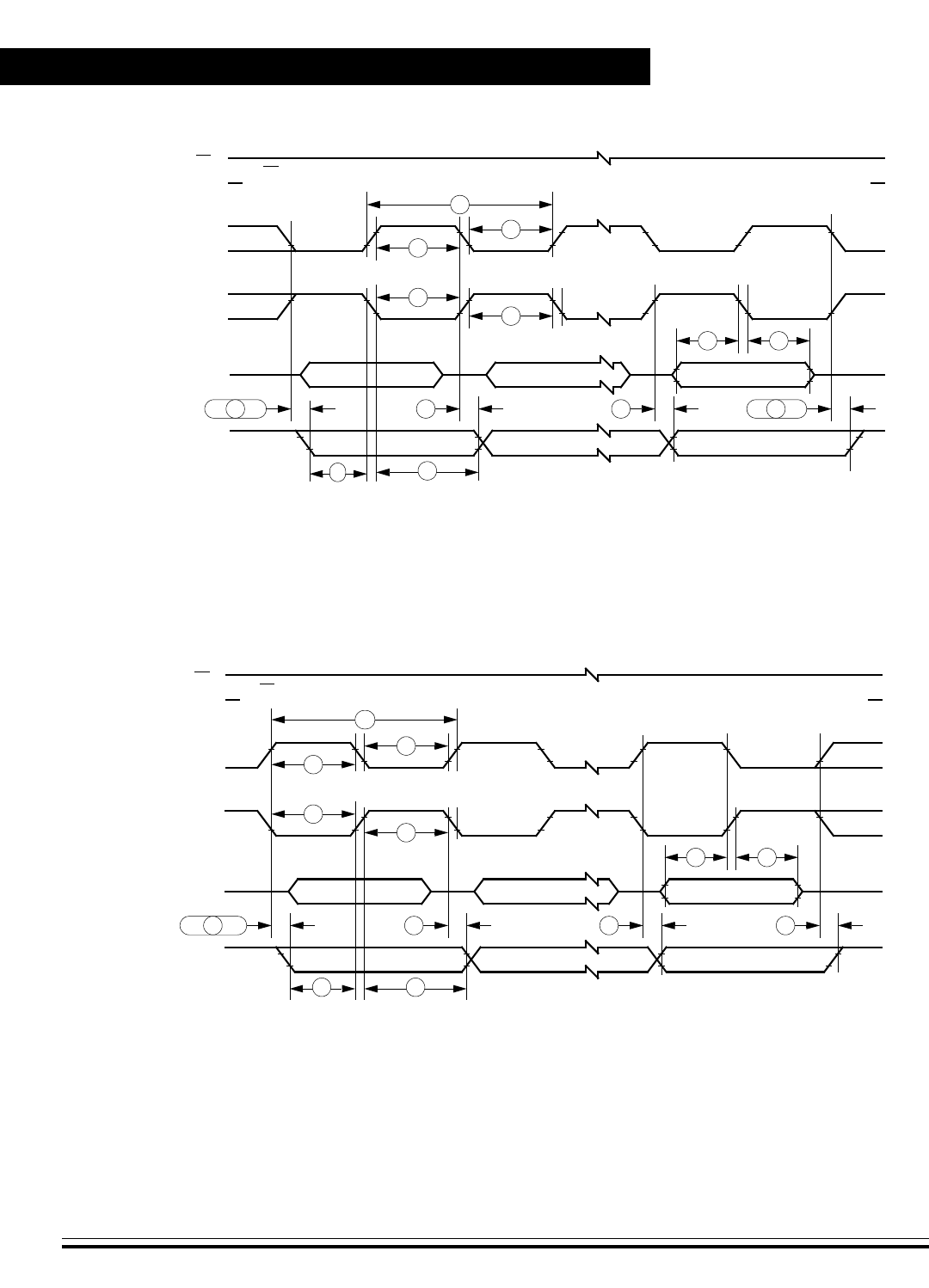
Electrical Specifications
Technical Data MC68HC08AZ60 — Rev 1.1
436 Electrical Specifications Freescale Semiconductor
Figure 26-1. SPI Master Timing Diagram
NOTE
NOTE: This first clock edge is generated internally, but is not seen at the SCK pin.
SS pin of master held high.
MSB IN
SS
(INPUT)
SCK (CPOL = 0)
(OUTPUT)
SCK (CPOL = 1)
(OUTPUT)
MISO
(INPUT)
MOSI
(OUTPUT)
NOTE
4
5
5
1
4
BITS 6–1 LSB IN
MASTER MSB OUT BITS 6–1 MASTER LSB OUT
10 11 10 11
76
NOTE
NOTE: This last clock edge is generated internally, but is not seen at the SCK pin.
SS pin of master held high.
MSB IN
SS
(INPUT)
SCK (CPOL = 0)
(OUTPUT)
SCK (CPOL = 1)
(OUTPUT)
MISO
(INPUT)
MOSI
(OUTPUT)
NOTE
4
5
5
1
4
BITS 6–1 LSB IN
MASTER MSB OUT BITS 6–1 MASTER LSB OUT
10 11 10 11
76
a) SPI Master Timing (CPHA = 0)
b) SPI Master Timing (CPHA = 1)
12 13
12 13
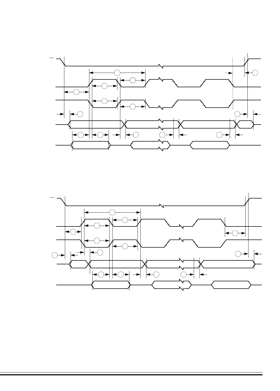
Electrical Specifications
Electrical Specifications
MC68HC08AZ60 — Rev 1.1 Technical Data
Freescale Semiconductor Electrical Specifications 437
Figure 26-2. SPI Slave Timing Diagram
NOTE: Not defined but normally MSB of character just received
SLAVE
SS
(INPUT)
SCK (CPOL = 0)
(INPUT)
SCK (CPOL = 1)
(INPUT)
MISO
(INPUT)
MOSI
(OUTPUT)
4
5
5
1
4
MSB IN
BITS 6–1
8
610
11
11
NOTESLAVE LSB OUT
9
3
LSB IN
2
7
BITS 6–1
MSB OUT
NOTE: Not defined but normally LSB of character previously transmitted
SLAVE
SS
(INPUT)
SCK (CPOL = 0)
(INPUT)
SCK (CPOL = 1)
(INPUT)
MISO
(OUTPUT)
MOSI
(INPUT)
4
5
5
1
4
MSB IN
BITS 6–1
8
610
NOTE SLAVE LSB OUT
9
3
LSB IN
2
7
BITS 6–1
MSB OUT
10
a) SPI Slave Timing (CPHA = 0)
b) SPI Slave Timing (CPHA = 1)
11
11

Electrical Specifications
Technical Data MC68HC08AZ60 — Rev 1.1
438 Electrical Specifications Freescale Semiconductor
26.2.8 CGM Operating Conditions
26.2.9 CGM Component Information
Characteristic Symbol Min Typ Max Comments
Operating Voltage VDD 4.5 V — 5.5 V
Crystal Reference Frequency fRCLK 1 4.9152 MHz 8
Module Crystal Reference
Frequency fXCLK — 4.9152 MHz — Same Frequency as
fRCLK
Range Nom. Multiplier (MHz) fNOM —4.9152 —
4.5–5.5 V, VDD only
VCO Center-of-Range Frequency
(MHz) fVRS 4.9152 — 32.0 4.5–5.5 V, VDD only
VCO Operating Frequency (MHZ) fVCLK 4.9152 — 32.0
Description Symbol Min Typ Max Comments
Crystal Load Capacitance CL—— —
Consult Crystal
Manufacturer’s Data
Crystal Fixed Capacitance C1 — 2 x CL — Consult Crystal
Manufacturer’s Data
Crystal Tuning Capacitance C2 — 2 x CL — Consult Crystal
Manufacturer’s Data
Filter Capacitor Multiply Factor CFACT 0.0154 F/s V
Filter Capacitor CF—
CFACT x
(VDDA/
fXCLK)
—
See External Filter
Capacitor Pin
(CGMXFC) on page
134
Bypass Capacitor CBYP —0.1 µF—
CBYP must provide
low AC impedance
from f = fXCLK/100 to
100 x fVCLK, so series
resistance must be
considered.

Electrical Specifications
Electrical Specifications
MC68HC08AZ60 — Rev 1.1 Technical Data
Freescale Semiconductor Electrical Specifications 439
26.2.10 CGM Acquisition/Lock Time Information
Description Symbol Min Typ Max Notes
Manual Mode Time to Stable tACQ —(8 x VDDA)/(fXCLK x KACQ) —If CF Chosen
Correctly
Manual Stable to Lock Time tAL —(4 x VDDA)/(fXCLK x KTRK)—If CF Chosen
Correctly
Manual Acquisition Time tLOCK —tACQ+tAL —
Tracking Mode Entry
Frequency Tolerance DTRK 0—± 3.6%
Acquisition Mode Entry
Frequency Tolerance DUNT ± 6.3% — ± 7.2%
LOCK Entry Freq. Tolerance DLOCK 0—± 0.9%
LOCK Exit Freq. Tolerance DUNL ± 0.9% — ± 1.8%
Reference Cycles per
Acquisition Mode
Measurement
nACQ —32—
Reference Cycles per
Tracking Mode
Measurement
nTRK —128—
Automatic Mode Time
to Stable tACQ nACQ/fXCLK (8 x VDDA)/(fXCLK x KACQ) If CF Chosen
Correctly
Automatic Stable to Lock
Time tAL nTRK/fXCLK (4 x VDDA)/(fXCLK x KTRK)—If CF Chosen
Correctly
Automatic Lock Time tLOCK —tACQ+tAL —
PLL Jitter, Deviation of
Average Bus Frequency
over 2 ms 0—
± (fCRYS)
x (.025%)
x (N/4)
N = VCO
Freq. Mult.
(GBNT)
NOTES:
1.GBNT guaranteed but not tested
2.VDD = 5.0 Vdc ± 0.5v, VSS = 0 Vdc, TA = –40 °C to TA(MAX), unless otherwise noted.

Electrical Specifications
Technical Data MC68HC08AZ60 — Rev 1.1
440 Electrical Specifications Freescale Semiconductor
26.2.11 Timer Module Characteristics
26.2.12 Memory Characteristics
Characteristic Symbol Min Max Unit
Input Capture Pulse Width tTIH, tTIL 125 — ns
Input Clock Pulse Width tTCH, tTCL (1/fOP) + 5 —ns
Characteristic Symbol Min Max Unit
RAM Data Retention Voltage VRDR 0.7 — V
EEPROM Programming Time per Byte tEEPGM 10 — ms
EEPROM Erasing Time per Byte tEEBYTE 10 — ms
EEPROM Erasing Time per Block tEEBLOCK 10 — ms
EEPROM Erasing Time per Bulk tEEBULK 10 — ms
EEPROM Programming Voltage Discharge Period tEEFPV 100 — µs
EEPROM Write/Erase Cycles
@ 10 ms Write Time +125 °C10,000 — Cycles
EEPROM Data Retention
After 10,000 Write/Erase Cycles 10 — Years
EEPROM enable recovery time tEEOFF 600 — µs
EEPROM stop recovery time tEESTOP 600 — µs
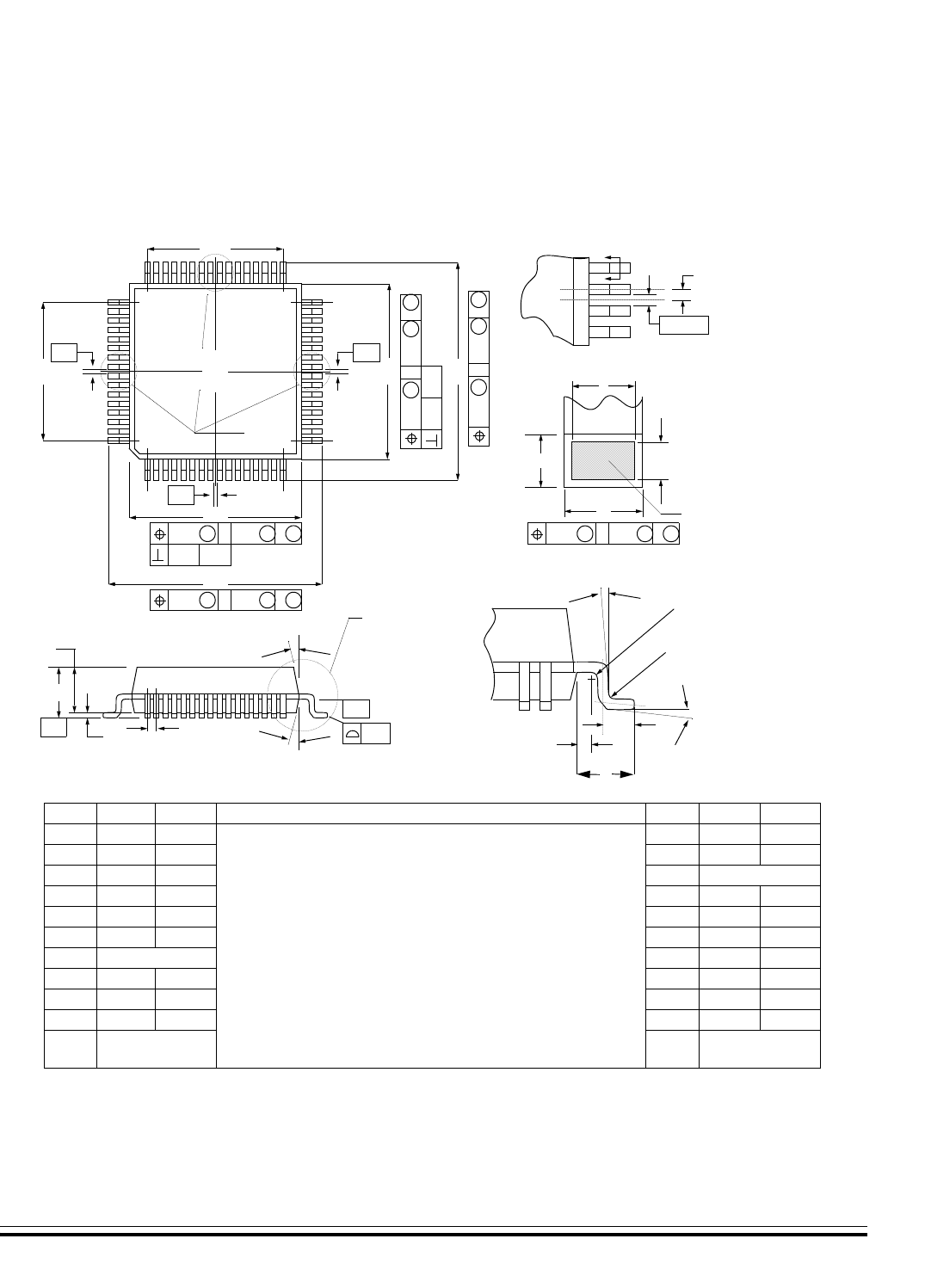
Electrical Specifications
Mechanical Specifications
MC68HC08AZ60 — Rev 1.1 Technical Data
Freescale Semiconductor Electrical Specifications 441
26.3 Mechanical Specifications
26.3.1 64-Pin Quad Flat Pack (QFP)
0.20 MCA – B SDS
L
3348
161
32
17
49
64
- B -
B V
0.05 A – B
- D -
A
S
0.20 MHA – B SDS
L
- A -
Detail A
B
B
- A, B, D -
P
Detail A
F
N
J
D
Section B–B
Base
Metal
G
H
E
C
-C-
M
Detail C
M
-H- Datum
Plane
Seating
Plane
UT
R
Q
K
W
X
0.20 MCA – B SDS
0.05 A – B
0.20 MHA – B SDS
0.20 MCA – B SDS
Dim. Min. Max. Notes Dim. Min. Max.
A 13.90 14.10 1. Dimensions and tolerancing per ANSI Y 14.5M, 1982.
2. All dimensions in mm.
3. Datum Plane –H– is located at bottom of lead and is coincident with
the lead where the lead exits the plastic body at the bottom of the part-
ing line.
4. Datums A–B and –D to be determined at Datum Plane –H–.
5. Dimensions S and V to be determined at seating plane –C–.
6. Dimensions A and B do not include mould protrusion. Allowable
mould protrusion is 0.25mm per side. Dimensions A and B do include
mould mismatch and are determined at Datum Plane –H–.
7. Dimension D does not include dambar protrusion. Allowable dam-
bar protrusion shall be 0.08 total in excess of the D dimension at max-
imum material condition. Dambar cannot be located on the lower
radius or the foot.
M5°10°
B 13.90 14.10 N 0.13 0.17
C 2.15 2.45 P 0.40 BSC
D 0.30 0.45 Q0°7°
E 2.00 2.40 R 0.13 0.30
F 0.30 0.40 S 16.95 17.45
G 0.80 BSC T0.13—
H — 0.25 U0°—
J 0.13 0.23 V 16.95 17.45
K 0.65 0.95 W 0.35 0.45
L12.00 REF X1.6 REF
0.01
Detail C

Electrical Specifications
Technical Data MC68HC08AZ60 — Rev 1.1
442 Electrical Specifications Freescale Semiconductor

MC68HC08AZ60 — Rev 1.1 Technical Data
Freescale Semiconductor Appendix: Future EEPROM Registers 443
Technical Data — MC68HC08AZ60
Section 27. Appendix: Future EEPROM Registers
NOTE: The following are proposed register addresses. Writing to them in
current software will have no effect.
27.1 EEPROM Timebase Divider Control Registers
To program or erase the EEPROM content, the EEPROM control
hardware requires a constant timebase of 35µs to drive its internal timer.
EEPROM Timebase Divider EEDIV is a clock-divider which divides the
selected reference clock source to generate this constant timebase. The
reference clock input of the EEDIV is driven by either the CGMXCLK or
the system bus clock. The selection of this reference clock is defined by
the EEDIVCLK bit in the Configuration Register.
EEPROM Timebase Divider EEDIV are defined by two registers
(EEDIVH and EEDIVL) and must be programmed with a proper value
before starting any EEPROM erase/program steps. EEDIV registers
must be re-programmed when ever its reference clock is changed. The
EEDIV value can be either pre-programmed in the EEDIVHNVR and
EEDIVLNVR non-volatide memory registers, (which upon reset will load
their contents into the EEDIVH and EEDIVL registers,) or programmed
directly by software into the EEDIVH and EEDIVL registers at system
initialization . The function of the divider is to provide a constant clock
source with a period of 35µs (better be within ± 2ms) to the internal timer
and related EEPROM circuits for proper program/erase operations. The
recommended frequency range of the reference clock is 250KHz to
32MHz.

Appendix: Future EEPROM Registers
Technical Data MC68HC08AZ60 — Rev 1.1
444 Appendix: Future EEPROM Registers Freescale Semiconductor
27.2 EEDIVH and EEDIVL Registers
EEDIVH and EEDIVL are used to store the 11-bit EEDIV value which
can be programmed by software at system initialization or during runtime
if the EEDIVSECD bit in the EEDIVH is not cleared. The EEDIV value is
calculated by the following formula:
Where the result inside the bracket [ ]is rounded down to the nearest
interger value.
For example, if the Reference Frequency is 4.9152MHz, the EEDIV
value in the above formula will be 172. To examine the timebase output
of the divider, the Reference Frequency is divided by the calculated
EEDIV value (172), which equals to 28.577KHz in frequency or 34.99µs
in period.
Programming/erasing the EEPROM with an improper EEDIV value may
result in data lost and reduce endurance of the EEPROM device.
EEDIV INT Reference Frequency (Hz) 35 10 6– 0.5+××[]=
Address: $FE1A
Bit 7654321Bit 0
Read: EEDIVSECD EEDIV10 EEDIV9 EEDIV8
Write:
Reset:EEDIVH-NVRxxxx
EEDIVH-
NVR
EEDIVH-
NVR
EEDIVH-
NVR
= Unimplemented
Figure 27-1. EEPROM-2 Divider High Register (EEDIVH)
Address: $FE1B
Bit 7654321Bit 0
Read: EEDIV7 EEDIV6 EEDIV5 EEDIV4 EEDIV3 EEDIV2 EEDIV1 EEDIV0
Write:
Reset: EEDIVH-NVR EEDIVH-NVR EEDIVH-NVR EEDIVH-NVR EEDIVH-NVR EEDIVH-NVR EEDIVH-NVR EEDIVH-NVR
= Unimplemented
Figure 27-2. EEPROM-2 Divider Low Register (EEDIVL)

Appendix: Future EEPROM Registers
EEDIV Non-volatile Registers
MC68HC08AZ60 — Rev 1.1 Technical Data
Freescale Semiconductor Appendix: Future EEPROM Registers 445
EEDIVSECD — EEPROM Divider Security Disable
This bit enables/disables the security feature of the EEDIV registers.
When EEDIV security feature is enabled, the state of the registers
EEDIVH and EEDIVL are locked (inclucding this EEDIVSECD bit).
Also the EEDIVHNVR and EEDIVLNVR non-volatile memory
registers are protected from being erased/programmed.
1 = EEDIV security feature disabled
0 = EEDIV security feature enabled
EEDIV10–EEDIV0 — EEPROM timebase prescalar.
These prescalar bits store the value of EEDIV which is used as the
divisor to derive a timebase of 35µs from the selected reference clock
source for the EEPROM related internal timer and circuits.
EEDIV0–10 are readable at any time. They are writable when EELAT
is not set and EEDIVSECD is not cleared.
27.3 EEDIV Non-volatile Registers
Address: $FE10
Bit 7654321Bit 0
Read: EEDIVSECD EEDIV10 EEDIV9 EEDIV8
Write:
Reset: PV PV PV PV PV PV PV PV
= Unimplemented
Figure 27-3. EEPROM-2 Divider High Non-volatile Register (EEDIVHNVR)
Address: $FE11
Bit 7654321Bit 0
Read: EEDIV7 EEDIV6 EEDIV5 EEDIV4 EEDIV3 EEDIV2 EEDIV1 EEDIV0
Write:
Reset: PV PV PV PV PV PV PV PV
= Unimplemented
Figure 27-4. EEPROM-2 Divider Low Non-volatile Register (EEDIVLNVR)

Appendix: Future EEPROM Registers
Technical Data MC68HC08AZ60 — Rev 1.1
446 Appendix: Future EEPROM Registers Freescale Semiconductor
PV = Programmed Value or ’1’ in the erased state.
The EEPROM Divider non-volatile registers (EEDIVHNVR and
EEDIVLNVR) store the reset values of the EEDIV0–10 and EEDIVSECD
bits which are non-volatile and are not modified by reset. On reset, these
two special registers load the EEDIV0–10 and EEDIVSECD bits into the
corresponding volatile EEDIV registers (EEDIVH and EEDIVL).
The EEDIVHNVR and EEDIVLNVR can be programmed/erased like
normal EEPROM bytes if the Divider Security Disable bit (EEDIVSECD)
in the EEDIVH is not cleared. The new 11-bit EEDIV value in the non-
volatile registers (EEDIVHNVR and EEDIVLNVR) together with the
EEPROM Divider Security Disable bit (EEDIVSECD) will only be loaded
into the EEDIVH & EEDIVL registers with a system reset.
NOTE: Once EEDIVSECD in the EEDIVHNVR is programmed to ‘0’ and after a
system reset, the EEDIV security feature is permanently enabled
because the EEDIVSECD bit in the EEDIVH is always loaded with a ‘0’
thereafter. Once this security feature is armed, erase and program
modes are disabled for EEDIVHNVR and EEDIVLNVR. Modifications to
the EEDIVH and EEDIVL registers are also disabled. Therefore, great
care should be taken before programming a value into the EEDIVHNVR.

MC68HC08AZ60 — Rev 1.1 Technical Data
Freescale Semiconductor Appendix: HC08AZ48 Memory Map 447
Technical Data — MC68HC08AZ60
Section 28. Appendix: HC08AZ48 Memory Map
28.1 Contents
28.2 Introduction. . . . . . . . . . . . . . . . . . . . . . . . . . . . . . . . . . . . . .447
28.3 I/O Section. . . . . . . . . . . . . . . . . . . . . . . . . . . . . . . . . . . . . . .450
28.2 Introduction
The MC68HC08AZ48 can address 48 Kbytes of memory space. It is
basically identical to the MC68HC08AZ60 part except that ROM and
EEPROM size are smaller. The memory map, shown in Figure 28-1,
includes:
• 48 Kbytes of ROM
• 1536 Bytes of RAM
• 768 Bytes of EEPROM with Protect Option
• 52 Bytes of User-Defined Vectors
• 224 Bytes of Monitor ROM
The following definitions apply to the memory map representation of
reserved and unimplemented locations.
•Reserved — Accessing a reserved location can have
unpredictable effects on MCU operation.
•Unimplemented — Accessing an unimplemented location
causes an illegal address reset if illegal address resets are
enabled.

Appendix: HC08AZ48 Memory Map
Technical Data MC68HC08AZ60 — Rev 1.1
448 Appendix: HC08AZ48 Memory Map Freescale Semiconductor
Figure 28-1. Memory Map
$0000
I/O REGISTERS (64 BYTES)
$0000
↓↓
$003F $003F
$0040
I/O REGISTERS, 16 BYTES
$0040
↓↓
$004F $004F
$0050
RAM-1, 1024 BYTES
$0050
↓↓
$044F $044F
$0450
RESERVED
$0450
↓↓
$04FF $04FF
$0500
CAN CONTROL AND MESSAGE
BUFFERS, 128 BYTES
$0500
↓↓
$057F $057F
$0580
RESERVED
$0580
↓↓
$05FF $05FF
$0600
EEPROM-2, 256 BYTES
$0600
↓↓
$06FF $06FF
$0700
RESERVED
$0700
↓↓
$07FF $07FF
$0800
EEPROM-1, 512 BYTES
$0800
↓↓
$09FF $09FF
$0A00
RAM-2, 512 BYTES
$0A00
↓↓
$0BFF $0BFF
$0C00
RESERVED
$0C00
↓↓
$0DFF $0DFF

Appendix: HC08AZ48 Memory Map
Introduction
MC68HC08AZ60 — Rev 1.1 Technical Data
Freescale Semiconductor Appendix: HC08AZ48 Memory Map 449
$0E00
RESERVED
$0E00
↓↓
$3FFF $3FFF
$4000
ROM-2, 16384 BYTES
$4000
↓↓
$7FFF $7FFF
$8000
ROM-1, 32,256BYTES
$8000
↓↓
$FDFF $FDFF
$FE00 SIM BREAK STATUS REGISTER (SBSR) $FE00
$FE01 SIM RESET STATUS REGISTER (SRSR) $FE01
$FE02 RESERVED $FE02
$FE03 SIM BREAK FLAG CONTROL REGISTER (SBFCR) $FE03
$FE04 RESERVED $FE04
$FE05 RESERVED $FE05
$FE06 UNIMPLEMENTED $FE06
$FE07 RESERVED $FE07
$FE08 RESERVED $FE08
$FE09 RESERVED $FE09
$FE0A RESERVED $FE0A
$FE0B RESERVED $FE0B
$FE0C BREAK ADDRESS REGISTER HIGH (BRKH) $FE0C
$FE0D BREAK ADDRESS REGISTER LOW (BRKL) $FE0D
$FE0E BREAK STATUS AND CONTROL REGISTER (BSCR) $FE0E
$FE0F LVI STATUS REGISTER (LVISR) $FE0F
$FE10 RESERVED $FE10
$FE11 RESERVED $FE11
$FE12
UNIMPLEMENTED (5BYTES)
$FE12
↓↓
$FE17 $FE17
$FE18 EEPROM NON-VOLATILE REGISTER (EENVR2) $FE18
$FE19 EEPROM CONTROL REGISTER (EECR2) $FE19
$FE1A RESERVED $FE1A
Figure 28-1. Memory Map (Continued)

Appendix: HC08AZ48 Memory Map
Technical Data MC68HC08AZ60 — Rev 1.1
450 Appendix: HC08AZ48 Memory Map Freescale Semiconductor
28.3 I/O Section
Addresses $0000–$003F, shown in Figure 28-2, contain most of the
control, status, and data registers. Additional I/O registers have these
addresses:
• $FE00 (SIM break status register, SBSR)
• $FE01 (SIM reset status register, SRSR)
• $FE03 (SIM break flag control register, SBFCR)
• $FE09 (configuration write-once register, CONFIG-2)
• $FE0C and $FE0D (break address registers, BRKH and BRKL)
• $FE0E (break status and control register, BRKSCR)
• $FE0F (LVI status register, LVISR)
• $FE18 (EEPROM non-volatile register, EENVR2)
$FE1B EEPROM ARRAY CONFIGURATION (EEACR2) $FE1B
$FE1C EEPROM NON-VOLATILE REGISTER (EENVR1) $FE1C
$FE1D EEPROM CONTROL REGISTER (EECR1) $FE1D
$FE1E RESERVED $FE1E
$FE1F EEPROM ARRAY CONFIGURATION (EEACR1) $FE1F
$FE20
MONITOR ROM (224 BYTES)
$FE20
↓↓
$FEFF $FEFF
$FF00
↓
$FF7F
UNIMPLEMENTED (128 BYTES)
$FF00
↓
$FF7F
$FF80 RESERVED $FF80
$FF81 RESERVED $FF81
$FF82
RESERVED (75 BYTES)
$FF82
↓↓
$FFCB $FFCB
$FFCC
VECTORS (52BYTES)
$FFCC
↓↓
$FFFF $FFFF
Figure 28-1. Memory Map (Continued)

Appendix: HC08AZ48 Memory Map
I/O Section
MC68HC08AZ60 — Rev 1.1 Technical Data
Freescale Semiconductor Appendix: HC08AZ48 Memory Map 451
• $FE19 (EEPROM control register, EECR2)
• $FE1B (EEPROM array configuration register, EEACR2)
• $FE1C (EEPROM non-volatile register, EENVR1)
• $FE1D (EEPROM control register, EECR1)
• $FE1F (EEPROM array configuration register, EEACR1)
• $FFFF (COP control register, COPCTL)
•Table 28-1 is a list of vector locations.

Appendix: HC08AZ48 Memory Map
Technical Data MC68HC08AZ60 — Rev 1.1
452 Appendix: HC08AZ48 Memory Map Freescale Semiconductor
Addr. Register Name Bit 7 6 5 4 3 2 1 Bit 0
$0000 Port A Data Register (PTA) Read: PTA7 PTA6 PTA5 PTA4 PTA3 PTA2 PTA1 PTA0
Write:
$0001 Port B Data Register (PTB) Read: PTB7 PTB6 PTB5 PTB4 PTB3 PTB2 PTB1 PTB0
Write:
$0002 Port C Data Register (PTC) Read: 0 0 PTC5 PTC4 PTC3 PTC2 PTC1 PTC0
Write:
$0003 Port D Data Register (PTD) Read: PTD7 PTD6 PTD5 PTD4 PTD3 PTD2 PTD1 PTD0
Write:
$0004 Data Direction Register A
(DDRA)
Read: DDRA7 DDRA6 DDRA5 DDRA4 DDRA3 DDRA2 DDRA1 DDRA0
Write:
$0005 Data Direction Register B
(DDRB)
Read: DDRB7 DDRB6 DDRB5 DDRB4 DDRB3 DDRB2 DDRB1 DDRB0
Write:
$0006 Data Direction Register C
(DDRC)
Read: MCLKE
N
0DDRC5 DDRC4 DDRC3 DDRC2 DDRC1 DDRC0
Write:
$0007 Data Direction Register D
(DDRD)
Read: DDRD7 DDRD6 DDRD5 DDRD4 DDRD3 DDR2 DDRD1 DDRD0
Write:
$0008 Port E Data Register (PTE) Read: PTE7 PTE6 PTE5 PTE4 PTE3 PTE2 PTE1 PTE0
Write:
$0009 Port F Data Register (PTF) Read: 0 PTF6 PTF5 PTF4 PTF3 PTF2 PTF1 PTF0
Write:
$000A Port G Data Register (PTG) Read: 0 0 0 0 0 PTG2 PTG1 PTG0
Write:
$000B Port H Data Register (PTH) Read: 0 0 0 0 0 0 PTH1 PTH0
Write:
$000C Data Direction Register E
(DDRE)
Read: DDRE7 DDRE6 DDRE5 DDRE4 DDRE3 DDRE2 DDRE1 DDRE0
Write:
$000D Data Direction Register F
(DDRF)
Read: 0 DDRF6 DDRF5 DDRF4 DDRF3 DDRF2 DDRF1 DDRF0
Write:
$000E Data Direction Register G
(DDRG)
Read: 0 0 0 0 0 DDRG2 DDRG1 DDRG0
Write:
$000F Data Direction Register H
(DDRH)
Read: 0 0 0 0 0 0 DDRH1 DDRH0
Write:
$0010 SPI Control Register (SPCR) Read: SPRIE R SPMSTR CPOL CPHA SPWOM SPE SPTIE
Write:
= Unimplemented R = Reserved
Figure 28-2. Control, Status, and Data Registers (Sheet 1 of 6)

Appendix: HC08AZ48 Memory Map
I/O Section
MC68HC08AZ60 — Rev 1.1 Technical Data
Freescale Semiconductor Appendix: HC08AZ48 Memory Map 453
$0011 SPI Status and Control
Register (SPSCR)
Read: SPRF ERRIE OVRF MODF SPTE MODFE
NSPR1 SPR0
Write:
$0012 SPI Data Register (SPDR) Read: R7 R6 R5 R4 R3 R2 R1 R0
Write: T7 T6 T5 T4 T3 T2 T1 T0
$0013 SCI Control Register 1 (SCC1) Read: LOOPS ENSCI TXINV M WAKE ILTY PEN PTY
Write:
$0014 SCI Control Register 2 (SCC2) Read: SCTIE TCIE SCRIE ILIE TE RE RWU SBK
Write:
$0015 SCI Control Register 3 (SCC3) Read: R8 T8 R R ORIE NEIE FEIE PEIE
Write:
$0016 SCI Status Register 1 (SCS1) Read: SCTE TC SCRF IDLE OR NF FE PE
Write:
$0017 SCI Status Register 2 (SCS2) Read: 0 0 0 0 0 0 BKF RPF
Write:
$0018 SCI Data Register (SCDR) Read: R7 R6 R5 R4 R3 R2 R1 R0
Write: T7 T6 T5 T4 T3 T2 T1 T0
$0019 SCI Baud Rate Register (SCBR) Read: 0 0 SCP1 SCP0 SCR2 SCR1 SCR0
Write:
$001A IRQ Status and Control
Register (ISCR)
Read: 0 0 0 0 IRQF 0 IMASK1 MODE1
Write: ACK1
$001B Keyboard Status and Control
Register (KBSCR)
Read: 0 0 0 0 KEYF 0 IMASKK MODEK
Write: ACKK
$001C PLL Control Register (PCTL) Read: PLLIE PLLF PLLON BCS 1111
Write:
$001D PLL Bandwidth Control
Register (PBWC)
Read: AUTO LOCK ACQ XLD 0000
Write:
$001E PLL Programming Register
(PPG)
Read: MUL7 MUL6 MUL5 MUL4 VRS7 VRS6 VRS5 VRS4
Write:
$001F Mask Option
Register (MOR)
Read: LVISTO
PROMSEC LVIRST LVIPWR SSREC COPS STOP COPD
Write:RRR R RRRR
$0020 Timer A Status and Control
Register (TASC)
Read: TOF TOIE TSTOP 00
PS2 PS1 PS0
Write: 0 TRST
$0021 Keyboard Interrupt Enable
Register (KBIE)
Read: 0 0 0 KBIE4 KBIE3 KBIE2 KBIE1 KBIE0
Write:
Addr. Register Name Bit 7 6 5 4 3 2 1 Bit 0
Figure 28-2. Control, Status, and Data Registers (Sheet 2 of 6)

Appendix: HC08AZ48 Memory Map
Technical Data MC68HC08AZ60 — Rev 1.1
454 Appendix: HC08AZ48 Memory Map Freescale Semiconductor
$0022 Timer A Counter Register
High (TACNTH)
Read: Bit 15 14 13 12 11 10 9 Bit 8
Write:
$0023 Timer A Counter Register
Low (TACNTL)
Read: Bit 7 6 5 4 3 2 1 Bit 0
Write:
$0024 Timer A Modulo Register
High (TAMODH)
Read: Bit 15 14 13 12 11 10 9 Bit 8
Write:
$0025 Timer A Modulo Register
Low (TAMODL)
Read: Bit 7 6 5 4 3 2 1 Bit 0
Write:
$0026 Timer A Channel 0 Status and
Control Register (TASC0)
Read: CH0F CH0IE MS0B MS0A ELS0B ELS0A TOV0 CH0MAX
Write: 0
$0027 Timer A Channel 0 Register
High (TACH0H)
Read: Bit 15 14 13 12 11 10 9 Bit 8
Write:
$0028 Timer A Channel 0 Register
Low (TACH0L)
Read: Bit 7 6 5 4 3 2 1 Bit 0
Write:
$0029 Timer A Channel 1 Status and
Control Register (TASC1)
Read: CH1F CH1IE 0MS1A ELS1B ELS1A TOV1 CH1MAX
Write: 0
$002A Timer A Channel 1 Register
High (TACH1H)
Read: Bit 15 14 13 12 11 10 9 Bit 8
Write:
$002B Timer A Channel 1 Register
Low (TACH1L)
Read: Bit 7 6 5 4 3 2 1 Bit 0
Write:
$002C Timer A Channel 2 Status and
Control Register (TASC2)
Read: CH2F CH2IE MS2B MS2A ELS2B ELS2A TOV2 CH2MAX
Write: 0
$002D Timer A Channel 2 Register
High (TACH2H)
Read: Bit 15 14 13 12 11 10 9 Bit 8
Write:
$002E Timer A Channel 2 Register
Low (TACH2L)
Read: Bit 7 6 5 4 3 2 1 Bit 0
Write:
$002F Timer A Channel 3 Status and
Control Register (TASC3)
Read: CH3F CH3IE 0MS3A ELS3B ELS3A TOV3 CH3MAX
Write: 0
$0030 Timer A Channel 3 Register
High (TACH3H)
Read: Bit 15 14 13 12 11 10 9 Bit 8
Write:
$0031 Timer A Channel 3 Register
Low (TACH3L)
Read: Bit 7 6 5 4 3 2 1 Bit 0
Write:
$0032 Timer A Channel 4 Status and
Control Register (TASC4)
Read: CH4F CH4IE MS4B MS4A ELS4B ELS4A TOV4 CH4MAX
Write: 0
$0033 Timer A Channel 4 Register High
(TACH4H)
Read: Bit 15 14 13 12 11 10 9 Bit 8
Write:
Addr. Register Name Bit 7 6 5 4 3 2 1 Bit 0
Figure 28-2. Control, Status, and Data Registers (Sheet 3 of 6)

Appendix: HC08AZ48 Memory Map
I/O Section
MC68HC08AZ60 — Rev 1.1 Technical Data
Freescale Semiconductor Appendix: HC08AZ48 Memory Map 455
$0034 Timer A Channel 4 Register Low
(TACH4L)
Read: Bit 7 6 5 4 3 2 1 Bit 0
Write:
$0035 Timer A Channel 5 Status and
Control Register (TASC5)
Read: CH5F CH5IE 0MS5A ELS5B ELS5A TOV5 CH5MAX
Write: 0
$0036 Timer A Channel 5 Register
High (TACH5H)
Read: Bit 15 14 13 12 11 10 9 Bit 8
Write:
$0037 Timer A Channel 5 Register
Low (TACH5L)
Read: Bit 7 6 5 4 3 2 1 Bit 0
Write:
$0038 Analog-to-Digital Status and
Control Register (ADSCR)
Read: COCO AIEN ADCO ADCH4 ADCH3 ADCH2 ADCH1 ADCH0
Write: R
$0039 Analog-to-Digital Data Register
(ADR)
Read: AD7 AD6 AD5 AD4 AD3 AD2 AD1 AD0
Write:
$003A Analog-to-Digital Input Clock
Register (ADICLK)
Read: ADIV2 ADIV1 ADIV0 ADICLK 0000
Write:
$0040 Timer B Status and Control
Register (TBSCR)
Read: TOF TOIE TSTOP 00
PS2 PS1 PS0
Write: TRST
$0041 Timer B Counter Register High
(TBCNTH)
Read: Bit 15 14 13 12 11 10 9 Bit 8
Write:
$0042 Timer B Counter Register Low
(TBCNTL)
Read: Bit 7 6 5 4 3 2 1 Bit 0
Write:
$0043 Timer B Modulo Register High
(TBMODH)
Read: Bit 15 14 13 12 11 10 9 Bit 8
Write:
$0044 Timer B Modulo Register Low
(TBMODL)
Read: Bit 7 6 5 4 3 2 1 Bit 0
Write:
$0045 Timer B CH0 Status and Control
Register (TBSC0)
Read: CH0F CH0IE MS0B MS0A ELS0B ELS0A TOV0 CH0MAX
Write: 0
$0046 Timer B CH0 Register High
(TBCH0H)
Read: Bit 15 14 13 12 11 10 9 Bit 8
Write:
$0047 Timer B CH0 Register Low
(TBCH0L)
Read: Bit 7 6 5 4 3 2 1 Bit 0
Write:
Timer B CH1 Status and Control
Register (TBSC1)
Read: CH1F CH1IE 0MS1A ELS1B ELS1A TOV1 CH1MAX
$0048 Write: 0
$0049 Timer B CH1 Register High
(TBCH1H)
Read: Bit 15 14 13 12 11 10 9 Bit 8
Write:
$004A Timer B CH1 Register Low
(TBCH1L)
Read: Bit 7 6 5 4 3 2 1 Bit 0
Write:
Addr. Register Name Bit 7 6 5 4 3 2 1 Bit 0
Figure 28-2. Control, Status, and Data Registers (Sheet 4 of 6)

Appendix: HC08AZ48 Memory Map
Technical Data MC68HC08AZ60 — Rev 1.1
456 Appendix: HC08AZ48 Memory Map Freescale Semiconductor
$004B TIM Status and Control Register
(TSC)
Read: TOF TOIE TSTOP 00
PS2 PS1 PS0
Write: TRST
$004C TIM Counter Register High
(TCNTH)
Read: Bit 15 14 13 12 11 10 9 Bit 8
Write:
$004D TIM Counter Register Low
(TCNTL)
Read: Bit 7 6 5 4 3 2 1 Bit 0
Write:
$004E TIM Modulo Register High
(TMODH)
Read: Bit 15 14 13 12 11 10 9 Bit 8
Write:
$004F TIM Modulo Register Low
(TMODL)
Read: Bit 7 6 5 4 3 2 1 Bit 0
Write:
$FE00 SIM Break Status Register
(SBSR)
Read: R R R R R R SBSW R
Write:
$FE01 SIM Reset Status Register (SRSR) Read: POR PIN COP ILOP ILAD 0 LVI 0
Write:
$FE03 SIM Break Flag Control Register
(SBFCR)
Read: BCFERR R RRRR
Write:
$FE09 RESERVED Read: RRR R RRRR
Write:
$FE0B RESERVED Read: RRR R RRRR
Write:
$FE0C Break Address Register High
(BRKH)
Read: Bit 15 14 13 12 11 10 9 Bit 8
Write:
$FE0D Break Address Register Low
(BRKL)
Read: Bit 7 6 5 4 3 2 1 Bit 0
Write:
$FE0E Break Status and Control
Register (BRKSCR)
Read: BRKE BRKA 0 0 0000
Write:
$FE0F LVI Status Register (LVISR) Read: LVIOUT 0 0 0 0 0 0 0
Write:
$FE11 RESERVED Read: RRR R RRRR
Write:
$FE18 EEPROM Nonvolatile Register
(EENVR2)
Read: EERA CON2 CON1 EEPRTC
TEEBP3 EEBP2 EEBP1 EEBP0
Write:
$FE19 EEPROM Control
Register (EECR2)
Read: EEBCLK 0EEOFF EERAS1 EERAS0 EELAT 0EEPGM
Write:
$FE1A Reserved Read: RRR R RRRR
Write:
Addr. Register Name Bit 7 6 5 4 3 2 1 Bit 0
Figure 28-2. Control, Status, and Data Registers (Sheet 5 of 6)
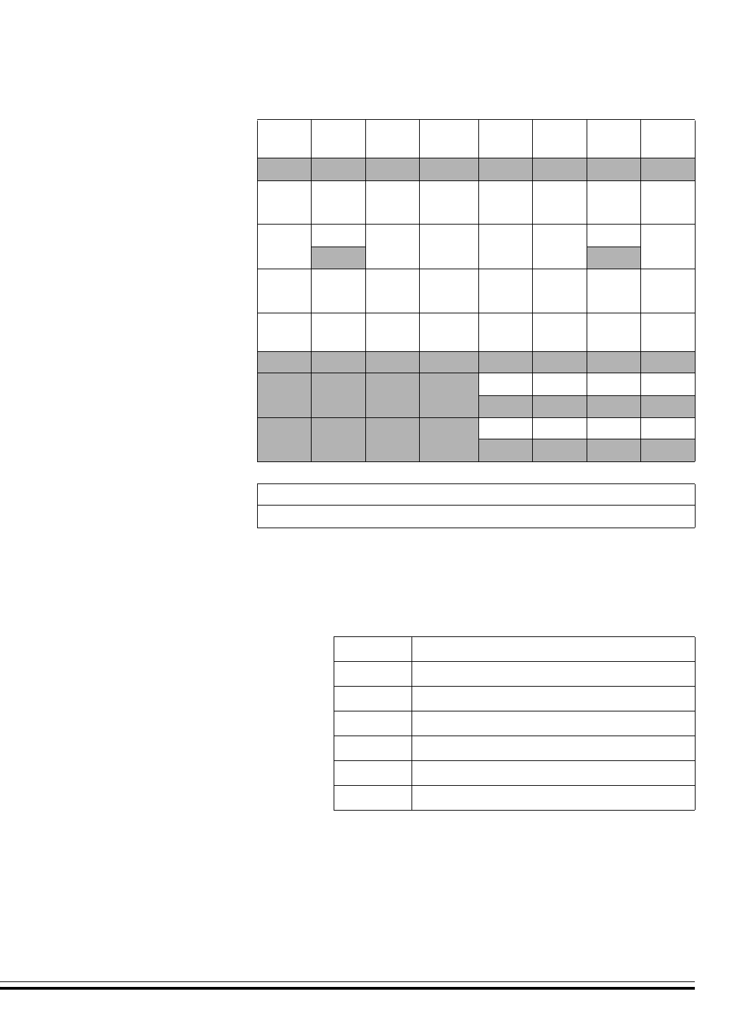
Appendix: HC08AZ48 Memory Map
I/O Section
MC68HC08AZ60 — Rev 1.1 Technical Data
Freescale Semiconductor Appendix: HC08AZ48 Memory Map 457
$FE1B EEPROM Array Control Register
(EEACR2)
Read: EERA CON2 CON1 EEPRTC
TEEBP3 EEBP2 EEBP1 EEBP0
Write:
$FE1C EEPROM Nonvolatile Register
(EENVR1)
Read: EERA CON2 CON1 EEPRTC
TEEBP3 EEBP2 EEBP1 EEBP0
Write:
$FE1D EEPROM Control
Register (EECR1)
Read: EEBCLK 0EEOFF EERAS1 EERAS0 EELAT 0EEPGM
Write:
$FE1E Reserved Read: RRR R RRRR
Write:
$FE1F EEPROM Array Control Register
(EEACR1)
Read: EERA CON2 CON1 EEPRTC
TEEBP3 EEBP2 EEBP1 EEBP0
Write:
$FF80 RESERVED Read: RRRR
Write:
$FF81 RESERVED Read: RRRR
Write:
$FFFF COP Control Register (COPCTL) Read: LOW BYTE OF RESET VECTOR
Write: WRITING TO $FFFF CLEARS COP COUNTER
Addr. Register Name Bit 7 6 5 4 3 2 1 Bit 0
Figure 28-2. Control, Status, and Data Registers (Sheet 6 of 6)
Table 28-1. Vector Addresses
Address Vector
Low
$FFCC TIMA Channel 5 Vector (High)
$FFCD TIMA Channel 5 Vector (Low)
$FFCE TIMA Channel 4 Vector (High)
$FFCF TIMA Channel 4 Vector (Low)
$FFD0 ADC Vector (High)
$FFD1 ADC Vector (Low)

Appendix: HC08AZ48 Memory Map
Technical Data MC68HC08AZ60 — Rev 1.1
458 Appendix: HC08AZ48 Memory Map Freescale Semiconductor
$FFD2 Keyboard Vector (High)
$FFD3 Keyboard Vector (Low)
$FFD4 SCI Transmit Vector (High)
$FFD5 SCI Transmit Vector (Low)
$FFD6 SCI Receive Vector (High)
$FFD7 SCI Receive Vector (Low)
$FFD8 SCI Error Vector (High)
$FFD9 SCI Error Vector (Low)
$FFDA CAN Transmit Vector (High)
$FFDB CAN Transmit Vector (Low)
$FFDC CAN Receive Vector (High)
$FFDD CAN Receive Vector (Low)
$FFDE CAN Error Vector (High)
$FFDF CAN Error Vector (Low)
$FFE0 CAN Wakeup Vector (High)
$FFE1 CAN Wakeup Vector (Low)
$FFE2 SPI Transmit Vector (High)
$FFE3 SPI Transmit Vector (Low)
$FFE4 SPI Receive Vector (High)
$FFE5 SPI Receive Vector (Low)
$FFE6 TIMB Overflow Vector (High)
$FFE7 TIMB Overflow Vector (Low)
$FFE8 TIMB CH1 Vector (High)
$FFE9 TIMB CH1 Vector (Low)
$FFEA TIMB CH0 Vector (High)
$FFEB TIMB CH0 Vector (Low)
$FFEC TIMA Overflow Vector (High)
$FFED TIMA Overflow Vector (Low)
$FFEE TIMA CH3 Vector (High)
$FFEF TIMA CH3 Vector (Low)
$FFF0 TIMA CH2 Vector (High)
$FFF1 TIMA CH2 Vector (Low)
Table 28-1. Vector Addresses (Continued)
Address Vector
Priority
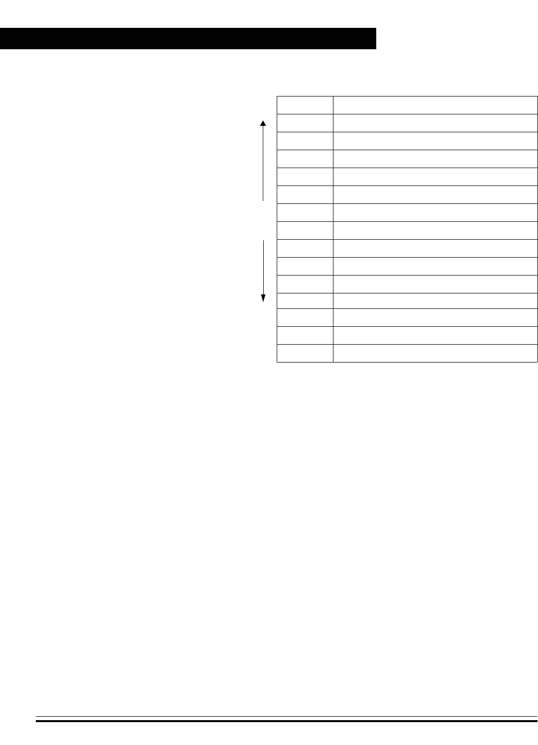
Appendix: HC08AZ48 Memory Map
Technical Data MC68HC08AZ60 — Rev 1.1
459 Appendix: HC08AZ48 Memory Map Freescale Semiconductor
Note that all available ROM locations that not defined by the user will,
by default, be filled with the software interrupt instruction (SWI, opcode
83) – see Central Processing Unit (CPU). Please take this into
account when defining vector addresses. It is recommended that all
vector addresses are defined.
$FFF2 TIMA CH1 Vector (High)
$FFF3 TIMA CH1 Vector (Low)
$FFF4 TIMA CH0 Vector (High)
$FFF5 TIMA CH0 Vector (Low)
$FFF6 TIM Vector (High)
$FFF7 TIM Vector (Low)
$FFF8 PLL Vector (High)
$FFF9 PLL Vector (Low)
$FFFA IRQ1 Vector (High)
$FFFB IRQ1 Vector (Low)
$FFFC SWI Vector (High)
$FFFD SWI Vector (Low)
High
$FFFE Reset Vector (High)
$FFFF Reset Vector (Low)
Table 28-1. Vector Addresses (Continued)
Address Vector
Priority

Appendix: HC08AZ48 Memory Map
Technical Data MC68HC08AZ60 — Rev 1.1
460 Appendix: HC08AZ48 Memory Map Freescale Semiconductor

MC68HC908AZ60A — Rev 1.1 Technical Data
Freescale Semiconductor Glossary 461
Technical Data — MC68HC908AZ60A
Glossary
A — See “accumulator (A).”
accumulator (A) — An 8-bit general-purpose register in the CPU08. The CPU08 uses the
accumulator to hold operands and results of arithmetic and logic operations.
acquisition mode — A mode of PLL operation during startup before the PLL locks on a
frequency. Also see "tracking mode."
address bus — The set of wires that the CPU or DMA uses to read and write memory locations.
addressing mode — The way that the CPU determines the operand address for an instruction.
The M68HC08 CPU has 16 addressing modes.
ALU — See “arithmetic logic unit (ALU).”
arithmetic logic unit (ALU) — The portion of the CPU that contains the logic circuitry to perform
arithmetic, logic, and manipulation operations on operands.
asynchronous — Refers to logic circuits and operations that are not synchronized by a common
reference signal.
baud rate — The total number of bits transmitted per unit of time.
BCD — See “binary-coded decimal (BCD).”
binary — Relating to the base 2 number system.
binary number system — The base 2 number system, having two digits, 0 and 1. Binary
arithmetic is convenient in digital circuit design because digital circuits have two
permissible voltage levels, low and high. The binary digits 0 and 1 can be interpreted to
correspond to the two digital voltage levels.
binary-coded decimal (BCD) — A notation that uses 4-bit binary numbers to represent the 10
decimal digits and that retains the same positional structure of a decimal number. For
example,
234 (decimal) = 0010 0011 0100 (BCD)
bit — A binary digit. A bit has a value of either logic 0 or logic 1.

Glossary
Technical Data MC68HC908AZ60A — Rev 1.1
462 Glossary Freescale Semiconductor
branch instruction — An instruction that causes the CPU to continue processing at a memory
location other than the next sequential address.
break module — A module in the M68HC08 Family. The break module allows software to halt
program execution at a programmable point in order to enter a background routine.
breakpoint — A number written into the break address registers of the break module. When a
number appears on the internal address bus that is the same as the number in the break
address registers, the CPU executes the software interrupt instruction (SWI).
break interrupt — A software interrupt caused by the appearance on the internal address bus
of the same value that is written in the break address registers.
bus — A set of wires that transfers logic signals.
bus clock — The bus clock is derived from the CGMOUT output from the CGM. The bus clock
frequency, fop, is equal to the frequency of the oscillator output, CGMXCLK, divided by
four.
byte — A set of eight bits.
C — The carry/borrow bit in the condition code register. The CPU08 sets the carry/borrow bit
when an addition operation produces a carry out of bit 7 of the accumulator or when a
subtraction operation requires a borrow. Some logical operations and data manipulation
instructions also clear or set the carry/borrow bit (as in bit test and branch instructions and
shifts and rotates).
CCR — See “condition code register.”
central processor unit (CPU) — The primary functioning unit of any computer system. The
CPU controls the execution of instructions.
CGM — See “clock generator module (CGM).”
clear — To change a bit from logic 1 to logic 0; the opposite of set.
clock — A square wave signal used to synchronize events in a computer.
clock generator module (CGM) — A module in the M68HC08 Family. The CGM generates a
base clock signal from which the system clocks are derived. The CGM may include a
crystal oscillator circuit and or phase-locked loop (PLL) circuit.
comparator — A device that compares the magnitude of two inputs. A digital comparator defines
the equality or relative differences between two binary numbers.
computer operating properly module (COP) — A counter module in the M68HC08 Family that
resets the MCU if allowed to overflow.

Glossary
MC68HC908AZ60A — Rev 1.1 Technical Data
Freescale Semiconductor Glossary 463
condition code register (CCR) — An 8-bit register in the CPU08 that contains the interrupt
mask bit and five bits that indicate the results of the instruction just executed.
control bit — One bit of a register manipulated by software to control the operation of the
module.
control unit — One of two major units of the CPU. The control unit contains logic functions that
synchronize the machine and direct various operations. The control unit decodes
instructions and generates the internal control signals that perform the requested
operations. The outputs of the control unit drive the execution unit, which contains the
arithmetic logic unit (ALU), CPU registers, and bus interface.
COP — See "computer operating properly module (COP)."
counter clock — The input clock to the TIM counter. This clock is the output of the TIM
prescaler.
CPU — See “central processor unit (CPU).”
CPU08 — The central processor unit of the M68HC08 Family.
CPU clock — The CPU clock is derived from the CGMOUT output from the CGM. The CPU
clock frequency is equal to the frequency of the oscillator output, CGMXCLK, divided by
four.
CPU cycles — A CPU cycle is one period of the internal bus clock, normally derived by dividing
a crystal oscillator source by two or more so the high and low times will be equal. The
length of time required to execute an instruction is measured in CPU clock cycles.
CPU registers — Memory locations that are wired directly into the CPU logic instead of being
part of the addressable memory map. The CPU always has direct access to the
information in these registers. The CPU registers in an M68HC08 are:
• A (8-bit accumulator)
• H:X (16-bit index register)
• SP (16-bit stack pointer)
• PC (16-bit program counter)
• CCR (condition code register containing the V, H, I, N, Z, and C
bits)
CSIC — customer-specified integrated circuit
cycle time — The period of the operating frequency: tCYC =1/f
OP.
decimal number system — Base 10 numbering system that uses the digits zero through nine.

Glossary
Technical Data MC68HC908AZ60A — Rev 1.1
464 Glossary Freescale Semiconductor
direct memory access module (DMA) — A M68HC08 Family module that can perform data
transfers between any two CPU-addressable locations without CPU intervention. For
transmitting or receiving blocks of data to or from peripherals, DMA transfers are faster
and more code-efficient than CPU interrupts.
DMA — See "direct memory access module (DMA)."
DMA service request — A signal from a peripheral to the DMA module that enables the DMA
module to transfer data.
duty cycle — A ratio of the amount of time the signal is on versus the time it is off. Duty cycle is
usually represented by a percentage.
EEPROM — Electrically erasable, programmable, read-only memory. A nonvolatile type of
memory that can be electrically reprogrammed.
EPROM — Erasable, programmable, read-only memory. A nonvolatile type of memory that can
be erased by exposure to an ultraviolet light source and then reprogrammed.
exception — An event such as an interrupt or a reset that stops the sequential execution of the
instructions in the main program.
external interrupt module (IRQ) — A module in the M68HC08 Family with both dedicated
external interrupt pins and port pins that can be enabled as interrupt pins.
fetch — To copy data from a memory location into the accumulator.
firmware — Instructions and data programmed into nonvolatile memory.
free-running counter — A device that counts from zero to a predetermined number, then rolls
over to zero and begins counting again.
full-duplex transmission — Communication on a channel in which data can be sent and
received simultaneously.
H — The upper byte of the 16-bit index register (H:X) in the CPU08.
H — The half-carry bit in the condition code register of the CPU08. This bit indicates a carry from
the low-order four bits of the accumulator value to the high-order four bits. The half-carry
bit is required for binary-coded decimal arithmetic operations. The decimal adjust
accumulator (DAA) instruction uses the state of the H and C bits to determine the
appropriate correction factor.
hexadecimal — Base 16 numbering system that uses the digits 0 through 9 and the letters A
through F.
high byte — The most significant eight bits of a word.

Glossary
MC68HC908AZ60A — Rev 1.1 Technical Data
Freescale Semiconductor Glossary 465
illegal address — An address not within the memory map
illegal opcode — A nonexistent opcode.
I — The interrupt mask bit in the condition code register of the CPU08. When I is set, all interrupts
are disabled.
index register (H:X) — A 16-bit register in the CPU08. The upper byte of H:X is called H. The
lower byte is called X. In the indexed addressing modes, the CPU uses the contents of
H:X to determine the effective address of the operand. H:X can also serve as a temporary
data storage location.
input/output (I/O) — Input/output interfaces between a computer system and the external world.
A CPU reads an input to sense the level of an external signal and writes to an output to
change the level on an external signal.
instructions — Operations that a CPU can perform. Instructions are expressed by programmers
as assembly language mnemonics. A CPU interprets an opcode and its associated
operand(s) and instruction.
interrupt — A temporary break in the sequential execution of a program to respond to signals
from peripheral devices by executing a subroutine.
interrupt request — A signal from a peripheral to the CPU intended to cause the CPU to
execute a subroutine.
I/O — See “input/output (I/0).”
IRQ — See "external interrupt module (IRQ)."
jitter — Short-term signal instability.
latch — A circuit that retains the voltage level (logic 1 or logic 0) written to it for as long as power
is applied to the circuit.
latency — The time lag between instruction completion and data movement.
least significant bit (LSB) — The rightmost digit of a binary number.
logic 1 — A voltage level approximately equal to the input power voltage (VDD).
logic 0 — A voltage level approximately equal to the ground voltage (VSS).
low byte — The least significant eight bits of a word.
low voltage inhibit module (LVI) — A module in the M68HC08 Family that monitors power
supply voltage.

Glossary
Technical Data MC68HC908AZ60A — Rev 1.1
466 Glossary Freescale Semiconductor
LVI — See "low voltage inhibit module (LVI)."
M68HC08 — A Freescale family of 8-bit MCUs.
mark/space — The logic 1/logic 0 convention used in formatting data in serial communication.
mask — 1. A logic circuit that forces a bit or group of bits to a desired state. 2. A photomask used
in integrated circuit fabrication to transfer an image onto silicon.
mask option — A optional microcontroller feature that the customer chooses to enable or
disable.
mask option register (MOR) — An EPROM location containing bits that enable or disable
certain MCU features.
MCU — Microcontroller unit. See “microcontroller.”
memory location — Each M68HC08 memory location holds one byte of data and has a unique
address. To store information in a memory location, the CPU places the address of the
location on the address bus, the data information on the data bus, and asserts the write
signal. To read information from a memory location, the CPU places the address of the
location on the address bus and asserts the read signal. In response to the read signal,
the selected memory location places its data onto the data bus.
memory map — A pictorial representation of all memory locations in a computer system.
microcontroller — Microcontroller unit (MCU). A complete computer system, including a CPU,
memory, a clock oscillator, and input/output (I/O) on a single integrated circuit.
modulo counter — A counter that can be programmed to count to any number from zero to its
maximum possible modulus.
monitor ROM — A section of ROM that can execute commands from a host computer for testing
purposes.
MOR — See "mask option register (MOR)."
most significant bit (MSB) — The leftmost digit of a binary number.
multiplexer — A device that can select one of a number of inputs and pass the logic level of that
input on to the output.
N — The negative bit in the condition code register of the CPU08. The CPU sets the negative bit
when an arithmetic operation, logical operation, or data manipulation produces a negative
result.
nibble — A set of four bits (half of a byte).

Glossary
MC68HC908AZ60A — Rev 1.1 Technical Data
Freescale Semiconductor Glossary 467
object code — The output from an assembler or compiler that is itself executable machine code,
or is suitable for processing to produce executable machine code.
opcode — A binary code that instructs the CPU to perform an operation.
open-drain — An output that has no pullup transistor. An external pullup device can be
connected to the power supply to provide the logic 1 output voltage.
operand — Data on which an operation is performed. Usually a statement consists of an
operator and an operand. For example, the operator may be an add instruction, and the
operand may be the quantity to be added.
oscillator — A circuit that produces a constant frequency square wave that is used by the
computer as a timing and sequencing reference.
OTPROM — One-time programmable read-only memory. A nonvolatile type of memory that
cannot be reprogrammed.
overflow — A quantity that is too large to be contained in one byte or one word.
page zero — The first 256 bytes of memory (addresses $0000–$00FF).
parity — An error-checking scheme that counts the number of logic 1s in each byte transmitted.
In a system that uses odd parity, every byte is expected to have an odd number of logic
1s. In an even parity system, every byte should have an even number of logic 1s. In the
transmitter, a parity generator appends an extra bit to each byte to make the number of
logic 1s odd for odd parity or even for even parity. A parity checker in the receiver counts
the number of logic 1s in each byte. The parity checker generates an error signal if it finds
a byte with an incorrect number of logic 1s.
PC — See “program counter (PC).”
peripheral — A circuit not under direct CPU control.
phase-locked loop (PLL) — A oscillator circuit in which the frequency of the oscillator is
synchronized to a reference signal.
PLL — See "phase-locked loop (PLL)."
pointer — Pointer register. An index register is sometimes called a pointer register because its
contents are used in the calculation of the address of an operand, and therefore points to
the operand.
polarity — The two opposite logic levels, logic 1 and logic 0, which correspond to two different
voltage levels, VDD and VSS.
polling — Periodically reading a status bit to monitor the condition of a peripheral device.
port — A set of wires for communicating with off-chip devices.

Glossary
Technical Data MC68HC908AZ60A — Rev 1.1
468 Glossary Freescale Semiconductor
prescaler — A circuit that generates an output signal related to the input signal by a fractional
scale factor such as 1/2, 1/8, 1/10 etc.
program — A set of computer instructions that cause a computer to perform a desired operation
or operations.
program counter (PC) — A 16-bit register in the CPU08. The PC register holds the address of
the next instruction or operand that the CPU will use.
pull — An instruction that copies into the accumulator the contents of a stack RAM location. The
stack RAM address is in the stack pointer.
pullup — A transistor in the output of a logic gate that connects the output to the logic 1 voltage
of the power supply.
pulse-width — The amount of time a signal is on as opposed to being in its off state.
pulse-width modulation (PWM) — Controlled variation (modulation) of the pulse width of a
signal with a constant frequency.
push — An instruction that copies the contents of the accumulator to the stack RAM. The stack
RAM address is in the stack pointer.
PWM period — The time required for one complete cycle of a PWM waveform.
RAM — Random access memory. All RAM locations can be read or written by the CPU. The
contents of a RAM memory location remain valid until the CPU writes a different value or
until power is turned off.
RC circuit — A circuit consisting of capacitors and resistors having a defined time constant.
read — To copy the contents of a memory location to the accumulator.
register — A circuit that stores a group of bits.
reserved memory location — A memory location that is used only in special factory test modes.
Writing to a reserved location has no effect. Reading a reserved location returns an
unpredictable value.
reset — To force a device to a known condition.
ROM — Read-only memory. A type of memory that can be read but cannot be changed (written).
The contents of ROM must be specified before manufacturing the MCU.
SCI — See "serial communication interface module (SCI)."
serial — Pertaining to sequential transmission over a single line.

Glossary
MC68HC908AZ60A — Rev 1.1 Technical Data
Freescale Semiconductor Glossary 469
serial communications interface module (SCI) — A module in the M68HC08 Family that
supports asynchronous communication.
serial peripheral interface module (SPI) — A module in the M68HC08 Family that supports
synchronous communication.
set — To change a bit from logic 0 to logic 1; opposite of clear.
shift register — A chain of circuits that can retain the logic levels (logic 1 or logic 0) written to
them and that can shift the logic levels to the right or left through adjacent circuits in the
chain.
signed — A binary number notation that accommodates both positive and negative numbers.
The most significant bit is used to indicate whether the number is positive or negative,
normally logic 0 for positive and logic 1 for negative. The other seven bits indicate the
magnitude of the number.
software — Instructions and data that control the operation of a microcontroller.
software interrupt (SWI) — An instruction that causes an interrupt and its associated vector
fetch.
SPI — See "serial peripheral interface module (SPI)."
stack — A portion of RAM reserved for storage of CPU register contents and subroutine return
addresses.
stack pointer (SP) — A 16-bit register in the CPU08 containing the address of the next available
storage location on the stack.
start bit — A bit that signals the beginning of an asynchronous serial transmission.
status bit — A register bit that indicates the condition of a device.
stop bit — A bit that signals the end of an asynchronous serial transmission.
subroutine — A sequence of instructions to be used more than once in the course of a program.
The last instruction in a subroutine is a return from subroutine (RTS) instruction. At each
place in the main program where the subroutine instructions are needed, a jump or branch
to subroutine (JSR or BSR) instruction is used to call the subroutine. The CPU leaves the
flow of the main program to execute the instructions in the subroutine. When the RTS
instruction is executed, the CPU returns to the main program where it left off.
synchronous — Refers to logic circuits and operations that are synchronized by a common
reference signal.
TIM — See "timer interface module (TIM)."

Glossary
Technical Data MC68HC908AZ60A — Rev 1.1
470 Glossary Freescale Semiconductor
timer interface module (TIM) — A module used to relate events in a system to a point in time.
timer — A module used to relate events in a system to a point in time.
toggle — To change the state of an output from a logic 0 to a logic 1 or from a logic 1 to a logic 0.
tracking mode — Mode of low-jitter PLL operation during which the PLL is locked on a
frequency. Also see "acquisition mode."
two’s complement — A means of performing binary subtraction using addition techniques. The
most significant bit of a two’s complement number indicates the sign of the number (1
indicates negative). The two’s complement negative of a number is obtained by inverting
each bit in the number and then adding 1 to the result.
unbuffered — Utilizes only one register for data; new data overwrites current data.
unimplemented memory location — A memory location that is not used. Writing to an
unimplemented location has no effect. Reading an unimplemented location returns an
unpredictable value. Executing an opcode at an unimplemented location causes an illegal
address reset.
V —The overflow bit in the condition code register of the CPU08. The CPU08 sets the V bit when
a two's complement overflow occurs. The signed branch instructions BGT, BGE, BLE,
and BLT use the overflow bit.
variable — A value that changes during the course of program execution.
VCO — See "voltage-controlled oscillator."
vector — A memory location that contains the address of the beginning of a subroutine written
to service an interrupt or reset.
voltage-controlled oscillator (VCO) — A circuit that produces an oscillating output signal of a
frequency that is controlled by a dc voltage applied to a control input.
waveform — A graphical representation in which the amplitude of a wave is plotted against time.
wired-OR — Connection of circuit outputs so that if any output is high, the connection point is
high.
word — A set of two bytes (16 bits).
write — The transfer of a byte of data from the CPU to a memory location.
X — The lower byte of the index register (H:X) in the CPU08.
Z — The zero bit in the condition code register of the CPU08. The CPU08 sets the zero bit when
an arithmetic operation, logical operation, or data manipulation produces a result of $00.

MC68HC08AZ60 — Rev 1.1 Technical Data
Freescale Semiconductor Revision History 471
Technical Data — MC68HC08AZ60
Revision History
This section contains the revision history for the MC68HC08AZ60
advance information data book.
Date Revision
Level Description Page
Number(s)
July,
2005 1.1 Updated to meet Freescale identity guidelines Throughout

Revision History
Technical Data MC68HC08AZ60 — Rev 1.1
472 Revision History Freescale Semiconductor

How to Reach Us:
Home Page:
www.freescale.com
E-mail:
support@freescale.com
USA/Europe or Locations Not Listed:
Freescale Semiconductor
Technical Information Center, CH370
1300 N. Alma School Road
Chandler, Arizona 85224
+1-800-521-6274 or +1-480-768-2130
support@freescale.com
Europe, Middle East, and Africa:
Freescale Halbleiter Deutschland GmbH
Technical Information Center
Schatzbogen 7
81829 Muenchen, Germany
+44 1296 380 456 (English)
+46 8 52200080 (English)
+49 89 92103 559 (German)
+33 1 69 35 48 48 (French)
support@freescale.com
Japan:
Freescale Semiconductor Japan Ltd.
Headquarters
ARCO Tower 15F
1-8-1, Shimo-Meguro, Meguro-ku,
Tokyo 153-0064
Japan
0120 191014 or +81 3 5437 9125
support.japan@freescale.com
Asia/Pacific:
Freescale Semiconductor Hong Kong Ltd.
Technical Information Center
2 Dai King Street
Tai Po Industrial Estate
Tai Po, N.T., Hong Kong
+800 2666 8080
support.asia@freescale.com
For Literature Requests Only:
Freescale Semiconductor Literature Distribution Center
P.O. Box 5405
Denver, Colorado 80217
1-800-441-2447 or 303-675-2140
Fax: 303-675-2150
LDCForFreescaleSemiconductor@hibbertgroup.com
Information in this document is provided solely to enable system and software
implementers to use Freescale Semiconductor products. There are no express or
implied copyright licenses granted hereunder to design or fabricate any integrated
circuits or integrated circuits based on the information in this document.
Freescale Semiconductor reserves the right to make changes without further notice to
any products herein. Freescale Semiconductor makes no warranty, representation or
guarantee regarding the suitability of its products for any particular purpose, nor does
Freescale Semiconductor assume any liability arising out of the application or use of any
product or circuit, and specifically disclaims any and all liability, including without
limitation consequential or incidental damages. “Typical” parameters that may be
provided in Freescale Semiconductor data sheets and/or specifications can and do vary
in different applications and actual performance may vary over time. All operating
parameters, including “Typicals”, must be validated for each customer application by
customer’s technical experts. Freescale Semiconductor does not convey any license
under its patent rights nor the rights of others. Freescale Semiconductor products are
not designed, intended, or authorized for use as components in systems intended for
surgical implant into the body, or other applications intended to support or sustain life,
or for any other application in which the failure of the Freescale Semiconductor product
could create a situation where personal injury or death may occur. Should Buyer
purchase or use Freescale Semiconductor products for any such unintended or
unauthorized application, Buyer shall indemnify and hold Freescale Semiconductor and
its officers, employees, subsidiaries, affiliates, and distributors harmless against all
claims, costs, damages, and expenses, and reasonable attorney fees arising out of,
directly or indirectly, any claim of personal injury or death associated with such
unintended or unauthorized use, even if such claim alleges that Freescale
Semiconductor was negligent regarding the design or manufacture of the part.
Freescale™ and the Freescale logo are trademarks of Freescale Semiconductor, Inc.
All other product or service names are the property of their respective owners. The ARM
POWERED logo is a registered trademark of ARM Limited. ARM7TDMI-S is a
trademark of ARM Limited. Java and all other Java-based marks are trademarks or
registered trademarks of Sun Microsystems, Inc. in the U.S. and other countries. The
Bluetooth trademarks are owned by their proprietor and used by Freescale
Semiconductor, Inc. under license.
© Freescale Semiconductor, Inc. 2005. All rights reserved.
Rev. 1.1
MC68HC08AZ60/D
July 14, 2005
RoHS-compliant and/or Pb- free versions of Freescale products have the functionality
and electrical characteristics of their non-RoHS-compliant and/or non-Pb- free
counterparts. For further information, see http://www.freescale.com or contact your
Freescale sales representative.
For information on Freescale.s Environmental Products program, go to
http://www.freescale.com/epp.
