MCP251XXFD CAN FD Controller Module Family Reference Manual 20005678B
MCP251XXFD-CAN-FD-Controller-Module-Family-Reference-Manual-20005678B
User Manual:
Open the PDF directly: View PDF ![]() .
.
Page Count: 80
- CAN FD Controller Module
- 1.0 Introduction
- 2.0 Modes of Operation
- 3.0 Configuration
- 4.0 Message Transmission
- 4.1 Transmit Message Object
- 4.2 Loading Messages into a Transmit FIFO
- 4.3 Loading Messages into the Transmit Queue
- TABLE 4-1: Transmit message object (TXQ AND TX FIFO)
- 4.4 Requesting Transmission of a Message in a Transmit FIFO
- 4.5 Requesting Transmission of a Message in the Transmit Queue
- 4.6 CiTXREQ Register
- 4.7 Transmit Priority
- 4.8 Transmit Bandwidth Sharing
- 4.9 Retransmission Attempts
- 4.10 Aborting a Transmission
- 4.11 Remote Transmit Request
- 4.12 Mismatch of DLC and Payload Size During Transmission
- 4.13 Transmit State Diagram
- 4.14 Resetting a Transmit FIFO
- 4.15 Resetting the Transmit Queue (TXQ)
- 4.16 Message Transmission Code Example
- 5.0 Transmit Event FIFO
- 6.0 Message Filtering
- 7.0 Message Reception
- 8.0 FIFO Behavior
- 9.0 Timestamping
- 10.0 Interrupts
- 11.0 Error Handling
- 12.0 Appendix A: MCP25xxFD canfdspi API
- 13.0 Related Documents
- 14.0 Revision History
- Worldwide Sales and Service

2017-2018 Microchip Technology Inc. DS20005678B-page 1
HIGHLIGHTS
This section of the manual contains the following major topics:
1.0 Introduction ....................................................................................................................... 2
2.0 Modes of Operation .......................................................................................................... 8
3.0 Configuration................................................................................................................... 13
4.0 Message Transmission ................................................................................................... 26
5.0 Transmit Event FIFO....................................................................................................... 33
6.0 Message Filtering............................................................................................................36
7.0 Message Reception ........................................................................................................ 41
8.0 FIFO Behavior................................................................................................................. 45
9.0 Timestamping.................................................................................................................. 58
10.0 Interrupts......................................................................................................................... 59
11.0 Error Handling................................................................................................................. 68
12.0 Appendix A: MCP25xxFD canfdspi API .......................................................................... 70
13.0 Related Documents ........................................................................................................ 76
14.0 Revision History .............................................................................................................. 77
CAN FD Controller Module
MCP25xxFD Family Reference Manual
DS20005678B-page 2 2017-2018 Microchip Technology Inc.
1.0 INTRODUCTION
1.1 CAN FD vs. CAN 2.0
CAN FD addresses the increasing demand for bandwidth on CAN buses. The two major
enhancements over CAN 2.0 are:
• Increased data field up to 64 data bytes (from maximum 8 data bytes for CAN 2.0).
• Option to switch to faster bit rate in the data phase. The arbitration bit rate is the same as in
CAN 2.0.
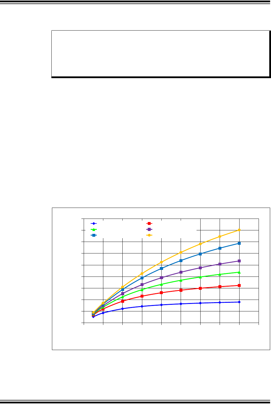
Figure 1-1 shows the possible increase in effective bit rate due to the higher data bit rate and
increased data bytes per frame. The graph uses a CAN FD Base frame with 11 bit identifier and
500 kbps bit rate during the arbitration phase.
The CAN FD protocol was defined to allow CAN 2.0 messages and CAN FD messages to co-
exist on the same bus. This does not imply that non-CAN FD controllers can be mixed with CAN
FD controllers on the same bus. Non-CAN FD controllers will generate error frames while
receiving a CAN FD message.
The CAN FD protocol (Data Link Layer) is defined in ISO 11898-1:2015.
Figure 1-1: Effective CAN FD Bit Rate
(Base Frame: 11 Bit ID, Nominal Bit Rate = 500 Kbps)
Note: This family reference manual section is meant to serve as a complement to the
device data sheet. Please refer to the data sheet for the memory organization and
register definitions of the device.
Device data sheets, application notes and code samples (MCP25xxFD canfdspi
API) are available for download from the Microchip web site (www.microchip.com).
All code samples in this manual use the MCP25xxFD canfdspi API. Please refer to
the API header files for the documentation of structures and function prototypes.
0
05
1
15
2
25
3
35
4
45
0123456789
Effective Bit Rate/Mbps
Data Bit Rate/Mbps
8 Bytes Payload 16 Bytes Payload
24 Bytes Payload 32 Bytes Payload
48 Bytes Payload 64 Bytes Payload

2017-2018 Microchip Technology Inc. DS20005678B-page 3
CAN FD Controller Module
1.2 Features
The CAN FD Controller Module has the following features:
General
• External CAN FD Controller with SPI Interface
• Nominal (Arbitration) Bit Rate up to 1 Mbps
• Data Bit Rate up to 8 Mbps
• CAN FD Controller modes
- Mixed CAN 2.0B and CAN FD mode
- CAN 2.0B mode
• Conforms to ISO 11898-1:2015
Message FIFOs
• 31 FIFOs, Configurable as Transmit or Receive FIFOs
• One Transmit Queue (TXQ)
• Transmit Event FIFO (TEF) with 32-Bit Timestamp
Message Transmission
• Message Transmission Prioritization:
- Based on priority bit field, and/or
- Message with lowest ID gets transmitted first using the Transmit Queue (TXQ)
• Programmable Automatic Retransmission Attempts: unlimited, 3 attempts, or disabled
Message Reception
• 32 Flexible Filter and Mask Objects
• Each object can be configured to filter either:
- Standard ID + first 18 data bits, or
- Extended ID
• 32-Bit Timestamp

MCP25xxFD Family Reference Manual
DS20005678B-page 4 2017-2018 Microchip Technology Inc.
1.3 Module Block Diagram
Figure 1-2 shows the block diagram of the CAN FD Controller Module.
• The CAN FD Controller Module has multiple modes:
- Configuration,
- Normal CAN FD,
- Normal CAN 2.0,
- Sleep (normal Sleep mode and Low Power Mode),
- Listen Only,
- Restricted Operation, and
- Internal and External Loopback modes.
• The CAN FD Bit Stream Processor (BSP) implements the Medium Access Control of the
CAN FD protocol described in ISO 11898-1:2015. It serializes and deserializes the bit
stream, encodes and decodes the CAN FD frames, manages the medium access,
acknowledges frames, and detects and signals errors.
• The TX Handler prioritizes the messages that are requested for transmission by the
Transmit FIFOs. It uses the RAM Interface to fetch the transmit data from RAM and
provides it to the BSP for transmission.
• The BSP provides received messages to the RX Handler. The RX Handler uses
Acceptance Filter to filter out messages that shall be stored into Receive FIFOs. It uses the
RAM Interface to store received data into RAM.
• Each FIFO can be configured either as a Transmit or Receive FIFO. The FIFO Control
keeps track of the FIFO Head and Tail, and calculates the User Address. For a TX FIFO,
the User Address points to the address in RAM where the data for the next transmit
message shall be stored. For a RX FIFO, the User Address points to the address in RAM
where the data of the next receive message shall be read. The user notifies the FIFO that a
message was written to or read from RAM by incrementing the Head/Tail of the FIFO.
• The Transmit Queue (TXQ) is a special transmit FIFO that transmits the messages based
on the ID of the messages stored in the queue.
• The Transmit Event FIFO (TEF) stores the message IDs of the transmitted messages.
• A free-running Time Base Counter is used to timestamp received messages. Messages in
the TEF can also be timestamped.
• The CAN FD Controller Module generates interrupts when new messages are received or
when messages were transmitted successfully.
• The Special Function Registers (SFR) are used to control and to read the status of the CAN
FD Controller Module.
Figure 1-2: Module Block Diagram
CAN FD
Bit Stream
Processor
RAM
Interface
TX Handler
TX Prioritization
RX Handler
Acceptance
Filter
TXQ Control
TEF
Control
FIFO
Control
SFR
Interrupt
Control
Error
Handling
Diagnostics
Time Stamping
TBC
Mode
Control

2017-2018 Microchip Technology Inc. DS20005678B-page 5
CAN FD Controller Module
1.4 CAN FD Message Frames
The ISO 11898-1:2015 describes the different CAN message frames in detail. Figure 1-3
through Figure 1-7 clarify and summarize the construction of the messages and fields.
There are four different CAN Data/Remote frames, see Figure 1-4:
• CAN Base frame: Classic CAN 2.0 frame using Standard ID.
• CAN FD Base frame: CAN FD frame using Standard ID.
• CAN Extended frame: Classic CAN 2.0 frame using Extended ID.
• CAN FD Extended frame: CAN FD frame using Extended ID.
There are no Remote frames in CAN FD frames, therefore, the RTR bit is replaced with the
RRS bit, see Figure 1-4. The RRS bit in the CAN FD Base frame can be used to extend the SID
to 12 bit. When enabled it is referred to as SID11, it is the LSB of SID<11:0>.
Figure 1-5 specifies the Control field of the different CAN messages. Before CAN FD was
added to the ISO 11898-1:2015, the FDF bit was a reserved bit. Now the FDF bit selects
between Classic and CAN FD formats.
The BRS bit selects if the bit rate should be switched in the data phase of CAN FD frames.
Figure 1-8 illustrates the Error and Overload frames. These special frames didn’t change. Note
that if an error is detected during the data phase of a CAN FD frame, the bit rate will be switched
back to the Nominal Bit Rate. Error frames are always transmitted at the arbitration bit rate.
1.4.1 ISO VS. NON ISO CRC
To support the system validation of Non-ISO CRC ECUs, the CAN FD Controller Module
supports both ISO CRC (according to ISO 11898-1:2015) and Non-ISO CRC, see Figure 1-6
and Figure 1-7. The CRC field is selectable using CiCON.ISOCRCEN. The ISO CRC field
contains the Stuff Count. This count wasn’t included in the original CAN FD specification. It was
added to fix a weakness in the error detection of the original specification.
CAN FD frames use two different lengths of CRC: 17 bit for up to 16 data bytes, and 21 bits for
20 or more data bytes. Technically, there are a total of six different CAN Data/Remove frames in
CAN FD.
Figure 1-3: General Data Frame
Figure 1-4: Arbitration Field
SOF
(1b) ARBITRATION(12/32b) CTRL(6/8/9b) DATA(0 to 64B) CRC(16/18/22b)
CRC(16/22/26b) ACK(2b) EOF(7b) IFS(≥3b)IFS(≥3b)
DATA FRAME
ARBITRATION(12/32b)
SID<10:0> RTR
SID<10:0> SRR IDE EID<17:0> RTR
SID<10:0> RRS
SID11
SID<10:0> SRR IDE EID<17:0> RRS
CAN BASE
CAN FD BASE
CAN EXT
CAN FD EXT
MCP25xxFD Family Reference Manual
DS20005678B-page 6 2017-2018 Microchip Technology Inc.
Figure 1-5: Control Field
Figure 1-6: ISO CRC Field
Figure 1-7: NON-ISO CRC Field
CTRL(6/8/9b)
IDE FDF DLC<3:0>
IDE res DLC<3:0>FDF BRS ES I
FDF r0 DLC<3:0>
res DLC<3:0>FDF BRS ES I
CAN BASE
CAN FD BASE
CAN EXT
CAN FD EXT
CRC(16/22/26b)
CRC(15b)
CRC(15b)
CRC(17/21b)
CRC(17/21b)
CRC
DEL
CRC
DEL
STUFF
CNT (4b)
CRC
DEL
STUFF
CNT (4b)
CRC
DEL
CAN BASE
CAN FD BASE
CAN EXT
CAN FD EXT
CRC(16/18/22b)
CRC(15b) CRC
DEL
CRC(15b) CRC
DEL
CRC(17/21b) CRC
DEL
CRC(17/21b) CRC
DEL
CAN BASE
CAN FD BASE
CAN EXT
CAN FD EXT

2017-2018 Microchip Technology Inc. DS20005678B-page 7
CAN FD Controller Module
Figure 1-8: Error and Overload Frame
1.4.2 DLC ENCODING
The Data Length Code (DLC) specifies how many data bytes a message frame contains.
Table 1-1 illustrates the encoding.
Table 1-1: DLC Encoding
ERRFLAG(6b) ERRDEL(8b)ANYWHERE WITHIN DATA FRAME IFS(≥3b) or OVL
OVLFLAG(6b) OVLDEL(8b)EOF or ERRDEL or OVLDEL IFS(≥3b) or OVL
ERROR
OVERLOAD
Frame DLC Number of
data bytes
CAN 2.0 and CAN FD 0 0
11
22
33
44
55
66
77
88
CAN 2.0 9-15 8
CAN FD 9 12
10 16
11 20
12 24
13 32
14 48
15 64

MCP25xxFD Family Reference Manual
DS20005678B-page 8 2017-2018 Microchip Technology Inc.
2.0 MODES OF OPERATION
The CAN FD Controller Module has eight modes of operation:
• Configuration mode
• Normal CAN FD mode: supports mixing of CAN FD and CAN 2.0 messages
• Normal CAN 2.0 mode: will generate error frames while receiving CAN FD messages. The
FDF bit is forced to zero, and only CAN 2.0 frames are sent, even if the FDF bit is set in the
Transmit Message Object.
• Sleep mode (normal Sleep mode and Low Power Mode)
• Listen Only mode
• Restricted Operation mode
• Internal Loopback mode
• External Loopback mode
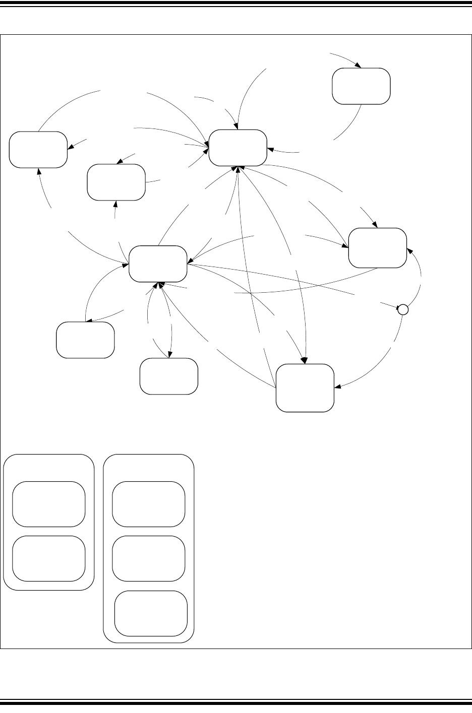
The modes of operation can be grouped into four main groups of modes: Configuration, Normal,
Sleep, and Debug, see Figure 2-1.
2.1 Mode Change
Figure 2-1 illustrates the possible mode transitions. New Modes of operation are requested by
writing to CiCON.REQOP. The modes of operation don’t change immediately. The modes will
only change when the bus is idle.
The current operating mode is indicated in CiCON.OPMOD. The application can enable an
interrupt on OPMOD change, or poll OPMOD.
2.1.1 CHANGING BETWEEN NORMAL MODES
Directly changing between Normal modes is not allowed. The Configuration Mode must be
selected first before a new Normal mode can be selected.
2.1.2 CHANGING BETWEEN DEBUG MODES
Directly changing between Debug modes is not allowed. The Configuration mode must be
selected first before a new Debug mode can be selected.
2.1.3 EXITING NORMAL MODE
The device will only transition to Configuration or Sleep mode after the message that is currently
being transmitted has finished.
2.1.4 ENTERING AND EXITING SLEEP MODE
The CAN FD Controller Module enters Sleep mode after a Sleep Mode request.
The device exits Sleep mode due to a dominant edge on RXCAN or by enabling the oscillator
(clearing OSC.OSCDIS). The module will transition automatically to Configuration mode.
2.1.5 INTEGRATING
The CAN FD Controller Module integrates to the bus according to the ISO 11898-1:2015
(eleven consecutive recessive bits) under the following conditions:
• Change from Configuration mode to Normal or Debug modes.
2017-2018 Microchip Technology Inc. DS20005678B-page 9
CAN FD Controller Module
Figure 2-1: Modes of Operation
Normal FD
Mode
Normal 2.0
Mode
External/Internal
Loopback
Mode
Listen Only
Mode
“Normal” Modes “Debug” Modes
Restricted
Operation
Mode
REQOP=Sleep
AndOSC.LPMEN=0
WAKIF
OrAssertnCS
REQOP=Sleep
AndOSC.LPMEN=1
AndBusIdle
REQOP=Sleep
AndOSC.LPMEN=1
REQOP=Restricted
AndBusIdle
No
Yes
REQOP=”Normal”
REQOP=ListenOnly
AndBusIdle
REQOP=Config
(AndBusIdle)
REQOP=Restricted
AndBusIdle
Resbit=1received
AndPXEDIS=0
Waitfor
BusIdle
Waitfor
128Idleconditions
TXBO
Systemerror
REQOP=”Normal”
REQOP=Config
(AndBusIdle) REQOP=ListenOnly
AndBusIdle
REQOP=Config
AndBusIdle
REQOP=LoopbackInt/Ext
AndBusIdle
(Integrating)
WAKIF
OrOSC.OSCDIS=0
REQOP=Sleep
AndOSC.LPMEN=0
AndBusIdle
REQOP=Config
AndBusIdle
REQOP=”Normal”
AndBusIdle
(Integrating)
POR
Configuration
Mode
SleepMode
ClockOff
TXCANrecessive
“Normal”
Modes
RXandTX
Loopback
Modes
ListenOnly
Mode
RXOnly
TXpinhigh
TXREQignored
BusOff
ClearallTXREQ
(FRESETTXFIFOs/
TXQ)
Protocol
ExceptionEvent
NoTX
Restricted
Operation
Mode
RX
TX:onlyACK
TXREQignored
cSERR2LOM==1?
LPM
DigitalLogicOff
TXCANrecessive

MCP25xxFD Family Reference Manual
DS20005678B-page 10 2017-2018 Microchip Technology Inc.
2.2 Configuration Mode
After Reset, the CAN FD Controller Module is in Configuration mode. The error counters are
cleared and all registers contain the reset values.
The CAN FD Controller Module has to be initialized before activation. This is only possible if the
module is in the Configuration mode, OPMOD = 100. The Configuration mode is requested by
setting REQOP = 100.
The CAN FD Controller Module will protect the user from accidentally violating the CAN protocol
through programming errors. The following registers and bit fields can only be programmed
during Configuration mode:
• CiCON: TXQEN, STEF, SERR2LOM, ESIGM, RTXAT, WAKFIL, PXEDIS, ISOCRCEN
• CiNBTCFG, CiDBTCFG, CiTDC
• CiTXQCON: PLSIZE, FSIZE
• CiFIFOCONm: PLSIZE, FSIZE, TXEN, RXTSEN
• CiTEFCON: FSIZE, TEFTSEN
The CAN FD Controller Module will not be allowed to enter the Configuration mode while a
transmission or reception is taking place in order to prevent the module from causing errors on
the CAN bus. The following registers are reset when exiting Configuration mode:
• CiTREC
• CiBDIAG0
• CiBDIAG1
In Configuration mode, FRESET is set in CiFIFOCONm, CiTXQCON, and CiTEFCON registers,
and all FIFOs and the Transmit Queue are reset.
2.3 Normal Modes
2.3.1 NORMAL CAN FD MODE
Once the device is configured, Normal Operation mode can be requested by setting
REQOP = 000.
In this mode, the device will be on the CAN bus. It can transmit and receive messages in CAN
FD mode: bit rate switching can be enabled, and up to 64 data bytes can be transmitted and
received.
2.3.2 NORMAL CAN 2.0 MODE
The Normal CAN 2.0 Operation mode can be requested by setting REQOP = 110.
In this mode, the device will be on the CAN bus. This is a the Classic CAN 2.0 mode. The
module will not receive CAN FD frames. It might send error frames if CAN FD frames are
detected on the bus. The FDF, BRS, and ESI bits in the TX objects will be ignored and
transmitted as ‘0’.

2017-2018 Microchip Technology Inc. DS20005678B-page 11
CAN FD Controller Module
2.4 Sleep Mode
Sleep mode is a low-power mode, where register and RAM contents are preserved, and the
clock is switched off.
Sleep mode is requested by clearing OSC.LPMEN, and setting REQOP = 001.
The CAN module will not enter Sleep mode while a transmission or reception is taking place to
prevent causing errors on the CAN bus. The module will enter Sleep mode when the current
message completes.
The OPMOD bits indicate Configuration mode (OPMOD = 100), and OSC.OSCDIS will read
‘1’. The application software should use these bit fields as a handshake indication for the Sleep
mode request. The TXCAN pin will stay in the recessive state while the module is in Sleep
mode to prevent inadvertent CAN bus errors.
2.4.1 EXITING SLEEP MODE
There are two ways to exit Sleep mode:
• Clearing OSC.OSCDIS.
• Wake-up interrupt due to CAN bus activity.
Both ways will reenable the clock and the CAN FD Controller Module will transition to
Configuration mode.
The module will monitor the RXCAN pin for activity while the module is in Sleep mode. The
device will generate a wake-up interrupt on the falling edges of RXCAN, if WAKIE is enabled.
2.5 Low-Power Mode (LPM)(Note 3)
LPM is an ultra-low-power mode, where the majority of the chip is powered down. Only the logic
required for wake-up is powered. This significantly reduces the leakage of the device at high
temperature.
LPM is requested by setting OSC.LPMEN, and setting REQOP = 001.
The CAN module will not enter LPM while a transmission or reception is taking place to prevent
causing errors on the CAN bus. The module will enter LPM when the current message
completes.
2.5.1 EXITING LPM
There are two ways to exit LPM:
• Asserting nCS
• Wake-up interrupt due to CAN bus activity
Exiting LPM is similar to a POR. The CAN FD Controller Module will transition to Configuration
mode. All registers will be reset, and RAM data will be lost. The device has to be reconfigured.
The module will monitor the RXCAN pin for activity while the module is in LPM. The device will
generate a wake-up interrupt on the falling edges of RXCAN, if WAKIE is enabled.
Note 1: If the module is in Sleep mode or LPM, the module generates an interrupt if the WAKIE
bit in the CiINT register is set and bus activity is detected. The oscillator starts up.
Messages that caused the wake-up will be lost until the oscillator is stable and the
device was switched to Normal mode.
2: The module can be programmed to apply a low-pass filter to the RXCAN pin while in
Sleep mode and LPM. This feature can be used to protect the module from wake-up
due to short glitches on the RXCAN pin. The WAKFIL bit in the CiCON register
enables or disables the filter while the module is in Sleep mode and LPM. The filter
time is programmable using the WFT bits in the CiCON register.
3: LPM is NOT implemented in the MCP2517FD.

MCP25xxFD Family Reference Manual
DS20005678B-page 12 2017-2018 Microchip Technology Inc.
2.6 Debug Modes
2.6.1 LISTEN ONLY MODE
Listen Only mode is a variant of Normal CAN FD Operation mode. If the Listen Only mode is
activated, the module on the CAN bus is passive. It will receive messages, but it will not transmit
any bits. TXREQ bits will be ignored. No error flags or acknowledge signals are sent. The error
counters are deactivated in this state. The Listen Only mode can be used for detecting the baud
rate on the CAN bus. It is necessary that there are at least two further nodes that communicate
with each other. The baud rate can be detected empirically by testing different values, until a
message is received successfully. This mode is also useful for monitoring the CAN bus without
influencing it.
2.6.2 RESTRICTED OPERATION MODE
In Restricted Operation mode, the node is able to receive data and Remote frames, and to
acknowledge valid frames, but it does not send Data frames, Remote frames, Error frames or
Overload frames. In case of an error condition or overload condition, it does not send dominant
bits; instead it waits for the occurrence of the bus Idle condition to resynchronize itself to the
CAN communication. The error counters are not incremented.
2.6.3 LOOPBACK MODE
Loopback mode is a variant of Normal CAN FD Operation mode. This mode will allow internal
transmission of messages from the transmit FIFOs to the receive FIFOs. The module does not
require an external acknowledge from the bus. No messages can be received from the bus,
because the RXCAN pin is disconnected.
2.6.3.1 Internal Loopback Mode
The transmit signal is internally connected to receive, and TXCAN is driven high.
2.6.3.2 External Loopback Mode
The transmit signal is internally connected to receive, and transmit messages can be monitored
on the TXCAN pin.
2017-2018 Microchip Technology Inc. DS20005678B-page 13
CAN FD Controller Module
3.0 CONFIGURATION
The MCP25xxFD should be reset and must be in Configuration mode before starting
configuration. The oscillator, FIFOs and bit time can only be configured in Configuration mode.
This prevents the device from accidentally disturbing the CAN bus.
3.1 Oscillator Configuration
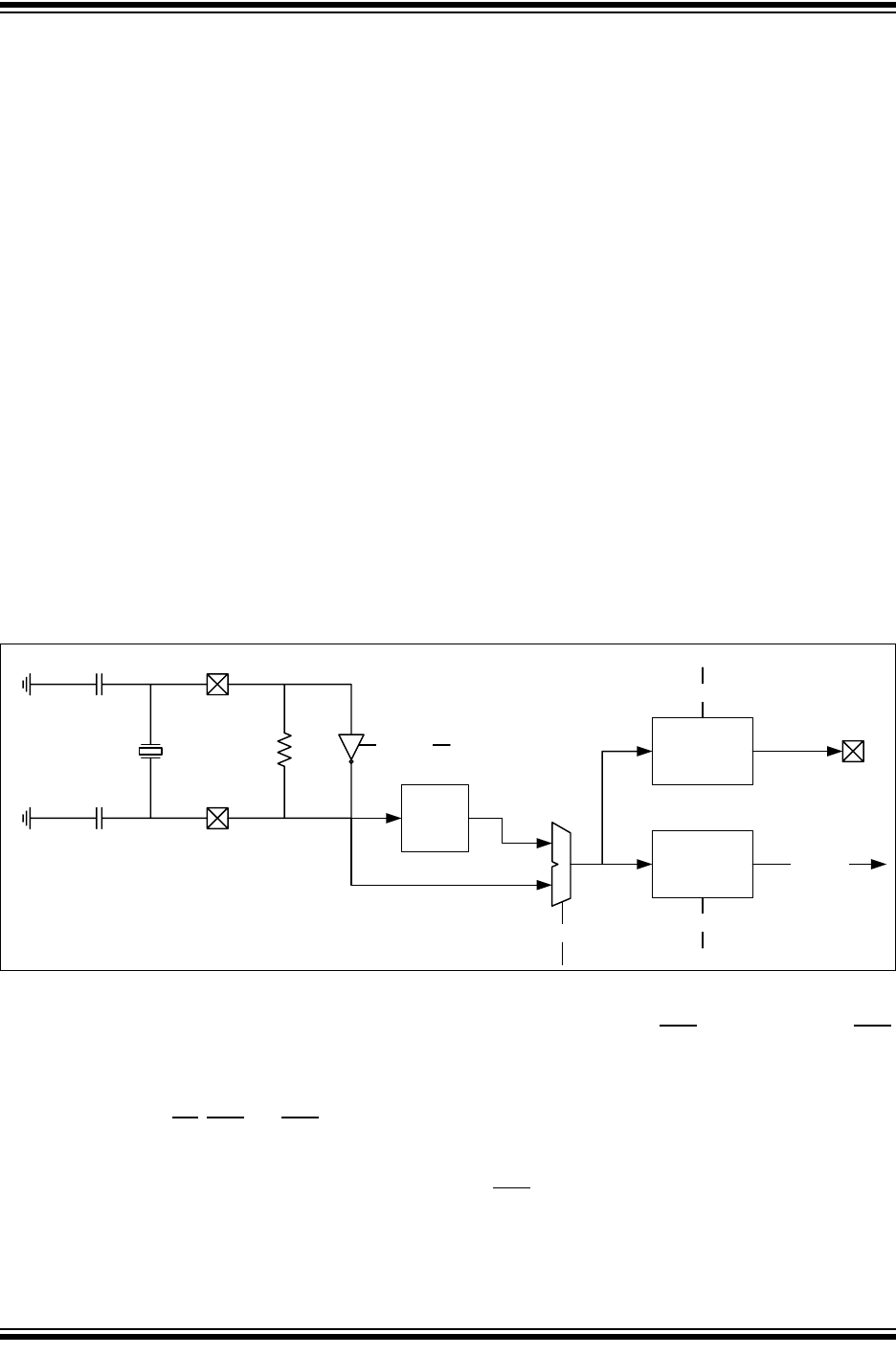
Figure 3-1 shows the block diagram of the oscillator. The oscillator generates the SYSCLK that
is used by the CAN FD Controller Module. CAN FD requires that the sample point in every node
is setup identically. Therefore, a 40 MHz or 20 MHz SYSCLK is recommended. The oscillator
uses a crystal or ceramic resonator, or an external clock as the clock reference.
The OSC register is used to configure the oscillator. A PLL can be enabled to multiply a 4 MHz
clock by 10 by setting the PLLEN bit. Setting the SCLKDIV bit divides the SYSCLK by 2. The
clock is available on the CLKO pin and can be divided using the CLKODIV bits.
The oscillator will be disabled after requesting Sleep mode. OSCDIS can only be cleared by the
application. It will be set automatically after the module enters Sleep mode. Reading
OSCDIS = ‘1’ indicates that the module has entered Sleep mode.
3.1.1 CRYSTAL/RESONATOR SELECTION
Selecting the correct crystal oscillator or ceramic resonator components depends on multiple
factors that are application dependent. Please review section 6.7 of the “PIC32 Family Reference
Manual (DS611112)” and refer to the application notes listed in Section 13.0 “Related
Documents”.
The following crystals, together with 18 pF load capacitors, were successfully used in one of our
evaluation boards: ABM8G-40.000MHZ-18-D2Y-T and ABM8G-20.000MHZ-18-D2Y-T.
Figure 3-1: MCP251xFD Oscillator Block Diagram
3.2 Input/Output Pin Configuration
The IOCON register configures the I/O of the MCP25xxFD. The INT0/GPIO0/XSTBY and INT1/
GPIO1 pins can be configured as interrupt pins or as GPIO pins using the PM0 and PM1 bits. In
case the pins are configured as GPIO pins the direction of the pin is selected using the TRIS0
and TRIS1 bits.
INT, INT0 and INT1 (when configured as interrupts) can be configured as push/pull or open drain
outputs using the INTOD bit. The TXCAN pin can also be configured as open drain by setting the
TXCANOD bit.
Setting the XSTBYEN bit configures the INT0/GPIO0/XSTBY pin to automatically control the
stand-by pin of an external CAN transceiver. The pin is driven high when the MCP25xxFD enters
Sleep mode, and driven low when it exits Sleep mode. Stand-by pin control is not available in
LPM. IOCON is reset in LPM and GPIO0 will be configured as an input.
OSC1
OSC2
4, 40 or 20 MHz
CLKIN,
Crystal or
Ceramic Res.
40/20 MHz
PLLEN
OSCDIS
Divide
By 1, 2
SCLKDIV
SYSCLK
Divide
By 1, 2, 4, 10
CLKO
CLKODIV
PLL
x10

MCP25xxFD Family Reference Manual
DS20005678B-page 14 2017-2018 Microchip Technology Inc.
Setting the SOF bit will output a pulse on the CLKO/SOF pin every time a start bit of a CAN
message is transmitted or received.
3.3 CAN Configuration
The CiCON register contains several bits that can only be configured in Configuration mode.
3.3.1 ISO CRC ENABLE
The module supports ISO CRC (according to ISO 11898-1:2015) and non-ISO CRC, see
Section 1.4.1 “ISO vs. NON ISO CRC”. ISO CRC is enabled by setting the ISOCRCEN bit.
3.3.2 PROTOCOL EXCEPTION DISABLE
The negative edge between the FDF bit and the “res bit” in CAN FD frames is important for the
calculation of the transceiver delay, and for hard-synchronization. Therefore, if the “res bit”
following the FDF bit is detected recessive, the CAN FD Controller Module will treat this as a
form error. This is called “Protocol Exception Event Detection Disabled”, and is configured by
setting the PXEDIS bit.
The Protocol Exception Event Detection can be enabled by clearing the PXEDIS bit. As a
reaction to the protocol exception event, the error counters are not changed, hard
synchronization is enabled, the module sends recessive bits and enters the bus integration
state.
3.3.3 WAKE-UP FILTER
The WAKFIL bit is used to enable/disable the low-pass filter on the RXCAN pin. The filter is only
active during Sleep mode. The WFT bits allow the configuration of different filter times.
3.3.4 RESTRICTION OF TRANSMISSION ATTEMPTS
ISO 11898-1:2015 requires that frames that lost arbitration, were not acknowledged or were
destroyed by errors are automatically retransmitted. Optionally, the number of retransmission
attempts can be limited.
When the RTXAT bit is set, retransmission attempts can be limited using the TXAT bits in the
FIFO control registers. If the RTXAT bit is clear, then TXAT in the FIFO control register is
ignored and the retransmission attempts are unlimited.
3.3.5 ERROR STATE INDICATOR (ESI) IN GATEWAY MODE
Normally the ESI bit in a transmitted message reflects the error status of the CAN FD Controller
Module. ESI is transmitted recessive when the module is error passive. In case the module is
used in a Gateway application, there are situations were the ESI bit in the message should be
transmitted recessive, even though the Gateway module is error active. This can be configured
by setting the ESIGM bit.
3.3.6 MODE SELECTION IN CASE OF SYSTEM ERROR
The SERR2LOM bit selects to which mode the module will transition in case of a System Error.
The module can either transition to Restricted Operation mode or Listen Only mode.
3.3.7 RESERVING MESSAGE MEMORY FOR TX QUEUE AND TRANSMIT
EVENT FIFO
Setting the TXQEN bit will reserve RAM for the TXQ. If the TXQEN bit is cleared then the TXQ
can’t be used.
Setting the STEF bit will reserve RAM for the TEF, and all transmitted messages will be stored
in the TEF.

2017-2018 Microchip Technology Inc. DS20005678B-page 15
CAN FD Controller Module
3.4 CAN FD Bit Time Configuration
In order to achieve higher bandwidth, bits inside a CAN FD frame are transmitted with two
different bit rates:
• Nominal Bit Rate (NBR): used during arbitration until the sample point of the BRS bit, and
from the sample point of the CRC delimiter until the EOF.
• Data Bit Rate (DBR): used during the data and CRC field.
NBR is limited by the propagation delay of the CAN network, see Section 3.4.2 “Propagation
Delay”. In the data phase, only one transmitter remains, therefore, the bit rate can be increased.
The transmitting node always compares the intended transmitted bits with the actual bits on the
CAN bus. The propagation delay in the data phase can be longer than the bit time. In this case,
the data bits are sampled at a Secondary Sample Point (SSP), see Section 3.4.3 “Transmitter
Delay Compensation (TDC)”.
NBR is the number of bits per second during the arbitration phase. It is the inverse of the Nominal
Bit Time (NBT), see Equation 3-1.
Equation 3-1: Nominal Bit Rate/Time
DBR is the number of bits per second during the data phase. It is the inverse of the Data Bit Time
(DBT), see Equation 3-1.
Equation 3-2: Data Bit Rate/Time
The Baud Rate Prescaler (BRP) is used to divide the SYSCLK. The divided SYSCLK is used to
generate the bit times.
There are two prescaler: NBRP for the nominal bit rate, and DBRP for the data bit rate. The
Time Quanta (NTQ and DTQ) are selected as shown in Equation 3-3 and Equation 3-4:
Equation 3-3: Nominal Time Quanta
Equation 3-4: Data Time Quanta
CAN bit times are made up of four segments as specified in ISO 11898-1:2015, see Figure 3-2.
Synchronization Segment (SYNC) – Synchronizes the different nodes connected on the CAN
bus. A bit edge is expected to be within this segment. The Synchronization Segment is always 1
TQ.
Propagation Segment (PRSEG) – Compensates for the propagation delay on the bus. PRSEG
has to be longer than the maximum propagation delay.
Phase Segment 1 (PHSEG1) – This time segment compensates for errors that may occur due
to phase shifts in the edges. The time segment may be automatically lengthened during
resynchronization to compensate for the phase shift.
Phase Segment 2 (PHSEG2) – This time segment compensates for errors that may occur due
to phase shifts in the edges. The time segment may be automatically shortened during
resynchronization to compensate for the phase shift.
NBR 1
NBT
-----------=
DBR 1
DBT
------------=
NTQ NBRP TSYSCLK
NBRP
FSYSCLK
--------------------------==
DTQ DBRP TSYSCLK
DBRP
FSYSCLK
--------------------------==
MCP25xxFD Family Reference Manual
DS20005678B-page 16 2017-2018 Microchip Technology Inc.
In the bit time registers, PRSEG and PHSEG1 are combined to TSEG1. PHSEG2 is called
TSEG2. Each segment is made up of multiple Time Quanta (TQ). The sample point lies between
TSEG1 and TSEG2.
Table 3-1 and Tabl e 3 -2 show the ranges for the bit time configuration parameters.
Figure 3-2: Partition of Bit Time
The total number of TQ in a bit time is programmable and can be calculated using Equation 3-5
and Equation 3-6.
Equation 3-5: Number of NTQ in a NBT
Equation 3-6: Number of DTQ in a DBT
Table 3-1: Nominal Bit Rate Configuration Ranges
Table 3-2: Data Bit Rate Configuration Ranges
3.4.1 SAMPLE POINT
The sample point is the point in the bit time at which the logic level of the bit is read and
interpreted. The sample point in percent can be calculated using Equation 3-7 and Equation 3-8.
Equation 3-7: Nominal Sample Point (%)
Segment Min. Max.
NSYNC 1 1
NTSEG1 2 256
NTSEG2 1 128
NSJW 1 128
NTQ per Bit 4 385
Segment Min. Max.
DSYNC 1 1
DTSEG1 1 32
DTSEG2 1 16
DSJW 1 16
DTQ per Bit 3 49
SY NC PRSE G PHSE G1 PHSE G2
TB
IT
SY NC TSEG1 TSEG2
Sample point
NBT
NTQ
------------ NSYNC NTSEG1 NTSEG2++=
DBT
DTQ
------------ D S Y N C D T S E G 1 D T S E G 2++=
NSP 1NTSEG1+
NBT
NTQ
------------
---------------------------------100=
2017-2018 Microchip Technology Inc. DS20005678B-page 17
CAN FD Controller Module
Equation 3-8: Data Sample Point (%)
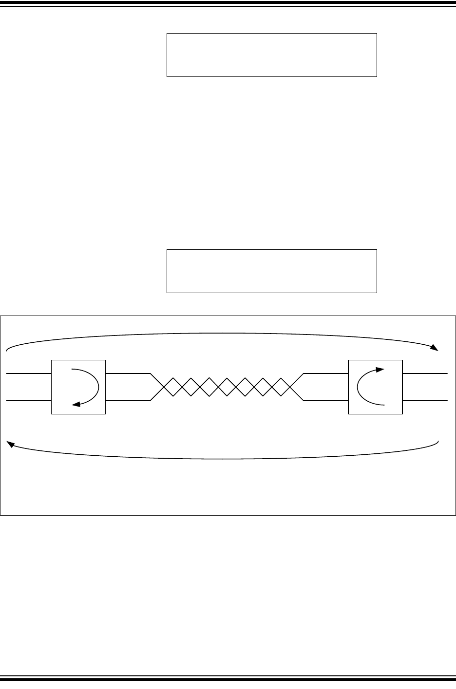
3.4.2 PROPAGATION DELAY
Figure 3-3 illustrates the propagation delay between two CAN Nodes on the bus, assuming Node
A is transmitting a CAN message. The transmitted bit will propagate from the transmitting CAN
Node A, through the transmitting CAN transceiver, over the CAN bus, through the receiving CAN
transceiver, into the receiving CAN Node B.
During the arbitration phase of a CAN message, the transmitter samples the CAN bus and
checks if the transmitted bit matches the received bit. The transmitting node has to place the
sample point after the maximum propagation delay.
Equation 3-9 describes the maximum propagation delay; where tTXD-RXD is the propagation
delay of the transceiver, maximum 255 ns according to ISO 11898-1:2015; TBUS is the delay on
the CAN bus, approximately 5 ns/m. The factor two comes from the worst case, when Node B
starts transmitting exactly when the bit from Node A arrives.
Equation 3-9: Max. Prop. Delay
Figure 3-3: Propagation Delay
DSP 1DTSEG1+
DBT
DTQ
------------
--------------------------------- 100=
TPROP 2t
TXD RXD–TBUS
+=
TPROP TPROPAB TPROPBA
+2tTXD RXD–TBUS
+==
Node A
TXCAN
RXCAN
CANH
CANL
Node B
RXCAN
TXCAN
CANH
CANL
Delay: Node A to B (TPROPAB)
CAN bus (T
BUS
)
Transceiver Propagation
Delay (t
TXD-RXD
)
Delay: Node B to A (T
PROPBA
)
Transceiver Propagation
Delay (t
TXD-RXD
)
MCP25xxFD Family Reference Manual
DS20005678B-page 18 2017-2018 Microchip Technology Inc.
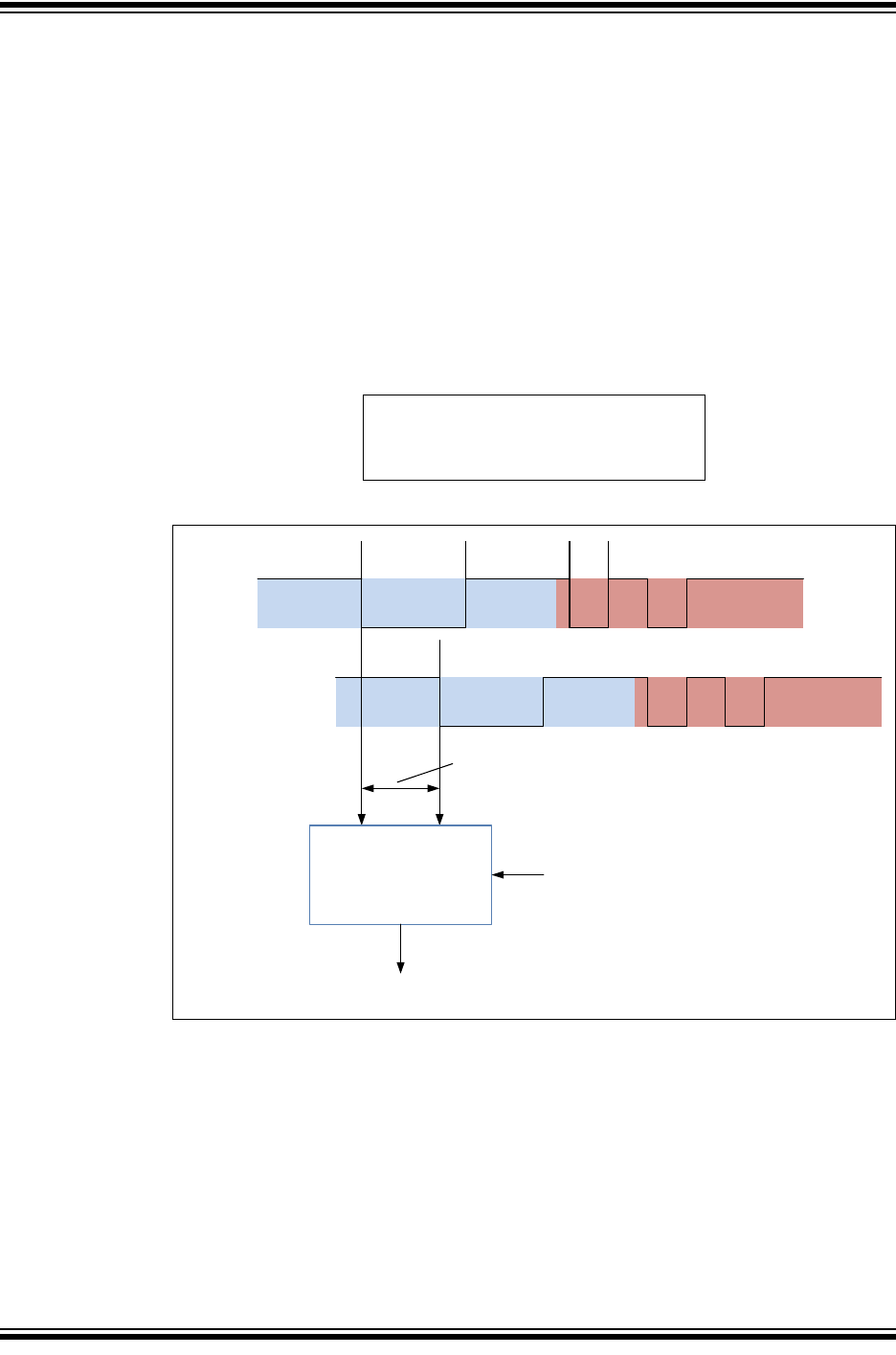
3.4.3 TRANSMITTER DELAY COMPENSATION (TDC)
During the data phase of a CAN FD transmission, only one node is transmitting; all others are
receiving. Therefore, the propagation delay does not limit the maximum data rate.
When transmitting via pin TXCAN, the CAN FD Controller Module receives the transmitted data
from its local CAN transceiver via pin RXCAN. The received data is delayed by the CAN
transceiver’s loop delay. In case this delay is greater than 1+DTSEG1, a bit error would be
detected.
In order to enable a data phase bit time that is shorter than the transceiver loop delay, the
Transmitter Delay Compensation (TDC) is implemented. Instead of sampling after DTSEG1, a
Secondary Sample Point (SSP) is calculated and used for sampling during the data phase of a
CAN FD message.
Figure 3-4 illustrates how the transceiver loop delay is measured and Equation 3-10 shows how
the SSP is calculated.
Equation 3-10: Secondary Sample Point
Figure 3-4: Measurement of Transceiver Delay (TDCV)
3.4.4 SYNCHRONIZATION
To compensate for phase shifts between the oscillator frequencies of the nodes on the CAN bus,
each CAN controller must be able to synchronize to the relevant edge of the incoming signal.
The CAN controller expects an edge in the received signal to occur within the SYNC segment.
Only recessive-to-dominant edges are used for synchronization.
There are two mechanisms used for synchronization:
•Hard synchronization - forces the edge that has occurred to lie within the SYNC segment.
The bit time counter is restarted with SYNC.
•Resynchronization - if the edge falls outside the SYNC segment, PHSEG1 or PHSEG2
will be adjusted.
SSP TDCV TDCO+=
TXCAN
FDF res BRS ESI DLC
Arbitration Phase Data Phase
RXCAN Arbitration Phase Data Phase
Transmitter Delay
Start Stop
Transmitter Delay
Measurement
TDCO
Secondary Sample Point (SSP)
FDF

2017-2018 Microchip Technology Inc. DS20005678B-page 19
CAN FD Controller Module
For a more detailed description of the CAN synchronization, please refer to ISO 11898-1:2015.
3.4.5 SYNCHRONIZATION JUMP WIDTH
The Synchronization Jump Width (SJW) is the maximum amount PHSEG1 and PHSEG2 can be
adjusted during resynchronization. SJW is programmable, see Tabl e 3-1 and Table 3-2.
3.4.6 OSCILLATOR TOLERANCE
The oscillator tolerance, df, around the nominal frequency of the oscillator, fnom, is defined in
Equation 3-11.
Equation 3-12 through Equation 3-16 describe the conditions for the maximum tolerance of the
oscillator.
Equation 3-11: Oscillator Tolerance
Equation 3-12: Condition 1
Equation 3-13: Condition 2
Equation 3-14: Condition 3
Equation 3-15: Condition 4
Equation 3-16: Condition 5
1df–fnomFSYSCLK 1df+fnom
df NSJW
210NBT
NTQ
------------
----------------------------------
df min NPHSEG1 NPHSEG2,
213
NBT
NTQ
------------
NPHSEG2–
-------------------------------------------------------------------------
df DSJW
210DBT
DTQ
------------
----------------------------------
df min NPHSEG1 NPHSEG2,
26
DBT
DTQ
------------
DPHSEG2–
DBRP
NBRP
----------------7NBT
NTQ
------------
+
--------------------------------------------------------------------------------------------------------------------------------
df
DSJW max 0 NBRP
DBRP
----------------1–
,
–
22
NBT
NTQ
------------
HNSEGP2
NBRP
DBRP
----------------DPHSEG2 4 DBT
DTQ
------------
++
-------------------------------------------------------------------------------------------------------------------------------------------------------------------

MCP25xxFD Family Reference Manual
DS20005678B-page 20 2017-2018 Microchip Technology Inc.
3.4.7 RECOMMENDATIONS FOR BIT TIME CONFIGURATION
The following recommendations should be considered when configuring the bit time:
• Select the highest available CAN clock frequency
- Short TQ lead to high resolution for selecting the sample point.
- Use 20 or 40 MHz for SYSCLK.
• Select the lowest NBRP and DBRP
- Low BRP lead to short TQ.
- NSYNC and DSYNC will be short and reduce the quantization error.
- The receiving node can synchronize more accurately to the transmitting node.
• Set NBRP equal to DBRP
- Identical TQ in both phases prevent quantization errors during bit rate switching.
• Use the same Nominal Sample Point (NSP) in all nodes on the CAN FD network
Use the same Data Sample Point (DSP) in all nodes on the CAN FD network
- Different sample points in the different nodes lead to different length of the BRS and
CRC delimiter bits and introduce phase errors when switching the bit rate.
- NSP doesn’t have to be equal to DSP.
- The SSP can be different in different CAN FD nodes.
• Select the largest possible NSJW and DSJW
- Maximizes the oscillator tolerance.
- Allows the receiving nodes to quickly resynchronize to the transmitting nodes.
• Enable automatic TDC for DBR of 1Mbps and higher
- Automatic TDC measurement compensations for transmitter delay variations.
3.4.8 BIT TIME CONFIGURATION EXAMPLE
The following example illustrates the configuration of the CAN FD bit time registers, assuming a
CAN FD network in an automobile with the following parameters:
• 500 kbps NBR; sample point at 80%.
• 2 Mbps DBR; sample point at 80%.
• 40m minimum bus length
Table 3-3 and Ta ble 3 - 4 illustrate how the bit time parameters are calculated. Since the
parameters depend on multiple constraints and equations, and are calculated using an iterative
process, it is recommended to enter the equations into a spread sheet.
Table 3-5 translates the calculated values into register values. It is recommended to let the CAN
FD Controller Module measure the Transmitter Delay Compensation Value (TDCV). This is
accomplished by setting CiTDC.TDCMOD = 10 (automatic mode). In order to set the SSP to
80%, TDCO is set to (DBRP*DTSEG1).

2017-2018 Microchip Technology Inc. DS20005678B-page 21
CAN FD Controller Module
Table 3-3: Step-by-Step Nominal Bit Rate Configuration
Table 3-4: Step-by-Step Data Bit Rate Configuration
Table 3-5: Bit Time Register Initialization (500k/2M)
Parameter Constraint Val. Unit Equations and Comments
NBT NBT ≥ 1 µs 2 µs Equation 3-1.
FSYSCLK FSYSCLK ≤ 40 MHz 40 MHz Select crystal or resonator frequency, usually 40 or
20 MHz.
NBRP 1 to 256 1 Select smallest possible BRP value to maximize
resolution.
NTQ NBT, FSYSCLK 25 ns Equation 3-3.
NBT/NTQ 4 to 385 80 Equation 3-5.
NSYNC Fixed 1 NTQ Defined in ISO 11898-1:2015.
NPRSEG NPRSEG > TPROP 47 NTQ Equation 3-9: TPROP = 910 ns,
minimum NPRSEG = TPROP/NTQ = 36.4 NTQ.
Selecting 47 will allow up to 60m bus length.
NTSEG1 2 to 256 NTQ 63 NTQ Equation 3-7. Select NTSEG1 to achieve 80% NSP.
NTSEG2 1 to 128 NTQ 16 NTQ There are 16 NTQ left to reach NBT/NTQ = 80.
NSJW 1 to 128 NTQ;
SJW ≤ min(NPHSEG1, NPHSEG2)
16 NTQ Maximizing NSJW lessens the requirement for the
oscillator tolerance.
Parameter Constraint Val. Unit Equations and Comments
DBT DBT ≥ 125 ns 500 ns Equation 3-2.
DBRP 1 to 256 1 Selecting the same prescaler as for NBT makes
sure that the TQ resolution doesn’t change during
the bit rate switching.
DTQ DBT, FSYSCLK 25 ns Equation 3-4.
DBT/DTQ 3 to 49 20 Equation 3-6.
DSYNC Fixed 1 DTQ Defined in ISO 11898-1:2015.
DTSEG1 1 to 32 DTQ 15 DTQ Equation 3-7. Select DTSEG1 to achieve 80% DSP.
DTSEG2 1 to 16 DTQ 4 DTQ There are 4 DTQ left to reach DBT/DTQ = 20.
DSJW 1 to 16 DTQ;
SJW ≤ min(DPHSEG1, DPHSEG2)
4 DTQ Maximizing DSJW lessens the requirement for the
oscillator tolerance.
Oscillator Tolerance
Condition 1-5
Minimum of Condition 1-5 0.78 % Equation 3-11 through Equation 3-16.
CiNBTCFG Value CiDBTCFG Value CiTDC Value
BRP 0 BRP 0 TDCMOD 2
TSEG1 62 TSEG1 14 TDCO 15
TSEG2 15 TSEG2 3 TDCV 0
SJW 15 SJW 3
MCP25xxFD Family Reference Manual
DS20005678B-page 22 2017-2018 Microchip Technology Inc.
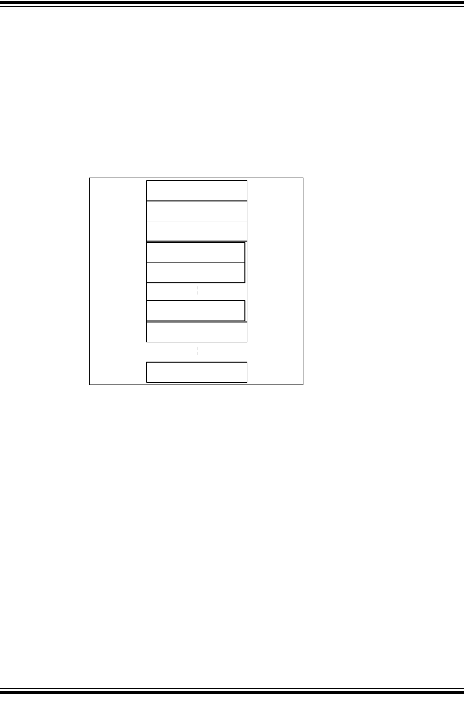
3.5 Message Memory Configuration
The message objects of the Transmit Event FIFO, Transmit Queue and Transmit/Receive FIFOs
are located in RAM; see Figure 3-5. The application must configure the number of message
objects inside a FIFO between one message object and 32 message objects. Additionally, the
application must configure the payload size of the message objects inside each FIFO. This
configuration determines where message objects are located in RAM. The RAM allocation can
only be configured in Configuration mode.
In order to optimize RAM usage, the application should start configuring the RAM with the TEF,
followed by the TXQ, and continue with FIFO 1, FIFO 2, FIFO 3 and so on. In case a user
application requires TEF, TXQ, and 16 additional FIFOs, it should configure TEF, TXQ, followed
by FIFO 1 through FIFO 16. It is not necessary to configure the unused FIFOs 17 through 31.
Figure 3-5: Message Memory Organization
3.5.1 TRANSMIT EVENT FIFO CONFIGURATION
In order to reserve space in RAM for the TEF, CiCON.STEF has to be set. The number of
message objects inside the TEF is configured using CiTEFCON.FSIZE. Transmitted messages
can be timestamped by setting CiTEFCON.TEFTSEN.
3.5.2 TRANSMIT QUEUE CONFIGURATION
In order to reserve space in RAM for the TXQ, CiCON.TXQEN has to be set. The number of
message objects inside the TXQ is configured using CiTXQCON.FSIZE. All objects inside the
TXQ use the same payload size (number of data bytes), which is configured using
CiTXQCON.PLSIZE.
3.5.3 TRANSMIT FIFO CONFIGURATION
FIFO 1 through FIFO 31 can be configured as Transmit FIFOs by setting TXEN in the
CiFIFOCONm register. The number of message objects inside each Transmit FIFO is configured
using CiFIFOCONm.FSIZE. All objects inside one Transmit FIFO use the same payload size
(number of data bytes), which is determined by CiFIFOCONm.PLSIZE.
3.5.4 RECEIVE FIFO CONFIGURATION
FIFO 1 through FIFO 31 can be configured as Receive FIFOs by clearing TXEN in the
CiFIFOCONm register. The number of message objects inside each Receive FIFO is configured
using CiFIFOCONm.FSIZE. All objects inside one Receive FIFO use the same payload size
(number of data bytes), which is determined by CiFIFOCONm.PLSIZE. Received messages can
be timestamped by setting CiFIFOCONm.RXTSEN.
TEF
TX Queue
FIFO 1
FIFO 3
FIFO 2: Message Object 0
FIFO 2: Message Object 1
FIFO 2: Message Object n
FIFO 31

2017-2018 Microchip Technology Inc. DS20005678B-page 23
CAN FD Controller Module
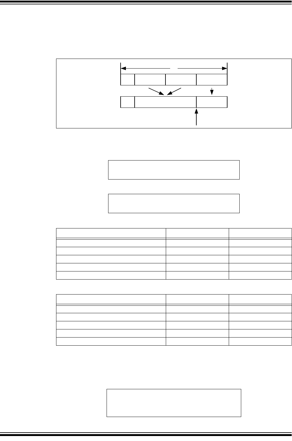
3.5.5 CALCULATION OF REQUIRED MESSAGE MEMORY
The size of required RAM depends on the configuration of each individual FIFO. Equation 3-17
through Equation 3-19 specify the sizes of the TEF, TXQ and the FIFOs in bytes. If the TEF or
TXQ is not used, their size is zero.
Since the size of the integrated RAM is limited, the user must check that the memory
configuration fits into RAM. The MCP25xxFD will not check that the configuration fits. Equation 3-
20 can be used to calculate the total RAM usage in bytes.
The size of the TEF objects depend on the enabling of timestamping. If TEFTSEN is set, then
tefts = 4, else tefts = 0.
The PayLoad(i) is defined in data bytes.
The size of a message object of a RX FIFO varies dependent on the enabling of timestamping.
If RXTSEN = 1 and TXEN = 0 for FIFO(i), then rxts(i) = 4, else rxts(i) = 0.
N is defined as the number of FIFOs used in addition to the TEF and the TXQ.
Equation 3-17: Size of TEF
Equation 3-18: Size of TXQ
Equation 3-19: Size of FIFOs
Equation 3-20: Total RAM Usage
STEF NElements TEFtefts 8+=
STXQ NElements TXQ8 PayLoad TXQ+=
SFIFO i NElements i rxts i 8 PayLoad i++=
SRAM STEF STXQ SFIFO i
i1=
N
++
=
MCP25xxFD Family Reference Manual
DS20005678B-page 24 2017-2018 Microchip Technology Inc.
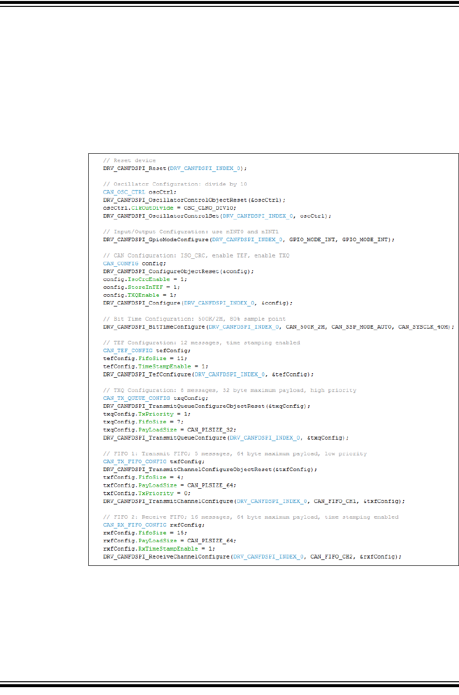
3.6 Configuration Code Example
Example 3-1 shows a code example of how to configure the MCP25xxFD:
• Reset the MCP25xxFD
• Configure the Oscillator and CLKO pin
• Configure the I/O pins
• Configure the CAN Control register
• Configure the Bit Time registers
• Configure the TEF, TXQ, TX and RX FIFOs
Example 3-1: Basic Configuration
2017-2018 Microchip Technology Inc. DS20005678B-page 25
CAN FD Controller Module
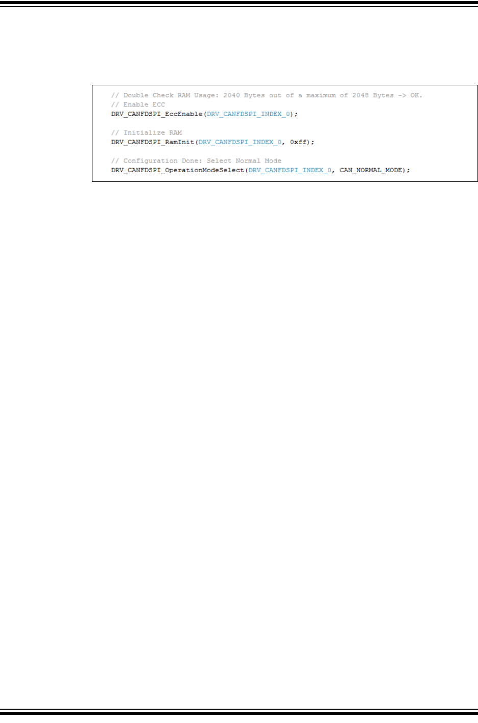
Now the device is ready to transition to Normal mode. Example 3-2 shows a code example of
how to enable ECC, initialize RAM, and select Normal mode.
Always calculate the actual RAM usage and make sure it fits into RAM.
Example 3-2: Initialize RAM, Select Normal Mode

MCP25xxFD Family Reference Manual
DS20005678B-page 26 2017-2018 Microchip Technology Inc.
4.0 MESSAGE TRANSMISSION
The application has to configure the FIFO or TXQ before it can be used for transmission,
see Section 3.5.3 “Transmit FIFO Configuration” and Section 3.5.2 “Transmit Queue
Configuration”.
4.1 Transmit Message Object
Table 4-1 specifies the Transmit Message Object used by the TXQ and the Transmit FIFOs. The
transmit objects contain the message ID, Control bits, and the payload:
•SID: Standard ID or Base ID.
•EID: ID Extension.
•DLC: Data Length Code; specifies the number of data bytes to transmit, see Section 1.4.2
“DLC Encoding”.
•IDE: ID extension selection; clearing this bit will transmit a Base frame, setting this bit will
transmit an Extended frame.
•RTR: Remote Transmit Request; this bit is only specified in CAN 2.0 frames. Setting this bit
will request a transmission of a receiving node.
•FDF: FD Format selection; if this bit is set, a CAN FD frame will be transmitted, otherwise,
a CAN 2.0 frame. If Normal CAN 2.0 mode is selected, this bit is ignored and only CAN 2.0
frames are transmitted.
•BRS: Bit Rate Switch; the data phase of a CAN FD frame will be transmitted using DBR if
this bit is set. If the bit is clear, the whole frame will be transmitted using NBR.
•ESI: Error State Indicator; normally, the ESI bit reflects the error status of the transmitting
node. A recessive ESI bit inside a CAN FD frame indicates that the transmitting node is
error passive, a dominant bit shows that the transmitting node is error active. If
CiCON.ESIGM=0, this bit inside the object is ignored. If CiCON.ESIGM=1, the ESI bit
inside the transmitted message will be transmitted recessive, if the CAN FD Controller
Module is error passive, or if the ESI bit in the message object is set. A Gateway
application would use it to signal that the ESI bit of the transmitting node was set.
•SEQ: Sequence number; SEQ is not transmitted on the CAN bus. It is used to keep track of
transmitted messages. SEQ is stored in the TEF message object.
•Transmit Buffer Data: Contains the payload of the message. Only the number of data
bytes specified by the DLC are transmitted. Byte 0 is transmitted first, followed by 1, 2, and
so on.
4.2 Loading Messages into a Transmit FIFO
Before loading a message into the FIFO, the application must verify that the FIFO is not full.
There is room in the FIFO if CiFIFOSTAm.TFNRFNIF is set. Loading a message into a full FIFO
can corrupt a message that is being transmitted.
The FIFO User Address points to the address in RAM of the next Transmit Message Object,
where the application should store the message. The actual address in RAM is calculated using
Equation 4-1. T0 of the Transmit Message Object is loaded first, followed by T1, T2 and so on.
The maximum number of data bytes is limited by the configured payload. Only the number of data
bytes specified by the DLC have to be loaded.
Equation 4-1: Address of next Message Object
After the message object was loaded into RAM, the FIFO needs to be incremented by setting
CiFIFOCONm.UINC. This will cause the CAN FD Controller Module to increment the Head of the
FIFO, and update CiFIFOUAm.
Now the message is ready for transmission, and the next message can be loaded at the new
address.
A 0x400 CiFIFOUAm+=

2017-2018 Microchip Technology Inc. DS20005678B-page 27
CAN FD Controller Module
4.3 Loading Messages into the Transmit Queue
Loading Transmit Message Objects into the TXQ works the same ways as loading message
objects into a Transmit FIFO. The application must check CiTXQSTA if there is room in the TXQ,
use CiTXQUA instead of CiFIFOUAm to calculate the address to load the message, and set
CiTXQCON.UINC to increment the Head of the TXQ.
TABLE 4-1: TRANSMIT MESSAGE OBJECT (TXQ AND TX FIFO)
Word Bit
31/2315/7
Bit
30/22/14/6
Bit
29/21/13/5
Bit
28/20/12/4
Bit
27/19/11/3
Bit
26/18/10/2
Bit
25/17/9/1
Bit
24/16/8/0
T0 31:24 -— -— SID11 EID<17:6>
23:16 EID<12:5>
15:8 EID<4:0> SID<10:8>
7:0 SID<7:0>
T1 31:24 SEQ<22:15>
23:16 SEQ<14:7>
15:8 SEQ<6:0> ESI
7:0 FDF BRS RTR IDE DLC<3:0>
T2 (1) 31:24 Transmit Data Byte 3
23:16 Transmit Data Byte 2
15:8 Transmit Data Byte 1
7:0 Transmit Data Byte 0
T3 31:24 Transmit Data Byte 7
23:16 Transmit Data Byte 6
15:8 Transmit Data Byte 5
7:0 Transmit Data Byte 4
Ti 31:24 Transmit Data Byte n
23:16 Transmit Data Byte n-1
15:8 Transmit Data Byte n-2
7:0 Transmit Data Byte n-3
bit T0.31-30 Unimplemented: Read as ‘x’
bit T0.29 SID11: In FD mode the standard ID can be extended to 12 bit using r1
bit T0.28-11 EID<17:0>: Extended Identifier
bit T0.10-0 SID<10:0>: Standard Identifier
bit T1.31-9 SEQ<22:0>: Sequence to keep track of transmitted messages in Transmit Event FIFO (2)
bit T1.8 ESI: Error Status Indicator
In CAN to CAN gateway mode (CiCON.ESIGM=1), the transmitted ESI flag is a “logical OR” of T1.ESI
and error passive state of the CAN controller;
In normal mode ESI indicates the error status
1 = Transmitting node is error passive
0 = Transmitting node is error active
bit T1.7 FDF: FD Frame; distinguishes between CAN and CAN FD formats
bit T1.6 BRS: Bit Rate Switch; selects if data bit rate is switched
bit T1.5 RTR: Remote Transmission Request; not used in CAN FD
bit T1.4 IDE: Identifier Extension Flag; distinguishes between base and extended format
bit T1.3-0 DLC<3:0>: Data Length Code
Note 1: Data Bytes 0-n: payload size is configured individually in control register (CiFIFOCONm.PLSIZE<2:0>).
2: SEQ<22:7> are NOT implemented in the MCP2517FD.

MCP25xxFD Family Reference Manual
DS20005678B-page 28 2017-2018 Microchip Technology Inc.
4.4 Requesting Transmission of a Message in a Transmit FIFO
After a message was loaded into a Transmit FIFO. The message is ready for transmission. The
application initiates the transmission of all messages inside a FIFO by setting
CiFIFOCONm.TXREQ or by setting the corresponding bit inside the CiTXREQ register. When all
messages have been transmitted, TXREQ will be cleared. The application can request transmis-
sion of multiple FIFOs and the TXQ simultaneously. The FIFO or TXQ with the highest priority
will start transmitting first. Messages inside a FIFO will be transmitted First In First Out.
Messages can be loaded into a FIFO while the FIFO is transmitting messages. Since TXREQ is
cleared by the FIFO automatically after the FIFO empties, UINC and TXREQ of the
CiFIFOCONm register must be set at the same time after appending a message. This makes
sure that all messages inside the FIFO are transmitted, including the appended messages.
4.5 Requesting Transmission of a Message in the Transmit Queue
After a message was loaded into the TXQ. The message is ready for transmission. The applica-
tion initiates the transmission of all messages inside the queue by setting CiTXQCON.TXREQ.
When all messages have been transmitted, TXREQ will be cleared. The application can request
transmission of the TXQ and multiple FIFOs simultaneously. The TXQ or FIFO of the CiTXQCON
register must be set with the highest priority will start transmitting first. Messages inside the TXQ
will be transmitted based on their ID. The message with the highest priority ID, lowest ID value
will be transmitted first.
Messages can be loaded into the TXQ while the TXQ is transmitting messages. Since TXREQ
is cleared by the TXQ automatically after the TXQ empties, UINC and TXREQ of the CiTXQCON
register must be set at the same time after appending a message. This makes sure that all
messages inside the TXQ are transmitted, including the appended messages.
4.6 CiTXREQ Register
The CiTXREQ register contains the TXREQ bits of the TXQ and of all the TX FIFOs. It has the
following two purposes:
• The user application can request transmission of the TXQ, and/or one or more TX FIFOs
using only one SPI instruction, by setting the corresponding bits in the CiTXREQ register.
Clearing a bit does NOT abort any transmissions.
• Reading the CiTXREQ register gives information about which transmit FIFOs have
transmissions pending.
CiTXREQ<0> is mapped to the TXQ, CiTXREQ<1> is mapped to TX FIFO 1, CiTXREQ<2> is
mapped to TX FIFO 2, and so on, CiTXREQ<31> is mapped to TX FIFO 31.
4.7 Transmit Priority
The transmit priority of the FIFOs and TXQ needs to be configured using CiFIFOCONm.TXPRI
and CiTXQCON.TXPRI.
Before transmitting a message, the priorities of the TXQ and the TX FIFOs queued for
transmission are compared. The FIFO/TXQ with the highest priority will be transmitted first. For
example, if transmit FIFO 1 has a higher priority setting than FIFO 3, all messages in FIFO 1 will
be transmitted first. If multiple FIFOs have the same priority, the FIFO with the highest index is
transmitted. For example, if FIFO 1 and FIFO 3 have the same priority setting, all messages in
FIFO 3 will be transmitted first. If the TXQ and one or more FIFOs have the same priority, all
messages in the TXQ will be transmitted first.
The transmit priority will be recalculated after every successful transmission of a single
message.
4.7.1 TRANSMIT PRIORITY OF MESSAGES INSIDE A FIFO
As the name suggests, messages inside a FIFO are transmitted First-In-First-Out.

2017-2018 Microchip Technology Inc. DS20005678B-page 29
CAN FD Controller Module
4.7.2 TRANSMIT PRIORITY OF MESSAGES INSIDE THE TXQ
Messages inside the Transmit Queue are transmitted based on the message ID. The message
with the lowest message ID (highest priority) is transmitted first.
4.7.3 TRANSMIT PRIORITY BASED ON ID
The goal of transmitting CAN messages based on ID is to avoid “Inner Priority Inversion”. If a
low priority message is waiting to get transmitted due to bus traffic (arbitration), a higher priority
message could be prevented from being transmitted. The TXQ helps solving that issue by
reprioritizing the messages inside the queue based on priority (ID).
4.8 Transmit Bandwidth Sharing
The bandwidth sharing feature works as follows:
• After a successful transmission of a message, the module will idle for n arbitration bit times
before it attempts to transmit the next message. It suspends the next transmission.
• After the device has received a message, it can transmit the next message as soon as the
bus is idle.
This allows other nodes on the bus to transmit their messages, even if they are lower priority.
The number of arbitration bit times between transmissions can be configured using
CiCON.TXBWS.
4.9 Retransmission Attempts
The number of retransmission attempts can be configured as follows:
• Retransmission attempts disabled
• Three retransmission attempts
• Unlimited retransmissions
The retransmission attempts can be restricted by setting CiCON.RTXAT. The number of
retransmission attempts can be configured individually for each transmit FIFO and the TXQ
using CiFIFOCONm.TXAT and CiTXQCON.TXAT, respectively.
In case CiCON.RTXAT=0, unlimited retransmission attempts will be used for all transmit FIFOs
and the TXQ, and TXAT will be ignored.
4.9.1 RETRANSMISSION ATTEMPTS DISABLED
TXREQ will be cleared after the attempt to transmit the message. If the message was not
successfully transmitted due to loss of arbitration or due to an error, TXATIF in CiFIFOSTAm or
CiTXQSTA will be set.
4.9.2 THREE RETRANSMISSION ATTEMPTS
In case an error is detected during transmission, the CAN FD Controller Module will decrement
the number of remaining attempts and try to retransmit the message the next time the bus is
idle. In case arbitration is lost, the number of remaining attempts will not change. If all
retransmission attempts are exhausted, TXREQ will be cleared, and TXATIF in CiFIFOSTAm/
CiTXQSTA will be set.
Before retransmitting the message, the transmit priority will be recalculated. The retransmission
attempts will be reinitialized if a different TX FIFO or TXQ is selected for transmission, or if a
message was received after the last transmission attempt.
4.9.3 UNLIMITED RETRANSMISSIONS
TXREQ will only be cleared after all messages inside the TX FIFO or TXQ were successfully
transmitted.

MCP25xxFD Family Reference Manual
DS20005678B-page 30 2017-2018 Microchip Technology Inc.
4.10 Aborting a Transmission
A pending transmission can only be aborted before the transmission of the message starts,
before SOF.
The transmission of a specific FIFO can be aborted by clearing TXREQ in the object control
register, it can’t be aborted by clearing the bit in the CiTXREQ register. Writing a 0 to one of the
bits in the CiTXREQ register will be ignored. Bit TXABT in the FIFO control register will be set
after a successful abortion. TXREQ will remain set until the message either aborts or is
successfully transmitted.
Setting CiCON.ABAT will abort all pending messages of all FIFOs. After all TXREQ bits are
cleared, CiCON.ABAT has to be cleared in order to be able to transmit new messages.
Clearing TXREQ for a Transmit FIFO will attempt to abort all transmissions in the FIFO. If a
message is successfully transmitted, the FIFO Index will be updated as normal. If the message
is successfully aborted, the FIFO Index will not change.
The user can then use the internal index, CiFIFOSTAx.FIFOCI, to determine which messages
have already been transmitted. To reset the Transmit FIFO Index and erase all pending
messages the user can set FRESET. The FIFO can then be loaded with new messages to be
transmitted.
4.11 Remote Transmit Request
The CAN bus system has a method for allowing a master node to request data from another
node. The master sends a message with the RTR bit set. The message contains no data, only
an address to trigger a filter match.
Remote frames are only specified for CAN 2.0 frames, they are not supported in CAN FD frames.
The filter that is configured to respond to a remote transmit request will point to a FIFO that is
configured for transmission and RTREN has to be set.
Automatic remote data requests can be handled without MCU intervention. If a FIFO is properly
configured, when a filter matches and points to the FIFO, the FIFO will be queued for
transmission.
The FIFO must be configured as follows:
• Set TXEN to ‘1’.
• A filter must be enabled and loaded with a matching message identifier
• The buffer pointer for that filter must point to the TX FIFO. (Normally a filter points to an RX
FIFO)
• RTREN bit must be set to ‘1’ to enable RTR.
• The FIFO must be preloaded with at least one message to be sent.
When a remote transmit request message is received, and it matches a filter pointing to a
properly configured transmit FIFO, the TXREQ is set, queuing the object for transmission,
according to priorities.
A FIFO will only be transmitted if TXEN and RTREN are set, and if it is NOT empty. When a
request for a remote transmission occurs while the FIFO is empty, the event will be treated as an
overflow and the RXOVIF bit will be set.
4.12 Mismatch of DLC and Payload Size During Transmission
The PLSIZE reserves a certain number of bytes in the transmit FIFO. The CAN FD Controller
Module handles mismatches between DLC and payload size as follows:
• If the DLC is smaller than the reserved payload, the number of data bytes specified by the
DLC will be transmitted.
• If the DLC is bigger than the reserved payload, the module will not transmit the message,
but instead it will set the CiINT.IVMIF and CiBDIAG1.DLCMM flags and clear the TXREQ
flag. The application can use the TEF to determine which message wasn’t transmitted.
2017-2018 Microchip Technology Inc. DS20005678B-page 31
CAN FD Controller Module
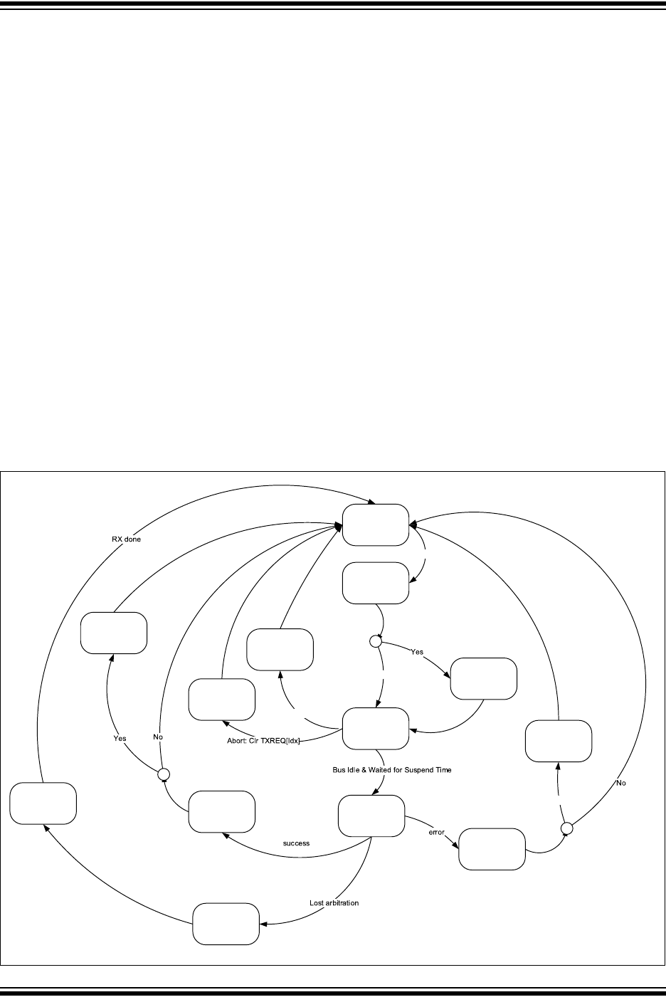
4.13 Transmit State Diagram
Figure 4-1 describes how messages are queued for transmission. It illustrates how the most
important transmit flags are set and cleared:
• Messages are queued for transmission by setting the TXREQ flag.
• Next the transmit priority will be determined. The FIFO or TXQ with the highest priority
TXPRI flag will be selected. The index of the TX message inside the FIFO or TXQ will be
calculated.
• Next the TX message is pending for transmission.
• Transmission can only start when the bus is idle.
• A pending transmission can only be aborted before SOF is transmitted.
• During the transmission of a message, the CAN FD Controller Module checks for the
following:
- Loss of arbitration, during the arbitration field.
- Transmit errors.
• In case a message of a TX FIFO or the TXQ was transmitted successfully, the TXREQ will
only be cleared after all messages of the FIFO are transmitted. After the transmission of
any message, the status flags of the FIFO or TXQ are updated. In case CiCON.STEF is
set, the message will be stored into the TEF, and a timestamp will be attached, if enabled.
• In case arbitration is lost, TXLARB of the TX FIFO or TXQ will be set, and the device will
switch over to receiving the message, see Section 7.0 “Message Reception”.
• In case an error is detected, during the transmission of a message, an Error frame will be
transmitted and the appropriate Error Flags will be set. Messages will be retransmitted
according to Section 4.9 “Retransmission Attempts”.
Figure 4-1: Transmit State Diagram
No
Abort: Set ABAT
Yes
Any TXREQ
IDLE
Calculate
TX Priority
Result: Idx
TX Pending[Idx]
Wait for Suspend
Time
TX In Progress
SOF
Transmit[Idx]
TX ERR
Set TXERRIF flag
TX Attempts--
TX Successful
Set TXIF[Idx]
Clr TXREQ[Idx]
cSTEF==1?
Save Msg to TEF
TX ABORT
Set TXABT[Idx]
ABORT ALL
Clr All TXREQ
Set All TXABT
Lost Arbitration
Set LARB[Idx]
Clr TXREQ[Idx]
Set TXATIF[Idx]
RX Message
cTX Attempts Exhausted?
Re-Init TX
Attempts
Based on new Idx
c
New TX Idx or
Received a message?
MCP25xxFD Family Reference Manual
DS20005678B-page 32 2017-2018 Microchip Technology Inc.
4.14 Resetting a Transmit FIFO
A FIFO can be reset by:
• Setting CiFIFOCONm.FRESET, or
• Placing the module into Configuration Mode (OPMOD = 100)
Resetting the FIFO will reset the head and tail pointers, and the CiFIFOSTAm register. The
settings in the CiFIFOCONm register will not change.
Before resetting a TX FIFO using FRESET, ensure no transmissions are pending.
4.15 Resetting the Transmit Queue (TXQ)
The Transmit Queue can be reset by:
• Setting CiTXQCON.FRESET, or
• Placing the module into Configuration Mode (OPMOD = 100)
Resetting the TXQ will reset the head and tail pointers, and the CiTXQSTA register. The
settings in the CiTXQCON register will not change.
Before resetting the TXQ using FRESET, ensure no transmissions are pending.
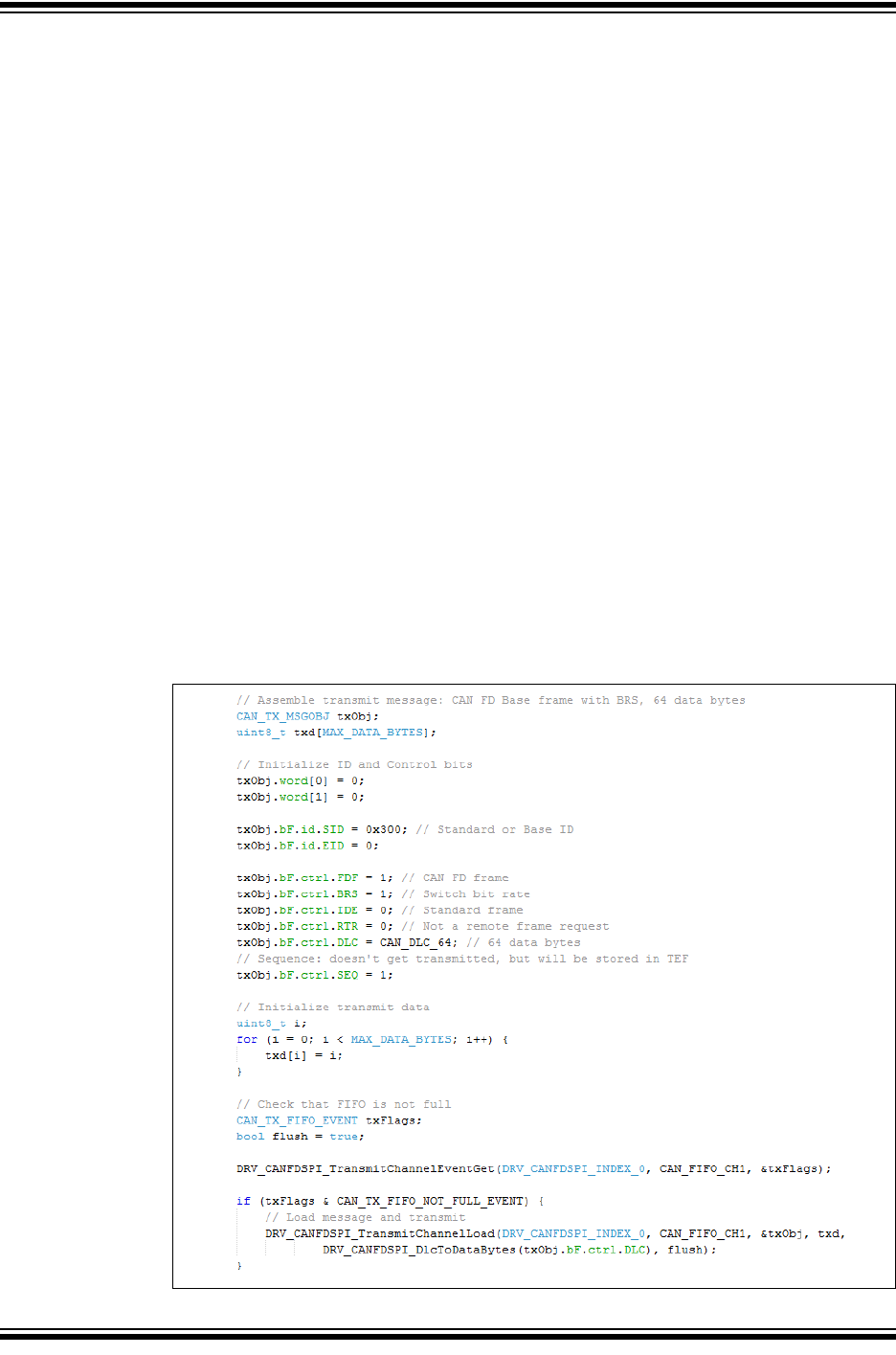
4.16 Message Transmission Code Example
Example 4-1 shows a code example of how to transmit a message using the following steps:
• Check that the FIFO is not full.
• Load the message into the FIFO
• Increment and flush the FIFO. UINC and TXREQ are set at the same time. This makes
sure that all messages from the FIFO are transmitted in case a message is appended to a
FIFO while it is already transmitting.
Example 4-1: Transmit Message from TX FIFO

2017-2018 Microchip Technology Inc. DS20005678B-page 33
CAN FD Controller Module
5.0 TRANSMIT EVENT FIFO
The Transmit Event FIFO (TEF) allows the application to keep track of the order and time the
messages were transmitted. The TEF works similar to a receive FIFO. Instead of storing
received messages, it stores transmitted messages. Messages are only saved if CiCON.STEF
is set. The sequence number (SEQ) of the transmitted message is copied into the TEF Object.
The payload data is not stored. Transmitted messages are timestamped if TEFTSEN is set.
Table 5-1 specifies the TEF Object. The first two words of the TEF Object are a copy of the
Transmit Message Object. Optionally, the TEF Object contains the timestamp when the
message was transmitted.
5.0.1 READING A TEF OBJECT
Before reading a TEF Object, the application must check that the TEF is not empty, by reading
the CiTEFSTA register. The TEF is not empty if TEFNEIF is set.
The TEF User Address points to the address in RAM of the next TEF Object to read. The actual
address in RAM is calculated using Equation 5-1. TE0 of the TEF Object is read first, followed
by TE1, and TE2.
Equation 5-1: Address of next TEF Object
After the TEF Object was read from RAM, the TEF needs to be incremented by setting
CiTEFCON.UINC. This will cause the CAN FD Controller Module to increment the Tail, and
update CiTEFUA.
Now the next message can be read from the TEF.
5.0.2 RESETTING THE TRANSMIT EVENT FIFO (TEF)
TEF can be reset by:
• Setting CiTEFCON.FRESET, or
• Placing the module into Configuration Mode (OPMOD = 100)
Resetting the FIFO will reset the head and tail pointers, and the CiTEFSTA register. The
settings in the CiTEFCON register will not change.
A 0x400 CiTEFUA+=

MCP25xxFD Family Reference Manual
DS20005678B-page 34 2017-2018 Microchip Technology Inc.
TABLE 5-1: TRANSMIT EVENT FIFO OBJECT
Word Bit
31/2315/7
Bit
30/22/14/6
Bit
29/21/13/5
Bit
28/20/12/4
Bit
27/19/11/3
Bit
26/18/10/2
Bit
25/17/9/1
Bit
24/16/8/0
TE0 31:24 -— -— SID11 EID<17:6>
23:16 EID<12:5>
15:8 EID<4:0> SID<10:8>
7:0 SID<7:0>
TE1 31:24 SEQ<22:15>
23:16 SEQ<14:7>
15:8 SEQ<6:0> ESI
7:0 FDF BRS RTR IDE DLC<3:0>
TE2 (1) 31:24 TXMSGTS<31:24>
23:16 TXMSGTS<23:16>
15:8 TXMSGTS<15:8>
7:0 TXMSGTS<7:0>
bit TE0.31-30 Unimplemented: Read as ‘x’
bit TE0.29 SID11: In FD mode the standard ID can be extended to 12 bit using r1
bit TE0.28-11 EID<17:0>: Extended Identifier
bit TE0.10-0 SID<10:0>: Standard Identifier
bit TE1.31-9 SEQ<22:0>: Sequence to keep track of transmitted messages (2)
bit TE1.8 ESI: Error Status Indicator
1 = Transmitting node is error passive
0 = Transmitting node is error active
bit TE1.7 FDF: FD Frame; distinguishes between CAN and CAN FD formats
bit TE1.6 BRS: Bit Rate Switch; selects if data bit rate is switched
bit TE1.5 RTR: Remote Transmission Request; not used in CAN FD
bit TE1.4 IDE: Identifier Extension Flag; distinguishes between base and extended format
bit TE1.3-0 DLC<3:0>: Data Length Code
bit TE2.31-0 TXMSGTS<31:0>: Transmit Message Timestamp
Note 1: TE2 (TXMSGTS) only exits in objects where CiTEFCON.TEFTSEN is set.
2: SEQ<22:7> are NOT implemented in the MCP2517FD.
2017-2018 Microchip Technology Inc. DS20005678B-page 35
CAN FD Controller Module
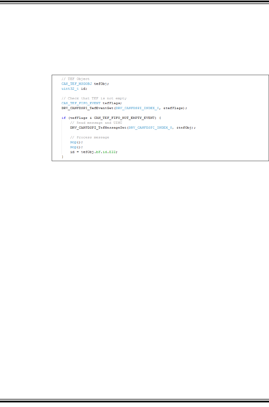
5.1 TEF Code Example
Example 5-1 shows a code example of how to read a message from the TEF:
• Check that the TEF is not empty.
• Read the message from the TEF.
• Increment the TEF by setting UINC.
• Process the TEF message.
Example 5-1: Reading a Message from the TEF

MCP25xxFD Family Reference Manual
DS20005678B-page 36 2017-2018 Microchip Technology Inc.
6.0 MESSAGE FILTERING
All messages on a CAN network will be received by all nodes. In order to process only messages
of interest, a hardware filtering mechanism is implemented. The CAN FD Controller Module can
be configured to receive only messages of interest. The module contains 32 acceptance filters.
Each acceptance filter contains a Filter Object and Mask Object. The user application configures
the specific filter to receive a message with a given identifier by setting the Filter Object and Mask
Object to match the identifier of the message to be received.
6.1 Filter Configuration
The filters are controlled by the CiFLTCONm registers. The filter must be disabled by clearing
the FLTEN bit, before changing the Filter or Mask Object. The module doesn’t have to be in
Configuration mode. After the Filter Object is updated, the Buffer Pointer, FnBP, has to be
initialized, and the filter can be enabled by setting the FLTEN bit. The Buffer Pointer points to
the FIFO where the matching receive message will be stored.
6.2 Filtering a Received Message
The CAN FD Controller Module starts acceptance filtering after the arbitration field and the first
3 data bytes of a message were received. Figure 6-1 describes the flow of message filtering.
The module loops through all the filters, starting with filter 0, which is the highest priority filter.
The message in the Receive Message Assembly Buffer (RXMAB) is compared to the filter and
mask. In case the message matches the filter, and it was received without any errors, the
message will be stored to the RX FIFO pointed to by the FnBP. Acceptance filtering is stopped,
and the associated RFIF is set.
In case a Remote Transmit Request (RTR) was received, the TXREQ bit of the TX FIFO
pointed to by FnBP will be set.
Filtering will continue with the next filter, and RXOVIF will be set, if one of the following happens:
• A filter matches, but the RX FIFO is full.
• When multiple filters match the same message, and all matching RX FIFOs are full, only
the RXOVIF of the FIFO pointed to by the highest priority filter will be set.
• The RXOVIF will be set, if the TX FIFO is empty during a RTR (TXEN = 1, RTREN = 1)
If none of the filters match, the received message will be discarded.
Note: If the module receives a message that matches a filter, but the corresponding FIFO is a
TX FIFO (TXEN = 1, RTREN = 0), the module will discard the received message.
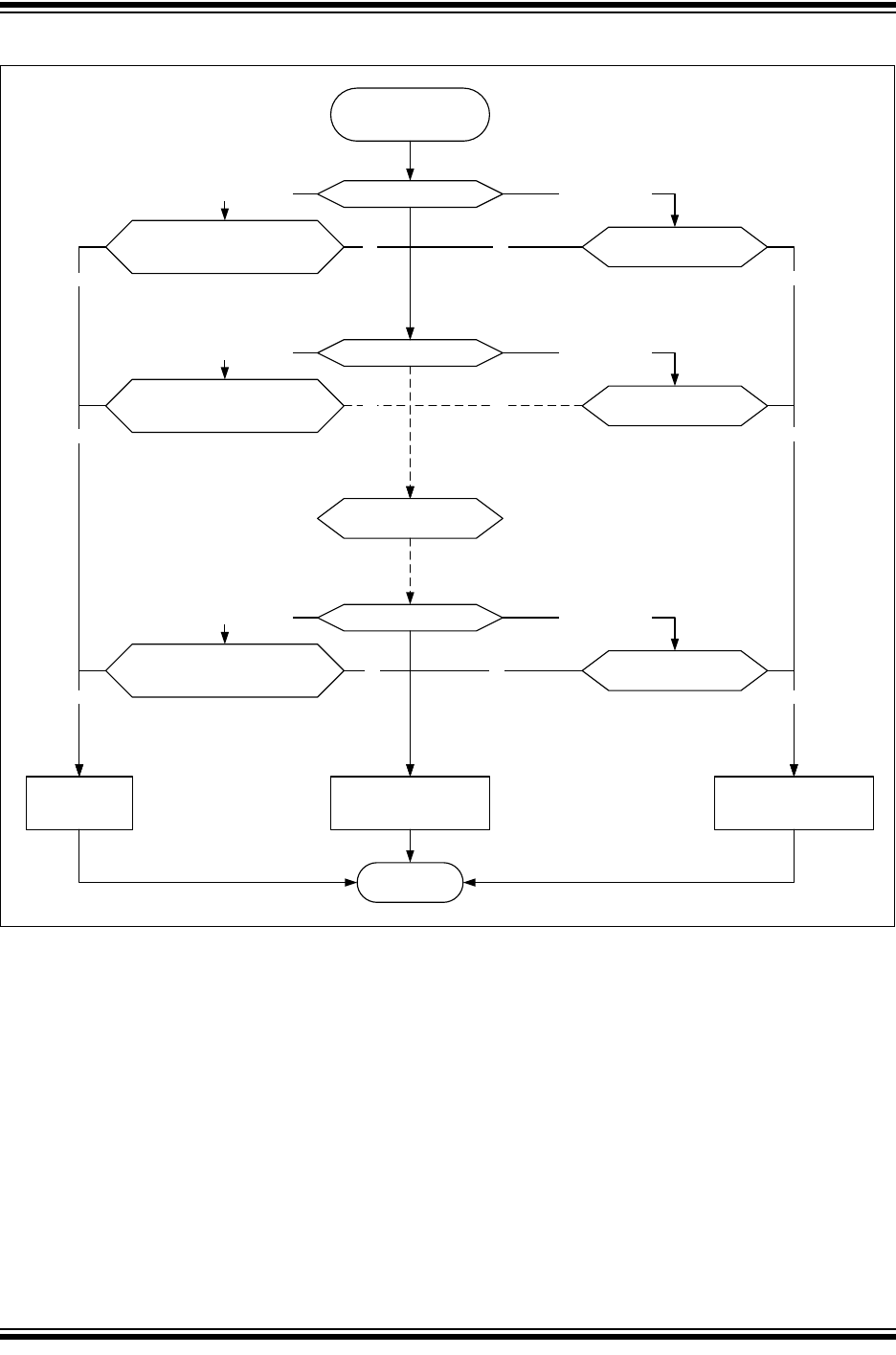
2017-2018 Microchip Technology Inc. DS20005678B-page 37
CAN FD Controller Module
Figure 6-1: Message Filtering Flow
6.2.1 FILTERING STANDARD OR EXTENDED FRAMES
Figure 6-2 illustrates the flow of matching a single Filter Object to the received message in the
RXMAB.
The Filter Object can be configured to accept either Standard, Extended or both frames. If MIDE
is clear, both Standard and Extended frames will be accepted.
If the filter should only accept Standard frames, then MIDE must be set, and EXIDE must be
cleared. If the filter should only accept Extended frames, then both MIDE and EXIDE must be
set.
6.2.2 MASK BITS
The Mask Object is used to ignore selected bits of the received identifier. The masked-out bits
(mask bits with value ‘0’) of the RXMAB will not be compared with the bits in the Filter Object.
For example, if the user would like to receive all messages with identifiers 0, 1, 2 and 3, the user
would mask-out the lower two bits of the identifier by clearing the corresponding bits of the Mask
Object.
Match Filter Objec t 0
Match Filter Objec t 1
No
FIFO Not Full?
Idx = F0BP
Yes and Not RTR
No
Accept Message:
Receiv e rest of Message
Store in FIFO [Idx]
Yes
FIFO Not Full?
Idx = F1BP
Yes and Not RTR
No
Yes
Match Filter Object 31
FIFO Not Full?
Idx = F31BP
Yes and Not RTR
No
Yes
Match Filter Objec t 2-30
Do the same
No
Discard Message
Done
No
Yes and RTR
FIFO Not Empty And
TXEN==1 and RTREN==1?
Idx = F0BP
No
Set TXREQ[Idx]
Yes
Yes and RTR
FIFO Not Empty And
TXEN==1 and RTREN==1?
Idx = F1BP
Yes and RTR
FIFO Not Empty And
TXEN==1 and RTREN==1?
Idx = F31BP
No
No
Yes
Yes
Arbitration Done and
Required Data Bytes
Received
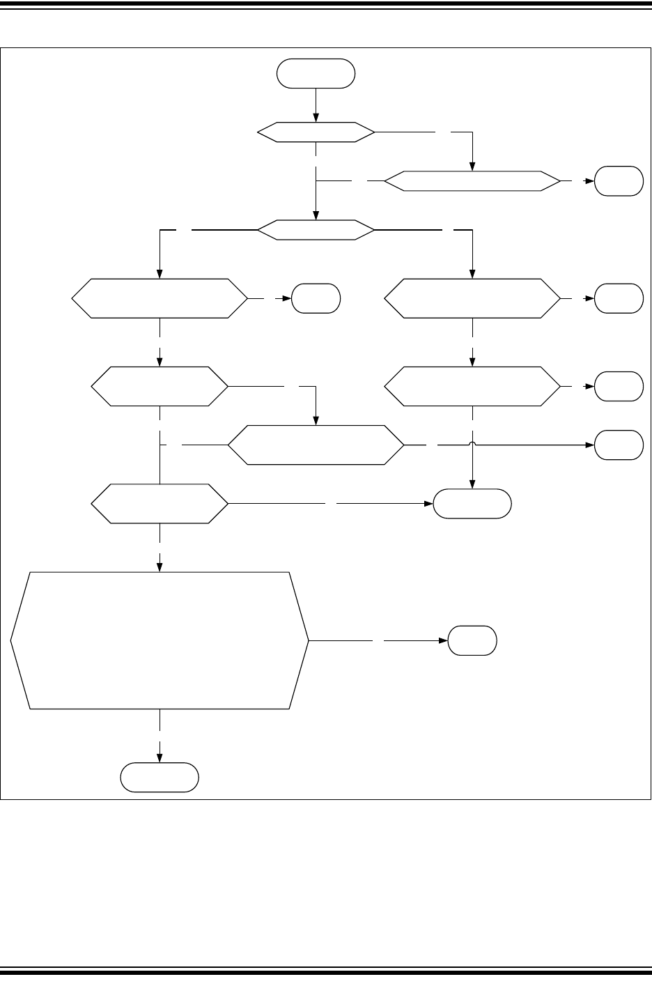
MCP25xxFD Family Reference Manual
DS20005678B-page 38 2017-2018 Microchip Technology Inc.
Figure 6-2: Filter Match
Start Matching
CiMASKm.MIDE
Set?
Check IDE:
CiFLTOBJm.EXIDE == RXMAB.IDE?
Yes
NO Match
Match
No
RXMAB.IDE == 0?
Base Format:
CiFLTOBJm.SID == RXMAB.SID,
CiMASKm.MSID[i] = 0 are Don’t
Care
Yes
Extended Form at:
CiFLTOBJm.SID == RXMAB.SID,
CiMASKm.MSID[i] = 0 are Don’t
Care
No
No
Yes
NO Match NO MatchNo No
CiFLTOBJm.EID == RXMAB.EID,
CiMASKm.MEID[i] = 0 are Don’t
Care
Yes
NO MatchNo
SID11:
CiTDC.SID11EN and
CiMASKm.MSID11
Check SID11:
CiFLTOBJ.SID11 ==
RXMAB.SID11?
Yes
Yes
Yes
Data Bytes:
CiCON.DNCNT > 0 ?
No
Yes NO MatchNo
No
Calculate number of bits to compare:
N = DNCNT
Calculate index:
M = 18-N
Assemble Receive Data Bytes:
RXDB = {RXMAB.DB0, RXMAB.DB1, RXMAB.DB2<7:6>}
Compare:
CiFLTOBJm.EID<0:N> == RXDB<17:M> ?
CiMASKm.MEID[i] = 0 are Don’t Care
Yes
NO MatchNo
Match
Yes

2017-2018 Microchip Technology Inc. DS20005678B-page 39
CAN FD Controller Module
6.2.3 FILTERING ON DATA BYTES
When the filter is set up for receiving Standard frames, the EID part of the Filter and Mask
Object can be selected to filter on data bytes. DNCNT in the CiCON is used to select how many
bits in the data bytes are compared. Table 6-1 explains how many data bits are compared, and
which filter bits and data bits are compared.
If DNCNT is ‘0’, then data byte filtering is disabled.
If DNCNT is non-zero, the filtering will commence on as many data bits as specified in DNCNT.
A filter hit will require matching of the SID bits and a match of n data bits with the filter’s
EID<0:17> bits. Data Byte 0<7> is always compared to EID<0>, Data Byte 0<6> to EID<1>,
Data Byte 2<6> to EID<17>.
If DNCNT is greater than 18, indicating that the user selected a number of bits greater than the
total number of EID bits, the filter comparison will terminate with the 18th bit of the data.
If DNCNT is greater than 16, and the received message has DLC = 2, indicating a payload of
two data bytes, the filter comparison will terminate with the 16th bit of the data.
If DNCNT is greater than 8, and the received message has DLC = 1, indicating a payload of one
data byte, the filter comparison will terminate with the 8th bit of the data.
If DNCNT is greater than 0, and the received message has DLC = 0, indicating no data payload,
the filter comparison will terminate with the identifier.
6.2.4 12 BIT STANDARD ID
Setting CiTDC.SID11EN allows the use of RRS as bit 12 of the SID (LSB). 12-bit SID mode is
only available for CAN FD Base frames. The filter is extended by SID11 and MSID11. Data
bytes can also be filtered in this mode.
Table 6-1: Data Byte Filter Configuration
DNCNT<4:0> Received Message Data Bits to be
Compared Byte <bits>
EID Bits Used for
Acceptance Filter
00000 No comparison No comparison
00001 Data Byte 0<7> EID<0>
00010 Data Byte 0<7:6> EID<0:1>
00011 Data Byte 0<7:5> EID<0:2>
00100 Data Byte 0<7:4> EID<0:3>
00101 Data Byte 0<7:3> EID<0:4>
00110 Data Byte 0<7:2> EID<0:5>
00111 Data Byte 0<7:1> EID<0:6>
01000 Data Byte 0<7:0> EID<0:7>
01001 Data Byte 0<7:0> and Data Byte 1<7> EID<0:8>
01010 Data Byte 0<7:0> and Data Byte 1<7:6> EID<0:9>
01011 Data Byte 0<7:0> and Data Byte 1<7:5> EID<0:10>
01100 Data Byte 0<7:0> and Data Byte 1<7:4> EID<0:11>
01101 Data Byte 0<7:0> and Data Byte 1<7:3> EID<0:12>
01110 Data Byte 0<7:0> and Data Byte 1<7:2> EID<0:13>
01111 Data Byte 0<7:0> and Data Byte 1<7:1> EID<0:14>
10000 Data Byte 0<7:0> and Data Byte 1<7:0> EID<0:15>
10001 Byte 0<7:0> and Byte 1<7:0> and Byte 2<7> EID<0:16>
10010 to 11111 Byte 0<7:0> and Byte 1<7:0> and Byte 2<7:6> EID<0:17>
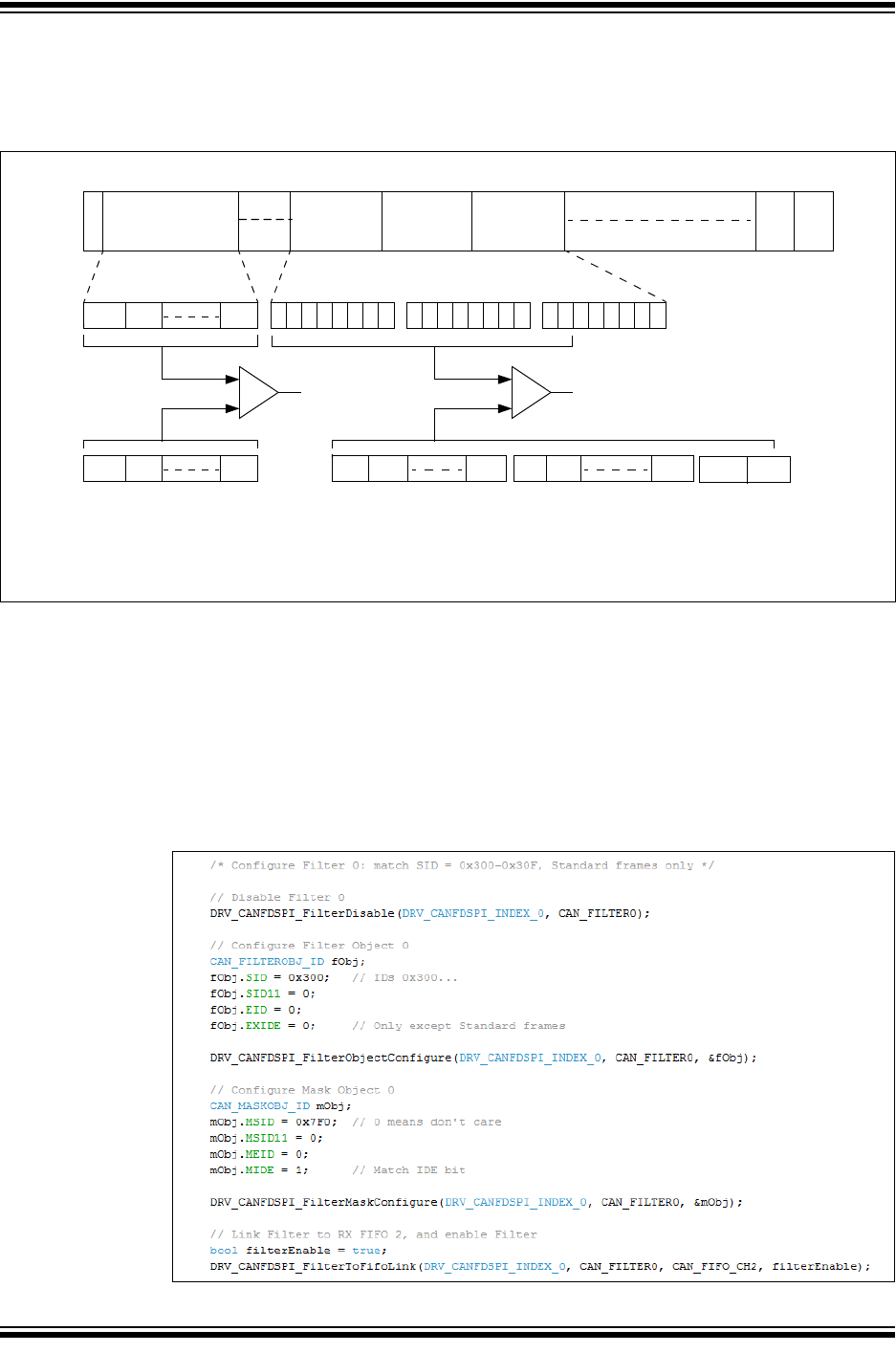
MCP25xxFD Family Reference Manual
DS20005678B-page 40 2017-2018 Microchip Technology Inc.
Figure 6-3 illustrates how the first 18 data bits of the received message data payload are
compared with the corresponding EID bits of the message acceptance filter (CiFLTOBJm.EID).
The IDE bit of the received message must be ‘0’.
Figure 6-3: CAN Operation with DeviceNet™ Filtering
6.3 Filter Configuration Code Example
Example 6-1 shows a code example of how to configure a filter to match Standard frames with
SID=0x300-0x30F using the following steps:
• Disable the Filter.
• Configure the Filter Object: assign SID, clear EXIDE.
• Configure the Mask Object: assign MSID, set MIDE to filter only Standard frames.
• Link the filter to an RX FIFO and enable the filter.
Example 6-1: Filter Configuration to Match a Standard Frame Range
SID10 SID9
S
O
F
IDENTIFIER
11 Bits
EOF
7 Bits 3 Bits
SID0
Accept/Reject Message
IFS
DATA BYTE 0 DATA BYTE 1 DATA BYTE 2
7654321 0 76543210 76543210
Data Byte 0 Data Byte 1 Data Byte 2MESSAGE SID<10:0>
SID10 SID9 SID0
EID0 EID1 EID7
EID8 EID9 EID15 EID1
6
EID17
STANDARD MESSAGE DATA FRAME
MESSAGE ACCEPTANCE FILTER
SID<10:0>
MESSAGE ACCEPTANCE FILTER
EID<0:17>
Note: The DeviceNet™ filtering configuration shown for EID bits is DNCNT<4:0> = 10010.

2017-2018 Microchip Technology Inc. DS20005678B-page 41
CAN FD Controller Module
7.0 MESSAGE RECEPTION
The application has to configure the RX FIFO before it can be used for reception, see
Section 3.5.4 “Receive FIFO Configuration”. In addition, the application has to configure and
enable at least one filter, see Section 6.1 “Filter Configuration”.
The CAN FD Controller Module continuously monitors the CAN bus. Messages that match a filter
are stored into the RX FIFO pointed to by the filter, see Section 6.2 “Filtering a Received
Message”. The message data is stored into Receive Message Objects.
7.1 Receive Message Object
Table 7-1 specifies the Receive Message Object used by the RX FIFOs. The receive objects
contain the message ID, Control bits, payload and timestamp:
•SID: Standard ID or Base ID
•EID: ID Extension
•DLC: Data Length Code; specifies the number of data bytes in the frame, see
Section 1.4.2 “DLC Encoding”.
•IDE: ID extension selection; IDE = 0 means a Base frame was received, IDE = 1 means an
Extended frame was received.
•RTR: Remote Transmit Request; this bit is only specified in CAN 2.0 frames. If this bit is
set, the module is requested to respond with a frame transmission.
•FDF: FD Format selection; if this bit is set, a CAN FD frame was received, otherwise, a
CAN 2.0 frame.
•BRS: Bit Rate Switch; the data phase of a CAN FD frame was received using DBR, if this
bit is set. If the bit is clear, the whole frame was received using NBR.
•ESI: Error State Indicator; the ESI bit reflects the error status of the transmitting node. A
recessive ESI bit inside a CAN FD frame indicates that the transmitting node is error
passive, a dominant bit shows that the transmitting node is error active.
•FILHIT: Indicates the number of the filter that matched the received message.
•RXMSGTS: Timestamp of the received message. Timestamping can be enabled for each
RX FIFO individually using CiFIFOCONm.RXTSEN. The Receive Message Object will not
contain RXMSGTS, if timestamping is disabled.
•Receive Buffer Data: contains the payload of the message. The maximum payload is
configured in CiFIFOCONm.PLSIZE.
7.1.1 READING A RECEIVE MESSAGE OBJECT
Before reading a Receive Message Object, the application must check that the RX FIFO is not
empty, by reading the CiFIFOSTAm register. The RX FIFO is not empty if TFNRFNIF is set.
The RX FIFO User Address points to the address in RAM of the next Receive Message Object
to read. The actual address in RAM is calculated using Equation 7-1. R0 of the Receive Message
Object is read first, followed by R1, R2, and so on.
Equation 7-1: Address of next Message Object
After the Receive Message Object was read from RAM, the RX FIFO needs to be incremented
by setting CiFIFOCONm.UINC. This will cause the CAN FD Controller Module to increment the
Tail of the FIFO, and update CiFIFOUAm.
Now the application can read the next message from the RX FIFO.
A 0x400 CiFIFOUAm+=

MCP25xxFD Family Reference Manual
DS20005678B-page 42 2017-2018 Microchip Technology Inc.
TABLE 7-1: RECEIVE MESSAGE OBJECT
Word Bit
31/2315/7
Bit
30/22/14/6
Bit
29/21/13/5
Bit
28/20/12/4
Bit
27/19/11/3
Bit
26/18/10/2
Bit
25/17/9/1
Bit
24/16/8/0
R0 31:24 -— -— SID11 EID<17:6>
23:16 EID<12:5>
15:8 EID<4:0> SID<10:8>
7:0 SID<7:0>
R1 31:24 -— -— -— -— -— -— -— -—
23:16 -— -— -— -— -— -— -— -—
15:8 FILHIT<4:0> -— -— ESI
7:0 FDF BRS RTR IDE DLC<3:0>
R2 (2) 31:24 RXMSGTS<31:24>
23:16 RXMSGTS<23:16>
15:8 RXMSGTS<15:8>
7:0 RXMSGTS<7:0>
R3 (1) 31:24 Receive Data Byte 3
23:16 Receive Data Byte 2
15:8 Receive Data Byte 1
7:0 Receive Data Byte 0
R4 31:24 Receive Data Byte 7
23:16 Receive Data Byte 6
15:8 Receive Data Byte 5
7:0 Receive Data Byte 4
Ri 31:24 Receive Data Byte n
23:16 Receive Data Byte n-1
15:8 Receive Data Byte n-2
7:0 Receive Data Byte n-3
bit R0.31-30 Unimplemented: Read as ‘x’
bit R0.29 SID11: In FD mode the standard ID can be extended to 12 bit using r1
bit R0.28-11 EID<17:0>: Extended Identifier
bit R0.10-0 SID<10:0>: Standard Identifier
bit R1.31-16 Unimplemented: Read as ‘x’
bit R1.15-11 FILTHIT<4:0>: Filter Hit, number of filter that matched
bit R1.10-9 Unimplemented: Read as ‘x’
bit R1.8 ESI: Error Status Indicator
1 = Transmitting node is error passive
0 = Transmitting node is error active
bit R1.7 FDF: FD Frame; distinguishes between CAN and CAN FD formats
bit R1.6 BRS: Bit Rate Switch; indicates if data bit rate was switched
bit R1.5 RTR: Remote Transmission Request; not used in CAN FD
bit R1.4 IDE: Identifier Extension Flag; distinguishes between base and extended format
bit R1.3-0 DLC<3:0>: Data Length Code
bit R2.31-0 RXMSGTS<31:0>: Receive Message Timestamp
Note 1: RXMOBJ: Data Bytes 0-n: payload size is configured individually in the FIFO control register
(CiFIFOCONm.PLSIZE<2:0>).
2: R2 (RXMSGTS) only exits in objects where CiFIFOCONm.RXTSEN is set.
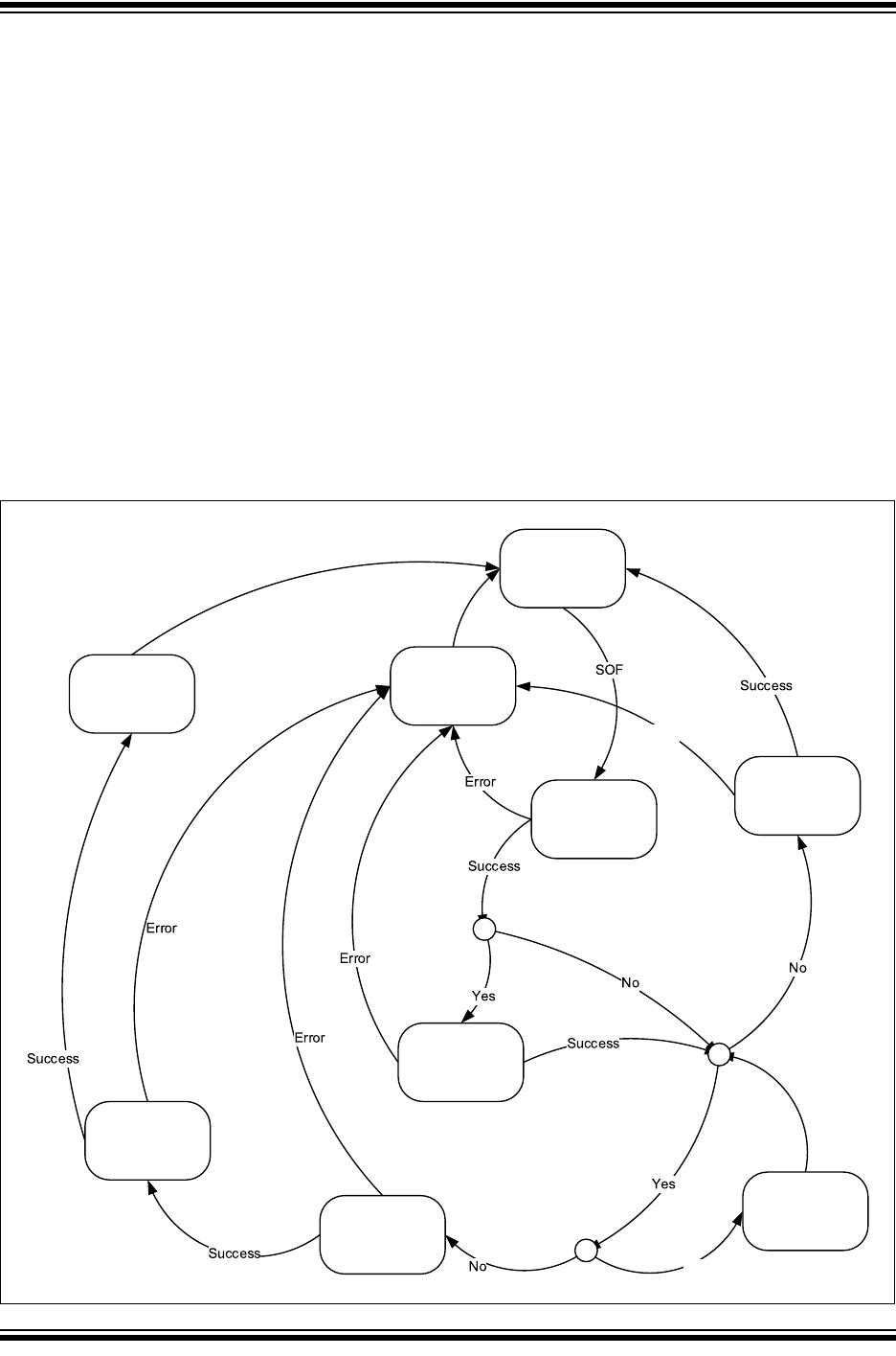
2017-2018 Microchip Technology Inc. DS20005678B-page 43
CAN FD Controller Module
7.2 Receive State Diagram
Figure 7-1 illustrates how messages are received. It illustrates how the most important receive
flags are set and cleared:
• The CAN FD Controller Module remains IDLE until a SOF is detected.
• After a SOF was detected, the module will receive the Arbitration and Control fields.
• Based on the DNCNT and the received DLC, acceptance filtering will start. See Figure 6-1
for more details.
• If none of the filters match, the message will still be received, but it will not be stored.
• If a filter matches, the device checks, if the receive object, the filter points to, is full.
• If the receive object is full, the RXOVIF will be set.
• If the receive object is not full, the rest of the data bytes are received and stored to the
receive object.
• If a complete message was received, the message will be stored, a timestamp will be
attached, and the receive flags will be set: the FIFO status flags will be updated, and the
FIFO head will be incremented.
• In case an error is detected, during the reception of a message, an Error frame will be
transmitted and the appropriate Error Flags will be set.
Figure 7-1: Receive State Diagram
Error
Yes
IDLE
Receive
ARBITRATION
and CTRL field
Transmit Error
Frame
Set Error Flags
c
Filter Match?
Store Message to
Object
Set FIFO status
flags
c
Object Full?
Set RXOVIF
c
DNCNT>0 and DLC>0?
Receive
DATA B YTE 0-3
Receive
remaining
DATA B YTES
And Store them
Receive Rest of
Message
Receive Rest of
Message
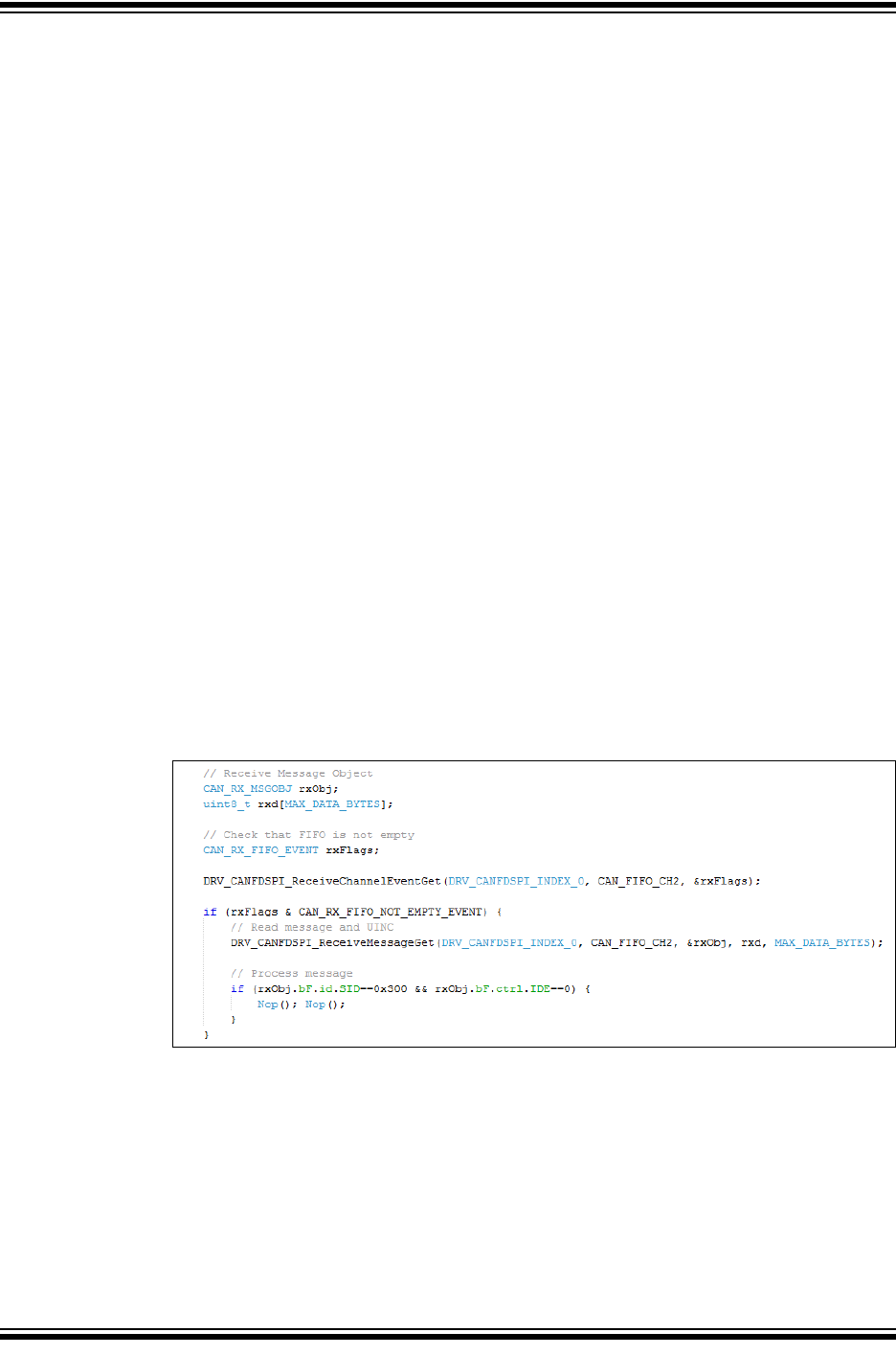
MCP25xxFD Family Reference Manual
DS20005678B-page 44 2017-2018 Microchip Technology Inc.
7.3 Resetting a RX FIFO
A FIFO can be reset by:
• Setting CiFIFOCONm.FRESET, or
• Placing the module into Configuration Mode (OPMOD = 100)
Resetting the FIFO will reset the head and tail pointers, and the CiFIFOSTAm register. The
settings in the CiFIFOCONm register will not change.
Before resetting a RXFIFO using FRESET, ensure that no enabled filter is pointing to the FIFO.
7.4 Mismatch of DLC and Payload Size During Reception
The PLSIZE reserves a certain number of bytes in the Receive Message Object. The module
handles mismatches between DLC and payload size as follows:
• If the number of bytes specified by the DLC is smaller than the number of bytes specified
by the PLSIZE, the received message bytes will be stored in the message object, without
any padding.
• If the number of bytes specified by the DLC is bigger than the number of bytes specified by
the PLSIZE, the data bytes that fit in the Receive Message Object will be stored. The data
bytes that don’t fit into the Receive Message Object will be discarded. The module makes
sure that the next message object in RAM doesn’t get overwritten. The module will store
the message in the receive object and the RX FIFO status flags will be updated. In addition,
the CiINT.IVMIF and CiBDIAG1.DLCMM flags will be set.
7.5 Message Reception Code Example
Example 7-1 shows a code example of how to receive a message using the following steps:
• Check that the FIFO is not empty.
• Read the message from the FIFO.
• Increment the FIFO by setting UINC.
• Process the received message.
Example 7-1: Receiving a Message

2017-2018 Microchip Technology Inc. DS20005678B-page 45
CAN FD Controller Module
8.0 FIFO BEHAVIOR
This section explains the FIFO behavior based on the configuration used in Section 3.6,
Configuration Code Example. The MCP25xxFD was configured as shown in Table 8-1. TEF, and
TXQ were enabled. FIFO1 was configured as a TX FIFO, and FIFO2 as an RX FIFO. All other
FIFOs were not configured.
The start addresses are calculated based on the number of objects in the FIFO and the payload
size. TEF always starts at address 0x400.
Table 8-1: Example FIFO Configuration
8.1 FIFO Status Flags
FIFO 1 through 31 can be configured as transmit or receive FIFOs. The same status flags in
CiFIFOSTAm are used for transmit and receive. The status flags behave differently based on the
selected configuration.
8.1.1 TX FIFO STATUS FLAGS
There are three transmit status flags:
•TFEIF (TFERFFIF): Transmit FIFO Empty IF; set when the FIFO is empty.
• TFHIF (TFHRFHIF): Transmit FIFO Half Empty IF; set when FIFO is less than half full.
• TFNIF (TFNRFNIF): Transmit FIFO Not Full IF; set when FIFO is not full.
The status flags of a transmit FIFO are set, when there is room to load a new message object
into the FIFO. Before the first message object is loaded (after the FIFO was reset), all status flags
are set. When the FIFO is fully loaded, all flags are clear.
8.1.2 RX FIFO STATUS FLAGS
There are three receive status flags:
• RFFIF (TFERFFIF): Receive FIFO Full IF; set when the FIFO is full.
•RFHIF (TFHRFHIF): Receive FIFO Half Full IF; set when the FIFO is at least half full.
•RFNIF (TFNRFNIF): Receive FIFO Not Empty IF; set when there is at least one message
in the FIFO.
The status flags of the receive FIFO are set, when there are received messages in the FIFO.
Before the first message is received (after the FIFO was reset), all status flags are clear. When
the FIFO is full, all flags are set.
FIFO Objects
in FIFO
Payload
per Object Timestamp Bytes in
Object
Bytes in
FIFO Start Address
TEF 12 N/A Yes 12 144 0x400
TXQ 8 32 N/A 40 320 0x490
FIFO1 5 64 N/A 72 360 0x5D0
FIFO2 16 64 Yes 76 1216 0x738
FIFO3 N/A 0xBF8

MCP25xxFD Family Reference Manual
DS20005678B-page 46 2017-2018 Microchip Technology Inc.
8.1.3 TXQ STATUS FLAGS
There are two TXQ status flags:
• TXQEIF: TXQ Empty IF; set when the TXQ is empty.
• TXQNIF: TXQ Not Full IF; set when TXQ is not full.
The status flags of the TXQ are set, when there is room to load a new message object into the
TXQ. Before the first message object is loaded (after the TXQ was reset), all status flags are set.
When the TXQ is fully loaded, all flags are clear.
8.1.4 TEF STATUS FLAGS
There are four TEF status flags:
• TEFFIF: TEF Full IF; set when the TEF is full.
• TEFHIF: TEF Half Full IF; set when the TEF is at least half full.
• TEFNEIF: TEF Not Empty IF; set when there is at least one message in the TEF.
The status flags of the TEF are set, when there are transmitted messages in the FIFO. Before
the first message is stored (after the TEF was reset), all status flags are clear. When the TEF is
full, all flags are set.
2017-2018 Microchip Technology Inc. DS20005678B-page 47
CAN FD Controller Module
8.2 Transmit FIFO Behavior
FIFO 1 is configured as a TX FIFO. C1FIFOCON1 is used to control the FIFO. C1FIFOSTA1
contains the status flags, and the FIFO index (FIFOCI). C1FIFOUA1 contains the user address
of the next transmit message object to be loaded.
Remember that the actual RAM address is calculated using Equation 4-1.
Figure 8-1 through Figure 8-6 illustrate how the status flags, user address, and FIFO index are
updated.
Figure 8-1 shows the status of FIFO 1 after reset. Message Objects MO0 to MO4 are empty. All
status flags are set. The user address and the FIFO index point to MO0.
Figure 8-1: FIFO 1 - Initial State
Figure 8-2 illustrates the status of FIFO 1 after the first message (MSG0) was loaded. MO0
contains now MSG0. The user application sets C1FIFOCON1.UINC, which causes the FIFO
head to advance. The user address points now to MO1. TFEIF is cleared, since the FIFO is no
longer empty. The user application now sets TXREQ to request the transmission of MSG0.
Figure 8-2: FIFO 1 - First Message Loaded
Figure 8-3 illustrates the status of FIFO 1 after MSG0 was transmitted. The FIFO is empty again.
TFEIF is set, and TXREQ is cleared. FIFOCI now points to MO1 with user address 0x218.
Figure 8-3: FIFO 1 - First Message Transmitted
MO0
MO1
MO2
MO3
MO4
C1FIFOUA1 = 0x1D0
C1FIFOSTA1:
FIFOCI = 0
TFEIF = 1
TFHIF = 1
TFNIF = 1
C1FIFOCON1:
TXREQ = 0
MO0 / MSG0
MO1
MO2
MO3
MO4
C1FIFOUA1 = 0x218
C1FIFOSTA1:
FIFOCI = 0
TFEIF = 0
TFHIF = 1
TFNIF = 1
C1FIFOCON1:
TXREQ = 1
MO1
MO2
MO3
MO4
C1FIFOUA1 = 0x218
C1FIFOSTA1:
FIFOCI = 1
TFEIF = 1
TFHIF = 1
TFNIF = 1
C1FIFOCON1:
TXREQ = 0
MO0
MCP25xxFD Family Reference Manual
DS20005678B-page 48 2017-2018 Microchip Technology Inc.
Figure 8-4 illustrates the status of FIFO 1 after three more messages were loaded: MSG1-MSG3.
The user address points now to MO4. TFHIF was cleared, because the FIFO is now less than
half empty.
Figure 8-4: FIFO 1 - Three More Messages Loaded
Figure 8-5 illustrates the status of FIFO 1 after two more messages were loaded: MSG4-MSG5.
C1FIFOUA1 points now to MO1. All status flags are now cleared, because the FIFO is full. The
user address and the FIFO index point now to MO1. The user application now sets TXREQ to
request the transmission of MSG1-MSG5.
Figure 8-5: FIFO 1 - FIFO Fully Loaded
Figure 8-6 illustrates the status of FIFO 1 after MSG1-MSG5 were transmitted. The FIFO is
empty again. all status flags are set, and TXREQ is cleared. The user address and the FIFO
index point to MO1 again.
Figure 8-6: FIFO 1 - FIFO Fully Transmitted
MO1 / MSG1
MO2 /MSG2
MO3 / MSG3
MO4
C1FIFOUA1 = 0x2F0
C1FIFOSTA1:
FIFOCI = 1
TFEIF = 0
TFHIF = 0
TFNIF = 1
C1FIFOCON1:
TXREQ = 0
MO0
MO1 / MSG1
MO2 / MSG2
MO3 / MSG3
MO4 / MSG4
C1FIFOUA1 = 0x218
C1FIFOSTA1:
FIFOCI = 1
TFEIF = 0
TFHIF = 0
TFNIF = 0
C1FIFOCON1:
TXREQ = 1
MO0 / MSG5
MO1
MO2
MO3
MO4
C1FIFOUA1 = 0x218
C1FIFOSTA1:
FIFOCI = 1
TFEIF = 1
TFHIF = 1
TFNIF = 1
C1FIFOCON1:
TXREQ = 0
MO0
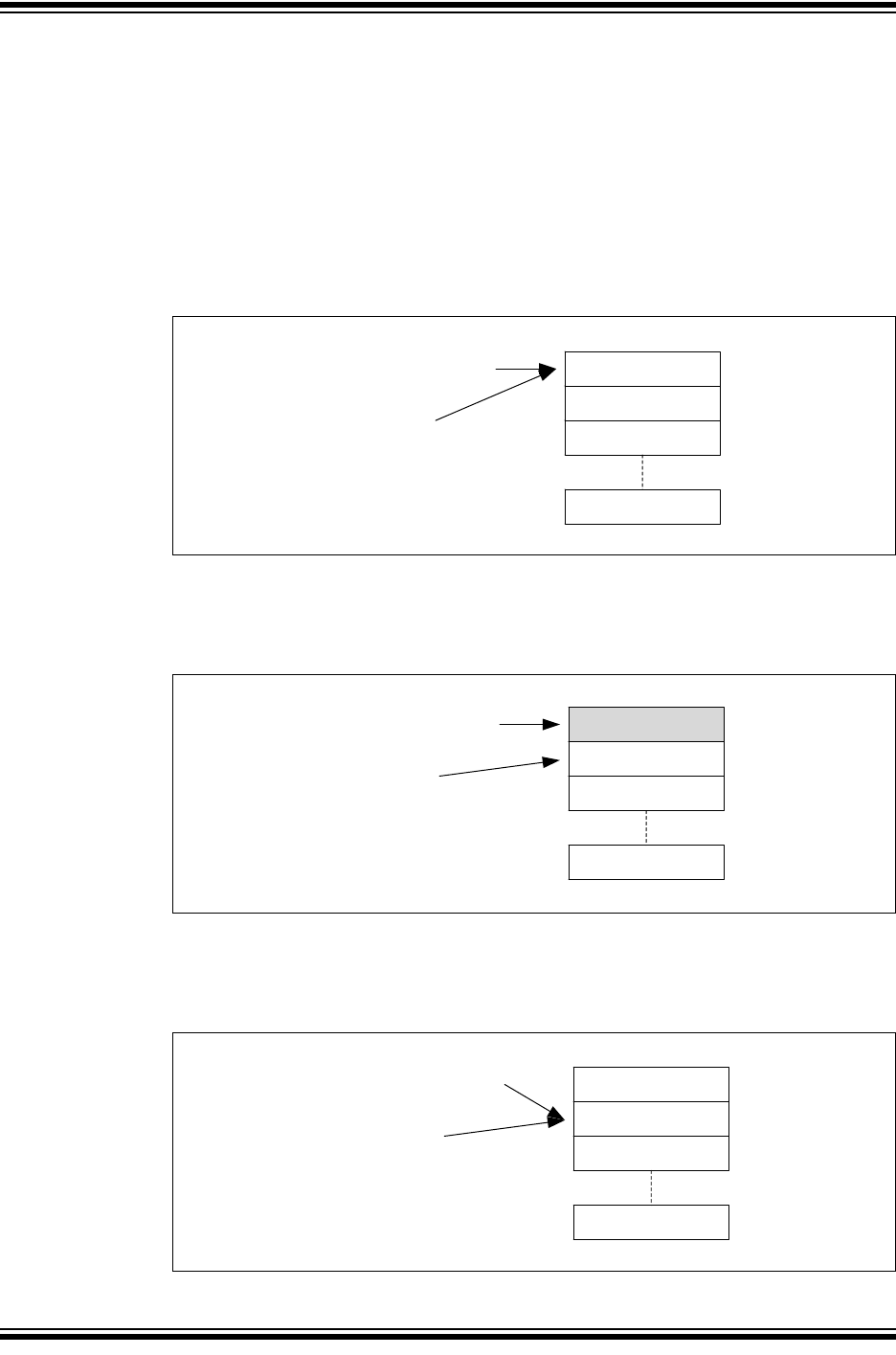
2017-2018 Microchip Technology Inc. DS20005678B-page 49
CAN FD Controller Module
8.3 Receive FIFO Behavior
FIFO 2 is configured as a RX FIFO. C1FIFOCON2 is used to control the FIFO. C1FIFOSTA2
contains the status flags, and the FIFO index (FIFOCI). C1FIFOUA2 contains the user address
of the next message object to read.
Remember that the actual RAM address is calculated using Equation 7-1.
Figure 8-7 through Figure 8-14 illustrate how the status flags, user address, and FIFO index are
updated.
Figure 8-7 shows the status of FIFO 2 after reset. Message Objects MO0 to MO15 are empty. All
status flags are clear. The user address and the FIFO index point to MO0.
Figure 8-7: FIFO 2 - Initial State
Figure 8-8 illustrates the status of FIFO 2 after the first message (MSG0) was received. MO0
contains now MSG0. The FIFO index points now to MO1. RFNIF is set, since the FIFO is not
empty anymore.
Figure 8-8: FIFO 2 - First Message Received
Figure 8-9 illustrates the status of FIFO 2 after MSG0 was read. The user application reads the
message from RAM and sets C1FIFOCON2.UINC. The user address increments and points to
MO1. The FIFO index is unchanged. The FIFO is empty again. All flags are clear.
Figure 8-9: FIFO 2 - First Message Read
MO0
MO1
MO2
MO15
C1FIFOUA2 = 0x338
C1FIFOSTA2:
FIFOCI = 0
RFFIF = 0
RFHIF = 0
RFNIF = 0
RXOVIF = 0
MO0 / MSG0
MO1
MO2
MO15
C1FIFOUA2 = 0x338
C1FIFOSTA2:
FIFOCI = 1
RFFIF = 0
RFHIF = 0
RFNIF = 1
RXOVIF = 0
MO1
MO2
MO15
C1FIFOUA2 = 0x384
C1FIFOSTA2:
FIFOCI = 1
RFFIF = 0
RFHIF = 0
RFNIF = 0
RXOVIF = 0
MO0
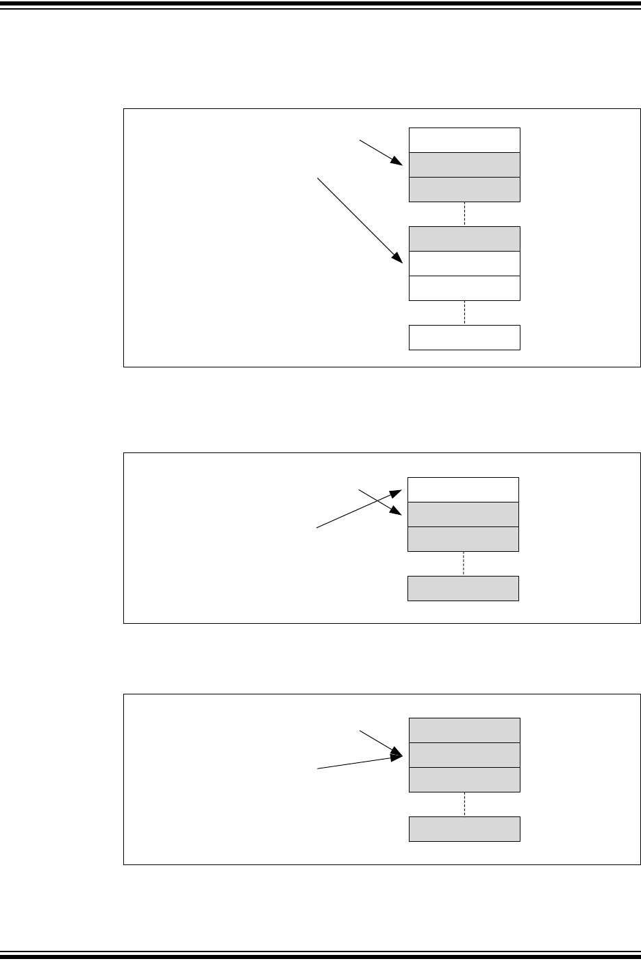
MCP25xxFD Family Reference Manual
DS20005678B-page 50 2017-2018 Microchip Technology Inc.
Figure 8-10 illustrates the status of FIFO 2 after eight more messages were received: MSG1-
MSG8. The user address still points to MO1. RFNIF and RFHIF are set, because the FIFO is now
half full. The FIFO index points to MO9.
Figure 8-10: FIFO 2 - Half Full
Figure 8-11 illustrates the status of FIFO 2 after seven more messages were received: MSG5-
MSG15. The user address still points to MO1. The FIFO index points to MO0. RFNIF and RFHIF
are set.
Figure 8-11: FIFO 2 - FIFO Almost Full
Figure 8-12 illustrates the status of FIFO 2 after one more message was received: MSG16. All
status flags are set, because the FIFO is full. The user address and the FIFO index point to MO1.
Figure 8-12: FIFO 2 - FIFO Full
MO1 / MSG1
MO2 / MSG2
MO9
C1FIFOUA2 = 0x384
C1FIFOSTA2:
FIFOCI = 9
RFFIF = 0
RFHIF = 1
RFNIF = 1
RXOVIF = 0
MO0
MO8 / MSG8
MO15
MO10
MO1 / MSG1
MO2 / MSG2
C1FIFOUA2 = 0x384
C1FIFOSTA2:
FIFOCI = 0
RFFIF = 0
RFHIF = 1
RFNIF = 1
RXOVIF = 0
MO0
MO15 / MSG15
MO1 / MSG1
MO2 / MSG2
C1FIFOUA2 = 0x384
C1FIFOSTA2:
FIFOCI = 1
RFFIF = 1
RFHIF = 1
RFNIF = 1
RXOVIF = 0
MO0 / MSG16
MO15 / MSG15
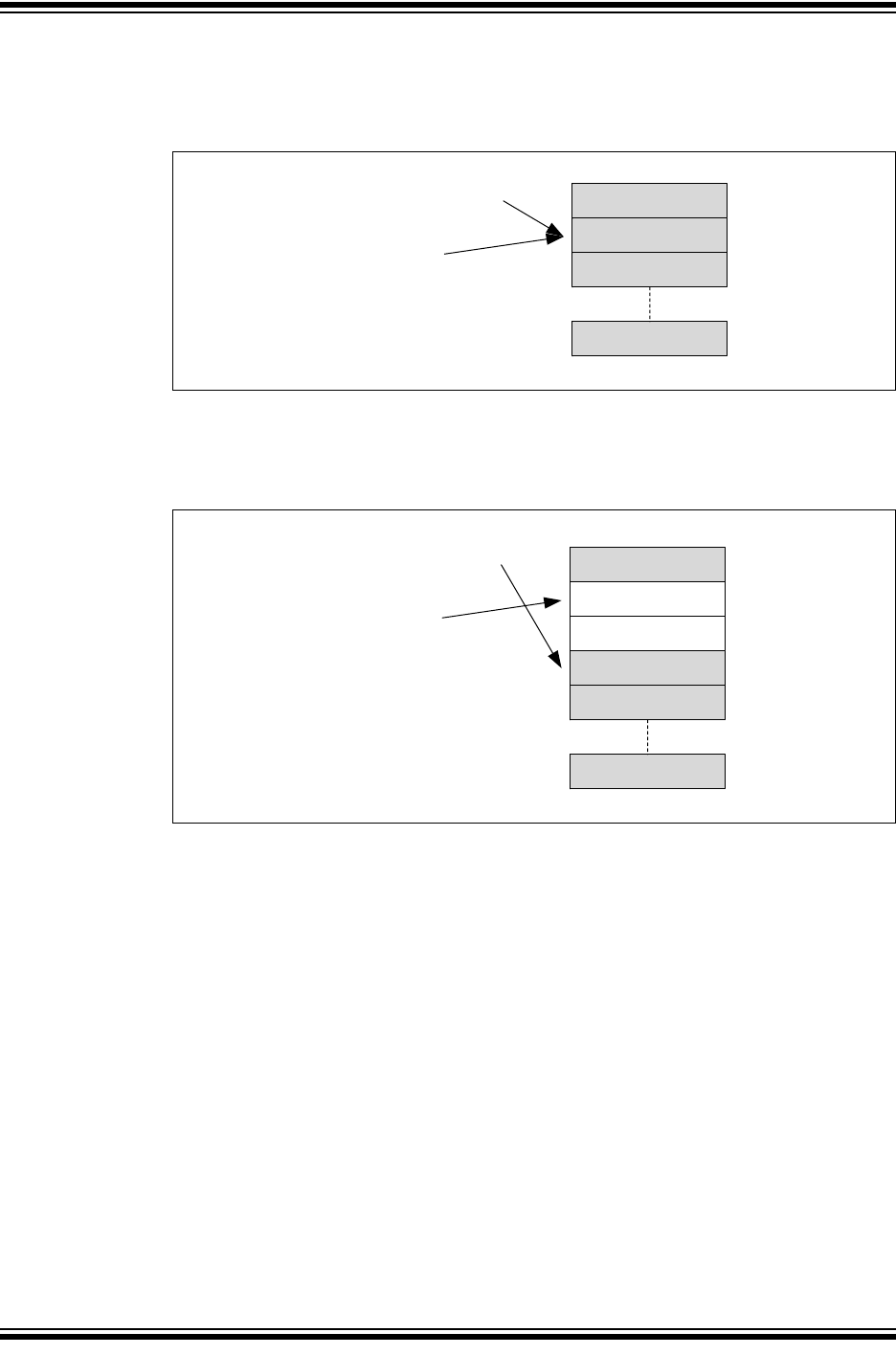
2017-2018 Microchip Technology Inc. DS20005678B-page 51
CAN FD Controller Module
Figure 8-13 illustrates the status of FIFO 2 after one more message was received. Since FIFO 2
was already full, an overflow occurred. The message is discarded, and RXOVIF is set. The user
address and FIFO index didn’t change.
Figure 8-13: FIFO 2 - FIFO Overflow
Figure 8-14 illustrates the status of FIFO 2 after the application cleared RXOVIF and read two
more messages. RFFIF is clear, because the FIFO isn’t full anymore. The user address points to
MO3. The FIFO index didn’t change.
Figure 8-14: FIFO 2 - Two More Messages Read
MO1 / MSG1
MO2 / MSG2
C1FIFOUA2 = 0x384
C1FIFOSTA2:
FIFOCI = 1
RFFIF = 1
RFHIF = 1
RFNIF = 1
RXOVIF = 1
MO0 / MSG16
MO15 / MSG15
MO3 / MSG3
MO4 / MSG4
C1FIFOUA2 = 0x41C
C1FIFOSTA2:
FIFOCI = 1
RFFIF = 0
RFHIF = 1
RFNIF = 1
RXOVIF = 0
MO0 / MSG16
MO15 / MSG15
MO1
MO2
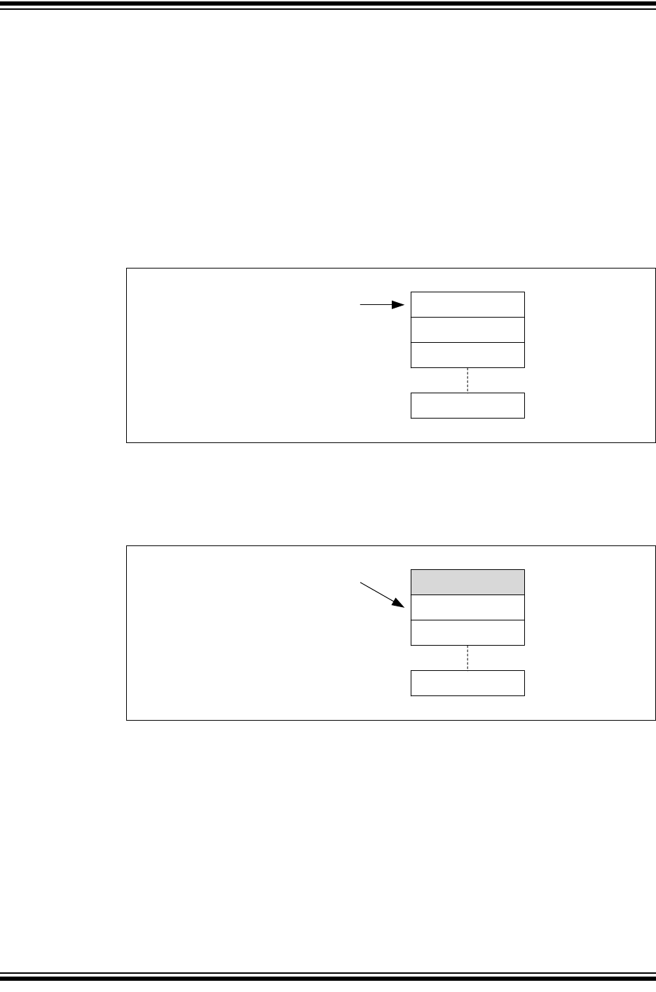
MCP25xxFD Family Reference Manual
DS20005678B-page 52 2017-2018 Microchip Technology Inc.
8.4 Transmit Queue Behavior
C1TXQCON is used to control the TXQ. C1TXQSTA contains the status flags, and the TXQ index
(TXQCI). C1TXQUA contains the user address of the next transmit message object to be loaded.
The TXQCI is used by the CAN FD Controller Module to calculate the next message to transmit.
TXQCI is not incremented linearly. It is recalculated every time a message gets transmitted, or
TXREQ gets set.
Remember that the actual RAM address is calculated using Equation 4-1.
Figure 8-15 through Figure 8-20 illustrate how the status flags, and user address are updated.
There is no need for the user application to use TXQCI, therefore, it is not shown in the figures.
Figure 8-15 shows the status of the TXQ after reset. Message Objects MO0 to MO7 are empty.
All status flags are set. The user address points to MO0.
Figure 8-15: TXQ - Initial State
Figure 8-16 illustrates the status of the TXQ after the first message (MSG0) was loaded. MO0
contains now MSG0. The user application sets C1TXQCON.UINC, which causes the FIFO head
to advance. The user address points now to MO1. TXQEIF is cleared, since the queue isn’t
empty anymore. The user application now sets TXREQ to request the transmission of MSG0.
Figure 8-16: TXQ - First Message Loaded
MO0
MO1
MO2
MO7
C1TXQUA = 0x090
C1TXQSTA:
TXQEIF = 1
TXQNIF = 1
C1TXQCON:
TXREQ = 0
MO0 / MSG0
MO1
MO2
MO7
C1TXQUA = 0x0B8
C1TXQSTA:
TXQEIF = 0
TXQNIF = 1
C1TXQCON:
TXREQ = 1
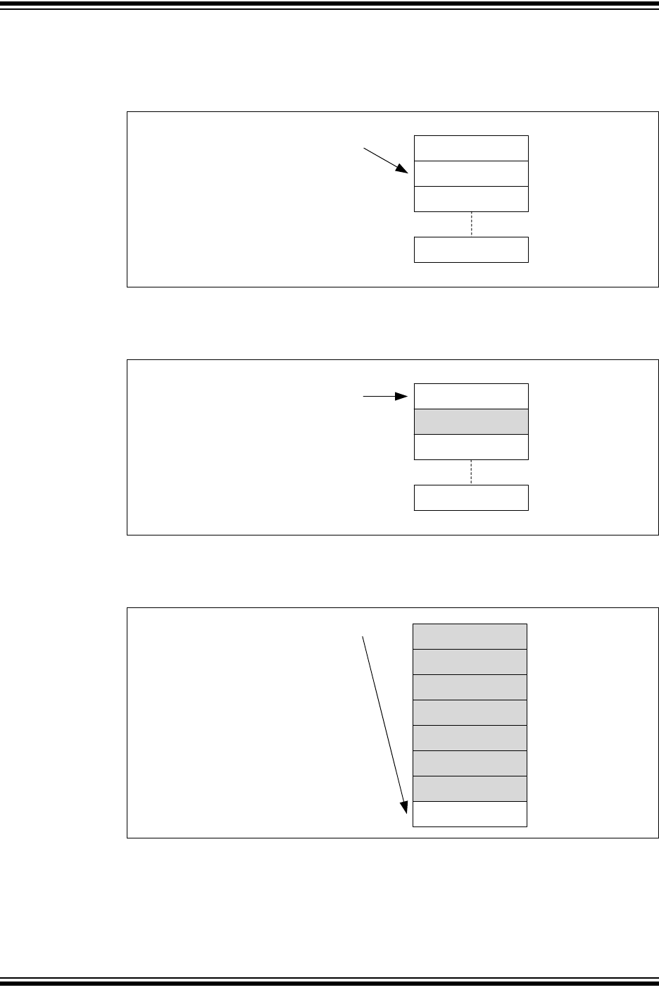
2017-2018 Microchip Technology Inc. DS20005678B-page 53
CAN FD Controller Module
Figure 8-17 illustrates the status of the TXQ after MSG0 was transmitted. The TXQ is empty
again. TFEIF is set, and TXREQ is cleared. The user address still points at MO1, because UINC
wasn’t set.
Figure 8-17: TXQ - First Message Transmitted
Figure 8-18 illustrates the status of the TXQ after MSG1 was loaded, and UINC was set. The user
address now points to the next free message object: MO0.
Figure 8-18: TXQ - Next Message Loaded
Figure 8-19 illustrates the status of the TXQ after six more messages were loaded: MSG2-
MSG7. The user address now points to the last free message object: MO7.
Figure 8-19: TXQ - Next Six Messages Loaded
MO0
MO1
MO2
MO7
C1TXQUA = 0x0B8
C1TXQSTA:
TXQEIF = 1
TXQNIF = 1
C1TXQCON:
TXREQ = 0
MO0
MO1 / MSG1
MO2
MO7
C1TXQUA = 0x090
C1TXQSTA:
TXQEIF = 0
TXQNIF = 1
C1TXQCON:
TXREQ = 0
MO0 / MSG2
MO1 / MSG1
MO2 / MSG3
C1TXQUA = 0x1A8
C1TXQSTA:
TXQEIF = 0
TXQNIF = 1
C1TXQCON:
TXREQ = 0
MO7
MO3 / MSG4
MO4 / MSG5
MO5 / MSG6
MO6 / MSG7

MCP25xxFD Family Reference Manual
DS20005678B-page 54 2017-2018 Microchip Technology Inc.
Figure 8-20 illustrates the status of the TXQ after MSG8 was loaded, and UINC was set. The
TXQ is now full, all flags are clear. The user address now points to MO0. The user application
now sets TXREQ. The messages will be transmitted based on the priority of their IDs.
Figure 8-20: TXQ - Full
MO0 / MSG2
MO1 / MSG1
MO2 / MSG3
C1TXQUA = 0x090
C1TXQSTA:
TXQEIF = 0
TXQNIF = 0
C1TXQCON:
TXREQ = 1
MO7 / MSG8
MO3 / MSG4
MO4 / MSG5
MO5 / MSG6
MO6 / MSG7
2017-2018 Microchip Technology Inc. DS20005678B-page 55
CAN FD Controller Module
8.5 Transmit Event FIFO Behavior
C1TEFCON is used to control the TEF. C1TEFSTA contains the status flags. C1TEFUA contains
the user address of the next message object to read.
Remember that the actual RAM address is calculated using Equation 5-1.
Figure 8-21 through Figure 8-28 illustrate how the status flags and user address are updated.
The TEF stores transmitted messages. Therefore, the flags behaves similar to a RX FIFO.
Figure 8-21 shows the status of the TEF after reset. Message Objects MO0 to MO11 are empty.
All status flags are clear. The user address points to MO0.
Figure 8-21: TEF - Initial State
Figure 8-22 shows the status of the TEF after the first transmit message was stored. MO0
contains ID0, the ID of MSG0. TEFNEIF is set, since the TEF is not empty. The user address
points to MO0.
Figure 8-22: TEF - First Transmit Message Was Stored
Figure 8-23 illustrates the status of the TEF after ID0 was read. The user application reads the
ID from RAM and sets C1TEFCON.UINC. The user address increments and points to MO1. The
TEF is empty again. All flags are clear.
Figure 8-23: TEF - First ID Read
MO0
MO1
MO2
MO11
C1TEFUA = 0x000
C1TEFSTA:
TEFFIF = 0
TEFHIF = 0
TEFNEIF = 0
TEFOVIF = 0
MO1
MO2
MO11
C1TEFUA = 0x000
C1TEFSTA:
TEFFIF = 0
TEFHIF = 0
TEFNEIF = 1
TEFOVIF = 0
MO0 / ID0
MO0
MO1
MO2
MO11
C1TEFUA = 0x00C
C1TEFSTA:
TEFFIF = 0
TEFHIF = 0
TEFNEIF = 0
TEFOVIF = 0
MCP25xxFD Family Reference Manual
DS20005678B-page 56 2017-2018 Microchip Technology Inc.
Figure 8-24 illustrates the status of the TEF after six more messages were transmitted: MSG1-
MSG6. The user address points to MO1. TEFNEIF and TEFHIF are set, because the TEF is now
half full.
Figure 8-24: TEF - Half Full
Figure 8-25 illustrates the status of the TEF after five more messages were transmitted: MSG7-
MSG11. The user address still points to MO1. TEFNEIF and TEFHIF are set.
Figure 8-25: TEF - Almost Full
Figure 8-26 illustrates the status of the TEF after one more message was transmitted: MSG12.
All status flags are set, because the TEF is full. The user address points to MO1.
Figure 8-26: TEF - Full
MO1 / ID1
MO7
MO6 / ID6
MO8
MO0
MO11
C1TEFUA = 0x00C
C1TEFSTA:
TEFFIF = 0
TEFHIF = 1
TEFNEIF = 1
TEFOVIF = 0
MO2 / ID2
MO1 / ID1
MO11 / ID11
C1TEFUA = 0x00C
C1TEFSTA:
TEFFIF = 0
TEFHIF = 1
TEFNEIF = 1
TEFOVIF = 0
MO2 / ID2
MO0
MO1 / ID1
MO11 / ID11
C1TEFUA = 0x00C
C1TEFSTA:
TEFFIF = 1
TEFHIF = 1
TEFNEIF = 1
TEFOVIF = 0
MO2 / ID2
MO0 / ID12
2017-2018 Microchip Technology Inc. DS20005678B-page 57
CAN FD Controller Module
Figure 8-27 illustrates the status of the TEF after one more message was transmitted. Since the
TEF was already full an overflow occurred. The ID is discarded, and TEFOVIF is set. The user
address didn’t change.
Figure 8-27: TEF - Overflow
Figure 8-28 illustrates the status of the TEF after the application cleared TEFOVIF and read one
more message. TEFFIF is clear, because the TEF isn’t full anymore. The user address points to
MO2.
Figure 8-28: TEF - One More ID Read
MO1 / ID1
MO11 / ID11
C1TEFUA = 0x00C
C1TEFSTA:
TEFFIF = 1
TEFHIF = 1
TEFNEIF = 1
TEFOVIF = 1
MO2 / ID2
MO0 / ID12
MO11 / ID11
C1TEFUA = 0x018
C1TEFSTA:
TEFFIF = 0
TEFHIF = 1
TEFNEIF = 1
TEFOVIF = 0
MO2 / ID2
MO0 / ID12
MO1
MO3 / ID3
MCP25xxFD Family Reference Manual
DS20005678B-page 58 2017-2018 Microchip Technology Inc.
9.0 TIMESTAMPING
The CAN FD Controller Module contains a Time Base Counter (TBC). The TBC is a 32-bit free-
running counter that increments on multiples of SYSCLK and rolls over to zero.
• CiTSCON.TBCPRE is used to configure the prescaler for the TBC.
• Setting CiTSCON.TBCEN enables the TBC.
• Clearing TBCEN disables, stops and resets the TBC.
• The TBC has to be disabled, before writing to CiTBC by clearing CiTSCON.TBCEN.
• CiTEFCON.TEFTSEN has to be set to timestamp messages in the Transmit Event FIFO.
• CiFIFOCONm.RXTSEN has to be set to timestamp messages in the individual RX FIFO.
• The application can read CiTBC at any time. Like with any multi-byte counter, the
application has to consider that the counter increments, and might roll-over, between
reading the different bytes of the counter.
All timestamps are 32-bit, allowing timestamps to be used for system time synchronization with
high resolution.
A roll-over of the TBC will generate an interrupt, if TBCIE is set.
Messages can be timestamped either at the beginning of a frame or at the end, depending on
CiTSCON.TSEOF. When TSEOF = 0, CiTSCON.TSRES specifies if FD frames are
timestamped at SOF or the res bit. Tab l e 9- 1 specifies the reference points when the
timestamping occurs. At the reference point the value of the TBC (CiTBC) is captured and
stored into the message object:
• Receive Message Object: the TBC value is stored in RXMSGTS, see Table 7-1.
• TEF Object: the TBC value is stored in TXMSGTS, see Table 5-1.
Table 9-1: Reference Point
9.1 TBC Configuration Code Example
Example 9-1 shows a code example of how to configure the TBC:
• Disable the TBC
• Configure the Prescaler
• Optionally, set the TBC to a certain value
• Enable the TBC.
Example 9-1: Configuration of TBC
Frame CAN 2.0 CAN FD
Start of TX Sample point of SOF Sample point of SOF or the bit after FDF
Start of RX Sample point of SOF Sample point of SOF or the bit after FDF
Valid TX No error till end of EOF No error till end of EOF
Valid RX No error till the last but one bit of
EOF
No error till the last but one bit of EOF

2017-2018 Microchip Technology Inc. DS20005678B-page 59
CAN FD Controller Module
10.0 INTERRUPTS
Interrupts can be classified into multiple layers. Lower layer interrupts propagate to higher
layers by multiplexing them into single interrupts. Figure 10-1 illustrates the layers of interrupts:
1. FIFO Individual Interrupts
2. FIFO Combined Interrupts
3. Main Interrupts
These interrupts are then funneled into three separate module interrupts:
1. Receive Interrupt
2. Transmit Interrupt
3. Information Interrupt
All module interrupts are persistent, meaning the condition that caused the interrupt must be
cleared within the module for the interrupt request to be removed.
In addition, the MCP25xxFD generates interrupts for the following events:
• SPI CRC errors: Format and CRC error.
• ECC errors: Single Error Corrected (SEC), Double Error Detected (DED).
MCP25xxFD Family Reference Manual
DS20005678B-page 60 2017-2018 Microchip Technology Inc.
Figure 10-1: Interrupt Multiplexing
31x
RFFIE
RFFIF
RFHIE
RFHIF
RFNIE
RFNIF
31 FIFOS
31x
CiRXIF.RFIF<31:1>
CiTXQCON, CiTXQSTA
CiFIFOCONm, CiFIFOSTAm
CiINT.RXIE
CiINT.RXIF
31x
TFEIE
TFEIF
TFHIE
TFHIF
TFNIE
TFNIF
31 FIFOS
32x
CiTXIF.TFIF<31:1>
CiINT.TXIE
CiINT.TXIF
31x
RXOVIE
RXOVIF
31 FIFOS 31x
CiRXOVIF.RFOVIF<31:1>
CiINT.RXOVIE
CiINT.RXOVIF
31x
TXATIE
TXATIF
31 FIFOS 32x
CiTXATIF.TFATIF<31:1>
CiINT.TXATIE
CiINT.TXATIF
TEFFIE
TEFFIF
TEFHIE
TEFHIF
TEFNEIE
TEFNEIF
1 FIFO CiINT.TEFIE
CiINT.TEFIF
CiINT.IVMIE
CiINT.IVMIF
CiINT.WAKIE
CiINT.WAKIF
CiINT.CERRIE
CiINT.CERRIF
CiINT.MODIE
CiINT.MODIF
CiINT.TBCIE
CiINT.TBCIF
CiINT.SERRIE
CiINT.SERRIF
FIFO Individual
Interrupts
FIFO Combined
Interrupts
Main Interrupts Interrupt Pins
TEFOVIE
TEFOVIF
RX Interrupt
TX Interrupt
Info Interrupt
CiTEFCON
CiTEFSTA
CiINT.SPICRCIE
CiINT.ECCIE
CiINT.ECCIF
OR
FERRIE
FERRIF
CRCERRIE
CRCERRIF
SECIE
SECIF
DEDIE
DEDIF
MCP25xxFD
MCP25xxFD
1x
TXQEIE
TXQEIF
TXQNIE
TXQNIF
CiTXIF.TFIF<0>
1x
TXATIE
TXATIF
1 TXQ CiTXATIF.TFATIF<0>
1 TXQ
CiINT.SPICRCIF

2017-2018 Microchip Technology Inc. DS20005678B-page 61
CAN FD Controller Module
10.1 FIFO Individual Interrupts
CiFIFOCONm contains the interrupt enable and CiFIFOSTAm contains the interrupt flags for
the FIFOs. There is a separate register for each individual FIFO.
10.1.1 TRANSMIT QUEUE (TXQ) INTERRUPTS
CiTXQCON contains the interrupt enable and CiTXQSTA contains the interrupt flags for the
TXQ.
The TXQ interrupt occurs when there is a change in the status of the TXQ. There are two
interrupt sources:
• TXQ Not Full Interrupt - TXQNIF
• TXQ Empty Interrupt - TXQEIF
Both interrupts can be enabled individually. The interrupts cannot be cleared by the application;
they will be cleared when the condition of the FIFO terminates.
Both interrupt sources are OR’d together and reflected in the CiTXIF.TFIF<0> flag.
10.1.2 RECEIVE FIFO INTERRUPT - RFIF
The Receive FIFO interrupt occurs when there is a change in the status of the Receive FIFO.
There are three interrupt sources:
• Receive FIFO Full Interrupt - RFFIF
• Receive FIFO Half Full Interrupt - RFHIF
• Receive FIFO Not Empty Interrupt - RFNIF
All three interrupts can be enabled individually. The interrupts can not be cleared by the
application, they will be cleared when the condition of the FIFO terminates.
The three interrupt sources are OR’d together and reflected in the CiRXIF.RFIF<m> flag.
10.1.3 TRANSMIT FIFO INTERRUPT - TFIF
The Transmit FIFO interrupt occurs when there is a change in the status of the Transmit FIFO.
There are three interrupt sources:
• Transmit FIFO Not Full Interrupt - TFNIF
• Transmit FIFO Half Empty Interrupt - TFHIF
• Transmit FIFO Empty Interrupt - TFEIF
All three interrupts can be enabled individually. The interrupts can not be cleared by the
application, they will be cleared when the condition of the FIFO terminates.
The three interrupt sources are OR’d together and reflected in the CiTXIF.TFIF<m> flag.
10.1.4 RECEIVE FIFO OVERRUN INTERRUPT - RXOVIF
When a message is successfully received, but the FIFO is full, the RXOVIF of the individual
FIFO is set. The flag must be cleared by the application.
10.1.5 TRANSMIT FIFO ATTEMPT INTERRUPT - TXATIF
When the retransmission of a message fails due to an error and all retransmission attempts are
exhausted, the TXATIF is set. The flag must be cleared by the application.
10.1.6 TRANSMIT EVENT FIFO INTERRUPT - TEFIF
The Transmit Event FIFO (TEF) interrupt occurs when there is a change in the status of the
Transmit Event FIFO. There are four interrupt sources:
• TEF Full Interrupt - TEFFIF
• TEF Half Full Interrupt - TEFHIF
• TEF Not Empty Interrupt - TEFNEIF
• TEF Overrun Interrupt - TEFOVIF

MCP25xxFD Family Reference Manual
DS20005678B-page 62 2017-2018 Microchip Technology Inc.
The TEF interrupts work similar to the Receive FIFO interrupts. All four interrupts can be
enabled individually.
TEFFIF, TEFHIF and TEFNEIF can not be cleared by the application, they will be cleared when
the status of the FIFO terminates.
The TEFOVIF must be cleared by the application.
The four interrupt sources are OR’d together and reflected in the CiINT.TEFIF flag.
10.2 MCP25xxFD SPI CRC Interrupts
The CRC register contains the interrupt enable bits, FERRIE, and CRCERRIE; and the interrupt
status flags, FERRIF, and CRCERRIF.
The status flags must be cleared by the application.
10.3 MCP25xxFD RAM ECC Interrupts
The ECCCON register contains the interrupt enable bits, DEDIE, and SECIE.
The ECCSTA register contains the interrupt status flags, DEDIF, and SECIF.
The status flags must be cleared by the application.
10.4 FIFO Combined Interrupts
The following interrupts are individual FIFO interrupts:
• FIFOs/TXQ: RFIF, TFIF, RFOVIF and TFATIF
They are combined into single interrupt status registers:
• CiRXIF, CiTXIF, CiRXOVIF and CiTXATIF.
The bits inside the status registers are mapped to the FIFOs as follows: Bit 0 to TXQ, Bit 1 to
FIFO 1, Bit 2 to FIFO 2, and so on, Bit 31 to FIFO 31. Since Bit 0 corresponds to the TXQ, Bit 0
of CiRXIF and CiRXOVIF are reserved. Therefore, by reading one register the application can
check the status of all FIFOs for a particular interrupt (e.g. any RFIF pending).
The FIFO interrupts are enabled in CiFIFOCONm.
TXQ interrupts are enabled in CiTXQCON.
The clearing of the FIFO interrupts is explained in Section 10.1 “FIFO Individual Interrupts”.
10.5 Main Interrupts
The CiINT register contains all main interrupts. The following interrupts are a logical ‘or’ of all
combined FIFO interrupts: RXIF, TXIF, RXOVIF, TXATIF. These flags are read-only and must be
cleared in preceding hierarchies.
The TEFIF is generated in the Transmit Event FIFO. The flag is read-only, and must be cleared
in preceding hierarchies.
All interrupts in CiINT can be enabled individually.
10.5.1 INVALID MESSAGE INTERRUPT - IVMIF
If a CAN bus error or DLC mismatch was detected during the last message transmitted or
received, the IVMIF will be set. The CiBDIAG1 register sets a flag for each specific error. The
flag must be cleared by the application.
The following CAN bus errors will trigger the interrupt in case an error frame was transmitted:
CRC, Stuff bit, Form, Bit, ACK.
The flag will not be set if the ESI of a received message was set.
10.5.2 WAKE-UP INTERRUPT - WAKIF
Bus activity has been detected while the module is in Sleep Mode. The flag must be cleared by
the application.

2017-2018 Microchip Technology Inc. DS20005678B-page 63
CAN FD Controller Module
10.5.3 CAN BUS ERROR INTERRUPT - CERRIF
The CiTREC register will count the errors during transmit and receive according to the ISO
11898-1:2015. The CERRIF flag will be set based on the error counter values. The flag must be
cleared by the application.
CERRIF will be set each time a threshold in the TEC/REC counter is crossed by the following
conditions:
• TEC or REC exceeds the Error Warning state threshold
• The transmitter or receiver transitions to Error Passive state
• The transmitter transitions to Bus Off state
• The transmitter or receiver transitions from Error Passive to Error Active state
• The module transitions from Bus Off to Error Active state, after the bus off recovery
sequence
When the user clears CERRIF, it will remain clear until a new counter crossing occurs.
10.5.4 CAN MODE CHANGE INTERRUPT - MODIF
When the OPMOD bits change, the MODIF flag will be set. The flag must be cleared by the
application.
10.5.5 CAN TIMER INTERRUPT - TBCIF
When the Time Base Counter rolls-over, TBCIF will be set. The flag must be cleared by the
application.
10.5.6 SYSTEM ERROR INTERRUPT - SERRIF
Bus Bandwidth Error:
Bandwidth errors can happen during receive and transmit.
Receive Message Assembly Buffer (RX MAB) overflow occurs when the module is unable to
write a received CAN message to RAM before the next message arrives.
Transmit Message Assembly Buffer (TX MAB) underflow occurs when the module can’t feed the
TX MAB fast enough to provide consistent data to the Bit Stream Processor.
The SERRIF flag will be set and CiVEC.ICODE bits will be set to 100 0101.
Handling of RX MAB Overflow Errors:
RX MAB overflows are not accepted by automotive OEM. To prevent overflows, frame filtering
and data saving starts as early as possible, the latest at the beginning of the CRC field of the
received message. Updating the FIFO status has to wait until the beginning of the 7th bit of the
EOF field, since the received frame is only valid at this point. The complete message has to be
saved and the FIFO has to be updated, until the end of the arbitration field of the next message.
In case of an RX MAB overflow, the new message that caused the RX MAB overflow will be
discarded. The module continues to store the message that was already completely received
and filtered. Afterwards, the module will be able to receive new messages on the bus. The
application will be notified using the SERRIF.
SERRIF will be cleared by writing a zero to CiINT.SERRIF. This will also clear the SERRIF
condition from the ICODE.
Handling of TX MAB Underflow Errors:
ISO 11898-1:2015 requires MAC data consistency: a transmitted message must contain
consistent data. If data errors occur due to ECC errors, or TX MAB underflow, the transmission
shall not be started. If it is already in progress, the transmission shall be stopped, and the
module shall transition to either Restricted Operation or Listen Only mode, selectable using
CiCON.SERR2LOM.
The module handles these errors by stopping the transmission and transitioning to Restricted
Operation or Listen Only mode. The TXCAN pin will be forced high. Additionally, all TXREQ are
ignored. The application will be notified using SERRIF. The module will continue receiving mes-
sages.

MCP25xxFD Family Reference Manual
DS20005678B-page 64 2017-2018 Microchip Technology Inc.
10.5.7 SPI CRC INTERRUPT - SPICRCIF
The individual SPI CRC error interrupts are combined into the SPICRCIF. The flag is read-only
and must be cleared in preceding hierarchies.
10.5.8 ECC INTERRUPT - ECCIF
The individual ECC error interrupts are combined into the ECCIF. The flag is read-only and must
be cleared in preceding hierarchies.
10.6 Interrupt Handling
The CAN FD Controller Module allows the application to handle interrupts efficiently in two
different ways:
• Implementing a lookup table using the CiVEC register.
• Using the status registers and decide which interrupt to service first.
The application can also use a combination of the two.
10.6.1 INTERRUPT LOOKUP TABLE
The ICODE and FILTHIT bits in the CiVEC register enable the application to use a lookup table
to implement the interrupt service routine.
The following bit fields allow the application to make full use of the three interrupt pins:
• TXCODE: Reflects which object has a transmit interrupt pending.
• RXCODE: Reflects which object has a receive interrupt pending.
A separate lookup table can be implemented for transmit and receive interrupts.
If more than one object has an interrupt pending, the interrupt or FIFO with the highest number
will show up in RXCODE, TXCODE and ICODE. Once the interrupt with the highest priority is
cleared, the next highest priority interrupt will show up in CiVEC. RXCODE, TXCODE and
ICODE are implemented with combinatorial logic using the interrupt flags as inputs.
10.6.2 INTERRUPT STATUS REGISTERS
The CAN FD Controller Module contains 31 FIFOs and a TXQ. It could be too inflexible to use
the ICODE, since the interrupt priorities are determined by the module. Therefore, other
measures were taken to assure efficient servicing of interrupts:
• CiINT contains all main interrupt sources. The application can find out which categories of
interrupts are pending and decides which interrupts to service first (e.g., RXIF).
• All categories of interrupts for all FIFOs are combined into single registers: CiRXIF, CiTXIF,
CiRXOVIF and CiTXATIF. The application can find out which RFIFs are pending by reading
only one register. The same is true for TFIF, RXOVIF and TXATIF.
• In the register map, the interrupt status registers are arranged in a single block: CiVEC,
followed by CiINT, CiRXIF, CiTXIF, CiRXOVIF and CiTXATIF. This allows reading all status
registers with a single SPI read access.

2017-2018 Microchip Technology Inc. DS20005678B-page 65
CAN FD Controller Module
10.7 Interrupt Flags
Table 10-1 summarizes all interrupt flags, and lists how interrupts are cleared.
Table 10-1: Interrupt Flags
Flag Register Category Cleared by
Module(1)
Cleared by
Application Read-Only(2)Description
RFFIF
RFHIF
RFNIF
CiFIFOSTAm FIFO X — — RX FIFO
TFNIF
TFHIF
TFEIF
CiFIFOSTAm FIFO X — — TX FIFO
TXQNIF
TXQEIF
CiTXQSTA TXQ X — — Transmit Queue
RXOVIF CiFIFOSTAm FIFO — X — RX Overrun
TXATIF CiFIFOSTAm
CiTXQSTA
FIFO
TXQ
— X — TX Attempt
TEFFIF
TEFHIF
TEFNEIF
CiTEFSTA FIFO X — — TEF
TEFOVIF CiTEFSTA FIFO — X — TEF Overrun
RFIF CiRXIF Combined — — X All RX FIFOs
TFIF CiTXIF Combined — — X All TX FIFOs
RFOVIF CiRXOVIF Combined — — X All RX FIFO
Overruns
TFATIF CiTXATIF Combined — — X All TX FIFO Attempts
FERRIF
CRCERRIF
CRC MCP25xxFD — X — SPI CRC Errors
SECIF
DEDIF
ECCSTA MCP25xxFD — X — ECC Errors
RXIF CiINT Main — — X RX
TXIF CiINT Main — — X TX
RXOVIF CiINT Main — — X RX Overrun
TXATIF CiINT Main — — X TX Attempt
TEFIF CiINT Main — — X TEF
IVMIF CiINT Main — X — Invalid Message
WAKIF CiINT Main — X — Wake-up
CERRIF CiINT Main — X — CAN Bus Error
MODIF CiINT Main — X — Mode Change
TBCIF CiINT Main — X — Time Base Counter
SERRIF CiINT Main — X — System Error
SPICRCIF CiINT Main — — X SPI CRC Error
ECCIF CiINT Main — — X RAM ECC Error
Note 1:The flags will be cleared, when the condition of the FIFO terminates, initiated by CiFIFOCONm.UINC.
2:The flags need to be cleared in the preceding hierarchies.
MCP25xxFD Family Reference Manual
DS20005678B-page 66 2017-2018 Microchip Technology Inc.
10.8 Interrupt Configuration and Handling Code Examples
Example 10-1 shows a code example of how to configure the TX and RX interrupts:
• Clear Module Interrupts. TX and RX interrupts are cleared when the condition of the FIFO
terminates, therefore, they can’t be cleared by the application.
• Enable Transmit Queue interrupt.
• Enable Receive FIFO interrupt.
• Enable RX and TX interrupts in CiINT.
Example 10-1: Configuration of Interrupts
Example 10-2 shows a code example of how to use the TX interrupt pin (INT0) to check if the
TXQ is ready for transmission:
• Check that the TXQ is not full.
• Load the message into the TXQ.
• Increment and flush the TXQ. UINC and TXREQ are set at the same time. This makes sure
that all messages in the TXQ are transmitted in case a message is appended to the TXQ
while it is already transmitting.
Example 10-2: Using TX Interrupt Pin to Check if TXQ is Ready for Transmission
2017-2018 Microchip Technology Inc. DS20005678B-page 67
CAN FD Controller Module
Example 10-3 shows a code example of how to use the RX interrupt pin (INT1) to check it there
is a receive message in FIFO 2:
• Check that the FIFO is not empty.
• Read the message from the FIFO.
• Increment the FIFO by setting UINC.
• Process the received message.
Example 10-3: Using RX Interrupt Pin to Check if FIFO 2 Contains a New Message
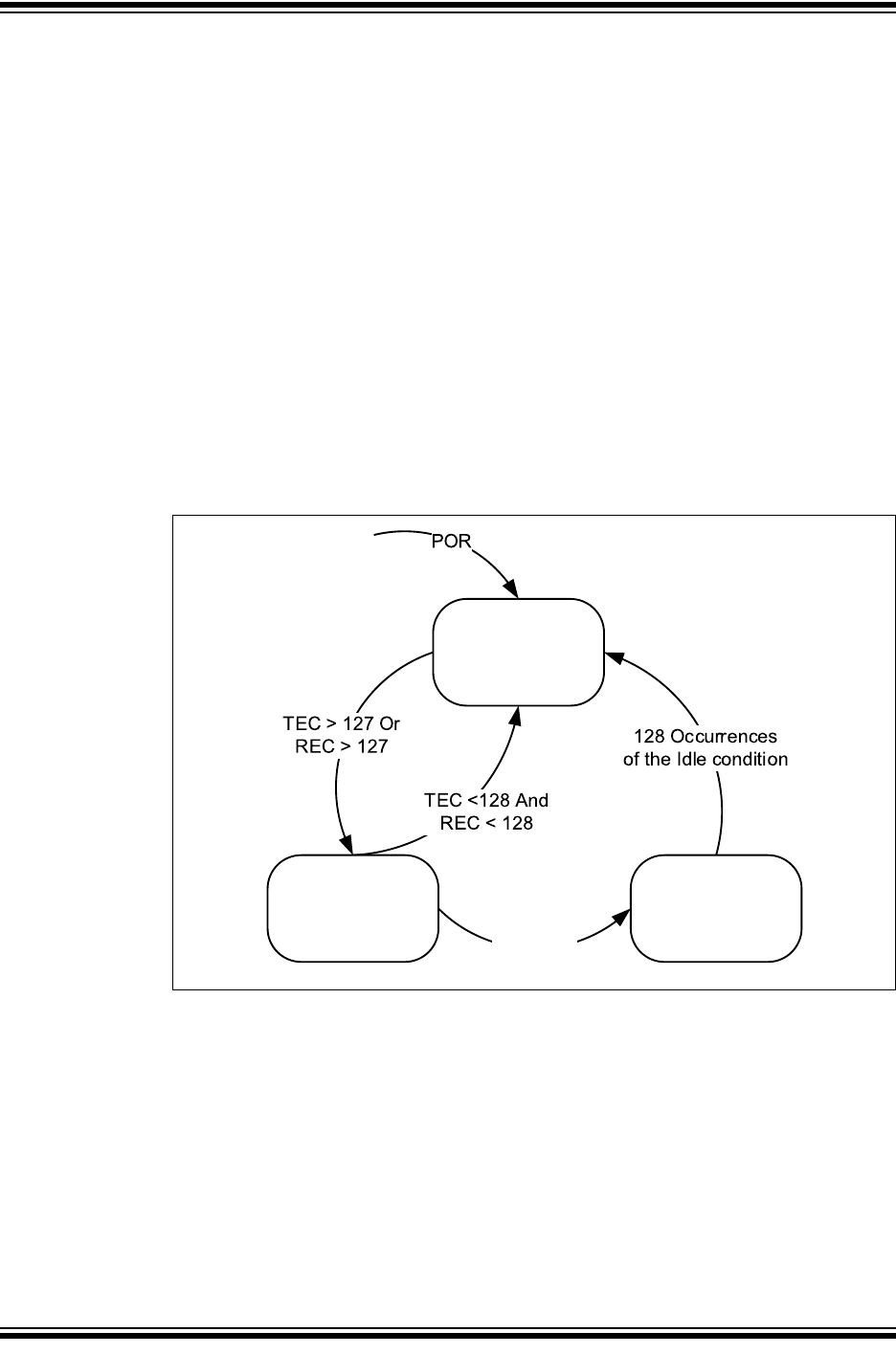
MCP25xxFD Family Reference Manual
DS20005678B-page 68 2017-2018 Microchip Technology Inc.
11.0 ERROR HANDLING
Every CAN controller checks the messages on the bus for the following errors: Bit, Stuff, CRC,
Form, and ACK errors. Whenever the controller detects an error, an Error frame is transmitted
that usually destroys the message on the bus. Error frames are always signaled using the
Nominal Bit Rate.
Error Detection and Fault Confinement is described in the ISO 11898-1:2015. CiTREC contains
the error counters, TEC and REC. It also contains the Error Warning and Error State bits. TEC
and REC increment and decrement according to ISO 11898-1:2015.
Figure 11-1 illustrates the different Error states of the CAN FD Controller Module. The module
starts out in Error Active state. If the TEC or REC exceed 127, the module transitions to Error
Passive state. If the TEC exceeds 255, the module will go to Bus Off state.
The module transmits Active Error frames, when in Error Active state. It will transmit Passive
Error frames, while in Error Passive state. When the module is Bus Off, TXCAN is always driven
high, and no dominant bits are transmitted.
In order to avoid transitioning to Error Passive state, the module will warn the application if the
TEC or REC reach 96 using the CERRIF interrupt flag, see Section 10.5.3 “CAN Bus Error
Interrupt - CERRIF”. This allows the application to take action before it enters Error Passive
state.
Figure 11-1: Error States
The Bus Diagnostics registers provide additional information about the health of the CAN bus:
• CiBDIAG0 contains separate Error Counters for receive/transmit and for nominal/data bit
rates. The counters work differently than the counters in the CiTREC register. They are
simply incremented by one on every error. They are never decremented, but can be
cleared by writing zero to the register.
• CiBDIAG1 keeps track of the kind of error that occurred since the last clearing of the
register. The register also contains the Error Free Message Counter. The flags and the
counter are cleared by writing zero to the register.
The Error Free Message Counter together with the Error Counters, and the Error Flags can be
used to determine the quality of the bus.
TEC> 255
Error
Active
Error
Passive Bus Off

2017-2018 Microchip Technology Inc. DS20005678B-page 69
CAN FD Controller Module
11.1 Recovery from Bus Off State
If the TEC exceeds 255, CiTREC.TXBO and CiINT.CERRIF will be set. The module will go Bus
Off and start the bus off recovery sequence.
The bus off recovery sequence is started automatically. The module will transition out of Bus Off
only after the detection of 128 idle conditions, see “ISO11898-1:2015: Bus Off Management”.
The module will set FRESET for all transmit FIFOs when entering Bus Off state to ensure the
module doesn't try to retransmit indefinitely. The application will be notified by CERRIF and has
the option to queue new messages for transmission.
The module signals the exit from the Bus Off state with a CERRIF, and by setting
CiBDIAG1.TXBOERR. Additionally, CiTREC will be reset.

MCP25xxFD Family Reference Manual
DS20005678B-page 70 2017-2018 Microchip Technology Inc.
12.0 APPENDIX A: MCP25XXFD CANFDSPI API
12.1 Introduction
The Application Programming Interface (API) provides a firmware library for the MCP25xxFD.
The API simplifies the development of a CAN FD application by providing type definitions and
functions for the following tasks:
• Configuration: Bit Time, FIFOs, Filters and Masks
• Mode Selection
• Message Transmission
• Message Reception
• Event (Interrupt) Handling
• Error State Tracking.
The API is MCU independent by using the peripheral library or drivers for the SPI transfer. The
API calls only one hardware dependent SPI function: DRV_SPI_TransferData. The
application must implement an SPI initialization function and the DRV_SPI_TransferData on
the selected target MCU.
12.2 Abstraction Model
The API provides a hardware abstraction of the CAN FD Controller Module with a C interface to
the application, see Figure 12-1.
The API provides interface routines to interact with the CAN FD Controller Module. A channel
(FIFO) can be either a transmit channel or a receive channel. The size of the payload of a CAN
message can be configured between 8 and 64 bytes. The number of message objects of a chan-
nel (the number of messages in the FIFO) is configurable between 1 and 32 messages. The API
provides access to these channels and message objects via the library interface.
The application must enable and configure message acceptance filters to receive messages.
These filters compare the ID field of the incoming message with configured values and accepts
the messages if IDs match. The message is then stored in a selectable receive channel. At least
one message acceptance filter object and one mask object must be enabled for the CAN FD
Controller Module to receive messages. A mask allows specified filter bits to be ignored during
the comparison process. This allows the filter to accept messages with a range of IDs.
The API provides functions to configure and handle events (interrupts). Events can be generated
at the channel level and at the module level. Channel events are generated by transmit and
receive channels. Module events are generated by various sources (including channels) within
the CAN FD Controller Module. Each event can be enabled or disabled. Enabling a channel
event will cause the CAN FD Controller Module to generate a module event. An enabled module
level event will cause the MCP25xxFD to assert one or more of the interrupt pins. The interrupt
pins of the MCP25xxFD are connected to MCU input pins. The application can either poll the
input pins, or setup external interrupts on these inputs.
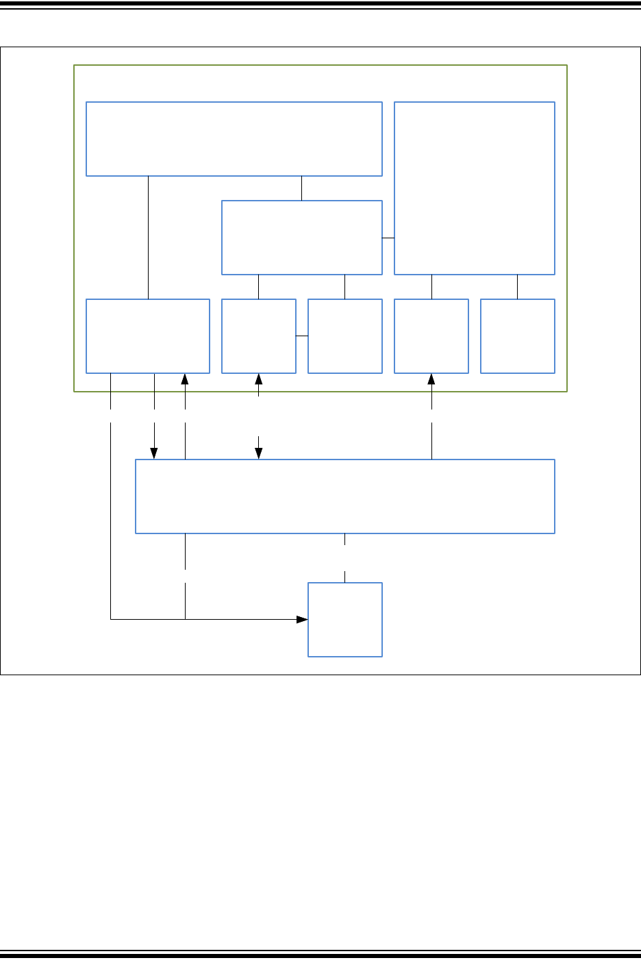
2017-2018 Microchip Technology Inc. DS20005678B-page 71
CAN FD Controller Module
Figure 12-1: Hardware Abstraction Model
MCP25xxFD
DRV_SPI DMA TMRISR
SYS
CS
CAN
XCR
TXCAN
RXCAN
INT0:2
SCK
SDI
SDO
INT0:2
XSTBY
I/O
PLIB
DRV_CANFDSPI
CANFDApplication
XSTBY
MCUFirmware
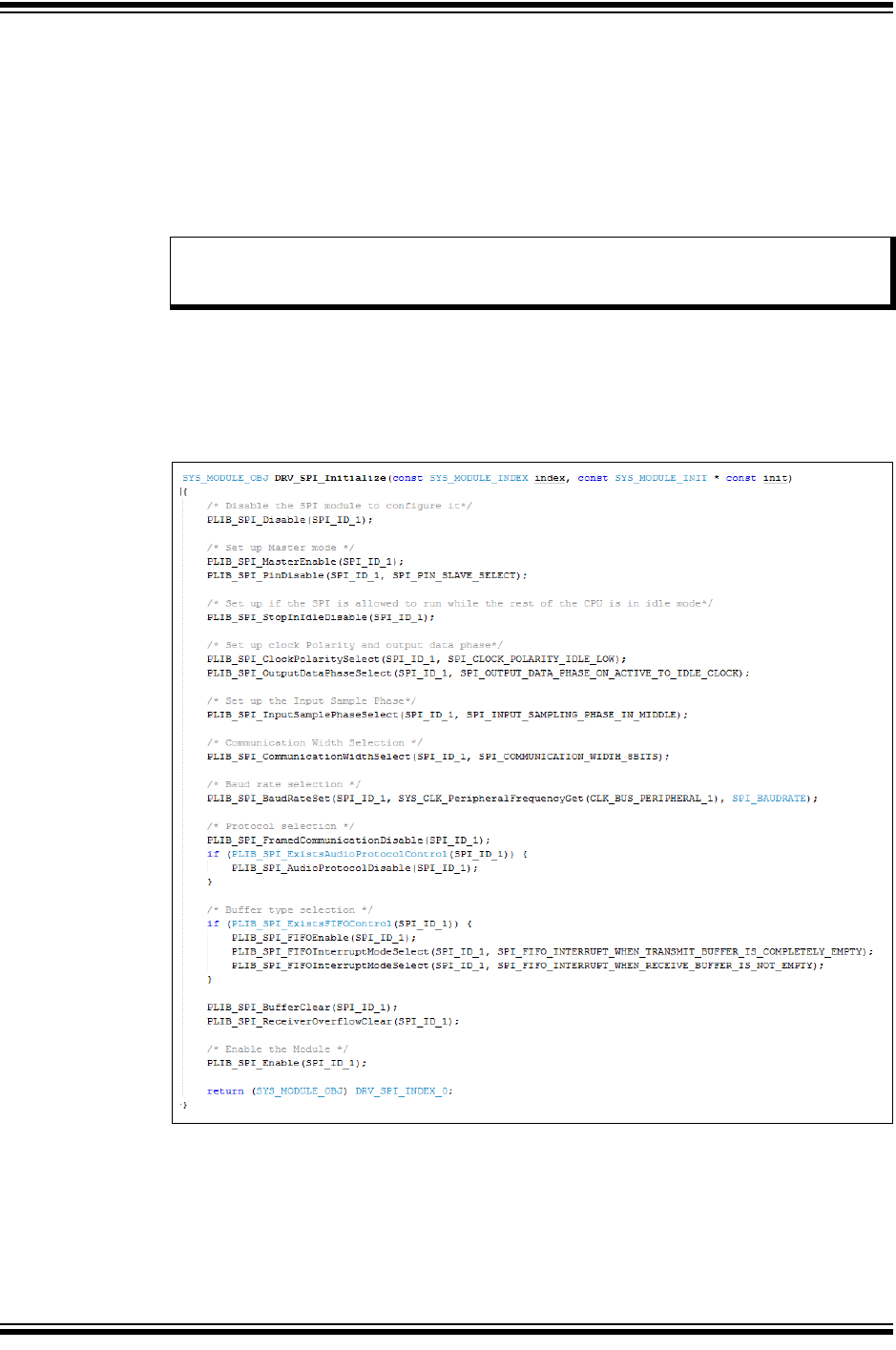
MCP25xxFD Family Reference Manual
DS20005678B-page 72 2017-2018 Microchip Technology Inc.
12.3 Getting Started with the SPI Communication
The application must implement a minimum of two SPI functions on the target MCU:
• Initialization: this function initializes the SPI peripheral. Please review the “SPI Interface”
section of the device data sheet for details on the SPI configuration.
• Transfer Data: this function asserts nCS, writes/reads n data bytes, and de-asserts nCS.
In order to minimize the SPI transfer time, the application should make use of SPI FIFO buffers,
or use DMAs to feed the SPI.
12.3.1 SPI INITIALIZATION CODE EXAMPLE
Example 12-1 shows the initialization function for a PIC32MX470F512H. It was generated using
MBLAB Harmony Configurator. The SPI is setup as a Master in mode 0,0. The application takes
advantage of the Enhanced Buffering mode, which minimizes the SPI transfer time.
Example 12-1: SPI Initialization Function
Note: The frequency of SCK has to be less than or equal to half the frequency of SYSY-
CLK. This ensures that the synchronization between SCK and SYSCLK works
correctly.
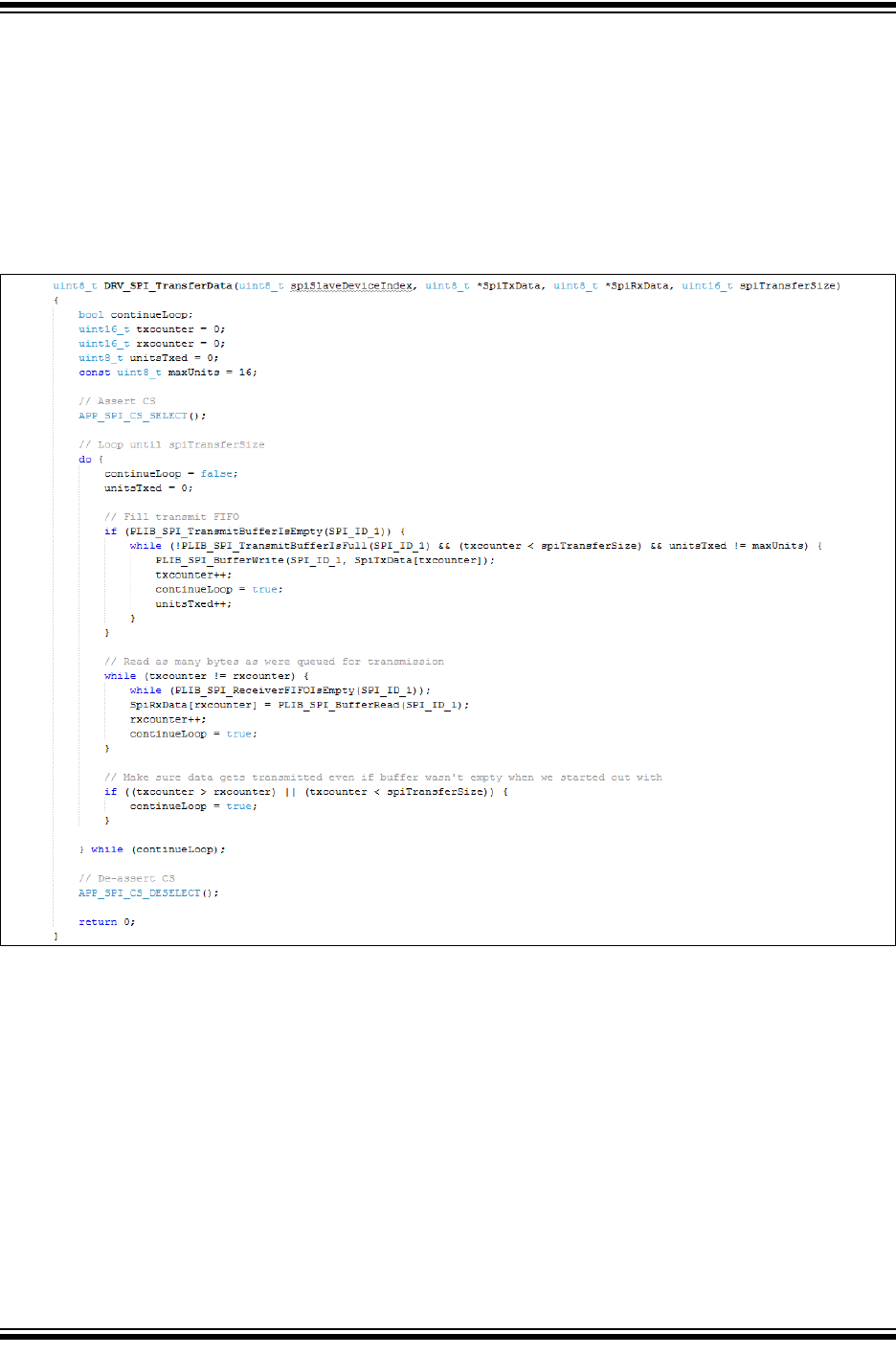
2017-2018 Microchip Technology Inc. DS20005678B-page 73
CAN FD Controller Module
12.3.2 SPI DATA TRANSFER CODE EXAMPLE
Example 12-2 shows the data transfer function for a PIC32MX470F512H. It was generated using
MBLAB Harmony Configurator and slightly modified. The function makes use of the 16 byte SPI
FIFO buffer. It first fills the transmit buffer with up to 16 bytes, then reads back as many bytes as
were transmitted, therefore, minimizing the dead time between the SPI bytes.
The application passes the transmit data to the function using the SpiTxData pointer. The func-
tion returns the read data to the application in the array pointed to by the SpiRxData. A total of
spiTransferSize bytes are transfered.
Example 12-2: SPI Data Transfer Function
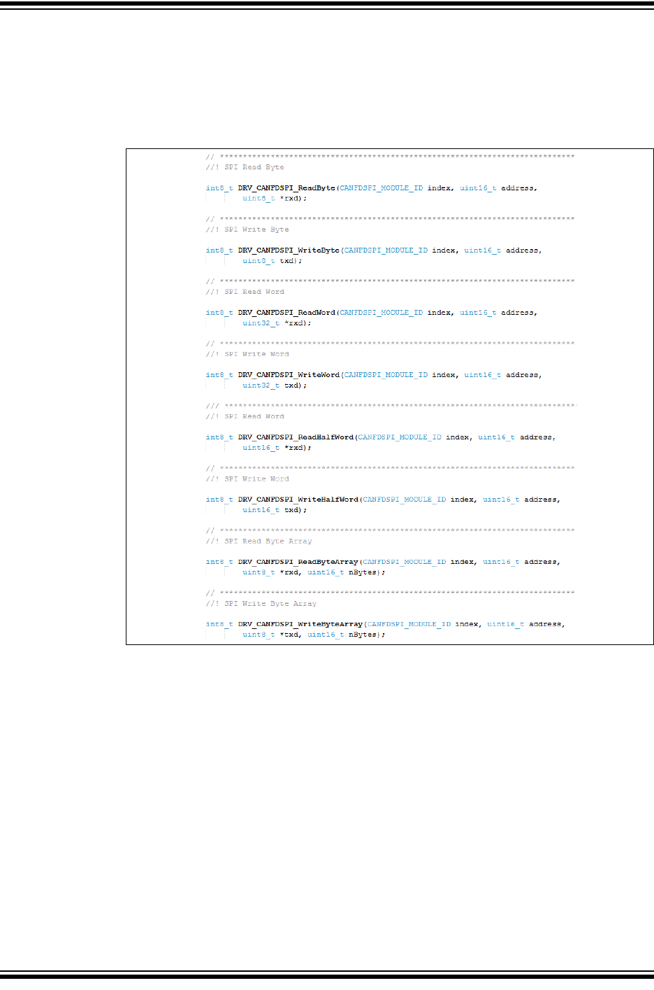
MCP25xxFD Family Reference Manual
DS20005678B-page 74 2017-2018 Microchip Technology Inc.
12.3.3 SPI READ AND WRITE ACCESS FUNCTIONS
Example 12-3 lists some of the SPI access functions. The access functions use the
DRV_SPI_TransferData to send read and write commands to the MCP25xxFD. These
functions can be used for communication between the MCU and the MCP25xxFD, or for testing
the DRV_SPI_TransferData function.
Example 12-3: SPI Access Functions
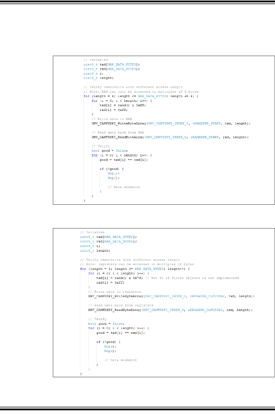
2017-2018 Microchip Technology Inc. DS20005678B-page 75
CAN FD Controller Module
12.3.4 VERIFICATION OF THE SPI COMMUNICATION
Example 12-4 shows an example of verifying that reads and writes to RAM work correctly. Since
all SPI access functions use the DRV_SPI_TransferData, only one of the access function
needs to be used to verify DRV_SPI_TransferData.
Example 12-4: Verifying SPI Communication using RAM Access
Example 12-5 shows an example of verifying that reads and writes to registers work correctly.
Example 12-5: Verifying SPI Communication using Register Access

MCP25xxFD Family Reference Manual
DS20005678B-page 76 2017-2018 Microchip Technology Inc.
13.0 RELATED DOCUMENTS
This section lists documents that are related to this section of the manual. These documents may
not be written specifically for the MCP25xxFD device family, but the concepts are pertinent and
could be used with modification and possible limitations. The current documents related to the
CAN FD Controller Module include the following:
Title Document #
PIC32 Family Reference Manual - Section 34. Controller Area Network (CAN) DS61154
PIC32 Family Reference Manual - Section 6. Oscillators DS61112
Crystal Oscillator Basics and Crystal Selection for rfPIC® and PIC® MCU Devices DS00826
Basic PIC® Microcontroller Oscillator Design DS00849
Practical PIC® Microcontroller Oscillator Analysis and Design DS00943
Making Your Oscillator Work DS00949
Note: Please visit the Microchip web site (www.microchip.com) for additional application
notes and code examples for the MCP25xxFD family of devices.

2017-2018 Microchip Technology Inc. DS20005678B-page 77
CAN FD Controller Module
14.0 REVISION HISTORY
Revision B (May 2018)
• Added MCP2518FD.
• Added LPM description.
• Increased SEQ field for Transmit Message and TEF objects.
Revision A (September 2017)
• Original release of this document.

MCP25xxFD Family Reference Manual
DS20005678B-page 78 2017-2018 Microchip Technology Inc.
NOTES:

2017-2018 Microchip Technology Inc. DS20005678B-page 79
Information contained in this publication regarding device
applications and the like is provided only for your convenience
and may be superseded by updates. It is your responsibility to
ensure that your application meets with your specifications.
MICROCHIP MAKES NO REPRESENTATIONS OR
WARRANTIES OF ANY KIND WHETHER EXPRESS OR
IMPLIED, WRITTEN OR ORAL, STATUTORY OR
OTHERWISE, RELATED TO THE INFORMATION,
INCLUDING BUT NOT LIMITED TO ITS CONDITION,
QUALITY, PERFORMANCE, MERCHANTABILITY OR
FITNESS FOR PURPOSE. Microchip disclaims all liability
arising from this information and its use. Use of Microchip
devices in life support and/or safety applications is entirely at
the buyer’s risk, and the buyer agrees to defend, indemnify and
hold harmless Microchip from any and all damages, claims,
suits, or expenses resulting from such use. No licenses are
conveyed, implicitly or otherwise, under any Microchip
intellectual property rights unless otherwise stated.
Trademarks
The Microchip name and logo, the Microchip logo, AnyRate, AVR,
AVR logo, AVR Freaks, BeaconThings, BitCloud, CryptoMemory,
CryptoRF, dsPIC, FlashFlex, flexPWR, Heldo, JukeBlox, KEELOQ,
KEELOQ logo, Kleer, LANCheck, LINK MD, maXStylus,
maXTouch, MediaLB, megaAVR, MOST, MOST logo, MPLAB,
OptoLyzer, PIC, picoPower, PICSTART, PIC32 logo, Prochip
Designer, QTouch, RightTouch, SAM-BA, SpyNIC, SST, SST
Logo, SuperFlash, tinyAVR, UNI/O, and XMEGA are registered
trademarks of Microchip Technology Incorporated in the U.S.A.
and other countries.
ClockWorks, The Embedded Control Solutions Company,
EtherSynch, Hyper Speed Control, HyperLight Load, IntelliMOS,
mTouch, Precision Edge, and Quiet-Wire are registered
trademarks of Microchip Technology Incorporated in the U.S.A.
Adjacent Key Suppression, AKS, Analog-for-the-Digital Age, Any
Capacitor, AnyIn, AnyOut, BodyCom, chipKIT, chipKIT logo,
CodeGuard, CryptoAuthentication, CryptoCompanion,
CryptoController, dsPICDEM, dsPICDEM.net, Dynamic Average
Matching, DAM, ECAN, EtherGREEN, In-Circuit Serial
Programming, ICSP, Inter-Chip Connectivity, JitterBlocker,
KleerNet, KleerNet logo, Mindi, MiWi, motorBench, MPASM, MPF,
MPLAB Certified logo, MPLIB, MPLINK, MultiTRAK, NetDetach,
Omniscient Code Generation, PICDEM, PICDEM.net, PICkit,
PICtail, PureSilicon, QMatrix, RightTouch logo, REAL ICE, Ripple
Blocker, SAM-ICE, Serial Quad I/O, SMART-I.S., SQI,
SuperSwitcher, SuperSwitcher II, Total Endurance, TSHARC,
USBCheck, VariSense, ViewSpan, WiperLock, Wireless DNA, and
ZENA are trademarks of Microchip Technology Incorporated in the
U.S.A. and other countries.
SQTP is a service mark of Microchip Technology Incorporated in
the U.S.A.
Silicon Storage Technology is a registered trademark of Microchip
Technology Inc. in other countries.
GestIC is a registered trademark of Microchip Technology
Germany II GmbH & Co. KG, a subsidiary of Microchip Technology
Inc., in other countries.
All other trademarks mentioned herein are property of their
respective companies.
© 2017-2018, Microchip Technology Incorporated, All Rights
Reserved.
ISBN: 978-1-5224-2986-9
Note the following details of the code protection feature on Microchip devices:
• Microchip products meet the specification contained in their particular Microchip Data Sheet.
• Microchip believes that its family of products is one of the most secure families of its kind on the market today, when used in the
intended manner and under normal conditions.
• There are dishonest and possibly illegal methods used to breach the code protection feature. All of these methods, to our
knowledge, require using the Microchip products in a manner outside the operating specifications contained in Microchip’s Data
Sheets. Most likely, the person doing so is engaged in theft of intellectual property.
• Microchip is willing to work with the customer who is concerned about the integrity of their code.
• Neither Microchip nor any other semiconductor manufacturer can guarantee the security of their code. Code protection does not
mean that we are guaranteeing the product as “unbreakable.”
Code protection is constantly evolving. We at Microchip are committed to continuously improving the code protection features of our
products. Attempts to break Microchip’s code protection feature may be a violation of the Digital Millennium Copyright Act. If such acts
allow unauthorized access to your software or other copyrighted work, you may have a right to sue for relief under that Act.
Microchip received ISO/TS-16949:2009 certification for its worldwide
headquarters, design and wafer fabrication facilities in Chandler and
Tempe, Arizona; Gresham, Oregon and design centers in California
and India. The Company’s quality system processes and procedures
are for its PIC® MCUs and dsPIC® DSCs, KEELOQ® code hopping
devices, Serial EEPROMs, microperipherals, nonvolatile memory and
analog products. In addition, Microchip’s quality system for the design
and manufacture of development systems is ISO 9001:2000 certified.
QUALITYMANAGEMENTS
YSTEM
CERTIFIEDBYDNV
== ISO/TS16949==

DS20005678B-page 80 2017-2018 Microchip Technology Inc.
AMERICAS
Corporate Office
2355 West Chandler Blvd.
Chandler, AZ 85224-6199
Tel: 480-792-7200
Fax: 480-792-7277
Technical Support:
http://www.microchip.com/
support
Web Address:
www.microchip.com
Atlanta
Duluth, GA
Tel: 678-957-9614
Fax: 678-957-1455
Austin, TX
Tel: 512-257-3370
Boston
Westborough, MA
Tel: 774-760-0087
Fax: 774-760-0088
Chicago
Itasca, IL
Tel: 630-285-0071
Fax: 630-285-0075
Dallas
Addison, TX
Tel: 972-818-7423
Fax: 972-818-2924
Detroit
Novi, MI
Tel: 248-848-4000
Houston, TX
Tel: 281-894-5983
Indianapolis
Noblesville, IN
Tel: 317-773-8323
Fax: 317-773-5453
Tel: 317-536-2380
Los Angeles
Mission Viejo, CA
Tel: 949-462-9523
Fax: 949-462-9608
Tel: 951-273-7800
Raleigh, NC
Tel: 919-844-7510
New York, NY
Tel: 631-435-6000
San Jose, CA
Tel: 408-735-9110
Tel: 408-436-4270
Canada - Toronto
Tel: 905-695-1980
Fax: 905-695-2078
ASIA/PACIFIC
Australia - Sydney
Tel: 61-2-9868-6733
China - Beijing
Tel: 86-10-8569-7000
China - Chengdu
Tel: 86-28-8665-5511
China - Chongqing
Tel: 86-23-8980-9588
China - Dongguan
Tel: 86-769-8702-9880
China - Guangzhou
Tel: 86-20-8755-8029
China - Hangzhou
Tel: 86-571-8792-8115
China - Hong Kong SAR
Tel: 852-2943-5100
China - Nanjing
Tel: 86-25-8473-2460
China - Qingdao
Tel: 86-532-8502-7355
China - Shanghai
Tel: 86-21-3326-8000
China - Shenyang
Tel: 86-24-2334-2829
China - Shenzhen
Tel: 86-755-8864-2200
China - Suzhou
Tel: 86-186-6233-1526
China - Wuhan
Tel: 86-27-5980-5300
China - Xian
Tel: 86-29-8833-7252
China - Xiamen
Tel: 86-592-2388138
China - Zhuhai
Tel: 86-756-3210040
ASIA/PACIFIC
India - Bangalore
Tel: 91-80-3090-4444
India - New Delhi
Tel: 91-11-4160-8631
India - Pune
Tel: 91-20-4121-0141
Japan - Osaka
Tel: 81-6-6152-7160
Japan - Tokyo
Tel: 81-3-6880- 3770
Korea - Daegu
Tel: 82-53-744-4301
Korea - Seoul
Tel: 82-2-554-7200
Malaysia - Kuala Lumpur
Tel: 60-3-7651-7906
Malaysia - Penang
Tel: 60-4-227-8870
Philippines - Manila
Tel: 63-2-634-9065
Singapore
Tel: 65-6334-8870
Taiwan - Hsin Chu
Tel: 886-3-577-8366
Taiwan - Kaohsiung
Tel: 886-7-213-7830
Taiwan - Taipei
Tel: 886-2-2508-8600
Thailand - Bangkok
Tel: 66-2-694-1351
Vietnam - Ho Chi Minh
Tel: 84-28-5448-2100
EUROPE
Austria - Wels
Tel: 43-7242-2244-39
Fax: 43-7242-2244-393
Denmark - Copenhagen
Tel: 45-4450-2828
Fax: 45-4485-2829
Finland - Espoo
Tel: 358-9-4520-820
France - Paris
Tel: 33-1-69-53-63-20
Fax: 33-1-69-30-90-79
Germany - Garching
Tel: 49-8931-9700
Germany - Haan
Tel: 49-2129-3766400
Germany - Heilbronn
Tel: 49-7131-67-3636
Germany - Karlsruhe
Tel: 49-721-625370
Germany - Munich
Tel: 49-89-627-144-0
Fax: 49-89-627-144-44
Germany - Rosenheim
Tel: 49-8031-354-560
Israel - Ra’anana
Tel: 972-9-744-7705
Italy - Milan
Tel: 39-0331-742611
Fax: 39-0331-466781
Italy - Padova
Tel: 39-049-7625286
Netherlands - Drunen
Tel: 31-416-690399
Fax: 31-416-690340
Norway - Trondheim
Tel: 47-7289-7561
Poland - Warsaw
Tel: 48-22-3325737
Romania - Bucharest
Tel: 40-21-407-87-50
Spain - Madrid
Tel: 34-91-708-08-90
Fax: 34-91-708-08-91
Sweden - Gothenberg
Tel: 46-31-704-60-40
Sweden - Stockholm
Tel: 46-8-5090-4654
UK - Wokingham
Tel: 44-118-921-5800
Fax: 44-118-921-5820
Worldwide Sales and Service
10/25/17
