MCS 2000 VHF 25W Mobile MCS2000/MCS2000 Service Manual Vol 2g 6881080C48 O MCS2000
User Manual: -MCS2000/MCS2000 service manual vol-2g 6881080C48-O
Open the PDF directly: View PDF ![]() .
.
Page Count: 48

68P81080C48-O, Issued 12/98
MCS 2000 Mobile Radio
Service Instructions
Volume 2g
VHF Frequency Range, 25W Specific
1998 by Motorola, Inc., Radio Network Solutions Group
8000 West Sunrise Boulevard
Ft. Lauderdale, FL 33322
All rights reserved.

Safety 0
Safety Information
Every radio, when transmitting, radiates energy into the atmosphere which
may, under certain conditions, cause the generation of a spark.
All users of vehicles fitted with radios should be aware of the following
warnings:
Do not operate radio near flammable liquids or in the vicinity of explosive
devices.
To ensure personal safety, please observe the following simple rules:
Check
the laws and regulations on the use of two-way mobile radios in the
areas where you drive. Always obey them. Also, when using your radio while
driving, please:
•
Give full attention to driving,
•
Use hands-free operation, if available and
•
Pull off the road and park before making or answering a call if driving
conditions so require.
Airbag
Warning
Installation of vehicle communication equipment should be performed by a
professional installer/technician qualified in the requirements for such
installations.
An air bag’s size, shape and deployment area can vary by vehicle make, model
and front compartment configuration (e.g., bench seat vs. bucket seats).
Contact the vehicle manufacturer’s corporate headquarters, if necessary, for
specific air bag information for the vehicle make, model and front
compartment configuration involved in your communication equipment
installation.
LP Gas
Warning
It is mandatory that radios installed in vehicles fuelled by liquefied petroleum
gas conform to the National Fire Protection Association standard NFPA 58,
which applies to vehicles with a liquid propane (LP) gas container in the trunk
or other sealed off space within the interior of the vehicle. The NFPA58
requires the following:
•
Any space containing radio equipment shall be isolated by a seal from the
VEHICLES EQUIPPED WITH AIR BAGS
An air bag inflates with great force. DO NOT place objects, including
communication equipment, in the area over the air bag or in the air bag
deployment area. If the communication equipment is improperly
installed and the air bag inflates, this could cause serious injury.

Safety 1
space in which the LP gas container and its fittings are located.
•
Removable (outside) filling connections shall be used.
•
The container space shall be vented to the outside.
Anti-Lock Braking System (ABS) and
Anti-Skid Braking System Precautions
Disruption of the anti-skid/anti-lock braking system by the radio
transmitter may result in unexpected vehicle motion.
Motorola recommends the following radio installation precautions and
vehicle braking system test procedures to ensure that the radio, when
transmitting, does not interfere with operation of the vehicle braking system.
Installation Precautions
1. Always provide as much distance as possible between braking modulator
unit and radio, and between braking modulator unit and radio antenna
and associated antenna transmission line. Before installing radio,
determine location of braking modulator unit in vehicle. Depending on
make and model of vehicle, braking modulator unit may be located in
trunk, under dashboard, in engine compartment, or in some other cargo
area. If you cannot determine location of braking modulator unit, refer
to vehicle service manual or contact a dealer for the particular make of
vehicle.
2. If braking modulator unit is located on left side of the vehicle, install
radio on right side of vehicle, and conversely.
3. Route all radio wiring including antenna transmission line as far away as
possible from braking modulator unit and associated braking system
wiring.
4. Never activate radio transmitter while vehicle is in motion and vehicle
trunk lid is open.
Braking System Tests
The following procedure checks for the most common types of interference
that may be caused to vehicle braking system by a radio transmitter.
1. Run vehicle engine at idle speed and set vehicle transmission selector to
PARK. Release brake pedal completely and key radio transmitter. Verify
that there are no unusual effects (visual or audible) to vehicle lights or
other electrical equipment and accessories while microphone is NOT
being spoken into.
2. Repeat step 1. except do so while microphone IS being spoken into.
3. Press vehicle brake pedal slightly just enough to light vehicle brake
light(s). Then repeat step 1. and step 2.
4. Press the vehicle brake pedal firmly and repeat step 1. and step 2.
5. Ensure that there is a minimum of two vehicle lengths between front of
vehicle and any object in vehicle’s forward path. Then, set vehicle
!
W A R N I N G
!

Safety 2
transmission selector to DRIVE. Press brake pedal just far enough to stop
vehicle motion completely. Key radio transmitter. Verify that vehicle
does not start to move while microphone is NOT being spoken into.
6. Repeat step 5. except do so while microphone IS being spoken into.
7. Release brake pedal completely and accelerate vehicle to a speed between
15 and 25 miles/25 and 40 kilometers per hour. Ensure that a minimum
of two vehicle lengths is maintained between front of vehicle and any
object in vehicle’s forward path. Have another person key radio
transmitter and verify that vehicle can be braked normally to a moderate
stop while microphone is NOT being spoken into.
8. Repeat step 7. except do so while microphone IS being spoken into.
9. Release brake pedal completely and accelerate vehicle to a speed of 20
miles/30 kilometers per hour. Ensure that a minimum of two vehicle
lengths is maintained between front of vehicle and any object in
vehicle’s forward path. Have another person key radio transmitter and
verify that vehicle can be braked properly to a sudden (panic) stop while
microphone is NOT being spoken into.
10. Repeat step 9. except do so while microphone IS being spoken into.
11. Repeat step 9. and step 10. except use a vehicle speed of 30 miles/50
kilometers per hour.

List of Effective Pages A
LIST OF EFFECTIVE PAGES
MCS 2000 Mobile Radio Service Instructions
Volume 2g
VHF Frequency Range, 25W Specific Information
Motorola Publication Number 68P81080C48-O
I
ssue Dates of Original and Revised Pages are:
Revision O: December1998
The Number of pages in this publication is 50 consisting of the
following:
Note: The letter O in the Revision Letter column of the table above denotes an original page. Original pages
ARE NOT identified as such in the page footors except by the absence of a change letter and date.
Page Number Revision Letter Page Number Revision Letter
Front cover O 1 through 36 O
Inside front cover (blank) O Questionnaire (Front) O
Title O Questionnaire (Back) O
Safety 0 through
Safety 2 O Inside Back Cover
(Replacement Parts
Ordering)
C
A and B O Back Cover (Not
Marked with Revision
Letter
O
i and ii O

B
IMPORTANT
ELECTROMAGNETIC
EMISSION
INFORMATION
In August, 1996, The Federal Communications Commission (FCC)
adopted an updated safety standard for human exposure to radio
frequency electromagnetic energy emitted by FCC regulated
equipment. Motorola subscribes to this same updated safety standard
for the use of its products.
In keeping with sound installation practice and to maximize radiation
efficiency, a one-quarter (1/4) wave length antenna should be installed
at the center of the vehicle roof. If it is necessary to mount the
antenna on the vehicle's trunk lid, an appropriate 3db gain antenna
should be used. This installation procedure will assure that vehicle
occupants will be exposed to radio frequency energy levels lower than
the limits specified in the standard adopted by the FCC in General
Docket 79144.
To assure that radio frequency (RF) energy exposure to bystanders
external to a vehicle is lower than that recommended by FCC adopted
standard, transmit with any mobile radio only when bystanders are at
least two (2) feet away from a properly installed externally mounted
antenna for radios with less than 50 watts of output power, or three (3)
feet away for radios with 50 watts or greater power.
Control Station Operation
In the event of Control Station operation, to assure operators and
bystanders are exposed to radio frequency (RF) energy levels lower
than the limits specified in the FCC adopted standard, the antenna
should be installed outside of any building, but in no instance shall
the antenna be within two feet (less than 50 watts power output) or
within three feet (50 watts or higher power output) of station
operators or bystanders.

Table of Contents i
Table of Contents
Safety Information . . . . . . . . . . . . . . . . . . . . . . . . . . . . . . . . . . . . . . . . . . . . . . . . . . Safety 0
List of Effective Pages . . . . . . . . . . . . . . . . . . . . . . . . . . . . . . . . . . . . . . . . . . . . . . . . . . . . . A
Important Electromagnetic Emission Information. . . . . . . . . . . . . . . . . . . . . . . . . . . . . .B
List of Figures . . . . . . . . . . . . . . . . . . . . . . . . . . . . . . . . . . . . . . . . . . . . . . . . . . . . . . . . . . . . ii
List of Tables. . . . . . . . . . . . . . . . . . . . . . . . . . . . . . . . . . . . . . . . . . . . . . . . . . . . . . . . . . . . . ii
1- Introduction. . . . . . . . . . . . . . . . . . . . . . . . . . . . . . . . . . . . . . . . . . . . . . . . . . . . . . . . . . . .1
2- Theory of Operation . . . . . . . . . . . . . . . . . . . . . . . . . . . . . . . . . . . . . . . . . . . . . . . . . . . . .3
Introduction . . . . . . . . . . . . . . . . . . . . . . . . . . . . . . . . . . . . . . . . . . . . . . . . . . . . . . . . . . . . . . . . . . . 3
Block Diagram Level Theory of Operation. . . . . . . . . . . . . . . . . . . . . . . . . . . . . . . . . . . . . . . . . . . . 4
Receiver Detailed Functional Description . . . . . . . . . . . . . . . . . . . . . . . . . . . . . . . . . . . . . . . . . . . . 7
Receiver Front End . . . . . . . . . . . . . . . . . . . . . . . . . . . . . . . . . . . . . . . . . . . . . . . . . . . . . . . . . . . . . 7
Receiver Intermediate Frequency (IF). . . . . . . . . . . . . . . . . . . . . . . . . . . . . . . . . . . . . . . . . . . . . . . 8
Receiver Back End. . . . . . . . . . . . . . . . . . . . . . . . . . . . . . . . . . . . . . . . . . . . . . . . . . . . . . . . . . . . . . 8
Transmitter Detailed Functional Description. . . . . . . . . . . . . . . . . . . . . . . . . . . . . . . . . . . . . . . . . . 9
Synthesizer Detailed Functional Description. . . . . . . . . . . . . . . . . . . . . . . . . . . . . . . . . . . . . . . . . 9
Power Amplifier . . . . . . . . . . . . . . . . . . . . . . . . . . . . . . . . . . . . . . . . . . . . . . . . . . . . . . . . . . . . . . 11
Overall PA. . . . . . . . . . . . . . . . . . . . . . . . . . . . . . . . . . . . . . . . . . . . . . . . . . . . . . . . . . . . . . . . . . 11
PA Power Control . . . . . . . . . . . . . . . . . . . . . . . . . . . . . . . . . . . . . . . . . . . . . . . . . . . . . . . . . . . . 13
Controller Detailed Functional Description. . . . . . . . . . . . . . . . . . . . . . . . . . . . . . . . . . . . . . . . . . 14
Dc Power Control and Regulation Detailed Functional Description. . . . . . . . . . . . . . . . . . . . . . . 14
4 - Reference Drawings . . . . . . . . . . . . . . . . . . . . . . . . . . . . . . . . . . . . . . . . . . . . . . . . . . . .15

ii List of Figures
List of Figures
Figure 1. Overall Radio Functional Block Diagram . . . . . . . . . . . . . . . . . . . . . . . . . . . . . . . . . . . . . . . 5
Figure 2. Transceiver Board Section Locations . . . . . . . . . . . . . . . . . . . . . . . . . . . . . . . . . . . . . . . . .16
List of Tables
Table 1. Schematic Diagram Interconnection List . . . . . . . . . . . . . . . . . . . . . . . . . . . . . . . . . . . . . . . 29
Note
:
Reference drawings (component locations, schematic diagrams, and parts lists) are listed
on page15
.

Introduction 1
Introduction
1
This publication (Service Manual Volume 2g, Motorola Publication
68P81080C48) provides frequency-range-specific information for the
25-Watt MCS 2000 radio that operates in the VHF frequency range
(136 to 174 MHz).
This publication is a companion volume to Service Manual Volume 1
for MCS 2000 Radios, Motorola Publication Number 68P81083C20,
which provides non-frequency-range-specific information for all MCS
2000 Radios. Service personnel must have both Volume 1 and Volume
2d of this Service Manual in order to have all service information for
the 25-Watt MCS 2000 Radio that operates in the VHF frequency
range.
There are other Volume 2 service manuals (e.g., Volume 2b, 2c, 2d,),
which cover models of the MCS 2000 Radio for other frequency ranges
and power levels. Refer to Volume 1 of this service manual for a list of
the manuals related to operation and maintenance of all models of the
MCS 2000 Radio, and the Motorola publication numbers for those
manuals.
Hereafter in this manual, the MCS 2000 Radio is referred to as the
radio. The specific hardware portions of the radio covered in this
volume of the service manual are as follows:
•
Receiver Front End
•
Receiver Intermediate Frequency (IF)
•
Receiver Back End
•
Power Amplifier
•
Synthesizer
This volume (Volume 2g) of the service manual covers the following
four topics for the specific hardware portions of the VHF radio:
•
Theory of operation
•
Component locations
•
Parts lists
•
Schematic diagrams and associated interconnect information

2 Introduction
The four topics listed above for the controller section and for the
control heads are covered in Volume 1 of this service manual,
Motorola Publication Number 68P81083C20.
All the radios covered in this service manual contain a single circuit
card assembly (a printed circuit board with components mounted),
which is called the transceiver board.

Theory of Operation 3
Theory of
Operation
2
This chapter provides theory of operation information for the radio. It
starts with a block diagram level functional description of the entire
radio. This is followed by a detailed functional description for each of
the four major functions of the radio.
Introduction
The radio is composed of the following five major functions:
•
Receiver
•
Transmitter
•
Controller
•
Dc Power Control and Regulation
•
Operator Interface (Control Head)
The receiver, transmitter, controller, and dc power control and
regulation functions are all located on a single circuit card assembly
(CCA) in the main body of the radio. The CCA is called the transceiver
board. The operator interface function consists of the control head,
which plugs into the main body of the radio. There are three different
control head types: the Model I for the Model I Radio; the Model II for
the Model II Radio; and the Model III for the Model III Radio. The three
control heads are covered in their entirety in Volume 1 of this service
manual.
The transceiver board in the main body of the radio is physically
separated into six functional sections as follows:
•
Receiver Front End
•
Receiver Intermediate Frequency (IF)
•
Receiver Back End
•
Power Amplifier (PA)
•
Synthesizer
•
Controller
The controller section is further divided into two sub-sections: main
controller; and power control.
The mechanical layout of the transceiver board is illustrated in
Chapter 3.

4 Theory of Operation
Separate component location diagrams, parts lists, and schematic
diagrams are provided in this service manual for each of the six
physical sections of the transceiver board and for the control heads.
The component location diagrams, parts lists, and schematic diagrams
for the controller section of the transceiver board and for the three
types of control heads are located in Volume 1 of this service manual.
The component location diagrams, parts lists, and schematic diagrams
for the other five physical sections of the transceiver board are located
in this volume.
Block Diagram
Level Theory of
Operation
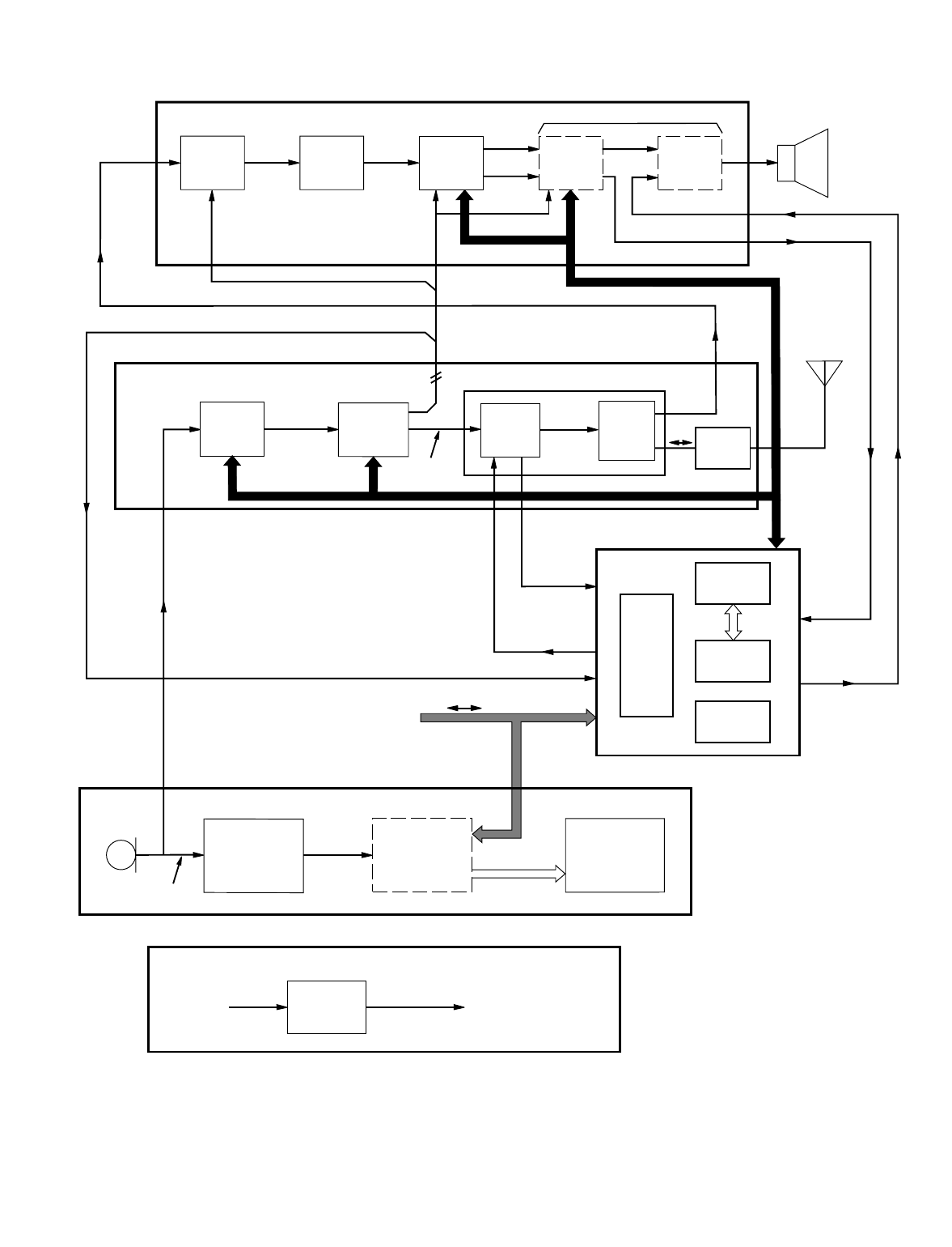
The following discussion refers to the functional block diagram for the
radio, Figure 1.
The receiver function of the radio detects, demodulates, amplifies, and
outputs via the loudspeaker, radio signals picked up by the vehicle or
fixed-station antenna. The radio signal input reaches the receiver from
the antenna via the antenna switch, which is located in the transmit-
ter function of the radio. The radio signals picked up by the antenna
are signals that have been re-broadcast by trunked or conventional
repeaters, or that have been broadcast directly by other mobile or fixed
station radios.
The receiver function of the radio consists of: the receiver front end
section; the receiver intermediate frequency (IF) section; the receiver
back end section; and the audio signal filter (ASFIC) and receiver audio
power amplifier circuits in the controller section.
The receiver function of the radio uses the double conversion super-
heterodyne design to optimize image rejection and selectivity. The
receiver front end section converts the receiver input signal to a first
IF of 44.85 MHz. The frequency upon which the receiver operates is
determined by a first local oscillator signal generated by the synthesiz-
er section. For the purpose of this discussion, the synthesizer section is
considered to be part of the transmitter function of the radio.
The 44.85 MHz IF output signal from the receiver front end section
passes through the receiver IF section where it is filtered and amplified.
The output of the receiver IF section goes to the receiver back end
section. In the receiver back end section, which contains the zero
intermediate frequency (ZIF) integrated circuit (IC), the receiver IF
signal is demodulated to produce receiver audio and squelch signals.
The receiver audio and squelch signal outputs from the receiver back
end section are processed by the audio signal filter integrated circuit
(ASFIC) in the controller section of the radio to generate receiver audio
(filtered) and squelch detect signals. The filtering characteristics and
other processes of the ASFIC are controlled by the central processor
unit in the controller section.
The receiver audio signal (filtered) from the output of the ASFIC goes
to the input of the receiver audio power amplifier circuit, which is
located in the controller section of the radio.
Theory of Operation 5
RECEIVER
RECEIVE
RF SIGNAL
RECEIVE RF SIGNAL
RECEIVER
FRONT END
SECTION
RECEIVER IF
SECTION
RECEIVER
AUDIO AUDIO
SIGNAL
FILTER
(ASFIC)
AUDIO PA
ENABLE
SQUELCH
DETECT
RECEIVER
AUDIO RECEIVER
AUDIO
POWER
AMPLIFIER
RECEIVER
BACK END
SECTION
(ZERO IF) SQUELCH
FIRST
RECEIVER
LOCAL
OSCILLATOR
2.1 MHz
REFERENCE
OSCILLATOR
IF IF
LOUDSPEAKER
P/O CONTROLLER SECTION (NOTE 1)
DC POWER CONTROL AND REGULATION
13.8VDC
FROM VEHICLE
BATTERY OR
BASE STATION
POWER SUPPLY
CONTROL AND
REGULATION
CIRCUITS
REGULATED
DC POWER
P/O CONTROLLER SECTION
(NOTE 1)
TO TRANSCEIVER BOARD AND
CONTROL HEAD CIRCUITS
P/O CONTROLLER
SECTION
(NOTE 1)
AUDIO
SIGNAL
FILTER
(ASFIC)
AUDIO
MODULATION
SIGNAL SYNTHESIZER
SECTION
MEMORY
RF
POWER
CONTROL
FEEDBACK
CONTROL
SB9600
DATA BUS
ACCESSORY
INPUTS AND
OUTPUTS
2.1 MHz
REFERENCE
OSCILLATOR
CENTRAL
PROCESSOR
UNIT (CPU)
SUPPORT
LOGIC
(SLIC)
RF POWER
AMPLIFIER
TRANSMIT
RF SIGNAL
POWER
DETECTOR
AND
ANTENNA
SWITCH
ANTENNA
TRANSMITTER POWER AMPLIFIER SECTION
FIRST RECEIVER
LOCAL OSCILLATOR,
2.1 MHz
REFERENCE OSCILLATOR
TRANSMITTER
INJECTION
SIGNAL SERIAL
PERIPHERAL
INTERFACE
(SPI) BUS
AUDIO PA
ENABLE
TRANSMITTER
MICROPHONE
PUSH TO
TALK (PTT)
OPERATOR
KEYBOARD,
PUSHBUTTONS,
AND OTHER
CONTROLS
MICROPHONE
AUDIO
CONTROL HEAD
PROCESSOR OPERATOR
DISPLAY
DISPLAY DATA
1. REFER TO VOLUME 1 OF THIS
SERVICE MANUAL FOR INFORMATION
ABOUT CONTROLLER SECTION.
NOTES:
2. REFER TO VOLUME 1 OF THIS
SERVICE MANUAL FOR INFORMATION
ABOUT CONTROL HEAD.
OPERATOR INTERFACE (CONTROL HEAD - NOTE 2)
MAEPF-26567-B
P/O CONTROLLER
SECTION (NOTE 1)
HARMONIC
FILTER
Figure 1 . Overall Radio Functional Block Diagram

6 Theory of Operation
The receiver audio power amplifier circuit does not pass the receiver
audio signal to the loudspeaker until it receives an audio PA enable
signal from the controller section of the radio. The reason is that the
receiver portion of the radio includes a squelch function, which
prevents receiver noise from passing to the loudspeaker during periods
of no signal reception.The controller generates the audio PA enable
signal based on such variables as the level of the received signal, the
frequency channel, and the operating mode of the radio. When the
audio PA enable signal is generated, the audio power amplifier (PA) is
activated and passes the receiver audio signal to the loudspeaker.
The transmitter function of the radio produces a nominal 25-Watt
radio frequency output signal. The radio frequency output signal is
frequency modulated by an audio signal from the microphone or from
another source such as a telephone keypad or handset.
The transmitter function of the radio consists of: the audio signalling
filter integrated circuit (ASFIC) in the controller section; the
synthesizer section; and the transmitter power amplifier (PA) section.
The ASFIC develops a modulation signal by amplifying an audio signal
from the microphone, keypad, or handset. The synthesizer section
generates a radio frequency carrier signal upon which the transmitter
portion of the radio operates.The radio frequency carrier signal
generated by the synthesizer section is frequency modulated in the
synthesizer section by the modulation signal output from the ASFIC.
The frequency modulated output signal from the synthesizer section
is amplified to the required nominal 25-Watt power level by the power
amplifier (PA) section.The output of the PA section passes through the
antenna switch and is radiated by the vehicle antenna or fixed-station
antenna.
The controller section of the radio contains a microprocessor that
controls the radio in accordance with its built in programming as well
as commands input manually by the radio operator. The radio
operator inputs manual commands to the controller section using the
pushbuttons and other controls located on the control head. In
addition to its controlling functions, the controller section provides
audio amplification of the audio output signal in the receiver
function. It also contains squelch detect circuitry based on a buffered
discriminator signal from the Zero Intermediate Frequency Integrated
Circuit (ZIF IC).
The operator interface function of the radio consists of: a microphone
or the microphone portion of a telephone handset; a telephone
keypad if used; the pushbuttons and other controls on the control
head; and the digital and graphics displays on the control head. The
pushbuttons and other controls on the control head provide digital
commands to the controller section, and in some instances, hardwired
commands to controlled circuits. The digital and graphics displays
receive display data from the controller section. The control head
contains its own microprocessor, which communicates with the
controller section of the radio via an SB9600 serial digital data bus.
The DC power control and regulation function regulates and
distributes to the various sections of the radio, DC power from the
vehicle battery or fixed station power supply.

Theory of Operation 7
Receiver
Detailed Functional
Description
The portion of the receiver function that is not part of the controller
section of the radio is composed of three main sections: receiver front
end; receiver intermediate frequency (IF), and receiver back end. The
receiver covers the VHF range from 136 to 174 MHz.
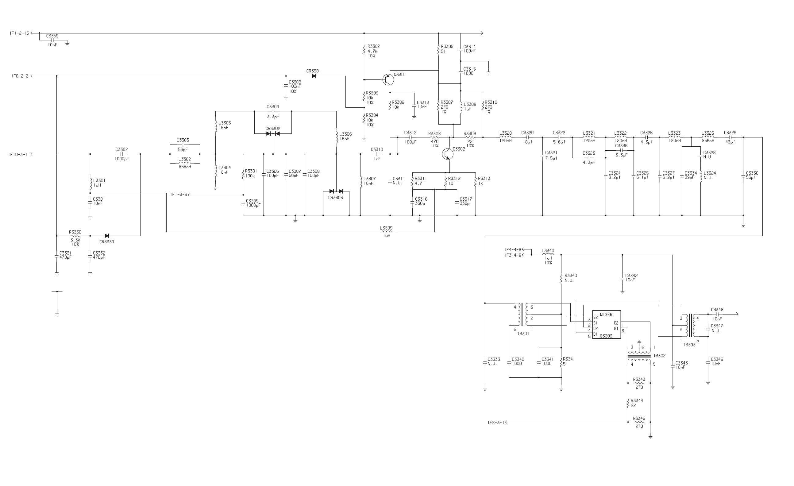
Receiver Front End
The following discussion is based on the schematic diagram for the
receiver front end section on page 19.
Varactor Tuned Band-
pass Filter
A two pole filter tuned by dual varactor diode CR3302 preselects the
incoming receive signal at terminal IF10-3-1 to reduce spurious effects
to the stages that follow. The filter tuning voltage at terminal IF1-3-6,
which ranges from 2.5 VDC to 7.5 VDC, is controlled by a digital to
analog (D/A) converter integrated circuit in the controller section of
the radio. The filter has three bandstops: at approximately at 45 MHz
for the first IF; at 95 MHz for broadcast frequencies; and at the receive
frequency plus 50 MHz for the receiver local oscillator frequency. The
three bandstops improve receiver performance at those three specific
spurious signal frequencies.
In transmit mode, the input signal to the receiver front end is reduced
by PIN diode CR3330, which is part of the RX/TX switch in the power
amplifier section of the radio. A dual hot carrier diode (CR3303) limits
any in-band signal to 10 dBm to prevent damage to the receiver
preamplifier.
Preamplifier
The receiver preamplifier (Q3302) is a surface mount device (SMD),
which has emitter and collector base feedback to stabilize gain and
impedance, and minimize intermodulation distortion. To provide
optimum transistor current drain, Q3302 is actively biased by a
collector current sense circuit (Q3301 and associated components),
which in receive mode is also used to bias the receive series PIN diode
CR3641 (in the power amplifier section) via the decoupled emitter
path of Q3302.
The Q3302 collector current is set to approximately 22 mA at an
emitter voltage of about 2 volts. The combined preamplifier and PIN
diode bias circuit is driven by the keyed 9-Volt line (K9V1) from the
controller section of the radio.
To stabilize its output impedance, the preamplifier is followed by a
3 dB pad.
Fixed Tuned
Band-pass Filter
A five pole fixed tuned band-pass filter, with two bandstops (both at
approximately 220 MHz to suppress image frequencies), is included
after the preamplifier. The filter provides signal transmission over the
VHF range, wideband spurious signal suppression, and preamplifier to
mixer matching.
Mixer
Q3303 is a double balanced active Gallium Arsenide (GaAs) mixer. Its
three ports are matched for incoming VHF signal conversion to the
44.85 MHz IF using high-side injection. The mixer bias is set by R3341
to approximately 24 mA with P
inj
(RX INJ) = 5 dBm.
The mixer IF output signal is fed through transformer T3303, where its
impedance is transformed to match the input impedance of the
receiver IF section.

8 Theory of Operation
Receiver Intermediate
Frequency (IF)
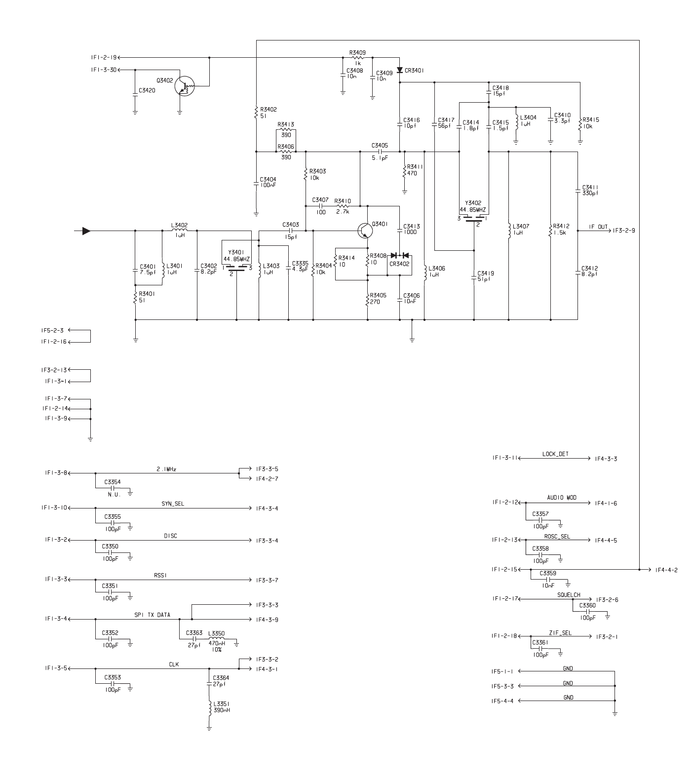
The following discussion is based on the schematic diagram for the
receiver IF section on page 21.
Intermediate Frequency
(IF) First Selection
To optimize half-IF stability, a diplexer shunt circuit (C3401, R3401,
L3401, C3402) matches the output impedance of the mixer in the
receiver front end section to the input of two pole crystal filter Y3401
at the input of the receiver IF section. The output of filter Y3401 is
matched to the following IF amplifier (Q3401).
IF Amplifier
IF amplifier Q3401 is a surface mount device of the same type as
preamplifier Q3302 in the receiver front end section. It is actively
biased by a collector base feedback circuit to a current drain of
approximately 10 mA. Its output voltage swing is limited by a dual hot
carrier diode (CR3402) to reduce overdrive effects at RF input signal
levels above 27 dBm.
IF second selection
IF amplifier Q3401 is followed by matching networks into and out of
the second crystal filter (Y3402). To optimize the filter pass band, a
certain amount of signal is coupled from the input to the output of the
filter to achieve a notch at the higher and lower adjacent channel. This
improves the adjacent channel selectivity.
The output from filter Y3402 is coupled via capacitor C3411 and
terminal 1F3-2-9 to the input of the receiver back end section.
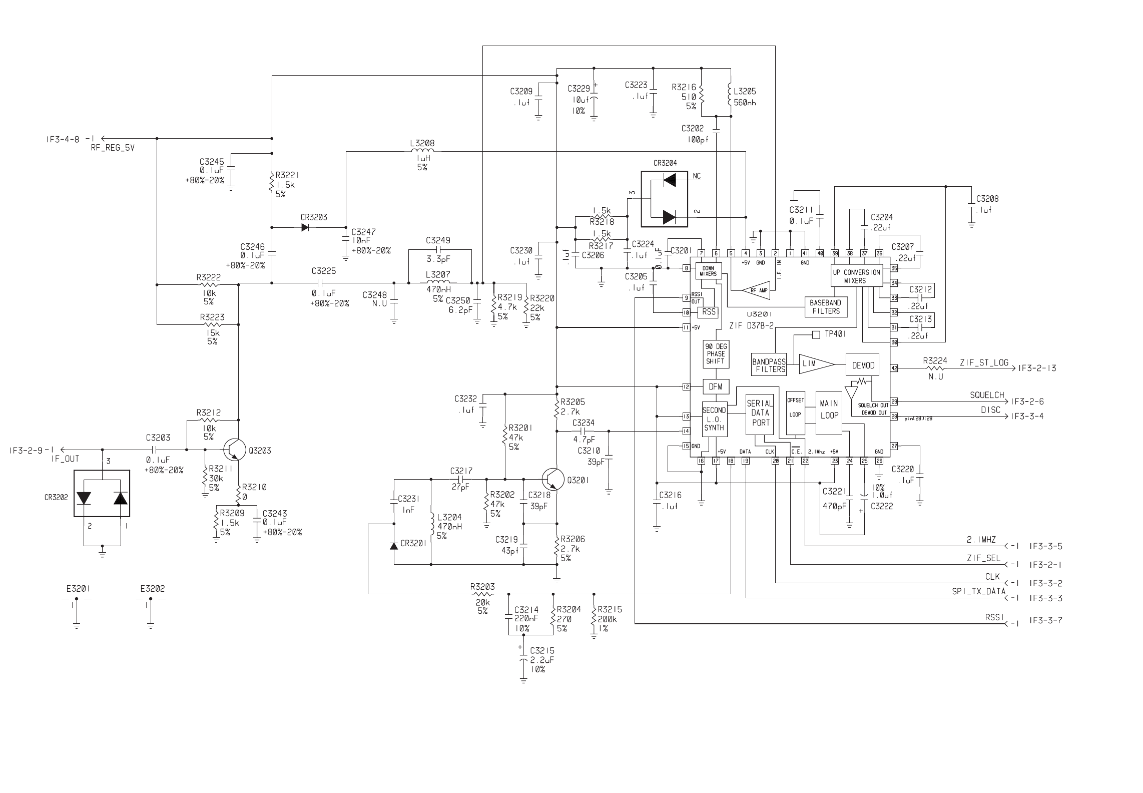
Receiver Back End
The following discussion is based on the schematic diagram for the
receiver back end section on page 23.
Zero IF (ZIF) Isolation
Amplifier
To obtain proper operation of the ZIF IC (U3201) in the receiver back
end section, an isolation amplifier (Q3203) combined with an IF
automatic gain control (AGC) and a low-pass filter follows. The
collector path of Q3203 is loaded with a PIN diode (CR3203) in shunt
configuration. Its control voltage is generated by a bias circuit with
CR3204 in conjunction with the voltage out of U3201 pin 4
(U3201-4). This configuration provides a maximum AGC dynamic
range of 40 dB and isolates the sensitive ZIF IC from an overdriving IF
level. Additionally, the signal is low-pass filtered to suppress non-
linear effects within the ZIF IC.
ZIF IC (U3201)
Within the ZIF IC, the 44.85 MHz IF signal is mixed in two quadrature
paths down to baseband, filtered, processed, and FM demodulated.
The conversion process to baseband is performed by using a second LO
circuit consisting of Q3201, inductor L3204 and several capacitors
that, in combination with varactor diode CR3201 and a loop filtered
steering line from U3201-18, closes a phase locked loop (PLL).
The demodulated audio signal exits the ZIF IC at U3201-28 and is
applied to the Audio Signalling Filter IC (ASFIC), which is located in
the controller section of the radio.

Theory of Operation 9
Transmitter
Detailed Functional
Description
The transmitter function of the radio is distributed between the
controller, synthesizer, and power amplifier (PA) sections of the radio.
This is shown on the overall functional block diagram for the radio,
Figure 1.
The portion of the transmitter function physically located in the
controller section is described in the
Controller Section Theory of
Operation
located in Volume 1 of this service manual. That portion
includes the audio circuits that filter, amplify, and otherwise process
the audio signal from the microphone and/or telephone handset.
The portion of the transmitter function located in the synthesizer
section of the radio is described in the
Synthesizer Detailed Functional
Description
, which follows this paragraph.
The remaining part of the transmitter function of the radio is located
in the power amplifier section, which is described after the description
of the synthesizer.
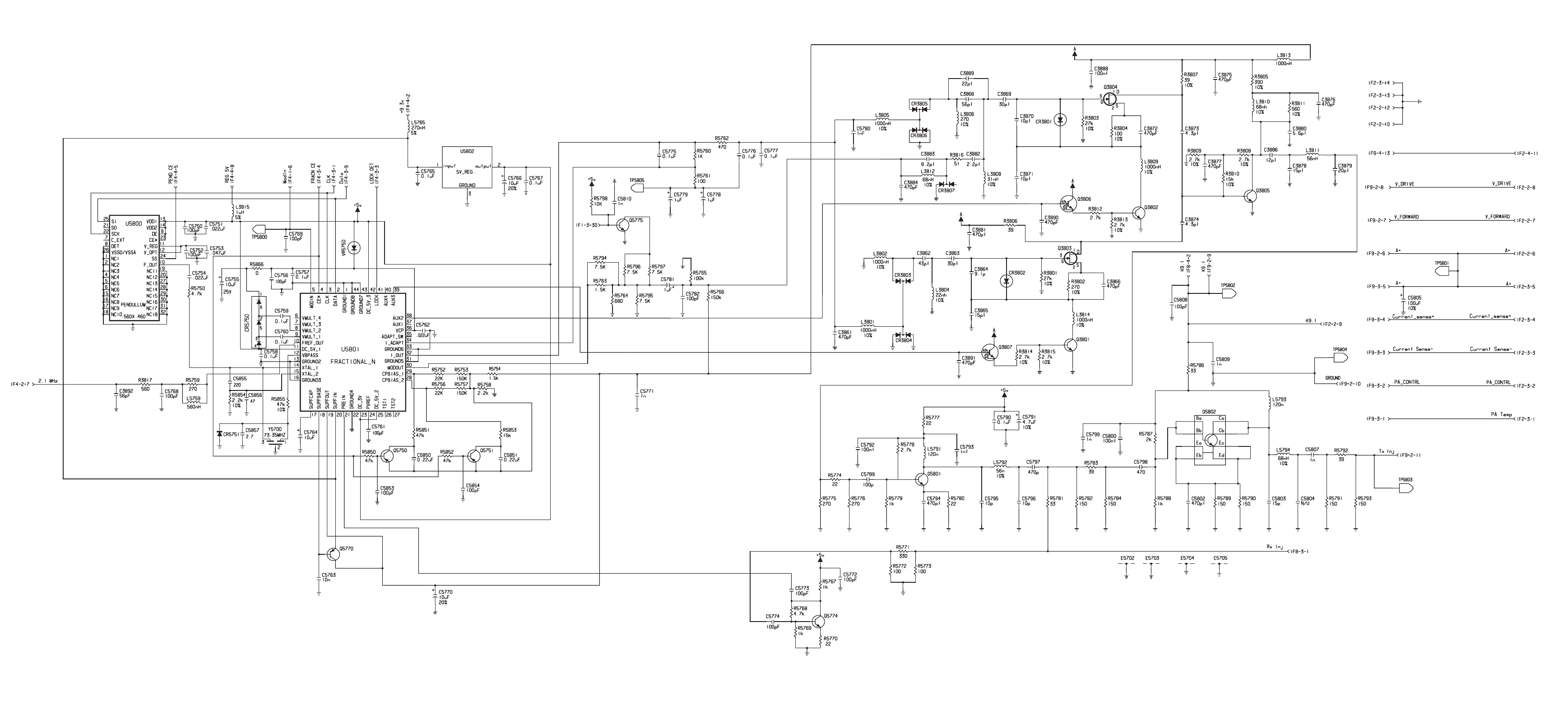
Synthesizer Detailed
Functional Description
The synthesizer section of the transmitter receives the amplified and
processed audio signal from the controller section of the radio and
produces a frequency-modulated radio frequency carrier signal (the
transmitter injection signal), which is input to the transmitter power
amplifier (PA) section.
The synthesizer section of the radio also generates the first conversion
local oscillator signal (180.85 to 218.85 MHz) and the second
conversion reference oscillator signal (2.1 Mhz) for the receiver and
controller sections of the radio.
The following discussion is based on the schematic diagram for the
synthesizer section on page 25.
Synthesizer Circuitry
The synthesizer consists of Pendulum reference oscillator U5800,
Fractional-N integrated circuit (IC) U5801, transmit and receive
voltage controlled oscillators (VCOs) Q3803 and Q3804, buffer
amplifiers Q3805 and Q5801, transmit injection amplifier Q5802, and
feedback amplifier Q5774.
Pendulum reference oscillator U5800 contains a temperature
compensated quartz crystal oscillator with a frequency of 16.8 MHz.
The oscillator is tuned by a temperature referenced 5-bit analog-to-
digital (A/D) converter located in the controller section of the radio.
The output of the oscillator (U5800-10) is applied to U5801-14
(XTAL1) via C5754 and R5750.
The transmit and receive VCOs are the grounded drain Colpitts type
using junction field effect transistors (JFETs) and lumped elements.
The transmit VCO covers the frequency range of 136 to174 MHz. The
receive VCO covers the range of 180.85 to 218.85 MHz. The transmit
VCO is activated by U5801-38 (AUX2) and the action of transistor
switches Q3806 and Q3802. The receive VCO is activated by U5801-39
(AUX3) and the action of transistor switches Q3807 and Q3801. The
frequency of each VCO is proportional to the applied control voltage,
which is in the range of 2 to11 VDC. The control voltage is applied to
frequency control varactors CR3803 through CR3806 via a loop filter.

10 Theory of Operation
The Fractional-N synthesizer Integrated Circuit (U5801) contains the
following circuits:
- Prescaler
- Programmable loop divider
- Control divider logic
- Phase detector
- Charge pump
- A/D converter for low frequency modulation
- Modulation low-frequency/high-frequency balance attenuator
- Positive voltage multiplier drivers
- Serial interface for control
- Super filter low noise supply
Transistor Q5770 is a current amplifier for the super filter low noise
supply. The super filter drops 9.3 VDC (emitter of Q5770) to about 8.6
VDC (collector of Q5770). The filtered 8.6 VDC supplies the oscillator
circuit, modulation circuit, VCO switching circuits, and synthesizer
charge pump resistor network. Feedback amplifier Q5774 provides the
amplification and isolation necessary to drive the prescaler input
(U5801-21). Three-terminal regulator U5802 drops 9.3 VDC from the
controller section of the radio to 5 VDC required by the Fractional-N
synthesizer IC.
To generate a high voltage needed by the phase detector (charge
pump) output stage at U5801-36 (VCP), a voltage of 13 VDC at
CR5750-1 is generated by a positive voltage multiplier (CR5750,
C5759, C5760). The positive voltage multiplier is basically a diode
capacitor network driven by two 1.05-MHz 180 degrees out of phase
signals (U5801-8 and U5801-9).
The serial interface (SRL) of the microprocessor in the controller
section of the radio is connected to the data line (U5801-2), clock line
(U5801-3), and chip enable line (U5801-4) of the fractional-N IC.
Synthesizer Operation
The complete synthesizer works as follows: Fractional-N IC U5801 is
programmed for either transmit or receive via the serial data bus. The
appropriate VCO is activated via the AUX control pins of U5801 and
the prescaler and loop divider are set for the desired frequency. The
outputs from the VCOs are amplified by buffer amplifiers Q3805 and
Q5801. The output of buffer amplifier Q5801 is split three ways. First,
the feedback amplifier Q5774 is connected via the resistive attenuator
consisting of R5773, R5771, and R5772. The local oscillator port for
the mixer in the receiver front end section of the radio is also
connected at this node (Rx Inj). Finally, transmit injection amplifier
Q5802 is connected at this node via the resistive attenuator composed
of R5782, R5783, and R5784. The output of amplifier Q5802 (TX inj)
is connected to the transmitter power amplifier.
The prescaler in the synthesizer (Fractional-N IC U5801) is basically a
dual modulus prescaler with selectable divider ratios. The divider ratio
of the prescaler is controlled by a loop divider, which in turn receives
its inputs via the SRL. The output of the prescaler is applied to the loop
divider. The output of the loop divider is connected to the phase
detector, which compares the loop divider output signal with a
reference signal. The reference signal is generated by dividing down
the signal of the reference oscillator (Pendulum oscillator U5800). The

Theory of Operation 11
output signal of the phase detector is a pulsed DC signal, which is
routed to the charge pump. The charge pump outputs a current at
U5801-32 (I OUT). The loop filter (which consists of R5760 through
R5762 and C5775 through C5780) transforms this current into a
voltage, which is applied to both VCOs to control their output
frequencies.
The current can be set to a value fixed in the FRACN IC or to a value
determined by the currents flowing into CPBIAS 1 (U5801-29) or
CPBIAS 2 (U5801-28). The currents are set by the values of R5752 and
R5753 or R5756 and R5757, respectively. Selection of one of the three
different bias sources is done by the radio software.
To reduce synthesizer lock time when new frequency data has been
loaded into the synthesizer, the magnitude of the loop current is
increased by enabling the I ADAPT line (U5801-34) for a certain
software-controlled amount of time (Adapt Mode). Additionally the
loop current is increased by bypassing R5752 and R5753 with Q5750,
and bypassing R5756 and R5757 with Q5751. Bypassing starts when
the FRACN CE line changes from high to low and ends a certain delay
time after the transition from low back to high. The adapt mode timer
and the bypassing delay are both started by the low to high transition
of the FRACN CE line. The adapt mode time is programmed to be
somewhat shorter than the bypassing delay time, which is hardware
dependent. This causes two different current levels during frequency
acquisition of the loop. When the synthesizer is within the lock range,
the current is determined only by the resistors connected to CPBIAS 1,
CPBIAS 2, or the internal current source.
The output of the balance attenuator is MODOUT (U5801-30) and is
connected to the transmit VCO modulation network. The modulation
is applied to the transmit VCO via varactor diode CR3807.
Transmit Injection
Amplifier
Transmit injection amplifier Q5802 increases the output of Q5801 to
about +13 dBm. This is the level required by the first stage of the
transmitter power amplifier. The transmit injection amplifier collector
supply of 9.1 volts and originates in the controller section of the radio.
It is active only during transmit.
Power Amplifier
Overall PA
The power amplifier (PA) is a radio frequency (rf) power amplifier,
which amplifies the output from the injection string (TX_INJ) to an RF
output power level of 25 Watts.
The following discussion is based on the schematic diagram for the
power amplifier (PA), on page 27
The PA is a three stage amplifier, which amplifies the output from the
transmitter injection string in the Synthesizer Section to the transmit
level (nominally 25 Watts).
The first stage (Q3521) of the PA is a bipolar stage, which is controlled
via the PA control line. It is followed by two Metal Oxide
Semiconductor Field Effect Transistor (MOSFET) devices, Q3541 and
Q3561.
Devices Q3521 and Q3541 are surface mounted. To remove heat from
Q3541, the surface mounted heat spreader on the opposite side of the

12 Theory of Operation
printed circuit board provides thermal contact of the transistor to the
heat sink on the radio chassis. Transistor Q3561 is attached directly to
the heat sink.
The RF power output of Q3521 is proportional to the Q3521collector
current. This current is adjusted by the PA control voltage (PA
Control). If the PA control voltage raises, the base voltage of Q3601 is
also raised, which causes more current to flow to the collector of
Q3601 and a higher voltage drop across R3606. This results in more
current being drawn by Q3501 so that the base current on Q3521 is
increased. This in turn causes higher collector current to flow through
Q3521. The collector current settles when the voltage drop across the
parallel combination of resistors R3530 throughR3533 equals the
voltage drop across R3606 minus the base-to-emitter voltage drop of
Q3501.
By controlling the output power of Q3521 and in turn the input power
of the following stages, the automatic level control (ALC) loop is able
to regulate the output power of the transmitter.
The MOSFET devices Q3541 and Q3561 are enhancement mode N-
Channel MOSFETS. For proper operation, these devices require a
positive gate bias voltage and a quiescent current flow with no drive.
To achieve these requirements, the gates are biased through the
network consisting of R3582, R3525, and R3526 for Q3541 and
similarly R3585, R3544, and R3545 for Q3561. The actual value of the
voltage at this gate is device dependent and determined by trim in the
factory when the radio is built.
The output of Q3561 goes through the matching network consisting
of four transmission lines, inductor L3566, and several capacitors to
the directional coupler.
Directional Coupler, RX-TX
Switch, and
Harmonic Filter
The forward power detector (directional coupler) is a microstrip
printed circuit, which couples a small amount of the forward RF
energy off and sends it to diode CR3671 where it is rectified. The
rectified signal forms the V detect voltage, which is proportional to the
rectified RF energy appearing across the diode. The power control
circuit holds this voltage constant, thus ensuring that the forward
power out of the radio is held constant.
The antenna switch is switched synchronously with the keyed 9.1
voltage (K 9V1). In transmit mode, the K 9V1 line is high and the
current turns on the PIN diode CR3641. The receiver preamplifier
transistor Q3302, also turned off by the keyed 9.1 voltage, cuts off the
current through the PIN diode CR3642 and turns off transistor Q3641.
In receive mode the K 9V1 line is low. This turns off the PIN diode
CR3641 and turns on the receiver preamp transistor Q3302. The
current through Q3302 turns on the PIN diode CR3642 and transistor
Q3641. Q3641 shorts R3644 to increase the current through Q3302.
Harmonics of the transmitter are attenuated by the harmonic filter
formed by inductors L3661 through L3663, and capacitors C3661
through C3664. This network forms a low-pass filter to attenuate
harmonic energy of the transmitter to an acceptable level. L3664
provides electrostatic protection for the power amplifier.
Temperature Sense
In the PA compartment, 100K ohm thermistor R3610 senses the
temperature of MOSFET devices Q3541 and Q3561. This signal is fed
back into the power control circuit to protect the power amplifier

Theory of Operation 13
against over temperature conditions. The power control circuit senses
the voltage drop across shunt resistor R3615, which is determined by
the magnitude of the drain current in Q3561. This is a limit
mechanism whereby the power control limits the magnitude of
current that can be drawn by Q3561 to protect the device from
excessive power dissipation.
PA Power Control
The maximum value of the PA control line is limited by R3601 and
R3602, the resistor divider off of PA control. This inputs a signal back
into the power control circuit that limits the magnitude of the voltage
to which the PA control line can rise.
Reverse polarity protection for the transmitter is provided by diode
CR3601. This diode is soldered to the board as well as being pressed
against a member in the chassis heat sink so under reverse polarity
conditions to the radio this diode conducts and protects the radio
from damage. This diode also provides transient over-voltage
protection by breaking down when the supply voltage to the radio
exceeds 25 volts.
The power control circuit (located in the controller section of the
radio) consists of the control amplifier (U0550-9), the control voltage
limiter (U0202), the detector voltage buffer/amplifier (U0550-12, -13,
-14) the PA temperature sense circuit (U0550-1, -2, -3) and the current
limit circuit.
The voltage from the forward power detector in the PA is amplified by
U0550-12, -13, -14. The output voltage is added to the PA power set
voltage at the inverting input of control amplifier U0550-9. Its
noninverting input is set to a fixed 4.65 volts. As long as there is a
differential input voltage at the control amplifier input, the output
voltage (PA control voltage) is altered. This in turn causes a change of
the RF output power level and the detector voltage, which leads to a
changing differential input voltage. When the control loop is in steady
state the voltages at both the inverting and the noninverting input are
equal.
To obtain a higher RF output level, the power set voltage generated by
the D/A converter U0551-2 is reduced. This causes a lower level at the
summing point U0550-9. The control loop compensates this
difference by increasing RF power and detector voltage until balance
between the two control amplifier inputs is obtained again. Reduction
of the power level works in the opposite manner.
Operational amplifier U0202 functions as an integrator, which
controls, via Q0556, the control voltage slope during key up and
dekey.
During RX operation, Q0556 pulls R0590 down, the output of U0202
is at its maximum level, Q0555 conducts and the output of U0550 is
at its minimum output level.
After pressing PTT, transistor Q0556 switches off. Capacitor C0552 is
charged via R0584 and R0590. In turn the output voltage of U0202
decreases which causes an increase of the voltage at the non-inverting
input of U550. This increases the PA control voltage. The loop is closed
via R0591 and R0592. This feedback causes an exponential like rising
edge of the control voltage. Such a smoothed keyup leads to an
improved adjacent channel power reduction during TX keyup
compared with a linear ramp.

14 Theory of Operation
After keyup the circuit does not effect the performance of the power
control circuit as long as the control voltage does not increase over a
certain value defined by R0591/R0592 and the voltage applied to
R0584 by the D/A output U0055-13. If this occurs the control voltage
will be limited to the predefined value and the PA prevented from
being damaged.
If the radio switches from TX to RX transistor Q0556 pulls R0590
down and C0552 is discharged via R0590. This causes the output of
U0202 to go up and tie down the noninverting input of U0550. The
control voltage decreases controlled by the loop U0202, Q0555, and
U0550.
The protection features in the PA power control operate by raising the
non-inverted input to the operational amplifier above the reference
voltage, which has the same effect as a larger input from the coupler.
The thermal shutback circuit works when the temperature of R3610
decreases its resistance, the output at pin 1 of U0550 increases. When
that voltage rises above the reference voltage at pin 10 of U0550, the
control voltage of the PA is decreased lowering the power output. The
current limiting circuit measures the voltage drop across R3615
causing an adjustable offset to the voltage controlled by the D to A
output for current limit set. The difference of that is amplified at pin 7
of U0550. When the voltage exceeds the reference at pin 10 of U0550,
then current limit starts to engage reducing power output.
Controller Detailed
Functional
Description
The theory of operation for the controller section of the radio is
located in Volume 1 of this service manual.
DC Power Control
and Regulation
Detailed Functional
Description
The theory of operation for the dc power control and regulation
section of the radio is located in Volume 1 of this service manual.

Reference Drawings 15
Reference Drawings
3
This section contains the reference drawings listed below for the
receiver (front end, IF, and back end), transmitter, and synthesizer
portions of the radio.
•
Overall Radio:
-
Transceiver Board Section Locations - Page 16
-
Schematic Diagram Interconnection List, Table 2 - Page 29
•
Receiver:
-
Receiver Front End Component Locations and Parts List -
Page 18
-
Receiver Front End Schematic Diagram - Page 19
-
Receiver IF Component Locations and Parts List - Page 20
-
Receiver IF Schematic Diagram - Page 21
-
Receiver Back End Component Locations and Parts List -
Page 22
-
Receiver Back End Schematic Diagram - Page 23
•
Synthesizer:
-
Synthesizer Component Locations and Parts List - Page 24
-
Synthesizer Schematic Diagram - Page 25
•
Power Amplifier:
-
Power Amplifier Component Locations and Parts List -
Page 26
-
Power Amplifier Schematic Diagram -
Page 27
Refer to Volume 1 of this service manual (Motorola Publication
68P81083C20) for reference drawings for the controller and control
head portions of the radio.
Refer to the Secure Option service manual (Motorola Publication
68P81083C25) for reference drawings for the secure option for the
radio.
Referen
16 Reference Drawings
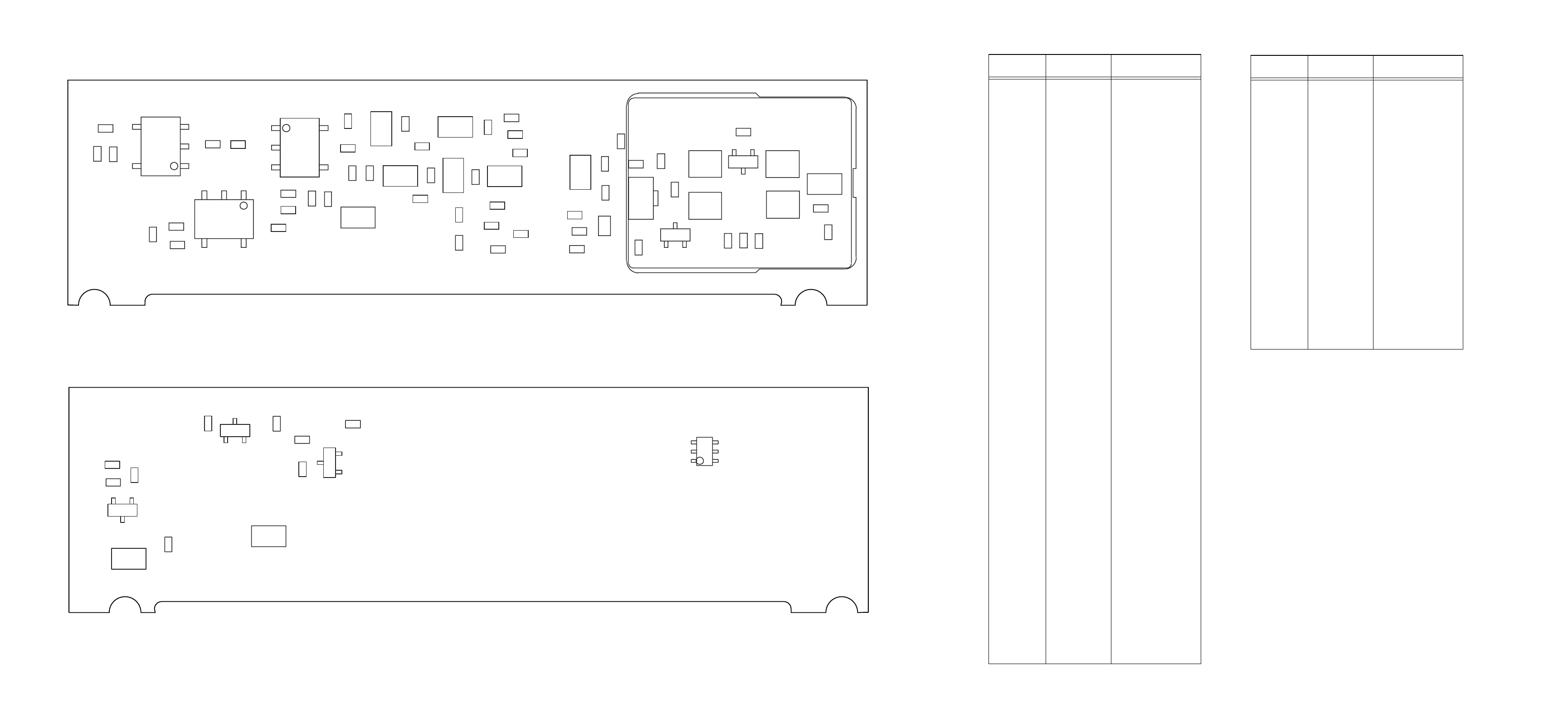
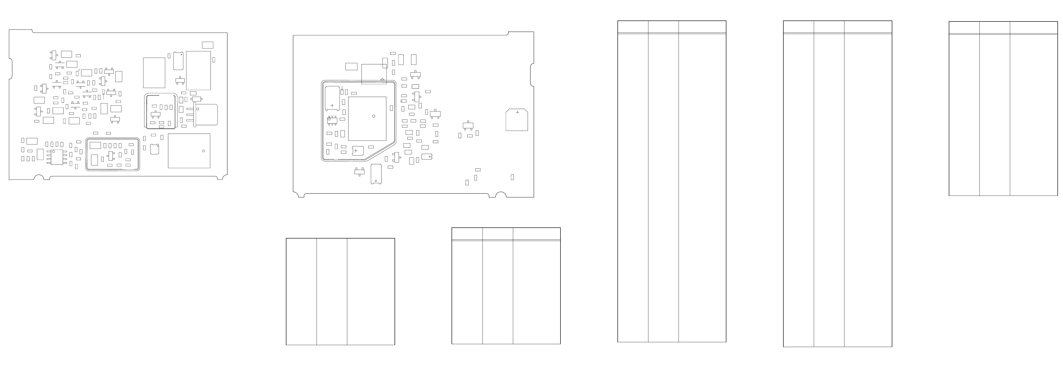
Figure 2 Transceiver Board Section Locations
TRANSMITTER PA
CONTROLLER
AUDIO AND POWER
REGULATION
SYNTHESIZER
RECEIVER
IF
RECEIVER
BACK END
RECEIVER
FRONT END
CONTROLLER
COMMON
MAEPF-26504-O

Reference Drawings 17
NOTES
18
RESISTORS:
R3301 0662057A97 100K
R3302 0662057A65 4700
R3303 0662057A73 10K
R3304 0662057A73 10K
R3305 0662057A18 51
R3306 0662057A73 10K
R3307 0662057A35 270
R3308 0662057A41 470
R3309 0662057A09 22
R3310 0662057A35 270
R3311 0662057C19 4.7
R3312 0662057A01 10
R3313 0662057A49 1000
R3330 0662057A61 3300
R3341 0662057A18 51
R3343 0662057A35 270
R3344 0662057A09 22
R3345 0662057A35 270
TRANSFORMERS:
T3301 2505515V03 4:1 BALUN
T3302 2505515V03 4:1 BALUN
T3303 2505515V07 4:1 BALUN
Printed Circuit Board
(For Reference Only):
8402573Y06
and
8402573Y09
For Kit HUD4012D
REFERENCE
SYMBOL MOTOROLA
PART NUMBER DESCRIPTION
REFERENCE
SYMBOL MOTOROLA
PART NUMBER DESCRIPTION
CAPACITORS:
C3301 2113741F49 0.01 uF
C3302 2113741F25 1000 pF
C3303 2113740F45 56 pF
C3304 2113740F15 3.3 pF
C3306 2113740F51 100 pF
C3307 2113740F51 100 pF
C3308 2113740F51 100 pF
C3309 2113743K15 0.1 uF
C3310 2113741F25 1000 pF
C3312 2113740F51 100 pF
C3313 2113741F49 0.01 uF
C3314 2113743K15 0.1 uF
C3315 2113741F25 1000 pF
C3316 2113741F13 330 pF
C3317 2113741F13 330 pF
C3320 2113740F33 18 p F
C3321 2113740F24 7.5 pF
C3322 2113740F21 5.6 pF
C3323 2113740F18 4.3 pF
C3324 2113740F25 8.2 pF
C3325 2113740F20 5.1 pF
C3326 2113740F18 4.3 pF
C3327 2113740F22 6.2 pF
C3329 2113740F42 43 pF
C3330 2113740F45 56 pF
C3331 2113741F17 470 pF
C3332 2113741F17 470 pF
C3334 2113740F42 43 pF
C3336 2113740F15 3.3 pF
C3340 2113741F25 1000 pF
C3341 2113741F25 1000 pF
C3342 2113741F49 0.01 uF
C3343 2113741F49 0.01 uF
C3346 2113741F49 0.01 uF
C3348 2113741F49 0.01 uF
DIODES:
CR3301 4813833C02 Dual, 70V, Common
Cathode
CR3302 4802081B58 Dual, Varicap
CR3303 4880154K03 Dual, Schottky Mixer
CR3330 4880142L01 PIN
SHIELDS:
E3301 2602474Y01 Preselector
INDUCTORS:
L3301 2462587T30 1000 nH
L3302 2462587T12 56 nH
L3304 2460591L29 16.03 nH, Airwound
L3305 2460591L29 16.03 nH, Airwound
L3306 2460591L29 16.03 nH, Airwound
L3307 2460591L29 16.03 nH, Airwound
L3308 2462587T30 1000 nH
L3309 2462587T30 1000 nH
L3320 2462587T16 120 nH
L3321 2462587T16 120 nH
L3322 2462587T16 120 nH
L3323 2462587T16 120 nH
L3325 2462587T12 56 nH
L3340 2462587T30 1000 nH
TRANSISTORS:
Q3301 4813824A17 PNP
Q3302 4882971R01 NPN
RECEIVER FRONT END PARTS LIST
C3348
C3343
R3345
R3343
C3341
L3325
R3309
R3307
R3305
C3314
R3313
R3312
E3301
C3304
CR3302
L3305
L3302
MAEPF-26494-O
L3306
CR3303
C3303
L3307 L3304
C3316
L3320
C3321
C3320
L3323
L3321
C3322
C3324
C3342
C3326
C3333
C3329
C3334
C3328
C3325
L3322
C3315 R3310
C3336
L3308
C3312
R3301
C3308
C3317
C3310
R3306
Q3302
C3306
C3307
C3302
C3311
R3308
R3311
C3323
C3340
L3324
C3327
R3340
R3341
C3330
C3347
C3346
R3344
T3303
T3301
T3302
HEAVY COMPONENTS SIDE
MAEPF-26495-O
C3331
R3330
C3301
C3309
R3304
C3313
Q3301
C3332
CR3330
CR3301
R3303
R3302
L3301
L3309
Q3303
LIGHT COMPONENTS SIDE
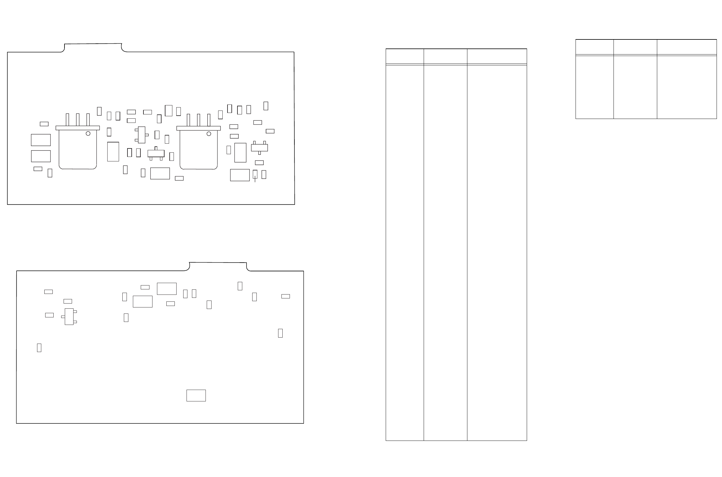
Receiver Front End (Kit HUD4012D)
Component Locations and Parts List
RECEIVER FRONT END COMPONENT LOCATIONS
NOTES:
1. All resistance values are in ohms unless indicated otherwise.
2. Components shown on component location and schematic
diagrams but not included in parts list are not placed.
This document was created with FrameMaker 4.0.3
19
9.3V
N.U.
IF_IN
(TO RECEIVER IF)
RX INJ
REG 5V
9.3V IF4-4-2
E3301
63A81090C56-O
Receiver Front End (Kit HUD4012D) Schematic Diagram
This document was created with FrameMaker 4.0.3
10_RFE SD p19 Page 19 Tuesday, January 19, 1999 4:57 PM
20
FILTERS:
Y3401 4805846W01 Crystal, 44.85 MHz
Y3402 4805846W03 Crystal, 44.85 MHz
PRINTED CIRCUIT
BOARD (For
Reference Only):
8402573Y06
and
8402573Y09
For Kit HUD4012D
REFERENCE
SYMBOL MOTOROLA
PART NUMBER DESCRIPTION
C3402
R3410
CR3402
L3407
R3412
C3418
C3411
C3417
C3414
C3416 R3409
C3409
L3406
C3419
R3403
MAEPF-26496-O
L3402
Y3401 Y3402
L3401
C3401
R3401
C3335
R3404
C3407
C3403
L3403
R3408
R3405
R3414 R3413
R3406
R3402
C3415
R3415
CR3401 C3408
C3410
C3412
L3404
C3404
C3405
R3411
C3413
C3406 Q3401
MAEPF-26497-O
C3361
C3305
C3351
L3340
C3364
L3351
L3350
C3420
C3360
Q3402
C3350
C3363
C3352
C3353
C3354
C3357
C3358
C3355
C3359
Receiver IF (Kit HUD4012D)
Component Locations and Parts List
RECEIVER IF COMPONENT LOCATIONS
REFERENCE
SYMBOL MOTOROLA
PART NUMBER DESCRIPTION
CAPACITORS:
C3305 2113741F49 0.01 uF
C3335 2113740F18 4.3 pF
C3350 2113740F51 100 pF
C3351 2113740F51 100 pF
C3352 2113740F51 100 pF
C3353 2113740F51 100 pF
C3355 2113740F51 100 pF
C3357 2113740F51 100 pF
C3358 2113741F58 100 pF
C3359 2113741F49 0.01 uF
C3360 2113740F51 100 pF
C3361 2113740F51 100 pF
C3401 2113740F24 7.5 pF
C3402 2113740F25 8.2 pF
C3403 2113740F31 15 pF
C3404 2113743A19 0.1 uF
C3405 2113740F24 7.5 pF
C3406 2113741F49 0.01 uF
C3407 2113740F51 100 pF
C3408 2113741F49 0.01 uF
C3409 2113741F49 0.01 uF
C3410 2113740F15 3.3 pF
C3411 2113741F13 330 pF
C3412 2113740F25 8.2 pF
C3413 2113741F25 1000 pF
C3414 2113740F09 1.8 pF
C3415 2113740F09 1.8 pF
C3416 2113740F27 10 pF
C3417 2113740F45 56 pF
C3418 2113740F31 15 pF
C3419 2113740F44 51 pF
DIODES:
CR3401 4880142L01 PIN
CR3402 4880154K03 Dual Schottky Mixer
INDUCTORS:
L3401 2462587T30 1000 nH
L3402 2462587T30 1000 nH
L3403 2462587T30 1000 nH
L3404 2462587T30 1000 nH
L3406 2462587T30 1000 nH
L3407 2462587T30 1000 nH
TRANSISTORS:
Q3303 5105625U28 Mixer, Integrated Circuit
Q3401 4882022N70 NPN
RESISTORS:
R3401 0662057A18 51
R3402 0662057A18 51
R3403 0662057A73 10K
R3404 0662057A73 10K
R3405 0662057A35 270
R3406 0662057A39 390
R3408 0662057A01 10
R3409 0662057A49 1000
R3410 0662057A59 2700
R3411 0662057A41 470
R3412 0662057A53 1500
R3413 0662057A39 390
R3414 0662057A01 10
R3415 0662057A73 10K
RECEIVER IF PARTS LIST
NOTES:
1. All resistance values are in ohms unless indicated otherwise.
2. Components shown on component location and schematic
diagrams but not included in parts list are not placed.
HEAVY COMPONENTS SIDE
LIGHT COMPONENTS SIDE
This document was created with FrameMaker 4.0.3
11_RIF CL/PL p20 Page 20 Tuesday, January 19, 1999 4:58 PM
21
N.U. N.U.
N.U.
N.U.
9.3V
9.3V
9.3V
N.U.
N.U. 47k
47k
IF_IN
(FROM RECEIVER
FRONT END)
63A81090C57-O
N.U.
Receiver IF (Kit HUD4012D)Schematic Diagram
This document was created with FrameMaker 4.0.3
22
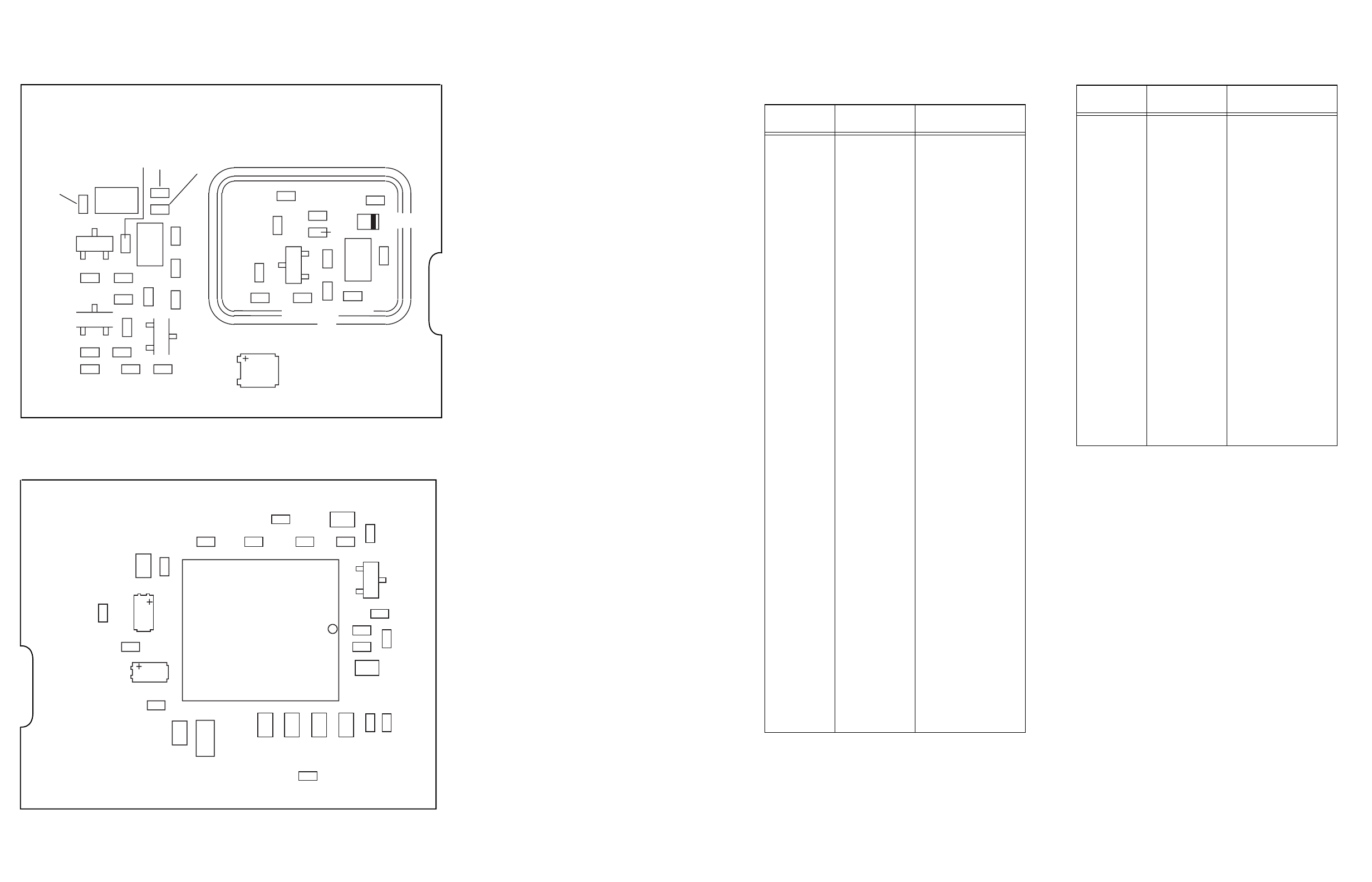
REFERENCE
SYMBOL MOTOROLA
PART NUMBER DESCRIPTION
CAPACITORS:
C3201 2113743K15 0.1 uF
C3202 2113740F51 100 pF
C3203 2113743K15 0.1 uF
C3204 2113743A23 0.22 uF
C3205 2113743K15 0.1 uF
C3206 2113743K15 0.1 uF
C3207 2113743A23 0.22 uF
C3208 2113743K15 0.1uF
C3209 2113743K15 0.1uF
C3210 2113740F41 39 pF
C3211 2113743A19 0.1uF
C3212 2113743A23 0.22uF
C3213 2113743A23 0.22uF
C3214 2113741A51 0.018 uF
C3215 2311049A02 0.15 uF
C3216 2113743K15 0.1 uF
C3217 2113740F37 27 pF
C3218 2113740F41 39 pF
C3219 2113740F42 43 pF
C3220 2109720D14 0.1 uF
C3221 2113741F17 470 pF
C3222 2109720D14 0.1 uF
C3223 2113743K15 0.1 uF
C3224 2113743K15 0.1 uF
C3225 2113743K15 0.1 uF
C3229 2311049J23 10 uF
C3230 2113743K15 0.1uF
C3231 2113741F25 1000 pF
C3232 2113743K15 0.1uF
C3234 2113740F19 4.7 pF
C3243 2113743K15 0.1uF
C3245 2113743K15 0.1uF
C3246 2113743K15 0.1uF
C3247 2113741F49 0.01 uF
C3249 2113740F15 3.3 pF
C3250 2113740F22 6.2 pF
DIODES:
CR3201 4862824C01 Varactor
CR3203 4805129M96 Dual
CR3204 4880154K03 Dual Schottky Mixer
SHIELD:
E3201 2605261V01 ZIF
INDUCTORS:
L3204 2462587T23 470 nH
L3205 2462587Q44 560 nH
L3207 2462587T23 470 nH
L3208 2462587T30 1000 nH
TRANSISTORS:
Q3201 4882022N70 NPN
Q3203 4882022N70 NPN
RECEIVER BACK END PARTS LIST
RESISTORS:
R3201 0662057A89 47K
R3202 0662057A89 47K
R3203 0662057A80 20K
R3204 0662057A59 2.7K
R3205 0662057A59 2.7K
R3206 0662057A59 2.7K
R3209 0662057A53 1.5K
R3210 0662057B47 0
R3211 0662057A84 30K
R3212 0662057A73 10K
R3215 0662057B05 200K
R3216 0662057A42 510
R3217 0662057A53 1.5K
R3218 0662057A53 1.5K
R3219 0662057A65 4.7K
R3220 0662057A81 22K
R3221 0662057A53 1.5K
R3222 0662057A73 10K
R3223 0662057A77 15K
INTEGRATED CIRCUITS:
U3201 5186296A02 Zero IF, F91 P-3
PRINTED CIRCUIT
BOARD (For
Reference Only):
8402573Y06
and
8402573Y09
For KIt HUD4012D
REFERENCE
SYMBOL MOTOROLA
PART NUMBER DESCRIPTION
C3247
C3249
C3250
R3219
R3220
C3248
R3205
R3206
C3234
C3218
L3204
C3231
C3225
R3223
R3210
R3212
R3211
Q3203 L3207
CR3203
E3201
R3201
R3202
C3217
MAEPF-26498-O
C3210
C3229
C3232
Q3201
C3219 R3203
CR3201
R3221
R3209
C3243 R3222
C3203
CR3202
C3246
L3208
MAEPF-26499-O
U3201
R3224
C3216 C3222
R3215
C3221
C3220
C3213
C3212
C3207
C3245
C3211
R3217
C3230 C3205
C3201
C3202
L3205
R3216
R3218
C3224
C3204
C3208
C3209 C3206 CR3204 C3223
C3214
R3204
C3215
Receiver Back End (Kit HUD4012D)
Component Locations and Parts List
RECEIVER BACK END COMPONENT LOCATIONS
HEAVY
COMPONENTS
SIDE
LIGHT
COMPONENTS
SIDE
NOTES:
1. All resistance values are in ohms unless indicated otherwise.
2. Components shown on component location and schematic
diagrams but not included in parts list are not placed.
This document was created with FrameMaker 4.0.3
13_RBE CL/PL p22 Page 22 Tuesday, January 19, 1999 5:03 PM
23
DEPC-97142-O/None
Receiver Back End (Kit HUD4012D) Schematic Diagram
This document was created with FrameMaker 4.0.3
14_RBE SD p23 Page 23 Tuesday, January 19, 1999 5:04 PM
24
R5777 0662057A09 22
R5778 0662057A59 2.7K
R5779 0662057A49 1K
R5780 0662057A09 22
R5781 0662057A13 33
R5782 0662057A29 150
R5783 0662057A15 39
R5784 0662057A29 150
R5786 0662057A13
33
R5787 0662057A56 2K
R5788 0662057A49 1K
R5789 0662057A29 150
R5790 0662057A29 150
R5791 0662057A29 150
R5792 0662057A15 39
R5793 0662057A29 150
R5850 0662057A89 47K
R5851 0662057A89 47K
R5866 0662057B47 0
INTEGRATED CIRCUITS:
U5800 5105279V38 Oscillator, 16.8 MHz
U5801 5105457W73 FRACTN
U5802 5113816A07 Regulator, 5 VDC,
500 mA
ZENER DIODE:
VR5750 481380A23 10 VDC, 225 mW
PRINTED CIRCUIT
BOARD (For reference
only):
8402573Y06
and
8402573Y09
For kit HUD4012D
REFERENCE
SYMBOL MOTOROLA
PART NO. DESCRIPTION
CR3804
C3864
R3802
C3866 CR3801
L3812
Q3802
C3883
CR3807
C3865
L3801
L3802
L3806
C3869
C3870
L3814
L3810
L3811
C3886
Q3805
R3811
C3876
C3873 R3807
R3810
R3804
C3875
C3874
Q3803
Q3804
L3813
L5794
R5792
C3888
C3862
C3868
C3882
C3872
R3816
L3805
CR3805
C3889
CR3806
C3863
C3871
R3803
R3801
R3805
C3880
C3884
R3806
C3881
R3808
C3877
R3809
L3809
C3878
R5789
C5802
R5790
R5788
R5784
C5796
C5797
C5803
C5804
C5807
R5791
R5793
C5799
L5793
R5787 C5798
R5782
L5791
C5793
C5795
Q5801
C5792
C5789
R5777
C5773
C5767
C5766
C5765
R5767
C5772
C5763
C5751
C5791
MAEPF-26500-O
R5769
R5770
C5774
R5768
Q5774
C5857
R5855
C5856 CR5751
C5754
C5790
C5750
R5750 C5855
R5854
R5779
R5778
R5783
R5776
R5774
R5775
C3879
R5780
L5792
C5794
R5781
E5702
E5704
L5765
VR5750
R5773
R5771
U5800
Y5700
U5802
C5778
VIEWED FROM SIDE 1
R5772
Q5802
Q3801
CR3802
CR3803
C3861
VIEWED
FROM
SIDE
2
MAEPF-26501-O
C5779
R5762
C5780
Q5751
C5853
R5850
C5850
Q5750
L3815
C5776
C5775
R5760
R5761
CR5750
C5769
C5760
R5759
C5753 C5764
Q5770
C5810
R5797
R5765
C5782
R3815
C5800
C5805
R5766
R5763
R5753
R5756
R5758
C5851
R5752
R5796
R5754
R3812
C5771 Q3806
Q3807
C5781
C5761
C5752
C5758
R3817
U5801
C5756
E5705
C5777
R5851
R5866 C5757
C5755
C5759
L5759
C5762
C5854
C3892
C5768
R5798
R5795
C3891
R3814
C5808
R5786
C5809
R3813
R5764
Q5775
C5770
R5757
C3890
R5853
R5852
R5794
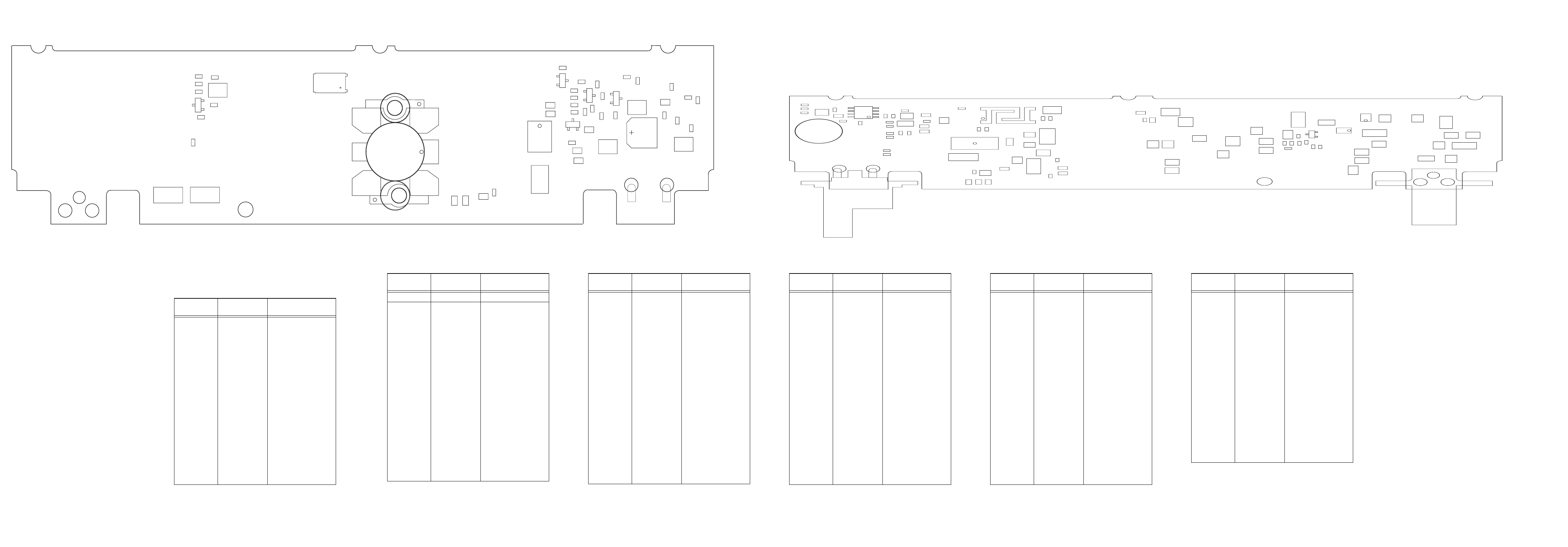
SYNTHESIZER COMPONENT LOCATIONS
HEAVY COMPONENTS SIDE
REFERENCE
SYMBOL MOTOROLA
PART NO. DESCRIPTION
CAPACITORS:
C3861 2113741F17 470 pF
C3862 2113740F42 43 pF
C3863 2113740F37 27 pF
C3864 2113740F27 10 pF
C3865 2113740F27 10 pF
C3866 2113741F17 470 pF
C3868 2113740F45 56 pF
C3869 2113740F39 33 pF
C3870 2113740F27 10 pF
C3871 2113740F29 12 pF
C3872 2113741F17 470 pF
C3873 2113740F18 4.3 pF
C3874 2113740F18 4.3 pF
C3875 2113741F17 470 pF
C3876 2113741F17 470 pF
C3877 2113741F17 470 pF
C3878 2113740F29 12 pF
C3879 2113740F34 20 pF
Synthesizer (Kit HUD4012D)
Component Locations and Parts List
C3880 2113740F21 5.6 pF
C3881 2113741F17 470 pF
C3882 2113740F07 1.5 pF
C3883 2113740F25 8.2 pF
C3884 2113741F17 470 pF
C3886 2113740F29 12 pF
C3888 2113743K15 0.1 uF
C3889 2113740F35 22 pF
C3890 2113741F17 470 pF
C3891 2113741F17 470 pF
C3892 2113740F45 56 pF
C5750 2113741F49 0.01 uF
C5751 2113743E07 0.022 uF
C5752 2113741F49 0.01 uF
C5753 2113743K07 0.047 uF
C5754 2113743E07 0.022 uF
C5755 2311049A19 10 uF
C5756 2113741F49 0.01 uF
C5757 2113743K15 0.1 uF
C5758 2113743K15 0.1 uF
C5759 2113743K15 0.1 uF
REFERENCE
SYMBOL MOTOROLA
PART NO. DESCRIPTION
C5760 2113743K15 0.1 uF
C5761 2113741F25 1000 uF
C5762 2113743E07 0.022 uF
C5763 2113741F49 0.01 uF
C5764 2311049J23 10 uF
C5765 2113743K15 0.1 uF
C5766 2311049J26 10 uF
C5767 2113743K15 0.1 uF
C5768 2113740F51 100 pF
C5769 2113741F25 1000 pF
C5770 2311049J26 10 uF
C5771 2113741F25 1000 pF
C5772 2113741F25 1000 pF
C5773 2113741F49 0.01 uF
C5774 2113741F49 0.01 uF
C5775 2109720D14 0.1 uF
C5776 2109720D14 0.1 uF
C5778 0811051A19 1 uF
C5780 2113741F25 1000 pF
C5781 2311049A07 1 uF
C5782 2113741F25 1000 pF
C5789 2113743K15 0.1 uF
C5790 2113743K15 0.1 uF
C5791 2311049J11 4.7 uF
C5792 2113743K15 0.1 uF
C5793 2113741F25 1000 pF
C5794 2113741F17 470 pF
C5795 2113740F31 15 pF
C5796 2113740F27 10 pF
C5797 2113741F17 470 pF
C5798 2113741F17 470 pF
C5799 2113741F25 1000 pF
C5800 2113743K15 0.1 uF
C5802 2113741F17 470 pF
C5803 2113740F29 12 pF
C5807 2113741F25 1000 pF
C5808 2113740F51 100 pF
C5809 2113741F25 1000 pF
C5850 2113743A19 0.1 uF
C5853 2113740F51 100 pF
DIODES:
CR3801 4880236E05 Hot Carrier
CR3802 4880236E05 Hot Carrier
CR3803 4805649Q13 Varactor
CR3804 4805649Q13 Varactor
CR3805 4805649Q13 Varactor
CR3806 4805649Q13 Varactor
CR3807 4805649Q13 Varactor
CR5750 4802233J09 Triple
SHIELDS:
E3801 2602641Y01 VCO
E5702 2602660J02
E5704 2605259V01
E5705 2602658J02
INDUCTORS:
L3801 2462587T30 1000 nH
L3802 2462587T30 1000 nH
L3804 0105950T44 Helical Coil, Square
L3805 2462587T30 1000 nH
L3806 2462587T20 270 nH
L3808 0105950T45 Helical Coil, Square
L3809 2462587T30 1000 nH
REFERENCE
SYMBOL MOTOROLA
PART NO. DESCRIPTION
L3810 2462587T13 68 nH
L3811 2462587T12 56 nH
L3812 2462587T13 68 nH
L3813 2462587T30 1000 nH
L3814 2462587T30 1000 nH
L3815 2462587T20 270 nH
L5765 L2462587T17 150 nH
L5791 2462587T16 120 nH
L5792 2462587T12 56 nH
L5793 2462587T16 120 nH
L5794 2462587T13 68 nH
TRANSISTORS:
Q3801 4813824A10 NPN
Q3802 4813824A10 NPN
Q3803 4813823A05 N-Channel RFJFET
Q3804 4813823A05 N-Channel RF JFET
Q3805 4882022N70 NPN
Q3806 4880048M01 NPN
Q3807 4880048M01 NPN
Q5750 4813824A17 PNP
Q5770 4813824A17 PNP
Q5774 4882022N70 NPN
Q5801 4882022N70 NPN
Q5802 4813827A26 NPN
RESISTORS:
R3801 0662057A83 27K
R3802 0662057A33 220
R3803 0662057A83 27K
R3804 0662057A25 100
R3805 0662057A39 390
R3806 0662057A15 39
R3807 0662057A15 39
R3808 0662057A59 2.7K
R3809 0662057A59 2.7K
R3810 0662057A77 15K
R3811 0662057A43 560
R3812 0662057A59 2.7K
R3813 0662057A59 2.7K
R3814 0662057A59 2.7K
R3815 0662057A59 2.7K
R3816 0662057A18 51
R3817 0662057A43 560
R5750 0662057A65 4.7K
R5752 0662057B02 150K
R5753 0662057B02 150K
R5754 0662057A53 1.5K
R5758 0662057A57 2.2K
R5759 0662057A35 270
R5760 0662057A49 1K
R5761 0662057A25 100
R5762 0662057A41 470
R5763 0662057A59 2.7K
R5764 0662057A53 1.5K
R5766 0662057B02 150K
R5767 0662057A35 270
R5768 0662057A59 2.7K
R5769 0662057A49 1K
R5770 0662057B47 0
R5771 0662057A43 560
R5772 0662057A18 51
R5773 0662057A25 100
R5774 0662057A09 22
R5775 0662057A35 270
R5776 0662057A35 270
REFERENCE
SYMBOL MOTOROLA
PART NO. DESCRIPTION
LIGHT COMPONENTS SIDE
SYNTHESIZER PARTS LIST
NOTES:
1. All resistance values are in ohms unless indicated otherwise.
2. Components shown on component location and schematic
diagrams but not included in parts list are not placed
This document was created with FrameMaker 4.0.3
15_Syn CL/PL p24 Page 24 Tuesday, January 19, 1999 5:06 PM
25
63A81090C73-O
Synthesizer (Kit HUD4012D) Schematic Diagram
This document was created with FrameMaker 4.0.3
26
REFERENCE
SYMBOL MOTOROLA
PART NUMBER DESCRIPTION
CAPACITORS:
C3501 2113740F25 8.2 pF
C3502 2113740A67 330 pF
C3504 2113741F49 0.01 uF
C3505 2113741F49 0.01 uF
C3521 2113740F29 12 pF
C3522 2113741F29 1500 pF
C3523 2113741F49 0.01 uF
C3524 2113740A67 330 pF
C3526 2113740A67 330 pF
C3528 2113740A67 330 pF
C3529 2113741A33 3300 pF
C3530 2113740F37 27 pF
C3541 2113740A67 330 pF
C3542 2113741A33 3300 pF
C3543 2113741A57 0.033 uF
C3545 2111078B38 68 pF
C3547 2113740A67 330 pF
C3548 2113740A67 330 pF
C3553 2113740F34 20 pF
C3554 2113740A67 330 pF
C3561 2113740A67 330 pF
C3562 2113741F25 1000 pF
C3563 2113741A33 3300 pF
C3564 2311049A45 10 uF
C3565 2111078B49 180 pF
C3567 2111078B49 180 pF
C3568 2111078B41 91 pF
C3569 2111078B59 470 pF
C3570 2111078B59 470 pF
C3571 2111078B36 56 pF
C3572 2111078B21 20 pF
C3583 2113741F49 0.01 uF
C3602 2113741F17 470 pF
C3603 2113741F49 0.01 uF
C3604 2113741F49 0.01 uF
C3605 2113741F17 470 pF
C3606 2113741F25 1000 pF
C3608 2113743K15 0.1 uF
C3609 2113741F49 0.01 uF
C3610 2113741F17 470 pF
C3612 2113741F49 0.01 uF
C3613 2113741F17 470 pF
C3614 2113741F49 0.01 uF
C3616 2113741F49 0.01 uF
C3619 2380090M24 10 uF
C3620 2113741F17 470 pF
C3621 2113741F17 470 pF
C3623 2113741F17 470 pF
C3624 2113741F17 470 pF
C3625 2113741F17 470 pF
REFERENCE
SYMBOL MOTOROLA
PART NUMBER DESCRIPTION
POWER AMPLIFIER PARTS LIST
R3501
L3501 C3530 C3606
R3615
R3527
E3501
VIEWED FROM SIDE 1
L3608
C3526
R3522
R3530
R3533
R3532
L3522
R3531
C3626
C3625
J2
C3527 L3548
L3547
C3545
C3548
C3547
C3566 C3565
C3568 L3566 C3570
C3572
C3675
L3641
L3661
CR3671
CR3642
CR3641
C3665 C3662
L3562
C3569
C3571
R3671
L3643
R3672
R3675
R3674 C3661
C3660 C3663
C3669
L3663
J1
L3664
C3664
C3667
C3666
MAEPF-26502-O
L3672
C3674
C3673
C3672
R3673
L3662
C3573
C3567
CR3601
R3502
C3501
C3502
Q3521
C3521
R3521
L3523
C3524
L3521
C3504
C3522
C3523
C3620
C3621
R3610
L3545
C3554
L3540
C3543
C3553
C3541
C3542
R3548
C3552 C3623
C3624
C3563 L3560
C3562
C3561
R3543
R3542
R3503
R3504
LIGHT COMPONENTS SIDE
HEAVY COMPONENTS SIDE
R3641
R3642
C3641
C3642
L3642
R3643 R3644
C3564
Q3561
E3503
R3586
C3528
C3604
R3603
R3604
C3603
C3610
R3602 R3608
R3601
L3605
C3612
L3603
L3607
R3525
R3526
C3583
R3583
CR3581
MAEPF-26503-O
C3529
E3504
R3544
R3545
R3585
R3541
Q3541 C3619
VR3602
C3605
Q3601
R3605
R3606
R3582
C3609
C3616
C3602
C3608
C3614
C3613
R3607
C3505
Q3501
R3676
R3677
CR3673
C3676
Power Amplifier (Kit HUE4012D)
Component Locations and Parts List
POWER AMPLIFIER COMPONENT LOCATIONS
INDUCTORS:
L3501 2460591N36 43.67 nH
L3521 2460591C23 13.85 nH
L3522 2462587T17 150 nH
L3523 2460591B80 19.61 nH
L3540 2460591B80 19.61 nH
L3545 2460591C23 13.85 nH
L3547 2460591B80 19.61 nH
L3548 2460591B80 19.61 nH
L3560 2484657R01 Ferrite Bead
L3562 2460591M77 38.13 nH
L3566 2460591M77 38.13 nH
L3603 2484657R01 Ferrite Bead
L3605 2484657R01 Ferrite Bead
L3607 2484657R01 Ferrite Bead
L3608 2484657R01 Ferrite Bead
L3641 2462587T30 1000 nH
L3642 2484657R01 Ferrite Bead
L3643 2462587T30 1000 nH
L3661 2460591W04 55nH
L3662 2460591W04 55nH
L3663 2460591W04 55nH
L3664 2462587T30 1000 nH
L3672 2462587T18 180 nH
TRANSISTORS:
Q3501 4813824A17 PNP
Q3521 4813827A26 NPN
REFERENCE
SYMBOL MOTOROLA
PART NUMBER DESCRIPTION
Q3541 4813827A36 N-Channel FET (Note 3)
Q3561 4805538W01 N-Channel FET (Note 3)
Q3601 4813824A10 NPN
RESISTORS:
R3501 0662057A01 10
R3502 0662057A25 100
R3503 0662057A01 10
R3504 0662057A56 2K
R3521 0662057A25 100
R3522 0662057A49 1K
R3525 0660081A73 10K
R3526 0660081A73 10K
R3527 0683962T51 120
R3530 0662057A18 51
R3531 0662057A18 51
R3532 0605057A18 51
R3533 0662057A18 51
R3542 0683962T51 120
R3543 0680194M18 51
R3545 0660081A73 10K
R3548 0662057A49 1K
R3582 0662057A81 22K
R3583 0660081A73 10K
R3585 0662057A89 47K
R3586 0660081A73 10K
R3601 0662057C01 0
R3603 0662057A49 1K
REFERENCE
SYMBOL MOTOROLA
PART NUMBER DESCRIPTION
R3604 0662057A56 2K
R3605 0662057A49 1K
R3606 0662057A37 330
R3607 0662057A25 100
R3608 0662057A25 100
R3610 0680149M02 100K Thermistor
R3615 1705603W01 30 m Shunt
R3641 0662057A01 10
R3642 0662057A01 10
R3643 0680194M18 51
R3644 0680194M18 51
R3671 0662057A84 30K
R3672 0662057A53 1.5K
R3673 0683962T51 120
R3674 0662057A49 1K
R3675 0662057A43 560
R3676 0662057A57 2.2K
R3677 0662057A25 100
PRINTED CIRCUIT
BOARD (For Reference
Only):
8402573Y06
and
8402573Y09
For Kit HUD4012D
REFERENCE
SYMBOL MOTOROLA
PART NUMBER DESCRIPTION
C3626 2113741F49 0.01 uF
C3641 2113741F25 1000 pF
C3642 2113741F25 1000 pF
C3661 2111078B18 15 pF
C3662 2111078B32 39 pF
C3663 2111078B32 39 pF
C3664 2111078B18 15 pF
C3666 2111078B59 470 pF
C3667 2111078B59 470 pF
C3672 2113741F25 1000 pF
C3673 2113740F35 22 pF
C3674 2113741F25 1000 pF
C3675 2113740F29 12 pF
C3676 2113741F25 1000 pF
DIODES:
CR3601 4880222R01 Reverse Polarity
CR3641 4802482J02 PIN
CR3642 4802482J02 PIN
CR3671 4880236E05 Hot Carrier
CR3673 4880236E05 Hot Carrier
SHIELD:
E3501 2602604Y01 Heat Spreader, RF
Power Amplifier
CONNECTORS:
J1 0905901V06
Antenna
J2 0905902V04
DC Power
REFERENCE
SYMBOL MOTOROLA
PART NUMBER DESCRIPTION
NOTES:
1. All resistance values are in ohms unless indicated otherwise.
2. Components shown on component location and schematic
diagrams but not included in parts list are not placed.
3. When replacing transistors Q3541 or Q3561, perform Q3541 or
Q3561 bias measurement and adjustment procedure on page
28.
This document was created with FrameMaker 4.0.3
17_PA CL/PL p26 Page 26 Tuesday, January 19, 1999 5:08 PM
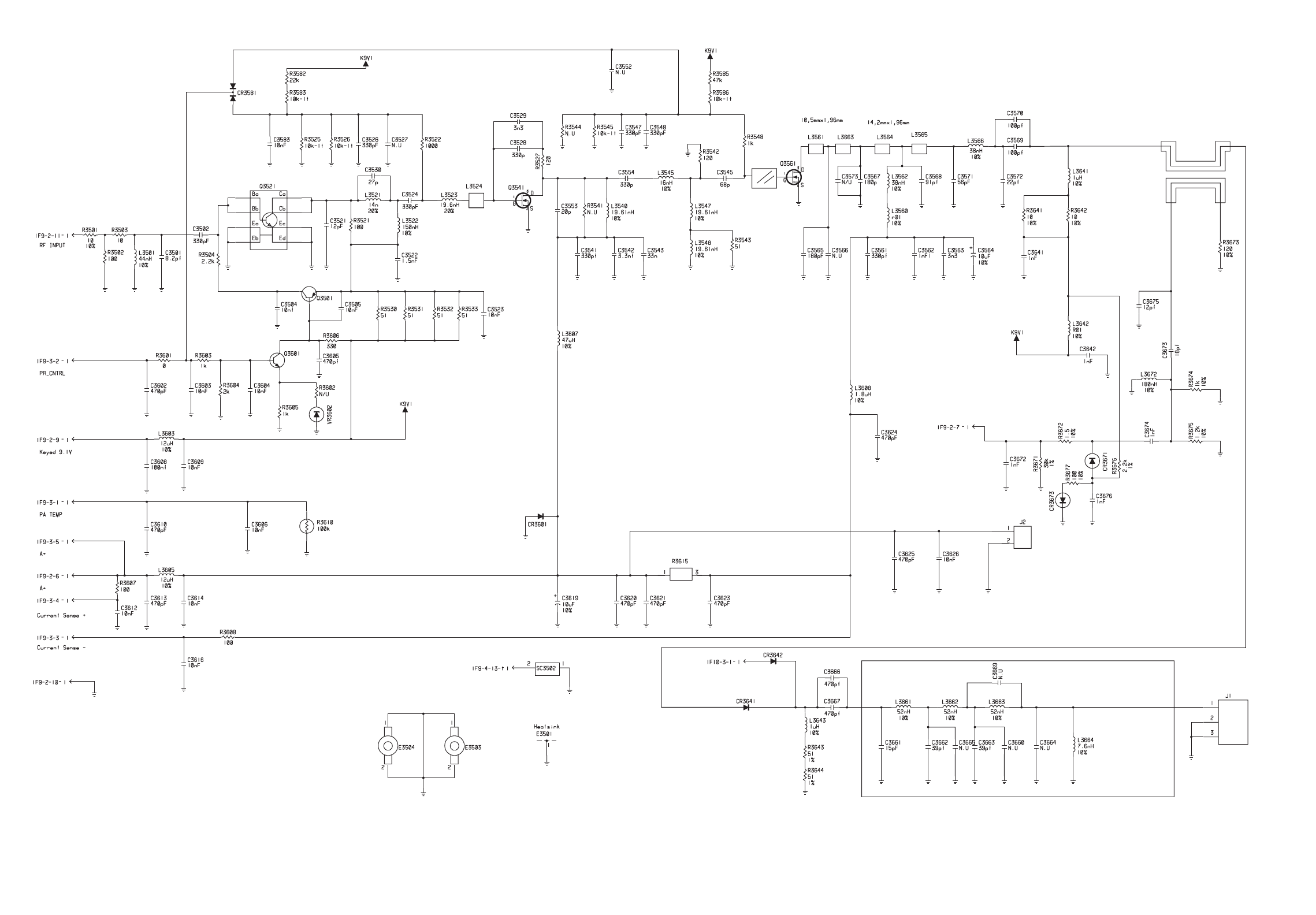
27
DEPC-97139-O/None
Power Amplifier (Kit HUD4012D) Schematic Diagram
This document was created with FrameMaker 4.0.3
28
Q3541 Bias Measurement and Adjustment Procedure:
1. Disconnect A+ supply from radio.
2. Remove resistor R3503 and ferrite bead L3607 from PCB.
3. On PCB, tack solder wires onto pads for L3607 temporarily and connect the wires to a digital milliammeter.
4. Reconnect A+ supply to radio. Set A+ supply to 13.6 volts, and current limit to 4.0 Amperes.
5. Key up transmitter and observe current indicated on milliammeter. If current is between 120 and 180
milliamperes, skip to step 14. Otherwise, proceed to step 6.
6. Dekey transmitter and disconnect A+ supply from radio.
7. Remove trim resistors R3525 and R3526 from PCB.
8. Place a 10K Ohm resistor in place of R3525.
9. Reconnect A+ supply to radio. Set A+ supply to 13.6 volts, and current limit to 4.0 Amperes.
10. Key up transmitter and observe current indicated on milliammeter. If current is between 120 and 180
milliamperes, skip to step 14. Otherwise, proceed to step 11.
11. Dekey transmitter and disconnect A+ supply from radio.
12. If current observed in step 10 is less than 120 milliamperes, replace R3525 with next higher standard value
(i.e., 12K) and repeat steps 9 and 10. Otherwise, proceed to step 13.
13. If current observed in step 10 is more than 180 milliamperes, replace R3525 with next lower standard value
(i.e., 9.1K) and repeat steps 9 and 10.
14. Dekey transmitter, disconnect A+ supply from radio, and disconnect milliammeter wires from PCB.
15. Reinstall R3503 and L3607 on PCB.
Q3561 Bias Measurement and Adjustment Procedure:
1. Disconnect A+ supply from radio.
2. Remove resistor R3503 and ferrite bead L3560 from PCB.
3. On PCB, tack solder wires onto pads for L3560 temporarily and connect the wires to a digital milliammeter.
4. Reconnect A+ supply to radio. Set A+ supply to 13.6 volts, and current limit to 4.0 Amperes.
5. Key up transmitter and observe current indicated on milliammeter. If current is between 1400 and 2200
milliamperes, skip to step 14. Otherwise, proceed to step 6.
6. Dekey transmitter and disconnect A+ supply from radio.
7. Remove trim resistor R3545 from PCB.
8. Place a 10K Ohm resistor in place of R3545.
9. Reconnect A+ supply to radio. Set A+ supply to 13.6 volts, and current limit to 4.0 Amperes.
10. Key up transmitter and observe current indicated on milliammeter. If current is between 1400 and 2200
milliamperes, skip to step 14. Otherwise, proceed to step 11.
11. Dekey transmitter and disconnect A+ supply from radio.
12. If current observed in step 10 is less than 1400 milliamperes, replace R3545 with next higher standard value
(i.e., 12K) and repeat steps 9 and 10. Otherwise, proceed to step 13.
13. If current observed in step 10 is more than 2200 milliamperes, replace R3545 with next lower standard value
(i.e., 9.1K) and repeat steps 9 and 10.
14. Dekey transmitter, disconnect A+ supply from radio, and disconnect milliammeter wires from PCB.
15. Reinstall R3503 and L3560 on PCB.
Note
In step 12 and/or 13, if the required current level of 120- to 180-milliamperes can-
not be obtained using a standard value resistor for R3525, place a resistor on pads
for R3526 to form a parallel resistance network with R3525. The parallel resistance
(R) of R3525 and R3526 is: R= R3525 * R3526/(R3525 + R3526).
Note
In step 12 and/or 13, if the required current level of 1400- to 2200-milliamperes
cannot be obtained using a standard value resistor for R3545, place a resistor on
pads for R3544 to form a parallel resistance network with R3545. The parallel
resistance (R) of R3544 and R3545 is: R= R3544 * R3544/R3544 + R3545.

29
1
Table 1:
Schematic Diagram Interconnection List
From/To From/To
Node Signal Name Schematic Diagram
Title Publication Node Signal Name Schematic Diagram
Title Publication
IF1-2-12 AUDIO_MOD Main Controller Block
Diagram
68P81083C20 IF1-2-12 AUDIO_MOD Receiver IF 68P81080C48
IF1-2-13 ROSC_SEL Main Controller Block
Diagram
68P81083C20 IF1-2-13 ROSC_SEL Receiver IF 68P81080C48
IF1-2-14 GND Main Controller Block
Diagram
68P81083C20 IF1-2-14 GND Receiver IF 68P81080C48
IF1-2-15 9V3 Main Controller Block
Diagram
68P81083C20 IF1-2-15 9.3V Receiver Front End
and Receiver IF
68P81080C48
IF1-2-16 PA_CNTL_LIM Main Controller Block
Diagram
68P81083C20 IF1-2-16 Not Indicated Receiver IF 68P81080C48
IF1-2-17 SQUELCH Main Controller Block
Diagram
68P81083C20 IF1-2-17 SQUELCH Receiver IF 68P81080C48
IF1-2-18 ZIF_SEL Main Controller Block
Diagram
68P81083C20 IF1-2-18 ZIF_SEL Receiver IF 68P81080C48
IF1-2-19 DUPLEX_SYN_SEL Main Controller Block
Diagram
68P81083C20 IF1-2-19 Not Indicated Receiver IF 68P81080C48
IF1-3-1 DUPLEX_LOCK_DET Main Controller Block
Diagram
68P81083C20 IF1-3-1 Not Indicated Receiver IF 68P81080C48
IF1-3-2 DISC Main Controller Block
Diagram
68P81083C20 IF1-3-2 DISC Receiver IF 68P81080C48
IF1-3-3 RSSI Main Controller Block
Diagram
68P81083C20 IF1-3-3 RSSI Receiver IF 68P81080C48

30
IF1-3-4 SDATA Main Controller Block
Diagram
68P81083C20 IF1-3-4 SPI TX DATA Receiver IF 68P81080C48
IF1-3-5 SCLK Main Controller Block
Diagram
68P81083C20 IF1-3-5 CLK Receiver IF 68P81080C48
IF1-3-6 RX_CNTL_I_SRC Main Controller Block
Diagram
68P81083C20 IF1-3-6 Not Indicated Receiver Front End 68P81080C48
IF1-3-7 GND Main Controller Block
Diagram
68P81083C20 IF1-3-7 GND Receiver IF 68P81080C48
IF1-3-8 2.1MHz Main Controller Block
Diagram
68P81083C20 IF1-3-8 2.1MHz Receiver IF 68P81080C48
IF1-3-9 GND Main Controller Block
Diagram
68P81083C20 IF1-3-9 GND Receiver IF 68P81080C48
IF1-3-10 SYN_SEL Main Controller Block
Diagram
68P81083C20 IF1-3-10 SYN_SEL Receiver IF 68P81080C48
IF1-3-11 LOCK_DET Main Controller Block
Diagram
68P81083C20 IF1-3-11 LOCK_DET Receiver IF 68P81080C48
IF1-3-30 Not Indicated Synthesizer 68P81080C48 IF1-3-30 Not Indicated Receiver IF 68P81080C48
IF2-2-6 A+ Synthesizer 68P81080C48 IF2-2-6 A+_CONT Main Controller Block
Diagram
68P81083C20
IF2-2-7 V_FORWARD Synthesizer 68P81080C48 IF2-2-7 V_FORWARD Main Controller Block
Diagram
68P81083C20
IF2-2-8 V_DRIVE Synthesizer 68P81080C48 IF2-2-8 V_CNTL Main Controller Block
Diagram
68P81083C20
IF2-2-9 K9.1 Synthesizer 68P81080C48 IF2-2-9 K9V1 Main Controller Block
Diagram
68P81083C20
IF2-2-10 GND Synthesizer 68P81080C48 IF2-2-10 GND
Table 1:
Schematic Diagram Interconnection List
From/To From/To
Node Signal Name Schematic Diagram
Title Publication Node Signal Name Schematic Diagram
Title Publication

31
IF2-2-12 GND Synthesizer 68P81080C48
IF2-3-1 PA Temp Synthesizer 68P81080C48 IF2-3-1 PA_TEMP Main Controller Block
Diagram
68P81083C20
IF2-3-2 PA_CONTRL Synthesizer 68P81080C48 IF2-3-2 PA_CNTL Main Controller Block
Diagram
68P81083C20
IF2-3-3 Current_Sense- Synthesizer 68P81080C48 IF2-3-3 CURRENT_SENSE_- Main Controller Block
Diagram
68P81083C20
IF2-3-4 Current_Sense+ Synthesizer 68P81080C48 IF2-3-4 CURRENT_SENSE_+ Main Controller Block
Diagram
68P81083C20
IF2-3-5 A+ Synthesizer 68P81080C48 IF2-3-5 A+_CONT Main Controller Block
Diagram
68P81083C20
IF2-3-13 GND Synthesizer 68P81080C48
IF2-3-14 GND Synthesizer 68P81080C48
IF2-4-11 GROUND Synthesizer 68P81080C48 IF2-4-11 GROUND Main Controller Block
Diagram
68P81083C20
IF3-2-1 ZIF_SEL Receiver IF 68P81080C48 IF3-2-1 ZIF_SEL Receiver Back End 68P81080C48
IF3-2-6 SQUELCH Receiver IF 68P81080C48 IF3-2-6 SQUELCH Receiver Back End 68P81080C48
IF3-2-9 IF OUT Receiver IF 68P81080C48 IF3-2-9 IF_OUT Receiver Back End 68P81080C48
IF3-2-13 Not Indicated Receiver Back End 68P81080C48 IF3-2-13 ZIF_ST_LOG Receiver Back End 68P81080C48
IF3-3-2 CLK Receiver IF 68P81080C48 IF3-3-2 CLK Receiver Back End 68P81080C48
IF3-3-3 SPI TX DATA Receiver IF 68P81080C48 IF3-3-3 SPI_TX_DATA Receiver Back End 68P81080C48
IF3-3-4 DISC Receiver IF 68P81080C48 IF3-3-4 DISC Receiver Back End 68P81080C48
IF3-3-5 2.1MHz Receiver IF 68P81080C48 IF3-3-5 2.1Mhz Receiver Back End 68P81080C48
IF3-3-7 RSSI Receiver IF 68P81080C48 IF3-3-7 RSSI Receiver Back End 68P81080C48
Table 1:
Schematic Diagram Interconnection List
From/To From/To
Node Signal Name Schematic Diagram
Title Publication Node Signal Name Schematic Diagram
Title Publication

32
IF3-4-8 Not Indicated Receiver Front End 68P81080C48 IF3-4-8 RF_REG_5V Receiver Back End 68P81080C48
IF4-1-6 Mod In Synthesizer 68P81080C48 IF4-1-6 AUDIO MOD Receiver IF 68P81080C48
IF4-2-7 2.1 MHz Synthesizer 68P81080C48 IF4-2-7 2.1MHz Receiver IF 68P81080C48
IF4-3-1 CLK Synthesizer 68P81080C48 IF4-3-1 CLK Receiver IF 68P81080C48
IF4-3-3 LOCK DET Synthesizer 68P81080C48 IF4-3-3 LOCK_DET Receiver IF 68P81080C48
IF4-3-4 FRACN CE Synthesizer 68P81080C48 IF4-3-4 SYN_SEL Receiver IF 68P81080C48
IF4-3-9 Data Synthesizer 68P81080C48 IF4-3-9 SPI TX DATA Receiver IF 68P81080C48
IF4-4-2 +9.3V Synthesizer 68P81080C48 IF4-4-2 9.3V Receiver IF 68P81080C48
IF4-4-5 PEND CE Synthesizer 68P81080C48 IF4-4-5 ROSC_SEL Receiver IF 68P81080C48
IF4-4-8 REG 5V Synthesizer 68P81080C48 IF4-4-8 Regulated 5V Receiver Front End 68P81080C48
IF5-1-1 GND Receiver IF 68P81080C48
IF5-2-3 Jumper Receiver IF 68P81080C48 1F1-2-16
IF5-3-3 GND Receiver IF 68P81080C48
IF5-4-4 GND Receiver IF 68P81080C48
IF7-1-11 SPK+ Main Controller Block
Diagram
68P81083C20 IF7-1-11 SPK+ Controller Power
Control
68P81083C20
IF7-1-12 SPK- Main Controller Block
Diagram
68P81083C20 IF7-2-12
IF7-1-15 PA_CNTL Main Controller Block
Diagram
68P81083C20 IF2-3-2
IF7-1-17 GND Main Controller Block
Diagram
68P81083C20 IF7-1-17 GND Controller Power
Control
68P81083C20
IF7-1-23 PWR_RST Main Controller Block
Diagram
68P81083C20 IF7-1-23 PWR_RST Controller Power
Control
68P81083C20
Table 1:
Schematic Diagram Interconnection List
From/To From/To
Node Signal Name Schematic Diagram
Title Publication Node Signal Name Schematic Diagram
Title Publication

33
IF7-1-31 TEMP_GND Main Controller Block
Diagram
68P81083C20
IF7-2-3 V_CNTL IF7-2-3 V_CNTL Controller Power
Control
68P81083C20
IF7-2-4 V_FORWARD Main Controller Block
Diagram
68P81083C20 IF7-2-4 V_FORWARD Controller Power
Control
68P81083C20
IF7-2-7 UNSW_5V Main Controller Block
Diagram
68P81083C20 IF7-2-7 UNSW_5V Controller Power
Control
68P81083C20
IF7-2-8 CL_UNSW_5V Main Controller Block
DIagram
68P81083C20 IF7-2-8 CL_UNSW_5V Controller Power
Control
68P81083C20
IF7-2-10 RX_AUDIO, IF7-4-10 Main Controller Block
Diagram
68P81083C20
IF7-2-12 SPK-, IF7-1-12 Main Controller Block
Diagram
68P81083C20
IF7-2-13 CURRENT_SENSE_+ Main Controller Block
Diagram
68P81083C20 IF7-2-13 CURRENT_SENSE_+ Controller Power
Control
68P81083C20
IF7-2-20 CLEAR IF7-2-20 CLEAR Controller Power
Control
68P81083C20
IF7-2-21 B+_IGNITION Main Controller Block
Diagram
68P81083C20 IF7-2-21 B+_IGNITION Controller Power
Control
68P81083C20
IF7-2-24 A+ Main Controller Block
Diagram
68P81083C20
IF7-2-25 A+_CONT Main Controller Block
Diagram
68P81083C20 IF7-2-25 A+_CONT Controller Power
Control
68P81083C20
IF7-2-26 9V3 Main Controller Block
DIagram
68P81083C20 IF7-2-26 9V3 Controller Power
Control
68P81083C20
IF7-2-27 SW_B+ Main Controller Block
Diagram
68P81083C20 IF7-2-27 SW_B+ Controller Power
Control
68P81083C20
Table 1:
Schematic Diagram Interconnection List
From/To From/To
Node Signal Name Schematic Diagram
Title Publication Node Signal Name Schematic Diagram
Title Publication

34
IF7-2-28 Vdd Main Controller Block
Diagram
68P81083C20 IF7-2-28 Vdd Controller Power
Control
68P81083C20
IF7-2-29 SW_B+ Controller Power
Control
68P81083C20 IF7-2-27
IF7-2-30 9V4 IF7-2-30 9V3 Controller Power
Control
68P81083C20
IF7-3-5 K9V1 Main Controller Block
Diagram
68P81083C20 IF7-3-5 K9V1 Controller Power
Control
68P81083C20
IF7-3-6 PA_TEMP Main Controller Block
Diagram
68P81083C20 IF7-3-6 PA_TEMP Controller Power
Control
68P81083C20
IF7-3-14 CURRENT_SENSE - Controller Power
Control
68P81083C20 IF2-3-3
IF7-3-15 PA_CNTL Controller Power
Control
68P81083C20 IF2-3-2
IF7-3-18 Vaud Main Controller Block
Diagram
68P81083C20 IF7-3-18 Vaud Controller Power
Control
68P81083C20
IF7-3-22 +5V Controller Power
Control
68P81083C20 IF7-4-22
IF7-4-1 VFWD_BUF Main Controller Block
Diagram
68P81083C20 IF7-4-1 VFWD_BUF Controller Power
Control
68P81083C20
IF7-4-2 VSUM Main Controller Block
Diagram
68P81083C20 IF7-4-2 VSUM Controller Power
Control
68P81083C20
IF7-4-9 AUPA_EN Main Controller Block
Diagram
68P81083C20 IF7-4-9 AUPA_EN Controller Power
Control
68P81083C20
1F7-4-10 RX_AUDIO 1F7-2-10
1F7-4-14 CURRENT_SENSE Main Controller Block
Diagram
68P81083C20 1F2-3-3
1F7-4-16 A+
Table 1:
Schematic Diagram Interconnection List
From/To From/To
Node Signal Name Schematic Diagram
Title Publication Node Signal Name Schematic Diagram
Title Publication

35
1F7-4-19 B+_ON_OFF Main Controller Block
Diagram
68P81083C20
IF7-4-22 +5V Main Controller Block
Diagram
68P81083C20 IF7-3-22,
IF7-4-24
A+ Controller Power
Control
68P81083C20
IF8-2-2 K9V1 Receiver Front End 69P81080C48 1F8-4-2 Synthesizer 68P81080C48
IF8-3-1 Rx Inj Synthesizer 68P81080C48 IF8-3-1 Not Indicated Receiver Front End 68P81080C48
IF8-4-2 K9.1 Synthesizer 68P81080C48 1F9-2-9 Synthesizer 68P81080C48
IF9-2-6 A+ Power Amplifier 68P81080C48 IF9-2-6 A+ Synthesizer 68P81080C48
IF9-2-7 Not indicated Power Amplifier 68P81080C48 IF9-2-7 V_FORWARD Synthesizer 68P81080C48
IF9-2-8 V_DRIVE Synthesizer 68P81080C48 IF2-2-8
IF9-2-9 Keyed 9.1V Power Amplifier 68P81080C48 IF9-2-9 K9.1 Synthesizer 68P81080C48
IF9-2-10 GND Power Amplifier 68P81080C48 IF9-2-10 GROUND Synthesizer 68P81080C48
IF9-2-11 RF Input Power Amplifier 68P81080C48 IF9-2-11 Tx Inj Synthesizer 68P81080C48
IF9-3-1 PA TEMP Power Amplifier 68P81080C48 IF9-3-1 PA Temp Synthesizer 68P81080C48
IF9-3-2 PA_CNTL Power Amplifier 68P81080C48 IF9-3-2 PA_CONTRL Synthesizer 68P81080C48
IF9-3-3 Current Sense - Power Amplifier 68P81080C48 IF9-3-3 Current_Sense- Synthesizer 68P81080C48
IF9-3-4 Current Sense + Power Amplifier 68P81080C48 IF9-3-4 Current_Sense+ Synthesizer 68P81080C48
IF9-3-5 A+ Power Amplifier 68P81080C48 IF9-3-5 A+ Synthesizer 68P81080C48
IF9-4-13 Not indicated Power Amplifier 68P81080C48 IF9-4-13 Not Indicated Synthesizer 68P81080C48
IF10-3-1 Not indicated Power Amplifier 68P81080C48 IF10-3-1 Not Indicated Receiver Front End 68P81080C48
Table 1:
Schematic Diagram Interconnection List
From/To From/To
Node Signal Name Schematic Diagram
Title Publication Node Signal Name Schematic Diagram
Title Publication

36
NOTES
SERVICE MANUAL QUESTIONNAIRE
We believe that reports from users provide valuable information for producing quality manuals.
By taking a few moments to answer the following questions as they relate to this specific man-
ual, you can take an active role in the continuing effort to ensure that our manuals contain the
most accurate and complete information of benefit to you. Thank you for your cooperation.
In reference to Manual Number: 68P81080C48-C
MCS 2000™ Mobile Radio
1. Please check all the appropriate boxes:
2. How would you rate the overall organization of this manual?
excellent very good good fair poor
3. Did this Service manual provide you with the information necessary to service and maintain
the specific equipment?
very much so generally yes to some extent no
4. How do you rate this particular Service Manual?
excellent very good good fair poor
5. We would appreciate any corrections or recommendations for improving this manual. Please
include the specific page number(s) of the diagram or procedure in question.
a. Disassembly Procedures:(Page No. __________ )
b. Alignment Procedures:(Page No. __________ )
c. Exploded Views:(Page No. __________ )
Complete
Incomplete
Correct
Incorrect
Clear
Confusing
Size
Adequate
Size
Too Small
Not Covered
in This Manual
Disassembly
Procedures
Alignment
Procedures
Exploded
Views
Schematic
Diagrams
Circuit Board
Details
Electrical Parts
Lists
Exploded View
Parts List
Cut along dotted line
FOLD FOLD
(Continued)
Please specify the page number along with any corrections or recommendations for improvement.
d. Schematic Diagrams: (Page No. __________ )
e. Component Location Details: (Page No. __________ )
f. Electrical Parts List: (Page No. __________ )
g. Exploded View Parts List: (Page No. __________ )
6. General comments/suggestions:
Name:............................................................................................................................................
Company:......................................................................................................................................
Customer COSC MSS FTR Other
Address: ........................................................................................................................................
City/State/Zip:................................................................................................................................
Phone Number (Please include Area Code): ................................................................................
PLEASE USE TAPE TO SEAL
POSTAL REGULATIONS PROHIBIT USE OF STAPLES
NO POSTAGE
NECESSARY
IF MAILED
IN THE
UNITED STATES
BUSINESS REPLY MAIL
FIRST CLASS MAIL PERMIT NO 9040 FT. LAUDERDALE, FL
POSTAGE WILL BE PAID BY ADDRESSEE
Attention: Media and Communication
8000 W. Sunrise Boulevard
Ft. Lauderdale, FL 33322

1
REPLACEMENT PARTS ORDERING
ORDERING INFORMATION
MAIL ORDERS
Send written orders to the following addresses:
TELEPHONE ORDERS
United States and Canada Accessories and Aftermarket Division: Servicers Training (VHS Video Tapes):
Call: 1-800-422-4210 Call: 847-576-2828
1-800-826-1913 (For Federal Government Orders)
1-847-538-8023 (International Orders)
FAX ORDERS
United States and Canada Accessories and Aftermarket Division: Federal Government Orders:
FAX: 847-538-8198 (Domestic) FAX: 410-712-4991
847-576-3023 (International) International: 410-712-6200
Parts ID: 847-538-8194
PARTS CUSTOMER SERVICE PRODUCT CUSTOMER SERVICE
When ordering replacement parts or equipment
information, the complete identification number
should be included. This applies to all components,
kits, and chassis. If the component part number is
not known, the order should include the number of
the chassis or kit of which it is a part, and sufficient
description of the desired component to identify it.
Crystal and channel element orders should specify
the crystal or channel element type number, crystal
and carrier frequency, and the model number in
which the part is used.
Replacement Parts/
Test Equipment/Manuals/
Crystal Service Items:
Motorola Inc.
United States and Canada
Accessories and Aftermarket
Division
Attention: Order Processing
1313 E. Algonquin Road
Schaumburg, IL 60196
Federal Government Orders:
Motorola Inc.
United States and Canada
Accessories and Aftermarket
Division
Attention: Order Processing
7230 Parkway Drive
Landover, MD 21076
International Orders:
Motorola Inc.
United States and Canada
Accessories and Aftermarket
Division
Attention: International Order
Processing
1313 E. Algonquin Road
Schaumburg, IL 60196
United States and Canada Accessories and
Aftermarket Division:
Call: 1-800-422-4210
Parts Identification:
Call: 847-538-0021
Customer Response Center
(Sales and Service Assistance):
Call: 1-800-247-2346
FAX: 1-800-232-9272
TEPF-9679-T

MCS 2000 Mobile Radio Service Instructions
Publication Number 68P81080C48-O
6881080C48-O
VHF Frequency Range, 25W Specific
