TWR KE18F User's Guide MKE1x F TWRKE18F User
User Manual:
Open the PDF directly: View PDF ![]() .
.
Page Count: 16

© 2016 NXP B.V.
TWR-KE18F User's Guide
1. Introduction
The NXP Tower development platform is a set of
software and hardware tools for evaluation and
development. It is an ideal tool for the rapid prototyping
of microcontroller-based applications.
The TWR-KE18F supports a power supply voltage
range from 3.3 V to 5 V. It features a MKE18F16, a
device featuring a maximum operating frequency of
168 MHz, up to 512 KB Flash size, and numerous
analog and digital peripherals.
The TWR-KE18F includes the ARM® open standard
embedded serial and debug adapter known as
OpenSDA(CMSIS-DAP). This circuit offers the user
several options for serial communications, flash
programming, and run-control debugging.
The TWR-KE18F microcontroller module is designed
to work either in standalone mode or as part of the NXP
Tower System, a modular development platform that
enables rapid prototyping and tool re-use through
reconfigurable hardware.
There are many software development tool options
available to the user. Choices include Kinetis Design
Studio (KDS), IAR Embedded Workbench, and Keil
MDK featuring the µVision IDE.
All of these features combine to give users the Tower
needed to rapidly prototype many embedded designs: a
powerful microcontroller built on a very low-power
core and SOC platform, easy-access to I/O with a large
NXP Semiconductors
Document Number: TWRKE18FUG
User's Guide
Rev. 0
,
09/2016
Contents
1. Introduction .................................................................... 1
2. Getting Started ................................................................ 2
3. TWR-KE18F Features ..................................................... 2
4. TWR-KE18F Hardware Description ................................ 4
4.1. Power supply ........................................................ 4
4.2. OpenSDA circuit (CMSIS-DAP) ........................... 5
4.3. Microcontroller ..................................................... 7
4.4. Sensor .................................................................. 9
4.5. Infrared port ....................................................... 10
4.6. CAN transceiver ................................................. 11
4.7. Potentiometer, thermistor, pushbuttons, and LEDs 12
4.8. FlexIO header ..................................................... 12
5. Default Jumper Setting .................................................. 13
6. References .................................................................... 14
7. Revision History ........................................................... 15

TWR-KE18F Features
TWR-KE18F User's Guide, Rev. 0, 09/2016
2 NXP Semiconductors
ecosystem of compatible hardware, a flexible programming and debug interface, and a large ecosystem
of software development environments.
2. Getting Started
Refer to the TWR-KE18F Quick Start Package for step-by-step instructions for getting started with the
Tower board. See the “Jump Start Your Design” section at nxp.com/TWR-KE18F for the Quick Start
Package and software lab guides.
3. TWR-KE18F Features
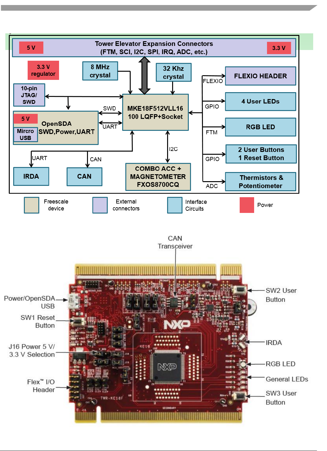
The TWR-KE18F hardware is a NXP Tower development board assembled with the following features:
• MKE18F512VLL16 MCU (168 MHz core clock, 512 KB flash, 64 KB RAM, 100LQFP
package)
• Tower-compatible processor board
• Onboard OpenSDA (CMSIS-DAP) circuit: K20DX128VFM5 with debug and virtual serial port
• Four user-controlled status LEDs and one RGB LED
• Two mechanical push buttons and one reset button
• I/O headers for easy access to MCU I/O pins
• Thermistors and potentiometer
• FXOS8700CQ 3D accelerometer + 3D magnetometer
• Board power select with 3.3 V or 5 V MCU operation
• Infrared port communication
• CAN transceiver
• Flex™ I/O header
The TWR-KE18F features two MCUs: The target MCU is the MKE18F512VLL16. The
OpenSDA(CMSIS-DAP) MCU is the MK20DX128VFM5.
Figure 1 shows the block diagram of the TWR-KE18F board. The primary components and their
location on the hardware assembly are shown in Figure 2 and Figure 3.
TWR-KE18F Features
TWR-KE18F User's Guide, Rev. 0, 09/2016
NXP Semiconductors 3
Figure 1. TWR-KE18F block diagram
Figure 2. Front Side of TWR-KE18F
TWR-KE18F Hardware Description
TWR-KE18F User's Guide, Rev. 0, 09/2016
4 NXP Semiconductors
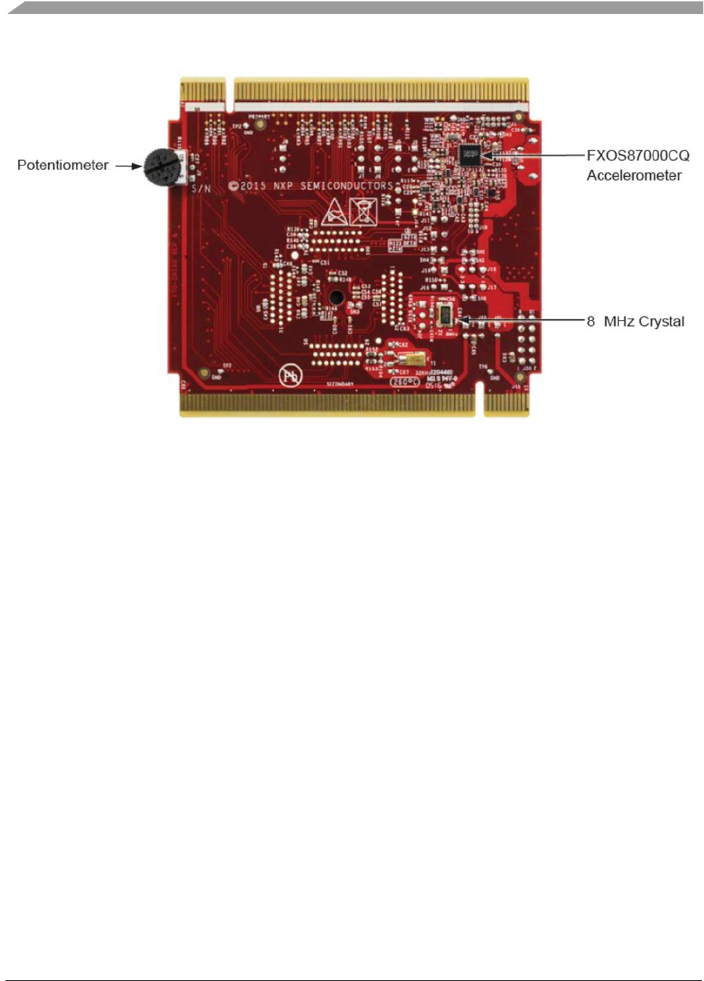
Figure 3. Back Side of TWR-KE18F
4. TWR-KE18F Hardware Description
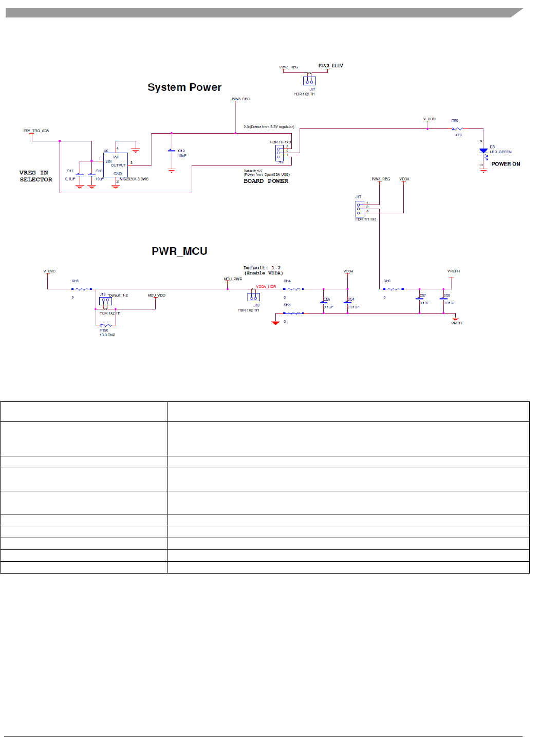
4.1. Power supply
When TWR-KE18F is installed into the Tower System, the board power supply can be either from an
on-board source (CMSIS-DAP USB connector) or from another source through Tower Elevator. By
default, in stand-alone operation, the TWR-KE18F board power source is 5.0 V, which is derived from
the CMSIS-DAP USB microB connector J2. One low-dropout regulator U6 provides 3.3 V supply from
the 5.0 V input voltage. All of the user-selectable power options for peripherals can be configured by
headers. Refer to the default headers setting table section 5.
The following figure shows the schematic drawing for the power supply inputs and the on-board voltage
regulator.
TWR-KE18F Hardware Description
TWR-KE18F User's Guide, Rev. 0, 09/2016
NXP Semiconductors 5
Figure 4. Power supply
The following table lists some power sources descriptions.
Table 1. TWR-KE18F power sources
Power Source Name
Description
P5V_TRG_SDA
Output of USB power switch controlled by the VTRG_EN signal from the OpenSDA
and the ELE_PS_SENSE signal from the TWR elevator connectors. Goes to
regulator input select header.
P5V_ELEV
Power to the elevator boards.
P3V3_REG
Output of 3.3 V regulator or from the Elevator connectors. May also be supplied
externally by connecting to the board voltage select header.
V_BRD
Output of 3.3 V or 5 V regulators as selected by the board voltage select header. May
also be supplied externally by connecting to the board voltage select header.
VREG_IN
Power into the on board voltage regulators.
MCU_PWR
MCU digital power. Filtered from V_BRD.
MCU_VDD
MCU digital power input after current measurement jumper.
VDDA
VDDA power for MCU and analog circuits. Filtered from MCU_PWR.
VREFH
Upper reference voltage for ADC on the MCU. Filtered from VDDA.
4.2. OpenSDA circuit (CMSIS-DAP)
The OpenSDA circuit (CMSIS–DAP) is an open-standard serial and debug adapter. It bridges serial and
debug communications between a USB host and an embedded target processor as shown in Figure 5.
CMSIS-DAP features a mass storage device (MSD) bootloader, which provides a quick and easy
mechanism for loading different CMSIS-DAP Applications such as flash programmers, run-control
debug interfaces, serial-to-USB converters, and more. Two or more CMSIS-DAP applications can run
simultaneously. For example, run-control debug application and serial-to-USB converter runs in parallel
to provide a virtual COM communication interface while allowing code debugging via CMSIS-DAP
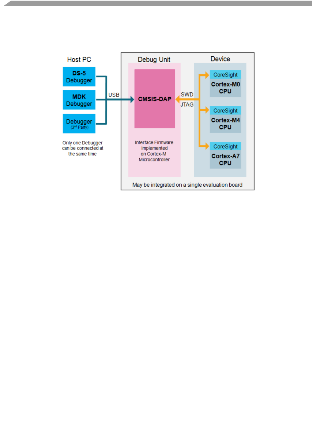
TWR-KE18F Hardware Description
TWR-KE18F User's Guide, Rev. 0, 09/2016
6 NXP Semiconductors
with just single USB connection. These two applications are provided in a single code package. Refer to
the CMSIS-DAP User’s Guide for more details.
Figure 5. CMSIS-DAP block diagram
CMSIS-DAP is managed by a Kinetis K20 MCU built on the ARM Cortex-M4 core. The CMSIS-DAP
circuit includes a status LED (D1) and a RESET pushbutton (SW1). The pushbutton asserts the Reset
signal to the KE18F target MCU. It can also be used to place the CMSIS-DAP circuit into bootloader
mode by holding down the RESET pushbutton while plugging the USB cable to USB connector J2.
Once the CMSIS-DAP enters bootloader mode, other CMSIS-DAP applications such as debug app can
be programmed. SPI and GPIO signals provide an interface to the SWD debug port of the KE18F.
Additionally, signal connections are available to implement a UART serial channel. The CMSIS-DAP
circuit receives power when the USB connector is plugged into a USB host.
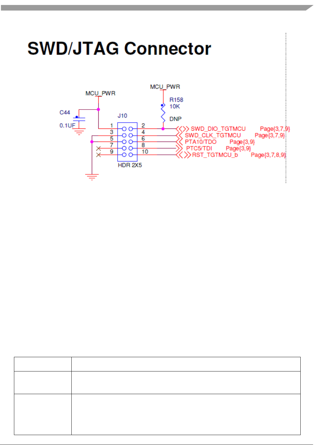
4.2.1. Debug interface
Signals with SPI and GPIO capability are used to connect directly to the SWD of the KE18F. These
signals are also brought out to a standard 10-pin Cortex Debug connector (J10) as shown in Figure 6.
The user could use J10 to debug and download code to KE18F with this SWD/JTAG interface.
TWR-KE18F Hardware Description
TWR-KE18F User's Guide, Rev. 0, 09/2016
NXP Semiconductors 7
Figure 6. SWD/JTAG debug connector
4.2.2. Virtual serial port
A serial port connection is available between the CMSIS-DAP MCU and pins PTB1 and PTB0 of the
KE18F. Several of the default CMSIS-DAP applications provided by NXP, including the MSD Flash
Programmer and the CMSIS-DAP USB HID interface, provide a USB communications device class
(CDC) interface that bridges serial communications between the USB host and this serial interface.
4.3. Microcontroller
MKE18F16 MCU is the high end series MCU in Kinetis E family, providing robust 5 V solution with
the high performance ARM® Cortex®-M4 core clock running up to 168 MHz, flash size up to 512 KB. It
offers multiple ADCs and Flextimers, a CAN 2.0B compliant FlexCAN module and rich suite of
communication interfaces including UARTs, I2Cs, SPIs, and FlexIO which provide flexibility for serial
communication emulation.
The following table lists the features of MKE18F512VLL16.
Table 2. Features of MKE18F512VLL16
Feature
Description
ARM Cortex-M4 core
32-bit MCU core from ARM's Cortex-M class adding DSP instructions and
single-precision floating point unit based on ARMv7 architecture
System
System integration module
Power management and mode controllers
o Multiple power modes available based on high speed run, run, wait, stop,
and power-down modes
Miscellaneous control module
Crossbar switch

TWR-KE18F Hardware Description
TWR-KE18F User's Guide, Rev. 0, 09/2016
8 NXP Semiconductors
Table 2. Features of MKE18F512VLL16
Feature
Description
Memory protection unit
Peripheral bridge
Direct memory access (DMA) controller with multiplexer to increase available DMA
requests. DMA can now handle transfers in VLPS mode
External watchdog monitor (EWM)
Watchdog (WDOG)
Memories
Program flash memory
FlexMemory
o FlexNVM
o FlexRAM
SRAM
Boot ROM
Clocks
Multiple clock generation options available from internally and externally generated
clocks
System oscillator to provide clock source for the MCU
Security
Cyclic Redundancy Check (CRC) module for error detection
Software watchdog (WDOG) with independent clock source
External watchdog monitor (EWM) module
Error-correcting code (ECC) on Flash memories
128-bit unique identification (ID) number
Memory Protection Unit (MPU) module
ADC self-test and calibration feature
Analog
High speed analog-to-digital converter (ADC)
Comparator (CMP)
Digital-to-analog converter (DAC)
Bandgap voltage reference (1V reference voltage)
Timers
Programmable delay block (PDB)
FlexTimers
Low-power periodic interrupt timer (LPIT)
Low power timer (LPTMR)
Independent real time clock (RTC)
Communications
FlexCAN
Low-power Serial peripheral interface (LPSPI)
Low-power Inter-integrated circuit (LPI2C)
Low-power UART (LPUART)
FlexIO
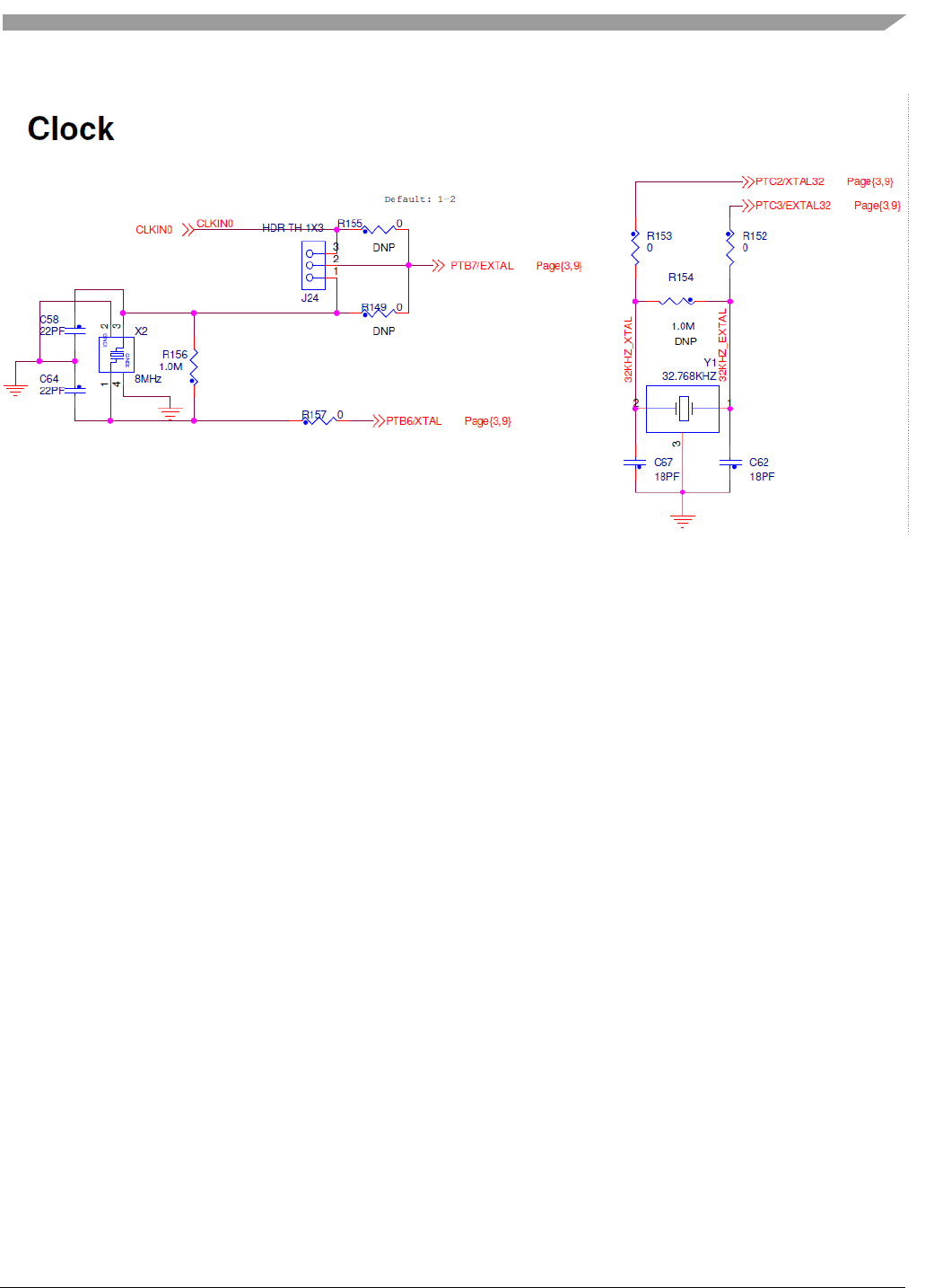
4.3.1. Clock source
The KE18F MCU starts up to the default reset clock for core/system clock, which is 48 MHz from
FIRC. Software can enable the main external oscillator (EXTAL/XTAL), or slow frequency internal
reference (SIRC) 2/8 MHz if desired as the core/system clock. There is one System PLL inside KE18F
clock module, it enables the chip to run up to the maximum frequency of 168 Mhz.
The external oscillator/resonator can range from 32.768 KHz to 32 MHz. Its main usage is for RTC time
base. An 8 MHz crystal is the default external source for the SCG oscillator inputs (XTAL/EXTAL).
The clock source diagram is shown in the following figure.
TWR-KE18F Hardware Description
TWR-KE18F User's Guide, Rev. 0, 09/2016
NXP Semiconductors 9
Figure 7. Clock source
4.3.2. Serial port
The primary serial port interface signals are PTB1 and PTB0. These signals are connected to both the
CMSIS-DAP and to the J3/J5 TWR elevator connector.
4.3.3. Reset
The PTA5/RESET signal on KE18F is connected externally to a pushbutton, SW1, and also to the
CMSIS-DAP circuit. The reset button can be used to force an external reset event in the target MCU.
The reset button can also be used to force the CMSIS-DAP circuit into bootloader mode.
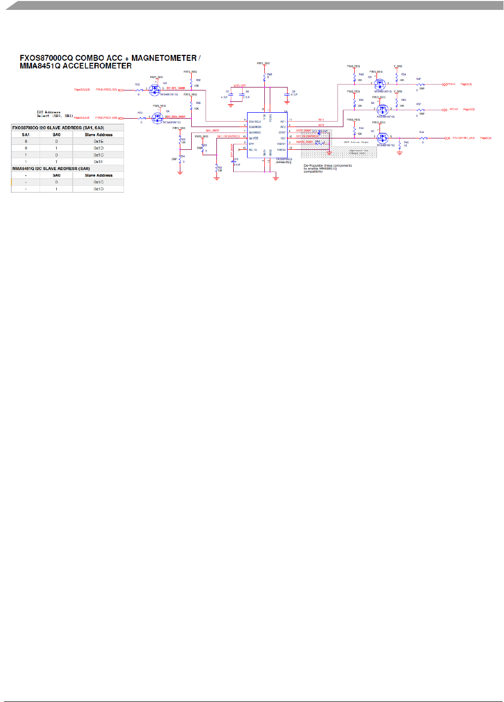
4.4. Sensor
FXOS8700CQ is a small, low-power, 3-axis, linear accelerometer + magnetometer. The device features
a selectable I2C or point-to-point SPI serial interface with 8-bit accelerometer and 14-bit magnetometer
ADC resolution along with smart-embedded functions. It is interfaced through an I2C bus and three
GPIO signals as shown in the following figure.
TWR-KE18F Hardware Description
TWR-KE18F User's Guide, Rev. 0, 09/2016
10 NXP Semiconductors
Figure 8. FXOS8700CQ sensor
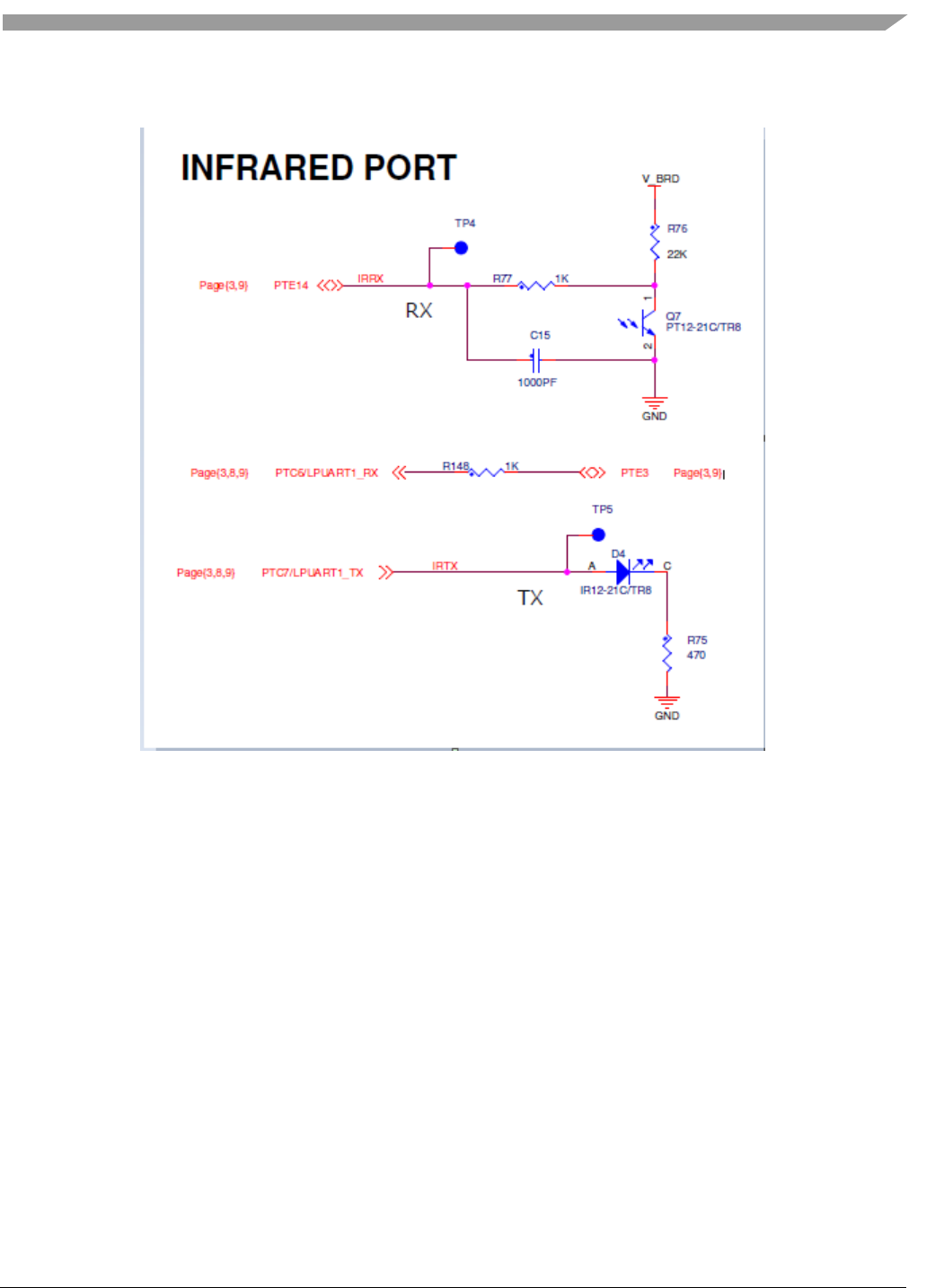
4.5. Infrared port
An infrared transmit and receive interface is implemented on the board. The PTC7 pin directly drives an
infrared diode. The receiver uses an infrared phototransistor connected to an on-chip analog comparator
ACMP2_IN3 through a low-pass filter. Then the output of the analog comparator ACMP2_OUT is
routed to a UART module externally for easier processing of the incoming data stream. The Infrared
port schematic is shown in the following figure.
TWR-KE18F Hardware Description
TWR-KE18F User's Guide, Rev. 0, 09/2016
NXP Semiconductors 11
Figure 9. Infrared port
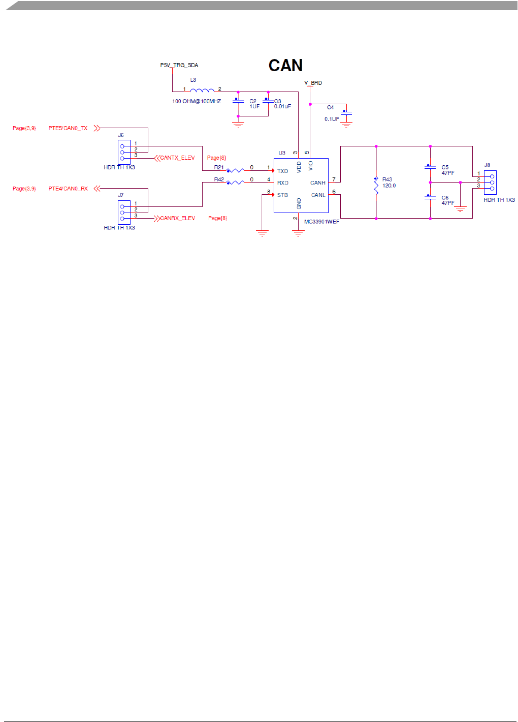
4.6. CAN transceiver
The TWR-KE18F features a Controller Area Network interface using a NXP MC33901WEF CAN
transceiver. The signals from the transceiver are connected to two 3-pin headers with the FlexCAN
module pin out of KE18F. They can also be routed to the CAN transceiver TJA1051T/3 on TWR SER
board through the elevator. The CAN transceiver schematic is shown in the following figure.
TWR-KE18F Hardware Description
TWR-KE18F User's Guide, Rev. 0, 09/2016
12 NXP Semiconductors
Figure 10. CAN receiver
4.7. Potentiometer, thermistor, pushbuttons, and LEDs
The TWR-KE18F features:
• A potentiometer connected to an ADC input channel (PTC14/ADC0_SE12)
• A thermistor connected to two ADC input channels (PTA0/ADC0_SE0 and PTA1/ADC0_SE1)
• Two pushbutton switches (SW2 and SW3 connected to PTD3 and PTD6)
• User controllable LEDs connected to GPIO signals
— Yellow LED D8 connected to PTC12
— Red LED D6 connected to PTC10
— Orange LED D9 connected to PTC13
— GREEN LED D7 connected to PTC11
• A RGB LEDs connected to FTM signals
— RED color connected to PTD16/FTM0_CH1
— GREEN color connected to PTD15/FTM0_CH0
— BLUE color connected to PTB5/FTM0_CH5
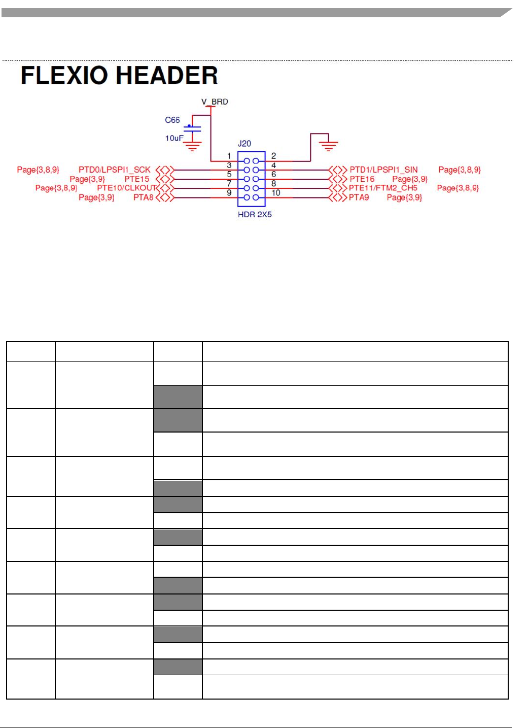
4.8. FlexIO header
KE18F has one on-chip FlexIO module, which is capable of supporting a wide range of protocols
including: UART, I2C, SPI, I2S, and PWM generation. It is more efficient than integrating multiple
peripherals for each desired protocol. There are eight FlexIO pins implemented in total and bonded out
on J20, as shown in the following figure.
Default Jumper Setting
TWR-KE18F User's Guide, Rev. 0, 09/2016
NXP Semiconductors 13
Figure 11. FlexIO header
5. Default Jumper Setting
There are several jumpers provided for isolation, configuration, and feature selection. The following
table provides details.
Table 3. Default jumper settings
Jumper
Option
Setting
Description
J3
UART TX
Selection
1-2
Connect to Elevator UART TX
2-3
Connect to OpenSDA UART TX
J4
Reset Selection
1-2
Connect OpenSDA reset to MCU
2-3
Connect pin reset to MCU directly, when OpenSDA is not
powered
J5
UART RX
Selection
1-2
Connect to Elevator UART RX
2-3
Connect to OpenSDA UART RX
J6
CAN TX
Selection
1-2
Connect CAN transceiver to MCU CAN0 TX pin directly
2-3
Connect CAN transceiver to Elevator CAN TX
J7
CAN RX
Selection
1-2
Connect CAN transceiver to MCU CAN0 RX pin directly
2-3
Connect CAN transceiver to Elevator CAN RX
J8
CAN Transceiver
connection
ON
Connection with external board
OFF
No connection with external board
J9
POTENTIOMETER
Enable
ON
Enable potentiometer
OFF
Disable potentiometer
J11
OpenSDA SWD
CLK connection
ON
Connect SWD_CLK to OpenSDA circuit
OFF
Disconnect SWD_CLK to OpenSDA circuit
J12
OpenSDA SWD
DIO connection
ON
Connect SWD_DIO to OpenSDA circuit
OFF
Disconnect SWD_DIO to OpenSDA circuit
References
TWR-KE18F User's Guide, Rev. 0, 09/2016
14 NXP Semiconductors
Table 3. Default jumper settings
Jumper
Option
Setting
Description
J13
Reset connection
ON
Connect reset signal to MCU pin
OFF
Disconnect reset signal to MCU pin
J16
Board power
supply selection
1-2
Board voltage V_BRD power from OpenSDA USB, 5V
2-3
Board voltage V_BRD power from regulator,3.3V
J17
Upper reference
voltage VREFH
selection
1-2
VREFH from 3.3V regulator
2-3
VREFH from VDDA
J18
Analog circuits
power VDDA
connection
ON
Connect VDDA to board power V_BRD
OFF
Disconnect VDDA to board power V_BRD
J19
MCU digital power
connection
ON
Connect MCU_VDD to board power V_BRD
OFF
Disconnect MCU_VDD to board power V_BRD
J21
Elevator 3.3V
connection
ON
Connect 3.3V regulator output to TWR elevator
OFF
Disconnect 3.3V regulator output to TWR elevator
J22
Elevator 5V
connection
ON
Connect 5V USB power switch output to TWR elevator
OFF
Disconnect 5V USB power switch output to TWR elevator
J23
Elevator 5V
connection
ON
Connect 5V OpenSDA input to TWR elevator
OFF
Disconnect 5V OpenSDA input to TWR elevator
J24
External clock
selection
1-2
External 8Mhz crystal input
2-3
External oscillator input to EXTAL pin directly
6. References
The reference documents for the TWR-KE18F hardware are shown below. All of these documents are
available online at www.nxp.com/TWR-KE18F.
• TWR-KE18F Quick Start Guide: Quick Start Guide and supporting files for getting started with
the TWR-KE18F.
• TWR-KE18F User’s Guide: Document overview and detailed information for the TWR- KE18F
hardware.
• TWR-KE18F Schematics PDF: Schematics for the TWR- KE18F hardware.
• KE18F Sub-Family Reference Manual: A reference manual for KE18F sub-family devices

Revision History
TWR-KE18F User's Guide, Rev. 0, 09/2016
NXP Semiconductors 15
7. Revision History
Table 4. Revision history
Revision number
Date
Substantive changes
0
09/2016
Initial release

Document Number: TWRKE18FUG
Rev. 0
09/2016
How to Reach Us:
Home Page:
nxp.com
Web Support:
nxp.com/support
Information in this document is provided solely to enable system and software
implementers to use NXP products. There are no express or implied copyright licenses
granted hereunder to design or fabricate any integrated circuits based on the
information in this document. NXP reserves the right to make changes without further
notice to any products herein.
NXP makes no warranty, representation, or guarantee regarding the suitability of its
products for any particular purpose, nor does NXP assume any liability arising out of
the application or use of any product or circuit, and specifically disclaims any and all
liability, including without limitation consequential or incidental damages. “Typical”
parameters that may be provided in NXP data sheets and/or specifications can and do
vary in different applications, and actual performance may vary over time. All operating
parameters, including “typicals,” must be validated for each customer application by
customer’s technical experts. NXP does not convey any license under its patent rights
nor the rights of others. NXP sells products pursuant to standard terms and conditions
of sale, which can be found at the following address:
nxp.com/SalesTermsandConditions.
NXP, the NXP logo, NXP SECURE CONNECTIONS FOR A SMARTER WORLD,
Freescale, the Freescale logo, and Kinetis are trademarks of NXP B.V. All other
product or service names are the property of their respective owners.
ARM, the ARM Powered logo, and Cortex are registered trademarks of ARM Limited (or
its subsidiaries) in the EU and/or elsewhere. All rights reserved.
© 2016 NXP B.V.
