MPR601UM 01_Power PC_601_Users_Manual_1995 01 Power PC 601 Users Manual 1995
User Manual: MPR601UM-01_PowerPC_601_Users_Manual_1995
Open the PDF directly: View PDF ![]() .
.
Page Count: 777 [warning: Documents this large are best viewed by clicking the View PDF Link!]
- 1.1 PowerPC 601 Microprocessor Overview
- 1.2 Levels of the PowerPC Architecture
- 1.3 The 601 as a PowerPC Implementation
- 2.1 Normal Instruction Execution State
- 2.2 User-Level Registers
- 2.3 Supervisor-Level Registers
- 2.3.1 Machine State Register (MSR)
- 2.3.2 Segment Registers
- 2.3.3 Supervisor-Level SPRs
- 2.3.3.1 Synchronization for Supervisor-Level SPRs ...
- 2.3.3.2 DAE/Source Instruction Service Register (D...
- 2.3.3.3 Data Address Register (DAR)
- 2.3.3.4 Real-Time Clock (RTC) Registers (Superviso...
- 2.3.3.5 Decrementer (DEC) Register
- 2.3.3.6 Table Search Description Register 1 (SDR1)...
- 2.3.3.7 Machine Status Save/Restore Register 0 (SR...
- 2.3.3.8 Machine Status Save/Restore Register 1 (SR...
- 2.3.3.9 General SPRs (SPRG0–SPRG3)
- 2.3.3.10 External Access Register (EAR)
- 2.3.3.11 Processor Version Register (PVR)
- 2.3.3.12 BAT Registers
- 2.3.3.13 601 Implementation-Specific HID Registers...
- 2.4 Operand Conventions
- 2.5 Floating-Point Execution Models
- 2.6 PowerPC Registers Unimplemented in the 601
- 2.7 Reset
- 3.1 Memory Addressing
- 3.2 Exception Summary
- 3.3 Integer Instructions
- 3.4 Floating-Point Instructions
- 3.5 Load and Store Instructions
- 3.5.1 Integer Load and Store Address Generation
- 3.5.2 Integer Load Instructions
- 3.5.3 Integer Store Instructions
- 3.5.4 Integer Load and Store with Byte Reversal In...
- 3.5.5 Integer Load and Store Multiple Instructions...
- 3.5.6 Integer Move String Instructions
- 3.5.7 Memory Synchronization Instructions
- 3.5.8 Floating-Point Load and Store Address Genera...
- 3.5.9 Floating-Point Load Instructions
- 3.5.10 Floating-Point Store Instructions
- 3.5.11 Floating-Point Move Instructions
- 3.6 Branch and Flow Control Instructions
- 3.6.1 Branch instruction Address Calculation
- 3.6.2 Conditional Branch Control
- 3.6.3 Basic Branch Mnemonics
- 3.6.4 Branch Mnemonics Incorporating Conditions
- 3.6.5 Branch Instructions
- 3.6.6 Condition Register Logical Instructions
- 3.6.7 System Linkage Instructions
- 3.6.8 Simplified Mnemonics for Branch Processor In...
- 3.6.9 Trap Instructions and Mnemonics
- 3.7 Processor Control Instructions
- 3.8 Memory Control Instructions
- 3.9 External Control Instructions
- 3.10 Miscellaneous Simplified Mnemonics
- 4.1 Cache Organization
- 4.2 Cache Arbitration
- 4.3 Cache Access Priorities
- 4.4 Basic Cache Operations
- 4.5 Cache Data Transactions
- 4.6 Access to I/O Controller Interface Segments
- 4.7 Cache Coherency
- 4.7.1 Memory Management Access Mode Bits—W, I, and...
- 4.7.2 MESI Protocol
- 4.7.3 MESI State Diagram
- 4.7.4 MESI Hardware Considerations
- 4.7.5 Coherency Precautions
- 4.7.6 Memory Loads and Stores
- 4.7.7 Atomic Memory References
- 4.7.8 Snoop Response to Bus Operations
- 4.7.9 Cache Reaction to Specific Bus Operations
- 4.7.10 Internal ARTRY Scenarios
- 4.7.11 Enveloped High-Priority Cache Sector Push O...
- 4.8 Cache Control Instructions
- 4.8.1 Cache Line Compute Size Instruction (clcs)
- 4.8.2 Data Cache Block Touch Instruction (dcbt)
- 4.8.3 Data Cache Block Touch for Store Instruction...
- 4.8.4 Data Cache Block Set to Zero Instruction (dc...
- 4.8.5 Data Cache Block Store Instruction (dcbst)
- 4.8.6 Data Cache Block Flush Instruction (dcbf)
- 4.8.7 Enforce In-Order Execution of I/O Instructio...
- 4.8.8 Instruction Cache Block Invalidate Instructi...
- 4.8.9 Instruction Synchronize Instruction (isync)
- 4.9 Bus Operations Caused by Cache Control 4.9 Ins...
- 4.10 Memory Unit
- 4.11 MESI State Transactions
- 5.1 Exception Classes
- 5.2 Exception Processing
- 5.3 Process Switching
- 5.4 Exception Definitions
- 5.4.1 Reset Exceptions (x'00100')
- 5.4.2 Machine Check Exception (x'00200')
- 5.4.3 Data Access Exception (x'00300')
- 5.4.4 Instruction Access Exception (x'00400')
- 5.4.5 External Interrupt (x'00500')
- 5.4.6 Alignment Exception (x'00600')
- 5.4.7 Program Exception (x'00700')
- 5.4.8 Floating-Point Unavailable Exception (x'0080...
- 5.4.9 Decrementer Exception (x'00900')
- 5.4.10 I/O Controller Interface Error Exception (x...
- 5.4.11 System Call Exception (x'00C00')
- 5.4.12 Run Mode/Trace Exception (x'02000')
- 6.1 MMU Overview
- 6.1.1 Memory Addressing
- 6.1.2 MMU Organization
- 6.1.3 Address Translation Mechanisms
- 6.1.4 Memory Protection Facilities
- 6.1.5 Page History Information
- 6.1.6 General Flow of MMU Address Translation
- 6.1.7 Memory/MMU Coherency Model
- 6.1.8 Effects of Instruction Fetch on MMU
- 6.1.9 Breakpoint Facility
- 6.1.10 MMU Exceptions Summary
- 6.1.11 MMU Instructions and Register Summary
- 6.1.12 TLB Entry Invalidation
- 6.2 ITLB Description
- 6.3 Memory/Cache Access Modes
- 6.4 General Memory Protection Mechanism
- 6.5 Selection of Address Translation Type
- 6.6 Direct Address Translation
- 6.7 Block Address Translation
- 6.8 Memory Segment Model
- 6.9 Hashed Page Tables
- 6.10 I/O Controller Interface Address Translation
- 6.10.1 Segment Register Format for I/O Controller ...
- 6.10.2 I/O Controller Interface Accesses
- 6.10.3 I/O Controller Interface Segment Protection...
- 6.10.4 Memory-Forced I/O Controller Interface Acce...
- 6.10.5 Instructions Not Supported in I/O Controlle...
- 6.10.6 Instructions with No Effect in I/O Controll...
- 6.10.7 I/O Controller Interface Summary Flow
- 7.1 Terminology and Conventions
- 7.2 Pipeline Description
- 7.3 Pipeline Timing
- 7.4 Execute Stage Delay Summary
- 8.1 Signal Configuration
- 8.2 Signal Descriptions
- 8.2.1 Address Bus Arbitration Signals
- 8.2.2 Address Transfer Start Signals
- 8.2.3 Address Transfer Signals
- 8.2.4 Address Transfer Attribute Signals
- 8.2.4.1 Transfer Type (TT0–TT4)
- 8.2.4.2 Transfer Size (TSIZ0–TSIZ2)
- 8.2.4.3 Transfer Burst (TBST)
- 8.2.4.4 Transfer Code (TC0–TC1)—Output
- 8.2.4.5 Cache Inhibit (CI)—Output
- 8.2.4.6 Write-Through (WT)—Output
- 8.2.4.7 Global (GBL)
- 8.2.4.8 Cache Set Element (CSE0–CSE2)—Output
- 8.2.4.9 High-Priority Snoop Request (HP_SNP_REQ)
- 8.2.5 Address Transfer Termination Signals
- 8.2.6 Data Bus Arbitration Signals
- 8.2.7 Data Transfer Signals
- 8.2.8 Data Transfer Termination Signals
- 8.2.9 System Status Signals
- 8.2.10 COP/Scan Interface
- 8.2.11 Clock Signals
- 8.3 Clocking in a Multiprocessor System
- 9.1 PowerPC 601 Microprocessor System Interface 9....
- 9.2 Memory Access Protocol
- 9.3 Address Bus Tenure
- 9.4 Data Bus Tenure
- 9.5 Timing Examples
- 9.6 Memory- vs. I/O-Mapped I/O Operations
- 9.7 Interrupt, Checkstop, and Reset Signals
- 9.8 Processor State Signals
- 9.9 IEEE 1149.1-Compatible Interface
- 9.9.1 Deviations from the IEEE 1149.1 Boundary-Sca...
- 9.9.2 Additional Information about the IEEE 1149.1...
- 9.9.3 IEEE 1149.1 Interface Description
- 9.9.4 IEEE Interface Clock Requirements
- 9.9.5 IEEE 1149.1 Interface Reset Requirements
- 9.9.6 IEEE Interface Instruction Set
- 9.9.7 IEEE 1149.1 Interface Boundary-Scan Chain
- 9.10 Using DBWO (Data Bus Write Only)
- 10.1 Instruction Formats
- 10.2 Instruction Set
- 10.3 Instructions Not Implemented by the 601

MPR601UM-01 MPC601UM/AD
PowerPC
™
601
RISC Microprocessor User's Manual

About This Book
xli
About This Book
The primary objective of this user’s manual is to define the functionality of the PowerPC™
601 microprocessor for use by software and hardware developers. The 601 processor is the
first in the family of PowerPC microprocessors, and can provide a reliable foundation for
developing products compatible with subsequent processors in the PowerPC family. The
601 provides a bridge between the POWER architecture and the PowerPC architecture, and
as a result differs from the PowerPC architecture in some respects. Therefore, a secondary
objective of this manual is to describe these differences.
The PowerPC architecture is comprised of the following components:
• PowerPC user instruction set architecture—This includes the base user-level
instruction set (excluding a few user-level cache-control instructions), user-level
registers, programming model, data types, and addressing modes.
• PowerPC virtual environment architecture—This describes the semantics of the
memory model that can be assumed by software processes and includes descriptions
of the cache model, cache-control instructions, address aliasing, and other related
issues. Implementations that conform to the PowerPC virtual environment
architecture also adhere to the PowerPC user instruction set architecture, but may
not necessarily adhere to the PowerPC operating environment architecture.
• PowerPC operating environment architecture—This includes the structure of the
memory management model, supervisor-level registers, and the exception model.
Implementations that conform to the PowerPC operating environment architecture
also adhere to the PowerPC user instruction set architecture and the PowerPC virtual
environment architecture.
It is beyond the scope of the manual to provide a thorough description of the PowerPC
architecture. It must be kept in mind that each PowerPC processor is a unique PowerPC
implementation.
For readers of this manual who are concerned about compatibility issues regarding
subsequent PowerPC processors, it is critical to read Chapter 1, “Overview,” and in
particular Appendix H, “Implementation Summary for Programmers,” which outlines in a
very general manner the components of the PowerPC architecture, and indicates where and
how the 601 diverges from the PowerPC definition. Instances where the 601 differs from
the PowerPC architecture are noted throughout the manual.

xlii
PowerPC 601 RISC Microprocessor User's Manual
Audience
This manual is intended for system software and hardware developers and applications
programmers who want to develop products for the 601 microprocessor and PowerPC
processors in general. It is assumed that the reader understands operating systems,
microprocessor system design, and the basic principles of RISC processing.
Organization
Following is a summary and a brief description of the major sections of this manual:
• Chapter 1, “Overview,” is useful for readers who want a general understanding of
the features and functions of the PowerPC architecture and the 601 processor. This
chapter also provides a general description of how the 601 differs from the PowerPC
architecture.
• Chapter 2, “Registers and Data Types,” is useful for software engineers who need to
understand the PowerPC programming model and the functionality of the registers
implemented in the 601. This chapter also describes PowerPC conventions for
storing data in memory.
• Chapter 3, “Addressing Modes and Instruction Set Summary,” provides an overview
of the PowerPC addressing modes and a description of the instructions implemented
by the 601, including the portion of the PowerPC instruction set and the additional
instructions implemented by the 601.
Specific differences between the 601 implementation and the PowerPC
implementation of individual instructions are noted.
• Chapter 4, “Cache and Memory Unit Operation,” provides a discussion of cache
timing, look-up process, MESI protocol, and interaction with other units. This
chapter contains information that pertains both to the PowerPC virtual environment
architecture and to the specific implementation in the 601.
• Chapter 5, “Exceptions,” describes the exception model defined in the PowerPC
operating environment architecture and the specific exception model implemented
in the 601.
• Chapter 6, “Memory Management Unit,” provides descriptions of the MMU,
interaction with other units, and address translation. Although this chapter does not
provide an in-depth description of both the 64-bit and 32-bit memory management
model defined by the PowerPC operating environment architecture, it does note
differences between the defined 32-bit PowerPC definition and the 601 memory
management implementation.
• Chapter 7, “Instruction Timing,” provides information about latencies, interlocks,
special situations, and various conditions to help make programming more efficient.
This chapter is of special interest to software engineers and system designers.
Because each PowerPC implementation is unique with respect to instruction timing,
this chapter primarily contains information specific to the 601.

About This Book
xliii
• Chapter 8, “Signal Descriptions,” provides descriptions of individual signals of the
601.
• Chapter 9, “System Interface Operation,” describes signal timings for various
operations. It also provides information for interfacing to the 601.
• Chapter 10, “Instruction Set,” functions as a handbook of the PowerPC instruction
set. It provides opcodes, sorted by mnemonic, as well as a more detailed description
of each instruction. Instruction descriptions indicate whether an instruction is part of
the PowerPC architecture or if it is specific to the 601. Each description indicates any
differences in how the 601 implementation differs from the PowerPC definition. The
descriptions also indicate the privilege level of each instruction and which execution
unit or units executes the instruction.
• Appendix A, “Instruction Set Listings,” lists the superset of PowerPC and 601
processor instructions.
• Appendix B, “POWER Architecture Cross Reference,” describes the relationship
between the 601 and the POWER architecture.
• Appendix C, “PowerPC Instructions Not Implemented,” describes the set of
PowerPC instructions not implemented in the 601 processor.
• Appendix D, “Classes of Instructions,” describes how instructions are classified
from the perspective of the PowerPC architecture.
• Appendix E, “Multiple-Precision Shifts,” describes how multiple-precision shift
operations can be programmed.
• Appendix F, “Floating-Point Models,” gives examples of how the floating-point
conversion instructions can be used to perform various conversions.
• Appendix G, “Synchronization Programming Examples,” gives examples showing
how synchronization instructions can be used to emulate various synchronization
primitives and how to provide more complex forms of synchronization.
• Appendix H, “Implementation Summary for Programmers,” is a compilation of the
differences between the 601 processor and the PowerPC architecture.
• Appendix I, “Instruction Timing Examples,” shows instruction timings for code
sequences, emphasizing situations where stalls may be encountered and showing
methods of avoiding stalls where possible.
• This manual also includes a glossary and an index.
In this document, the terms “PowerPC 601 microprocessor” and “601” are used to denote
the first microprocessor from the PowerPC architecture family. The PowerPC 601
microprocessors are available from IBM as PPC601 and from Motorola as MPC601.

xliv
PowerPC 601 RISC Microprocessor User's Manual
Additional Reading
Following is a list of additional reading that provides background for the information in
this manual:
• John L. Hennessy and David A. Patterson,
Computer Architecture: A Quantitative
Approach
, Morgan Kaufmann Publishers, Inc., San Mateo, CA
•
PowerPC 601 RISC Microprocessor Hardware Specifications
, MPC601EC/D
(Motorola order number) and MPR601HSU-01 (IBM order number)
•
PowerPC 601 RISC Microprocessor Technical Summary
, MPC601/D (Motorola
order number) and MPR601TSU-01 (IBM order number)
•
PowerPC Architecture
, published by International Business Machines Corporation,
52G7487 (order number)
Conventions
This document uses the following notational conventions:
ACTIVE_HIGH Names for signals that are active high are shown in uppercase text
without an overbar.
ACTIVE_LOW A bar over a signal name indicates that the signal is active low—for
example, ARTRY (address retry) and TS (transfer start). Active-low
signals are referred to as asserted (active) when they are low and
negated when they are high. Signals that are not active-low, such as
AP0–AP3 (address bus parity signals) and TT0–TT4 (transfer type
signals) are referred to as asserted when they are high and negated
when they are low.
mnemonics
Instruction mnemonics are shown in lowercase bold.
italics
Italics indicate variable command parameters, for example,
bcctr
x
x'0F' Hexadecimal numbers
b'0011' Binary numbers
r
A|0 The contents of a specified GPR or the value 0.
REG[FIELD] Abbreviations or acronyms for registers are shown in uppercase
text. Specific bit fields or ranges are shown in brackets.
x In certain contexts, such as a signal encoding, this indicates a don’t
care. For example, if TT0–TT3 are binary encoded b'x001', the state
of TT0 is a don’t care.
Acronyms and Abbreviations
Table i contains acronyms and abbreviations that are used in this document.

About This Book
xlv
Table i. Acronyms and Abbreviated Terms
Term Meaning
ALU Arithmetic logic unit
ATE Automatic test equipment
ASR Address space register
BAT Block address translation
BIST Built-in self test
BPU Branch processing unit
BUC Bus unit controller
BUID Bus unit ID
CAR Cache address register
CMOS Complementary metal-oxide semiconductor
COP Common on-chip processor
CR Condition register
CRTRY Cache retry queue
CTR Count register
DABR Data address breakpoint register
DAE Data access exception
DAR Data address register
DBAT Data BAT
DEC Decrementer register
DSISR DAE/source instruction service register
EA Effective address
EAR External access register
ECC Error checking and correction
FPECR Floating-point exception cause register
FPR Floating-point register
FPSCR Floating-point status and control register
FPU Floating-point unit
GPR General-purpose register
IABR Instruction address breakpoint register
IBAT Instruction BAT
IEEE Institute for Electrical and Electronics Engineers
IQ Instruction queue

xlvi
PowerPC 601 RISC Microprocessor User's Manual
ITLB Instruction translation lookaside buffer
IU Integer unit
L2 Secondary cache
LIFO Last-in-first-out
LR Link register
LRU Least recently used
LSB Least-significant byte
lsb Least-significant bit
MESI Modified/exclusive/shared/invalid—cache coherency protocol
MMU Memory management unit
MQ MQ register
MSB Most-significant byte
msb Most-significant bit
MSR Machine state register
NaN Not a number
No-Op No operation
PID Processor identification tag
PIR Processor identification register
POWER Performance Optimized with Enhanced RISC architecture
PR Privilege-level bit
PTE Page table entry
PTEG Page table entry group
PVR Processor version register
RAW Read-after-write
RISC Reduced instruction set computer
RTC Real-time clock
RTCL Real-time clock lower register
RTCU Real-time clock upper register
RTL Register transfer language
RWITM Read with intent to modify
SDR1 Table search description register 1
SLB Segment lookaside buffer
Table i. Acronyms and Abbreviated Terms (Continued)
Term Meaning

About This Book
xlvii
Terminology Conventions
Table ii describes terminology conventions used in this manual.
SPR Special-purpose register
SPRG
n
General SPR
SR Segment register
SRR0 Machine status save/restore register 0
SRR1 Machine status save/restore register 1
TAP Test access port
TB Time base register
TLB Translation lookaside buffer
TTL Transistor-to-transistor logic
UTLB Unified translation lookaside buffer
UUT Unit under test
WAR Write-after-read
WAW Write-after-write
WIM Write-through/cache-inhibited/memory-coherency enforced bits
XATC Extended address transfer code
XER Integer exception register
Table ii. Terminology Conventions
IBM This Manual
Data storage interrupt (DSI) Data access exception (DAE)
Direct store segment I/O controller interface segment
Effective address Effective or logical address (logical is used
in the context of address translation)
Effective segment ID (ESID) (64-bit
implementations—not on the 601) Logical segment ID (LSID) (64-bit
implementations—not on the 601)
Extended mnemonics Simplified mnemonics
Extended Opcode Secondary opcode
Fixed-point unit (FXU) Integer unit (IU)
Instruction storage interrupt (ISI) Instruction access exception (IAE)
Interrupt Exception
Problem mode (or problem state) User-level privilege
Table i. Acronyms and Abbreviated Terms (Continued)
Term Meaning

xlviii
PowerPC 601 RISC Microprocessor User's Manual
Table iii describes register and bit naming conventions used in this manual.
Programmable I/O (PIO) I/O controller interface operation
Real address Physical address
Real mode address translation Direct address translation
Relocation Translation
Special direct store segment Memory-forced I/O controller interface
segment
Storage (noun) Memory (noun)
Storage (verb) Access (verb)
Store in Write back
Store through Write through
Table iii. Register and Bit Name Convention
IBM This Manual
Problem mode bit (MSR[PR]) Privilege level bit (MSR[PR])
Instruction relocate bit (MSR[IR]) Instruction address translation bit (MSR[IT])
Data relocate bit (MSR[DR]) Data address translation bit (MSR[DT])
Interrupt prefix bit (MSR[IP]) Exception prefix bit (MSR[EP])
Recoverable interrupt bit (MSR[RI])
(not on the 601) Recoverable exception bit (MSR[RE])
(not on the 601)
Problem state protection key (SR[Kp]) User-state protection key (SR[Ku])
DSISR DSISR acronym redefined as “DAE/Source
Instruction Service Register”
SDR1 SDR1 acronym redefined as “Table Search
Description Register 1”
Block effective page index (BATx[BEPI]) Block logical page index (BATx[BLPI])
Block real page number (BATx[BRPN]) Physical block number (BATx[PBN])
Block length (BATx[BL]) Block size mask (BATx[BSM])
Real page number (PTE[RPN]) Physical page number (PTE[PPN])
Table ii. Terminology Conventions (Continued)
IBM This Manual

Chapter 1. Overview
1-1
Chapter 1
Overview
10
10
This chapter provides an overview of PowerPC™ 601 microprocessor features, including
a block diagram showing the major functional components. It also provides an overview of
the PowerPC architecture, and information about how the 601 implementation differs from
the architectural definitions.
1.1 PowerPC 601 Microprocessor Overview
This section describes the features of the 601, provides a block diagram showing the major
functional units, and gives an overview of how the 601 operates.
The 601 is the first implementation of the PowerPC family of reduced instruction set
computer (RISC) microprocessors. The 601 implements the 32-bit portion of the PowerPC
architecture, which provides 32-bit effective (logical) addresses, integer data types of 8, 16,
and 32 bits, and floating-point data types of 32 and 64 bits. For 64-bit PowerPC
implementations, the PowerPC architecture provides 64-bit integer data types, 64-bit
addressing, and other features required to complete the 64-bit architecture.
The 601 is a superscalar processor capable of issuing and retiring three instructions per
clock, one to each of three execution units. Instructions can complete out of order for
increased performance; however, the 601 makes execution appear sequential.
The 601 integrates three execution units—an integer unit (IU), a branch processing unit
(BPU), and a floating-point unit (FPU). The ability to execute three instructions in parallel
and the use of simple instructions with rapid execution times yield high efficiency and
throughput for 601-based systems. Most integer instructions execute in one clock cycle.
The FPU is pipelined so a single-precision multiply-add instruction can be issued every
clock cycle.
The 601 includes an on-chip, 32-Kbyte, eight-way set-associative, physically addressed,
unified instruction and data cache and an on-chip memory management unit (MMU). The
MMU contains a 256-entry, two-way set-associative, unified translation lookaside buffer
(UTLB) and provides support for demand paged virtual memory address translation and
variable-sized block translation. Both the UTLB and the cache use least recently used
(LRU) replacement algorithms.

1-2
PowerPC 601 RISC Microprocessor User's Manual
The 601 has a 64-bit data bus and a 32-bit address bus. The 601 interface protocol allows
multiple masters to compete for system resources through a central external arbiter.
Additionally, on-chip snooping logic maintains cache coherency in multiprocessor
applications. The 601 supports single-beat and burst data transfers for memory accesses; it
also supports both memory-mapped I/O and I/O controller interface addressing.
The 601 uses an advanced, 3.6-V CMOS process technology and maintains full interface
compatibility with TTL devices.
1.1.1 601 Features
This section describes details of the 601’s implementation of the PowerPC architecture.
Major features of the 601 are as follows:
• High-performance, superscalar microprocessor
— As many as three instructions in execution per clock (one to each of the three
execution units)
— Single clock cycle execution for most instructions
— Pipelined FPU for all single-precision and most double-precision operations
• Three independent execution units and two register files
— BPU featuring static branch prediction
— A 32-bit IU
— Fully IEEE 754-compliant FPU for both single- and double-precision operations
— Thirty-two GPRs for integer operands
— Thirty-two FPRs for single- or double-precision operands
• High instruction and data throughput
— Zero-cycle branch capability
— Programmable static branch prediction on unresolved conditional branches
— Instruction unit capable of fetching eight instructions per clock from the cache
— An eight-entry instruction queue that provides look-ahead capability
— Interlocked pipelines with feed-forwarding that control data dependencies in
hardware
— Unified 32-Kbyte cache—eight-way set-associative, physically addressed; LRU
replacement algorithm
— Cache write-back or write-through operation programmable on a per page or per
block basis
— Memory unit with a two-element read queue and a three-element write queue
— Run-time reordering of loads and stores
— BPU that performs condition register (CR) look-ahead operations

Chapter 1. Overview
1-3
— Address translation facilities for 4-Kbyte page size, variable block size, and
256-Mbyte segment size
— A 256-entry, two-way set-associative UTLB
— Four-entry BAT array providing 128-Kbyte to 8-Mbyte blocks
— Four-entry, first-level ITLB
— Hardware table search (caused by UTLB misses) through hashed page tables
— 52-bit virtual address; 32-bit physical address
• Facilities for enhanced system performance
— Bus speed defined as selectable division of operating frequency
— A 64-bit split-transaction external data bus with burst transfers
— Support for address pipelining and limited out-of-order bus transactions
— Snooped copyback queues for cache block (sector) copyback operations
— Bus extensions for I/O controller interface operations
— Multiprocessing support features that include the following:
– Hardware enforced, four-state cache coherency protocol (MESI)
– Separate port into cache tags for bus snooping
• In-system testability and debugging features through boundary-scan capability
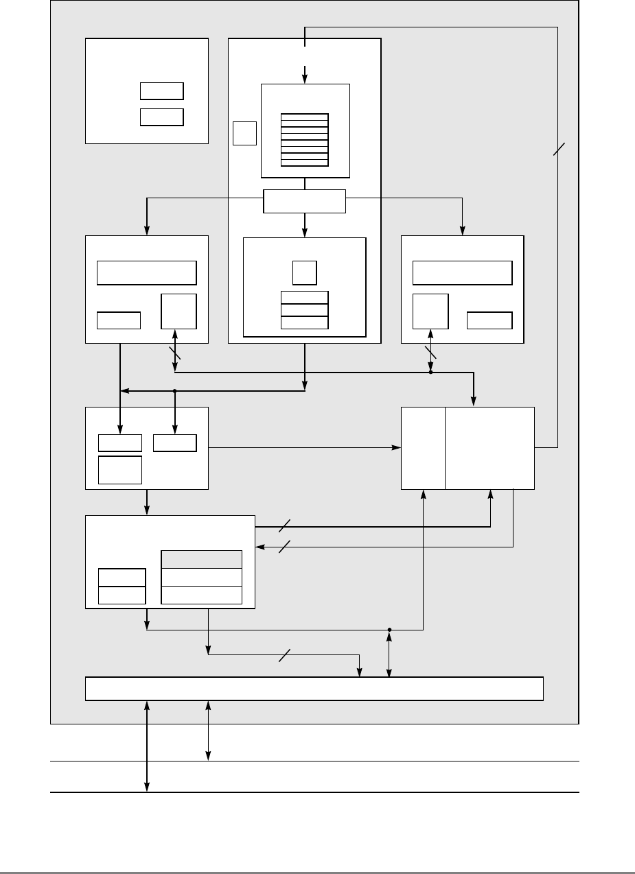
1.1.2 Block Diagram
Figure 1-1 provides a block diagram of the 601 that illustrates how the execution units—IU,
FPU, and BPU—operate independently and in parallel.
The 601's 32-Kbyte, unified cache tag directory has a port dedicated to snooping bus
transactions, preventing interference with processor access to the cache. The 601 also
provides address translation and protection facilities, including a UTLB and a BAT array,
and a four-entry ITLB that contains the four most recently used instruction address
translations for fast access by the instruction unit.
Instruction fetching and issuing is handled in the instruction unit. Translation of addresses
for cache or external memory accesses are handled by the memory management unit. Both
units are discussed in more detail in Sections 1.1.3, “Instruction Unit,” and 1.1.5, “Memory
Management Unit (MMU).”
1-4
PowerPC 601 RISC Microprocessor User's Manual
Figure 1-1. PowerPC 601 Microprocessor Block Diagram
(INSTRUCTION FETCH)
RTC
IU BPU FPU
MMU
SYSTEM INTERFACE
RTCU
RTCL
INSTRUCTION
QUEUE
+
+*/+
INSTRUCTIONINSTRUCTION
8 WORDS
XER
GPR
FILE
CTR
CR
LR
2 WORDS1 WORD DATA
ADDRESS
UTLB
BAT
ARRAY
ITLB TAGS
32-KBYTE
CACHE
(INSTRUC-
TION AND DA-
PHYSICAL ADDRESS
ADDRESS
DATA
SNOOP
ADDRESS
ADDRESS
DATA
64-BIT DATA BUS (2 WORDS)
32-BIT ADDRESS BUS (1 WORD)
MEMORY UNIT
SNOOP
READ
QUEUE WRITE QUEUE
+*/
FPR
FILE FPSCR
INSTRUCTION UNIT
ISSUE LOGIC
2 WORDS
4 WORDS DATA
8 WORDS

Chapter 1. Overview
1-5
1.1.3 Instruction Unit
As shown in Figure 1-1, the 601 instruction unit, which contains an instruction queue and
the BPU, provides centralized control of instruction flow to the execution units. The
instruction unit determines the address of the next instruction to be fetched based on
information from a sequential fetcher and the BPU. The IU also enforces pipeline interlocks
and controls feed-forwarding.
The sequential fetcher contains a dedicated adder that computes the address of the next
sequential instruction based on the address of the last fetch and the number of words
accepted into the queue. The BPU searches the bottom half of the instruction queue for a
branch instruction and uses static branch prediction on unresolved conditional branches to
allow the instruction fetch unit to fetch instructions from a predicted target instruction
stream while a conditional branch is evaluated. The BPU also folds out branch instructions
for unconditional branches.
Instructions issued beyond a predicted branch do not complete execution until the branch
is resolved, preserving the programming model of sequential execution. If any of these
instructions are to be executed in the BPU, they are decoded but not issued. FPU and IU
instructions are issued and allowed to complete up to the register write-back stage.
Write-back is performed when a correctly predicted branch is resolved, and instruction
execution continues without interruption along the predicted path.
If branch prediction is incorrect, the instruction fetcher flushes all predicted path
instructions and instructions are issued from the correct path.
1.1.3.1 Instruction Queue
The instruction queue, shown in Figure 1-1, holds as many as eight instructions (a cache
block) and can be filled from the cache during a single cycle. The instruction fetch can
access only one cache sector at a time and will load as many instruction as space in the IQ
allows.
The upper half of the instruction queue (Q4–Q7) provides buffering to reduce the frequency
of cache accesses. Integer and branch instructions are dispatched to their respective
execution units from Q0 through Q3. Q0 functions as the initial decode stage for the IU.
For a more detailed overview of instruction dispatch, see Section 1.3.7, “601 Instruction
Timing.”
1.1.4 Independent Execution Units
The PowerPC architecture’s support for independent floating-point, integer, and branch
processing execution units allows implementation of processors with out-of-order
instruction issue. For example, because branch instructions do not depend on GPRs or
FPRs, branches can often be resolved early, eliminating stalls caused by taken branches.
The following sections describe the 601’s three execution units—the BPU, IU, and FPU.

1-6
PowerPC 601 RISC Microprocessor User's Manual
1.1.4.1 Branch Processing Unit (BPU)
The BPU performs condition register (CR) look-ahead operations on conditional branches.
The BPU looks through the bottom half of the instruction queue for a conditional branch
instruction and attempts to resolve it early, achieving the effect of a zero-cycle branch in
many cases.
The BPU uses a bit in the instruction encoding to predict the direction of the conditional
branch. Therefore, when an unresolved conditional branch instruction is encountered, the
601 fetches instructions from the predicted target stream until the conditional branch is
resolved.
The BPU contains an adder to compute branch target addresses and three special-purpose,
user-control registers—the link register (LR), the count register (CTR), and the CR. The
BPU calculates the return pointer for subroutine calls and saves it into the LR for certain
types of branch instructions. The LR also contains the branch target address for the Branch
Conditional to Link Register (
bclr
x
) instruction. The CTR contains the branch target
address for the Branch Conditional to Count Register (
bcctr
x
) instruction. The contents of
the LR and CTR can be copied to or from any GPR. Because the BPU uses dedicated
registers rather than general-purpose or floating-point registers, execution of branch
instructions is largely independent from execution of integer and floating-point
instructions.
1.1.4.2 Integer Unit (IU)
The IU executes all integer instructions and executes floating-point memory accesses in
concert with the FPU. The IU executes one integer instruction at a time, performing
computations with its arithmetic logic unit (ALU), multiplier, divider, integer exception
register (XER), and the general-purpose register file. Most integer instructions are
single-cycle instructions.
The IU interfaces with the cache and MMU for all instructions that access memory.
Addresses are formed by adding the source 1 register operand specified by the instruction
(or zero) to either a source 2 register operand or to a 16-bit, immediate value embedded in
the instruction.
Load and store instructions are issued and translated in program order; however, the
accesses can occur out of order. Synchronizing instructions are provided to enforce strict
ordering.
Load and store instructions are considered to have completed execution with respect to
precise exceptions after the address is translated. If the address for a load or store
instruction hits in the UTLB or BAT array and it is aligned, the instruction execution (that
is, calculation of the address) takes one clock cycle, allowing back-to-back issue of load
and store instructions. The time required to perform the actual load or store operation varies
depending on whether the operation involves the cache, system memory, or an I/O device.

Chapter 1. Overview
1-7
1.1.4.3 Floating-Point Unit (FPU)
The FPU contains a single-precision multiply-add array, the floating-point status and
control register (FPSCR), and thirty-two 64-bit FPRs. The multiply-add array allows the
601 to efficiently implement floating-point operations such as multiply, add, divide, and
multiply-add. The FPU is pipelined so that most single-precision instructions and many
double-precision instructions can be issued back-to-back. The FPU contains two additional
instruction queues. These queues allow floating-point instructions to be issued from the
instruction queue even if the FPU is busy, making instructions available for issue to the
other execution units.
Like the BPU, the FPU can access instructions from the bottom half of the instruction queue
(Q3–Q0), which permits floating-point instructions that do not depend on unexecuted
instructions to be issued early to the FPU.
The 601 supports all IEEE 754 floating-point data types (normalized, denormalized, NaN,
zero, and infinity) in hardware, eliminating the latency incurred by software exception
routines.
1.1.5 Memory Management Unit (MMU)
The 601’s MMU supports up to 4 Petabytes (2
52
) of virtual memory and 4 Gigabytes (2
32
)
of physical memory. The MMU also controls access privileges for these spaces on block
and page granularities. Referenced and changed status are maintained by the processor for
each page to assist implementation of a demand-paged virtual memory system.
The instruction unit generates all instruction addresses; these addresses are both for
sequential instruction fetches and addresses that correspond to a change of program flow.
The integer unit generates addresses for data accesses (both for memory and the I/O
controller interface).
After an address is generated, the upper order bits of the logical (effective) address are
translated by the MMU into physical address bits. Simultaneously, the lower order address
bits (that are untranslated and therefore considered both logical and physical), are directed
to the on-chip cache where they form the index into the eight-way set-associative tag array.
After translating the address, the MMU passes the higher-order bits of the physical address
to the cache, and the cache lookup completes. For cache-inhibited accesses or accesses that
miss in the cache, the untranslated lower order address bits are concatenated with the
translated higher-order address bits; the resulting 32-bit physical address is then used by the
memory unit and the system interface, which accesses external memory.
The MMU also directs the address translation and enforces the protection hierarchy
programmed by the operating system in relation to the supervisor/user privilege level of the
access and in relation to whether the access is a load or store.
For instruction accesses, the MMU first performs a lookup in the four entries of the ITLB
for both block- and page-based physical address translation. Instruction accesses that miss
in the ITLB and all data accesses cause a lookup in the UTLB and BAT array for the

1-8
PowerPC 601 RISC Microprocessor User's Manual
physical address translation. In most cases, the physical address translation resides in one
of the TLBs and the physical address bits are readily available to the on-chip cache. In the
case where the physical address translation misses in the TLBs, the 601 automatically
performs a search of the translation tables in memory using the information in the table
search description register 1 (SDR1) and the corresponding segment register.
Memory management in the 601 is described in more detail in Section 1.3.6.2, “601
Memory Management.”
1.1.6 Cache Unit
The PowerPC 601 microprocessor contains a 32-Kbyte, eight-way set associative, unified
(instruction and data) cache. The cache line size is 64 bytes, divided into two eight-word
sectors, each of which can be snooped, loaded, cast-out, or invalidated independently. The
cache is designed to adhere to a write-back policy, but the 601 allows control of
cacheability, write policy, and memory coherency at the page and block level. The cache
uses a least recently used (LRU) replacement policy.
As shown in Figure 1-1, the cache provides an eight-word interface to the instruction
fetcher and load/store unit. The surrounding logic selects, organizes, and forwards the
requested information to the requesting unit. Write operations to the cache can be
performed on a byte basis, and a complete read-modify-write operation to the cache can
occur in each cycle.
The instruction unit provides the cache with the address of the next instruction to be
fetched. In the case of a cache hit, the cache returns the instruction and as many of the
instructions following it as can be placed in the eight-word instruction queue up to the cache
sector boundary. If the queue is empty, as many as eight words (an entire sector) can be
loaded into the queue in parallel.
The cache tag directory has one address port dedicated to instruction fetch and load/store
accesses and one dedicated to snooping transactions on the system interface. Therefore,
snooping does not require additional clock cycles unless a snoop hit that requires a cache
status update occurs.
1.1.7 Memory Unit
The 601’s memory unit contains read and write queues that buffer operations between the
external interface and the cache. These operations are comprised of operations resulting
from load and store instructions that are cache misses and read and write operations
required to maintain cache coherency, table search, and other operations. The memory unit
also handles address-only operations and cache-inhibited loads and stores. As shown in
Figure 1-2, the read queue contains two elements and the write queue contains three
elements. Each element of the write queue can contain as many as eight words (one sector)
of data. One element of the write queue, marked snoop in Figure 1-2, is dedicated to writing
cache sectors to system memory after a modified sector is hit by a snoop from another
processor or snooping device on the system bus. The use of the write queue guarantees a
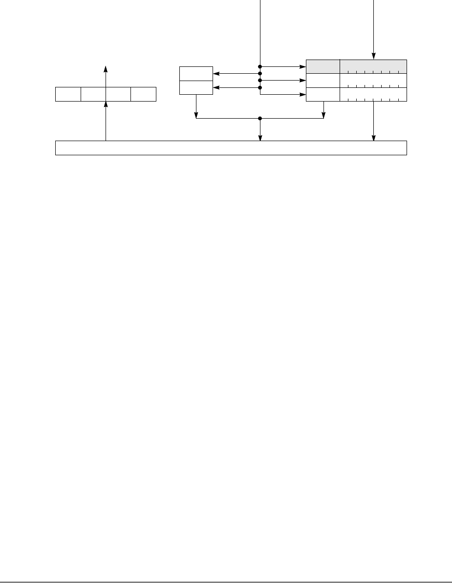
Chapter 1. Overview
1-9
high priority operation that ensures a deterministic response behavior when snooping hits
a modified sector.
Figure 1-2. Memory Unit
The other two elements in the write queue are used for store operations and writing back
modified sectors that have been deallocated by updating the queue; that is, when a cache
location is full, the least-recently used cache sector is deallocated by first being copied into
the write queue and from there to system memory. Note that snooping can occur after a
sector has been pushed out into the write queue and before the data has been written to
system memory. Therefore, to maintain a coherent memory, the write queue elements are
compared to snooped addresses in the same way as the cache tags. If a snoop hits a write
queue element, the data is first stored in system memory before it can be loaded into the
cache of the snooping bus master. Coherency checking between the cache and the write
queue prevents dependency conflicts. Single-beat writes in the write queue are not snooped;
coherency is ensured through the use of special cache operations that accompany the
single-beat write operation on the bus.
Execution of a load or store instruction is considered complete when the associated address
translation completes, guaranteeing that the instruction has completed to the point where it
is known that it will not generate an internal exception. However, after address translation
is complete, a read or write operation can still generate an external exception.
Load and store instructions are always issued and translated in program order with respect
to other load and store instructions. However, a load or store operation that hits in the cache
can complete ahead of those that miss in the cache; additionally, loads and stores that miss
the cache can be reordered as they arbitrate for the system bus.
If a load or store misses in the cache, the operation is managed by the memory unit which
prioritizes accesses to the system bus. Read requests, such as loads, RWITMs, and
instruction fetches have priority over single-beat write operations. The priorities for
accessing the system bus are listed in Section 4.10.2, “Memory Unit Queuing Priorities.”
READ
QUEUE WRITE QUEUE
SNOOP
ADDRESS DATA
ADDRESS
(from cache) DATA
(from cache)
SYSTEM INTERFACE
(to cache)
DATA QUEUE
(four word)

1-10
PowerPC 601 RISC Microprocessor User's Manual
The 601 ensures memory consistency by comparing target addresses and prohibiting
instructions from completing out of order if an address matches. Load and store operations
can be forced to execute in strict program order.
1.1.8 System Interface
Because the cache on the 601 is an on-chip, write-back primary cache, the predominant
type of transaction for most applications is burst-read memory operations, followed by
burst-write memory operations, I/O controller interface operations, and single-beat
(noncacheable or write-through) memory read and write operations. Additionally, there can
be address-only operations, variants of the burst and single-beat operations (global memory
operations that are snooped, and atomic memory operations, for example), and address
retry activity (for example, when a snooped read access hits a modified line in the cache).
Memory accesses can occur in single-beat (1–8 bytes) and four-beat burst (32 bytes) data
transfers. The address and data buses are independent for memory accesses to support
pipelining and split transactions. The 601 can pipeline as many as two transactions and has
limited support for out-of-order split-bus transactions.
Access to the system interface is granted through an external arbitration mechanism that
allows devices to compete for bus mastership. This arbitration mechanism is flexible,
allowing the 601 to be integrated into systems that implement various fairness and bus
parking procedures to avoid arbitration overhead. Additional multiprocessor support is
provided through coherency mechanisms that provide snooping, external control of the
on-chip cache and TLB, and support for a secondary cache. Multiprocessor software
support is provided through the use of atomic memory operations.
Typically, memory accesses are weakly ordered—sequences of operations, including
load/store string and multiple instructions, do not necessarily complete in the order they
begin—maximizing the efficiency of the bus without sacrificing coherency of the data. The
601 allows read operations to precede store operations (except when a dependency exists,
of course). In addition, the 601 can be configured to reorder high priority write operations
ahead of lower priority store operations. Because the processor can dynamically optimize
run-time ordering of load/store traffic, overall performance is improved.
1.2 Levels of the PowerPC Architecture
The PowerPC architecture consists of the following layers, and adherence to the PowerPC
architecture can be measured in terms of which of the following levels of the architecture
is implemented:
• PowerPC user instruction set architecture—Defines the base user-level instruction
set, user-level registers, data types, floating-point exception model, memory models
for a uniprocessor environment, and programming model for uniprocessor
environment.

Chapter 1. Overview
1-11
• PowerPC virtual environment architecture—Describes the memory model for a
multiprocessor environment, defines cache control instructions, and describes other
aspects of virtual environments. Implementations that conform to the PowerPC
virtual environment architecture also adhere to the PowerPC user instruction set
architecture, but may not necessarily adhere to the PowerPC operating environment
architecture.
• PowerPC operating environment architecture—Defines the memory management
model, supervisor-level registers, synchronization requirements, and the exception
model. Implementations that conform to the PowerPC operating environment
architecture also adhere to the PowerPC user instruction set architecture and the
PowerPC virtual environment architecture definition.
Note that while the 601 is said to adhere to the PowerPC architecture at all three levels, it
diverges in aspects of its implementation to a greater extent than should be expected of
subsequent PowerPC processors. Many of the differences result from the fact that the 601
design provides compatibility with an existing architecture standard (POWER), while
providing a reliable platform for hardware and software development compatible with
subsequent PowerPC processors.
Note that except for the POWER instructions and the RTC implementation, the differences
between the 601 and the PowerPC architecture are primarily differences in the operating
environment architecture.
The PowerPC architecture allows a wide range of designs for such features as cache and
system interface implementations.
1.3 The 601 as a PowerPC Implementation
The PowerPC architecture is derived from the IBM Performance Optimized with Enhanced
RISC (POWER) architecture. The PowerPC architecture shares the benefits of the POWER
architecture optimized for single-chip implementations. The architecture design facilitates
parallel instruction execution and is scalable to take advantage of future technological
gains. For compatibility, the 601 also implements instructions from the POWER user
programming model that are not part of the PowerPC definition.

1-12
PowerPC 601 RISC Microprocessor User's Manual
This section describes the PowerPC architecture in general, noting where the 601 differs.
The organization of this section follows the sequence of the chapters in this manual as
follows:
• Features—Section 1.3.1, “Features,” describes general features that the 601 shares
with the PowerPC family of microprocessors. It does not list PowerPC features not
implemented in the 601.
• Registers and programming model—Section 1.3.2, “Registers and Programming
Model,” describes the registers for the operating environment architecture common
among PowerPC processors and describes the programming model. It also describes
differences in how the registers are used in the 601 and describes the additional
registers that are unique to the 601.
• Instruction set and addressing modes—Section 1.3.3, “Instruction Set and
Addressing Modes,” describes the PowerPC instruction set and addressing modes
for the PowerPC operating environment architecture. It defines the PowerPC
instructions implemented in the 601 as well as additional instructions implemented
in the 601 but not defined in the PowerPC architecture.
• Cache implementation—Section 1.3.4, “Cache Implementation,” describes the
cache model that is defined generally for PowerPC processors by the virtual
environment architecture. It also provides specific details about the 601 cache
implementation.
• Exception model—Section 1.3.5, “Exception Model,” describes the exception
model of the PowerPC operating environment architecture and the differences in the
601 exception model.
• Memory management—Section 1.3.6, “Memory Management,” describes generally
the conventions for memory management among the PowerPC processors. This
section also describes the general differences between the 601 and the 32-bit
PowerPC memory management specification.
• Instruction timing—Section 1.3.7, “601 Instruction Timing,” provides a general
description of the instruction timing provided by the superscalar, parallel execution
supported by the PowerPC architecture.
• System interface—Section 1.3.8, “System Interface,” describes the signals
implemented on the 601.
1.3.1 Features
The 601 is a high-performance, superscalar PowerPC implementation. The PowerPC
architecture allows optimizing compilers to schedule instructions to maximize performance
through efficient use of the PowerPC instruction set and register model. The multiple,
independent execution units allow compilers to maximize parallelism and instruction

Chapter 1. Overview
1-13
throughput. Compilers that take advantage of the flexibility of the PowerPC architecture
can additionally optimize system performance of the PowerPC processors.
The 601 implements the PowerPC architecture, with the extensions and variances listed in
Appendix H, “Implementation Summary for Programmers.”
Specific features of the 601 are listed in Section 1.1.1, “601 Features.”
1.3.2 Registers and Programming Model
The following subsections describe the general features of the PowerPC registers and
programming model and of the specific 601 implementation, respectively.
1.3.2.1 PowerPC Registers and Programming Model
The PowerPC architecture defines register-to-register operations for most computational
instructions. Source operands for these instructions are accessed from the registers or are
provided as immediate values embedded in the instruction opcode. The three-register
instruction format allows specification of a target register distinct from the two source
operands. Load and store instructions transfer data between registers and memory.
PowerPC processors have two levels of privilege—supervisor mode of operation (typically
used by the operating environment) and one that corresponds to the user mode of operation
(used by the application software). The programming models incorporate 32 GPRs, 32
FPRs, special-purpose registers (SPRs), and several miscellaneous registers. Note that there
are several registers that are part of the PowerPC architecture that are not implemented in
the 601; for example, the time base registers are not implemented in the 601. Likewise, each
PowerPC implementation has its own unique set of hardware implementation (HID)
registers, which are implementation-specific.
This division allows the operating system to control the application environment (providing
virtual memory and protecting operating-system and critical machine resources).
Instructions that control the state of the processor, the address translation mechanism, and
supervisor registers can be executed only when the processor is operating in supervisor
mode.
The following sections summarize the PowerPC registers that are implemented in the 601
processor. Chapter 2, “Register Models and Data Types,” provides more detailed
information about the registers implemented in the 601.
1.3.2.1.1 General-Purpose Registers (GPRs)
The PowerPC architecture defines 32 user-level, general-purpose registers (GPRs). These
registers are either 32 bits wide in 32-bit PowerPC implementations and 64 bits wide in
64-bit PowerPC implementations. The GPRs serve as the data source or destination for all
integer instructions.

1-14
PowerPC 601 RISC Microprocessor User's Manual
1.3.2.1.2 Floating-Point Registers (FPRs)
The PowerPC architecture also defines 32 user-level 64-bit floating-point registers (FPRs).
The FPRs serve as the data source or destination for floating-point instructions. These
registers can contain data objects of either single- or double-precision floating-point
formats.
1.3.2.1.3 Condition Register (CR)
The CR is a 32-bit user-level register that consists of eight four-bit fields that reflect the
results of certain operations, such as move, integer and floating-point compare, arithmetic,
and logical instructions, and provide a mechanism for testing and branching.
1.3.2.1.4 Floating-Point Status and Control Register (FPSCR)
The floating-point status and control register (FPSCR) is a user-level register that contains
all exception signal bits, exception summary bits, exception enable bits, and rounding
control bits needed for compliance with the IEEE 754 standard.
1.3.2.1.5 Machine State Register (MSR)
The machine state register (MSR) is a supervisor-level register that defines the state of the
processor. The contents of this register is saved when an exception is taken and restored
when the exception handling completes. The 601 implements the MSR as a 32-bit register;
64-bit PowerPC processors implement a 64-bit MSR.
1.3.2.1.6 Segment Registers (SRs)
For memory management, 32-bit PowerPC implementations implement sixteen 32-bit
segment registers (SRs). Figure 2-12 shows the format of a segment register when the T bit
is cleared and Figure 2-13 shows the layout when the T bit (SR[0]) is set. The fields in the
segment register are interpreted differently depending on the value of bit 0.
1.3.2.1.7 Special-Purpose Registers (SPRs)
The PowerPC operating environment architecture defines numerous special-purpose
registers that serve a variety of functions, such as providing controls, indicating status,
configuring the processor, and performing special operations. Some SPRs are accessed
implicitly as part of executing certain instructions. All SPRs can be accessed by using the
Move to/from Special Purpose Register instructions, mtspr and mfspr.
In the 601, all SPRs are 32 bits wide.
1.3.2.1.8 User-Level SPRs
The following 601 SPRs are accessible by user-level software:
• Link register (LR)—The link register can be used to provide the branch target
address and to hold the return address after branch and link instructions. The LR is
32 bits wide in 32-bit implementations.
• Count register (CTR)—The CTR is decremented and tested automatically as a result
of branch-and-count instructions. The CTR is 32 bits wide in 32-bit
implementations.

Chapter 1. Overview 1-15
• Integer exception register (XER)—The 32-bit XER contains the integer carry and
overflow bits and two fields for the Load String and Compare Byte Indexed (lscbx)
instruction (a POWER instruction implemented in the 601 but not defined by the
PowerPC architecture).
1.3.2.1.9 Supervisor-Level SPRs
The 601 also contains SPRs that can be accessed only by supervisor-level software. These
registers consist of the following:
• The 32-bit data access exception (DAE)/source instruction service register (DSISR)
defines the cause of data access and alignment exceptions.
• The data address register (DAR) is a 32-bit register that holds the address of an
access after an alignment or data access exception.
• Decrementer register (DEC) is a 32-bit decrementing counter that provides a
mechanism for causing a decrementer exception after a programmable delay.
PowerPC architecture defines that the DEC frequency be provided as a subdivision
of the processor clock frequency; however, the 601 implements a separate clock
input that serves both the DEC and the RTC facilities.
• The 32-bit table search description register 1(SDR1) specifies the page table format
used in logical-to-physical address translation for pages.
• The machine status save/restore register 0 (SRR0) is a 32-bit register that is used by
the 601 for saving the address of the instruction that caused the exception, and the
address to return to when a Return from Interrupt (rfi) instruction is executed.
• The machine status save/restore register 1 (SRR1) is a 32-bit register used to save
machine status on exceptions and to restore machine status when an rfi instruction
is executed.
• General SPRs, SPRG0–SPRG3, are 32-bit registers provided for operating system
use.
• The external access register (EAR) is a 32-bit register that controls access to the
external control facility through the External Control Input Word Indexed (eciwx)
and External Control Output Word Indexed (ecowx) instructions.
• The processor version register (PVR) is a 32-bit, read-only register that identifies the
version (model) and revision level of the PowerPC processor.
• Block address translation (BAT) registers—The PowerPC architecture defines 16
BAT registers, divided into four pairs of data BATs (DBATs) and four pairs of
instruction BATs (IBATs). The 601 includes four pairs of unified BATs
(BAT0U–BAT3U and BAT0L–BAT3L). See Figure 1-3 for a list of the SPR
numbers for the BAT registers. Figure 2-23 and Figure 2-24 show the format of the
upper and lower BAT registers. Note that the format for the 601’s implementation of
the BAT registers differs from the PowerPC architecture definition.

1-16 PowerPC 601 RISC Microprocessor User's Manual
1.3.2.2 Additional Registers in the 601
During normal execution, a program can access the registers, shown in Figure 1-3,
depending on the program’s access privilege (supervisor or user, determined by the
privilege-level (PR) bit in the machine state register (MSR)). Note that registers such as the
general-purpose registers (GPRs) and floating-point registers (FPRs) are accessed through
operands that are part of the instructions. Access to registers can be explicit (that is, through
the use of specific instructions for that purpose such as Move to Special-Purpose Register
(mtspr) and Move from Special-Purpose Register (mfspr) instructions) or implicit as the
part of the execution of an instruction. Some registers are accessed both explicitly and
implicitly.
The numbers to the left of the SPRs indicate the number that is used in the syntax of the
instruction operands to access the register.
Figure 1-3 shows all the 601 registers and includes the following registers that are not part
of the PowerPC architecture:
• Real-time clock (RTC) registers—RTCU and RTCL (RTC upper and RTC lower).
The registers can be read from by user-level software, but can be written to only by
supervisor-level software. As shown in Figure 1-3, the SPR numbers for the RTC
registers depend on the type of access used. For more information, see
Section 2.2.5.3, “Real-Time Clock (RTC) Registers (User-Level).”
• MQ register (MQ). The MQ register is a 601-specific, 32-bit register used as a
register extension to accommodate the product for the multiply instructions and the
dividend for the divide instructions. It is also used as an operand of long rotate and
shift instructions. This register, and the instructions that require it, is provided for
compatibility with POWER architecture, and is not part of the PowerPC
architecture. For more information, see Section 2.2.5.1, “MQ Register (MQ).” The
MQ register is typically accessed implicitly as part of executing a computational
instruction.
• Block-address translation (BAT) registers. The 601 includes eight block-address
translation registers (BATs), consisting of four pairs of BATs (IBAT0U–IBAT3U
and IBAT0L–IBAT3L). See Figure 1-3 for a list of the SPR numbers for the BAT
registers. Figure 2-23 and Figure 2-24 show the formats of the upper and lower BAT
registers. Note that the PowerPC architecture has twice as many BAT registers as the
601.
• Hardware implementation registers (HID0–HID2, HID5, and HID15). These
registers are provided primarily for debugging. For more information, see Section
2.3.3.13.1, “Checkstop Sources and Enables Register—HID0” through Section
2.3.3.13.5, “Processor Identification Register (PIR)—HID15.” HID15 holds the
four-bit processor identification tag (PID) that is useful for differentiating processors
in multiprocessor system designs. For more information, see Section 2.3.3.13.5,
“Processor Identification Register (PIR)—HID15.” Note that while it is not
guaranteed that the implementation of HID registers is consistent among PowerPC
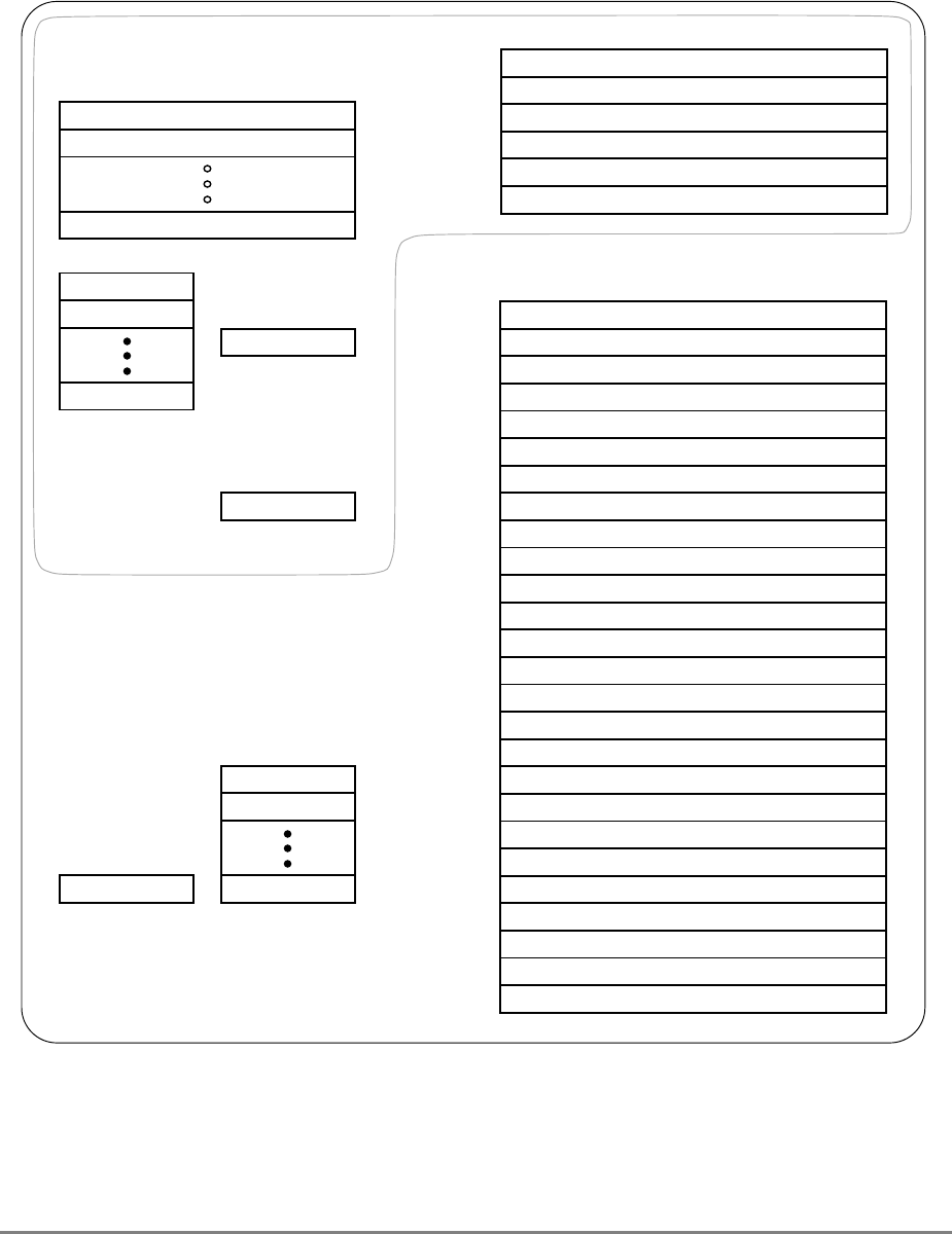
Chapter 1. Overview 1-17
processors, other processors may be designed with similar or identical HID
registers.
Figure 1-3. PowerPC 601 Microprocessor Programming Model—Registers
GPR0
GPR1
GPR31
031
User-Level SPRs
SPR0 MQ Register 1
SPR1 XER—Integer Exception Register
SPR4 RTCU—RTC Upper Register (For reading only)1,3
SPR5 RTCL—RTC Lower Register (For reading only)1,3
SPR8 LR—Link Register
SPR9 CTR—Count Register
USER PROGRAMMING
MODEL
Supervisor-Level SPRs
SPR18 DSISR—DAE/ Source Instruction Service Register
SPR19 DAR—Data Address Register
SPR20 RTCU—RTC Upper Register (For writing only)1,3
SPR21 RTCL—RTC Lower Register (For writing only)1,3
SPR22 DEC—Decrementer Register4
SPR25 SDR1—Table Search Description Register 1
SPR26 SRR0—Save and Restore Register 0
SPR27 SRR1—Save and Restore Register 1
SPR272 SPRG0—SPR General 0
SPR273 SPRG1—SPR General 1
SPR274 SPRG2—SPR General 2
SPR275 SPRG3—SPR General 3
SPR282 EAR—External Access Register
SPR287 PVR—Processor Version Register
SPR528 IBAT0U—BAT 0 Upper 2
SPR529 IBAT0L—BAT 0 Lower 2
SPR530 IBAT1U—BAT 1 Upper 2
SPR531 IBAT1L—BAT 1 Lower 2
SPR532 IBAT2U—BAT 2 Upper 2
SPR533 IBAT2L—BAT 2 Lower 2
SPR534 IBAT3U—BAT 3 Upper 2
SPR535 IBAT3L—BAT 3 Lower 2
SPR1008 HID0 1
SPR1009 HID1 1
SPR1010 HID2 (IABR) 1
SPR1013 HID5 (DABR) 1
063
SUPERVISOR PROGRAMMING
MODEL
Machine State
Register 2
1 601-only registers. These registers are not necessarily supported by other PowerPC processors.
2 These registers may be implemented differently on other PowerPC processors. The PowerPC architecture defines two sets of
BAT registers—eight IBATs and eight DBATs. The 601 implements the IBATs and treats them as unified BATs.
3 RTCU and RTCL registers can be written only in supervisor mode, in which case different SPR numbers are used.
4 DEC register can be read by user programs by specifying SPR6 in the mfspr instruction (for POWER compatibility).
FPR0
FPR1
FPR31
MSR
031
031
031
Segment
Registers
SR0
SR1
SR15
031
Floating Point
Status and
Control
Register
CR
031
FPSCR
031
Condition
Register

1-18 PowerPC 601 RISC Microprocessor User's Manual
1.3.3 Instruction Set and Addressing Modes
The following subsections describe the PowerPC instruction set and addressing modes in
general. Differences in the 601’s instruction set are described in Section 1.3.3.2, “601
Instruction Set.”
1.3.3.1 PowerPC Instruction Set and Addressing Modes
All PowerPC instructions are encoded as single-word (32-bit) opcodes. Instruction formats
are consistent among all instruction types, permitting efficient decoding to occur in parallel
with operand accesses. This fixed instruction length and consistent format greatly simplifies
instruction pipelining.
1.3.3.1.1 PowerPC Instruction Set
The PowerPC instructions are divided into the following categories:
• Integer instructions—These include computational and logical instructions.
— Integer arithmetic instructions
— Integer compare instructions
— Integer logical instructions
— Integer rotate and shift instructions
• Floating-point instructions—These include floating-point computational
instructions, as well as instructions that affect the floating-point status and control
register (FPSCR).
— Floating-point arithmetic instructions
— Floating-point multiply/add instructions
— Floating-point rounding and conversion instructions
— Floating-point compare instructions
— Floating-point status and control instructions
• Load/store instructions—These include integer and floating-point load and store
instructions.
— Integer load and store instructions
— Integer load and store multiple instructions
— Floating-point load and store
— Floating-point move instructions
— Primitives used to construct atomic memory operations (lwarx and stwcx.
instructions)
• Flow control instructions—These include branching instructions, condition register
logical instructions, trap instructions, and other instructions that affect the
instruction flow.
— Branch and trap instructions
— Condition register logical instructions

Chapter 1. Overview 1-19
• Processor control instructions—These instructions are used for synchronizing
memory accesses and management of caches, UTLBs, and the segment registers.
— Move to/from special purpose register instructions
— Move to/from MSR
— Synchronize
— Instruction synchronize
— TLB invalidate
• Memory control instructions—These instructions provide control of caches, TLBs,
and segment registers.
— Supervisor-level cache management instructions
— User-level cache instructions
— Segment register manipulation instructions
— Translation lookaside buffer management instructions
Note that this grouping of the instructions does not indicate which execution unit executes
a particular instruction or group of instructions. This information, which is useful in taking
full advantage of superscalar parallel instruction execution, is provided in Chapter 7,
“Instruction Timing,” and Chapter 10, “Instruction Set.”
Integer instructions operate on byte, half-word, and word operands. Floating-point
instructions operate on single-precision (one word) and double-precision (one double
word) floating-point operands. The PowerPC architecture uses instructions that are four
bytes long and word-aligned. It provides for byte, half-word, and word operand loads and
stores between memory and a set of 32 general-purpose registers (GPRs). It also provides
for word and double-word operand loads and stores between memory and a set of 32
floating-point registers (FPRs).
Computational instructions do not modify memory. To use a memory operand in a
computation and then modify the same or another memory location, the memory contents
must be loaded into a register, modified, and then written back to the target location with
distinct instructions.
PowerPC processors follow the program flow when they are in the normal execution state.
However, the flow of instructions can be interrupted directly by the execution of an
instruction or by an asynchronous event. Either kind of exception may cause one of several
components of the system software to be invoked.
1.3.3.1.2 Calculating Effective Addresses
The effective address (EA) is the 32-bit address computed by the processor when executing
a memory access or branch instruction or when fetching the next sequential instruction.

1-20 PowerPC 601 RISC Microprocessor User's Manual
The PowerPC architecture supports two simple memory addressing modes:
• EA = (rA|0) + offset (including offset = 0) (register indirect with immediate index)
• EA = (rA|0) + rB (register indirect with index)
These simple addressing modes allow efficient address generation for memory accesses.
Calculation of the effective address for aligned transfers occurs in a single clock cycle.
For a memory access instruction, if the sum of the effective address and the operand length
exceeds the maximum effective address, the storage operand is considered to wrap around
from the maximum effective address to effective address 0.
Effective address computations for both data and instruction accesses use 32-bit unsigned
binary arithmetic. A carry from bit 0 is ignored in 32-bit implementations.
1.3.3.2 601 Instruction Set
The 601 instruction set is defined as follows:
• The 601 implements the 32-bit PowerPC architecture instructions except as
indicated in Appendix C, “PowerPC Instructions Not Implemented.” Otherwise, all
instructions not implemented in the 601 are defined as optional in the PowerPC
architecture.
• The 601 supports a number of POWER instructions that are otherwise not
implemented in the PowerPC architecture. These are listed in Appendix B,
“POWER Architecture Cross Reference.” Individual instructions are described in
Chapter 10, “Instruction Set.”
• The 601 implements the External Control Input Word Indexed (eciwx) and External
Control Output Word Indexed (ecowx) instructions, which are optional in the
PowerPC architecture definition.
• Several of the instructions implemented in the 601 function somewhat differently
than they are defined in the PowerPC architecture. These differences typically stem
from design differences; for instance, the PowerPC architecture defines several
cache control instructions specific to separate instruction and data cache designs.
When executed on the 601, such instructions may provide a subset of the functions
of the instruction or they may be no-ops.
For a list of all PowerPC instructions and all 601-specific instructions, see Appendix A,
“Instruction Set Listings.” Chapter 10, “Instruction Set,” describes each instruction,
indicating whether an instruction is 601-specific and describing any differences in the
implementation on the 601.
1.3.4 Cache Implementation
The following subsections describe the PowerPC architecture’s treatment of cache in
general, and the 601-specific implementation, respectively.

Chapter 1. Overview 1-21
1.3.4.1 PowerPC Cache Characteristics
The PowerPC architecture does not define hardware aspects of cache implementations. For
example, some PowerPC processors may have separate instruction and data caches
(Harvard architecture), while others, such as the 601, implement a unified cache.
PowerPC implementations can control the following memory access modes on a page or
block basis:
• Write-back/write-through mode
• Cache-inhibited mode
• Memory coherency
Note that in the 601 processor, a block is defined as an eight-word sector. The PowerPC
virtual environment architecture defines cache management instructions that provide a
means by which the application programmer can affect the cache contents.
1.3.4.2 601 Cache Implementation
The 601 has a 32-Kbyte, eight-way set-associative unified (instruction and data) cache. The
cache is physically addressed and can operate in either write-back or write-through mode
as specified by the PowerPC architecture.
The cache is configured as eight sets of 64 lines. Each line consists of two sectors, four state
bits (two per sector), several replacement control bits, and an address tag. The two state bits
implement the four-state MESI (modified-exclusive-shared-invalid) protocol. Each sector
contains eight 32-bit words. Note that the PowerPC architecture defines the term block as
the cacheable unit. For the 601 processor, the block is a sector. A block diagram of the cache
organization is shown in Figure 1-4.
Each cache line contains 16 contiguous words from memory that are loaded from a 16-word
boundary (that is, bits A26–A31 of the logical addresses are zero); thus, a cache line never
crosses a page boundary. Misaligned accesses across a page boundary can incur a
performance penalty.
Cache reload operations are always performed on a sector basis (that is, the cache is
snooped and updated and coherency is maintained on a per-sector basis). However, if the
other sector in the line is marked invalid, an optional, low-priority update of that sector is
attempted after the sector that contained the critical word is filled. The ability to attempt the
other sector update can be disabled by the system software.
External bus transactions that load instructions or data into the cache always transfer the
missed quad word first, regardless of its location in a cache sector; then the rest of the cache
sector is filled. As the missed quad word is loaded into the cache, it is simultaneously
forwarded to the appropriate execution unit so instruction execution resumes as quickly as
possible.
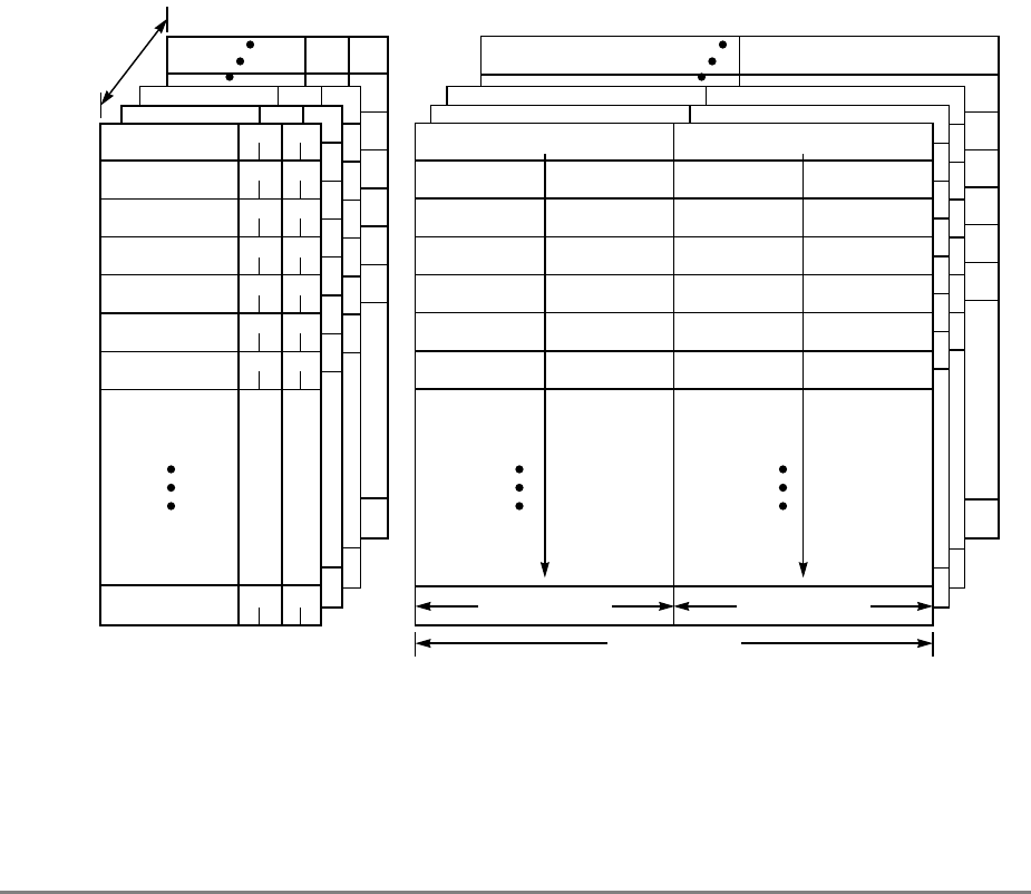
1-22 PowerPC 601 RISC Microprocessor User's Manual
To ensure coherency among caches in a multiprocessor (or multiple caching-device)
implementation, the 601 implements the MESI protocol. MESI stands for
modified/exclusive/shared/invalid. These four states indicate the state of the cache block as
follows:
• Modified—The cache block is modified with respect to system memory; that is, data
for this address is valid only in the cache and not in system memory.
• Exclusive—This cache block holds valid data that is identical to the data at this
address in system memory. No other cache has this data.
• Shared—This cache block holds valid data that is identical to this address in system
memory and at least one other caching device.
• Invalid—This cache block does not hold valid data.
Cache coherency is enforced by on-chip hardware bus snooping logic. Since the cache tag
directory has a separate port dedicated to snooping bus transactions, bus snooping traffic
does not interfere with processor access to the cache unless a snoop hit occurs.
Figure 1-4. Cache Unit Organization
1.3.5 Exception Model
The following subsections describe the PowerPC exception model and the 601
implementation, respectively.
LINE 63
LINE 0 ADDRESS TAG
ADDRESS TAG
SECTOR 0 SECTOR 1
8 WORDS 8 WORDS
16 WORDS
8 SETS

Chapter 1. Overview 1-23
1.3.5.1 PowerPC Exception Model
The PowerPC exception mechanism allows the processor to change to supervisor state as a
result of external signals, errors, or unusual conditions arising in the execution of
instructions. When exceptions occur, information about the state of the processor is saved
to certain registers and the processor begins execution at an address (exception vector)
predetermined for each exception. The exception handler at the specified vector is then
processed with the processor in supervisor mode. The PowerPC exception model is
described in detail in Chapter 5, “Exceptions.”
Although multiple exception conditions can map to a single exception vector, a more
specific condition may be determined by examining a register associated with the
exception—for example, the DAE/source instruction service register (DSISR) and the
floating-point status and control register (FPSCR). Additionally, some exception conditions
can be explicitly enabled or disabled by software.
The PowerPC architecture requires that exceptions be handled in program order; therefore,
although a particular implementation may recognize exception conditions out of order, they
are presented strictly in order. When an instruction-caused exception is recognized, any
unexecuted instructions that appear earlier in the instruction stream, including any that have
not yet entered the execute state, are required to complete before the exception is taken. Any
exceptions caused by those instructions are handled first. Likewise, exceptions that are
asynchronous and precise are recognized when they occur, but are not handled until all
instructions currently in the execute stage successfully complete execution and report their
results.
Unless a catastrophic condition causes a system reset or machine check exception, only one
exception is handled at a time. If, for example, a single instruction encounters multiple
exception conditions, those conditions are encountered sequentially. After the exception
handler handles an exception, the instruction execution continues until the next exception
condition is encountered. However, in many cases there is no attempt to reexecute the
instruction. This method of recognizing and handling exception conditions sequentially
guarantees that exceptions are recoverable.
Exception handlers should save the information stored in SRR0 and SRR1 early to prevent
the program state from being lost due to a system reset and machine check exception or to
an instruction-caused exception in the exception handler, and before enabling external
interrupts.
The PowerPC architecture supports four types of exceptions:
• Synchronous, precise—These are caused by instructions. All instruction-caused
exceptions are handled precisely; that is, the machine state at the time the exception
occurs is known and can be completely restored. This means that (excluding the trap
and system call exceptions) the address of the faulting instruction is provided to the
exception handler and that neither the faulting instruction nor subsequent
instructions in the code stream will complete execution. The instructions that invoke

1-24 PowerPC 601 RISC Microprocessor User's Manual
trap and system call exceptions complete execution before the exception is taken.
When exception processing completes, execution resumes at the address of the next
instruction.
• Synchronous, imprecise—The PowerPC architecture defines two imprecise
floating-point exception modes, recoverable and nonrecoverable. Even though the
601 provides a means to enable the imprecise modes, it implements these modes
identically to the precise mode (i.e., all enabled floating-point enabled exceptions
are always precise on the 601).
• Asynchronous, precise—The external interrupt and decrementer exceptions are
maskable asynchronous exceptions that are handled precisely. When these
exceptions occur, their handling is postponed until all instructions, and any
exceptions associated with those instructions, complete execution.
• Asynchronous, imprecise—There are two non-maskable asynchronous exceptions
that are imprecise: system reset and machine check exceptions. These exceptions
may not be recoverable, or may provide a limited degree of recoverability for
diagnostic purpose.
The PowerPC architecture defines several of the exceptions differently than the 601
implementation. For example, the PowerPC exception model provides a unique vector for
the trace exception; the 601 vectors trace exceptions to the run-mode exception handler.
Other differences are noted in the following section, Section 1.3.5.2, “The 601 Exception
Model.”
1.3.5.2 The 601 Exception Model
As specified by the PowerPC architecture, all 601 exceptions can be described as either
precise or imprecise and either synchronous or asynchronous. Asynchronous exceptions are
caused by events external to the processor’s execution; synchronous exceptions, which are
all handled precisely by the 601, are caused by instructions.
The 601 exception classes are shown in Table 1-1.
Although exceptions have other characteristics as well, such as whether they are maskable
or nonmaskable, the distinctions shown in Table 1-1 define categories of exceptions that the
601 handles uniquely. Note that Table 1-1 includes no synchronous imprecise instructions.
Table 1-1. PowerPC 601 Microprocessor Exception Classifications
Synchronous/Asynchronous Precise/Imprecise Exception Type
Asynchronous Imprecise Machine check
System reset
Asynchronous Precise External interrupt
Decrementer
Synchronous Precise Instruction-caused exceptions

Chapter 1. Overview 1-25
While the PowerPC architecture supports imprecise handling of floating-point exceptions,
the 601 implements these exception modes as precise exceptions.
The 601’s exceptions, and conditions that cause them, are listed in Table 1-2. Exceptions
that are specific to the 601 are indicated.
Table 1-2. Exceptions and Conditions
Exception
Type Vector Offset
(hex) Causing Conditions
Reserved 00000 —
System reset 00100 A system reset is caused by the assertion of either SRESET or HRESET.
Machine check 00200 A machine check is caused by the assertion of the TEA signal during a data bus
transaction.
Data access 00300 The cause of a data access exception can be determined by the bit settings in
the DSISR, listed as follows:
1 Set if the translation of an attempted access is not found in the primary
hash table entry group (HTEG), or in the rehashed secondary HTEG, or in
the range of a BAT register; otherwise cleared.
4 Set if a memory access is not permitted by the page or BAT protection
mechanism described in Chapter 6, “Memory Management Unit”; otherwise
cleared.
5 Set if the access was to an I/O segment (SR[T] =1) by an eciwx, ecowx,
lwarx, stwcx., or lscbx instruction; otherwise cleared. Set by an eciwx or
ecowx instruction if the access is to an address that is marked as
write-through.
6 Set for a store operation and cleared for a load operation.
9 Set if an EA matches the address in the DABR while in one of the three
compare modes.
11 Set if eciwx or ecowx is used and EAR[E] is cleared.
Instruction
access 00400 An instruction access exception is caused when an instruction fetch cannot be
performed for any of the following reasons:
• The effective (logical) address cannot be translated. That is, there is a page
fault for this portion of the translation, so an instruction access exception
must be taken to retrieve the translation from a storage device such as a
hard disk drive.
• The fetch access is to an I/O segment.
• The fetch access violates memory protection. If the key bits (Ks and Ku) in
the segment register and the PP bits in the PTE or BAT are set to prohibit
read access, instructions cannot be fetched from this location.
External
interrupt 00500 An external interrupt occurs when the INT signal is asserted.
Alignment 00600 An alignment exception is caused when the 601 cannot perform a memory
access for any of several reasons, such as when the operand of a floating-point
load or store operation is in an I/O segment (SR[T] = 1) or when a scalar
load/store operand crosses a page boundary. Specific exception sources are
described in Section 5.4.6, “Alignment Exception (x'00600').”

1-26 PowerPC 601 RISC Microprocessor User's Manual
Program 00700 A program exception is caused by one of the following exception conditions,
which correspond to bit settings in SRR1 and arise during execution of an
instruction:
• Floating-point enabled exception—A floating-point enabled exception
condition is generated when the following condition is met:
(MSR[FE0] | MSR[FE1]) & FPSCR[FEX] is 1.
FPSCR[FEX] is set by the execution of a floating-point instruction that
causes an enabled exception or by the execution of a “move to FPSCR”
instruction that results in both an exception condition bit and its
corresponding enable bit being set in the FPSCR.
• Illegal instruction—An illegal instruction program exception is generated
when execution of an instruction is attempted with an illegal opcode or illegal
combination of opcode and extended opcode fields (including PowerPC
instructions not implemented in the 601), or when execution of an optional
instruction not provided in the 601 is attempted (these do not include those
optional instructions that are treated as no-ops). The PowerPC instruction
set is described in Chapter 3, “Addressing Modes and Instruction Set
Summary.”
• Privileged instruction—A privileged instruction type program exception is
generated when the execution of a privileged instruction is attempted and the
MSR register user privilege bit, MSR[PR], is set. In the 601, this exception is
generated for mtspr or mfspr with an invalid SPR field if SPR[0] = 1 and
MSR[PR] = 1. This may not be true for all PowerPC processors.
• Trap—A trap type program exception is generated when any of the
conditions specified in a trap instruction is met.
Floating-point
unavailable 00800 A floating-point unavailable exception is caused by an attempt to execute a
floating-point instruction (including floating-point load, store, and move
instructions) when the floating-point available bit is disabled, MSR[FP] = 0.
Decrementer 00900 The decrementer exception occurs when the most significant bit of the
decrementer (DEC) register transitions from 0 to 1. Must also be enabled with
the MSR[EE] bit.
I/O controller
interface error 00A00 An I/O controller interface error exception is taken only when an operation to an
I/O controller interface segment fails (such a failure is indicated to the 601 by a
particular bus reply packet). If an I/O controller interface exception is taken on a
memory access directed to an I/O segment, the SRR0 contains the address of
the instruction following the offending instruction. Note that this exception is not
implemented in other PowerPC processors.
Reserved 00B00 —
System call 00C00 A system call exception occurs when a System Call (sc) instruction is executed.
Reserved 00D00 Other PowerPC processors may use this vector for trace exceptions.
Reserved 00E00 The 601 does not generate an interrupt to this vector. Other PowerPC
processors may use this vector for floating-point assist exceptions.
Reserved 00E10–00FFF —
Reserved 01000–01FFF Reserved, implementation-specific
Table 1-2. Exceptions and Conditions (Continued)
Exception
Type Vector Offset
(hex) Causing Conditions

Chapter 1. Overview 1-27
1.3.6 Memory Management
The following subsections describe the PowerPC memory management architecture, and
the specific 601 implementation, respectively.
1.3.6.1 PowerPC Memory Management
The primary functions of the MMU are to translate logical (effective) addresses to physical
addresses for memory accesses, I/O accesses (most I/O accesses are assumed to be
memory-mapped), and I/O controller interface accesses, and to provide access protection
on blocks and pages of memory.
There are three types of accesses generated by the 601 that require address translation:
instruction accesses, data accesses to memory generated by load and store instructions, and
I/O controller interface accesses generated by load and store instructions.
The PowerPC MMU and exception model support demand-paged virtual memory. Virtual
memory management permits execution of programs larger than the size of physical
memory; demand-paged implies that individual pages are loaded into physical memory
from system memory only when they are first accessed by an executing program.
The hashed page table is a variable-sized data structure that defines the mapping between
virtual page numbers and physical page numbers. The page table size is a power of 2, and
its starting address is a multiple of its size.
The page table contains a number of page table entry groups (PTEGs). A PTEG contains
eight page table entries (PTEs) of eight bytes each; therefore, each PTEG is 64 bytes long.
Run mode/
trace exception 02000 The run mode exception is taken depending on the settings of the HID1 register
and the MSR[SE] bit.
The following modes correspond with bit settings in the HID1 register:
• Normal run mode—No address breakpoints are specified, and the 601
executes from zero to three instructions per cycle
• Single instruction step mode—One instruction is processed at a time. The
appropriate break action is taken after an instruction is executed and the
processor quiesces.
• Limited instruction address compare—The 601 runs at full speed (in parallel)
until the EA of the instruction being decoded matches the EA contained in
HID2. Addresses for branch instructions and floating-point instructions may
never be detected.
• Full instruction address compare mode—Processing proceeds out of IQ0.
When the EA in HID2 matches the EA of the instruction in IQ0, the
appropriate break action is performed. Unlike the limited instruction address
compare mode, all instructions pass through the IQ0 in this mode. That is,
instructions cannot be folded out of the instruction stream.
The following mode is taken when the MSR[SE] bit is set.
• MSR[SE] trace mode—Note that in other PowerPC implementations, the
trace exception is a separate exception with its own vector x'00D00'.
Table 1-2. Exceptions and Conditions (Continued)
Exception
Type Vector Offset
(hex) Causing Conditions

1-28 PowerPC 601 RISC Microprocessor User's Manual
PTEG addresses are entry points for table search operations. Figure 6-16 shows two PTEG
addresses (PTEGaddr1 and PTEGaddr2) where a given PTE may reside.
Address translations are enabled by setting bits in the MSR—MSR[IT] enables instruction
translations and MSR[DT] enables data translations.
1.3.6.2 601 Memory Management
The 601 MMU provides 4 Gbytes of logical address space accessible to supervisor and user
programs with a 4-Kbyte page size and 256-Mbyte segment size. Block sizes range from
128 Kbyte to 8 Mbyte and are software selectable. In addition, the 601 uses an interim
52-bit virtual address and hashed page tables in the generation of 32-bit physical addresses.
A UTLB provides address translation in parallel with the on-chip cache access, incurring
no additional time penalty in the event of a UTLB hit. The UTLB is a cache of the most
recently used page table entries. Software is responsible for maintaining the consistency of
the UTLB with memory. The 601’s UTLB is a 256-entry, two-way set-associative cache
that contains instruction and data address translations. The 601 provides hardware table
search capability through the hashed page table on UTLB misses. Supervisor software can
invalidate UTLB entries selectively. In addition, UTLB control instructions can optionally
be broadcast on the external interface for remote invalidations.
The 601 also provides a four-entry BAT array that maintains address translations for blocks
of memory. These entries define blocks that can vary from 128 Kbytes to 8 Mbytes. The
BAT array is maintained by system software.
To accelerate the instruction unit operation, the 601 uses a four-entry ITLB. The ITLB
contains up to four copies of the most recently used instruction address translations (page
or block) providing the instruction unit access to the most recently used translations without
requiring the UTLB or BAT array. The processor ensures that the ITLB is consistent with
the UTLB, and uses an LRU replacement algorithm when a miss is encountered.
The 601 MMU relies on the exception processing mechanism for the implementation of the
paged virtual memory environment and for enforcing protection of designated memory
areas. Exception processing is described in Chapter 5, “Exceptions.” Section 2.3.1,
“Machine State Register (MSR),” describes the MSR of the 601, which controls some of
the critical functionality of the MMU.
As specified by the PowerPC architecture, the hashed page table is a variable-sized data
structure that defines the mapping between virtual page numbers and physical page
numbers. The page table size is a power of 2, and its starting address is a multiple of its size.
Also as specified by the PowerPC architecture, the page table contains a number of PTEGs.
A PTEG contains eight page table entries (PTEs) of eight bytes each; therefore each PTEG
is 64 bytes long. PTEG addresses are entry points for table search operations. Figure 6-16
shows two PTEG addresses (PTEGaddr1 and PTEGaddr2) where a given PTE may reside.

Chapter 1. Overview 1-29
1.3.7 601 Instruction Timing
The 601 is a pipelined superscalar processor. A pipelined processor is one in which the
processing of an instruction is broken down into discrete stages, such as decode, execute,
and writeback. Because the tasks required to process an instruction are broken into a series
of tasks, an instruction does not require the entire resources of an execution unit. For
example, after an instruction completes the decode stage, it can pass on to the next stage,
while the subsequent instruction can advance into the decode stage. This improves the
throughput of the instruction flow. For example, it may take three cycles for an integer
instruction to complete, but if there are no stalls in the integer pipeline, a series of integer
instructions can have a throughput of one instruction per cycle.
A superscalar processor is one in which multiple pipelines are provided to allow
instructions to execute in parallel. The 601 has three execution units, one each for integer
instructions, floating-point instructions, and branch instructions. The IU and the FPU each
have dedicated register files for maintaining operands (GPRs and FPRs, respectively),
allowing integer calculations and floating-point calculations to occur simultaneously
without interference.
The 601 pipeline description can be broken into two parts, the processor core, where
instruction execution takes place, and the memory subsystem, the interface between the
processor core and system memory. The system memory includes a unified 32-Kbyte cache
and the bus interface unit.
Figure 1-5 shows the 601’s instruction queue and the IU, FPU, and BPU pipelines.
Each of the stages shown in Figure 1-5 is described in Section 7.2, “Pipeline Description.”
As shown in Figure 1-5, integer instructions are dispatched only from IQ0 (where they are
also usually decoded); whereas branch and floating-point instructions can be dispatched
from any of the bottom four elements in the instruction queue (IQ0–IQ3). The dispatch of
integer instructions is restricted in this manner to provide an ordered flow of instructions
through the integer pipeline, which in turn provides a mechanism that ensures that all
instructions appear to complete in order. As branch and floating-point instructions are
dispatched their position in the instruction stream is recorded by means of tags that
accompany the previous integer instruction through the integer pipeline. Note that when a
floating-point or branch instruction cannot be tagged to an integer instruction, it is tagged
to a no-op, or bubble, in the integer pipeline.
Logic associated with the integer completion (IC) stage reconstructs the program order,
checks for data dependencies, and schedules the write-back stages of the three pipelines.
Note that it is not necessary that the write-back stages need only be serialized if there are
data dependencies. For example, instructions that update the condition register (CR) must
perform write-back in strict order.
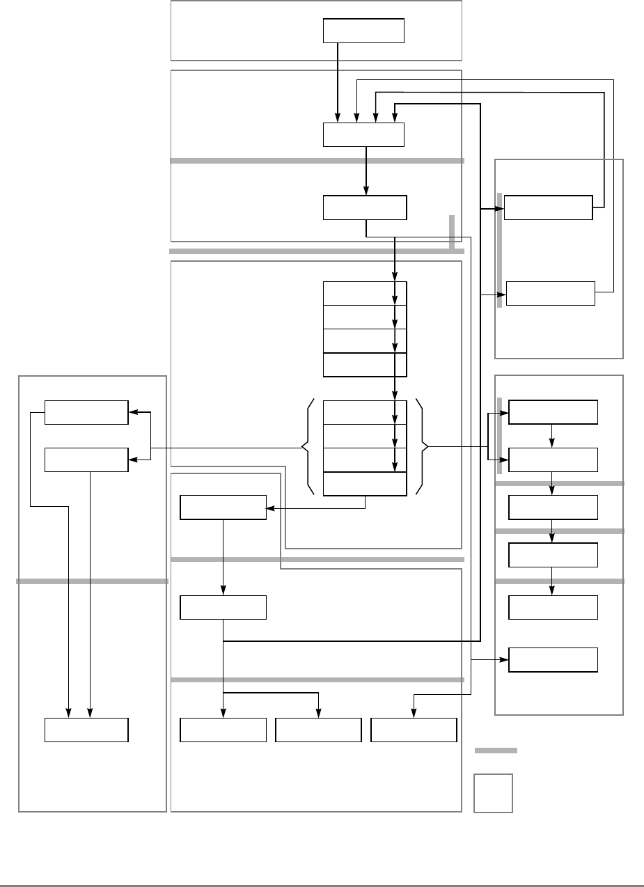
1-30 PowerPC 601 RISC Microprocessor User's Manual
.
Figure 1-5. Pipeline Diagram of the Processor Core
CARB
IQ7
IQ6
IQ1
IQ5
IQ4
IQ3
IQ2
IC
FD
FPA
FWA
FPM
F1
BE
MR
Dispatch Unit
Floating-Point
Integer Unit (IU)
Branch Processing
BW
CACC
Cache (memory subsystem)
IWA IWL
FWL
Data Access
Queueing Unit
Fetch Arbitration
Unit (BPU) = Unit Boundary
= Cycle Boundary
Unit (FPU)
FA
ISB
FPSB
ID
IE
IQ0
1 An integer instruction can be passed to the ID stage in the same cycle in which it enters IQ0.
1
(Instructions in the IQ
are said to be in the
dispatch stage (DS))

Chapter 1. Overview 1-31
The tagging mechanism is described in Section 7.3.1.4.4, “Synchronization Tags for the
Precise Exception Model.”
To minimize latencies due to data dependencies, the IU provides feed-forwarding. For
example, if an integer instruction requires data that is the result of the execution of the
previous instruction, that data is made available to the IU at the same time that the previous
instruction’s write-back stage updates the GPR. This eliminates an additional clock cycle
that would have been necessary if the IU had to access the GPR. Feed-forwarding is
available between IU execute and decode stage and IU write-back and decode stage.
Feed-forwarding is described in Section 7.2.1.2, “Integer Unit (IU).”
Most integer instructions require one clock cycle per stage. Because results for most integer
instructions are available at the end of the execute stage, a series of single-cycle integer
instructions allow a throughput of one instruction per clock cycle. Other instructions, such
as the integer multiply, require more than one clock cycle to complete execution. These
instructions reduce the throughput accordingly.
The floating-point pipeline has more stages than the IU pipeline, as shown in Figure 1-5.
The 601 supports both single- and double-precision floating-point operations, but
double-precision instructions generally take longer to execute, typically by requiring two
cycles in the FD, FPM, and FPA stages. However, many of these instructions, such as the
double-precision floating-point multiply (fmul) and double-precision floating-point
accumulate instructions (fmadd, fmsub, fnmadd, and fnmsub), allow stages to overlap.
For example, when the second cycle of the FD stage begins, the first stage of FPM begins.
Similarly the FPM stage overlaps with the FPA stage, allowing these instructions to
complete these stages in four clock cycles instead of six. The timings for these instructions
are shown in Section 7.3.4.5.2, “Double-Precision Instruction Timing.”
Because the PowerPC architecture can be applied to such a wide variety of
implementations, instruction timing among various PowerPC processors varies
accordingly.
1.3.8 System Interface
The system interface is specific for each PowerPC processor implementation.
The 601 provides a versatile system interface that allows for a wide range of
implementations. The interface includes a 32-bit address bus, a 64-bit data bus, and 52
control and information signals (see Figure 1-6). The system interface allows for
address-only transactions as well as address and data transactions. The 601 control and
information signals include the address arbitration, address start, address transfer, transfer
attribute, address termination, data arbitration, data transfer, data termination, and
processor state signals. Test and control signals provide diagnostics for selected internal
circuitry.

1-32 PowerPC 601 RISC Microprocessor User's Manual
Figure 1-6. System Interface
The system interface supports bus pipelining, which allows the address tenure of one
transaction to overlap the data tenure of another. The extent of the pipelining depends on
external arbitration and control circuitry. Similarly, the 601 supports split-bus transactions
for systems with multiple potential bus masters—one device can have mastership of the
address bus while another has mastership of the data bus. Allowing multiple bus
transactions to occur simultaneously increases the available bus bandwidth for other
activity and as a result, improves performance.
The 601 supports multiple masters through a bus arbitration scheme that allows various
devices to compete for the shared bus resource. The arbitration logic can implement priority
protocols, such as fairness, and can park masters to avoid arbitration overhead. The MESI
protocol ensures coherency among multiple devices and system memory. Also, the 601's
on-chip cache and UTLB and optional second-level caches can be controlled externally.
The 601 clocking structure allows the bus to operate at integer multiples of the processor
cycle time.
The following sections describe the 601 bus support for memory and I/O controller
interface operations. Note that some signals perform different functions depending upon
the addressing protocol used.
1.3.8.1 Memory Accesses
Memory accesses allow transfer sizes of 8, 16, 24, 32, 40, 48, 56, or 64 bits in one bus clock
cycle. Data transfers occur in either single-beat transactions or four-beat burst transactions.
A single-beat transaction transfers as much as 64 bits. Single-beat transactions are caused
by non-cached accesses that access memory directly (that is, reads and writes when caching
is disabled, cache-inhibited accesses, and stores in write-through mode). Burst transactions,
which always transfer an entire cache sector (32 bytes), are initiated when a sector in the
cache is read from or written to memory. Additionally, the 601 supports address-only
transactions used to invalidate entries in other processors’ TLBs and caches.
601
Processor
ADDRESS
ADDRESS ARBITRATION
ADDRESS START
ADDRESS TRANSFER
TRANSFER ATTRIBUTE
ADDRESS TERMINATION
CLOCKS
DATA
DATA ARBITRATION
DATA TRANSFER
DATA TERMINATION
PROCESSOR STATE
TEST AND CONTROL
+3.6 V

Chapter 1. Overview 1-33
1.3.8.2 I/O Controller Interface Operations
Both memory and I/O accesses can use the same bus transfer protocols. The 601 also has
the ability to define memory areas as I/O controller interface areas. Accesses to the I/O
controller interface redefine the function of some of the address transfer and transfer
attribute signals and add control to facilitate transfers between the 601 and specific I/O
devices that respond to this protocol. I/O controller interface transactions provide multiple
transaction operations for variably-sized data transfers (1 to 128 bytes) and support a split
request/response protocol. The distinction between the two types of transfers is made with
separate signals—TS for memory-mapped accesses and XATS for I/O controller interface
accesses. Refer to Chapter 9, “System Interface Operation,” for more information.
1.3.8.3 601 Signals
The 601 signals are grouped as follows:
• Address arbitration signals—The 601 uses these signals to arbitrate for address bus
mastership.
• Address transfer start signals—These signals indicate that a bus master has begun a
transaction on the address bus.
• Address transfer signals—These signals, which consist of the address bus, address
parity, and address parity error signals, are used to transfer the address and to ensure
the integrity of the transfer.
• Transfer attribute signals—These signals provide information about the type of
transfer, such as the transfer size and whether the transaction is bursted,
write-through, or cache-inhibited.
• Address transfer termination signals—These signals are used to acknowledge the
end of the address phase of the transaction. They also indicate whether a condition
exists that requires the address phase to be repeated.
• Data arbitration signals—The 601 uses these signals to arbitrate for data bus
mastership.
• Data transfer signals—These signals, which consist of the data bus, data parity, and
data parity error signals, are used to transfer the data and to ensure the integrity of
the transfer.
• Data transfer termination signals—Data termination signals are required after each
data beat in a data transfer. In a single-beat transaction, the data termination signals
also indicate the end of the tenure, while in burst accesses, the data termination
signals apply to individual beats and indicate the end of the tenure only after the final
data beat. They also indicate whether a condition exists that requires the data phase
to be repeated.
• System status signals—These signals include the interrupt signal, checkstop signals,
and both soft- and hard-reset signals. These signals are used to interrupt and, under
various conditions, to reset the processor.

1-34 PowerPC 601 RISC Microprocessor User's Manual
• Processor state signals—These two signals are used to set the reservation coherency
bit and set the size of the 601’s output buffers.
• Miscellaneous signals—These signals provide information about the state of the
reservation coherency bit.
• COP interface signals—The common on-chip processor (COP) unit is the master
clock control unit and it provides a serial interface to the system for performing
built-in self test (BIST).
• Test interface signals—These signals are used for internal testing.
• Clock signals—These signals determine the system clock frequency. These signals
can also be used to synchronize multiprocessor systems.
NOTE
A bar over a signal name indicates that the signal is active
low—for example, ARTRY (address retry) and TS (transfer
start). Active-low signals are referred to as asserted (active)
when they are low and negated when they are high. Signals that
are not active-low, such as AP0–AP3 (address bus parity
signals) and TT0–TT4 (transfer type signals) are referred to as
asserted when they are high and negated when they are low.
1.3.8.4 Signal Configuration
Figure 1-7 illustrates the 601 microprocessor's logical pin configuration, showing how the
signals are grouped.

Chapter 1. Overview 1-35
Figure 1-7. PowerPC 601 Microprocessor Signal Groups
1.3.8.5 Real-Time Clock
The real-time clock (RTC) facility, which is specific to the 601, provides a high-resolution
measure of real time to provide time of day and date with a calendar range of 136.19 years.
The RTC consists of two registers—the RTC upper (RTCU) register and the RTC lower
(RTCL) register. The RTCU register maintains the number of seconds from a point in time
specified by software. The RTCL register counts nanoseconds. The contents of either
register may be copied to any GPR.
1
1
1
1
1
32
4
1
1
4
2
3
1
1
1
1
3
1
1
1
1
1
1
1
1
1
1
1
64
8
1
1
1
1
1
1
1
1
1
1
1
7
21
1
1
1
601
BR
BG
ABB
TS
XATS
A0–A31
AP0–AP3
APE
TT4
TT0–TT3
TC0–TC1
TSIZ0–TSIZ2
TBST
CI
WT
GBL
CSE0–CSE2
HP_SNP_REQ
AACK
ARTRY
SHD
2X_PCLK
PCLK_EN
BCLK_EN
RTC
DBG
DBWO
DBB
DH0–DH31, DL0–DL31
DP0–DP7
DPE
TA
DRTRY
TEA
INT
CKSTP_IN
CKSTP_OUT
HRESET
SRESET
RSRV
SC_DRIVE
ESP INTERFACE
TEST INTERFACE
SYS_QUIESC
RESUME
QUIESC_REQ
ADDRESS
ARBITRATION
ADDRESS
TRANSFER
START
ADDRESS
TRANSFER
TRANSFER
ATTRIBUTE
ADDRESS
TERMINATION
CLOCKS
DATA
ARBITRATION
DATA
TRANSFER
DATA
TERMINATION
SYSTEM
STATUS
ESP SCAN
INTERFACE
TEST
SIGNALS
+3.6 V
59 59

1-36 PowerPC 601 RISC Microprocessor User's Manual

Chapter 2. Registers and Data Types 2-1
Chapter 2
Registers and Data Types
20
20
This chapter describes the PowerPC 601 microprocessor’s register organization, how these
registers are accessed, and how data is represented in these registers. The 601 always
operates in one of three distinct states which are described as follows:
• Normal instruction execution state—In this state, the 601 executes instructions in
either user mode or supervisor mode. User mode can be entered from supervisor
mode by executing the appropriate instructions. If an exception is detected while in
user mode, the processor enters supervisor mode and begins executing the
instructions at a predetermined location associated with the type of exception
detected. In supervisor mode, the program has access to memory, registers,
instructions, and other resources not available to programs executing in user mode.
• Reset state—In the reset state all processor instruction execution is aborted, registers
are initialized appropriately, and external signals are placed in the high-impedance
state. For more information about the reset state, see Section 2.7, “Reset.”
• Checkstop state—When a processor is in the checkstop state, instruction processing
is suspended and generally cannot be restarted without resetting the processor. The
checkstop state is provided to help identify and diagnose problems. The checkstop
state is described in Section 5.4.2.2, “Checkstop State (MSR[ME] = 0).”
The PowerPC architecture defines register-to-register operations for all computational
instructions. Source data for these instructions are accessed from the on-chip registers or
are provided as immediate values embedded in the opcode. The three-register instruction
format allows specification of a target register distinct from the two source registers, thus
preserving the original data for use by other instructions and reducing the number of
instructions required for certain operations. Data is transferred between memory and
registers with explicit load and store instructions only.
2.1 Normal Instruction Execution State
During normal execution, a program can access the registers, shown in Figure 2-1,
depending on the program’s access privilege (supervisor or user, determined by the
privilege-level (PR) bit in the machine state register (MSR)). The general-purpose registers
(GPRs) and floating-point registers (FPRs) are accessed through instruction operands.
Access to registers can be explicit (that is, through the use of specific instructions for that
2-2 PowerPC 601 RISC Microprocessor User's Manual
purpose such as Move to Special-Purpose Register (mtspr) and Move from Special-
Purpose Register (mfspr) instructions) or implicit as part of the execution of an instruction.
Some registers are accessed both explicitly and implicitly.
Figure 2-1. Programming Model—Registers
GPR0
GPR1
GPR31
031
User-Level SPRs
SPR0 MQ Register1
SPR1 XER—Integer Exception Register
SPR4 RTCU—RTC Upper Register (For reading only)1,3
SPR5 RTCL—RTC Lower Register (For reading only)1,3
SPR8 LR—Link Register
SPR9 CTR—Count Register
USER PROGRAMMING
MODEL
Supervisor-Level SPRs
SPR18 DSISR—DAE/ Source Instruction Service Register
SPR19 DAR—Data Address Register
SPR20 RTCU—RTC Upper Register (For writing only)1,3
SPR21 RTCL—RTC Lower Register (For writing only)1,3
SPR22 DEC—Decrementer Register4
SPR25 SDR1—Table Search Description Register 1
SPR26 SRR0—Save and Restore Register 0
SPR27 SRR1—Save and Restore Register 1
SPR272 SPRG0—SPR General 0
SPR273 SPRG1—SPR General 1
SPR274 SPRG2—SPR General 2
SPR275 SPRG3—SPR General 3
SPR282 EAR—External Access Register
SPR287 PVR—Processor Version Register
SPR528 IBAT0U—BAT 0 Upper 2
SPR529 IBAT0L—BAT 0 Lower 2
SPR530 IBAT1U—BAT 1 Upper 2
SPR531 IBAT1L—BAT 1 Lower 2
SPR532 IBAT2U—BAT 2 Upper 2
SPR533 IBAT2L—BAT 2 Lower 2
SPR534 IBAT3U—BAT 3 Upper 2
SPR535 IBAT3L—BAT 3 Lower 2
SPR1008 HID0 1
SPR1009 HID1 1
SPR1010 HID2 (IABR) 1
SPR1013 HID5 (DABR) 1
063
SUPERVISOR PROGRAMMING
MODEL
Machine State
Register 2
1 601-only registers. These registers are not necessarily supported by other PowerPC processors.
2 These registers may be implemented differently on other PowerPC processors. The PowerPC architecture defines two sets of
BAT registers—eight IBATs and eight DBATs.The 601 implements the IBATs and treats them as unified BATs.
3 RTCU and RTCL registers can be written only in supervisor mode, in which case different SPR numbers are used.
4 DEC register can be read by user programs by specifying SPR6 in the mfspr instruction (for POWER compatibility).
FPR0
FPR1
FPR31
MSR
031
031
031
Segment
Registers
SR0
SR1
SR15
031
Floating Point
Status and
Control
Register
CR
031
FPSCR
031
Condition
Register

Chapter 2. Registers and Data Types 2-3
The numbers to the left of the SPRs indicate the number that is used in the syntax of the
instruction operands to access the register.
The 601’s user- and supervisor-level registers are described as follows:
•User-level registers—The user-level registers can be accessed by all software with
either user or supervisor privileges. These include the following:
— General-purpose registers (GPRs). The 601 general-purpose register file consists
of thirty-two 32-bit GPRs designated as GPR0–GPR31. This register file serves
as the data source or destination for all integer instructions and provide data for
generating addresses. See Section 2.2.1, “General Purpose Registers (GPRs),”
for more information.
— Floating-point registers (FPRs). The floating-point register file consists of thirty-
two 64-bit FPRs designated as FPR0–FPR31, which serves as the data source or
destination for all floating-point instructions. These registers can contain data
objects of either single- or double-precision floating-point format. In the 601 the
floating-point register file is part of the FPU. For more information, see Section
2.2.2, “Floating-Point Registers (FPRs).”
— Floating-point status and control register (FPSCR). The FPSCR is a user-control
register in the FPU. It contains all floating-point exception signal bits, exception
summary bits, exception enable bits, and rounding control bits needed for
compliance with the IEEE 754 standard. For more information, see
Section 2.2.3, “Floating-Point Status and Control Register (FPSCR).”
— Condition register (CR). The condition register is a 32-bit register, divided into
eight 4-bit fields, CR0–CR7, that reflects the results of certain arithmetic
operations and provides a mechanism for testing and branching. For more
information, see Section 2.2.4, “Condition Register (CR).”
The remaining user-level registers are SPRs. Note, however, that the PowerPC
architecture provides a separate mechanism for accessing SPRs (the mtspr and
mfspr instructions). These instructions are commonly used to access certain
registers, while other SPRs may be more typically accessed as the side effect of
executing other instructions. The XER and MQ registers are set implicitly by many
instructions.
— MQ register (MQ). The MQ register is a 601-specific, 32-bit register used as a
register extension to accommodate the product for the multiply instructions and
the dividend for the divide instructions. It is also used as an operand of long
rotate and shift instructions. This register, and the instructions that require it, is
provided for compatibility with POWER architecture, and is not part of the
PowerPC architecture. For more information, see Section 2.2.5.1, “MQ Register
(MQ).” The MQ register is typically accessed implicitly as part of executing a
computational instruction.
— Integer exception register (XER). The XER is a 32-bit register that indicates
overflow and carries for integer operations. For more information, see Section
2.2.5.2, “Integer Exception Register (XER).”

2-4 PowerPC 601 RISC Microprocessor User's Manual
— Real-time clock (RTC) registers—RTCU and RTCL (RTC upper and RTC
lower). The RTCU register maintains the number of seconds from a time
specified by software. The RTCL register maintains a fraction of the current
second in nanoseconds. At the user-level, these registers can be read from with
the mfspr instruction. As shown in Figure 2-1, the SPR numbers for the RTC
registers depends on the type of access used. The contents of either register can
be copied to any GPR. These registers are specific to the 601. These registers are
not required by the PowerPC architecture, which instead uses the time base
facility. For more information, see Section 2.2.5.3, “Real-Time Clock (RTC)
Registers (User-Level).”
— Link register (LR). The 32-bit link register provides the branch target address for
the Branch Conditional to Link Register (bclrx) instruction, and can optionally
be used to hold the logical address of the instruction that follows a branch and
link instruction, typically used for linking to subroutines. For more information,
see Section 2.2.5.4, “Link Register (LR).”
— Count register (CTR). The count register is a 32-bit register for holding a loop
count that can be decremented during execution of appropriately coded branch
instructions. The CTR can also provide the branch target address for the Branch
Conditional to Count Register (bcctrx) instruction. For more information, see
Section 2.2.5.5, “Count Register (CTR).”
•Supervisor-level registers—The 601 incorporates registers that can be accessed
only by programs executed with supervisor privileges. These registers consist of the
machine state register, segment registers, and supervisor SPRs, described as
follows:
— Machine state register (MSR). A 32-bit register that defines the state of the
processor; see Figure 2-11. The MSR can be modified by the Move to Machine
State Register (mtmsr), System Call (sc), and Return from Exception (rfi)
instructions. It can be read by the Move from Machine State Register (mfmsr)
instruction. Note that the MSR is a 64-bit register in 64-bit PowerPC
implementations and a 32-bit register in 32-bit PowerPC implementations. For
more information see Section 2.3.1, “Machine State Register (MSR).”
— Segment registers (SR). The 601 implements sixteen 32-bit segment registers
(SR0–SR15). Figure 2-12 and Figure 2-13 show the format of a segment register.
The fields in the segment register are interpreted differently depending on the
value of bit 0. For more information, see Section 2.3.2, “Segment Registers.”

Chapter 2. Registers and Data Types 2-5
The remaining supervisor-level registers are SPRs:
— DAE/source instruction service register (DSISR). A 32-bit register that defines
the cause of data access and alignment exceptions; see Figure 2-14. For more
information, see Section 2.3.3.2, “DAE/Source Instruction Service Register
(DSISR).”
— Data address register (DAR). A 32-bit register shown in Figure 2-15. After a data
access or an alignment exception, DAR is set to the effective address generated
by the faulting instruction. For more information, see Section 2.3.3.3, “Data
Address Register (DAR).”
— Real-time clock (RTC) registers—RTCU and RTCL (RTC upper and RTC
lower). The registers can be read from by user-level software, but can be written
to only by supervisor-level software. As shown in Figure 2-1, the SPR numbers
for the RTC registers depend on the type of access used. For more information,
see Section 2.2.5.3, “Real-Time Clock (RTC) Registers (User-Level).”
— Decrementer register (DEC). This register is a 32-bit decrementing counter that
provides a mechanism for causing a decrementer exception after a
programmable delay. In the 601, the RTC provides the frequency for the DEC.
In other PowerPC implementations, the frequency is a subdivision of the
processor clock. For more information, see Section 2.3.3.5, “Decrementer
(DEC) Register.”
— Table search description register 1 (SDR1). This register is a 32-bit register that
specifies the page table base address used in virtual-to-physical address
translation. For more information, see Section 2.3.3.6, “Table Search
Description Register 1 (SDR1).”
— Machine status save/restore register 0 (SRR0). This register is a 32-bit register
that is used by the 601 for saving machine status on exceptions and restoring
machine status when an rfi instruction is executed. SRR0 is shown in
Figure 2-18. For more information, see Section 2.3.3.7, “Machine Status
Save/Restore Register 0 (SRR0).”
— Machine status save/restore register 1 (SRR1). This register is a 32-bit register
used to save machine status on exceptions and to restore machine status when an
rfi instruction is executed. SRR1 is shown in Figure 2-19. For more information,
see Section 2.3.3.8, “Machine Status Save/Restore Register 1 (SRR1).”
— General SPRs (SPRG0–SPRG3). These registers are 32-bit registers provided
for operating system use. See Figure 2-20. For more information, see
Section 2.3.3.9, “General SPRs (SPRG0–SPRG3).”
— External access register (EAR). This register is a 32-bit register used in
conjunction with the eciwx and ecowx instructions. Note that the EAR register
and the eciwx and ecowx instructions are optional in the PowerPC architecture
and may not be supported in other PowerPC processors. For more information
about the external control facility, see Section 2.3.3.10, “External Access
Register (EAR).”

2-6 PowerPC 601 RISC Microprocessor User's Manual
— Processor version register (PVR). This register is a 32-bit, read-only register that
identifies the version (model) and revision level of the PowerPC processor. For
more information, see Section 2.3.3.11, “Processor Version Register (PVR).”
— Block-address translation (BAT) registers. The 601 includes eight block-address
translation registers (BATs), consisting of four pairs of BATs (IBAT0U–IBAT3U
and IBAT0L–IBAT3L). See Figure 2-1 for a list of the SPR numbers for the BAT
registers. Figure 2-23 and Figure 2-24 show the formats of the upper and lower
BAT registers. Note that the PowerPC architecture has twice as many BAT
registers as the 601. For more information, see Section 2.3.3.12, “BAT
Registers.”
— Hardware implementation registers (HID0–HID2, HID5, and HID15). These
registers are provided primarily for debugging. For more information, see
Section 2.3.3.13.1, “Checkstop Sources and Enables Register—HID0” through
Section 2.3.3.13.5, “Processor Identification Register (PIR)—HID15.” HID15
holds the four-bit processor identification tag (PID) that is useful for
differentiating processors in multiprocessor system designs. For more
information, see Section 2.3.3.13.5, “Processor Identification Register (PIR)—
HID15.”
Note that there are registers common to other PowerPC processors that are not implemented
in the 601. When the 601 detects SPR encodings other than those defined in this document,
it either takes a program exception (if bit 0 of the SPR encoding is set) or it treats the
instruction as a no-op (if bit 0 of the SPR encoding is clear).
2.1.1 Changing Privilege Levels
Supervisor-level access is provided through the 601’s exception mechanism. That is, when
an exception is taken, either due to an error or problem that needs to be serviced or
deliberately through the use of a trap or System Call (sc) instruction, the processor begins
operating in supervisor mode. The level of access is indicated by the privilege-level (PR)
bit in the MSR.
In user mode, the processor has access to user-level registers, memory, and instructions. In
supervisor mode, the processor has access to additional registers, instructions, and usually
has more authority to access memory. Instructions that can be accessed only from
supervisor-level are listed in Section 3.2, “Exception Summary.”
2.2 User-Level Registers
This section describes in detail the registers that can be accessed by user-level software. All
user-level registers can be accessed by supervisor-level software.
2.2.1 General Purpose Registers (GPRs)
Integer data is manipulated in the IU’s thirty-two 32-bit GPRs shown in Figure 2-2. These
registers are accessed as source and destination registers in the instruction syntax.

Chapter 2. Registers and Data Types 2-7
Figure 2-2. General Purpose Registers (GPRs)
All GPRs are cleared by hard reset.
2.2.2 Floating-Point Registers (FPRs)
The PowerPC architecture provides thirty-two 64-bit FPRs as shown in Figure 2-3. These
registers are accessed as source and destination registers for floating-point instructions.
Each FPR supports the double-precision floating-point format. Every instruction that
interprets the contents of an FPR as a floating-point value uses the double-precision
floating-point format for this interpretation.
All floating-point arithmetic instructions operate on data located in FPRs and, with the
exception of compare instructions, place the result into an FPR. Information about the
status of floating-point operations is placed into the floating-point status and control
register (FPSCR) and in some cases, into CR after the completion of instruction execution.
For information on how CR is affected for floating-point operations, see Section 2.2.4,
“Condition Register (CR).”
Load and store double instructions transfer 64 bits of data between memory and the FPRs
with no conversion. Load single instructions are provided to read a single-precision
floating-point value from memory, convert it to double-precision floating-point format, and
place it in the target floating-point register. Store single instructions are provided to read a
double-precision floating-point value from a floating-point register, convert it to single-
precision floating-point format, and place it in the target memory location.
Single- and double-precision arithmetic instructions accept values from the FPRs in
double-precision format. For single-precision arithmetic instructions, all input values must
be representable in single-precision format; otherwise, the result placed into the target FPR
and the setting of status bits in the FPSCR and in the condition register are undefined.
The 601’s floating-point arithmetic instructions produce intermediate results that may be
regarded as infinitely precise. After normalization or denormalization, if the precision of the
intermediate result cannot be represented in the destination format (single or double
precision), it is rounded before being placed in the target FPR. The final result is then placed
into the FPR in the double-precision format.
GPR0
GPR1
. . .
. . .
GPR31
0 31
2-8 PowerPC 601 RISC Microprocessor User's Manual
Figure 2-3. Floating-Point Registers (FPRs)
All FPRs are cleared by hard reset.
2.2.3 Floating-Point Status and Control Register (FPSCR)
The FPSCR, shown in Figure 2-4, contains bits to do the following:
• Record exceptions generated by floating-point operations
• Record the type of the result produced by a floating-point operation
• Control the rounding mode used by floating-point operations
• Enable or disable the reporting of exceptions (invoking the exception handler)
Bits 0–23 are status bits. Bits 24–31 are control bits. Bits in the FPSCR are updated at the
completion of the instruction execution.
Except for the floating-point enabled exception summary (FEX) and floating-point invalid
operation exception summary (VX), the floating-point exception condition bits in the
FPSCR are bits 0–12 and 21–23 and are sticky. That is, once set, sticky bits remain set until
they are cleared by an mcrfs, mtfsfi, mtfsf, or mtfsb0 instruction.
FEX and VX are the logical ORs of other FPSCR bits. Therefore these two bits are not
listed among the FPSCR bits directly affected by the various instructions.
Figure 2-4. Floating-Point Status and Control Register (FPSCR)
A listing of FPSCR bit settings is shown in Table 2-1.
Table 2-2 illustrates the floating-point result flags used by the 601. The result flags
correspond to FPSCR bits 15–19.
FPR0
FPR1
. . .
. . .
FPR31
0 63
FPSCR
0 1 2 3 4 5 6 7 8 9 101112131415 192021222324252627282930 31
VXIDI
VXISI
VXSNAN
VXZDZ
VXIMZ
VXVC
VXSOFT
VXSQRT
VXCVI
Reserved
FX FEX VX OX UX ZX XX FR FI FPRF 0 VE OE UE ZE XE 0 RN

Chapter 2. Registers and Data Types 2-9
Table 2-1. FPSCR Bit Settings
Bit(s) Name Description
0 FX Floating-point exception summary (FX). Every floating-point instruction implicitly sets
FPSCR[FX] if that instruction causes any of the floating-point exception bits in the FPSCR to
transition from 0 to 1. The mcrfs instruction implicitly clears FPSCR[FX] if the FPSCR field
containing FPSCR[FX] is copied. The mtfsf, mtfsfi, mtfsb0, and mtfsb1 instructions can set
or clear FPSCR[FX] explicitly. This is a sticky bit.
1 FEX Floating-point enabled exception summary (FEX). This bit signals the occurrence of any of
the enabled exception conditions. It is the logical OR of all the floating-point exception bits
masked with their respective enable bits. The mcrfs instruction implicitly clears FPSCR[FEX]
if the result of the logical OR described above becomes zero. The mtfsf, mtfsfi, mtfsb0, and
mtfsb1 instructions cannot set or clear FPSCR[FEX] explicitly. This is not a sticky bit.
2 VX Floating-point invalid operation exception summary (VX). This bit signals the occurrence of
any invalid operation exception. It is the logical OR of all of the invalid operation exceptions.
The mcrfs instruction implicitly clears FPSCR[VX] if the result of the logical OR described
above becomes zero. The mtfsf, mtfsfi, mtfsb0, and mtfsb1 instructions cannot set or clear
FPSCR[VX] explicitly. This is not a sticky bit.
3 OX Floating-point overflow exception (OX). This is a sticky bit. See Section 5.4.7.4, “Overflow
Exception Condition.”
4 UX Floating-point underflow exception (UX). This is a sticky bit. See Section 5.4.7.5, “Underflow
Exception Condition.”
5 ZX Floating-point zero divide exception (ZX). This is a sticky bit. See Section 5.4.7.3, “Zero
Divide Exception Condition.”
6 XX Floating-point inexact exception (XX). This is a sticky bit. See Section 5.4.7.6, “Inexact
Exception Condition.”
7 VXSNAN Floating-point invalid operation exception for SNaN (VXSNAN). This is a sticky bit. See
Section 5.4.7.2, “Invalid Operation Exception Conditions.”
8 VXISI Floating-point invalid operation exception for ∞-∞ (VXISI). This is a sticky bit. See Section
5.4.7.2, “Invalid Operation Exception Conditions.”
9 VXIDI Floating-point invalid operation exception for ∞/∞ (VXIDI). This is a sticky bit. See Section
5.4.7.2, “Invalid Operation Exception Conditions.”
10 VXZDZ Floating-point invalid operation exception for 0/0 (VXZDZ). This is a sticky bit. See Section
5.4.7.2, “Invalid Operation Exception Conditions.”
11 VXIMZ Floating-point invalid operation exception for ∞*0 (VXIMZ). This is a sticky bit. See Section
5.4.7.2, “Invalid Operation Exception Conditions.”
12 VXVC Floating-point invalid operation exception for invalid compare (VXVC). This is a sticky bit.
See Section 5.4.7.2, “Invalid Operation Exception Conditions.”
13 FR Floating-point fraction rounded (FR). The last floating-point instruction that potentially
rounded the intermediate result incremented the fraction. See Section 2.5.6, “Rounding.” This
bit is not sticky.
14 FI Floating-point fraction inexact (FI). The last floating-point instruction that potentially rounded
the intermediate result produced an inexact fraction or a disabled overflow exception. See
Section 2.5.6, “Rounding.” This bit is not sticky.

2-10 PowerPC 601 RISC Microprocessor User's Manual
The FPSCR is cleared by hard reset.
15–19 FPRF Floating-point result flags (FPRF). This field is based on the value placed into the target
register even if that value is undefined. Refer to Table 2-2 for specific bit settings.
15 Floating-point result class descriptor (C). Floating-point instructions other than the
compare instructions may set this bit with the FPCC bits, to indicate the class of
the result.
16–19 Floating-point condition code (FPCC). Floating-point compare instructions always
set one of the FPCC bits to one and the other three FPCC bits to zero. Other
floating-point instructions may set the FPCC bits with the C bit, to indicate the
class of the result. Note that in this case the high-order three bits of the FPCC
retain their relational significance indicating that the value is less than, greater
than, or equal to zero.
16 Floating-point less than or negative (FL or <)
17 Floating-point greater than or positive (FG or >)
18 Floating-point equal or zero (FE or =)
19 Floating-point unordered or NaN (FU or ?)
20 — Reserved
21 VXSOFT Not implemented in the 601. This is a sticky bit. For more detailed information refer to
Table 5-17 and Section 5.4.7.2, “Invalid Operation Exception Conditions.”
22 VXSQRT Not implemented in the 601. For more detailed information refer to Table 5-17 and Section
5.4.7.2, “Invalid Operation Exception Conditions.”
23 VXCVI Floating-point invalid operation exception for invalid integer convert (VXCVI). This is a sticky
bit. See Section 5.4.7.2, “Invalid Operation Exception Conditions.”
24 VE Floating-point invalid operation exception enable (VE). See Section 5.4.7.2, “Invalid
Operation Exception Conditions.”
25 OE Floating-point overflow exception enable (OE). See Section 5.4.7.4, “Overflow Exception
Condition.”
26 UE Floating-point underflow exception enable (UE). This bit should not be used to determine
whether denormalization should be performed on floating-point stores. See Section 5.4.7.5,
“Underflow Exception Condition.”
27 ZE Floating-point zero divide exception enable (ZE). See Section 5.4.7.3, “Zero Divide Exception
Condition.”
28 XE Floating-point inexact exception enable (XE). See Section 5.4.7.6, “Inexact Exception
Condition.”
29 — Reserved. This bit may be implemented as the non-IEEE mode bit (NI) in other PowerPC
implementations.
30–31 RN Floating-point rounding control (RN). See Section 2.5.6, “Rounding.”
00 Round to nearest
01 Round toward zero
10 Round toward +infinity
11 Round toward –infinity
Table 2-1. FPSCR Bit Settings (Continued)
Bit(s) Name Description

Chapter 2. Registers and Data Types 2-11
2.2.4 Condition Register (CR)
The condition register (CR) is a 32-bit register that reflects the result of certain operations
and provides a mechanism for testing and branching. The bits in the CR are grouped into
eight 4-bit fields, CR0–CR7, as shown in Figure 2-5.
Figure 2-5. Condition Register (CR)
The CR fields can be set in one of the following ways:
• Specified fields of the CR can be set by a move instruction (mtcrf, or mcrfs) to the
CR from a GPR.
• Specified fields of the CR can be moved from one CRx field to another with the
mcrf instruction.
• A specified field of the CR can be set by a move instruction (mcrxr) to the CR from
the XER.
• Condition register logical instructions can be used to perform logical operations on
specified bits in the condition register.
• CR0 can be the implicit result of an integer operation.
• CR1 can be the implicit result of a floating-point operation.
• A specified CR field can be the explicit result of either an integer or floating-point
compare instruction.
Branch instructions are provided to test individual CR bits. The condition register is cleared
by hard reset.
Table 2-2. Floating-Point Result Flags in FPSCR
Result Flags
(Bits 15–19)
C < > = ? Result value class
1 0 0 0 1 Quiet NaN
0 1 0 0 1 –Infinity
0 1 0 0 0 –Normalized number
1 1 0 0 0 –Denormalized number
1 0 0 1 0 –Zero
0 0 0 1 0 +Zero
1 0 1 0 0 +Denormalized number
0 0 1 0 0 +Normalized number
0 0 1 0 1 +Infinity
CR0 CR1 CR2 CR3 CR4 CR5 CR6 CR7
0 34 7 8 1112 1516 1920 2324 2728 31

2-12 PowerPC 601 RISC Microprocessor User's Manual
2.2.4.1 Condition Register CR0 Field Definition
In most integer instructions, when the Rc bit is set, the first three bits of CR0 are set by an
algebraic comparison of the result to zero; the fourth bit of CR0 is copied from XER[SO].
The addic., andi., and andis. instructions set these four bits implicitly. These bits are
interpreted as shown in Table 2-3. If any portion of the result (the 32-bit value placed into
the target register) is undefined, the value placed into the first three bits of CR0 is undefined.
2.2.4.2 Condition Register CR1 Field Definition
In all floating-point instructions except mcrfs, fcmpu, and fcmpo, when Rc is specified,
CR1 is copied from bits 0–3 of the floating-point status and control register (FPSCR). For
more information about the FPSCR, see Section 2.2.3, “Floating-Point Status and Control
Register (FPSCR).” The bit settings for the CR1 field are shown in Table 2-4.
2.2.4.3 Condition Register CR
n
Field—Compare Instruction
When a specified CR field is set by a compare instruction, the bits of the specified field are
interpreted, as shown in Table 2-5. A condition register field can also be accessed by the
mfcr, mcrf, and mtcrf instructions.
Table 2-3. Bit Settings for CR0 Field of CR
CR0
Bit Description
0 Negative (LT)—This bit is set when the result is negative.
1 Positive (GT)—This bit is set when the result is positive (and not zero).
2 Zero (EQ)—This bit is set when the result is zero.
3 Summary overflow (SO)—This is a copy of the final state of XER[SO] at the completion of the instruction.
Table 2-4. Bit Settings for CR1 Field of CR
CR1
Bit Description
4 Floating-point exception (FX)—This is a copy of the final state of FPSCR[FX] at the completion of the
instruction.
5 Floating-point enabled exception (FEX)—This is a copy of the final state of FPSCR[FEX] at the
completion of the instruction.
6 Floating-point invalid exception (VX)—This is a copy of the final state of FPSCR[VX] at the completion of
the instruction.
7 Floating-point overflow exception (OX)—This is a copy of the final state of FPSCR[OX] at the completion
of the instruction.

Chapter 2. Registers and Data Types 2-13
2.2.5 User-Level SPRs
User-level SPRs can be accessed by either user- or supervisor-level instructions. The
mechanism referred to for accessing SPRs is the set of Move to Special Purpose Register
(mtspr) and Move from Special Purpose Register (mfspr) instructions. These instructions
are commonly used to access certain registers, while other SPRs may be more typically
accessed as the side effect of executing other instructions. Some SPRs are implementation-
specific; as noted, some SPRs in the 601 may not be implemented in other PowerPC
processors, or may not be implemented in the same way in other PowerPC processors.
In general for registers with reserved bits, implementations return zeros or return the value
last written to those bits. The only user-level SPR, in the 601,with reserved bits is the XER,
which returns zeros.
The RTCL register is defined as 32 bits, but the lowest-order seven bits are not
implemented. Those bits are reserved, and zeros are loaded into the respective bit positions
of the target register when the RTCL is read.
When the 601 detects SPR encodings other than those defined in this document, it either
takes a program exception (if bit 0 of the SPR encoding is set) or it treats the instruction as
a no-op (if bit 0 of the SPR encoding is clear).
2.2.5.1 MQ Register (MQ)
The MQ register (MQ), shown in Figure 2-6, is a 32-bit register used as a register extension
to accommodate the product for the multiply (mulx) instruction and the dividend for the
divide (divx) instruction. It is also used as an operand of long rotate and shift instructions.
Note that the mulx, divx, and some of the long rotate and shift instructions are not part of
Table 2-5. CR
n
Field Bit Settings for Compare Instructions
CR
n
Bit* Description
0 Less than, Floating-point less than (LT, FL).
For integer compare instructions, (rA) < SIMM, UIMM, or (rB) (algebraic comparison) or (rA) SIMM,
UIMM, or (rB) (logical comparison).
For floating-point compare instructions, (frA) < (frB).
1 Greater than, floating-point greater than (GT, FG).
For integer compare instructions, (rA) > SIMM, UIMM, or (rB) (algebraic comparison) or (rA) SIMM,
UIMM, or (rB) (logical comparison).
For floating-point compare instructions, (frA) > (frB).
2 Equal, floating-point equal (EQ, FE).
For integer compare instructions, (rA) = SIMM, UIMM, or (rB).
For floating-point compare instructions, (frA) = (frB).
3 Summary overflow, floating-point unordered (SO, FU).
For integer compare instructions, this is a copy of the final state of XER[SO] at the completion of the
instruction.
For floating-point compare instructions, one or both of (frA) and (frB) is not a number (NaN).
*Here, the bit indicates the bit number in any one of the four-bit subfields, CR0–CR7.

2-14 PowerPC 601 RISC Microprocessor User's Manual
the PowerPC architecture. See Chapter 10, “Instruction Set” for a more detailed account of
instructions not implemented in the PowerPC architecture.
Figure 2-6. MQ Register (MQ)
The MQ register is not defined in the PowerPC architecture. However, in the 601, it may be
modified as a side effect during the execution of the mulli, mullw, mulhs, mulhu, divw,
and divwu instructions, which are PowerPC instructions.
The value written to the MQ register during these operations is operand-dependent and
therefore, the MQ contents become undefined after any of these instructions executes. In
addition, the MQ is modified by the implementation-specific instructions supported by the
601 that are not part of the PowerPC architecture. These are listed in Table 2-6.
Table 2-6. PowerPC 601 Microprocessor-Specific Instructions that Modify the MQ
Register
Mnemonic Instruction Name Read/Write
mul Multiply Read/write
div Divide Read/write
divs Divide Short Read/write
sliq Shift Left Immediate with MQ Read/write
slliq Shift Left Long Immediate with MQ Read/write
sle Shift Left Extended Write
sleq Shift Left Extended with MQ Read/write
slliq Shift Left Long Immediate with MQ Read/write
sllq Shift Left Long with MQ Read/write
slq Shift Left with MQ Write
sraiq Shift Right Algebraic Immediate with MQ Write
sraq Shift Right Algebraic with MQ Write
sre Shift Right Extended Write
srea Shift Right Extended Algebraic Write
sreq Shift Right Extended with MQ Read/write
sriq Shift Right Immediate with MQ Write
srliq Shift Right Long Immediate with MQ Read/write
srlq Shift Right Long with MQ Read/write
srq Shift Right with MQ Write
MQ
0 31
Chapter 2. Registers and Data Types 2-15
The PowerPC instructions listed in Table 2-7 use the MQ register as a buffer to create a
temporary 64-bit value. These instructions leave the MQ register in an undefined state.
The Move to Special Purpose Register (mtspr) and Move from Special Purpose Register
(mfspr) can access the MQ register. The SPR number for the MQ register is 0.
The MQ register is not part of the PowerPC architecture and will not be supported in other
PowerPC microprocessors.
The MQ register is cleared by hard reset.
2.2.5.2 Integer Exception Register (XER)
The integer exception register (XER) is a user-level, 32-bit register as shown in Figure 2-7.
.
Figure 2-7. Integer Exception Register (XER)
XER is designated SPR1. The bit definitions for XER, shown in Table 2-8, are based on the
operation of an instruction considered as a whole, not on intermediate results. For example,
the result of the Subtract from Carrying (subfcx) instruction is specified as the sum of three
values. This instruction sets bits in the XER based on the entire operation, not on an
intermediate sum.
Table 2-7. PowerPC Instructions that Use the MQ Register
Mnemonic Instruction Name
mulli Multiply Low Immediate
mullw Multiply Low
mulhw Multiply High Word
mulhwu Multiply High Word Unsigned
divw Divide Word
divwu Divide Word Unsigned
Reserved
SO OV CA 0 0 0 0 0 0 0 0 0 0 0 0 0 Byte compare value 0 Byte count
0 1 2 3 15 16 23 24 25 31

2-16 PowerPC 601 RISC Microprocessor User's Manual
The XER is cleared by hard reset.
2.2.5.3 Real-Time Clock (RTC) Registers (User-Level)
The real-time clock (RTC) registers provide a high-resolution measure of real time for
indicating the date and time of day. The RTC facility provides a calendar range of roughly
135 years. The RTC registers are 601-specific.
The RTC input is sampled using the CPU clock. Therefore, if the CPU clock is less than
twice the RTC frequency, real-time clock (and decrementer) sampling and incrementing
errors will occur. Therefore, in systems that change the CPU clock frequency dynamically
beyond this limit, a method of saving and restoring the real-time clock register values via
external means is recommended for accuracy of the RTC.
The RTC registers, shown in Figure 2-8, consist of the following:
• Real-time clock upper (RTCU)—This register specifies the number of seconds that
have elapsed since the time specified in the software.
• Real-time clock lower (RTCL)—This register contains the number of nanoseconds
since the beginning of the current second.
Reading any portion of the RTC registers does not affect its contents. The writing of the
RTCU and RTCL registers is allowed for supervisor programs only (mtspr is supervisor-
Table 2-8. Integer Exception Register Bit Definitions
Bit(s) Name Description
0 SO Summary Overflow (SO)—The summary overflow bit (OV) is set whenever an instruction (except
mtspr) sets the overflow bit (OV) to indicate overflow and remains set until software clears it (with
the mtspr or mcrxr instruction). It is not altered by compare instructions or other instructions that
cannot overflow.
1 OV Overflow (OV)—The overflow bit is set to indicate that an overflow has occurred during execution
of an instruction. Integer and subtract instructions having OE = 1 set OV if the carry out of bit 0 is
not equal to the carry out of bit 1, and clear it otherwise. The OV bit is not altered by compare
instructions or other instructions that cannot overflow.
2 CA Carry (CA)—In general, the carry bit is set to indicate that a carry out of bit 0 occurred during
execution of an instruction. Add carrying, subtract from carrying, add extended, and subtract from
extended instructions set CA to one if there is a carry out of bit 0, and clear it otherwise. The CA
bit is not altered by compare instructions, or other instructions that cannot carry, except that shift
right algebraic instructions set the CA bit to indicate whether any “1” bits have been shifted out of
a negative quantity.
3–15 — Reserved
16–23 This field contains the byte to be compared by a Load String and Compare Byte Indexed (lscbx)
instruction. Note that lscbx is not a part of the PowerPC architecture.
24 — Reserved
25–31 This field specifies the number of bytes to be transferred by a Load String Word Indexed (lswx),
Store String Word Indexed (stswx) or Load String and Compare Byte Indexed (lscbx) instruction.
Chapter 2. Registers and Data Types 2-17
only for RTC registers) and as supervisor-level registers, RTCU and RTCL must be
accessed using different SPR numbers, as shown in Figure 2-1.
In user-level, RTCU and RTCL are read-only. The SPR numbers for the RTCU, RTCL, and
DEC registers differ depending upon whether the mtspr or mfspr instruction is used. For
the mtspr instruction, RTCU is SPR20, RTCL is SPR2. For the mfspr instruction, RTCU
is SPR4, RTCL is SPR5.
For compatibility with the PowerPC user instruction set architecture, it is recommended
that the Move from Time Base instruction (mftb) be used instead of the mfspr instruction.
This instruction, which is not implemented in the 601, causes an illegal instruction program
exception on the 601; the mfspr instruction can be used to perform the operation in the
601’s exception handler, and will function as defined in the architecture on other PowerPC
processors. The mftb instruction, is described in Appendix C, “PowerPC Instructions Not
Implemented.”
(1)
(2)
Figure 2-8. Real-Time Clock (RTC) Registers
The RTC runs constantly while power is applied and the external 7.8125 MHz oscillator is
connected. Note that the RTC will not be implemented in other PowerPC processors. The
condition register is cleared by hard reset. Note that when an external clock is connected to
the RTC, the RTCL and RTCU registers are incremented automatically.
Both registers are cleared by a hard reset.
2.2.5.3.1 Real-Time Clock Lower (RTCL) Register
The RTCL functions as a 23-bit counter that provides the lower word of the RTC. As an
indicator of the granularity of the RTC, enough bits are implemented to provide a resolution
that is finer than the time required to execute 10 Add Immediate (addi) instructions. The
following details describe the RTCL:
• Bits 0–1 and bits 25–31 are not implemented. (The number of lower order bits
required is determined by the frequency of the oscillator—7.8125 MHz)
• The least significant implemented bit of the RTCL (bit 24) is incremented every
128 nS.
• The period of the RTCL is one billion nanoseconds (one second).
RTCU
0 31
012 2425 31
0 0 RTCL 0 0 0 0 0 0 0
Reserved

2-18 PowerPC 601 RISC Microprocessor User's Manual
• Unless it is altered by software, the RTCL reaches its terminal count value of
999,999,872 (one billion minus 128) after 999,999,999 nS. The next time RTCL is
incremented, it cycles to all zeros and RTCU is incremented.
• Using the mfspr instruction with RTCL does not affect its contents. Unimplemented
bits are read as zeros.
• If the mtspr instruction is used to replace the contents of the RTCL with the contents
of a GPR, the values of the GPR corresponding to the unimplemented bits in the
RTCL are ignored.
2.2.5.3.2 Real-Time Clock Upper (RTCU) Register
The RTCU register is a 32-bit binary counter in which the least-significant bit is
incremented in synchronization with the transition to zero of the RTCL counter (after one-
billion nanoseconds—that is, every second). All 32 bits of the RTCU are implemented.
When the RTCU is set to all ones, the next time it is incremented it becomes all zeros.
When the contents of the RTCU or the RTCL are copied to a GPR, bits in the GPR
corresponding to the unimplemented bits in the RTCL are cleared.
2.2.5.3.3 Reading the RTC
The contents of either RTC register can be copied into a GPR by user programs with the
mfspr instruction. Because the RTCL continues to increment and the RTCU may be
incremented while instructions are being executed that read the two RTC registers, when
the current time is required in a form that includes more than the upper or lower word of
the RTC, the following procedure should be used:
1. Execute the following instruction sequence:
mfspr rA,r4 |read RTCL
mfspr rB,r5 |read RTCU
mfspr rC,r4 |read RTCL
2. If (rC) = (rA)
then the correct value has been obtained
else repeat step 1
Step 2 is required because the RTC continues to increment and the RTCU may increment
while the instructions that read the two halves of the RTC are being executed. If the values
in rC and rA match, the RTCU has not been incremented, and the RTCU value can be used
along with the value in rB as the current RTC value. However, if the values of rC and rA
differ, the RTCU has been incremented and it cannot be guaranteed which, if either, RTCU
value should be associated with the value in rB.
Successive readings of the RTC registers do not necessarily give unique values. If unique
values are required, and if updating the RTCL at least once in the time it takes to execute
10 addi instructions is insufficient to ensure unique values, a software solution is required.

Chapter 2. Registers and Data Types 2-19
2.2.5.3.4 RTC Synchronization in a Multiprocessor System
Typically, RTCs must be synchronized in a multiprocessor system. One way to achieve
synchronization is to use a gated RTC clock as the input to all 601s in a system. The gate
clock can be enabled and disabled through the use of an I/O access (either I/O controller
interface store instruction to a selected BUID, or a memory-mapped I/O access). This
allows the RTC input clock to all processors to be turned on and off at the same time. Each
processor’s RTC register can then be loaded to the same value before starting the RTC input
clock.
2.2.5.4 Link Register (LR)
The 32-bit link register (LR) supplies the branch target address for the Branch Conditional
to Link Register (bclrx) instruction, and can be used to hold the logical address of the
instruction that follows a branch and link instruction. The format of LR is shown in
Figure 2-9.
Figure 2-9. Link Register (LR)
Note that although the two least-significant bits can accept any values written to them, they
are ignored when the LR is used as an address. The link register can be accessed by the
mtspr and mfspr instructions using SPR number 8. Fetching instructions along the target
path (loaded by an mtspr instruction) is possible provided the link register is loaded
sufficiently ahead of the branch instruction. It is usually possible for the 601 to fetch along
a target path loaded by a branch and link instruction.
Both conditional and unconditional branch instructions include the option of placing the
effective address of the instruction following the branch instruction in the LR.
As a performance optimization, and as an aid for handling the precise exception model, the
601 implements a two-entry link register shadow. Shadowing allows the link register to be
updated by branch instructions that are executed out-of-order with respect to integer
instructions without destroying machine state information if any integer instructions takes
a precise exception. This is not visible from software. The link register is cleared by hard
reset.
Note that although the 601 does not implement a link stack register, one may be
implemented in subsequent PowerPC processors. For compatibility, use of the link register
should be controlled following the description in Section 3.6.1.5, “Branch Conditional to
Link Register Address Mode.”
Branch Address
0 31

2-20 PowerPC 601 RISC Microprocessor User's Manual
2.2.5.5 Count Register (CTR)
The count register (CTR) is a 32-bit register for holding a loop count that can be
decremented during execution of branch instructions that contain an appropriately coded
BO field. If the value in CTR is 0 before being decremented, it is –1 afterward. The count
register can also provide the branch target address for the Branch Conditional to Count
Register (bcctrx) instruction. The CTR is shown in Figure 2-10.
Figure 2-10. Count Register (CTR)
Fetching instructions along the target path is also possible provided the count register is
loaded sufficiently ahead of the branch instruction.
The count register can be accessed by the mtspr and mfspr instructions by specifying the
SPR number 9. In branch conditional instructions, the BO field specifies the conditions
under which the branch is taken. The first four bits of the BO field specify how the branch
is affected by or affects the condition register and the count register. The encoding for the
BO field is shown in Table 3-25. The count register is cleared by hard reset.
2.3 Supervisor-Level Registers
Some 601 registers can be accessed only by supervisor-level software. These include the
machine state register (MSR), the segment registers, and several SPRs.
2.3.1 Machine State Register (MSR)
The machine state register (MSR), shown in Figure 2-11, is a 32-bit register that defines the
state of the processor. When an exception occurs, MSR bits, as described in Table 2-9, are
altered as determined by the exception. The MSR can also be modified by the mtmsr, sc,
and rfi instructions. It can be read by the mfmsr instruction. Note that in 64-bit PowerPC
implementations, the MSR is a 64-bit register.
Figure 2-11. Machine State Register (MSR)
Table 2-9 shows the bit definitions for the MSR.
CTR
0 31
0 1516171819202122232425262728293031
Reserved
0 0 0 0 0 0 0 0 0 0 0 0 0 0 0 EE PR FP MEFE0 SE 0 FE1 0 EP IT DT 0 0 0 0

Chapter 2. Registers and Data Types 2-21
Table 2-9. Machine State Register Bit Settings
Bit(s) Name Description
0–15 — Reserved*
16 EE External exception enable
0 While the bit is cleared the processor delays recognition of external interrupts and
decrementer exception conditions.
1 The processor is enabled to take an external interrupt or the decrementer exception.
17 PR Privilege level
0 The processor can execute both user- and supervisor-level instructions.
1 The processor can only execute user-level instructions.
18 FP Floating-point available
0 The processor prevents dispatch of floating-point instructions, including floating-point
loads, stores, and moves.
1 The processor can execute floating-point instructions, and can take floating-point
enabled exception type program exceptions.
19 ME Machine check enable
0 A checkstop is taken, unless either HID0[CE] or HID0[EM] is cleared (disabled), in which
case the machine check exception is taken.
1 Machine check exceptions are enabled.
In the 601, this bit is set after a hard reset, although the PowerPC architecture specifies that
this bit is cleared.
20 FE0 Floating-point exception mode 0 (See Table 2-10).
21 SE Single-step trace enable
0 The processor executes instructions normally.
1 The processor generates a single-step trace exception upon the successful execution of
the next instruction. In the 601 this is implemented as a run-mode exception; the
PowerPC architecture defines this as a trace exception. When this bit is set, the
processor dispatches instructions in strict program order. Successful execution means
the instruction caused no other exception. Single-step tracing may not be present on all
implementations.
22 — Reserved * on the 601
23 FE1 Floating-point exception mode 1 (See Table 2-10).
24 — Reserved. This bit corresponds to the AL bit of the POWER architecture.
25 EP Exception prefix. The setting of this bit specifies whether an exception vector offset is
prepended with Fs or 0s. In the following description,
nnnnn
is the offset of the exception. See
Table 5-2.
0 Exceptions are vectored to the physical address x'000
n_nnnn
'.
1 Exceptions are vectored to the physical address x'FFF
n_nnnn
'.
26 IT Instruction address translation
0 Instruction address translation is disabled.
1 Instruction address translation is enabled.
For more information see Chapter 6, “Memory Management Unit.”
27 DT Data address translation
0 Data address translation is disabled.
1 Data address translation is enabled.
For more information see Chapter 6, “Memory Management Unit.”
28–29 — Reserved

2-22 PowerPC 601 RISC Microprocessor User's Manual
The floating-point exception mode bits are interpreted as shown in Table 2-10. For further
details, see Section 5.4.7.1, “Floating-Point Enabled Program Exceptions.” Note that these
bits are logically ORed, so that if either is set the processor operates in precise mode.
Table 2-11 indicates the state of the MSR after a hard reset.
2.3.2 Segment Registers
The sixteen 32-bit segment registers are present only in 32-bit PowerPC implementations.
Figure 2-12 shows the format of a segment register in the 601. The value of bit 0, the T bit,
determines how the remaining register bits are interpreted.
30 — Reserved* on the 601
31 — Reserved * on the 601
*These reserved bits may be used by other PowerPC processors. Attempting to change these bits does not
affect the operation of the 601. These bit positions always return a zero value when read. Note that bits 15 and
31 (ELE and LE) are defined by the PowerPC architecture to control little- and big-endian mode.
Table 2-10. Floating-Point Exception Mode Bits
FE0 FE1 Mode
0 0 Floating-point exceptions disabled
0 1 Floating-point imprecise nonrecoverable*
1 0 Floating-point imprecise recoverable*
1 1 Floating-point precise mode
*Because FE0 and FE1 are logically ORed on the
601, neither of these modes is available. If either bit
is set, the processor operates in precise mode.
Table 2-11. State of MSR at Power Up
Bit Description
0–15 0 (Reserved)
16–18 0
19 1
20–24 0
25 1
26–27 0
28–31 0 (Reserved)
Table 2-9. Machine State Register Bit Settings (Continued)
Bit(s) Name Description

Chapter 2. Registers and Data Types 2-23
Figure 2-12. Segment Register Format (T = 0)
Segment registers can be accessed by using the mtsr and mtsrin instructions. Segment
register bit settings when T = 0 are described in Table 2-12.
Figure 2-13 shows the bit definition when T = 1.
Figure 2-13. Segment Register Format (T = 1)
The bits in the segment register when T = 1 are described in Table 2-13.
Table 2-12. Segment Register Bit Settings (T = 0)
Bits Name Description
0 T T = 0 selects this format
1 Ks Supervisor-state protection key
2 Ku User-state protection key
3–7 — Reserved
8–31 VSID Virtual segment ID
Table 2-13. Segment Register Bit Settings (T = 1)
Bits Name Description
0 T T = 1 selects this format.
1 Ks Supervisor-state protection key
2 Ku User-state protection key
3–11 BUID Bus unit ID. If BUID = x'07F' the
transaction is a memory-forced I/O
controller interface operation.
12–27 — Device specific data for I/O controller
28–31 Packet 1(0–3) This field contains address bits 0–3 of the
packet 1 cycle (address-only).
0123 78 31
T Ks Ku 0 0 0 0 0 VSID
Reserved
T Ks Ku BUID Controller Specific Information Packet 1(0–3)
0 1 2 3 11 12 27 28 31

2-24 PowerPC 601 RISC Microprocessor User's Manual
If T = 0 in the selected segment register, the effective address is a reference to an ordinary
memory segment. For ordinary memory segments, the segmented address translation
mechanism may be superseded by the block address translation (BAT) mechanism. If not,
the 52-bit virtual address (VA) is formed by concatenating the following:
• The 24-bit VSID field from the segment register
• The 16-bit page index, EA[4–19]
• The 12-bit byte offset, EA[20–31]
The VA is then translated to a physical address as described in Section 6.8, “Memory
Segment Model.”
If T = 1 in the selected segment register, the effective address is a reference to an I/O
controller interface segment. No reference is made to the page tables. For further discussion
of address translation see Section 6.10, “I/O Controller Interface Address Translation.”
The 601 defines two types of I/O controller interface segments (segment register T-bit set)
based on the value of the bus unit ID (BUID), as follows:
• I/O controller interface (BUID ≠ x'07F')—I/O controller interface accesses include
all transactions between the 601 and subsystems (referred to as bus unit controllers
(BUCs) mapped through I/O controller interface address space).
• Memory-forced I/O controller interface (BUID = x'07F')—Memory-forced I/O
controller interface operations access memory space. They do not use the extensions
to the memory protocol described for I/O controller interface accesses, and they
bypass the page- and block-translation and protection mechanisms. The physical
address is found by concatenating bits 28–31 of the respective segment register with
bits 4–31 of the effective address. This address is marked as noncacheable, write-
through, and global.
Because memory-forced I/O controller interface accesses address memory space,
they are subject to the same coherency control as other memory reference
operations. More generally, accesses to memory-forced I/O controller interface
segments are considered to be cache-inhibited, write-through and memory-coherent
operations with respect to the 601 cache and bus interface.
See Section 9.6.2, “I/O Controller Interface Transaction Protocol Details,” for more
information about the BUID.
The segment registers are cleared by hard reset.
2.3.3 Supervisor-Level SPRs
Many of the SPRs can be accessed only by supervisor-level instructions; any attempt to
access these SPRs with user-level instructions will result in a privileged exception. Some
SPRs are implementation-specific; some 601 SPRs may not be implemented in other
PowerPC processors, or may not be implemented in the same way. Table 2-14 summarizes
how the 601 treats the undefined bits in supervisor-level SPRs.

Chapter 2. Registers and Data Types 2-25
In some cases, not all of a register’s bits are implemented in hardware. For example, the
RTCL register is defined to be 32 bits, but in the 601 only the 23 most significant bits exist
in hardware. Similarly, the DEC register is defined as having 32 bits, but only the 25 most
significant bits are implemented in hardware. In both cases, the unimplemented bits are
returned as zeros when they are read by the mfspr instruction.
The RTCU and RTCL register in supervisor mode and the mtspr instruction requires a
different SPR encoding. For the mtspr instruction, RTCU is SPR20 and RTCL is SPR21.
When the 601 detects SPR encodings other than those defined in this document, it either
takes a program exception (if bit 0 of the SPR encoding is set) or it treats the instruction as
a no-op (if bit 0 of the SPR encoding is clear).
2.3.3.1 Synchronization for Supervisor-Level SPRs and Segment
Registers
The processor has synchronization requirements when updating the following MMU
registers when the corresponding address translation is enabled (data accesses with
MSR[DT] = 1 or instruction fetches with MSR[IT] = 1):
• SDR1
• BATs (if MSR[DT] = 1 or MSR[IT] = 1)
• Segment registers
In addition, there are other software requirements that should be observed when modifying
these MMU registers and the MSR[IT] bit.
2.3.3.1.1 Context Synchronization
The processor checks for read and write dependencies with respect to segment registers and
special purpose registers, and executes a series of instructions involving those registers so
that read/write dependencies are not violated. For example, if an mtspr instruction writes
a value to a particular SPR and an mfspr instruction later in the instruction stream reads the
same SPR, the mfspr reads the value written by the mtspr.
Table 2-14. Undefined Bits in Supervisor-Level Registers
Register Value Returned for Undefined Bits
FPSCR Zero
SDR1 Zero
All BATs Value last written to that bit position
HID0 Zero
HID1 Value last written to that bit position
HID2 Value last written to that bit position
HID5 Value last written to that bit position
HID15 Zero

2-26 PowerPC 601 RISC Microprocessor User's Manual
It is important to note that dependencies caused by side effects of writing to segment
registers and SPRs are not checked automatically. If an mtspr instruction writes a value to
an SPR that changes how address translation is performed, a subsequent load instruction is
not guaranteed to use the new translation until the processor is explicitly synchronized by
using one of the following context-synchronizing operations:
•isync (Instruction Synchronize) instruction
•sc (System Call) instruction
•rfi (Return from Interrupt) instruction
• Any exception other than machine check and system reset
Table 2-15 provides information on data access synchronization requirements.
1 The context-synchronizing event (most likely an isync instruction) prior to the tlbie instruction ensures that all
previously issued memory access instructions have completed to a point where they will no longer cause an
exception. The context-synchronizing event following the tlbie instruction ensures that subsequent memory
access instructions will not use the TLB entry being invalidated. To ensure that all memory accesses previously
translated by the TLB entry being invalidated have completed with respect to memory and that reference and
change bit updates associated with those memory accesses have completed, a sync instruction rather than a
context-synchronizing event is required after the tlbie instruction. Multiprocessor systems have other
requirements to synchronize TLB invalidation.
For information on instruction access synchronization requirements see Table 2-16.
Table 2-15. Data Access Synchronization
Instruction/ Event Required Prior Required After
mtmsr (ME) None Context-synchronizing event
mtmsr (DT) None Context-synchronizing event
mtmsr (PR) None Context-synchronizing event
mtsr Context-synchronizing event Context-synchronizing event
mtspr (BAT) Context-synchronizing event Context-synchronizing event
mtspr (SDR1) sync Context-synchronizing event
mtspr (EAR) Context-synchronizing event Context-synchronizing event
tlbie1 Context-synchronizing event Context-synchronizing event
Table 2-16. Instruction Access Synchronization
Instruction/ Event Required Prior Required After
Exception 1 None None
mtmsr (EP) None None
mtmsr (EE) 2 None None
mtmsr (ME) None Context-synchronizing event
mtmsr (IT) None Context-synchronizing event

Chapter 2. Registers and Data Types 2-27
1 These events are context-synchronizing.
2 The effect of altering the EE bit is immediate as follows:
• If an mtmsr clears the EE bit, neither an external interrupt nor a decrementer exception occurs if the instruction
is executed.
• If an mtmsr sets the EE bit, and an external interrupt or decrementer exception was being held off by the EE
bit being 0, the exception is taken before the next instruction in the program stream that set the bit to 0 is
issued.
3 The mtspr(SDR1) instruction is shown for completeness. Data accesses have stronger requirements that
override this specification.
Note that the sync instruction, although not defined as context-synchronizing in the
PowerPC architecture, can sometimes be used to provide the required synchronization.
When a sync instruction is encountered, the 601 processor synchronizes updates to the CR,
CTR, LR, MSR, FPSCR, and XER registers.
In general, context-synchronization is required when writes to registers that affect
addressing are preceded or followed by load or store instructions. Specifically, a context-
synchronizing operation or a sync instruction must precede a modification of the BAT or
segment registers when the corresponding address translations are enabled. A sync
instruction must precede the modification of SDR1 when the corresponding (data accesses
with MSR[DT] = 1 or instruction fetches with MSR[IT] = 1) address translations are
enabled, guaranteeing that the reference and change bits are updated in the correct context.
If the corresponding address translations are enabled, a context synchronization operation
must follow the modification of any of the above registers.
When several of the registers listed above are modified with no intervening instructions that
are affected by the changes, context synchronization or sync instructions are not required
between the alterations. However, instructions fetched and/or executed after the alteration
but before the context synchronizing operation may be fetched and/or executed in either the
context that existed before the alteration or the context established by the alteration.
For synchronization within a sequence of instructions, the isync instruction can be used as
shown in the first example.
mtmsr (FP) None Context-synchronizing event
mtmsr (FE0,1) None Context-synchronizing event
mtmsr (SE) None Context-synchronizing event
rfi 1 None None
mtsr None Context-synchronizing event
mtspr (BAT) None Context-synchronizing event
mtspr (SDR1) 3 None Context-synchronizing event
tlbie None Context-synchronizing event
Table 2-16. Instruction Access Synchronization (Continued)
Instruction/ Event Required Prior Required After

2-28 PowerPC 601 RISC Microprocessor User's Manual
Example 1: Using the isync instruction—In this example a single segment register (n)
needs to be updated in a context where loads and stores might otherwise execute ahead of
the mtsr instruction and use the outdated address translation. Data and instruction address
translation is enabled (MSR[DT] = 1 and MSR[IT] = 1):
isync
mtsr sr,rn
isync
The first isync instruction allows all instructions in the pipeline to complete, allowing the
mtsr instruction to dispatch and execute by itself.
Example 2: Using the isync instruction with a series of register modifications—In
example 1, the single mtsr instruction could safely be replaced with a series of mtsr
instructions without each requiring an isync instruction. However, if both mtsr and mfsr
instructions are needed, they should be separated by an isync instruction, as follows:
isync
mtsr sr,r0
mtsr sr,r1
...
mtsr sr,r7
isync
mfsr r8,sr
mfsr r9,sr
...
mfsr r15,sr
isync
Example 3: Using the rfi instruction—When several registers are updated with no
intervening loads or stores with MSR[DT] = 1 or instruction fetches with MSR[IT] = 1,
context-synchronization between updates is unnecessary. When an exception is taken, the
processor is synchronized automatically. In this example, a list of segment registers is
updated with several mtsr instructions followed by a single context-synchronizing
operation.
Because this example modifies all 16 segment registers (and therefore, affects the segment
register(s) that control instruction fetching, this particular sequence must be executed in
direct address translation mode (MSR[IT] = 0). Therefore, no synchronization is required
before the segment registers are loaded. Even if the segment register(s) that control
instruction fetching is not to be reloaded, the sequence can be executed with instruction
address translation enabled (MSR[IT] = 1) and no additional synchronization before the
segment register instructions.
In this example the rfi instruction provides the needed synchronization after all 16 segment
registers are loaded and before translated loads and stores are executed.

Chapter 2. Registers and Data Types 2-29
mtsr sr,r0
mtsr sr,r1
...
mtsr sr,r15
<load rest of machine state>
rfi
2.3.3.1.2 Other Synchronization Requirements by Register
This section describes additional synchronization requirements.
SDR1 and MSR—The SDR1 register should be modified only when MSR[IT] = 0. In
addition, the MSR[IT] bit should be altered only by software that has an address mapping
such that logical addresses map directly to physical addresses.
Segment Registers—The only fields that should be modified in a segment register
currently used for instruction fetching are the Ks and Kp bits. Note that any time segment
registers are updated, the changes are guaranteed to take effect (including changes of the
Kx bits) only after a context-synchronizing operation has occurred.
BAT Registers—The only fields that should be modified in a BAT register currently used
for instruction fetching are the Ks, Kp and the V (valid) bits. In the case of modifying the
V bit for a BAT register currently used for instruction accesses, the instructions
immediately following the mtspr for the BAT register must also be mapped by the page
address translation mechanism with the same logical to physical address mapping (or
alternately, the instructions must be duplicated in the newly mapped space). Note that any
time the BAT registers are updated, the changes are guaranteed to take affect (including
changes of the Kx bits) only after a context-synchronizing operation has completed.
In order to make a BAT register pair valid such that the BAT array entry then translates the
current instruction stream, the following sequence should be used if fields in both the upper
and lower BAT registers are to be modified (for instruction address translation):
1. Clear the V bit in the BAT register pair.
2. Initialize the other fields in the BAT register pair appropriately.
3. Set the V bit in the BAT register pair.
4. Perform a context-synchronizing operation.
2.3.3.2 DAE/Source Instruction Service Register (DSISR)
The 32-bit DSISR, shown in Figure 2-14, identifies the cause of data access and alignment
exceptions.
Figure 2-14. DAE/Source Instruction Service Register (DSISR)
DSISR
0 31

2-30 PowerPC 601 RISC Microprocessor User's Manual
For information about bit settings, see Section 5.4.3, “Data Access Exception (x'00300'),”
and Section 5.4.6, “Alignment Exception (x'00600').”
The DSISR is cleared after a hard reset.
2.3.3.3 Data Address Register (DAR)
The DAR is a 32-bit register as shown in Figure 2-15.
Figure 2-15. Data Address Register (DAR)
The effective address generated by a memory access instruction is placed in the DAR if the
access causes an exception (I/O controller interface error, or alignment exception). For
information, see Section 5.4.3, “Data Access Exception (x'00300'),” and Section 5.4.6,
“Alignment Exception (x'00600').”
2.3.3.4 Real-Time Clock (RTC) Registers (Supervisor-Level)
The RTC registers can be written to only by supervisor-level software. Different SPR
numbers must be used with the mtspr instruction. The SPR number for the RTCU register
is 20; the SPR number for RTCL is 21.
The PowerPC architecture defines the DEC register as supervisor-only access for both
reads and writes. SPR22 is used for both reads and writes. The POWER architecture
provides user-level read access using SPR6. To ensure compatibility with subsequent
PowerPC processors, the mfspr instruction should not be used in user-level.
2.3.3.5 Decrementer (DEC) Register
The DEC, shown in Figure 2-16, is a 32-bit decrementing counter that provides a
mechanism for causing a decrementer exception after a programmable delay. On the 601,
the DEC is driven by the same frequency as the RTC (7.8125 MHz). On other PowerPC
processors, the DEC frequency is based on a subdivision of the processor clock. The DEC
is cleared by hard reset.
Figure 2-16. Decrementer Register (DEC)
DAR
0 31
DEC
0 31

Chapter 2. Registers and Data Types 2-31
2.3.3.5.1 Decrementer Operation
The DEC counts down, causing an exception (unless masked by MSR[EE]) when it passes
through zero. The DEC satisfies the following requirements:
• The operation of the RTC and the DEC are coherent (that is, the counters are driven
by the same fundamental time base).
• Loading a GPR from the DEC has no effect on the DEC.
• Storing a GPR to the DEC replaces the value in the DEC with the value in the GPR.
• Whenever bit 0 of the DEC changes from 0 to 1, a decrementer exception request is
signaled. (The exception breaks the pipeline in such a way that instructions in the
execute state (except for instructions that have been dispatched ahead of
undispatched integer instructions) complete execution, and instructions in decode
stage remain undecoded until the exception handler returns control to the interrupted
program). Multiple DEC exception requests may be received before the first
exception occurs; however, any additional requests are canceled when the exception
occurs for the first request.
• If the DEC is altered by software and the content of bit 0 is changed from 0 to 1, an
exception request is signaled.
Note that the seven low-order bits are not implemented. Bit 24 changes every 128 nS. The
RTC input is sampled using the CPU clock. Therefore, if the CPU clock is less than twice
the RTC frequency, real-time clock (and decrementer) sampling and incrementing errors
will occur. Therefore, in systems that change the CPU clock frequency dynamically beyond
this limit, a method of saving and restoring the real-time clock register values via external
means is required.
2.3.3.5.2 Writing and Reading the DEC
The content of the DEC can be read or written using the mfspr and mtspr instructions, both
of which are supervisor-level when they refer to the DEC. However, the 601 also allows the
reading of the DEC in user mode (for POWER compatibility) via the SPR6 register. Note
that this functionality will not be supported in subsequent PowerPC processors. Using a
simplified mnemonic for the mtspr instruction, the DEC may be written from GPR rA with
the following:
mtspr(dec) rA
If the execution of this instruction causes bit 0 of the DEC to change from 0 to 1, an
exception request is signaled. The DEC may be read into GPR rA with the following
sequence:
mfspr(dec) rA
2-32 PowerPC 601 RISC Microprocessor User's Manual
2.3.3.6 Table Search Description Register 1 (SDR1)
The table search description register 1 (SDR1) is shown in Figure 2-17.
Figure 2-17. Table Search Description Register 1 (SDR1)
The bits of the SDR1 are described in Table 2-17.
The HTABORG field in SDR1 contains the high-order 16 bits of the 32-bit physical address
of the page table. Therefore, the page table is constrained to lie on a 216 byte (64 Kbytes)
boundary at a minimum. At least 10 bits from the hash function are used to index into the
page table. The page table must consist of at least 64 Kbytes 210 PTEGs of 64 bytes each.
The page table can be any size 2n where 16 ≤ n ≤ 25. As the table size is increased, more
bits are used from the hash to index into the table and the value in HTABORG must have
more of its low-order bits equal to 0. The HTABMASK field in SDR1 contains a mask value
that determines how many bits from the hash are used in the page table index. This mask
must be of the form b'00...011...1'; that is, a string of 0 bits followed by a string of 1bits.
The 1 bits determine how many additional bits (at least 10) from the hash are used in the
index; HTABORG must have this same number of low-order bits equal to 0. See
Figure 6-21.
The number of low-order 0 bits in HTABORG must be at least the number of 1 bits in
HTABMASK so that the final 32-bit physical address can be formed by logically ORing the
various components.
2.3.3.7 Machine Status Save/Restore Register 0 (SRR0)
The machine status save/restore register 0 (SRR0) is a 32-bit register the 601 uses to save
machine status on exceptions and restore machine status when an rfi instruction is
executed. It also holds the EA for the instruction that follows the System Call (sc)
instruction. The SRR0 is shown in Figure 2-18.
Table 2-17. Table Search Description Register 1 (SDR1) Bit Settings
Bits Name Description
0–15 HTABORG The high-order 16 bits of the 32-bit physical address of the page table
16–22 — Reserved
23–31 HTABMASK Mask for page table address
HTABORG 0000000 HTABMASK
0 15 16 222331
Reserved

Chapter 2. Registers and Data Types 2-33
Figure 2-18. Save/Restore Register 0 (SRR0)
When an exception occurs, SRR0 is set to point to an instruction such that all prior
instructions have completed execution and no subsequent instruction has begun execution.
The instruction addressed by SRR0 may not have completed execution, depending on the
exception type. SRR0 addresses either the instruction causing the exception or the
immediately following instruction. The instruction addressed can be determined from the
exception type and status bits.
The SRR0 is cleared by hard reset.
For information on how specific exceptions affect SRR0, refer to the descriptions of
individual exceptions in Chapter 5, “Exceptions.”
2.3.3.8 Machine Status Save/Restore Register 1 (SRR1)
The SRR1 is a 32-bit register used to save machine status on exceptions and to restore
machine status when an rfi instruction is executed. The SRR1 is shown in Figure 2-19.
Figure 2-19. Machine Status Save/Restore Register 1 (SRR1)
In general, when an exception occurs, bits 0–15 of SRR1 are loaded with exception-specific
information and bits 16–31 of MSR are placed into bits 16–31 of SRR1.
The SRR1 is cleared by hard reset.
For information on how specific exceptions affect SRR1, refer to the individual exceptions
in Chapter 5, “Exceptions.”
2.3.3.9 General SPRs (SPRG0–SPRG3)
SPRG0 through SPRG3 are 32-bit registers provided for general operating system use, such
as performing a fast state save or for supporting multiprocessor implementations. SPRG0–
SPRG3 are shown in Figure 2-20.
SRR0
031
0 151631
SRR1

2-34 PowerPC 601 RISC Microprocessor User's Manual
Figure 2-20. General SPRs (SPRG0–SPRG3)
2.3.3.10 External Access Register (EAR)
The EAR is a 32-bit SPR that controls access to the external control facility and identifies
the target device for external control operations. The external control facility provides a
means for user-level instructions to communicate with special external devices. The EAR
is shown in Figure 2-21.
Figure 2-21. External Access Register (EAR)
This register is provided to support the External Control Input Word Indexed (eciwx) and
External Control Output Word Indexed (ecowx) instructions, which are described in
Chapter 10, “Instruction Set.” Although access to the EAR is privileged, the operating
system can determine which tasks are allowed to issue external access instructions and
when they are allowed to do so. The bit settings for the EAR are described in Table 2-18.
Interpretation of the physical address transmitted by the eciwx and ecowx instructions and
the 32-bit value transmitted by the ecowx instruction is not prescribed by the PowerPC
architecture but is determined by the target device.
For example, if the external control facility is used to support a graphics adapter, the ecowx
instruction could be used to send the translated physical address of a buffer containing
graphics data to the graphics device. The ecowx instruction could be used to load status
information from the graphics adapter.
SPRG0
SPRG1
SPRG2
SPRG3
0 31
01 272831
E 0 0 0 0 0 0 0 0 0 0 0 0 0 0 0 0 0 0 0 0 0 0 0 0 0 0 0 RID
Reserved

Chapter 2. Registers and Data Types 2-35
This register can also be accessed by using the mtspr and mfspr instructions using the
value 282, b'01000 11010'. Synchronization requirements for the EAR are shown in
Table 2-15 and Table 2-16.
The EAR is cleared by hard reset.
2.3.3.11 Processor Version Register (PVR)
The PVR is a 32-bit, read-only register that identifies the version and revision level of the
PowerPC processor (see Figure 2-22). The PVR cannot be modified. The contents of the
PVR can be copied to a GPR by the mfspr instruction. Read access to the PVR is available
in supervisor mode only; write access is not provided.
Figure 2-22. Processor Version Register (PVR)
The PVR consists of two 16-bit fields:
• Version (bits 0–15)—A 16-bit number that identifies the version of the processor
and of the PowerPC architecture. The processor version number is x'0001' for the
601.
• Revision (bits 16–31)—A 16-bit number that distinguishes between various releases
of a particular version, (that is, an engineering change level). The value of the
revision portion of the PVR is implementation-specific. The processor revision level
is changed for each revision of the device. Contact your support center for specific
information about the revision of the processor you are using.
Table 2-18. External Access Register (EAR) Bit Settings
Bit Name Description
0 E Enable bit
1 Enabled
0 Disabled
If this bit is set, the eciwx and ecowx instructions can perform the
specified external operation. If the bit is cleared, an eciwx or ecowx
instruction causes a data access exception.
1–27 — Reserved
28–31 RID Resource ID. The RID is formed by concatenating TBST||TSIZ0–
TSIZ2. Note that in other PowerPC implementations, this field may
use bits 26–31.
0 151631
Version Revision

2-36 PowerPC 601 RISC Microprocessor User's Manual
2.3.3.12 BAT Registers
The block address translation mechanism in the 601 is implemented as a software-
controlled array (BAT array). The BAT array maintains the address translation information
for four blocks of memory. The BAT array in the 601 is maintained by the system software
and is implemented as a set of eight special-purpose registers (SPRs). Each block is defined
by a pair of SPRs called upper and lower BAT registers.
The 601 includes eight block-address translation (BAT) registers, grouped into four register
pairs: (IBAT0U–IBAT3U and IBAT0L–IBAT3L). Note that the PowerPC architecture
identifies these SPRs as IBATs, in the 601, they are implemented as unified BATs. See
Figure 2-1 for a list of the SPR numbers for the BAT registers. Note that other PowerPC
implementations may have two sets of four pairs of BAT registers. The additional eight
registers are data BATs, or DBATs, (DBAT0U–DBAT3U and DBAT0L–DBAT3L). These
BATs use the eight SPR numbers subsequent to those used by the IBATs (536–543).
Note that the implementation of the bit fields in the BATs are different from the other
PowerPC implementations. Figure 2-23 and Figure 2-24 show the format of the upper and
lower BAT registers for the 601.
Figure 2-23. Upper BAT Register
Figure 2-24. Lower BAT Register
Table 2-19 describes the bits in the BAT registers.
BLPI 0 0 0 0 0 0 0 0 0 0 WIM Ks Ku PP
0141524252728293031
Reserved
PBN 0 0 0 0 0 0 0 0 0 0 V BSM
Reserved
0141524252631

Chapter 2. Registers and Data Types 2-37
Table 2-20 lists the BAT area lengths encoded in by BAT[BSM].
Table 2-19. BAT Registers
Register Bits Name Description
Upper
BAT
Registers
0–14 BLPI Block logical page index. This field is compared with bits 0–14 of the logical
address to determine if there is a hit in that BAT array entry.
15–24 — Reserved
25–27 WIM Memory/cache access mode bits
W Write-through
I Caching-inhibited
M Memory coherence
For detailed information about the WIM bits, see Section 6.3, “Memory/Cache
Access Modes.”
28 Ks Supervisor mode key. This bit interacts with MSR[PR] and the PP field to
determine the protection for the block. For more information, see Section 6.4,
“General Memory Protection Mechanism.”
29 Ku User mode key. This bit also interacts with MSR[PR] and the PP field to
determine the protection for the block. For more information, see Section 6.4,
“General Memory Protection Mechanism.”
30–31 PP Protection bits for block. This field interacts with MSR[PR] and the Ks or Ku to
determine the protection for the block as described in Section 6.4, “General
Memory Protection Mechanism.”
Lower
BAT
Registers
0–14 PBN Physical block number. This field is used in conjunction with the BSM field to
generate bits 0–14 of the physical address of the block.
15–24 — Reserved
25 V BAT register pair (BAT array entry) is valid if V = 1.
26–31 BSM Block size mask (0...5). BSM is a mask that encodes the size of the block.
Values for this field are listed in Table 2-20.
Table 2-20. BAT Area Lengths
BAT Area
Length BSM Encoding
128 Kbytes 00 0000
256 Kbytes 00 0001
512 Kbytes 00 0011
1 Mbyte 00 0111
2 Mbytes 00 1111
4 Mbytes 01 1111
8 Mbytes 11 1111

2-38 PowerPC 601 RISC Microprocessor User's Manual
Only the values shown in Table 2-20 are valid for the BSM field. The rightmost bit of BSM
is aligned with bit 14 of the logical address. A logical address is determined to be within a
BAT area if the logical address matches the value in the BLPI field.
The boundary between the string of zeros and the string of ones in BSM determines the bits
of logical address that participate in the comparison with BLPI. Bits in the logical address
corresponding to ones in BSM are cleared for this comparison.
Bits in the logical address corresponding to ones in the BSM field, concatenated with the
17 bits of the logical address to the right (more significant bits) of BSM, form the offset
within the BAT area. This is described in detail in Chapter 6, “Memory Management Unit.”
The value loaded into BSM determines both the length of the BAT area and the alignment
of the area in both logical and physical address space. The values loaded into BLPI and
PBN must have at least as many low-order zeros as there are ones in BSM.
The BAT registers are cleared by hard reset. Use of BAT registers is described in Chapter 6,
“Memory Management Unit.”
2.3.3.13 601 Implementation-Specific HID Registers
PowerPC processors may have implementation-specific SPRs, referred to as HID registers.
Additional SPR encodings allow access to the implementation-dependent registers within
the 601. The SPR encodings for the 601’s HID registers are described in Table 2-21. Note
that these encodings use split-field notation; that is, the order of two 5-bit components of
the 10-bit encoding is reversed.
For additional information about the mtspr and mfspr instructions, refer to Chapter 10,
“Instruction Set.”
2.3.3.13.1 Checkstop Sources and Enables Register—HID0
The checkstop sources and enables register (HID0), shown in Figure 2-25, is a supervisor-
level register that defines enable and monitor bits for each of the checkstop sources in the
601. The SPR number for HID0 is 1008.
Table 2-21. Additional SPR Encodings
SPR Number SPR Encoding
SPR(5–9)|SPR(0–4) Register Name Access
1008 11111 10000 Checkstop sources and enables register (HID0) Supervisor
1009 11111 10001 601 debug modes register (HID1) Supervisor
1010 11111 10010 IABR (HID2) Supervisor
1013 11111 10101 DABR (HID5) Supervisor
1023 11111 11111 PIR (HID15) Supervisor
Chapter 2. Registers and Data Types 2-39
Figure 2-25. Checkstop Sources and Enables Register (HID0)
Table 2-22 defines the bits in HID0. The enable bits (bits 15–31) can be used to mask
individual checkstop sources, although these are provided primarily to mask off any false
reports of such conditions for debugging purposes. Bit 0 (HID0[CE]) is a master checkstop
enable; if it is cleared, all checkstop conditions are disabled; if it is set, individual
conditions can be enabled separately. HID0[EM] (bit 16) enables and disables machine
check checkstops; clearing this bit masks machine check checkstop conditions that occur
when MSR[ME] is cleared. Bits 1–11 are the checkstop source bits, and can be used to
determine the specific cause of a checkstop condition.
Table 2-22. Checkstop Sources and Enables Register (HID0) Definition
Bit Name Description
0 CE Master checkstop enable. Enabled if set. If this bit is cleared and the TEA signal is asserted,
a machine check exception is taken, regardless of the setting of MSR[ME].
1 S Microcode checkstop detected if set.
2 M Double machine check detected if set.
3 TD Multiple TLB hit checkstop if set.
4 CD Multiple cache hit checkstop if set.
5 SH Sequencer time out checkstop if set.
6 DT Dispatch time out checkstop if set.
7 BA Bus address parity error if set.
8 BD Bus data parity error if set.
9 CP Cache parity error if set.
10 IU Invalid microcode instruction if set.
11 PP I/O controller interface access protocol error if set.
12–14 — Reserved
15 ES Enable microcode checkstop. Enabled by hard reset. Enabled if set.
Reserved
HID0
EDT
ESH
ECD
ETD
EBD
ECP
EIU
EPP
EBA
DRF
DRL
PAR
EMC EHP
CE S M TD CD SH DT BA BD CP IU PP 0 0 0 ES EM LM
0 1 2 3 4 5 6 7 8 9 10 11 12 13 14 15 16 17 18 19 20 21 22 23 24 25 26 27 28 29 30 31

2-40 PowerPC 601 RISC Microprocessor User's Manual
All enable bits except 15 and 24 are disabled at start up. The operating system should enable
these checkstop conditions before the power-on reset sequence is complete.
Checkstop enable bits can be set or cleared without restriction. If a checkstop source bit is
set, it can be cleared; however, if the corresponding checkstop condition is still present on
the next clock, the bit will be set again. A checkstop source bit can only be set when the
corresponding checkstop condition occurs and the checkstop enable bit is set; it cannot be
set via an mtspr instruction. That is, you cannot manually cause a checkstop.
16 EM Enable machine check checkstop. Disabled by hard reset. Enabled if set. If this bit is cleared
and the TEA signal is asserted, a machine check exception is taken, regardless of the setting
of MSR[ME].
17 ETD Enable TLB checkstop. Disabled by hard reset. Enabled if set.
18 ECD Enable cache checkstop. Disabled by hard reset. Enabled if set.
19 ESH Enable sequencer time out checkstop. Disabled by hard reset. Enabled if set.
20 EDT Enable dispatch time out checkstop. Disabled by hard reset. Enabled if set.
21 EBA Enable bus address parity checkstop. Disabled by hard reset. Enabled if set.
22 EBD Enable bus data parity checkstop. Disabled by hard reset. Enabled if set.
23 ECP Enable cache parity checkstop. Disabled by hard reset. Enabled if set.
24 EIU Enable for invalid ucode instruction checkstop. Enabled by hard reset. Enabled if set.
25 EPP Enable for I/O controller interface access protocol checkstop. Disabled by hard reset.
Enabled if set.
26 DRF 0 Optional reload of alternate sector on instruction fetch miss is enabled.
1 Optional reload of alternate sector on instruction fetch miss is disabled.
27 DRL 0 Optional reload of alternate sector on load/store miss is enabled.
1 Optional reload of alternate sector on load/store miss is disabled.
28 LM 0 Big-endian mode is enabled.
1 Little-endian mode is enabled.
For more information about byte ordering, see Section 2.4.3, “Byte and Bit Ordering.” Note
that in the PowerPC architecture, the selection between big- and little-endian mode is
controlled by two bits in the MSR.
29 PAR 0 Precharge of the ARTRY and SHD signals is enabled.
1 Precharge of the ARTRY and SHD signals is disabled.
30 EMC 0 No error detected in main cache during array initialization.
1 Error detected in main cache during array initialization.
31 EHP 0 The HP_SNP_REQ signal is disabled. Use of the WRS queue position is restricted to a
snoop hit that occurs when a read is pending. That is, its address tenure is complete but
the data tenure has not begun.
1 The HP_SNP_REQ signal is enabled. Use of the WRS queue position is restricted to a
snoop hit on an address tenure that had HP_SNP_REQ asserted.
Table 2-22. Checkstop Sources and Enables Register (HID0) Definition (Continued)
Bit Name Description

Chapter 2. Registers and Data Types 2-41
The HID0 register is set to x'80010080' by the hard reset operation. However, the state of
the EMC bit depends on the results of the power-on diagnostics for the main cache array.
This bit is set if the cache fails the built-in self test during the power-on sequence.
2.3.3.13.2 601 Debug Modes Register—HID1
The 601 debug modes register (HID1) is a supervisor-level register that defines enable bits
for the various debug modes supported by the 601; see Figure 2-26. The SPR number for
HID1 is 1009.
Figure 2-26. PowerPC 601 Microprocessor Debug Modes Register
Table 2-23 shows bit settings for the HID1 register. Note that if both the single instruction
step option is specified for the M field (b'100') and the trap to run mode exception option is
specified in the RM field (b'10'), the processor iterates in an infinite loop.
Table 2-23. HID1 Register Definition
Bit Name Description
0 — Reserved
1–3 M 601 run modes
000 Normal run mode
001 Undefined. Do not use.
010 Limited instruction address compare.
011 Undefined. Do not use.
100 Single instruction step
101 Undefined. Do not use.
110 Full instruction address compare
111 Full branch target address compare
4–7 — Reserved
8–9 RM Response to address compare or single step
00 Hard stop (Stop L1 clocks).
01 Soft stop (Wait for system activity to quiesce).
10 Trap to run mode exception (address vector x'02000'), with the base address
indicated in by the setting of MSR[IP]. This mode is valid for address comparisons
and may produce unpredictable results when used with HID single-instruction step
mode.
11 Reserved. Do not use.
Note that when HID1[8–9] = 10, the trap address of x'2000' has a base address
indicated by the setting of MSR[IP]. This mode is valid for address comparisons and
may produce unpredictable results when used with HID single-step mode.
10–16 — Reserved. Do not use.
17 TL When set, this bit disables the broadcast of the tlbie instruction.
18–31 — Reserved. Do not use.
HID1
01 34 78 910 161718 31
Reserved
0 M 0 0 0 0 RM 0 0 0 0 0 0 0 TL 0 0 0 0 0 0 0 0 0 0 0 0 0 0
2-42 PowerPC 601 RISC Microprocessor User's Manual
Note that when HID1[8–9] = 10, the trap address of x'2000' has a base address indicated by
the setting of MSR[IP]. This mode is valid for address comparisons and may produce
unpredictable results when used with the HID single-step mode.
The HID1 register is cleared by a hard reset.
2.3.3.13.3 Instruction Address Breakpoint Register (IABR)—HID2
The instruction address breakpoint register (IABR), is also HID2. The IABR, shown in
Figure 2-27, is a supervisor-level register defined to hold an effective address that is used
to compare with either the logical address of the instruction in the decode phase of the
pipeline or the EA of a branch target depending on the mode specified by the value of
HID1[M]. The results of the comparison are used differently depending on the debug mode
used.
Figure 2-27. Instruction Address Breakpoint Register (IABR)—HID2
Table 2-24 lists HID2 register definitions. The HID2 register is cleared by the hard reset
operation.
The SPR number for HID2 is 1010.
2.3.3.13.4 Data Address Breakpoint Register (DABR)—HID5
The data address breakpoint register (DABR) (HID5), as shown in Figure 2-28, is designed
to hold an effective address that is used to compare with the effective address generated by
a load or store operation. The results of the comparison are used to cause a data access
exception when the appropriate 601 debug mode bits are set (as described in
Section 2.3.3.13.2, “601 Debug Modes Register—HID1”).
Figure 2-28. Data Address Breakpoint Register (DABR)
Table 2-24. HID2 Register Definition
Bit Name Description
0–29 CEA Comparison effective address
30–31 — Reserved. This field should be
set to zero.
HID2
0 29 30 31
CEA 0 0
Reserved
HID5
0 28 29 30 31
Reserved
DAB 0 SA

Chapter 2. Registers and Data Types 2-43
Table 2-25 describes bit settings in HID5. The HID5 register is cleared by the hard reset
operation.
The SPR number for HID5 is 1013.
If the DABR feature is enabled, operations that hit against a properly enabled DABR cause
a data access exception. For this type of data access exception (DAE), bit 9 of the DSISR
is set and the data address register (DAR) contains the EA that caused the DABR match. If
the access crossed a double-word boundary, the DAR contains the EA of the access from
the first double word (even if the DABR match was on the second double word). For more
information about data access exceptions, see Section 5.4.3, “Data Access Exception
(x'00300').”
Table 2-26 describes how each instruction type interacts with the DABR feature.
Table 2-25. HID5 Register Definition
Bit Name Description
0–28 DAB Data address breakpoint (EA). This field is set to the double-word EA to compare with
enabled load or store EAs.
29 — Reserved, although on an mfspr (DABR), the value returned is the value last written.
30–31 SA Memory access types:
00 Breakpoints disabled
01 Breakpoints load accesses only
10 Breakpoints store accesses only
11 Breakpoints both load and store accesses
Table 2-26. DABR Results
Operation Description
Load
instructions If any part of the load access touches the double word specified in the DABR, and the appropriate
enable bit is set, then the DAE occurs. In this case, the memory read operation is inhibited and
register rD is not updated. If the operation is a load with update, the update to register rA is also
inhibited.
Store
instructions If any part of the store access touches the double word specified in the DABR and the appropriate
enable bit is set, the DAE occurs and the memory access is inhibited.
If the operation is a store with update, then the update to register rA is also inhibited.
If the operation is a Store Conditional instruction and the reservation bit is not set at the time of the
DABR compare (at the end of execution as soon as the EA is calculated), the DAE is not taken.
Load and store
string and
multiple
instructions
These instructions are sequenced one register (one word) at a time through the IU for EA
calculation. Each access is checked against the DABR as it is presented to the ATU. If a match
occurs, the instruction is aborted and a DAE is taken.
If the initial EA for the string or multiple is not word-aligned, some individual accesses may cross a
double-word boundary. If either double word hits in the DABR, the access is inhibited and the DAE
occurs.

2-44 PowerPC 601 RISC Microprocessor User's Manual
2.3.3.13.5 Processor Identification Register (PIR)—HID15
The PIR register, shown in Figure 2-29, is a 32-bit, supervisor-level register that holds the
4-bit processor identification tag (PID). This tag is useful for processor differentiation in
multiprocessor system designs. The tag is also used to identify the sender and receiver tag
for I/O controller interface operations. For more information, see Section 9.6, “Memory-
vs. I/O-Mapped I/O Operations.” The PIR can be accessed by the mfspr instruction by
using the SPR number 1023, as follows:
sync
mfspr rD,1023
sync
The PIR is cleared by the hard reset operation.
Figure 2-29. Processor Identification Register (PIR)
2.4 Operand Conventions
This section describes the conventions used for storing values in registers and memory.
2.4.1 Data Organization in Memory and Data Transfers
Bytes in memory are numbered consecutively starting with 0. Each number is the address
of the corresponding byte.
Memory operands may be bytes, half words, words, or double words, or, for the load/store
multiple and move assist instructions, a sequence of bytes or words. The address of a
memory operand is the address of its first byte (that is, of its lowest-numbered byte).
Operand length is implicit for each instruction.
lscbx
instruction This instruction is not supported by the DABR Feature. No DAE occurs, even if the EA matches.
Cache control
instructions These instructions are not supported by the DABR Feature. No DAE occurs even if the EA
matches.
Table 2-26. DABR Results (Continued)
Operation Description
PIR
0 27 28 31
Reserved
0 0 0 0 0 0 0 0 0 0 0 0 0 0 0 0 0 0 0 0 0 0 0 0 0 0 0 0 0 PID

Chapter 2. Registers and Data Types 2-45
2.4.1.1 Alignment and Misaligned Accesses
The operand of a single-register memory access instruction has a natural alignment
boundary equal to the operand length. In other words, the “natural” address of an operand
is an integral multiple of the operand length. A memory operand is said to be aligned if it
is aligned at its natural boundary; otherwise it is misaligned.
Operands for single-register memory access instructions have the characteristics shown in
Table 2-27. (Although not permitted as memory operands, quad words are shown because
quad-word alignment is desirable for certain memory operands).
The concept of alignment is also applied more generally to data in memory. For example,
12 bytes of data are said to be word-aligned if its address is a multiple of four.
Some instructions require their memory operands to have certain alignment. In addition,
alignment may affect performance. For single-register memory access instructions, the best
performance is obtained when memory operands are aligned. Additional effects of data
placement on performance are described in Chapter 7, “Instruction Timing.”
Instructions are four bytes long and word-aligned.
2.4.2 Effect of Operand Placement on Performance
The placement (location and alignment) of operands in memory affect the relative
performance of memory accesses. Best performance is guaranteed if memory operands are
aligned on natural boundaries. To obtain the best performance across the widest range of
PowerPC processor implementations, the programmer should assume the performance
model described in Figure 2-30 with respect to the placement of memory operands.
Table 2-27. Memory Operands
Operand Length Addr(28–31)
if aligned
Byte 8 bits xxxx
Half word 2 bytes xxx0
Word 4 bytes xx00
Double word 8 bytes x000
Note: An “x” in an address bit position indicates that the bit
can be 0 or 1 independent of the state of other bits in
the address.

2-46 PowerPC 601 RISC Microprocessor User's Manual
Figure 2-30. Performance Effects of Memory Operand Placement
The performance of accesses varies depending on the following:
• Operand size
• Operand alignment
• Crossing a cache block (sector) boundary
• Crossing a page boundary
• Crossing a BAT boundary
• Crossing a segment boundary
The load/store multiple instructions are defined by the PowerPC architecture to operate
only on aligned operands, although the 601 supports unaligned operands. The move assist
instructions have no alignment requirements.
2.4.2.1 Instruction Restart
If a memory access crosses a page or segment boundary, a number of conditions could abort
the execution of the instruction after part of the access has been performed. For example,
this may occur when a program attempts to access a page it has not previously accessed or
when the processor must check for a possible change in memory attributes when an access
crosses a page boundary. When this occurs, the operating system may restart the
instruction. If the instruction is restarted, some bytes at that word address may be loaded
from or stored to the target location a second time.
Operand Boundary Crossing
Size Byte Alignment None Cache Line Page BAT/Segment
Integer
4 Byte 4
<4 Optimal
Good —
Good —
Poor —
Poor
2 Byte 2
<2 Optimal
Good —
Good —
Poor —
Poor
1 Byte 1 Optimal — — —
Imw, stmw 4 Good Good Good Poor
String Good Good Poor Poor
Float
8 Byte 8
4
<4
Optimal
Good
Poor
—
Good
Poor
—
Poor
Poor
—
Poor
Poor
4 Byte 4
<4 optimal
Poor —
Poor —
Poor —
Poor
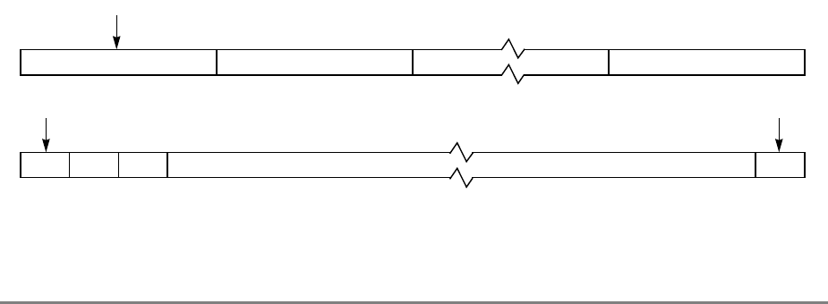
Chapter 2. Registers and Data Types 2-47
The following rules apply to memory accesses with regard to restarting the instruction:
• Aligned accesses—A single-register instruction that accesses an aligned operand is
not partially executed.
• Misaligned accesses—A single-register instruction that accesses a misaligned
operand may be partially executed if the access crosses a page boundary and a data
access exception occurs on the second page.
• Load/store multiple, move assist—These instructions may be partially executed if,
in accessing the locations specified by the instruction, a page boundary is crossed
and a data access exception occurs on the second page.
2.4.2.2 Atomicity
All aligned accesses are atomic. Instructions causing multiple accesses (for example,
load/store multiple and move assist instructions) are not atomic.
2.4.2.3 Access Order
The ordering of memory accesses is not guaranteed unless the programmer inserts
appropriate ordering instructions, even if the accesses are generated by a single instruction.
Misaligned accesses, load/store multiple instructions, and move assist instructions have no
implicit ordering characteristics. For example, processor A may store a word operand on an
odd half-word boundary. It may appear to processor A that the store completed atomically.
Processor or other mechanism B, executing a load from the same location, may get a result
that is a combination of the value of the first half word that existed prior to the store by
processor A and the value of the second half word stored by processor A.
2.4.3 Byte and Bit Ordering
The PowerPC architecture supports both big- and little-endian byte ordering. The default
byte- and bit ordering is big-endian, as shown in Figure 2-31. Byte ordering can be set to
little-endian by setting the LM bit in the HID0 register. Note that the mechanism for
selecting between byte orderings is different in the 601 than it is in the PowerPC
architecture. The PowerPC architecture provides two enable bits in the MSR that allow
independent control for user- and supervisor-level software.
Figure 2-31. Big-Endian Byte and Bit Ordering
Byte 0 Byte 1 Byte N (max)
Big-Endian Byte Ordering
012 n
Big-Endian Bit Ordering
MSB
msb bit n (max)

2-48 PowerPC 601 RISC Microprocessor User's Manual
If individual data items were indivisible, the concept of byte ordering would be
unnecessary. Order of bits or groups of bits within the smallest addressable unit of memory
is irrelevant, because nothing can be observed about such order. Order matters only when
scalars, which the processor and programmer regard as indivisible quantities, can be made
up of more than one addressable units of memory.
For a device in which the smallest addressable unit is the 64-bit double word, there is no
question of the order of bytes within double words. All transfers of individual scalars
between registers and memory are of double words. A subset of the 64 bit scalar (for
example, a byte) is not addressable in memory. As a result, to access any subset of the bits
of a scalar, the entire 64-bit scalar must be accessed, and when a memory location is read,
the 64-bit value returned is the 64-bit value last written to that location.
For PowerPC processors, the smallest addressable memory unit is the byte (8 bits), and
scalars are composed of one or more sequential bytes. When a 32-bit scalar is moved from
a register to memory, it occupies four consecutive byte addresses, and a decision must be
made regarding the order of these bytes in these four addresses.
The choice of byte ordering is arbitrary. Although there are 24 ways (4!) to specify the
ordering of four bytes within a word, illustrated as all the permutations of ordering of four
elements—ABCD, ABDC, ACBD, ACDB…DBCA, DCAB, DCBA—where the bytes are
ordered lowest address to highest address, only two of these orderings are practical—
ABCD (big-endian) and DCBA (little-endian).
The following example shows how the byte ordering is changed from big- to little-endian
mode by setting HID0[28] (n refers to the address):
<msr[ee] is off (zero) >
nsync |Instructions
n+4 sync |accessed in
n+8 sync |big-endian mode
n+c mtspr hid0(28)|
n+10 sync |Instructions
n+14 sync |accessed in
n+18 sync |little-endian mode
The same instruction sequence can be used to go from little- to big-endian mode by clearing
HID0[28].
2.4.3.1 Little-Endian Address Manipulation
In little-endian operations, the three least significant bits of an address are manipulated to
provide the appearance of a little-endian memory to the program for aligned loads and
stores, as follows:
New_addr(29) <- EA(29) xor (word | half | byte)
New_addr(30) <- EA(30) xor (half | byte)
New_addr(31) <- EA(31) xor (byte)

Chapter 2. Registers and Data Types 2-49
The physical address used for an access generated by a load or a store to an operand that is
less than a doubleword is modified as indicated. Addresses for aligned double-word
accesses and cache control operations are not modified since the endian mode has no effect
on aligned accesses larger than one word.
On a data access exception, the DAR contains the effective address (EA) generated by the
memory access instruction (that is, the address before modification) regardless of the
endian mode selected. SRR0 contains the EA of an instruction as described in Chapter 5,
“Exceptions,” (that is, the address before modification).
If the processor is in little-endian mode, the address is modified; if the processor is in big-
endian mode, the address is unmodified.
The T bit does not affect address manipulation or the detection of alignment exception
conditions. Therefore I/O interface controller operations and BUID x'07F' segments receive
the modified address. The ecowx and eciwx instructions are treated as no-ops if the T bit is
set regardless of whether the 601 is in little-endian mode.
Because the 601 defines a cache block as 32 bytes, bits 27–31 of the address are not used
for snooping. The program address should be specified, when an address is loaded into
HID2 or HID5. That is, if the processor is in little-endian mode, a little-endian address
should be specified, and if the processor is in big-endian mode, a big-endian address should
be specified.
2.4.3.2 Little-Endian Alignment Exceptions
Additional alignment exception conditions can occur when the processor is in little-endian
mode.
Load/store multiple operands (regardless of EA)
• lmw stmw
• lscbxxstswi
• lswi stswx
• lswx
The new alignment exception conditions are prioritized with other alignment exceptions
ahead of data access exceptions. See Section 2.4.5.2, “Misaligned Scalars” for more
information.
2.4.3.3 Little-Endian Instruction Fetching
In little-endian mode, instructions are fetched in big-endian order; however, the instructions
are swapped within a double word before being passed to the instruction queue, thus putting
the instructions in little-endian order for execution. On exceptions, the 601 reports the
correct effective address (as defined by the programming model or computed by a storage
access instruction) regardless of the endian mode selected.

2-50 PowerPC 601 RISC Microprocessor User's Manual
2.4.3.4 Big-Endian Byte Ordering
Big-endian ordering (ABCD) assigns the lowest address to the highest-order eight bits of
the scalar. This is called big-endian because the big end of the scalar, considered as a binary
number, comes first in memory.
2.4.3.5 Little-Endian Byte Ordering
Little-endian byte ordering (DCBA) assigns the lowest address to the lowest-order
(rightmost) 8 bits of the scalar. The little end of the scalar, considered as a binary number,
comes first in memory.
2.4.4 Structure Mapping Examples
The following C programming example contains an assortment of scalars and one character
string. The value presumed to be in each structure element is shown in hexadecimal in the
comments and are used below to show how the bytes that comprise each structure element
are mapped into memory.
struct {
int a; /* x'11121314' word */
double b; /* x'2122232425262728' doubleword */
char * c; /* x'31323334' word */
char d[7]; /* 'A','‘B','C','D','E','F','G' array of bytes */
short e; /* x'5152' halfword */
int f; /* x'61626364' word */
} s;
2.4.4.1 Big-Endian Mapping
The big-endian mapping of a structure S is shown in Figure 2-32. Addresses are shown in
hexadecimal at the left of each double word and in small figures below each byte. The
content of each byte, as shown in the preceding C programming example, is shown in
hexadecimal as characters for the elements of the string.
Figure 2-32. Big-Endian Mapping of Structure
S
00 11
00 12
01 13
02 14
03 (*)
04 (*)
05 (*)
06 (*)
07
08 21
08 22
09 23
0A 24
0B 25
0C 26
0D 27
0E 28
0F
10 31
10 32
11 33
12 34
13 ‘A’
14 ‘B’
15 ‘C’
16 ‘D’
17
18 ‘E’
18 ‘F’
19 ‘G’
1A (*)
1B 51
1C 52
1D (*)
1E (*)
1F
20 61
20 62
21 63
22 64
23

Chapter 2. Registers and Data Types 2-51
Note that the C structure mapping introduces padding (skipped bytes indicated by asterisks
“(*)” in Figure 2-32) in the map in order to align the scalars on their proper boundaries—
4 bytes between a and b, one byte between d and e, and two bytes between e and f. Both
big- and little-endian mappings use the same amount of padding.
2.4.4.2 Little-Endian Mapping
Figure 2-33 shows the structure, S, using little-endian mapping. Double words are laid out
from right to left.
Figure 2-33. Little-Endian Mapping of Structure
S
2.4.5 PowerPC Byte Ordering
The default mapping for PowerPC processors is big-endian. In the 601, little-endian mode
can be selected after a hard reset by setting the LM bit in the HID0 register in the 601
through the use of the mtspr instruction. Note that the PowerPC architecture defines two
bits in the MSR for specifying byte ordering—LE (little-endian mode) and ELE (exception
little-endian mode). These bits are not implemented in the 601.
The 601 big- and little-endian mode operation differs from the PowerPC architecture in the
following ways:
• Choice of big- or little-endian modes is provided through HID0[LM]—bit 28 of
HID0. The PowerPC architecture defines two bits in the MSR for this purpose.
• The basic mode switching sequence requires three sync instructions followed by the
mtspr access to HID0[28], followed by three more sync instructions. This sequence
should be used whenever the state of this bit is changed.
• External and decrementer exceptions should be disabled before executing the
sequence.
• The starting address of the sequence does not matter; however, the sequence cannot
cross a protection boundary.
• In some cases the mtspr access to HID0[LM] can occur twice depending on the
alignment of the instruction.
(*)
07 (*)
06 (*)
05 (*)
04 11
03 12
02 13
01 14
00 00
21
0F 22
0E 23
0D 24
0C 25
0B 26
0A 27
09 28
08 08
‘D’
17 ‘C’
16 ‘B’
15 ‘A’
14 31
13 32
12 33
11 34
10 10
(*)
1F (*)
1E 51
1D 52
1C (*)
1B ‘G’
1A ‘F’
19 ‘E’
18 18
61
23 62
22 63
21 64
20 20
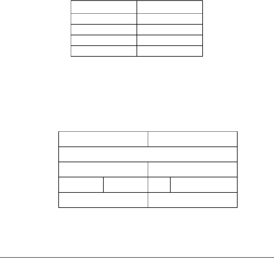
2-52 PowerPC 601 RISC Microprocessor User's Manual
• In some cases not all of the sync instructions will actually be executed, depending
on the starting address of the sequence.
• Although HID0[LM] can be switched dynamically, there are certain constraints
(such as turning off translation and emptying the memory queues) that must be
considered before the bit can be switched. Note that, when switching modes
between tasks, this code sequence may not allow the 601 to operate at an optimal
performance level.
2.4.5.1 Aligned Scalars
For the load and store instructions, the effective address is computed as specified in the
instruction descriptions in Chapter 3, “Addressing Modes and Instruction Set Summary.”
Table 2-28 shows how the physical address is modified.
The modified physical address is passed to the data cache or the main memory and the
specified width of the data is transferred between a GPR or FPR and the (as modified)
addressed memory locations. Although the data is stored using big-endian byte ordering
(but not in the same bytes within double words as with LM = 0), the modification of the EA
makes it appear to the processor that it is stored in little-endian mode.
The structure S would be placed in memory as shown in Figure 2-34.
Figure 2-34. PowerPC Little-Endian Structure
S
in Memory or Cache
Table 2-28. EA Modifications
Data Width (Bytes) EA Modification
8 No change
4 XOR with b'100'
2 XOR with b'110'
1 XOR with b'111'
00 00 01 02 03 11
04 12
05 13
06 14
07
08 21
08 22
09 23
0A 24
0B 25
0C 26
0D 27
0E 28
0F
10 ‘D’
10 ‘C’
11 ‘B’
12 ‘A’
13 31
14 32
15 33
16 34
17
18 (*)
18 (*)
19 51
1A 52
1B (*)
1C ‘G’
1D ‘F’
1E ‘E’
1F
20 (*)
20 (*)
21 (*)
22 (*)
23 61
24 62
25 63
26 64
27
Chapter 2. Registers and Data Types 2-53
Because of the modifications on the EA, the same structure S appears to the processor to be
mapped into memory this way when LM = 1 (little-endian enabled). This is shown in
Figure 2-35.
Figure 2-35. PowerPC Little-Endian Structure
S
as Seen by Processor
Note that as seen by the program executing in the processor, the mapping for the structure
S is identical to the little-endian mapping shown in Figure 2-33. From outside of the
processor, the addresses of the bytes making up the structure S are as shown in Figure 2-34.
These addresses match neither the big-endian mapping of Figure 2-32 or the little-endian
mapping of Figure 2-33. This must be taken into account when performing I/O operations
in little-endian mode; this is discussed in Section 2.4.7, “PowerPC Input/Output in Little-
Endian Mode.”
2.4.5.2 Misaligned Scalars
Performing an XOR operation on the low-order bits of the address of a scalar requires the
scalar to be aligned on a boundary equal to a multiple of its length. When executing in little-
endian mode (LM = 1), the 601 takes an alignment exception whenever a load or store
instruction is issued with a misaligned EA, regardless of whether such an access could be
handled without causing an exception in big-endian mode (LM = 0).
The PowerPC architecture states that half words, words, and double words be placed in
memory such that the little-endian address of the lowest-order byte is the EA computed by
the load or store instruction; the little-endian address of the next-lowest-order byte is one
greater, and so on. Figure 2-36 shows a four-byte word stored at little-endian address 5. The
word is presumed to contain the binary representation of x'11121314'.
Figure 2-36. PowerPC Little-Endian Mode, Word Stored at Address 5
07 06 05 04 11
03 12
02 13
01 14
00 00
21
0F 22
0E 23
0D 24
0C 25
0B 26
0A 27
09 28
08 08
‘D’
17 ‘C’
16 ‘B’
15 ‘A’
14 31
13 32
12 33
11 34
10 10
(*)
1F (*)
1E 51
1D 52
1C (*)
1B ‘G’
1A ‘F’
19 ‘E’
18 18
61
23 62
22 63
21 64
20 20
12
07 13
06 14
05 (*)
04 (*)
03 (*)
02 (*)
01 (*)
00 00
(*)
0F (*)
0E (*)
0D (*)
0C (*)
0B (*)
0A (*)
09 11
08 08

2-54 PowerPC 601 RISC Microprocessor User's Manual
Figure 2-37 shows the same word stored by a little-endian program, as seen by the memory
system (assuming big-endian mode).
Figure 2-37. Word Stored at Little-Endian Address 5 as Seen by Big-Endian
Addressing
Note that the misaligned word in this example spans two double words. The two parts of
the misaligned word are not contiguous in the big-endian addressing space.
2.4.5.3 Non-Scalars
The PowerPC architecture has two types of instructions that handle non-scalars (multiple
instances of scalars). Neither type can deal with the modified EAs required in little-endian
mode and both types cause alignment exceptions.
2.4.5.3.1 String Operations
The load and store string instructions, listed in Table 2-29, cause alignment exceptions
when they are executed in little-endian mode (HID0[LM] = 1).
String accesses are inherently byte-based operations, which, for improved performance, the
601 handles as a series of word-aligned accesses.
Note that the system software must determine whether to emulate the excepting instruction
or treat it as an illegal operation. Because little-endian mode programs are new with respect
to the PowerPC architecture—that is, they are not POWER binaries—having the compiler
generate these instructions in little-endian mode would be slower than processing the string
in-line or by using a subroutine call.
Table 2-29. Load/Store String Instructions that Take Alignment Exceptions if LM = 1
Mnemonic Description
lswi Load String Word Immediate
lswx Load String Word Indexed
stswi Store String Word Immediate
stswx Store String Word Indexed
lscbx Load String and Compare Byte Indexed

Chapter 2. Registers and Data Types 2-55
2.4.5.3.2 Load and Store Multiple Instructions
The instructions in Table 2-30 cause alignment exceptions when executed in little-endian
mode (HID0[LM] = 1).
Although the words addressed by these instructions are on word boundaries, each word is
in the half of its containing double word opposite from where it would be in big-endian
mode.
Note that the system software must determine whether to emulate the excepting instruction
or treat it as an illegal operation. Because little-endian mode programs are new with respect
to the PowerPC architecture—that is, they are not POWER binaries—having the compiler
generate these instructions in little-endian mode would be slower than processing the string
in-line or by using a subroutine call.
2.4.6 PowerPC Instruction Memory Addressing in Little-Endian
Mode
Each PowerPC instruction occupies 32 bits (one word) of memory. PowerPC processors
fetch and execute instructions as if the current instruction address had been advanced one
word for each sequential instruction. When operating with LM = 1, the address is modified
according to the little-endian rule for fetching word-length scalars; that is, it is XORed with
b'100'. A program is thus an array of little-endian words with each word fetched and
executed in order (not including branches).
Consider the following example:
loop:
cmplwi r5,0
beq done
lwzux r4, r5, r6
add r7, r7, r4
subi r5, 1
b loop
done:
stw r7, total
Assuming the program starts at address 0, these instructions are mapped into memory for
big-endian execution as shown in Figure 2-38.
Table 2-30. Load/Store Multiple Instructions that Take Alignment Exceptions if
LM = 1
Mnemonic Instruction
lmw Load Multiple Word
stmw Store Multiple Word

2-56 PowerPC 601 RISC Microprocessor User's Manual
Figure 2-38. PowerPC Big-Endian, Instruction Sequence as Seen by Processor
If this same program is assembled for and executed in little-endian mode, the mapping seen
by the processor appears as shown in Figure 2-39.
Each machine instruction appears in memory as a 32-bit integer containing the value
described in the instruction description, regardless of whether LM is set. This is because
scalars are always mapped in memory in big-endian byte order.
Figure 2-39. PowerPC Little-Endian, Instruction Sequence as Seen by Processor
When little-endian mapping is used, all references to the instruction stream must follow
little-endian addressing conventions, including addresses saved in system registers when
the exception is taken, return addresses saved in the link register, and branch displacements
and addresses.
• An instruction address placed in the link register by branch and link, or an
instruction address saved in an SPR when an exception is taken is the address that a
program executing in little-endian mode would use to access the instruction as a
word of data using a load instruction.
• An offset in a relative branch instruction reflects the difference between the
addresses of the instructions, where the addresses used are those that a program
executing in little-endian mode would use to access the instructions as data words
using a load instruction.
00 loop: cmplwi r5, 8 beq done
00 01 02 03 04 05 06 07
08 lwzux r4, r5, r6 add r7, r7, r4
08 09 0A 0B 0C 0D 0E 0F
10 subi r5, 1 b loop
10 11 12 13 14 15 16 17
18 done: stw r7, total
18 19 1A 1B 1C 1D 1E 1F
beq done loop: cmplwi 00
07 06 05 04 03 02 01 00
add r7, r7, r4 lwzux r4, r5, r6 08
0F 0E 0D 0C 0B 0A 09 08
b loop subi r5, 1 10
17 16 15 14 13 12 11 10
done: stw r7, total 18
1F 1E 1D 1C 1B 1A 19 18

Chapter 2. Registers and Data Types 2-57
• A target address in an absolute branch instruction is the address that a program
executing in little-endian mode would use to access the target instruction as a word
of data using a load instruction.
2.4.7 PowerPC Input/Output in Little-Endian Mode
Input/output operations, such as writing the contents of a memory page to disk, transfers a
byte stream on both big- and little-endian systems. For the disk transfer, byte 0 of the page
is written to the first byte of a disk record and so on.
For a PowerPC system running in big-endian mode, both the processor and the memory
subsystem recognize the same byte as byte 0. However, this is not true for a PowerPC
system running in little-endian mode because of the modification of the three low-order bits
when the processor accesses memory.
In order for I/O transfers in little-endian mode to appear to transfer bytes properly, they
must be performed as if the bytes transferred were accessed one at a time, using the little-
endian address modification appropriate for the single-byte transfers (XOR the bits with
b'111'). This does not mean that I/O on little-endian PowerPC machines must be done using
only one-byte-wide transfers. Data transfers can be as wide as desired, but the order of the
bytes within double words must be as if they were fetched or stored one at a time.
Note that I/O operations can also be performed with certain devices by merely storing to or
loading from addresses that are designated as I/O controller interface addresses (SR[T] is
set). Care must be taken with such operations when defining the addresses to be used
because these addresses are subjected to the EA modifications described in Table 2-28. A
load or store that maps to a control register on a device may require the bytes of the value
transferred to be reversed. If this reversal is required, the loads and stores with byte reversal
instructions may be used.
2.5 Floating-Point Execution Models
The IEEE-754 standard includes 32-bit and 64-bit arithmetic. The standard requires that
single-precision arithmetic be provided for single-precision operands. The standard permits
double-precision arithmetic instructions to have either (or both) single-precision or double-
precision operands, but states that single-precision arithmetic instructions should not accept
double-precision operands.
The PowerPC architecture follows these guidelines:
• Double-precision arithmetic instructions can have operands of either or both
precisions
• Single-precision arithmetic instructions require all operands to be single-precision
• Double-precision arithmetic instructions produce double-precision values
• Single-precision arithmetic instructions produce single-precision values

2-58 PowerPC 601 RISC Microprocessor User's Manual
For arithmetic instructions, conversions from double- to single-precision must be done
explicitly by software, while conversions from single- to double-precision are done
implicitly.
All PowerPC implementations provide the equivalent of the following execution models to
ensure that identical results are obtained. Definition of the arithmetic instructions for
infinities, denormalized numbers, and NaNs follow conventions described in the following
sections.
Although the double-precision format specifies an 11-bit exponent, exponent arithmetic
uses two additional bit positions to avoid potential transient overflow conditions. An extra
bit is required when denormalized double-precision numbers are prenormalized. A second
bit is required to permit computation of the adjusted exponent value in the following
examples when the corresponding exception enable bit is one:
• Underflow during multiplication using a denormalized factor.
• Overflow during division using a denormalized divisor.
2.5.1 Execution Model for IEEE Operations
The following description uses 64-bit arithmetic as an example; 32-bit arithmetic is similar
except that the fraction field is a 23-bit field and the single-precision guard, round, and
sticky bits (described in this section) are logically adjacent to the 23-bit FRACTION field.
The bits and fields for the IEEE 64-bit execution model are defined as follows:
• The S bit is the sign bit.
• The C bit is the carry bit that captures the carry out of the significand.
• The L bit is the leading unit bit of the significand which receives the implicit bit from
the operands.
• The FRACTION is a 52-bit field, which accepts the fraction of the operands.
• The guard (G), round (R), and sticky (X) bits are extensions to the low-order bits of
the accumulator. The G and R bits are required for post normalization of the result.
The G, R, and X bits are required during rounding to determine if the intermediate
result is equally near the two nearest representable values. The X bit serves as an
extension to the G and R bits by representing the logical OR of all bits that may
appear to the low-order side of the R bit, either due to shifting the accumulator right
or other generation of low-order result bits. The G and R bits participate in the left
shifts with zeros being shifted into the R bit. Table 2-31 shows the significance of
the G, R, and X bits with respect to the intermediate result (IR), the next lower in
magnitude representable number (NL), and the next higher in magnitude
representable number (NH).
Chapter 2. Registers and Data Types 2-59
The significand of the intermediate result is made up of the L bit, the FRACTION, and the
G, R, and X bits.
The infinitely precise intermediate result of an operation is the result normalized in bits L,
FRACTION, G, R, and X of the floating-point accumulator.
Before results are stored into an FPR, the significand is rounded if necessary, using the
rounding mode specified by FPSCR[RN]. If rounding causes a carry into C, the significand
is shifted right one position and the exponent is incremented by one. This may yield an
inexact result and possibly exponent overflow. Fraction bits to the left of the bit position
used for rounding are stored into the FPR, and low-order bit positions, if any, are set to zero.
Four rounding modes are provided which are user-selectable through FPSCR[RN] as
described in Section 2.5.6, “Rounding.” For rounding, the conceptual guard, round, and
sticky bits are defined in terms of accumulator bits.
Table 2-32 shows the positions of the guard, round, and sticky bits for double-precision and
single-precision floating-point numbers.
Rounding can be treated as though the significand were shifted right, if required, until the
least significant bit to be retained is in the low-order bit position of the FRACTION. If any
of the guard, round, or sticky bits are nonzero, the result is inexact.
Table 2-31. Interpretation of G, R, and X Bits
G R X Interpretation
0 0 0 IR is exact
001
IR closer to NL010
011
1 0 0 IR midway between NL & NH
101
IR closer to NH110
111
Table 2-32. Location of the Guard, Round and Sticky Bits
Format Guard Round Sticky
Double G bit R bit X bit
Single 24 25 26–52 G,R,X

2-60 PowerPC 601 RISC Microprocessor User's Manual
Z1 and Z2, defined in Section 2.5.6, “Rounding,” can be used to approximate the result in
the target format when one of the following rules is used:
• Round to nearest
— Guard bit = 0: The result is truncated. (Result exact (GRX = 000) or closest to
next lower value in magnitude (GRX = 001, 010, or 011)
— Guard bit = 1: Depends on round and sticky bits:
Case a: If the round or sticky bit is one (inclusive), the result is incremented.
(result closest to next higher value in magnitude (GRX = 101, 110, or 111))
Case b: If the round and sticky bits are zero (result midway between closest
representable values) then if the low-order bit of the result is one, the result is
incremented. Otherwise (the low-order bit of the result is zero) the result is
truncated (this is the case of a tie rounded to even).
• If during the round to nearest process, truncation of the unrounded number produces
the maximum magnitude for the specified precision, the following action is taken:
— Guard bit = 1: Store infinity with the sign of the unrounded result.
— Guard bit = 0: Store the truncated (maximum magnitude) value.
• Round toward zero—Choose the smaller in magnitude of Z1 or Z2. If the guard,
round, or sticky bit is nonzero, the result is inexact.
• Round toward +infinity
Choose Z1.
• Round toward –infinity
Choose Z2.
Where the result is to have fewer than 53 bits of precision because the instruction is
a floating round to single-precision or single-precision arithmetic instruction, the
intermediate result either is normalized or is placed in correct denormalized form
before the result is potentially rounded.
2.5.1.1 Execution Model for Multiply-Add Type Instructions
The PowerPC architecture makes use of a special instruction form that performs up to three
operations in one instruction (a multiply, an add, and a negate). With this added capability
is the ability to produce a more exact intermediate result as an input to the rounder. The 32-
bit arithmetic is similar except that the fraction field is smaller. Note that the rounding
occurs only after add; therefore, the computation of the sum and product together are
infinitely precise before the final result is rounded to a representable format.
The first part of the operation is a multiply. The multiply has two 53-bit significands as
inputs, which are assumed to be prenormalized, and produces a result conforming to the
above model. If there is a carry out of the significand (into the C bit), the significand is
shifted right one position, placing the L bit into the most significant bit of the FRACTION
and placing the C bit into the L bit. All 106 bits (L bit plus the fraction) of the product take
part in the add operation. If the exponents of the two inputs to the adder are not equal, the

Chapter 2. Registers and Data Types 2-61
significand of the operand with the smaller exponent is aligned (shifted) to the right by an
amount added to that exponent to make it equal to the other input’s exponent. Zeros are
shifted into the left of the significand as it is aligned and bits shifted out of bit 105 of the
significand are ORed into the X' bit. The add operation also produces a result conforming
to the above model with the X' bit taking part in the add operation.
The result of the add is then normalized, with all bits of the add result, except the X' bit,
participating in the shift. The normalized result provides an intermediate result as input to
the rounder that conforms to the model described in Section 2.5.1, “Execution Model for
IEEE Operations,” where:
• The guard bit is bit 53 of the intermediate result.
• The round bit is bit 54 of the intermediate result.
• The sticky bit is the OR of all remaining bits to the right of bit 55, inclusive.
If the instruction is floating negative multiply-add or floating negative multiply-subtract,
the final result is negated.
Status bits are set to reflect the result of the entire operation: for example, no status is
recorded for the result of the multiplication part of the operation.
2.5.2 Floating-Point Data Format
The PowerPC architecture defines the representation of a floating-point value in two
different binary, fixed-length formats. The format may be a 32-bit format for a single-
precision floating-point value or a 64-bit format for a double-precision floating-point value.
The single-precision format may be used for data in memory. The double-precision format
can be used for data in memory or in floating-point registers.
The length of the exponent and the fraction fields differ between these two precision
formats. The structure of the single-precision format is shown in Figure 2-40; the structure
of the double-precision format is shown in Figure 2-41.
Figure 2-40. Floating-Point Single-Precision Format
Figure 2-41. Floating-Point Double-Precision Format
S EXP FRACTION
01 89 31
S EXP FRACTION
0 1 11 12 63

2-62 PowerPC 601 RISC Microprocessor User's Manual
Values in floating-point format consist of three fields:
• S (sign bit)
• EXP (exponent + bias)
• FRACTION (fraction)
If only a portion of a floating-point data item in memory is accessed, as with a load or store
instruction for a byte or half word (or word in the case of floating-point double-precision
format), the value affected depends on whether the PowerPC system is using big- or little-
endian byte ordering, which is described in Section 2.4.3, “Byte and Bit Ordering.” Big-
endian mode is the default.
The significand consists of a leading implied bit concatenated on the right with the
FRACTION. This leading implied bit is a 1 for normalized numbers and a 0 for
denormalized numbers in the unit bit position (that is, the first bit to the left of the binary
point). Values representable within the two floating-point formats can be specified by the
parameters listed in Table 2-33.
The exponent is expressed as an 8-bit value for single-precision numbers or an 11-bit value
for double-precision numbers. These bits hold the biased exponent; the true value of the
exponent can be determined by subtracting 127 for single-precision numbers and 1023 for
double-precision values. This is shown in Figure 2-42. Note that using a bias eliminates the
need for a sign bit. The highest-order bit is used both to generate the number, and is an
implicit sign bit. Note also that two values are reserved—all bits set indicates that the
number is an infinity or NaN and all bits cleared indicates that the number is either zero or
denormalized.
Table 2-33. IEEE Floating-Point Fields
Parameter Single-Precision Double-Precision
Exponent bias +127 +1023
Maximum exponent
(unbiased) +127 +1023
Minimum exponent –126 –1022
Format width 32 bits 64 bits
Sign width 1 bit 1 bit
Exponent width 8 bits 11 bits
Fraction width 23 bits 52 bits
Significand width 24 bits 53 bits
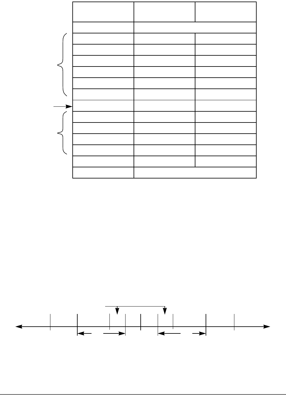
Chapter 2. Registers and Data Types 2-63
.
Figure 2-42. Biased Exponent Format
2.5.2.1 Value Representation
The PowerPC architecture defines numerical and non-numerical values representable
within single- and double-precision formats. The numerical values are approximations to
the real numbers and include the normalized numbers, denormalized numbers, and zero
values. The non-numerical values representable are the positive and negative infinities, and
the NaNs. The positive and negative infinities are adjoined to the real numbers but are not
numbers themselves, and the standard rules of arithmetic do not hold when they appear in
an operation. They are related to the real numbers by “order” alone. It is possible, however,
to define restricted operations among numbers and infinities as defined below. The relative
location on the real number line for each of the defined entities is shown in Figure 2-43.
Figure 2-43. Approximation to Real Numbers
Biased Exponent
(binary) Single-Precision
(unbiased) Double-Precision
(unbiased)
11. . . . .11 Reserved for Infinities and NaNs
11. . . . .10 +127 +1023
11. . . . .01 +126 +1022
...
...
...
10. . . . .00 1 1
01. . . . .11 0 0
01. . . . .10 –1 –1
...
...
...
00. . . . .01 –126 –1022
00. . . . .00 Reserved for Zeros and Denormalized Numbers
Positive
Negative
Zero
–∞–NORM –DENORM –0 +0 +DENORM +NORM +∞
Unrepresentable, small numbers
Tiny Tiny

2-64 PowerPC 601 RISC Microprocessor User's Manual
The positive and negative NaNs are not related to the numbers or ±∞ by order or value, but
they are encodings that convey diagnostic information such as the representation of
uninitialized variables. Table 2-34 describes each of the floating-point formats.
The following sections describe floating-point values defined in the architecture:
2.5.2.2 Binary Floating-Point Numbers
Binary floating-point numbers are machine-representable values used to approximate real
numbers. Three categories of numbers are supported: normalized numbers, denormalized
numbers, and zero values.
2.5.2.3 Normalized Numbers (±NORM)
The values for normalized numbers have a biased exponent value in the range:
• 1–254 in single-precision format
• 1–2046 in double-precision format
The implied unit bit is one. Normalized numbers are interpreted as follows:
NORM = (–1)s x 2E x (1.fraction)
where (s) is the sign, (E) is the unbiased exponent and (1.fraction) is the significand
composed of a leading unit bit (implied bit) and a fractional part. The format for normalized
numbers is shown in Figure 2-44.
Table 2-34. Recognized Floating-Point Numbers
Sign Bit Biased Exponent Leading Bit Fraction Value
0 Maximum x Nonzero +NaN
0 Maximum x Zero +Infinity
0 0 < Exponent < Maximum 1 Nonzero +Normalized
0 0 0 Nonzero +Denormalized
0 0 0 Zero +0
1 0 0 Zero –0
1 0 0 Nonzero –Denormalized
1 0 < Exponent < Maximum 1 Nonzero –Normalized
1 Maximum x Zero –Infinity
1 Maximum x Nonzero –NaN

Chapter 2. Registers and Data Types 2-65
Figure 2-44. Format for Normalized Numbers
The ranges covered by the magnitude (M) of a normalized floating-point number are
approximately equal to the following:
Single-precision format:
1.2x10–38 ≤ M ≤ 3.4x1038
Double-precision format:
2.2x10–308 ≤ M ≤ 1.8x10308
2.5.2.4 Zero Values (±0)
Zero values have a biased exponent value of zero and a mantissa (leading bit = 0) value of
zero. This is shown in Figure 2-45. Zeros can have a positive or negative sign. The sign of
zero is ignored by comparison operations (that is, comparison regards +0 as equal to –0).
Figure 2-45. Format for Zero Numbers
2.5.2.5 Denormalized Numbers (±DENORM)
Denormalized numbers have a biased exponent value of zero and a nonzero fraction field
value. The format for denormalized numbers is shown in Figure 2-46.
Figure 2-46. Format for Denormalized Numbers
MIN<EXPONENT<MAX
(BIASED) FRACTION = ANY BIT PATTERN
SIGN OF MANTISSA, 0 OR 1
FRACTION = 0
SIGN OF MANTISSA, 0 OR 1
EXPONENT = 0
(BIASED)
SIGN OF MANTISSA, 0 OR 1
EXPONENT = 0
(BIASED) FRACTION = ANY NONZERO
BIT PATTERN

2-66 PowerPC 601 RISC Microprocessor User's Manual
Denormalized numbers are nonzero numbers smaller in magnitude than the representable
normalized numbers. They are values in which the implied unit bit is zero. Denormalized
numbers are interpreted as follows:
DENORM = (–1)s x 2Emin x (0.fraction)
where (Emin) is the minimum representable exponent value (–126 for single-precision,
–1022 for double-precision).
2.5.2.6 Infinities (±∞)
Positive and negative infinities have the maximum biased exponent value:
• 255 in the single-precision format
• 2047 in the double-precision format
The format for infinities is shown in Figure 2-47.
Figure 2-47. Format for Positive and Negative Infinities
The fraction value is zero. Infinities are used to approximate values greater in magnitude
than the maximum normalized value. Infinity arithmetic is defined as the limiting case of
real arithmetic, with restricted operations defined between numbers and infinities. Infinities
and the reals can be related by ordering in the affine sense:
–∞ < every finite number < +∞
Arithmetic using infinite numbers is always exact and does not signal any exception, except
when an exception occurs due to the invalid operations as described in Section 5.4.7.2,
“Invalid Operation Exception Conditions.”
2.5.2.7 Not a Numbers (NaNs)
NaNs have the maximum biased exponent value and a nonzero fraction field value. The
format for NaNs is shown in Figure 2-48. The sign bit of NaNs is ignored (that is, NaNs are
neither positive nor negative). If the high-order bit of the fraction field is a zero, the NaN is
a signaling NaN; otherwise it is a quiet NaN (QNaN).
Figure 2-48. Format for NaNs
Signaling NaNs signal exceptions when they are specified as arithmetic operands.
SIGN OF MANTISSA, 0 OR 1
EXPONENT = MAXIMUM
(BIASED) FRACTION = 0
SIGN OF MANTISSA (0 for +NaN, 1 for –NaN)
EXPONENT = MAXIMUM
(BIASED) FRACTION = ANY NONZERO
BIT PATTERN

Chapter 2. Registers and Data Types 2-67
Quiet NaNs represent the results of certain invalid operations, such as invalid arithmetic
operations on infinities or on NaNs, when the invalid operation exception is disabled
(FPSCR[VE] = 0). QNaNs are generated under the following conditions:
• An invalid operation occurs and FPSCR[VE] = 0
• An mffs instruction is executed and the upper 32 bits are undefined (this case is 601-
specific).
• On Floating Convert to Integer with Round (fctir) and Floating Convert to Integer
with Round toward Zero (fctirz) the PowerPC architecture defines bits 0–31 of the
target floating point register as undefined. In the 601, these bits take on the value
x'FFF8 0000' (which is the representation for a QNaN).
Quiet NaNs propagate through all operations, except ordered comparison and conversion
to integer operations without signaling exceptions. Specific encodings in QNaNs can thus
be preserved through a sequence of operations and used to convey diagnostic information
to help identify results from invalid operations.
When a QNaN results from an operation because an operand is a NaN or because a QNaN
is generated due to a disabled invalid operation exception, the following rule is applied to
determine the QNaN with the high-order fraction bit set to one that is to be stored as the
result:
If (frA) is a NaN
Then frD ← (frA)
Else if (frB) is a NaN
Then frD ← (frB)
Else if (frC) is a NaN
Then frD ← (frC)
Else if generated QNaN
Then frD ← generated QNaN
If the operand specified by frA is a NaN, that NaN is stored as the result. Otherwise, if the
operand specified by frB is a NaN (if the instruction specifies an frB operand), that NaN is
stored as the result. Otherwise, if the operand specified by frC is a NaN (if the instruction
specifies an frC operand), that NaN is stored as the result. Otherwise, if a QNaN is
generated by a disabled invalid operation exception, that QNaN is stored as the result. If a
QNaN is to be generated as a result, the QNaN generated has a sign bit of zero, an exponent
field of all ones, and a high-order fraction bit of one with all other fraction bits zero. An
instruction that generates a QNaN as the result of a disabled invalid operation generates this
QNaN. This is shown in Figure 2-49.
Figure 2-49. Representation of Generated QNaN
SIGN OF MANTISSA, NaN OR 1
111...1 1000....0
0

2-68 PowerPC 601 RISC Microprocessor User's Manual
2.5.3 Sign of Result
The following rules govern the sign of the result of an arithmetic operation, when the
operation does not yield an exception. These rules apply even when the operands or results
are ±0 or ±∞:
• The sign of the result of an addition operation is the sign of the source operand
having the larger absolute value. If both operands have the same sign, the sign of the
result of an addition operation is the same as the sign of the operands. The sign of
the result of the subtraction operation, x – y, is the same as the sign of the result of
the addition operation, x + (–y).
• When the sum of two operands with opposite sign, or the difference of two operands
with the same sign, is exactly zero, the sign of the result is positive in all rounding
modes except round toward negative infinity(–∞), in which case the sign is negative.
• The sign of the result of a multiplication or division operation is the exclusive OR
of the signs of the source operands.
• The sign of the result of a round to single-precision or convert to/from integer
operation is the sign of the source operand.
For multiply-add instructions, these rules are applied first to the multiplication operation
and then to the addition or subtraction operation (one of the source operands to the addition
or subtraction operation is the result of the multiplication operation).
2.5.4 Normalization and Denormalization
When an arithmetic operation produces an intermediate result, consisting of a sign bit, an
exponent, and a nonzero significand with a zero leading bit, the result is not a normalized
number and must be normalized before it is stored.
A number is normalized by shifting its significand left while decrementing its exponent by
one for each bit shifted, until the leading significand bit becomes one. The guard bit and the
round bit participate in the shift with zeros shifted into the round bit; see Section 2.5.1,
“Execution Model for IEEE Operations.” During normalization, the exponent is regarded
as if its range were unlimited. If the resulting exponent value is less than the minimum value
that can be represented in the format specified for the result, the intermediate result is said
to be “tiny” and the stored result is determined by the rules described in Section 5.4.7.5,
“Underflow Exception Condition.” The sign of the number does not change.
When an arithmetic operation produces a nonzero intermediate result whose exponent is
less than the minimum value that can be represented in the format specified, the stored
result may need to be denormalized. The result is determined by the rules described in
Section 5.4.7.5, “Underflow Exception Condition.”
A number is denormalized by shifting its significand to the right while incrementing its
exponent by one for each bit shifted until the exponent equals the format’s minimum value.
If any significant bits are lost in this shifting process then “Loss of Accuracy” has occurred
and an underflow exception is signaled. The sign of the number does not change.

Chapter 2. Registers and Data Types 2-69
When denormalized numbers are operands of multiply and divide operations, operands are
prenormalized internally before performing the operations.
2.5.5 Data Handling and Precision
There are specific instructions for moving floating-point data between the FPRs and
memory. For double-precision format data, the data is not altered during the move. For
single-precision data, the format is converted to double-precision format when data is
loaded from memory into an FPR. A format conversion from double- to single-precision is
performed when data from an FPR is stored. Floating-point exceptions cannot occur during
these operations.
All arithmetic operations use floating-point double-precision format.
Floating-point single-precision formats are used by the following four types of instructions:
• Load Floating-Point Single-Precision (lfs)—This instruction accesses a single-
precision operand in single-precision format in memory, converts it to double-
precision, and loads it into an FPR. Exceptions are not detected during the load
operation.
• Floating-point Round to Single-Precision (frspx)—If the operand is not already in
single-precision range, the floating round to single-precision instruction rounds a
double-precision operand to single-precision, checking the exponent for single-
precision range and handling any exceptions according to respective enable bits in
the FPSCR. The instruction places that operand into an FPR as a double-precision
operand. For results produced by single-precision arithmetic instructions and by
single-precision loads, this operation does not alter the value.
• Single-precision arithmetic instructions—These instructions take operands from the
FPRs in double-precision format, performs the operation as if it produced an
intermediate result correct to infinite precision and with unbounded range, and then
forces this intermediate result to fit in single-precision format. Status bits in the
FPSCR and in the condition register are set to reflect the single-precision result. The
result is then converted to double-precision format and placed into an FPR. The
result falls within the range supported by the single format.
• For single-precision operations, source operands must be representable in single-
precision format. If they are not, the result placed into the target FPR, and the setting
of status bits in the FPSCR and in the condition register, are undefined.
• Store Floating-Point Single-Precision (stfs)—This form of instruction converts a
double-precision operand to single-precision format and stores that operand into
memory. If the operand requires denormalization in order to fit in single-precision
format, it is automatically denormalized prior to being stored. No exceptions are
detected on the store operation (the value being stored is effectively assumed to be
the result of an instruction of one of the preceding three types).

2-70 PowerPC 601 RISC Microprocessor User's Manual
When the result of a Load Floating-Point Single-Precision (lfs), Floating-Point Round to
Single-Precision (frspx), or single-precision arithmetic instruction is stored in an FPR, the
low-order 29 fraction bits are zero. This is shown in Figure 2-50.
Figure 2-50. Single-Precision Representation in an FPR
The frspx instruction allows conversion from double- to single-precision with appropriate
exception checking and rounding. This instruction should be used to convert double-
precision floating-point values (produced by double-precision load and arithmetic
instructions) to single-precision values before storing them into single-format memory
elements or using them as operands for single-precision arithmetic instructions. Values
produced by single-precision load and arithmetic instructions can be stored directly, or used
directly as operands for single-precision arithmetic instructions, without preceding the
store, or the arithmetic instruction, by frspx.
A single-precision value can be used in double-precision arithmetic operations. The reverse
is true only if the double-precision value can be represented in single-precision format.
Some implementations may execute single-precision arithmetic instructions faster than
double-precision arithmetic instructions. Therefore, if double-precision accuracy is not
required, using single-precision data and instructions can speed operations.
2.5.6 Rounding
All arithmetic instructions defined by the PowerPC architecture produce an intermediate
result considered infinitely precise. This result must then be written with a precision of
finite length into an FPR. After normalization or denormalization, if the infinitely precise
intermediate result cannot be represented in the precision required by the instruction, it is
rounded before being placed into the target FPR.
The instructions that potentially round their result are the arithmetic, multiply-add, and
rounding and conversion instructions. As shown in Figure 2-51, whether rounding occurs
depends on the source values.
S EXP x x x x x x x x x xx x x x x x x x x x x x x 00000000000000000000000000000
0 1 11 12 63
Bit 35
Chapter 2. Registers and Data Types 2-71
Figure 2-51. Rounding Flow Diagram
Each of these instructions sets FPSCR bits FR and FI, according to whether rounding
occurs (FI) and whether the fraction was incremented (FR). If rounding occurs, FI is set to
one and FR may be either zero or one. If rounding does not occur, both FR and FI are
cleared. Other floating-point instructions do not alter FR and FI. Four modes of rounding
are provided that are user-selectable through the floating-point rounding control field in the
FPSCR. See Section 2.2.3, “Floating-Point Status and Control Register (FPSCR).” These
are encoded as follows in Table 2-35.
Let Z be the infinitely precise intermediate arithmetic result or the operand of a conversion
operation. If Z can be represented exactly in the target format, no rounding occurs and the
result in all rounding modes is equivalent to truncation of Z. If Z cannot be represented
exactly in the target format, let Z1 and Z2 be the next larger and next smaller numbers
representable in the target format that bound Z; then Z1 or Z2 can be used to approximate
the result in the target format.
Table 2-35. FPSCR Bit Settings—RN Field
RN Rounding Mode
00 Round to nearest
01 Round toward zero
10 Round toward +infinity
11 Round toward –infinity
Rounding
Yes
No FI = 0
FR = 0
No
FI = 1
FR = 0
Yes
FI = 1
Fraction
Incremented

2-72 PowerPC 601 RISC Microprocessor User's Manual
Figure 2-52 shows a graphical representation of Z, Z1, and Z2 in this case and Figure 2-53
shows the selection of Z1 and Z2 for the four rounding settings.
Figure 2-52. Relation of Z1 and Z2
Rounding follows the four following rules:
• Round to nearest—Choose the best approximation (Z1 or Z2. In case of a tie, choose
the one which is even (least significant bit 0)).
• Round toward zero—Choose the smaller in magnitude (Z1 or Z2).
• Round toward +infinity—Choose Z1.
• Round toward –infinity—Choose Z2.
See Section 2.5.1, “Execution Model for IEEE Operations,” for a detailed explanation of
rounding. If Z is to be rounded up and Z1 does not exist (that is, if there is no number larger
than Z that is representable in the target format), then an overflow exception occurs if Z is
positive and an underflow exception occurs if Z is negative. Similarly, if Z is to be rounded
down and Z2 does not exist, then an overflow exception occurs if Z is negative and an
underflow exception occurs if Z is positive. The results in these cases are defined in Section
5.4.7.1, “Floating-Point Enabled Program Exceptions.”
By incrementing LSB of Z
Infinitely precise value
By truncating after LSB
Z2 Z1 0 Z2 Z1
ZZ
Negative values Positive values
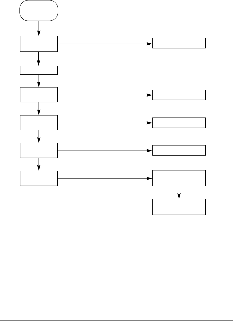
Chapter 2. Registers and Data Types 2-73
Figure 2-53. Selection of Z1 and Z2
2.6 PowerPC Registers Unimplemented in the 601
The following PowerPC registers are not implemented in the 601:
• The time base SPRs are used in the PowerPC architecture instead of the RTC
registers. The architected time base facility operates as a subdivision of the
frequency provided by the processor clock.
• Floating-point exception cause register (FPECR)—This is a supervisor-level SPR
(1023) that is used by some implementations to determine the cause of a floating-
point error.
Yes
No
Z is infinitely
precise result
or operand
Does Z fit
target format? Rounding = Truncation
No
Round
toward –∞?Choose Z2
Z1 ≤ Z ≤ Z2
Yes
No
Yes
Round
toward +∞?
No
Choose Z1
Yes
Round
toward 0?
No
Choose Z1
Round
to nearest Choose best approxi-
mation (Z1 or Z2)
if tie
Choose even value (Z1
or Z2 whose lsb is 0)

2-74 PowerPC 601 RISC Microprocessor User's Manual
• Address space register (ASR)—The ASR is a 64-bit SPR used in 64-bit
implementations to perform address translations.
• Each PowerPC processor implements a unique set of HID registers. Note that some
of these registers may be implemented the same way in more than one PowerPC
processor design.
An mtspr or mfspr instruction that specifies an unimplemented register is treated as a no-
op. If a privilege violation is indicated, the program exception has priority over the no-op.
This can occur if a user-mode program tries to access a register with bit 0 of the SPR
encoding field (in the instruction format) set. However, in this case the program exception
is taken regardless of whether the SPR encoding specified an implemented register.
2.7 Reset
The following sections describe hard reset and soft reset in the 601 processor. For more
information about the reset exception see Section 5.4.1, “Reset Exceptions (x'00100').”
2.7.1 Hard Reset
The hard reset sequence begins when the hard reset signal HRESET is negated after being
driven as described in Section 8.2.9.4.1, “Hard reset (HRESET)—Input.” Note that a hard
reset operation is required on power-on in order to properly reset the 601.
Table 2-36 shows the state of the registers after a hard reset and before it fetches the first
instruction from address x'FFF0 0100' in the system reset exception vector.
Table 2-36. Settings after Hard Reset (Used at Power-On)
Register Setting Register Setting
GPRs All 0s SRR1 00000000
FPRs All 0s SPRG0 00000000
FPSCR 00000000 SPRG1 00000000
Condition register All 0s SPRG2 00000000
Segment registers All 0s SPRG3 00000000
MSR 00001040 (ME and EP
set) EAR 00000000
MQ 00000000 PVR 000100011
XER 00000000 BAT registers All 0s
RTCU300000000 HID0 800100802
RTCL3000000003 HID1 00000000
Link register 00000000 HID2 00000000
CTR 00000000 HID5 00000000
DSISR 00000000 HID15 00000000

Chapter 2. Registers and Data Types 2-75
Notes: 1 In the earliest release of the 601 (DD1), this is 00010000. Later versions of the hardware may be different.
2 Master checkstop enable on, sequencer GPR self-test checkstop invalid microcode instruction checkstop on.
3 Note that if external clock is connected to RTC for the 601, then the RTCL, RTCU, and DEC can change from
their initial value of 0s without receiving instructions to load those registers.
The following is also true after a hard reset operation:
• External checkstops are enabled.
• The on-chip COP has given control of the PIs/POs to the rest of the chip for
functional use.
• Since the reset exception has data and instruction translation disabled (MSR[DT]
and MSR[IT] both cleared), the chip operates in direct address translation mode.
This implies that instruction fetches as well as loads and stores are cacheable.
(Operations that correspond to direct address translations are implicitly cacheable,
not write-through mode, and require coherency checking on the bus).
• All internal arrays and registers are cleared during the hard reset process.
• Reinitializes big-endian mode.
2.7.2 Soft Reset
Registers are not re-initialized when a soft reset occurs (SRESET is asserted as described
in Section 8.2.9.4.2, “Soft reset (SRESET)—Input”). The SRR0 and SRR1 registers are
updated with instruction and MSR data, and the MSR values are reset according to
procedures described in Section 5.4.1, “Reset Exceptions (x'00100').”
DAR 00000000 TLBs All 0s
DEC300000000 Cache All 0s
SDR1 00000000 Tag directory All 0s. (However, the LRU
bits are initialized such
that each side of the
cache has a unique LRU
value).
SRR0 00000000
Table 2-36. Settings after Hard Reset (Used at Power-On) (Continued)
Register Setting Register Setting

2-76 PowerPC 601 RISC Microprocessor User's Manual

Chapter 3. Addressing Modes and Instruction Set Summary 3-1
Chapter 3
Addressing Modes and Instruction Set
Summary
30
30
This chapter describes instructions and address modes supported by the PowerPC 601
microprocessor. These instructions are divided into the following categories:
• Integer instructions—These include arithmetic and logical instructions.
• Floating-point instructions—These include floating-point arithmetic instructions, as
well as instructions that affect the floating-point status and control register.
• Load/store instructions—These include integer and floating-point load and store
instructions.
• Flow control instructions—These include branching instructions, condition register
logical instructions, trap instructions, and other instructions that affect the
instruction flow.
• Processor control instructions—These instructions are used for synchronizing
memory accesses and management of caches, TLBs, and the segment registers.
This grouping of the instructions does not necessarily indicate the execution unit that
processes a particular instruction or group of instructions. This information, which is useful
in taking full advantage of the 601’s superscalar parallel instruction execution, is provided
in Chapter 10, “Instruction Set.”
Integer instructions operate on byte, half-word, and word operands. Floating-point
instructions operate on single-precision and double-precision floating-point operands. The
PowerPC architecture uses instructions that are four bytes long and word-aligned. It
provides for byte, half-word, and word operand fetches and stores between memory and a
set of 32 general-purpose registers (GPRs). It also provides for word and double-word
operand fetches and stores between memory and a set of 32 floating-point registers (FPRs).
Arithmetic and logical instructions do not read or modify memory. To use the contents of a
memory location in a computation and then modify the same or another memory location,
the memory contents must be loaded into a register, modified, and then written back to the
target location using load or store instructions.

3-2 PowerPC 601 RISC Microprocessor User's Manual
The 601 appears to execute instructions sequentially and in program order, but the
execution of a sequence of instructions may be interrupted as a result of an exception
caused by one of the instructions in the sequence, or by some asynchronous event.
3.1 Memory Addressing
A program references memory using the effective (logical) address computed by the
processor when it executes a memory access or branch instruction, or when the next
sequential instruction is fetched.
3.1.1 Effective Address Calculation
An effective address is the 32-bit sum computed by the processor when executing a
memory access or branch instruction or when fetching the next sequential instruction. For
a memory access instruction, if the sum of the effective address and the operand length
exceeds the maximum effective address, the memory operand is considered to wrap around
from the maximum effective address through effective address 0, as described in the
following paragraphs.
Effective address computations for both data and instruction accesses use 32-bit unsigned
binary arithmetic. A carry from bit 0 is ignored.
Load and store operations have three categories of effective address generation:
• Register indirect with immediate index mode. The d operand is added to the contents
of the GPR specified by the rA operand to generate the effective address.
• Register indirect with index mode. The contents of the GPR specified by rB operand
are added to the contents of the GPR specified by the rA operand to generate the
effective address.
• Register indirect mode. The contents of the GPR specified by the rA operand are
used as the effective address.
Branch instructions have three categories of effective address generation:
• Immediate addressing. The BD or LI operands are sign extended, and are appended
with b'00' in the two low-order bit positions (bits 30 and 31) to generate the branch
effective address. If the AA bit (bit 30) is cleared, the BD or LI operands are treated
as displacements; if the AA bit is set, the BD or LI operands are treated as absolute
addresses.
• Link register indirect. The contents of the link register with the two low-order bits
cleared to zero are used as the branch effective address.
• Count register indirect. The contents of the count register with the two low-order bits
cleared to zero are used as the branch effective address.
Branch instructions can optionally load the link register with the next sequential instruction
address (current instruction address + 4).

Chapter 3. Addressing Modes and Instruction Set Summary 3-3
3.1.2 Context Synchronization
The System Call (sc), Return from Interrupt (rfi), and Instruction Synchronize(isync)
instructions perform context synchronization by allowing previously issued instructions to
complete before performing a context switch. Execution of one of these instructions
ensures the following:
• No higher priority exception exists.
• All previous instructions have completed to a point where they can no longer cause
an exception. If a prior memory access instruction causes direct-store error
exceptions, the results must be determined before this instruction is executed.
• Previous instructions complete execution in the context (privilege, protection, and
address translation) under which they were issued.
• The instructions following the sc, rfi, or isync instruction execute in the context
established by these instructions.
The Move to Machine State Register instruction (mtmsr) is execution synchronizing. It
ensures that all preceding instructions have completed execution and will not cause an
exception before the instruction executes, but does not ensure subsequent instructions
execute in the newly established environment. For example, if the mtmsr sets the MSR(PR)
bit to 1, unless an isync immediately follows the mtmsr, a privileged instruction could be
executed or privileged access could be performed without causing an exception even
though the MSR(PR) bit indicates user mode.
3.2 Exception Summary
There are two kinds of exceptions in the 601—those caused directly by the execution of an
instruction and those caused by an asynchronous event. Either may cause components of
the system software to be invoked.
Exceptions can be caused directly by the execution of an instruction as follows:
• An attempt to execute an illegal instruction or an attempt by a user-level program to
execute the supervisor-level instructions listed below cause the illegal instruction or
supervisor-level instruction handler to be invoked. The 601provides the following
supervisor-level instructions: dcbi, mfmsr, mfspr, mfsr, mfsrin, mtmsr, mtspr,
mtsr, mtsrin, rfi, and tlbie. Note that the mfspr and mtspr instructions are
executable at both the user- and supervisor-level, depending on the SPR encoding.
• An attempt to access memory in a manner that violates memory protection, or an
attempt to access memory that is not available (page fault), causes the data access
exception handler or instruction access exception handler to be invoked.
• An attempt to access memory with an effective address alignment that is invalid for
the instruction causes the alignment exception handler to be invoked.
• The execution of an sc instruction causes the system service program to be invoked.

3-4 PowerPC 601 RISC Microprocessor User's Manual
• The execution of a trap instruction that traps causes the program exception trap
handler to be invoked.
• The execution of a floating-point instruction when floating-point instructions are
disabled causes the floating-point unavailable handler to be invoked.
• The execution of an instruction that causes a floating-point exception while
floating-point exceptions are enabled causes the floating-point enabled exception
handler to be invoked.
Exceptions caused by asynchronous events are described in Chapter 5, “Exceptions.”
3.3 Integer Instructions
This section describes the integer instructions. These consist of the following:
• Integer arithmetic instructions
• Integer compare instructions
• Integer rotate and shift instructions
• Integer logical instructions.
Integer instructions use the content of the GPRs as source operands and place results into
GPRs, into the integer exception register (XER), and into condition register fields. Trap
instructions compare the contents of one GPR with a second GPR or with immediate data
and, if the conditions are met, invoke the program exception trap handler.
These instructions treat the source operands as signed integers unless the instruction is
explicitly identified as an unsigned operation.
The integer instructions that are coded to update the condition register and the integer
logical and arithmetic instructions (addic., andi., and andis.) set condition register field
CR0 (bits 0–3) to characterize the result of the operation. The condition register field CR0
is set as if the result were compared algebraically to zero.
The integer arithmetic instructions (addic, addic., subfic, addc, subfc, adde, subfe,
addme, subfme, addze, and subfze) always set integer exception register bit, CA, to reflect
the carry out of bit 0. Integer arithmetic instructions with the overflow enable (OE) bit set
will cause the XER bits SO and OV to be set to reflect overflow of the 32-bit result.
Unless otherwise noted, when condition register field CR0 and the XER are affected they
reflect the value placed in the target register.
3.3.1 Integer Arithmetic Instructions
In the 601, instructions that select the overflow option (enable XER(OV)) or that set the
integer exception register carry bit (CA) may delay the execution of subsequent
instructions.

Chapter 3. Addressing Modes and Instruction Set Summary 3-5
The 601 integer unit contains the user accessible MQ register and supports the multiply
(mul), divide (div), shift, and rotate instructions that use this register. Neither the register
nor the associated instructions are present in other PowerPC processors nor are they defined
in the PowerPC architecture. The execution of any PowerPC multiply or divide instruction
causes the content of the MQ to be undefined.
Table 3-1 lists the integer arithmetic instructions for the 601. Note that some of the
instructions are specific to the 601 implementation.
Table 3-1. Integer Arithmetic Instructions
Name Mnemonic Operand
Syntax Operation
Add
Immediate addi rD,rA,SIMM The sum (rA|0) + SIMM is placed into register rD.
Add
Immediate
Shifted
addis rD,rA,SIMM The sum (rA|0) + (SIMM || x '0000') is placed into register rD.
Add add
add.
addo
addo.
rD,rA,rB The sum (rA) + (rB) is placed into register rD.
add Add
add. Add with CR Update. The dot suffix enables the update of
the condition register.
addo Add with Overflow Enabled. The o suffix enables the
overflow bit (OV) in the XER.
addo. Add with Overflow and CR Update. The o. suffix enables
the update of the condition register and enables the
overflow bit (OV) in the XER.
Subtract
from subf
subf.
subfo
subfo.
rD,rA,rB The sum ¬ (rA) + (rB) +1 is placed into rD.
subf Subtract from
subf. Subtract from with CR Update. The dot suffix enables the
update of the condition register.
subfo Subtract from with Overflow Enabled. The o suffix enables
the overflow. The o suffix enables the overflow bit (OV) in
the XER.
subfo. Subtract from with Overflow and CR Update. The o. suffix
enables the update of the condition register and enables
the overflow bit (OV) in the XER.
Add
Immediate
Carrying
addic rD,rA,SIMM The sum (rA) + SIMM is placed into register rD.
Add
Immediate
Carrying
and Record
addic. rD,rA,SIMM The sum (rA) + SIMM is placed into rD. The condition register is
updated.
Subtract
from
Immediate
Carrying
subfic rD,rA,SIMM The sum ¬ (rA) + SIMM + 1 is placed into register rD.

3-6 PowerPC 601 RISC Microprocessor User's Manual
Add
Carrying addc
addc.
addco
addco.
rD,rA,rB The sum (rA) + (rB) is placed into register rD.
addc Add Carrying
addc. Add Carrying with CR Update. The dot suffix enables the
update of the condition register.
addco Add Carrying with Overflow Enabled. The o suffix enables
the overflow bit (OV) in the XER.
addco. Add Carrying with Overflow and CR Update. The o. suffix
enables the update of the condition register and enables
the overflow bit (OV) in the XER.
Subtract
from
Carrying
subfc
subfc.
subfco
subfco.
rD,rA,rB The sum ¬ (rA) + (rB) + 1 is placed into register rD.
subfc Subtract from Carrying
subfc. Subtract from Carrying with CR Update. The dot suffix
enables the update of the condition register.
subfco Subtract from Carrying with Overflow. The o suffix enables
the overflow bit (OV) in the XER.
subfco. Subtract from Carrying with Overflow and CR Update.
The o. suffix enables the update of the condition register
and enables the overflow bit (OV) in the XER.
Add
Extended adde
adde.
addeo
addeo.
rD,rA,rB The sum (rA) + (rB) + XER[CA] is placed into register rD.
adde Add Extended
adde. Add Extended with CR Update. The dot suffix enables the
update of the condition register.
addeo Add Extended with Overflow. The o suffix enables the
overflow bit (OV) in the XER.
addeo. Add Extended with Overflow and CR Update. The o. suffix
enables the update of the condition register and enables
the overflow bit (OV) in the XER.
Subtract
from
Extended
subfe
subfe.
subfeo
subfeo.
rD,rA,rB The sum ¬ (rA) + (rB) + XER[CA] is placed into register rD.
subfe Subtract from Extended
subfe. Subtract from Extended with CR Update. The dot suffix
enables the update of the condition register.
subfeo Subtract from Extended with Overflow. The o suffix
enables the overflow bit (OV) in the XER.
subfeo. Subtract from Extended with Overflow and CR Update.
The o. suffix enables the update of the condition register
and enables the overflow (OV) bit in the XER.
Add to
Minus One
Extended
addme
addme.
addmeo
addmeo.
rD,rA The sum (rA) + XER[CA] + x'FFFFFFFF' is placed into register rD.
addme Add to Minus One Extended
addme. Add to Minus One Extended with CR Update. The dot
suffix enables the update of the condition register.
addmeo Add to Minus One Extended with Overflow. The o suffix
enables the overflow bit (OV) in the XER.
addmeo. Add to Minus One Extended with Overflow and CR
Update. The o. suffix enables the update of the condition
register and enables the overflow (OV) bit in the XER.
Table 3-1. Integer Arithmetic Instructions (Continued)
Name Mnemonic Operand
Syntax Operation

Chapter 3. Addressing Modes and Instruction Set Summary 3-7
Subtract
from Minus
One
Extended
subfme
subfme.
subfmeo
subfmeo.
rD,rA The sum ¬ (rA) + XER(CA) + x'FFFFFFFF' is placed into register rD.
subfme Subtract from Minus One Extended
subfme. Subtract from Minus One Extended with CR Update. The
dot suffix enables the update of the condition register.
subfmeo Subtract from Minus One Extended with Overflow. The o
suffix enables the overflow bit (OV) in the XER.
subfmeo. Subtract from Minus One Extended with Overflow and CR
Update. The o. suffix enables the update of the condition
register and enables the overflow bit (OV) in the XER.
Add to Zero
Extended addze
addze.
addzeo
addzeo.
rD,rA The sum (rA) + XER[CA] is placed into register rD.
addze Add to Zero Extended
addze. Add to Zero Extended with CR Update. The dot suffix
enables the update of the condition register.
addzeo Add to Zero Extended with Overflow. The o suffix enables
the overflow bit (OV) in the XER.
addzeo. Add to Zero Extended with Overflow and CR Update. The
o. suffix enables the update of the condition register and
enables the overflow bit (OV) in the XER.
Subtract
from Zero
Extended
subfze
subfze.
subfzeo
subfzeo.
rD,rA The sum ¬ (rA) + XER[CA] is placed into register rD.
subfze Subtract from Zero Extended
subfze. Subtract from Zero Extended with CR Update. The dot
suffix enables the update of the condition register.
subfzeo Subtract from Zero Extended with Overflow. The o suffix
enables the overflow bit (OV) in the XER.
subfzeo. Subtract from Zero Extended with Overflow and CR
Update. The o. suffix enables the update of the condition
register and enables the overflow bit (OV) in the XER.
Negate neg
neg.
nego
nego.
rD,rA The sum ¬ (rA) + 1 is placed into register rD.
neg Negate
neg. Negate with CR Update. The dot suffix enables the update
of the condition register.
nego Negate with Overflow. The o suffix enables the overflow bit
(OV) in the XER.
nego. Negate with Overflow and CR Update. The o. suffix
enables the update of the condition register and enables
the overflow bit (OV) in the XER.
Multiply
Low
Immediate
mulli rD,rA,SIMM The low-order 32 bits of the 48-bit product (rA)∗SIMM are placed into
register rD. The low-order 32 bits of the product are the correct 32-bit
product. The low-order bits are independent of whether the operands
are treated as signed or unsigned integers. However, XER[OV] is set
based on the result interpreted as a signed integer.
The high-order bits are lost. This instruction can be used with
mulhw
x
to calculate a full 64-bit product.
Table 3-1. Integer Arithmetic Instructions (Continued)
Name Mnemonic Operand
Syntax Operation

3-8 PowerPC 601 RISC Microprocessor User's Manual
Multiply
Low mullw
mullw.
mullwo
mullwo.
rD,rA,rB The low-order 32 bits of the 64-bit product (rA)∗(rB) are placed into
register rD. The low-order 32 bits of the product are the correct 32-bit
product. The low-order bits are independent of whether the operands
are treated as signed or unsigned integers. However, XER[OV] is set
based on the result interpreted as a signed integer.
The high-order bits are lost. This instruction can be used with
mulhw
x
to calculate a full 64-bit product.This instruction may execute
faster if rB contains the operand having the smaller absolute value.
mullw Multiply Low
mullw. Multiply Low with CR Update. The dot suffix enables the
update of the condition register.
mullwo Multiply Low with Overflow. The o suffix enables the
overflow bit (OV) in the XER.
mullwo. Multiply Low with Overflow and CR Update. The o. suffix
enables the update of the condition register and enables
the overflow bit (OV) in the XER.
Multiply
High Word mulhw
mulhw. rD,rA,rB The contents of rA and rB are interpreted as 32-bit signed integers.
The 64-bit product is formed. The high-order 32 bits of the 64-bit
product are placed into rD.
Both operands and the product are interpreted as signed integers.
This instruction may execute faster if rB contains the operand having
the smaller absolute value.
mulhw Multiply High Word
mulhw. Multiply High Word with CR Update. The dot suffix enables
the update of the condition register.
Multiply
High Word
Unsigned
mulhwu
mulhwu. rD,rA,rB The contents of rA and of rB are extracted and interpreted as 32-bit
unsigned integers. The 64-bit product is formed. The high-order 32
bits of the 64-bit product are placed into rD.
Both operands and the product are interpreted as unsigned integers.
This instruction may execute faster if rB contains the operand having
the smaller absolute value.
mulhwu Multiply High Word Unsigned
mulhwu. Multiply High Word Unsigned with CR Update. The dot
suffix enables the update of the condition register.
Table 3-1. Integer Arithmetic Instructions (Continued)
Name Mnemonic Operand
Syntax Operation

Chapter 3. Addressing Modes and Instruction Set Summary 3-9
Divide Word divw
divw.
divwo
divwo.
rD,rA,rB The dividend is the signed value of (rA). The divisor is the signed
value of (rB). The quotient is placed into rD. The remainder is not
supplied as a result.
Both operands are interpreted as signed integers. The quotient is the
unique signed integer that satisfies the following:
dividend = (quotient * divisor) + r
where 0 ≤ r < |divisor| if the dividend is non-negative, and –|divisor| <
r ≤ 0 if the dividend is negative.
If an attempt is made to perform any of the divisions
x'8000_0000' /–1
or
<anything> / 0
the contents of register rD are undefined, as are the contents of the
LT, GT, and EQ bits of the condition register field CR0 if the
instruction has condition register updating enabled. In these cases, if
instruction overflow is enabled, then XER[OV] is set.
The 32-bit signed remainder of dividing (rA) by (rB) can be computed
as follows, except in the case that (rA) = –231 and (rB) = –1:
divw rD,rA,rB rD = quotient
mullw rD,rD,rB rD = quotient ∗ divisor
subf rD,rD,rA rD = remainder
divw Divide Word
divw. Divide Word with CR Update. The dot suffix enables the
update of the condition register.
divwo Divide Word with Overflow. The o suffix enables the overflow
bit (OV) in the XER.
divwo. Divide Word with Overflow and CR Update. The o. suffix
enables the update of the condition register and enables the
overflow bit (OV) in the XER.
Table 3-1. Integer Arithmetic Instructions (Continued)
Name Mnemonic Operand
Syntax Operation

3-10 PowerPC 601 RISC Microprocessor User's Manual
Divide
Word
Unsigned
divwu
divwu.
divwuo
divwuo.
rD,rA,rB The dividend is the value of (rA). The divisor is the value of (rB). The
32-bit quotient is placed into rD. The remainder is not supplied as a
result.
Both operands are interpreted as unsigned integers. The quotient is
the unique unsigned integer that satisfies the following:
dividend = (quotient * divisor) + r
where 0 ≤ r < divisor.
If an attempt is made to perform the division
<anything> / 0
the contents of register rD are undefined, as are the contents of the
LT, GT, and EQ bits of the condition register field CR0 if the
instruction has the condition register updating enabled. In these
cases, if instruction overflow is enabled, then XER[OV] is set.
The 32-bit unsigned remainder of dividing (rA) by (rB) can be
computed as follows:
divwu rD,rA,rB rD = quotient
mullw rD,rD,rB rD = quotient * divisor
subf rD,rD,rA rD = remainder
divwu Divide Word Unsigned
divwu. Divide Word Unsigned with CR Update. The dot suffix
enables the update of the condition register.
divwuo Divide Word Unsigned with Overflow. The o suffix enables
the overflow bit (OV) in the XER.
divwuo. Divide Word Unsigned with Overflow and CR Update. The
o. suffix enables the update of the condition register and
enables the overflow bit (OV) in the XER.
Difference
or Zero
Immediate
dozi rD,rA,SIMM This is a POWER instruction, and is not part of the PowerPC
architecture. This instruction will not be supported by other
PowerPC implementations.
The sum ¬ (rA) + SIMM + 1 is placed into register rD if greater than 0;
if the sum is less than or equal to 0, register rD is cleared to 0.
This instruction is specific to the 601.
Table 3-1. Integer Arithmetic Instructions (Continued)
Name Mnemonic Operand
Syntax Operation

Chapter 3. Addressing Modes and Instruction Set Summary 3-11
Difference
or Zero doz
doz.
dozo
dozo.
rD,rA,rBThis is a POWER instruction, and is not part of the PowerPC
architecture. This instruction will not be supported by other
PowerPC implementations.
The sum ¬ (rA) + (rB) + 1 is placed into register rD. If the value in
register rA is algebraically greater than the value in register rB,
register rD is cleared.
If the instruction has condition register updating enabled, condition
register field CR0 is set to reflect the result placed in register rD (i.e.,
if register rD is set to zero, EQ is set to 1).
If the instruction has overflow enabled, XER[OV] is only set on
positive overflows.
doz Difference or Zero
doz. Difference or Zero with CR Update. The dot suffix enables
the update of the condition register.
dozo Difference or Zero with Overflow. The o suffix enables the
overflow bit (OV) in the XER.
dozo. Difference or Zero with Overflow and CR Update. The o.
suffix enables the update of the condition register and
enables the overflow bit (OV) in the XER.
This instruction is specific to the 601.
Absolute abs
abs.
abso
abso.
rD,rAThis is a POWER instruction, and is not part of the PowerPC
architecture. This instruction will not be supported by other
PowerPC implementations.
The absolute value |(rA)| is placed into register rD. If register rA
contains the most negative number (i.e., x ‘80000000'), the result of
the instruction is the most negative number and sets the XER[OV] bit
if enabled.
abs Absolute
abs. Absolute with CR Update. The dot suffix enables the
update of the condition register.
abso Absolute with Overflow. The o suffix enables the overflow
bit (OV) in the XER
abso. Absolute with Overflow and CR Update. The o. suffix
enables the update of the condition register and enables
the overflow bit (OV) in the XER.
This instruction is specific to the 601.
Table 3-1. Integer Arithmetic Instructions (Continued)
Name Mnemonic Operand
Syntax Operation

3-12 PowerPC 601 RISC Microprocessor User's Manual
Negative
Absolute nabs
nabs.
nabso
nabso.
rD,rAThis is a POWER instruction, and is not part of the PowerPC
architecture. This instruction will not be supported by other
PowerPC implementations.
The negative absolute value –|(rA)| is placed into register rD.
Note: nabs never overflows. If the instruction is overflow enabled,
then XER[OV] is cleared to zero and XER[SO] is not changed.
nabs Negative Absolute
nabs. Negative Absolute with CR Update. The dot suffix enables
the update of the condition register.
nabso Negative Absolute with Overflow. The o suffix enables the
overflow bit (OV) in the XER
nabso. Negative Absolute with Overflow and CR Update. The o.
suffix enables the update of the condition register and
enables the overflow bit (OV) in the XER.
This instruction is specific to the 601.
Multiply mul
mul.
mulo
mulo.
rD,rA,rBThis is a POWER instruction, and is not part of the PowerPC
architecture. This instruction will not be supported by other
PowerPC implementations.
Bits 0–31 of the product (rA)∗(rB) are placed into register rD. Bits
32–63 of the product (rA)∗(rB) are placed into the MQ register.
If the condition register updating is enabled, then LT, GT, and EQ
reflect the result in the low-order 32 bits (contents of MQ register). If
the instruction is overflow enabled, then the XER[SO] and XER[OV]
bits are set to one if the product cannot be represented in 32 bits.
mul Multiply
mul. Multiply with CR Update. The dot suffix enables the update
of the condition register.
mulo Multiply with Overflow. The o suffix enables the overflow
bit (OV) in the XER.
mulo. Multiply with Overflow and CR Update. The o. suffix
enables the update of the condition register and enables
the overflow bit (OV) in the XER.
This instruction is specific to the 601.
Table 3-1. Integer Arithmetic Instructions (Continued)
Name Mnemonic Operand
Syntax Operation

Chapter 3. Addressing Modes and Instruction Set Summary 3-13
Divide div
div.
divo
divo.
rD,rA,rBThis is a POWER instruction, and is not part of the PowerPC
architecture. This instruction will not be supported by other
PowerPC implementations.
The quotient [(rA) || (MQ)]/(rB) is placed into register rD. The
remainder is placed in the MQ register. The remainder has the same
sign as the dividend, except that a zero quotient or a zero remainder
is always positive. The results obey the equation:
dividend = (divisor ∗ quotient) + remainder
where dividend is the original (rA) || (MQ), divisor is the original (rB),
quotient is the final (rD), and remainder is the final (MQ).
If the condition register updating is enabled, condition register field
CR0 bits LT, GT, and EQ reflect the remainder. If the instruction is
overflow enabled, then the XER[SO] and XER[OV] bits are set to one
if the quotient cannot be represented in 32 bits.
For the case of –231/–1, the MQ register is cleared to zero and –231 is
placed in register rD. For all other overflows, (MQ), (rD), and
condition register field CR0 (if condition register updating is enabled)
are undefined.
div Divide
div. Divide with CR Update. The dot suffix enables the update
of the condition register.
divo Divide with Overflow. The o suffix enables the overflow bit
(OV) in the XER.
divo. Divide with Overflow and CR Update. The o. suffix enables
the update of the condition register and enables the
overflow bit (OV) in the XER.
This instruction is specific to the 601.
Table 3-1. Integer Arithmetic Instructions (Continued)
Name Mnemonic Operand
Syntax Operation

3-14 PowerPC 601 RISC Microprocessor User's Manual
In addition to supporting all of the PowerPC integer arithmetic instructions, the 601
supports the POWER arithmetic instructions summarized in Table 3-1 and Table 3-2 and
described in detail in Chapter 10, “Instruction Set.” Note that in order to achieve full
compatibility with future PowerPC implementations, it is up to software to either emulate
these operations in the program exception handler, or to completely avoid their use.
Divide Short divs
divs.
divso
divso.
rD,rA,rBThis is a POWER instruction, and is not part of the PowerPC
architecture. This instruction will not be supported by other
PowerPC implementations.
The quotient (rA)/(rB) is placed into register rD. The remainder is
placed in MQ. The remainder has the same sign as the dividend,
except that a zero quotient or a zero remainder is always positive.
The results obey the equation:
dividend = (divisor ∗ quotient) + remainder
where the dividend is the original (rA), divisor is the original (rB),
quotient is the final (rD), and remainder is the final (MQ).
If the condition register updating is enabled, then the condition
register field CR0 bits LT, EQ, and GT reflect the remainder. If the
instruction is overflow enabled, then the XER[SO] and XER[OV] bits
are set to one if the quotient cannot be represented in 32 bits (e.g., as
is the case when the divisor is zero, or the dividend is –231 and the
divisor is –1). For the case of –231/–1, the MQ register is cleared and
–231 is placed in register rD. For all other overflows, (MQ), (rD), and
condition register field CR0 (if condition register updating is enabled)
are undefined.
divs Divide Short
divs. Divide Short with CR Update. The dot suffix enables the
update of the condition register.
divso Divide Short with Overflow. The o suffix enables the
overflow bit (OV) in the XER.
divso. Divide Short with Overflow and CR Update. The o. suffix
enables the update of the condition register and enables
the overflow bit (OV) in the XER.
This instruction is specific to the 601.
Table 3-1. Integer Arithmetic Instructions (Continued)
Name Mnemonic Operand
Syntax Operation

Chapter 3. Addressing Modes and Instruction Set Summary 3-15
3.3.2 Integer Compare Instructions
The integer compare instructions algebraically or logically compare the contents of register
rA with either the UIMM operand, the SIMM operand, or the contents of register rB.
Algebraic comparison compares two signed integers. Logical comparison compares two
unsigned numbers. Table 3-3 summarizes the integer compare instructions provided by the
601processor.
While the PowerPC architecture specifies that the value in the L field determines whether
the operands are treated as 32- or 64-bit values, the 601 ignores the value in the L field and
treats the operands as 32-bit values. The simplified mnemonics for integer compare
instructions as shown in Table 3-4 correctly clear the L value in the instruction rather than
requiring it to be coded as a numeric operand.
Table 3-2. PowerPC 601 Microprocessor-Specific Integer Arithmetic Instruction
Summary
Mnemonic Instruction Name
dozi Difference or Zero Immediate
doz
x
Difference or Zero
abs
x
Absolute
nabs
x
Negative Absolute
mul
x
Multiply
div
x
Divide
divs
x
Divide Short
Table 3-3. Integer Compare Instructions
Name Mnemonic Operand
Syntax Operation
Compare
Immediate cmpi crfD,L,rA,SIMM The contents of register rA is compared with the sign-extended
value of the SIMM operand, treating the operands as signed
integers. The result of the comparison is placed into the CR field
specified by operand crfD.
Compare cmp crfD,L,rA,rB The contents of register rA is compared with register rB, treating
the operands as signed integers. The result of the comparison is
placed into the CR field specified by operand crfD.
Compare
Logical
Immediate
cmpli crfD,L,rA,UIMM The contents of register rA is compared with x'0000' || UIMM,
treating the operands as unsigned integers. The result of the
comparison is placed into the CR field specified by operand crfD.
Compare
Logical cmpl crfD,L,rA,rB The contents of register rA is compared with register rB, treating
the operands as unsigned integers. The result of the comparison is
placed into the CR field specified by operand crfD.

3-16 PowerPC 601 RISC Microprocessor User's Manual
The crfD field can be omitted if the result of the comparison is to be placed in CR0.
Otherwise the target CR field must be specified in the instruction crfD field, using one of
the CR field symbols (CR0–CR7) or an explicit field number.
The instructions listed in Table 3-4 are simplified mnemonics supported in all PowerPC
implementations that provide compare word capability for 32-bit operands.
The following examples demonstrate the use of the simplified word compare mnemonics:
• Compare 32 bits in register rA with immediate value 100 and place result in
condition register field CR0.
cmpwi rA,100 (equivalent to cmpi 0,0,rA,100)
• Same as (1), but place results in condition register field CR4.
cmpwi cr4,rA,100 (equivalent to cmpi 4,0,rA,100)
• Compare registers rA and rB as logical 32-bit quantities and place result in
condition register field CR0.
cmplw rA,rB (equivalent to cmpl 0,0,rA,rB)
3.3.3 Integer Logical Instructions
The logical instructions shown in Table 3-5 perform bit-parallel operations. Logical
instructions with the condition register update enabled and instructions andi. and andis. set
condition register field CR0 to characterize the result of the logical operation. These fields
are set as if the sign-extended low-order 32 bits of the result were algebraically compared
to zero. Logical instructions without condition register update and the remaining logical
instructions do not modify the condition register. Logical instructions do not change the
XER[SO], XER[OV], and XER[CA] bits.
Table 3-4. Word Compare Simplified Mnemonics
Operation Simplified Mnemonic Equivalent to:
Compare Word Immediate cmpwi crfD,rA,SIMM cmpi crfD,0,rA,SIMM
Compare Word cmpw crfD,rA,rBcmp crfD,0,rA,rB
Compare Logical Word
Immediate cmplwi crfD,rA,UIMM cmpli crfD,0,rA,UIMM
Compare Logical Word cmplw crfD,rA,rBcmpl crfD,0,rA,rB

Chapter 3. Addressing Modes and Instruction Set Summary 3-17
Table 3-5. Integer Logical Instructions
Name Mnemonic Operand
Syntax Operation
AND
Immediate andi. rA,rS,UIMM The contents of rS is ANDed with x'0000' || UIMM and the result is
placed into rA.
AND
Immediate
Shifted
andis. rA,rS,UIMM The contents of rS is ANDed with UIMM || x'0000' and the result is
placed into rA.
OR
Immediate ori rA,rS,UIMM The contents of rS is ORed with x'0000' || UIMM and the result is
placed into rA.
The preferred no-op is ori 0,0,0
OR
Immediate
Shifted
oris rA,rS,UIMM The contents of rS is ORed with UIMM ||x'0000' and the result is
placed into rA.
XOR
Immediate xori rA,rS,UIMM The contents of rS is XORed with x'0000' || UIMM and the result is
placed into rA.
XOR
Immediate
Shifted
xoris rA,rS,UIMM The contents of rS is XORed with UIMM ||x'0000' and the result is
placed into rA.
AND and
and. rA,rS,rB The contents of rS is ANDed with the contents of register rB and the
result is placed into rA.
and AND
and. AND with CR Update. The dot suffix enables the update of
the condition register.
OR or
or. rA,rS,rB The contents of rS is ORed with the contents of rB and the result is
placed into rA.
or OR
or. OR with CR Update. The dot suffix enables the update of the
condition register.
XOR xor
xor. rA,rS,rB The contents of rS is XORed with the contents of rB and the result is
placed into register rA.
xor XOR
xor. XOR with CR Update. The dot suffix enables the update of
the condition register.
NAND nand
nand. rA,rS,rB The contents of rS is ANDed with the contents of rB and the one’s
complement of the result is placed into register rA.
nand NAND
nand. NAND with CR Update. The dot suffix enables the update of
the condition register.
NAND with rA = rB can be used to obtain the one's complement.
NOR nor
nor. rA,rS,rB The contents of rS is ORed with the contents of rB and the one’s
complement of the result is placed into register rA.
nor NOR
nor. NOR with CR Update. The dot suffix enables the update of
the condition register.
NOR with rA = rB can be used to obtain the one's complement.

3-18 PowerPC 601 RISC Microprocessor User's Manual
3.3.4 Integer Rotate and Shift Instructions
Rotate and shift instructions provide powerful and general ways to manipulate register
contents. Table 3-6 shows the types of rotate and shift operations provided by the 601.
Equivalent eqv
eqv. rA,rS,rB The contents of rS is XORed with the contents of rB and the
complemented result is placed into register rA.
eqv Equivalent
eqv. Equivalent with CR Update. The dot suffix enables the
update of the condition register.
AND with
Complement andc
andc. rA,rS,rB The contents of rS is ANDed with the complement of the contents of
rB and the result is placed into rA.
andc AND with Complement
andc. AND with Complement with CR Update. The dot suffix
enables the update of the condition register.
OR with
Complement orc
orc. rA,rS,rB The contents of rS is ORed with the complement of the contents of rB
and the result is placed into rA.
orc OR with Complement
orc. OR with Complement with CR Update. The dot suffix
enables the update of the condition register.
Extend Sign
Byte extsb
extsb. rA,rS Register rS[24–31] are placed into rA[24–31]. Bit 24 of rS is placed
into rA[0–23].
extsb Extend Sign Byte
extsb. Extend Sign Byte with CR Update. The dot suffix enables the
update of the condition register.
Extend Sign
Half Word extsh
extsh. rA,rS Register rS[16–31] are placed into rA[16–31]. Bit 16 of rS is placed
into rA[0–15].
extsh Extend Sign Half Word
extsh. Extend Sign Half Word with CR Update. The dot suffix
enables the update of the condition register.
Count
Leading
Zeros Word
cntlzw
cntlzw. rA,rS A count of the number of consecutive zero bits of rS is placed into rA.
This number ranges from 0 to 32, inclusive.
cntlzw Count Leading Zeros Word
cntlzw. Count Leading Zeros Word with CR Update. The dot suffix
enables the update of the condition register.
When the Count Leading Zeros Word instruction has condition
register updating enabled, the LT field is cleared to zero in CR0.
Table 3-5. Integer Logical Instructions (Continued)
Name Mnemonic Operand
Syntax Operation

Chapter 3. Addressing Modes and Instruction Set Summary 3-19
The IU performs rotation operations on data from a GPR and returns the result, or a portion
of the result, to a GPR. Rotation operations rotate a 32-bit quantity left by a specified
number of bit positions. Bits that exit from position 0 enter at position 31. A rotate right
operation can be accomplished by specifying a rotation of 32-n bits, where n is the right
rotation amount.
Rotate and shift instructions employ a mask generator. The mask is 32 bits long and consists
of “1” bits from a start bit, MB, through and including a stop bit, ME, and “0” bits
elsewhere. The values of MB and ME range from 0 to 31. If MB > ME, the “1” bits wrap
around from position 31 to position 0. Thus the mask is formed as follows:
if MB ≤ ME then
mask[mstart–mstop] = ones
mask[all other bits] = zeros
else
mask[mstart–31] = ones
mask[0–mstop] = ones
mask[all other bits] = zeros
It is not possible to specify an all-zero mask. The use of the mask is described in the
following sections.
If condition register updating is enabled, rotate and shift instructions set condition register
field CR0 according to the contents of rA at the completion of the instruction. Rotate and
shift instructions do not change the values of XER[OV] and XER[SO] bits. Rotate and shift
instructions, except algebraic right shifts, do not change the XER[CA] bit.
Table 3-6. Rotate and Shift Operations
Operation Description
Extract Select a field of
n
bits starting at bit position
b
in the source register, right or left justify this field in the
target register, and clear all other bits of the target register to zero.
Insert Select a field of
n
bits in the source register, insert this field starting at bit position
b
of the target
register, and leave other bits of the target register unchanged. (No simplified mnemonic is provided for
insertion of a field when operating on double words; such an insertion requires more than one
instruction.)
Rotate Rotate the contents of a register right or left
n
bits without masking.
Shift Shift the contents of a register right or left
n
bits, clearing vacated bits to 0 (logical shift).
Clear Clear the leftmost or rightmost
n
bits of a register to 0.
Clear left
and shift
left
Clear the leftmost
b
bits of a register, then shift the register left by
n
bits. This operation can be used to
scale a known non-negative array index by the width of an element.

3-20 PowerPC 601 RISC Microprocessor User's Manual
Simplified mnemonics allow simpler coding of often-used functions such as clearing the
leftmost or rightmost bits of a register, left justifying or right justifying an arbitrary field,
and performing simple rotates and shifts. Some of these are shown as examples with the
rotate instructions.
POWER Compatibility Note: In addition to supporting the PowerPC integer rotate and
shift instructions, the 601 also supports all POWER rotate and shift instructions. Note that
in order to achieve full compatibility with all POWER applications on future PowerPC
implementations, it is left up to software to either emulate these operations in the
instruction exception handler, or to completely avoid their use. These 601-specific rotate
and shift instructions are summarized in Table 3-7.
Table 3-7. PowerPC 601 Microprocessor-Specific Rotate and Shift Instructions
Mnemonic Instruction Name
rlmi
x
Rotate Left then Mask Insert
rrib
x
Rotate Right and Insert Bit
maskg
x
Mask Generate
maskir
x
Mask Insert from Register
slq
x
Shift Left with MQ
srq
x
Shift Right with MQ
sliq
x
Shift Left Immediate with MQ
slliq
x
Shift Left Long Immediate with MQ
sriq
x
Shift Right Immediate with MQ
srliq
x
Shift Right Long Immediate with MQ
sllq
x
Shift Left Long with MQ
srlq
x
Shift Right Long with MQ
sle
x
Shift Left Extended
sleq
x
Shift Left Extended with MQ
sre
x
Shift Right Extended
sreq
x
Shift Right Extended with MQ
sraiq
x
Shift Right Algebraic Immediate with MQ
sraq
x
Shift Right Algebraic with MQ
srea
x
Shift Right Extended Algebraic

Chapter 3. Addressing Modes and Instruction Set Summary 3-21
3.3.4.1 Integer Rotate Instructions
Integer rotate instructions rotate the contents of a register. The result of the rotation is
inserted into the target register under control of a mask (if a mask bit is 1 the associated bit
of the rotated data is placed into the target register, and if the mask bit is 0 the associated
bit in the target register is unchanged), or ANDed with a mask before being placed into the
target register.
Rotate left instructions allow right-rotation of the contents of a register to be performed by
a left-rotation of 32 – n, where n is the number of bits by which to rotate right.
The integer rotate instructions are summarized in Table 3-8.
Table 3-8. Integer Rotate Instructions
Name Mnemonic Operand Syntax Operation
Rotate Left
Word
Immediate
then AND
with Mask
rlwinm
rlwinm. rA,rS,SH,MB,ME The contents of register rS are rotated left by the number of bits
specified by operand SH. A mask is generated having “1” bits from
the bit specified by operand MB through the bit specified by
operand ME and “0” bits elsewhere. The rotated data is ANDed
with the generated mask and the result is placed into register rA.
rlwinm Rotate Left Word Immediate then AND with Mask
rlwinm. Rotate Left Word Immediate then AND with Mask with
CR Update. The dot suffix enables the update of the
condition register.
Simplified mnemonics:
extlwi rA,rS,
n
,b rlwinm rA,rS,b,0,
n
-1
srwi rA,rS,
n
rlwinm rA,rS,32-
n
,
n
,31
clrrwi rA,rS,
n
rlwinm rA,rS,0,0,31-
n
Note: The rlwinm instruction can be used for extracting, clearing
and shifting bit fields using the methods shown below:
To extract an
n
-bit field that starts at bit position
b
in register rS,
right-justified into rA (clearing the remaining 32-
n
bits of rA), set
SH=
b
+
n
, MB=32-
n
, and ME=31.
To extract an
n
-bit field that starts at bit position
b
in rS,
left-justified into rA, set SH=
b
, MB=0, and ME=
n
–1.
To rotate the contents of a register left (right) by
n
bits, set SH=
n
(32–
n
), MB=0, and ME=31.
To shift the contents of a register right by
n
bits, set SH=32-
n
,
MB=
n
, and ME=31.
To clear the high-order
b
bits of a register and then shift the result
left by
n
bits, set SH=
n
, MB=
b
–
n
and ME=31-
n
.
To clear the low-order
n
bits of a register, set SH=0, MB=0, and
ME=31–
n
.

3-22 PowerPC 601 RISC Microprocessor User's Manual
Rotate Left
Word then
AND with
Mask
rlwnm
rlwnm. rA,rS,rB,MB,ME The contents of rS are rotated left by the number of bits specified
by rB[27–31]. A mask is generated having “1” bits from the bit
specified by operand MB through the bit specified by operand ME
and “0” bits elsewhere. The rotated data is ANDed with the
generated mask and the result is placed into rA.
rlwinm Rotate Left Word then AND with Mask
rlwinm. Rotate Left Word then AND with Mask with CR Update.
The dot suffix enables the update of the condition
register.
Simplified mnemonics:
rotlw rA,rS,rB rlwnm rA,rS,rB,0,31
Note: The rlwinm instruction can be used to extract and rotate bit
fields using the methods shown below:
To extract an
n
-bit field that starts at the variable bit position
b
in
the register specified by operand rS, right-justified into rA (clearing
the remaining 32-
n
bits of rA), set rB[27–31]=
b
+
n
, MB=32-
n
, and
ME=31.
To extract an
n
-bit field that starts at variable bit position
b
in the
register specified by operand rS, left-justified into rA (clearing the
remaining 32-
n
bits of rA), set rB[27–31]=
b
, MB=0, and ME=
n
-1.
To rotate the contents of the low-order 32 bits of a register left
(right) by variable
n
bits, set rB[27–31]=
n
(32-n), MB=0, and
ME=31.
Rotate Left
Word
Immediate
then Mask
Insert
rlwimi
rlwimi. rA,rS,SH,MB,ME The contents of rS are rotated left by the number of bits specified
by operand SH. A mask is generated having “1” bits from the bit
specified by MB through the bit specified by ME and “0” bits
elsewhere. The rotated data is inserted into rA under control of the
generated mask.
rlwimi Rotate Left Word Immediate then Mask
rlwimi. Rotate Left Word Immediate then Mask Insert with CR
Update. The dot suffix enables the update of the
condition register.
Simplified mnemonic:
inslwi rA,rS,
n
,
b
rlwimi rA,rS,32-
b
,
b
,
b
+
n
-1
Note: The opcode rlwimi can be used to insert a bit field into the
contents of register specified by operand rA using the methods
shown below:
To insert an
n
-bit field that is left-justified in rS into rA starting at bit
position
b
, set SH=32-
b
, MB=
b
, and ME=(
b
+
n
)-1.
To insert an
n
-bit field that is right-justified in rS into rA starting at
bit position
b
, set SH=32-(
b
+
n
), MB=
b
, and ME=(
b
+
n
)-1.
Simplified mnemonics are provided for both of these methods.
Table 3-8. Integer Rotate Instructions (Continued)
Name Mnemonic Operand Syntax Operation

Chapter 3. Addressing Modes and Instruction Set Summary 3-23
Rotate Left
then Mask
Insert
rlmi
rlmi. rA,rS,rB,MB,ME This is a POWER instruction, and is not part of the PowerPC
architecture. This instruction will not be supported by other
PowerPC implementations.
The contents of rS is rotated left the number of positions specified
by bits 27–31 of rB. The rotated data is inserted into rA under
control of the generated mask.
rlmi Rotate Left then Mask Insert
rlmi. Rotate Left then Mask Insert with CR Update. The dot
suffix enables the update of the condition register.
This instruction is specific to the 601.
Rotate
Right and
Insert Bit
rrib
rrib. rA,rS,rBThis is a POWER instruction, and is not part of the PowerPC
architecture. This instruction will not be supported by other
PowerPC implementations.
Bit 0 of rS is rotated right the amount specified by bits 27–31 of rB.
The bit is then inserted into rA.
rrib Rotate Right and Insert Bit
rrib. Rotate Right and Insert Bit with CR Update. The dot
suffix enables the update of the condition register.
This instruction is specific to the 601.
Mask
Generate maskg
maskg. rA,rS,rBThis is a POWER instruction, and is not part of the PowerPC
architecture. This instruction will not be supported by other
PowerPC implementations.
Let mstart = rS[27–31], specifying the starting point of a mask of
ones. Let mstop = rB[27–31], specifying the end point of the mask
of ones.
If mstart < mstop+1 then
MASK(mstart…mstop) = ones
MASK(all other bits) = zeros
If mstart = mstop+1 then
MASK(0-31) = ones
If mstart > mstop+1 then
MASK(mstop+1…mstart-1) = zeros
MASK(all other bits) = ones
MASK is then placed in rA.
maskg Mask Generate
maskg. Mask Generate with CR Update. The dot suffix enables
the update of the condition register.
This instruction is specific to the 601.
Mask
Insert from
Register
maskir
maskir. rA,rS,rBThis is a POWER instruction, and is not part of the PowerPC
architecture. This instruction will not be supported by other
PowerPC implementations.
Register rS is inserted into rA under control of the mask in rB.
maskir Mask Insert from Register
maskir. Mask Insert from Register with CR Update. The dot
suffix enables the update of the condition register.
This instruction is specific to the 601.
Table 3-8. Integer Rotate Instructions (Continued)
Name Mnemonic Operand Syntax Operation

3-24 PowerPC 601 RISC Microprocessor User's Manual
3.3.4.2 Integer Shift Instructions
The instructions in this section perform left and right shifts. Immediate-form logical
(unsigned) shift operations are obtained by specifying masks and shift values for certain
rotate instructions. Simplified mnemonics are provided to make coding of such shifts
simpler and easier to understand.
Any shift right algebraic instruction, followed by addze, can be used to divide quickly by
2n.
Multiple-precision shifts can be programmed as shown in Appendix E, “Multiple-Precision
Shifts.”
The integer shift instructions are summarized in Table 3-9.
Table 3-9. Integer Shift Instructions
Name Mnemonic Operand
Syntax Operation
Shift Left
Word slw
slw. rA,rS,rB The contents of rS are shifted left the number of bits specified by
rB[27–31]. Bits shifted out of position 0 are lost. Zeros are supplied to
the vacated positions on the right. The 32-bit result is placed into rA.
If rB[26] = 1, then rA is filled with zeros.
slw Shift Left Word
slw. Shift Left Word with CR Update. The dot suffix enables the
update of the condition register.
Shift Right
Word srw
srw. rA,rS,rB The contents of rS are shifted right the number of bits specified by
rB[27–31]. Zeros are supplied to the vacated positions on the left.
The 32-bit result is placed into rA.
If rB[26] = 1, then rA is filled with zeros.
srw Shift Right Word
srw. Shift Right Word with CR Update. The dot suffix enables
the update of the condition register.
Shift Right
Algebraic
Word
Immediate
srawi
srawi. rA,rS,SH The contents of rS are shifted right the number of bits specified by
operand SH. Bits shifted out of position 31 are lost. The 32-bit result
is sign extended and placed into rA. XER[CA] is set if rS contains a
negative number and any “1” bits are shifted out of position 31;
otherwise XER[CA] is cleared. An operand SH of zero causes rA to
be loaded with the contents of rS and XER[CA] to be cleared to 0.
srawi Shift Right Algebraic Word Immediate
srawi. Shift Right Algebraic Word Immediate with CR Update.
The dot suffix enables the update of the condition register.

Chapter 3. Addressing Modes and Instruction Set Summary 3-25
Shift Right
Algebraic
Word
sraw
sraw. rA,rS,rB The contents of rS are shifted right the number of bits specified by
rB[27–31]. If rB[26] = 1, then rA is filled with 32 sign bits (bit 0) from
rS. If rB[26] = 0, then rA is filled from the left with sign bits. XER[CA]
is set to 1 if rS contains a negative number and any “1” bits are
shifted out of position 31; otherwise XER[CA] is cleared to 0. An
operand (rB) of zero causes rA to be loaded with the contents of rS,
and XER[CA] to be cleared to 0. Condition register field CR0 is set
based on the value written into rA.
sraw Shift Right Algebraic Word
sraw. Shift Right Algebraic Word with CR Update. The dot suffix
enables the update of the condition register.
Shift Left
with MQ slq
slq. rA,rS,rBThis is a POWER instruction, and is not part of the PowerPC
architecture. This instruction will not be supported by other
PowerPC implementations.
Register rS is rotated left
n
bits where
n
is the shift amount specified
in bits 27–31 of register rB. The rotated word is placed in the MQ
register.
When bit 26 of register rB is a zero, a mask of 32 –
n
ones followed
by
n
zeros is generated.
When bit 26 of register rB is a one, a mask of all zeros is generated.
The logical AND of the rotated word and the generated mask is
placed into register rA.
slq Shift Left with MQ
slq. Shift Left with MQ with CR Update. The dot suffix enables
the update of the condition register.
This instruction is specific to the 601.
Shift Right
with MQ srq
srq. rA,rS,rBThis is a POWER instruction, and is not part of the PowerPC
architecture. This instruction will not be supported by other
PowerPC implementations.
Register rS is rotated left 32 –
n
bits where
n
is the shift amount
specified in bits 27–31 of register rB. The rotated word is placed into
the MQ register. When bit 26 of register rB is a zero, a mask of
n
zeros followed by 32-
n
ones is generated.
When bit 26 of register rB is a one, a mask of all zeros is generated.
The logical AND of the rotated word and the generated mask is
placed in rA.
srq Shift Right with MQ
srq. Shift Right with MQ with CR Update. The dot suffix
enables the update of the condition register.
This instruction is specific to the 601.
Table 3-9. Integer Shift Instructions (Continued)
Name Mnemonic Operand
Syntax Operation

3-26 PowerPC 601 RISC Microprocessor User's Manual
Shift Left
Immediate
with MQ
sliq
sliq. rA,rS,SH This is a POWER instruction, and is not part of the PowerPC
architecture. This instruction will not be supported by other
PowerPC implementations.
Register rS is rotated left
n
bits where
n
is the shift amount specified
by operand SH. The rotated word is placed in the MQ register. A
mask of 32 –
n
ones followed by
n
zeros is generated. The logical
AND of the rotated word and the generated mask is placed into
register rA.
sliq Shift Left Immediate with MQ
sliq. Shift Left Immediate with MQ with CR Update. The dot
suffix enables the update of the condition register.
This instruction is specific to the 601.
Shift Right
Immediate
with MQ
sriq
sriq. rA,rS,SH This is a POWER instruction, and is not part of the PowerPC
architecture. This instruction will not be supported by other
PowerPC implementations.
Register rS is rotated left 32 –
n
bits where
n
is the shift amount
specified by operand SH. The rotated word is placed into the MQ
register. A mask of
n
zeros followed by 32 –
n
ones is generated. The
logical AND of the rotated word and the generated mask is placed in
register rA.
sriq Shift Right Immediate with MQ
sriq. Shift Right Immediate with MQ with CR Update. The dot
suffix enables the update of the condition register.
This instruction is specific to the 601.
Shift Left
Long
Immediate
with MQ
slliq
slliq. rA,rS,SH This is a POWER instruction, and is not part of the PowerPC
architecture. This instruction will not be supported by other
PowerPC implementations.
Register rS is rotated left
n
bits where
n
is the shift amount specified
by SH. A mask of 32 –
n
ones followed by
n
zeros is generated. The
rotated word is then merged with the contents of MQ, under control of
the generated mask. The merged word is placed into rA. The rotated
word is placed into the MQ register.
slliq Shift Left Long Immediate with MQ
slliq. Shift Left Long Immediate with MQ with CR Update. The
dot suffix enables the update of the condition register.
This instruction is specific to the 601.
Table 3-9. Integer Shift Instructions (Continued)
Name Mnemonic Operand
Syntax Operation

Chapter 3. Addressing Modes and Instruction Set Summary 3-27
Shift Right
Long
Immediate
with MQ
srliq
srliq. rA,rS,SH This is a POWER instruction, and is not part of the PowerPC
architecture. This instruction will not be supported by other
PowerPC implementations.
Register rS is rotated left 32 –
n
bits where
n
is the shift amount
specified by operand SH. A mask of
n
zeros followed by 32 –
n
ones
is generated. The rotated word is then merged with the contents of
the MQ register, under control of the generated mask. The merged
word is placed in register rA. The rotated word is placed into the MQ
register.
srliq Shift Right Long Immediate with MQ
srliq. Shift Right Long Immediate with MQ with CR Update. The
dot suffix enables the update of the condition register.
This instruction is specific to the 601.
Shift Left
Long with
MQ
sllq
sllq. rA,rS,rBThis is a POWER instruction, and is not part of the PowerPC
architecture. This instruction will not be supported by other
PowerPC implementations.
Register rS is rotated left
n
bits where
n
is the shift amount specified
in bits 27–31 of register rB.
When bit 26 of register rB is a zero, a mask of 32 –
n
ones followed
by
n
zeros is generated. The rotated word is then merged with the
contents of the MQ register, under control of the generated mask.
When bit 26 of register rB is a one, a mask of 32 –
n
zeros followed
by
n
ones is generated. A word of zeros is then merged with the
contents of the MQ register, under control of the generated mask.
The merged word is placed in register rA. The MQ register is not
altered.
sllq Shift Left Long with MQ
sllq. Shift Left Long with MQ with CR Update. The dot suffix
enables the update of the condition register.
This instruction is specific to the 601.
Shift Right
Long with
MQ
srlq
srlq. rA,rS,rBThis is a POWER instruction, and is not part of the PowerPC
architecture. This instruction will not be supported by other
PowerPC implementations.
Register rS is rotated left 32 –
n
bits where
n
is the shift amount
specified in bits 27–31 of register rB.
When bit 26 of register rB is a zero, a mask of
n
zeros followed by
32 –
n
ones is generated. The rotated word is then merged with the
contents of the MQ register, under control of the generated mask.
When bit 26 of register rB is a one, a mask of
n
ones followed by
32 – n zeros is generated. A word of zeros is then merged with the
contents of the MQ register, under control of the generated mask.
The merged word is placed in register rA. The MQ register is not
altered.
srlq Shift Right Long with MQ
srlq. Shift Right Long with MQ with CR Update. The dot suffix
enables the update of the condition register.
This instruction is specific to the 601.
Table 3-9. Integer Shift Instructions (Continued)
Name Mnemonic Operand
Syntax Operation

3-28 PowerPC 601 RISC Microprocessor User's Manual
Shift Left
Extended sle
sle. rA,rS,rBThis is a POWER instruction, and is not part of the PowerPC
architecture. This instruction will not be supported by other
PowerPC implementations.
Register rS is rotated left
n
bits where
n
is the shift amount specified
in bits 27–31 of register rB. The rotated word is placed in the MQ
register. A mask of 32 –
n
ones followed by
n
zeros is generated.
The logical AND of the rotated word and the generated mask is
placed in register rA.
sle Shift Left Extended
sle. Shift Left Extended with CR Update. The dot suffix
enables the update of the condition register.
This instruction is specific to the 601.
Shift Right
Extended sre
sre. rA,rS,rBThis is a POWER instruction, and is not part of the PowerPC
architecture. This instruction will not be supported by other
PowerPC implementations.
Register rS is rotated left 32 –
n
bits where
n
is the shift amount
specified in bits 27–31 of register rB. The rotated word is placed into
the MQ register. A mask of
n
zeros followed by 32 –
n
ones is
generated.
The logical AND of the rotated word and the generated mask is
placed in register rA.
sre Shift Right Extended
sre. Shift Right Extended with CR Update. The dot suffix
enables the update of the condition register.
This instruction is specific to the 601.
Shift Left
Extended
with MQ
sleq
sleq. rA,rS,rBThis is a POWER instruction, and is not part of the PowerPC
architecture. This instruction will not be supported by other
PowerPC implementations.
Register rS is rotated left
n
bits where
n
is the shift amount specified
in bits 27–31 of register rB. A mask of 32 –
n
ones followed by
n
zeros is generated. The rotated word is then merged with the
contents of the MQ register, under control of the generated mask.
The merged word is placed in register rA. The rotated word is placed
in the MQ register.
sleq Shift Left Extended with MQ
sleq. Shift Left Extended with MQ with CR Update. The dot
suffix enables the update of the condition register.
This instruction is specific to the 601.
Table 3-9. Integer Shift Instructions (Continued)
Name Mnemonic Operand
Syntax Operation

Chapter 3. Addressing Modes and Instruction Set Summary 3-29
Shift Right
Extended
with MQ
sreq
sreq. rA,rS,rBThis is a POWER instruction, and is not part of the PowerPC
architecture. This instruction will not be supported by other
PowerPC implementations.
Register rS is rotated left 32 –
n
bits where
n
is the shift amount
specified in bits 27–31 of register rB. A mask of
n
zeros followed by
32 –
n
ones is generated. The rotated word is then merged with the
contents of the MQ register, under control of the generated mask.
The merged word is placed in register rA. The rotated word is placed
into the MQ register.
sreq Shift Right Extended with MQ
sreq. Shift Right Extended with MQ with CR Update. The dot
suffix enables the update of the condition register.
This instruction is specific to the 601.
Shift Right
Algebraic
Immediate
with MQ
sraiq
sraiq. rA,rS,SH This is a POWER instruction, and is not part of the PowerPC
architecture. This instruction will not be supported by other
PowerPC implementations.
Register rS is rotated left 32 –
n
bits where
n
is the shift amount
specified by the operand SH. A mask of
n
zeros followed by 32 –
n
ones is generated. The rotated word is placed in the MQ register.
The rotated word is then merged with a word of 32 sign bits from
register rS, under control of the generated mask. The merged word is
placed in register rA. The rotated word is ANDed with the
complement of the generated mask. This 32-bit result is ORed
together and then ANDed with bit 0 of register rS to produce
XER[CA].
Shift Right Algebraic instructions can be used for a fast divide by 2n if
followed with addze.
sraiq Shift Right Algebraic Immediate with MQ
sraiq. Shift Right Algebraic Immediate with MQ with CR Update.
The dot suffix enables the update of the condition register.
This instruction is specific to the 601.
Table 3-9. Integer Shift Instructions (Continued)
Name Mnemonic Operand
Syntax Operation

3-30 PowerPC 601 RISC Microprocessor User's Manual
Shift Right
Algebraic
with MQ
sraq
sraq. rA,rS,rBThis is a POWER instruction, and is not part of the PowerPC
architecture. This instruction will not be supported by other
PowerPC implementations.
Register rS is rotated left 32 –
n
bits where
n
is the shift amount
specified in bits 27–31 of register rB. When bit 26 of register rB is a
zero, a mask of
n
zeros followed by 32 –
n
ones is generated. When
bit 26 of register rB is a one, a mask of all zeros is generated. The
rotated word is placed in the MQ register. The rotated word is then
merged with a word of 32 sign bits from register rS, under control of
the generated mask.
The merged word is placed in register rA.
The rotated word is ANDed with the complement of the generated
mask. This 32-bit result is ORed together and then ANDed with bit 0
of register rS to produce XER[CA].
Shift Right Algebraic instructions can be used for a fast divide by 2n if
followed with addze.
sraq Shift Right Algebraic with MQ
sraq. Shift Right Algebraic with MQ with CR Update. The dot
suffix enables the update of the condition register.
This instruction is specific to the 601.
Shift Right
Extended
Algebraic
srea
srea. rA,rS,rBThis is a POWER instruction, and is not part of the PowerPC
architecture. This instruction will not be supported by other
PowerPC implementations.
Register rS is rotated left 32 –
n
bits where
n
is the shift amount
specified in bits 27–31 of register rB. A mask of
n
zeros followed by
32 –
n
ones is generated. The rotated word is placed in the MQ
register.
The rotated word is then merged with a word of 32 sign bits from
register rS, under control of the generated mask.
The merged word is placed in register rA.
The rotated word is ANDed with the complement of the generated
mask. This 32-bit result is ORed together and then ANDed with bit 0
of register rS to produce XER[CA].
srea Shift Right Extended Algebraic
srea. Shift Right Extended Algebraic with CR Update. The dot
suffix enables the update of the condition register.
This instruction is specific to the 601.
Table 3-9. Integer Shift Instructions (Continued)
Name Mnemonic Operand
Syntax Operation

Chapter 3. Addressing Modes and Instruction Set Summary 3-31
3.4 Floating-Point Instructions
This section describes the floating-point instructions, which include the following:
• Floating-point arithmetic instructions
• Floating-point multiply-add instructions
• Floating-point rounding and conversion instructions
• Floating-point compare instructions
• Floating-point status and control register instructions
Floating-point loads and stores are discussed in Section 3.5, “Load and Store Instructions.”
3.4.1 Floating-Point Arithmetic Instructions
Single-precision instructions execute faster than their double-precision equivalents in the
601. For additional details on floating-point performance, refer to Chapter 7, “Instruction
Timing.”
The floating-point arithmetic instructions are summarized in Table 3-10.
Table 3-10. Floating-Point Arithmetic Instructions
Name Mnemonic Operand
Syntax Operation
Floating-
Point Add fadd
fadd. frD,frA,frB The floating-point operand in register frA is added to the
floating-point operand in register frB. If the most significant bit of the
resultant significand is not a one the result is normalized. The result
is rounded to the target precision under control of the floating-point
rounding control field RN of the FPSCR and placed into register frD.
Floating-point addition is based on exponent comparison and
addition of the two significands. The exponents of the two operands
are compared, and the significand accompanying the smaller
exponent is shifted right, with its exponent increased by one for each
bit shifted, until the two exponents are equal. The two significands
are then added algebraically to form an intermediate sum. All 53 bits
in the significand as well as all three guard bits (G, R, and X) enter
into the computation.
If a carry occurs, the sum's significand is shifted right one bit position
and the exponent is increased by one.
FPSCR[FPRF] is set to the class and sign of the result, except for
invalid operation exceptions when FPSCR[VE] = 1.
fadd Floating-Point Add
fadd. Floating-Point Add with CR Update. The dot suffix enables
the update of the condition register.

3-32 PowerPC 601 RISC Microprocessor User's Manual
Floating-
Point Add
Single-
Precision
fadds
fadds. frD,frA,frB The floating-point operand in register frA is added to the
floating-point operand in register frB. If the most significant bit of the
resultant significand is not a one, the result is normalized. The result
is rounded to the target precision under control of the floating-point
rounding control field RN of the FPSCR and placed into register frD.
Floating-point addition is based on exponent comparison and
addition of the two significands. The exponents of the two operands
are compared, and the significand accompanying the smaller
exponent is shifted right, with its exponent increased by one for each
bit shifted, until the two exponents are equal. The two significands
are then added algebraically to form an intermediate sum. All 53 bits
in the significand as well as all three guard bits (G, R, and X) enter
into the computation.
If a carry occurs, the sum's significand is shifted right one bit position
and the exponent is increased by one.
FPSCR[FPRF] is set to the class and sign of the result, except for
invalid operation exceptions when FPSCR[VE] = 1.
fadds Floating-Point Single-Precision
fadds. Floating-Point Single-Precision with CR Update. The dot
suffix enables the update of the condition register.
Floating-
Point
Subtract
fsub
fsub. frD,frA,frB The floating-point operand in register frB is subtracted from the
floating-point operand in register frA. If the most significant bit of the
resultant significand is not a 1, the result is normalized. The result is
rounded to the target precision under control of the floating-point
rounding control field RN of the FPSCR and placed into register frD.
The execution of the Floating-Point Subtract instruction is identical to
that of Floating-Point Add, except that the contents of register frB
participates in the operation with its sign bit (bit 0) inverted.
FPSCR[FPRF] is set to the class and sign of the result, except for
invalid operation exceptions when FPSCR[VE] = 1.
fsub Floating-Point Subtract
fsub. Floating-Point Subtract with CR Update. The dot suffix
enables the update of the condition register.
Floating-
Point
Subtract
Single-
Precision
fsubs
fsubs. frD,frA,frB The floating-point operand in register frB is subtracted from the
floating-point operand in register frA. If the most significant bit of the
resultant significand is not a 1, the result is normalized. The result is
rounded to the target precision under control of the floating-point
rounding control field RN of the FPSCR and placed into register frD.
The execution of the Floating-Point Subtract instruction is identical to
that of Floating-Point Add, except that the contents of register frB
participates in the operation with its sign bit (bit 0) inverted.
FPSCR[FPRF] is set to the class and sign of the result, except for
invalid operation exceptions when FPSCR[VE] = 1.
fsubs Floating-Point Subtract Single-Precision
fsubs. Floating-Point Subtract Single-Precision with CR Update.
The dot suffix enables the update of the condition register.
Table 3-10. Floating-Point Arithmetic Instructions (Continued)
Name Mnemonic Operand
Syntax Operation

Chapter 3. Addressing Modes and Instruction Set Summary 3-33
Floating-
Point
Multiply
fmul
fmul. frD,frA,frC The floating-point operand in register frA is multiplied by the
floating-point operand in register frC.
If the most significant bit of the resultant significand is not a 1, the
result is normalized. The result is rounded to the target precision
under control of the floating-point rounding control field RN of the
FPSCR and placed into register frD.
Floating-point multiplication is based on exponent addition and
multiplication of the significands.
FPSCR[FPRF] is set to the class and sign of the result, except for
invalid operation exceptions when FPSCR[VE] = 1.
fmul Floating-Point Multiply
fmul. Floating-Point Multiply with CR Update. The dot suffix
enables the update of the condition register.
Floating-
Point
Multiply
Single-
Precision
fmuls
fmuls. frD,frA,frC The floating-point operand in register frA is multiplied by the
floating-point operand in register frC.
If the most significant bit of the resultant significand is not a 1, the
result is normalized. The result is rounded to the target precision
under control of the floating-point rounding control field RN of the
FPSCR and placed into register frD.
Floating-point multiplication is based on exponent addition and
multiplication of the significands.
FPSCR[FPRF] is set to the class and sign of the result, except for
invalid operation exceptions when FPSCR[VE] = 1.
fmuls Floating-Point Multiply Single-Precision
fmuls. Floating-Point Multiply Single-Precision with CR Update.
The dot suffix enables the update of the condition register.
Floating-
Point Divide fdiv
fdiv. frD,frA,frB The floating-point operand in register frA is divided by the
floating-point operand in register frB. No remainder is preserved.
If the most significant bit of the resultant significand is not a 1, the
result is normalized. The result is rounded to the target precision
under control of the floating-point rounding control field RN of the
FPSCR and placed into register frD.
Floating-point division is based on exponent subtraction and division
of the significands.
FPSCR[FPRF] is set to the class and sign of the result, except for
invalid operation exceptions when FPSCR[VE] = 1 and zero divide
exceptions when FPSCR[ZE] = 1.
fdiv Floating-Point Divide
fdiv. Floating-Point Divide with CR Update. The dot suffix
enables the update of the condition register.
Table 3-10. Floating-Point Arithmetic Instructions (Continued)
Name Mnemonic Operand
Syntax Operation

3-34 PowerPC 601 RISC Microprocessor User's Manual
3.4.2 Floating-Point Multiply-Add Instructions
These instructions combine multiply and add operations without an intermediate rounding
operation. The fractional part of the intermediate product is 106 bits wide, and all 106 bits
take part in the add/subtract portion of the instruction.
The floating-point multiply-add instructions are summarized in Table 3-11.
Floating-
Point
Divide
Single-
Precision
fdivs
fdivs. frD,frA,frB The floating-point operand in register frA is divided by the
floating-point operand in register frB. No remainder is preserved.
If the most significant bit of the resultant significand is not a 1, the
result is normalized. The result is rounded to the target precision
under control of the floating-point rounding control field RN of the
FPSCR and placed into register frD.
Floating-point division is based on exponent subtraction and division
of the significands.
FPSCR[FPRF] is set to the class and sign of the result, except for
invalid operation exceptions when FPSCR[VE] = 1 and zero divide
exceptions when FPSCR[ZE] = 1.
fdivs Floating-Point Divide Single-Precision
fdivs. Floating-Point Divide Single-Precision with CR Update.
The dot suffix enables the update of the condition register.
Table 3-11. Floating-Point Multiply-Add Instructions
Name Mnemonic Operand
Syntax Operation
Floating-
Point
Multiply-
Add
fmadd
fmadd. frD,frA,frC,frB The floating-point operand in register frA is multiplied by the
floating-point operand in register frC. The floating-point operand in
register frB is added to this intermediate result.
If the most significant bit of the resultant significand is not a one the
result is normalized. The result is rounded to the target precision
under control of the floating-point rounding control field RN of the
FPSCR and placed into register frD.
FPSCR[FPRF] is set to the class and sign of the result, except for
invalid operation exceptions when FPSCR[VE] = 1.
fmadd Floating-Point Multiply-Add
fmadd. Floating-Point Multiply-Add with CR Update. The dot suffix
enables the update of the condition register.
Table 3-10. Floating-Point Arithmetic Instructions (Continued)
Name Mnemonic Operand
Syntax Operation

Chapter 3. Addressing Modes and Instruction Set Summary 3-35
Floating-
Point
Multiply-
Add
Single-
Precision
fmadds
fmadds. frD,frA,frC,frB The floating-point operand in register frA is multiplied by the
floating-point operand in register frC. The floating-point operand in
register frB is added to this intermediate result.
If the most significant bit of the resultant significand is not a one the
result is normalized. The result is rounded to the target precision
under control of the floating-point rounding control field RN of the
FPSCR and placed into register frD.
FPSCR[FPRF] is set to the class and sign of the result, except for
invalid operation exceptions when FPSCR[VE] = 1.
fmadds Floating-Point Multiply-Add Single-Precision
fmadds. Floating-Point Multiply-Add Single-Precision with CR
Update. The dot suffix enables the update of the condition
register.
Floating-
Point
Multiply-
Subtract
fmsub
fmsub. frD,frA,frC,frB The floating-point operand in register frA is multiplied by the
floating-point operand in register frC. The floating-point operand in
register frB is subtracted from this intermediate result.
If the most significant bit of the resultant significand is not a one the
result is normalized. The result is rounded to the target precision
under control of the floating-point rounding control field RN of the
FPSCR and placed into register frD.
FPSCR[FPRF] is set to the class and sign of the result, except for
invalid operation exceptions when FPSCR[VE] = 1.
fmsub Floating-Point Multiply-Subtract
fmsub. Floating-Point Multiply-Subtract with CR Update. The dot
suffix enables the update of the condition register.
Floating-
Point
Multiply-
Subtract
Single-
Precision
fmsubs
fmsubs. frD,frA,frC,frB The floating-point operand in register frA is multiplied by the
floating-point operand in register frC. The floating-point operand in
register frB is subtracted from this intermediate result.
If the most significant bit of the resultant significand is not a one the
result is normalized. The result is rounded to the target precision
under control of the floating-point rounding control field RN of the
FPSCR and placed into register frD.
FPSCR[FPRF] is set to the class and sign of the result, except for
invalid operation exceptions when FPSCR[VE] = 1.
fmsubs Floating-Point Multiply-Subtract Single-Precision
fmsubs. Floating-Point Multiply-Subtract Single-Precision with CR
Update. The dot suffix enables the update of the condition
register.
Table 3-11. Floating-Point Multiply-Add Instructions (Continued)
Name Mnemonic Operand
Syntax Operation

3-36 PowerPC 601 RISC Microprocessor User's Manual
Floating-
Point
Negative
Multiply-
Add
fnmadd
fnmadd. frD,frA,frC,frB The floating-point operand in register frA is multiplied by the
floating-point operand in register frC. The floating-point operand in
register frB is added to this intermediate result.
If the most significant bit of the resultant significand is not a one the
result is normalized. The result is rounded to the target precision
under control of the floating-point rounding control field RN of the
FPSCR, then negated and placed into register frD.
This instruction produces the same result as would be obtained by
using the floating-point multiply-add instruction and then negating the
result, with the following exceptions:
• QNaNs propagate with no effect on their sign bit.
• QNaNs that are generated as the result of a disabled invalid
operation exception have a "sign" bit of zero.
• SNaNs that are converted to QNaNs as the result of a disabled
invalid operation exception retain the "sign" bit of the SNaN.
FPSCR[FPRF] is set to the class and sign of the result, except for
invalid operation exceptions when FPSCR[VE] = 1.
fnmadd Floating-Point Negative Multiply-Add
fnmadd. Floating-Point Negative Multiply-Add with CR Update. The
dot suffix enables the update of the condition register.
Floating-
Point
Negative
Multiply-
Add
Single-
Precision
fnmadds
fnmadds. frD,frA,frC,frB The floating-point operand in register frA is multiplied by the
floating-point operand in register frC. The floating-point operand in
register frB is added to this intermediate result.
If the most significant bit of the resultant significand is not a one the
result is normalized. The result is rounded to the target precision
under control of the floating-point rounding control field RN of the
FPSCR, then negated and placed into register frD.
This instruction produces the same result as would be obtained by
using the floating-point multiply-add instruction and then negating the
result, with the following exceptions:
• QNaNs propagate with no effect on their sign bit.
• QNaNs that are generated as the result of a disabled invalid
operation exception have a “sign” bit of zero.
• SNaNs that are converted to QNaNs as the result of a disabled
invalid operation exception retain the “sign” bit of the SNaN.
FPSCR[FPRF] is set to the class and sign of the result, except for
invalid operation exceptions when FPSCR[VE] = 1.
fnmadds Floating-Point Negative Multiply-Add Single-Precision
fnmadds. Floating-Point Negative Multiply-Add Single-Precision with
CR Update. The dot suffix enables the update of the
condition register.
Table 3-11. Floating-Point Multiply-Add Instructions (Continued)
Name Mnemonic Operand
Syntax Operation

Chapter 3. Addressing Modes and Instruction Set Summary 3-37
Floating-
Point
Negative
Multiply-
Subtract
fnmsub
fnmsub. frD,frA,frC,frB The floating-point operand in register frA is multiplied by the
floating-point operand in register frC. The floating-point operand in
register frB is subtracted from this intermediate result.
If the most significant bit of the resultant significand is not a one the
result is normalized. The result is rounded to the target precision
under control of the floating-point rounding control field RN of the
FPSCR, then negated and placed into register frD.
This instruction produces the same result as would be obtained by
using the floating-point multiply-subtract instruction and then negating
the result, with the following exceptions:
• QNaNs propagate with no effect on their sign bit.
• QNaNs that are generated as the result of a disabled invalid
operation exception have a sign bit of zero.
• SNaNs that are converted to QNaNs as the result of a disabled
invalid operation exception retain the sign bit of the SNaN.
FPSCR[FPRF] is set to the class and sign of the result, except for
invalid operation exceptions when FPSCR[VE] = 1.
fnmsub Floating-Point Negative Multiply-Subtract
fnmsub. Floating-Point Negative Multiply-Subtract with CR Update.
The dot suffix enables the update of the condition register.
Floating-
Point
Negative
Multiply-
Subtract
Single-
Precision
fnmsubs
fnmsubs. frD,frA,frC,frB The floating-point operand in register frA is multiplied by the
floating-point operand in register frC. The floating-point operand in
register frB is subtracted from this intermediate result.
If the most significant bit of the resultant significand is not a one the
result is normalized. The result is rounded to the target precision
under control of the floating-point rounding control field RN of the
FPSCR, then negated and placed into register frD.
This instruction produces the same result as would be obtained by
using the floating-point multiply-subtract instruction and then negating
the result, with the following exceptions:
• QNaNs propagate with no effect on their "sign" bit.
• QNaNs that are generated as the result of a disabled invalid
operation exception have a "sign" bit of zero.
• SNaNs that are converted to QNaNs as the result of a disabled
invalid operation exception retain the "sign" bit of the SNaN.
FPSCR[FPRF] is set to the class and sign of the result, except for
invalid operation exceptions when FPSCR[VE] = 1.
fnmsubs Floating-Point Negative Multiply-Subtract Single-Precision
fnmsubs. Floating-Point Negative Multiply-Subtract
Single-Precision with CR Update. The dot suffix enables
the update of the condition register.
Table 3-11. Floating-Point Multiply-Add Instructions (Continued)
Name Mnemonic Operand
Syntax Operation

3-38 PowerPC 601 RISC Microprocessor User's Manual
3.4.3 Floating-Point Rounding and Conversion Instructions
The floating-point rounding instruction is used to truncate a 64-bit double-precision
number to a 32-bit single-precision floating-point number. The floating-point convert
instructions converts a 64-bit double-precision floating point number to a 32-bit signed
integer number.
The PowerPC architecture defines bits 0–31 of floating-point register frD as undefined
when executing the Floating-Point Convert to Integer Word (fctiw) and Floating-Point
Convert to Integer Word with Round toward Zero (fctiwz) instructions. In the 601, these
bits take on the value x'FFF8 0000' (which is the representation for a QNaN). This value
may differ in future PowerPC processors, and software should avoid dependence on this
601 feature.
The floating-point rounding and conversion instructions are shown in Table 3-12.
Examples of uses of these instructions to perform various conversions can be found in
Appendix F, “Floating-Point Models.”
Table 3-12. Floating-Point Rounding and Conversion Instructions
Name Mnemonic Operand
Syntax Operation
Floating-
Point
Round to
Single-
Precision
frsp
frsp. frD,frB If it is already in single-precision range, the floating-point operand in
register frB is placed into register frD. Otherwise the floating-point
operand in register frB is rounded to single-precision using the
rounding mode specified by FPSCR[RN] and placed into register frD.
The rounding is described fully in Appendix F, “Floating-Point
Models.”
FPSCR[FPRF] is set to the class and sign of the result, except for
invalid operation exceptions when FPSCR[VE] = 1.
frsp Floating-Point Round to Single-Precision
frsp. Floating-Point Round to Single-Precision with CR Update.
The dot suffix enables the update of the condition register.
Floating-
Point
Convert to
Integer
Word
fctiw
fctiw. frD,frB The floating-point operand in register frB is converted to a 32-bit
signed integer, using the rounding mode specified by FPSCR[RN],
and placed in bits 32–63 of register frD. Bits 0–31 of register frD are
undefined.
If the operand in register frB is greater than 231 – 1, bits 32–63 of
register frD are set to x'7FFF_FFFF'.
If the operand in register frB is less than –231, bits 32–63 of register
frD are set to x '8000_0000'.
The conversion is described fully in Appendix F, “Floating-Point
Models.”
Except for trap-enabled invalid operation exceptions, FPSCR[FPRF]
is undefined. FPSCR[FR] is set if the result is incremented when
rounded. FPSCR[FI] is set if the result is inexact.
fctiw Floating-Point Convert to Integer Word
fctiw. Floating-Point Convert to Integer Word with CR Update.
The dot suffix enables the update of the condition register.

Chapter 3. Addressing Modes and Instruction Set Summary 3-39
3.4.4 Floating-Point Compare Instructions
Floating-point compare instructions compare the contents of two floating-point registers
and the comparison ignores the sign of zero (that is, +0 = –0). The comparison can be
ordered or unordered. The comparison sets one bit in the designated CR field and clears the
other three bits. The FPCC (floating-point condition code; bits 16–19 in the floating-point
status and control register) is set in the same way.
The CR field and the FPCC are interpreted as shown in Table 3-13.
The PowerPC architecture defines CR1 and the CR field specified by operand crfD as
undefined when executing the Floating-Point Compare Unordered (fcmpu) and
Floating-Point Compare Ordered (fcmpo) instructions with condition register updating
enabled.
Floating-
Point
Convert to
Integer
Word with
Round
fctiwz
fctiwz. frD,frB The floating-point operand in register frB is converted to a 32-bit
signed integer, using the rounding mode Round toward Zero, and
placed in bits 32–63 of register frD. Bits 0–31 of register frD are
undefined.
If the operand in frB is greater than 231 – 1, bits 32–63 of frD are set
to x'7FFF_FFFF'.
If the operand in register frB is less than –231, bits 32–63 of register
frD are set to x '8000_0000'.
The conversion is described fully in Appendix F, “Floating-Point
Models.”
Except for trap-enabled invalid operation exceptions, FPSCR[FPRF]
is undefined. FPSCR[FR] is set if the result is incremented when
rounded. FPSCR[FI] is set if the result is inexact.
fctiwz Floating-Point Convert to Integer Word with Round Toward
Zero
fctiwz. Floating-Point Convert to Integer Word with Round Toward
Zero with CR Update. The dot suffix enables the update of
the condition register.
Table 3-13. CR Bit Settings
Bit Name Description
0FL (frA) < (frB)
1FG (frA) > (frB)
2FE (frA) = (frB)
3FU (frA) ? (frB) (unordered)
Table 3-12. Floating-Point Rounding and Conversion Instructions (Continued)
Name Mnemonic Operand
Syntax Operation

3-40 PowerPC 601 RISC Microprocessor User's Manual
The floating-point compare instructions are summarized in Table 3-14.
3.4.5 Floating-Point Status and Control Register Instructions
Every FPSCR instruction appears to synchronize the effects of all floating-point
instructions executed by a given processor. Executing an FPSCR instruction ensures that all
floating-point instructions previously initiated by the given processor appear to have
completed before the FPSCR instruction is initiated and that no subsequent floating-point
instructions appear to be initiated by the given processor until the FPSCR instruction has
completed. In particular:
• All exceptions caused by the previously initiated instructions are recorded in the
FPSCR before the FPSCR instruction is initiated.
• All invocations of the floating-point exception handler caused by the previously
initiated instructions have occurred before the FPSCR instruction is initiated.
• No subsequent floating-point instruction that depends on or alters the settings of any
FPSCR bits appears to be initiated until the FPSCR instruction has completed.
Floating-point memory access instructions are not affected by the execution of the FPSCR
instructions.
The floating-point status and control register instructions are summarized in Table 3-15.
Table 3-14. Floating-Point Compare Instructions
Name Mnemonic Operand
Syntax Operation
Floating-
Point
Compare
Unordered
fcmpu crfD,frA,frB The floating-point operand in register frA is compared to the
floating-point operand in register frB. The result of the compare is
placed into CR field crfD and the FPCC.
If an operand is a NaN, either quiet or signaling, CR field crfD and the
FPCC are set to reflect unordered. If an operand is a Signaling NaN,
VXSNAN is set.
Floating-
Point
Compare
Ordered
fcmpo crfD,frA,frB The floating-point operand in register frA is compared to the
floating-point operand in register frB. The result of the compare is
placed into CR field crfD and the FPCC.
If an operand is a NaN, either quiet or signalling, CR field crfD and
the FPCC are set to reflect unordered. If an operand is a Signalling
NaN, VXSNAN is set, and if invalid operation is disabled (VE = 0)
then VXVC is set. Otherwise, if an operand is a Quiet NaN, VXVC is
set.

Chapter 3. Addressing Modes and Instruction Set Summary 3-41
Table 3-15. Floating-Point Status and Control Register Instructions
Name Mnemonic Operand
Syntax Operation
Move from
FPSCR mffs
mffs. frD The contents of the FPSCR are placed into bits 32–63 of register frD.
In the 601, bits 0–31 of floating-point register frD are set to the value
x'FFFF_FFFF'.
mffs Move from FPSCR
mffs. Move from FPSCR with CR Update. The dot suffix enables
the update of the condition register.
Move to
Condition
Register
from FPSCR
mcrfs crfD,crfS The contents of FPSCR field specified by operand crfS are copied to
the CR field specified by operand crfD. All exception bits copied are
cleared to zero in the FPSCR.
Move to
FPSCR
Field
Immediate
mtfsfi
mtfsfi. crfD,IMM The value of the IMM field is placed into FPSCR field crfD. All other
FPSCR fields are unchanged.
mtfsfi Move to FPSCR Field Immediate
mtfsfi. Move to FPSCR Field Immediate with CR Update. The dot
suffix enables the update of the condition register.
When FPSCR[0–3] is specified, bits 0 (FX) and 3 (OX) are set to the
values of IMM[0] and IMM[3] (that is, even if this instruction causes
OX to change from 0 to 1, FX is set from IMM[0] and not by the usual
rule that FX is set to 1 when an exception bit changes from 0 to 1).
Bits 1 and 2 (FEX and VX) are set according to the usual rule
described in Section 2.2.3, “Floating-Point Status and Control
Register (FPSCR),” and not from IMM[1–2].
Move to
FPSCR
Fields
mtfsf
mtfsf. FM,frB Bits 32–63 of register frB are placed into the FPSCR under control of
the field mask specified by FM. The field mask identifies the 4-bit
fields affected. Let
i
be an integer in the range 0–7. If FM = 1 then
FPSCR field
i
(FPSCR bits 4∗
i
through 4∗
i
+3) is set to the contents
of the corresponding field of the low-order 32 bits of register frB.
mtfsf Move to FPSCR Fields
mtfsf. Move to FPSCR Fields with CR Update. The dot suffix
enables the update of the condition register.
In other PowerPC implementations, the mtfsf instruction may
perform more slowly when only a portion of the fields are updated.
This is not the case in the 601.
When FPSCR[0–3] is specified, bits 0 (FX) and 3 (OX) are set to the
values of frB[32] and frB[35] (that is, even if this instruction causes
OX to change from 0 to 1, FX is set from frB[32] and not by the usual
rule that FX is set to 1 when an exception bit changes from 0 to 1).
Bits 1 and 2 (FEX and VX) are set according to the usual rule
described in Section 2.2.3, “Floating-Point Status and Control
Register (FPSCR),” and not from frB[33–34].
Move to
FPSCR Bit 0 mtfsb0
mtfsb0. crbD The bit of the FPSCR specified by operand crbD is cleared to 0.
Bits 1 and 2 (FEX and VX) cannot be explicitly reset.
mtfsb0 Move to FPSCR Bit 0
mtfsb0. Move to FPSCR Bit 0 with CR Update. The dot suffix
enables the update of the condition register.

3-42 PowerPC 601 RISC Microprocessor User's Manual
3.5 Load and Store Instructions
This section describes the load and store instructions of the 601, which consist of the
following:
• Integer load instructions
• Integer store instructions
• Integer load and store with byte reversal instructions
• Integer load and store multiple instructions
• Floating-point load instructions
• Floating-point store instructions
• Floating-point move instructions
• Memory synchronization instructions
3.5.1 Integer Load and Store Address Generation
Integer load and store operations generate effective addresses using register indirect with
immediate index mode, register indirect with index mode, or register indirect mode. Note
that the 601 is optimized for load and store operations that are aligned on natural
boundaries, and operations that are not naturally aligned may suffer performance
degradation. Refer to section 5.4.6.1, “Integer Alignment Exceptions” for additional
information about load and store address alignment exceptions.
3.5.1.1 Register Indirect with Immediate Index Addressing
Instructions using this addressing mode contain a signed 16-bit immediate index
(d operand) which is sign extended to 32 bits, and added to the contents of a general
purpose register specified in the instruction (rA operand) to generate the effective address.
If the rA field of the instruction specifies r0, a value of zero will be added to the immediate
index (d operand) in place of the contents of r0. The option to specify rA or 0 is shown in
the instruction descriptions as (rA|0).
Figure 3-1 shows how an effective address is generated when using register indirect with
immediate index addressing.
Move to
FPSCR Bit 1 mtfsb1
mtfsb1. crbD The bit of the FPSCR specified by operand crbD is set to 1.
Bits 1 and 2 (FEX and VX) cannot be reset explicitly.
mtfsb1 Move to FPSCR Bit 1
mtfsb1. Move to FPSCR Bit 1 with CR Update. The dot suffix
enables the update of the condition register.
Table 3-15. Floating-Point Status and Control Register Instructions (Continued)
Name Mnemonic Operand
Syntax Operation
Chapter 3. Addressing Modes and Instruction Set Summary 3-43
.
Figure 3-1. Register Indirect with Immediate Index Addressing
3.5.1.2 Register Indirect with Index Addressing
Instructions using this addressing mode cause the contents of two general purpose registers
(specified as operands rA and rB) to be added in the generation of the effective address. A
zero in place of the rA operand causes a zero to be added to the contents of the general
purpose register specified in operand rB. The option to specify rA or 0 is shown in the
instruction descriptions as (rA|0).
Figure 3-2 shows how an effective address is generated when using register indirect with
index addressing.
Figure 3-2. Register Indirect with Index Addressing
No
0161731
Sign Extension d
031
GPR (rA)
0
031
GPR (rD/rS)
Store
Load
Yes
Instruction Encoding:
06711121617 31
Opcode rD/rSrAd
+
031
Effective Address
rA=0?
Memory
Interface
No
031
GPR (rA)
0
+
031
GPR (rD/rS) Memory
Interface
Store
Load
Yes
031
GPR (rB)
Instruction Encoding:
rA=0?
031
Effective Address
0 6 7 1112 16 17 21 22 30 31
Opcode rD/rSrArB Subopcode 0
Reserved
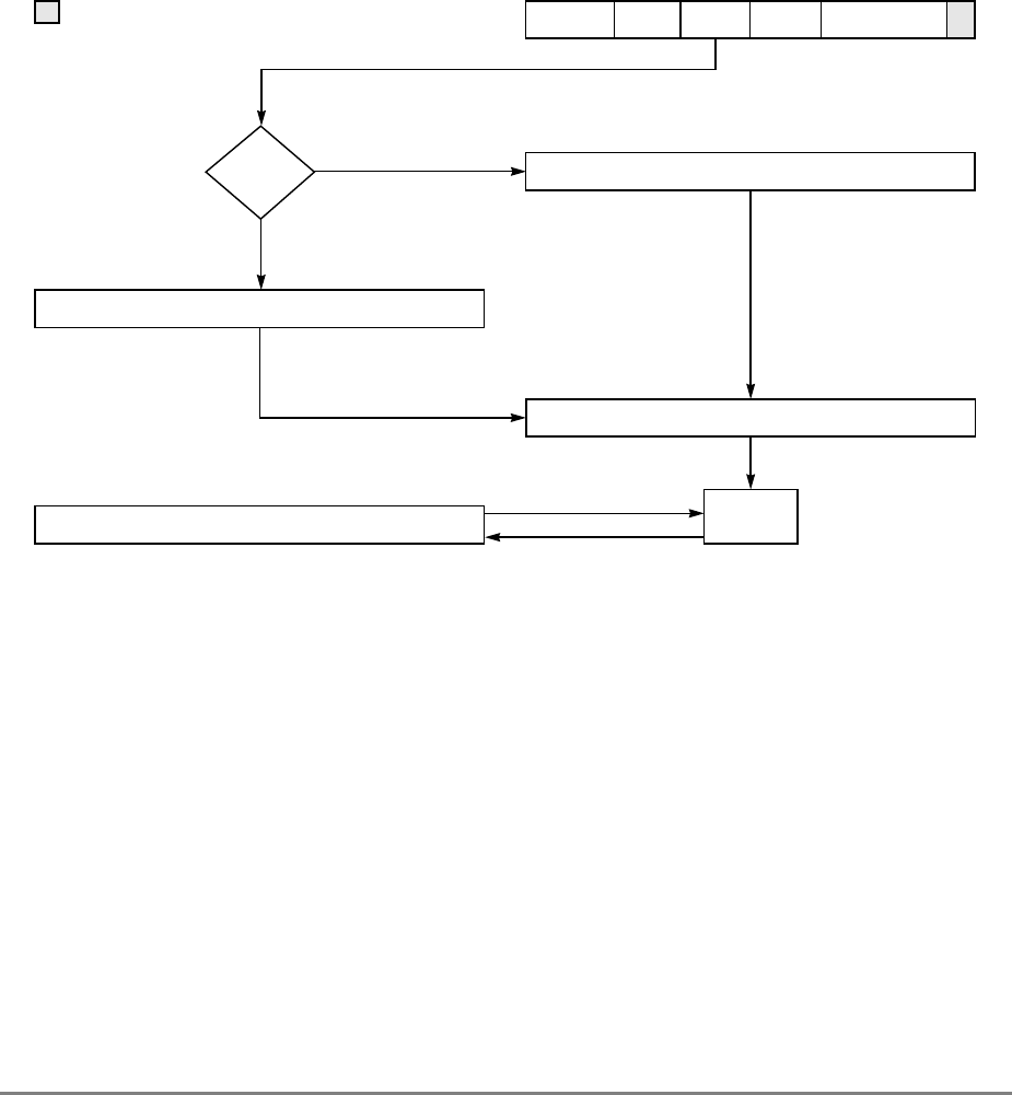
3-44 PowerPC 601 RISC Microprocessor User's Manual
3.5.1.3 Register Indirect Addressing
Instructions using this addressing mode use the contents of the general purpose register
specified by the rA operand as the effective address. A zero in the rA operand causes an
effective address of zero to be generated. The option to specify rA or 0 is shown in the
instruction descriptions as (rA|0).
Figure 3-3 shows how an effective address is generated when using register indirect
addressing.
Figure 3-3. Register Indirect Addressing
3.5.2 Integer Load Instructions
For load instructions, the byte, half word, word, or double word addressed by EA is loaded
into rD. Many integer load instructions have an update form, in which rA is updated with
the generated effective address. For these forms, if rA ≠ 0 and rA ≠ rD, the effective
address is placed into rA and the memory element (byte, half word, or word) addressed by
EA is loaded into rD.
Note that non-601 implementations of the architecture may run the load half algebraic
instructions (lha, lhax) and the load with update (lbzu, lbzux, lhzu, lhzux, lhau, lhaux)
instructions with greater latency than other types of load instructions. In the 601, these
instructions operate with the same latency as other load instructions. For details on
instruction timing, see Chapter 7, “Instruction Timing.”
No
Store
Load
Yes 031
0 0 0 0 0•••••••••••••••••••••••••••••••••••••••••••••••••••• 0 0 0 0 0
Instruction Encoding:
067111216172122 3031
rA=0?
031
GPR (rA)
031
Effective Address
Opcode rD/rSrA NB Subopcode 0
031
GPR (rD/rS) Memory
Interface
Reserved

Chapter 3. Addressing Modes and Instruction Set Summary 3-45
The PowerPC architecture defines load with update instructions with rA = 0 or rA = rD as
an invalid form. In the POWER architecture, these forms are not considered invalid and
specifications exist for these cases. To maintain compatibility with the POWER
architecture, for the case where rA = 0, the 601 does not update r0. In cases where rA = rD,
the load data is loaded into rD and the register rA update is suppressed. In addition, the
PowerPC architecture defines integer load instructions with the condition register update
option enabled to be an invalid form and the POWER architecture does not. For
compatibility, the 601 executes the instruction in a manner consistent with the PowerPC
architecture and it causes an undefined value to be placed into the condition register CR0
field.
Table 3-16 summarizes the load instructions available for the 601.
Table 3-16. Integer Load Instructions
Name Mnemonic Operand
Syntax Operation
Load Byte
and Zero lbz rD,d(rA) The effective address is the sum (rA|0)+d. The byte in memory
addressed by the EA is loaded into register rD[24–31]. The remaining
bits in register rD are cleared to 0.
Load Byte
and Zero
Indexed
lbzx rD,rA,rB The effective address is the sum (rA|0)+(rB). The byte in memory
addressed by the EA is loaded into register rD[24–31]. The remaining
bits in register rD are cleared to 0.
Load Byte
and Zero
with Update
lbzu rD,d(rA) The effective address (EA) is the sum (rA|0)+d. The byte in memory
addressed by the EA is loaded into register rD[24–31]. The remaining
bits in register rD are cleared to 0. The EA is placed into register rA. If
operand rA = 0 the 601 does not update r0, or if rA = rD the load data
is loaded into register rD and the register update is suppressed.
Although the PowerPC architecture defines load with update
instructions with operand rA = 0 or rA = rD as invalid forms, the 601
allows these cases.
Load Byte
and Zero
with
Update
Indexed
lbzux rD,rA,rB The effective address (EA)is the sum (rA|0)+(rB). The byte
addressed by the EA is loaded into register rD[24–31]. The remaining
bits in register rD are cleared to 0. The EA is placed into register rA. If
operand rA = 0 the 601 does not update register r0, or if rA = rD the
load data is loaded into register rD and the register update is
suppressed. Although the PowerPC architecture defines load with
update instructions with operand rA = 0 or rA = rD as invalid forms,
the 601 allows these cases.
Load
Half Word
and Zero
lhz rD,d(rA) The effective address is the sum (rA|0)+d. The half word in memory
addressed by the EA is loaded into register rD[16–31]. The remaining
bits in rD are cleared to 0.
Load
Half Word
and Zero
Indexed
lhzx rD,rA,rB The effective address is the sum (rA|0)+(rB). The half word in
memory addressed by the EA is loaded into register rD[16–31]. The
remaining bits in register rD are cleared.

3-46 PowerPC 601 RISC Microprocessor User's Manual
Load
Half Word
and Zero
with Update
lhzu rD,d(rA) The effective address is the sum (rA|0)+d. The half word in memory
addressed by the EA is loaded into register rD[16–31]. The remaining
bits in register rD are cleared.
The EA is placed into register rA.
If operand rA = 0 the 601 does not update register r0, or if rA = rD the
load data is loaded into register rD and the register update is
suppressed. Although the PowerPC architecture defines load with
update instructions with operand rA = 0 or rA = rD as invalid forms,
the 601 allows these cases.
Load
Half Word
and Zero
with
Update
Indexed
lhzux rD,rA,rB The effective address is the sum (rA|0)+(rB). The half word in
memory addressed by the EA is loaded into register rD[16–31]. The
remaining bits in register rD are cleared. The EA is placed into
register rA. Although the PowerPC architecture defines load with
update instructions with operand rA = 0 or rA = rD as invalid forms,
the 601 allows these cases.
Load
Half Word
Algebraic
lha rD,d(rA) The effective address is the sum (rA|0)+d. The half word in memory
addressed by the EA is loaded into register rD[16–31]. The remaining
bits in register rD are filled with a copy of the most significant bit of
the loaded half word.
Load
Half Word
Algebraic
Indexed
lhax rD,rA,rB The effective address is the sum (rA|0)+(rB). The half word in
memory addressed by the EA is loaded into register rD[16–31]. The
remaining bits in register rD are filled with a copy of the most
significant bit of the loaded half word.
Load
Half Word
Algebraic
with Update
lhau rD,d(rA) The effective address is the sum (rA|0)+d. The half word in memory
addressed by the EA is loaded into register rD[16–31]. The remaining
bits in register rD are filled with a copy of the most significant bit of
the loaded half word. The EA is placed into register rA. If operand
rA = 0 the 601 does not update register r0, or if rA = rD the load data
is loaded into register rD and the register update is suppressed.
Although the PowerPC architecture defines load with update
instructions with operand rA = 0 or rA = rD as invalid forms, the 601
allows these cases.
Load
Half Word
Algebraic
with
Update
Indexed
lhaux rD,rA,rB The effective address is the sum (rA|0)+(rB). The half word in
memory addressed by the EA is loaded into register rD[16–31]. The
remaining bits in register rD are filled with a copy of the most
significant bit of the loaded half-word. The EA is placed into register
rA. If operand rA=0 the 601 does not update r0, or if rA = rD the load
data is loaded into register rD and the register update is suppressed.
Although the PowerPC architecture defines load with update
instructions with operand rA = 0 or rA = rD as invalid forms, the 601
allows these cases.
Load Word
and Zero lwz rD,d(rA) The effective address is the sum (rA|0)+d. The word in memory
addressed by the EA is loaded into register rD[0–31].
Load Word
and Zero
Indexed
lwzx rD,rA,rB The effective address is the sum (rA|0)+(rB). The word in memory
addressed by the EA is loaded into register rD[0–31].
Table 3-16. Integer Load Instructions (Continued)
Name Mnemonic Operand
Syntax Operation

Chapter 3. Addressing Modes and Instruction Set Summary 3-47
3.5.3 Integer Store Instructions
For integer store instructions, the contents of register rS are stored into the byte, half word,
word or double word in memory addressed by EA. Many store instructions have an update
form, in which register rA is updated with the effective address. For these forms, the
following rules apply:
•If rA ≠ 0, the effective address is placed into register rA.
• If rS = rA, the contents of register rS are copied to the target memory element, then
the generated EA is placed into rA.
The PowerPC architecture defines store with update instructions with rA = 0 as an invalid
form. In the POWER architecture, this form is not considered invalid and in this case rA is
not updated. To maintain compatibility with POWER in this case, the 601 does not update
register r0. In addition, the PowerPC architecture defines integer store instructions with the
condition register update option enabled to be an invalid form and the POWER architecture
does not. To maintain compatibility in these cases, the 601 executes the instruction as
described in the PowerPC architecture, and it loads an undefined value into CR0 field of the
condition register.
Table 3-17 provides a summary of the integer store instructions for the 601.
Load Word
and Zero
with Update
lwzu rD,d(rA) The effective address is the sum (rA|0)+d. The word in memory
addressed by the EA is loaded into register rD[0–31]. The EA is
placed into register rA. If operand rA = 0 the 601 does not update
register r0, or if rA = rD the load data is loaded into register rD and
the register update is suppressed. Although the PowerPC
architecture defines load with update instructions with operand rA = 0
or rA = rD as invalid forms, the 601 allows these cases.
Load Word
and Zero
with
Update
Indexed
lwzux rD,rA,rB The effective address is the sum (rA|0)+(rB). The word in memory
addressed by the EA is loaded into register rD[0–31]. The EA is
placed into register rA. If operand rA = 0 the 601 does not update
register r0, or if rA = rD the load data is loaded into register rD and
the register update is suppressed. Although the PowerPC
architecture defines load with update instructions with operand rA = 0
or rA = rD as invalid forms, the 601 allows these cases.
Table 3-16. Integer Load Instructions (Continued)
Name Mnemonic Operand
Syntax Operation

3-48 PowerPC 601 RISC Microprocessor User's Manual
Table 3-17. Integer Store Instructions
Name Mnemonic Operand
Syntax Operation
Store Byte stb rS,d(rA) The effective address is the sum (rA|0) + d. Register rS[24–31] is
stored into the byte in memory addressed by the EA.
Store Byte
Indexed stbx rS,rA,rB The effective address is the sum (rA|0) + (rB). rS[24–31] is stored
into the byte in memory addressed by the EA.
Store Byte
with Update stbu rS,d(rA) The effective address is the sum (rA|0) + d. rS[24–31] is stored into
the byte in memory addressed by the EA. The EA is placed into
register rA.
Store Byte
with
Update
Indexed
stbux rS,rA,rB The effective address is the sum (rA|0) + (rB). rS[24–31] is stored
into the byte in memory addressed by the EA. The EA is placed into
register rA.
Store
Half Word sth rS,d(rA) The effective address is the sum (rA|0) + d. rS[16–31] is stored into
the half word in memory addressed by the EA.
Store
half Word
Indexed
sthx rS,rA,rB The effective address (EA) is the sum (rA|0) + (rB). rS[16–31] is
stored into the half word in memory addressed by the EA.
Store
Half Word
with Update
sthu rS,d(rA) The effective address is the sum (rA|0) + d. rS[16–31] is stored into
the half word in memory addressed by the EA. The EA is placed into
register rA.
Store
Half Word
with
Update
Indexed
sthux rS,rA,rB The effective address is the sum (rA|0) + (rB). rS[16–31] is stored
into the half word in memory addressed by the EA. The EA is placed
into register rA.
Store Word stw rS,d(rA) The effective address is the sum (rA|0) + d. Register rS is stored into
the word in memory addressed by the EA.
Store Word
Indexed stwx rS,rA,rB The effective address is the sum (rA|0) + (rB). rS is stored into the
word in memory addressed by the EA.
Store Word
with Update stwu rS,d(rA) The effective address is the sum (rA|0) + d.
Register rS is stored into the word in memory addressed by the EA.
The EA is placed into register rA.
Store Word
with
Update
Indexed
stwux rS,rA,rB The effective address is the sum (rA|0) + (rB). Register rS is stored
into the word in memory addressed by the EA. The EA is placed into
register rA.

Chapter 3. Addressing Modes and Instruction Set Summary 3-49
3.5.4 Integer Load and Store with Byte Reversal Instructions
Table 3-18 describes integer load and store with byte reversal instructions. Note that in
other PowerPC implementations, load byte-reverse instructions may have greater latency
than other load instructions.
This is not the case in the 601. These instructions operate with the same latency as other
load instructions.
3.5.5 Integer Load and Store Multiple Instructions
The load/store multiple instructions are used to move blocks of data to and from the GPRs.
The load multiple and store multiple instructions may have operands that require memory
accesses crossing a 4-Kbyte page boundary. As a result, these instructions may be
interrupted by a data access exception associated with the address translation of the second
page. In this case, the 601 performs all of the memory references from the first page, and
none of the memory references from the second page before taking the exception. For
additional information, refer to Section 5.4.3, “Data Access Exception (x'00300').”
In future implementations, these instructions are likely to have greater latency and take
longer to execute, perhaps much longer, than a sequence of individual load or store
instructions that produce the same results.
Table 3-18. Integer Load and Store with Byte Reversal Instructions
Name Mnemonic Operand
Syntax Operation
Load
Half Word
Byte-
Reverse
Indexed
lhbrx rD,rA,rB The effective address is the sum (rA|0) + (rB). Bits 0–7 of the half
word in memory addressed by the EA are loaded into rD[24–31].
Bits 8–15 of the half word in memory addressed by the EA are
loaded into rD[16–23]. The rest of the bits in rD are cleared to 0.
Load Word
Byte-
Reverse
Indexed
lwbrx rD,rA,rB The effective address is the sum (rA|0) + (rB). Bits 0–7 of the
word in memory addressed by the EA are loaded into rD[24–31].
Bits 8–15 of the word in memory addressed by the EA are loaded
into rD[16–23]. Bits 16–23 of the word in memory addressed by
the EA are loaded into rD[8–15]. Bits 24–31 of the word in
memory addressed by the EA are loaded into rD[0–7].
Store
Half Word
Byte-
Reverse
Indexed
sthbrx rS,rA,rB The effective address is the sum (rA|0) + (rB). rS[24–31] are
stored into bits 0–7 of the half word in memory addressed by the
EA. rS[16–23] are stored into bits 8–15 of the half word in
memory addressed by the EA.
Store Word
Byte-
Reverse
Indexed
stwbrx rS,rA,rB The effective address is the sum (rA|0) + (rB). rS[24–31] are
stored into bits 0–7 of the word in memory addressed by EA.
rS[16–23] are stored into bits 8–15 of the word in memory
addressed by the EA. rS[8–15] are stored into bits 16–23 of the
word in memory addressed by the EA. rS[0–7] are stored into bits
24–31 of the word in memory addressed by the EA.

3-50 PowerPC 601 RISC Microprocessor User's Manual
The PowerPC architecture defines the load multiple word (lmw) instruction with rA in the
range of registers to be loaded as an invalid form. In the POWER architecture, this form is
not considered invalid. To maintain compatibility with the POWER architecture in this
case, the 601 will execute the instruction normally, except that the loading of register rA is
skipped. If rA = 0, the register is not considered to be actually used for addressing, and the
update of r0 (if it is in the range of registers to be loaded) is loaded. In addition, the
PowerPC architecture defines the load multiple and store multiple instructions with
misaligned operands (that is, the EA is not a multiple of 4) to be an invalid form and the
POWER architecture does not. To maintain compatibility with the POWER architecture,
the 601 executes these instructions subject to the performance degradation as described in
5.4.6.1, “Integer Alignment Exceptions.” Note that on other PowerPC implementations,
load and store multiple instructions that are not on a word boundary either take an
alignment exception or generate results that are boundedly undefined.
Table 3-19 summarizes the integer load and store multiple instructions for the 601.
3.5.6 Integer Move String Instructions
The integer move string instructions allow movement of data from memory to registers or
from registers to memory without concern for alignment. These instructions can be used for
a short move between arbitrary memory locations or to initiate a long move between
misaligned memory fields. However, in future implementations, these instructions are
likely to have greater latency and take longer to execute, perhaps much longer, than a
sequence of individual load or store instructions that produce the same results.
Table 3-19. Integer Load and Store Multiple Instructions
Name Mnemoni
cOperand
Syntax Operation
Load
Multiple
Word
lmw rD,d(rA) The effective address is the sum (rA|0) + d.
n
= 32 – rD.
n
consecutive words starting at EA are loaded into the GPR specified
by rD through GPR 31.
If the EA is not a multiple of four, the alignment exception handler
may be invoked if a page boundary is crossed.
Store
Multiple
Word
stmw rS,d(rA) The effective address is the sum (rA|0) + d.
n
= (32 – rS).
n
consecutive words starting at the EA are stored from the GPR
specified by rS through GPR 31.
If the EA is not a multiple of four, the alignment exception handler
may be invoked if a page boundary is crossed.

Chapter 3. Addressing Modes and Instruction Set Summary 3-51
Load/store string indexed instructions of zero length have no effect. Table 3-20 summarizes
the integer move string instructions available for the 601.
Table 3-20. Integer Move String Instructions
Name Mnemonic Operand
Syntax Operation
Load String
Word
Immediate
lswi rD,rA,NB The EA is (rA|0).
Let
n
= NB if NB ≠ 0,
n
= 32 if NB = 0;
n
is the number of bytes to load.
Let
nr
= (
n
/4);
nr
is the number of registers to receive data.
n
consecutive bytes starting at the EA are loaded into GPRs rD
through rD+
nr
-1. Bytes are loaded left to right in each register. The
sequence of registers wraps around to r0 if required. If the four bytes
of register rD+
nr
-1 are only partially filled, the unfilled low-order
byte(s) of that register are cleared to 0.
If rA is in the range of registers specified to be loaded, it will be
skipped in the load process. If operand rA = 0, the register is not
considered as used for addressing, and will be loaded.
Load String
Word
Indexed
lswx rD,rA,rB The EA is the sum (rA|0)+(rB).
Let
n
= XER[25–31];
n
is the number of bytes to load.
Let
nr
= CEIL(
n
/4);
nr
is the number of registers to receive data.
If
n
>0,
n
consecutive bytes starting at the EA are loaded into registers
rD through rD+
nr
-1.
Bytes are loaded left to right in each register. The sequence of
registers wraps around to r0 if required. If the four bytes of register
rD+
nr
-1 are only partially filled, the unfilled low-order byte(s) of that
register are cleared to 0.
If
n
=0, the contents of register rD is undefined.
If rA is in the range of registers specified to be loaded, it will be
skipped in the load process. If operand rA=0, the register is not
considered as used for addressing, and will be loaded.

3-52 PowerPC 601 RISC Microprocessor User's Manual
Load string and store string instructions may involve operands that are not word-aligned.
As described in Section 5.4.6, “Alignment Exception (x'00600'),” a misaligned string
operation suffers a performance penalty compared to an aligned operation of the same type.
A non-word-aligned string operation that crosses a 4-Kbyte boundary, or a word-aligned
string operation that crosses a 256-Mbyte boundary always causes an alignment exception.
Load String
and
Compare
Byte
Indexed
lscbx
lscbx. rD,rA,rBThis is a POWER instruction, and is not part of the PowerPC
architecture. This instruction will not be supported by other
PowerPC implementations.
The EA is the sum (rA|0)+(rB). XER[25–31] contains the byte count.
Register rD is the starting register.
n
= XER[25–31], which is the
number of bytes to be loaded.
nr
= CEIL(
n
/4), which is the number of
registers to receive data. Starting with the leftmost byte in rD,
consecutive bytes in memory addressed by the EA are loaded into rD
through rD+
nr
-1, wrapping around back through GPR 0 if required,
until either a byte match is found with XER[16–23] or
n
bytes have
been loaded. If a byte match is found, that byte is also loaded.
Bytes are always loaded left to right in the register. In the case when
a match was found before
n
bytes were loaded, the contents of the
rightmost byte(s) not loaded of that register and the contents of all
succeeding registers up to and including rD+
nr
-1 are undefined. Also,
no reference is made to memory after the matched byte is found. In
the case when a match was not found, the contents of the rightmost
byte(s) not loaded of rD+
nr
-1 is undefined.
When XER[25–31]=0, the content of rD is unchanged. The count of
the number of bytes loaded up to and including the matched byte, if a
match was found, is placed in XER[25–31].
lscbx Load String and Compare Byte Indexed
lscbx. Load String and Compare Byte Indexed with CR Update.
The dot suffix enables the update of the condition register.
This instruction is specific to the 601.
Store
String
Word
Immediate
stswi rS,rA,NB The EA is (rA|0).
Let
n
= NB if NB ≠ 0,
n
= 32 if NB = 0;
n
is the number of bytes to
store.
Let
nr
= CEIL(
n
/4);
nr
is the number of registers to supply data.
n
consecutive bytes starting at the EA are stored from register rS
through rS+
nr
-1.
Bytes are stored left to right from each register. The sequence of
registers wraps around through r0 if required.
Store
String
Word
Indexed
stswx rS,rA,rB The effective address is the sum (rA|0)+(rB).
Let
n
= XER[25–31];
n
is the number of bytes to store.
Let
nr
= CEIL(
n
/4);
nr
is the number of registers to supply data.
n
consecutive bytes starting at the EA are stored from register rS
through rS+
nr
-1.
Bytes are stored left to right from each register. The sequence of
registers wraps around through r0 if required.
Table 3-20. Integer Move String Instructions (Continued)
Name Mnemonic Operand
Syntax Operation

Chapter 3. Addressing Modes and Instruction Set Summary 3-53
A non-word-aligned string operation that crosses a double-word boundary is also slower
than a word-aligned string operation.
Although a word-aligned string operation that crosses a 4-Kbyte boundary operates at the
601's fastest rate, the instruction may be interrupted by a data access exception associated
with the address translation of the second page. In this case, the 601 performs all memory
references from the first page and none from the second before taking the exception. For
more information, refer to Section 5.4.3, “Data Access Exception (x'00300').”
The Load String and Compare Byte Indexed (lscbx) instruction can lead to several
architecturally undefined results. When the last register loaded is only partially filled, the
remaining bytes are considered to be undefined. If loading is terminated due to a byte
match, all succeeding bytes are considered to be undefined. In addition, if the condition
register update option is enabled, and XER[25–31] = 0, condition register field CR0 is
undefined. In all of these cases, the 601 does not guarantee particular results for these
undefined fields. The values should simply be treated as undefined.
If the EA associated with an lscbx instruction is directed to a memory-forced I/O controller
interface segment (that is, the segment register T bit is set and the BUID field equals x'07F'),
the address is translated appropriately and the operation proceeds. On the other hand, if the
EA associated with an lscbx instruction is directed to an I/O segment (that is, the segment
register T bit is set but the BUID does not equal x'07F'), the 601 takes a data access
exception and sets bit 5 of the DSISR.
If rA is in the range of registers to be loaded for a Load String Word Immediate (lswi)
instruction or if either rA or rB are in the range of registers to be loaded for a Load String
Word Indexed (lswx) or lscbx instruction, then the PowerPC architecture considers the
instruction to be of an invalid form. In the POWER architecture, this form is not considered
invalid and specifications exist for these cases. To maintain compatibility with the POWER
architecture in this case, the 601 executes the instruction normally, but loading of these
registers is inhibited. In addition, the lswx, lscbx and stswx instructions that specify a string
length of zero are considered an invalid form in the PowerPC architecture, but not in the
POWER architecture. For compatibility with the POWER architecture, the 601 executes
these instructions, but does not alter register rD or cause a memory access.
3.5.7 Memory Synchronization Instructions
Memory synchronization instructions control the order in which memory operations are
completed with respect to asynchronous events, and the order in which memory operations
are seen by other processors or memory access mechanisms. Additional information about
these instructions and about related aspects of memory management can be found in
Chapter 6, “Memory Management Unit.”
Internally, the 601 handles the synchronize (sync) and the Enforce In-Order Execution of
I/O (eieio) instructions identically. These instructions delay execution of subsequent
instructions until previous instructions have completed to the point that they can no longer

3-54 PowerPC 601 RISC Microprocessor User's Manual
cause an exception, until all previous memory accesses are performed globally, and the
sync or eieio operation is broadcast onto the 601 bus interface.
System designs that use a second-level cache should take special care to accept the
broadcast sync operation and perform the appropriate actions to guarantee that memory
references that may be queued internally to the second-level cache have been performed
globally.
The number of cycles required to complete a sync or eieio instruction depends on system
parameters and on the processor's state when the instruction is issued. As a result, frequent
use of these instructions may degrade performance slightly.
The PowerPC architecture defines the sync instruction with condition register update
enabled to be an invalid form, whereas the POWER architecture does not. For
compatibility, the 601 executes the instruction consistently with the PowerPC architecture,
and loads an undefined value into condition register field CR0.
The Instruction Synchronize (isync) instruction causes the 601 to purge its instruction
buffers, wait for any preceding sync instructions to complete, and then branch to the next
sequential instruction (which has the effect of clearing the pipeline behind the isync
instruction).
The proper paired use of the Load Word and Reserve Indexed (lwarx) and Store Word
Conditional Indexed (stwcx.) instructions allows programmers to emulate common
semaphore operations such as “test and set”, “compare and swap”, “exchange memory”,
and “fetch and add”. Examples of these semaphore operations can be found in Appendix G,
“Synchronization Programming Examples.” The lwarx instruction must be paired with an
stwcx. instruction with the same effective address used for both instructions of the pair, and
the reservation granularity is 32 bytes.
The concept behind the use of the lwarx and stwcx. instructions is that a processor may
load a semaphore from memory, compute a result based on the value of the semaphore, and
conditionally store it back to the same location. The conditional store is performed based
upon the existence of a reservation established by the preceding lwarx. If the reservation
exists when the store is executed, the store is performed and a bit is set to one in the
Condition Register. If the reservation does not exist when the store is executed, the target
memory location is not modified and a bit is set to zero in the condition register.
The lwarx and stwcx. primitives allow software to read a semaphore, compute a result
based on the value of the semaphore, store the new value back into the semaphore location
only if that location has not been modified since it was first read, and determine if the store
was successful. If the store was successful, the sequence of instructions from the read of the
semaphore to the store that updated the semaphore appear to have been executed atomically
(that is, no other processor or mechanism modified the semaphore location between the
read and the update), thus providing the equivalent of a real atomic operation. However,
other processors may have read from the location during this operation.

Chapter 3. Addressing Modes and Instruction Set Summary 3-55
The lwarx and stwcx. instructions require the EA to be aligned. Exception handling
software should not attempt to emulate a misaligned lwarx or stwcx. instruction, because
there is no correct way to define the address associated with the reservation.
In general, the lwarx and stwcx. instructions should be used only in system programs,
which can be invoked by application programs as needed.
At most one reservation exists simultaneously on any processor. The address associated
with the reservation can be changed by a subsequent lwarx instruction. The conditional
store is performed based upon the existence of a reservation established by the preceding
lwarx regardless of whether the address generated by the lwarx matches that generated by
the stwcx. A reservation held by the processor is cleared by any of the following:
• executing an stwcx. instruction to any address,
• execution of an sc instruction,
• execution of an instruction that causes an exception,
• occurrence of an asynchronous exception,
• attempt by some other device to modify a location in the reservation granularity (32
bytes).
The memory synchronization instructions available for the 601 are summarized in
Table 3-21.
Table 3-21. Memory Synchronization Instructions
Name Mnemonic Operand
Syntax Operation
Enforce
In-Order
Execution of
I/O
eieio The eieio instruction provides an ordering function for the effects of
load and store instructions executed by a given processor. Executing
an eieio instruction ensures that all memory accesses previously
initiated by the given processor are complete with respect to main
memory before allowing any memory accesses subsequently initiated
by the given processor to access main memory.
The eieio instruction orders load and store operations to cache-
inhibited memory, and store operations to write-through cache
memory.
The eieio instruction performs the same function as a sync
instruction when executed by the 601.
Instruction
Synchronize isync This instruction waits for all previous instructions to complete, and
then discards any fetched instructions, causing subsequent
instructions to be fetched (or refetched) from memory and to execute
in the context established by the previous instructions. This
instruction has no effect on other processors or on their caches.

3-56 PowerPC 601 RISC Microprocessor User's Manual
3.5.8 Floating-Point Load and Store Address Generation
Floating point load and store operations generate effective addresses using the register
indirect with immediate index mode and register indirect with index mode, the details of
which are described below. Floating-point loads and stores are not supported for I/O
accesses when the SR[BUID] is not equal to x'07F'. The use of floating-point loads and
stores for I/O access will result in an alignment exception.
Load Word
and
Reserve
Indexed
lwarx rD,rA,rB The effective address is the sum (rA|0)+(rB). The word in memory
addressed by the EA is loaded into register rD.
This instruction creates a reservation for use by an stwcx. instruction.
An address computed from the EA is associated with the reservation,
and replaces any address previously associated with the reservation.
The EA must be a multiple of 4. If it is not, the alignment exception
handler will be invoked if the word loaded crosses a page boundary,
or the results may be undefined.
Store Word
Conditional
Indexed
stwcx. rS,rA,rB The effective address is the sum (rA|0)+(rB).
If a reservation exists, register rS is stored into the word in memory
addressed by the EA and the reservation is cleared.
If a reservation does not exist, the instruction completes without
altering memory or the contents of the cache.
The EQ bit in the condition register field CR0 is modified to reflect
whether the store operation was performed (i.e., whether a
reservation existed when the stwcx. instruction began execution). If
the store was completed successfully, the EQ bit is set to one.
The EA must be a multiple of 4; otherwise, the alignment exception
handler will be invoked if the word stored crosses a page boundary,
or the results may be undefined.
Synchronize sync Executing a sync instruction ensures that all instructions previously
initiated by the given processor appear to have completed before any
subsequent instructions are initiated by the given processor. When
the sync instruction completes, all memory accesses initiated by the
given processor prior to the sync will have been performed with
respect to all other mechanisms that access memory. The sync
instruction can be used to ensure that the results of all stores into a
data structure, performed in a “critical section” of a program, are seen
by other processors before the data structure is seen as unlocked.
The eieio instruction may be more appropriate than sync for cases in
which the only requirement is to control the order in which memory
references are seen by I/O devices.
Table 3-21. Memory Synchronization Instructions (Continued)
Name Mnemonic Operand
Syntax Operation
Chapter 3. Addressing Modes and Instruction Set Summary 3-57
3.5.8.1 Register Indirect with Immediate Index Addressing
Instructions using this addressing mode contain a signed 16-bit immediate index (d
operand) which is sign extended to 32 bits, and added to the contents of a general purpose
register specified in the instruction (rA operand) to generate the effective address. A zero
in the rA operand causes a zero to be added to the immediate index (d operand). This is
shown in the instruction descriptions as (rA|0).
Figure 3-4 shows how an effective address is generated when using register indirect with
immediate index addressing.
Figure 3-4. Register Indirect with Immediate Index Addressing
3.5.8.2 Register Indirect with Index Addressing
Instructions using this addressing mode add the contents of two general purpose registers
(specified in operands rA and rB) to generate the effective address. A zero in the rA
operand causes a zero to be added to the contents of general purpose register specified in
operand rB. This is shown in the instruction descriptions as (rA|0).
Figure 3-5 shows how an effective address is generated when using register indirect with
index addressing.
No
0161731
Sign Extension d
0
+
Store
Load
Yes
Instruction Encoding:
06711121617 31
Opcode frD/frSrAd
031
Effective Address
rA=0
Memory
Access
063
FPR (frD/frS)
031
GPR (rA)
3-58 PowerPC 601 RISC Microprocessor User's Manual
Figure 3-5. Register Indirect with Index Addressing
The PowerPC architecture defines floating-point load and store with update instructions
(lfsu, lfsux, lfdu, lfdux, stfsu, stfsux, stfdu, stfdux) with operand rA = 0 as invalid forms
of the instructions, but the POWER architecture does not. To maintain compatibility with
the POWER architecture, the 601 accesses memory for these cases but inhibits the update
of the integer register r0.
In addition, the PowerPC architecture defines floating-point load and store instructions with
the condition register update option enabled to be an invalid form. For compatibility with
the POWER architecture, the 601 executes the instruction normally, but also writes an
undefined value into the condition register field CR1.
The PowerPC architecture defines that the FPSCR[UE] bit should not be used to determine
whether denormalization should be performed on floating-point stores. The 601 complies
with this definition, although this is different from some POWER architecture
implementations.
3.5.9 Floating-Point Load Instructions
There are two forms of the floating-point load instruction—single-precision and
double-precision formats. Because the FPRs support only floating-point, double-precision
format, single-precision floating-point load instructions convert single-precision data to
double-precision format before loading the operands into the target FPR. This conversion
is described in Section 3.5.9.1, “Double-Precision Conversion for Floating-Point Load
Instructions.” Table 3-22 provides a summary of the floating-point load instructions.
No
031
GPR (rA)
0
+
063
FPR (frD/frS) Memory
Access
Store
Load
Yes
031
GPR (rB)
031
Effective Address
Instruction Encoding:
067111216172122 3031
rA=0?
Opcode frD/frSrArB Subopcode 0
Reserved

Chapter 3. Addressing Modes and Instruction Set Summary 3-59
Table 3-22. Floating-Point Load Instructions
Name Mnemonic Operand
Syntax Operation
Load
Floating-Point
Single-
Precision
lfs frD,d(rA) The effective address is the sum (rA|0)+d.
The word in memory addressed by the EA is interpreted as a
floating-point single-precision operand. This word is converted to
floating-point double-precision format and placed into register frD.
Load
Floating- Point
Single-
Precision
Indexed
lfsx frD,rA,rB The effective address is the sum (rA|0)+(rB).
The word in memory addressed by the EA is interpreted as a
floating-point single-precision operand. This word is converted to
floating-point double-precision and placed into register frD.
Load
Floating-Point
Single-
Precision with
Update
lfsu frD,d(rA) The effective address is the sum (rA|0)+d.
The word in memory addressed by the EA is interpreted as a
floating-point single-precision operand. This word is converted to
floating-point double-precision (see Section 3.5.9.1,
“Double-Precision Conversion for Floating-Point Load Instructions,”)
and placed into register frD.
The EA is placed into the register specified by rA.
Load
Floating-Point
Single-
Precision with
Update
Indexed
lfsux frD,rA,rB The effective address is the sum (rA|0)+(rB).
The word in memory addressed by the EA is interpreted as a
floating-point single-precision operand. This word is converted to
floating-point double-precision (see Section 3.5.9.1,
“Double-Precision Conversion for Floating-Point Load Instructions,”)
and placed into register frD.
The EA is placed into the register specified by rA.
Load
Floating-Point
Double-
Precision
lfd frD,d(rA) The effective address is the sum (rA|0)+d.
The double word in memory addressed by the EA is placed into
register frD.
Load
Floating-Point
Double-
Precision
Indexed
lfdx frD,rA,rB The effective address is the sum (rA|0)+(rB).
The double word in memory addressed by the EA is placed into
register frD.
Load
Floating-Point
Double-
Precision with
Update
lfdu frD,d(rA) The effective address is the sum (rA|0)+d.
The double word in memory addressed by the EA is placed into
register frD.
The EA is placed into the register specified by rA.
Load
Floating-Point
Double-
Precision with
Update
Indexed
lfdux frD,rA,rB The effective address is the sum (rA|0)+(rB).
The double word in memory addressed by the EA is placed into
register frD.
The EA is placed into the register specified by rA.

3-60 PowerPC 601 RISC Microprocessor User's Manual
3.5.9.1 Double-Precision Conversion for Floating-Point Load
Instructions
The steps for converting a floating-point value from a single-precision memory format to
the double-precision register format are as follows:
WORD[0–31] is the floating-point, single-precision operand accessed from memory.
Normalized Operand
If WORD[1–8] > 0 and WORD[1–8] < 255
frD[0–1] < WORD[0–1]
frD[2] < ¬WORD[1]
frD[3] < ¬WORD[1]
frD[4] < ¬WORD[1]
frD[5–63] < WORD[2–31] || 29b'0'
Denormalized Operand
If WORD[1–8] = 0 and WORD[9–31] ≠ 0
sign < WORD[0]
exp < –126
frac[0–52] < b'0'‘|| WORD[9–31] || 29b'0'
normalize the operand
Do while frac 0 = 0
frac < frac[1–52] || b'0'
exp < exp – 1
End
frD[0] < sign
frD[1–11] < exp + 1023
frD[12–63] < frac[1–52]
Infinity / QNaN / SNaN / Zero
If WORD[1–8] = 255 or WORD[1–31] = 0
frD[0–1] < WORD[0–1]
frD[2] < WORD[1]
frD[3] < WORD[1]
frD[4] < WORD[1]
frD[5–63] < WORD[2–31] || 29b'0'
For double-precision floating-point load instructions, no conversion is required as the data
from memory is copied directly into the FPRs.
Many floating-point load instructions have an update form in which register rA is updated
with the EA. For these forms, if operand rA ≠ 0, the effective address is placed into register
rA and the memory element (word or double word) addressed by the EA is loaded into the
floating-point register specified by operand frD.

Chapter 3. Addressing Modes and Instruction Set Summary 3-61
3.5.10 Floating-Point Store Instructions
This section describes floating-point store instructions. There are two basic forms of the
store instruction—single- and double-precision. Because the FPRs support only
floating-point, double-precision format, single-precision floating-point store instructions
convert double-precision data to single-precision format before storing the operands. The
conversion steps are described in Section 3.5.10.1, “Double-Precision Conversion for
Floating-Point Store Instructions.” Table 3-23 is a summary of the floating point store
instructions provided by the 601.
Table 3-23. Floating-Point Store Instructions
Name Mnemonic Operand
Syntax Operation
Store
Floating-Point
Single-Precision
stfs frS,d(rA) The EA is the sum (rA|0)+d.
The contents of register frS is converted to single-precision and
stored into the word in memory addressed by the EA.
Store
Floating-Point
Single-Precision
Indexed
stfsx frS,rA,rB The EA is the sum (rA|0)+(rB).
The contents of register frS is converted to single-precision and
stored into the word in memory addressed by the EA.
Store
Floating-Point
Single-Precision
with Update
stfsu frS,d(rA) The EA is the sum (rA|0)+d.
The contents of register frS is converted to single-precision and
stored into the word in memory addressed by the EA.
The EA is placed into the register specified by operand rA.
Store
Floating-Point
Single-Precision
with Update
Indexed
stfsux frS,rA,rB The EA is the sum (rA|0)+(rB).
The contents of register frS is converted to single-precision and
stored into the word in memory addressed by the EA.
The EA is placed into the register specified by operand rA.
Store
Floating-Point
Double-Precision
stfd frS,d(rA) The effective address is the sum (rA|0)+d.
The contents of register frS is stored into the double word in
memory addressed by the EA.
Store
Floating-Point
Double-Precision
Indexed
stfdx frS,rA,rB The EA is the sum (rA|0)+(rB).
The contents of register frS is stored into the double word in
memory addressed by the EA.
Store
Floating-Point
Double-Precision
with Update
stfdu frS,d(rA) The effective address is the sum (rA|0)+d.
The contents of register frS is stored into the double word in
memory addressed by the EA.
The EA is placed into register rA.
Store
Floating-Point
Double-Precision
with Update
Indexed
stfdux frS,rA,rB The EA is the sum (rA|0)+(rB).
The contents of register frS is stored into the double word in
memory addressed by EA.
The EA is placed into register rA.

3-62 PowerPC 601 RISC Microprocessor User's Manual
3.5.10.1 Double-Precision Conversion for Floating-Point Store
Instructions
The steps for converting a floating-point value from the double-precision register format to
single-precision memory format are as follows:
Let WORD[0–31] be the word in memory written to.
No Denormalization Required
If frS[1–11] > 896 or frS[1–63] = 0
WORD[0–1] < frS[0–1]
WORD[2–31]< frS[5–34]
Denormalization Required
If 874 ≤ frS[1–11] ≤ 896
sign < frS[0]
exp < frS[1–11] – 1023
frac < b'1' || frS[12–63]
Denormalize operand
Do while exp < –126
frac < b'0' || frac[0–62]
exp < exp + 1
End
WORD[0] < sign
WORD[1–8] < x'00'
WORD[9–31] < frac[1–23]
For double-precision floating-point store instructions, no conversion is required as the data
from the FPRs is copied directly into memory. Many floating-point store instructions have
an update form, in which register rA is updated with the effective address. For these forms,
if operand rA ≠ 0, the effective address is placed into register rA.
Floating-point store instructions are listed in Table 3-23. Recall that rA, rB, and rD denote
GPRs, while frA, frB, frC, frS, and frD denote FPRs.
3.5.11 Floating-Point Move Instructions
Floating-point move instructions copy data from one floating-point register to another with
data modifications as described for each instruction. These instructions do not modify the
FPSCR. The condition register update option in these instructions controls the placing of
result status into condition register field CR1. If the condition register update option is
enabled, then CR1 is set, otherwise CR1 is unchanged. Floating-point move instructions are
listed in Table 3-24.

Chapter 3. Addressing Modes and Instruction Set Summary 3-63
3.6 Branch and Flow Control Instructions
Branch instructions are executed by the BPU. Some of these instructions can redirect
instruction execution conditionally based on the value of bits in the condition register.
When the branch processor encounters one of these instructions, it scans the execution
pipelines to determine whether an instruction in progress may affect the particular
condition register bit. If no interlock is found, the branch can be resolved immediately by
checking the bit in the condition register and taking the action defined for the branch
instruction.
If an interlock is detected, the branch is considered unresolved and the direction of the
branch is predicted using the “y” bit as described in Table 3-25. The interlock is monitored
while instructions are fetched for the predicted branch. When the interlock is cleared, the
branch processor determines whether the prediction was correct based on the value of the
condition register bit. If the prediction is correct, the branch is considered completed and
instruction fetching continues. If the prediction is incorrect, the fetched instructions are
purged, and instruction fetching continues along the alternate path.
3.6.1 Branch instruction Address Calculation
Branch instructions can alter the sequence of instruction execution. Instruction addresses
are always assumed to be word aligned with the 601; the processor ignores the two
low-order bits of the generated branch target address.
Table 3-24. Floating-Point Move Instructions
Name Mnemonic Operand
Syntax Operation
Floating-
Point Move
Register
fmr
fmr. frD,frB The contents of register frB is placed into frD.
fmr Floating-Point Move Register
fmr. Floating-Point Move Register with CR Update. The dot
suffix enables the update of the condition register.
Floating-
Point
Negate
fneg
fneg. frD,frB The contents of register frB with bit 0 inverted is placed into register
frD.
fneg Floating-Point Negate
fneg. Floating-Point Negate with CR Update. The dot suffix
enables the update of the condition register.
Floating-
Point
Absolute
Value
fabs
fabs. frD,frB The contents of frB with bit 0 cleared to 0 is placed into frD.
fabs Floating-Point Absolute Value
fabs. Floating-Point Absolute Value with CR Update. The dot
suffix enables the update of the condition register.
Floating-
Point
Negative
Absolute
Value
fnabs
fnabs. frD,frB The contents of frB with bit 0 set to one is placed into frD.
fnabs Floating-Point Negative Absolute Value
fnabs. Floating-Point Negative Absolute Value with CR Update.
The dot suffix enables the update of the condition register.
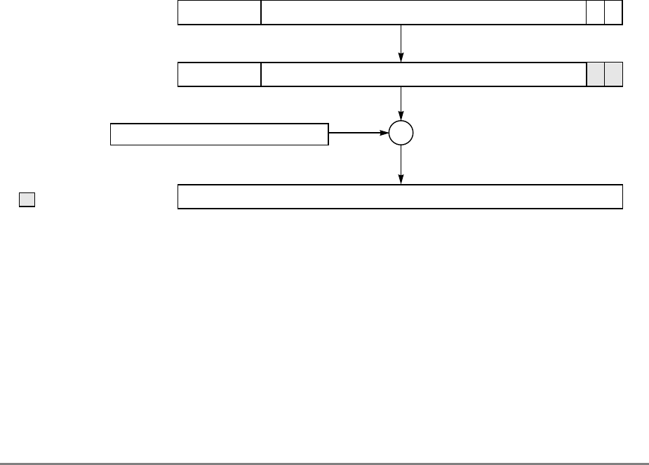
3-64 PowerPC 601 RISC Microprocessor User's Manual
Branch instructions compute the effective address (EA) of the next instruction address
using the following addressing modes:
• Branch relative
• Branch conditional to relative address
• Branch to absolute address
• Branch conditional to absolute address
• Branch conditional to link register
• Branch conditional to count register
3.6.1.1 Branch Relative Address Mode
Instructions that use branch relative addressing generate the next instruction address by
sign extending and appending b'00' to the immediate displacement operand LI, and adding
the resultant value to the current instruction address. Branches using this address mode
have the absolute addressing option (AA) disabled. If the link register update option (LK)
is enabled, the effective address of the instruction following the branch instruction is placed
in the link register.
Figure 3-6 shows how the branch target address is generated when using the branch relative
addressing mode.
Figure 3-6. Branch Relative Addressing
3.6.1.2 Branch Conditional Relative Address Mode
If the branch conditions are met, instructions that use the branch conditional relative
address mode generate the next instruction address by sign extending and appending b'00'
to the immediate displacement operand (BD) and adding the resultant value to the current
instruction address. Branches using this address mode have the absolute addressing option
(AA) disabled. If the link register update option (LK) is enabled, the effective address of
the instruction following the branch instruction is placed in the link register.
067 293031
18 LI AA LK
0 31
Branch Target Address
Instruction Encoding:
+
0 31
Current Instruction Address
067 293031
LI 0 0
Sign Extension
Reserved
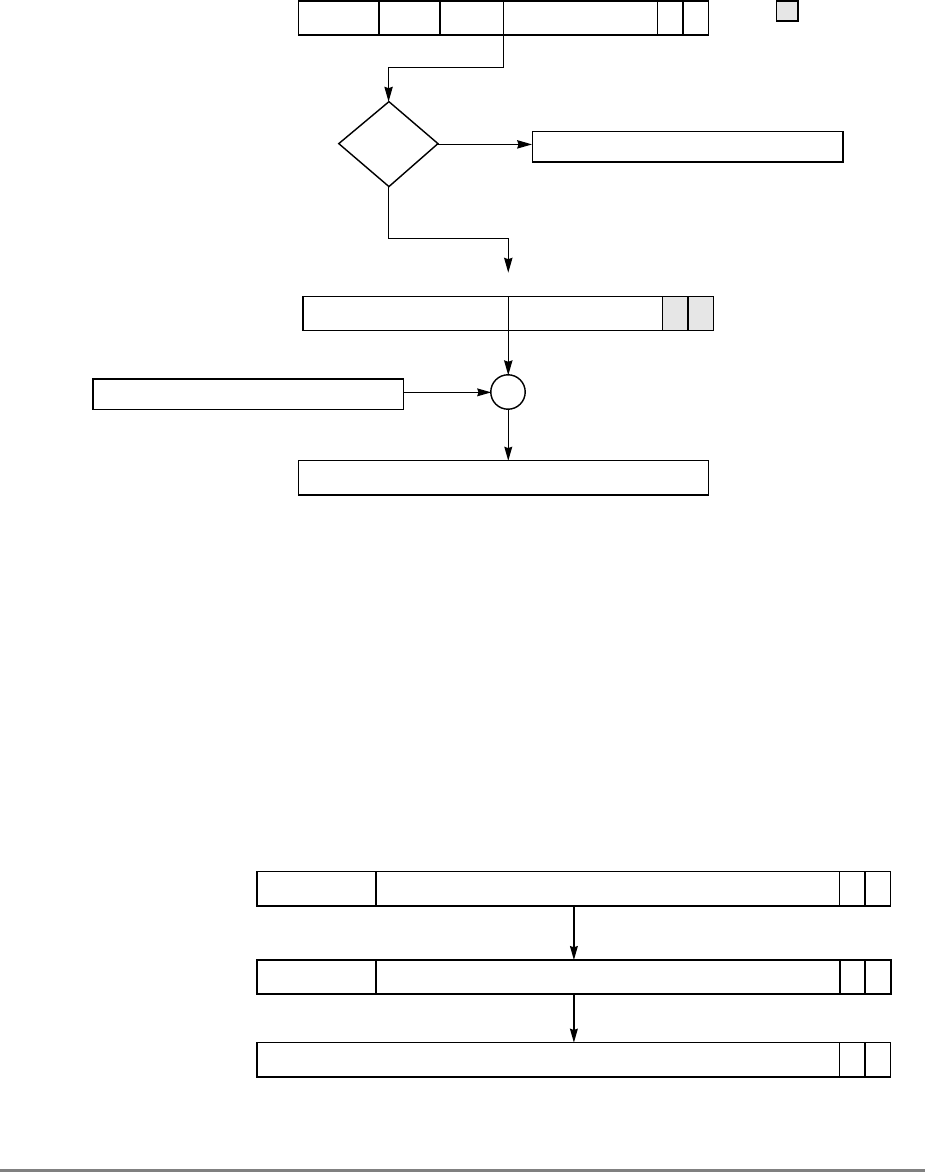
Chapter 3. Addressing Modes and Instruction Set Summary 3-65
Figure 3-7 shows how the branch target address is generated when using the branch
conditional relative addressing mode.
Figure 3-7. Branch Conditional Relative Addressing
3.6.1.3 Branch to Absolute Address Mode
Instructions that use branch to absolute address mode generate the next instruction address
by sign extending and appending b'00' to the LI operand. Branches using this address mode
have the absolute addressing option (AA) enabled. If the link register update option (LK)
is enabled, the effective address of the instruction following the branch instruction is placed
in the link register.
Figure 3-8 shows how the branch target address is generated when using the branch to
absolute address mode.
Figure 3-8. Branch to Absolute Addressing
0 6 7 1112 16 17 30 31
16 BO BI BD AA LK
Yes
031
Branch Target Address
Instruction Encoding:
No
+
0 31
Current Instruction Address
0 31
Next Sequential Instruction Address
01617293031
Sign Extension BD 0 0
Condition
Met?
Reserved
067 293031
18 LI AA LK
067 293031
0 29 30 31
Branch Target Address
Instruction Encoding:
LI 1 0
Sign Extension
00
3-66 PowerPC 601 RISC Microprocessor User's Manual
3.6.1.4 Branch Conditional to Absolute Address Mode
If the branch conditions are met, instructions that use the branch conditional to absolute
address mode generate the next instruction address by sign extending and appending b'00'
to the BD operand. Branches using this address mode have the absolute addressing option
(AA) enabled. If the link register update option (LK) is enabled, the effective address of the
instruction following the branch instruction is placed in the link register.
Figure 3-9 shows how the branch target address is generated when using the branch
conditional to absolute address mode.
Figure 3-9. Branch Conditional to Absolute Addressing
3.6.1.5 Branch Conditional to Link Register Address Mode
If the branch conditions are met, the branch conditional to link register instruction generates
the next instruction address by fetching the contents of the link register and clearing the two
low order bits to zero. If the link register update option (LK) is enabled, the effective
address of the instruction following the branch instruction is placed in the link register.
Figure 3-10 shows how the branch target address is generated when using the branch
conditional to link register address mode.
06711121617 293031
16 BO BI BD AA LK
0 16 17 293031
0 293031
Branch Target Address
Instruction Encoding:
No 0 31
Next Sequential Instruction Address
Sign Extension BD 1 0
Condition
Met?
Yes
00
Chapter 3. Addressing Modes and Instruction Set Summary 3-67
Figure 3-10. Branch Conditional to Link Register Addressing
3.6.1.6 Branch Conditional to Count Register
If the branch conditions are met, the branch conditional to count register instruction
generates the next instruction address by fetching the contents of the count register and
clearing the two low order bits to zero. If the link register update option (LK) is enabled,
the effective address of the instruction following the branch instruction is placed in the link
register.
Figure 3-11 shows how the branch target address is generated when using the branch
conditional to count register address mode.
0671112161721223031
Condition
Met?
00
30 31
LR
029
031
Branch Target Address
Instruction Encoding:
No 0 31
Next Sequential Instruction Address
Yes
19 BO BI 0 0 0 0 0 16 LK
||
Reserved
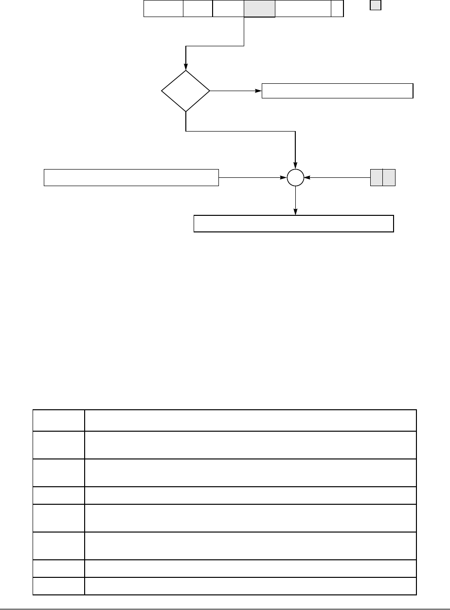
3-68 PowerPC 601 RISC Microprocessor User's Manual
Figure 3-11. Branch Conditional to Count Register Addressing
3.6.2 Conditional Branch Control
For branch conditional instructions, the BO operand specifies the conditions under which
the branch is taken. The first four bits of the BO operand specify how the branch is affected
by or affects the condition and count registers. The fifth bit, shown in Table 3-25 as having
the value y, is used by some PowerPC implementations for branch prediction as described
below.
The encodings for the BO operands are shown in Table 3-25.
Table 3-25. BO Operand Encodings
BO Description
0000
y
Decrement the CTR, then branch if the decremented CTR ≠ 0 and the condition is
FALSE.
0001
y
Decrement the CTR, then branch if the decremented CTR = 0 and the condition is
FALSE.
001
zy
Branch if the condition is FALSE.
0100
y
Decrement the CTR, then branch if the decremented CTR ≠ 0 and the condition is
TRUE.
0101
y
Decrement the CTR, then branch if the decremented CTR = 0 and the condition is
TRUE.
011
zy
Branch if the condition is TRUE.
1
z
00
y
Decrement the CTR, then branch if the decremented CTR ≠ 0.
00
30 31
CTR
029
031
Branch Target Address
Instruction Encoding:
Condition
Met?
No
Yes
0 31
Next Sequential Instruction Address
0 6 7 1112 16 17 21 22 30 31
19 BO BI 00000 528 LK
||
Reserved

Chapter 3. Addressing Modes and Instruction Set Summary 3-69
The “branch always” encoding of the BO operand does not have a “y” bit.
Setting the “y” bit to 0 indicates a predicted behavior for the branch instruction:
• For bcx with a negative value in the displacement operand, the branch is taken.
• In all other cases (bcx with a non-negative value in the displacement operand, bclrx,
or bcctrx), the branch is not taken.
Setting the “y” bit to 1 reverses the preceding indications.
The sign of the displacement operand is used as described above even if the target is an
absolute address. The default value for the “y” bit should be 0, and should only be set to 1
if software has determined that the prediction corresponding to “y” = 1 is more likely to be
correct than the prediction corresponding to “y” = 0. Software that does not compute branch
predictions should set the “y” bit to zero.
In most cases, the branch should be predicted to be taken if the value of the following
expression is 1, and to fall through if the value is 0.
((BO[0] & BO[2]) | S) ⊕ BO[4]
In the expression above, S (bit 16 of the branch conditional instruction coding) is the sign
bit of the displacement operand if the instruction has a displacement operand and is 0 if the
operand is reserved. BO[4] is the “y” bit, or 0 for the “branch always” encoding of the BO
operand. (Advantage is taken of the fact that, for bclrx and bcctrx, bit 16 of the instruction
is part of a reserved operand and therefore must be 0.)
The 5-bit BI operand in branch conditional instructions specifies which of the 32 bits in the
CR represents the condition to test.
When the branch instructions contain immediate addressing operands, the target addresses
can be computed sufficiently ahead of the branch instruction that instructions can be
fetched along the target path. If the branch instructions use the link and count registers,
instructions along the target path can be fetched if the link or count register is loaded
sufficiently ahead of the branch instruction.
1
z
01
y
Decrement the CTR, then branch if the decremented CTR = 0.
1
z
1
zz
Branch always.
The
z
indicates a bit that must be zero; otherwise, the instruction form is invalid.
The
y
bit provides a hint about whether a conditional branch is likely to be taken and is used by the
601 to improve performance. Other implementations may ignore the
y
bit.
Table 3-25. BO Operand Encodings (Continued)
BO Description

3-70 PowerPC 601 RISC Microprocessor User's Manual
Branching can be conditional or unconditional, and optionally a branch return address is
created by the storage of the effective address of the instruction following the branch
instruction in the link register after the branch target address has been computed. This is
done regardless of whether the branch is taken. While the 601 does not provide a link
register stack, future implementations may keep a stack of the link register values most
recently set by branch and link instructions, with the possible exception of the form shown
below for obtaining the address of the next instruction. To benefit from this stack, the
following programming conventions should be used.
In the examples below, let A, B, and Glue represent subroutine labels.
Obtaining the address of the next instruction– use the following form of branch and link.
bcl 20,31,$+4
Loop counts– keep them in the count register, and use one of the branch conditional
instructions to decrement the count and to control branching (for example, branching back
to the start of a loop if the decremented counter value is nonzero).
Computed GOTOs, case statements, etc.– Use the count register to hold the address to
branch to, and use the bcctr instruction with the link register option disabled (LK = 0) to
branch to the selected address.
Direct subroutine linkage– where A calls B and B returns to A. The two branches should
be as follows:
• A calls B—Use a branch instruction that enables the link register (LK = 1).
• B returns to A—Use the bclr instruction with the link register option disabled
(LK = 0) (the return address is in, or can be restored to, the link register).
Indirect subroutine linkage– where A calls Glue, Glue calls B, and B returns to A rather than
to Glue. (Such a calling sequence is common in linkage code used when the subroutine that
the programmer wants to call, here B, is in a different module from the caller: the binder
inserts “glue” code to mediate the branch.)
The three branches should be as follows:
• A calls Glue—Use a branch instruction that sets the link register with the link
register option enabled (LK = 1).
• Glue calls B—Place the address of B in the count register, and use the bcctr
instruction with the link register option disabled (LK = 0).
• B returns to A—Use the bclr instruction with the link register option disabled
(LK = 0) (the return address is in, or can be restored to, the link register).
3.6.3 Basic Branch Mnemonics
The mnemonics in Table 3-26 allow all the common BO operand encodings to be specified
as part of the mnemonic, along with the absolute address (AA) and set link register (LK)
bits.

Chapter 3. Addressing Modes and Instruction Set Summary 3-71
Notice that there are no simplified mnemonics for relative and absolute unconditional
branches. For these, the basic mnemonics b, ba, bl, and bla are used.
Table 3-26 provides the abbreviated set of simplified mnemonics for the most commonly
performed conditional branches. Unusual cases of conditional branches can be coded using
a basic branch conditional mnemonic (bc, bclr, bcctr) with the condition to be tested
specified as a numeric first operand.
Instructions using a mnemonic from Table 3-26 that tests a condition specify the condition
as the first operand of the instruction. Table 3-27 summarizes the mnemonic symbols and
the equivalent numeric values used to interpret a condition register CR field during a branch
conditional instruction compare operation.
Table 3-26. Simplified Branch Mnemonics
LR bit not set LR bit set
Branch Semantics bc
Relative bca
Absolute bclr to
LR bcctr
to
CTR
bcl
Relative bcla
Absolute bclrl to
LR bcctrl
to CTR
Branch unconditionally — — blr bctr — — blrl bctrl
Branch if condition true bt bta btlr btctr btl btla btlrl btctrl
Branch if condition
false bf bfa bflr bfctr bfl bfla bflrl bfctrl
Decrement CTR,
branch if CTR nonzero bdnz bdnza bdnzlr — bdnzl bdnzla bdnzlrl —
Decrement CTR,
branch if CTR nonzero
AND condition true
bdnzt bdnzta bdnztlr — bdnztl bdnztla bdnztlrl —
Decrement CTR,
branch if CTR nonzero
AND condition false
bdnzf bdnzfa bdnzflr — bdnzfl bdnzfla bdnzflrl —
Decrement CTR,
branch if CTR zero bdz bdza bdzlr — bdzl bdzla bdzlrl —
Decrement CTR,
branch if CTR zero
AND condition true
bdzt bdzta bdztlr — bdztl bdztla bdztlrl —
Decrement CTR,
branch if CTR zero
AND condition false
bdzf bdzfa bdzflr — bdzfl bdzfla bdzflrl —

3-72 PowerPC 601 RISC Microprocessor User's Manual
Table 3-28 summarizes the mnemonic symbols and the equivalent numeric values used to
identify the condition register CR field to be evaluated by the compare operation.
The simplified branch mnemonics and the symbols in Table 3-27 and Table 3-28 are
combined in an expression that identifies the bit (0–31) of CR to be tested, as follows:
Examples:
• Decrement CTR and branch if it is still nonzero (closure of a loop controlled by a
count loaded into CTR).
bdnz target (equivalent to bc 16,0,target)
• Same as (1) but branch only if CTR is nonzero and condition in CR0 is “equal.”
bdnzt eq,target (equivalent to bc 8,2,target)
• Same as (2), but “equal” condition is in CR5.
bdnzt 4*cr5+eq,target (equivalent to bc 8,22,target)
Table 3-27. Condition Register CR Field Bit Symbols
Symbol Value Meaning
lt 0 Less than
gt 1 Greater than
eq 2 Equal
so 3 Summary overflow
un 3 Unordered (after
floating-point comparison)
Table 3-28. Condition Register CR Field Identification Symbols
Symbol Value Meaning
cr0 0 CR0
cr1 4 CR1
cr2 8 CR2
cr3 12 CR3
cr4 16 CR4
cr5 20 CR5
cr6 24 CR6
cr7 28 CR7

Chapter 3. Addressing Modes and Instruction Set Summary 3-73
• Branch if bit 27 of CR is false.
bf 27,target (equivalent to bc 4,27,target)
• Same as (4), but set the link register. This is a form of conditional “call.”
bfl 27,target (equivalent to bcl 4,27,target)
3.6.4 Branch Mnemonics Incorporating Conditions
The mnemonics defined in Table 3-30 are variations of the “branch if condition true” and
“branch if condition false” BO encodings, with the most common values of the BI operand
represented in the mnemonic rather than specified as a numeric operand.
The two-letter codes for the most common combinations of branch conditions are shown in
Table 3-29.
These codes are reflected in the simplified mnemonics shown in Table 3-30.
Table 3-29. Two-Letter Codes for Branch Comparison Conditions
Code Meaning
lt Less than
le Less than or equal
eq Equal
ge Greater than or equal
gt Greater than
nl Not less than
ne Not equal
ng Not greater than
so Summary overflow
ns Not summary overflow
un Unordered (after floating-point comparison)
nu Not unordered (after floating-point
comparison)

3-74 PowerPC 601 RISC Microprocessor User's Manual
Instructions using the mnemonics in Table 3-30 specify the condition register field in an
optional first operand. If the CR field being tested is CR0, this operand need not be
specified. Otherwise, one of the CR field symbols listed in Table 3-28 is coded as the first
operand.
Examples:
• Branch if CR0 reflects condition “not equal.”
bne target (equivalent to bc 4,2,target)
• Same as (1), but condition is in CR3.
bne cr3,target (equivalent to bc 4,14,target)
• Branch to an absolute target if CR4 specifies “greater than,” setting the link register.
This is a form of conditional “call”, as the return address is saved in the link register.
bgtla cr4,target (equivalent to bcla 12,17,target)
• Same as (3), but target address is in the count register.
bgtctrl cr4 (equivalent to bcctrl 12,17)
Table 3-30. Simplified Branch Mnemonics with Comparison Conditions
LR bit not set LR bit set
Branch Semantics bc
Relative bca
Absolute bclr to
LR bcctr
to CTR bcl
Relative bcla
Absolute bclrl to
LR bcctrl
to CTR
Branch if less than blt blta bltlr bltctr bltl bltla bltlrl bltctrl
Branch if less than or equal ble blea blelr blectr blel blela blelrl blectrl
Branch if equal beq beqa beqlr beqctr beql beqla beqlrl beqctrl
Branch if greater than or
equal bge bgea bgelr bgectr bgel bgela bgelrl bgectrl
Branch if greater than bgt bgta bgtlr bgtctr bgtl bgtla bgtlrl bgtctrl
Branch if not less than bnl bnla bnllr bnlctr bnll bnlla bnllrl bnlctrl
Branch if not equal bne bnea bnelr bnectr bnel bnela bnelrl bnectrl
Branch if not greater than bng bnga bnglr bngctr bngl bngla bnglrl bngctrl
Branch if summary
overflow bso bsoa bsolr bsoctr bsol bsola bsolrl bsoctrl
Branch if not summary
overflow bns bnsa bnslr bnsctr bnsl bnsla bnslrl bnsctrl
Branch if unordered bun buna bunlr bunctr bunl bunla bunlrl bunctrl
Branch if not unordered bnu bnua bnulr bnuctr bnul bnula bnulrl bnuctrl

Chapter 3. Addressing Modes and Instruction Set Summary 3-75
3.6.5 Branch Instructions
Table 3-31 describes the branch instructions provided by the 601.
Table 3-31. Branch Instructions
Name Mnemonic Operand
Syntax Operation
Branch b
ba
bl
bla
imm_addr bBranch. Branch to the address computed as the sum of
the immediate address and the address of the current
instruction.
ba Branch Absolute. Branch to the absolute address
specified.
bl Branch then Link. Branch to the address computed as the
sum of the immediate address and the address of the
current instruction. The instruction address following this
instruction is placed into the link register (LR).
bla Branch Absolute then Link. Branch to the absolute
address specified. The instruction address following this
instruction is placed into the link register (LR).
Branch
Conditional bc
bca
bcl
bcla
BO,BI,
target_addr The BI operand specifies the bit in the condition register (CR) to be
used as the condition of the branch. The BO operand is used as
described in Table 3-25.
bc Branch Conditional. Branch conditionally to the address
computed as the sum of the immediate address and the
address of the current instruction.
bca Branch Conditional Absolute. Branch conditionally to the
absolute address specified.
bcl Branch Conditional then Link. Branch conditionally to the
address computed as the sum of the immediate address
and the address of the current instruction. The instruction
address following this instruction is placed into the link
register.
bcla Branch Conditional Absolute then Link. Branch
conditionally to the absolute address specified. The
instruction address following this instruction is placed into
the link register.
Branch
Conditional
to Link
Register
bclr
bclrlBO,BI The BI operand specifies the bit in the condition register to be used
as the condition of the branch. The BO operand is used as described
in Table 3-25.
bclr Branch Conditional to Link Register. Branch conditionally
to the address in the link register.
bclrl Branch Conditional to Link Register then Link. Branch
conditionally to the address specified in the link register.
The instruction address following this instruction is then
placed into the link register.

3-76 PowerPC 601 RISC Microprocessor User's Manual
3.6.6 Condition Register Logical Instructions
Condition register logical instructions, shown in Table 3-32, and the Move Condition
Register Field (mcrf) instruction are defined as flow control instructions, although they are
executed by the IU.
Note that if the link register update option (LR) is enabled for any of these instructions, the
PowerPC architecture defines these forms of the instructions as invalid; however, the 601
executes these instructions and leaves the link register in an undefined state.
Branch
Conditional
to Count
Register
bcctr
bcctrl BO,BI The BI operand specifies the bit in the condition register to be used
as the condition of the branch. The BO operand is used as described
in Table 3-25.
bcctr Branch Conditional to Count Register. Branch
conditionally to the address specified in the count register.
bcctrl Branch Conditional to Count Register then Link. Branch
conditionally to the address specified in the count register.
The instruction address following this instruction is placed
into the link register.
Note: If the “decrement and test CTR” option is specified (BO[2]=0),
the instruction form is invalid. For the 601, the decremented count
register is tested for zero and branches based on this test, but
instruction fetching is directed to the address specified by the
nondecremented version of the count register. Use of this invalid form
of this instruction is not recommended.
Table 3-31. Branch Instructions (Continued)
Name Mnemonic Operand
Syntax Operation

Chapter 3. Addressing Modes and Instruction Set Summary 3-77
Table 3-32. Condition Register Logical Instructions
Name Mnemonic Operand
Syntax Operation
Condition
Register
AND
crand crbD,crbA,crbB The bit in the condition register specified by crbA is ANDed with
the bit in the condition register specified by crbB. The result is
placed into the condition register bit specified by crbD.
Condition
Register OR cror crbD,crbA,crbB The bit in the condition register specified by crbA is ORed with
the bit in the condition register specified by crbB. The result is
placed into the condition register bit specified by crbD.
Condition
Register
XOR
crxor crbD,crbA,crbB The bit in the condition register specified by crbA is XORed with
the bit in the condition register specified by crbB. The result is
placed into the condition register bit specified by crbD.
Condition
Register
NAND
crnand crbD,crbA,crbB The bit in the condition register specified by crbA is ANDed with
the bit in the condition register specified by crbB. The
complemented result is placed into the condition register bit
specified by crbD.
Condition
Register
NOR
crnor crbD,crbA,crbB The bit in the condition register specified by crbA is ORed with
the bit in the condition register specified by crbB. The
complemented result is placed into the condition register bit
specified by crbD.
Condition
Register
Equivalent
creqv crbD,crbA,
crbBThe bit in the condition register specified by crbA is XORed with
the bit in the condition register specified by crbB. The
complemented result is placed into the condition register bit
specified by crbD.
Condition
Register
AND with
Complement
crandc crbD,crbA,
crbBThe bit in the condition register specified by crbA is ANDed with
the complement of the bit in the condition register specified by
crbB and the result is placed into the condition register bit
specified by crbD.
Condition
Register
OR with
Complement
crorc crbD,crbA,
crbBThe bit in the condition register specified by crbA is ORed with
the complement of the bit in the condition register specified by
crbB and the result is placed into the condition register bit
specified by crbD.
Move
Condition
Register
Field
mcrf crfD,crfS The contents of crfS are copied into crfD. No other condition
register fields are changed.

3-78 PowerPC 601 RISC Microprocessor User's Manual
3.6.7 System Linkage Instructions
This section describes the system linkage instructions (see Table 3-33). The System Call
(sc) instruction permits a program to call on the system to perform a service.
3.6.8 Simplified Mnemonics for Branch Processor Instructions
To simplify assembly language programming, a set of simplified mnemonics and symbols
is provided that defines simple shorthand for the most frequently used forms of branch
conditional, compare, trap, rotate and shift, and certain other instructions.
Mnemonics are provided so that branch conditional instructions can be coded with the
condition as part of the instruction mnemonic rather than as a numeric operand. Some of
these are shown as examples with the branch instructions.
The PowerPC architecture-compliant assemblers provide the mnemonics and symbols
listed here and possibly others. Programs written to be portable across various assemblers
for the PowerPC architecture should not assume the existence of mnemonics not defined
here.
Table 3-33. System Linkage Instructions
Name Mnemonic Operand
Syntax Operation
System Call sc — When executed, the effective address of the instruction following the
sc instruction is placed into SRR0. Bits 16–31 of the MSR are placed
into bits 16–31 of SRR1, and bits 0–15 of SRR1 are set to undefined
values. Then a system call exception is generated. The exception
causes the MSR to be altered as described in Section 5.4, “Exception
Definitions.”
The exception causes the next instruction to be fetched from offset
x'C00' from the base physical address indicated by the new setting of
MSR[IP]. For a discussion of POWER compatibility with respect to
instruction bits 16–29, refer to Appendix B, Section B.10, “System
Call/Supervisor Call.” To ensure compatibility with future versions of
the PowerPC architecture, bits 16–29 should be coded as zero and
bit 30 should be coded as a 1. The PowerPC architecture defines bit
31 as reserved, and thereby cleared to 0; in order for the 601 to
maintain compatibility with the POWER architecture, the execution of
an sc instruction with bit 31 (the LK bit) set to 1 will cause an update
of the Link register with the address of the instruction following the sc
instruction.
This instruction is context synchronizing.
Return
from
Interrupt
rfi — Bits 16–31 of SRR1 are placed into bits 16–31 of the MSR, then the
next instruction is fetched, under control of the new MSR value, from
the address SRR0[0–29] || b'00'.
This instruction is a supervisor-level instruction and is context
synchronizing.

Chapter 3. Addressing Modes and Instruction Set Summary 3-79
3.6.9 Trap Instructions and Mnemonics
The trap instructions shown in Table 3-34 are provided to test for a specified set of
conditions. If any of the conditions tested by a trap instruction are met, the system trap
handler is invoked. If the tested conditions are not met, instruction execution continues
normally.
The trap instructions evaluate a trap condition as follows:
The contents of register rA is compared with either the sign-extended SIMM field or with
the contents of register rB, depending on the trap instruction. The comparison results in
five conditions which are ANDed with operand TO. If the result is not 0, the trap exception
handler is invoked. These conditions are provided in Table 3-35.
A standard set of codes has been adopted for the most common combinations of trap
conditions, as shown in Table 3-36. The mnemonics defined in Table 3-37 are variations of
the trap instructions, with the most useful values of the trap instruction TO operand
represented as a mnemonic rather than specified as a numeric operand.
Table 3-34. Trap Instructions
Name Mnemonic Operand
Syntax Operand Syntax
Trap Word
Immediate twi TO,rA,SIMM The contents of rA is compared with the sign-extended SIMM
operand. If any bit in the TO operand is set to 1 and its corresponding
condition is met by the result of the comparison, then the system trap
handler is invoked.
Trap Word tw TO,rA,rB The contents of rA is compared with the contents of rB. If any bit in
the TO operand is set to 1 and its corresponding condition is met by
the result of the comparison, then the system trap handler is invoked.
Table 3-35. TO Operand Bit Encoding
TO Bit ANDed with Condition
0 Less than
1 Greater than
2 Equal
3 Logically less than
4 Logically greater than

3-80 PowerPC 601 RISC Microprocessor User's Manual
Note: <U indicates an unsigned less than evaluation will be performed.
>U indicates an unsigned greater than evaluation will be performed.
These codes are reflected in the mnemonics shown in Table 3-37.
Table 3-36. Trap Mnemonics Coding
Code Meaning TO Operand
Encoding < > = <U >U
lt Less than 16 10000
le Less than or equal 20 10100
eq Equal 4 00100
ge Greater than or equal 12 01100
gt Greater than 8 01000
nl Not less than 12 01100
ne Not equal 24 11000
ng Not greater than 20 10100
llt Logically less than 2 00010
lle Logically less than or equal 6 00110
lge Logically greater than or
equal 5 00101
lgt Logically greater than 1 00001
lnl Logically not less than 5 00101
lng Logically not greater than 6 00110
(none) Unconditional 31 11111
Table 3-37. Trap Mnemonics
32-Bit Comparison
Trap Semantics twi Immediate tw Register
Trap unconditionally — trap
Trap if less than twlti twlt
Trap if less than or equal twlei twle
Trap if equal tweqi tweq
Trap if greater than or equal twgei twge
Trap if greater than twgti twgt
Trap if not less than twnli twnl
Trap if not equal twnei twne
Trap if logically less than twllti twllt

Chapter 3. Addressing Modes and Instruction Set Summary 3-81
Examples:
• Trap if Rx, considered as a 32-bit quantity, is logically greater than x'7FF'.
twlg rA, x'7FF' (equivalent to twi 1,rA, x'7FF')
• Trap unconditionally
trap (equivalent to tw 31,0,0)
3.7 Processor Control Instructions
Processor control instructions are used to read from and write to the machine state register
(MSR), condition register (CR), and special purpose registers (SPRs).
3.7.1 Move to/from Machine State Register and Condition Register
Instructions
Table 3-38 summarizes the instructions provided by the 601 for reading from or writing to
the machine state register and the condition register.
Trap if not greater than twngi twng
Trap if logically less than twllti twllt
Trap if logically less than or equal twllei twlle
Trap if logically greater than or equal twlgei twlge
Trap if logically greater than twlgti twlgt
Trap if logically not less than twlnli twlnl
Trap if logically not greater than twlngi twlng
Table 3-37. Trap Mnemonics (Continued)
32-Bit Comparison
Trap Semantics twi Immediate tw Register

3-82 PowerPC 601 RISC Microprocessor User's Manual
3.7.2 Move to/from Special-Purpose Register Instructions
The 601 defines an additional register (MQ register) to the user register set and
programming model. As a result, the mtspr and mfspr instructions have been extended to
accommodate access to the MQ register for the 601. The SPR field encoding for the MQ
register is b'00000 00000'.
For compatibility with the POWER architecture, the 601 also allows user-level read access
to the decrementer (DEC) register. Note that the PowerPC architecture does not allow
user-level access to the DEC register. The SPR encoding for DEC is b'00110 00000' and is
valid only for the mfspr instruction. For more information about the mtspr and mfspr
instructions, refer to Chapter 10, “Instruction Set.”
Simplified mnemonics are provided for the mtspr and mfspr instructions so they can be
coded with the SPR name as part of the mnemonic rather than as a numeric operand. Some
of these are shown as examples with the two instructions (see Table 3-39).
Table 3-38. Move to/from Machine State Register/Condition Register Instructions
Name Mnemonic Operand
Syntax Operation
Move to
Condition
Register
Fields
mtcrf CRM,rS The contents of rS are placed into the condition register under control
of the field mask specified by operand CRM. The field mask identifies
the 4-bit fields affected. Let
i
be an integer in the range 0–7. If
CRM(
i
) = 1, then CR field
i
(CR bits 4*
i
through 4*
i
+3) is set to the
contents of the corresponding field of rS.
In some PowerPC implementations, this instruction may perform
more slowly when only a portion of the fields are updated as opposed
to all of the fields. This is not true for the 601.
Move to
Condition
Register
from XER
mcrxr crfD The contents of XER[0–3] are copied into the condition register field
designated by crfD. All other fields of the condition register remain
unchanged. XER[0–3] is cleared to 0.
Move from
Condition
Register
mfcr rD The contents of the condition register are placed into rD.
Move to
Machine
State
Register
mtmsr rS The contents of rS are placed into the MSR.
This instruction is a supervisor-level instruction and is context
synchronizing.
Move from
Machine
State
Register
mfmsr rD The contents of the MSR are placed into rD. This is a
supervisor-level instruction.

Chapter 3. Addressing Modes and Instruction Set Summary 3-83
For mtspr and mfspr instructions, the SPR number coded in assembly language does not
appear directly as a 10-bit binary number in the instruction. The number coded is split into
two 5-bit halves that are reversed in the instruction, with the high-order 5 bits appearing in
bits 16–20 of the instruction and the low-order 5 bits in bits 11–15.
Table 3-40 summarizes the SPR encodings to which the 601 permits user-level access.
Table 3-39. Move to/from Special Purpose Register Instructions
Name Mnemonic Operand
Syntax Operation
Move to
Special
Purpose
Register
mtspr SPR,rS The SPR field denotes a special purpose register, encoded as shown
in Table 3-40. The contents of rS are placed into the designated SPR.
Simplified mnemonic examples:
mtxer rA mtspr 1,rA
mtlr rA mtspr 8,rA
mtctr rAmtspr 9,rA
Move from
Special
Purpose
Register
mfspr rD,SPR The SPR field denotes a special purpose register, encoded as shown
in Table 3-40. The contents of the designated SPR are placed into rD.
Simplified mnemonic examples:
mfxer rAmfspr rA,1
mflr rAmfspr rA,8
mfctr rAmfspr rA,9
Table 3-40. User-Level SPR Encodings
Decimal
Value in rDSPR[0–4] SPR[5–9] Register
Name Description
0 b'00000 00000' MQ MQ register
1 b'00001 00000' XER Integer exception register
4 b'00100 00000' RTCU Real- time clock upper
register1
5 b'00101 00000' RTCL Real- time clock lower register1
6 b'00110 00000' DEC Decrementer register 2
8 b'01000 00000' LR Link register
9 b'01001 00000' CTR Count register
1 Read-only when accessed at user-level.
2 Access to the DEC register is restricted to read-only while the processor is in the user
mode. User-level decrementer access is provided for POWER compatibility, and is
specific to the 601.

3-84 PowerPC 601 RISC Microprocessor User's Manual
Table 3-41 summarizes SPR encodings that the 601 permits at the supervisor level.
Table 3-41. Supervisor-Level SPR Encodings
Decimal
Value in rDSPR[0–4] SPR[5–9] Register
Name
Description
18 b'10010 00000' DSISR DAE/source instruction service
register
19 b'10011 00000' DAR Data address register
20 b'10100 00000' RTCU Real- time clock upper register
21 b'10101 00000' RTCL Real- time clock lower register
22 b'10110 00000' DEC Decrementer register
25 b'11001 00000' SDR1 Table search description
register 1
26 b'11010 00000' SRR0 Save and restore register 0
27 b'11011 00000' SRR1 Save and restore register 1
272 b'10000 01000' SPRG0 SPR general 0
273 b'10001 01000' SPRG1 SPR general 1
274 b'10010 01000' SPRG2 SPR general 2
275 b'10011 01000' SPRG3 SPR general 3
282 b'11010 01000' EAR External access register
287 b'11111 01000' PVR Processor version register
528 b'10000 10000' IBAT0U Instruction BAT 0 upper
529 b'10001 10000' IBAT0L Instruction BAT 0 lower
530 b'10010 10000' IBAT1U Instruction BAT 1 upper
531 b'10011 10000' IBAT1L Instruction BAT 1 lower
532 b'10100 10000' IBAT2U Instruction BAT 2 upper
533 b'10101 10000' IBAT2L Instruction BAT 2 lower
534 b'10110 10000' IBAT3U Instruction BAT 3 upper
535 b'10111 10000' IBAT3L Instruction BAT 3 lower
1008 b'10000 11111' Checkstop
(HID0) Checkstop sources and
enables register
1009 b'10001 11111' Debug
(HID1) Debug modes register
1010 b'10010 11111' IABR
(HID2) Instruction address breakpoint
register
1013 b'10101 11111' DABR
(HID5) Data address breakpoint
register

Chapter 3. Addressing Modes and Instruction Set Summary 3-85
SPR encodings shown in Table 3-40 can also be used while at the supervisor level.
The mtspr and mfspr instructions specify a special purpose register (SPR) as a numeric
operand. Simplified mnemonics are provided that represent the SPR in the mnemonic rather
than requiring it to be coded as an operand. Table 3-42 below specifies the simplified
mnemonics provided on the 601 for SPR operations.
1023 b'11111 11111' PIR
(HID15) Processor identification
register
If the SPR field contains any value other than one of the values shown in Table 3-40, the
instruction form is invalid. For an invalid instruction form in which SPR[0]=1, the system
supervisor-level instruction error handler will be invoked if the instruction is executed by a
user-level program. If the instruction is executed by a supervisor-level program, the result
is a no-op.
SPR[0]=1 if and only if writing the register is supervisor-level. Execution of this instruction
specifying a defined and supervisor-level register when MSR[PR]=1 results in a privilege
violation type program exception.
SPR encodings for the DEC, MQ, RTCL, and RTCU registers are not part of the PowerPC
architecture. For forward compatability with other members of the PowerPC
microprocessor family the mftb instruction should be used to obtain the contents of the
RTCL and RTCU registers. The mftb instruction is a PowerPC instruction unimplemented
by the 601, and will be trapped by the illegal instruction exception handler, which can then
issue the appropriate mfspr instructions for reading the RTCL and RTCU registers
The PVR (processor version register) is a read-only register.
Table 3-42. SPR Simplified Mnemonics
Special Purpose
Register
Move to SPR
Simplified
Mnemonic
Move to SPR
Instruction
Move from SPR
Simplified
Mnemonic
Move from SPR
Instruction
Integer unit exception
register mtxer rSmtspr 1,rSmfxer rDmfspr rD,1
Link register mtlr rSmtspr 8,rSmflr rDmfspr rD,8
Count register mtctr rSmtspr 9,rSmfctr rDmfspr rD,9
DAE/source instruction
service register mtdsisr rSmtspr 18,rSmfdsisr rDmfspr rD,18
Data address register mtdar rSmtspr 19,rSmfdar rDmfspr rD,19
Decrementer mtdec rSmtspr 22,rSmfdec rDmfspr rD,22
Table search
description register 1 mtsdr1 rSmtspr 25,rSmfsdr1 rDmfspr rD,25
Status save/restore
register 0 mtsrr0 rSmtspr 26,rSmfsrr0 rDmfspr rD,26
Table 3-41. Supervisor-Level SPR Encodings (Continued)
Decimal
Value in rDSPR[0–4] SPR[5–9] Register
Name
Description

3-86 PowerPC 601 RISC Microprocessor User's Manual
3.8 Memory Control Instructions
This section describes memory control instructions, which include the following:
• Cache management instructions
• Segment register manipulation instructions
• Translation lookaside buffer management instructions
3.8.1 Supervisor-Level Cache Management Instruction
Table 3-43 summarizes the operation of the only supervisor-level cache management
instruction implemented on the 601.
Status save/restore
register 1 mtsrr1 rSmtspr 27,rSmfsrr1 rDmfspr rD,27
General SPRs
(SPRG0—SPRG3) mtsprg
n,
rSmtspr 272+
n
,rSmfsprg rD
, n
mfspr rD,272+
n
External access register mtear rSmtspr 282,rSmfear rDmfspr rD,282
Processor version
register __ mfpvr rDmfspr rD,287
BAT register, upper mtibatu
n,
rSmtspr 528+(2*
n
),rSmfibatu
rD
, n
mfspr rD,528+(2*
n
)
Bat register, lower mtibatl
n,
rSmtspr 529+ (2*
n
),rSmfibatl rD
, n,
mfspr rD,529+(2*
n
)
Table 3-42. SPR Simplified Mnemonics (Continued)
Special Purpose
Register
Move to SPR
Simplified
Mnemonic
Move to SPR
Instruction
Move from SPR
Simplified
Mnemonic
Move from SPR
Instruction

Chapter 3. Addressing Modes and Instruction Set Summary 3-87
3.8.2 User-Level Cache Instructions
The instructions summarized in this section provide user-level programs the ability to
manage the 601’s unified cache. The term block in the context of the cache refers to a sector
within the cache (and not a block defined by the block address translation (BAT)
mechanism).
As with other memory-related instructions, the effect of the cache instructions on memory
are weakly consistent. If the programmer needs to ensure that cache or other instructions
have been performed with respect to all other processors and mechanisms, a sync
instruction must be placed in the program following those instructions.
When data address translation is disabled (MSR[DT] = 0), the Data Cache Block Set to
Zero (dcbz) instruction allocates a line in the cache and may not verify that the physical
address is valid. If a line is created for an invalid physical address, a machine check
Table 3-43. Cache Management Supervisor-Level Instruction
Name Mnemonic Operand
Syntax Operation
Data
Cache
Block
Invalidate
dcbi rA,rB The effective address is the sum (rA|0)+(rB).
The action taken depends on the memory mode associated with the
target, and the state (modified, unmodified) of the block. The
following list describes the action to take if the block containing the
byte addressed by the EA is or is not in the cache.
• Coherency required (WIM = xx1)
— Unmodified block—Invalidates copies of the block in the
caches of all processors.
— Modified block—Invalidates copies of the block in the caches
of all processors. (Discards the modified contents.)
— Absent block—If copies are in the caches of any other
processor, causes the copies to be invalidated. (Discards any
modified contents.)
• Coherency not required (WIM = xx0)
— Unmodified block—Invalidates the block in the local cache.
— Modified block—Invalidates the block in the local cache.
(Discards the modified contents.)
— Absent block—No action is taken.
When data address translation is enabled, MSR[DT]=1, and the
logical (effective) address has no translation, a data access exception
occurs. See Section 5.4.3, “Data Access Exception (x'00300').”
The function of this instruction is independent of the write-through
and cache-inhibited/allowed modes determined by the WIM bit
settings of the block containing the byte addressed by the EA.
This instruction is treated as a store to the addressed byte with
respect to address translation and protection. The reference and
change bits are modified appropriately.
If the EA specifies a memory address for which T = 1 in the
corresponding segment register, the instruction is treated as a no-op.
This is a supervisor-level instruction.

3-88 PowerPC 601 RISC Microprocessor User's Manual
condition may result when an attempt is made to write that line back to memory. The line
could be written back as the result of the execution of an instruction that causes a cache miss
and the invalid addressed line is the target for replacement or a Data Cache Block Store
(dcbst) instruction.
Any cache control instruction that generates an effective address that corresponds to an I/O
controller interface segment (SR[T] = 1) that has the SR[BUID] field equal to x'07F'
translates the address appropriately and performs the cache operation based on that address.
A cache control instruction that generates an effective address that corresponds to an I/O
controller interface segment (SR[T] = 1), but with the SR[BUID] not equal to x'07F' is
treated as a no-op.
Since the 601 is implemented with a unified (combined instruction and data) cache, the
Instruction Cache Block Invalidate (icbi) instruction is treated as a no-op by the 601
processor. Table 3-44 summarizes the cache instructions that are accessible to user-level
programs.
Table 3-44. User-Level Cache Instructions
Name Mnemonic Operand
Syntax Operation
Data
Cache
Block Touch
dcbt rA,rB The EA is the sum (rA|0)+(rB).
This instruction provides a method for improving performance
through the use of software-initiated fetch hints. The 601 performs the
fetch for the cases when the address hits in the UTLB or the BTLB,
and when it is permitted load access from the addressed page. The
operation is treated similarly to a byte load operation with respect to
memory protection.
If the address translation does not hit in the UTLB or BTLB, or if it
does not have load access permission, the instruction is treated as a
no-op.
If the access is directed to a cache-inhibited page, or to an I/O
controller interface segment, then the bus operation occurs, but the
cache is not updated.
This instruction never affects the reference or change bits in the
hashed page table.
While the 601 maintains a cache line size of 64 bytes, the dcbt
instruction may only result in the fetch of a 32-byte sector (the one
directly addressed by the EA). The other 32-byte sector in the cache
line may or may not be fetched, depending on activity in the dynamic
memory queue.
A successful dcbt instruction will affect the state of the TLB and
cache LRU bits as defined by the LRU algorithm.
Data
Cache
Block
Touch for
Store
dcbtst rA,rB The EA is the sum (rA|0)+(rB).
The dcbtst instruction operates exactly like the dcbt instruction as
implemented on the 601.

Chapter 3. Addressing Modes and Instruction Set Summary 3-89
Cache Line
Compute
Size
clcs rD,rAThis is a POWER instruction, and is not part of the PowerPC
architecture. This instruction will not be supported by other
PowerPC implementations.
This instruction places the cache line size specified by operand rA
into register rD. The rA operand is encoded as follows:
01100 Instruction cache line size (returns value of 64)
01101 Data cache line size (returns value of 64)
01110 Minimum line size (returns value of 64)
01111 Maximum line size (returns value of 64)
All other encodings of the rA operand return undefined values.
This instruction is specific to the 601.
Data
Cache
Block Set
to Zero
dcbz rA,rB The EA is the sum (rA|0)+(rB).
If the block (the cache sector consisting of 32 bytes) containing the
byte addressed by the EA is in the data cache, all bytes are cleared
to 0.
If the block containing the byte addressed by the EA is not in the data
cache and the corresponding page is caching-allowed, the block is
established in the data cache without fetching the block from main
memory, and all bytes of the block are cleared to 0.
If the page containing the byte addressed by the EA is
caching-inhibited or write-through, then the system alignment
exception handler is invoked.
If the block containing the byte addressed by the EA is in coherence
required mode, and the block exists in the data cache(s) of any other
processor(s), it is kept coherent in those caches.
The dcbz instruction is treated as a store to the addressed byte with
respect to address translation and protection.
If the EA corresponds to an I/O controller interface segment
(SR[T] = 1), the dcbz instruction is treated as a no-op.
Data
Cache
Block Store
dcbst rA,rB The EA is the sum(rA|0)+(rB).
If the block (the cache sector consisting of 32 bytes) containing the
byte addressed by the EA is in coherence required mode, and a block
containing the byte addressed by the EA is in the data cache of any
processor and has been modified, the writing of it to main memory is
initiated.
The function of this instruction is independent of the write-through
and cache-inhibited/allowed modes of the block containing the byte
addressed by the EA.
This instruction is treated as a load from the addressed byte with
respect to address translation and protection.
If the EA corresponds to an I/O controller interface segment
(SR[T] = 1), the dcbst instruction is treated as a no-op.
Table 3-44. User-Level Cache Instructions (Continued)
Name Mnemonic Operand
Syntax Operation

3-90 PowerPC 601 RISC Microprocessor User's Manual
3.8.3 Segment Register Manipulation Instructions
The instructions listed in Table 3-45 provide access to the segment registers of the 601.
These instructions operate completely independently of the MSR[IT] and MSR[DT] bit
settings. Note that the rA operand is not defined for the mtsrin and mfsrin instructions in
the 601. Refer to Section 2.3.3.1, “Synchronization for Supervisor-Level SPRs and
Segment Registers,” for serialization requirements and other recommended precautions to
observe when manipulating the segment registers.
Data
Cache
Block Flush
dcbf rA,rB The EA is the sum (rA|0) + (rB).
The action taken depends on the memory mode associated with the
target, and on the state of the block. The following list describes the
action taken for the various cases, regardless of whether the page or
block containing the addressed byte is designated as write-through or
if it is in the caching-inhibited or caching-allowed mode.
• Coherency required (WIM = xx1)
— Unmodified block—Invalidates copies of the block in the
caches of all processors.
— Modified block—Copies the block to memory. Invalidates
copies of the block in the caches of all processors.
— Absent block—If modified copies of the block are in the caches
of other processors, causes them to be copied to memory and
invalidated. If unmodified copies are in the caches of other
processors, causes those copies to be invalidated.
• Coherency not required (WIM = xx0)
— Unmodified block—Invalidates the block in the processor’s
cache.
— Modified block—Copies the block to memory. Invalidates the
block in the processor’s cache.
— Absent block—Does nothing.
Table 3-44. User-Level Cache Instructions (Continued)
Name Mnemonic Operand
Syntax Operation

Chapter 3. Addressing Modes and Instruction Set Summary 3-91
3.8.4 Translation Lookaside Buffer Management Instruction
The 601 implements a TLB that caches portions of the page table. As changes are made to
the address translation tables, the TLB must be updated. This is done by explicitly
invalidating TLB entries (both in the set) with the Translation Lookaside Buffer Invalidate
Entry (tlbie) instruction. Refer to Chapter 6, “Memory Management Unit” for additional
information about TLB operation. Table 3-46 summarizes the operation of the tlbie
instruction.
Table 3-45. Segment Register Manipulation Instructions
Name Mnemonic Operand
Syntax Operation
Move to
Segment
Register
mtsr SR,rS The contents of rS is placed into segment register specified by
operand SR.
This is a supervisor-level instruction.
Move to
Segment
Register
Indirect
mtsrin rS,rB The contents of rS are copied to the segment register selected by bits
0–3 of rB.
This is a supervisor-level instruction.
Move from
Segment
Register
mfsr rD,SR The contents of the segment register specified by operand SR are
placed into rD.
This is a supervisor-level instruction.
Move from
Segment
Register
Indirect
mfsrin rD,rB The contents of the segment register selected by bits 0–3 of rB are
copied into rD.
This is a supervisor-level instruction.

3-92 PowerPC 601 RISC Microprocessor User's Manual
Because the presence, absence, and exact semantics of the translation lookaside buffer
management instruction is implementation dependent, system software should encapsulate
uses of the instruction into subroutines to minimize the impact of migrating from one
implementation to another.
3.9 External Control Instructions
The external control instructions provide a means for a user-level program to communicate
with a special-purpose device. Two instructions are provided and are summarized in
Table 3-47.
Table 3-46. Translation Lookaside Buffer Management Instruction
Name Mnemonic Operand
Syntax Operation
Translation
Lookaside
Buffer
Invalidate
Entry
tlbie rB The effective address is the contents of rB. If the TLB contains an
entry corresponding to the EA, that entry is removed from the TLB.
The TLB search is done regardless of the settings of MSR[IT] and
MSR[DT]. Also, a TLB invalidate operation is broadcast on the
system bus unless disabled by setting bit 17 in HID1.
Block address translation for the EA, if any, is ignored.
Because the 601 supports broadcast of TLB entry invalidate
operations, the following must be observed:
• The tlbie instruction must be contained in a critical section of
memory controlled by software locking, so that the tlbie is issued
on only one processor at a time.
•A sync instruction must be issued after every tlbie and at the end
of the critical section. This causes hardware to wait for the effects
of the preceding tlbie instructions(s) to propagate to all
processors.
A processor detecting a TLB invalidate broadcast does the following:
1. Prevents execution of any new load, store, cache control or tlbie
instructions and prevents any new reference or change bit
updates
2. Waits for completion of any outstanding memory operations
(including updates to the reference and change bits associated
with the entry to be invalidated)
3. Invalidates the two entries (both associativity classes) in the UTLB
indexed by the matching address
4. Resumes normal execution
This is a supervisor-level instruction.
Nothing is guaranteed about instruction fetching in other processors if
tlbie deletes the page in which another processor is executing.

Chapter 3. Addressing Modes and Instruction Set Summary 3-93
3.10 Miscellaneous Simplified Mnemonics
In order to make assembly language programs simpler to write and easier to understand, a
set of simplified mnemonics is provided that define a shorthand for some of the most
frequently used instructions. PowerPC compliant assemblers provide the simplified
mnemonics listed here, and in the sections describing the branch, arithmetic, compare, trap,
rotate and shift, and move to/from special purpose register instructions. Programs written
to be portable across the various assemblers for the PowerPC architecture should not
assume the existence of mnemonics not defined in this user’s manual.
Table 3-47. External Control Instructions
Name Mnemonic Operand
Syntax Operation
External
Control
Input Word
Indexed
eciwx rD,rA,rB The EA is the sum (rA|0) + (rB).
If the external access register (EAR) E-bit (bit 0) is set to 1, a load
request for the physical address corresponding to the EA is sent to
the device identified by the EAR Resource ID bits (bits 28–31),
bypassing the cache. The word returned by the device is placed in
rD. The EA sent to the device must be word aligned.
If the EAR[E] = 0, a data access exception is invoked, with bit 11 of
DSISR set to 1, and bit 6 cleared to 0 to indicate that the exception
occurred during a load operation.
The eciwx instruction is supported for EAs that reference ordinary
memory segments (SR[T] = 0), for EAs mapped by BAT registers,
and for EAs generated when MSR[DT] = 0.The instruction is treated
as a no-op for EAs in I/O controller interface segments (SR[T] = 1).
The access caused by this instruction is treated as a load from the
location addressed by the EA with respect to protection and
reference and change recording.
External
Control
Output
Word
Indexed
ecowx rS,rA,rB The EA is the sum (rA|0) + (rB).
If the External Access Register (EAR) E-bit (bit 0) is set to 1, a store
request for the physical address corresponding to the EA and the
contents of rS are sent to the device identified by EAR[RID] (resource
ID) (bits 28–31), bypassing the cache. The EA sent to the device
must be word aligned.
If the EAR[E] = 0, a data access exception is invoked, with bit 11 of
DSISR set to 1, and bit 6 set to 1 to indicate that the exception
occurred during a store operation.
The ecowx instruction is supported for EAs that reference ordinary
memory segments (SR[T] = 0), for EAs mapped by BAT registers,
and for EAs generated when MSR[DT] = 0.The instruction is treated
as a no-op for EAs in I/O controller interface segments (SR[T] = 1).
The access caused by this instruction is treated as a store to the
location addressed by the EA with respect to protection and
reference and change recording

3-94 PowerPC 601 RISC Microprocessor User's Manual
3.10.1 No-Op
Many PowerPC instructions can be coded in a way that, effectively, no operation is
performed. An additional mnemonic is provided for the preferred form of no-op. If an
implementation performs any type of run-time optimization related to no-ops, the preferred
form is the no-op that will trigger this.
no-op (equivalent to ori 0,0,0)
3.10.2 Load Immediate
The addi and addis instructions can be used to load an immediate value into a register.
Additional mnemonics are provided to convey the idea that no addition is being performed
but that data is being moved from the immediate operand of the instruction to a register.
Load a 16-bit signed immediate value into rA:
li rD,value (equivalent to addi rA,0,value)
Load a 16-bit signed immediate value, shifted left by 16 bits, into rA:
lis rD,value (equivalent to addis rA,0,value)
3.10.3 Load Address
This mnemonic permits computing the value of a base-displacement operand, using the
addi instruction which normally requires a separate register and immediate operands.
la rD,SIMM(rA) (equivalent to addi rD,rA,SIMM)
The la mnemonic is useful for obtaining the address of a variable specified by name,
allowing the assembler to supply the base register number and compute the displacement.
If the variable v is located at offset SIMMv bytes from the address in register rv, and the
assembler has been told to use register rv as a base for references to the data structure
containing v, then the following line causes the address of v to be loaded into register rD.
la rD,v(equivalent to addi rD,rA,SIMMv
3.10.4 Move Register
Several PowerPC instructions can be coded to simply copy the contents of one register to
another. An extended mnemonic is provided to move data from one register to another with
no computational activity.
The following instruction copies the contents of register rS into register rA. This
mnemonic can be coded with a “.” to cause the condition register update option to be
specified in the underlying instruction.
mr rA,rS (equivalent to or rA,rS,rS)

Chapter 3. Addressing Modes and Instruction Set Summary 3-95
3.10.5 Complement Register
Several PowerPC instructions can be coded to complement the contents of one register and
place the result in another register. A simplified mnemonic is provided that complements
the contents of rS and places the results into register rA. This mnemonic can be coded with
a “.” to cause the condition register update option to be specified in the underlying
instruction.
not rA,rS (equivalent to nor rA,rS,rS)

3-96 PowerPC 601 RISC Microprocessor User's Manual

Chapter 4. Cache and Memory Unit Operation 4-1
Chapter 4
Cache and Memory Unit Operation
40
40
The PowerPC 601 microprocessor contains a 32-Kbyte, eight-way set associative, unified
(instruction and data) cache. The cache line size is 64 bytes, divided into two eight-word
sectors, each of which can be snooped, loaded, cast-out, or invalidated independently. The
cache is designed to adhere to a write-back policy, but the 601 allows control of
cacheability, write policy, and memory coherency at the page and block level. The cache
uses a least recently used (LRU) replacement policy.
The 601’s on-chip cache is nonblocking. Burst operations to the cache are the result of a
cache sector reload caused by a cache miss, and are buffered such that the cache update is
reduced to two single-cycle operations of four words. That is, the results of the first two and
the last two beats are buffered and written to the cache in single cycles apiece. This frees
the cache to perform lower priority operations in the meantime.
System operations, including cache operations, connect to the system interface through the
memory unit, which includes a two-element read queue and a three-element write queue.
As shown in Figure 1-1, the cache provides an eight-word interface to the instruction
fetcher and load/store unit. The surrounding logic selects, organizes, and forwards the
requested information to the requesting unit. Write operations to the cache can be
performed on a byte basis, and a complete read-modify-write operation to the cache can
occur in each cycle.
The cache unit and the memory unit coordinate cache reload and cast-out operations so that
a cache miss does not block the use of the cache for other operations during the next cycle.
Cache reload operations always occur on a sector basis, with the option of reloading the
additional sector as a low-priority operation. On load operations and fetch operations, the
critical data is forwarded to the requesting unit without waiting for the entire cache line to
be loaded.
The 601 maintains cache coherency in hardware by coordinating activity between the
cache, the memory unit, and the bus interface logic. As bus operations are performed on the
bus by other processors, the 601 bus snooping logic monitors the addresses that are
referenced. These addresses are compared with the addresses resident in the cache. The
cache unit uses a second port into its tag directory to check for a matching entry and the

4-2 PowerPC 601 RISC Microprocessor User's Manual
memory queue unit does the same. If there is a snoop hit, the 601’s bus snooping logic
responds to the bus interface with the appropriate snoop status. An additional snoop action
may be forwarded to the cache or to the memory unit as a result of a snoop hit.
Note that in this chapter the term multiprocessor is used in the context of maintaining cache
coherency, although the system could include other devices that can access system memory,
maintain their own caches, and function as bus masters requiring cache coherency.
This chapter describes the organization of the 601’s on-chip cache, the MESI cache
coherency protocol, special concerns for cache coherency in single- and multiple-processor
systems, cache control instructions, various cache operations, and the interaction between
the cache and the memory unit.
4.1 Cache Organization
The cache is configured as eight sets of 64 lines. Each line consists of two sectors, four state
bits (two per sector), an address tag, and several bits to maintain the LRU function. The two
state bits implement the four-state MESI (modified-exclusive-shared-invalid) protocol.
Each sector contains eight 32-bit words. Note that PowerPC architecture defines the
cacheable unit as a block, which is a sector in the 601.
The instruction unit accesses the cache frequently in order to maintain the flow of
instructions through the instruction queue. The queue is eight words (one sector) long, so
an entire sector can be loaded into the instruction unit on a single clock cycle.
The cache organization is shown in Figure 4-1. Note that the replacement algorithm is
strictly an LRU algorithm; that is, the least recently used sector is used, which may mean
that a modified sector will be replaced on a miss if it is the least recently used, even if invalid
sectors are available. However, for performance reasons, certain conditions (for example,
the execution of some cache instructions) generate accesses to the cache without modifying
the bits that perform the LRU function.
Each cache line contains 16 contiguous words from memory that are loaded from a 16-word
boundary (that is, bits A26–A31 of the logical (effective) addresses are zero); as a result,
cache lines are aligned with page boundaries.
Note that address bits A20–A25 provide an index to select a line. Bits A26–A31 select a
byte within a line. The tags consists of bits PA0–PA19. Address translation occurs in
parallel, such that higher-order bits (the tag bits in the cache) are physical.
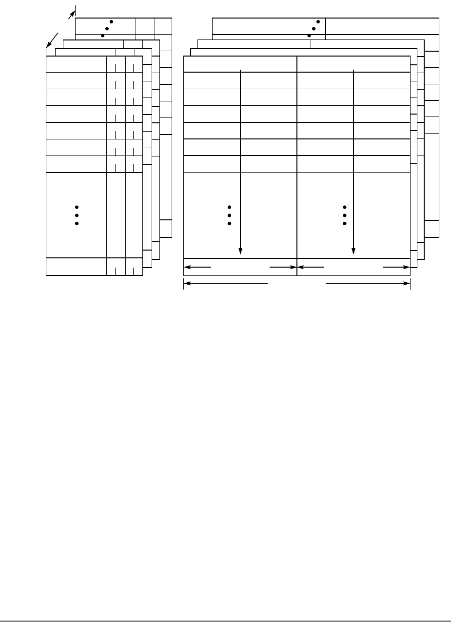
Chapter 4. Cache and Memory Unit Operation 4-3
Figure 4-1. Cache Organization
4.2 Cache Arbitration
The instruction unit and the integer unit both access the cache; however, the cache unit
handles only one access per cycle. Furthermore, since the cache is nonblocking, a preceding
cache operation may generate a cache reload operation which must also compete for cache
access. The bus snooping logic may create additional snoop actions that use the cache. The
601 efficiently handles simultaneous requests to access the on-chip cache.
The 601 implements cache arbitration logic to prioritize the various cache requests that can
occur on each cycle. The cache unit provides a cache retry queue (CRTRY) if a caching
operation cannot be completed. There are three entries in this queue, providing a buffer for
one outstanding floating-point store, a buffer for an integer load/store or floating-point load,
and a buffer for an instruction fetch. Priority is given first to floating-point stores, then to
integer stores, and finally to instruction fetches.
A similar situation arises with respect to the bus. Internal bus arbitration logic chooses the
highest priority operation from the memory queue for presentation onto the bus. These
priorities are listed in Section 4.10.2, “Memory Unit Queuing Priorities.”
LINE 63
LINE 0 ADDRESS TAG
ADDRESS TAG
SECTOR 0 SECTOR 1
8 WORDS 8 WORDS
16 WORDS
8 SETS

4-4 PowerPC 601 RISC Microprocessor User's Manual
The 601 supports a fully-coherent 4-Gbyte physical memory address space. Bus snooping
is used to drive a MESI four-state cache-coherency protocol that ensures the coherency of
all processor and DMA transactions to and from global memory with respect to the
processor’s cache. The MESI protocol is described in Section 4.7.2, “MESI Protocol.” All
potential bus masters must employ similar snooping and coherency-control mechanisms.
4.3 Cache Access Priorities
The 601 prioritizes pending cache operations as follows:
1. Cache reloads. Note that the cache is nonblocking. Four-beat burst reloads on the
system bus are buffered into two, single-cycle transactions of four words each,
freeing the cache to perform lower priority operations in the meantime.
2. Second-cycle cast-out operations when the additional sector is modified
3. Snoop requests that hit in the tag directory. These may generate a cache sector push
operation or cache state change.
4. Floating-point store operations.
5. Integer operation retries. If a higher priority operation occurs when an integer
operation is ready to cache its results, the results are held in a buffer until the higher
priority operation completes, then it is retried on the next clock cycle. This prevents
the integer unit from stalling when this situation occurs.
6. Integer unit requests
7. Instruction fetches
4.4 Basic Cache Operations
This section describes operations that can occur to the cache, and how these operations are
implemented in the 601.
4.4.1 Cache Reloads
A cache sector is reloaded after a read miss occurs in the cache. The cache sector that
contains the address is updated by a burst transfer of the data from system memory. Note
that if a read miss occurs in a multiprocessor system, and the data is modified in another
cache, the modified data is first written to external memory before the cache reload occurs.
An instruction fetch that is generated to fill the instruction queue (not explicitly required by
the program flow) does not generate a reload operation in the case of a cache miss.
4.4.2 Cache Cast-Out Operation
The 601 uses an LRU replacement algorithm to determine which of the eight possible cache
locations should be used for a cache update. Adding a new sector to the cache causes any
modified data associated with the least recently used element to be written back, or cast out,

Chapter 4. Cache and Memory Unit Operation 4-5
to system memory. This may be both sectors of the line, depending on which sectors are
modified, even though only one sector may be reloaded. Casting out of the adjacent sector
is referred to as a second-cycle cast-out operation.
4.4.3 Cache Sector Push Operation
When a cache sector in the 601 is snooped and hit by another processor and the data is
modified, the cache sector must be written to memory and made available to the snooping
device. The cache sector that is hit is said to be pushed out onto the bus. The 601 supports
two kinds of push operations—normal push operations and enveloped high-priority push
operations, which are described in Section 4.7.11, “Enveloped High-Priority Cache Sector
Push Operation.”
4.4.4 Optional Cache Sector Line-Fill Operation
The two sectors in a cache line contain contiguous memory addresses; therefore, the two
sectors share the same line address tag. Cache coherency, however, is maintained on a
sector granularity, so there are separate coherency state bits for each sector. If one sector of
the line is filled from memory, the 601 may attempt to load the other sector as a low-priority
bus operation. If the other sector is not transferred, the cache line in the snooping processor
contains one sector that is in the shared state (the one that was transferred because of the
snoop hit) and one sector that is invalid (if the optional cache line fill is not performed).
Correspondingly, the processor issuing the reload request may bring in the second cache
sector in a shared or exclusive state.
Note that the optional reload of an adjacent sector on an instruction fetch miss can be
disabled globally by setting bit 26 in the HID0 register, and the optional reload of the
adjacent sector on a load/store miss can be disabled by setting bit 27.
4.5 Cache Data Transactions
The 601 output signal TBST (transfer burst) indicates to the system whether the current
transaction is a single-beat transaction or four-beat burst transfer. Burst transactions have
an assumed address order. For cacheable load operations or cacheable, non-write-through
store operations that miss the cache, the 601 presents the quad-word aligned address
associated with the read or store that initiated the transaction.
As shown in Figure 4-2, this quad word contains the address of the load or store that missed
the cache. This minimizes latency by allowing the critical code or data to be forwarded to
the processor before the rest of the sector is filled. For all other burst operations, however,
the entire sector is transferred in order (oct-word aligned).

4-6 PowerPC 601 RISC Microprocessor User's Manual
Figure 4-2. Quad-Word Address Ordering
4.6 Access to I/O Controller Interface Segments
The 601 supports both memory-mapped and I/O-mapped access to I/O devices. In addition
to the high-performance bus protocol for memory-mapped I/O accesses, the 601 provides
the ability to map memory areas to the I/O controller interface (SR[T] = 1) with the
following two kinds of operations:
• I/O controller interface operations. These operations are considered to address the
noncoherent and noncacheable I/O controller interface; therefore, the 601 does not
maintain coherency for these operations, and the cache is bypassed completely.
• Memory-forced I/O controller interface operations. These operations are considered
to address memory space and are therefore subject to the same coherency control as
memory accesses. These operations are global memory references within the 601
and are considered to be noncacheable.
Cache behavior (write-back, cache-inhibition, and enforcement of MESI coherency) for
these operations is determined by the settings of the WIM bits; see Section 6.3,
“Memory/Cache Access Modes.”
4.7 Cache Coherency
The primary objective of a coherent memory system is to provide the same image of
memory to all devices using the system. Coherency allows synchronization, cooperative
use of shared resources, and task migration among the processors. Otherwise, multiple
copies of a memory location, some containing stale values, could exist in a system resulting
ABC D
601 Cache Address
Bits (27..28)
Beat
Beat
0 0 0 1 1 0 1 1
ABC D
012 3
If address requested is in double word A or B then the address placed on the bus are that of
quad-word A, and the four data beats are ordered in the following manner:
If address requested is in double word C or D then the address placed on the bus will be that
of quad-word C, and the four data beats are ordered in the following manner:
CDA B
012 3

Chapter 4. Cache and Memory Unit Operation 4-7
in errors when the stale values are used. Each potential bus master must follow rules for
managing the state of its cache. For example, a device must broadcast its intention to read
a sector that is not currently in the cache. It must also broadcast the intention to write into
a sector that is currently not owned exclusively. Other devices respond to these broadcasts
by snooping their caches for the broadcast addresses and reporting status back to the
originating device. The status returned includes a shared indicator (another device has a
copy of the addressed sector) and a retry indicator (another device either has a modified
copy of the addressed sector that it needs to push out of the chip, or another device had a
problem that prevented appropriate snooping).
For faster performance, the 601 has a second path into the cache directory so snooping and
mainstream instruction processing occur concurrently. Instruction processing is interrupted
only when the snoop control logic detects a state change or that a snoop push of modified
data is required to maintain memory coherency.
To maintain coherency, secondary caches must forward all relevant system bus traffic onto
the 601 bus, which takes the appropriate actions to maintain the MESI protocol.
Support for lwarx and stwcx. instructions on noncacheable pages may be somewhat more
complicated for a secondary cache than normal cacheable memory accesses. This is
because the secondary cache may not normally forward writes to noncacheable pages in the
processor. However, to maintain the reservation coherency bit, the secondary cache must
forward all writes that hit against the address of a reservation set by a lwarx instruction
until the reservation is cleared.
4.7.1 Memory Management Access Mode Bits—W, I, and M
Some memory characteristics can be set on either a block or page basis by using the WIM
bits in the BAT registers or page table entry (PTE) respectively. The WIM bits control the
following functionality:
• Write-through (W bit)
• Caching-inhibited (I bit)
• Memory coherency (M bit)
These bits allow both single- and multiprocessor-system designs to exploit numerous
system-level performance optimizations. These bits are described in detail in Chapter 2,
“Registers and Data Types,” and Chapter 6, “Memory Management Unit.” Using these bits
carelessly can cause coherency problems—the processor must ensure that the coherency of
the location is maintained (i.e., the processor must manage mismatched W bit handling in
cases of mixed WIM = b'101' and WIM = b'001'.) The 601 considers either of these cases
to be a programming error that may compromise memory coherency. These paradoxes can
occur within a single processor or across several devices, as described in Section 4.7.5.1,
“Coherency in Single-Processor Systems,” and Section 4.7.5.2, “Coherency in
Multiprocessor Systems.”

4-8 PowerPC 601 RISC Microprocessor User's Manual
4.7.2 MESI Protocol
The 601 cache characterizes each 32-byte sector it contains as being in one of four MESI
states. Addresses presented to the cache are indexed into the cache directory with bits A20–
A25 and the upper-order 20 bits from the physical address translation (PA0–PA19) are
compared against the indexed cache directory tags. If no tags match, the result is a cache
miss. If a tag matches, a cache hit occurred and the directory indicates the state of the sector
through two state bits kept with the tag. The four possible states for a sector in the cache
are the invalid state (I), the shared state (S), the exclusive state (E), and the modified state
(M). The four MESI states are defined in Table 4-1 and illustrated in Figure 4-3.
Table 4-1. MESI State Definitions
MESI State Definition
Modified (M) The addressed sector is valid in the cache and in only this cache. The sector is modified with
respect to system memory—that is, the modified data in the sector has not been written back to
memory.
Exclusive (E) The addressed sector is in this cache only. The data in this sector is consistent with system
memory.
Shared (S) The addressed sector is valid in the cache and in at least one other cache. This sector is always
consistent with system memory. That is, the shared state is shared-unmodified; there is no shared-
modified state.
Invalid (I) This state indicates that the addressed sector is not resident in the cache.
Chapter 4. Cache and Memory Unit Operation 4-9
Figure 4-3. MESI States
4.7.3 MESI State Diagram
The 601 provides dedicated hardware to provide memory coherency by snooping bus
transactions. The address retry capability of the 601 enforces the MESI protocol, as shown
in Figure 4-4. Figure 4-4 assumes that the WIM bits are set to 001; that is, write-back,
caching-not-inhibited, and memory coherency enforced.
Modified in Cache A
Cache A Cache B
System Memory
Cache A Cache B
System Memory
Cache A Cache B Cache A Cache B
System Memory
Valid Data
MInvalid Data
I
Shared in Cache A
Valid Data Valid Data
SS
Invalid Data Valid Data
Exclusive in Cache A
EValid Data Invalid Data
I
Valid Data
Invalid Data
IDon’t Care
X
Invalid in Cache A
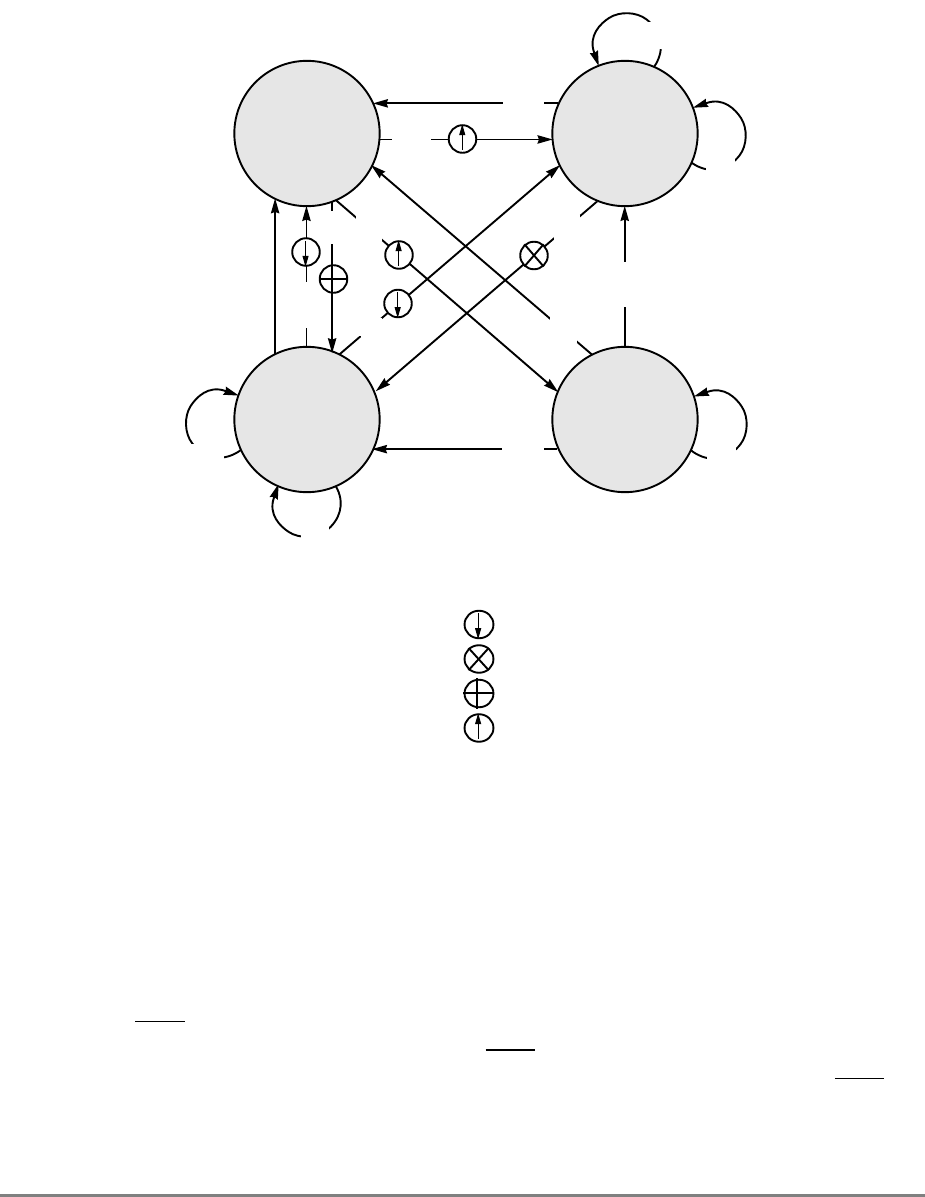
4-10 PowerPC 601 RISC Microprocessor User's Manual
Table 4-7 gives a detailed list of MESI transitions for various operations and WIM bit
settings.
Figure 4-4. MESI Cache Coherency Protocol—State Diagram (WIM = 001)
4.7.4 MESI Hardware Considerations
In addition to the hardware required to monitor bus traffic for coherency, the 601 has a
cache port dedicated to snooping so that comparing cache entries to address traffic on the
bus does not affect the 601’s on-chip cache.
The global (GBL) signal, asserted as part of the address attribute field, enables the snooping
hardware of the 601. Address bus masters assert GBL to indicate that the current transaction
is a global access (that is, an access to memory shared by more than one device). If GBL is
not asserted for the transaction, that transaction is not snooped.
SHW
(sector write-back)
SHARED
SHR
RH
RH
EXCLUSIVE
SHW
RMS
SHR
SHWSHR
RME WH
WH
WH
RH
MODIFIED
SHW
INVALID
(On a miss, the
replaced line is first
cast out to memory
if modified)
WM
BUS TRANSACTIONS
RH = Read Hit = Snoop Push
RMS = Read Miss, Shared
RME = Read Miss, Exclusive = Invalidate Transaction
WH = Write Hit
WM = Write Miss = Read-with-Intent-to-Modify
SHR = Snoop Hit on a Read
SHW = Snoop Hit on a Write or = Read
Read-with-Intent-to-Modify

Chapter 4. Cache and Memory Unit Operation 4-11
Normally, GBL reflects the M-bit value specified for the memory reference in the
corresponding translation descriptor(s). Care must be taken to minimize the number of
pages marked as global, because the retry protocol enforces coherency and can use
considerable bus bandwidth if much data is shared. Therefore available bus bandwidth can
decrease as more traffic is marked global. Note that in Figure 4-4, write hits to unmodified
lines of nonglobal pages do not generate invalidate broadcasts.
The 601 snoops a transaction if the transfer start (TS) and GBL inputs are asserted together
in the same bus clock (this is a qualified snooping condition). No snoop update to the 601
cache occurs if the snooped transaction is not marked global. This includes invalidation
cycles.
When the 601 detects a qualified snoop condition, the address associated with the TS is
compared with the cache tags through a dedicated cache-tag snoop port. Snooping finishes
if no hit is detected. If, however, the address hits in the cache, the 601 reacts according to
the MESI protocol shown in Figure 4-4.
Because they do not require snooping, cache sector cast-outs, and snoop pushes do not
assert GBL. The 601 marks these transactions as nonglobal.
To facilitate external monitoring of the internal cache tags, the cache set member signals
(CSE0–CSE2) represent in binary the sector of the cache set being replaced on read
operations (including read-with-intent-to-modify operations). This does not apply and is
not necessary for write operations to memory. Note that these signals are valid only for 601
burst operations. Table 4-2 shows the (cache set element) CSE encodings.
4.7.5 Coherency Precautions
Cache coherency is greatly affected by whether the 601 is used in a single- or multiple-
processor implementation. This section describes precautions for implementing coherent
single- and multiple-processor systems.
Table 4-2. CSE0–CSE2 Signals
CSE0–CSE2 Cache Set Element
000 Set 0
001 Set 1
010 Set 2
011 Set 3
100 Set 4
101 Set 5
110 Set 6
111 Set 7

4-12 PowerPC 601 RISC Microprocessor User's Manual
4.7.5.1 Coherency in Single-Processor Systems
The following situations concerning coherency can be encountered within a single-
processor implementation:
• Load or store to a cache-inhibited page (WIM = b'X1X') and a cache hit occurs
Caching is inhibited for this page (I = 1). Load or store operations to a cache-
inhibited page that hit in the cache cause a paradox. If the addressed sector is not
modified, the 601 invalidates the sector and performs the memory access. If the
addressed sector in the cache line is modified, the 601 flushes the modified sector
before accessing memory.
• Store to a page marked write-through (WIM = b'10X') and a cache hit to a modified
sector
This page is marked as write-through (W = 1). The 601 pushes the modified sector
to memory and marks the sector exclusive (E). Then the 601writes the data into the
cache, marking it exclusive and passing on a write-with-flush operation (to the
memory queue).
Note that when WIM bits are changed, it is critical that the cache contents should reflect the
new WIM bit settings. For example, if a block or page that had allowed caching becomes
caching-inhibited, software should ensure that the appropriate cache sectors are flushed to
memory and invalidated.
4.7.5.2 Coherency in Multiprocessor Systems
Other situations concerning coherency can occur across multiple processors (or systems
that employ multiple devices that incorporate caches). Paradoxes in multiprocessor systems
are particularly difficult to handle since some scenarios cause modified data to be purged
and others may lead to bus deadlock scenarios.
Most multiprocessor paradoxes center around the interprocessor coherency of the memory
coherency bit (the M bit). Improper use of the M bit can lead to multiple devices accepting
a cache sector and marking the data as exclusive, leading to the possibility of the same
cache line being modified in multiple caches.
Although these coherency paradoxes are considered programming errors, the 601 attempts
to handle the offending conditions and minimize the negative effects on memory coherency.
Note that the intent of this effort is to ease the debugging of multiprocessor operating
system development.

Chapter 4. Cache and Memory Unit Operation 4-13
The following list shows some of the operations provided by the 601:
• Noncacheable write operations appear on the processor bus as write-with-flush
operations, which forces other processors with modified copies of the addressed
sector to write data back to memory and to mark the sector as invalid in the cache.
Devices with an unmodified copy of the sector must mark the sector as invalid in
their caches.
• All noncacheable read operations appear on the 601 bus as read (with clean)
operations, which forces processors with modified copies of the addressed data to
write the data back to memory before the read operation completes.
Note that when WIM bits are changed, it is critical that the cache contents should reflect the
new WIM bit settings. For example, if a block or page that had allowed caching becomes
caching-inhibited, the appropriate cache sectors should be updated to leave no indication
that caching had previously been allowed.
Additional information on bus operations that are generated for specific instructions and
state conditions can be found in Chapter 9, “System Interface Operation.”
4.7.6 Memory Loads and Stores
Table 4-3 provides a general overview of memory coherency actions performed by the 601
on load operations.
Noncacheable cases are not part of this table. The first three cases also involve selecting a
replacement class and casting-out modified data that may have resided in that replacement
class.
Table 4-4 provides an overview of memory coherency actions on store operations. This
table does not include noncacheable or write-through cases nor does it completely describe
the exact mechanisms for the operations described. It describes generally what happens
within the chip. The read-with-intent-to-modify (RWITM) examples involve selecting a
replacement class and casting-out modified data that may have resided in that replacement
class.
Table 4-3. Memory Coherency Actions on Load Operations
Cache State Bus
Operation ARTRY SHD Action
I Read Negated Negated Load data and mark E
I Read Negated Asserted Load data and mark S
I Read Asserted Don’t care Retry read operation
S None Don’t care Don’t care Read from cache
E None Don’t care Don’t care Read from cache
M None Don’t care Don’t care Read from cache

4-14 PowerPC 601 RISC Microprocessor User's Manual
4.7.7 Atomic Memory References
The lwarx/stwcx. instruction combination can be used to emulate atomic memory
references. These instructions are described in Chapter 3, “Addressing Modes and
Instruction Set Summary,” and Chapter 10, “Instruction Set.”
4.7.8 Snoop Response to Bus Operations
When the 601 is not the bus master, it monitors bus traffic and performs cache and memory-
queue snooping as appropriate. The snooping operation is triggered by the receipt of a
qualified snoop request. A qualified snoop request is generated by the simultaneous
assertion of the TS and GBL bus signals.
Instruction processing is interrupted only when a snoop hit occurs and the snoop state
machine determines that an additional cache snoop is required to resolve the coherency of
the offended sector.
The 601 maintains a write queue of bus operations in progress and/or pending arbitration.
This write queue is also be snooped in response to qualified snoop requests. Note that
sector-length (four-beat) write operations, are always snooped in the write queue; however,
single-beat writes are not snooped. Coherency for single-beat writes is maintained by the
use of cache operations that are broadcast with the write on the system interface.
The 601 drives two snoop status signals (ARTRY and SHD) in response to a qualified snoop
request that hits. These signals provide information about the state of the addressed sector
for the current bus operation. For more information about these signals, see Chapter 8,
“Signal Descriptions.”
Table 4-4. Memory Coherency Actions on Store Operations
Cache State Bus
Operation ARTRY SHD Action
I RWITM Negated Don’t care Load data, modify it, mark M
I RWITM Asserted Don’t care Retry the RWITM
S Kill Negated Don’t care Modify cache, mark M
S Kill Asserted Don’t care Retry the kill operation
E None Don't care Don’t care Modify cache, mark M
M None Don't care Don’t care Modify cache

Chapter 4. Cache and Memory Unit Operation 4-15
4.7.9 Cache Reaction to Specific Bus Operations
There are several bus transaction types defined for the 601 bus. The 601 must snoop these
transactions and perform the appropriate action to maintain memory coherency; see
Table 4-5. For example, because single-beat write operations are not snooped when they are
queued in the memory unit, additional operations such as flush or kill operations, must be
broadcast when the write is passed to the system interface to ensure coherency.
A processor may assert ARTRY for any bus transaction due to internal conflicts that prevent
the appropriate snooping. In general, if ARTRY is not asserted, each snooping processor
must take full ownership for the effects of the bus transaction with respect to the state of the
processor. The processor can assert ARTRY if an internal conflict prevents it from snooping
properly.
The transactions in Table 4-5 correspond to the transfer type signals TT0–TT4, which are
described in Section 8.2.4.1, “Transfer Type (TT0–TT4).”
Table 4-5. Response to Bus Transactions
Transaction Response
Clean block The clean operation is an address-only bus transaction, initiated by executing a dcbst
instruction. This operation affects only sectors marked as modified (M). Assuming the
GBL signal is asserted, modified sectors are pushed out to memory, changing the state
to E.
Flush block The flush operation is an address-only bus transaction initiated by executing a dcbf
instruction. Assuming the GBL signal is asserted, the flush block operation results in the
following:
• If the addressed sector is shared or exclusive, an additional snoop action is
generated internally that invalidates the addressed sector.
• If the addressed sector is in the M state, ARTRY is asserted and an additional
internally generated snoop action is initiated that pushes the modified sector out of the
cache and invalidates the sector.
• If HID0[31] = 0, and any bus read operation is pending during this snoop operation,
the write-back of the modified sector is considered to be a high-priority bus operation
that may be enveloped within the pending load operation.
• If HID0[31] = 1, and the snoop flush was presented with HP_SNP_REQ asserted, the
write-back of the modified sector is considered to be a high-priority bus operation that
may be enveloped within the pending load operation.
• If the addressed sector hits any of the three entries in the write queue, that entry is
tagged as a high-priority push, after which it can be loaded from memory.

4-16 PowerPC 601 RISC Microprocessor User's Manual
Write with flush
Write with flush atomic Write-with-flush and write-with-flush-atomic operations occur after the processor issues
a store or stwcx. instruction, respectively.
• If the addressed sector is in the shared or exclusive state, the address snoop forces
the state of the addressed sector to invalid.
• If the addressed sector is in the modified state, the address snoop causes the ARTRY
to be asserted and initiates a push of the modified sector out of the cache and
changes the state of the sector to invalid.
• If HID0[31] = 0, and any bus read operation is pending during this snoop operation,
the write-back of the modified sector is considered to be a high-priority bus operation
that may be enveloped within the pending load operation.
• If HID0[31] = 1, and the snoop write was presented with HP_SNP_REQ asserted, the
write-back of the modified sector is considered to be a high-priority bus operation that
may be enveloped within the pending load operation.
• If the addressed sector hits any of the three entries in the write queue, that entry is
tagged as a high-priority push operation.
Kill block The kill-block operation is an address-only bus transaction initiated when one of the
following occurs:
•a dcbi instruction is executed
•a dcbz operation to a block marked S or I is executed
• a write operation to a block marked S occurs
If a snoop hit occurs, an additional snoop is initiated internally and the sector is forced to
the I state, effectively killing any modified data that may have been in the sector. The
three-entry write queue is also snooped, and if a queue entry hits, it is purged.
Write with kill In a write-with-kill operation, the processor snoops the cache for a copy of the
addressed sector. If one is found, an additional snoop action is initiated internally and
the sector is forced to the I state, killing modified data that may have been in the sector.
In addition to snooping the cache, the three-entry write queue is also snooped. A kill
operation that hits an entry in the write queue purges that entry from the queue.
Read
Read atomic The read operation is used by most single-beat and burst read operations on the bus. A
read on the bus with the GBL signal asserted causes the following responses:
• If the addressed sector is in the cache but is invalid, the 601 takes no action.
• If the sector is in the shared state, the 601 asserts the shared snoop status indicator.
• If the sector is in the E state, the 601 asserts the shared snoop status indicator and
initiates an additional snoop action to change the state of that sector from E to S.
• If the sector is in the cache in the M state, the 601 asserts both the ARTRY and the
SHD snoop status signals. It also initiates an additional snoop action to push the
modified sector out of the chip and to mark that cache sector as shared.
Read atomic operations appear on the bus in response to lwarx instructions and
generate the same snooping responses as read operations.
Read with intent to modify
(RWITM)
RWITM atomic
An RWITM operation is issued to acquire exclusive use of a memory location for the
purpose of modifying it.
• If the addressed sector is in the I state, the 601 takes no action.
• If the addressed sector is in the cache and in the S or E state, the 601 initiates an
additional snoop action to change the state of the cache sector to I.
• If the addressed sector is in the cache and in the M state, the 601 asserts both the
ARTRY and the SHD snoop status signals. It also initiates an additional snoop action
to push the modified sector out of the chip and to change the state of that sector in the
cache from M to I.
The RWITM atomic operations appear on the bus in response to stwcx. instructions
and are snooped like RWITM instructions.
Table 4-5. Response to Bus Transactions (Continued)
Transaction Response

Chapter 4. Cache and Memory Unit Operation 4-17
4.7.10 Internal ARTRY Scenarios
The following scenarios, along with others, cause the 601 to assert the ARTRY signal.
• Snoop hits to a sector in the M state (optional on kill requests)
• Snoop hits when a reload dump request is active
• Snoop hits on a valid (that is, not cancelled) operation that is queued internally.
• Snoop hits while a cast-out request is pending during this or the next clock cycle.
4.7.11 Enveloped High-Priority Cache Sector Push Operation
If the 601 has a read operation outstanding on the bus and another pipelined bus operation
hits against a modified sector, the 601 provides a high-priority push operation. This
transaction can be enveloped within the address and data tenures of a read operation. This
feature prevents deadlocks in system organizations that support multiple memory-mapped
buses. More specifically, the 601 internally detects the scenario where a load request is
outstanding and the processor has pipelined a write operation on top of the load. Normally,
when the data bus is granted to the 601, the resulting data bus tenure is used for the load
operation. The enveloped high-priority cache sector push feature defines a bus signal, the
data bus write only qualifier (DBWO), which, when asserted with a qualified data-bus
grant, indicates that the resulting data tenure should be used for the store operation instead.
This signal is described in Section 9.10, “Using DBWO (Data Bus Write Only).” Note that
the enveloped copy-back operation is an internally pipelined bus operation.
4.8 Cache Control Instructions
Software must use the appropriate cache management instructions to ensure that caches are
kept consistent when data is modified by the processor or by input data transfer. When a
processor alters a memory location that may be contained in an instruction cache, software
must ensure that updates to memory are visible to the instruction fetching mechanism.
sync The sync instruction causes an address-only bus transaction. The 601 asserts the
ARTRY snoop status if there are any TLB-related snoop operations pending in the chip.
This transaction is also generated by the eieio instruction on the 601.
TLB invalidate A TLB invalidation operation is caused by executing a tlbie instruction. This instruction
transmits the 601’s TLB index (bits 12–19 of the EA) onto the system bus. Other
processors on the bus invalidate TLB entries associated with EAs that match those bits.
I/O reply The I/O reply operation is part of the I/O controller interface operation. It serves as the
final bus operation in the series of bus operations that service an I/O controller interface
operation.
Table 4-5. Response to Bus Transactions (Continued)
Transaction Response

4-18 PowerPC 601 RISC Microprocessor User's Manual
Although the instructions to enforce coherency vary among implementations and hence
many operating systems will provide a system service for this function, the following
sequence is typical:
1. dcbst (update memory)
2. sync (wait for update)
3. icbi (invalidate copy in cache)
4. isync (invalidate copy in own instruction buffer)
These operations are necessary because the processor is not required to maintain instruction
memory consistent with data memory. Software is responsible for enforcing consistency of
instruction and data memory. Since instruction fetching may bypass the data cache,
changes made to items in the data cache may not be reflected in memory until after the
instruction fetch completes.
The PowerPC architecture defines instructions for controlling both the instruction and data
caches. Instruction cache control instructions are valid instructions on the 601, but may
function differently than they do when used on PowerPC processors that have separate
instruction and data caches.
Note that in the PowerPC architecture, the term cache block, or simply block when used in
the context of cache implementations, refers to the unit of memory at which coherency is
maintained. For the 601 this is the eight-word sector. This value may be different for other
PowerPC implementations. In-depth descriptions of coding these instructions is provided
in Chapter 3, “Addressing Modes and Instruction Set Summary,” and Chapter 10,
“Instruction Set.”
4.8.1 Cache Line Compute Size Instruction (clcs)
The clcs instruction places the cache information specified in the instruction into a target
register. This instruction is used by the POWER architecture to determine the maximum
and minimum line sizes for cache implementations. For a complete description of this
instruction, refer to Chapter 10, “Instruction Set.”
4.8.2 Data Cache Block Touch Instruction (dcbt)
This instruction provides a method for improving performance through the use of software-
initiated fetch hints. The 601 performs the fetch for the cases when the address hits in the
UTLB or the BTLB, and when it is permitted load access from the addressed page. The
operation is treated similarly to a byte load operation with respect to memory protection.
If the address translation does not hit in the UTLB or BTLB, or if it does not have load
access permission, the instruction is treated as a no-op.
If the access is directed to a cache-inhibited page, or to an I/O controller interface segment,
then the bus operation occurs, but the cache is not updated.
This instruction never affects the reference or change bits in the hashed page table.

Chapter 4. Cache and Memory Unit Operation 4-19
While the 601 maintains a cache line size of 64 bytes, the dcbt instruction may only result
in fetching a 32-byte sector (the one directly addressed by the EA). The other 32-byte sector
in the cache line may or may not be fetched, depending on activity in the dynamic memory
queue.
A successful dcbt instruction will affect the state of the UTLB and cache LRU bits as
defined by the LRU algorithm.
4.8.3 Data Cache Block Touch for Store Instruction (dcbtst)
The dcbtst instruction behaves exactly like the dcbt instruction as implemented on the 601.
4.8.4 Data Cache Block Set to Zero Instruction (dcbz)
If the block (the cache sector consisting of 32 bytes) containing the byte addressed by the
EA is in the data cache, all bytes are cleared to 0.
If the block containing the byte addressed by the EA is not in the data cache and the
corresponding page is caching-allowed, the block is established in the data cache without
fetching the block from main memory, and all bytes of the block are cleared to 0.
If the page containing the byte addressed by the EA is caching-inhibited or write-through,
then the system alignment exception handler is invoked.
If the block containing the byte addressed by the EA is in coherence required mode, and
the block exists in the data cache(s) of any other processor(s), it is kept coherent in those
caches.
The dcbz instruction is treated as a store to the addressed byte with respect to address
translation and protection.
If the EA corresponds to an I/O controller interface segment (SR[T] = 1), the dcbz
instruction is treated as a no-op.
See Chapter 5, “Exceptions,” for more information about a possible delayed machine check
exception interrupt that can occur by use of dcbz if the operating system has set up an
incorrect memory mapping.
4.8.5 Data Cache Block Store Instruction (dcbst)
If the block (the cache sector consisting of 32 bytes) containing the byte addressed by the
EA is in coherence required mode, and a block containing the byte addressed by the EA is
in the data cache of any processor and has been modified, the writing of it to main memory
is initiated.
The function of this instruction is independent of the write-through and cache-
inhibited/allowed modes of the block containing the byte addressed by the EA.

4-20 PowerPC 601 RISC Microprocessor User's Manual
This instruction is treated as a load from the addressed byte with respect to address
translation and protection.
If the EA specifies a memory address for an I/O controller interface segment (segment
register T-bit = 1), the dcbst instruction is treated as a no-op.
4.8.6 Data Cache Block Flush Instruction (dcbf)
The action taken depends on the memory mode associated with the target, and on the state
of the sector. The list below describes the action taken for the various cases. The actions
described must be executed regardless of whether the page containing the addressed byte
is in caching-inhibited or caching-allowed mode.
• Coherence-required mode
Unmodified sector—Invalidates copies of the sector in the caches of all processors.
Modified sector—Copies the sector to memory. Invalidates copies of the sector in
the caches of all processors.
Absent sector—If modified copies of the sector are in the caches of other processors,
causes them to be copied to memory and invalidated. If unmodified copies are in the
caches of other processors, cause those copies to be invalidated.
• Coherence-not-required mode
Unmodified sector—Invalidates the sector in the processor’s cache.
Modified sector—Copies the sector to memory. Invalidate the sector in the
processor’s cache.
Absent sector—Does nothing.
The 601 treats this instruction as a load from the addressed byte with respect to address
translation and protection.
4.8.7 Enforce In-Order Execution of I/O Instruction (eieio)
The eieio instruction provides an ordering function for the effects of load and store
instructions executed by a given processor. Executing eieio ensures that all memory
accesses previously initiated by the given processor are completed with respect to main
memory before any memory accesses subsequently initiated by the processor access main
memory.
The eieio instruction orders loads and stores to caching-inhibited memory only.
The eieio instruction is intended for use only in doing memory-mapped I/O. It can be
thought of as placing a barrier into the stream of memory accesses issued by a processor,
such that any given memory access appears to be on the same side of the barrier to both the
processor and the I/O device.
The eieio instruction may complete before previously initiated memory accesses have been
performed with respect to other processors and mechanisms.

Chapter 4. Cache and Memory Unit Operation 4-21
Unlike the sync instruction, eieio need not serialize the processor. It requires only that the
processor execute memory accesses in the order described above, and enforce that order in
any queues in the memory subsystem.
4.8.8 Instruction Cache Block Invalidate Instruction (icbi)
The icbi instruction is provided in the PowerPC architecture for use in processors with
separate instruction and data caches. The effective (logical) address is computed, translated,
and checked for protection violations as defined in the PowerPC architecture; however, the
instruction functions as a no-op on the 601.
In the PowerPC architecture, the icbi instruction performs the following function:
• If the block (sector) containing the byte addressed by EA is in coherency-required
mode and a sector containing the byte addressed by EA is in the instruction cache of
any processor, the sector is made invalid in all such processors, so that subsequent
references cause the sector to be refetched.
• If coherency is not required for the sector containing the byte addressed by EA and
a sector containing the byte addressed by EA is in the instruction cache of this
processor, the sector is made invalid in this processor so that subsequent references
cause the sector to be fetched from main memory (or from a cache).
4.8.9 Instruction Synchronize Instruction (isync)
The isync instruction waits for all previous instructions to complete and then discards any
previously fetched instructions, causing subsequent instructions to be fetched (or refetched)
from memory and to execute in the context established by the previous instructions. This
instruction has no effect on other processors or on their caches.
4.9 Bus Operations Caused by Cache Control
Instructions
Table 4-6 provides an overview of the bus operations initiated by cache control instructions.
Note that Table 4-6 assumes that the WIM bits are set to 001; that is, since the cache is
operating in write-back mode, caching is permitted and coherency is enforced.

4-22 PowerPC 601 RISC Microprocessor User's Manual
Table 4-6 does not include noncacheable or write-through cases, nor does it completely
describe the mechanisms for the operations described. For more information, see
Section 4.11, “MESI State Transactions.”
Chapter 3, “Addressing Modes and Instruction Set Summary,” and Chapter 10, “Instruction
Set,” describe the cache control instructions in detail. Several of the cache control
instructions broadcast onto the 601 interface so that all processors in a multiprocessor
system can take appropriate actions. The 601 contains snooping logic to monitor the bus for
these commands and the control logic required to keep the cache and the memory queues
coherent. For additional details about the specific bus operations performed by the 601, see
Chapter 9, “System Interface Operation.”
4.10 Memory Unit
The 601’s memory unit contains read and write queues that buffer operations between the
external interface and the cache. These operations are comprised of operations resulting
from load and store instructions that are cache misses, read and write operations required
to maintain cache coherency, and table search operations. As shown in Figure 4-5, the read
queue contains two elements and the write queue contains three elements. Each element of
the write queue can contain as many as eight words (one sector) of data. One element of the
write queue, marked snoop in Figure 4-5, is dedicated to writing cache sectors to system
memory after a modified sector is hit by a snoop from another processor or snooping device
on the system bus. The use of this queue guarantees that a high-priority operation receives
a deterministic response time when snooping hits a modified sector.
Table 4-6. Bus Operations Caused by Cache Control Instructions (WIM = 001)
Operation Cache State Next Cache State Bus Operations Comment
sync/eieio Don’t care No change sync First clears memory queue
dcbi Don’t care I Kill —
dcbf I, S, E I Flush —
dcbf M I Write with kill Sector is pushed
dcbst I, S, E No change Clean —
dcbst M E Write with kill Sector is pushed
dcbz I M Kill May also cast out a sector
dcbz S M Kill —
dcbz E, M M None Writes over modified data
dcbt I No change Read State change on reload
may cast out sector
dcbt S, E, M No change None —
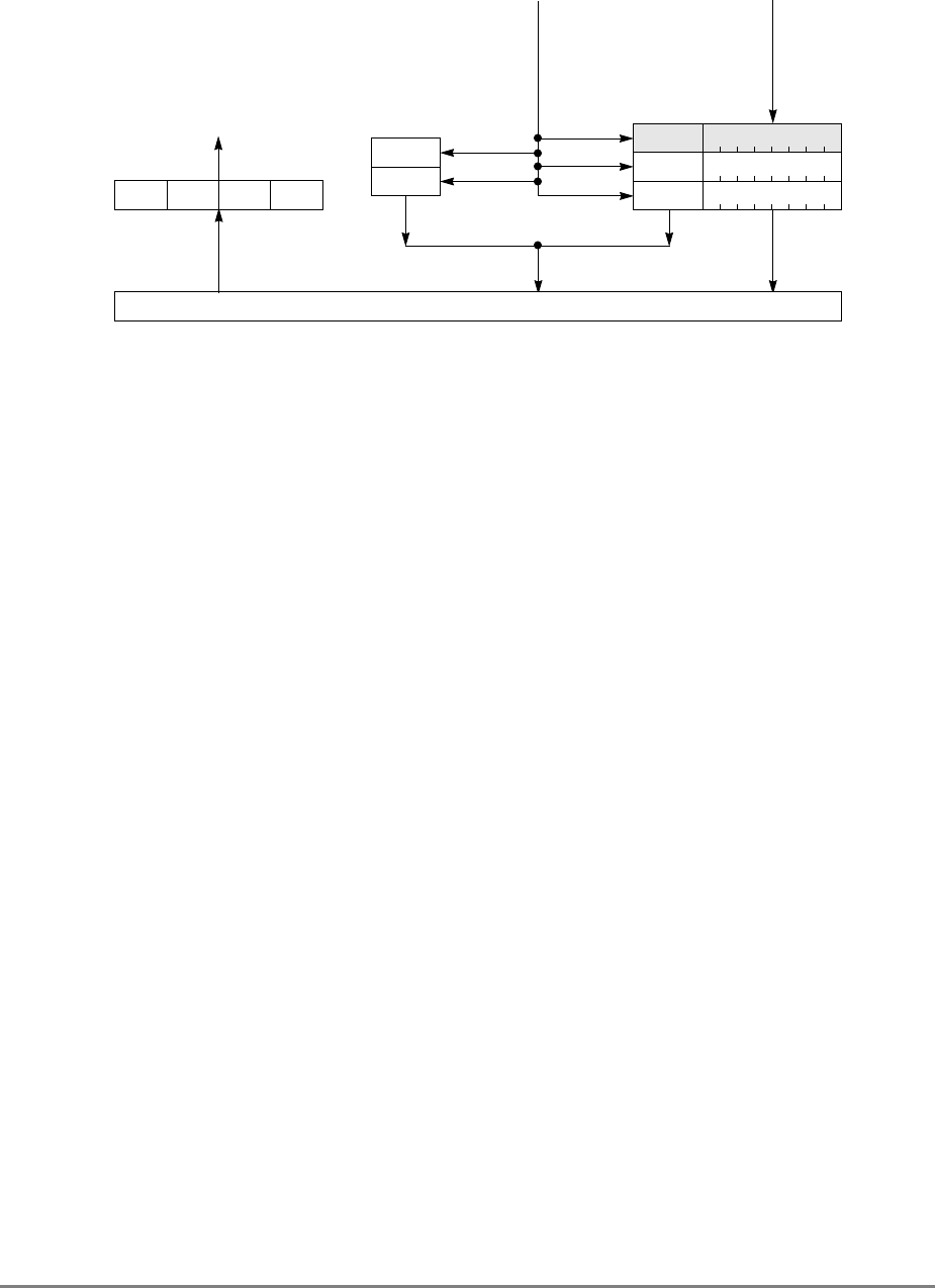
Chapter 4. Cache and Memory Unit Operation 4-23
Figure 4-5. Memory Unit
The other two elements in the write queue are used for store operations and writing back
modified sectors that have been deallocated by updating the queue; that is, when a cache
sector is full, the least-recently used cache sector is deallocated by first being copied into
the write queue and from there to system memory if it is modified. Note that snooping can
occur after a sector has been pushed out into the write queue and before the data has been
written to system memory. Therefore, to maintain a coherent memory, the write queue
elements are compared to snooped addresses in the same way as the cache tags. If a snoop
hits a write queue element, the data is first stored in system memory before it can be loaded
into the cache of the snooping bus master. Full coherency checking between the cache and
the write queue prevents dependency conflicts.
For a detailed discussion about the retry signals and bus operations pertaining to snooping,
see Chapter 9, “System Interface Operation.”
Execution of a load or store instruction is considered complete when the associated address
translation completes, guaranteeing that the instruction has completed to the point where it
is known that it will not generate an internal exception. However, after address translation
is complete, a read or write operation can generate an external exception.
Load and store instructions are always issued and translated in program order with respect
to other load and store instructions. However, a load or store operation that hits in the cache
can complete ahead of those that miss in the cache; additionally, loads and stores that miss
the cache can be reordered as they arbitrate for the system bus.
If a load or store misses in the cache, the operation is managed by the memory unit which
prioritizes accesses to the system bus. Read requests, such as loads, RWITMs, and
instruction fetches have priority over single-beat write operations The priorities for
accessing the system bus are listed in Section 4.10.2, “Memory Unit Queuing Priorities.”
The 601 ensures memory consistency by comparing target addresses and prohibiting
READ
QUEUE WRITE QUEUE
SNOOP
ADDRESS DATA
ADDRESS
(from cache) DATA
(from cache)
SYSTEM INTERFACE
(to cache)
DATA QUEUE
(four word)

4-24 PowerPC 601 RISC Microprocessor User's Manual
instructions from completing out of order if an address matches. Load and store operations
can be forced to execute in strict program order by inserting a sync instruction between each
sequential memory access instruction.
4.10.1 Memory Unit Queuing Structure
The memory queue receives requests from the cache unit for arbitration onto the 601 bus
interface. These requests may either be presented immediately to the bus interface logic or
they may be queued for future arbitration onto the bus. The memory queue consists of a
two-element read queue and a three-element write queue. Each write queue element can
hold a sector of data (32 bytes) associated with a single address.
Some operations presented to the memory queue cannot be queued. These operations
typically require synchronization with respect to either the execution units, the cache, or the
memory queue itself. In general, when these requests are presented and not arbitrated
directly onto the bus, they stall above the cache (but do not necessarily prevent use of the
cache) and attempt to re-arbitrate on the next cycle. These operations include the following:
• Cache control instructions that are broadcast
• Execution of the tlbie instruction
• Execution of the sync instruction
• Execution of the eieio instruction
• Cache requests for exclusive ownership when the sector is resident but not exclusive
in the cache
The memory queue also allows the optional loading of the sector adjacent to the one
containing the critical data. As the memory read queue receives and processes cache sector
reload requests, it is advantageous to fetch the other sector if it is not already in the cache
unless fetching the other sector delays access to data required for the machine to continue
processing. The memory unit logic detects whether other operations are pending; if not, it
initiates a fetch for the other sector. Note that this function can be disabled by setting bit 26
in HID0 (for instruction fetch misses) and bit 27 in HID0 (for load/store misses).
4.10.2 Memory Unit Queuing Priorities
This section describes the priorities for access to the system interface:
1. High-priority cache push-out operations
2. Normal snoop push-out operations
3. I/O controller interface segment accesses that incur no additional delays (that is, they
have not been retried because of latency).
4. Cache instruction operations
5. Read requests, such as loads, RWITMs, and instruction fetches
6. Single-beat write operations
7. sync instructions

Chapter 4. Cache and Memory Unit Operation 4-25
8. Optional cache-line fill operations
9. Cache sector cast-out operations
10.I/O controller interface segment accesses that incur additional delays (that is, they
have been retried because of external device latency)
4.10.3 Bus Interface
The bus interface logic sequences operations onto the 601 bus according to defined
protocols. The bus interface logic is also responsible for snooping other bus traffic,
presenting these operations to the rest of the device for coherency considerations and
reporting the appropriate snoop status onto the bus.
For additional information about the 601 bus interface and the bus protocols, refer to
Chapter 9, “System Interface Operation.”
4.11 MESI State Transactions
Table 4-7 shows MESI state transitions for various operations. The bus synchronization
column indicates whether exclusivity is required. Bus operations are described in
Table 4-5.
Table 4-7. MESI State Transitions
Operation Cache
Operation Bus
sync WIM Current
State Next
State Cache Actions Bus
Operation
Load or Fetch
(T = 0) Read No x0x I Same 1 Cast out of modified
sector 1 (as required) Write with kill
2 Pass four-beat read
to memory queue Read
3 Secondary cast out
of sector 2 (as
required)
Write with kill
Load or Fetch
(T = 0) Read No x0x S,E,M Same Read data from cache —
Load or Fetch
T = 0 or Load
(T = 1,
BUID = x'7F')
Read No x1x I Same Pass single-beat read
to memory queue Read
Load or Fetch
T = 0 or Load
(T = 1,
BUID = x'7F')
Read No x1x S,E I CRTRY read —
Load or Fetch
T = 0 or Load
(T = 1,
BUID = x'7F')
Read No x1x M I CRTRY read (push
sector to write queue) Write with kill

4-26 PowerPC 601 RISC Microprocessor User's Manual
Load
(T = 1,
BUID ≠ x'7F')
I/O
controller
load
— x1x — — — I/O load
lwarx Read Acts like other reads but bus operation uses special encoding
Store
(T = 0) Write No 00x I Same 1 Cast out of modified
sector (if necessary) Write with kill
2 Pass RWITM to
memory queue RWITM
3 Cast out of sector 2
(if necessary) Write with kill
Store
(T = 0) Write Yes 00x S Same 1 CRTRY write —
2 Pass kill Kill
M 3 Write data to cache —
Store
(T = 0) Write No 00x E,M M Write data to cache —
Store ≠ stwcx.
(T = 0) Write No 10x I Same Pass single-beat write
to memory queue Write with
flush
Store ≠ stwcx.
(T = 0) Write No 10x S,E Same 1 Write data to cache —
2 Pass single-beat
write to memory
queue
Write with
flush
Store ≠ stwcx.
(T = 0) Write No 10x M E 1 CRTRY write —
2 Push sector to write
queue Write with kill
Store (T = 0)
or stwcx.
(WIM = 10x)
or store (T = 1,
BUID = x'7F'
Write No x1x I Same Pass single-beat write
to memory queue Write with
flush
Store (T = 0)
or stwcx.
(WIM = 10x)
or store (T = 1,
BUID = x'7F')
Write No x1x S,E I CRTRY write —
Store (T = 0)
or stwcx.
(WIM = 10x)
or store (T = 1,
BUID = x'7F')
Write No x1x M I 1 CRTRY write —
2 Push sector to write
queue Write with kill
Store (T = 1,
BUID ≠ x'7F') I/O
controller No — — — — I/O store
request
Table 4-7. MESI State Transitions (Continued)
Operation Cache
Operation Bus
sync WIM Current
State Next
State Cache Actions Bus
Operation

Chapter 4. Cache and Memory Unit Operation 4-27
stwcx. Conditional
write If the reserved bit is set, this operation is like other writes except the bus operation
uses a special encoding.
dcbf Data cache
block flush Yes xxx I,S,E Same 1 CRTRY dcbf —
2 Pass flush Flush
Same I 3 State change only —
dcbf Data cache
block flush No xxx M I Push sector to write
queue Write with kill
dcbst Data cache
block store Yes xxx I,S,E Same 1 CRTRY dcbst —
2 Pass clean Clean
Same Same 3 No action —
dcbst Data cache
block store No xxx M E Push sector to write
queue Write with kill
dcbz Data cache
block set to
zero
No x1x x x Alignment trap —
dcbz Data cache
block set to
zero
No 10x x x Alignment trap —
dcbz Data cache
block set to
zero
Yes 00x I Same 1 CRTRY dcbz —
2 Cast out of modified
sector Write with kill
3 Pass kill Kill
4 Secondary cast out
of sector 2 Write with kill
Same M 5 Clear sector —
dcbz Data cache
block set to
zero
Yes 00x S Same 1 CRTRY dcbz —
2 Pass kill Kill
Same M 3 Clear sector —
dcbz Data cache
block set to
zero
No 00x E,M M Clear sector —
dcbt Data cache
block touch No x1x I Same Pass single-beat read
to memory queue Read
dcbt Data cache
block touch No x1x S,E I CRTRY read —
dcbt Data cache
block touch No x1x M I 1 CRTRY read —
2 Push sector to write
queue Write with kill
Table 4-7. MESI State Transitions (Continued)
Operation Cache
Operation Bus
sync WIM Current
State Next
State Cache Actions Bus
Operation

4-28 PowerPC 601 RISC Microprocessor User's Manual
dcbt Data cache
block touch No x0x I Same 1 Cast out of modified
sector (as required) Write with kill
2 Pass four-beat read
to memory queue Read
3 Secondary cast out
of sector (as
required)
Write with kill
dcbt Data cache
block touch No x0x S,E,M Same No action —
Secondary
cast out Secondary
cast out No xxx I Same Cast out Write with kill
Single-beat
read Reload
dump 1 No xxx I Same Forward data_in —
Four-beat
read (quad-
word 1)
Reload
dump 1 No xxx I Same 1 Forward data_in —
2 Write data_in to
cache —
Four-beat
read (quad-
word 2)—S
Reload
dump 2 No xxx I S Write data_in to cache —
Four-beat
read (quad-
word 2)—E
Reload
dump 2 No xxx I E Write data_in to cache —
Four-beat
write (quad-
word 1)
Reload
dump1 No xxx I Same 1 Splice and forward
data_in —
2 Write data_in to
cache —
Four-beat
write (quad-
word 2)
Reload
dump 2 No xxx I M Write data_in to cache —
Optional
reload of
adjacent
sector (quad-
word 1)
Reload
dump 1 No xxx I Same Write data_in to cache —
Optional
reload of
adjacent
sector (quad-
word 2)—S
Reload
dump 2 No xxx I S Write data_in to cache —
Optional
reload of
adjacent
sector (quad-
word 2)—E
Reload
dump 2 No xxx I E Write data_in to cache —
Table 4-7. MESI State Transitions (Continued)
Operation Cache
Operation Bus
sync WIM Current
State Next
State Cache Actions Bus
Operation

Chapter 4. Cache and Memory Unit Operation 4-29
Note that dcbt is presented to the cache as a load operation. The instructions tlbie and sync/eieio cause no
state transitions and are not cache operations but are included in the table to show how they are performed
by the memory unit queueing mechanism.
Note also that single-beat writes are not snooped in the write queue.
E→S Snoop
read No xxx E S State change only
(committed) —
S→I Snoop
write or kill No xxx S I State change only
(committed) —
E→I Snoop
write or kill No xxx E I State change only
(committed) —
M→I Snoop
kill No xxx M I State change only
(committed) —
Push
M→SSnoop
read No xxx M S Conditionally push Write with kill
Push
M→ISnoop
flush No xxx M I Conditionally push Write with kill
Push
M→ESnoop
clean No xxx M E Conditionally push Write with kill
tlbie TLB
invalidate Yes xxx x x 1 CRTRY TLB
invalidate —
2 Pass TLB invalidate TLB invalidate
3 No action —
sync/eieio Synchroniz
ation Yes xxx x x 1 CRTRY sync —
2 Pass sync dsync
3 No action —
Table 4-7. MESI State Transitions (Continued)
Operation Cache
Operation Bus
sync WIM Current
State Next
State Cache Actions Bus
Operation

4-30 PowerPC 601 RISC Microprocessor User's Manual

Chapter 5. Exceptions 5-1
Chapter 5
Exceptions
50
50
The PowerPC exception mechanism allows the processor to change to supervisor state as a
result of external signals, errors, or unusual conditions arising in the execution of
instructions. When exceptions occur, information about the state of the processor is saved
to certain registers and the processor begins execution at an address (exception vector)
predetermined for each exception. The exception handler at the specified vector is then
processed with the processor in supervisor mode.
Although multiple exception conditions can map to a single exception vector, a more
specific condition may be determined by examining a register associated with the
exception—for example, the DAE/source instruction service register (DSISR) and the
floating-point status and control register (FPSCR). Additionally, some exception conditions
can be explicitly enabled or disabled by software.
Except for the catastrophic asynchronous exceptions (machine check and system reset) the
PowerPC 601 microprocessor exception model is precise, defined as follows:
• The exception handler is given the address of the excepting instruction (or the next
instruction to execute in the case of asynchronous, precise exceptions).
• All instructions prior to the excepting instruction in the instruction stream have
completed execution and have written back their results.
• No instructions subsequent to the excepting instruction in the instruction stream
have been issued.
A detailed description of how the instruction flow is handled in a precise fashion is provided
in 7.3.1.4.4, “Synchronization Tags for the Precise Exception Model.”
The PowerPC architecture requires that exceptions be handled in program order; therefore,
although a particular implementation may recognize exception conditions out of order, they
are presented strictly in order. When an instruction-caused exception is recognized, any
unexecuted instructions that appear earlier in the instruction stream, including any that have
not yet entered the execute state, are required to complete before the exception is taken. Any
exceptions caused by those instructions are handled first. Likewise, exceptions that are
asynchronous and precise are recognized when they occur, but are not handled until all
instructions currently in the execute stage successfully complete execution and report their
results.

5-2 PowerPC 601 RISC Microprocessor User's Manual
Unless a catastrophic condition causes a system reset or machine check exception, only one
exception is handled at a time. If, for example, a single instruction encounters multiple
exception conditions, those conditions are encountered sequentially. After the exception
handler handles an exception, the instruction execution continues until the next exception
condition is encountered. However, in many cases there is no attempt to reexecute the
instruction. This method of recognizing and handling exception conditions sequentially
guarantees that exceptions are recoverable.
Exception handlers should save the information stored in SRR0 and SRR1 early to prevent
the program state from being lost due to a system reset and machine check exception or to
an instruction-caused exception in the exception handler, and before enabling external
interrupts.
This chapter describes the 601 exception model, it explains each class of instruction, and it
describes how the program state is saved for individual exceptions.
5.1 Exception Classes
As specified by the PowerPC architecture, all 601 exceptions can be described as either
precise or imprecise and either synchronous or asynchronous. Asynchronous exceptions are
caused by events external to the processor’s execution; synchronous exceptions, which are
all handled precisely by the 601, are caused by instructions.
The 601 exceptions are shown in Table 5-1.
Although exceptions have other characteristics as well, such as whether they are maskable
or nonmaskable, the distinctions shown in Table 5-1 define categories of exceptions that the
601 recognizes. Note that Table 5-1 includes no synchronous imprecise instructions. While
the PowerPC architecture supports imprecise floating-point exceptions, they do not occur
in the 601.
Exceptions, and conditions that cause them, are listed in Table 5-2.
Table 5-1. PowerPC 601 Microprocessor Exception Classifications
Synchronous/Asynchronous Precise/Imprecise Exception Type
Asynchronous Imprecise Machine check
System reset
Asynchronous Precise External interrupt
Decrementer
Synchronous Precise Instruction-caused exceptions

Chapter 5. Exceptions 5-3
Table 5-2. Exceptions, Vector Offsets, and Conditions
Exception
Type Vector Offset
(hex) Causing Conditions
Reserved 00000 —
System reset 00100 A system reset is caused by the assertion of either SRESET or HRESET.
Machine check 00200 A machine check is caused by the assertion of the TEA signal during a data bus
transaction.
Data access 00300 The cause of a data access exception can be determined by the bit settings in
the DSISR, listed as follows:
1 Set if the translation of an attempted access is not found in the primary
hash table entry group (HTEG), or in the rehashed secondary HTEG, or in
the range of a BAT register; otherwise cleared.
4 Set if a memory access is not permitted by the page or BAT protection
mechanism described in Chapter 6, “Memory Management Unit”; otherwise
cleared.
5 Set if the access was to an I/O segment (SR[T] =1) by an eciwx, ecowx,
lwarx, stwcx., or lscbx instruction; otherwise cleared. Set by an eciwx or
ecowx instruction if the access is to an address that is marked as write-
through.
6 Set for a store operation and cleared for a load operation.
9 Set if an EA matches the address in the DABR while in one of the three
compare modes.
11 Set if eciwx or ecowx is used and EAR[E] is cleared.
Instruction
access 00400 An instruction access exception is caused when an instruction fetch cannot be
performed for any of the following reasons:
• The effective (logical) address cannot be translated. That is, there is a page
fault for this portion of the translation, so an instruction access exception
must be taken to retrieve the translation from a storage device such as a
hard disk drive.
• The fetch access is to an I/O segment.
• The fetch access violates memory protection. If the key bits (Ks and Ku) in
the segment register and the PP bits in the PTE or BAT are set to prohibit
read access, instructions cannot be fetched from this location.
External
interrupt 00500 An external interrupt occurs when the INT signal is asserted.
Alignment 00600 An alignment exception is caused when the 601 cannot perform a memory
access for any of several reasons, such as when the operand of a floating-point
load or store operation is in an I/O segment (SR[T] = 1) or a scalar load/store
operand crosses a page boundary. Specific exception sources are described in
Section 5.4.6, “Alignment Exception (x'00600').”

5-4 PowerPC 601 RISC Microprocessor User's Manual
Program 00700 A program exception is caused by one of the following exception conditions,
which correspond to bit settings in SRR1 and arise during execution of an
instruction:
• Floating-point enabled exception—A floating-point enabled exception
condition is generated when the following condition is met:
(MSR[FE0] | MSR[FE1]) & FPSCR[FEX] is 1.
FPSCR[FEX] is set by the execution of a floating-point instruction that
causes an enabled exception or by the execution of a “move to FPSCR”
instruction that results in both an exception condition bit and its
corresponding enable bit being set in the FPSCR.
• Illegal instruction—An illegal instruction program exception is generated
when execution of an instruction is attempted with an illegal opcode or illegal
combination of opcode and extended opcode fields (including PowerPC
instructions not implemented in the 601), or when execution of an optional
instruction not provided in the 601 is attempted (these do not include those
optional instructions that are treated as no-ops). The PowerPC instruction
set is described in Chapter 3, “Addressing Modes and Instruction Set
Summary.”
• Privileged instruction—A privileged instruction type program exception is
generated when the execution of a supervisor instruction is attempted and
the MSR register user privilege bit, MSR[PR], is set. In the 601, this
exception is generated for mtspr or mfspr with an invalid SPR field if
SPR[0] = 1 and MSR[PR] = 1. This may not be true for all PowerPC
processors.
• Trap—A trap type program exception is generated when any of the
conditions specified in a trap instruction is met.
Floating-point
unavailable 00800 A floating-point unavailable exception is caused by an attempt to execute a
floating-point instruction (including floating-point load, store, and move
instructions) when the floating-point available bit is disabled (MSR[FP] = 0).
Decrementer 00900 The decrementer exception occurs when the most significant bit of the
decrementer (DEC) register transitions from 0 to 1. Must also be enabled with
the MSR[EE] bit.
I/O controller
interface error 00A00 An I/O controller interface error exception is taken only when an operation to an
I/O controller interface segment fails (such a failure is indicated to the 601 by a
particular bus reply packet). If an I/O controller interface exception is taken on a
memory access directed to an I/O segment, the SRR0 contains the address of
the instruction following the offending instruction. Note that this exception is not
implemented in other PowerPC processors.
Reserved 00B00 —
System call 00C00 A system call exception occurs when a System Call (sc) instruction is executed.
Reserved 00D00 Other PowerPC processors may use this vector for trace exceptions.
Reserved 00E00 The 601 does not generate an interrupt to this vector. Other PowerPC
processors may use this vector for floating-point assist exceptions.
Reserved 00E10–00FFF —
Reserved 01000–01FFF Reserved, implementation-specific
Table 5-2. Exceptions, Vector Offsets, and Conditions (Continued)
Exception
Type Vector Offset
(hex) Causing Conditions

Chapter 5. Exceptions 5-5
5.1.1 Precise Exceptions
In the 601, all synchronous exceptions and the asynchronous external interrupt and
decrementer exceptions are handled precisely; that is, all instructions that occur in the
instruction stream before the excepting event appear to complete and subsequent
instructions execute after the exception has been handled. When one of the 601’s precise
exceptions occurs, SRR0 is set to point to an instruction such that all prior instructions in
the instruction stream have completed execution and no subsequent instruction has begun
execution. However, depending on the exception type, the instruction addressed by SRR0
may not have completed execution.
When an exception occurs, instruction dispatch (the issuance of instructions by the
instruction fetch unit to any instruction execution unit) is halted and the following
synchronization is performed:
1. The exception mechanism waits for all previous instructions in the instruction
stream to complete to a point where they report all exceptions they will cause.
2. The processor ensures that all previous instructions in the instruction stream
complete in the context in which they began execution.
3. The exception mechanism is responsible for saving and restoring the processor state.
After control passes back to the program that encountered the exception, there are
no instructions in execute stage, and the user program instructions are dispatched
and executed in this new context.
Run mode/
trace exception 02000 The run mode exception is taken depending on the settings of the HID1 register
and the MSR[SE] bit.
The following modes correspond with bit settings in the HID1 register:
• Normal run mode—No address breakpoints are specified, and the 601
executes from zero to three instructions per cycle
• Single instruction step mode—One instruction is processed at a time. The
appropriate break action is taken after an instruction is executed and the
processor quiesces.
• Limited instruction address compare—The 601 runs at full speed (in parallel)
until the EA of the instruction being decoded matches the EA contained in
HID2. Addresses for branch instructions and floating-point instructions may
never be detected.
• Full instruction address compare mode—Processing proceeds out of IQ0.
When the EA in HID2 matches the EA of the instruction in IQ0, the
appropriate break action is performed. Unlike the limited instruction address
compare mode, all instructions pass through the IQ0 in this mode. That is,
instructions cannot be folded out of the instruction stream.
The following mode is taken when the MSR[SE] bit is set.
• MSR[SE] trace mode—Note that in other PowerPC implementations, the
trace exception is a separate exception with its own vector x'00D00'.
Reserved 02001–03FFF —
Table 5-2. Exceptions, Vector Offsets, and Conditions (Continued)
Exception
Type Vector Offset
(hex) Causing Conditions

5-6 PowerPC 601 RISC Microprocessor User's Manual
5.1.1.1 Synchronous/Precise Exceptions
In the 601, all exceptions caused by instructions are precise. When instruction execution
causes a precise exception, the following conditions exist at the exception point:
• Depending on the type of exception, SRR0 addresses either the instruction causing
the exception or the immediately following instruction. The instruction addressed
can be determined from the exception type and status bits, which are described with
the description of each exception.
• All instructions that precede the excepting instruction are allowed to complete
before the exception is processed. However, some memory accesses generated by
these preceding instructions may not have been performed with respect to all other
processors or system devices.
• The instruction causing the exception may not have begun execution, may have
partially completed, or may have completed, depending on the exception type.
• No subsequent instructions in the instruction stream complete execution.
Note that other PowerPC microprocessors may support optional imprecise floating-point
exception modes. While parallel processing allows the possibility of two instructions
reporting exceptions during the same cycle, they are handled in program order. If a single
instruction generates multiple exception conditions, those exceptions are handled
sequentially, as described in Section 5.1.3, “Recognition of Exceptions.” Exception
priorities are described in Section 5.1.2, “Exception Priorities.”
5.1.1.2 Asynchronous/Precise Exceptions
The 601 supports two asynchronous, precise exceptions—external interrupt and
decrementer exceptions. For asynchronous exceptions, the following conditions exist at the
exception point:
• All instructions issued before the event that caused the exception, and any
undispatched instructions that precede those instructions in the instruction stream,
appear to have completed before the exception is processed. However, some
memory accesses generated by these preceding instructions may not have been
performed with respect to all other processors or system devices.
• SRR0 addresses the instruction that would have been executed next had the
exception not occurred.
• Architecturally, no subsequent instructions in the instruction stream complete
execution.
These two exceptions are maskable. When the machine state register external interrupt
enable bits are cleared (MSR[EE] = 0), these exception conditions are latched and are not
recognized until the EE bit is set. MSR[EE] is cleared automatically when an exception is
taken to delay recognition of conditions causing asynchronous, precise exceptions. No two
precise exceptions can be recognized simultaneously. Handling of an asynchronous,
precise exception does not begin until all currently executing instructions complete and any
synchronous, precise exceptions caused by those instructions have been handled, as

Chapter 5. Exceptions 5-7
described in Section 5.1.3, “Recognition of Exceptions.” Exception priorities are described
in Section 5.1.2, “Exception Priorities.”
5.1.1.3 Asynchronous, Imprecise Exceptions
There are two asynchronous, imprecise exceptions—system reset and machine check.
These two exceptions have the highest priority and can occur while other exceptions are
being processed. Note that asynchronous, imprecise exceptions cannot be masked;
therefore, if two of these exceptions occur in immediate succession, the state information
saved by the first exception may be overwritten when the subsequent exception occurs.
These exceptions cannot be masked by using the MSR[EE] bit. A machine check exception
occurs if the machine check enable bit, MSR[ME], is set. If MSR[ME] is cleared, the
processor goes directly into checkstop state (if the machine-check checkstop condition is
properly enabled). When an imprecise exception occurs, the following conditions exist at
the exception point:
• The integer instruction pipeline acts as the synchronizing mechanism for the three
pipelines (branch, floating-point, and integer). When an asynchronous interrupt
occurs, integer instructions that have entered or passed through the integer execute
stage and the instructions tagged to them are allowed to complete, no other
instructions are allowed to start execution and synchronization. The value in SRR0
is the address of the instruction, which would execute after the last instruction that
was actually completed.
For more information on the tagging mechanism, refer to Section 7.3.1.4.4,
“Synchronization Tags for the Precise Exception Model.”
• SRR0 addresses either the instruction that would have completed or some
instruction following it that would have completed if the exception had not occurred.
• An exception is generated such that all instructions preceding the instruction
addressed by SRR0 appear to have completed with respect to the executing
processor.
5.1.2 Exception Priorities
This section describes how exceptions are prioritized. Exceptions are roughly prioritized by
exception class, as follows:
1. Asynchronous, imprecise exceptions have priority over all other exceptions. These
exceptions do not wait for the completion of any precise exception handling.
2. Synchronous, precise exceptions are caused by instructions and are presented in
strict program order.
3. Asynchronous, precise exceptions (external interrupt and decrementer exceptions)
are delayed until higher priority exceptions are presented.

5-8 PowerPC 601 RISC Microprocessor User's Manual
The exceptions are listed in Table 5-3 in order of highest to lowest priority.
5.1.3 Recognition of Exceptions
The order in which exceptions are recognized is determined by program order and whether
the exception is synchronous or asynchronous, precise or imprecise, and masked or
nonmasked.
Synchronous, precise exceptions (that is, exceptions that are caused by instructions) are
handled in strict program order, even though instructions can execute and exceptions can
be detected out of order. Therefore, before the 601 processes an instruction-caused
exception, it executes all instructions, and handles any resulting exceptions, that appear
earlier in the instruction stream.
A single instruction may generate multiple exception conditions. Of these exceptions, the
601 handles the exception it encounters first; software determines if execution of
instructions is resumed after an exception.
If the exception is asynchronous and precise (namely an external interrupt or decrementer
exception), the 601 synchronizes the pipeline by completing the execution of any
Table 5-3. Exception Priorities
Exception
Class Priority Exception
Asynchronous,
imprecise 1 System reset—The system reset exception has the highest priority of all exceptions.
If this exception exists, the exception mechanism ignores all other exceptions and
generates a system reset exception. Instructions issued before the generation of a
system reset exception cannot generate a nonmaskable exception.
2 Machine check—The machine check exception is the second-highest priority
exception. If this exception occurs, the exception mechanism ignores all other
exceptions (except reset) and generates a machine check exception. Instructions
issued before the generation of a machine check exception cannot generate a
nonmaskable exception.
Synchronous,
precise 3 Instruction dependent— When an instruction causes an exception, the exception
mechanism waits for any instructions prior to the excepting instruction in the
instruction stream to execute. Any exceptions caused by these instructions are
handled first. It then generates the appropriate exception if no higher priority
exception exists.
Note that a single instruction can cause multiple exceptions. The ordering of such
exceptions is described in 5.1.3, “Recognition of Exceptions.”
Asynchronous,
precise 4 External interrupt—The external interrupt mechanism waits for instructions currently
dispatched to complete execution. After all dispatched instructions are executed, and
any exceptions caused by those instructions are handled, the exception mechanism
generates this exception if no higher priority exception exists. This exception is
delayed while MSR[EE] is cleared.
5 Decrementer—This exception is the lowest priority exception. When this exception is
created, the exception mechanism waits for all other possible exceptions to be
reported. It then generates this exception if no higher priority exception exists. This
exception is delayed while MSR[EE] is cleared.

Chapter 5. Exceptions 5-9
instruction in the execute stage and any undispatched instructions that appear earlier in the
instruction stream (including any exceptions they generate) before handling the external
interrupt or decrementer exceptions.
5.1.3.1 Recognition of Asynchronous, Imprecise Exceptions
Exceptions that are nonmasked, imprecise, and asynchronous (namely system reset or
machine check exceptions) may occur at any time. That is, these exceptions are not delayed
if another exception is being handled. As a result, state information for the interrupted
exception may be lost; therefore, these exceptions are typically nonrecoverable.
All other exceptions have lower priority than system reset and machine check exceptions.
5.1.3.2 Recognition of Precise Exceptions
Only one precise exception can be reported at a time. (Note that PowerPC implementations
that support imprecise-mode floating-point enabled exceptions allow those to be handled in
the same manner as described in this section.)
Figure 5-1 illustrates the ordering of precise exceptions. Note that this ordering is on a per-
instruction basis. If a precise, asynchronous exception condition occurs while instruction-
caused exceptions are being processed, its handling is delayed until all instruction-caused
exceptions are handled.
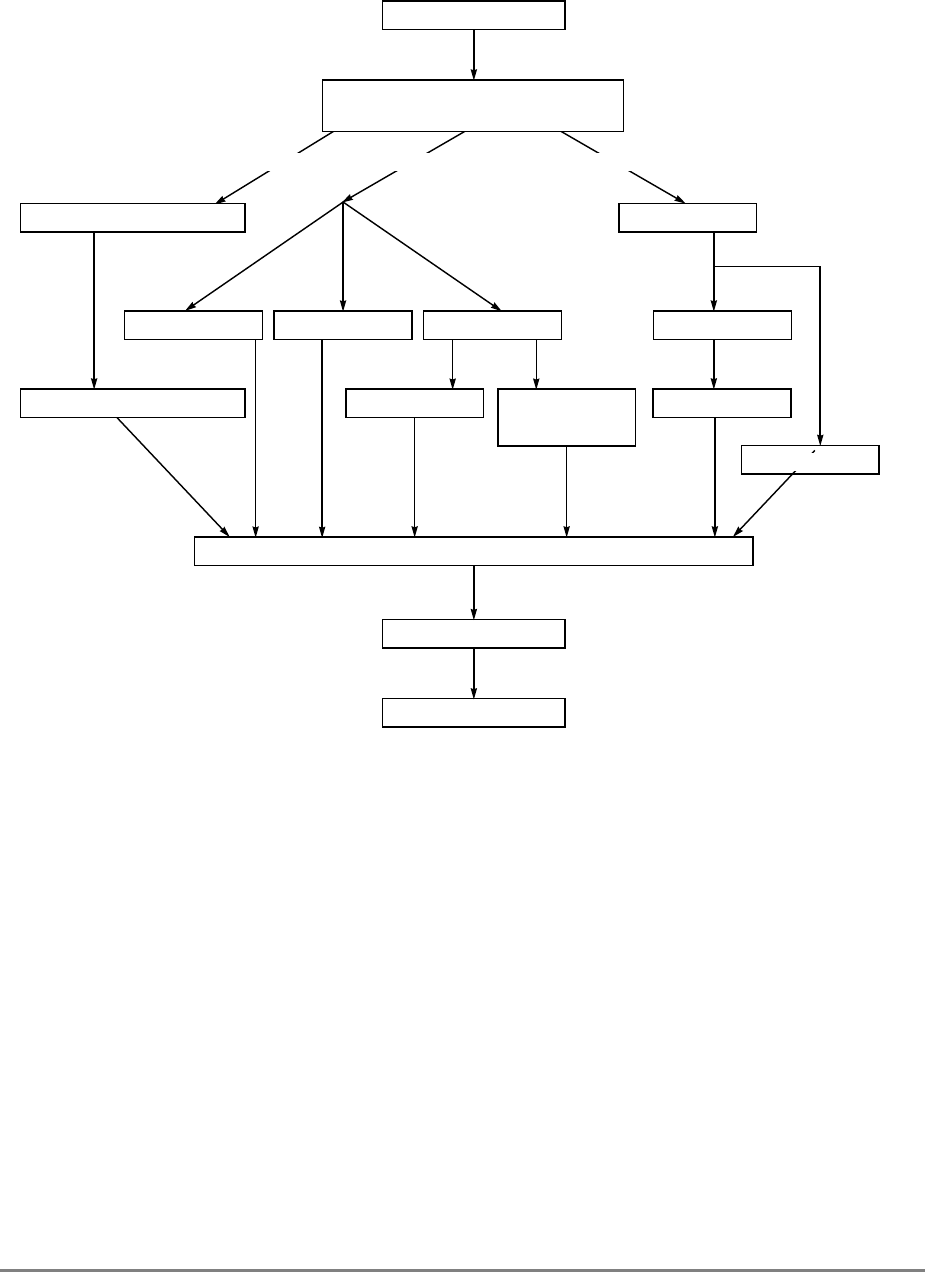
5-10 PowerPC 601 RISC Microprocessor User's Manual
Figure 5-1. Recognition of Precise Exception Conditions
5.2 Exception Processing
When an exception is taken, the 601 uses the save/restore registers, SRR0 and SRR1, to
save the contents of the machine state register and to identify where instruction execution
should resume after the exception is handled. The machine status save/restore register 0
(SRR0) is a 32-bit register that the 601 uses to save either the address of the instruction that
causes the exception, the one that follows, or the next instruction that would have executed
in the case of an asynchronous, imprecise exception. This address is used typically when a
Return from Interrupt (rfi) instruction is executed. The SRR0 is shown in Figure 5-2.
Instruction Access
Trap System Call
Data Access
FP Unavailable
Alignment
External Interrupt
Decrementer
Floating Point1
1Not all floating-point instructions can cause enabled exceptions.
2If the MSR bits FE0 and FE1 are set such that precise mode floating-point enabled exceptions are
enabled and the FPSCR[FEX] bit is set, a program exception results.
3Floating-point precise exceptions are taken only when either MSR[FE0] or MSR[FE1] are set.
Program Exception
(Illegal/Privileged Instruction)
Integer
Precise Mode FP Enabled2
rfi or mtmsr
I/O Cont I/F
Error
FP Alignment
Data Access
Privileged Instruction
Run Mode and Trace3
Floating Point1
Chapter 5. Exceptions 5-11
Figure 5-2. Machine Status Save/Restore Register 0 (SRR0)
When an exception occurs, SRR0 is set to point to an instruction such that all prior
instructions have completed execution and no subsequent instruction has begun execution.
The instruction addressed by SRR0 may not have completed execution, depending on the
exception type. SRR0 addresses either the instruction causing the exception or the
immediately following instruction. The instruction addressed can be determined from the
exception type bits.
The SRR1 is a 32-bit register used to save machine status on exceptions and to restore
machine status when rfi is executed. The SRR1 is shown in Figure 5-3.
Figure 5-3. Machine Status Save/Restore Register 1 (SRR1)
In general, when an exception occurs, bits 0–15 of SRR1 are loaded with exception-specific
information and bits 16–31 of the machine state register (MSR) are placed into bits 16–31
of SRR1. The machine state register is shown in Figure 5-4.
.
Figure 5-4. Machine State Register (MSR)
Table 5-4 shows the bit definitions for the MSR.
Table 5-4. Machine State Register Bit Settings
Bit(s) Name Description
0–15 — Reserved
16 EE External interrupt enable
0 The processor delays recognition of external interrupts and decrementer exception
conditions.
1 The processor is enabled to take an external interrupt or the decrementer exception.
17 PR Privilege level
0 The processor can execute both user and supervisor instructions.
1 The processor can only execute user-level instructions.
SRR0 (Holds EA for resuming program execution)
0 31
0151631
Exception-Specific Data MSR[16–31]
0 1516171819202122232425262728293031
Reserved
0 0 0 0 0 0 0 0 0 0 0 0 0 0 0 EE PR FP MEFE0 SE 0 FE1 0 EP IT DT 0 0 0 0

5-12 PowerPC 601 RISC Microprocessor User's Manual
18 FP Floating-point available
0 The processor prevents dispatch of floating-point instructions, including floating-point
loads, stores, and moves. Floating-point enabled program exceptions can still occur and
the FPRs can still be accessed.
1 The processor can execute floating-point instructions, and can take floating-point
enabled exception type program exceptions.
19 ME Machine check enable
0 Machine check exceptions are disabled. If this bit is cleared, the 601 attempts to go into
checkstop mode. Note however, if is not enabled in HID0, the machine check exception
is taken.
1 Machine check exceptions are enabled.
20 FE0 Floating-point exception mode 0 (See Table 5-5.)
21 SE Single-step trace enable
0 The processor executes instructions normally.
1 The processor generates a trace exception upon the successful execution of the next
instruction. When this bit is set, the processor dispatches instructions in strict program
order. Successful execution means the instruction caused no other exception. Single-
step tracing may not be present on all implementations. If the function is not
implemented, MSR[SE] should be treated as a reserved MSR bit: mfmsr may return the
last value written to the bit, or may return 0 always.
22 — Reserved * on the 601
23 FE1 Floating-point exception mode 1 (See Table 5-5.)
24 — Reserved. This bit corresponds to the AL bit of the POWER Architecture.
25 EP Exception prefix. The setting of this bit specifies whether an exception vector offset is
prepended with Fs or 0s. In the following description,
nnnnn
is the offset of the exception. See
Table 5-2.
0 Exceptions are vectored to the physical address x'000
n_nnnn
'.
1 Exceptions are vectored to the physical address x'FFF
n_nnnn
'.
26 IT Instruction address translation
0 Instruction address translation is disabled. When instruction address translation is
disabled, EA is interpreted as described in Chapter 6, “Memory Management Unit.”
1 Instruction address translation is enabled.
27 DT Data address translation
0 Data address translation is disabled. When data relocation is off, EA is interpreted as
described in Chapter 6, “Memory Management Unit.”
1 Data address translation is enabled.
28–29 — Reserved
30 — Reserved * on the 601
31 — Reserved * on the 601
*These reserved bits may be used by other PowerPC processors. Attempting to change these bits does
not affect the operation of the processor. These bit positions always return a zero value when read.
Table 5-4. Machine State Register Bit Settings (Continued)
Bit(s) Name Description

Chapter 5. Exceptions 5-13
The floating-point exception mode bits are interpreted as shown in Table 5-5. For further
details see Section 5.4.7.1, “Floating-Point Enabled Program Exceptions.”
MSR bits 16–31 are guaranteed to be written to SRR1 when the first instruction of the
exception handler is encountered.
The data address register (DAR) is a 32-bit register used by several exceptions (data access,
I/O controller interface error, and alignment) to identify the address of a memory element.
5.2.1 Enabling and Disabling Exceptions
When a condition exists that causes an exception to be generated, it must be determined
whether the exception is enabled for that condition.
• Floating-point enabled exceptions (a type of program exception) can be disabled by
clearing both MSR[FE0] and MSR[FE1]. If either or both of these bits are set, all
floating-point exceptions are taken and are precise and cause a program exception.
Other PowerPC processors may support imprecise floating-point exceptions.
Individual conditions that can generate floating-point exceptions can be enabled and
disabled with bits in the FPSCR register.
• Asynchronous, precise exceptions are enabled by setting the MSR[EE] bit. When
MSR[EE] = 0, recognition of these exception conditions is delayed. MSR[EE] is
cleared automatically when an exception is taken to delay recognition of conditions
causing those exceptions.
• A machine check exception can only occur if the machine check enable bit,
MSR[ME], is set. If MSR[ME] is cleared, the processor goes directly into checkstop
state when a machine-check exception condition occurs.
• The run mode exception, which is used to set an instruction breakpoint, can be
enabled and disabled using bits 8 and 9 of HID1 (HID1[RM]). Note that this stops
the processor and is used for debug purposes only.
• The data address breakpoint can be enabled and disabled using bits 30 and 31 of the
DABR (HID5[SA]).
• System reset exceptions cannot be masked.
Table 5-5. Floating-Point Exception Mode Bits
FE0 FE1 Mode
0 0 Floating-point exceptions disabled
0 1 Floating-point imprecise nonrecoverable *
1 0 Floating-point imprecise recoverable*
1 1 Floating-point precise mode
* Not implemented in the 601

5-14 PowerPC 601 RISC Microprocessor User's Manual
5.2.2 Steps for Exception Processing
After it is determined that the exception can be taken (by confirming that any instruction-
caused exceptions occurring earlier in the instruction stream have been handled, and by
confirming that the exception is enabled for the exception condition), the 601 does the
following:
1. The SRR0 is loaded with an instruction address that depends on the type of
exception. See the individual exception description for details about how this
register is used for specific exceptions.
2. Bits 0–15 of SRR1 are loaded with 16 bits of information specific to the exception
type or all zeros.
3. Bits 16–31 of SRR1 are loaded with a copy of bits 16–31 of the MSR.
4. The MSR is set as described in Table 5-4. The new values take effect beginning with
the fetching of the first instruction of the exception-handler routine located at the
exception vector address.
Note that MSR[IT] and MSR[DT] are cleared for all exception types; therefore,
address translation is disabled for both instruction fetches and data accesses
beginning with the first instruction of the exception-handler routine.
5. Instruction fetch and execution resumes, using the new MSR value, at a location
specific to the exception type. The location is determined by adding the exception's
vector (see Table 5-2) to the base address determined by MSR[EP]. If EP is cleared,
exceptions are vectored to the physical address x'000n_nnnn'. If EP is set, exceptions
are vectored to the physical address x'FFFn_nnnn'. For a machine check exception
that occurs when MSR[ME] = 0 (machine check exceptions are disabled), the
checkstop state is entered (the machine stops executing instructions). See
Section 5.4.2, “Machine Check Exception (x'00200').”
6. The lwarx and stwcx. instructions require special handling if a reservation is still set
when an exception occurs. Exceptions clear reservations set with lwarx (or ldarx).
5.2.3 Returning from Supervisor Mode
The Return from Interrupt (rfi) instruction performs context synchronization by allowing
previously issued instructions to complete before returning to the interrupted process.
Execution of the rfi instruction ensures the following:
• All previous instructions have completed to a point where they can no longer cause
an exception. If a prior instruction causes an I/O controller interface error exception,
the results must be determined before this instruction is executed.
• Previous instructions complete execution in the context (privilege, protection, and
address translation) under which they were issued.
• The instructions following this instruction execute in the context established by this
instruction.

Chapter 5. Exceptions 5-15
5.3 Process Switching
The operating system should execute the following when processes are switched:
• The sync instruction, to resolve any data dependencies between the processes and to
synchronize the use of segment registers and SPRs. For an example showing use of
the sync instruction, see Section 2.3.3.1, “Synchronization for Supervisor-Level
SPRs and Segment Registers.”
• The isync instruction, to ensure that undispatched instructions not in the new
process are not used by the new process
• The stwcx. instruction, to clear any outstanding reservations, which ensures that an
lwarx instruction in the old process is not paired with an stwcx. in the new process.
Note that if an exception handler is used to emulate an instruction that is not implemented
in the 601, the exception handler must report in SRR0 (and in the data address register
[DAR] if applicable) the EA computed by the instruction being emulated and not one used
to emulate the instruction being emulated. For example, the Move to Time Base instruction
(mttb) was created for compatibility between the 601 and other PowerPC processors. The
601 implements a real-time clock (RTC) rather than the time base (TB), and when this
instruction is encountered by the 601 an illegal instruction program exception is taken and
the operation is performed by the 601’s mtspr instruction that accesses the appropriate
RTC register. When the exception caused by the mttb instruction is taken, the EA reported
should be that computed by the mttb instruction and not the mtspr instruction used in the
exception handler.
5.4 Exception Definitions
Table 5-6 shows all the types of exceptions that can occur with the 601 and the MSR bit
settings when the processor transitions to supervisor mode. The state of these bits prior to
the exception is typically stored in SRR1.
Table 5-6. MSR Setting Due to Exception
Exception Type
MSR Bit
EE
16 PR
17 FP
18 ME
19 FE0
20 SE
21 FE1
23 EP
25 IT
26 DT
27
Soft reset 0 0 0 — 0 0 0 — 0 0
Machine check 0000000—00
Data access 0 0 0 — 0 0 0 — 0 0
Instruction access 0 0 0 — 0 0 0 — 0 0
External 0 0 0 — 0 0 0 — 0 0
Alignment 0 0 0 — 0 0 0 — 0 0
Program 0 0 0—0 0 0—0 0

5-16 PowerPC 601 RISC Microprocessor User's Manual
The setting of the exception prefix (EP) bit in the MSR determines how exceptions are
vectored. If the bit is cleared, exceptions are vectored to the physical address x'000n_nnnn'
(where nnnnn is the vector offset); if EP is set, exceptions are vectored to the physical
address x'FFFn_nnnn'. Table 5-2 shows the exception vector offset of the first instruction
of the exception handler routine for each exception type.
5.4.1 Reset Exceptions (x'00100')
The system reset exception is a nonmaskable, asynchronous exception signaled to the 601
either through the assertion of either of the reset signals (SRESET or HRESET). The
assertion of the soft reset signal, SRESET, as described in Section 8.2.9.4.2, “Soft Reset
(SRESET)—Input” causes the soft reset exception to be taken and the physical base
address of the handler is determined by the MSR[EP] bit. The assertion of the hard reset
signal, HRESET, as described in Section 8.2.9.4.1, “Hard Reset (HRESET)—Input” causes
the hard reset exception to be taken and the physical address of the handler is always x'FFF0
0100'.
5.4.1.1 Soft Reset
When a soft reset exception occurs, registers are set as shown in Table 5-7.
Floating-point
unavailable 0 0 0—0 0 0—0 0
Decrementer 0 0 0 — 0 0 0 — 0 0
System call 0 0 0 — 0 0 0 — 0 0
Run mode/ trace
exception 0 0 0—0 0 0—0 0
I/O controller interface
error exception 0 0 0—0 0 0—0 0
0 Bit is cleared
1 Bit is set
— Bit is not altered
Reserved bits are read as if written as 0.
Table 5-6. MSR Setting Due to Exception (Continued)
Exception Type
MSR Bit
EE
16 PR
17 FP
18 ME
19 FE0
20 SE
21 FE1
23 EP
25 IT
26 DT
27

Chapter 5. Exceptions 5-17
When a soft reset exception is taken, instruction execution resumes at offset x'00100' from
the physical base address indicated by MSR[EP].
Before returning to the main program, the exception handler should do the following:
1. SRR0 and SRR1 should be given the values used by the rfi instruction.
2. Execute rfi.
It is not guaranteed that execution is recoverable. Other registers and the MSR are not reset
by hardware.
5.4.1.2 Hard Reset
This section describes the 601’s reset state after performing a hard reset operation (asserting
HRESET as described in Section 8.2.9.4.1, “Hard Reset (HRESET)—Input”). Note that a
hard reset operation should be performed on power-on to appropriately reset the processor.
Table 5-8 shows the state of the machine just before it fetches the first instruction after a
hard reset. Because of the setting of the MSR[EP] bit caused by a hard reset, the first
instruction is fetched from address x'FFF0 0100'.
Table 5-7. Soft Reset Exception—Register Settings
Register Setting Description
SRR0 Set to the effective address of the instruction that the processor would have attempted to execute next
if no exception conditions were present.
SRR1 0–15 Cleared
16–31 Loaded from bits 16–31 of the MSR. Note that if the processor state is corrupted to the extent
that execution cannot be reliably restarted, SRR1[30] is cleared.
MSR EE 0 SE 0
PR 0 FE1 0
FP 0 EP —
ME — IT 0
FE0 0 DT 0
Table 5-8. Settings Caused by Hard Reset
Register Setting
GPRs All 0s
FPRs All 0s
FPSCR 00000000
CR All 0s
SRs All 0s
MSR 00001040
MQ 00000000
XER 00000000

5-18 PowerPC 601 RISC Microprocessor User's Manual
1 Early releases (DD1) of the 601 hardware set this to x'00010000'. Other versions of silicon may be different
(see Section 2.3.3.11, “Processor Version Register (PVR)” for setting information).
2 Master checkstop enabled; internal power-on reset checkstops enabled.
3 Note that if external clock is connected to RTC for the 601, then the RTCL, RTCU, and DEC registers can
change from their initial value of 0s without receiving instructions to load those registers.
RTCU 00000000
RTCL 000000003
LR 00000000
CTR 00000000
DSISR 00000000
DAR 00000000
DEC 00000000
SDR1 00000000
SRR0 00000000
SRR1 00000000
SPRGs 00000000
EAR 00000000
PVR 000100011
BATs All 0s
HID0 800100802
HID1 00000000
HID2 00000000
HID5 00000000
HID15 00000000
TLBs All 0s
Cache All 0s
Tag directory All 0s. (However, LRU bits are initialized so each side of the cache has a unique LRU value.)
Table 5-8. Settings Caused by Hard Reset (Continued)
Register Setting

Chapter 5. Exceptions 5-19
The following is also true after a hard reset operation:
• External checkstops are enabled.
• The on-chip test interface has given control of the I/Os to the rest of the chip for
functional use.
• Since the reset exception has data and instruction translation disabled (MSR[DT]
and MSR[IT] both cleared), the chip operates in direct address translation mode.
This implies that instruction fetches as well as loads and stores are cacheable.
(Operations that correspond to direct address translations are implicitly cacheable,
not write-through mode, and require coherency checking on the bus.)
• All internal arrays and registers are cleared during the hard reset process.
5.4.2 Machine Check Exception (x'00200')
The 601 conditionally initiates a machine-check exception after detecting the assertion of
the TEA signal on the 601 interface. The assertion of the TEA signal indicates that a bus
error occurred and the system terminates the current transaction. One clock cycle after TEA
is asserted, the data bus signals go to the high-impedance state; however, data entering the
GPR or the cache is not invalidated.
If the MSR[ME] bit is set, the exception is recognized and handled; otherwise, the 601
attempts to enter an internal checkstop condition. This may not lead to a checkstop
depending upon the state of the various checkstop enable control bits in the HID0 register.
These are shown in Table 5-9. If the ME bit is cleared, and the HID0[CE] and HID0[EM]
bits are cleared (that is, when both the master checkstop and the machine check checkstops
are disabled), the machine check exception is taken.
The ability to disable the machine-check checkstop is useful for debugging. The HID0
register is described in Section 2.3.3.13.1, “Checkstop Sources and Enables Register—
HID0.”
In general, it is expected that the TEA signal would be used by a memory controller to
indicate a memory parity error or an uncorrectable memory ECC error. Note that the
resulting machine check exception is imprecise and has priority over any exceptions caused
by the instruction that generated the bus operation.
Machine check exceptions are enabled when MSR[ME] = 1; this is described in
Section 5.4.2.1, “Machine Check Exception Enabled (MSR[ME] = 1).” If MSR[ME] = 0
and a machine check occurs, the processor enters the checkstop state. Checkstop state is
described in 5.4.2.2, “Checkstop State (MSR[ME] = 0).”

5-20 PowerPC 601 RISC Microprocessor User's Manual
5.4.2.1 Machine Check Exception Enabled (MSR[ME] = 1)
When a machine check exception is taken, registers are updated as shown in Table 5-9.
When a machine check exception is taken, instruction execution resumes at offset x'00200'
from the physical base address indicated by MSR[EP].
Before returning to the main program, the exception handler should do the following:
1. SRR0 and SRR1 should be given the values to be used by the rfi instruction.
2. Execute rfi.
5.4.2.2 Checkstop State (MSR[ME] = 0)
When a processor is in the checkstop state, instruction processing is suspended and
generally cannot be restarted without resetting the processor. The contents of all latches are
frozen within two cycles upon entering checkstop state so that the state of the processor can
be analyzed as an aid in problem determination.
A machine check exception may result from referring to a nonexistent physical address. In
some implementations, for example, execution of a Data Cache Block Set to Zero (dcbz)
instruction that introduces a block into the cache associated with a nonexistent physical
address may delay the machine check exception until an attempt is made to store that block
to main memory.
Note that not all PowerPC processors provide the same level of error checking. The reasons
a processor can enter checkstop state is implementation-dependent.
Table 5-9. Machine Check Exception—Register Settings
Register Setting Description
SRR0 Set to the address of the next instruction that would have been executed in the interrupted
instruction stream. Neither this instruction nor any others beyond it will have been executed. All
preceding instructions will have been completed.
SRR1 0–15 Cleared
16–31 Loaded from MSR[16–31]. Note that if the processor state is corrupted to the extent that
execution cannot be reliably restarted, SRR1[30] is cleared.
MSR EE 0
PR 0
FP 0
ME 0
Note that when a machine check exception is taken, the exception handler should set MSR[ME]
as soon as it is practical to handle another TEA assertion. Otherwise, subsequent TEA assertions
cause the processor to automatically enter the checkstop state.
FE0 0
SE 0
FE1 0
EP Value is not altered
IT 0
DT 0

Chapter 5. Exceptions 5-21
5.4.3 Data Access Exception (x'00300')
A data access exception occurs when no higher priority exception exists and a data memory
access cannot be performed. The condition that caused the data access exception can be
determined by reading the DAE/source instruction service register (DSISR), a supervisor-
level SPR (SPR18) that can be read by using the mfspr instruction. Bit settings are
provided in Table 5-10. Table 5-10 also indicates which memory element is saved to the
DAR. Data access exceptions can occur for any of the following reasons:
• The effective address cannot be translated. That is, there is a page fault for this
portion of the translation, so a data access exception must be taken to retrieve the
translation from a storage device such as a hard disk drive.
• The instruction is not supported for the type of memory addressed. Invalid
instructions are described in Section D.1.1.1, “Invalid Instruction Forms.” I/O
controller interface segments are described in Section 9.6, “Memory- vs. I/O-
Mapped I/O Operations.”
• The access violates memory protection. Access is not permitted by the key (Ks and
Ku) and PP bits, which are set in the segment register and PTE for page protection
and in the BATs for block protection.
• The execution of an eciwx or ecowx instruction is disallowed because the external
access register enable bit (EAR[E]) is cleared.
These scenarios are common among all PowerPC processors. The following additional
scenarios can cause a data access exception in the 601:
• An lwarx, stwcx., or lscbx instruction refers to a non–memory-forced I/O controller
interface segment (that is, when SR[T] = 1 and BUID ≠ x'07F').
• An effective address matches the address in the data-address breakpoint register
(DABR) while in one of the appropriate compare modes. For additional information
on the DABR and the compare modes, refer to Section 2.3.3.13.4, “Data Address
Breakpoint Register (DABR)—HID5.”
Data access exceptions can be generated by load/store instructions, and the cache control
instructions (dcbi, dcbz, dcbst, and dcbf).
Although the 601 does not generally support memory accesses that cross a page boundary,
load or store multiple as well as load or store string instructions that are word-aligned and
cross a page boundary are handled. In these cases, if the second page has a translation error
or protection violation associated with it, the 601 takes the data access exception in the
middle of the instruction. In this case, the data address register (DAR) always points to the
first byte address of the offending page.

5-22 PowerPC 601 RISC Microprocessor User's Manual
If an stwcx. instruction has an effective address for which a normal store operation would
cause a data access exception but the processor does not have the reservation from lwarx,
the 601 determines whether a data access exception occurs as follows:
• If the reservation bit is cleared before the stwcx. instruction executes, that
instruction cannot generate an exception, regardless of whether the address
translation would have failed, page protection would have been violated, or the
address matches one in the DABR.
• A data access exception is taken if there is an address translation or page protection
error, or if the address hits in the DABR as long as the reservation bit is set when the
stwcx. instruction begins execution. In particular, the exception is taken even if the
reservation bit is cleared after execution begins.
If the XER indicates that the byte count for an lswi, stswi or lscbx instruction is zero, a data
access exception does not occur, regardless of the effective address.
The condition that caused the exception is defined in the DSISR. These conditions also use
the data address register (DAR) as shown in Table 5-10.
Table 5-10. Data Access Exception—Register Settings
Register Setting Description
SRR0 Set to the effective address of the instruction that caused the exception.
SRR1 0–15 Cleared
16–31 Loaded from bits 16–31 of the MSR
MSR EE 0 PR 0
FP 0 ME Value is not altered
FE0 0 SE 0
FE1 0 EP Value is not altered
IT 0 DT 0
DSISR 0 Reserved on the 601. The PowerPC architecture uses this bit for I/O controller interface error
exceptions, which are vectored to x'00A00' on the 601.
1 Set if the translation of an attempted access is not found in the primary hash table entry group
(HTEG), or in the rehashed secondary HTEG, or in the range of a BAT register; otherwise
cleared.
2–3 Cleared
4 Set if a memory access is not permitted by the page or BAT protection mechanism; otherwise
cleared.
5 Set if the eciwx, ecowx, lwarx, stwcx., or lscbx instruction is attempted to I/O controller
interface space, or if the lwarx or stwcx. instruction is used with addresses that are marked as
write-through.
6 Set for a store operation and cleared for a load operation.
7–8 Cleared
9 Set if an EA matches the address in the DABR while in one of the three compare modes.
10 Cleared.
11 Set if the instruction was an eciwx or ecowx and EAR[E] = 0.
12–31 Cleared

Chapter 5. Exceptions 5-23
When a data access exception is taken, instruction execution resumes at offset x'00300'
from the physical base address indicated by MSR[EP].
The architecture permits certain instructions to be partially executed when they cause a data
access exception. These are as follows:
• Load multiple or load string instructions—Some registers in the range of registers to
be loaded may have been loaded. On the 601, all of the first page is accessed and
none of the second page is accessed.
• Store multiple or store string instructions—Some bytes of memory in the range
addressed may have been updated. On the 601, all of the first page is accessed and
none of the second page is accessed.
In the cases above, the questions of how many registers and how much memory is altered
are instruction- and boundary-dependent. However, memory protection is not violated.
Furthermore, if some of the data accessed is in memory-forced I/O controller interface
space (SR[T] = 1) and BUID = x'7F', and the instruction is not supported for I/O controller
interface accesses, the locations in I/O controller interface space are not accessed.
For update forms, the update register (rA) is not altered.
5.4.4 Instruction Access Exception (x'00400')
An instruction access exception occurs when no higher priority exception exists and an
attempt to fetch the next instruction to be executed cannot be performed for any of the
following reasons:
• The effective address cannot be translated. That is, there is a page fault for this
portion of the translation, so an instruction access exception must be taken to retrieve
the translation from a storage device such as a hard disk drive.
• The fetch access is to an I/O controller interface segment that is not memory-forced.
• The fetch access violates memory protection. Access is not permitted by the key bits
(Ks and Ku) and PP bits, which are set in the segment register and PTE for page
protection and in the BATs for block protection.
An instruction fetch to an I/O controller interface segment while MSR[IT] is set causes an
instruction access exception on the 601. Register settings for instruction access exceptions
are shown in Table 5-11.
DAR Set to the effective address of a memory element as described in the following list:
• A byte in the first word accessed in the page that caused the data access exception, for a byte, half
word, or word memory access.
• A byte in the first double word accessed in the page that caused the data access exception, for a
double-word memory access.
Table 5-10. Data Access Exception—Register Settings (Continued)
Register Setting Description

5-24 PowerPC 601 RISC Microprocessor User's Manual
When an instruction access exception is taken, instruction execution resumes at offset
x'00400' from the physical base address indicated by MSR[EP].
5.4.5 External Interrupt (x'00500')
An external interrupt is signaled to the 601 by the assertion of the INT signal as described
in Section 8.2.9.1, “Interrupt (INT)—Input.” The interrupt may be delayed by other higher
priority exceptions or if the MSR[EE] bit is cleared when the exception occurs.
After the INT is detected, the 601 stops dispatching instructions and waits for executing
instructions to complete. Therefore, exceptions caused by instructions in progress are taken
before the external interrupt exception is taken. After all instructions complete, the 601
takes the external interrupt exception.
The register settings for the external interrupt exception are shown in Table 5-12.
Table 5-11. Instruction Access Exception—Register Settings
Register Setting
SRR0 Set to the effective address of the instruction that the processor would have attempted to execute next
if no exception conditions were present (if the exception occurs on attempting to fetch a branch target,
SRR0 is set to the branch target address).
SRR1 0 Cleared
1 Set if the translation of an attempted access is not found in the primary hash table entry group
(HTEG), or in the rehashed secondary HTEG, or in the range of a BAT register; otherwise
cleared.
2 Cleared
3 Cleared. Note that the PowerPC architecture defines this as set if the fetch access was to an I/O
controller interface segment (SR[T]=1). Note that this condition causes SRR1[0–15] to be
cleared in the 601.
4 Set if a memory access is not permitted by the page or BAT protection mechanism, described in
Chapter 6, “Memory Management Unit”; otherwise cleared.
5–9 Cleared
10 Set if the page table search fails to find a translation for the effective address; otherwise cleared.
11–15 Cleared
16–31 Loaded from bits 16–31 of the MSR
MSR EE 0 SE 0
PR 0 FE1 0
FP 0 EP Value is not altered
ME Value is not altered IT 0
FE0 0 DT 0

Chapter 5. Exceptions 5-25
When an external interrupt exception is taken, instruction execution resumes at offset
x'00500' from the physical base address indicated by MSR[EP].
In early versions of the 601 (processor revision level x'0000'), the external interrupt is a
level-sensitive signal and should be held active until reset by the interrupt service routine.
Phantom interrupts due to phenomena such as crosstalk and bus noise should be avoided.
The INT signal is used to signal an external interrupt to the 601. The 601 latches the
interrupt condition if the MSR[EE] bit is set; and it ignores the interrupt condition if the
MSR[EE] bit is cleared. To guarantee that the external interrupt is taken, the INT signal
must be held active until the 601 takes the interrupt. If the INT signal is negated before the
interrupt is taken, the 601 is not guaranteed to take an external interrupt, depending on
whether the MSR[EE] bit was set while INT signal was held active. To clear the interrupt,
the interrupt handler must send a command to the device that signaled the interrupt.
5.4.6 Alignment Exception (x'00600')
This section describes conditions that can cause alignment exceptions in the 601. Similar
to data access exceptions, alignment exceptions use the SRR0 and SRR1 to save the
machine state and the DSISR to determine the source of the exception.
The register settings for alignment exceptions are shown in Table 5-13.
Table 5-12. External Interrupt—Register Settings
Register Setting Description
SRR0 Set to the effective address of the instruction that the processor would have attempted to execute next
if no interrupt conditions were present.
SRR1 0–15 Cleared
16–31 Loaded from bits 16–31 of the MSR
MSR EE 0 SE 0
PR 0 FE1 0
FP 0 EP Value is not altered
ME Value is not altered IT 0
FE0 0 DT 0
Table 5-13. Alignment Exception—Register Settings
Register Setting Description
SRR0 Set to the effective address of the instruction that caused the exception.
SRR1 0–15 Cleared
16–31 Loaded from bits 16–31 of the MSR
MSR EE 0 SE 0
PR 0 FE1 0
FP 0 EP Value is not altered
ME Value is not altered IT 0
FE0 0 DT 0

5-26 PowerPC 601 RISC Microprocessor User's Manual
5.4.6.1 Integer Alignment Exceptions
The 601 is optimized for load and store operations that are aligned on natural boundaries.
Operations that are not naturally aligned may suffer performance degradation, depending
on the type of operation, the boundaries crossed, and the mode that the processor is in
during execution. More specifically, these operations may either cause an alignment
exception or they may cause the processor to break the memory access into multiple,
smaller accesses with respect to the cache and the memory subsystem.
The 601 can initiate alignment exception for the accesses as shown in Table 5-14. In all of
these cases, the appropriate range check is performed before the instruction begins
DSISR 0–11 Cleared
12–13 Cleared. (Note that these bits can be set by several 64-bit PowerPC
instructions that are not supported in the 601.)
14 Cleared
15–16 For instructions that use register indirect with index addressing—set
to bits 29–30 of the instruction.
For instructions that use register indirect with immediate index
addressing—cleared.
17 For instructions that use register indirect with index addressing—set
to bit 25 of the instruction.
For instructions that use register indirect with immediate index
addressing— Set to bit 5 of the instruction
18–21 For instructions that use register indirect with index addressing—set
to bits 21–24 of the instruction.
For instructions that use register indirect with immediate index
addressing—set to bits 1–4 of the instruction.
22–26 Set to bits 6–10 (source or destination) of the instruction. Undefined
for dcbz.
27–31 Set to bits 11–15 of the instruction (rA)
Set to either bits 11–15 of the instruction or to any register number not
in the range of registers loaded by a valid form instruction, for lmw,
lswi, and lswx instructions. Otherwise undefined.
Note that for load or store instructions that use register indirect with index
addressing, the DSISR can be set to the same value that would have
resulted if the corresponding instruction uses register indirect with immediate
index addressing had caused the exception. Similarly, for load or store
instructions that use register indirect with immediate index addressing,
DSISR can hold a value that would have resulted from an instruction that
uses register indirect with index addressing. For example, an unaligned lwax
instruction that crosses a protection boundary would normally cause the
DSISR to be set to the following binary value:
000000000000 00 0 01 0 0101 ttttt ?????
The value ttttt refers to the destination and ????? indicates undefined bits.
However, this register may be set as if the instruction were lwa, as follows:
000000000000 10 0 00 0 1101 ttttt ?????
If there is no corresponding instruction, no alternative value can be specified.
DAR Set to the EA of the data access as computed by the instruction causing the
alignment exception.
Table 5-13. Alignment Exception—Register Settings (Continued)
Register Setting Description

Chapter 5. Exceptions 5-27
execution. As a result, if an alignment exception is taken, it is guaranteed that no portion of
the instruction has been executed.
5.4.6.1.1 Direct-Translation Access
A direct-translation access occurs when both MSR[DT] and SR[T] are cleared. If a
256-Mbyte boundary is crossed by any portion of the memory being accessed by an
instruction (including string/multiples), an alignment exception is taken.
5.4.6.1.2 I/O Controller Interface Access
The 601 supports memory-mapped I/O with the high-performance memory bus protocol.
Additionally, the 601 has an I/O controller interface for compatibility with certain external
devices that implement this protocol. An I/O controller interface access occurs when a data
access is initiated, SR[T] is set, and SR[BUID] is not equal to x'07F'. In the 601 (but not for
the general PowerPC processor case), MSR[DT] is a don't care for this case. The following
apply for I/O controller interface accesses:
• If a 256-Mbyte boundary will be crossed by any portion of the I/O controller
interface space accessed by an instruction (the entire string for strings/multiples), an
alignment exception is taken.
• Floating-point loads and stores to I/O controller interface segments always cause an
alignment exception, regardless of operand alignment.
Note that other I/O controller interface errors may generate an I/O controller interface error
exception, as described in Section 5.4.10, “I/O Controller Interface Error Exception
(x'00A00').”
5.4.6.1.3 Memory-Forced I/O Controller Interface Access
A memory-forced I/O controller interface access occurs when SR[T] is set, and SR[BUID]
is x'07F' in the 601 (not defined as part of the PowerPC architecture). MSR[DT] is a don't
care for this case.
If a 256-Mbyte boundary is crossed by any portion of the memory being accessed by an
instruction (including string/multiples), an alignment exception is taken.
Note that floating-point instructions and lwarx, stwcx., and lscbx instructions are handled
as the page- and block-address translation cases for the memory-forced I/O controller
interface segments.
Table 5-14. Access Types
MSR[DT] SR[T] SR[BUID] Access Type
0 0 x Direct translation access
x 1 Not x'07F' I/O controller interface access
x 1 x'07F' Memory-forced I/O controller interface access
1 0 x Page-address translation access

5-28 PowerPC 601 RISC Microprocessor User's Manual
5.4.6.1.4 Page Address Translation Access
A page-address translation access occurs when MSR[DT] is set, SR[T] is cleared, and there
is not a BAT array match. Note the following points:
• The following is true for all loads and stores except strings/multiples:
— An alignment exception is taken if the operand spans a 4-Kbyte boundary.
— Byte operands never cause an alignment exception.
— Half-word operands cause an alignment exception if the EA ends in x'FFF'.
— Word operands cause an alignment exception if the EA ends in x'FFD–FFF'.
— Double-word operands cause an alignment exception if the EA ends in x'FF9–
FFF'.
• The lscbx instruction causes an alignment exception if any portion of the entire
string crosses into the next 4-Kbyte page of memory. This is taken regardless of the
starting address, even if the lscbx operand starts on a word boundary.
• All other string/multiple instructions (except lscbx) take alignment exceptions as
follows:
— If the string/multiple starts on a word boundary and a 256-Mbyte boundary is
crossed by any portion of the entire string/multiple, an alignment exception is
taken. Note that it must be a 256-Mbyte crossing—a simple 4-Kbyte crossing
does not cause an exception for a word-aligned string/multiple operation.
— If any portion of the string/multiple will cross into the next 4-Kbyte page of
memory, an alignment exception is taken.
Note that on other PowerPC implementations, load and store multiple instructions
that are not on a word boundary either take an alignment exception or generate
results that are boundedly undefined.
• The dcbz instruction causes an alignment exception if the access is to a page or
block with the W (write-through) or I (cache-inhibit) bit set in the UTLB or BAT
array entry, respectively.
Note that the above summary indicates that a 256-Mbyte crossing always causes an
alignment exception. This includes accesses of all four types regardless of alignment. Of
course, non-string/multiple load and store operations can only cross this boundary if they
are not aligned.
Misaligned memory accesses that do not cause an alignment exception may not perform as
well as an aligned access of the same type. In general, the IU is designed to efficiently
handle memory access quantities of eight bytes or fewer that lie within a double-word
boundary. Internally, all integer memory access instructions that involve more than four
bytes of data are broken into multiple access of four bytes or fewer. Floating-point memory
access instructions always involve either four or eight bytes of data. Any memory access
that crosses a double-word boundary is further broken into two smaller accesses that do not

Chapter 5. Exceptions 5-29
cross the double-word boundary. For multiple-word and string operations, the 601 does not
force alignment to reduce the number of accesses.
The resulting performance degradation due to misaligned accesses depends on how well
each individual access behaves with respect to the memory hierarchy. At a minimum,
additional cache access cycles are required that can delay other processor resources from
using the cache. More dramatically, for an access to a noncacheable page, each discrete
access involves individual 601 bus operations that reduce the effective bandwidth of that
bus.
Finally, note that when the 601 is in page address translation mode, there is no special
handling for accesses that fall into BAT regions. If one of the 4-Kbyte crossing conditions
indicated above happens to be completely contained within a BAT register, the 601 still
takes the alignment exception.
5.4.6.2 Floating-Point Alignment Exceptions
An alignment exception occurs when no higher priority exception exists and the 601 cannot
perform a memory access for one of the following reasons:
• The operand of a floating-point load or store operation is in a non–memory-forced
I/O controller interface segment (SR[T] = 1).
• The operand of a load or store crosses a 4-Kbyte boundary if MSR[DT] is set or if
the operand crosses a 256-Mbyte boundary if MSR[DT] is cleared or set.
5.4.6.3 Little-Endian Mode Alignment Exceptions
In little-endian mode, any operand that is not properly aligned (as described in
Section 2.4.3, “Byte and Bit Ordering”), causes an alignment exception. Additionally, any
attempted execution of the string/multiple instructions causes an alignment exception.
5.4.6.4 Interpretation of the DSISR as Set by an Alignment Exception
For most alignment exceptions, an exception handler may be designed to emulate the
instruction that causes the exception.
In order for emulation to occur, it needs the following characteristics of the instruction:
• Load or store
• Length (half word, word, or double word)
• String, multiple, or normal load/store
• Integer or floating-point
• Whether the instruction performs update
• Whether the instruction performs byte reversal
• Whether it is a dcbz instruction
The PowerPC architecture provides this information implicitly, by setting opcode bits in the
DSISR that identify the excepting instruction type. The exception handler does not need to

5-30 PowerPC 601 RISC Microprocessor User's Manual
load the excepting instruction from memory. The mapping for all exception possibilities is
unique except for the few exceptions discussed below.
Table 5-15 shows the inverse mapping—how the DSISR bits identify the instruction that
caused the exception.
The alignment exception handler cannot distinguish a floating-point load or store that
causes an exception because it is misaligned, or because it addresses the I/O controller
interface space. However, this does not matter; in either case it is emulated with integer
instructions.
Table 5-15. DSISR(15–21) Settings to Determine Misaligned Instruction
DSISR[15–21] Instruction
00 0 0000 lwarx, lwz, reserved 1
00 0 0010 stw
00 0 0100 lhz
00 0 0101 lha
00 0 0110 sth
00 0 0111 lmw
00 0 1000 lfs
00 0 1001 lfd
00 0 1010 stfs
00 0 1011 stfd
00 1 0000 lwzu
00 1 0010 stwu
00 1 0100 lhzu
00 1 0101 lhau
00 1 0110 sthu
00 1 0111 stmw
00 1 1000 lfsu
00 1 1001 lfdu
00 1 1010 stfsu
00 1 1011 stfdu
01 0 0101 lwax
01 0 1000 lswx
01 0 1001 lswi
01 0 1010 stswx
01 0 1011 stswi

Chapter 5. Exceptions 5-31
1 The instructions lwz and lwarx give the same DSISR bits (all zero). But if lwarx causes an alignment
exception, it is an invalid form, so it need not be emulated in any precise way. It is adequate for the
alignment exception handler to simply emulate the instruction as if it were an lwz. It is important that the
emulator use the address in the DAR, rather than computing it from rA/rB/D, because lwz and lwarx use
different addressing modes.
01 1 0101 lwaux
10 0 0010 stwcx.
10 0 1000 lwbrx
10 0 1010 stwbrx
10 0 1100 lhbrx
10 0 1110 sthbrx
10 1 1111 dcbz
11 0 0000 lwzx
11 0 0010 stwx
11 0 0100 lhzx
11 0 0101 lhax
11 0 0110 sthx
11 0 1000 lfsx
11 0 1001 lfdx
11 0 1010 stfsx
11 0 1011 stfdx
11 1 0000 lwzux
11 1 0010 stwux
11 1 0100 lhzux
11 1 0101 lhaux
11 1 0110 sthux
11 1 1000 lfsux
11 1 1001 lfdux
11 1 1010 stfsux
11 1 1011 stfdux
Table 5-15. DSISR(15–21) Settings to Determine Misaligned Instruction (Continued)

5-32 PowerPC 601 RISC Microprocessor User's Manual
5.4.7 Program Exception (x'00700')
A program exception occurs when no higher priority exception exists and one or more of
the following exception conditions, which correspond to bit settings in SRR1, occur during
execution of an instruction:
• System floating-point enabled exception—A system floating-point enabled
exception is generated when the following condition is met:
(MSR[FE0] | MSR[FE1]) & FPSCR[FEX] is 1.
FPSCR[FEX] is set by the execution of a floating-point instruction that causes an
enabled exception or by the execution of a “move to FPSCR” type instruction that
sets an exception bit when its corresponding enable bit is set. In the 601, all floating-
point enabled exceptions are handled in a precise manner. As a result, all program
exceptions taken on behalf of a floating-point enabled exception clear SRR1[15] to
indicate that the address in SRR0 points to the instruction that caused the exception.
For more information, refer to Section 5.4.7.1, “Floating-Point Enabled Program
Exceptions.”
• Illegal instruction—An illegal instruction program exception is generated when
execution of an instruction is attempted with an illegal opcode or illegal combination
of opcode and extended opcode fields (these include PowerPC instructions not
implemented in the 601), or when execution of an optional instruction not provided
in the 601 is attempted.
• Privileged instruction—A privileged instruction type program exception is
generated when the execution of a supervisor instruction is attempted and the MSR
register user privileged bit, MSR[PR], is set. Some implementations may generate
this exception for mtspr or mfspr with an invalid SPR field if SPR[0] = 1 and
MSR[PR] = 1.
• Trap—A trap type program exception is generated when any of the conditions
specified in a trap instruction is met. Trap instructions are described in Chapter 3,
“Addressing Modes and Instruction Set Summary.”
Note that instructions using an invalid instruction form do not take a program exception,
but instead cause results that are boundedly undefined.
The register settings are shown in Table 5-16.
Chapter 5. Exceptions 5-33
When a program exception is taken, instruction execution resumes at offset x'00700' from
the physical base address indicated by MSR[EP].
5.4.7.1 Floating-Point Enabled Program Exceptions
In the 601, floating-point exceptions are signaled by condition bits set in the floating-point
status and control register (FPSCR). They can cause the system floating-point enabled
exception error handler to be invoked. All floating-point exceptions are handled precisely.
The FPSCR is shown in Figure 5-5.
Figure 5-5. Floating-Point Status and Control Register (FPSCR)
Table 5-16. Program Exception—Register Settings
Register Setting Description
SRR0 Contains the effective address of the excepting instruction
SRR1 0–10 Cleared
11 Set for a floating-point enabled program exception; otherwise cleared.
12 Set for an illegal instruction program exception; otherwise cleared.
13 Set for a privileged instruction program exception; otherwise cleared.
14 Set for a trap program exception; otherwise cleared.
15 Cleared if SRR0 contains the address of the instruction causing the exception, and set if SRR0
contains the address of a subsequent instruction.
16–31 Loaded from bits 16–31 of the MSR.
Note that only one of bits 11–14 can be set.
MSR EE 0 PR 0
FP 0 ME Value is not altered
FE0 0 SE 0
FE1 0 EP Value is not altered
IT 0 DT 0
FPSCR
0 123456789101112131415 19202122232425262728293031
FX FEXVX OX UX ZX XX FR FI FPRF VE OE UE ZE XE RN
VXIDI
VXISI
VXSNAN
VXZDZ
VXIMZ
VXVC
Reserved
VXSOFT
VXSQRT
VXCVI

5-34 PowerPC 601 RISC Microprocessor User's Manual
A listing of FPSCR bit settings is shown in Table 5-17.
Table 5-17. FPSCR Bit Settings
Bit(s) Description
0 Floating-point exception summary (FX). Every floating-point instruction implicitly sets FPSCR[FX] if that
instruction causes any of the floating-point exception bits in the FPSCR to transition from 0 to 1. The
mcrfs instruction implicitly clears FPSCR[FX] if the FPSCR field containing FPSCR[FX] is copied. The
mtfsf, mtfsfi, mtfsb0, and mtfsb1 instructions can set or clear FPSCR[FX] explicitly. This is a sticky bit.
1 Floating-point enabled exception summary (FEX). This bit signals the occurrence of any of the enabled
exception conditions. It is the logical OR of all the floating-point exception bits masked with their
respective enables. The mcrfs instruction implicitly clears FPSCR[FEX] if the result of the logical OR
described above becomes zero. The mtfsf, mtfsfi, mtfsb0, and mtfsb1 instructions cannot set or clear
FPSCR[FEX] explicitly. This is not a sticky bit.
2 Floating-point invalid operation exception summary (VX). This bit signals the occurrence of any invalid
operation exception. It is the logical OR of all of the invalid operation exceptions. The mcrfs implicitly
clears FPSCR[VX] if the result of the logical OR described above becomes zero. The mtfsf, mtfsfi,
mtfsb0, and mtfsb1 instructions cannot set or clear FPSCR[VX] explicitly. This is not a sticky bit.
3 Floating-point overflow exception (OX). This is a sticky bit.
4 Floating-point underflow exception (UX). This is a sticky bit.
5 Floating-point zero divide exception (ZX). This is a sticky bit.
6 Floating-point inexact exception (XX). This is a sticky bit.
7 Floating-point invalid operation exception for SNaN (VXSNAN). This is a sticky bit.
8 Floating-point invalid operation exception for ∞-∞ (VXISI). This is a sticky bit.
9 Floating-point invalid operation exception for ∞/∞ (VXIDI). This is a sticky bit.
10 Floating-point invalid operation exception for 0/0 (VXZDZ). This is a sticky bit.
11 Floating-point invalid operation exception for ∞*0 (VXIMZ). This is a sticky bit.
12 Floating-point invalid operation exception for invalid compare (VXVC). This is a sticky bit.
13 Floating-point fraction rounded (FR). The last floating-point instruction that potentially rounded the
intermediate result incremented the fraction.
14 Floating-point fraction inexact (FI). The last floating-point instruction that potentially rounded the
intermediate result produced an inexact fraction or a disabled exponent overflow.
15–19 Floating-point result flags (FPRF). This field is based on the value placed into the target register even if
that value is undefined. Refer to Table 2-2 for specific bit settings.
15 Floating-point result class descriptor (C). Floating-point instructions other than the compare
instructions may set this bit with the FPCC bits, to indicate the class of the result.
16–19 Floating-point condition code (FPCC). Floating-point compare instructions always set one of
the FPCC bits to one and the other three FPCC bits to zero. Other floating-point instructions
may set the FPCC bits with the C bit, to indicate the class of the result. Note that in this case the
high-order three bits of the FPCC retain their relational significance indicating that the value is
less than, greater than, or equal to zero.
16 Floating-point less than or negative (FL or <)
17 Floating-point greater than or positive (FG or >)
18 Floating-point equal or zero (FE or =)
19 Floating-point unordered or NaN (FU or ?)
20 Reserved

Chapter 5. Exceptions 5-35
The following conditions that can cause program exceptions are detected by the processor.
These conditions may occur during execution of floating-point arithmetic instructions. The
corresponding bits set in the FPSCR are indicated in parentheses.
• Invalid floating-point operation exception condition (VX)
— SNaN condition (VXSNAN)
— Infinity–infinity condition (VXISI)
— Infinity/infinity condition (VXIDI)
— Zero/zero condition (VXZDZ)
— Infinity*zero condition (VXIMZ)
— Illegal compare condition (VXVC)
These exception conditions are described in Section 5.4.7.2, “Invalid Operation
Exception Conditions.”
• Software request condition (VXSOFT). These exception conditions are described in
Section 5.4.7.2, “Invalid Operation Exception Conditions.”
• Illegal integer convert condition (VXCVI). These exception conditions are
described in Section 5.4.7.2, “Invalid Operation Exception Conditions.”
21 Floating-point invalid operation exception for software request (VXSOFT). This bit can be altered only by
the mcrfs, mtfsfi, mtfsf, mtfsb0, or mtfsb1 instructions. The purpose of VXSOFT is to allow software to
cause an invalid operation condition for a condition that is not necessarily associated with the execution of
a floating-point instruction. For example, it might be set by a program that computes a square root if the
source operand is negative. This is a sticky bit.
22 Floating-point invalid operation exception for invalid square root (VXSQRT). This is a sticky bit. This
guarantees that software can simulate fsqrt and frsqrte, and to provide a consistent interface to handle
exceptions caused by square-root operations.
23 Floating-point invalid operation exception for invalid integer convert (VXCVI). This is a sticky bit. See
Section 5.4.7.2, “Invalid Operation Exception Conditions."
24 Floating-point invalid operation exception enable (VE)
25 Floating-point overflow exception enable (OE)
26 Floating-point underflow exception enable (UE). This bit should not be used to determine whether
denormalization should be performed on floating-point stores
27 Floating-point zero divide exception enable (ZE)
28 Floating-point inexact exception enable (XE)
29 Reserved. This bit may be implemented as the non-IEEE mode bit (NI) in other PowerPC implementations.
30–31 Floating-point rounding control (RN).
00 Round to nearest
01 Round toward zero
10 Round toward +infinity
11 Round toward –infinity
Table 5-17. FPSCR Bit Settings (Continued)
Bit(s) Description

5-36 PowerPC 601 RISC Microprocessor User's Manual
• Zero divide exception condition (ZX). These exception conditions are described in
Section 5.4.7.3, “Zero Divide Exception Condition.”
• Overflow Exception Condition (OX). These exception conditions are described in
Section 5.4.7.4, “Overflow Exception Condition.”
• Underflow Exception Condition (UX). These exception conditions are described in
Section 5.4.7.5, “Underflow Exception Condition.”
• Inexact Exception Condition (XX). These exception conditions are described in
Section 5.4.7.6, “Inexact Exception Condition.”
Each floating-point exception condition and each category of illegal floating-point
operation exception condition, has a corresponding exception bit in the FPSCR. In addition,
each floating-point exception has a corresponding enable bit in the FPSCR. The exception
bit indicates the occurrence of the corresponding condition. If a floating-point exception
occurs, the corresponding enable bit governs the result produced by the instruction and, in
conjunction with bits FE0 and FE1, whether and how the system floating-point enabled
exception error handler is invoked. (The “enabling” specified by the enable bit is of
invoking the system error handler, not of permitting the exception condition to occur. The
occurrence of an exception condition depends only on the instruction and its inputs, not on
the setting of any control bits.)
The floating-point exception summary bit (FX) in the FPSCR is set when any of the
exception condition bits transitions from a zero to a one or when explicitly set by software.
The floating-point enabled exception summary bit (FEX) in the FPSCR is set when any of
the exception condition bits is set and the exception is enabled (enable bit is one).
A single instruction may set more than one exception condition bit in the following cases:
• The inexact exception condition bit may be set with overflow exception condition.
• The inexact exception condition bit may be set with underflow exception condition.
• The illegal floating-point operation exception condition bit (SNaN) may be set with
illegal floating-point operation exception condition (∞*0) for multiply-add
instructions.
• The illegal operation exception condition bit (SNaN) may be set with illegal
floating-point operation exception condition (illegal compare) for compare ordered
instructions.
• The illegal floating-point operation exception condition bit (SNaN) may be set with
illegal floating-point operation exception condition (illegal integer convert) for
convert to integer instructions.
When an exception occurs, the instruction execution may be suppressed or a result may be
delivered, depending on the exception condition.

Chapter 5. Exceptions 5-37
Instruction execution is suppressed for the following kinds of exception conditions, so that
there is no possibility that one of the operands is lost:
• Enabled illegal floating-point operation
• Enabled zero divide
For the remaining kinds of exception conditions, a result is generated and written to the
destination specified by the instruction causing the exception. The result may be a different
value for the enabled and disabled conditions for some of these exception conditions. The
kinds of exception conditions that deliver a result are the following:
• Disabled illegal floating-point operation
• Disabled zero divide
• Disabled overflow
• Disabled underflow
• Disabled inexact
• Enabled overflow
• Enabled underflow
• Enabled inexact
Subsequent sections define each of the floating-point exception conditions and specify the
action taken when they are detected.
The IEEE standard specifies the handling of exception conditions in terms of traps and trap
handlers. In the PowerPC architecture, setting an FPSCR exception enable bit causes
generation of the result value specified in the IEEE standard for the trap enabled case—the
expectation is that the exception is detected by software, which will revise the result.
Clearing an FPSCR exception enable bit causes generation of the default result value
specified for the trap disabled case (or no trap occurs or trap is not implemented)—the
expectation is that the exception will not be detected by software, and the default result is
used. The result to be delivered in each case for each exception is described in the following
paragraphs.
The IEEE default behavior when an exception occurs, which is to generate a default value
and not to notify software, is obtained by clearing all FPSCR exception enable bits and
using ignore exceptions mode (see Table 5-18). In this case the system floating-point
enabled exception error handler is not invoked, even if floating-point exceptions occur. If
necessary, software can inspect the FPSCR exception bits to determine whether exceptions
have occurred.
If the program exception handler notifies software that a given exception condition has
occurred, the corresponding FPSCR exception enable bit must be set and a mode other than
ignore exceptions mode must be used. In this case the system floating-point enabled
exception error handler is invoked if an enabled floating-point exception condition occurs.

5-38 PowerPC 601 RISC Microprocessor User's Manual
Whether and how the system floating-point enabled exception error handler is invoked if an
enabled floating-point exception occurs is controlled by MSR bits FE0 and FE1 as shown
in Table 5-18. (The system floating-point enabled exception error handler is never invoked
if the appropriate floating-point exception is disabled.)
Note that in the 601, FE0 and FE1 are ORed; therefore, unless both FE0 and FE1 are
cleared, the 601 operates in precise mode. Whether a floating-point result is stored and what
value is stored is determined by the FPSCR exception enable bits, as described in
subsequent sections, and are not affected by any MSR bit settings.
Whenever the system floating-point enabled exception error handler is invoked, the
microprocessor ensures that all instructions logically residing before the excepting
instruction have completed, and no instruction after that instruction has been executed.
If exceptions are ignored, an FPSCR instruction can be used to force any exceptions, due
to instructions initiated before the FPSCR instruction, to be recorded in the FPSCR. A sync
instruction can also be used to force exceptions, but is likely to degrade performance more
than an FPSCR instruction.
Table 5-18. MSR[FE0] and MSR[FE1] Bit Settings
FE0 FE1 Description
0 0 Ignore exceptions mode—Floating-point exceptions do not cause the program exception error
handler to be invoked.
0 1 Imprecise nonrecoverable mode—This mode is not applicable to the 601. FE0 and FE1 are ORed, so
setting either bit results in running the processor in precise mode. Note that in PowerPC processors
that support this mode, the system floating-point enabled exception error handler is invoked at some
point at or beyond the instruction that caused the enabled exception. The state of the processor may
include conditions and data affected by the exception (that is, hazards are not avoided). It may not be
possible to identify the excepting instruction or the data that caused the exception (that is, the data is
not recoverable).
1 0 Imprecise recoverable mode—This mode is not applicable to the 601. FE0 and FE1 are ORed, so
setting either bit results in running the processor in precise mode. Note that in PowerPC processors
that support this mode, the system floating-point enabled exception error handler is invoked at some
point at or beyond the instruction that caused the enabled exception. Sufficient information is
provided to the system floating-point enabled exception error handler that it can identify the excepting
instruction and the operands, and correct the result. All hazards caused by the exception are avoided
(for example, use of the data that would have been produced by the excepting instruction).
1 1 Precise mode—The system floating-point enabled exception error handler is invoked precisely at the
instruction that caused the enabled exception.

Chapter 5. Exceptions 5-39
For the best performance across the widest range of implementations, the following
guidelines should be considered:
• If the IEEE default results are acceptable to the application, FE0 and FE1 should be
cleared (ignore exceptions mode). All FPSCR exception enable bits should be
cleared.
• Ignore exceptions mode should not, in general, be used when any FPSCR exception
enable bits are set.
• Precise mode may degrade performance in some implementations, perhaps
substantially, and therefore should be used only for debugging and other specialized
applications.
5.4.7.2 Invalid Operation Exception Conditions
An invalid operation exception occurs when an operand is invalid for the specified
operation. The invalid operations are as follows:
• Any operation except load, store, move, select, or mtfsf on a signaling NaN (SNaN)
• For add or subtract operations, magnitude subtraction of infinities (∞-∞)
• Division of infinity by infinity (∞/∞)
• Division of zero by zero (0/0)
• Multiplication of infinity by zero (∞*0)
• Ordered comparison involving a NaN (invalid compare)
• Square root or reciprocal square root of a negative, nonzero number (invalid square
root)
• Integer convert involving a number that is too large to be represented in the format,
an infinity, or a NaN (invalid integer convert)
FPSCR[VXSOFT] allows software to cause an invalid operation exception for a condition
that is not necessarily associated with the execution of a floating-point instruction. For
example, it might be set by a program that computes a square root if the source operand is
negative. This facilitates the emulation of PowerPC instructions not implemented in the
601.

5-40 PowerPC 601 RISC Microprocessor User's Manual
5.4.7.2.1 Action for Invalid Operation Exception Conditions
The action to be taken depends on the setting of the invalid operation exception enable bit
of the FPSCR. When invalid operation exception is enabled (FPSCR[VE] = 1) and invalid
operation occurs or software explicitly requests the exception, the following actions are
taken:
• One or two invalid operation exceptions is set
FPSCR[VXSNAN] (if SNaN)
FPSCR[VXISI] (if ∞-∞)
FPSCR[VXIDI] (if ∞/∞)
FPSCR[VXZDZ](if 0/0)
FPSCR[VXIMZ] (if ∞*0)
FPSCR[VXVC] (if invalid comparison)
FPSCR[VXSOFT] (if software request)
FPSCR[VXCVI] (if invalid integer convert)
• If the operation is an arithmetic or convert-to-integer operation,
the target FPR is unchanged
FPSCR[FR FI] are cleared
FPSCR[FPRF] is unchanged
• If the operation is a compare,
FPSCR[FR FI C] are unchanged
FPSCR[FPCC] is set to reflect unordered
• If software explicitly requests the exception,
FPSCR[FR FI FPRF] are as set by the mtfsfi, mtfsf, or mtfsb1 instruction
When invalid operation exception condition is disabled (FPSCRVE = 0) and invalid
operation occurs or software explicitly requests the exception, the following actions are
taken:
• One or two invalid operation exception condition bits is set
FPSCR[VXSNAN] (if SNaN)
FPSCR[VXISI] (if ∞-∞)
FPSCR[VXIDI] (if ∞/∞)
FPSCR[VXZDZ] (if 0/0)
FPSCR[VXIMZ] (if ∞*0)
FPSCR[VXVC] (if invalid comparison)
FPSCR[VXSOFT] (if software request)
FPSCR[VXCVI] (if invalid integer convert)
• If the operation is an arithmetic operation, the target FPR is set to a quiet NaN
FPSCR[FR FI] are cleared
FPSCR[FPRF] is set to indicate the class of the result (quiet NaN)

Chapter 5. Exceptions 5-41
• If the operation is a convert to 32-bit integer operation, the target FPR is set as
follows:
FRT[0–31] = undefined
FRT[32–63] = most negative 32-bit integer FPSCR[FR FI] are cleared
FPSCR[FPRF] is undefined
• If the operation is a convert to 64-bit integer operation, the target FPR is set as
follows:
FRT[0–63] = most negative 64-bit integer
FPSCR[FR FI] are cleared
FPSCR[FPRF] is undefined
• If the operation is a compare,
FPSCR[FR FI C] are unchanged
FPSCR[FPCC] is set to reflect unordered
• If software explicitly requests the exception,
FPSCR[FR FI FPRF] are as set by the mtfsfi, mtfsf, or mtfsb1 instruction
5.4.7.3 Zero Divide Exception Condition
A zero divide exception condition occurs when a divide instruction is executed with a zero
divisor value and a finite, nonzero dividend value.
The name is a misnomer used for historical reasons. The proper name for this exception
condition should be exact infinite result from finite operands exception condition
corresponding to a mathematical pole.
5.4.7.3.1 Action for Zero Divide Exception Condition
The action to be taken depends on the setting of the zero divide exception condition enable
bit of the FPSCR. When the zero divide exception condition is enabled (FPSCR[ZE] = 1)
and a zero divide condition occurs, the following actions are taken:
• Zero divide exception condition bit is set
FPSCR[ZX] = 1
• The target FPR is unchanged
• FPSCR[FR FI] are cleared
• FPSCR[FPRF] is unchanged
When zero divide exception condition is disabled (FPSCR[ZE] = 0) and zero divide occurs,
the following actions are taken:
• Zero divide exception condition bit is set
FPSCR[ZX] = 1
• The target FPR is set to a ±infinity, where the sign is determined by the
XOR of the signs of the operands
• FPSCR[FR FI] are cleared
• FPSCR[FPRF] is set to indicate the class and sign of the result (±infinity)

5-42 PowerPC 601 RISC Microprocessor User's Manual
5.4.7.4 Overflow Exception Condition
Overflow occurs when the magnitude of what would have been the rounded result, if the
exponent range were unbounded, exceeds that of the largest finite number of the specified
result precision.
5.4.7.4.1 Action for Overflow Exception Condition
The action to be taken depends on the setting of the overflow exception condition enable
bit of the FPSCR. When the overflow exception condition is enabled (FPSCR[OE] = 1) and
an exponent overflow condition occurs, the following actions are taken:
• Overflow exception condition bit is set
FPSCR[OX] = 1
• For double-precision arithmetic instructions, the exponent of the normalized
intermediate result is adjusted by subtracting 1536
• For single-precision arithmetic instructions and the floating round to single-
precision instruction, the exponent of the normalized intermediate result is adjusted
by subtracting 192
• The adjusted rounded result is placed into the target FPR
• FPSCR[FPRF] is set to indicate the class and sign of the result (±normal number)
When the overflow exception condition is disabled (FPSCR[OE] = 0) and an overflow
condition occurs, the following actions are taken:
• Overflow exception condition bit is set
FPSCR[OX] = 1
• Inexact exception condition bit is set
FPSCR[XX] = 1
• The result is determined by the rounding mode (FPSCR[RN]) and the sign of the
intermediate result as follows:
— Round to nearest
Store ±infinity, where the sign is the sign of the intermediate result
— Round toward zero
Store the format’s largest finite number with the sign of the intermediate result
— Round toward +infinity
For negative overflows, store the format’s most negative finite number; for
positive overflows, store +infinity
— Round toward –infinity
For negative overflows, store –infinity; for positive overflows, store the format's
largest finite number

Chapter 5. Exceptions 5-43
• The result is placed into the target FPR
• FPSCR[FR FI] are cleared
• FPSCR[FPRF] is set to indicate the class and sign of the result (±infinity
or ±normal number)
5.4.7.5 Underflow Exception Condition
The underflow exception condition is defined separately for the enabled and disabled states:
• Enabled—Underflow occurs when the intermediate result is “Tiny.”
• Disabled—Underflow occurs when the intermediate result is “Tiny” and there is
“Loss of Accuracy.”
A “Tiny” result is detected before rounding, when a nonzero result value computed as
though the exponent range were unbounded would be less in magnitude than the smallest
normalized number.
If the intermediate result is “tiny” and the underflow exception condition enable bit is
cleared (FPSCR[UE]=0), the intermediate result is denormalized (see Section 2.5.4,
“Normalization and Denormalization”) and rounded (see Section 2.5.6, “Rounding”).
“Loss of Accuracy” is detected when the delivered result value differs from what would
have been computed were both the exponent range and precision unbounded.
5.4.7.5.1 Action for Underflow Exception Condition
The action to be taken depends on the setting of the underflow exception condition enable
bit of the FPSCR.
When the underflow exception condition is enabled (FPSCR[UE]=1) and an exponent
underflow condition occurs, the following actions are taken:
• Underflow exception condition bit is set
FPSCR[UX] = 1
• For double-precision arithmetic and conversion instructions, the exponent of the
normalized intermediate result is adjusted by adding 1536.
• For single-precision arithmetic instructions and the Floating-Point Round to Single-
Precision (frsp) instruction, the exponent of the normalized intermediate result is
adjusted by adding 192.
• The adjusted rounded result is placed into the target FPR.
• FPSCR[FPRF] is set to indicate the class and sign of the result (±normalized
number).
The FR and FI bits in the FPSCR allow the system floating-point enabled exception error
handler, when invoked because of an underflow exception condition, to simulate a trap
disabled environment. That is, the FR and FI bits allow the system floating-point enabled
exception error handler to unround the result, thus allowing the result to be denormalized.

5-44 PowerPC 601 RISC Microprocessor User's Manual
When the underflow exception condition is disabled (FPSCR[UE]=0) and an underflow
condition occurs, the following actions are taken:
• Underflow exception condition enable bit is set
FPSCR[UX] = 1
• The rounded result is placed into the target FPR
• FPSCR[FPRF] is set to indicate the class and sign of the result
(±denormalized number or ±zero)
5.4.7.6 Inexact Exception Condition
The inexact exception condition occurs when one of two conditions occur during rounding:
• The rounded result differs from the intermediate result assuming the intermediate
result exponent range and precision to be unbounded.
• The rounded result overflows and overflow exception condition is disabled.
5.4.7.6.1 Action for Inexact Exception Condition
The action to be taken does not depend on the setting of the inexact exception condition
enable bit of the FPSCR.
When the inexact exception condition occurs, the following actions are taken:
• Inexact exception condition enable bit in the FPSCR is set
FPSCR[XX] = 1
• The rounded or overflowed result is placed into the target FPR
• FPSCR[FPRF] is set to indicate the class and sign of the result
In other PowerPC implementations, enabling inexact exception conditions may have
greater latency than enabling other types of floating-point exception condition.
5.4.8 Floating-Point Unavailable Exception (x'00800')
A floating-point unavailable exception occurs when no higher priority exception exists, an
attempt is made to execute a floating-point instruction (including floating-point load, store,
and move instructions), and the floating-point available bit in the MSR is disabled,
(MSR[FP]=0).
The register settings for floating-point unavailable exceptions are shown in Table 5-19.

Chapter 5. Exceptions 5-45
When a floating-point unavailable exception is taken, instruction execution resumes at
offset x'00800' from the physical base address indicated by MSR[EP].
5.4.9 Decrementer Exception (x'00900')
A decrementer exception occurs when no higher priority exception exists, the decrementer
register has completed decrementing, and MSR[EE] = 1. The decrementer exception
request is canceled when the exception is handled. The decrementer register counts down,
causing an exception (unless masked) when passing through zero. The decrementer
implementation meets the following requirements:
• The operation of the RTC and the decrementer are coherent; that is, the counters are
driven by the same fundamental time base (7.8125 MHz).
• Loading a GPR from the decrementer does not affect the decrementer.
• Storing a GPR value to the decrementer replaces the value in the decrementer with
the value in the GPR.
• Whenever bit 0 of the decrementer changes from 0 to 1, an exception request is
signaled. If multiple decrementer exception requests are received before the first can
be reported, only one exception is reported. The occurrence of a decrementer
exception cancels the request.
• If the decrementer is altered by software and if bit 0 is changed from 0 to 1, an
interrupt request is signaled.
The register settings for the decrementer exception are shown in Table 5-20.
Table 5-19. Floating-Point Unavailable Exception—Register Settings
Register Setting Description
SRR0 Set to the effective address of the instruction that caused the exception.
SRR1 0–15 Cleared
16–31 Loaded from bits 16–31 of the MSR
MSR EE 0 SE 0
PR 0 FE1 0
FP 0 EP Value is not altered
ME Value is not altered IT 0
FE0 0 DT 0

5-46 PowerPC 601 RISC Microprocessor User's Manual
When a decrementer exception is taken, instruction execution resumes at offset x'00900'
from the physical base address indicated by MSR[EP].
5.4.10 I/O Controller Interface Error Exception (x'00A00')
An I/O controller interface error exception occurs when no higher-order priority exists and
a load or store corresponding to an I/O controller interface segment generates an error. I/O
controller interface operations are described in Section 9.6, “Memory- vs. I/O-Mapped I/O
Operations.”
This exception is taken only when an operation to an I/O controller interface segment fails
(such a failure is indicated to the 601 by a particular bus reply packet). If an I/O controller
interface error exception occurs, the SRR0 contains the address of the instruction following
the excepting instruction.
Note the following:
• Illegal accesses to I/O controller interface space cause alignment or data access
exceptions. For information refer to Section 5.4.6.1.2, “I/O Controller Interface
Access.” Note that this exception is specific to the 601. The PowerPC architecture
treats I/O controller interface exceptions as data access exceptions (x'00300').
• Unlike exceptions that occur with memory accesses, loads and both loads and stores
with update cause the target register to be updated, even though an exception is
taken.
• The lwarx, stwcx. and lscbx instructions never cause an I/O controller interface
error exception; instead they take a data access exception as defined in the PowerPC
architecture.
• Floating point loads and stores to I/O controller interface segments are not supported
on the 601 even though they are allowed in the PowerPC architecture. For those
instructions, the 601 takes an alignment interrupt.
Table 5-20. Decrementer Exception—Register Settings
Register Setting Description
SRR0 Set to the effective address of the instruction that the processor would have attempted to execute next
if no exception conditions were present.
SRR1 0–15 Cleared
16–31 Loaded from bits 16–31 of the MSR
MSR EE 0 SE 0
PR 0 FE1 0
FP 0 EP Value is not altered
ME Value is not altered IT 0
FE0 0 DT 0

Chapter 5. Exceptions 5-47
The register settings for I/O controller interface error exceptions are shown in Table 5-21.
When an I/O controller interface error exception is taken, instruction execution resumes at
offset x'00A00' from the physical base address indicated by MSR[EP].
5.4.11 System Call Exception (x'00C00')
A system call exception occurs when a System Call (sc) instruction is executed. The
effective address of the instruction following the sc instruction is placed into SRR0. Bits
16–31 of the MSR are placed into bits 16–31 of SRR1, and bits 0–15 of SRR1 are set to
undefined values. Then a system call exception is generated.
The system call exception causes the next instruction to be fetched from offset x'00C00'
from the physical base address indicated by the setting of MSR[EP]. This instruction is
context synchronizing. That is, when a system call exception occurs, instruction dispatch is
halted.
Table 5-21. I/O Controller Interface Error Exception—Register Settings
Register Setting Description
SRR0 Set to the effective address of the instruction following the instruction that caused the instruction. This
and subsequent instructions have not been executed. SRR0 contains the EA of the instruction
following the load or store that caused the exception.
SRR1 0–15 Cleared
16–31 Loaded from bits 16–31 of the MSR
MSR EE 0 SE 0
PR 0 FE1 0
FP 0 EP Value is not altered
ME Value is not altered IT 0
FE0 0 DT 0
DSISR Unchanged.
DAR For scalar (nonmultiple or string) loads and stores, the DAR points to the first byte of the operand,
regardless of the alignment. For multiple and string loads and stores, the DAR points to the first byte in
the last word.
GPRs • On update form loads/stores, rA contains the updated EA. If rA=0, then R0 is not updated. If
rA = rD, the register gets the target data instead of the updated EA.
• On simple loads, the target register rD will have been updated with the word (or bytes) received
from the I/O controller interface operation.
• On simple stores the source register rS will have been sent to the I/O controller as store data.
Whether the store actually occurred at the I/O device depends on the controller implementation
and perhaps the specific type of error detected.
• On load multiples and load strings, all of the target registers will have been updated with data
received from the I/O controller. However, the addressing registers are not updated if they are in
the range of target registers specified by the instruction.
• On store multiples and store strings, all source registers will have been presented to the I/O
controller via normal extended transfer bus protocols.

5-48 PowerPC 601 RISC Microprocessor User's Manual
The following synchronization is performed:
1. The exception mechanism waits for all instructions in execution to complete to a
point where they report all exceptions they will cause.
2. The processor ensures that all instructions in execution complete in the context in
which they began execution.
3. Instructions dispatched after the exception is processed are fetched and executed in
the context established by the exception mechanism.
Register settings are shown in Table 5-22.
When a system call exception is taken, instruction execution resumes at offset x'00C00'
from the physical base address indicated by MSR[EP].
5.4.12 Run Mode/Trace Exception (x'02000')
Vector x'02000' is used for the implementation-specific run mode exception, and the trace
exception, which is defined in the PowerPC architecture, but which uses a different vector.
5.4.12.1 Run Mode Exception
The 601 defines an implementation-specific exception called the run mode exception. This
exception is taken by the 601 under the following circumstances:
• Instruction address compare
• Branch target address compare
• Trace mode (MSR[SE] is set)—When an instruction clears MSR[SE], trace mode
ends immediately. Note that other PowerPC processors implement a separate trace
exception at vector x'00D00'.
Note that this exception may not be implemented by other PowerPC processors, and that
this exception can be enabled and disabled using bits 8 and 9 in HID1; the exception is
enabled when HID1[8,9] = b'10'. When this exception occurs, the registers are set as
indicated in Table 5-23.
Table 5-22. System Call Exception—Register Settings
Register Setting Description
SRR0 Set to the effective address of the instruction following the sc instruction
SRR1 0–15 Loaded from bits 16–31 of the instruction
16–31 Loaded from bits 16–31 of the MSR
MSR EE 0 SE 0
PR 0 FE1 0
FP 0 EP Value is not altered
ME Value is not altered IT 0
FE0 0 DT 0

Chapter 5. Exceptions 5-49
The run mode is determined by the settings of HID1[1–3]. These settings are defined in
Table 5-24.
Table 5-23. Run Mode Exception—Register Settings
Register Setting
SRR0 Set to the address of the instruction that causes the run mode exception
SRR1 Loaded from bits 0–31 of the MSR.
MSR EE 0 SE 0
PR 0 FE1 0
FP 0 EP Value is not altered
ME Value is not altered IT 0
FE0 0 DT 0
Table 5-24. Run Mode Exception Actions
HID1(1–3)
Setting Mode Description
000 Normal Run Mode No address break points are specified and the 601 processes zero to three
instructions per cycle.
001 — Undefined. Do not use.
010 Limited Instruction
Address Compare
Mode
The 601 runs at full speed until the EA of the instruction in the lowest position
in the instruction queue (IQ0) matches the one specified in HID2. At this point
the appropriate break action is performed. This is a limited compare in that
branches and floating-point operations and the addresses associated with
them may never be detected.
011 — Undefined. Do not use.
100 Single Instruction
Step Mode If you clear HID1[1:3] and set HID1[8:9] to 10, the processor branches to
offset x'02000' and enters an infinite loop, executing the instruction at
x'02000'.
Unless the user needs this mode specifically, the trace exception should be
used.
101 — Undefined. Do not use.
110 Full Instruction
Address Compare
Mode
In full instruction address compare mode, processing proceeds out of IQ0.
When the EA in HID2 matches the EA of the instruction in IQ0, the
appropriate break action is performed. Unlike the limited instruction address
compare mode, all instructions pass through the IQ0 in this mode. That is,
instructions cannot be folded out of the instruction stream.
111 Full Branch Target
Address Compare
Mode
This mode is similar to full instruction address compare mode except that the
branch target is compared against HID2. When addresses match, the
appropriate break action is taken. This allows the programmer to see how a
program got to an address. This mode can be used with b, bc, bcr, and bcc
instructions.

5-50 PowerPC 601 RISC Microprocessor User's Manual
5.4.12.2 Trace Exception
When the trace exception is enabled, (MSR[SE] is set), a trace interrupt is taken after each
instruction that completes without causing a exception or context change (such as a sc, rfi,
or a load instruction that causes an exception). MSR[SE] is cleared when the trace
exception is taken. In the normal use of this function, MSR[SE] is restored when the
exception handler returns to the interrupted program using an rfi instruction.
Register settings for the trace mode are described in Table 5-25.
When a run mode or trace exception is taken, instruction execution resumes as offset
x'02000' from the base address indicated by MSR[EP].
Table 5-25. Trace Exception—Register Settings
Register Setting
SRR0 Set to the address of the next instruction to be executed in the program for which the trace
exception was generated.
SRR1 0–15 Cleared
16–31 Loaded from bits 16–31 of the MSR
MSR EE 0 SE 0
PR 0 FE1 0
FP 0 EP Value is not altered
ME Value is not altered IT 0
FE0 0 DT 0

Chapter 6. Memory Management Unit 6-1
Chapter 6
Memory Management Unit
60
60
This chapter describes the PowerPC 601 microprocessor’s memory management unit
(MMU). The primary functions of the MMU are to translate logical (effective) addresses to
physical addresses for memory accesses, I/O accesses (most I/O accesses are assumed to
be memory-mapped), and I/O controller interface accesses, and to provide access
protection on a block or page basis.
There are three types of accesses generated by the 601 that require address translation:
instruction accesses, data accesses to memory generated by load and store instructions, and
I/O controller interface accesses generated by load and store instructions.
The 601 MMU provides 4 Gbytes of logical address space accessible to supervisor and user
programs with a 4-Kbyte page size and 256-Mbyte segment size. Block sizes range from
128 Kbyte to 8 Mbyte and are software selectable. In addition, the 601 uses an interim 52-
bit virtual address and hashed page tables in the generation of 32-bit physical addresses.
The MMU contains three translation lookaside buffers (TLBs). There is a 256-entry, two-
way set-associative unified (instruction and data address) TLB (UTLB) for storing recently-
used address translations, and a four-entry fully-associative first-level instruction TLB
(ITLB) that is used only by instruction accesses for storing recently used instruction
address translations. Additionally, there is a four-entry block address translation array (BAT
array) that stores the available block address translations (for instruction or data addresses).
BAT array entries are implemented as the block address translation (BAT) registers that are
accessible as supervisor special-purpose registers (SPRs). UTLB entries are generated
automatically by the 601 hardware via a search of the page tables in memory. The 601
maintains all the segment information on-chip in 16 supervisor-level segment registers.
This chapter describes the MMU address translation mechanisms, the MMU conditions
that cause 601 exceptions, the instructions used to program the MMU, and the
corresponding registers.
The 601 MMU relies on the exception processing mechanism for the implementation of the
paged virtual memory environment and for enforcing protection of designated memory
areas. Exception processing is described in Chapter 5, “Exceptions.” Section 2.3.1,
“Machine State Register (MSR),” describes the MSR of the 601, which controls some of
the critical functionality of the MMU.

6-2 PowerPC 601 RISC Microprocessor User's Manual
The operation of the 601 MMU conforms to the operating environment defined by the
PowerPC architecture for 32-bit implementations in most respects. However, the number
and format of the BAT registers is different, as is the available range of block sizes. In
addition, the protection mechanism provided by the BAT registers is different from that
defined for the PowerPC architecture, as is the bit settings in the SRR1 register for one case
of the instruction access exception. Also, the PowerPC architecture defines the concept of
guarded memory that is not implemented in the 601. Finally, some MMU instructions of
the PowerPC architecture (including tlbsync) are not implemented in the 601.
Note that the memory-forced I/O controller interface functionality described for the 601 is
not defined as part of the PowerPC architecture, and will not be present in other PowerPC
processors. Also note that the hardware implementation details of the 601 MMU are not
contained in the architectural definition of PowerPC processors and are invisible to the
programming model.
6.1 MMU Overview
The 601 MMU and exception model support demand paged virtual memory. Virtual
memory management permits execution of programs larger than the size of physical
memory; demand paged implies that individual pages are loaded into physical memory
from backing storage only as they are accessed by an executing program.
The memory management model of the 601 includes the concept of a virtual address that
is not only larger than that of the maximum physical memory allowed but a virtual address
space that is also larger than the logical address space. Each logical address generated by
the 601 is 32 bits wide. In the address translation process, a logical address is converted to
a 52-bit virtual address (as governed by the operating system) and then translated back to a
32-bit physical address.
The operating system is responsible for managing the system’s physical memory resources.
Consequently, the operating system programs the MMU registers (segment registers, BAT
registers, and table search description register 1 (SDR1)) and sets up the page tables in
memory appropriately. The MMU then assists the operating system by managing page
status and maintaining the recently-used address translations on-chip for quick access.
The 601 logical address spaces are divided into 256-Mbyte regions called segments or other
large regions called blocks (128 Kbyte–8 Mbyte). Segments that correspond to memory or
memory-mapped devices can be further subdivided into smaller regions called pages (4
Kbyte). For each block or page, the operating system creates an address descriptor (page
table entry (PTE) or BAT array entry) that the MMU uses to generate the physical address
and the protection and other access control information when an address within the block
or page is accessed. Address descriptors for pages reside in tables (as PTEs) in the physical
memory; for faster accesses, the MMU maintains on-chip copies of recently used PTEs in
the ITLB and UTLB, and keeps the block information on-chip in the BAT array (comprised
of the BAT registers).

Chapter 6. Memory Management Unit 6-3
This section provides an overview of the high-level organization and operational concepts
of the 601 MMU, and a summary of all MMU control registers. Section 2.3.3.6, “Table
Search Description Register 1 (SDR1),” describes the SDR1 register, Section 2.3.2,
“Segment Registers,” describes the segment registers, Section 2.3.1, “Machine State
Register (MSR),” describes the MSR, and Section 2.3.3.12, “BAT Registers,” describes the
BAT registers.
6.1.1 Memory Addressing
A program references memory using the effective (logical) address computed by the
processor when it executes a load, store, branch, or cache instruction, and when it fetches
the next instruction. The effective (logical) address is translated to a physical address
according to the procedures described throughout this chapter. The memory subsystem uses
the physical address for the access.
For a complete discussion of effective address calculation, see Section 3.1.1, “Effective
Address Calculation.”
6.1.2 MMU Organization
Figure 6-1 shows the conceptual organization of the MMU and its relationship to some of
the other functional units in the 601. The instruction unit generates all instruction addresses;
these addresses are both for sequential instruction fetches and addresses that correspond to
a change of program flow. The integer unit generates addresses for data accesses (both for
memory and the I/O controller interface).
After an address is generated, the upper order bits of the logical address, LA0–LA19 (or a
smaller set of address bits, LA0–LAn, in the cases of blocks), are translated by the MMU
into physical address bits PA0–PA19. Simultaneously, the lower order address bits,
A20–A31 (that are untranslated and therefore considered both logical and physical), are
directed to the on-chip cache where they form the index into the eight-way set-associative
tag array. After translating the address, the MMU passes the higher-order bits of the
physical address to the cache, and the cache lookup completes. For cache-inhibited
accesses or accesses that miss in the cache, the untranslated lower order address bits are
concatenated with the translated higher-order address bits; the resulting 32-bit physical
address is then used by the memory unit and the system interface, which accesses external
memory.
In addition to the upper-order address bits, the MMU automatically keeps an internal
indicator of whether each access was generated as an instruction or data access and a
supervisor/user indicator that reflects the state of the PR bit of the MSR when the logical
address was generated. In addition, for data accesses, there is an indicator of whether the
access is for a load or a store operation. This information is then used by the MMU to
appropriately direct the address translation and to enforce the protection hierarchy
programmed by the operating system. See Section 2.3.1, “Machine State Register (MSR),”
for more information about the MSR.
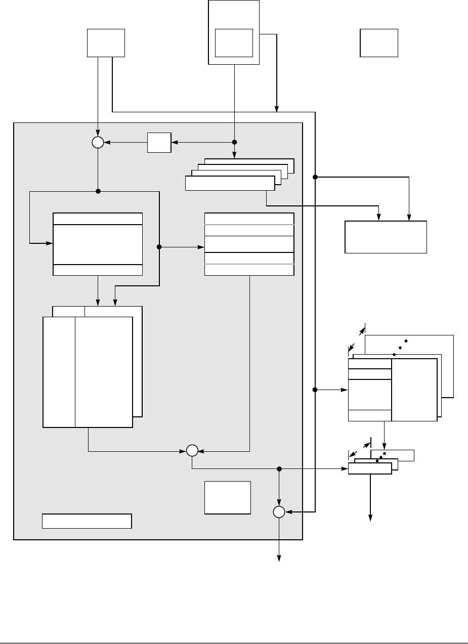
6-4 PowerPC 601 RISC Microprocessor User's Manual
Figure 6-1. MMU Block Diagram
Instruction
Unit
Integer
Unit BPU FPU
MMU
A20–A31
XITLB
Miss
LA0–LA19
LA0–LA19
ITLB
LA0–LA19
LA0–LA3
Select
0
15
Segment Registers
.
.
.
LA4–LA19
UTLB
0
127
BAT0U
BAT0L
•
•
BAT3U
BAT3L
0
3
BAT Array
PA0–PA19
Table
Search
Logic
SDR1 SPR25
PA0–PA31
Cache
8
TAGS
•
•
PA0–PA19
8
Compare
Cache
Hit/Miss
Select
0
63
+
X
ITLB hit accesses
arbitrate for cache
independently
ITLB Hit
A20–A31
ITLB Hit
PA0–PA19
LA0-LA14

Chapter 6. Memory Management Unit 6-5
For instruction accesses, the MMU first performs a lookup in the four entries of the ITLB
for the physical address translation. Instruction accesses that miss in the ITLB and data
accesses cause a lookup in the UTLB and BAT array for the physical address translation.
In most cases, the physical address translation resides in one of the TLBs and the physical
address bits are readily available to the on-chip cache. In the case where the physical
address translation misses in the TLBs, the 601 automatically performs a search of the
translation tables in memory using the information in the SDR1 and the corresponding
segment register.
6.1.3 Address Translation Mechanisms
The 601 supports the following four main types of address translation:
• Page address translation—translates the page frame address for a 4-Kbyte page size
• Block address translation—translates the block number for blocks that range in size
from 128 Kbyte to 8 Mbyte
• I/O controller interface address translation—used to generate I/O controller
interface accesses on the external bus
• Direct address translation—when address translation is disabled, the physical
address is identical to the logical address
Figure 6-2 shows the four main address translation mechanisms provided by the 601. The
segment registers shown in the figure control both the page and I/O controller interface
address translation mechanisms. When an access uses the page or I/O controller interface
address translation, one of the 16 on-chip segment registers is selected by the highest-order
logical address bits. A control bit in the corresponding segment register then determines if
the access is to memory (memory-mapped) or to the I/O controller interface space.
For memory accesses selected by the segment register, the segment register information is
used to generate the interim 52-bit virtual address. Page address translation corresponds to
the conversion of this virtual address into the 32-bit physical address used by the cache or
by external memory. In most cases, the physical address for the page resides in the UTLB
and is available for quick access. However, if the page address translation misses in the
UTLB, the 601 automatically searches the page tables in memory (using the virtual address
information and a hashing function) to locate the required physical address.
Block address translation occurs in parallel with page and I/O controller interface address
translation and is similar to page address translation, except that there are fewer upper-order
logical address bits to be translated into physical address bits (more lower-order address
bits (at least 17) are untranslated to form the offset into a block). Also, instead of segment
registers and a UTLB, block address translations use the on-chip BAT registers as a fully-
associative array. If the logical address of an access matches the corresponding field of a
BAT register, the information in the BAT register is used to generate the physical address;
in this case, the results of the page translation (occurring in parallel) are ignored.
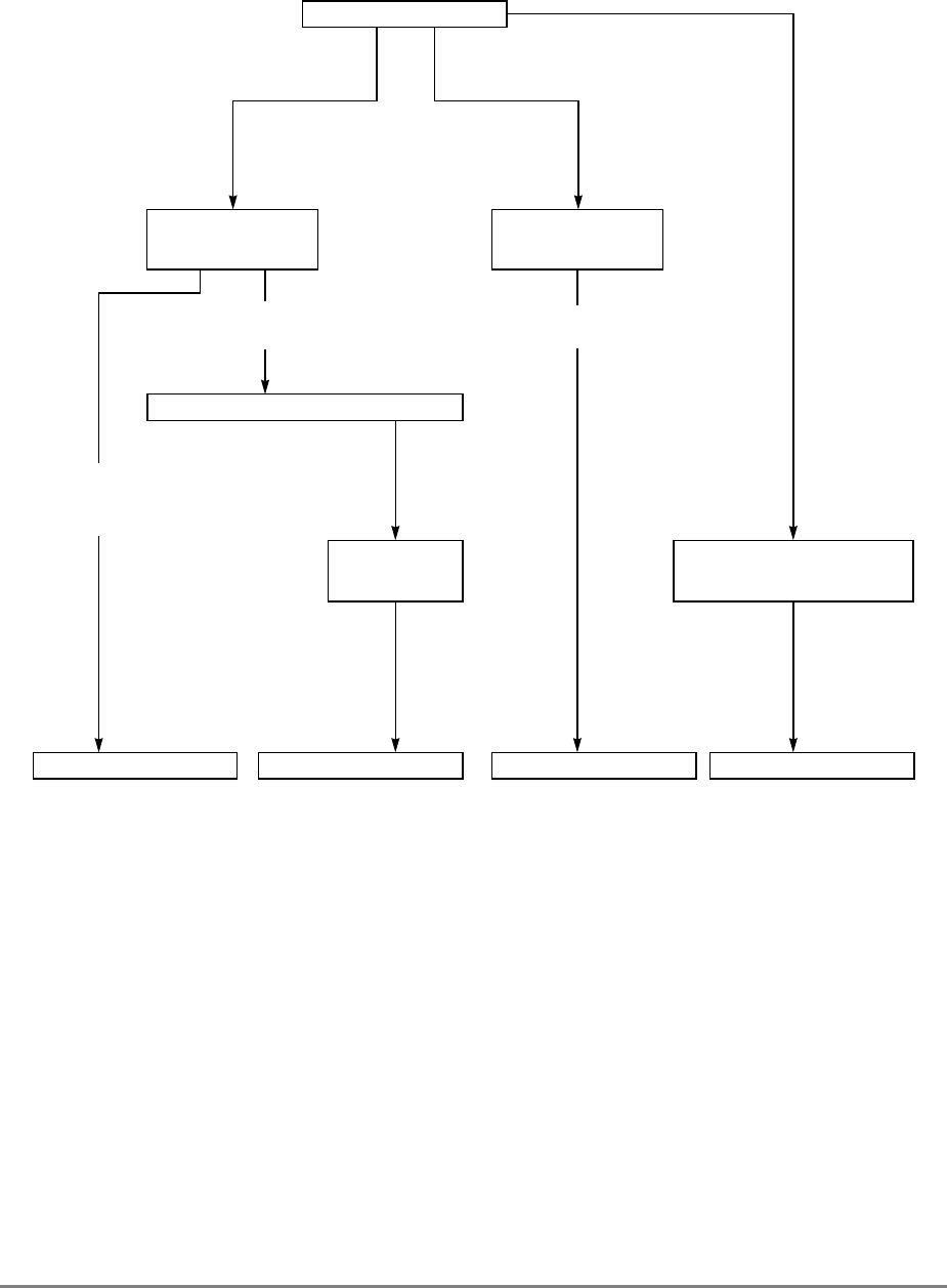
6-6 PowerPC 601 RISC Microprocessor User's Manual
Figure 6-2. Address Translation Types
I/O controller interface address translation is enabled when the I/O controller interface
translation control bit (T-bit) in the selected segment register (segment register selected by
the highest-order address bits) is set. In this case, the remaining information in the segment
register is interpreted as identifier information that is used with the remaining logical
address bits to generate the packets used in an I/O controller interface access on the external
interface; additionally, no UTLB lookup or page table search is performed and the BAT
array lookup results are ignored. For more information about the I/O controller interface
operations, see Section 9.6, “Memory- vs. I/O-Mapped I/O Operations.”
A special case of I/O controller interface address translation (not shown in Figure 6-2) is
supported that forces an I/O controller interface address translation to be interpreted as a
memory access (that is, it uses the usual memory access protocol rather than the I/O
031
Logical Address
051
Virtual Address
Segment Register
Select Match with BAT Reg-
isters
031
Physical Address
031
I/O Cont. I/F Address
031
Physical Address
031
Physical Address
Look up in
Page Table
Direct Address Translation
Logical Address = Physical Address
Address Translation Disabled*
* In the 601, I/O controller interface translation may
occur when data address translation is disabled.
Page
Address
I/O Controller
Interface Trans-
lation
Block Address
Translation

Chapter 6. Memory Management Unit 6-7
controller interface access protocol on the external interface). This occurs when a field in
the selected segment register (with the T-bit set) is encoded as memory-forced I/O
controller space. This feature effectively allows the specification of a 256-Mbyte “block”
of memory (with a common physical block number) with the use of only one segment
register, bypassing the page and block address translation and protection mechanisms
described above.
Direct address translation occurs when address translation is disabled; in this case the
physical address generated is identical to the logical address. The translation of addresses
for instruction and data accesses is enabled (and disabled) independently with the MSR[IT]
and MSR[DT] bits, respectively. Thus when the instruction unit generates an instruction
access, and instruction address translation is disabled (MSR[IT] = 0), the resulting physical
address is identical to the logical address and all other translation mechanisms are ignored.
When a data access occurs and MSR[DT] = 0, the resulting physical address is identical to
the logical address with one exception—I/O controller interface address translation for data
accesses is allowed, even when MSR[DT] = 0. In this case, the segment registers are used
in the same way as if translation were enabled. Note that this case of data accesses to the
I/O controller interface while MSR[DT] = 0 will not be supported in other PowerPC
processors.
6.1.4 Memory Protection Facilities
In addition to the translation of logical addresses to physical addresses, the MMU provides
access protection of supervisor areas from user access and can designate areas of memory
as read-only. Table 6-1 shows the four protection options supported by the 601.
Each of these options is enforced at the block or page level. Thus, the supervisor-only
option allows only read and write operations generated while the 601 is operating in
supervisor mode (corresponding to MSR[PR] = 0) to use the selected address translation
(block or page). User accesses that map into these blocks or pages cause an exception to be
taken.
As shown in the table, the supervisor-write-only option allows both user and supervisor
accesses to read from the selected area of memory but only supervisor programs can update
(write to) that area. There is also an option that allows both supervisor and user programs
read and write access (both user/supervisor option), and finally, there is an option to
Table 6-1. Access Protection Options
Option User Read User Write Supervisor
Read Supervisor
Write
Supervisor-only Not allowed Not allowed √√
Supervisor-write-only √Not allowed √√
Both user/supervisor √√√√
Both read-only √Not allowed √Not allowed

6-8 PowerPC 601 RISC Microprocessor User's Manual
designate an area of memory as read-only, both for user and supervisor programs (both
read-only option).
For I/O controller interface segments, the MMU calculates a “key” bit based on the
protection values programmed in the segment register, and the specific user/supervisor and
read/write information for the particular access. However, this bit is merely passed on to the
system interface to be transmitted in the context of the I/O controller interface protocol as
described in Section 9.6, “Memory- vs. I/O-Mapped I/O Operations.” The MMU does not
itself enforce any protection or cause any exception based on the state of the key bit for
these accesses. The I/O controller device or other external hardware can optionally use this
bit to enforce any protection required.
6.1.5 Page History Information
The 601 MMU also maintains reference (R) and change (C) bits in the page address
translation mechanism that can be used as history information relevant to the page. This
information can then be used by the operating system to determine which areas of memory
to write back to disk when new pages must be allocated in main memory. While these bits
are initially programmed by the operating system into the page table, the 601 automatically
updates these bits when required. Note that the updates to these bits in the page tables are
performed with standard read and write transactions on the bus (not locked read-modify-
write operations). However, when multiple 601 devices have shared access to the page
tables, the bit settings are guaranteed to be updated correctly.
6.1.6 General Flow of MMU Address Translation
When an instruction or data access is generated and the corresponding instruction or data
translation is disabled (MSR[IT] = 0 or MSR[DT] = 0), direct translation is used and the
access continues to the cache. When the selected segment register indicates that the access
is an I/O controller interface access, I/O controller interface address translation occurs. See
Section 6.5, “Selection of Address Translation Type” for more information regarding the
selection of address translation mode used for all cases.
For instruction accesses, if translation is enabled (MSR[IT] = 1), the ITLB is first checked
for a matching page or block address translation. If there is a miss, then the MMU uses the
block and page address translation mechanisms to find the address translation. Figure 6-3
shows the flow used to search for the block or page address translation.
Although the 601 performs the block and page TLB lookups simultaneously, the flow
diagram shows that if a BAT array hit occurs, that particular translation is performed
regardless of the results of the UTLB lookup. If the BAT array misses, the results of the
UTLB search are considered. If the UTLB hits, the page translation occurs and the physical
address bits are forwarded to the cache (if the access is cacheable).
Chapter 6. Memory Management Unit 6-9
Figure 6-3. MMU Block and Page Address Translation Flow
If the UTLB misses, the 601 automatically searches the page tables in memory. If the page
table entry (PTE) is successfully read, a new UTLB entry (and an ITLB entry for the
instruction access case) is created and the page translation is once again attempted. This
time, the UTLB (and ITLB for instruction access case) is guaranteed to hit. If the PTE is
not found by the table search operation, an instruction access or data access exception is
generated.
BAT array
Miss BAT array
Hit
Access Faulted
Generate 52-bit
Virtual Address
from Segment Reg-
Compare Virtual
Address with UTLB
Entries
Access
Protected
Translate Address
Access
Permitted
UTLB
Miss UTLB
Hit
Continue Access
to Cache
Access Faulted
Access Faulted
Logical Address
Generated
Select Segment
Register
Compare Address
with BAT array
(BAT Registers)
Translate Address
Continue Access
to Cache
Access
Protected Access
Permitted
PTE Found PTE Not
Found
Block/Page Address
Translation
Load UTLB Entry
See Figure 6-4
Perform Table
Search Operation

6-10 PowerPC 601 RISC Microprocessor User's Manual
Note that if either the BAT array or UTLB results in a hit, the access is qualified with the
appropriate protection bits. If the access is determined to be protected (not allowed), an
exception (instruction access or data access) is generated.
6.1.7 Memory/MMU Coherency Model
The memory model of the 601 provides the following features:
• Performance benefits of weak ordering of memory accesses
• Memory coherency among processors and between a processor and I/O devices
controlled at the block and page level
• Instructions that ensure a coherent and ordered memory state.
• Processor address order guaranteed
The memory implementations in 601 systems can take advantage of the performance
benefits of weak ordering of memory accesses between processors or between processors
and other external devices without any additional complications. The MMU assumes that
all accesses are ordered. Thus, the priority of accesses is determined at the external
interface in a way that provides maximum throughput for most cases.
In addition, at the system level, the memory coherency among processors and between a
processor and I/O devices is programmed through the following three mode control bits in
the MMU:
• Write-through (W bit)
• Caching-inhibited (I bit)
• Memory coherency (M bit)
Both the block and page address translation mechanisms contain the WIM bits for each
TLB entry; these bits are used to control all accesses that correspond to the particular block
or page. The four possible combinations of the W and M bits yield modes that are supported
for I = 0 (caching-allowed) as shown in Table 6-2. For the caching-inhibited (I = 1) case,
there are only two modes defined, corresponding to W=0/M=0, and W=0/M=1.
Table 6-2. Defined WIM Combinations
WIM
000
001
100
101
010
011

Chapter 6. Memory Management Unit 6-11
The 601 also provides instructions (the cache instructions, isync, sync, eieio, lwarx, and
stwcx.) to ensure a coherent and ordered memory state. These instructions are described in
Chapter 3, “Addressing Modes and Instruction Set Summary,” and in Chapter 10,
“Instruction Set.” Memory accesses performed by a single processor appear to complete
sequentially from the view of the programming model but may complete out of order with
respect to the ultimate destination in the memory hierarchy. Order is guaranteed at each
level of the memory hierarchy for accesses to the same address from the same processor.
Memory coherency can be enforced externally by a snooping bus design, a centralized
cache directory design, or other design that can take advantage of these coherency features.
6.1.8 Effects of Instruction Fetch on MMU
Speculative instruction execution occurs when the 601 executes instructions in advance in
case the result is needed. If subsequent events indicate that the speculative instruction
should not have been executed, the processor abandons the results produced by that
instruction. Typically, the 601 executes instructions speculatively when it has resources that
would otherwise be idle, so the operation is done at little or no cost.
The 601 executes computational instructions speculatively (beyond a branch instruction)
and performs instruction fetches speculatively (it fetches instructions ahead in the
instruction stream). However, the 601 does not execute any load or store instructions
speculatively. Speculative execution of computational instructions does not involve the
MMU.
To avoid instruction fetch delay, the processor typically fetches instructions in advance of
when they are needed. Such instruction fetching is speculative in that fetched instructions
may not be executed due to intervening branches or exceptions.
Instruction fetching from I/O controller interface segments (T = 1) only occurs from those
segments designated as memory-forced I/O controller interface segment. See Section 6.10,
“I/O Controller Interface Address Translation” for more information about I/O controller
interface segments.
Machine check exceptions that result from instruction fetching may be generated, even if
the instruction fetched would not have been executed because of a previous branch or
change in program flow. See Section 5.4.2, “Machine Check Exception (x'00200'),” for
more information on the machine check exception.
Memory in 601 systems is considered not “guarded” in the sense that fetching may occur
to any area of memory. For example, if a data area is adjacent to an instruction area of
memory, the 601 could fetch from that data area. Furthermore, if a word in that data area
contains the encoding for an unconditional branch instruction, the processor could even
continue to fetch from the address it interprets as the target of the branch. Care may be
required to prevent these situations, particularly if peripheral devices that cannot recover
from extraneous accesses reside in these areas. Areas of memory in other PowerPC

6-12 PowerPC 601 RISC Microprocessor User's Manual
processors may be designated as guarded within the MMU in that speculative operations
do not occur.
6.1.9 Breakpoint Facility
Through the use of the HIDx registers (HID1, HID2, and HID5), the 601 has the ability to
perform a breakpoint operation for both instruction and data accesses independently. For
instruction accesses, the logical addresses of instructions in decode are compared with the
address specified in the instruction address breakpoint register (IABR). If there is a match,
then the processor takes a run mode exception. Similarly, data breakpoints occur when the
logical address of a data access matches the address specified in the data address breakpoint
register (DABR) register. However, when a data address matches, the 601 takes a data
access exception.
The instruction and data breakpoint functionality is controlled by bit settings in the
601debug modes register (HID1). Various combinations and levels of breakpoints can be
enabled. Section 2.3.3.13, “601 Implementation-Specific HID Registers” describes the
breakpoint functionality provided in the 601. Note that these breakpoints occur completely
independently of the MSR[DT] and MSR[IT] bit settings.
6.1.10 MMU Exceptions Summary
In order to complete any memory access, the logical address must be translated to a
physical address. An MMU exception condition occurs if this translation fails for one of the
following reasons:
• There is no valid entry in the page table for the page specified by the logical address
(and segment register).
• An address translation is found but the access is not allowed by the memory
protection mechanism.
Most MMU exception conditions cause either the instruction access exception or the data
access exception to be taken. The state saved by the 601 for each of these exceptions
contains information that identifies the address of the failing instruction. Refer to
Chapter 5, “Exceptions,” for a more detailed description of exception processing.
There are 11 types of conditions that can cause an MMU exception to occur. The exception
conditions map to the 601 exception as shown in Table 6-3. The only MMU exception
condition recognized when MSR[IT] = 0 is the instruction breakpoint match condition. The
only exception conditions that occur when MSR[DT] = 0 are the data breakpoint match
condition and the conditions that cause the alignment exception for data accesses. For more
detailed information about the conditions that cause the alignment exception (in particular
for string/multiple instructions) see 5.4.6, “Alignment Exception (x'00600').”

Chapter 6. Memory Management Unit 6-13
Table 6-3. MMU Exception Conditions/Exception Mapping
Condition Description Exception
Page fault No matching PTE found in page
tables I access: instruction access exception
SRR1[1] = 1
D access: data access exception
DSISR[1] = 1
Block protection violation Conditions described in
Table 6-7 for block I access: instruction access exception
SRR1[4] = 1
D access: data access exception
DSISR[4] =1
Page protection violation Conditions described in
Table 6-7 for page I access: instruction access exception
SRR1[4] = 1
D access: data access exception
DSISR[4] = 1
dcbz with W or I = 1 dcbz instruction to write-through
or cache-inhibited segment or
block
Alignment exception
Instruction access to I/O
controller interface space Attempt to fetch instruction when
SR[T] = 1, SR[BUID] ≠ '07F' Instruction access exception
Causes no SRR1 bits to be set*
lwarx, stwcx., lscbx instruction
to I/O controller interface space Reservation instruction or load
string and compare byte
instruction when SR[T] = 1,
SR[BUID] ≠ '07F'
Data access exception
DSISR[5] = 1
Floating-point load or store to I/O
controller interface space FP memory access when
SR[T] = 1, SR[BUID] ≠ '07F' Alignment exception
Instruction breakpoint match Instruction address matches the
address in HID2 Run mode exception
Data breakpoint match Data address matches the
address in HID5 Data access exception
DSISR[9] = 1
Operand misalignment:
256-Mbyte boundary Operand crosses a 256-Mbyte
boundary (regardless of
MSR[DT] and MSR[IT] setting)
Alignment exception
Operand misalignment:
4-Kbyte boundary Translation enabled and operand
crosses a 4 Kbyte boundary
(page or block)
Alignment exception
* This is only true for the 601; other PowerPC processors will set SRR1[3] for this case.

6-14 PowerPC 601 RISC Microprocessor User's Manual
6.1.11 MMU Instructions and Register Summary
Table 6-4 summarizes the instructions of the 601 that specifically control the MMU. For
more detailed information about the instructions, refer to Chapter 10, “Instruction Set.”
Table 6-5 summarizes the registers that the operating system uses to program the MMU.
These registers are accessible to supervisor-level software only. These registers are
described in detail in Chapter 2, “Registers and Data Types.”
6.1.12 TLB Entry Invalidation
The UTLB (and ITLB) maintains on-chip copies of the PTEs that are resident in physical
memory. The 601 has the ability to invalidate resident UTLB entries through the use of the
tlbie instruction. Additionally, the tlbie instruction optionally (as programmed in the HID1
register—see Section 2.3.3.13.2, “601 Debug Modes Register—HID1”) causes a TLB
invalidate broadcast (an address-only operation) to occur on the system bus so that other
processors also invalidate their resident copies of the matching PTE. See Chapter 10,
Table 6-4. Instruction Summary—Control MMU
Instruction Description
mtsr SR,rS Move to Segment Register
SR[SR#]← rS
mtsrin rS,rB Move to Segment Register Indirect
SR[rB[0–3]]←rS
mfsr rD,SR Move from Segment Register
rD←SR[SR#]
mfsrin rD,rB Move from Segment Register Indirect
rD←SR[rB[0–3]]
tlbie rB Translation Lookaside Buffer Invalidate Entry
If TLB hit (for logical address specified as rB), TLB[V]←0
Causes TLBI operation on the system bus.
Table 6-5. MMU Registers
Register Description
Segment registers
(SR0–SR15) The sixteen 32-bit segment registers are present only in 32-bit implementations of
the PowerPC architecture. Figure 6-13 shows the format of a segment register. The
fields in the segment register are interpreted differently depending on the value of bit
0. The segment registers are accessed by the mtsr, mtsrin, mfsr, and mfsrin
instructions
BAT registers
(BAT0U–BAT3U and
BAT0L–BAT3L)
The 601 includes eight block-address translation registers (BATs), organized as four
pairs (BAT0U–BAT3U and BAT0L–BAT3L). Figure 6-6 and Figure 6-7 show the
format of the upper and lower BAT registers. These are special-purpose registers
that are accessed by the mtspr and mfspr instructions.
Table search description
register 1
(SDR1)
The 32-bit table search description register 1 (SDR1) specifies the variables used in
accessing the page tables in memory. This is a special-purpose register that is
accessed by the mtspr and mfspr instructions.

Chapter 6. Memory Management Unit 6-15
“Instruction Set” for detailed information about the tlbie instruction and Section 9.3.2.2.1,
“Transfer Type (TT0–TT4) Signals” for more information on address-only bus
transactions.
The snooping hardware of the 601 detects when other processors perform a TLB invalidate
broadcast on the bus. In the case of a hit with an on-chip UTLB entry, the 601 performs the
following:
1. Prevents execution of any new load, store, cache control or tlbie instructions and
prevents any new reference or change bit updates
2. Waits for completion of any outstanding memory operations (including updates to
the reference and change bits associated with the entry to be invalidated)
3. Invalidates the two entries (both associativity classes) in the UTLB indexed by the
matching address
4. Invalidates all entries in the ITLB
5. Resumes normal execution
6.2 ITLB Description
The 601 implements a four-entry, fully-associative TLB for storing the most recently used
instruction address translations. The 601 automatically generates an entry in the ITLB
whenever the page or block address translation mechanism generates a new logical-to-
physical mapping for a page or block used for instruction fetch. Each ITLB entry can
contain the translation information for either an entire block or a page. The 601 uses the
ITLB for address translation of instruction accesses when MSR[IT] = 1.
The instruction unit accesses the ITLB independently of the rest of the MMU. Therefore,
when instruction accesses hit in the ITLB, the page and block translation mechanisms are
available for use by data accesses simultaneously.
The 601 also automatically maintains the integrity of the entries in the ITLB by purging the
contents when any of the following conditions occur:
• An mtsr or mtsrin instruction is executed
• An mtspr instruction that modifies any of the BAT registers is executed
•A tlbie instruction is executed
• A TLB invalidate operation is detected on the system interface (via snooping)
Since these conditions potentially cause the MMU context to be changed, the ITLB entries
may no longer be valid. Therefore, the MMU automatically detects these conditions and
clears all the valid bits in the ITLB array.
Finally, the 601 replaces ITLB entries on a least-recently-used (LRU) basis. Throughout the
remainder of this chapter, the page and block translations that are resident in the ITLB are
described within the context of page address translation and block address translation, as

6-16 PowerPC 601 RISC Microprocessor User's Manual
the contents of the ITLB are always a subset of translations that were generated for the
UTLB and/or the BAT array.
Accesses to the ITLB are transparent to the executing program, except that hits in the ITLB
contribute to a higher overall instruction throughput by allowing data translations to occur
in parallel.
6.3 Memory/Cache Access Modes
All instruction and data accesses are performed under the control of the three mode control
bits that are defined by the MMU for each access. The three mode control bits, W, I, and M,
have the following effects. The W and I bits control how the processor performing the
access uses its own cache. The M bit specifies whether the processor performing the access
must use the memory coherency protocol to ensure that all copies of the addressed memory
location are consistent.
When an access requires coherency, the processor performing the access must inform the
coherency mechanisms throughout the system that the access requires memory coherency.
The M bit determines the kind of access performed on the bus (global or local). Note that
these mode-control bits are relevant only when an address is translated and are not saved
along with data in the on-chip cache (for cacheable accesses). Once an access has been
translated, the MESI bits in the cache then control the coherency to that cache location
made by subsequent accesses from other processors. See Chapter 4, “Cache and Memory
Unit Operation,” for more information about cache accesses.
The operating system programs the WIM bits for each page or block as required. The WIM
bits reside in the BAT registers for block address translation and in the PTEs for page
address translation. Thus these bits are programmed as follows:
• The operating system uses the mtspr instruction to program the WIM bits in the
BAT registers for block address translation.
• The operating system programs the WIM bits for each page into the PTEs in system
memory as it sets up the page tables.
Note that for accesses performed with direct address translation (MSR[IT] = 0 or
MSR[DT] = 0 for instruction or data access, respectively), the WIM bits are automatically
generated as b'001' (the data is write-back, caching is enabled, and memory coherency is
enforced).
6.3.1 Write-Through Bit (W)
When an access is designated as write-through (W = 1), if the data is in the cache, a store
operation updates the cached copy of the data. In addition, the update is written to the
external memory location (as described below). Store-combining compiler optimizations
are allowed for write-through accesses except when the store instructions are separated by
a sync instruction. Note that a store operation that uses the write-through mode may cause
any part of valid data in the cache to be written back to main memory.

Chapter 6. Memory Management Unit 6-17
The definition of the external memory location to be written to in addition to the on-chip
cache depends on the implementation of the memory system but can be illustrated by the
following examples:
• RAM—The store must be sent to the RAM controller to be written into the target
RAM.
• I/O device—The store must be sent to the I/O control hardware to be written to the
target register or memory location.
In systems with multilevel caching, the store must be written to at least a depth in the
memory hierarchy that is seen by all processors and devices.
Accesses that correspond to W = 0 are considered write-back. For this case, although the
store operation is performed to the cache, it is only made to external memory when a copy-
back operation is required. Use of the write-back mode (W = 0) can improve overall
performance for areas of the memory space that are seldom referenced by other masters in
the system. See Chapter 4, “Cache and Memory Unit Operation,” for more information
about cache accesses.
6.3.2 Caching Inhibited Bit (I)
If I = 1, the memory access is completed by referencing the location in main memory,
completely bypassing the on-chip cache of the 601. During the access, the accessed
location is not loaded into the cache nor is the location allocated in the cache. If a copy of
the accessed data is in the cache, that copy is not updated, flushed, or invalidated. Data
accesses from more than one instruction may not be combined (as a compiler optimization)
for cache-inhibited operations.
6.3.3 Memory Coherence Bit (M)
This mode control bit is provided to allow improved performance in systems where
hardware-enforced coherency is relatively slow, and software is able to enforce the required
coherency. When M = 0, the 601 does not enforce data coherency. When M = 1, the
processor enforces data coherency and the corresponding access is considered to be a
global access. When the M bit is set, and the access is performed to external memory, the
GBL signal is asserted and the access is designated as global. Other processors affected by
the access must then respond to this global access and signal whether it is shared. If the data
in another processor is modified, then address retry is signaled.

6-18 PowerPC 601 RISC Microprocessor User's Manual
6.3.4 W, I, and M Bit Combinations
Table 6-6 summarizes the six combinations of the WIM bits defined for the 601..
If the system software maps the same physical page with multiple page table entries that
have different W, I, or M values, the results of the translation are undefined.
Table 6-6. Combinations of W, I, and M Bits
WIM Setting Meaning
000 Data may be cached.
Loads or stores whose target hits in the cache use that entry in the cache.
Exclusive ownership of the block containing the target location is not required for store accesses
and coherency operations for the block do not occur when fetching the block, storing it back, or
changing its state from shared to exclusive.
001 Data may be cached.
Loads or stores whose target hits in the cache use that entry in the cache.
Memory coherency is enforced by hardware as follows: exclusive ownership of the block
containing the target location is required before store accesses are allowed. When fetching the
block, the processor indicates on the bus transaction that coherency is to be enforced. If the state
of the block is shared-unmodified, the processor must gain exclusive use of the block before
storing into it.
This encoding is used for addresses translated via direct address translation (MSR[IT] = 0 or
MSR[DT] = 0).
010 Caching is inhibited.
The access is performed to external memory, completely bypassing the cache.
Hardware enforced memory coherency is not required.
011 Caching is inhibited.
The access is performed to external memory, completely bypassing the cache.
Memory coherency must be enforced by external hardware (601 asserts GBL).
100 Data may be cached.
Loads whose target hits in the cache use that entry in the cache.
Stores are written to external memory. The target location of the store may be cached and is
updated on a hit.
Exclusive ownership of the block containing the target location is not required for store accesses
and coherency operations for the block do not occur when fetching the block, storing it back, or
changing its state from shared to exclusive.
101 Data may be cached.
Loads whose target hits in the cache use that entry in the cache.
Stores are written to external memory. The target location of the store may be cached and is
updated on a hit.
Memory coherency is enforced by hardware as follows: exclusive ownership of the block
containing the target location is required before store accesses are allowed. When fetching the
block, the processor indicates on the bus transaction that coherency is to be enforced. If the state
of the block is shared, the processor must gain exclusive use of the block before storing into it.

Chapter 6. Memory Management Unit 6-19
6.4 General Memory Protection Mechanism
Another aspect of the MMU that is programmed at the block and page level is the memory
protection option. The memory protection mechanism allows selectively granting read
access, granting read/write access, and prohibiting access to areas of memory based on a
number of control criteria.
The memory protection mechanism is used by both the block and page address translation
mechanisms in a similar way, as described here. However, the protection mechanism in the
601 differs from that defined in the PowerPC architecture in that the PowerPC operating
environment architecture defines valid bits rather than key bits for the block address
translation mechanism. For specific information unique to block address translation, refer
to Section 6.7.4, “Block Memory Protection.” For specific information unique to page
address translation, refer to Section 6.8.5, “Page Memory Protection.”
For both block and page address translation in the 601, the memory protection mechanism
is controlled by the following:
• MSR[PR], which defines the mode of the access as follows:
— MSR[PR] = 0 corresponds to supervisor mode
— MSR[PR] = 1 corresponds to user mode
• Ks and Ku, the supervisor and user key bits, which define the key for the block or
page
• The PP bits, which define the access options for the block or page
The key bits (Ks and Ku) and the PP bits are located as follows for block and page address
translation:
• Ks and Ku are located in the upper BAT register for block address translation and in
the selected segment register for a page address translation.
• The PP bits are located in the upper BAT register for block address translation and
in the PTE for page address translation.
The key bits, the PP bits, and the MSR[PR] bit are used as follows:
• When an access is generated, one of the key bits (Ks or Ku) is selected to be the key
as follows:
— For supervisor accesses (MSR[PR] = 0), the Ks bit is used and Ku is ignored
— For user accesses (MSR[PR] = 1), the Ku bit is used and Ks is ignored
• The selected key is used with the PP bits to determine if the load or store access is
allowed.

6-20 PowerPC 601 RISC Microprocessor User's Manual
Table 6-7 shows the types of accesses that are allowed for the general case (all possible Ks,
Ku, and PP bit combinations).
Thus, the conditions that cause a protection violation are depicted in Table 6-8. Any access
attempted (read or write) when the key = 1 and PP = 00, results in a protection violation
exception condition. When key = 1 and PP = 01, an attempt to perform a write access causes
a protection violation exception condition. When PP = 10, all accesses are allowed, and
when PP = 11, write accesses always cause an exception. The 601 takes either the
instruction access exception or the data access exception (for an instruction or data access,
respectively) when there is an attempt to violate the memory protection.
Although any combination of the Ks, Ku and PP bits is allowed, the Ks and Ku bits can be
programmed so that the value of the key bit for Table 6-7 directly matches the MSR[PR]
bit for the access. In this case, the encoding of Ks = 0 and Ku = 1 is used for the BAT array
entry or the PTE, and the PP bits then enforce the protection options shown in Table 6-9.
Table 6-7. Access Protection Control with Key
Key1PP2Block or Page Type
0 00 Read/write
0 01 Read/write
0 10 Read/write
0 11 Read only
1 00 No access
1 01 Read only
1 10 Read/write
1 11 Read only
1 Ks or Ku selected by state of MSR[PR]
2 PP protection option bits in BAT array entry or
PTE
Table 6-8 . Exception Conditions for Key and PP Combinations
Key PP Prohibited
Accesses
1 00 Read/write
1 01 Write
x 10 None
x 11 Write

Chapter 6. Memory Management Unit 6-21
However, if the setting Ks = 1 is used, supervisor accesses are treated as user reads and
writes with respect to Table 6-9. Likewise, if the setting Ku = 0 is used, user accesses to the
block or page are treated as supervisor accesses in relation to Table 6-9. Therefore, by
modifying one of the key bits (in either the BAT register or the segment register), the way
the 601 interprets accesses (supervisor or user) in a particular block or segment can easily
be changed. Note, however, that only supervisor programs can modify the key bits for the
block or the segment as access to the BAT registers and the segment registers is privileged.
When the memory protection mechanism prohibits a reference, one of the following occurs,
depending on the type of access that was attempted:
• For data accesses, a data access exception is generated and bit 4 of DSISR is set. If
the access is a store, bit 6 of DSISR is also set.
• For instruction accesses, an instruction access exception is generated and bit 4 of
SRR1 is set.
See Chapter 5, “Exceptions,” for more information about these exceptions.
6.5 Selection of Address Translation Type
A description of the selection flow for determining the type of address translation to be
performed is provided in Figure 6-4. The selection of address translation type differs for
instruction and data accesses in that I/O controller interface accesses are not allowed for
instruction accesses when instruction address translation is disabled, and I/O controller
interface accesses for data occur without regard for the enabling of data address translation.
6.5.1 Address Translation Selection for Instruction Accesses
Addresses for instruction accesses are translated under control of the IT bit of MSR. When
any context-synchronizing event occurs within the 601, any fetched instructions are
discarded and refetched using the updated state of MSR[IT].
Table 6-9. Access Protection Encoding of PP Bits
PP
Field Option User Read
(Key = 1) User Write
(Key = 1)
Supervisor
Read
(Key = 0)
Supervisor
Write
(Key = 0)
00 Supervisor-only Not allowed Not allowed √√
01 Supervisor-write-only √Not allowed √√
10 Both user/supervisor √√√√
11 Both read-only √Not allowed √Not allowed
6-22 PowerPC 601 RISC Microprocessor User's Manual
Figure 6-4. Address Translation Type Selection
6.5.1.1 Instruction Address Translation Disabled: MSR[IT] = 0
When instruction address translation is disabled, designated by MSR[IT] = 0, the logical
address is interpreted as described in Section 6.6, “Direct Address Translation.”
6.5.1.2 Instruction Address Translation Enabled: MSR[IT] = 1
When instruction address translation is enabled (MSR[IT] = 1), instruction fetching occurs
under control of one of the following address translation mechanisms:
• Page address translation
• Block address translation
Note that for either of these translation mechanisms, the ITLB is first checked for the
address translation. If the ITLB misses, then the corresponding segment register is accessed
to see if the access is to the I/O controller interface space. If the access is not to the I/O
controller interface space, the page and block address translation mechanisms are used as
shown in Figure 6-3.
Instruction Access Data Access
Logical Address
Generated
Select Segment
Register
Translation Enabled
(MSR[DT]=1) Translation Disabled
(MSR[DT]=0)
Translation Enabled
(MSR[IT]=1) Translation Disabled
(MSR[IT]=0)
Perform Direct
Translation
Perform Lookup
in ITLB
ITLB
Miss
ITLB
Hit
Extract Physical
Address from ITLB Select Segment
Register
Continue Access
to Cache Perform Direct
Translation
Perform I/O Cont.
I/F Translation
Perform Block or Page
Address Translation
Perform I/O Cont.
I/F Translation
otherwise (T=0)
Not I/O Cont. I/F
Address (T=0)
I/O Cont. I/F
Address (T=1)
I/O Cont. I/F
Address (T=1)

Chapter 6. Memory Management Unit 6-23
In most cases, instructions cannot be fetched from the I/O controller interface segments and
attempting to fetch an instruction from an I/O controller interface segment causes an
instruction access exception. However, instruction fetches are allowed when the address
translation maps to segments with the T bit set (I/O controller interface segment) and with
the memory-forced I/O controller interface encoding. This case is described in more detail
in Section 6.10.4, “Memory-Forced I/O Controller Interface Accesses.”
6.5.2 Address Translation Selection for Data Accesses
As shown in Figure 6-4, for data accesses, the corresponding segment register is selected
independent of the DT bit of MSR. Addresses for data accesses are translated first under
control of the T bit of the selected segment register. If T = 1, the translation is to an I/O
controller interface segment. Otherwise, the translation is governed by the state of the DT
bit of MSR. When the state of MSR[DT] changes, subsequent accesses are made using the
new state of MSR[DT].
6.5.2.1 I/O Controller Interface Address Translation: T = 1 in Segment
Register
I/O controller interface segments are used independently of MSR[DT]. When the segment
register indexed by the upper-order logical address bits has the T bit set, the access is
considered an I/O controller interface access and the I/O controller interface protocol of the
external interface is used to perform the access to I/O controller space.
Note, however, that an x'07F' encoding in the BUID field of the segment register defines an
access as a memory-forced I/O controller interface access. In this case, the memory
protocol is used on the external interface. See Section 6.10, “I/O Controller Interface
Address Translation” for more information on address translation for I/O controller
interface accesses.
6.5.2.2 Data Translation Disabled: MSR[DT] = 0
When MSR[DT] = 0, the logical address is interpreted as described in Section 6.6, “Direct
Address Translation.” Note that as shown in Figure 6-4, the determination of whether the
address maps to an I/O controller interface segment occurs prior to the checking of
MSR[DT]. Therefore, I/O controller interface address translation occurs independently of
MSR[DT] for data accesses. The attempted execution of the eciwx or ecowx instructions
while MSR[DT] = 0 causes boundedly undefined results.
6.5.2.3 Data Translation Enabled: MSR[DT] = 1
When data address translation is enabled (MSR[DT] = 1), data accesses employ one of the
following translation mechanisms:
• Page address translation
• Block address translation
The block and page address translation mechanisms locate the physical address for the
access as described in Figure 6-3.

6-24 PowerPC 601 RISC Microprocessor User's Manual
6.6 Direct Address Translation
If address translation is disabled (MSR[IT] = 0 or MSR[DT] = 0) for a particular access
(fetch, load, or store), the logical address is treated as the physical address and is passed
directly to the memory subsystem as a direct address translation.
The addresses for accesses that occur in direct translation mode bypass all memory
protection checks as described in Section 6.4, “General Memory Protection Mechanism,”
and do not cause the recording of reference and change information (described in
Section 6.8.4, “Page History Recording”). Such accesses are performed as though the
memory access mode bits (“WIM”) were 001. That is, the cache is write-back and system
memory does not need to be updated (W = 0), caching is enabled (I = 0), and data coherency
is enforced with memory, I/O, and other processors (caches) (M = 1 so data is global).
Whenever an exception occurs, the 601 clears both the MSR[IT] and MSR[DT] bits.
Therefore, at least at the beginning of all exception handlers (including reset), the 601
operates in direct address translation mode for instruction accesses (and data accesses that
do not map to I/O controller interface space). If address translation is required for the
exception handler code, the software must explicitly enable address translation by
accessing the MSR as described in Chapter 2, “Registers and Data Types.”
Note that when translation is disabled, I/O controller interface segments can still be used
for data accesses as the T bit of the segment registers is checked and segment registers with
T = 1 are used independently of MSR[DT].
Note also that an attempt to fetch from, load from, or store to a physical address that is not
physically present in the system may cause a machine check exception (or even a checkstop
condition), depending on the response by the system for this case. See Section 5.4.2,
“Machine Check Exception (x'00200'),” for more information on machine check
exceptions.
6.7 Block Address Translation
The block address translation (BAT) mechanism in the 601provides a way to map ranges of
logical addresses larger than a single page into contiguous areas of physical memory. Such
areas can be used for data that is not subject to normal virtual memory handling (paging),
such as a memory-mapped display buffer or an extremely large array of numerical data.
The implementation of block address translation in the 601 including the block protection
mechanism is described followed by a block translation summary with a detailed flow
diagram.
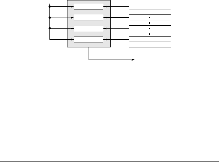
Chapter 6. Memory Management Unit 6-25
6.7.1 BAT Array Organization
The block address translation mechanism in the 601 is implemented as a software-
controlled array (BAT array). The BAT array maintains the address translation information
for four blocks of memory. The BAT array in the 601 is maintained by the system software
and is implemented as a set of eight special-purpose registers (SPRs). Each block is defined
by a pair of SPRs called upper and lower BAT registers.
The BAT registers can be read from or written to by the mfspr and mtspr instructions;
access to the BAT registers is privileged. Section 6.7.3, “BAT Register Implementation of
BAT Array,” gives more information about the BAT registers. Note that the BAT array
entries are completely ignored for TLB invalidate operations detected on the system bus
and in the execution of the tlbie instruction.
Figure 6-5 shows the organization of the BAT array. Four pairs of BAT registers are
provided for translating instruction and data addresses. These four pairs of BAT registers
comprise the four-entry fully-associative BAT array (each BAT array entry corresponds to
a pair of BAT registers). The BAT array is fully-associative in that all four entries are
compared with the logical address of the access to check for a match simultaneously.
Figure 6-5. BAT Array Organization
Each pair of BAT registers defines the starting address of a block in the logical address
space, the size of the block, and the start of the corresponding block in physical address
space. If a logical address is within the range defined by a pair of BAT registers, its physical
address is defined as the starting physical address of the block plus the lower order logical
address bits.
Blocks are restricted to a finite set of sizes, from 128 Kbytes (217 bytes) to 8 Mbytes (223
bytes). The starting address of a block in both logical address space and physical address
space is defined as a multiple of the block size.
Unmasked bits of LA0–LA14
(Instruction or Data Access)
BAT array
Compare BLPI
Compare
Compare
Compare
BAT0U
BAT0L
BAT3U
BAT3L
SPR528
SPR535

6-26 PowerPC 601 RISC Microprocessor User's Manual
Because the BAT array entries are used for both instruction and data access, if the same
memory address is to be mapped for both instruction fetching and data load and store
operations, the address mapping must only be loaded into one register pair.
It is an error for system software to program the BAT registers such that a logical address
is translated by more than one BAT pair. If this occurs, the results are undefined and may
include a spurious violation of the memory protection mechanism, a machine check
exception, or a check stop condition.
6.7.2 Recognition of Addresses in BAT Array
The BAT array (BAT registers) is accessed in parallel with segmented address translation
to determine whether a particular logical address corresponds to a block defined by the BAT
array. If a logical address is within a valid BAT area, the physical address for the memory
access is determined, as described in Section 6.7.5, “Block Physical Address Generation.”
Block address translation is enabled only when address translation is enabled
(MSR[IT] = 1 and/or MSR[DT] = 1) and only when the indexed segment register specifies
T = 0. That is, the BAT mechanism in the 601 does not apply to I/O controller interface
segments (T = 1). When the segment register has T = 1, the segment register translation is
used. (This is true for both I/O controller interface segments and memory-forced I/O
controller interface segments.) Note, however, that this differs from other PowerPC
processors, as the PowerPC operating environment architecture defines that a matching
BAT array entry always takes precedence over any segment register translation,
independent of the setting of the SR[T] bit.
The BAT registers and the segmented address translation mechanism can be programmed
such that a particular logical address is within a BAT area and that logical address also has
a segment register translation that corresponds to page address translation (T = 0 in the
segment register). When this occurs, the block address translation is used as shown in
Table 6-10 and the segment address translation is ignored.
Additionally, a block can be defined to overlay part of a segment such that the block portion
is non-paged although the rest of the segment is pageable. This allows non-paged areas to
be specified within a segment, and PTEs for the part of the segment overlaid by the block
are not required.
Table 6-10. Address Translation Precedence for Blocks and Segments
Segment Register
T bit Address Translation
0 Matching BAT array entry prevails
1 Segment register prevails

Chapter 6. Memory Management Unit 6-27
6.7.3 BAT Register Implementation of BAT Array
Recall that the BAT array is comprised of four entries used for instruction accesses and data
accesses. Each BAT array entry consists of a pair of BAT registers—an upper and a lower
BAT register for each entry. The BAT registers are accessed with the mtspr and mfspr
instructions and are only accessible to supervisor-level programs. See Section 3.7,
“Processor Control Instructions,” for a list of simplified mnemonics for use with the BAT
registers.
Figure 6-6 shows the format of the upper BAT registers and Figure 6-7 shows the format of
the lower BAT registers. The format and bit definitions of the upper and lower BAT registers
in the 601 differs from that of the BAT registers in other PowerPC processors.
Figure 6-6. Format of Upper BAT Registers
.
Figure 6-7. Format of Lower BAT Registers
The BAT registers contain the logical to physical address mappings for blocks of memory.
This mapping information includes the logical address bits that are compared with the
logical address of the access, the memory/cache access mode bits (WIM) and the protection
bits for the block. In addition, the size of the block and the starting address of the block are
defined by the block page number and block size mask fields.
Table 6-11 describes the bits in the upper and lower BAT registers.
BLPI 0 0 0 0 0 0 0 0 0 0 WIM KSKUPP
0141524252728293031
Reserved
PBN 0 0 0 0 0 0 0 0 0 0 V BSM
Reserved
0141524252631

6-28 PowerPC 601 RISC Microprocessor User's Manual
The BSM field in the lower BAT register is a mask that encodes the size of the block.
Table 6-12 defines the bit encodings for the BSM field of the lower BAT register. Note that
the range of block sizes is a subset of that defined by the PowerPC architecture.
Table 6-11. BAT Registers—Field and Bit Descriptions
Register Bits Name Description
Upper
BAT
Registers
0–14 BLPI Block logical page index. This field is compared with bits 0–14 of the logical
address to determine if there is a hit in that BAT array entry.
15–24 — Reserved
25–27 WIM Memory/cache access mode bits
W Write-through
I Caching-inhibited
M Memory coherence
For detailed information about the WIM bits, see Section 6.3, “Memory/Cache
Access Modes."
28 Ks Supervisor mode key. This bit interacts with MSR[PR] and the PP field to
determine the protection for the block. For more information, see Section 6.4,
“General Memory Protection Mechanism."
29 Ku User mode key. This bit also interacts with MSR[PR] and the PP field to
determine the protection for the block. For more information, see Section 6.4,
“General Memory Protection Mechanism."
30–31 PP Protection bits for block. This field interacts with MSR[PR] and the Ks or Ku
to determine the protection for the block as described in Section 6.4,
“General Memory Protection Mechanism."
Lower
BAT
Registers
0–14 PBN Physical block number. This field is used in conjunction with the BSM field to
generate bits 0-14 of the physical address of the block.
15–24 — Reserved
25 V BAT register pair (BAT array entry) is valid if V = 1
26–31 BSM Block size mask (0...5). BSM is a mask that encodes the size of the block.
Values for this field are listed in Table 6-12.
Table 6-12. Lower BAT Register Block Size Mask Encodings
Block Size BSM Encoding
128 Kbytes 00 0000
256 Kbytes 00 0001
512 Kbytes 00 0011
1 Mbyte 00 0111
2 Mbytes 00 1111
4 Mbytes 01 1111
8 Mbytes 11 1111

Chapter 6. Memory Management Unit 6-29
Only the values shown in Table 6-12 are valid for BSM. A logical address is determined to
be within a BAT area if the appropriate bits (determined by the BSM field) of the logical
address matches the value in the BLPI field of the upper BAT register, and if the valid bit
(V) of the corresponding lower BAT register is set.
The boundary between the strings of zeros and ones in the BSM field determines the bits
of the logical address that are used in the comparison with the BLPI field to determine if
there is a hit in that BAT array entry. The rightmost bit of the BSM field is aligned with bit
14 of the logical address; bits of the logical address corresponding to ones in the BSM field
are then forced to zero for the comparison.
The value loaded into the BSM field determines both the length of the block and the
alignment of the block in both logical address space and physical address space. The values
loaded into the BLPI and PBN fields must have at least as many low-order zeros as there
are ones in BSM.
6.7.4 Block Memory Protection
If a logical address is determined to be within a block defined by the BAT array, the access
is next validated by the memory protection mechanism. If this protection mechanism
prohibits the access, a block protection violation exception condition (data access exception
or instruction access exception) is generated.
The block protection mechanism provides protection at the granularity defined by the block
size (128 Kbyte to 8 Mbyte) and is described in Section 6.4, “General Memory Protection
Mechanism.”
The Ks, Ku, and PP bits are located in the upper BAT register for block address translation.
Note, however, that the block protection defined by the PowerPC architecture’s operating
environment implements valid bits rather than key bits in defining user and supervisor
blocks.
When the block protection mechanism prohibits a reference, one of the following occurs,
depending on the type of access that was attempted:
• For data accesses, a data access exception is generated and bit 4 of DSISR is set. If
the access was a store, bit 6 of DSISR is additionally set.
• For instruction accesses, an instruction access exception is generated and bit 4 of
SRR1 is set.
6.7.5 Block Physical Address Generation
If the block protection mechanism validates the access, a physical address is formed as
shown in Figure 6-8. Bits in the logical address corresponding to ones in the BSM field,
concatenated with the 17 lower-order bits of the logical address form the offset within the
block of memory in the case of a hit. Bits in the logical address corresponding to zeros in
the BSM field are then logically ORed with the corresponding bits in the PBN field to form
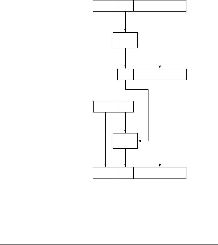
6-30 PowerPC 601 RISC Microprocessor User's Manual
the next higher-order bits of the physical address. Finally, the highest-order nine bits of the
PBN field form bits 0–8 of the physical address (PA0–PA8).
Access to the physical memory within the block is made according to the memory/cache
access mode defined by the WIM bits in the upper BAT register. These bits apply to the
entire block rather than to an individual page and are described in Section 6.3,
“Memory/Cache Access Modes.”
Figure 6-8. Block Physical Address Generation
6.7.6 Block Address Translation Summary
Figure 6-9 provides the detailed flow for the block address translation mechanism.
Figure 6-9 is an expansion of the “BAT Array Hit” branch of Figure 6-3. Note that if the
dcbz instruction is attempted to be executed with either W = 1 or I = 1, the alignment
exception is generated.
Physical Block Number
Logical Address
Physical Address
9-bit 6-bit 17-bit
Block Size
9-bit 6-bit
9-bit 6-bit 17-bit
MASK
OR
6-bit 17-bit
0891415 31
0891415 31
Chapter 6. Memory Management Unit 6-31
Figure 6-9. Block Address Translation Flow
Figure 6-10 further expands on the determination of a memory protection violation and the
subsequent actions taken by the processor in this case. Note that in the case of a memory
protection violation for the attempted execution of a dcbt of dcbtst instruction, the
translation is aborted and the instruction executes as a no-op (no violation is reported).
BAT Array Hit
BLPI (0–8) = LA0–LA8, and
BLPI (9–14) = (LA9–LA14) & (BSM), and
V = 1
Alignment
Exception
otherwisedcbz Instruction
with W or I = 1
Select Key:
If MSR[PR] = 0, Key = Ks
If MSR[PR] = 1, Key = Ku
PA0–PA31 = PBN (0–8) ||
PBN (9–14) OR ((LA9–LA14) & (BSM)) ||
LA15–LA31
Continue Access to Cache with
WIM in Upper BAT Register
Memory Protection
Violation Flow
otherwise Memory Protection
Violation
(See Figure 6-10)
6-32 PowerPC 601 RISC Microprocessor User's Manual
Figure 6-10. Memory Protection Violation Flow
Store
Operation
Load
Operation
Data Access
Exception
Set DSISR[6] = 1
Memory Protection
Violation
Set DSISR[4] = 1
Write Access with
Key || PP = any of:
011
100
101
111
Read Access
with Key || PP = 100
Abort Access
dcbt/dcbtst
Instruction
otherwise
Instruction
Access Data
Access
Set SRR1[4] = 1
Instruction Access
Exception

Chapter 6. Memory Management Unit 6-33
6.8 Memory Segment Model
Memory in the 601 is divided into sixteen 256-Mbyte segments. The segmented memory
model of the 601 provides a way to map 4-Kbyte pages of logical addresses to 4-Kbyte
pages in physical memory (page address translation), while providing the programming
flexibility afforded by a large virtual address (52 bits).
The page address translation mechanism may be superseded by the block address
translation (BAT) mechanism described in Section 6.7, “Block Address Translation.” If not,
the translation proceeds in two steps: from logical address to the 52-bit virtual address
(which never exists as a specific entity but can be considered to be the concatenation of the
virtual page number and the byte offset within a page), and from virtual address to physical
address.
The implementation of the page address translation mechanism in the 601 is described
followed by a summary of page address translation with a detailed flow diagram.
6.8.1 Page Address Translation Resources
The page address translation performed by the 601 is facilitated by the 16 segment registers,
which provide virtual address and protection information, and by the UTLB, which
maintains 256 recently-used page table entries (PTEs). The segment registers are
programmed by the operating system to provide the virtual ID for a segment. In addition,
the operating system also creates the page tables in memory that provide the logical to
physical address mappings (in the form of PTEs) for the pages in memory.
As shown in Figure 6-11, when an access occurs, one of the 16 segment registers is selected
with LA0–LA3. For page address translation, the virtual ID field in the segment register is
then compared with the corresponding field of the two entries in the UTLB selected by
LA13–LA19 (one entry corresponding to set 0 and the other to set 1). In the case of a hit,
the result of this comparison is then used to select which physical page number (PPN) (from
set 0 or 1) to use for the access.
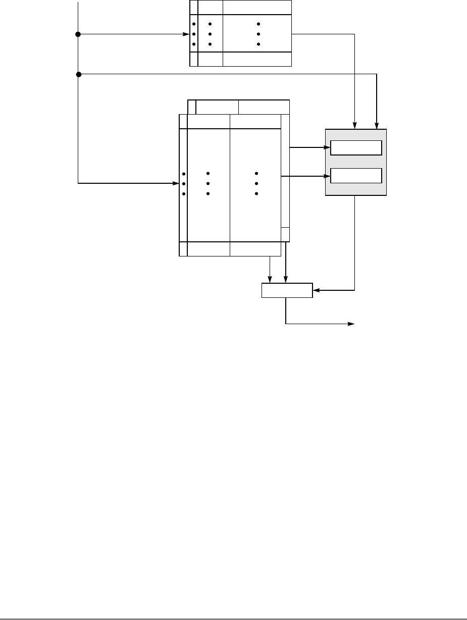
6-34 PowerPC 601 RISC Microprocessor User's Manual
Figure 6-11. Segment Register and UTLB Organization
In the case of a UTLB miss, the table search hardware in the MMU automatically searches
for the required PTE in the page tables in memory. The MMU then automatically loads the
UTLB with the PTE and the address translation is performed. Note that for an instruction
access, the required PTE is also loaded into the ITLB for future use.
If the table search operations fail to locate the required PTE, then the appropriate exception
(instruction access exception or data access exception) is taken. See Section 6.9.2, “Page
Table Search Operation” for more information on the context for these exception
conditions.
6.8.2 Recognition of Addresses in Segments
As described in Section 6.7.2, “Recognition of Addresses in BAT Array,” the block and
page translation mechanisms operate in parallel such that if the logical address of an access
hits in the BAT array (the address can be translated as a block address), the selected segment
register is ignored, unless T = 1 in the segment register.
Segment Registers
078 31
T
T VSID
0
15
UTLB
0
127
V
V
VSID
LA0–LA31
LA0–LA3
LA13–LA19
Compare
Compare
Set 1
Set 0
MUX
Set 1/Set 0 Hit
PA0–PA19
PPN
Select
Select
LA4–LA12

Chapter 6. Memory Management Unit 6-35
Segments in the 601 are defined as one of the following two types:
• Memory segment—A logical address in these segments represents a virtual address
that is used to define the physical address of the page. Note that for best
performance, I/O devices can be memory-mapped (SR[T] = 0).
• I/O controller interface segment—References made to I/O controller interface
segments use the I/O controller interface bus protocol described in Section 9.6,
“Memory- vs. I/O-Mapped I/O Operations,” and do not use the virtual paging
mechanism of the 601. See Section 6.10, “I/O Controller Interface Address
Translation,” for a complete description of the mapping of I/O controller interface
segments.
The T bit in a segment register selects between memory segments and I/O controller
interface segments, as shown in Table 6-13.
The types of address translation used by the 601 MMU are shown in the flow diagram of
Figure 6-4.
6.8.2.1 Selection of Memory Segments
All accesses generated by the 601 index into the array of segment registers and select one
of the 16 with LA0–LA3. If MSR[IT] = 0 or MSR[DT] = 0 for an instruction or data access,
respectively, then direct address translation is performed as described in Section 6.6,
“Direct Address Translation.” Otherwise, if T = 0 for the selected segment register, the
access maps to memory space and page address translation is performed.
After a memory segment is selected, the 601 creates the 52-bit virtual address for the
segment and searches for the PTE (first in the UTLB, then in the page tables in memory)
that dictates the physical page number to be used for the access. Note that I/O devices can
easily be mapped into memory space and used as memory-mapped I/O.
6.8.2.2 Selection of I/O Controller Interface Segments
All data accesses generated by the 601 index into the array of segment registers and select
one of the 16 with LA0–LA3. If T = 1 for the selected segment register, the access maps to
the I/O controller interface and the access proceeds as described in Section 6.10, “I/O
Controller Interface Address Translation.” This is true, even if data address translation is
disabled (MSR[DT] = 0).
For the case of instruction accesses, however, the 601 checks the state of the MSR[IT] bit
before checking the T bit in the segment register. If MSR[IT] = 0, direct address translation
Table 6-13. Segment Register Types
Segment Register
T Bit Segment Type
0 Memory segment
1 I/O controller interface segment

6-36 PowerPC 601 RISC Microprocessor User's Manual
is performed as described in Section 6.6, “Direct Address Translation.” If MSR[IT] = 1 and
the T bit of the selected segment register is set, then the MMU further checks the state of
the BUID field of the segment register. If BUID has the encoding x'07F', the segment is
designated as a memory-forced I/O controller interface segment and the instruction fetch
occurs as described in Section 6.10.4, “Memory-Forced I/O Controller Interface Accesses.”
Otherwise, an instruction access exception occurs.
6.8.3 Page Address Translation
The first step in page address translation is the conversion of the 32-bit logical address of
an access into the 52-bit virtual address. The virtual address is then used to locate the PTE
either in the UTLB or in the page tables in memory. The physical page number is then
extracted from the PTE and used in the formation of the physical address of the access.
Figure 6-12 shows the translation of a logical address to a physical address as follows:
• Bits 0–3 of the logical address comprise the segment register number used to select
a segment register, from which the virtual segment ID (VSID) is extracted.
• Bits 4–19 of the logical address correspond to the page number within the segment;
these are concatenated with the VSID from the segment register to form the virtual
page number (VPN). The VPN is used to search for the PTE in either the UTLB or
the page table. The PTE then provides the physical page number (PPN).
• Bits 20–31 of the logical address are the byte offset within the page; these are
concatenated with the PPN field of a PTE to form the physical address used to access
memory.
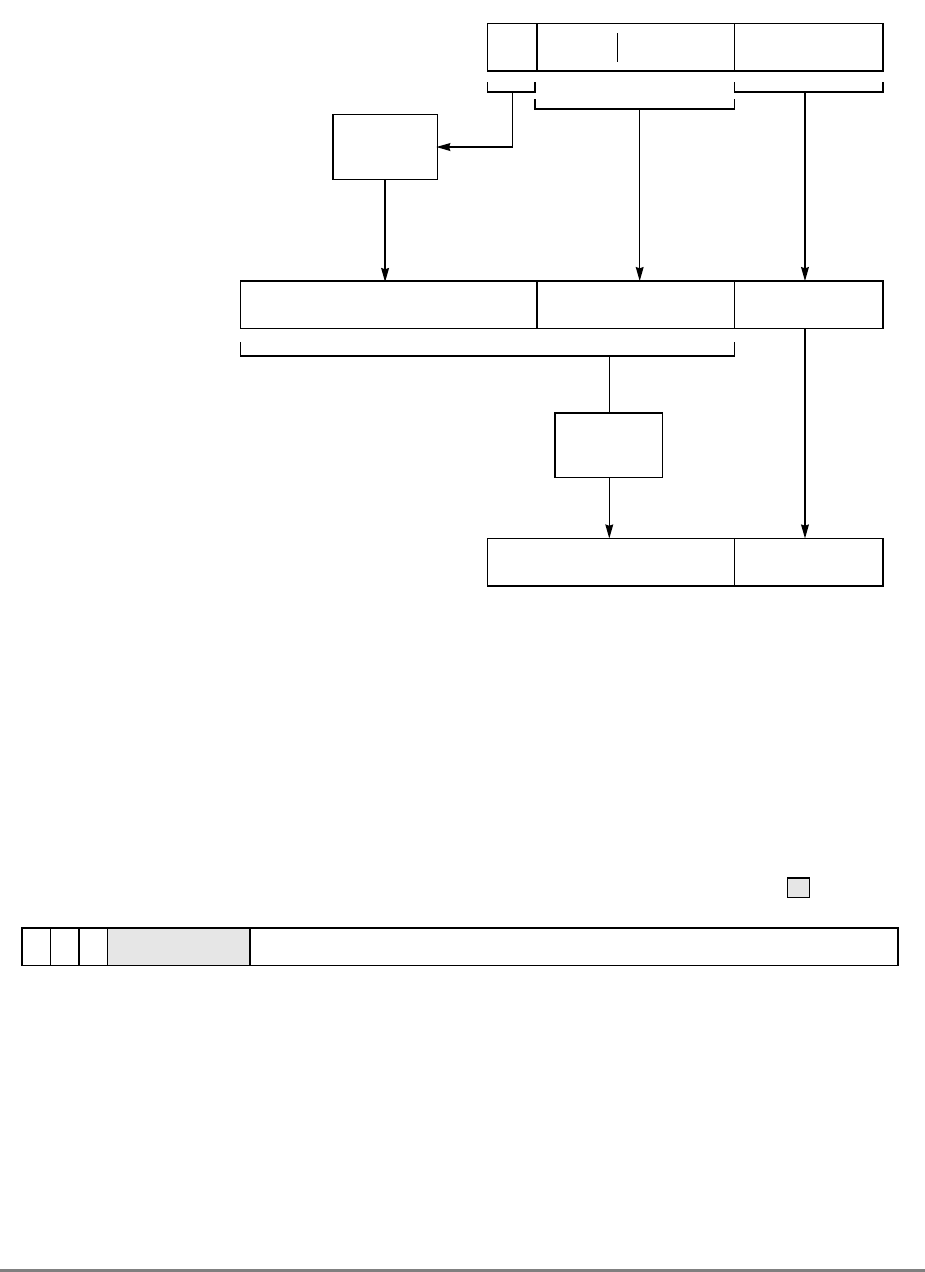
Chapter 6. Memory Management Unit 6-37
Figure 6-12. Page Address Translation Overview
6.8.3.1 Segment Register Definition
The fields in the 16 segment registers are interpreted differently depending on the value of
bit 0 (the T bit). When T = 1, the segment register defines an I/O controller interface
segment, and the format is described in Section 6.10.1, “Segment Register Format for I/O
Controller Interface.” Figure 6-13 shows the format of a segment register used in page
address translation (T = 0).
Figure 6-13. Segment Register Format for Page Address Translation
Table 6-14 provides the definitions of the segment register bits for page address translation.
52-Bit Virtual Address
32-Bit Logical Address
32-Bit Physical Address
SR# API Byte Offset
(4-bit) (6-bit) (12-bit)
Virtual Segment ID (VSID) Page Index Byte Offset
(24-bit) (16-bit) (12-bit)
Physical Page Number (PPN) Byte Offset
(20-bit) (12-bit)
UTLB/Page
Table
Page Index (16-bit)
PTE
034 1920 31
Segment
Registers
02324394051
Virtual Page Number (VPN)
T Ks Ku 0 0 0 0 0 VSID
Reserved
0123 78 31

6-38 PowerPC 601 RISC Microprocessor User's Manual
The Ks and Ku bits partially define the access protection for the pages within the segment.
The page protection provided in the 601 is described in Section 6.8.5, “Page Memory
Protection.” The virtual segment ID field is used as the high-order bits of the virtual page
number (VPN) as shown in Figure 6-12.
The segment registers are programmed with 601-specific instructions that implicitly
reference the segment registers. The 601 segment register instructions are summarized in
Table 6-15. These instructions are privileged in that they are executable only while
operating in supervisor mode. See Section 2.3.3.1, “Synchronization for Supervisor-Level
SPRs and Segment Registers” for information about the synchronization requirements
when modifying the segment registers. See Chapter 10, “Instruction Set,” for more detail
on the encodings of these instructions.
6.8.3.2 Page Table Entry (PTE) Format
Page table entries (PTEs) are generated and placed in page tables in memory by the
operating system using the hashing algorithm described in Section 6.9.1.3, “Hashing
Functions.” Each PTE is a 64-bit entity (two words) that maps one virtual page number
(VPN) to one physical page number (PPN). Information in the PTE controls the table
search process and provides input to the memory protection mechanism. Figure 6-14 shows
the format of both words that comprise a PTE.
Table 6-14. Segment Register Bit Definition for Page Address Translation
Bit Name Description
0 T T = 0 selects this format
1Ks Supervisor-state protection key
2Ku User-state protection key
3–7 — Reserved
8–31 VSID Virtual segment ID
Table 6-15. Segment Register Instructions
Instruction Description
mtsr SR#,rS Move to Segment Register
SR[SR#]← rS
mtsrin rS,rB Move to Segment Register Indirect
SR[rB[0–3]]←rS
mfsr rD,SR# Move from Segment Register
rD←SR[SR#]
mfsrin rD,rB Move from Segment Register Indirect
rD←SR[rB[0–3]]
These instructions are specific to the 601 and not guaranteed on
other PowerPC processors.
Chapter 6. Memory Management Unit 6-39
Figure 6-14. Page Table Entry Format
Table 6-16 lists the bit definitions for each word in a PTE.
All other fields are reserved.
The PTE contains an abbreviated page index rather than the complete page index field
because at least ten of the low-order bits of the page index are used in the hash function to
select a PTE group (PTEG) address (PTEG addresses define the location of a PTE). These
bits are not repeated in the PTEs of that PTEG. However, when a PTE is loaded into the
UTLB, the entire page index (PI) field must be loaded into the UTLB entry. The PI field is
then compared with incoming logical address bits LA4–LA12 (LA13–LA16 select the
UTLB entries to be compared) to determine if there is a hit.
The virtual segment ID field corresponds to the high-order bits of the virtual page number
(VPN), and, along with the H bit, it is used to locate the PTE. The R and C bits maintain
history information for the page as described in Section 6.8.4, “Page History Recording.”
The WIM bits define the memory/cache control mode for accesses to the page. Finally, the
PP bits define the remaining access protection constraints for the page. The page protection
provided in the 601 is described in Section 6.8.5, “Page Memory Protection.”
Table 6-16. PTE Bit Definitions
Word Bit Name Description
0 0 V Entry valid (V = 1) or invalid (V = 0)
1–24 VSID Virtual segment ID
25 H Hash function identifier
26–31 API Abbreviated page index
1 0–19 PPN Physical page number
20–22 — Reserved
23 R Reference bit
24 C Change bit
25–27 WIM Memory/cache control bits
28–29 — Reserved
30–31 PP Page protection bits
Reserved
0 1920 22232425 2728293031
V VSID H API
01 24 25 26 31
PPN 0 0 0 R C WIM 0 0 PP

6-40 PowerPC 601 RISC Microprocessor User's Manual
Conceptually, the page table is searched by the address translation hardware to translate the
address of every reference. For performance reasons, the UTLB maintains recently-used
PTEs so that the table search time is eliminated for most accesses. The UTLB is searched
for the address translation first. If the PTE is found, then no page table search is performed.
As a result, software that changes the page tables in any way must perform the appropriate
TLB invalidate operations to keep the UTLB (and ITLB) coherent with respect to the page
tables.
6.8.4 Page History Recording
Reference (R) and change (C) bits are automatically maintained by the 601 in the PTE for
each physical page (for accesses made with page table address translation) to keep history
information about the page. This information can then be used by the operating system to
determine which areas of memory to write back to disk when new pages must be allocated
in main memory. Reference and change recording is not performed for translations made
with the BAT or for accesses that correspond to I/O controller interface (T = 1) segments.
Furthermore, R and C bits are maintained only for accesses made while address translation
is enabled (MSR[IT] = 1 or MSR[DT] = 1).
The reference and change bits are automatically updated by the 601 under the following
circumstances:
• For UTLB hits, if the C bit requires updating (as shown in Table 6-16).
• For UTLB misses, when a table search is in progress to locate a PTE. The R and C
bits are updated (set, if required) to reflect the status of the page based on this access.
Note that the processor updates the C bit based only on the status of the C bit in the UTLB
entry in the case of a UTLB hit (the R bit is assumed to be set in the page tables if there is
a UTLB hit). Therefore, when software clears the R and C bits in the page tables in memory,
it must invalidate the UTLB entries associated with the pages whose reference and change
bits were cleared. See Section 6.9.3, “Page Table Updates,” for all of the constraints
imposed on the software when updating the reference and change bits in the page tables.
The R bit or the C bit for a page is not set by the execution of the Data Cache Block Touch
instructions (dcbt, or dcbtst).
Table 6-17. Table Search Operations to Update History Bits—UTLB Hit Case
R and C bits
in UTLB entry PowerPC 601 Microprocessor Action
00 Combination doesn’t occur
01 Combination doesn’t occur
10 Read: No special action
Write: Table search operation to update C
11 No special action for read or write

Chapter 6. Memory Management Unit 6-41
6.8.4.1 Reference Bit
The reference bit of a page is located both in the PTE in the page table and in the copy of
the PTE loaded into the UTLB. Every time a page is referenced (with a read or write access)
the reference bit is set in the page table by the 601. Because the reference to a page is what
causes a PTE to be loaded into the UTLB, the reference bit in all UTLB entries is always
set. The processor never automatically clears the reference bit.
The reference bit is only a hint to the operating system about the activity of a page. At times,
the reference bit may be set although the access was not logically required by the program
or even if the access was prevented by memory protection. Examples of this include the
following:
• Fetching of instructions not subsequently executed
• Accesses that cause exceptions and are not completed
6.8.4.2 Change Bit
The change bit of a page is also located both in the PTE in the page table and in the copy
of the PTE loaded into the UTLB. Whenever a data store instruction is executed
successfully, if the UTLB search (for page address translation) results in a hit, the change
bit in the matching UTLB entry is checked. If it is already set, the processor does not change
the C bit. If the UTLB change bit is 0, it is set and a table search operation is performed to
set the C bit also in the corresponding PTE in the page table.
The change bit (in both the UTLB and the PTE in the page tables) is set only when a store
operation is allowed by the page memory protection mechanism.
The automatic update of the reference and change bits in the 601 is performed with single-
beat read and write transactions on the bus (not with atomic read/modify/write operations).
During a table search operation, PTEs are fetched as global, nonexclusive read transactions
(not as read-with-intent-to-modify transactions). This reduces cache thrashing in other
processors (in a multiprocessor system) caused by UTLB load operations because other
processors do not have to invalidate their resident copies of the PTEs. The response on the
bus to a PTE load transaction should then be exclusive (SHD signal not asserted) if no other
processor has a copy. Because PTEs are considered as cacheable, the MESI protocol of the
cache then ensures that coherency is maintained among multiple processors for C bit
updates to the page tables.
6.8.5 Page Memory Protection
Similar to the block memory protection mechanism, the page memory protection of the 601
provides selective access to each page in memory. If a logical address is determined to be
within a page defined by the segment registers and an entry in the UTLB, the access is next
validated by the page protection mechanism. If this protection mechanism prohibits the
access, a page protection violation (data access exception or instruction access exception)
is generated.

6-42 PowerPC 601 RISC Microprocessor User's Manual
When the page protection mechanism prohibits a reference, one of the following occurs,
depending on the type of access that was attempted.
• For data accesses, a data access exception is generated and bit 4 of DSISR is set. If
the access was a store, bit 6 of DSISR is additionally set.
• For instruction accesses, an instruction access exception is generated and bit 4 of
SRR1 is set.
See Chapter 5, “Exceptions,” for more information on these types of exceptions
A store operation that is not permitted because of the page protection mechanism does not
cause the change (C) bit to be set in the PTE (in either the UTLB or in the page tables in
memory); however, a prohibited store access may cause a PTE to be loaded into the UTLB
and consequently cause the reference bit to be set in a PTE (both in the UTLB and in the
page table in memory).
6.8.6 Page Address Translation Summary
Figure 6-15 provides the detailed flow for the page address translation mechanism. The
figure is an expansion of the “UTLB Hit” branch of Figure 6-3. The detailed flow for the
“UTLB Miss” branch of Figure 6-3 is described in Section 6.9.2, “Page Table Search
Operation." Note that as in the case of block address translation, if the dcbz instruction is
attempted to be executed with either W = 1 or I = 1, the alignment exception is generated.
Also note that the memory protection violation flow for page address translation is identical
to that of the block memory protection violation and is provided in Figure 6-10.
6.9 Hashed Page Tables
When an access that is to be translated by the page address translation mechanism results
in a miss in the UTLB (a PTE corresponding to the VSID of the segment register is not
resident in either of the UTLB entries indexed by LA13–LA19), the 601 automatically
searches the page tables set up by the operating system in main memory.
The algorithm used by the processor in searching the page tables includes a hashing
function on some of the virtual address bits. Thus, the addresses for PTEs are allocated
more evenly within the page tables and the hit rate of the page tables is maximized. This
algorithm must be synthesized by the operating system for it to correctly place the page
table entries in main memory.
This section describes the format of the page tables and the algorithm used to access them.
In addition, the constraints imposed on the software in updating the page tables (and other
MMU resources) are described.
Chapter 6. Memory Management Unit 6-43
Figure 6-15. Page Address Translation Flow—UTLB Hit
UTLB Hit
Case
Alignment
Exception
Logical Address
Generated
Generate 52-bit
Virtual Address
from Segment Regis-
ter
Compare Virtual
Address with UTLB
Entries
LA13–LA19 select a UTLB entry for each set (Set 0 and Set 1)
Segment Register [VSID] = VSID in UTLB entry
LA4–LA12 = PI in UTLB entry
UTLB entry [V] = 1
otherwisedcbz Instruction
with W or I = 1
Memory Protection
Violation
See Figure 6-10
Continue Access to Cache
with WIM from UTLB entry
otherwise
Store Access with
UTLB entry [C] = 0
Table Search
Operation
otherwise
PA0–PA31←PPN||A20–A31
Select Key:
If MSR[PR] = 0, key = Ks
If MSR[PR] = 1, key = Ku
Invalidate UTLB entry
(and force to LRU)

6-44 PowerPC 601 RISC Microprocessor User's Manual
6.9.1 Page Table Definition
The hashed page table is a variable-sized data structure that defines the mapping between
virtual page numbers and physical page numbers. The page table size is a power of 2, and
its starting address is a multiple of its size.
The page table contains a number of page table entry groups (PTEGs). A PTEG contains
eight page table entries (PTEs) of eight bytes each; therefore, each PTEG is 64 bytes long.
PTEG addresses are entry points for table search operations. Figure 6-16 shows two PTEG
addresses (PTEGaddr1 and PTEGaddr2) where a given PTE may reside.
Figure 6-16. Page Table Definitions
A given PTE can reside in one of two possible PTEGS. For each PTEG address, there is a
complementary PTEG address—one is the primary PTEG and the other is the secondary
PTEG. Additionally, a given PTE can reside in any of the PTE locations within an
addressed PTEG. Thus, a given PTE may reside in one of 16 possible locations within the
page table. If a given PTE is not resident within either the primary or secondary PTEG, a
page table miss occurs, corresponding to a page fault condition.
A table search operation is defined as the search of a PTE within a primary and secondary
PTEG. When a table search operation commences, a primary hashing function is performed
on the virtual address. The output of the hashing function is then concatenated with bits
(some of them masked) programmed into the SDR1 register by the operating system to
create the physical address of the primary PTEG. The PTEs in the PTEG are then checked,
one by one, to see if there is a hit within the PTEG. In case the PTE is not located during
this PTEG, a secondary hashing function is performed, a new physical address is generated
PTE0 PTE1 PTE7 PTEG0
PTE0 PTE1 PTE7
PTE0 PTE1 PTE7
PTEGn
PTEGaddr1
PTEGaddr2
Page Table
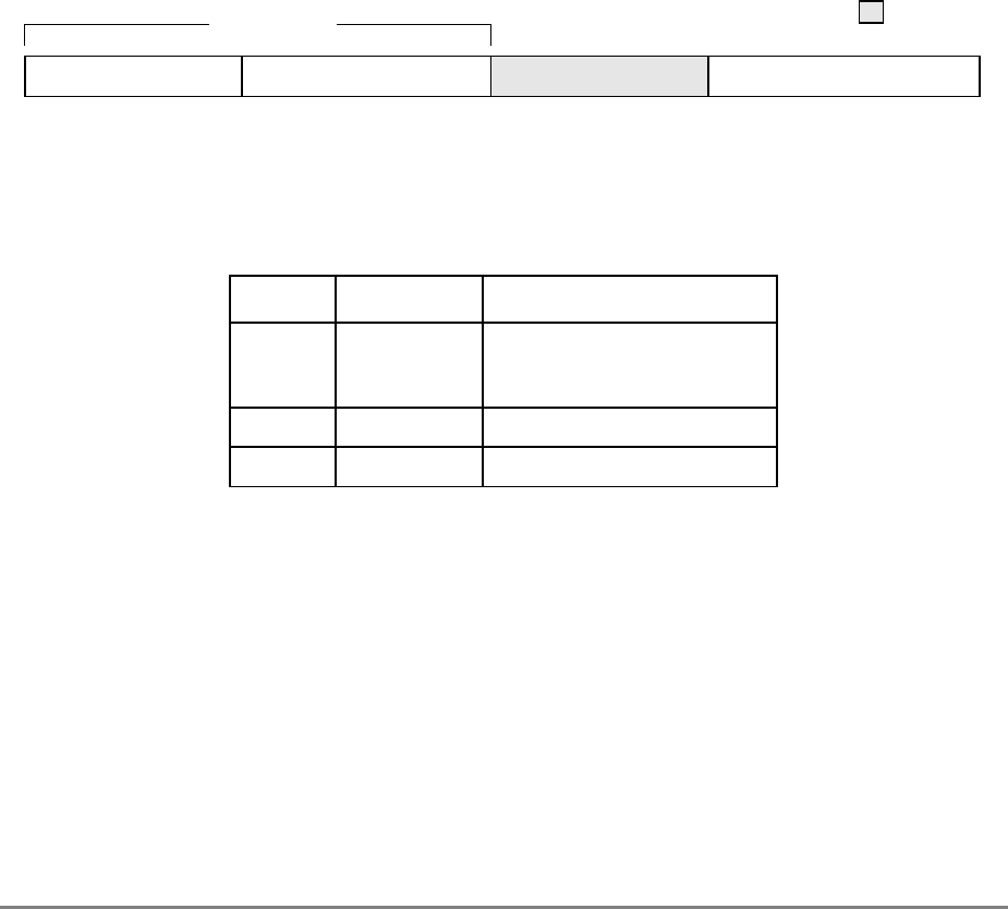
Chapter 6. Memory Management Unit 6-45
for the PTEG, and the PTE is searched for again, this time using the secondary PTEG
address.
Note, however, that although a given PTE may reside in one of 16 possible locations, an
address that is a primary PTEG address for some accesses also functions as a secondary
PTEG address for a second set of accesses (as defined by the secondary hashing function).
Therefore, these 16 possible locations are really shared by two different sets of logical
addresses. Section 6.9.1.5.1, “Page Table Structure Example” illustrates how PTEs map
into the 16 possible locations as primary and secondary PTEs.
6.9.1.1 Table Search Description Register (SDR1)
The SDR1 register contains the control information for the table structure in that it defines
the highest order bits for the physical base address of the page table and it defines the size
of the table. The format of the SDR1 register is shown in Figure 6-17 and the bit settings
are described in Table 6-18.
Figure 6-17. SDR1 Register Format
The HTABORG field in SDR1 contains the high-order 7–16 bits of the 32-bit physical
address of the page table. Therefore, the beginning of the page table lies on a 216 byte (64
Kbyte) boundary at a minimum.
A page table can be any size 2n where 16 ≤ n ≤ 25. The HTABMASK field in SDR1
contains a mask value that determines how many bits from the output of the hashing
function are used as the page table index. This mask must be of the form b'00...011...1' (a
string of 0 bits followed by a string of 1 bits). As the table size increases, more bits are
used from the output of the hashing function to index into the table. The 1 bits in
HTABMASK determine how many additional bits (beyond the minimum of 10) from the
hash are used as the index; the HTABORG field must have the same number of lower-order
bits equal to 0 as the HTABMASK field has lower-order bits equal to 1.
Table 6-18. SDR1 Register Bit Settings
Bits Name Description
0–15 HTABORG Physical base address of page
table (Base Address bits plus
Maskable bits)
16–22 — Reserved
23–31 HTABMASK Mask for page table address
Base Address Maskable Bits 0 0 0 0 0 0 0 HTABMASK
Reserved
067 15162223 31
HTABORG

6-46 PowerPC 601 RISC Microprocessor User's Manual
6.9.1.2 Page Table Size
The number of entries in the page table directly affects performance because it influences
the hit ratio in the page table and thus the rate of page fault exception conditions. If the table
is too small, not all virtual pages that have physical page frames assigned may be mapped
via the page table. This can happen if there are more than 16 entries that map to the same
primary/secondary pair of PTEGs; in this case, many hash collisions may occur.
The minimum allowable size for a page table is 64 Kbytes (210 PTEGs of 64 bytes each).
However, it is recommended that the total number of PTEGs (primary plus secondary) in
the page table be greater than half the number of physical page frames to be mapped. While
avoidance of hash collisions cannot be guaranteed for any size page table, making the page
table larger than the recommended minimum size reduces the frequency of such collisions,
by making the primary PTEGs more sparsely populated, and further reducing the need to
use the secondary PTEGs.
Table 6-18 shows some example sizes for total main memory. The recommended minimum
page table size for these example memory sizes are then outlined, along with their
corresponding HTABORG and HTABMASK settings. Note that systems with less than
eight Mbytes of main memory may be designed with the 601, but the minimum amount of
memory that can be used for the page tables is 64 Kbytes.
As an example, if the physical memory size is 229 bytes (512 Mbyte), then there are 229–
212 (4 Kbyte page size) = 217 (128 Kbyte) total page frames. If this number of page frames
Table 6-19. Recommended Page Table Sizes (Minimum)
Total Main Memory
Recommended Minimum Settings for
Recommended Minimum
Memory for
Page Tables
Number of
Mapped
Pages
(PTEs)
Number of
PTEGs
HTABORG
(Maskable
bits 7-15) HTABMASK
8 Mbytes (223) 64 Kbytes (216)2
13 210 x xxxx xxxx 0 0000 0000
16 Mbytes (224) 128 Kbytes (217)2
14 211 x xxxx xxx0 0 0000 0001
32 Mbytes (225) 256 Kbytes (218)2
15 212 x xxxx xx00 0 0000 0011
64 Mbytes (226) 512 Kbytes (219)2
16 213 x xxxx x000 0 0000 0111
128 Mbytes (227) 1 Mbytes (220)2
17 214 x xxxx 0000 0 0000 1111
256 Mbytes (228) 2 Mbytes (221)2
18 215 x xxx0 0000 0 0001 1111
512 Mbytes (229) 4 Mbytes (222)2
19 216 x xx00 0000 0 0011 1111
1 Gbytes (230) 8 Mbytes (223)2
20 217 x x000 0000 0 0111 1111
2 Gbytes (231) 16 Mbytes (224)2
21 218 x 0000 0000 0 1111 1111
4 Gbytes (232) 32 Mbytes (225)2
22 219 0 0000 0000 1 1111 1111

Chapter 6. Memory Management Unit 6-47
is divided by 2, the resultant minimum recommended page table size is 216 PTEGs, or 222
bytes (4 Mbytes) of memory for the page tables.
6.9.1.3 Hashing Functions
The processor uses two different hashing functions, a primary and a secondary, in the
creation of the physical addresses used in a page table search operation. These hashing
functions efficiently distribute the PTEs within the page table, in that there are two possible
PTEGs where a given PTE can reside. Additionally, there are eight possible PTE locations
within a PTEG where a given PTE can reside. If a PTE is not found using the primary
hashing function, the secondary hashing function is performed, and the secondary PTEG is
searched. Note that these two functions must also be used by the operating system to
appropriately set up the page tables in memory.
The use of the two hashing functions provides a high probability that a required PTE is
resident in the page tables, without requiring the definition of all possible PTEs in main
memory. However, if a PTE is not found in the secondary PTEG, then a page fault occurs
and an exception is taken. Thus, the required PTE can then be placed into either the primary
or secondary PTEG by the system software, and on the next UTLB miss to this page, the
PTE will be found.
The address of a page table is derived from the HTABORG field of the SDR1 register, and
the output of the corresponding hashing function (primary hashing function for primary
PTEG and secondary hashing function for a secondary PTEG). The value in HTABMASK
determines how many of the higher-order hash value bits are masked and how many are
used in the generation of the physical address of the page table.
Figure 6-18 depicts the hashing functions used by the 601. The inputs to the primary
hashing function are the lower-order 19 bits of the VSID field of the selected segment
register (bits 5–23 of the 52-bit virtual address), and the page index field of the logical
address (bits 24–39 of the virtual address) concatenated with three zero higher-order bits.
The XOR of these two values generates the output of the primary hashing function (hash
value 1).
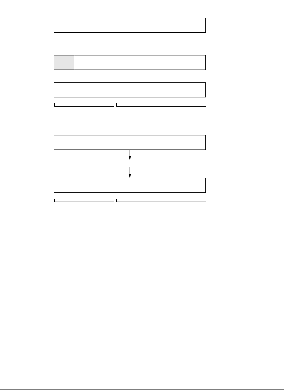
6-48 PowerPC 601 RISC Microprocessor User's Manual
Figure 6-18. Hashing Functions
When the secondary hashing function is required, the output of the primary hashing
function is complemented with one’s complement arithmetic, to provide hash value 2.
6.9.1.4 Page Table Addresses
Figure 6-19 illustrates the generation of the addresses used for accessing the hashed page
tables defined for the 601. As stated earlier, the operating system must synthesize the table
search algorithm for setting up the tables.
As shown in Figure 6-19, two of the elements that define the 52-bit virtual address (the
segment register VSID field and the page index field of the logical address) are used as
inputs into a hashing function. Depending on whether the primary or secondary PTEG is to
be accessed, the processor uses either the primary or secondary hashing function.
Low-Order 19 Bits of VSID (From Segment Register)
523
24 39
Primary Hash:
XOR
Output of Hashing Function 1
089 18
=
Secondary Hash:
Hash Value 1
018
Output of Hashing Function 2
089 18
Hash Value 1
Hash Value 2
One’s Complement Function
0 0 0 Page Index (From Logical Address)
Chapter 6. Memory Management Unit 6-49
Figure 6-19. Generation of Addresses for Page Tables
Virtual Segment ID API Byte Offset
(24-bit) (6-bit) (12-bit)
Virtual Page Number (VPN)
PAGE TABLE
(3-bit)
0 4 5 23 24 29 30 394051
SDR1
xxxx xx . . . . . . 00 00 . . . . 011 . .
.1
067 1516 2223 31018
32-bit Physical Address of Page Table Entry
PTE0
64 Bytes
52-Bit Virtual Address
PTE7
8 bytes
32-bit Physical Address
VSID API
(24-bit) (6-bit)
V H
Physical Page Number (PPN)
(20-bit)
019252731
R
C
WIM
AND
OR
(7-bit) (9-bit) (10-bit)
PPN Byte Offset
(20-bit) (12-bit)
(16-bit)
Hash Function
Hash Value
(19-bit)
PTEG0
PTEGn
Page Index (16-bit)
Mask
067 1516 252631
PTEG Select
PP
PTE
01 24 25 26 31
9 bits 10 bits
0 0 0 0 0 0 0
00 0
0 0 0
0 0 0 0 0 0
(6-bit)
Base
Address Maskable
bits

6-50 PowerPC 601 RISC Microprocessor User's Manual
The base address of the page table is defined by the higher order bits of SDR1[HTABORG].
Bits 7–15 of the PTEG address are derived from the masking of the higher-order bits of the
hash value (as defined by SDR1[HTABMASK]) concatenated with (implemented as an OR
function) the remaining bits of SDR1[HTABORG]. Bits 16-25 of the PTEG address are the
10 lower order bits of the hash value, and bits 26-31 of the PTEG address are zero. In the
process of searching for a PTE, the processor first checks PTE0 (at the PTEG base address).
6.9.1.5 Page Table Structure
In the process of searching for a PTE, the processor interprets the values read from memory
as described in Section 6.8.3.2, “Page Table Entry (PTE) Format.” The VSID and the
abbreviated page index (API) fields of the 52-bit virtual address of the access are compared
to those same fields of the PTEs in memory. In addition, the valid (V) bit and the hashing
function (H) bit are also checked. For a hit to occur, the V bit of the PTE in memory must
be set. If the fields match and the entry is valid, the PTE is considered a hit if the H bit is
set as follows:
• If this is the primary PTEG, H = 0
• If this is the secondary PTEG, H = 1
The physical address of the PTEs to be checked is derived as shown in Figure 6-19, and is
the address of a group of eight PTEs (a PTEG). During a table search operation, the
processor first compares the PTE0 location defined by the primary hashing function. If the
VSID and API fields do not match (or if V or H are not set appropriately), the processor
increments the lower order address bits by eight bytes and checks the PTE1 location and so
on, until all eight PTEs in the PTEG have been checked.
If no match is found, the secondary hashing function is performed, and the secondary
PTEG address is derived. The eight PTEs within the secondary PTEG are then similarly
checked. If the required PTE is not found in any of the 16 possible locations (the eight PTEs
within the primary PTEG and the eight PTEs within the secondary PTEG), then a page fault
occurs and an exception is taken. Thus, if a valid PTE is located in the page tables, the page
is considered resident; if no matching (and valid) PTE is found for an access, the page is
interpreted as non-resident (page fault) and the operating system must load the PTE (and
possibly the page) into main memory.
Note that for performance reasons, PTEs should be allocated by the operating system first
beginning with the PTE0 locations within the primary PTEG, then PTE1, and so on. If more
than eight PTEs are required within the address space that defines a PTEG address, the
secondary PTEG can be used. Nonetheless, it may be desirable to place the PTEs that will
require most frequent access at the beginning of a PTEG and reserve the PTEs in the
secondary PTEG for the least frequently accessed PTEs.

Chapter 6. Memory Management Unit 6-51
6.9.1.5.1 Page Table Structure Example
Figure 6-20 shows the structure of an example page table. The base address of this page
table is defined by bits 0–13 in SDR1[HTABORG]; note that bits 14 and 15 of HTABORG
must be zero because the lower order two bits of HTABMASK are ones. The addresses for
individual PTEGs within this page table are then defined by bits 14–25 as an offset from
bits 0–13 of this base address. Thus the size of the page table is defined as 4096 PTEGs.
Figure 6-20. Example Page Table Structure
Two example PTEG addresses are shown in the figure as PTEGaddr1 and PTEGaddr2. Bits
14–25 of each PTEG address in this example page table are derived from the output of the
hashing function (bits 26–31 are zero to start with PTE0 of the PTEG). In this example, the
'b' bits in PTEGaddr2 are the one’s complement of the 'a' bits in PTEGaddr1. The 'm' bits
PTE0 PTE1 PTE7 PTEG0
PTE0 PTE1 PTE7
PTE0 PTE1 PTE7
PTEG4095
PTEGaddr1
PTEGaddr2
Page Table
Example:
Given: SDR1 1010 0110 0000 0000 0000 0000 0000 0011
0152331
Base Address
$A600 0000
PTEGaddr1 =1010 0110 0000 00mm aaaa aaaa aa00 0000
0142531
PTEGaddr2= 1010 0110 0000 00nn bbbb bbbb bb00 0000
0142531
HTABORG HTABMASK

6-52 PowerPC 601 RISC Microprocessor User's Manual
are also the one’s complement of the 'n' bits, but these two bits are generated from bits 7–8
of the output of the hashing function, logically ORed with bits 14–15 of the HTABORG
field (which are zero in this example). If bits 14–25 of PTEGaddr1 were derived by using
the primary hashing function, then PTEGaddr2 corresponds to the secondary PTEG.
Note, however, that bits 14–25 in PTEGaddr2 can also be derived from a combination of
logical address bits, segment register bits, and the primary hashing function. In this case,
then PTEGaddr1 corresponds to the secondary PTEG. Thus, while a PTEG may be
considered a primary PTEG for some logical addresses (and segment register bits), it may
also correspond to the secondary PTEG for a different logical address (and segment register
value).
It is the value of the H bit in each of the individual PTEs that identifies a particular PTE as
either primary or secondary (there may be PTEs that correspond to a primary PTEG and
PTEs that correspond to a secondary PTEG, all within the same physical PTEG address
space). Thus, only the PTEs that have H = 0 are checked for a hit during a primary PTEG
search. Likewise, only PTEs with H = 1 are checked in the case of a secondary PTEG
search.
6.9.1.5.2 PTEG Address Mapping Example
Figure 6-21 shows an example of a logical address and how its address translation (the
PTE) maps into the primary PTEG in physical memory. The example illustrates how the
processor generates PTEG addresses for a table search operation; this is also the algorithm
that must be used by the operating system in creating the page tables.
In the example, the value in SDR1 defines a page table at address x'0F98 0000' that contains
8192 PTEGs. The example logical address selects segment register 0 (SR0) with the highest
order four bits. The contents of SR0 are then used along with bits 4–19 of the logical
address to create the 52-bit virtual address.
To generate the address of the primary PTEG, bits 5–23, and bits 24–39 of the virtual
address are then used as inputs into the primary hashing function (XOR) to generate hash
value 1. The lower order 13 bits of hash value 1 are then concatenated with the higher order
13 bits of HTABORG, defining the address of the primary PTEG (x'0F9F F980').
Chapter 6. Memory Management Unit 6-53
Figure 6-21. Example Primary PTEG Address Generation
Figure 6-22 shows the generation of the secondary PTEG address for this example. If the
secondary PTEG is required, the secondary hash function is performed and the lower order
13 bits of hash value 2 are then concatenated with the higher order 13 bits of HTABORG,
defining the address of the secondary PTEG (x'0F98 0640').
As described in Figure 6-19, the 10 lower-order bits of the page index field are always used
in the generation of a PTEG address (through the hashing function). This is why only the
abbreviated page index (API) is defined for a PTE (the entire page index field does not need
to be checked). For a given logical address, the lower order 10 bits of the page index (at
least) contribute to the PTEG address (both primary and secondary) where the
corresponding PTE may reside in memory. Therefore, if the higher order 6 bits (the API
field) of the page index match with the API field of a PTE within the specified PTEG, the
PTE mapping is guaranteed to be the unique PTE required.
Example:
Given: SDR1 0000 1111 1001 1000 0000 0000 0000 0111
0152331
HTABORG HTABMASK
0000 0000 1111 1111 1010 0000 0001 1011
0 4 19 20 25 31
LA = x'00FF A01B':
SR0
Segment Register Select
0010 0000 1100 1010 0111 0000 0001 1100
x'C A 7 0 1 C’
831
1100 1010 0111 0000 0001 1100 0000 1111 1111 1010 0000 0001 1011
5242539
Virtual Address:
Byte Offset
Page Index
VSID
Primary Hash: 010 0111 0000 0001 1100
XOR
000 0000 1111 1111 1010
Hash Value 1 010 0111 1111 1110 0110
9-bits 10-bits
0000 1111 1001 1111 1111 1001 1000 0000
x’0F9F F9 80’
Primary PTEG Address:
Start at PTE0HTABORG 13 16 25
6-54 PowerPC 601 RISC Microprocessor User's Manual
Figure 6-22. Example Secondary PTEG Address Generation
Note that a given PTEG address does not map back to a unique logical address. Not only
can a given PTEG be considered both a primary and a secondary PTEG (as described in
Section 6.9.1.5.1, “Page Table Structure Example”), but in this example, bits 24–26 of the
page index field of the virtual address are not used to generate the PTEG address. Therefore,
any of the eight combinations of these bits will map to the same primary PTEG address.
(However, these bits are part of the API and are therefore compared for each PTE within
the PTEG to determine if there is a hit.) Furthermore, a logical address can select a different
segment register with a different value such that the output of the primary (or secondary)
hashing function happens to equal the hash values shown in the example. Thus these logical
addresses would also map to the same PTEG addresses shown.
Hash Value 2: 101 1000 0000 0001 1001
Secondary PTEG Address:
0000 1111 1001 1000 0000 0110 0100 0000
x’0F98 06 40’
9 bits 10 bits
1) First compare 8 PTEs
at x'0F9F F980'
2) Then, compare 8 PTEs
at x'0F98 0640',
if necessary
HTABORG
x'0F98 0000'
x'0F98 0640'
x'0F9F F980'
PTEG0
PTEG25
PTEG8166
PTEG8191
PTE0 PTE7
PTE0 PTE7
010 0111 1111 1110 0110
One’s Complement
Secondary Hash:
010 0111 1111 1110 0110
Hash Value 1:
Start at PTE0

Chapter 6. Memory Management Unit 6-55
6.9.2 Page Table Search Operation
An outline of the table search process performed by the 601 in the search of a PTE is as
follows:
1. The 32-bit physical address of the primary PTEG is generated as described in
Section 6.9.1.4, “Page Table Addresses”.
2. The first PTE (PTE0) in the primary PTEG is read from memory. PTE reads occur
with an implied WIM memory/cache mode control bit setting of b'001'. Therefore,
they are considered cacheable and burst in from memory and placed in the cache.
3. The PTE in the selected PTEG is tested for a match with the virtual page number
(VPN) of the access. The VPN is the VSID concatenated with the page index fields
of the virtual address. For a match to occur, the following must be true:
— PTE[H] = 0
— PTE[V] = 1
— PTE[VSID] = VA[0–23]
— PTE[API] = VA[24–29]
4. If a match is not found, step 3 is repeated for each of the other seven PTEs in the
primary PTEG. If a match is found, the table search process continues as described
in step 8. If a match is not found within the 8 PTEs of the primary PTEG, the address
of the secondary PTEG is generated.
5. The first PTE (PTE0) in the secondary PTEG is read from memory. Again, because
PTE reads have an implied WIM bit combination of b'001', an entire cache line is
burst into the on-chip cache.
6. The PTE in the selected secondary PTEG is tested for a match with the virtual page
number (VPN) of the access. For a match to occur, the following must be true:
— PTE[H] = 1
— PTE[V] = 1
— PTE[VSID] = VA[0–23]
— PTE[API] = VA[24–29]
7. If a match is not found, step 6 is repeated for each of the other seven PTEs in the
secondary PTEG.
8. If a match is found, the PTE is written into the UTLB and the R bit is updated in the
PTE in memory (if necessary). If there is no memory protection violation, the C bit
is also updated in memory and the table search is complete.
9. If a match is not found within the 8 PTEs of the secondary PTEG, the search fails,
and a page fault exception condition occurs (either an instruction access exception
or a data access exception).
Reads from memory for table search operations are performed as global (but not exclusive),
cacheable operations, and are loaded into the on-chip cache of the 601.

6-56 PowerPC 601 RISC Microprocessor User's Manual
Figure 6-23 and Figure 6-24 provide detailed flow diagrams of the table search operations
performed by the 601. Figure 6-23 shows the case of a dcbz instruction executed with
W = 1 or I = 1, and that the R bit is updated in memory (if required) before the alignment
exception occurs. The R bit is also updated (if required) in the case of a memory protection
violation except for the case of a dcbt or a dcbtst instruction. If either of these instructions
is executed and a protection violation occurs, the translation is simply aborted, the R bit is
not set in memory and the instruction execution becomes a no-op (not shown in the figure).
Chapter 6. Memory Management Unit 6-57
Figure 6-23. Primary Table Search Flow
Generate PA using Primary Hash Function
PA ← Base PA of PTEG
(PA26-PA31=0)
Fetch PTE from PTEG
Select Key:
If MSR[PR] = 0, key = KS
If MSR[PR] = 1, key = KU
Burst read from PA (fill cache line)
Fetch PTE (64 bits)
otherwise
otherwise
PA ← PA+8
(Fetch next PTE in PTEG)
Perform Secondary
Table Search
PA26-PA31=56
(Last PTE in PTEG)
PTE [VSID, API, H, V]=
Segment Register [VSID], LA[API], 0, 1
Secondary Table
Search Hit
PTE[R]=0PTE[R]=1
PTE[R] ← 1
R_Flag ← 1
Write PTE
into UTLB
Primary Table Search
otherwise dcbz Instruction
with W or I = 1
otherwise
Alignment
Exception
otherwise Memory Protection
Violation
otherwise
See Figure 6-10
Byte write to
update PTE[R] in
memory
otherwise
Table Search
Complete
UTLB[PTE[C]] ← 1
PTE[C] ← 1
Half word write to
update PTE[C]
in memory
Store operation with
PTE[C]=0
otherwise
Table Search
Complete
R_Flag=1 R_Flag=1
R_Flag=1
Byte write to
update PTE[R] in
memory
Byte write to
update PTE[R] in
memory
6-58 PowerPC 601 RISC Microprocessor User's Manual
Figure 6-24. Secondary Table Search Flow
6.9.3 Page Table Updates
This section describes the requirements on the software when updating page tables in
memory via some pseudo-code examples. In a multiprocessor system the rules described in
this section must be followed so that all processors operate with a consistent set of page
tables. Even in a single processor system, certain rules must be followed, regarding
reference and change bit updates, because software changes must be synchronized with
automatic updates made by the hardware. Updates to the tables include the following
operations:
• Adding a PTE
• Modifying a PTE, including modifying the R and C bits of a PTE
• Deleting a PTE
PTEs must be ‘locked’ on multiprocessor systems. Access to PTEs must be appropriately
synchronized by software locking of (i.e., guaranteeing exclusive access to) PTEs or
PTEGs if more than one processor can modify the table at that time. In the examples below,
Secondary Table Search
Generate PA using Secondary Hash Function
PA ← Base PA of PTEG
(PA26–PA31=0)
Fetch PTE from PTEG
Single-beat read from PA
Fetch PTE (64 bits)
otherwise
otherwise
PA ← PA+8
(Fetch next PTE in PTEG)
PTE [VSID, API, H, V]=
Segment Register [VSID], LA[API], 1, 1
Secondary Table
Search Hit
PA26–PA31=56
(Last PTE in PTEG)
Page Fault
Data Access
Exception
Instruction Access
Exception
Set SRR1[1]=1 Set SDISR[1]=1
Data Access
Instruction Access
(See Figure 6-23)

Chapter 6. Memory Management Unit 6-59
“lock()” and “unlock()” refer to software locks that must be performed to provide exclusive
status for the PTE being updated. See Appendix G, “Synchronization Programming
Examples,” for more information about the use of the lwarx and stwcx. instructions to
perform software interlocks.
On single processor systems, PTEs need not be locked. To adapt the examples given below
for the single processor case, simply delete the “lock()” and “unlock()” lines from the
examples. The sync instructions shown are required even for single processor systems.
The UTLB (and ITLB) are non-coherent caches of the page tables. UTLB entries must be
flushed explicitly with the TLB invalidate entry instruction (tlbie) whenever the
corresponding PTE is modified. In a multiprocessor system, the tlbie instruction must be
controlled by software locking, so that the tlbie is issued on only one processor at a time.
The sync instruction causes the processor to wait until the TLB invalidate operation in
progress by this processor is complete.
The PowerPC architecture defines the tlbsync instruction (an illegal instruction in the 601)
that ensures that TLB invalidate operations executed by this processor have caused all
appropriate actions in other processors on the system bus. In a system that contains both
601 processors and other PowerPC processors, the tlbsync functionality must be emulated
for the 601 in order to ensure proper synchronization with the other PowerPC processors.
Any processor, including the processor modifying the page table, may access the page table
at any time in an attempt to reload a UTLB entry. An inconsistent page table entry must
never accidentally become visible; thus there must be synchronization between
modifications to the valid bit and any other modifications. This requires as many as two
sync operations for each PTE update.
The 601 writes reference and change bits with unsynchronized, atomic byte store
operations. Note that the V, R, and C bits each resides in a distinct byte of a PTE. Therefore,
extreme care must be taken to ensure that no store operation inadvertently overwrites one
of these bytes.
6.9.3.1 Adding a Page Table Entry
Adding a page table entry requires only a lock on the PTE in a multiprocessor system. The
bytes in the PTE are then written, except for the valid bit. A sync instruction then ensures
that the updates have been made to memory, and lastly, the valid bit is set.
lock(PTE)
PTE[VSID,H,API] ← new values
PTE[PPN,R,C,WIM,PP] ← new values
sync
PTE[V] ← 1
unlock(PTE)

6-60 PowerPC 601 RISC Microprocessor User's Manual
6.9.3.2 Modifying a Page Table Entry
This section describes several scenarios for modifying a PTE.
6.9.3.2.1 General Case
In the general case, a currently-valid PTE must be changed. To do this, the PTE must be
locked, marked invalid, flushed from the TLB, updated, marked valid again, and unlocked.
The sync instruction must be used at appropriate times to wait for modifications to
complete.
Note that the tlbsync and the sync instruction that follow are only required if compatibility
is must be maintained with other PowerPC processors that implement the tlbsync
instruction. The tlbsync instruction is not implemented in the 601 but can be emulated in
the illegal instruction exception handler.
lock(PTE)
PTE[V] ← 0
sync
tlbie(PTE)
sync
tlbsync
sync
PTE[VSID,H,API] ← new values
PTE[PPN,R,C,WIM,PP] ← new values
sync
PTE[V] ← 1
unlock(PTE)
6.9.3.2.2 Clearing the Reference (R) Bit
When the PTE is modified only to clear the R bit to 0, a much simpler algorithm suffices
because the R bit need not be maintained exactly.
lock(PTE)
oldR ← PTE[R]
PTE[R] ← 0
if oldR = 1, then tlbie(PTE)
unlock(PTE)
Since only the R and C bits are modified by the processor, and since they reside in different
bytes, the R bit can be cleared by reading the current contents of the byte in the PTE
containing R (bits 16–23 of the second word), ANDing the value with x'FE', and storing the
byte back into the PTE.

Chapter 6. Memory Management Unit 6-61
6.9.3.2.3 Modifying the Virtual Address
If the virtual address is being changed to a different address within the same hash class
(primary or secondary), the following flow suffices:
lock(PTE)
val ← PTE[VSID,API,H,V]
val ← new VSID
PTE[VSID,API,H,V] ← val
sync
tlbie(PTE)
sync
tlbsync
sync
unlock(PTE)
In this pseudo-code flow, note that the store into the first word of the PTE is performed
atomically. Also, the tlbsync and the sync instruction that follow are only required if
compatibility is must be maintained with other PowerPC processors that implement the
tlbsync instruction. The tlbsync instruction is not implemented in the 601 but can be
emulated in the illegal instruction exception handler.
6.9.3.3 Deleting a Page Table Entry
In this example, the entry is locked, marked invalid, invalidated in the TLBs, and unlocked.
Again, note that the tlbsync and the sync instruction that follow are only required if
compatibility is must be maintained with other PowerPC processors that implement the
tlbsync instruction. The tlbsync instruction is not implemented in the 601 but can be
emulated in the illegal instruction exception handler.
lock(PTE)
PTE[V] ← 0
sync
tlbie(PTE)
sync
tlbsync
sync
unlock(PTE)
6.9.4 Segment Register Updates
There are certain synchronization requirements for using the move to segment register
instructions. These are described in Section 2.3.3.1, “Synchronization for Supervisor-Level
SPRs and Segment Registers.”
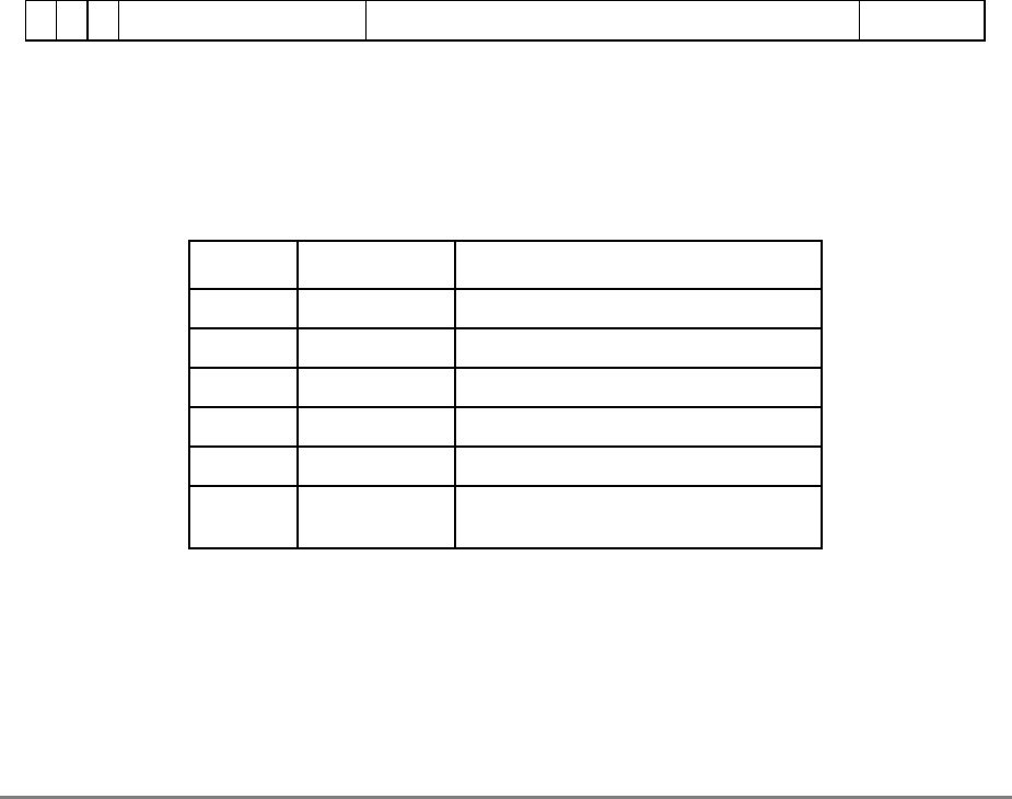
6-62 PowerPC 601 RISC Microprocessor User's Manual
6.10 I/O Controller Interface Address Translation
An I/O controller interface segment is a mapping of logical addresses to the I/O controller
interface bus protocol. I/O controller interface segments are provided for POWER
compatibility. Applications that require low-latency load/store access to external address
space should use memory-mapped I/O, rather than the I/O controller interface.
A logical address within the I/O controller interface space corresponds to a segment register
which has T = 1. For more details about memory references to I/O controller interface
segments, refer to Chapter 9, “System Interface Operation.”
As a subset of I/O controller interface address translation, the 601 also provides a way to
force I/O controller interface accesses to be made to memory. This memory-forced I/O
controller interface capability allows a 256-Mbyte segment of memory to be mapped with
only one segment register and no page translation overhead. Note that this functionality
may not be provided in other PowerPC processors.
6.10.1 Segment Register Format for I/O Controller Interface
Figure 6-25 shows the register format for the segment registers when the T bit is set.
Figure 6-25. Segment Register Format for I/O Controller Interface
Table 6-20 shows the bit definitions for the segment registers when the T bit is set.
Table 6-20. Segment Register Bit Definitions for I/O Controller Interface
Bit Name Description
0 T T = 1 selects this format
1 Ks Supervisor mode memory key
2 Ku User mode memory key
3–11 BUID Bus unit ID
12–27 — Device specific data for I/O controller
28–31 Packet 1(0–3) This field contains address bits 0–3 of the
packet 1 cycle (address-only).
T Ks Ku BUID Controller Specific Information Packet 1(0–3)
0 1 2 3 11 12 27 28 31

Chapter 6. Memory Management Unit 6-63
6.10.2 I/O Controller Interface Accesses
When the address translation process determines that the segment has T = 1, I/O controller
interface address translation is selected and any match due to block address translation (see
Section 6.7, “Block Address Translation”) is ignored. Additionally, no reference is made
to the page tables. The following data is sent to the memory controller in the protocol (two
packets consisting of address-only cycles) described in Section 9.6, “Memory- vs. I/O-
Mapped I/O Operations”:
• Packet 0
— One of the Kx bits (Ks or Ku) is selected to be the key as follows:
– For supervisor accesses (MSR[PR] = 0), the Ks bit is used and Ku is ignored
– For user accesses (MSR[PR] = 1), the Ku bit is used and Ks is ignored
— The contents of bits 3–31 of the segment register, which is the BUID field
concatenated with the “controller-specific” field.
• Packet 1—SR[28–31] concatenated with the 28 lower-order bits of the logical
address, LA4–LA31.
The WIM bits for I/O controller interface accesses are forced to b'010'. Some instructions
cause multiple address/data transactions to occur on the bus. The address for each
transaction is handled individually with respect to the MMU.
6.10.3 I/O Controller Interface Segment Protection
Page-level protection as described in Section 6.8.5, “Page Memory Protection,” is not
provided by the 601 for I/O controller interface segments. The appropriate key bit (Ks or
Ku) from the segment register is sent to the memory controller, and the memory controller
implements any protection required. Frequently, no such mechanism is provided; the fact
that a I/O controller interface segment is mapped into the address space of a process may
be regarded as sufficient authority to access the segment.
6.10.4 Memory-Forced I/O Controller Interface Accesses
The 601 performs memory-forced I/O controller interface accesses when the T bit in the
selected segment register is set and the BUID field in the segment register is x'07F'. In this
case, the processor bypasses all protection mechanisms and generates a memory access
with the physical address specified by the lowest-order four bits in the segment register
(SR[28–31]) concatenated with LA4–LA31. In this case, the processor assumes the WIM
bits to be '011', denoting the access as cache-inhibited and global. An example of address
generation for a memory-forced I/O controller interface access is shown in Figure 6-26.

6-64 PowerPC 601 RISC Microprocessor User's Manual
Figure 6-26. Memory-Forced I/O Controller Interface Access Example
6.10.5 Instructions Not Supported in I/O Controller Interface
Segments
The following instructions are not supported when issued with a logical address that selects
a segment register that has T = 1:
• lwarx
• stwcx.
• lscbx
If one of the above instructions is executed with a logical address corresponding to a
segment with T = 1, a data access exception occurs and DSISR[5] is set.
The following instructions are not supported at all and cause boundedly undefined results
when issued with a logical address that selects a segment register that has T = 1(or when
MSR[DT] = 0):
• eciwx
• ecowx
6.10.6 Instructions with No Effect in I/O Controller Interface
Segments
The following instructions are executed as no-ops when issued with a logical address that
selects a segment where T = 1:
• dcbt
• dcbtst
• dcbf
• dcbi
• dcbst
• dcbz
1 Ks Ku 0 0111 1111 x.........x PPPP
0 1 2 3 1112 27 28 31
SR6
0110
034 31
LA
PA PPPP
034 31
Chapter 6. Memory Management Unit 6-65
6.10.7 I/O Controller Interface Summary Flow
Figure 6-27 shows the flow used by the MMU when I/O controller interface address
translation is selected. This figure expands the I/O Controller Interface Translation stub
found in Figure 6-4 for both instruction and data accesses.
Figure 6-27. I/O Controller Interface Translation Flow
Memory Access
Performed
Perform I/O Controller
Interface Access
Instruction Access
Exception*
Data Access
Instruction Access
I/O Controller
Interface Translation
T=1
SR[BUID] = X’07F’ (Memory-Forced)
otherwise
otherwise
Floating-Point
Load or Store
Alignment Exception
lwarx, stwcx., or
lscbx Instruction otherwise
Cache Instruction
(dcbt, dcbtst, dcbf,
dcbi, dcbst, or dcbz)
No-Op
Set DSISR[5]=1
PA0–PA31 ← SR[28–31] ||
LA4–LA31
otherwise
Data Access
Exception
PA0–PA31 ← SR[28–31] ||
LA4–LA31
* No SRR1 bits are set for this case; this differs from the PowerPC architecture, which specifies that SRR1[3]
is set for this condition.

6-66 PowerPC 601 RISC Microprocessor User's Manual

Chapter 7. Instruction Timing 7-1
Chapter 7
Instruction Timing
70
70
This chapter describes how instructions flow through the PowerPC 601 microprocessor. A
logical model of the 601 pipeline is presented as a framework for understanding the
functionality and performance of the hardware. While this pipeline model is an abstraction
of the hardware implementation, it can yield accurate instruction timing information.
7.1 Terminology and Conventions
This section describes terminology and conventions used in this chapter and in Appendix I,
“Instruction Timings.”
7.1.1 Definition of Terms
This section defines terms used in this chapter.
• Stage—An element in the pipeline at which certain actions are performed, such as
decoding the instruction, performing an arithmetic operation, and writing back the
results. A stage typically takes a cycle to perform its operation, however, some stages
are repeated (a double-precision floating-point multiply, for example). When this
occurs, an instruction immediately following it in the pipeline is forced to stall in its
cycle.
An instruction may also occupy more than one stage simultaneously; for example,
the IQ0 position in the dispatch stage (DS) is usually identical to the integer decode
(ID) stage, or an instruction in the integer store buffer stage (ISB) remains in that
stage until it completes the cache access stage (CACC).
After an instruction is fetched, it can always be defined as being in a stage.
• Boundary—A boundary is the infinitely small period of time between stages.
• Pipeline—In the context of instruction timing, the term pipeline refers to the
interconnection of the stages. The events necessary to process an instruction are
broken into several cycle-length tasks to allow work to be performed on several
instructions simultaneously—analogous to an assembly line. As an instruction is
processed, it passes from one stage to the next. When it does, the completed stage is
now available for the next instruction.
Although it may take many cycles to complete the processing of an individual
instruction (the number of cycles is called the instruction latency), pipelining makes

7-2 PowerPC 601 RISC Microprocessor User's Manual
it possible to overlap the processing so that the throughput (number of instructions
completed per cycle) is greater than if pipelining were not implemented.
Note that with respect to the 601, each of the three executions units (floating-point
unit, or FPU; branch processing unit, or BPU; and the integer unit, or IU) has its own
pipeline. This implementation of parallel pipelines is called superscalar architecture.
• Branch folding—The elimination of a branch instruction from the pipeline after the
direction has been determined. The next sequential instruction is allowed to take its
place in the pipeline.
• Branch prediction—The process of guessing whether a branch will be taken. Such
predictions can be correct or incorrect; the term predicted as it is used here does not
imply that the prediction is correct (successful).
• Branch resolution—The determination of whether a branch is taken or not taken. A
branch is said to be resolved when it can exactly be determined which path it will
take. If branch is resolved as predicted, speculatively executed instructions can
complete execution. If the branch is not resolved as predicted, instructions are
purged from the instruction pipeline and are replaced with the instructions from the
nonpredicted path.
• Instruction stream collapsing—The elimination of empty queue positions between
instructions in the instruction queue (functionally part of the IU pipeline) when
branch and floating-point instructions are dispatched out of order. The remaining
integer instructions comprise the reference pipeline and are assigned tags that permit
all instructions to complete writeback in program order. This is shown in
Section 7.3.1.4.4, “Synchronization Tags for the Precise Exception Model.”
• Program order—The original order in which program instructions are provided to
the instruction queue from the cache.
• Bubble—A bubble is caused by a lost opportunity to execute an instruction resulting
from conditions such as pipeline stalls and by dynamics of the IQ and dispatch
mechanism. A bubble reduces the throughput (number of instructions
completed/number of cycles required) by increasing the size of the denominator.
Note that unless the bubble is a tagged bubble, it can be eliminated if the preceding
instruction causes a stall.
• Tagged bubble—A bubble in the integer pipeline that exists solely to allow branch
and floating-point instructions dispatched out of order to be reordered correctly at
the writeback stage. Sometimes it is necessary to create a tagged bubble in order to
maintain the precise exception model.
• Stall—An occurrence when an instruction cannot proceed to the next stage because
that stage is occupied by the previous instruction.
• Latency—The number of cycles required to complete the processing of a particular
instruction.

Chapter 7. Instruction Timing 7-3
• Throughput—A measure of the number of instructions that are processed per cycle.
For example, a series of integer add instructions can execute at a throughput of one
instruction per clock cycle.
• Commitment (of an instruction)—Execution has completed, data dependencies have
been resolved, and the process of recording the results has begun and must complete.
Once an instruction is committed, an exception cannot prevent the instruction from
writing back its results.
• Feed-forwarding—The action of passing the results of one instruction directly to a
subsequent, data dependent instruction. For example, there is a feed-forwarding
mechanism in the 601 IU pipeline that allows the results of the execute (IE) stage to
be available to the subsequent instruction that is in the integer decode (ID) stage.
Note that most of the discussions in this chapter and in the examples in Appendix I,
“Instruction Timing Examples,” assume that the floating-point precise mode is disabled
(that is MSR[FE0] and MSR[FE1] are not both set).
7.1.2 Timing Tables
This section describes how to use the tables in this chapter that illustrate the timings of
instructions through their respective pipeline. An example showing the flow of rotate, mask,
and shift instructions through the IU pipeline is given in Table 7-1.
The first row in the timing tables indicates the number of cycles an instruction spends in
each pipeline stage. The second row shows the pipeline stages. For integer instructions, the
stages are—integer decode (ID), integer execute (IE), integer completion (IC), integer
writeback for ALU operations (IWA), integer writeback for load operations (IWL), and
cache access (CACC). Sub rows are included with a different pipeline stage in each sub-
row. Some instructions simultaneously occupy multiple stages, while some instructions
spend several cycles in the same stage. The classic RISC instruction flow is shown in
Table 7-1—the instruction moves from ID to IE to IWA spending one cycle in each stage.
The third row in the tables shows which resources are required nonexclusively. Typically
these resources are registers that are read by the instruction. The fourth row shows
a. Table 7-23 summarizes the resources required by individual instructions.
Table 7-1. Rotate, Mask, and Shift Instruction Timing
Number of Cycles 1 1 1
Pipeline stages ID
IE
IC
IWA
Resources required nonexclusivelyarA, rB, rS, CA, MQ
Resources required exclusivelya. rA, MQ, CR0

7-4 PowerPC 601 RISC Microprocessor User's Manual
resources that are required exclusively; such resources are typically registers that are being
written by the instruction.
The columns indicate a cycle progression. The leftmost column being the first cycle.
7.2 Pipeline Description
The 601 is a pipelined superscalar processor. A pipelined processor is one in which the
processing of an instruction is broken down into discrete stages, such as decode, execute,
and writeback. Because the tasks required to process an instruction are broken into a series
of tasks, an instruction does not require the entire resources of an execution unit. For
example, after an instruction completes the decode stage, it can pass on to the next stage,
while the subsequent instruction can advance into the decode stage. This improves the
throughput of the instruction flow. For example, it may take three cycles for an integer
instruction to complete, but if there are no stalls in the integer pipeline, a series of integer
instructions can have a throughput of one instruction per cycle.
A superscalar processor is one in which multiple pipelines are provided to allow
instructions to execute in parallel. The 601 has three execution units, one each for integer
instructions, floating-point instructions, and branch instructions. The IU and the FPU each
have dedicated register files for maintaining operands (GPRs and FPRs, respectively),
allowing integer calculations and floating-point calculations to occur simultaneously
without interference.
Note that in the 601, instructions are typically dispatched out of order. Branch and floating-
point instructions are tagged to instructions in the integer pipeline, and any order-related
dependencies are tracked and handled appropriately by completion logic in the IU (the IC
stage). Note that it is not always necessary for instructions to complete in order, and the 601
allows instructions to complete in a manner that ensures the integrity of data and registers.
The 601 pipeline description can be broken into two parts, the processor core, where
instruction execution takes place, and the memory subsystem, the interface between the
processor core and system memory. The system memory includes a unified 32-Kbyte cache
and the bus interface unit.
7.2.1 Processor Core
The 601 processor core, shown in Figure 7-1, contains 20 distinct pipeline stages.

Chapter 7. Instruction Timing 7-5
Figure 7-1. Instruction Flow Diagram Showing the Processor Core
CARB
IQ7
IQ6
IQ1
IQ5
IQ4
IQ3
IQ2
IC
FD
FPA
FWA
FPM
F1
BE
MR
Dispatch Unit
Floating-Point
Integer Unit (IU)
Branch Processing
BW
CACC
Cache (memory subsystem)
IWA IWL
FWL
Data Access
Queueing Unit
Fetch Arbitration
Unit (BPU) = Unit Boundary
= Cycle Boundary
Unit (FPU)
FA
ISB
FPSB
ID
IE
IQ0
1 An integer instruction can be passed to the ID stage in the same cycle in which it enters IQ0.
1
(Instructions in the IQ
are said to be in the
dispatch stage (DS))

7-6 PowerPC 601 RISC Microprocessor User's Manual
Note that some stages can contain multiple instructions during a given cycle, and some
instructions can reside in multiple stages during a given cycle. This section gives a brief
description of each stage. Later sections go into more detail about each stage and how
individual instructions flow through the pipeline.
The processor core is shown in Figure 7-1.
Table 7-2 describes the common stages in the 601.
Table 7-3 describes the stages in the integer pipeline. Not all integer instructions pass
through every IU stage.
Table 7-2. PowerPC 601 Microprocessor Pipeline Stages—Common Stages
Stage Description
FA Fetch Arbitration—During fetch arbitration, the address of the next instructions (fetch group) to be fetched
is generated and sent to the memory subsystem (the cache arbitration stage). Any instructions that are
going to arrive at the dispatch stage as a result of the cache access associated with the address
generated during the FA stage is considered to be in the FA stage. All instructions must pass through the
FA stage.
CARB Cache Arbitration—For most operations, the CARB stage of the cache is overlapped with one or more
other stages. The CARB and CACC stages may be used by the memory subsystem for cache reload
operations and for some snoop operations. These relationships are shown in the multiple instruction timing
diagrams in Appendix I.
CACC Cache Access—The cache is the only interface point between the memory subsystem and the processor
core; if the data being accessed by the instruction in the CACC stage is in the cache, it is passed to the
processor core during that cycle (that is, a single-cycle cache access). If the data is not in the cache, no
data is passed to the processor core. The 601 cache is nonblocking, that is, once an instruction misses in
the cache, the CACC stage is free to service another instruction. For more information, see Section 7.2.2,
“Memory Subsystem.” The CARB and CACC stages may be used by the memory subsystem for cache
reload operations, and some snoop operations. During a cache reload, the data being reloaded is brought
in from the memory system and is available for use in the processor core on the next cycle.
DS Dispatch—The dispatch stage is associated with the eight-entry instruction queue (IQ0–IQ7). The 601 can
dispatch as many as three instructions on every clock cycle, one to each of the processing units (the IU,
the BPU, and the FPU) from the same dispatch stage. As many as eight instructions can be in the dispatch
stage (instruction queue), but instructions can be dispatched only from IQ0–IQ3. Note that only three of
the first four (in program order) can be dispatched on a given cycle.
Note that the bottom element of the instruction queue (IQ0) can be viewed as part of the integer decode
(ID) stage.

Chapter 7. Instruction Timing 7-7
The data access queueing unit provides a buffer between the IU and the memory subsystem.
It contains two stages—the floating-point store buffer stage (FPSB), and the integer store
buffer stage (ISB). The stages in this unit are described in Table 7-4. The data access
queueing unit is described with the IU in Section 7.3.3, “Integer Pipeline Stages.”
The floating-point pipeline contains six stages below the DS stage. These stages are
described in Table 7-5. Note that all floating-point arithmetic instructions must pass
through each of these stages (with the exception of F1); details of how each type of
instruction makes use of each floating-point stage is provided in Section 7.3.4, “Floating-
Point Pipeline Stages.”
Table 7-3. PowerPC 601 Microprocessor Pipeline Stages—Integer Pipeline
Stage Description
ID Integer Decode—In the ID stage, integer instructions are decoded and the operands are fetched from the
GPRs. Note that an integer instruction typically enters the decode stage when it enters IQ0; when and
instruction stalls in the ID stage, a new instruction may move into IQ0; however, IQ0 and ID will be the
same after the instruction is no longer stalled in the ID stage.
IE Integer Execute—In the IE stage, integer ALU operations are executed, the EA for memory access
instructions is calculated and translated, and the request is made to the memory subsystem (that is, the
instruction simultaneously occupies the CARB and CACC stages).
There is feed-forwarding for ALU operations in the IE stage. This means that the results calculated in the
IE stage are available as sources to the instruction that enters IE stage in the next cycle. This eliminates
stalls due to data dependencies between consecutive integer ALU instructions. There is also feed-
forwarding from the CACC stage to the IE stage resulting in only a one-cycle stall for a dependent
operation directly following a load instruction. For more information, see Section 7.3.3, “Integer Pipeline
Stages.”
IC Integer Completion—In the IC stage, results of instructions are made available for use unless
synchronous exceptions are detected. Tags for branch and floating-point instructions must pass through
this stage.
IWA Integer Arithmetic Writeback—In the IWA stage, the general purpose registers (GPRs) are updated with
the results from integer arithmetic operations.
IWL Integer Load Writeback—In the IWL stage, integer load operations a write operation in the GPRs with from
the cache or from memory.
Table 7-4. PowerPC 601 Microprocessor Pipeline Stages—Data Access Queueing
Unit
Stage Description
FPSB Floating-Point Store Buffer— The FPSB stage is used for floating-point store instructions that have been
committed (or are being committed) but for which the floating-point data is not yet available. All floating-
point store instructions must pass through this stage. This stage allows the instruction to free up the IE
stage. An instruction remains in this stage until it completes the CACC stage. The data in this stage is kept
memory-coherent by the processor.
ISB Integer Store Buffer—The ISB stage is used to buffer data accesses that were not arbitrated into the
cache due to a higher priority access (such as a cache reload). This stage allows the instruction to free up
the IE stage. An instruction remains in this stage until it completes the CACC stage.The buffer used in this
stage is kept memory-coherent by the processor.

7-8 PowerPC 601 RISC Microprocessor User's Manual
The BPU pipeline contains three stages below the DS stage—the branch execute stage
(BE), the mispredict recovery stage (MR), and the branch writeback stage (BW). These are
described in Table 7-6.
Some integer and floating-point instructions must repeat stages in their respective pipelines,
which causes subsequent instructions in the pipeline to stall. In addition to the multicycle
operations, data dependencies can cause stalls as described in Section 7.3.3, “Integer
Pipeline Stages,” and Section 7.3.4, “Floating-Point Pipeline Stages.”
Synchronization is handled relative to the integer pipeline. To ensure that LR and CR are
updated in order, neither the BPU nor the FPU can perform their write-back operations until
their tags complete the IC stage in the integer pipeline. Instructions in the IU cannot get
ahead of instructions in the BPU, but may get ahead of instructions in the FPU by as many
Table 7-5. PowerPC 601 Microprocessor Pipeline Stages—Floating-Point Pipeline
Stage Description
F1 Floating-Point Instruction Queue—The F1 stage is a one-entry queue that buffers floating-point
instructions that have been dispatched but cannot be decoded because an instruction is stalled in the FD
stage.
FD Floating-Point Decode—In the FD stage, instructions are decoded and operands are fetched from the
FPRs.
FPM Floating-Point Multiply—In the FPM stage, operands are fed through a multiplier that performs the first part
of a multiply operation. The multiplier performs a single-precision multiply with a throughput of one per
cycle or a double-precision multiply with a throughput of one per two cycles.
FPA Floating-Point Add—In the FPA stage, an addition is performed for add instructions or to complete multiply
or accumulate instructions.
FWA Floating-Point Arithmetic Writeback—In the FWA stage, normalization and rounding occur, FPRs are
updated, store data is sent to the memory subsystem, and bits are set in the FPSCR. Data written to the
FPRs during the FWA stage is available to the FD stage in the following cycle.
FWL Float Load Writeback—During the FWL stage, load data is written into the FPRs. Load data that is being
written to the FPRs is also available to the FD stage in the same cycle.
Table 7-6. PowerPC 601 Microprocessor Pipeline Stages—Branch Pipeline
Stage Description
BE Branch Execute—In the BE stage, the target address of a branch is calculated and the branch direction is
either determined or predicted depending on the state of the condition register (CR) and the type of branch
instruction. Note that the BE stage is parallel with the FA stage of the target instructions of a taken branch.
MR Mispredict Recovery—Conditional branches also go into the MR stage (in parallel with entering the BE
stage) and stay there until the branch is resolved (the CR is coherent). If a branch was predicted
incorrectly, the MR stage logic allows the fetcher to recover and start executing the correct path.
BW Branch Writeback—In the BW stage, branch instructions that update the link register (LR) or count register
(CTR) do so. Note that many branches can be in the BW stage at any given cycle, but that no more than
two can write back in one cycle. An infinite stream of taken branches that hit in the cache has a throughput
of one branch every two cycles.

Chapter 7. Instruction Timing 7-9
as three instructions if floating-point exceptions are disabled (that is, the processor logs the
exception but does not trap to an exception vector). However, when floating-point
exceptions are enabled, (controlled by MSR[FE0] and MSR [FE1]) the IU cannot get ahead
of the FPU. This is described in Section 7.3.1.4.4, “Synchronization Tags for the Precise
Exception Model.”
Performance is affected whenever the IU is required to synchronize with the FPU, as
described in Section 7.3.4, “Floating-Point Pipeline Stages.”
When a floating-point or branch instruction is dispatched, it is tagged to the previous integer
instruction (in program order). This tag is used to ensure that execution appears to be in
program order. There are certain restrictions, such as the fact that only one floating-point
instruction can be tagged to an integer instruction, that may cause an instruction to be
tagged to a bubble (nonexecuting placeholder) in the IU pipeline, thus reducing throughput.
These restrictions are described in Section 7.3.1.4, “Common Stages—Dispatch (DS)
Stage,” and Section 7.3.1.4.4, “Synchronization Tags for the Precise Exception Model.”
7.2.1.1 Dispatch Stage Logic
The DS stage, which contains instruction queue (IQ), resides between the memory
subsystem and the execution units and accounts for the time required to fetch the instruction
and to dispatch it to one of the execution units. The instruction queue can hold as many as
eight instructions, so an entire cache sector can be fetched into the DS stage in one cycle.
The following characteristics and restrictions regarding instruction dispatch should be
noted:
• Floating-point, branch, and integer instructions can be dispatched out-of-order.
• Floating-point and branch instructions are tagged to a previous integer instruction in
program order or to a bubble in the IU pipeline. Typically, a floating-point or branch
instruction is dispatched before the integer instruction or bubble to which it is
tagged. Tagging is described in Section 7.3.1.4.4, “Synchronization Tags for the
Precise Exception Model. “
• Floating-point and integer instructions flow through their respective pipelines in
program order. Under certain conditions, branch instructions can be dispatched out
of order, as described in Section 7.2.1.4, “Branch Processing Unit (BPU).”
• Integer and load/store instructions are dispatched in order relative to all instructions
(that is, an integer instruction cannot be dispatched until all instructions before it in
program order have been dispatched).
• Branch and floating-point instructions can be dispatched in program order from
IQ0–IQ3. However, an integer instruction is dispatched only when it is the first
instruction in the DS stage (typically IQ0) in program order. Branch and integer
instructions are dispatched in zero cycles, while floating-point instructions take one
cycle to dispatch.

7-10 PowerPC 601 RISC Microprocessor User's Manual
Several situations can cause dispatch stalls—instruction synchronization requirements of
the precise exception model, resource dependencies and data dependencies. These stalls are
described in Section 7.3.1.4, “Common Stages—Dispatch (DS) Stage.”
7.2.1.2 Integer Unit (IU)
The integer unit (IU) executes the following types of instructions:
• Integer arithmetic instructions
• Integer logical instructions
• All load operations and store operations (both integer and floating-point)
• CR instructions
• Memory management instructions
• Miscellaneous special purpose register instructions.
Different types of instructions use different portions of the IU pipeline.
All instructions that execute in the IU use the ID stage in the same way—the instruction is
decoded, immediate constants are pulled from the instruction, and the appropriate operands
are fetched from the GPRs.
All instructions that execute in the IU use the IE stage and writeback stages (IWA and
IWL), but different types of instructions use these stages in different ways. These
instructions can grouped by function. Within a group, the functions performed in these
stages are very similar. However, the functions performed in these stages differ greatly from
one group to another. Instructions that execute in the IU can be divided into the following
groups:
• The single-cycle integer operations—These operations take one cycle in the IE
stage, one cycle in the IWA stage, and an overlapping cycle in the IC stage (typically
these instructions are in the IC stage at the same time as the IWA stage). This class
of operations includes integer addition operations, rotate/shift operations, integer
logical operations, CR manipulations, and some register move operations.
• The multicycle integer operations use the IE stage, the IWA stage, and the IC stage,
but take multiple cycles in at least one of these stages. Included in this class are
integer multiply instructions, integer divide instructions, and some register move
operations.
• All single-cycle load/store instructions spend one cycle (simultaneously) in the IE
and CARB stages, followed by at least one cycle in the CACC and in the IC stages.
Note that additional cycles may be required in either the FPSB or the ISB stage if
there is a stall, and note also that when the instruction is in the CACC stage it must
also occupy either the FPSB or the ISB stage in case a cache retry condition forces
the instruction to back out of the CACC stage. Finally, they may spend at least one
cycle in either the IWL or the FWL stage. Single-cycle load/store operations include
all integer and floating-point load/store operations except for the load/store

Chapter 7. Instruction Timing 7-11
string/multiple operations. Logical addresses are translated to physical addresses
during the IE stage. The update of rA for update-form load and store operations uses
the IWA stage in parallel with the IC stage.
• The load/store multiple/string instructions use the same stages as the single-cycle
load/store instructions but they spend multiple cycles in each stage. Note there are
no floating-point load/store multiple/string instructions.
The execution of some instructions is shared between the IU and other units on the 601. For
example, floating-point store operations are executed in both the IU and FPU. The IU
generates the effective store address while the FPU provides the store data. Cache
instructions (such as dcbz and dcbi) are decoded in the IU, and as the instruction is passed
into the IE stage it is simultaneously passed to the CARB stage, and subsequently to the
CACC (and ISB) stage where the appropriate actions are performed.
The flow of instructions through the integer pipeline, and dependencies and considerations
associated with the IU pipeline, are described in Section 7.3.3, “Integer Pipeline Stages.”
7.2.1.3 Floating-Point Unit (FPU)
The FPU executes all floating-point arithmetic instructions and floating-point store
operations, as described in Section 7.2.1.2, “Integer Unit (IU).” The FPU conforms to
IEEE/ANSI standards for both single- and double-precision arithmetic. Double-precision
floating-point values are stored in the thirty-two 64-bit floating-point registers (FPRs)
contained within the FPU. Single-precision floating-point values are also contained in the
FPRs (although only 32 single-precision values may be stored in the FPRs).
With the exception of the F1 stage, which acts as a buffer between the DS and FD stages
when the FD stage stalls or is busy, all floating-point instructions must complete each stage
in the floating-point pipeline. Special case numbers, such as denormalized numbers, NaNs,
and infinity, are fully handled in hardware and may be required to repeat the path through
the floating-point pipeline.
In the FD stage, instructions are decoded and operands are fetched from the FPRs. The
number of cycles required to decode a floating-point instruction depends on the type of
instruction:
• Single-precision multiply and add instructions, double-precision add instructions,
register move instructions, conversion instructions, and store instructions each
spend one cycle in the FD stage.
• Double-precision multiply instructions spend two cycles in the FD stage. The 601
employs a single-precision multiply-add array spread across the FPM and FPA
stages. Double-precision multiply operations are split into two operations, each of
which uses the FD, FPM, and FPA stages twice. The results are added in the second
cycle in the FPA stage. Note that this operation is fully pipelined—the second cycle
in FD overlaps the first cycle of FPM; and the second cycle of FPM overlaps the first

7-12 PowerPC 601 RISC Microprocessor User's Manual
cycle of FPA. This results in a throughput of one double-precision multiply per two
cycles. This process is described in Section 7.3.4.5.2, “Double-Precision Instruction
Timing.”
• Divide instructions continue to occupy the FD stage until it enters its final FWL
cycle—either about 18 (single-precision) or about 30 (double-precision).
• Some special case numbers cause stalls in the FD stage.
Floating-point arithmetic instructions write back in the FWA stage and do not use the FWL
stage, while floating-point load instructions write back in the FWL stage, and do not use
the FWA stage.
7.2.1.4 Branch Processing Unit (BPU)
The BPU handles branch prediction and resolution in addition to branch target calculation.
The BPU generates two addresses that feed the FA stage—the branch target address (for
taken branches), and the mispredict recovery address (the recovery address for
mispredicted branches).
Branch instructions can be divided into four groups, depending upon whether they require
the MR and BW stages. These are shown in Table 7-7. Note that branch instructions that do
not require MR or BW can always be folded, and they never require tags in the IU pipeline.
* Conditions that can prevent branch folding are described in Section 7.3.1.4.5, “Dispatch Considerations Related
to IU/FPU Synchronization.”
All branch instructions use the BE stage, during which, the target address for the branch is
calculated and if the branch is either resolved to be or predicted to be taken, the address for
the branch is passed to the FA stage (in zero cycles).
Branches that are conditional on the CR are predicted in the BE stage (unless they can
already be resolved). The address of the nonpredicted path is stored in the MR stage (see
below) in case the prediction is incorrect. The 601 uses a static prediction scheme.
Branches that are conditional on the CR also enter the MR stage in parallel with BE stage.
The branch stays in the MR stage until it is resolved. If the prediction is incorrect, the
mispredict address (stored in the MR stage) is sent to the FA stage. The MR stage can hold
only one mispredicted branch address, so the 601 can only handle one unresolved
Table 7-7. Branch Instruction Folding
Branch Instruction Type MR Stage BW Stage Folded
Nonconditional/nonupdating No No Always*
Nonconditional/updating No Yes (synchronous with IU WB) Usually*
Conditional/nonupdating Yes No Sometimes*
Conditional/updating Yes Yes (synchronous with IU WB) Usually*

Chapter 7. Instruction Timing 7-13
conditional branch at a time—any other conditional branch stalls at DS, although branches
that do not depend on the CR can still be dispatched and executed.
The BPU contains two link shadow registers to store link addresses when branch-and-link
instructions are executed out of order. When a branch-and-link instruction is dispatched, a
tag is generated in the integer pipeline. This tag is used to synchronize completion of
instructions. Branch-and-link instruction can execute and clear the BE stage, but the LR is
updated only when the tag completes the IC stage. Similarly, branch-and-decrement
instructions do not immediately update the CTR when they execute; instead, they generate
a tag used to decrement the CTR when it clears the IC stage. This is described in
Section 7.3.1.4.4, “Synchronization Tags for the Precise Exception Model.”
Branch instructions that update LR or CTR must go through the BW stage. The branch
instruction enters the BW stage on the cycle immediately following the BE stage and stalls
there waiting for its tag to complete (tags complete by passing through the IC stage). As
many as nine branches can reside in the BW stage simultaneously, which eliminates stalls
due to the BW stage filling up; however, only two branches can write back on a given cycle
(one to the LR and one to the CTR).
7.2.1.5 Memory Subsystem Pipeline Stages
The CARB and CACC stages are part of the memory subsystem. These stages represent the
only path between the processor core and main system memory. Memory accesses must
pass through both the CARB and the CACC stages. The CARB stage is responsible for
arbitration between different memory access requests generated by the processor core and
the memory subsystem. The different types of requests are prioritized as follows:
1. Cache maintenance accesses (generated by the memory subsystem). These include
the following in order of priority:
a) The reload access for reloading a cache line on a cache miss
b) The cast-out access for casting-out a modified adjacent sector
c) The snoop push required by a snoop operation
2. Data load requests (generated by the processor core). Note that loads precede stores
with respect to the memory queues; however cache accesses occur in program order
(assuming cache hits). The memory queues are described in Section 7.2.2.2, “Bus
Interface Unit.”
3. Data store requests (generated by the processor core). Note that loads precede stores
with respect to the memory queues; however cache accesses occur in program order
(assuming cache hits).
4. Instruction fetch requests (generated by the processor core)
Only one request is granted in a given cycle, and that request is forwarded to the CACC
stage in the next cycle. If a cache miss occurs, no data is returned from the CACC stage.
There are conditions where a stall may occur in the CARB or CACC stages associated with
cache retry, as described in Chapter 4, “Cache and Memory Unit Operation.” The data is

7-14 PowerPC 601 RISC Microprocessor User's Manual
available during the CACC stage of the cache reload, as described in Section 7.2.2.3.3,
“Cache Miss Timing”; thus in this case, a request can be satisfied even if it is not arbitrated
into the cache (the CARB stage).
Throughout much of this document, cache hits are assumed on all requests generated by the
processor core; requests generated by the memory subsystem are ignored. Timing
information including memory subsystem activity and cache misses can be determined by
applying the timing of the memory substage to the CARB and CACC stage timing, as
described in the following section, Section 7.2.2, “Memory Subsystem.”
7.2.2 Memory Subsystem
The memory subsystem of the 601 consists of a unified cache and a bus interface that
employs extensive queueing to increase performance. The cache supports the four-state
MESI protocol and the bus interface implements snooping protocol to maintain cache
coherency for symmetric multiprocessor implementations.
This section describes the components of the memory subsystem—the cache unit,
described in Section 7.2.2.3, “Cache Unit,” and the system interface, described in
Section 7.2.2.2, “Bus Interface Unit.” This section also describes how memory accesses
affect instruction timing.
7.2.2.1 Memory Management Unit (MMU)
The 601 MMU supports both the standard page table translation mechanism and the block
address translation (BAT) mechanism. There is a unified 256-entry, two-way set associative
translation lookaside buffer (TLB) in the MMU. The TLB is maintained in hardware,
including a hardware reload on a TLB miss. The BAT registers are maintained by software
as specified by the PowerPC architecture. One MMU is used for both instruction and data
translation with data accesses given priority over instruction accesses. Translation occurs
during execute stage for load operations and store operations. For more detailed
information about translation mechanism, see Chapter 6, “Memory Management Unit.”
7.2.2.2 Bus Interface Unit
The bus interface unit of the 601, shown in Figure 7-2, consists of a memory queue and bus
control logic. The memory queue contains two read queues and three write queues (one of
which is reserved for snoop pushes).
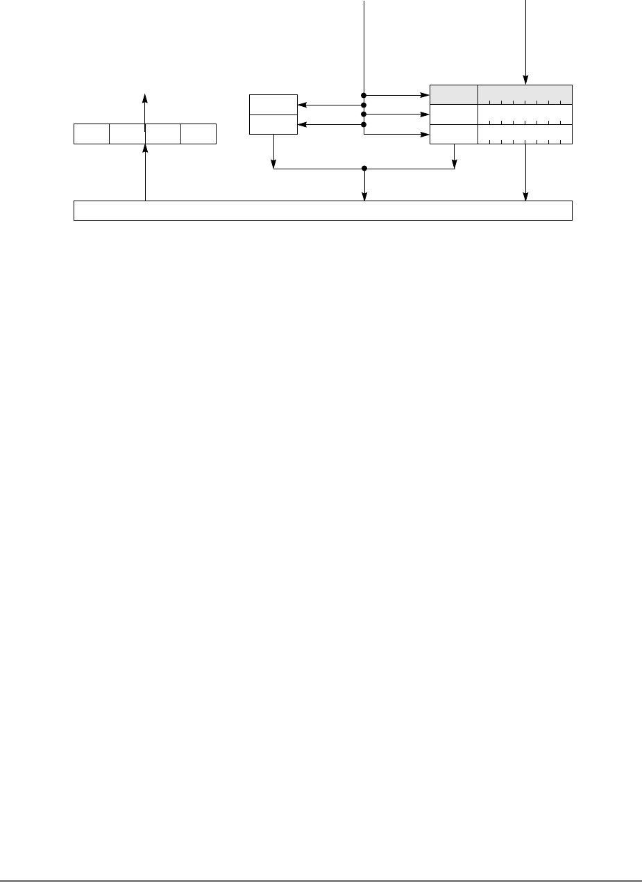
Chapter 7. Instruction Timing 7-15
Figure 7-2. Bus Interface Unit
The read queues may hold any combination of the following three cache misses—one fetch,
one load, and one cacheable write-back store operation.
For better overall processor performance, the queueing allows high priority operations
(such as read misses) to bypass low priority operations (such as cache write-back
operations). This prioritizing is discussed in Section 7.2.2.2.3, “Bus Interface Arbitration.”
The bus interface features include pipelining of up to two operations, data forwarding (after
two data beats have been received), bus parking, and optional loading of the adjacent sector
in a cache line to decrease the latency of memory accesses. This is described in detail in
Chapter 9, “System Interface Operation.”
The bus interface allows zero wait state data to stream into or out of the chip, providing a
maximum data bus bandwidth of 320 Mbytes/second (at 50 MHz). This high bandwidth is
achieved by using the 601’s zero wait state capability and the ability to burst data, to
pipeline two addresses onto the bus and overlap slave access time for the second tenure with
that of the first.
7.2.2.2.1 Write Queue
For each position in the write queue, there is space for the physical address and for the
associated data (each capable of holding a sector). One position, marked snoop in
Figure 7-2, is provided for high-priority bus operations when a snoop hits a modified sector.
This is described in Section 9.10, “Using DBWO (Data Bus Write Only).”
Burst writes are always sector aligned.
7.2.2.2.2 Read Queue
For burst read operations, the address is modified to be the quadword address of the
requested data. By requesting the quadword, the hardware can forward data to the internal
target after only two beats of the data have been received. On the other hand, the memory
system need only be able to provide two orderings of data coming back (first quadword of
a sector then second or second quadword then first).
READ
QUEUE WRITE QUEUE
SNOOP
ADDRESS DATA
ADDRESS
(from cache) DATA
(from cache)
SYSTEM INTERFACE
(to cache)
DATA QUEUE
(four word)

7-16 PowerPC 601 RISC Microprocessor User's Manual
Data that is read from memory is sent to a buffer that accepts a quadword of data before
accessing the cache to write the data (and forward it to the processor if required).
The read queues also allow an optional reload of the adjacent sector of a cache line if it is
not already valid in the cache, a read request is queued for that sector if no other read misses
are present. How these operations are prioritized is shown in Section 7.2.2.2.3, “Bus
Interface Arbitration.”
For code and data with good locality of reference, this can lead to significant performance
increases by reducing the number of cache misses. This optional reload can be disabled for
instruction fetches by setting HID0[26] and for load/store misses by setting HID0[27]. For
more information about the HID0 register, see Section 2.3.3.13.1, “Checkstop Sources and
Enables Register—HID0.”
7.2.2.2.3 Bus Interface Arbitration
The 601 arbitrates all queue positions for bus access using the following priority scheme
(which is optimized for minimal processor stall):
1. High-priority cache push-out operations (using the DBWO signal)
2. Normal snoop push-out operations
3. I/O controller interface segment accesses that incur no additional delays (that is, they
have not been retried because of I/O latency). When these accesses have been
retried, these operations are given lowest priority.
4. Cache instruction operations
5. Read requests, such as load operations, RWITMs, and instruction fetches
6. Single-beat write operations
7. sync instructions
8. Optional cache-line fill operations
9. Cache sector cast-out operations
10.I/O controller interface segment accesses that incur additional delays (that is, they
have been retried because of I/O latency). This is described in Chapter 4, “Cache and
Memory Unit Operation.”
Because write operations do not stall the processor, they are performed after read
operations. If, however, a read misses and a write to the same block is in the queue, that
write is prioritized ahead of any other read operations. This allows the read miss to be
queued so the cache can be accessed for some other request.
I/O controller interface operations are typically ARTRYed multiple times. To allow other
operations to finish in the interim, these I/O controller interface operations are given lowest
priority (until the 601 begins another bus operation).
Chapter 7. Instruction Timing 7-17
A read miss can be arbitrated directly from the cache access point to the bus if no other
reads are queued. This eliminates having to queue the operation before arbitrating for the
bus.
7.2.2.2.4 Bus Parking
Bus parking is associated with the address portion of the bus interface unit. It is a part of
the bus protocol that eliminates as many as two cycles of bus arbitration overhead by having
the bus pregranted to a particular master. If the master is given a bus grant (BG) on the cycle
that it needs to request the bus, it begins a tenure by asserting the TS signal. Bus parking
saves the cycle where bus request would have been asserted and the cycle of the grant, as
shown in Figure 7-3. In some systems, these two cycles may be the same cycle. The transfer
start occurs up to two cycles earlier when the bus is parked compared to when the bus is not
parked.
Figure 7-3. Bus Timing for Parked and Nonparked Bus Masters
For more information about bus parking refer to Section 9.3.1, “Address Bus Arbitration.”
7.2.2.3 Cache Unit
The 601 has a unified 32-Kbyte, eight-way set associative cache. The cache access time is
one processor cycle and it is nonblocking on misses. The cache tag directory is dual ported
with one port dedicated for bus snooping. The cache array is not accessed by snoops unless
a snoop push is required (that is, a snoop results in a data access action). The 601 uses a
single cache for both data and instruction accesses. The cache uses a least-recently-used
(LRU) algorithm for replacing cache lines.
7.2.2.3.1 Cache Arbiter
Because the cache is single-ported and unified, all cache accesses must be prioritized.
Cache arbitration is prioritized as shown in 7.2.1.5, “Memory Subsystem Pipeline Stages.”
Note that instruction fetch accesses have the lowest priority access to the cache.
7.2.2.3.2 Cache Hit Timing
To determine if the appropriate data resides in the cache, the cache data array and the cache
tag directory are accessed in parallel. As shown in Figure 7-4, for a cache hit, data is
BR
BG
TS
BR
BG
TS
Cache miss detected
(Inactive)
(Active)
Processor
Not Parked
Processor
Parked

7-18 PowerPC 601 RISC Microprocessor User's Manual
available at the output of the cache one cycle after the read address is arbitrated. If
necessary, the tag directory is updated in the same cycle that the cache data is available
(cycle 1). The processor can forward the data to the IE stage in cycle 1. This feed-
forwarding mechanism is described further in Section 7.3.3, “Integer Pipeline Stages.”
Figure 7-4. Cache Hit Timing for a Load Access and a Fetch Access
If a cache hit is detected when a write access is arbitrated into the cache, the cache is
accessed and written in the same cycle. If necessary, the tag directory is also updated in the
same cycle (cycle 1) in Figure 7-4. Store operations have the same arbitration priority as
load operations. As long as they hit in the cache, a read access can immediately follow a
write access and a write access can immediately follow a read access unless there are data
dependencies. Data dependencies are shown in the examples in Appendix I, “Instruction
Timing Examples.”
7.2.2.3.3 Cache Miss Timing
The cache miss timing is a function of several variables, including bus speed, memory
access time and interleaving structure, and bus arbitration schemes. This section considers
the fastest possible system, then provides formulas for calculating numbers for any real
system. For the rest of this section, the terms processor cycle and bus cycle are used to
differentiate the actual amount of time elapsing. Bus cycles are integer multiples of
processor cycles, and the multiple is system-dependent.
7.2.2.3.4 Timings When the Processor Clock Frequency Equals the Bus
Clock Frequency
The following discussion assumes a 1:1 bus clock to processor clock frequency ratio. For
information about 601 clock operation, refer to Section 8.2.11, “Clock Signals.” Figure 7-5
shows the best-case timing for a cache miss with the processor and bus operating at the
same frequency. This example assumes a one bus cycle access time to main memory, bus
running at full speed, no delay between the data beats (that is the transfer acknowledge, TA,
signal is asserted without delay for each beat), no address retry (ARTRY) on the address
tenure, and the processor is parked on the bus.
Arbitrate
load into
the cache.
Access cache,
determine that there
is a cache hit. Data
available to the IE
stage.
Target
GPR
written,
dependent
operation
executes.
Arbitrate
fetch into
the cache.
(FA stage)
Access cache,
determine that
there is a cache hit.
Instructions are
placed in the IQ.
(DS stage)
0 1Cycle:0 1 2Cycle:
Instruction
available
for
dispatch
2
Load Access: Fetch Access:

Chapter 7. Instruction Timing 7-19
Figure 7-5. Cache Miss Timing When the Processor Clock Equals the Bus Clock
(Best-Case Timing)
When a cache miss is detected it is immediately arbitrated onto the bus if nothing of higher
priority is queued (Clock 0). The bus grant signal (BG, is asserted in the next clock cycle
(Clock 1) if there is no higher priority transaction on the bus. However, if the processor is
parked on the bus (BG is already asserted), a transfer begins on the next bus cycle. In this
example, the transfer begins in Clock 2. The operation is also placed in the read queue
(shown in Figure 7-2), so the data can be pipelined back to the processor and the cache.
Sometime after the transfer has begun (perhaps as soon as the next bus cycle as shown here
in Clock 3), data begins to come into the processor. Data arrives in four double-word beats
(for a cache sector of data). After the second beat of data arrives (Clock 4), the bus interface
unit makes a request (Clock 5) to write the four words into the cache (a “reload dump”).
The first four words contain the critical word.
During the next processor cycle (Clock 6), data is written to the cache and forwarded to the
processor core if required (either to the register or to the IQ, depending on whether the
action was a load or a code fetch). After the last two beats of data arrive, a second request
to write to the cache is made (Clock 7). During Clock 8, the cache receives the remaining
four words of data (bursts three and four) and the cache tag is validated. In Clock 9, if an
access to this sector is arbitrated into the cache, the cache tags signal a cache hit, as shown
in Figure 7-5.
Figure 7-6 shows a formula for calculating the number of processor cycles from cache miss
(that is, cycle 1 in Figure 7-5) to dependent operation execution (cycle 7 in Figure 7-5)
assuming a 1:1 processor-to-bus-clock ratio.
Arbitrate
load
into the
cache
(CARB).
Cache
miss.
Receive
bus
grant
(BG).
Load in
memory
queue,
assert TS,
receive
data bus
grant
(DBG)
1st data
beat
returned
2nd data
beat
returned
3rd data
beat
returned;
arbitrate
reload
dump
into
cache.
4th data beat,
first two beats
of data written
to cache and
forwarded to
IE stage, and
IQ.
dependent
operation
executes,
arbitrate
reload
dump 2
into cache.
Reload
dump 2,
cache
tags
validated
for
sector.
New
sector
usable
in cache.
0 1 2 3 4 5 6 7 8 9

7-20 PowerPC 601 RISC Microprocessor User's Manual
Figure 7-6. Formula for Calculating Total Time from Cache Miss to Execution of
Dependent Operation
Bus parking is described in Section 7.2.2.2.4, “Bus Parking.”
Figure 7-7 provides a formula for calculating the total number of processor cycles from
cache miss to data available for next cache hit assuming the processor clock frequency
equals bus clock frequency.
Figure 7-7. Formula for Calculating Total Time from Cache Miss to Data Available
for the Next Cache Hit
7.2.2.3.5 Timings When the Processor Clock Frequency Does Not Equal the Bus
Clock Frequency
This section describes timings when the bus clock frequency does not equal the processor
clock. Information regarding configuring the clock signals is given in Section 8.2.11,
“Clock Signals.” Figure 7-8 shows the timing for a cache miss when the processor clock is
twice as fast as the bus clock.
Total = 3 + 3 + AT + TD + SDD1 + BNP
cycles from the assertion of TS to the assertion of the first TA
delay between the first and second beats
cycles while DRTRY is asserted after second TA
processor cycles spent in the 601
minimum time spent on the bus
penalty if the bus is not parked
Total = 3 + 5 + AT + STD + SDD2 + BNP
cycles from the assertion of TS to the assertion of the first TA
sum of delays between TAs
cycles while DRTRY is asserted after all TAs
processor cycles spent in the 601
minimum time spent on the bus
penalty if the bus is not parked

Chapter 7. Instruction Timing 7-21
Figure 7-8. Cache Miss Timing when the Processor Clock Frequency is Twice the
Bus Clock Frequency (Best-Case)
Processor cycles are indicated by both dashed and solid lines, while bus cycles are indicated
by the solid lines only.
Note that typically there is a one-half processor cycle penalty for synchronizing to the bus
clock when the processor clock frequency is twice the bus clock frequency (half the time
the cache miss occurs one processor clock before a bus transition processor clock, half the
time it occurs in a bus transition processor clock). This penalty is larger for larger processor
clock to bus clock ratios, as the average number of processor cycles of delay increases.
Also, all bus related parameters now have to be multiplied by the processor clock to bus
clock ratio.
Figure 7-9 shows these factors in calculating total processor cycles for cache-miss-to-
dependent-operation execution when the bus clock frequency does not equal the processor
clock frequency.
Load in
cache,
cache
miss.
Load in
memory
queue,
arbitrate
to the
bus, BG
asserted
Assert
TS Receive
DBG.First
data
beat
returned
Second
data
beat
returned
.
Third
data
beat
returned
and
arbitrate
reload
dump
into
Data
written to
cache and
forwarded
to IE stage
or IQ
Fourth data
beat
returned,
dependent
operation
executes
0 1 2 3 4 5 6 7 8 9 10 11
Arbitrate
reload
dump2
into the
cache
Reload
dump2,
cache
tags
validate
d for
sector.
New
sector
usable.
12 13 14 15
NOTE: Processor cycles are indicated by both
solid and dashed lines. Bus cycles are
indicated by solid lines.
50% of the time, this clock is not wasted because the miss occurs on the bus transition cycle
instead of the nontransition cycle as shown here.

7-22 PowerPC 601 RISC Microprocessor User's Manual
Figure 7-9. Formula for Calculating Total Time from Cache Miss to Dependent
Operation Execution (Processor Clock/Bus Clock ≠ 1:1)
Figure 7-10 shows a formula for calculating the total number of processor cycles from
cache miss to data available for next cache hit on a bus that is not running at the same
frequency as the processor.
Figure 7-10. Formula for Calculating Total Time from Cache Miss to Data Available
for Next Cache Hit (Processor Clock ≠ Bus Clock)
7.3 Pipeline Timing
This section, describes the exact timing of the pipeline stages, including specific
information for every instruction and descriptions of data dependencies that may affect
throughput. It is organized into three main parts. The first part discusses timing for stages
common to all instructions and the closely related branch pipeline. Subsequent sections
discuss timing for stages specific to the IU and FPU pipelines.
Total = 3 + ASP + (3 + AT + TD + SDD1 + BNP) * PBR
memory access time
delays between first and second TAs
penalty if the bus is not parked
processor clock/bus clock ratio
processor cycles spent in the 601
minimum time spent on the bus
average number of processor cycles lost for synchronizing to the bus
cycles while DRTRY is asserted after second TA
Total = 3 + ASP + (5 + AT + TD + SDD2 + BNP) * PBR
memory access time
delays between first and second TAs
penalty if the bus is not parked
processor clock/bus clock ratio
processor cycles spent in the 601
minimum time spent on the bus
average number of processor cycles lost for synchronizing to the bus
cycles while DRTRY is asserted after all TAs

Chapter 7. Instruction Timing 7-23
7.3.1 Common Stages/BPU Pipeline Stages
This section describes timing of the pipeline stages that are common to every instruction
and the closely related branch pipeline.
The common stages are as follows:
• Fetch arbitration stage (FA)—In this stage, the fetch address is sent to the memory
subsystem. The FA stage is described in Section 7.3.1.1, “Common Stages—Fetch
Arbitration (FA) Stage.”
• Cache arbitration (CARB) and cache access (CACC) stages—In these stages
instructions are read from the memory subsystem (from the address sent to the
memory subsystem in the FA stage) and loaded into the instruction queue (DS
stage). The CARB stage is described in Section 7.3.1.1, “Common Stages—Fetch
Arbitration (FA) Stage and Section 7.3.1.3, “Common Stages—Cache Access
(CACC) Stage.”
• Dispatch stage (DS)—The common stages end when instructions are dispatched to
the appropriate execution unit(s) in the dispatch stage (DS). The dispatch stage has
different timing for different instructions.
The BPU pipeline is included in this discussion because it is tightly coupled to the common
stages in that the results of a branch instruction determine which instructions enter the FA
stage. The BPU generates the branch target address and the mispredict address that can go
to the memory subsystem in the FA stage.
7.3.1.1 Common Stages—Fetch Arbitration (FA) Stage
During the FA stage, the address for the next instruction needed by the processor core is
sent to the memory subsystem. The possible sources of stalls can be grouped into the two
following categories:
• External events—Anything that occurs outside the BPU that stops the fetch address
from accessing the memory subsystem. For more information see Section 7.2.2.3.1,
“Cache Arbiter.”
• Inability to generate a correct address—These conditions are primarily related to an
inability to translate the fetch address. For more information see Section 7.2.2.1,
“Memory Management Unit (MMU).”
Note that because the fetch bandwidth (up to eight instructions per cycle) is greater than the
dispatch bandwidth (up to three instructions per cycle), stalls in the FA stage do not
necessarily cause bubbles in the dispatch stage or in execution unit pipeline stages.
The address that the fetcher sends to the memory subsystem comes from one of three
sources (in order of decreasing priority): the mispredict recovery address, the branch target
address, or, the next sequential address.
The sequential fetcher is used to generate the next sequential address. This address is used
when there is not a taken branch or a mispredicted branch recovery, and is calculated by

7-24 PowerPC 601 RISC Microprocessor User's Manual
taking the current fetch address and adding to it the number of instructions loaded into the
DS stage this cycle (times four—because each instruction is four bytes long).
When a branch is dispatched to the BPU, its target EA is calculated and then sent to the
MMU for translation. For conditional branches that depend on the CR, while the target EA
is being calculated, the CR is also being checked for coherency (on a four-bit field
granularity).
If the CR is coherent (that is, no instructions remaining in the pipeline below the branch are
going to update the CR field to which the branch refers), the branch direction is resolved.
If the CR is not coherent, the branch is predicted. The recovery address (the nonpredicted
address) is saved in the MR stage. Based on the direction of the branch prediction, the
translated target address (from the MMU) or the translated next-sequential address (from
the MMU) is sent to the memory subsystem. If a previous branch prediction is determined
to have failed, the translated address is not sent to the memory system, and the current
branch instruction is removed as part of the mispredict recovery.
After a branch is predicted, the CR is checked for coherency in each subsequent cycle.
When the CR becomes coherent, the branch is resolved. If the branch is predicted correctly,
the MR stage is cleared and fetching continues from the current fetch address (the current
address could be either a sequential fetch address or a target address from a subsequent
branch that does not depend on the CR). If the branch was predicted incorrectly, any
instructions fetched from the predicted path are purged and the translated mispredict
recovery address is sent to the memory subsystem as discussed in Section 7.3.2.1,
“Speculative Execution and Mispredict Recovery Mechanism.”
7.3.1.2 Common Stages—Cache Arbitration (CARB) Stage
The commons stages include cache arbitration and cache access stages. During the CARB
stage, the instruction fetching mechanism arbitrates for access to the cache. For most
operations, the CARB stage of the cache is overlapped with one or more other stages (such
as fetch arbitration and cache arbitration occur in one cycle). Note that the CARB and
CACC stages may be used by the memory subsystem for cache reload operations and for
some snoop operations. For more details about the CARB stage, including cache access
priorities, see Section 7.2.1.5, “Memory Subsystem Pipeline Stages.”
7.3.1.3 Common Stages—Cache Access (CACC) Stage
During the CACC stage, instructions are read from the cache and loaded into the instruction
queue (DS stage). At most, eight instructions are loaded into the IQ during the CACC stage;
the number of instructions fetched depends on the following:
• The type of access—A cache hit (eight instructions maximum), a cache reload (four
instructions maximum if the fetch occurs between the second and the fourth data
beat, otherwise eight instructions) or a noncacheable fetch (two instructions
maximum)

Chapter 7. Instruction Timing 7-25
• The alignment of the fetch address
• How full the IQ is—Any instructions that do not fit into the IQ are refetched later.
Any instructions being dispatched from the DS stage during this cycle may be
replaced with incoming instructions.
7.3.1.4 Common Stages—Dispatch (DS) Stage
During the DS stage, instructions are dispatched to the appropriate execution units.
Different instructions take different numbers of cycles for the dispatch stage—this is the
first stage where different types of instructions are distinguished. In general, branch and
integer instructions are dispatched in zero cycles, while floating-point instructions are
dispatched in one cycle.
Instructions in the IQ are considered to be in the dispatch stage, and in some contexts, such
as instruction timing diagrams, it is useful to refer to the different elements of the
instruction queue (IQ0–IQ7) as stages.
7.3.1.4.1 Branch Dispatch
Branches take zero cycles to dispatch—the branch being dispatched is in the BE stage in
the same cycle in which it is in the DS stage. The following is a list of reasons for a branch
to be stalled at the DS stage:
1. There is a dependency on the LR caused by an mtlr instruction preceding the branch
instruction in program order. For more information, see Table 7-9.
2. There is a dependency on the CTR caused by an mtctr instruction preceding the
branch instruction in program order. For more information see Table 7-10.
3. The link shadow registers are both full and the branch instruction that needs to be
dispatched next has the link bit set. For more information, see Section 7.2.1.4,
“Branch Processing Unit (BPU).”
4. The branch that is to be dispatched next depends on if the CR and the MR stage is
occupied. For more information, see Section 7.3.2.1, “Speculative Execution and
Mispredict Recovery Mechanism.
5. The branch is on a nonpurged path. For more information, see Section 7.3.2.1,
“Speculative Execution and Mispredict Recovery Mechanism.”
Notice that the BPU is the only unit for which dependency checking is done in the dispatch
stage.
7.3.1.4.2 Integer Dispatch
As noted in Section 7.2.1.1, “Dispatch Stage Logic,” the integer pipeline is used to ensure
that completion of instruction appears to be in program order. An integer instruction is
dispatched only after all instructions in front of it have been dispatched. To enforce this
requirement, an integer instruction is only dispatched when it is the first instruction in the
IQ stage (IQ0). Unless there are stalls in the IU pipeline, dispatch takes zero cycles.
Although instructions can stall in the dispatch stage, there are no conditions inherent to the
dispatch stage that can cause an integer instruction to stall.
7-26 PowerPC 601 RISC Microprocessor User's Manual
7.3.1.4.3 Floating-Point Dispatch
Floating-point instructions take a full cycle to dispatch. Floating-point instructions are
dispatched from the DS stage into either the FD stage or the F1 stage, depending on whether
FD is stalled on the dispatch cycle. If the F1 stage is full, floating-point instructions cannot
be dispatched (even if the F1 stage is being emptied during this cycle). This is the only
dispatch stall for floating-point instructions.
7.3.1.4.4 Synchronization Tags for the Precise Exception Model
The 601 supports a precise exceptions model for integer and branch instructions, while
precise floating-point exceptions mode can be enabled or disabled through MSR[FE0] and
MSR[FE1]. This section describes timing considerations when floating-point exceptions
are disabled (MSR[FE0] = MSR[FE1] = 0). Floating-point exceptions enabled mode is
discussed in Section 7.3.1.4.5, “Dispatch Considerations Related to IU/FPU
Synchronization.”
Regardless of whether floating-point precise exceptions are enabled, branch instructions
that update the CTR or LR and all floating-point instructions generate tags when they are
dispatched. These tags follow integer instructions (or bubbles in the IU pipeline when no
integer instruction is available) through the IU pipeline to keep the program order
information that is used to synchronize the three pipelines. When either a floating-point or
a branch instruction is dispatched, the remaining instructions are collapsed into the space
left by the dispatched instructions, as shown in Figure 7-11.
Figure 7-11. Collapsing of Instruction Stream after Out-of-Order Dispatch
All floating-point and branch instructions except unconditional branch instructions that do
not update the LR generate a tag that ensures that instructions will write back in an orderly
fashion. The three types of synchronization tags are as follows:
Integer 2
Branch 1 (B1)
Float 1 (F1)
Integer 1
—
—
—
Integer 2
—
—
—
—
IQ3:
IQ2:
IQ1:
IQ0:
State 1 State 2 State 3
Integer 1
—
—
Integer 2
Integer 1;
—
—
Integer 2
ID:
IE:
IC:
TAGF1; TAGB1
Integer 1;
TAGF1; TAGB1
Chapter 7. Instruction Timing 7-27
• Floating-point tags
• LR tags
• CTR tags
• There is a fourth tag that is used for mispredicted branch recovery called a predicted
branch tag; this tag is discussed in Section 7.3.2.1, “Speculative Execution and
Mispredict Recovery Mechanism.”
Generally, the synchronization tag is placed with the closest integer instruction preceding
it in program order. However, in some situations an instruction is tagged to a bubble in the
IU pipeline. For example, this occurs when a tag is already taken—when there are two
floating-point instructions with no intervening integer instruction, the first floating-point
instruction can use the floating-point tag of the previous integer instruction, but since that
tag has been used, the second floating-point instruction must tag to a bubble in the integer
pipeline. A tagged bubble must also be created when a floating-point instruction updates
the CR as described in Section 7.3.1.4.5, “Dispatch Considerations Related to IU/FPU
Synchronization.” This also occurs when floating-point precise mode is enabled.
Multiple instructions can be tagged to a bubble in the same way that multiple instructions
can be tagged to an integer instruction. This is shown in Figure 7-12.
Figure 7-12. Instruction Tagging in the IU Pipeline
The actual synchronization between units is performed relative to the integer completion
stage (IC). As an integer instruction completes the IC stage, the completion logic checks for
any tags.When tags are detected, any dependencies are checked, and writeback is withheld
until any dependencies related to the tags are resolved. Note that instructions are not forced
to complete in strict program order; the IC stage logic ensures that dependencies (such as
the CR) implied by program order are handled properly.
Float 2 (F2)
Float 1 (F1)
Integer 2
Integer 1
—
Branch 1 (Link) (L1)
Float 2
Integer 2; TagF1
—
—
—
TagF2; TagL1
IQ3:
IQ2:
IQ1:
IQ0:
State 1 State 2 State 3
Integer 1
—
—
Integer 2; TagF1
Integer 1
—
TagF2; TagL1
Integer 2; TagF1
Integer 1
ID:
IE:
IC:

7-28 PowerPC 601 RISC Microprocessor User's Manual
Figure 7-12 illustrates the necessity of creating a bubble in the IU pipeline to provide a tag
when there are two consecutive floating-point instructions. Note that Float 2 cannot be
folded because Integer 2 already has a floating-point tag on it. As a result, the tag for Float
2 occupies integer decode (ID) in state 3.
If a floating-point instruction is in the floating-point writeback stage (FW), it is allowed to
complete; otherwise, the completion logic remembers that a floating-point instruction can
complete when it arrives in the FW stage. The completion logic can keep track of as many
as three floating-point tags for which no floating-point instruction has written back. In other
words, the IU can complete instructions past three incomplete floating-point instructions
without stalling. It stalls when the fourth floating-point tag is in the IC stage. Again, this
assumes the processor is in floating-point instruction exceptions disabled mode, as
described in Section 7.3.1.4.5, “Dispatch Considerations Related to IU/FPU
Synchronization.” Link and count tags cause the LR and CTR to be updated in the BPU as
the integer instruction clears the IC stage. The BPU is always ready to write back
instructions by the time their tags reach the IC stage, so it can always update these registers
synchronously with the IC stage.
Branch and floating-point instructions are considered to complete when their tags leave the
IC stage (floating-point instructions may write back later, and branch instructions may get
resolved later). Thus the 601 supports in-order completion, but permits out-of-order
writeback.
7.3.1.4.5 Dispatch Considerations Related to IU/FPU Synchronization
There are some additional dispatch considerations regarding synchronization between the
FPU and the IU:
• Floating-point store operations are dispatched to both the FPU (for data fetch) and
the IU (for EA calculation). Floating-point store operations may be dispatched to the
FPU before they are dispatched to the IU; they can be dispatched to the FPU as soon
as the standard floating-point dispatch criteria are met. For more information, see
Section 7.3.1.4.3, “Floating-Point Dispatch.”
When a floating-point store is dispatched to the FPU, a float tag is generated and
placed on the floating-point store that needs to be dispatched to the IU. From here
on, the floating-point store behaves like a standard integer instruction tagged with a
floating-point tag. When a floating-point store clears the IC stage, if the FPU is
behind, (that is, the store has not arrived at the FW stage), then the store address
(physical address—rA) is put into a floating-point store buffer to wait for the
floating-point data—the FPSB stage. Only one instruction can reside in the FPSB
stage at a time, so if another floating-point store arrives in the IC stage before the
first store clears the FW stage, the second one remains in the IC stage until the FPSB
stage is available. This is shown in Appendix I, “Instruction Timing Examples.”
• Floating-point instructions that update the CR, complete synchronously with the IC
stage. Additionally, they are never dispatched out of order and are always tagged to
a bubble in the integer pipeline rather than to an integer instruction. Thus a floating-

Chapter 7. Instruction Timing 7-29
point instruction that updates the CR never shares the position in the IU pipeline
with an integer instruction. The bubble in the IU pipeline stalls at the IC stage until
the instruction reaches the FW stage.
• When precise floating-point exceptions mode is enabled, a floating-point instruction
may cause an exception at the FW stage, preventing its completion. Therefore, its
tag cannot leave the IC stage until the instruction is in the FW stage. In this mode,
floating-point instructions are forced to be dispatched in order and must be tagged
to bubbles in the IU pipeline to facilitate this synchronization requirement. Thus in
floating-point exceptions enabled mode, floating-point and integer instructions are
dispatched strictly in order (although branch instructions can be tagged to the integer
instruction or to the bubble in the IU pipeline required by the floating-point
instruction).
7.3.2 BPU Pipeline Stages
The BPU has three unique pipeline stages:
• Branch execute (BE)—During the BE stage, the branch target address is calculated
and the branch direction is either determined (for nonconditional branches or
conditional branches for which the CR is coherent), or predicted (for conditional
branches for which the CR is not coherent). The BE stage is one cycle for all
branches.
• Mispredict recovery (MR)—During the MR stage, the conditional branches stay
until they are resolved. They enter the MR stage and the BE stage at the same time.
A resolved conditional branch can leave the MR stage in one cycle, but an
unresolved conditional branch stays in the MR stage until it is resolved. A
(conditional) branch in the MR stage does not prevent another (unconditional)
branch from entering the BE stage.
• Branch writeback (BW)—The BW stage can contain as many as nine branch
instructions waiting to write back. They can leave after they complete (their tags
leave the IC stage). Only branches that update the LR or the CTR must pass through
the BW stage.
7.3.2.1 Speculative Execution and Mispredict Recovery Mechanism
The 601 uses a static branch prediction algorithm for predicting unresolved conditional
branches. The prediction algorithm is shown in Table 7-8. Notice that if the information is
available, the branch instruction should be coded such that the prediction is correct most of
the time.

7-30 PowerPC 601 RISC Microprocessor User's Manual
When a branch is predicted, (recall that the CR is not coherent on the cycle in which the
branch is in BE), the address of the nonpredicted path is held in the MR stage along with
the information required to determine whether the prediction is correct. If the branch is
resolved as correctly predicted, the MR stage is cleared and no recovery is performed.
If the branch is not resolved as predicted, the mispredict recovery address at MR is used as
the fetch address and any instructions from the nonpredicted path are purged from the IQ.
Note that the MR and BW stages are different and that a branch does not necessarily leave
the MR stage before it leaves the BW stage. Also note that only branches that are
conditional on the CR need to pass through the MR stage; unconditional branches and
branch-and-decrement branches that do not need the CR need not pass through the MR
stage and can execute even when the MR stage is busy.
When a branch is resolved as predicted, there are generally instructions behind it in
program order already in the DS stage. Because the processor could not determine whether
those instructions are needed before the branch is resolved, it waits until the target
instructions are loaded into the IQ before writing the instructions from the predicted path
over those from the nonpredicted path. This is referred to as a delayed purge. If the branch
is not resolved as predicted and resolution occurs before the target instructions are written
into the IQ, the sequential path is kept and the target instructions are not loaded into the IQ.
While the nonpredicted path is in the IQ, it is referred to as the nonpurged path. Examples
showing how these instructions are handled are provided in Appendix I, “Instruction
Timing Examples.”
The speculative instructions in the pipeline are marked with the predicted branch tag, which
marks the position of the predicted branch in program order in the integer pipeline. No
instructions can be dispatched onto a predicted branch tag (although a predicted branch tag
can be placed on top of other tags). Also, instructions cannot be dispatched onto conditional
branch instructions that are going to generate a predicted branch tag (that is, any branches
that are conditional on the CR). Speculative execution is supported for the FPU and the
BPU in the 601. The predicted branch tag is different from other tags in that it is not allowed
to progress beyond the IE stage; thus speculative integer instructions are not allowed past
the ID stage (they cannot go past the predicted branch tag in the IE stage).
Table 7-8. Branch Prediction
Instruction BO[y]
01
bc (forward) Not-taken Taken
bc (backward) Taken Not-taken
bclr Not-taken Taken
bcctr Not-taken Taken

Chapter 7. Instruction Timing 7-31
The predicted branch tag is used for mispredict recovery to determine which instructions to
purge. Any instructions behind the predicted branch tag in program order are speculative
and therefore purged. This tag is also used to mark the division between nonspeculative
instructions and the nonpurged path when a delayed purge occurs. When a branch is
resolved as predicted, the predicted branch tag is deleted. Note that there can only be one
outstanding predicted branch and therefore only one predicted branch tag at a time. This is
shown in Appendix I, Section I.1.1.6, “Conditional Branch Timing.”
7.3.2.2 Branch Pipeline Timing
Table 7-9 through Table 7-12 show the timings of the four different types of branch
instructions executed by the BPU. These tables describe the ideal pipeline timing and the
processor resources used. Resources are used either exclusively, (that is, no other
instruction can access the resource at the same time—a write lock), or nonexclusively, (that
is, other instructions can access the resource at the same time—a read lock).
Note that for these tables, all memory accesses are assumed to hit in the cache. The number
of cycles for a memory access is larger for a cache miss. For more information, see
Section 7.2.2.3.3, “Cache Miss Timing.” Timing examples for multiple instruction
sequences involving branches are given in Appendix I, Section I.1, “Branch Instruction
Timing Examples.”
Table 7-9 shows the timing for the b, ba, bl, and bla instructions. Note that branch
writeback is delayed until the branch’s tag completes the IU pipeline. For branches with the
link bit set (LK = 1), the new link value is stored in a link shadow register and is written to
the architected LR in the BW stage. The branch-and-link instruction use one of the two link
shadow registers from the cycle it is dispatched until the cycle after the LR is updated
(BW).

7-32 PowerPC 601 RISC Microprocessor User's Manual
Table 7-10 shows the instruction timing for the bc, bcl, bca, and bcla instructions. For
branches that are resolved k cycles after they are executed, k may be 0, in which case the
CR is accessed in the DS/BE/MR cycle—this corresponds to the case when the condition
upon which the branch depends is already resolved.
Branch writeback is delayed until the branch tag completes (n cycles). Note that only
branches that update either the CTR or LR need to pass through the BW stage. If n is less
than k, the branch remains in the MR stage but leaves the BW stage.
a. Branch writeback is delayed
n
cycles until the branch’s tag completes. Note that only branches with LK=1
need to pass through the BW stage.
b. This is the FA stage for the instructions on the taken path for taken branches.
c. For branches with the link bit set (LK = 1), the new link value is stored in a link shadow register and is
written to the architected LR in the BW stage. The branch-and-link instruction use one of the two link
shadow registers from the cycle it is dispatched until the cycle after the LR is updated (BW).
Table 7-9. Branch Instruction Timing—b, ba, bl, bla
Number of Cycles 1 1 1 na
Pipeline stages FA FAb
CARB CARB
CACC
DS
BE
BW
Resources required nonexclusively
Resources required exclusively Link shadow
registercLink shadow
registerc.; LRc.

Chapter 7. Instruction Timing 7-33
a. For branches that are resolved
k
cycles after they are executed.
k
may be 0 in which case the architected CR
is accessed in the DS/BE/MR cycle—this corresponds to the case when the condition upon which the branch
depends is already resolved.
b. Branch writeback is delayed until the branch tag completes (
n
cycles). Note that only branches that update
either the CTR or the LR need to pass through the BW stage. If n < k, the branch remains in the MR stage but
leaves the BW stage.
c. This is the FA stage for the target instructions of the branch (only for taken branches).
d. For branches with BO field specifying ‘decrement count and branch.’
e. Conditional branches access the architected CR on the last cycle of the MR stage; this access is what ends
the MR stage.
f. For branches with the link bit set (LK=1), the new link value is stored in a link shadow register and is written to
the architected LR in the BW stage. The branch-and-link instruction will use one of the two link shadow
registers from the cycle it is dispatched until the cycle after the LR is updated (BW).
Table 7-10. Branch Instruction Timing—bc, bcl, bca, bcla
Number of Cycles 1 1 1 kan-kb
Pipeline stages FA FAc
CARB CARB
CACC
DS
BE
MR MR
BW BW
Resources required nonexclusively CTRdCRe
Resources required exclusively Link shadow
registerfLink shadow
registerf. LRf., CTRd.

7-34 PowerPC 601 RISC Microprocessor User's Manual
Table 7-11 shows the instruction timing for the bclr and bclrl instructions.
a. For branches that are resolved
k
cycles after they are executed.
k
may be 0 in which case the CR is accessed
in the DS/BE/MR cycle—this corresponds to the case when the condition upon which the branch depends is
already resolved.
b. Branch writeback is delayed
n
cycles—until the branch tag completes. Note that only branches that update
either the CTR or the LR need to pass through the BW stage. If n < k, then the branch remains in the MR stage
but leaves the BW stage.
c. This is the FA stage for the target instructions of the branch (
only
for taken branches).
d. For branches with BO field specifying ‘decrement count and branch.’
e. The bclr instruction needs the most recent LR (look-ahead state) and can access the link shadow registers.
f. Conditional branches access the architected CR on the last cycle of the MR stage; this access is what ends the
MR stage.
g. For branches with the link bit set (LK = 1), the new link value is stored in a link shadow register and is written to
the architected LR in the BW stage. The branch-and-link instruction will use one of the two link shadow
registers from the cycle it is dispatched until the cycle after the LR is updated (BW).
Table 7-12 shows the instruction timing for the bcctr and bcctrl instructions.
Table 7-11. Branch Instruction Timing—bclr, bclrl
Number of Cycles 1 1 1 kan-kb
Pipeline stages FA FAc
CARB CARB
CACC
D
BE
MR MR
BW BW
Resources required nonexclusively CTRd, LReCRf
Resources required exclusively Link shadow
registergLink shadow
registerg. LRg., CTRd.

Chapter 7. Instruction Timing 7-35
7.3.3 Integer Pipeline Stages
This section discusses the IU pipeline. The objective is to explain how each instruction
flows through the IU pipeline. A block diagram of the IU pipeline is shown in Figure 7-13.
a. For branches that are resolved
k
cycles after they are executed.
k
may be 0 in which case the architected CR is
accessed in the DS/BE/MR cycle—this corresponds to the case when the condition upon which the branch
depends is already resolved.
b. Branch writeback is delayed
n
cycles—until the branch tag completes. Note that only branches that update
either the CTR or the LR need to pass through the BW stage. If n < k, then the branch remains in the MR stage
but leaves the BW stage.
c. This is the FA stage for the target instructions of the branch (
only
for taken branches).
d. The bcctr instruction needs the most recent CTR (look-ahead state) and can access the results of previous
‘decrement count branches’ before they writeback (leave BW).
e. For branches with the link bit set (LK = 1), the new link value is stored in a link shadow register and is written to
the architected LR in the BW stage. The branch-and-link instruction will use one of the two link shadow
registers from the cycle it is dispatched until the cycle after the LR is updated (BW).
Table 7-12. Branch Instruction Timing—bcctr, bcctrl
Number of Cycles 1 1 1 kan-kb
Pipeline stages FA FAc
CARB CARB
CACC
D
BE
MR MR
BW BW
Resources required nonexclusively CTRdCR
Resources required exclusively Link shadow
registereLink shadow
registere. LRe.
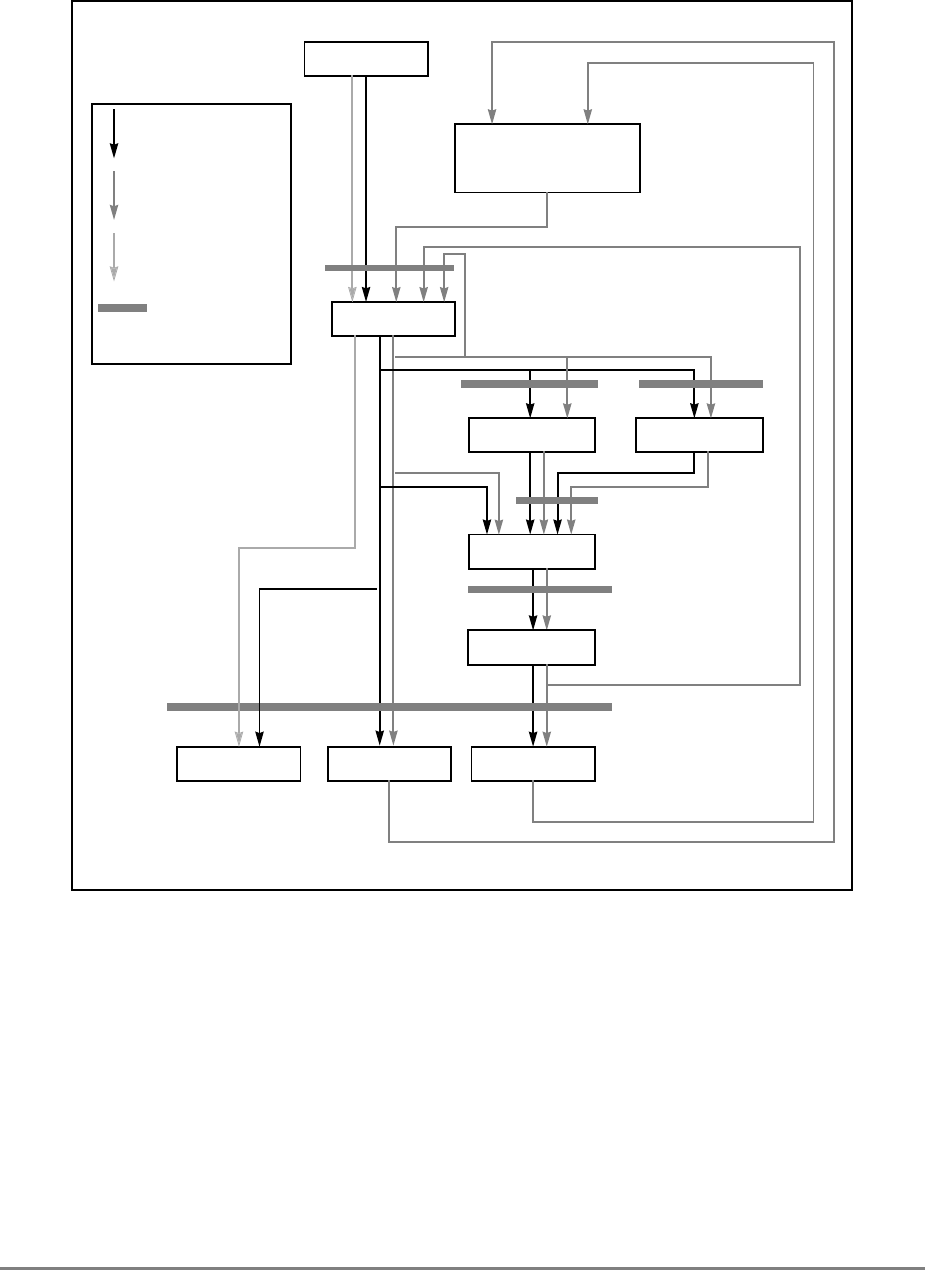
7-36 PowerPC 601 RISC Microprocessor User's Manual
Figure 7-13. IU Pipeline Showing Data, Instruction, and Tag Flow
Each block in the diagram represents a different stage (except for the box labeled “GPRs”,
which represents the IU general purpose registers). There are three different flows shown
in the diagram—the instruction flow; the tag flow, and the data flow.
In most cases, it takes one cycle to go from one stage to another, as shown by the marked
cycle boundaries in the diagram. However, an instruction that wishes to access the cache
(load or store) resides in the CARB stage (cache arbitration) on the same cycle it is in IE
(integer execute). Also, instructions that are in writeback can provide data to the ID/IE
boundary through the GPRs in the same cycle. Each instruction uses a subset of the stages
GPRs
ID
IE
ISB FPSB
CARB
IWLIWAIC
From Floating-Point Unit
Feed-Forwarding
= Instruction Flow
= Data Flow
= Tag Flow
CACC
Cycle
Boundary

Chapter 7. Instruction Timing 7-37
identified, although the subset varies from instruction to instruction. Likewise, the
operations performed in each stage may vary from one instruction to another.
All instructions executed by the IU are dispatched to integer decode (ID), which is identical
to IQ0 unless there is a stall in the IU pipeline, in which case the next integer instruction
may fall into IQ0 without entering ID. ID is the first IU stage for all IU instructions.
From ID all instructions go to integer execute (IE) where, for most instructions, most of the
instruction’s function is carried out (e.g. add instructions add two numbers together, etc...).
All IU instructions spend one or more cycles in this stage. Instructions that use the cache
or bus interface unit (BIU) arbitrate for cache access while the instruction is in IE. The
block marked CARB is the cache arbitration block.
Where an instruction goes from IE depends on the instruction type. Arithmetic and logical
instructions go to integer writeback for ALU operations (IWA). Integer instructions that
access the cache simultaneously enter the CARB and IE stages and then go to the integer
store buffer (ISB) and cache access (CACC) stages. Note that while the instruction is in the
CACC stage, it must also remain in the ISB stage simultaneously in case the instruction in
CACC is unable to successfully access the cache because of a cache retry. If that is the case,
ISB holds the original request so that it can participate in the arbitration process on
subsequent cycles, and eventually the instruction accesses the cache successfully.
Floating-point store operations are unique in that the store address is provided by the IU
and the store data is provided by the FPU. The FPSB holds the store request and address
while the data is being generated in the FPU. When the data is available, the instruction in
the FPSB participates in the arbitration. Link integer instructions, floating-point store
instructions in the CACC stage also reside in the FPSB stage in case of a cache retry.
The IC stage is entered the first cycle after an instruction leaves IE in parallel with the
instruction moving into some other stage (CACC for load/stores; IWA for arithmetic
operations). When an instruction moves into IC, it indicates that the instruction is
committed, even though that instruction’s results may not have been written back to the
appropriate register (or cache) yet. Tags flowing through IC represent instruction
completion for instructions that are executed in the BPU or the FPU.
Load operations have one more stage to enter beyond CACC. Integer load operations move
to integer writeback for load operations (IWL) the cycle after a successful cache access, and
floating-point load operations move to floating-point writeback for load operations (FWL)
on the cycle after a successful cache access. From these stages the registers are written with
data read from the cache/memory subsystem.
7.3.3.1 Integer Pipeline—Integer Decode (ID) Stage
The Integer Unit (IU) pipeline receives instructions from the fetcher/dispatch unit into the
ID stage. The instructions are decoded and data is read from the register file. All IU
instructions take one cycle in the IU decode stage. Instructions may be held in the decode
stage by the 601 control logic for two reasons.

7-38 PowerPC 601 RISC Microprocessor User's Manual
• There is an instruction in the IU execute stage (IE) and it is being held there for some
reason, such as when additional cycles are required to perform a calculation or gain
access to a resource.
• The instruction in decode is trying to read the CR or XER that is being written by
the instruction in execute.
Note that instructions are not held in decode for most register hazards. There is a forward
path, shown in Figure 7-13, that brings ALU results to decode (bypassing the GPR file
when the instruction in decode wants to use the results of the instruction in execute).
7.3.3.2 Integer Pipeline—Integer Execute (IE) Stage
The IU execute stage receives the instruction and its associated register data from decode.
The following is a list of the major functions performed in the IU execute (IE) stage.
• The IE stage is where data manipulation occurs for all of the ALU instructions—
arithmetic, logical, CR logical, shifts, and rotates.
• Many of the SPRs are written and read during the IE stage.
• Instructions that require translation are translated by the MMU when they are in the
IE stage.
• Instructions that need to access the cache send a request from IE to the cache arbiter.
That is, such an instruction enters the CARB stage simultaneously with the last cycle
of the IE stage.
• There are several reasons an instruction may be held (stall) in IE. These reasons
include:
— The instruction needs to access the cache and the cache is busy.
— The instruction in IWA is being held (stalled)—perhaps for pipeline
synchronization—so the instruction in IE cannot proceed.
— The IE instruction may have a GPR dependency with an outstanding load.
— Floating-point load operations may have an outstanding floating-point ALU
instruction.
When an instruction is stalled in IE, instructions in ID also stall.
7.3.3.2.1 IE Stage—ALU Instruction Operation
Most ALU instructions spend one cycle in IE. Data is taken from latches that separate ID
from IE and is manipulated as required by the instruction. As shown in Figure 7-13, the
results are made available both to the IWA stage and to the latch between the ID and IE
stages for use by the next instruction for use in the next cycle.
Multiply and divide instructions take more than one cycle in IE, which reduces the
throughput accordingly. For example, the mulli instruction always takes five cycles in IE,
as shown in Table 7-16, and each of the divide instructions always take 36 cycles in IE. The
number of cycles in IE taken by mul, mullw, mulhw, and mulhwu depends on the data
specified in rB, as shown in Table 7-15. If bits 0–16 of the rB operand are sign bits

Chapter 7. Instruction Timing 7-39
(positive: rB < (215 – 1 or negative: rB ≤ –215), the instruction spends five cycles in IE.
Otherwise, the instructions spends nine cycles in IE. For the mulhwu instruction only, if
the most significant bit of rB is a 1, the instruction takes 10 cycles in IE.
Many IU instructions have certain side effects defined as part of their operation. These side
effects include the update of the CR field 0, XER[CA], XER[SO], and XER[OV], which
occurs on the last cycle that the instruction is in IE.
7.3.3.2.2 IE Stage—Basic Load and Store Instruction Operation
Load operations and store operations perform different logic functions in IE than ALU
operations. The EA of the load or store is generated in IE and EA is passed to the MMU for
translation. The translated address and a set of control bits are passed to the cache arbiter
to request cache access. The control bits include information that identifies the operation as
a load, store, or cache operation; it indicates the size of the operand; and identifies the target
register for load operations.
Accesses to the memory subsystem are described in Section 7.3.3.3, “Integer Operations
that Access the Memory Subsystem.”
Load operations and store operations that are aligned on an addressing boundary at least as
large as the size of the operand can do all of this work in one IE cycle. For example, an lw
instruction with an EA of x'00004C34' is properly aligned and completes in one IE cycle.
On the 601, improperly aligned load operations and store operations can be handled in one
cycle only if the operand does not cross a double-word addressing boundary; otherwise an
additional cycle is required for the additional access.
The IU performs the EA generation, translates the address, and makes cache requests on
behalf of the FPU for floating-point load operations and store operations. Floating-point
load operations are only dispatched to the IU. Floating-point store operations are
simultaneously dispatched to both the FPU and the IU. The FPU provides the store data;
however, it may not be available until after the cache request is made by the IU. Therefore,
there is a floating-point store buffer (FPSB) that holds the address and request information
until the floating-point store data is available. This buffer allows the IU pipeline to continue
executing instructions after a floating-point store.
7.3.3.3 Integer Operations that Access the Memory Subsystem
Some operations in the integer pipeline require access to the memory subsystem. As shown
in Figure 7-13, such operations enter the CARB stage during the same cycle that they are
in the IE stage. The instruction continues to occupy the IE stage until it can either enter the
CACC stage or one of the store buffer stages (ISB or FPSB).
7.3.3.3.1 Integer Pipeline—CARB Stage
If the instruction in IE wins the arbitration, the cache access occurs on the next cycle;
otherwise, the request is saved in a set of retry latches inside the data access queueing unit,
shown as the integer store buffer (ISB) and floating-point store buffer (FPSB) in
Figure 7-13. Examples of when the store buffers are required are shown in the multiple

7-40 PowerPC 601 RISC Microprocessor User's Manual
instruction timing examples in Appendix I, “Instruction Timing Examples.” A request in
the store buffers is arbitrated as soon as it is the highest priority request. The requesting
instruction is allowed to move out of IE because the request is either granted access or
queued by the arbiter. However, each store buffer is only one element deep. Therefore, if
there is an IU request in the ISB stage, the instruction in IE cannot arbitrate for cache
access. In other words, the instruction is held (stalled) in execute until the ISB stage is
empty.
7.3.3.3.2 Integer and Floating-Point Store Buffer Stages (ISB and FPSB)
When an integer instruction enters the CACC stage after the IE stage is completed, it also
occupies the appropriate store buffer. This provides a place for the instruction if a cache
retry is necessary. The instruction remains in the buffer until the CACC stage is complete.
7.3.3.3.3 Address Translation
A TLB miss occurs if the translation for an instruction is not in the BAT registers or the
translation lookaside buffer (TLB). A TLB miss causes the cache request to be aborted and
starts a state machine that performs a table search operation. A page fault occurs if the page
table in memory does not contain the page requested. If the TLB reload is successful, the
request goes through arbitration for the cache (the CARB stage). It then proceeds like a
normal load/store operation to the CACC and IWL stages.
7.3.3.3.4 Unaligned Load/Store Operations
Unaligned load operations and store operations and load/store string/multiple instructions
may spend more than one cycle in IE. Load operations and store operations with unaligned
operands may access two different aligned double words of data in cache or memory.
However, the 601 can only handle data contained within one double word when servicing
a load or store. Therefore, the IU splits load operations and store operations that cross a
double word addressing boundary into two pieces. The first piece (called a splice 1 request)
accesses data in the first double word. The second piece (called a splice 2 request) accesses
data within the second double word. Logic in the IE stage detects these double-word
boundary crossings and splits the request into two pieces: the splice 1 and the splice 2. To
do this the instruction is held in IE one extra cycle—for a total of two cycles in IE. For load
operations, the data from the two requests are spliced together before the data is written into
the register file. For store operations the two requests are serviced by the memory
subsystem completely independently of each other. For both load operations and store
operations, unaligned support requires two cache access (CACC) cycles (one each for the
splice 1 and the splice 2 requests). If the load operations/store operations are to a cache
inhibited or write-through page, the splice 1 and splice 2 each require a separate bus
arbitration and data transfer.
As a result, load/store accesses that cross a double-word addressing boundary provide half
the throughput of aligned access. Load/store accesses that cross a 4-Kbyte page boundary
or 256-Mbyte segment boundary may take an alignment exception. For more details on the
alignment exceptions see Chapter 5, “Exceptions.”

Chapter 7. Instruction Timing 7-41
7.3.3.3.5 Load/Store String/Multiple Operations
Load/store string/multiple instructions typically transfer several words of data. On the 601,
these instructions split the transfer up into word-length pieces of data. Each word of data
corresponds to a register to be read from (store operations) or written to (load operations).
These instructions make one cache request for every cycle that they are in IE until enough
requests are made to transfer all of the data specified by the instruction. For example, lmw
28,0(r1) transfers four words from memory addressed by r1 to register r28, r29, r30, and
r31. A request is made for a word of data for r28 during the first cycle in IE; for r29 during
the second cycle in IE; for r30 during the third cycle in IE; and for r31 during the fourth
cycle in IE. The cache accesses occur in consecutive cycles (one cycle delayed from the
requests made from IE) as long as the load hits in the cache and there are no higher priority
requests made to the cache arbiter.
Note that in future implementations these instructions are likely to have greater latency and
take longer to execute, perhaps much longer, than a sequence of individual load or store
instructions.
Since string operations specify the transfer size in bytes, the last request generated by a
string is for one, two, three, or four bytes of data.
Load/store string/multiple operations are subject to the same behavior for unaligned data as
normal load operations and store operations. As previously discussed, cache requests are
made for word size pieces of data (one for each register source/target register specified by
the instruction). If the word-length pieces of data cross a double-word addressing boundary,
the access for that word is broken into two pieces (splice 1 and splice 2). In the limit, a
load/store string/multiple operation that is not aligned on a word boundary takes 50%
longer than the same instruction aligned on a word boundary (ignoring alignment
exceptions at 4-Kbyte page crossings).
7.3.3.3.6 Integer Pipeline—Cache Access (CACC) Stage
For load, store, and cache operations, there is a cache access stage immediately following
the IE stage. That is, store data is written into the cache and load data is read from the cache
on this cycle. If it is a cache miss, the request is sent to the bus interface unit. On a cache
hit, load data from the cache is forwarded to the latches above the execute (IE) stage. All of
the load data modification necessary before writing the GPRs is done on this cycle before
the data is latched up. (Load data modifications include: sign extension, zero extension, and
byte reversal.) On the next cycle, the data is available for the instruction in the IE stage to
begin execution, and the data is written into the GPRs in the IWL stage.
A sequence of load operations and store operations may be processed by the cache, one on
each consecutive cycle if they all hit in the cache. There are other system activities that may
require the cache on a given cycle; in which case, the load or store from IU would stall if
the ISB stage is already full. These activities would include cast out operations resulting
from a bus snoop hit in the cache or reload activity due to a previous cache miss.

7-42 PowerPC 601 RISC Microprocessor User's Manual
7.3.3.4 Integer Pipeline—Integer Writeback Stages (IWA and IWL)
The IU writeback stage is different for ALU operations than for load operations. Store
operations (except for store with update operations) do not have a writeback stage. ALU
operations have a writeback stage (IWA) on the cycle immediately following IE stage. The
ALU writeback stage has a dedicated write port into the GPR register file. Load operations
have a writeback stage (IWL) on the cycle that follows the cache access. The IWL also has
a dedicated write port into the register file. These two writeback stages are independent of
each other and may have different instructions on the same cycle. Both write ports can be
used simultaneously—with the exception that they cannot both write the same register on
the same cycle.
Update-form load operations and store operations write the EA into the addressing register
(rA) during the ALU writeback stage (IWA) in parallel with the cache access.
Some instructions are executed with assistance from the sequencer. These instructions
typically spend two cycles in execute and N cycles in writeback. (N varies from 1 to 20
cycles depending on the instruction.)
All integer instructions pass through the IWA stage, even though some of these instructions
(such as cmp and store instructions) write to the GPRs.
7.3.3.5 Integer Pipeline Instruction Timings
This section describes the flow of an integer instruction through the integer pipeline
ignoring any interaction with other instructions. In the real world there are data
dependencies and pipeline synchronization issues that must be considered. Such situations
are shown in Appendix I, “Instruction Timing Examples.”
7.3.3.5.1 Arithmetic Instructions
The timing of the add and subtract instructions is described in Table 7-13. This timing is
appropriate for the following instructions: addi, addis, add, addic, addic., subfic, subf,
addc, subfc, adde, subfe, addme, subfme, addze, subfze, neg, abs, nabs, doz, and dozi.
The instruction spends one cycle in IE. The status bits (XER[CA], XER[OV SO], and CR0)
are all written from IE. Resource usage of the various types of instructions is summarized
in Table 7-14.
Table 7-13. Integer Addition Instruction Timing
Number of Cycles 1 1 1
Pipeline stages ID
IE
IC
IWA
Resources required nonexclusively rA, rB, CA
Resources required exclusively CA, SO, OV, CR0, rD

Chapter 7. Instruction Timing 7-43
The multiply instructions are shown in Table 7-15 (mul, mullw, mulhw, mulhwu) and
Table 7-16 (mulli). These instructions take 5, 9, or 10 cycles in IE as described in
Section 7.3.3.2.1, “IE Stage—ALU Instruction Operation.” All of the multiply instructions
in the 601 use the MQ register, which is undefined after an mulhw or mulhwu instruction.
Table 7-15 shows the timing for the mul, mullw, mulhw, and mulhwu instructions.
Table 7-14. Resource Usage for Integer Addition Instructions
Instruction
Nonexclusive Resource Usage Exclusive Resource Usage
Read CA Read rARead rBUpdate CA Update CR0 Update SO,
OV
add No If !(rA = 0) Yes No If (RC = 1) If (OE = 1)
addc No Yes Yes Yes If (RC = 1) If (OE = 1)
adde Yes Yes Yes Yes If (RC = 1) If (OE = 1)
addi No If !(rA = 0) No No No No
addic No Yes No Yes No No
addic. NoYesNoYesYesNo
addis No If !(rA = 0) No No No No
addme Yes Yes No Yes If (RC = 1) If (OE = 1)
addze No Yes Yes Yes If (RC = 1) If (OE = 1)
neg No Yes No No If (RC = 1) If (OE = 1)
subf No Yes Yes No If (RC = 1) If (OE = 1)
subfc No Yes Yes Yes If (RC = 1) If (OE = 1)
subfe Yes Yes Yes Yes If (RC = 1) If (OE = 1)
subfic No Yes No Yes No No
subfme Yes Yes No Yes If (RC = 1) If (OE = 1)
subfze No Yes Yes Yes If (RC = 1) If (OE = 1)

7-44 PowerPC 601 RISC Microprocessor User's Manual
As shown in Table 7-16, the mulli instruction takes only five cycles in IE.
Table 7-17 shows the timing for divide instructions (div, divs, divw, and divwu). Each
divide instructions takes 36 cycles in the IE stage. They all use the MQ register. PowerPC
divide instructions do not return the remainder and the contents of the MQ after the
instruction completes is undefined. The 601 handles the MQ for POWER divide
instructions as defined in the POWER architecture. These instructions are described in
Chapter 10, “Instruction Set.”
a. Number of cycles is data dependent.
b. Update CR0 if (RC=1), updates SO and OV if (OE=1).
Table 7-15. Multiply Instruction Timing (mul, mullw, mulhw, mulhwu)
Number of Cycles 1 5/9/10a1
Pipeline stages ID
IE
IC
IWA
Resources required nonexclusively rA, rB
Resources required exclusively rD, MQ, CR0, SO,OVb
Table 7-16. Multiply Instruction Timing (mulli)
Number of Cycles 1 5 1
Pipeline stages ID
IE
IC
IWA
Resources required nonexclusively rA
Resources required exclusively rD, MQ

Chapter 7. Instruction Timing 7-45
Compare instructions spend one cycle in ID and one cycle in IE, but essentially have no
IWA stage. The compare results are written to the CR and forwarded to the BPU (for
conditional branch evaluation) in the middle of the IE cycle. The timing for the compare
instructions is shown in Table 7-18.
The flow of the trap instructions (tw and twi) depends on whether they cause a program
exception. If they do not cause a program exception, one cycle is required in IWA. If they
cause a program exception, 22 cycles are required in the IWA stage. It is important to note
that this performance penalty occurs only when the trap condition is met. Typically, this is
a rare condition and performance is not critical.
a. rB is used only by the cmp and cmpl instructions.
b. Compare results are forwarded to the BPU for branch resolution.
Table 7-17. Divide Instruction Timings (div, divs, divw, divwu)
Number of Cycles 1 36 1
Pipeline stages ID
IE
IC
IWA
Resources required nonexclusively rA, rB, MQ,
Resources required exclusively rD, MQ, CR0, SO OV
Table 7-18. Integer Compare Instruction Timing (cmp, cmpi, cmpl, cmpli)
Number of Cycles 1 1 1
Pipeline stages ID
IE
IC
IWA
Resources required nonexclusively rA, rBa
Resources required exclusively CR[BF]b

7-46 PowerPC 601 RISC Microprocessor User's Manual
7.3.3.5.2 Boolean Logic Instruction Timings
Boolean logic instructions include the standard Boolean logic functions, sign extension of
a byte within a register, sign extension of a halfword within the register, and a count leading
zeros in a register instruction. These instructions include the following: andi., andis., ori,
oris, xori, xoris, and, andc, eqv, nand, nor, or, orc, xor, extsb, extsh, and cntlzw. These
instructions flow through the integer pipeline in the same manner, spending a single cycle
in IE and completing in IWA. Timing for Boolean instructions is shown in Table 7-20.
Table 7-21 lists the resources required by the Boolean logic instructions.
a. One cycle is required if the trap is not taken; 22 cycles are required if it is taken.
b. Only the tw instruction uses rB.
a. Table 7-21 summarizes resources used by individual instructions.
Table 7-19. Trap Instruction Timing (tw, twi)
Number of Cycles 1 1 1 or 22a
Pipeline stages ID
IE
IC
IWA
Resources required nonexclusively rA, rBb
Resources required exclusively
Table 7-20. Boolean Logic Instruction Timing
Number of Cycles 1 1 1
Pipeline stages ID
IE
IC
IWA
Resources required nonexclusively rS, rB
Resources required exclusively rA, CR0a

Chapter 7. Instruction Timing 7-47
7.3.3.5.3 Rotate, Shift, and Mask Instruction Timings
The 601 supports rotate, shift and mask instructions of both the POWER and PowerPC
architectures. These instructions each spend one cycle in each of the ID, IE, and IWA
stages. However, there is a wide variation in the resources that these instructions read to and
write from.
Table 7-22 shows the timing for rotate, mask, and shift instructions, which include the
following: rlimi, rlmi, rlinm, rlnm, rrib, sl, sr, slq, srq, sliq, sriq, slliq, srliq, sllq, srlq,
sle, sre, sleq, sreq, srai, sra, sraiq, sraq, srea, maskg, and maskir.
a. Table 7-23 summarizes the resources required by individual instructions.
Table 7-21. Resource Usage for Boolean Logic Instructions
Instruction Nonexclusive Resource Usage Exclusive Resource Usage
Read rARead rBUpdate CR0
andi., andis. Yes N o Yes
ori, oris, xori, xoris Yes No No
and, andc, eqv, nand, nor, or,
orc, xor Yes Yes If (RC=1)
extsb, extsh, cntlzw Yes No If (RC=1)
Table 7-22. Rotate, Mask, and Shift Instruction Timing
Number of Cycles 1 1 1
Pipeline stages ID
IE
IC
IWA
Resources required nonexclusivelyarA, rB, rS, CA, MQ
Resources required exclusivelya. rA, MQ, CR0

7-48 PowerPC 601 RISC Microprocessor User's Manual
Table 7-23 summarizes resources required by each instruction and indicates which are used
exclusively (writes) and which are used nonexclusively (reads).
Table 7-23. Resource Usage for Rotate, Shift, and Mask Instructions
Instruction Nonexclusive Resource Usage Exclusive Resource Usage
Read rBRead MQ Update CA Update MQ Update CR0
maskg Yes No No No If (RC=1)
maskir Yes No No No If (RC=1)
rlimi No No No No If (RC=1)
rlmi Yes No No No If (RC=1)
rlinm No No No No If (RC=1)
rlnm Yes No No No If (RC=1)
rrib Yes No No No If (RC=1)
sl Yes No No No If (RC=1)
sr Yes No No No If (RC=1)
slq Yes No No Yes If (RC=1)
srq Yes No No Yes If (RC=1)
sliq No No No Yes If (RC=1)
sriq No No No Yes If (RC=1)
slliq No Yes No Yes If (RC=1)
srliq No Yes No Yes If (RC=1)
sllq Yes Yes No No If (RC=1)
srlq Yes Yes No No If (RC=1)
sle Yes No No Yes If (RC=1)
sre Yes No No Yes If (RC=1)
sleq Yes Yes No Yes If (RC=1)
sreq Yes Yes No Yes If (RC=1)
srai No No Yes No If (RC=1)
sra Yes No Yes No If (RC=1)
sraiq No No Yes Yes If (RC=1)
sraq Yes No Yes Yes If (RC=1)
srea Yes No Yes Yes If (RC=1)

Chapter 7. Instruction Timing 7-49
7.3.3.5.4 Condition Register (CR) Instruction Timings
Although the CR can be modified in many different ways, it is most often altered when the
RC bit on an instruction encoding is set. Setting RC does not increase the instruction
execution time for integer instructions; however, for floating-point instructions, setting the
RC bit requires that the IU and FPU pipelines be synchronized. This section shows timing
diagrams for IU instructions that read or write the CR.
Integer ALU instructions that have the RC bit set write the CR from IE and there is no
additional latency. See Table 7-13.
As shown in Table 7-24, each of the eight CR logical instructions (crand, cror, crxor,
crnand, crnor, crandc, creqv, and crorc) flow through the IU pipeline in the same way.
The mtcrf instruction, shown in Table 7-25, copies the contents of a GPR into the CR on a
field-by-field basis. Although the PowerPC architecture allows performance to degrade if
more than one field is being written, the 601 has the same optimal performance regardless
of the field mask specified in the instruction. The CR is written during the IE stage.
a. Any combination of fields can be written as specified by the mask field in the
instruction.
Table 7-24. CR Logical Instruction Timing
Number of Cycles 1 1 1
Pipeline stages ID
IE
IC
IWA
Resources required nonexclusively CR[BA], CR[BB]
Resources required exclusively CR[BT]
Table 7-25. mtcrf Instruction Timing
Number of Cycles 1 1 1
Pipeline stages ID
IE
IC
IWA
Resources required nonexclusively rA
Resources required exclusively CR0–CR7a

7-50 PowerPC 601 RISC Microprocessor User's Manual
The mfcr instruction, shown in Table 7-26, reads the CR from IE and copies that value into
the specified GPR during IWA.
The mcrf instruction, shown in Table 7-27, copies the contents of one specified field of the
CR into another. This instruction is unusual in that it reads the CR from the decode stage.
The timing for this instruction is the same regardless of which fields are specified.
The mcrxr instruction, shown in Table 7-28, copies bits 0–3 from the XER to the specified
field in the CR. This instruction reads the XER in the ID stage and writes to the CR in the
IE stage. The performance is the same regardless of which bit field is specified.
Table 7-26. mfcr Instruction Timing
Number of Cycles 1 1 1
Pipeline stages ID
IE
IC
IWA
Resources required nonexclusively CR
Resources required exclusively rD
Table 7-27. mcrf Timing
Number of Cycles 1 1 1
Pipeline stages ID
IE
IC
IWA
Resources required nonexclusively CR[BFA]
Resources required exclusively CR[BF]
Table 7-28. mcrxr Instruction Timing
Number of Cycles 1 1 1
Pipeline stages ID
IE
IC
IWA
Resources required nonexclusively XER[0–3]
Resources required exclusively CR[BF]

Chapter 7. Instruction Timing 7-51
7.3.3.5.5 Move to SPR (mtspr) Instruction Timings
The mtspr and mfspr instructions flow differently through the IU pipeline depending on
which SPR is accessed. Timing of the mtspr instruction through the IU pipeline depends
on the SPR being accessed.
• SPR accesses that require one cycle per stage—MQ, XER, PIR, DABR, EAR,
RTCL, DEC, LR, and CTR (shown in Table 7-29) are both read from and written in
the IE cycle.
The SDR1 register requires one cycle per stage, but is written from IE and can be
read from the IWA stage (see Table 7-29).
• SPR accesses that require two cycles in the IE stage and one cycle in each of the
other stages—This group includes accesses to SPRGn, DSISR, DAR, RTCU, SRR0,
SRR1. These accesses require two cycles in IE and one cycle in IWA. Note that if the
next instruction is another of these instructions, it requires two additional cycles in
IE.
Table 7-29. mtspr Instruction Timing (One Cycle per Stage)
Number of Cycles 1 1 1
Pipeline stages ID
IE
IC
IWA
Resources required nonexclusively rS
Resources required exclusively SPR
Table 7-30. mtspr Instruction Timing (SDR1)
Number of Cycles 1 1 1
Pipeline stages ID
IE
IC
IWA
Resources required nonexclusively rS
Resources required exclusively SPR

7-52 PowerPC 601 RISC Microprocessor User's Manual
Timing for this access is shown in Table 7-31.
• Three of the 601’s hardware implementation-dependent registers (HID0, HID1, and
HID2)—These SPRs take 11, 12, and 17 cycles in writeback respectively. Timing
for these instruction is shown in Table 7-32. Writes to these SPRs are context-
synchronizing, which causes the instructions in the IQ to be purged and restarts
fetching under the new context. This causes a minimum three-cycle penalty before
the next instruction can be executed (in IE).
7.3.3.5.6 Move to MSR (mtmsr) Instruction
The mtmsr instruction flows through the IU pipeline similarly to the mtspr for HID0,
HID1, and HID2 (shown in Table 7-31), except that it is context-synchronizing. It spends
two cycles in execute and either 17 or 20 cycles in IWA. The instruction may cause an
immediate exception if an exception condition is present and the enable is turned from off
to on. If it does not cause an exception, it takes 17 cycles in IWA if the FPSCR[FEX] bit is
cleared; otherwise it takes 20 cycles in IWA.
Because mtmsr instruction is context-synchronizing, it is held in ID until IE and IWA are
empty, and instructions in the IQ are purged. After the mtmsr instruction completes,
subsequent instructions are refetched, which causes at least a three-cycle stall before the
Table 7-31. mtspr Instruction Timing (Two Cycles in the IE Stage and One Cycle in
the Writeback Stage)
Number of Cycles 1 2 1
Pipeline stages ID
IE
IC
IWA
Resources required nonexclusively rS
Resources required exclusively SPR SPR
Table 7-32. mtspr Instruction Timing (Two Cycles in the IE Stage and Multiple
Cycles in the Writeback Stage)—(HID0, HID1, and HID2)
Number of Cycles 1 2 n
Pipeline stages ID
IE
IC
IWA
Resources required nonexclusively rS
Resources required exclusively SPR SPR

Chapter 7. Instruction Timing 7-53
subsequent instructions can enter the ID stage. Therefore, it is the only instruction in the
machine at the time. Timing for this instruction is shown in Table 7-33.
In Table 7-33, n is 17 cycles if the FPSCR[FEX] bit is clear, and is 20 if the FPSCR[FEX]
bit is set.
7.3.3.5.7 Move to Segment Register Instructions
The mtsr and mtsrin instructions spend one cycle in the IE stage and write the register
from the IWA stage. An mtsr instruction in the IWA stage writes the register during the first
half of the cycle. Timing for these instruction are shown in Table 7-34.
a. The mtmsr instruction remains in the decode stage (ID) until all previous
instructions in program order have completed processing. This latency is
variable for this reason.
b. Because the mtspr instruction is context-synchronizing, there are no other
instructions in the pipeline, so all resources are not considered to be required
exclusively or nonexclusively in the conventional sense.
Table 7-33. mtmsr Instruction Timing
Number of Cycles
n
a
2
n
Pipeline stages ID
IE
IC
IWA
Resources requiredb rS, SPR SPR
Table 7-34. mtsr and mtsrin Instruction Timing
Number of Cycles 1 1 1
Pipeline stages ID
IE
IC
IWA
Resources required nonexclusively rS
Resources required exclusively SR

7-54 PowerPC 601 RISC Microprocessor User's Manual
7.3.3.5.8 Move from Special Purpose Register (mfspr)
The timing of the mfspr instruction depends on the SPR being accessed, which are as
follows:
• Some SPRs take one cycle in IE and one cycle in IWA. These include the following
registers—MQ, XER, PIR, DABR, EAR, RTCL, DEC, LR, AND CTR. The SPR is
read from IE and the GPR is written during IWA. Timing for these accesses is shown
in Table 7-35.
• Some SPR accesses spend two cycles in IE and multiple cycles in IWA. Accesses to
the SPRGn, DSISR, DAR, HID0, HID1, HID2, RTCU, SRR0, and SRR1 registers
require four cycles in IWA; accesses to the PVR register take seven cycles. These
accesses take longer than mtspr accesses to the same registers. Timing for these
accesses is shown in Table 7-36.
• As with the mtspr instruction, accesses to the SDR1 register with the mfspr
instruction have a unique timing. These accesses take one cycle in IE where the
SDR1 is read, and it spends one cycle in IWA where the GPR is written. Data cannot
be forwarded for this register; therefore, a dependent operation that follows
immediately after mfspr stalls for one cycle in IE. Timing for this instruction is
shown in Table 7-37.
a. PVR is the only SPR that takes seven cycles in the IWA stage. The rest of the SPR’s
listed in this table take four cycles in IWA.
Table 7-35. mfspr Instructions—One Cycle in IE and One Cycle in IWA
Number of Cycles 1 1 1
Pipeline stages ID
IE
IC
IWA
Resources required nonexclusively SPR
Resources required exclusively rD
Table 7-36. mfspr Instructions—Two Cycles in IE and Multiple Cycles in IWA
Number of Cycles 1 2 4 or 7 a
Pipeline stages ID
IE
IC
IWA
Resources required nonexclusively SPR
Resources required exclusively rDrD

Chapter 7. Instruction Timing 7-55
7.3.3.5.9 Move from Machine State Register (mfmsr) Instruction Timing
The timing of the mfmsr instruction is similar to the mfspr instruction shown in
Table 7-36—two cycles are spent in IE and two cycles are spent in the IWA stage. The
register can be read during the IWA stage. Timing for this instruction is shown in
Table 7-38.
7.3.3.5.10 Move from Segment Register Instruction Timing
The mfsr and mfsrin instructions have the same timing. The segment registers are read
during the IE stage and written to the GPR during the IWA stage. The timings for these
instructions are shown in Table 7-39. Because data written into the GPR cannot not be
forwarded to the instruction that immediately follows, a one-cycle stall occurs if the next
instruction depends on data in this GPR.
Table 7-37. mfspr Instruction Timing (SDR1)
Number of Cycles 1 1 1
Pipeline stages ID
IE
IC
IWA
Resources required nonexclusively SPR
Resources required exclusively rDrD
Table 7-38. mfmsr Instruction Timing
Number of Cycles 1 2 2
Pipeline stages ID
IE
IC
IWA
Resources required nonexclusively MSR
Resources required exclusively rDrD

7-56 PowerPC 601 RISC Microprocessor User's Manual
.
7.3.3.5.11 System Call (sc) and Return from Interrupt (rfi) Instruction
Timings
Both the sc and rfi instructions are context synchronizing; they establish a new context and
then branch to that target. All prefetched instructions are discarded and fetching begins
again at the new address under the new machine state. This causes at least a three-cycle stall
before the next instruction can enter the IE stage. These instructions are held in the ID stage
until all preceding instructions have completed. The sc instruction takes 16 cycles in IWA,
and the rfi instruction takes 13 cycles in IWA. Timing for these instructions is shown in
Table 7-40.
7.3.3.5.12 Cache Instruction Timings
Table 7-41 and Table 7-42 provide best-case examples for cache instructions. Timings for
cache instructions depend upon the MESI state of the cache block. Timing for cache
instructions that require bus activity, shown in Table 7-41, also depend upon bus speed,
timing of the AACK signal, whether the processor is parked on the bus, and bus
synchronization. The timing for the CACC stage may be longer for a given system
implementation.
a. The sc instruction takes 16 cycles in IWA; the rfi instruction takes 13 cycles in IWA.
Both instructions are context-synchronizing, which causes at least a three-cycle stall
before the next instruction can enter the IE stage.
Table 7-39. mfsr and mfsrin Instruction Timing
Number of Cycles 1 1 1
Pipeline stages ID
IE
IC
IWA
Resources required nonexclusively SR
Resources required exclusively rDrD
Table 7-40. rfi and sc Instruction Timings
Number of Cycles 1 2 13 or 16a
Pipeline stages ID
IE
IC
IWA
Resources required nonexclusively MSR
Resources required exclusively rDrD

Chapter 7. Instruction Timing 7-57
Timings here assume that the WIM bits are set to b'001'—that is, write-back, caching
enabled, and memory coherency enforced.
There are three cycles of processor activity and at least three cycles of bus activity for a total
of at least six cycles in the CACC (cache access) stage. The following formula can be used
to calculate the delay for a specific system implementation:
CACC latency = 3 + ASP + (2 + AD + BNP) * BPR
In this formula, ASP is a synchronization parameter. AD is the number of bus cycles delay
for the AACK signal, BNP is 0 if the bus is parked and 1 otherwise. BPR is the bus-to-
processor clock frequency ratio (1 for a full-speed bus, 2 for a half-speed bus, 3 for a third-
speed bus, etc...).
Table 7-41 shows the timing for the tlbi, sync, dcbf(E,S,I), dcbst(E,S,I), dcbi, dcbz(S,I),
and store(S) instructions.
Table 7-42 shows best-case timings for the dcbf(M), dcbst(M), and dcbz(M,E)
instructions. Note that the CACC stage requires only one cycle because these instructions
do not require access to the system interface.
a. Note that this is the best-case timing. The time in this stage may be longer for a
given system implementation. Actual timing is dependent on bus speed, timing of the
AACK signal, whether the processor is parked on the bus, and bus synchronization.
Table 7-41. Cache Instruction Timings—tlbi, sync, dcbf(E,S,I),
dcbst(E,S,I), dcbi, dcbz(S,I), store(S)
Number of Cycles 1 1 6a
Pipeline stages ID
IE
CARB
CACC
IC
Resources required nonexclusively rA, rB
Resources required exclusively

7-58 PowerPC 601 RISC Microprocessor User's Manual
7.3.3.5.13 Load Instruction Timing
All load operations (except string and multiple load operations) spend one cycle in IE if the
operand does not cross a double-word boundary. Table 7-43 shows the timing for these
instructions, which include the lbz, lbzx, lhz, lhzx, lha, lhax, lwz, lwzx, lwarx, lfs, lfsx,
lfd, and lfdx instructions.For more information, see Section 7.3.3.2.2, “IE Stage—Basic
Load and Store Instruction Operation.” Note that for floating-point loads, the target register
is an FPR.
As shown in Table 7-44, the same load instructions (lbz, lbzx, lhz, lhzx, lha, lhax, lwz,
lwzx, lwarx, lfs, lfsx, lfd, lfdx) take two cycles in IE and CACC stages if the operand
crosses a double-word addressing boundary; this is because the data from doublewords
requires separate cache accesses (splice 1 and 2). Note that in the third cycle the first access
in the cache (splice 1) overlaps with the second arbitration for the cache (splice 2). It then
takes one extra cycle for the register data to become available. For more information, see
Section 7.3.3.3.4, “Unaligned Load/Store Operations.”
Table 7-42. Cache Instruction Timings—dcbf(M), dcbst(M), dcbz(M,E)
Number of Cycles 1 1 1
Pipeline stages ID
IE
CARB
CACC
IC
Resources required nonexclusively rA, rB
Resources required exclusively
Table 7-43. Single-Cycle Load Instruction Timing—Operand Does Not Cross a
Double-Word Boundary
Number of Cycles 1111
Pipeline stages ID
IE
CARB
CACC
IC
IWL or FWL
Resources required nonexclusively rA, rB
Resources required exclusively rDrD

Chapter 7. Instruction Timing 7-59
Note that for floating-point loads, the target register is an FPR.
7.3.3.5.14 Load with Update Instruction Timing
Load operations that use the update option also write the addressing register rA with the
EA in addition to loading the target register. These operations are similar to conventional
load operations except that rA is required exclusively when the instruction is in IE. Timing
for these instructions (lbzu, lbzux, lhzu, lhzux, lhau, lhaux, lwzu, lwzux, lfsu, lfsux, lfdu
and lfdux) is shown in Table 7-45.
Note that for floating-point loads, the target register is an FPR.
Like load operations that do not update, when these instructions (lbzu, lbzux, lhzu, lhzux,
lhau, lhaux, lwzu, lwzux, lfsu, lfsux, lfdu, and lfdux) have operands that cross a double-
Table 7-44. Single-Cycle Load Instruction Timing—Operand Crosses Double-Word
Boundary
Number of Cycles 11111
Pipeline stages ID
IE IE
CARB CARB
CACC CACC
IC
IWL or FWL
Resources required nonexclusively rA, rB
Resources required exclusively rDrDrD
Table 7-45. Update Form Load Instruction Timing—Operand Does Not Cross
Double-Word Boundary
Number of Cycles 1 1 1 1
Pipeline stages ID
IE
CARB
CACC
IC
IWA
IWL or FWL
Resources required nonexclusively rA, rB
Resources required exclusively rA, rDrD

7-60 PowerPC 601 RISC Microprocessor User's Manual
word addressing boundary, they must spend an extra cycle in IE and CACC. Timing for
these operations is shown in Table 7-46.
Note that for floating-point loads, the target register is an FPR.
7.3.3.5.15 Load Multiple Word (lmw) and Load String Word Immediate
(lswi)
Load multiple word (lmw) and load string word immediate (lswi) instructions spend one
cycle in IE for each register of data to be transferred (shown as the variable n). Timing for
these operations is shown in Table 7-47.
a. where
n
is the number of registers to be loaded.
b. where i ranges from 0 to
n
-3 (incrementing each cycle).
Table 7-46. Update Form Load Instruction Timing—Operand Crosses Double-Word
Boundary
Number of Cycles 1 1 1 1 1
Pipeline stages ID
IE IE
CARB CARB
CACC CACC
IC
IWA
IWL or FWL
Resources required nonexclusively rA, rB
Resources required exclusively rDrDrD
Table 7-47. Load Multiple Word (lmw) and Load String Word Immediate
(lwsi)—Operand is Word-Aligned
Number of Cycles 1 1 1 na-2 1 1
Pipeline stages ID
IE IE IE
CARB CARB CARB
CACC CACC CACC
IC
IWL[rD+i]bIWL[rD+n-2] IWL[rD+n-1]
Resources required
nonexclusively rA
Resources required
exclusively rDrD, rD+1 rD+i+1,
rD+i+2b. rD+n-1

Chapter 7. Instruction Timing 7-61
The instruction flow becomes more complex when the initial address is not on a word-
length addressing boundary, causing every other register to receive data that spans a double-
word addressing boundary. Requests for data for those registers is split into two pieces
(splice 1 and splice 2). Such load operations take 50% longer when the word is aligned. The
timing for this operation is shown in Table 7-48.
7.3.3.5.16 Load String Word Indexed (lswx) and Load String and Compare
Byte Indexed (lscbx) Instruction Timing
Timing for the lswx and lscbx instructions differs from the lswi and lmw instructions in that
both rB and the XER are read in ID. Also the lscbx instruction reads the XER throughout
the execution of the instruction and may write the XER if a byte-compare match is found.
Since the determination of when the XER is written is data-dependent, the XER must be
accessed exclusively throughout the execution of the instruction. Timing for these
instructions is shown in Table 7-49.
a. where
n
is the number of registers to be loaded.
b. where i ranges from 0 to
n
-3 (incrementing by 2 each iteration (every three cycles).
Table 7-48. Load Multiple Word (lmw) and Load String Word Immediate (lswi)
Timing —Not Word-Aligned
Number
of Cycles 11 1 (n
a
-2)/2 (3 cycle iteration) 1 1
Pipeline
stages ID
IE IE IE IE IE
CARB CARB CARB CARB CARB
CACC CACC CACC CACC CACC
IC
IWL[rD+i]bIWL[rD+n-2] IWL[rD+n-2] IWL[rD+n-1]
Resources
required
non
exclusively
rA
Resources
required
exclusively
rDrD rD+i,
rD+i+1b. rD+i+1,
rD+i+2b. rD+i+2b. rD+n-1

7-62 PowerPC 601 RISC Microprocessor User's Manual
When the operand is not on a word boundary, these two instructions take an extra cycle for
every other register of data (that is, each time the word boundary is crossed). For more
information, see Section 7.3.3.5.15, “Load Multiple Word (lmw) and Load String Word
Immediate (lswi).” Timing is shown in Table 7-50.
a. where
n
is the number of registers to be loaded.
b. where i ranges from 0 to
n
-3 (incrementing each cycle).
c. The lscbx instruction reads the XER continuously and writes the XER when a byte compare match occurs.
The lswx never writes the XER and only reads the XER from ID.
a. where
n
is the number of registers to be loaded.
b. where i ranges from 0 to
n
-3 (incrementing by 2 each iteration (every three cycles).
Table 7-49. lswx and lscbx Instruction Timing—Word-Aligned
Number of Cycles 1 1 1 na-2 1 1
Pipeline stages ID
IE IE IE
CARB CARB CARB
CACC CACC CACC
IC
IWL[rD+i]bIWL[rD+n-2] IWL[rD+n-1]
Resources required
nonexclusively XER rA, rB
Resources required
exclusively rD,
XERcrD, rD+1,
XER rD+i+1,
rD+i+2b., XER rD+n-1, XER
Table 7-50. lswx and lscbx Instruction Timings—Operand Not on a Word Boundary
Number of Cycles 1 1 1 na-2/2 (3 cycle iteration) 1 1
Pipeline stages ID
IE IE IE IE IE
CARB CARB CARB CARB CARB
CACC CACC CACC CACC CACC
IC
IWL[rD+i]bIWL[rD+n-2] IWL[rD+n-2] IWL[rD+n-1]
Resources required
nonexclusively rA
Resources required
exclusively rDrD rD+i,
rD+i+1b. rD+i+1,
rD+i+2b. rD+i+2b. rD+n-1

Chapter 7. Instruction Timing 7-63
7.3.3.5.17 Integer Store Instruction Timings
This section describes integer store operations, except for the string/multiple instructions
(stmw, stswx, and stswi) and store instructions that specify the update option. Timings for
store operations differ from load operations primarily in that they do not write back to
registers. Store operations calculate the EA in the IE stage and arbitrate (CARB) for cache
access in parallel with the IE stage. Store operations have the same alignment
properties/requirements as load operations.
Timings for scalar store operations are shown in Table 7-51.
If the operand specified by the store crosses a double-word boundary, the access is split into
two pieces (See Section 7.3.3.3.4, “Unaligned Load/Store Operations”); therefore, the store
spends two cycles in IE (as do load operations). The timings for store instructions (stb,
stbx, sth, sthx, stw, stwx, sthbrx, and stwbrx) whose operands cross a double-word
boundary are shown in Table 7-52.
Table 7-51. Integer Store Instruction Timings—Operand Does Not Cross a
Double-Word Boundary
Number of Cycles 1 1 1
Pipeline stages ID
IE
CARB
CACC
IC
Resources required nonexclusively rA, rB, rS
Resources required exclusively
Table 7-52. Integer Store Instruction Timings—Operand Crosses a Double-Word
Boundary
Number of Cycles 1111
Pipeline stages ID
IE IE
CARB CARB
CACC CACC
IC
Resources required nonexclusively rA, rB, rS
Resources required exclusively

7-64 PowerPC 601 RISC Microprocessor User's Manual
7.3.3.5.18 Store with Update Instruction Timing
Store operations that update register write the rA addressing register with the EA calculated
by the store, requiring the IWA stage. The timings for these store operations (stbu, stbux,
sthu, sthux, stwu, stwux) that have operands that do not cross a double-word boundary are
shown in Table 7-53.
The timings for misaligned store operations with update (stbu, stbux, sthu, sthux, stwu,
and stwux) with operands crossing a double-word boundary are shown in Table 7-54.
7.3.3.5.19 Floating-Point Store Instruction Timing
Floating-point store operations are dispatched to the IU, which generates the address and
provides access to the MMU cache interface, and to the FPU, which provides the data
properly formatted. Note that the tag does not have to be dispatched in the IU pipeline at
the same time that the floating-point instruction is dispatched to the FPU pipeline.
Therefore the timing for floating-point store operations is very different from other
Table 7-53. Update Form Store Instruction Timings—Operand Does Not Cross a
Double-Word Boundary
Number of Cycles 1 1 1
Pipeline stages ID
IE
CARB
CACC
IC
IWA
Resources required nonexclusively rA, rB, rS
Resources required exclusively
Table 7-54. Update Form Store Instruction Timings—Operand Crosses a
Double-Word Boundary
Number of Cycles 1111
Pipeline stages ID
IE IE
CARB CARB
CACC CACC
IC
IWA
Resources required nonexclusively rA, rB, rS
Resources required exclusively

Chapter 7. Instruction Timing 7-65
instructions. The instruction may complete in the IC stage and wait in the FPSB stage for
the data to be available before it can arbitrate for the cache.
Table 7-55 shows the timing for the stfs, stfsx, stfd, and stfdx instructions when no operand
crosses a double-word boundary.
Store accesses that cross a double-word boundary must be broken into two pieces, each of
which requires a cache access. However, because the FPSB stage is only one-element deep,
it stays full with the first request until the data is made available from the FPU, delaying
arbitration for the second cache access for three cycles. As shown in Table 7-56, this takes
five cycles in IE for stfs, stfsx, stfd, stfdx instructions instead of one for an aligned floating-
point store.
Table 7-55. Floating-Point Store Instruction Timings—Operand Does Not Cross a
Double-Word Boundary
Number of Cycles 1 1 1111
Pipeline stages ID
IE
FPSB FPSB FPSB
CARB
CACC
IC
FD
FPM
FPA
FW
Resources required nonexclusively rA, rB, frS
Resources required exclusively

7-66 PowerPC 601 RISC Microprocessor User's Manual
7.3.3.5.20 Update-Form Floating-Point Store Instruction Timings
The timings for floating-point store operations that update differ from the nonupdate forms
in that they update rA from the IWA stage. Table 7-57 shows timings for the stfsu, stfsux,
stfdu, and stfdux instructions when operands do not cross a double-word boundary.
Table 7-56. Floating-Point Store Instruction Timings—Operand Crosses a
Double-Word Boundary
Number of Cycles 1 1 1 1 1 1 1 1
Pipeline stages ID
IE IE IE IE IE
FPSB FPSB FPSB FPSB FPSB FPSB
CARB CARB
CACC CACC
IC
FD
FPM
FPA
FW
Resources required nonexclusively rA, rB, frS
Resources required exclusively

Chapter 7. Instruction Timing 7-67
Table 7-58 shows timings for the stfsu, stfsx, stfdu, and stfdux instructions when the
operand crosses a double-word boundary.
Table 7-57. Floating-Point Store Instruction Timings—Operand Does Not Cross a
Double-Word Boundary
Number of Cycles 1 1 1111
Pipeline stages ID
IE
FPSB FPSB FPSB
CARB
CACC
IC
IWA
FD
FPM
FPA
FW
Resources required nonexclusively rA, rB, frS
Resources required exclusively

7-68 PowerPC 601 RISC Microprocessor User's Manual
7.3.3.5.21 Store Multiple Word (stmw) and Store String Word Immediate
(stswi)
The stmw and stswi instructions spend a cycle in each of the IE, CARB, and CACC stages
for each register of data to be transferred. The timings for these instructions are shown in
Table 7-59. The number of registers to be transferred in this example is 3 (9–12 bytes of
data for the stswi instruction, 12 bytes of data for the stmw instruction). If four registers of
data were specified, there would be four IE, CARB, and CACC cycles—all overlapping as
shown.
Table 7-58. Floating-Point Store Instruction Timings—Operand Crosses a
Double-Word Boundary
Number of Cycles 11111111
Pipeline stages ID
IE IE IE IE IE
FPSB FPSB FPSB FPSB FPSB FPSB
CARB CARB
CACC CACC
IC
IWA
FD
FPM
FPA
FW
Resources required
nonexclusively rA, rB,
frS
Resources required
exclusively

Chapter 7. Instruction Timing 7-69
Because the accesses are made one word at a time, if the EA specified is not on a word
boundary, every other access crosses a double-word boundary. Accesses that cross a
double-word boundary are split into two pieces just as for scalar store operations. Timing
for stmw and stswi when operands are not on a word boundary is shown in Table 7-60.
7.3.3.5.22 Store String Word Indexed (stswx) Instruction Timings
Timing for the stswx instruction differs from the timing for the stswi instruction in that it
reads the XER (byte count) from ID and it reads the rB. The timing for this instruction
a. where
n
is the number of registers to be loaded.
b. rS is only accessed on one cycle because the four memory locations associated with these four bytes of data
are within the same double-word address.
c. rS + 1 is accessed twice in the IE stage because the four memory locations associated with these four bytes
of data are not within the same double-word address.
d. rS + 2 is only accessed on one cycle because the four memory locations associated with these four bytes of
data are within the same double-word address.
Table 7-59. stmw and stswi Instruction Timing (Word-Aligned)
Number of Cycles 1 1111
Pipeline stages ID
IE IE IE
CARB CARB CARB
CACC CACC CACC
IC
Resources required nonexclusively rA, rSrSrS + 2
Resources required exclusively rSrS+1 rS +2
Table 7-60. stmw and stswi Instruction Timing (Not Word-Aligned)
Number of Cycles 1 1 (na-1)/2 (3 cycle iteration) 1
Pipeline stages ID
IE IE IE IE
CARB CARB CARB CARB
CACC CACC CACC CACC
Resource required nonexclusively rA, rSbrS + 1crS + 1 rS + 2d
Resources required exclusively

7-70 PowerPC 601 RISC Microprocessor User's Manual
when the operand is on a word boundary is shown in Table 7-61. The number of registers
to be transferred in this example is 3 (9 to 12 bytes of data). If four registers of data are
specified, then there would be four IE, CARB, and CACC cycles—all overlapping as
shown.
When the operand is not on a word boundary, every other access takes two cycles in the IE,
the CARB, and the CACC stages. The timing for the stswx instruction when the operands
are not word-aligned is shown in Table 7-62.
a. The variable
n
represents the number of registers to be loaded.
b. rS is only accessed on one cycle because the four memory locations associated with these four bytes of data
are within the same double-word address.
c. rS + 1 is accessed twice in the IE stage because the four memory locations associated with these four bytes of
data are not within the same double-word address.
d. rS + 2 is only accessed on one cycle because the four memory locations associated with these four bytes of
data are within the same double-word address.
Table 7-61. stswx Instruction Timing (Word-Aligned)
Number of Cycles 11111
Pipeline stages ID
IE IE IE
CARB CARB CARB
CACC CACC CACC
IC
Resources required nonexclusively rA, rSrSrS + 2
Resources required exclusively rSrS+1 rS +2
Table 7-62. stswx Instruction Timing (Not Word-Aligned)
Number of Cycles 1 1 (na-1)/2 (3 cycle iteration) 1
Pipeline stages ID
IE IE IE IE
CARB CARB CARB CARB
CACC CACC CACC CACC
Resources required nonexclusively rA, rSbrS + 1crS + 1 rS + 2d
Resources required exclusively

Chapter 7. Instruction Timing 7-71
7.3.3.5.23 Store Conditional Word Indexed Instruction
The stwcx. instruction differs from that of other store operations in that it must set the CR
after it determines whether it can successfully complete the store operations. The
architecture does not support this instruction with an operand address that is not on a word
boundary (results of a misaligned stwcx. on the 601 are boundedly undefined). The timing
for the stwcx. instruction is shown in Table 7-63.
Because the reservation bit may not be set by the time the stwcx. instruction is executed,
only one cycle is spent in IWA. The flow with the reservation bit cleared is shown in
Table 7-64.
a. The XXX’s indicate that an instruction cannot be executing in IE while a stwcx. is in IWA. An instruction
may be present in IE, but if there is one, it will be held (stall).
a. The XXX’s indicate that an instruction cannot be executing in the IE stage while a stwcx. is in
the IWA stage. An instruction may be present in IE, but if there is one, it will be held (stall).
Table 7-63. stwcx. Instruction Timing—Reservation Set
Number of Cycles 1111
Pipeline stages ID
IE XXXaXXX
CARB
CACC
IC
IWA IWA
Resources required nonexclusively rA, rB, rS
Resources required exclusively
Table 7-64. stwcx. Instruction Timing—Reservation Cleared
Number of Cycles 1 1 1
Pipeline stages ID
IE XXXa
CARB
CACC
IC
IWA
Resources required nonexclusively rA,rB, rS
Resources required exclusively
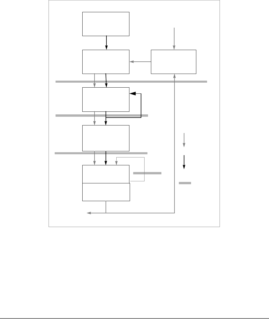
7-72 PowerPC 601 RISC Microprocessor User's Manual
7.3.4 Floating-Point Pipeline Stages
As shown in Figure 7-1, the FPU has a four-stage pipeline with a one-entry queue (F1)
above it that holds an instruction if the previous instruction stalls in FD. All instructions
occupy each of the remaining FPU stages for at least one cycle. The FPU pipeline stages
are shown in Figure 7-14.
Figure 7-14. Floating-Point Data and Instruction Flow
Some instructions require more than one cycle in a stage, and some of those instructions
may occupy multiple stages simultaneously. This process is described in Section 7.3.1.4.3,
“Floating-Point Dispatch.”
The FPU uses the multiply/add (fmadd) instruction (D = AC + B) as the base for other
floating-point operations. Other instructions are implemented using this instruction and
setting one or more of the operands with a constant (in the FD stage). These are shown as
follows:
FPM
(Multiply Stage)
Normalizer,
FPA
(Add Stage)
FD
(Decode Stage)
F1
(Queue)
Feedback for
Double
Precision
Multiply
to Memory
= Instruction
flow
= Data flow
FWA
FPR
(Floating Point
Registers)
Load Data
(From Memory Subsystem)
Store Data
Subsystem
= Cycle
boundary
Rounder
(Writeback)

Chapter 7. Instruction Timing 7-73
•Accumulate instructions (AC + B)—This is the base instruction in the FPU. There
are both single- and double-precision versions of these instructions.
•Add instructions (A + B)— These are treated as accumulate instructions with C=1.
This group of instructions includes add, subtract, round-to-single, and floating-point
compare instructions. There are both single- and double-precision versions of these
instructions.
•Multiply instructions (AC)—These are treated as accumulate instructions with
B=0. There are both single- and double-precision versions of these instructions.
•Divide instructions —This instruction is handled with repeated iterations of the
accumulate instructions. There are both single- and double-precision versions of
these instructions.
•Move instructions —These instructions are treated as accumulate instructions with
A = 0.
•Load instructions —These are handled entirely in the IU. Because the FPRs have
a dedicated port for load data being written back, loads never interfere with
arithmetic instructions writing back their data. There are both single- and double-
precision versions of these instructions.
•Store instructions —These behave like move instructions, except that they do not
write back to the FPRs. There are both single- and double-precision versions of these
instructions.
•Special instructions —Depending on the instruction, these instructions are handled
in control logic or similarly to the move instructions.
•Convert-to-integer instructions —These instructions work on both single- and
double-precision data. There is a convert-to-integer instruction with a round-to-zero
mode.
PowerPC floating-point arithmetic is IEEE-compliant, and the following sections assume a
familiarity with the PowerPC implementation of IEEE floating-point numbers and
arithmetic, which is described in Section 2.5, “Floating-Point Execution Models.”
7.3.4.1 Floating-Point Decode Stage (FD)
In the FD stage, floating-point instructions are decoded, their operands are fetched, and any
required constants in the base instruction (D = AC + B) are set. Stalls can occur in the FD
stage for the following reasons:
• Data dependencies—Instructions stall in FD because of true data dependencies
(read-after-write, or RAW, dependencies) between the source operands of the
instruction in the FD stage and the target registers required by instructions in the
FPM, FPA, or FWA stages, or between the source operands of the instructions in the
FD stage and the target register of an outstanding load instruction. All dependency
checking is performed at FD regardless of the stage at which the operand is first
required. In other words, a floating-point move instruction may stall in the FD stage

7-74 PowerPC 601 RISC Microprocessor User's Manual
because of a dependency on an instruction in FPA even though the register move
instruction does not need its operand until the FW stage. For more information, see
Appendix I, Section I.3.1, “Floating-Point Data Dependency Stalls.”
However, floating-point store instructions stall in FD stage not because of a
dependency on an instruction in the FPM stage, but rather because of a dependency
on an instruction in FPA or FPW.
• Multicycle floating-point operations—Two types of multicycle operations in the 601
can appear in the FPU pipeline—divide and double-precision accumulate/multiply
operations. The divide instructions are implemented with a 2-bit, nonrestoring
division algorithm that iterates using accumulate instructions and requires the entire
floating-point pipeline for many cycles.
Double-precision multiply/accumulate instructions must repeat both the FPM and
FPA stages twice (pipelined) because the 53- by 53-bit multiplication is split into
two 27- by 53-bit multiplications. This is described in Section 7.2.1.3, “Floating-
Point Unit (FPU).” Timing for these instructions is shown in Section 7.3.4.5.2,
“Double-Precision Instruction Timing.”
• Special-case numbers (such as denormalized numbers)—Two conditions related to
special-case numbers cause stalls in the FD stage. The first case is when one or more
of the operands of the instruction in the FD stage require prenormalization. To
perform the prenormalization function, the operands must be cycled through the
entire pipeline and make use of the normalizer in the FW stage, as described in
Section 7.3.4.4, “Floating-Point Write-Back Stage (FWA).” Denormalized operands
for multiply and divide instructions require prenormalization in the 601.
Stalls also occur in the FD stage when the FPU predicts that the result of the
operation produces a denormalized number (that is, an underflow condition), in
which case, output must be cycled through the entire pipeline again in order to
denormalize the answer before it is written back. This is described in
Section 7.3.4.5.6, “Floating-Point Special-Case Number-Handling Stalls.”
7.3.4.2 Floating-Point Multiply Stage (FPM)
The FPM stage performs 27- by 53-bit multiplication (which is the first half of a 53- by 53-
bit multiplication for double-precision operations). Although instructions that must repeat
this stage may cause stalls in FD (as described in Section 7.3.4.1, “Floating-Point Decode
Stage (FD)”) there are no stalls inherent to this stage; instructions can stall here only
because of an instruction in a subsequent stage. Operands used by this stage are set up in
the FD stage—that is, constants are put in the appropriate places and double-precision
multiply instructions are split into two pieces.
7.3.4.3 Floating-Point Add Stage (FPA)
The FPA stage is similar to the FPM stage; however, the FPA stage must shift the results of
the two halves of the double-precision multiply/accumulate instructions appropriately to
correctly calculate the double-precision sum. Although instructions that must repeat this

Chapter 7. Instruction Timing 7-75
stage may cause stalls in FD (as described in Section 7.3.4.1, “Floating-Point Decode Stage
(FD)”) there are no stalls inherent to this stage.
7.3.4.4 Floating-Point Write-Back Stage (FWA)
Normalization, rounding, and writeback occur in the FWA stage. Stalls can occur in the
FWA stage for the following reasons:
• Normalization—The normalizer in the FWA stage can shift by as many as 16 bits in
a cycle. Additionally, a shift of as many as 48 bits can occur at the bottom of the FPA
stage. Thus if the intermediate result of an operation contains more than 64 zeros,
there is at least a one-cycle stall in the FWA stage. The intermediate result in the FPU
contains 161 bits, so the worst case normalization time (corresponding to a one in
the 161st position with 160 leading zeros), is seven cycles (48 bits are shifted out in
the FPA stage, then 16 additional bits are shifted out in each of the next seven cycles
in the FWA stage).
• Synchronization—The stalls associated with synchronization relate back to the
precise exception model. A floating-point instruction cannot complete before an
instruction ahead of it in program order that may still cause a synchronous
exception. See Section 7.3.1.4.4, “Synchronization Tags for the Precise Exception
Model.”
The FPRs contain two write ports, one dedicated to load data and one dedicated to
arithmetic instruction results; thus there is never interference between these two types of
instructions at the FWA stage and the FWL stage. One load and one arithmetic instruction
can write back in one cycle.
7.3.4.5 Floating-Point Pipeline Timing
In the following sections, we give timing examples of the floating-point instructions.
7.3.4.5.1 Single-Precision Instructions
This section contains timing diagrams for the single-precision arithmetic instructions that
are implemented in the FPU. Table 7-65 shows the timing for a single-precision add
instruction with no special-case data.

7-76 PowerPC 601 RISC Microprocessor User's Manual
Table 7-66 shows the timing for a single-precision multiple instruction with no special-case
data.
Table 7-67 shows the timing for a single-precision divide instruction with no special-case
data.
Table 7-65. Single-Precision Add (fadds, fsubs) Instruction Timing—No Special-
Case Data
Number of Cycles 1111
Pipeline stages
FD
FPM
FPA
FWA
Resources required nonexclusively frA, frB
Resources required exclusively frD
Cache access
Table 7-66. Single-Precision Multiply Instruction (fmuls)—No Special-Case Data
Number of Cycles 1111
Pipeline stages
FD
FPM
FPA
FWA
Resources required nonexclusively frA, frC
Resources required exclusively frD
Cache access

Chapter 7. Instruction Timing 7-77
Table 7-68 shows the timing for single-precision accumulate instructions with no special-
case data.
7.3.4.5.2 Double-Precision Instruction Timing
This section contains timing diagrams for the double-precision arithmetic instructions
implemented in the FPU.
Table 7-69 shows the timing for a double-precision add instruction with no special-case
data. Note that the fcmpu and fcmpo instructions write to CR[BF] instead of frD
Table 7-67. Single-Precision Divide Instruction (fdivs)—No Special-Case Data
Number of Cycles 1 1 1 14 1
Pipeline stages
FD FD FD FD
FPM FPM FPM
FPA FPA
FWA FWA
Resources required nonexclusively frA, frB
Resources required exclusively frD
Cache access
Table 7-68. Single-Precision Accumulate Instructions (fmadds, fmsubs, fnmadds,
fnmsubs)—No Special-Case Data
Number of Cycles 1111
Pipeline stages
FD
FPM
FPA
FWA
Resources required nonexclusively frA, frB, frC
Resources required exclusively frD
Cache access

7-78 PowerPC 601 RISC Microprocessor User's Manual
.
Table 7-70 shows the timing for a double-precision multiply instruction with no special-
case data. Note that in this example, the instruction requires two cycles in the FD, FPM, and
FPM stages; however, because the instruction is self-pipelining, there is only a one-cycle
delay before the next instruction can enter the decode stage.
Table 7-71 shows the timing for a double-precision divide instruction with no special-case
data. Note that the instruction occupies the decode stage and subsequent stage until the
instruction enters the last cycle of the writeback stage.
a. The fcmpu and fcmpo instructions write to CR[BF] instead of frD.
Table 7-69. Double-Precision Add Instructions (fadd, fsub, frsp, fcmpu, fcmpo)—No
Special-Case Data
Number of Cycles 1111
Pipeline stages
FD
FPM
FPA
FWA
Resources required nonexclusively frA, frB
Resources required exclusively frDa
Cache access
Table 7-70. Double-Precision Multiply Instructions (fmul)—No Special-Case Data
Number of Cycles 11111
Pipeline stages
FD FD
FPM FPM
FPA FPA
FWA
Resources required nonexclusively frA, frCfrA, frC
Resources required exclusively frD
Cache access

Chapter 7. Instruction Timing 7-79
Table 7-72 shows the timing for a double-precision accumulate instruction with no
special-case data. Note that the timing for this instruction is similar to that of the fmul
instruction, in that it requires two cycles in the FD, FPM, and FPA stages. However,
because the instruction is self-pipelining, its can begin the first cycle of the FPM stage
while it enters the second cycle of the FD stage. This allows the next instruction to enter
the decode stage on the third clock cycle.
Table 7-71. Double-Precision Divide Instructions (fdiv)—No Special-Case Data
Number of Cycles 1 1 1 28 1
Pipeline stages
FD FD FD FD
FPM FPM FPM
FPA FPA
FWA FWA
Resources required nonexclusively frA, frB
Resources required exclusively frD
Cache access
Table 7-72. Double-Precision Accumulate Instructions (fmadd, fmsub, fnmadd,
fnmsub)—No Special-Case Data
Number of Cycles 1 1 1 1 1
Pipeline stages FD FD
FPM FPM
FPA FPA
FWA
Resources required nonexclusively frA, frB, frCfrA, frB, frC
Resources required exclusively frD
Cache access

7-80 PowerPC 601 RISC Microprocessor User's Manual
7.3.4.5.3 Floating-Point Move/Store Instruction Timing
Table 7-73 illustrates the timing of floating-point move instructions.
7.3.4.5.4 Convert-to-Integer Instruction Timing
This section contains timing information for the convert to integer instructions.
Table 7-74 shows the timing for floating-point convert to integer instructions with no
special-case data.
7.3.4.5.5 Special Instructions Implemented in the FPU
This section contains timing information for the special instructions (mtfsfi, mtfsf, mtfsb0,
and mtfsb1; see Table 7-75) implemented in the FPU—these instructions fit none of the
previous categories. Note that in this example frB is used only by the mtfsf instruction.
Table 7-73. Floating Point Move/Store Instructions (fmr, fabs, fneg, fnabs, stfs,
stfsu, stfsx, stfsux, stfd, stfdu, stfdx, stfdux)—No Special-Case Data
Number of Cycles 1111
Pipeline stages FD
FPM
FPA
FWA
Resources required nonexclusively frB
Resources required exclusively frD
Cache access
Table 7-74. Floating-Point Convert to Integer Instructions (fctiw, fctiwz)—No
Special-Case Data
Number of Cycles 1111
Pipeline stages FD
FPM
FPA
FWA
Resources required nonexclusively frB
Resources required exclusively frD
Cache access

Chapter 7. Instruction Timing 7-81
Table 7-76 shows the timing for the Move From FPSCR instructions, which are
implemented in the FPU. Note that in this example, frD is the target only of the mffs
instruction and CR[BF] is the target of the mcrfs instruction.
7.3.4.5.6 Floating-Point Special-Case Number-Handling Stalls
Special-case numbers can generate stalls and require the instruction to go through a portion
of the pipeline twice in order to prenormalize or denormalize an operand.
Table 7-77 shows the timing for a single-precision instruction when the result causes an
overflow. Single-precision accumulate instructions are shown in this example, but the
timing can be generalized for single-precision instructions in general. Note that to
denormalize the result of this instruction, it must pass through the FPU pipeline. Note that
a. Note that frB is used only by the mtfsf instruction.
a. frD is the target of the mffs instruction.
b. CR[BF] is the target of the mcrfs instruction.
Table 7-75. Move to FPSCR Instruction Timing (mtfsfi, mtfsf, mtfsb0, mtfsb1)
Number of Cycles 1111
Pipeline stages
FD FD FD FD
FPM FPM FPM
FPA FPA
FWA
Resources required nonexclusively frBa
Resources required exclusively FPSCR
Cache access
Table 7-76. Move from FPSCR Instruction Timing (mffs, mcrfs)
Number of Cycles 1 1 1 1
Pipeline stages
FD
FPM
FPA
FWA
Resources required nonexclusively FPSCR
Resources required exclusively frDa, CR[BF]b
Cache Access

7-82 PowerPC 601 RISC Microprocessor User's Manual
a stall occurs if an underflow condition is predicted, even though the condition may not
occur. In either case, the instruction occupies the decode stage for four cycles. Note that
while the latency of the instruction may differ in these two cases, the throughput is the
same.
Table 7-78 shows the timing for single-precision accumulate instructions (fmadds,
fmsubs, fnmadds, and fnmsubs). In this example, one operand requires prenormalization.
This operand travels through the pipeline before execution can begin.
a. The operand that needs prenormalization traverses the pipeline before the execution of the instruction starts.
b. The operands are now ready and the instruction can actually start execution.
Table 7-77. Single-Precision Accumulate Instruction Timing (fmadds, fmsubs,
fnmadds, fnmsubs)—Result Underflow
Number of Cycles 1111111
Pipeline stages
FD FD FD FD
FPM FPM
FPA FPA
FW FW
Resources required
nonexclusively
Resources required
exclusively
Cache access
Table 7-78. Single-Precision Accumulate Instruction Timing
Number of Cycles 1111111
Pipeline stages
FDaFD FD FD FDb
FPM FPM
FPA FPA
FW FW
Resources required
nonexclusively
Resources required
exclusively
Cache access

Chapter 7. Instruction Timing 7-83
Table 7-79 shows the timing when two operands of a single-precision accumulate
instruction require prenormalization.
7.3.4.5.7 Floating-Point Normalization Stalls
Table 7-80 shows the worst-case timing for when an operand of a double-precision
accumulate instruction requires normalization.
a. The first operand that needs prenormalization traverses the pipeline before the execution of the instruction
starts.
b. The second operand that needs prenormalization traverses the pipeline (immediately behind the first operand)
before the execution of the instruction starts.
c. The operands are now ready and the instruction can actually start execution.
Table 7-79. Single-Precision Accumulate Instructions (fmadds, fmsubs, fnmadds,
fnmsubs)—Two Operands Require Prenormalization
Number of Cycles 111111111
Pipeline stages
FDaFDbFD FD FD FDc
FPM FPM FPM
FPA FPA FPA
FW FPW FW
Resources required
nonexclusively
Resources required
exclusively
Table 7-80. Double-Precision Accumulate Instruction Timing
(Worst-Case Normalization)
Number of Cycles 1 1 1 1 6 1
Pipeline stages
FD FD
FPM FPM
FPA FPA
FW FW
Resources required
nonexclusively frA, frB, frC Shift by 48
bits Shift by 16
bits per cycle Shift by 16
bits per cycle
Resources required
exclusively frD

7-84 PowerPC 601 RISC Microprocessor User's Manual
7.4 Execute Stage Delay Summary
Table 7-81 shows potential delays that may be caused by instructions implemented in the
601. The pipeline column indicates which execution unit is used to process the instruction
(for example, floating-point loads and stores are processed in the integer pipeline). The
table shows the number of cycles each instruction spends in the execute stage, assuming
normal operations. The table also shows the delay that a subsequent instruction may
encounter if there is a data dependency. Note that this total time ignores the instruction
decode and fetch times for integer instructions but not for floating-point instructions.
As previously stated, the FPU has no feed-forwarding capabilities. In other words, as a
floating-point operation completes, another floating-point instruction that may be waiting
for those results must wait for the data to be written into the register file before decode can
begin. This extra time is accounted for in Table 7-81.
Note that Table 7-1 contains no 64-bit architected instructions. These instructions trap to an
illegal instruction exception handler when encountered.
Table 7-81. PowerPC 601 Microprocessor Instruction Latencies
Mnemonic Instruction Pipeline Number of
Cycles in
Execute Stage
Execute Stage
Delay if Next
Instruction is
Dependent
abs Absolute IU 1 0
add[o][.] Add IU 1 0
addc[o][.] Add Carrying IU 1 0
adde[o][.] Add Extended IU 1 0
addi. Add Immediate IU 1 0
addic Add Immediate Carrying IU 1 0
addic. Add Immediate Carrying and Record IU 1 0
addis Add Immediate Shifted IU 1 0
addme[o][.] Add to Minus One Extended IU 1 0
addze[o][.] Add to Zero Extended IU 1 0
and[.] AND IU 1 0
andc[.] AND with Complement IU 1 0
andi. AND Immediate IU 1 0
andis. AND Immediate Shifted IU 1 0
b[l][a] Branch BPU 1 —
bc[l][a] Branch Conditional BPU 1 —
bcctr[l] Branch Conditional to CTR BPU 1 —
bclr[l] Branch Conditional to LR BPU 1 —

Chapter 7. Instruction Timing 7-85
cmp Compare IU 1 0
cmpi Compare Immediate IU 1 0
cmpl Compare Logical IU 1 0
cmpli Compare Logical Immediate IU 1 0
cntlzw[.] Count Leading Zeros Word IU 1 0
crand CR AND IU 1 0
crandc CR AND with Complement IU 1 0
creqv CR Equivalent IU 1 0
crnand CR NAND IU 1 0
crnor CR NOR IU 1 0
cror CR OR IU 1 0
crorc CR OR with Complement IU 1 0
crxor CR XOR IU 1 0
dcbf Data Cache Block Flush IU 1102
dcbi Data Cache Block Invalidate IU 1102
dcbst Data Cache Block Store IU 1102
dcbt Data Cache Block Touch IU 1102
dcbtst Data Cache Block Touch for Store IU 1102
dcbz Data Cache Block Set to Zero IU 1102
div[o][.] Divide IU 36 0
divs[o][.] Divide Short IU 36 0
divw[o][.] Divide Word IU 36 0
divwu[o][.] Divide Word Unsigned IU 36 0
doz[o][.] Difference or Zero IU 1 0
dozi Difference or Zero Immediate IU 1 0
eciwx External Control Input Word Indexed IU 11Bus dependent
ecowx External Control Output Word Indexed IU 110
eieio Enforce In-Order Execution of I/O IU 110 2
eqv[.] Equivalent IU 1 0
extsb[.] Extend Sign Byte IU 1 0
extsh[.] Extend Sign Half Word IU 1 0
Table 7-81. PowerPC 601 Microprocessor Instruction Latencies (Continued)
Mnemonic Instruction Pipeline Number of
Cycles in
Execute Stage
Execute Stage
Delay if Next
Instruction is
Dependent

7-86 PowerPC 601 RISC Microprocessor User's Manual
fabs[.] Floating-Point Absolute Value FPU 1 3
fadd[.] Floating-Point Add FPU 1 3
fadds[.] Floating-Point Add Single-Precision FPU 1 3
fcmpo Floating-Point Compare Ordered FPU 1 1
fcmpu Floating-Point Compare Unordered FPU 1 1
fctiw[.] Floating-Point Convert to Integer Word FPU 1 3
fctiwz[.] Floating-Point Convert to Integer Word with
Round toward Zero FPU 1 3
fdiv[.] Floating-Point Divide FPU 31 0
fdivs[.] Floating-Point Divide Single-Precision FPU 17 0
fmadd[.] Floating-Point Multiply-Add FPU 2 3
fmadds[.] Floating-Point Multiply-Add Single-
Precision FPU 1 3
fmr[.] Floating-Point Move Register FPU 1 3
fmsub[.] Floating-Point Multiply-Subtract FPU 2 3
fmsubs[.] Floating-Point Multiply-Subtract Single-
Precision FPU 1 3
fmul[.] Floating-Point Multiply FPU 2 3
fmuls[.] Floating-Point Multiply Single-Precision FPU 1 3
fnabs[.] Floating-Point Negative Absolute Value FPU 1 3
fneg[.] Floating-Point Negate FPU 1 3
fnmadd[.] Floating-Point Negative Multiply-Add FPU 2 3
fnmadds[.] Floating-Point Negative Multiply-Add
Single-Precision FPU 1 3
fnmsub[.] Floating-Point Negative Multiply-Subtract FPU 2 3
fnmsubs[.] Floating-Point Negative Multiply-Subtract
Single-Precision FPU 1 3
fres[.] Floating-Point Reciprocal Estimate Single-
Precision — Not
implemented
(trap)
—
frsp[.] Floating-Point Round to Single-Precision FPU 1 3
frsqrte[.] Floating-Point Reciprocal Square Root
Estimate — Not
implemented
(trap)
—
Table 7-81. PowerPC 601 Microprocessor Instruction Latencies (Continued)
Mnemonic Instruction Pipeline Number of
Cycles in
Execute Stage
Execute Stage
Delay if Next
Instruction is
Dependent

Chapter 7. Instruction Timing 7-87
fsel[.] Floating-Point Select — Not
implemented
(trap)
—
fsqrt[.] Floating-Point Square Root — Not
implemented
(trap)
—
fsqrts[.] Floating-Point Square Root Single-
Precision — Not
implemented
(trap)
—
fsub[.] Floating-Point Subtract FPU 1 3
fsubs[.] Floating-Point Subtract Single-Precision FPU 1 3
icbi Instruction Cache Block Invalidate (no-op in
the 601) IU 1 0
isync Instruction Synchronize IU Serialize Serialize
lbz Load Byte and Zero IU 1 1
lbzu Load Byte and Zero with Update IU 1 1
lbzux Load Byte and Zero with Update Indexed IU 1 1
lbzx Load Byte and Zero Indexed IU 1 1
lfd Load Floating-Point Double-Precision IU 1 2
lfdu Load Floating-Point Double-Precision with
Update IU 1 2
lfdux Load Floating-Point Double-Precision with
Update Indexed IU 1 2
lfdx Load Floating-Point Double-Precision
Indexed IU 1 2
lfs Load Floating-Point Single-Precision IU 1 2
lfsu Load Floating-Point Single-Precision with
Update IU 1 2
lfsux Load Floating-Point Single-Precision with
Update Indexed IU 1 2
lfsx Load Floating-Point Single-Precision
Indexed IU 1 2
lha Load Half Word Algebraic IU 1 1
lhau Load Half Word Algebraic with Update IU 1 1
lhaux Load Half Word Algebraic with Update
Indexed IU 1 1
lhax Load Half Word Algebraic Indexed IU 1 1
Table 7-81. PowerPC 601 Microprocessor Instruction Latencies (Continued)
Mnemonic Instruction Pipeline Number of
Cycles in
Execute Stage
Execute Stage
Delay if Next
Instruction is
Dependent

7-88 PowerPC 601 RISC Microprocessor User's Manual
lhbrx Load Half Word Byte-Reverse Indexed IU 1 1
lhz Load Half Word and Zero IU 1 1
lhzu Load Half Word and Zero with Update IU 1 1
lhzux Load Half Word and Zero with Update
Indexed IU 1 1
lhzx Load Half Word and Zero Indexed IU 1 1
lmw Load Multiple Word IU Number of
registers
transferred
1
lscbx Load String and Compare Byte Indexed IU Number of
registers
transferred
1
lswi Load String Word Immediate IU Number of
registers
transferred
1
lswx Load String Word Indexed IU Number of
registers
transferred
1
lwarx Load Word and Reserve Indexed IU 1 1
lwbrx Load Word Byte-Reverse Indexed IU 1 1
lwz Load Word and Zero IU 1 1
lwzu Load Word and Zero with Update IU 1 1
lwzux Load Word and Zero with Update Indexed IU 1 1
lwzx Load Word and Zero Indexed IU 1 1
maskg[.] Mask Generate IU 1 0
maskir[.] Mask Insert from Register IU 1 0
mcrf Move CR Field IU 1 0
mcrfs Move to CR from FPSCR IU 1 1
mcrxr Move to CR from XER IU 1 0
mfcr Move from CR IU 1 0
mffs[.] Move from FPSCR FPU 1 3
mfmsr Move from Machine State Register IU 2 1
mfspr Move from Special Purpose Register IU Variable 1
mfsr Move from Segment Register IU 1 1
Table 7-81. PowerPC 601 Microprocessor Instruction Latencies (Continued)
Mnemonic Instruction Pipeline Number of
Cycles in
Execute Stage
Execute Stage
Delay if Next
Instruction is
Dependent

Chapter 7. Instruction Timing 7-89
mfsrin Move from Segment Register Indirect IU 1 1
mftb Move from Time Base — Not
implemented
(trap)
—
mtcrf Move to CR Fields IU 1 0
mtfsb0[.] Move to FPSCR Bit 0 IU 1 3
mtfsb1[.] Move to FPSCR Bit 1 IU 1 3
mtfsf[.] Move to FPSCR Fields IU 1 3
mtfsfi[.] Move to FPSCR Field Immediate IU 1 3
mtmsr Move to Machine State Register IU Serialize Serialize
mtspr Move to Special Purpose Register IU Variable 0
mtsr Move to Segment Register IU 1 0
mtsrin Move to Segment Register Indirect IU 1 0
mul[o][.] Multiply IU 5/930
mulhw[.] Multiply High Word IU 5/930
mulhwu[.] Multiply High Word Unsigned IU 5/9/1040
mulli Multiply Low Immediate IU 5 0
mulw[o][.] Multiply Low Word IU 5/930
nabs Negative Absolute IU 1 0
nand[.] NAND IU 1 0
neg[o][.] Negate IU 1 0
nor[.] NOR IU 1 0
or[.] OR IU 1 0
orc[.] OR with Complement IU 1 0
ori OR Immediate IU 1 0
oris OR Immediate Shifted IU 1 0
rfi Return from Interrupt IU Serialize Serialize
rlmi[.] Rotate Left then Mask Insert IU 1 0
rlwimi[.] Rotate Left Word Immediate then Mask
Insert IU 1 0
rlwinm[.] Rotate Left Word Immediate then AND with
Mask IU 1 0
Table 7-81. PowerPC 601 Microprocessor Instruction Latencies (Continued)
Mnemonic Instruction Pipeline Number of
Cycles in
Execute Stage
Execute Stage
Delay if Next
Instruction is
Dependent

7-90 PowerPC 601 RISC Microprocessor User's Manual
rlwnm[.] Rotate Left Word then AND with Mask IU 1 0
rrib[.] Rotate Right and Insert Bit IU 1 0
sc System Call IU Serialize Serialize
sle[.] Shift Left Extended IU 1 0
sleq[.] Shift Left Extended with MQ IU 1 0
sliq[.] Shift Left Immediate with MQ IU 1 0
slliq[.] Shift Left Long Immediate with MQ IU 1 0
sllq[.] Shift Left Long with MQ IU 1 0
slq[.] Shift Left with MQ IU 1 0
slw[.] Shift Left Word IU 1 0
sraq[.] Shift Right Algebraic with MQ IU 1 0
sraiq[.] Shift Right Algebraic Immediate with MQ IU 1 0
sraw[.] Shift Right Algebraic Word IU 1 0
srawi[.] Shift Right Algebraic Word Immediate IU 1 0
sre[.] Shift Right Extended IU 1 0
srea[.] Shift Right Extended Algebraic IU 1 0
sreq[.] Shift Right Extended with MQ IU 1 0
sriq[.] Shift Right Immediate with MQ IU 1 0
srliq[.] Shift Right Long Immediate with MQ IU 1 0
srlq[.] Shift Right Long with MQ IU 1 0
srq[.] Shift Right with MQ IU 1 0
srw[.] Shift Right Word IU 1 0
stb Store Byte IU 1 0
stbu Store Byte with Update IU 1 0
stbux Store Byte with Update Indexed IU 1 0
stbx Store Byte Indexed IU 1 0
stfd Store Floating-Point Double-Precision IU 1 0
stfdu Store Floating-Point Double-Precision with
Update IU 1 0
stfdux Store Floating-Point Double-Precision with
Update Indexed IU 1 0
Table 7-81. PowerPC 601 Microprocessor Instruction Latencies (Continued)
Mnemonic Instruction Pipeline Number of
Cycles in
Execute Stage
Execute Stage
Delay if Next
Instruction is
Dependent

Chapter 7. Instruction Timing 7-91
stfdx Store Floating-Point Double-Precision
Indexed IU 1 0
stfiwx Store Floating-Point as integer Word
Indexed IU 1 0
stfs Store Floating-Point Single-Precision IU 1 0
stfsu Store Floating-Point Single-Precision with
Update IU 1 0
stfsux Store Floating-Point Single-Precision with
Update Indexed IU 1 0
stfsx Store Floating-Point Single-Precision
Indexed IU 1 0
sth Store Half Word IU 1 0
sthbrx Store Half Word Byte-Reverse Indexed IU 1 0
sthu Store Half Word with Update IU 1 0
sthux Store Half Word with Update Indexed IU 1 0
sthx Store Half Word Indexed IU 1 0
stmw Store Multiple Word IU Number of
registers
transferred
0
stswi Store String Word Immediate IU Number of
registers
transferred
0
stswx Store String Word Indexed IU Number of
registers
transferred
0
stw Store Word IU 1 0
stwbrx Store Word Byte-Reverse Indexed IU 1 0
stwcx. Store Word Conditional Indexed IU 2 0
stwu Store Word with Update IU 1 0
stwux Store Word with Update Indexed IU 1 0
stwx Store Word Indexed IU 1 0
subf[o][.] Subtract from IU 1 0
subfc[o][.] Subtract from Carrying IU 1 0
subfe[o][.] Subtract from Extended IU 1 0
subfic Subtract from Immediate Carrying IU 1 0
Table 7-81. PowerPC 601 Microprocessor Instruction Latencies (Continued)
Mnemonic Instruction Pipeline Number of
Cycles in
Execute Stage
Execute Stage
Delay if Next
Instruction is
Dependent

7-92 PowerPC 601 RISC Microprocessor User's Manual
1These instructions access the system bus, thus the latency may vary depending on the exact state of the
machine
2 A delay may be incurred if the subsequent instruction requires access to the cache; for example a store
instruction.
3The longer latency may occur if the contents of rB is larger than 16 bits (not including sign-extending bits.
4Shortest latency occurs if rB ≤ 16 bits. Longer latency occurs if rB > 16 bits, but most significant bit is still 0.
Longest latency occurs if most significant bit is 1.
5These instructions serialize the processor if the trap is taken.
subfme[o][.] Subtract from Minus One Extended IU 1 0
subfze[o][.] Subtract from Zero Extended IU 1 0
sync Synchronize IU Serialize bus
operations Serialize bus
operations
tlbia Translation Lookaside Buffer Invalidate All — Not
implemented
(trap)
—
tlbie Translation Lookaside Buffer Invalidate
Entry IU Serialize Serialize
tw Trap Word IU 150
twi Trap Word Immediate IU 150
xor[.] XOR IU 1 0
xori XOR Immediate IU 1 0
xoris XOR Immediate Shifted IU 1 0
Table 7-81. PowerPC 601 Microprocessor Instruction Latencies (Continued)
Mnemonic Instruction Pipeline Number of
Cycles in
Execute Stage
Execute Stage
Delay if Next
Instruction is
Dependent

Chapter 8. Signal Descriptions 8-1
Chapter 8
Signal Descriptions
80
80
This chapter describes the PowerPC 601 microprocessor’s external signals. It contains a
concise description of individual signals, showing behavior when the signal is asserted and
negated and when the signal is an input and an output.
NOTE
A bar over a signal name indicates that the signal is active
low—for example, ARTRY (address retry) and TS (transfer
start). Active-low signals are referred to as asserted (active)
when they are low and negated when they are high. Signals that
are not active-low, such as AP0–AP3 (address bus parity
signals) and TT0–TT4 (transfer type signals) are referred to as
asserted when they are high and negated when they are low.
The 601 signals are grouped as follows:
• Address arbitration signals—The 601 uses these signals to arbitrate for address bus
mastership.
• Address transfer start signals—These signals indicate that a bus master has begun a
transaction on the address bus.
• Address transfer signals—These signals, which consist of the address bus, address
parity, and address parity error signals, are used to transfer the address and to ensure
the integrity of the transfer.
• Transfer attribute signals—These signals provide information about the type of
transfer, such as the transfer size and whether the transaction is bursted, write-
through, or cache-inhibited.
• Address transfer termination signals—These signals are used to acknowledge the
end of the address phase of the transaction. They also indicate whether a condition
exists that requires the address phase to be repeated.
• Data arbitration signals—The 601 uses these signals to arbitrate for data bus
mastership.
• Data transfer signals—These signals, which consist of the data bus, data parity, and
data parity error signals, are used to transfer the data and to ensure the integrity of
the transfer.

8-2 PowerPC 601 RISC Microprocessor User's Manual
• Data transfer termination signals—Data termination signals are required after each
data beat in a data transfer. In a single-beat transaction, the data termination signals
also indicate the end of the tenure, while in burst accesses, the data termination
signals apply to individual beats and indicate the end of the tenure only after the final
data beat. They also indicate whether a condition exists that requires the data phase
to be repeated.
• System status signals—These signals include the external interrupt signal,
checkstop signals, and both soft- and hard-reset signals. These signals are used to
interrupt and, under various conditions, to reset the processor.
• COP/scan interface signals—The common on-chip processor (COP) unit and scan
(IEEE 1149.1) interface provides a serial interface to the system for performing
monitoring and boundary tests.
• Test signals—These signals are used for internal testing.
• Clock signals—These signals determine the system clock frequency. These signals
can also be used to synchronize multiprocessor systems.
8.1 Signal Configuration
Figure 8-1 illustrates the 601 microprocessor’s pin configuration, showing how the signals
are grouped.
NOTE
A pinout showing actual pin numbers is included in the
PowerPC 601 RISC Microprocessor Hardware Specifications.
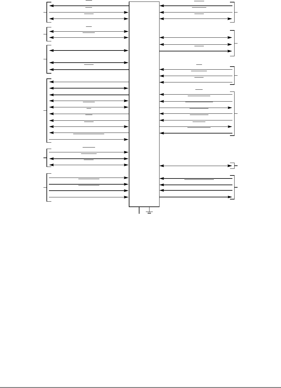
Chapter 8. Signal Descriptions 8-3
Figure 8-1. PowerPC 601 Microprocessor Signal Groups
8.2 Signal Descriptions
This section describes individual 601 signals, grouped according to Figure 8-1. Note that
the following sections are intended to provide a quick summary of signal functions.
Chapter 9, “System Interface Operation,” describes many of these signals in greater detail,
both with respect to how individual signals function and how groups of signals interact.
8.2.1 Address Bus Arbitration Signals
The address arbitration signals are a collection of input and output signals the 601 uses to
request the address bus, recognize when the request is granted, and indicate to other devices
when mastership is granted. For a detailed description of how these signals interact, see
Section 9.3.1, “Address Bus Arbitration.”
1
1
1
1
1
32
4
1
1
4
2
3
1
1
1
1
3
1
1
1
1
1
1
1
1
1
1
1
64
8
1
1
1
1
1
1
1
1
1
1
1
7
21
1
1
1
601
BR
BG
ABB
TS
XATS
A0–A31
AP0–AP3
APE
TT4
TT0–TT3
TC0–TC1
TSIZ0–TSIZ2
TBST
CI
WT
GBL
CSE0–CSE2
HP_SNP_REQ
AACK
ARTRY
SHD
2X_PCLK
PCLK_EN
BCLK_EN
RTC
DBG
DBWO
DBB
DH0–DH31, DL0–DL31
DP0–DP7
DPE
TA
DRTRY
TEA
INT
CKSTP_IN
CKSTP_OUT
HRESET
SRESET
RSRV
SC_DRIVE
SCAN INTERFACE
TEST INTERFACE
SYS_QUIESC
RESUME
QUIESC_REQ
ADDRESS
ARBITRATION
ADDRESS
TRANSFER
START
ADDRESS
TRANSFER
TRANSFER
ATTRIBUTE
ADDRESS
TERMINATION
CLOCKS
DATA
ARBITRATION
DATA
TRANSFER
DATA
TERMINATION
SYSTEM
STATUS
COP/ SCAN
INTERFACE
TEST
SIGNALS
+3.6 V
59 59

8-4 PowerPC 601 RISC Microprocessor User's Manual
8.2.1.1 Bus Request (BR)—Output
The bus request (BR) signal is an output signal on the 601. Following are the state meaning
and timing comments for the BR signal.
State Meaning Asserted—Indicates that the 601 is requesting mastership of the
address bus. See Section 9.3.1, “Address Bus Arbitration.”
Negated—Indicates that the 601 is not requesting the address bus.
The 601 may have no bus operation pending, it may be parked, or the
ARTRY input was asserted on the previous bus clock cycle.
Timing Comments Assertion—Occurs when the 601 is not parked and a bus transaction
is needed. This may occur even if the two possible pipeline accesses
have occurred.
Negation—Occurs for at least one bus clock cycle after an accepted,
qualified bus grant (see BG and ABB), even if another transaction is
pending. It is also negated for at least one bus clock cycle when the
assertion of ARTRY is detected on the bus.
8.2.1.2 Bus Grant (BG)—Input
The bus grant (BG) signal is an input signal on the 601. Following are the state meaning
and timing comments for the BG signal.
State Meaning Asserted—Indicates that the 601 may, with the proper qualification,
assume mastership of the address bus. A qualified bus grant occurs
when BG is asserted and ABB and ARTRY are not asserted. The
ABB signal is driven by the 601 or another bus master, and ARTRY
is driven by other bus masters. If the 601 is parked, BR need not be
asserted for the qualified bus grant. See Section 9.3.1, “Address Bus
Arbitration.”
Negated— Indicates that the 601 is not the next potential address bus
master.
Timing Comments Assertion—May occur at any time to indicate the 601 is free to use
the address bus. After the 601 assumes bus mastership, it does not
check for a qualified bus grant again until the cycle during which the
address bus tenure is completed (assuming it has another transaction
to run). The 601 does not accept a BG in the cycles between the
assertion of any TS or XATS and AACK.
Negation—May occur at any time to indicate the 601 cannot use the
bus. The 601 may still assume bus mastership on the bus clock cycle
of the negation of BG because during the previous cycle BG
indicated to the 601 that it was free to take mastership (if qualified).

Chapter 8. Signal Descriptions 8-5
8.2.1.3 Address Bus Busy (ABB)
The address bus busy (ABB) signal is both an input and an output signal.
8.2.1.3.1 Address Bus Busy (ABB)—Output
Following are the state meaning and timing comments for the ABB output signal.
State Meaning Asserted—Indicates that the 601 is the address bus master. See
Section 9.3.1, “Address Bus Arbitration.”
Negated— Indicates that the 601 is not using the address bus. If ABB
is negated during the bus clock cycle following a qualified bus grant,
the 601 did not accept mastership, even if BR was asserted. This can
occur if a potential transaction is aborted internally before the
transaction is started.
Timing Comments Assertion—Occurs on the bus clock cycle following a qualified BG
that is accepted by the processor (see Negated).
Negation—Occurs on the bus clock cycle following the assertion of
AACK. If ABB is negated during the bus clock cycle following a
qualified bus grant, the 601 did not accept mastership, even if BR
was asserted.
High Impedance—Occurs one-half processor clock cycle after ABB
is negated.
8.2.1.3.2 Address Bus Busy (ABB)—Input
Following are the state meaning and timing comments for the ABB input signal.
State Meaning Asserted—Indicates that the address bus is in use. This condition
effectively blocks the 601 from assuming address bus ownership,
regardless of the BG input. (See Section 9.3.1, “Address Bus
Arbitration.”).
Negated—Indicates that the address bus is not owned by another bus
master and that it is available to the 601 when accompanied by a
qualified bus grant.
Timing Comments Assertion—May occur when the 601 must be prevented from using
the address bus (and the processor is not currently asserting ABB).
Negation—May occur whenever the 601 can use the address bus.
Note that this signal is logically ORed with an internally generated address bus busy signal.
For more information, see Section 9.3.1, “Address Bus Arbitration.”

8-6 PowerPC 601 RISC Microprocessor User's Manual
8.2.2 Address Transfer Start Signals
Address transfer start signals are input and output signals that indicate that an address bus
transfer has begun. The transfer start (TS) signal identifies the operation as a memory
transaction; extended address transfer start (XATS) identifies the transaction as an I/O
controller interface operation.
For detailed information about how TS and XATS interact with other signals, refer to
Section 9.3.2, “Address Transfer,” and Section 9.6, “Memory- vs. I/O-Mapped I/O
Operations,” respectively.
8.2.2.1 Transfer Start (TS)
The TS signal is both an input and an output signal on the 601.
8.2.2.1.1 Transfer Start (TS)—Output
Following are the state meaning and timing comments for the TS output signal.
State Meaning Asserted—Indicates that the 601 has begun a memory bus
transaction and that the address-bus and transfer-attribute signals are
valid. It is also an implied data bus request for a memory transaction
(unless it is an address-only operation.)
Negated—Is negated during an I/O controller interface operation.
Timing Comments Assertion—Coincides with the assertion of ABB.
Negation—Occurs one bus clock cycle after TS is asserted.
High Impedance—Coincides with the negation of ABB.
8.2.2.1.2 Transfer Start (TS)—Input
Following are the state meaning and timing comments for the TS input signal.
State Meaning Asserted—Indicates that another master has begun a bus transaction
and that the address bus and transfer attribute signals are valid for
snooping (see GBL).
Negated—Indicates that no bus transaction is occurring.
Timing Comments Assertion—May occur during the assertion of ABB.
Negation—Must occur one bus clock cycle after TS is asserted.
8.2.2.2 Extended Address Transfer Start (XATS)
The XATS signal is both an input and an output signal on the 601.

Chapter 8. Signal Descriptions 8-7
8.2.2.2.1 Extended Address Transfer Start (XATS)—Output
Following are the state meaning and timing comments for the XATS output signal.
State Meaning Asserted—Indicates that the 601 has begun an I/O controller
interface operation and that the first address cycle is valid. It is also
an implied data bus request for certain I/O controller interface
operation (unless it is an address-only operation.)
Negated—Is negated during an entire memory transaction.
Timing Comments Assertion—Coincides with the assertion of ABB.
Negation—Occurs one bus clock cycle after the assertion of XATS.
High Impedance—Coincides with the negation of ABB.
8.2.2.2.2 Extended Address Transfer Start (XATS)—Input
Following are the state meaning and timing comments for the XATS input signal.
State Meaning Asserted—Indicates that the 601 must check for an I/O controller
interface operation reply with a receiver tag that matches bits 28–31
of the 601 PID register.
Negated—Indicates that there is no need to check for an I/O
controller interface operation reply.
Timing Comments Assertion—May occur while ABB is asserted.
Negation—Must occur one bus clock cycle after XATS is asserted.
8.2.3 Address Transfer Signals
The address transfer signals are used to transmit the address and to generate and monitor
parity for the address transfer. For a detailed description of how these signals interact, refer
to Section 9.3.2, “Address Transfer.”
8.2.3.1 Address Bus (A0–A31)
The address bus (A0–A31) consists of 32 signals that are both input and output signals.
8.2.3.1.1 Address Bus (A0–A31)—Output (Memory Operations)
Following are the state meaning and timing comments for the A0–A31 output signals.
State Meaning Asserted/Negated—Represents the physical address of the data to be
transferred. On burst transfers, the address bus presents the quad-
word–aligned address containing the critical code/data that missed
the cache. See Section 9.3.2, “Address Transfer.”
Timing Comments Assertion/Negation—Occurs on the bus clock cycle after a qualified
bus grant (coincides with assertion of ABB and TS.)
High Impedance—Occurs one bus clock cycle after AACK is
asserted.

8-8 PowerPC 601 RISC Microprocessor User's Manual
8.2.3.1.2 Address Bus (A0–A31)—Input (Memory Operations)
Following are the state meaning and timing comments for the A0–A31 input signals.
State Meaning Asserted/Negated—Represents the physical address of a snoop
operation.
Timing Comments Assertion/Negation—Must occur on the same bus clock cycle as the
assertion of TS.
8.2.3.1.3 Address Bus (A0–A31)—Output (I/O Controller Interface
Operations)
Following are the state meaning and timing comments for the address bus signals (A0 to
A31) for output I/O controller interface operations on the 601.
State Meaning Asserted/Negated—For I/O controller interface operations where the
601 is the master, the address tenure consists of two packets (each
requiring a bus cycle). For packet 0, these signals convey control and
tag information. For packet 1, these signals represent the physical
address of the data to be transferred.
Timing Comments Assertion/Negation—Address tenure consists of two beats. The first
beat occurs on the bus clock cycle after a qualified bus grant,
coinciding with XATS. The address bus transitions to the second beat
on the next bus clock cycle.
High Impedance—Occurs on the bus clock cycle after AACK is
asserted.
8.2.3.1.4 Address Bus (A0–A31)—Input (I/O Controller Interface
Operations)
Following are the state meaning and timing comments for input I/O controller interface
operations on the 601.
State Meaning Asserted/Negated—When the 601 is not the master, it snoops (and
checks address parity) on the first address beat only of all I/O
controller interface operations for an I/O reply operation with a
receiver tag that matches its PID tag. See Section 9.6, “Memory- vs.
I/O-Mapped I/O Operations.”
Timing Comments Assertion/Negation—The 601 looks for only the first beat of the I/O
transfer address tenure, which coincides with XATS. The second
address bus beat is not required by the 601.
8.2.3.2 Address Bus Parity (AP0–AP3)
The address bus parity (AP0–AP3) signals are both input and output signals reflecting one
bit of odd-byte parity for each of the four bytes of address when a valid address is on the
bus.

Chapter 8. Signal Descriptions 8-9
8.2.3.2.1 Address Bus Parity (AP0–AP3)—Output
Following are the state meaning and timing comments for the AP0–AP3 output signal on
the 601.
State Meaning Asserted/Negated—Represents odd parity for each of four bytes of
the physical address for a transaction. Odd parity means that an odd
number of bits, including the parity bit, are driven high. The signal
assignments correspond to the following:
AP0 A0–A7
AP1 A8–A15
AP2 A16–A23
AP3 A24–A31
For more information, see Section 9.3.2.1, “Address Bus Parity.”
Timing Comments Assertion/Negation—The same as A0–A31.
High Impedance—The same as A0–A31.
8.2.3.2.2 Address Bus Parity (AP0–AP3)—Input
Following are the state meaning and timing comments for the AP0–AP3 input signal on the
601.
State Meaning Asserted/Negated—Represents odd parity for each of four bytes of
the physical address for snooping and I/O controller interface
operations. Detected even parity causes the processor to enter the
checkstop state if address parity checking is enabled in the HID0
register (see Section 2.3.3.13.1, “Checkstop Sources and Enables
Register—HID0”). (See also the APE signal description below.)
Timing Comments Assertion/Negation—The same as A0–A31.
8.2.3.3 Address Parity Error (APE)—Output
The address parity error (APE) signal is an output signal on the 601. Note that the (APE)
signal is an open-drain type output, and requires an external pull-up resistor (for example,
10 KΩ to Vdd) to assure proper de-assertion of the (APE) signal. Following are the state
meaning and timing comments for the APE signal on the 601. For more information, see
Section 9.3.2.1, “Address Bus Parity.”
State Meaning Asserted—Indicates incorrect address bus parity has been detected
by the 601 on a snoop (GBL asserted). This includes the first address
beat of an I/O controller interface operation.
Negated—Indicates that the 601 has not detected a parity error (even
parity) on the address bus.
Timing Comments Assertion—Occurs on the second bus clock cycle after TS or XATS
is asserted.
High Impedance—Occurs on the third bus clock cycle after TS or
XATS is asserted.

8-10 PowerPC 601 RISC Microprocessor User's Manual
8.2.4 Address Transfer Attribute Signals
The transfer attribute signals are a set of signals that further characterize the transfer—such
as the size of the transfer, whether it is a read or write operation, and whether it is a burst
or single-beat transfer. For a detailed description of how these signals interact, see
Section 9.3.2, “Address Transfer.”
Note that some signal functions vary depending on whether the transaction is a memory
access or an I/O access. For a description of how these signals function for I/O controller
interface operations, see Section 9.6, “Memory- vs. I/O-Mapped I/O Operations.”
8.2.4.1 Transfer Type (TT0–TT4)
The transfer type (TT0–TT4) signals consist of four input/output signals and one output-
only signal on the 601. For a complete description of TT0–TT4 signals, see Table 8-1 and
for transfer type encodings, see Table 8-2.
8.2.4.1.1 Transfer Type (TT0–TT4)—Output
Following are the state meaning and timing comments for the TT0–TT4 output signals on
the 601.
State Meaning Asserted/Negated—Indicates the type of transfer in progress. These
bits roughly correspond to the following decoded operations:
• Atomic
• Read/write
• Invalidate
• Memory cycle
For I/O controller interface operations these signals are part of the
extended address transfer code (XATC) along with TSIZ and TBST:
XATC(0–7)=TT(0–3)||TBST||TSIZ(0–2).
TT4 is driven negated as an output on the 601 and is defined for
future expansion.
Timing Comments Assertion/Negation/High Impedance—The same as A0–A31.
8.2.4.1.2 Transfer Type (TT0–TT3)—Input
Following are the state meaning and timing comments for the TT0–TT3 input signals on
the 601.
State Meaning Asserted/Negated—Indicates the type of transfer in progress (see
Table 8-2). For I/O controller interface operations these signals form
part of the XATC and are snooped by the 601 if XATS is asserted.
Timing Comments Assertion/Negation—The same as A0–A31.

Chapter 8. Signal Descriptions 8-11
Table 8-1 provides the signal descriptions for TT0–TT4.
Table 8-2 describes the encodings for TT0–TT3.
Table 8-1. TT0–TT4 Signal Description
Signal Description
TT0 Special operations: This signal is asserted whenever a bus transaction is run in response to a
lwarx/stwcx. instruction pair, a TLBI (translation lookaside buffer invalidate) operation, or either an
eciwx or ecowx instruction.
TT1 Read (or write) operations: This signal indicates whether the transaction is a read (TT1 high) or a write
(TT1 low). This assumes that the transaction is not address-only.
TT2 Invalidate operations: When asserted with GBL, the TT2 output signal indicates that all other caches in
the system should invalidate the cache entry on a snoop hit. If the snoop hit is to a modified entry, the
sector should be copied back before being invalidated.
TT3 Address-only operations: This signal, when asserted, indicates that the data transfer is to/from memory.
External logic can synthesize a data bus request from the combined assertions of TS (or XATS) and TT3.
If TT3 is not asserted with the address, the associated bus transaction is considered to be a broadcast
operation that all potential bus masters must honor (or a reserved operation), except for the external
control functions (eciwx and ecowx) which require both address and data tenures.
TT4 Reserved. Always negated (low state). (For expandability)
Table 8-2. Transfer Type Encodings
TT0 TT1 TT2 TT3 Operation Bus Transaction 1Comment
0000Clean sector Address only Due to cache control
operation2
0001Write with flush Single-beat write —
0010Flush sector Address only Due to cache control
operation 2
0011Write with kill Burst Cache sector writes
(replacement sector copy
backs and snoop push
operations)
0100sync Address only Due to cache control
operation 2
0101Read Single-beat read or burst —
0110Kill sector Address only Store hit on shared sector
or cache control operation 2
0111Read with intent to modify Burst Store cache miss
1000— — Reserved
1001Write with flush atomic Single-beat write Caused by stwcx.
1010External control out Single-beat write Caused by ecowx 3
1011— — Reserved

8-12 PowerPC 601 RISC Microprocessor User's Manual
1. These are the transactions the 601 produces for the given encodings, and may not be the same
transactions produced by other bus masters with the same encoding. For example the encoding b'0001' is
a single-beat write coming from the 601, but another master may use this encoding or another type of
write transaction. Bus participants should use the TT pins in conjunction with the other transfer attribute
pins to determine the type of transaction.
2. Cache control operations resulting from explicit cache control instructions (for example, dclf, sync, dclz,
dcli).
3. The signal encodings for these operations do not use the TT0 and TT3 signals in the manner described in
Table 8-1. Note that TT4 is reserved.
8.2.4.2 Transfer Size (TSIZ0–TSIZ2)
The transfer size (TSIZ0–TSIZ2) signals consist of three input/output signals on the 601.
8.2.4.2.1 Transfer Size (TSIZ0–TSIZ2)—Output
Following are the state meaning and timing comments for the TSIZ0–TSIZ2 output signals
on the 601.
State Meaning Asserted/Negated—For memory accesses, these signals along with
TBST, indicate the data transfer size for the current bus operation, as
shown in Table 8-3. Table 9-2 shows how the TSIZ signals are used
with the address signals for aligned transfers. Table 9-3 shows how
the TSIZ signals are used with the address signals for misaligned
transfers. For I/O transfer protocol, these signals form part of the I/O
transfer code (see the description in Section 8.2.4.1, “Transfer Type
(TT0–TT4)”).
For external control instructions (eciwx and ecowx), TSIZ0–TSIZ2
are used to output bits 29–31 of the external access register (EAR),
which are used to form the resource ID (TBST||TSIZ0–TSIZ2).
Timing Comments Assertion/Negation—The same as A0–A31.
High Impedance—The same as A0–A31.
1100TLB invalidate Address only —
1101Read atomic Single-beat read or burst Caused by lwarx
instruction
1110External control in Single-beat read Caused by eciwx 3
1111Read with intent to modify
atomic Burst Caused by stwcx.
instruction
Table 8-2. Transfer Type Encodings (Continued)
TT0 TT1 TT2 TT3 Operation Bus Transaction 1Comment

Chapter 8. Signal Descriptions 8-13
8.2.4.2.2 Transfer Size (TSIZ0–TSIZ2)—Input
Following are the state meaning and timing comments for the TSIZ0–TSIZ2 input signals
on the 601.
State Meaning Asserted/Negated—Represents the size of the current transfer, as
shown in Table 8-3. For the I/O controller interface protocol, these
signals form part of the I/O transfer code (see Section 8.2.4.1,
“Transfer Type (TT0–TT4)”).
Timing Comments Assertion/Negation—The same as A0–A31.
8.2.4.3 Transfer Burst (TBST)
The transfer burst (TBST) signal is an input/output signal on the 601.
8.2.4.3.1 Transfer Burst (TBST)—Output
Following are the state meaning and timing comments for the TBST output signal.
State Meaning Asserted—Indicates that a burst transfer is in progress.
Negated—Indicates that a burst transfer is not in progress. Also, part
of I/O transfer code (see Section 8.2.4.1, “Transfer Type (TT0–
TT4)”).
For external control instructions (eciwx and ecowx), TBST is used to
output bit 28 of the EAR, which is used to form the resource ID
(TBST||TSIZ0–TSIZ2).
Timing Comments Assertion/Negation—The same as A0–A31.
High Impedance—The same as A0–A31.
Table 8-3. Data Transfer Size
TBST TSIZ0–
TSIZ2 Transfer
Size
Asserted 010 Burst (32
bytes)
Negated 000 8 bytes
Negated 001 1 byte
Negated 010 2 bytes
Negated 011 3 bytes
Negated 100 4 bytes
Negated 101 5 bytes
Negated 110 6 bytes
Negated 111 7 bytes

8-14 PowerPC 601 RISC Microprocessor User's Manual
8.2.4.3.2 Transfer Burst (TBST)—Input
Following are the state meaning and timing comments for the TBST input signal.
State Meaning Asserted/Negated—Indicates that a burst transfer is in progress
when asserted and TSIZ0–TSIZ2 are set to 010. For the I/O transfer
protocol, this signal forms part of the I/O transfer code (see
Section 8.2.4.1, “Transfer Type (TT0–TT4)”).
Timing Comments Assertion/Negation—The same as A0–A31.
8.2.4.4 Transfer Code (TC0–TC1)—Output
The transfer code (TC0–TC1) consists of two output signals on the 601. Following are the
state meaning and timing comments for the TC0–TC1 signals.
State Meaning Asserted/Negated—Represents a special encoding for the transfer in
progress (see Table 8-4).
Timing Comments Assertion/Negation—The same as A0–A31.
High Impedance—The same as A0–A31.
8.2.4.5 Cache Inhibit (CI)—Output
The cache inhibit (CI) signal is an output signal on the 601. Following are the state meaning
and timing comments for the CI signal.
State Meaning Asserted—Indicates that a single-beat transfer will not change the
cache, reflecting the setting of the I bit for the block or page that
contains the address of the current transaction.
Negated—Indicates that a burst transfer will allocate a sector in the
601 data cache.
Timing Comments Assertion/Negation—The same as A0–A31.
High Impedance—The same as A0–A31.
Table 8-4. Encodings for TC0–TC1
Signal Description
TC0 Depends on whether the current transaction is a read or write operation; therefore, TC0 should be
used with TT1. On a read operation, TC0 asserted indicates the transaction is an instruction fetch
operation; otherwise, the read operation is a data operation.
Asserting TC0 for write operations indicates the cache sector associated with a write is being
invalidated; TC0 negated indicates the cache sector associated with a write is
not
being invalidated.
TC1 TC1, when asserted, indicates that an operation to reload the other sector is queued; therefore, the
next bus transaction will likely be to the same page of memory. After the addressed sector in a cache
line is loaded from memory, the 601 attempts to load the other sector in the cache line. This is a low-
priority bus operation and may not be the next transaction. The assertion of TC1 suggests that the
next access may be to the same page; the hint may be wrong depending on the bus traffic/code
execution dynamics.

Chapter 8. Signal Descriptions 8-15
8.2.4.6 Write-Through (WT)—Output
The write-through (WT) signal is an output signal on the 601. Following are the state
meaning and timing comments for the WT signal.
State Meaning Asserted—Indicates that a single-beat transaction is write-through,
reflecting the value of the W bit for the block or page that contains
the address of the current transaction. For burst writes, this indicates
that the write is the result of a dcbf and dcbst instruction.
Negated—Indicates that a transaction is not write-through. For
bursts it is negated for cast-outs and snoop pushes.
Timing Comments Assertion/Negation—The same as A0–A31.
High Impedance—The same as A0–A31.
8.2.4.7 Global (GBL)
The global (GBL) signal is an input/output signal on the 601.
8.2.4.7.1 Global (GBL)—Output
Following are the state meaning and timing comments for the GBL output signal.
State Meaning Asserted—Indicates that a transaction is global, reflecting the setting
of the M bit for the block or page that contains the address of the
current transaction (except in the case of copy-back operations,
which are non-global.)
Negated—Indicates that a transaction is not global.
Timing Comments Assertion/Negation—The same as A0–A31.
High Impedance—The same as A0–A31.
8.2.4.7.2 Global (GBL)—Input
Following are the state meaning and timing comments for the GBL input signal.
State Meaning Asserted— Indicates that a transaction must be snooped by the 601.
Negated—Indicates that a transaction is not snooped by the 601
(even if TT0–TT4 indicate an invalidation transaction).
Timing Comments Assertion/Negation—The same as A0–A31.
8.2.4.8 Cache Set Element (CSE0–CSE2)—Output
The cache set element (CSE0–CSE2) signals consist of three output signals on the 601.
Following are the state meaning and timing comments for the CSE signals.

8-16 PowerPC 601 RISC Microprocessor User's Manual
State Meaning Asserted/Negated—Represents the cache replacement set element
for the current transaction reloading into or writing out of the cache.
Can be used with the address bus and the transfer attribute signals to
externally track the state of each cache sector in the 601’s cache. See
Section 4.7.4, “MESI Hardware Considerations.”
Timing Comments Assertion/Negation—The same as A0–A31.
High Impedance—The same as A0–A31.
8.2.4.9 High-Priority Snoop Request (HP_SNP_REQ)
The high-priority snoop request (HP_SNP_REQ) signal is an input signal (input-only) on
the 601. This pin must be enabled by setting HID0[31] if it is to be used. Following are the
state meaning and timing comments for the HP_SNP_REQ signal
State Meaning Asserted—Indicates that the 601 may add an additional reserved
queue position to the list of available queue positions for push
transactions that are a result of a snoop hit.
Negated—Indicates that the 601 will not make available the reserved
queue for a snoop hit push resulting from a transaction. This is the
“normal” mode.
Timing Comments Assertion/Negation—Must be valid through the entire address
tenure.
Note: This pin is a feature of the 601 only and will not be available in any other PowerPC
processors.
8.2.5 Address Transfer Termination Signals
The address transfer termination signals are used to indicate either that the address phase
of the transaction has completed successfully or must be repeated, and when it should be
terminated. These signals are also used to maintain MESI protocol. For detailed
information about how these signals interact, see Section 9.3.3, “Address Transfer
Termination.”
8.2.5.1 Address Acknowledge (AACK)—Input
The address acknowledge (AACK) signal is an input signal (input-only) on the 601.
Following are the state meaning and timing comments for the AACK signal.
State Meaning Asserted—Indicates that the address phase of a transaction is
complete. The address bus will go to a high impedance state on the
next bus clock cycle. The 601 samples ARTRY on the bus clock
cycle following the assertion of AACK.
Negated—(During ABB) indicates that the address bus and the
transfer attributes must remain driven.

Chapter 8. Signal Descriptions 8-17
Timing Comments Assertion—May occur as early as the bus clock cycle after TS or
XATS is asserted; assertion can be delayed to allow adequate address
access time for slow devices. For example, if an implementation
supports slow snooping devices, an external arbiter can postpone the
assertion of AACK.
Negation—Must occur one bus clock cycle after the assertion of
AACK.
8.2.5.2 Address Retry (ARTRY)
The address retry (ARTRY) signal is both an input and output signal on the 601.
8.2.5.2.1 Address Retry (ARTRY)—Output
Following are the state meaning and timing comments for the ARTRY output signal.
State Meaning Asserted—Indicates that the 601 detects a condition in which a
snooped address tenure must be retried (see Table 8-5 for encoding).
If the 601 needs to update memory as a result of the snoop that
caused the retry, the 601 asserts BR (unless it is parked).
High Impedance—Indicates that the 601 does not need the snooped
address tenure to be retried.
Timing Comments Assertion—Occurs two bus cycles immediately following the
assertion of TS if a retry is required.
Negation—Occurs the second bus cycle after the assertion of AACK.
Since this signal may be simultaneously driven by multiple devices,
it negates in a unique fashion. First the buffer goes to high impedance
for one bus cycle, then it is driven high for one 2XPCLK cycle before
returning to high impedance.
This special method of negation may be disabled by setting
HID0[29].
Table 8-5 shows the relationship between the SHD and ARTRY signals.
Table 8-5. SHD and ARTRY Signals
SHD ARTRY Description
Z Z No snoop hit, no busy
pipeline
Z A Pipeline busy
A Z Snoop hit shared
A A Snoop hit modified

8-18 PowerPC 601 RISC Microprocessor User's Manual
8.2.5.2.2 Address Retry (ARTRY)—Input
Following are the state meaning and timing comments for the ARTRY input signal.
State Meaning Asserted—If the 601 is the address bus master, ARTRY indicates
that the 601 must retry the preceding address tenure and immediately
negate BR (if asserted). If the 601 is not the address bus master, this
input indicates that the 601 should immediately negate BR for one
bus clock cycle following the assertion of ARTRY. Note that the
subsequent address retried may not be the same one associated with
the assertion of the ARTRY signal.
Negated/High Impedance—Indicates that the 601 does not need to
retry the last address tenure.
Timing Comments Assertion—Must occur by the bus clock cycle immediately
following the assertion of AACK if a retry is required.
Negation—Must occur during the second cycle after the assertion of
AACK. Note that this signal is sampled only following the assertion
of AACK.
8.2.5.3 Shared (SHD)
The shared (SHD) signal is both an input and output signal on the 601.
8.2.5.3.1 Shared (SHD)—Output
Following are the state meaning and timing comments for the SHD output signal.
State Meaning Asserted—Indicates that the 601 either needs the data to be marked
shared (in response to a snoop hit for transaction not requiring
invalidation) or with ARTRY indicates the 601 has a hit on a cache
sector marked as modified.
Negated/High Impedance—Indicates that the 601 did not have a
cache hit on the snooped address.
Timing Comments Assertion—The same as ARTRY.
Negation—The same as ARTRY.
High Impedance—The same as ARTRY.
See Table 8-5 for information about SHD and ARTRY signals.

Chapter 8. Signal Descriptions 8-19
8.2.5.3.2 Shared (SHD)—Input
Following are the state meaning and timing comments for the SHD input signal.
State Meaning Asserted—Indicates that for a self-generated transaction, the 601
must allocate the incoming sector as shared (unmodified). If ARTRY
is asserted, the transaction must be retried after the other master
updates memory.
Negated—Indicates that the address for the current transaction is not
in any other cache.
Timing Comments Assertion—The same as ARTRY.
Negation—The same as ARTRY.
8.2.6 Data Bus Arbitration Signals
Like the address bus arbitration signals, data bus arbitration signals maintain an orderly
process for determining data bus mastership. Note that there is no data bus arbitration signal
equivalent to the address bus arbitration signal BR (bus request), because, except for
address-only transactions, TS and XATS imply data bus requests. For a detailed description
on how these signals interact, see Section 9.4.1, “Data Bus Arbitration.”
One special signal, DBWO, allows the 601 to be configured dynamically to write data out
of order with respect to read data. For detailed information about using DBWO, see
Section 9.10, “Using DBWO (Data Bus Write Only).”
8.2.6.1 Data Bus Grant (DBG)—Input
The data bus grant (DBG) signal is an input signal (input-only) on the 601. Following are
the state meaning and timing comments for the DBG signal.
State Meaning Asserted—Indicates that the 601 may, with the proper qualification,
assume mastership of the data bus. The 601 derives a qualified data
bus grant when DBG is asserted and DBB, DRTRY, and ARTRY are
negated; that is, the data bus is not busy (DBB is negated), there is no
outstanding attempt to retry the current data tenure (DRTRY is
negated), and there is no outstanding attempt to perform an ARTRY
of the associated address tenure.
Negated—Indicates that the 601 must hold off its data tenures.
Timing Comments Assertion—May occur any time to indicate the 601 is free to take
data bus mastership. It is not sampled until TS or XATS is asserted.
Negation—May occur at any time to indicate the 601 cannot assume
data bus mastership.

8-20 PowerPC 601 RISC Microprocessor User's Manual
8.2.6.2 Data Bus Write Only (DBWO)—Input
The data bus write only (DBWO) signal is an input signal (input-only) on the 601.
Following are the state meaning and timing comments for the DBWO signal.
State Meaning Asserted—Indicates that the 601 may run the data bus tenure for an
outstanding write address even if a read address is pipelined before
the write address. If DBWO is asserted, the 601 only assumes data
bus ownership for a pending data bus write operation (that is, the 601
does not take the data bus for a pending read operation if this input
is asserted along with DBG). Refer to Section 9.10, “Using DBWO
(Data Bus Write Only),” for detailed instructions for using DBWO.
Negated—Indicates that the 601 must run the data bus tenures in the
same order as the address tenures.
Timing Comments Assertion—Must occur no later than a qualified DBG for a previous
write tenure. Do not assert if no pending data bus write tenures are
pending from previous address tenures.
Negation—May occur any time after a qualified DBG and before the
next assertion of DBG.
8.2.6.3 Data Bus Busy (DBB)
The data bus busy (DBB) signal is both an input and output signal on the 601.
8.2.6.3.1 Data Bus Busy (DBB)—Output
Following are the state meaning and timing comments for the DBB output signal.
State Meaning Asserted—Indicates that the 601 is the data bus master. The 601
always assumes data bus mastership if it needs the data bus and is
given a qualified data bus grant (see DBG).
Negated—Indicates that the 601 is not using the data bus.
Timing Comments Assertion—Occurs during the bus clock cycle following a qualified
DBG.
Negation—Occurs during the bus clock cycle following the assertion
of the final TA.
High Impedance—Occurs one-half processor clock cycle after DBB
is negated.
8.2.6.3.2 Data Bus Busy (DBB)—Input
Following are the state meaning and timing comments for the DBB input signal.
State Meaning Asserted—Indicates that another device is bus master.
Negated—Indicates that the data bus is free (with proper
qualification, see DBG) for use by the 601.

Chapter 8. Signal Descriptions 8-21
Timing Comments Assertion—Must occur when the 601 must be prevented from using
the data bus.
Negation—May occur whenever the data bus is available.
8.2.7 Data Transfer Signals
Like the address transfer signals, the data transfer signals are used to transmit data and to
generate and monitor parity for the data transfer. For a detailed description of how the data
transfer signals interact, see Section 9.4.2, “Data Transfer.”
8.2.7.1 Data Bus (DH0–DH31, DL0–DL31)
The data bus (DH0–DH31 and DL0–DL31) consists of 64 signals that are both input and
output on the 601. Following are the state meaning and timing comments for the DH and
DL signals.
State Meaning The data bus has two halves—data bus high (DH) and data bus low
(DL). See Table 8-6 for the data bus lane assignments. I/O controller
interface operations use DH exclusively (that is, there are no 64-bit,
I/O transfers).
Timing Comments The data bus is driven once for non-cached transactions and four
times for cache transactions (bursts).
Table 8-6. Data Bus Lane Assignments
Data Bus Signals Byte Lane
DH0–DH7 0
DH8–DH15 1
DH16–DH23 2
DH24–DH31 3
DL0–DL7 4
DL8–DL15 5
DL16–DL23 6
DL24–DL31 7

8-22 PowerPC 601 RISC Microprocessor User's Manual
8.2.7.1.1 Data Bus (DH0–DH31, DL0–DL31)—Output
Following are the state meaning and timing comments for the DH and DL output signals.
State Meaning Asserted/Negated—Represents the state of data during a data write.
Unused byte lanes are driven to deterministic values.
Timing Comments Assertion/Negation—Initial beat coincides with DBB and, for
bursts, transitions on the bus clock cycle following each assertion of
TA.
High Impedance—Occurs on the bus clock cycle after the final
assertion of TA.
8.2.7.1.2 Data Bus (DH0–DH31, DL0–DL31)—Input
Following are the state meaning and timing comments for the DH and DL input signals.
State Meaning Asserted/Negated—Represents the state of data during a data read
transaction.
Timing Comments Assertion/Negation—Data must be valid on the same bus clock cycle
that TA is asserted; however, if DRTRY is asserted, valid data must
coincide with the assertion of the final DRTRY for a given data beat.
8.2.7.2 Data Bus Parity (DP0–DP7)
The eight data bus parity (DP0–DP7) signals on the 601 are both output and input signals.
8.2.7.2.1 Data Bus Parity (DP0–DP7)—Output
Following are the state meaning and timing comments for the DP output signals.
State Meaning Asserted/Negated—Represents odd parity for each of eight bytes of
data write transactions. Odd parity means that an odd number of bits,
including the parity bit, are driven high. The signal assignments are
listed in Table 8-7.
Timing Comments Assertion/Negation—The same as DL0–DL31.
High Impedance—The same as DL0–DL31.

Chapter 8. Signal Descriptions 8-23
8.2.7.2.2 Data Bus Parity (DP0–DP7)—Input
Following are the state meaning and timing comments for the DP input signals.
State Meaning Asserted/Negated—Represents odd parity for each byte of read data.
Parity is checked on all data byte lanes, regardless of the size of the
transfer. Detected even parity causes a checkstop if data parity errors
are enabled in the HID register. (See DPE.)
Timing Comments Assertion/Negation—The same as DL0–DL31.
8.2.7.3 Data Parity Error (DPE)—Output
The data parity error (DPE) signal is an output signal (output-only) on the 601. Note that
the (DPE) signal is an open-drain type output, and requires an external pull-up resistor (for
example, 10 KΩ to Vdd) to assure proper de-assertion of the (DPE) signal. Following are
the state meaning and timing comments for the DPE signal.
State Meaning Asserted—Indicates incorrect data bus parity.
Negated—Indicates correct data bus parity.
Timing Comments Assertion—Occurs on the second bus clock cycle after TA is asserted
to the 601.
High Impedance—Occurs on the third bus clock cycle after TA is
asserted to the 601.
8.2.8 Data Transfer Termination Signals
Data termination signals are required after each data beat in a data transfer. Note that in a
single-beat transaction, the data termination signals also indicate the end of the tenure,
while in burst accesses, the data termination signals apply to individual beats and indicate
the end of the tenure only after the final data beat.
Table 8-7. DP0–DP7 Signal Assignments
Signal Name Signal Assignments
DP0 DH0–DH7
DP1 DH8–DH15
DP2 DH16–DH23
DP3 DH24–DH31
DP4 DL0–DL7
DP5 DL8–DL15
DP6 DL16–DL23
DP7 DL24–DL31

8-24 PowerPC 601 RISC Microprocessor User's Manual
For a detailed description of how these signals interact, see Section 9.4.3, “Data Transfer
Termination.”
8.2.8.1 Transfer Acknowledge (TA)—Input
The transfer acknowledge (TA) signal is an input signal (input-only) on the 601. Following
are the state meaning and timing comments for the TA signal.
State Meaning Asserted— Indicates that a single-beat data transfer completed
successfully or that a data beat in a burst transfer completed
successfully (unless DRTRY is asserted on the next bus clock cycle).
Note that TA must be asserted for each data beat in a burst
transaction. For more information refer to Section 9.4.3, “Data
Transfer Termination.”
Negated—(During DBB) indicates that, until TA is asserted, the 601
must continue to drive the data for the current write or must wait to
sample the data for reads.
Timing Comments Assertion—Must not occur before AACK for the current transaction
(if the address retry mechanism is to be used; otherwise, assertion
may occur at any time during the assertion of DBB). The system can
withhold assertion of TA to indicate that the 601 should insert wait
states to extend the duration of the data beat.
Negation—Must occur after the bus clock cycle of the final (or only)
data beat of the transfer. For a burst transfer, the system can assert TA
for one bus clock cycle and then negate it to advance the burst
transfer to the next beat and insert wait states during the next beat.
8.2.8.2 Data Retry (DRTRY)—Input
The data retry (DRTRY) signal is input only on the 601. Following are the state meaning
and timing comments for the DRTRY signal.
State Meaning Asserted—Indicates that the 601 must invalidate the data from the
previous read operation.
Negated—Indicates that data presented with TA on the previous read
operation is valid. This is essentially a late TA to allow speculative
forwarding of data (with TA) during reads. Note that DRTRY is
ignored for write transactions
Timing Comments Assertion—Must occur during the bus clock cycle immediately after
TA is asserted if a retry is required. The DRTRY signal may be held
asserted for multiple bus clock cycles. When DRTRY is negated,
data must be valid.
Negation—Must occur during the bus clock cycle after a valid data

Chapter 8. Signal Descriptions 8-25
beat. This may occur several cycles after DBB is negated, effectively
extending the data bus tenure.
8.2.8.3 Transfer Error Acknowledge (TEA)—Input
The transfer error acknowledge (TEA) signal is input only on the 601. Following are the
state meaning and timing comments for the TEA signal.
State Meaning Asserted—Indicates that a bus error occurred. Causes a machine
check exception (and possibly causes the processor to enter
checkstop state if machine check enable bit is cleared
(MSR[ME] = 0)). For more information see Section 5.4.2.2,
“Checkstop State (MSR[ME] = 0).” Assertion terminates the current
transaction; that is, assertion of TA and DRTRY are ignored. The
assertion of TEA causes the negation/high impedance of DBB in the
next clock cycle. However, data entering the GPR or the cache are
not invalidated.
Negated—Indicates that no bus error was detected.
Timing Comments Assertion—May be asserted while DBB and/or DRTRY is asserted.
Negation— TEA must be negated no later than the negation of DBB
or the last DRTRY.
8.2.9 System Status Signals
Most system status signals are input signals that indicate when exceptions are received,
when checkstop conditions have occurred, and when the 601 must be reset. The 601
generates the output signal, CKSTP_OUT, when it detects a checkstop condition. For a
detailed description of these signals, see Section 9.7, “Interrupt, Checkstop, and Reset
Signals.”
8.2.9.1 Interrupt (INT)—Input
The interrupt (INT) signal is input only. Following are the state meaning and timing
comments for the INT signal.
State Meaning Asserted—The 601 latches the interrupt condition if MSR[EE] is set;
otherwise, the 601 ignores the interrupt condition. To guarantee that
the 601 will take the external interrupt, the INT pin must be held
active until the 601 takes the interrupt; otherwise, whether the 601
takes an external interrupt, depends on whether the MSR[EE] bit was
set while the INT signal was held active.
Negated—Indicates that normal operation should proceed. See
Section 9.7.1, “External Interrupt.”

8-26 PowerPC 601 RISC Microprocessor User's Manual
Timing Comments Assertion—May occur at any time.
Negation—May occur any time after the minimum pulse width has
been met. (Minimum pulse width is three processor clock cycles.)
After the minimum pulse width has been met, an interrupt exception
occurs.
8.2.9.2 Checkstop Input (CKSTP_IN)—Input
The checkstop input (CKSTP_IN) signal is input only on the 601. Following are the state
meaning and timing comments for the CKSTP_IN signal.
State Meaning Asserted—Indicates that the 601 must terminate operation by
internally gating off all clocks. Once CKSTP_IN has been asserted
it must remain asserted until the system has been reset.
Negated—Indicates that normal operation should proceed. See
Section 9.7.2, “Checkstops.”
Timing Comments Assertion—May occur at any time and may be asserted
asynchronously to the input clocks. CKSTP_IN must be asserted for
a minimum of three PCLK_EN clock cycles. Or, it may be asserted
synchronously meeting setup and hold times (specified in the
PowerPC 601 RISC Microprocessor Hardware Specifications) and
must be asserted for at least two PCLK_EN clock cycles.
Negation—May occur any time after the CKSTP_OUT output signal
has been asserted.
8.2.9.3 Checkstop Output (CKSTP_OUT)—Output
The checkstop output (CKSTP_OUT) signal is output only on the 601. Note that the
(CKSTP_OUT) signal is an open-drain type output, and requires an external pull-up
resistor (for example, 10 KΩ to Vdd) to assure proper de-assertion of the (CKSTP_OUT)
signal. Following are the state meaning and timing comments for the CKSTP_OUT signal.
State Meaning Asserted—Indicates that the 601 has detected a checkstop condition
and has ceased operation.
Negated—Indicates that the 601 is operating normally.
See Section 9.7.2, “Checkstops.”
Timing Comments Assertion—May occur at any time and may be asserted
asynchronously to the 601 input clocks.
Negation—Requires HRESET assertion.
8.2.9.4 Reset Signals
There are two reset signals on the 601—hard reset (HRESET) and soft reset (SRESET).
Descriptions of the reset signals are as follows.

Chapter 8. Signal Descriptions 8-27
8.2.9.4.1 Hard Reset (HRESET)—Input
The hard reset (HRESET) signal is input only and must be used at power-on to properly
reset the processor. Following are the state meaning and timing comments for the HRESET
signal.
State Meaning Asserted—Initiates a complete hard reset operation when this input
transitions from asserted to negated. Causes a reset exception as
described in Section 5.4.1.2, “Hard Reset.” Output drivers are
released to high impedance within three clocks after the assertion of
HRESET.
Negated—Indicates that normal operation should proceed. See
Section 9.7.3, “Reset Inputs.”
Timing Comments Assertion—May occur at any time and may be asserted
asynchronously to the 601 input clocks.
Negation—May occur any time after the minimum reset pulse width
has been met. (Minimum pulse width is 300 processor clock cycles.)
This input has additional functionality in certain test modes.
8.2.9.4.2 Soft Reset (SRESET)—Input
The soft reset (SRESET) signal is input only. Following are the state meaning and timing
comments for the SRESET signal.
State Meaning Asserted— Initiates processing for a reset exception as described in
Section 5.4.1.1, “Soft Reset.”
Negated—Indicates that normal operation should proceed. See
Section 9.7.3, “Reset Inputs.”
Timing Comments Assertion—May occur at any time.
Negation—May occur any time after the minimum soft-reset pulse
width has been met. (Minimum pulse width is 10 processor clock
cycles.)
This input has additional functionality in certain test modes.
8.2.9.5 System Quiesced (SYS_QUIESC)
The system quiesced (SYS_QUIESC) signal is input only. Following are the state meaning
and timing comments for the SYS_QUIESC signal.
State Meaning Asserted—Enables soft stop in the 601. For more information about
soft stop state, see Section 9.7.4, “Soft Stop Control Signals.”
Negated—Indicates that soft stop is not enabled in the 601processor.
Timing Comments Assertion/Negation—Must meet setup and hold times as described
in the PowerPC 601 RISC Microprocessor Hardware Specifications.

8-28 PowerPC 601 RISC Microprocessor User's Manual
Note that systems that do not use this signal should tie it low.
8.2.9.6 Resume (RESUME)
The resume (RESUME) signal is input only. Following are the state meaning and timing
comments for the RESUME signal.
State Meaning Asserted—Restarts the 601 after a soft stop.
Negated—Indicates that the 601 is not allowed to resume normal
operation if a soft stop has occurred.
Timing Comments Assertion—May occur at any time and may be asserted
asynchronously to the 601 input clocks. RESUME must be asserted
for a minimum of three PCLK_EN clock cycles. Or, it may be
asserted synchronously meeting setup and hold times (specified in
the PowerPC 601 RISC Microprocessor Hardware Specifications)
and must be asserted for at least two PCLK_EN clock cycles.
Negation—May occur any time after the minimum pulse width has
been met.
Note that systems that do not use this signal should tie it low.
8.2.9.7 Quiesce Request (QUIESC_REQ)
The quiesce request (QUIESC_REQ) signal is output only. Following are the state meaning
and timing comments for the QUIESC_REQ signal.
State Meaning Asserted—Indicates that the 601 is requesting a soft stop for the
system.
Negated—Indicates that the 601 is operating normally.
Timing Comments Assertion—May occur at any time to indicate that the 601 is
requesting a soft stop.
Negation—May occur at any time to indicate that the 601 is not
requesting a soft stop.
8.2.9.8 Reservation (RSRV)—Output
The reservation (RSRV) signal is output only on the 601. Following are the state meaning
and timing comments for the RSRV signal.
State Meaning Asserted/Negated—Represents the state of the reservation
coherency bit in the reservation address register that is used by the
lwarx and stwcx. instructions. See Section 9.8.1, “Support for the
lwarx/stwcx. Instruction Pair.”

Chapter 8. Signal Descriptions 8-29
Timing Comments Assertion/Negation—Occurs synchronously with respect to bus
clock cycles. The execution of an lwarx instruction sets the internal
reservation condition. When the next bus transition occurs, RSRV is
asserted.
8.2.9.9 Driver Mode (SC_DRIVE)
The driver mode (SC_DRIVE) signal is input only on the 601. Following are the state
meaning and timing comments for the SC_DRIVE signal.
State Meaning Asserted—Indicates that the drive current for the following output
buffers is increased; ABB, DBB, ARTRY, SHD, TS, XATS
(approximately 2x).
Negated—The drive current for the six signals above will be the
same as all other signals for the 601.
Timing Comments Assertion/Negation—This is not a dynamic signal; it must not
change after HRESET is negated.
8.2.10 COP/Scan Interface
The 601 has extensive on-chip test capability including the following:
• Built-in self test (BIST)
• Debug control/observation (COP)
• Boundary scan (IEEE 1149.1 compatible interface)
The BIST hardware is exercised as part of the POR sequence. The COP and boundary scan
logic are not used under typical operating conditions.
Detailed discussion of the 601 test functions is beyond the scope of this document;
however, sufficient information has been provided to allow the system designer to disable
the test functions that would impede normal operation.
The interface is shown in Figure 8-2. For more information, refer to Section 9.9, “IEEE
1149.1-Compatible Interface.”
8-30 PowerPC 601 RISC Microprocessor User's Manual
Figure 8-2. IEEE 1149.1-Compatible Boundary Scan Interface
See Table 8-8 for the COP/scan interface signals.
8.2.11 Clock Signals
The clock signal inputs of the 601 determine the system clock frequency and provide a
flexible clocking scheme that allows the processor to operate at an integer multiple of the
system clock frequency.
Refer to the PowerPC 601 RISC Microprocessor Hardware Specifications for exact timing
relationships of the clock signals.
8.2.11.1 Double-Speed Processor Clock (2X_PCLK)—Input
The double-speed processor clock (2X_PCLK) signal is input only on the 601. This signal
is the highest frequency input to the 601; it switches at twice the frequency of the internal
P_CLOCK provided that the PCLK_EN signal is half the frequency of the 2X_PLCLK as
shown in Figure 8-3. This input clocks the latch that samples the PCLK_EN input,
providing duty-cycle control for the internal P_CLOCK (see Figure 8-3).
Table 8-8. COP/Scan Interface
SIgnal Name I/O Timing Comments
SCAN_CTL I This input signal should be driven high for normal operation.
SCAN_CLK I This input signal should be driven high for normal operation.
SCAN_SIN I This input signal should be driven low for normal operation.
ESP_EN I This input signal should be driven high for normal operation.
BSCAN_E N I This input signal should be driven high for normal operation.
RUN_NSTOP O This output signal is a no connect (NC) for normal operation.
SCAN_OUT O This output signal is a no connect (NC) for normal operation.
TDI (Test Data Input)
TMS (Test Mode Select)
TCK (Test Clock input)
BSCAN_EN
(Boundary Scan Enable)
TDO (Test Data Output)
TRST/HRESET (Test Reset)
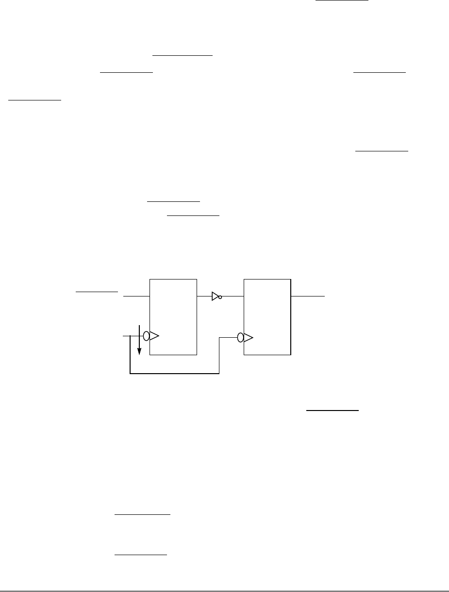
Chapter 8. Signal Descriptions 8-31
Following are the state meaning and timing comments for the 2X_PCLK signal.
State Meaning Rising edge—Is the clocking edge for a synchronizing latch used to
generate the internal processor clock (see PCLK_EN).
Timing Comments Duty cycle—Refer to the PowerPC 601 RISC Microprocessor
Hardware Specifications.
8.2.11.2 Clock Phase (PCLK_EN)—Input
The clock phase (PCLK_EN) signal is input only on the 601. The PCLK_EN signal
switches at the same frequency as the internal CPU clock (P_CLOCK in Figure 8-3). The
PCLK_EN signal determines the phase of the internal P_CLOCK (timing and duty cycle
are derived from the 2X_PCLK input); therefore, this input can be used to synchronize
multiple 601s.
Figure 8-3 shows how the internal P_CLOCK is always identical to the PCLK_EN signal
except it is inverted and delayed by one full 2X_PCLK cycle.
The 601 can tolerate dynamic P_CLOCK cycle stretching. This can be accomplished by
altering the duty cycle of the PCLK_EN input. For example, the system can extend a given
CPU clock cycle by negating PCLK_EN for more than one 2X_PCLK cycle. This
effectively delays the bus clock input sampling points and output drive points in half of a
processor cycle increments and further delays execution of instructions accordingly.
Figure 8-3. Internal P_CLOCK Generation
Following are the state meaning and timing comments for the PCLK_EN signal.
State Meaning Asserted—Indicates that the 601 should generate the high phase of
the internal processor clock synchronized to 2X_PCLK.
Negated—Indicates that the 601 should generate the low phase of the
internal processor clock synchronized to 2X_PCLK.
Timing Comments Assertion—May occur one 2X_PCLK cycle after the negation of
PCLK_EN with appropriate setup to the falling edge of 2X_PCLK.
Negation—Must occur one 2X_PCLK cycle after the assertion of
PCLK_EN with appropriate setup to the falling edge of 2X_PCLK.
2X_PCLK
D
PCLK_EN D
(IN) OUT
CLK CLK
(internal)
P_CLOCK
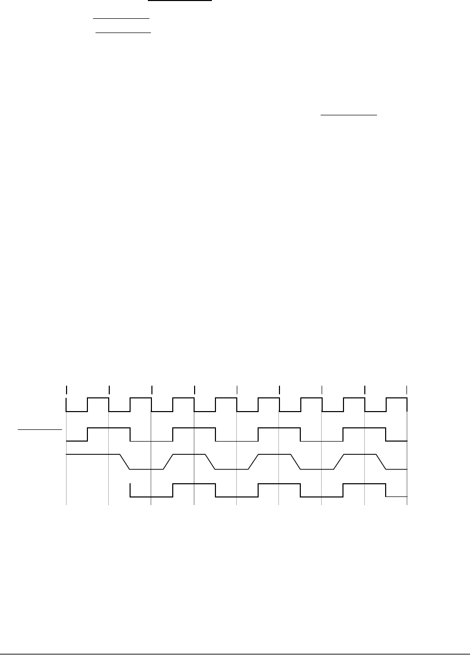
8-32 PowerPC 601 RISC Microprocessor User's Manual
8.2.11.3 Bus Phase (BCLK_EN)—Input
The bus phase (BCLK_EN) signal is input only on the 601. This input determines, in
conjunction with PCLK_EN and 2X_PCLK, the transition timing for the 601 bus interface.
While all timing is derived from the rising edge of the 2X_PCLK input, the two phase
inputs qualify the edge on which the processor and bus interface sequential logic can
proceed. Inputs are sampled and outputs are driven with the qualified rising edge of the
2X_PCLK input (see Figure 8-4).
Following are the state meaning and timing comments for the BCLK_EN signal.
State Meaning Asserted— Indicates that the 601 must use the rising edge of the
internal processor clock to sample and drive the bus interface.
Negated—Indicates that the 601 outputs must not change state, and
the inputs will not be sampled. This signal can be treated as a
synchronous enable for the bus clock cycle clock.
Timing Comments Assertion/Negation—With appropriate setup and hold time to the
2X_PCLK provided the rising edge of the internal processor clock
coincides with the 2X_PCLK.
Figure 8-4 through Figure 8-8 illustrate how the 601 clocking signals can be used to
generate a logical bus clock. Note that the resulting logical bus clock is represented as an
arrow coincident with the rising edge of the resulting signal. It should not be inferred that
the duty cycle of the bus clock signal is 50 percent.
Figure 8-4 shows how the clock inputs can be used to control the 601. Note that the signal
IN is the output of the inverter shown in Figure 8-3.
Figure 8-4. Generation of Internal Clock (P_CLK)
Figure 8-5 shows a simple 601 clock implementation with the frequency of the logical bus
clock equal to that of the P_CLK.
2X_PCLK
PCLK_EN
IN
P_CLK
01234567
****
***
*Delay of inverter output
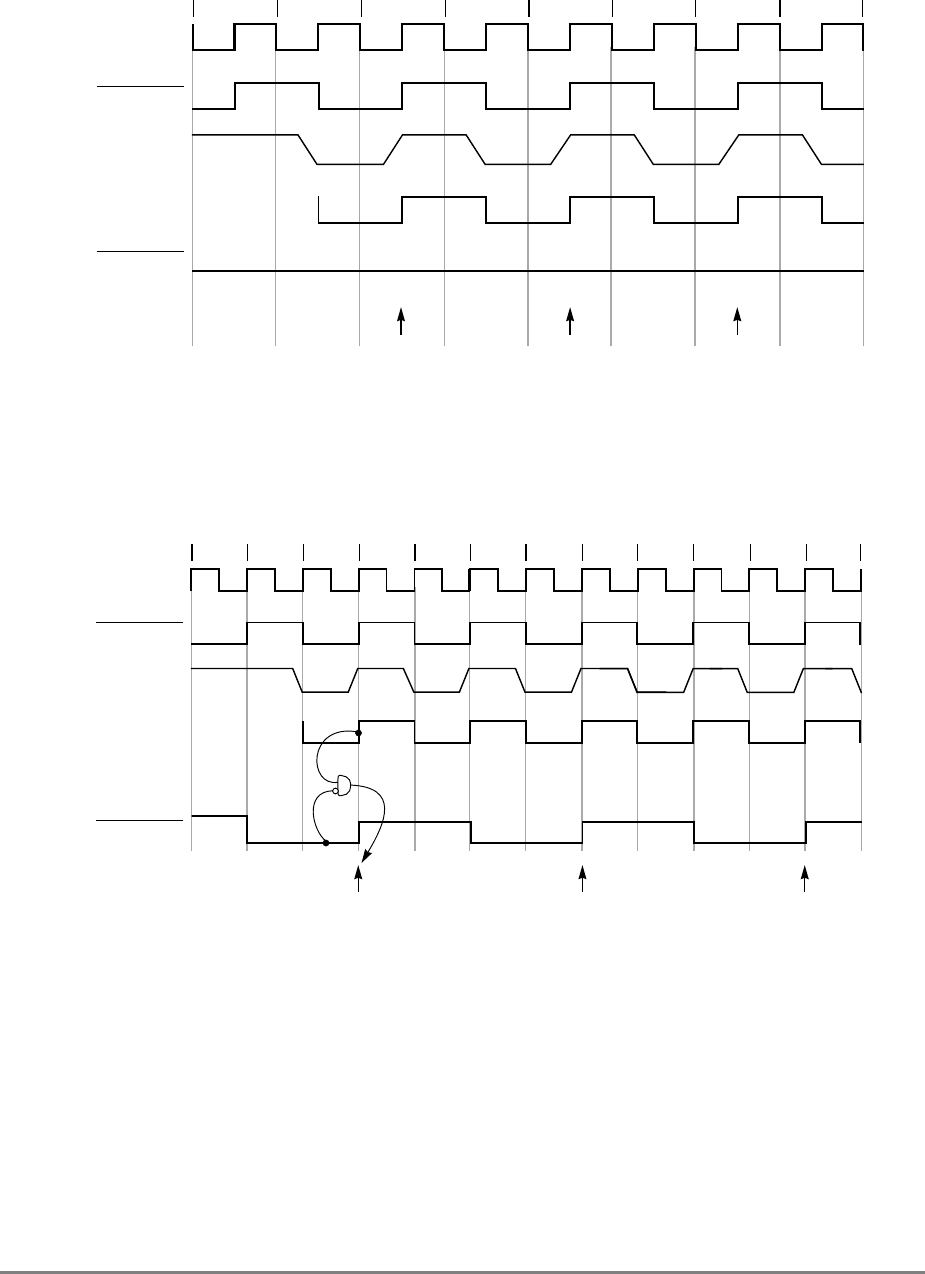
Chapter 8. Signal Descriptions 8-33
Figure 8-5. Generation of Bus Transitions—Logical Bus Clock = P_CLK
Figure 8-6 shows the generation of the logical bus clock at one-half the frequency of the
P_CLK.
Figure 8-6. Generation of Bus Transitions—Logical Bus Clock = 1/2 P_CLK
Figure 8-7 shows the generation of the logical bus clock at one-third the frequency of the
P_CLK.
2X_PCLK
PCLK_EN
IN
P_CLK
BCLK_EN
Logical Bus Clock
01234567
****
***
*Delay of inverter output
2X_PCLK
PCLK_EN
IN
P_CLK
BCLK_EN
Bus Transition
0 1 2 3 4 5 6 7 8 9 10 11
*Delay of inverter output
** **
***
**
**
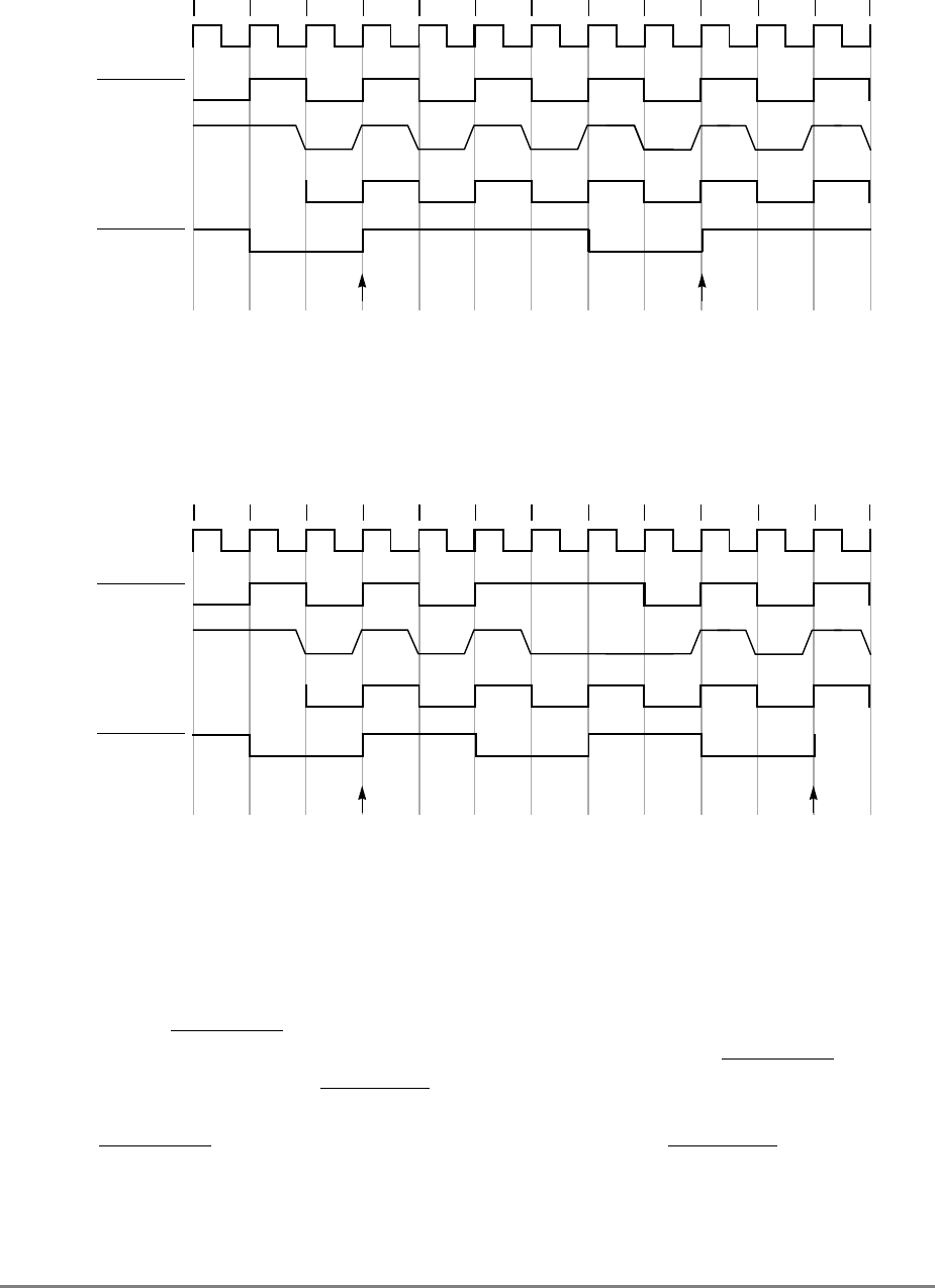
8-34 PowerPC 601 RISC Microprocessor User's Manual
Figure 8-7. Generation of Bus Transitions—Logical Bus Clock=1/3 P_CLK
Figure 8-8 shows how the PCLK_EN signal can be manipulated to perform cycle stretching
on the 601.
Figure 8-8. Generation of Bus Transitions—Cycle Stretching
In this document, processor clock refers to the internal P_CLOCK signal; bus clock refers
to the clock that causes the bus transitions.
Figure 8-5 and Figure 8-6 show two examples of the generation of bus transitions. In the
first example, BCLK_EN is grounded (always asserted) and the bus clock period is
equivalent to the P_CLOCK cycle period. In the second example, the BCLK_EN input is
driven by a clock switching at PCLK_EN/2 frequency. This allows the 601 bus interface to
run at half the frequency of the CPU P_CLOCK, easing system design constraints. Note
that the BCLK_EN input can be divided further (with respect to PCLK_EN), allowing an
even greater ratio between the clock- and bus-cycle frequencies.
2X_PCLK
PCLK_EN
IN
P_CLK
BCLK_EN
Bus Transition
0 1 2 3 4 5 6 7 8 9 10 11
*Delay of inverter output
** **
***
**
**
2X_PCLK
PCLK_EN
IN
P_CLK
BCLK_EN
Bus Transition
0 1 2 3 4 5 6 7 8 9 10 11
*Delay of inverter output
** **
***
**
**

Chapter 8. Signal Descriptions 8-35
To operate the bus interface slower than P_CLOCK/2, BCLK_EN must be asserted only for
the intended P_CLOCK window (for example, the duty cycle can be skewed such that the
bus logic increments only once during each assertion of BCLK_EN).
8.2.11.4 Real-Time Clock (RTC)—Input
The real-time clock (RTC) signal is input only on the 601, and should be driven by a 7.8125
MHz oscillator. Following are the state meaning and timing comments for the RTC signal.
State Meaning Rising edge—Increments the real-time clock in the 601.
Timing Comments Duty cycle—See the PowerPC 601 RISC Microprocessor Hardware
Specifications.
8.3 Clocking in a Multiprocessor System
Clocking in a multiprocessor system adds a level of complexity. The 601 defines the AC
timing specifications for the chip inputs and outputs to allow for a reasonable amount of
system-level skew and still allow the chip to meet its timing goals. These timing
specifications can be found in the PowerPC 601 RISC Microprocessor Hardware
Specifications.

8-36 PowerPC 601 RISC Microprocessor User's Manual

Chapter 9. System Interface Operation 9-1
Chapter 9
System Interface Operation
90
90
This section describes the PowerPC 601 microprocessor bus interface and its operation. It
shows how the 601 signals, defined in Chapter 8, “Signal Descriptions,” interact to perform
address and data transfers.
9.1 PowerPC 601 Microprocessor System Interface
Overview
The system interface performs external accesses for loading and storing data and fetching
instructions.
Instructions are automatically fetched from the memory system into the instruction unit
where they are dispatched to the execution units at a maximum rate of three instructions per
clock. Conversely, load and store instructions explicitly specify the movement of operands
to and from the integer and floating-point register files and the memory system.
When the 601 encounters an instruction or data access, it calculates the logical address
(effective address) and uses the low-order address bits to check for a hit in the on-chip, 32-
Kbyte cache. Operation of the cache is described in Section 9.1.1, “Operation of the On-
Chip Cache.” During the cache lookup, the memory management unit (MMU) uses the
upper-order address bits to calculate the virtual address, from which it calculates the
physical address. The physical address bits are then compared with the corresponding
cache tag bits to determine if a cache hit occurred. If the access misses in the cache, the
physical address is used to access system memory.
In addition to the loads, stores, and instruction fetches, the 601 performs other read and
write operations for table searches, cache cast-out operations when least-recently used
sectors are written to memory after a cache miss, and cache-sector snoop push-out
operations when a modified sector experiences a snoop hit from another bus master.
All read and write operations are handled by the memory unit, which consists of a two-
element read queue that holds addresses for read operations, and a three-element write
queue that contains addresses and data for write operations. To maintain coherency, the
queues are included in snooping. The interface allows one level of pipelining; that is, with
certain restrictions discussed later, there can be two outstanding transactions at any given

9-2 PowerPC 601 RISC Microprocessor User's Manual
time. Accesses are prioritized. The operation of the memory unit is described in
Section 9.1.2, “Operation of the Memory Unit for Loads and Stores.”
Figure 9-1 shows the address path from the execution units and instruction fetcher, through
the translation logic to the cache and system interface logic.
The 601 uses separate address and data buses and a variety of control and status signals for
performing reads and writes. The address bus is 32 bits wide and the data bus is 64 bits
wide. The interface is synchronous—all timing is derived from the start of the bus cycle.
All 601 inputs are sampled at and all outputs are driven from this edge. The bus can run at
the full processor-clock frequency or at an integer division of the processor-clock speed.
The 601 provides a TTL-compatible interface.
9.1.1 Operation of the On-Chip Cache
The 601’s cache is a combined instruction and data (or unified) cache. It is a physically-
addressed, virtually-indexed, 32-Kbyte cache with eight-way set associativity. The cache
consists of eight sets of 128 sectors. Each 16-word cache line consists of two 8-word
sectors. Both sectors share the same line address tag. Cache coherency, however, is
maintained for each sector, so there are separate coherency state bits for each sector. If one
sector of the line is filled from memory, the 601 attempts to load the other sector as a low-
priority bus operation. There is no guarantee that the other sector will be loaded.
Because the cache on the 601 is an on-chip, write-back primary cache, the predominant
type of transaction for most applications is burst-read memory operations, followed by
burst-write memory operations, I/O controller interface operations, and single-beat
(noncacheable or write-through) memory read and write operations. Additionally, there can
be address-only operations, variants of the burst and single-beat operations (global memory
operations that are snooped, and atomic memory operations, for example), and address
retry activity (for example, when a snooped read access hits a modified line in the cache).
The cache tag directory has one address port dedicated to instruction fetch and load/store
accesses and one dedicated to snooping transactions on the system interface. Therefore,
snooping does not require additional clock cycles unless a snoop hit that requires a cache
status update occurs.
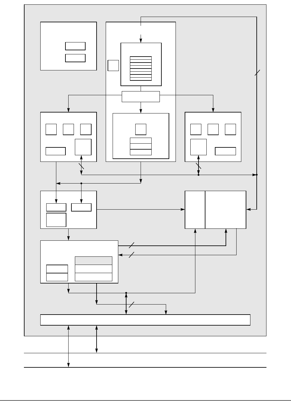
Chapter 9. System Interface Operation 9-3
Figure 9-1. PowerPC 601 Microprocessor Block Diagram
(INSTRUCTION FETCH)
RTC
IU BPU FPU
MMU
SYSTEM INTERFACE
RTCU
RTCL
INSTRUCTION
QUEUE
+
+*/+
INSTRUCTIONINSTRUCTION
8 WORDS
XER
GPR
FILE
CTR
CR
LR
2 WORDS1 WORD DATA
ADDRESS
UTLB
BAT
ARRAY
ITLB TAGS
32-KBYTE
CACHE
(INSTRUC-
TION AND DA-
PHYSICAL ADDRESS
ADDRESS
DATA
SNOOP
ADDRESS
ADDRESS
DATA
64-BIT DATA BUS
32-BIT ADDRESS BUS
MEMORY UNIT
SNOOP
A
B
READ
QUEUE WRITE QUEUE
+*/
FPR
FILE FPSCR
INSTRUCTION UNIT
ISSUE LOGIC
2 WORDS
4 WORDS DATA
8 WORDS

9-4 PowerPC 601 RISC Microprocessor User's Manual
9.1.2 Operation of the Memory Unit for Loads and Stores
As shown in Figure 9-1, the memory unit includes two read-queue elements and three
write-queue elements. The read queue buffers are used for holding addresses for read
operations; the write queue buffers are used for holding addresses and data for write
operations and to support such features as address pipelining, snooping, and write
buffering, described as follows:
• The two read-queue elements allow the system interface logic to buffer as many as
two outstanding read operations. There are two restrictions that apply to filling the
two read-queue elements described as follows:
— There cannot be two outstanding load operations.
— There cannot be two outstanding read-with-intent-to-modify instructions.
• Note that when a read miss causes the cache to be updated, only the sector with the
required data is guaranteed to be updated. The other sector can be updated only if
both read-queue elements are free. The update of the other sector can be disabled by
setting bits in the HID0 register. HID0[DRF], bit 26, can be used to disable fetches
and HID0[DRL], bit 27, can be used to disable loads and stores.
• Two of the three write-queue elements, marked “A” and “B” in Figure 9-1, are
buffers for write operations. They buffer store operations and sectors that are written
back to memory such as when a cache location is updated after a cache miss. This
allows the cache to be updated before the replaced sector is written back to system
memory. Write-queue elements A or B will be used for snoop push operations if
high-priority copyback is not enabled.
• The third queue element, marked “snoop” in Figure 9-1, has two modes of
operation. The default mode provides high-priority copy-back operations that result
from snoop hits to modified data (cache-sector snoop push-out operations while a
read operation is pending on the bus). Snoop hits to modified data create a high-
priority store operation that allows the processor to become bus master to store the
modified data to memory, where it in turn is read by the snooping device. The
override mode uses the HP_SNP_REQ signal to determine if the snoop queue is to
be used. This mode is enabled by setting HID0[31].
9.1.3 Operation of the System Interface
Memory accesses can occur in single-beat (1–8 bytes) and four-beat burst (32 bytes) data
transfers. The address and data buses are independent for memory accesses to support
pipelining and split transactions. The 601 can pipeline as many as two transactions and has
limited support for out-of-order split-bus transactions.
Access to the system interface is granted through an external arbitration mechanism that
allows devices to compete for bus mastership. This arbitration mechanism is flexible,
allowing the 601 to be integrated into systems that implement various fairness and bus
parking procedures to avoid arbitration overhead. Additional multiprocessor support is
provided through coherency mechanisms that provide snooping, external control of the on-

Chapter 9. System Interface Operation 9-5
chip cache and TLB, and support for a secondary cache. Multiprocessor software support
is provided through the use of atomic memory operations.
Typically, memory accesses are weakly ordered—sequences of operations, including
load/store string and multiple instructions, do not necessarily complete in the order they
begin—maximizing the efficiency of the bus without sacrificing coherency of the data. The
601 allows read operations to precede store operations (except when a dependency exists,
of course). In addition, the 601 can be configured to reorder high priority write operations
ahead of lower priority store operations. Because the processor can dynamically optimize
run-time ordering of load/store traffic, overall performance is improved.
Note that the Synchronize (sync) or Enforce In-Order Execution of I/O (eieio) instruction
can be used to enforce strong ordering.
The following sections describe how the 601 interface operates, providing detailed timing
diagrams that illustrate how the signals interact. A collection of more general timing
diagrams are included as examples of typical bus operations.
Figure 9-2 is a legend of the conventions used in the timing diagrams.
This is a synchronous interface—all 601 input signals except the PCLK_EN signals are
sampled relative to the start of the bus clock cycle. Outputs are driven off the start of the
bus cycle (see the PowerPC 601 RISC Microprocessor Hardware Specifications for exact
timing information).
9.1.4 I/O Controller Interface Accesses
In addition to supporting memory-mapped I/O with the high-performance memory
interface, the 601 also implements the I/O controller interface protocol for compatibility
with certain external devices. Memory and I/O controller interface accesses use the 601
signals differently.
The 601 defines separate memory and I/O address spaces, or segments, distinguished by the
segment register T bit in the address translation logic of the 601. If the T-bit is cleared, the
memory reference is a normal memory access and can use the virtual memory management
hardware of the 601. If the T-bit is set, the memory reference is an I/O controller interface
access.
The function and timing of some address transfer and attribute signals (such as TT0–TT3,
TBST, and TSIZ0–TSIZ2) are changed for I/O controller interface accesses. Additional
controls are required to facilitate transfers between the 601 and intelligent I/O devices. I/O
controller interface and memory transfers are distinguished from one another by their
address transfer start signals—TS indicates that a memory transfer is starting and XATS
indicates that an I/O controller interface transaction is starting.
Unlike memory accesses, I/O controller interface accesses cannot be pipelined and must be
strongly ordered—each access occurs in strict program order and completes before another
9-6 PowerPC 601 RISC Microprocessor User's Manual
access can begin. For this reason, I/O controller interface accesses are less efficient than
memory accesses. The I/O extensions also allow for additional bus pacing and multiple
transaction operations for variably-sized data transfers (1 to 128 bytes), and they support a
tagged, split request/response protocol. The I/O controller interface access protocol also
requires the slave device to function as a bus master.
Figure 9-2. Timing Diagram Legend
9.2 Memory Access Protocol
Memory accesses are divided into address and data tenures. Each tenure has three phases—
bus arbitration, transfer, and termination. The 601 also supports address-only transactions.
Note that address and data tenures can overlap, as shown in Figure 9-3.
Figure 9-3 shows that the address and data tenures are distinct from one another and that
both consist of three phases—arbitration, transfer, and termination. Address and data
601 input (while the 601 is a bus master)
601 output (while the 601 is a bus master)
601 output (grouped: here, address plus attributes)
601 internal signal (inaccessible to the user, but used in
diagrams to clarify operations)
Compelling dependency—event will occur on the
next clock cycle
Prerequisite dependency—event will occur on an
undetermined subsequent clock cycle
601 three-state output or input
601 nonsampled input
Signal with sample point
A sampled condition (dot on high or low state)
with multiple dependencies
Timing for a signal had it been asserted (it is not
actually asserted)
Bar over signal name indicates active low
ap0
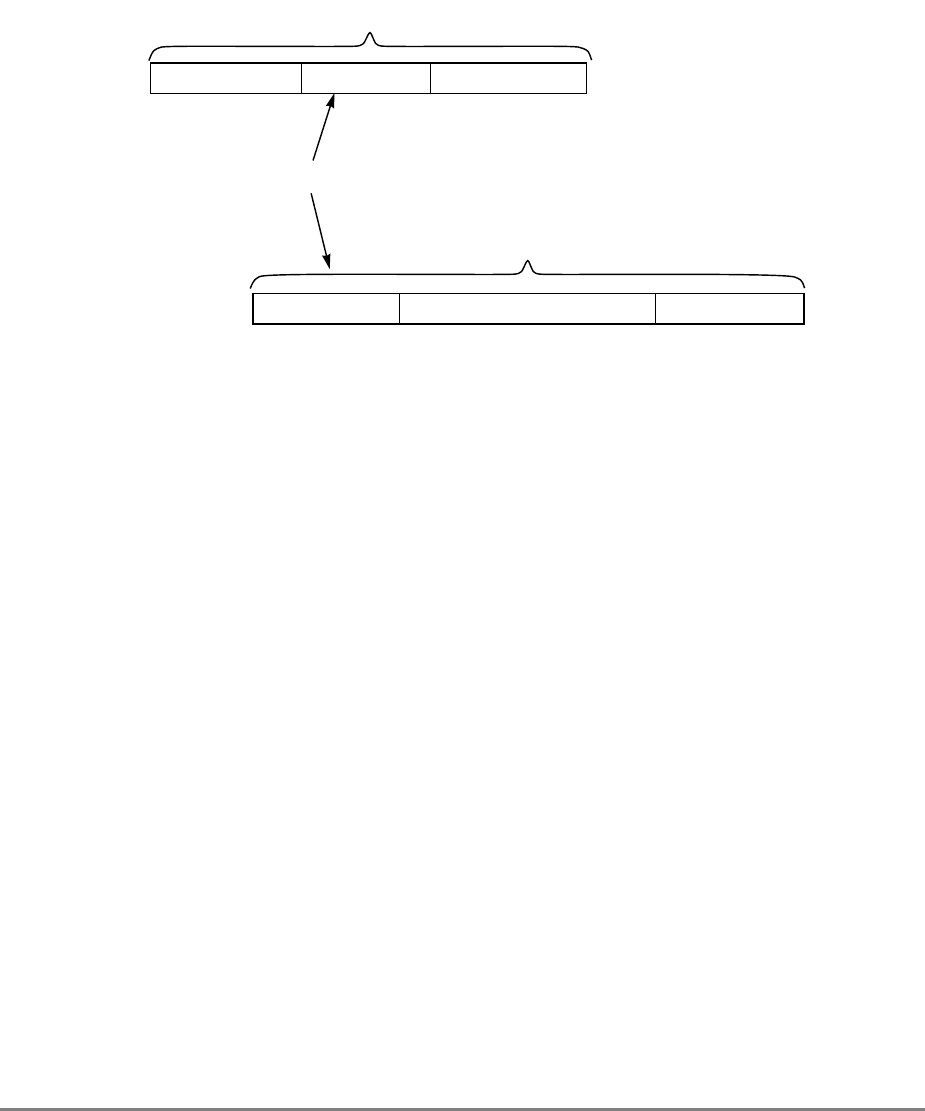
Chapter 9. System Interface Operation 9-7
tenures are independent (indicated in Figure 9-3 by the fact that the data tenure begins
before the address tenure ends), which allows split-bus transactions to be implemented at
the system level in multiprocessor systems. Figure 9-3 shows a data transfer that consists
of a single-beat transfer of as many as 64 bits. Four-beat burst transfers of 32-byte cache
sectors require data transfer termination signals for each beat of data.
Figure 9-3. Overlapping Tenures on the PowerPC 601 Microprocessor Bus for a
Single-Beat Transfer
The basic functions of the address and data tenures are as follows:
• Address tenure
— Arbitration: During arbitration, address bus arbitration signals are used to gain
mastership of the address bus.
— Transfer: After the 601 is the address bus master, it transfers the address on the
address bus. The address signals and the transfer attribute signals control the
address transfer. The address parity and address parity error signals ensure the
integrity of the address transfer.
— Termination: After the address transfer, the system signals that the address tenure
is complete or that it must be repeated.
• Data tenure
— Arbitration: To begin the data tenure, the 601 arbitrates for mastership of the data
bus.
— Transfer: After the 601 is the data bus master, it samples the data bus for read
operations or drives the data bus for write operations. The data parity and data
parity error signals ensure the integrity of the data transfer.
— Termination: Data termination signals are required after each data beat in a data
transfer. Note that in a single-beat transaction, the data termination signals also
indicate the end of the tenure, while in burst accesses, the data termination
signals apply to individual beats and indicate the end of the tenure only after the
final data beat.
ARBITRATION TRANSFER TERMINATION
ADDRESS TENURE
ARBITRATION SINGLE-BEAT TRANSFER TERMINATION
DATA TENURE
INDEPENDENT ADDRESS AND DATA

9-8 PowerPC 601 RISC Microprocessor User's Manual
The 601 bus supports address-only transfers, which use only the address bus, with no data
transfer involved. This is useful in multiprocessor environments where external control of
on-chip primary caches and TLB entries is desirable. Additionally, the 601’s retry
capability provides an efficient snooping protocol for systems with multiple memory
systems (including caches) that must remain coherent.
9.2.1 Arbitration Signals
Arbitration for both address and data bus mastership in a multiprocessor system is
performed by a central, external arbiter and, minimally, by the arbitration signals shown in
Section 8.2.1, “Address Bus Arbitration Signals.” Most arbiter implementations require
additional signals to coordinate bus master/slave/snooping activities. Note that address bus
busy (ABB) and data bus busy (DBB) are bidirectional signals. These signals are inputs
unless the 601 has mastership of one or both of the respective buses; they must be connected
high through pull-up resistors so that they remain negated when no devices have control of
the buses.
The following list describes the address arbitration signals:
•BR (bus request)—Assertion indicates that the 601 is requesting mastership of the
address bus.
•BG (bus grant)—Assertion indicates that the 601 may, with the proper
qualification, assume mastership of the address bus. A qualified bus grant occurs
when BG is asserted and ABB and ARTRY are negated.
If the 601 is parked, BR need not be asserted for the qualified bus grant.
•ABB (address bus busy)— Assertion indicates that the 601 is the address bus
master.
The following list describes the data arbitration signals:
•DBG (data bus grant)—Indicates that the 601 may, with the proper qualification,
assume mastership of the data bus. A qualified data bus grant occurs when DBG is
asserted while DBB, DRTRY, and ARTRY are negated.
DBB signal is driven by the current bus master, DRTRY is only driven from the bus,
and ARTRY is from the bus, but only for the address bus tenure associated with the
current data bus tenure (that is, not from another address tenure).
•DBWO (data bus write only)—Assertion indicates that the 601 may run the data
bus tenure for an outstanding write address even if a read address is pipelined before
the write address. If DBWO is asserted, the 601 only assumes data bus mastership
for a pending data bus write operation (that is, the 601 does not take the data bus for
a pending read operation if this input is asserted along with DBG). Care must be
taken with DBWO to ensure the desired write is queued (for example, a cache-sector
snoop push-out operation).

Chapter 9. System Interface Operation 9-9
• DBB (data bus busy)—Assertion indicates that the 601 is the data bus master. The
601 always assumes data bus mastership if it needs the data bus and is given a
qualified data bus grant (see DBG).
For more detailed information on the arbitration signals, refer to Section 8.2.1,
“Address Bus Arbitration Signals,” and Section 8.2.6, “Data Bus Arbitration
Signals.”
9.2.2 Address Pipelining and Split-Bus Transactions
The 601 protocol provides independent address and data bus capability to support pipelined
and split-bus transaction system organizations. Address pipelining allows a new bus
transaction to begin before the current transaction has finished. Split-bus transaction
capability allows the address bus and data bus to have different masters at the same time.
While this capability does not inherently reduce memory latency, support for address
pipelining and split-bus transactions can greatly improve effective bus/memory throughput.
For this reason, these techniques are most effective in shared-memory multiprocessor
implementations where bus bandwidth is an important measurement of system
performance.
External arbitration is required in systems in which multiple devices must compete for the
system bus. The design of the external arbiter affects pipelining by regulating address bus
grant (BG), data bus grant (DBG), and AACK signals. For example, a one-level pipeline is
enabled by asserting AACK to the current address bus master and granting mastership of
the address bus to the next requesting master before the current data bus tenure has
completed. Two address tenures can occur before the current data bus tenure completes.
The 601 can pipeline its own transactions to a depth of one level (intraprocessor pipelining);
however, the 601 bus protocol does not constrain the maximum number of levels of
pipelining that can occur on the bus between multiple masters (interprocessor pipelining).
The external arbiter must control the pipeline depth and synchronization between masters
and slaves.
In a pipelined implementation, data bus tenures are kept in strict order with respect to
address tenures. However, external hardware can further decouple the address and data
buses, allowing the data tenures to occur out of order with respect to the address tenures.
This requires some form of system tag to associate the out-of-order data transaction with
the proper originating address transaction (not defined for the 601 interface). Individual bus
requests and data bus grants from each processor can be used by the system to implement
tags to support interprocessor, out-of-order transactions.
The 601 supports a limited intraprocessor out-of-order, split-transaction capability via the
data bus write only (DBWO) signal. For more information about using DBWO, see
Section 9.10, “Using DBWO)—(Data Bus Write Only).”
9-10 PowerPC 601 RISC Microprocessor User's Manual
9.3 Address Bus Tenure
This section describes the three phases of the address tenure—address bus arbitration,
address transfer, and address termination.
9.3.1 Address Bus Arbitration
When the 601 needs access to the external bus and it is not parked (BG is negated), it asserts
bus request (BR) until it is granted mastership of the bus and the bus is available (see
Figure 9-4). The external arbiter must grant master-elect status to the potential master by
asserting the bus grant (BG) signal. The 601 requesting the bus determines that the bus is
available when the ABB input is negated. When the address bus is not busy (ABB input is
negated), BG is asserted and the address retry (ARTRY) input is negated. This is referred
to as a qualified bus grant. The potential master assumes address bus mastership by
asserting ABB when it receives a qualified bus grant.
The 601 also provides an internally generated address bus busy signal, which it logically
ORs with the ABB signal received off of the bus. This internal address bus busy signal is
asserted with any TS or XATS signal and is negated with a valid AACK. This internally
generated address bus busy signal is useful in systems that do not use ABB.
Figure 9-4. Address Bus Arbitration
External arbiters must allow only one device at a time to be address bus master. In
implementations in which no other device can be a master, BG can be grounded (always
asserted) to continually grant mastership of the address bus to the 601.
-1 0 1
bg
abb
artry
Logical Bus Clock
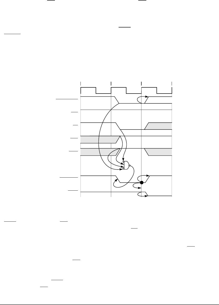
Chapter 9. System Interface Operation 9-11
If the 601 asserts BR before the external arbiter asserts BG, the 601 is considered to be
unparked, as shown in Figure 9-4. Figure 9-5 shows the parked case, where a qualified bus
grant exists on the clock edge following a need_bus condition. Notice that the bus clock
cycle required for arbitration is eliminated if the 601 is parked, reducing overall memory
latency for a transaction. The 601 always negates ABB for at least one bus clock cycle after
AACK is asserted, even if it is parked and has another transaction pending.
Typically, bus parking is provided to the device that was the most recent bus master;
however, system designers may choose other schemes, such as providing unrequested bus
grants in situations where it is easy to correctly predict the next device requesting bus
mastership.
Figure 9-5. Address Bus Arbitration Showing Bus Parking
When the 601 receives a qualified bus grant, it assumes address bus mastership by asserting
ABB and negating the BR output signal. Meanwhile, the 601 drives the address for the
requested access onto the address bus and asserts TS to indicate the start of a new
transaction.
When designing external bus arbitration logic, note that the 601 may assert BR without
using the bus after it receives the qualified bus grant. For example, in a system using bus
snooping, if the 601 asserts BR to perform a replacement copy-back operation, another
device can invalidate that sector before the 601 is granted mastership of the bus. Once the
601 is granted the bus, it no longer needs to perform the copy-back operation; therefore, the
601 does not assert ABB and does not use the bus for the copy-back operation. Note that
the 601 asserts BR for at least one clock cycle in these instances.
-1 0 1
bg
abb
artry
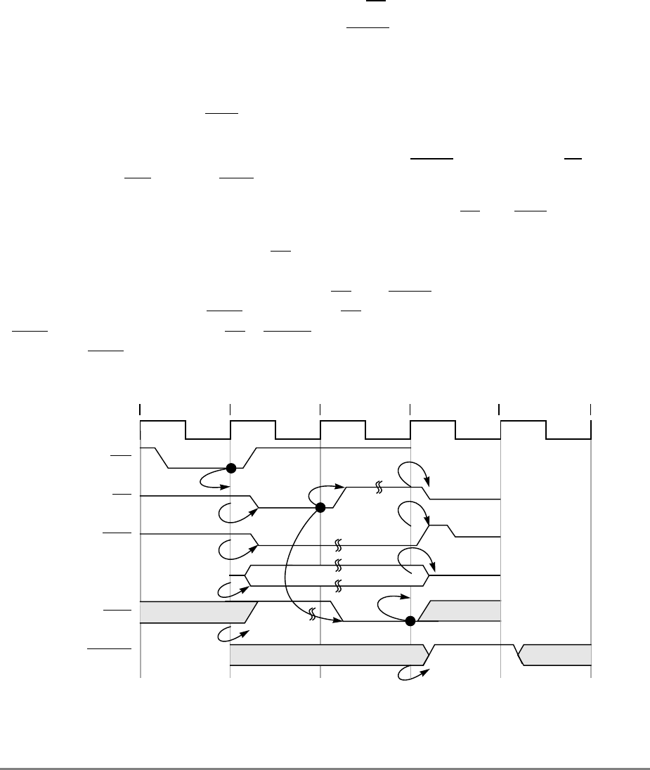
9-12 PowerPC 601 RISC Microprocessor User's Manual
9.3.2 Address Transfer
During the address transfer, the physical address and all attributes of the transaction are
transferred from the bus master to the slave device(s). Snooping logic may monitor the
transfer to enforce cache coherency (see discussion about snooping in Section 9.3.3,
“Address Transfer Termination”). The signals used in the address transfer include the
following signal groups (see Figure 8-1):
• Address transfer start signal: Transfer start (TS)
Note that extended address transfer start (XATS) is used for I/O controller interface
operations and has no function for memory accesses. See Section 9.6, “Memory- vs.
I/O-Mapped I/O Operations.”
• Address transfer signals: Address bus (A0–A31), address parity (AP0–AP3), and
address parity error (APE)
• Address transfer attribute signals: Transfer type (TT0–TT4), transfer code (TC0–
TC3), transfer size (TSIZ0–TSIZ2), transfer burst (TBST), cache inhibit (CI), write-
through (WT), global (GBL), and cache set element (CSE0–CSE2)
Figure 9-6 shows that the timing for all of these signals, except TS and APE, is identical.
All of the address transfer and address transfer attribute signals are combined into the
ADDR+ grouping in Figure 9-6. The TS signal indicates that the 601 has begun an address
transfer and that the address and transfer attributes are valid (within the context of a
synchronous bus). The 601 always asserts TS (or XATS for I/O controller interface
operations) coincident with ABB. As an input, TS need not coincide with the assertion of
ABB on the bus (that is, either TS or XATS can be asserted with, or on, a subsequent clock
cycle after ABB is asserted; the 601 tracks this transaction correctly).
Figure 9-6. Address Bus Transfer
01234
aack
artry_in

Chapter 9. System Interface Operation 9-13
In Figure 9-6, the address transfer occurs during bus clock cycles 1 and 2 (arbitration occurs
in bus clock cycle 0 and the address transfer is terminated in bus clock 3). In this diagram,
the address bus termination input, AACK, is asserted to the 601 on the bus clock following
assertion of TS (as shown by the dependency line). This is the minimum duration of the
address transfer for the 601; the duration can be extended by delaying the assertion of
AACK for one or more bus clocks.
9.3.2.1 Address Bus Parity
The 601 always generates one bit of correct odd-byte parity for each of the four bytes of
address when a valid address is on the bus. The calculated values are placed on the AP0–
AP3 outputs when the 601 is the address bus master. If the 601 is not the master and TS and
GBL are asserted together (qualified condition for snooping memory operations), the
calculated values are compared with the AP0–AP3 inputs. If there is an error, the APE
output is asserted. An address bus parity error causes a checkstop condition if the bus parity
checkstop source is enabled in HID0. For more information, see Chapter 5, “Exceptions.”
9.3.2.2 Address Transfer Attribute Signals
The transfer attribute signals include several encoded signals such as the transfer type
(TT0–TT4) signals, transfer burst (TBST) signal, transfer size (TSIZ0–TSIZ2) signals, and
transfer code (TC0–TC1) signals. Section 8.2.4, “Address Transfer Attribute Signals,”
describes the encodings for the address transfer attribute signals. Note that TT0–TT4,
TBST, and TSIZ0–TSIZ2 have alternate functions for I/O controller interface operations
(see Section 9.6, “Memory- vs. I/O-Mapped I/O Operations).”
9.3.2.2.1 Transfer Type (TT0–TT4) Signals
Snooping logic should fully decode the transfer type signals if the GBL signal is asserted.
Slave devices can use the individual transfer type signals without fully decoding the group.
The transfer type signals generally have the following individual functions:
•TT0—Special operations: This signal is asserted by the 601 whenever a bus
transaction occurs in response to a lwarx/stwcx. (Load Word and Reserve
Indexed/Store Word Conditional Indexed) instruction pair (see Chapter 3,
“Addressing Modes and Instruction Set Summary”), an eciwx or ecowx instruction,
or for a Translation Lookaside Buffer Invalidate Entry (tlbie) operation.
•TT1—Read (/write) operations: The TT1 signal indicates whether the transaction is
a read (TT1 high) or a write (TT1 low) transaction. This is valid for transactions that
are not address only.
•TT2—Invalidate operations: When asserted with GBL, the TT2 output signal
indicates that all other caches in the system should invalidate the cache entry on a
snoop hit. If the snoop hit is to a modified entry, the sector should be copied back
before being invalidated.
•TT3—Memory (/address-only) operations: Except for eciwx or ecowx instructions
(TT0–TT3 encodings 1010 or 1110) the TT3 signal, when asserted, indicates that the
associated data transfer is to/from memory and that use of the data bus will be
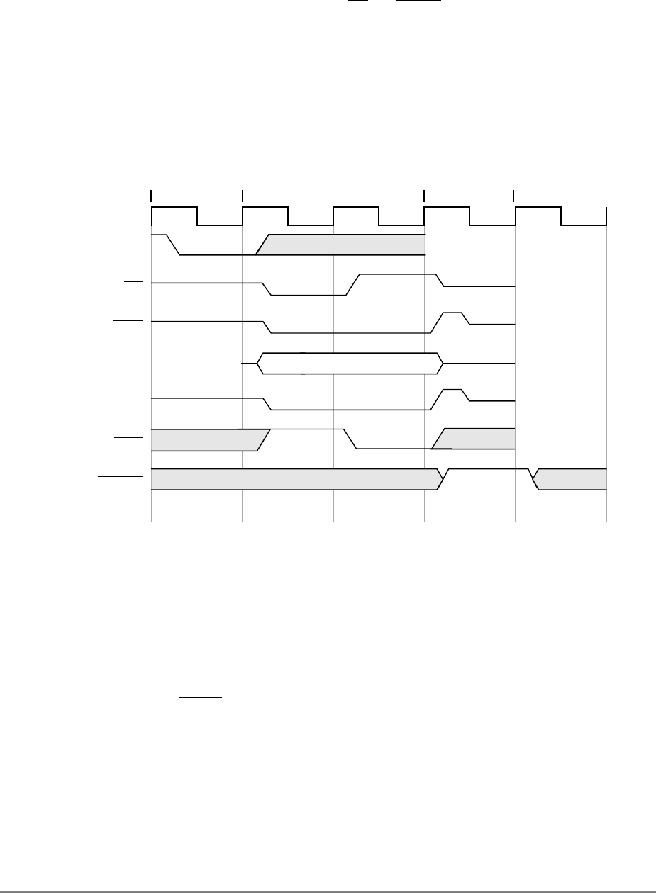
9-14 PowerPC 601 RISC Microprocessor User's Manual
required in order for the transaction to complete. External logic can synthesize the
data bus request from the combination of TS (or XATS) and TT3 (DBR=TS&TT3).
If TT3 is not asserted with the address, the associated bus transaction is considered
to be a broadcast operation that all bus participants must honor (or a reserved
operation). This is an address-only transaction; the 601 does not need and will not
acquire data bus ownership, even if it receives a qualified data bus grant. Figure 9-7
shows an address-only transaction. On the start of bus cycle 2, TT3 is not asserted;
therefore, the data bus will not be needed.
•TT4—The TT4 signal is reserved for future expansion.
Figure 9-7. Address-Only Bus Transaction
9.3.2.2.2 Transfer Size (TSIZ0–TSIZ2) Signals
The transfer size signals (TSIZ0–TSIZ2) indicate the size of the requested data transfer as
shown in Table 9-1. The TSIZ0–TSIZ2 signals may be used along with TBST and A29–
A31 to determine which portion of the data bus contains valid data for a write transaction
or which portion of the bus should contain valid data for a read transaction. Note that for a
burst transaction (as indicated by the assertion of TBST) TSIZ0–TSIZ2 are always set to
b'010'. Therefore, if the TBST signal is asserted, the memory system should transfer a total
of eight words (32 bytes), regardless of the TSIZ0–TSIZ2 encoding.
01234
bg
aack
artry_in

Chapter 9. System Interface Operation 9-15
The basic coherency size of the bus is defined to be 32 bytes (corresponding to one cache
sector). Data transfers that cross an aligned, 32-byte boundary either must present a new
address onto the bus at that boundary (for coherency consideration) or must operate as
noncoherent data with respect to the 601.
9.3.2.3 Effect of Alignment in Data Transfers
Table 9-2 lists the aligned transfers that can occur on the 601 bus. These are transfers in
which the data is aligned to an address that is an integer multiple of the size of the data. For
example, Table 9-2 shows that one-byte data is always aligned; however, for a four-byte
word to be aligned, it must be oriented on an address that is a multiple of four.
Table 9-1. Transfer Size Signal Encodings
TBST TSIZ0 TSIZ1 TSIZ2 Transfer Size
Asserted 0 1 0 Eight-word burst
Negated 0 0 0 Eight bytes
Negated 0 0 1 One byte
Negated 0 1 0 Two bytes
Negated 0 1 1 Three bytes
Negated 1 0 0 Four bytes
Negated 1 0 1 Five bytes
Negated 1 1 0 Six bytes
Negated 1 1 1 Seven bytes

9-16 PowerPC 601 RISC Microprocessor User's Manual
Notes:
√ The byte portions of the requested operand that are read or written during that bus transaction.
— These entries are not required and are ignored during read transactions and are driven with undefined
data during all write transactions (except noncacheable write transfers, in which data is mirrored on both
word lanes if the transfer does not exceed four bytes).
Data bus byte lane 0 corresponds to DH0-DH7, byte lane 7 corresponds to DL24-DL31.
The 601 also supports misaligned memory operations. These transfers address memory that
is not aligned to the size of the data being transferred (such as, a word read of an odd byte
address). Although most of these operations hit in the primary cache (or generate burst
memory operations if they miss), the 601 interface supports misaligned transfers within a
double-word (64-bit aligned) boundary, as shown in Table 9-3. Note that the three-byte
transfer in Table 9-3 is only one example of misalignment. As long as the attempted transfer
does not cross a double-word boundary, the 601 can transfer the data on the misaligned
address (for example, a word read from an odd byte-aligned address, or a seven-byte read
from an odd byte-aligned address).
An attempt to address data that crosses a double-word boundary requires two bus transfers
to access the data. This is illustrated in the last example of a three-byte transfer in Table 9-3.
The transfer requires two accesses—the first for the last two bytes of one double-word
Table 9-2. Aligned Data Transfers
Transfer Size Data Bus Byte Lane(s)
TSIZ0 TSIZ1 TSIZ2 A29–A31 01234567
Byte 0 0 1 000 √———————
0 0 1 001 — √——————
0 0 1 010 — — √—————
0 0 1 011 — — — √————
0 0 1 100 ———— √———
0 0 1 101 ————— √——
0 0 1 110 —————— √—
0 0 1 111 ——————— √
Half word 0 1 0 000 √√——————
0 1 0 010 — — √√————
0 1 0 100 ———— √√——
0 1 0 110 —————— √√
Word 1 0 0 000 √√√√————
1 0 0 100 ———— √√√√
Double word 0 0 0 000 √√√√√√√√

Chapter 9. System Interface Operation 9-17
address, the second for one byte from the next double-word address. The TBST, TSIZ0–
TSIZ2, and A29–A31 signals provide enough information to determine the size of the
transfer and the data bus byte lanes involved in the misaligned transfer.
Although misaligned transfers are supported, they may degrade performance substantially.
In addition to the double-word straddle boundary condition, the address translation logic
can generate substantial exception overhead when the microcoded, sequenced, load/store
multiple and load/store string instructions access misaligned data. It is strongly
recommended that software attempt to align code and data where possible.
9.3.2.3.1 Alignment of External Control Instructions
The size of the data transfer associated with the eciwx and ecowx instructions is always four
bytes. However, if the eciwx or ecowx instruction is unaligned and crosses a double-word
boundary, the 601 will generate two bus operations, each with a size of fewer than four
bytes. For the first bus operation, bits A29–A31 will equal bits 29–31 of the effective
address of the instruction, which will be b'101', b'110', or b'111'. The size associated with
the first bus operation will be 3, 2, or 1 bytes, respectively. For the second bus operation,
bits A29–A31 will equal b'000', and the size associated with the operation will be 1, 2, or 3
bytes, respectively. For both operations, TSIZ0–TSIZ2 equal bits 29–31 of the EAR, not
the size. The size of the second bus operation cannot be deduced from the operation itself;
Table 9-3. Misaligned Data Transfer (Three-Byte Examples)
Transfer Size Data Bus Byte Lanes
TSIZ(0–2) A29–A31 01234567
Three bytes 011 000 A A A —————
011 001 — A A A ————
011 010 — — A A A — — —
011 011 — — — A A A — —
011 100 ———— A A A —
011 101 ————— A A A
First transfer:
two bytes 010 110 —————— A A
Second
transfer:
one byte
001 000 A ———————
First transfer:
one byte 001 111 ——————— A
Second
transfer:
two bytes
010 000 A A —————
A: Byte lane used
—:Byte lane not used

9-18 PowerPC 601 RISC Microprocessor User's Manual
the system must determine how many bytes were transferred on the first bus operation to
determine the size of the second operation.
Furthermore, the two bus operations associated with such an unaligned external control
instruction are not atomic. That is, the 601 may initiate other types of memory operations
between the two transfers. Also, the two bus operations associated with an unaligned ecowx
may be interrupted by an eciwx bus operation, and vice versa. The 601 does guarantee that
the two operations associated with an unaligned ecowx will not be interrupted by another
ecowx operation; and likewise for eciwx.
Because an unaligned external control address is considered a programming error, the
system may choose to assert TEA or otherwise cause an exception when an unaligned
external control bus operation occurs.
9.3.2.4 Transfer Code (TC0–TC1) Signals
The TC0 and TC1 signals provide supplemental information about the corresponding
address. Note that the TCx signals can be used with the TT0–TT4 and TBST signals to
further define the current transaction. These encodings may be useful for debugging.
The meaning of TC0 depends on whether the current transaction is a read or write
operation. On a read operation, TC0 asserted indicates that the transaction is an instruction
fetch operation; otherwise, the read operation is a data operation. On a 601 write operation,
TC0 asserted indicates that the associated sector is invalidated for a copy-back replacement,
a Data Cache Block Flush instruction (dcbf), or snoop that causes invalidation (for example
a flush or kill). TC0 negated indicates the write is not invalidating any cache sector (for
example, write-through or cache-inhibited write operations.)
The TC1 signal is asserted on read and RWITM operations to indicate that a low-priority
operation to load the sector adjacent to one that was previously loaded due to a cache miss
is queued; therefore, the next bus transaction will likely access the same page of memory.
This operation may not be the next transaction if, for instance, a copy-back operation that
resulted from a snoop hit is required. Note that TC1 asserted indicates to the memory
system the likelihood that the next access is on the same page, but it does not guarantee this
will occur because of transfer priorities and the bus traffic/code execution dynamics. TC1
is negated for all write operations on the bus.
Table 9-4 shows the encodings of the TC0 and TC1 signals.

Chapter 9. System Interface Operation 9-19
9.3.3 Address Transfer Termination
The 601 does not terminate the address transfer until the AACK (address acknowledge)
input is asserted; therefore, the system can extend the address transfer phase by delaying
the assertion of AACK to the 601. Although AACK can be asserted as early as the bus clock
cycle following TS (see Figure 9-8), to support snooping, address transfers require at least
three bus clock cycles to negate and tristate the shared ARTRY and SHD signals with no
contention between devices. As shown in Figure 9-8, these signals are asserted for one bus
clock cycle, tristated for the next bus clock cycle, driven high for the next 2X_PCLK cycle
time, and finally tristated. Note that AACK is asserted for only one bus clock cycle.
Note that precharging of the ARTRY and SHD signals during the negation period can be
disabled by enabling HID0[29]. After ARTRY and SHD are asserted, they will be three-
stated for two bus cycles and the system is responsible for precharging both ARTRY and
SHD signals. This allows masters in a system that uses both 3.6-V and 5-V levels to use the
same system bus.
The address transfer can be terminated with the requirement to retry if ARTRY is asserted
during the bus clock cycle following AACK. If ARTRY is asserted in this window, the 601
negates BR in the following bus clock cycle; after that, it attempts to retry the address
transfer. By delaying the bus request by one bus clock cycle, the protocol provides an
opportunity for the snooping device that asserted the ARTRY to access the bus next, and
therefore retry determinacy is possible. In order for the retry determinacy to be guaranteed,
however, the external bus arbitration logic must ensure that the snooping device is granted
the bus next.
Table 9-4. Transfer Code Signal Encodings
Signal State Definition
TC0 Asserted Bus operation is an instruction fetch
Write: Operation is invalidating the cache line in the 601.
Kill (address only): Operation is invalidating the cache line in the 601.
Negated Bus operation is a data read
Write: Operation is not invalidating the cache line in the 601.
Kill (address only): Operation is not invalidating the cache line.
TC1 Asserted The next access is likely to be on same page. A sector has been loaded, and a
low-priority load of the adjacent sector is queued.
Negated The next access is not likely to be on the next page; an optional low-priority
load of an adjacent sector is not queued.
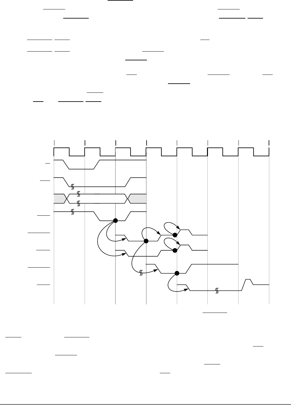
9-20 PowerPC 601 RISC Microprocessor User's Manual
The only valid window for the ARTRY input is the one bus clock cycle following the
assertion of AACK. Snooping devices must monitor the assertion of AACK to know when
to deassert/tristate ARTRY, as shown in Figure 9-8. The assertion of ARTRY/SHD can be
derived in one of the following ways:
•AR
TRY/SHD can be asserted on the second clock after TS is asserted.
•ARTRY/SHD can be asserted before AACK is asserted, but is not qualified by the
master 601 until the clock after AACK is asserted.
The 601 requires that the first (or only) TA not be asserted before AACK (note that TA can
be held off directly by the slave device delaying AACK assertion or indirectly by an
external arbiter delaying DBG assertion). This requirement guarantees the relationship
between TA and ARTRY/SHD such that, in the case of an address retry, the 601 can purge
the data/instructions from its data path queues and waive off the data/instructions before
they are forwarded to the cache/CPU.
Figure 9-8. Snooped Address Cycle with ARTRY
When the data tenure begins before the address tenure is complete, if the 601 has asserted
DBB, assertion of ARTRY causes the 601 to terminate the data bus transaction and retry
both the address and data tenures later. If the transfer is a single-beat transfer and TA occurs
as early as the AACK window, there is no indication of an early data bus termination.
However, if a burst transaction is in progress, the 601 negates DBB early in response to
ARTRY. The system logic does not need to assert TA for four bus clock cycles in this case.
12 34567
ts
abb
addr
aack

Chapter 9. System Interface Operation 9-21
If DBG is not asserted until the ARTRY window and ARTRY is asserted, the 601 does not
become data bus master. Note that some system designs, such as single-master systems, do
not require the use of ARTRY.
For information about ARTRY scenarios, see Section 9.3.3.1, “Address Retry Sources.”
For information about MESI protocol and its effect on address tenure termination, refer to
Section 9.4.4, “Memory Coherency—MESI Protocol.”
9.3.3.1 Address Retry Sources
The assertion of the SHD and ARTRY input signals provide sufficient information for the
appropriate handling of cache sector coherency. They encode information about a
transaction, as shown in Table 9-5.
If the SHD and ARTRY inputs are not asserted for a cache-sector fill operation, the sector
is marked as exclusive (see Section 9.4.4, “Memory Coherency—MESI Protocol”). If the
SHD input is asserted without ARTRY, the sector is marked as shared.
Note: If the invalidate (TT2) output signal is asserted for the transaction, the sector is
marked exclusive regardless of the state of the SHD signal. If ARTRY is asserted without
SHD, a device cannot service the address transaction currently (because of queuing
constraints) and the transaction is retried later. The 601 reacts to the assertion of ARTRY
the same way, regardless of the state of SHD. The timing of the SHD input is the same as
the timing for ARTRY.
One or more devices can indicate a queuing retry condition by asserting ARTRY while one
or more devices separately indicate the snoop-hit shared condition by asserting SHD. This
condition appears as a snoop hit modified condition on the bus, since both SHD and
ARTRY are asserted. This is not a problem for the 601 since ARTRY is not qualified by
SHD (that is, SHD is a don't care if ARTRY is asserted to the 601).
9.4 Data Bus Tenure
This section describes the data bus arbitration, transfer, and termination phases defined by
the 601 memory access protocol. The phases of the data tenure are identical to those of the
address tenure, underscoring the symmetry in the control of the two buses.
Table 9-5. Address Retry Causes
SHD ARTRY Definition
High impedance High impedance Exclusive. No snoop hit. Pipeline not busy.
High impedance Asserted Pipeline busy. Queuing retry.
Asserted High impedance Snoop hit (shared).
Asserted Asserted Snoop hit (modified).
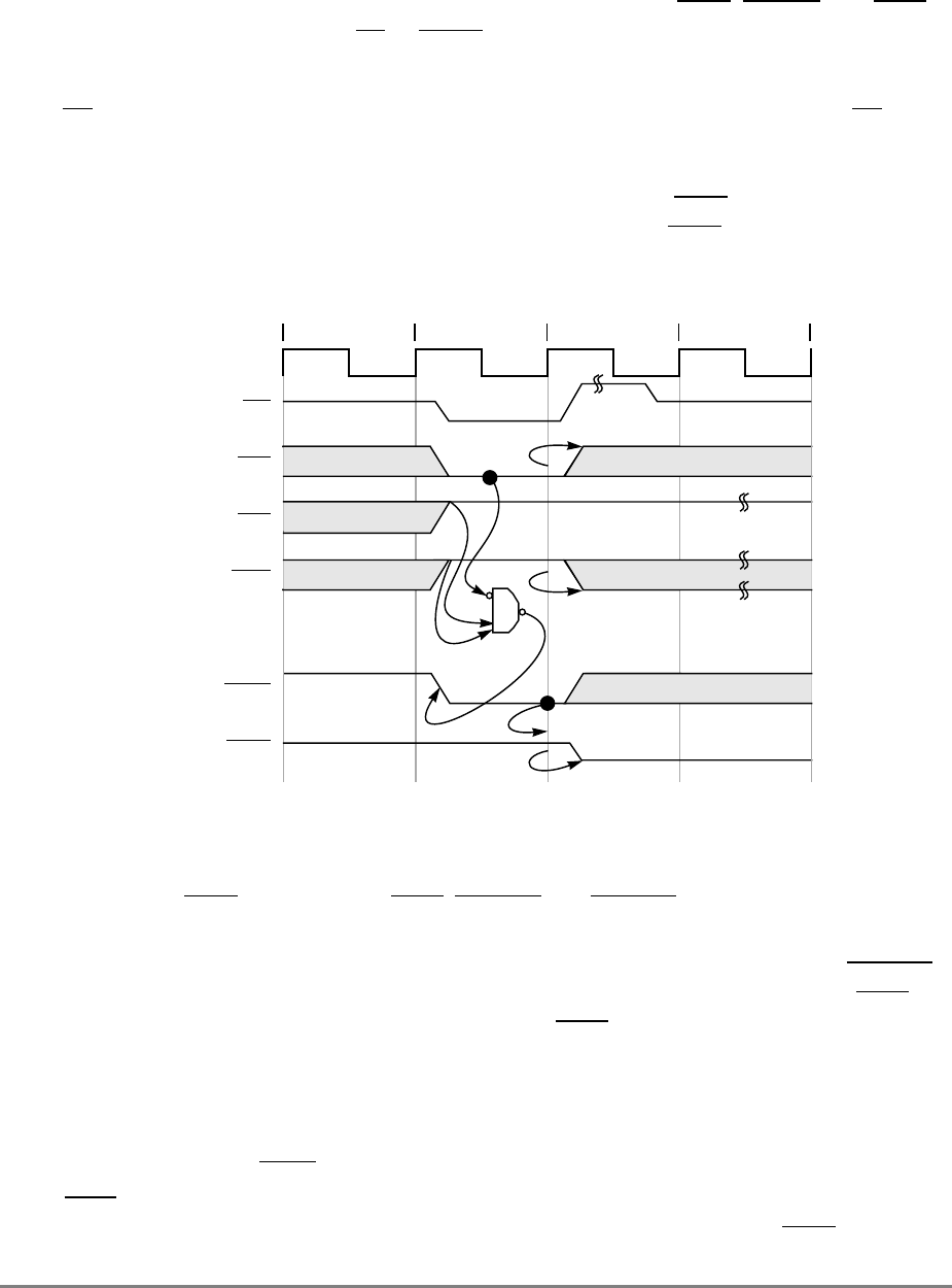
9-22 PowerPC 601 RISC Microprocessor User's Manual
9.4.1 Data Bus Arbitration
Data bus arbitration uses the data arbitration signal group, that is, DBG, DBWO, and DBB.
Additionally, the combination of TS or XATS and TT3 (address-only signal) function as a
data bus request.
The TS signal is an implied data bus request from the 601; the arbiter must qualify TS with
the transfer type (TT) encodings to determine if the current address transfer is an address-
only operation, which does not require a data bus transfer (see Figure 9-7). If the data bus
is needed, the arbiter grants data bus mastership by asserting the DBG input to the 601. As
with the address-bus arbitration phase, the 601 must qualify the DBG input with a number
of input signals before assuming bus mastership, as shown in Figure 9-9.
Figure 9-9. Data Bus Arbitration
A qualified data bus grant can be expressed as the following:
QDBG = DBG asserted while DBB, DRTRY, and ARTRY (associated with the data
bus operation) are negated.
When a data tenure overlaps with its associated address tenure, a qualified ARTRY
assertion coincident with a data bus grant does not result in data bus mastership (DBB is
not asserted). Otherwise, the 601 always asserts DBB on the bus clock cycle after
recognition of a qualified data bus grant. Since the 601 can pipeline transactions, there may
be an outstanding data bus transaction when a new address transaction is retried. In this
case, the 601 becomes the data bus master to complete the previous transaction.
9.4.1.1 Using the DBB Signal
The DBB signal should be connected between masters only if data tenure hand-off is left
to the masters. The memory system can control data hand-off directly with DBG.
0123
dbg
dbb
drtry

Chapter 9. System Interface Operation 9-23
The 601 asserts DBB throughout the data transaction; however, the 601 does not park the
data bus and assert DBB across multiple transactions. DBB is negated on the bus clock
cycle after a final TA is received from the bus.
9.4.2 Data Transfer
The data transfer signals include DH0–DH31, DL0–DL31, DP0–DP7 and DPE. For
memory accesses, the DH and DL signals form a 64-bit data path for read and write
operations.
The 601 transfers data in either single- or four-beat burst transfers. Single-beat operations
can transfer from one to eight bytes at a time and can be misaligned (see Section 9.3.2.3,
“Effect of Alignment in Data Transfers”). Burst operations always transfer eight words and
are aligned to four- or eight-word address boundaries. Burst transfers can achieve
significantly higher bus throughput than single-beat operations.
The type of transaction initiated by the 601 depends on whether the code or data is
cacheable and, for store operations, whether the cache is operated in write-back or write-
through mode which software controls at either the page or block basis. Burst transfers
support cacheable operations only; that is, memory structures must be marked as cacheable
(and write-back for data store operations) in the respective TLB entry to take advantage of
burst transfers.
The 601 output TBST indicates to the system whether the current transaction is a single- or
four-beat transfer. A burst transfer has an assumed address order. For load or store
operations that miss in the cache (and are marked as cacheable and, for stores, write-back
in the MMU), the 601 presents the quad-word–aligned address associated with the critical
code or data that initiated the transaction. This minimizes latency by allowing the critical
code or data to be forwarded to the processor before the rest of the sector is filled. For all
other burst operations, however, the sector is transferred beginning with the oct-word
aligned data. Note that this difference can complicate cache-to-cache implementations.
The 601 does not directly support interfacing to subsystems with less than a 64-bit data path
(except for I/O controller interface operations, which are discussed in Section 9.6,
“Memory- vs. I/O-Mapped I/O Operations”). However, the 601 duplicates, or mirrors, the
transfer data on the unused word lane, for store operations to pages marked as
noncacheable. This means, for example, that for a noncacheable byte store operation, the
valid byte is present on two byte lanes—one in the upper word and one in the lower word.
For a word store operation, the word is mirrored across both word lanes. Unused byte lanes
are undefined.
The data is not mirrored, however, for other store operations (including write-through). A
cache hit causes the double word of data containing the data being transferred to be output
on the data bus lanes.
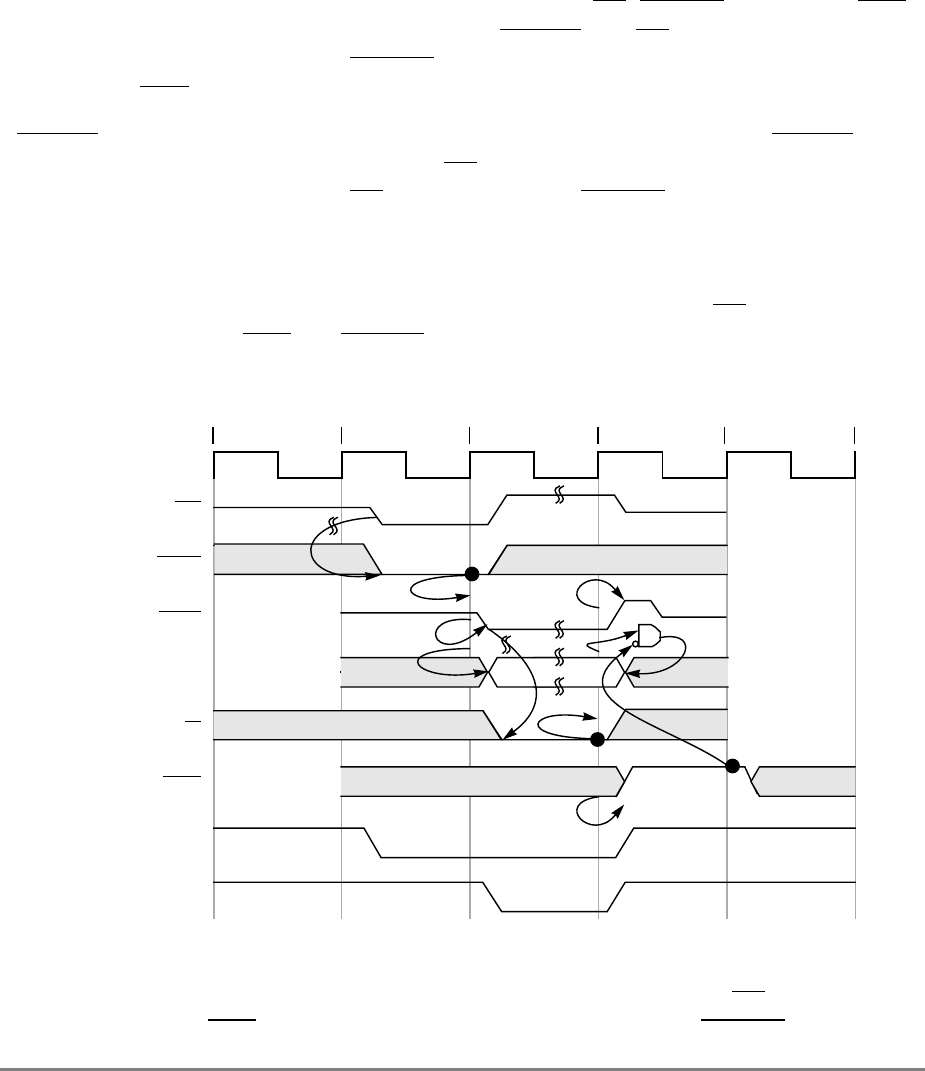
9-24 PowerPC 601 RISC Microprocessor User's Manual
CAUTION
While this information may be useful to some applications that
do not cache data structures, data mirroring may not be
supported on future versions of the 601 or other PowerPC
processors.
9.4.3 Data Transfer Termination
Four signals are used to terminate data bus transactions: TA, DRTRY (data retry), TEA
(transfer error acknowledge), and in some cases ARTRY. The TA signal indicates normal
termination of data transactions. DRTRY indicates invalid read data in the previous bus
clock cycle. TEA indicates a nonrecoverable bus error event.
ARTRY can also terminate a data bus transaction. For burst transactions, this ARTRY must
occur no later than the cycle of the second TA. For single-beat transactions, it must occur
no later than the cycle following TA. In either case, the ARTRY must be for the address
bus tenure associated with the data bus tenure.
9.4.3.1 Normal Single-Beat Termination
Normal termination of a single-beat data read operation occurs when TA is asserted by a
responding slave. The TEA and DRTRY signals must remain negated during the transfer
(see Figure 9-10).
Figure 9-10. Normal Single-Beat Read Termination
Normal termination of a single-beat data write transaction occurs when TA is asserted by
a responding slave. TEA must remain negated during the transfer. The DRTRY signal is not
01234
data
ta
drtry
TT2
AACK
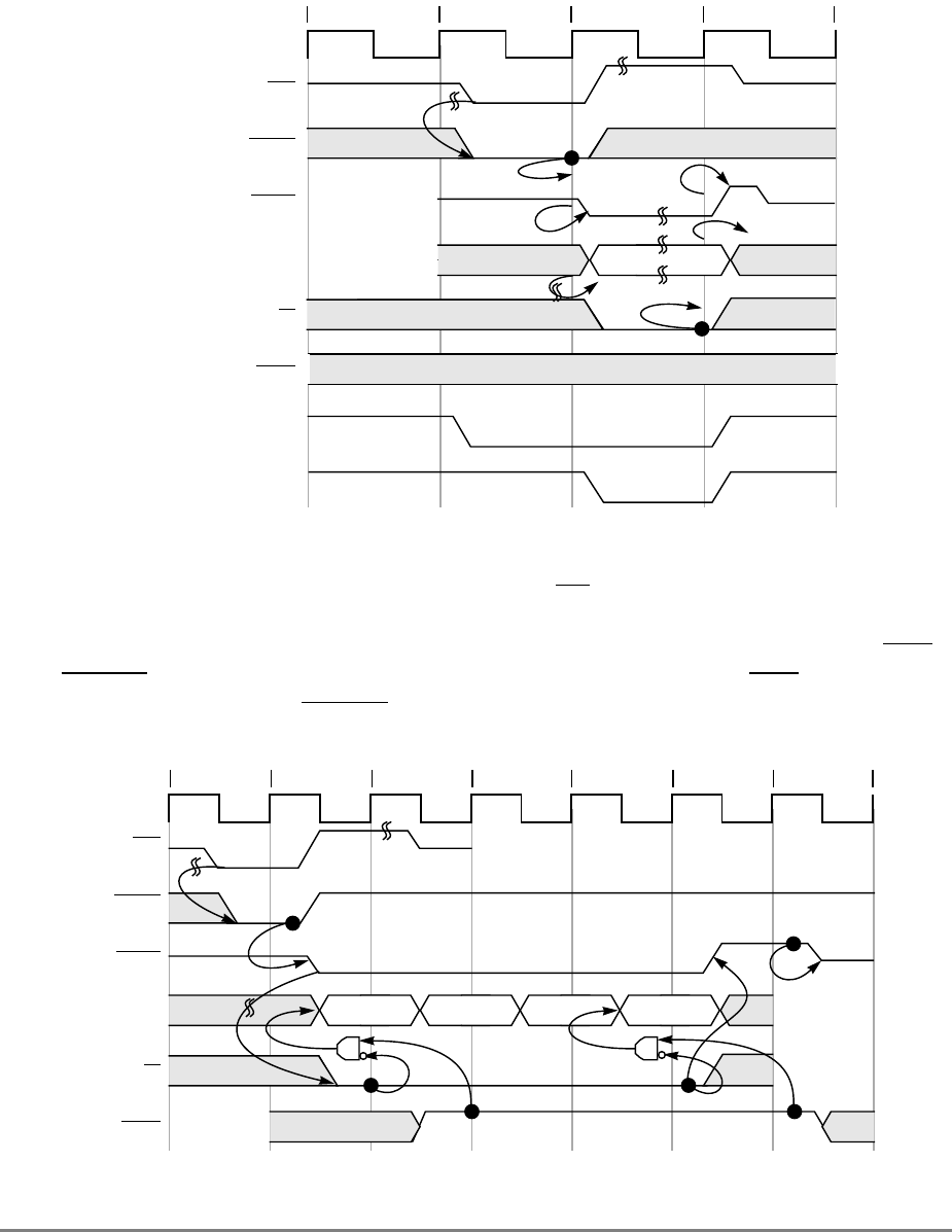
Chapter 9. System Interface Operation 9-25
sampled during data writes, as shown in Figure 9-11. As shown in both Figure 9-10 and
Figure 9-11, the TT1 signal driven low by the 601 indicates a write is in progress.
Figure 9-11. Normal Single-Beat Write Termination
Normal termination of a burst transfer occurs when TA is asserted during four bus clock
cycles, as shown in Figure 9-12. The bus clock cycles need not be consecutive, thus
allowing pacing of the data transfer beats. For read bursts to terminate successfully, TEA
and DRTRY must remain negated during the transfer. For write bursts, TEA must remain
negated during the transfer. DRTRY is ignored during data writes.
Figure 9-12. Normal Burst Transaction
0123
data
ta
drtry
TT2
AACK
12 34567
data
ta
drtry
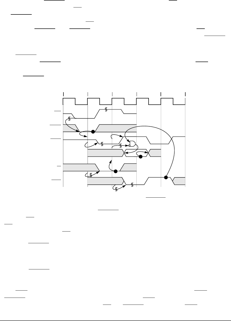
9-26 PowerPC 601 RISC Microprocessor User's Manual
For read bursts, DRTRY may be asserted one bus clock cycle after TA is asserted to signal
that the data presented with TA is invalid and that the processor must wait for the negation
of DRTRY before forwarding data to the processor (see Figure 9-13). Thus, a data beat can
be speculatively terminated with TA and then one bus clock cycle later confirmed with the
negation of DRTRY. The DRTRY signal is valid only for read transactions. TA must be
asserted on the bus clock cycle before the first bus clock cycle of the assertion of DRTRY;
otherwise the results are undefined.
The DRTRY signal extends data bus mastership such that other processors cannot use the
data bus until DRTRY is negated. Therefore, in the example in Figure 9-13, DBB cannot
be asserted until bus clock cycle 5. This is true for both read and write operations even
though DRTRY does not hold the master on write operations.
Figure 9-13. Termination with DRTRY
Figure 9-14 shows the effect of using DRTRY during a burst read. It also shows the effect
of using TA to pace the data transfer rate. Notice that in bus clock cycle 3 of Figure 9-14,
TA is negated for the second data beat. The 601 data pipeline does not proceed until bus
clock cycle 4 when the TA is reasserted.
Note that DRTRY is useful for systems that implement speculative forwarding of data such
as those with direct-mapped, second-level caches where hit/miss is determined on the
following bus clock cycle, or for parity- or ECC-checked memory systems.
Note that DRTRY may not be implemented on other PowerPC processors.
9.4.3.2 Data Transfer Termination Due to a Bus Error
The TEA signal indicates that a bus error occurred. It may be asserted while DBB (and/or
DRTRY for read operations) is asserted. Asserting TEA to the 601 terminates the
transaction; that is, further assertions of TA and DRTRY are ignored and DBB is negated.
12 345
data
ta
drtry
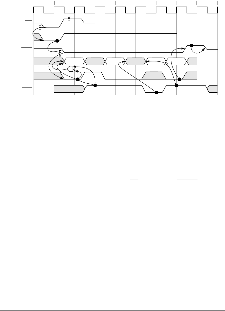
Chapter 9. System Interface Operation 9-27
Figure 9-14. Read Burst with TA Wait States and DRTRY
Assertion of the TEA signal causes a machine-check exception (and possibly a check-stop
condition within the 601). For more information, see Section 5.4.2, “Machine Check
Exception (x'00200').” However assertion of TEA does not invalidate data entering the GPR
or the cache; therefore, the 601 may act on invalid code/data (although the exception will
eventually be recognized, if enabled). Additionally, the corresponding address of the access
that caused TEA to be asserted is not latched by the 601. To recover, the 601 must be reset;
therefore, this function should only be used to flag fatal system conditions to the processor
(such as parity or uncorrectable ECC errors).
After the 601 has committed to run a transaction, that transaction must eventually complete.
Address retry causes the transaction to be restarted; TA wait states and DRTRY assertion
for reads delay termination of individual data beats. Eventually, however, the system must
either terminate the transaction or assert the TEA signal to put the 601 into checkstop mode.
For this reason, care must be taken to check for the end of physical memory and the location
of certain system facilities.
Note that TEA generates a machine-check exception depending on the ME bit in the MSR.
Setting the checkstop enable control bits properly leads to a true checkstop condition.
Note also that the 601 does not implement a synchronous error capability for memory
accesses (see Section 9.6, “Memory- vs. I/O-Mapped I/O Operations”). This means that the
exception instruction pointer does not point to the memory operation that caused the
assertion of TEA, but to the instruction about to be executed (perhaps several instructions
later).
data
ta
drtry
123456789

9-28 PowerPC 601 RISC Microprocessor User's Manual
9.4.4 Memory Coherency—MESI Protocol
The 601 provides dedicated hardware to provide memory coherency by snooping bus
transactions. The address retry capability enforces the four-state, MESI cache-coherency
protocol (see Figure 9-15). In addition to the hardware required to monitor bus traffic for
coherency, the 601 has a cache port dedicated to snooping so that comparing cache entries
to address traffic on the bus does not tie up the 601's on-chip cache.
The global (GBL) signal output, indicates whether the current transaction must be snooped
by other snooping devices on the bus. Address bus masters assert GBL to indicate that the
current transaction is a global access (that is, an access to memory shared by more than one
processor/cache). If GBL is not asserted for the transaction, that transaction is not snooped.
When other devices detect the GBL input asserted, they must respond by snooping the
broadcast address.
Normally, GBL reflects the M-bit value specified for the memory reference in the
corresponding translation descriptor(s). Note that care must be taken to minimize the
number of pages marked as global, because the retry protocol discussed in the previous
section is used to enforce coherency and can require significant bus bandwidth.
When the 601 is not the address bus master, GBL is an input. The 601 snoops a transaction
if TS and GBL are asserted together in the same bus clock cycle (this is a qualified snooping
condition). No snoop update to the 601 cache occurs if the snooped transaction is not
marked global. This includes invalidation cycles.
When the 601 detects a qualified snoop condition, the address associated with the TS is
compared against the unified cache tags through a dedicated cache-tag port. Snooping
completes if no hit is detected. If, however, the address hits in the cache, the 601 reacts
according to the MESI protocol shown in Figure 9-15, assuming the WIM bits are set to
write-back mode, caching allowed, and coherency enforced (WIM = 001).
Note that write hits to clean lines of nonglobal pages do not generate invalidate broadcasts.
There are several types of bus transactions that involve the movement of data that can no
longer access the TLB M-bit (for example, replacement sector copy-back, snoop push, and
table-search operations). In these cases, the hardware cannot determine whether the sector
was originally marked global; therefore, the 601 marks these transactions as nonglobal to
avoid retry deadlocks.
The 601's on-chip cache is implemented as an eight-way set-associative cache. To facilitate
external monitoring of the internal cache tags, the cache set element (CSE0–CSE2) signals
indicate which sector of the cache set is being replaced on read operations (including
RWITM). Note that these signals are valid only for 601 burst operations; for all other bus
operations, the CSE signals should be ignored.
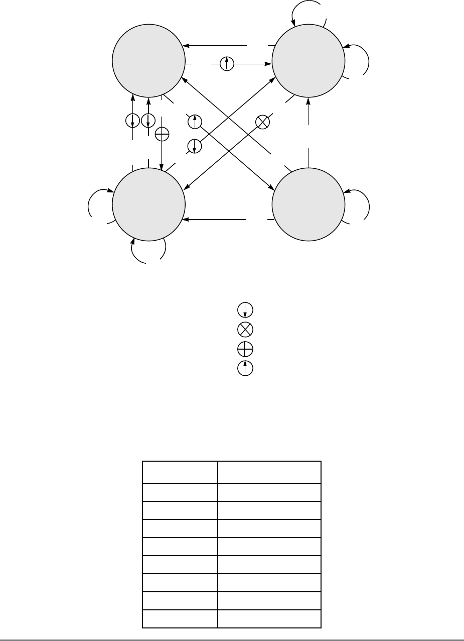
Chapter 9. System Interface Operation 9-29
Figure 9-15. MESI Cache Coherency Protocol—State Diagram (WIM = 001)
Table 9-6 shows the CSE encodings.
Table 9-6. CSE(0–2) Signals
CSE0–CSE2 Cache Set Element
000 Set 0
001 Set 1
010 Set 2
011 Set 3
100 Set 4
101 Set 5
110 Set 6
111 Set 7
SHARED
SHR
RH
RH
EXCLUSIVE
SHW
RMS
SHR
SHWSHR
RME WH
WH
WH
RH
MODIFIED
SHW
SHW
(burst)
INVALID
(On a miss, the old
line is first invalidated
and copied back
if M)
WM
BUS TRANSACTIONS
RH = Read Hit = Snoop Push
RMS = Read Miss, Shared
RME = Read Miss, Exclusive = Invalidate Transaction
WH = Write Hit
WM = Write Miss = Read-with-Intent-to-Modify
SHR = Snoop Hit on a Read
SHW = Snoop Hit on a Write or = Cache Sector Fill
Read-with-Intent-to-Modify
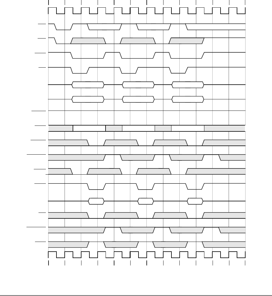
9-30 PowerPC 601 RISC Microprocessor User's Manual
9.5 Timing Examples
This section shows timing diagrams for various scenarios. Figure 9-16 illustrates the fastest
single-beat reads. This figure shows both minimal latency and maximum single-beat
throughput. By delaying the data bus tenure, the latency increases, but, because of split-
transaction pipelining, the overall throughput is not affected unless the data bus latency
causes the third address tenure to be delayed.
Note that all bidirectional signals go to high-impedance between bus tenures.
Figure 9-16. Fastest Single-Beat Reads
BR
BG
ABB
TS
A0–A31
TT0–TT3
TBST
GBL
AACK
ARTRY
DBG
DBB
D0–D63
TA
DRTRY
TEA
123456789101112
123456789101112
CPU A CPU A CPU A
Read Read Read
In In In
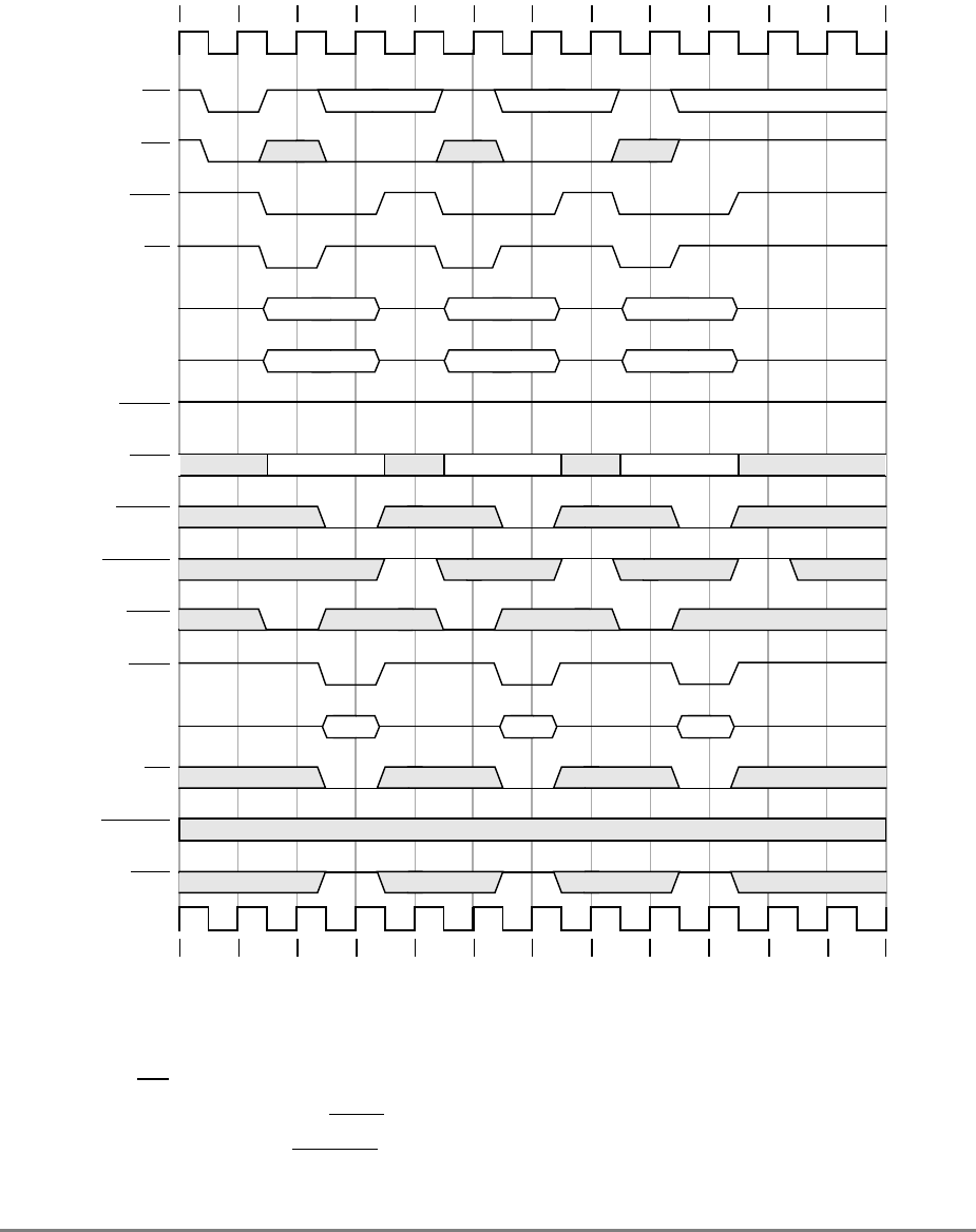
Chapter 9. System Interface Operation 9-31
Figure 9-17 illustrates the fastest single-beat writes. Note that all bidirectional signals go to
high-impedance between bus tenures. TT1–TT3 are binary encoded b'x001'. TT0 can be
either 0 or 1, TT1 and TT2 are 0, and TT3 is 1.
Figure 9-17. Fastest Single-Beat Writes
Figure 9-18 shows three ways to delay single-beat reads showing data-delay controls:
• The TA hold-off can be used to insert wait states in clock cycles 3 and 4.
• For the second access, DBG could have been asserted in clock cycle 6.
• In the third access, DRTRY is asserted in clock cycle 11 to flush the previous data.
BR
BG
ABB
TS
A0–A31
TT0–TT3
TBST
GBL
AACK
ARTRY
DBG
DBB
D0–D63
TA
DRTRY
TEA
123456789101112
123456789101112
CPU A CPU A CPU A
SBW SBW SBW
Out Out Out
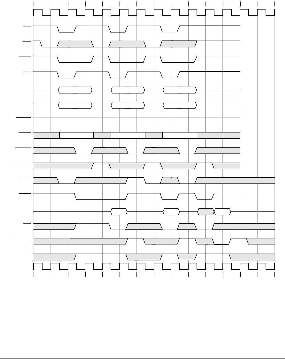
9-32 PowerPC 601 RISC Microprocessor User's Manual
Note that all bidirectional signals go to high-impedance between bus tenures. The
pipelining shown in Figure 9-18 can occur if the second access is not another load, (for
example, an instruction fetch).
Figure 9-18. Single-Beat Reads Showing Data-Delay Controls
BR
BG
ABB
TS
A0–A31
TT0–TT3
TBST
GBL
AACK
ARTRY
DBG
DBB
D0–D63
TA
DRTRY
TEA
CPU A CPU A CPU A
Read Read Read
In In Bad
1234567891011121314
1234567891011121314
In
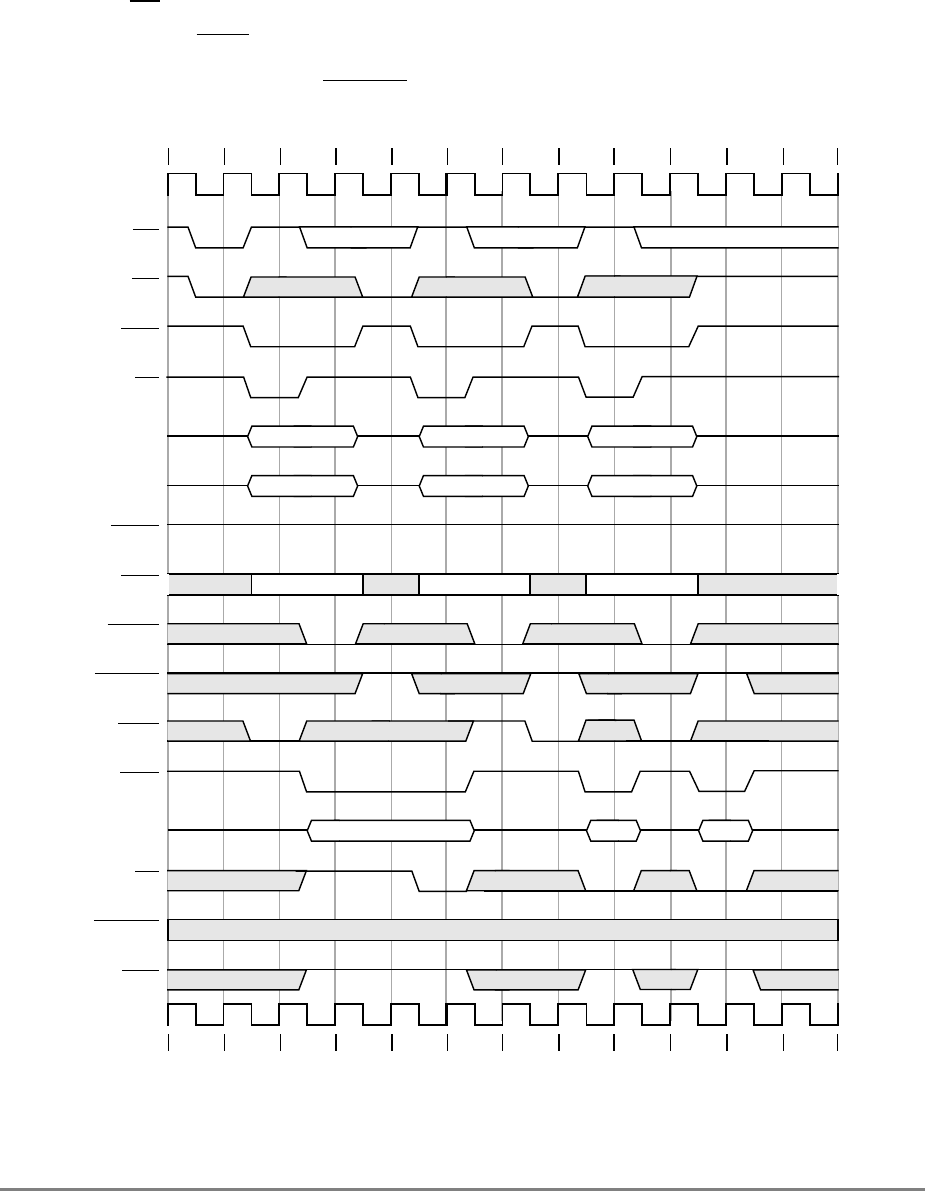
Chapter 9. System Interface Operation 9-33
Figure 9-19 shows data-delay controls in a single-beat write. Note that all bidirectional
signals are set to high impedance between bus tenures. Data transfers are delayed in the
following ways:
• The TA holdoff is used to insert wait states in clocks 3 and 4.
• In clock 6, DBG is held negated, delaying the start of the data tenure.
The last access is not delayed (DRTRY is valid only for read operations).
Figure 9-19. Single-Beat Writes Showing Data Delay Controls
BR
BG
ABB
TS
A0–A31
TT0–TT3
TBST
GBL
AACK
ARTRY
DBG
DBB
D0–D63
TA
DRTRY
TEA
123456789101112
123456789101112
CPU A CPU A CPU A
SBW SBW SBW
Out Out Out
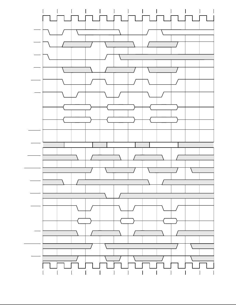
9-34 PowerPC 601 RISC Microprocessor User's Manual
Figure 9-20 shows three single-beat transfers back-to-back. Note that all bidirectional
signals are set at high-impedance state between tenures.
Figure 9-20. Back-to-Back Single-Beat Transfers
CPU A BR
CPU A BG
CPU B BR
CPU B BG
ABB
TS
A0–A31
TT0–TT3
TBST
GBL
AACK
ARTRY
CPU A DBG
CPU B DBG
DBB
D0–D63
TA
DRTRY
TEA
123456789101112
123456789101112
CPU A CPU B CPU A
Read SBW Read
In Out In
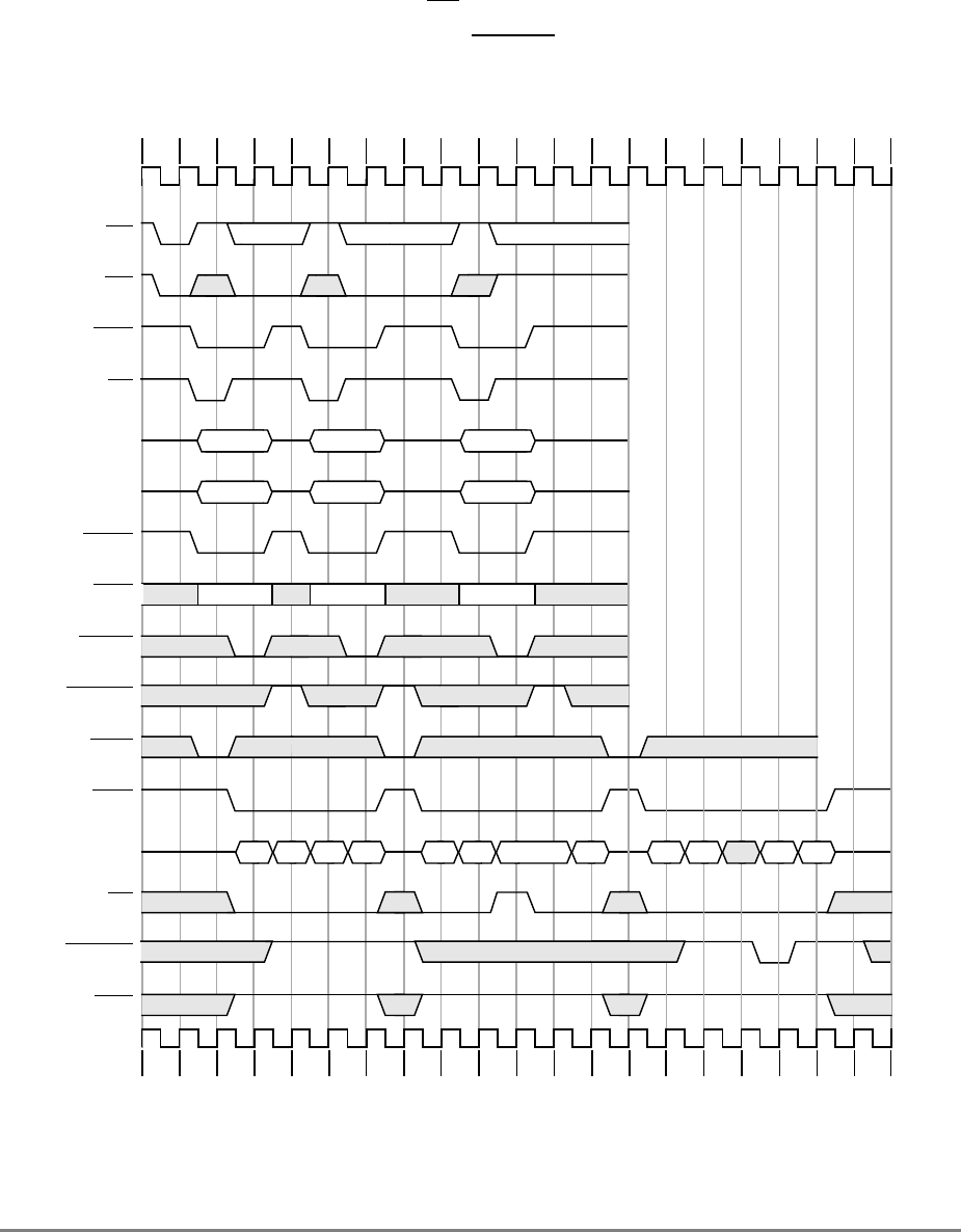
Chapter 9. System Interface Operation 9-35
Figure 9-21 shows the use of data-delay controls with burst transfers. Note that all
bidirectional signals are set to high impedance between bus tenures. Note the following:
• The first data beat of bursted read data (clock 0) is the critical quad word.
• The write burst shows the use of TA holdoff on the third data beat.
• The final read burst shows the use of DRTRY on the third data beat.
• The address for the third transfer is held off until the first transfer completes.
Figure 9-21. Burst Transfers with Data Delay Controls
BR
BG
ABB
TS
A0–A31
TT0–TT3
TBST
GBL
AACK
ARTRY
DBG
DBB
D0–D63
TA
DRTRY
TEA
CPU A
In 0
1 2 3 4 5 6 7 8 9 1011121314151617181920
1 2 3 4 5 6 7 8 9 1011121314151617181920
CPU A CPU A
Read Write Read
In 1 In 2 In 3 Out 0 Out 1 Out 2 Out 3 In 0 In 1 In 2 In 3In 2
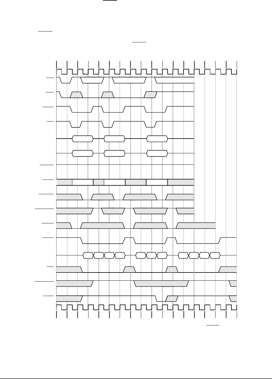
9-36 PowerPC 601 RISC Microprocessor User's Manual
Figure 9-22 shows the use of the TEA signal. Note that all bidirectional signals are set to
high impedance between bus tenures. Note the following:
• The first data beat of the read burst (in clock 0) is the critical quad-word.
• The TEA signal truncates the burst write transfer on the third data beat.
• The 601 eventually interrupts on the TEA event.
Figure 9-22. Use of Transfer Error Acknowledge (TEA)
BR
BG
ABB
TS
A0–A31
TT0–TT3
TBST
GBL
AACK
ARTRY
DBG
DBB
D0–D63
TA
DRTRY
TEA
CPU A
In 0
1 2 3 4 5 6 7 8 9 1011121314151617
CPU A CPU A
Read Write Read
In 1 In 2 In 3 Out 0 Out 1 Out 2 In 0 In 1 In 3In 2
1 2 3 4 5 6 7 8 9 1011121314151617

Chapter 9. System Interface Operation 9-37
9.6 Memory- vs. I/O-Mapped I/O Operations
The 601 defines separate memory and I/O address spaces, or segments, distinguished by the
segment register T-bit in the address translation logic of the 601. If the T-bit is cleared, the
memory reference is a normal memory access and can use the virtual memory management
hardware of the 601. For highest performance, it is recommended that I/O devices be
mapped through the memory interface.
However, if the T-bit is set, the external reference is to an I/O controller interface area. This
mapping is provided to implement the I/O controller interface protocol for compatibility
with certain devices that respond to it.
The following points should be considered for I/O controller interface accesses:
• I/O controller interface accesses must be strongly ordered; for example, these
accesses must run on the bus strictly in order with respect to the instruction stream.
• I/O controller interface accesses must provide synchronous error reporting.
Chapter 4, “Cache and Memory Unit Operation,” describes architectural aspects of
I/O controller interface segments, as well as an overview of the PowerPC
architecture’s segmented address space management.
The 601 defines two types of I/O controller interface segments (segment register T-bit set)
based on the value of the bus unit ID (BUID), as follows:
• I/O controller interface (BUID ≠ x'07F')—I/O controller interface accesses include
all transactions between the 601 and subsystems (referred to as bus unit controllers
(BUCs) mapped through I/O controller interface address space).
• Memory-forced I/O controller interface (BUID = x'07F')—Memory-forced I/O
controller interface operations access memory space. They do not use the extensions
to the memory protocol described for I/O controller interface accesses, and they
bypass the page- and block-translation and protection mechanisms. The physical
address is found by concatenating bits 28–31 of the respective segment register with
bits 4–31 of the effective address. This address is marked as noncacheable, write-
through, and global.
Because memory-forced I/O controller interface accesses address memory space,
they are subject to the same coherency control as other memory reference
operations. More generally, accesses to memory-forced I/O controller interface
segments are considered to be cache-inhibited, write-through and memory-coherent
operations with respect to the 601 cache and bus interface.
See Section 9.6.2, “I/O Controller Interface Transaction Protocol Details,” for more
information about the BUID.
The 601 has a single bus interface to support accesses to both memory accesses and I/O
controller interface segment accesses.

9-38 PowerPC 601 RISC Microprocessor User's Manual
The system recognizes the assertion of the TS signal as the start of a memory access. The
assertion of XATS indicates an I/O controller interface access. This allows memory devices
to ignore I/O controller interface transactions. If XATS is asserted, the access is to I/O
space and the following extensions to the memory access protocol apply:
• A new set of bus operations are defined. The transfer type, transfer burst, and transfer
size signals are redefined for I/O controller interface operations; they convey the
opcode for the I/O transaction (see Table 9-7).
• There are two beats of address for each I/O controller interface transfer. The first
beat (packet 0) provides basic address information such as the segment register and
the sender tag and several control bits; the second beat (packet 1) provides additional
addressing bits from the segment register and the logical address.
• Explicit sender/receiver tags are provided.
• The sender that initiated the transaction must wait for a reply from the receiver bus-
unit controller (BUC) before starting a new operation.
• The 601 does not burst I/O controller interface transactions, but streaming is
permitted. Streaming (in this context) allows multiple single-beat transactions to
occur before a reply from the I/O receiver is required.
I/O controller interface transactions use separate arbitration for the split address and data
buses and define address-only and single-beat transactions. The address-retry vehicle is
identical, although there is no hardware coherency support for I/O controller interface
transactions. ARTRY is useful, however, for pacing 601 transactions, effectively indicating
to the 601 that the BUC is in a queue-full condition and cannot accept new data.
In addition to the extensions noted above, there are fundamental differences between
memory and I/O controller interface operations. For example, use of DRTRY is undefined
for 601 I/O controller interface operations. Additionally, only half of the 64-bit data path is
available for 601 I/O controller interface transactions. This lowers the pin-count for I/O
interfaces but generally results in substantially less bandwidth than memory accesses.
Additionally, load/store instructions that address I/O controller interface segments cannot
complete successfully without an error-free reply from the addressed BUC. Because
normal I/O controller interface accesses involve multiple I/O transactions (streaming), they
are likely to be very long latency instructions; therefore, I/O controller interface operations
usually stall 601 instruction issue.
Figure 9-23 shows an I/O controller interface tenure. Note that the I/O response is an
address-only bus transaction.
The decision on whether to map I/O peripherals into memory or I/O controller interface
space depends on many factors; however, it should be noted that in the best case, the use of
the 601 I/O controller interface protocol degrades performance and requires the addressed
controllers to implement 601 bus master capability to generate the reply transactions.
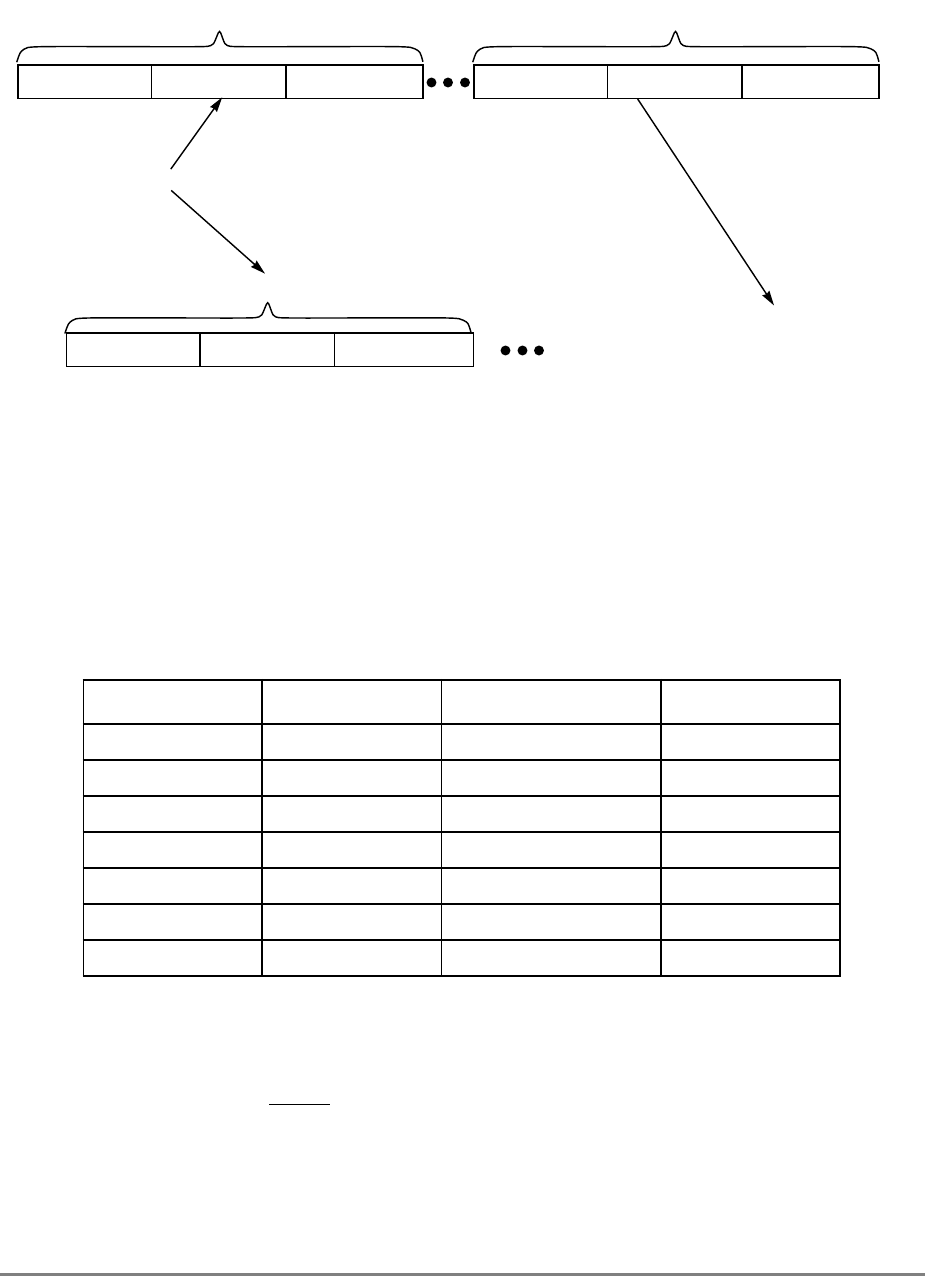
Chapter 9. System Interface Operation 9-39
Figure 9-23. I/O Controller Interface Tenures
9.6.1 I/O Controller Interface Transactions
Seven I/O controller interface transaction operations are defined by the 601, as shown in
Table 9-7. These operations permit communication between the 601 and BUCs. A single
601 store or load instruction (that translates to an I/O controller interface access) generates
one or more I/O controller interface operations (two or more I/O controller interface
operations for loads) from the 601 and one reply operation from the addressed BUC.
For the first beat of the address bus, the extended address transfer code (XATC), contains
the I/O opcode as shown in Table 9-7; the opcode is formed by concatenating the transfer
type, transfer burst, and transfer size signals defined as follows:
XATC = TT(0–3)||TBST||TSIZ(0–2)
Table 9-7. I/O Controller Interface Bus Operations
Operation Address Only Direction XATC Encoding
Load start (request) Yes 601 ⇒ IO 0100 0000
Load immediate No 601 ⇒ IO 0101 0000
Load last No 601 ⇒ IO 0111 0000
Store immediate No 601 ⇒ IO 0001 0000
Store last No 601 ⇒ IO 0011 0000
Load reply Yes IO ⇒ 601 1100 0000
Store reply Yes IO ⇒ 601 1000 0000
ARBITRATION TRANSFER TERMINATION
ADDRESS TENURE
DATA TENURE
INDEPENDENT ADDRESS AND DATA
ARBITRATION TRANSFER TERMINATION
I/O RESPONSE
ARBITRATION TRANSFER TERMINATION
NO DATA TENURE FOR I/O RESPONSE
(I/O responses are address-only)

9-40 PowerPC 601 RISC Microprocessor User's Manual
9.6.1.1 Store Operations
There are three operations defined for I/O controller interface store operations from the 601
to the BUC, defined as follows:
• Store immediate operations transfer up to 32 bits of data each from the 601 to the
BUC.
• Store last operations transfer up to 32 bits of data each from the 601 to the BUC
• Store reply from the BUC reveals the success/failure of that I/O controller interface
access to the 601.
An I/O controller interface store access consists of one or more data transfer operations
followed by the I/O store reply operation from the BUC. If the data can be transferred in
one 32-bit data transaction, it is marked as a store last operation followed by the store reply
operation; no store immediate operation is involved in the transfer, as shown in the
following sequence:
STORE LAST (from the 601)
•
•
STORE REPLY (from BUC)
However, if more data is involved in the I/O controller interface access, there will be one or
more store immediate operations. The BUC can detect when the last data is being
transferred by looking for the store last opcode, as shown in the following sequence:
STORE IMMEDIATE(s)
•
•
STORE LAST
•
•
STORE REPLY
9.6.1.2 Load Operations
I/O controller interface load accesses are similar to store operations, except that the 601
latches data from the addressed BUC rather than supplying the data to the BUC. As with
memory accesses, the 601 is the master on both load and store operations; the external
system must provide the data bus grant to the 601 when the BUC is ready to supply the data
to the 601.

Chapter 9. System Interface Operation 9-41
The load request I/O controller interface operation has no analogous store operation; it
informs the addressed BUC of the total number of bytes of data that the BUC must provide
to the 601 on the subsequent load immediate/load last operations. For I/O controller
interface load accesses, the simplest, 32-bit (or fewer) data transfer sequence is as follows:
LOAD REQUEST
•
•
LOAD LAST
•
•
LOAD REPLY(from BUC)
However, if more data is involved in the I/O controller interface access, there will be one or
more load immediate operations. The BUC can detect when the last data is being
transferred by looking for the load last opcode, as seen in the following sequence:
LOAD REQUEST
•
•
LOAD IMM(s)
•
•
LOAD LAST
•
•
LOAD REPLY
Note that three of the seven defined operations are address-only transactions and do not use
the data bus. However, unlike the memory transfer protocol, these transactions are not
broadcast from one master to all snooping devices; The I/O controller interface address-
only transaction protocol strictly controls communication between the 601 and the BUC.
9.6.2 I/O Controller Interface Transaction Protocol Details
As mentioned previously, there are two address-bus beats corresponding to two packets of
information about the address. The two packets contain the sender and receiver tags, the
address and extended address bits, and extra control and status bits. The two beats of the
address bus (plus attributes) are shown at the top of Figure 9-24 as two packets. The first
packet, packet 0, is then expanded to depict the XATC and address bus information in
detail.
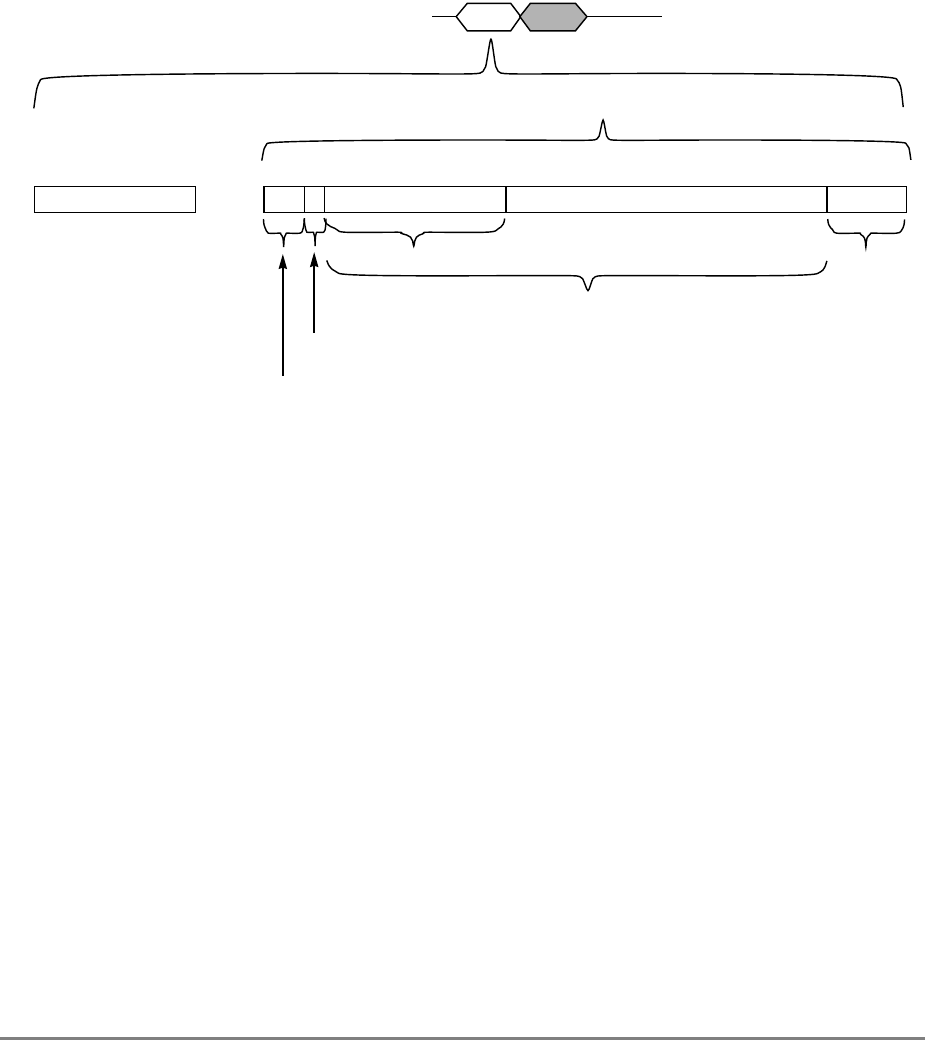
9-42 PowerPC 601 RISC Microprocessor User's Manual
9.6.2.1 Packet 0
Figure 9-24 shows the organization of the first packet in an I/O controller interface
transaction.
The XATC contains the I/O opcode, as discussed earlier and as shown in Table 9-7. The
address bus contains the following:
Key bit || segment register || sender tag
Figure 9-24. I/O Controller Interface Operation—Packet 0
This information is organized as follows:
• Bits 0 and 1 of the address bus are reserved—The 601 always drives these bits to
zero.
• Key bit—Bit 2 is the key bit from the segment register (either SR[Ku] or SR[Ks]).
Ku indicates user-level access and Ks indicate supervisor-level access. The 601
multiplexes the correct key bit into this position according to the current operating
context (user or supervisor).
• Segment register—Address bits 3–27 correspond to bits 3–27 of the segment
register. Note that address bits 3–11 form the nine-bit receiver tag. Software must
initialize these bits in the segment register to the ID of the BUC to be addressed; they
are referred to as the BUID (bus unit ID) bits.
• PID (sender tag)—Address bits 28–31 form the four-bit sender tag. These bits come
from bits 28–31 of the 601 PID (processor ID) register. A four-bit tag allows a
maximum of 16 processor IDs to be defined for a given system. If more bits are
needed for a very large multiprocessor system, for example, it is envisioned that the
second-level cache (or equivalent logic) can append a larger processor tag as needed.
The BUC addressed by the receiver tag should latch the sender address required by
the subsequent I/O reply operation.
I/O Opcode
0 1 2 3 1112 27 28 3107
A (0–31) + Attributes
Address Bus (A0–A31)
PKT 0 PKT 1
+
XATC
Reserved
Key bit
From Segment Register
BUID PID

Chapter 9. System Interface Operation 9-43
9.6.2.2 Packet 1
The second address beat, packet 1, transfers byte counts and the physical address for the
transaction, as shown in Figure 9-25.
Figure 9-25. I/O Controller Interface Operation—Packet 1
For packet 1, the XATC is defined as follows:
• Load request operations—XATC contains the total number of bytes to be transferred
(128 bytes maximum for the 601)
• Immediate/last (load or store) operations—XATC contains the current transfer byte
count (one to four bytes.)
Address bits 0–31 contain the physical address of the transaction. The physical address is
generated by concatenating segment register bits 28–31 with bits 4-31 of the effective
address, as follows:
Segment register (bits 28–31) || effective address (bits 4–31)
While the 601 provides the address of the transaction to the BUC, the BUC must maintain
a valid address pointer for the reply.
9.6.3 I/O Reply Operations
BUCs must respond to 601 I/O controller interface transactions with an I/O reply operation,
as shown in Figure 9-26. The purpose of this reply operation is to inform the 601 of the
success or failure of the attempted I/O controller interface access. This requires the system
I/O controller interface to have 601 bus mastership capability—a substantially more
complex design task than bus slave implementations that use memory-mapped I/O access.
Reply operations from the BUC to the 601 are address-only transactions. As with packet 0
of the address bus on 601 I/O controller interface operations, the XATC contains the opcode
for the operation (see Table 9-7). Additionally, the I/O reply operation transfers the
sender/receiver tags in the first beat.
Byte Count
07
ADDR +
Address Bus (A0–A31)
PKT 0 PKT 1
+
XATC Bus Address
034 31
SR(28-31)

9-44 PowerPC 601 RISC Microprocessor User's Manual
Figure 9-26. I/O Reply Operation
The address bits are described in Table 9-8.
The second beat of the address bus is reserved; the XATC and address buses should be
driven to zero to preserve compatibility with future protocol enhancements.
The following sequence occurs when the 601 detects an error bit set on an I/O reply
operation:
1. The 601 completes the instruction that initiated the access.
2. If the instruction is a load, the data is forwarded onto the register file(s)/sequencer.
3. An I/O controller interface error exception is generated, which transfers 601 control
to the I/O controller interface error exception handler to recover from the error. Refer
to Section 5.4.10, “I/O Controller Interface Error Exception (x'00A00'),” for more
information.
If the error bit is not set, the 601 instruction that initiated the access completes and
instruction execution resumes.
Table 9-8. Address Bits for I/O Reply Operations
Address Bits Description
0–1 Reserved. These bits should be set to zero for compatibility with future PowerPC microprocessors.
2 Error bit. It is set if the BUC records an error in the access.
3–11 BUID. Sender tag of a reply operation. Corresponds with bits 3–11 of one of the 601 segment
registers.
12–27 Address bits 12–27 are BUC-specific and are ignored by the 601.
28–31 PID (receiver tag). The 601 effectively snoops operations on the bus and, on reply operations,
compares this field to bits 28–31 of the PID register to determine if it should recognize this I/O reply.
I/O Opcode
07
Address Bus (A0–A31)
+
XATC
Reserved
Error
Bit Segment Register
BUID PID
BUC Specific
0 1 2 3 1112 27 28 31

Chapter 9. System Interface Operation 9-45
System designers should note the following:
• “Misplaced” reply operations (that match the processor tag and arrive unexpectedly)
cause a checkstop condition. Refer to Chapter 5, “Exceptions,” for more
information.
• External logic must assert AACK for the 601, even though it is the receiver of the
reply operation. AACK is an input-only to the 601.
• The 601 monitors address parity when enabled by software and XATS and reply
operations (load or store).
9.6.4 I/O Controller Interface Operation Timing
The following timing diagrams show the sequence of events in a typical 601 I/O controller
interface load access (Figure 9-27) and a typical 601 I/O controller interface store access
(Figure 9-28). All arbitration signals except for ABB and DBB have been omitted for
clarity. Note that for either case, the number of immediate operations depends on the
amount and the alignment of data to be transferred. If no more than four bytes are being
transferred, and the data is double-word aligned (that is, does not straddle an eight-byte
address boundary), there will be no immediate operation as shown in the figures.
The 601 can transfer as many as 128 bytes of data in one load or store instruction (requiring
more than 33 immediate operations in the case of misaligned operands).
In Figure 9-27, XATS is asserted with the same timing relationship as TS in a memory
access. Notice, however, that the address bus (and XATC) transition on the next bus clock
cycle. The first of the two beats on the address bus is valid for one bus clock cycle window
only, and that window is defined by the assertion of XATS. The second address bus beat,
however, can be extended by delaying the assertion of AACK until the system has latched
the address.
The load request and load reply operations shown in Figure 9-27 are address-only
transactions as denoted by the negated TT3 signal during their respective address tenures.
Note that other types of bus operations can occur between the individual I/O controller
interface operations on the bus. The 601 involved in this transaction, however, does not
initiate any other I/O controller load or store operations once the first I/O controller
interface operation has begun address tenure; however, if the I/O operation is retried, other
higher-priority operations can occur.
Notice that, in this example (zero wait states), 13 bus clock cycles are required to transfer
no more than eight bytes of data.
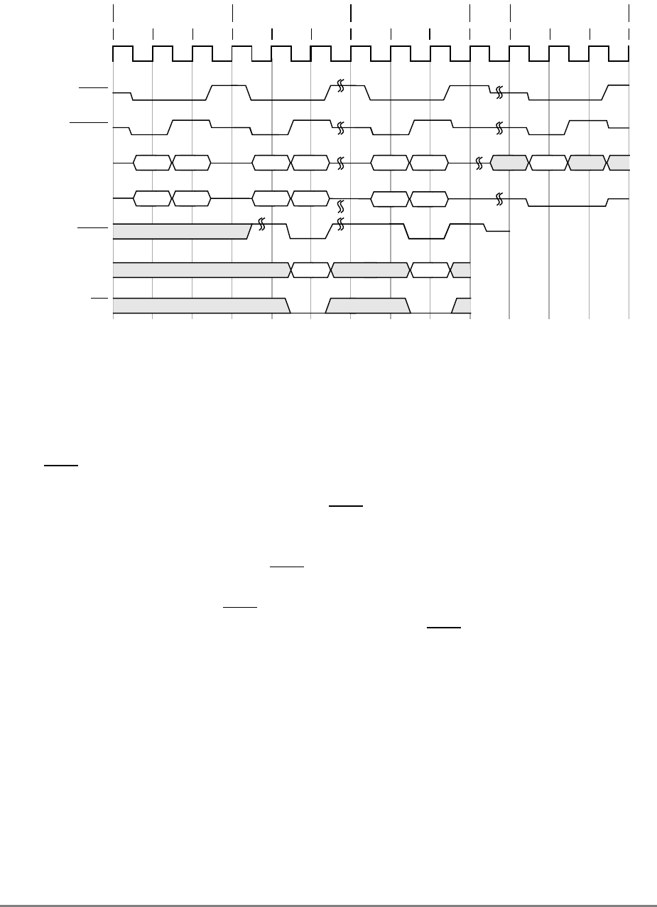
9-46 PowerPC 601 RISC Microprocessor User's Manual
Figure 9-27. I/O Controller Interface Load Access Example
Figure 9-28 shows an I/O store access, comprised of three I/O controller interface
operations in this example. As with the example in Figure 9-27, notice that data is
transferred only on the 32 bits of the DH bus. As opposed to Figure 9-27, there is no request
operation since the 601 has the data ready for the BUC.
The TEA signal may be asserted on any I/O controller interface operation. If it is asserted,
the processor enters a checkstop condition if MSR[ME] is cleared, or it will queue a
machine check exception if ME is set. After TEA is asserted, it must be reasserted for all
tenures associated with the current I/O controller interface operation until the load last or
store last operation occurs. When the operation occurs, the execution unit is released to take
the machine check exception. If the TEA signal is asserted for an I/O controller interface
operation, the reply operations (store reply or load reply) must not occur. If it does, it causes
a checkstop condition. If the TEA signal is not asserted with each tenure of a given I/O
controller interface operation, the result of the assertion of TEA is unpredictable. The 601
may take a machine check exception or cause a checkstop condition.
DH0–DH31
TA
12345678910111213
PKT 0 PKT 1 PKT 0 PKT 1 PKT 0 PKT 1 Reply Rsrvd
REQUEST OP IMM. OP LAST OP REPLY OP
PKT 0 PKT 1 PKT 0 PKT 1 PKT 0 PKT 1
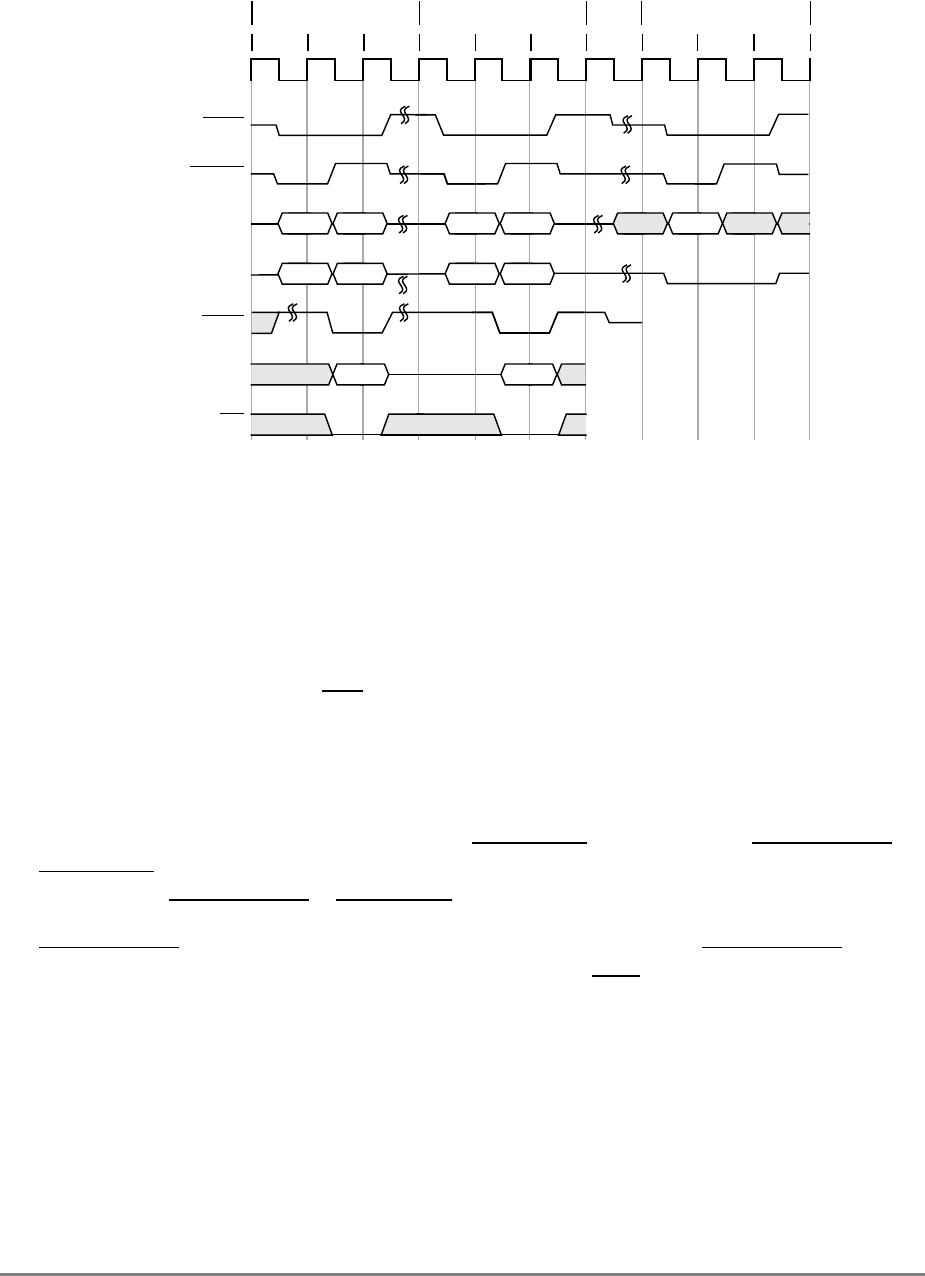
Chapter 9. System Interface Operation 9-47
Figure 9-28. I/O Controller Interface Store Access Example
9.7 Interrupt, Checkstop, and Reset Signals
This section describes external interrupts, checkstop operations, and hard and soft reset
inputs.
9.7.1 External Interrupt
The maskable interrupt input (INT) to the 601 eventually forces the processor to take the
external interrupt vector if the MSR(EE) bit is set. See Chapter 5, “Exceptions,” for more
information about interrupts and exceptions.
9.7.2 Checkstops
The 601 has two checkstop signals, an input (CKSTP_IN) and an output (CKSTP_OUT).
If CKSTP_IN is asserted, the 601 halts operations by gating off all internal clocks. The 601
does not assert CKSTP_OUT if CKSTP_IN if asserted.
If CKSTP_OUT is asserted, the 601 has checkstopped internally. The CKSTP_OUT signal
can be asserted for various reasons including receiving a TEA signal, as the result of the
lack of an instruction dispatch, or internal and external parity errors. For more information
on checkstop state, refer to Section 5.4.2.2, “Checkstop State (MSR[ME] = 0).”
Note that checkstop conditions can be disabled by setting bits in the HID0 register. For
information, see Section 2.3.3.13.1, “Checkstop Sources and Enables Register—HID0.”
DH0–DH31
TA
12345678910
PKT 0 PKT 1 PKT 0 PKT 1 Reply Rsrvd
IMM. OP LAST OP REPLY OP
PKT 0 PKT 1 PKT 0 PKT 1

9-48 PowerPC 601 RISC Microprocessor User's Manual
9.7.3 Reset Inputs
The 601 has two reset inputs, described as follows:
• HRESET (hard reset)—The HRESET signal is used for power-on reset sequences,
or for situations in which the 601 must go through the entire cold-start sequence of
self-tests. Once asserted, this input must be held asserted for a minimum of 300
processor clock cycles to ensure that the processor has had enough time to recognize
the input and initialize registers. For more information about hard reset, see
Section 2.7.1, “Hard Reset.”
• SRESET (soft reset)—The soft reset input provides warm reset capability. This
input can be used to avoid forcing the 601 to complete the cold start sequence. This
can be useful to recover from such conditions as check stop or some machine-check
states that cannot be restarted.
When either reset input is negated and if the self-test sequence completes without error, the
processor attempts to fetch code from the system reset exception vector. The vector is
located at offset x'00100' from the exception prefix (all zeros or ones, depending on the
setting of the exception prefix bit in the machine state register (MSR[EP]). The EP bit is set
for HRESET.
9.7.4 Soft Stop Control Signals
The soft stop control signals allow the processor to stop the clocks and bring the activity to
a quiescent state in an orderly fashion (as opposed to a hard stop, which simply halts the
clocks without regard to system activity).
The soft stop state is entered by asserting the QUIESC_REQ signal. This signal allows the
system to complete any bus activities that might be affected by stopping the clocks. When
the system is ready to enter the soft stop state, it asserts the SYS_QUIESC signal. At this
time the 601 takes a soft stop.
During a soft stop all internal clocking is disabled after the system activity quiesces in an
orderly manner, that is, there are no partially finished instructions. Soft stop is typically
used for debugging; during the soft stop, the state bits in the chip can be scanned, examined
and scanned back in. The processor returns to normal operation when the RESUME signal
is asserted.
9.8 Processor State Signals
This section describes the 601's support for atomic update and memory through the use of
the lwarx/stwcx. opcode pair and the configuration options for the 601 output buffer.
9.8.1 Support for the lwarx/stwcx. Instruction Pair
The Load Word and Reserve Indexed (lwarx) and the Store Word Conditional Indexed
(stwcx.) instructions provide a means for atomic memory updating. Memory can be
updated atomically by setting a reservation on the load and checking that the reservation is

Chapter 9. System Interface Operation 9-49
still valid before the store is performed. In the 601, the reservations are made on behalf of
aligned, 32-byte sections of the memory address space.
The reservation (RSRV) output signal is always driven by bus clock cycle and reflects the
status of the reservation coherency bit in the reservation address register (see Chapter 4,
“Cache and Memory Unit Operation,” for more information). See Section 8.2.9.8,
“Reservation (RSRV)—Output,” for information about timing.
9.9 IEEE 1149.1-Compatible Interface
The 601 boundary-scan interface is IEEE 1149.1 compatible only and is not a fully
compliant implementation of the IEEE 1149.1 standard. Although the standard allows
built-in self-test (BIST), the 601 interface supports only boundary scan. This section
describes the 601 interface and its differences with the IEEE 1149.1 interface.
9.9.1 Deviations from the IEEE 1149.1 Boundary-Scan Specifications
The 601 deviates from the IEEE 1149.1 specifications in the following ways:
• In the IEEE 1149.1 specifications, no mode pin is required to use the IEEE 1149.1
boundary-scan interface. However, in the 601, the scan enable mode input
(BSCAN_EN) signal must be asserted to run boundary-scan testing. The signal must
be pulled up when boundary-scan testing is not being performed.
• Whereas the IEEE 1149.1 specifications indicate that only the TCK signal should be
used to clock data-register latches, in the 601 the processor system clock must be
active (oscillating) during testing.
• The 601 implements only the PRELOAD portion of the SAMPLE/PRELOAD
function.
• IEEE 1149.1 specifies that data on the primary output should be held valid while the
processor is in the SHIFT DR state and that data should change only in the UPDATE
DR or UPDATE IR states (assuming the instruction is valid). In the 601, no stable
values are held on primary outputs for the SHIFT DR state. The SHIFT DR state
forces primary outputs to high impedance. Outputs are enabled if the instruction
register (IR) contains a valid instruction and the test access port (TAP) is in the
UPDATE DR or UPDATE IR state.
• IEEE 1149.1 specifies that asserting the TRST signal should reset only the TAP. In
the 601, the TRST signal resets the TAP, system logic, and the COP.
IEEE 1149.1 also specifies the use of the TRST signal to disable TAP. On the 601,
this can be done by negating the BSCAN_EN signal, which prohibits resetting the
TAP and system logic independently. The TRST signal should not be used to disable
the TAP in the system functional environment; the BSCAN_EN signal should be
used. The user can use the TRST signal as described above or hold TMS high for
five TCK cycles. Note that not all SRLs in the 601 are boundary-scan SRLs. The
boundary-scan chain includes functional system SRLs.

9-50 PowerPC 601 RISC Microprocessor User's Manual
9.9.2 Additional Information about the IEEE 1149.1 Interface
Note the following points concerning the IEEE 1149.1 interface:
• Because the driver inhibit to all COMMON I/O signals is controlled by a common
signal, all COMMON INPUT/OUTPUT devices are either configured as input pins
or output pins, as determined by the JTAGEN bit (bit position 418) in the boundary-
scan chain.
• Not all latches in the boundary-scan chain are boundary-scan latches.
9.9.3 IEEE 1149.1 Interface Description
There are five device pins used for the IEEE 1149.1 interface on the 601. These pins also
perform other functions in the 601 and consequently have signal names describing their
other (non-IEEE 1149.1) functions. Table 9-9 shows the signal name, IEEE 1149.1
function and package pin number of the five TAP pins.
Note: The SCAN_SIN must be pulled-up while performing IEEE 1149.1 testing and must
be pulled down when IEEE 1149.1 testing is not being performed.
The BSCAN_EN input pin must be driven low to enable the boundary-scan test mode.
Additionally, the BSCAN_EN input must be pulled-up when boundary-scan testing is not
being performed. The addition of this pin is a deviation from the IEEE 1149.1 specification
which only defines five pins for the test interface.
9.9.4 IEEE Interface Clock Requirements
In addition to the five standard IEEE 1149.1 signals, the 601 requires that its 2X_PCLK and
PCLK_EN clock inputs remain active during IEEE 1149.1 operation. The 2X_PCLK and
PCLK_EN signals can be supplied by automatic test equipment or the clock generation
circuits on the unit under test. Timing of the IEEE 1149.1 signals is pseudo asynchronous
to the 601 clock inputs and mimics typical IEEE 1149.1 timing. The timing of the IEEE
1149.1 signals can be treated as asynchronous to the 601 clocks as long as they remain
asserted for several PCLK_EN cycles.
Table 9-9. IEEE Interface Pin Descriptions
Signal
Name IEEE 1149.1
Function Package
Pin
SCAN_CTL TMS 184
SCAN_CLK TCK 187
SCAN_SIN TDI 186
SCAN_OUT TDO 78
HRESET TRST 279

Chapter 9. System Interface Operation 9-51
The recommended method of IEEE 1149.1 operation is to limit TCK frequency to 20% or
less of the PCLK_EN frequency; this allows five PCLK_EN cycles for each TCK cycle.
This insures that at least one positive transition of PCLK_EN will occur on each half cycle
of TCK within the required set-up and hold times even if the duty cycle of TCK varies by
20%. Figure 9-29 shows TCK = 0.2 (PCLK_EN) and the duty cycle of TCK ± 20%. Note
that there is no edge timing relationship between TCK and 2X_PCLK, even though
Figure 9-29 may tend to indicate otherwise.
Figure 9-29. IEEE 1149.1 Interface TCK Requirements
Typical PCLK_EN frequency will be 50–66 MHz if supplied by the clock circuits on the
unit under test. This allows TCK frequencies of 10–13 MHz. In most IEEE 1149.1 testing
scenarios, the TCK frequency is likely to be much less than 20% of the PCLK_EN
frequency. When PCLK_EN and 2X_PCLK are provided by the automatic test equipment,
it is acceptable to run these clocks at a much lower frequency than they would normally run.
For example, if PCLK_EN = 5 MHz and 2X_PCLK = 10 MHz, then TCK must be ≤ 1
MHz.
The timing relationships between the IEEE 1149.1 signals is shown in Figure 9-30 and the
signal timing requirements are given in Table 9-10. All the timing parameters are specified
as a portion of the PCLK_EN cycle time.
PCLK_EN
TCK
Normal
TCK
–20%
TCK
+20%
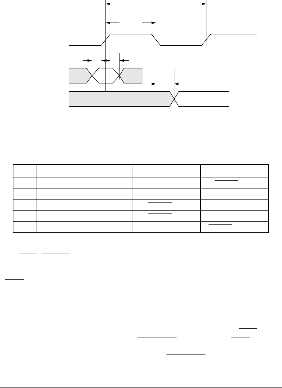
9-52 PowerPC 601 RISC Microprocessor User's Manual
Figure 9-30. IEEE 1149.1 Signal Clocking Requirements
Table 9-10 provides signal timing requirements for the IEEE 1149.1 interface for the
signals shown in Figure 9-30.
9.9.5 IEEE 1149.1 Interface Reset Requirements
The TRST (HRESET) input is used to reset the TAP, and must be held low for a minimum
of 60 TCK cycles to accomplish a reset. The TRST (HRESET) signal will reset the whole
chip including the TAP controller. This deviates from the IEEE 1149.1 specification in that
TRST should only reset the TAP, and not the system logic. The TAP controller can be reset
to the “Test-Logic-Reset” state at any time by holding TMS (SCAN_CTL) high for 5 TCK
cycles. This 5-cycle reset will only reset the TAP controller to the “Test-Logic-Reset” state
and fill the instruction register with all 1’s (BYPASS command), it does not reset the
boundary-scan chain or any other chip logic.
The IEEE specification also provides for the ability to disable the TAP via the TRST input.
This can be performed on the 601 via the BSCAN_EN input. Using the TRST input to
disable the TAP will cause the entire chip to reset. When IEEE 1149.1 testing is not being
performed the TAP should be disabled by pulling the BSCAN_EN input high.
Table 9-10. IEEE 1149.1 Signal Timing Requirements
Label Characteristic Minimum Maximum
1 TCK frequency 0.2 (PCLK_EN) frequency
2 TCK duty cycle 30% 80%
3 Input setup time for TDI and TMS One PCLK_EN period
4 Input hold time for TDI and TMS One PCLK_EN period
5 Output delay time for TDO 1 PCLK_EN period +10 ns
2
34
5
1
TCK
TDI
or
TMS
TDO

Chapter 9. System Interface Operation 9-53
9.9.6 IEEE Interface Instruction Set
The 601 processor implements three IEEE 1149.1 instructions, BYPASS, EXTEST and
SAMPLE/PRELOAD. The 601 provides no SAMPLE function in the
SAMPLE/PRELOAD instruction, which is a deviation from the IEEE 1149.1 specification.
The instruction register is three bits long. Table 9-11 provides the binary encoding for the
IEEE 1149.1 instructions.
When using the EXTEST instruction, note that no stable logic levels will be held on the
outputs while in the SHIFT DR state. The 601 outputs are forced to the high impedance
state while the TAP controller is in the SHIFT DR state. The 601 outputs will be enabled if
a valid instruction is in the instruction register and the TAP controller is in the UPDATE DR
or UPDATE IR state. This is a deviation from the IEEE 1149.1 standard which requires
outputs to be held valid while in the SHIFT DR state.
9.9.7 IEEE 1149.1 Interface Boundary-Scan Chain
The 601 boundary-scan chain is 424 bits long (0–423.) Not every bit in the boundary- scan
chain is directly controllable or observable during inbound and outbound testing in the
EXTEST mode. Table 9-12 shows the pin number, signal name, and scan chain bit position
for each boundary-scan pin. Note that the pins that do not have boundary-scan latches are
shown with N/A in the bit position column. The last column of the table shows which of
the 601 pins have an inverter between the package pin and the boundary-scan latch. All
bidirectional I/O pins have two boundary latches associated with them, one for the input
and one for the output. In the table, the bidirectional I/O pins are shown as type I/O and the
boundary-scan chain bit positions for these pins are shown in Input/Output order.
Table 9-12 describes the boundary-scan string.
Table 9-11. IEEE Interface Instruction Set
Instruction Code
BYPASS 111
EXTEST 000
SAMPLE/PRELOAD 101

9-54 PowerPC 601 RISC Microprocessor User's Manual
Table 9-12. IEEE 1149.1 Boundary-Scan Chain Description
Pin Number Signal Name Type Bit
Position Inverted
1 TST21 Input N/A
3 TST20 Input N/A
4 TST16 Input N/A
5 TST11 Input N/A
7 TST13 Input N/A
8 TST15 Input N/A
9 TST17 Input N/A
10 TST14 Input N/A
13 TST9 Input N/A
14 TST6 Input N/A
15 TST7 Input N/A
17 TST8 Input N/A
18 A0 I/O 141/108
19 A1 I/O 142/109
21 A2 I/O 143/110
22 A3 I/O 144/111
23 A4 I/O 145/112
26 A5 I/O 146/113
27 A6 I/O 147/114
28 A7 I/O 148/115
30 A8 I/O 149/116
31 A9 I/O 150/117
32 A10 I/O 151/118
34 A11 I/O 152/119
35 A12 I/O 153/120
36 A13 I/O 154/121
41 A14 I/O 155/122
42 A15 I/O 156/123
43 A16 I/O 157/124
45 A17 I/O 158/125
46 A18 I/O 159/126

Chapter 9. System Interface Operation 9-55
47 A19 I/O 160/127
49 A20 I/O 161/128
50 A21 I/O 162/129
51 A22 I/O 163/130
54 A23 I/O 164/131
55 A24 I/O 165/132
56 A25 I/O 166/133
58 A26 I/O 167/134
59 A27 I/O 168/135
60 A28 I/O 169/136
62 A29 I/O 170/137
63 A30 I/O 171/138
64 A31 I/O 172/139
67 AP0 I/O 198/269
68 AP1 I/O 199/270
69 AP2 I/O 200/271
70 TST19 Output N/A
71 AP3 I/O 201/272
72 CKSTP_OUT Output 423
74 RUN_NSTOP Output N/A
75 DH31 I/O 376/32
78 SCAN_OUT Output N/A
80 DH30 I/O 375/31
81 DH29 I/O 374/30
82 DH28 I/O 373/29
83 DH27 I/O 372/28
84 DH26 I/O 371/27
85 DH25 I/O 370/26
86 DH24 I/O 369/25
90 DH23 I/O 368/24
91 DH22 I/O 367/23
93 DH21 I/O 366/22
Table 9-12. IEEE 1149.1 Boundary-Scan Chain Description (Continued)
Pin Number Signal Name Type Bit
Position Inverted

9-56 PowerPC 601 RISC Microprocessor User's Manual
94 DH20 I/O 365/21
95 DH19 I/O 364/20
97 DH18 I/O 363/19
98 DH17 I/O 362/18
99 DH16 I/O 361/17
103 DH15 I/O 360/16
104 DH14 I/O 359/15
106 DH13 I/O 358/14
107 DH12 I/O 357/13
108 DH11 I/O 356/12
110 DH10 I/O 355/11
111 DH9 I/O 354/10
112 DH8 I/O 353/9
118 DH7 I/O 352/8
119 DH6 I/O 351/7
121 DH5 I/O 350/6
122 DH4 I/O 349/5
123 DH3 I/O 348/4
125 DH2 I/O 347/3
126 DH1 I/O 346/2
127 DH0 I/O 345/1
130 DL31 I/O 413/69
131 DL30 I/O 412/68
132 DL29 I/O 411/67
134 DL28 I/O 410/66
135 DL27 I/O 409/65
136 DL26 I/O 408/64
138 DL25 I/O 407/63
139 DL24 I/O 406/62
140 DL23 I/O 405/61
143 DL22 I/O 404/60
144 DL21 I/O 403/59
Table 9-12. IEEE 1149.1 Boundary-Scan Chain Description (Continued)
Pin Number Signal Name Type Bit
Position Inverted

Chapter 9. System Interface Operation 9-57
145 DL20 I/O 402/58
147 DL19 I/O 401/57
148 DL18 I/O 400/56
149 DL17 I/O 399/55
151 DL16 I/O 398/54
155 DL15 I/O 397/53
157 DL14 I/O 396/52
159 DL13 I/O 395/51
161 DL12 I/O 394/50
165 DL11 I/O 393/49
167 DL10 I/O 392/48
168 DL9 I/O 391/47
169 DL8 I/O 390/46
172 DL7 I/O 389/45
173 DL6 I/O 388/44
178 DL5 I/O 387/43
180 DL4 I/O 386/42
181 DL3 I/O 385/41
182 DL2 I/O 384/40
184 SCAN_CTL Input N/A
185 DL1 I/O 383/39
186 SCAN_SIN Input N/A
187 SCAN_CLK Input N/A
188 DL0 I/O 382/38
194 DP7 I/O 417/73
195 DP6 I/O 416/72
197 DP5 I/O 415/71
198 DP4 I/O 414/70
199 DP3 I/O 380/36
201 DP2 I/O 379/35
202 DP1 I/O 378/34
203 DP0 I/O 377/33
Table 9-12. IEEE 1149.1 Boundary-Scan Chain Description (Continued)
Pin Number Signal Name Type Bit
Position Inverted

9-58 PowerPC 601 RISC Microprocessor User's Manual
210 SC_DRIVE Input 231
211 CSE1 Output 87
212 CSE2 Output 88
214 WT Output 84 Inverted
215 CSE0 Output 86
216 CI Output 83 Inverted
219 BR Output 209 Inverted
220 DBB I/O 177/217
221 ARTRY I/O 175/326
222 DPE Output 97
224 ABB I/O 205/216
226 TS I/O 186/214 Inverted input only
227 TT1 I/O 191/274
228 TT0 I/O 190/273
229 XATS I/O 194/211 Inverted input only
231 APE Output 98
232 TSIZ1 I/O 188/279
233 GBL I/O 181/85 Inverted output only
235 SHD I/O 182/325
236 TBST I/O 184/277
237 TSIZ2 I/O 189/280
238 TT4 Output 286
241 TSIZ0 I/O 187/278
243 TC0 Output 89
244 TT3 I/O 193/276
246 TST2 Output N/A
247 TST3 Output N/A
248 TT2 I/O 192/275
250 HP_SNP_REQ IN 196
251 TC1 Output 90
254 RSRV Output 210
255 TST22 Input 232
Table 9-12. IEEE 1149.1 Boundary-Scan Chain Description (Continued)
Pin Number Signal Name Type Bit
Position Inverted

Chapter 9. System Interface Operation 9-59
Note that the internal signal JTAGEN shown at the end of Table 9-12 is used to control the
direction of all the bidirectional pins of the 601. JTAGEN is bit position 420 in the
boundary-scan chain and needs to be set by the user when EXTEST operation is desired.
Setting the JTAGEN bit to 1 places all the 601 bidirectional I/O pins in the output enabled
(drive) mode. When JTAGEN is cleared to 0 all the 601 bidirectional I/O pins are set to the
input (receive) mode.
256 QUIESC_REQ Input N/A
258 CKSTP_IN Input 423
260 SYS_QUIESC Input N/A
262 INT Input 233
264 SRESET Input 234
271 BCLK_EN Input 204
273 RTC Input N/A
275 ESP_EN Input N/A
277 RESUME Input N/A
279 HRESET Input N/A
282 2X_PCLK Input N/A
285 PCLK_EN Input N/A
288 TST5 Input N/A
290 TA Input 183
291 TEA Input 185 Inverted
292 DRTRY Input 180
295 AACK Input 174
297 DBWO Input 179
298 BG Input 176
299 BSCAN_EN Input N/A
300 DBG Input 178
302 TST12 Input N/A
303 TST18 Input N/A
304 TST10 Input N/A
N/A JTAGEN Internal 420
Table 9-12. IEEE 1149.1 Boundary-Scan Chain Description (Continued)
Pin Number Signal Name Type Bit
Position Inverted

9-60 PowerPC 601 RISC Microprocessor User's Manual
9.10 Using DBWO (Data Bus Write Only)
The 601 supports split transaction pipelined transactions. Additionally, the DBWO signal
allows the 601 to be configured dynamically to source write data out of order with respect
to read data.
In general, an address tenure on the bus is followed strictly in order by its associated data
tenure. Transactions pipelined by a single 601 complete strictly in order. However, the 601
can run bus transactions out of order only when the external system allows the 601 to
perform a cache-sector snoop push-out operation (or other write transaction, if pending in
the 601 write queues) between the address and data tenures of a read operation through the
use of DBWO. This effectively envelopes the write operation within the read operation.
This can be useful in some external queued controller scenarios or for more complex
memory implementations that can support so-called dump-and-run operations. These
include the cache sector cast out of a modified sector caused by a load miss. A replacement
copyback operation can be written to memory buffers while the memory location is being
accessed for the line fill. The sector is written (dumped) into memory buffers while the
memory is accessed for the load operation. Optimally, the replacement copy-back operation
can be absorbed by the memory system without affecting load memory latency. Figure 9-31
gives an example of the use of the DBWO input.
Figure 9-31 illustrates the following sequence of operations:
1. Processor A begins a read operation. (Bus clock cycle 2)
2. Processor B attempts a global read but is interrupted by a retry from processor A (bus
clock cycle 7)
3. Processor A performs a cache-sector snoop push-out operation out of order because
of the assertion of DBWO (bus clock cycle 8)
4. Processor B successfully performs the global read (bus clock cycle 13)
5. Processor A successfully concludes its original read operation (bus clock cycle 16)
Note that steps 4 and 5 can occur in either order.
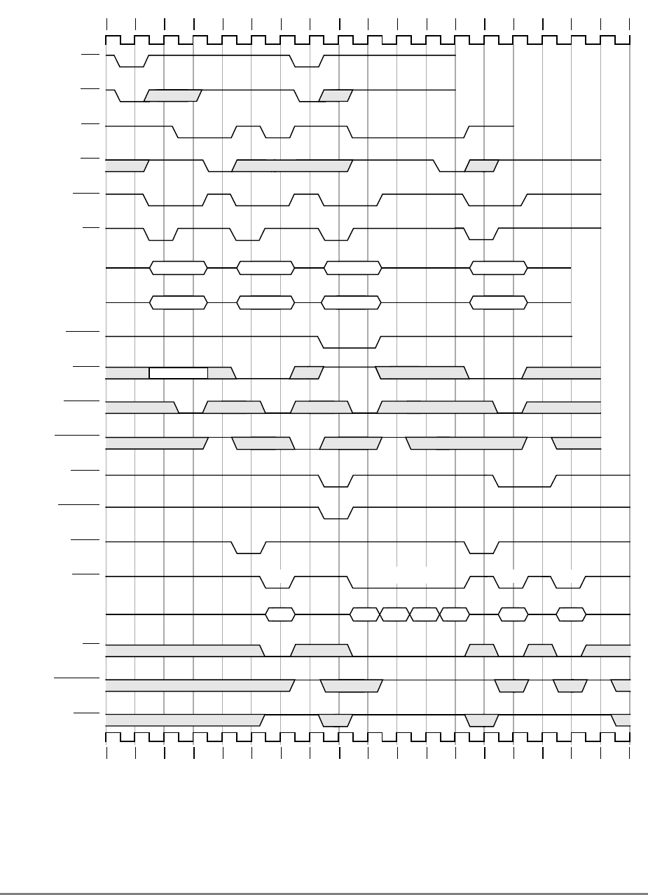
Chapter 9. System Interface Operation 9-61
Figure 9-31. Data Bus Write-Only Transaction
1 2 3 4 5 6 7 8 9 101112131415161718
CPU A BR
CPU A BG
CPU B BR
CPU B BG
ABB
TS
A0–A31
TT0–TT3
TBST
GBL
AACK
ARTRY
CPU A DBG
CPU A DBWO
CPU B DBG
DBB
D0–D63
TA
DRTRY
TEA
CPU A CPU B CPU A CPU B
Read Read Snoop Push CPU B
1 2 3 4 5 6 7 8 9 101112131415161718
In* Out Out Out Out In In
* Indicates the 601 flushed this data due to address retry
CPU ACPU B CPU B CPU A

9-62 PowerPC 601 RISC Microprocessor User's Manual
Note that although the 601 can pipeline any write transaction behind the read transaction,
special care should be used when using the enveloped write feature. It is envisioned that
most system implementations will not need this capability; for these applications DBWO
should remain negated. In systems where this capability is needed, DBWO should be
asserted under the following scenario:
1. The 601 initiates a read transaction (either single-beat or burst) by completing the
read address tenure with no address retry.
2. Then, the 601 initiates a write transaction by completing the write address tenure,
with no address retry.
3. At this point, if DBWO is asserted with a qualified data bus grant to the 601, the 601
asserts DBB and drives the write data onto the data bus, out of order with respect to
the address pipeline. The write transaction concludes with the 601 negating DBB.
4. The next qualified data bus grant signals the 601 to complete the outstanding read
transaction by latching the data on the bus. This assertion of DBG should not be
accompanied by an asserted DBWO.
Any number of bus transactions by other bus masters can be attempted between any of these
steps.
Note the following regarding DBWO:
• DBWO cannot be asserted if no data bus write tenures are pending.
• DBWO can be asserted if no data bus read is pending, but it has no effect on write
ordering.
• The ordering and presence of data bus writes is determined by the writes in the write
queues at the time BG is asserted for the write address (not DBG). If a particular
write is desired (for example, a cache-sector snoop push-out operation), then BG
must be asserted after that particular write is in the queue and it must be the highest
priority write in the queue at that time. A cache-sector snoop push-out operations
may be the highest priority write, but more than one may be queued.
• Because more than one write may be in the write queue when DBG is asserted for
the write address, more than one data bus write may be enveloped by a pending data
bus read.
The arbiter must monitor bus operations and coordinate the various masters and slaves with
respect to the use of the data bus when DBWO is used. Individual DBG signals associated
with each bus device should allow the arbiter to synchronize both pipelined and split-
transaction bus organizations. Individual DBG signals provide a primitive form of source-
level tagging for the granting of the data bus.
Note that use of the DBWO signal allows some operation-level tagging with respect to the
601 and the use of the data bus.

Chapter 10. Instruction Set 10-1
Chapter 10
Instruction Set
100
100
This chapter describes individual instructions, including a description of instruction
formats and notation and an alphabetical listing of the PowerPC 601 microprocessor’s
instructions by mnemonic.
10.1 Instruction Formats
Instructions are four bytes long and word-aligned, so when instruction addresses are
presented to the processor (as in branch instructions) the two low-order bits are ignored.
Similarly, whenever the processor develops an instruction address, its two low-order bits
are zero.
Bits 0–5 always specify the primary opcode. Many instructions also have a secondary
opcode. The remaining bits of the instruction contain one or more fields for the different
instruction formats.
Some instruction fields are reserved or must contain a predefined value as shown in the
individual instruction layouts. If a reserved field does not have all bits set to 0, or if a field
that must contain a particular value does not contain that value, the instruction form is
invalid and the results are as described in Appendix D, “Classes of Instructions”.
10.1.1 Split-Field Notation
Some instruction fields occupy more than one contiguous sequence of bits or occupy a
contiguous sequence of bits used in permuted order. Such a field is called a split field. In
the format diagrams and in the individual instruction layouts, the name of a split field is
shown in small letters, once for each of the contiguous sequences. In the pseudocode
description of an instruction having a split field and in some places where individual bits of
a split field are identified, the name of the field in small letters represents the concatenation
of the sequences from left to right. Otherwise, the name of the field is capitalized and
represents the concatenation of the sequences in some order, which need not be left to right,
as described for each affected instruction.

10-2 PowerPC 601 RISC Microprocessor User's Manual
10.1.2 Instruction Fields
Table 10-1 describes the instruction fields used in the various instruction formats.
Table 10-1. Instruction Formats
Field Description
AA (30) Absolute address bit
0 The immediate field represents an address relative to the current instruction address. The
effective (logical) address of the branch is either the sum of the LI field sign-extended to 32
bits and the address of the branch instruction or the sum of the BD field sign-extended to 32
bits and the address of the branch instruction.
1 The immediate field represents an absolute address. The effective address of the branch is
the LI field sign-extended to 32 bits or the BD field sign-extended to 32 bits.
BD (16–29) Immediate field specifying a 14-bit signed two's complement branch displacement that is
concatenated on the right with b'00' and sign-extended to 32 bits.
BI (11–15) Field used to specify a bit in the CR to be used as the condition of a branch conditional
instruction
BO (6–10) Field used to specify options for the branch conditional instructions. The encoding is described in
Section 3.6.2, “Conditional Branch Control.”
crbA (11–15) Field used to specify a bit in the CR to be used as a source
crbB (16–20) Field used to specify a bit in the CR to be used as a source
crbD (6–10) Field used to specify a bit in the CR or in the FPSCR as the destination of the result of an
instruction
crfD (6–8) Field used to specify one of the CR fields or one of the FPSCR fields as a destination
crfS (11–13) Field used to specify one of the CR fields or one of the FPSCR fields as a source
CRM (12–19) Field mask used to identify the CR fields that are to be updated by the mtcrf instruction
d(16–31) Immediate field specifying a 16-bit signed two's complement integer that is sign-extended to 32
bits
FM (7–14) Field mask used to identify the FPSCR fields that are to be updated by the mtfsf instruction
frA (11–15) Field used to specify an FPR as a source of an operation
frB (16–20) Field used to specify an FPR as a source of an operation
frC (21–25) Field used to specify an FPR as a source of an operation
frD (6–10) Field used to specify an FPR as the destination of an operation
frS (6–10) Field used to specify an FPR as a source of an operation
IMM (16–19) Immediate field used as the data to be placed into a field in the FPSCR
LI (6–29) Immediate field specifying a 24-bit, signed two's complement integer that is concatenated on the
right with b'00' and sign-extended to 32 bits
LK (31) Link bit.
0 Does not update the link register.
1 Updates the link register. If the instruction is a branch instruction, the address of the instruction
following the branch instruction is placed into the link register.

Chapter 10. Instruction Set 10-3
MB (21–25) and
ME (26–30) Fields used in rotate instructions to specify a 32-bit mask consisting of “1” bits from bit MB+32
through bit ME+32 inclusive, and “0” bits elsewhere, as described in Section 3.3.4, “Integer
Rotate and Shift Instructions”.
NB (16–20) Field used to specify the number of bytes to move in an immediate string load or store
opcode (0–5) Primary opcode field
OE (21) Used for extended arithmetic to enable setting OV and SO in the XER
rA (11–15) Field used to specify a GPR to be used as a source or as a destination
rB (16–20) Field used to specify a GPR to be used as a source
Rc (31) Record bit
0 Does not update the condition register
1 Updates the condition register (CR) to reflect the result of the operation.
For integer instructions, CR bits 0–3 are set to reflect the result as a signed quantity. The
result as an unsigned quantity or a bit string can be deduced from the EQ bit. For floating-point
instructions, CR bits 4–7 are set to reflect floating-point exception, floating-point enabled
exception, floating-point invalid operation exception, and floating-point overflow exception.
rD(6–10) Field used to specify a GPR to be used as a destination
rS (6–10) Field used to specify a GPR to be used as a source
SH (16–20) Field used to specify a shift amount
SIMM (16–31) Immediate field used to specify a 16-bit signed integer
SPR (11–20) Field used to specify a special purpose register for the mtspr and mfspr instructions. The
encoding is described in Section 3.7.2, “Move to/from Special-Purpose Register Instructions.”
TO (6–10) Field used to specify the conditions on which to trap. The encoding is described in Section 3.6.9,
“Trap Instructions and Mnemonics
UIMM (16–31) Immediate field used to specify a 16-bit unsigned integer
XO (21–30, 22–
30, 26–30, or 30) Secondary opcode field
Table 10-1. Instruction Formats (Continued)
Field Description

10-4 PowerPC 601 RISC Microprocessor User's Manual
10.1.3 Notation and Conventions
The operation of some instructions is described by a semiformal language (pseudocode).
See Table 10-2 for a list of pseudocode notation and conventions used throughout this
chapter.
Table 10-2. Pseudocode Notation and Conventions
Notation/Convention Meaning
←Assignment
←iea Assignment of an instruction effective address.
¬ NOT logical operator
∗Multiplication
÷Division (yielding quotient)
+ Two’s-complement addition
- Two’s-complement subtraction, unary minus
=, ≠Equals and Not Equals relations
<,≤,>,≥Signed comparison relations
<U,>U Unsigned comparison relations
? Unordered comparison relation
&, | AND, OR logical operators
|| Used to describe the concatenation of two values (i.e., 010 || 111 is the same as 010111)
⊕, ≡Exclusive-OR, Equivalence logical operators ((a ≡ b) = (a ⊕ ¬ b))
b'
nnnn
' A number expressed in binary format
x'
nnnn
' A number expressed in hexadecimal format
(rA|0) The contents of rA if the rA field has the value 1–31, or the value 0 if the rA field is 0
. (period) As the last character of an instruction mnemonic, a period (.) means that the instruction
updates the condition register field.
CEIL(x) Least integer ≥ x
DOUBLE(x) Result of converting x form floating-point single format to floating-point double format.
EXTS(x) Result of extending x on the left with sign bits
GPR(x) General purpose register x
MASK(x, y) Mask having 1s in positions x through y (wrapping if x > y) and 0s elsewhere
MEM(x, y) Contents of y bytes of memory starting at address x
ROTL[32](x, y) Result of rotating the 64-bit value x||x left y positions, where x is 32 bits long
SINGLE(x) Result of converting x from floating-point double format to floating-point single format
SPR(x) Special purpose register x

Chapter 10. Instruction Set 10-5
Precedence rules for pseudocode operators are summarized in Table 10-3.
x
n
x is raised to the
n
th power
(
n
)x The replication of x,
n
times (i.e., x concatenated to itself
n
-1 times). (
n
)0 and (
n
)1 are
special cases
x[
n
]
n
is a bit or field within x, where x is a register
TRAP Invoke the system trap handler
Undefined An undefined value. The value may vary from one implementation to another, and from
one execution to another on the same implementation.
Characterization Reference to the setting of status bits, in a standard way that is explained in the text
CIA Current instruction address, which is the 32-bit address of the instruction being
described by a sequence of pseudocode. Used by relative branches to set the next
instruction address (NIA). Does not correspond to any architected register.
NIA Next instruction address, which is the 32-bit address of the next instruction to be
executed (the branch destination) after a successful branch. In pseudocode, a
successful branch is indicated by assigning a value to NIA. For instructions which do not
branch, the next instruction address is CIA + 4.
if...then...else... Conditional execution, indenting shows range, else is optional
Do Do loop, indenting shows range. “To” and/or “by” clauses specify incrementing an
iteration variable, and “while” and/or “until” clauses give termination conditions, in the
usual manner.
Leave Leave innermost do loop, or do loop described in leave statement
Table 10-3. Precedence Rules
Operators Associativity
x[
n
], function evaluation Left to right
(
n
)x or replication,
x(
n
) or exponentiation Right to left
unary -, ¬ Right to left
∗, ÷Left to right
+,- Left to right
|| Left to right
=,≠,<,≤,>,≥,<U,>U,? Left to right
&,⊕,≡ Left to right
| Left to right
– (range) None
←None
Table 10-2. Pseudocode Notation and Conventions (Continued)
Notation/Convention Meaning
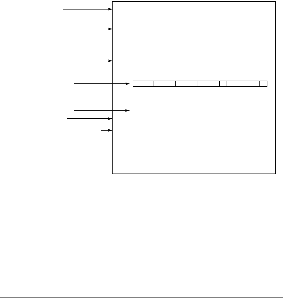
10-6 PowerPC 601 RISC Microprocessor User's Manual
Note that operators higher in Table 10-3 are applied before those lower in the table.
Operators at the same level in the table associate from left to right, from right to left, or not
at all, as shown.
10.2 Instruction Set
The remainder of this chapter lists and describes the instruction set for the 601. The
instructions are listed in alphabetical order by mnemonic and include those instructions that
are specific to the 601 that are not specified as part of the PowerPC architecture. Figure 10-1
shows the format for each instruction description page.
Figure 10-1. Instruction Description
Note in Figure 10-1 that the execution unit that executes the instruction may not be the same
for other PowerPC processors.
add
x
add
x
Add Integer Unit
add rD,rA,rB (OE=0 Rc=0)
add. rD,rA,rB (OE=0 Rc=1)
addo rD,rA,rB (OE=1 Rc=0)
addo. rD,rA,rB (OE=1 Rc=1)
[POWER mnemonics: cax, cax., caxo, caxo.]
rD ← (rA) + (rB)
The sum (rA) + (rB) is placed into rD.
Other registers altered:
• Condition Register (CR0 Field):
Affected: LT, GT, EQ, SO (if Rc=1)
• XER:
Affected: SO, OV (if OE=1)
05610111516202122 3031
31 D A B OE 266 Rc
Instruction name
Instruction syntax
Equivalent POWER mnemonics
Instruction encoding
Pseudocode description of
instruction operation
Text description of
instruction operation
Registers altered by instruction

Chapter 10. Instruction Set 10-7
abs
x
POWER Architecture Instruction abs
x
Absolute Integer Unit
abs rD,rA (OE=0 Rc=0)
abs. rD,rA (OE=0 Rc=1)
abso rD,rA (OE=1 Rc=0)
abso. rD,rA (OE=1 Rc=1)
This instruction is not part of the PowerPC architecture.
The absolute value |(rA)| is placed into rD. If rA contains the most negative number (i.e.,
x'8000 0000'), the result of the instruction is the most negative number and sets XER[OV]
if overflow signaling is enabled.
Other registers altered:
• Condition Register (CR0 Field):
Affected: LT, GT, EQ, SO (if Rc=1)
• XER:
Affected: SO, OV (if OE=1)
Note: This instruction is specific to the 601.
05610111516202122 3031
Reserved
31 D A 0 0 0 0 0 OE 360 Rc

10-8 PowerPC 601 RISC Microprocessor User's Manual
add
x
add
x
Add Integer Unit
add rD,rA,rB (OE=0 Rc=0)
add. rD,rA,rB (OE=0 Rc=1)
addo rD,rA,rB (OE=1 Rc=0)
addo. rD,rA,rB (OE=1 Rc=1)
[POWER mnemonics: cax, cax., caxo, caxo.]
rD ← (rA) + (rB)
The sum (rA) + (rB) is placed into rD.
Other registers altered:
• Condition Register (CR0 Field):
Affected: LT, GT, EQ, SO (if Rc=1)
• XER:
Affected: SO, OV (if OE=1)
05610111516202122 3031
31 D A B OE 266 Rc

Chapter 10. Instruction Set 10-9
addc
x
addc
x
Add Carrying Integer Unit
addc rD,rA,rB (OE=0 Rc=0)
addc. rD,rA,rB (OE=0 Rc=1)
addco rD,rA,rB (OE=1 Rc=0)
addco. rD,rA,rB (OE=1 Rc=1)
[POWER mnemonics: a, a., ao, ao.]
rD ← (rA) + (rB)
The sum (rA) + (rB) is placed into rD.
Other registers altered:
• Condition Register (CR0 Field):
Affected: LT, GT, EQ, SO (if Rc=1)
• XER:
Affected: CA
Affected: SO, OV (if OE=1)
05610111516202122 3031
31 D A B OE 10 Rc

10-10 PowerPC 601 RISC Microprocessor User's Manual
adde
x
adde
x
Add Extended Integer Unit
adde rD,rA,rB (OE=0 Rc=0)
adde. rD,rA,rB (OE=0 Rc=1)
addeo rD,rA,rB (OE=1 Rc=0)
addeo. rD,rA,rB (OE=1 Rc=1)
[POWER mnemonics: ae, ae., aeo, aeo.]
rD ← (rA) + (rB) + XER[CA]
The sum (rA) + (rB) + XER[CA] is placed into rD.
Other registers altered:
• Condition Register (CR0 Field):
Affected: LT, GT, EQ, SO (if Rc=1)
• XER:
Affected: CA
Affected: SO, OV (if OE=1)
05610111516202122 3031
31 D A B OE 138 Rc

Chapter 10. Instruction Set 10-11
addi addi
Add Immediate Integer Unit
addi rD,rA,SIMM
[POWER mnemonic: cal]
if rA=0 then rD←EXTS(SIMM)
else rD←(rA)+EXTS(SIMM)
The sum (rA| 0) + SIMM is placed into rD.
Other registers altered:
• None
Simplified mnemonics:
subi rA,rB,value equivalent to addi rD,rA,-value
05610111516 31
14 D A SIMM

10-12 PowerPC 601 RISC Microprocessor User's Manual
addic addic
Add Immediate Carrying Integer Unit
addic rD,rA,SIMM
[POWER mnemonic: ai]
rD ← (rA) + EXTS(SIMM)
The sum (rA) + SIMM is placed into rD.
Other registers altered:
• XER:
Affected: CA
05610111516 31
12 D A SIMM

Chapter 10. Instruction Set 10-13
addic. addic.
Add Immediate Carrying and Record Integer Unit
addic. rD,rA,SIMM
[POWER mnemonic: ai.]
rD ← (rA) + EXTS(SIMM)
The sum (rA) + SIMM is placed into rD.
Other registers altered:
• Condition Register (CR0 Field):
Affected: LT, GT, EQ, SO
• XER:
Affected: CA
05610111516 31
13 D A SIMM

10-14 PowerPC 601 RISC Microprocessor User's Manual
addis addis
Add Immediate Shifted Integer Unit
addis rD,rA,SIMM
[POWER mnemonic: cau]
if rA=0 then rD←(SIMM || (16)0)
else rD←(rA)+(SIMM || (16)0)
The sum (rA| 0) + (SIMM || x'0000') is placed into rD.
Other registers altered:
• None
05610111516 31
15 D A SIMM

Chapter 10. Instruction Set 10-15
addme
x
addme
x
Add to Minus One Extended Integer Unit
addme rD,rA (OE=0 Rc=0)
addme. rD,rA (OE=0 Rc=1)
addmeo rD,rA (OE=1 Rc=0)
addmeo. rD,rA (OE=1 Rc=1)
[POWER mnemonics: ame, ame., ameo, ameo.]
rD ← (rA) + XER[CA] - 1
The sum (rA)+XER[CA]+x'FFFFFFFF' is placed into rD.
Other registers altered:
• Condition Register (CR0 Field):
Affected: LT, GT, EQ, SO (if Rc=1)
• XER:
Affected: CA
Affected: SO, OV (if OE=1)
05610111516202122 3031
Reserved
31 D A 0 0 0 0 0 OE 234 Rc

10-16 PowerPC 601 RISC Microprocessor User's Manual
addze
x
addze
x
Add to Zero Extended Integer Unit
addze rD,rA (OE=0 Rc=0)
addze. rD,rA (OE=0 Rc=1)
addzeo rD,rA (OE=1 Rc=0)
addzeo. rD,rA (OE=1 Rc=1)
[POWER mnemonics: aze, aze., azeo, azeo.]
rD ← (rA) + XER[CA]
The sum (rA)+XER[CA] is placed into rD.
Other registers altered:
• Condition Register (CR0 Field):
Affected: LT, GT, EQ, SO (if Rc=1)
• XER:
Affected: CA
Affected: SO, OV (if OE=1)
05610111516202122 3031
Reserved
31 D A 0 0 0 0 0 OE 202 Rc

Chapter 10. Instruction Set 10-17
and
x
and
x
AND Integer Unit
and rA,rS,rB (Rc=0)
and. rA,rS,rB (Rc=1)
rA ← (rS) & (rB)
The contents of rS is ANDed with the contents of rB and the result is placed into rA.
Other registers altered:
• Condition Register (CR0 Field):
Affected: LT, GT, EQ, SO (if Rc=1)
056101115162021 3031
31 S A B 28 Rc

10-18 PowerPC 601 RISC Microprocessor User's Manual
andc
x
andc
x
AND with Complement Integer Unit
andc rA,rS,rB (Rc=0)
andc. rA,rS,rB (Rc=1)
rA←(rS)+ ¬ (rB)
The contents of rS is ANDed with the one’s complement of the contents of rB and the result
is placed into rA.
Other registers altered:
• Condition Register (CR0 Field):
Affected: LT, GT, EQ, SO (if Rc=1)
056101115162021 3031
31 S A B 60 Rc

Chapter 10. Instruction Set 10-19
andi. andi.
AND Immediate Integer Unit
andi. rA,rS,UIMM
[POWER mnemonic: andil.]
)
rA ← (rS) & ((48)0 || UIMM)
The contents of rS is ANDed with x'0000' || UIMM and the result is placed into rA.
Other registers altered:
• Condition Register (CR0 Field):
Affected: LT, GT, EQ, SO
05610111516 31
28 S A UIMM

10-20 PowerPC 601 RISC Microprocessor User's Manual
andis. andis.
AND Immediate Shifted Integer Unit
andis. rA,rS,UIMM
[POWER mnemonic: andiu.]
rA ← (rS) + ((32)0 || UIMM || (16)0)
The contents of rS is ANDed with x'0000_0000' || UIMM || x'0000' and the result is placed
into rA.
Other registers altered:
• Condition Register (CR0 Field):
Affected: LT, GT, EQ, SO
05610111516 31
29 S A UIMM

Chapter 10. Instruction Set 10-21
b
x
b
x
Branch Branch Processing Unit
b target_addr (AA=0 LK=0)
ba target_addr (AA=1 LK=0)
bl target_addr (AA=0 LK=1)
bla target_addr (AA=1 LK=1)
if AA, then NIA ←iea EXTS(LI || b'00')
else NIA ←iea CIA+EXTS(LI || b'00')
if LK, then
LR ←iea CIA+4
target_addr specifies the branch target address.
If AA=0, then the branch target address is the sum of LI || b'00' sign-extended and the
address of this instruction.
If AA=1, then the branch target address is the value LI || b'00' sign-extended.
If LK=1, then the effective address of the instruction following the branch instruction is
placed into the link register.
Other registers altered:
Affected: Link Register (LR) (if LK=1)
056 29 30 31
18 LI AA LK

10-22 PowerPC 601 RISC Microprocessor User's Manual
bc
x
bc
x
Branch Conditional Branch Processing Unit
bc BO,BI,target_addr (AA=0 LK=0)
bca BO,BI,target_addr (AA=1 LK=0)
bcl BO,BI,target_addr (AA=0 LK=1)
bcla BO,BI,target_addr (AA=1 LK=1)
if ¬ BO[2], then CTR ← CTR-1
ctr_ok ← BO[2] | ((CTR≠0) ⊕ BO[3])
cond_ok ← BO[0] | (CR[BI] ≡ BO[1])
if ctr_ok & cond_ok, then
if AA, then NIA ←iea EXTS(BD || b'00')
else NIA ←iea CIA+EXTS(BD || b'00')
if LK, then
LR ←iea CIA+4
The BI field specifies the bit in the Condition Register (CR) to be used as the condition of
the branch. The BO field is used as described above.
target_addr specifies the branch target address.
If AA=0, the branch target address is the sum of BD || b'00' sign-extended and the address
of this instruction.
If AA=1, the branch target address is the value BD || b'00' sign-extended.
If LK=1, the effective address of the instruction following the branch instruction is placed
into the link register.
Other registers altered:
Affected: Count Register (CTR) (if BO[2]=0)
Affected: Link Register (LR) (if LK=1)
Simplified mnemonics:
blt target equivalent to bc 12,0,target
bne cr2,target equivalent to bc 4,10,target
bdnz target equivalent to bc 16,0,target
05610111516 293031
16 BO BI BD AA LK

Chapter 10. Instruction Set 10-23
bcctr
x
bcctr
x
Branch Conditional to Count Register Branch Processing Unit
bcctr BO,BI (LK=0)
bcctrl BO,BI (LK=1)
[POWER mnemonics: bcc, bccl]
cond_ok ← BO[0] | (CR[BI] ≡ BO[1])
if cond_ok then
NIA ←iea CTR || b'00'
if LK then
LR ←iea CIA+4
The BI field specifies the bit in the condition register to be used as the condition of the
branch. The BO field is used as described above, and the branch target address is
CTR[0–29] || b'00'.
If LK=1, the effective address of the instruction following the branch instruction is placed
into the link register.
If the “decrement and test CTR” option is specified (BO[2]=0), the instruction form is
invalid.
In the case of BO[2]=0 on the 601, the decremented count register is tested for zero and
branches based on this test, but instruction fetching is directed to the address specified by
the nondecremented version of the count register. The use of this invalid form of the bcctrx
instruction is not recommended. This description is provided for informational purposes
only.
Other registers altered:
Affected: Link Register (LR) (if LK=1)
Simplified mnemonics:
bltctr equivalent to bcctr 12,0
bnectr cr2 equivalent to bcctr 4,10
056101115162021 3031
Reserved
19 BO BI 0 0 0 0 0 528 LK

10-24 PowerPC 601 RISC Microprocessor User's Manual
bclr
x
bclr
x
Branch Conditional to Link Register Branch Processing Unit
bclr BO,BI (LK=0)
bclrl BO,BI (LK=1)
[POWER mnemonics: bcr, bcrl]
if ¬ BO[2] then CTR ← CTR-1
ctr_ok ← BO[2] | ((CTR≠0) ⊕ BO[3])
cond_ok ← BO[0] | (CR[BI] ≡ BO[1])
if ctr_ok & cond_ok then
NIA ←iea LR || b'00'
if LK then
LR ←iea CIA+4
The BI field specifies the bit in the condition register to be used as the condition of the
branch. The BO field is used as described above, and the branch target address is
LR[0–29] || b'00'.
If LK=1 then the effective address of the instruction following the branch instruction is
placed into the link register.
Other registers altered:
Affected: Count Register (CTR) (if BO[2]=0)
Affected: Link Register (LR) (if LK=1)
Simplified mnemonics:
bltlr equivalent to bclr 12,0
bnelr cr2 equivalent to bclr 4,10
bdnzlr equivalent to bclr 16,0
056101115162021 3031
Reserved
19 BO BI 0 0 0 0 0 16 LK

Chapter 10. Instruction Set 10-25
clcs POWER Architecture Instruction clcs
Cache Line Compute Size Integer Unit
clcs rD,rA
This instruction is not part of the PowerPC architecture.
This instruction places the cache line size specified by rA into rD, according to the
following:
The value placed in rD shall be 64 for valid values of rA.
Other registers altered:
• Condition Register (CR0 Field):
Affected: Undefined (if Rc=1)
(rA) Line Size Returned in rD
00xxx Undefined
010xx Undefined
01100 Instruction Cache Line Size (64)
01101 Data Cache Line Size (64)
01110 Minimum Line Size (64)
01111 Maximum Line Size (64)
1xxxx Undefined
056101115162021 3031
Reserved
31 D A 0 0 0 0 0 531 Rc

10-26 PowerPC 601 RISC Microprocessor User's Manual
cmp cmp
Compare Integer Unit
cmp crfD,L,rA,rB
a ← (rA)
b ← (rB)
if a < b then c ← b'100'
else if a > b then c ← b'010'
else c ← b'001'
CR[4∗crfD–4∗crfD+3] ← c || XER[SO]
The contents of rA is compared with the contents of rB, treating the operands as signed
integers. The result of the comparison is placed into CR Field crfD.
The L operand controls whether the instruction operands are treated as 64- or 32-bit
operands, with L=0 indicating 32-bit operands and L=1 indicating 64-bit operands. The
state of the L operand does not affect the operation of the 601.
Other registers altered:
• Condition Register (CR Field specified by operand crfD):
Affected: LT, GT, EQ, SO
05689101115162021 3031
Reserved
B0 031 crfD 0 L A

Chapter 10. Instruction Set 10-27
cmpi cmpi
Compare Immediate Integer Unit
cmpi crfD,L,rA,SIMM
a ← (rA)
if a < EXTS(SIMM) then c ← b'100'
else if a > EXTS(SIMM) then c ← b'010'
else c ← b'001'
CR[4∗crfD–4∗crfD+3] ← c || XER[SO]
The contents of rA is compared with the sign-extended value of the SIMM field, treating
the operands as signed integers. The result of the comparison is placed into CR Field crfD.
The L operand controls whether the instruction operands are treated as 64- or 32-bit
operands, with L=0 indicating 32-bit operands and L=1 indicating 64-bit operands. The
state of the L operand does not affect the operation of the 601.
Other registers altered:
• Condition Register (CR Field specified by operand crfD):
Affected: LT, GT, EQ, SO
0568910111516 31
Reserved
SIMM11 crfD 0 L A

10-28 PowerPC 601 RISC Microprocessor User's Manual
cmpl cmpl
Compare Logical Integer Unit
cmpl crfD,L,rA,rB
a ← (rA)
b ← (rB)
if a <U b then c ← b'100'
else if a >U b then c ← b'010'
else c ← b'001'
CR[4∗crfD–4∗crfD+3] ← c || XER[SO]
The contents of rA is compared with the contents of rB, treating the operands as unsigned
integers. The result of the comparison is placed into CR Field crfD.
The L operand controls whether the instruction operands are treated as 64- or 32-bit
operands, with L=0 indicating 32-bit operands and L=1 indicating 64-bit operands. The
state of the L operand does not affect the operation of the 601.
Other registers altered:
• Condition Register (CR Field specified by operand crfD):
Affected: LT, GT, EQ, SO
05689101115162021 31
Reserved
31 crfD 0 L A B 32 0

Chapter 10. Instruction Set 10-29
cmpli cmpli
Compare Logical Immediate Integer Unit
cmpli crfD,L,rA,UIMM
a ← (rA)
if a <U ((48)0 || UIMM) then c ← b'100'
else if a >U ((48)0 || UIMM) then c ← b'010'
else c ← b'001'
CR[4∗crfD–4∗crfD+3] ← c || XER[SO]
The contents of rA is compared with x'0000' || UIMM, treating the operands as unsigned
integers. The result of the comparison is placed into CR Field crfD.
The L operand controls whether the instruction operands are treated as 64- or 32-bit
operands, with L=0 indicating 32-bit operands and L=1 indicating 64-bit operands. The
state of the L operand does not affect the operation of the 601.
Other registers altered:
• Condition Register (CR Field specified by operand crfD):
Affected: LT, GT, EQ, SO
0568910111516 31
Reserved
UIMM10 crfD 0 L A

10-30 PowerPC 601 RISC Microprocessor User's Manual
cntlzw
x
cntlzw
x
Count Leading Zeros Word Integer Unit
cntlzw rA,rS (Rc=0)
cntlzw. rA,rS (Rc=1)
[POWER mnemonics: cntlz, cntlz.]
n
← 0
do while
n
< 32
if rS[
n
]=1 then leave
n
←
n
+1
rA ←
n
A count of the number of consecutive zero bits starting at bit 0 of rS is placed into rA. This
number ranges from 0 to 32, inclusive.
Other registers altered:
• Condition Register (CR0 Field):
Affected: LT, GT, EQ, SO (if Rc=1)
For count leading zeros instructions, if Rc=1 then LT is cleared to zero in the CR0 field.
056101115162021 3031
Reserved
31 S A 0 0 0 0 0 26 Rc

Chapter 10. Instruction Set 10-31
crand crand
Condition Register AND Integer Unit
crand crbD,crbA,crbB
CR[crbD] ← CR[crbA] & CR[crbB]
The bit in the condition register specified by crbA is ANDed with the bit in the condition
register specified by crbB. The result is placed into the condition register bit specified by
crbD.
Other registers altered:
• Condition Register:
Affected: Bit specified by operand crbD
056101115162021 3031
Reserved
19 crbD crbA crbB 257 0

10-32 PowerPC 601 RISC Microprocessor User's Manual
crandc crandc
Condition Register AND with Complement Integer Unit
crandc crbD,crbA,crbB
CR[crbD] ← CR[crbA] & ¬ CR[crbB]
The bit in the condition register specified by crbA is ANDed with the complement of the
bit in the condition register specified by crbB and the result is placed into the condition
register bit specified by crbD.
Other registers altered:
• Condition Register:
Affected: Bit specified by operand crbD
056101115162021 3031
Reserved
19 crbD crbA crbB 129 0

Chapter 10. Instruction Set 10-33
creqv creqv
Condition Register Equivalent Integer Unit
creqv crbD,crbA,crbB
CR[crbD] ← CR[crbA] ≡ CR[crbB]
The bit in the condition register specified by crbA is XORed with the bit in the condition
register specified by crbB and the complemented result is placed into the condition register
bit specified by crbD.
Other registers altered:
• Condition Register:
Affected: Bit specified by operand crbD
056101115162021 3031
Reserved
19 crbD crbA crbB 289 0

10-34 PowerPC 601 RISC Microprocessor User's Manual
crnand crnand
Condition Register NAND Integer Unit
crnand crbD,crbA,crbB
CR[crbD] ← ¬ (CR[crbA] & CR[crbB])
The bit in the condition register specified by crbA is ANDed with the bit in the condition
register specified by crbB and the complemented result is placed into the condition register
bit specified by crbD.
Other registers altered:
• Condition Register:
Affected: Bit specified by operand crbD
056101115162021 3031
Reserved
19 crbD crbA crbB 225 0

Chapter 10. Instruction Set 10-35
crnor crnor
Condition Register NOR Integer Unit
crnor crbD,crbA,crbB
CR[crbD] ← ¬ (CR[crbA] | CR[crbB])
The bit in the condition register specified by crbA is ORed with the bit in the condition
register specified by crbB and the complemented result is placed into the condition register
bit specified by crbD.
Other registers altered:
• Condition Register:
Affected: Bit specified by operand crbD
056101115162021 3031
Reserved
19 crbD crbA crbB 33 0

10-36 PowerPC 601 RISC Microprocessor User's Manual
cror cror
Condition Register OR Integer Unit
cror crbD,crbA,crbB
CR[crbD] ← CR[crbA] | CR[crbB]
The bit in the condition register specified by crbA is ORed with the bit in the condition
register specified by crbB. The result is placed into the condition register bit specified by
crbD.
Other registers altered:
• Condition Register:
Affected: Bit specified by operand crbD
056101115162021 3031
Reserved
19 crbD crbA crbB 449 0

Chapter 10. Instruction Set 10-37
crorc crorc
Condition Register OR with Complement Integer Unit
crorc crbD,crbA,crbB
CR[crbD] ← CR[crbA] | ¬ CR[crbB]
The bit in the condition register specified by crbA is ORed with the complement of the
condition register bit specified by crbB and the result is placed into the condition register
bit specified by crbD.
Other registers altered:
• Condition Register:
Affected: Bit specified by operand crbD
056101115162021 3031
Reserved
19 crbD crbA crbB 417 0

10-38 PowerPC 601 RISC Microprocessor User's Manual
crxor crxor
Condition Register XOR Integer Unit
crxor crbD,crbA,crbB
CR[crbD] ← CR[crbA] ⊕ CR[crbB]
The bit in the condition register specified by crbA is XORed with the bit in the condition
register specified by crbB and the result is placed into the condition register specified by
crbD.
Other registers altered:
• Condition Register:
Affected: Bit specified by crbD
056101115162021 3031
Reserved
19 crbD crbA crbB 193 0

Chapter 10. Instruction Set 10-39
dcbf dcbf
Data Cache Block Flush Integer Unit
dcbf rA,rB
EA is the sum (rA|0)+(rB).
The action taken depends on the memory mode associated with the target address, and on
the state of the block. The list below describes the action taken for the various cases. The
actions described will be executed regardless of whether the page or block containing the
addressed byte is designated as write-through or if it is in caching-inhibited or caching
allowed mode.
• Coherency Required (WIM = xx1)
— Unmodified Block—Invalidates copies of the block in the caches of all
processors.
— Modified Block—Copies the block to memory. Invalidates copies of the block in
the caches of all processors.
— Absent Block—If modified copies of the block are in the caches of other
processors, causes them to be copied to memory and invalidated. If unmodified
copies are in the caches of other processors, causes those copies to be
invalidated.
• Coherency Not Required (WIM = xx0)
— Unmodified Block—Invalidates the block in the processor’s cache.
— Modified Block—Copies the block to memory. Invalidates the block in the
processor’s cache.
— Absent Block—Does nothing.
This instruction operates as a load from the addressed byte with respect to address
translation and protection.
If EA specifies a memory address for which SR[T]=1, the instruction is treated as a no-op.
Other registers altered:
• None
056101115162021 3031
Reserved
B86031 0 0 0 0 0 A

10-40 PowerPC 601 RISC Microprocessor User's Manual
dcbi dcbi
Data Cache Block Invalidate Integer Unit
dcbi rA,rB
EA is the sum (rA|0)+(rB).
The action taken is dependent on the memory mode associated with the target, and the state
of the block. The list below describes the action to take if the block containing the byte
addressed by EA is or is not in the cache. The actions described must be executed regardless
of whether the page containing the addressed byte is in caching-inhibited or caching-
allowed mode. This is a supervisor-level instruction.
• Coherency Required (WIM = xx1)
— Unmodified Block—Invalidates copies of the block in the caches of all
processors.
— Modified Block—Invalidates copies of the block in the caches of all processors.
(Discards the modified contents.)
— Absent Block—If copies are in the caches of any other processor, causes the
copies to be invalidated. (Discards any modified contents.)
• Coherency Not Required (WIM = xx0)
— Unmodified Block—Invalidates the block in the local cache.
— Modified Block—Invalidates the block in the local cache. (Discards the modified
contents.)
— Absent Block—No action is taken.
This instruction operates as a store to the addressed byte with respect to address translation
and protection. The reference and change bits are modified appropriately. If EA specifies a
memory address for which SR[T]=1, the instruction is treated as a no-op.
Other registers altered:
• None
056101115162021 3031
Reserved
B 470 031 0 0 0 0 0 A

Chapter 10. Instruction Set 10-41
dcbst dcbst
Data Cache Block Store Integer Unit
dcbst rA,rB
EA is the sum (rA|0)+(rB).
If the block containing the byte addressed by EA is in coherency required mode, and a
block containing the byte addressed by EA is in the data cache of any processor and has
been modified, the writing of it to main memory is initiated.
If the block containing the byte addressed by EA is in coherency not required mode, and a
block containing the byte addressed by EA is in the data cache of this processor and has
been modified, the writing of it to main memory is initiated.
The function of this instruction is independent of the write-through and caching
inhibited/allowed modes of the page or block containing the byte addressed by EA.
This instruction operates as a load from the addressed byte with respect to address
translation and protection.
If the EA specifies a memory address for an I/O controller interface segment (segment
register T-bit=1), the dcbst instruction operates as a no-op.
Other registers altered:
• None
056101115162021 3031
Reserved
B54031 0 0 0 0 0 A

10-42 PowerPC 601 RISC Microprocessor User's Manual
dcbt dcbt
Data Cache Block Touch Integer Unit
dcbt rA,rB
EA is the sum (rA|0)+(rB).
This instruction is a hint that performance will probably be improved if the block
containing the byte addressed by EA is fetched into the data cache, because the program
will probably soon load from the addressed byte. Executing dcbt does not cause any
exceptions to be invoked.
This instruction operates as a load from the addressed byte with respect to address
translation and protection except that no exception occurs in the case of a translation fault
or protection violation.
If the EA specifies a memory address for which SR[T]=1, the instruction is treated as a no-
op.
The purpose of this instruction is to allow the program to request a cache block fetch before
it is actually needed by the program. The program can later perform loads to put data into
registers. However, the processor is not obliged to load the addressed block into the data
cache. If the sector is loaded, it will be either in shared state or exclusive unmodified state.
Other registers altered:
• None
056101115162021 3031
Reserved
B 278 031 0 0 0 0 0 A

Chapter 10. Instruction Set 10-43
dcbtst dcbtst
Data Cache Block Touch for Store Integer Unit
dcbtst rA,rB
EA is the sum (rA|0)+(rB).
This instruction is a hint that performance will probably be improved if the block
containing the byte addressed by EA is fetched into the data cache, because the program
will probably soon store into the addressed byte. Executing dcbtst does not cause any
exceptions to be invoked.
This instruction operates as load from the addressed byte with respect to address translation
and protection, except that no exception occurs in the case of a translation fault or
protection violation. Since dcbtst does not modify memory, it is not recorded as a store (the
change (C) bit is not modified in the page tables).
If the EA specifies a memory address for which SR[T]=1, the instruction is treated as a no-
op.
The dcbtst instruction behaves exactly like the dcbt instruction as implemented on the 601.
The purpose of this instruction is to allow the program to schedule a cache block fetch
before it is actually needed by the program. The program can later perform stores to put
data into memory. However the processor is not obliged to load the addressed block into
the data cache.
Other registers altered:
• None
056101115162021 3031
Reserved
B 246 031 0 0 0 0 0 A

10-44 PowerPC 601 RISC Microprocessor User's Manual
dcbz dcbz
Data Cache Block Set to Zero Integer Unit
dcbz rA,rB
[POWER mnemonic: dclz]
EA is the sum (rA|0)+(rB).
If the block containing the byte addressed by EA is in the data cache, all bytes of the block
are cleared to zero.
If the block containing the byte addressed by EA is not in the data cache and the
corresponding page is caching allowed, the block is allocated in the data cache without
fetching the block from main memory, and all bytes of the block are set to zero.
If the page containing the byte addressed by EA is caching inhibited or write-through, then
the alignment exception handler is invoked and the handler should clear to zero all bytes of
the area of memory that corresponds to the addressed block. If the block containing the byte
addressed by EA is in coherency required mode, and the block exists in the data cache(s)
of any other processor(s), it is kept coherent in those caches.
This instruction is treated as a store to the addressed byte with respect to address translation
and protection.
If the EA specifies a memory address for an I/O controller interface segment (segment
register T-bit=1), the dcbz instruction is treated as a no-op.
See Chapter 5, “Exceptions” for a discussion about a possible delayed machine check
exception that can occur by use of dcbz if the operating system has set up an incorrect
memory mapping.
Other registers altered:
• None
056101115162021 3031
Reserved
B 1014 031 0 0 0 0 0 A

Chapter 10. Instruction Set 10-45
div
x
POWER Architecture Instruction div
x
Divide Integer Unit
div rD,rA,rB (OE=0 Rc=0)
div. rD,rA,rB (OE=0 Rc=1)
divo rD,rA,rB (OE=1 Rc=0)
divo. rD,rA,rB (OE=1 Rc=1)
This instruction is not part of the PowerPC architecture.
The quotient [(rA)||(MQ)]÷(rB) is placed into rD. The remainder is placed in the MQ
register. The remainder has the same sign as the dividend, except that a zero quotient or a
zero remainder is always positive. The results obey the equation:
dividend=(divisor x quotient)+remainder
where dividend is the original (rA)||(MQ), divisor is the original (rB), quotient is the final
(rD), and remainder is the final (MQ).
If Rc=1, then CR bits LT, GT, and EQ reflect the remainder. If OE=1, then SO and OV are
set to one if the quotient cannot be represented in 32 bits. For the case of –231÷ –1, the MQ
register is cleared to zero and –231 is placed in rD. For all other overflows, MQ, rD and the
CR0 field are undefined (if Rc=1).
Other registers altered:
• Condition Register (CR0 Field):
Affected: LT, GT, EQ, SO (if Rc=1)
• XER:
Affected: SO, OV (if OE=1)
Note: This instruction is specific to the 601.
05610111516202122 3031
31 D A B OE 331 Rc

10-46 PowerPC 601 RISC Microprocessor User's Manual
divs
x
POWER Architecture Instruction divs
x
Divide Short Integer Unit
divs rD,rA,rB (OE=0 Rc=0)
divs. rD,rA,rB (OE=0 Rc=1)
divso rD,rA,rB (OE=1 Rc=0)
divso. rD,rA,rB (OE=1 Rc=1)
This instruction is not part of the PowerPC architecture.
The quotient (rA)÷(rB) is placed into rD. The remainder is placed in the MQ register. The
remainder has the same sign as the dividend, except that a zero quotient or a zero remainder
is always positive. The results obey the equation:
dividend=(divisor∗quotient)+remainder
where dividend is the original rA, divisor is the original rB, quotient is the final rD, and
remainder is the final MQ.
If Rc=1 then the CR bits LT, GT, and EQ reflect the remainder. If OE=1,then SO and OV
are set to one if the quotient cannot be represented in 32 bits (e.g., as is the case when the
divisor is zero, or the dividend is –231 and the divisor is –1), the MQ register is cleared to
zero and –231 is placed in rD. For all other overflows, MQ, rD and the CR0 field (if Rc=1)
are undefined.
Other registers altered:
• Condition Register (CR0 Field):
Affected: LT, GT, EQ, SO (if Rc=1)
• XER:
Affected: SO, OV (If OE=1)
Note: This instruction is specific to the 601.
05610111516202122 3031
31 D A B OE 363 Rc

Chapter 10. Instruction Set 10-47
divw
x
divw
x
Divide Word Integer Unit
divw rD,rA,rB (OE=0 Rc=0)
divw. rD,rA,rB (OE=0 Rc=1)
divwo rD,rA,rB (OE=1 Rc=0)
divwo. rD,rA,rB (OE=1 Rc=1)
dividend ←(rA)
divisor ←(rB)
rD ← dividend ÷ divisor
Register rA is the 32-bit dividend. Register rB is the 32-bit divisor. A 32-bit quotient is
formed and placed into rD. The remainder is not supplied as a result.
Both operands are interpreted as signed integers. The quotient is the unique signed integer
that satisfies the following:
dividend=(quotient times divisor)+r
where
0≤ r < |divisor|
if the dividend is non-negative, and
–|divisor| < r ≤ 0
if the dividend is negative.
If an attempt is made to perform any of the divisions
x'8000 0000' / –1
<anything> / 0
then the contents of rD are undefined as are (if Rc=1) the contents of the LT, GT, and EQ
bits of the CR0 field. In these cases, if OE=1 then OV is set to 1.
05610111516202122 3031
31 D A B OE 491 Rc

10-48 PowerPC 601 RISC Microprocessor User's Manual
Other registers altered:
• Condition Register (CR0 Field):
Affected: LT, GT, EQ, SO (if Rc=1)
• XER:
Affected: SO, OV (if OE=1)
The 32-bit signed remainder of dividing rA by rB can be computed as follows, except in
the case that rA=–231 and rB=–1.
divw rD,rA,rB# rD=quotient
mull rD,rD,rB# rD=quotient∗divisor
subf rD,rD,rA# rD=remainder

Chapter 10. Instruction Set 10-49
divwu
x
divwu
x
Divide Word Unsigned Integer Unit
divwu rD,rA,rB (OE=0 Rc=0)
divwu. rD,rA,rB (OE=0 Rc=1)
divwuo rD,rA,rB (OE=1 Rc=0)
divwuo. rD,rA,rB (OE=1 Rc=1)
dividend ← (rA)
divisor ← (rB)
rD ← dividend ÷ divisor
The dividend is the contents of rA. The divisor is the contents of rB. A 32-bit quotient is
formed and placed into rD. The remainder is not supplied as a result.
Both operands are interpreted as unsigned integers. The quotient is the unique unsigned
integer that satisfies the following:
dividend=(quotient ∗ divisor)+r
where
0≤ r < divisor.
If an attempt is made to divide by zero, the contents of rD are undefined as are (if Rc=1)
the contents of the LT, GT, and EQ bits of the CR0 field. In this case, if OE=1 then OV is
set to 1.
Other registers altered:
• Condition Register (CR0 Field):
Affected: LT, GT, EQ, SO (if Rc=1)
• XER:
Affected: SO, OV (if OE=1)
The 32-bit signed remainder of dividing rA by rB can be computed as follows, except in
the case that rA=–231 and rB=–1.
divwu rD,rA,rB # rD=quotient
mull rD,rD,rB # rD=quotient∗divisor
subf rD,rD,rA # rD=remainder
05610111516202122 3031
31 D A B OE 459 Rc

10-50 PowerPC 601 RISC Microprocessor User's Manual
doz
x
POWER Architecture Instruction doz
x
Difference or Zero Integer Unit
doz rD,rA,rB (OE=0 Rc=0)
doz. rD,rA,rB (OE=0 Rc=1)
dozo rD,rA,rB (OE=1 Rc=0)
dozo. rD,rA,rB (OE=1 Rc=1)
This instruction is not part of the PowerPC architecture.
The sum ¬ (rA)+(rB) +1 is placed into rD. If the value in rA is algebraically greater than
the value in rB, rD is set to zero. If Rc=1, the CR0 field is set to reflect the result placed in
rD (i.e., if rD is set to zero, EQ is set to 1). If OE=1, OV can only be set on positive
overflows.
Other registers altered:
• Condition Register (CR0 Field):
Affected: LT, GT, EQ, SO (if Rc=1)
• XER:
Affected: SO, OV (if OE=1)
Note: This instruction is specific to the 601.
05610111516202122 3031
31 D A B OE 264 Rc

Chapter 10. Instruction Set 10-51
dozi POWER Architecture Instruction dozi
Difference or Zero Immediate Integer Unit
dozi rD,rA,SIMM
This instruction is not part of the PowerPC architecture.
The sum ¬ (rA)+SIMM+1 is placed into rD. If the value in rA is algebraically greater than
the value of the SIMM field, rD is set to zero.
Other registers altered:
• None
Note: This instruction is specific to the 601.
05610111516 31
9 D A SIMM

10-52 PowerPC 601 RISC Microprocessor User's Manual
eciwx eciwx
External Control Input Word Indexed Integer Unit
eciwx rD,rA,rB
if rA=0 then b ← 0
else b ← (rA)
EA ← b+(rB)
if EAR[E]=1 then
paddr ← address translation of EA
send load request for paddr to device identified by EAR[RID]
rD ← word from device
else
DSISR[11] ← 1
generate data access exception
EA is the sum (rA|0)+(rB).
If EAR[E]=1, a load request for the physical address corresponding to EA is sent to the
device identified by EAR[RID], bypassing the cache. The word returned by the device is
placed in rD. The EA sent to the device must be word aligned, or the results will be
boundedly undefined.
If EAR[E]=0, a data access exception is taken, with bit 11 of DSISR set to 1.
The eciwx instruction is supported for effective addresses that reference ordinary
(SR[T]=0) segments, and for EAs mapped by the BAT registers. The eciwx instruction
support EAs generated when MSR[DT]=0 and MSR[DT]=1 when executed by the 601,
while the PowerPC architecture only supports EAs generated when MSR[DT]=1. The
instruction is treated as a no-op for EAs that correspond to I/O controller interface
(SR[T]=1) segments.
The access caused by this instruction is treated as a load from the location addressed by EA
with respect to protection and reference and change recording.
This instruction is defined as an optional instruction by the PowerPC architecture, and may
not be available in all PowerPC implementations.
Other registers altered:
• None
056101115162021 3031
Reserved
31 D A B 310 0

Chapter 10. Instruction Set 10-53
ecowx ecowx
External Control Output Word Indexed Integer Unit
ecowx rS,rA,rB
if rA=0 then b ← 0
else b ← (rA)
EA ← b+(rB)
if EAR[E]=1 then
paddr ← address translation of EA
send store request for paddr to device identified by EAR[RID]
send rS to device
else
DSISR[11] ← 1
generate data access exception
EA is the sum (rA|0)+(rB).
If EAR[E]=1, a store request for the physical address corresponding to EA and the contents
of rS are sent to the device identified by EAR[RID], bypassing the cache. The EA sent to
the device must be word aligned, or the results will be boundedly undefined.
If EAR[E]=0, a data access exception is taken, with bit 11 of DSISR set to 1.
The ecowx instruction is supported for effective addresses that reference ordinary
(SR[T]=0) segments, and for EAs mapped by the BAT registers. The ecowx instruction
support EAs generated when MSR[DT]=0 and MSR[DT]=1 when executed by the 601,
while the PowerPC architecture only supports EAs generated when MSR[DT]=1. The
instruction is treated as a no-op for EAs that correspond to I/O controller interface
(SR[T]=1) segments. The access caused by this instruction is treated as a store to the
location addressed by EA with respect to protection and reference and change recording.
This instruction is defined as an optional instruction by the PowerPC architecture, and may
not be available in all PowerPC implementations.
Other registers altered:
• None
056101115162021 3031
Reserved
31 S A B 438 0

10-54 PowerPC 601 RISC Microprocessor User's Manual
eieio eieio
Enforce In-Order Execution of I/O Integer Unit
The eieio instruction provides an ordering function for the effects of load and store
instructions executed by a given processor. Executing an eieio instruction ensures that all
memory accesses previously initiated by the given processor are complete with respect to
main memory before any memory accesses subsequently initiated by the given processor
access main memory.
The synchronize (sync) and the enforce in-order execution of I/O (eieio) instructions are
handled in the same manner internally to the 601. These instructions delay execution of
subsequent instructions until all previous instructions have completed to the point that they
can no longer cause an exception, all previous memory accesses are performed globally,
and the sync or eieio operation is broadcast onto the 601 bus interface.
eieio orders loads/stores to caching inhibited memory and stores to write-through required
memory.
Other registers altered:
• None
The eieio instruction is intended for use only in performing memory-mapped I/O
operations and to prevent load/store combining operations in main memory. It can be
thought of as placing a barrier into the stream of memory accesses issued by a processor,
such that any given memory access appears to be on the same side of the barrier to both the
processor and the I/O device.
The eieio instruction may complete before previously initiated memory accesses have been
performed with respect to other processors and mechanisms.
056101115162021 3031
Reserved
31 0 0 0 0 0 0 0 0 0 0 0 0 0 0 0 854 0

Chapter 10. Instruction Set 10-55
eqv
x
eqv
x
Equivalent Integer Unit
eqv rA,rS,rB (Rc=0)
eqv. rA,rS,rB (Rc=1)
rA ← ((rS) ≡ (rB))
The contents of rS is XORed with the contents of rB and the complemented result is placed
into rA.
Other registers altered:
• Condition Register (CR0 Field):
Affected: LT, GT, EQ, SO (if Rc=1)
05610111516 2122 3031
31 S A B 284 Rc

10-56 PowerPC 601 RISC Microprocessor User's Manual
extsb
x
extsb
x
Extend Sign Byte Integer Unit
extsb rA,rS (Rc=0)
extsb. rA,rS (Rc=1)
S ← rS[24]
rA[24–31] ← rS[24–31]
rA[0–23] ← (24)S
The contents of rS[24–31] are placed into rA[24–31]. Bit 24 of rS is placed into rA[0–23].
Other registers altered:
• Condition Register (CR0 Field):
Affected: LT, GT, EQ, SO (if Rc=1)
056101115162021 3031
Reserved
31 S A 0 0 0 0 0 954 Rc

Chapter 10. Instruction Set 10-57
extsh
x
extsh
x
Extend Sign Half Word Integer Unit
extsh rA,rS (Rc=0)
extsh. rA,rS (Rc=1)
[POWER mnemonics: exts, exts.]
S ← rS[16]
rA[16–31]← rS[16–31]
rA[0–15] ← (16)S
The contents of rS[16–31] are placed into rA[16–31]. Bit 16 of rS is placed into rA[0–15].
Other registers altered:
• Condition Register (CR0 Field):
Affected: LT, GT, EQ, SO (if Rc=1)
056101115162021 3031
Reserved
31 S A 0 0 0 0 0 922 Rc

10-58 PowerPC 601 RISC Microprocessor User's Manual
fabs
x
fabs
x
Floating-Point Absolute Value Floating-Point Unit
fabs frD,frB (Rc=0)
fabs. frD,frB (Rc=1)
The contents of frB with bit 0 cleared to zero is placed into frD.
Other registers altered:
• Condition Register (CR1 Field):
Affected: FX, FEX, VX, OX (if Rc=1)
056101115162021 3031
Reserved
63 D 0 0 0 0 0 B 264 Rc

Chapter 10. Instruction Set 10-59
fadd
x
fadd
x
Floating-Point Add Floating-Point Unit
fadd frD,frA,frB (Rc=0)
fadd. frD,frA,frB (Rc=1)
[POWER mnemonics: fa, fa.]
The floating-point operand in frA is added to the floating-point operand in frB. If the most
significant bit of the resultant significand is not a one, the result is normalized. The result
is rounded to the target precision under control of the floating-point rounding control field
RN of the FPSCR and placed into frD.
Floating-point addition is based on exponent comparison and addition of the two
significands. The exponents of the two operands are compared, and the significand
accompanying the smaller exponent is shifted right, with its exponent increased by one for
each bit shifted, until the two exponents are equal. The two significands are then added
algebraically to form an intermediate sum. All 53 bits in the significand as well as all three
guard bits (G, R, and X) enter into the computation.
If a carry occurs, the sum's significand is shifted right one bit position and the exponent is
increased by one. FPSCR[FPRF] is set to the class and sign of the result, except for invalid
operation exceptions when FPSCR[VE]=1.
Other registers altered:
• Condition Register (CR1 Field):
Affected: FX, FEX, VX, OX (if Rc=1)
• Floating-point Status and Control Register:
Affected: FPRF, FR, FI, FX, OX, UX, XX,VXSNAN, VXISI
05610111516202125263031
Reserved
63 D A B 0 0 0 0 0 21 Rc

10-60 PowerPC 601 RISC Microprocessor User's Manual
fadds
x
fadds
x
Floating-Point Add Single-PrecisionFloating-Point Unit
fadds frD,frA,frB (Rc=0)
fadds. frD,frA,frB (Rc=1)
The floating-point operand in frA is added to the floating-point operand in frB. If the most
significant bit of the resultant significand is not a one, the result is normalized. The result
is rounded to the target precision under control of the floating-point rounding control field
RN of the FPSCR and placed into frD.
Floating-point addition is based on exponent comparison and addition of the two
significands. The exponents of the two operands are compared, and the significand
accompanying the smaller exponent is shifted right, with its exponent increased by one for
each bit shifted, until the two exponents are equal. The two significands are then added
algebraically to form an intermediate sum. All 53 bits in the significand as well as all three
guard bits (G, R, and X) enter into the computation.
If a carry occurs, the sum's significand is shifted right one bit position and the exponent is
increased by one. FPSCR[FPRF] is set to the class and sign of the result, except for invalid
operation exceptions when FPSCR[VE]=1.
Other registers altered:
• Condition Register (CR1 Field):
Affected: FX, FEX, VX, OX (if Rc=1)
• Floating-point Status and Control Register:
Affected: FPRF, FR, FI, FX, OX, UX, XX,VXSNAN, VXISI
05610111516202125263031
Reserved
59 D A B 0 0 0 0 0 21 Rc

Chapter 10. Instruction Set 10-61
fcmpo fcmpo
Floating-Point Compare Ordered Floating-Point Unit
fcmpo crfD,frA,frB
The floating-point operand in frA is compared to the floating-point operand in frB. The
result of the compare is placed into CR Field crfD and the FPCC.
If one of the operands is a NaN, either quiet or signaling, then CR Field crfD and the FPCC
are set to reflect unordered. If one of the operands is a signaling NaN, then VXSNAN is set,
and if invalid operation is disabled (VE=0) then VXVC is set. Otherwise, if one of the
operands is a QNaN then VXVC is set.
Other registers altered:
• Condition Register (CR Field specified by operand crfD):
Affected: FPCC, FX, VXSNAN, VXVC
05689101115162021 3031
Reserved
B32063 crfD 0 0 A

10-62 PowerPC 601 RISC Microprocessor User's Manual
fcmpu fcmpu
Floating-Point Compare Unordered Floating-Point Unit
fcmpu crfD,frA,frB
The floating-point operand in register frA is compared to the floating-point operand in
register frB. The result of the compare is placed into CR Field crfD and the FPCC.
If one of the operands is a NaN, either quiet or signaling, then CR Field crfD and the FPCC
are set to reflect unordered. If one of the operands is a signaling NaN, then VXSNAN is set.
Other registers altered:
• Condition Register (CR Field specified by operand crfD):
Affected: FPCC, FX, VXSNAN
05689101115162021 3031
Reserved
B0063 crfD 0 0 A

Chapter 10. Instruction Set 10-63
fctiw
x
fctiw
x
Floating-Point Convert to Integer Word Floating-Point Unit
fctiw frD,frB (Rc=0)
fctiw. frD,frB (Rc=1)
The floating-point operand in register frB is converted to a 32-bit signed integer, using the
rounding mode specified by FPSCR[RN], and placed in bits 32–63 of frD. Bits 0–31 of frD
are undefined.
If the contents of frB is greater than 231 – 1, bits 32–63 of frD are set to x '7FFF_FFFF '.
If the contents of frB is less than –231, bits 32–63 of frD are set to x '8000_0000 '.
The conversion is described fully in Section F.2, “Conversion from Floating-Point Number
to Unsigned Fixed-Point Integer Word.”
Except for trap-enabled invalid operation exceptions, FPSCR[FPRF] is undefined.
FPSCR[FR] is set if the result is incremented when rounded. FPSCR[FI] is set if the result
is inexact.
Other registers altered:
• Condition Register (CR1 Field):
Affected: FX, FEX, VX, OX (if Rc=1)
• Floating-point Status and Control Register:
Affected: FPRF (undefined), FR, FI, FX, XX, VXSNAN, VXCVI
056101115162021 3031
Reserved
B14Rc63 D 0 0 0 0 0

10-64 PowerPC 601 RISC Microprocessor User's Manual
fctiwz
x
fctiwz
x
Floating-Point Convert to Integer Word with Round toward Zero Floating-Point Unit
fctiwz frD,frB (Rc=0)
fctiwz. frD,frB (Rc=1)
The floating-point operand in register frB is converted to a 32-bit signed integer, using the
rounding mode round toward zero, and placed in bits 32–63 of frD. Bits 0–31 of frD are
undefined.
If the operand in frB is greater than 231 – 1, bits 32–63 of frD are set to x '7FFF_FFFF '.
If the operand in frB is less than –231, bits 32–63 of frD are set to x '8000_0000 '.
The conversion is described fully in Section F.2, “Conversion from Floating-Point Number
to Unsigned Fixed-Point Integer Word.”
Except for trap-enabled invalid operation exceptions, FPSCR[FPRF] is undefined.
FPSCR[FR] is set if the result is incremented when rounded. FPSCR[FI] is set if the result
is inexact.
Other registers altered:
• Condition Register (CR1 Field):
Affected: FX, FEX, VX, OX (if Rc=1)
• Floating-point Status and Control Register:
Affected: FPRF (undefined), FR, FI, FX, XX, VXSNAN, VXCVI
056101115162021 3031
Reserved
B15Rc63 D 0 0 0 0 0

Chapter 10. Instruction Set 10-65
fdiv
x
fdiv
x
Floating-Point Divide Floating-Point Unit
fdiv frD,frA,frB (Rc=0)
fdiv. frD,frA,frB (Rc=1)
[POWER mnemonics: fd, fd.]
The floating-point operand in register frA is divided by the floating-point operand in
register frB. No remainder is preserved.
If an operand is a denormalized number then it is prenormalized before the operation is
started. If the most significant bit of the resultant significand is not a one the result is
normalized. The result is rounded to the target precision under control of the floating-point
rounding control field RN of the FPSCR and placed into frD.
Floating-point division is based on exponent subtraction and division of the significands.
FPSCR[FPRF] is set to the class and sign of the result, except for invalid operation
exceptions when FPSCR[VE]=1 and zero divide exceptions when FPSCR[ZE]=1.
Other registers altered:
• Condition Register (CR1 Field):
Affected: FX, FEX, VX, OX (if Rc=1)
• Floating-point Status and Control Register:
Affected: FPRF, FR, FI, FX, OX, UX, ZX, XX, VXSNAN, VXIDI, VXZDZ
05610111516202125263031
Reserved
B 0 0 0 0 0 18 Rc63 D A

10-66 PowerPC 601 RISC Microprocessor User's Manual
fdivs
x
fdivs
x
Floating-Point Divide Single-Precision Floating-Point Unit
fdivs frD,frA,frB (Rc=0)
fdivs. frD,frA,frB (Rc=1)
The floating-point operand in register frA is divided by the floating-point operand in
register frB. No remainder is preserved.
If an operand is a denormalized number then it is prenormalized before the operation is
started. If the most significant bit of the resultant significand is not a one the result is
normalized. The result is rounded to the target precision under control of the floating-point
rounding control field RN of the FPSCR and placed into frD.
Floating-point division is based on exponent subtraction and division of the significands.
FPSCR[FPRF] is set to the class and sign of the result, except for invalid operation
exceptions when FPSCR[VE]=1 and zero divide exceptions when FPSCR[ZE]=1.
Other registers altered:
• Condition Register (CR1 Field):
Affected: FX, FEX, VX, OX (if Rc=1)
• Floating-point Status and Control Register:
Affected: FPRF, FR, FI, FX, OX, UX, ZX, XX, VXSNAN, VXIDI, VXZDZ
05610111516202125263031
Reserved
B 0 0 0 0 0 18 Rc59 D A

Chapter 10. Instruction Set 10-67
fmadd
x
fmadd
x
Floating-Point Multiply-Add Floating-Point Unit
fmadd frD,frA,frC,frB (Rc=0)
fmadd. frD,frA,frC,frB (Rc=1)
[POWER mnemonics: fma, fma.]
The following operation is performed:
frD ← [(frA)∗(frC)]+(frB)
The floating-point operand in register frA is multiplied by the floating-point operand in
register frC. The floating-point operand in register frB is added to this intermediate result.
If an operand is a denormalized number then it is prenormalized before the operation is
started. If the most significant bit of the resultant significand is not a one the result is
normalized. The result is rounded to the target precision under control of the floating-point
rounding control field RN of the FPSCR and placed into frD.
FPSCR[FPRF] is set to the class and sign of the result, except for invalid operation
exceptions when FPSCR[VE]=1.
Other registers altered:
• Condition Register (CR1 Field):
Affected: FX, FEX, VX, OX (if Rc=1)
• Floating-point Status and Control Register:
Affected: FPRF, FR, FI, FX, OX, UX, XX, VXSNAN, VXISI, VXIMZ
05610111516202125263031
B C 29 Rc63 D A

10-68 PowerPC 601 RISC Microprocessor User's Manual
fmadds
x
fmadds
x
Floating-Point Multiply-Add Single-Precision Floating-Point Unit
fmadds frD,frA,frC,frB (Rc=0)
fmadds. frD,frA,frC,frB (Rc=1)
The following operation is performed:
frD ← [(frA)∗(frC)]+(frB)
The floating-point operand in register frA is multiplied by the floating-point operand in
register frC. The floating-point operand in register frB is added to this intermediate result.
If an operand is a denormalized number then it is prenormalized before the operation is
started. If the most significant bit of the resultant significand is not a one the result is
normalized. The result is rounded to the target precision under control of the floating-point
rounding control field RN of the FPSCR and placed into frD.
FPSCR[FPRF] is set to the class and sign of the result, except for invalid operation
exceptions when FPSCR[VE]=1.
Other registers altered:
• Condition Register (CR1 Field):
Affected: FX, FEX, VX, OX (if Rc=1)
• Floating-point Status and Control Register:
Affected: FPRF, FR, FI, FX, OX, UX, XX, VXSNAN, VXISI, VXIMZ
05610111516202125263031
B C 29 Rc59 D A

Chapter 10. Instruction Set 10-69
fmr
x
fmr
x
Floating-Point Move Register Floating-Point Unit
fmr frD,frB (Rc=0)
fmr. frD,frB (Rc=1)
The contents of register frB is placed into frD.
Other registers altered:
• Condition Register (CR1 Field):
Affected: FX, FEX, VX, OX (if Rc=1)
056101115162021 3031
Reserved
B72Rc63 D 0 0 0 0 0

10-70 PowerPC 601 RISC Microprocessor User's Manual
fmsub
x
fmsub
x
Floating-Point Multiply-Subtract Floating-Point Unit
fmsub frD,frA,frC,frB (Rc=0)
fmsub. frD,frA,frC,frB (Rc=1)
[POWER mnemonics: fms, fms.]
The following operation is performed:
frD ← [(frA)∗(frC)] - (frB)
The floating-point operand in register frA is multiplied by the floating-point operand in
register frC. The floating-point operand in register frB is subtracted from this intermediate
result.
If an operand is a denormalized number then it is prenormalized before the operation is
started. If the most significant bit of the resultant significand is not a one the result is
normalized. The result is rounded to the target precision under control of the floating-point
rounding control field RN of the FPSCR and placed into frD.
FPSCR[FPRF] is set to the class and sign of the result, except for invalid operation
exceptions when FPSCR[VE]=1.
Other registers altered:
• Condition Register (CR1 Field):
Affected: FX, FEX, VX, OX (if Rc=1)
• Floating-point Status and Control Register:
Affected: FPRF, FR, FI, FX, OX, UX, XX, VXSNAN, VXISI, VXIMZ
05610111516202125263031
B C 28 Rc63 D A

Chapter 10. Instruction Set 10-71
fmsubs
x
fmsubs
x
Floating-Point Multiply-Subtract Single-Precision Floating-Point Unit
fmsubs frD,frA,frC,frB (Rc=0)
fmsubs. frD,frA,frC,frB (Rc=1)
The following operation is performed:
frD ← [(frA)∗(frC)] - (frB)
The floating-point operand in register frA is multiplied by the floating-point operand in
register frC. The floating-point operand in register frB is subtracted from this intermediate
result.
If an operand is a denormalized number then it is prenormalized before the operation is
started. If the most significant bit of the resultant significand is not a one the result is
normalized. The result is rounded to the target precision under control of the floating-point
rounding control field RN of the FPSCR and placed into frD.
FPSCR[FPRF] is set to the class and sign of the result, except for invalid operation
exceptions when FPSCR[VE]=1.
Other registers altered:
• Condition Register (CR1 Field):
Affected: FX, FEX, VX, OX (if Rc=1)
• Floating-point Status and Control Register:
Affected: FPRF, FR, FI, FX, OX, UX, XX, VXSNAN, VXISI, VXIMZ
05610111516202125263031
B C 28 Rc59 D A

10-72 PowerPC 601 RISC Microprocessor User's Manual
fmul
x
fmul
x
Floating-Point Multiply Floating-Point Unit
fmul frD,frA,frC (Rc=0)
fmul. frD,frA,frC (Rc=1)
[POWER mnemonics: fm, fm.]
The floating-point operand in register frA is multiplied by the floating-point operand in
register frC.
If an operand is a denormalized number then it is prenormalized before the operation is
started. If the most significant bit of the resultant significand is not a one the result is
normalized. The result is rounded to the target precision under control of the floating-point
rounding control field RN of the FPSCR and placed into frD.
Floating-point multiplication is based on exponent addition and multiplication of the
significands.
FPSCR[FPRF] is set to the class and sign of the result, except for invalid operation
exceptions when FPSCR[VE]=1.
Other registers altered:
• Condition Register (CR1 Field):
Affected: FX, FEX, VX, OX (if Rc=1)
• Floating-point Status and Control Register:
Affected: FPRF, FR, FI, FX, OX, UX, XX, VXSNAN, VXIMZ
05610111516202125263031
Reserved
0 0 0 0 0 C 25 Rc63 D A

Chapter 10. Instruction Set 10-73
fmuls
x
fmuls
x
Floating-Point Multiply Single-Precision Floating-Point Unit
fmuls frD,frA,frC (Rc=0)
fmuls. frD,frA,frC (Rc=1)
The floating-point operand in register frA is multiplied by the floating-point operand in
register frC.
If an operand is a denormalized number then it is prenormalized before the operation is
started. If the most significant bit of the resultant significand is not a one the result is
normalized. The result is rounded to the target precision under control of the floating-point
rounding control field RN of the FPSCR and placed into frD.
Floating-point multiplication is based on exponent addition and multiplication of the
significands.
FPSCR[FPRF] is set to the class and sign of the result, except for invalid operation
exceptions when FPSCR[VE]=1.
Other registers altered:
• Condition Register (CR1 Field):
Affected: FX, FEX, VX, OX (if Rc=1)
• Floating-point Status and Control Register:
Affected: FPRF, FR, FI, FX, OX, UX, XX, VXSNAN, VXIMZ
05610111516202125263031
Reserved
0 0 0 0 0 C 25 Rc59 D A

10-74 PowerPC 601 RISC Microprocessor User's Manual
fnabs
x
fnabs
x
Floating-Point Negative Absolute Value Floating-Point Unit
fnabs frD,frB (Rc=0)
fnabs. frD,frB (Rc=1)
The contents of register frB with bit 0 set to one is placed into frD.
Other registers altered:
• Condition Register (CR1 Field):
Affected: FX, FEX, VX, OX (if Rc=1)
05610111516202125263031
Reserved
B 136 Rc63 D 0 0 0 0 0

Chapter 10. Instruction Set 10-75
fneg
x
fneg
x
Floating-Point Negate Floating-Point Unit
fneg frD,frB (Rc=0)
fneg. frD,frB (Rc=1)
The contents of register frB with bit 0 inverted is placed into frD.
Other registers altered:
• Condition Register (CR1 Field):
Affected: FX, FEX, VX, OX (if Rc=1)
056101115162021 3031
Reserved
B40Rc63 D 0 0 0 0 0

10-76 PowerPC 601 RISC Microprocessor User's Manual
fnmadd
x
fnmadd
x
Floating-Point Negative Multiply-Add Floating-Point Unit
fnmadd frD,frA,frC,frB (Rc=0)
fnmadd. frD,frA,frC,frB (Rc=1)
[POWER mnemonics: fnma, fnma.]
The following operation is performed:
frD ← - ([(frA)∗(frC)]+(frB))
The floating-point operand in register frA is multiplied by the floating-point operand in
register frC. The floating-point operand in register frB is added to this intermediate result.
If an operand is a denormalized number then it is prenormalized before the operation is
started. If the most significant bit of the resultant significand is not a one the result is
normalized. The result is rounded to the target precision under control of the floating-point
rounding control field RN of the FPSCR, then negated and placed into frD.
This instruction produces the same result as would be obtained by using the floating-point
multiply-add instruction and then negating the result, with the following exceptions:
• QNaNs propagate with no effect on their sign bit.
• QNaNs that are generated as the result of a disabled invalid operation exception have
a sign bit of zero.
• SNaNs that are converted to QNaNs as the result of a disabled invalid operation
exception retain the sign bit of the SNaN.
FPSCR[FPRF] is set to the class and sign of the result, except for invalid operation
exceptions when FPSCR[VE]=1.
Other registers altered:
• Condition Register (CR1 Field):
Affected: FX, FEX, VX, OX (if Rc=1)
• Floating-point Status and Control Register:
Affected: FPRF, FR, FI, FX, OX, UX, XX, VXSNAN, VXISI, VXIMZ
05610111516202125263031
B C 31 Rc63 D A

Chapter 10. Instruction Set 10-77
fnmadds
x
fnmadds
x
Floating-Point Negative Multiply-Add Single-Precision Floating-Point Unit
fnmadds frD,frA,frC,frB (Rc=0)
fnmadds. frD,frA,frC,frB (Rc=1)
The following operation is performed:
frD ← -([(frA)∗(frC)]+(frB))
The floating-point operand in register frA is multiplied by the floating-point operand in
register frC. The floating-point operand in register frB is added to this intermediate result.
If an operand is a denormalized number then it is prenormalized before the operation is
started. If the most significant bit of the resultant significand is not a one the result is
normalized. The result is rounded to the target precision under control of the floating-point
rounding control field RN of the FPSCR, then negated and placed into frD.
This instruction produces the same result as would be obtained by using the floating-point
multiply-add instruction and then negating the result, with the following exceptions:
• QNaNs propagate with no effect on their sign bit.
• QNaNs that are generated as the result of a disabled invalid operation exception have
a sign bit of zero.
• SNaNs that are converted to QNaNs as the result of a disabled invalid operation
exception retain the sign bit of the SNaN.
FPSCR[FPRF] is set to the class and sign of the result, except for invalid operation
exceptions when FPSCR[VE]=1.
Other registers altered:
• Condition Register (CR1 Field):
Affected: FX, FEX, VX, OX (if Rc=1)
• Floating-point Status and Control Register:
Affected: FPRF, FR, FI, FX, OX, UX, XX, VXSNAN, VXISI, VXIMZ
05610111516202125263031
B C 31 Rc59 D A

10-78 PowerPC 601 RISC Microprocessor User's Manual
fnmsub
x
fnmsub
x
Floating-Point Negative Multiply-Subtract Floating-Point Unit
fnmsub frD,frA,frC,frB (Rc=0)
fnmsub. frD,frA,frC,frB (Rc=1)
[POWER mnemonics: fnms, fnms.
]
The following operation is performed:
frD ← - ([(frA)∗(frC)] - (frB))
The floating-point operand in register frA is multiplied by the floating-point operand in
register frC. The floating-point operand in register frB is subtracted from this intermediate
result.
If an operand is a denormalized number, it is prenormalized before the operation is started.
If the most significant bit of the resultant significand is not one, the result is normalized.
The result is rounded to the target precision under control of the floating-point rounding
control field RN of the FPSCR, then negated and placed into frD.
This instruction produces the same result obtained by negating the result of a floating
multiply-subtract instruction with the following exceptions:
• QNaNs propagate with no effect on their sign bit.
• QNaNs that are generated as the result of a disabled invalid operation exception have
a sign bit of zero.
• SNaNs that are converted to QNaNs as the result of a disabled invalid operation
exception retain the sign bit of the SNaN.
FPSCR[FPRF] is set to the class and sign of the result, except for invalid operation
exceptions when FPSCR[VE]=1.
Other registers altered:
• Condition Register (CR1 Field)
Affected: FX, FEX, VX, OX (if Rc=1)
• Floating-point Status and Control Register:
Affected: FPRF, FR, FI, FX, OX, UX, XX, VXSNAN, VXISI, VXIMZ
05610111516202125263031
B C 30 Rc63 D A

Chapter 10. Instruction Set 10-79
fnmsubs
x
fnmsubs
x
Floating-Point Negative Multiply-Subtract Single-Precision
fnmsubs frD,frA,frC,frB (Rc=0)
fnmsubs. frD,frA,frC,frB (Rc=1)
)
The following operation is performed:
frD ← -([(frA)∗(frC)] - (frB))
The floating-point operand in register frA is multiplied by the floating-point operand in
register frC. The floating-point operand in register frB is subtracted from this intermediate
result.
If an operand is a denormalized number, it is prenormalized before the operation is started.
If the most significant bit of the resultant significand is not one, the result is normalized.
The result is rounded to the target precision under control of the floating-point rounding
control field RN of the FPSCR, then negated and placed into frD.
This instruction produces the same result obtained by negating the result of a floating
multiply-subtract instruction with the following exceptions:
• QNaNs propagate with no effect on their sign bit.
• QNaNs that are generated as the result of a disabled invalid operation exception have
a sign bit of zero.
• SNaNs that are converted to QNaNs as the result of a disabled invalid operation
exception retain the sign bit of the SNaN.
FPSCR[FPRF] is set to the class and sign of the result, except for invalid operation
exceptions when FPSCR[VE]=1.
Other registers altered:
• Condition Register (CR1 Field)
Affected: FX, FEX, VX, OX (if Rc=1)
• Floating-point Status and Control Register:
Affected: FPRF, FR, FI, FX, OX, UX, XX, VXSNAN, VXISI, VXIMZ
05610111516202125263031
B C 30 Rc59 D A

10-80 PowerPC 601 RISC Microprocessor User's Manual
frsp
x
frsp
x
Floating-Point Round to Single-Precision Floating-Point Unit
frsp frD,frB (Rc=0)
frsp. frD,frB (Rc=1)
If it is already in single-precision range, the floating-point operand in register frB is placed
into frD. Otherwise the floating-point operand in register frB is rounded to single-precision
using the rounding mode specified by FPSCR[RN] and placed into frD.
The rounding is described fully in Appendix F, Section F.1, “Conversion from Floating-
Point Number to Signed Fixed-Point Integer Word.”
FPSCR[FPRF] is set to the class and sign of the result, except for invalid operation
exceptions when FPSCR[VE]=1.
Other registers altered:
• Condition Register (CR1 Field):
Affected: FX, FEX, VX, OX (if Rc=1)
• Floating-point Status and Control Register:
Affected: FPRF, FR, FI, FX, OX, UX, XX, VXSNAN
056101115162021 3031
Reserved
B12Rc63 D 0 0 0 0 0

Chapter 10. Instruction Set 10-81
fsub
x
fsub
x
Floating-Point Subtract Floating-Point Unit
fsub frD,frA,frB (Rc=0)
fsub. frD,frA,frB (Rc=1)
[POWER mnemonics: fs, fs.]
The floating-point operand in register frB is subtracted from the floating-point operand in
register frA. If the most significant bit of the resultant significand is not a one the result is
normalized. The result is rounded to the target precision under control of the floating-point
rounding control field RN of the FPSCR and placed into frD.
The execution of the floating-point subtract instruction is identical to that of floating-point
add, except that the contents of frB participates in the operation with its sign bit (bit 0)
inverted.
FPSCR[FPRF] is set to the class and sign of the result, except for invalid operation
exceptions when FPSCR[VE]=1.
Other registers altered:
• Condition Register (CR1 Field):
Affected: FX, FEX, VX, OX (if Rc=1)
• Floating-point Status and Control Register:
Affected: FPRF, FR, FI, FX, OX, UX, XX, VXSNAN, VXISI
05610111516202125263031
Reserved
B 0 0 0 0 0 20 Rc63 D A

10-82 PowerPC 601 RISC Microprocessor User's Manual
fsubs
x
fsubs
x
Floating-Point Subtract Single-Precision Floating-Point Unit
fsubs frD,frA,frB (Rc=0)
fsubs. frD,frA,frB (Rc=1)
The floating-point operand in register frB is subtracted from the floating-point operand in
register frA. If the most significant bit of the resultant significand is not a one the result is
normalized. The result is rounded to the target precision under control of the floating-point
rounding control field RN of the FPSCR and placed into frD.
The execution of the floating-point subtract instruction is identical to that of floating-point
add, except that the contents of frB participates in the operation with its sign bit (bit 0)
inverted.
FPSCR[FPRF] is set to the class and sign of the result, except for invalid operation
exceptions when FPSCR[VE]=1.
Other registers altered:
• Condition Register (CR1 Field):
Affected: FX, FEX, VX, OX (if Rc=1)
• Floating-point Status and Control Register:
Affected: FPRF, FR, FI, FX, OX, UX, XX, VXSNAN, VXISI
05610111516202125263031
Reserved
B 0 0 0 0 0 20 Rc59 D A

Chapter 10. Instruction Set 10-83
icbi icbi
Instruction Cache Block Invalidate Integer Unit
icbi rA,rB
EA is the sum (rA|0)+(rB)
In other PowerPC processors, if the block containing the byte addressed by EA is in
coherency required mode, and a block containing the byte addressed by EA is in the
instruction cache of any processor, the block is made invalid in all such processors, so that
subsequent references cause the block to be refetched.
Also, if the block containing the byte addressed by EA is in coherency not required mode,
and a block containing the byte addressed by EA is in the instruction cache of this
processor, the block is made invalid in this processor, so that subsequent references cause
the block to be fetched from main memory (or perhaps from a data cache).
Since the 601 has a unified cache, it treats the icbi instruction as a no-op, even to the extent
of not validating the EA.
Other registers altered:
• None
056101115162021 3031
Reserved
B 982 031 0 0 0 0 0 A

10-84 PowerPC 601 RISC Microprocessor User's Manual
isync isync
Instruction Synchronize Integer Unit
isync
[POWER mnemonic: ics]
This instruction waits for all previous instructions to complete and then discards any
fetched instructions, causing subsequent instructions to be fetched (or refetched) from
memory and to execute in the context established by the previous instructions. This
instruction has no effect on other processors or on their caches.
This instruction is context synchronizing.
Other registers altered:
• None
056101115162021 3031
Reserved
19 0 0 0 0 0 0 0 0 0 0 0 0 0 0 0 150 0

Chapter 10. Instruction Set 10-85
lbz lbz
Load Byte and Zero Integer Unit
lbz rD,d(rA)
if rA=0 then b ← 0
else b ← (rA)
EA ← b+EXTS(d)
rD ← (24)0 || MEM(EA, 1)
The effective address is the sum (rA|0) + d. The byte in memory addressed by EA is loaded
into rD[24–31]. Bits rD[0–23] are cleared to 0.
Other registers altered:
• None
05610111516 31
d34 D A

10-86 PowerPC 601 RISC Microprocessor User's Manual
lbzu lbzu
Load Byte and Zero with Update Integer Unit
lbzu rD,d(rA)
EA ← rA+EXTS(d)
rD←(24)0 || MEM(EA, 1)
rA←EA
EA is the sum (rA|0) + d. The byte in memory addressed by EA is loaded into rD[24–31].
Bits rD[0-23] are cleared to 0.
EA is placed into rA.
If operand rA=0 the 601 does not update register r0, or if rA=rD the load data is loaded
into register rD and the register update is suppressed. The PowerPC architecture defines
load with update instructions with operand rA=0 or rA=rD as invalid forms
Other registers altered:
• None
05610111516 31
d35 D A

Chapter 10. Instruction Set 10-87
lbzux lbzux
Load Byte and Zero with Update Indexed Integer Unit
lbzux rD,rA,rB
EA ← (rA)+(rB)
rD ← (24)0 || MEM(EA, 1)
rA ← EA
EA is the sum (rA|0) + (rB). The byte addressed by EA is loaded into rD[24–31]. Bits
rD[0–23] are set to 0.
EA is placed into rA.
If operand rA=0 the 601 does not update register r0, or if rA=rD the load data is loaded
into register rD and the register update is suppressed. The PowerPC architecture defines
load with update instructions with operand rA=0 or rA=rD as invalid forms
Other registers altered:
• None
056101115162021 3031
Reserved
B 119 031 D A

10-88 PowerPC 601 RISC Microprocessor User's Manual
lbzx lbzx
Load Byte and Zero Indexed Integer Unit
lbzx rD,rA,rB
if rA=0 then b ← 0
else b ← (rA)
EA ← b+(rB)
rD ← (24)0 || MEM(EA, 1)
EA is the sum (rA|0) + (rB). The byte in memory addressed by EA is loaded into
rD[24–31].
Bits rD[0–23] are set to 0.
Other registers altered:
• None
056101115162021 3031
Reserved
B87031 D A

Chapter 10. Instruction Set 10-89
lfd lfd
Load Floating-Point Double-Precision Integer Unit and
Floating-Point Unit
lfd frD,d(rA)
if rA=0 then b ← 0
else b ← (rA)
EA ← b+EXTS(d)
frD ← MEM(EA, 8)
EA is the sum (rA|0) + d.
The double word in memory addressed by EA is placed into frD.
Other registers altered:
• None
05610111516 31
d50 D A

10-90 PowerPC 601 RISC Microprocessor User's Manual
lfdu lfdu
Load Floating-Point Double-Precision with Update Integer Unit and
Floating-Point Unit
lfdu frD,d(rA)
EA ← rA+EXTS(d)
frD ← MEM(EA, 8)
rA ← EA
EA is the sum (rA|0) + d.
The double word in memory addressed by EA is placed into frD.
EA is placed into rA.
If operand rA=0 the 601 does not update register r0. The PowerPC architecture defines load
with update instructions with operand rA=0 as an invalid form.
Other registers altered:
• None
05610111516 31
d51 D A

Chapter 10. Instruction Set 10-91
lfdux lfdux
Load Floating-Point Double-Precision with Update Indexed Integer Unit and
Floating-Point Unit
lfdux frD,rA,rB
EA ← (rA)+(rB)
frD ← MEM(EA, 8)
rA ← EA
EA is the sum (rA|0) + (rB).
The double word in memory addressed by EA is placed into frD.
EA is placed into rA.
If operand rA=0 the 601 does not update register r0. The PowerPC architecture defines load
with update instructions with operand rA=0 as an invalid form.
Other registers altered:
• None
056101115162021 3031
Reserved
B 631 031 D A

10-92 PowerPC 601 RISC Microprocessor User's Manual
lfdx lfdx
Load Floating-Point Double-Precision Indexed Integer Unit and
Floating-Point Unit
lfdx frD,rA,rB
if rA=0 then b ← 0
else b ← (rA)
EA ← b+(rB)
frD ← MEM(EA, 8)
EA is the sum (rA|0) + (rB).
The double word in memory addressed by EA is placed into frD.
Other registers altered:
• None
056101115162021 3031
Reserved
B 599 031 D A

Chapter 10. Instruction Set 10-93
lfs lfs
Load Floating-Point Single-Precision Integer Unit and
Floating-Point Unit
lfs frD,d(rA)
if rA=0 then b ← 0
else b ← (rA)
EA ← b+EXTS(d)
frD ← DOUBLE(MEM(EA, 4))
EA is the sum (rA|0) + d.
The word in memory addressed by EA is interpreted as a floating-point single-precision
operand. This word is converted to floating-point double-precision (see Section 3.5.9.1,
“Double-Precision Conversion for Floating-Point Load Instructions”) and placed into frD.
Other registers altered:
• None
05610111516 31
d48 D A

10-94 PowerPC 601 RISC Microprocessor User's Manual
lfsu lfsu
Load Floating-Point Single-Precision with Update Integer Unit and
Floating-Point Unit
lfsu frD,d(rA)
EA ← (rA)+EXTS(d)
frD ← DOUBLE(MEM(EA, 4))
rA ← EA
EA is the sum (rA|0) + d.
The word in memory addressed by EA is interpreted as a floating-point single-precision
operand. This word is converted to floating-point double-precision (see Section 3.5.9.1,
“Double-Precision Conversion for Floating-Point Load Instructions”) and placed into frD.
EA is placed into rA.
If operand rA=0 the 601 does not update register r0. The PowerPC architecture defines load
with update instructions with operand rA=0 as an invalid form.
Other registers altered:
• None
05610111516 31
d49 D A

Chapter 10. Instruction Set 10-95
lfsux lfsux
Load Floating-Point Single-Precision with Update Indexed Integer Unit and
Floating-Point Unit
lfsux frD,rA,rB
EA ← (rA)+(rB)
frD ← DOUBLE(MEM(EA, 4))
rA ← EA
EA is the sum (rA|0) + (rB).
The word in memory addressed by EA is interpreted as a floating-point single-precision
operand. This word is converted to floating-point double-precision (see Section 3.5.9.1,
“Double-Precision Conversion for Floating-Point Load Instructions”) and placed into frD.
EA is placed into rA.
If operand rA=0 the 601 does not update register r0. The PowerPC architecture defines load
with update instructions with operand rA=0 as an invalid form.
Other registers altered:
• None
056101115162021 3031
Reserved
B 567 031 D A

10-96 PowerPC 601 RISC Microprocessor User's Manual
lfsx lfsx
Load Floating-Point Single-Precision Indexed Integer Unit and
Floating-Point Unit
lfsx frD,rA,rB
if rA=0 then b ← 0
else b ← (rA)
EA ← b+(rB)
frD ← DOUBLE(MEM(EA, 4))
EA is the sum (rA|0) + (rB).
The word in memory addressed by EA is interpreted as a floating-point single-precision
operand. This word is converted to floating-point double-precision (see Section 3.5.9.1,
“Double-Precision Conversion for Floating-Point Load Instructions”) and placed into frD.
Other registers altered:
• None
056101115162021 3031
Reserved
B 535 031 D A

Chapter 10. Instruction Set 10-97
lha lha
Load Half Word Algebraic Integer Unit
lha rD,d(rA)
if rA=0 then b ← 0
else b ← (rA)
EA ← b+EXTS(d)
rD ← EXTS(MEM(EA, 2))
EA is the sum (rA|0) + d. The half word in memory addressed by EA is loaded into
rD[16–31]. Bits rD[0–15] are filled with a copy of the most significant bit of the loaded
half word.
Other registers altered:
• None
05610111516 31
d42 D A

10-98 PowerPC 601 RISC Microprocessor User's Manual
lhau lhau
Load Half Word Algebraic with Update Integer Unit
lhau rD,d(rA)
EA ← (rA)+EXTS(d)
rD ← EXTS(MEM(EA, 2))
rA ← EA
EA is the sum (rA|0) + d. The half word in memory addressed by EA is loaded into rD[16–
31].
Bits rD[0–15] are filled with a copy of the most significant bit of the loaded half word.
EA is placed into rA.
If operand rA=0 the 601 does not update register r0, or if rA = rD the load data is loaded
into register rD and the register update is suppressed. The PowerPC architecture defines
load with update instructions with operand rA = 0 or rA = rD as invalid forms
Other registers altered:
• None
05610111516 31
d43 D A

Chapter 10. Instruction Set 10-99
lhaux lhaux
Load Half Word Algebraic with Update Indexed Integer Unit
lhaux rD,rA,rB
EA ← (rA)+(rB)
rD ← EXTS(MEM(EA, 2))
rA ← EA
EA is the sum (rA|0) + (rB). The half word in memory addressed by EA is loaded into
rD[16-31]. Bits rD[0–15] are filled with a copy of the most significant bit of the loaded half
word.
EA is placed into rA.
If operand rA=0 the 601 does not update register r0, or if rA = rD the load data is loaded
into register rD and the register update is suppressed. The PowerPC architecture defines
load with update instructions with operand rA = 0 or rA = rD as invalid forms
Other registers altered:
• None
056101115162021 3031
Reserved
B 375 031 D A

10-100 PowerPC 601 RISC Microprocessor User's Manual
lhax lhax
Load Half Word Algebraic Indexed Integer Unit
lhax rD,rA,rB
if rA=0 then b ← 0
else b ← (rA)
EA ← b+(rB)
rD ← EXTS(MEM(EA, 2))
EA is the sum (rA|0) + (rB). The half word in memory addressed by EA is loaded into
rD[16-31]. Bits rD[0–15] are filled with a copy of the most significant bit of the loaded half
word.
Other registers altered:
• None
056101115162021 3031
Reserved
B 343 031 D A

Chapter 10. Instruction Set 10-101
lhbrx lhbrx
Load Half Word Byte-Reverse Indexed Integer Unit
lhbrx rD,rA,rB
if rA=0 then b ← 0
else b ← (rA)
EA ← b+(rB)
rD ← (16)0 || MEM(EA+1, 1) || MEM(EA,1)
EA is the sum (rA|0) + (rB). Bits 0–7 of the half word in memory addressed by EA are
loaded into rD[24–31]. Bits 8–15 of the half word in memory addressed by EA are loaded
into rD[16–23]. Bits rD[0–15] are cleared to 0.
The PowerPC architecture cautions programmers that some implementations of the
architecture may run the lhbrx instructions with greater latency than other types of load
instructions. This is not the case in the 601. This instruction operates with the same latency
as other load instructions.
Other registers altered:
• None
056101115162021 3031
Reserved
B 790 031 D A

10-102 PowerPC 601 RISC Microprocessor User's Manual
lhz lhz
Load Half Word and Zero Integer Unit
lhz rD,d(rA)
if rA=0 then b←0
else b ← rA
EA ← b+EXTS(d)
rD ← (16)0 || MEM(EA, 2)
EA is the sum (rA|0) + d. The half word in memory addressed by EA is loaded into rD[16–
31]. Bits rD[0–15] are cleared to 0.
Other registers altered:
• None
05610111516 31
d40 D A

Chapter 10. Instruction Set 10-103
lhzu lhzu
Load Half Word and Zero with Update Integer Unit
lhzu rD,d(rA)
EA ← rA+EXTS(d)
rD ← (16)0 || MEM(EA, 2)
rA ← EA
EA is the sum (rA|0) + d. The half word in memory addressed by EA is loaded into rD[16–
31]. Bits rD[0–15] are cleared to 0.
EA is placed into rA.
If operand rA=0 the 601 does not update register r0, or if rA = rD the load data is loaded
into register rD and the register update is suppressed. The PowerPC architecture defines
load with update instructions with operand rA = 0 or rA = rD as invalid forms.
Other registers altered:
• None
05610111516 31
d41 D A

10-104 PowerPC 601 RISC Microprocessor User's Manual
lhzux lhzux
Load Half Word and Zero with Update Indexed Integer Unit
lhzux rD,rA,rB
EA ← (rA)+(rB)
rD←(16)0 || MEM(EA, 2)
rA←EA
EA is the sum (rA|0) + (rB). The half word in memory addressed by EA is loaded into
rD[16–31]. Bits rD[0–15] are cleared to 0.
EA is placed into rA.
If operand rA=0 the 601 does not update register r0, or if rA = rD the load data is loaded
into register rD and the register update is suppressed. The PowerPC architecture defines
load with update instructions with operand rA = 0 or rA = rD as invalid forms.
Other registers altered:
• None
056101115162021 3031
Reserved
B 311 031 D A

Chapter 10. Instruction Set 10-105
lhzx lhzx
Load Half Word and Zero Indexed Integer Unit
lhzx rD,rA,rB
if rA=0 then b←0
else b←rA
EA←b+rB
rD←(16)0 || MEM(EA, 2)
The effective address is the sum (rA|0) + (rB). The half word in memory addressed by EA
is loaded into rD[16–31]. Bits rD[0–15] are cleared to 0.
Other registers altered:
• None
056101115162021 3031
Reserved
B 279 031 D A

10-106 PowerPC 601 RISC Microprocessor User's Manual
lmw lmw
Load Multiple Word Integer Unit
lmw rD,d(rA)
[POWER mnemonic: lm]
if rA=0 then b←0
else b←rA
EA←b+EXTS(d)
r←rD
do while r ≤ 31
GPR(r)← MEM(EA, 4)
r←r+1
EA←EA+4
EA is the sum (rA|0) + d.
n=(32-rD).
n consecutive words starting at EA are loaded into GPRs rD through r31. EA must be a
multiple of 4; otherwise, the system alignment exception handler is invoked if the load
crosses a page boundary. For additional information about data alignment exceptions, see
chapter 5, section 5.4.3, “Data Access Exception (x'00300').
If rA is in the range of registers specified to be loaded, it will be skipped in the load process.
If operand rA=0, the register is not considered as used for addressing, and will be loaded.
Other registers altered:
• None
In future implementations, this instruction is likely to have greater latency and take longer
to execute, perhaps much longer, than a sequence of individual load instructions that
produce the same results.
Note that on other PowerPC implementations, load and store multiple instructions that are
not on a word boundary either take an alignment exception or generate results that are
boundedly undefined.
05610111516 31
d46 D A

Chapter 10. Instruction Set 10-107
lscbx
x
POWER Architecture Instruction lscbx
x
Load String and Compare Byte Indexed Integer Unit
lscbx rD,rA,rB (Rc=0)
lscbx. rD,rA,rB (Rc=0)
This instruction is not part of the PowerPC architecture.
EA is the sum (rA|0) + (rB). XER[25–31] contains the byte count. Register rD is the
starting register.
n=XER[25–31], which is the number of bytes to be loaded. nr=CEIL(n/4), which is the
number of registers to receive data.
Starting with the leftmost byte in rD, consecutive bytes in memory addressed by the EA are
loaded into rD through rD + nr – 1, wrapping around back through GPR 0 if required, until
either a byte match is found with XER[16–23] or n bytes have been loaded. If a byte match
is found, that byte is also loaded.
Bytes are always loaded left to right in the register. In the case when a match was found
before n bytes were loaded, the contents of the rightmost byte(s) not loaded of that register
and the contents of all succeeding registers up to and including rD + nr – 1 are undefined.
Any reference made to memory after the matched byte is found will not cause a memory
exception. In the case when a match was not found, the contents of the rightmost byte(s)
not loaded of rD + nr – 1 is undefined.
When XER[25–31]=0, the content of rD is undefined.
The count of the number of bytes loaded up to and including the matched byte, if a match
was found, is placed in XER[25–31]. If there is no match, the contents of XER[25–31] are
unchanged.
If rA and rB are in the range of registers specified to be loaded, it will be skipped in the
load process. If operand rA=0, the register is not considered as used for addressing, and will
be loaded.
Under certain conditions (for example, segment boundary crossings) the data alignment
error handler may be invoked. For additional information about data alignment exceptions,
see chapter 5, section 5.4.3, “Data Access Exception (x'00300').
056101115162021 3031
B 277 Rc31 D A

10-108 PowerPC 601 RISC Microprocessor User's Manual
Other registers affected:
• Condition Register (CR0 Field):
Affected: LT, GT, EQ, SO (if Rc=1)
• XER:
Affected: XER[25–31]=# of bytes loaded
Note: If Rc=1 and XER[25–31]=0 then the CR0 field is undefined. If Rc=1 and
XER[25–31]≠0 then the CR0 field is set as follows:
LT, GT, EQ, SO =b'00' || match || XER(SO)
Note: This instruction is specific to the 601.

Chapter 10. Instruction Set 10-109
lswi lswi
Load String Word Immediate Integer Unit
lswi rD,rA,NB
[POWER mnemonic: lsi]
if rA=0 then EA←0
else EA←rA
if NB=0 then
n
←32
else
n
←NB
r←rD - 1
i←32
do while
n
≥ 0
if i=32 then
r←r+1 (mod 32)
GPR(r)←0
GPR(r)[i–i+7]←MEM(EA, 1)
i←i+8
The EA is (rA|0).
Let n = NB if NB ≠ 0, n = 32 if NB = 0; n is the number of bytes to load. Let nr = CEIL(n/4);
nr is the number of registers to be loaded with data.
n consecutive bytes starting at the EA are loaded into GPRs rD through rD+nr–1. Bytes
are loaded left to right in each register. The sequence of registers wraps around to r0 if
required. If the four bytes of register rD+nr–1 are only partially filled, the unfilled low-
order byte(s) of that register are cleared to 0.
If rA is in the range of registers specified to be loaded, it will be skipped in the load process.
If operand rA=0, the register is not considered as used for addressing, and will be loaded.
Under certain conditions (for example, segment boundary crossing) the data alignment
error handler may be invoked. For additional information about data alignment exceptions,
see chapter 5, section 5.4.3, “Data Access Exception (x'00300').
Other registers altered:
• None
In future implementations, this instruction is likely to have greater latency and take longer
to execute, perhaps much longer, than a sequence of individual load instructions that
produce the same results.
056101115162021 3031
Reserved
NB 597 031 D A

10-110 PowerPC 601 RISC Microprocessor User's Manual
lswx lswx
Load String Word Indexed Integer Unit
lswx rD,rA,rB
[POWER mnemonic: lsx]
if rA=0 then b←0
else b←rA
EA←b+rB
n
←XER[25–31]
r←rD - 1
i←32
do while
n
> 0
if i=32 then
r←r+1 (mod 32)
GPR(r)←0
GPR(r)[i–i+7]←MEM(EA, 1)
i←i+8
EA is the sum (rA|0) + (rB). Let n = XER[25–31]; n is the number of bytes to load. Let
nr = CEIL(n/4): nr is the number of registers to receive data. If n>0, n consecutive bytes
starting at EA are loaded into GPRs rD through rD + nr – 1.
Bytes are loaded left to right in each register. The sequence of registers wraps around
through r0 if required. If the bytes of rD + nr – 1 are only partially filled, the unfilled low-
order byte(s) of that register are cleared to 0. If n=0, the content of rD is undefined.
If rA and rB are in the range of registers specified to be loaded, it will be skipped in the
load process. If operand rA = 0, the register is not considered as used for addressing, and
will be loaded.
Under certain conditions (for example, segment boundary crossings) the alignment error
handler may be invoked. For additional information about alignment exceptions, see
Section 5.4.6, “Alignment Exception (x'00600').”
Other registers altered:
• None
In future implementations, this instruction is likely to have greater latency and take longer
to execute, perhaps much longer, than a sequence of individual load instructions that
produce the same results.
056101115162021 3031
Reserved
B 533 031 D A

Chapter 10. Instruction Set 10-111
lwarx lwarx
Load Word and Reserve Indexed Integer Unit
lwarx rD,rA,rB
if rA=0 then b←0
else b←rA
EA←b+rB
RESERVE←1
RESERVE_ADDR←func(EA)
rD←MEM(EA,4)
EA is the sum (rA|0) + (rB). The word in memory addressed by EA is loaded into rD.
This instruction creates a reservation for use by a store word conditional instruction. The
physical address computed from the EA is associated with the reservation, and replaces any
address previously associated with the reservation.
The EA must be a multiple of 4. If it is not, the alignment exception handler will be invoked
if the load crosses a page boundary, or the results will be boundedly undefined.
Other registers altered:
• None
056101115162021 3031
Reserved
B20031 D A

10-112 PowerPC 601 RISC Microprocessor User's Manual
lwbrx lwbrx
Load Word Byte-Reverse Indexed Integer Unit
lwbrx rD,rA,rB
[POWER mnemonic: lbrx]
if rA=0 then b←0
else b←rA
EA←b+rB
rD←MEM(EA+3, 1) || MEM(EA+2, 1) || MEM(EA+1, 1) || MEM(EA, 1)
EA is the sum (rA|0)+(rB). Bits 0–7 of the word in memory addressed by EA are loaded
into rD[24–31]. Bits 8–15 of the word in memory addressed by EA are loaded into
rD[16–23]. Bits 16–23 of the word in memory addressed by EA are loaded into rD[8–15].
Bits 24–31 of the word in memory addressed by EA are loaded into rD[0–7].
The PowerPC architecture cautions programmers that some implementations of the
architecture may run the lwbrx instructions with greater latency than other types of load
instructions. This is not the case in the 601. This instruction operates with the same latency
as other load instructions.
Other registers altered:
• None
056101115162021 3031
Reserved
B 534 031 D A

Chapter 10. Instruction Set 10-113
lwz lwz
Load Word and Zero Integer Unit
lwz rD,d(rA)
[POWER mnemonic: l]
if rA=0 then b←0
else b←rA
EA←b+EXTS(d)
rD←MEM(EA, 4)
EA is the sum (rA|0) + d. The word in memory addressed by EA is loaded into rD.
Other registers altered:
• None
05610111516 31
d32 D A

10-114 PowerPC 601 RISC Microprocessor User's Manual
lwzu lwzu
Load Word and Zero with Update Integer Unit
lwzu rD,d(rA)
[POWER mnemonic: lu]
EA ← rA+EXTS(d)
rD←MEM(EA, 4)
rA←EA
EA is the sum (rA|0) + d. The word in memory addressed by EA is loaded into rD.
EA is placed into rA.
If operand rA=0 the 601 does not update register r0, or if rA = rD the load data is loaded
into rD and the register update is suppressed. The PowerPC architecture defines load with
update instructions with operand rA = 0 or rA = rD as invalid forms.
Other registers altered:
• None
05610111516 31
d33 D A

Chapter 10. Instruction Set 10-115
lwzux lwzux
Load Word and Zero with Update Indexed Integer Unit
lwzux rD,rA,rB
[POWER mnemonic: lux]
EA ← (rA)+(rB)
rD←MEM(EA, 4)
rA←EA
EA is the sum (rA|0)+(rB). The word in memory addressed by EA is loaded into rD.
EA is placed into rA.
If operand rA=0 the 601 does not update register r0, or if rA = rD the load data is loaded
into register rD and the register update is suppressed. The PowerPC architecture defines
load with update instructions with operand rA = 0 or rA = rD as invalid forms
Other registers altered:
• None
056101115162021 3031
Reserved
B55031 D A

10-116 PowerPC 601 RISC Microprocessor User's Manual
lwzx lwzx
Load Word and Zero Indexed Integer Unit
lwzx rD,rA,rB
[POWER mnemonic: lx]
if rA=0 then b←0
else b←rA
EA←b+rB
rD←MEM(EA, 4)
EA is the sum (rA|0) + (rB). The word in memory addressed by EA is loaded into rD.
Other registers altered:
• None
056101115162021 3031
Reserved
B23031 D A

Chapter 10. Instruction Set 10-117
maskg
x
POWER Architecture Instruction maskg
x
Mask Generate Integer Unit
maskg rA,rS,rB (Rc=0)
maskg. rA,rS,rB (Rc=1)
This instruction is not part of the PowerPC architecture.
Let mstart=rS[27–31], specifying the starting point of a mask of ones. Let
mstop=rB[27–31], specifying the end point of the mask of ones.
If mstart < mstop + 1 then
MASK(mstart..mstop) = ones
MASK(all other bits) = zeros
If mstart = mstop = 1 then
MASK(0–31) = ones
If mstart > mstop + 1 then
MASK(mstop + 1..mstart – 1) = zeros
MASK(all other bits) = ones
MASK is then placed in rA.
Other registers altered:
• Condition Register (CR0 Field):
Affected: LT, GT, EQ, SO (if Rc=1)
Note: This instruction is specific to the 601.
056101115162021 3031
B29Rc31 S A

10-118 PowerPC 601 RISC Microprocessor User's Manual
maskir
x
POWER Architecture Instruction maskir
x
Mask Insert from Register Integer Unit
maskir rA,rS,rB (Rc=0)
maskir. rA,rS,rB (Rc=1)
This instruction is not part of the PowerPC architecture.
Register rS is inserted into rA under control of the mask in rB.
Other registers altered:
• Condition Register (CR0 Field):
Affected: LT, GT, EQ, SO (if Rc=1)
Note: This instruction is specific to the 601.
056101115162021 3031
B 541 Rc31 S A

Chapter 10. Instruction Set 10-119
mcrf mcrf
Move Condition Register Field Integer Unit
mcrf crfD,crfS
CR[4∗crfD–4∗crfD+3] ← CR[4∗crfS–4∗crfS+3]
The contents of condition register field crfS are copied into condition register field crfD.
All other condition register fields remain unchanged.
Note that if the link bit (bit 31) is set for this instruction, the PowerPC architecture considers
the instruction to be of an invalid form. Relative to the 601, this instruction executes and
the link register is left in an undefined state.
Note: Use of invalid instruction forms is not recommended. This description is provided
for informational purposes only.
Other registers altered:
• Condition Register (CR field specified by operand crfD):
Affected: LT, GT, EQ, SO
056891011131415162021 3031
Reserved
19 crfD 0 0 crfS 0 0 0 0 0 0 0 0 0

10-120 PowerPC 601 RISC Microprocessor User's Manual
mcrfs mcrfs
Move to Condition Register from FPSCR Floating-Point Unit
mcrfs crfD,crfS
The contents of FPSCR field crfS are copied to CR Field crfD. All exception bits copied
are reset to zero in the FPSCR.
Other registers altered:
• Condition Register (CR Field specified by operand crfS):
Affected: FX, OX (if crfS=0)
Affected: UX, ZX, XX, VXSNAN (if crfS=1)
Affected: VXISI, VXIDI, VXZDZ, VXIMZ (if crfS=2)
Affected: VXVC (if crfS=3)
Affected: VXSOFT, VXSQRT, VXCVI (if crfS=5)
056891011131415162021 3031
Reserved
63 crfD 0 0 crfS 0 0 0 0 0 0 0 64 0

Chapter 10. Instruction Set 10-121
mcrxr mcrxr
Move to Condition Register from XER Integer Unit
mcrxr crfD
CR[4∗crfD+3]←XER[0–3]
XER[0–3]← b'0000'
The contents of XER[0–3] are copied into the condition register field designated by crfD.
All other fields of the condition register remain unchanged. XER[0–3] is cleared to zero.
Other registers altered:
• Condition Register (CR Field specified by crfD operand):
Affected: LT, GT, EQ, SO
• XER[0–3]
05689101115162021 3031
Reserved
31 crfD 0 0 0 0 0 0 0 0 0 0 0 0 512 0

10-122 PowerPC 601 RISC Microprocessor User's Manual
mfcr mfcr
Move from Condition Register Integer Unit
mfcr rD
rD← CR
The contents of the condition register are placed into rD.
Other registers altered:
• None
056101115162021 3031
Reserved
0 0 0 0 0 19 031 D 0 0 0 0 0

Chapter 10. Instruction Set 10-123
mffs
x
mffs
x
Move from FPSCR Floating-Point Unit
mffs frD (Rc=0)
mffs. frD (Rc=1)
The contents of the FPSCR are placed into bits 32–63 of register frD. Bits 0–31 of register
frD are undefined.
Other registers altered:
• Condition Register (CR1 Field):
Affected: LT, GT, EQ, SO (if Rc=1)
POWER Compatibility Note: The PowerPC architecture defines bits 0–31 of floating-
point register frD as undefined. In the 601, these bits take on the value x'FFF8_ 0000'.
056101115162021 3031
Reserved
0 0 0 0 0 583 Rc63 frD 0 0 0 0 0

10-124 PowerPC 601 RISC Microprocessor User's Manual
mfmsr mfmsr
Move from Machine State Register Integer Unit
mfmsr rD
rD← MSR
The contents of the MSR are placed into rD.
This is a supervisor-level instruction.
Other registers altered:
• None
056101115162021 3031
Reserved
0 0 0 0 0 83 031 D 0 0 0 0 0

Chapter 10. Instruction Set 10-125
mfspr mfspr
Move from Special Purpose Register Integer Unit
mfspr rD,SPR
n
←SPR[5–9] || SPR[0–4]
rD← SPR(
n
)
The SPR field denotes a special purpose register, encoded as shown in Table 10-4. The
contents of the designated special purpose register are placed into rD.
The value of SPR[0] is 1 if and only if reading the register is at the supervisor-level.
Execution of this instruction specifying a supervisor-level register when MSR[PR]=1 will
result in a supervisor-level instruction type program exception.
If the SPR field contains a value that is not valid for the 601, the instruction is treated as a
no-op. For an invalid instruction form in which SPR[0]=1, if MSR[PR]=1 a supervisor-
level instruction type program exception will occur instead of a no-op.
Other registers altered:
• None
Table 10-4. SPR Encodings for mfspr
SPR1
Register Name Access
Decimal SPR[5–9] SPR[0–4]
0 00000 00000 MQ User
1 00000 00001 XER User
4 00000 00100 RTCU2User
5 00000 00101 RTCL2User
6 00000 00110 DEC3User
8 00000 01000 LR User
9 00000 01001 CTR User
18 00000 10010 DSISR Supervisor
19 00000 10011 DAR Supervisor
22 00000 10110 DEC3Supervisor
25 00000 11001 SDR1 Supervisor
0561011 2021 3031
Reserved
SPR 339 031 D

10-126 PowerPC 601 RISC Microprocessor User's Manual
1Note that the order of the two 5-bit halves of the SPR number is reversed compared with actual instruction
coding. If the SPR field contains any value other than one of these implementation-specific values or one of
the values shown in Table 3-40, the instruction form is invalid. SPR[0]=1 if and only if the register is being
accessed at the supervisor level. Execution of this instruction specifying a defined and supervisor-level
register when MSR[PR]=1 results in a privilege violation type program exception.
For mtspr and mfspr instructions, SPR number coded in assembly language does not appear directly as a
10-bit binary number in the instruction. The number coded is split into two 5-bit halves that are reversed in
the instruction, with high-order 5 bits appearing in bits 16–20 of the instruction and low-order 5 bits in bits 11
to 15.
SPR encodings for DEC, MQ, RTCL, and RTCU are not part of the PowerPC architecture.
2On the 601, the mfspr instruction for the RTCU and RTCL registers must use these encodings (SPR4 and
SPR5, respectively) regardless whether the processor is in supervisor or user mode. The mtspr instruction,
which is supervisor-only for the RTCU and RTCL registers, must use the SPR20 and SPR21 encodings,
respectively.
26 00000 11010 SRR0 Supervisor
27 00000 11011 SRR1 Supervisor
272 01000 10000 SPRG0 Supervisor
273 01000 10001 SPRG1 Supervisor
274 01000 10010 SPRG2 Supervisor
275 01000 10011 SPRG3 Supervisor
282 01000 11010 EAR Supervisor
287 01000 11111 PVR Supervisor
528 10000 10000 BAT0U Supervisor
529 10000 10001 BAT0L Supervisor
530 10000 10010 BAT1U Supervisor
531 10000 10011 BAT1L Supervisor
532 10000 10100 BAT2U Supervisor
533 10000 10101 BAT2L Supervisor
534 10000 10110 BAT3U Supervisor
535 10000 10111 BAT3L Supervisor
1008 11111 10000 Checkstop Register (HID0) Supervisor
1009 11111 10001 Debug Mode Register (HID1) Supervisor
1010 11111 10010 IABR (HID2) Supervisor
1013 11111 10101 DABR (HID5) Supervisor
1023 11111 11111 PIR (HID15) Supervisor
Table 10-4. SPR Encodings for mfspr(Continued)
SPR1
Register Name Access
Decimal SPR[5–9] SPR[0–4]

Chapter 10. Instruction Set 10-127
For forward compatability with other members of the PowerPC microprocessor family the mftb instruction
should be used to obtain the contents of the RTCL and RTCU registers. The mftb instruction is a PowerPC
instruction unimplemented by the 601, and will be trapped by the illegal instruction exception handler, which
can then issue the appropriate mfspr instructions for reading the RTCL and RTCU registers
3Read access to the DEC register is supervisor-only in the PowerPC architecture, using SPR22. However,
the POWER architecture allows user-level read access using SPR6. Note that the SPR6 encoding for the
DEC will not be supported by other PowerPC processors.

10-128 PowerPC 601 RISC Microprocessor User's Manual
mfsr mfsr
Move from Segment Register Integer Unit
mfsr rD,SR
rD←SEGREG(SR)
The contents of segment register SR is placed into rD.
This is a supervisor-level instruction.
This instruction is defined only for 32-bit implementations; using it on a 64-bit
implementation causes an illegal instruction type program exception.
Other registers altered:
• None
05610111215162021 3031
Reserved
0 0 0 0 0 595 031 D 0 SR

Chapter 10. Instruction Set 10-129
mfsrin mfsrin
Move from Segment Register Indirect Integer Unit
mfsrin rD,rB
rD←SEGREG(rB[0–3])
The contents of the segment register selected by bits 0–3 of rB are copied into rD.
This is a supervisor-level instruction.
This instruction is defined only for 32-bit implementations. Using it on a 64-bit
implementation causes an illegal instruction exception.
Other registers altered:
• None
056101115162021 3031
Reserved
B 659 031 D 0 0 0 0 0

10-130 PowerPC 601 RISC Microprocessor User's Manual
mtcrf mtcrf
Move to Condition Register Fields Integer Unit
mtcrf CRM,rS
mask←(4)(CRM[0]) || (4)(CRM[1]) ||... (4)(CRM[7])
CR←(rS[32–63] & mask) | (CR & ¬ mask)
The contents of rS are placed into the condition register under control of the field mask
specified by CRM. The field mask identifies the 4-bit fields affected. Let i be an integer in
the range 0–7. If CRM(i) = 1, CR Field i (CR bits 4∗i through 4∗i+3) is set to the contents
of the corresponding field of the of rS.
Other registers altered:
• CR fields selected by mask
0 5 6 101112 192021 3031
Reserved
CRM 0 144 031 S 0

Chapter 10. Instruction Set 10-131
mtfsb0
x
mtfsb0
x
Move to FPSCR Bit 0 Integer Unit
mtfsb0 crbD (Rc=0)
mtfsb0. crbD (Rc=1)
Bit crbD of the FPSCR is cleared to zero.
Other registers altered:
• Condition Register (CR1 Field):
Affected: LT, GT, EQ, SO (if Rc=1)
• Floating-point Status and Control Register:
Affected: FPSCR bit crbD
Note: Bits 1 and 2 (FEX and VX) cannot be explicitly reset.
056101115162021 3031
Reserved
0 0 0 0 0 70 Rc63 crb D 0 0 0 0 0

10-132 PowerPC 601 RISC Microprocessor User's Manual
mtfsb1
x
mtfsb1
x
Move to FPSCR Bit 1 Integer Unit
mtfsb1 crbD (Rc=0)
mtfsb1. crbD (Rc=1)
Bit crbD of the FPSCR is set to one.
Other registers altered:
• Condition Register (CR1 Field):
Affected: LT, GT, EQ, SO (if Rc=1)
• Floating-point Status and Control Register:
FPSCR bit crbD
Note: Bits 1 and 2 (FEX and VX) cannot be explicitly reset.
056101115162021 3031
Reserved
0 0 0 0 0 38 Rc63 crbD 0 0 0 0 0

Chapter 10. Instruction Set 10-133
mtfsf
x
mtfsf
x
Move to FPSCR Fields Integer Unit
mtfsf FM,frB (Rc=0)
mtfsf. FM,frB (Rc=1)
Bits 32–63 of register frB are placed into the FPSCR under control of the field mask
specified by FM. The field mask identifies the 4-bit fields affected. Let i be an integer in the
range 0–7. If FM(i) = 1, FPSCR Field i (FPSCR bits 4∗i through 4∗i+3) is set to the contents
of the corresponding field of the low-order 32 bits of register frB.
The other PowerPC implementations, the move to FPSCR fields (mtfsf) instruction may
perform more slowly when only a portion of the fields are updated.
Other registers altered:
• Condition Register (CR1 Field):
Affected: LT, GT, EQ, SO (if Rc=1)
• Floating-point Status and Control Register:
FPSCR fields selected by mask
Updating fewer than all eight fields of the FPSCR may have substantially poorer
performance on some implementations than updating all the fields.
When FPSCR[0–3] is specified, bits 0 (FX) and 3 (OX) are set to the values of frB[32] and
frB[35] (that is, even if this instruction causes OX to change from 0 to 1, FX is set from
frB[32] and not by the usual rule that FX is set to 1 when an exception bit changes from 0
to 1). Bits 1 and 2 (FEX and VX) are set according to the usual rule and not from
frB[33–34].
0 5 6 7 14 15 16 20 21 30 31
Reserved
63 0 FM 0 frB 711 Rc

10-134 PowerPC 601 RISC Microprocessor User's Manual
mtfsfi
x
mtfsfi
x
Move to FPSCR Field Immediate Integer Unit
mtfsfi crfD,IMM (Rc=0)
mtfsfi. crfD,IMM (Rc=1)
The value of the IMM field is placed into FPSCR field crfD.
Other registers altered:
• Condition Register (CR1 Field):
Affected: LT, GT, EQ, SO (if Rc=1)
• Floating-point Status and Control Register:
FPSCR field crfD
When FPSCR[0–3] is specified, bits 0 (FX) and 3 (OX) are set to the values of IMM[0] and
IMM[3] (that is, even if this instruction causes OX to change from 0 to 1, FX is set from
IMM[0] and not by the usual rule that FX is set to 1 when an exception bit changes from 0
to 1). Bits 1 and 2 (FEX and VX) are set according to the usual rule, given in Section 2.2.3,
“Floating-Point Status and Control Register (FPSCR)” and not from IMM[1–2].
0 5 6 8 9101112 1516 192021 3031
Reserved
63 crfD 0 0 0 0 0 0 0 IMM 0 134 Rc

Chapter 10. Instruction Set 10-135
mtmsr mtmsr
Move to Machine State Register Integer Unit
mtmsr rS
MSR←rS[0–31]
The contents of rS are placed into the MSR.
This is a supervisor-level instruction and execution synchronizing.
Other registers altered:
• MSR
056101115162021 3031
Reserved
0 0 0 0 0 146 031 S 0 0 0 0 0

10-136 PowerPC 601 RISC Microprocessor User's Manual
mtspr mtspr
Move to Special Purpose Register Integer Unit
mtspr SPR,rS
n
= SPR[5–9] || SPR[0–4]
SPREG(
n
)←rS[0–31]
The SPR field denotes a special purpose register, encoded as shown in Table 10-4. The
contents of rS are placed into the designated special purpose register.
The value of SPR[0] is 1 if and only if writing the register is a supervisor-level operation.
Execution of this instruction specifying a defined and supervisor-level register when
MSR[PR]=1 results in a supervisor-level instruction exception.
If the SPR field contains an invalid value, the instruction is treated as a no-op. For an invalid
instruction form in which SPR[0]=1, if MSR[PR]=1 a supervisor-level instruction
exception will occur instead of a no-op.
Other registers altered:
• None
Table 10-4 lists the SPR encodings for the 601.
Table 10-5. SPR Encodings for mtspr
SPR1
Register Name Access
Decimal SPR[5–9] SPR[0–4]
0 00000 00000 MQ User
1 00000 00001 XER User
8 00000 01000 LR User
9 00000 01001 CTR User
18 00000 10010 DSISR Supervisor
19 00000 10011 DAR Supervisor
20 00000 10100 RTCU2Supervisor
21 00000 10101 RTCL2Supervisor
22 00000 10110 DEC3Supervisor
0561011 2021 3031
Reserved
SPR 467 031 S

Chapter 10. Instruction Set 10-137
1Note that the order of the two 5-bit halves of the SPR number is reversed compared with actual instruction
coding. If the SPR field contains any value other than one of these implementation-specific values or one of
the values shown in Table 3-40, the instruction form is invalid. SPR[0]=1 if and only if the register is being
accessed at the supervisor level. Execution of this instruction specifying a defined and supervisor-level
register when MSR[PR]=1 results in a privilege violation type program exception.
For mtspr and mfspr instructions, SPR number coded in assembly language does not appear directly as a
10-bit binary number in the instruction. The number coded is split into two 5-bit halves that are reversed in the
instruction, with high-order 5 bits appearing in bits 16–20 of the instruction and low-order 5 bits in bits 11–15.
SPR encodings for DEC, MQ, RTCL, and RTCU are not part of the PowerPC architecture.
2On the 601, the mfspr instruction for the RTCU and RTCL registers must use these encodings (SPR4 and
SPR5, respectively) regardless whether the processor is in supervisor or user mode. The mtspr instruction,
which is supervisor-only for the RTCU and RTCL registers, must use the SPR20 and SPR21 encodings,
respectively.
3Read access to the DEC register is supervisor-only in the PowerPC architecture, using SPR22. However,
the POWER architecture allows user-level read access using SPR6. Note that the SPR6 encoding for the
DEC will not be supported by other PowerPC processors.
25 00000 11001 SDR1 Supervisor
26 00000 11010 SRR0 Supervisor
27 00000 11011 SRR1 Supervisor
272 01000 10000 SPRG0 Supervisor
273 01000 10001 SPRG1 Supervisor
274 01000 10010 SPRG2 Supervisor
275 01000 10011 SPRG3 Supervisor
282 01000 11010 EAR Supervisor
528 10000 10000 IBAT0U Supervisor
529 10000 10001 IBAT0L Supervisor
530 10000 10010 IBAT1U Supervisor
531 10000 10011 IBAT1L Supervisor
532 10000 10100 IBAT2U Supervisor
533 10000 10101 IBAT2L Supervisor
534 10000 10110 IBAT3U Supervisor
535 10000 10111 IBAT3L Supervisor
1008 11111 10000 Checkstop Register (HID0) Supervisor
1009 11111 10001 Debug Mode Register (HID1) Supervisor
1010 11111 10010 IABR (HID2) Supervisor
1013 11111 10101 DABR (HID5) Supervisor
1023 11111 11111 PIR (HID15) Supervisor
Table 10-5. SPR Encodings for mtspr(Continued)
SPR1
Register Name Access
Decimal SPR[5–9] SPR[0–4]

10-138 PowerPC 601 RISC Microprocessor User's Manual
mtsr mtsr
Move to Segment Register Integer Unit
mtsr SR,rS
SEGREG(SR)←(rS)
The contents of rS is placed into SR.
This is a supervisor-level instruction.
This instruction is defined only for 32-bit implementations. Using it on a 64-bit
implementation causes an illegal instruction type program exception.
Other registers altered:
• None
05610111215162021 3031
Reserved
0 0 0 0 0 210 031 S 0 SR

Chapter 10. Instruction Set 10-139
mtsrin mtsrin
Move to Segment Register Indirect Integer Unit
mtsrin rS,rB
[POWER mnemonic: mtsri]
SEGREG(rB[0–3])←(rS)
The contents of rS are copied to the segment register selected by bits 0–3 of rB.
This is a supervisor-level instruction.
This instruction is defined only for 32-bit implementations. Using it on a 64-bit
implementation causes an illegal instruction exception.
Other registers altered:
• None
056101115162021 3031
Reserved
B 242 031 S 0 0 0 0 0

10-140 PowerPC 601 RISC Microprocessor User's Manual
mul
x
POWER Architecture Instruction mul
x
Multiply Integer Unit
mul rD,rA,rB (OE=0 Rc=0)
mul. rD,rA,rB (OE=0 Rc=1)
mulo rD,rA,rB (OE=1 Rc=0)
mulo. rD,rA,rB (OE=1 Rc=1)
This instruction is not part of the PowerPC architecture.
Bits 0–31 of the product (rA)∗(rB) are placed into rD. Bits 32–63 of the product (rA)∗(rB)
are placed into the MQ register.
If Rc=1, then LT,GT and EQ reflect the result in the MQ register (the low order 32 bits). If
OE=1 then SO and OV are set to one if the product cannot be represented in 32 bits.
If the smaller absolute value of the two multipliers is placed in rB, the instruction may
complete execution more quickly. See Chapter 7, “Instruction Timing,” for additional
information about instruction performance.
Other registers altered:
• Condition Register (CR0 Field):
Affected: LT, GT, EQ, SO (if Rc=1)
• XER:
Affected: SO, OV (if OE=1)
Note: This instruction is specific to the 601.
05610111516202122 3031
B OE 107 Rc31 D A

Chapter 10. Instruction Set 10-141
mulhw
x
mulhw
x
Multiply High Word Integer Unit
mulhw rD,rA,rB (Rc=0)
mulhw. rD,rA,rB (Rc=1)
prod[0–63]←rA[32–63]∗rB[32–63]
rD[32–63]←prod[0–31]
rD[0–31]←undefined
The contents of rA and of rB are interpreted as 32-bit signed integers. They are multiplied
to form a 64-bit signed integer product. The high-order 32 bits of the 64-bit product are
placed into rD.
If the smaller absolute value of the two multipliers is placed in rB, the instruction may
complete execution more quickly. See Chapter 7, “Instruction Timing,” for additional
information about instruction performance.
Other registers altered:
• Condition Register (CR0 Field):
Affected: LT, GT, EQ, SO (if Rc=1)
Reserved
05610111516202122 3031
31 D A B 0 75 Rc

10-142 PowerPC 601 RISC Microprocessor User's Manual
mulhwu
x
mulhwu
x
Multiply High Word Unsigned Integer Unit
mulhwu rD,rA,rB (Rc=0)
mulhwu. rD,rA,rB (Rc=1)
prod[0–63]←rA[32–63]∗rB[32–63]
rD[32–63]←prod[0–31]
rD[0–31]←undefined
The contents of rA and of rB are extracted and interpreted as 32-bit unsigned integers. They
are multiplied to form a 64-bit unsigned integer product. The high-order 32 bits of the 64-
bit product are placed into rD.
If the smaller absolute value of the two multipliers is placed in rB, the instruction may
complete execution more quickly. See Chapter 7, “Instruction Timing,” for additional
information about instruction performance.
This instruction causes the contents of the MQ to become undefined.
Other registers altered:
• Condition Register (CR0 Field):
Affected: LT, GT, EQ, SO (if Rc=1)
Reserved
05610111516202122 3031
31 D A B 0 11 Rc

Chapter 10. Instruction Set 10-143
mulli mulli
Multiply Low Immediate Integer Unit
mulli rD,rA,SIMM
[POWER mnemonic: muli]
prod[0–48]←rA∗SIMM
rD←prod[16–48]
The low-order 32 bits of the 48-bit product (rA)∗SIMM are placed into rD. The low-order
bits of the 32-bit product are independent of whether the operands are treated as signed or
unsigned integers.
Other registers altered:
• None
05610111516 31
SIMM07 D A

10-144 PowerPC 601 RISC Microprocessor User's Manual
mullw
x
mullw
x
Multiply Low Integer Unit
mullw rD,rA,rB (OE=0 Rc=0)
mullw. rD,rA,rB (OE=0 Rc=1)
mullwo rD,rA,rB (OE=1 Rc=0)
mullwo. rD,rA,rB (OE=1 Rc=1)
[POWER mnemonics: muls, muls., mulso, mulso.]
rD←rA[32–63]∗rB[32–63]
The low-order 32 bits of the 64-bit product (rA)∗(rB) are placed into rD. The low-order
bits of the 32-bit product are independent of whether the operands are treated as signed or
unsigned integers. However, OV is set based on the result interpreted as a signed integer.
If the smaller absolute value of the two multipliers is placed in rB, the instruction may
complete execution more quickly. See Chapter 7, “Instruction Timing,” for additional
information about instruction performance.
If OE=1, then OV is set to one if the product cannot be represented in 32 bits.
Other registers altered:
• Condition Register (CR0 Field):
Affected: LT, GT, EQ, SO (if Rc=1)
• XER:
Affected: SO, OV (if OE=1)
05610111516202122 3031
31 D A B OE 235 Rc

Chapter 10. Instruction Set 10-145
nabs
x
POWER Architecture Instruction nabs
x
Negative Absolute Integer Unit
nabs rD,rA (OE=0 Rc=0)
nabs. rD,rA (OE=0 Rc=1)
nabso rD,rA (OE=1 Rc=0)
nabso. rD,rA (OE=1 Rc=1)
This instruction is not part of the PowerPC architecture.
The negative absolute value –|(rA)| is placed into rD.
Other registers altered:
• Condition Register (CR0 Field):
Affected: LT, GT, EQ, SO (if Rc=1)
• XER:
Affected: SO, OV (if OE=1)
Note that nabs never overflows. If OE=1 then XER(OV) is cleared to zero and XER(SO)
is not changed.
Note: This instruction is specific to the 601.
Reserved
05610111516202122 3031
31 D A 0 0 0 0 0 OE 488 Rc

10-146 PowerPC 601 RISC Microprocessor User's Manual
nand
x
nand
x
NAND Integer Unit
nand rA,rS,rB (Rc=0)
nand. rA,rS,rB (Rc=1)
rA← ¬ ((rS) & (rB))
The contents of rS are ANDed with the contents of rB and the one’s complement of the
result is placed into rA.
Other registers altered:
• Condition Register (CR0 Field):
Affected: LT, GT, EQ, SO (if Rc=1)
NAND with rA=rB can be used to obtain the one's complement.
056101115162021 3031
31 S A B 476 Rc

Chapter 10. Instruction Set 10-147
neg
x
neg
x
Negate Integer Unit
neg rD,rA (OE=0 Rc=0)
neg. rD,rA (OE=0 Rc=1)
nego rD,rA (OE=1 Rc=0)
nego. rD,rA (OE=1 Rc=1)
rD← ¬ (rA) + 1
The sum ¬ (rA) + 1 is placed into rD.
If rA contains the most negative 32-bit number (x'8000_0000'), the low-order 32 bits of the
result contain the most negative 32-bit number and, if OE=1, OV is set.
Other registers altered:
• Condition Register (CR0 Field):
Affected: LT, GT, EQ, SO (if Rc=1)
• XER:
Affected: SO OV (if OE=1)
Reserved
05610111516202122 3031
31 D A 0 0 0 0 0 OE 104 Rc

10-148 PowerPC 601 RISC Microprocessor User's Manual
nor
x
nor
x
NOR Integer Unit
nor rA,rS,rB (Rc=0)
nor. rA,rS,rB (Rc=1)
rA← ¬ ((rS) | (rB))
The contents of rS are ORed with the contents of rB and the one’s complement of the result
is placed into rA.
Other registers altered:
• Condition Register (CR0 Field):
Affected: LT, GT, EQ, SO (if Rc=1)
056101115162021 3031
31 S A B 124 Rc

Chapter 10. Instruction Set 10-149
or
x
or
x
OR Integer Unit
or rA,rS,rB (Rc=0)
or. rA,rS,rB (Rc=1)
rA←(rS) | (rB)
The contents of rS is ORed with the contents of rB and the result is placed into rA.
Other registers altered:
• Condition Register (CR0 Field):
Affected: LT, GT, EQ, SO (if Rc=1)
056101115162021 3031
31 S A B 444 Rc

10-150 PowerPC 601 RISC Microprocessor User's Manual
orc
x
orc
x
OR with Complement Integer Unit
orc rA,rS,rB (Rc=0)
orc. rA,rS,rB (Rc=1)
rA ← (rS) | ¬ (rB)
The contents of rS is ORed with the complement of the contents of rB and the result is
placed into rA.
Other registers altered:
• Condition Register (CR0 Field):
Affected: LT, GT, EQ, SO (if Rc=1)
056101115162021 3031
31 S A B 412 Rc

Chapter 10. Instruction Set 10-151
ori ori
OR Immediate Integer Unit
ori rA,rS,UIMM
[POWER mnemonic: oril]
rA←(rS) | ((16)0 || UIMM)
The contents of rS is ORed with x'0000' || UIMM and the result is placed into rA.
The preferred "no-op" (an instruction that does nothing) is:
ori 0,0,0
Other registers altered:
• None
05610111516 31
24 S A UIMM

10-152 PowerPC 601 RISC Microprocessor User's Manual
oris oris
OR Immediate Shifted Integer Unit
oris rA,rS,UIMM
[POWER mnemonic: oriu]
rA←(rS) | (UIMM || (16)0)
The contents of rS is ORed with UIMM || x'0000' and the result is placed into rA.
Other registers altered:
• None
05610111516 31
25 S A UIMM

Chapter 10. Instruction Set 10-153
rfi rfi
Return from Interrupt Integer Unit
MSR[16–31]←SRR1[16–31]
NIA←iea SRR0[0–29] || 0b00
Bits 16–31 of SRR1 are placed into bits 16–31 of the MSR, then the next instruction is
fetched, under control of the new MSR value, from the address SRR0[0–29] || b'00'.
This is a supervisor-level instruction and is context synchronizing.
Other registers altered:
• MSR
Reserved
056101115162021 3031
19 0 0 0 0 0 0 0 0 0 0 0 0 0 0 0 50 0

10-154 PowerPC 601 RISC Microprocessor User's Manual
rlmi
x
POWER Architecture Instruction rlmi
x
Rotate Left then Mask Insert Integer Unit
rlmi rA,rS,rB,MB,ME (Rc=0)
rlmi. rA,rS,rB,MB,ME (Rc=1)
This instruction is not part of the PowerPC architecture.
The contents of rS is rotated left the number of positions specified by bits 27–31 of rB. The
rotated data is inserted into rA under control of the generated mask.
Other registers altered:
• Condition Register (CR0 Field):
Affected: LT, GT, EQ, SO (if Rc=1)
Note: This instruction is specific to the 601.
05610111516202125263031
22 S A BMBMERc

Chapter 10. Instruction Set 10-155
rlwimi
x
rlwimi
x
Rotate Left Word Immediate then Mask Insert Integer Unit
rlwimi rA,rS,SH,MB,ME (Rc=0)
rlwimi. rA,rS,SH,MB,ME (Rc=1)
[POWER mnemonics: rlimi, rlimi.]
n
←SH
r←ROTL(rS,
n
)
m←MASK(MB, ME)
rA←(r&m) | (rA & ¬ m)
The contents of rS are rotated left SH bits. A mask is generated having 1-bits from bit MB
through bit ME and 0-bits elsewhere. The rotated data is inserted into rA under control of
the generated mask.
Other registers altered:
• Condition Register (CR0 Field):
Affected: LT, GT, EQ, SO (if Rc=1)
05610111516202125263031
20 S A SH MB ME Rc

10-156 PowerPC 601 RISC Microprocessor User's Manual
rlwinm
x
rlwinm
x
Rotate Left Word Immediate then AND with Mask Integer Unit
rlwinm rA,rS,SH,MB,ME (Rc=0)
rlwinm. rA,rS,SH,MB,ME (Rc=1)
[POWER mnemonics: rlinm, rlinm.]
n
←SH
r←ROTL(rS,
n
)
m←MASK(MB, ME)
rA←r & m
The contents of rS are rotated left SH bits. A mask is generated having 1-bits from bit MB
through bit ME and 0-bits elsewhere. The rotated data is ANDed with the generated mask
and the result is placed into rA.
Other registers altered:
• Condition Register (CR0 Field):
Affected: LT, GT, EQ, SO (if Rc=1)
The opcode rlwinm can be used to extract an n-bit field, that starts at bit position b in rS[0–
31], right-justified into rA (clearing the remaining 32 – n bits of rA), by setting SH = b + n,
MB = 32-n, and ME = 31. It can be used to extract an n-bit field, that starts at bit position
b in rS[0–31], left-justified into rA (clearing the remaining 32 – n bits of rA), by setting
SH = b, MB = 0, and ME = n – 1. It can be used to rotate the contents of a register left (or
right) by n bits, by setting SH = n(32– n), MB = 0, and ME = 31. It can be used to shift the
contents of a register right by n bits, by setting SH = 32 – N, MB = n, and ME = 31. It can
be used to clear the high-order b bits of a register and then shift the result left by n bits by
setting SH = n, MB = b – n and ME = 31 – n. It can be used to clear the low-order n bits of
a register, by setting SH = 0, MB = 0, and ME = 31 – n.
05610111516202125263031
21 S A SH MB ME Rc

Chapter 10. Instruction Set 10-157
rlwnm
x
rlwnm
x
Rotate Left Word then AND with Mask Integer Unit
rlwnm rA,rS,rB,MB,ME (Rc=0)
rlwnm. rA,rS,rB,MB,ME (Rc=1)
[POWER mnemonics: rlnm, rlnm.]
n
←rB[27-31]
r←ROTL(rS,
n
)
m←MASK(MB, ME)
rA←r & m
The contents of rS are rotated left the number of bits specified by rB[27–31]. A mask is
generated having 1-bit from bit MB through bit ME and 0-bits elsewhere. The rotated data
is ANDed with the generated mask and the result is placed into rA.
Other registers altered:
• Condition Register (CR0 Field):
Affected: LT, GT, EQ, SO (if Rc=1)
The opcode rlwnm can be used to extract an n-bit field, that starts at variable bit position b
in rS[0–31], right-justified into rA (clearing the remaining 32 – n bits of rA), by setting
rB[27–31] = b + n, MB = 32 – n, and ME = 31. It can be used to extract an n-bit field, that
starts at variable bit position b in rS[0–31], left-justified into rA (clearing the remaining
32 – n bits of rA), by setting rB[27–31] = b, MB = 0, and ME = n – 1. It can be used to
rotate the contents of a register left (or right) by variable n bits, by setting rB[27–31] =
n(32 – N), MB = 0, and ME = 31.
Equivalent mnemonics are provided for some of these uses.
05610111516202125263031
23 S A BMBMERc

10-158 PowerPC 601 RISC Microprocessor User's Manual
rrib
x
POWER Architecture Instruction rrib
x
Rotate Right and Insert Bit Integer Unit
rrib rA,rS,rB (Rc=0)
rrib. rA,rS,rB (Rc=1)
This instruction is not part of the PowerPC architecture.
Bit 0 of rS is rotated right the amount specified by bits 27–31 of rB. The bit is then inserted
into rA.
Other registers altered:
• Condition Register (CR0 Field):
Affected: LT, GT, EQ, SO (if Rc=1)
Note: This instruction is specific to the 601.
056101115162021 3031
31 S A B 537 Rc

Chapter 10. Instruction Set 10-159
sc sc
System Call Integer Unit
[POWER mnemonic: svca]
This instruction calls the operating system to perform a service. When control is returned
to the program that executed the system call, the content of the registers depends on the
register conventions used by the program providing the system service.
This instruction is context synchronizing, as described in Section 3.1.2, “Context
Synchronization”. Although the PowerPC architecture considers sc to be a branch
processor instruction, it is executed by the integer processor in the 601.
Other registers altered:
• Dependent on the system service
POWER Compatibility Note: The PowerPC sc instruction is substantially different from
the POWER svc instruction. The following aspects of these instructions were considered
with respect to POWER compatibility:
The PowerPC architecture defines the sc instruction with the “LK” bit set to be an invalid
form. POWER architecture defines the svc instruction (same opcode as PowerPC sc
instruction) with the “LK” bit set as a valid form which places the address of the instruction
following the svc into the link register. In the case of the 601, an sc instruction with the
“LK” bit set will execute correctly (as defined in the PowerPC architecture) and will update
the link register with the address of the instruction following the sc instruction.
The PowerPC architecture defines the sc instruction in such a manner that requires bit 30
of the instruction to be b'1' (when bit 30 is b'0', the instruction is considered reserved). The
POWER architecture svc instruction does not have such a restriction, and uses this bit to
define an alternate form of the svc instruction. Although the 601 does not support this
alternate form of the svc instruction, it does ignore the state of bit 30 of the instruction
during decode and execution.
As a result of executing an sc instruction, the PowerPC architecture defines bits 0–15 of
register SRR1 to be undefined. In the case of the 601, execution of the sc instruction will
cause bits 16–31 of the instruction to be placed into bits 0–15 of register SRR1.
The effective (logical) address of the instruction following the system call instruction is
placed into SRR0. Bits 16–31 of the MSR are placed into bits 16–31 of SRR1.
Reserved
05610111516 293031
17 0 0 0 0 0 0 0 0 0 0 0 0 0 0 0 0 0 0 0 0 0 0 0 0 0 1 0

10-160 PowerPC 601 RISC Microprocessor User's Manual
Then a system call exception is generated. The exception causes the MSR to be altered as
described in Section 5.4, “Exception Definitions.”
The exception causes the next instruction to be fetched from offset x'C00' from the physical
base address indicated by the new setting of MSR[EP]. This instruction is context-
synchronizing.
Other registers altered:
• SRR0 SRR1 MSR

Chapter 10. Instruction Set 10-161
sle
x
POWER Architecture Instruction sle
x
Shift Left Extended Integer Unit
sle rA,rS,rB (Rc=0)
sle. rA,rS,rB (Rc=1)
This instruction is not part of the PowerPC architecture.
Register rS is rotated left n bits where n is the shift amount specified in bits 27–31 of rB.
The rotated word is placed in the MQ register. A mask of 32 – n ones followed by n zeros
is generated. The logical AND of the rotated word and the generated mask is placed in rA.
Other registers altered:
• Condition Register (CR0 Field):
Affected: LT, GT, EQ, SO (if Rc=1)
Note: This instruction is specific to the 601.
056101115162021 3031
31 S A B 153 Rc

10-162 PowerPC 601 RISC Microprocessor User's Manual
sleq
x
POWER Architecture Instruction sleq
x
Shift Left Extended with MQ Integer Unit
sleq rA,rS,rB (Rc=0)
sleq. rA,rS,rB (Rc=1)
This instruction is not part of the PowerPC architecture.
Register rS is rotated left n bits where n is the shift amount specified in bits 27–31 of rB.
A mask of 32 – n ones followed by n zeros is generated. The rotated word is then merged
with the contents of the MQ register, under control of the generated mask. The merged word
is placed in rA. The rotated word is placed in the MQ register.
Other registers altered:
• Condition Register (CR0 Field):
Affected: LT, GT, EQ, SO (if Rc=1)
Note: This instruction is specific to the 601.
056101115162021 3031
31 S A B 217 Rc

Chapter 10. Instruction Set 10-163
sliq
x
POWER Architecture Instruction sliq
x
Shift Left Immediate with MQ Integer Unit
sliq rA,rS,SH (Rc=0)
sliq. rA,rS,SH (Rc=1)
This instruction is not part of the PowerPC architecture.
Register rS is rotated left n bits where n is the shift amount specified by SH. The rotated
word is placed in the MQ register. A mask of 32 – n ones followed by n zeros is generated.
The logical AND of the rotated word is placed into rA.
Other registers altered:
• Condition Register (CR0 Field):
Affected: LT, GT, EQ, SO (if Rc=1)
Note: This instruction is specific to the 601.
056101115162021 3031
31 S A SH 184 Rc

10-164 PowerPC 601 RISC Microprocessor User's Manual
slliq
x
POWER Architecture Instruction slliq
x
Shift Left Long Immediate with MQ Integer Unit
slliq rA,rS,SH (Rc=0)
slliq. rA,rS,SH (Rc=1)
This instruction is not part of the PowerPC architecture.
Register rS is rotated left n bits where n is the shift amount specified by SH. A mask of
32 – n ones followed by n zeros is generated. The rotated word is then merged with the
contents of the MQ register, under control of the generated mask. The merged word is
placed into rA. The rotated word is placed into the MQ register.
Other registers altered:
• Condition Register (CR0 Field):
Affected: LT, GT, EQ, SO (if Rc=1)
Note: This instruction is specific to the 601.
056101115162021 3031
31 S A SH 248 Rc

Chapter 10. Instruction Set 10-165
sllq
x
POWER Architecture Instruction sllq
x
Shift Left Long with MQ Integer Unit
sllq rA,rS,rB (Rc=0)
sllq. rA,rS,rB (Rc=1)
This instruction is not part of the PowerPC architecture.
Register rS is rotated left n bits where n is the shift amount specified in bits 27–31 of rB.
When bit 26 of rB is a zero, a mask of 32 – n ones followed by n zeros is generated. A word
of zeros is then merged with the contents of the MQ register, under control of the generated
mask.
When bit 26 of rB is a one, a mask of 32 – n ones followed by n ones is generated. A word
of zeros is then merged with the contents of the MQ register, under control of the generated
mask.
The merged word is placed into rA. The MQ register is not altered.
Other registers altered:
• Condition Register (CR0 Field):
Affected: LT, GT, EQ, SO (if Rc=1)
Note: This instruction is specific to the 601.
056101115162021 3031
31 S A B 216 Rc

10-166 PowerPC 601 RISC Microprocessor User's Manual
slq
x
POWER Architecture Instruction slq
x
Shift Left with MQ Integer Unit
slq rA,rS,rB (Rc=0)
slq. rA,rS,rB (Rc=1)
This instruction is not part of the PowerPC architecture.
Register rS is rotated left n bits where n is the shift amount specified in bits 27–31 of rB.
The rotated word is placed in the MQ register.
When bit 26 of rB is a zero, a mask of 32 – n ones followed by n zeros is generated.
When bit 26 of rB is a one, a mask of all zeros is generated.
The logical AND of the rotated word and the generated mask is placed into rA.
Other registers altered:
• Condition Register (CR0 Field):
Affected: LT, GT, EQ, SO (if Rc=1)
Note: This instruction is specific to the 601.
056101115162021 3031
31 S A B 152 Rc

Chapter 10. Instruction Set 10-167
slw
x
slw
x
Shift Left Word Integer Unit
slw rA,rS,rB (Rc=0)
slw. rA,rS,rB (Rc=1)
[POWER mnemonics: sl, sl.]
n
←rB[27-31]
rA←ROTL(rS,
n
)
If bit 16 of rB=0, the contents of rS are shifted left the number of bits specified by rB[27–
31]. Bits shifted out of position 0 are lost. Zeros are supplied to the vacated positions on the
right. The 32-bit result is placed into rA. If bit 16 of rB=1, 32 zeros are placed into rA.
Other registers altered:
• Condition Register (CR0 Field):
Affected: LT, GT, EQ, SO (if Rc=1)
056101115162021 3031
31 S A B24Rc

10-168 PowerPC 601 RISC Microprocessor User's Manual
sraiq
x
POWER Architecture Instruction sraiq
x
Shift Right Algebraic Immediate with MQ Integer Unit
sraiq rA,rS,SH (Rc=0)
sraiq. rA,rS,SH (Rc=1)
This instruction is not part of the PowerPC architecture.
Register rS is rotated left 32 – n bits where n is the shift amount specified by SH. A mask
of n zeros followed by 32 – n ones is generated. The rotated word is placed in the MQ
register. The rotated word is then merged with a word of 32 sign bits from rS, under control
of the generated mask.
The merged word is placed in rA.
The rotated word is ANDed with the complement of the generated mask. This 32-bit result
is ORed together and then ANDed with bit 0 of rS to produce XER[CA].
Other registers altered:
• Condition Register (CR0 Field):
Affected: LT, GT, EQ, SO (if Rc=1)
• XER:
Affected: CA
All shift right algebraic instructions can be used for a fast divide by 2(n) if followed with
addze.
Note: This instruction is specific to the 601.
056101115162021 3031
31 S A SH 952 Rc

Chapter 10. Instruction Set 10-169
sraq
x
POWER Architecture Instruction sraq
x
Shift Right Algebraic with MQ Integer Unit
sraq rA,rS,rB (Rc=0)
sraq. rA,rS,rB (Rc=1)
This instruction is not part of the PowerPC architecture.
Register rS is rotated left 32 – n bits where n is the shift amount specified in bits 27–31 of
rB. When bit 26 of rB is a zero, a mask of n zeros followed by 32 – n ones is generated.
When bit 26 of rB is a one, a mask of all zeros is generated. The rotated word is placed in
the MQ register. The rotated word is then merged with a word of 32 sign bits from rS, under
control of the generated mask.
The merged word is placed in rA.
The rotated word is ANDed with the complement of the generated mask. This 32-bit result
is ORed together and then ANDed with bit 0 of rS to produce XER[CA].
Other registers altered:
• Condition Register (CR0 Field):
Affected: LT, GT, EQ, SO (if Rc=1)
• XER:
Affected: CA
All shift right algebraic instructions can be used for a fast divide by 2(n) if followed with
addze.
Note: This instruction is specific to the 601.
056101115162021 3031
31 S A B 920 Rc

10-170 PowerPC 601 RISC Microprocessor User's Manual
sraw
x
sraw
x
Shift Right Algebraic Word Integer Unit
sraw rA,rS,rB (Rc=0)
sraw. rA,rS,rB (Rc=1)
[POWER mnemonics: sra, sra.]
n
←rB[27-31]
rA←ROTL(rS,
n
)
If rB[26]=0,then the contents of rS are shifted right the number of bits specified by rB[27–
31]. Bits shifted out of position 31 are lost. The result is padded on the left with sign bits
before being placed into rA. If rB[26]=1, then rA is filled with 32 sign bits (bit 0) from rS.
CR0 is set based on the value written into rA.
Other registers altered:
• Condition Register (CR0 Field):
Affected: LT, GT, EQ, SO (if Rc=1)
• XER:
Affected: CA
056101115162021 3031
31 S A B 792 Rc

Chapter 10. Instruction Set 10-171
srawi
x
srawi
x
Shift Right Algebraic Word Immediate Integer Unit
srawi rA,rS,SH (Rc=0)
srawi. rA,rS,SH (Rc=1)
[POWER mnemonics: srai, srai.]
n
←SH
rA←ROTL(rS, 32-
n
)
The contents of rS are shifted right SH bits. Bits shifted out of position 31 are lost. The
shifted value is sign extended before being placed in rA. The 32-bit result is placed into rA.
XER[CA] is set to 1 if rS contains a negative number and any 1-bits are shifted out of
position 31; otherwise XER[CA] is cleared to 0. A shift amount of zero causes XER[CA]
to be cleared to 0.
Other registers altered:
• Condition Register (CR0 Field):
Affected: LT, GT, EQ, SO (if Rc=1)
• XER:
Affected: CA
056101115162021 3031
31 S A SH 824 Rc

10-172 PowerPC 601 RISC Microprocessor User's Manual
sre
x
POWER Architecture Instruction sre
x
Shift Right Extended Integer Unit
sre rA,rS,rB (Rc=0)
sre. rA,rS,rB (Rc=1)
This instruction is not part of the PowerPC architecture.
Register rS is rotated left 32 – n bits where n is the shift amount specified in bits 27–31 of
rB. The rotated word is placed in the MQ register. A mask of n zeros followed by 32 – n
ones is generated. The logical AND of the rotated word and the generated mask is placed
in rA.
Other registers altered:
• Condition Register (CR0 Field):
Affected: LT, GT, EQ, SO (if Rc=1)
Note: This instruction is specific to the 601.
056101115162021 3031
31 S A B 665 Rc

Chapter 10. Instruction Set 10-173
srea
x
POWER Architecture Instruction srea
x
Shift Right Extended Algebraic Integer Unit
srea rA,rS,rB (Rc=0)
srea. rA,rS,rB (Rc=1)
This instruction is not part of the PowerPC architecture.
Register rS is rotated left 32 – n bits where n is the shift amount specified in bits 27–31 of
rB. A mask of n zeros followed by 32 – n ones is generated. The rotated word is placed in
the MQ register. The rotated word is then merged with a word of 32 sign bits from rS, under
control of the generated mask.
The merged word is placed in rA.
The rotated word is ANDed with the complement of the generated mask. This 32-bit result
is ORed together and then ANDed with bit 0 of rS to produce XER[CA].
Other registers altered:
• Condition Register (CR0 Field):
Affected: LT, GT, EQ, SO (if Rc=1)
• XER:
Affected: CA
Note: This instruction is specific to the 601.
056101115162021 3031
31 S A B 921 Rc

10-174 PowerPC 601 RISC Microprocessor User's Manual
sreq
x
POWER Architecture Instruction sreq
x
Shift Right Extended with MQ Integer Unit
sreq rA,rS,rB (Rc=0)
sreq. rA,rS,rB (Rc=1)
This instruction is not part of the PowerPC architecture.
Register rS is rotated left 32 – n bits where n is the shift amount specified in bits 27–31 of
rB. A mask of n zeros followed by 32 – n ones is generated. The rotated word is then
merged with the contents of the MQ register, under control of the generated mask. The
merged word is placed in rA. The rotated word is placed into the MQ register.
Other registers altered:
• Condition Register (CR0 Field):
Affected: LT, GT, EQ, SO (if Rc=1)
Note: This instruction is specific to the 601.
056101115162021 3031
31 S A B 729 Rc

Chapter 10. Instruction Set 10-175
sriq
x
POWER Architecture Instruction sriq
x
Shift Right Immediate with MQ Integer Unit
sriq rA,rS,SH (Rc=0)
sriq. rA,rS,SH (Rc=1)
This instruction is not part of the PowerPC architecture.
Register rS is rotated left 32 – n bits where n is the shift amount specified by SH. The
rotated word is placed into the MQ register. A mask of n zeros followed by 32 – n ones is
generated. The logical AND of the rotated word and the generated mask is placed in rA.
Other registers altered:
• Condition Register (CR0 Field):
Affected: LT, GT, EQ, SO (if Rc=1)
Note: This instruction is specific to the 601.
056101115162021 3031
31 S A SH 696 Rc

10-176 PowerPC 601 RISC Microprocessor User's Manual
srliq
x
POWER Architecture Instruction srliq
x
Shift Right Long Immediate with MQ Integer Unit
srliq rA,rS,SH (Rc=0)
srliq. rA,rS,SH (Rc=1)
This instruction is not part of the PowerPC architecture.
Register rS is rotated left 32 – n bits where n is the shift amount specified by SH. A mask
of n zeros followed by 32 – n ones is generated. The rotated word is then merged with the
MQ register, under control of the generated mask. The merged word is placed in rA. The
rotated word is placed into the MQ register.
Other registers altered:
• Condition Register (CR0 Field):
Affected: LT, GT, EQ, SO (if Rc=1)
Note: This instruction is specific to the 601.
056101115162021 3031
31 S A SH 760 Rc

Chapter 10. Instruction Set 10-177
srlq
x
POWER Architecture Instruction srlq
x
Shift Right Long with MQ Integer Unit
srlq rA,rS,rB (Rc=0)
srlq. rA,rS,rB (Rc=1)
This instruction is not part of the PowerPC architecture.
Register rS is rotated left 32 – n bits where n is the shift amount specified in bits 27–31 of
rB. When bit 26 of rB is a zero, a mask of n zeros followed by 32 – n ones is generated.
The rotated word is then merged with the MQ register, under control of the generated mask.
When bit 26 of rB is a one, a mask of n ones followed by 32 – n zeros is generated. A word
of zeros is then merged with the contents of the MQ register, under control of the generated
mask.
The merged word is placed in rA. The MQ register is not altered.
Other registers altered:
• Condition Register (CR0 Field):
Affected: LT, GT, EQ, SO (if Rc=1)
Note: This instruction is specific to the 601.
056101115162021 3031
31 S A B 728 Rc

10-178 PowerPC 601 RISC Microprocessor User's Manual
srq
x
POWER Architecture Instruction srq
x
Shift Right with MQ Integer Unit
srq rA,rS,rB (Rc=0)
srq. rA,rS,rB (Rc=1)
This instruction is not part of the PowerPC architecture.
Register rS is rotated left 32 – n bits where n is the shift amount specified in bits 27–31 of
rB. The rotated word is placed into the MQ register.
When bit 26 of rB is a zero, a mask of n zeros followed by 32 – n ones is generated.
When bit 26 of rB is a one, a mask of all zeros is generated.
The logical AND of the rotated word and the generated mask is placed in rA.
Other registers altered:
• Condition Register (CR0 Field):
Affected: LT, GT, EQ, SO (if Rc=1)
Note: This instruction is specific to the 601.
056101115162021 3031
31 S A B 664 Rc

Chapter 10. Instruction Set 10-179
srw
x
srw
x
Shift Right Word Integer Unit
srw rA,rS,rB (Rc=0)
srw. rA,rS,rB (Rc=1)
[POWER mnemonics: sr, sr.]
n
←rB[27-31]
rA←ROTL(rS, 32-
n
)
If rB[26]=0, the contents of rA are shifted right the number of bits specified by rA[27–31].
Bits shifted out of position 31 are lost. Zeros are supplied to the vacated positions on the
left. The 32-bit result is placed into rA.
If rB[26]=1, then rA is filled with zeros.
Other registers altered:
• Condition Register (CR0 Field):
Affected: LT, GT, EQ, SO (if Rc=1)
056101115162021 3031
31 S A B 536 Rc

10-180 PowerPC 601 RISC Microprocessor User's Manual
stb stb
Store Byte Integer Unit
stb rS,d(rA)
if rA = 0 then b←0
else b←(rA)
EA←b + EXTS(d)
MEM(EA, 1)←rS[24-31]
EA is the sum (rA|0)+d. Register rS[24–31] is stored into the byte in memory addressed
by EA. Register rS is unchanged.
Other registers altered:
• None
05610111516 31
38 S A d

Chapter 10. Instruction Set 10-181
stbu stbu
Store Byte with Update Integer Unit
stbu rS,d(rA)
EA←(rA) + EXTS(d)
MEM(EA, 1)←rS[24-31]
rA←EA
EA is the sum (rA|0)+d. Register rS[24–31] is stored into the byte in memory addressed
by EA.
EA is placed into rA.
While the PowerPC architecture defines the instruction form as invalid if rA=0, the 601
supports execution with rA=0 as shown above.
Other registers altered:
• None
05610111516 31
39 S A d

10-182 PowerPC 601 RISC Microprocessor User's Manual
stbux stbux
Store Byte with Update Indexed Integer Unit
stbux rS,rA,rB
EA←(rA) + (rB)
MEM(EA, 1)←rS[24-31]
rA←EA
EA is the sum (rA|0)+(rB). Register rS[24–31] is stored into the byte in memory addressed
by EA.
EA is placed into rA.
While the PowerPC architecture defines the instruction form as invalid if rA=0, the 601
supports execution with rA=0 as shown above.
Other registers altered:
• None
Reserved
05610111516 2122 3031
31 S A B 247 0

Chapter 10. Instruction Set 10-183
stbx stbx
Store Byte Indexed Integer Unit
stbx rS,rA,rB
if rA = 0 then b←0
else b←(rA)
EA←b + (rB)
MEM(EA, 1) ← rS[24-31]
EA is the sum (rA|0)+(rB). Register rS[24–31] is stored into the byte in memory addressed
by EA. Register rS is unchanged.
Other registers altered:
• None
Reserved
05610111516 2122 3031
31 S A B 215 0

10-184 PowerPC 601 RISC Microprocessor User's Manual
stfd stfd
Store Floating-Point Double-Precision Floating-Point Unit
stfd frS,d(rA)
if rA = 0 then b←0
else b←(rA)
EA←b + EXTS(d)
MEM(EA, 8)←(frS)
EA is the sum (rA|0) + d.
The contents of register frS is stored into the double word in memory addressed by EA.
Other registers altered:
• None
05610111516 3031
54 frS A d

Chapter 10. Instruction Set 10-185
stfdu stfdu
Store Floating-Point Double-Precision with Update Floating-Point Unit
stfdu frS,d(rA)
if rA = 0 then b←0
else b←(rA)
EA←b + d
MEM(EA, 4)← SINGLE(frS)
rA←EA
EA is the sum (rA|0) + d.
The contents of register frS is stored into the double word in memory addressed by EA.
EA is placed into rA.
While the PowerPC architecture defines the instruction form as invalid if rA=0, the 601
supports execution with rA=0 as shown above.
Other registers altered:
• None
05610111516 31
55 frS A d

10-186 PowerPC 601 RISC Microprocessor User's Manual
stfdux stfdux
Store Floating-Point Double-Precision with Update Indexed Floating-Point Unit
stfdux frS,rA,rB
EA←(rA) + (rB)
MEM(EA, 8)←(frS)
rA←EA
EA is the sum (rA|0) + (rB).
The contents of register frS is stored into the double word in memory addressed by EA.
EA is placed into rA.
While the PowerPC architecture defines the instruction form as invalid if rA=0, the 601
supports execution with rA=0 as shown above.
Other registers altered:
• None
Reserved
056101115162021 3031
31 frS A B 759 0

Chapter 10. Instruction Set 10-187
stfdx stfdx
Store Floating-Point Double-Precision Indexed Floating-Point Unit
stfdx frS,rA,rB
if rA = 0 then b ←0
else b←(rA)
EA←b + (rB)
MEM(EA, 8)←(frS)
EA is the sum (rA|0) + (rB).
The contents of register frS is stored into the double word in memory addressed by EA.
Other registers altered:
• None
Reserved
056101115162021 3031
31 frS A B 727 0

10-188 PowerPC 601 RISC Microprocessor User's Manual
stfs stfs
Store Floating-Point Single-Precision Integer Unit and
Floating-Point Unit
stfs frS,d(rA)
if rA = 0 then b←0
else b←(rA)
EA←b + EXTS(d)
MEM(EA, 4)←SINGLE(frS)
EA is the sum (rA|0)+d.
The contents of register frS is converted to single-precision and stored into the word in
memory addressed by EA.
Other registers altered:
• None
05610111516 31
52 frS A d

Chapter 10. Instruction Set 10-189
stfsu stfsu
Store Floating-Point Single-Precision with Update Integer Unit and
Floating-Point Unit
stfsu frS,d(rA)
EA←rA + EXTS(d)
MEM(EA, 4)←SINGLE(frS)
rA←EA
EA is the sum (rA|0) + d.
The contents of frS is converted to single-precision and stored into the word in memory
addressed by EA.
EA is placed into rA.
While the PowerPC architecture defines the instruction form as invalid if rA=0, the 601
supports execution with rA=0 as shown above.
Other registers altered:
• None
05610111516 31
53 frS A d

10-190 PowerPC 601 RISC Microprocessor User's Manual
stfsux stfsux
Store Floating-Point Single-Precision with Update Indexed Integer Unit and
Floating-Point Unit
stfsux frS,rA,rB
EA←(rA) + (rB)
MEM(EA, 4)←SINGLE(frS)
rA←EA
EA is the sum (rA|0) + (rB).
The contents of frS is converted to single-precision and stored into the word in memory
addressed by EA.
EA is placed into rA.
While the PowerPC architecture defines the instruction form as invalid if rA=0, the 601
supports execution with rA=0 as shown above.
Other registers altered:
• None
Reserved
056101115162021 3031
31 frS A B 695 0

Chapter 10. Instruction Set 10-191
stfsx stfsx
Store Floating-Point Single-Precision Indexed Integer Unit and
Floating-Point Unit
stfsx frS,rA,rB
if rA=0 then b←0
else b←(rA)
EA←b + (rB)
MEM(EA, 4)←SINGLE(frS)
EA is the sum (rA|0) + (rB).
The contents of register frS is converted to single-precision and stored into the word in
memory addressed by EA.
Other registers altered:
• None
Reserved
056101115162021 3031
31 frS A B 663 0

10-192 PowerPC 601 RISC Microprocessor User's Manual
sth sth
Store Half Word Integer Unit
sth rS,d(rA)
if rA = 0 then b←0
else b←(rA)
EA←b + EXTS(d)
MEM(EA, 2)←rS[16-31]
EA is the sum (rA|0) + d. Register rS[16–31] is stored into the half word in memory
addressed by EA.
Other registers altered:
• None
05610111516 31
44 S A d

Chapter 10. Instruction Set 10-193
sthbrx sthbrx
Store Half Word Byte-Reverse Indexed Integer Unit
sthbrx rS,rA,rB
if rA = 0 then b←0
else b←(rA)
EA←b + (rB)
MEM(EA, 2)←rS[24-31] || rS[16-23]
EA is the sum (rA|0)+(rB). The contents of rS[24–31] are stored into bits 0–7 of the half
word in memory addressed by EA. Bits rS[16–23] are stored into bits 8–15 of the half word
in memory addressed by EA.
Other registers altered:
• None
Reserved
056101115162021 3031
31 S A B 918 0

10-194 PowerPC 601 RISC Microprocessor User's Manual
sthu sthu
Store Half Word with Update Integer Unit
sthu rS,d(rA)
EA←rA + EXTS(d)
MEM(EA, 2)←rS[16-31]
rA←EA
EA is the sum (rA|0)+d. The contents of rS[16–31] are stored into the half word in memory
addressed by EA.
EA is placed into rA.
While the PowerPC architecture defines the instruction form as invalid if rA=0, the 601
supports execution with rA=0 as shown above.
Other registers altered:
• None
05610111516 31
45 S A d

Chapter 10. Instruction Set 10-195
sthux sthux
Store Half Word with Update Indexed Integer Unit
sthux rS,rA,rB
EA←(rA) + (rB)
MEM(EA, 2)←rS[16-31]
rA←EA
EA is the sum (rA|0)+(rB). Register rS[16–31] is stored into the half word in memory
addressed by EA.
EA is placed into rA.
While the PowerPC architecture defines the instruction form as invalid if rA=0, the 601
supports execution with rA=0 as shown above.
Other registers altered:
• None
Reserved
056101115162021 3031
31 S A B 439 0

10-196 PowerPC 601 RISC Microprocessor User's Manual
sthx sthx
Store Half Word Indexed Integer Unit
sthx rS,rA,rB
if rA = 0 then b←0
else b←(rA)
EA←b + (rB)
MEM(EA, 2)←rS[16-31]
EA is the sum (rA|0) + (rB). Register rS[16–31] is stored into the half word in memory
addressed by EA.
Other registers altered:
• None
Reserved
056101115162021 3031
31 S A B 407 0

Chapter 10. Instruction Set 10-197
stmw stmw
Store Multiple Word Integer Unit
stmw rS,d(rA)
[POWER mnemonic: stm]
if rA = 0 then b←0
else b←(rA)
EA←b + EXTS(d)
r←rS
do while r ≤ 31
MEM(EA, 4) ← GPR(r)
r←r + 1
EA← EA + 4
EA is the sum (rA|0) + d.
n = (32 – rS).
n consecutive words starting at EA are stored from the GPRs rS through 31. For example,
if rS=30, 2 words are stored.
EA must be a multiple of 4; otherwise, the system alignment error handler may be invoked.
For additional information about alignment and data access exceptions, see Section 5.4.3,
“Data Access Exception (x'00300').”
Other registers altered:
• None
In future implementations, this instruction is likely to have greater latency and take longer
to execute, perhaps much longer, than a sequence of individual store instructions that
produce the same results.
Note that on other PowerPC implementations, load and store multiple instructions that are
not on a word boundary either take an alignment exception or generate results that are
boundedly undefined.
05610111516 31
47 S A d

10-198 PowerPC 601 RISC Microprocessor User's Manual
stswi stswi
Store String Word Immediate Integer Unit
stswi rS,rA,NB
[POWER mnemonic: stsi]
if rA = 0 then EA←0
else EA←(rA)
if NB = 0 then
n
←32
else
n
←NB
r←rS-1
i←0
do while
n
>0
if i = 0 then r←r+1 (mod 32)
MEM(EA, 1)←GPR(r)[i–i+7]
i←i+8
if i = 32 then i←0
EA←EA+1
n
←
n
-1
EA is (rA|0). Let n = NB if NB≠0, n = 32 if NB = 0; n is the number of bytes to store. Let
nr = CEIL(n/4): nr is the number of registers to supply data.
n consecutive bytes starting at EA are stored from GPRs rS through rS + nr – 1.
Under certain conditions (for example, segment boundary crossings) the data alignment
error handler may be invoked. For additional information about data alignment exceptions,
see Section 5.4.3, “Data Access Exception (x'00300').”
Bytes are stored left to right from each register. The sequence of registers wraps around
through GPR0 if required.
Other registers altered:
• None
In future implementations, this instruction is likely to have greater latency and take longer
to execute, perhaps much longer, than a sequence of individual store instructions that
produce the same results.
Reserved
056101115162021 3031
31 S A NB 725 0

Chapter 10. Instruction Set 10-199
stswx stswx
Store String Word Indexed Integer Unit
stswx rS,rA,rB
[POWER mnemonic: stsx]
if rA = 0 then b←0
else b←(rA)
EA←b+(rB)
n←XER[25-31]
r←rS-1
i←0
do while
n
>0
if i = 0 then r←r+1 (mod 32)
MEM(EA, 1)←GPR(r)[i–i+7]
i←i+8
if i = 32 then i←0
EA←EA+1
n
←
n
-1
EA is the sum (rA|0)+(rB). Let n = XER[25–31]; n is the number of bytes to store.
Let nr = CEIL(n/4): nr is the number of registers to supply data.
n consecutive bytes starting at EA are stored from GPRs rS through rS + nr – 1.
Under certain conditions (for example, segment boundary crossings) the data alignment
error handler may be invoked. For additional information about data alignment exceptions,
see Section 5.4.3, “Data Access Exception (x'00300').”
Bytes are stored left to right from each register. The sequence of registers wraps around
through GPR0 if required.
Other registers altered:
• None
In future implementations, this instruction is likely to have greater latency and take longer
to execute, perhaps much longer, than a sequence of individual store instructions that
produce the same results.
Reserved
056101115162021 3031
31 S A B 661 0

10-200 PowerPC 601 RISC Microprocessor User's Manual
stw stw
Store Word Integer Unit
stw rS,d(rA)
[POWER mnemonic: st]
if rA = 0 then b←0
else b←(rA)
EA←b + EXTS(d)
MEM(EA, 4)←rS
EA is the sum (rA|0) + d. The contents of rS are stored into the word in memory addressed
by EA.
Other registers altered:
• None
05610111516 31
36 S A d

Chapter 10. Instruction Set 10-201
stwbrx stwbrx
Store Word Byte-Reverse Indexed Integer Unit
stwbrx rS,rA,rB
[POWER mnemonic: stbrx]
if rA = 0 then b←0
else b←(r
A)
EA
←
b + (
r
B)
MEM(EA, 4)
←
r
S[24-31] ||
r
S[16-23] ||
r
S[8-15] ||
r
S[0-7]
EA is the sum (
r
A|0) + (
r
B). The contents of
r
S[24–31] are stored into bits 0–7 of the word
in memory addressed by EA. Bits
r
S[16–23] are stored into bits 8–15 of the word in
memory addressed by EA. Bits
r
S[8–15] are stored into bits 16–23 of the word in memory
addressed by EA. Bits
r
S[0–7] are stored into bits 24–31 of the word in memory addressed
by EA.
Other registers altered:
• None
Reserved
056101115162021 3031
31 S A B 662 0

10-202
PowerPC 601 RISC Microprocessor User's Manual
stwcx. stwcx.
Store Word Conditional Indexed Integer Unit
stwcx. r
S
,r
A
,r
B
if
r
A = 0 then b
←
0
else b
←
(
r
A)
EA
←
b + (
r
B)
if RESERVE then
MEM(EA, 4)
←
r
S
RESERVE
←
0
CR0
←
0b00 || 0b1|| XER[SO]
else
CR0
←
0B00 || 0B0 || XER[SO]
EA is the sum (
r
A|0)+(
r
B).
If a reservation exists, the contents of
r
S are stored into the word in memory addressed by
EA and the reservation is cleared. If no reservation exists, the instruction completes without
altering memory or cache.
CR0 Field is set to reflect whether the store operation was performed (i.e., whether a
reservation existed when the
stwcx.
instruction commenced execution) as follows.
CR0[LT GT EQ S0]
←
b'00' || store_performed || XER[SO]
The EQ bit in the condition register field CR0 is modified to reflect whether the store
operation was performed (i.e., whether a reservation existed when the
stwcx.
instruction
began execution). If the store was completed successfully, the EQ bit is set to one.
EA must be a multiple of 4; otherwise, the system alignment error handler may be invoked
or the results may be boundedly undefined.
Other registers altered:
• Condition Register (CR0 Field):
Affected: LT, GT, EQ, SO
056101115162021 3031
31 S A B 150 1

Chapter 10. Instruction Set
10-203
stwu stwu
Store Word with Update Integer Unit
stwu r
S
,
d
(r
A
)
[POWER mnemonic:
stu
]
EA
←
r
A + EXTS(d)
MEM(EA, 4)
←
r
S
r
A
←
EA
EA is the sum (
r
A|0)+d. The contents of
r
S are stored into the word in memory addressed
by EA.
EA is placed into
r
A.
While the PowerPC architecture defines the instruction form as invalid if
r
A=0, the 601
supports execution with
r
A=0 as shown above.
Other registers altered:
• None
05610111516 31
37 S A d

10-204
PowerPC 601 RISC Microprocessor User's Manual
stwux stwux
Store Word with Update Indexed Integer Unit
stwux r
S
,r
A
,r
B
[POWER mnemonic:
stux
]
EA
←
(
r
A) + (
r
B)
MEM(EA, 4)
←
r
S
r
A
←
EA
EA is the sum (
r
A|0)+(
r
B). The contents of
r
S are stored into the word in memory
addressed by EA.
EA is placed into
r
A.
While the PowerPC architecture defines the instruction form as invalid if
r
A=0, the 601
supports execution with
r
A=0 as shown above.
Other registers altered:
• None
Reserved
056101115162021 3031
31 S A B 183 0

Chapter 10. Instruction Set
10-205
stwx stwx
Store Word Indexed Integer Unit
stwx r
S
,r
A
,r
B
[POWER mnemonic:
stx
]
if
r
A = 0 then b
←
0
else b
←
(
r
A)
EA
←
b + (
r
B)
MEM(EA, 4)
←
r
S
EA is the sum (
r
A|0)+(
r
B). The contents of
r
S are is stored into the word in memory
addressed by EA.
Other registers altered:
• None
Reserved
056101115162021 3031
31 S A B 151 0

10-206
PowerPC 601 RISC Microprocessor User's Manual
subf
x
subf
x
Subtract from Integer Unit
subf r
D,rA,rB (OE=0 Rc=0)
subf. rD,rA,rB (OE=0 Rc=1)
subfo rD,rA,rB (OE=1 Rc=0)
subfo. rD,rA,rB (OE=1 Rc=1)
rD ← ¬ (rA) + (rB) + 1
The sum ¬ (rA) + (rB) +1 is placed into rD.
Other registers altered:
• Condition Register (CR0 Field):
Affected: LT, GT, EQ, SO (if Rc=1)
• XER:
Affected: SO, OV (if OE=1)
05610111516202122 3031
31 D A BOE 40 Rc

Chapter 10. Instruction Set 10-207
subfc
x
subfc
x
Subtract from Carrying Integer Unit
subfc rD,rA,rB (OE=0 Rc=0)
subfc. rD,rA,rB (OE=0 Rc=1)
subfco rD,rA,rB (OE=1 Rc=0)
subfco. rD,rA,rB (OE=1 Rc=1)
[POWER mnemonics: sf, sf., sfo, sfo.]
rD← ¬ (rA) + (rB) + 1
The sum ¬ (rA) + (rB) + 1 is placed into rD.
Other registers altered:
• Condition Register (CR0 Field):
Affected: LT, GT, EQ, SO (if Rc=1)
• XER:
Affected: CA
Affected: SO, OV (if OE=1)
05610111516202122 3031
31 D A BOE 8 Rc

10-208 PowerPC 601 RISC Microprocessor User's Manual
subfe
x
subfe
x
Subtract from Extended Integer Unit
subfe rD,rA,rB (OE=0 Rc=0)
subfe. rD,rA,rB (OE=0 Rc=1)
subfeo rD,rA,rB (OE=1 Rc=0)
subfeo. rD,rA,rB (OE=1 Rc=1)
[POWER mnemonics: sfe, sfe., sfeo, sfeo.]
rD← ¬ (rA) + (rB) + XER[CA]
The sum ¬ (rA) + (rB) + XER[CA] is placed into rD.
Other registers altered:
• Condition Register (CR0 Field):
Affected: LT, GT, EQ, SO (if Rc=1)
• XER:
Affected: CA
Affected: SO, OV (if OE=1)
05610111516202122 3031
31 D A B OE 136 Rc

Chapter 10. Instruction Set 10-209
subfic subfic
Subtract from Immediate Carrying Integer Unit
subfic rD,rA,SIMM
[POWER mnemonic: sfi]
rD← ¬ (rA) + EXTS(SIMM) + 1
The sum ¬ (rA) + EXTS(SIMM) + 1 is placed into rD.
Other registers altered:
• XER:
Affected: CA
05610111516 31
08 D A SIMM

10-210 PowerPC 601 RISC Microprocessor User's Manual
subfme
x
subfme
x
Subtract from Minus One Extended Integer Unit
subfme rD,rA (OE=0 Rc=0)
subfme. rD,rA (OE=0 Rc=1)
subfmeo rD,rA (OE=1 Rc=0)
subfmeo. rD,rA (OE=1 Rc=1)
[POWER mnemonics: sfme, sfme., sfmeo, sfmeo.]
rD← ¬ (rA) + XER[CA] – 1
The sum ¬ (rA) + XER[CA] + x'FFFFFFFF' is placed into rD.
Other registers altered:
• Condition Register (CR0 Field):
Affected: LT, GT, EQ, SO (if Rc=1)
• XER:
Affected: CA
Affected: SO, OV (if OE=1)
05610111516202122 3031
31 D A
Reserved
0 0 0 0 0 OE 232 Rc

Chapter 10. Instruction Set 10-211
subfze
x
subfze
x
Subtract from Zero Extended Integer Unit
subfze rD,rA (OE=0 Rc=0)
subfze. rD,rA (OE=0 Rc=1)
subfzeo rD,rA (OE=1 Rc=0)
subfzeo. rD,rA (OE=1 Rc=1)
[POWER mnemonics: sfze, sfze., sfzeo, sfzeo.]
rD← ¬ (rA) + XER[CA]
The sum ¬ (rA) + XER[CA] is placed into rD.
Other registers altered:
• Condition Register (CR0 Field):
Affected: LT, GT, EQ, SO (if Rc=1)
• XER:
Affected: CA
Affected: SO, OV (if OE=1)
05610111516202122 3031
31 D A
Reserved
0 0 0 0 0 OE 200 Rc

10-212 PowerPC 601 RISC Microprocessor User's Manual
sync sync
Synchronize Integer Unit
[POWER mnemonic: dcs]
The sync instruction provides an ordering function for the effects of all instructions
executed by a given processor. Executing a sync instruction ensures that all instructions
previously initiated by the given processor appear to have completed before any subsequent
instructions are initiated by the given processor. When the sync instruction completes, all
external accesses initiated by the given processor prior to the sync will have been
performed with respect to all other mechanisms that access memory.
The sync instruction can be used to ensure that the results of all stores into a data structure,
performed in a “critical section” of a program, are seen by other processors before the data
structure is seen as unlocked. The eieio instruction may be more appropriate than sync for
cases in which the only requirement is to control the order in which external references are
seen by I/O devices.
Other registers altered:
• None
05610111516 2021 3031
Reserved
31 0 0 0 0 0 0 0 0 0 0 0 0 0 0 0 598 0

Chapter 10. Instruction Set 10-213
tlbie tlbie
Translation Lookaside Buffer Invalidate Entry Integer Unit
tlbie rB
[POWER mnemonic: tlbi]
VPI←rB[4–19]
Identify TLB entries corresponding to VPI
each such TLB entry←invalid
EA is the contents of rB. The translation lookaside buffer (referred to as the TLB)
containing entries corresponding to the EA are made invalid (i.e., removed from the TLB).
Additionally, a TLB invalidate operation is broadcast on the system interface. The TLB
search is done regardless of the settings of MSR[IT] and MSR[DT]. Block address
translation for EA, if any, is ignored.
Because the 601 supports broadcast of TLB entry invalidate operations, the following must
be observed:
• The tlbie instruction(s) must be contained in a critical section, controlled by
software locking, so that tlbie is issued on only one processor at a time.
•A sync instruction must be issued after every tlbie and at the end of the critical
section. This causes the hardware to wait for the effects of the preceding tlbie
instructions(s) to propagate to all processors.
A processor detecting a TLB invalidate broadcast performs the following:
1. Prevents execution of any new load, store, cache control or tlbie instructions and
prevents any new reference or change bit updates
2. Waits for completion of any outstanding memory operations (including updates to
the reference and change bits associated with the entry to be invalidated)
3. Invalidates the two entries (both associativity classes) in the UTLB indexed by the
matching address
4. Resumes normal execution
This is a supervisor-level instruction. It is optional in the PowerPC architecture.
Nothing is guaranteed about instruction fetching in other processors if the tlbie instruction
deletes the page in which some other processor is currently executing.
Other registers altered:
• None
05610111516 2021 3031
Reserved
31 0 0 0 0 0 0 0 0 0 0 B 306 0

10-214 PowerPC 601 RISC Microprocessor User's Manual
tw tw
Trap Word Integer Unit
tw TO,rA,rB
[POWER mnemonic: t]
a← EXTS(rA)
b← EXTS(rB)
if (a < b) & TO[0] then TRAP
if (a > b) & TO[1] then TRAP
if (a = b) & TO[2] then TRAP
if (a <U b) & TO[3] then TRAP
if (a >U b) & TO[4] then TRAP
The contents of rA are compared with the contents of rB. If any bit in the TO field is set to
1 and its corresponding condition is met by the result of the comparison, then the system
trap handler is invoked.
Other registers altered:
• None
056101115162021 3031
Reserved
31 TO A B40

Chapter 10. Instruction Set 10-215
twi twi
Trap Word Immediate Integer Unit
twi TO,rA,SIMM
[POWER mnemonic: ti]
a← EXTS(rA)
if (a < EXTS(SIMM)) & TO[0] then TRAP
if (a > EXTS(SIMM)) & TO[1] then TRAP
if (a = EXTS(SIMM)) & TO[2] then TRAP
if (a <U EXTS(SIMM)) & TO[3] then TRAP
if (a >U EXTS(SIMM)) & TO[4] then TRAP
The contents of rA are compared with the sign-extended SIMM field. If any bit in the TO
field is set to 1 and its corresponding condition is met by the result of the comparison, then
the system trap handler is invoked.
Other registers altered:
• None
05610111516 31
03 TO A SIMM

10-216 PowerPC 601 RISC Microprocessor User's Manual
xor
x
xor
x
XOR Integer Unit
xor rA,rS,rB (Rc=0)
xor. rA,rS,rB (Rc=1)
rA←(rS) ⊕ (rB)
The contents of rA is XORed with the contents of rB and the result is placed into rA.
Other registers altered:
• Condition Register (CR0 Field):
Affected: LT, GT, EQ, SO (if Rc=1)
056101115162021 3031
31 S A B 316 Rc

Chapter 10. Instruction Set 10-217
xori xori
XOR Immediate Integer Unit
xori rA,rS,UIMM
[POWER mnemonic: xoril]
rA←(rS) ⊕ ((16)0 || UIMM)
The contents of rS is XORed with x'0000' || UIMM and the result is placed into rA.
Other registers altered:
• None
05610111516 31
26 S A UIMM

10-218 PowerPC 601 RISC Microprocessor User's Manual
xoris xoris
XOR Immediate Shifted Integer Unit
xoris rA,rS,UIMM
[POWER mnemonic: xoriu]
rA←(rS) ⊕ (UIMM || (16)0)
The contents of rS is XORed with UIMM || x'0000' and the result is placed into rA.
Other registers altered:
• None
05610111516 31
27 S A UIMM

Chapter 10. Instruction Set 10-219
10.3 Instructions Not Implemented by the 601
Table 10-6 provides a list of 32-bit instructions that are not implemented by the 601, and
that generate an illegal instruction exception. Refer to Appendix C, “PowerPC Instructions
Not Implemented”, for a more detailed description of the instructions.
Table 10-7 provides a list of 32-bit SPR encodings that are not implemented by the 601.
Table 10-6. 32-Bit Instructions Not Implemented by the PowerPC 601
Microprocessor
Mnemonic Instruction
fres Floating-Point Reciprocal Estimate Single-Precision
frsqrte Floating-Point Reciprocal Square Root Estimate
fsel Floating-Point Select
fsqrt Floating-Point Square Root
fsqrts Floating-Point Square Root Single-Precision
mftb Move from Time Base
stfiwx Store Floating-Point as Integer Word Indexed
tlbia Translation Lookaside Buffer Invalidate All
tlbsync Translation Lookaside Buffer Synchronize
Table 10-7. 32-Bit SPR Encodings Not Implemented by the PowerPC 601
Microprocessor
SPR Register
Name Access
Decimal SPR[5–9] SPR[0–4]
284 01000 11100 TB Supervisor
285 01000 11101 TBU Supervisor
536 10000 11000 DBAT0U Supervisor
537 10000 11001 DBAT0L Supervisor
538 10000 11010 DBAT1U Supervisor
539 10000 11011 DBAT1L Supervisor
540 10000 11100 DBAT2U Supervisor
541 10000 11101 DBAT2L Supervisor
542 10000 11110 DBAT3U Supervisor
543 10000 11111 DBAT3L Supervisor

10-220 PowerPC 601 RISC Microprocessor User's Manual
Table 10-8 provides a list of 64-bit instructions that are not implemented by the 601, and
that generate an illegal instruction exception. Refer to Appendix C, “PowerPC Instructions
Not Implemented.”
Table 10-8. 64-Bit Instructions Not Implemented by the PowerPC 601
Microprocessor
Mnemonic Instruction
cntlzd Count Leading Zeros Double Word
divd Divide Double Word
divdu Divide Double Word Unsigned
extsw Extend Sign Word
fcfid Floating Convert From Integer Double Word
fctid Floating Convert to Integer Double Word
fctidz Floating Convert to Integer Double Word with Round to Zero
ld Load Double Word
ldarx Load Double Word and Reserve Indexed
ldu Load Double Word with Update
ldux Load Double Word with Update Indexed
ldx Load Double Word Indexed
lwa Load Word Algebraic
lwaux Load Word Algebraic with Update Indexed
lwax Load Word Algebraic Indexed
mulld Multiply Low Double Word
mulhd Multiply High Double Word
mulhdu Multiply High Double Word Unsigned
rldcl Rotate Left Double Word then Clear Left
rldcr Rotate Left Double Word then Clear Right
rldic Rotate Left Double Word Immediate then Clear
rldicl Rotate Left Double Word Immediate then Clear Left
rldicr Rotate Left Double Word Immediate then Clear Right
rldimi Rotate Left Double Word Immediate then Mask Insert
slbia SLB Invalidate All
slbie SLB Invalidate Entry
sld Shift Left Double Word
srad Shift Right Algebraic Double Word
sradi Shift Right Algebraic Double Word Immediate

Chapter 10. Instruction Set 10-221
Table 10-9 provides the 64-bit SPR encoding that is not implemented by the 601.
srd Shift Right Double Word
std Store Double Word
stdcx. Store Double Word Conditional Indexed
stdu Store Double Word with Update
stdux Store Double Word Indexed with Update
stdx Store Double Word Indexed
td Trap Double Word
tdi Trap Double Word Immediate
Table 10-9. 64-Bit SPR Encoding Not Implemented by the PowerPC 601
Microprocessor
SPR Register
Name Access
Decimal SPR[5–9] SPR[0–4]
280 01000 11000 ASR Supervisor
Table 10-8. 64-Bit Instructions Not Implemented by the PowerPC 601
Microprocessor (Continued)
Mnemonic Instruction

10-222 PowerPC 601 RISC Microprocessor User's Manual

© Motorola Inc. 1995
Portions hereof © International Business Machines Corp. 1991–1995. All rights reserved.
This document contains information on a new product under development by Motorola and IBM. Motorola and IBM reserve the right to change or
discontinue this product without notice. Information in this document is provided solely to enable system and software implementers to use PowerPC
microprocessors. There are no express or implied copyright or patent licenses granted hereunder by Motorola or IBM to design, modify the design of, or
fabricate circuits based on the information in this document.
The PowerPC 601 microprocessor embodies the intellectual property of Motorola and of IBM. However, neither Motorola nor IBM assumes any
responsibility or liability as to any aspects of the performance, operation, or other attributes of the microprocessor as marketed by the other party or by
any third party. Neither Motorola nor IBM is to be considered an agent or representative of the other, and neither has assumed, created, or granted hereby
any right or authority to the other, or to any third party, to assume or create any express or implied obligations on its behalf. Information such as data
sheets, as well as sales terms and conditions such as prices, schedules, and support, for the product may vary as between parties selling the product.
Accordingly, customers wishing to learn more information about the products as marketed by a given party should contact that party.
Both Motorola and IBM reserve the right to modify this manual and/or any of the products as described herein without further notice. NOTHING IN THIS
MANUAL, NOR IN ANY OF THE ERRATA SHEETS, DATA SHEETS, AND OTHER SUPPORTING DOCUMENTATION, SHALL BE INTERPRETED AS
THE CONVEYANCE BY MOTOROLA OR IBM OF AN EXPRESS WARRANTY OF ANY KIND OR IMPLIED WARRANTY, REPRESENTATION, OR
GUARANTEE REGARDING THE MERCHANTABILITY OR FITNESS OF THE PRODUCTS FOR ANY PARTICULAR PURPOSE. Neither Motorola nor
IBM assumes any liability or obligation for damages of any kind arising out of the application or use of these materials. Any warranty or other obligations
as to the products described herein shall be undertaken solely by the marketing party to the customer, under a separate sale agreement between the
marketing party and the customer. In the absence of such an agreement, no liability is assumed by Motorola, IBM, or the marketing party for any damages,
actual or otherwise.
“Typical” parameters can and do vary in different applications. All operating parameters, including “Typicals,” must be validated for each customer
application by customer’s technical experts. Neither Motorola nor IBM convey any license under their respective intellectual property rights nor the rights
of others. Neither Motorola nor IBM makes any claim, warranty, or representation, express or implied, that the products described in this manual are
designed, intended, or authorized for use as components in systems intended for surgical implant into the body, or other applications intended to support
or sustain life, or for any other application in which the failure of the product could create a situation where personal injury or death may occur. Should
customer purchase or use the products for any such unintended or unauthorized application, customer shall indemnify and hold Motorola and IBM and
their respective officers, employees, subsidiaries, affiliates, and distributors harmless against all claims, costs, damages, and expenses, and reasonable
attorney fees arising out of, directly or indirectly, any claim of personal injury or death associated with such unintended or unauthorized use, even if such
claim alleges that Motorola or IBM was negligent regarding the design or manufacture of the part.
Motorola and are registered trademarks of Motorola, Inc. Motorola, Inc. is an Equal Opportunity/Affirmative Action Employer.
IBM and IBM logo are registered trademarks, and IBM Microelectronics is a trademark of International Business Machines Corp.
The PowerPC name, PowerPC logotype,PowerPC 601, PowerPC 603, PowerPC 603e, PowerPC Architectur, and POWER Architecture are trademarks
of International Business Machines Corp. used by Motorola under license from International Business Machines Corp. International Business Machines
Corp. is an Equal Opportunity/Affirmative Action Employer.
