MT7682 HDKs' Stamp Module Layout Guide HDK
User Manual:
Open the PDF directly: View PDF ![]() .
.
Page Count: 17

MT7682 HDKs' Stamp Module Layout
Guide
Version: 1.0
Release date: 5 May 2017
© 2015 - 2017 Airoha Technology Corp.
This document contains information that is proprietary to Airoha Technology Corp. (“Airoha”) and/or its licensor(s). Airoha cannot grant you
permission for any material that is owned by third parties. You may only use or reproduce this document if you have agreed to and been
bound by the applicable license agreement with Airoha (“License Agreement”) and been granted explicit permission within the License
Agreement (“Permitted User”). If you are not a Permitted User, please cease any access or use of this document immediately. Any
unauthorized use, reproduction or disclosure of this document in whole or in part is strictly prohibited. THIS DOCUMENT IS PROVIDED ON AN
“AS-IS” BASIS ONLY. AIROHA EXPRESSLY DISCLAIMS ANY AND ALL WARRANTIES OF ANY KIND AND SHALL IN NO EVENT BE LIABLE FOR ANY
CLAIMS RELATING TO OR ARISING OUT OF THIS DOCUMENT OR ANY USE OR INABILITY TO USE THEREOF. Specifications contained herein are
subject to change without notice.

MT7682 HDKs' Stamp Module Layout
Guide
© 2015 - 2017 Airoha Technology Corp.
Page i of iii
This document contains information that is proprietary to Airoha Technology Corp. (“Airoha”) and/or its licensor(s).
Any unauthorized use, reproduction or disclosure of this document in whole or in part is strictly prohibited.
Document Revision History
Revision Date Description
1.0 5 May 2017 Initial release

MT7682 HDKs' Stamp Module Layout
Guide
© 2015 - 2017 Airoha Technology Corp.
Page ii of iii
This document contains information that is proprietary to Airoha Technology Corp. (“Airoha”) and/or its licensor(s).
Any unauthorized use, reproduction or disclosure of this document in whole or in part is strictly prohibited.
Table of Contents
1. Introduction ........................................................................................................................................... 1
2. PCB Specifications .................................................................................................................................. 2
2.1. PCB stack-up ....................................................................................................................................... 2
2.2. PCB design rules ................................................................................................................................. 2
2.3. Layers .................................................................................................................................................. 3
3. Layout .................................................................................................................................................... 4
3.1. Component placement ....................................................................................................................... 4
3.2. 4 Layer PCB design .............................................................................................................................. 4
4. Layout Guidelines .................................................................................................................................. 7
4.1. RF section ........................................................................................................................................... 7
4.2. Power section ................................................................................................................................... 10
4.3. Clock section ..................................................................................................................................... 12
4.4. Digital I/O .......................................................................................................................................... 12
4.5. QFN Ground ...................................................................................................................................... 12

MT7682 HDKs' Stamp Module Layout
Guide
© 2015 - 2017 Airoha Technology Corp.
Page iii of iii
This document contains information that is proprietary to Airoha Technology Corp. (“Airoha”) and/or its licensor(s).
Any unauthorized use, reproduction or disclosure of this document in whole or in part is strictly prohibited.
Lists of Tables and Figures
Table 1. The stack-up diagram of the MT7682 stamp module ............................................................................... 2
Table 2. PCB design rules ........................................................................................................................................ 2
Table 3. Layer description ....................................................................................................................................... 3
Table 4. Recommended values for the PCB .......................................................................................................... 10
Figure 1. MT7682 HDK’s front view with the stamp module .................................................................................. 1
Figure 2. MT7682 stamp module placement diagram ............................................................................................ 4
Figure 3. Layer 1 ...................................................................................................................................................... 5
Figure 4. Layer 2 ...................................................................................................................................................... 5
Figure 5. Layer 3 ...................................................................................................................................................... 6
Figure 6. Layer 4 ...................................................................................................................................................... 6
Figure 7. RF section ................................................................................................................................................. 7
Figure 8. RF component placement and routing .................................................................................................... 8
Figure 9. Stamp module located on the main board .............................................................................................. 9
Figure 10. CPW with ground ................................................................................................................................... 9
Figure 11. CPW with ground top view .................................................................................................................. 10
Figure 12. Placement and routing example of LXBK and C7 ................................................................................. 11
Figure 13. Placement and routing example of AVDD15 ........................................................................................ 11
Figure 14. Placement and routing of AVDD33_WF0_G_PA and AVDD33_WF0_G_TX ......................................... 12
Figure 15. QFN 5x5 ground vias on the ground pad ............................................................................................. 13
MT7682 HDKs' Stamp Module Layout
Guide
© 2015 - 2017 Airoha Technology Corp.
Page 1 of 13
This document contains information that is proprietary to Airoha Technology Corp. (“Airoha”) and/or its licensor(s).
Any unauthorized use, reproduction or disclosure of this document in whole or in part is strictly prohibited.
1. Introduction
MT7682is a single chip IEEE 802.11 b/g/n Wi-Fi microcontroller unit (MCU) integrated with high-performance
ARM® Cortex®-M4 MCU. MT7682 enables convenient application development with a single integrated circuit (IC).
With the on-chip Wi-Fi, internet and robust security protocols, no prior Wi-Fi experience is required for developers
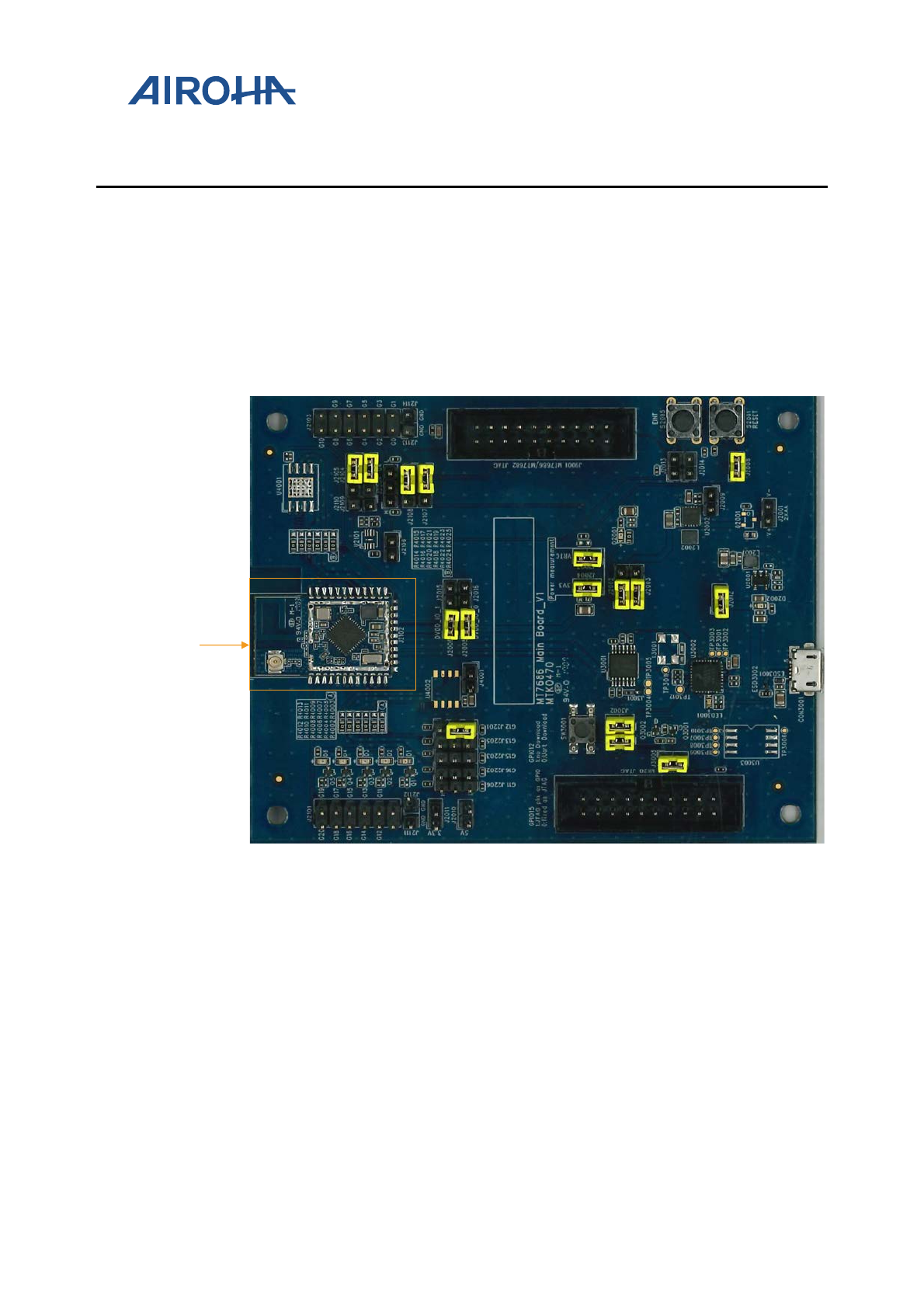
to rapidly implement a connected application. The system includes a main board and a MT7682 stamp module, as
shown in Figure 1.
This document provides design guidelines for a 4-layer PCB board of the MT7682 stamp module. MT7682 is simple
to layout the Quad Flat No-Lead (QFN) packaged devices. This document guides you to achieve high performance
results using the MT7682 with a custom design.
Figure 1. MT7682 HDK’s front view with the stamp module
MT7682
MT7682
Stamp
Module

MT7682 HDKs' Stamp Module Layout
Guide
© 2015 - 2017 Airoha Technology Corp.
Page 2 of 13
This document contains information that is proprietary to Airoha Technology Corp. (“Airoha”) and/or its licensor(s).
Any unauthorized use, reproduction or disclosure of this document in whole or in part is strictly prohibited.
2. PCB Specifications
2.1. PCB stack-up
The MT7682 stamp module has four different layers, as shown in a stack-up diagram (see Table 1). The developers
can alter the stack-up layers based on their requirements, but the impedance of 50Ω lines should be recalculated.
See section 2.2, ”PCB design rules”, for more details on impedance control. Having the L1-L2 distance reduced
helps improve the grounding and the RF decoupling.
Table 1. The stack-up diagram of the MT7682 stamp module
Top side solder mask 1.00 mils
L1 TOP Differential and Signal Copper and
plating
1.70 mils
Prepreg 5.90 mils
L2 GND copper 1.25 mils
core 20.00 mils
L3 VCC copper 1.25 mils
Prepreg 5.90 mils
L4 Bottom Differential and Signal copper 1.70 mils
Bottom side solder mask 1.00 mils
TOTAL 39.70 mils
1.01 mm
Total thickness: 1.0mm (
±
10%)
Note, it is recommended to keep the L1-L2 distance the same as the suggested value (see Table 1).
2.2. PCB design rules
This section provides the PCB design rules for MT7682 stamp module (see Table 2).
Table 2. PCB design rules
Parameter Value Comments
Number of layers 4
Thickness 1.0 mm (±10%) For greater thickness increase the
distance between L2 and L3.
Size of PCB 20.5mm x 33mm
Solder mask Blue Can be replaced with any color.
Dielectric FR4
Silk White Can be replaced with any color.
Minimum track width 5 mils Minimum track width can be reduced
but the cost would be higher.
MT7682 HDKs' Stamp Module Layout
Guide
© 2015 - 2017 Airoha Technology Corp.
Page 3 of 13
This document contains information that is proprietary to Airoha Technology Corp. (“Airoha”) and/or its licensor(s).
Any unauthorized use, reproduction or disclosure of this document in whole or in part is strictly prohibited.
Parameter Value Comments
Minimum spacing 5 mils Minimum spacing can be reduced but
the cost would be higher.
Middle drill diameter 8 mils
Copper thickness 1 oz
Lead free / Restriction of
Hazardous Substances (ROHS)
Yes
Impedance control Yes • 50Ω controlled impedance trace of
8 mils width on L1 with respect to
L2 (GND).
• Air gap = 5mils
Note, the above calculations are based
on coplanar waveguide (CPW) not the
microstrip.
2.3. Layers
The 4-layer PCB is used with the configuration, as shown in Table 3.
Table 3. Layer description
Layer Usage Notes
1 Signal and RF RF trace is a CPW on L1 with respect to
L2 ground.
2 GND Reference plane for RF.
3 Power and Signal
4 Power and Signal
MT7682 HDKs' Stamp Module Layout
Guide
© 2015 - 2017 Airoha Technology Corp.
Page 4 of 13
This document contains information that is proprietary to Airoha Technology Corp. (“Airoha”) and/or its licensor(s).
Any unauthorized use, reproduction or disclosure of this document in whole or in part is strictly prohibited.
3. Layout
3.1. Component placement
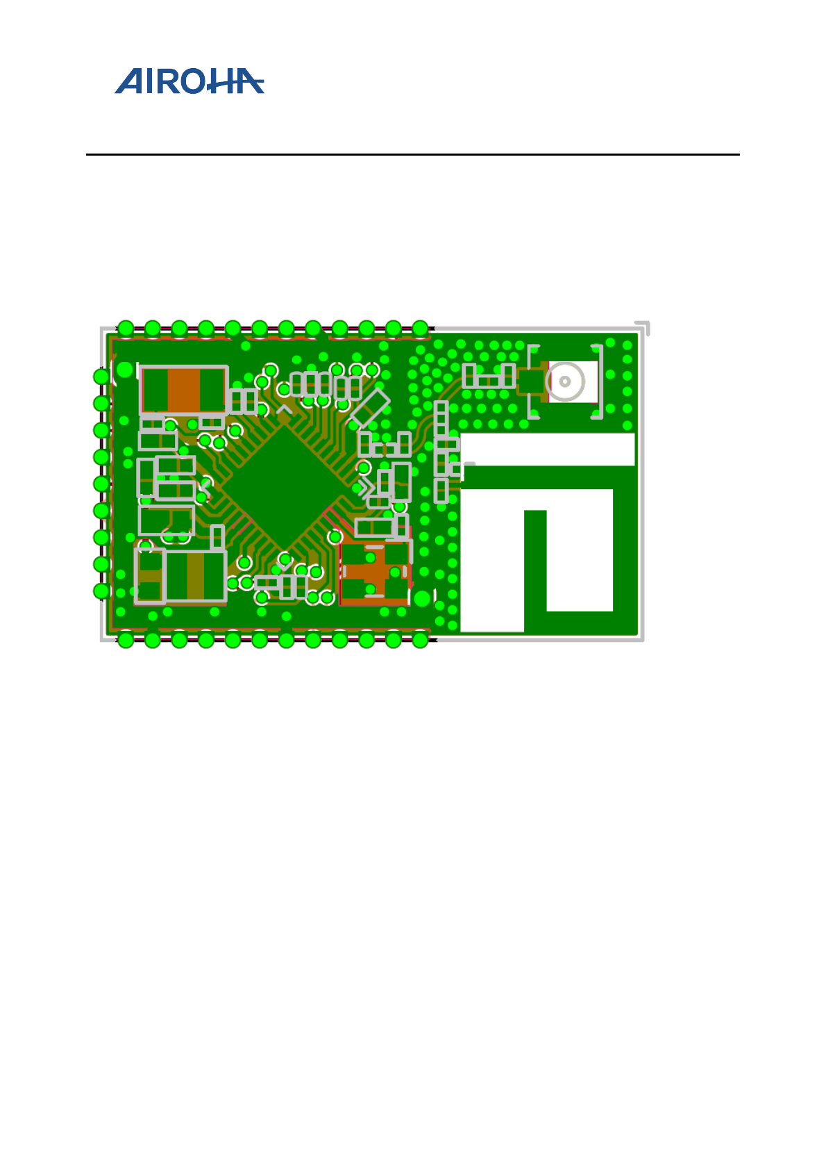
The component placement on the MT7682 stamp module is provided in Figure 2. This placement provides
optimum device performance. Great care has to be given to the power inductor to ensure reduced emissions and
optimum error vector magnitude (EVM) and mass performance. The power inductor should be placed very close to
the device and the power trace should be minimized. MT7682 is sensitive to the layout of the DC-DC converter and
it can affect the performance of the device.
Figure 2. MT7682 stamp module placement diagram
3.2. 4 Layer PCB design
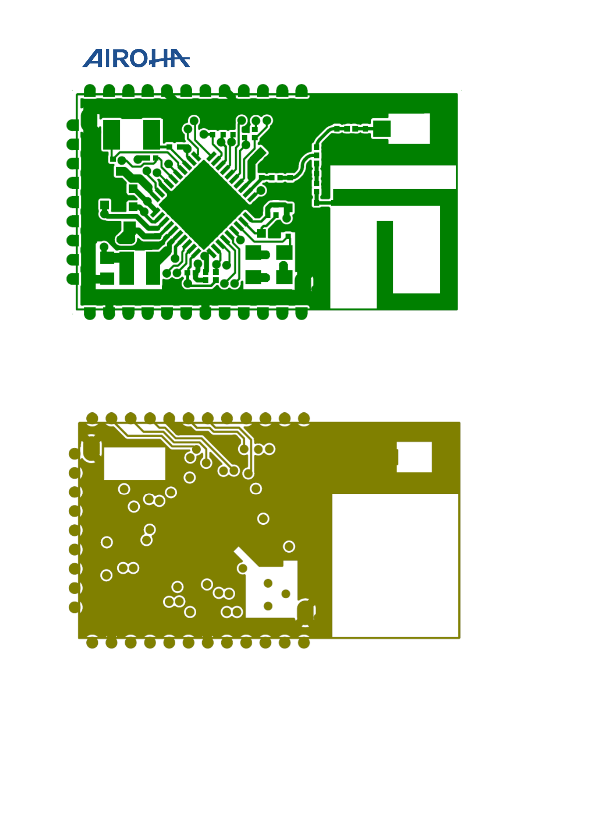
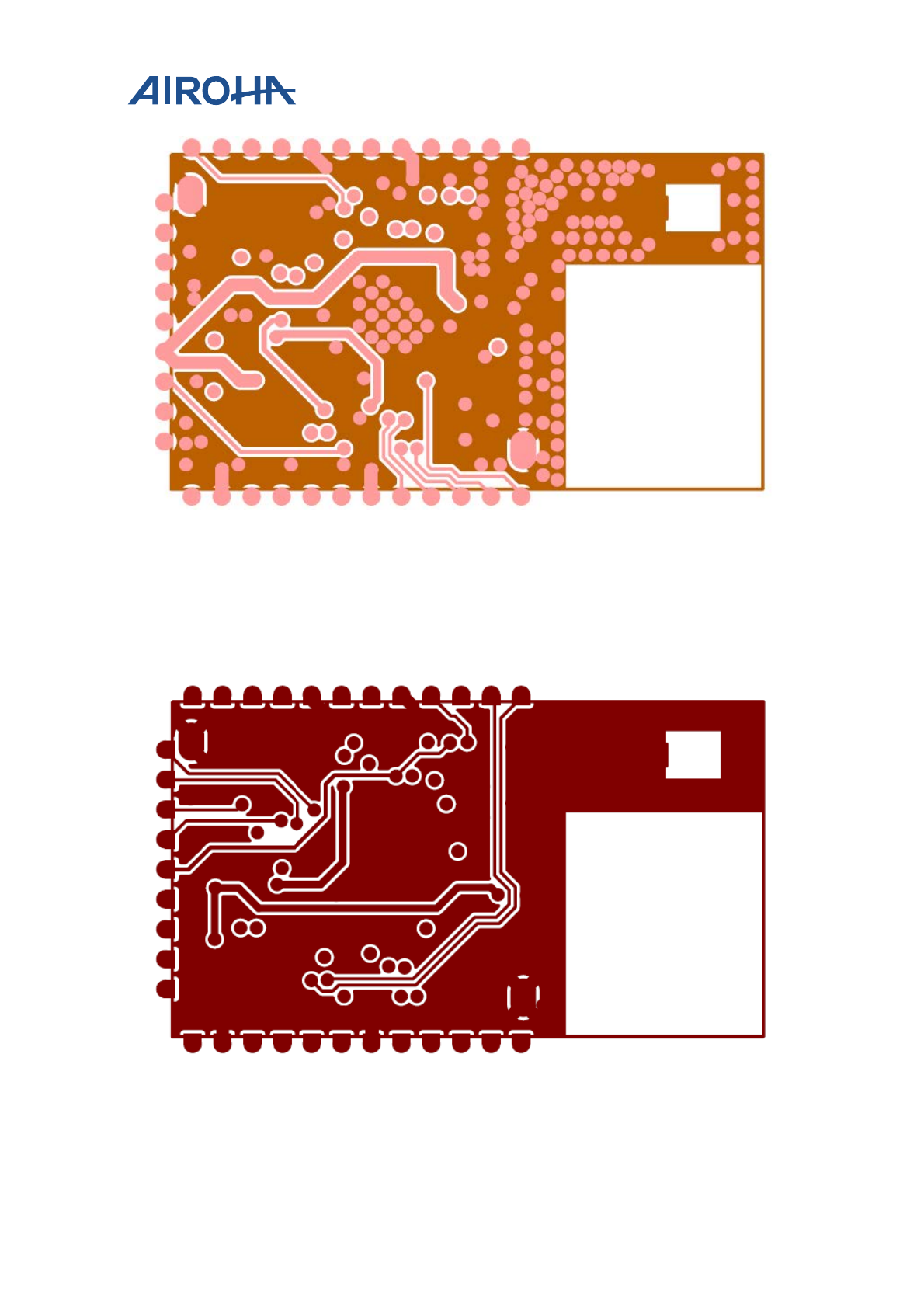
3.2.1. Layer 1
Most of the routing is performed on Layer 1 to avoid power vias on the board (see Figure 3). The trace widths are
maximized for high current pins and minimized for signal pins.
MT7682 HDKs' Stamp Module Layout
Guide
© 2015 - 2017 Airoha Technology Corp.
Page 5 of 13
This document contains information that is proprietary to Airoha Technology Corp. (“Airoha”) and/or its licensor(s).
Any unauthorized use, reproduction or disclosure of this document in whole or in part is strictly prohibited.
Figure 3. Layer 1
3.2.2. Layer 2
Layer 2 is the primary ground plane for the board reference. It has a void for the antenna section based on the
antenna guidelines (see Figure 4).
Figure 4. Layer 2
3.2.3. Layer 3
Layer 3 is used to route the power lines to the device (see Figure 5). The width of the power traces is necessary for
the main input supply to the device, see section 4.2, “Power section”.
MT7682 HDKs' Stamp Module Layout
Guide
© 2015 - 2017 Airoha Technology Corp.
Page 6 of 13
This document contains information that is proprietary to Airoha Technology Corp. (“Airoha”) and/or its licensor(s).
Any unauthorized use, reproduction or disclosure of this document in whole or in part is strictly prohibited.
Figure 5. Layer 3
3.2.4. Layer 4
Layer 4 is used for routing the power and the signal lines on the board. It is also the main power dissipation ground
(GND) layer for the QFN package (see Figure 6). The bottom GND plane has to be maximized for the best thermal
performance.
Figure 6. Layer 4
MT7682 HDKs' Stamp Module Layout
Guide
© 2015 - 2017 Airoha Technology Corp.
Page 7 of 13
This document contains information that is proprietary to Airoha Technology Corp. (“Airoha”) and/or its licensor(s).
Any unauthorized use, reproduction or disclosure of this document in whole or in part is strictly prohibited.
4. Layout Guidelines
4.1. RF section
It is essential to provide a correct layout for the RF section (see Figure 7) for the wireless device in order to achieve
optimum device performance. A poor layout can cause performance degradation for the output power, EVM,
harmonic emission, sensitivity and spectral mask.
Figure 7. RF section
4.1.1. RF component placement and routing
The LC filter is used on the board to perform the important function of attenuating the out-of-band emissions from
the device, as shown in Figure 8. Reserve LC filter to optimize transmit and receive performance. The component
placement and routing also effect the performance of wireless transmit and receive operations.
Antenna
matching
LC filter
U.FL
Connector
PCB
Antenna
Connector
matching
MT7682 HDKs' Stamp Module Layout
Guide
© 2015 - 2017 Airoha Technology Corp.
Page 8 of 13
This document contains information that is proprietary to Airoha Technology Corp. (“Airoha”) and/or its licensor(s).
Any unauthorized use, reproduction or disclosure of this document in whole or in part is strictly prohibited.
Figure 8. RF component placement and routing
Apply the following RF component placement and routing guidelines.
1) Place LC matching network close to the MT7682 pin out. Route the RF lines using a CPW with ground
structure.
2) Use via stitching along the RF trace to reduce emissions and keep the fields confined within the trace
boundary.
3) Use an impedance of 50Ω only with a tolerance of 10%. Use the stack-up and the trace width provided for
reference see section 2.2, “PCB design rules”.
4) In case a conducted test is required on the PCB, it is recommended to add a U.FL connector, as shown in
Figure 7.
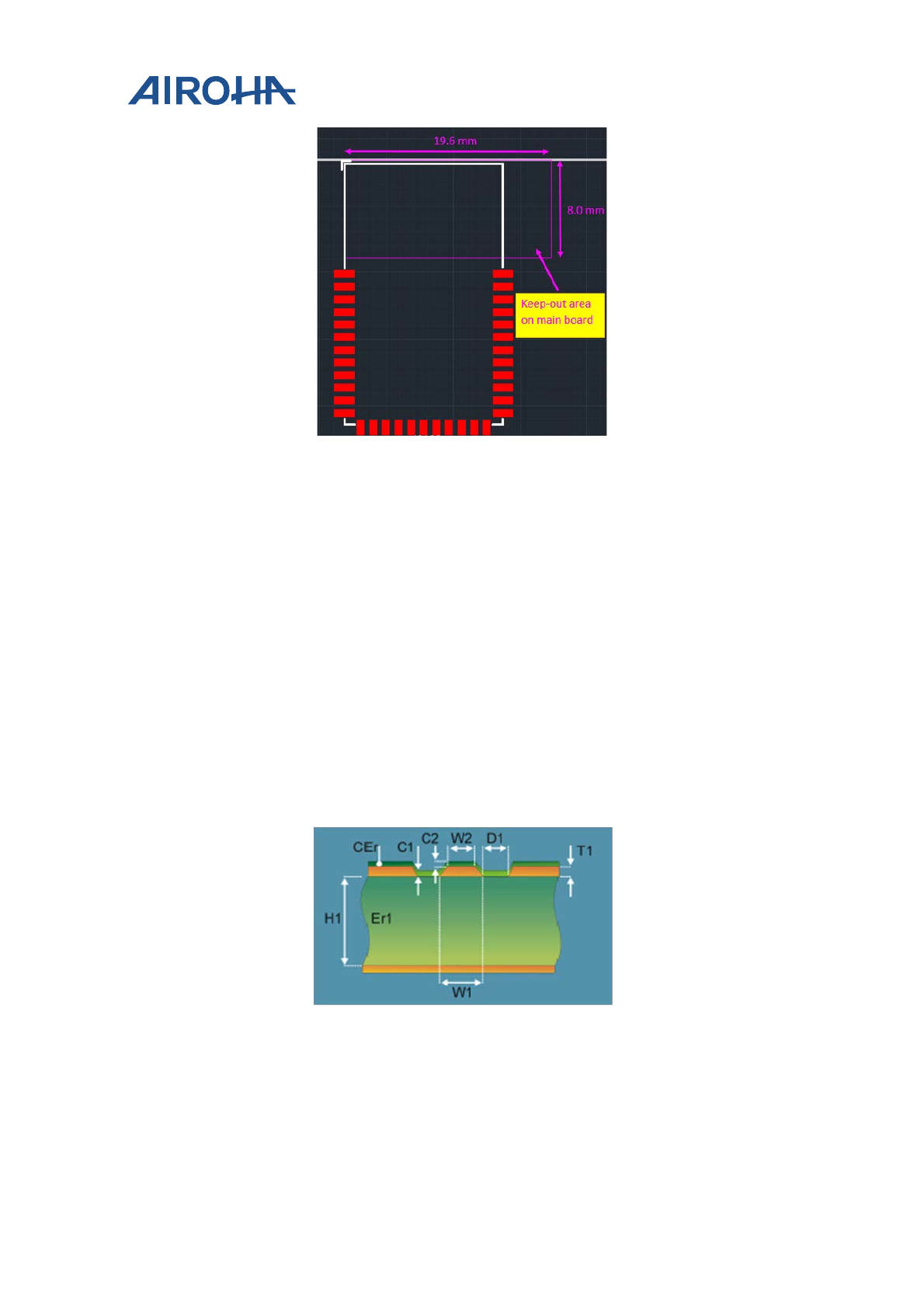
4.1.2. Antenna placement and routing
The antenna is an element used to convert the guided waves on the PCB traces to the free-space electromagnetic
radiation. The placement and layout of the antenna is the key to increase in range and data rates. MT7682 module
is designed with a stamp module and a PCB antenna. In order to optimize the antenna performance, it needs to
mount the stamp module on a main board, as shown in Figure 9.
LC filter
MT7682 HDKs' Stamp Module Layout
Guide
© 2015 - 2017 Airoha Technology Corp.
Page 9 of 13
This document contains information that is proprietary to Airoha Technology Corp. (“Airoha”) and/or its licensor(s).
Any unauthorized use, reproduction or disclosure of this document in whole or in part is strictly prohibited.
Figure 9. Stamp module located on the main board
Apply the following guidelines for the antenna placement.
1) Place the PCB antenna on an intermediate edge of the PCB.
2) Ensure that no signals are routed across the antenna elements on all the layers of the PCB.
3) The antenna requires ground clearance on all layers of the PCB. Ensure that the ground is cleared on inner
layers as well.
4) Ensure that there is provision to place matching components for the antenna. These need to be tuned for
the best return loss once the complete board is assembled. Any plastics or casing should also be mounted
while tuning the antenna as this can affect the impedance.
5) Ensure that the antenna impedance is 50Ω as the device is rated to work only with a 50Ω system.
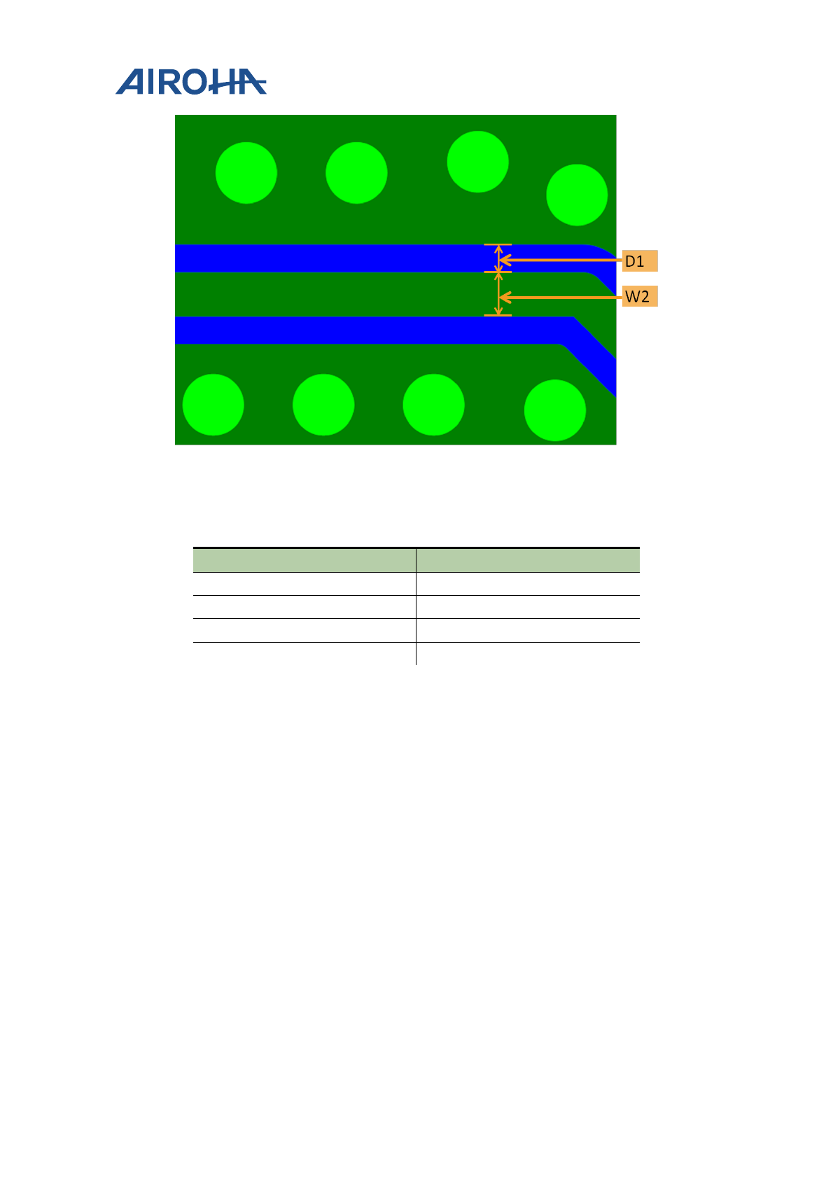
4.1.3. Transmission line
The RF signal from the chip output is routed to the antenna using a CPW with ground structure. This structure
offers the best possible shielding to the RF lines, as shown in Figure 10. In addition to the ground on the Layer 1,
placing GND vias along the RF trace provides additional shielding.
Figure 10. CPW with ground
MT7682 HDKs' Stamp Module Layout
Guide
© 2015 - 2017 Airoha Technology Corp.
Page 10 of 13
This document contains information that is proprietary to Airoha Technology Corp. (“Airoha”) and/or its licensor(s).
Any unauthorized use, reproduction or disclosure of this document in whole or in part is strictly prohibited.
Figure 11. CPW with ground top view
The recommended values for the PCB (see Figure 10 and Figure 11) are provided in Table 4.
Table 4. Recommended values for the PCB
Parameter Value (mils)
W2 8
D1 5
H1 5.9
Er1 3.66
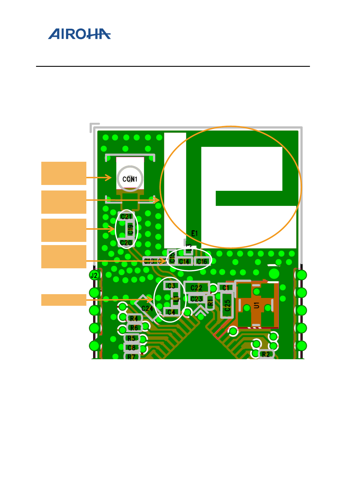
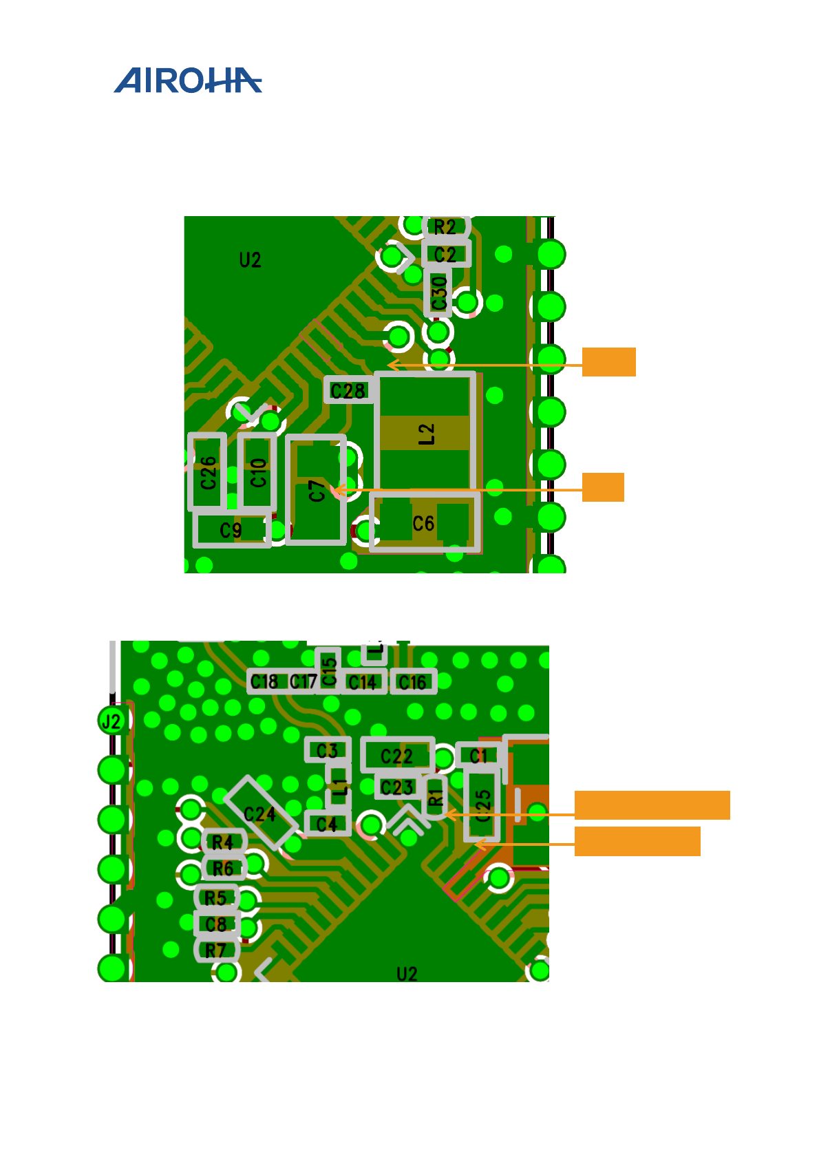
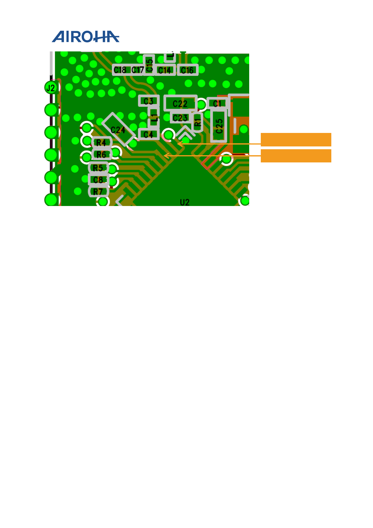
4.2. Power section
This section provides detailed description to design a power efficient device. The details on net or pin locations are
shown in Figure 12, Figure 13 and Figure 14.
1) Make the buck inductor trace loop as short as possible.
2) The de-cap routing has to be in a correct order.
3) The LXBK (net of Buck output) trace width should be 30mil (recommended) not less than 9mil because of
the large current flow. LXBK trace width that is close to IC should be no less than 9mil.
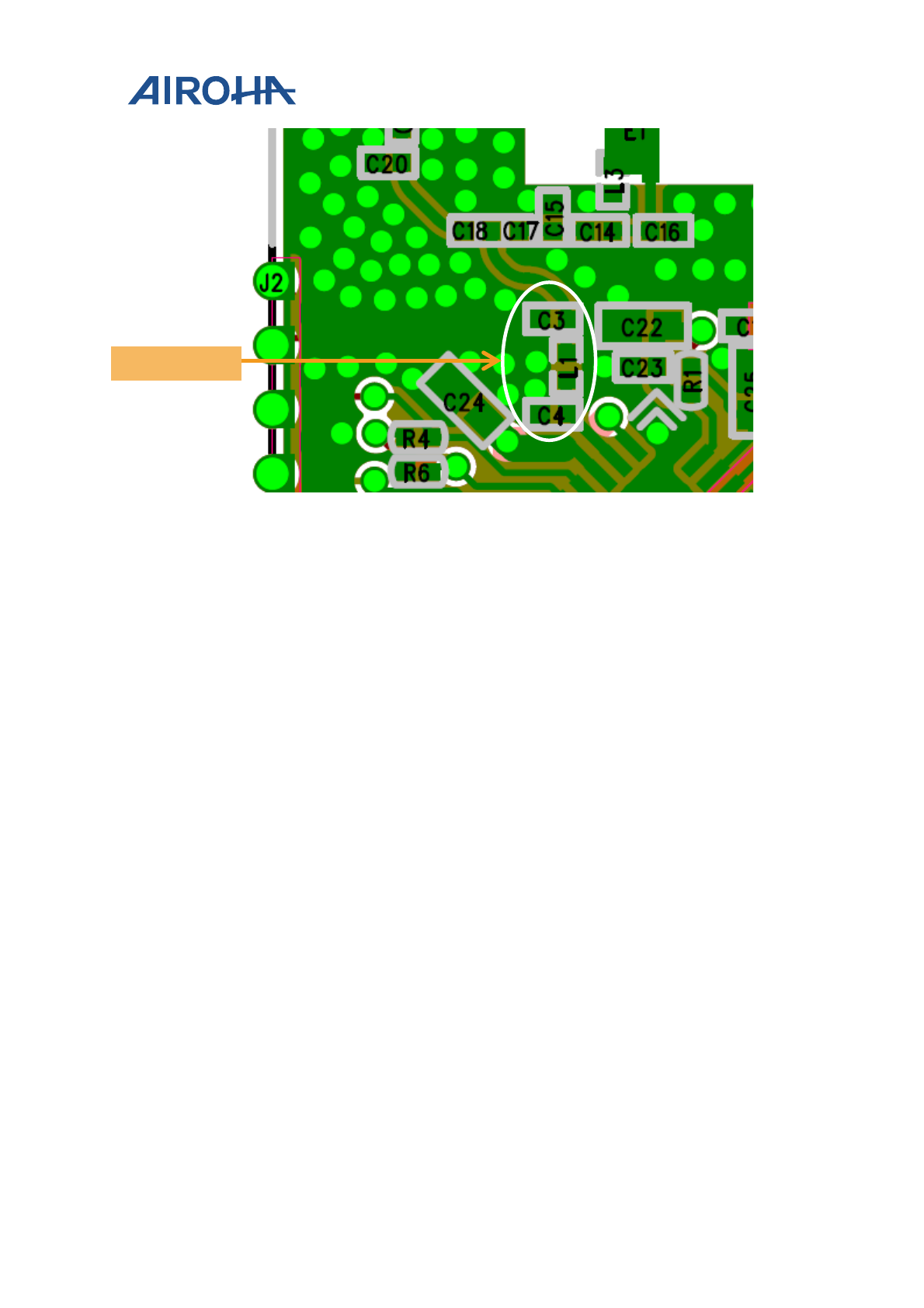
4) Place C7 close to MT7682 as close as possible (see Figure 12).
5) Place C25 close to MT7682.
6) MT7682 power input pins' decouple capacitors should be placed as close as possible.
• AVDD15_WF0_TRX, AVDD15_XO (see Figure 13).
• AVDD33_WF0_G_TX, AVDD33_WF0_G_PA (see Figure 14).
7) There are many high current input pins on the MT7682. Ensure the trace feeding these pins is capable of
handling the below currents.
MT7682 HDKs' Stamp Module Layout
Guide
© 2015 - 2017 Airoha Technology Corp.
Page 11 of 13
This document contains information that is proprietary to Airoha Technology Corp. (“Airoha”) and/or its licensor(s).
Any unauthorized use, reproduction or disclosure of this document in whole or in part is strictly prohibited.
• AVDD33_WF0_G_PA input : Max 500mA
• LXBK switching node : Max 600 mA
• AVDD33_BUCK input : Max 300 mA
• AVDD15_CLDO input : Max 300mA
Figure 12. Placement and routing example of LXBK and C7
Figure 13. Placement and routing example of AVDD15
LXBK
C7
AVDD15_XO
AVDD15_WF0_TRX
MT7682 HDKs' Stamp Module Layout
Guide
© 2015 - 2017 Airoha Technology Corp.
Page 12 of 13
This document contains information that is proprietary to Airoha Technology Corp. (“Airoha”) and/or its licensor(s).
Any unauthorized use, reproduction or disclosure of this document in whole or in part is strictly prohibited.
Figure 14. Placement and routing of AVDD33_WF0_G_PA and AVDD33_WF0_G_TX
4.3. Clock section
4.3.1. 26MHz XTAL
26MHz XTAL should be placed closer to the QFN package. The frequency tolerance for the XTAL across
temperature with aging should be ± 20ppm. In addition, ensure no high frequency lines are routed closer to the
XTAL routing to avoid any phase noise degradation.
4.3.2. 32.768kHz XTAL
32.768kHz XTAL should be placed closer to the QFN package. Ensure the load capacitance is tuned based on board
parasitic, so that the frequency tolerance is within ± 150ppm.
4.4. Digital I/O
Route serial peripheral interface (SPI) and universal asynchronous receiver/transmitter (UART) lines away from any
RF traces since these digital I/O lines are high frequency lines and can cause interference to the RF signal.
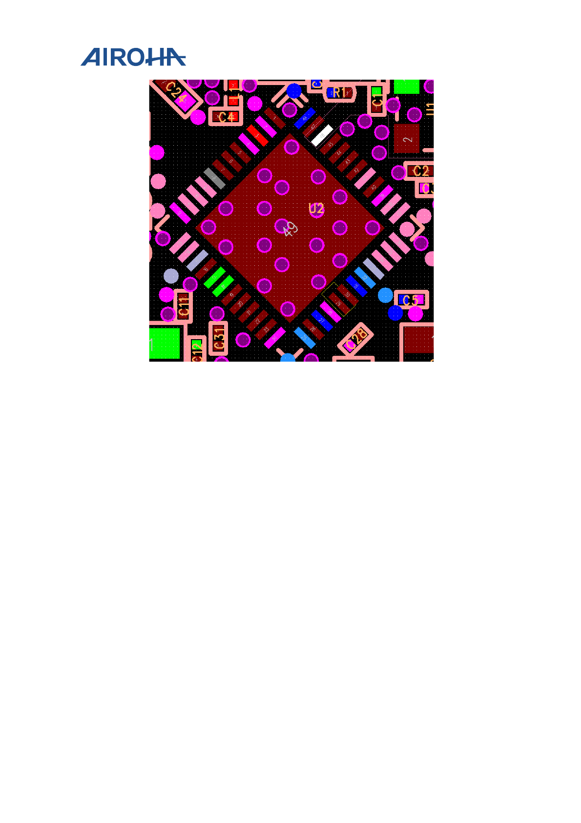
4.5. QFN Ground
Make sure QFN 5x5 ground vias are placed on the ground pad for optimum thermal dissipation, as shown in Figure
15.
AVDD33_WF0_G_PA
AVDD33_WF0_G_TX
MT7682 HDKs' Stamp Module Layout
Guide
© 2015 - 2017 Airoha Technology Corp.
Page 13 of 13
This document contains information that is proprietary to Airoha Technology Corp. (“Airoha”) and/or its licensor(s).
Any unauthorized use, reproduction or disclosure of this document in whole or in part is strictly prohibited.
Figure 15. QFN 5x5 ground vias on the ground pad
