MT7686 Reference Manual
MT7686_Reference_Manual
MT7686_Reference_Manual
MT7686_Reference_Manual
MT7686_Reference_Manual
MT7686_Reference_Manual
User Manual:
Open the PDF directly: View PDF ![]() .
.
Page Count: 544 [warning: Documents this large are best viewed by clicking the View PDF Link!]
- 1. Documentation General Conventions
- 2. Bus Architecture and Memory Map
- 3. External Interrupt Controller
- 4. Direct Memory Access
- 5. Universal Asynchronous Receiver/Transmitter
- 6. Serial Peripheral Interface Master Controller
- 7. Serial Peripheral Interface Slave Controller
- 8. Inter-Integrated Circuit Controller
- 9. SD/SDIO Card Controller
- 10. I2S0
- 11. I2S1
- 12. I2S0 and I2S1 Audio PLL Settings
- 13. SDIO
- 14. General Purpose Timer
- 15. Pulse Width Modulation
- 16. Cortex-M4 L1 Cache Controller
- 17. Auxiliary ADC Unit
- 18. Reset Generation Unit
- 19. True Random Number Generator
- 20. Real Time Clock (RTC)
- 21. General Purpose Inputs/Outputs
- 22. Clock Configuration

MT7686 Reference Manual
Version: 1.1
Release date: 16 August 2017
© 2016 - 2017 MediaTek Inc.
This document contains information that is proprietary to MediaTek Inc. (“MediaTek”) and/or its licensor(s). MediaTek cannot grant you
permission for any material that is owned by third parties. You may only use or reproduce this document if you have agreed to and been
bound by the applicable license agreement with MediaTek (“License Agreement”) and been granted explicit permission within the License
Agreement (“Permitted User”). If you are not a Permitted User, please cease any access or use of this document immediately. Any
unauthorized use, reproduction or disclosure of this document in whole or in part is strictly prohibited. THIS DOCUMENT IS PROVIDED ON AN
“AS-IS” BASIS ONLY. MEDIATEK EXPRESSLY DISCLAIMS ANY AND ALL WARRANTIES OF ANY KIND AND SHALL IN NO EVENT BE LIABLE FOR ANY
CLAIMS RELATING TO OR ARISING OUT OF THIS DOCUMENT OR ANY USE OR INABILITY TO USE THEREOF. Specifications contained herein are
subject to change without notice.

MT7686 Reference Manual
© 2016 - 2017 MediaTek Inc.
Page i of vii
This document contains information that is proprietary to MediaTek Inc. (“MediaTek”) and/or its licensor(s).
Any unauthorized use, reproduction or disclosure of this document in whole or in part is strictly prohibited.
Document Revision History
Revision Date Description
1.0 30 June 2017 Initial draft
1.1 16 August 2017 Modified section 5.5

MT7686 Reference Manual
© 2016 - 2017 MediaTek Inc.
Page ii of vii
This document contains information that is proprietary to MediaTek Inc. (“MediaTek”) and/or its licensor(s).
Any unauthorized use, reproduction or disclosure of this document in whole or in part is strictly prohibited.
Table of Contents
1. Documentation General Conventions .................................................................................................... 1
1.1. Abbreviations for control modules ..................................................................................................... 1
1.2. Abbreviations for registers ................................................................................................................. 2
2. Bus Architecture and Memory Map ....................................................................................................... 3
3. External Interrupt Controller ................................................................................................................. 7
3.1. Overview ............................................................................................................................................. 7
3.2. Features .............................................................................................................................................. 7
3.3. Block diagram ..................................................................................................................................... 7
3.4. Wakeup event management .............................................................................................................. 7
3.5. Functions ............................................................................................................................................ 8
3.6. External interrupt or event line mapping ........................................................................................... 9
3.7. Register mapping .............................................................................................................................. 10
4. Direct Memory Access .......................................................................................................................... 20
4.1. Overview ........................................................................................................................................... 20
4.2. Features ............................................................................................................................................ 20
4.3. Functions .......................................................................................................................................... 21
4.4. Application and programming sequence .......................................................................................... 23
4.5. Register mapping .............................................................................................................................. 24
5. Universal Asynchronous Receiver/Transmitter ..................................................................................... 52
5.1. Overview ........................................................................................................................................... 52
5.2. Features ............................................................................................................................................ 52
5.3. Block diagram ................................................................................................................................... 52
5.4. Functions .......................................................................................................................................... 53
5.5. Register mapping .............................................................................................................................. 55
6. Serial Peripheral Interface Master Controller ....................................................................................... 70
6.1. Features ............................................................................................................................................ 70
6.2. Block diagram ................................................................................................................................... 72
6.3. Functions .......................................................................................................................................... 72
6.4. Register mapping .............................................................................................................................. 74
7. Serial Peripheral Interface Slave Controller .......................................................................................... 83
7.1. Features ............................................................................................................................................ 83
7.2. Block diagram ................................................................................................................................... 85
7.3. Functions .......................................................................................................................................... 85
7.4. Register mapping .............................................................................................................................. 89
8. Inter-Integrated Circuit Controller ........................................................................................................ 98
8.1. Overview ........................................................................................................................................... 98
8.2. Features ............................................................................................................................................ 98
8.3. Block diagram ................................................................................................................................... 98
8.4. Functions .......................................................................................................................................... 99
8.5. Programming guide ........................................................................................................................ 101
8.6. Manual and DMA transfer modes for I2C controller ...................................................................... 102
8.7. Register mapping ............................................................................................................................ 102
9. SD/SDIO Card Controller ..................................................................................................................... 115
9.1. Overview ......................................................................................................................................... 115
9.2. Features .......................................................................................................................................... 115
9.3. Block diagram ................................................................................................................................. 116

MT7686 Reference Manual
© 2016 - 2017 MediaTek Inc.
Page iii of vii
This document contains information that is proprietary to MediaTek Inc. (“MediaTek”) and/or its licensor(s).
Any unauthorized use, reproduction or disclosure of this document in whole or in part is strictly prohibited.
9.4. Functions ........................................................................................................................................ 116
9.5. Programming sequence .................................................................................................................. 117
9.6. Register mapping ............................................................................................................................ 117
10. I2S0 ..................................................................................................................................................... 149
10.1. Overview ......................................................................................................................................... 149
10.2. IO interface ..................................................................................................................................... 149
10.3. I2S OUT and I2S IN .......................................................................................................................... 151
10.4. DL FIFO and UL FIFO ....................................................................................................................... 152
10.5. Data format of FIFO ........................................................................................................................ 152
10.6. Programming guide ........................................................................................................................ 153
10.7. Register mapping ............................................................................................................................ 156
11. I2S1 ..................................................................................................................................................... 164
11.1. Overview ......................................................................................................................................... 164
11.2. IO interface ..................................................................................................................................... 164
11.3. I2S OUT and I2S IN .......................................................................................................................... 165
11.4. DL FIFO and UL FIFO ....................................................................................................................... 166
11.5. Data format of FIFO ........................................................................................................................ 166
11.6. Programming guide ........................................................................................................................ 167
11.7. Register mapping ............................................................................................................................ 169
12. I2S0 and I2S1 Audio PLL Settings ......................................................................................................... 180
12.1. XPLL block diagram ......................................................................................................................... 180
12.2. Fractional-N PLL power on sequence ............................................................................................. 180
12.3. XPLL frequency setting (Integer) .................................................................................................... 181
12.4. DDS PCW setting ............................................................................................................................. 182
12.5. XPLL frequency change sequence ................................................................................................... 182
12.6. XPLL turn on programming sequence............................................................................................. 182
12.7. XPLL turn off programming sequence ............................................................................................ 186
13. SDIO ................................................................................................................................................... 187
13.1. Overview ......................................................................................................................................... 187
13.2. Features .......................................................................................................................................... 187
13.3. Block diagram ................................................................................................................................. 188
13.4. Functions ........................................................................................................................................ 188
13.5. Register mapping ............................................................................................................................ 191
14. General Purpose Timer ....................................................................................................................... 331
14.1. Overview ......................................................................................................................................... 331
14.2. Features .......................................................................................................................................... 331
14.3. Limitations ...................................................................................................................................... 331
14.4. Block diagram ................................................................................................................................. 332
14.5. Functions ........................................................................................................................................ 332
14.6. Programming sequence .................................................................................................................. 332
14.7. Register mapping ............................................................................................................................ 333
15. Pulse Width Modulation ..................................................................................................................... 354
15.1. Overview ......................................................................................................................................... 354
15.2. Features .......................................................................................................................................... 354
15.3. Block diagram ................................................................................................................................. 354
15.4. Functions ........................................................................................................................................ 355
15.5. Register mapping ............................................................................................................................ 356
16. Cortex-M4 L1 Cache Controller ........................................................................................................... 359
16.1. Overview ......................................................................................................................................... 359
16.2. Cache optimization ......................................................................................................................... 361
16.3. Register mapping ............................................................................................................................ 366

MT7686 Reference Manual
© 2016 - 2017 MediaTek Inc.
Page iv of vii
This document contains information that is proprietary to MediaTek Inc. (“MediaTek”) and/or its licensor(s).
Any unauthorized use, reproduction or disclosure of this document in whole or in part is strictly prohibited.
16.4. Cacheable region controller ........................................................................................................... 372
16.5. Remapping ...................................................................................................................................... 375
17. Auxiliary ADC Unit .............................................................................................................................. 379
17.1. Features .......................................................................................................................................... 379
17.2. Block diagram ................................................................................................................................. 379
17.3. Functions ........................................................................................................................................ 380
17.4. Programming sequence .................................................................................................................. 380
17.5. Register mapping ............................................................................................................................ 382
18. Reset Generation Unit ........................................................................................................................ 386
18.1. Features .......................................................................................................................................... 386
18.2. Block diagram ................................................................................................................................. 386
18.3. WDT timeout and interval source .................................................................................................. 386
18.4. Register mapping ............................................................................................................................ 387
19. True Random Number Generator ....................................................................................................... 398
19.1. Overview ......................................................................................................................................... 398
19.2. Features .......................................................................................................................................... 398
19.3. Block diagram ................................................................................................................................. 398
19.4. Function description ....................................................................................................................... 399
19.5. Programming sequence .................................................................................................................. 400
19.6. Register mapping ............................................................................................................................ 401
20. Real Time Clock (RTC) ......................................................................................................................... 405
20.1. Features .......................................................................................................................................... 405
20.2. Block diagram ................................................................................................................................. 405
20.3. Functions ........................................................................................................................................ 406
20.4. Programming sequence .................................................................................................................. 406
20.5. Register mapping ............................................................................................................................ 406
21. General Purpose Inputs/Outputs ........................................................................................................ 417
21.1. Overview ......................................................................................................................................... 417
21.2. IO pull up or down control truth table ........................................................................................... 417
21.3. Register mapping ............................................................................................................................ 419
22. Clock Configuration ............................................................................................................................ 482
22.1. Clock configuration programming guide ........................................................................................ 482
22.2. Register mapping ............................................................................................................................ 488

MT7686 Reference Manual
© 2016 - 2017 MediaTek Inc.
Page v of vii
This document contains information that is proprietary to MediaTek Inc. (“MediaTek”) and/or its licensor(s).
Any unauthorized use, reproduction or disclosure of this document in whole or in part is strictly prohibited.
Lists of Tables and Figures
Table 2.1-1. MT7686 bus connection ...................................................................................................................... 3
Table 2.1-2. Top view memory map ....................................................................................................................... 3
Table 2.1-3. Always-on domain peripherals ........................................................................................................... 4
Table 2.1-4. Power-down domain peripherals ........................................................................................................ 5
Table 3.6-1. External interrupt sources................................................................................................................... 9
Table 4.4-1. Virtual FIFO access ports ................................................................................................................... 23
Table 5.5-1. SPI master controller interface ......................................................................................................... 70
Table 6.4-1. SPI slave controller interface ............................................................................................................ 83
Table 7.3-1. SPI slave controller interface ............................................................................................................ 85
Table 7.3-2. SPI slave status description (use RS command to poll SPI slave status) ........................................... 87
Table 9.4-1. Sharing of pins for SD memory card controller ............................................................................... 116
Table 9.6-1. MSDC register definition ................................................................................................................. 117
Table 10.2-1. I2S mode interface – master mode ............................................................................................... 149
Table 10.2-2. I2S mode interface – slave mode .................................................................................................. 150
Table 10.2-3. TDM mode interface – master mode ............................................................................................ 150
Table 10.2-4. TDM mode interface – slave mode ............................................................................................... 150
Table 10.2-5. Relationship between MCLK and sample rate .............................................................................. 150
Table 10.3-1. Down rate example for slave mode .............................................................................................. 151
Table 10.5-1. 16bits I2S data format of FIFO ..................................................................................................... 152
Table 10.5-2. 16bits TDM 4 channel data format of FIFO .................................................................................. 152
Table 11.2-1. I2S mode interface – master mode ............................................................................................... 164
Table 11.2-2. I2S mode interface – slave mode .................................................................................................. 165
Table 11.2-3. Relationship between MCLK and sample rate .............................................................................. 165
Table 11.5-1. 16bits I2S data format of FIFO ...................................................................................................... 166
Table 11.5-2. 24bits I2S data format of FIFO ...................................................................................................... 167
Table 13.4-1. SDIO pin definitions ....................................................................................................................... 188
Table 13.4-2. Bus signal voltage .......................................................................................................................... 189
Table 13.4-3. Bus timing parameter values (default) .......................................................................................... 190
Table 13.4-4. High-speed timing parameter values ............................................................................................ 191
Table 14.5-1. GPT operation modes ................................................................................................................... 332
Table 16.1-1. TCM address spaces for different cache size settings ................................................................... 360
Table 16.2-1. Write-back mode cache read or write operations ........................................................................ 365
Table 16.2-2. Write-through mode cache R/W action summary ........................................................................ 366
Table 16.4-1. Cacheable attribute bit encoding .................................................................................................. 373
Table 16.5-1. Region size and bit encoding ......................................................................................................... 377
Table 17.3-1. AUXADC channel description ........................................................................................................ 380
Table 22.1-1. Clock switch ................................................................................................................................... 483
Table 22.1-2. Relationship between XO_PDN_COND0 bit number and configuration register ......................... 484
Table 22.1-3. Clock multiplexer switch method of HF_FSYS_CK ......................................................................... 485
Table 22.1-4. Relationship between PDN_COND0 bit number and configuration register ................................ 485

MT7686 Reference Manual
© 2016 - 2017 MediaTek Inc.
Page vi of vii
This document contains information that is proprietary to MediaTek Inc. (“MediaTek”) and/or its licensor(s).
Any unauthorized use, reproduction or disclosure of this document in whole or in part is strictly prohibited.
Table 22.1-5. Clock multiplexer switch method of HF_FSFC_CK ........................................................................ 486
Table 22.1-6. Clock multiplexer switch method of F_FSDIOMST_CK .................................................................. 486
Table 22.1-7. Clock multiplexer switch method of F_FSDIOMST_CK .................................................................. 487
Table 22.1-8. Clock multiplexer switch method of F_FSDIOMST_CK .................................................................. 487
Table 22.1-9. Clock multiplexer switch method of F_FSDIOMST_CK .................................................................. 488
Figure 3.3-1. EINT block diagram ............................................................................................................................ 7
Figure 4.1-1. Variety data paths of DMA transfers ............................................................................................... 20
Figure 4.2-1. DMA block diagram .......................................................................................................................... 21
Figure 4.3-1. Ring buffer and double buffer memory data movement ................................................................ 22
Figure 4.3-2. Unaligned word accesses ................................................................................................................. 22
Figure 4.3-3. Virtual FIFO DMA ............................................................................................................................. 23
Figure 5.3-1. UART block diagram ......................................................................................................................... 53
Figure 5.4-1. UART data format ............................................................................................................................ 54
Figure 5.5-1. Pin connection between SPI master and SPI slave .......................................................................... 70
Figure 6.1-1. SPI transmission formats ................................................................................................................. 71
Figure 6.1-2. Operation flow with or without PAUSE mode ................................................................................. 71
Figure 6.1-3. CS de-assert mode ........................................................................................................................... 71
Figure 6.1-4. SPI master controller delay sample ................................................................................................. 72
Figure 6.2-1. Block diagram of SPI master controller ............................................................................................ 72
Figure 6.3-1. SPI master single mode .................................................................................................................... 73
Figure 6.3-2. SPI master dual mode write data ..................................................................................................... 73
Figure 6.3-3. SPI master dual mode read data ...................................................................................................... 73
Figure 6.3-4. SPI master quad mode write data ................................................................................................... 73
Figure 6.3-5. SPI master quad mode read data..................................................................................................... 74
Figure 6.4-1. Pin connection between SPI master and SPI slave .......................................................................... 83
Figure 7.1-1. SPI transmission formats ................................................................................................................. 84
Figure 7.1-2. SPI slave controller early transmit ................................................................................................... 84
Figure 7.2-1. Block diagram of SPI slave controller ............................................................................................... 85
Figure 7.3-1. SPI slave controller commands waveform ....................................................................................... 86
Figure 7.3-2. Config read/write (CR/CW) command format ................................................................................. 86
Figure 7.3-3. SPI slave control flow diagram ......................................................................................................... 87
Figure 7.3-4. SPI slave single mode write data ..................................................................................................... 88
Figure 7.3-5. SPI slave single mode read data ....................................................................................................... 88
Figure 7.3-6. SPI slave dual mode write data ........................................................................................................ 88
Figure 7.3-7. SPI slave dual mode read data ......................................................................................................... 88
Figure 7.3-8. SPI slave quad mode write data ....................................................................................................... 89
Figure 7.3-9. SPI slave quad mode read data ........................................................................................................ 89
Figure 8.3-1. I2C block diagram............................................................................................................................. 99
Figure 8.4-1. I2C single transfer single byte access ............................................................................................... 99
Figure 8.4-2. I2C single transfer multi byte access .............................................................................................. 100
Figure 8.4-3. I2C multi transfer multi byte access .............................................................................................. 100
Figure 8.4-4. I2C multi transfer multi byte access with RS.................................................................................. 100
Figure 8.4-5. I2C multi transfer multi byte access with direction-change function ............................................ 101

MT7686 Reference Manual
© 2016 - 2017 MediaTek Inc.
Page vii of vii
This document contains information that is proprietary to MediaTek Inc. (“MediaTek”) and/or its licensor(s).
Any unauthorized use, reproduction or disclosure of this document in whole or in part is strictly prohibited.
Figure 8.5-1. I2C transfer format programming guide ........................................................................................ 101
Figure 8.5-2. I2C timing format programming guide .......................................................................................... 102
Figure 9.3-1. MSDC block diagram ...................................................................................................................... 116
Figure 10.1-1. I2S block diagram ......................................................................................................................... 149
Figure 10.3-1. I2S protocol waveform ................................................................................................................. 151
Figure 10.3-2. Sample m of TDM32 with nT delay .............................................................................................. 151
Figure 10.3-3. Sample m of TDM32 with nT delay and bclk inverse ................................................................... 152
Figure 10.3-4. Sample m of TDM64 with nT delay .............................................................................................. 152
Figure 11.1-1. I2S block diagram ......................................................................................................................... 164
Figure 11.3-1. I2S protocol waveform ................................................................................................................. 166
Figure 12.1-1. XPLL block diagram ...................................................................................................................... 180
Figure 12.2-1. Fractional-N PLL power on sequence .......................................................................................... 181
Figure 12.4-1. DDS PCW settings ........................................................................................................................ 182
Figure 12.5-1. XPLL frequency change sequence ................................................................................................ 182
Figure 13.3-1. SDIO controller block diagram ..................................................................................................... 188
Figure 13.4-1. Signal connections to 4-bit SDIO cards ........................................................................................ 188
Figure 13.4-2. Bus signal levels ........................................................................................................................... 189
Figure 13.4-3. Bus timing diagram (default) ....................................................................................................... 190
Figure 13.4-4. High-speed timing diagram .......................................................................................................... 191
Figure 14.4-1. GPT block diagram ....................................................................................................................... 332
Figure 15.1-1. PWM waveform ........................................................................................................................... 354
Figure 15.3-1. PWM block diagram ..................................................................................................................... 355
Figure 15.4-1. PWM waveform with register values........................................................................................... 356
Figure 16.1-1. MCU, Cache, TCM and AHB bus connectivity .............................................................................. 359
Figure 16.1-2. Cache size and TCM settings ........................................................................................................ 360
Figure 16.2-1. Cache lookup for 4-way set associative ....................................................................................... 362
Figure 16.2-2. Cache miss/refill criteria .............................................................................................................. 364
Figure 16.4-1. Cacheable setting example .......................................................................................................... 372
Figure 16.5-1. Example settings of cache remapping ......................................................................................... 375
Figure 16.5-1. SAR ADC waveform ...................................................................................................................... 379
Figure 17.2-1. AUXADC block diagram ................................................................................................................ 380
Figure 17.4-1. Immediate mode programming sequence .................................................................................. 381
Figure 18.2-1. Block diagram of RGU .................................................................................................................. 386
Figure 18.3-1. WDT timeout length and interval time ........................................................................................ 387
Figure 19.3-1. TRNG block diagram .................................................................................................................... 398
Figure 19.3-2. Ring Oscillator .............................................................................................................................. 399
Figure 19.3-3. Inverter Core ................................................................................................................................ 399
Figure 19.4-1. TRNG operation flow ................................................................................................................... 400
Figure 20.2-1. RTC block diagram ....................................................................................................................... 406
Figure 21.1-1. GPIO block diagram ..................................................................................................................... 417
Figure 22.1-1. Clock source architecture ............................................................................................................ 483

MT7686 Reference Manual
© 2016 - 2017 MediaTek Inc.
Page 1 of 536
This document contains information that is proprietary to MediaTek Inc. (“MediaTek”) and/or its licensor(s).
Any unauthorized use, reproduction or disclosure of this document in whole or in part is strictly prohibited.
1. Documentation General Conventions
1.1. Abbreviations for control modules
Abbreviation Full name
EINT External interrupt controller
DMA Direct memory access
UART Universal asynchronous receiver transmitter
SPI master Serial peripheral interface master controller
SPI slave Serial peripheral interface slave controller
I2C Inter-integrated circuit interface
MSDC SD memory card controller
I2S0 Inter-IC sound channel 0
XPLL Audio phase-locked loop
SDIO Secure digital input/output
I2S1 Inter-IC sound channel 1
GPT General purpose timer
PWM Pulse width modulation
AUXADC Auxiliary ADC
RGU Reset generation unit
RTC Real-time clock
TRNG True random number generator
GPIO General purpose input/output

MT7686 Reference Manual
© 2016 - 2017 MediaTek Inc.
Page 2 of 536
This document contains information that is proprietary to MediaTek Inc. (“MediaTek”) and/or its licensor(s).
Any unauthorized use, reproduction or disclosure of this document in whole or in part is strictly prohibited.
1.2. Abbreviations for registers
Abbreviation Full name
RW Read and write
RO Read only
WO Write only
RC Read 1 to clear
WC Write 1 to clear
RWC Read or write 1 to clear
FM Frequency measurement
FRC Free running counter
MT7686 Reference Manual
© 2016 - 2017 MediaTek Inc.
Page 3 of 536
This document contains information that is proprietary to MediaTek Inc. (“MediaTek”) and/or its licensor(s).
Any unauthorized use, reproduction or disclosure of this document in whole or in part is strictly prohibited.
2. Bus Architecture and Memory Map
MediaTek MT7686 adopts 32-bit multi-AHB matrix to provide low power, fast and flexible data operation for IoT
and Wearables applications. Table 2.1-1 shows the interconnections between bus masters (Cortex-M4, four SPI
masters, SPI slave, debug system, Wi-Fi connectivity system, crypto engine and direct memory access (DMA)
controller) and slaves (AO APB peripherals, PD APB peripherals, TCM, SFC, EMI, SYSRAM, RTC RAM, Wi-Fi
connectivity system).
Table 2.1-1. MT7686 bus connection
Master
Slave
ARM
Cortex-M4 PD DMA SPM SPI Master SPI Slave SDIO
Master
SDIO
Slave
Crypto
Engine
CONNSYS
Master
AO APB
Peripherals
● ● ● ●
PD APB
Peripherals
● ● ● ●
TCM ● ● ● ●
EMI ● ● ● ● ● ● ● ● ●
SFC ● ● ● ●
SYSRAM ● ● ● ● ● ● ● ● ●
RTC SRAM ● ● ● ● ● ● ● ● ●
CONNSYS ● ● ● ●
Table 2.1-2. Top view memory map
Start Address End Address Module
0x0000_0000 0x03FF_FFFF EMI
0x0400_0000 0x0400_7FFF Cortex-M4 TCM/cache
0x0400_8000 0x0401_7FFF Cortex-M4 TCM
0x0410_0000 0x041F_FFFF Boot ROM
0x0420_0000 0x0425_FFFF SYSRAM
0x0430_0000 0x043F_FFFF Retention SRAM

MT7686 Reference Manual
© 2016 - 2017 MediaTek Inc.
Page 4 of 536
This document contains information that is proprietary to MediaTek Inc. (“MediaTek”) and/or its licensor(s).
Any unauthorized use, reproduction or disclosure of this document in whole or in part is strictly prohibited.
Start Address End Address Module
0x0440_0000 0x044F_FFFF Wi-Fi ROM
0x0800_0000 0x0FFF_FFFF SFC
0xA000_0000 0xA0FF_FFFF PD APB peripherals
0xA100_0000 0xA1FF_FFFF PD AHB peripherals
0xA200_0000 0xA20F_FFFF AO APB peripherals
0xC000_0000 0xCFFF_FFFF CONNSYS
0xE000_0000 0xE003_FFFF Cortex-M4 private peripheral bus
- internal
0xE004_0000 0xE00F_FFFF Cortex-M4 private peripheral bus
- external
0xE010_0000 0xE01F_FFFF Cortex-M4 peripheral
Table 2.1-3. Always-on domain peripherals
Start Address Module Bus Interface Notes
A200_0000 VERSION_CTRL APB Mapped to 0x8000_0000
A201_0000 Configuration registers APB Clock, power down, version and
reset
A202_0000 BBPLL control APB
A203_0000 XPLL control APB
A204_0000 Analog chip interface controller APB PLL, CLKSQ, FH, CLKSW and
SIMLS
A205_0000 Top clock control APB DCM, CG
A206_0000 RF XTAL control APB
A207_0000 PMU configuration APB
A208_0000 Real-time clock APB
A209_0000 Reset generation unit APB
A20A_0000 eFuse APB
A20B_0000 General purpose inputs/outputs APB
A20C_0000 IO configuration 0 APB
A20D_0000 IO configuration 1 APB

MT7686 Reference Manual
© 2016 - 2017 MediaTek Inc.
Page 5 of 536
This document contains information that is proprietary to MediaTek Inc. (“MediaTek”) and/or its licensor(s).
Any unauthorized use, reproduction or disclosure of this document in whole or in part is strictly prohibited.
Start Address Module Bus Interface Notes
A20E_0000 SEJ APB
A20F_0000 SPM APB
A210_0000 Interrupt controller (EINT) APB
A211_0000 GP Timer APB
A212_0000 Pulse width modulation outputs 0 APB
A213_0000 Pulse width modulation outputs 1 APB
A214_0000 Pulse width modulation outputs 2 APB
A215_0000 Pulse width modulation outputs 3 APB
A216_0000 Pulse width modulation outputs 4 APB
A217_0000 Pulse width modulation outputs 5 APB
A21D_0000 Configuration Registers APB Clock, 96MHz
A21E_0000 CM4_CFG_PRIVATE APB
A21F_0000 INFRA BUS configuration APB
Table 2.1-4. Power-down domain peripherals
Start Address Module Bus Interface
A001_0000 TRNG APB
A002_0000 DMA controller APB
A003_0000 INFRA MBIST configuration APB
A004_0000 Serial flash APB
A005_0000 External memory interface APB
A006_0000 Crypto Engine APB
A007_0000 ADUIO APB
A008_0000 ASYS APB
A00A_0000 SPI_MASTER 0 APB
A00B_0000 SPI_SLAVE APB
A00C_0000 UART 0 APB

MT7686 Reference Manual
© 2016 - 2017 MediaTek Inc.
Page 6 of 536
This document contains information that is proprietary to MediaTek Inc. (“MediaTek”) and/or its licensor(s).
Any unauthorized use, reproduction or disclosure of this document in whole or in part is strictly prohibited.
Start Address Module Bus Interface
A00D_0000 UART 1 APB
A00E_0000 UART 2 APB
A010_0000 I2C_0 APB
A011_0000 I2C_1 APB
A012_0000 Auxiliary ADC Unit APB
A100_0000 PD DMA AHB
A101_0000 ADUIO AHB
A102_0000 ASYS AHB
A103_0000 SDIO Master AHB
A104_0000 SDIO Slave AHB
MT7686 Reference Manual
© 2016 - 2017 MediaTek Inc.
Page 7 of 536
This document contains information that is proprietary to MediaTek Inc. (“MediaTek”) and/or its licensor(s).
Any unauthorized use, reproduction or disclosure of this document in whole or in part is strictly prohibited.
3. External Interrupt Controller
3.1. Overview
The external interrupt controller (EINT) consists of up to 32 edge detectors to generate event or interrupt
requests. Each input line can be independently configured to select type (event or interrupt) and the
corresponding trigger event (rising edge or falling edge or both or level). Each line can also be masked
independently. A pending register maintains the status line of the interrupt requests.
3.2. Features
The EINT controller offers the following main features:
• Independent trigger and mask on each interrupt/event line.
• Dedicated status bit for each interrupt line.
• Generation of up to 32 software interrupt/event requests.
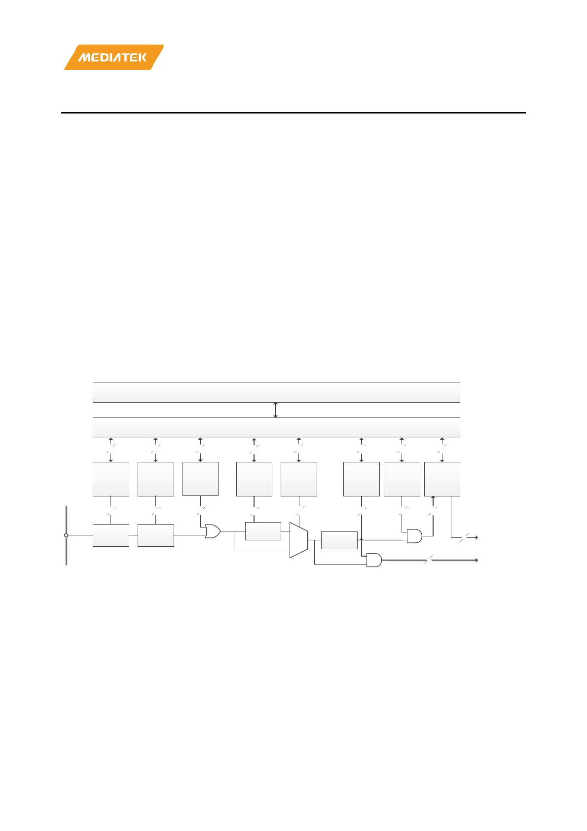
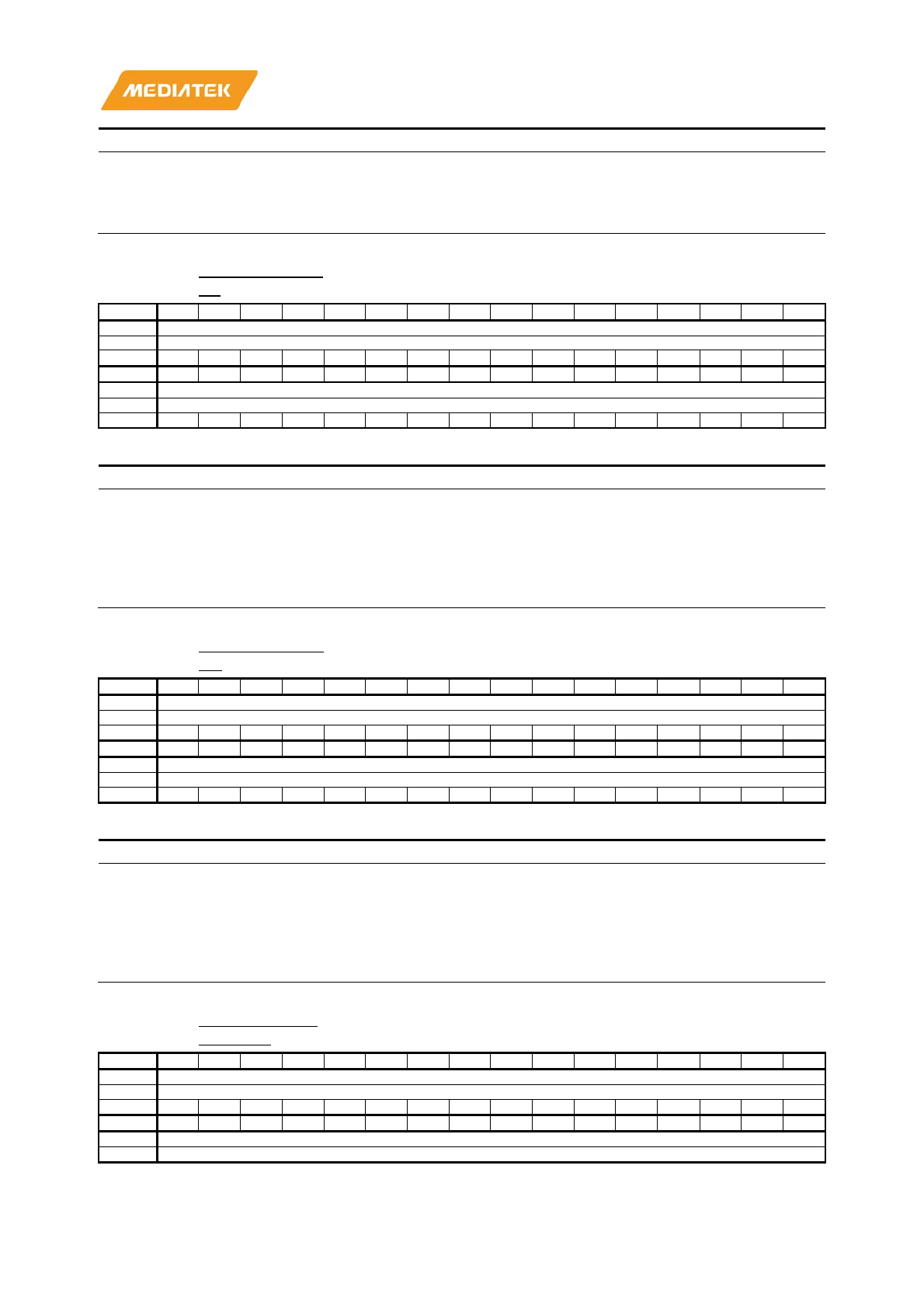
3.3. Block diagram
Figure 3.3-1 shows the block diagram of the EINT controller.
AMBA APB bus
Peripheral interface
De-bounce
circuit
Polarity
detect
circuit
Edge detect
circuit Sync circuit
De-bounce
config
register
32
32
Polarity
set/clear
register
32
32
Software
interrupt
register
32
32
Sensitivity
set/clear
register
32
32
Dual edge
sensitivity
set/clear
register
32
32
Interrupt
mask
set/clear
register
32
32
Wakeup
event mask
set/clear
register
32
32
Interrupt
mask
set/clear
register
32
32
1
1
To NVIC
interrupt
controller
To SPM event
cotroller
Figure 3.3-1. EINT block diagram
3.4. Wakeup event management
MT7686 is able to handle external or internal events in order to wake up the core (WFI). The wakeup event can be
generated by:
• Configuring an external or internal EINT line in event mode. When the CPU resumes from WFI, it is not
necessary to clear the peripheral interrupt pending bit or the NVIC IRQ channel pending bit as the pending
bit corresponding to the event line is not set.

MT7686 Reference Manual
© 2016 - 2017 MediaTek Inc.
Page 8 of 536
This document contains information that is proprietary to MediaTek Inc. (“MediaTek”) and/or its licensor(s).
Any unauthorized use, reproduction or disclosure of this document in whole or in part is strictly prohibited.
3.5. Functions
To generate an interrupt, an interrupt line should be configured and enabled. Program two trigger registers with
desired edge detection (EINT_SENS, EINT_DUALEDGE_SENS, EINT_POL) and enable an interrupt request by
writing “1” to the corresponding bit in the interrupt mask clear register (EINT_MASK_CLR). When the selected
trigger occurs on the external interrupt line, an interrupt request is generated. The pending bit corresponding to
the interrupt line is also set in the EINT interrupt status register (EINT_STA). This request is reset by writing “1” in
the EINT interrupt acknowledge register (EINT_INTACK).
To generate the event, the event line should be configured and enabled. Program three trigger registers with
desired edge detection (EINT_SENS, EINT_DUALEDGE_SENS, EINT_POL) and enable the event request by
writing “1” to the corresponding bit in the event mask clear register (EINT_WACKUP_MASK_CLR) and interrupt
mask clear register (EINT_MASK_CLR). When the selected trigger occurs on the event line, an event request is
generated. The pending bit corresponding to the event line is also set in the EINT interrupt status register
(EINT_STA). This request is reset by writing “1” in the EINT interrupt acknowledge register (EINT_INTACK).
3.5.1. Hardware interrupt
To configure the 32 lines as interrupt sources:
• Configure the mask bits of the 32 interrupt lines (EINT_MASK_CLR).
• Configure the trigger selection bits of the interrupt lines (EINT_SENS_SET, EINT_SENS_CLR,
EINT_DUALEDGE_SENS_SET, EINT_DUALEDGE_SENS_CLR, EINT_POL_SET, EINT_POL_CLR).
Register setting
Trigger Type
EINT_SENS_SET EINT_SENS_CLR EINT_DUALEDGE
_SENS_SET
EINT_DUALEDGE
_SENS_CLR
EINT_POL_SET EINT_POL_CLR
↑
(Rising Edge)
0
1
0
1
1
0
↓(Falling Edge)
0
1
0
1
0
1
↑↓
(Dual Edge)
0
1
1
0
Don’t care
Don’t care
(High Level)
1
0
Don’t care
Don’t care
1
0
(Low Level)
1
0
Don’t care
Don’t care
0
1
• Configure the enable and mask bits that control the NVIC IRQ channel mapped to the external interrupt
controller (EINT) so that an interrupt coming from one of the 32 lines can be correctly acknowledged.
3.5.2. Hardware events
To configure the 32 lines as event sources:
• Configure the mask bits of the 32 event lines (EINT_WACKUP_MASK_CLR and EINT_MASK_CLR).
• Configure the trigger selection bits of the event lines (EINT_SENS_SET, EINT_SENS_CLR,
EINT_DUALEDGE_SENS_SET, EINT_DUALEDGE_SENS_CLR, EINT_POL_SET, EINT_POL_CLR).
3.5.3. Software interrupt
The 32 lines can be configured as software interrupt lines. To generate a software interrupt:
• Configure the mask bits of the 32 interrupt lines (EINT_MASK_CLR).
• Set the required bit in the software interrupt register (EINT_SOFT_SET).

MT7686 Reference Manual
© 2016 - 2017 MediaTek Inc.
Page 9 of 536
This document contains information that is proprietary to MediaTek Inc. (“MediaTek”) and/or its licensor(s).
Any unauthorized use, reproduction or disclosure of this document in whole or in part is strictly prohibited.
3.6. External interrupt or event line mapping
Up to 21 GPIOs are connected to the 20 external interrupt/event lines, as shown in Table 3.6-1.
Table 3.6-1. External interrupt sources
EINT Source pin
EINT0 PAD_GPIO_0 if (GPIO0_MODE==1)
EINT1 PAD_GPIO_1 if (GPIO1_MODE==1)
EINT2 PAD_GPIO_2 if (GPIO2_MODE==1)
EINT3 PAD_GPIO_3 if (GPIO3_MODE==1)
EINT4 PAD_GPIO_4 if (GPIO4_MODE==3)
EINT5 PAD_GPIO_5 if (GPIO5_MODE==3)
EINT6 PAD_GPIO_6 if (GPIO6_MODE==3)
EINT7 PAD_GPIO_7 if (GPIO7_MODE==3)
EINT8 PAD_GPIO_8 if (GPIO8_MODE==3)
EINT9 PAD_GPIO_9 if (GPIO9_MODE==3)
EINT10 PAD_GPIO_10 if (GPIO10_MODE==1)
EINT11 PAD_GPIO_11 if (GPIO11_MODE==1)
EINT12 PAD_GPIO_12 if (GPIO12_MODE==6)
EINT13 PAD_GPIO_13 if (GPIO13_MODE==8)
EINT14 PAD_GPIO_14 if (GPIO14_MODE==8)
EINT15 PAD_GPIO_15 if (GPIO15_MODE==8)
EINT16 PAD_GPIO_16 if (GPIO16_MODE==8)
EINT17 PAD_GPIO_17 if (GPIO17_MODE==8)
EINT18 PAD_GPIO_18 if (GPIO18_MODE==8)
EINT19 PAD_GPIO_19 if (GPIO19_MODE==2)
PAD_GPIO_21 if (GPIO19_MODE==2) in MT5932
EINT20 PAD_GPIO_20 if (GPIO20_MODE==2)
PAD_GPIO_22 if (GPIO20_MODE==2) in MT5932
EINT21 uart0_rxd
EINT22 uart1_rxd
EINT23 uart2_rxd
EINT24 rtc_event_b
EINT25 conn2ap_hif_int_b
EINT26 conn2ap_pse_irq_b
EINT27 conn2ap_wdt_irq_b
EINT28 conn2ap_mac_irq_b
EINT29 pmu_int_b
EINT30
EINT31
MT7686 Reference Manual
© 2016 - 2017 MediaTek Inc.
Page 10 of 536
This document contains information that is proprietary to MediaTek Inc. (“MediaTek”) and/or its licensor(s).
Any unauthorized use, reproduction or disclosure of this document in whole or in part is strictly prohibited.
3.7. Register mapping
Module name: EINT Base address: (+A2100000h)
Address
Name
Width
Register Function
A2100300
EINT_STA
32
EINT interrupt status register
A2100308
EINT_INTACK
32
EINT interrupt acknowledge register
A2100310
EINT_EEVT
32
EINT wakeup event_b status register
A2100320
EINT_MASK
32
EINT interrupt mask register
A2100328
EINT_MASK_SET
32
EINT interrupt mask set register
A2100330
EINT_MASK_CLR
32
EINT interrupt mask clear register
A2100340
EINT_WAKEUP_MA
SK
32
EINT wakeup event mask register
A2100348
EINT_WAKEUP_MA
SK_SET
32
EINT wakeup event mask set register
A2100350
EINT_WACKUP_MA
SK_CLR
32
EINT wakeup event mask clear register
A2100360
EINT_SENS
32
EINT sensitivity register
A2100368
EINT_SENS_SET
32
EINT sensitivity set register
A2100370
EINT_SENS_CLR
32
EINT sensitivity clear register
A2100380
EINT_DUALEDGE_S
ENS
32
EINT dual edge sensitivity register
A2100388
EINT_DUALEDGE_S
ENS_SET
32
EINT dual edge sensitivity set register
A2100390
EINT_DUALEDGE_S
ENS_CLR
32
EINT dual edge sensitivity clear register
A21003A0
EINT_POL
32
EINT polarity register
A21003A8
EINT_POL_SET
32
EINT polarity set register
A21003B0
EINT_POL_CLR
32
EINT polarity clear register
A21003C0
EINT_SOFT
32
EINT software interrupt register
A21003C8
EINT_SOFT_SET
32
EINT software interrupt set register
A21003D0
EINT_SOFT_CLR
32
EINT software interrupt clear register
A2100400 ~
A210047C
EINTi_CON[n]
(n=0~31)
32
EINTi configuration register
3.7.1. Register definitions
A2100300
EINT_STA
EINT interrupt status register
00000000
Bit
31
30
29
28
27
26
25
24
23
22
21
20
19
18
17
16
Mne
EINT_STA[31:16]
Type
RO
Reset
0
0
0
0
0
0
0
0
0
0
0
0
0
0
0
0
Bit
15
14
13
12
11
10
9
8
7
6
5
4
3
2
1
0
Mne
EINT_STA[15:0]
Type
RO
Reset
0
0
0
0
0
0
0
0
0
0
0
0
0
0
0
0
Bit(s)
Mnemonic
Name
Description
31:0
EINT_STA
External interrupt status
This register tracks
interrupt request status generated by certain EINT
sources. If the EINT sources are set to edge sensitivity, EINT_IRQ is de-
MT7686 Reference Manual
© 2016 - 2017 MediaTek Inc.
Page 11 of 536
This document contains information that is proprietary to MediaTek Inc. (“MediaTek”) and/or its licensor(s).
Any unauthorized use, reproduction or disclosure of this document in whole or in part is strictly prohibited.
asserted while the corresponding EINT_INTACK is set to 1.
EINT_STA[i]
for EINTi.
•
0: No external interrupt request is generated.
•
1: External interrupt request is pending.
A2100308
EINT_INTACK
EINT interrupt acknowledge register
00000000
Bit
31
30
29
28
27
26
25
24
23
22
21
20
19
18
17
16
Mne
EINT_INTACK[31:16]
Type
WO
Reset
0
0
0
0
0
0
0
0
0
0
0
0
0
0
0
0
Bit
15
14
13
12
11
10
9
8
7
6
5
4
3
2
1
0
Mne
EINT_INTACK[15:0]
Type
WO
Reset
0
0
0
0
0
0
0
0
0
0
0
0
0
0
0
0
Bit(s)
Mnemonic
Name
Description
31:0
EINT_INTACK
Interrupt acknowledgement
Writing "1" to the specific bit position will acknowledge the interrupt
request correspondingly to the external interrupt line source.
EINT_INTACK[i] for EINTi.
0: No effect
1: Interrupt request is acknowledged.
A2100310
EINT_EEVT
EINT wakeup event_b
status register
00010000
Bit
31
30
29
28
27
26
25
24
23
22
21
20
19
18
17
16
Name
Type
Reset
Bit
15
14
13
12
11
10
9
8
7
6
5
4
3
2
1
0
Name
EEB
Type
RO
Reset
0
Bit(s)
Mnemonic
Name
Description
0
EEB
EINT wake up event_b
This register is a debugging port to monitor internal signals. It is an
asynchronous signal.
0: EINT wakes up the system from sleep mode.
1: EINT does not wake up the system from sleep mode.
A2100320
EINT_MASK
EINT interrupt mask register
FFFFFFFF
Bit
31
30
29
28
27
26
25
24
23
22
21
20
19
18
17
16
Name
EINT_MASK[31:16]
Type
RO
Reset
1
1
1
1
1
1
1
1
1
1
1
1
1
1
1
1
Bit
15
14
13
12
11
10
9
8
7
6
5
4
3
2
1
0
Name
EINT_MASK[15:0]
Type
RO
Reset
1
1
1
1
1
1
1
1
1
1
1
1
1
1
1
1
Bit(s)
Mnemonic
Name
Description
31:0
EINT_MASK
Interrupt mask
This register controls whether the EINT source is allowed to generate
MT7686 Reference Manual
© 2016 - 2017 MediaTek Inc.
Page 12 of 536
This document contains information that is proprietary to MediaTek Inc. (“MediaTek”) and/or its licensor(s).
Any unauthorized use, reproduction or disclosure of this document in whole or in part is strictly prohibited.
Bit(s)
Mnemonic
Name
Description
an interrupt request. Setting a specific bit position to "1" will prevent
activation of the external interrupt line.
EINT_MASK[i] for EINTi.
0: Interrupt request is enabled.
1: Interrupt request is disabled.
A2100328
EINT_MASK_S
ET
EINT interrupt mask set register
00000000
Bit
31
30
29
28
27
26
25
24
23
22
21
20
19
18
17
16
Name
EINT_MASK[31:16]
Type
WO
Reset
0
0
0
0
0
0
0
0
0
0
0
0
0
0
0
0
Bit
15
14
13
12
11
10
9
8
7
6
5
4
3
2
1
0
Name
EINT_MASK[15:0]
Type
WO
Reset
0
0
0
0
0
0
0
0
0
0
0
0
0
0
0
0
Bit(s)
Mnemonic
Name
Description
31:0
EINT_MASK
Enables mask for the associated external interrupt source
This register is used to set up individual mask bits. Only the bits set to 1
are effective. EINT_MASK bits are also set to 1. Otherwise,
EINT_MASK bits will retain the original value.
EINT_MASK[i] for EINTi.
0: No effect
1: Enables the corresponding MASK bit.
A2100330
EINT_MASK_C
LR
EINT interrupt mask
clear register
00000000
Bit
31
30
29
28
27
26
25
24
23
22
21
20
19
18
17
16
Name
EINT_MASK[31:16]
Type
WO
Reset
0
0
0
0
0
0
0
0
0
0
0
0
0
0
0
0
Bit
15
14
13
12
11
10
9
8
7
6
5
4
3
2
1
0
Name
EINT_MASK[15:0]
Type
WO
Reset
0
0
0
0
0
0
0
0
0
0
0
0
0
0
0
0
Bit(s)
Mnemonic
Name
Description
31:0
EINT_MASK
Disables mask for the associated external interrupt source
This register is used to clear individual mask bits. Only the bits set to 1
are effective. EINT_MASK bits are also cleared (set to 0). Otherwise,
EINT_MASK bits will retain the original value.
EINT_MASK[i] for EINTi.
0: No effect
1: Disables the corresponding MASK bit.
A2100340
EINT_WAKEU
P_MASK
EINT wakeup event mask register
FFFFFFFF
Bit
31
30
29
28
27
26
25
24
23
22
21
20
19
18
17
16
Name
EINT_WAKEUP_MASK[31:16]
Type
RO
Reset
1
1
1
1
1
1
1
1
1
1
1
1
1
1
1
1
Bit
15
14
13
12
11
10
9
8
7
6
5
4
3
2
1
0
Name
EINT_WAKEUP_MASK[15:0]
Type
RO
MT7686 Reference Manual
© 2016 - 2017 MediaTek Inc.
Page 13 of 536
This document contains information that is proprietary to MediaTek Inc. (“MediaTek”) and/or its licensor(s).
Any unauthorized use, reproduction or disclosure of this document in whole or in part is strictly prohibited.
Reset
1
1
1
1
1
1
1
1
1
1
1
1
1
1
1
1
Bit(s)
Mnemonic
Name
Description
31:0
EINT_WAKEUP_M
ASK
Wakeup event mask
This register controls whether the EINT source is allowed to generate a
wakeup event request. Setting a specific bit position to "1" will prevent
activation of the external interrupt line.
EINT_WAKEUP_MASK[i] for EINTi.
0: Wakeup event request is enabled.
1: Wakeup event request is disabled.
A2100348
EINT_WAKEU
P_MASK_SET
EINT wakeup
event mask set register
00000000
Bit
31
30
29
28
27
26
25
24
23
22
21
20
19
18
17
16
Name
EINT_WAKEUP_MASK[31:16]
Type
WO
Reset
0
0
0
0
0
0
0
0
0
0
0
0
0
0
0
0
Bit
15
14
13
12
11
10
9
8
7
6
5
4
3
2
1
0
Name
EINT_WAKEUP_MASK[15:0]
Type
WO
Reset
0
0
0
0
0
0
0
0
0
0
0
0
0
0
0
0
Bit(s)
Mnemonic
Name
Description
31:0
EINT_WAKEUP_M
ASK
Enables mask for the associated external interrupt source
This register is used to set up individual mask bits. Only the bits set to 1
are effective. EINT_WAKEUP_MASK bits are also set to 1. Otherwise,
EINT_WAKEUP_MASK bits will retain the original value.
EINT_WAKEUP_MASK[i] for EINTi.
0: No effect
1: Enables the corresponding MASK bit.
A2100350
EINT_WAC
KU
P_MASK_CLR
EINT wakeup event mask clear register
00000000
Bit
31
30
29
28
27
26
25
24
23
22
21
20
19
18
17
16
Name
EINT_WAKEUP_MASK[31:16]
Type
WO
Reset
0
0
0
0
0
0
0
0
0
0
0
0
0
0
0
0
Bit
15
14
13
12
11
10
9
8
7
6
5
4
3
2
1
0
Name
EINT_WAKEUP_MASK[15:0]
Type
WO
Reset
0
0
0
0
0
0
0
0
0
0
0
0
0
0
0
0
Bit(s)
Mnemonic
Name
Description
31:0
EINT_WAKEUP_M
ASK
Disables mask for the associated external interrupt source
This register is used to clear individual mask bits. Only the bits set to 1
are effective. EINT_WAKEUP_MASK bits are also cleared (set to 0).
Otherwise, EINT_WAKEUP_MASK bits will retain the original value.
EINT_WAKEUP_MASK[i] for EINTi.
0: No effect
1: Disables the corresponding MASK bit.
A2100360
EINT_SENS
EINT sensitivity register
00000000
Bit
31
30
29
28
27
26
25
24
23
22
21
20
19
18
17
16
Name
EINT_SENS[31:16]
MT7686 Reference Manual
© 2016 - 2017 MediaTek Inc.
Page 14 of 536
This document contains information that is proprietary to MediaTek Inc. (“MediaTek”) and/or its licensor(s).
Any unauthorized use, reproduction or disclosure of this document in whole or in part is strictly prohibited.
Type
RO
Reset
0
0
0
0
0
0
0
0
0
0
0
0
0
0
0
0
Bit
15
14
13
12
11
10
9
8
7
6
5
4
3
2
1
0
Name
EINT_SENS[15:0]
Type
RO
Reset
0
0
0
0
0
0
0
0
0
0
0
0
0
0
0
0
Bit(s)
Mnemonic
Name
Description
31:0
EINT_SENS
Sensitivity type of the associated external interrupt source
Sensitivity type of external interrupt source.
EINT_SENS[i] for EINTi.
0: Edge sensitivity (active high or low depends on POL setting)
1: Level sensitivity (active high or low depends on POL setting)
A2100368
EINT_SENS_S
ET
EINT sensitivity set register
00000000
Bit
31
30
29
28
27
26
25
24
23
22
21
20
19
18
17
16
Name
EINT_SENS[31:16]
Type
WO
Reset
0
0
0
0
0
0
0
0
0
0
0
0
0
0
0
0
Bit
15
14
13
12
11
10
9
8
7
6
5
4
3
2
1
0
Name
EINT_SENS[15:0]
Type
WO
Reset
0
0
0
0
0
0
0
0
0
0
0
0
0
0
0
0
Bit(s)
Mnemonic
Name
Description
31:0
EINT_SENS
Enables sensitive for the associated external interrupt
source.
This register is used to set up individual sensitive bits. Only the bits set
to 1 are effective. EINT_SENS bits are also set to 1. Otherwise,
EINT_SENS bits will retain the original value.
EINT_SENS[i] for EINTi.
0: No effect
1: Enables the corresponding SENS bit.
A2100370
EINT_SENS_C
LR
EINT sensitivity
clear register
00000000
Bit
31
30
29
28
27
26
25
24
23
22
21
20
19
18
17
16
Name
EINT_SENS[31:16]
Type
WO
Reset
0
0
0
0
0
0
0
0
0
0
0
0
0
0
0
0
Bit
15
14
13
12
11
10
9
8
7
6
5
4
3
2
1
0
Name
EINT_SENS[15:0]
Type
WO
Reset
0
0
0
0
0
0
0
0
0
0
0
0
0
0
0
0
Bit(s)
Mnemonic
Name
Description
31:0
EINT_SENS
Disables sensitive for the associated external interrupt
source.
This register is used to clear individual sensitive bits. Only the bits set
to 1 are effective. EINT_SENS bits are also cleared (set to 0).
Otherwise, EINT_SENS bits will retain the original value.
EINT_SENS[i] for EINTi.
0: No effect
1: Disables the corresponding SENS bit.
MT7686 Reference Manual
© 2016 - 2017 MediaTek Inc.
Page 15 of 536
This document contains information that is proprietary to MediaTek Inc. (“MediaTek”) and/or its licensor(s).
Any unauthorized use, reproduction or disclosure of this document in whole or in part is strictly prohibited.
A2100380
EINT_DUALED
GE_SENS
EINT dual edge sensitivity register
00000000
Bit
31
30
29
28
27
26
25
24
23
22
21
20
19
18
17
16
Name
EINT_DUALEDGE_SENS[31:16]
Type
RO
Reset
0
0
0
0
0
0
0
0
0
0
0
0
0
0
0
0
Bit
15
14
13
12
11
10
9
8
7
6
5
4
3
2
1
0
Name
EINT_DUALEDGE_SENS[15:0]
Type
RO
Reset
0
0
0
0
0
0
0
0
0
0
0
0
0
0
0
0
Bit(s)
Mnemonic
Name
Description
31:0
EINT_DUALEDGE_
SENS
Dual edge sensitivity type of the associated external interrupt
source
Dual edge sensitivity type of external interrupt source. (EINT_SENS
should be 0)
EINT_DUALEDGE_SENS[i] for EINTi.
0: Disable
1: Enable (no dependency on POL).
A2100388
EINT_DUALED
GE_SENS_SET
EINT dual edge sensitivity set register
00000000
Bit
31
30
29
28
27
26
25
24
23
22
21
20
19
18
17
16
Name
EINT_DUALEDGE_SENS[31:16]
Type
WO
Reset
0
0
0
0
0
0
0
0
0
0
0
0
0
0
0
0
Bit
15
14
13
12
11
10
9
8
7
6
5
4
3
2
1
0
Name
EINT_DUALEDGE_SENS[15:0]
Type
WO
Reset
0
0
0
0
0
0
0
0
0
0
0
0
0
0
0
0
Bit(s)
Mnemonic
Name
Description
31:0
EINT_DUALEDGE_
SENS
Enables dual edge sensitivity for the associated external
interrupt source.
This register is used to set up individual dual edge sensitive bits.
(EINT_SENS should be 0)
Only the bits set to 1 are effective. EINT_DUALEDGE_SENS bits are
also set to 1. Otherwise, EINT_DUALEDGE_SENS bits will retain the
original value.
EINT_DUALEDGE_SENS[i] for EINTi.
0: No effect
1: Enables the corresponding DUALEDGE bit.
A2100390
EINT_DUALED
GE_SENS_CLR
EINT dual edge sensitivity clear register
00000000
Bit
31
30
29
28
27
26
25
24
23
22
21
20
19
18
17
16
Name
EINT_DUALEDGE_SENS[31:16]
Type
WO
Reset
0
0
0
0
0
0
0
0
0
0
0
0
0
0
0
0
Bit
15
14
13
12
11
10
9
8
7
6
5
4
3
2
1
0
Name
EINT_DUALEDGE_SENS[15:0]
Type
WO
Reset
0
0
0
0
0
0
0
0
0
0
0
0
0
0
0
0
MT7686 Reference Manual
© 2016 - 2017 MediaTek Inc.
Page 16 of 536
This document contains information that is proprietary to MediaTek Inc. (“MediaTek”) and/or its licensor(s).
Any unauthorized use, reproduction or disclosure of this document in whole or in part is strictly prohibited.
Bit(s)
Mnemonic
Name
Description
31:0
EINT_DUALEDGE_
SENS
Disables dual edge sensitive for the associated external
interrupt source.
This register is used to clear individual sensitive bits. Only the bits set
to 1 are effective.
EINT_DUALEDGE_SENS bits are also cleared (set to
0). Otherwise, EINT_DUALEDGE_SENS bits will retain the original
value.
EINT_DUALEDGE_SENS[i] for EINTi.
0: No effect
1: Disables the corresponding DUALEDGE bit.
A21003A0
EINT_POL
EINT polarity register
00000000
Bit
31
30
29
28
27
26
25
24
23
22
21
20
19
18
17
16
Name
EINT_POL[31:16]
Type
RO
Reset
0
0
0
0
0
0
0
0
0
0
0
0
0
0
0
0
Bit
15
14
13
12
11
10
9
8
7
6
5
4
3
2
1
0
Name
EINT_POL[15:0]
Type
RO
Reset
0
0
0
0
0
0
0
0
0
0
0
0
0
0
0
0
Bit(s)
Mnemonic
Name
Description
31:0
EINT_POL
Configures polarity of the associated external interrupt
source.
Activation type of the EINT source.
EINT_POL[i] for EINTi.
0: Active low
1: Active high
A21003A8
EINT_POL_SE
T
EINT polarity set register
00000000
Bit
31
30
29
28
27
26
25
24
23
22
21
20
19
18
17
16
Name
EINT_POL[31:16]
Type
WO
Reset
0
0
0
0
0
0
0
0
0
0
0
0
0
0
0
0
Bit
15
14
13
12
11
10
9
8
7
6
5
4
3
2
1
0
Name
EINT_POL[15:0]
Type
WO
Reset
0
0
0
0
0
0
0
0
0
0
0
0
0
0
0
0
Bit(s)
Mnemonic
Name
Description
31:0
EINT_POL
Enables polarity configuration for the associated external
interrupt source
This register is used to set up individual polarity bits. Only the bits set
to 1 are effective. EINT_POL bits are also set to 1. Otherwise,
EINT_POL bits will retain the original value.
EINT_POL[i] for EINTi.
0: No effect
1: Enables the corresponding POL bit.
A21003B0
EINT_POL_CL
R
EINT polarity clear register
00000000
Bit
31
30
29
28
27
26
25
24
23
22
21
20
19
18
17
16
Name
EINT_POL[31:16]
Type
WO
Reset
0
0
0
0
0
0
0
0
0
0
0
0
0
0
0
0
MT7686 Reference Manual
© 2016 - 2017 MediaTek Inc.
Page 17 of 536
This document contains information that is proprietary to MediaTek Inc. (“MediaTek”) and/or its licensor(s).
Any unauthorized use, reproduction or disclosure of this document in whole or in part is strictly prohibited.
Bit
15
14
13
12
11
10
9
8
7
6
5
4
3
2
1
0
Name
EINT_POL[15:0]
Type
WO
Reset
0
0
0
0
0
0
0
0
0
0
0
0
0
0
0
0
Bit(s)
Mnemonic
Name
Description
31:0
EINT_POL
Polarity configuration set
This register is used to clear individual polarity bits. Only the bits set to
1 are effective. EINT_POL bits are also cleared (set to 0). Otherwise,
EINT_POL bits will retain the original value.
EINT_POL[i] for EINTi.
0: No effect
1: Disables the corresponding POL bit.
A21003C0
EINT_SOFT
EINT software
interrupt register
00000000
Bit
31
30
29
28
27
26
25
24
23
22
21
20
19
18
17
16
Name
EINT_SOFT[31:16]
Type
RO
Reset
0
0
0
0
0
0
0
0
0
0
0
0
0
0
0
0
Bit
15
14
13
12
11
10
9
8
7
6
5
4
3
2
1
0
Name
EINT_SOFT[15:0]
Type
RO
Reset
0
0
0
0
0
0
0
0
0
0
0
0
0
0
0
0
Bit(s)
Mnemonic
Name
Description
31:0
EINT_SOFT
Software interrupt
This register is used for debugging purposes.
EINT_SOFT[i] for EINTi.
0: No effect
1: Triggers an EINT
A21003C8
EINT_SOFT_S
ET
EINT
software interrupt set register
00000000
Bit
31
30
29
28
27
26
25
24
23
22
21
20
19
18
17
16
Name
EINT_SOFT[31:16]
Type
WO
Reset
0
0
0
0
0
0
0
0
0
0
0
0
0
0
0
0
Bit
15
14
13
12
11
10
9
8
7
6
5
4
3
2
1
0
Name
EINT_SOFT[15:0]
Type
WO
Reset
0
0
0
0
0
0
0
0
0
0
0
0
0
0
0
0
Bit(s)
Mnemonic
Name
Description
31:0
EINT_SOFT
Enables software for the associated external interrupt source
This register is used to set up individual software bits. Only the bits set
to 1 are effective. EINT_SOFT bits are also set to 1. Otherwise,
EINT_SOFT bits will retain the original value.
EINT_SOFT[i] for EINTi.
0: No effect
1: Enables the corresponding SOFT bit.
A21003D0
EINT_SOFT_C
LR
EINT software
interrupt clear register
00000000
Bit
31
30
29
28
27
26
25
24
23
22
21
20
19
18
17
16
MT7686 Reference Manual
© 2016 - 2017 MediaTek Inc.
Page 18 of 536
This document contains information that is proprietary to MediaTek Inc. (“MediaTek”) and/or its licensor(s).
Any unauthorized use, reproduction or disclosure of this document in whole or in part is strictly prohibited.
Name
EINT_SOFT[31:16]
Type
WO
Reset
0
0
0
0
0
0
0
0
0
0
0
0
0
0
0
0
Bit
15
14
13
12
11
10
9
8
7
6
5
4
3
2
1
0
Name
EINT_SOFT[15:0]
Type
WO
Reset
0
0
0
0
0
0
0
0
0
0
0
0
0
0
0
0
Bit(s)
Mnemonic
Name
Description
31:0
EINT_SOFT
Disables software for the associated external interrupt
source
This register is used to clear individual software bits. Only the bits set
to 1 are effective. EINT_SOFT bits are also cleared (set to 0).
Otherwise, EINT_SOFT bits will retain the original value.
EINT_SOFT[i] for EINTi.
0: No effect
1: Disables the corresponding SOFT bit.
A2100400~
A210047C
(step =
0x4)
EINTi_CON[n]
(n=0~31)
EINTi config register
00000000
Bit
31
30
29
28
27
26
25
24
23
22
21
20
19
18
17
16
Name
RSTD
BC
DBC_
EN
Type
WO
RW
Reset
0
0
Bit
15
14
13
12
11
10
9
8
7
6
5
4
3
2
1
0
Name
DBC_CON
Type
RW
Reset
0
0
0
0
0
0
0
0
0
0
0
0
0
0
0
Bit(s)
Mnemonic
Name
Description
24
RSTDBC
EINTi debounce count reset
Write 1 to reset the de-bounce counter so that EINT can be updated
immediately without de-bounce latency. This option needs 100usec
latency to take effect.
0: no effect
1: reset
16
DBC_EN
EINTi debounce circuit enable
0: disable
1: enable
14:0
DBC_CON
EINTi debounce count setting
DBC_CNT = DBC_CON[10:0]
EINTi debounce duration config
(clock period is determined in PRESCALER)
Note: When DBD_CON[10:0] = 0 and DBC_EN = 1
, there are still two
32K clock cycles (62.5 us) debounce. If you want to disable debounce
function, DBC_EN should be set to 0 (Zero).
PRESCALER = DBC_CON[14:12]
EINTi debounce clock cycle period prescaler.
000: 32,768Hz, max. 0.0625sec
001: 16,384Hz
010: 8,192Hz
011: 4,096Hz
100: 2,048Hz, max. 1sec
101: 1,024Hz

MT7686 Reference Manual
© 2016 - 2017 MediaTek Inc.
Page 19 of 536
This document contains information that is proprietary to MediaTek Inc. (“MediaTek”) and/or its licensor(s).
Any unauthorized use, reproduction or disclosure of this document in whole or in part is strictly prohibited.
Bit(s)
Mnemonic
Name
Description
110: 512Hz
111: 256Hz, max. 8secs
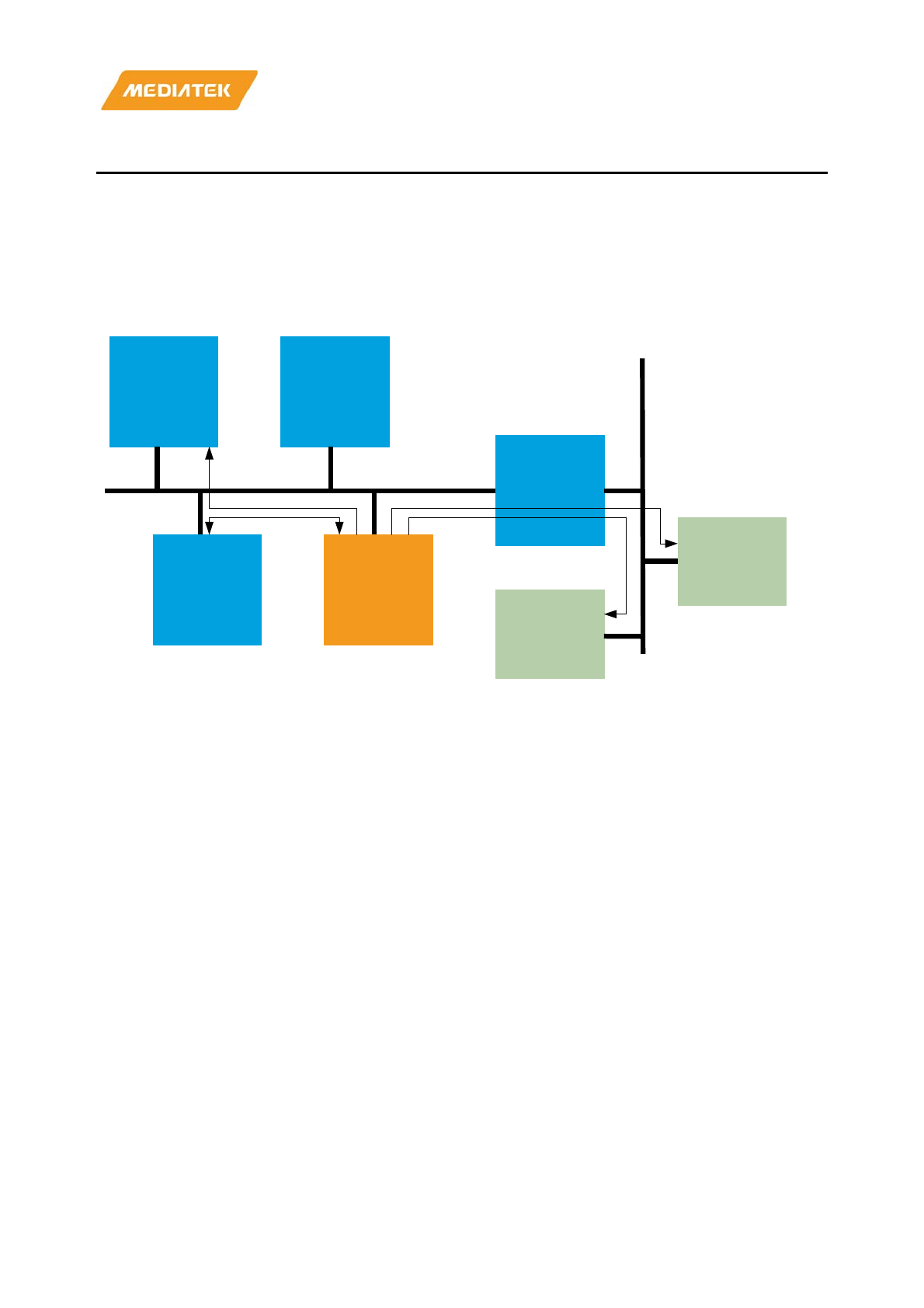
MT7686 Reference Manual
© 2016 - 2017 MediaTek Inc.
Page 20 of 536
This document contains information that is proprietary to MediaTek Inc. (“MediaTek”) and/or its licensor(s).
Any unauthorized use, reproduction or disclosure of this document in whole or in part is strictly prohibited.
4. Direct Memory Access
4.1. Overview
A DMA controller is placed on AHB bus to support fast data transfers and off-load the processor. With this
controller, specific devices on AHB or APB buses can benefit greatly from quick completion of data movement from
or to memory modules. Such generic DMA controller can also be used to connect two devices other than memory
modules as long as they can be addressed in memory space. Figure 4.1-1 illustrates the system connections.
Memory Arbiter
DMA
Peripheral
MCU-DSP
Interface
ABP
Bridge
Peripheral
AHB Bus
APB Bus
Figure 4.1-1. Variety data paths of DMA transfers
4.2. Features
There is a round-robin arbitration mechanism to support up to 16 channels working simultaneously. Each channel
has a similar set of registers to be configured to different schemes as desired. Both interrupt and polling based
schemes are supported to handle the completion events.
The block diagram of DMA operation is shown in Figure 4.2-1.
MT7686 Reference Manual
© 2016 - 2017 MediaTek Inc.
Page 21 of 536
This document contains information that is proprietary to MediaTek Inc. (“MediaTek”) and/or its licensor(s).
Any unauthorized use, reproduction or disclosure of this document in whole or in part is strictly prohibited.
PDMA
VDMA
GDMA
Global Controller
APB
Interface AHB
Interface
Configuration
Configuration Transaction
Transaction
Transaction
Configuration
Configuration
Figure 4.2-1. DMA block diagram
4.3. Functions
There are three types of DMA channels in the DMA controller: full-size DMA, half-size DMA and virtual FIFO DMA.
Channel 1 is a full-size DMA channel, channels 2 to 6 are half-size channels and channels 7 to 16 are virtual FIFO
DMA channels. The difference between the first two types of DMA channels is that source and destination
addresses are programmable as full-size DMA channels, but the address of either source or destination only can be
programmed as a half-size DMA channel, while the address of the other side is fixed.
4.3.1. Ring buffer and double buffer memory data transfer
DMA channels 1 to 7 support ring-buffer and double-buffer memory data transfer. This can be achieved by
programming DMA_WPPT and DMA_WPTO, as well as setting up WPEN in the DMA_CON register to enable, as
shown in Figure 4.3-1. The next address jumps to WPTO address after WPPT data transfer is complete, once the
transfer counter reaches WPPT.
Note that only one side can be configured as ring-buffer or double-buffer memory, and this is controlled by WPSD
in the DMA_CON register.
MT7686 Reference Manual
© 2016 - 2017 MediaTek Inc.
Page 22 of 536
This document contains information that is proprietary to MediaTek Inc. (“MediaTek”) and/or its licensor(s).
Any unauthorized use, reproduction or disclosure of this document in whole or in part is strictly prohibited.
Figure 4.3-1. Ring buffer and double buffer memory data movement
4.3.2. Unaligned word access
The address of word access on AHB bus must be aligned to word boundary (the address must be multiple of 4), or
the two LSB are truncated to 00b. If the LSB is truncated incorrect data may be fetched. If the data is moved from
unaligned to aligned address, the word is usually split into four bytes then moved byte by byte. Thus, the four read
and four write transfers will appear on the bus.
To improve bus efficiency, the unaligned-word access is provided in DMA 2 to 7. If “byte-to-word (B2W)” function
is enabled in PDMAx_CON, the DMAs will move data from the unaligned address to aligned address by executing
four continuous byte-read accesses and one word-write access, reducing the number of transfers on the bus by
three, as shown in Figure 4.3-2.
Figure 4.3-2. Unaligned word accesses
4.3.3. Virtual FIFO DMA
Virtual FIFO DMA is used to ease UART control. The difference between the virtual FIFO DMA and the ordinary
DMA is that the virtual FIFO DMA contains additional FIFO controllers. The read and write pointers are kept in the
virtual FIFO DMA. To read from FIFO, the read pointer points to the address of the next data. To write into the
FIFO, the write pointer moves to the next address. If the FIFO is empty, a FIFO read will not be allowed. Similarly,
the data will not be written to the FIFO if the FIFO is full. Due to UART flow control requirements, an alert length
MT7686 Reference Manual
© 2016 - 2017 MediaTek Inc.
Page 23 of 536
This document contains information that is proprietary to MediaTek Inc. (“MediaTek”) and/or its licensor(s).
Any unauthorized use, reproduction or disclosure of this document in whole or in part is strictly prohibited.
(VDMAx_ALTLEN) is programmed. If the FIFO space is smaller than this value, an alert signal is issued to enable the
UART flow control. The type of flow control performed depends on the UART configuration settings.
Each virtual FIFO DMA can be programmed as receive (RX) or transmit (TX) FIFO. This depends on the DIR setting in
the DMA_CON register. If DIR is “0” (READ), the virtual FIFO DMA is specified as a TX FIFO. On the other hand, if
DIR is “1” (WRITE), the virtual FIFO DMA will be specified as an RX FIFO.
The virtual FIFO DMA provides an interrupt to MCU to notify data availability in the FIFO and the amount of data is
above or under the value defined in the DMA_COUNT register. Based on this, the MCU does not need to poll the
DMA to know when the data must be removed from or put into the FIFO.
Memory
Destination Address
FIFO Size
Virtual FIFO
Read Pointer
(MCU)
Write Pointer
(UART RX)
Memory
Source Address
FIFO Size
Virtual FIFO
Read Pointer
(UART TX)
Write Pointer
(MCU)
Figure 4.3-3. Virtual FIFO DMA
4.4. Application and programming sequence
DMA channels 7 to 16 are virtual FIFO DMA with corresponding peripherals. The access ports for the MCU of each
VDMA are listed in Table 4.4-1. MCU treats the virtual FIFO access port as a real FIFO, but the physical location or
size is configured by registers of each channel.
Table 4.4-1. Virtual FIFO access ports
DMA number Address of virtual FIFO access port Reference UART
DMA7 A100_0000h AUD_TX
DMA8 A100_0100h AUD_RX
DMA9 A100_0200h ASYS TX
DMA10 A100_0300h ASYS RX
DMA11 A100_0400h UART2 TX
DMA12 A100_0500h UART2 RX
DMA13 A100_0600h UART1 TX

MT7686 Reference Manual
© 2016 - 2017 MediaTek Inc.
Page 24 of 536
This document contains information that is proprietary to MediaTek Inc. (“MediaTek”) and/or its licensor(s).
Any unauthorized use, reproduction or disclosure of this document in whole or in part is strictly prohibited.
DMA number Address of virtual FIFO access port Reference UART
DMA14 A100_0700h UART1 RX
DMA15 A100_0800h UART0 TX
DMA16 A100_0900h UART0 RX
Due to different types of DMA, the limitations for each peripheral are listed below.
Table 4-2. Function list of DMA channels
DMA number Type Ring
buffer
Double
buffer
Burst
mode
Unaligned
word access
Peripheral
DMA1 Full size
●
●
●
DMA2 Half size
●
●
●
●
I2C0 TX
DMA3 Half size
●
●
●
●
I2C0 RX
DMA4 Half size
●
●
●
●
I2C1 TX
DMA5 Half size
●
●
●
●
I2C1 RX
DMA6 Half size
●
●
●
●
HIF_TX,RX
DMA7 Virtual
FIFO
●
AUD_TX
DMA8 Virtual
FIFO
●
AUD_RX
DMA9 Virtual
FIFO
●
ASYS TX
DMA10 Virtual
FIFO
●
ASYS RX
DMA11 Virtual
FIFO
●
UART2 TX
DMA12 Virtual
FIFO
●
UART2 RX
DMA13 Virtual
FIFO
● UART1 TX
DMA14 Virtual
FIFO
● UART1 RX
DMA15 Virtual
FIFO
● UART0 TX
DMA16 Virtual
FIFO
●
UART0 RX
4.5. Register mapping
There are 16 DMA channels in this SOC. The usage of the registers below is the same except that the base address
should be changed to respective ones.
Module name: DMA Base address: (+a0020000h)
Address
Name
Width
Register Functionality
MT7686 Reference Manual
© 2016 - 2017 MediaTek Inc.
Page 25 of 536
This document contains information that is proprietary to MediaTek Inc. (“MediaTek”) and/or its licensor(s).
Any unauthorized use, reproduction or disclosure of this document in whole or in part is strictly prohibited.
A0020000
DMA_GLBSTA
32
DMA global status
A0020008
DMA_GLB_CPU0_CF
G
32
DMA top hierarchy interrupt
configuration
A002000C
DMA_GLB_CPU0_SE
T
32
DMA top hierarchy interrupt
setting
A0020010
DMA_GLB_CPU0_CL
R
32
DMA top hierarchy interrupt clear
A0020028
DMA_GLBLIMITER
32
DMA global bandwidth limiter register
A0020020
DMA_GLB_SWRST
32
DMA global software reset
A0020040
DMA_GLB_BUSY
32
DMA global busy status
A0020044
DMA_GLB_INTR
32
DMA global interrupt status
A0020100
GDMA1_SRC
32
DMA channel 1
source address
A0020104
GDMA1_DST
32
DMA channel 1 destination address
A0020108
GDMA1_WPPT
32
DMA channel 1 wrap point address
A002010C
GDMA1_WPTO
32
DMA channel 1
wrap to address
A0020110
GDMA1_COUNT
32
DMA channel 1 transfer count
A0020114
GDMA1_CON
32
DMA channel 1 control
A0020118
GDMA1_START
32
DMA channel 1 start
A002011C
GDMA1_INTSTA
32
DMA channel 1 interrupt status
A0020120
GDMA1_ACKINT
32
DMA channel 1 interrupt acknowledge
A0020124
GDMA1_RLCT
32
DMA channel 1 remaining
length of
current transfer
A0020128
GDMA1_LIMITER
32
DMA channel 1 bandwidth limiter
A0020208
PDMA2_WPPT
32
DMA channel 2 wrap point address
A002020C
PDMA2_WPTO
32
DMA channel 2 wrap to address
A0020210
PDMA2_COUNT
32
DMA channel 2 transfer count
A0020214
PDMA2_CON
32
DMA channel 2 control
A0020218
PDMA2_START
32
DMA channel
2 start
A002021C
PDMA2_INTSTA
32
DMA channel 2 interrupt status
A0020220
PDMA2_ACKINT
32
DMA channel 2 interrupt acknowledge
A0020224
PDMA2_RLCT
32
DMA channel 2
remaining length of
current transfer
A0020228
PDMA2_LIMITER
32
DMA channel 2 bandwidth limiter
A002022C
PDMA2_PGMADDR
32
DMA channel 2 programmable address
A0020308
PDMA3_WPPT
32
DMA channel 3 wrap point address
A002030C
PDMA3_WPTO
32
DMA channel 3 wrap to address
A0020310
PDMA3_COUNT
32
DMA channel 3 transfer count
A0020314
PDMA3_CON
32
DMA channel 3 control
A0020318
PDMA3_START
32
DMA channel 3 start
A002031C
PDMA3_INTSTA
32
DMA channel 3 interrupt status
A0020320
PDMA3_ACKINT
32
DMA channel 3 interrupt acknowledge
A0020324
PDMA3_RLCT
32
DMA channel 3 remaining length of
MT7686 Reference Manual
© 2016 - 2017 MediaTek Inc.
Page 26 of 536
This document contains information that is proprietary to MediaTek Inc. (“MediaTek”) and/or its licensor(s).
Any unauthorized use, reproduction or disclosure of this document in whole or in part is strictly prohibited.
current transfer
A0020328
PDMA3_LIMITER
32
DMA channel 3
bandwidth limiter
A002032C
PDMA3_PGMADDR
32
DMA channel 3 programmable address
A0020408
PDMA4_WPPT
32
DMA channel 4 wrap point address
A002040C
PDMA4_WPTO
32
DMA
channel 4 wrap to address
A0020410
PDMA4_COUNT
32
DMA channel 4 transfer count
A0020414
PDMA4_CON
32
DMA channel 4 control
A0020418
PDMA4_START
32
DMA channel 4
start
A002041C
PDMA4_INTSTA
32
DMA channel 4 interrupt status
A0020420
PDMA4_ACKINT
32
DMA channel 4 interrupt acknowledge
A0020424
PDMA4_RLCT
32
DMA channel 4
remaining length of
current transfer
A0020428
PDMA4_LIMITER
32
DMA channel 4 bandwidth limiter
A002042C
PDMA4_PGMADDR
32
DMA channel 4 programmable address
A0020508
PDMA5_WPPT
32
DMA channel 5 wrap point address
A002050C
PDMA5_WPTO
32
DMA channel 5 wrap to address
A0020510
PDMA5_COUNT
32
DMA channel 5 transfer count
A0020514
PDMA5_CON
32
DMA channel 5 control
A0020518
PDMA5_START
32
DMA channel 5 start
A002051C
PDMA5_INTSTA
32
DMA channel 5 interrupt status
A0020520
PDMA5_ACKINT
32
DMA channel 5 interrupt acknowledge
A0020524
PDMA5_RLCT
32
DMA channel 5 remaining length of
current transfer
A0020528
PDMA5_LIMITER
32
DMA channel 5 bandwidth limiter
A002052C
PDMA5_PGMADDR
32
DMA channel 5 programmable address
A0020608
PDMA6_WPPT
32
DMA channel 6 wrap point address
A002060C
PDMA6_WPTO
32
DMA channel 6 wrap to
address
A0020610
PDMA6_COUNT
32
DMA channel 6 transfer count
A0020614
PDMA6_CON
32
DMA channel 6 control
A0020618
PDMA6_START
32
DMA channel 6 start
A002061C
PDMA6_INTSTA
32
DMA channel 6 interrupt status
A0020620
PDMA6_ACKINT
32
DMA channel 6 interrupt acknowledge
A0020624
PDMA6_RLCT
32
DMA channel 6 remaining length of
current transfer
A0020628
PDMA6_LIMITER
32
DMA channel 6 bandwidth limiter
A002062C
PDMA6_PGMADDR
32
DMA channel 6 programmable address
A0020710
VDMA7_COUNT
32
DMA
channel 7 transfer count
A0020714
VDMA7_CON
32
DMA channel 7 control
A0020718
VDMA7_START
32
DMA channel 7 start register
A002071C
VDMA7_INTSTA
32
DMA channel 7
interrupt status
A0020720
VDMA7_ACKINT
32
DMA channel 7 interrupt acknowledge

MT7686 Reference Manual
© 2016 - 2017 MediaTek Inc.
Page 27 of 536
This document contains information that is proprietary to MediaTek Inc. (“MediaTek”) and/or its licensor(s).
Any unauthorized use, reproduction or disclosure of this document in whole or in part is strictly prohibited.
A0020728
VDMA7_LIMITER
32
DMA channel 7 bandwidth limiter
A002072C
VDMA7_PGMADDR
32
DMA channel 7 programmable address
A0020730
VDMA7_WRPTR
32
DMA channel 7 write pointer
A0020734
VDMA7_RDPTR
32
DMA channel 7 read pointer
A0020738
VDMA7_FFCNT
32
DMA channel 7 FIFO count
A002073C
VDMA7_FFSTA
32
DMA channel 7 FIFO status
A0020740
VDMA7_ALTLEN
32
DMA channel 7 alert length
A0020744
VDMA7_FFSIZE
32
DMA channel
7 FIFO size
A0020810
VDMA8_COUNT
32
DMA channel 8 transfer count
A0020814
VDMA8_CON
32
DMA channel 8 control
A0020818
VDMA8_START
32
DMA channel 8 start register
A002081C
VDMA8_INTSTA
32
DMA channel 8 interrupt status
A0020820
VDMA8_ACKINT
32
DMA channel 8 interrupt acknowledge
A0020828
VDMA8_LIMITER
32
DMA channel 8
bandwidth limiter
A002082C
VDMA8_PGMADDR
32
DMA channel 8 programmable address
A0020830
VDMA8_WRPTR
32
DMA channel 8 write pointer
A0020834
VDMA8_RDPTR
32
DMA
channel 8 read pointer
A0020838
VDMA8_FFCNT
32
DMA channel 8 FIFO count
A002083C
VDMA8_FFSTA
32
DMA channel 8 FIFO status
A0020840
VDMA8_ALTLEN
32
DMA channel 8
alert length
A0020844
VDMA8_FFSIZE
32
DMA channel 8 FIFO size
A0020910
VDMA9_COUNT
32
DMA channel 9 transfer count
A0020914
VDMA9_CON
32
DMA channel 9 control
A0020918
VDMA9_START
32
DMA channel 9 start register
A002091C
VDMA9_INTSTA
32
DMA channel 9 interrupt status
A0020920
VDMA9_ACKINT
32
DMA channel 9 interrupt
acknowledge
A0020928
VDMA9_LIMITER
32
DMA channel 9 bandwidth limiter
A002092C
VDMA9_PGMADDR
32
DMA channel 9 programmable address
A0020930
VDMA9_WRPTR
32
DMA
channel 9 write pointer
A0020934
VDMA9_RDPTR
32
DMA channel 9 read pointer
A0020938
VDMA9_FFCNT
32
DMA channel 9 FIFO count
A002093C
VDMA9_FFSTA
32
DMA channel 9
FIFO status
A0020940
VDMA9_ALTLEN
32
DMA channel 9 alert length
A0020944
VDMA9_FFSIZE
32
DMA channel 9 FIFO size
A0020A10
VDMA10_COUNT
32
DMA channel 10 transfer
count
A0020A14
VDMA10_CON
32
DMA channel 10 control
A0020A18
VDMA10_START
32
DMA channel 10 start register
A0020A1C
VDMA10_INTSTA
32
DMA channel 10 interrupt
status

MT7686 Reference Manual
© 2016 - 2017 MediaTek Inc.
Page 28 of 536
This document contains information that is proprietary to MediaTek Inc. (“MediaTek”) and/or its licensor(s).
Any unauthorized use, reproduction or disclosure of this document in whole or in part is strictly prohibited.
A0020A20
VDMA10_ACKINT
32
DMA channel 10 interrupt acknowledge
A0020A28
VDMA10_LIMITER
32
DMA channel 10 bandwidth limiter
A0020A2C
VDMA10_PGMADDR
32
DMA
channel 10 programmable address
A0020A30
VDMA10_WRPTR
32
DMA channel 10 write pointer
A0020A34
VDMA10_RDPTR
32
DMA channel 10 read pointer
A0020A38
VDMA10_FFCNT
32
DMA channel 10 FIFO count
A0020A3C
VDMA10_FFSTA
32
DMA channel 10 FIFO status
A0020A40
VDMA10_ALTLEN
32
DMA channel 10 alert length
A0020A44
VDMA10_FFSIZE
32
DMA
channel 10 FIFO size
A0020B10
VDMA11_COUNT
32
DMA channel 11 transfer count
A0020B14
VDMA11_CON
32
DMA channel 11 control
A0020B18
VDMA11_START
32
DMA channel 11
start register
A0020B1C
VDMA11_INTSTA
32
DMA channel 11 interrupt status
A0020B20
VDMA11_ACKINT
32
DMA channel 11 interrupt acknowledge
A0020B28
VDMA11_LIMITER
32
DMA channel 11 bandwidth limiter
A0020B2C
VDMA11_PGMADDR
32
DMA channel 11 programmable address
A0020B30
VDMA11_WRPTR
32
DMA channel 11 write pointer
A0020B34
VDMA11_RDPTR
32
DMA channel 11 read pointer
A0020B38
VDMA11_FFCNT
32
DMA channel 11 FIFO count
A0020B3C
VDMA11_FFSTA
32
DMA channel 11 FIFO status
A0020B40
VDMA11_ALTLEN
32
DMA channel 11 alert length
A0020B44
VDMA11_FFSIZE
32
DMA channel 11 FIFO size
A0020C10
VDMA12_COUNT
32
DMA channel 12 transfer count
A0020C14
VDMA12_CON
32
DMA channel 12 control
A0020C18
VDMA12_START
32
DMA channel 12 start register
A0020C1C
VDMA12_INTSTA
32
DMA channel 12 interrupt status
A0020C20
VDMA12_ACKINT
32
DMA channel 12 interrupt acknowledge
A0020C28
VDMA12_LIMITER
32
DMA channel 12 bandwidth limiter
A0020C2C
VDMA12_PGMADDR
32
DMA channel 12 programmable address
A0020C30
VDMA12_WRPTR
32
DMA channel 12 write pointer
A0020C34
VDMA12_RDPTR
32
DMA channel 12 read pointer
A0020C38
VDMA12_FFCNT
32
DMA channel 12 FIFO count

MT7686 Reference Manual
© 2016 - 2017 MediaTek Inc.
Page 29 of 536
This document contains information that is proprietary to MediaTek Inc. (“MediaTek”) and/or its licensor(s).
Any unauthorized use, reproduction or disclosure of this document in whole or in part is strictly prohibited.
A0020C3C
VDMA12_FFSTA
32
DMA channel 12 FIFO status
A0020C40
VDMA12_ALTLEN
32
DMA channel 12 alert length
A0020C44
VDMA12_FFSIZE
32
DMA channel 12 FIFO size
A0020D10
VDMA13_COUNT
32
DMA channel 13 transfer count
A0020D14
VDMA13_CON
32
DMA channel 13 control
A0020D18
VDMA13_START
32
DMA channel 13 start register
A0020D1C
VDMA13_INTSTA
32
DMA channel 13 interrupt status
A0020D20
VDMA13_ACKINT
32
DMA channel 13 interrupt acknowledge
A0020D28
VDMA13_LIMITER
32
DMA channel 13 bandwidth
limiter
A0020D2C
VDMA13_PGMADDR
32
DMA channel 13 programmable address
A0020D30
VDMA13_WRPTR
32
DMA channel 13 write pointer
A0020D34
VDMA13_RDPTR
32
DMA channel
13 read pointer
A0020D38
VDMA13_FFCNT
32
DMA channel 13 FIFO count
A0020D3C
VDMA13_FFSTA
32
DMA channel 13 FIFO status
A0020D40
VDMA13_ALTLEN
32
DMA channel 13
alert length
A0020D44
VDMA13_FFSIZE
32
DMA channel 13 FIFO size
A0020E10
VDMA14_COUNT
32
DMA channel 14 transfer count
A0020E14
VDMA14_CON
32
DMA channel 14
control
A0020E18
VDMA14_START
32
DMA channel 14 start register
A0020E1C
VDMA14_INTSTA
32
DMA channel 14 interrupt status
A0020E20
VDMA14_ACKINT
32
DMA channel 14
interrupt acknowledge
A0020E28
VDMA14_LIMITER
32
DMA channel 14 bandwidth limiter
A0020E2C
VDMA14_PGMADDR
32
DMA channel 14 programmable address
A0020E30
VDMA14_WRPTR
32
DMA channel 14 write pointer
A0020E34
VDMA14_RDPTR
32
DMA channel 14 read pointer
A0020E38
VDMA14_FFCNT
32
DMA channel 14 FIFO count
A0020E3C
VDMA14_FFSTA
32
DMA channel 14 FIFO status
A0020E40
VDMA14_ALTLEN
32
DMA channel 14 alert length
A0020E44
VDMA14_FFSIZE
32
DMA channel 14 FIFO size
A0020F10
VDMA15_COUNT
32
DMA channel 15 transfer count
A0020F14
VDMA15_CON
32
DMA channel 15 control
A0020F18
VDMA15_START
32
DMA channel 15 start register
A0020F1C
VDMA15_INTSTA
32
DMA channel 15 interrupt status
MT7686 Reference Manual
© 2016 - 2017 MediaTek Inc.
Page 30 of 536
This document contains information that is proprietary to MediaTek Inc. (“MediaTek”) and/or its licensor(s).
Any unauthorized use, reproduction or disclosure of this document in whole or in part is strictly prohibited.
A0020F20
VDMA15_ACKINT
32
DMA channel 15 interrupt acknowledge
A0020F28
VDMA15_LIMITER
32
DMA channel 15 bandwidth limiter
A0020F2C
VDMA15_PGMADDR
32
DMA channel 15 programmable address
A0020F30
VDMA15_WRPTR
32
DMA channel 15 write pointer
A0020F34
VDMA15_RDPTR
32
DMA channel 15 read pointer
A0020F38
VDMA15_FFCNT
32
DMA channel 15 FIFO count
A0020F3C
VDMA15_FFSTA
32
DMA channel 15 FIFO status
A0020F40
VDMA15_ALTLEN
32
DMA channel 15 alert length
A0020F44
VDMA15_FFSIZE
32
DMA channel 15 FIFO size
A0021010
VDMA16_COUNT
32
DMA channel 16 transfer count
A0021014
VDMA16_CON
32
DMA channel 16 control
A0021018
VDMA16_START
32
DMA channel 16 start register
A002101C
VDMA16_INTSTA
32
DMA channel 16 interrupt status
A0021020
VDMA16_ACKINT
32
DMA channel 16 interrupt acknowledge
A0021028
VDMA16_LIMITER
32
DMA channel 16 bandwidth limiter
A002102C
VDMA16_PGMADDR
32
DMA channel 16 programmable address
A0021030
VDMA16_WRPTR
32
DMA channel 16
write pointer
A0021034
VDMA16_RDPTR
32
DMA channel 16 read pointer
A0021038
VDMA16_FFCNT
32
DMA channel 16 FIFO count
A002103C
VDMA16_FFSTA
32
DMA channel 16 FIFO
status
A0021040
VDMA16_ALTLEN
32
DMA channel 16 alert length
A0021044
VDMA16_FFSIZE
32
DMA channel 16 FIFO size
A0020000
DMA_GLBSTA
DMA global status
00000000
Bit
31
30
29
28
27
26
25
24
23
22
21
20
19
18
17
16
Name IT16
RUN1
6
IT15
RUN1
5
IT14
RUN1
4
IT13
RUN1
3
IT12
RUN1
2
IT11
RUN1
1
IT10
RUN1
0
IT9
RUN9
Type
RO
RO
RO
RO
RO
RO
RO
RO
RO
RO
RO
RO
RO
RO
RO
RO
Reset
0
0
0
0
0
0
0
0
0
0
0
0
0
0
0
0
Bit
15
14
13
12
11
10
9
8
7
6
5
4
3
2
1
0
Name
IT8
RUN8
IT7
RUN7
IT6
RUN6
IT5
RUN5
IT4
RUN4
IT3
RUN3
IT2
RUN2
IT1
RUN1
Type
RO
RO
RO
RO
RO
RO
RO
RO
RO
RO
RO
RO
RO
RO
RO
RO
Reset
0
0
0
0
0
0
0
0
0
0
0
0
0
0
0
0
Bit(s)
Name
Description
31
IT16
Channel 16 interrupt status
30
RUN16
Channel 16 running status
29
IT15
Channel 15 interrupt status
MT7686 Reference Manual
© 2016 - 2017 MediaTek Inc.
Page 31 of 536
This document contains information that is proprietary to MediaTek Inc. (“MediaTek”) and/or its licensor(s).
Any unauthorized use, reproduction or disclosure of this document in whole or in part is strictly prohibited.
28
RUN15
Channel 15 running status
27
IT14
Channel 14 interrupt status
26
RUN14
Channel 14 running status
25
IT13
Channel 13 interrupt status
24
RUN13
Channel 13 running status
23
IT12
Channel 12 interrupt status
22
RUN12
Channel 12 running status
21
IT11
Channel 11 interrupt status
20
RUN11
Channel 11 running status
19
IT10
Channel 10 interrupt status
18
RUN10
Channel 10 running status
17
IT9
channel 9 interrupt status
16
RUN9
channel 9 running status
15
IT8
Channel 8 interrupt status
14
RUN8
Channel 8 running status
13
IT7
Channel 7 interrupt status
12
RUN7
Channel 7 running status
11
IT6
Channel 6 interrupt status
10
RUN6
Channel 6 running status
9
IT5
Channel 5
interrupt status
8
RUN5
Channel 5 running status
7
IT4
Channel 4 interrupt status
6
RUN4
Channel 4 running status
5
IT3
Channel 3 interrupt status
4
RUN3
Channel 3 running status
3
IT2
Channel 2 interrupt status
2
RUN2
Channel 2 running status
1
IT1
Channel 1 interrupt status
0
RUN1
Channel 1 running status
A0020008
DMA_GLB_CPU0_CFG
DMA top hierarchy interrupt config
00000000
Bit
31
30
29
28
27
26
25
24
23
22
21
20
19
18
17
16
Name
Type
Reset
Bit
15
14
13
12
11
10
9
8
7
6
5
4
3
2
1
0
Name
CPU0
_CFG
16
CPU0
_CFG
15
CPU0
_CFG
14
CPU0
_CFG
13
CPU0
_CFG
12
CPU0
_CFG
11
CPU0
_CFG
10
CPU0
_CFG
9
CPU0
_CFG
8
CPU0
_CFG
7
CPU0
_CFG
6
CPU0
_CFG
5
CPU0
_CFG
4
CPU0
_CFG
3
CPU0
_CFG
2
CPU0
_CFG
1
Type
RW
RW
RW
RW
RW
RW
RW
RW
RW
RW
RW
RW
RW
RW
RW
RW
Reset
0
0
0
0
0
0
0
0
0
0
0
0
0
0
0
0
Bit(s)
Name
Description
15
CPU0_CFG16
Channel 16 CPU0 interrupt enable configure
MT7686 Reference Manual
© 2016 - 2017 MediaTek Inc.
Page 32 of 536
This document contains information that is proprietary to MediaTek Inc. (“MediaTek”) and/or its licensor(s).
Any unauthorized use, reproduction or disclosure of this document in whole or in part is strictly prohibited.
14
CPU0_CFG15
Channel 15 CPU0 interrupt enable configure
13
CPU0_CFG14
Channel 14 CPU0
interrupt enable configure
12
CPU0_CFG13
Channel 13 CPU0 interrupt enable configure
11
CPU0_CFG12
Channel 12 CPU0 interrupt enable configure
10
CPU0_CFG11
Channel 11 CPU0 interrupt enable configure
9
CPU0_CFG10
Channel 10 CPU0 interrupt enable
configure
8
CPU0_CFG9
Channel 9 CPU0 interrupt enable configure
7
CPU0_CFG8
Channel 8 CPU0 interrupt enable configure
6
CPU0_CFG7
Channel 7 CPU0 interrupt enable configure
5
CPU0_CFG6
Channel 6 CPU0 interrupt enable configure
4
CPU0_CFG5
Channel 5
CPU0 interrupt enable configure
3
CPU0_CFG4
Channel 4 CPU0 interrupt enable configure
2
CPU0_CFG3
Channel 3 CPU0 interrupt enable configure
1
CPU0_CFG2
Channel 2 CPU0 interrupt enable configure
0
CPU0_CFG1
Channel 1 CPU0 interrupt enable configure
A002000C
DMA_GLB_CPU0_SET
DMA top hierarchy interrupt set
00000000
Bit
31
30
29
28
27
26
25
24
23
22
21
20
19
18
17
16
Name
Type
Reset
Bit
15
14
13
12
11
10
9
8
7
6
5
4
3
2
1
0
Name
CPU0
_SET
16
CPU0
_SET
15
CPU0
_SET
14
CPU0
_SET
13
CPU0
_SET
12
CPU0
_SET
11
CPU0
_SET
10
CPU0
_SET
9
CPU0
_SET
8
CPU0
_SET
7
CPU0
_SET
6
CPU0
_SET
5
CPU0
_SET
4
CPU0
_SET
3
CPU0
_SET
2
CPU0
_SET
1
Type
WO
WO
WO
WO
WO
WO
WO
WO
WO
WO
WO
WO
WO
WO
WO
WO
Reset
0
0
0
0
0
0
0
0
0
0
0
0
0
0
0
0
Bit(s)
Name
Description
15
CPU0_SET16
Channel 16 CPU0 interrupt enable set
14
CPU0_SET15
Channel 15 CPU0 interrupt enable set
13
CPU0_SET14
Channel 14 CPU0 interrupt
enable set
12
CPU0_SET13
Channel 13 CPU0 interrupt enable set
11
CPU0_SET12
Channel 12 CPU0 interrupt enable set
10
CPU0_SET11
Channel 11 CPU0 interrupt enable set
9
CPU0_SET10
Channel 10 CPU0 interrupt enable set
8
CPU0_SET9
Channel 9 CPU0 interrupt
enable set
7
CPU0_SET8
Channel 8 CPU0 interrupt enable set
6
CPU0_SET7
Channel 7 CPU0 interrupt enable set
5
CPU0_SET6
Channel 6 CPU0 interrupt enable set
4
CPU0_SET5
Channel 5 CPU0 interrupt enable set
3
CPU0_SET4
Channel 4 CPU0 interrupt enable set
2
CPU0_SET3
Channel 3 CPU0 interrupt enable set
1
CPU0_SET2
Channel 2 CPU0 interrupt enable set
0
CPU0_SET1
Channel 1 CPU0 interrupt enable set
MT7686 Reference Manual
© 2016 - 2017 MediaTek Inc.
Page 33 of 536
This document contains information that is proprietary to MediaTek Inc. (“MediaTek”) and/or its licensor(s).
Any unauthorized use, reproduction or disclosure of this document in whole or in part is strictly prohibited.
A0020010
DMA_GLB_CPU0_CLR
DMA top hierarchy interrupt clr
00000000
Bit
31
30
29
28
27
26
25
24
23
22
21
20
19
18
17
16
Name
Type
Reset
Bit
15
14
13
12
11
10
9
8
7
6
5
4
3
2
1
0
Name
CPU0
_CLR
16
CPU0
_CLR
15
CPU0
_CLR
14
CPU0
_CLR
13
CPU0
_CLR
12
CPU0
_CLR
11
CPU0
_CLR
10
CPU0
_CLR
9
CPU0
_CLR
8
CPU0
_CLR
7
CPU0
_CLR
6
CPU0
_CLR
5
CPU0
_CLR
4
CPU0
_CLR
3
CPU0
_CLR
2
CPU0
_CLR
1
Type
WO
WO
WO
WO
WO
WO
WO
WO
WO
WO
WO
WO
WO
WO
WO
WO
Reset
0
0
0
0
0
0
0
0
0
0
0
0
0
0
0
0
Bit(s)
Name
Description
15
CPU0_CLR16
Channel 16 CPU0 interrupt enable clear
14
CPU0_CLR15
Channel 15 CPU0 interrupt enable clear
13
CPU0_CLR14
Channel 14 CPU0 interrupt
enable clear
12
CPU0_CLR13
Channel 13 CPU0 interrupt enable clear
11
CPU0_CLR12
Channel 12 CPU0 interrupt enable clear
10
CPU0_CLR11
Channel 11 CPU0 interrupt enable clear
9
CPU0_CLR10
Channel 10 CPU0 interrupt enable clear
8
CPU0_CLR9
Channel 9 CPU0
interrupt enable clear
7
CPU0_CLR8
Channel 8 CPU0 interrupt enable clear
6
CPU0_CLR7
Channel 7 CPU0 interrupt enable clear
5
CPU0_CLR6
Channel 6 CPU0 interrupt enable clear
4
CPU0_CLR5
Channel 5 CPU0 interrupt enable clear
3
CPU0_CLR4
Channel 4 CPU0
interrupt enable clear
2
CPU0_CLR3
Channel 3 CPU0 interrupt enable clear
1
CPU0_CLR2
Channel 2 CPU0 interrupt enable clear
0
CPU0_CLR1
Channel 1 CPU0 interrupt enable clear
A0020028
DMA_GLBLIMITER
DMA global bandwidth limiter
register
00000000
Bit
31
30
29
28
27
26
25
24
23
22
21
20
19
18
17
16
Name
Type
Reset
Bit
15
14
13
12
11
10
9
8
7
6
5
4
3
2
1
0
Name
LIMITER
Type
WO
Reset
0
0
0
0
0
0
0
0
Bit(s)
Name
Description
7:0
LIMITER
Utilization suppression
This register suppresses the bus utilization of the DMA channel.
From 0 to 255. 0 means no limitation, 255 means totally banned.
All other values indicate bus access permission for every (4 x n)
AHB clock.
A0020020
DMA_GLB_SWR
ST
DMA global software reset
00000000
MT7686 Reference Manual
© 2016 - 2017 MediaTek Inc.
Page 34 of 536
This document contains information that is proprietary to MediaTek Inc. (“MediaTek”) and/or its licensor(s).
Any unauthorized use, reproduction or disclosure of this document in whole or in part is strictly prohibited.
Bit
31
30
29
28
27
26
25
24
23
22
21
20
19
18
17
16
Name
Type
Reset
Bit
15
14
13
12
11
10
9
8
7
6
5
4
3
2
1
0
Name
SW_
RESE
T
Type
RW
Reset
0
Bit(s)
Name
Description
0
SW_RESET
Software reset
Write 1 to the register to reset
A0020040
DMA_GLB_BUSY
DMA global busy status
00000000
Bit
31
30
29
28
27
26
25
24
23
22
21
20
19
18
17
16
Name
Type
Reset
Bit
15
14
13
12
11
10
9
8
7
6
5
4
3
2
1
0
Name
RUN1
6
RUN1
5
RUN1
4
RUN1
3
RUN1
2
RUN1
1
RUN1
0
RUN9
RUN8
RUN7
RUN6
RUN5
RUN4
RUN3
RUN2
RUN1
Type
RW
RW
RW
RW
RW
RW
RW
RW
RW
RW
RW
RW
RW
RW
RW
RW
Reset
0
0
0
0
0
0
0
0
0
0
0
0
0
0
0
0
Bit(s)
Name
Description
15
RUN16
Channel 16 running status
14
RUN15
Channel 15 running status
13
RUN14
Channel 14 running status
12
RUN13
Channel 13 running status
11
RUN12
Channel 12 running status
10
RUN11
Channel 11 running status
9
RUN10
Channel 10 running status
8
RUN9
Channel 9 running status
7
RUN8
Channel 8 running status
6
RUN7
Channel 7 running status
5
RUN6
Channel 6 running status
4
RUN5
Channel 5 running status
3
RUN4
Channel 4 running status
2
RUN3
Channel 3 running status
1
RUN2
Channel 2 running status
0
RUN1
Channel 1 running status
A0020044
DMA_GLB_INTR
DMA global interrupt status
00000000
Bit
31
30
29
28
27
26
25
24
23
22
21
20
19
18
17
16
Name
Type
Reset
MT7686 Reference Manual
© 2016 - 2017 MediaTek Inc.
Page 35 of 536
This document contains information that is proprietary to MediaTek Inc. (“MediaTek”) and/or its licensor(s).
Any unauthorized use, reproduction or disclosure of this document in whole or in part is strictly prohibited.
Bit
15
14
13
12
11
10
9
8
7
6
5
4
3
2
1
0
Name
IT16
IT15
IT14
IT13
IT12
IT11
IT10
IT9
IT8
IT7
IT6
IT5
IT4
IT3
IT2
IT1
Type
RW
RW
RW
RW
RW
RW
RW
RW
RW
RW
RW
RW
RW
RW
RW
RW
Reset
0
0
0
0
0
0
0
0
0
0
0
0
0
0
0
0
Bit(s)
Name
Description
15
IT16
Channel 16 interrupt status
14
IT15
Channel 15 interrupt status
13
IT14
Channel 14 interrupt status
12
IT13
Channel 13 interrupt status
11
IT12
Channel 12 interrupt status
10
IT11
Channel 11 interrupt status
9
IT10
Channel 10
interrupt status
8
IT9
Channel 9 interrupt status
7
IT8
Channel 8 interrupt status
6
IT7
Channel 7 interrupt status
5
IT6
Channel 6 interrupt status
4
IT5
Channel 5 interrupt status
3
IT4
Channel 4 interrupt status
2
IT3
Channel 3 interrupt status
1
IT2
Channel 2 interrupt status
0
IT1
Channel 1 interrupt status
A0020100
GDMA1_SRC
DMA channel 1 source address
00000000
Bit
31
30
29
28
27
26
25
24
23
22
21
20
19
18
17
16
Nam
e
SRC
Type
RW
Rese
t
0 0 0 0 0 0 0 0 0 0 0 0 0 0 0 0
Bit
15
14
13
12
11
10
9
8
7
6
5
4
3
2
1
0
Nam
e
SRC
Type
RW
Rese
t
0 0 0 0 0 0 0 0 0 0 0 0 0 0 0 0
Bit(s)
Name
Description
31:0
SRC
GDMA source address
This register contains the base or current source address that the
DMA channel is currently operating on.
•
Writing into this register specifies the base address of the
transfer source for a DMA channel.
•
Reading this register will return the address value from which
the DMA is reading.
A0020104
GDMA1_DST
DMA channel 1 destination address
00000000
Bit
31
30
29
28
27
26
25
24
23
22
21
20
19
18
17
16
Nam
DST
MT7686 Reference Manual
© 2016 - 2017 MediaTek Inc.
Page 36 of 536
This document contains information that is proprietary to MediaTek Inc. (“MediaTek”) and/or its licensor(s).
Any unauthorized use, reproduction or disclosure of this document in whole or in part is strictly prohibited.
e
Type
RW
Rese
t
0 0 0 0 0 0 0 0 0 0 0 0 0 0 0 0
Bit
15
14
13
12
11
10
9
8
7
6
5
4
3
2
1
0
Nam
e
DST
Type
RW
Rese
t
0 0 0 0 0 0 0 0 0 0 0 0 0 0 0 0
Bit(s)
Name
Description
31:0
DST
GDMA destination address
This register contains the base or current destination address that
the DMA channel is currently operating on.
•
Writing into this register specifies the base address of the
transfer destination for a DMA channel.
•
Reading this register will return the address value to which the
DMA is writing.
A0020108
GDMA1_WPPT
DMA channel 1 wrap point
address
00000000
Bit
31
30
29
28
27
26
25
24
23
22
21
20
19
18
17
16
Nam
e
Type
Rese
t
Bit
15
14
13
12
11
10
9
8
7
6
5
4
3
2
1
0
Nam
e
WPPT
Type
RW
Rese
t
0 0 0 0 0 0 0 0 0 0 0 0 0 0 0 0
Bit(s)
Name
Description
15:0
WPPT
Transfer counts before jump
This register specifies the transfer count required to perform before
the jump point. This can be used to support ring buffer or double
buffer memory access. To enable the wrap function, two control
bits,
WPEN and WPSD in the DMA control register must be
programmed. If the transfer counter in the DMA engine matches
this value, an address jump will occur, and the next address will be
the address specified in
GDMAn_WPTO. To enable this function,
set up
WPEN in GDMAn_CON.
Note, that the total size of data specified in the wrap point count in
a DMA channel is determined by WPPT together with
SIZE in
GDMAn_CON
, such as WPPT x SIZE.
A002010C
GDMA1_WPTO
DMA channel 1 wrap to address
00000000
Bit
31
30
29
28
27
26
25
24
23
22
21
20
19
18
17
16
Nam
e
WPTO
Type
RW
Rese
0
0
0
0
0
0
0
0
0
0
0
0
0
0
0
0
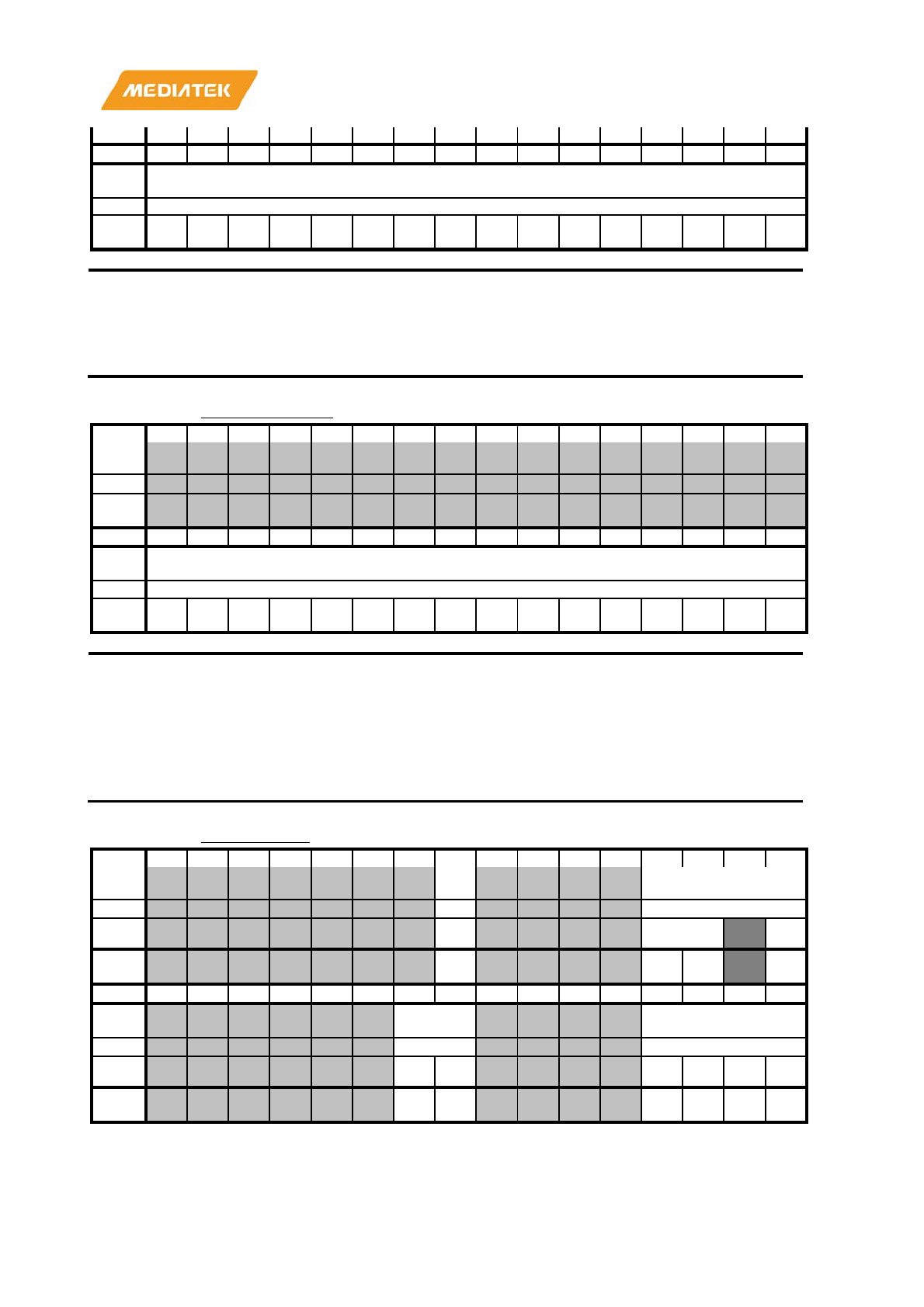
MT7686 Reference Manual
© 2016 - 2017 MediaTek Inc.
Page 37 of 536
This document contains information that is proprietary to MediaTek Inc. (“MediaTek”) and/or its licensor(s).
Any unauthorized use, reproduction or disclosure of this document in whole or in part is strictly prohibited.
t
Bit
15
14
13
12
11
10
9
8
7
6
5
4
3
2
1
0
Nam
e
WPTO
Type
RW
Rese
t
0 0 0 0 0 0 0 0 0 0 0 0 0 0 0 0
Bit(s)
Name
Description
31:0
WPTO
Jump address
This register specifies the destination address of a given DMA transfer to
support ring buffer or double buffer memory access. To enable the wrap
function, set the two control bits,
WPEN and WPSD
in the DMA control register.
A0020110
GDMA1_COUNT
DMA channel 1 transfer count
00000000
Bit
31
30
29
28
27
26
25
24
23
22
21
20
19
18
17
16
Nam
e
Type
Rese
t
Bit
15
14
13
12
11
10
9
8
7
6
5
4
3
2
1
0
Nam
e
COUNT
Type
RW
Rese
t
0 0 0 0 0 0 0 0 0 0 0 0 0 0 0 0
Bit(s)
Name
Description
15:0
COUNT
Number of transfers
This register specifies the number of transfers of the DMA channel is required to
perform. Upon completion, the DMA channel generates an interrupt request to
the processor while
ITEN in GDMAn_CON is set to 1.
•
Note that the total size of transfer data is determined by LEN and SIZE in
GDMAn_CON, such as LEN x SIZE.
A0020114
GDMA1_CON
DMA channel 1 control
00000000
Bit
31
30
29
28
27
26
25
24
23
22
21
20
19
18
17
16
Nam
e
ITE
N
SETTING
Type
RW
RW
BURST
DR
EQ
Rese
t
0 0 0 0 0
Bit
15
14
13
12
11
10
9
8
7
6
5
4
3
2
1
0
Nam
e
SIZE DIRECTION
Type
RW
RW
WP
EN
WP
SD
DIN
C
SIN
C
Rese
t
0 0 0 0 0 0

MT7686 Reference Manual
© 2016 - 2017 MediaTek Inc.
Page 38 of 536
This document contains information that is proprietary to MediaTek Inc. (“MediaTek”) and/or its licensor(s).
Any unauthorized use, reproduction or disclosure of this document in whole or in part is strictly prohibited.
Bit(s)
Name
Description
24
ITEN
Enable DMA transfer
completion interrupt
•
0: Disable
•
1: Enable
19:16
SETTING
[16] Throttle and handshake control for DMA transfer.
The DMA master is able to throttle down the transfer rate by
request
-grant handshake process.
[19:18] Transfer type.
The burst
-type transfers have better bus efficiency. Apply this type
for larger data movement.
Note that the burst
-type transfer will not stop until all of the beats
in a burst are complete or the transfer length is reached. The
transfer type is restricted by SIZE. If SIZE is 00b,
i.e. byte transfer,
all four transfer types can be used. If SIZE is 01b (half
-word
transfer), 16
-
beat incrementing burst cannot be used. If SIZE is 10b,
i.e. word transfer, only single and 4
-beat incrementing burst can be
used.
•
[16] DREQ: 0, No throttle control during DMA transfer or
transfers occurred only between memories; 1, Hardware
handshake management.
•
[19:18] BURST: 00 = Single; 01 = Reserved; 10 = 4-beat
incrementing burst; 11 = Reserved;
9:8
SIZE
Data size within the confine of a bus cycle per
transfer.
These bits confine the data transfer size between the source and
destination to the specified value for individual bus cycle. The size
is in bytes and the maximum value is 4 bytes. It is mainly decided
by the data width of a DMA master.
•
00: Byte transfer/1 byte
•
01: Half-word transfer/2 bytes
•
10: Word transfer/4 bytes
•
11: Reserved
3:0
DIRECTION
[0] Incremental source address.
The source addresses increments after each transfer. If SIZE is in
bytes, the source address will increase by 1, if it’s in
half-word, it
will increase by 2 and if word, increase by 4.
[1] Incremental destination address.
The destination address increments after each transfer. If SIZE is in
bytes, the destination address will increase by 1, if it’s in half
-word,
it will incre
ase by 2 and if word, increase by 4.
[2] Wrap select
The side using address
-wrapping function. Only one side of a DMA
channel can activate the address
-wrapping function at a time.
[3] Wrap enable
Address
-wrapping for ring buffer and double buffer. The next
address of DMA jumps to
WRAP TO address when the current
address matches
WRAP POINT count.
•
[0]SINC:0=Disable; 1=Enable
•
[1]DINC:0=Disable; 1=Enable
•
[2]WPSD: 0=Address-wrapping on source; 1=Address-
wrapping on destination
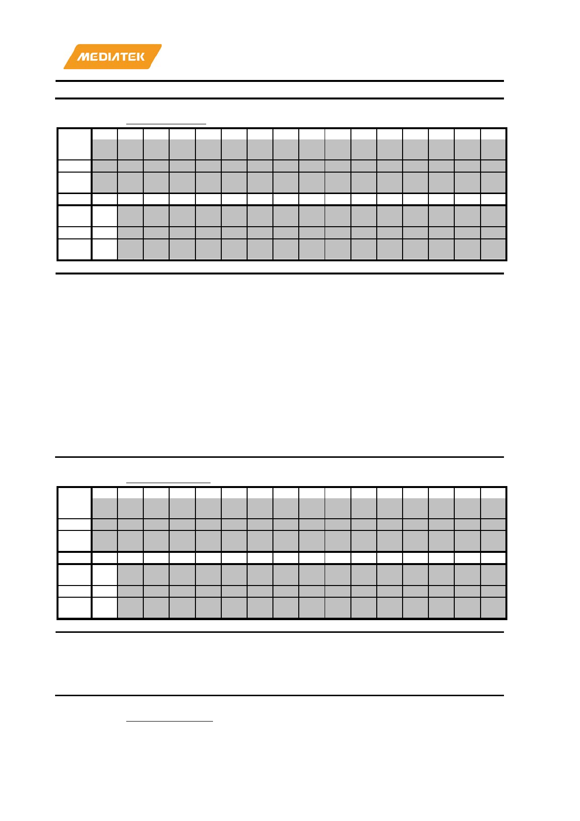
MT7686 Reference Manual
© 2016 - 2017 MediaTek Inc.
Page 39 of 536
This document contains information that is proprietary to MediaTek Inc. (“MediaTek”) and/or its licensor(s).
Any unauthorized use, reproduction or disclosure of this document in whole or in part is strictly prohibited.
•
[3]WPEN: 0=Disable; 1=Enable
A0020118
GDMA1_START
DMA channel 1 start
00000000
Bit
31
30
29
28
27
26
25
24
23
22
21
20
19
18
17
16
Nam
e
Type
Rese
t
Bit
15
14
13
12
11
10
9
8
7
6
5
4
3
2
1
0
Nam
e
ST
R
Type
RW
Rese
t
0
Bit(s)
Name
Description
15
STR
Start control for a DMA channel
This register controls the activity of a DMA channel. Note, that
prior to
setting STR to 1, all the register settings should be
configured. Once STR is set to 1, the hardware will not clear it
automatically no matter the DMA channel accomplishes the DMA
transfer or not. In other words, the value of STR stays at 1
regardless of t
he completion of the DMA transfer. Therefore, the
software program should reset STR to 0 before restarting another
DMA transfer. If this bit is cleared to 0 when DMA transfer is
active, the software should poll RUNn in DMA_GLBSTA after this
bit is cleared
to ensure the current DMA transfer is terminated by
the DMA engine.
•
0: The DMA channel is stopped.
•
1: The DMA channel is started and running.
A002011C
GDMA1_INTSTA
DMA channel 1 interrupt status
00000000
Bit
31
30
29
28
27
26
25
24
23
22
21
20
19
18
17
16
Nam
e
Type
Rese
t
Bit
15
14
13
12
11
10
9
8
7
6
5
4
3
2
1
0
Nam
e
INT
Type
RW
Rese
t
0
Bit(s)
Name
Description
15
INT
Interrupt
status for DMA channel
•
0: No interrupt request is generated.
•
1: An interrupt request is pending and waiting for service.
A0020120
GDMA1_ACKINT
DMA channel 1 interrupt acknowledge
00000000
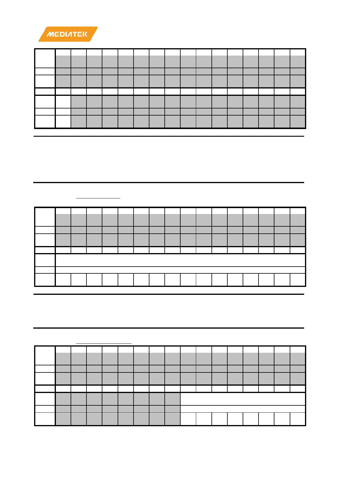
MT7686 Reference Manual
© 2016 - 2017 MediaTek Inc.
Page 40 of 536
This document contains information that is proprietary to MediaTek Inc. (“MediaTek”) and/or its licensor(s).
Any unauthorized use, reproduction or disclosure of this document in whole or in part is strictly prohibited.
Bit
31
30
29
28
27
26
25
24
23
22
21
20
19
18
17
16
Nam
e
Type
Rese
t
Bit
15
14
13
12
11
10
9
8
7
6
5
4
3
2
1
0
Nam
e
AC
K
Type
WO
Rese
t
0
Bit(s)
Name
Description
15
ACK
Interrupt acknowledge
for the DMA channel
•
0: No effect
•
1: Interrupt request is acknowledged and should be
relinquished.
A0020124
GDMA1_RLCT
DMA channel 1 remaining length of
current transfer
00000000
Bit
31
30
29
28
27
26
25
24
23
22
21
20
19
18
17
16
Nam
e
Type
Rese
t
Bit
15
14
13
12
11
10
9
8
7
6
5
4
3
2
1
0
Nam
e
RLCT
Type
RO
Rese
t
0 0 0 0 0 0 0 0 0 0 0 0 0 0 0 0
Bit(s)
Name
Description
15:0
RLCT
This register is to reflect the remaining length of current
transfer (RLCT).
Note that this value is the transfer count, not the transfer data size.
A0020128
GDMA1_LIMITER
DMA channel 1 bandwidth limiter
00000000
Bit
31
30
29
28
27
26
25
24
23
22
21
20
19
18
17
16
Nam
e
Type
Rese
t
Bit
15
14
13
12
11
10
9
8
7
6
5
4
3
2
1
0
Nam
e
LIMITER
Type
RW
Rese
t
0 0 0 0 0 0 0 0
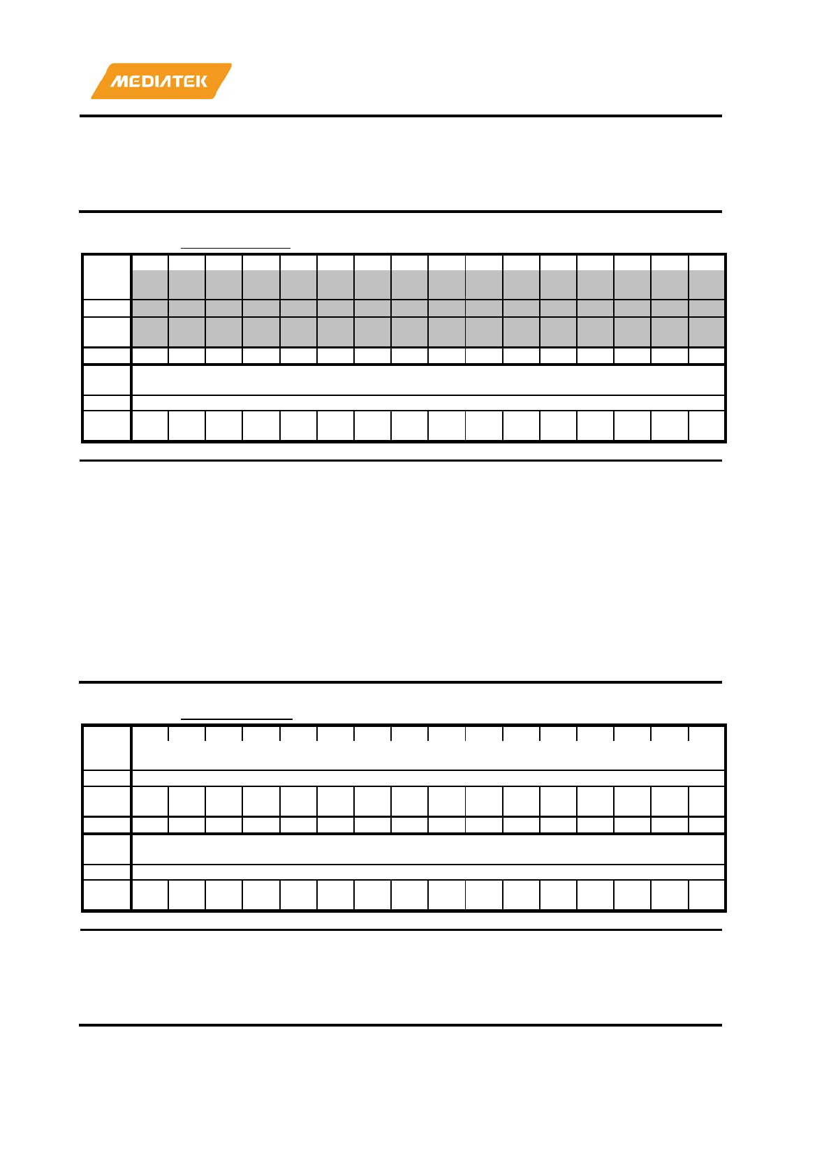
MT7686 Reference Manual
© 2016 - 2017 MediaTek Inc.
Page 41 of 536
This document contains information that is proprietary to MediaTek Inc. (“MediaTek”) and/or its licensor(s).
Any unauthorized use, reproduction or disclosure of this document in whole or in part is strictly prohibited.
Bit(s)
Name
Description
7:0
LIMITER
Utilization Suppression
This register suppresses the bus utilization of the DMA channel.
From 0 to 255. 0 means no limitation, 255 means totally banned,
and others mean bus access permission every (4 x n) AHB clock.
A0020208
PDMA2_WPPT
DMA channel 2 wrap point address
00000000
Bit
31
30
29
28
27
26
25
24
23
22
21
20
19
18
17
16
Nam
e
Type
Rese
t
Bit
15
14
13
12
11
10
9
8
7
6
5
4
3
2
1
0
Nam
e
WPPT
Type
RW
Rese
t
0 0 0 0 0 0 0 0 0 0 0 0 0 0 0 0
Bit(s)
Name
Description
15:0
WPPT
Transfer counts before jump
This register specifies the transfer count required to perform before
the jump point. This can be used to support ring buffer or double
buffer memory access. To enable the wrap function, two control
bits,
WPEN and WPSD in the DMA control register must be
p
rogrammed. If the transfer counter in the DMA engine matches
this value, an address jump will occur, and the next address will be
the address specified in
GDMAn_WPTO. To enable this function,
set up
WPEN in GDMAn_CON.
Note, that the total size of data specified in the wrap point count in
a DMA channel is determined by WPPT together with
SIZE in
GDMAn_CON
, such as WPPT x SIZE.
A002020C
PDMA2_WPTO
DMA channel 2 wrap to address
00000000
Bit
31
30
29
28
27
26
25
24
23
22
21
20
19
18
17
16
Nam
e
WPTO
Type
RW
Rese
t
0 0 0 0 0 0 0 0 0 0 0 0 0 0 0 0
Bit
15
14
13
12
11
10
9
8
7
6
5
4
3
2
1
0
Nam
e
WPTO
Type
RW
Rese
t
0 0 0 0 0 0 0 0 0 0 0 0 0 0 0 0
Bit(s)
Name
Description
31:0
WPTO
Jump address
This register specifies the address of the jump destination of a given DMA transfer
to support ring buffer or double buffer memory access. To enable this function, set
the two control bits, WPEN and WPSD in the DMA control register.
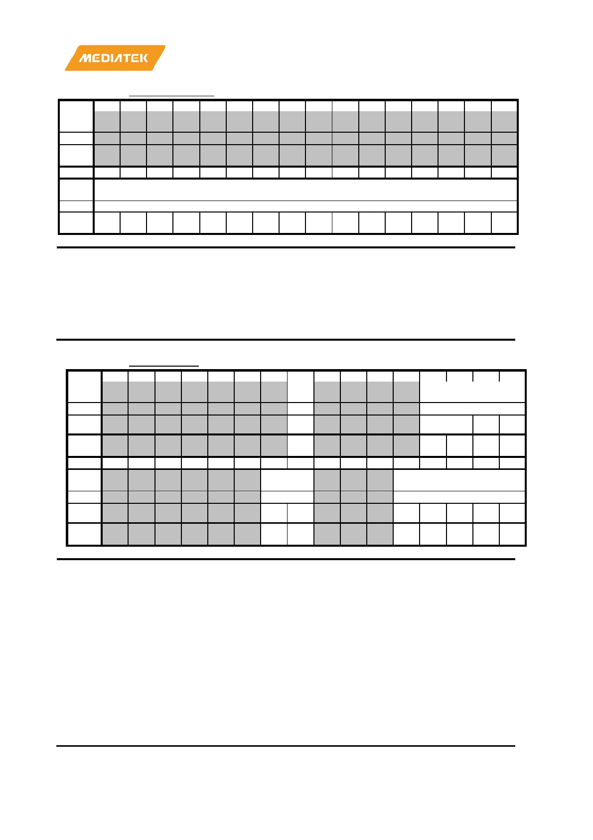
MT7686 Reference Manual
© 2016 - 2017 MediaTek Inc.
Page 42 of 536
This document contains information that is proprietary to MediaTek Inc. (“MediaTek”) and/or its licensor(s).
Any unauthorized use, reproduction or disclosure of this document in whole or in part is strictly prohibited.
A0020210
PDMA2_COUNT
DMA channel 2 transfer count
00000000
Bit
31
30
29
28
27
26
25
24
23
22
21
20
19
18
17
16
Nam
e
Type
Rese
t
Bit
15
14
13
12
11
10
9
8
7
6
5
4
3
2
1
0
Nam
e
COUNT
Type
RW
Rese
t
0 0 0 0 0 0 0 0 0 0 0 0 0 0 0 0
Bit(s)
Name
Description
15:0
COUNT
Number of transfers
This register specifies the number of transfers of the DMA channel is required to
perform. Upon completion, the DMA channel generates an interrupt request to
the processor while
ITEN in GDMAn_CON is set to 1.
Note that the total size of transfer data is d
etermined by LEN and SIZE in
GDMAn_CON
, such as LEN x SIZE.
A0020214
PDMA2_CON
DMA channel 2 control
00000000
Bit
31
30
29
28
27
26
25
24
23
22
21
20
19
18
17
16
Nam
e
ITE
N
SETTING
Type
RW
RW
BURST
B2
W
DR
EQ
Rese
t
0 0 0 0 0
Bit
15
14
13
12
11
10
9
8
7
6
5
4
3
2
1
0
Nam
e
SIZE DIRECTION
Type
RW
RW
DIR
WP
EN
WP
SD
DIN
C
SIN
C
Rese
t
0 0 0 0 0 0 0
Bit(s)
Name
Description
24
ITEN
Enable DMA
transfer completion interrupt
•
0: Disable
•
1: Enable
19:16
SETTING
[16] Throttle and handshake control for DMA transfer.
The DMA master is able to throttle down the transfer rate by
request
-grant handshake process.
[17]Byte to word
Word to byte or byte to
word transfer for the applications of
transferring non
-word-aligned-address data to word-aligned-
address data. Note that BURST is set to 4
-
beat burst this function is
enabled, and the SIZE is set to byte.
[19:18] Transfer type.
The burst-type transfers have better bus efficiency. Apply this type

MT7686 Reference Manual
© 2016 - 2017 MediaTek Inc.
Page 43 of 536
This document contains information that is proprietary to MediaTek Inc. (“MediaTek”) and/or its licensor(s).
Any unauthorized use, reproduction or disclosure of this document in whole or in part is strictly prohibited.
for mass data movement.
Note that the burst
-type transfer will not stop until all of the beats
in a burst are complete or the transfer length is reached. The
transfer type is restricted by SIZE. If SIZE is 00b,
i.e. byte transfer,
all four transfer types can be used. If SIZE is 01b (half
-word
transfer), 16
-
beat incrementing burst cannot be used. If SIZE is 10b,
i.e. word transfer, only single and 4
-beat incrementing burst can be
used.
•
[16] DREQ: 0, No throttle control during DMA transfer or
transfers occurred only between memories; 1, Hardware
handshake management.
•
[17]B2W: 0=Disable; 1=Enable
•
[19:18] BURST: 00 = Single; 01 = Reserved; 10 = 4-beat
incrementing burst; 11 = Reserved;
9:8
SIZE
Data size within the
confine of a bus cycle per transfer.
These bits confine the data transfer size between the source and
destination to the specified value for individual bus cycle. The size
is in bytes and the maximum value is 4 bytes. It is mainly decided
by the data width
of a DMA master.
•
00: Byte transfer/1 byte
•
01: Half-word transfer/2 bytes
•
10: Word transfer/4 bytes
•
11: Reserved
4:0
DIRECTION
[0] Incremental source address.
The source addresses increments after each transfer. If SIZE is in
bytes, the source address wil
l increase by 1, if it’s in half-word, it
will increase by 2 and if word, increase by 4.
[1] Incremental destination address.
The destination address increments after each transfer. If SIZE is in
bytes, the destination address will increase by 1, if it’s
in half-word,
it will increase by 2 and if word, increase by 4.
[2] Wrap select
The side using address
-wrapping function. Only one side of a DMA
channel can activate the address
-wrapping function at a time.
[3] Wrap enable
Address
-wrapping for ring buffer and double buffer. The next
address of DMA jumps to
WRAP TO address when the current
address matches
WRAP POINT count.
•
[0]SINC:0=Disable; 1=Enable
•
[1]DINC:0=Disable; 1=Enable
•
[2]WPSD: 0=Address-wrapping on source; 1=Address-
wrapping on destination
•
[3]WPEN: 0=Disable; 1=Enable
•
[4]DIR: 0=peripheral TX; 1=peripheral RX
A0020218
PDMA2_START
DMA channel 2 start
00000000
Bit
31
30
29
28
27
26
25
24
23
22
21
20
19
18
17
16
Nam
e
Type
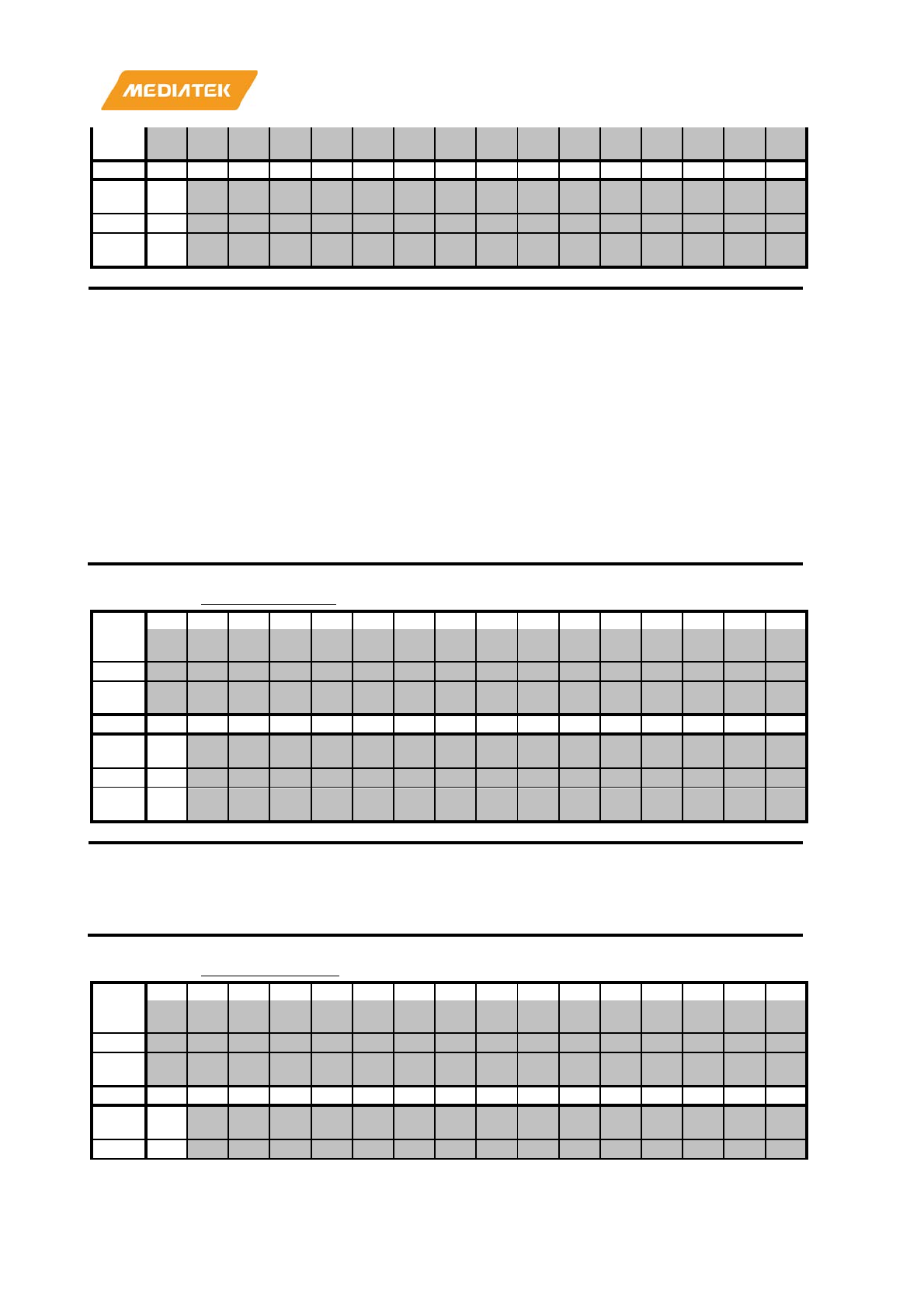
MT7686 Reference Manual
© 2016 - 2017 MediaTek Inc.
Page 44 of 536
This document contains information that is proprietary to MediaTek Inc. (“MediaTek”) and/or its licensor(s).
Any unauthorized use, reproduction or disclosure of this document in whole or in part is strictly prohibited.
Rese
t
Bit
15
14
13
12
11
10
9
8
7
6
5
4
3
2
1
0
Nam
e
ST
R
Type
RW
Rese
t
0
Bit(s)
Name
Description
15
STR
Start control for a DMA channel
This register controls the activity of a DMA channel. Note that prior
to setting STR to 1, all the register settings should be configured.
Once STR is set to 1, the hardware will not clear it automatically no
matter the DMA channel accomplishes the DMA transfer or not. In
other words, the value of STR stays at 1 regardless of the completion
of the DMA transfer. Therefore, the software program should reset
STR to 0 before restarting another DMA transfer. If this bit is
cleared to 0 when DMA transfer is active, the software should poll
RUNn in DMA_GLBSTA after this bit is
cleared to ensure the
current DMA transfer is terminated by the DMA engine.
•
0: The DMA channel is stopped.
•
1: The DMA channel is started and running.
A002021C
PDMA2_INTSTA
DMA channel 2 interrupt status
00000000
Bit
31
30
29
28
27
26
25
24
23
22
21
20
19
18
17
16
Nam
e
Type
Rese
t
Bit
15
14
13
12
11
10
9
8
7
6
5
4
3
2
1
0
Nam
e
INT
Type
RW
Rese
t
0
Bit(s)
Name
Description
15
INT
Interrupt status for DMA channel
0: No interrupt request is generated.
1: One interrupt request is pending and waiting for service.
A0020220
PDMA2_ACKINT
DMA channel 2 interrupt acknowledge
00000000
Bit
31
30
29
28
27
26
25
24
23
22
21
20
19
18
17
16
Nam
e
Type
Rese
t
Bit
15
14
13
12
11
10
9
8
7
6
5
4
3
2
1
0
Nam
e
AC
K
Type
WO
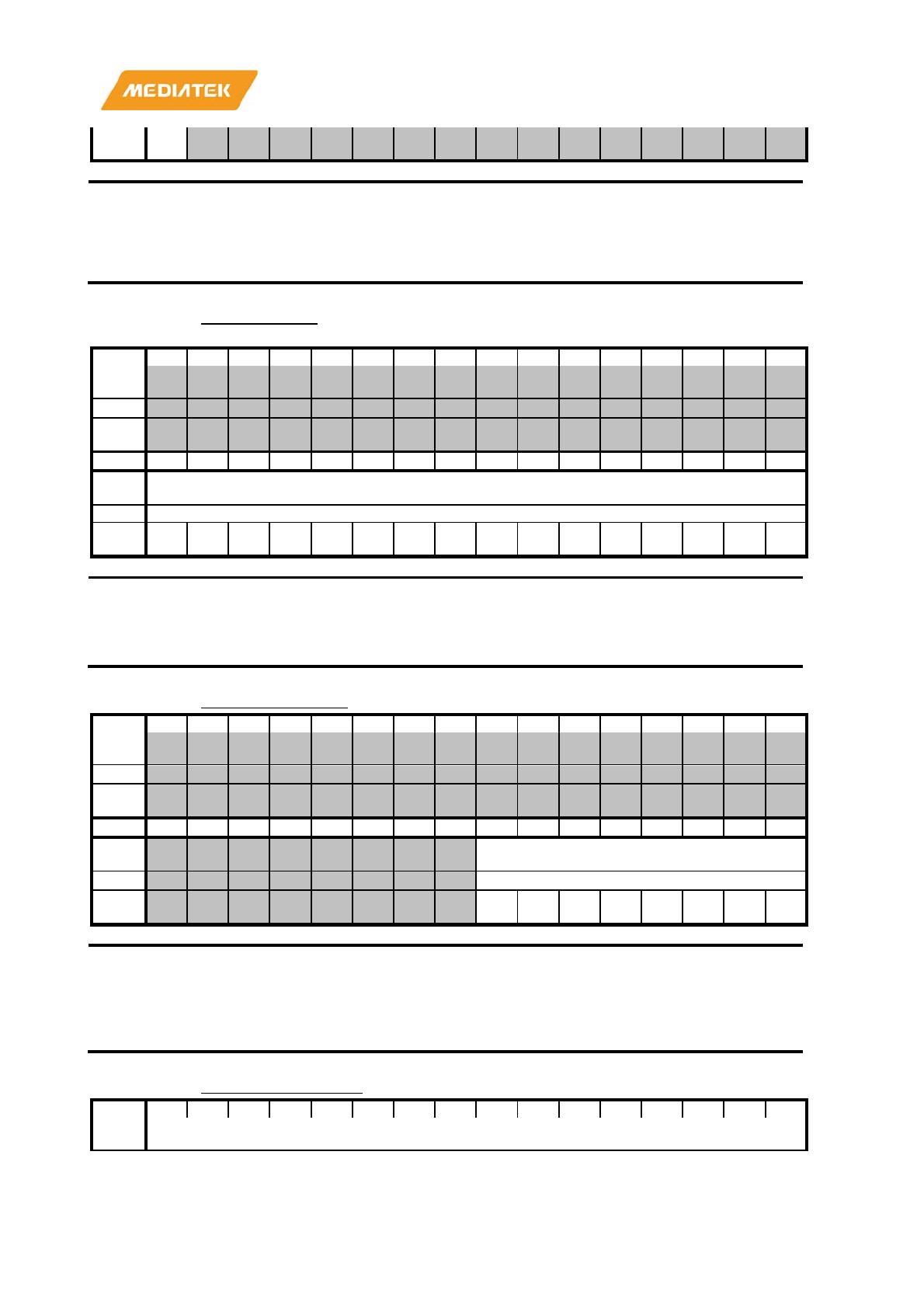
MT7686 Reference Manual
© 2016 - 2017 MediaTek Inc.
Page 45 of 536
This document contains information that is proprietary to MediaTek Inc. (“MediaTek”) and/or its licensor(s).
Any unauthorized use, reproduction or disclosure of this document in whole or in part is strictly prohibited.
Rese
t
0
Bit(s)
Name
Description
15
ACK
Interrupt
acknowledgement for the DMA channel
•
0: No effect
•
1: Interrupt request is acknowledged and should be relinquished.
A0020224
PDMA2_RLCT
DMA channel 2 remaining length of
current transfer
00000000
Bit
31
30
29
28
27
26
25
24
23
22
21
20
19
18
17
16
Nam
e
Type
Rese
t
Bit
15
14
13
12
11
10
9
8
7
6
5
4
3
2
1
0
Nam
e
RLCT
Type
RO
Rese
t
0 0 0 0 0 0 0 0 0 0 0 0 0 0 0 0
Bit(s)
Name
Description
15:0
RLCT
This register is to reflect the
remaining length of current
transfer (RLCT).
Note that this value is transfer count, not the transfer data size.
A0020228
PDMA2_LIMITER
DMA channel 2 bandwidth limiter
00000000
Bit
31
30
29
28
27
26
25
24
23
22
21
20
19
18
17
16
Nam
e
Type
Rese
t
Bit
15
14
13
12
11
10
9
8
7
6
5
4
3
2
1
0
Nam
e
LIMITER
Type
RW
Rese
t
0 0 0 0 0 0 0 0
Bit(s)
Name
Description
7:0
LIMITER
Utilization Suppression
This
register suppresses the bus utilization of the DMA channel.
From 0 to 255. 0 means no limitation, 255 means totally banned,
and others mean bus access permission every (4 x n) AHB clock.
A002022C
PDMA2_PGMADDR
DMA channel 2 prog
rammable address
00000000
Bit
31
30
29
28
27
26
25
24
23
22
21
20
19
18
17
16
Nam
e
PGMADDR
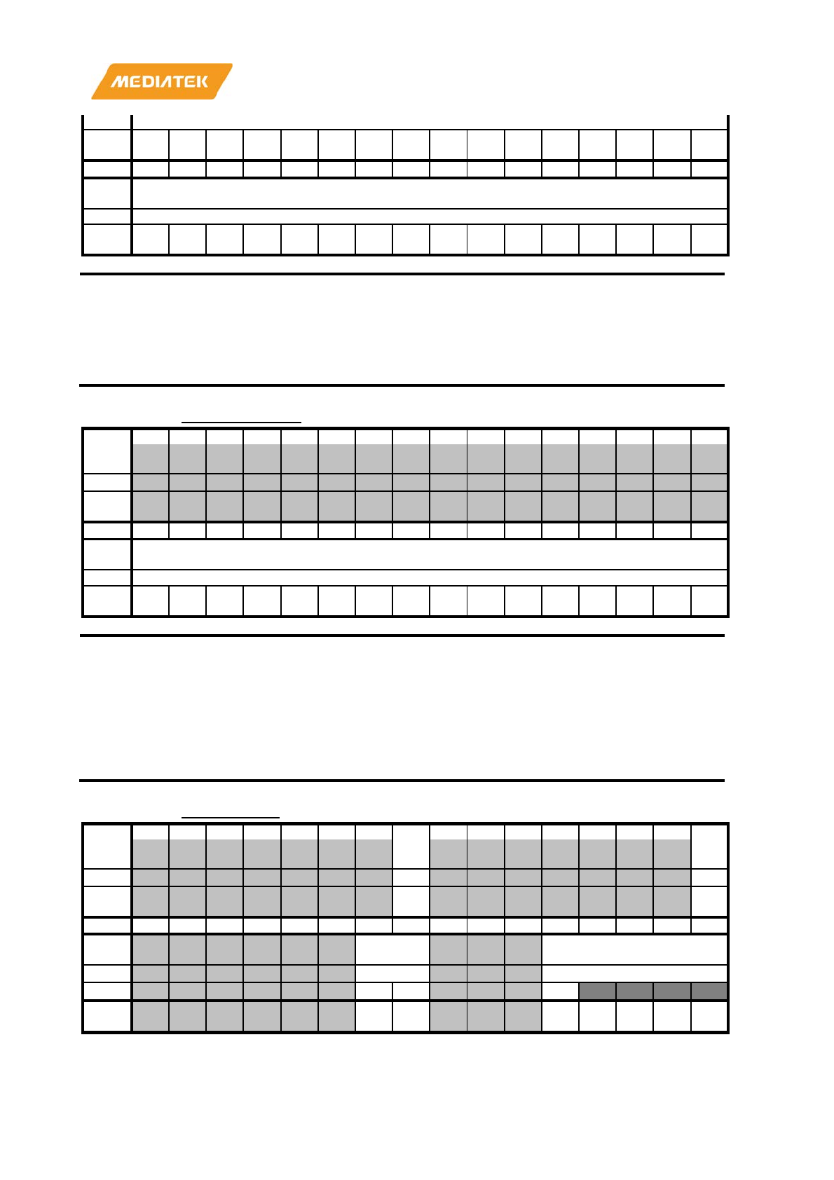
MT7686 Reference Manual
© 2016 - 2017 MediaTek Inc.
Page 46 of 536
This document contains information that is proprietary to MediaTek Inc. (“MediaTek”) and/or its licensor(s).
Any unauthorized use, reproduction or disclosure of this document in whole or in part is strictly prohibited.
Type
RW
Rese
t
0 0 0 0 0 0 0 0 0 0 0 0 0 0 0 0
Bit
15
14
13
12
11
10
9
8
7
6
5
4
3
2
1
0
Nam
e
PGMADDR
Type
RW
Rese
t
0 0 0 0 0 0 0 0 0 0 0 0 0 0 0 0
Bit(s)
Name
Description
31:0
PGMADDR
PDMA programmable address.
The above registers specify the address for a half
-
size DMA channel.
This address represents the source address if DIR in DMA_CON is
set to 0 and represents the destination address if DIR in
PDMAn_CON
is set to 1.
A0020710
VDMA7_COUNT
DMA channel 7 transfer count
00000000
Bit
31
30
29
28
27
26
25
24
23
22
21
20
19
18
17
16
Nam
e
Type
Rese
t
Bit
15
14
13
12
11
10
9
8
7
6
5
4
3
2
1
0
Nam
e
COUNT
Type
RW
Rese
t
0 0 0 0 0 0 0 0 0 0 0 0 0 0 0 0
Bit(s)
Name
Description
15:0
COUNT
FIFO threshold
For virtual FIFO DMA, this register is used to configure the RX
threshold and TX threshold. The interrupt is triggered when FIFO
count is larger than or equal to RX threshold in RX path or FIFO
count is less than or equal to TX threshold in TX path.
Note,
that the ITEN bit in the VDMAn_CON register shall be set or
no interrupt will be issued. n is from 1 to 16.
A0020714
VDMA7_CON
DMA channel 7 control
00000000
Bit
31
30
29
28
27
26
25
24
23
22
21
20
19
18
17
16
Nam
e
ITE
N
DR
EQ
Type
RW
RW
Rese
t
0 0
Bit
15
14
13
12
11
10
9
8
7
6
5
4
3
2
1
0
Nam
e
SIZE DIRECTION
Type
RW
RW
DIR
Rese
t
0 0 0 0 0 0 0

MT7686 Reference Manual
© 2016 - 2017 MediaTek Inc.
Page 47 of 536
This document contains information that is proprietary to MediaTek Inc. (“MediaTek”) and/or its licensor(s).
Any unauthorized use, reproduction or disclosure of this document in whole or in part is strictly prohibited.
Bit(s)
Name
Description
24
ITEN
Enable DMA transfer completion interrupt
•
0: Disable
•
1: Enable
16
DREQ
Throttle and handshake control for DMA transfer.
The DMA master is able to throttle down the transfer rate by request
-grant
handshake.
•
0: No throttle control during DMA transfer or transfers occurred only
between memories
•
1: Hardware handshake management
9:8
SIZE
Data size within the confine of a bus cycle per transfer.
These bits confine the data transfer size between the source and destination
to the specified value for individual bus cycle. The size is in terms of byte,
and the maximum value is 4 bytes. It is mainly decided by the data width of
a DMA master.
•
00: Byte transfer/1 byte
•
01: Half-word transfer/2 bytes
•
10: Word transfer/4 bytes
•
11: Reserved
4:0
DIRECTION
[4]Directions of VDMA transfer
The direction is from the perspective of the DMA masters. WRITE means
reading from master and then writing to the address specified in
VDMAn_PGMADDR
, and vice versa. No effect on channel 1.
[4]DIR: 0=peripheral TX; 1=peripheral RX
A0020718
VDMA7_START
DMA channel 7 start register
00000000
Bit
31
30
29
28
27
26
25
24
23
22
21
20
19
18
17
16
Nam
e
Type
Rese
t
Bit
15
14
13
12
11
10
9
8
7
6
5
4
3
2
1
0
Nam
e
ST
R
Type
RW
Rese
t
0
Bit(s)
Name
Description
15
STR
Start control for a DMA channel
This register controls the activity of a DMA channel. Note that prior
to setting STR to 1, all the register settings should be configured.
Once STR is set to 1, the hardware will not clear it automatically no
matter the DMA channel accomplishes the DMA transfer or not. In
other words, the value of STR stays at 1 regardless of the completion
of the DMA transfer. Therefore, the software program should reset
STR to 0 before restarting another DMA transfer. If this bit is
cleared to 0 when DMA transfer is active, the software should poll
RUNn in DMA_GLBSTA after this bit is clear
ed to ensure the
current DMA transfer is terminated by the DMA engine.
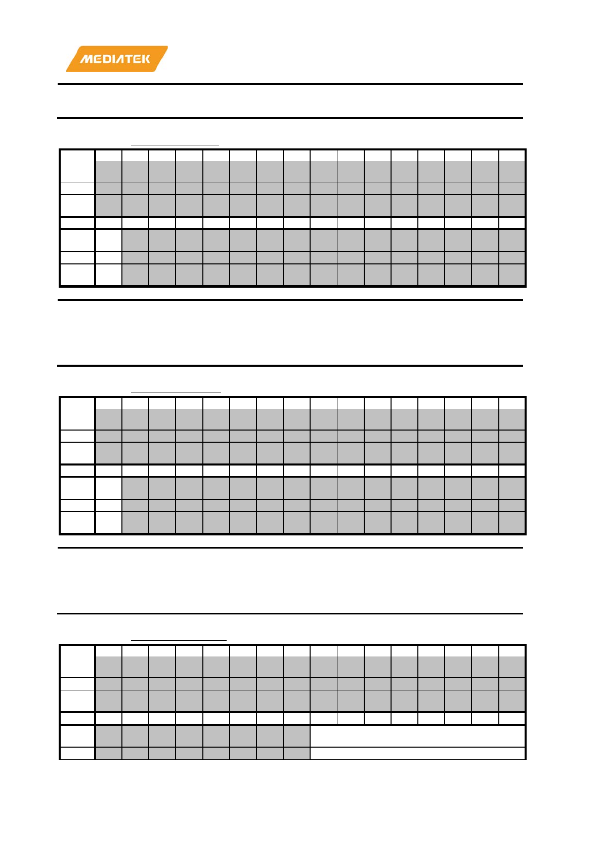
MT7686 Reference Manual
© 2016 - 2017 MediaTek Inc.
Page 48 of 536
This document contains information that is proprietary to MediaTek Inc. (“MediaTek”) and/or its licensor(s).
Any unauthorized use, reproduction or disclosure of this document in whole or in part is strictly prohibited.
•
0: The DMA channel is stopped.
•
1: The DMA channel is started and running.
A002071C
VDMA7_INTSTA
DMA channel 7 interrupt status
00000000
Bit
31
30
29
28
27
26
25
24
23
22
21
20
19
18
17
16
Nam
e
Type
Rese
t
Bit
15
14
13
12
11
10
9
8
7
6
5
4
3
2
1
0
Nam
e
INT
Type
RO
Rese
t
0
Bit(s)
Name
Description
15
INT
Interrupt status for DMA channel
•
0: No interrupt request is generated.
•
1: An interrupt request is pending and waiting for service.
A0020720
VDMA7_ACKINT
DMA channel 7 interrupt acknowledge
00000000
Bit
31
30
29
28
27
26
25
24
23
22
21
20
19
18
17
16
Nam
e
Type
Rese
t
Bit
15
14
13
12
11
10
9
8
7
6
5
4
3
2
1
0
Nam
e
AC
K
Type
WO
Rese
t
0
Bit(s)
Name
Description
15
ACK
Interrupt
acknowledgement for the DMA channel
•
0: No effect
•
1: Interrupt request is acknowledged and should be relinquished.
A0020728
VDMA7_LIMITER
DMA channel 7 bandwidth limiter
00000000
Bit
31
30
29
28
27
26
25
24
23
22
21
20
19
18
17
16
Nam
e
Type
Rese
t
Bit
15
14
13
12
11
10
9
8
7
6
5
4
3
2
1
0
Nam
e
LIMITER
Type
RW
MT7686 Reference Manual
© 2016 - 2017 MediaTek Inc.
Page 49 of 536
This document contains information that is proprietary to MediaTek Inc. (“MediaTek”) and/or its licensor(s).
Any unauthorized use, reproduction or disclosure of this document in whole or in part is strictly prohibited.
Rese
t
0 0 0 0 0 0 0 0
Bit(s)
Name
Description
7:0
LIMITER
Utilization Suppression
This
register suppresses the bus utilization of the DMA channel.
From 0 to 255. 0 means no limitation, 255 means totally banned,
and others mean request for bus access permission every (4 x n)
AHB clock.
A002072C
VDMA7_PGMADDR
DMA ch
annel 7 programmable address
00000000
Bit
31
30
29
28
27
26
25
24
23
22
21
20
19
18
17
16
Nam
e
PGMADDR
Type
RW
Rese
t
0 0 0 0 0 0 0 0 0 0 0 0 0 0 0 0
Bit
15
14
13
12
11
10
9
8
7
6
5
4
3
2
1
0
Nam
e
PGMADDR
Type
RW
Rese
t
0 0 0 0 0 0 0 0 0 0 0 0 0 0 0 0
Bit(s)
Name
Description
31:0
PGMADDR
VDMA programmable address.
Specifies the address for a half
-size DMA channel. This address
indicates that the source address if DIR in
DMA_CON is set to 0
and the destination address of DIR in
VDMAn_CON is set to 1.
A0020730
VDMA7_WRPTR
DMA channel 7 write pointer
00000000
Bit
31
30
29
28
27
26
25
24
23
22
21
20
19
18
17
16
Nam
e
WRPTR
Type
RO
Rese
t
0 0 0 0 0 0 0 0 0 0 0 0 0 0 0 0
Bit
15
14
13
12
11
10
9
8
7
6
5
4
3
2
1
0
Nam
e
WRPTR
Type
RO
Rese
t
0 0 0 0 0 0 0 0 0 0 0 0 0 0 0 0
Bit(s)
Name
Description
31:0
WRPTR
Virtual FIFO write pointer
A0020734
VDMA7_RDPTR
DMA channel 7 read pointer
00000000
Bit
31
30
29
28
27
26
25
24
23
22
21
20
19
18
17
16
Nam
e
RDPTR
Type
RO
Rese
t
0 0 0 0 0 0 0 0 0 0 0 0 0 0 0 0

MT7686 Reference Manual
© 2016 - 2017 MediaTek Inc.
Page 50 of 536
This document contains information that is proprietary to MediaTek Inc. (“MediaTek”) and/or its licensor(s).
Any unauthorized use, reproduction or disclosure of this document in whole or in part is strictly prohibited.
Bit
15
14
13
12
11
10
9
8
7
6
5
4
3
2
1
0
Nam
e
RDPTR
Type
RO
Rese
t
0 0 0 0 0 0 0 0 0 0 0 0 0 0 0 0
Bit(s)
Name
Description
31:0
RDPTR
Virtual FIFO read pointer
A0020738
VDMA7_FFCNT
DMA channel 7 FIFO count
00000000
Bit
31
30
29
28
27
26
25
24
23
22
21
20
19
18
17
16
Nam
e
Type
Rese
t
Bit
15
14
13
12
11
10
9
8
7
6
5
4
3
2
1
0
Nam
e
FFCNT
Type
RO
Rese
t
0 0 0 0 0 0 0 0 0 0 0 0 0 0 0 0
Bit(s)
Name
Description
15:0
FFCNT
Displays the number of data stored in FIFO.
•
0: FIFO is empty,
•
FFCNT = FFSIZE: FIFO is full.
A002073C
VDMA7_FFSTA
DMA channel 7 FIFO status
00000000
Bit
31
30
29
28
27
26
25
24
23
22
21
20
19
18
17
16
Nam
e
Type
Rese
t
Bit
15
14
13
12
11
10
9
8
7
6
5
4
3
2
1
0
Nam
e AL
T
EM
PT
Y
FU
LL
Type
RO
RO
RO
Rese
t
0 0 0
Bit(s)
Name
Description
2
ALT
Indicates FIFO count is larger than ALTLEN.
DMA issues an alert signal to UART/BRIF to enable UART/BRIF
flow control.
0: Did not reach the alert region
1: Reached the alert region
1
EMPTY
Indicates FIFO is empty
0: Not empty
MT7686 Reference Manual
© 2016 - 2017 MediaTek Inc.
Page 51 of 536
This document contains information that is proprietary to MediaTek Inc. (“MediaTek”) and/or its licensor(s).
Any unauthorized use, reproduction or disclosure of this document in whole or in part is strictly prohibited.
1: Empty
0
FULL
Indicates FIFO is full
0: Not full
1: Full
A0020740
VDMA7_ALTLEN
DMA channel 7 alert length
00000000
Bit
31
30
29
28
27
26
25
24
23
22
21
20
19
18
17
16
Nam
e
Type
Rese
t
Bit
15
14
13
12
11
10
9
8
7
6
5
4
3
2
1
0
Nam
e
ALTLEN
Type
RW
Rese
t
0 0 0 0 0 0
Bit(s)
Name
Description
5:0
ALTLEN
Specifies the alert length of virtual FIFO DMA.
Once the remaining FIFO space is less than
ALTLEN
, an alert signal
will be issued to
UART/BRIF to enable the flow control. Normally,
ALTLEN
shall be bigger than 16 for UART/BRIF application.
A0020744
VDMA7_FFSIZE
DMA channel 7 FIFO size
00000000
Bit
31
30
29
28
27
26
25
24
23
22
21
20
19
18
17
16
Nam
e
Type
Rese
t
Bit
15
14
13
12
11
10
9
8
7
6
5
4
3
2
1
0
Nam
e
FFSIZE
Type
RW
Rese
t
0 0 0 0 0 0 0 0 0 0 0 0 0 0 0 0
Bit(s)
Name
Description
15:0
FFSIZE
Specifies the FIFO
size of virtual FIFO DMA

MT7686 Reference Manual
© 2016 - 2017 MediaTek Inc.
Page 52 of 536
This document contains information that is proprietary to MediaTek Inc. (“MediaTek”) and/or its licensor(s).
Any unauthorized use, reproduction or disclosure of this document in whole or in part is strictly prohibited.
5. Universal Asynchronous Receiver/Transmitter
5.1. Overview
The universal asynchronous receiver transmitter (UART) provides full duplex serial communication channels
between the baseband chipset and external devices.
The UART has both M16C450 and M16550A modes of operation, which are compatible with a range of standard
software drivers. The extensions are designed to be broadly software compatible with M16550A variants, but
certain areas offer no consensus.
The UART supports word lengths from 5 to 8 bits, an optional parity bit and one or two stop bits and is fully
programmable by an 8-bit CPU interface. A 16-bit programmable baud rate generator and an 8-bit scratch register
are included, together with separate transmit and receive FIFOs. Two modem control lines and a diagnostic loop-
back mode are provided. The UART also includes two DMA handshake lines, indicating when the FIFOs are ready to
transfer data to the CPU.
Note that the UART is designed so that all internal operation is synchronized by the clock signal. This
synchronization results in minor timing differences between the UART and industry standard M16550A device,
which means that the core is not clocked for clock identical to the original device.
After hardware reset, the UART will be in M16C450 mode. Its FIFOs can then be enabled and the UART can enter
M16550A mode. The UART also has further additional functions beyond the M16550A mode. Each of the extended
functions can be selected individually under software control.
5.2. Features
• There are three UART channels supporting hardware and software flow control. Each UART has an
individual interrupt source.
• For transmission, the UART supports word lengths from 5 to 8 bits with an optional parity bit and one or
two stop bits, and baud rate from 110bps to 921,600bps.
• There are dedicated DMA channels for both TX and RX for each UART.
• The UART supports auto baud rate detection in RX mode. The recommended baud rate range is from
300bps to 115,200bps.
5.3. Block diagram
Figure 5.3-1 shows the detailed UART block diagram.
MT7686 Reference Manual
© 2016 - 2017 MediaTek Inc.
Page 53 of 536
This document contains information that is proprietary to MediaTek Inc. (“MediaTek”) and/or its licensor(s).
Any unauthorized use, reproduction or disclosure of this document in whole or in part is strictly prohibited.
TSRTHR
RBR RSR
Tx Machine
Rx Machine
Modem
Control
UART
Registers
Baud
Generator
Baud
Auto
Baud
Detection
Tx Data
APB
Divisor
RTS
CTS
Rx Data
Tx Data
CTS
RTS
Rx Data
Figure 5.3-1. UART block diagram
5.4. Functions
5.4.1. Baud rate generation
The UART contains a programmable baud generator. The baud rate generator divides the input clock by a divisor to
generate a baud clock for data sampling. The baud clock is n times the baud rate where n is a positive integer. The
formula to calculate the baud rate is:
Baud Rate = (Input Clock Frequency)Divisor n
The input clock frequency can be either F_FXO_CK or F_FXO_CK/2, the frequency of F_FXO_CK is 26MHz or 20MHz
depending on the type of XO crystal. The divisor is stored in two 8-bit register fields (DLH and DLL) in register DL.
The positive integer n is controlled by HIGHSPEED.SPEED.
• When HIGHSPEED.SPEED = 0, n = 16 and the data is sampled in the eighth baud clock cycle. When
HIGHSPEED.SPEED = 1, n = 8 and the data is sampled in the fourth baud clock cycle.
• When HIGHSPEED.SPEED = 2, n = 4 and the data is sampled in the second baud clock cycle.
• When HIGHSPEED.SPEED = 3, n = SAMPLE_REG.SAMPLE_COUNT+1 and the data is sampled in the
(SAMPLE_REG.SAMPLE_POINT)th baud clock cycle.
5.4.2. Data format
The data format of the UART is shown in Figure 5.4-1. One transmission includes 1 start bit; 5, 6, 7 or 8 data bits; 1
optional parity bit; and 1 or 2 stop bits. The start bit is always low, the parity bit can be either odd or even parity,
and the end bit is always high.

MT7686 Reference Manual
© 2016 - 2017 MediaTek Inc.
Page 54 of 536
This document contains information that is proprietary to MediaTek Inc. (“MediaTek”) and/or its licensor(s).
Any unauthorized use, reproduction or disclosure of this document in whole or in part is strictly prohibited.
Start bit Data Data Data Parity End bit
…
5~8 bit data
Figure 5.4-1. UART data format
5.4.3. Transmission
Transmission of the UART includes a TX holding register (THR) and TX shift register (TSR). THR receives data from
Advanced Peripheral Bus (APB) and shifts to TSR. The data in TSR will then be serialized and sent to General-
Purpose Input/Output (GPIO). In FIFO mode, the THR becomes a 16-byte FIFO.
5.4.4. Reception
Reception of the UART includes an RX buffer register (RBR) and RX shift register (RSR). RSR receives and
concatenates the serial data bits from GPIO. The data will then be moved from RSR to RBR and ready to be read by
APB. In FIFO mode, the RBR becomes a 32-byte FIFO.
5.4.5. Direct Memory Access (DMA) mode
The UART supports DMA mode operation only when the FIFOs are enabled (FCR.FIFOE == 1). Set
DMA_CON.TX_DMA_EN and DMA_CON.RX_DMA_EN to 1 to enable DMA mode of transmission and reception,
respectively.
5.4.6. Hardware flow control
The UART supports RTS/CTS hardware flow control. In transmission mode, the UART will pause transmission if CTS
is asserted, and will resume transmission after CTS is de-asserted. In reception mode, the UART will assert RTS if
one of the following conditions is met:
1) RBR is occupied in non-FIFO mode.
2) The amount of data in RBR is above threshold in FIFO mode or DMA mode.
3) The amount of data in virtual FIFO DMA is above threshold in DMA mode.
4) The system is entering sleep mode.
The UART will de-assert RTS when all of the above conditions are no longer met.
5.4.7. Software flow control
The UART supports XON/XOFF flow control. In transmission mode, the UART will pause transmission if an XOFF
character is received and will resume transmission after receiving an XON character. In reception mode, the UART
will send an XOFF character if one of the following conditions is met:
1) RBR is occupied in non-FIFO mode.
2) The amount of data in RBR is above threshold in FIFO mode or DMA mode.
3) The amount of data in virtual FIFO DMA is above threshold in DMA mode.
4) The system is entering sleep mode.
The UART will send an XON character when conditions 1, 2, and 3 are no longer valid. However, if the UART sends
an XOFF character due to condition 4, the user should send an XON character manually after wake-up since the
UART is powered down and all settings are cleared in sleep mode.
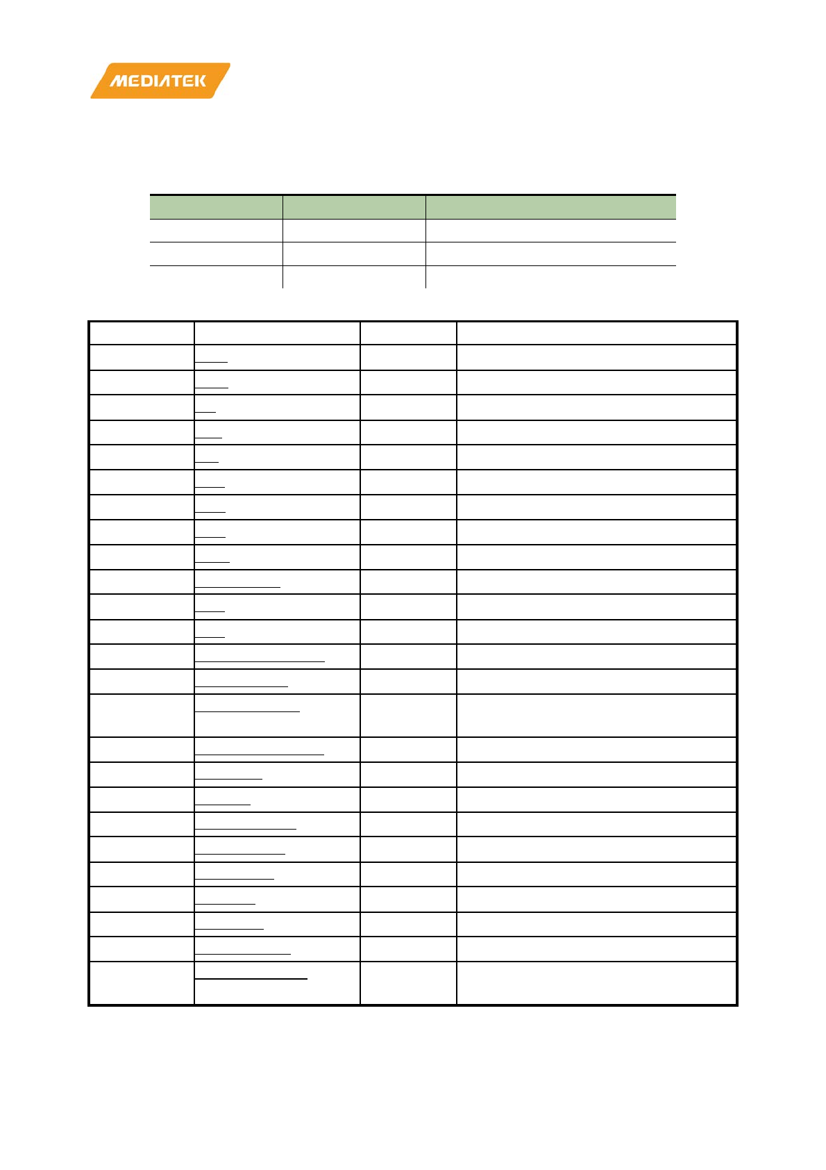
MT7686 Reference Manual
© 2016 - 2017 MediaTek Inc.
Page 55 of 536
This document contains information that is proprietary to MediaTek Inc. (“MediaTek”) and/or its licensor(s).
Any unauthorized use, reproduction or disclosure of this document in whole or in part is strictly prohibited.
5.5. Register mapping
There are three UART interfaces supported in this chipset. The registers below are the same for all UARTs. The only
difference is the base address.
UART number Base address Feature
UART0 0xA00C0000 Supports DMA, hardware flow control
UART1 0xA00D0000 Supports DMA, hardware flow control
UART2 0xA00E0000 Supports DMA, hardware flow control
Module name: UART0 Base address: (+a00c0000h)
Address
Name
Width
(bits)
Register Function
A00C0000
RBR
32
RX buffer register
A00C0004
THR
32
TX holding register
A00C0008
DL
32
Divisor latch
A00C000C
IER
32
Interrupt enable register
A00C0010
IIR
32
Interrupt identification register
A00C0014
FCR
32
FIFO control register
A00C0018
EFR
32
Enhanced feature register
A00C001C
LCR
32
Line control register
A00C0020
MCR
32
Modem control register
A00C0024
XON_XOFF
32
XON & XOFF character
A00C0028
LSR
32
Line status register
A00C002C
SCR
32
Scratch register
A00C0030
AUTOBAUD_CON
32
Auto
-baud control register
A00C0034
HIGHSPEED
32
High speed mode register
A00C0038
SAMPLE_REG
32
Sample counter & sample point
register
A00C003C
AUTOBAUD_REG
32
Auto
-baud monitor register
A00C0040
RATEFIX
32
Clock rate fix register
A00C0044
GUARD
32
Guard interval register
A00C0048
ESCAPE_REG
32
Escape character register
A00C004C
SLEEP_REG
32
Sleep mode control
register
A00C0050
DMA_CON
32
DMA mode control register
A00C0054
RXTRIG
32
RX FIFO trigger threshold
A00C0058
FRACDIV
32
Fractional divisor
A00C005C
RX_TO_CON
32
RX timeout mode control
A00C0060
RX_TOC_DEST
32
RX timeout counter destination value
MT7686 Reference Manual
© 2016 - 2017 MediaTek Inc.
Page 56 of 536
This document contains information that is proprietary to MediaTek Inc. (“MediaTek”) and/or its licensor(s).
Any unauthorized use, reproduction or disclosure of this document in whole or in part is strictly prohibited.
A00C0000
RBR
RX buffer register
00000000
Bit
31
30
29
28
27
26
25
24
23
22
21
20
19
18
17
16
Name
Type
Reset
Bit
15
14
13
12
11
10
9
8
7
6
5
4
3
2
1
0
Name
RBR
Type
RU
Reset
0
0
0
0
0
0
0
0
Bit(s)
Name
Description
7:0
RBR
RX buffer register
A00C0004
THR
TX holding register
00000000
Bit
31
30
29
28
27
26
25
24
23
22
21
20
19
18
17
16
Name
Type
Reset
Bit
15
14
13
12
11
10
9
8
7
6
5
4
3
2
1
0
Name
THR
Type
WO
Reset
0
0
0
0
0
0
0
0
Bit(s)
Name
Description
7:0
THR
TX holding register
A00C0008
DL
Divisor latch
00000001
Bit
31
30
29
28
27
26
25
24
23
22
21
20
19
18
17
16
Name
Type
Reset
Bit
15
14
13
12
11
10
9
8
7
6
5
4
3
2
1
0
Name
DLM
DLL
Type
RW
RW
Reset
0
0
0
0
0
0
0
0
0
0
0
0
0
0
0
1
Bit(s)
Name
Description
15:8
DLM
Divisor latch [15:8]
7:0
DLL
Divisor latch [7:0]
A00C000C
IER
Interrupt enable
register
00000000
Bit
31
30
29
28
27
26
25
24
23
22
21
20
19
18
17
16
Name
CTSI_RTSI
XOF
FI
Type
RW
RW
Reset
0
0
0
Bit
15
14
13
12
11
10
9
8
7
6
5
4
3
2
1
0
Name
ELSI_ERB
FI
ETB
EI
Type
RW
RW
MT7686 Reference Manual
© 2016 - 2017 MediaTek Inc.
Page 57 of 536
This document contains information that is proprietary to MediaTek Inc. (“MediaTek”) and/or its licensor(s).
Any unauthorized use, reproduction or disclosure of this document in whole or in part is strictly prohibited.
Reset
0
0
0
Bit(s)
Name
Description
25:24
CTSI_RTSI
CTS & RTS interrupt
Note: This interrupt is only enabled when hardware flow control is
enabled.
•
Bit[1] - When a rising edge is detected on the CTS modem
control line:
o 0: No effect
o 1: Interrupt is generated
•
Bit[0] - When a rising edge is detected on the RTS modem
control line:
o 0: No effect
o
1: Interrupt is generated
16
XOFFI
XOFF interrupt
Note: This interrupt is only enabled when software flow control is
enabled.
•
When an XOFF character is received:
o 0: No effect
o
1: Interrupt is generated
9:8
ELSI_ERBFI
RX interrupt
Bit[1]
- When BI, FE, PE, or OE becomes set:
0: No effect
1: Interrupt is generated
Bit[0]
- When RX buffer register is full or RX FIFO threshold is
reached:
0: No effect
1: Interrupt
is generated
0
ETBEI
TX interrupt
•
When TX holding register is empty or TX FIFO threshold is
reached:
o 0: No effect
o
1: Interrupt is generated
A00C0010
IIR
Interrupt identification register
00000001
Bit
31
30
29
28
27
26
25
24
23
22
21
20
19
18
17
16
Name
Type
Reset
Bit
15
14
13
12
11
10
9
8
7
6
5
4
3
2
1
0
Name
ID
Type
RU
Reset
0
0
0
0
0
1
Bit(s)
Name
Description
5:0
ID
IIR[5:0] Priority Interrupt source
000001 - No pending interrupt
000110 1 Line Status Interrupt: BI, FE, PE, or OE set in
LSR

MT7686 Reference Manual
© 2016 - 2017 MediaTek Inc.
Page 58 of 536
This document contains information that is proprietary to MediaTek Inc. (“MediaTek”) and/or its licensor(s).
Any unauthorized use, reproduction or disclosure of this document in whole or in part is strictly prohibited.
001100 2 RX data timeout
000100 3 RX data received or RX trigger level reached
000010 4 TX holding register is empty or TX trigger level
reached
010000 5 Software flow control: received XOFF
100000 6 Hardware flow control: CTS or RTS rising
edge
Line status interrupt:
RX line status interrupt is generated, if IER [9] and any of BI, FE, PE or OE (LSR
[4:1]) are set. The interrupt is cleared by reading the L
SR register.
RX data timeout interrupt:
(RX_TO_MODE = 0)
When RX DMA mode is disabled, RX data timeout interrupt is generated, if the
following conditions apply:
•
FIFO is not empty.
•
No data is received for four transmission periods
•
FIFO is not read by the CPU for four transmission periods.
The timeout timer restarts upon receipt of a new byte from the RX shift register or
upon a CPU read from the RX FIFO. The RX data timeout interrupt is enabled by
setting IER[8] to 1 and RX_TO_MOD
E to 0, and is cleared by reading RX FIFO.
When RX DMA mode is enabled, RX data timeout interrupt is generated, if the
following conditions apply:
•
FIFO is empty.
•
The most recent character is received longer than four character periods ago
(including all start, parity and stop bits).
The timeout timer restarts upon receipt of a new byte from the RX shift register or
reading the DMA_CON register. The RX data timeout interrupt is enabled by setting
IER[8] to 1 and RX_TO_MODE to 0, and is cleared by reading t
he DMA_CON
register.
(RX_TO_MODE = 1)
When RX DMA mode is disabled, RX data timeout interrupt is generated, if the
following conditions apply:
•
FIFO is not empty.
•
No data is received for a certain period (defined by RX_TOC_DEST).
•
FIFO is not read by the CPU for a certain period (defined by RX_TOC_DEST).
The timeout timer restarts upon receipt of a new byte from the RX shift register or
upon a CPU read from the RX FIFO. The RX data timeout interrupt is enabled by
setting IER[8] to 1 and RX_TO_MODE to 1, and
is cleared by reading RX FIFO.
When RX DMA mode is enabled, RX data timeout interrupt is generated, if the
following conditions apply:
•
FIFO is empty.
•
The most recent character is received longer than a certain period ago (defined by
RX_TOC_DEST).
MT7686 Reference Manual
© 2016 - 2017 MediaTek Inc.
Page 59 of 536
This document contains information that is proprietary to MediaTek Inc. (“MediaTek”) and/or its licensor(s).
Any unauthorized use, reproduction or disclosure of this document in whole or in part is strictly prohibited.
The timeout timer restarts upon receipt of a new byte from the RX shift register or
reading the DMA_CON register. The RX data timeout interrupt is enabled by setting
IER[8] to 1 and RX_TO_MODE to 1, and is cleared by reading the DMA_CON
register.
RX data rece
ived an interrupt:
RX data received an interrupt is generated if IER[8] is set and either RX data are
placed in the RX buffer register or the RX trigger level is reached. The interrupt is
cleared by reading the RX buffer register or the RX FIFO (if enable
d).
TX holding register empty interrupt:
A TX holding register empty interrupt is generated, if IER[0] is set and either the TX
holding register is empty or the contents of the TX FIFO are reduced to its trigger
level. The interrupt is cleared by writing
to the TX holding register or TX FIFO (if
enabled).
Software flow control interrupt:
A software flow control interrupt is generated, if the software flow control is enabled
and XOFFI (IER[16]) is set, indicating that an XOFF character has been received.
The
interrupt is cleared by reading the IIR register.
Hardware flow control interrupt:
A hardware flow control interrupt is generated, if the hardware flow control is enabled
and either IER[24] or IER[25] is set indicating that a rising edge has been detected on
RTS or CTS modem control line. The interrupt is cleared by reading the IIR register.
A00C0014
FCR
FIFO control register
00000000
Bit
31
30
29
28
27
26
25
24
23
22
21
20
19
18
17
16
Name
CLRT
CLRR
Type
WO
WO
Reset
0
0
Bit
15
14
13
12
11
10
9
8
7
6
5
4
3
2
1
0
Name RFTL_TFTL
FIFO
E
Type
RW
RW
Reset
0
0
0
0
0
Bit(
s)
Name
Description
24
CLRT
Clear TX FIFO
•
0: No effect
•
1: Clear
16
CLRR
Clear RX FIFO
•
0: No effect
•
1: Clear
11:8
RFTL_TFTL
RX & TX FIFO trigger threshold
•
Bit[3:2] - RX FIFO threshold (total 32 bytes):
o 00: 1
o 01: 6
o
10: 12
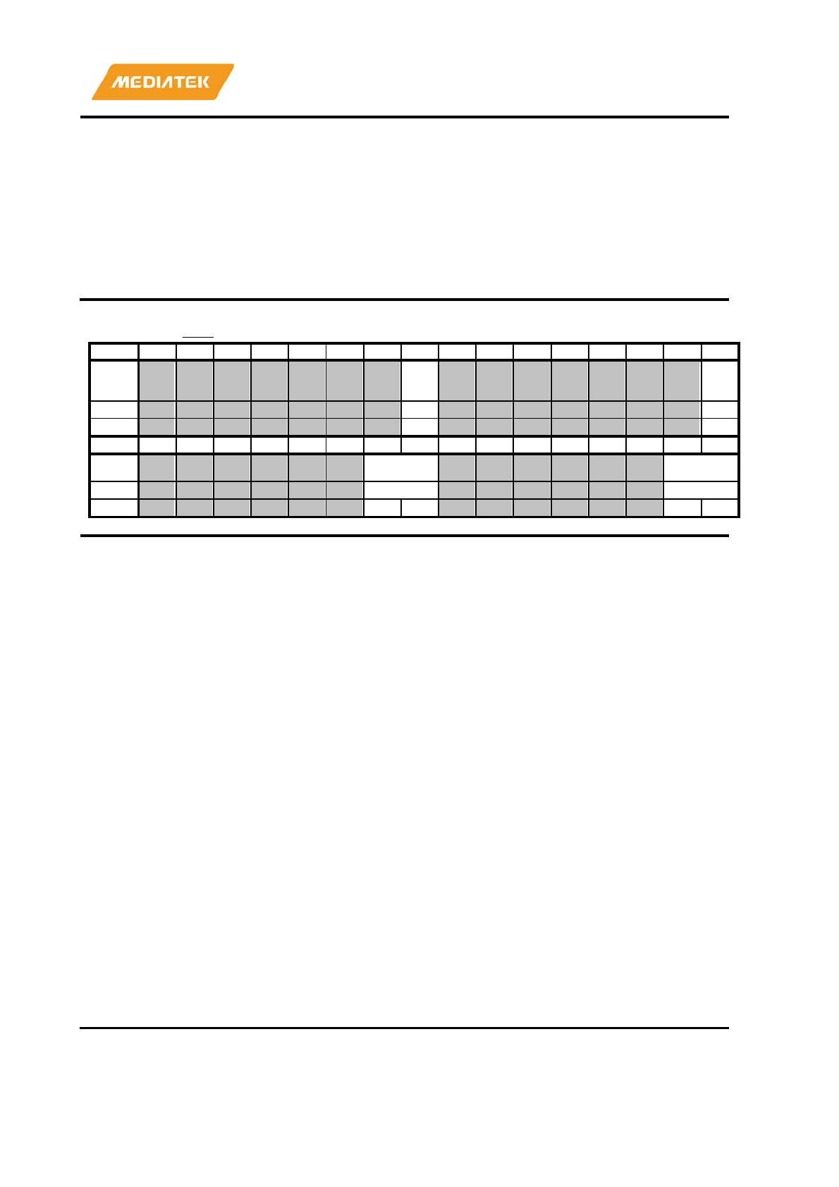
MT7686 Reference Manual
© 2016 - 2017 MediaTek Inc.
Page 60 of 536
This document contains information that is proprietary to MediaTek Inc. (“MediaTek”) and/or its licensor(s).
Any unauthorized use, reproduction or disclosure of this document in whole or in part is strictly prohibited.
o 11: Use RXTRIG register value
•
Bit[1:0] - TX FIFO threshold (total 16 bytes):
o 00: 1
o 01: 4
o 10: 8
o
11: 14
0
FIFOE
Enable RX & TX FIFOs
•
0: Disable
•
1: Enable
A00C0018
EFR
Enhanced feature register
00000000
Bit
31
30
29
28
27
26
25
24
23
22
21
20
19
18
17
16
Name SEND
_XON
SEND
_XOF
F
Type
WO
WO
Reset
0
0
Bit
15
14
13
12
11
10
9
8
7
6
5
4
3
2
1
0
Name
HW_FLOW
_CONT
SW_FLOW
_CONT
Type
RW
RW
Reset
0
0
0
0
Bit(s)
Na
me
Description
24
SEND_XON
Send XON
Note: effective only when TX software flow control is disabled
0: No effect
1: Auto send one XON character
16
SEND_XOFF
Send XOFF
Note: effective only when TX software flow control is disabled
0: No
effect
1: Auto send one XOFF character
9:8
HW_FLOW_CONT
Hardware flow control
Bit[1]
- TX hardware flow control:
0: Disable TX flow control
1: Enable TX to receive CTS
Bit[0]
- RX hardware flow control:
0: Disable RX flow control
1:
Enable RX to send RTS
1:0
SW_FLOW_CONT
Software flow control
Bit[1]
- TX software flow control:
0: Disable TX flow control
1: Transmit XON/XOFF as flow control byte
Bit[0]
- RX software flow control:
0: Disable RX flow control
1: Receive
XON/XOFF as flow control byte
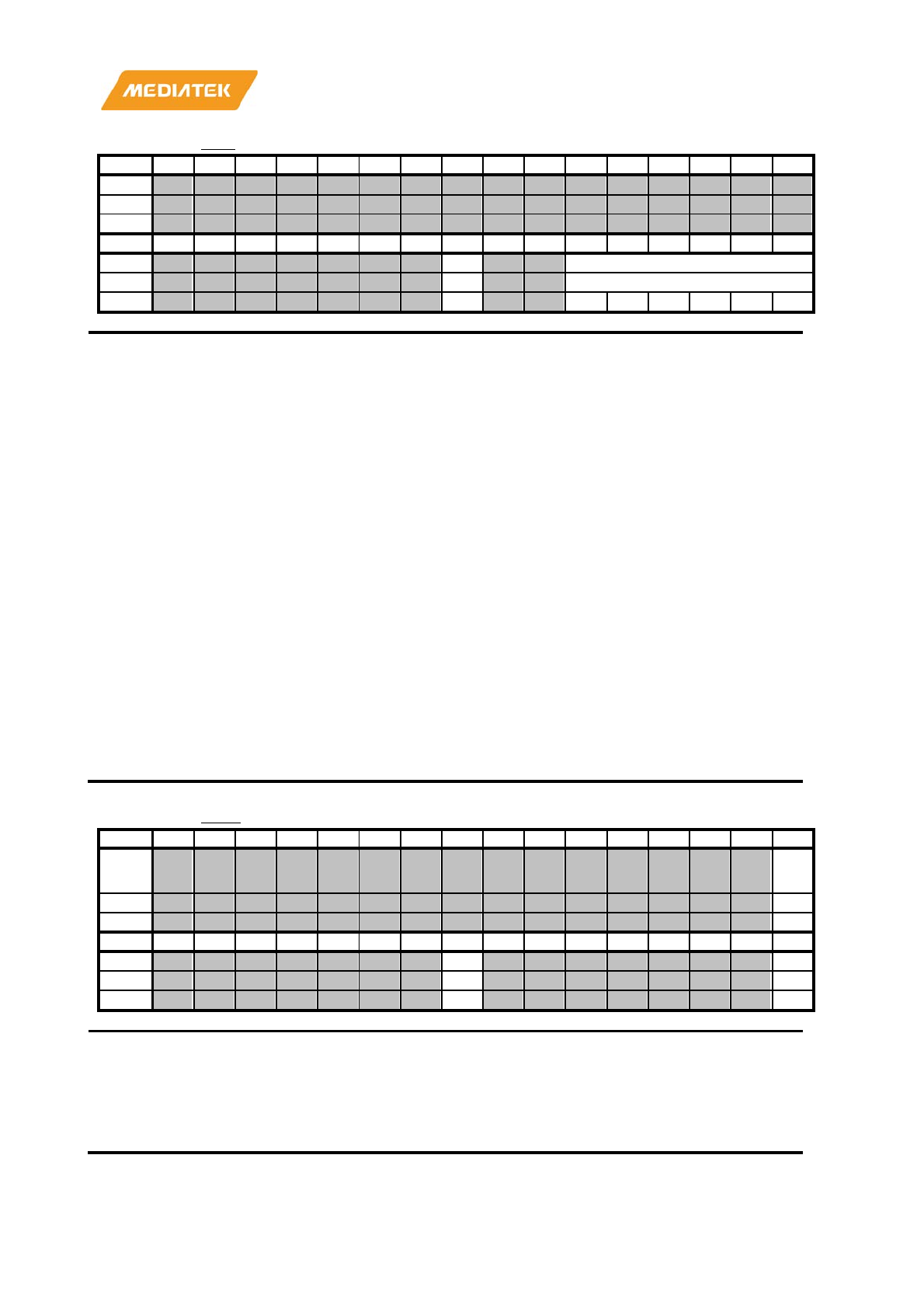
MT7686 Reference Manual
© 2016 - 2017 MediaTek Inc.
Page 61 of 536
This document contains information that is proprietary to MediaTek Inc. (“MediaTek”) and/or its licensor(s).
Any unauthorized use, reproduction or disclosure of this document in whole or in part is strictly prohibited.
A00C001C
LCR
Line control register
00000020
Bit
31
30
29
28
27
26
25
24
23
22
21
20
19
18
17
16
Name
Type
Reset
Bit
15
14
13
12
11
10
9
8
7
6
5
4
3
2
1
0
Name
SB
PAR_STB_WLS
Type
RW
RW
Reset
0
1
0
0
0
0
0
Bit(s)
Name
Description
8
SB
Set break
0: No effect
1: TX signal is forced to 0
5:0
PAR_STB_WLS
Parity, stop bits, & word length setting
Bit[5:3]
- Parity type:
000: Even parity
001: Odd parity
010: Parity is forced to 0
011: Parity is forced to 1
100: No parity
Bit[2]
- Number of stop bits:
0: 1 stop bit
1: 2
stop bits (effective only when word length > 5 bits)
Bit[1:0]
- Word length:
00: 5 bits
01: 6 bits
10: 7 bits
11: 8 bits
A00C0020
MCR
Modem control register
00000000
Bit
31
30
29
28
27
26
25
24
23
22
21
20
19
18
17
16
Name
XOFF
_STA
TUS
Type
RU
Reset
0
Bit
15
14
13
12
11
10
9
8
7
6
5
4
3
2
1
0
Name
LOOP
RTS
Type
RW
RW
Reset
0
0
Bit(s)
Name
Description
16
XOFF_STATUS
XOFF status
0: No XOFF character is received
1: A XOFF character is received
8
LOOP
Enable loop
-back mode, i.e. connect TX to RX
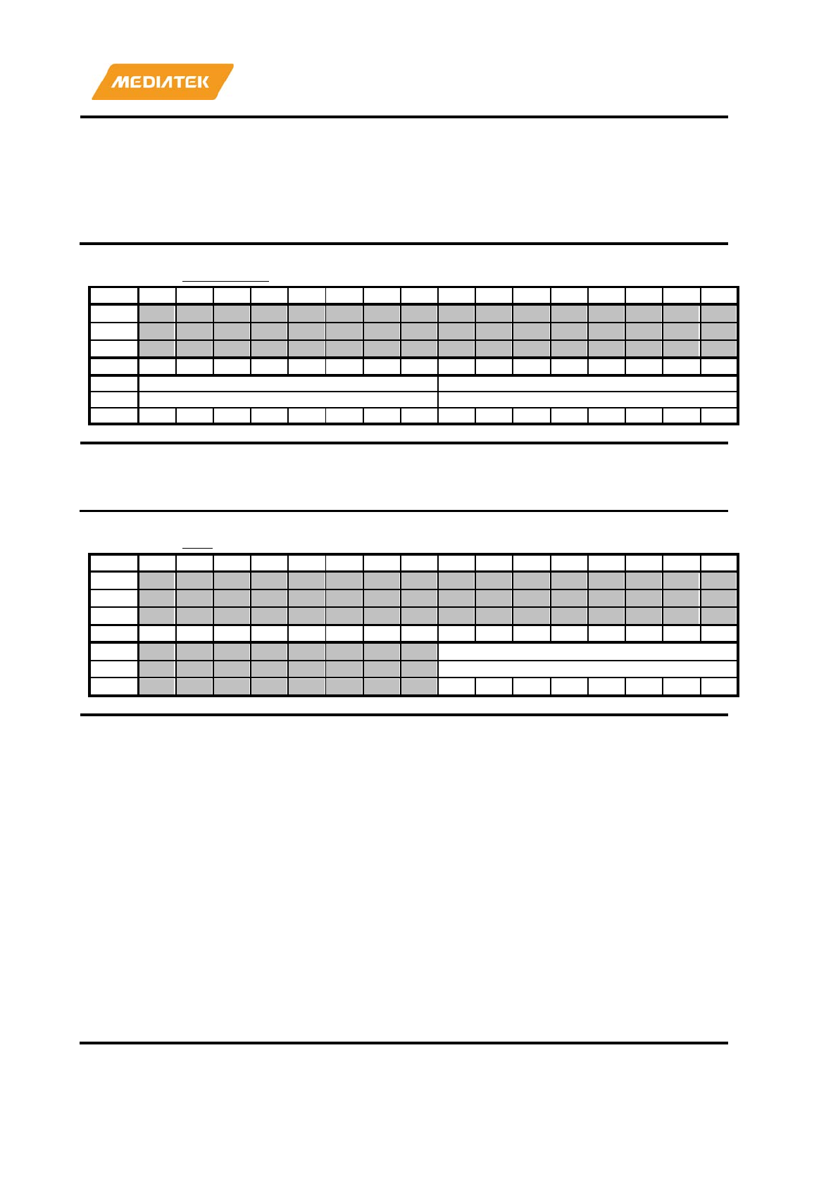
MT7686 Reference Manual
© 2016 - 2017 MediaTek Inc.
Page 62 of 536
This document contains information that is proprietary to MediaTek Inc. (“MediaTek”) and/or its licensor(s).
Any unauthorized use, reproduction or disclosure of this document in whole or in part is strictly prohibited.
Note: HW flow control will be disabled in loop-back mode
0: Disable
1: Enable
0
RTS
RTS state
0: RTS is always 1
1: RTS value will be decided by hardware flow control
A00C0024
XON_XOFF
XON & XOFF character
00000000
Bit
31
30
29
28
27
26
25
24
23
22
21
20
19
18
17
16
Name
Type
Reset
Bit
15
14
13
12
11
10
9
8
7
6
5
4
3
2
1
0
Name
XON_CHAR
XOFF_CHAR
Type
RW
RW
Reset
0
0
0
0
0
0
0
0
0
0
0
0
0
0
0
0
Bit(s)
Name
Description
15:8
XON_CHAR
XON character for software flow control
7:0
XOFF_CHAR
XOFF
character for software flow control
A00C0028
LSR
Line status register
00000060
Bit
31
30
29
28
27
26
25
24
23
22
21
20
19
18
17
16
Name
Type
Reset
Bit
15
14
13
12
11
10
9
8
7
6
5
4
3
2
1
0
Name
LSR
Type
RU
Reset
0
1
1
0
0
0
0
0
Bit(s)
Name
Description
7:0
LSR
Line status register
Bit[7]
- RX FIFO error:
0: No PE, FE, and BI in the RX
FIFO
1: At least one of PE, FE, or BI in the RX FIFO
Bit[6]
- TX holding register/TX FIFO and TX shift register are
empty:
0: Empty conditions below are not met.
1: Set whenever the TX FIFO and the TX shift register are empty
(FIFOs are
enabled), or TX holding register and TX shift register
are empty (FIFOs are disabled).
Bit[5]
- TX holding register is empty or TX FIFO is below threshold:
0: Reset whenever the contents of the TX FIFO are above threshold
(FIFOs are enabled), or TX holding register is not empty (FIFOs are
disabled).
1: Set whenever the contents of the TX FIFO are below threshold
(FIFOs are enabled), or TX holding register is empty and ready to
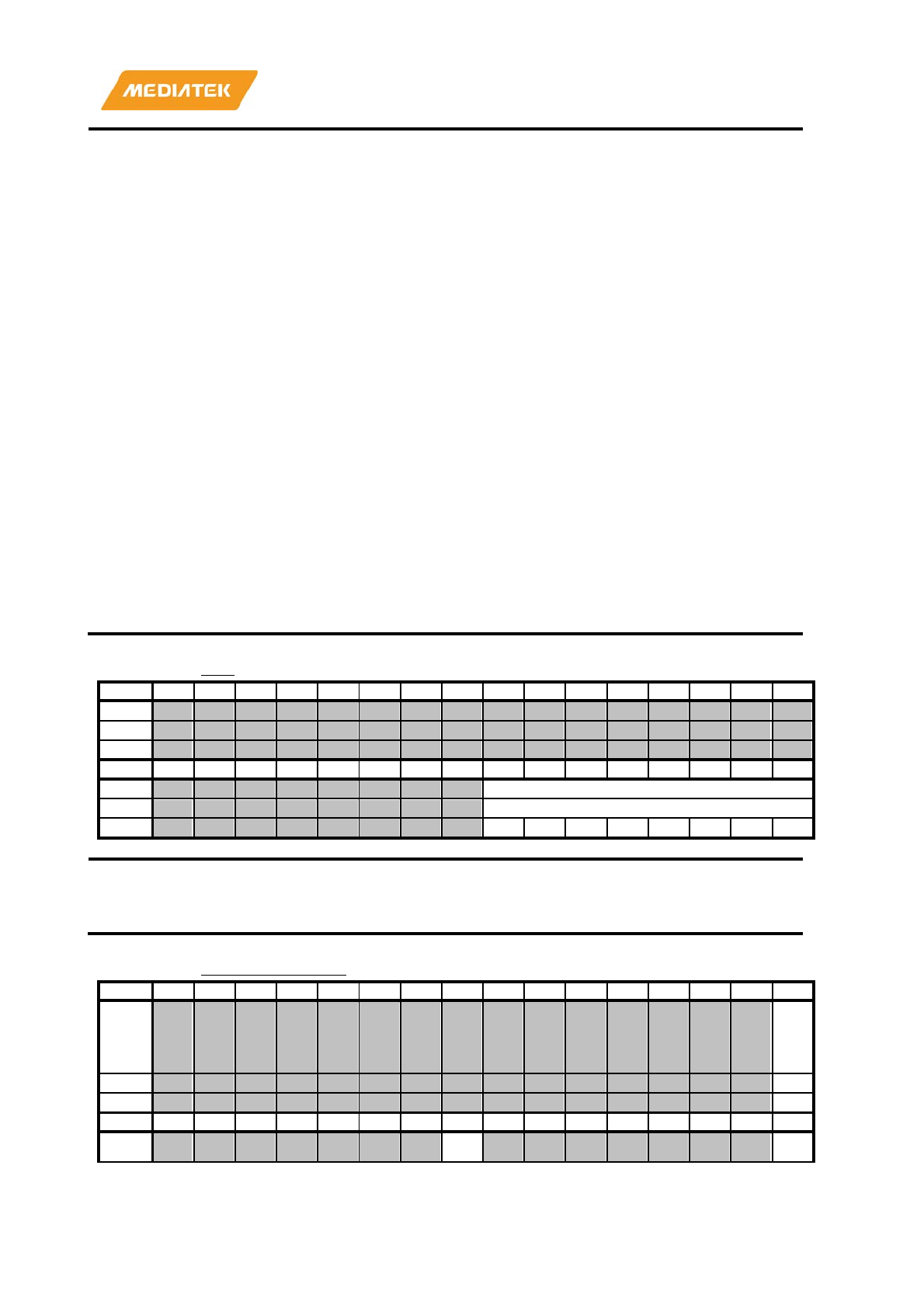
MT7686 Reference Manual
© 2016 - 2017 MediaTek Inc.
Page 63 of 536
This document contains information that is proprietary to MediaTek Inc. (“MediaTek”) and/or its licensor(s).
Any unauthorized use, reproduction or disclosure of this document in whole or in part is strictly prohibited.
accept new data (FIFOs are disabled).
Bit[4]
- Break interrupt (BI):
0: Reset by CPU reading this register.
1: Set if the RX is held in 0 state for more than one transmission
time (START bit + DATA bits + PARITY + STOP bits).
Bit[3]
- Framing error (FE):
0: Reset by CPU reading this register.
1: Set if the
received data does not have a valid STOP bit.
Bit[2]
- Parity error (PE):
0: Reset by CPU reading this register.
1: Set if the received data do not have a valid parity bit.
Bit[1]
- Overrun error (OE):
0: Reset by CPU reading this register.
1: Set if the RX buffer register is overwritten (FIFOs are disabled),
or both RX FIFO and RX shift register is full (FIFOs are enabled).
Note, that if OE occurs and UART is still receiving data in FIFO
mode, the data in the FIFO will be keep but the RX
shifter register
will be overwritten.
Bit[0]
- Data ready (DR):
0: Reset by CPU reading the RX buffer or by reading all the FIFO
bytes.
1: Set if the RX buffer register or FIFO is not empty.
A00C002C
SCR
Scratch
register
00000000
Bit
31
30
29
28
27
26
25
24
23
22
21
20
19
18
17
16
Name
Type
Reset
Bit
15
14
13
12
11
10
9
8
7
6
5
4
3
2
1
0
Name
SCR
Type
RW
Reset
x
x
x
x
x
x
x
x
Bit(s)
Name
Description
7:0
SCR
General purpose read/write register
Note: This register will not be reset
A00C0030
AUTOBAUD_CON
Autobaud control register
00000000
Bit
31
30
29
28
27
26
25
24
23
22
21
20
19
18
17
16
Name
AUTO
BAU
D_SL
EEP_
ACK
Type
RW
Reset
0
Bit
15
14
13
12
11
10
9
8
7
6
5
4
3
2
1
0
Name
AUTO
BAUD
AUTO
BAU
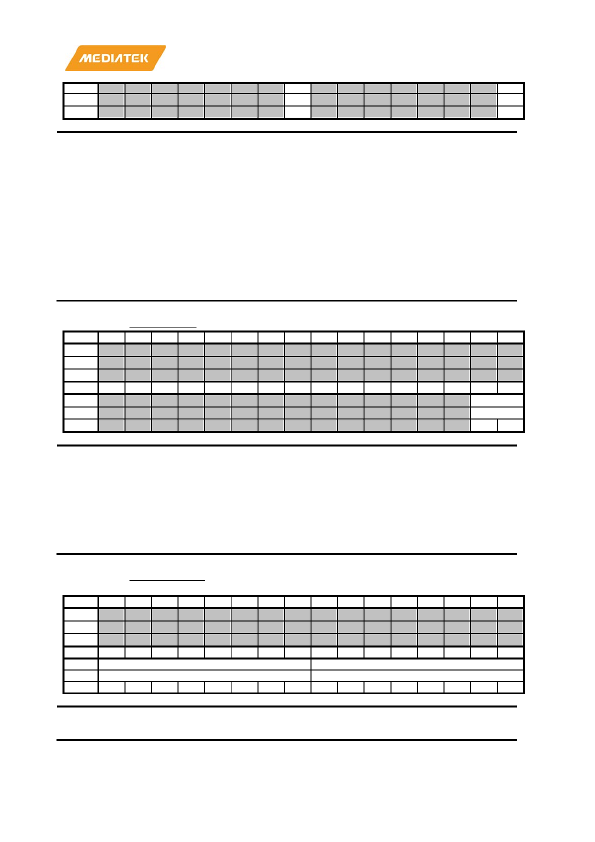
MT7686 Reference Manual
© 2016 - 2017 MediaTek Inc.
Page 64 of 536
This document contains information that is proprietary to MediaTek Inc. (“MediaTek”) and/or its licensor(s).
Any unauthorized use, reproduction or disclosure of this document in whole or in part is strictly prohibited.
_SEL
D_EN
Type
RW
RW
Reset
0
0
Bit(s)
Name
Description
16
AUTOBAUD_SLEEP_ACK
Enable auto
-baud sleep acknowledgment
Note: effective only when auto
-baud is enabled
0: Enable
1: Disable
8
AUTOBAUD_SEL
Auto
-baud mode
0: Support standard baud rate
1:
Support non-standard baud rate (from 300 to 115200 Hz)
0
AUTOBAUD_EN
Enable auto
-baud
0: Disable
1: Enable
A00C0034
HIGHSPEED
High speed mode register
00000000
Bit
31
30
29
28
27
26
25
24
23
22
21
20
19
18
17
16
Name
Type
Reset
Bit
15
14
13
12
11
10
9
8
7
6
5
4
3
2
1
0
Name
SPEED
Type
RW
Reset
0
0
Bit(s)
Na
me
Description
1:0
SPEED
Sample counter period
0: 16*(baud pulse)
1: 8*(baud pulse)
2: 4*(baud pulse)
3: (SAMPLE_REG.SAMPLE_COUNT+1)*(baud pulse)
Note: Baud rate = system clock frequency/speed/DL
A00C0038
SAMPLE_REG
Sample counter & sample point
register
0000FF00
Bit
31
30
29
28
27
26
25
24
23
22
21
20
19
18
17
16
Name
Type
Reset
Bit
15
14
13
12
11
10
9
8
7
6
5
4
3
2
1
0
Name
SAMPLE_POINT
SAMPLE_COUNT
Type
RW
RW
Reset
1
1
1
1
1
1
1
1
0
0
0
0
0
0
0
0
Bit(s)
Name
Description
15:8
SAMPLE_POINT
Sample point
MT7686 Reference Manual
© 2016 - 2017 MediaTek Inc.
Page 65 of 536
This document contains information that is proprietary to MediaTek Inc. (“MediaTek”) and/or its licensor(s).
Any unauthorized use, reproduction or disclosure of this document in whole or in part is strictly prohibited.
Note: Usually (SAMPLE_COUNT
-1)/2 without decimal. Effective
only when SPEED = 3
7:0
SAMPLE_COUNT
Sample counter
Note: Effective only when SPEED = 3
A00C003C
AUTOBAUD_REG
Autobaud monitor register
00000000
Bit
31
30
29
28
27
26
25
24
23
22
21
20
19
18
17
16
Name
Type
Reset
Bit
15
14
13
12
11
10
9
8
7
6
5
4
3
2
1
0
Name
BAUD_STAT
BAUD_RATE
Type
RU
RU
Reset
0
0
0
0
0
0
0
0
Bit(s)
Name
Description
11:8
BAUD_STAT
Auto
-baud state
0: Detecting
1: AT_7N1
2: AT_7O1
3: AT_7E1
4: AT_8N1
5: AT_8O1
6: AT_8E1
7: at_7N1
8: at_7E1
9: at_7O1
10: at_8N1
11: at_8E1
12: at_8O1
13: Detection fail
3:0
BAUD_RATE
Auto
-baud rate
0: 115,200
1: 57,600
2: 38,400
3: 19,200
4: 9,600
5:
4,800
6: 2,400
7: 1,200
8: 300
A00C0040
RATEFIX
Clock rate fix register
0000000D
Bit
31
30
29
28
27
26
25
24
23
22
21
20
19
18
17
16
Name
RATE
FIX
MT7686 Reference Manual
© 2016 - 2017 MediaTek Inc.
Page 66 of 536
This document contains information that is proprietary to MediaTek Inc. (“MediaTek”) and/or its licensor(s).
Any unauthorized use, reproduction or disclosure of this document in whole or in part is strictly prohibited.
Type
RW
Reset
0
Bit
15
14
13
12
11
10
9
8
7
6
5
4
3
2
1
0
Name
AUTO
BAUD
_RAT
EFIX
AUTOBAUD_SAMPLE
Type
RW
RW
Reset
0
0
0
1
1
0
1
Bit(s)
Name
Description
16
RATEFIX
System clock rate for TX/RX
0: 26MHz / 20MHz
1:
13MHz / 10MHz
8
AUTOBAUD_RATEFIX
System clock rate for auto
-baud detection
0: 26MHz / 20MHz
1: 13MHz / 10MHz
5:0
AUTOBAUD_SAMPLE
Clock division for auto
-baud detection
I
f AUTOBAUD_CON.AUTOBAUD_SEL = 0
AUTOBAUD_RATE_FIX = 0: 0xd
AUTOBAUD_RATE_FIX =
1: 0x6
If
AUTOBAUD_CON.AUTOBAUD_SEL = 1
{ RATE_FIX, AUTOBAUD_RATEFIX } = { 0, 0 }: 0xf
{ RATE_FIX, AUTOBAUD_RATEFIX } = { 0, 1 }: 0x7
{ RATE_FIX, AUTOBAUD_RATEFIX } = { 1, 0 }: 0x1f
{ RATE_FIX, AUTOBAUD_RATEFIX } = { 1, 1 }: 0xf
A00C0044
GUARD
Guard interval register
0000000F
Bit
31
30
29
28
27
26
25
24
23
22
21
20
19
18
17
16
Name
Type
Reset
Bit
15
14
13
12
11
10
9
8
7
6
5
4
3
2
1
0
Name
GUARD
Type
RW
Reset
0
1
1
1
1
Bit(s)
Name
Description
4:0
GUARD
Guard interval setting
Bit[4]
- Enable guard interval:
0: No guard
interval
1: Add guard interval after stop bit
Bit[3:0]
- Guard interval count value:
A00C0048
ESCAPE_REG
Escape character register
000000FF
Bit
31
30
29
28
27
26
25
24
23
22
21
20
19
18
17
16
Name
MT7686 Reference Manual
© 2016 - 2017 MediaTek Inc.
Page 67 of 536
This document contains information that is proprietary to MediaTek Inc. (“MediaTek”) and/or its licensor(s).
Any unauthorized use, reproduction or disclosure of this document in whole or in part is strictly prohibited.
Type
Reset
Bit
15
14
13
12
11
10
9
8
7
6
5
4
3
2
1
0
Name
ESC_
EN
ESC_CHAR
Type
RW
RW
Reset
0
1
1
1
1
1
1
1
1
Bit(s)
Name
Description
8
ESC_EN
Enable escape character
0: Disable
1: Enable
7:0
ESC_CHAR
Escape character setting
A00C004C
SLEEP_REG
Sleep mode control register
00000000
Bit
31
30
29
28
27
26
25
24
23
22
21
20
19
18
17
16
Name
Type
Reset
Bit
15
14
13
12
11
10
9
8
7
6
5
4
3
2
1
0
Name
SLEE
P_EN
Type
RW
Reset
0
Bit(s)
Name
Description
0
SLEEP_EN
For sleep mode issue
0: No active flow control when the chip enters sleep mode.
1: Active hardware flow control (assert RTS) or software flow
control (send XOFF) when the chip enters sleep
mode. Release
hardware flow control (de
-assert RTS) when the chip wakes up.
However, for software control, XON should be sent manually when
awakened (can use the SEND_XON register).
A00C0050
DMA_CON
DMA mode control register
00000000
Bit
31
30
29
28
27
26
25
24
23
22
21
20
19
18
17
16
Name
FIFO
_LSR
_SEL
Type
RW
Reset
0
Bit
15
14
13
12
11
10
9
8
7
6
5
4
3
2
1
0
Name
TX_D
MA_
EN
RX_
DMA
_EN
Type
RW
RW
Reset
0
0
Bit(s)
Name
Description
16
FIFO_LSR_SEL
FIFO LSR mode
MT7686 Reference Manual
© 2016 - 2017 MediaTek Inc.
Page 68 of 536
This document contains information that is proprietary to MediaTek Inc. (“MediaTek”) and/or its licensor(s).
Any unauthorized use, reproduction or disclosure of this document in whole or in part is strictly prohibited.
0: LSR holds the first line status error state until the LSR register is
read.
1: LSR updates automatically
8
TX_DMA_EN
Enable TX DMA mode
0: Disable
1: Enable
0
RX_DMA_EN
Enable RX DMA mode
0: Disable
1: Enable
A00C0054
RXTRIG
RX FIFO trigger threshold
00000000
Bit
31
30
29
28
27
26
25
24
23
22
21
20
19
18
17
16
Name
Type
Reset
Bit
15
14
13
12
11
10
9
8
7
6
5
4
3
2
1
0
Name
RXTRIG
Type
RW
Reset
0
0
0
0
Bit(s)
Name
Description
3:0
RXTRIG
RX FIFO trigger threshold
Note: effective only when RFTL = 3
A00C0058
FRACDIV
Fractional divisor
00000000
Bit
31
30
29
28
27
26
25
24
23
22
21
20
19
18
17
16
Name
Type
Reset
Bit
15
14
13
12
11
10
9
8
7
6
5
4
3
2
1
0
Name
FRACDIV
Type
RW
Reset
0
0
0
0
0
0
0
0
0
0
Bit(s)
Name
Description
9:0
FRACDIV
Fractional divisor
Note: effective only when SPEED = 3. Add sampling count (+1) for
corresponding data
bit
A00C005C
RX_TO_CON
RX timeout mode control
00000000
Bit
31
30
29
28
27
26
25
24
23
22
21
20
19
18
17
16
Name
Type
Reset
Bit
15
14
13
12
11
10
9
8
7
6
5
4
3
2
1
0
Name
TO_C
NT_A
UTOR
ST
RX_T
O_M
ODE
MT7686 Reference Manual
© 2016 - 2017 MediaTek Inc.
Page 69 of 536
This document contains information that is proprietary to MediaTek Inc. (“MediaTek”) and/or its licensor(s).
Any unauthorized use, reproduction or disclosure of this document in whole or in part is strictly prohibited.
Type
RW
RW
Reset
0
0
Bit(s)
Name
Description
8
TO_CNT_AUTORST
Time
-out counter auto reset
•
0: Reset the RX timeout interrupt manually (see IIR for
detailed information)
•
1: RX timeout counter is reset automatically
0
RX_TO_MODE
RX timeout mode
•
0: Timeout when RX idle for 4 characters
•
1: Timeout when RX idle for a certain period of time (defined
by RX_TOC_DEST)
A00C0060
RX_TOC_DEST
RX timeout counter destination value
0000FFFF
Bit
31
30
29
28
27
26
25
24
23
22
21
20
19
18
17
16
Name
Type
Reset
Bit
15
14
13
12
11
10
9
8
7
6
5
4
3
2
1
0
Name
RX_TOC_DEST
Type
RW
Reset
1
1
1
1
1
1
1
1
1
1
1
1
1
1
1
1
Bit(s)
Name
Description
15:0
RX_TOC_DEST
RX timeout counter destination value
Note: effective only when RX_TO_CON[0]
= 1
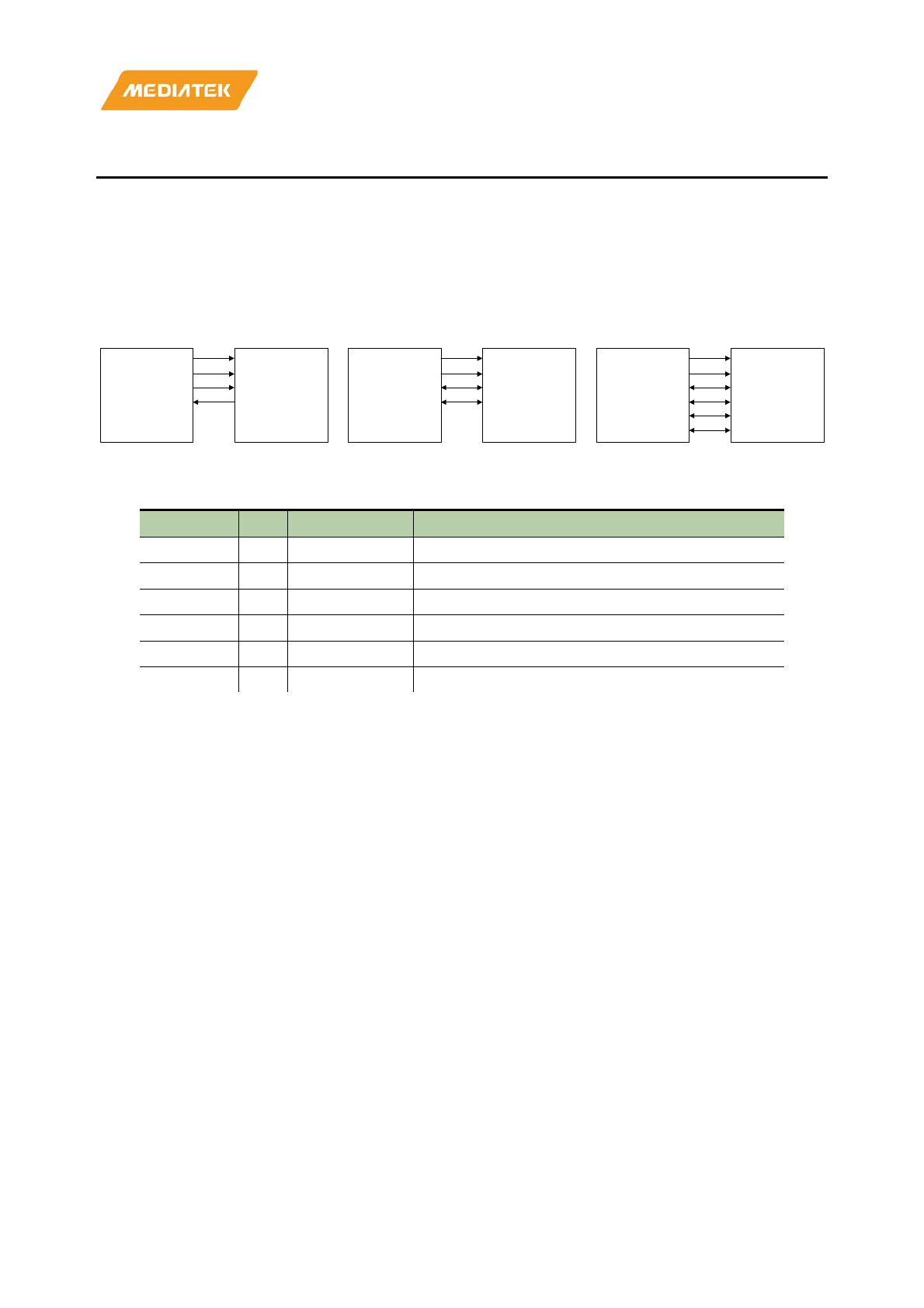
MT7686 Reference Manual
© 2016 - 2017 MediaTek Inc.
Page 70 of 536
This document contains information that is proprietary to MediaTek Inc. (“MediaTek”) and/or its licensor(s).
Any unauthorized use, reproduction or disclosure of this document in whole or in part is strictly prohibited.
6. Serial Peripheral Interface Master Controller
The Serial Peripheral Interface (SPI) is a bit-serial transmission protocol. MT7686 supports single mode (four-pin),
dual mode (four-pin) and quad mode (six-pin) for increased data throughput. The maximum serial clock (SCK)
frequency is 48MHz. Note that the single mode can support full duplex, but dual quad mode only supports half-
duplex. Figure 5.5-1 is an example of the connection between the SPI master and SPI slave. The SPI controller is a
master responsible for data transmission with slave.
CS
SCK
SIO0
SIO1
SIO2
SIO3
SPI
Master
CS
SCK
SIO0
SIO1
SIO2
SIO3
SPI
Slave
CS
SCK
SIO0
SIO1
SIO2
SIO3
SPI
Master
CS
SCK
SIO0
SIO1
SIO2
SIO3
SPI
Slave
CS
SCK
SIO0
SIO1
SIO2
SIO3
SPI
Master
CS
SCK
SIO0
SIO1
SIO2
SIO3
SPI
Slave
Single SPI Dual SPI Quad SPI
Figure 5.5-1. Pin connection between SPI master and SPI slave
Table 5.5-1. SPI master controller interface
Signal name Type Default value Description
CS O 1 (output) Low active chip selection signal
SCK O 0 (output) The (bit) serial clock (Max SCK clock rate is 48MHz)
SIO0 I/O 1 (output) Data signal 0
SIO1 I/O pull down (input) Data signal 1
SIO2 I/O 1 (output) Data signal 2
SIO3 I/O 1 (output) Data signal 3
6.1. Features
• The SPI master controller supports single mode (four-pin), dual mode (four-pin) and quad mode (six-pin).
The controller can automatically set port direction for data input/output if registers SPIM_TYPE and
SPIM_RW_MODE are already set.
• The SCK frequency supports maximum 48MHz with CPOL and CPHA features and can be configured as
96/N MHz (where N is from 2 to 217) for different applications. CPOL defines the clock polarity in the
transmission. CPHA defines the legal timing to sample data. The chip select (CS) signal setup time, hold
time and idle time can be configured, too. The detailed timing diagram of the SCK and CS signals is shown
in Figure 6.1-1.
• There are two configurable modes for the source of the transfer data:
o DMA mode, the SPI master controller includes the DMA design, it can automatically read or write
data from memory continuously;
o Direct mode, the CPU directly reads data from the SPI master controller FIFO or writes data to the SPI
master controller FIFO. In DMA mode, the endian order of memory data is adjustable.
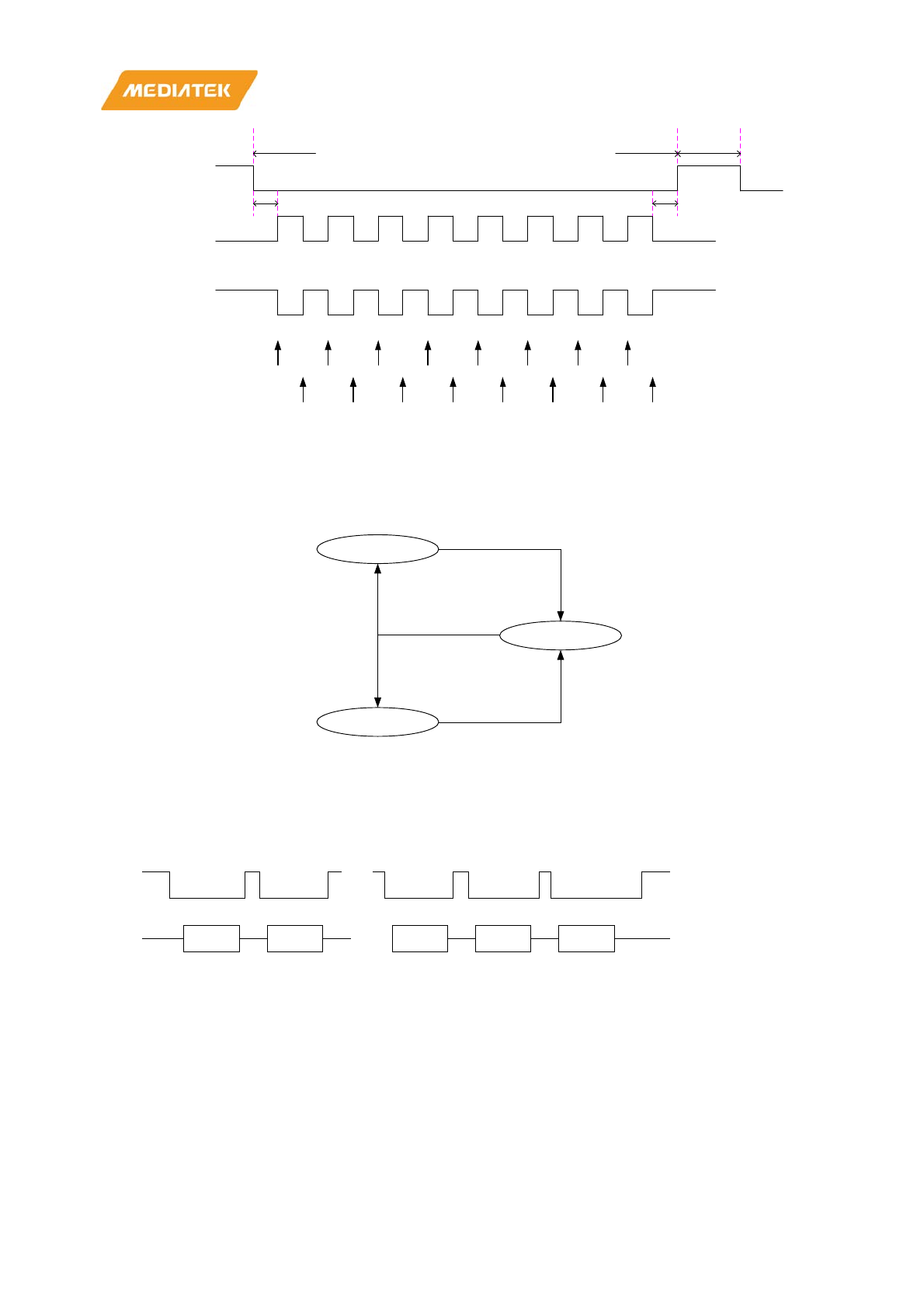
MT7686 Reference Manual
© 2016 - 2017 MediaTek Inc.
Page 71 of 536
This document contains information that is proprietary to MediaTek Inc. (“MediaTek”) and/or its licensor(s).
Any unauthorized use, reproduction or disclosure of this document in whole or in part is strictly prohibited.
CS
SCK
(CPOL=0)
SCK Edge
Number
SCK
(CPOL=1)
1 2 3 4 5 6 7 8 9 10 11 12 13 14 15 16
SAMPLE Input data
(CPHA=0)
SAMPLE Input data
(CPHA=1)
Data Transmission
CS idle time
CS setup time CS hold time
Figure 6.1-1. SPI transmission formats
• Unlimited length for transmission can be achieved in Pause mode. In Pause mode, the CS signal will stay
active (low) after the transmission. During this period, the SPI controller will be in PAUSE_IDLE state,
ready to receive the resume command. Figure 6.1-2 is the state transition diagram.
IDLE
PAUSE IDLE
BUSY
activate
resume
! (pause)
pause
Figure 6.1-2. Operation flow with or without PAUSE mode
• A configurable option to control CS de-assertion between byte transfers is available. The SPI master
controller supports a special transmission format called CS de-assert mode. Figure 6.1-3 illustrates the
waveform in this transmission format.
CS
BYTESCK BYTE BYTE
... BYTE BYTE
Figure 6.1-3. CS de-assert mode
• When the SPI master controller operates in dual or quad mode, the transmission package includes three
parts: command phase, dummy phase and data phase.
o Command phase always operates at Single mode;
o Dummy phase cannot transmit or receive data;
o Data phase operation depends on SPIM_TYPE and SPIM_RW_MODE settings. The Command
phase and Dummy phase are useful for special applications, such as read or write serial flash data.
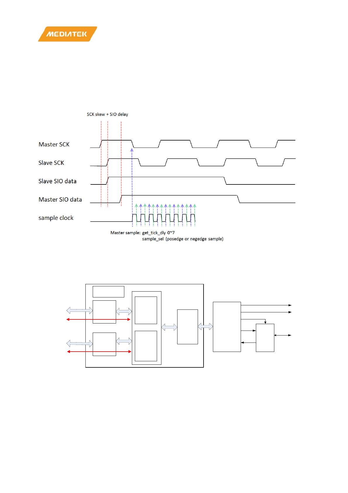
MT7686 Reference Manual
© 2016 - 2017 MediaTek Inc.
Page 72 of 536
This document contains information that is proprietary to MediaTek Inc. (“MediaTek”) and/or its licensor(s).
Any unauthorized use, reproduction or disclosure of this document in whole or in part is strictly prohibited.
• For high-speed transmission, the SPI master controller can enable the delay sample feature (registers
SPIM_GET_DLY and SAMPLE_SEL) to resolve data path latency issues. The critical path of SPI
transmission includes two parts:
o Master transmits SCK signal to slave;
o Slave feeds back SIO data to master. Each interval of sample delay is 10.42 ns, and SAMPLE_SEL
defines the trigger edge of sample clock, such as, if 0 - positive edge sample data; 1 - negative edge
sample data. The detailed description is shown in Figure 6.1-4.
Figure 6.1-4. SPI master controller delay sample
6.2. Block diagram
SIO_oe
miso
TX_FIFO
(32 bytes)
RX_FIFO
(32 bytes)
spi_engine
dma_engine
apb_regif
memory
CPU
spi_state_ctrl
AHB
APB
mosi
SCK
CS
S
P
I
_
m
a
s
t
e
r
_
P
A
D
_
M
A
C
R
O
FIFO
DMA mode
Direct mode
G
P
I
O
m
u
x
SIO[0:3]
Figure 6.2-1. Block diagram of SPI master controller
6.3. Functions
• SPI master single mode. Typical SPI transmission mode is single SPI, a 4-pin protocol. Set the register
SPIM_TYPE to 0 to enter single mode. In this mode, the register settings for SPIM_RW_MODE,
SPIM_DUMMY_CNT and SPIM_COMMAND_CNT are not supported. The single mode data
transmission diagram is shown in Figure 6.3-1.
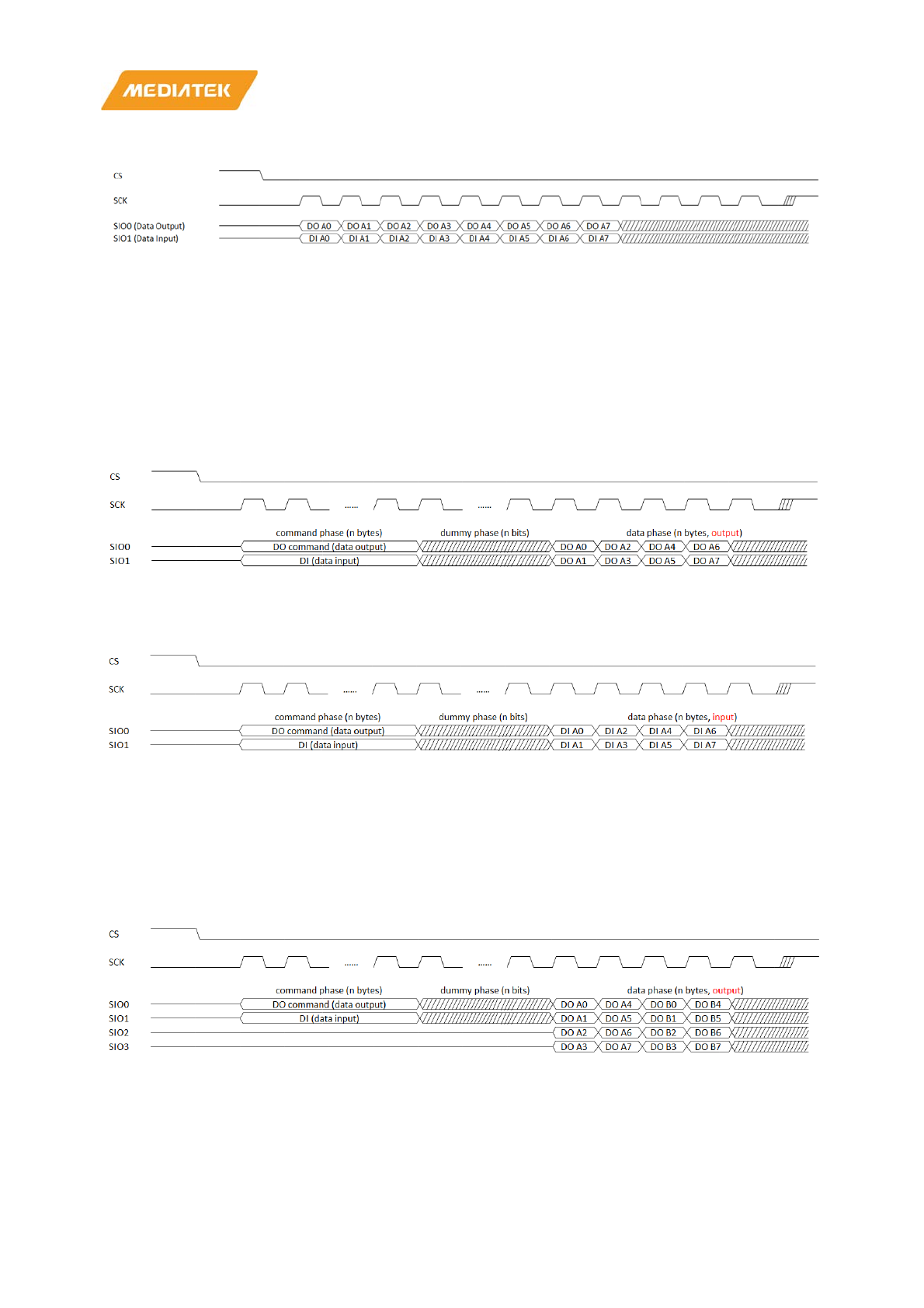
MT7686 Reference Manual
© 2016 - 2017 MediaTek Inc.
Page 73 of 536
This document contains information that is proprietary to MediaTek Inc. (“MediaTek”) and/or its licensor(s).
Any unauthorized use, reproduction or disclosure of this document in whole or in part is strictly prohibited.
Figure 6.3-1. SPI master single mode
• SPI master dual mode. The dual mode SPI is also a 4-pin protocol. Set the register SPIM_TYPE to 1 to
enter this mode. In dual mode, the SPI master controller only supports half duplex, and the data
transmission direction is configured by register SPIM_RW_MODE (0: read data, 1: write data). The
registers SPIM_DUMMY_CNT, SPIM_COMMAND_CNT can be activated with user configuration. In
addition, SPIM_DUMMY_CNT and SPIM_COMMAND_CNT can be set to 0 to disable these features.
The dual mode data transmission diagram is shown in Figure 6.3-2 and Figure 6.3-3.
Figure 6.3-2. SPI master dual mode write data
Figure 6.3-3. SPI master dual mode read data
• SPI master quad mode. The quad mode SPI is a 6-pin protocol. Set the register SPIM_TYPE to 2 to enter
this mode. Similar to dual mode, in quad mode, the SPI master controller only supports half duplex, and
the data transmission direction is configured by register SPIM_RW_MODE (0: read data, 1: write data).
The registers SPIM_DUMMY_CNT, SPIM_COMMAND_CNT can also be activated. The quad mode
data transmission diagram is shown in Figure 6.3-4 and Figure 6.3-5.
Figure 6.3-4. SPI master quad mode write data
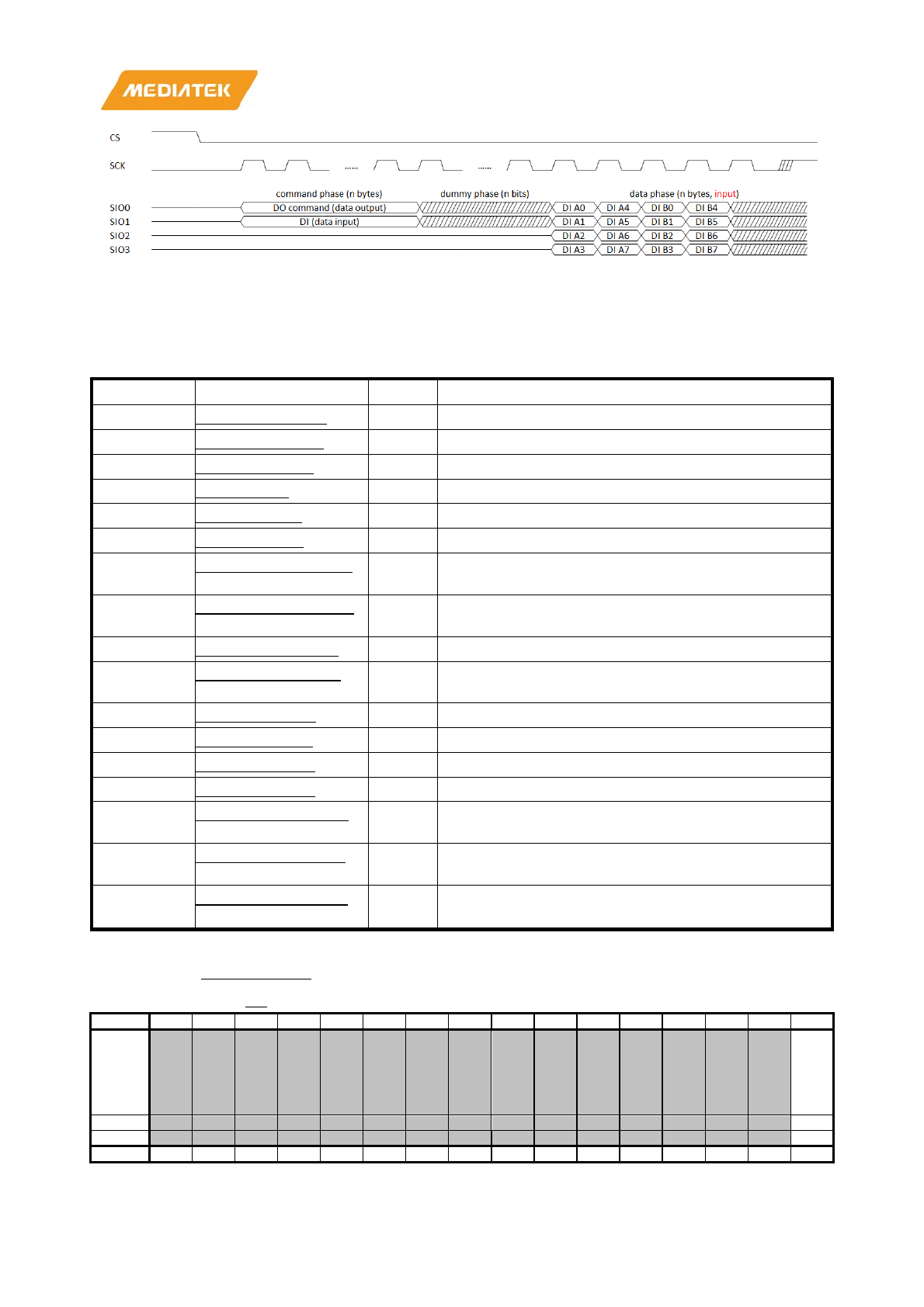
MT7686 Reference Manual
© 2016 - 2017 MediaTek Inc.
Page 74 of 536
This document contains information that is proprietary to MediaTek Inc. (“MediaTek”) and/or its licensor(s).
Any unauthorized use, reproduction or disclosure of this document in whole or in part is strictly prohibited.
Figure 6.3-5. SPI master quad mode read data
6.4. Register mapping
Module name: SPI_MASTER Base address: (+A00A0000h)
Address Name Width Register Function
A00A0000
SPIMST_CTRL0
32
SPI Master Control 0 Register
A00A0004
SPIMST_CTRL1
32
SPI Master Control 1 Register
A00A0008
SPIMST_TRIG
32
SPI Master Trigger Register
A00A000C
SPIMST_IE
32
SPI Master Interrupt Enable
A00A0010
SPIMST_INT
32
SPI Master Interrupt
A00A0014
SPIMST_STA
32
SPI Master Status
A00A0018
SPIMST_TX_DATA
32
SPI Master TX Data
A00A001C
SPIMST_RX_DATA
32
SPI Master RX Data
A00A0020
SPIMST_TX_SRC
32
SPI Master TX Source Address Register
A00A0024
SPIMST_RX_DST
32
SPI Master RX Destination Address Register
A00A0028
SPIMST_CFG0
32
SPI Master Configuration 0 Register
A00A002C
SPIMST_CFG1
32
SPI Master Configuration 1 Register
A00A0030
SPIMST_CFG2
32
SPI Master Configuration 2 Register
A00A0034
SPIMST_CFG3
32
SPI Master Configuration 3 Register
A00A0038
SPIMST_DLYSEL0
32
SPI Master Delay Select 0 Register
A00A003C
SPIMST_DLYSEL1
32
SPI Master Delay Select 1 Register
A00A0040
SPIMST_DLYSEL2
32
SPI
Master Delay Select 2 Register
A00A000
0
SPIMST_CTR
L0 SPI Master Control 0 Register 00000000
Bit
31
30
29
28
27
26
25
24
23
22
21
20
19
18
17
16
Name
SPI
M_
PA
US
E_
EN
Type
RW
Reset
0
Bit
15
14
13
12
11
10
9
8
7
6
5
4
3
2
1
0
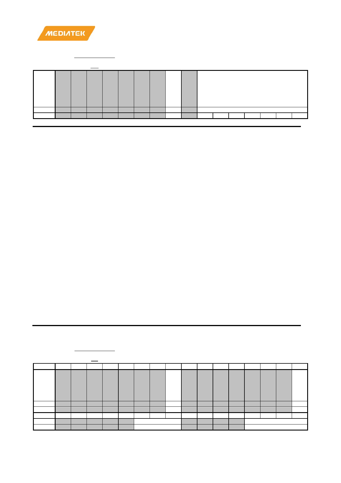
MT7686 Reference Manual
© 2016 - 2017 MediaTek Inc.
Page 75 of 536
This document contains information that is proprietary to MediaTek Inc. (“MediaTek”) and/or its licensor(s).
Any unauthorized use, reproduction or disclosure of this document in whole or in part is strictly prohibited.
A00A000
0
SPIMST_CTR
L0 SPI Master Control 0 Register 00000000
Name
SPI
M_
DE
ASS
ER
T_E
N
SPIM_CTRL0
Type
RW
RW
Reset
0
0
0
0
0
0
0
0
Bit(s)
Name
Description
16
SPIM_PAUSE_EN
Pause mode enable
Set the pause mode bit to 1 to enable this mode.
8
SPIM_DEASSERT_EN
De
-assert mode enable
Enable bit of the chip select de
-assertion mode. Set it to1 to enable this mode.
6:0
SPIM_CTRL0
SPI
master general configure set 0
•
[6]: SPIM_RW_MODE
, indicates SPI master received/sent data, only used
in Dual/Quad SPI (SPIM_TYPE = 1 or 2).
o 0: Read mode, SPI master receive data
o 1: Write mode, SPI master send data
•
[5:4]: SPIM_TYPE, indicates the SPI data transmission type
o 0: Single SPI
o 1: Dual SPI
o 2: Quad SPI
o 3: Not used
•
[3]: RXMSBF, indicates the RX data received is MSB first or not. Set
RXMSBF to 1 for MSB first, otherwise set it to 0.
•
[2]: TXMSBF, indicates the TX data sent is MSB first or not. Set TXMSBF
to 1 for MSB first, otherwise set it to 0.
•
[1]: CPOL, control bit of the SCK polarity.
o 0: CPOL = 0
o 1: CPOL = 1
•
[0]: CPHA, control bit of the SCK sample data phase.
o 0: CPHA = 0
o
1: CPHA = 1
A00A000
4
SPIMST_CTR
L1 SPI Master Control 1 Register 00000000
Bit
31
30
29
28
27
26
25
24
23
22
21
20
19
18
17
16
Name
SPI
M_
RX
DM
A_
EN
SPI
M_
TX
DM
A_
EN
Type
RW
RW
Reset
0
0
Bit
15
14
13
12
11
10
9
8
7
6
5
4
3
2
1
0
Name
SPIM_GET_DLY
SPIM_CTRL1
Type
RW
RW
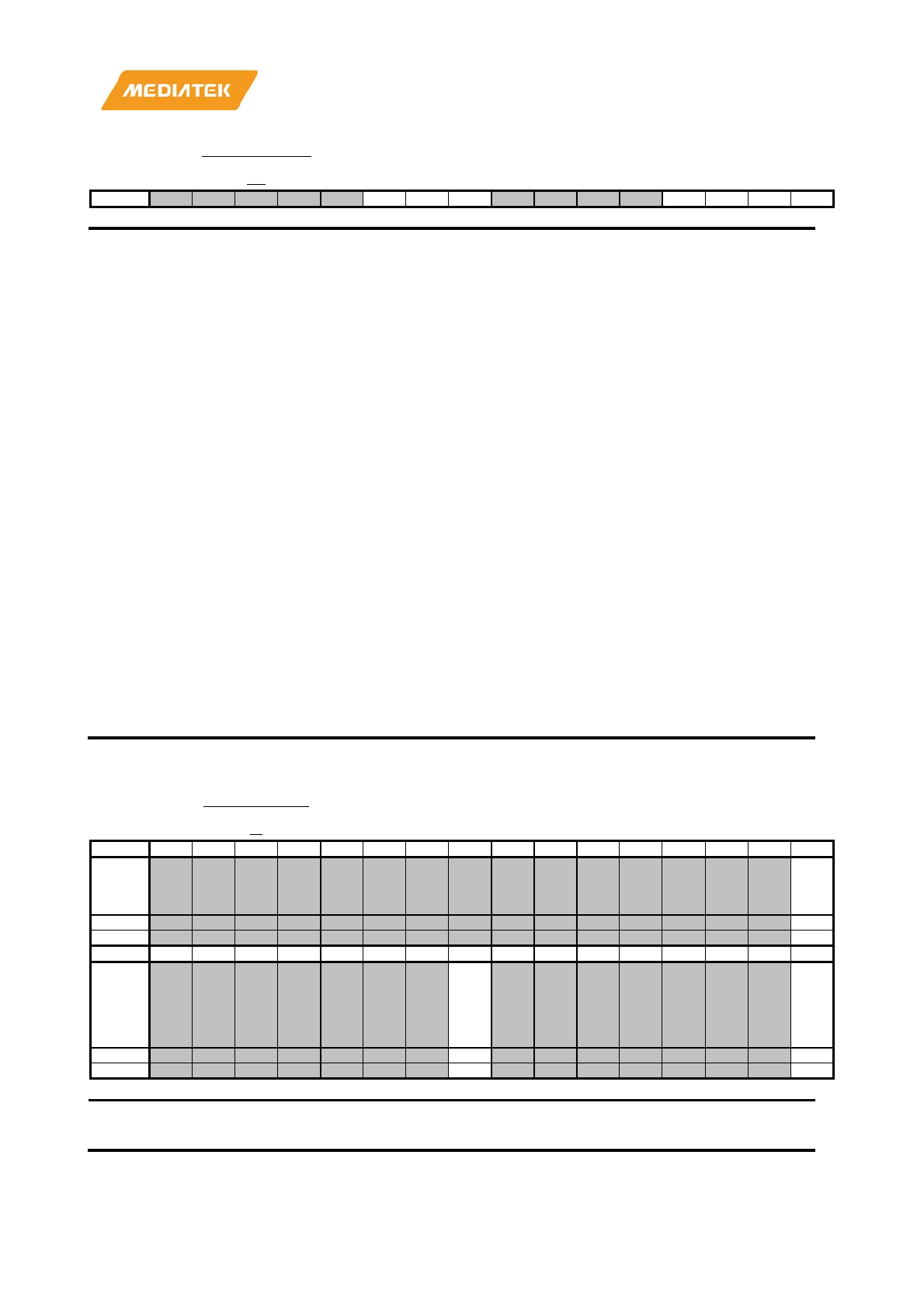
MT7686 Reference Manual
© 2016 - 2017 MediaTek Inc.
Page 76 of 536
This document contains information that is proprietary to MediaTek Inc. (“MediaTek”) and/or its licensor(s).
Any unauthorized use, reproduction or disclosure of this document in whole or in part is strictly prohibited.
A00A000
4
SPIMST_CTR
L1 SPI Master Control 1 Register 00000000
Reset
0
0
0
0
0
0
0
Bit(s)
Name
Description
24
SPIM_RXDMA_EN
RX DMA enable
DMA mode enable bit of the data being received. Default (0) is not to enable.
16
SPIM_TXDMA_EN
TX DMA enable
DMA
mode enable bit of the data to be transmitted. Default (0) is not to enable.
10:8
SPIM_GET_DLY
Receive data get delay
If the latency of the signal that SPI master received is too large, the register can
help to tolerate get_tick timing. The timing is CLK_
PERIOD (10.42ns) *
SPIM_GET_DLY
.
3:0
SPIM_CTRL1
SPI master general configure set 1
•
[3]: RX_ENDIAN, defines whether to reverse the endian order of the data
DMA to memory. Default (0) is not to reverse.
o 0: RX data format is data[31:0]
o 1: RX data format is {data[7:0], data[15:8], data[23:16], data[31:24]}
•
[2]: TX_ENDIAN, defines whether to reverse the endian order of the data
DMA from memory. Default (0) is not to reverse.
o 0: TX data format is data[31:0]
o 1: TX data format is {data[7:0], data[15:8], data[23:16], data[31:24]}
•
[1]: CS_POL, control bit of chip select polarity
o 0: Active low
o 1: Active high
•
[0]: SAMPLE_SEL, control bit of sample edge of RX data
o 0: Positive edge
o
1: Negative edge
A00A000
8
SPIMST_TRI
G SPI Master Trigger Register 00000000
Bit
31
30
29
28
27
26
25
24
23
22
21
20
19
18
17
16
Name
SPI
M_
RS
T
Type
WO
Reset
0
Bit
15
14
13
12
11
10
9
8
7
6
5
4
3
2
1
0
Name
SPI
M_
RE
SU
ME
SPI
M_
CM
D_
AC
T
Type
WO
WO
Reset
0
0
Bit(s)
Name
Description
16
SPIM_RST
Reset
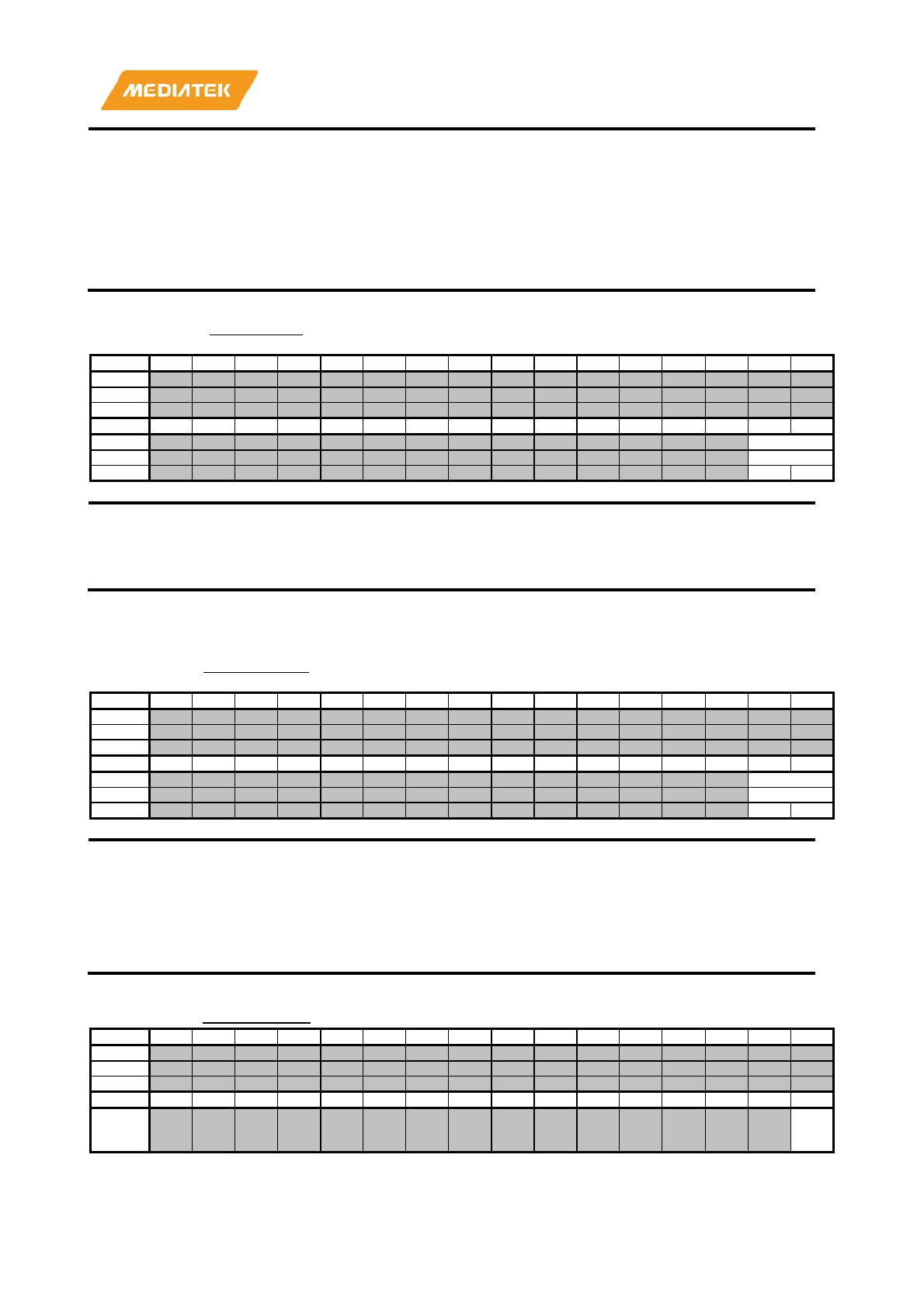
MT7686 Reference Manual
© 2016 - 2017 MediaTek Inc.
Page 77 of 536
This document contains information that is proprietary to MediaTek Inc. (“MediaTek”) and/or its licensor(s).
Any unauthorized use, reproduction or disclosure of this document in whole or in part is strictly prohibited.
Software reset bit; resets the state machine and data FIFO of SPI master controller
(not the register value). When this bit is 1, software reset is active high and
hardware can automatically return to 0. The default value is 0.
8
SPIM_RESUME
Resume
This
bit is used when the controller is in PAUSE IDLE state. Write 1 to this bit to
trigger the SPI controller resume transfer from PAUSE IDLE state.
0
SPIM_CMD_ACT
Command activate
Write 1 to this bit to trigger the SPI master controller to start the transmis
sion.
A00A000
C SPIMST_IE SPI Master Interrupt Enable 00000000
Bit
31
30
29
28
27
26
25
24
23
22
21
20
19
18
17
16
Name
Type
Reset
Bit
15
14
13
12
11
10
9
8
7
6
5
4
3
2
1
0
Name
SPIM_IE
Type
RW
Reset
0
0
Bit(s)
Name
Description
1:0
SPIM_IE
SPI master interrupt source enable
[1]:
PAUSE_IE, interrupt enable bit of pause flag in SPI status register.
[0]:
FINISH_IE, interrupt enable bit of finish flag in SPI status register.
A00A001
0 SPIMST_INT SPI Master Interrupt 00000000
Bit
31
30
29
28
27
26
25
24
23
22
21
20
19
18
17
16
Name
Type
Reset
Bit
15
14
13
12
11
10
9
8
7
6
5
4
3
2
1
0
Name
SPIM_INT
Type
RC
Reset
0
0
Bit(s)
Name
Description
1:0
SPIM_INT
SPI master interrupt source
•
[1]: PAUSE_INT, interrupt status bit in pause mode. It will be set by the SPI
controller when it completes the transaction, entering the PAUSE IDLE state.
•
[0]: FINISH_INT, interrupt status bit in non-pause mode. It will be set by the
SPI controller when it completes the transaction, entering the IDLE state.
A00A0014 SPIMST_STA SPI Master Status 00000000
Bit
31
30
29
28
27
26
25
24
23
22
21
20
19
18
17
16
Name
Type
Reset
Bit
15
14
13
12
11
10
9
8
7
6
5
4
3
2
1
0
Name
SPI
M_
BU
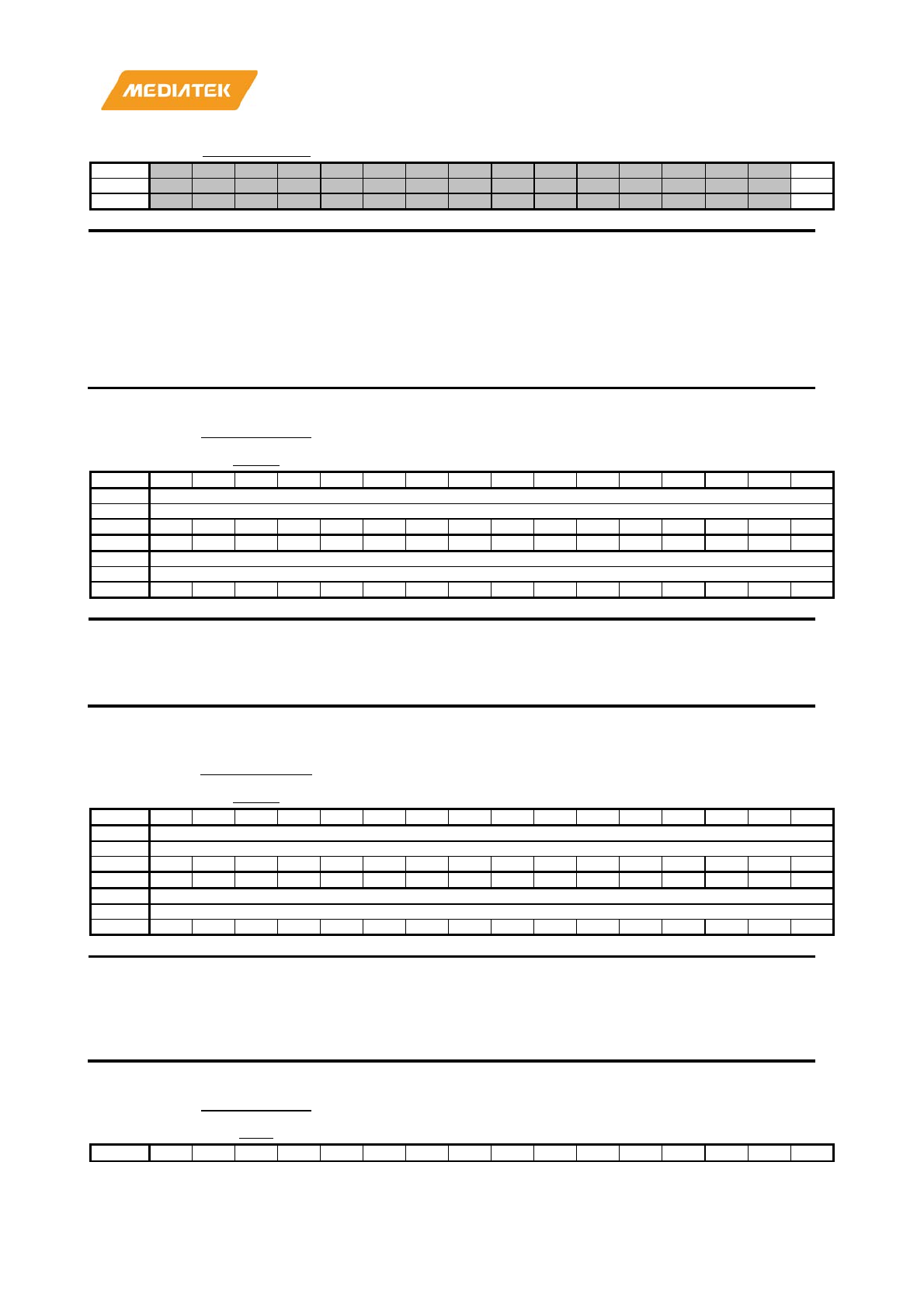
MT7686 Reference Manual
© 2016 - 2017 MediaTek Inc.
Page 78 of 536
This document contains information that is proprietary to MediaTek Inc. (“MediaTek”) and/or its licensor(s).
Any unauthorized use, reproduction or disclosure of this document in whole or in part is strictly prohibited.
A00A0014 SPIMST_STA SPI Master Status 00000000
SY
Type
RO
Reset
0
Bit(s)
Name
Description
0
SPIM_BUSY
SPI master status
This status flag reflects whether the SPI controller is busy. This bit is high active,
i.e. 1 represents the SPI controller is currently busy. The state diagram is shown in
Figure
6.1-2. Operation flow with or without PAUSE modeFigure 6.1-2.
•
1'b1: busy
•
1'b0: idle
A00A0018 SPIMST_TX_
DATA SPI Master TX Data 00000000
Bit
31
30
29
28
27
26
25
24
23
22
21
20
19
18
17
16
Name
SPIM_TX_DATA[31:16]
Type
WO
Reset
0
0
0
0
0
0
0
0
0
0
0
0
0
0
0
0
Bit
15
14
13
12
11
10
9
8
7
6
5
4
3
2
1
0
Name
SPIM_TX_DATA[15:0]
Type
WO
Reset
0
0
0
0
0
0
0
0
0
0
0
0
0
0
0
0
Bit(s)
Name
Description
31:0
SPIM_TX_DATA
TX data
The depth of the TX FIFO is 32 bytes. Write to this register to write 4 bytes into TX
FIFO. The TX FIFO pointer will automatically move toward to the next four bytes.
A00A001
C
SPIMST_RX_
DATA SPI Master RX Data 00000000
Bit
31
30
29
28
27
26
25
24
23
22
21
20
19
18
17
16
Name
SPIM_RX_DATA[31:16]
Type
RO
Reset
0
0
0
0
0
0
0
0
0
0
0
0
0
0
0
0
Bit
15
14
13
12
11
10
9
8
7
6
5
4
3
2
1
0
Name
SPIM_RX_DATA[15:0]
Type
RO
Reset
0
0
0
0
0
0
0
0
0
0
0
0
0
0
0
0
Bit(s)
Name
Description
31:0
SPIM_RX_DATA
RX data
The depth of the RX FIFO is 32 bytes. Read from this register to read 4 bytes from
the RX FIFO. The RX FIFO pointer will automatically move toward to the next
four bytes.
A00A002
0
SPIMST_TX_
SRC SPI Master TX Source Address Register 00000000
Bit
31
30
29
28
27
26
25
24
23
22
21
20
19
18
17
16
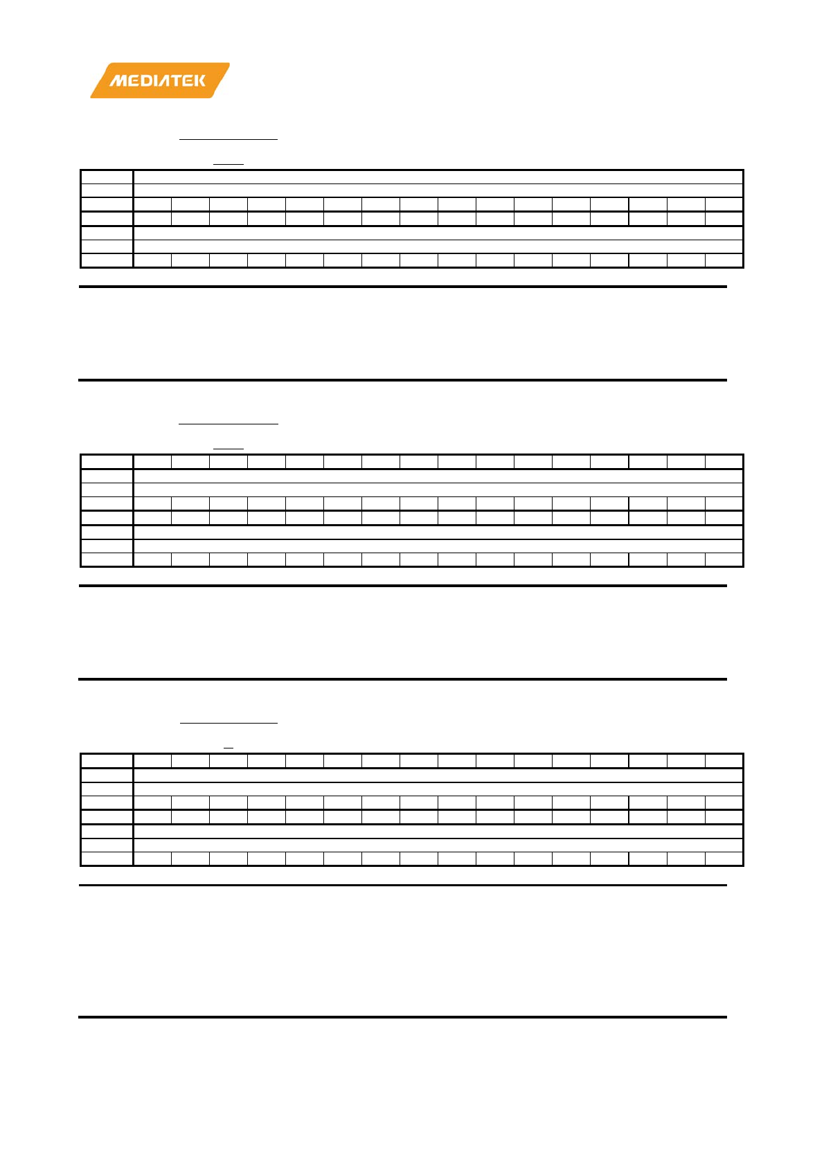
MT7686 Reference Manual
© 2016 - 2017 MediaTek Inc.
Page 79 of 536
This document contains information that is proprietary to MediaTek Inc. (“MediaTek”) and/or its licensor(s).
Any unauthorized use, reproduction or disclosure of this document in whole or in part is strictly prohibited.
A00A002
0
SPIMST_TX_
SRC SPI Master TX Source Address Register 00000000
Name
SPIM_TX_SRC[31:16]
Type
RW
Reset
0
0
0
0
0
0
0
0
0
0
0
0
0
0
0
0
Bit
15
14
13
12
11
10
9
8
7
6
5
4
3
2
1
0
Name
SPIM_TX_SRC[15:0]
Type
RW
Reset
0
0
0
0
0
0
0
0
0
0
0
0
0
0
0
0
Bit(s)
Name
Description
31:0
SPIM_TX_SRC
TX data source address
SPIM_TX_SRC
defines the memory address from which the SPI controller reads
transmitted data. The address must be aligned with the word boundary. Note, the
SPI master cannot read serial flash data.
A00A002
4
SPIMST_RX_
DST SPI Master RX Destination Address Register 00000000
Bit
31
30
29
28
27
26
25
24
23
22
21
20
19
18
17
16
Name
SPIM_RX_DST[31:16]
Type
RW
Reset
0
0
0
0
0
0
0
0
0
0
0
0
0
0
0
0
Bit
15
14
13
12
11
10
9
8
7
6
5
4
3
2
1
0
Name
SPIM_RX_DST[15:0]
Type
RW
Reset
0
0
0
0
0
0
0
0
0
0
0
0
0
0
0
0
Bit(s)
Name
Description
31:0
SPIM_RX_DST
RX data destination address
SPI_RX_DST
defines the memory address to which the SPI controller stores the
data. The address must be aligned with the word boundary. Note, the SPI master
cannot read serial flash data.
A00A002
8
SPIMST_CFG
0 SPI Master Configuration 0 Register 00000000
Bit
31
30
29
28
27
26
25
24
23
22
21
20
19
18
17
16
Name
SPIM_CS_SETUP_CNT
Type
RW
Reset
0
0
0
0
0
0
0
0
0
0
0
0
0
0
0
0
Bit
15
14
13
12
11
10
9
8
7
6
5
4
3
2
1
0
Name
SPIM_CS_HOLD_CNT
Type
RW
Reset
0
0
0
0
0
0
0
0
0
0
0
0
0
0
0
0
Bit(s)
Name
Description
31:16
SPIM_CS_SETUP_CNT
Chip select setup time
Setup time =
(SPIM_CS_SETUP_CNT+1) * CLK_PERIOD, where
CLK_PERIOD
(10.42ns) is the cycle time of the clock the SPI engine adopts.
15:0
SPIM_CS_HOLD_CNT
Chip select
hold time
Hold time =
(SPIM_CS_HOLD_COUNT+1) * CLK_PERIOD, where
CLK_PERIOD
(10.42ns) is the cycle time of the clock the SPI engine adopts.
MT7686 Reference Manual
© 2016 - 2017 MediaTek Inc.
Page 80 of 536
This document contains information that is proprietary to MediaTek Inc. (“MediaTek”) and/or its licensor(s).
Any unauthorized use, reproduction or disclosure of this document in whole or in part is strictly prohibited.
A00A002
C
SPIMST_CFG
1 SPI Master Configuration 1 Register 00000000
Bit
31
30
29
28
27
26
25
24
23
22
21
20
19
18
17
16
Name
SPIM_SCK_LOW_CNT
Type
RW
Reset
0
0
0
0
0
0
0
0
0
0
0
0
0
0
0
0
Bit
15
14
13
12
11
10
9
8
7
6
5
4
3
2
1
0
Name
SPIM_SCK_HIGH_CNT
Type
RW
Reset
0
0
0
0
0
0
0
0
0
0
0
0
0
0
0
0
Bit(s)
Name
Description
31:16
SPIM_SCK_LOW_CNT
SPI master clock low time
SCK low time =
(SPIM_SCK_LOW_CNT+1) * CLK_PERIOD (10.42ns)
15:0
SPIM_SCK_HIGH_CNT
SPI master clock high time
SCK high time =
(SPIM_SCK_HIGH_CNT+1) * CLK_PERIOD (10.42ns)
A00A003
0
SPIMST_CFG
2 SPI Master Configuration 2 Register 00000000
Bit
31
30
29
28
27
26
25
24
23
22
21
20
19
18
17
16
Name
SPIM_PACKET_LENGTH_CNT
Type
RW
Reset
0
0
0
0
0
0
0
0
0
0
0
0
0
0
0
0
Bit
15
14
13
12
11
10
9
8
7
6
5
4
3
2
1
0
Name
SPIM_PACKET_LOOP_CNT
SPIM_CS_IDLE_CNT
Type
RW
RW
Reset
0
0
0
0
0
0
0
0
0
0
0
0
0
0
0
0
Bit(s)
Name
Description
31:16
SPIM_PACKET_LENGTH_CNT
Transmission package length
The number of bytes in one packet =
PACKET_LENGTH_CNT + 1.
Total number bytes of one transmission =
(PACKET_LENGTH_CNT+1)
* (PACKET_LOOP_CNT+1)
.
15:8
SPIM_PACKET_LOOP_CNT
Transmission loop times
The number of packets in one transmission =
PACKET_LOOP_CNT + 1.
7:0
SPIM_CS_IDLE_CNT
Chip select idle time
Time between consecutive transmissions =
(CS_HOLD_COUNT+1) *
CLK_PERIOD
.
A00A003
4
SPIMST_CFG
3 SPI Master Configuration 3 Register 00000000
Bit
31
30
29
28
27
26
25
24
23
22
21
20
19
18
17
16
Name
Type
Reset
Bit
15
14
13
12
11
10
9
8
7
6
5
4
3
2
1
0
Name SPIM_DUMMY_CNT
SPIM_COMMAND_CN
T
Type
RW
RW
Reset
0
0
0
0
0
0
0
0
Bit(s)
Name
Description
MT7686 Reference Manual
© 2016 - 2017 MediaTek Inc.
Page 81 of 536
This document contains information that is proprietary to MediaTek Inc. (“MediaTek”) and/or its licensor(s).
Any unauthorized use, reproduction or disclosure of this document in whole or in part is strictly prohibited.
11:8
SPIM_DUMMY_CNT
Dummy count
The number
of dummy bits in one packet. Dummy phase is the second
transmission of packet between command phase and data phase. Dummy
phase cannot transmit or receive data, it’s only used in Dual/Quad SPI
(
SPIM_TYPE = 1 or 2).
3:0
SPIM_COMMAND_CNT
Command count
The n
umber of command bytes in one packet. Command phase is the first
transmission of packet before dummy phase and data phase. The command
phase is used in Dual/Quad SPI (
SPIM_TYPE = 1 or 2).
A00A003
8
SPIMST_DLY
SEL0 SPI Master Delay Select 0 Register 00000000
Bit
31
30
29
28
27
26
25
24
23
22
21
20
19
18
17
16
Name
SPIM_MOSI3_D
LYSEL
SPIM_MOSI2_D
LYSEL
Type
RW
RW
Reset
0
0
0
0
0
0
Bit
15
14
13
12
11
10
9
8
7
6
5
4
3
2
1
0
Name
SPIM_MOSI1_D
LYSEL
SPIM_MOSI0_D
LYSEL
Type
RW
RW
Reset
0
0
0
0
0
0
Bit(s)
Name
Description
26:24
SPIM_MOSI3_DLYSEL
MOSI3 delay select
The register can configure MOSI3 output signal delay. The delay is
SPIM_MOSI3_DLYSEL * 1.5 ns
.
18:16
SPIM_MOSI2_DLYSEL
MOSI2 delay select
The register can configure MOSI2 output signal delay. The delay is
SPIM_MOSI2_DLYSEL * 1.5 ns
.
10:8
SPIM_MOSI1_DLYSEL
MOSI1 delay select
The register can configure MOSI1 output signal delay. The delay is
SPIM_M
OSI1_DLYSEL * 1.5 ns.
2:0
SPIM_MOSI0_DLYSEL
MOSI0 delay select
The register can configure MOSI0 output signal delay. The delay is
SPIM_MOSI0_DLYSEL * 1.5 ns
.
A00A003
C
SPIMST_DLY
SEL1 SPI Master Delay Select 1 Register 00000000
Bit
31
30
29
28
27
26
25
24
23
22
21
20
19
18
17
16
Name
SPIM_MISO3_D
LYSEL
SPIM_MISO2_D
LYSEL
Type
RW
RW
Reset
0
0
0
0
0
0
Bit
15
14
13
12
11
10
9
8
7
6
5
4
3
2
1
0
Name
SPIM_MISO1_D
LYSEL
SPIM_MISO0_D
LYSEL
Type
RW
RW
Reset
0
0
0
0
0
0
Bit(s)
Name
Description
26:24
SPIM_MISO3_DLYSEL
MISO3 delay select
The register can configure MISO3 input signal delay. The delay is
MT7686 Reference Manual
© 2016 - 2017 MediaTek Inc.
Page 82 of 536
This document contains information that is proprietary to MediaTek Inc. (“MediaTek”) and/or its licensor(s).
Any unauthorized use, reproduction or disclosure of this document in whole or in part is strictly prohibited.
SPIM_MISO3_DLYSEL * 1.5 ns.
18:16
SPIM_MISO2_DLYSEL
MISO2 delay select
The register can configure MISO2 input signal delay. The delay is
SPIM_MISO2_DLYSEL * 1.5 ns
.
10:8
SPIM_MISO1_DLYSEL
MISO1 delay select
The register can configure MISO1 input signal delay. The delay is
SPIM_MISO1_DLYSE
L * 1.5 ns.
2:0
SPIM_MISO0_DLYSEL
MISO0 delay select
The register can configure MISO0 input signal delay. The delay is
SPIM_MISO0_DLYSEL * 1.5 ns
.
A00A004
0
SPIMST_DLY
SEL2 SPI Master Delay Select 2 Register 00000000
Bit
31
30
29
28
27
26
25
24
23
22
21
20
19
18
17
16
Name
Type
Reset
Bit
15
14
13
12
11
10
9
8
7
6
5
4
3
2
1
0
Name
SPIM_SCK_DLY
SEL
Type
RW
Reset
0
0
0
Bit(s)
Name
Description
2:0
SPIM_SCK_DLYSEL
SCK delay select
The register can configure SCK output signal delay. The delay is
SPIM_SCK_DLYSEL * 1.5 ns
.
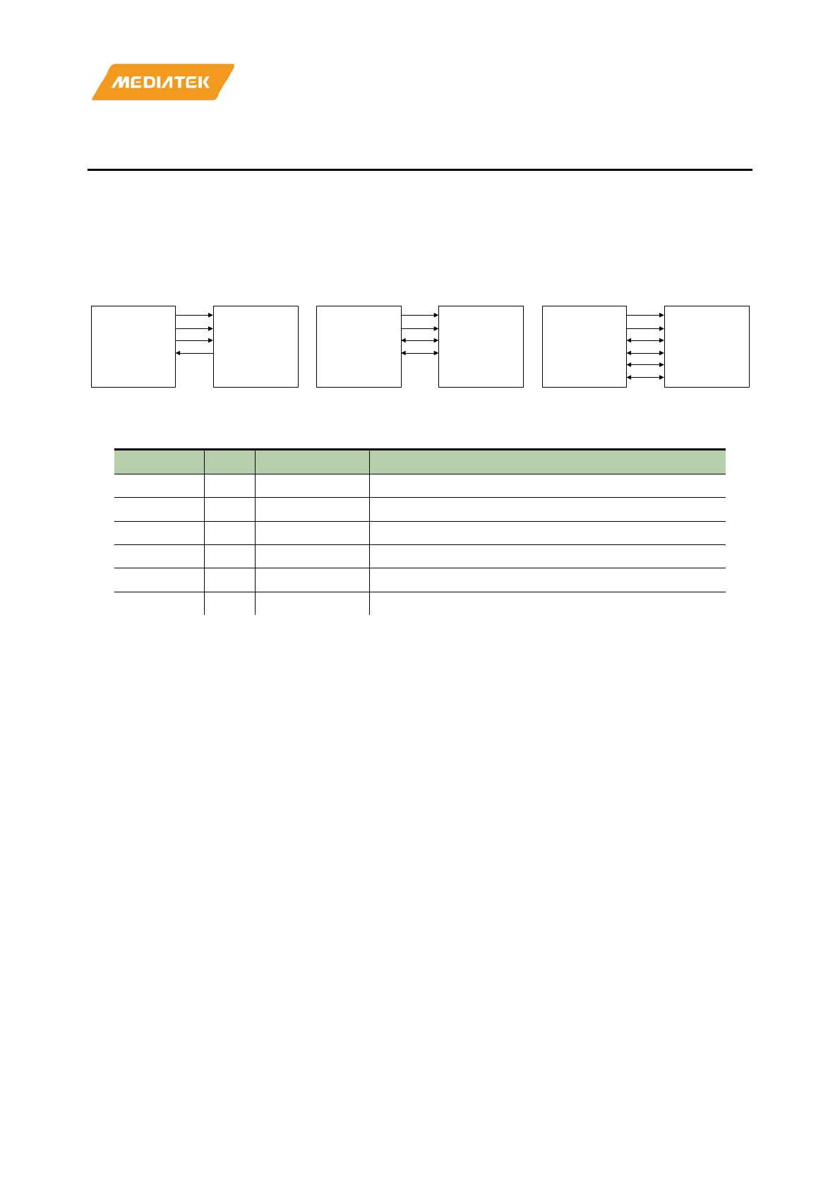
MT7686 Reference Manual
© 2016 - 2017 MediaTek Inc.
Page 83 of 536
This document contains information that is proprietary to MediaTek Inc. (“MediaTek”) and/or its licensor(s).
Any unauthorized use, reproduction or disclosure of this document in whole or in part is strictly prohibited.
7. Serial Peripheral Interface Slave Controller
The Serial Peripheral Interface (SPI) is a bit-serial transmission protocol. MT7686 supports single mode (four-pin),
dual mode (four-pin) and quad mode (six-pin) to increase data throughput. The maximum serial clock (SCK)
frequency is 48MHz. Figure 6.4-1 is an example of the connection between the SPI master and SPI slave. The SPI
controller is a slave responsible for data transmission with master.
CS
SCK
SIO0
SIO1
SIO2
SIO3
SPI
Master
CS
SCK
SIO0
SIO1
SIO2
SIO3
SPI
Slave
CS
SCK
SIO0
SIO1
SIO2
SIO3
SPI
Master
CS
SCK
SIO0
SIO1
SIO2
SIO3
SPI
Slave
CS
SCK
SIO0
SIO1
SIO2
SIO3
SPI
Master
CS
SCK
SIO0
SIO1
SIO2
SIO3
SPI
Slave
Single SPI Dual SPI Quad SPI
Figure 6.4-1. Pin connection between SPI master and SPI slave
Table 6.4-1. SPI slave controller interface
Signal name Type Default value Description
CS I pull up (input) Low active chip selection signal
SCK I pull down (input) The (bit) serial clock (Max SCK clock rate is 48MHz)
SIO0 I/O pull down (input) Data signal 0
SIO1 I/O 0 (output) Data signal 1
SIO2 I/O pull down (input) Data signal 2
SIO3 I/O pull down (input) Data signal 3
7.1. Features
• The SPI slave controller supports single mode (four-pin), dual mode (four-pin) and quad mode (six-pin).
The controller can automatically set port direction for data input/output if register SPIM_TYPE is set.
• Each databyte transmit/receive sequence can be configured separately with registers TXMSBF and
RXMSBF.
• The memory address of the SPI slave controller’s internal DMA read/write data can be configured by two
methods: SPI master command (hardware) configure and software configure.
o When register SPIS_DEC_ADDR_EN is 0, enable hardware configuration feature. The address of
DMA read/write is the SPI master CR/CW configuration address and SPISLV_BUFFER_BASE_ADDR.
For example, if the SPI master CR address is 0x1000 and SPISLV_BUFFER_BASE_ADDR is
0x2500, the address of DMA read/write will be 0x3500.
o When register SPIS_DEC_ADDR_EN is 1, enable software configuration feature. The SPI master
DMA reads and writes data from the address SPISLV_BUFFER_BASE_ADDR.
• The serial clock frequency supports maximum of 48MHz with CPOL and CPHA features. CPOL defines the
clock polarity in the transmission. CPHA defines the legal timing to sample data. The detailed timing
diagram of the SCK and CS signal is shown in Figure 7.1-1.
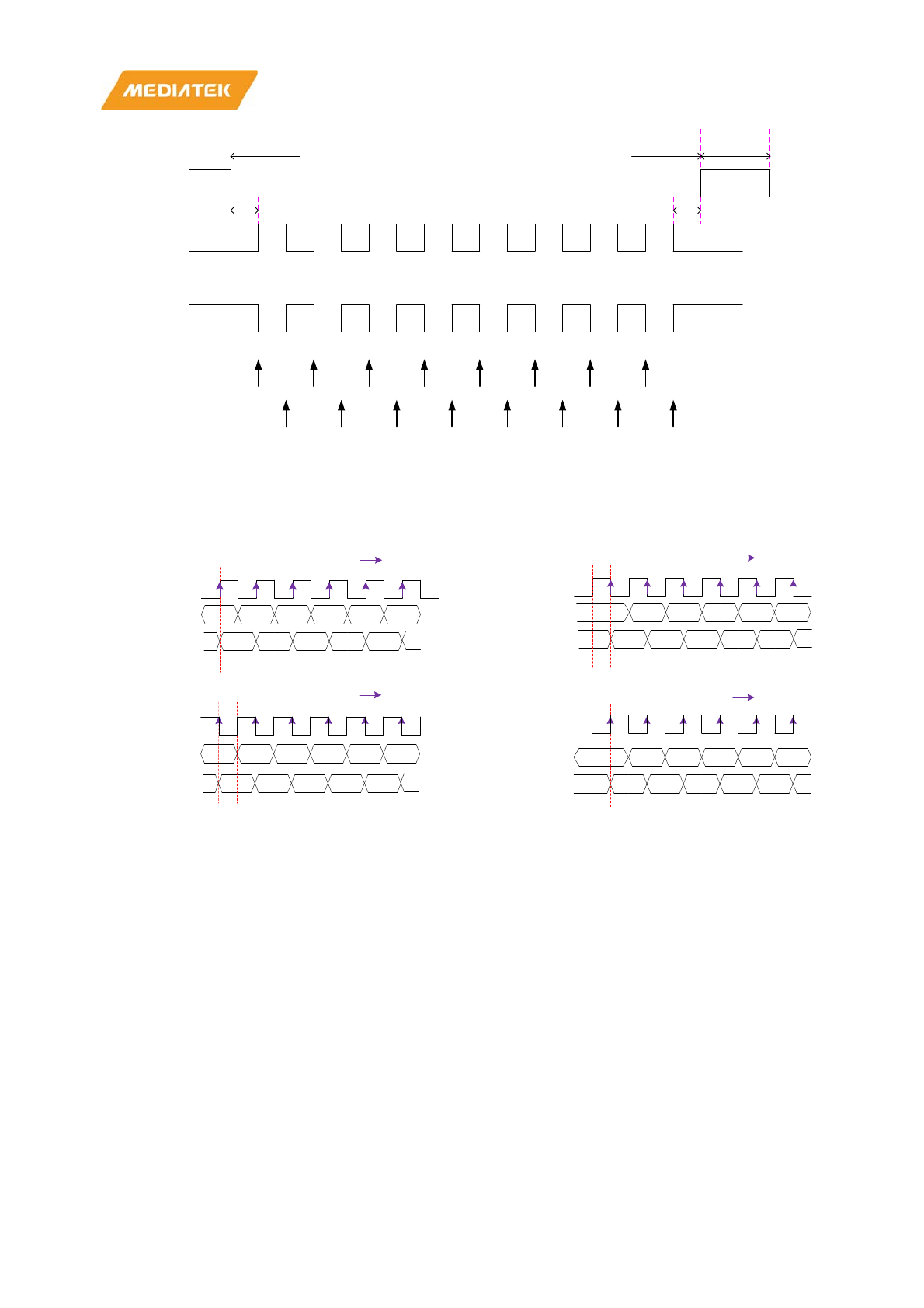
MT7686 Reference Manual
© 2016 - 2017 MediaTek Inc.
Page 84 of 536
This document contains information that is proprietary to MediaTek Inc. (“MediaTek”) and/or its licensor(s).
Any unauthorized use, reproduction or disclosure of this document in whole or in part is strictly prohibited.
CS
SCK
(CPOL=0)
SCK Edge
Number
SCK
(CPOL=1)
12 3 4 5 6 7 8 9 10 11 12 13 14 15 16
Sample input data
(CPHA=0)
Sample input data
(CPHA=1)
Data Transmission
CS idle time
CS setup time CS hold time
Figure 7.1-1. SPI transmission formats
• For high-speed transmission, the SPI slave controller can enable early transmission feature (register) to
resolve data path latency issue. The detailed description is shown in Figure 7.1-2.
sck
cpol=0 cpha=
0
012345
serial data
out(!early)
0 1 2 3 4 5
serial data
out(early)
master sample
data
cpol=0 cpha=1
0 1 2 3 4 5
0 1 2 3 4 5
master
sample data
cpol=1 cpha=1
0 1 2 3 4 5
0 1 2 3 4 5
master sample
data
cpol=1 cpha=0
0 1 2 3 4 5
0 1 2 3 4 5
master sample
data
sck
serial data
out(!early)
serial data
out(early)
sck
serial data
out(!early)
serial data
out(early)
sck
serial data
out(!early)
serial data
out(early)
Figure 7.1-2. SPI slave controller early transmit
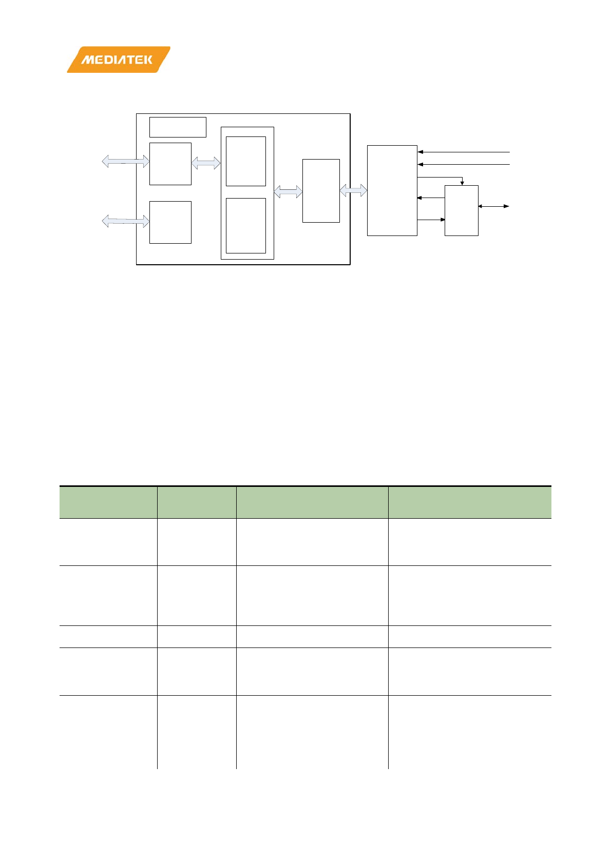
MT7686 Reference Manual
© 2016 - 2017 MediaTek Inc.
Page 85 of 536
This document contains information that is proprietary to MediaTek Inc. (“MediaTek”) and/or its licensor(s).
Any unauthorized use, reproduction or disclosure of this document in whole or in part is strictly prohibited.
7.2. Block diagram
SIO_oe
miso
TX_FIFO
(64 bytes)
RX_FIFO
(64 bytes)
spi_engine
dma_engine
apb_regif
memory
CPU
spi_state_ctrl
AHB
APB
mosi
SCK
CS
S
P
I
_
s
l
a
v
e
_
P
A
D
_
M
A
C
R
O
FIFO
G
P
I
O
m
u
x
SIO[0:3]
Figure 7.2-1. Block diagram of SPI slave controller
• The SPI slave controller accesses memory through the AHB interface and the CPU can access the SPI slave
controller through the APB interface.
• The SPI slave controller has an internal direct memory access (DMA) engine to access memory and FIFO to
store data during transmission.
• The SPI slave controller can set the direction (in or out) of GPIO pinmux by SIO_oe (defined by
SPIM_TYPE).
7.3. Functions
The SPI slave controller has nine commands that can be configured by the SPI master transmit data, the command
set is shown in Table 7.3-1 and the command format is shown in Figure 7.3-1 and Figure 7.3-2.
Table 7.3-1. SPI slave controller interface
Command field
[7:0]
CMD default
code
Data field length Description
Power Off (PWOFF) 8’h02 0 byte
Master uses this configure
command so that the MCU turns off
the SPI slave controller.
Power On (PWON) 8’h04 0 byte
Master uses this configure
command to wakeup the system
and tell the MCU to turn on the SPI
slave controller.
Read Status (RS) 8’h06 1 byte (SPI slave feedback)
Master reads Slave status register.
Write Status (WS) 8’h08 1 byte
Master writes Slave status register
to clean the error bit, such as write
1 to clear.
Config Read (CR) 8’h0a SIZE_OF_ADDR
• 1: 4 bytes address, 4 bytes
data length.
• 0: 2 bytes address, 2 bytes
data length.
Master configures the SPI Slave to
read data.
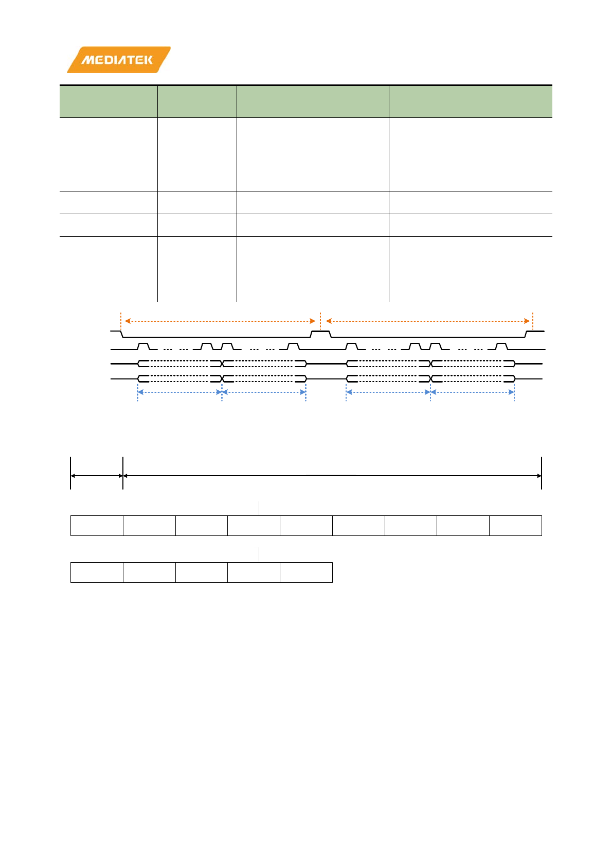
MT7686 Reference Manual
© 2016 - 2017 MediaTek Inc.
Page 86 of 536
This document contains information that is proprietary to MediaTek Inc. (“MediaTek”) and/or its licensor(s).
Any unauthorized use, reproduction or disclosure of this document in whole or in part is strictly prohibited.
Command field
[7:0]
CMD default
code
Data field length Description
Config Write (CW) 8’h0c SIZE_OF_ADDR
• 1: 4 bytes address, 4 bytes
data length.
• 0: 2 bytes address, 2 bytes
data length.
Master configures the SPI Slave to
write data.
Read Data (RD) 8’h81 N bytes. Burst data payload.
Master reads data.
Write Data (WD) 8’h0e N bytes. Burst data payload.
Master writes data.
Config Type (CT) 8’h10 1 byte:
• [7:3] Not used
• [2] SIZE_OF_ADDR
• [1:0] SPIS_TYPE
Master configures the SPI Slave
type.
CS
SCK
MOSI
MISO
Command 1Command 2
Command field
(1 byte)
Command field
(1 byte)
Data field
(1 byte)
Data field
(1 byte)
Figure 7.3-1. SPI slave controller commands waveform
Command field
CR/CW addr[7:0] addr[15:8] addr[23:16]addr[31:24]length[7:0] length[15:8] length[23:16]length[31:24]
CR/CW addr[7:0] addr[15:8] length[7:0] length[15:8]
Data field
SIZE_OF_ADDR = 1: 4 bytes address, 4 by tes len gt h
SIZE_OF_ADDR = 0: 2 bytes address, 2 by tes len gt h
Figure 7.3-2. Config read/write (CR/CW) command format
7.3.1. SPI slave control flow
The SPI slave control flow is shown in Figure 7.3-3. First, the SPI master sends a “power on” command to turn on
the SPI slave controller then transmits a “config read/write” command to configure the transfer data length and
read/write address of the memory. After the SPI slave is configured, it can send/receive data package with SPI
master by the “read/write data” command. Last, use the “power off” command to turn off the SPI slave controller.
In each state, the SPI master transmits the “read status” command to poll SPI slave status. If the SPI master detects
an error state flag bit, it should send a “write status” command to clear the bit and poll this bit until it turns low.
The SPI master can transmit a “config type” command to configure data transmission type (Single, Dual, or Quad
mode) according to user requirements. The SPI slave control flow is shown in Table 7.3-2.
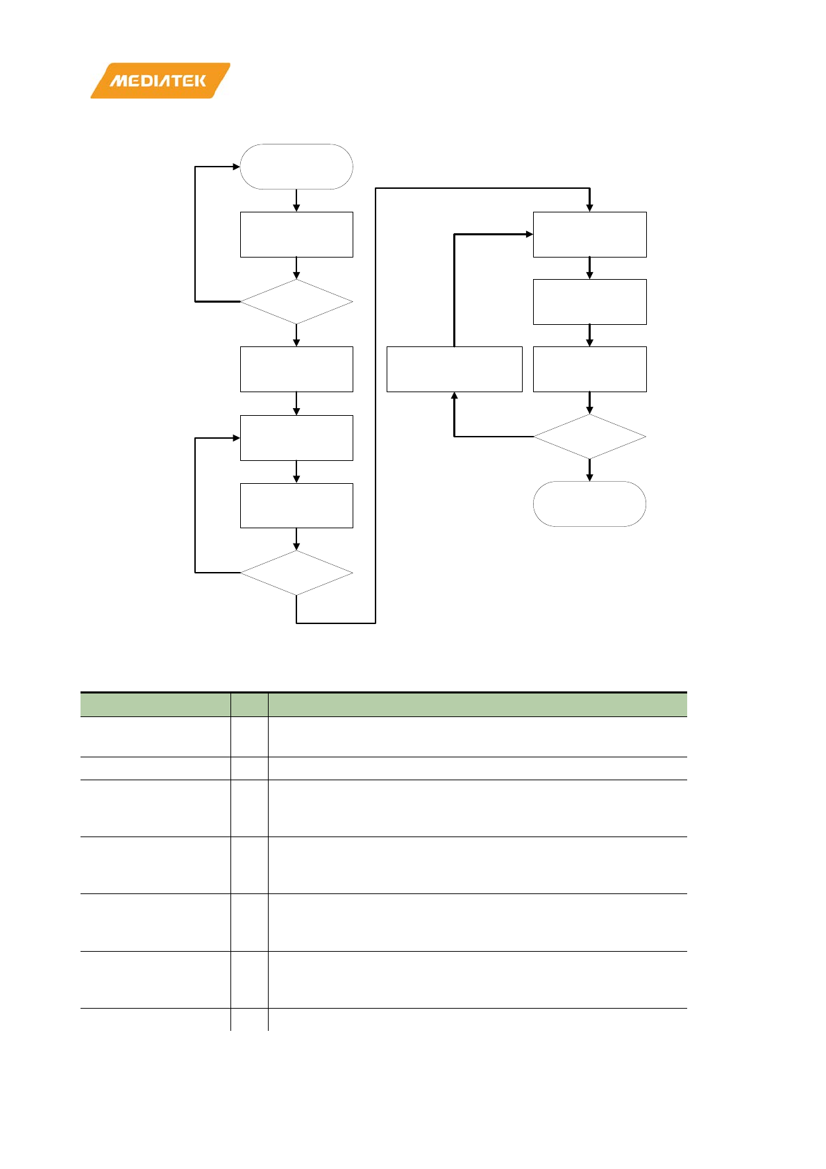
MT7686 Reference Manual
© 2016 - 2017 MediaTek Inc.
Page 87 of 536
This document contains information that is proprietary to MediaTek Inc. (“MediaTek”) and/or its licensor(s).
Any unauthorized use, reproduction or disclosure of this document in whole or in part is strictly prohibited.
Read Status
CMD
Config Read/Write
CMD
Read Status
CMD
Read/Write Data
CMD
SPI Transmission
Read Status
CMD
SLV_ON = 1
Power On
CMD
CFG_SUCESS = 1 &
TXRX_FIFO_RDY = 1
RDWR_FINISH = 1 &
RD_ERR/WR_ERR = 0
Power Off
CMD
Y
N
Y
Y
N
Write Status CMD
(clear RD_ERR/WR_ERR)
N
Config Type
CMD (Maybe)
Figure 7.3-3. SPI slave control flow diagram
Table 7.3-2. SPI slave status description (use RS command to poll SPI slave status)
Function
Bit
Usage (status[bit] = function)
SLV_ON 0
Master polls this bit until slave is on after sending POWERON CMD or
off after sending POWEROFF CMD.
SR_CFG_SUCCESS 1
Master checks this bit for the CW/CR command status.
SR_TXRX_FIFO_RDY 2
Set this bit when the slave is ready to send/receive data (master can
send RD/WD command). Clean the bit after SPI slave receives a CR/CW
command.
SR_RD_ERR 3
After a read command, master can read this bit to check for an error in
the read transfer. If there is an error, the master should send WS
command to clear this bit and poll this bit until it’s 0.
SR_WR_ERR 4
After a WD command, master can read this bit to check for an error in
the write transfer. If there is an error, the master should send WS
command to clear this bit and poll this bit until it’s 0.
SR_RDWR_FINISH 5
After RD/WD transaction, master can poll this bit to check if read/write
transfer is finished. Clean the bit after the SPI slave receives a CR/CW
command.
SR_TIMOUT_ERR 6
Indicates the SPI slave didn’t receive input signal for sometime when
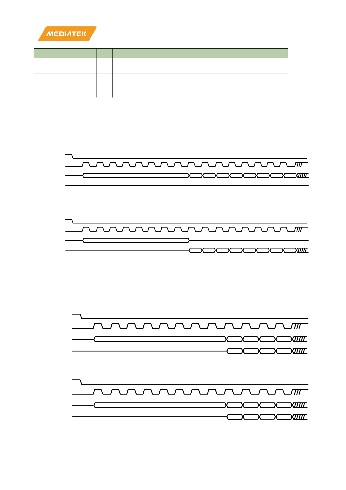
MT7686 Reference Manual
© 2016 - 2017 MediaTek Inc.
Page 88 of 536
This document contains information that is proprietary to MediaTek Inc. (“MediaTek”) and/or its licensor(s).
Any unauthorized use, reproduction or disclosure of this document in whole or in part is strictly prohibited.
Function
Bit
Usage (status[bit] = function)
chip select signal was active. The SPI master should send a WS
command to clear this bit and poll this bit until it’s 0.
SR_CMD_ERR 7
If master sends an error command in the first byte, master detects the
error status through the received data. Clean it after the SPI slave
receives a correct command.
7.3.2. SPI slave modes
1) SPI slave single mode.
The typical SPI transmission mode is single SPI, it’s a 4-pin protocol. Set the register SPIS_TYPE to 0 to enter single
mode. The single mode data transmission diagrams are shown in Figure 7.3-4 and Figure 7.3-5.
CS
SCK
SIO0
SIO1
DI A0DI A1DI A2DI A3DI A4DI A5DI A6DI A7
WD command
Figure 7.3-4. SPI slave single mode write data
CS
SCK
SIO0
SIO1DO A0DO A1DO A2DO A3DO A4DO A5DO A6DO A7
RD c ommand
Figure 7.3-5. SPI slave single mode read data
2) SPI slave dual mode.
The dual mode SPI is also a 4-pin protocol. Set the register SPIS_TYPE to 1 to enter this mode. The dual mode
data transmission diagrams are shown in Figure 7.3-6 and Figure 7.3-7.
CS
SCK
SIO0
SIO1
DI A0
DI A1
DI A2
DI A3
DI A4
DI A5
DI A6
DI A7
WD command
Figure 7.3-6. SPI slave dual mode write data
CS
SCK
SIO0
SIO1
DO A0
DO A1
DO A2
DO A3
DO A4
DO A5
DO A6
DO A7
RD command
Figure 7.3-7. SPI slave dual mode read data
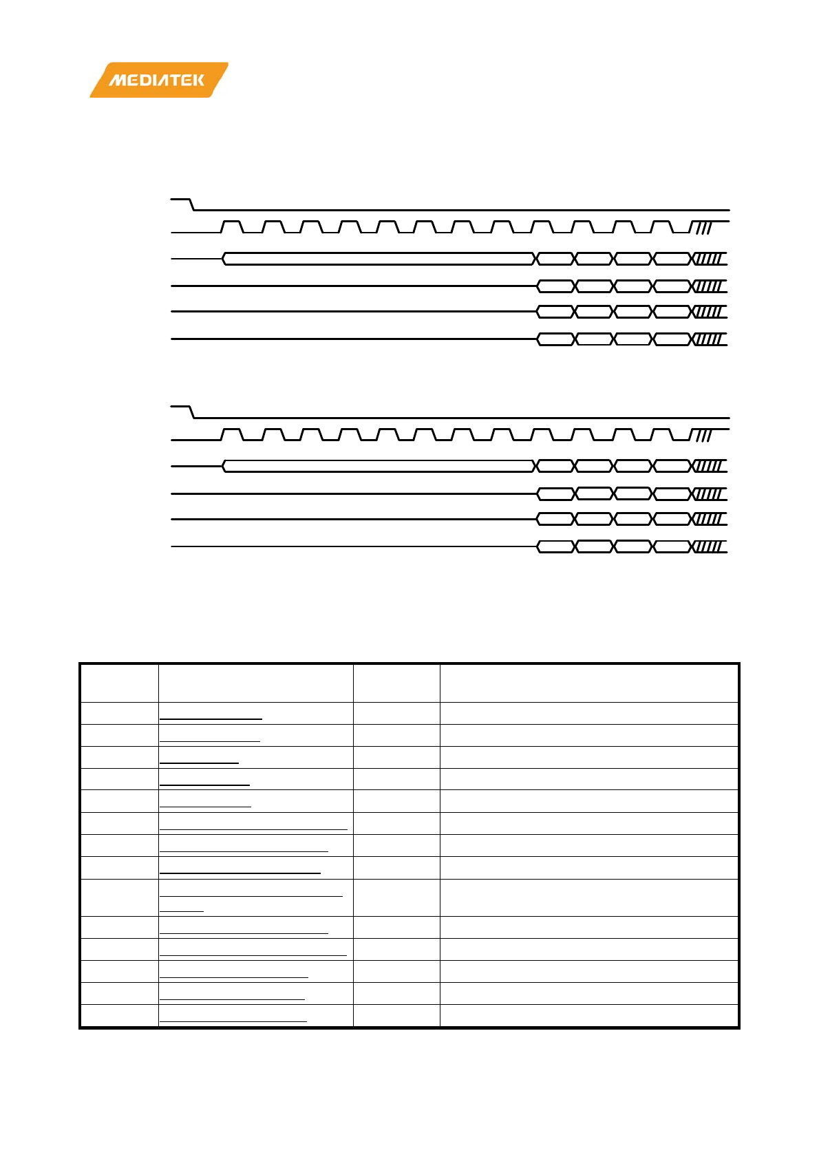
MT7686 Reference Manual
© 2016 - 2017 MediaTek Inc.
Page 89 of 536
This document contains information that is proprietary to MediaTek Inc. (“MediaTek”) and/or its licensor(s).
Any unauthorized use, reproduction or disclosure of this document in whole or in part is strictly prohibited.
3) SPI slave quad mode.
The quad mode SPI is a 6-pin protocol. Set the register SPIS_TYPE to 2 to enter this mode. The quad mode
transmission diagrams are shown in Figure 7.3-8 and Figure 7.3-9.
CS
SCK
SIO0
SIO1
DI A0
DI A1
DI A4
DI A5
DI B0
DI B1
DI B4
DI B5
WD command
SIO2
SIO3
DI A2
DI A3
DI A6
DI A7
DI B2
DI B3
DI B6
DI B7
Figure 7.3-8. SPI slave quad mode write data
CS
SCK
SIO0
SIO1
DO A0
DO A1
DO A4
DO A5
DO B0
DO B1
DO B4
DO B5
RD command
SIO2
SIO3
DO A2
DO A3
DO A6
DO A7
DO B2
DO B3
DO B6
DO B7
Figure 7.3-9. SPI slave quad mode read data
7.4. Register mapping
Module name: SPI_SLAVE Base address: (+A00B0000h)
Address Name Width
(bits) Register Function
A00B0000
SPISLV_CTRL
32
SPI Slave Control
Register
A00B0004
SPISLV_TRIG
32
SPI Slave Trigger Register
A00B0008
SPISLV_IE
32
SPI Slave Interrupt Enable
A00B000C
SPISLV_INT
32
SPI Slave Interrupt
A00B0010
SPISLV_STA
32
SPI Slave Status
A00B0014
SPISLV_TRANS_LENGTH
32
SPI Slave Transfer Length Register
A00B0018
SPISLV_TRANS_ADDR
32
SPI
Slave Transfer Address Register
A00B001C
SPISLV_TMOUT_THR
32
SPI Slave Timeout Threshold Register
A00B0020
SPISLV_BUFFER_BASE_
ADDR
32
SPI Slave Buffer Base Address
Register
A00B0024
SPISLV_BUFFER_SIZE
32
SPI Slave Buffer Size Register
A00B0028
SPISLV_CMD_RECEIVED
32
SPI Slave CMD Received
A00B002C
SPISLV_CMD_DEF0
32
SPI Slave Command Define 0
A00B0030
SPISLV_CMD_DEF1
32
SPI Slave Command Define 1
A00B0034
SPISLV_CMD_DEF2
32
SPI Slave Command Define 2
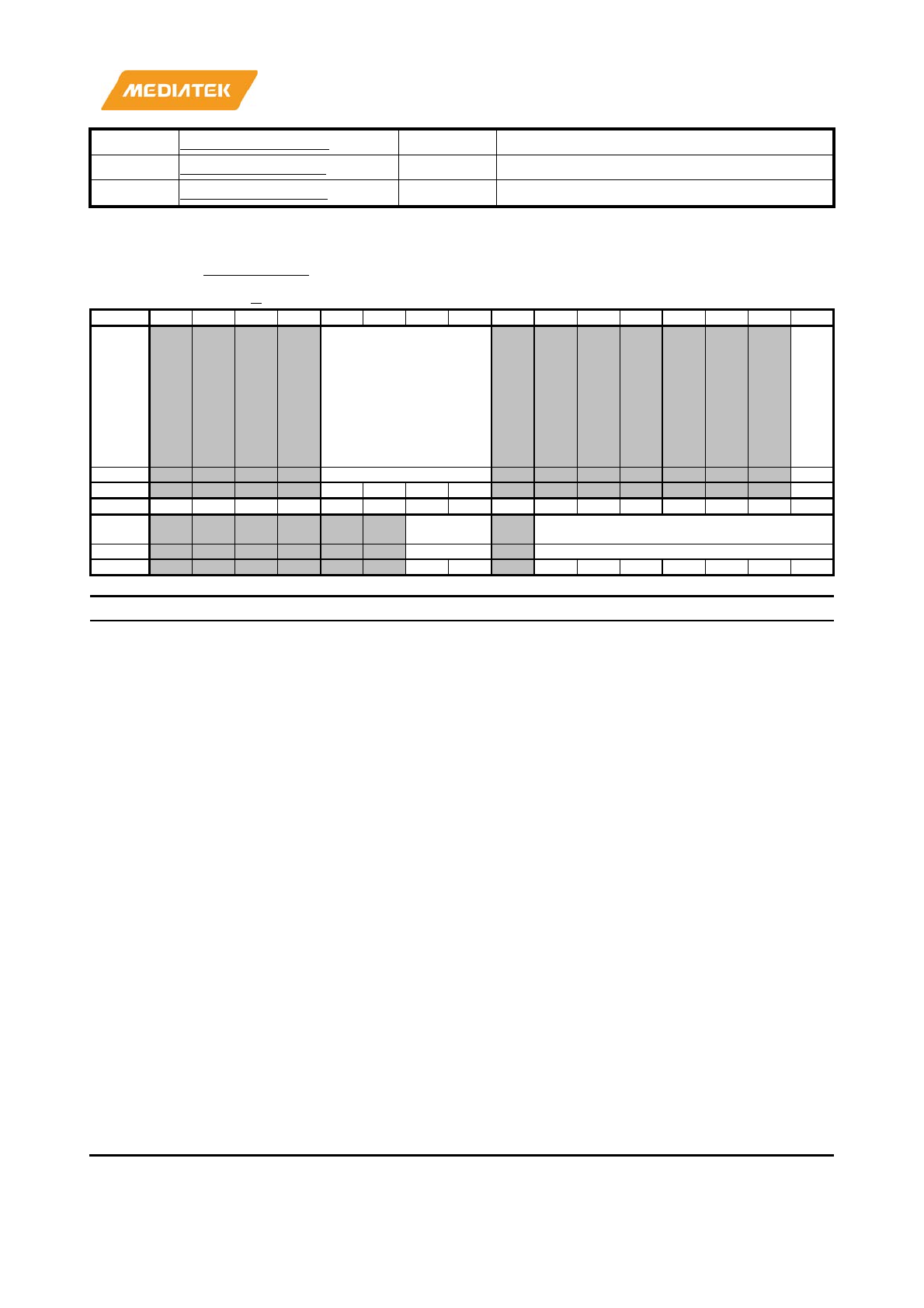
MT7686 Reference Manual
© 2016 - 2017 MediaTek Inc.
Page 90 of 536
This document contains information that is proprietary to MediaTek Inc. (“MediaTek”) and/or its licensor(s).
Any unauthorized use, reproduction or disclosure of this document in whole or in part is strictly prohibited.
A00B0038
SPISLV_DLYSEL0
32
SPI Slave Delay Select 0 Register
A00B003C
SPISLV_DLYSEL1
32
SPI Slave Delay Select 1 Register
A00B0040
SPISLV_DLYSEL2
32
SPI
Slave Delay Select 2 Register
A00B000
0
SPISLV_CTR
L SPI Slave Control Register 00000100
Bit
31
30
29
28
27
26
25
24
23
22
21
20
19
18
17
16
Name SPIS_DUMMY_CNT
SPI
S_
MI
SO
_E
AR
LY
_T
RA
NS
Type
RW
RW
Reset
0
0
0
0
0
Bit
15
14
13
12
11
10
9
8
7
6
5
4
3
2
1
0
Name
SPIS_CTR
L1
SPIS_CTRL0
Type
RW
RW
Reset
0
1
0
0
0
0
0
0
0
Bit(s) Name Description
27:24 SPIS_DUMMY_CNT Dummy count
The number of dummy bits in one packet.
• Dummy phase is the second transmission of packet between
command phase and data phase.
• Dummy phase cannot transmit/receive data, it’s only used in dual or
quad SPI modes (SPIS_TYPE is 1 or 2).
16 SPIS_MISO_EARLY_TRAN
S Early transmit data
Defines whether to transmit data half SCK cycle early. It’s used to improve
the SPI timing.
9:8 SPIS_CTRL1 SPI slave general configuration setting 1
• [1]: SPIS_DEC_ADDR_EN, indicates whether software decode
address is sent by the SPI master.
o 0: software will not decode the address. The address of
read/write memory is set by master configure read/write
command.
o 1: software will decode the address of read/write memory.
• [0]: SPIS_SW_RDY_EN, if the value is 1, defines whether hardware
automatically sets the register SPIS_TXDMA_SW_RDY or
SPIS_RXDMA_SW_RDY.
6:0 SPIS_CTRL0 SPI slave general configuration setting 0
• [6]: SIZE_OF_ADDR, defines CW/CR command format, can be
configured by master command or slave software settings.
o 0: Data filed includes 2 bytes of transfer address and 2 bytes of
transfer length.
o 1: Data filed includes 4 bytes of transfer address and 4 bytes of
transfer length.
• [5:4]: SPIS_TYPE, indicates the SPI data transmission type, can be
configured by master command or software settings.
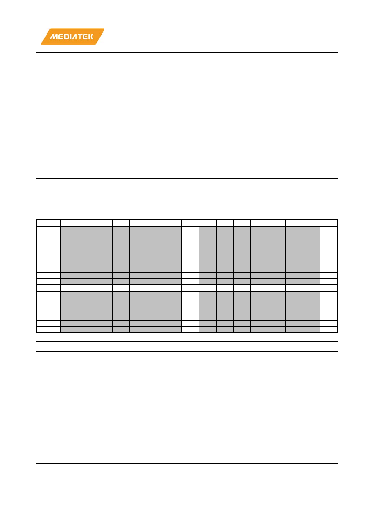
MT7686 Reference Manual
© 2016 - 2017 MediaTek Inc.
Page 91 of 536
This document contains information that is proprietary to MediaTek Inc. (“MediaTek”) and/or its licensor(s).
Any unauthorized use, reproduction or disclosure of this document in whole or in part is strictly prohibited.
o 0: Single SPI
o 1: Dual SPI
o 2: Quad SPI
o 3: Not used
• [3]: RXMSBF, indicates whether the first byte of the received RX data
received is MSB. Set RXMSBF to 1 to define the first byte as MSB,
otherwise set it to 0.
• [2]: TXMSBF, indicates the first byte of the transmitted TX data is
MSB. Set TXMSBF to 1 to define the first byte as MSB, otherwise set it
to 0.
• [1]: CPOL, control bit of the SCK polarity.
o 0: CPOL = 0
o 1: CPOL = 1
• [0]: CPHA, control bit of the SCK sample data phase
o 0: CPHA = 0
o
1: CPHA = 1
A00B000
4
SPISLV_TRI
G SPI Slave Trigger Register 00000000
Bit
31
30
29
28
27
26
25
24
23
22
21
20
19
18
17
16
Name
SPI
S_
RX
DM
A_
SW
_R
DY
SPI
S_T
XD
MA
_S
W_
RD
Y
Type
WO
WO
Reset
0
0
Bit
15
14
13
12
11
10
9
8
7
6
5
4
3
2
1
0
Name
SPI
S_S
W_
RS
T
SPI
S_S
W_
ON
Type
WO
WO
Reset
0
0
Bit(s) Name Description
24 SPIS_RXDMA_SW_RDY Software ready to receive data
Write 1 to this bit to indicate the SPI slave can receive RX data.
TXRX_FIFO_RDY of the status of STA register will be set. And master can
query the status to check whether the slave is ready to receive data.
16 SPIS_TXDMA_SW_RDY Software ready to transmit data
Write 1 to this bit to indicate the SPI slave can transmit TX data.
TXRX_FIFO_RDY of STA register status will be set. And the master can
query the status to check whether the slave is ready to transmit data.
8 SPIS_SW_RST Software reset
Software reset bit; resets the state machine and data FIFO of SPI slave
controller (not the register define). When this bit is 1, software reset is active
high, and hardware can automatically recover to 0. The default value is 0.
0 SPIS_SW_ON Software ON
The SPI slave controller is enabled by software, the slave software can set
SR_SLV_ON by SPIS_SW_ON control.
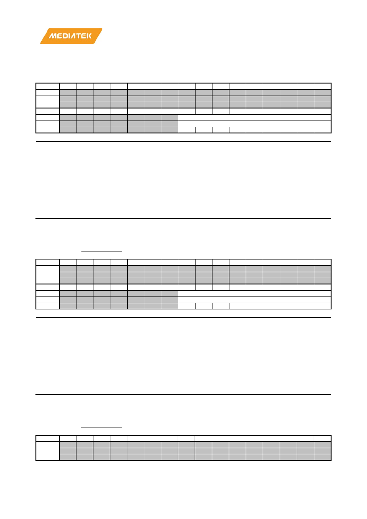
MT7686 Reference Manual
© 2016 - 2017 MediaTek Inc.
Page 92 of 536
This document contains information that is proprietary to MediaTek Inc. (“MediaTek”) and/or its licensor(s).
Any unauthorized use, reproduction or disclosure of this document in whole or in part is strictly prohibited.
A00B000
8 SPISLV_IE SPI Slave Interrupt Enable 00000000
Bit
31
30
29
28
27
26
25
24
23
22
21
20
19
18
17
16
Name
Type
Reset
Bit
15
14
13
12
11
10
9
8
7
6
5
4
3
2
1
0
Name
SPIS_IE
Type
RW
Reset
0
0
0
0
0
0
0
0
0
Bit(s) Name Description
8:0 SPIS_IE SPI slave interrupt source enable
[8]: TMOUT_ERR_IE, interrupt enable bit of timeout error
[7]: WR_DATA_ERR_IE, interrupt enable bit of SPI master write data error
[6]: RD_DATA_ERR_IE, interrupt enable bit of SPI master read data error
[5]: POWER_ON_IE, interrupt enable bit of SPI slave receive power-on command
[4]: POWER_OFF_IE, interrupt enable bit of SPI slave receive power-off
[3]: WR_TRANS_FINISH_IE, interrupt enable bit of SPI master write data finish
[2]: RD_TRANS_FINISH_IE, interrupt enable bit of SPI master read data finish
[1]: WR_CFG_FINISH_IE, interrupt enable bit of SPI master configure write finish
[0]: RD_CFG_FINISH_IE, interrupt enable bit of SPI master configure read finish
A00B000
C SPISLV_INT SPI Slave Interrupt 00000000
Bit
31
30
29
28
27
26
25
24
23
22
21
20
19
18
17
16
Name
Type
Reset
Bit
15
14
13
12
11
10
9
8
7
6
5
4
3
2
1
0
Name
SPIS_INT
Type
RC
Reset
0
0
0
0
0
0
0
0
0
Bit(s) Name Description
8:0 SPIS_INT SPI slave interrupt source
[8]: TMOUT_ERR_INT, timeout error interrupt
[7]: WR_DATA_ERR_INT, SPI master write data error interrupt
[6]: RD_DATA_ERR_INT, SPI master read data error interrupt
[5]: POWER_ON_INT, SPI slave receive power-on command interrupt
[4]: POWER_OFF_INT, SPI slave receive power-off command interrupt
[3]: WR_TRANS_FINISH_INT, SPI master write data finish interrupt
[2]: RD_TRANS_FINISH_INT, SPI master read data finish interrupt
[1]: WR_CFG_FINISH_INT, SPI master configure write finish interrupt
[0]: RD_CFG_FINISH_INT, SPI master configure read finish interrupt
A00B001
0 SPISLV_STA SPI Slave Status 00000000
Bit
31
30
29
28
27
26
25
24
23
22
21
20
19
18
17
16
Name
Type
Reset

MT7686 Reference Manual
© 2016 - 2017 MediaTek Inc.
Page 93 of 536
This document contains information that is proprietary to MediaTek Inc. (“MediaTek”) and/or its licensor(s).
Any unauthorized use, reproduction or disclosure of this document in whole or in part is strictly prohibited.
A00B001
0 SPISLV_STA SPI Slave Status 00000000
Bit
15
14
13
12
11
10
9
8
7
6
5
4
3
2
1
0
Name
SPIS_STA
Type
RO
Reset
0
0
0
0
0
0
0
0
0
0
0
0
0
0
Bit(s) Name Description
13:0 SPIS_STA SPI slave status
• SPIS_STA[7:0] is the feedback data when SPI master send read status
command
o [13]: SR_POWER_ON
SPI slave receives power-on command.
Cleared after SPIS_SW_ON is set to 1.
o [12]: SR_POWER_OFF
SPI slave receives power-off command.
Cleared after SPIS_SW_ON is set to 0.
o [11]: SR_WR_FINISH
SPI master write data finish.
Cleared after the next configure write or read (CW/CR) command.
o [10]: SR_RD_FINISH
SPI master read data finish.
Cleared after the next CW/CR command.
o [9]: SR_CFG_WRITE_FINISH
SPI slave receive CW command is complete.
Cleared after SR_TXRX_FIFO_RDY = 1.
o [8]: SR_CFG_READ_FINISH
SPI slave receive CR command is finished.
Cleared after SR_TXRX_FIFO_RDY = 1.
o [7]: SR_CMD_ERROR
Used for SPI master to debug.
Cleared after SPI master sends a correct command.
o [6]: SR_TIMOUT_ERR
• SPI slave doesn’t receive SCK signal for some time when chip select signal is
active.
If there is an error, master must send WS command to clear this bit and poll
this bit until it’s 0.
o [5]: SR_RDWR_FINISH
The bit is set to 1 when SPI slave receives or sends all data.
Cleared after SPI slave receives CR/CW command.
o [4]: SR_WR_ERR
After a WR command, master can read this bit to check for an error in
the write transfer through RS command.
If there is an error, master must send WS command to clear this bit and
poll this bit until it’s 0.
o [3]: SR_RD_ERR
After an RD command, master can read this bit to check for an error in
the read transfer through RS.
If there is timeout error, master must send WS command to clear this bit
and poll this bit until it’s 0.
o [2]: SR_TXRX_FIFO_RDY
When CR, this bit used to indicate whether TX FIFO is ready. Master
polls this bit to know if the slave is ready to send data, then master can
send the RD command.
• When CW, this bit used to indicate whether RX FIFO is ready. Master polls
this bit to know if the slave is ready to send data, then master can send WD
command.
This bit will be cleared after SPI slave receives CR/CW command.
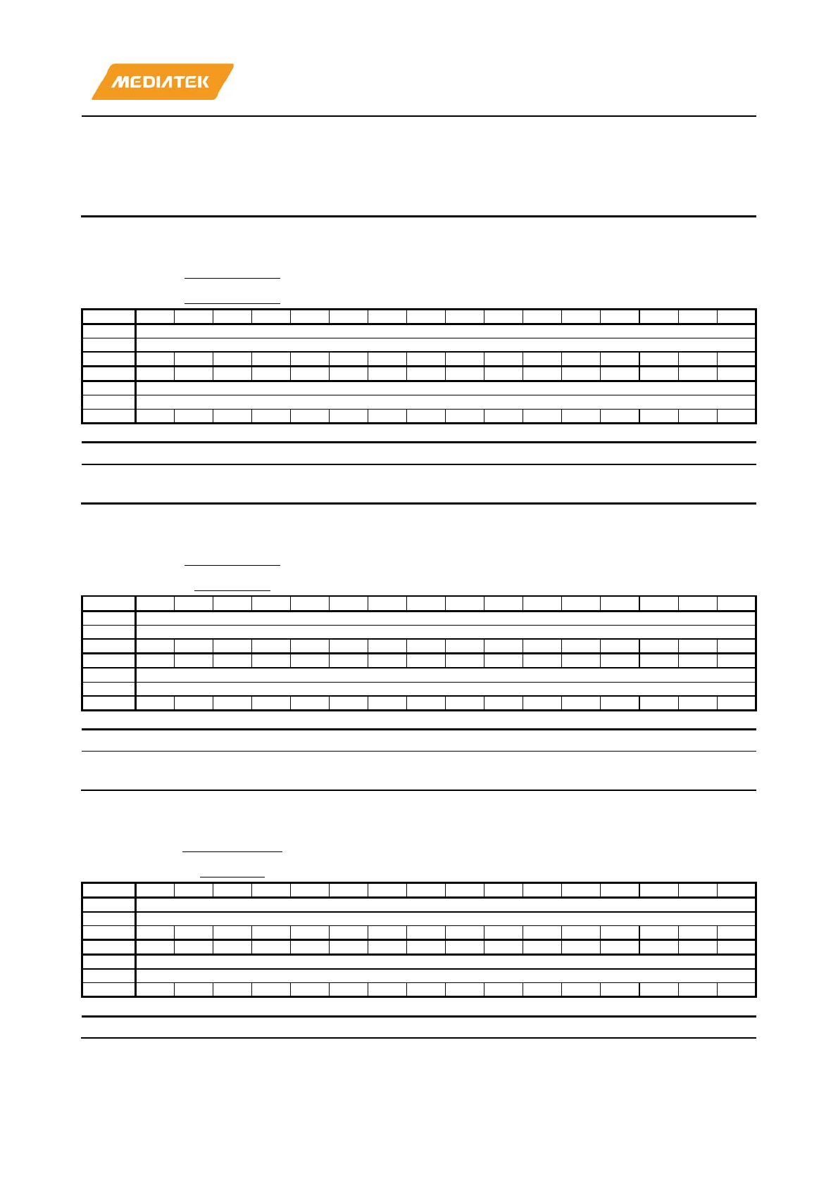
MT7686 Reference Manual
© 2016 - 2017 MediaTek Inc.
Page 94 of 536
This document contains information that is proprietary to MediaTek Inc. (“MediaTek”) and/or its licensor(s).
Any unauthorized use, reproduction or disclosure of this document in whole or in part is strictly prohibited.
o [1]: SR_CFG_SUCESS
SPI master configure package address/length successfully.
o [0]: SR_SLV_ON
• SPI slave controller enable by set SPIS_SW_ON = 1. After SPI slave receive
POWER-ON command, slave software can set this bit by control
SPIS_SW_ON.
A00B0014 SPISLV_TRA
NS_LENGTH SPI Slave Transfer Length Register 00000000
Bit
31
30
29
28
27
26
25
24
23
22
21
20
19
18
17
16
Name
SPIS_TRANS_LENGTH[31:16]
Type
RO
Reset
0
0
0
0
0
0
0
0
0
0
0
0
0
0
0
0
Bit
15
14
13
12
11
10
9
8
7
6
5
4
3
2
1
0
Name
SPIS_TRANS_LENGTH[15:0]
Type
RO
Reset
0
0
0
0
0
0
0
0
0
0
0
0
0
0
0
0
Bit(s) Name Description
31:0 SPIS_TRANS_LENGTH Transfer length
Defines the SPI master transfer package length in bytes.
A00B0018 SPISLV_TRA
NS_ADDR SPI Slave Transfer Address Register 00000000
Bit
31
30
29
28
27
26
25
24
23
22
21
20
19
18
17
16
Name
SPIS_TRANS_ADDR[31:16]
Type
RO
Reset
0
0
0
0
0
0
0
0
0
0
0
0
0
0
0
0
Bit
15
14
13
12
11
10
9
8
7
6
5
4
3
2
1
0
Name
SPIS_TRANS_ADDR[15:0]
Type
RO
Reset
0
0
0
0
0
0
0
0
0
0
0
0
0
0
0
0
Bit(s) Name Description
31:0 SPIS_TRANS_ADDR Transfer address
Defines the SPI master transfer package start address.
A00B001
C
SPISLV_TMO
UT_THR SPI Slave Timeout Threshold Register 000000FF
Bit
31
30
29
28
27
26
25
24
23
22
21
20
19
18
17
16
Name
SPIS_TMOUT_THR[31:16]
Type
RW
Reset
0
0
0
0
0
0
0
0
0
0
0
0
0
0
0
0
Bit
15
14
13
12
11
10
9
8
7
6
5
4
3
2
1
0
Name
SPIS_TMOUT_THR[15:0]
Type
RW
Reset
0
0
0
0
0
0
0
0
1
1
1
1
1
1
1
1
Bit(s) Name Description
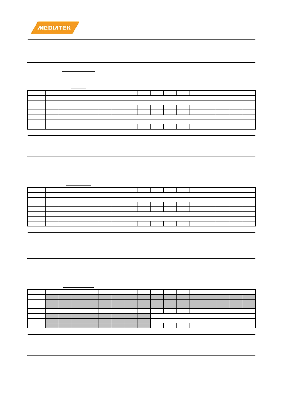
MT7686 Reference Manual
© 2016 - 2017 MediaTek Inc.
Page 95 of 536
This document contains information that is proprietary to MediaTek Inc. (“MediaTek”) and/or its licensor(s).
Any unauthorized use, reproduction or disclosure of this document in whole or in part is strictly prohibited.
31:0 SPIS_TMOUT_THR Timeout threshold time
Timeout interrupt occurs if SPI slave doesn’t receive SCK signal when the CS
select signal is active and the period exceeds this threshold time. The timeout
counter unit is 3.05µs.
A00B002
0
SPISLV_BUF
FER_BASE_
ADDR
SPI Slave Buffer Base Address Register 00000000
Bit
31
30
29
28
27
26
25
24
23
22
21
20
19
18
17
16
Name
SPIS_BUFFER_BASE_ADDR[31:16]
Type
RW
Reset
0
0
0
0
0
0
0
0
0
0
0
0
0
0
0
0
Bit
15
14
13
12
11
10
9
8
7
6
5
4
3
2
1
0
Name
SPIS_BUFFER_BASE_ADDR[15:0]
Type
RW
Reset
0
0
0
0
0
0
0
0
0
0
0
0
0
0
0
0
Bit(s) Name Description
31:0 SPIS_BUFFER_BASE_ADDR Buffer base address
Configurable DMA address to access memory.
A00B002
4
SPISLV_BUF
FER_SIZE SPI Slave Buffer Size Register 00000000
Bit
31
30
29
28
27
26
25
24
23
22
21
20
19
18
17
16
Name
SPIS_BUFFER_SIZE[31:16]
Type
RW
Reset
0
0
0
0
0
0
0
0
0
0
0
0
0
0
0
0
Bit
15
14
13
12
11
10
9
8
7
6
5
4
3
2
1
0
Name
SPIS_BUFFER_SIZE[15:0]
Type
RW
Reset
0
0
0
0
0
0
0
0
0
0
0
0
0
0
0
0
Bit(s) Name Description
31:0 SPIS_BUFFER_SIZE Buffer base size
Configurable buffer size indicating whether SPI master is configured
successfully.
A00B002
8
SPISLV_CMD
_RECEIVED SPI Slave CMD Received 00000000
Bit
31
30
29
28
27
26
25
24
23
22
21
20
19
18
17
16
Name
Type
Reset
Bit
15
14
13
12
11
10
9
8
7
6
5
4
3
2
1
0
Name
SPIS_CMD_RECEIVED
Type
RO
Reset
0
0
0
0
0
0
0
0
Bit(s) Name Description
7:0 SPIS_CMD_RECEIVED Command received
SPI slave received a command.
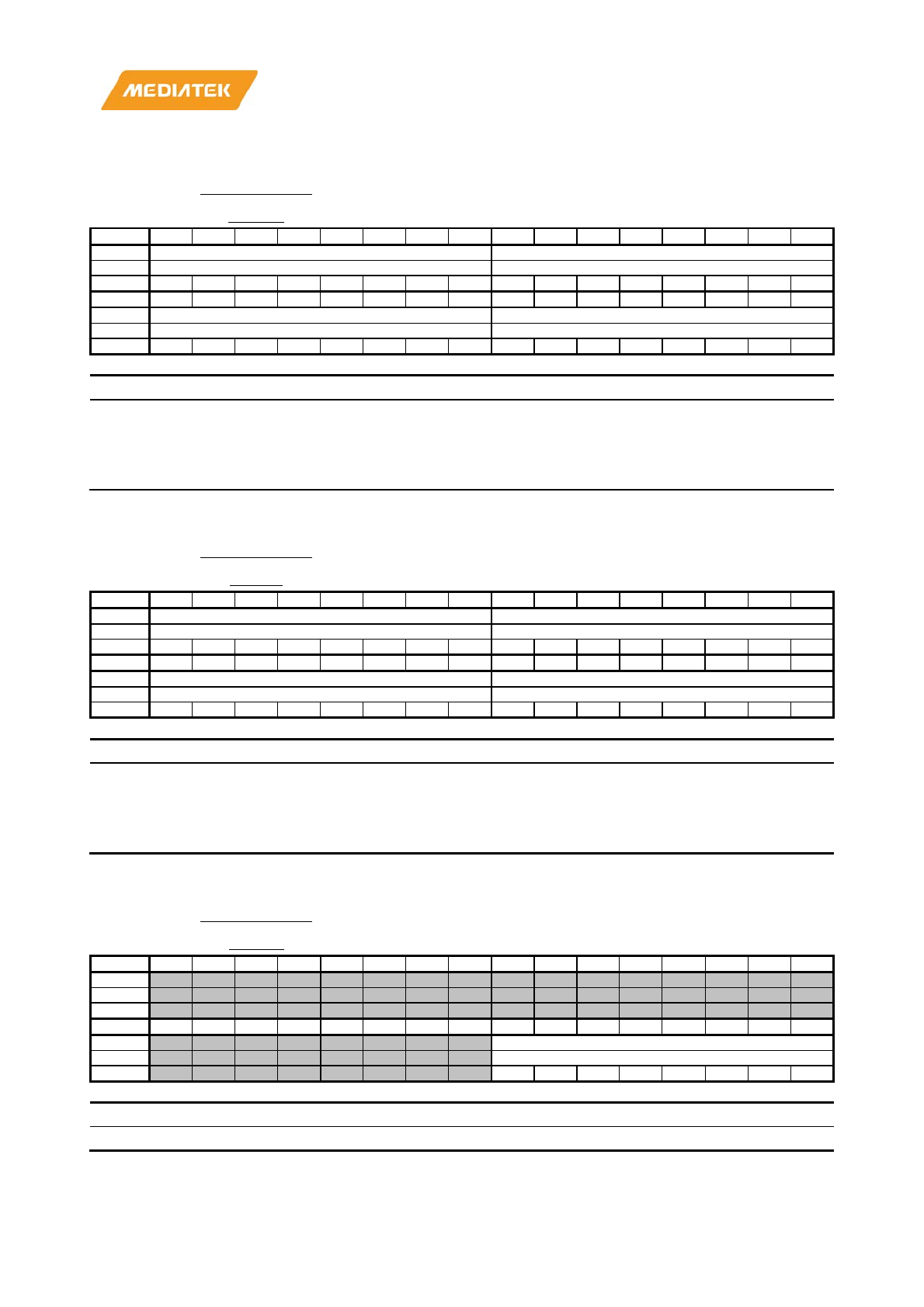
MT7686 Reference Manual
© 2016 - 2017 MediaTek Inc.
Page 96 of 536
This document contains information that is proprietary to MediaTek Inc. (“MediaTek”) and/or its licensor(s).
Any unauthorized use, reproduction or disclosure of this document in whole or in part is strictly prohibited.
A00B002
C
SPISLV_CMD
_DEF0 SPI Slave Command Define 0 08060402
Bit
31
30
29
28
27
26
25
24
23
22
21
20
19
18
17
16
Name
SPIS_CMD_WS
SPIS_CMD_RS
Type
RW
RW
Reset
0
0
0
0
1
0
0
0
0
0
0
0
0
1
1
0
Bit
15
14
13
12
11
10
9
8
7
6
5
4
3
2
1
0
Name
SPIS_CMD_PWON
SPIS_CMD_PWOFF
Type
RW
RW
Reset
0
0
0
0
0
1
0
0
0
0
0
0
0
0
1
0
Bit(s) Name Description
31:24 SPIS_CMD_WS Defines Write Status (WS) command value, default value is 0x08.
23:16 SPIS_CMD_RS Defines Read Status (RS) command value, default value is 0x06.
15:8 SPIS_CMD_PWON Defines Power-ON (PWON) command value, default value is 0x04.
7:0 SPIS_CMD_PWOFF Defines Power-OFF (PWOFF) command value, default value is 0x02.
A00B003
0
SPISLV_CMD
_DEF1 SPI Slave Command Define 1 0E810C0A
Bit
31
30
29
28
27
26
25
24
23
22
21
20
19
18
17
16
Name
SPIS_CMD_WR
SPIS_CMD_RD
Type
RW
RW
Reset
0
0
0
0
1
1
1
0
1
0
0
0
0
0
0
1
Bit
15
14
13
12
11
10
9
8
7
6
5
4
3
2
1
0
Name
SPIS_CMD_CW
SPIS_CMD_CR
Type
RW
RW
Reset
0
0
0
0
1
1
0
0
0
0
0
0
1
0
1
0
Bit(s) Name Description
31:24 SPIS_CMD_WR Defines Write Data (WR) command value, default value is 0x0e.
23:16 SPIS_CMD_RD Defines Read Data (RD) command value, default value is 0x81.
15:8 SPIS_CMD_CW Defines Configure Write (CW) command value, default value is 0x0c.
7:0 SPIS_CMD_CR Defines Configure Read (CR) command value, default value is 0x0a.
A00B003
4
SPISLV_CMD
_DEF2 SPI Slave Command Define 2 00000010
Bit
31
30
29
28
27
26
25
24
23
22
21
20
19
18
17
16
Name
Type
Reset
Bit
15
14
13
12
11
10
9
8
7
6
5
4
3
2
1
0
Name
SPIS_CMD_CT
Type
RW
Reset
0
0
0
1
0
0
0
0
Bit(s) Name Description
7:0 SPIS_CMD_CT Defines Configure Type (CT) command value, default value is 0x10.

MT7686 Reference Manual
© 2016 - 2017 MediaTek Inc.
Page 97 of 536
This document contains information that is proprietary to MediaTek Inc. (“MediaTek”) and/or its licensor(s).
Any unauthorized use, reproduction or disclosure of this document in whole or in part is strictly prohibited.

MT7686 Reference Manual
© 2016 - 2017 MediaTek Inc.
Page 98 of 536
This document contains information that is proprietary to MediaTek Inc. (“MediaTek”) and/or its licensor(s).
Any unauthorized use, reproduction or disclosure of this document in whole or in part is strictly prohibited.
8. Inter-Integrated Circuit Controller
8.1. Overview
Inter-Integrated Circuit (I2C) is a two-wire serial interface. The two signals are SCL and SDA. SCL is a clock signal
driven by the master. SDA is a bi-directional data signal that can be driven by either the master or the slave. This
generic controller supports master role and conforms to the I2C specification.
8.2. Features
• I2C compliant master mode operation
• Adjustable clock speed for LS/FS mode operation
• Supports 7-bit/10-bit addressing
• Supports high-speed mode
• Supports slave clock extension under open-drain mode
• START/STOP/REPEATED START condition
• Polling/DMA Transfer Mode
• Multi-write per transfer (up to 65535 data bytes)
• Multi-read per transfer (up to 65535 data bytes)
• Multi-transfer per transaction (up to 65535 data bytes)
• Combined format transfer with length change capability
• Active drive/wired-and I/O configuration
8.3. Block diagram
The block diagram of the I2C is shown in Figure 8.3-1.
MT7686 Reference Manual
© 2016 - 2017 MediaTek Inc.
Page 99 of 536
This document contains information that is proprietary to MediaTek Inc. (“MediaTek”) and/or its licensor(s).
Any unauthorized use, reproduction or disclosure of this document in whole or in part is strictly prohibited.
FIFO[0]
FIFO[1]
FIFO[2]
FIFO[3]
FIFO[4]
FIFO[5]
FIFO[6]
FIFO[7]
fifo_rd_data
fifo_rd_empty
fifo_wr_full
fifo_rd_data
fifo_rd_empty
fifo_wr_full
8
rx_en
tx_en
i2c_wr
i2c_rd
i2c_data_in
wr_addr
rd_addr
8
master_read
master_write
i2c_fifo_wr
i2c_fifo_rd
i2c_data_in
8
1
1
1
1
8
1
1
i2c_data_in
fifo_data_in
8
8
one_bi
t_data
sda_in_sync
sda_out
scl_out
sda_oe_pre
scl_oe_pre
scl_in_sync
sda_out
scl_out
sda_oe_pre
scl_oe_pre
sda_oe
scl_oe
sda_out
scl_out
4
4
APB control signals
i2c_tx_dmaack
i2c_rx_dmaack
i2c_tx_dmareq
i2c_rx_dmareq
DMA
Controller
pwdata
i2c_fifo i2c_master i2c_bus
apb_reg
apb2fifo
8
APB control signals
apb2master
APB control signals
apb2bus
fifo2apb
bus2apb
master2apb
sda_in_sync
scl_in_sync
sda_in
scl_in
apb bus I2C bus
Interrupt
controller
Figure 8.3-1. I2C block diagram
8.4. Functions
The controller is designed to be as generic as possible in order to support a wide range of devices for different
combinations of transfer formats. Transfer format types supported through different software configurations are
listed below:
Note: Terms used in the context of this document.
• Transfer. Any content encapsulated between a pair of Start, Stop and Repeated Start (RS).
• Transfer length. Number of bytes within the transfer.
• Transaction. A transaction contains multiple transfers and is sent after START register is set to 1.
• Transaction length. Number of transfers.
Master to slave dir
Slave to master dir
1) Single-byte access. In this case, TRANSAC_LEN and TRANSFER_LEN are both set to 1.
Slave Address AS DATA A P
Slave Address AS DATA nA P
Single Byte Write
Single Byte Read
Figure 8.4-1. I2C single transfer single byte access
MT7686 Reference Manual
© 2016 - 2017 MediaTek Inc.
Page 100 of 536
This document contains information that is proprietary to MediaTek Inc. (“MediaTek”) and/or its licensor(s).
Any unauthorized use, reproduction or disclosure of this document in whole or in part is strictly prohibited.
2) Multi-byte access. In this case, TRANSAC_LEN is set to 1 and TRANSFER_LEN is set to N. Overall multi-byte
transfer is N bytes with an ACK.
Slave Address AS DATA A P
N bytes + ack
Slave Address A
S DATA A/
nA P
N bytes + ack/nack
Multi Byte Write
Multi Byte Read
Figure 8.4-2. I2C single transfer multi byte access
3) Multi-byte transfer and multi-transfer (same direction, either read or write). In this case, TRANSAC_LEN is
set to X and TRANSFER_LEN is set to N.
Slave
Address ADATA AS P
Slave
Address ADATA A/
nA
S P
N bytes + ack/nack
N bytes + ack/nack
Multi Byte Write + Multi Transfer
Multi Byte Read + Multi Transfer
X transfers
+ wait time +
X transfers
+ wait time +
Figure 8.4-3. I2C multi transfer multi byte access
4) Multi-byte transfer and multi-transfer with RS (same direction). If RS_STOP is set to 1, the Stop then Start
in the middle of transaction will be replaced by Repeated Start.
Slave
Address A DATA A
S R
Slave
Address A DATA A/
nA
SR
N bytes + ack/nack
N bytes + ack/nack
Multi Byte Write + Multi Transfer + Repeated Start
Multi Byte Read + Multi Transfer + Repeated Start
X transfers
X transfers
++
P
P
+
Figure 8.4-4. I2C multi transfer multi byte access with RS
MT7686 Reference Manual
© 2016 - 2017 MediaTek Inc.
Page 101 of 536
This document contains information that is proprietary to MediaTek Inc. (“MediaTek”) and/or its licensor(s).
Any unauthorized use, reproduction or disclosure of this document in whole or in part is strictly prohibited.
5) Combined write or read with Repeated Start (direction change). In this case, TRANSAC_LEN is set to 2,
TRANSFER_LEN is set to N and TRANSFER_LEN_AUX is set to M. If DIR_CHANGE is 1, the SLAVE_ADDR LSB
will change from 0 to 1, which means write to read, after first transfer. Also the TRANSFER_LEN_AUX will
be used after first transfer.
Note:
1. This format only supports write and then read sequence. Read and then write is not supported.
2. The transaction length in Figure 8.4-5 is 2.
Slave
Address A
SDATA AR
N bytes + ack/nack
Slave
Address ADATA AP
M bytes + ack/nack
Combined Multi Byte Write + Multi Byte Read
Figure 8.4-5. I2C multi transfer multi byte access with direction-change function
8.5. Programming guide
Common transfer programmable parameters
Slave
Address ADATA AS P/
RS
1
st
Transfer must use
TRANSFER_LEN
Programmable Parameters
TRANSAC_LEN
DATA A
RS_STOP
SLAVE_ADDR
Slave
Address ADATA AS P/
RS
DATA A
DELAY_LEN
2
nd
Transfer or later uses
TRANSFER_LEN
TRANSFER_LEN_AUX
(if DIR_CHANGE or
TRANSFER_LEN_CHANGE is enabled)
SLAVE ADDR
DIR_CHANGE(optional)
Figure 8.5-1. I2C transfer format programming guide
After all the parameters above are set, set START register to 1. The START register will auto clear to 0 after
transaction is over. To know when the transaction is over, one can poll the START register or disable INTR_MASK
and wait for interrupt.
Output waveform timing programmable parameters
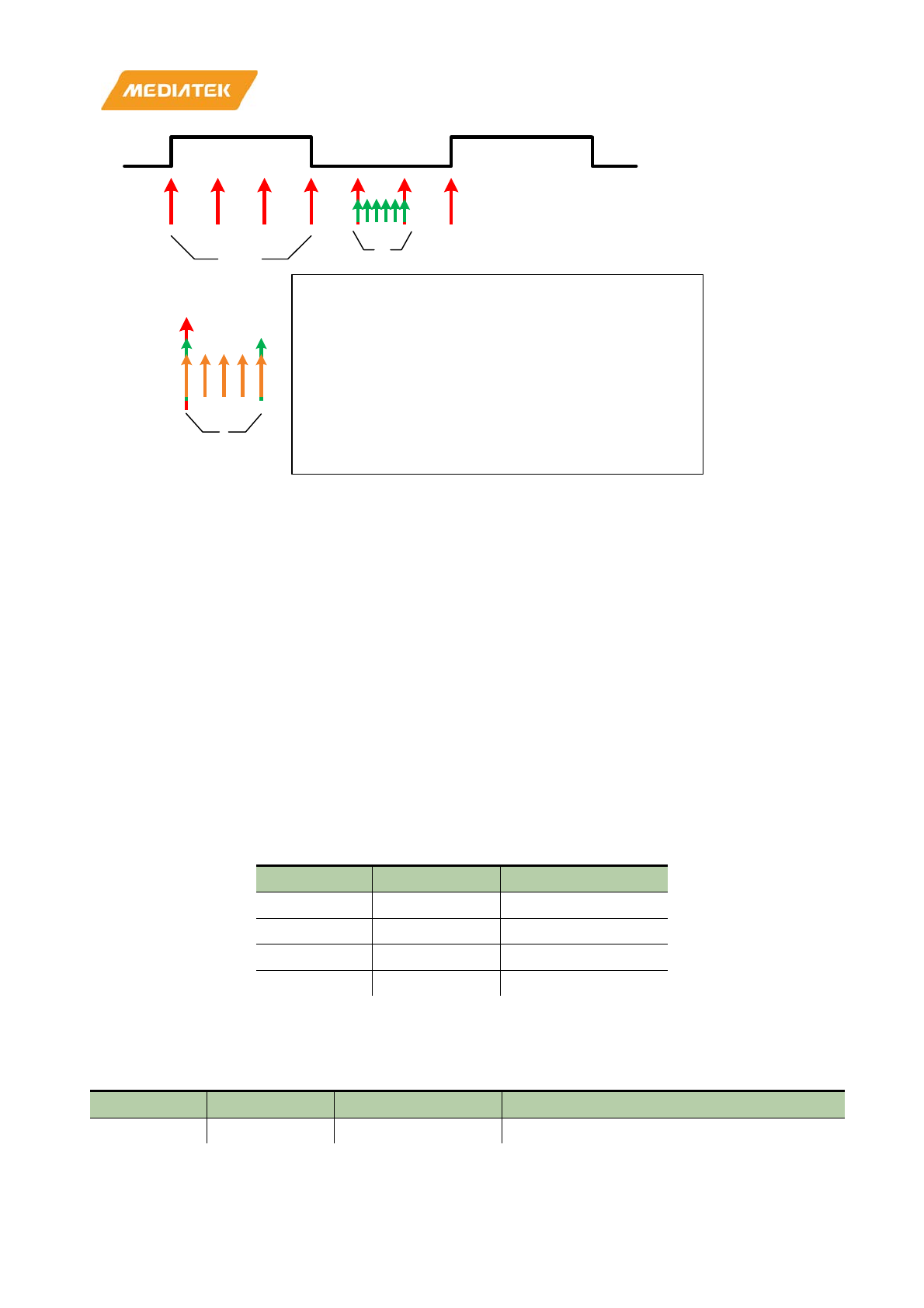
MT7686 Reference Manual
© 2016 - 2017 MediaTek Inc.
Page 102 of 536
This document contains information that is proprietary to MediaTek Inc. (“MediaTek”) and/or its licensor(s).
Any unauthorized use, reproduction or disclosure of this document in whole or in part is strictly prohibited.
STEP_CNT_DIV+1
(here STEP_CNT_DIV=3) SAMPLE_CNT_DIV+1
(here SAMPLE_CNT_DIV=5)
CLOCK_DIV+1
(here CLOCK_DIV=4)
Output Timing Control Example:
Clock Source of I2C is 96 MHz
Freq
SAMPLE_EN
= Clock Source / CLOCK_DIV+1 = 19.2 MHz
Freq
STEP_EN
= Freq
SAMPLE_EN
/ SAMPLE_CNT_DIV+1 = 3.2 MHz
Freq
Half Pulse
= Freq
STEP_EN
/ STEP_CNT_DIV+1 = 800 kHz
I2C data rate (one complete SCL cycle) = 400 kHz
Formula
I2C frequency = BUS clock(96M at default) / ((CLOCK_DIV+1) *
2 * ( SAMPLE_CNT_DIV+1)*( STEP_CNT_DIV+1))
SCL
Figure 8.5-2. I2C timing format programming guide
8.6. Manual and DMA transfer modes for I2C controller
The controller offers two types of transfer modes, manual and DMA.
• When Manual mode is selected, in addition to the slave address register, the controller has a built-in 8
byte deep FIFO which allows the MCU to prepare up to 8 bytes of data for a write transfer or read up to 8
bytes of data for a read transfer.
• When DMA mode is enabled, the data to and from the FIFO is controlled by DMA transfer and can
therefore support up to 65535 bytes of consecutive read or write with data read from or written into
another memory space. When DMA mode is enabled, the flow control mechanism is also implemented to
hold the bus clock (SCL) when FIFO underflow or overflow condition is encountered.
Note: After enabling DMA_EN register in I2C, starting data transfer isn’t controlled by the START register in I2C, but
by a register in DMA (PDMAx_START). To avoid errors, it’s suggested using SOFTRESET and FIFO_ADDR_CLR
registers when PDMAx_START is 0.
DMA number START register Peripheral
DMA2 PDMA2_START I2C0 TX
DMA3 PDMA3_START I2C0 RX
DMA4 PDMA4_START I2C1 TX
DMA5 PDMA5_START I2C1 RX
8.7. Register mapping
There are two I2C channels in this SOC.
I2C number Base address Feature Source clock
I2C0 0xA0100000 Supports DMA mode Bus Clock (96MHz when CPU frequency is 192MHz)
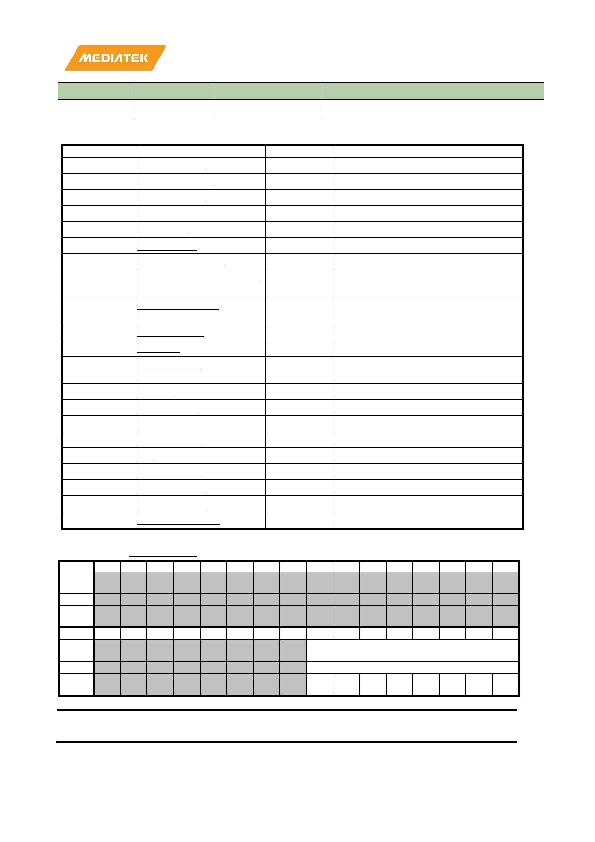
MT7686 Reference Manual
© 2016 - 2017 MediaTek Inc.
Page 103 of 536
This document contains information that is proprietary to MediaTek Inc. (“MediaTek”) and/or its licensor(s).
Any unauthorized use, reproduction or disclosure of this document in whole or in part is strictly prohibited.
I2C number Base address Feature Source clock
I2C1 0xA0110000 Supports DMA mode Bus Clock (96MHz when CPU frequency is 192MHz)
Module name: I2C0 Base address: (+A0100000h)
Address
Name
Width (bits)
Register Functionality
A0110000
DATA_PORT
32
Data port
A0110004
SLAVE_ADDR
32
Slave address
A0110008
INTR_MASK
32
Interrupt mask
A011000C
INTR_STAT
32
Interrupt status
A0110010
CONTROL
32
Control
A0110014
CONTROL2
32
Control2
A0110020
TRANSFER_LEN
32
Number of bytes per transfer
A0110024
TRANSFER_LEN_AUX
32
Number of bytes per transfer
A0110028
TRANSAC_LEN
32
Number of transfers per transaction
A011002C
DELAY_LEN
32
Inter delay length
A0110030
TIMING
32
Timing control register
A0110034
CLOCK_DIV
32
Clock divergence of I2C source clock
A0110038
START
32
Start the I2C transfer
A0110040
FIFO_STAT
32
FIFO status
A0110048
FIFO_ADDR_CLR
32
FIFO address clear
A0110050
IO_CONFIG
32
IO configuration
A0110060
HS
32
High speed mode
A0110070
SOFTRESET
32
Soft Reset
A0110074
DEBUGSTAT
32
Debug status
A0110078
DEBUGCTRL
32
Debug control
A0110080
ACKERR_FLAG
32
ACK error flag
A0100000
DATA_PORT
Data Port
00000000
Bit
31
30
29
28
27
26
25
24
23
22
21
20
19
18
17
16
Nam
e
Type
Rese
t
Bit
15
14
13
12
11
10
9
8
7
6
5
4
3
2
1
0
Nam
e
DATA_PORT
Type
RW
Rese
t
0 0 0 0 0 0 0 0
Bit(s)
Name
Description
7:0
DATA_PORT
FIFO access port. During master write sequence (
slave_addr[0] =
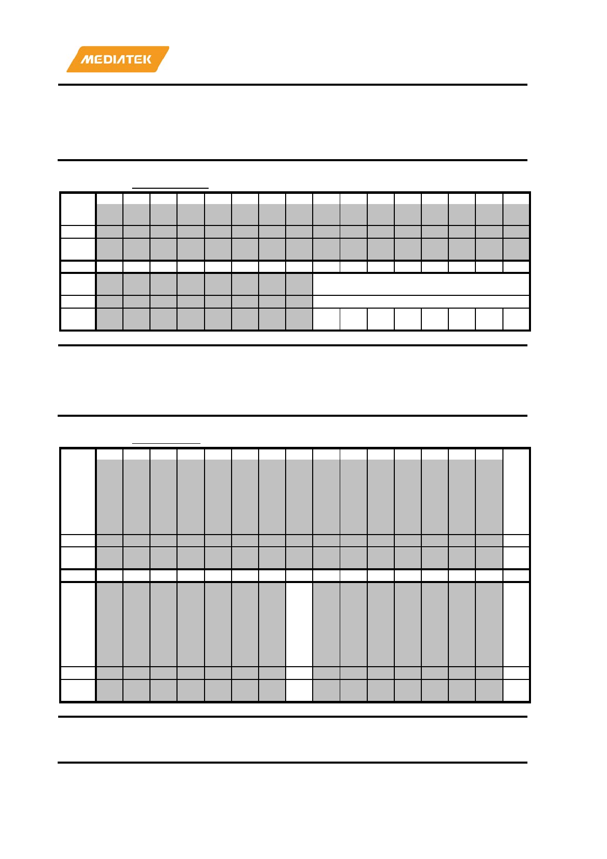
MT7686 Reference Manual
© 2016 - 2017 MediaTek Inc.
Page 104 of 536
This document contains information that is proprietary to MediaTek Inc. (“MediaTek”) and/or its licensor(s).
Any unauthorized use, reproduction or disclosure of this document in whole or in part is strictly prohibited.
0), this port can be written by APB and during master read
sequence (
slave_addr[0] = 1), this port can be read by APB.
Note, that
slave_addr must be set correctly before accessing the
FIFO.
(DEBUG ONLY) If the
fifo_apb_debug bit is set, then the FIFO can
be read and written by the APB.
A0100004
SLAVE_ADDR
Slave Address
000000BF
Bit
31
30
29
28
27
26
25
24
23
22
21
20
19
18
17
16
Nam
e
Type
Rese
t
Bit
15
14
13
12
11
10
9
8
7
6
5
4
3
2
1
0
Nam
e
SLAVE_ADDR
Type
RW
Rese
t
1 0 1 1 1 1 1 1
Bit(s)
Name
Description
7:0
SLAVE_ADDR
This specifies the slave address of the device to be accessed. Bit 0 is
defined by the I2C protocol to indicate the direction of transfer.
1: master read
0: master write
A0100008
INTR_MASK
Interrupt Mask
00000000
Bit
31
30
29
28
27
26
25
24
23
22
21
20
19
18
17
16
Nam
e
MA
SK
_H
S_
NA
CK
ER
R
Type
RW
Rese
t
0
Bit
15
14
13
12
11
10
9
8
7
6
5
4
3
2
1
0
Nam
e
MA
SK
_A
CK
ER
R
MA
SK
_T
RA
NS
AC
_C
OM
P
Type
RW
RW
Rese
t
0 0
Bit(s)
Name
Description
16
MASK_HS_NACKERR
Mask of HS Mode NACK error interrupt
0: disable
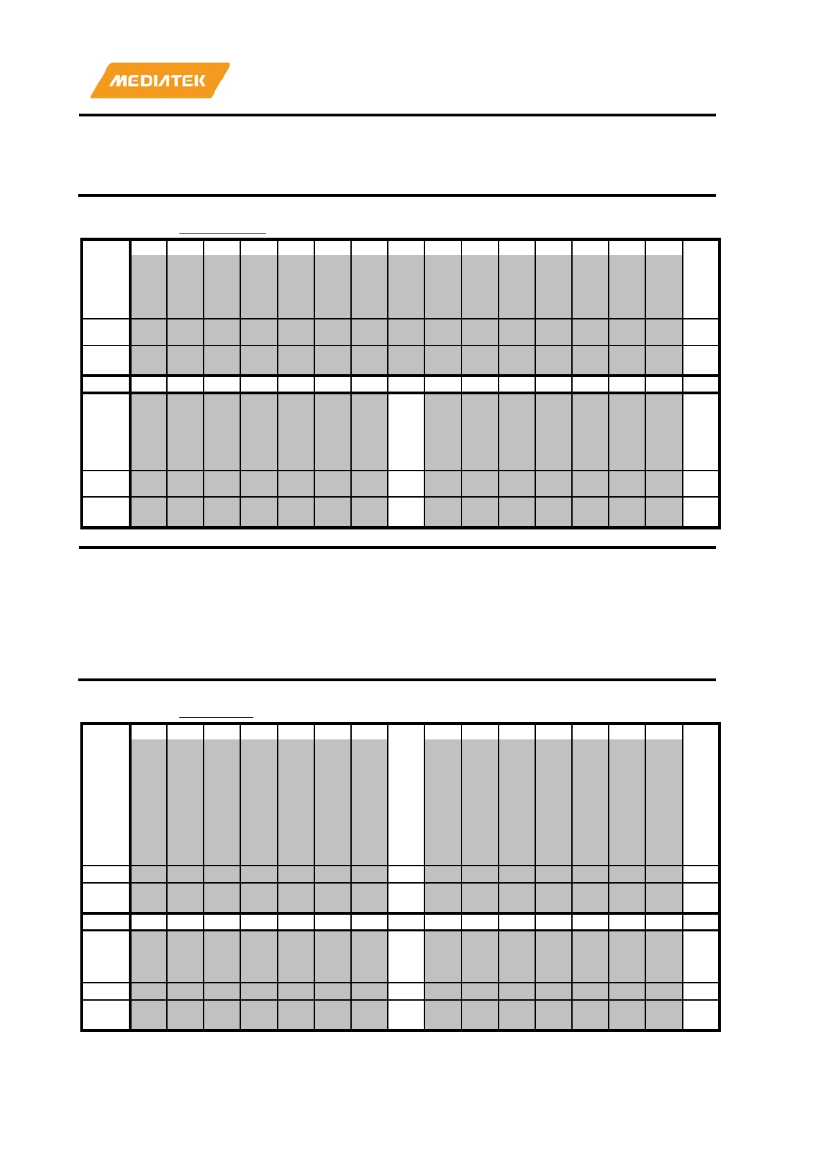
MT7686 Reference Manual
© 2016 - 2017 MediaTek Inc.
Page 105 of 536
This document contains information that is proprietary to MediaTek Inc. (“MediaTek”) and/or its licensor(s).
Any unauthorized use, reproduction or disclosure of this document in whole or in part is strictly prohibited.
8
MASK_ACKERR
Mask of ACK error interrupt
0: disable
0
MASK_TRANSAC_COMP
Mask of Transaction complete interrupt
0: disable
A010000C
INTR_STAT
Interrupt Status
00000000
Bit
31
30
29
28
27
26
25
24
23
22
21
20
19
18
17
16
Nam
e
HS
_N
AC
KE
RR
Type
W1
C
Rese
t
0
Bit
15
14
13
12
11
10
9
8
7
6
5
4
3
2
1
0
Nam
e AC
KE
RR
TR
AN
SA
C_
CO
MP
Type
W1
C
W1
C
Rese
t
0 0
Bit(s)
Name
Description
16
HS_NACKERR
This status is asserted if the HS master code not acknowledged
(NACK) error detection is enabled. If enabled, the transaction will
be
stopped.
8
ACKERR
This status is asserted if ACK error detection is enabled. If enabled,
the transaction will be stopped.
0
TRANSAC_COMP
This status is asserted when a transaction is complete.
A0100010
CONTROL
Control
00000000
Bit
31
30
29
28
27
26
25
24
23
22
21
20
19
18
17
16
Nam
e
TR
AN
SF
ER
_L
EN
_C
HA
NG
E
DI
R_
CH
AN
GE
Type
RW
RW
Rese
t
0 0
Bit
15
14
13
12
11
10
9
8
7
6
5
4
3
2
1
0
Nam
e DM
A_
EN
RS
_S
TO
P
Type
RW
RW
Rese
t
0 0
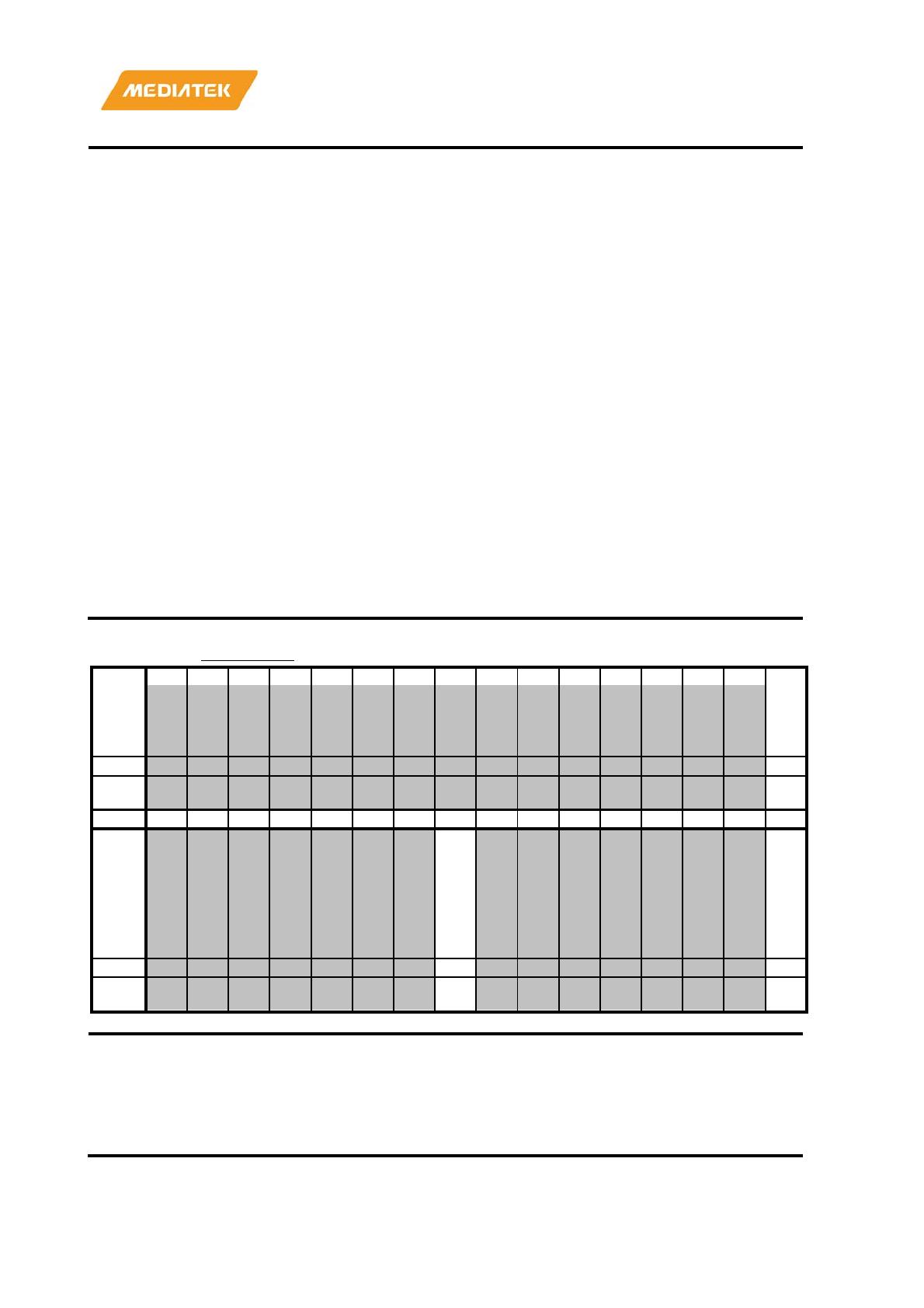
MT7686 Reference Manual
© 2016 - 2017 MediaTek Inc.
Page 106 of 536
This document contains information that is proprietary to MediaTek Inc. (“MediaTek”) and/or its licensor(s).
Any unauthorized use, reproduction or disclosure of this document in whole or in part is strictly prohibited.
Bit(s)
Name
Description
24
TRANSFER_LEN_CHANGE
This option specifies whether to change the transfer length after the
first transfer is complete. If enabled, the transfers after the first
transfer will use the
TRANSFER_LEN_AUX parameter.
0: disable
1: enable
16
DIR_CHANGE
This option is used for combined transfer format, where the direction
of transfer is to be changed from write to read after the FIRST RS
condition. Note: when set to 1, the transfers after the
direction change
will be based on the TRANSFER_LEN_AUX parameter.
0: disable
1: enable
8
DMA_EN
By default, it’s disabled, and FIFO data shall be manually prepared by
MCU. This setting is used for transfer sizes of less than 8 bytes and no
multiple trans
fer is configured. When enabled, DMA requests are
turned on, and the FIFO data is prepared in memory.
0: disable
1:enable
0
RS_STOP
In LS/FS mode, this bit affects multi
-transfer transaction only. It
controls whether REPEATED
-START condition is used between
transfers. The last transfer always ends with a STOP.
In HS mode, this bit must be set to 1.
0: use STOP
1: use REPEATED
-START
A0100014
CONTROL2
CONTROL2
00000001
Bit
31
30
29
28
27
26
25
24
23
22
21
20
19
18
17
16
Nam
e
CL
K_
EX
T_
EN
Type
RW
Rese
t
0
Bit
15
14
13
12
11
10
9
8
7
6
5
4
3
2
1
0
Nam
e
AC
KE
RR
_D
ET
_E
N
HS
_N
AC
KE
RR
_D
ET
_E
N
Type
RW
RW
Rese
t
0 1
Bit(s)
Name
Description
16
CLK_EXT_EN
I2C specification allows slaves to hold the SCL line low if it’s not yet ready
for further processing. Therefore, if this bit
is set to 1, master controller
will enter a high wait state until the slave releases the SCL line. Note that
this feature is only supported under open
-drain mode.
0: disable
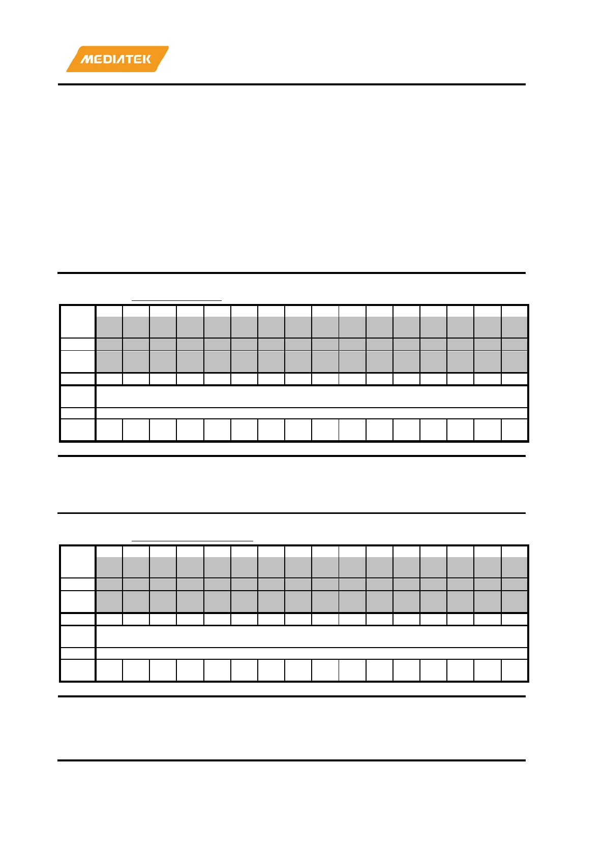
MT7686 Reference Manual
© 2016 - 2017 MediaTek Inc.
Page 107 of 536
This document contains information that is proprietary to MediaTek Inc. (“MediaTek”) and/or its licensor(s).
Any unauthorized use, reproduction or disclosure of this document in whole or in part is strictly prohibited.
1: enable
8
ACKERR_DET_EN
This option enables slave acknowledgment error detection. When enabled,
if slave acknowledge error is detected, the master terminates the
transaction issuing a STOP condition and then asserts acknowledge error
interrupt. The user software handles the error and then resets the FIFO
address before reissuing tra
nsaction. If this option is disabled, the
controller will ignore the slave ACK error and continue with the scheduled
transaction.
0: disable
1: enable
0
HS_NACKERR_DET_EN
This enables NACKERR detection during the master code transmission.
When enabled, if
NACK is not received after master code has been
transmitted, the transaction will terminate with a STOP condition.
0: disable
1: enable
A0100020
TRANSFER_LEN
Number of Bytes per Transfer
00000001
Bit
31
30
29
28
27
26
25
24
23
22
21
20
19
18
17
16
Nam
e
Type
Rese
t
Bit
15
14
13
12
11
10
9
8
7
6
5
4
3
2
1
0
Nam
e
TRANSFER_LEN
Type
RW
Rese
t
0 0 0 0 0 0 0 0 0 0 0 0 0 0 0 1
Bit(s)
Name
Description
15:0
TRANSFER_LEN
This indicates the number of data bytes to be transferred in 1
transfer unit (excluding slave address byte).
Note, no data will be transferred if the value is less than 1.
A0100024
TRANSFER_LEN_AUX
*Number of Bytes per Transfe
r
00000001
Bit
31
30
29
28
27
26
25
24
23
22
21
20
19
18
17
16
Nam
e
Type
Rese
t
Bit
15
14
13
12
11
10
9
8
7
6
5
4
3
2
1
0
Nam
e
TRANSFER_LEN_AUX
Type
RW
Rese
t
0 0 0 0 0 0 0 0 0 0 0 0 0 0 0 1
Bit(s)
Name
Description
15:0
TRANSFER_LEN_AUX
This field is valid only when
DIR_CHANGE is set to 1. This
indicates the number of data bytes to transfer in a single transfer
unit (excluding slave address byte) for the transfers following the
direction change. If DIR_CHANGE is 1, the first write transfer
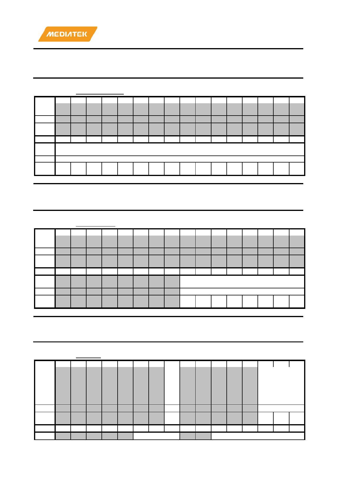
MT7686 Reference Manual
© 2016 - 2017 MediaTek Inc.
Page 108 of 536
This document contains information that is proprietary to MediaTek Inc. (“MediaTek”) and/or its licensor(s).
Any unauthorized use, reproduction or disclosure of this document in whole or in part is strictly prohibited.
length depends on TRANSFER_LEN, while the second read
transfer length depends on
TRANSFER_LEN_AUX. Direction
change is always after the first transfer.
Note, no data will be transferred if the value is less than 1.
A0100028
TRANSAC_LEN
Number of Transfers per Transaction
00000001
Bit
31
30
29
28
27
26
25
24
23
22
21
20
19
18
17
16
Nam
e
Type
Rese
t
Bit
15
14
13
12
11
10
9
8
7
6
5
4
3
2
1
0
Nam
e
TRANSAC_LEN
Type
RW
Rese
t
0 0 0 0 0 0 0 0 0 0 0 0 0 0 0 1
Bit(s)
Name
Description
15:0
TRANSAC_LEN
This indicates the number of transfers in a single transaction.
Note, no data will be transferred if the value is less than 1.
A010002C
DELAY_LEN
Inter Delay Length
00000002
Bit
31
30
29
28
27
26
25
24
23
22
21
20
19
18
17
16
Nam
e
Type
Rese
t
Bit
15
14
13
12
11
10
9
8
7
6
5
4
3
2
1
0
Nam
e
DELAY_LEN
Type
RW
Rese
t
0 0 0 0 0 0 1 0
Bit(s)
Name
Description
7:0
DELAY_LEN
This sets the wait delay between consecutive transfers when
RS_STOP
bit is set to 0 (the unit is the same as half pulse width).
A0100030
TIMING
Timing Control Register
00010303
Bit
31
30
29
28
27
26
25
24
23
22
21
20
19
18
17
16
Nam
e
DA
TA
_R
EA
D_
AD
J
DATA_READ_T
IME
Type
RW
RW
Rese
t
0 0 0 1
Bit
15
14
13
12
11
10
9
8
7
6
5
4
3
2
1
0
Nam
SAMPLE_CNT_
STEP_CNT_DIV
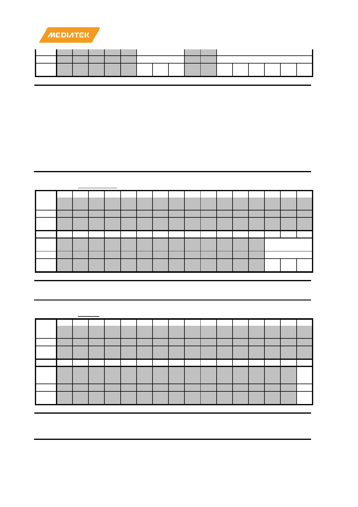
MT7686 Reference Manual
© 2016 - 2017 MediaTek Inc.
Page 109 of 536
This document contains information that is proprietary to MediaTek Inc. (“MediaTek”) and/or its licensor(s).
Any unauthorized use, reproduction or disclosure of this document in whole or in part is strictly prohibited.
e
DIV
Type
RW
RW
Rese
t
0 1 1 0 0 0 0 1 1
Bit(s)
Name
Description
24
DATA_READ_ADJ
When set to 1, data latch in sampling time during master reads are
adjusted according to DATA_READ_TIME value. Otherwise, by
default, data is latched at half of the high pulse width point.
18:16
DATA_READ_TIME
This value is valid only when DATA_READ_ADJ
is set to 1. This
can be used to adjust so that data is latched in at earlier sampling
points (assuming data is settled by then) This value must be set to
less than or equal to half the high pulse width.
10:8
SAMPLE_CNT_DIV
Used for LS/FS only. This adjus
ts the width of each sample.
5:0
STEP_CNT_DIV
This specifies the number of samples per half pulse width (each
high or low pulse).
A0100034
CLOCK_DIV
Clock Divergence of I2C Source Clock
00000004
Bit
31
30
29
28
27
26
25
24
23
22
21
20
19
18
17
16
Nam
e
Type
Rese
t
Bit
15
14
13
12
11
10
9
8
7
6
5
4
3
2
1
0
Nam
e
CLOCK_DIV
Type
RW
Rese
t
1 0 0
Bit(s)
Name
Description
2:0
CLOCK_DIV
f_clock_div
is equal to SCK / (CLOCK_DIV+1)
A0100038
START
Start
00000000
Bit
31
30
29
28
27
26
25
24
23
22
21
20
19
18
17
16
Nam
e
Type
Rese
t
Bit
15
14
13
12
11
10
9
8
7
6
5
4
3
2
1
0
Nam
e
ST
AR
T
Type
RW
Rese
t
0
Bit(s)
Name
Description
0
START
This register starts the transaction on the bus. It is automatically
de
-asserted at the end of the transaction.
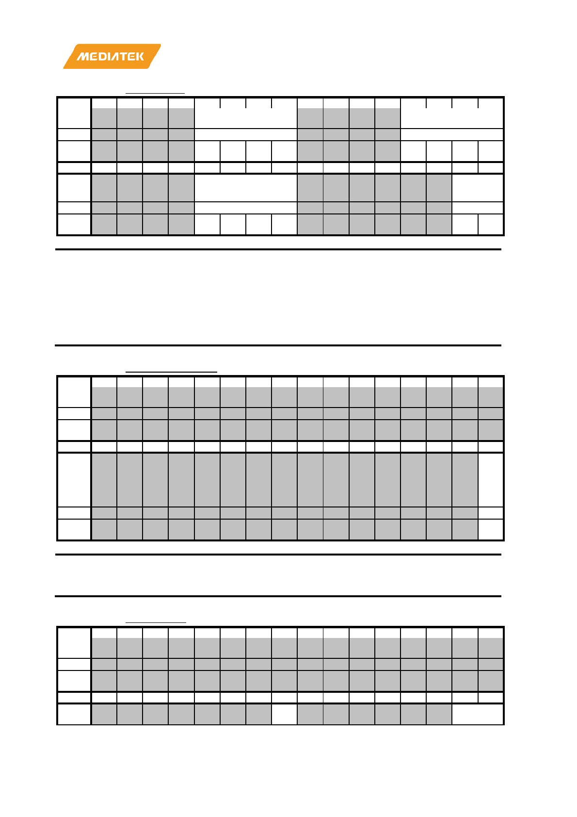
MT7686 Reference Manual
© 2016 - 2017 MediaTek Inc.
Page 110 of 536
This document contains information that is proprietary to MediaTek Inc. (“MediaTek”) and/or its licensor(s).
Any unauthorized use, reproduction or disclosure of this document in whole or in part is strictly prohibited.
A0100040
FIFO_STAT
FIFO Status
00000001
Bit
31
30
29
28
27
26
25
24
23
22
21
20
19
18
17
16
Nam
e
RD_ADDR WR_ADDR
Type
RO
RO
Rese
t
0 0 0 0 0 0 0 0
Bit
15
14
13
12
11
10
9
8
7
6
5
4
3
2
1
0
Nam
e FIFO_OFFSET
WR_FUL
L_RD_E
MPTY_
Type
RO
RO
Rese
t
0 0 0 0 0 1
Bit(s)
Name
Description
27:24
RD_ADDR
The current read address pointer. (only bit [2:0] has physical
meaning)
.
19:16
WR_ADDR
The current write address pointer. (only bit [2:0] has
physical
meaning)
.
11:8
FIFO_OFFSET
WR_ADDR[3:0]
- RD_ADDR[3:0]
1:0
WR_FULL_RD_EMPTY_
Bit 0 : FIFO is empty; Bit 1 : FIFO is full.
A0100048
FIFO_ADDR_CLR
FIFO Address Clear
00000000
Bit
31
30
29
28
27
26
25
24
23
22
21
20
19
18
17
16
Nam
e
Type
Rese
t
Bit
15
14
13
12
11
10
9
8
7
6
5
4
3
2
1
0
Nam
e
FIF
O_
AD
DR
_C
LR
Type
WO
Rese
t
0
Bit(s)
Name
Description
0
FIFO_ADDR_CLR
When written with a 1'b1, a 1 pulse
FIFO_ADDR_CLR is generated
to clear the FIFO address to back to 0.
A0100050
IO_CONFIG
IO Config
00000000
Bit
31
30
29
28
27
26
25
24
23
22
21
20
19
18
17
16
Nam
e
Type
Rese
t
Bit
15
14
13
12
11
10
9
8
7
6
5
4
3
2
1
0
Nam
e
IDL
E_ SDA_SCL
_IO_CON
MT7686 Reference Manual
© 2016 - 2017 MediaTek Inc.
Page 111 of 536
This document contains information that is proprietary to MediaTek Inc. (“MediaTek”) and/or its licensor(s).
Any unauthorized use, reproduction or disclosure of this document in whole or in part is strictly prohibited.
OE
_E
N
FIG
Type
RW
RW
Rese
t
0 0 0
Bit(s)
Name
Description
8
IDLE_OE_EN
In open
-drain mode, this bit should be set to 0. In push-pull mode,
this bit determines whether to drive bus in idle state.
0: don't drive bus in idle state
1: drive bus in idle state
1:0
SDA_SCL_IO_CONFIG
Bit 0 configures SCL IO; Bit 1 configures SDA IO
00: normal tri
-state IO mode (push-pull mode)
11: open
-drain mode
A0100060
HS
High Speed Mode
00010000
Bit
31
30
29
28
27
26
25
24
23
22
21
20
19
18
17
16
Nam
e
HS_SAMPLE_C
NT_DIV
HS_STEP_CNT
_DIV
Type
RW
RW
Rese
t
0 0 0 0 0 1
Bit
15
14
13
12
11
10
9
8
7
6
5
4
3
2
1
0
Nam
e MASTER_CODE
HS
_E
N
Type
RW
RW
Rese
t
0 0 0 0
Bit(s)
Name
Description
26:24
HS_SAMPLE_CNT_DIV
Entering high
-speed mode after the master code transfer is
complete the sample width becomes dependent on this parameter.
18:16
HS_STEP_CNT_DIV
Entering high
-speed mode after the master code transfer is
complete the number of samples per half pulse width becomes
dependent on this value.
10:8
MASTER_CODE
This is a 3
-bit programmable value to transmit the master code.
When set to HS mode, the frequency of master code is defined by
TIMING register and the frequency after the master code is defined
by HS register.
0
HS_EN
This enables the high
-speed transaction. Note, set the RS_STOP to
1.
A0100070
SOFTRESET
Soft Reset
00000000
Bit
31
30
29
28
27
26
25
24
23
22
21
20
19
18
17
16
Nam
e
Type
Rese
t
Bit
15
14
13
12
11
10
9
8
7
6
5
4
3
2
1
0
Nam
e
SO
FT
_R
MT7686 Reference Manual
© 2016 - 2017 MediaTek Inc.
Page 112 of 536
This document contains information that is proprietary to MediaTek Inc. (“MediaTek”) and/or its licensor(s).
Any unauthorized use, reproduction or disclosure of this document in whole or in part is strictly prohibited.
ES
ET
Type
WO
Rese
t
0
Bit(s)
Name
Description
0
SOFT_RESET
When written with a 1'b1, a 1 pulse soft reset is used as synchronous
reset to reset the I2C internal hardware
circuits.
A0100074
DEBUGSTAT
Debug Status
00000100
Bit
31
30
29
28
27
26
25
24
23
22
21
20
19
18
17
16
Nam
e
MA
ST
ER
_W
RIT
E
Type
RO
Rese
t
0
Bit
15
14
13
12
11
10
9
8
7
6
5
4
3
2
1
0
Nam
e
MA
ST
ER
_R
EA
D
MASTER_STATE
Type
RO
RO
Rese
t
1 0 0 0 0 0
Bit(s)
Name
Description
16
MASTER_WRITE
DEBUG ONLY: 1 = current transfer is in the master write
direction
8
MASTER_READ
DEBUG ONLY: 1 = current transfer is in
the master read
direction
4:0
MASTER_STATE
DEBUG ONLY: reads back the current master_state.
0: idle state;
1: I2C master is preparing to send the start bit, SCL=1, SDA=1;
2: I2C master is sending out the start bit, SCL=1, SDA=0;
3: I2C master/slave is pre
paring to transmit the data bit, SCL=0,
SDA=data bit (data bit can be changed when SCL=0);
4: I2C master/slave is transmitting data bit, SCL=1, SDA=data bit
(data bit is stable when SCL=1);
5: I2C master/slave is preparing to transmit ACK bit, SCL=0,
SDA=ACK (ACK bit can be changed when SCL=0);
6: I2C master/slave is transmitting the ACK bit, SCL=1, SDA=0
(ACK bit is stable when SCL=1);
7: I2C master is preparing to send the stop bit or repeated
-start bit,
SCL=0, SDA=0/1 (0: stop bit; 1: repeated
-start bit);
8: i2c master is sending out stop bit or repeated
-start bit, SCL=1,
SDA=1/0 (1: stop bit; 0: repeated
-start bit);
9: I2C master is in delay start between two transfers, SCL=1,
SDA=1;
10: I2C master is in FIFO wait state; for write transaction, it means
MT7686 Reference Manual
© 2016 - 2017 MediaTek Inc.
Page 113 of 536
This document contains information that is proprietary to MediaTek Inc. (“MediaTek”) and/or its licensor(s).
Any unauthorized use, reproduction or disclosure of this document in whole or in part is strictly prohibited.
FIFO is empty and the DMA controller needs to write data into
FIFO; for read transaction, it means FIFO is full and I2C master is
waiting for DMA controller to read data from FIFO, SCL=0,
SDA=don't care;
12: I2C master is preparing to send data bits of
master code. This
state is used only in high
-speed transaction, SCL=0, SDA=data bit
of master code (data bit of master code can be changed when
SCL=0);
13: I2C master is sending out data bit of master code. This state is
used only in high
-speed transaction, SCL=1, SDA=data bit of
master code (data bit of master code is stable when SCL=1);
14: I2C master/slave is preparing to transmit NACK bit, SCL=0,
SDA=NACK bit (NACK bit can be changed when SCL=0); This state
is used only in high
-speed transaction;
15: I
2C master/slave is transmitting NACK bit, SCL=1, SDA=1; This
state is used only in high
-speed transaction.
A0100078
DEBUGCTRL
Debug Control
00000000
Bit
31
30
29
28
27
26
25
24
23
22
21
20
19
18
17
16
Nam
e
Type
Rese
t
Bit
15
14
13
12
11
10
9
8
7
6
5
4
3
2
1
0
Nam
e
AP
B_
DE
BU
G_
RD
FIF
O_
AP
B_
DE
BU
G
Type
WO
RW
Rese
t
0 0
Bit(s)
Name
Description
8
APB_DEBUG_RD
This bit is only valid when
FIFO_APB_DEBUG is set to 1. Writing
to this register will generate a single pulsed read signal for reading
the FIFO data.
0
FIFO_APB_DEBUG
This is used for debug purposes. Use debugging tools to view the
memory map. Turning this bit on will block the norm
al APB read
access. APB read access to the FIFO is then enabled by writing to
APB_DEBUG_RD
.
0: disable
A0110080
ACKERR_FLAG
ACK Error Flag
00000000
Bit
31
30
29
28
27
26
25
24
23
22
21
20
19
18
17
16
Nam
e
Type
Rese
t
Bit
15
14
13
12
11
10
9
8
7
6
5
4
3
2
1
0
Nam
DA
DA

MT7686 Reference Manual
© 2016 - 2017 MediaTek Inc.
Page 114 of 536
This document contains information that is proprietary to MediaTek Inc. (“MediaTek”) and/or its licensor(s).
Any unauthorized use, reproduction or disclosure of this document in whole or in part is strictly prohibited.
e
TA
_A
CK
ER
R_
CL
EA
R
TA
_A
CK
ER
R
Type
RW
RW
Rese
t
0 0
Bit(s)
Name
Description
2
DATA_ACKERR_CLEAR
Write 1 to clear data
phase acknowledgment error (bit[0]). Must
write back to 0 after clear.
0
DATA_ACKERR
After receiving ACK error interrupt (
INTR_STAT
[8]), check this bit
to distinguish address phase ACK error from data phase ACK error
0: address phase ACK error
1: data ph
ase ACK error. Note data phase ACK error cannot be
detected during master receive mode
.

MT7686 Reference Manual
© 2016 - 2017 MediaTek Inc.
Page 115 of 536
This document contains information that is proprietary to MediaTek Inc. (“MediaTek”) and/or its licensor(s).
Any unauthorized use, reproduction or disclosure of this document in whole or in part is strictly prohibited.
9. SD/SDIO Card Controller
9.1. Overview
The chipset hosts a mass storage device class (MSDC) — a USB computer peripheral connection protocol
supporting removable disk storage and an SD card controller.
1) SD memory card specification version 2.0
2) SDIO card specification version 2.0.
The controller can be configured as a host for the SD/SDIO card.
9.2. Features
The main features of the controller:
• 32-bit access for control registers
• 8, 16, 32-bit access for FIFO in PIO mode
• Built-in CRC circuit
• Supports PIO mode, basic DMA mode, descriptor DMA mode for SD/SDIO
• Interrupt capabilities
• Data rate of up to 48Mbps in 1-bit mode, 48 x 4 Mbps in 4-bit mode, the module is targeted at 48MHz
operating clock
• Programmable serial clock rate on SD bus (256 gears)
• Card detection capabilities: MT7686 uses the EINT controller for card detection
• Does not support SPI mode for SD memory card
• Does not support suspend or resume for SD memory Card
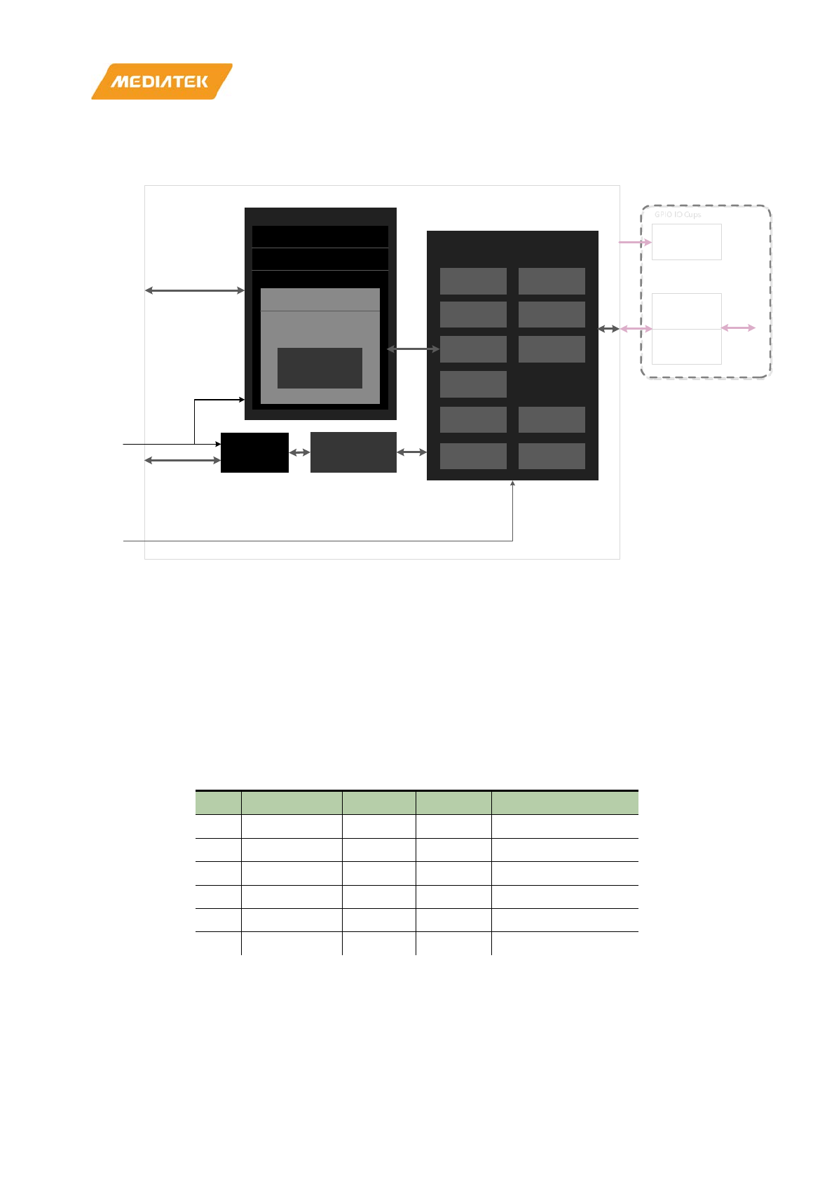
MT7686 Reference Manual
© 2016 - 2017 MediaTek Inc.
Page 116 of 536
This document contains information that is proprietary to MediaTek Inc. (“MediaTek”) and/or its licensor(s).
Any unauthorized use, reproduction or disclosure of this document in whole or in part is strictly prohibited.
9.3. Block diagram
Figure 9.3-1 shows the MSDC block diagram.
Figure 9.3-1. MSDC block diagram
9.4. Functions
9.4.1. Pin assignment
Table 9.4-1 presents the pins required for the SD memory card. Each pin corresponds to one IO pad. Note, that all
IO pads have embedded pull-up and pull-down resistors as they are shared by the SD memory card. The resistors
are controlled by the MSDC top register. The pull-down resistors for these pins can be used to save power.
Table 9.4-1. Sharing of pins for SD memory card controller
No. Name Type SD Description
1 MA_MC0_CK O CLK Clock
2 MA_MC0_DA0 I/O/PP DAT0 Data line bit 0
3 MA_MC0_DA1 I/O/PP DAT1 Data line bit 1
4 MA_MC0_DA2 I/O/PP DAT2 Data line bit 2
5 MA_MC0_DA3 I/O/PP DAT3 Data line bit 3
6 MA_MC0_CM0 I/O/PP CMD Command / Bus State
MSDC_TOP
MSDC_GDMA
GDMA_WQMU
GDMA_WDMA
MSDC_REG MSDC_REG_SYNC
MSDC_CORE
GDMA_WDMU
MSDC_RCTL SPC
MSDC_WCTL
FIFO
FIFOC
MSDC_EVT
SD_AU TOCMD
PSC
SD
SD_CARD_CLKGE
N
SD_VOLTAGE_DE
T
AHB Master Bus
HCLK_CK
AHB Slave Bus
32-bit
32-bit
32-bit
MSDC_SRC_CK
1-bit/4-bit
MSDC_CLKPAD
MSDC_CMDPAD
MSDC_DATPAD*4
GPIO IO Cups
SD/
SDIO
GDMA_WBLK
GDMA_SH_BUF
(128Bytes)
GDMA_WDCH

MT7686 Reference Manual
© 2016 - 2017 MediaTek Inc.
Page 117 of 536
This document contains information that is proprietary to MediaTek Inc. (“MediaTek”) and/or its licensor(s).
Any unauthorized use, reproduction or disclosure of this document in whole or in part is strictly prohibited.
9.5. Programming sequence
9.5.1. MSDC recommended command sequence
1) SD command without response.
• Check, if SDC_STA.SDCBUSY is 0 before issuing this command.
• Check the status for MSDC_INT.SD_CMDRDY, MSDC_INT.SD_CMDTO and MSDC_INT.SD_RESP_CRCERR
bits.
2) SD command with response or R1B.
• Check, if SDC_STA.SDCBUSY is 0 before issuing this command.
• Check the status for MSDC_INT.SD_CMDRDY, MSDC_INT.SD_CMDTO and MSDC_INT.SD_RESP_CRCERR
bits.
• The response can be found in SDC_RESP0 to SDC_RESP3.
3) SD command with data read/write transfer.
• Check, if SDC_STA.SDCBUSY is 0 before issuing this command.
• Check MSDC_INT.SD_CMDRDY/SD_CMDTO/SD_RESP_CRCERR bits for command phase status.
• The response can be found in SDC_RESP0 to SDC_RESP3.
• Enable DMA, if needed (DMA_CTRL register should be programmed).
Note, that DMA_CTRL register should be programmed after command register is programmed.
• PIO mode can also be used to move data (MSDC_FIFOCS, MSDC_RXDAT, MSDC_TXDAT registers).
• PIO mode and DMA mode cannot be switched during transfer or the result will be unexpected.
• Check MSDC_INT.SD_XFER_COMPLETE/ DMA_DONE/ SD_DATTO/ SD_DATA_CRCERR for data phase
status.
4) For SD, software can choose to always check the status of SDC_STA.SDCBUSY before issuing a new
command. SDC_STA_CMDBUSY represents the command status.
9.6. Register mapping
There is one MSDC IP in this SoC.
Table 9.6-1. MSDC register definition
Module name: MSDC0 Base address: (+A1030000h)
Address
Name
Width
Register Function
A1030000
MSDC_CFG
32
MSDC Configuration Register
A1030004
MSDC_IOCON
32
MSDC IO Configuration Register
A1030008
MSDC_PS
32
MSDC Pin Status Register
A103000C
MSDC_INT
32
MSDC Interrupt Register
A1030010
MSDC_INTEN
32
MSDC Interrupt Enable Register
A1030014
MSDC_FIFOCS
32
MSDC FIFO Control and Status Register
MSDC number Base address Feature
MSDC0 0xA1030000 SD2.0/SDIO2.0
MT7686 Reference Manual
© 2016 - 2017 MediaTek Inc.
Page 118 of 536
This document contains information that is proprietary to MediaTek Inc. (“MediaTek”) and/or its licensor(s).
Any unauthorized use, reproduction or disclosure of this document in whole or in part is strictly prohibited.
Address
Name
Width
Register Function
A1030018
MSDC_TXDATA
32
MSDC TX Data Port Register
A103001C
MSDC_RXDATA
32
MSDC RX Data Port Register
A1030030
SDC_CFG
32
SD Configuration Register
A1030034
SDC_CMD
32
SD Command Register
A1030038
SDC_ARG
32
SD Argument Register
A103003C
SDC_STS
32
SD Status Register
A1030040
SDC_RESP0
32
SD Response Register 0
A1030044
SDC_RESP1
32
SD Response Register 1
A1030048
SDC_RESP2
32
SD Response Register 2
A103004C
SDC_RESP3
32
SD Response Register 3
A1030050
SDC_BLK_NUM
32
SD
Block Number Register
A1030058
SDC_CSTS
32
SD Card Status Register
A103005C
SDC_CSTS_EN
32
SD Card Status Enable Register
A1030060
SDC_DATCRC_STS
32
SD Card
Data CRC Status Register
A1030080
SD_ACMD_RESP
32
SD ACMD Response Register
A1030090
DMA_SA
32
DMA Start Address Register
A1030094
DMA_CA
32
DMA Current
Address Register
A1030098
DMA_CTRL
32
DMA Control Register
A103009C
DMA_CFG
32
DMA Configuration Register
A10300A0
SW_DBG_SEL
32
MSDC Software Debug Selection Register
A10300A4
SW_DBG_OUT
32
MSDC Software Debug Output Register
A10300A8
DMA_LENGTH
32
DMA Length Register
A10300B0
PATCH_BIT0
32
MSDC Patch
Bit Register 0
A10300B4
PATCH_BIT1
32
MSDC Patch Bit Register 1
A10300EC
PAD_TUNE
32
MSDC Pad Tuning Register
A10300F0
DAT_RD_DLY0
32
MSDC Data Delay Line Register 0
A10300F4
DAT_RD_DLY1
32
MSDC Data Delay Line Register 1
A10300F8
HW_DBG_SEL
32
MSDC Hardware Debug Selection Register
A1030100
MAIN_VER
32
MSDC
Main Version Register
A1030104
ECO_VER
32
MSDC ECO Version Register
A1030000
MSDC_CFG
MSDC Configuration Register
00000099
Bit
31
30
29
28
27
26
25
24
23
22
21
20
19
18
17
16
Name
CARD
_CK_
MOD
E
Type
RW
Reset
0
Bit
15
14
13
12
11
10
9
8
7
6
5
4
3
2
1
0
Name CARD_CK_DIV
CARD
_CK_
STAB
LE
CARD
_CK_
DRV_
EN
PIO_
MOD
E RST
CARD
_CK_
PWD
N
MSD
C
Type
RW
RU
RW
RW
A0
RW
RW
Reset
0
0
0
0
0
0
0
0
1
1
1
0
0
1

MT7686 Reference Manual
© 2016 - 2017 MediaTek Inc.
Page 119 of 536
This document contains information that is proprietary to MediaTek Inc. (“MediaTek”) and/or its licensor(s).
Any unauthorized use, reproduction or disclosure of this document in whole or in part is strictly prohibited.
Bit(s)
Mnemonic
Name
Description
16
CCKMD
CARD_CK_MODE
MS/SD
card clock mode
1'b0: Use clock divider output
where msdc_ ck
is divided
by
msdc_src_ck and program the bits bit[15]~bit[8].
1'b1: Use msdc_src_ck as msdc_ck, bit[15]~bit[8] is
ignored.
15:8
CCKDIV
CARD_CK_DIV
MS/SD
card clock divider
The register field controls clock frequency of serial clock
on MS/SD bus.
In non-DDR mode, msdc_ck equals SD
bus clock.
For example, for SDR25 or HS, msdc_ck and
SD bus clock will be
the same at 50MHz. In DDR mode,
msdc_ck
is twice the SD bus clock. For example, for
DDR50, msdc_ck should be set to 100MHz and bus
clock will be 50MHz
.
8'b00000000: msdc_ck =(1/2) * msdc_src_ck
8'b00000001: msdc_ck = (1/(4*1)) * msdc_src_ck
8'b00000010: msdc_ck = (1/(4*2)) * msdc_src_ck
8'b00000011:
msdc_ck = (1/(4*3))* msdc_src_ck
8'b00010000: msdc_ck = (1/(4*16))* msdc_src_ck
8'b11111111: msdc_ck = (1/(4*255)) * msdc_src_ck
7
CCKSB
CARD_CK_STABLE
MS/SD
card clock stability
After programming the CARD_CK_MODE or
CARD_CK_DIV, this bit will
immediately go to "0" and
return to "1", if
the clock output is stable. User should
poll this register to
ensure the safety control of MSDC.
1'b0: Clock output is not stable
1'b1: Clock output is stable
4
CCKDRVE
CARD_CK_DRV_EN
SD/MS Card Bus Clock drive enable bit
Set this bit to 1 to enable MSDC bus clock driver.
The defaul
t bus state depends on MSDC_CFG[1]
CARD_CK_PWDN bit.
If MSDC_CFG[1] CARD_CK_PWDN= 1, the default
clock
is in freerun state.
If MSDC_CFG[1] CARD_CK_PWDN =
0, the default
clock state is gated to 0.
Set this bit to 0
to put the bus state into tri-state.
Default is 1.
1'b0:
Set the clock pad into tri-state.
1'b1: Enable MSDC to drive
the clock pad, the state of
CLK depends on MSDC_CFG[1] CARD_CK_PWDN
3
PIO
PIO_MODE
MS/SD PIO mode
PIO mode selection. Default is in PIO mode.
1'b0: DMA mode
1'b1: PIO mode
2
RST
RST
Software reset
Writing 1 to this register will cause internal synchronous
reset of MS/SD controller, and it will not reset register
MT7686 Reference Manual
© 2016 - 2017 MediaTek Inc.
Page 120 of 536
This document contains information that is proprietary to MediaTek Inc. (“MediaTek”) and/or its licensor(s).
Any unauthorized use, reproduction or disclosure of this document in whole or in part is strictly prohibited.
settings and DMA controller.
The
controller resets when this bit is 0. Software should
wait
for this bit to return to 0 after writing 1.
1'b0: MS/SD controller is not in reset state
1'b1: MS/SD controller is in reset state
1
CCKPD
CARD_CK_PWDN
MSDC bus clock power down mode
This bit controls the card clock power down mode.
1'b0: Clock is gated to 0
, if no command or data is
transmitted.
1
’b1: Clock is in freerun state even if no command or
data is transmitted. The clock may still be stopped when
MSDC write data is not enough or
there is no space for
next read data
.
0
MSDC
MSDC
MS/SD mode selection
The register bit is used to configure the controller as the
host of
a removable storage device or as the host of
SD/MMC
memory card. The default value is to
configure the controller as the host of
a removable
storage device
.
1'b0: Configure the controller as the host of
removable
storage device.
1'b1: Configure th
e controller as the host of SD/MMC
m
emory card
A1030004
MSDC_IOCON
MSDC IO Configuration Register
00000000
Bit
31
30
29
28
27
26
25
24
23
22
21
20
19
18
17
16
Name
R_D7
_SMP
L
R_D6
_SMP
L
R_D5
_SMP
L
R_D4
_SMP
L
R_D3
_SMP
L
R_D2
_SMP
L
R_D1
_SMP
L
R_D0
_SMP
L
Type
RW
RW
RW
RW
RW
RW
RW
RW
Reset
0
0
0
0
0
0
0
0
Bit
15
14
13
12
11
10
9
8
7
6
5
4
3
2
1
0
Name W_D
3_SM
PL
W_D
2_SM
PL
W_D1
_SMP
L
W_D
0_SM
PL
W_D
_SMP
L_SE
L
W_D
_SMP
L
R_D_
SMPL
_SEL
D_DL
YLIN
E_SE
L
R_D_
SMPL
R_SM
PL
SDR1
04_C
LK_S
EL
Type
RW
RW
RW
RW
RW
RW
RW
RW
RW
RW
RW
Reset
0
0
0
0
0
0
0
0
0
0
0
Bit(s)
Mnemonic
Name
Description
23
RD7SPL
R_D7_SMPL
Read data 7 sample selection
This bit is only valid when bit 5 is ON
1'b0: Sample read data by external bus
clock rising
edge
1'b1: Sample read data by external bus clock falling
edge
22
RD6SPL
R_D6_SMPL
Read data 6 sample selection
This bit is only valid when bit 5 is ON
1'b0: Sample read data by external bus clock rising
edge

MT7686 Reference Manual
© 2016 - 2017 MediaTek Inc.
Page 121 of 536
This document contains information that is proprietary to MediaTek Inc. (“MediaTek”) and/or its licensor(s).
Any unauthorized use, reproduction or disclosure of this document in whole or in part is strictly prohibited.
1'b1: Sample read
data by external bus clock falling
edge
21
RD5SPL
R_D5_SMPL
Read data 5 sample selection
This bit is only valid when bit 5 is ON
1'b0: Sample read data by external bus clock rising
edge
1'b1: Sample read data by external bus clock falling
edge
20
RD4SPL
R_D4_SMPL
Read data 4 sample selection
This bit is only valid when bit 5 is ON
1'b0: Sample read data by external bus clock rising
edge
1'b1: Sample read data by external bus clock falling
edge
19
RD3SPL
R_D3_SMPL
Read data 3 sample
selection
This bit is only valid when bit 5 is ON
1'b0: Sample read data by external bus clock rising
edge
1'b1: Sample read data by external bus clock falling
edge
18
RD2SPL
R_D2_SMPL
Read data 2 sample selection
This bit is only valid when bit 5
is ON
1'b0: Sample read data by external bus clock rising
edge
1'b1: Sample read data by external bus clock falling
edge
17
RD1SPL
R_D1_SMPL
Read data 1 sample selection
This bit is only valid when bit 5 is ON
1'b0: Sample read data by
external bus clock rising
edge
1'b1: Sample read data by external bus clock falling
edge
16
RD0SPL
R_D0_SMPL
Read data 0 sample selection
This bit is only valid when bit 5 is ON
1'b0: Sample read data by external bus clock rising
edge
1'b1:
Sample read data by external bus clock falling
edge
13
WD3SPL
W_D3_SMPL
SDIO interrupt sample selection
This bit is only valid when bit 9 is ON
1'b0: Sample SDIO interrupt by external bus clock
rising edge
1'b1: Sample SDIO interrupt by external
bus clock
falling edge
12
WD2SPL
W_D2_SMPL
SDIO interrupt sample selection
This bit is only valid when bit 9 is ON
1'b0: Sample SDIO interrupt by external bus clock

MT7686 Reference Manual
© 2016 - 2017 MediaTek Inc.
Page 122 of 536
This document contains information that is proprietary to MediaTek Inc. (“MediaTek”) and/or its licensor(s).
Any unauthorized use, reproduction or disclosure of this document in whole or in part is strictly prohibited.
rising edge
1'b1: Sample SDIO interrupt by external bus clock
falling edge
11
WD1SPL
W_D1_SMPL
SDIO interrupt sample selection
This bit is only valid when bit 9 is ON
1'b0: Sample SDIO interrupt by external bus clock
rising edge
1'b1: Sample SDIO interrupt by external bus clock
falling edge
10
WD0SPL
W_D0_SMPL
CRC Status
and SDIO interrupt sample
selection
This bit is only valid when bit 9 is ON
1'b0: Sample CRC Status and SDIO interrupt by
external bus clock rising edge
1'b1: Sample CRC Status and SDIO interrupt by
external bus clock falling edge
9
WDSPLSEL
W_D_SMPL_SEL
Data line rising/falling latch fine tune selection
in write transaction
1'b0: All data lines share
the same value indicated by
MSDC_IOCON.W_D_SMPL
1'b1: Each data line has its own selection value
indicated by
Data line 0:
MSDC_IOCON.W_D0_SMPL
Data line 1: MSDC_IOCON.W_D1_SMPL
Data line 2: MSDC_IOCON.W_D2_SMPL
Data line 3: MSDC_IOCON.W_D3_SMPL
8
WDSPL
W_D_SMPL
CRC Status and SDIO interrupt sample
selection
1'b0: Sample CRC status and SDIO interrupt by
external bus clock rising edge
1'b1: Sample CRC status and SDIO interrupt by
external bus clock falling edge
5
RDSPLSEL
R_D_SMPL_SEL
Data line rising/falling latch fine tune selection
in read transaction
1'b0: All data lines share
the same value indicated by
MSDC_IOCON.R_D_SMPL
1'b1: Each data line has its own selection value
indicated by
Data line 0: MSDC_IOCON.R_D0_SMPL
Data line 1: MSDC_IOCON.R_D1_SMPL
Data line 2: MSDC_IOCON.R_D2_SMPL
Data line 3:
MSDC_IOCON.R_D3_SMPL
Data line 4: MSDC_IOCON.R_D4_SMPL
Data line 5: MSDC_IOCON.R_D5_SMPL
Data line 6: MSDC_IOCON.R_D6_SMPL
Data line 7: MSDC_IOCON.R_D7_SMPL
MT7686 Reference Manual
© 2016 - 2017 MediaTek Inc.
Page 123 of 536
This document contains information that is proprietary to MediaTek Inc. (“MediaTek”) and/or its licensor(s).
Any unauthorized use, reproduction or disclosure of this document in whole or in part is strictly prohibited.
3
DDLSEL
D_DLYLINE_SEL
Data line delay line fine tune selection
1'b0: All data lines share
the same
delay selection value
indicated by PAD_TUNE.PAD_DAT_RD_RXDLY
1'b1: Each data line has its own delay selection value
indicated by
Data line 0: DAT_RD_DLY0.DAT0_RD_DLY
Data line 1: DAT_RD_DLY0.DAT1_RD_DLY
Data line 2: DAT_RD_DLY0.DAT2_RD_DLY
Data line 3: DAT_RD_DLY0.DAT3_RD_DLY
Data line 4: DAT_RD_DLY1.DAT4_RD_DLY
Data line 5: DAT_RD_DLY1.DAT5_RD_DLY
Data line 6: DAT_RD_DLY1.DAT6_RD_DLY
Data line 7: DAT_RD_DLY1.DAT7_RD_DLY
2
RDSPL
R_D_SMPL
Read data sample selection
1'b0: Sample read data by external bus clock rising
edge
1'b1: Sample read data by external bus clock falling
edge
1
RSPL
R_SMPL
Command response sample selection
1'b0: Sample response by external bus clock rising edge
1'b1: Sample response by external bus clock falling
edge
0
SDR104CKS
SDR104_CLK_SEL
SDR104 SCLK output clock control
This bit is only used
when MSDC_CFG[17:16]
CARD_CK_MODE is 2'b01.
1'b0: Bus clock output equals inverted msdc_src_ck
1'b1: Bus clock output equals msdc_src_ck
A1030008
MSDC_PS
MSDC Pin Status Register
810F0002
Bit
31
30
29
28
27
26
25
24
23
22
21
20
19
18
17
16
Name
SD_
WP
CMD DAT
Type
RU
RU
RU
Reset
1
1
0
0
0
0
1
1
1
1
Bit
15
14
13
12
11
10
9
8
7
6
5
4
3
2
1
0
Name CDDEBOUNCE
CDST
S
CDEN
Type
RW
RU
RW
Reset
0
0
0
0
1
0
Bit(s)
Mn
emonic
Name
Description
31
SDWP
SD_WP
Write
protection switch status on SD memory
c
ard
The register bit shows the status of
the write p
rotection
s
witch on the SD memory card. There is no default
reset value. The
write protection pin is only used when
the controller is configured for
the SD memory card.
MT7686 Reference Manual
© 2016 - 2017 MediaTek Inc.
Page 124 of 536
This document contains information that is proprietary to MediaTek Inc. (“MediaTek”) and/or its licensor(s).
Any unauthorized use, reproduction or disclosure of this document in whole or in part is strictly prohibited.
1'b0: Write
protection switch is ON. It means that
memory card is write
-protected.
1'b1: Write
protection Switch is OFF. It means that
memory card is writable.
24
CMD
CMD
Command line status
This bit reflects the command line value of the MSDC
bus.
23:16
DAT
DAT
Data line status
This bit reflects the data line value of MSDC bus (8
-
bits).
15:12
CDDBCE
CDDEBOUNCE
Card detection de
-bounce timer
The register field specifies the time interval for card de
-
bounce detection. The default value is 0. It means that
de
-bounce interval is one 32kHz cycle. Increase the
counter by 1m to increase the interval by one clock
cycle.
1
CDSTS
CDSTS
Card detection
status
1'b0: Card detection pin status is logic low
1'b1: Card detection pin status is logic high
0
CDEN
CDEN
Card detect enable
The register bit is used to control the card detection
circuit.
1'b0: Card detection is disabled
1'b1: Card
detection is enabled
A103000C
MSDC_INT
MSDC Interrupt Register
00000000
Bit
31
30
29
28
27
26
25
24
23
22
21
20
19
18
17
16
Name
DMA
_PRO
TECT
GPD_
CS_E
RR
BD_C
S_ER
R
Type
W1C
W1C
W1C
Reset
0
0
0
Bit
15
14
13
12
11
10
9
8
7
6
5
4
3
2
1
0
Name
SD_D
ATA_
CRCE
RR
SD_D
ATTO
DMA
_XFE
R_DO
NE
SD_X
FER_
COM
PLET
E
SD_C
STA
SD_R
ESP_
CRCE
RR
SD_C
MDT
O
SD_C
MDR
DY
SD_S
DIOI
RQ
DMA
_Q_E
MPTY
SD_A
UTOC
MD_
RESP
_CRC
ERR
SD_A
UTOC
MD_
CMD
TO
SD_A
UTOC
MD_
CMD
RDY
MSD
C_CD
SC MMC
_IRQ
Type
W1C
W1C
W1C
W1C
RU
W1C
W1C
W1C
W1C
W1C
W1C
W1C
W1C
W1C
W1C
Reset
0
0
0
0
0
0
0
0
0
0
0
0
0
0
0
Bit(s)
Mnemonic
Name
Description
19
DMAPROTECT
DMA_PROTECT
This register identifies if t
here is a write
operation to
the DMA start address, length,
start bit or last buf
fer bit.
18
GPDCSERR
GPD_CS_ERR
GPD checksum error
detected
17
BDCSERR
BD_CS_ERR
BD checksum error detected

MT7686 Reference Manual
© 2016 - 2017 MediaTek Inc.
Page 125 of 536
This document contains information that is proprietary to MediaTek Inc. (“MediaTek”) and/or its licensor(s).
Any unauthorized use, reproduction or disclosure of this document in whole or in part is strictly prohibited.
15
SDDCRCERR
SD_DATA_CRCERR
SD Data CRC error interrupt
Indicates that MS/SD controller detects a CRC error
after reading a block of data from the DAT line or
SD/MMC signals a CRC error after
writing a block of
data to the DAT line.
1'b0: Otherwise
1'b1: MS/SD controller detected a CRC error after
reading a block of data from the DAT line or SD/MMC
signaled a CRC error after writing a block of data to the
DAT line
14
SDDTO
SD_DATTO
SD
data timeout interrupt
Indicates that SD/MMC controller detects a timeout
condition while waiting for data token on the DAT line.
This bit is for both data read and data write.
For SD data read, timeout will occur when the read
data is not presented.
For
SD data write, timeout will occur when the write
data CRC status is not presented if PATCH_BIT[30]
DETECT_WR_CRC_TIMEOUT = 1
1'b0: Otherwise
1'b1: SD/MMC controller detects a timeout condition
while waiting for data token on the DAT line
13
DMAXFDNE
DMA_XFER_DONE
DMA transfer done interrupt
The register bit indicates the status of data block
transfer.
1'b0: Otherwise
1'b1: A data block was successfully transferred
12
SDXFCPL
SD_XFER_COMPLETE
SD Data transfer complete interrupt
This
bit indicates the transaction is complete. While
performing tuning procedure (
execute tuning is set to
1), SD_XFER_COMPLETE is not set to 1.
11
SDCSTA
SD_CSTA
SD CSTA update interrupt
The register bit indicates any bit in the register
SDC_CSTA is active,
the register bit will be set to 1.
Software should clear the SDC_CSTA and this bit will
be de
-asserted automatically.
1'b0: No SD memory card interrupt
1'b1: SD memory card interrupt exists
10
SDRCRCER
SD_RESP_CRCERR
SD Command CRC error interrupt
Indicates that SD/MMC controller detected a CRC
error after reading a response from the CMD line.
1'b0: Otherwise
1'b1: SD/MMC controller detected a CRC error after
reading a response from the CMD line
9
SDCTO
SD_CMDTO
SD Command timeout
interrupt
Indicates that SD/MMC controller detected a timeout
while waiting for a response on the CMD line.
1'b0: Otherwise

MT7686 Reference Manual
© 2016 - 2017 MediaTek Inc.
Page 126 of 536
This document contains information that is proprietary to MediaTek Inc. (“MediaTek”) and/or its licensor(s).
Any unauthorized use, reproduction or disclosure of this document in whole or in part is strictly prohibited.
1'b1: SD/MMC controller detected a timeout condition
while waiting for a response on the CMD line
8
SDCRDY
SD_CMDRDY
SD
Command ready interrupt
For the command without response, the register bit
will be 1 once the command is complete on SD/MMC
bus.
For a command with response without busy, the
register bit will be 1 whenever the command is issued
onto SD/MMC bus and its cor
responding response is
received without CRC error.
For a command with response with busy in DAT0, the
register bit will be 1 whenever the command is issued
onto SD/MMC bus and its corresponding response is
received without CRC error and the DAT0 transited
from busy to idle.
1'b0: Otherwise
1'b1: Command finished successfully without a CRC
error
7
SDIOIRQ
SD_SDIOIRQ
SD SDIO interrupt
This bit indicates an interrupt occurred in the SDIO
bus.
1'b0: No interrupt on SDIO bus
1'b1: Interrupt on
SDIO bus
6
DMAQEPTY
DMA_Q_EMPTY
DMA queue empty interrupt
This bit is used to indicate
that
the current DMA queue
is empty. Only for Descriptor mode and Enhanced
mode.
5
SDACDRCRCER
SD_AUTOCMD_RESP_
CRCERR
SD auto command CRC error interrupt
This bit is
set when detecting a CRC error in the Auto
command response.
4
SDACDCTO
SD_AUTOCMD_CMDT
O
SD auto command timeout interrupt
This bit is set if no response is returned within a
specified cycle (64
clock cycles in spec) from the end
bit of
auto command.
3
S
DACDCRDY
SD_AUTOCMD_CMDR
DY
SD auto command ready interrupt
This bit is set if auto command is executed without
CRC error or time out.
1
MSDCCDSC
MSDC_CDSC
MSDC Card detection status change interrupt
The register bit indicates if any interrupt for memory
card insertion/removal exists. Whenever memory card
is inserted or removed and card detection circuit is
enabled, i.e., the register bit CDEN in the register
MSDC_PS is set to 1, the register bit will be set to 1. It
will be reset when the register is read
.
1'b0: Otherwise
1'b1: Card is inserted or removed
0
MMCIRQ
MMC_IRQ
MMC card interrupt
1'b0: Otherwise
1'b1:
Indicates that MMC card interrupt event occurred
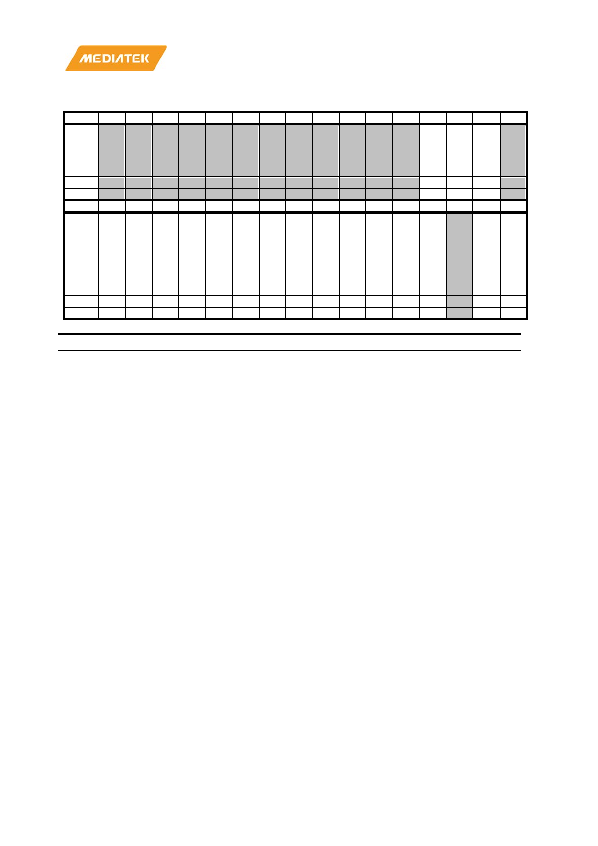
MT7686 Reference Manual
© 2016 - 2017 MediaTek Inc.
Page 127 of 536
This document contains information that is proprietary to MediaTek Inc. (“MediaTek”) and/or its licensor(s).
Any unauthorized use, reproduction or disclosure of this document in whole or in part is strictly prohibited.
A1030010
MSDC_INTEN
MSDC Interrupt Enable Register
00000000
Bit
31
30
29
28
27
26
25
24
23
22
21
20
19
18
17
16
Name
EN_
DMA
_PR
OTE
CT
EN_
GPD
_CS_
ERR
EN_
BD_
CS_E
RR
Type
RW
RW
RW
Reset
0
0
0
Bit
15
14
13
12
11
10
9
8
7
6
5
4
3
2
1
0
Name
EN_
SD_
DAT
A_C
RCE
RR
EN_
SD_
DAT
TO
EN_
SD_
DMA
_XF
ER_
DON
E
EN_
SD_
XFE
R_C
OMP
LETE
EN_
SD_
CSTA
EN_
SD_
RES
P_C
RCE
RR
EN_
SD_
CMD
TO
EN_
SD_
CMD
RDY
EN_
SD_S
DIOI
RQ
EN_
DMA
_Q_
EMP
TY
EN_
SD_
AUT
OCM
D_R
ESP_
CRC
ERR
EN_
SD_
AUT
OCM
D_C
MDT
O
EN_
AUT
OCM
D_C
MDR
DY
EN_
MSD
C_C
DSC
EN_
MMC
_IRQ
Type
RW
RW
RW
RW
RW
RW
RW
RW
RW
RW
RW
RW
RW
RW
RW
Reset
0
0
0
0
0
0
0
0
0
0
0
0
0
0
0
Bit(s)
Mnemonic
Name
Description
19
ENDMAPROTECT
EN_DMA_PROTECT
DMA protection interrupt enable
1'b0: Disable interrupt
1'b1: Enable interrupt
18
ENGPDCSERR
EN_GPD_CS_ERR
GPD checksum error interrupt enable
1'b0: Disable
interrupt
1'b1: Enable interrupt
17
ENBDCSERR
EN_BD_CS_ERR
BD checksum error interrupt enable
1'b0: Disable interrupt
1'b1: Enable interrupt
15
ENSDDCRCERR
EN_SD_DATA_CRCERR
SD Data CRC error interrupt enable
1'b0: Disable interrupt
1'b1: Enable
interrupt
14
ENSDDTO
EN_SD_DATTO
SD Data timeout interrupt enable
1'b0: Disable interrupt
1'b1: Enable interrupt
13
ENDMAXFDNE
EN_SD_DMA_XFER_DONE
DMA transfer done interrupt enable
1'b0: Disable interrupt
1'b1: Enable interrupt
12
ENSDXFCPL
EN_SD_XFER_COMPLETE
SD Data transfer complete interrupt
enable
1'b0: Disable interrupt
1'b1: Enable interrupt
11
ENSDCSTA
EN_SD_CSTA
SD CSTA update interrupt enable
1'b0: Disable interrupt
1'b1: Enable interrupt
10
ENSDRCRCER
EN_SD_RESP_CRCERR
SD Command
CRC error interrupt enable
1'b0: Disable interrupt
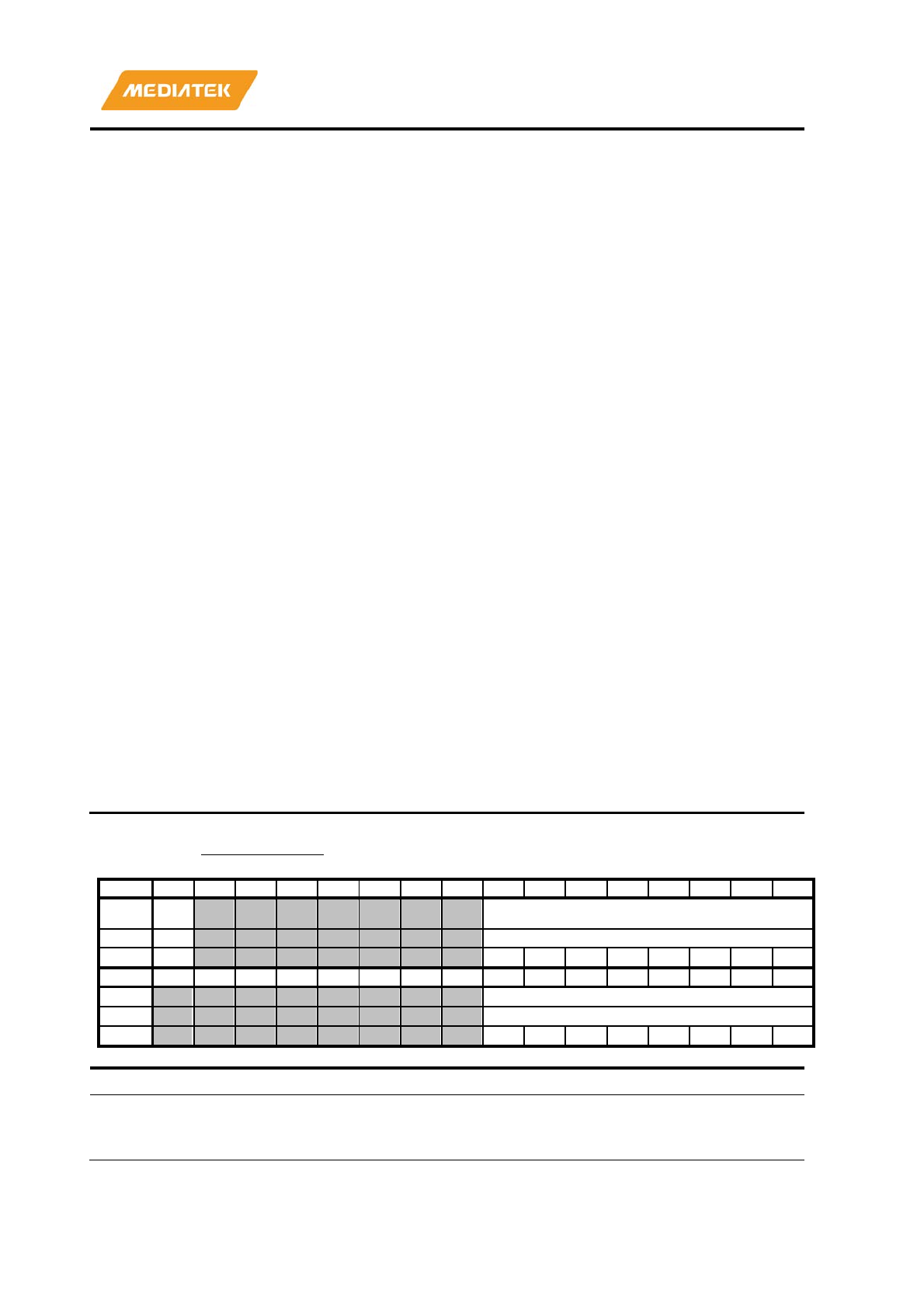
MT7686 Reference Manual
© 2016 - 2017 MediaTek Inc.
Page 128 of 536
This document contains information that is proprietary to MediaTek Inc. (“MediaTek”) and/or its licensor(s).
Any unauthorized use, reproduction or disclosure of this document in whole or in part is strictly prohibited.
1'b1: Enable interrupt
9
ENSDCTO
EN_SD_CMDTO
SD Command timeout interrupt enable
1'b0: Disable interrupt
1'b1: Enable interrupt
8
ENSDCRDY
EN_SD_CMDRDY
SD Command ready interrupt enable
1'b0: Disable
interrupt
1'b1: Enable interrupt
7
ENSDIOIRQ
EN_SD_SDIOIRQ
SD SDIO interrupt enable
1'b0: Disable interrupt
1'b1: Enable interrupt
6
ENDMAQEPTY
EN_DMA_Q_EMPTY
DMA queue empty interrupt enable
1'b0: Disable interrupt
1'b1: Enable interrupt
5
ENSDACDRCRCER
EN_SD_AUTOCMD_RESP_C
RCERR
SD auto command CRC error interrupt
enable
1'b0: Disable interrupt
1'b1: Enable interrupt
4
ENSDACDCTO
EN_SD_AUTOCMD_CMDTO
SD auto command timeout interrupt
enable
1'b0: Disable interrupt
1'b1: Enable interrupt
3
ENSDACDCRDY
EN_AUTOCMD_CMDRDY
SD auto command ready interrupt enable
1'b0: Disable interrupt
1'b1: Enable interrupt
1
ENMSDCCDSC
EN_MSDC_CDSC
MSDC Card detection status change
interrupt enable
1'b0: Disable interrupt
1'b1: Enable interrupt
0
ENMMCIRQ
EN_MMC_IRQ
MMC card interrupt enable
1'b0: Disable interrupt
1'b1: Enable interrupt
A1030014
MSDC_FIFOCS
MSDC FIFO Control and Status
Register
00000000
Bit
31
30
29
28
27
26
25
24
23
22
21
20
19
18
17
16
Name
FIFO
CLR
TXFIFOCNT
Type
A0
RU
Reset
0
0
0
0
0
0
0
0
0
Bit
15
14
13
12
11
10
9
8
7
6
5
4
3
2
1
0
Name
RXFIFOCNT
Type
RU
Reset
0
0
0
0
0
0
0
0
Bit(s)
Mnemonic
Name
Description
31
FIFOCLR
FIFOCLR
Embedded FIFO clear
Write 1 into this bit to clear the FIFO. It returns to 0
when FIFO is cleared.
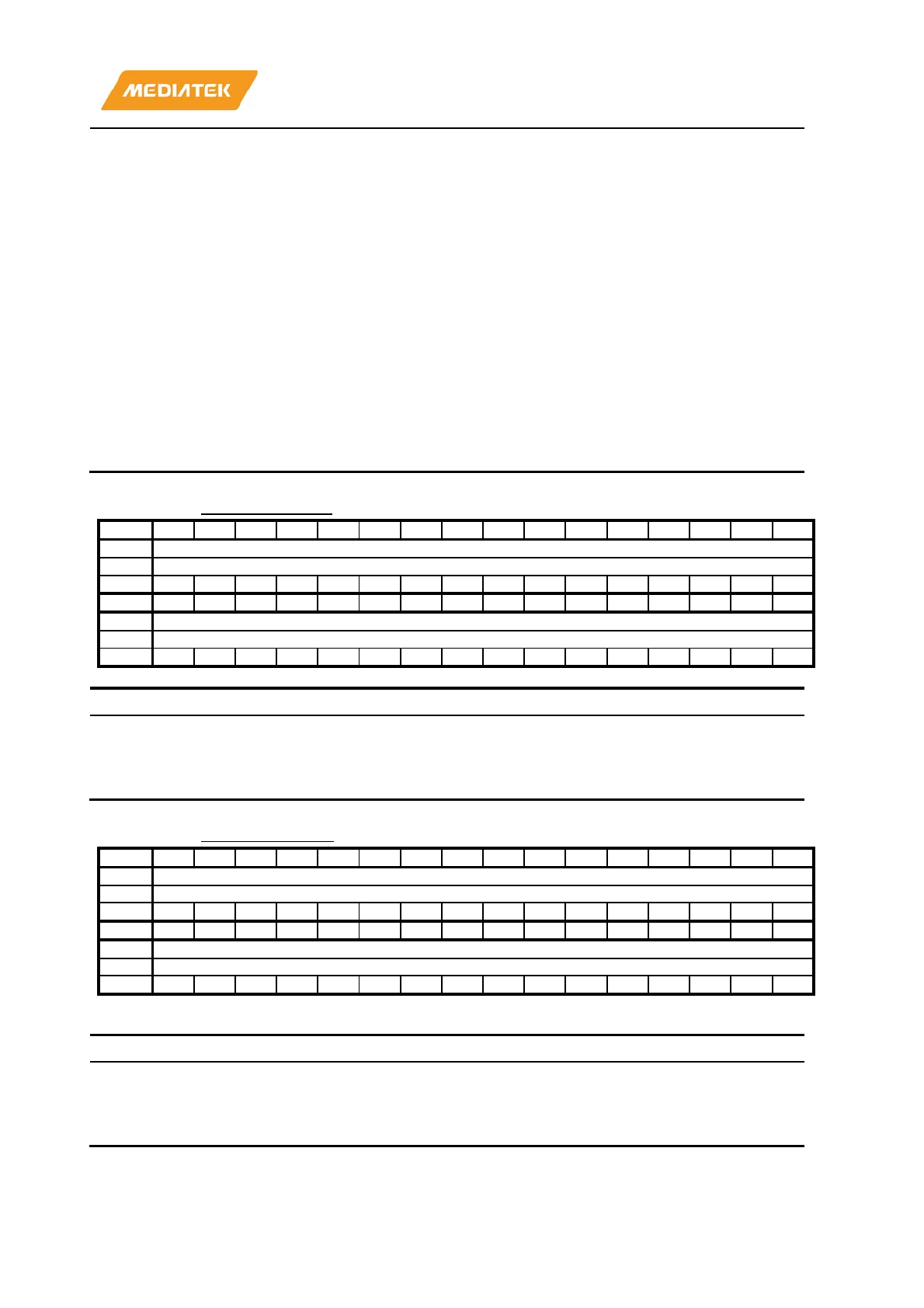
MT7686 Reference Manual
© 2016 - 2017 MediaTek Inc.
Page 129 of 536
This document contains information that is proprietary to MediaTek Inc. (“MediaTek”) and/or its licensor(s).
Any unauthorized use, reproduction or disclosure of this document in whole or in part is strictly prohibited.
Software needs to check this bit to make sure clearing
FIFO sequence is done.
This bit can be used when the data read/write
sequence has an error.
23:16
TXFIFOCNT
TXFIFOCNT
TX
FIFO count for MSDC write
8'd0: No data in FIFO
8'd1: 1 byte data in FIFO
8'd2: 2 bytes data in FIFO
8'd131: Maximum 131 bytes data in FIFO
Others: reserved
7:0
RXFIFOCNT
RXFIFOCNT
RX FIFO count for MSDC read
8'd0: No data in FIFO
8'd1: 1 byte data in
FIFO
8'd2: 2 bytes data in FIFO
8'd131: Maximum 131 bytes data in FIFO
Others: reserved
A1030018
MSDC_TXDATA
MSDC TX Data Port Register
00000000
Bit
31
30
29
28
27
26
25
24
23
22
21
20
19
18
17
16
Name
PIO_TXDATA
Type
WO
Reset
0
0
0
0
0
0
0
0
0
0
0
0
0
0
0
0
Bit
15
14
13
12
11
10
9
8
7
6
5
4
3
2
1
0
Name
PIO_TXDATA
Type
WO
Reset
0
0
0
0
0
0
0
0
0
0
0
0
0
0
0
0
Bit(s)
Mnemonic
Name
Description
31:0
PIOTXDATA
PIO_TXDATA
PIO mode TXDATA port
This register can be
accessed by byte, half-word or
word. This port can only be accessed in PIO mode.
Otherwise, the transaction will be discarded.
A103001C
MSDC_RXDATA
MSDC RX Data Port Register
00000000
Bit
31
30
29
28
27
26
25
24
23
22
21
20
19
18
17
16
Name
PIO_RXDATA
Type
RU
Reset
0
0
0
0
0
0
0
0
0
0
0
0
0
0
0
0
Bit
15
14
13
12
11
10
9
8
7
6
5
4
3
2
1
0
Name
PIO_RXDATA
Type
RU
Reset
0
0
0
0
0
0
0
0
0
0
0
0
0
0
0
0
Bit(s)
Mnemonic
Name
Description
31:0
PIORXDATA
PIO_RXDATA
PIO mode
RXDATA port
This register can be accessed by byte, half
-word or
word. This port can only be accessed in PIO mode.
Otherwise, the transaction will be discarded.
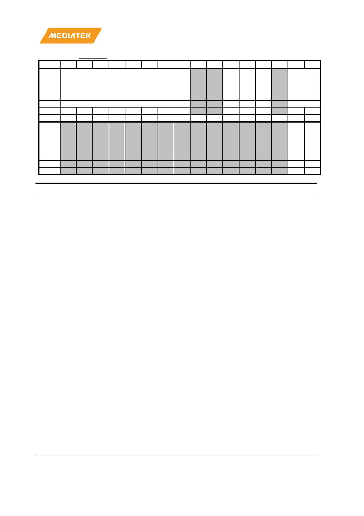
MT7686 Reference Manual
© 2016 - 2017 MediaTek Inc.
Page 130 of 536
This document contains information that is proprietary to MediaTek Inc. (“MediaTek”) and/or its licensor(s).
Any unauthorized use, reproduction or disclosure of this document in whole or in part is strictly prohibited.
A1030030
SDC_CFG
SD Configuration Register
00100000
Bit
31
30
29
28
27
26
25
24
23
22
21
20
19
18
17
16
Name DTOC
INT_
AT_
BLO
CK_
GAP
SDIO
_INT
_DE
T_E
N
SDIO
BUSWIDT
H
Type
RW
RW
RW
RW
RW
Reset
0
0
0
0
0
0
0
0
0
1
0
0
0
Bit
15
14
13
12
11
10
9
8
7
6
5
4
3
2
1
0
Name
WAK
EUP
_INS
_EN
WAK
EUP
_SDI
OIN
T_E
N
Type
RW
RW
Reset
0
0
Bit(s)
Mnemonic
Name
Description
31:24
DTOC
DTOC
Data Timeout Counter
The period from the end of initial host read command
or the last read data block in a multiple block read
operation to the start bit of next read data block
requires at
least two serial clock cycles. The counter is
used to extend the period (Read Data Access Time) in
unit of 1048576 serial clocks.
8'b00000000: Extend 1048576 more serial clock cycle
8'b00000001: Extend 1048576x2 more serial clock
cycle
8'b00000010: Extend 1048576x3 more serial clock
cycle
8'b11111111: Extend 1048576x 256 more serial clock
cycle
21
INTBGP
INT_AT_BLOCK_GAP
Interrupt at block
gap
This bit is valid only in 4
-bit mode of the SDIO card
and selects a sample point in the
interrupt cycle.
Setting to 1 enables interrupt detection at the block gap
for a multiple block transfer. Setting to 0 disables
interrupt detection during a multiple block transfer. If
the SD card cannot signal an interrupt during a
multiple block transfer
, this bit should be set to 0.
When the Host Driver detects an SD card insertion, it
shall set this bit according to the CCCR of the SDIO
card.
1'b0: Disable interrupt detection at the block gap
1'b1: Enable interrupt detection at the block gap
20
SDIOIDE
SDIO_INT_DET_EN
SDIO interrupt detection enable
This bit is to inform the SD controller to sense the
SDIO interrupt
1'b0: SDIO interrupt detection is disabled
1'b1: SDIO interrupt detection is enabled if the SDIO
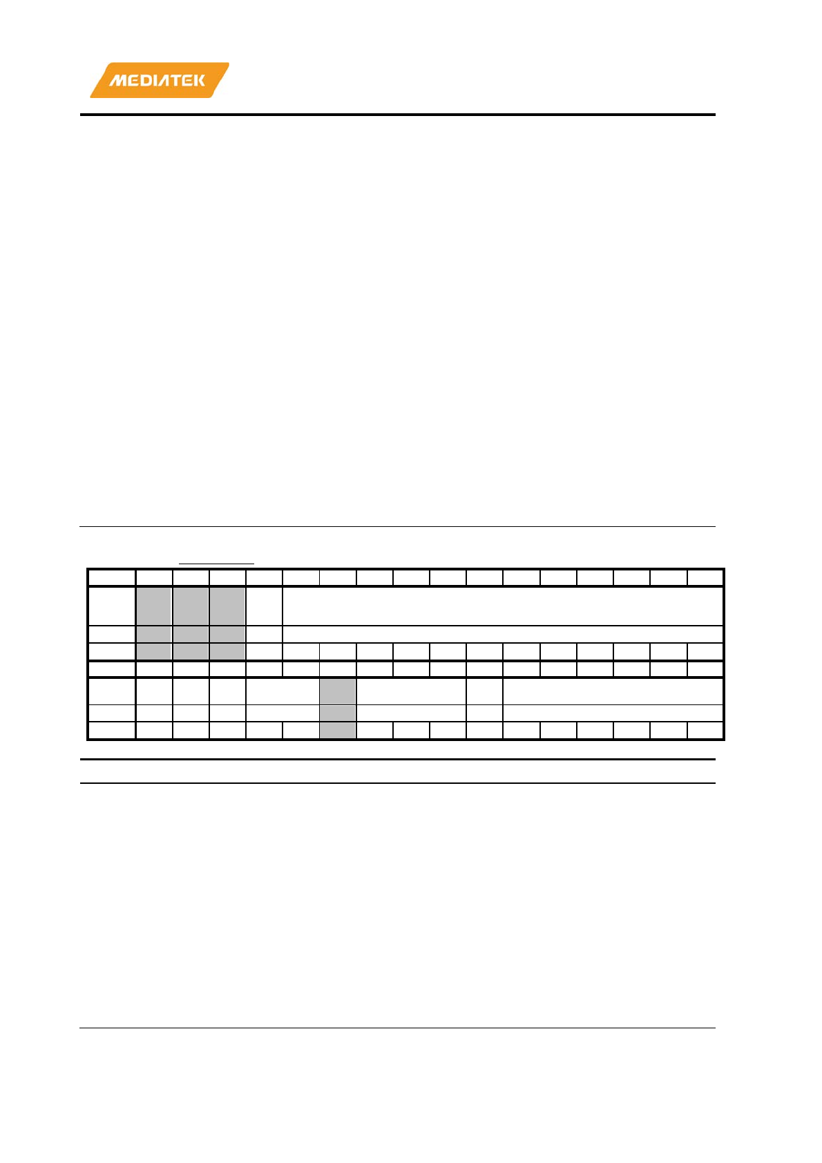
MT7686 Reference Manual
© 2016 - 2017 MediaTek Inc.
Page 131 of 536
This document contains information that is proprietary to MediaTek Inc. (“MediaTek”) and/or its licensor(s).
Any unauthorized use, reproduction or disclosure of this document in whole or in part is strictly prohibited.
bit is also on
19
SDIO
SDIO
SDIO mode enable bit
This bit is to enable the support to sense the SDIO
interrupt and disable the R4 response CRC check for
SDIO card
1'b0: SDIO mode is disabled
1'b1: SDIO mode is enabled
17:16
BUSWD
BUSWIDTH
Bus width configuration
This
field is used to define the SD/MMC bus width
2'b00: 1 bit mode
2'b01: 4 bit mode
2'b10: 8 bit mode
2'b11: reserved
1
ENWKUPINS
WAKEUP_INS_EN
Card status change wakeup event enable bit
1'b0: Disable wakeup event for card status change
1'b1: Enable wakeup event for card status change
0
ENWKUPSDIOINT
WAKEUP_SDIOINT_E
N
SDIO card interrupt wakeup event enable bit
1'b0: Disable wakeup event for SDIO card interrupt
1'b1: Enable wakeup event for SDIO card interrupt
A1030034
SDC_CMD
SD Command Register
00000000
Bit
31
30
29
28
27
26
25
24
23
22
21
20
19
18
17
16
Name
AUTO
_CM
D
LEN
Type
RW
RW
Reset
0
0
0
0
0
0
0
0
0
0
0
0
0
Bit
15
14
13
12
11
10
9
8
7
6
5
4
3
2
1
0
Name
GO_I
RQ
STOP
RW DTYPE RSPTYP
BREA
K
CMD
Type
RW
RW
RW
RW
RW
RW
RW
Reset
0
0
0
0
0
0
0
0
0
0
0
0
0
0
0
Bit(s)
Mnemonic
Name
Description
28
ACMD
AUTO_CMD
Auto command enable
This field determines use of auto command functions.
This function can be used in all modes
including
PIO/Basic DMA/Descriptor DMA/Enhanced Mode.
There are two methods to stop Multiple
-
block read and
write operation.
(1) Auto CMD12 Enable
Multiple
-block read and write commands for memory
require CMD12 to stop the operation. When ACMD
-12
is used, MSDC issues CMD12 automatically when last
block transfer completes. Auto CMD12 error is
indicated to the MSDC_INT register. The Host Driver
shall n
ot set this bit if the command does not require
CMD12. In particular, secure commands defined in the

MT7686 Reference Manual
© 2016 - 2017 MediaTek Inc.
Page 132 of 536
This document contains information that is proprietary to MediaTek Inc. (“MediaTek”) and/or its licensor(s).
Any unauthorized use, reproduction or disclosure of this document in whole or in part is strictly prohibited.
Part 3 File Security specification do not require
CMD12.
(2) Auto CMD23 Enable
When ACMD
-23 is used, MSDC issues a CMD23
automatically before issuing a com
mand specified in
the CMD field. The Host Controller Version 3.00 and
later shall support this function. By writing the
Command register, MSDC issues a CMD23 first and
then issues a command specified by the CMD field in
SDC_CMD register. If response errors
of CMD23 are
detected, the second command is not issued. A CMD23
error is indicated in the MSDC_INT register. 32
-bit
block count value for CMD23 is set to
SDC_BLOCK_NUM register.
1'b0: Disable Auto Command
1'b1: Enable Auto CMD12
27:16
LEN
LEN
Length
The register field is used to define the length of one
block in unit of byte in a data transaction of block
mode or the data length in unit of byte in data
transaction of byte mode. The maximal value of block
length is 2048 bytes.
12'b000000000000: Reserved
12'b000000000001: Block length is 1 byte
12'b000000000010: Block length is 2 byte
12'b011111111111: Block length is 2047 byte
12'b100000000000: Block length is 2048 byte
15
GOIRQ
GO_IRQ
GO_IRQ command
The
register bit indicates if the command is
GO_IRQ_STATE (CMD40) and used only for MMC
protocol. If the command is GO_IRQ_STATE, the
period between command token and response token
will not be limited.
1'b0: The command is not GO_IRQ_STATE
1'b1: The
command is GO_IRQ_STATE
14
STOP
STOP
Stop command
The register bit indicates if the command is a stop
transmission command. It should be set to 1 when
CMD12 (SD/MMC) or CMD52 with I/O abort (SDIO)
is to be issued.
1'b0: The command is not a stop
transmission
command
1'b1: The command is a stop transmission command
13
RW
RW
Command read write selection
The register bit defines
if the command is a read
command or write command. The register bit is valid
only when the command will cause a
transaction with
data token.

MT7686 Reference Manual
© 2016 - 2017 MediaTek Inc.
Page 133 of 536
This document contains information that is proprietary to MediaTek Inc. (“MediaTek”) and/or its licensor(s).
Any unauthorized use, reproduction or disclosure of this document in whole or in part is strictly prohibited.
1'b0: The command is a read command
1'b1: The command is a write command
12:11
DTYPE
DTYPE
Data block selection
The register field defines data token type for the
command.
2'b00: No data token for the command
2'b01: Single block transaction (only available in block
mode)
2'b10: Multiple block transaction. (only available in
block mode)
2'b11: Stream operation. It only shall be used in MMC
protocol. (only available in block mode)
9:7
RSPTYP
RSPTYP
Command response type
3'b000: This command has no response.
3'b001: The command has R1/R5/R6/R7 response.
The response token is 48
-bit with CRC check (For
SD/MMC/SDIO) (Not includ
ing the SDIO abort
command)
3'b010: The command has R2 response.
The response
token is 136
-bit (For SD/MMC)
3'b011: The command has R3 response. The response
token is 48
-bit response, no CRC check (For SD/MMC)
3'b100: The command has R4 response. The response
token is 48
-bit without CRC check (For SDIO) The
res
ponse token is 48-bit with CRC check (For MMC)
3'b111: The command has R1b response. The response
token is 48
-bit (For SD/MMC/SDIO)
6
BREAK
BREAK
Abort a pending MMC GO_IRQ command
It is only valid for a pending GO_IRQ_MODE
command waiting for MMC
interrupt response.
1'b0: Not a b
reak command
1'b1: Break a pending MMC GO_IRQ_MODE
command in the controller.
5:0
CMD
CMD
SD Memory Card command
A1030038
SDC_ARG
SD Argument Register
00000000
Bit
31
30
29
28
27
26
25
24
23
22
21
20
19
18
17
16
Name
ARG
Type
RW
Reset
0
0
0
0
0
0
0
0
0
0
0
0
0
0
0
0
Bit
15
14
13
12
11
10
9
8
7
6
5
4
3
2
1
0
Name
ARG
Type
RW
Reset
0
0
0
0
0
0
0
0
0
0
0
0
0
0
0
0
Bit(s)
Mnemonic
Name
Description
31:0
ARG
ARG
Memory card
controller argument register
MT7686 Reference Manual
© 2016 - 2017 MediaTek Inc.
Page 134 of 536
This document contains information that is proprietary to MediaTek Inc. (“MediaTek”) and/or its licensor(s).
Any unauthorized use, reproduction or disclosure of this document in whole or in part is strictly prohibited.
A103003C
SDC_STS
SD Status Register
00000000
Bit
31
30
29
28
27
26
25
24
23
22
21
20
19
18
17
16
Name
MMC
_ST
REA
M_
WR_
COM
PL
CMD
_WR
_BU
SY
Type
RU
W1C
Reset
0
0
Bit
15
14
13
12
11
10
9
8
7
6
5
4
3
2
1
0
Name
CMD
BUS
Y
SDC
BUS
Y
Type
RU
RU
Reset
0
0
Bit(s)
Mnemonic
Name
Description
31
MMCSWRCPL
MMC_STREAM_WR_C
OMPL
MMC Stream mode write data is all flushed to
MMC card
Software can use this bit to confirm last write data are
flushed to MMC then issue a STOP command.
This bit is only valid
when the command
SDC_CMD.DTYPE=2'b11.
1'b0: Last Data are partially inside MSDC
1'b1: Last data are flushed to MMC card
16
CMD_WR_BUSY
1
CMDBSY
CMDBUSY
SD Command line busy status
Software should always read this bit to make sure the
command line is not busy before sending the next
command.
If the command is R1B or data read/write command,
Software
should check the SDCBUSY bit, too.
Note: When
auto command 12 is enabled, this bit will
be asserted immediately after SDC_CMD is written
and de
-asserted after auto command 12 finishes.
1'b0: No transmission
going on in CMD line on SD bus
1'b1: There
is transmission going on in
CMD line on SD
bus
0
SDCBSY
SDCBUSY
SD controller
busy status
1'b0: SD controller is idle
1'b1: SD controller is busy
A1030040
SDC_RESP0
SD Response Register 0
00000000
Bit
31
30
29
28
27
26
25
24
23
22
21
20
19
18
17
16
Name
RESP0
Type
RU
Reset
0
0
0
0
0
0
0
0
0
0
0
0
0
0
0
0
Bit
15
14
13
12
11
10
9
8
7
6
5
4
3
2
1
0
Name
RESP0
MT7686 Reference Manual
© 2016 - 2017 MediaTek Inc.
Page 135 of 536
This document contains information that is proprietary to MediaTek Inc. (“MediaTek”) and/or its licensor(s).
Any unauthorized use, reproduction or disclosure of this document in whole or in part is strictly prohibited.
Type
RU
Reset
0
0
0
0
0
0
0
0
0
0
0
0
0
0
0
0
Bit(s)
Mnemonic
Name
Description
31:0
RESP0
RESP0
Memory card controller response register 0
A1030044
SDC_RESP1
SD Response Register 1
00000000
Bit
31
30
29
28
27
26
25
24
23
22
21
20
19
18
17
16
Name
RESP1
Type
RU
Reset
0
0
0
0
0
0
0
0
0
0
0
0
0
0
0
0
Bit
15
14
13
12
11
10
9
8
7
6
5
4
3
2
1
0
Name
RESP1
Type
RU
Reset
0
0
0
0
0
0
0
0
0
0
0
0
0
0
0
0
Bit(s)
Mnemonic
Name
Description
31:0
RESP1
RESP1
Memory card controller response register 1
A1030048
SDC_RESP2
SD Response Register 2
00000000
Bit
31
30
29
28
27
26
25
24
23
22
21
20
19
18
17
16
Name
RESP2
Type
RU
Reset
0
0
0
0
0
0
0
0
0
0
0
0
0
0
0
0
Bit
15
14
13
12
11
10
9
8
7
6
5
4
3
2
1
0
Name
RESP2
Type
RU
Reset
0
0
0
0
0
0
0
0
0
0
0
0
0
0
0
0
Bit(s)
Mnemonic
Name
Description
31:0
RESP2
RESP2
Memory card controller response register 2
A103004C
SDC_RESP3
SD Response Register 3
00000000
Bit
31
30
29
28
27
26
25
24
23
22
21
20
19
18
17
16
Name
RESP3
Type
RU
Reset
0
0
0
0
0
0
0
0
0
0
0
0
0
0
0
0
Bit
15
14
13
12
11
10
9
8
7
6
5
4
3
2
1
0
Name
RESP3
Type
RU
Reset
0
0
0
0
0
0
0
0
0
0
0
0
0
0
0
0
Bit(s)
Mnemonic
Name
Description
31:0
RESP3
RESP3
Memory card controller response register 3
A1030050
SDC_BLK_NUM
SD Block Number Register
00000001
Bit
31
30
29
28
27
26
25
24
23
22
21
20
19
18
17
16
Name
BLOCK_NUMBER
Type
RW
MT7686 Reference Manual
© 2016 - 2017 MediaTek Inc.
Page 136 of 536
This document contains information that is proprietary to MediaTek Inc. (“MediaTek”) and/or its licensor(s).
Any unauthorized use, reproduction or disclosure of this document in whole or in part is strictly prohibited.
Reset
0
0
0
0
0
0
0
0
0
0
0
0
0
0
0
0
Bit
15
14
13
12
11
10
9
8
7
6
5
4
3
2
1
0
Name
BLOCK_NUMBER
Type
RW
Reset
0
0
0
0
0
0
0
0
0
0
0
0
0
0
0
1
Bit(s)
Mnemonic
Name
Description
31:0
BLKNUM
BLOCK_NUMBER
Memory card
controller Block number
This field indicates the block number of data
transaction.
32'd0: Reserved
32'd1: 1 data block
32'd2: 2 data block
32'd3: 3 data block
32'hffffffff: 4GB
-1 data block
A1030058
SDC_CSTS
SD Card Status
Register
00000000
Bit
31
30
29
28
27
26
25
24
23
22
21
20
19
18
17
16
Name
CSTS
Type
W1C
Reset
0
0
0
0
0
0
0
0
0
0
0
0
0
0
0
0
Bit
15
14
13
12
11
10
9
8
7
6
5
4
3
2
1
0
Name
CSTS
Type
W1C
Reset
0
0
0
0
0
0
0
0
0
0
0
0
0
0
0
0
Bit(s)
Mnemonic
Name
Description
31:0
CSTS
CSTS
The register provides SD/MMC card status in the
response R1 or R1b field.
32’h0: keep the current value
Others: write 1 to each bit to clear the corresponding
bit.
A103005C
SDC_CSTS_EN
SD Card
Status Enable Register
00000000
Bit
31
30
29
28
27
26
25
24
23
22
21
20
19
18
17
16
Name
CSTS_EN
Type
RW
Reset
0
0
0
0
0
0
0
0
0
0
0
0
0
0
0
0
Bit
15
14
13
12
11
10
9
8
7
6
5
4
3
2
1
0
Name
CSTS_EN
Type
RW
Reset
0
0
0
0
0
0
0
0
0
0
0
0
0
0
0
0
Bit(s)
Mnemonic
Name
Description
31:0
CSTS_EN
CSTS_EN
This register is used to control the CSTA bit that will
generate MSDC_INT.SDCSTA
A1030060
SDC_DATCRC_STS
SD Card Data CRC Status Register
00000000
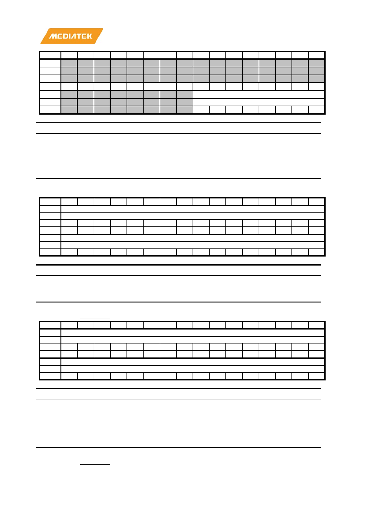
MT7686 Reference Manual
© 2016 - 2017 MediaTek Inc.
Page 137 of 536
This document contains information that is proprietary to MediaTek Inc. (“MediaTek”) and/or its licensor(s).
Any unauthorized use, reproduction or disclosure of this document in whole or in part is strictly prohibited.
Bit
31
30
29
28
27
26
25
24
23
22
21
20
19
18
17
16
Name
Type
Reset
Bit
15
14
13
12
11
10
9
8
7
6
5
4
3
2
1
0
Name
DAT_CRCSTS_POS
Type
RU
Reset
0
0
0
0
0
0
0
0
Bit(s)
Mnemonic
Name
Description
7:0
DCSSP
DAT_CRCSTS_POS
MSDC read DATA CRC status
This register reflects the CRC status of data line[7:0].
This register is only for MSDC Read.
1'b0: No CRC error
1'b1: CRC error
A1030080
SD_ACMD_RESP
SD ACMD Response Register
00000000
Bit
31
30
29
28
27
26
25
24
23
22
21
20
19
18
17
16
Name
AUTOCMD_RESP
Type
RU
Reset
0
0
0
0
0
0
0
0
0
0
0
0
0
0
0
0
Bit
15
14
13
12
11
10
9
8
7
6
5
4
3
2
1
0
Name
AUTOCMD_RESP
Type
RU
Reset
0
0
0
0
0
0
0
0
0
0
0
0
0
0
0
0
Bit(s)
Mnemonic
Name
Description
31:0
ACMDRESP
AUTOCMD_RESP
SD
Auto command response register
This register stores the response [39:8] of
ACMD12/ACMD23/ACMD19.
A1030090
DMA_SA
DMA Start Address Register
00000000
Bit
31
30
29
28
27
26
25
24
23
22
21
20
19
18
17
16
Name
DMA_STR_ADDR
Type
RW
Reset
0
0
0
0
0
0
0
0
0
0
0
0
0
0
0
0
Bit
15
14
13
12
11
10
9
8
7
6
5
4
3
2
1
0
Name
DMA_STR_ADDR
Type
RW
Reset
0
0
0
0
0
0
0
0
0
0
0
0
0
0
0
0
Bit(s)
Mnemonic
Name
Description
31:0
DMASA
DMA_STR_ADDR
The start address of the DMA address
This register is used to set the start address of the
DMA. In DMA basic mode, this field indicates the
source or destination address of the data transfer
which depends on the command. In
Descriptor DMA
mode
, this is the descriptor chain start address.
A1030094
DMA_CA
DMA Current Address Register
00000000
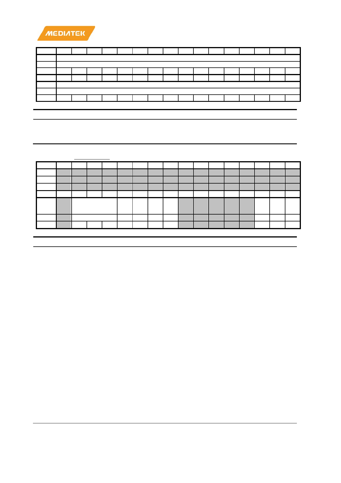
MT7686 Reference Manual
© 2016 - 2017 MediaTek Inc.
Page 138 of 536
This document contains information that is proprietary to MediaTek Inc. (“MediaTek”) and/or its licensor(s).
Any unauthorized use, reproduction or disclosure of this document in whole or in part is strictly prohibited.
Bit
31
30
29
28
27
26
25
24
23
22
21
20
19
18
17
16
Name
DMA_CURR_ADDR
Type
RU
Reset
0
0
0
0
0
0
0
0
0
0
0
0
0
0
0
0
Bit
15
14
13
12
11
10
9
8
7
6
5
4
3
2
1
0
Name
DMA_CURR_ADDR
Type
RU
Reset
0
0
0
0
0
0
0
0
0
0
0
0
0
0
0
0
Bit(s)
Mnemonic
Name
Description
31:0
DMACA
DMA_CURR_ADDR
The current address of the DMA address
This register is used to read the current address of the
DMA descriptor chain.
A1030098
DMA_CTRL
DMA Control Register
00006000
Bit
31
30
29
28
27
26
25
24
23
22
21
20
19
18
17
16
Name
Type
Reset
Bit
15
14
13
12
11
10
9
8
7
6
5
4
3
2
1
0
Name BURST_SIZE
DMA
_SPLI
T_1K
LAST
_BUF
DMA
_ALI
GN
DMA
_MO
DE
DMA
_RES
UME
DMA
_STO
P
DMA
_STA
RT
Type
RW
RW
RW
RW
RW
WO
A0
WO
Reset
1
1
0
0
0
0
0
0
0
0
Bit(s)
Mnemonic
Name
Description
14:12
BSTSZ
BURST_SIZE
DMA burst size
This field is used to specify the maximum transfer
bytes allowed at the device per DMA burst. This field
cannot be modified when the DMA status is 1.
3'd3: 8 Bytes
3'd4: 16 Bytes
3'd5: 32
Bytes
3'd6: 64 Bytes
Other: Reserved
11
SPLIT1K
DMA_SPLIT_1K
This field is used to specify whether to split
burst when it crosses
the 1K address boundary
1'b0:1K boundary not split
1'b1:1K boundary split
10
LASTBF
LAST_BUF
Last buffer of
the basic DMA mode
This field indicates the last buffer in the basic DMA
mode
9
DMAALIGN
DMA_ALIGN
This field is used to specify whether
there is
address alignment burst size
1'b0:
No DMA burst size alignment
1'b1:DMA burst size alignment
8
DMAMOD
DMA_MODE
DMA operation mode
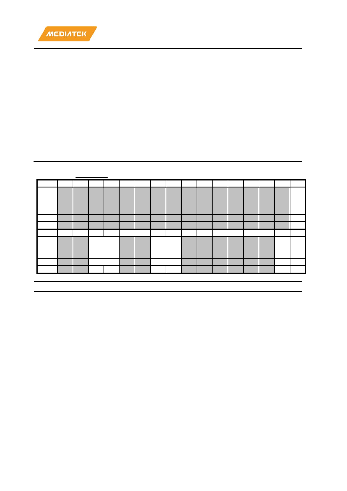
MT7686 Reference Manual
© 2016 - 2017 MediaTek Inc.
Page 139 of 536
This document contains information that is proprietary to MediaTek Inc. (“MediaTek”) and/or its licensor(s).
Any unauthorized use, reproduction or disclosure of this document in whole or in part is strictly prohibited.
This field indicates the operation mode of DMA
1'b0: Basic DMA mode
1'b1: Descriptor base DMA mode
2
DMARSM
DMA_RESUME
DMA resume control register
This bit is used to resume the DMA transaction. Read
always
returns 0
1
DMASTOP
DMA_STOP
DMA Stop control register
This bit is used to stop the DMA transaction. When
software issues STOP command, it must wait for this
bit to de
-assert or inactivate the DMA to guarantee a
complete stop.
0
DMASTART
DMA_START
DMA
start control register
This bit is used to start the DMA transaction. Read
always return
s 0
A103009C
DMA_CFG
DMA Configuration Register
00000000
Bit
31
30
29
28
27
26
25
24
23
22
21
20
19
18
17
16
Name
DMA
_CH
K_SU
M_12
B
Type
RW
Reset
0
Bit
15
14
13
12
11
10
9
8
7
6
5
4
3
2
1
0
Name MSDC_ACT
IVE_EN AHB_HPRO
T_2_EN
DMA
_DSC
P_CS
_EN
DMA
_STA
TUS
Type
RW
RW
RW
RU
Reset
0
0
0
0
0
0
Bit(s)
Mn
emonic
Name
Description
16
DMACHKSUM12B
DMA_CHK_SUM_12B
This register indicates GPD/BD checksum
length
is 16bytes or 12bytes
1'b0: GPD/BD checksum cover 16byte
1'b1: GPD/BD checksum only cover 12byte
13:12
MSDCACTIVEEN
MSDC_ACTIVE_EN
This
register indicates how to control
msdc_active
2'b00: dynamic control msdc_active
2'b01: msdc_active = 0
2'b10: msdc_active = 1
2'b11: Reserved
9:8
AHBHPROT2EN
AHB_HPROT_2_EN
This register determines how to control
hprot_2 pin of AHB bus
AHB_HPROT_2_EN = 2'b00, and Basic DMA Mode
All write transfers of a burst
are accessed in bufferable
mode except the last
DMA burst
AHB_HPROT2_2_EN=2'b00, and Descriptor DMA
Mode
all write transfers of a burst are accessed in
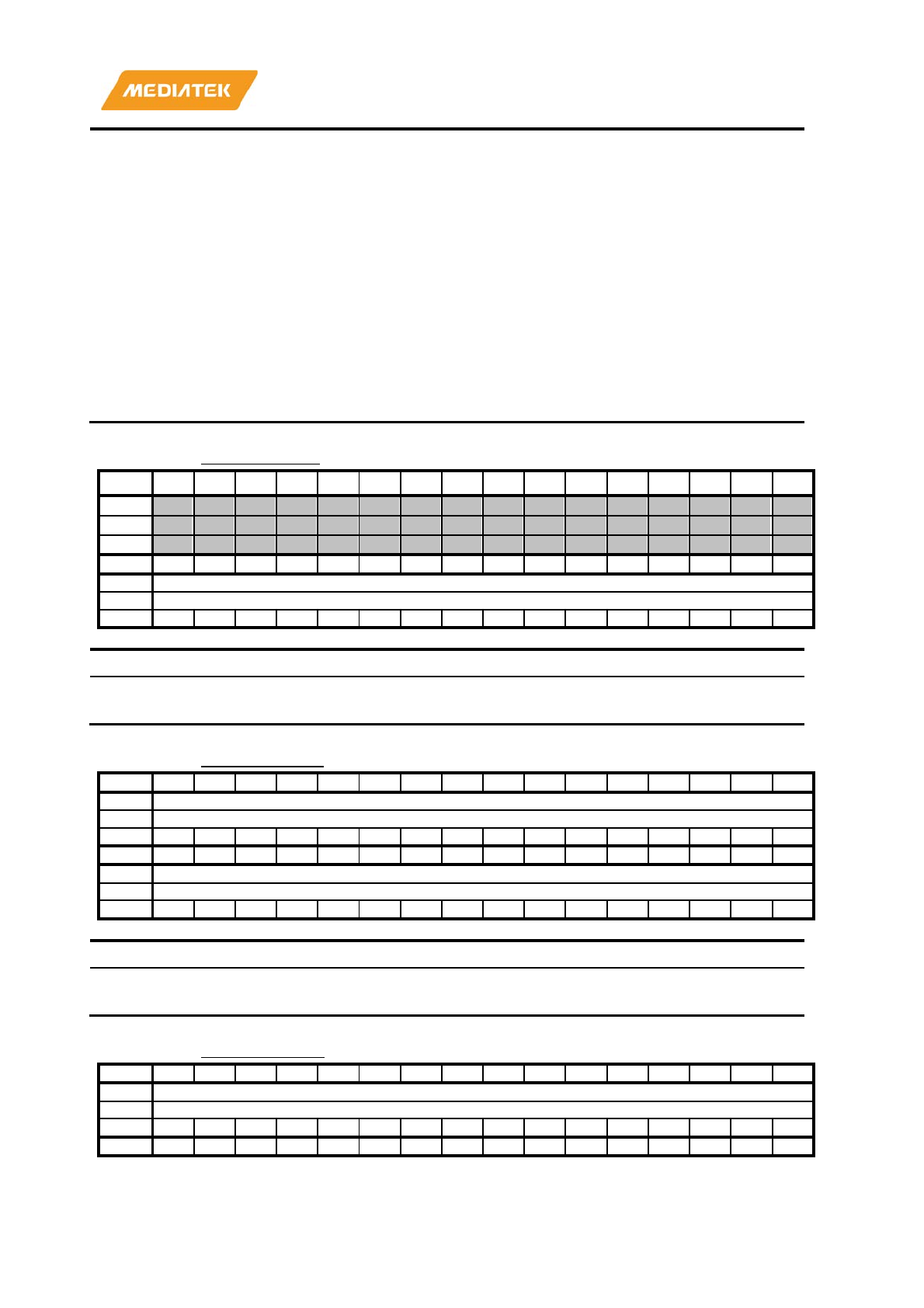
MT7686 Reference Manual
© 2016 - 2017 MediaTek Inc.
Page 140 of 536
This document contains information that is proprietary to MediaTek Inc. (“MediaTek”) and/or its licensor(s).
Any unauthorized use, reproduction or disclosure of this document in whole or in part is strictly prohibited.
bufferable mode except the hardware’s own update
transfer
.
2'b00: dynamic control hprot_2
2'b01: hprot_2 = 0
2'b10: hprot_2 = 1
1
DSCPCSEN
DMA_DSCP_CS_EN
DMA descriptor checksum enable
This bit is used to enable or disable the checksum
validation function for the descriptor. This field cannot
be modified when the DMA status is 1.
0
DMASTS
DMA_STATUS
DMA status
This bit is used to indicate the status of the DMA.
1'b0: DMA engine is inactive
1'b1: DMA engine is active
A10300A0
SW_DBG_SEL
MSDC S/W Debug Selection Register
00000000
Bit
31
30
29
28
27
26
25
24
23
22
21
20
19
18
17
16
Name
Type
Reset
Bit
15
14
13
12
11
10
9
8
7
6
5
4
3
2
1
0
Name
DBG_SEL
Type
RW
Reset
0
0
0
0
0
0
0
0
0
0
0
0
0
0
0
0
Bit(s)
Mnemonic
Name
Description
15:0
SWDBGSEL
DBG_SEL
MSDC debug selection
Reserved
A10300A4
SW_DBG_OUT
MSDC S/W Debug Output Register
00000000
Bit
31
30
29
28
27
26
25
24
23
22
21
20
19
18
17
16
Name
DBG_OUT
Type
RU
Reset
0
0
0
0
0
0
0
0
0
0
0
0
0
0
0
0
Bit
15
14
13
12
11
10
9
8
7
6
5
4
3
2
1
0
Name
DBG_OUT
Type
RU
Reset
0
0
0
0
0
0
0
0
0
0
0
0
0
0
0
0
Bit(s)
Mnemonic
Name
Description
31:0
SWDBGO
DBG_OUT
MSDC debug output
32 bit output selected by SW_DBG_SEL register
A10300A8
DMA_LENGTH
DMA Length Register
00000000
Bit
31
30
29
28
27
26
25
24
23
22
21
20
19
18
17
16
Name
XFER_SIZE
Type
RW
Reset
0
0
0
0
0
0
0
0
0
0
0
0
0
0
0
0
Bit
15
14
13
12
11
10
9
8
7
6
5
4
3
2
1
0
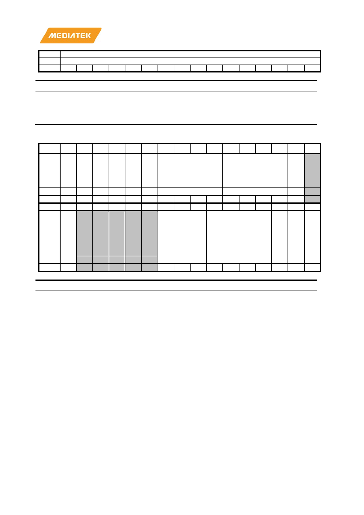
MT7686 Reference Manual
© 2016 - 2017 MediaTek Inc.
Page 141 of 536
This document contains information that is proprietary to MediaTek Inc. (“MediaTek”) and/or its licensor(s).
Any unauthorized use, reproduction or disclosure of this document in whole or in part is strictly prohibited.
Name
XFER_SIZE
Type
RW
Reset
0
0
0
0
0
0
0
0
0
0
0
0
0
0
0
0
Bit(s)
Mnemonic
Name
Description
31:0
XFSZ
XFER_SIZE
DMA total transfer size
This field is used to specify the number of DMA
transfer bytes. This field is only valid in basic DMA
mode.
A10300B0
PATCH_BIT0
MSDC Patch Bit Register 0
403C004F
Bit
31
30
29
28
27
26
25
24
23
22
21
20
19
18
17
16
Name
EN_
MMC
_DRV
_RES
P
DETE
CT_
WR_
CRC_
TIME
OUT
SPC_
ALW
AYS_
PUSH
SDIO
_INT
_DLY
_SEL
SDC_
CMD
_CM
DFAI
L_SE
L
SDC_
CMD
_IDR
T_SE
L
SDC_CFG_WDOD SDC_CFG_BSYDLY
SDIO
_CFG
_INT
C_SE
L
Type
RW
RW
RW
RW
RW
RW
RW
RW
RW
Reset
0
1
0
0
0
0
0
0
0
0
1
1
1
1
0
Bit
15
14
13
12
11
10
9
8
7
6
5
4
3
2
1
0
Name
MSD
C_FI
FO_R
D_DI
S
INT_DAT_LATCH
_CK_SEL reserved1
DIS_
REFL
ECT_
CMD
WR_
WHE
N_BS
Y
EN_S
DC_O
DD_8
BIT_
SUP
reser
ved0
Type
RW
RW
RW
RW
RW
RW
Reset
0
0
0
0
1
0
0
1
1
1
1
Bit(s)
Mnemonic
Name
Description
31
PTCH31
EN_MMC_DRV_RESP
Enable MSDC always drives
the bus,
when
the output is a wakeup response,
such as
BREAK.
1'b0: Disable
1'b1: Enable
30
PTCH30
DETECT_WR_CRC_TIMEOUT
MSDC write data CRC phase timeout
detection
1'b0: Does not detect CRC
phase timeout
1'b1: Detects CRC phase timeout
29
PTCH29
SPC_ALWAYS_PUSH
SPC Buffer push mechanism
1'b0: Push the buffer only when read transfer is
on
-going
1'b1: Always push the buffer
28
PTCH28
SDIO_INT_DLY_SEL
SDIO interrupt latch time
selection
1'b0: Latch the data line value in internal SDIO
interrupt period
1'b1: Latch the data line value in 1 clock delay of
internal SDIO interrupt period

MT7686 Reference Manual
© 2016 - 2017 MediaTek Inc.
Page 142 of 536
This document contains information that is proprietary to MediaTek Inc. (“MediaTek”) and/or its licensor(s).
Any unauthorized use, reproduction or disclosure of this document in whole or in part is strictly prohibited.
27
PTCH27
SDC_CMD_CMDFAIL_SEL
SDIO interrupt period recovery selection
1'b0: SDIO
interrupt period will re-start after a
CMD12 or CMD52 command is issued
1'b1: SDIO interrupt period whenever DAT line
is not busy
26
PTCH26
SDC_CMD_IDRT_SEL
SD identification response time selection
The register bit indicates if the command has a
response with NID (that is, 5 serial clock cycles
as defined in SD Memory Card Specification
Part 1 Physical Layer Specification version 1.0)
response time. The register bit is valid only
when the command has a response token. Thus,
the register bit must b
e set to 1 for CMD2
(ALL_SEND_CID) and ACMD41
(SD_APP_OP_CMD).
1'b0: Otherwise.
1'b1: The command has a response with NID
response time.
25:22
PTCH22
SDC_CFG_WDOD
SD Write Data Output Delay
The period from response
finish for the initial
host write command or the last write data block
in a multiple block write operation to the start
bit of the next write data block requires at least
two serial clock cycles. The register field is used
to extend the period (Write Data Output
Delay)
in
the unit of one serial clock.
4'b0000: Not extended.
4'b0001: Extended by one more serial clock
cycle.
4'b0010: Extended by two more serial clock
cycles.
4'b1111: Extended by fifteen more serial clock
cycles.
21:18
PTCH18
SDC_CFG_BSYDLY
SD R1B busy detection mode
The register field is only valid for the commands
with R1b response. If the command has a
response of R1b type, MS/SD controller must
monitor the data line 0 for card busy status from
the bit time that is two seria
l clock cycles after
the command end bit to check if operations in
SD/MMC Memory Card have finished. The
register field is used to expand the time between
the command end bit and end of detection
period to detect card busy status. If time is up
and there i
s no card busy status on data line 0,
then the controller will abandon the detection.
4'b0000: Not extended.
4'b0001: Extended by one more serial clock
cycle.
4'b0010: Extend
ed by two more serial clock
cycles.
MT7686 Reference Manual
© 2016 - 2017 MediaTek Inc.
Page 143 of 536
This document contains information that is proprietary to MediaTek Inc. (“MediaTek”) and/or its licensor(s).
Any unauthorized use, reproduction or disclosure of this document in whole or in part is strictly prohibited.
4'b1111: Extend
ed by fifteen more serial clock
cycle
s.
17
PTCH17
SDIO_CFG_INTC_SEL
SDIO Interrupt model selection
1'b0: Only when data line [1] = 0 and then
trigger SDIO interrupt event
1'b1: Only when data line [3:0] = 4'b1101 and
then trigger SDIO interrupt event
15
PTCH15
MSDC_FIFO_RD_DIS
MSDC RXFIFO Read Disable
1'b0: Disable FIFO read permission to RXFIFO
in PIO mode
1'b1: Enable FIFO read permission to RXFIFO in
PIO mode
9:7
INTCKS
INT_DAT_LATCH_CK_SEL
Internal MSDC clock phase selection
Total 8
stages, each stage can delay 1 clock
period of msdc_src_ck
6:3
reserved1
2
PTCH02
DIS_REFLECT_CMDWR_WHEN_
BSY
Enable SD command register write
monitor
1'b0: Enable monitor function
1'b1: Disable monitor function
1
PTCH01
EN_SDC_ODD_8BIT_SUP
Enable SD odd number support for 8
-bit
data bus
1'b0: Disable
1'b1: Enable
0
reserved0
A10300B4
PATCH_BIT1
MSDC Patch Bit Register 1
FFFE0009
Bit
31
30
29
28
27
26
25
24
23
22
21
20
19
18
17
16
Name
MSD
C_CK
_SHB
FF_C
KEN
MSD
C_CK
_RCT
L_CK
EN
MSD
C_CK
_WC
TL_C
KEN
MSD
C_CK
_SD_
CKEN
MSD
C_CK
_AC
MD_
CKEN
MSD
C_CK
_VOL
DET_
CKEN
MSD
C_CK
_PSC
_CKE
N
MSD
C_CK
_SPC
_CKE
N
AHB_
CK_G
DMA
_CKE
N
reserved2
ENAB
LE_S
INGL
E_BU
RST
Type
RW
RW
RW
RW
RW
RW
RW
RW
RW
RW
RW
Reset
1
1
1
1
1
1
1
1
1
1
1
1
1
1
1
0
Bit
15
14
13
12
11
10
9
8
7
6
5
4
3
2
1
0
Name
BIAS
_EXT
BIAS
_28N
M
BIAS
_EN1
8IO_
28NM
BIAS_TUNE_28NM GET_
CRC_
MAR
GIN
GET_
BUSY
_MA
RGIN
CMD_RSP_TA_CN
TR WRDAT_CRCS_T
A_CNTR
Type
RW
RW
RW
RW
RW
RW
RW
Reset
0
0
0
0
0
0
0
0
0
0
1
0
0
1
Bit(s)
Mnemonic
Name
Description
31
MSHBFCKEN
MSDC_CK_SHBFF_CKEN
msdc_src_ck clock enable bit for SHBFF
1'b0: Disable
1'b1: Enable
30
MRCTLCKEN
MSDC_CK_RCTL_CKEN
msdc_src_ck clock enable bit for RCTL

MT7686 Reference Manual
© 2016 - 2017 MediaTek Inc.
Page 144 of 536
This document contains information that is proprietary to MediaTek Inc. (“MediaTek”) and/or its licensor(s).
Any unauthorized use, reproduction or disclosure of this document in whole or in part is strictly prohibited.
1'b0: Disable
1'b1: Enable
29
MWCTLCKEN
MSDC_CK_WCTL_CKEN
msdc_src_ck clock enable bit for WCTL
1'b0: Disable
1'b1: Enable
28
MSDCKEN
MSDC_CK_SD_CKEN
msdc_src_ck clock enable bit for SD
1'b0: Disable
1'b1: Enable
27
MACMDCKEN
MSDC_CK_ACMD_CKEN
msdc_src_ck clock enable bit for
ACMD
1'b0: Disable
1'b1: Enable
26
MVOLDTCKEN
MSDC_CK_VOLDET_CKEN
msdc_src_ck clock enable bit for
VOLDET
1'b0: Disable
1'b1: Enable
25
MPSCCKEN
MSDC_CK_PSC_CKEN
msdc_src_ck clock enable bit for PSC
1'b0: Disable
1'b1: Enable
24
MSPCCKEN
MSDC_CK_SPC_CKEN
msdc_src_ck clock enable bit for
SPC
1'b0: Disable
1'b1: Enable
23
HGDMACKEN
AHB_CK_GDMA_CKEN
hclk_ck clock enable bit for GDMA
1'b0: Disable
1'b1: Enable
22:17
reserved2
16
SINGLEBURST
ENABLE_SINGLE_BURST
The AHB bus will not support incr1 burst
type in the future. It will only affect
the
AHB bus
MSDC design, but not the AXI
bus design
1'b0:h
ardware will send incr1 burst type
1'b1: hardware will send single burst type
instead of incr1 type
13
BIAS28R0
BIAS_EXTBIAS_28NM
28NM BIAS Controller register 0
12
BIAS28R1
BIAS_EN18IO_28NM
28NM BIAS Controller register 1
11:8
BIAS28R2
BIAS_TUNE_28NM
28NM BIAS Controller register 2
7
GETCRCMARGIN
GET_CRC_MARGIN
This
will add margin for getting the CRC
status when
the card response CRC does
no
t match with the 2 cycles
(described in
the SD specification) starting
from the
end bit
1'b0: 8 cycles are reserved to get the CRC status
from write data CRC end bit
1'b1: 16 cycle
s reserved for getting CRC status
from write data
CRC end bit
6
GETBUSYMARGIN
GET_BUSY_MARGIN
This
will add margin for the get busy
MT7686 Reference Manual
© 2016 - 2017 MediaTek Inc.
Page 145 of 536
This document contains information that is proprietary to MediaTek Inc. (“MediaTek”) and/or its licensor(s).
Any unauthorized use, reproduction or disclosure of this document in whole or in part is strictly prohibited.
state of data0
1'b0: 1 cycle reserved for get busy state from
SRC
status end bit
1'b1: 3
cycles reserved for get busy state from
SRC
status end bit
5:3
CMDTA
CMD_RSP_TA_CNTR
CMD response turn around period
The turn around cycle = CMD_RSP_TA_CNTR
+ 2, Only for USH104 mode, this register
should be set to 0 in non
-UHS104 mode
2:0
WRTA
WRDAT_CRCS_TA_CNTR
Write data and CRC status turn
around
period
The turn around cycle =
WRDAT_CRCS_TA_CNTR + 2, Only for
USH104 mode, this register should be set to 0
in non
-UHS104 mode
A10300EC
PAD_TUNE
MSDC Pad Tuning Register
00000000
Bit
31
30
29
28
27
26
25
24
23
22
21
20
19
18
17
16
Name PAD_CLK_TXDLY PAD_CMD_RESP_RXDLY
PAD_
CMD
_RD_
RXDL
Y_SE
L
PAD_CMD_RXDLY
Type
RW
RW
RW
RW
Reset
0
0
0
0
0
0
0
0
0
0
0
0
0
0
0
0
Bit
15
14
13
12
11
10
9
8
7
6
5
4
3
2
1
0
Name
PAD_
DAT_
RD_R
XDLY
_SEL
PAD_DAT_RD_RXDLY
DELA
Y_EN
PAD_DAT_WR_RXDLY
Type
RW
RW
RW
RW
Reset
0
0
0
0
0
0
0
0
0
0
0
0
Bit(s)
Mnemonic
Name
Description
31:27
CLKTDLY
PAD_CLK_TXDLY
CLK Pad TX Delay Control
This register is used to add delay to CLK phase.
Total 32 stages
26:22
CMDRRDLY
PAD_CMD_RESP_RXD
LY
CMD Response Internal Delay Line Control
This register is used to fine
-tune response phase
latched by MSDC internal clock
Total 32 stages
21
CMDRRDLYSEL
PAD_CMD_RD_RXDLY
_SEL
Decide
if CMD Response passes through data
delay line1 or not
1'b0: pass
1'b1: do not pass
20:16
CMDRDLY
PAD_CMD_RXDLY
CMD Pad RX Delay Line Control
This register is used to fine
-tune CMD pad macro
response latch timing
Total 32 stages
13
DATRRDLYSEL
PAD_DAT_RD_RXDLY
Decide
if RX data passes through data delay
MT7686 Reference Manual
© 2016 - 2017 MediaTek Inc.
Page 146 of 536
This document contains information that is proprietary to MediaTek Inc. (“MediaTek”) and/or its licensor(s).
Any unauthorized use, reproduction or disclosure of this document in whole or in part is strictly prohibited.
_SEL
line1 or not
1'b0: pass
1'b1: do not pass
12:8
DATRRDLY
PAD_DAT_RD_RXDLY
DAT Pad RX Delay Line Control (for MSDC
read only)
This register is used to fine
-tune DAT pad macro read
data latch timing
Total 32 stages
7
DELAYEN
DELAY_EN
E
nable all delay cell toggling when powered on
1'b0:
disable delay cell toggling default
1'b1:
enable delay cell toggling default
4:0
DATWRDLY
PAD_DAT_WR_RXDLY
Write Data Status Internal Delay Line Control
This register is used to
fine-tune write status phase
latched by MSDC internal clock
Total 32 stages
A10300F0
DAT_RD_DLY0
MSDC Data Delay Line Register 0
00000000
Bit
31
30
29
28
27
26
25
24
23
22
21
20
19
18
17
16
Name
DAT0_RD_DLY
DAT1_RD_DLY
Type
RW
RW
Reset
0
0
0
0
0
0
0
0
0
0
Bit
15
14
13
12
11
10
9
8
7
6
5
4
3
2
1
0
Name
DAT2_RD_DLY
DAT3_RD_DLY
Type
RW
RW
Reset
0
0
0
0
0
0
0
0
0
0
Bit(s)
Mnemonic
Name
Description
28:24
DAT0RDDLY
DAT0_RD_DLY
DAT0 Pad RX
Delay Line Control (for MSDC
RD)
Total 32 stages
20:16
DAT1RDDLY
DAT1_RD_DLY
DAT1 Pad RX Delay Line Control (for MSDC
RD)
Total 32 stages
12:8
DAT2RDDLY
DAT2_RD_DLY
DAT2 Pad RX Delay Line Control (for MSDC
RD)
Total 32 stages
4:0
DAT3RDDLY
DAT3_RD_DLY
DAT3 Pad RX Delay Line Control (for MSDC
RD)
Total 32 stages
A10300F4
DAT_RD_DLY1
MSDC Data Delay Line Register 1
00000000
Bit
31
30
29
28
27
26
25
24
23
22
21
20
19
18
17
16
Name
DAT4_RD_DLY
DAT5_RD_DLY
Type
RW
RW
Reset
0
0
0
0
0
0
0
0
0
0
Bit
15
14
13
12
11
10
9
8
7
6
5
4
3
2
1
0
Name
DAT6_RD_DLY
DAT7_RD_DLY
Type
RW
RW
MT7686 Reference Manual
© 2016 - 2017 MediaTek Inc.
Page 147 of 536
This document contains information that is proprietary to MediaTek Inc. (“MediaTek”) and/or its licensor(s).
Any unauthorized use, reproduction or disclosure of this document in whole or in part is strictly prohibited.
Reset
0
0
0
0
0
0
0
0
0
0
Bit(s)
Mnemonic
Name
Description
28:24
DAT4RDDLY
DAT4_RD_DLY
DAT4 Pad RX Delay Line
Control (for MSDC
RD)
Total 32 stages
20:16
DAT5RDDLY
DAT5_RD_DLY
DAT5 Pad RX Delay Line Control (for MSDC
RD)
Total 32 stages
12:8
DAT6RDDLY
DAT6_RD_DLY
DAT6 Pad RX Delay Line Control (for MSDC
RD)
Total 32 stages
4:0
DAT7RDDLY
DAT7_RD_DLY
DAT7 Pad RX
Delay Line Control (for MSDC
RD)
Total 32 stages
A10300F8
HW_DBG_SEL
MSDC H/W Debug Selection Register
00000000
Bit
31
30
29
28
27
26
25
24
23
22
21
20
19
18
17
16
Name
HW_
DBG_
WRA
P_SE
L
HW_DBG0_SEL HW_DBG_
WRAP_TYP
E_SEL HW_DBG1_SEL
Type
RW
RW
RW
RW
Reset
0
0
0
0
0
0
0
0
0
0
0
0
0
0
0
Bit
15
14
13
12
11
10
9
8
7
6
5
4
3
2
1
0
Name
HW_DBG2_SEL
HW_DBG3_SEL
Type
RW
RW
Reset
0
0
0
0
0
0
0
0
0
0
0
0
0
0
Bit(s)
Mnemonic
Name
Description
30
DBGWSEL
HW_DBG_WRAP_SEL
Hardware debug output selection for wrapper
0: Select original debug pins
1: Select wrapper debug pins
29:24
DBG0SEL
HW_DBG0_SEL
Hardware
debug output selection
23:22
DBGWTSEL
HW_DBG_WRAP_TYP
E_SEL
Hardware
debug output selection for wrapper
2'd0: Select dbg_in20~dbg_in3b = DRAM_DBG
2'd1: Select dbg_in20~dbg_in3b = RISC_DBG
2'd2: Select dbg_in20~dbg_in3b = AHBM_DBG
2'd3: Select dbg_in20~dbg_in3b = AHBS_DBG
21:16
DBG1SEL
HW_DBG1_SEL
Hardware
debug output selection
13:8
DBG2SEL
HW_DBG2_SEL
Hardware
debug output selection
7:0
DBG3SEL
HW_DBG3_SEL
Hardware
debug output selection
A1030100
MAIN_VER
MSDC Main Version Register
20160503
Bit
31
30
29
28
27
26
25
24
23
22
21
20
19
18
17
16
Name
MAIN_VER
Type
RO
Reset
0
0
1
0
0
0
0
0
0
0
0
1
0
1
1
0

MT7686 Reference Manual
© 2016 - 2017 MediaTek Inc.
Page 148 of 536
This document contains information that is proprietary to MediaTek Inc. (“MediaTek”) and/or its licensor(s).
Any unauthorized use, reproduction or disclosure of this document in whole or in part is strictly prohibited.
Bit
15
14
13
12
11
10
9
8
7
6
5
4
3
2
1
0
Name
MAIN_VER
Type
RO
Reset
0
0
0
0
0
1
0
1
0
0
0
0
0
0
1
1
Bit(s)
Mnemonic
Name
Description
31:0
MAINVER
MAIN_VER
Main
Version
A1030104
ECO_VER
MSDC ECO Version Register
00000000
Bit
31
30
29
28
27
26
25
24
23
22
21
20
19
18
17
16
Name
ECO_VER
Type
RO
Reset
0
0
0
0
0
0
0
0
0
0
0
0
0
0
0
0
Bit
15
14
13
12
11
10
9
8
7
6
5
4
3
2
1
0
Name
ECO_VER
Type
RO
Reset
0
0
0
0
0
0
0
0
0
0
0
0
0
0
0
0
Bit(s)
Mnemonic
Name
Description
31:0
ECOVER
ECO_VER
ECO Version
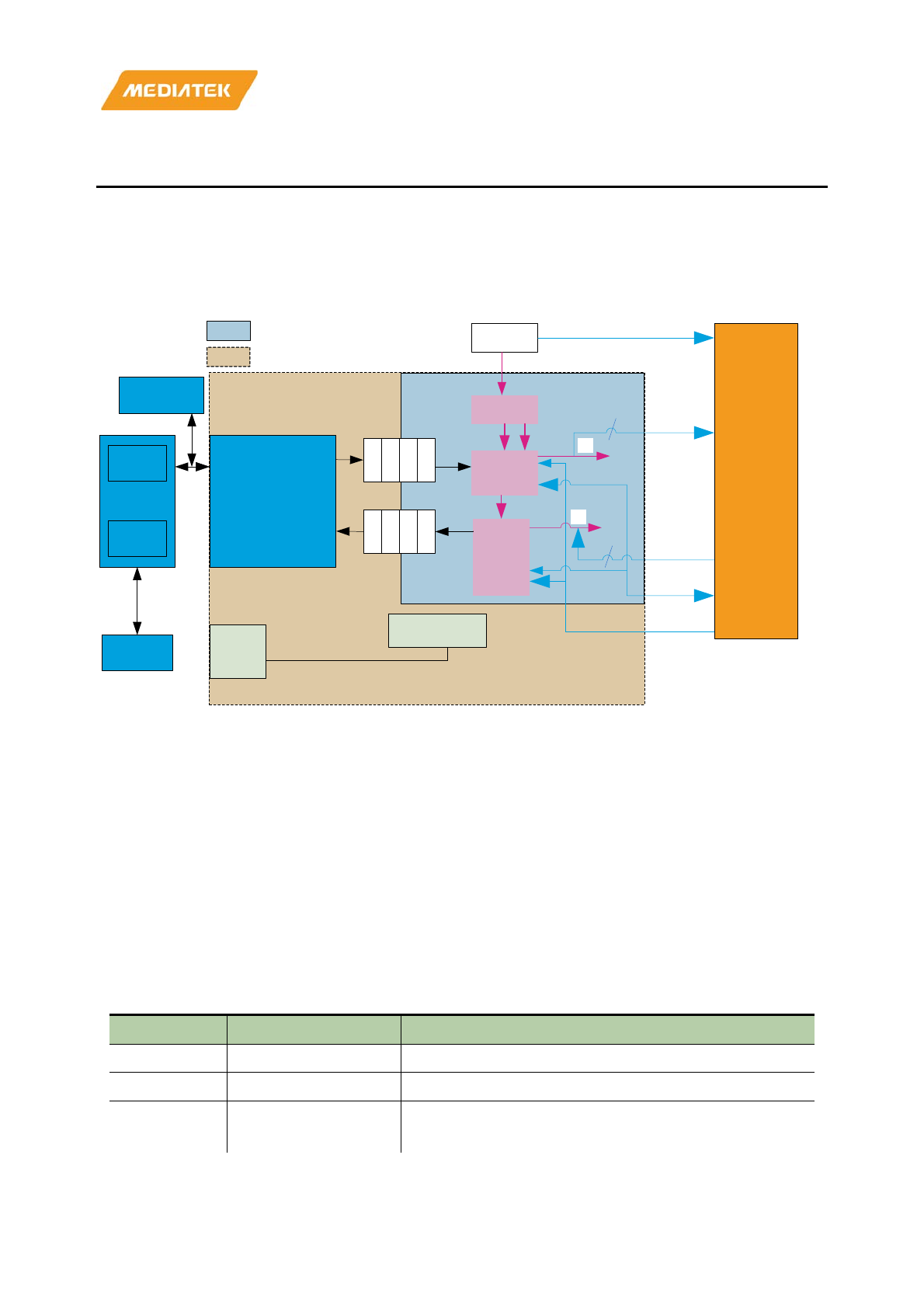
MT7686 Reference Manual
© 2016 - 2017 MediaTek Inc.
Page 149 of 536
This document contains information that is proprietary to MediaTek Inc. (“MediaTek”) and/or its licensor(s).
Any unauthorized use, reproduction or disclosure of this document in whole or in part is strictly prohibited.
10. I2S0
10.1. Overview
I2S0 is placed on AHB bus to support fast data transfers and has APB interface for setting the control register (CR).
I2S0 contains CLK CON, I2S OUT, I2S IN, DL FIFO and ULFIFO. The block diagram is shown in Figure 10.1-1.
DL FIFO
UL FIFO
DMA
Memory
Audio top CR
XO/XPLL/I2S_BCLK domain
PLL1/PLL2 domain
XPLL
CLK ON
I _
1
1
2S MCLK
I2S_TX
I2S_RX
I2S_FS
I2S_ BCLK
External
audio
codec
I2S OUT
I2S IN
APB
slave
audio_ahb_slave
(h2s bridge)
-Cortex M4
DMA
RX
2I S
I S2
DMA
TX
Figure 10.1-1. I2S block diagram
Keywords: Audio Codec, XPLL, CLKCON, I2S, AHB slave, DMA, UL DL FIFO, I2S0 CR, APB slave, XO (26M only), PLL1,
PLL2.
10.2. IO interface
• AHB slave interface (refer to AMBA v2.0)
• APB slave interface (refer to AMBA v3.0)
• Maximum internal delay of each interface is 13.3ns. Only supports 16bits per channel.
The I2S mode interface for master mode and slave mode is shown in Table 10.2-1 and Table 10.2-2. The TDM
mode interface for master mode and slave mode is shown in Table 10.2-3 and Table 10.2-4.
Table 10.2-1. I2S mode interface – master mode
PIN name
Direction
Description
I2S_MCLK Output 26/24.576/22.5792MHz
I2S_BCLK Master : Output I2S_FS*32
I2S_FS Master : Output 11.025, 22.05, 44.1, 88.2, 176.4 kHz
8, 12, 16, 24, 32, 48, 96, 192 kHz

MT7686 Reference Manual
© 2016 - 2017 MediaTek Inc.
Page 150 of 536
This document contains information that is proprietary to MediaTek Inc. (“MediaTek”) and/or its licensor(s).
Any unauthorized use, reproduction or disclosure of this document in whole or in part is strictly prohibited.
PIN name
Direction
Description
I2S_TX Output TX data
I2S_RX Input RX data
Table 10.2-2. I2S mode interface – slave mode
PIN name Direction Description
I2S_MCLK Output 26/24.576/22.5792MHz
I2S_BCLK Slave : Input I2S_FS*32
I2S_FS Slave : Input 11.025, 22.05, 44.1, 88.2, 176.4 kHz
8, 12, 16, 24, 32, 48, 96, 192 kHz
I2S_TX Output TX data
I2S_RX Input RX data
Table 10.2-3. TDM mode interface – master mode
PIN name Direction Description
I2S_MCLK Output 26/24.576/22.5792MHz
I2S_BCLK Master : Output I2S_FS*32, I2S_FS*64
I2S_FS Master : Output
11.025, 22.05, 44.1, 88.2, 176.4 kHz
8, 12, 16, 24, 32, 48, 96, 192 kHz
I2S_TX Output TX data
I2S_RX Input RX data
Table 10.2-4. TDM mode interface – slave mode
PIN name Direction Description
I2S_MCLK Output 26/24.576/22.5792MHz
I2S_BCLK Slave : Input I2S_FS*32, I2S_FS*64, I2S_FS*128
I2S_FS Slave : Input
11.025, 22.05, 44.1, 88.2, 176.4 kHz
8, 12, 16, 24, 32, 48, 96, 192 kHz
I2S_TX Output TX data
I2S_RX Input RX data
NOTE1: 8 channel TDM doesn’t support 192kHz and 176.4kHz
NOTE2: For master mode, I2S_MCLK frequencies only support relative sample rates listed in Table 10.2-5,
I2S_MCLK from 24.576/22.5792MHz is for high definition (HD) mode.
Table 10.2-5. Relationship between MCLK and sample rate
I2S_MCLK Sample Rate
26MHz (XO or XPLL) 8, 12, 16, 24, 32, 48 kHz
24.576MHz (XPLL) 8, 12, 16, 24, 32, 48, 96, 192 kHz
22.5792MHz (XPLL) 11.025, 22.05, 44.1, 88.2, 176.4 kHz
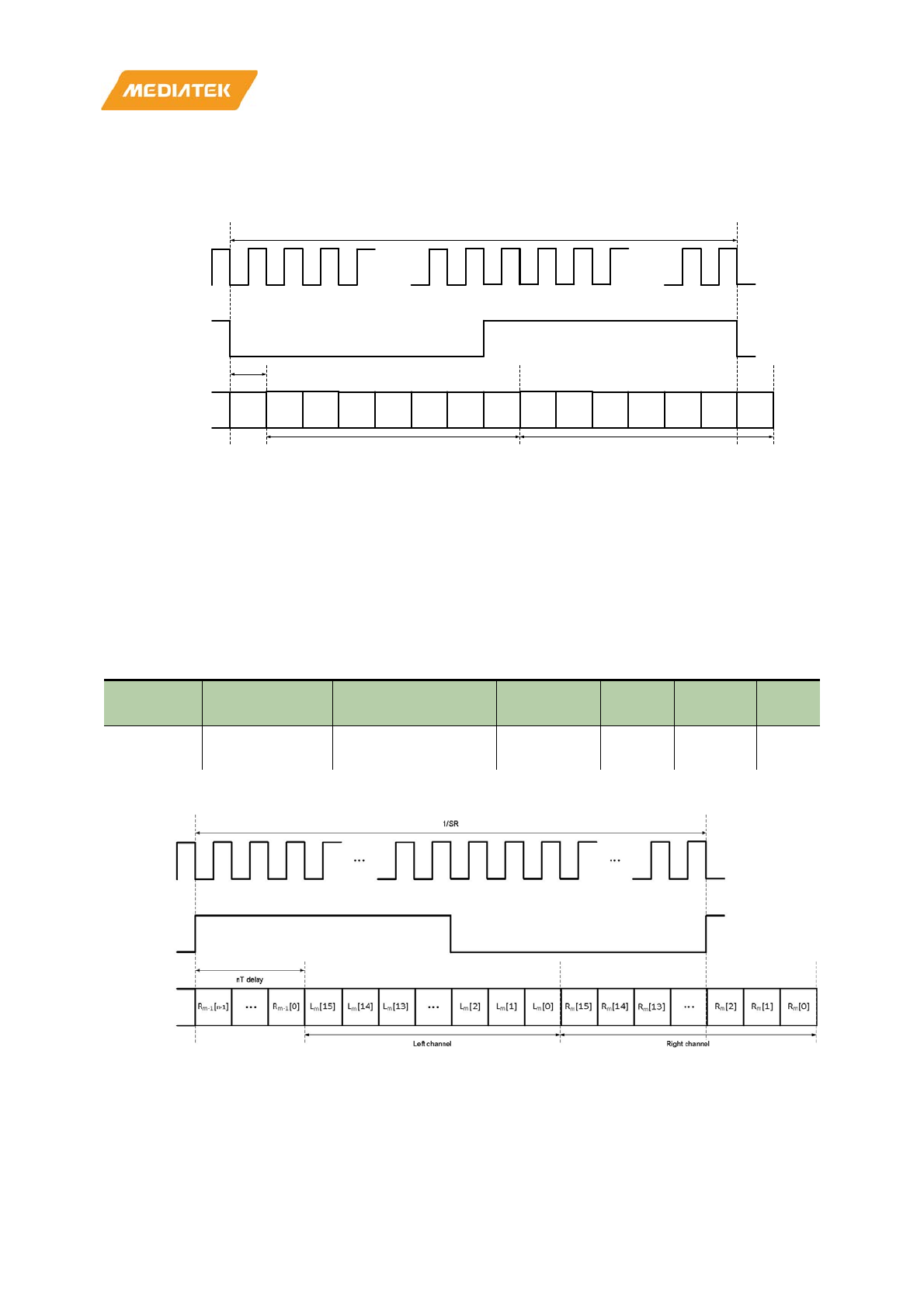
MT7686 Reference Manual
© 2016 - 2017 MediaTek Inc.
Page 151 of 536
This document contains information that is proprietary to MediaTek Inc. (“MediaTek”) and/or its licensor(s).
Any unauthorized use, reproduction or disclosure of this document in whole or in part is strictly prohibited.
10.3. I2S OUT and I2S IN
I2S OUT and I2S IN support standard I2S protocol and both master/slave mode. The I2S protocol is in Figure 10.3-1.
The TDM mode protocol is in Figure 10.3-2, Figure 10.3-3 and Figure 10.3-4.
I2S_FS
I2S_TX/RX L[15] L[14]L[13]L[2] L[1]
…L[0] R[15] R[14]R[13]R[2] R[1]
…R[0]
I2S_BCLK ……
R[0]
1T delay
Left channel Right channel
1/SR
Figure 10.3-1. I2S protocol waveform
If I2S OUT operates in mono mode, R[15:0] will be the same as L[15:0]. If I2S IN operates in mono mode, R[15:0]
will not affect I2S IN’s output to UL FIFO.
Note: When I2S acts as slave and connects to the external codec, I2S IN and I2S OUT will use the same BCLK/FS
from the external codec. Therefore, the sample rate of TX/RX should be the same. However, there is a down rate
mode where TX SR could be twice of RX SR. In this mode, RX will receive one duplicate data in every SR cycle and
I2S IN will automatically discard the duplicate data and not send it into UL FIFO. Example is shown in Table 10.3-1.
Table 10.3-1. Down rate example for slave mode
Slave Mode Input Sample
Rate
Output Sample Rate Mono/Stereo MCLK
(output)
BCLK
(input)
LRCLK
(input)
Down Rate
Mode
16b, 24kHz 16b, 48kHz Both 24.576
MHz
1.536MHz 48kHz
I2S_BCLK
I2S_FS
I2S_TX/RX
Figure 10.3-2. Sample m of TDM32 with nT delay
Keywords: I2S_BCLK, I2S_FS, I2S_TX/RX, R_, L_
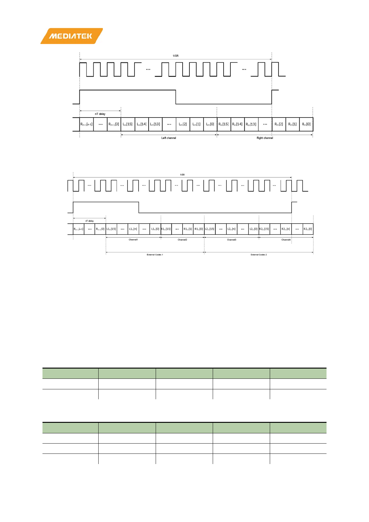
MT7686 Reference Manual
© 2016 - 2017 MediaTek Inc.
Page 152 of 536
This document contains information that is proprietary to MediaTek Inc. (“MediaTek”) and/or its licensor(s).
Any unauthorized use, reproduction or disclosure of this document in whole or in part is strictly prohibited.
I2S_BCLK
I2S_FS
I2S_TX/RX
Figure 10.3-3. Sample m of TDM32 with nT delay and bclk inverse
Keywords: I2S_BCLK, I2S_FS, I2S_TX/RX, R_, L_
I2S_BCLK
I2S_FS
I2S_TX/RX
Figure 10.3-4. Sample m of TDM64 with nT delay
Keywords: I2S_BCLK, I2S_FS, I2S_TX/RX, R_, L_
10.4. DL FIFO and UL FIFO
DL FIFO and UL FIFO are asynchronous FIFOs with depth 8. One side of these asynchronous FIFO is in BUS clock
domain and the other is in XPLL or I2S_BCLK clock domain.
10.5. Data format of FIFO
16bits I2S and 16bits TDM data format of FIFO are shown in Table 10.5-1 and Table 10.5-2.
Table 10.5-1. 16bits I2S data format of FIFO
Byte 3 Byte 2 Byte 1 Byte 0
Stereo R[15:8] R[7:0] L[15:8] L[7:0]
Mono 8’b0 8’b0 L[15:8] L[7:0]
Table 10.5-2. 16bits TDM 4 channel data format of FIFO
Byte 3 Byte 2 Byte 1 Byte 0
Channel 0 & 1 CH1[15:8] CH1 [7:0] CH0 [15:8] CH0[7:0]
Byte 7 Byte 6 Byte 5 Byte 4
Channel 2 & 3 CH3[15:8] CH3[7:0] CH2[15:8] CH2[7:0]

MT7686 Reference Manual
© 2016 - 2017 MediaTek Inc.
Page 153 of 536
This document contains information that is proprietary to MediaTek Inc. (“MediaTek”) and/or its licensor(s).
Any unauthorized use, reproduction or disclosure of this document in whole or in part is strictly prohibited.
10.6. Programming guide
I2S0 supports two I2S interface modes: 16bits I2S mode and 16bits TDM mode. Before I2S transfer, GPIO should be
set to related modes in the software, please refer to the GPIO section in this manual.
DMA should be turned on to prevent FIFO overflow. For the related DMA register map, please refer to the DMA
section in this manual. The I2S0 DMA programming guide for PSRAM data input is as follows:
1) To turn on the DMA clock:
• Write: PDN_CLRD0 = 0x1;
2) To set DMA CH7 for I2S_TX:
• Write: VDMA7_PGMADDR = 0x10000; //to set start address
• Write: VDMA7_COUNT = 0x9C4; //to set transfer threshold
• Write: VDMA7_FFSIZE = 0x9C4; //to set transfer length
• Write: VDMA7_CON = 0x10200; //[16]: to enable hardware hand shake, [9:8]: to set word size = 2, [4]: to
set DIR: 0=peripheral TX
3) To set DMA CH8 for I2S_RX:
• Write: VDMA8_PGMADDR = 0x10000; //to set start address
• Write: VDMA8_COUNT = 0x9C4; //to set transfer threshold
• Write: VDMA8_FFSIZE = 0x9C4; //to set transfer length
• Write: VDMA8_CON = 0x10210; //[16]: to enable hardware hand shake, [9:8]: to set word size = 2, [4]: to
set DIR: 1=peripheral RX
4) To start DMA transfer:
• Write: VDMA7_START = 0x8000;
• Write: VDMA8_START = 0x8000;
5) To use HD mode, please refer to Chapter 12, “I2S0 and I2S1 Audio PLL Settings” to enable XPLL.
10.6.1. I2S0 general programming guide
1) If XPLL is on, XPLL is 26MHz,
• Write: I2S_GLOBAL_CONTROL= 0x2A0C0028;
Or if XPLL is 24.576MHz,
• Write: I2S_GLOBAL_CONTROL= 0x000C0028;
Or if XPLL is 22.5792MHz,
• Write: I2S_GLOBAL_CONTROL= 0x150C0028;
Or if XO is 26MHz
• Write: I2S_GLOBAL_CONTROL= 0x2A080028;
2) If in slave mode,
• Write: I2S_GLOBAL_CONTROL[27:24]=0xF
• Write: I2S_GLOBAL_CONTROL[20]=1;
3) If in slave mode, BCLK is inverse to protocol,

MT7686 Reference Manual
© 2016 - 2017 MediaTek Inc.
Page 154 of 536
This document contains information that is proprietary to MediaTek Inc. (“MediaTek”) and/or its licensor(s).
Any unauthorized use, reproduction or disclosure of this document in whole or in part is strictly prohibited.
• Write: I2S_GLOBAL_CONTROL[19]=0
4) For data loopback test,
• Write: I2S_GLOBAL_CONTROL[31]=1
10.6.2. I2S mode
1) If in master mode,
• Write: I2S_DL_CONTROL=0x08008009;
• Write: I2S_UL_CONTROL=0x08008009;
Or
• Write: I2S_DL_CONTROL=0x0800800D;
• Write: I2S_UL_CONTROL=0x0800800D;
2) If in down rate mode,
• Write: I2S_UL_CONTROL[16]=1;
10.6.3. TDM mode
1) If in master mode,
For TDM64 channel 4,
• Write: I2S_DL_CONTROL=0x2800A021;
• Write: I2S_UL_CONTROL=0x2800A021;
• Write: I2S_DL_CONTROL[7]=1;
For TDM64 channel 2,
• Write: I2S_DL_CONTROL=0x0800A021;
• Write: I2S_UL_CONTROL=0x0800A021;
For TDM128 channel 4,
• Write: I2S_DL_CONTROL=0x2800C021;
• Write: I2S_UL_CONTROL=0x2800C021;
• Write: I2S_DL_CONTROL[7]=1;
For TDM128 channel 2,
• Write: I2S_DL_CONTROL=0x0800C021;
• Write: I2S_UL_CONTROL=0x0800C021;
For TDM32 channel 2,
• Write: I2S_DL_CONTROL=0x08008021;
• Write: I2S_UL_CONTROL=0x08008021;
Or if in slave mode,
For TDM64 channel 4,
• Write: I2S_DL_CONTROL=0x2800A025;

MT7686 Reference Manual
© 2016 - 2017 MediaTek Inc.
Page 155 of 536
This document contains information that is proprietary to MediaTek Inc. (“MediaTek”) and/or its licensor(s).
Any unauthorized use, reproduction or disclosure of this document in whole or in part is strictly prohibited.
• Write: I2S_UL_CONTROL=0x2800A025;
• Write: I2S_DL_CONTROL[7]=1;
For TDM64 channel 2,
• Write: I2S_DL_CONTROL=0x0800A025;
• Write: I2S_UL_CONTROL=0x0800A025;
For TDM128 channel 4,
• Write: I2S_DL_CONTROL=0x2800C025;
• Write: I2S_UL_CONTROL=0x2800C025;
• Write: I2S_DL_CONTROL[7]=1;
For TDM128 channel 2,
• Write: I2S_DL_CONTROL=0x0800C025;
• Write: I2S_UL_CONTROL=0x0800C025;
For TDM32 channel 2,
• Write: I2S_DL_CONTROL=0x08008025;
• Write: I2S_UL_CONTROL=0x08008025;
2) If MSB delays one clock cycle,
• Write: I2S_DL_CONTROL[23:17]= 0x2
• Write: I2S_UL_CONTROL[23:17]= 0x2
10.6.4. Set sample rate and enable I2S
1) To set sample rate:
• Write: I2S_DL_SR_EN_CONTROL__F_CR_I2S_OUT_SR = 0x0~0x1E; // bit[4]: HD mode
• Write: I2S_UL_SR_EN_CONTROL__F_CR_I2S_IN_SR = 0x0~0x1E; // bit[4]: HD mode
2) To enable clock,
• Write: PDN_CLRD0 = 0x80;
• Write: I2S_GLOBAL_EN_CONTROL__F_CR_PDN_AUD_26M = 0;
• Write: I2S_UL_SR_EN_CONTROL__F_CR_PDN_I2SIN = 0;
• Write: I2S_DL_SR_EN_CONTROL__F_CR_PDN_I2SO = 0;
3) To do soft reset before active,
• Write: I2S_SOFT_RESET = 0x1;
• Write: I2S_SOFT_RESET = 0x0;
4) To enable FIFO and I2S,
• Write: I2S_GLOBAL_EN_CONTROL__F_CR_UL_FIFO_EN = 1;
• Write: I2S_GLOBAL_EN_CONTROL__F_CR_DL_FIFO_EN = 1;
• Write: I2S_UL_SR_EN_CONTROL__F_CR_I2S_IN_EN = 1;
• Write: I2S_DL_SR_EN_CONTROL__F_CR_I2S_OUT_EN = 1;

MT7686 Reference Manual
© 2016 - 2017 MediaTek Inc.
Page 156 of 536
This document contains information that is proprietary to MediaTek Inc. (“MediaTek”) and/or its licensor(s).
Any unauthorized use, reproduction or disclosure of this document in whole or in part is strictly prohibited.
• Write: I2S_GLOBAL_EN_CONTROL__F_CR_ENABLE = 1;
5) To read RX data from FIFO,
• Read = ((UINT32P)(0xA1000100))
6) To write data to TX FIFO
• Write: ((UINT32P)(0xA1000000)) = write_data
10.7. Register mapping
Module name: I2S0 Base address: (+A0070000h)
Address Name Width
(bits) Register Function
A0070000
I2S_GLOBAL_CONTROL
32
AUDIO TOP CONTROL REGISTER
A0070004
I2S_DL_CONTROL
32
DL I2S CONTROL REGISTER
A0070008
I2S_UL_CONTROL
32
UL I2S CONTROL REGISTER
A007000C
I2S_SOFT_RESET
32
DLUL SOFT RESET REGISTER
A0070018
I2S_DL_FIFO_STATUS
32
DL FIFO CONTROL
STATUS REGISTER
A007001C
I2S_UL_FIFO_STATUS
32
UL FIFO CONTROL STATUS REGISTER
A0070030
I2S_GLOBAL_EN_CONTRO
L
32
AUDIO TOP ENABLE CONTROL REGISTER
A0070034
I2S_DL_SR_EN_CONTROL
32
DL I2S SAMPLE RATE ENABLE CONTROL
REGISTER
A0070038
I2S_UL_SR_EN_CONTROL
32
UL I2S SAMPLE RATE ENABLE CONTROL
REGISTER
A0070040
I2S_DL_INT_CONTROL
32
I2S DL INTERRUPT ENABLE CONTROL
REGISTER
A0070044
I2S_UL_INT_CONTROL
32
I2S UL INTERRUPT ENABLE CONTROL
REGISTER
A0070048
I2S_INT_ACK_CONTROL
32
I2S UL INTERRUPT ENABLE CONTROL
REGISTER
A0070000
I2S_GLOBAL_C
ONTROL
AUDIO TOP CONTROL REGISTER
00020028
Bit
31
30
29
28
27
26
25
24
23
22
21
20
19
18
17
16
Mne
CR_I2S_GLOBAL_CONTROL[31:16]
Type
RW
Reset
0
0
0
0
0
0
0
0
0
0
0
0
0
0
1
0
Bit
15
14
13
12
11
10
9
8
7
6
5
4
3
2
1
0
Mne
CR_I2S_GLOBAL_CONTROL[15:0]
Type
RW
Reset
0
0
0
0
0
0
0
0
0
0
1
0
1
0
0
0
Overview
Bit(s)
Mnemonic
Name
Description
31:0
CR_I2S_GLOBAL_C
ONTROL
CR_I2S_GLOBAL_CONTR
OL
[31] CR_I2S_LOOPBACK
I2S out to I2S in loopback
0: disable
1: enable
[29:28] CR_EXT_MCLK_SEL
00 : 24.576M
01 : 22.5792M

MT7686 Reference Manual
© 2016 - 2017 MediaTek Inc.
Page 157 of 536
This document contains information that is proprietary to MediaTek Inc. (“MediaTek”) and/or its licensor(s).
Any unauthorized use, reproduction or disclosure of this document in whole or in part is strictly prohibited.
10 : 26M (depend on 26M_SEL)
[27:26] CR_CK_OUT_SEL
I2S out clock source selection
00 : 24.576M
01 : 22.5792M
10 : 26M (depend on 26M_SEL)
11 : external bclk in (slave)
[25:24] CR_CK_IN_SEL
I2S in source selection
00 : 24.576M
01 : 22.5792M
10 : 26M (depend on 26M_SEL)
11 : external bclk in (slave)
[21] CR_EN_PSEL_CODEC
Reserved
[20] CR_NEG_CAP_EN
Negative edge capture RX data
0: disable
1: enable
[19] CR_MCLK_INV
MCLK clock inverse
0: disable
1: enable
[18] CR_CK_SEL
26M clock source selection
0 : XTAL 26M
1 : XPLL 26M
[17] CR_CODEC_26M_EN
cg of internal codec(default on)
[14:10] CR_DBG_SEL
Reserved
[9] CR_DL_MONO_DUP
When DL_MONO=1, if right channel send
duplicate data.
0: right channel send all 0.
1: right channel send the same data as the left.
[8] CR_DL_MONO
DL MONO mode
0: STEREO
1: MONO
[7] CR_DL_LRSW
DL with LR switch
0: LR no swap
1: LR swap
[6] CR_EXT_LRSW
External codec with LR switch
0: LR no swap
1: LR swap
[5] CR_EXT_MODE
External codec mode(slave)
0: internal codec
1: external codec
[4] CR_EXT_IO_CK
Clock source of external codec mode (slave)
0: from i2s_in
1: from i2s_out
[3] CR_ENGEN_EN
Engen enable (Reserved)
A0070004
I2S_DL_CONT
ROL
DL I2S
CONTROL REGISTER
00000008
Bit
31
30
29
28
27
26
25
24
23
22
21
20
19
18
17
16
Mne
CR_I2S_DL_CONTROL[31:16]
Type
RW
Reset
0
0
0
0
0
0
0
0
0
0
0
0
0
0
0
0

MT7686 Reference Manual
© 2016 - 2017 MediaTek Inc.
Page 158 of 536
This document contains information that is proprietary to MediaTek Inc. (“MediaTek”) and/or its licensor(s).
Any unauthorized use, reproduction or disclosure of this document in whole or in part is strictly prohibited.
Bit
15
14
13
12
11
10
9
8
7
6
5
4
3
2
1
0
Mne
CR_I2S_DL_CONTROL[15:0]
Type
RW
Reset
0
0
0
0
0
0
0
0
0
0
0
0
1
0
0
0
Ov
erview
Bit(s)
Mnemonic
Name
Description
31:0
CR_I2S_DL
_CONTROL
CR_I2S_DL_CONT
ROL
DL I2S control register
[31] LR_SWAP Swap the data of Right and Left channels
0: no swap
1: swap
[30:29] CH_PER_S Number of channels in each FS cycle (just used in
TDM mode)
00: 2 channels
01: 4 channels
[23:17] MSB_OFFSET Delay cycle from rising edge of FS to first
channel MSB
0 : 0 cycle
n : n cycles
[14:13] BIT_PER_S Number of bits in each FS cycle
00: 32 bits
01: 64 bits
10: 128 bits
[7] DL FIFO 2D EQ Mode
[5] WSINV WS reverse
0 : no reverse
1 : reverse
[4] DIR 0 : TX
[3] FMT Data Format
1 : I2S
0 : TDM
[2] SRC Master/Slave mode
0 : master
1 : slave
[1] WLEN Sample Size
0: 16bits
A0070008
I2S_UL_CONTR
OL
UL I2S CONTROL REGISTER
00000008
Bit
31
30
29
28
27
26
25
24
23
22
21
20
19
18
17
16
Mne
CR_I2S_UL_CONTROL[31:16]
Type
RW
Reset
0
0
0
0
0
0
0
0
0
0
0
0
0
0
0
0
Bit
15
14
13
12
11
10
9
8
7
6
5
4
3
2
1
0
Mne
CR_I2S_UL_CONTROL[15:0]
Type
RW
Reset
0
0
0
0
0
0
0
0
0
0
0
0
1
0
0
0
Overview
Bit(s)
Mnemonic
Name
Description
31:0
CR_I2S_UL
_CONTROL
CR_I2S_UL_CONT
ROL
UL I2S control register
[31] LR_SWAP Swap the data of Right and Left channels
0: no swap
1: swap
[30:29] CH_PER_S Number of channels in each FS cycle (just used in
TDM mode)
00: 2 channels
01: 4 channels
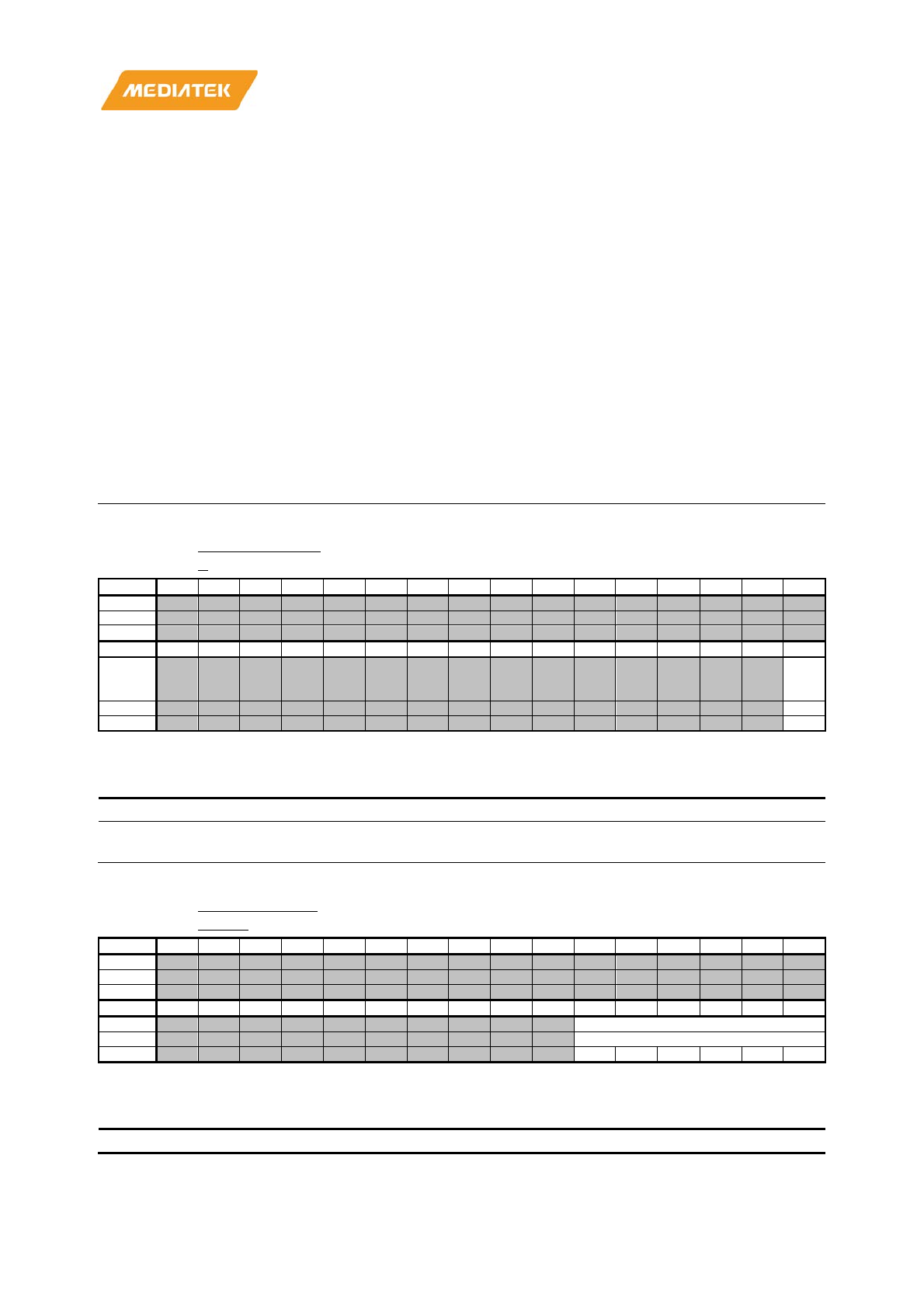
MT7686 Reference Manual
© 2016 - 2017 MediaTek Inc.
Page 159 of 536
This document contains information that is proprietary to MediaTek Inc. (“MediaTek”) and/or its licensor(s).
Any unauthorized use, reproduction or disclosure of this document in whole or in part is strictly prohibited.
[28:24] UPDATE_WORD Select duration to update FIFO data
[23:17] MSB_OFFSET Delay cycle from rising edge of FS to first
channel MSB
0 : 0 cycle
n : n cycles
[16] DOWN_RATE Real sample rate is 1/2 of SR
0: real sample rate = SR
1: drop 1 sample in each 2 input samples
[14:13] BIT_PER_S Number of bits in each FS cycle
00: 32 bits
01: 64 bits
10: 128 bits
[5] WSINV WS reverse
0 : no reverse
1 : reverse
[4] DIR 1 : RX
[3] FMT Data Format
1 : I2S
0 : TDM
[2] SRC Master/Slave mode
0 : master
1 : slave
[1] WLEN Sample Size
0: 16bits
A007000C
I2S_SOFT_RESE
T
DLUL SOFT RESET REGISTER
00000000
Bit
31
30
29
28
27
26
25
24
23
22
21
20
19
18
17
16
Name
Type
Reset
Bit
15
14
13
12
11
10
9
8
7
6
5
4
3
2
1
0
Name
CR_S
OFT_
RSTB
Type
RW
Reset
0
Overview
Bit(s)
Mnemonic
Name
Description
0
CR_SOFT_
RSTB
CR_SOFT_RSTB
soft reset audio_top and codec, active high.
To reset, please set this bit to 1 and then set 0.
A0070018
I2S_DL_FIFO_S
TATUS
DL FIFO CONTROL STATUS REGISTER
00000000
Bit
31
30
29
28
27
26
25
24
23
22
21
20
19
18
17
16
Name
Type
Reset
Bit
15
14
13
12
11
10
9
8
7
6
5
4
3
2
1
0
Name
CR_FIFO_DL_STATUS
Type
RO
Reset
0
0
0
0
0
0
Overview
Bit(s)
Mnemonic
Name
Description
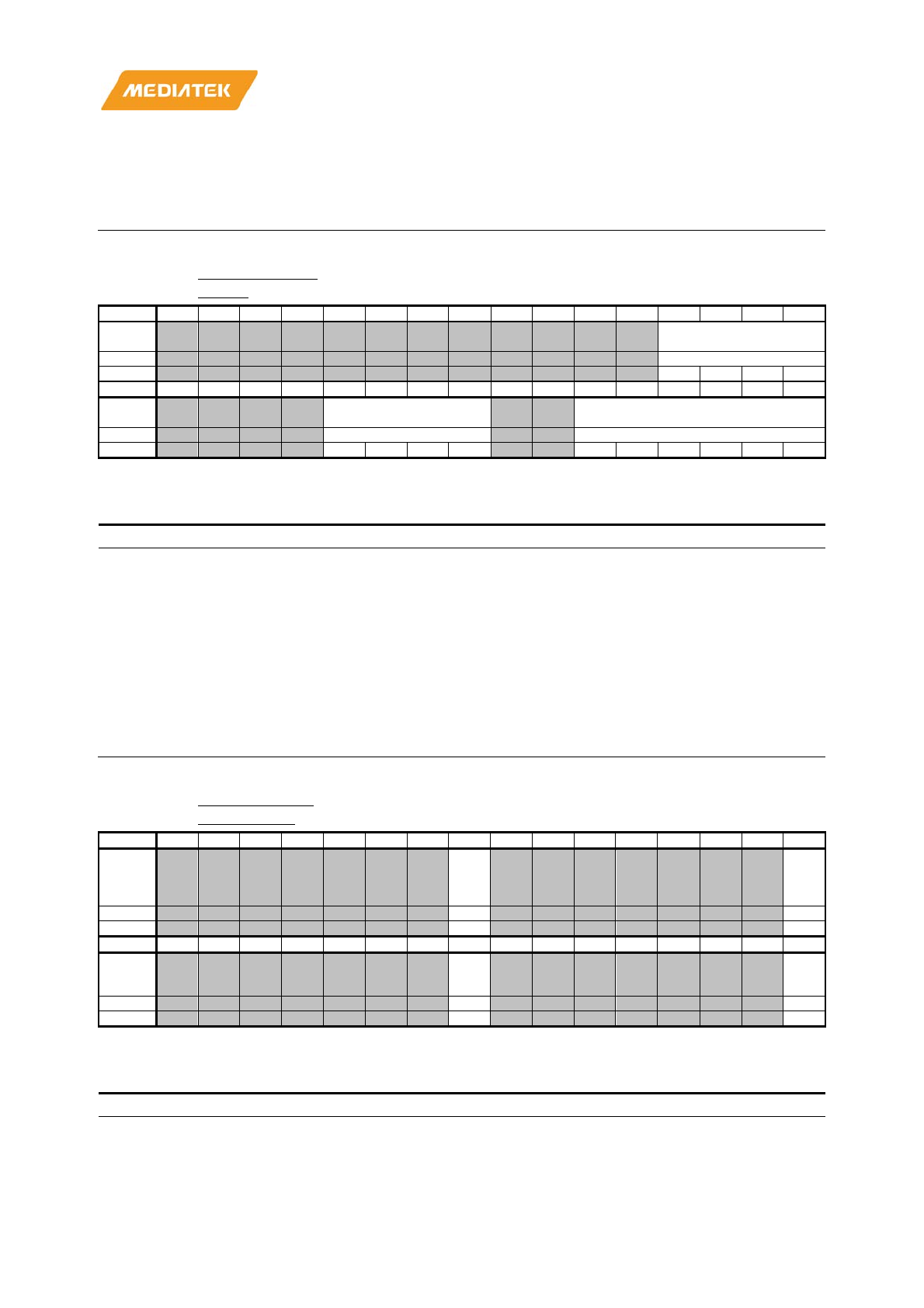
MT7686 Reference Manual
© 2016 - 2017 MediaTek Inc.
Page 160 of 536
This document contains information that is proprietary to MediaTek Inc. (“MediaTek”) and/or its licensor(s).
Any unauthorized use, reproduction or disclosure of this document in whole or in part is strictly prohibited.
5:0
CR_FIFO_
DL_STATU
S
CR_FIFO_DL_STA
TUS
[5] CR_FIFO_DL_W_READY
[4] CR_FIFO_DL_R_READY
[3] CR_FIFO_DL_FDLL
[2] CR_FIFO_DL_AFDLL
[1] CR_FIFO_DL_EMPTY
[0] CR_FIFO_DL_AEMPTY
A007001C
I2S_UL_FIFO_S
TATUS
UL FIFO CONTROL STATUS REGISTER
00000000
Bit
31
30
29
28
27
26
25
24
23
22
21
20
19
18
17
16
Name
CR_FIFO_UL_WFIFO_C
NT
Type
RO
Reset
0
0
0
0
Bit
15
14
13
12
11
10
9
8
7
6
5
4
3
2
1
0
Name
CR_FIFO_UL_RFIFO_C
NT
CR_FIFO_UL_STATUS
Type
RO
RO
Reset
0
0
0
0
0
0
0
0
0
0
Overvi
ew
Bit(s)
Mnemonic
Name
Description
19:16
CR_FIFO_
UL_WFIFO
_CNT
CR_FIFO_UL_WFI
FO_CNT
Reserved
11:8
CR_FIFO_
UL_RFIFO
_CNT
CR_FIFO_UL_RFIF
O_CNT
Reserved
5:0
CR_FIFO_
UL_STATU
S
CR_FIFO_UL_STA
TUS
[5] CR_FIFO_UL_W_READY
[4] CR_FIFO_UL_R_READY
[3] CR_FIFO_UL_FULL
[2] CR_FIFO_UL_AFULL
[1] CR_FIFO_UL_EMPTY
[0] CR_FIFO_UL_AEMPTY
A0070030
I2S_GLOBAL_E
N_CONTROL
AUDIO TOP ENABLE CONTROL REGISTER
01000000
Bit
31
30
29
28
27
26
25
24
23
22
21
20
19
18
17
16
Name
CR_P
DN_A
UD_2
6M
CR_U
L_FIF
O_EN
Type
RW
RW
Reset
1
0
Bit
15
14
13
12
11
10
9
8
7
6
5
4
3
2
1
0
Name
CR_D
L_FIF
O_EN
CR_E
NABL
E
Type
RW
RW
Reset
0
0
Overview
Bit(s)
Mnemonic
Name
Description
24
CR_PDN_A
UD_26M
CR_PDN_AUD_26
M
0: Normal
1: Power down
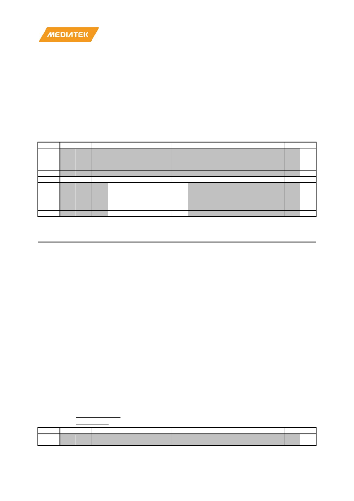
MT7686 Reference Manual
© 2016 - 2017 MediaTek Inc.
Page 161 of 536
This document contains information that is proprietary to MediaTek Inc. (“MediaTek”) and/or its licensor(s).
Any unauthorized use, reproduction or disclosure of this document in whole or in part is strictly prohibited.
16
CR_UL_FIF
O_EN
CR_UL_FIFO_EN
DL_FIFO enable
0: disable
1: enable
8
CR_DL_FIF
O_EN
CR_DL_FIFO_EN
DL_FIFO enable
0: disable
1: enable
0
CR_ENABL
E
CR_ENABLE
Audio top enable
0: disable
1: enable
A0070034
I2S_DL_SR_EN
_CONTROL
DL I2S SAMPLE RATE ENABLE CONTROL
REGISTER
00010000
Bit
31
30
29
28
27
26
25
24
23
22
21
20
19
18
17
16
Name
CR_P
DN_I
2SO
Type
RW
Reset
1
Bit
15
14
13
12
11
10
9
8
7
6
5
4
3
2
1
0
Name
CR_I2S_OUT_SR
CR_I
2S_O
UT_E
N
Type
RW
RW
Reset
0
0
0
0
0
0
Overview
Bit(s)
Mnemonic
Name
Description
16
CR_PDN_I
2SO
CR_PDN_I2SO
0: Normal
1: Power down
12:8
CR_I2S_O
UT_SR
CR_I2S_OUT_SR
[11:8]I2S mode select:
0000b: 8kHz
0001b: 11.025kHz
0010b: 12kHz
0100b: 16kHz
0101b: 22.05kHz
0110b: 24kHz
1000b: 32kHz
1001b: 44.1kHz
1010b: 48kHz
1011b: 88.2kHz
1100b: 96kHz
1101b: 176.4kHz
1110b: 192kHz
0011b: 384kHz
[12] hd_en
0: disable
1: enable
0
CR_I2S_O
UT_EN
CR_I2S_OUT_EN
I2S out enable
0: disable
1: enable
A0070038
I2S_UL_SR_EN
_CONTROL
UL I2S SAMPLE RATE ENABLE CONTROL
REGISTER
00010000
Bit
31
30
29
28
27
26
25
24
23
22
21
20
19
18
17
16
Name
CR_P
DN_I
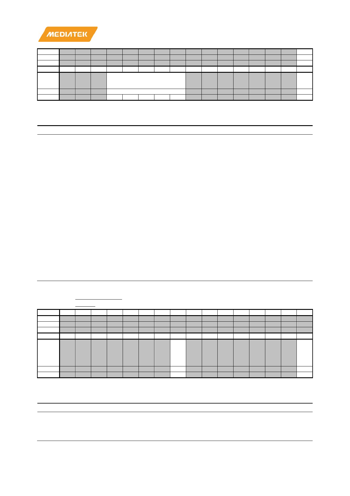
MT7686 Reference Manual
© 2016 - 2017 MediaTek Inc.
Page 162 of 536
This document contains information that is proprietary to MediaTek Inc. (“MediaTek”) and/or its licensor(s).
Any unauthorized use, reproduction or disclosure of this document in whole or in part is strictly prohibited.
2SIN
Type
RW
Reset
1
Bit
15
14
13
12
11
10
9
8
7
6
5
4
3
2
1
0
Name
CR_I2S_IN_SR
CR_I
2S_I
N_EN
Type
RW
RW
Reset
0
0
0
0
0
0
Overview
Bit(s)
Mnemonic
Name
Description
16
CR_PDN_I
2SIN
CR_PDN_I2SIN
0: Normal
1: Power down
12:8
CR_I2S_IN
_SR
CR_I2S_IN_SR
[11:8]I2S mode select:
0000b: 8kHz
0001b: 11.025kHz
0010b: 12kHz
0100b: 16kHz
0101b: 22.05kHz
0110b: 24kHz
1000b: 32kHz
1001b: 44.1kHz
1010b: 48kHz
1011b: 88.2kHz
1100b: 96kHz
1101b: 176.4kHz
1110b: 192kHz
0011b: 384kHz
[12] hd_en
0: disable
1: enable
0
CR_I2S_IN
_EN
CR_I2S_IN_EN
I2S out enable
0: disable
1: enable
A0070040
I2S_DL_INT_CO
NTROL
I2S DL INTERRUPT ENABLE CONTROL REGISTER
00000000
Bit
31
30
29
28
27
26
25
24
23
22
21
20
19
18
17
16
Name
Type
Reset
Bit
15
14
13
12
11
10
9
8
7
6
5
4
3
2
1
0
Name
CR_D
L_IN
TSTS
_INT
CR_D
L_CO
NTRL
_ITE
N
Type
RO
RW
Reset
0
0
Overview
Bit(s)
Mnemonic
Name
Description
8
CR_DL_IN
TSTS_INT
CR_DL_INTSTS_IN
T
0
CR_DL_CO
NTRL_ITE
CR_DL_CONTRL_I
TEN
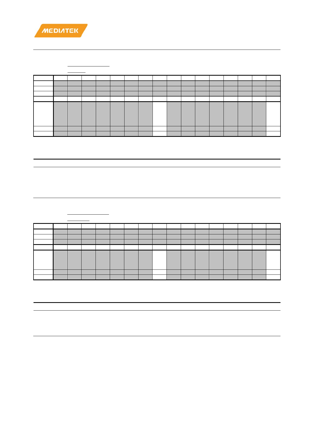
MT7686 Reference Manual
© 2016 - 2017 MediaTek Inc.
Page 163 of 536
This document contains information that is proprietary to MediaTek Inc. (“MediaTek”) and/or its licensor(s).
Any unauthorized use, reproduction or disclosure of this document in whole or in part is strictly prohibited.
N
A0070044
I2S_UL_INT_CO
NTROL
I2S UL INTERRUPT ENABLE CONTROL REGISTER
00000000
Bit
31
30
29
28
27
26
25
24
23
22
21
20
19
18
17
16
Name
Type
Reset
Bit
15
14
13
12
11
10
9
8
7
6
5
4
3
2
1
0
Name
CR_U
L_IN
TSTS
_INT
CR_U
L_CO
NTRL
_ITE
N
Type
RO
RW
Reset
0
0
Overview
Bit(s)
Mnemonic
Name
Description
8
CR_UL_IN
TSTS_INT
CR_UL_INTSTS_IN
T
0
CR_UL_CO
NTRL_ITE
N
CR_UL_CONTRL_I
TEN
A0070048
I2S_INT_ACK_C
ONTROL
I2S UL INTERRUPT ENABLE CONTROL REGISTER
00000000
Bit
31
30
29
28
27
26
25
24
23
22
21
20
19
18
17
16
Name
Type
Reset
Bit
15
14
13
12
11
10
9
8
7
6
5
4
3
2
1
0
Name
CR_D
L_AC
KINT
_ACK
CR_U
L_AC
KINT
_ACK
Type
RW
RW
Reset
0
0
Overview
Bit(s)
Mnemonic
Name
Description
8
CR_DL_AC
KINT_ACK
CR_DL_ACKINT_A
CK
0
CR_UL_AC
KINT_ACK
CR_UL_ACKINT_A
CK
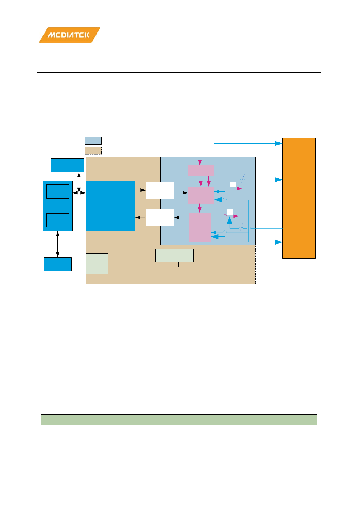
MT7686 Reference Manual
© 2016 - 2017 MediaTek Inc.
Page 164 of 536
This document contains information that is proprietary to MediaTek Inc. (“MediaTek”) and/or its licensor(s).
Any unauthorized use, reproduction or disclosure of this document in whole or in part is strictly prohibited.
11. I2S1
11.1. Overview
I2S1 is placed on AHB bus to support fast data transfers and has APB interface for setting the control register (CR).
I2S1 contains CLK CON, I2S OUT, I2S IN, DL FIFO and ULFIFO. The block diagram is shown in Figure 11.1-1.
DL FIFO
UL FIFO
DMA
Memory
Audio top CR
XO/XPLL/I2S_BCLK domain
PLL1/PLL2 domain
XPLL
CLK ON
I _
1
1
2S MCLK
I2S_TX
I2S_RX
I2S_FS
I2S_ BCLK
External
audio
codec
I2S OUT
I2S IN
APB
slave
audio_ahb_slave
(h2s bridge)
-Cortex M4
DMA
RX
2I S
I S2
DMA
TX
Figure 11.1-1. I2S block diagram
Keywords: Audio Codec, XPLL, CLKCON, I2S, AHB slave, DMA, UL DL FIFO, I2S1 CR, APB slave, XO (26M only), PLL1,
PLL2.
11.2. IO interface
• AHB slave interface (refer to AMBA v2.0)
• APB slave interface (refer to AMBA v3.0)
• Maximum internal delay of each interface is 13.3ns. Only supports 16bits per channel.
The I2S mode interface for master mode and slave mode is shown in Table 11.2-1 and Table 11.2-2.
Note, when using I2S RX master and the I2S_FS pin is at 176.4kHz or 192kHz, the output data delay of the relative
I2S TX slave codec should be shorter than 19ns.
Table 11.2-1. I2S mode interface – master mode
PIN name Direction Description
I2S_MCLK Output 26/24.576/22.5792MHz
I2S_BCLK Master : Output I2S_FS*32, I2S_FS*64

MT7686 Reference Manual
© 2016 - 2017 MediaTek Inc.
Page 165 of 536
This document contains information that is proprietary to MediaTek Inc. (“MediaTek”) and/or its licensor(s).
Any unauthorized use, reproduction or disclosure of this document in whole or in part is strictly prohibited.
PIN name Direction Description
I2S_FS Master : Output
11.025, 22.05, 44.1, 88.2, 176.4 kHz
8, 12, 16, 24, 32, 48, 96, 192 kHz
I2S_TX Output TX data
I2S_RX Input RX data
Table 11.2-2. I2S mode interface – slave mode
PIN name Direction Description
I2S_MCLK Output 26/24.576/22.5792MHz
I2S_BCLK Slave : Input I2S_FS*32, I2S_FS*64
I2S_FS Slave : Input
11.025, 22.05, 44.1, 88.2, 176.4 kHz
8, 12, 16, 24, 32, 48, 96, 192 kHz
I2S_TX Output TX data
I2S_RX Input RX data
Note, for master mode, I2S_MCLK frequencies only support relative sample rates listed in Table 11.2-3, I2S_MCLK
from 24.576 or 22.5792MHz is for high definition (HD) mode.
Table 11.2-3. Relationship between MCLK and sample rate
I2S_MCLK Sample Rate
26MHz (XO or XPLL) 8, 12, 16, 24, 32, 48 kHz
24.576MHz (XPLL) 8, 12, 16, 24, 32, 48, 96, 192 kHz
22.5792MHz (XPLL) 11.025, 22.05, 44.1, 88.2, 176.4 kHz
11.3. I2S OUT and I2S IN
I2S OUT & I2S IN support standard I2S protocol and both master/slave mode. The 16bits and 24bits I2S protocol is
shown in Figure 11.3-1.
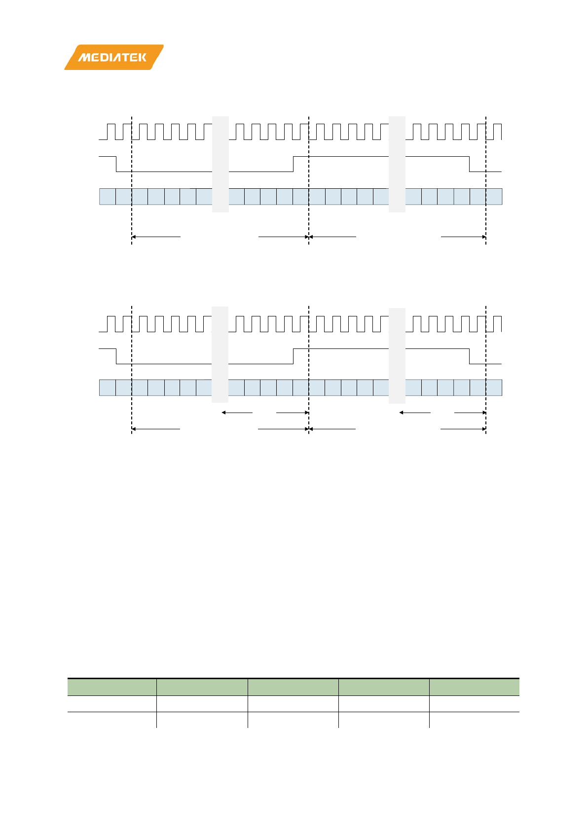
MT7686 Reference Manual
© 2016 - 2017 MediaTek Inc.
Page 166 of 536
This document contains information that is proprietary to MediaTek Inc. (“MediaTek”) and/or its licensor(s).
Any unauthorized use, reproduction or disclosure of this document in whole or in part is strictly prohibited.
I2S 16bit word length
BCK
LRCK
SDAT
BCK
LRCK
SDAT
I2S 24bit word length in 32bit channel length
Left channel data Right channel data
Left channel data Right channel data
S’b0
S’b0
MSB
MSB LSB MSB
LSB MSB
LSB
LSB
S’b0
015 43210 4321014 13 12 11 15 14 13 12 11 15
031 43210 4321030 29 28 27 31 30 29 28 27 31
Figure 11.3-1. I2S protocol waveform
Keywords: I2S_BCLK, I2S_FS, I2S_TX/RX
If the 16bits I2S OUT operates in mono mode, R[15:0] will be the same as L[15:0]. If I2S IN operates in mono mode,
R[15:0] will not affect I2S IN’s output to UL FIFO. Operation for 24bits I2S is also the same.
Note: When I2S acts as slave and connects to the external codec, I2S IN and I2S OUT will use the same BCLK/FS
from the external codec. Therefore, the sample rate of TX/RX should be the same.
11.4. DL FIFO and UL FIFO
DL FIFO & UL FIFO are asynchronous FIFO with depth 8. One side of these asynchronous FIFO is in BUS clock
domain and the other is in XPLL or I2S_BCLK clock domain.
11.5. Data format of FIFO
16bits I2S and 24bits I2S data format of FIFO are shown in Table 11.5-1 and Table 11.5-2.
Table 11.5-1. 16bits I2S data format of FIFO
Byte 3 Byte 2 Byte 1 Byte 0
Stereo R[15:8] R[7:0] L[15:8] L[7:0]
Mono 8’b0 8’b0 L[15:8] L[7:0]

MT7686 Reference Manual
© 2016 - 2017 MediaTek Inc.
Page 167 of 536
This document contains information that is proprietary to MediaTek Inc. (“MediaTek”) and/or its licensor(s).
Any unauthorized use, reproduction or disclosure of this document in whole or in part is strictly prohibited.
Table 11.5-2. 24bits I2S data format of FIFO
Byte 3 Byte 2 Byte 1 Byte 0
Left Channel L0[23:16] L0[15:8] L0[7:0] 8’b0
Byte 7 Byte 6 Byte 5 Byte 4
Right Channel R0[23:16] R0[15:8] R0[7:0] 8’b0
11.6. Programming guide
I2S1 supports two I2S interface modes: 16bits I2S Mode and 24bits I2S Mode. Before I2S transfer, GPIO should be
set to related modes in the software, please refer to the GPIO section in this manual.
DMA should be turned on to prevent FIFO overflow. For the related DMA register map, please refer to the DMA
section in this manual. The I2S1 DMA programming guide for PSRAM data input is as follows:
To turn on DMA clock:
• Write: PDN_CLRD0 = 0x1;
To set DMA CH7 for I2S_TX:
• Write: VDMA9_PGMADDR = 0x10000; //to set start address
• Write: VDMA9_COUNT = 0x9C4; //to set transfer threshold
• Write: VDMA9_FFSIZE = 0x9C4; //to set transfer length
• Write: VDMA9_CON = 0x10200; //[16]: to enable hardware hand shake, [9:8]: to set word size = 2, [4]: to
set DIR: 0=peripheral TX
To set DMA CH8 for I2S_RX:
• Write: VDMA10_PGMADDR = 0x10000; //to set start address
• Write: VDMA10_COUNT = 0x9C4; //to set transfer threshold
• Write: VDMA10_FFSIZE = 0x9C4; //to set transfer length
• Write: VDMA10_CON = 0x10210; //[16]: to enable hardware hand shake, [9:8]: to set word size = 2, [4]: to
set DIR: 1=peripheral RX
To start DMA transfer:
• Write: VDMA9_START = 0x8000;
• Write: VDMA10_START = 0x8000;
To use HD mode, please refer to Chapter 12, “I2S0 and I2S1 Audio PLL Settings” to enable XPLL.
11.6.1. I2S1 general programming guide
1) Select 26M source, if XPLL is on,
• Write: I2S1_GLOBAL_CONTROL= 0x40028;
2) Or XO is 26MHz
• Write: I2S1_GLOBAL_CONTROL= 0x00028;
3) For data loopback test,

MT7686 Reference Manual
© 2016 - 2017 MediaTek Inc.
Page 168 of 536
This document contains information that is proprietary to MediaTek Inc. (“MediaTek”) and/or its licensor(s).
Any unauthorized use, reproduction or disclosure of this document in whole or in part is strictly prohibited.
• Write: I2S1_GLOBAL_CONTROL[31]=1
4) Select MCLK source I2S1_GLOBAL_CONTROL[29:28]
• For 24.576MHz : 00
• 22.5792MHz : 01
• 26 MHz: 10
11.6.2. 16bits I2S mode
1) If in master mode,
• Write: I2S1_DL_CONTROL=0x20009;
• Write: I2S1_UL_CONTROL=0x28009;
Or
• Write: I2S1_DL_CONTROL=0x2000D;
• Write: I2S1_UL_CONTROL=0x2800D;
11.6.3. 24bits I2S mode
1) If in master mode,
• Write: I2S1_DL_CONTROL=0x6008B;
• Write: I2S1_UL_CONTROL=0x6800B;
Or
• Write: I2S1_DL_CONTROL=0x6008F;
• Write: I2S1_UL_CONTROL=0x6800F;
11.6.4. Set sample rate and enable I2S
To set sample rate:
• Write: I2S1_DL_SR_EN_CONTROL__F_CR_I2S1_OUT_SR = 0x0~0x1E; // bit[4]: HD mode
• Write: I2S1_UL_SR_EN_CONTROL__F_CR_I2S1_IN_SR = 0x0~0x1E; // bit[4]: HD mode
To enable clock,
• Write: PDN_CLRD0 = 0x10;
• Write: I2S1_GLOBAL_EN_CONTROL__F_CR_PDN_AUD_26M = 0;
• Write: I2S1_UL_SR_EN_CONTROL__F_CR_PDN_I2SIN1 = 0;
• Write: I2S1_DL_SR_EN_CONTROL__F_CR_PDN_I2SO1= 0;
To do soft reset before active,
• Write: I2S1_SOFT_RESET = 0x1;
• Write: I2S1_SOFT_RESET = 0x0;
To enable FIFO and I2S,
• Write: I2S1_GLOBAL_EN_CONTROL__F_CR_I2S1_UL_FIFO_EN = 1;
MT7686 Reference Manual
© 2016 - 2017 MediaTek Inc.
Page 169 of 536
This document contains information that is proprietary to MediaTek Inc. (“MediaTek”) and/or its licensor(s).
Any unauthorized use, reproduction or disclosure of this document in whole or in part is strictly prohibited.
• Write: I2S1_GLOBAL_EN_CONTROL__F_CR_I2S1_DL_FIFO_EN = 1;
• Write: I2S1_UL_SR_EN_CONTROL__F_CR_I2S1_IN_EN = 1;
• Write: I2S1_DL_SR_EN_CONTROL__F_CR_I2S1_OUT_EN = 1;
• Write: I2S1_GLOBAL_EN_CONTROL__F_CR_I2S1_ENABLE = 1;
To read RX data from FIFO,
• Read = ((UINT32P)(0xA1000300))
To write data to TX FIFO,
• Write: ((UINT32P)(0xA1000200)) = write_data
11.7. Register mapping
Module name: I2S1 Base address: (+A0080000h)
Address
Name
Width
(bits)
Register Function
A0080000
I2S1_GLOBAL_C
ONTROL
32
AUDIO TOP CONTROL REGISTER
A0080004 I2S1_DL_CONTR
OL
32
DL I2S CONTROL REGISTER
A0080008
I2S1_UL_CONTR
OL
32
UL I2S CONTROL REGISTER
000
A008000C I2S1_SOFT_RESE
T
32
DLUL SOFT RESET REGISTER
A0080010
I2S1_DL_FIFO
32
DL FIFO CONTROL REGISTER
A0080014 I2S1_UL_FIFO
32
UL FIFO CONTROL REGISTER
A0080018
I2S1_DL_FIFO_S
TATUS
32
DL FIFO CONTROL STATUS REGISTER
A008001C I2S1_UL_FIFO_S
TATUS
32
UL FIFO CONTROL STATUS REGISTER
A0080020
I2S1_SCAN_RSV
32
SCAN RESERVED REGISTER
A0080030 I2S1_GLOBAL_E
N_CONTROL
32
AUDIO TOP ENABLE CONTROL REGISTER
A0080034
I2S1_DL_SR_EN
_CONTROL
32
DL I2S SAMPLE RATE ENABLE CONTROL REGISTER
A0080038 I2S1_UL_SR_EN
_CONTROL
32
UL I2S SAMPLE RATE ENABLE CONTROL REGISTER
A008003C
I2S_MONITOR
32
I2S_MONITOR
A0080040 I2S1_DL_INT_CO
NTROL
32
I2S DL INTERRUPT ENABLE CONTROL REGISTER
A0080044
I2S1_UL_INT_CO
NTROL
32
I2S UL INTERRUPT ENABLE CONTROL REGISTER
A0080048 I2S1_INT_ACK_C
ONTROL
32
I2S UL INTERRUPT ENABLE CONTROL REGISTER
A008000
0 I2S1_GLOBA
L_CONTROL AUDIO TOP CONTROL REGISTER 00020028
Bit
31
30
29
28
27
26
25
24
23
22
21
20
19
18
17
16
Mne
CR_I2S1_GLOBAL_CONTROL[31:16]
Type
RW

MT7686 Reference Manual
© 2016 - 2017 MediaTek Inc.
Page 170 of 536
This document contains information that is proprietary to MediaTek Inc. (“MediaTek”) and/or its licensor(s).
Any unauthorized use, reproduction or disclosure of this document in whole or in part is strictly prohibited.
A008000
0 I2S1_GLOBA
L_CONTROL AUDIO TOP CONTROL REGISTER 00020028
Reset
0
0
0
0
0
0
0
0
0
0
0
0
0
0
1
0
Bit
15
14
13
12
11
10
9
8
7
6
5
4
3
2
1
0
Mne
CR_I2S1_GLOBAL_CONTROL[15:0]
Type
RW
Reset
0
0
0
0
0
0
0
0
0
0
1
0
1
0
0
0
Overview
Bit(s)
Mnemonic
Name
Description
31:0
CR_I2S1_G
LOBAL_CO
NTROL
CR_I2S1_GLOBAL_
CONTROL
[31] CR_I2S_LOOPBACK_DAT
I2S out to I2S in data loopback
0: disable
1: enable
[29:28] CR_EXT_MCLK_SEL
00b : 24.576MHz
01b : 22.5792MHz
10b : 26MHz
[27] CR_I2S_LOOPBACK
I2S in/out clk, ws loopback
0: disable
1: enable
[18] CR_CK_SEL
26M clock source selection
0 : XTAL 26M
1 : XPLL 26M
[17] CR_CODEC_26M_EN
cg of internal codec (default on)
[14:10] CR_DBG_SEL
[9] CR_DL_MONO_DUP
When DL_MONO=1, if right channel sends duplicate data.
0: right channel sends all 0.
1: right channel sends the same data as the left.
[8] CR_DL_MONO
DL MONO mode
0: STEREO
1: MONO
[5] CR_EXT_MODE
External codec mode (slave)
0: internal codec
1: external codec
[4] CR_EXT_IO_CK
Clock source of external codec mode (slave)
0: from i2s_in
1: from i2s_out
[3] CR_ENGEN_EN
Engen enable (reserved)
A008000
4
I2S1_DL_CO
NTROL DL I2S CONTROL REGISTER 00000000
Bit
31
30
29
28
27
26
25
24
23
22
21
20
19
18
17
16
Mne
CR_I2S1_DL_CONTROL[31:16]
Type
RW
Reset
0
0
0
0
0
0
0
0
0
0
0
0
0
0
0
0
Bit
15
14
13
12
11
10
9
8
7
6
5
4
3
2
1
0
Mne
CR_I2S1_DL_CONTROL[15:0]
Type
RW
MT7686 Reference Manual
© 2016 - 2017 MediaTek Inc.
Page 171 of 536
This document contains information that is proprietary to MediaTek Inc. (“MediaTek”) and/or its licensor(s).
Any unauthorized use, reproduction or disclosure of this document in whole or in part is strictly prohibited.
A008000
4
I2S1_DL_CO
NTROL DL I2S CONTROL REGISTER 00000000
Reset
0
0
0
0
0
0
0
0
0
0
0
0
0
0
0
0
Overview
Bit(s) Mnemoni
c Name Description
31:0
CR_I2S1_
DL_CON
TROL
CR_I2S1_DL_CO
NTROL
[30] I2S_soft_reset
[27] i2s_in_ck_inv
[26] i2s_in_ws_inv
[18] i2s out 24bits FIFO mode
[17] i2s in out couple mode
[7] DL FIFO 2D EQ Mode
[5] I2S ws invert
[3] I2S FMT
0: EIAJ
1: I2S
[2] I2S slave mode sel
0: master mode
1: slave mode
[1] I2S WLEN
0: 16 bits
1: 32 bits
A008000
8
I2S1_UL_CO
NTROL UL I2S CONTROL REGISTER 00000008
Bit
31
30
29
28
27
26
25
24
23
22
21
20
19
18
17
16
Mne
CR_I2S1_UL_CONTROL[31:16]
Type
RW
Reset
0
0
0
0
0
0
0
0
0
0
0
0
0
0
0
0
Bit
15
14
13
12
11
10
9
8
7
6
5
4
3
2
1
0
Mne
CR_I2S1_UL_CONTROL[15:0]
Type
RW
Reset
0
0
0
0
0
0
0
0
0
0
0
0
1
0
0
0
Overview 000
Bit(s)
Mnemonic
Name
Description
31:0
CR_I2S1_U
L_CONTRO
L
CR_I2S1_UL_CONT
ROL
[30] I2S_soft_reset
[27] i2s_in_ck_inv
[26] i2s_in_ws_inv
[18] i2s in 24bits FIFO mode
[17] i2s in out couple mode
[15] low fill zero (when the lrck 32 cycle number and the 24/16 bit is
valid, the low 16/24bit is zero)
0:high bit fill zero (32)
1:low bit fill zero (32)
[5] I2S ws invert
[3] I2S FMT
0: EIAJ (right adjust)
1: I2S
[2] I2S slave mode select
0: master mode
1: slave mode
[1] I2S WLEN
0: 16 bits
1: 32 bits
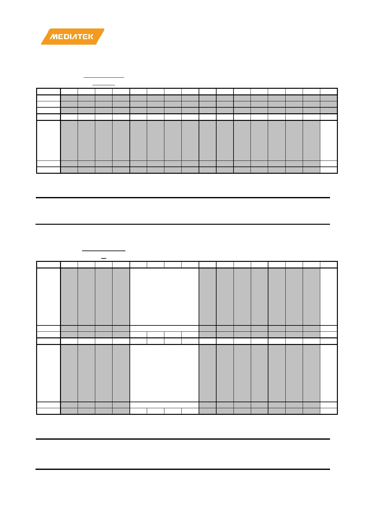
MT7686 Reference Manual
© 2016 - 2017 MediaTek Inc.
Page 172 of 536
This document contains information that is proprietary to MediaTek Inc. (“MediaTek”) and/or its licensor(s).
Any unauthorized use, reproduction or disclosure of this document in whole or in part is strictly prohibited.
A008000
C
I2S1_SOFT_
RESET DLUL SOFT RESET REGISTER 00000000
Bit
31
30
29
28
27
26
25
24
23
22
21
20
19
18
17
16
Name
Type
Reset
Bit
15
14
13
12
11
10
9
8
7
6
5
4
3
2
1
0
Name
CR
_I2
S1_
SO
FT_
RS
TB
Type
RW
Reset
0
Overview
Bit(s)
Mnemonic
Name
Description
0
CR_I2S1_S
OFT_RSTB
CR_I2S1_SOFT_RS
TB
soft reset audio_top and codec, active high.
To reset, please write this bit to 1 and then write 0.
A0080010 I2S1_DL_FIF
O DL FIFO CONTROL REGISTER 00000000
Bit
31
30
29
28
27
26
25
24
23
22
21
20
19
18
17
16
Name CR_I2S1_FIFO_DL_W
_THRESHOLD
CR
_I2
S1_
FIF
O_
DL
_W
CL
EA
R
Type
RW
RW
Reset
0
0
0
0
0
Bit
15
14
13
12
11
10
9
8
7
6
5
4
3
2
1
0
Name CR_I2S1_FIFO_DL_R_
THRESHOLD
CR
_I2
S1_
FIF
O_
DL
_R
CL
EA
R
Type
RW
RW
Reset
0
0
0
0
0
Overview
Bit(s)
Mnemonic
Name
Description
27:24
CR_I2S1_F
IFO_DL_W
_THRESHO
CR_I2S1_FIFO_DL
_W_THRESHOLD
Reserved
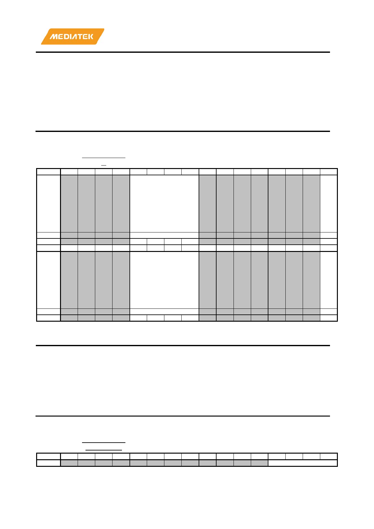
MT7686 Reference Manual
© 2016 - 2017 MediaTek Inc.
Page 173 of 536
This document contains information that is proprietary to MediaTek Inc. (“MediaTek”) and/or its licensor(s).
Any unauthorized use, reproduction or disclosure of this document in whole or in part is strictly prohibited.
LD
16
CR_I2S1_F
IFO_DL_W
CLEAR
CR_I2S1_FIFO_DL
_WCLEAR
Reserved
11:8
CR_I2S1_F
IFO_DL_R
_THRESHO
LD
CR_I2S1_FIFO_DL
_R_THRESHOLD
Reserved
0
CR_I2S1_F
IFO_DL_R
CLEAR
CR_I2S1_FIFO_DL
_RCLEAR
Reserved
A0080014 I2S1_UL_FIF
O UL FIFO CONTROL REGISTER 00000000
Bit
31
30
29
28
27
26
25
24
23
22
21
20
19
18
17
16
Name CR_I2S1_FIFO_UL_W
_THRESHOLD
CR
_I2
S1_
FIF
O_
UL
_W
CL
EA
R
Type
RW
RW
Reset
0
0
0
0
0
Bit
15
14
13
12
11
10
9
8
7
6
5
4
3
2
1
0
Name CR_I2S1_FIFO_UL_R_
THRESHOLD
CR
_I2
S1_
FIF
O_
UL
_R
CL
EA
R
Type
RW
RW
Reset
0
0
0
0
0
Overview
Bit(s)
Mnemonic
Name
Description
27:24
CR_I2S1_FIFO_UL_W_T
HRESHOLD
CR_I2S1_FIFO_UL_W_THRESHOLD
Reserved
16
CR_I2S1_FIFO_UL_WCL
EAR
CR_I2S1_FIFO_UL_WCLEAR
Reserved
11:8
CR_I2S1_FIFO_UL_R_T
HRESHOLD
CR_I2S1_FIFO_UL_R_THRESHOLD
Reserved
0
CR_I2S1_FIFO_UL_RCL
EAR
CR_I2S1_FIFO_UL_RCLEAR
Reserved
A0080018 I2S1_DL_FIF
O_STATUS DL FIFO CONTROL STATUS REGISTER 00000000
Bit
31
30
29
28
27
26
25
24
23
22
21
20
19
18
17
16
Name
CR_I2S1_FIFO_DL_W
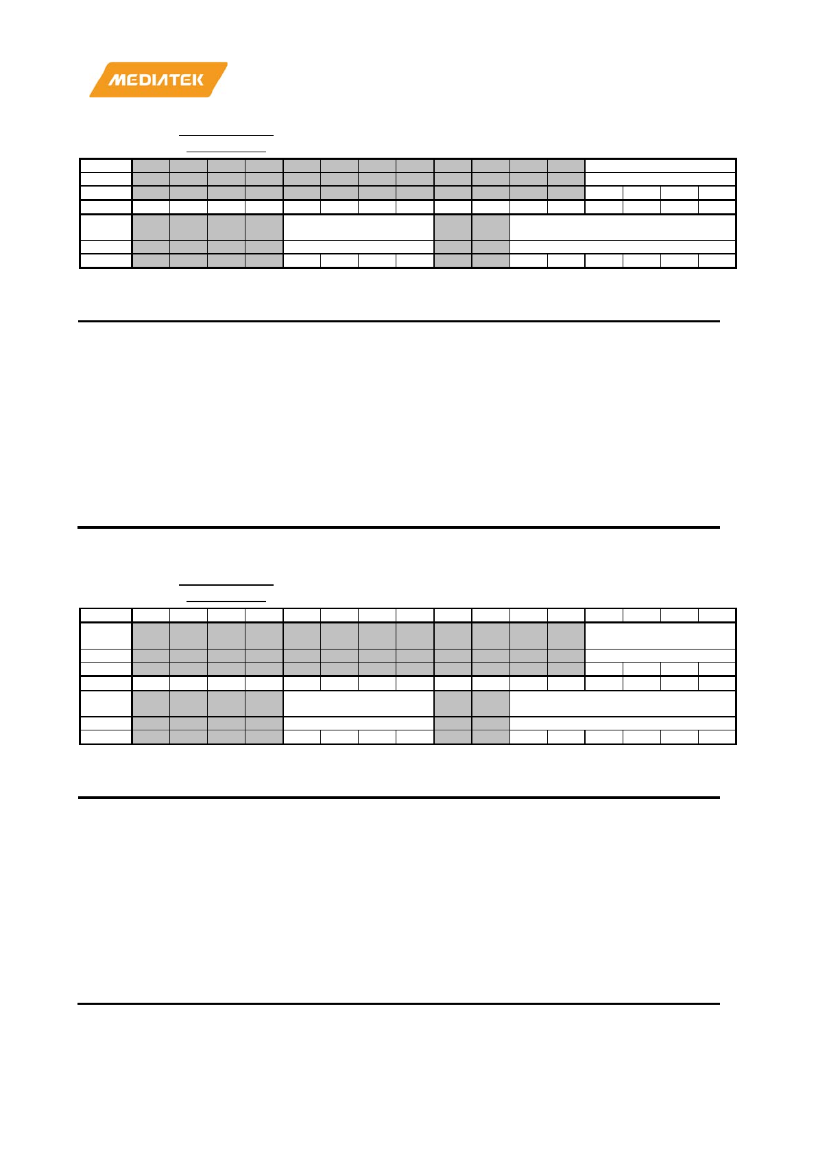
MT7686 Reference Manual
© 2016 - 2017 MediaTek Inc.
Page 174 of 536
This document contains information that is proprietary to MediaTek Inc. (“MediaTek”) and/or its licensor(s).
Any unauthorized use, reproduction or disclosure of this document in whole or in part is strictly prohibited.
A0080018 I2S1_DL_FIF
O_STATUS DL FIFO CONTROL STATUS REGISTER 00000000
FIFO_CNT
Type
RO
Reset
0
0
0
0
Bit
15
14
13
12
11
10
9
8
7
6
5
4
3
2
1
0
Name
CR_I2S1_FIFO_DL_RF
IFO_CNT
CR_I2S1_FIFO_DL_STATUS
Type
RO
RO
Reset
0
0
0
0
0
0
0
0
0
0
Overview
Bit(s)
Mnemonic
Name
Description
19:16
CR_I2S1_F
IFO_DL_W
FIFO_CNT
CR_I2S1_FIFO_DL
_WFIFO_CNT
Reserved
11:8
CR_I2S1_F
IFO_DL_R
FIFO_CNT
CR_I2S1_FIFO_DL
_RFIFO_CNT
Reserved
5:0
CR_I2S1_F
IFO_DL_ST
ATUS
CR_I2S1_FIFO_DL
_STATUS
[5] CR_FIFO_DL_W_READY
[4] CR_FIFO_DL_R_READY
[3] CR_FIFO_DL_FDLL
[2] CR_FIFO_DL_AFDLL
[1] CR_FIFO_DL_EMPTY
[0] CR_FIFO_DL_AEMPTY
A008001C I2S1_UL_FIF
O_STATUS UL FIFO CONTROL STATUS REGISTER 00000000
Bit
31
30
29
28
27
26
25
24
23
22
21
20
19
18
17
16
Name
CR_I2S1_FIFO_UL_W
FIFO_CNT
Type
RO
Reset
0
0
0
0
Bit
15
14
13
12
11
10
9
8
7
6
5
4
3
2
1
0
Name
CR_I2S1_FIFO_UL_RF
IFO_CNT
CR_I2S1_FIFO_UL_STATUS
Type
RO
RO
Reset
0
0
0
0
0
0
0
0
0
0
Overview
Bit(s)
Mnemonic
Name
Description
19:16
CR_I2S1_F
IFO_UL_W
FIFO_CNT
CR_I2S1_FIFO_UL
_WFIFO_CNT
Reserved
11:8
CR_I2S1_F
IFO_UL_R
FIFO_CNT
CR_I2S1_FIFO_UL
_RFIFO_CNT
Reserved
5:0
CR_I2S1_F
IFO_UL_ST
ATUS
CR_I2S1_FIFO_UL
_STATUS
[5] CR_FIFO_UL_W_READY
[4] CR_FIFO_UL_R_READY
[3] CR_FIFO_UL_FULL
[2] CR_FIFO_UL_AFULL
[1] CR_FIFO_UL_EMPTY
[0] CR_FIFO_UL_AEMPTY
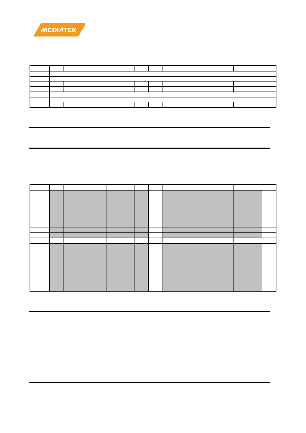
MT7686 Reference Manual
© 2016 - 2017 MediaTek Inc.
Page 175 of 536
This document contains information that is proprietary to MediaTek Inc. (“MediaTek”) and/or its licensor(s).
Any unauthorized use, reproduction or disclosure of this document in whole or in part is strictly prohibited.
A008002
0
I2S1_SCAN_
RSV SCAN RESERVED REGISTER 00000000
Bit
31
30
29
28
27
26
25
24
23
22
21
20
19
18
17
16
Name
CR_I2S1_RESERVED[31:16]
Type
RW
Reset
0
0
0
0
0
0
0
0
0
0
0
0
0
0
0
0
Bit
15
14
13
12
11
10
9
8
7
6
5
4
3
2
1
0
Name
CR_I2S1_RESERVED[15:0]
Type
RW
Reset
0
0
0
0
0
0
0
0
0
0
0
0
0
0
0
0
Overview
Bit(s)
Mnemonic
Name
Description
31:0
CR_I2S1_R
ESERVED
CR_I2S1_RESERVE
D
Reserved
A008003
0
I2S1_GLOBA
L_EN_CONT
ROL
AUDIO TOP ENABLE CONTROL REGISTER 01000000
Bit
31
30
29
28
27
26
25
24
23
22
21
20
19
18
17
16
Name
CR
_P
DN
_A
UD
_26
M
CR
_I2
S1_
UL
_FI
FO
_E
N
Type
RW
RW
Reset
1
0
Bit
15
14
13
12
11
10
9
8
7
6
5
4
3
2
1
0
Name
CR
_I2
S1_
DL
_FI
FO
_E
N
CR
_I2
S1_
EN
AB
LE
Type
RW
RW
Reset
0
0
Overview
Bit(s)
Mnemonic
Name
Description
24
CR_PDN_AUD_26M
CR_PDN_AUD_26M
0: Normal
1: Power down
16
CR_I2S1_UL_FIFO_EN
CR_I2S1_UL_FIFO_EN
UL_FIFO enable
0: disable
1: enable
8
CR_I2S1_DL_FIFO_EN
CR_I2S1_DL_FIFO_EN
DL_FIFO enable
0: disable
1: enable
0
CR_I2S1_ENABLE
CR_I2S1_ENABLE
Audio top enable
0: disable
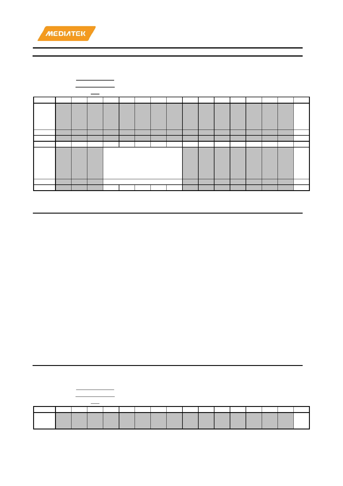
MT7686 Reference Manual
© 2016 - 2017 MediaTek Inc.
Page 176 of 536
This document contains information that is proprietary to MediaTek Inc. (“MediaTek”) and/or its licensor(s).
Any unauthorized use, reproduction or disclosure of this document in whole or in part is strictly prohibited.
1: enable
A008003
4
I2S1_DL_SR
_EN_CONTR
OL
DL I2S SAMPLE RATE ENABLE CONTROL
REGISTER 00010000
Bit
31
30
29
28
27
26
25
24
23
22
21
20
19
18
17
16
Name
CR
_P
DN
_I2
SO1
Type
RW
Reset
1
Bit
15
14
13
12
11
10
9
8
7
6
5
4
3
2
1
0
Name CR_I2S1_OUT_SR
CR
_I2
S1_
OU
T_
EN
Type
RW
RW
Reset
0
0
0
0
0
0
Overview
Bit(s)
Mnemonic
Name
Description
16
CR_PDN_I
2SO1
CR_PDN_I2SO1
0: Normal
1: Power down
12:8
CR_I2S1_O
UT_SR
CR_I2S1_OUT_SR
[11:8]I2S mode select:
0000b: 8kHz
0001b: 11.025kHz
0010b: 12kHz
0100b: 16kHz
0101b: 22.05kHz
0110b: 24kHz
1000b: 32kHz
1001b: 44.1kHz
1010b: 48kHz
1011b: 88.2kHz
1100b: 96kHz
1101b: 176.4kHz
1110b: 192kHz
[12] hd_en
0: disable
1: enable
0
CR_I2S1_O
UT_EN
CR_I2S1_OUT_EN
I2S out enable
0: disable
1: enable
A008003
8
I2S1_UL_SR
_EN_CONTR
OL
UL I2S SAMPLE RATE ENABLE CONTROL
REGISTER 00010000
Bit
31
30
29
28
27
26
25
24
23
22
21
20
19
18
17
16
Name
CR
_P
DN
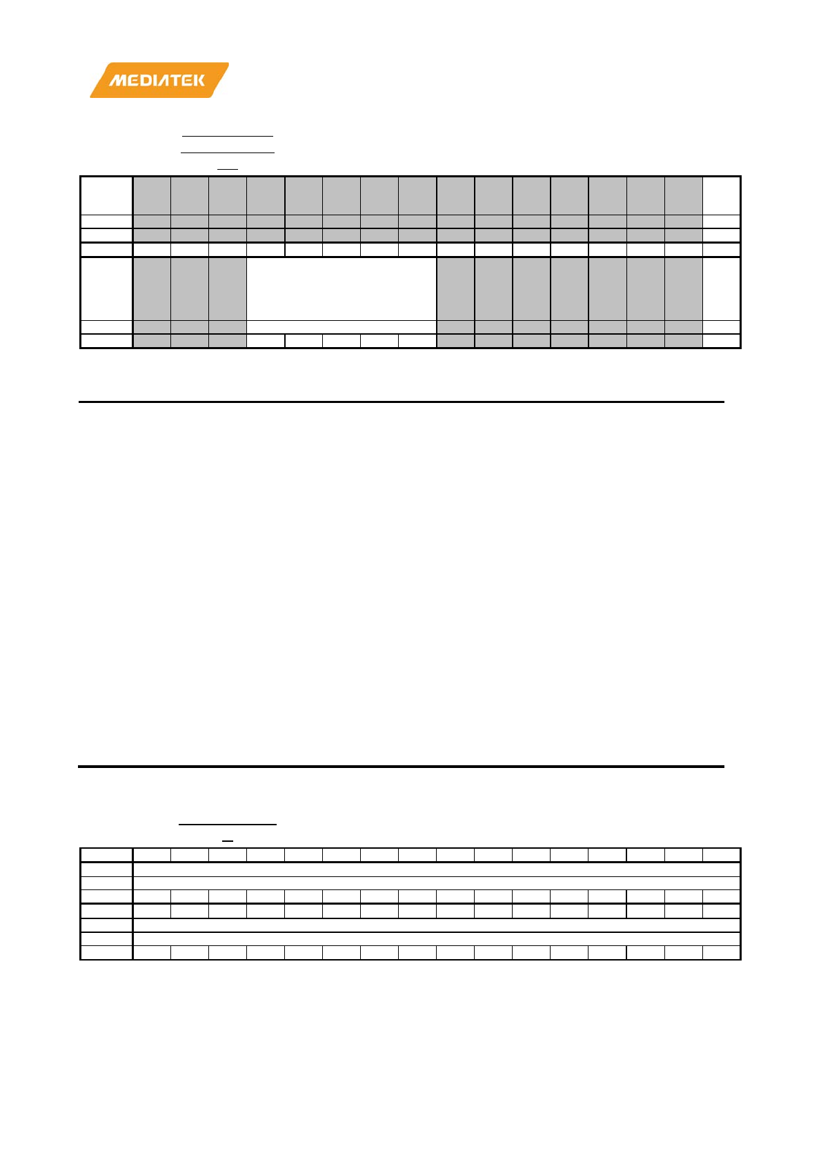
MT7686 Reference Manual
© 2016 - 2017 MediaTek Inc.
Page 177 of 536
This document contains information that is proprietary to MediaTek Inc. (“MediaTek”) and/or its licensor(s).
Any unauthorized use, reproduction or disclosure of this document in whole or in part is strictly prohibited.
A008003
8
I2S1_UL_SR
_EN_CONTR
OL
UL I2S SAMPLE RATE ENABLE CONTROL
REGISTER 00010000
_I2
SIN
1
Type
RW
Reset
1
Bit
15
14
13
12
11
10
9
8
7
6
5
4
3
2
1
0
Name CR_I2S1_IN_SR
CR
_I2
S1_
IN_
EN
Type
RW
RW
Reset
0
0
0
0
0
0
Overview
Bit(s)
Mnemonic
Name
Description
16
CR_PDN_I
2SIN1
CR_PDN_I2SIN1
0: Normal
1: Power down
12:8
CR_I2S1_I
N_SR
CR_I2S1_IN_SR
[11:8]I2S mode select:
0000b: 8kHz
0001b: 11.025kHz
0010b: 12kHz
0100b: 16kHz
0101b: 22.05kHz
0110b: 24kHz
1000b: 32kHz
1001b: 44.1kHz
1010b: 48kHz
1011b: 88.2kHz
1100b: 96kHz
1101b: 176.4kHz
1110b: 192kHz
[12] hd_en
0: disable
1: enable
0
CR_I2S1_I
N_EN
CR_I2S1_IN_EN
I2S out enable
0: disable
1: enable
A008003
C
I2S_MONITO
R I2S_MONITOR 00000000
Bit
31
30
29
28
27
26
25
24
23
22
21
20
19
18
17
16
Name
CR_I2S_MONITOR[31:16]
Type
RO
Reset
0
0
0
0
0
0
0
0
0
0
0
0
0
0
0
0
Bit
15
14
13
12
11
10
9
8
7
6
5
4
3
2
1
0
Name
CR_I2S_MONITOR[15:0]
Type
RO
Reset
0
0
0
0
0
0
0
0
0
0
0
0
0
0
0
0
Overview
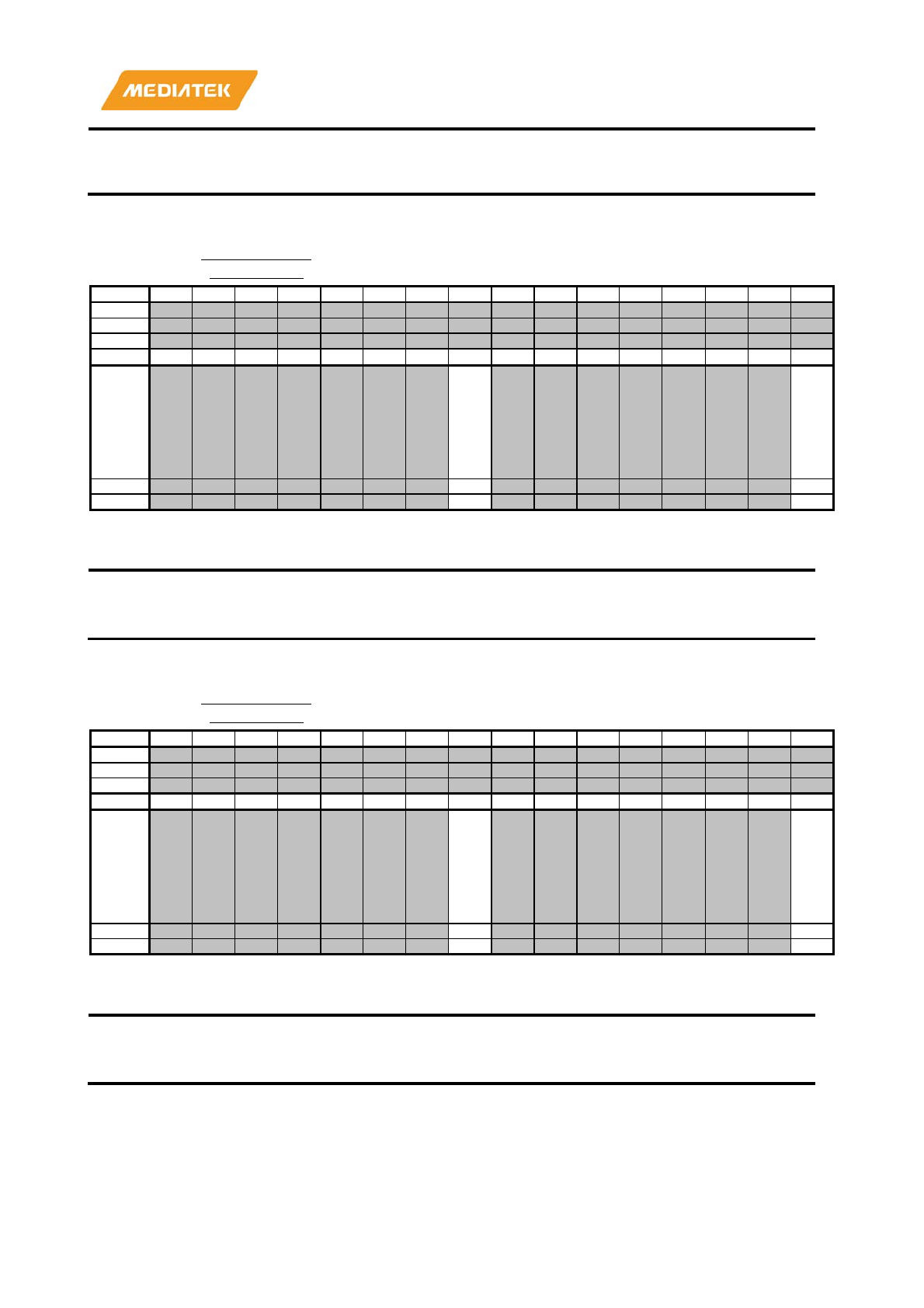
MT7686 Reference Manual
© 2016 - 2017 MediaTek Inc.
Page 178 of 536
This document contains information that is proprietary to MediaTek Inc. (“MediaTek”) and/or its licensor(s).
Any unauthorized use, reproduction or disclosure of this document in whole or in part is strictly prohibited.
Bit(s)
Mnemonic
Name
Description
31:0
CR_I2S_M
ONITOR
CR_I2S_MONITOR
[15:8] i2s_out_bcount_monitor
[7:0] i2s_in_bcount_monitor
A008004
0
I2S1_DL_INT
_CONTROL
I2S DL INTERRUPT ENABLE CONTROL
REGISTER 00000000
Bit
31
30
29
28
27
26
25
24
23
22
21
20
19
18
17
16
Name
Type
Reset
Bit
15
14
13
12
11
10
9
8
7
6
5
4
3
2
1
0
Name
CR
_D
L_I
NT
STS
_IN
T
CR
_D
L_
CO
NT
RL
_IT
EN
Type
RO
RW
Reset
0
0
Overview
Bit(s)
Mnemonic
Name
Description
8
CR_DL_INTSTS_INT
CR_DL_INTSTS_INT
0
CR_DL_CONTRL_ITEN
CR_DL_CONTRL_ITEN
A008004
4
I2S1_UL_INT
_CONTROL
I2S UL INTERRUPT ENABLE CONTROL
REGISTER 00000000
Bit
31
30
29
28
27
26
25
24
23
22
21
20
19
18
17
16
Name
Type
Reset
Bit
15
14
13
12
11
10
9
8
7
6
5
4
3
2
1
0
Name
CR
_U
L_I
NT
STS
_IN
T
CR
_U
L_
CO
NT
RL
_IT
EN
Type
RO
RW
Reset
0
0
Overview
Bit(s)
Mnemonic
Name
Description
8
CR_UL_INTSTS_INT
CR_UL_INTSTS_INT
0
CR_UL_CONTRL_ITEN
CR_UL_CONTRL_ITEN
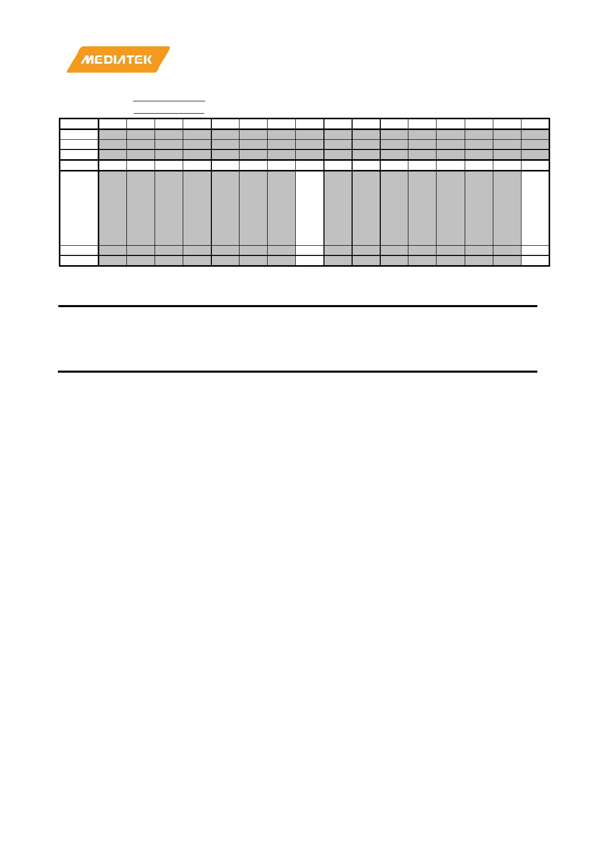
MT7686 Reference Manual
© 2016 - 2017 MediaTek Inc.
Page 179 of 536
This document contains information that is proprietary to MediaTek Inc. (“MediaTek”) and/or its licensor(s).
Any unauthorized use, reproduction or disclosure of this document in whole or in part is strictly prohibited.
A008004
8
I2S1_INT_AC
K_CONTROL
I2S UL INTERRUPT ENABLE CONTROL
REGISTER 00000000
Bit
31
30
29
28
27
26
25
24
23
22
21
20
19
18
17
16
Name
Type
Reset
Bit
15
14
13
12
11
10
9
8
7
6
5
4
3
2
1
0
Name
CR
_D
L_
AC
KI
NT
_A
CK
CR
_U
L_
AC
KI
NT
_A
CK
Type
RW
RW
Reset
0
0
Overview
Bit(s)
Mnemonic
Name
Description
8
CR_DL_AC
KINT_ACK
CR_DL_ACKINT_A
CK
0
CR_UL_AC
KINT_ACK
CR_UL_ACKINT_A
CK
MT7686 Reference Manual
© 2016 - 2017 MediaTek Inc.
Page 180 of 536
This document contains information that is proprietary to MediaTek Inc. (“MediaTek”) and/or its licensor(s).
Any unauthorized use, reproduction or disclosure of this document in whole or in part is strictly prohibited.
12. I2S0 and I2S1 Audio PLL Settings
12.1. XPLL block diagram
The audio phase-locked loop (XPLL) supports:
1) REF_CK: 26MHz or 40MHz.
2) PLL VCO frequency Output frequency: 832MHz, 786.432MHz or 722.5344MHz
3) PLL output frequency: 26MHz, 24.576MHz or 22.5792MHz
0
1
26MHz
REF_CK
FB_CK
CHPFD LPF VCO
DDS
Analog PLL Core
/1-128 /1,2,4
/1,2
/1,2,4 /16
<700MHz
416MHz
<700MHz
416MHz
RG_XPLLL_DDSEN RG_XPLL_PCW_NCPO<30:0> RG_DDS_PREDIV2
(always TIEH,
no need to set)
416MHz832MHz AD_XPLL_CLK
RG_XPLLL_FBSEL<1:0>
RG_XPLLL_FBDIV<6:0>
Figure 12.1-1. XPLL block diagram
Keywords: analog PLL core, CHPFD, LPF, VCO, FB_CK
12.2. Fractional-N PLL power on sequence
1) Set RG_XPLL_FBDIV<6:0> to nearest integer
2) PLL power on and settle (after AD_RGS_PLL_VCO_CPLT=1)
3) Set DDS power on registers

MT7686 Reference Manual
© 2016 - 2017 MediaTek Inc.
Page 181 of 536
This document contains information that is proprietary to MediaTek Inc. (“MediaTek”) and/or its licensor(s).
Any unauthorized use, reproduction or disclosure of this document in whole or in part is strictly prohibited.
RG_XPLL_BIAS_PWD
RG_XPLL_PWD
RG_XPLL_DDS_PWDB
AD_RGS_PLL_VCOCAL_CPLT
RG_XPLL_DDS_RSTB
RG_XPLL_PCW_NCPO_CHG
RG_XPLL_NCPO_EN
RG_XPLL_DDSEN
RG_XPLL_BIAS_RST
XPLL ready
XPLL calibration
>30n
>30n
>30n
>1u
>20u
Figure 12.2-1. Fractional-N PLL power on sequence
Keywords: XPLL calibration, XPLL ready
12.3. XPLL frequency setting (Integer)
Freq=Fin*(FBDIV+1)*FBSEL/PREDIV/POSDIV
1) Pre-divider ratio (PREDIV)
2'b00: Fref = Fin/1
2'b01: Fref = Fin/2
2'b1X: Fref = Fin/4
2) Post-divider ratio for single-phase output (POSDIV)
2'b00: VCO/1
2'b01: VCO/2
2'b1X: VCO/4
3) Feedback clock select (FBSEL)
2'b00: Fvco/1
2'b01: Fvco/2
2'b1X: Fvco/4
4) Feedback divide ratio (FBDIV)
7'd0: /1
7'd1: /2
MT7686 Reference Manual
© 2016 - 2017 MediaTek Inc.
Page 182 of 536
This document contains information that is proprietary to MediaTek Inc. (“MediaTek”) and/or its licensor(s).
Any unauthorized use, reproduction or disclosure of this document in whole or in part is strictly prohibited.
…...
7'd127: /128
12.4. DDS PCW setting
RG_PCW_NCPO[30:0] Integer part Fraction part
…
30 29 28 27 26 25 24 23 22 21 20 19 18 1 0
Figure 12.4-1. DDS PCW settings
1) 2 < divisor < 128
2) RG_XPLL_PCW_NCPO[30:0] = (Period-1)*2^24
3) Ex. Fin=26MHz, Fout=416MHz
• RG_XPLL_PCW_NCPO[30:0]=(416/26-1)*2^24=16’d251658240
12.5. XPLL frequency change sequence
• Set RG_XPLL_PCW_NCPO<30:0>
• Toggle RG_XPLL_PCW_NCPO_CHG
(Both edges will do)
RG_XPLL_PCW_NCPO[30:0]
RG_XPLL_PCW_NCPO_CHG
>30n
>1n >1n
Figure 12.5-1. XPLL frequency change sequence
Keyword: RG_XPLL_PCW_MCPO
12.6. XPLL turn on programming sequence
Read CKSYS_XTAL_FREQ__F_F_FXO_IS_26M (0xA20202A3) for REF_CK (1: 26MHz, 0: 40MHz)
1) If REF_CK = 26MHz, AD_XPLL_CK = 26MHz
• Write: XPLL_CTL0 = 0x441F;
• Write: XPLL_CTL1 = 0x441F;
• Write: XPLL_CTL2 = 0x7320;
• Write: XPLL_CTL3 = 0x1E000000;
• Write: XPLL_CTL8 = 0x2F00;
• Wait: 20us;
• Write: XPLL_CTL0 = 0x441E;
• Write: XPLL_CTL8 = 0x2F008;
• Polling: XPLL_CTL4[1] = 1; //bit[1]: AD_RGS_PLL_VCOCAL_CPLT

MT7686 Reference Manual
© 2016 - 2017 MediaTek Inc.
Page 183 of 536
This document contains information that is proprietary to MediaTek Inc. (“MediaTek”) and/or its licensor(s).
Any unauthorized use, reproduction or disclosure of this document in whole or in part is strictly prohibited.
• Write: XPLL_CTL4 = 0x2A;
• Write: XPLL_CTL8 = 0x2F018;
• Write: XPLL_CTL3 = 0x1E000001;
• Wait: 1us;
• Write: XPLL_CTL8 = 0x2F038;
• Wait: 1us;
• Write: XPLL_CTL2 = 0xF302;
• Write: XPLL_CTL8 = 0xF038;
• Wait: 20us;
2) If REF_CK = 26MHz, AD_XPLL_CK = 24.576MHz
• Write: XPLL_CTL0 = 0x441D;
• Write: XPLL_CTL1 = 0xD861;
• Write: XPLL_CTL2 = 0x7302;
• Write: XPLL_CTL3 = 0x1C3F549A;
• Write: XPLL_CTL8 = 0x20000;
• Wait: 20us;
• Write: XPLL_CTL0 = 0x441C;
• Write: XPLL_CTL8 = 0x20008;
• Polling: XPLL_CTL4[1] = 1; //bit[1]: AD_RGS_PLL_VCOCAL_CPLT
• Write: XPLL_CTL4 = 0x2A;
• Write: XPLL_CTL8 = 0x20018;
• Write: XPLL_CTL3 = 0x1C3F549B;
• Wait: 1us;
• Write: XPLL_CTL8 = 0x20038;
• Wait: 1us;
• Write: XPLL_CTL2 = 0xF302;
• Write: XPLL_CTL8 = 0x38;
• Wait: 20us;
3) If REF_CK = 26MHz, AD_XPLL_CK = 22.5792MHz
• Write: XPLL_CTL0 = 0x435;
• Write: XPLL_CTL1 = 0xC861;
• Write: XPLL_CTL2 = 0x7302;
• Write: XPLL_CTL3 = 0x19CA2F54;
• Write: XPLL_CTL8 = 0x2F000;

MT7686 Reference Manual
© 2016 - 2017 MediaTek Inc.
Page 184 of 536
This document contains information that is proprietary to MediaTek Inc. (“MediaTek”) and/or its licensor(s).
Any unauthorized use, reproduction or disclosure of this document in whole or in part is strictly prohibited.
• Wait: 20us;
• Write: XPLL_CTL0 = 0x434;
• Write: XPLL_CTL8 = 0x2F008;
• Polling: XPLL_CTL4[1] = 1; //bit[1]: AD_RGS_PLL_VCOCAL_CPLT
• Write: XPLL_CTL4 = 0x2A;
• Write: XPLL_CTL8 = 0x2F018;
• Write: XPLL_CTL3 = 0x19CA2F55;
• Wait: 1us;
• Write: XPLL_CTL8 = 0x2F038;
• Wait: 1us;
• Write: XPLL_CTL2 = 0xF302;
• Write: XPLL_CTL8 = 0xF038;
• Wait: 20us;
4) If REF_CK = 40MHz, AD_XPLL_CK = 26MHz
• Write: XPLL_CTL0 = 0x4413;
• Write: XPLL_CTL1 = 0x6861;
• Write: XPLL_CTL2 = 0x7303;
• Write: XPLL_CTL3 = 0x12CCCCCC;
• Write: XPLL_CTL8 = 0x2F000;
• Wait: 20us;
• Write: XPLL_CTL0 = 0x4412;
• Write: XPLL_CTL8 = 0x2F008;
• Polling: XPLL_CTL4[1] = 1; //bit[1]: AD_RGS_PLL_VCOCAL_CPLT
• Write: XPLL_CTL4 = 0x2A;
• Write: XPLL_CTL8 = 0x2F008;
• Write: XPLL_CTL3 = 0x12CCCCCD;
• Wait: 1us;
• Write: XPLL_CTL8 = 0x2F038;
• Wait: 1us;
• Write: XPLL_CTL2 = 0xF303;
• Write: XPLL_CTL8 = 0xF038;
• Wait: 20us;
5) If REF_CK = 40MHz, AD_XPLL_CK = 24.576MHz
• Write: XPLL_CTL0 = 0x4411;

MT7686 Reference Manual
© 2016 - 2017 MediaTek Inc.
Page 185 of 536
This document contains information that is proprietary to MediaTek Inc. (“MediaTek”) and/or its licensor(s).
Any unauthorized use, reproduction or disclosure of this document in whole or in part is strictly prohibited.
• Write: XPLL_CTL1 = 0x5861;
• Write: XPLL_CTL2 = 0x7303;
• Write: XPLL_CTL3 = 0x11A92A30;
• Write: XPLL_CTL8 = 0x2F000;
• Wait: 20us;
• Write: XPLL_CTL0 = 0x4410;
• Write: XPLL_CTL8 = 0x2F008;
• Polling: XPLL_CTL4[1] = 1; //bit[1]: AD_RGS_PLL_VCOCAL_CPLT
• Write: XPLL_CTL4 = 0x2A;
• Write: XPLL_CTL8 = 0x2F018;
• Write: XPLL_CTL3 = 0x11A92A31;
• Wait: 1us;
• Write: XPLL_CTL8 = 0x2F038;
• Wait: 1us;
• Write: XPLL_CTL2 = 0xF303;
• Write: XPLL_CTL8 = 0xF038;
• Wait: 20us;
6) If REF_CK = 40MHz, AD_XPLL_CK = 22.5792MHz
• Write: XPLL_CTL0 = 0x423;
• Write: XPLL_CTL1 = 0x5861;
• Write: XPLL_CTL2 = 0x7303;
• Write: XPLL_CTL3 = 0x1010385C;
• Write: XPLL_CTL8 = 0x2F000;
• Wait: 20us;
• Write: XPLL_CTL0 = 0x422;
• Write: XPLL_CTL8 = 0x2F008;
• Polling: XPLL_CTL4[1] = 1; //bit[1]: AD_RGS_PLL_VCOCAL_CPLT
• Write: XPLL_CTL4 = 0x2A;
• Write: XPLL_CTL8 = 0x2F018;
• Write: XPLL_CTL3 = 0x1010385D;
• Wait: 1us;
• Write: XPLL_CTL8 = 0x2F038;
• Wait: 1us;
• Write: XPLL_CTL2 = 0xF303;
• Write: XPLL_CTL8 = 0xF038;

MT7686 Reference Manual
© 2016 - 2017 MediaTek Inc.
Page 186 of 536
This document contains information that is proprietary to MediaTek Inc. (“MediaTek”) and/or its licensor(s).
Any unauthorized use, reproduction or disclosure of this document in whole or in part is strictly prohibited.
• Wait: 20us;
12.7. XPLL turn off programming sequence
1) To turn off XPLL when no need:
• Write: XPLL_CTL0[0] = 1;
• Wait: 1us;
• Write: XPLL_CTL8[3] = 0;
• Wait: 1us;
• Write: XPLL_CTL8[16] = 1;

MT7686 Reference Manual
© 2016 - 2017 MediaTek Inc.
Page 187 of 536
This document contains information that is proprietary to MediaTek Inc. (“MediaTek”) and/or its licensor(s).
Any unauthorized use, reproduction or disclosure of this document in whole or in part is strictly prohibited.
13. SDIO
13.1. Overview
The SD Input/Output (SDIO) card is based on and compatible with the SD memory card. The controller fully
supports the SD memory card bus protocol as defined in SD Memory Card Specification Part 1 Physical Layer
Specification version 2.0 and SDIO Specification version 2.0.
SDIO provides high-speed data IO with low power consumption. MT7686 SDIO module provides an SDIO2.0 card
interface connected to the host and can support multiple speed modes including default speed, SDR12 and SDR25.
13.2. Features
• Provides SDIO2.0 host interfaces
o SDIO2.0:
1-bit and 4-bit SD data transfer modes
Default mode: Variable clock rate 0-25 MHz, up to 12.5 MB/sec interface speed (using 4 parallel
data lines)
High-Speed mode: Variable clock rate 0-50 MHz, up to 25 MB/sec interface speed (using 4 data
lines)
Data rate up to 50Mbps in serial mode, 50 x 4 Mbps in parallel mode, the module is targeted at
50MHz operating clock.
32-bit access for control registers
32-bit access for FIFO
Built-in 32 bytes FIFO buffers for transmit and receive, FIFO is shared for transmit and receive
Built-in CRC circuit
Interrupt capabilities
Does not support SPI
Supports DMA
WLAN TX packet de-aggregation and WLAN RX packet aggregation
WLAN WHISR/ RX enhanced read mode
• CR and data port access
o Supports CR port single read/write access (AHB slave)
o Supports data port single and burst read/write access (AHB master)
• DMA function
o One TX channel and two RX channels
o AHB master interface
o Moves TX data from HIF buffer to system, EMI, retention memory
o Moves RX data or firmware prepared data from system, EMI, retention memory to HIF buffer
MT7686 Reference Manual
© 2016 - 2017 MediaTek Inc.
Page 188 of 536
This document contains information that is proprietary to MediaTek Inc. (“MediaTek”) and/or its licensor(s).
Any unauthorized use, reproduction or disclosure of this document in whole or in part is strictly prohibited.
13.3. Block diagram
The block diagram of the SDIO controller is shown in Figure 13.3-1.
sdctl_sdio1
(SDIO)
sdctl_eng
(Main queue/DMA engine)
sdctl_whdcr
Drive control/status
register (CSR)
sdctl_hfcr
Firmware control/status
register (CSR)
sdctl_top
(SDIO controller)
SD BUS AHB master bus
AHB slave bus
(MCU)
sdctl_cis_buf
Card information
structure (CIS)
buffer
sdctl_debug_flag
(Debug flag)
Figure 13.3-1. SDIO controller block diagram
13.4. Functions
From the external view, the SDIO interface mainly includes the SD bus and AHB master and slave. The AHB master
is used for DMA operations and the AHB slave is used for register access from the MCU. The SD bus provides an
interface for SD specification.
13.4.1. Signal pins
SD Host SD I/O
Card
SDIO_CLK
SDIO_DAT0~3
CMD
Figure 13.4-1. Signal connections to 4-bit SDIO cards
Table 13.4-1. SDIO pin definitions
Pin Name SD 4-bit mode SD 1-bit mode
1 SLV_MC0_DA3 DAT[3] Data line3 N/C Not used
2 SLV_MC0_CM0 CMD Command line CMD Command line
3 VSS1 VSS1 Ground VSS1 Ground
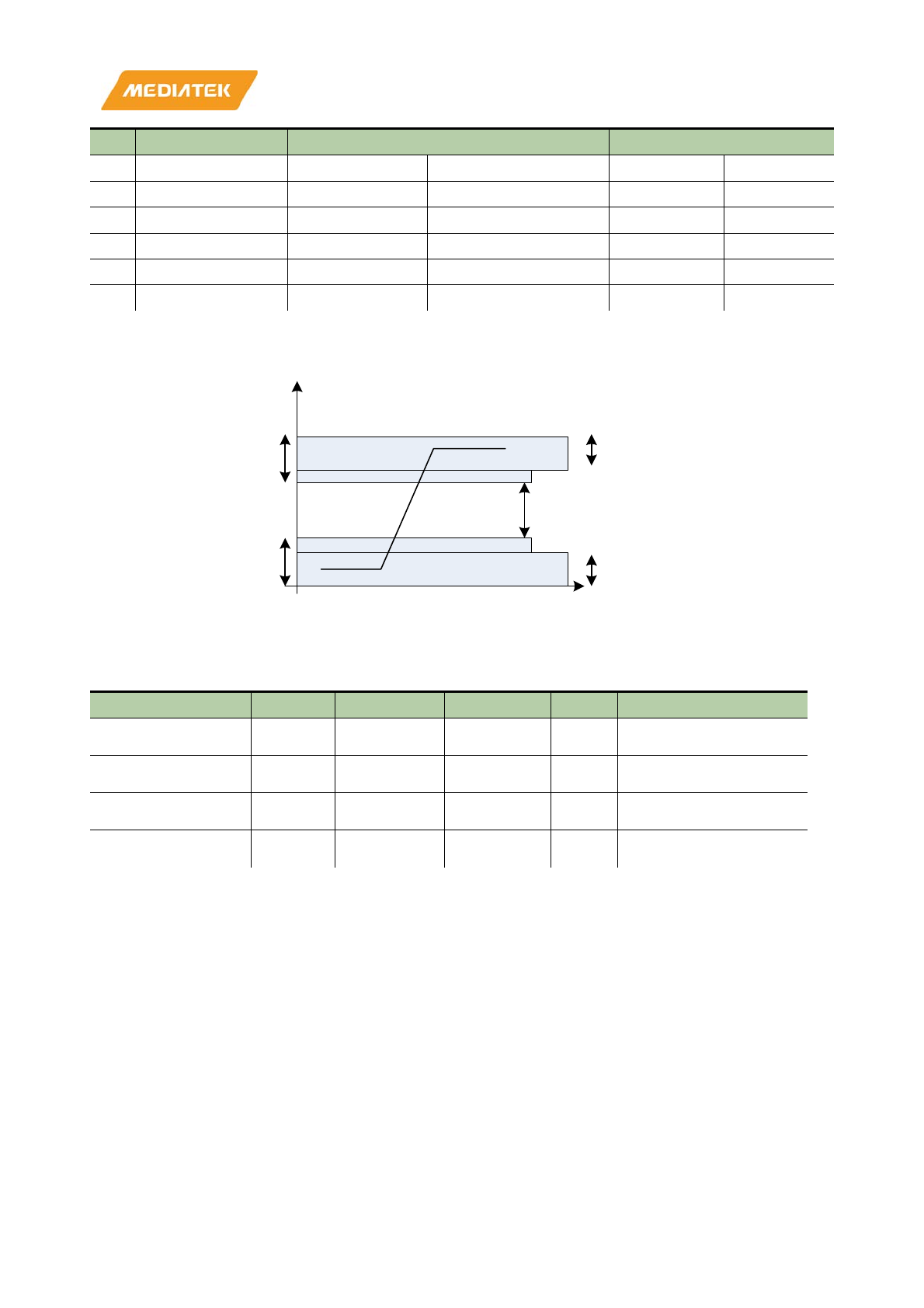
MT7686 Reference Manual
© 2016 - 2017 MediaTek Inc.
Page 189 of 536
This document contains information that is proprietary to MediaTek Inc. (“MediaTek”) and/or its licensor(s).
Any unauthorized use, reproduction or disclosure of this document in whole or in part is strictly prohibited.
Pin Name SD 4-bit mode SD 1-bit mode
4 VDD VDD Supply voltage VDD Supply voltage
5 SLV_MC0_CK CLK Clock CLK Clock
6 VSS2 VSS2 Ground VSS2 Ground
7 SLV_MC0_DA0 DAT[0] Data line 0 DATA Data line
8 SLV_MC0_DA1 DAT[1] Data line1 or interrupt IRQ Interrupt
9 SLV_MC0_DA2 DAT[2] Data line2 RW Not used
13.4.2. SDIO timing waveform (3.3V)
Figure 13.4-2. Bus signal levels
Table 13.4-2. Bus signal voltage
Parameter Symbol Min. Max. Unit Conditions
Output High Voltage VOH 0.75*VDD V IOH=-2mA VDD min
Output Low Voltage VOL
0.125*VDD V IOL = 2mA VDD min
Input High Voltage VIH 0.625*VDD VDD+0.3 V
Input Low Voltage VIL Vss-0.3 0.25*VDD V
V
undefined
Output
high level
Output
low level
t
V
DD
V
OH
V
IH
V
IL
V
OL
V
SS
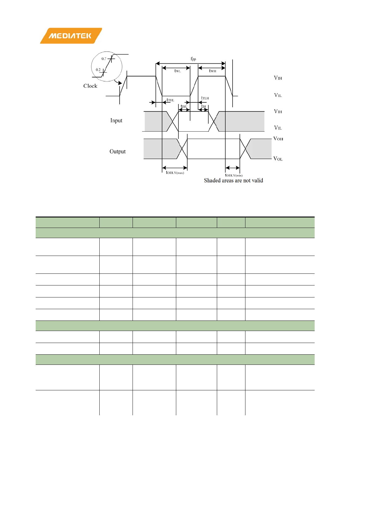
MT7686 Reference Manual
© 2016 - 2017 MediaTek Inc.
Page 190 of 536
This document contains information that is proprietary to MediaTek Inc. (“MediaTek”) and/or its licensor(s).
Any unauthorized use, reproduction or disclosure of this document in whole or in part is strictly prohibited.
Figure 13.4-3. Bus timing diagram (default)
Table 13.4-3. Bus timing parameter values (default)
Parameter
Symbol
Minimum
Maximum
Unit
Remark
Clock CLK (All values are referred to min (VIH) and max (VIL)
Clock frequency data
transfer mode
fPP
0
25
MHz
CCARD ≤ 10 pF (1 card)
Clock frequency
identification mode
fOD
0/100
400
kHz
CCARD ≤ 10 pF (1 card)
Clock low time
tWL
10
ns
CCARD ≤ 10 pF (1 card)
Clock high time
tWH
10
ns
CCARD ≤ 10 pF (1 card)
Clock rise time
tTLH
10
ns
CCARD ≤ 10 pF (1 card)
Clock fall time
tTHL
10
ns
CCARD ≤ 10 pF (1 card)
Inputs CMD, DAT (referenced to CLK)
Input set-up time
tISU
5
ns
CCARD ≤ 10 pF (1 card)
Input hold time
tIH
5
ns
CCARD ≤ 10 pF (1 card)
Outputs CMD, DAT (referenced to CLK)
Output delay time
during data transfer
mode
tOLDY
0
14
ns
CL ≤ 40 pF (1 card)
Output delay time
during identification
mode
tOLDY
0
50
ns
CL ≤ 40 pF (1 card)
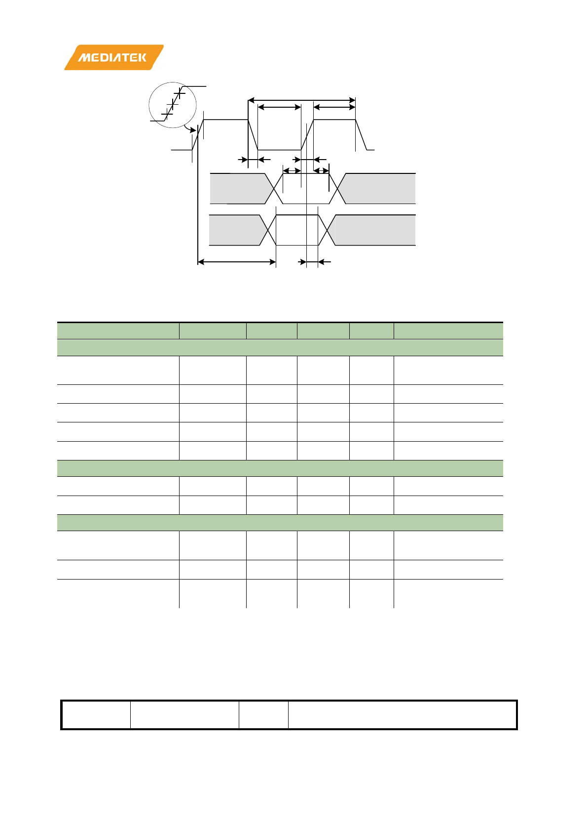
MT7686 Reference Manual
© 2016 - 2017 MediaTek Inc.
Page 191 of 536
This document contains information that is proprietary to MediaTek Inc. (“MediaTek”) and/or its licensor(s).
Any unauthorized use, reproduction or disclosure of this document in whole or in part is strictly prohibited.
Figure 13.4-4. High-speed timing diagram
Table 13.4-4. High-speed timing parameter values
Parameter
Symbol
Minimum
Maximum
Unit
Remark
Clock CLK (All values are referred to min (VIH) and max (VIL)
Clock frequency data
transfer mode
fPP
0
50
MHz
CCARD ≤ 10 pF (1 card)
Clock low time
tWL
7
ns
CCARD ≤ 10 pF (1 card)
Clock high time
tWH
7
ns
CCARD ≤ 10 pF (1 card)
Clock rise time
tTLH
3
ns
CCARD ≤ 10 pF (1 card)
Clock fall time
tTHL
3
ns
CCARD ≤ 10 pF (1 card)
Inputs CMD, DAT (referenced to CLK)
Input set-up time
tISU
6
ns
CCARD ≤ 10 pF (1 card)
Input hold time
tIH
2
ns
CCARD ≤ 10 pF (1 card)
Outputs CMD, DAT (referenced to CLK)
Output delay time during
data transfer mode
tOLDY
14
ns
CL ≤ 40 pF (1 card)
Output hold time
tOH
2.5
ns
CL ≥ 40 pF (1 card)
Total system capacitance
for each line (1)
CL
40
pF
1 card
(1) In order to satisfy the serving time, the host shall drive only one card
13.5. Register mapping
13.5.1. Firmware register
Module name: SDIO_FW Base address: (+A1040000h)
Address
Name
Width
(bits)
Register
Functionality
VIH
VIL
VIH
VIL
VOH
VOL
0.7
0.2
fpp
Input
Output
Clock
t
WL
t
WH
t
TLH
t
THL
t
ISU
t
IH
t
ODLY(max)
t
OH
50%VDD

MT7686 Reference Manual
© 2016 - 2017 MediaTek Inc.
Page 192 of 536
This document contains information that is proprietary to MediaTek Inc. (“MediaTek”) and/or its licensor(s).
Any unauthorized use, reproduction or disclosure of this document in whole or in part is strictly prohibited.
A1040000
HGFCR
32
HIF Global Firmware Configuration
Register
A1040004
HGFISR
32
HIF Global Firmware Interrupt Status
Register
A1040008
HGFIER
32
HIF Global
Firmware Interrupt Enable
Register
A1040010
HSDBDLSR
32
HIF SDIO Bus Delay Selection Register
A1040014
HSDLSR
32
HIF SRAM Delay Selection Register
A1040018
HCSDCR
32
HIF Clock Stop Detection register
A104001C
HGH2DR
32
HIF Global Host to Device Register
A1040020
HDBGCR
32
HIF Debug Control Register
A104002C
FWDSIOCR
32
DS Pad Macro
IO Control Register
A1040030
HGTMTCR
32
Test Mode Trigger Control Register
A1040034
HGTMCR
32
Test Mode Control Register
A1040038
HGTMDPCR0
32
Test Mode Data
Pattern Control Register 0
A104003C
HGTMDPCR1
32
Test Mode Data Pattern Control Register 1
A1040040
FWCLKIOCR_T28LP
32
Clock Pad Macro IO Control Register
A1040044
FWCMDIOCR_T28L
P
32
Command Pad Macro IO Control Register
A1040048
FWDAT0IOCR_T28L
P
32
Data 0 Pad Macro IO Control Register
A104004C
FWDAT1IOCR_T28L
P
32
Data 1 Pad Macro IO Control Register
A1040050
FWDAT2IOCR_T28L
P
32
Data 2 Pad Macro IO Control Register
A1040054
FWDAT3IOCR_T28L
P
32
Data 3 Pad Macro IO
Control Register
A1040058
FWCLKDLYCR
32
Clock Pad Macro Delay Chain Control
Register
A104005C
FWCMDDLYCR
32
Command Pad Macro Delay Chain Control
Register
A1040060
FWODATDLYCR
32
SDIO Output Data Delay Chain Control
Register
A1040064
FWIDATDLYCR1
32
SDIO Input Data Delay Chain Control
Register 1
A1040068
FWIDATDLYCR2
32
SDIO Input Data Delay Chain Control
Register 2
A104006C
FWILCHCR
32
SDIO Input Data Latch Time Control
Register
A1040070
CIS0R00
32
CIS0 Register 0
A1040074
CIS0R01
32
CIS0 Register 1
A1040078
CIS0R02
32
CIS0 Register 2
A104007C
CIS0R03
32
CIS0 Register 3
A1040080
CIS0R04
32
CIS0 Register 4
A1040084
CIS0R05
32
CIS0 Register 5

MT7686 Reference Manual
© 2016 - 2017 MediaTek Inc.
Page 193 of 536
This document contains information that is proprietary to MediaTek Inc. (“MediaTek”) and/or its licensor(s).
Any unauthorized use, reproduction or disclosure of this document in whole or in part is strictly prohibited.
A1040088
CIS0R06
32
CIS0 Register 6
A104008C
CIS0R07
32
CIS0 Register 7
A1040090
CIS0R08
32
CIS0 Register 8
A1040094
CIS0R09
32
CIS0 Register 9
A1040098
CIS0R0A
32
CIS0 Register A
A104009C
CIS0R0B
32
CIS0 Register B
A10400A0
CIS0R0C
32
CIS0
Register C
A10400A4
CIS0R0D
32
CIS0 Register D
A10400A8
CIS0R0E
32
CIS0 Register E
A10400AC
CIS0R0F
32
CIS0 Register F
A10400B0
CIS1R00
32
CIS1 Register 0
A10400B4
CIS1R01
32
CIS1 Register 1
A10400B8
CIS1R02
32
CIS1 Register 2
A10400BC
CIS1R03
32
CIS1 Register 3
A10400C0
CIS1R04
32
CIS1 Register 4
A10400C4
CIS1R05
32
CIS1 Register 5
A10400C8
CIS1R06
32
CIS1 Register 6
A10400CC
CIS1R07
32
CIS1 Register 7
A10400D0
CIS1R08
32
CIS1 Register 8
A10400D4
CIS1R09
32
CIS1 Register 9
A10400D8
CIS1R0A
32
CIS1 Register A
A10400DC
CIS1R0B
32
CIS1 Register B
A10400E0
CIS1R0C
32
CIS1 Register C
A10400E4
CIS1R0D
32
CIS1 Register D
A10400E8
CIS1R0E
32
CIS1 Register E
A10400EC
CIS1R0F
32
CIS1
Register F
A10400F0
CISRDY
32
CIS Ready Flag Register
A10400F4
CCCR0
32
CC Register 0
A10400F8
CCCR1
32
CC Register 1
A10400FC
CCRDY
32
CC
Ready Flag Register
A1040100
HWFISR
32
HIF WLAN Firmware Interrupt Status
Register
A1040104
HWFIER
32
HIF WLAN Firmware Interrupt Enable
Register
A1040108
HWFISR1
32
Reserved for HWFISR1
A104010C
HWFIER1
32
Reserved for HWFIER1
A1040110
HWFTE0SR
32
HIF WLAN Firmware TX Event 0 Status
Register
A1040114
HWFTE1SR
32
Reserved for
HWFTE1SR
A1040118
HWFTE2SR
32
Reserved for HWFTE2SR
A104011C
HWFTE3SR
32
Reserved for HWFTE3SR
A1040120
HWFTE0ER
32
HIF WLAN Firmware TX Event 0 Enable
Register

MT7686 Reference Manual
© 2016 - 2017 MediaTek Inc.
Page 194 of 536
This document contains information that is proprietary to MediaTek Inc. (“MediaTek”) and/or its licensor(s).
Any unauthorized use, reproduction or disclosure of this document in whole or in part is strictly prohibited.
A1040124
HWFTE1ER
32
Reserved for HWFTE1ER
A1040128
HWFTE2ER
32
Reserved for HWFTE2ER
A104012C
HWFTE3ER
32
Reserved for HWFTE3ER
A1040130
HWFRE0SR
32
HIF WLAN Firmware RX Event 0 Status
Register
A1040134
HWFRE1SR
32
HIF WLAN Firmware RX Event 1 Status
Register
A1040138
HWFRE2SR
32
Reserve for HWFRE2SR
A104013C
HWFRE3SR
32
Reserve for HWFRE3SR
A1040140
HWFRE0ER
32
HIF WLAN Firmware RX Event 0 Enable
Register
A1040144
HWFRE1ER
32
HIF WLAN Firmware RX Event 1 Enable
Register
A1040148
HWFRE2ER
32
Reserve for HWFRE2ER
A104014C
HWFRE3ER
32
Reserve for HWFRE3ER
A1040150
HWFICR
32
HIF WLAN Firmware Interrupt Control
Register
A1040154
HWFCR
32
HIF WLAN Firmware Control Register
A1040158
HWTDCR
32
HIF WLAN TX DMA Control Register
A104015C
HWTPCCR
32
HIF WLAN TX Packet Count Control
Register
A1040160
HWFTQ0SAR
32
HIF WLAN Firmware TX Queue 0 Start
Address Register
A1040164
HWFTQ1SAR
32
HIF WLAN Firmware TX Queue 1 Start
Address Register
A1040168
HWFTQ2SAR
32
HIF WLAN Firmware TX Queue 2 Start
Address Register
A104016C
HWFTQ3SAR
32
HIF WLAN Firmware TX Queue 3 Start
Address Register
A1040170
HWFTQ4SAR
32
HIF WLAN Firmware TX Queue 4 St
art
Address Register
A1040174
HWFTQ5SAR
32
Reserved for HIF WLAN Firmware TX
Queue 5 Start Address Register
A1040178
HWFTQ6SAR
32
Reserved for HIF WLAN Firmware TX
Queue 6 Start Address
Register
A104017C
HWFTQ7SAR
32
Reserved for HIF WLAN Firmware TX
Queue 7 Start Address Register
A1040180
HWFRQ0SAR
32
HIF WLAN Firmware RX Queue 0 Start
Address Register
A1040184
HWFRQ1SAR
32
HIF WLAN Firmware RX Queue 1 Start
Address Register
A1040188
HWFRQ2SAR
32
HIF WLAN Firmware RX Queue 2 Start
Address Register
A104018C
HWFRQ3SAR
32
HIF WLAN Firmware RX Queue 3 Start
Address Register
A1040190
HWFRQ4SAR
32
Reserve for HIF WLAN Firmware RX Queue
4 Start Address Register

MT7686 Reference Manual
© 2016 - 2017 MediaTek Inc.
Page 195 of 536
This document contains information that is proprietary to MediaTek Inc. (“MediaTek”) and/or its licensor(s).
Any unauthorized use, reproduction or disclosure of this document in whole or in part is strictly prohibited.
A1040194
HWFRQ5SAR
32
Reserve for HIF WLAN Firmware RX
Queue
5 Start Address Register
A1040198
HWFRQ6SAR
32
Reserved for HIF WLAN Firmware RX
Queue 6 Start Address Register
A104019C
HWFRQ7SAR
32
Reserved for HIF WLAN Firmware RX
Queue 7 Start
Address Register
A10401A0
H2DRM0R
32
Host to Device Receive Mailbox 0 Register
A10401A4
H2DRM1R
32
Host to Device Receive Mailbox 1 Register
A10401A8
D2HSM0R
32
Device to Host Send Mailbox 0 Register
A10401AC
D2HSM1R
32
Device to Host Send Mailbox 1 Register
A10401B0
D2HSM2R
32
Device to Host Send Mailbox 2 Register
A10401C0
HWRQ0CR
32
HIF WLAN RX Queue 0 Control Register
A10401C4
HWRQ1CR
32
HIF WLAN RX Queue 1 Control Register
A10401C8
HWRQ2CR
32
HIF WLAN RX Queue 2 Control Register
A10401CC
HWRQ3CR
32
HIF WLAN RX Queue 3 Control Register
A10401D0
HWRQ4CR
32
Reserved for HWRQ4CR
A10401D4
HWRQ5CR
32
Reserved for HWRQ5CR
A10401D8
HWRQ6CR
32
Reserved for HWRQ6CR
A10401DC
HWRQ7CR
32
Reserved for HWRQ7CR
A10401E0
HWRLFACR
32
HIF WLAN RX Length FIFO Available Count
Register
A10401E4
HWRLFACR1
32
Reserved for HWRLFACR1
A10401E8
HWDMACR
32
HIF WLAN DMA Control Register
A10401EC
HWFIOCDR
32
HIF WLAN Firmware GPD IOC bit Disable
Register
A10401F0
HSDIOTOCR
32
HIF SDIO Time
-Out Control Register
A1040200
HWFTSR0
32
HIF WLAN Firmware TX Status Register 0
A1040204
HWFTSR1
32
HIF WLAN Firmware TX Status Register 1
A1040210
HWDBGCR
32
HIF WLAN Debug Control Register
A1040214
HWDBGPLR
32
HIF WLAN Debug Packet Length Register
A1040218
HSPICSR
32
WLAN SPI Control Status Register (SPI
Only)
A1040220
HWRX0CGPD
32
DMA RX0 Current GPD Address Register
A1040224
HWRX1CGPD
32
DMA RX1 Current GPD Address Register
A1040228
HWRX2CGPD
32
DMA RX2 Current GPD Address
Register
A104022C
HWRX3CGPD
32
DMA RX3 Current GPD Address Register
A1040230
HWTX0CGPD
32
DMA TX0 Current GPD Address Register
A1040234
HWTX1Q1CGPD
32
DMA TX1
Que Type 1 Current GPD Address
Register
A1040238
HWTX1Q2CGPD
32
DMA TX1 Que Type 2 Current GPD Address
Register
A104023C
HWTX1Q3CGPD
32
DMA TX1 Que Type 3 Current GPD Address
Register
A1040240
HWTX1Q4CGPD
32
DMA TX1 Que Type 4 Current GPD Address
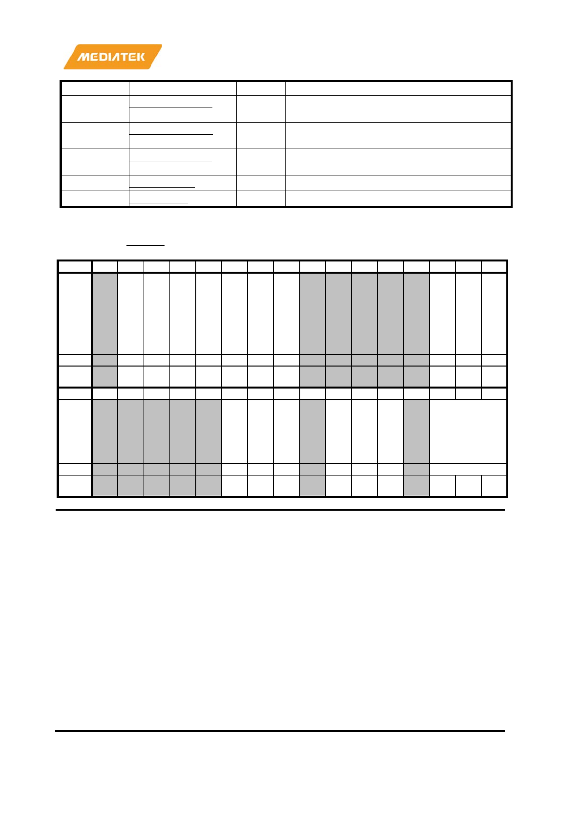
MT7686 Reference Manual
© 2016 - 2017 MediaTek Inc.
Page 196 of 536
This document contains information that is proprietary to MediaTek Inc. (“MediaTek”) and/or its licensor(s).
Any unauthorized use, reproduction or disclosure of this document in whole or in part is strictly prohibited.
Register
A1040244
HWTX1Q5CGPD
32
DMA TX1 Que Type 5 Current GPD Address
Register
A1040248
HWTX1Q6CGPD
32
DMA TX1 Que Type 6 Current GPD Address
Register
A104024C
HWTX1Q7CGPD
32
DMA TX1 Que Type 7 Current GPD Address
Register
A10403F4
HSDIOCRCR
32
HIF SDIO CRC status Register
A10403F8
HSDIORCR
32
HIF SDIO Read Control Register
A1040000
HGFCR
HIF Global Firmware Configuration
Register
40020041
Bit
31
30
29
28
27
26
25
24
23
22
21
20
19
18
17
16
Nam
e
SW
_S
EL
_C
LK
BL
C
SW
_S
ET
_C
LK
_N
ON
BL
C
PA
D_
CR
_S
ET
_B
Y_
FW
PB
_H
CL
K_
DIS
EH
PI_
HC
LK
_D
IS
SPI
_H
CL
K_
DIS
SDI
O_
HC
LK
_D
IS
FO
RC
E_
SD
_H
S
HC
LK
_N
O_
GA
TE
D
INT
_T
ER
_C
YC
_M
AS
K
Type
RW
RW
RW
RW
RW
RW
RW
RW
RW
RW
Rese
t
1 0 0 0 0 0 0 0 1 0
Bit
15
14
13
12
11
10
9
8
7
6
5
4
3
2
1
0
Nam
e
SD
CT
L_
BU
SY
CA
RD
_IS
_18
V
HI
NT
_A
S_
FW
_O
B
SDI
O_
PIO
_S
EL
EH
PI_
MO
DE
SPI
_M
OD
E DB_HIF_SEL
Type
RO
RW
RW
RO
RO
RO
RO
Rese
t
0 0 0 1 0 0 0 0 1
Bit(s)
Name
Description
30
SW_SEL_CLKBLC
Software enables this bit to take over balance and
non-
balance SD clock control for pad macro. The need for non
-
balance SD clock for pad macro is due to tight output
timing specifications. The default setting is controlled by
hardware to decide the clock balance. However, software
is flexible to determine
the balance or non-balance clock
tree for the SDIO pad macro.
•
0: The balance/non-balance SD clock for pad macro is
controlled by hardware.
•
1: The balance/non-balance SD clock for pad macro is
controlled by software.
29
SW_SET_CLK_NONBLC
Software enables
this bit to use balance and non-balance
SD clock for pad macro.
•
0: Use balance SD clock for pad macro.
•
1: Use non-balance SD clock for pad macro.
28
PAD_CR_SET_BY_FW
Enable the pad macro control register test mode.

MT7686 Reference Manual
© 2016 - 2017 MediaTek Inc.
Page 197 of 536
This document contains information that is proprietary to MediaTek Inc. (“MediaTek”) and/or its licensor(s).
Any unauthorized use, reproduction or disclosure of this document in whole or in part is strictly prohibited.
Firmware writes this bit and then gets the ownership to
access the pad macro control registers.
•
0: Pad macro control register set by the host driver (normal
mode).
•
1: Pad macro control register set by the firmware (test mode).
27
PB_HCLK_DIS
Used to disable the AHB clock for PIO
-based function
design. It is set when PIO
-based function is not used in
some specific configurations. Otherwise, the PIO
-based
function might fail.
•
0: AHB clock is not disabled.
•
1: Disable AHB clock.
26
EHPI_HCLK_DIS
Used to disable the AHB clock for EHPI interface. It
would
be set when EHPI is not used in some specific
configuration. Otherwise, the EHPI operation will fail.
•
0: AHB clock is not disabled.
•
1: Disable AHB clock.
25
SPI_HCLK_DIS
Used to disable the AHB clock for SPI interface. It would
be set when SPI is n
ot used in some specific
configurations. Otherwise, the SPI operation will fail.
•
0: AHB clock is not disabled.
•
1: Disable AHB clock.
24
SDIO_HCLK_DIS
Used to disable the AHB clock for SDIO1 interface. It
would be set when SDIO is not used in some specific
configurations. Otherwise, the SDIO operation will fail.
•
0: AHB clock is not disabled.
•
1: Disable AHB clock.
18
FORCE_SD_HS
Note, that the card can operate in high speed mode, using
an external effuse or read or write interface to enable this
function ac
cording to IP configuration.
•
0: SDIO is in the operation mode specified in EHS of CCCR.
•
1: FORCE SDIO to operate in high speed mode despite the
values of EHS of CCCR.
17
HCLK_NO_GATED
•
0: SDIO controller would close some part of the AHB clock
inside automatically for the unused period by the clock gating
cell
•
1: The AHB clock inside SDIO controller is always on.
16
INT_TER_CYC_MASK
This field is used to determine whether SDIO should drive
high to bus bit1 during the interrupt termination cycle.
•
0 : always drive high during the termination cycle.
•
1: drive high during the termination cycle only if it is in
interrupt period.
10
SDCTL_BUSY
Indicates whether SDIO controller is busy.
•
0: SDIO controller is not busy.
•
1: SDIO controller is still busy.
9
CARD_IS_18
V
Firmware writes 1 to this field to show whether the
voltage has switched and if the card is in 1.8V state.
•
0: card is not in 1.8V state.
•
1: card is in 1.8V state (UHS mode).
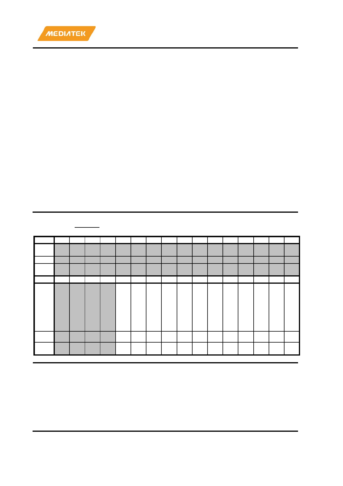
MT7686 Reference Manual
© 2016 - 2017 MediaTek Inc.
Page 198 of 536
This document contains information that is proprietary to MediaTek Inc. (“MediaTek”) and/or its licensor(s).
Any unauthorized use, reproduction or disclosure of this document in whole or in part is strictly prohibited.
8
HINT_AS_FW_OB
Use an interrupt to host as a firmware ownership back
control
•
0: Hosting interrupt to host would NOT trigger firmware
ownership back
•
1: Hosting interrupt to host would trigger firmware ownership
back
6
SDIO_PIO_SEL
Host interface for SDIO PIO
-based function is used.
•
0: SDIO PIO mode is not used.
•
1: SDIO PIO mode is used.
5
EHPI_MODE
This bit indicates if EHPI8
-mode or EHPI16-mode is used.
•
0: EHPI16-mode of EHPI is used.
•
1: EHPI8-mode of EHPI is used.
4
SPI_MODE
This bit indicates if TI
-mode or Motor-mode is used.
•
0: Motor-mode of SPI is used.
•
1: TI-mode of SPI is used.
2:0
DB_HIF_SEL
Host interface for DMA
-based function is used;
•
0x1: SDIO1
•
0x2: SPI
•
0x4: EHPI
A1040004
HGFISR
HIF Global Firmware Interrupt Status
Register
00000000
Bit
31
30
29
28
27
26
25
24
23
22
21
20
19
18
17
16
Nam
e
Type
Rese
t
Bit
15
14
13
12
11
10
9
8
7
6
5
4
3
2
1
0
Nam
e
SD1
_S
ET
_D
S_I
NT
SD1
_S
ET
_X
TA
L_
UP
D_
INT
CH
G_
TO
_18
V_
RE
Q_I
NT
CR
C_
ER
RO
R_I
NT
PB
_I
NT
DB
_I
NT
SDI
O_
SE
T_
AB
T
SDI
O_
SE
T_
RE
S
DR
V_
SE
T_
PB
_IO
E
DR
V_
SE
T_
DB
_IO
E
DR
V_
CL
R_
PB
_IO
E
DR
V_
CL
R_
DB
_IO
E
Type
W1
C
W1
C
W1
C
W1
C
RO RO
W1
C
W1
C
W1
C
W1
C
W1
C
W1
C
Rese
t
0 0 0 0 0 0 0 0 0 0 0 0
Bit(s)
Name
Description
11
SD1_SET_DS_INT
This bit is for SDIO interface only.
If the CCCR deep sleep register is set by host, this bit will be set,
too. Once the firmware detects this event, it will set the device into
deep sleep mode.
Firmware can clear this bit by writing 1.
Writing 0 does nothing.
10
SD1_SET_XTAL_UPD_INT
This b
it is for SDIO interface only.
If the CCCR XTAL frequency update register is set in the host, this
bit will be set, too. Once the firmware detects this event, it will

MT7686 Reference Manual
© 2016 - 2017 MediaTek Inc.
Page 199 of 536
This document contains information that is proprietary to MediaTek Inc. (“MediaTek”) and/or its licensor(s).
Any unauthorized use, reproduction or disclosure of this document in whole or in part is strictly prohibited.
know that the host has updated the XTAL frequency. Firmware can
then read HGH2DR to find
the updated frequency value.
Firmware can clear this bit by writing 1.
Writing 0 does nothing.
9
CHG_TO_18V_REQ_INT
Host sends command 11 to request the device to change
the voltage to 1.8V. Firmware receives the interrupt or
polling status to switch th
e voltage. Then the firmware
writes that the card is in 1.8V status to HGFCR.
8
CRC_ERROR_INT
The status bit of TX data port CRC error interrupt.
7
PB_INT
The status bit of PIO
-based function firmware interrupt.
6
DB_INT
The status bit of DMA
-based function firmware interrupt.
5
SDIO_SET_ABT
SDIO writes 1 to SDIO CCCR. ABORT to abort the
transaction. Once the firmware detects this event, the TX
and RX queues are stopped and the data in the buffer is
discarded.
Firmware can clear this bit by writing
1. Writing 0 does nothing.
4
SDIO_SET_RES
SDIO writes 1 to SDIO CCCR.RES to assert software reset.
Once the firmware detects this event, it disables the sub
-
systems on SDIO interface.
Firmware can clear this bit by writing 1.
Writing 0 does nothing.
3
DR
V_SET_PB_IOE
This bit is for SDIO interface only.
This bit is set if the host sets the CCCR.IOE bit of PIO
-based
functional block. Once the firmware detects this event, it enables
the sub
-system that uses PIO-based function.
Firmware can clear this bit by writing 1.
Writing 0 does nothing.
2
DRV_SET_DB_IOE
This bit is for SDIO interface only.
This bit is set if the host sets the CCCR.IOE bit of DMA
-based
functional block. Once the firmware detects this event, it enables
the s
ub-system that uses DMA-based function.
Firmware can clear this bit by writing 1.
Writing 0 does nothing.
1
DRV_CLR_PB_IOE
This bit is for SDIO interface only.
This bit is set if the host clears the CCCR.IOE bit of PIO
-based
functional block. Once the fir
mware detects this event, it disables
the sub
-system that uses PIO-based function.
Firmware can clear this bit by writing 1.
Writing 0 does nothing.
0
DRV_CLR_DB_IOE
This bit is for SDIO interface only.
This bit is set if the host clears the CCCR.IOE bit
of DMA-based
functional block. Once the firmware detects this event, it disables
the sub
-system which uses DMA-based function.
Firmware can clear this bit by writing 1.
Writing 0 does nothing.
A1040008
HGFIER
HIF Global Firmware
Interrupt Enable
Register
00000000
Bit
31
30
29
28
27
26
25
24
23
22
21
20
19
18
17
16
Nam
e
Type
Rese
t
Bit
15
14
13
12
11
10
9
8
7
6
5
4
3
2
1
0
Nam
e
SD1
_S
ET
_D
S_I
SD1
_S
ET
_X
TA
CH
G_
TO
_18
V_
CR
C_
ER
RO
R_I
PB
_I
NT
_E
N
DB
_I
NT
_E
N
SDI
O_
SE
T_
AB
SDI
O_
SE
T_
RE
DR
V_
SE
T_
PB
DR
V_
SE
T_
DB
DR
V_
CL
R_
PB
DR
V_
CL
R_
DB

MT7686 Reference Manual
© 2016 - 2017 MediaTek Inc.
Page 200 of 536
This document contains information that is proprietary to MediaTek Inc. (“MediaTek”) and/or its licensor(s).
Any unauthorized use, reproduction or disclosure of this document in whole or in part is strictly prohibited.
NT
_E
N
L_
UP
D_
INT
_E
N
RE
Q_I
NT
_E
N
NT
_E
N
T_I
NT
_E
N
S_I
NT
_E
N
_IO
E_I
NT
_E
N
_IO
E_I
NT
_E
N
_IO
E_I
NT
_E
N
_IO
E_I
NT
_E
N
Type
RW
RW
RW
RW
RW
RW
RW
RW
RW
RW
RW
RW
Rese
t
0 0 0 0 0 0 0 0 0 0 0 0
Bit(s)
Name
Description
11
SD1_SET_DS_INT_EN
Common firmware interrupt output control for each bit
corresponding to bits defined in HGFISR.
If the related bit is
•
0: Disable the related bit interrupt output.
•
1: Enable the related bit interrupt output.
10
SD1_SET_XTAL_UPD_INT_EN
Common firmware interrupt output control for each bit
corresponding to bits defined in HGFISR.
If the related bit is
•
0: Disable the related bit interrupt output.
•
1: Enable the related bit interrupt output.
9
C
HG_TO_18V_REQ_INT_EN
Common firmware interrupt output control for each bit
corresponding to bits defined in HGFISR.
If the related bit is
•
0: Disable the related bit interrupt output.
•
1: Enable the related bit interrupt output.
8
CRC_ERROR_INT_EN
Common
firmware interrupt output control for each bit
corresponding to bits defined in HGFISR.
If the related bit is
•
0: Disable the related bit interrupt output.
•
1: Enable the related bit interrupt output.
7
PB_INT_EN
Common firmware interrupt output control for
each bit
corresponding to bits defined in HGFISR.
If the related bit is
•
0: Disable the related bit interrupt output.
•
1: Enable the related bit interrupt output.
6
DB_INT_EN
Common firmware interrupt output control for each bit
corresponding to bits
defined in HGFISR.
If the related bit is
•
0: Disable the related bit interrupt output.
•
1: Enable the related bit interrupt output.
5
SDIO_SET_ABT_INT_EN
Common firmware interrupt output control for each bit
corresponding to bits defined in HGFISR.
If the r
elated bit is
•
0: Disable the related bit interrupt output.
•
1: Enable the related bit interrupt output.
4
SDIO_SET_RES_INT_EN
Common firmware interrupt output control for each bit
corresponding to bits defined in HGFISR.
If the related bit is
MT7686 Reference Manual
© 2016 - 2017 MediaTek Inc.
Page 201 of 536
This document contains information that is proprietary to MediaTek Inc. (“MediaTek”) and/or its licensor(s).
Any unauthorized use, reproduction or disclosure of this document in whole or in part is strictly prohibited.
•
0: Disable the related bit interrupt output.
•
1: Enable the related bit interrupt output.
3
DRV_SET_PB_IOE_INT_EN
Common firmware interrupt output control for each bit
corresponding to bits defined in HGFISR.
If the related bit is
•
0: Disable the related bit interrupt output.
•
1: Enable the related bit interrupt output.
2
DRV_SET_DB_IOE_INT_EN
Common firmware interrupt output control for each bit
corresponding to bits defined in HGFISR.
If the related bit is
•
0: Disable the related bit interrupt output.
•
1: Enable the related bit interrupt output.
1
DRV_CLR_PB_IOE_INT_EN
Common firmware interrupt output control for each bit
corresponding to bits defined in HGFISR.
If the related bit is
•
0: Disable the related bit interrupt output.
•
1: Enable the related bit interrupt output.
0
DRV_CLR_DB_IOE_INT_EN
Common firmware interrupt output control for each bit
corresponding to bits defined in HGFISR.
If the related bit is
•
0: Disable the related bit interrupt output.
•
1: Enable the related bit interrupt output.
A1040010
HSDBDLSR
HIF SDIO Bus Delay Selection Register
00000000
Bit
31
30
29
28
27
26
25
24
23
22
21
20
19
18
17
16
Nam
e
Type
Rese
t
Bit
15
14
13
12
11
10
9
8
7
6
5
4
3
2
1
0
Nam
e
SD1_DAT3_DEL
SEL
SD1_DAT2_DEL
SEL
SD1_DAT1_DEL
SEL
SD1_DAT0_DEL
SEL
Type
RW
RW
RW
RW
Rese
t
0 0 0 0 0 0 0 0 0 0 0 0
Bit(s)
Name
Description
14:12
SD1_DAT3_DELSEL
It is used to tune the SDIO1 bit3 bus delay for
desensitization
•
7: about 1.4ns.
•
6: about 1.2ns.
•
5: about 1.0ns.
•
4: about 0.8ns.
•
3: about 0.6ns.
•
2: about 0.4ns.
•
1: about 0.2ns.

MT7686 Reference Manual
© 2016 - 2017 MediaTek Inc.
Page 202 of 536
This document contains information that is proprietary to MediaTek Inc. (“MediaTek”) and/or its licensor(s).
Any unauthorized use, reproduction or disclosure of this document in whole or in part is strictly prohibited.
•
0: no delay.
10:8
SD1_DAT2_DELSEL
It is used to tune the SDIO1 bit2 bus delay for
desensitization
(bit 2)
•
7: about 1.4ns.
•
6: about 1.2ns.
•
5: about 1.0ns.
•
4: about 0.8ns.
•
3: about 0.6ns.
•
2: about 0.4ns.
•
1: about 0.2ns.
•
0: no delay.
6:4
SD1_DAT1_DELSEL
It is used to tune the SDIO1 bit1 bus delay for
desensitization
•
7: about 1.4ns.
•
6: about 1.2ns.
•
5: about 1.0ns.
•
4: about 0.8ns.
•
3: about 0.6ns.
•
2: about 0.4ns.
•
1: about 0.2ns.
•
0: no delay
2:0
SD1_DAT0_DELSEL
It is used to tune the SDIO1 bit0 bus delay for
desensitization
•
7: about 1.4ns.
•
6: about 1.2ns.
•
5: about 1.0ns
•
4: about 0.8ns
•
3: about 0.6ns.
•
2: about 0.4ns.
•
1: about 0.2ns.
•
0: no delay
A1040014
HSDLSR
HIF SRAM Delay Selection Register
00000F0A
Bit
31
30
29
28
27
26
25
24
23
22
21
20
19
18
17
16
Nam
e
Type
Rese
t
Bit
15
14
13
12
11
10
9
8
7
6
5
4
3
2
1
0
Nam
e
PB_DELS
EL_3_2
PB_DELS
EL_1_0
DB_DELS
EL_3_2
DB_DELS
EL_1_0
Type
RW
RW
RW
RW
Rese
t
1 1 1 1 1 0 1 0
MT7686 Reference Manual
© 2016 - 2017 MediaTek Inc.
Page 203 of 536
This document contains information that is proprietary to MediaTek Inc. (“MediaTek”) and/or its licensor(s).
Any unauthorized use, reproduction or disclosure of this document in whole or in part is strictly prohibited.
Bit(s)
Name
Description
11:10
PB_DELSEL_3_2
Delay selection of SRAM of PIO
-based part of SDIO
controller
Note, that the
default value is different for different processes.
9:8
PB_DELSEL_1_0
Delay selection of SRAM of PIO
-based part of SDIO
controller
Note, that the default value is different for different processes.
3:2
DB_DELSEL_3_2
Delay selection of SRAM of DMA
-based part of SDIO
controller
Note, that the default value is different for different processes.
1:0
DB_DELSEL_1_0
Delay selection of SRAM of DMA
-based part of SDIO
controller
Note, that the default value is different for different processes.
A1040018
HCSDCR
HIF Clock Stop Detection register
0000FDE8
Bit
31
30
29
28
27
26
25
24
23
22
21
20
19
18
17
16
Nam
e
SDCLK_STOP_NUM
Type
RW
Rese
t
0 0 0 0
Bit
15
14
13
12
11
10
9
8
7
6
5
4
3
2
1
0
Nam
e
SDCLK_STOP_NUM
Type
RW
Rese
t
1 1 1 1 1 1 0 1 1 1 1 0 1 0 0 0
Bit(s)
Name
Description
19:0
SDCLK_STOP_NUM
For SDIO 3.0 design, host driver needs to issue CMD11 to switch
the
voltage to 1.8V to enter UHS mode. This field is to set the
hardware timer threshold for SDIO hardware to
determine whether
the SD clock has stopped. According to SDIO 3.0 specification
s, the
host should stop
the clock at least 5ms for the device to switch the
voltage from 3.3
V to 1.8V
. The unit of this field is based on the AHB
clock cycle number.
A104001C
HGH2DR
HIF Global Host to Device Register
00000003
Bit
31
30
29
28
27
26
25
24
23
22
21
20
19
18
17
16
Nam
e
Type
Rese
t
Bit
15
14
13
12
11
10
9
8
7
6
5
4
3
2
1
0
Nam
e
XTAL_FREQ
Type
RO
Rese
t
0 1 1
Bit(s)
Name
Description
MT7686 Reference Manual
© 2016 - 2017 MediaTek Inc.
Page 204 of 536
This document contains information that is proprietary to MediaTek Inc. (“MediaTek”) and/or its licensor(s).
Any unauthorized use, reproduction or disclosure of this document in whole or in part is strictly prohibited.
2:0
XTAL_FREQ
The h
ost can write this CCCR vendor unique register to update the
XTAL
frequency information for firmware to read. When the host
write
s 1 to this field, hardware would send an interrupt to firmware
to noti
fy that the host has updated the XTAL frequency. Firmware
can read the firmware domai
n HGH2DR register to derive the
updated
XTAL frequency.
A1040020
HDBGCR
HIF Debug Control Register
11110000
Bit
31
30
29
28
27
26
25
24
23
22
21
20
19
18
17
16
Nam
e
DEBUG_MONH DEBUG_MONL
Type
RO
RO
Rese
t
0 0 0 1 0 0 0 1 0 0 0 1 0 0 0 1
Bit
15
14
13
12
11
10
9
8
7
6
5
4
3
2
1
0
Nam
e
FLAG_HSEL FLAG_LSEL
Type
RW
RW
Rese
t
0 0 0 0 0 0 0 0 0 0 0 0 0 0 0 0
Bit(s)
Name
Description
31:24
DEBUG_MONH
Debug flag monitor for High byte
Show the flag value specified in FLAG_HSEL
23:16
DEBUG_MONL
Debug flag monitor for Low byte
Show the flag value specified in FLAG_LSEL
15:8
FLAG_HSEL
Flag number of High byte for debug
Select which flag for debug in high byte
7:0
FLAG_LSEL
Flag number of Low byte for debug
Select which flag for debug in low byte
A104002C
FWDSIOCR
DS Pad Macro IO Control Register
80000422
Bit
31
30
29
28
27
26
25
24
23
22
21
20
19
18
17
16
Nam
e
DS
_R
ES
P_
EN
DS_RDSEL DS_TDSEL
Type
RW
RW
RW
Rese
t
1 0 0 0 0 0 0 0 0 0 0
Bit
15
14
13
12
11
10
9
8
7
6
5
4
3
2
1
0
Nam
e DS_E8E4E2 DS
_S
MT
DS
_P
UP
D
DS
_R
1
DS
_R
0
DS
_IE
S
DS
_S
R
Type
RW
RW
RW
RW
RW
RW
RW
Rese
t
1 0 0 1 0 0 0 1 0
Bit(s)
Name
Description
31
DS_RESP_EN
HS400 mode response ds toggle enable bit
0:response DS toggle disable
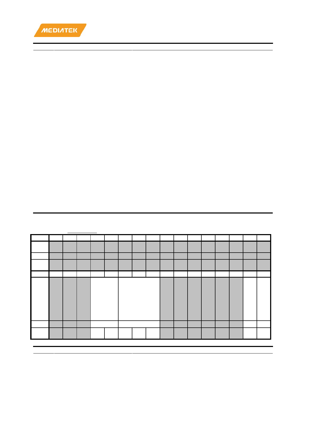
MT7686 Reference Manual
© 2016 - 2017 MediaTek Inc.
Page 205 of 536
This document contains information that is proprietary to MediaTek Inc. (“MediaTek”) and/or its licensor(s).
Any unauthorized use, reproduction or disclosure of this document in whole or in part is strictly prohibited.
Bit(s)
Name
Description
1: response DS toggle enable
29:24
DS_RDSEL
RX duty select
RDSEL[1:0]: Input buffer duty high when asserted (high pulse
width adjustment)
RDSEL[3:2]: Input buffer duty low when asserted (low pulse width
adjustment)
RDSEL[5:4]: Level shifter duty high when asserted (high pulse
width adjustment)
RDSEL[7:6]: Level shifter duty low when asserted (low pulse width
adjustment)
19:16
DS_TDSEL
TX duty select
TDSEL[1:0]: Output level shifter duty high when asserted (high
pulse width adjustment)
TDSEL[3:2]: Output level shifter duty low when asserted (low pulse
width adjustment)
10:8
DS_E8E4E2
TX Driving Strength Control.
5
DS_SMT
RX input buffer Schmitt trigger hysteresis control enable.
High asserted.
SMT=1, Schmitt Trigger enable
4
DS_PUPD
Pull-up / pull-down selection.
0: pull
-up resistor
1: pull
-down resistor
CLK pad default no pull
3
DS_R1
Select 50K resistor (0: not select, 1: select)
2
DS_R0
Select 10K resistor (0: not select, 1: select)
1
DS_IES
RX input buffer enable. High asserted.
Datapath: from IO to O. IES=0, O=0
0
DS_SR
Output Slew Rate Control. High asserted.
SR=1, slower slew.
SR=0, no slew rate controlled.
A1040030
HGTMTCR
Test Mode Trigger Control Register
00001300
Bit
31
30
29
28
27
26
25
24
23
22
21
20
19
18
17
16
Nam
e
Type
Rese
t
Bit
15
14
13
12
11
10
9
8
7
6
5
4
3
2
1
0
Nam
e TM_BUS
_WIDTH TM_BSS
FW
_T
RI
GG
ER
_C
RC
_S
TS
FW
_T
RI
GG
ER
_T
M_
DA
TA
Type
RW
RW
RW
RW
Rese
t
1 0 0 1 1 0 0
Bit(s)
Name
Description
12:11
TM_BUS_WIDTH
For Test Mode, set the bus width of SDIO bus interface
0x0: SD1-bit
0x1: Reserved
0x2: SD4-bit
0x3: SD8-bit
10:8
TM_BSS
For Test Mode, set the bus speed of SDIO bus interface
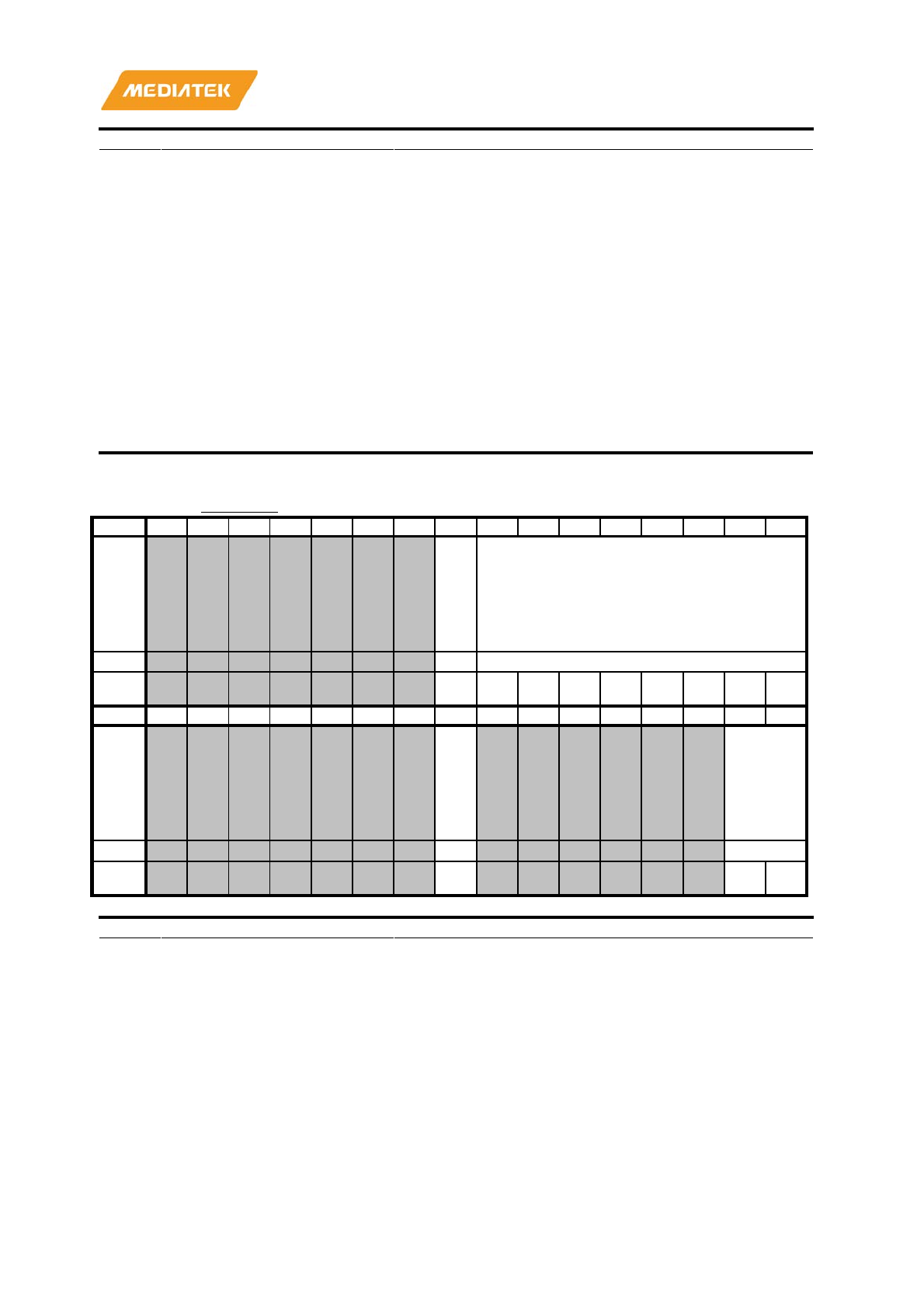
MT7686 Reference Manual
© 2016 - 2017 MediaTek Inc.
Page 206 of 536
This document contains information that is proprietary to MediaTek Inc. (“MediaTek”) and/or its licensor(s).
Any unauthorized use, reproduction or disclosure of this document in whole or in part is strictly prohibited.
Bit(s)
Name
Description
0x0: SDR12
0x1: SDR25
0x2: SDR50
0x3: SDR104
0x4: DDR50
1
FW_TRIGGER_CRC_STS
For Test Mode: Send a good CRC status after firmware
trigger is enabled. The firmware polls this bit to make it 0
to trigger another event.
0: Disable SDIO Device Send CRC Status
1: Enable SDIO Device Send CRC Status
0
FW_TRIGGER_TM_DATA
For the Test Mode: Send a specific response and block
data after firmware trigger is enabled. The firmware polls
this bit to make it 0
to trigger another event.
Note, that the content is configured similar to the host initiated
pattern generation
0: Disable SDIO Device Send Response and block data.
1: Enable SDIO Device Send Response and block data.
A1040034
HGTMCR
Test Mode Control Register
00080000
Bit
31
30
29
28
27
26
25
24
23
22
21
20
19
18
17
16
Nam
e
TE
ST
_M
OD
E_
FW
_O
WN
PRBS_INIT_VAL
Type
RW
RW
Rese
t
0 0 0 0 0 1 0 0 0
Bit
15
14
13
12
11
10
9
8
7
6
5
4
3
2
1
0
Nam
e
TE
ST
_M
OD
E_
ST
AT
US
TEST_MO
DE_SELE
CT
Type
RO
RW
Rese
t
0 0 0
Bit(s)
Name
Description
24
TEST_MODE_FW_OWN
Indicates the ownership of Test Mode Control Register :
WTMCR,WTMDPCR0,WTMDPCR1
0: Host has the ownership.
1: Firmware has the ownership.
23:16
PRBS_INIT_VAL
Initial Value For PRBS generator
8
TEST_MODE_STATUS
To record the comparison result of the latest Test Mode
write operation.
0: Data compare of Test Mode write is Pass
1: Data compare of Test Mode write is Fail
1:0
TEST_MODE_SELECT
Select the test mode data pattern
-
64-bits configurable data register
(WTMDPCR0:WTMDPCR1)
-32-bits configurable data register
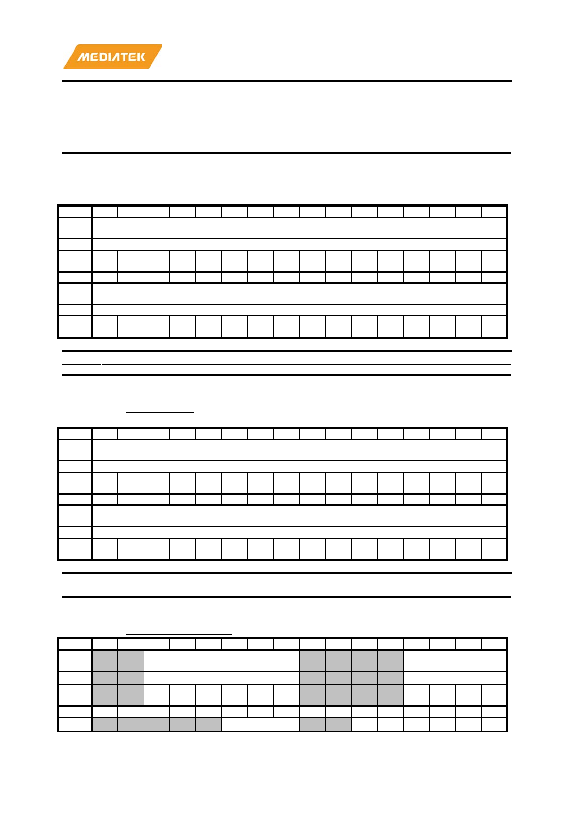
MT7686 Reference Manual
© 2016 - 2017 MediaTek Inc.
Page 207 of 536
This document contains information that is proprietary to MediaTek Inc. (“MediaTek”) and/or its licensor(s).
Any unauthorized use, reproduction or disclosure of this document in whole or in part is strictly prohibited.
Bit(s)
Name
Description
-PRBS
00: the 32bit data pattern
01: the 64bit data pattern
10: the PRBS data pattern
11: reserved
A1040038
HGTMDPCR0
Test Mode Data Pattern Control
Register 0
F0F0F0F0
Bit
31
30
29
28
27
26
25
24
23
22
21
20
19
18
17
16
Nam
e
TEST_MODE_DATA_PATTERN_0
Type
RW
Rese
t
1 1 1 1 0 0 0 0 1 1 1 1 0 0 0 0
Bit
15
14
13
12
11
10
9
8
7
6
5
4
3
2
1
0
Nam
e
TEST_MODE_DATA_PATTERN_0
Type
RW
Rese
t
1 1 1 1 0 0 0 0 1 1 1 1 0 0 0 0
Bit(s)
Name
Description
31:0
TEST_MODE_DATA_PATTERN_0
Data pattern for Test Mode read
A104003C
HGTMDPCR1
Test Mode Data Pattern Control
Register 1
F0F0F0F0
Bit
31
30
29
28
27
26
25
24
23
22
21
20
19
18
17
16
Nam
e
TEST_MODE_DATA_PATTERN_1
Type
RW
Rese
t
1 1 1 1 0 0 0 0 1 1 1 1 0 0 0 0
Bit
15
14
13
12
11
10
9
8
7
6
5
4
3
2
1
0
Nam
e
TEST_MODE_DATA_PATTERN_1
Type
RW
Rese
t
1 1 1 1 0 0 0 0 1 1 1 1 0 0 0 0
Bit(s)
Name
Description
31:0
TEST_MODE_DATA_PATTERN_1
Data pattern for Test Mode write
A1040040
FWCLKIOCR_T28LP
Clock Pad Macro IO Control Register
00000422
Bit
31
30
29
28
27
26
25
24
23
22
21
20
19
18
17
16
Nam
e
CLK_RDSEL CLK_TDSEL
Type
RW
RW
Rese
t
0 0 0 0 0 0 0 0 0 0
Bit
15
14
13
12
11
10
9
8
7
6
5
4
3
2
1
0
Nam
CLK_E8E4E2
CL CL CL CL CL CL
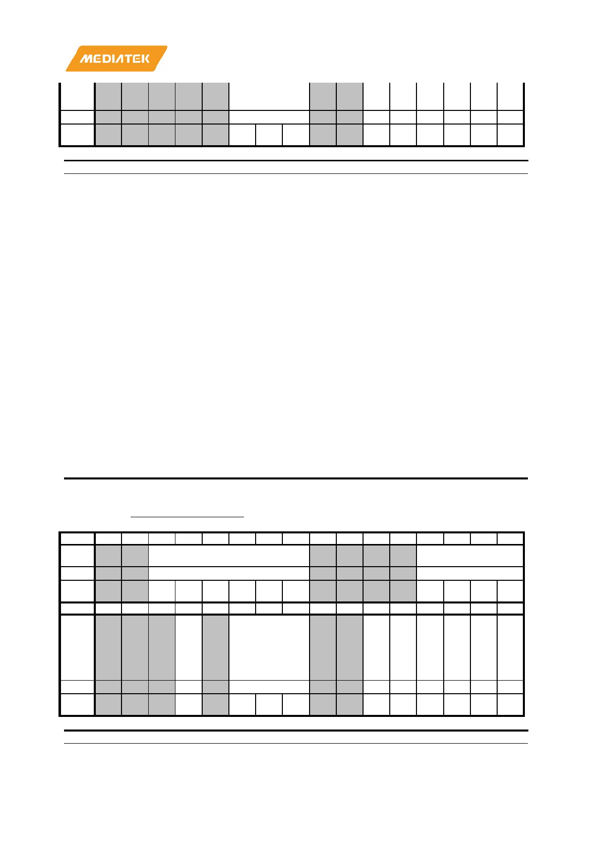
MT7686 Reference Manual
© 2016 - 2017 MediaTek Inc.
Page 208 of 536
This document contains information that is proprietary to MediaTek Inc. (“MediaTek”) and/or its licensor(s).
Any unauthorized use, reproduction or disclosure of this document in whole or in part is strictly prohibited.
e
K_
SM
T
K_
PU
PD
K_
R1
K_
R0
K_I
ES
K_
SR
Type
RW
RW
RW
RW
RW
RW
RW
Rese
t
1 0 0 1 0 0 0 1 0
Bit(s)
Name
Description
29:24
CLK_RDSEL
RX duty select
RDSEL[1:0]: Input buffer duty high when asserted (high pulse
width adjustment)
RDSEL[3:2]: Input buffer duty low when
asserted (low pulse width
adjustment)
RDSEL[5:4]: Level shifter duty high when asserted (high pulse
width adjustment)
RDSEL[7:6]: Level shifter duty low when asserted (low pulse width
adjustment)
19:16
CLK_TDSEL
TX duty select
TDSEL[1:0]: Output level
shifter duty high when asserted (high
pulse width adjustment)
TDSEL[3:2]: Output level shifter duty low when asserted (low pulse
width adjustment)
10:8
CLK_E8E4E2
TX Driving Strength Control.
5
CLK_SMT
RX input buffer Schmitt trigger hysteresis control enable.
High asserted.
SMT=1, Schmitt Trigger enable
4
CLK_PUPD
Pull-up / pull-down selection.
0: pull
-up resistor
1: pull
-down resistor
CLK pad default no pull
3
CLK_R1
Select 50K resistor (0: not select, 1: select)
2
CLK_R0
Select 10K resistor (0: not select, 1: select)
1
CLK_IES
RX input buffer enable. High asserted.
Datapath: from IO to O. IES=0, O=0
0
CLK_SR
Output Slew Rate Control. High asserted.
SR=1, slower slew.
SR=0, no slew rate controlled.
A1040044
FWCMDIOCR_T28LP
Command Pad Macro IO Control
Register
00000422
Bit
31
30
29
28
27
26
25
24
23
22
21
20
19
18
17
16
Nam
e
CMD_RDSEL CMD_TDSEL
Type
RW
RW
Rese
t
0 0 0 0 0 0 0 0 0 0
Bit
15
14
13
12
11
10
9
8
7
6
5
4
3
2
1
0
Nam
e
RE
G_
CM
D_
SA
MP
LE
CMD_E8E4E2
CM
D_
SM
T
CM
D_
PU
PD
CM
D_
R1
CM
D_
R0
CM
D_
IES
CM
D_
SR
Type
RW
RW
RW
RW
RW
RW
RW
RW
Rese
t
0 1 0 0 1 0 0 0 1 0
Bit(s)
Name
Description
29:24
CMD_RDSEL
RX duty select
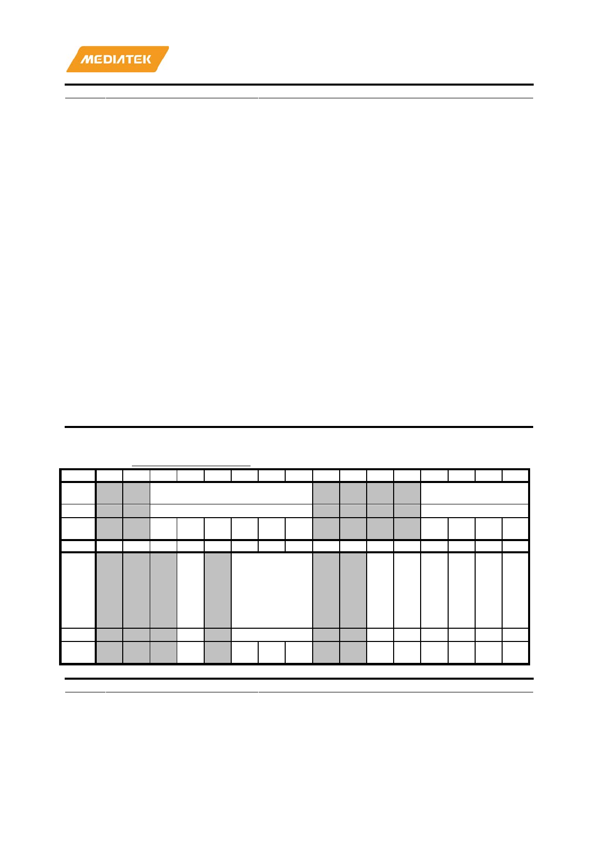
MT7686 Reference Manual
© 2016 - 2017 MediaTek Inc.
Page 209 of 536
This document contains information that is proprietary to MediaTek Inc. (“MediaTek”) and/or its licensor(s).
Any unauthorized use, reproduction or disclosure of this document in whole or in part is strictly prohibited.
Bit(s)
Name
Description
RDSEL[1:0]: Input buffer duty high when asserted (high pulse
width adjustment)
RDSEL[3:2]: Input buffer duty low when asserted (low pulse width
adjustment)
RDSEL[5:4]: Level shifter duty high when asserted (high pulse
width adjustment)
RDSEL[7:6]: Level sh
ifter duty low when asserted (low pulse width
adjustment)
19:16
CMD_TDSEL
TX duty select
TDSEL[1:0]: Output level shifter duty high when asserted (high
pulse width adjustment)
TDSEL[3:2]: Output level shifter duty low when asserted (low pulse
width adjustment)
12
REG_CMD_SAMPLE
Select clock edge to latch input bus signal.
0: Use positive SD clock edge to latch input command
1: Use negative SD clock edge to latch input command
10:8
CMD_E8E4E2
TX Driving Strength Control.
5
CMD_SMT
RX input buffer Schmitt trigger hysteresis control enable.
High asserted.
SMT=1, Schmitt Trigger enable
4
CMD_PUPD
Pull-up / pull-down selection.
0: pull
-up resistor
1: pull
-down resistor
CMD pad default no pull
3
CMD_R1
Select 50K resistor (0: not select, 1: select)
2
CMD_R0
Select 10K resistor (0: not select, 1: select)
1
CMD_IES
RX input buffer enable. High asserted.
Datapath: from IO to O. IES=0, O=0
0
CMD_SR
Output Slew Rate Control. High asserted.
SR=1, slower slew.
SR=0, no slew rate controlled.
A1040048
FWDAT0IOCR_T28LP
Data 0 Pad Macro IO Control Register
00000422
Bit
31
30
29
28
27
26
25
24
23
22
21
20
19
18
17
16
Nam
e
DATA0_RDSEL DATA0_TDSEL
Type
RW
RW
Rese
t
0 0 0 0 0 0 0 0 0 0
Bit
15
14
13
12
11
10
9
8
7
6
5
4
3
2
1
0
Nam
e
RE
G_
DA
TA
0_
SA
MP
LE
DATA0_E8E4E2
DA
TA
0_
SM
T
DA
TA
0_
PU
PD
DA
TA
0_
R1
DA
TA
0_
R0
DA
TA
0_I
ES
DA
TA
0_
SR
Type
RW
RW
RW
RW
RW
RW
RW
RW
Rese
t
0 1 0 0 1 0 0 0 1 0
Bit(s)
Name
Description
29:24
DATA0_RDSEL
RX duty select
RDSEL[1:0]: Input buffer duty high when asserted (high pulse
width adjustment)
RDSEL[3:2]: Input buffer duty low when asserted (low pulse width
adjustment)
RDSEL[5:4]: Level shifter duty high when asserted (high pulse
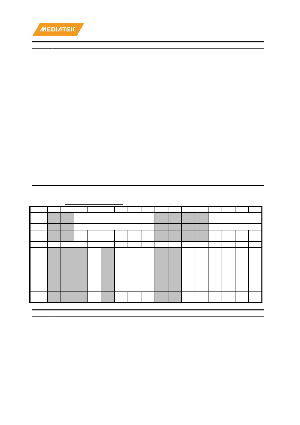
MT7686 Reference Manual
© 2016 - 2017 MediaTek Inc.
Page 210 of 536
This document contains information that is proprietary to MediaTek Inc. (“MediaTek”) and/or its licensor(s).
Any unauthorized use, reproduction or disclosure of this document in whole or in part is strictly prohibited.
Bit(s)
Name
Description
width adjustment)
RDSE
L[7:6]: Level shifter duty low when asserted (low pulse width
adjustment)
19:16
DATA0_TDSEL
TX duty select
TDSEL[1:0]: Output level shifter duty high when asserted (high
pulse width adjustment)
TDSEL[3:2]: Output level shifter duty low when asserted (low pulse
width adjustment)
12
REG_DATA0_SAMPLE
Select clock edge to latch input bus signal.
0: Use positive SD clock edge to latch input data 0
1: Use negative SD clock edge to latch input data 0
10:8
DATA0_E8E4E2
TX Driving Strength Control.
5
DATA0_SMT
RX input buffer Schmitt trigger hysteresis control enable.
High asserted.
SMT=1, Schmitt Trigger enable
4
DATA0_PUPD
Pull-up / pull-down selection.
0: pull
-up resistor
1: pull
-down resistor
DATA 0 pad default no pull
3
DATA0_R1
Select 50K resistor (0: not select, 1: select)
2
DATA0_R0
Select 10K resistor (0: not select, 1: select)
1
DATA0_IES
RX input buffer enable. High asserted.
Datapath: from IO to O. IES=0, O=0
0
DATA0_SR
Output Slew Rate Control. High asserted.
SR=1, slower slew.
SR=0, no slew rate controlled.
A104004C
FWDAT1IOCR_T28LP
Data 1 Pad Macro IO Control Register
00000422
Bit
31
30
29
28
27
26
25
24
23
22
21
20
19
18
17
16
Nam
e
DATA1_RDSEL DATA1_TDSEL
Type
RW
RW
Rese
t
0 0 0 0 0 0 0 0 0 0
Bit
15
14
13
12
11
10
9
8
7
6
5
4
3
2
1
0
Nam
e
RE
G_
DA
TA1
_S
AM
PL
E
DATA1_E8E4E2
DA
TA1
_S
MT
DA
TA1
_P
UP
D
DA
TA1
_R
1
DA
TA1
_R
0
DA
TA1
_IE
S
DA
TA1
_S
R
Type
RW
RW
RW
RW
RW
RW
RW
RW
Rese
t
0 1 0 0 1 0 0 0 1 0
Bit(s)
Name
Description
29:24
DATA1_RDSEL
RX duty select
RDSEL[1:0]: Input buffer duty high when asserted (high pulse
width adjustment)
RDSEL[3:2]: Input buffer duty low when asserted (low pulse width
adjustment)
RDSEL[5:4]: Level shifter duty high when asserted (high pulse
width
adjustment)
RDSEL[7:6]: Level shifter duty low when asserted (low pulse width
adjustment)
19:16
DATA1_TDSEL
TX duty select
TDSEL[1:0]: Output level shifter duty high when asserted (high
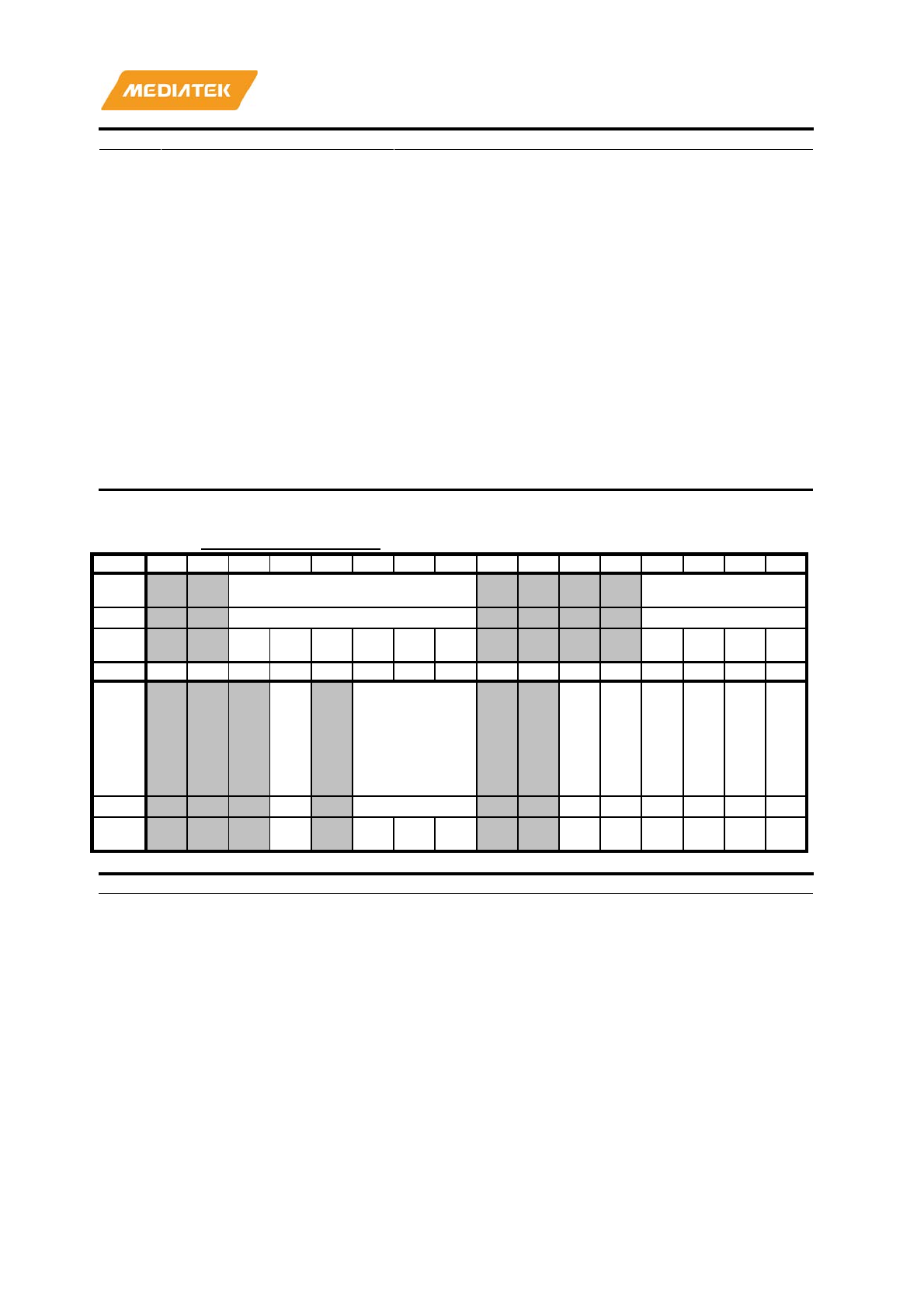
MT7686 Reference Manual
© 2016 - 2017 MediaTek Inc.
Page 211 of 536
This document contains information that is proprietary to MediaTek Inc. (“MediaTek”) and/or its licensor(s).
Any unauthorized use, reproduction or disclosure of this document in whole or in part is strictly prohibited.
Bit(s)
Name
Description
pulse width adjustment)
TDSEL[3:2]: Output level shifter duty low when asserted (low pulse
width adjustment)
12
REG_DATA1_SAMPLE
Select clock edge to latch input bus signal.
0: Use positive SD clock edge to latch input data 1
1: Use negative SD clock edge to latch input data 1
10:8
DATA1_E8E4E2
TX Driving Strength Control.
5
DATA1_SMT
RX input buffer Schmitt trigger hysteresis control enable.
High asserted.
SMT=1, Schmitt Trigger enable
4
DATA1_PUPD
Pull-up / pull-down selection.
0: pull
-up resistor
1: pull
-down resistor
DATA 1 pad default no pull
3
DATA1_R1
Select 50K resistor (0: not select, 1: select)
2
DATA1_R0
Select 10K resistor (0: not select, 1: select)
1
DATA1_IES
RX input buffer enable. High asserted.
Datapath: from IO to O. IES=0, O=0
0
DATA1_SR
Output Slew Rate Control. High asserted.
SR=1, slower slew.
SR=0, no slew rate controlled.
A1040050
FWDAT2IOCR_T28LP
Data 2 Pad Macro IO Control Register
00000422
Bit
31
30
29
28
27
26
25
24
23
22
21
20
19
18
17
16
Nam
e
DATA2_RDSEL DATA2_TDSEL
Type
RW
RW
Rese
t
0 0 0 0 0 0 0 0 0 0
Bit
15
14
13
12
11
10
9
8
7
6
5
4
3
2
1
0
Nam
e
RE
G_
DA
TA
2_
SA
MP
LE
DATA2_E8E4E2
DA
TA
2_
SM
T
DA
TA
2_
PU
PD
DA
TA
2_
R1
DA
TA
2_
R0
DA
TA
2_I
ES
DA
TA
2_
SR
Type
RW
RW
RW
RW
RW
RW
RW
RW
Rese
t
0 1 0 0 1 0 0 0 1 0
Bit(s)
Name
Description
29:24
DATA2_RDSEL
RX duty select
RDSEL[1:0]: Input buffer duty high when asserted (high pulse
width adjustment)
RDSEL[3:2]: Input buffer duty low when asserted (low pulse width
adjustment)
RDSEL[5:4]: Level shifter duty high when a
sserted (high pulse
width adjustment)
RDSEL[7:6]: Level shifter duty low when asserted (low pulse width
adjustment)
19:16
DATA2_TDSEL
TX duty select
TDSEL[1:0]: Output level shifter duty high when asserted (high
pulse width adjustment)
TDSEL[3:2]: Output
level shifter duty low when asserted(low pulse
width adjustment)
12
REG_DATA2_SAMPLE
Select clock edge to latch input bus signal.
0: Use positive SD clock edge to latch input data 2
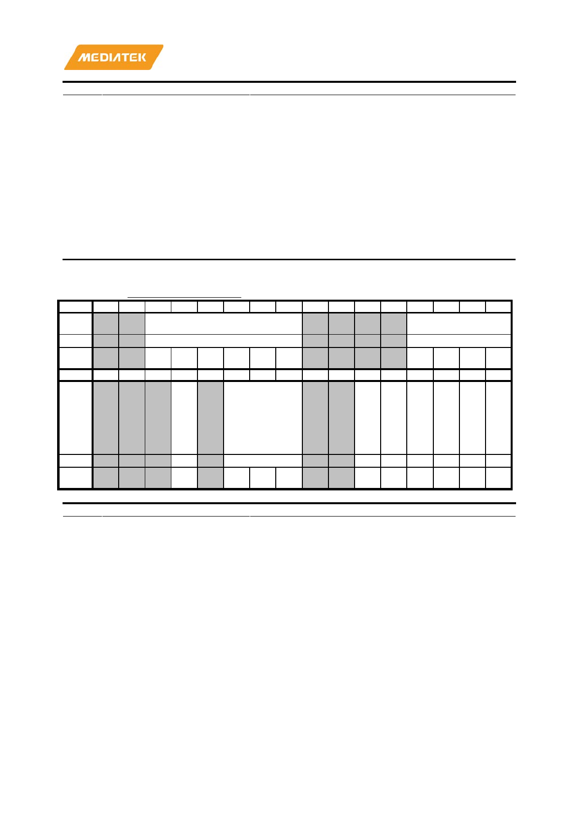
MT7686 Reference Manual
© 2016 - 2017 MediaTek Inc.
Page 212 of 536
This document contains information that is proprietary to MediaTek Inc. (“MediaTek”) and/or its licensor(s).
Any unauthorized use, reproduction or disclosure of this document in whole or in part is strictly prohibited.
Bit(s)
Name
Description
1: Use negative SD clock edge to latch input data 2
10:8
DATA2_E8E4E2
TX Driving Strength Control.
5
DATA2_SMT
RX input buffer Schmitt trigger hysteresis control enable.
High asserted.
SMT=1, Schmitt Trigger enable
4
DATA2_PUPD
Pull-up / pull-down selection.
0: pull
-up resistor
1: pull
-down resistor
DATA 2 pad default no pull
3
DATA2_R1
Select 50K resistor (0: not select, 1: select)
2
DATA2_R0
Select 10K resistor (0: not select, 1: select)
1
DATA2_IES
RX input buffer enable. High asserted.
Datapath: from IO to O. IES=0, O=0
0
DATA2_SR
Output Slew Rate Control. High asserted.
SR=1, slower slew.
SR=0, no slew rate controlled.
A1040054
FWDAT3IOCR_T28LP
Data 3 Pad Macro IO Control Register
0000042A
Bit
31
30
29
28
27
26
25
24
23
22
21
20
19
18
17
16
Nam
e
DATA3_RDSEL DATA3_TDSEL
Type
RW
RW
Rese
t
0 0 0 0 0 0 0 0 0 0
Bit
15
14
13
12
11
10
9
8
7
6
5
4
3
2
1
0
Nam
e
RE
G_
DA
TA
3_
SA
MP
LE
DATA3_E8E4E2
DA
TA
3_
SM
T
DA
TA
3_
PU
PD
DA
TA
3_
R1
DA
TA
3_
R0
DA
TA
3_I
ES
DA
TA
3_
SR
Type
RW
RW
RW
RW
RW
RW
RW
RW
Rese
t
0 1 0 0 1 0 1 0 1 0
Bit(s)
Name
Description
29:24
DATA3_RDSEL
RX duty select
RDSEL[1:0]: Input buffer duty high when asserted (high pulse
width adjustment)
RDSEL[3:2]: Input buffer duty low when asserted (low pulse width
adjustment)
RDSEL[5:4]: Level shifter duty high when asserted (high pulse
width adjustment)
RDSEL[7:6]: Level shifter duty low when asserted (low pulse width
adjustment)
19:16
DATA3_TDSEL
TX duty select
TDSEL[1:0]: Output level shifter duty high when asserted (high
pulse width adjustment)
TDSEL[3:2]: Output level shifter duty low when asserted (low pulse
width adjustment)
12
REG_DATA3_SAMPLE
Select clock edge to latch input bus signal.
0: Use positive SD clock edge to latch input data 3
1: Use negative SD clock edge to latch input data 3
10:8
DATA3_E8E4E2
TX Driving Strength Control.
5
DATA3_SMT
RX input buffer Schmitt trigger hysteresis control enable.
High asserted.
SMT=1, Schmitt Trigger enable
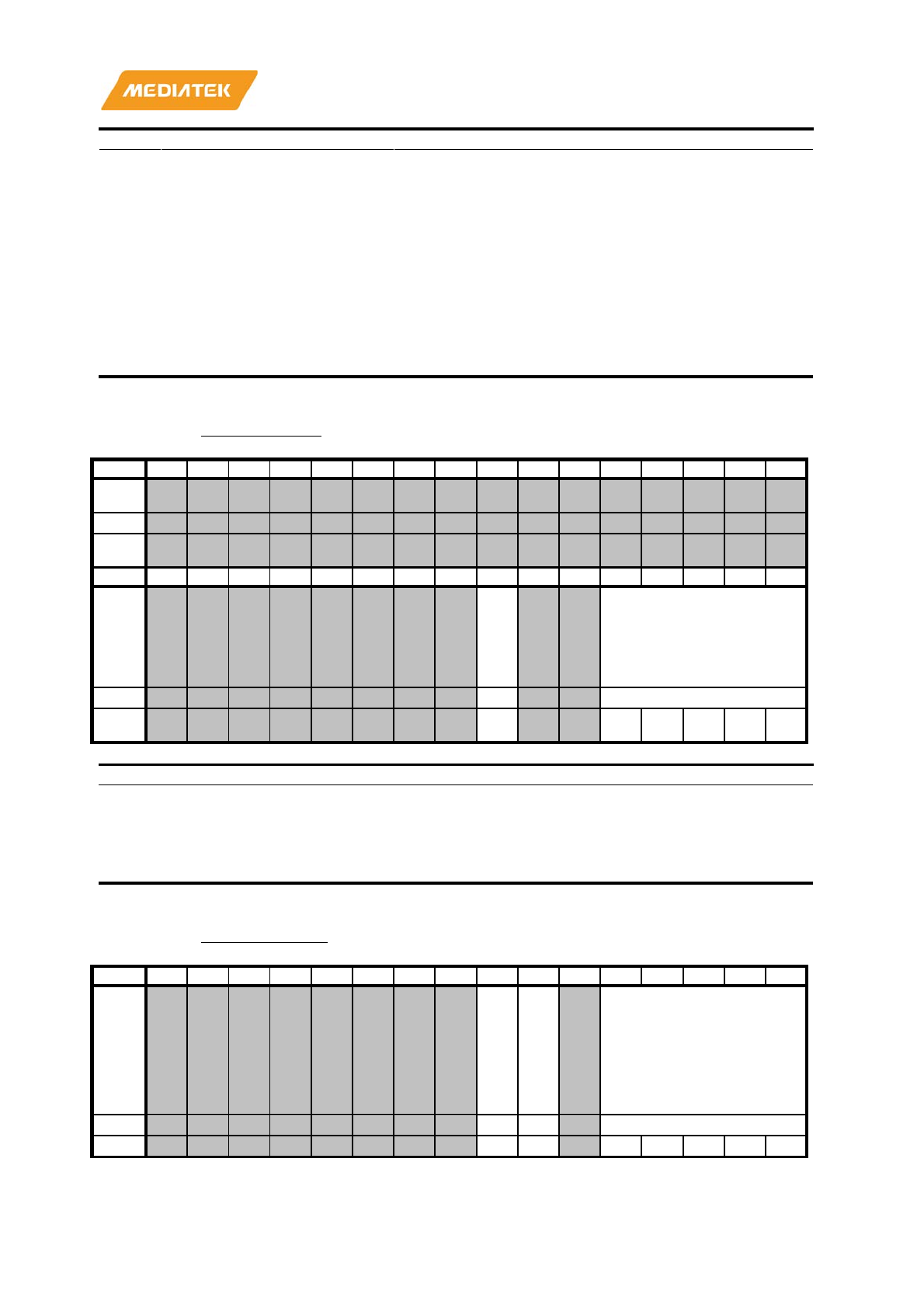
MT7686 Reference Manual
© 2016 - 2017 MediaTek Inc.
Page 213 of 536
This document contains information that is proprietary to MediaTek Inc. (“MediaTek”) and/or its licensor(s).
Any unauthorized use, reproduction or disclosure of this document in whole or in part is strictly prohibited.
Bit(s)
Name
Description
4
DATA3_PUPD
Pull-up / pull-down selection.
0: pull
-up resistor
1: pull
-down resistor
DATA 3 pad default would pull up with 50K resistor. (for card
detection)
After host driver writes cd_disable to CCCR register, data 3 pad
would become no pull.
3
DATA3_R1
Select 50K resistor (0: not select, 1: select)
2
DATA3_R0
Select 10K resistor (0: not select, 1: select)
1
DATA3_IES
RX input buffer enable. High asserted.
Datapath: from IO to O. IES=0, O=0
0
DATA3_SR
Output Slew Rate Control. High asserted.
SR=1, slower slew.
SR=0, no slew rate controlled.
A1040058
FWCLKDLYCR
Clock Pad Macro Delay Chain Control
Register
00000000
Bit
31
30
29
28
27
26
25
24
23
22
21
20
19
18
17
16
Nam
e
Type
Rese
t
Bit
15
14
13
12
11
10
9
8
7
6
5
4
3
2
1
0
Nam
e
RE
G_
CK
_D
LY
_E
N
CLK_DLY_SEL
Type
RW
RW
Rese
t
0 0 0 0 0 0
Bit(s)
Name
Description
7
REG_CK_DLY_EN
Enable input clock through delay chain.
0: Input clock does not pass through delay chain.
1: Input clock pass through delay chain.
4:0
CLK_DLY_SEL
CLK Pad Input Delay Control
This register is used to add delay to CLK phase.
Total 32 stages
A104005C
FWCMDDLYCR
Command Pad Macro Delay Chain
Control Register
00000000
Bit
31
30
29
28
27
26
25
24
23
22
21
20
19
18
17
16
Nam
e
RE
G_
CM
D_
O_
DL
Y_
EN
RE
G_
CM
D_
OE
_D
LY
_E
N
CMD_O_DLY
Type
RW
RW
RW
Rese
0
0
0
0
0
0
0
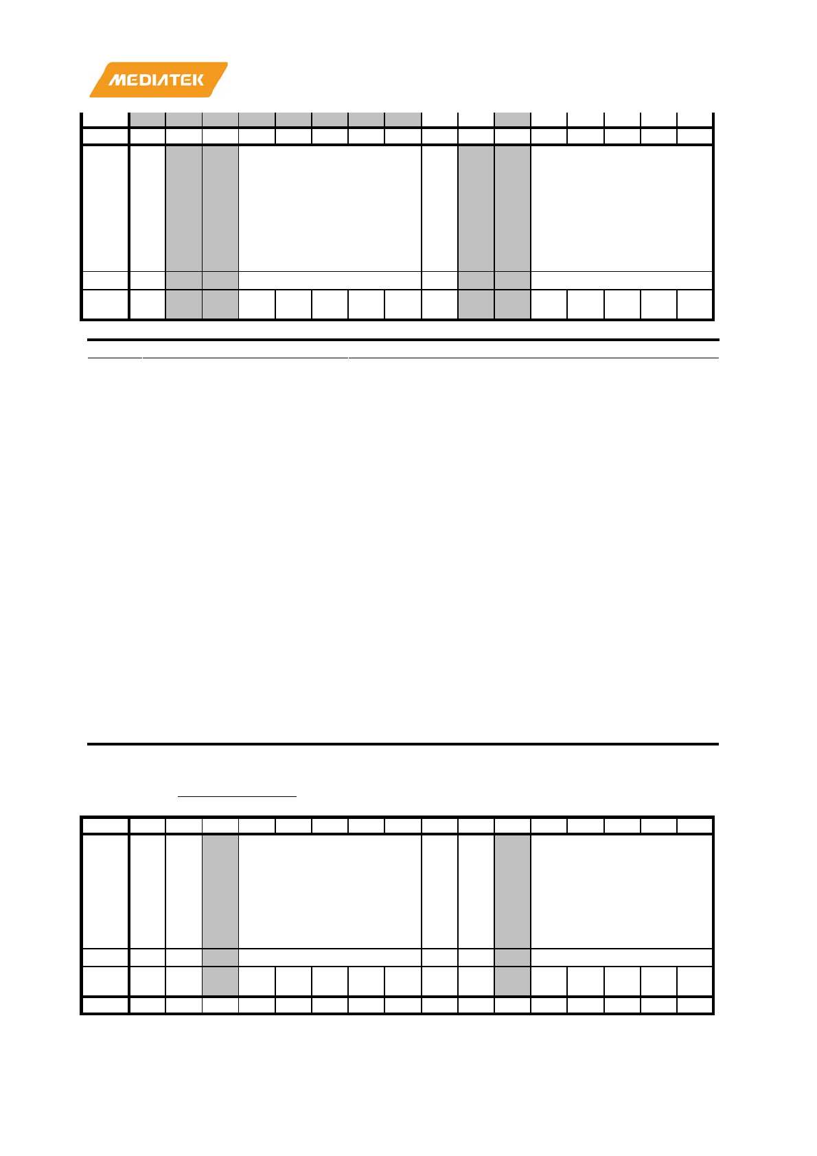
MT7686 Reference Manual
© 2016 - 2017 MediaTek Inc.
Page 214 of 536
This document contains information that is proprietary to MediaTek Inc. (“MediaTek”) and/or its licensor(s).
Any unauthorized use, reproduction or disclosure of this document in whole or in part is strictly prohibited.
t
Bit
15
14
13
12
11
10
9
8
7
6
5
4
3
2
1
0
Nam
e
RE
G_
CM
D_
NE
G_I
_D
LY
_E
N
CMD_NEG_I_DLY
RE
G_
CM
D_
PO
S_I
_D
LY
_E
N
CMD_POS_I_DLY
Type
RW
RW
RW
RW
Rese
t
0 0 0 0 0 0 0 0 0 0 0 0
Bit(s)
Name
Description
23
REG_CMD_O_DLY_EN
Enable output response through delay chain. (to I of
IOCUP)
0: Output response does not pass through delay chain.
1: Output response passes through delay chain.
22
REG_CMD_OE_DLY_EN
Enable response output enable through delay chain. (to E
of IOCUP)
0: Response output enable does not pass through delay chain.
1: Response output enable passes through delay chain.
20:16
CMD_O_DLY
CMD Pad Output Delay Control
This register is used to add delay to an output response phase.
Total 32 stages
15
REG_CMD_NEG_I_DLY_EN
Enable input command through delay chain to be latched
with negative clock edge.
0: Input command does not pass through delay chain.
1: Input command passes through delay chain.
12:8
CMD_NEG_I_DLY
CMD Pad Input Delay Control for data latch with negative
clock edge.
This register is used to add delay to input command phase.
Total 32 stages
7
REG_CMD_POS_I_DLY_EN
Enable input command through delay chain to be latched
with positive clock edge.
0: Input command does not pass through delay chain.
1: Input command passes through delay chain.
4:0
CMD_POS_I_DLY
CMD Pad Input Delay Control for data latch with positive
clock edge.
This register is used to add delay to an input command phase.
Total 32 stages
A1040060
FWODATDLYCR
SDIO Output Data Delay Chain Control
Register
00000000
Bit
31
30
29
28
27
26
25
24
23
22
21
20
19
18
17
16
Nam
e
RE
G_
DA
T3
_O
_D
LY
_E
N
RE
G_
DA
T3
_O
E_
DL
Y_
EN
DAT3_O_DLY
RE
G_
DA
T2
_O
_D
LY
_E
N
RE
G_
DA
T2
_O
E_
DL
Y_
EN
DAT2_O_DLY
Type
RW
RW
RW
RW
RW
RW
Rese
t
0 0 0 0 0 0 0 0 0 0 0 0 0 0
Bit
15
14
13
12
11
10
9
8
7
6
5
4
3
2
1
0

MT7686 Reference Manual
© 2016 - 2017 MediaTek Inc.
Page 215 of 536
This document contains information that is proprietary to MediaTek Inc. (“MediaTek”) and/or its licensor(s).
Any unauthorized use, reproduction or disclosure of this document in whole or in part is strictly prohibited.
Nam
e
RE
G_
DA
T1_
O_
DL
Y_
EN
RE
G_
DA
T1_
OE
_D
LY
_E
N
DAT1_O_DLY
RE
G_
DA
T0
_O
_D
LY
_E
N
RE
G_
DA
T0
_O
E_
DL
Y_
EN
DAT0_O_DLY
Type
RW
RW
RW
RW
RW
RW
Rese
t
0 0 0 0 0 0 0 0 0 0 0 0 0 0
Bit(s)
Name
Description
31
REG_DAT3_O_DLY_EN
Enable output data 3 through delay chain. (to I of IOCUP)
0: Output data 3 does not pass through delay chain.
1: Output data 3 passes through delay chain.
30
REG_DAT3_OE_DLY_EN
Enable data 3 output enable through delay chain. (to E of
IOCUP)
0: Data 3 output enable does not pass through delay chain.
1: Data 3 output enable passes through delay chain.
28:24
DAT3_O_DLY
DATA 3 Pad Output Delay Control
This register is used to add delay to output response phase.
Total 32 stages
23
REG_DAT2_O_DLY_EN
Enable output data 2 through delay chain. (to I of IOCUP)
0: Output data 2 does not pass through delay chain.
1: Output data 2 passes through delay chain.
22
REG_DAT2_OE_DLY_EN
Enable data 2 output enable through delay chain. (to E of
IOCUP)
0: Data 2 output enable does not pass through delay chain.
1: Data 2 output enable pass through delay chain.
20:16
DAT2_O_DLY
DATA 2 Pad Output Delay Control
This register is used to add delay to output response phase.
Total 32 stages
15
REG_DAT1_O_DLY_EN
Enable output data 1 through delay chain. (to I of IOCUP)
0: Output data 1 does not pass through delay chain.
1: Output data 1 passes through delay chain.
14
REG_DAT1_OE_DLY_EN
Enable data 1 output enable through delay chain. (to E of
I
OCUP)
0: Data 1 output enable does not pass through delay chain.
1: Data 1 output enable passes through delay chain.
12:8
DAT1_O_DLY
DATA 1 Pad Output Delay Control
This register is used to add delay to output response phase.
Total 32 stages
7
REG_DAT0_O_DLY_EN
Enable output data 0 through delay chain. (to I of IOCUP)
0: Output data 0 does not pass through delay chain.
1: Output data 0 passes through delay chain.
6
REG_DAT0_OE_DLY_EN
Enable data 0 output enable through delay chain. (to E of
IO
CUP)
0: Data 0 output enable does not pass through delay chain.
1: Data 0 output enable passes through delay chain.
4:0
DAT0_O_DLY
DATA 0 Pad Output Delay Control
This register is used to add delay to output response phase.
Total 32 stages
A1040064
FWIDATDLYCR1
SDIO Input Data Delay Chain Control
Register 1
00000000
Bit
31
30
29
28
27
26
25
24
23
22
21
20
19
18
17
16
Nam
e
RE
G_
DA
T3
DAT3_POS_I_DLY
RE
G_
DA
T2
DAT2_POS_I_DLY
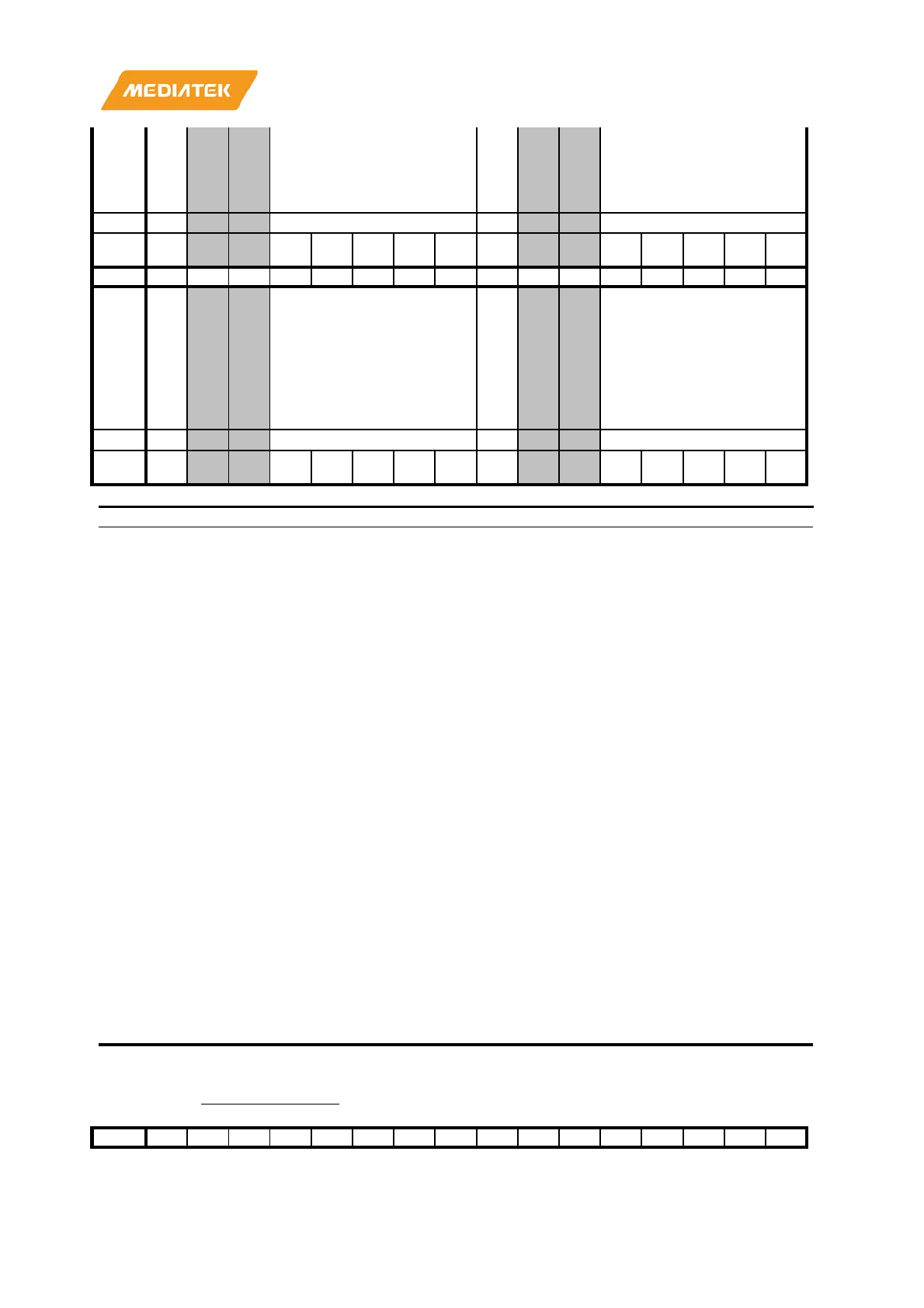
MT7686 Reference Manual
© 2016 - 2017 MediaTek Inc.
Page 216 of 536
This document contains information that is proprietary to MediaTek Inc. (“MediaTek”) and/or its licensor(s).
Any unauthorized use, reproduction or disclosure of this document in whole or in part is strictly prohibited.
_P
OS
_I_
DL
Y_
EN
_P
OS
_I_
DL
Y_
EN
Type
RW
RW
RW
RW
Rese
t
0 0 0 0 0 0 0 0 0 0 0 0
Bit
15
14
13
12
11
10
9
8
7
6
5
4
3
2
1
0
Nam
e
RE
G_
DA
T1_
PO
S_I
_D
LY
_E
N
DAT1_POS_I_DLY
RE
G_
DA
T0
_P
OS
_I_
DL
Y_
EN
DAT0_POS_I_DLY
Type
RW
RW
RW
RW
Rese
t
0 0 0 0 0 0 0 0 0 0 0 0
Bit(s)
Name
Description
31
REG_DAT3_POS_I_DLY_EN
Enable input data 3 through delay chain to be latched with
positive clock edge.
0: Input data 3 does not pass through delay chain.
1: Input data 3 passes through delay chain.
28:24
DAT3_POS_I_DLY
DATA 3 Pad Input Delay Control for datalatch with
positive clock edge.
This register is used to add delay to input data 3 phase.
Total 32 stages
23
REG_DAT2_POS_I_DLY_EN
Enable input data 2 through delay chain to be latched with
positive clock edge.
0:
Input data 2 does not pass through delay chain.
1: Input data 2 passes through delay chain.
20:16
DAT2_POS_I_DLY
DATA 2 Pad Input Delay Control for data latch with
positive clock edge.
This register is used to add delay to input data 2 phase.
Total 32 stages
15
REG_DAT1_POS_I_DLY_EN
Enable input data 1 through delay chain to be latched with
positive clock edge.
0: Input data 1 does not pass through delay chain.
1: Input data 1 passes through delay chain.
12:8
DAT1_POS_I_DLY
DATA 1 Pad Input Delay Control for data latch with
positive clock edge.
This register is used to add delay to input data 1 phase.
Total 32 stages
7
REG_DAT0_POS_I_DLY_EN
Enable input data 0 through delay chain to be latched with
positive clock edge.
0: Input data 0 does not pass through delay chain.
1: Input data 0 passes through delay chain.
4:0
DAT0_POS_I_DLY
DATA 0 Pad Input Delay Control for data latch with
positive clock edge.
This register is used to add delay to input data 0 phase.
Total 32 stages
A1040068
FWIDATDLYCR2
SDIO Input Data Delay Chain Control
Register 2
00000000
Bit
31
30
29
28
27
26
25
24
23
22
21
20
19
18
17
16
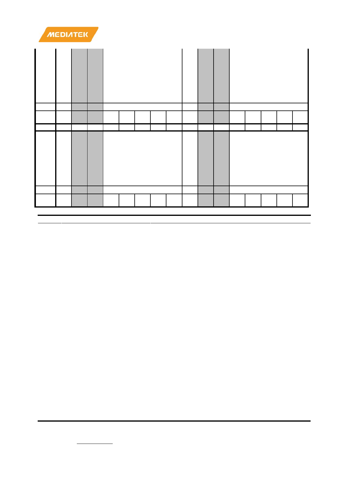
MT7686 Reference Manual
© 2016 - 2017 MediaTek Inc.
Page 217 of 536
This document contains information that is proprietary to MediaTek Inc. (“MediaTek”) and/or its licensor(s).
Any unauthorized use, reproduction or disclosure of this document in whole or in part is strictly prohibited.
Nam
e
RE
G_
DA
T3
_N
EG
_I_
DL
Y_
EN
DAT3_NEG_I_DLY
RE
G_
DA
T2
_N
EG
_I_
DL
Y_
EN
DAT2_NEG_I_DLY
Type
RW
RW
RW
RW
Rese
t
0 0 0 0 0 0 0 0 0 0 0 0
Bit
15
14
13
12
11
10
9
8
7
6
5
4
3
2
1
0
Nam
e
RE
G_
DA
T1_
NE
G_I
_D
LY
_E
N
DAT1_NEG_I_DLY
RE
G_
DA
T0
_N
EG
_I_
DL
Y_
EN
DAT0_NEG_I_DLY
Type
RW
RW
RW
RW
Rese
t
0 0 0 0 0 0 0 0 0 0 0 0
Bit(s)
Name
Description
31
REG_DAT3_NEG_I_DLY_EN
Enable input data 3 through delay chain to be latched with
negative clock edge.
0: Input data 3 does not pass through delay chain.
1: Input data 3 passes through delay chain.
28:24
DAT3_NEG_I_DLY
DATA 3 Pad Input Delay Control for data latch with
negative clock edge.
This register is used to add delay to input data 3 phase.
Total 32 stages
23
REG_DAT2_NEG_I_DLY_EN
Enable input data 2 through delay chain to be latched with
negative clock edge.
0: Input data 2 does not pass through delay chain.
1: Input data 2 passes through delay chain.
20:16
DAT2_NEG_I_DLY
DATA 2 Pad Input Delay Control for data latch with
negative clock edge.
This register is used to add delay to input data 2 phase.
Total 32 stages
15
REG_DAT1_NEG_I_DLY_EN
Enable input data 1 through delay chain to be latched with
negative clock edge.
0: Input data 1 does not pass through delay chain.
1: Input data 1 passes through delay chain.
12:8
DAT1_NEG_I_DLY
DATA 1 Pad Input Delay Control for data latch with
negative clock edge.
This register is used to add delay to input data 1 phase.
Total 32 stages
7
REG_DAT0_NEG_I_DLY_EN
Enable input data 0 through delay chain to be latched with
negative clock edge.
0: Input data 0 does not pass through delay chain.
1: Input data 0 passes through delay chain.
4:0
DAT0_NEG_I_DLY
DATA 0 Pad Input Delay Control for data latch with
negative clock edge.
This register is used to add delay to input data 0 phase.
Total 32 stages
A104006C
FWILCHCR
SDIO Input Data Latch Time Control
00011111

MT7686 Reference Manual
© 2016 - 2017 MediaTek Inc.
Page 218 of 536
This document contains information that is proprietary to MediaTek Inc. (“MediaTek”) and/or its licensor(s).
Any unauthorized use, reproduction or disclosure of this document in whole or in part is strictly prohibited.
Register
Bit
31
30
29
28
27
26
25
24
23
22
21
20
19
18
17
16
Nam
e
REG_CM
D_LATCH
_SEL
Type
RW
Rese
t
0 1
Bit
15
14
13
12
11
10
9
8
7
6
5
4
3
2
1
0
Nam
e
REG_DA
T3_LATC
H_SEL
REG_DA
T2_LATC
H_SEL
REG_DA
T1_LATC
H_SEL
REG_DA
T0__LAT
CH_SEL
Type
RW
RW
RW
RW
Rese
t
0 1 0 1 0 1 0 1
Bit(s)
Name
Description
17:16
REG_CMD_LATCH_SEL
Controls the input command latch timing depending on
the SDIO output enable signal to avoid latching device
output data as host transfers data in UHS104 mode.
2'b00: latch input command after 1 cycle of output enable is
asserted.
2'b01: latch input command after 2 cycles of output enable is
asserted
2'b10: latch input command after 3 cycles of output enable is
asserted
2'b11: latch input command after 4 cycles of output enable is
asserted
13:12
REG_DAT3_LATCH_SEL
Controls the input data 3 latch timing depending on the
SDIO output enable signal to avoid latching device output
data as host transfers data in UHS104 mode.
2'b00: latch input data 3 after 1T of output enable asserted
2'b01: latch input data 3 after 2T of output enable asserted
2'b10: latch input data 3 after 3T of output enable asserted
2'b11: latch input data 3 after 4T of output enable asserted
9:8
REG_DAT2_LATCH_SEL
Control the input data 2 latch timing depending on SDIO
output enable signal to avoid latching device output data
as host transferred data in UHS104 mode.
2'b00: latch input data 2 after 1T of output enable asserted
2'b01: latch input data 2 after 2T of output enable asserted
2'b10: latch input data 2 after 3T of output enable asserted
2'b11: latch input data 2 after 4T of output enable asserted
5:4
REG_DAT1_LATCH_SEL
Control the input data 1 latch timing depending on SDIO
output enable signal to avoid latching device output data
as host transferred data in UHS104 mode.
2'b00: latch input data 1 after 1T of output enable asserted
2'b01: latch input data 1 after 2T of output enable asserted
2'b10: latch input data 1 after 3T of output enable asserted
2'b11: latch input data 1 after 4T of output enable asserted
1:0
REG_DAT0__LATCH_SEL
Control the input data 0 latch timing depending on SDIO
output enable signal to avoid latching device output data
as host transferred data in UHS104 mode.
2'b00: latch input data 0 after 1T of output enable asserted
2'b01: latch input data 0 after 2T of output enable asserted
2'b10: latch input data 0 after 3T of output enable asserted
2'b11: latch input data 0 after 4T of output enable asserted
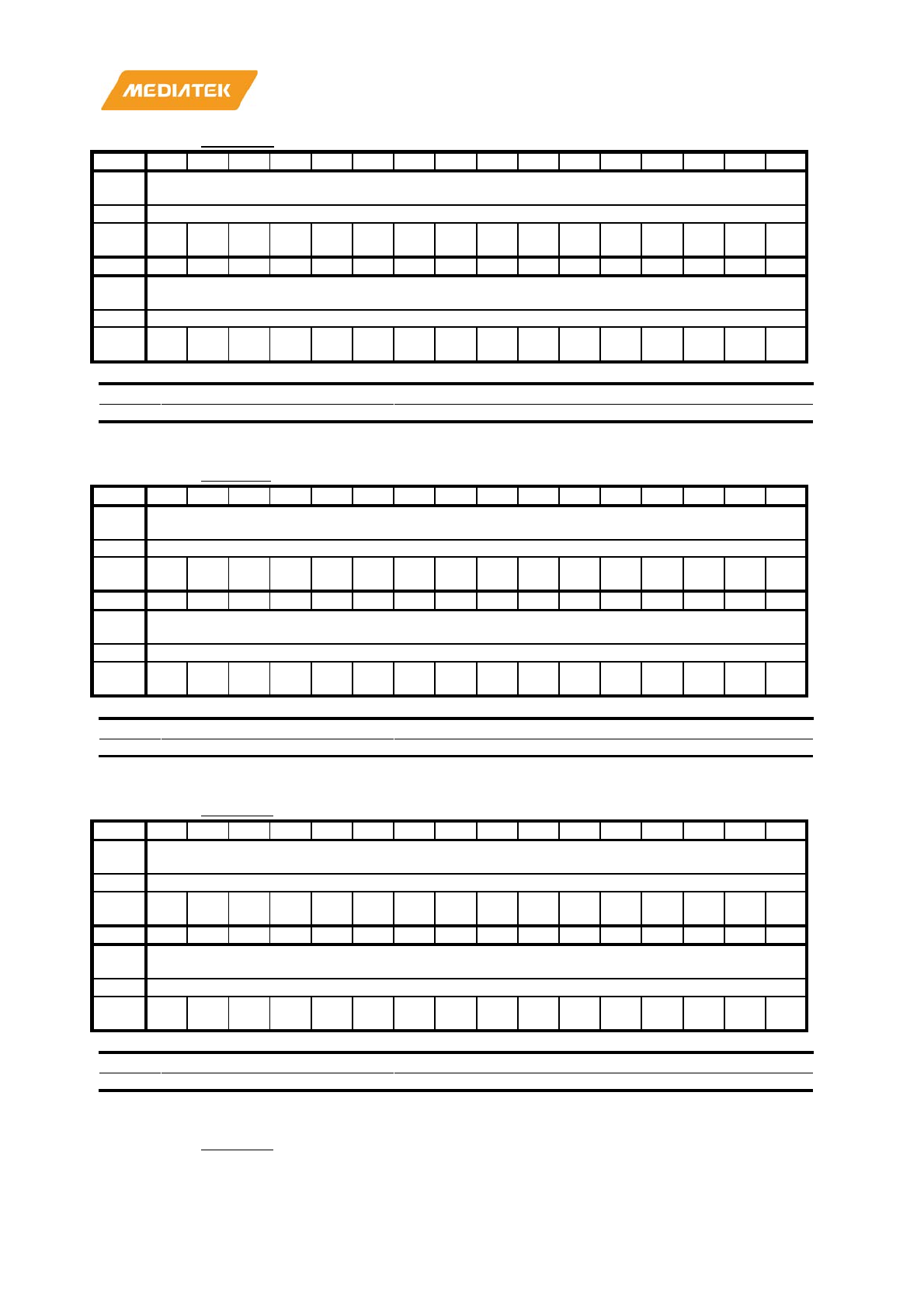
MT7686 Reference Manual
© 2016 - 2017 MediaTek Inc.
Page 219 of 536
This document contains information that is proprietary to MediaTek Inc. (“MediaTek”) and/or its licensor(s).
Any unauthorized use, reproduction or disclosure of this document in whole or in part is strictly prohibited.
A1040070
CIS0R00
CIS0 Register 0
00000000
Bit
31
30
29
28
27
26
25
24
23
22
21
20
19
18
17
16
Nam
e
CIS0_W00
Type
RW
Rese
t
0 0 0 0 0 0 0 0 0 0 0 0 0 0 0 0
Bit
15
14
13
12
11
10
9
8
7
6
5
4
3
2
1
0
Nam
e
CIS0_W00
Type
RW
Rese
t
0 0 0 0 0 0 0 0 0 0 0 0 0 0 0 0
Bit(s)
Name
Description
31:0
CIS0_W00
CIS0 Register used in ciscc firmware register mode
A1040074
CIS0R01
CIS0 Register 1
00000000
Bit
31
30
29
28
27
26
25
24
23
22
21
20
19
18
17
16
Nam
e
CIS0_W01
Type
RW
Rese
t
0 0 0 0 0 0 0 0 0 0 0 0 0 0 0 0
Bit
15
14
13
12
11
10
9
8
7
6
5
4
3
2
1
0
Nam
e
CIS0_W01
Type
RW
Rese
t
0 0 0 0 0 0 0 0 0 0 0 0 0 0 0 0
Bit(s)
Name
Description
31:0
CIS0_W01
CIS0 Register used in ciscc firmware register mode
A1040078
CIS0R02
CIS0 Register 2
00000000
Bit
31
30
29
28
27
26
25
24
23
22
21
20
19
18
17
16
Nam
e
CIS0_W02
Type
RW
Rese
t
0 0 0 0 0 0 0 0 0 0 0 0 0 0 0 0
Bit
15
14
13
12
11
10
9
8
7
6
5
4
3
2
1
0
Nam
e
CIS0_W02
Type
RW
Rese
t
0 0 0 0 0 0 0 0 0 0 0 0 0 0 0 0
Bit(s)
Name
Description
31:0
CIS0_W02
CIS0 Register used in ciscc firmware register mode
A104007C
CIS0R03
CIS0 Register 3
00000000
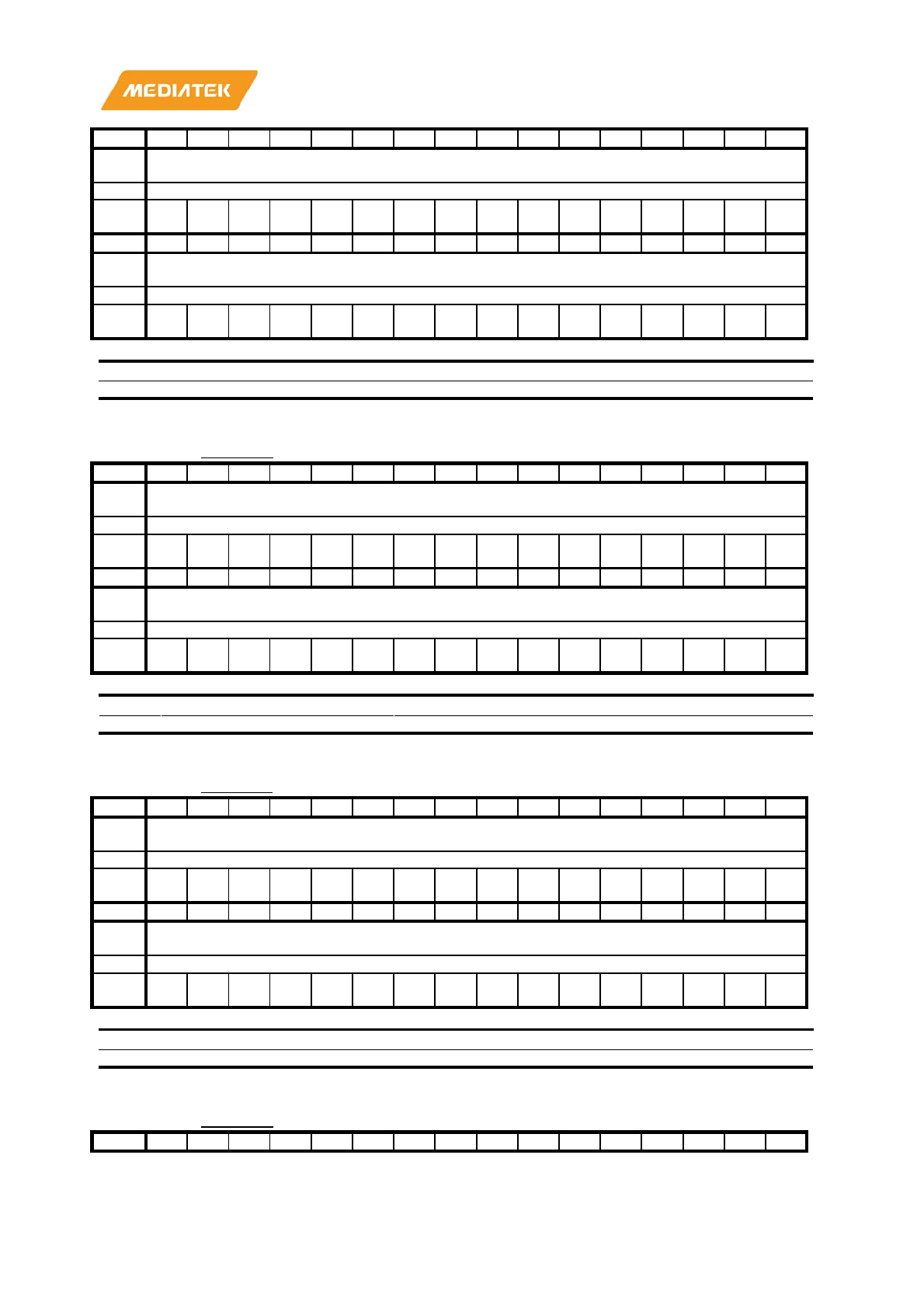
MT7686 Reference Manual
© 2016 - 2017 MediaTek Inc.
Page 220 of 536
This document contains information that is proprietary to MediaTek Inc. (“MediaTek”) and/or its licensor(s).
Any unauthorized use, reproduction or disclosure of this document in whole or in part is strictly prohibited.
Bit
31
30
29
28
27
26
25
24
23
22
21
20
19
18
17
16
Nam
e
CIS0_W03
Type
RW
Rese
t
0 0 0 0 0 0 0 0 0 0 0 0 0 0 0 0
Bit
15
14
13
12
11
10
9
8
7
6
5
4
3
2
1
0
Nam
e
CIS0_W03
Type
RW
Rese
t
0 0 0 0 0 0 0 0 0 0 0 0 0 0 0 0
Bit(s)
Name
Description
31:0
CIS0_W03
CIS0 Register used in ciscc firmware register mode
A1040080
CIS0R04
CIS0 Register 4
00000000
Bit
31
30
29
28
27
26
25
24
23
22
21
20
19
18
17
16
Nam
e
CIS0_W04
Type
RW
Rese
t
0 0 0 0 0 0 0 0 0 0 0 0 0 0 0 0
Bit
15
14
13
12
11
10
9
8
7
6
5
4
3
2
1
0
Nam
e
CIS0_W04
Type
RW
Rese
t
0 0 0 0 0 0 0 0 0 0 0 0 0 0 0 0
Bit(s)
Name
Description
31:0
CIS0_W04
CIS0 Register used in ciscc firmware register mode
A1040084
CIS0R05
CIS0 Register 5
00000000
Bit
31
30
29
28
27
26
25
24
23
22
21
20
19
18
17
16
Nam
e
CIS0_W05
Type
RW
Rese
t
0 0 0 0 0 0 0 0 0 0 0 0 0 0 0 0
Bit
15
14
13
12
11
10
9
8
7
6
5
4
3
2
1
0
Nam
e
CIS0_W05
Type
RW
Rese
t
0 0 0 0 0 0 0 0 0 0 0 0 0 0 0 0
Bit(s)
Name
Description
31:0
CIS0_W05
CIS0 Register used in ciscc firmware register mode
A1040088
CIS0R06
CIS0 Register 6
00000000
Bit
31
30
29
28
27
26
25
24
23
22
21
20
19
18
17
16
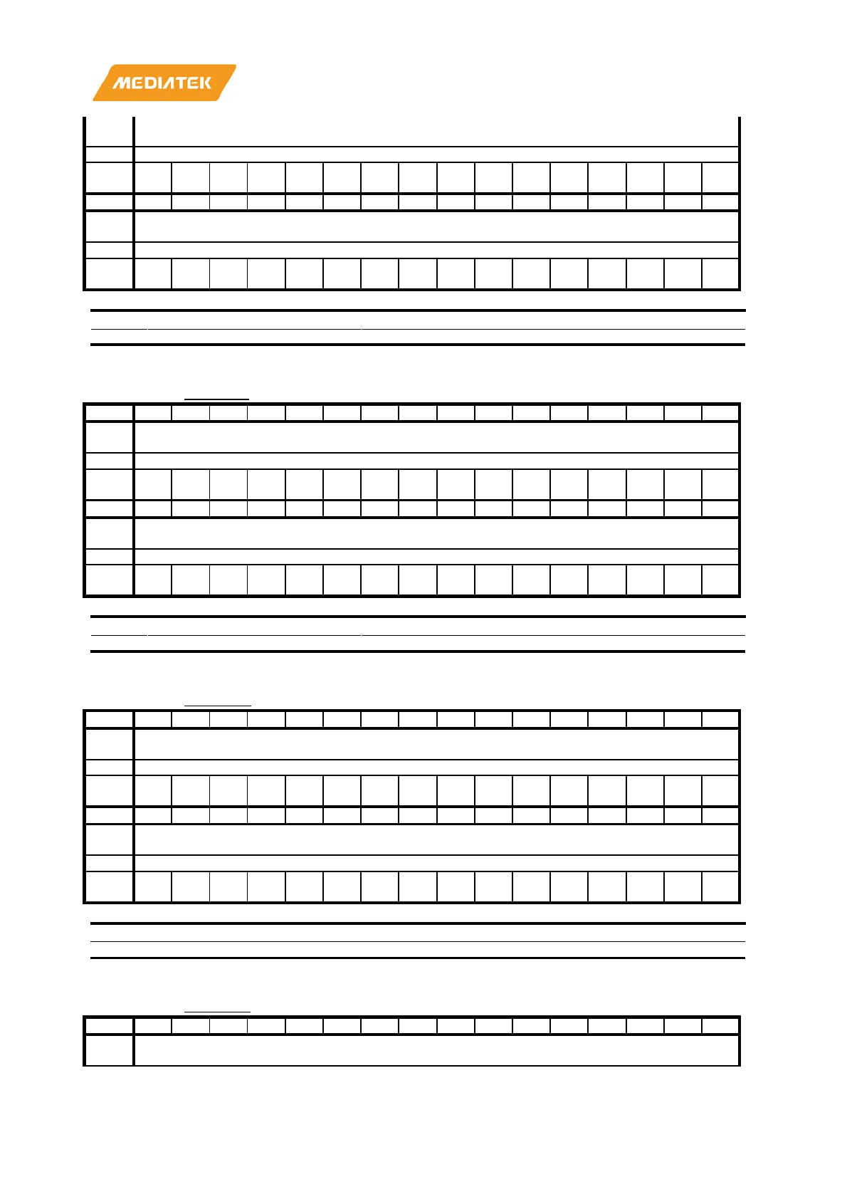
MT7686 Reference Manual
© 2016 - 2017 MediaTek Inc.
Page 221 of 536
This document contains information that is proprietary to MediaTek Inc. (“MediaTek”) and/or its licensor(s).
Any unauthorized use, reproduction or disclosure of this document in whole or in part is strictly prohibited.
Nam
e
CIS0_W06
Type
RW
Rese
t
0 0 0 0 0 0 0 0 0 0 0 0 0 0 0 0
Bit
15
14
13
12
11
10
9
8
7
6
5
4
3
2
1
0
Nam
e
CIS0_W06
Type
RW
Rese
t
0 0 0 0 0 0 0 0 0 0 0 0 0 0 0 0
Bit(s)
Name
Description
31:0
CIS0_W06
CIS0 Register used in ciscc firmware register mode
A104008C
CIS0R07
CIS0 Register 7
00000000
Bit
31
30
29
28
27
26
25
24
23
22
21
20
19
18
17
16
Nam
e
CIS0_W07
Type
RW
Rese
t
0 0 0 0 0 0 0 0 0 0 0 0 0 0 0 0
Bit
15
14
13
12
11
10
9
8
7
6
5
4
3
2
1
0
Nam
e
CIS0_W07
Type
RW
Rese
t
0 0 0 0 0 0 0 0 0 0 0 0 0 0 0 0
Bit(s)
Name
Description
31:0
CIS0_W07
CIS0 Register used in ciscc firmware register mode
A1040090
CIS0R08
CIS0 Register 8
00000000
Bit
31
30
29
28
27
26
25
24
23
22
21
20
19
18
17
16
Nam
e
CIS0_W08
Type
RW
Rese
t
0 0 0 0 0 0 0 0 0 0 0 0 0 0 0 0
Bit
15
14
13
12
11
10
9
8
7
6
5
4
3
2
1
0
Nam
e
CIS0_W08
Type
RW
Rese
t
0 0 0 0 0 0 0 0 0 0 0 0 0 0 0 0
Bit(s)
Name
Description
31:0
CIS0_W08
CIS0 Register used in ciscc firmware register mode
A1040094
CIS0R09
CIS0 Register 9
00000000
Bit
31
30
29
28
27
26
25
24
23
22
21
20
19
18
17
16
Nam
e
CIS0_W09
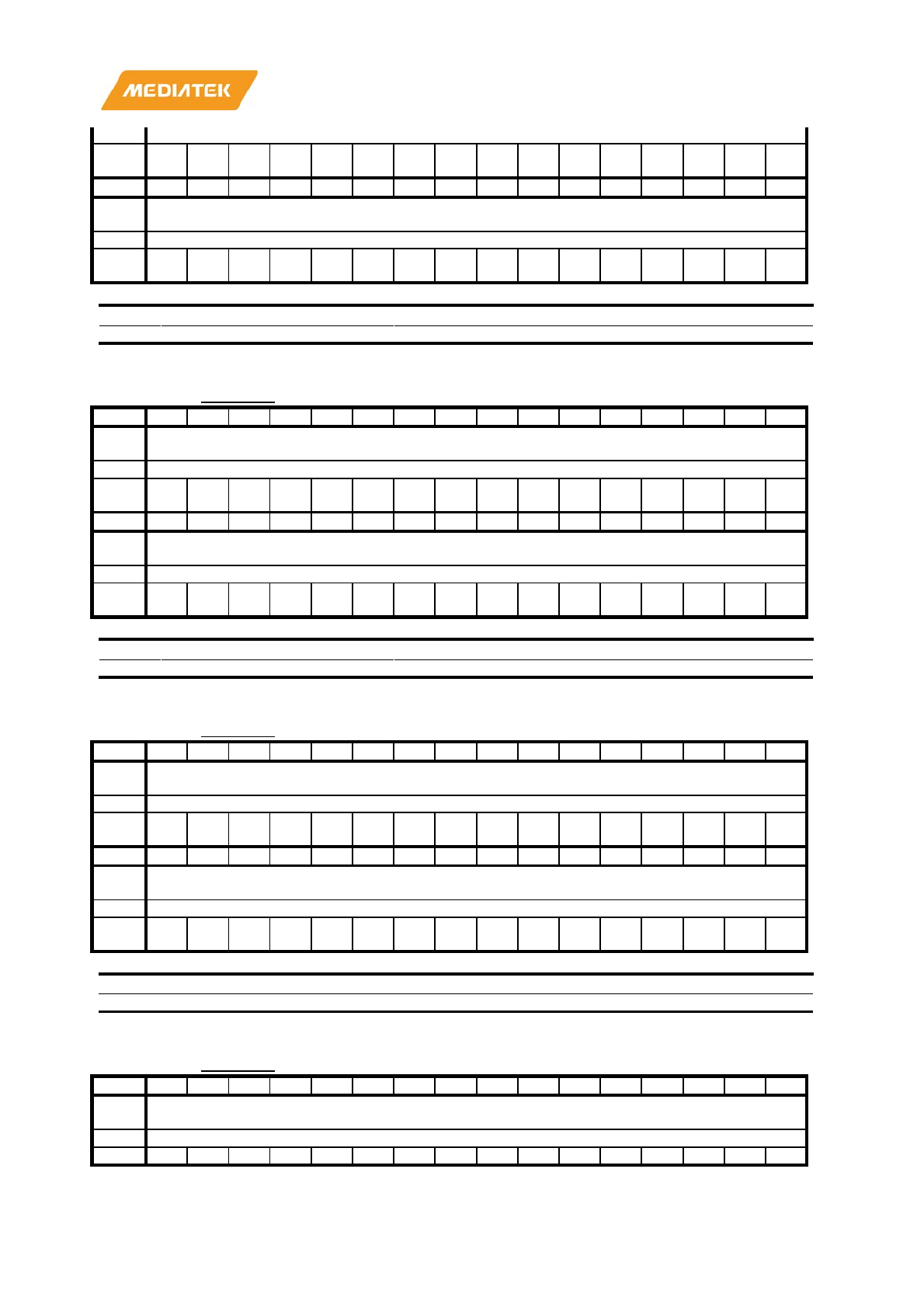
MT7686 Reference Manual
© 2016 - 2017 MediaTek Inc.
Page 222 of 536
This document contains information that is proprietary to MediaTek Inc. (“MediaTek”) and/or its licensor(s).
Any unauthorized use, reproduction or disclosure of this document in whole or in part is strictly prohibited.
Type
RW
Rese
t
0 0 0 0 0 0 0 0 0 0 0 0 0 0 0 0
Bit
15
14
13
12
11
10
9
8
7
6
5
4
3
2
1
0
Nam
e
CIS0_W09
Type
RW
Rese
t
0 0 0 0 0 0 0 0 0 0 0 0 0 0 0 0
Bit(s)
Name
Description
31:0
CIS0_W09
CIS0 Register used in ciscc firmware register mode
A1040098
CIS0R0A
CIS0 Register A
00000000
Bit
31
30
29
28
27
26
25
24
23
22
21
20
19
18
17
16
Nam
e
CIS0_W0A
Type
RW
Rese
t
0 0 0 0 0 0 0 0 0 0 0 0 0 0 0 0
Bit
15
14
13
12
11
10
9
8
7
6
5
4
3
2
1
0
Nam
e
CIS0_W0A
Type
RW
Rese
t
0 0 0 0 0 0 0 0 0 0 0 0 0 0 0 0
Bit(s)
Name
Description
31:0
CIS0_W0A
CIS0 Register used in ciscc firmware register mode
A104009C
CIS0R0B
CIS0 Register B
00000000
Bit
31
30
29
28
27
26
25
24
23
22
21
20
19
18
17
16
Nam
e
CIS0_W0B
Type
RW
Rese
t
0 0 0 0 0 0 0 0 0 0 0 0 0 0 0 0
Bit
15
14
13
12
11
10
9
8
7
6
5
4
3
2
1
0
Nam
e
CIS0_W0B
Type
RW
Rese
t
0 0 0 0 0 0 0 0 0 0 0 0 0 0 0 0
Bit(s)
Name
Description
31:0
CIS0_W0B
CIS0 Register used in ciscc firmware register mode
A10400A0
CIS0R0C
CIS0 Register C
00000000
Bit
31
30
29
28
27
26
25
24
23
22
21
20
19
18
17
16
Nam
e
CIS0_W0C
Type
RW
Rese
0
0
0
0
0
0
0
0
0
0
0
0
0
0
0
0
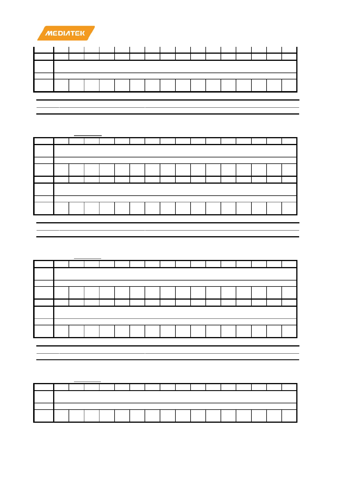
MT7686 Reference Manual
© 2016 - 2017 MediaTek Inc.
Page 223 of 536
This document contains information that is proprietary to MediaTek Inc. (“MediaTek”) and/or its licensor(s).
Any unauthorized use, reproduction or disclosure of this document in whole or in part is strictly prohibited.
t
Bit
15
14
13
12
11
10
9
8
7
6
5
4
3
2
1
0
Nam
e
CIS0_W0C
Type
RW
Rese
t
0 0 0 0 0 0 0 0 0 0 0 0 0 0 0 0
Bit(s)
Name
Description
31:0
CIS0_W0C
CIS0 Register used in ciscc firmware register mode
A10400A4
CIS0R0D
CIS0 Register D
00000000
Bit
31
30
29
28
27
26
25
24
23
22
21
20
19
18
17
16
Nam
e
CIS0_W0D
Type
RW
Rese
t
0 0 0 0 0 0 0 0 0 0 0 0 0 0 0 0
Bit
15
14
13
12
11
10
9
8
7
6
5
4
3
2
1
0
Nam
e
CIS0_W0D
Type
RW
Rese
t
0 0 0 0 0 0 0 0 0 0 0 0 0 0 0 0
Bit(s)
Name
Description
31:0
CIS0_W0D
CIS0 Register used in ciscc firmware register mode
A10400A8
CIS0R0E
CIS0 Register E
00000000
Bit
31
30
29
28
27
26
25
24
23
22
21
20
19
18
17
16
Nam
e
CIS0_W0E
Type
RW
Rese
t
0 0 0 0 0 0 0 0 0 0 0 0 0 0 0 0
Bit
15
14
13
12
11
10
9
8
7
6
5
4
3
2
1
0
Nam
e
CIS0_W0E
Type
RW
Rese
t
0 0 0 0 0 0 0 0 0 0 0 0 0 0 0 0
Bit(s)
Name
Description
31:0
CIS0_W0E
CIS0 Register used in ciscc firmware register mode
A10400AC
CIS0R0F
CIS0 Register F
00000000
Bit
31
30
29
28
27
26
25
24
23
22
21
20
19
18
17
16
Nam
e
CIS0_W0F
Type
RW
Rese
t
0 0 0 0 0 0 0 0 0 0 0 0 0 0 0 0
MT7686 Reference Manual
© 2016 - 2017 MediaTek Inc.
Page 224 of 536
This document contains information that is proprietary to MediaTek Inc. (“MediaTek”) and/or its licensor(s).
Any unauthorized use, reproduction or disclosure of this document in whole or in part is strictly prohibited.
Bit
15
14
13
12
11
10
9
8
7
6
5
4
3
2
1
0
Nam
e
CIS0_W0F
Type
RW
Rese
t
0 0 0 0 0 0 0 0 0 0 0 0 0 0 0 0
Bit(s)
Name
Description
31:0
CIS0_W0F
CIS0 Register used in ciscc firmware register mode
A10400B0
CIS1R00
CIS1 Register 0
00000000
Bit
31
30
29
28
27
26
25
24
23
22
21
20
19
18
17
16
Nam
e
CIS1_W00
Type
RW
Rese
t
0 0 0 0 0 0 0 0 0 0 0 0 0 0 0 0
Bit
15
14
13
12
11
10
9
8
7
6
5
4
3
2
1
0
Nam
e
CIS1_W00
Type
RW
Rese
t
0 0 0 0 0 0 0 0 0 0 0 0 0 0 0 0
Bit(s)
Name
Description
31:0
CIS1_W00
CIS1 Register used in ciscc firmware register mode
A10400B4
CIS1R01
CIS1 Register 1
00000000
Bit
31
30
29
28
27
26
25
24
23
22
21
20
19
18
17
16
Nam
e
CIS1_W01
Type
RW
Rese
t
0 0 0 0 0 0 0 0 0 0 0 0 0 0 0 0
Bit
15
14
13
12
11
10
9
8
7
6
5
4
3
2
1
0
Nam
e
CIS1_W01
Type
RW
Rese
t
0 0 0 0 0 0 0 0 0 0 0 0 0 0 0 0
Bit(s)
Name
Description
31:0
CIS1_W01
CIS1 Register used in ciscc firmware register mode
A10400B8
CIS1R02
CIS1 Register 2
00000000
Bit
31
30
29
28
27
26
25
24
23
22
21
20
19
18
17
16
Nam
e
CIS1_W02
Type
RW
Rese
t
0 0 0 0 0 0 0 0 0 0 0 0 0 0 0 0
Bit
15
14
13
12
11
10
9
8
7
6
5
4
3
2
1
0
MT7686 Reference Manual
© 2016 - 2017 MediaTek Inc.
Page 225 of 536
This document contains information that is proprietary to MediaTek Inc. (“MediaTek”) and/or its licensor(s).
Any unauthorized use, reproduction or disclosure of this document in whole or in part is strictly prohibited.
Nam
e
CIS1_W02
Type
RW
Rese
t
0 0 0 0 0 0 0 0 0 0 0 0 0 0 0 0
Bit(s)
Name
Description
31:0
CIS1_W02
CIS1 Register used in ciscc firmware register mode
A10400BC
CIS1R03
CIS1 Register 3
00000000
Bit
31
30
29
28
27
26
25
24
23
22
21
20
19
18
17
16
Nam
e
CIS1_W03
Type
RW
Rese
t
0 0 0 0 0 0 0 0 0 0 0 0 0 0 0 0
Bit
15
14
13
12
11
10
9
8
7
6
5
4
3
2
1
0
Nam
e
CIS1_W03
Type
RW
Rese
t
0 0 0 0 0 0 0 0 0 0 0 0 0 0 0 0
Bit(s)
Name
Description
31:0
CIS1_W03
CIS1 Register used in ciscc firmware register mode
A10400C0
CIS1R04
CIS1 Register 4
00000000
Bit
31
30
29
28
27
26
25
24
23
22
21
20
19
18
17
16
Nam
e
CIS1_W04
Type
RW
Rese
t
0 0 0 0 0 0 0 0 0 0 0 0 0 0 0 0
Bit
15
14
13
12
11
10
9
8
7
6
5
4
3
2
1
0
Nam
e
CIS1_W04
Type
RW
Rese
t
0 0 0 0 0 0 0 0 0 0 0 0 0 0 0 0
Bit(s)
Name
Description
31:0
CIS1_W04
CIS1 Register used in ciscc firmware register mode
A10400C4
CIS1R05
CIS1 Register 5
00000000
Bit
31
30
29
28
27
26
25
24
23
22
21
20
19
18
17
16
Nam
e
CIS1_W05
Type
RW
Rese
t
0 0 0 0 0 0 0 0 0 0 0 0 0 0 0 0
Bit
15
14
13
12
11
10
9
8
7
6
5
4
3
2
1
0
Nam
e
CIS1_W05
MT7686 Reference Manual
© 2016 - 2017 MediaTek Inc.
Page 226 of 536
This document contains information that is proprietary to MediaTek Inc. (“MediaTek”) and/or its licensor(s).
Any unauthorized use, reproduction or disclosure of this document in whole or in part is strictly prohibited.
Type
RW
Rese
t
0 0 0 0 0 0 0 0 0 0 0 0 0 0 0 0
Bit(s)
Name
Description
31:0
CIS1_W05
CIS1 Register used in ciscc firmware register mode
A10400C8
CIS1R06
CIS1 Register 6
00000000
Bit
31
30
29
28
27
26
25
24
23
22
21
20
19
18
17
16
Nam
e
CIS1_W06
Type
RW
Rese
t
0 0 0 0 0 0 0 0 0 0 0 0 0 0 0 0
Bit
15
14
13
12
11
10
9
8
7
6
5
4
3
2
1
0
Nam
e
CIS1_W06
Type
RW
Rese
t
0 0 0 0 0 0 0 0 0 0 0 0 0 0 0 0
Bit(s)
Name
Description
31:0
CIS1_W06
CIS1 Register used in ciscc firmware register mode
A10400CC
CIS1R07
CIS1 Register 7
00000000
Bit
31
30
29
28
27
26
25
24
23
22
21
20
19
18
17
16
Nam
e
CIS1_W07
Type
RW
Rese
t
0 0 0 0 0 0 0 0 0 0 0 0 0 0 0 0
Bit
15
14
13
12
11
10
9
8
7
6
5
4
3
2
1
0
Nam
e
CIS1_W07
Type
RW
Rese
t
0 0 0 0 0 0 0 0 0 0 0 0 0 0 0 0
Bit(s)
Name
Description
31:0
CIS1_W07
CIS1 Register used in ciscc firmware register mode
A10400D0
CIS1R08
CIS1 Register 8
00000000
Bit
31
30
29
28
27
26
25
24
23
22
21
20
19
18
17
16
Nam
e
CIS1_W08
Type
RW
Rese
t
0 0 0 0 0 0 0 0 0 0 0 0 0 0 0 0
Bit
15
14
13
12
11
10
9
8
7
6
5
4
3
2
1
0
Nam
e
CIS1_W08
Type
RW
MT7686 Reference Manual
© 2016 - 2017 MediaTek Inc.
Page 227 of 536
This document contains information that is proprietary to MediaTek Inc. (“MediaTek”) and/or its licensor(s).
Any unauthorized use, reproduction or disclosure of this document in whole or in part is strictly prohibited.
Rese
t
0 0 0 0 0 0 0 0 0 0 0 0 0 0 0 0
Bit(s)
Name
Description
31:0
CIS1_W08
CIS1 Register used in ciscc firmware register mode
A10400D4
CIS1R09
CIS1 Register 9
00000000
Bit
31
30
29
28
27
26
25
24
23
22
21
20
19
18
17
16
Nam
e
CIS1_W09
Type
RW
Rese
t
0 0 0 0 0 0 0 0 0 0 0 0 0 0 0 0
Bit
15
14
13
12
11
10
9
8
7
6
5
4
3
2
1
0
Nam
e
CIS1_W09
Type
RW
Rese
t
0 0 0 0 0 0 0 0 0 0 0 0 0 0 0 0
Bit(s)
Name
Description
31:0
CIS1_W09
CIS1 Register used in ciscc firmware register mode
A10400D8
CIS1R0A
CIS1 Register A
00000000
Bit
31
30
29
28
27
26
25
24
23
22
21
20
19
18
17
16
Nam
e
CIS1_W0A
Type
RW
Rese
t
0 0 0 0 0 0 0 0 0 0 0 0 0 0 0 0
Bit
15
14
13
12
11
10
9
8
7
6
5
4
3
2
1
0
Nam
e
CIS1_W0A
Type
RW
Rese
t
0 0 0 0 0 0 0 0 0 0 0 0 0 0 0 0
Bit(s)
Name
Description
31:0
CIS1_W0A
CIS1 Register used in ciscc firmware register mode
A10400DC
CIS1R0B
CIS1 Register B
00000000
Bit
31
30
29
28
27
26
25
24
23
22
21
20
19
18
17
16
Nam
e
CIS1_W0B
Type
RW
Rese
t
0 0 0 0 0 0 0 0 0 0 0 0 0 0 0 0
Bit
15
14
13
12
11
10
9
8
7
6
5
4
3
2
1
0
Nam
e
CIS1_W0B
Type
RW
Rese
t
0 0 0 0 0 0 0 0 0 0 0 0 0 0 0 0
MT7686 Reference Manual
© 2016 - 2017 MediaTek Inc.
Page 228 of 536
This document contains information that is proprietary to MediaTek Inc. (“MediaTek”) and/or its licensor(s).
Any unauthorized use, reproduction or disclosure of this document in whole or in part is strictly prohibited.
Bit(s)
Name
Description
31:0
CIS1_W0B
CIS1 Register used in ciscc firmware register mode
A10400E0
CIS1R0C
CIS1 Register C
00000000
Bit
31
30
29
28
27
26
25
24
23
22
21
20
19
18
17
16
Nam
e
CIS1_W0C
Type
RW
Rese
t
0 0 0 0 0 0 0 0 0 0 0 0 0 0 0 0
Bit
15
14
13
12
11
10
9
8
7
6
5
4
3
2
1
0
Nam
e
CIS1_W0C
Type
RW
Rese
t
0 0 0 0 0 0 0 0 0 0 0 0 0 0 0 0
Bit(s)
Name
Description
31:0
CIS1_W0C
CIS1 Register used in ciscc firmware register mode
A10400E4
CIS1R0D
CIS1 Register D
00000000
Bit
31
30
29
28
27
26
25
24
23
22
21
20
19
18
17
16
Nam
e
CIS1_W0D
Type
RW
Rese
t
0 0 0 0 0 0 0 0 0 0 0 0 0 0 0 0
Bit
15
14
13
12
11
10
9
8
7
6
5
4
3
2
1
0
Nam
e
CIS1_W0D
Type
RW
Rese
t
0 0 0 0 0 0 0 0 0 0 0 0 0 0 0 0
Bit(s)
Name
Description
31:0
CIS1_W0D
CIS1 Register used in ciscc firmware register mode
A10400E8
CIS1R0E
CIS1 Register E
00000000
Bit
31
30
29
28
27
26
25
24
23
22
21
20
19
18
17
16
Nam
e
CIS1_W0E
Type
RW
Rese
t
0 0 0 0 0 0 0 0 0 0 0 0 0 0 0 0
Bit
15
14
13
12
11
10
9
8
7
6
5
4
3
2
1
0
Nam
e
CIS1_W0E
Type
RW
Rese
t
0 0 0 0 0 0 0 0 0 0 0 0 0 0 0 0
MT7686 Reference Manual
© 2016 - 2017 MediaTek Inc.
Page 229 of 536
This document contains information that is proprietary to MediaTek Inc. (“MediaTek”) and/or its licensor(s).
Any unauthorized use, reproduction or disclosure of this document in whole or in part is strictly prohibited.
Bit(s)
Name
Description
31:0
CIS1_W0E
CIS1 Register used in ciscc firmware register mode
A10400EC
CIS1R0F
CIS1 Register F
00000000
Bit
31
30
29
28
27
26
25
24
23
22
21
20
19
18
17
16
Nam
e
CIS1_W0F
Type
RW
Rese
t
0 0 0 0 0 0 0 0 0 0 0 0 0 0 0 0
Bit
15
14
13
12
11
10
9
8
7
6
5
4
3
2
1
0
Nam
e
CIS1_W0F
Type
RW
Rese
t
0 0 0 0 0 0 0 0 0 0 0 0 0 0 0 0
Bit(s)
Name
Description
31:0
CIS1_W0F
CIS1 Register used in ciscc firmware register mode
A10400F0
CISRDY
CIS Ready Flag Register
00000000
Bit
31
30
29
28
27
26
25
24
23
22
21
20
19
18
17
16
Nam
e
CIS_RDY
Type
RW
Rese
t
0 0 0 0 0 0 0 0 0 0 0 0 0 0 0 0
Bit
15
14
13
12
11
10
9
8
7
6
5
4
3
2
1
0
Nam
e
CIS_RDY
Type
RW
Rese
t
0 0 0 0 0 0 0 0 0 0 0 0 0 0 0 0
Bit(s)
Name
Description
31:0
CIS_RDY
CIS Ready Flag Register that is set after software decodes
the
CIS and finishes the SA initial flow, to proceed with
transf
er.
A10400F4
CCCR0
CC Register 0
00000000
Bit
31
30
29
28
27
26
25
24
23
22
21
20
19
18
17
16
Nam
e
CCCR0
Type
RW
Rese
t
0 0 0 0 0 0 0 0 0 0 0 0 0 0 0 0
Bit
15
14
13
12
11
10
9
8
7
6
5
4
3
2
1
0
Nam
e
CCCR0
Type
RW
Rese
t
0 0 0 0 0 0 0 0 0 0 0 0 0 0 0 0
MT7686 Reference Manual
© 2016 - 2017 MediaTek Inc.
Page 230 of 536
This document contains information that is proprietary to MediaTek Inc. (“MediaTek”) and/or its licensor(s).
Any unauthorized use, reproduction or disclosure of this document in whole or in part is strictly prohibited.
Bit(s)
Name
Description
31:0
CCCR0
Card Capability Register 0
A10400F8
CCCR1
CC Register 1
00000000
Bit
31
30
29
28
27
26
25
24
23
22
21
20
19
18
17
16
Nam
e
CCCR1
Type
RW
Rese
t
0 0 0 0 0 0 0 0 0 0 0 0 0 0 0 0
Bit
15
14
13
12
11
10
9
8
7
6
5
4
3
2
1
0
Nam
e
CCCR1
Type
RW
Rese
t
0 0 0 0 0 0 0 0 0 0 0 0 0 0 0 0
Bit(s)
Name
Description
31:0
CCCR1
Card Capability Register 1
A10400FC
CCRDY
CC Ready Flag Register
00000000
Bit
31
30
29
28
27
26
25
24
23
22
21
20
19
18
17
16
Nam
e
CC_RDY
Type
RW
Rese
t
0 0 0 0 0 0 0 0 0 0 0 0 0 0 0 0
Bit
15
14
13
12
11
10
9
8
7
6
5
4
3
2
1
0
Nam
e
CC_RDY
Type
RW
Rese
t
0 0 0 0 0 0 0 0 0 0 0 0 0 0 0 0
Bit(s)
Name
Description
31:0
CC_RDY
CC Ready Flag Register that is set after the CIS is
programmed
A1040100
HWFISR
HIF WLAN Firmware Interrupt Status
Register
00000000
Bit
31
30
29
28
27
26
25
24
23
22
21
20
19
18
17
16
Nam
e
H2D_SW_INT
Type
W1C
Rese
t
0 0 0 0 0 0 0 0 0 0 0 0 0 0 0 0
Bit
15
14
13
12
11
10
9
8
7
6
5
4
3
2
1
0
Nam
e
RX
_E
VE
NT
_1
RX
_E
VE
NT
_0
TX
_E
VE
NT
_0
WR
_TI
ME
OU
T_I
NT
RD
_TI
ME
OU
T_I
NT
D2
HS
M2
R_
RD
_I
DR
V_
CL
R_
FW
_O
DR
V_
SE
T_
FW
_O

MT7686 Reference Manual
© 2016 - 2017 MediaTek Inc.
Page 231 of 536
This document contains information that is proprietary to MediaTek Inc. (“MediaTek”) and/or its licensor(s).
Any unauthorized use, reproduction or disclosure of this document in whole or in part is strictly prohibited.
NT
WN
WN
Type RO RO RO
W1
C
W1
C
W1
C
W1
C
W1
C
Rese
t
0 0 0 0 0 0 0 0
Bit(s)
Name
Description
31:16
H2D_SW_INT
This field is used for software interrupt for WLAN
operation.
Host driver writes 1s to WSICR
[31:16] to set the corresponding bit
field.
13
RX_EVENT_1
This bit is asserted, if there is any interrupt asserted in
HWFRE1SR.
The bit will be de
-asserted after software driver clears the
interrupt event in HWFRE1SR.
12
RX_EVENT_0
This bit is asserted, if there is any interrupt asserted in
HWFRE0SR. The bit will be de
-asserted after software
driver clears the interrupt event in HWFRE0SR.
8
TX_EVENT_0
This bit is asserted, if there is any interrupt asserted in
HWFTE0SR. The bit will be
de-asserted after software
driver clears the interrupt event in HWFTE0SR.
4
WR_TIMEOUT_INT
Write timeout interrupt is triggered, if the host writes
data and the device is unable to receive it in a pre
-defined
period. Firmware should receive the write
timeout
interrupt and tx_overflow interrupt, simultaneously.
3
RD_TIMEOUT_INT
A timeout interrupt is triggered, if the host reads data and
the device is unable prepare the data in a pre
-defined
period. Firmware should receive the read timeout
interrupt and rx_underflow interrupt, simultaneously.
2
D2HSM2R_RD_INT
This interrupt is set when the host reads the D2HRM2R
register.
1
DRV_CLR_FW_OWN
This bit is set to 1, if software driver writes 1 into
"WHLPCR.FW_OWN_REQ_CLR", to indicate
that the
software driver requests the control WLAN sub
-system
from the firmware. The firmware wakes up the WLAN
sub
-system from sleep mode and writes 1 into
HWFICR.FW_OWN_BACK_INT_SET.
Firmware can clear this bit by writing 1. Writing 0 does nothing.
0
DRV_SET_FW_OWN
This bit is set to 1, if software driver writes 1 into
"WHLPCR.FW_OWN_REQ_SET", to indicate that the
software driver transfers the ownership of WLAN sub
-
system to the firmware. The firmware can force WLAN
sub
-system into sleep mode.
Firmware can clear this bit by writing 1. Writing 0 does nothing.
A1040104
HWFIER
HIF WLAN Firmware Interrupt Enable
00000000
MT7686 Reference Manual
© 2016 - 2017 MediaTek Inc.
Page 232 of 536
This document contains information that is proprietary to MediaTek Inc. (“MediaTek”) and/or its licensor(s).
Any unauthorized use, reproduction or disclosure of this document in whole or in part is strictly prohibited.
Register
Bit
31
30
29
28
27
26
25
24
23
22
21
20
19
18
17
16
Nam
e
H2D_SW_INT_EN
Type
RW
Rese
t
0 0 0 0 0 0 0 0 0 0 0 0 0 0 0 0
Bit
15
14
13
12
11
10
9
8
7
6
5
4
3
2
1
0
Nam
e
RX
_E
VE
NT
_1_
INT
_E
N
RX
_E
VE
NT
_0
_I
NT
_E
N
TX
_E
VE
NT
_0
_I
NT
_E
N
WR
_TI
ME
OU
T_I
NT
_E
N
RD
_TI
ME
OU
T_I
NT
_E
N
D2
HS
M2
R_
RD
_I
NT
_E
N
DR
V_
CL
R_
FW
_O
WN
_I
NT
_E
N
DR
V_
SE
T_
FW
_O
WN
_I
NT
_E
N
Type
RW
RW
RW
RW
RW
RW
RW
RW
Rese
t
0 0 0 0 0 0 0 0
Bit(s)
Name
Description
31:16
H2D_SW_INT_EN
WLAN firmware interrupt output control for each bit.
If the related bit is
0: Disable the related bit interrupt output.
1: Enable the related bit interrupt output.
13
RX_EVENT_1_INT_EN
WLAN firmware interrupt output control for each bit.
If the related bit is
0: Disable the related bit interrupt output.
1: Enable the related bit interrupt output.
12
RX_EVENT_0_INT_EN
WLAN firmware interrupt output control for each bit.
If the related bit is
0: Disable the related bit interrupt output.
1: Enable the related bit interrupt output.
8
TX_EVENT_0_INT_EN
WLAN firmware interrupt output control for each bit.
If the related bit is
0: Disable the related bit interrupt output.
1: Enable the related bit interrupt output.
4
WR_TIMEOUT_INT_EN
WLAN firmware interrupt output control for each bit.
If the related bit is
0: Disable the related bit interrupt output.
1: Enable the related bit interrupt output.
3
RD_TIMEOUT_INT_EN
WLAN firmware interrupt output control for each bit.
If the related bit is
0: Disable the related bit interrupt output.
1: Enable the related bit interrupt output.
2
D2HSM2R_RD_INT_EN
WLAN firmware interrupt output control for each bit.
If the related bit is
0: Disable the related bit interrupt output.
1: Enable the related bit interrupt output.
1
DRV_CLR_FW_OWN_INT_EN
WLAN firmware interrupt output control for each bit.
If the related bit is
0: Disable the related bit interrupt output.
1: Enable the related bit interrupt output.
0
DRV_SET_FW_OWN_INT_EN
WLAN firmware interrupt output control for each bit.
If the related bit is
0: Disable the related bit interrupt output.
MT7686 Reference Manual
© 2016 - 2017 MediaTek Inc.
Page 233 of 536
This document contains information that is proprietary to MediaTek Inc. (“MediaTek”) and/or its licensor(s).
Any unauthorized use, reproduction or disclosure of this document in whole or in part is strictly prohibited.
Bit(s)
Name
Description
1: Enable the related bit interrupt output.
A1040108
HWFISR1
Reserve for HWFISR1
00000000
Bit
31
30
29
28
27
26
25
24
23
22
21
20
19
18
17
16
Nam
e
RESV_HWFISR1
Type
RW
Rese
t
0 0 0 0 0 0 0 0 0 0 0 0 0 0 0 0
Bit
15
14
13
12
11
10
9
8
7
6
5
4
3
2
1
0
Nam
e
RESV_HWFISR1
Type
RW
Rese
t
0 0 0 0 0 0 0 0 0 0 0 0 0 0 0 0
Bit(s)
Name
Description
31:0
RESV_HWFISR1
RESV_HWFISR1
A104010C
HWFIER1
Reserve for HWFIER1
00000000
Bit
31
30
29
28
27
26
25
24
23
22
21
20
19
18
17
16
Nam
e
RESV_HWFIER1
Type
RW
Rese
t
0 0 0 0 0 0 0 0 0 0 0 0 0 0 0 0
Bit
15
14
13
12
11
10
9
8
7
6
5
4
3
2
1
0
Nam
e
RESV_HWFIER1
Type
RW
Rese
t
0 0 0 0 0 0 0 0 0 0 0 0 0 0 0 0
Bit(s)
Name
Description
31:0
RESV_HWFIER1
RESV_HWFIER1
A1040110
HWFTE0SR
HIF WLAN Firmware TX Event 0
Status Register
00000000
Bit
31
30
29
28
27
26
25
24
23
22
21
20
19
18
17
16
Nam
e
TX
7D
_L
EN
_E
RR
TX
6D
_L
EN
_E
RR
TX
5D
_L
EN
_E
RR
TX
4D
_L
EN
_E
RR
TX
3D
_L
EN
_E
RR
TX
2D
_L
EN
_E
RR
TX
1D
_L
EN
_E
RR
TX
0D
_L
EN
_E
RR
TX
7D
_C
HK
SU
M_
ER
R
TX
6D
_C
HK
SU
M_
ER
R
TX
5D
_C
HK
SU
M_
ER
R
TX
4D
_C
HK
SU
M_
ER
R
TX
3D
_C
HK
SU
M_
ER
R
TX
2D
_C
HK
SU
M_
ER
R
TX
1D
_C
HK
SU
M_
ER
R
TX
0D
_C
HK
SU
M_
ER
R
Type
W1
C
W1
C
W1
C
W1
C
W1
C
W1
C
W1
C
W1
C
W1
C
W1
C
W1
C
W1
C
W1
C
W1
C
W1
C
W1
C
Rese
t
0 0 0 0 0 0 0 0 0 0 0 0 0 0 0 0
Bit
15
14
13
12
11
10
9
8
7
6
5
4
3
2
1
0
Nam
TX
TX
TX
TX
TX
TX
TX
TX
TX
TX

MT7686 Reference Manual
© 2016 - 2017 MediaTek Inc.
Page 234 of 536
This document contains information that is proprietary to MediaTek Inc. (“MediaTek”) and/or its licensor(s).
Any unauthorized use, reproduction or disclosure of this document in whole or in part is strictly prohibited.
e
1_
OV
ER
FL
OW
0_
OV
ER
FL
OW
7_
RD
Y
6_
RD
Y
5_
RD
Y
4_
RD
Y
3_
RD
Y
2_
RD
Y
1_
RD
Y
0_
RD
Y
Type
W1
C
W1
C
W1
C
W1
C
W1
C
W1
C
W1
C
W1
C
W1
C
W1
C
Rese
t
0 0 0 0 0 0 0 0 0 0
Bit(s)
Name
Description
31
TX7D_LEN_ERR
TX queue 7 descriptor length error
A length error interrupt is triggered, when transmitted data amount
from the host is greater than the allowed buffer length.
30
TX6D_LEN_ERR
TX queue 6 descriptor length error
A length error interrupt is triggered, when transmitted data amount
from the host is greater than the allowed buffer length.
29
TX5D_LEN_ERR
TX queue 5 descriptor length error
A length error interrupt is triggered, when transmitted data amount
from the host is greater than the allowed buffer length.
28
TX4D_LEN_ERR
TX queue 4 descriptor length error
A length error interrupt is triggered, when transmitted data amount
from the host is greater than the allowed buffer length.
27
TX3D_LEN_ERR
TX queue 3 descriptor length error
A length error interrupt is triggered, when transmitted data amount
from the host is greater than the allowed buffer length.
26
TX2D_LEN_ERR
TX queue 2 descriptor length error
A length error interrupt is triggered, when transmitted data amount
from the host is greater than the allowed buffer length.
25
TX1D_LEN_ERR
TX queue 1 descriptor length error
A length error interrupt is triggered, when transmitted data amount
from the host is greater than the allowed buffer length.
24
TX0D_LEN_ERR
TX queue 0 descriptor length error
A length error interrupt is triggered, when transmitted data amount
from the host is greater than the allowed buffer length.
23
TX7D_CHKSUM_ERR
TX queue 7 descriptor checksum error
When HWFCR. TRX_DESC_CHKSUM_EN is enabled; hardware
validates
the checksum value of each TX descriptor before
transferring data. This interrupt is triggered, if TX descriptor
checksum error occurred.
22
TX6D_CHKSUM_ERR
TX queue 6 descriptor checksum error
When HWFCR. TRX_DESC_CHKSUM_EN is enabled; hardware
validate
s the checksum value of each TX descriptor before
transferring data. This interrupt is triggered, if TX descriptor
checksum error occurred.
21
TX5D_CHKSUM_ERR
TX queue 5 descriptor checksum error
When HWFCR. TRX_DESC_CHKSUM_EN is enabled; hardware
validates the checksum value of each TX descriptor before
transferring data. This interrupt is triggered, if TX descriptor
checksum error occurred.
20
TX4D_CHKSUM_ERR
TX queue 4 descriptor checksum error
When HWFCR. TRX_DESC_CHKSUM_EN is enabled; hardware
validates the checksum value of each TX descriptor before
transferring data. This interrupt is triggered, if TX descriptor
checksum error occurred.
19
TX3D_CHKSUM_ERR
TX queue 3 descriptor checksum error
When HWFCR. TRX_DESC_CHKSUM_EN is enabled; hardwar
e
validates the checksum value of each TX descriptor before
transferring data. This interrupt is triggered, if TX descriptor
checksum error occurred.
18
TX2D_CHKSUM_ERR
TX queue 2 descriptor checksum error
When HWFCR. TRX_DESC_CHKSUM_EN is enabled; hardware
validates the checksum value of each TX descriptor before
transferring data. This interrupt is triggered, if TX descriptor

MT7686 Reference Manual
© 2016 - 2017 MediaTek Inc.
Page 235 of 536
This document contains information that is proprietary to MediaTek Inc. (“MediaTek”) and/or its licensor(s).
Any unauthorized use, reproduction or disclosure of this document in whole or in part is strictly prohibited.
Bit(s)
Name
Description
checksum error occurred.
17
TX1D_CHKSUM_ERR
TX queue 1 descriptor checksum error
When HWFCR. TRX_DESC_CHKSUM_EN is enabled; hardware
validates the checksum value of each TX descriptor before
transferring data. This interrupt is triggered, if TX descriptor
checksum error occurred.
16
TX0D_CHKSUM_ERR
TX queue 0 descriptor checksum error
When HWFCR. TRX_DESC_CHKSUM_EN is enabled; hardware
validates the checksum value of each TX descriptor before
transferring data. This interrupt is triggered, if TX descriptor
checksum error occurred.
9
TX1_OVERFLOW
Data overflow at the WLAN TX1 port..
Firmware can clear this bit by writing 1. Writing 0 does nothing.
8
TX0_OVERFLOW
Data overflow at the WLAN TX0 port.
Firmware can clear this bit by writing 1. Writing 0 does nothing.
7
TX7_RDY
Set this bit, if a complete frame is transferred to WLAN
TX7
queue from host and the ownership bit of the buffer
descriptor is cleared.
Firmware can clear this bit by writing 1. Writing 0 does nothing.
6
TX6_RDY
Set this bit, if a complete frame is transferred to WLAN
TX6 queue from host and the ownership bit of
the buffer
descriptor is cleared.
Firmware can clear this bit by writing 1. Writing 0 does nothing.
5
TX5_RDY
Set this bit, if a complete frame is transferred to WLAN
TX5 queue from host and the ownership bit of the buffer
descriptor is cleared.
Firmware can clear this bit by writing 1. Writing 0 does nothing.
4
TX4_RDY
Set this bit, if a complete frame istransferred to WLAN
TX4 queue from host and the ownership bit of the buffer
descriptor is cleared.
Firmware can clear this bit by writing 1. Writing 0 does nothing.
3
TX3_RDY
Set this bit, if a complete frame is transferred to WLAN
TX3 queue from host and the ownership bit of the buffer
descriptor is cleared.
Firmware can clear this bit by writing 1. Writing 0 does nothing.
2
TX2_RDY
Set this bit, if a complete frame is transferred to WLAN
TX2 queue from host and the ownership bit of the buffer
descriptor is cleared.
Firmware can clear this bit by writing 1. Writing 0 does nothing.
1
TX1_RDY
Set this bit, if a complete frame istransferred to WLAN
TX1
queue from host and the ownership bit of the buffer
descriptor is cleared.
Firmware can clear this bit by writing 1. Writing 0 does nothing.
0
TX0_RDY
Set this bit, if a complete frame is transferred to WLAN
TX0 queue from host and the ownership bit of t
he buffer
descriptor is cleared.
Firmware can clear this bit by writing 1. Writing 0 does nothing.
A1040114
HWFTE1SR
Reserve for HWFTE1SR
00000000
Bit
31
30
29
28
27
26
25
24
23
22
21
20
19
18
17
16
Nam
e
RESV_HWFTE1SR
Type
W1C
Rese
t
0 0 0 0 0 0 0 0 0 0 0 0 0 0 0 0
Bit
15
14
13
12
11
10
9
8
7
6
5
4
3
2
1
0
Nam
e
RESV_HWFTE1SR
Type
W1C
MT7686 Reference Manual
© 2016 - 2017 MediaTek Inc.
Page 236 of 536
This document contains information that is proprietary to MediaTek Inc. (“MediaTek”) and/or its licensor(s).
Any unauthorized use, reproduction or disclosure of this document in whole or in part is strictly prohibited.
Rese
t
0 0 0 0 0 0 0 0 0 0 0 0 0 0 0 0
Bit(s)
Name
Description
31:0
RESV_HWFTE1SR
RESV_HWFTE1SR
A1040118
HWFTE2SR
Reserve for HWFTE2SR
00000000
Bit
31
30
29
28
27
26
25
24
23
22
21
20
19
18
17
16
Nam
e
RESV_HWFTE2SR
Type
W1C
Rese
t
0 0 0 0 0 0 0 0 0 0 0 0 0 0 0 0
Bit
15
14
13
12
11
10
9
8
7
6
5
4
3
2
1
0
Nam
e
RESV_HWFTE2SR
Type
W1C
Rese
t
0 0 0 0 0 0 0 0 0 0 0 0 0 0 0 0
Bit(s)
Name
Description
31:0
RESV_HWFTE2SR
RESV_HWFTE2SR
A104011C
HWFTE3SR
Reserve for HWFTE3SR
00000000
Bit
31
30
29
28
27
26
25
24
23
22
21
20
19
18
17
16
Nam
e
RESV_HWFTE3SR
Type
W1C
Rese
t
0 0 0 0 0 0 0 0 0 0 0 0 0 0 0 0
Bit
15
14
13
12
11
10
9
8
7
6
5
4
3
2
1
0
Nam
e
RESV_HWFTE3SR
Type
W1C
Rese
t
0 0 0 0 0 0 0 0 0 0 0 0 0 0 0 0
Bit(s)
Name
Description
31:0
RESV_HWFTE3SR
RESV_HWFTE3SR
A1040120
HWFTE0ER
HIF WLAN Firmware TX Event 0
Enable Register
00000000
Bit
31
30
29
28
27
26
25
24
23
22
21
20
19
18
17
16
Nam
e
TX
7D
_L
EN
_E
RR
_I
NT
_E
N
TX
6D
_L
EN
_E
RR
_I
NT
_E
N
TX
5D
_L
EN
_E
RR
_I
NT
_E
N
TX
4D
_L
EN
_E
RR
_I
NT
_E
N
TX
3D
_L
EN
_E
RR
_I
NT
_E
N
TX
2D
_L
EN
_E
RR
_I
NT
_E
N
TX
1D
_L
EN
_E
RR
_I
NT
_E
N
TX
0D
_L
EN
_E
RR
_I
NT
_E
N
TX
7D
_C
HK
SU
M_
ER
R_I
NT
_E
N
TX
6D
_C
HK
SU
M_
ER
R_I
NT
_E
N
TX
5D
_C
HK
SU
M_
ER
R_I
NT
_E
N
TX
4D
_C
HK
SU
M_
ER
R_I
NT
_E
N
TX
3D
_C
HK
SU
M_
ER
R_I
NT
_E
N
TX
2D
_C
HK
SU
M_
ER
R_I
NT
_E
N
TX
1D
_C
HK
SU
M_
ER
R_I
NT
_E
N
TX
0D
_C
HK
SU
M_
ER
R_I
NT
_E
N

MT7686 Reference Manual
© 2016 - 2017 MediaTek Inc.
Page 237 of 536
This document contains information that is proprietary to MediaTek Inc. (“MediaTek”) and/or its licensor(s).
Any unauthorized use, reproduction or disclosure of this document in whole or in part is strictly prohibited.
Type
RW
RW
RW
RW
RW
RW
RW
RW
RW
RW
RW
RW
RW
RW
RW
RW
Rese
t
0 0 0 0 0 0 0 0 0 0 0 0 0 0 0 0
Bit
15
14
13
12
11
10
9
8
7
6
5
4
3
2
1
0
Nam
e
TX
1_
OV
ER
FL
OW
_I
NT
_E
N
TX
0_
OV
ER
FL
OW
_I
NT
_E
N
TX
7_
RD
Y_I
NT
_E
N
TX
6_
RD
Y_I
NT
_E
N
TX
5_
RD
Y_I
NT
_E
N
TX
4_
RD
Y_I
NT
_E
N
TX
3_
RD
Y_I
NT
_E
N
TX
2_
RD
Y_I
NT
_E
N
TX
1_
RD
Y_I
NT
_E
N
TX
0_
RD
Y_I
NT
_E
N
Type
RW
RW
RW
RW
RW
RW
RW
RW
RW
RW
Rese
t
0 0 0 0 0 0 0 0 0 0
Bit(s)
Name
Description
31
TX7D_LEN_ERR_INT_EN
WLAN firmware interrupt output control for each bit.
If the related bit is
0: Disable the related bit interrupt output.
1: Enable the related bit interrupt output.
30
TX6D_LEN_ERR_INT_EN
WLAN firmware interrupt output control for each bit.
If the related bit is
0: Disable the related bit interrupt output.
1: Enable the related bit interrupt output.
29
TX5D_LEN_ERR_INT_EN
WLAN firmware interrupt output control for each bit.
If the related bit is
0: Disable the related bit interrupt output.
1: Enable the related bit interrupt output.
28
TX4D_LEN_ERR_INT_EN
WLAN firmware interrupt output control for each bit.
If the related bit is
0: Disable the related bit interrupt output.
1: Enable the related bit interrupt output.
27
TX3D_LEN_ERR_INT_EN
WLAN firmware interrupt output control for each bit.
If the related bit is
0: Disable the related bit interrupt output.
1: Enable the related bit interrupt output.
26
TX2D_LEN_ERR_INT_EN
WLAN firmware interrupt output control for each bit.
If the related bit is
0: Disable the related bit interrupt output.
1: Enable the related bit interrupt output.
25
TX1D_LEN_ERR_INT_EN
WLAN firmware interrupt output control for each bit.
If the related bit is
0: Disable the related bit interrupt output.
1: Enable the related bit interrupt output.
24
TX0D_LEN_ERR_INT_EN
WLAN firmware interrupt output control for each bit.
If the related bit is
0: Disable the related bit interrupt output.
1: Enable the related bit interrupt output.
23
TX7D_CHKSUM_ERR_INT_EN
WLAN firmware interrupt output control for each bit.
If the related bit is
0: Disable the related bit interrupt output.
1: Enable the related bit interrupt output.
22
TX6D_CHKSUM_ERR_INT_EN
WLAN firmware interrupt output control for each bit.
If the related bit is
0: Disable the related bit interrupt output.
1: Enable the related bit interrupt output.
21
TX5D_CHKSUM_ERR_INT_EN
WLAN firmware interrupt output control for each bit.

MT7686 Reference Manual
© 2016 - 2017 MediaTek Inc.
Page 238 of 536
This document contains information that is proprietary to MediaTek Inc. (“MediaTek”) and/or its licensor(s).
Any unauthorized use, reproduction or disclosure of this document in whole or in part is strictly prohibited.
Bit(s)
Name
Description
If the related bit is
0: Disable the related bit interrupt output.
1: Enable the related bit interrupt output.
20
TX4D_CHKSUM_ERR_INT_EN
WLAN firmware interrupt output control for each bit.
If the related bit is
0: Disable the related bit interrupt output.
1: Enable the related bit interrupt output.
19
TX3D_CHKSUM_ERR_INT_EN
WLAN firmware interrupt output control for each bit.
If the related bit is
0: Disable the related bit interrupt output.
1: Enable the related bit interrupt output.
18
TX2D_CHKSUM_ERR_INT_EN
WLAN firmware interrupt output control for each bit.
If the related bit is
0: Disable the related bit interrupt output.
1: Enable the related bit interrupt output.
17
TX1D_CHKSUM_ERR_INT_EN
WLAN firmware interrupt output control for each bit.
If the related bit is
0: Disable the related bit interrupt output.
1: Enable the related bit interrupt output.
16
TX0D_CHKSUM_ERR_INT_EN
WLAN firmware interrupt output control for each bit.
If the related bit is
0: Disable the related bit interrupt output.
1: Enable the related bit interrupt output.
9
TX1_OVERFLOW_INT_EN
WLAN firmware interrupt output control for each bit.
If the related bit is
0: Disable the related bit interrupt output.
1: Enable the related bit interrupt output.
8
TX0_OVERFLOW_INT_EN
WLAN firmware interrupt output control for each bit.
If the related bit is
0: Disable the related bit interrupt output.
1: Enable the related bit interrupt output.
7
TX7_RDY_INT_EN
WLAN firmware interrupt output control for each bit.
If the related bit is
0: Disable the related bit interrupt output.
1: Enable the related bit interrupt output.
6
TX6_RDY_INT_EN
WLAN firmware interrupt output control for each bit.
If the related bit is
0: Disable the related bit interrupt output.
1: Enable the related bit interrupt output.
5
TX5_RDY_INT_EN
WLAN firmware interrupt output control for each bit.
If the related bit is
0: Disable the related bit interrupt output.
1: Enable the related bit interrupt output.
4
TX4_RDY_INT_EN
WLAN firmware interrupt output control for each bit.
If the related bit is
0: Disable the related bit interrupt output.
1: Enable the related bit interrupt output.
3
TX3_RDY_INT_EN
WLAN firmware interrupt output control for each bit.
If the related bit is
0: Disable the related bit interrupt output.
1: Enable the related bit interrupt output.
2
TX2_RDY_INT_EN
WLAN firmware interrupt output control for each bit.
If the related bit is
0: Disable the related bit interrupt output.
1: Enable the related bit interrupt output.
1
TX1_RDY_INT_EN
WLAN firmware interrupt output control for each bit.
If the related bit is
MT7686 Reference Manual
© 2016 - 2017 MediaTek Inc.
Page 239 of 536
This document contains information that is proprietary to MediaTek Inc. (“MediaTek”) and/or its licensor(s).
Any unauthorized use, reproduction or disclosure of this document in whole or in part is strictly prohibited.
Bit(s)
Name
Description
0: Disable the related bit interrupt output.
1: Enable the related bit interrupt output.
0
TX0_RDY_INT_EN
WLAN firmware interrupt output control for each bit.
If the related bit is
0: Disable the related bit interrupt output.
1: Enable the related bit interrupt output.
A1040124
HWFTE1ER
Reserve for HWFTE1ER
00000000
Bit
31
30
29
28
27
26
25
24
23
22
21
20
19
18
17
16
Nam
e
RESV_HWFTE1ER
Type
RW
Rese
t
0 0 0 0 0 0 0 0 0 0 0 0 0 0 0 0
Bit
15
14
13
12
11
10
9
8
7
6
5
4
3
2
1
0
Nam
e
RESV_HWFTE1ER
Type
RW
Rese
t
0 0 0 0 0 0 0 0 0 0 0 0 0 0 0 0
Bit(s)
Name
Description
31:0
RESV_HWFTE1ER
RESV_HWFTE1ER
A1040128
HWFTE2ER
Reserve for HWFTE2ER
00000000
Bit
31
30
29
28
27
26
25
24
23
22
21
20
19
18
17
16
Nam
e
RESV_HWFTE2ER
Type
RW
Rese
t
0 0 0 0 0 0 0 0 0 0 0 0 0 0 0 0
Bit
15
14
13
12
11
10
9
8
7
6
5
4
3
2
1
0
Nam
e
RESV_HWFTE2ER
Type
RW
Rese
t
0 0 0 0 0 0 0 0 0 0 0 0 0 0 0 0
Bit(s)
Name
Description
31:0
RESV_HWFTE2ER
RESV_HWFTE2ER
A104012C
HWFTE3ER
Reserve for HWFTE3ER
00000000
Bit
31
30
29
28
27
26
25
24
23
22
21
20
19
18
17
16
Nam
e
RESV_HWFTE3ER
Type
RW
Rese
t
0 0 0 0 0 0 0 0 0 0 0 0 0 0 0 0
Bit
15
14
13
12
11
10
9
8
7
6
5
4
3
2
1
0
Nam
e
RESV_HWFTE3ER
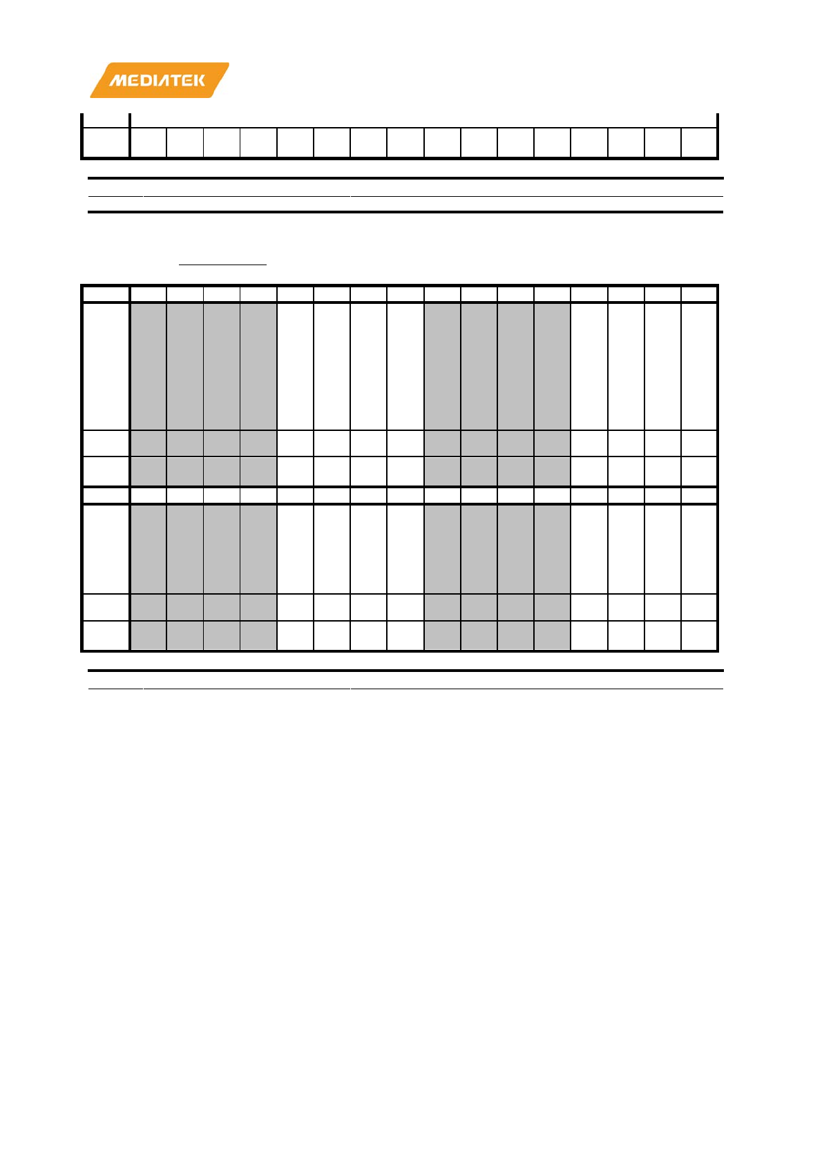
MT7686 Reference Manual
© 2016 - 2017 MediaTek Inc.
Page 240 of 536
This document contains information that is proprietary to MediaTek Inc. (“MediaTek”) and/or its licensor(s).
Any unauthorized use, reproduction or disclosure of this document in whole or in part is strictly prohibited.
Type
RW
Rese
t
0 0 0 0 0 0 0 0 0 0 0 0 0 0 0 0
Bit(s)
Name
Description
31:0
RESV_HWFTE3ER
RESV_HWFTE3ER
A1040130
HWFRE0SR
HIF WLAN Firmware RX Event 0
Status Register
00000000
Bit
31
30
29
28
27
26
25
24
23
22
21
20
19
18
17
16
Nam
e
RX
_L
EN
_FI
FO
3_
OV
ER
FL
OW
RX
_L
EN
_FI
FO
2_
OV
ER
FL
OW
RX
_L
EN
_FI
FO
1_
OV
ER
FL
OW
RX
_L
EN
_FI
FO
0_
OV
ER
FL
OW
RX
3D
_C
HK
SU
M_
ER
R
RX
2D
_C
HK
SU
M_
ER
R
RX
1D
_C
HK
SU
M_
ER
R
RX
0D
_C
HK
SU
M_
ER
R
Type
W1
C
W1
C
W1
C
W1
C
W1
C
W1
C
W1
C
W1
C
Rese
t
0 0 0 0 0 0 0 0
Bit
15
14
13
12
11
10
9
8
7
6
5
4
3
2
1
0
Nam
e
RX
3_
UN
DE
RF
LO
W
RX
2_
UN
DE
RF
LO
W
RX
1_
UN
DE
RF
LO
W
RX
0_
UN
DE
RF
LO
W
RX
3_
DO
NE
RX
2_
DO
NE
RX
1_
DO
NE
RX
0_
DO
NE
Type
W1
C
W1
C
W1
C
W1
C
W1
C
W1
C
W1
C
W1
C
Rese
t
0 0 0 0 0 0 0 0
Bit(s)
Name
Description
27
RX_LEN_FIFO3_OVERFLOW
RX length FIFO 3 overflow
This interrupt is generated whenever the firmware attempts to set
RX FIFO length by HWRQ3CR when the packet FIFO length is
already full. This leads to FIFO overflow.
The entry in packet length FIFO will be pushed
-
in by firmware, and
then popped
-out when corresponding RX length is read by the host
driver.
26
RX_LEN_FIFO2_OVERFLOW
RX length FIFO 2 overflow
This interrupt is generated whenever the firmware attempts to set
RX FIFO length by HWRQ3CR when the packet FIFO length is
already full. This leads to FIFO overflow.
The entry in packet length FIFO will be pu
shed-
in by firmware, and
then popped
-out when corresponding RX length is read by the host
driver.
25
RX_LEN_FIFO1_OVERFLOW
RX length FIFO 1 overflow
This interrupt is generated whenever the firmware attempts to set
RX FIFO length by HWRQ3CR when the
packet FIFO length is
already full. This leads to FIFO overflow.
The entry in packet length FIFO will be pushed
-
in by firmware, and
then popped-out when corresponding RX length is read by the host

MT7686 Reference Manual
© 2016 - 2017 MediaTek Inc.
Page 241 of 536
This document contains information that is proprietary to MediaTek Inc. (“MediaTek”) and/or its licensor(s).
Any unauthorized use, reproduction or disclosure of this document in whole or in part is strictly prohibited.
Bit(s)
Name
Description
driver.
24
RX_LEN_FIFO0_OVERFLOW
RX length FIFO 0 overflow
This interrupt is generated whenever the firmware attempts to set
RXFIFO length by HWRQ3CR when the packet FIFO length is
already full. This leads to FIFO overflow.
The entry in packet length FIFO will be push
-in by firmware, and
then popped
-out when corresponding RX length is read by the host
driver.
19
RX3D_CHKSUM_ERR
RX 3 descriptor checksum error
When HWFCR. TRX_DESC_CHKSUM_EN is enabled; hardware
validates the checksum value of each RX descriptor before
transferring the data movement.
This interrupt is generated, if RX
descriptor checksum error occurred.
18
RX2D_CHKSUM_ERR
RX 2 descriptor checksum error
When HWFCR. TRX_DESC_CHKSUM_EN is enabled; hardware
validates the checksum value of each RX descriptor before
transferring the dat
a. This interrupt is generated if RX descriptor
checksum error occurred.
17
RX1D_CHKSUM_ERR
RX 1 descriptor checksum error
When HWFCR. TRX_DESC_CHKSUM_EN is enabled; hardware
validates the checksum value of each RX descriptor before
transferring the
data. This interrupt is generated if RX descriptor
checksum error occurred.
16
RX0D_CHKSUM_ERR
RX 0 descriptor checksum error
When HWFCR. TRX_DESC_CHKSUM_EN is enabled; hardware
validates the checksum value of each RX descriptor before
transferring
the data. This interrupt is generated if RX descriptor
checksum error occurred.
11
RX3_UNDERFLOW
Data underflow at the WLAN RX3 port.
Firmware can clear this bit by writing 1. Writing 0 does nothing.
10
RX2_UNDERFLOW
Data underflow at the WLAN RX2 port.
Firmware can clear this bit by writing 1. Writing 0 does nothing.
9
RX1_UNDERFLOW
Data underflow at the WLAN RX1 port.
Firmware can clear this bit by writing 1. Writing 0 does nothing.
8
RX0_UNDERFLOW
Data underflow at the WLAN RX0 port.
Firmware can clear this bit by writing 1. Writing 0 does nothing.
3
RX3_DONE
Set this bit, if a complete frame is moved to host from
WLAN RX3 queue (which also implies the corresponding
entry is popped
-out from RX3 FIFO length).
Firmware can clear this bit by writing 1. Writing 0 does nothing.
2
RX2_DONE
Set this bit, if a complete frame is moved to host from
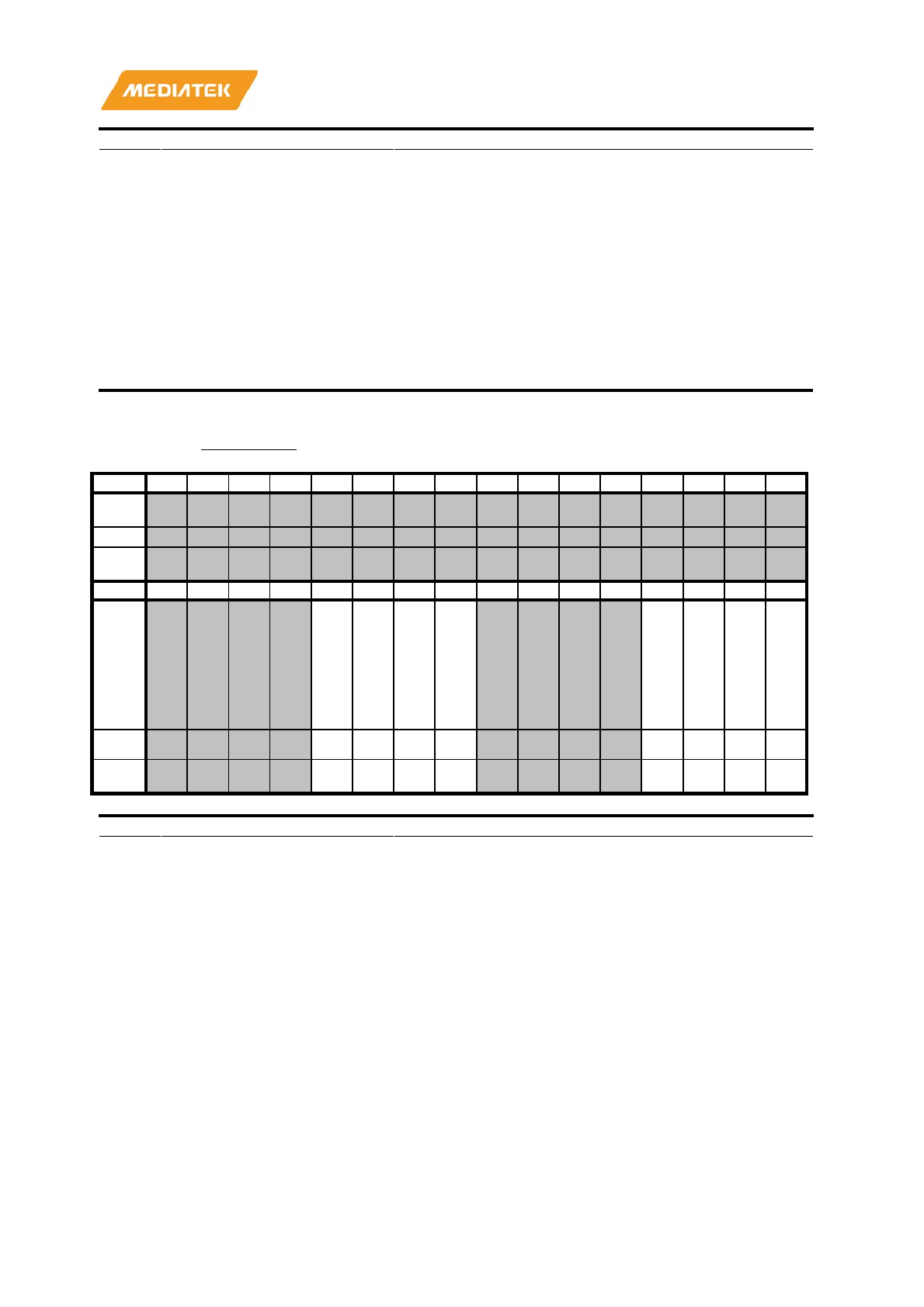
MT7686 Reference Manual
© 2016 - 2017 MediaTek Inc.
Page 242 of 536
This document contains information that is proprietary to MediaTek Inc. (“MediaTek”) and/or its licensor(s).
Any unauthorized use, reproduction or disclosure of this document in whole or in part is strictly prohibited.
Bit(s)
Name
Description
WLAN RX2 queue (which also implies the corresponding
entry is popped
-out from RX2 length FIFO).
Firmware can clear this bit by writing 1. Writing 0 does nothing.
1
RX1_DONE
Set this bit, if a complete frame is moved to host from
WLAN RX1 queue (which also implies the corresponding
entry is popped
-out from RX0 length FIFO).
Firmware can clear this bit by writing 1. Writing 0 does nothing.
0
RX0_DONE
Set this bit, if a complete frame is moved to host from
WLAN RX0 queue (which also implies the corresponding
entry is popped
-out from RX0 length FIFO).
Firmware can clear this bit by writing 1. Writing 0 does nothing.
A1040134
HWFRE1SR
HIF WLAN Firmware RX Event 1
Status Register
00000000
Bit
31
30
29
28
27
26
25
24
23
22
21
20
19
18
17
16
Nam
e
Type
Rese
t
Bit
15
14
13
12
11
10
9
8
7
6
5
4
3
2
1
0
Nam
e
RX
3_
LE
N_
ER
R
RX
2_
LE
N_
ER
R
RX
1_L
EN
_E
RR
RX
0_
LE
N_
ER
R
RX
3_
OW
N_
CL
EA
R_
DO
NE
RX
2_
OW
N_
CL
EA
R_
DO
NE
RX
1_
OW
N_
CL
EA
R_
DO
NE
RX
0_
OW
N_
CL
EA
R_
DO
NE
Type
W1
C
W1
C
W1
C
W1
C
W1
C
W1
C
W1
C
W1
C
Rese
t
0 0 0 0 0 0 0 0
Bit(s)
Name
Description
11
RX3_LEN_ERR
RX queue 3 descriptor length error
If the extension length and RX data length are zero in the generic
packet descriptor or buffer descriptor, an interrupt is triggered.
Firmware can clear this bit by writing 1. Writing 0 does nothing.
10
RX2_LEN_ERR
RX queue 2 descriptor length error
If the extension length and RX data length are zero in the generic
packet descriptor or buffer descriptor, an interrupt is triggered.
Firmware can clear this bit by writing 1. Writing 0 does nothing.
9
RX1_LEN_ERR
RX queue 1 descriptor length error
If the extension length and RX data length are zero in the generic
packet descriptor or buffer descriptor, an interrupt is triggered.
Firmware can clear this bit by writing 1. Writing 0 does nothing.
8
RX0_LEN_ERR
RX queue 0 descriptor length error
If the extension length and RX data length are zero in the generic
packet descriptor or buffer descriptor, an interrupt is triggered.
Firmware can clear this bit by writing 1. Writing 0 does nothing.
3
RX3_OWN_CLEAR_DONE
Set this bit, if a complete frame is moved to internal FIFO
from WLAN RX3 queue and the ownership bit of the
buffer descriptor is cleared.
Firmware can clear this bit by writing 1. Writing 0 does nothing.
MT7686 Reference Manual
© 2016 - 2017 MediaTek Inc.
Page 243 of 536
This document contains information that is proprietary to MediaTek Inc. (“MediaTek”) and/or its licensor(s).
Any unauthorized use, reproduction or disclosure of this document in whole or in part is strictly prohibited.
Bit(s)
Name
Description
2
RX2_OWN_CLEAR_DONE
Set this bit, if a complete frame is moved to internal FIFO
from WLAN RX2 queue and the ownership bit of the
buffer descriptor is cleared.
Firmware can clear this bit by writing 1. Writing 0 does nothing.
1
RX1_OWN_CLEAR_DONE
Set this bit, if a complete frame is moved to internal FIFO
from WLAN RX1 queue and the ownership bit of the
buffer descriptor is cleared.
Firmware can clear this bit by writing 1. Writing 0 does nothing.
0
RX0_OWN_CLEAR_DONE
Set this bit, if a complete frame is moved to internal FIFO
from
WLAN RX0 queue and the ownership bit of the
buffer descriptor is cleared.
Firmware can clear this bit by writing 1. Writing 0 does nothing.
A1040138
HWFRE2SR
Reserve for HWFRE2SR
00000000
Bit
31
30
29
28
27
26
25
24
23
22
21
20
19
18
17
16
Nam
e
RESV_HWFRE2SR
Type
W1C
Rese
t
0 0 0 0 0 0 0 0 0 0 0 0 0 0 0 0
Bit
15
14
13
12
11
10
9
8
7
6
5
4
3
2
1
0
Nam
e
RESV_HWFRE2SR
Type
W1C
Rese
t
0 0 0 0 0 0 0 0 0 0 0 0 0 0 0 0
Bit(s)
Name
Description
31:0
RESV_HWFRE2SR
RESV_HWFRE2SR
A104013C
HWFRE3SR
Reserve for HWFRE3SR
00000000
Bit
31
30
29
28
27
26
25
24
23
22
21
20
19
18
17
16
Nam
e
RESV_HWFRE3SR
Type
W1C
Rese
t
0 0 0 0 0 0 0 0 0 0 0 0 0 0 0 0
Bit
15
14
13
12
11
10
9
8
7
6
5
4
3
2
1
0
Nam
e
RESV_HWFRE3SR
Type
W1C
Rese
t
0 0 0 0 0 0 0 0 0 0 0 0 0 0 0 0
Bit(s)
Name
Description
31:0
RESV_HWFRE3SR
RESV_HWFRE3SR
A1040140
HWFRE0ER
HIF WLAN Firmware RX Event 0
Enable Register
00000000
Bit
31
30
29
28
27
26
25
24
23
22
21
20
19
18
17
16
Nam
e
RX
_L
EN
RX
_L
EN
RX
_L
EN
RX
_L
EN
RX
3D
_C
RX
2D
_C
RX
1D
_C
RX
0D
_C

MT7686 Reference Manual
© 2016 - 2017 MediaTek Inc.
Page 244 of 536
This document contains information that is proprietary to MediaTek Inc. (“MediaTek”) and/or its licensor(s).
Any unauthorized use, reproduction or disclosure of this document in whole or in part is strictly prohibited.
_FI
FO
3_
OV
ER
FL
OW
_I
NT
_E
N
_FI
FO
2_
OV
ER
FL
OW
_I
NT
_E
N
_FI
FO
1_
OV
ER
FL
OW
_I
NT
_E
N
_FI
FO
0_
OV
ER
FL
OW
_I
NT
_E
N
HK
SU
M_
ER
R_I
NT
_E
N
HK
SU
M_
ER
R_I
NT
_E
N
HK
SU
M_
ER
R_I
NT
_E
N
HK
SU
M_
ER
R_I
NT
_E
N
Type
RW
RW
RW
RW
RW
RW
RW
RW
Rese
t
0 0 0 0 0 0 0 0
Bit
15
14
13
12
11
10
9
8
7
6
5
4
3
2
1
0
Nam
e
RX
3_
UN
DE
RF
LO
W_
INT
_E
N
RX
2_
UN
DE
RF
LO
W_
INT
_E
N
RX
1_
UN
DE
RF
LO
W_
INT
_E
N
RX
0_
UN
DE
RF
LO
W_
INT
_E
N
RX
3_
DO
NE
_I
NT
_E
N
RX
2_
DO
NE
_I
NT
_E
N
RX
1_
DO
NE
_I
NT
_E
N
RX
0_
DO
NE
_I
NT
_E
N
Type
RW
RW
RW
RW
RW
RW
RW
RW
Rese
t
0 0 0 0 0 0 0 0
Bit(s)
Name
Description
27
RX_LEN_FIFO3_OVERFLOW_INT
_EN
WLAN firmware interrupt output control for each bit.
If the related bit is
0: Disable the related bit interrupt output.
1: Enable the related bit interrupt output.
26
RX_LEN_FIFO2_OVERFLOW_INT
_EN
WLAN firmware interrupt output control for each bit.
If the related bit is
0: Disable the related bit interrupt output.
1: Enable the related bit interrupt output.
25
RX_LEN_FIFO1_OVERFLOW_INT
_EN
WLAN firmware interrupt output control for each bit.
If the related bit is
0: Disable the related bit interrupt output.
1: Enable the related bit interrupt output.
24
RX_LEN_FIFO0_OVERFLOW_INT
_EN
WLAN firmware interrupt output control for each bit.
If the related bit is
0: Disable the related bit interrupt output.
1: Enable the related bit interrupt output.
19
RX3D_CHKSUM_ERR_INT_EN
WLAN firmware interrupt output control for each bit.
If the related bit is
0: Disable the related bit interrupt output.
1: Enable the related bit interrupt output.
18
RX2D_CHKSUM_ERR_INT_EN
WLAN firmware interrupt output control for each bit.
If the related bit is
0: Disable the related bit interrupt output.
1: Enable the related bit interrupt output.
17
RX1D_CHKSUM_ERR_INT_EN
WLAN firmware interrupt output control for each bit.
If the related bit is
0: Disable the related bit interrupt output.
1: Enable the related bit interrupt output.
16
RX0D_CHKSUM_ERR_INT_EN
WLAN firmware interrupt output control for each bit.
If the related bit is
0: Disable the related bit interrupt output.
1: Enable the related bit interrupt output.
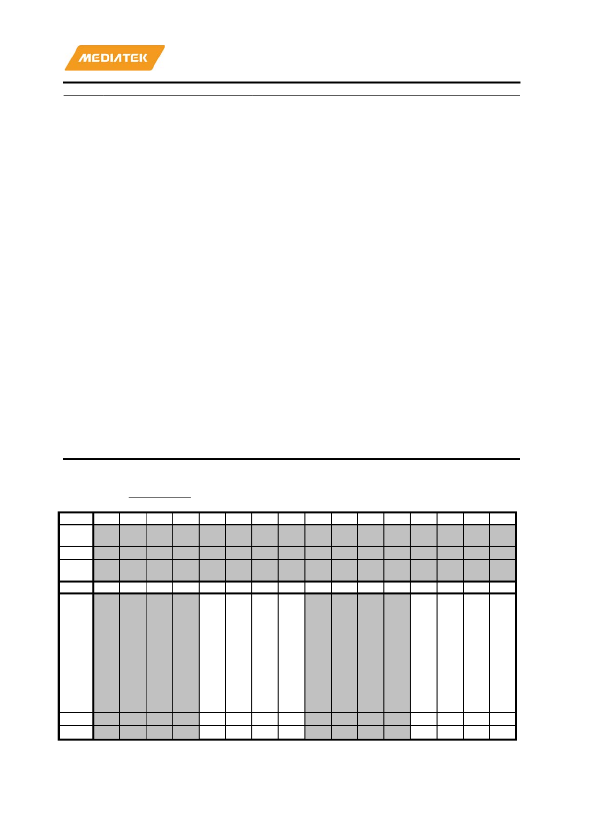
MT7686 Reference Manual
© 2016 - 2017 MediaTek Inc.
Page 245 of 536
This document contains information that is proprietary to MediaTek Inc. (“MediaTek”) and/or its licensor(s).
Any unauthorized use, reproduction or disclosure of this document in whole or in part is strictly prohibited.
Bit(s)
Name
Description
11
RX3_UNDERFLOW_INT_EN
WLAN firmware interrupt output control for each bit.
If the related bit is
0: Disable the related bit interrupt output.
1: Enable the related bit interrupt output.
10
RX2_UNDERFLOW_INT_EN
WLAN firmware interrupt output control for each bit.
If the related bit is
0: Disable the related bit interrupt output.
1: Enable the related bit interrupt output.
9
RX1_UNDERFLOW_INT_EN
WLAN firmware interrupt output control for each bit.
If the related bit is
0: Disable the related bit interrupt output.
1: Enable the related bit interrupt output.
8
RX0_UNDERFLOW_INT_EN
WLAN firmware interrupt output control for each bit.
If the related bit is
0: Disable the related bit interrupt output.
1: Enable the related bit interrupt output.
3
RX3_DONE_INT_EN
WLAN firmware interrupt output control for each bit.
If the related bit is
0: Disable the related bit interrupt output.
1: Enable the related bit interrupt output.
2
RX2_DONE_INT_EN
WLAN firmware interrupt output control for each bit.
If the related bit is
0: Disable the related bit interrupt output.
1: Enable the related bit interrupt output.
1
RX1_DONE_INT_EN
WLAN firmware interrupt output control for each bit.
If the related bit is
0: Disable the related bit interrupt output.
1: Enable the related bit interrupt output.
0
RX0_DONE_INT_EN
WLAN firmware interrupt output control for each bit.
If the related bit is
0: Disable the related bit interrupt output.
1: Enable the related bit interrupt output.
A1040144
HWFRE1ER
HIF WLAN Firmware RX Event 1
Enable Register
00000000
Bit
31
30
29
28
27
26
25
24
23
22
21
20
19
18
17
16
Nam
e
Type
Rese
t
Bit
15
14
13
12
11
10
9
8
7
6
5
4
3
2
1
0
Nam
e
RX
3_
LE
N_
ER
R_I
NT
_E
N
RX
2_
LE
N_
ER
R_I
NT
_E
N
RX
1_L
EN
_E
RR
_I
NT
_E
N
RX
0_
LE
N_
ER
R_I
NT
_E
N
RX
3_
OW
N_
CL
EA
R_
DO
NE
_I
NT
_E
N
RX
2_
OW
N_
CL
EA
R_
DO
NE
_I
NT
_E
N
RX
1_
OW
N_
CL
EA
R_
DO
NE
_I
NT
_E
N
RX
0_
OW
N_
CL
EA
R_
DO
NE
_I
NT
_E
N
Type
RW
RW
RW
RW
RW
RW
RW
RW
Rese
0
0
0
0
0
0
0
0

MT7686 Reference Manual
© 2016 - 2017 MediaTek Inc.
Page 246 of 536
This document contains information that is proprietary to MediaTek Inc. (“MediaTek”) and/or its licensor(s).
Any unauthorized use, reproduction or disclosure of this document in whole or in part is strictly prohibited.
t
Bit(s)
Name
Description
11
RX3_LEN_ERR_INT_EN
WLAN firmware interrupt output control for each bit.
If the related bit is
0: Disable the related bit interrupt output.
1: Enable the related bit interrupt output.
10
RX2_LEN_ERR_INT_EN
WLAN firmware interrupt output control for each bit.
If the related bit is
0: Disable the related bit interrupt output.
1: Enable the related bit interrupt output.
9
RX1_LEN_ERR_INT_EN
WLAN firmware interrupt output control for each bit.
If the related bit is
0: Disable the related bit interrupt output.
1: Enable the related bit interrupt output.
8
RX0_LEN_ERR_INT_EN
WLAN firmware interrupt output control for each bit.
If the related bit is
0: Disable the related bit interrupt output.
1: Enable the related bit interrupt output.
3
RX3_OWN_CLEAR_DONE_INT_E
N
WLAN firmware interrupt output control for each bit.
If the related bit is
0: Disable the related bit interrupt output.
1: Enable the related bit interrupt output.
2
RX2_OWN_CLEAR_DONE_INT_E
N
WLAN firmware interrupt output control for each bit.
If the related bit is
0: Disable the related bit interrupt output.
1: Enable the related bit interrupt output.
1
RX1_OWN_CLEAR_DONE_INT_E
N
WLAN firmware interrupt output control for each bit.
If the related bit is
0: Disable the related bit interrupt output.
1: Enable the related bit interrupt output.
0
RX0_OWN_CLEAR_DONE_INT_E
N
WLAN firmware interrupt output control for each bit.
If the related bit is
0: Disable the related bit interrupt output.
1: Enable the related bit interrupt output.
A1040148
HWFRE2ER
Reserve for HWFRE2ER
00000000
Bit
31
30
29
28
27
26
25
24
23
22
21
20
19
18
17
16
Nam
e
RESV_HWFRE2ER
Type
RW
Rese
t
0 0 0 0 0 0 0 0 0 0 0 0 0 0 0 0
Bit
15
14
13
12
11
10
9
8
7
6
5
4
3
2
1
0
Nam
e
RESV_HWFRE2ER
Type
RW
Rese
t
0 0 0 0 0 0 0 0 0 0 0 0 0 0 0 0
Bit(s)
Name
Description
31:0
RESV_HWFRE2ER
WLAN firmware interrupt output control for each bit.
If the related bit is
0: Disable the related bit interrupt output.
1: Enable the related bit interrupt output.
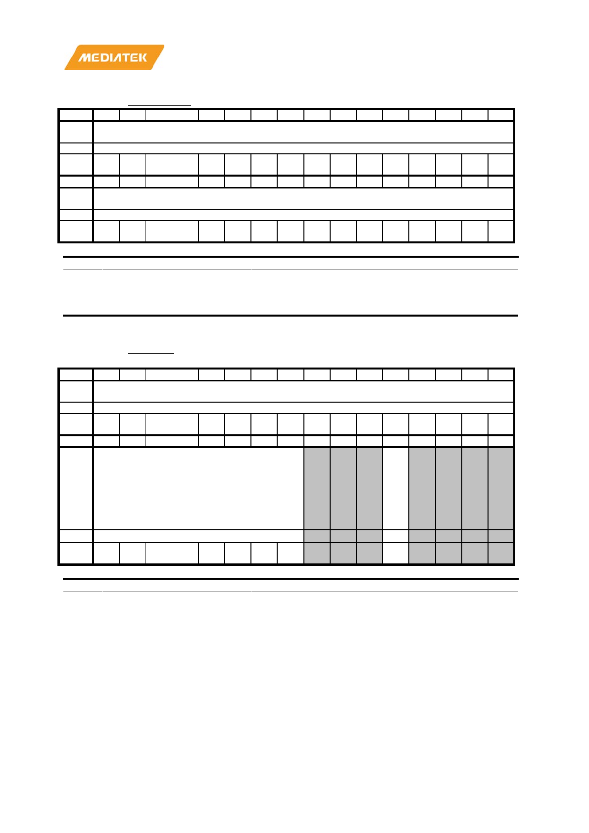
MT7686 Reference Manual
© 2016 - 2017 MediaTek Inc.
Page 247 of 536
This document contains information that is proprietary to MediaTek Inc. (“MediaTek”) and/or its licensor(s).
Any unauthorized use, reproduction or disclosure of this document in whole or in part is strictly prohibited.
A104014C
HWFRE3ER
Reserve for HWFRE3ER
00000000
Bit
31
30
29
28
27
26
25
24
23
22
21
20
19
18
17
16
Nam
e
RESV_HWFRE3ER
Type
RW
Rese
t
0 0 0 0 0 0 0 0 0 0 0 0 0 0 0 0
Bit
15
14
13
12
11
10
9
8
7
6
5
4
3
2
1
0
Nam
e
RESV_HWFRE3ER
Type
RW
Rese
t
0 0 0 0 0 0 0 0 0 0 0 0 0 0 0 0
Bit(s)
Name
Description
31:0
RESV_HWFRE3ER
WLAN firmware interrupt output control for each bit.
If the related bit is
0: Disable the related bit interrupt output.
1: Enable the related bit interrupt output.
A1040150
HWFICR
HIF WLAN Firmware Interrupt
Control Register
00000010
Bit
31
30
29
28
27
26
25
24
23
22
21
20
19
18
17
16
Nam
e
D2H_SW_INT_SET
Type
W1S
Rese
t
0 0 0 0 0 0 0 0 0 0 0 0 0 0 0 0
Bit
15
14
13
12
11
10
9
8
7
6
5
4
3
2
1
0
Nam
e D2H_SW_INT_SET
FW
_O
WN
_B
AC
K_I
NT
_S
ET
Type
W1S
W1S
Rese
t
0 0 0 0 0 0 0 0 1
Bit(s)
Name
Description
31:8
D2H_SW_INT_SET
Firmware writes 1s to set WHISR.D2H_SW_INT. Writing
0 does nothing
.
Read always returns 0.
This is used as a communication between firmware and driver, with
interrupt trigger to host driver HIF.
4
FW_OWN_BACK_INT_SET
Firmware writes 1 to set WHISR.FW_OWN_BACK_INT.
Writing 0 does nothing
. It will also clear
WLAN_FW_OWN bit and set
WHLPCR.WLAN_DRV_OWN bit.
Firmware sets this bit, if the driver requests firmware to return the
ownership or the firmware requires to wake up
the driver
Read the bit will get the status of WLAN_FW_OWN bit.
WLAN_FW_OWN indicates that WLAN firmware has the

MT7686 Reference Manual
© 2016 - 2017 MediaTek Inc.
Page 248 of 536
This document contains information that is proprietary to MediaTek Inc. (“MediaTek”) and/or its licensor(s).
Any unauthorized use, reproduction or disclosure of this document in whole or in part is strictly prohibited.
Bit(s)
Name
Description
ownership of the WLAN sub-system.
This bit is cleared by firmware writing 1 into
HWFICR.FW_OWN_BACK_INT_SET or any WLAN driver
-
domain interrupt.
0: WLAN firmware doesn't have any ownership.
1: WLAN firmware has an ownership.
A1040154
HWFCR
HIF WLAN Firmware Control Register
00000000
Bit
31
30
29
28
27
26
25
24
23
22
21
20
19
18
17
16
Nam
e
Type
Rese
t
Bit
15
14
13
12
11
10
9
8
7
6
5
4
3
2
1
0
Nam
e
RX
_N
O_
TAI
L
TX
_N
O_
HE
AD
ER
RX
_U
DP
_C
S_
OF
LD
_E
N
RX
_T
CP
_C
S_
OF
LD
_E
N
RX
_IP
V4
_C
S_
OF
LD
_E
N
RX
_IP
V6
_C
S_
OF
LD
_E
N
TX
_C
S_
OF
LD
_E
N
TR
X_
DE
SC
_C
HK
SU
M_
12B
TR
X_
DE
SC
_C
HK
SU
M_
EN
W_
FU
NC
_R
DY
Type
RW
RW
RW
RW
RW
RW
RW
RW
RW
RW
Rese
t
0 0 0 0 0 0 0 0 0 0
Bit(s)
Name
Description
9
RX_NO_TAIL
RX packet tail is used to send the checksum offload status.
If the checksum offload hardware is not configured, the
tail would be
4B zero. Firmware can write 1 to prevent the
RX packet from sending to host.
0: RX packet tail will be sent to host.
1: RX packet tail will not be sent to host.
8
TX_NO_HEADER
Firmware writes 1 to this field so that the host will send
the TX packet header instead of writing it to the AHB bus.
0: TX packet header from host will be written to AHB bus.
1: TX packet header from host will not be written to AHB bus.
7
RX_UDP_CS_OFLD_EN
Enable RX UDP checksum verification function
When enabled, the
checksum of RX packet with UDP header is
calculated and verified with the field in the original RX packet. The
verified status will be padding in the last DWORD of the RX packet.
6
RX_TCP_CS_OFLD_EN
Enable RX TCP checksum verification function
When enabl
ed, the checksum of RX packet with TCP header is
calculated and verified with the field in the original RX packet. The
verified status will be padding in the last DWORD of the RX packet.
5
RX_IPV4_CS_OFLD_EN
Enable RX IPv4 checksum verification function
When enabled, the checksum of RX packet with IPv4 header will be
calculated, and verified with the field in original RX packet. The
verified status will be padding in the last DWORD of the RX packet.
4
RX_IPV6_CS_OFLD_EN
Enable RX IPv6 checksum (without extension header)
verification function
When enabled, packets checksum of RX packet with IPv6 header
will be calculated, and verified with the field in original RX packet.
The verified status will be padding in the last DWORD of the RX
packet.
3
TX_CS_OFLD_EN
Enable TX IPV6/IPV4/TCP/UDP checksum generation
function

MT7686 Reference Manual
© 2016 - 2017 MediaTek Inc.
Page 249 of 536
This document contains information that is proprietary to MediaTek Inc. (“MediaTek”) and/or its licensor(s).
Any unauthorized use, reproduction or disclosure of this document in whole or in part is strictly prohibited.
Bit(s)
Name
Description
2
TRX_DESC_CHKSUM_12B
Firmware write 1 to this filed to change the descriptor
checksum calculation method to 12B. The default
calculation method is based on the 16B descriptor
checksum.
0: Descriptor checksum calculation is based on first 16B.
1: Descriptor checksum calculation is based on first 12B
1
TRX_DESC_CHKSUM_EN
Enable TX/ RX descriptor checksum for debug purpose.
HW will validate if the summation of descriptor checksum is 0xff
b
efore data movement for the descriptor. If it is invalid,
corresponding interrupt status (TXD_CHKSUM_ERR/
RXD_CHKSUM_ERR) will be generated.
0
W_FUNC_RDY
Indicate the WLAN functional block's current status. If
WLAN functional block has finished its
initial procedure
and it is ready for normal operation, firmware should set
this bit. If WLAN functional block was disabled, this bit
should be cleared.
This is a sticky bit of WCIR.W_FUNC_RDY.
0: WLAN functional block is not ready for normal operation.
1: WLAN functional block is ready for normal operation.
A1040158
HWTDCR
HIF WLAN TX DMA Control Register
00000000
Bit
31
30
29
28
27
26
25
24
23
22
21
20
19
18
17
16
Nam
e
TX
Q7
_D
MA
_S
TA
TU
S
TX
Q6
_D
MA
_S
TA
TU
S
TX
Q5
_D
MA
_S
TA
TU
S
TX
Q4
_D
MA
_S
TA
TU
S
TX
Q3
_D
MA
_S
TA
TU
S
TX
Q2
_D
MA
_S
TA
TU
S
TX
Q1
_D
MA
_S
TA
TU
S
TX
Q0
_D
MA
_S
TA
TU
S
TX
Q7
_D
MA
_R
UM
TX
Q6
_D
MA
_R
UM
TX
Q5
_D
MA
_R
UM
TX
Q4
_D
MA
_R
UM
TX
Q3
_D
MA
_R
UM
TX
Q2
_D
MA
_R
UM
TX
Q1
_D
MA
_R
UM
TX
Q0
_D
MA
_R
UM
Type
RO
RO
RO
RO
RO
RO
RO
RO
W1S
W1S
W1S
W1S
W1S
W1S
W1S
W1S
Rese
t
0 0 0 0 0 0 0 0 0 0 0 0 0 0 0 0
Bit
15
14
13
12
11
10
9
8
7
6
5
4
3
2
1
0
Nam
e
TX
Q7
_D
MA
_S
TA
RT
TX
Q6
_D
MA
_S
TA
RT
TX
Q5
_D
MA
_S
TA
RT
TX
Q4
_D
MA
_S
TA
RT
TX
Q3
_D
MA
_S
TA
RT
TX
Q2
_D
MA
_S
TA
RT
TX
Q1
_D
MA
_S
TA
RT
TX
Q0
_D
MA
_S
TA
RT
TX
Q7
_D
MA
_S
TO
P
TX
Q6
_D
MA
_S
TO
P
TX
Q5
_D
MA
_S
TO
P
TX
Q4
_D
MA
_S
TO
P
TX
Q3
_D
MA
_S
TO
P
TX
Q2
_D
MA
_S
TO
P
TX
Q1
_D
MA
_S
TO
P
TX
Q0
_D
MA
_S
TO
P
Type
W1S
W1S
W1S
W1S
W1S
W1S
W1S
W1S
W1S
W1S
W1S
W1S
W1S
W1S
W1S
W1S
Rese
t
0 0 0 0 0 0 0 0 0 0 0 0 0 0 0 0
Bit(s)
Name
Description
31
TXQ7_DMA_STATUS
Read for the TX4 queue DMA status.
When the HIF Controller is reset, the queue is in the inactive state
by default. After receiving a START or RESUME command and
executing it without error, the queue enters the active state. When
the queue is empty or stopped by a STOP com
mand, it returns to
the inactive state.
0: inactive
1: active
30
TXQ6_DMA_STATUS
Read for the TX6 queue DMA status.
When the HIF Controller is reset, the queue is in the inactive state
by default. After receiving a START or RESUME command and
executing it without error, the queue enters the active state. When

MT7686 Reference Manual
© 2016 - 2017 MediaTek Inc.
Page 250 of 536
This document contains information that is proprietary to MediaTek Inc. (“MediaTek”) and/or its licensor(s).
Any unauthorized use, reproduction or disclosure of this document in whole or in part is strictly prohibited.
Bit(s)
Name
Description
the queue is empty or stopped by a STOP command, it returns to
the inactive state.
0: inactive
1: active
29
TXQ5_DMA_STATUS
Read for the TX5 queue DMA status.
When the HIF Controller is reset, the queue is in the inactive state
by default. After receiving a START or RESUME command and
executing it without
error, the queue enters the active state. When
the queue is empty or stopped by a STOP command, it returns to
the inactive state.
0: inactive
1: active
28
TXQ4_DMA_STATUS
Read for the TX4 queue DMA status.
When the HIF Controller is reset, the queue
is in the inactive state
by default. After receiving a START or RESUME command and
executing it without error, the queue enters the active state. When
the queue is empty or stopped by a STOP command, it returns to
the inactive state.
0: inactive
1: active
27
TXQ3_DMA_STATUS
Read for the TX3 queue DMA status.
When the HIF Controller is reset, the queue is in the inactive state
by default. After receiving a START or RESUME command and
executing it without error, the queue enters the active state. When
the queue is empty or stopped by a STOP command, it returns to
the inactive state.
0: inactive
1: active
26
TXQ2_DMA_STATUS
Read for the TX2 queue DMA status.
When the HIF Controller is reset, the queue is in the inactive state
by default. After
receiving a START or RESUME command and
executing it without error, the queue enters the active state. When
the queue is empty or stopped by a STOP command, it returns to
the inactive state.
0: inactive
1: active
25
TXQ1_DMA_STATUS
Read for the TX1 queue DMA status.
When the HIF Controller is reset, the queue is in the inactive state
by default. After receiving a START or RESUME command and
executing it without error, the queue enters the active state. When
the queue is empty or stopped by a STOP com
mand, it returns to
the inactive state.
0: inactive
1: active
24
TXQ0_DMA_STATUS
Read for the TX0 queue DMA status.
When the HIF Controller is reset, the queue is in the inactive state
by default. After receiving a START or RESUME command and
executing it without error, the queue enters the active state. When
the queue is empty or stopped by a STOP command, it returns to
the inactive state.
0: inactive
1: active
23
TXQ7_DMA_RUM
Resume the TX7 queue DMA to operate.
The DMA will reload the
chain descriptor from the current address.
Firmware writes 1 to enable the DMA. Writing 0 does nothing.
Read always returns 0.
22
TXQ6_DMA_RUM
Resume the TX6 queue DMA to operate.
The DMA will reload the chain descriptor from the current address.
Firmware writes 1 to enable the DMA. Writing 0 does nothing.
Read always returns 0.

MT7686 Reference Manual
© 2016 - 2017 MediaTek Inc.
Page 251 of 536
This document contains information that is proprietary to MediaTek Inc. (“MediaTek”) and/or its licensor(s).
Any unauthorized use, reproduction or disclosure of this document in whole or in part is strictly prohibited.
Bit(s)
Name
Description
21
TXQ5_DMA_RUM
Resume the TX5 queue DMA to operate.
The DMA will reload the chain descriptor from the current address.
Firmware writes 1 to enable the DMA. Writing 0 does
nothing.
Read always returns 0.
20
TXQ4_DMA_RUM
Resume the TX4 queue DMA to operate.
The DMA will reload the chain descriptor from the current address.
Firmware writes 1 to enable the DMA. Writing 0 does nothing.
Read always returns 0.
19
TXQ3_DMA_RUM
Resume the TX3 queue DMA to operate.
The DMA will reload the chain descriptor from the current address.
Firmware writes 1 to enable the DMA. Writing 0 does nothing.
Read always returns 0.
18
TXQ2_DMA_RUM
Resume the TX2 queue DMA to operate.
The DMA will r
eload the chain descriptor from the current address.
Firmware writes 1 to enable the DMA. Writing 0 does nothing.
Read always returns 0.
17
TXQ1_DMA_RUM
Resume the TX1 queue DMA to operate.
The DMA will reload the chain descriptor from the current
address.
Firmware writes 1 to enable the DMA. Writing 0 does nothing.
Read always returns 0.
16
TXQ0_DMA_RUM
Resume the TX0 queue DMA to operate.
The DMA will reload the chain descriptor from the current address.
Firmware writes 1 to enable the DMA. Writi
ng 0 does nothing.
Read always returns 0.
15
TXQ7_DMA_START
Start the TX7 queue DMA operation.
The DMA will load the chain descriptor from the address assigned
by HWFTQ7SAR.
SW must check TXQ7_DMA_STATUS is inactive before start.
Writing 0 does nothing. Read always returns 0.
14
TXQ6_DMA_START
Start the TX6 queue DMA operation.
The DMA will load the chain descriptor from the address assigned
by HWFTQ6SAR.
SW must check TXQ6_DMA_STATUS is inactive before start.
Writing 0 does nothing. Read always returns 0.
13
TXQ5_DMA_START
Start the TX5 queue DMA operation.
The DMA will load the chain descriptor from the address assigned
by HWFTQ5SAR.
SW must check TXQ5_DMA_STATUS is inactive before start.
Writing 0 does nothing. Read always returns 0.
12
TXQ4_DMA_START
Start the TX4 queue DMA operation.
The DMA will load the chain descriptor from the address assigned
by HWFTQ4SAR.
SW must check TXQ4_DMA_STATUS is inactive before start.
Writing 0 does nothing. Read always returns 0.
11
TXQ3_DMA_START
Start the TX3 queue DMA operation.
The DMA will load the chain descriptor from the address assigned
by HWFTQ3SAR.
SW must check TXQ3_DMA_STATUS is inactive before start.
Writing 0 does nothing. Read always returns 0.
10
TXQ2_DMA_START
Start the TX2 queue DMA operation.
The DMA will load the chain descriptor from the address assigned
by HWFTQ2SAR.
SW must check TXQ2_DMA_STATUS is inactive before start.
Writing 0 does nothing. Read always returns 0.
9
TXQ1_DMA_START
Start the TX1 queue DMA operation.
The DMA wi
ll load the chain descriptor from the address assigned
by HWFTQ1SAR.
SW must check TXQ1_DMA_STATUS is inactive before start.
Writing 0 does nothing. Read always returns 0.
8
TXQ0_DMA_START
Start the TX0 queue DMA operation.
The DMA will load the chain
descriptor from the address assigned
by HWFTQ0SAR.
SW must check TXQ0_DMA_STATUS is inactive before start.

MT7686 Reference Manual
© 2016 - 2017 MediaTek Inc.
Page 252 of 536
This document contains information that is proprietary to MediaTek Inc. (“MediaTek”) and/or its licensor(s).
Any unauthorized use, reproduction or disclosure of this document in whole or in part is strictly prohibited.
Bit(s)
Name
Description
Writing 0 does nothing. Read always returns 0.
7
TXQ7_DMA_STOP
Stop the TX7 queue DMA operation. It will NOT clear the
result of TX count set by
HWTPCCR(WTSR0/ WTSR1).
Firmware writes 1 to stop the DMA. Writing 0 does nothing.
Read always returns current DMA activity (0: stopped, 1: stop
command is on
-going).
If one data port to multiple queues design is configured, any one of
these queues stop would lead to these queues stop at the same time.
(e.g. If TX queue 1 stops, then TX queue 2, 3, 4, 5, 6, 7 would also be
stopped by HW since they share the same data port.)
6
TXQ6_DMA_STOP
Stop the TX6 queue DMA operation. It will NOT clear the
result of TX
count set by HWTPCCR(WTSR0/ WTSR1).
Firmware writes 1 to stop the DMA. Writing 0 does nothing.
Read always returns current DMA activity (0: stopped, 1: stop
command is on
-going).
If one data port to multiple queues design is configured, any one of
these queues stop would lead to these queues stop at the same time.
(e.g. If TX queue 1 stops, then TX queue 2, 3, 4, 5, 6, 7 would also be
stopped by HW since they share the same data port.)
5
TXQ5_DMA_STOP
Stop the TX5 queue DMA operation. It will NOT clear the
result of TX count set by HWTPCCR(WTSR0/ WTSR1).
Firmware writes 1 to stop the DMA. Writing 0 does nothing.
Read always returns current DMA activity (0: stopped, 1: stop
command is on
-going).
If one data port to multiple queues design is configured, any
one of
these queues stop would lead to these queues stop at the same time.
(e.g. If TX queue 1 stops, then TX queue 2, 3, 4, 5, 6, 7 would also be
stopped by HW since they share the same data port.)
4
TXQ4_DMA_STOP
Stop the TX4 queue DMA operation. It will NOT clear the
result of TX count set by HWTPCCR(WTSR0/ WTSR1).
Firmware writes 1 to stop the DMA. Writing 0 does nothing.
Read always returns current DMA activity (0: stopped, 1: stop
command is on
-going).
If one data port to multiple queues design is c
onfigured, any one of
these queues stop would lead to these queues stop at the same time.
(e.g. If TX queue 1 stops, then TX queue 2, 3, 4, 5, 6, 7 would also be
stopped by HW since they share the same data port.)
3
TXQ3_DMA_STOP
Stop the TX3 queue DMA operation. It will NOT clear the
result of TX count set by HWTPCCR(WTSR0/ WTSR1).
Firmware writes 1 to stop the DMA. Writing 0 does nothing.
Read always returns current DMA activity (0: stopped, 1: stop
command is on
-going).
If one data port to multiple qu
eues design is configured, any one of
these queues stop would lead to these queues stop at the same time.
(e.g. If TX queue 1 stops, then TX queue 2, 3, 4, 5, 6, 7 would also be
stopped by HW since they share the same data port.)
2
TXQ2_DMA_STOP
Stop the TX2 queue DMA operation. It will NOT clear the
result of TX count set by HWTPCCR(WTSR0/ WTSR1).
Firmware writes 1 to stop the DMA. Writing 0 does nothing.
Read always returns current DMA activity (0: stopped, 1: stop
command is on
-going).
If one data port
to multiple queues design is configured, any one of
these queues stop would lead to these queues stop at the same time.
(e.g. If TX queue 1 stops, then TX queue 2, 3, 4, 5, 6, 7 would also be
stopped by HW since they share the same data port.)
1
TXQ1_DMA_STOP
Stop the TX1 queue DMA operation. It will NOT clear the
result of TX count set by HWTPCCR(WTSR0/ WTSR1).
Firmware writes 1 to stop the DMA. Writing 0 does nothing.
Read always returns current DMA activity (0: stopped, 1: stop
command is on
-going).
If one data port to multiple queues design is configured, any one of
these queues stop would lead to these queues stop at the same time.
(e.g. If TX queue 1 stops, then TX queue 2, 3, 4, 5, 6, 7 would also be
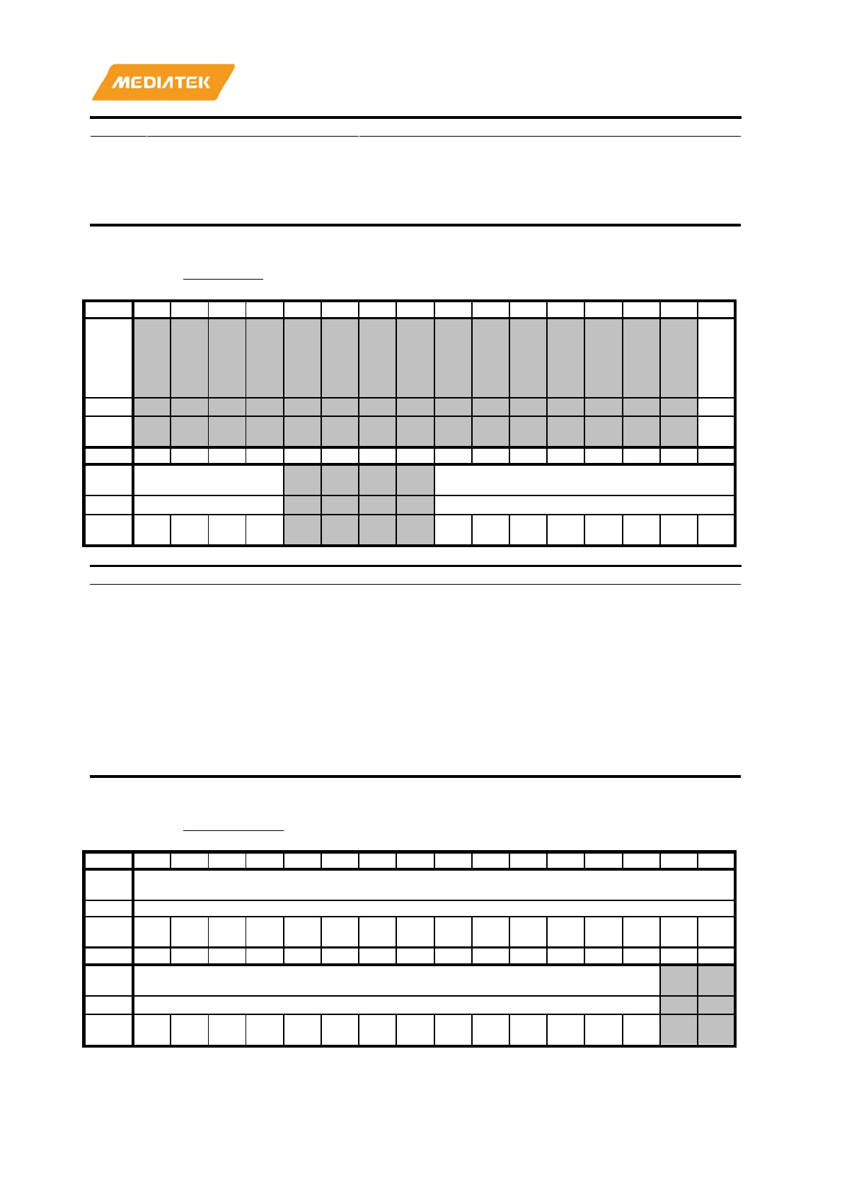
MT7686 Reference Manual
© 2016 - 2017 MediaTek Inc.
Page 253 of 536
This document contains information that is proprietary to MediaTek Inc. (“MediaTek”) and/or its licensor(s).
Any unauthorized use, reproduction or disclosure of this document in whole or in part is strictly prohibited.
Bit(s)
Name
Description
stopped by HW since they share the same data port.)
0
TXQ0_DMA_STOP
Stop the TX0 queue DMA operation. It will NOT clear the
result of TX count set by HWTPCCR(WTSR0/ WTSR1).
Firmware writes 1 to stop the DMA. Writing 0 does nothing.
Read always returns current DMA activity (0: stopped, 1: stop
command is on-going).
A104015C
HWTPCCR
HIF WLAN TX Packet Count Control
Register
00000000
Bit
31
30
29
28
27
26
25
24
23
22
21
20
19
18
17
16
Nam
e
TQ
_C
NT
_R
ES
ET
Type
W1S
Rese
t
0
Bit
15
14
13
12
11
10
9
8
7
6
5
4
3
2
1
0
Nam
e
TQ_INDEX INC_TQ_CNT
Type
WO
WO
Rese
t
0 0 0 0 0 0 0 0 0 0 0 0
Bit(s)
Name
Description
16
TQ_CNT_RESET
Firmware writes 1 to reset the count accumulated for TQ0
~ TQ7.
Writing 0 does nothing. Read always returns 0.
15:12
TQ_INDEX
Firmware writes the TQ index to be increased by setting
this field which leads to the same number increased in
WTSR.TQX_CNT.
Writing 0 does nothing. Read always returns 0. (X depends on the
TQ index)
7:0
INC_TQ_CNT
Firmware writes the available TQ buffer count by setting
this field which leads to the same number increased in
WTSR.TQX_CNT.
Writing 0 does nothing. Read always returns 0. (X depends on the
TQ index)
A1040160
HWFTQ0SAR
HIF WLAN Firmware TX Queue 0 Start
Address Register
00000000
Bit
31
30
29
28
27
26
25
24
23
22
21
20
19
18
17
16
Nam
e
WLAN_TXQ0_DMA_SADDR
Type
RW
Rese
t
0 0 0 0 0 0 0 0 0 0 0 0 0 0 0 0
Bit
15
14
13
12
11
10
9
8
7
6
5
4
3
2
1
0
Nam
e
WLAN_TXQ0_DMA_SADDR
Type
RW
Rese
t
0 0 0 0 0 0 0 0 0 0 0 0 0 0
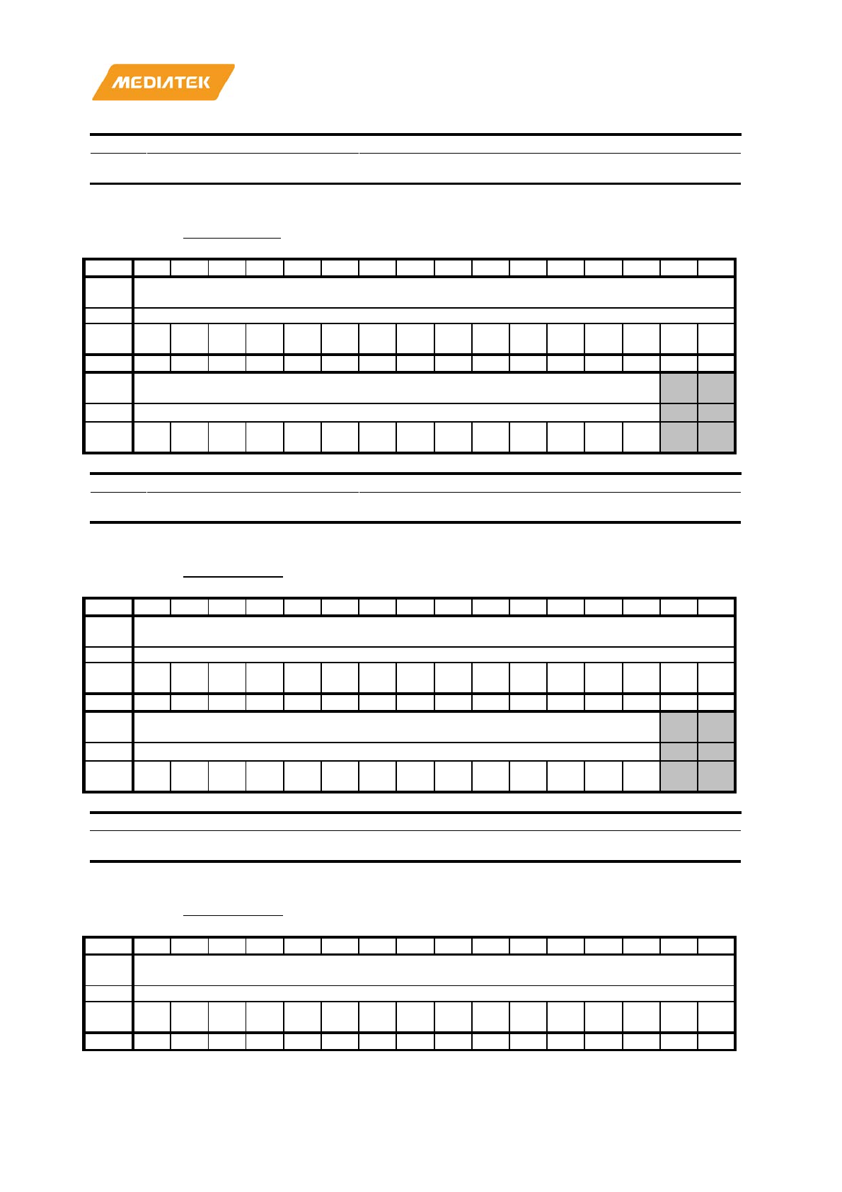
MT7686 Reference Manual
© 2016 - 2017 MediaTek Inc.
Page 254 of 536
This document contains information that is proprietary to MediaTek Inc. (“MediaTek”) and/or its licensor(s).
Any unauthorized use, reproduction or disclosure of this document in whole or in part is strictly prohibited.
Bit(s)
Name
Description
31:2
WLAN_TXQ0_DMA_SADDR
The start address of buffer chain of TX0 queue in unit of
DW.
A1040164
HWFTQ1SAR
HIF WLAN Firmware TX Queue 1 Start
Address
Register
00000000
Bit
31
30
29
28
27
26
25
24
23
22
21
20
19
18
17
16
Nam
e
WLAN_TXQ1_DMA_SADDR
Type
RW
Rese
t
0 0 0 0 0 0 0 0 0 0 0 0 0 0 0 0
Bit
15
14
13
12
11
10
9
8
7
6
5
4
3
2
1
0
Nam
e
WLAN_TXQ1_DMA_SADDR
Type
RW
Rese
t
0 0 0 0 0 0 0 0 0 0 0 0 0 0
Bit(s)
Name
Description
31:2
WLAN_TXQ1_DMA_SADDR
The start address of buffer chain of TX1 queue in unit of
DW.
A1040168
HWFTQ2SAR
HIF WLAN Firmware TX Queue 2 Start
Address Register
00000000
Bit
31
30
29
28
27
26
25
24
23
22
21
20
19
18
17
16
Nam
e
WLAN_TXQ2_DMA_SADDR
Type
RW
Rese
t
0 0 0 0 0 0 0 0 0 0 0 0 0 0 0 0
Bit
15
14
13
12
11
10
9
8
7
6
5
4
3
2
1
0
Nam
e
WLAN_TXQ2_DMA_SADDR
Type
RW
Rese
t
0 0 0 0 0 0 0 0 0 0 0 0 0 0
Bit(s)
Name
Description
31:2
WLAN_TXQ2_DMA_SADDR
The start address of buffer chain of TX2 queue in unit of
DW.
A104016C
HWFTQ3SAR
HIF WLAN Firmware TX Queue 3 Start
Address Register
00000000
Bit
31
30
29
28
27
26
25
24
23
22
21
20
19
18
17
16
Nam
e
WLAN_TXQ3_DMA_SADDR
Type
RW
Rese
t
0 0 0 0 0 0 0 0 0 0 0 0 0 0 0 0
Bit
15
14
13
12
11
10
9
8
7
6
5
4
3
2
1
0
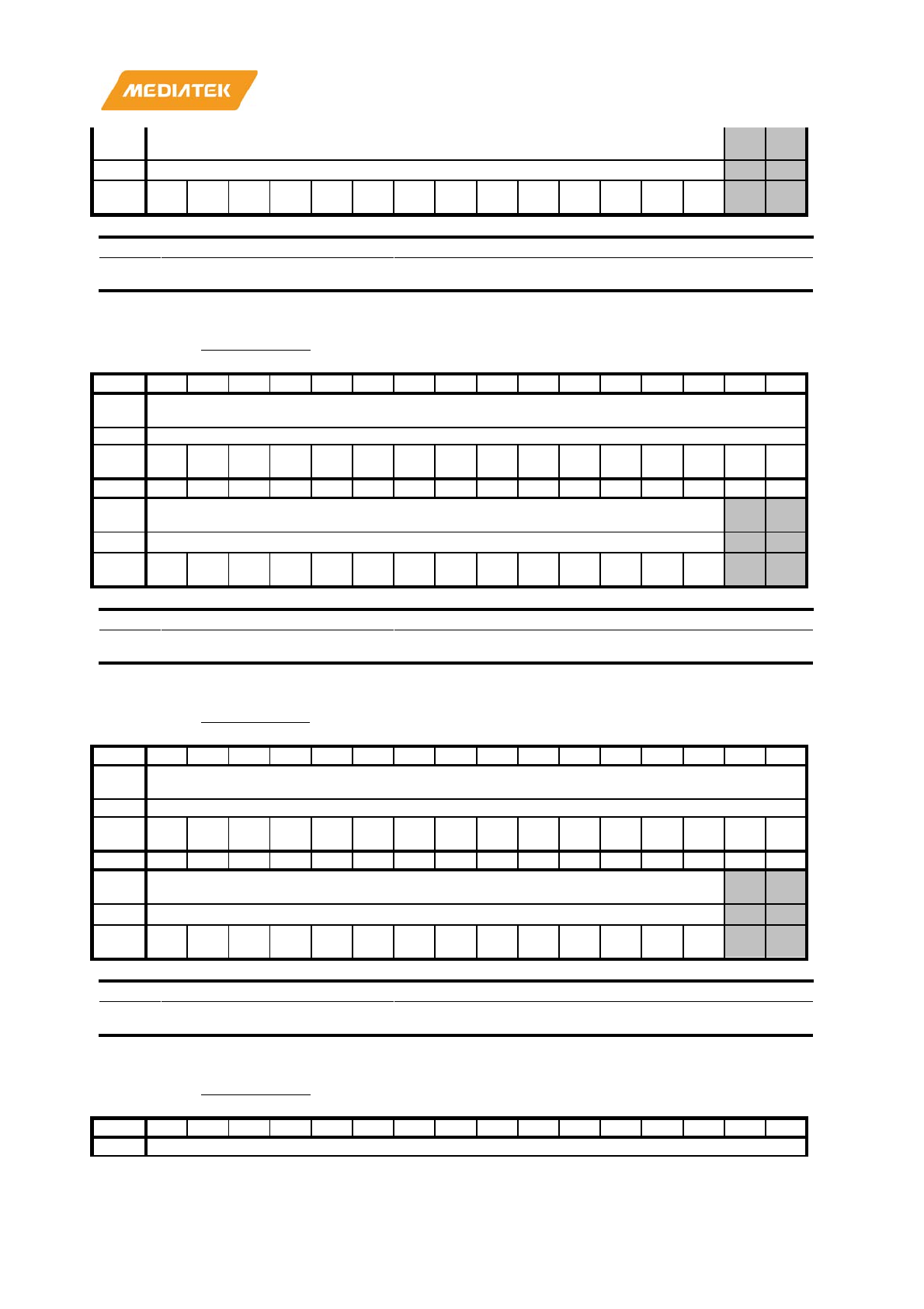
MT7686 Reference Manual
© 2016 - 2017 MediaTek Inc.
Page 255 of 536
This document contains information that is proprietary to MediaTek Inc. (“MediaTek”) and/or its licensor(s).
Any unauthorized use, reproduction or disclosure of this document in whole or in part is strictly prohibited.
Nam
e
WLAN_TXQ3_DMA_SADDR
Type
RW
Rese
t
0 0 0 0 0 0 0 0 0 0 0 0 0 0
Bit(s)
Name
Description
31:2
WLAN_TXQ3_DMA_SADDR
The start address of buffer chain of TX3 queue in unit of
DW.
A1040170
HWFTQ4SAR
HIF WLAN Firmware TX Queue 4 Start
Address Register
00000000
Bit
31
30
29
28
27
26
25
24
23
22
21
20
19
18
17
16
Nam
e
WLAN_TXQ4_DMA_SADDR
Type
RW
Rese
t
0 0 0 0 0 0 0 0 0 0 0 0 0 0 0 0
Bit
15
14
13
12
11
10
9
8
7
6
5
4
3
2
1
0
Nam
e
WLAN_TXQ4_DMA_SADDR
Type
RW
Rese
t
0 0 0 0 0 0 0 0 0 0 0 0 0 0
Bit(s)
Name
Description
31:2
WLAN_TXQ4_DMA_SADDR
The start address of buffer chain of TX4 queue in unit of
DW.
A1040174
HWFTQ5SAR
Reserve for HIF WLAN Firmware TX
Queue 5 Start Address Register
00000000
Bit
31
30
29
28
27
26
25
24
23
22
21
20
19
18
17
16
Nam
e
WLAN_TXQ5_DMA_SADDR
Type
RW
Rese
t
0 0 0 0 0 0 0 0 0 0 0 0 0 0 0 0
Bit
15
14
13
12
11
10
9
8
7
6
5
4
3
2
1
0
Nam
e
WLAN_TXQ5_DMA_SADDR
Type
RW
Rese
t
0 0 0 0 0 0 0 0 0 0 0 0 0 0
Bit(s)
Name
Description
31:2
WLAN_TXQ5_DMA_SADDR
The start address of buffer chain of TX5 queue in unit of
DW.
A1040178
HWFTQ6SAR
Reserve for HIF WLAN Firmware TX
Queue 6 Start Address Register
00000000
Bit
31
30
29
28
27
26
25
24
23
22
21
20
19
18
17
16
Nam
WLAN_TXQ6_DMA_SADDR
MT7686 Reference Manual
© 2016 - 2017 MediaTek Inc.
Page 256 of 536
This document contains information that is proprietary to MediaTek Inc. (“MediaTek”) and/or its licensor(s).
Any unauthorized use, reproduction or disclosure of this document in whole or in part is strictly prohibited.
e
Type
RW
Rese
t
0 0 0 0 0 0 0 0 0 0 0 0 0 0 0 0
Bit
15
14
13
12
11
10
9
8
7
6
5
4
3
2
1
0
Nam
e
WLAN_TXQ6_DMA_SADDR
Type
RW
Rese
t
0 0 0 0 0 0 0 0 0 0 0 0 0 0
Bit(s)
Name
Description
31:2
WLAN_TXQ6_DMA_SADDR
The start address of buffer chain of TX6 queue in unit of
DW.
A104017C
HWFTQ7SAR
Reserve for HIF WLAN Firmware TX
Queue 7 Start Address Register
00000000
Bit
31
30
29
28
27
26
25
24
23
22
21
20
19
18
17
16
Nam
e
WLAN_TXQ7_DMA_SADDR
Type
RW
Rese
t
0 0 0 0 0 0 0 0 0 0 0 0 0 0 0 0
Bit
15
14
13
12
11
10
9
8
7
6
5
4
3
2
1
0
Nam
e
WLAN_TXQ7_DMA_SADDR
Type
RW
Rese
t
0 0 0 0 0 0 0 0 0 0 0 0 0 0
Bit(s)
Name
Description
31:2
WLAN_TXQ7_DMA_SADDR
The start address of buffer chain of TX7 queue in unit of
DW.
A1040180
HWFRQ0SAR
HIF WLAN Firmware RX Queue 0 Start
Address Register
00000000
Bit
31
30
29
28
27
26
25
24
23
22
21
20
19
18
17
16
Nam
e
WLAN_RXQ0_DMA_SADDR
Type
RW
Rese
t
0 0 0 0 0 0 0 0 0 0 0 0 0 0 0 0
Bit
15
14
13
12
11
10
9
8
7
6
5
4
3
2
1
0
Nam
e
WLAN_RXQ0_DMA_SADDR
Type
RW
Rese
t
0 0 0 0 0 0 0 0 0 0 0 0 0 0
Bit(s)
Name
Description
31:2
WLAN_RXQ0_DMA_SADDR
The start address of buffer chain of RX0 queue in unit of
DW.
MT7686 Reference Manual
© 2016 - 2017 MediaTek Inc.
Page 257 of 536
This document contains information that is proprietary to MediaTek Inc. (“MediaTek”) and/or its licensor(s).
Any unauthorized use, reproduction or disclosure of this document in whole or in part is strictly prohibited.
A1040184
HWFRQ1SAR
HIF WLAN Firmware RX Queue 1 Start
Address Register
00000000
Bit
31
30
29
28
27
26
25
24
23
22
21
20
19
18
17
16
Nam
e
WLAN_RXQ1_DMA_SADDR
Type
RW
Rese
t
0 0 0 0 0 0 0 0 0 0 0 0 0 0 0 0
Bit
15
14
13
12
11
10
9
8
7
6
5
4
3
2
1
0
Nam
e
WLAN_RXQ1_DMA_SADDR
Type
RW
Rese
t
0 0 0 0 0 0 0 0 0 0 0 0 0 0
Bit(s)
Name
Description
31:2
WLAN_RXQ1_DMA_SADDR
The start address of buffer chain of RX1 queue in unit of
DW.
A1040188
HWFRQ2SAR
HIF WLAN Firmware RX Queue 2 Start
Address Register
00000000
Bit
31
30
29
28
27
26
25
24
23
22
21
20
19
18
17
16
Nam
e
WLAN_RXQ2_DMA_SADDR
Type
RW
Rese
t
0 0 0 0 0 0 0 0 0 0 0 0 0 0 0 0
Bit
15
14
13
12
11
10
9
8
7
6
5
4
3
2
1
0
Nam
e
WLAN_RXQ2_DMA_SADDR
Type
RW
Rese
t
0 0 0 0 0 0 0 0 0 0 0 0 0 0
Bit(s)
Name
Description
31:2
WLAN_RXQ2_DMA_SADDR
The start address of buffer chain of RX2 queue in unit of
DW.
A104018C
HWFRQ3SAR
HIF WLAN Firmware RX Queue 3 Start
Address Register
00000000
Bit
31
30
29
28
27
26
25
24
23
22
21
20
19
18
17
16
Nam
e
WLAN_RXQ3_DMA_SADDR
Type
RW
Rese
t
0 0 0 0 0 0 0 0 0 0 0 0 0 0 0 0
Bit
15
14
13
12
11
10
9
8
7
6
5
4
3
2
1
0
Nam
e
WLAN_RXQ3_DMA_SADDR
Type
RW
Rese
t
0 0 0 0 0 0 0 0 0 0 0 0 0 0
MT7686 Reference Manual
© 2016 - 2017 MediaTek Inc.
Page 258 of 536
This document contains information that is proprietary to MediaTek Inc. (“MediaTek”) and/or its licensor(s).
Any unauthorized use, reproduction or disclosure of this document in whole or in part is strictly prohibited.
Bit(s)
Name
Description
31:2
WLAN_RXQ3_DMA_SADDR
The start address of buffer chain of RX3 queue in unit of
DW.
A1040190
HWFRQ4SAR
Reserve for HIF WLAN Firmware RX
Queue 4 Start Address Register
00000000
Bit
31
30
29
28
27
26
25
24
23
22
21
20
19
18
17
16
Nam
e
WLAN_RXQ4_DMA_SADDR
Type
RW
Rese
t
0 0 0 0 0 0 0 0 0 0 0 0 0 0 0 0
Bit
15
14
13
12
11
10
9
8
7
6
5
4
3
2
1
0
Nam
e
WLAN_RXQ4_DMA_SADDR
Type
RW
Rese
t
0 0 0 0 0 0 0 0 0 0 0 0 0 0
Bit(s)
Name
Description
31:2
WLAN_RXQ4_DMA_SADDR
The start address of buffer chain of RX4 queue in unit of
DW.
A1040194
HWFRQ5SAR
Reserve for HIF WLAN Firmware RX
Queue 5 Start Address Register
00000000
Bit
31
30
29
28
27
26
25
24
23
22
21
20
19
18
17
16
Nam
e
WLAN_RXQ5_DMA_SADDR
Type
RW
Rese
t
0 0 0 0 0 0 0 0 0 0 0 0 0 0 0 0
Bit
15
14
13
12
11
10
9
8
7
6
5
4
3
2
1
0
Nam
e
WLAN_RXQ5_DMA_SADDR
Type
RW
Rese
t
0 0 0 0 0 0 0 0 0 0 0 0 0 0
Bit(s)
Name
Description
31:2
WLAN_RXQ5_DMA_SADDR
The start address of buffer chain of RX5 queue in unit of
DW.
A1040198
HWFRQ6SAR
Reserve for HIF WLAN Firmware RX
Queue 6 Start Address Register
00000000
Bit
31
30
29
28
27
26
25
24
23
22
21
20
19
18
17
16
Nam
e
WLAN_RXQ6_DMA_SADDR
Type
RW
Rese
t
0 0 0 0 0 0 0 0 0 0 0 0 0 0 0 0
Bit
15
14
13
12
11
10
9
8
7
6
5
4
3
2
1
0
Nam
WLAN_RXQ6_DMA_SADDR
MT7686 Reference Manual
© 2016 - 2017 MediaTek Inc.
Page 259 of 536
This document contains information that is proprietary to MediaTek Inc. (“MediaTek”) and/or its licensor(s).
Any unauthorized use, reproduction or disclosure of this document in whole or in part is strictly prohibited.
e
Type
RW
Rese
t
0 0 0 0 0 0 0 0 0 0 0 0 0 0
Bit(s)
Name
Description
31:2
WLAN_RXQ6_DMA_SADDR
The start address of buffer chain of RX6 queue in unit of
DW.
A104019C
HWFRQ7SAR
Reserve for HIF WLAN Firmware RX
Queue 7 Start Address Register
00000000
Bit
31
30
29
28
27
26
25
24
23
22
21
20
19
18
17
16
Nam
e
WLAN_RXQ7_DMA_SADDR
Type
RW
Rese
t
0 0 0 0 0 0 0 0 0 0 0 0 0 0 0 0
Bit
15
14
13
12
11
10
9
8
7
6
5
4
3
2
1
0
Nam
e
WLAN_RXQ7_DMA_SADDR
Type
RW
Rese
t
0 0 0 0 0 0 0 0 0 0 0 0 0 0
Bit(s)
Name
Description
31:2
WLAN_RXQ7_DMA_SADDR
The start address of buffer chain of RX7 queue in unit of
DW.
A10401A0
H2DRM0R
Host to Device Receive Mailbox 0
Register
00000000
Bit
31
30
29
28
27
26
25
24
23
22
21
20
19
18
17
16
Nam
e
H2D_RM0
Type
RO
Rese
t
0 0 0 0 0 0 0 0 0 0 0 0 0 0 0 0
Bit
15
14
13
12
11
10
9
8
7
6
5
4
3
2
1
0
Nam
e
H2D_RM0
Type
RO
Rese
t
0 0 0 0 0 0 0 0 0 0 0 0 0 0 0 0
Bit(s)
Name
Description
31:0
H2D_RM0
This register is used by firmware to receive data from
SDIO controller, which is updated through H2DSM0R by
host driver.
A10401A4
H2DRM1R
Host to Device Receive Mailbox 1
Register
00000000
Bit
31
30
29
28
27
26
25
24
23
22
21
20
19
18
17
16
Nam
H2D_RM1

MT7686 Reference Manual
© 2016 - 2017 MediaTek Inc.
Page 260 of 536
This document contains information that is proprietary to MediaTek Inc. (“MediaTek”) and/or its licensor(s).
Any unauthorized use, reproduction or disclosure of this document in whole or in part is strictly prohibited.
e
Type
RO
Rese
t
0 0 0 0 0 0 0 0 0 0 0 0 0 0 0 0
Bit
15
14
13
12
11
10
9
8
7
6
5
4
3
2
1
0
Nam
e
H2D_RM1
Type
RO
Rese
t
0 0 0 0 0 0 0 0 0 0 0 0 0 0 0 0
Bit(s)
Name
Description
31:0
H2D_RM1
This register is used by firmware to receive data from
SDIO controller, which is updated through H2DSM1R by
host driver.
A10401A8
D2HSM0R
Device to Host Send Mailbox 0 Register
00000000
Bit
31
30
29
28
27
26
25
24
23
22
21
20
19
18
17
16
Nam
e
D2H_SM0
Type
RW
Rese
t
0 0 0 0 0 0 0 0 0 0 0 0 0 0 0 0
Bit
15
14
13
12
11
10
9
8
7
6
5
4
3
2
1
0
Nam
e
D2H_SM0
Type
RW
Rese
t
0 0 0 0 0 0 0 0 0 0 0 0 0 0 0 0
Bit(s)
Name
Description
31:0
D2H_SM0
This register is used by firmware to transmit data to SDIO
controller, it will be updated to D2HRM0R and read by
host driver.
A10401AC
D2HSM1R
Device to Host Send Mailbox 1 Register
00000000
Bit
31
30
29
28
27
26
25
24
23
22
21
20
19
18
17
16
Nam
e
D2H_SM1
Type
RW
Rese
t
0 0 0 0 0 0 0 0 0 0 0 0 0 0 0 0
Bit
15
14
13
12
11
10
9
8
7
6
5
4
3
2
1
0
Nam
e
D2H_SM1
Type
RW
Rese
t
0 0 0 0 0 0 0 0 0 0 0 0 0 0 0 0
Bit(s)
Name
Description
31:0
D2H_SM1
This register is used by firmware to transmit data to SDIO
controller, it will be updated to D2HRM1R and read by
host driver.
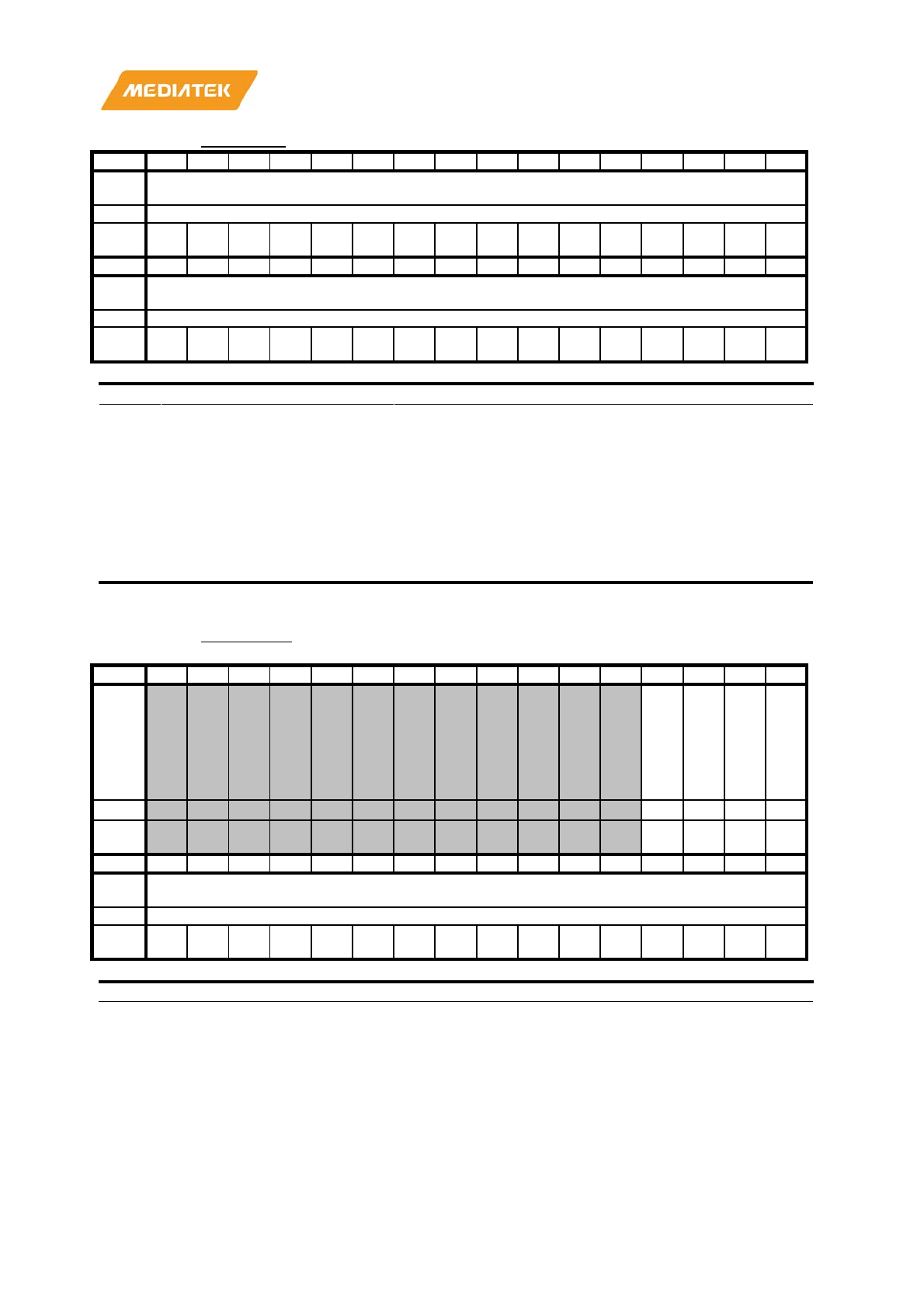
MT7686 Reference Manual
© 2016 - 2017 MediaTek Inc.
Page 261 of 536
This document contains information that is proprietary to MediaTek Inc. (“MediaTek”) and/or its licensor(s).
Any unauthorized use, reproduction or disclosure of this document in whole or in part is strictly prohibited.
A10401B0
D2HSM2R
Device to Host Send Mailbox 2 Register
00000000
Bit
31
30
29
28
27
26
25
24
23
22
21
20
19
18
17
16
Nam
e
D2H_SM2
Type
RW
Rese
t
0 0 0 0 0 0 0 0 0 0 0 0 0 0 0 0
Bit
15
14
13
12
11
10
9
8
7
6
5
4
3
2
1
0
Nam
e
D2H_SM2
Type
RW
Rese
t
0 0 0 0 0 0 0 0 0 0 0 0 0 0 0 0
Bit(s)
Name
Description
31:0
D2H_SM2
This register is used by firmware to transmit data to SDIO
controller, it will be updated to D2HRM2R and read by
host driver.
When reading this register, it may not get the value that firmware
just writes, it may read the older value that firmware had written
before. It results from the synchronization issue
of hardware.
Firmware would get the value that host is tending to read when host
clock turns on.
Note that host driver could read D2HRM2R without system AHB
clock. Hence, after firmware set this register, MCU could turn off
system AHB clock to save power if necessary.
A10401C0
HWRQ0CR
HIF WLAN RX Queue 0 Control
Register
00000000
Bit
31
30
29
28
27
26
25
24
23
22
21
20
19
18
17
16
Nam
e
RX
Q0
_D
MA
_S
TA
TU
S
RX
Q0
_D
MA
_R
UM
RX
Q0
_D
MA
_S
TA
RT
RX
Q0
_D
MA
_S
TO
P
Type
RO
W1S
W1S
W1S
Rese
t
0 0 0 0
Bit
15
14
13
12
11
10
9
8
7
6
5
4
3
2
1
0
Nam
e
RXQ0_PACKET_LENGTH
Type
RW
Rese
t
0 0 0 0 0 0 0 0 0 0 0 0 0 0 0 0
Bit(s)
Name
Description
19
RXQ0_DMA_STATUS
Read for the RX0 queue DMA status.
When the SDIO Controller is reset, the queue is in the inactive state
by default. After receiving a START or RESUME command and
executing it without error, the queue enters the active state. When
the queue is empty or stopped by a STOP command, it returns to
the inactive state.
0: inactive
1: active
18
RXQ0_DMA_RUM
Resume the RX0 queue DMA to operate.
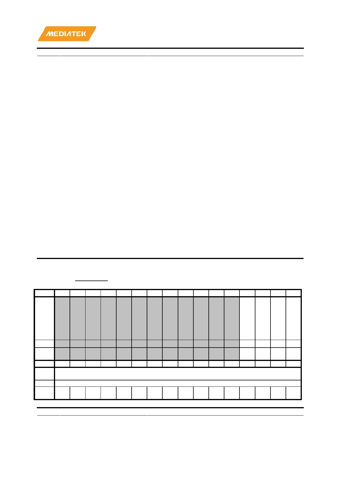
MT7686 Reference Manual
© 2016 - 2017 MediaTek Inc.
Page 262 of 536
This document contains information that is proprietary to MediaTek Inc. (“MediaTek”) and/or its licensor(s).
Any unauthorized use, reproduction or disclosure of this document in whole or in part is strictly prohibited.
Bit(s)
Name
Description
The DMA will reload the chain descriptor from the current address.
Firmware writes 1 to enable the DMA. Writing 0 does nothing.
Read always returns 0.
17
RXQ0_DMA_START
Start the RX0 queue DMA operation.
The DMA will load the chain descriptor from the address assigned
by HWFRQ0SAR.
SW must check RXQ0_DMA_STATUS is inactive before start.
Writing 0 does nothing. Read always returns 0.
16
RXQ0_DMA_STOP
Stop the RX0 queue DMA operation, the content in the
RXQ0 FIFO and RXQ0 length FIFO will be cleared.
Firmware writes 1 to stop the DMA. Writing 0 does nothing.
Read returns current RXQ0 operation state (1: stop operation is on
-
going, 0: stop operation is finished).
15:0
RXQ0_PACKET_LENGTH
When write:
To indicate HIF that 1 RX packet in this packet length is queued
into this RX queue.
When read:
Read the 1st RX packet length indicated from this queue, and will
be 0 when queue is empty.
FW will write this FIFO
-like port (at most 64 entries depends on
the hardware configuration for each project) together with
RXQ1_DMA_RUM bit been set, after RX packet is queued into
descriptor chain.
RX packet with length been set by this field is able to
be read by
host driver, which is through reading WRPLR, or INT enhance
mode, or RX enhance mode.
None
-empty entry will generate RX done interrupt, and
corresponding entry will be cleared by HW after this packet length
is read by host driver.
Writing 0 does nothing.
0: inactive
1: active
A10401C4
HWRQ1CR
HIF WLAN RX Queue 1 Control
Register
00000000
Bit
31
30
29
28
27
26
25
24
23
22
21
20
19
18
17
16
Nam
e
RX
Q1
_D
MA
_S
TA
TU
S
RX
Q1
_D
MA
_R
UM
RX
Q1
_D
MA
_S
TA
RT
RX
Q1
_D
MA
_S
TO
P
Type
RO
W1S
W1S
W1S
Rese
t
0 0 0 0
Bit
15
14
13
12
11
10
9
8
7
6
5
4
3
2
1
0
Nam
e
RX1_PACKET_LENGTH
Type
RW
Rese
t
0 0 0 0 0 0 0 0 0 0 0 0 0 0 0 0
Bit(s)
Name
Description
19
RXQ1_DMA_STATUS
Read for the RXQ1 DMA status.
When the SDIO Controller is reset, the queue is in the inactive state
by default. After receiving a START or RESUME command and
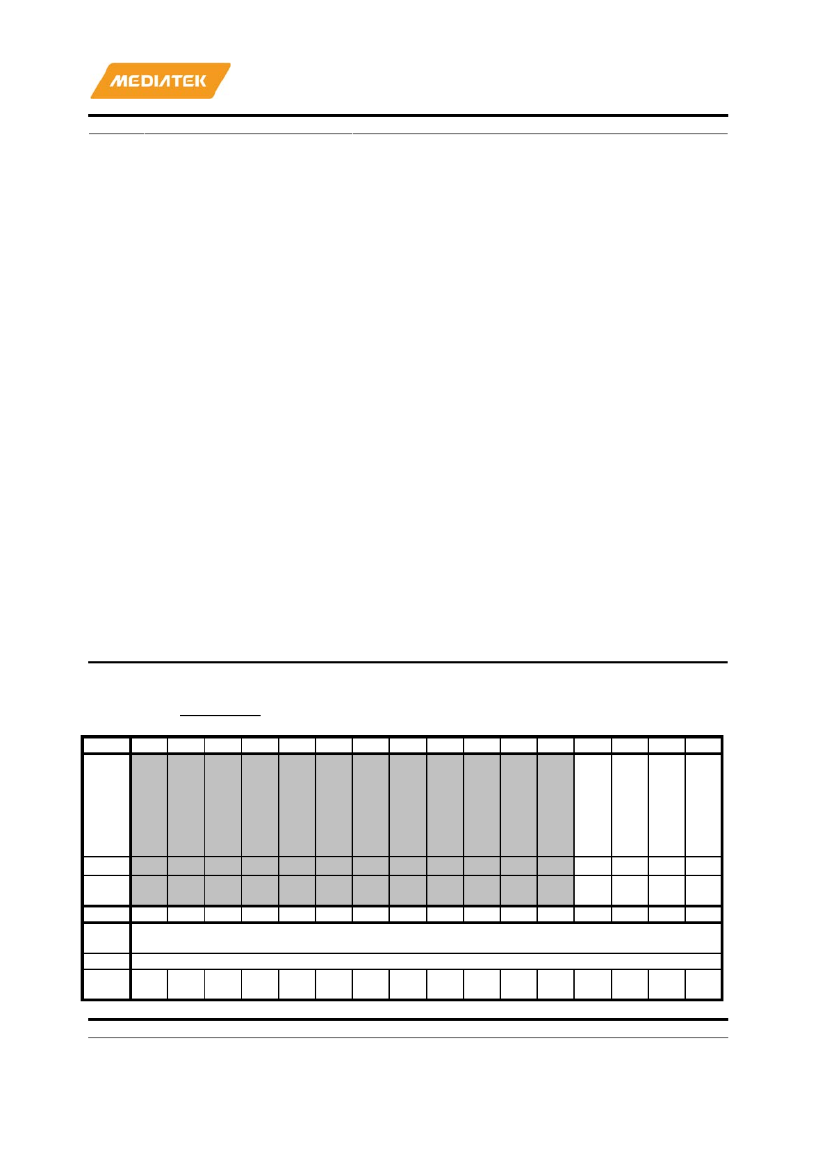
MT7686 Reference Manual
© 2016 - 2017 MediaTek Inc.
Page 263 of 536
This document contains information that is proprietary to MediaTek Inc. (“MediaTek”) and/or its licensor(s).
Any unauthorized use, reproduction or disclosure of this document in whole or in part is strictly prohibited.
Bit(s)
Name
Description
executing it without error, the queue enters the active state. When
the queue is empty or stopped by a STOP command, it
returns to
the inactive state.
0: inactive
1: active
18
RXQ1_DMA_RUM
Resume the RX1 queue DMA to operate.
The DMA will reload the chain descriptor from the current address.
Firmware writes 1 to enable the DMA. Writing 0 does nothing.
Read always returns 0.
17
RXQ1_DMA_START
Start the RX1 queue DMA operation.
The DMA will load the chain descriptor from the address assigned
by HWFRQ1SAR.
SW must check RXQ1_DMA_STATUS is inactive before start.
Writing 0 does nothing. Read always returns 0.
16
RXQ1_DMA_STOP
Stop the RX1 queue DMA operation, the content in the
RXQ1 FIFO and RXQ1 length FIFO will be cleared.
Firmware writes 1 to stop the DMA. Writing 0 does nothing.
Read returns current RXQ1 operation state (1: active, 0: stopped).
15:0
RX1_PACKET_LENGTH
When write:
To indicate HIF that 1 RX packet in this packet length is queued
into this RX queue.
When read:
Read the 1st RX packet length indicated from this queue, and will
be 0 when queue is empty.
FW will write this FIFO
-like port (at most 64 entries depends on
the hardware configuration for each project) together with
RXQ1_DMA_RUM bit been set, after RX packet is queued into
descriptor chain.
RX packet with length been set by this field is able t
o be read by
host driver, which is through reading WRPLR, or INT enhance
mode, or RX enhance mode.
None
-empty entry will generate RX done interrupt, and
corresponding entry will be cleared by HW after this packet length
is read by host driver.
Writing 0 does nothing.
A10401C8
HWRQ2CR
HIF WLAN RX Queue 2 Control
Register
00000000
Bit
31
30
29
28
27
26
25
24
23
22
21
20
19
18
17
16
Nam
e
RX
Q2
_D
MA
_S
TA
TU
S
RX
Q2
_D
MA
_R
UM
RX
Q2
_D
MA
_S
TA
RT
RX
Q2
_D
MA
_S
TO
P
Type
RO
W1S
W1S
W1S
Rese
t
0 0 0 0
Bit
15
14
13
12
11
10
9
8
7
6
5
4
3
2
1
0
Nam
e
RX2_PACKET_LENGTH
Type
RW
Rese
t
0 0 0 0 0 0 0 0 0 0 0 0 0 0 0 0
Bit(s)
Name
Description

MT7686 Reference Manual
© 2016 - 2017 MediaTek Inc.
Page 264 of 536
This document contains information that is proprietary to MediaTek Inc. (“MediaTek”) and/or its licensor(s).
Any unauthorized use, reproduction or disclosure of this document in whole or in part is strictly prohibited.
Bit(s)
Name
Description
19
RXQ2_DMA_STATUS
Read for the RXQ2 DMA status.
When the SDIO Controller is reset, the queue is in the inactive state
by default. After receiving a START or RESUME command and
executing it without error, the queue enters the active state. When
the queue is empty or stopped by a STOP command, it returns to
the inactive state.
0: inactive
1: active
18
RXQ2_DMA_RUM
Resume the RX2 queue DMA to operate.
The DMA will reload the chain descriptor from the current address.
Firmware writes 1 to enable the DMA. Writing 0 does nothing.
Read always returns 0.
17
RXQ2_DMA_START
Start the RX2 queue DMA operation.
The DMA will load the chain descriptor from the address assigned
by HWFRQ1SAR.
SW must check RXQ2_DMA_STATUS is inactive before start.
Writing 0 does nothing. Read always returns 0.
16
RXQ2_DMA_STOP
Stop the RX2 queue DMA operation, the content in the
RXQ2 FIFO and RXQ2 length FIFO will be cleared.
Firmware writes 1 to stop the DMA. Writing 0 does nothing.
Read returns current RXQ2 operation state (1: active, 0: stopped).
15:0
RX2_PACKET_LENGTH
When write:
To indicate HIF
that 1 RX packet in this packet length is queued
into this RX queue.
When read:
Read the 1st RX packet length indicated from this queue, and will
be 0 when queue is empty.
FW will write this FIFO
-like port (at most 64 entries depends on
the hardware configuration for each project) together with
RXQ2_DMA_RUM bit been set, after RX packet is queued into
descriptor chain.
RX packet with length been set by this field is able to
be read by
host driver, which is through reading WRPLR, or INT enhance
mode, or RX enhance mode.
None
-empty entry will generate RX done interrupt, and
corresponding entry will be cleared by HW after this packet length
is read by host driver.
Writing 0 does nothing.
A10401CC
HWRQ3CR
HIF WLAN RX Queue 3 Control
Register
00000000
Bit
31
30
29
28
27
26
25
24
23
22
21
20
19
18
17
16
Nam
e
RX
Q3
_D
MA
_S
TA
TU
S
RX
Q3
_D
MA
_R
UM
RX
Q3
_D
MA
_S
TA
RT
RX
Q3
_D
MA
_S
TO
P
Type
RO
W1S
W1S
W1S
Rese
t
0 0 0 0
Bit
15
14
13
12
11
10
9
8
7
6
5
4
3
2
1
0
Nam
e
RX3_PACKET_LENGTH
Type
RW
Rese
t
0 0 0 0 0 0 0 0 0 0 0 0 0 0 0 0

MT7686 Reference Manual
© 2016 - 2017 MediaTek Inc.
Page 265 of 536
This document contains information that is proprietary to MediaTek Inc. (“MediaTek”) and/or its licensor(s).
Any unauthorized use, reproduction or disclosure of this document in whole or in part is strictly prohibited.
Bit(s)
Name
Description
19
RXQ3_DMA_STATUS
Read for the RXQ3 DMA status.
When the SDIO Controller is reset, the queue is in the inactive state
by default. After receiving a START or RESUME command and
executing it without error, the queue enters the active state. When
the queue is empty or stopped by a STOP command, it returns to
the inactive state.
0: inactive
1: active
18
RXQ3_DMA_RUM
Resume the RX3 queue DMA to operate.
The DMA will reload the chain descriptor from the current address.
Firmware writes 1 to enable the DMA. Writing 0 does nothing.
Read always returns 0.
17
RXQ3_DMA_START
Start the RX3 queue DMA operation.
The DMA will load the chain descriptor from the address assigned
by HWFRQ1SAR.
SW must check RXQ3_DMA_STATUS is inactive before start.
Writing 0 does nothing. Read always returns 0.
16
RXQ3_DMA_STOP
Stop the RX3 queue DMA operation, the content in the
RXQ3 FIFO and RXQ3 length FIFO will be cleared.
Firmware writes 1 to stop the DMA. Writing 0 does nothing.
Read returns current RXQ3 operation state (1: active, 0: stopped).
15:0
RX3_PACKET_LENGTH
When write:
To indicate HIF
that 1 RX packet in this packet length is queued
into this RX queue.
When read:
Read the 1st RX packet length indicated from this queue, and will
be 0 when queue is empty.
FW will write this FIFO
-like port (at most 64 entries depends on
the hardware configuration for each project) together with
RXQ3_DMA_RUM bit been set, after RX packet is queued into
descriptor chain.
RX packet with length been set by this field is able t
o be read by
host driver, which is through reading WRPLR, or INT enhance
mode, or RX enhance mode.
None
-empty entry will generate RX done interrupt, and
corresponding entry will be cleared by HW after this packet length
is read by host driver.
Writing 0 does nothing.
A10401D0
HWRQ4CR
Reserve for HWRQ4CR
00000000
Bit
31
30
29
28
27
26
25
24
23
22
21
20
19
18
17
16
Nam
e
RESV_FOR_HWRQ4CR
Type
RW
Rese
t
0 0 0 0 0 0 0 0 0 0 0 0 0 0 0 0
Bit
15
14
13
12
11
10
9
8
7
6
5
4
3
2
1
0
Nam
e
RESV_FOR_HWRQ4CR
Type
RW
Rese
t
0 0 0 0 0 0 0 0 0 0 0 0 0 0 0 0
Bit(s)
Name
Description
31:0
RESV_FOR_HWRQ4CR
RESV_FOR_HWRQ4CR
MT7686 Reference Manual
© 2016 - 2017 MediaTek Inc.
Page 266 of 536
This document contains information that is proprietary to MediaTek Inc. (“MediaTek”) and/or its licensor(s).
Any unauthorized use, reproduction or disclosure of this document in whole or in part is strictly prohibited.
A10401D4
HWRQ5CR
Reserve for HWRQ5CR
00000000
Bit
31
30
29
28
27
26
25
24
23
22
21
20
19
18
17
16
Nam
e
RESV_FOR_HWRQ5CR
Type
RW
Rese
t
0 0 0 0 0 0 0 0 0 0 0 0 0 0 0 0
Bit
15
14
13
12
11
10
9
8
7
6
5
4
3
2
1
0
Nam
e
RESV_FOR_HWRQ5CR
Type
RW
Rese
t
0 0 0 0 0 0 0 0 0 0 0 0 0 0 0 0
Bit(s)
Name
Description
31:0
RESV_FOR_HWRQ5CR
RESV_FOR_HWRQ5CR
A10401D8
HWRQ6CR
Reserve for HWRQ6CR
00000000
Bit
31
30
29
28
27
26
25
24
23
22
21
20
19
18
17
16
Nam
e
RESV_FOR_HWRQ6CR
Type
RW
Rese
t
0 0 0 0 0 0 0 0 0 0 0 0 0 0 0 0
Bit
15
14
13
12
11
10
9
8
7
6
5
4
3
2
1
0
Nam
e
RESV_FOR_HWRQ6CR
Type
RW
Rese
t
0 0 0 0 0 0 0 0 0 0 0 0 0 0 0 0
Bit(s)
Name
Description
31:0
RESV_FOR_HWRQ6CR
RESV_FOR_HWRQ6CR
A10401DC
HWRQ7CR
Reserve for HWRQ7CR
00000000
Bit
31
30
29
28
27
26
25
24
23
22
21
20
19
18
17
16
Nam
e
RESV_FOR_HWRQ7CR
Type
RW
Rese
t
0 0 0 0 0 0 0 0 0 0 0 0 0 0 0 0
Bit
15
14
13
12
11
10
9
8
7
6
5
4
3
2
1
0
Nam
e
RESV_FOR_HWRQ7CR
Type
RW
Rese
t
0 0 0 0 0 0 0 0 0 0 0 0 0 0 0 0
Bit(s)
Name
Description
31:0
RESV_FOR_HWRQ7CR
RESV_FOR_HWRQ7CR
MT7686 Reference Manual
© 2016 - 2017 MediaTek Inc.
Page 267 of 536
This document contains information that is proprietary to MediaTek Inc. (“MediaTek”) and/or its licensor(s).
Any unauthorized use, reproduction or disclosure of this document in whole or in part is strictly prohibited.
A10401E0
HWRLFACR
HIF WLAN RX Length FIFO Available
Count Register
40404040
Bit
31
30
29
28
27
26
25
24
23
22
21
20
19
18
17
16
Nam
e
RX3_LEN_FIFO_AVAIL_CNT RX2_LEN_FIFO_AVAIL_CNT
Type
RO
RO
Rese
t
1 0 0 0 0 0 0 1 0 0 0 0 0 0
Bit
15
14
13
12
11
10
9
8
7
6
5
4
3
2
1
0
Nam
e
RX1_LEN_FIFO_AVAIL_CNT RX0_LEN_FIFO_AVAIL_CNT
Type
RO
RO
Rese
t
1 0 0 0 0 0 0 1 0 0 0 0 0 0
Bit(s)
Name
Description
30:24
RX3_LEN_FIFO_AVAIL_CNT
It indicates the RX3 length FIFO available count. SW
should prevent push extra entries into FIFO.
If under the define of SDCTL_RX3_PACKET_LEN_64,
The maximum is 64.
If under the define of SDCTL_RX3_PACKET_LEN_32,
The maximum is 32.
If under the define of SDCTL_RX3_PACKET_
LEN_16,
The maximum is 16.
22:16
RX2_LEN_FIFO_AVAIL_CNT
It indicates the RX2 length FIFO available count. SW
should prevent push extra entries into FIFO.
If under the define of SDCTL_RX2_PACKET_LEN_64,
The maximum is 64.
If under the define of SDCTL_RX2_PACKET_LEN_32,
The maximum is 32.
If under the define of SDCTL_RX2_PACKET_LEN_16,
The maximum is 16.
14:8
RX1_LEN_FIFO_AVAIL_CNT
It indicates the RX1 length FIFO available count. SW
should prevent push extra entries in
to FIFO.
If under the define of SDCTL_RXD_PACKET_LEN_64,
The maximum is 64.
If under the define of SDCTL_RXD_PACKET_LEN_32,
The maximum is 32.
If under the define of SDCTL_RXD_PACKET_LEN_16,
The maximum is 16.
6:0
RX0_LEN_FIFO_AVAIL_CNT
It indicates the RX0 length FIFO available count. SW
should prevent push extra entries into FIFO.
If under the define of SDCTL_RXE_PACKET_LEN_64,
The maximum is 64.
If under the define of SDCTL_RXE_PACKET_LEN_32,
The maximum is 32.
If under the define of SDCTL_RXE_PACKET_LEN_16,
The maximum is 16.
A10401E4
HWRLFACR1
Reserve for HWRLFACR1
00000000
Bit
31
30
29
28
27
26
25
24
23
22
21
20
19
18
17
16
Nam
e
RESV_FOR_HWRLFACR1
Type
RO
Rese
t
0 0 0 0 0 0 0 0 0 0 0 0 0 0 0 0
Bit
15
14
13
12
11
10
9
8
7
6
5
4
3
2
1
0
Nam
RESV_FOR_HWRLFACR1

MT7686 Reference Manual
© 2016 - 2017 MediaTek Inc.
Page 268 of 536
This document contains information that is proprietary to MediaTek Inc. (“MediaTek”) and/or its licensor(s).
Any unauthorized use, reproduction or disclosure of this document in whole or in part is strictly prohibited.
e
Type
RO
Rese
t
0 0 0 0 0 0 0 0 0 0 0 0 0 0 0 0
Bit(s)
Name
Description
31:0
RESV_FOR_HWRLFACR1
RESV_FOR_HWRLFACR1
A10401E8
HWDMACR
HIF WLAN DMA Control Register
0000004A
Bit
31
30
29
28
27
26
25
24
23
22
21
20
19
18
17
16
Nam
e
Type
Rese
t
Bit
15
14
13
12
11
10
9
8
7
6
5
4
3
2
1
0
Nam
e DMA_BS
T_SIZE AHB_PR
OT2_CTL
AR
BIT
ER
_M
OD
E
DE
ST
_B
ST
_T
YP
AH
B_1
KB
ND
RY
_P
RT
CT
Type
RW
RW
RW
RW
RW
Rese
t
0 1 0 0 1 1 0
Bit(s)
Name
Description
7:6
DMA_BST_SIZE
This field is used to determine the DMA burst size
0 : burst size = 4 DW
1: burst size = 8 DW
2: burst_size = 16DW
5:4
AHB_PROT2_CTL
This field is used to Control AHB bus Protection 2
function
00: DMA engine would use HPROT[2] signal on AHB bus to be 0 to
protect HWO write back. This is used to guarantee that MCU would
receive interrupt after the HWO is
written. For other data writes,
HPROT[2] is set to 1 to indicate that it is Bufferable
01: The HPROT[2] signal on AHB bus is always set to 0, which
means all AHB writes are not Bufferable
10: The HPROT[2] signal on AHB bus is always set to 1, which
means all AHB writes are Bufferable
3
ARBITER_MODE
For Normal Mode, the arbitration algorithm is more
preference for TX direction (from HOST to FW), which is
good for reducing the duration time during write busy in
SDIO interface.
And for the Reserve Mode,
it is more aggressive than the Normal
Mode which means RX will not be executed unless the TX has been
completed.
0: Reserve Mode
1: Normal Mode (Recommend)
1
DEST_BST_TYP
This field is used to specify the AHB burst type for HWO
write back.
0: HIFSYS DMA engine would use non-post-write (INCR, burst
type = 3'b001) to write 0 to HWO when the responding data is
dealt. This access could guarantee that MCU would receive
interrupt after the HWO is written.
1: HIFSYS DMA engine would use post-write (SINGLE, burst type =

MT7686 Reference Manual
© 2016 - 2017 MediaTek Inc.
Page 269 of 536
This document contains information that is proprietary to MediaTek Inc. (“MediaTek”) and/or its licensor(s).
Any unauthorized use, reproduction or disclosure of this document in whole or in part is strictly prohibited.
Bit(s)
Name
Description
3'b000) to write 0 to HWO when the responding data is dealt. This
access could NOT guarantee that MCU would receive interrupt after
the HWO is written.
0
AHB_1KBNDRY_PRTCT
This field is used to specify whether to protect the 1K
boundary or not
0: Don't protect.
1: DMA will guarantee the AHB will not cross 1K boundary in a
burst.
A10401EC
HWFIOCDR
HIF WLAN Firmware GPD IOC bit
Disable Register
00000FFF
Bit
31
30
29
28
27
26
25
24
23
22
21
20
19
18
17
16
Nam
e
Type
Rese
t
Bit
15
14
13
12
11
10
9
8
7
6
5
4
3
2
1
0
Nam
e
RX
Q3
_IO
C_
DIS
RX
Q2
_IO
C_
DIS
RX
Q1
_IO
C_
DIS
RX
Q0
_IO
C_
DIS
TX
Q7
_IO
C_
DIS
TX
Q6
_IO
C_
DIS
TX
Q5
_IO
C_
DIS
TX
Q4
_IO
C_
DIS
TX
Q3
_IO
C_
DIS
TX
Q2
_IO
C_
DIS
TX
Q1
_IO
C_
DIS
TX
Q0
_IO
C_
DIS
Type
RW
RW
RW
RW
RW
RW
RW
RW
RW
RW
RW
RW
Rese
t
1 1 1 1 1 1 1 1 1 1 1 1
Bit(s)
Name
Description
11
RXQ3_IOC_DIS
If firmware write 1 to this register, the corresponding
queue always issue interrupt event when GPD is done.
If firmware write 0 to this register, the corresponding queue will
issue interrupt event base on GPD IOC bit. If current GPD IOC = 1,
GPD done int
errupt event will be issued and latched into
HWFRE1SR.
0: Enable IOC function.
1: Disable IOC function (always issue interrupt when GPD done)
10
RXQ2_IOC_DIS
If firmware write 1 to this register, the corresponding
queue always issue interrupt event when GPD is done.
If firmware write 0 to this register, the corresponding queue will
issue interrupt event base on GPD IOC bit. If current GPD IOC = 1,
GPD done int
errupt event will be issued and latched into
HWFRE1SR.
0: Enable IOC function.
1: Disable IOC function (always issue interrupt when GPD done)
9
RXQ1_IOC_DIS
If firmware write 1 to this register, the corresponding
queue always issue interrupt event when GPD is done.
If firmware write 0 to this register, the corresponding queue will
issue interrupt event base on GPD IOC bit. If current GPD IOC = 1,
GPD done int
errupt event will be issued and latched into
HWFRE1SR.
0: Enable IOC function.
1: Disable IOC function (always issue interrupt when GPD done)
8
RXQ0_IOC_DIS
If firmware write 1 to this register, the corresponding
queue always issue interrupt event when GPD is done.
If firmware write 0 to this register, the corresponding queue will
issue interrupt event base on GPD IOC bit. If current GPD IOC = 1,
GPD done int
errupt event will be issued and latched into
HWFRE1SR.

MT7686 Reference Manual
© 2016 - 2017 MediaTek Inc.
Page 270 of 536
This document contains information that is proprietary to MediaTek Inc. (“MediaTek”) and/or its licensor(s).
Any unauthorized use, reproduction or disclosure of this document in whole or in part is strictly prohibited.
Bit(s)
Name
Description
0: Enable IOC function.
1: Disable IOC function (always issue interrupt when GPD done)
7
TXQ7_IOC_DIS
If firmware write 1 to this register, the corresponding
queue always issue interrupt event when GPD is done.
If firmware write 0 to this register, the corresponding queue will
issue interrupt event base on GPD IOC bit. If current GPD IOC = 1,
GPD done int
errupt event will be issued and latched into
HWFTE0SR.
0: Enable IOC function.
1: Disable IOC function (always issue interrupt when GPD done)
6
TXQ6_IOC_DIS
If firmware write 1 to this register, the corresponding
queue always issue interrupt event w
hen GPD is done.
If firmware write 0 to this register, the corresponding queue will
issue interrupt event base on GPD IOC bit. If current GPD IOC = 1,
GPD done interrupt event will be issued and latched into
HWFTE0SR.
0: Enable IOC function.
1: Disable IOC function (always issue interrupt when GPD done)
5
TXQ5_IOC_DIS
If firmware write 1 to this register, the corresponding
queue always issue interrupt event when GPD is done.
If firmware write 0 to this register, the corresponding queue will
iss
ue interrupt event base on GPD IOC bit. If current GPD IOC = 1,
GPD done interrupt event will be issued and latched into
HWFTE0SR.
0: Enable IOC function.
1: Disable IOC function (always issue interrupt when GPD done)
4
TXQ4_IOC_DIS
If firmware write 1 to this register, the corresponding
queue always issue interrupt event when GPD is done.
If firmware write 0 to this register, the corresponding queue will
issue interrupt event base on GPD IOC bit. If current GPD IOC = 1,
GPD done int
errupt event will be issued and latched into
HWFTE0SR.
0: Enable IOC function.
1: Disable IOC function (always issue interrupt when GPD done)
3
TXQ3_IOC_DIS
If firmware write 1 to this register, the corresponding
queue always issue interrupt event when GPD is done.
If firmware write 0 to this register, the corresponding queue will
issue interrupt event base on GPD IOC bit. If current GPD IOC = 1,
GPD done int
errupt event will be issued and latched into
HWFTE0SR.
0: Enable IOC function.
1: Disable IOC function (always issue interrupt when GPD done)
2
TXQ2_IOC_DIS
If firmware write 1 to this register, the corresponding
queue always issue interrupt event when GPD is done.
If firmware write 0 to this register, the corresponding queue will
issue interrupt event base on GPD IOC bit. If current GPD IOC = 1,
GPD done int
errupt event will be issued and latched into
HWFTE0SR.
0: Enable IOC function.
1: Disable IOC function (always issue interrupt when GPD done)
1
TXQ1_IOC_DIS
If firmware write 1 to this register, the corresponding
queue always issue interrupt event when GPD is done.
If firmware write 0 to this register, the corresponding queue will
issue interrupt event base on GPD IOC bit. If current GPD IOC = 1,
GPD done int
errupt event will be issued and latched into
HWFTE0SR.
0: Enable IOC function.
1: Disable IOC function (always issue interrupt when GPD done)
0
TXQ0_IOC_DIS
If firmware write 1 to this register, the corresponding
queue always issue interrupt event when GPD is done.
MT7686 Reference Manual
© 2016 - 2017 MediaTek Inc.
Page 271 of 536
This document contains information that is proprietary to MediaTek Inc. (“MediaTek”) and/or its licensor(s).
Any unauthorized use, reproduction or disclosure of this document in whole or in part is strictly prohibited.
Bit(s)
Name
Description
If firmware write 0 to this register, the corresponding queue will
issue interrupt event base on GPD IOC bit. If current GPD IOC = 1,
GPD done interrupt event will be issued and latched into
HWFTE0SR.
0: Enable IOC function.
1: Disable IOC function (always issue interrupt when GPD done)
A10401F0
HSDIOTOCR
HIF SDIO Time-Out Control Register
00032000
Bit
31
30
29
28
27
26
25
24
23
22
21
20
19
18
17
16
Nam
e
RE
G_
WR
_TI
ME
OU
T_
EN
RE
G_
RD
_TI
ME
OU
T_
EN
Type
RW
RW
Rese
t
1 1
Bit
15
14
13
12
11
10
9
8
7
6
5
4
3
2
1
0
Nam
e
REG_TIMEOUT_NUM
Type
RW
Rese
t
0 0 1 0 0 0 0 0 0 0 0 0 0 0 0 0
Bit(s)
Name
Description
17
REG_WR_TIMEOUT_EN
Firmware can write 0 to this field to disable SDIO write
timeout function and write 1 to enable the function.
0: Disable SDIO timeout function.
1: Enable SDIO timeout function.
16
REG_RD_TIMEOUT_EN
Firmware can write 0 to this field to disable SDIO read
timeout function and write 1 to enable the function.
0: Disable SDIO timeout function.
1: Enable SDIO timeout function.
15:0
REG_TIMEOUT_NUM
Firmware can write this field to decide the timeout
threshold. The unit is SDIO clock cycle number.
A1040200
HWFTSR0
HIF WLAN Firmware TX Status
Register 0
00000000
Bit
31
30
29
28
27
26
25
24
23
22
21
20
19
18
17
16
Nam
e
TQ3_CNT TQ2_CNT
Type
RO
RO
Rese
t
0 0 0 0 0 0 0 0 0 0 0 0 0 0 0 0
Bit
15
14
13
12
11
10
9
8
7
6
5
4
3
2
1
0
Nam
e
TQ1_CNT TQ0_CNT
Type
RO
RO
Rese
t
0 0 0 0 0 0 0 0 0 0 0 0 0 0 0 0
Bit(s)
Name
Description

MT7686 Reference Manual
© 2016 - 2017 MediaTek Inc.
Page 272 of 536
This document contains information that is proprietary to MediaTek Inc. (“MediaTek”) and/or its licensor(s).
Any unauthorized use, reproduction or disclosure of this document in whole or in part is strictly prohibited.
Bit(s)
Name
Description
31:24
TQ3_CNT
Firmware can read this field to know the accumulated TX
queue count in SDIO controller which are still not read by
host driver.
23:16
TQ2_CNT
Firmware can read this field to know the accumulated TX
queue count in SDIO controller which are still not read by
host driver.
15:8
TQ1_CNT
Firmware can read this field to know the accumulated TX
queue count in SDIO controller which are still not read by
host driver.
7:0
TQ0_CNT
Firmware can read this field to know the accumulated TX
queue count in SDIO controller which are still not read by
host driver.
A1040204
HWFTSR1
HIF WLAN Firmware TX Status
Register 1
00000000
Bit
31
30
29
28
27
26
25
24
23
22
21
20
19
18
17
16
Nam
e
TQ7_CNT TQ6_CNT
Type
RO
RO
Rese
t
0 0 0 0 0 0 0 0 0 0 0 0 0 0 0 0
Bit
15
14
13
12
11
10
9
8
7
6
5
4
3
2
1
0
Nam
e
TQ5_CNT TQ4_CNT
Type
RO
RO
Rese
t
0 0 0 0 0 0 0 0 0 0 0 0 0 0 0 0
Bit(s)
Name
Description
31:24
TQ7_CNT
Firmware can read this field to know the accumulated TX
queue count in SDIO controller which are still not read by
host driver.
23:16
TQ6_CNT
Firmware can read this field to know the accumulated TX
queue count in SDIO controller
which are still not read by
host driver.
15:8
TQ5_CNT
Firmware can read this field to know the accumulated TX
queue count in SDIO controller which are still not read by
host driver.
7:0
TQ4_CNT
Firmware can read this field to know the accumulated TX
que
ue count in SDIO controller which are still not read by
host driver.
A1040210
HWDBGCR
HIF WLAN Debug Control Register
00000000
Bit
31
30
29
28
27
26
25
24
23
22
21
20
19
18
17
16
Nam
e
TX
1_
RE
CO
RD
_E
N
RX
1_
RE
CO
RD
_E
N
RX
0_
RE
CO
RD
_E
N
NO
_D
MU
_D
BG
_M
OD
E
Type
RW
RW
RW
RW
Rese
t
0 0 0 0
Bit
15
14
13
12
11
10
9
8
7
6
5
4
3
2
1
0
Nam
DBG_PKTLEN_OFFSET
MT7686 Reference Manual
© 2016 - 2017 MediaTek Inc.
Page 273 of 536
This document contains information that is proprietary to MediaTek Inc. (“MediaTek”) and/or its licensor(s).
Any unauthorized use, reproduction or disclosure of this document in whole or in part is strictly prohibited.
e
Type
RW
Rese
t
0 0 0 0 0 0 0 0 0 0 0 0 0 0 0 0
Bit(s)
Name
Description
19
TX1_RECORD_EN
Firmware can write 1 to this field to enable TX1 data port
record in debug mode.
18
RX1_RECORD_EN
Firmware can write 1 to this field to enable RX1 data port
record in debug mode.
17
RX0_RECORD_EN
Firmware can write 1 to this field to enable RX0 data port
record in debug mode.
16
NO_DMU_DBG_MODE
Firmware can write 1 to this field to enable the virtual
direct DMA debug mode. When this mode is enabled, the
data transfer between SDIO controller and SDIO wrapper
would also be written to SDIO
internal memory in PIO
mode for debug use. Firmware can enable the data port to
be recorded by writing 1 to the corresponding field in this
register. Only one data port should be recorded each
single time for the debug mode so that the record
condition can
be applied to that port correctly. The record
condition would be packet size and packet length offset.
Packets that meet both two criteria would be recorded.
15:0
DBG_PKTLEN_OFFSET
Since the memory used for debug is only roughly 2KB and
might not be enou
gh to record one full packet size,
firmware can set this field to indicate the offset of one
packet size to be recorded. This field is limited to be DW
alignment size. E.g. firmware writes 20 to this field
meaning that the data from byte 21 would be recorded.
A1040214
HWDBGPLR
HIF WLAN Debug Packet Length
Register
00000000
Bit
31
30
29
28
27
26
25
24
23
22
21
20
19
18
17
16
Nam
e
DBG_LEN_UP_BOUND
Type
RW
Rese
t
0 0 0 0 0 0 0 0 0 0 0 0 0 0 0 0
Bit
15
14
13
12
11
10
9
8
7
6
5
4
3
2
1
0
Nam
e
DBG_LEN_LOW_BOUND
Type
RW
Rese
t
0 0 0 0 0 0 0 0 0 0 0 0 0 0 0 0
Bit(s)
Name
Description
31:16
DBG_LEN_UP_BOUND
Firmware can write this field to decide the upper bound
packet size to record. Packets that meet both the upper
and lower bound criteria would be recorded.
15:0
DBG_LEN_LOW_BOUND
Firmware can write this field to decide the lower bound
packet size to record. Packets that meet both the upper
and lower bound criteria would be recorded.
A1040218
HSPICSR
WLAN SPI Control Status Register (SPI
Only)
00000000
Bit
31
30
29
28
27
26
25
24
23
22
21
20
19
18
17
16
Nam
D_ D_ D_ D_
D_ D_ D_BIT_M D_
MT7686 Reference Manual
© 2016 - 2017 MediaTek Inc.
Page 274 of 536
This document contains information that is proprietary to MediaTek Inc. (“MediaTek”) and/or its licensor(s).
Any unauthorized use, reproduction or disclosure of this document in whole or in part is strictly prohibited.
e
CP
OL
_S
ET
_C
ON
TR
OL
CP
HA
_S
ET
_C
ON
TR
OL
MO
DE
_S
ET
_C
ON
TR
OL
EN
DI
AN
_S
ET
_C
ON
TR
OL
CP
OL
CP
HA
ODE
EN
DI
AN
Type
RO
RO
RO
RO
RO
RO
RO
RO
Rese
t
0 0 0 0 0 0 0 0 0
Bit
15
14
13
12
11
10
9
8
7
6
5
4
3
2
1
0
Nam
e
CP
OL
_S
ET
_C
ON
TR
OL
CP
HA
_S
ET
_C
ON
TR
OL
MO
DE
_S
ET
_C
ON
TR
OL
EN
DI
AN
_S
ET
_C
ON
TR
OL
CP
OL CP
HA BIT_MOD
E
EN
DI
AN
Type
RW
RW
RW
RW
RW
RW
RW
RW
Rese
t
0 0 0 0 0 0 0 0 0
Bit(s)
Name
Description
27
D_CPOL_SET_CONTROL
[debug bit]
0: CPOL set by firmware or eFuse
1: CPOL set by wspicsr bit[6]
26
D_CPHA_SET_CONTROL
[debug bit]
0: CPHA set by firmware or eFuse
1: CPHA set by wspicsr bit[5]
25
D_MODE_SET_CONTROL
[debug bit]
0: BIT MODE set by firmware or eFuse
1: BIT MODE set by wspicsr bit[4:3]
24
D_ENDIAN_SET_CONTROL
[debug bit]
0: ENDIAN set by firmware or eFuse
1: ENDIAN set by wspicsr bit[2]
20
D_CPOL
[debug bit]
CPOL : the final work value
19
D_CPHA
[debug bit]
CPHA : the final work value
18:17
D_BIT_MODE
[debug bit]
BIT_MODE : the final work value
16
D_ENDIAN
[debug bit]
ENDIAN : the final work value
11
CPOL_SET_CONTROL
0: CPOL set by eFuse
1: CPOL set by firmware
10
CPHA_SET_CONTROL
0: CPHA set by eFuse
1: CPHA set by firmware
9
MODE_SET_CONTROL
0: BIT MODE set by eFuse
1: BIT MODE set by firmware
8
ENDIAN_SET_CONTROL
0: ENDIAN set by eFuse
1: ENDIAN set by firmware
4
CPOL
CPOL need to be coordinated with bit[11]
0: set CPOL 0
1: set CPOL 1
3
CPHA
CPHA need to be coordinated with bit[10]
0: set CPHA 0
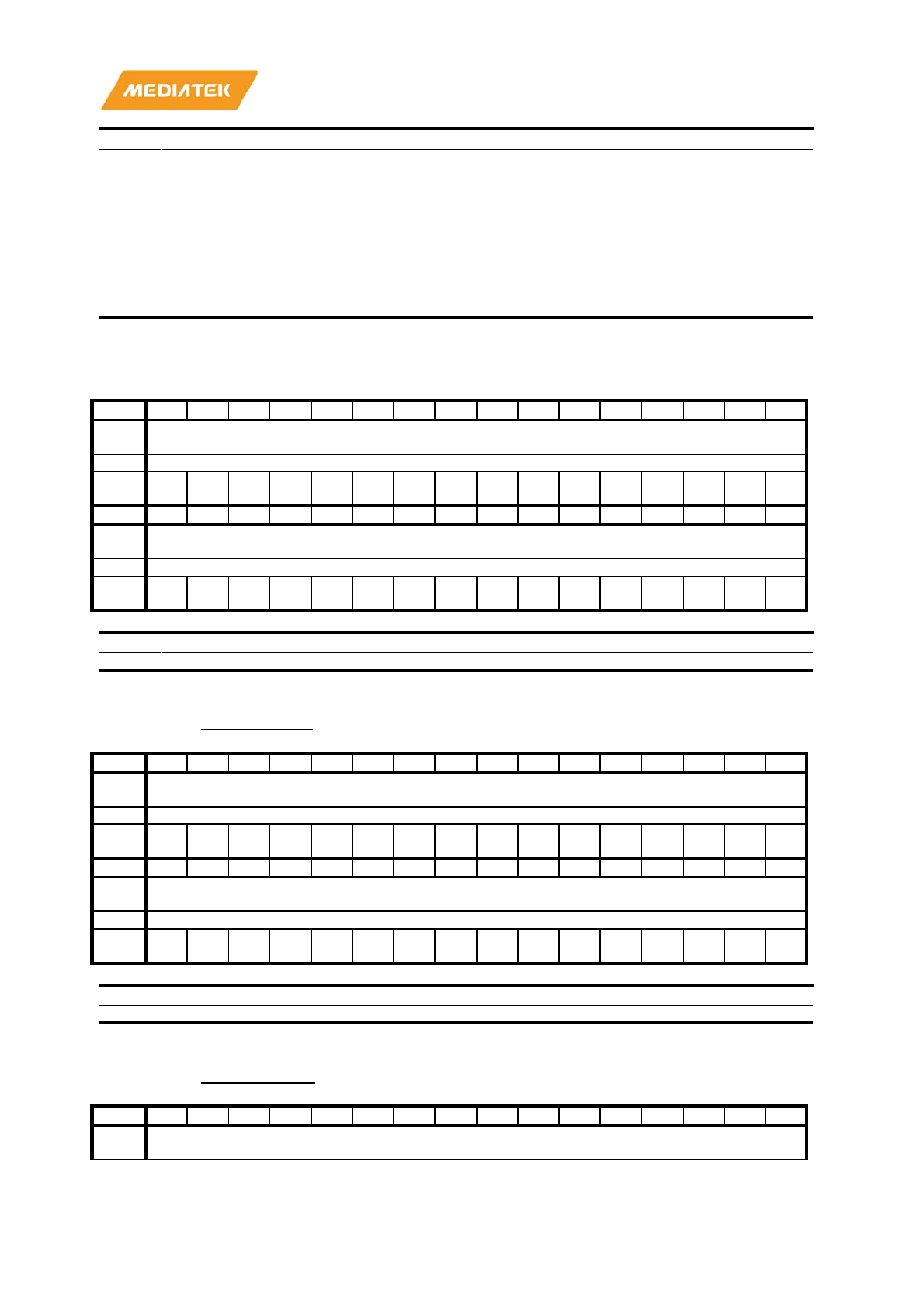
MT7686 Reference Manual
© 2016 - 2017 MediaTek Inc.
Page 275 of 536
This document contains information that is proprietary to MediaTek Inc. (“MediaTek”) and/or its licensor(s).
Any unauthorized use, reproduction or disclosure of this document in whole or in part is strictly prohibited.
Bit(s)
Name
Description
1: set CPHA 1
2:1
BIT_MODE
this bit need to be coordinated with bit[9]
2b'00: 8bit mode
2b'01:16bit mode
2b'10:32bit mode
2b'11: 8bit mode
0
ENDIAN
this bit need to be coordinated with bit[8]
0: Little Endian
1: Big Endian
A1040220
HWRX0CGPD
DMA RX0 Current GPD Address
Register
00000000
Bit
31
30
29
28
27
26
25
24
23
22
21
20
19
18
17
16
Nam
e
RX0_CURR_GPD_ADDR
Type
RO
Rese
t
0 0 0 0 0 0 0 0 0 0 0 0 0 0 0 0
Bit
15
14
13
12
11
10
9
8
7
6
5
4
3
2
1
0
Nam
e
RX0_CURR_GPD_ADDR
Type
RO
Rese
t
0 0 0 0 0 0 0 0 0 0 0 0 0 0 0 0
Bit(s)
Name
Description
31:0
RX0_CURR_GPD_ADDR
the address of RX0 current GPD that is being processed
A1040224
HWRX1CGPD
DMA RX1 Current GPD Address
Register
00000000
Bit
31
30
29
28
27
26
25
24
23
22
21
20
19
18
17
16
Nam
e
RX1_CURR_GPD_ADDR
Type
RO
Rese
t
0 0 0 0 0 0 0 0 0 0 0 0 0 0 0 0
Bit
15
14
13
12
11
10
9
8
7
6
5
4
3
2
1
0
Nam
e
RX1_CURR_GPD_ADDR
Type
RO
Rese
t
0 0 0 0 0 0 0 0 0 0 0 0 0 0 0 0
Bit(s)
Name
Description
31:0
RX1_CURR_GPD_ADDR
the address of RX1 current GPD that is being processed
A1040228
HWRX2CGPD
DMA RX2 Current GPD Address
Register
00000000
Bit
31
30
29
28
27
26
25
24
23
22
21
20
19
18
17
16
Nam
e
RX2_CURR_GPD_ADDR

MT7686 Reference Manual
© 2016 - 2017 MediaTek Inc.
Page 276 of 536
This document contains information that is proprietary to MediaTek Inc. (“MediaTek”) and/or its licensor(s).
Any unauthorized use, reproduction or disclosure of this document in whole or in part is strictly prohibited.
Type
RO
Rese
t
0 0 0 0 0 0 0 0 0 0 0 0 0 0 0 0
Bit
15
14
13
12
11
10
9
8
7
6
5
4
3
2
1
0
Nam
e
RX2_CURR_GPD_ADDR
Type
RO
Rese
t
0 0 0 0 0 0 0 0 0 0 0 0 0 0 0 0
Bit(s)
Name
Description
31:0
RX2_CURR_GPD_ADDR
the address of RX2 current GPD that is being processed
A104022C
HWRX3CGPD
DMA RX3 Current GPD Address
Register
00000000
Bit
31
30
29
28
27
26
25
24
23
22
21
20
19
18
17
16
Nam
e
RX3_CURR_GPD_ADDR
Type
RO
Rese
t
0 0 0 0 0 0 0 0 0 0 0 0 0 0 0 0
Bit
15
14
13
12
11
10
9
8
7
6
5
4
3
2
1
0
Nam
e
RX3_CURR_GPD_ADDR
Type
RO
Rese
t
0 0 0 0 0 0 0 0 0 0 0 0 0 0 0 0
Bit(s)
Name
Description
31:0
RX3_CURR_GPD_ADDR
the address of RX3 current GPD that is being processed
A1040230
HWTX0CGPD
DMA TX0 Current GPD Address
Register
00000000
Bit
31
30
29
28
27
26
25
24
23
22
21
20
19
18
17
16
Nam
e
TX0_CURR_GPD_ADDR
Type
RO
Rese
t
0 0 0 0 0 0 0 0 0 0 0 0 0 0 0 0
Bit
15
14
13
12
11
10
9
8
7
6
5
4
3
2
1
0
Nam
e
TX0_CURR_GPD_ADDR
Type
RO
Rese
t
0 0 0 0 0 0 0 0 0 0 0 0 0 0 0 0
Bit(s)
Name
Description
31:0
TX0_CURR_GPD_ADDR
the address of TX0 GPD that is processing
A1040234
HWTX1Q1CGPD
DMA TX1 Que Type 1 Current GPD
Address Register
00000000
Bit
31
30
29
28
27
26
25
24
23
22
21
20
19
18
17
16
MT7686 Reference Manual
© 2016 - 2017 MediaTek Inc.
Page 277 of 536
This document contains information that is proprietary to MediaTek Inc. (“MediaTek”) and/or its licensor(s).
Any unauthorized use, reproduction or disclosure of this document in whole or in part is strictly prohibited.
Nam
e
TX1_Q1_CURR_GPD_ADDR
Type
RO
Rese
t
0 0 0 0 0 0 0 0 0 0 0 0 0 0 0 0
Bit
15
14
13
12
11
10
9
8
7
6
5
4
3
2
1
0
Nam
e
TX1_Q1_CURR_GPD_ADDR
Type
RO
Rese
t
0 0 0 0 0 0 0 0 0 0 0 0 0 0 0 0
Bit(s)
Name
Description
31:0
TX1_Q1_CURR_GPD_ADDR
the address of TX1 channel and que type 1 GPD that is
processing
A1040238
HWTX1Q2CGPD
DMA TX1 Que Type 2 Current GPD
Address Register
00000000
Bit
31
30
29
28
27
26
25
24
23
22
21
20
19
18
17
16
Nam
e
TX1_Q2_CURR_GPD_ADDR
Type
RO
Rese
t
0 0 0 0 0 0 0 0 0 0 0 0 0 0 0 0
Bit
15
14
13
12
11
10
9
8
7
6
5
4
3
2
1
0
Nam
e
TX1_Q2_CURR_GPD_ADDR
Type
RO
Rese
t
0 0 0 0 0 0 0 0 0 0 0 0 0 0 0 0
Bit(s)
Name
Description
31:0
TX1_Q2_CURR_GPD_ADDR
the address of TX1 channel and que type 2 GPD that is
processing
A104023C
HWTX1Q3CGPD
DMA TX1 Que Type 3 Current GPD
Address Register
00000000
Bit
31
30
29
28
27
26
25
24
23
22
21
20
19
18
17
16
Nam
e
TX1_Q3_CURR_GPD_ADDR
Type
RO
Rese
t
0 0 0 0 0 0 0 0 0 0 0 0 0 0 0 0
Bit
15
14
13
12
11
10
9
8
7
6
5
4
3
2
1
0
Nam
e
TX1_Q3_CURR_GPD_ADDR
Type
RO
Rese
t
0 0 0 0 0 0 0 0 0 0 0 0 0 0 0 0
Bit(s)
Name
Description
31:0
TX1_Q3_CURR_GPD_ADDR
the address of TX1 channel and que type 3 GPD that is
processing
MT7686 Reference Manual
© 2016 - 2017 MediaTek Inc.
Page 278 of 536
This document contains information that is proprietary to MediaTek Inc. (“MediaTek”) and/or its licensor(s).
Any unauthorized use, reproduction or disclosure of this document in whole or in part is strictly prohibited.
A1040240
HWTX1Q4CGPD
DMA TX1 Que Type 4 Current GPD
Address Register
00000000
Bit
31
30
29
28
27
26
25
24
23
22
21
20
19
18
17
16
Nam
e
TX1_Q4_CURR_GPD_ADDR
Type
RO
Rese
t
0 0 0 0 0 0 0 0 0 0 0 0 0 0 0 0
Bit
15
14
13
12
11
10
9
8
7
6
5
4
3
2
1
0
Nam
e
TX1_Q4_CURR_GPD_ADDR
Type
RO
Rese
t
0 0 0 0 0 0 0 0 0 0 0 0 0 0 0 0
Bit(s)
Name
Description
31:0
TX1_Q4_CURR_GPD_ADDR
the address of TX1 channel and que type 4 GPD that is
processing
A1040244
HWTX1Q5CGPD
DMA TX1 Que Type 5 Current GPD
Address Register
00000000
Bit
31
30
29
28
27
26
25
24
23
22
21
20
19
18
17
16
Nam
e
TX1_Q5_CURR_GPD_ADDR
Type
RO
Rese
t
0 0 0 0 0 0 0 0 0 0 0 0 0 0 0 0
Bit
15
14
13
12
11
10
9
8
7
6
5
4
3
2
1
0
Nam
e
TX1_Q5_CURR_GPD_ADDR
Type
RO
Rese
t
0 0 0 0 0 0 0 0 0 0 0 0 0 0 0 0
Bit(s)
Name
Description
31:0
TX1_Q5_CURR_GPD_ADDR
the address of TX1 channel and que type 5 GPD that is
processing
A1040248
HWTX1Q6CGPD
DMA TX1 Que Type 6 Current GPD
Address Register
00000000
Bit
31
30
29
28
27
26
25
24
23
22
21
20
19
18
17
16
Nam
e
TX1_Q6_CURR_GPD_ADDR
Type
RO
Rese
t
0 0 0 0 0 0 0 0 0 0 0 0 0 0 0 0
Bit
15
14
13
12
11
10
9
8
7
6
5
4
3
2
1
0
Nam
e
TX1_Q6_CURR_GPD_ADDR
Type
RO
Rese
t
0 0 0 0 0 0 0 0 0 0 0 0 0 0 0 0
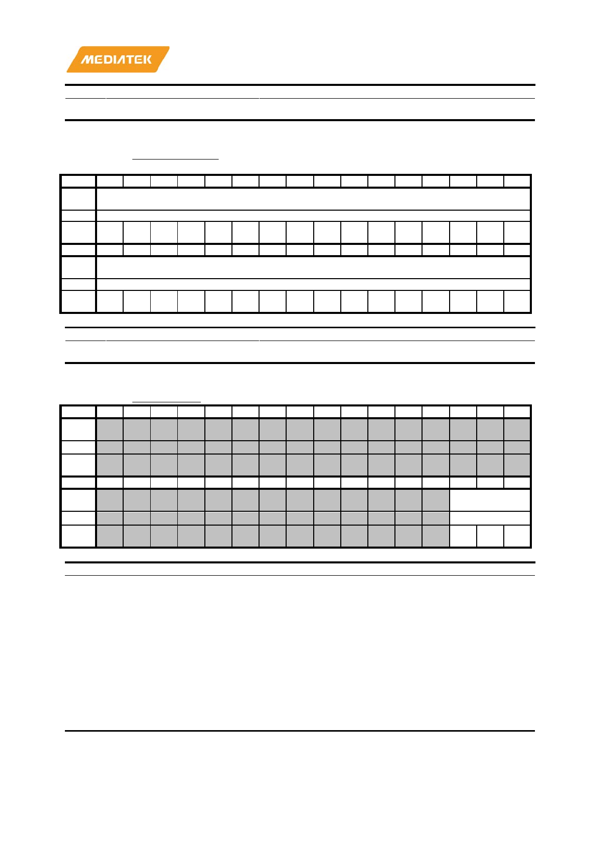
MT7686 Reference Manual
© 2016 - 2017 MediaTek Inc.
Page 279 of 536
This document contains information that is proprietary to MediaTek Inc. (“MediaTek”) and/or its licensor(s).
Any unauthorized use, reproduction or disclosure of this document in whole or in part is strictly prohibited.
Bit(s)
Name
Description
31:0
TX1_Q6_CURR_GPD_ADDR
the address of TX1 channel and que type 6 GPD that is
processing
A104024C
HWTX1Q7CGPD
DMA TX1 Que Type 7 Current GPD
Address Register
00000000
Bit
31
30
29
28
27
26
25
24
23
22
21
20
19
18
17
16
Nam
e
TX1_Q7_CURR_GPD_ADDR
Type
RO
Rese
t
0 0 0 0 0 0 0 0 0 0 0 0 0 0 0 0
Bit
15
14
13
12
11
10
9
8
7
6
5
4
3
2
1
0
Nam
e
TX1_Q7_CURR_GPD_ADDR
Type
RO
Rese
t
0 0 0 0 0 0 0 0 0 0 0 0 0 0 0 0
Bit(s)
Name
Description
31:0
TX1_Q7_CURR_GPD_ADDR
the address of TX1 channel and que type 7 GPD that is
processing
A10403F4
HSDIOCRCR
HIF SDIO CRC status Register
00000000
Bit
31
30
29
28
27
26
25
24
23
22
21
20
19
18
17
16
Nam
e
Type
Rese
t
Bit
15
14
13
12
11
10
9
8
7
6
5
4
3
2
1
0
Nam
e
REG_CRC_STS
_CYCLE
Type
RW
Rese
t
0 0 0
Bit(s)
Name
Description
2:0
REG_CRC_STS_CYCLE
In SDIO 3.0 spec. for SDR50 and SDR104 mode, the CRC
status can be sent 2 to 8 cycles after one data block.
Firmware could write this register to change the response
timing of SDIO IP. Default value is set to be 2 cycles after
one data block.
0: 2 cycles after data block
1: 3 cycles after data block
2: 4 cycles after data block
3: 5 cycles after data block
4: 6 cycles after data block
5: 7 cycles after data block
6: 8 cycles after data block
7: 9 cycles after data block
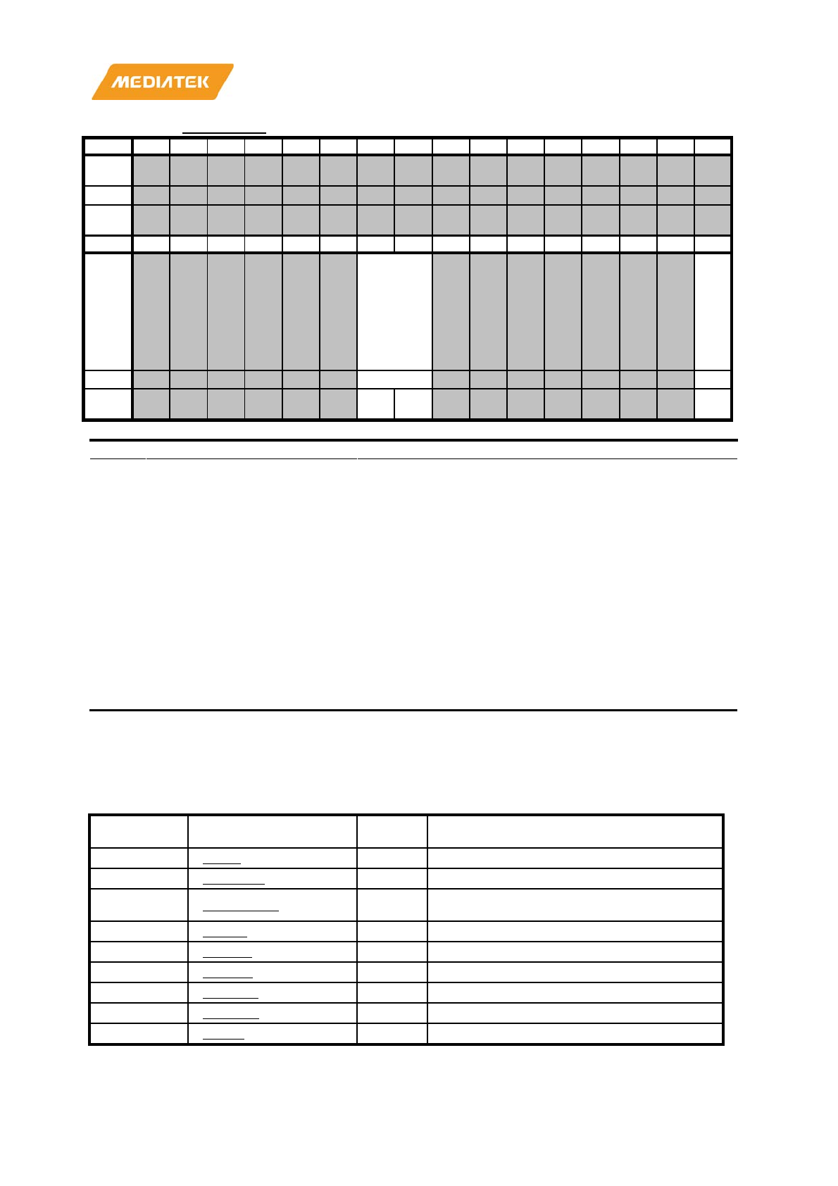
MT7686 Reference Manual
© 2016 - 2017 MediaTek Inc.
Page 280 of 536
This document contains information that is proprietary to MediaTek Inc. (“MediaTek”) and/or its licensor(s).
Any unauthorized use, reproduction or disclosure of this document in whole or in part is strictly prohibited.
A10403F8
HSDIORCR
HIF SDIO Read Control Register
00000001
Bit
31
30
29
28
27
26
25
24
23
22
21
20
19
18
17
16
Nam
e
Type
Rese
t
Bit
15
14
13
12
11
10
9
8
7
6
5
4
3
2
1
0
Nam
e
REG_SDI
O_RD_TI
MING_SE
L
RE
G_
TI
ME
OU
T_
NU
M_
EN
Type
RW
RW
Rese
t
0 0 1
Bit(s)
Name
Description
9:8
REG_SDIO_RD_TIMING_SEL
Use this register, if the firmware is unable to prepare the
data on time for the host to read. The SDIO prefetch
operation can be
delayed according to the data depth in
current RX FIFO. Firmware can write to this field to
change the data depth constraint.
2b'00: 4B
2b'01: 8B
2b'10:16B
2b'11: 64B
0
REG_TIMEOUT_NUM_EN
Use this register, if the firmware is unable to prepare the
data on time for the host to read. The SDIO read timing
adjustment function is implemented to protect the read
data underflow. Firmware can write 1 to enable and write
0 to disable the function.
0: Disable SDIO Read timing adjust function.
1: Enable SDIO Read timing adjust function.
13.5.2. Host domain register
Module name: SDIO_SLV Base address: (+0h)
Address Name
Width
(bits)
Register Functionality
00000000
WCIR
32
WLAN Chip ID Register
00000004
WHLPCR
32
WLAN HIF Low Power Control Register
00000008
WSDIOCSR
32
WLAN SDIO Control Status Register (SDIO
Only)
0000000C
WHCR
32
WLAN HIF Control Register
00000010
WHISR
32
WLAN HIF Interrupt Status Register
00000014
WHIER
32
WLAN HIF Interrupt Enable Register
00000018
WHISR1
32
Reserve for WHISR1
0000001C
WHIER1
32
Reserve for WHIER1
00000020
WASR
32
WLAN Abnormal Status Register

MT7686 Reference Manual
© 2016 - 2017 MediaTek Inc.
Page 281 of 536
This document contains information that is proprietary to MediaTek Inc. (“MediaTek”) and/or its licensor(s).
Any unauthorized use, reproduction or disclosure of this document in whole or in part is strictly prohibited.
Address Name
Width
(bits)
Register Functionality
00000024
WSICR
32
WLAN Software Interrupt Control
Register
00000028
WTSR0
32
WLAN TX Status Register
0000002C
WTSR1
32
WLAN TX Status Register
00000030
WTDR0
32
Reserve
00000034
WTDR1
32
WLAN TX Data Register
1
00000038
WTDR2
32
Reserve for WTDR2
0000003C
WTDR3
32
Reserve for WTDR3
00000040
WTDR4
32
Reserve for WTDR4
00000044
WTDR5
32
Reserve
for WTDR5
00000048
WTDR6
32
Reserve for WTDR6
0000004C
WTDR7
32
Reserve for WTDR7
00000050
WRDR0
32
WLAN RX Data Register 0
00000054
WRDR1
32
WLAN RX Data Register 1
00000058
WRDR2
32
Reserve
0000005C
WRDR3
32
Reserve
00000060
WRDR4
32
Reserve for WRDR4
00000064
WRDR5
32
Reserve for WRDR5
00000068
WRDR6
32
Reserve for WRDR6
0000006C
WRDR7
32
Reserve for WRDR7
00000070
H2DSM0R
32
Host to Device Send Mailbox 0 Register
00000074
H2DSM1R
32
Host to Device Send Mailbox 1 Register
00000078
D2HRM0R
32
Device to Host Receive Mailbox 0 Register
0000007C
D2HRM1R
32
Device to Host Receive Mailbox
1 Register
00000080
D2HRM2R
32
Reserve
00000090
WRPLR
32
WLAN RX Packet Length Register
00000094
WRPLR1
32
WLAN RX Packet Length Register 1
00000098
WRPLR2
32
Reserve for WRPLR2
0000009C
WRPLR3
32
Reserve for WRPLR3
000000A0
EHTCR
32
EHPI transaction count register (EHPI
only)
000000AC
WOLTCR
32
On Line
-Tuning Control Register
000000B0
WTMDR
32
Test Mode Data Port
000000B4
WTMCR
32
Test Mode Control Register
000000B8
WTMDPCR0
32
Test Mode Data Pattern Control Register 0
000000BC
WTMDPCR1
32
Test Mode Data Pattern Control Register 1
000000C0
FWDLDR
32
Firmware Download Data Register
000000C4
FWDLDSAR
32
Firmware Download Destination Starting
Address Register
000000C8
FWDLSR
32
Firmware Download Status Register
000000CC
FWDLCMR0
32
Firmware Download Customized Register
0
000000D0
FWDLCMR1
32
Firmware Download Customized Register
1
000000D4
WPLRCR
32
WLAN Packet Length Report Control
Register
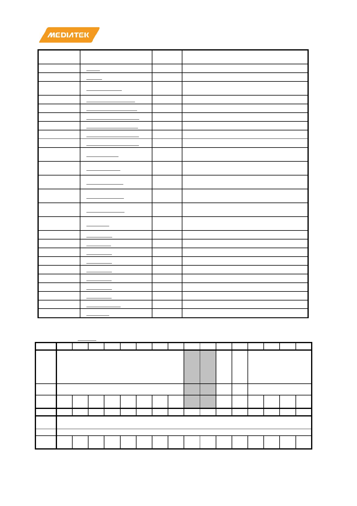
MT7686 Reference Manual
© 2016 - 2017 MediaTek Inc.
Page 282 of 536
This document contains information that is proprietary to MediaTek Inc. (“MediaTek”) and/or its licensor(s).
Any unauthorized use, reproduction or disclosure of this document in whole or in part is strictly prohibited.
Address Name
Width
(bits)
Register Functionality
000000D8
WSR
32
WLAN Snapshot Register
000000F8
VSCR
32
Version Control Register
000000FC
WSDIOAICR
32
Common SDIO Asynchronous Interrupt
Control Register
00000100
CLKIOCR_T28LP
32
Clock Pad Macro IO Control
Register
00000104
CMDIOCR_T28LP
32
Command Pad Macro IO Control Register
00000108
DAT0IOCR_T28LP
32
Data 0 Pad Macro IO Control Register
0000010C
DAT1IOCR_T28LP
32
Data 1 Pad Macro IO Control Register
00000110
DAT2IOCR_T28LP
32
Data 2 Pad Macro IO Control Register
00000114
DAT3IOCR_T28LP
32
Data 3 Pad Macro IO Control Register
00000118
CLKDLYCR
32
Clock Pad Macro Delay Chain Control
Register
0000011C
CMDDLYCR
32
Command Pad Macro Delay Chain Control
Register
00000120
ODATDLYCR
32
SDIO Output Data Delay Chain Control
Register
00000124
IDATDLYCR1
32
SDIO Input Data Delay Chain Control
Register 1
00000128
IDATDLYCR2
32
SDIO Input Data Delay Chain Control
Register 2
0000012C
ILCHCR
32
SDIO Input Data Latch Time Control
Register
00000130
WTQCR0
32
WLAN TXQ Count Register 0
00000134
WTQCR1
32
WLAN TXQ Count Register 1
00000138
WTQCR2
32
WLAN TXQ Count Register 2
0000013C
WTQCR3
32
WLAN TXQ Count Register 3
00000140
WTQCR4
32
WLAN TXQ Count
Register 4
00000144
WTQCR5
32
WLAN TXQ Count Register 5
00000148
WTQCR6
32
WLAN TXQ Count Register 6
0000014C
WTQCR7
32
WLAN TXQ Count Register 7
00000154
SWPCDBGR
32
WLAN PC Value debug register
00000158
DSIOCR
32
DS Pad Macro IO Control Register
00000000
WCIR
WLAN Chip ID Register
00106630
Bit
31
30
29
28
27
26
25
24
23
22
21
20
19
18
17
16
Nam
e DEVICE_STATUS
W_
FU
NC
_R
DY
PO
R_I
ND
ICA
TO
R
REVISION_ID
Type RO RO
W1
C
RO
Rese
t
0 0 0 0 0 0 0 0 0 1 0 0 0 0
Bit
15
14
13
12
11
10
9
8
7
6
5
4
3
2
1
0
Nam
e
CHIP_ID
Type
RO
Rese
t
0 1 1 0 0 1 1 0 0 0 1 1 0 0 0 0
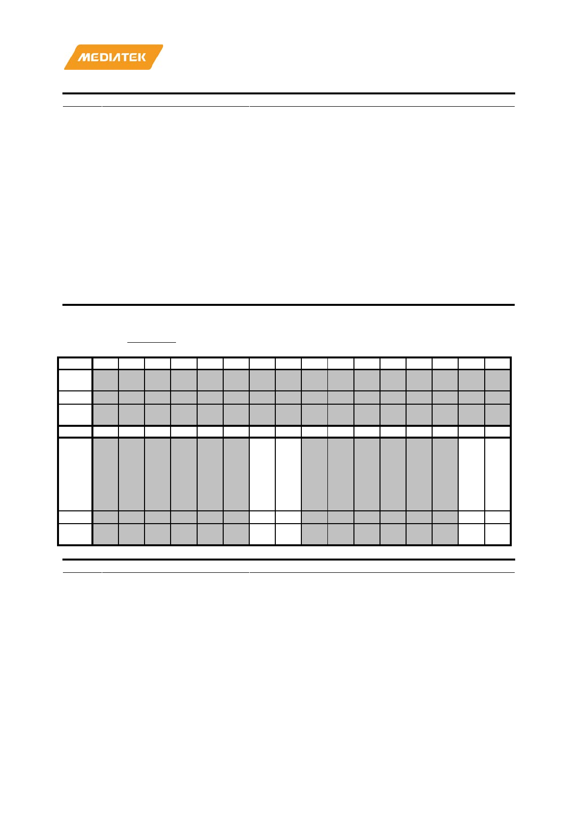
MT7686 Reference Manual
© 2016 - 2017 MediaTek Inc.
Page 283 of 536
This document contains information that is proprietary to MediaTek Inc. (“MediaTek”) and/or its licensor(s).
Any unauthorized use, reproduction or disclosure of this document in whole or in part is strictly prohibited.
Bit(s)
Name
Description
31:24
DEVICE_STATUS
These status bits are defined by users and could be read by
host driver via SDIO bus interface. For example, watch
dog reset status could be one that could be read by host
driver even when there is no AHB clock in SDIO
controller.
21
W_FUNC_RDY
Indicate that WLAN functional block has finished its
initial procedure and it is ready for normal operation.
This is a sticky bit of HWFCR.W_FUNC_RDY.
Driver will keep polling this bit on initialization. Once after FW is
ready
and set corresponding bit in FW, driver can do following
control to FW.
0: WLAN functional block is not ready for normal operation.
1: WLAN functional block is ready for normal operation.
20
POR_INDICATOR
This bit indicates a reset occurs including external pin
reset, power detect reset, power on reset, SDIO
CCCR(0x06).Bit[3] reset (only in SDIO).
Write 1 to clear this bit. Writing 0 does nothing.
19:16
REVISION_ID
Revision ID
15:0
CHIP_ID
Chip ID
00000004
WHLPCR
WLAN HIF Low Power Control
Register
00000000
Bit
31
30
29
28
27
26
25
24
23
22
21
20
19
18
17
16
Nam
e
Type
Rese
t
Bit
15
14
13
12
11
10
9
8
7
6
5
4
3
2
1
0
Nam
e
W_
FW
_O
WN
_R
EQ
_C
LR
W_
FW
_O
WN
_R
EQ
_S
ET
W_
INT
_E
N_
CL
R
W_
INT
_E
N_
SE
T
Type
W1S
W1S
W1S
W1S
Rese
t
0 0 0 0
Bit(s)
Name
Description
9
W_FW_OWN_REQ_CLR
Write 1 to this bit to request firmware to return the
ownership of chip WLAN function to host driver. Write 0
has no
meaning (Refer chapter "Power management" for
details).
Read always return 0.
This bit will be set on initial, or by firmware written 1 to HWFICR.
FW_OWN_BACK_INT_SET or any driver
-domain WLAN
interrupts.
8
W_FW_OWN_REQ_SET
Write 1 to this bit to transfer ownership of chip WLAN
function to firmware. Write 0 has no meaning (Refer
chapter "Power management" for details). Host driver
should set this bit to give ownership to firmware only
when host driver has ownership.
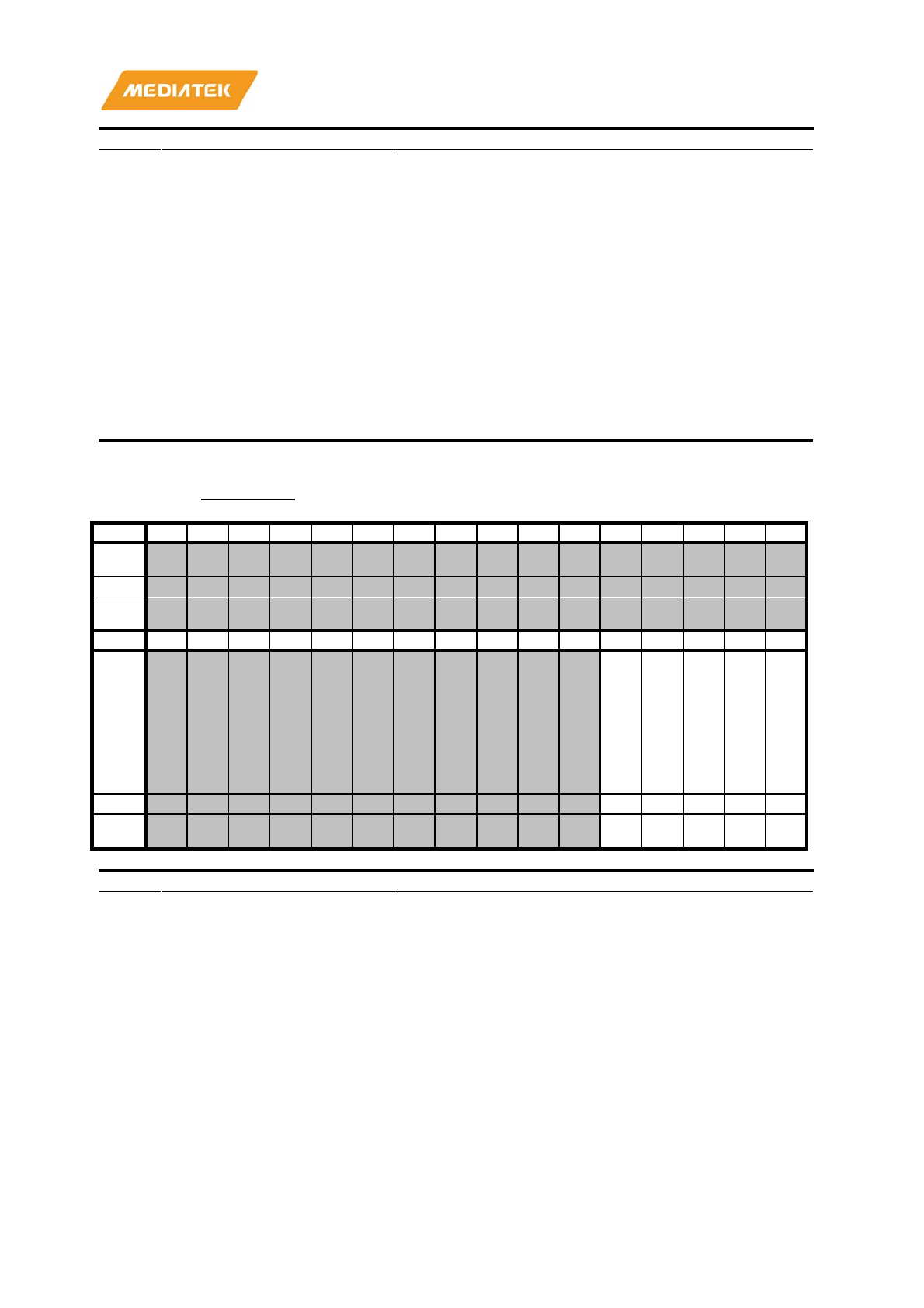
MT7686 Reference Manual
© 2016 - 2017 MediaTek Inc.
Page 284 of 536
This document contains information that is proprietary to MediaTek Inc. (“MediaTek”) and/or its licensor(s).
Any unauthorized use, reproduction or disclosure of this document in whole or in part is strictly prohibited.
Bit(s)
Name
Description
Read will get the status of WLAN_DRV_OWN.
WLAN_DRV_OWN indicates that software driver has the
ownership of chip WLAN sub-system.
0: WLAN driver doesn't have ownership
1: WLAN driver has ownership
1
W_INT_EN_CLR
Write 0 has no meaning, and write 1 to clear WLAN
interrupt enable signal.
Read always return 0.
0
W_INT_EN_SET
Write 0 has no meaning, and write 1 to set WLAN
interrupt enable signal.
Read will get the status of W_INT_EN.
W_INT_EN indicates the current value of WLAN interrupt enable
signal. This
enable signal is used for controlling the output of
WLAN interrupt signal.
0: WLAN interrupt can't output to host.
1: WLAN interrupt can output to host.
00000008
WSDIOCSR
WLAN SDIO Control Status Register
(SDIO Only)
0000000D
Bit
31
30
29
28
27
26
25
24
23
22
21
20
19
18
17
16
Nam
e
Type
Rese
t
Bit
15
14
13
12
11
10
9
8
7
6
5
4
3
2
1
0
Nam
e
DB
_C
MD
7_
RE
SE
LE
CT
_D
IS
DB
_W
R_
BU
SY
_E
N
DB
_R
D_
BU
SY
_E
N
SDI
O_I
NT
_C
TL
SDI
O_
RE
_I
NIT
_E
N
Type
RW
RW
RW
RW
RO
Rese
t
0 1 1 0 1
Bit(s)
Name
Description
4
DB_CMD7_RESELECT_DIS
Control the cmd7 with response when the card is during
re-select
0: Host use cmd7 reselect and card will have response.
1: Host use cmd7 reselect and card will NOT have response.
3
DB_WR_BUSY_EN
Write busy function control bit. If the available space of
internal TX FIFO is smaller than the pre
-defined
maximum block size, the write busy will be asserted. The
write busy functio
n can be used only when the block size
is smaller than pre
-defined FIFO size (that is maximum
block size).
0: DMA write busy function disable
1: DMA write busy function enable
2
DB_RD_BUSY_EN
Read busy function control bit. If the usage of internal RX
FIFO is smaller than the pre
-
defined maximum block size,
the read busy would be triggered except the data is the last
part of this transaction. The read busy function can be
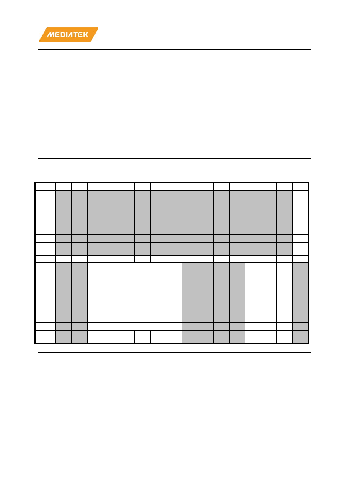
MT7686 Reference Manual
© 2016 - 2017 MediaTek Inc.
Page 285 of 536
This document contains information that is proprietary to MediaTek Inc. (“MediaTek”) and/or its licensor(s).
Any unauthorized use, reproduction or disclosure of this document in whole or in part is strictly prohibited.
Bit(s)
Name
Description
used only when the block size set is smaller than pre-
defined FIFO size (i.e. max block size).
0: DMA read busy function disable
1: DMA read busy function enable
1
SDIO_INT_CTL
Asynchronous interrupt is supported in SDIO 4-bit mode
0: Not supported; The host should switch to 1-bit mode before it
turns off SD clock. Device can wake up host via 1
-bit mode
asynchronous interrupt. (according to SDIO v2.0 spec)
1: Supported; The host could send asynchronous interrupt to host
during asynchronous interrupt period so that
the host does not
need to switch to 1
-
bit mode before it turns off SD clock. (according
to SDIO v3.0 spec)
0
SDIO_RE_INIT_EN
When asserted, this bit is used to let SDIO IP back to idle
state when a new SDIO CMD 5 is received.
Default value can use fixed
default value or use an engine to set or
use an external bus for it.
0000000C
WHCR
WLAN HIF Control Register
00000000
Bit
31
30
29
28
27
26
25
24
23
22
21
20
19
18
17
16
Nam
e
RX
_E
NH
AN
CE
_M
OD
E
Type
RW
Rese
t
0
Bit
15
14
13
12
11
10
9
8
7
6
5
4
3
2
1
0
Nam
e MAX_HIF_RX_LEN_NUM
RP
T_
OW
N_
RX
_P
AC
KE
T_
LE
N
RE
CV
_M
AIL
BO
X_
RD
_C
LR
_E
N
W_
INT
_C
LR
_C
TR
L
Type
RW
RW
RW
RW
Rese
t
0 0 0 0 0 0 0 0 0
Bit(s)
Name
Description
16
RX_ENHANCE_MODE
Enable the read of TX count status, RX length, and
mailbox information in RX packet enhance mode. Refer
chapter 3.4 for more details.
0: Disables RX packet enhanced mode
1: Enables the read of TX count status, RX length, and mailbox
information in RX packet enhanced mode.
13:8
MAX_HIF_RX_LEN_NUM
The maximum number of SDIO controller to report the
per
-queue RX packets length via INT/ RX enhanced mode.
0: report entire 64 RX packets length in the same RX queue without
limitation.
Others (N): report at most N RX packet lengths for each RX queue
3
RPT_OWN_RX_PACKET_LEN
This field is to control the RX packet report length and
structure during enhance mode. If this bit is set to 1, each

MT7686 Reference Manual
© 2016 - 2017 MediaTek Inc.
Page 286 of 536
This document contains information that is proprietary to MediaTek Inc. (“MediaTek”) and/or its licensor(s).
Any unauthorized use, reproduction or disclosure of this document in whole or in part is strictly prohibited.
Bit(s)
Name
Description
RX queue can report its own length according to the
setting in WPLRCR. Also, the total report length would be
changed if this bit is set. Host driver should parse the
enhanced mode status according to the length setting in
WPLRCR to get correct information.
0: disable the function that each RX queue can report its own
packet length and the maximal report length is constrained by
max_hif_rx_len_num field in WHCR
1: enable the function that each RX queue can report its own packet
length and the maximal report length can be different by each
queue according to the setting in WPLRCR
2
RECV_MAILBOX_RD_CLR_EN
This is to control whether the received mail-box
(D2HRM0R, D2HRM1R) will be read cleared or not (this
include read from enhance mode structure).
1: read clear
0: no effect after read
1
W_INT_CLR_CTRL
This bit is used to select the clear mechanism of WLAN
interrupt statue (WHISR).
0: Read clear
1: Write 1 clear
00000010
WHISR
WLAN HIF Interrupt Status Register
00000000
Bit
31
30
29
28
27
26
25
24
23
22
21
20
19
18
17
16
Nam
e
D2H_SW_INT
Type
RC
Rese
t
0 0 0 0 0 0 0 0 0 0 0 0 0 0 0 0
Bit
15
14
13
12
11
10
9
8
7
6
5
4
3
2
1
0
Nam
e D2H_SW_INT
FW
_O
WN
_B
AC
K_I
NT
AB
NO
RM
AL
_I
NT
RX
3_
DO
NE
_I
NT
RX
2_
DO
NE
_I
NT
RX
1_
DO
NE
_I
NT
RX
0_
DO
NE
_I
NT
TX
_D
ON
E_I
NT
Type
RC
RC
RO
RO
RO
RO
RO
RO
Rese
t
0 0 0 0 0 0 0 0 0 0 0 0 0 0 0
Bit(s)
Name
Description
31:8
D2H_SW_INT
This field is used for software interrupt for WLAN
function in FW to host driver direction.
WLAN firmware writes 1s to HWFICR.Bit[31:8] will set
corresponding bit field.
7
FW_OWN_BACK_INT
Firmware has returned the ownership to host driver. This
field is set with driver own
-back only.
Firmware write 1 to HWFICR. Bit[4] will set this bit.
6
ABNORMAL_INT
Abnormal event interrupt.
The abnormal status will be shown
in WASR, which includes
Data overflow of WLAN TX0 and TX1 port.
Data underflow of WLAN RX0 and RX1 port.
FW_OWN_INVALID_ACCESS
4
RX3_DONE_INT
When any of the RX length data of RX3 is existed in HIF
RX length FIFO, this bit will be asserted.
3
RX2_DONE_INT
When any of the RX length data of RX2 is existed in HIF
RX length FIFO, this bit will be asserted.
2
RX1_DONE_INT
When any of the RX length data of RX1 is existed in HIF
RX length FIFO, this bit will be asserted.

MT7686 Reference Manual
© 2016 - 2017 MediaTek Inc.
Page 287 of 536
This document contains information that is proprietary to MediaTek Inc. (“MediaTek”) and/or its licensor(s).
Any unauthorized use, reproduction or disclosure of this document in whole or in part is strictly prohibited.
Bit(s)
Name
Description
1
RX0_DONE_INT
When any of the RX length data of RX0 is existed in HIF
RX length FIFO, this bit will be asserted.
0
TX_DONE_INT
If WTSR0 or WTSR1 is not 0, this bit will be set.
0: WTSR0 and WTSR1 is 0.
1: WTSR0 or WTSR1 is not 0.
00000014
WHIER
WLAN HIF Interrupt Enable Register
00000000
Bit
31
30
29
28
27
26
25
24
23
22
21
20
19
18
17
16
Nam
e
D2H_SW_INT_EN
Type
RW
Rese
t
0 0 0 0 0 0 0 0 0 0 0 0 0 0 0 0
Bit
15
14
13
12
11
10
9
8
7
6
5
4
3
2
1
0
Nam
e D2H_SW_INT_EN
FW
_O
WN
_B
AC
K_I
NT
_E
N
AB
NO
RM
AL
_I
NT
_E
N
RX
3_
DO
NE
_I
NT
_E
N
RX
2_
DO
NE
_I
NT
_E
N
RX
1_
DO
NE
_I
NT
_E
N
RX
0_
DO
NE
_I
NT
_E
N
TX
_D
ON
E_I
NT
_E
N
Type
RW
RW
RW
RW
RW
RW
RW
RW
Rese
t
0 0 0 0 0 0 0 0 0 0 0 0 0 0 0
Bit(s)
Name
Description
31:8
D2H_SW_INT_EN
WLAN host interrupt output control bits.
If any bit is
0: Mask the WLAN related bit interrupt output, corresponding bits
will be still written to WHISR without triggering interrupt.
1: Enable the WLAN related bit interrupt output.
7
FW_OWN_BACK_INT_EN
WLAN host interrupt output control bits.
If any bit is
0: Mask the WLAN related bit interrupt output, corresponding bits
will be still written to WHISR without triggering interrupt.
1: Enable the WLAN related bit interrupt output.
6
ABNORMAL_INT_EN
WLAN host interrupt output control bits.
If any bit is
0: Mask the WLAN related bit interrupt output, corresponding bits
will be still written to WHISR without triggering interrupt.
1: Enable the WLAN related bit interrupt output.
4
RX3_DONE_INT_EN
WLAN host interrupt output control bits.
If any bit is
0: Mask the WLAN related bit interrupt output, corresponding bits
will be still written to WHISR without triggering interrupt.
1: Enable the WLAN related bit interrupt output.
3
RX2_DONE_INT_EN
WLAN host interrupt output control bits.
If any bit is
0: Mask the WLAN related bit interrupt output, corresponding bits
will be still written to WHISR without triggering interrupt.
1: Enable the WLAN related bit interrupt output.
2
RX1_DONE_INT_EN
WLAN host interrupt output control bits.
If any bit is
0: Mask the WLAN related bit interrupt output, corresponding bits
will be still written to WHISR without triggering interrupt.
1: Enable the WLAN related bit interrupt output.
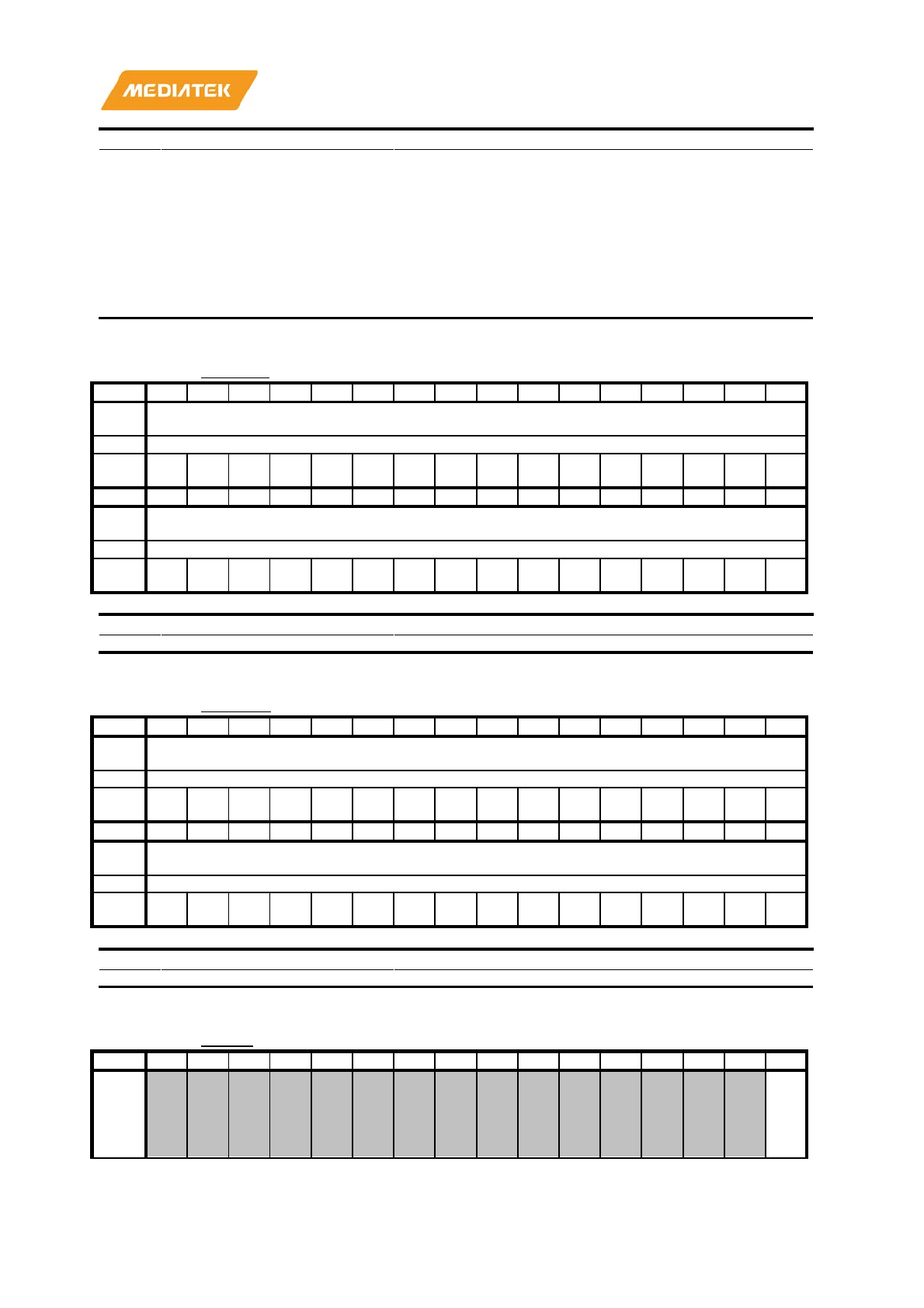
MT7686 Reference Manual
© 2016 - 2017 MediaTek Inc.
Page 288 of 536
This document contains information that is proprietary to MediaTek Inc. (“MediaTek”) and/or its licensor(s).
Any unauthorized use, reproduction or disclosure of this document in whole or in part is strictly prohibited.
Bit(s)
Name
Description
1
RX0_DONE_INT_EN
WLAN host interrupt output control bits.
If any bit is
0: Mask the WLAN related bit interrupt output, corresponding bits
will be still written to WHISR without triggering interrupt.
1: Enable the WLAN related bit interrupt output.
0
TX_DONE_INT_EN
WLAN host interrupt output control bits.
If any bit is
0: Mask the WLAN related bit interrupt output, corresponding bits
will be still written to WHISR without triggering interrupt.
1: Enable the WLAN related bit interrupt output.
00000018
WHISR1
Reserve for WHISR1
00000000
Bit
31
30
29
28
27
26
25
24
23
22
21
20
19
18
17
16
Nam
e
RESV_WHISR1
Type
RO
Rese
t
0 0 0 0 0 0 0 0 0 0 0 0 0 0 0 0
Bit
15
14
13
12
11
10
9
8
7
6
5
4
3
2
1
0
Nam
e
RESV_WHISR1
Type
RO
Rese
t
0 0 0 0 0 0 0 0 0 0 0 0 0 0 0 0
Bit(s)
Name
Description
31:0
RESV_WHISR1
RESV_WHISR1
0000001C
WHIER1
Reserve for WHIER1
00000000
Bit
31
30
29
28
27
26
25
24
23
22
21
20
19
18
17
16
Nam
e
RESV_WHIER1
Type
RO
Rese
t
0 0 0 0 0 0 0 0 0 0 0 0 0 0 0 0
Bit
15
14
13
12
11
10
9
8
7
6
5
4
3
2
1
0
Nam
e
RESV_WHIER1
Type
RO
Rese
t
0 0 0 0 0 0 0 0 0 0 0 0 0 0 0 0
Bit(s)
Name
Description
31:0
RESV_WHIER1
RESV_WHIER1
00000020
WASR
WLAN Abnormal Status Register
00000000
Bit
31
30
29
28
27
26
25
24
23
22
21
20
19
18
17
16
Nam
e
FW
_O
WN
_I
NV
ALI
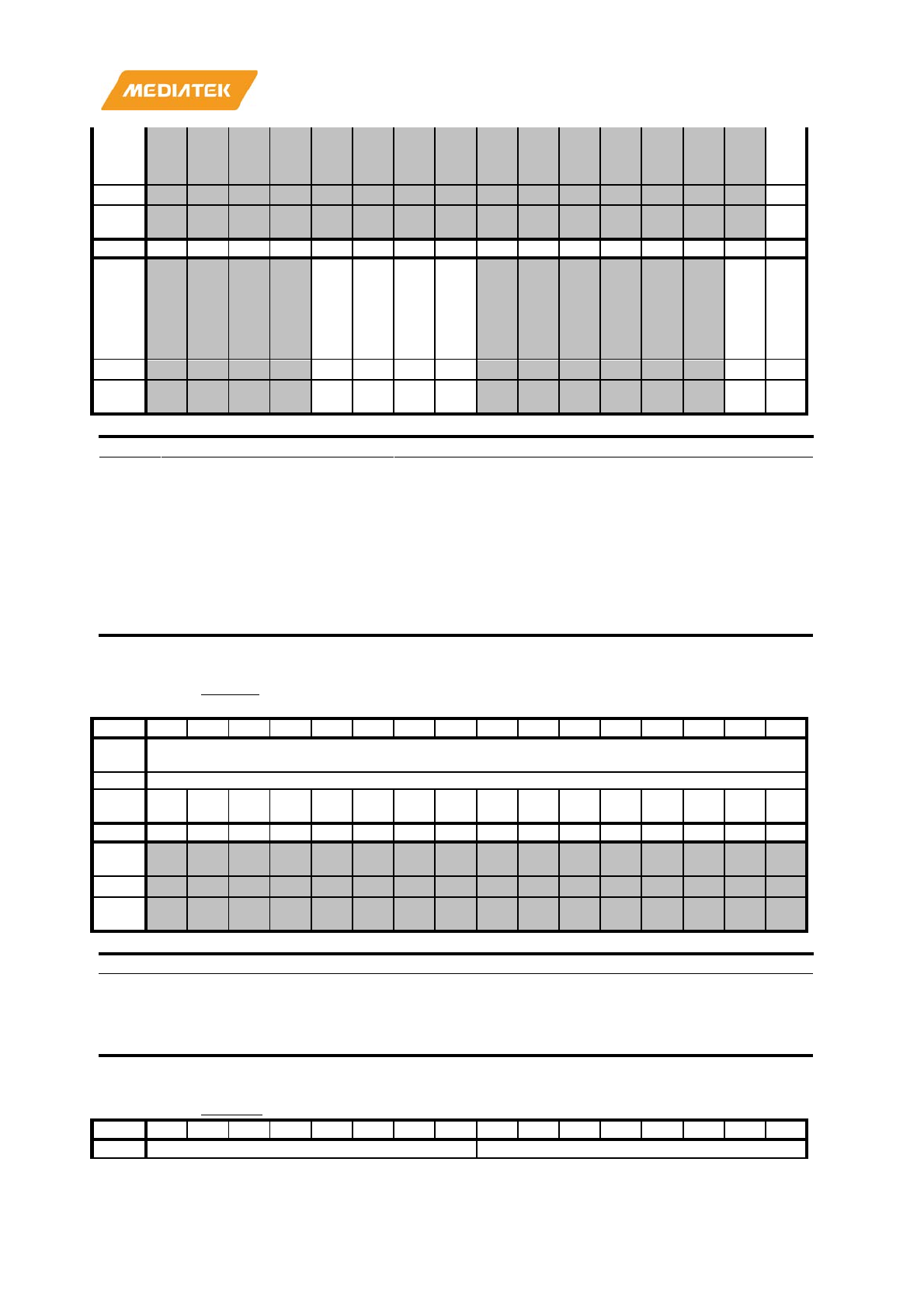
MT7686 Reference Manual
© 2016 - 2017 MediaTek Inc.
Page 289 of 536
This document contains information that is proprietary to MediaTek Inc. (“MediaTek”) and/or its licensor(s).
Any unauthorized use, reproduction or disclosure of this document in whole or in part is strictly prohibited.
D_
AC
CE
SS
Type
RC
Rese
t
0
Bit
15
14
13
12
11
10
9
8
7
6
5
4
3
2
1
0
Nam
e
RX
3_
UN
DE
RF
LO
W
RX
2_
UN
DE
RF
LO
W
RX
1_
UN
DE
RF
LO
W
RX
0_
UN
DE
RF
LO
W
TX
1_
OV
ER
FL
OW
TX
0_
OV
ER
FL
OW
Type
RC
RC
RC
RC
RC
RC
Rese
t
0 0 0 0 0 0
Bit(s)
Name
Description
16
FW_OWN_INVALID_ACCESS
It will be asserted when register other than WCIR,
WHLPCR, WSPICSR, WSDIOCSR, WEHPICSR, and
firmware download relative registers
are accessed when
FW own = 1
It is purely for host driver debug purpose.
11
RX3_UNDERFLOW
Data underflow of WLAN RX3 port.
10
RX2_UNDERFLOW
Data underflow of WLAN RX2 port.
9
RX1_UNDERFLOW
Data underflow of WLAN RX1 port.
8
RX0_UNDERFLOW
Data underflow of WLAN RX0 port.
1
TX1_OVERFLOW
Data overflow of WLAN TX1 port.
0
TX0_OVERFLOW
Data overflow of WLAN TX0 port.
00000024
WSICR
WLAN Software Interrupt Control
Register
00000000
Bit
31
30
29
28
27
26
25
24
23
22
21
20
19
18
17
16
Nam
e
H2D_SW_INT_SET
Type
W1S
Rese
t
0 0 0 0 0 0 0 0 0 0 0 0 0 0 0 0
Bit
15
14
13
12
11
10
9
8
7
6
5
4
3
2
1
0
Nam
e
Type
Rese
t
Bit(s)
Name
Description
31:16
H2D_SW_INT_SET
Host driver writes 1s will set HWFISR.
HOST_DRIVER_INT.
Writing 0 does nothing.
Read always returns 0.
This is used as a communication between FW to driver, with
interrupt functionality to SDIO controller.
00000028
WTSR0
WLAN TX Status Register
00000000
Bit
31
30
29
28
27
26
25
24
23
22
21
20
19
18
17
16
Nam
TQ3_CNT
TQ2_CNT
MT7686 Reference Manual
© 2016 - 2017 MediaTek Inc.
Page 290 of 536
This document contains information that is proprietary to MediaTek Inc. (“MediaTek”) and/or its licensor(s).
Any unauthorized use, reproduction or disclosure of this document in whole or in part is strictly prohibited.
e
Type
RC
RC
Rese
t
0 0 0 0 0 0 0 0 0 0 0 0 0 0 0 0
Bit
15
14
13
12
11
10
9
8
7
6
5
4
3
2
1
0
Nam
e
TQ1_CNT TQ0_CNT
Type
RC
RC
Rese
t
0 0 0 0 0 0 0 0 0 0 0 0 0 0 0 0
Bit(s)
Name
Description
31:24
TQ3_CNT
This field indicates the released packet count of TQ3
during two WTSR0 read access.
This field is cleared by read operation. Write has no meaning.
23:16
TQ2_CNT
This field indicates the released packet count of TQ2
during two WTSR0 read access.
This field is cleared by read operation. Write has no meaning.
15:8
TQ1_CNT
This field indicates the released packet count of TQ1
during two WTSR0 read access.
This field is cleared by read operation. Write has no meaning.
7:0
TQ0_CNT
This field indicates the released packet count of TQ0
during two WTSR0 read access.
This field is cleared by read operation. Write has no meaning.
0000002C
WTSR1
WLAN TX Status Register
00000000
Bit
31
30
29
28
27
26
25
24
23
22
21
20
19
18
17
16
Nam
e
TQ7_CNT TQ6_CNT
Type
RC
RC
Rese
t
0 0 0 0 0 0 0 0 0 0 0 0 0 0 0 0
Bit
15
14
13
12
11
10
9
8
7
6
5
4
3
2
1
0
Nam
e
TQ5_CNT TQ4_CNT
Type
RC
RC
Rese
t
0 0 0 0 0 0 0 0 0 0 0 0 0 0 0 0
Bit(s)
Name
Description
31:24
TQ7_CNT
This field indicates the released packet count of TQ7
during two WTSR0 read access.
This field is cleared by read operation. Write has no meaning.
23:16
TQ6_CNT
This field indicates the released packet count of TQ6
during two WTSR0 read access.
This field is cleared by read operation. Write has no meaning.
15:8
TQ5_CNT
This field indicates the released packet count of TQ5
during two WTSR1 read access.
This field is cleared by read operation. Write has no meaning.
7:0
TQ4_CNT
This field indicates the released packet count of TQ4
during two WTSR1 read access.
This field is cleared by read operation. Write has no meaning.
00000030
WTDR0
WLAN TX Data Register 0
00000000
Bit
31
30
29
28
27
26
25
24
23
22
21
20
19
18
17
16
Nam
TX0_DATA
MT7686 Reference Manual
© 2016 - 2017 MediaTek Inc.
Page 291 of 536
This document contains information that is proprietary to MediaTek Inc. (“MediaTek”) and/or its licensor(s).
Any unauthorized use, reproduction or disclosure of this document in whole or in part is strictly prohibited.
e
Type
WO
Rese
t
0 0 0 0 0 0 0 0 0 0 0 0 0 0 0 0
Bit
15
14
13
12
11
10
9
8
7
6
5
4
3
2
1
0
Nam
e
TX0_DATA
Type
WO
Rese
t
0 0 0 0 0 0 0 0 0 0 0 0 0 0 0 0
Bit(s)
Name
Description
31:0
TX0_DATA
TX0 write data port. Read always return 0.
Data must be padded to multiples of block when the data to write is
more than the size of a single block. Writing data with multiple
blocks in one transaction and the remaining in another with byte
mode is prohibited.
00000034
WTDR1
WLAN TX Data Register 1
00000000
Bit
31
30
29
28
27
26
25
24
23
22
21
20
19
18
17
16
Nam
e
TX1_DATA
Type
WO
Rese
t
0 0 0 0 0 0 0 0 0 0 0 0 0 0 0 0
Bit
15
14
13
12
11
10
9
8
7
6
5
4
3
2
1
0
Nam
e
TX1_DATA
Type
WO
Rese
t
0 0 0 0 0 0 0 0 0 0 0 0 0 0 0 0
Bit(s)
Name
Description
31:0
TX1_DATA
TX1 write data port. Read always return 0.
Data must be padded to multiples of block when the data to write is
more than the size of a single block. Writing data with
multiple
blocks in one transaction and the remaining in another with byte
mode is prohibited.
00000038
WTDR2
Reserve for WTDR2
00000000
Bit
31
30
29
28
27
26
25
24
23
22
21
20
19
18
17
16
Nam
e
RESV_WTDR2
Type
WO
Rese
t
0 0 0 0 0 0 0 0 0 0 0 0 0 0 0 0
Bit
15
14
13
12
11
10
9
8
7
6
5
4
3
2
1
0
Nam
e
RESV_WTDR2
Type
WO
Rese
t
0 0 0 0 0 0 0 0 0 0 0 0 0 0 0 0
MT7686 Reference Manual
© 2016 - 2017 MediaTek Inc.
Page 292 of 536
This document contains information that is proprietary to MediaTek Inc. (“MediaTek”) and/or its licensor(s).
Any unauthorized use, reproduction or disclosure of this document in whole or in part is strictly prohibited.
Bit(s)
Name
Description
31:0
RESV_WTDR2
RESV_WTDR2
0000003C
WTDR3
Reserve for WTDR3
00000000
Bit
31
30
29
28
27
26
25
24
23
22
21
20
19
18
17
16
Nam
e
RESV_WTDR3
Type
WO
Rese
t
0 0 0 0 0 0 0 0 0 0 0 0 0 0 0 0
Bit
15
14
13
12
11
10
9
8
7
6
5
4
3
2
1
0
Nam
e
RESV_WTDR3
Type
WO
Rese
t
0 0 0 0 0 0 0 0 0 0 0 0 0 0 0 0
Bit(s)
Name
Description
31:0
RESV_WTDR3
RESV_WTDR3
00000040
WTDR4
Reserve for WTDR4
00000000
Bit
31
30
29
28
27
26
25
24
23
22
21
20
19
18
17
16
Nam
e
RESV_WTDR4
Type
WO
Rese
t
0 0 0 0 0 0 0 0 0 0 0 0 0 0 0 0
Bit
15
14
13
12
11
10
9
8
7
6
5
4
3
2
1
0
Nam
e
RESV_WTDR4
Type
WO
Rese
t
0 0 0 0 0 0 0 0 0 0 0 0 0 0 0 0
Bit(s)
Name
Description
31:0
RESV_WTDR4
RESV_WTDR4
00000044
WTDR5
Reserve for WTDR5
00000000
Bit
31
30
29
28
27
26
25
24
23
22
21
20
19
18
17
16
Nam
e
RESV_WTDR5
Type
WO
Rese
t
0 0 0 0 0 0 0 0 0 0 0 0 0 0 0 0
Bit
15
14
13
12
11
10
9
8
7
6
5
4
3
2
1
0
Nam
e
RESV_WTDR5
Type
WO
Rese
t
0 0 0 0 0 0 0 0 0 0 0 0 0 0 0 0
Bit(s)
Name
Description

MT7686 Reference Manual
© 2016 - 2017 MediaTek Inc.
Page 293 of 536
This document contains information that is proprietary to MediaTek Inc. (“MediaTek”) and/or its licensor(s).
Any unauthorized use, reproduction or disclosure of this document in whole or in part is strictly prohibited.
Bit(s)
Name
Description
31:0
RESV_WTDR5
RESV_WTDR5
00000048
WTDR6
Reserve for WTDR6
00000000
Bit
31
30
29
28
27
26
25
24
23
22
21
20
19
18
17
16
Nam
e
RESV_WTDR6
Type
WO
Rese
t
0 0 0 0 0 0 0 0 0 0 0 0 0 0 0 0
Bit
15
14
13
12
11
10
9
8
7
6
5
4
3
2
1
0
Nam
e
RESV_WTDR6
Type
WO
Rese
t
0 0 0 0 0 0 0 0 0 0 0 0 0 0 0 0
Bit(s)
Name
Description
31:0
RESV_WTDR6
RESV_WTDR6
0000004C
WTDR7
Reserve for WTDR7
00000000
Bit
31
30
29
28
27
26
25
24
23
22
21
20
19
18
17
16
Nam
e
RESV_WTDR7
Type
WO
Rese
t
0 0 0 0 0 0 0 0 0 0 0 0 0 0 0 0
Bit
15
14
13
12
11
10
9
8
7
6
5
4
3
2
1
0
Nam
e
RESV_WTDR7
Type
WO
Rese
t
0 0 0 0 0 0 0 0 0 0 0 0 0 0 0 0
Bit(s)
Name
Description
31:0
RESV_WTDR7
RESV_WTDR7
00000050
WRDR0
WLAN RX Data Register 0
00000000
Bit
31
30
29
28
27
26
25
24
23
22
21
20
19
18
17
16
Nam
e
RX0_DATA
Type
RO
Rese
t
0 0 0 0 0 0 0 0 0 0 0 0 0 0 0 0
Bit
15
14
13
12
11
10
9
8
7
6
5
4
3
2
1
0
Nam
e
RX0_DATA
Type
RO
Rese
t
0 0 0 0 0 0 0 0 0 0 0 0 0 0 0 0
Bit(s)
Name
Description
MT7686 Reference Manual
© 2016 - 2017 MediaTek Inc.
Page 294 of 536
This document contains information that is proprietary to MediaTek Inc. (“MediaTek”) and/or its licensor(s).
Any unauthorized use, reproduction or disclosure of this document in whole or in part is strictly prohibited.
Bit(s)
Name
Description
31:0
RX0_DATA
RX0 read data port. Write has no effect.
The RX0 data port support data aggregation. Driver should read the
entire RX packets by last SDIO controller indicated information.
The number of total RX aggregation packets is restricted by WHCR.
MAX_HIF_RX_LEN_NUM.
(details is in chapter 3.1):
Length to read must be extended to multiples of block when the
data to read is more than the size of a single block. Reading data
with multiple blocks in one transaction and the remaining in
another with by
te mode is prohibited.
Also as long as host driver knows the total available packet number
and length via enhanced interrupt response and/or RX packet
enhanced mode, host driver must read all RX packets in a single
transaction. Reading for partial packets is prohibited either.
00000054
WRDR1
WLAN RX Data Register 1
00000000
Bit
31
30
29
28
27
26
25
24
23
22
21
20
19
18
17
16
Nam
e
RX1_DATA
Type
RO
Rese
t
0 0 0 0 0 0 0 0 0 0 0 0 0 0 0 0
Bit
15
14
13
12
11
10
9
8
7
6
5
4
3
2
1
0
Nam
e
RX1_DATA
Type
RO
Rese
t
0 0 0 0 0 0 0 0 0 0 0 0 0 0 0 0
Bit(s)
Name
Description
31:0
RX1_DATA
RX1 read data port. Write has no effect.
The RX1 data port support data aggregation. Driver should read the
entire RX packets by last SDIO
controller indicated information.
The number of total RX aggregation packets is restricted by WHCR.
MAX_HIF_RX_LEN_NUM.
(details is in chapter 3.1):
Data length to read must be extended to multiples of block when
the data to read is more than the size of a single block. Reading data
with multiple blocks in one transaction and the remaining in
another with byte mode is prohibited.
Also as long as host driver knows the total available packet number
and length via enhanced interrupt response and/or RX packet
enhanced mode, host driver must read all RX packets in a single
transaction. Reading for partial packets is prohibited either.
00000058
WRDR2
WLAN RX Data Register 2
00000000
Bit
31
30
29
28
27
26
25
24
23
22
21
20
19
18
17
16
Nam
e
RX2_DATA
Type
RO
Rese
t
0 0 0 0 0 0 0 0 0 0 0 0 0 0 0 0

MT7686 Reference Manual
© 2016 - 2017 MediaTek Inc.
Page 295 of 536
This document contains information that is proprietary to MediaTek Inc. (“MediaTek”) and/or its licensor(s).
Any unauthorized use, reproduction or disclosure of this document in whole or in part is strictly prohibited.
Bit
15
14
13
12
11
10
9
8
7
6
5
4
3
2
1
0
Nam
e
RX2_DATA
Type
RO
Rese
t
0 0 0 0 0 0 0 0 0 0 0 0 0 0 0 0
Bit(s)
Name
Description
31:0
RX2_DATA
RX2 read data port. Write has no effect.
The RX2 data port support data aggregation. Driver should read the
entire RX packets by last SDIO controller indicated information.
The number of total RX aggregation packets is restricted by WHCR.
MAX_HIF_RX_LEN_NUM.
(details is in chapter 3.1):
Data le
ngth to read must be extended to multiples of block when
the data to read is more than the size of a single block. Reading data
with multiple blocks in one transaction and the remaining in
another with byte mode is prohibited.
Also as long as host driver
knows the total available packet number
and length via enhanced interrupt response and/or RX packet
enhanced mode, host driver must read all RX packets in a single
transaction. Reading for partial packets is prohibited either.
0000005C
WRDR3
WLAN RX Data Register 3
00000000
Bit
31
30
29
28
27
26
25
24
23
22
21
20
19
18
17
16
Nam
e
RX3_DATA
Type
RO
Rese
t
0 0 0 0 0 0 0 0 0 0 0 0 0 0 0 0
Bit
15
14
13
12
11
10
9
8
7
6
5
4
3
2
1
0
Nam
e
RX3_DATA
Type
RO
Rese
t
0 0 0 0 0 0 0 0 0 0 0 0 0 0 0 0
Bit(s)
Name
Description
31:0
RX3_DATA
RX3 read data port. Write has no effect.
The RX3 data port support data aggregation. Driver should read the
entire RX packets by last SDIO controller indicated information.
The number of
total RX aggregation packets is restricted by WHCR.
MAX_HIF_RX_LEN_NUM.
(details is in chapter 3.1):
Data length to read must be extended to multiples of block when
the data to read is more than the size of a single block. Reading data
with multiple bloc
ks in one transaction and the remaining in
another with byte mode is prohibited.
Also as long as host driver knows the total available packet number
and length via enhanced interrupt response and/or RX packet
enhanced mode, host driver must read all RX pa
ckets in a single
transaction. Reading for partial packets is prohibited either.
MT7686 Reference Manual
© 2016 - 2017 MediaTek Inc.
Page 296 of 536
This document contains information that is proprietary to MediaTek Inc. (“MediaTek”) and/or its licensor(s).
Any unauthorized use, reproduction or disclosure of this document in whole or in part is strictly prohibited.
00000060
WRDR4
Reserve for WRDR4
00000000
Bit
31
30
29
28
27
26
25
24
23
22
21
20
19
18
17
16
Nam
e
RESV_WRDR4
Type
RO
Rese
t
0 0 0 0 0 0 0 0 0 0 0 0 0 0 0 0
Bit
15
14
13
12
11
10
9
8
7
6
5
4
3
2
1
0
Nam
e
RESV_WRDR4
Type
RO
Rese
t
0 0 0 0 0 0 0 0 0 0 0 0 0 0 0 0
Bit(s)
Name
Description
31:0
RESV_WRDR4
RESV_WRDR4
00000064
WRDR5
Reserve for WRDR5
00000000
Bit
31
30
29
28
27
26
25
24
23
22
21
20
19
18
17
16
Nam
e
RESV_WRDR5
Type
RO
Rese
t
0 0 0 0 0 0 0 0 0 0 0 0 0 0 0 0
Bit
15
14
13
12
11
10
9
8
7
6
5
4
3
2
1
0
Nam
e
RESV_WRDR5
Type
RO
Rese
t
0 0 0 0 0 0 0 0 0 0 0 0 0 0 0 0
Bit(s)
Name
Description
31:0
RESV_WRDR5
RESV_WRDR5
00000068
WRDR6
Reserve for WRDR6
00000000
Bit
31
30
29
28
27
26
25
24
23
22
21
20
19
18
17
16
Nam
e
RESV_WRDR6
Type
RO
Rese
t
0 0 0 0 0 0 0 0 0 0 0 0 0 0 0 0
Bit
15
14
13
12
11
10
9
8
7
6
5
4
3
2
1
0
Nam
e
RESV_WRDR6
Type
RO
Rese
t
0 0 0 0 0 0 0 0 0 0 0 0 0 0 0 0
Bit(s)
Name
Description
31:0
RESV_WRDR6
RESV_WRDR6
0000006C
WRDR7
Reserve for WRDR7
00000000
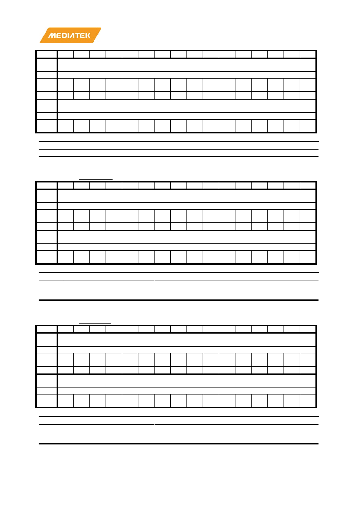
MT7686 Reference Manual
© 2016 - 2017 MediaTek Inc.
Page 297 of 536
This document contains information that is proprietary to MediaTek Inc. (“MediaTek”) and/or its licensor(s).
Any unauthorized use, reproduction or disclosure of this document in whole or in part is strictly prohibited.
Bit
31
30
29
28
27
26
25
24
23
22
21
20
19
18
17
16
Nam
e
RESV_WRDR7
Type
RO
Rese
t
0 0 0 0 0 0 0 0 0 0 0 0 0 0 0 0
Bit
15
14
13
12
11
10
9
8
7
6
5
4
3
2
1
0
Nam
e
RESV_WRDR7
Type
RO
Rese
t
0 0 0 0 0 0 0 0 0 0 0 0 0 0 0 0
Bit(s)
Name
Description
31:0
RESV_WRDR7
RESV_WRDR7
00000070
H2DSM0R
Host to Device Send Mailbox 0 Register
00000000
Bit
31
30
29
28
27
26
25
24
23
22
21
20
19
18
17
16
Nam
e
H2D_SM0
Type
RW
Rese
t
0 0 0 0 0 0 0 0 0 0 0 0 0 0 0 0
Bit
15
14
13
12
11
10
9
8
7
6
5
4
3
2
1
0
Nam
e
H2D_SM0
Type
RW
Rese
t
0 0 0 0 0 0 0 0 0 0 0 0 0 0 0 0
Bit(s)
Name
Description
31:0
H2D_SM0
This register is used by host driver to transmit data to
SDIO controller, which will be updated to H2DRM0R and
read by FW.
00000074
H2DSM1R
Host to Device Send Mailbox 1 Register
00000000
Bit
31
30
29
28
27
26
25
24
23
22
21
20
19
18
17
16
Nam
e
H2D_SM1
Type
RW
Rese
t
0 0 0 0 0 0 0 0 0 0 0 0 0 0 0 0
Bit
15
14
13
12
11
10
9
8
7
6
5
4
3
2
1
0
Nam
e
H2D_SM1
Type
RW
Rese
t
0 0 0 0 0 0 0 0 0 0 0 0 0 0 0 0
Bit(s)
Name
Description
31:0
H2D_SM1
This register is used by host driver to transmit data to
SDIO controller, which will be updated to H2DRM1R and
read by FW.
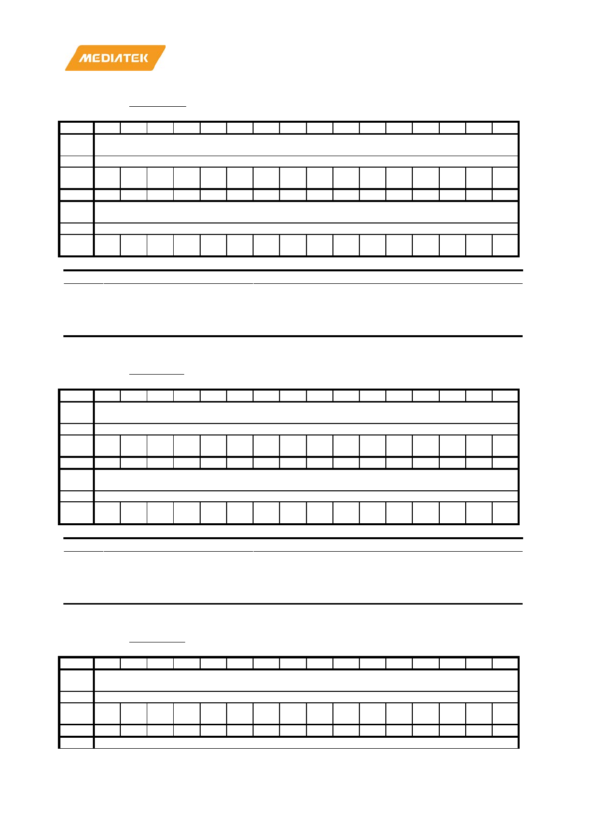
MT7686 Reference Manual
© 2016 - 2017 MediaTek Inc.
Page 298 of 536
This document contains information that is proprietary to MediaTek Inc. (“MediaTek”) and/or its licensor(s).
Any unauthorized use, reproduction or disclosure of this document in whole or in part is strictly prohibited.
00000078
D2HRM0R
Device to Host Receive Mailbox 0
Register
00000000
Bit
31
30
29
28
27
26
25
24
23
22
21
20
19
18
17
16
Nam
e
D2H_RM0
Type
RO
Rese
t
0 0 0 0 0 0 0 0 0 0 0 0 0 0 0 0
Bit
15
14
13
12
11
10
9
8
7
6
5
4
3
2
1
0
Nam
e
D2H_RM0
Type
RO
Rese
t
0 0 0 0 0 0 0 0 0 0 0 0 0 0 0 0
Bit(s)
Name
Description
31:0
D2H_RM0
This register is used by host driver to receive data from
SDIO controller, which is updated through D2HSM0R by
FW.
The property of RO/ RC is by control of WHCR.
RECV_MAILBOX_RD_CLR_EN bit.
0000007C
D2HRM1R
Device to Host Receive Mailbox 1
Register
00000000
Bit
31
30
29
28
27
26
25
24
23
22
21
20
19
18
17
16
Nam
e
D2H_RM1
Type
RO
Rese
t
0 0 0 0 0 0 0 0 0 0 0 0 0 0 0 0
Bit
15
14
13
12
11
10
9
8
7
6
5
4
3
2
1
0
Nam
e
D2H_RM1
Type
RO
Rese
t
0 0 0 0 0 0 0 0 0 0 0 0 0 0 0 0
Bit(s)
Name
Description
31:0
D2H_RM1
This register is used by host driver to receive data from
SDIO controller, which is updated through D2HSM1R by
FW.
The property of RO/ RC is by control of WHCR.
RECV_MAILBOX_RD_CLR_EN bit.
00000080
D2HRM2R
Device to Host Receive Mailbox 2
Register
00000000
Bit
31
30
29
28
27
26
25
24
23
22
21
20
19
18
17
16
Nam
e
D2H_RM2
Type
RO
Rese
t
0 0 0 0 0 0 0 0 0 0 0 0 0 0 0 0
Bit
15
14
13
12
11
10
9
8
7
6
5
4
3
2
1
0
Nam
D2H_RM2
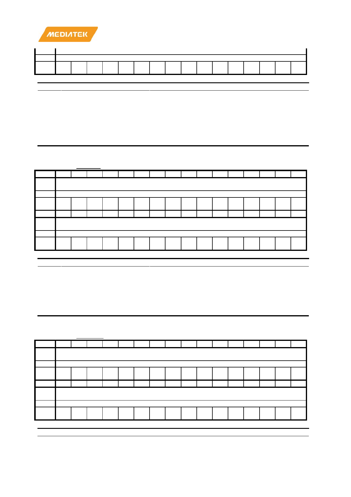
MT7686 Reference Manual
© 2016 - 2017 MediaTek Inc.
Page 299 of 536
This document contains information that is proprietary to MediaTek Inc. (“MediaTek”) and/or its licensor(s).
Any unauthorized use, reproduction or disclosure of this document in whole or in part is strictly prohibited.
e
Type
RO
Rese
t
0 0 0 0 0 0 0 0 0 0 0 0 0 0 0 0
Bit(s)
Name
Description
31:0
D2H_RM2
This register is used by host driver to receive data from
SDIO controller, which is updated through D2HSM2R by
FW. For
synchronization of hardware, it is recommended
to read this register more than once to give more host
clock cycles to device to get the latest result, especially for
EHPI interface.
Note that this register could be read when there is no AHB clock,
i.e. hos
t driver could get this message when chip is in low power
mode.
00000090
WRPLR
WLAN RX Packet Length Register
00000000
Bit
31
30
29
28
27
26
25
24
23
22
21
20
19
18
17
16
Nam
e
RX1_PACKET_LENGTH
Type
RO
Rese
t
0 0 0 0 0 0 0 0 0 0 0 0 0 0 0 0
Bit
15
14
13
12
11
10
9
8
7
6
5
4
3
2
1
0
Nam
e
RX0_PACKET_LENGTH
Type
RO
Rese
t
0 0 0 0 0 0 0 0 0 0 0 0 0 0 0 0
Bit(s)
Name
Description
31:16
RX1_PACKET_LENGTH
This register is used to get the next RX packet length in
the RX1
length FIFO, which is updated by FW HWRQ1CR.
When this field is read, it will report only 1 RX packet length in this
RX queue, and at most 1 packet will return by next RX port read.
15:0
RX0_PACKET_LENGTH
This register is used to get the next RX packet length in
the RX0 length FIFO, which is updated by FW HWRQ0CR.
When this field is read, it will report only 1 RX packet length in this
RX queue, and at most 1 packet will return by next RX port read.
00000094
WRPLR1
WLAN RX Packet Length Register 1
00000000
Bit
31
30
29
28
27
26
25
24
23
22
21
20
19
18
17
16
Nam
e
RX3_PACKET_LENGTH
Type
RO
Rese
t
0 0 0 0 0 0 0 0 0 0 0 0 0 0 0 0
Bit
15
14
13
12
11
10
9
8
7
6
5
4
3
2
1
0
Nam
e
RX2_PACKET_LENGTH
Type
RO
Rese
t
0 0 0 0 0 0 0 0 0 0 0 0 0 0 0 0
Bit(s)
Name
Description
31:16
RX3_PACKET_LENGTH
This register is used to get the next RX packet length in
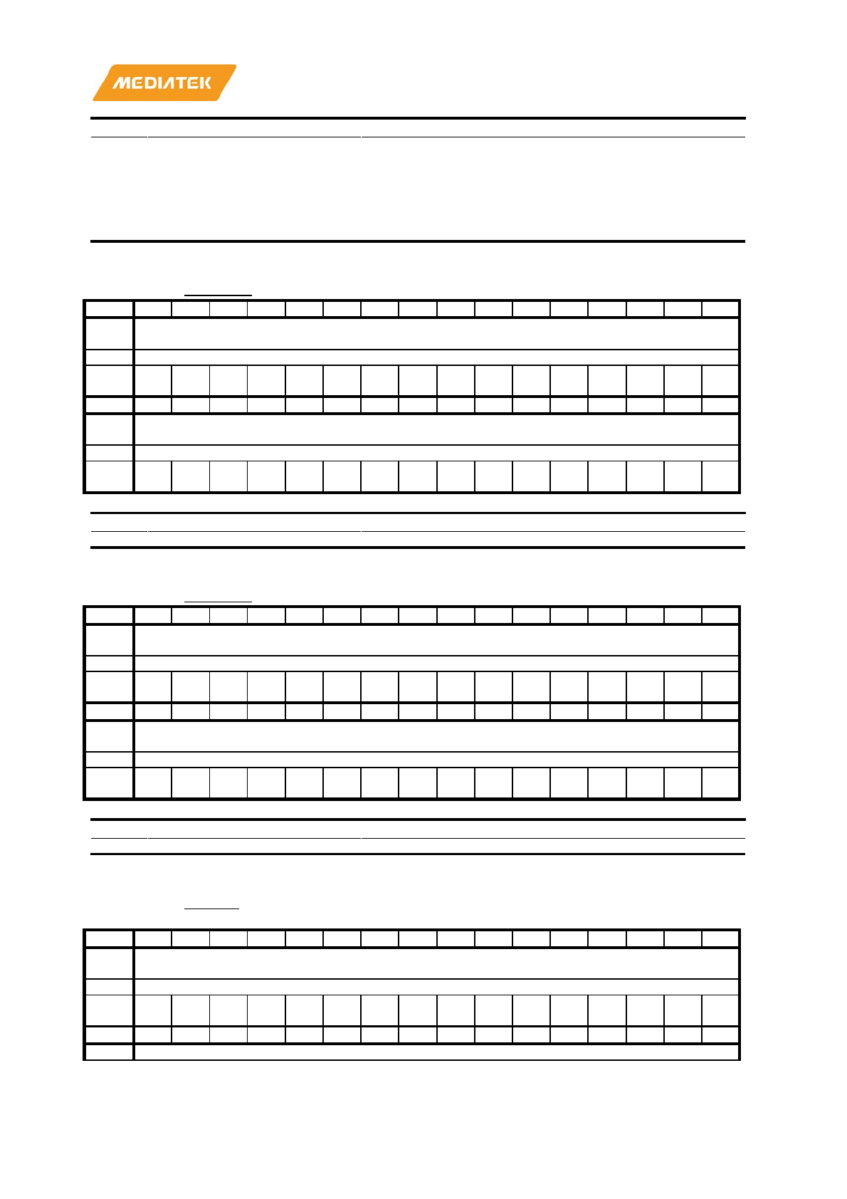
MT7686 Reference Manual
© 2016 - 2017 MediaTek Inc.
Page 300 of 536
This document contains information that is proprietary to MediaTek Inc. (“MediaTek”) and/or its licensor(s).
Any unauthorized use, reproduction or disclosure of this document in whole or in part is strictly prohibited.
Bit(s)
Name
Description
the RX3 length FIFO, which is updated by FW HWRQ3CR.
When this field is read, it will report only 1 RX packet length in this
RX queue, and at most 1 packet will return by next RX port read.
15:0
RX2_PACKET_LENGTH
This register is used to get the next RX packet length in
the RX2 length FIFO, which is updated by FW HWRQ2CR.
When this field is read, it will report only 1 RX packet
length in this
RX queue, and at most 1 packet will return by next RX port read.
00000098
WRPLR2
Reserve for WRPLR2
00000000
Bit
31
30
29
28
27
26
25
24
23
22
21
20
19
18
17
16
Nam
e
RESV_WRPLR2
Type
RO
Rese
t
0 0 0 0 0 0 0 0 0 0 0 0 0 0 0 0
Bit
15
14
13
12
11
10
9
8
7
6
5
4
3
2
1
0
Nam
e
RESV_WRPLR2
Type
RO
Rese
t
0 0 0 0 0 0 0 0 0 0 0 0 0 0 0 0
Bit(s)
Name
Description
31:0
RESV_WRPLR2
RESV_WRPLR2
0000009C
WRPLR3
Reserve for WRPLR3
00000000
Bit
31
30
29
28
27
26
25
24
23
22
21
20
19
18
17
16
Nam
e
RESV_WRPLR3
Type
RO
Rese
t
0 0 0 0 0 0 0 0 0 0 0 0 0 0 0 0
Bit
15
14
13
12
11
10
9
8
7
6
5
4
3
2
1
0
Nam
e
RESV_WRPLR3
Type
RO
Rese
t
0 0 0 0 0 0 0 0 0 0 0 0 0 0 0 0
Bit(s)
Name
Description
31:0
RESV_WRPLR3
RESV_WRPLR3
000000A0
EHTCR
EHPI transaction count register (EHPI
only)
00000004
Bit
31
30
29
28
27
26
25
24
23
22
21
20
19
18
17
16
Nam
e
EHPI_TRANS_CNT_REG
Type
RW
Rese
t
0 0 0 0 0 0 0 0 0 0 0 0 0 0 0 0
Bit
15
14
13
12
11
10
9
8
7
6
5
4
3
2
1
0
Nam
EHPI_TRANS_CNT_REG
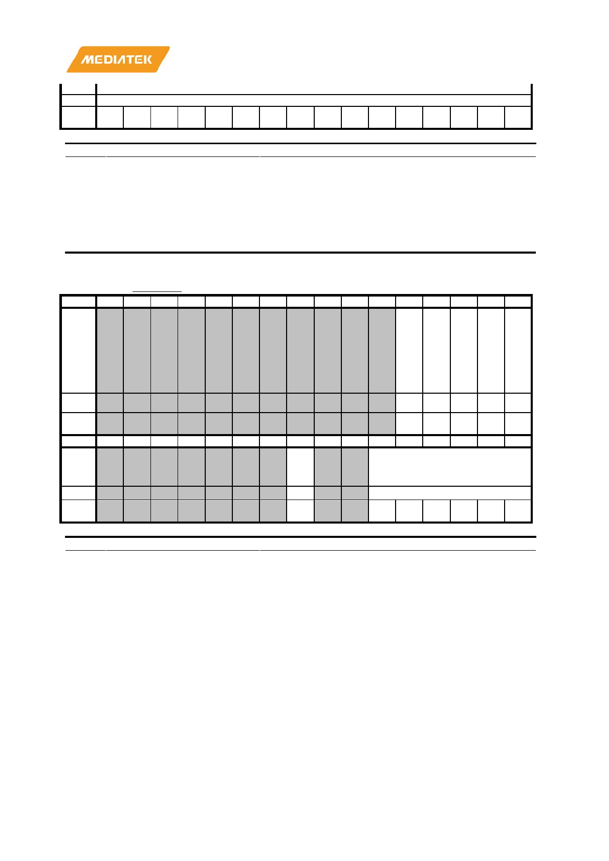
MT7686 Reference Manual
© 2016 - 2017 MediaTek Inc.
Page 301 of 536
This document contains information that is proprietary to MediaTek Inc. (“MediaTek”) and/or its licensor(s).
Any unauthorized use, reproduction or disclosure of this document in whole or in part is strictly prohibited.
e
Type
RW
Rese
t
0 0 0 0 0 0 0 0 0 0 0 0 0 1 0 0
Bit(s)
Name
Description
31:0
EHPI_TRANS_CNT_REG
This register is used for SDIO controller to know the
transaction boundary of
EHPI burst access. For normal
registers, it is limited to access them in 4B boundary. For
data port access (WTDR0, WTDR1, WRDR0 and WRDR1
etc.) and WHISR enhanced access, the length can be more
then 4B, Hence, host needs set it before it access these
regi
ster and SDIO controller would take this length as
transaction length. The transacation count should be set
with 4B alignment
000000AC
WOLTCR
On Line-Tuning Control Register
00000000
Bit
31
30
29
28
27
26
25
24
23
22
21
20
19
18
17
16
Nam
e
DA
T3
_O
UT
_O
F_
BO
UN
D
DA
T2
_O
UT
_O
F_
BO
UN
D
DA
T1_
OU
T_
OF
_B
OU
ND
DA
T0
_O
UT
_O
F_
BO
UN
D
CM
D_
OU
T_
OF
_B
OU
ND
Type
W1
C
W1
C
W1
C
W1
C
W1
C
Rese
t
0 0 0 0 0
Bit
15
14
13
12
11
10
9
8
7
6
5
4
3
2
1
0
Nam
e
TR
AI
N_
EN
TRAIN_WINDOW
Type
RW
RW
Rese
t
0 0 0 0 0 0 0
Bit(s)
Name
Description
20
DAT3_OUT_OF_BOUND
This field is to notice host driver that the train window of
data 3 is out of available delay gears.
The boundary of delay gears would be 0 and
31. If the applied
training window out of the bound then this field would be asserted.
Host driver can read these fields to know if any delay training is out
of boundary. Also, the host driver can write 1 to this field to clear
the status. This field is primary for no training window indication.
19
DAT2_OUT_OF_BOUND
This field is to notice host driver that the train window of
data 2 is out of available delay gears.
The boundary of delay gears would be 0 and 31. If the applied
training window out of the
bound then this field would be asserted.
Host driver can read these fields to know if any delay training is out
of boundary. Also, the host driver can write 1 to this field to clear
the status. This field is primary for no training window indication.
18
DAT1_OUT_OF_BOUND
This field is to notice host driver that the train window of
data 1 is out of available delay gears.
The boundary of delay gears would be 0 and 31. If the applied
training window out of the bound then this field would be asserted.
Host driver can read these fields to know if any delay training is out
of boundary. Also, the host driver can write 1 to this field to clear
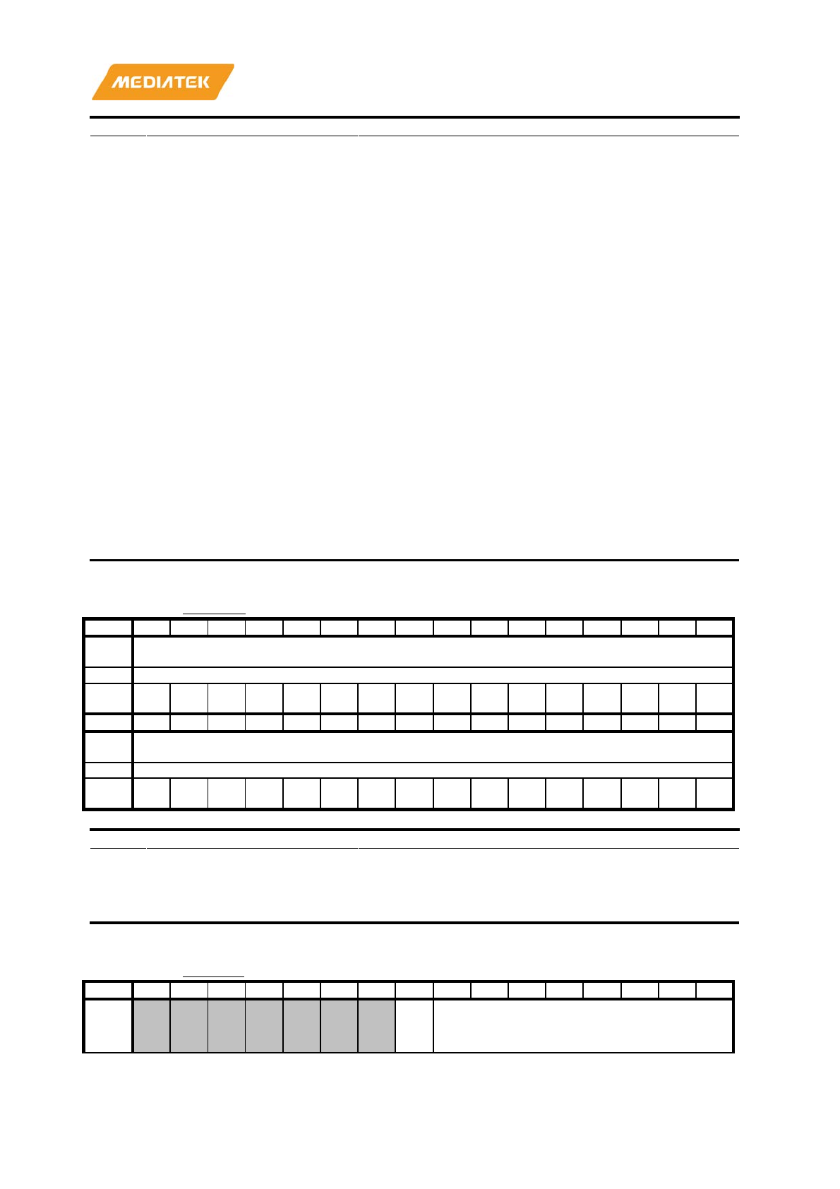
MT7686 Reference Manual
© 2016 - 2017 MediaTek Inc.
Page 302 of 536
This document contains information that is proprietary to MediaTek Inc. (“MediaTek”) and/or its licensor(s).
Any unauthorized use, reproduction or disclosure of this document in whole or in part is strictly prohibited.
Bit(s)
Name
Description
the status. This field is primary for no training window indication.
17
DAT0_OUT_OF_BOUND
This field is to notice host driver that the train window of
data 0 is out of available delay gears.
The boundary of delay gears would be 0 and 31. If the applied
training window out of the bound then this field would be asserted.
Host driver can read these fields to know if any delay training is out
of boundary. Also, the host driver can write 1 to this field to clear
the status. This field is primary for no training window indication.
16
CMD_OUT_OF_BOUND
This field is to notice host driver that the train window of
command is out of available delay gears.
The boundary of delay gears would be 0 and 31. If the applied
training window out of the bound then this field would be asserted.
Host driver can read these fields to know if any delay training is out
of boundary. Also, the host driver can write 1 to this field to clear
the status. This field is primary for no training window indication.
8
TRAIN_EN
Host driver can set this field to enable SDIO on-line
tun
ing function.
This field is about SDIO on
-line tuning function implying that
hardware could automatically tune the delay training gear to know
the surrounding delay gears are safe or not.
5:0
TRAIN_WINDOW
Host driver can set this field to set the training window
size which decides how many gears would be involved.
This field is about SDIO on
-line tuning function implying that
hardware could automatically tune the delay training gear for test.
The total delay gears for one data bus are 32. So the maximal
t
raining window size would be 32. For example, if the current delay
gear is 15 and the train window is set to 5. When the on
-line delay
training is enabled, the five
-time training delay gears would be 13,
14, 15, 16, and 17.
000000B0
WTMDR
Test Mode Data Port
00000000
Bit
31
30
29
28
27
26
25
24
23
22
21
20
19
18
17
16
Nam
e
TEST_MODE_DATA_PORT
Type
RW
Rese
t
0 0 0 0 0 0 0 0 0 0 0 0 0 0 0 0
Bit
15
14
13
12
11
10
9
8
7
6
5
4
3
2
1
0
Nam
e
TEST_MODE_DATA_PORT
Type
RW
Rese
t
0 0 0 0 0 0 0 0 0 0 0 0 0 0 0 0
Bit(s)
Name
Description
31:0
TEST_MODE_DATA_PORT
For Test Mode Read / Write.
According to the configuration of WTMCR[1:0]:
-
64-bits configurable data register
-
32-bits configurable data register
-PRBS
000000B4
WTMCR
Test Mode Control Register
00080000
Bit
31
30
29
28
27
26
25
24
23
22
21
20
19
18
17
16
Nam
e
TE
ST
_M
OD
PRBS_INIT_VAL
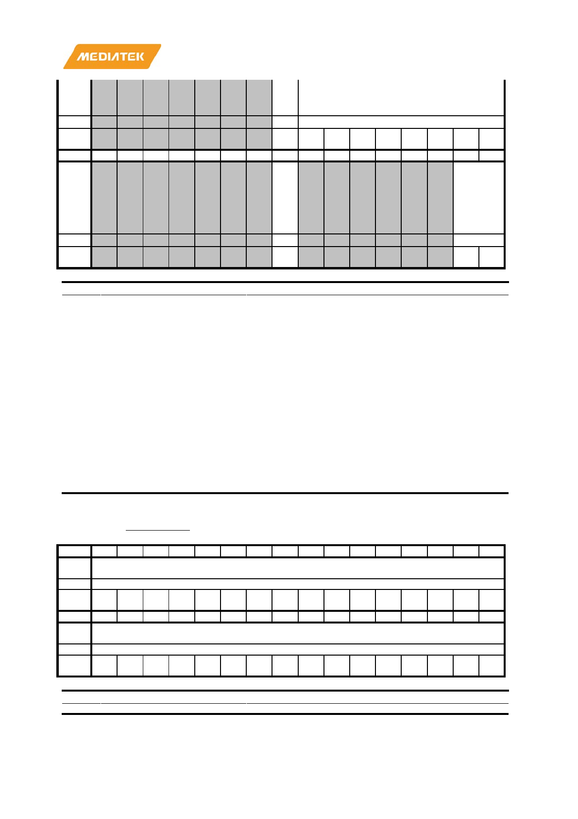
MT7686 Reference Manual
© 2016 - 2017 MediaTek Inc.
Page 303 of 536
This document contains information that is proprietary to MediaTek Inc. (“MediaTek”) and/or its licensor(s).
Any unauthorized use, reproduction or disclosure of this document in whole or in part is strictly prohibited.
E_
FW
_O
WN
Type
RO
RW
Rese
t
0 0 0 0 0 1 0 0 0
Bit
15
14
13
12
11
10
9
8
7
6
5
4
3
2
1
0
Nam
e
TE
ST
_M
OD
E_
ST
AT
US
TEST_MO
DE_SELE
CT
Type
RO
RW
Rese
t
0 0 0
Bit(s)
Name
Description
24
TEST_MODE_FW_OWN
Indicate the ownership of Test Mode Control Register :
WTMCR,WTMDPCR0,WTMDPCR1
0: Host has the ownership
1: FirmWare has the ownership
23:16
PRBS_INIT_VAL
Initial Value For PRBS Generator
8
TEST_MODE_STATUS
To Record the compare result of latest Test Mode write , It
is read only for Host and Firmware.
0: Data compare of Test Mode write is Pass
1: Data compare of Test Mode write is Fail
1:0
TEST_MODE_SELECT
Select the test mode data pattern
-
64-bits configurable data register
(WTMDPCR0:WTMDPCR1)
-
32-bits configurable data register
-PRBS
00: the 32bit data pattern
01: the 64bit data pattern
10: the PRBS data pattern
11: reserved
000000B8
WTMDPCR0
Test Mode Data Pattern Control
Register 0
F0F0F0F0
Bit
31
30
29
28
27
26
25
24
23
22
21
20
19
18
17
16
Nam
e
TEST_MODE_DATA_PATTERN_0
Type
RW
Rese
t
1 1 1 1 0 0 0 0 1 1 1 1 0 0 0 0
Bit
15
14
13
12
11
10
9
8
7
6
5
4
3
2
1
0
Nam
e
TEST_MODE_DATA_PATTERN_0
Type
RW
Rese
t
1 1 1 1 0 0 0 0 1 1 1 1 0 0 0 0
Bit(s)
Name
Description
31:0
TEST_MODE_DATA_PATTERN_0
Data pattern for Test Mode read
MT7686 Reference Manual
© 2016 - 2017 MediaTek Inc.
Page 304 of 536
This document contains information that is proprietary to MediaTek Inc. (“MediaTek”) and/or its licensor(s).
Any unauthorized use, reproduction or disclosure of this document in whole or in part is strictly prohibited.
000000BC
WTMDPCR1
Test Mode Data Pattern Control
Register 1
F0F0F0F0
Bit
31
30
29
28
27
26
25
24
23
22
21
20
19
18
17
16
Nam
e
TEST_MODE_DATA_PATTERN_1
Type
RW
Rese
t
1 1 1 1 0 0 0 0 1 1 1 1 0 0 0 0
Bit
15
14
13
12
11
10
9
8
7
6
5
4
3
2
1
0
Nam
e
TEST_MODE_DATA_PATTERN_1
Type
RW
Rese
t
1 1 1 1 0 0 0 0 1 1 1 1 0 0 0 0
Bit(s)
Name
Description
31:0
TEST_MODE_DATA_PATTERN_1
Data pattern for Test Mode write
000000C0
FWDLDR
Firmware Download Data Register
00000000
Bit
31
30
29
28
27
26
25
24
23
22
21
20
19
18
17
16
Nam
e
FWDL_DATA
Type
WO
Rese
t
0 0 0 0 0 0 0 0 0 0 0 0 0 0 0 0
Bit
15
14
13
12
11
10
9
8
7
6
5
4
3
2
1
0
Nam
e
FWDL_DATA
Type
WO
Rese
t
0 0 0 0 0 0 0 0 0 0 0 0 0 0 0 0
Bit(s)
Name
Description
31:0
FWDL_DATA
This register is used by host to send SDIO controller
TX_HEADER with firmware scatter to specified
destination address.
The first DW of the TX data is treated as HIF TX header, which
shares the same format with TX packet
format. SDIO controller
would transmit these data to the destination address starting from
FWDLDSAR in turn. Host could aggregate multiple transmission
data packets in one transaction. Note that it is not allowed to cut
data packet in different transaction
s as normal TX case.
For firmware download, host could access this register without
driver own = 1, but be sure that system AHB clock for SDIO
controller, AHB bus and destination memory is on by using
FWDLCMR0 and FWDLCMR1 first.
000000C4
FWDLDSAR
Firmware Download Destination
Starting Address Register
00000000
Bit
31
30
29
28
27
26
25
24
23
22
21
20
19
18
17
16
Nam
e
FWDL_DEST_STARTING_ADDR
Type
RW
Rese
0
0
0
0
0
0
0
0
0
0
0
0
0
0
0
0
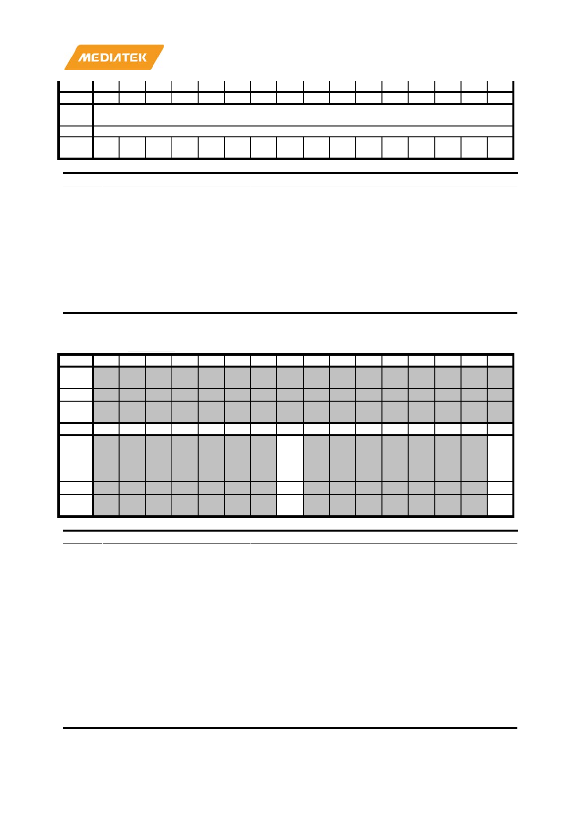
MT7686 Reference Manual
© 2016 - 2017 MediaTek Inc.
Page 305 of 536
This document contains information that is proprietary to MediaTek Inc. (“MediaTek”) and/or its licensor(s).
Any unauthorized use, reproduction or disclosure of this document in whole or in part is strictly prohibited.
t
Bit
15
14
13
12
11
10
9
8
7
6
5
4
3
2
1
0
Nam
e
FWDL_DEST_STARTING_ADDR
Type
RW
Rese
t
0 0 0 0 0 0 0 0 0 0 0 0 0 0 0 0
Bit(s)
Name
Description
31:0
FWDL_DEST_STARTING_ADDR
This register is used by host to specify firmware download
destination starting address. Note that it
should be 4B-
align address.
Destination address is automatically increased after TX data has
been written to AHB, and could be read back by host software for
reference. It would be updated by per
-packet based.
For firmware download, host could access thi
s register without
driver own = 1, but be sure that system AHB clock for SDIO
controller, AHB bus and destination memory is on by using
FWDLCMR0 and FWDLCMR1 first.
000000C8
FWDLSR
Firmware Download Status Register
00000100
Bit
31
30
29
28
27
26
25
24
23
22
21
20
19
18
17
16
Nam
e
Type
Rese
t
Bit
15
14
13
12
11
10
9
8
7
6
5
4
3
2
1
0
Nam
e
FW
DL
_R
DY
FW
DL
_M
OD
E
Type
RO
RW
Rese
t
1 0
Bit(s)
Name
Description
8
FWDL_RDY
Host driver needs to check if this bit is 1 to set new
FWDLDSAR for firmware download of new segment.
Then it could write firmware content to SDIO controller.
0 : It is NOT ready to write firmware from host to SDIO controller.
1 : It is ready to write firmware from host to SDIO controller.
0
FWDL_MODE
For firmware download, host could access this register
without driver own = 1, but be sure that system AHB clock
for SDIO controller, AHB bus and destination memory
is
on by using FWDLCMR0 and FWDLCMR1 first. Then host
driver can turn on this bit to switch to firmware download
mode to execute firmware download. Note that the
normal TX/RX path can't work in this mode, host driver
have to turn off this mode after firmw
are download
procedure is done.
0 : Firmware download mode is disabled
1 : Firmware download mode is enabled

MT7686 Reference Manual
© 2016 - 2017 MediaTek Inc.
Page 306 of 536
This document contains information that is proprietary to MediaTek Inc. (“MediaTek”) and/or its licensor(s).
Any unauthorized use, reproduction or disclosure of this document in whole or in part is strictly prohibited.
000000CC
FWDLCMR0
Firmware Download Customized
Register 0
00000000
Bit
31
30
29
28
27
26
25
24
23
22
21
20
19
18
17
16
Nam
e
Type
Rese
t
Bit
15
14
13
12
11
10
9
8
7
6
5
4
3
2
1
0
Nam
e
FW
DL
_C
MR
0_1
5
FW
DL
_C
MR
0_1
4
FW
DL
_C
MR
0_1
3
FW
DL
_C
MR
0_1
2
FW
DL
_C
MR
0_1
1
FW
DL
_C
MR
0_1
0
FW
DL
_C
MR
0_
9
FW
DL
_C
MR
0_
8
FW
DL
_C
MR
0_7
FW
DL
_C
MR
0_
6
FW
DL
_C
MR
0_
5
FW
DL
_C
MR
0_
4
FW
DL
_C
MR
0_
3
FW
DL
_C
MR
0_
2
FW
DL
_C
MR
0_1
FW
DL
_C
MR
0_
0
Type
RO
RO
RO
RO
RO
RO
RO
RO
RO
RO
RO
RO
RO
RO
RO
RO
Rese
t
0 0 0 0 0 0 0 0 0 0 0 0 0 0 0 0
Bit(s)
Name
Description
15
FWDL_CMR0_15
Function of this register is user-defined and is used in
firmware download stage.
When there no system AHB clock after power
-on and host driver
has not got driver own. It could set this register to notice HW and
could also read this register from HW.
For example, host driver could set some register to
request clock
controller to turn on AHB clock of system bus and memory storage.
And it could be read if the platform state is in sleep state, firmware
download state or fully operation state. The meaning of these bits
are all defined by customer, it is transparent to SDIO controller.
14
FWDL_CMR0_14
Function of this register is user-defined and is used in
firmware download stage.
When there no system AHB clock after power
-on and host driver
has not got driver own. It could set this register to notice HW and
could also read this register from HW.
For example, host driver could set some register to request clock
controller to turn o
n AHB clock of system bus and memory storage.
And it could be read if the platform state is in sleep state, firmware
download state or fully operation state. The meaning of these bits
are all defined by customer, it is transparent to SDIO controller.
13
FWDL_CMR0_13
Function of this register is user-defined and is used in
firmware download stage.
When there no system AHB clock after power
-on and host driver
has not got driver own. It could set this register to notice HW and
could also read this register from HW.
For example, host driver could set some register to request clock
controller to turn o
n AHB clock of system bus and memory storage.
And it could be read if the platform state is in sleep state, firmware
download state or fully operation state. The meaning of these bits
are all defined by customer, it is transparent to SDIO controller.
12
FWDL_CMR0_12
Function of this register is user-defined and is used in
firmware download stage.
When there no system AHB clock after power
-on and host driver
has not got driver own. It could set this register to notice HW and
could also read this register from HW.
For example, host driver could set some register to request clock
controller to turn o
n AHB clock of system bus and memory storage.
And it could be read if the platform state is in sleep state, firmware
download state or fully operation state. The meaning of these bits
are all defined by customer, it is transparent to SDIO controller.
11
FWDL_CMR0_11
Function of this register is user-defined and is used in

MT7686 Reference Manual
© 2016 - 2017 MediaTek Inc.
Page 307 of 536
This document contains information that is proprietary to MediaTek Inc. (“MediaTek”) and/or its licensor(s).
Any unauthorized use, reproduction or disclosure of this document in whole or in part is strictly prohibited.
Bit(s)
Name
Description
firmware download stage.
When there no system AHB clock after power
-on and host driver
has not got driver own. It could set this register to notice HW and
could also read this register fr
om HW.
For example, host driver could set some register to request clock
controller to turn on AHB clock of system bus and memory storage.
And it could be read if the platform state is in sleep state, firmware
download state or fully operation state. The
meaning of these bits
are all defined by customer, it is transparent to SDIO controller.
10
FWDL_CMR0_10
Function of this register is user-defined and is used in
firmware download stage.
When there no system AHB clock after power
-on and host driver
has no
t got driver own. It could set this register to notice HW and
could also read this register from HW.
For example, host driver could set some register to request clock
controller to turn on AHB clock of system bus and memory storage.
And it could be read i
f the platform state is in sleep state, firmware
download state or fully operation state. The meaning of these bits
are all defined by customer, it is transparent to SDIO controller.
9
FWDL_CMR0_9
Function of this register is user-defined and is used in
firmware download stage.
When there no system AHB clock after power
-on and host driver
has not got driver own. It could set this register to notice HW and
could also read this register from HW.
For example, host driver could set some register to request c
lock
controller to turn on AHB clock of system bus and memory storage.
And it could be read if the platform state is in sleep state, firmware
download state or fully operation state. The meaning of these bits
are all defined by customer, it is transparent to SDIO controller.
8
FWDL_CMR0_8
Function of this register is user-defined and is used in
firmware download stage.
When there no system AHB clock after power
-on and host driver
has not got driver own. It could set this register to notice HW and
could als
o read this register from HW.
For example, host driver could set some register to request clock
controller to turn on AHB clock of system bus and memory storage.
And it could be read if the platform state is in sleep state, firmware
download state or full
y operation state. The meaning of these bits
are all defined by customer, it is transparent to SDIO controller.
7
FWDL_CMR0_7
Function of this register is user-defined and is used in
firmware download stage.
When there no system AHB clock after power
-on and host driver
has not got driver own. It could set this register to notice HW and
could also read this register from HW.
For example, host driver could set some register to request clock
controller to turn on AHB clock of system bus and memory storage.
A
nd it could be read if the platform state is in sleep state, firmware
download state or fully operation state. The meaning of these bits
are all defined by customer, it is transparent to SDIO controller.
6
FWDL_CMR0_6
Function of this register is user-defined and is used in
firmware download stage.
When there no system AHB clock after power
-on and host driver
has not got driver own. It could set this register to notice HW and
could also read this register from HW.
For example, host driver could se
t some register to request clock
controller to turn on AHB clock of system bus and memory storage.
And it could be read if the platform state is in sleep state, firmware
download state or fully operation state. The meaning of these bits
are all defined by customer, it is transparent to SDIO controller.
5
FWDL_CMR0_5
Function of this register is user-defined and is used in
firmware download stage.
When there no system AHB clock after power
-on and host driver
has not got driver own. It could set this register to notice HW and

MT7686 Reference Manual
© 2016 - 2017 MediaTek Inc.
Page 308 of 536
This document contains information that is proprietary to MediaTek Inc. (“MediaTek”) and/or its licensor(s).
Any unauthorized use, reproduction or disclosure of this document in whole or in part is strictly prohibited.
Bit(s)
Name
Description
could also read this register from HW.
For example, host driver could set some register to request clock
controller to turn on AHB clock of system bus and memory storage.
And it could be read if the platform state is in sleep state, fir
mware
download state or fully operation state. The meaning of these bits
are all defined by customer, it is transparent to SDIO controller.
4
FWDL_CMR0_4
Function of this register is user-defined and is used in
firmware download stage.
When there no system AHB clock after power
-on and host driver
has not got driver own. It could set this register to notice HW and
could also read this register from HW.
For example, host driver could set some register to request clock
controller to turn o
n AHB clock of system bus and memory storage.
And it could be read if the platform state is in sleep state, firmware
download state or fully operation state. The meaning of these bits
are all defined by customer, it is transparent to SDIO controller.
3
FWDL_CMR0_3
Function of this register is user-defined and is used in
firmware download stage.
When there no system AHB clock after power
-on and host driver
has not got driver own. It could set this register to notice HW and
could also read this register from
HW.
For example, host driver could set some register to request clock
controller to turn on AHB clock of system bus and memory storage.
And it could be read if the platform state is in sleep state, firmware
download state or fully operation state. The me
aning of these bits
are all defined by customer, it is transparent to SDIO controller.
2
FWDL_CMR0_2
Function of this register is user-defined and is used in
firmware download stage.
When there no system AHB clock after power
-on and host driver
has not go
t driver own. It could set this register to notice HW and
could also read this register from HW.
For example, host driver could set some register to request clock
controller to turn on AHB clock of system bus and memory storage.
And it could be read if th
e platform state is in sleep state, firmware
download state or fully operation state. The meaning of these bits
are all defined by customer, it is transparent to SDIO controller.
1
FWDL_CMR0_1
Function of this register is user-defined and is used in
firmware download stage.
When there no system AHB clock after power
-on and host driver
has not got driver own. It could set this register to notice HW and
could also read this register from HW.
For example, host driver could set some register to request c
lock
controller to turn on AHB clock of system bus and memory storage.
And it could be read if the platform state is in sleep state, firmware
download state or fully operation state. The meaning of these bits
are all defined by customer, it is transparent to SDIO controller.
0
FWDL_CMR0_0
Function of this register is user-defined and is used in
firmware download stage.
When there no system AHB clock after power
-on and host driver
has not got driver own. It could set this register to notice HW and
could als
o read this register from HW.
For example, host driver could set some register to request clock
controller to turn on AHB clock of system bus and memory storage.
And it could be read if the platform state is in sleep state, firmware
download state or full
y operation state. The meaning of these bits
are all defined by customer, it is transparent to SDIO controller.
000000D0
FWDLCMR1
Firmware Download Customized
Register 1
00000000
Bit
31
30
29
28
27
26
25
24
23
22
21
20
19
18
17
16

MT7686 Reference Manual
© 2016 - 2017 MediaTek Inc.
Page 309 of 536
This document contains information that is proprietary to MediaTek Inc. (“MediaTek”) and/or its licensor(s).
Any unauthorized use, reproduction or disclosure of this document in whole or in part is strictly prohibited.
Nam
e
Type
Rese
t
Bit
15
14
13
12
11
10
9
8
7
6
5
4
3
2
1
0
Nam
e
FW
DL
_C
MR
1_1
5
FW
DL
_C
MR
1_1
4
FW
DL
_C
MR
1_1
3
FW
DL
_C
MR
1_1
2
FW
DL
_C
MR
1_1
1
FW
DL
_C
MR
1_1
0
FW
DL
_C
MR
1_9
FW
DL
_C
MR
1_8
FW
DL
_C
MR
1_7
FW
DL
_C
MR
1_6
FW
DL
_C
MR
1_5
FW
DL
_C
MR
1_4
FW
DL
_C
MR
1_3
FW
DL
_C
MR
1_2
FW
DL
_C
MR
1_1
FW
DL
_C
MR
1_0
Type
RO
RO
RO
RO
RO
RO
RO
RO
RO
RO
RO
RO
RO
RO
RO
RO
Rese
t
0 0 0 0 0 0 0 0 0 0 0 0 0 0 0 0
Bit(s)
Name
Description
15
FWDL_CMR1_15
Function of this register is user-defined and is used in
firmware download stage.
When there no system AHB clock after power
-on and host driver
has not got driver own. It could set this register to notice HW and
could also read this register from HW.
For example, host driver could set some register to
request clock
controller to turn on AHB clock of system bus and memory storage.
And it could be read if the platform state is in sleep state, firmware
download state or fully operation state. The meaning of these bits
are all defined by customer, it is transparent to SDIO controller.
14
FWDL_CMR1_14
Function of this register is user-defined and is used in
firmware download stage.
When there no system AHB clock after power
-on and host driver
has not got driver own. It could set this register to notice HW and
could also read this register from HW.
For example, host driver could set some register to request clock
controller to turn o
n AHB clock of system bus and memory storage.
And it could be read if the platform state is in sleep state, firmware
download state or fully operation state. The meaning of these bits
are all defined by customer, it is transparent to SDIO controller.
13
FWDL_CMR1_13
Function of this register is user-defined and is used in
firmware download stage.
When there no system AHB clock after power
-on and host driver
has not got driver own. It could set this register to notice HW and
could also read this register fr
om HW.
For example, host driver could set some register to request clock
controller to turn on AHB clock of system bus and memory storage.
And it could be read if the platform state is in sleep state, firmware
download state or fully operation state. The
meaning of these bits
are all defined by customer, it is transparent to SDIO controller.
12
FWDL_CMR1_12
Function of this register is user-defined and is used in
firmware download stage.
When there no system AHB clock after power
-on and host driver
has not got driver own. It could set this register to notice HW and
could also read this register from HW.
For example, host driver could set some register to request clock
controller to turn o
n AHB clock of system bus and memory storage.
And it could be read if the platform state is in sleep state, firmware
download state or fully operation state. The meaning of these bits
are all defined by customer, it is transparent to SDIO controller.
11
FWDL_CMR1_11
Function of this register is user-defined and is used in
firmware download stage.
When there no system AHB clock after power
-on and host driver
has not got driver own. It could set this register to notice HW and
could also read this register fr
om HW.
For example, host driver could set some register to request clock

MT7686 Reference Manual
© 2016 - 2017 MediaTek Inc.
Page 310 of 536
This document contains information that is proprietary to MediaTek Inc. (“MediaTek”) and/or its licensor(s).
Any unauthorized use, reproduction or disclosure of this document in whole or in part is strictly prohibited.
Bit(s)
Name
Description
controller to turn on AHB clock of system bus and memory storage.
And it could be read if the platform state is in sleep state, firmware
download state or fully operation state. The
meaning of these bits
are all defined by customer, it is transparent to SDIO controller.
10
FWDL_CMR1_10
Function of this register is user-defined and is used in
firmware download stage.
When there no system AHB clock after power
-on and host driver
has no
t got driver own. It could set this register to notice HW and
could also read this register from HW.
For example, host driver could set some register to request clock
controller to turn on AHB clock of system bus and memory storage.
And it could be read i
f the platform state is in sleep state, firmware
download state or fully operation state. The meaning of these bits
are all defined by customer, it is transparent to SDIO controller.
9
FWDL_CMR1_9
Function of this register is user-defined and is used in
firmware download stage.
When there no system AHB clock after power
-on and host driver
has not got driver own. It could set this register to notice HW and
could also read this register from HW.
For example, host driver could set some register to request c
lock
controller to turn on AHB clock of system bus and memory storage.
And it could be read if the platform state is in sleep state, firmware
download state or fully operation state. The meaning of these bits
are all defined by customer, it is transparent to SDIO controller.
8
FWDL_CMR1_8
Function of this register is user-defined and is used in
firmware download stage.
When there no system AHB clock after power
-on and host driver
has not got driver own. It could set this register to notice HW and
could also read this register from HW.
For example, host driver could set some register to request clock
controller to turn o
n AHB clock of system bus and memory storage.
And it could be read if the platform state is in sleep state, firmware
download state or fully operation state. The meaning of these bits
are all defined by customer, it is transparent to SDIO controller.
7
FWDL_CMR1_7
Function of this register is user-defined and is used in
firmware download stage.
When there no system AHB clock after power
-on and host driver
has not got driver own. It could set this register to notice HW and
could also read this register from
HW.
For example, host driver could set some register to request clock
controller to turn on AHB clock of system bus and memory storage.
And it could be read if the platform state is in sleep state, firmware
download state or fully operation state. The me
aning of these bits
are all defined by customer, it is transparent to SDIO controller.
6
FWDL_CMR1_6
Function of this register is user-defined and is used in
firmware download stage.
When there no system AHB clock after power
-on and host driver
has not got driver own. It could set this register to notice HW and
could also read this register from HW.
For example, host driver could set some register to request clock
controller to turn o
n AHB clock of system bus and memory storage.
And it could be read if the platform state is in sleep state, firmware
download state or fully operation state. The meaning of these bits
are all defined by customer, it is transparent to SDIO controller.
5
FWDL_CMR1_5
Function of this register is user-defined and is used in
firmware download stage.
When there no system AHB clock after power
-on and host driver
has not got driver own. It could set this register to notice HW and
could also read this register from
HW.
For example, host driver could set some register to request clock
controller to turn on AHB clock of system bus and memory storage.
And it could be read if the platform state is in sleep state, firmware
download state or fully operation state. The meaning of these bits

MT7686 Reference Manual
© 2016 - 2017 MediaTek Inc.
Page 311 of 536
This document contains information that is proprietary to MediaTek Inc. (“MediaTek”) and/or its licensor(s).
Any unauthorized use, reproduction or disclosure of this document in whole or in part is strictly prohibited.
Bit(s)
Name
Description
are all defined by customer, it is transparent to SDIO controller.
4
FWDL_CMR1_4
Function of this register is user-defined and is used in
firmware download stage.
When there no system AHB clock after power
-on and host driver
has not got driver own. It could set this register to notice HW and
could also read this register from HW.
For example, host driver could set some register to request clock
controller to turn o
n AHB clock of system bus and memory storage.
And it could be read if the platform state is in sleep state, firmware
download state or fully operation state. The meaning of these bits
are all defined by customer, it is transparent to SDIO controller.
3
FWDL_CMR1_3
Function of this register is user-defined and is used in
firmware download stage.
When there no system AHB clock after power
-on and host driver
has not got driver own. It could set this register to notice HW and
could also read this register from
HW.
For example, host driver could set some register to request clock
controller to turn on AHB clock of system bus and memory storage.
And it could be read if the platform state is in sleep state, firmware
download state or fully operation state. The me
aning of these bits
are all defined by customer, it is transparent to SDIO controller.
2
FWDL_CMR1_2
Function of this register is user-defined and is used in
firmware download stage.
When there no system AHB clock after power
-on and host driver
has not go
t driver own. It could set this register to notice HW and
could also read this register from HW.
For example, host driver could set some register to request clock
controller to turn on AHB clock of system bus and memory storage.
And it could be read if th
e platform state is in sleep state, firmware
download state or fully operation state. The meaning of these bits
are all defined by customer, it is transparent to SDIO controller.
1
FWDL_CMR1_1
Function of this register is user-defined and is used in
firmware download stage.
When there no system AHB clock after power
-on and host driver
has not got driver own. It could set this register to notice HW and
could also read this register from HW.
For example, host driver could set some register to request c
lock
controller to turn on AHB clock of system bus and memory storage.
And it could be read if the platform state is in sleep state, firmware
download state or fully operation state. The meaning of these bits
are all defined by customer, it is transparent to SDIO controller.
0
FWDL_CMR1_0
Function of this register is user-defined and is used in
firmware download stage.
When there no system AHB clock after power
-on and host driver
has not got driver own. It could set this register to notice HW and
could als
o read this register from HW.
For example, host driver could set some register to request clock
controller to turn on AHB clock of system bus and memory storage.
And it could be read if the platform state is in sleep state, firmware
download state or full
y operation state. The meaning of these bits
are all defined by customer, it is transparent to SDIO controller.
000000D4
WPLRCR
WLAN Packet Length Report Control
Register
00000000
Bit
31
30
29
28
27
26
25
24
23
22
21
20
19
18
17
16
Nam
e
RX3_RPT_PKT_LEN RX2_RPT_PKT_LEN
Type
RW
RW
Rese
t
0 0 0 0 0 0 0 0 0 0 0 0

MT7686 Reference Manual
© 2016 - 2017 MediaTek Inc.
Page 312 of 536
This document contains information that is proprietary to MediaTek Inc. (“MediaTek”) and/or its licensor(s).
Any unauthorized use, reproduction or disclosure of this document in whole or in part is strictly prohibited.
Bit
15
14
13
12
11
10
9
8
7
6
5
4
3
2
1
0
Nam
e
RX1_RPT_PKT_LEN RX0_RPT_PKT_LEN
Type
RW
RW
Rese
t
0 0 0 0 0 0 0 0 0 0 0 0
Bit(s)
Name
Description
29:24
RX3_RPT_PKT_LEN
If the RPT_OWN_RX_PACKET_LEN bit in WHCR is set,
host driver can set this field to decide the maximal report
length for RX queue 3 during enhance mode.
If under the define of SDCTL_RX3_PACKET_LEN_64,
The default value
0 is to report maximal packet number 64. Host
driver can set the required length from 0 to 63.
If under the define of SDCTL_RX3_PACKET_LEN_32,
The default value 0 is to report maximal packet number 32. Host
driver can set the required length from 0 to
31.
If under the define of SDCTL_RX3_PACKET_LEN_16,
The default value 0 is to report maximal packet number 16. Host
driver can set the required length from 0 to 15.
It is not allowed to set this field with the value larger than the
maximal packet number.
21:16
RX2_RPT_PKT_LEN
If the RPT_OWN_RX_PACKET_LEN bit in WHCR is set,
host driver can set this field to decide the maximal report
length for RX queue 2 during enhance mode.
If under the define of SDCTL_RX2_PACKET_LEN_64,
The default value 0 is to rep
ort maximal packet number 64.
Host driver can set the required length from 0 to 63.
If under the define of SDCTL_RX2_PACKET_LEN_32,
The default value 0 is to report maximal packet number 32. Host
driver can set the required length from 0 to 31.
If unde
r the define of SDCTL_RX2_PACKET_LEN_16,
The default value 0 is to report maximal packet number 16. Host
driver can set the required length from 0 to 15.
It is not allowed to set this field with the value larger than the
maximal packet number.
13:8
RX1_RPT_PKT_LEN
If the RPT_OWN_RX_PACKET_LEN bit in WHCR is set,
host driver can set this field to decide the maximal report
length for RX queue 1 during enhance mode.
If under the define of SDCTL_RXD_PACKET_LEN_64,
The default value 0 is to report maxi
mal packet number 64.
Host driver can set the required length from 0 to 63.
If under the define of SDCTL_RXD_PACKET_LEN_32,
The default value 0 is to report maximal packet number 32. Host
driver can set the required length from 0 to 31.
If under the de
fine of SDCTL_RXD_PACKET_LEN_16,
The default value 0 is to report maximal packet number 16. Host
driver can set the required length from 0 to 15.
It is not allowed to set this field with the value larger than the
maximal packet number.
5:0
RX0_RPT_PKT_LEN
If the RPT_OWN_RX_PACKET_LEN bit in WHCR is set,
host driver can set this field to decide the maximal report
length for RX queue 0 during enhance mode.
If under the define of SDCTL_RXE_PACKET_LEN_64,
The default value 0 is to report maximal packet
number 64.
Host driver can set the required length from 0 to 63.
If under the define of SDCTL_RXE_PACKET_LEN_32,
The default value 0 is to report maximal packet number 32. Host
driver can set the required length from 0 to 31.
If under the define of SD
CTL_RXE_PACKET_LEN_16,
The default value 0 is to report maximal packet number 16. Host
driver can set the required length from 0 to 15.
It is not allowed to set this field with the value larger than the
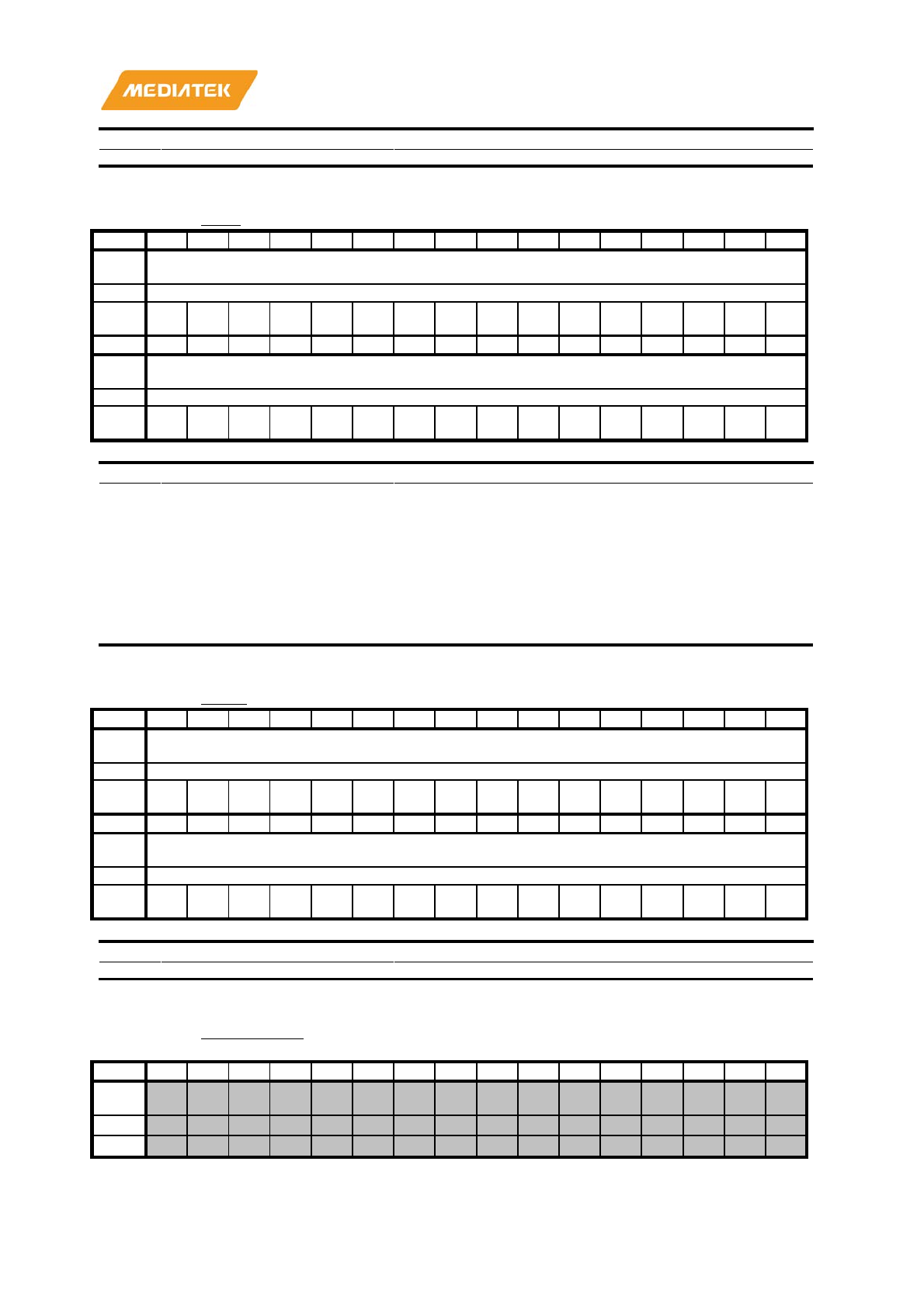
MT7686 Reference Manual
© 2016 - 2017 MediaTek Inc.
Page 313 of 536
This document contains information that is proprietary to MediaTek Inc. (“MediaTek”) and/or its licensor(s).
Any unauthorized use, reproduction or disclosure of this document in whole or in part is strictly prohibited.
Bit(s)
Name
Description
maximal packet number.
000000D8
WSR
WLAN Snapshot Register
00000000
Bit
31
30
29
28
27
26
25
24
23
22
21
20
19
18
17
16
Nam
e
SNAPSHOT
Type
RO
Rese
t
0 0 0 0 0 0 0 0 0 0 0 0 0 0 0 0
Bit
15
14
13
12
11
10
9
8
7
6
5
4
3
2
1
0
Nam
e
SNAPSHOT
Type
RO
Rese
t
0 0 0 0 0 0 0 0 0 0 0 0 0 0 0 0
Bit(s)
Name
Description
31:0
SNAPSHOT
A 32-bits register which could copy the content of AHB
clock domain register being read.
For register with RC property, If there is CRC Error during the read
access, host driver shall keep reading this snapshot register until
there is no CRC error to avoid information loss. SW should not go
to read other register first, it is atomic operation.
For register without RC property, If there is CRC Error during the
read access, host could just read the original register again.
Value in this register is undefined if previous read is reading
register without RC property.
000000F8
VSCR
Version Control Register
00000000
Bit
31
30
29
28
27
26
25
24
23
22
21
20
19
18
17
16
Nam
e
HW_VERSION
Type
RO
Rese
t
0 0 0 0 0 0 0 0 0 0 0 0 0 0 0 0
Bit
15
14
13
12
11
10
9
8
7
6
5
4
3
2
1
0
Nam
e
HW_VERSION
Type
RO
Rese
t
0 0 0 0 0 0 0 0 0 0 0 0 0 0 0 0
Bit(s)
Name
Description
31:0
HW_VERSION
Indicating the HW version
000000FC
WSDIOAICR
Common SDIO Asynchronous
Interrupt Control Register
00000004
Bit
31
30
29
28
27
26
25
24
23
22
21
20
19
18
17
16
Nam
e
Type
Rese
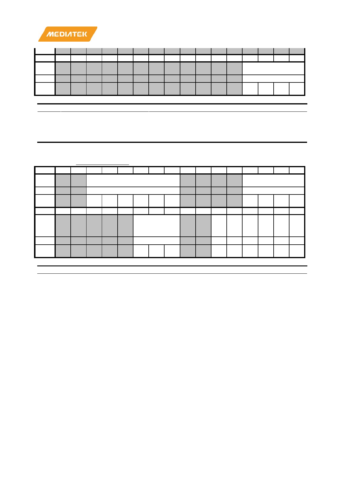
MT7686 Reference Manual
© 2016 - 2017 MediaTek Inc.
Page 314 of 536
This document contains information that is proprietary to MediaTek Inc. (“MediaTek”) and/or its licensor(s).
Any unauthorized use, reproduction or disclosure of this document in whole or in part is strictly prohibited.
t
Bit
15
14
13
12
11
10
9
8
7
6
5
4
3
2
1
0
Nam
e
SYNC_INT_CYCLE_N
UM
Type
RW
Rese
t
0 1 0 0
Bit(s)
Name
Description
3:0
SYNC_INT_CYCLE_NUM
Control the sync. interrupt cycles before the
asynchronous interrrupt period. (4 cycle in default
defined in SDIO spec. 3.0) This is for some specific host
that could stop the SD clock before the defined
asynchronous interrupt period
00000100
CLKIOCR_T28LP
Clock Pad Macro IO Control Register
000A0422
Bit
31
30
29
28
27
26
25
24
23
22
21
20
19
18
17
16
Nam
e
CLK_RDSEL CLK_TDSEL
Type
RW
RW
Rese
t
0 0 0 0 0 0 1 0 1 0
Bit
15
14
13
12
11
10
9
8
7
6
5
4
3
2
1
0
Nam
e CLK_E8E4E2
CL
K_
SM
T
CL
K_
PU
PD
CL
K_
R1
CL
K_
R0
CL
K_I
ES
CL
K_
SR
Type
RW
RW
RW
RW
RW
RW
RW
Rese
t
1 0 0 1 0 0 0 1 0
Bit(s)
Name
Description
29:24
CLK_RDSEL
RX duty select
RDSEL[1:0]: Input buffer duty high when asserted (high
pulse
width adjustment)
RDSEL[3:2]: Input buffer duty low when asserted(low pulse width
adjustment)
RDSEL[5:4]: Level shifter duty high when asserted (high pulse
width adjustment)
RDSEL[7:6]: Level shifter duty low when asserted (low pulse width
adjustment)
19:16
CLK_TDSEL
TX duty select
TDSEL[1:0]: Output level shifter duty high when asserted (high
pulse width adjustment)
TDSEL[3:2]: Output level shifter duty low when asserted(low pulse
width adjustment)
10:8
CLK_E8E4E2
TX Driving Strength Control.
5
CLK_SMT
RX input buffer schmit trigger hysteresis control enable.
High asserted.
SMT=1, Schmit Trigger enable
4
CLK_PUPD
Pull-up / pull-down selection.
0: pull
-up resistor
1: pull
-down resistor
CLK pad default no pull
3
CLK_R1
Select 50K resistor (0: not select, 1: select)
2
CLK_R0
Select 10K resistor (0: not select, 1: select)
1
CLK_IES
RX input buffer enable. High asserted.
Datapath: from IO to O. IES=0, O=0
According to IOCUP spec.

MT7686 Reference Manual
© 2016 - 2017 MediaTek Inc.
Page 315 of 536
This document contains information that is proprietary to MediaTek Inc. (“MediaTek”) and/or its licensor(s).
Any unauthorized use, reproduction or disclosure of this document in whole or in part is strictly prohibited.
Bit(s)
Name
Description
Power down mode, IES=0 must
Quiescent mode, IES=0 suggested
0
CLK_SR
Output Slew Rate Control. High asserted.
SR=1, slower slew.
SR=0, no slew rate controlled.
00000104
CMDIOCR_T28LP
Command Pad Macro IO Control
Register
000A0422
Bit
31
30
29
28
27
26
25
24
23
22
21
20
19
18
17
16
Nam
e
CMD_RDSEL CMD_TDSEL
Type
RW
RW
Rese
t
0 0 0 0 0 0 1 0 1 0
Bit
15
14
13
12
11
10
9
8
7
6
5
4
3
2
1
0
Nam
e
RE
G_
CM
D_
SA
MP
LE
CMD_E8E4E2
CM
D_
SM
T
CM
D_
PU
PD
CM
D_
R1
CM
D_
R0
CM
D_
IES
CM
D_
SR
Type
RW
RW
RW
RW
RW
RW
RW
RW
Rese
t
0 1 0 0 1 0 0 0 1 0
Bit(s)
Name
Description
29:24
CMD_RDSEL
RX duty select
RDSEL[1:0]: Input buffer duty high when asserted (high pulse
width adjustment)
RDSEL[3:2]: Input buffer duty low when asserted(low pulse width
adjustment)
RDSEL[5:4]: Level shifter duty high when asserted (high pulse
width adjustment)
RDSEL[7:6]: Level shifter duty low when asserted (low pulse width
adjustment)
19:16
CMD_TDSEL
TX duty select
TDSEL[1:0]: Output level shifter duty high when asserted (high
pulse width adjustment)
TDSEL[3:2]: Output level shifter duty low when asserted(low pulse
width adjustment)
12
REG_CMD_SAMPLE
Select clock edge to latch input bus signal.
0: Use positive sd clock edge to latch input command
1: Use negative sd clock edge to latch input command
10:8
CMD_E8E4E2
TX Driving Strength Control.
5
CMD_SMT
RX input buffer schmit trigger hysteresis control enable.
High asserted.
SMT=1, Schmit Trigger enable
4
CMD_PUPD
Pull-up / pull-down selection.
0: pull
-up resistor
1:
pull-down resistor
CMD pad default no pull
3
CMD_R1
Select 50K resistor (0: not select, 1: select)
2
CMD_R0
Select 10K resistor (0: not select, 1: select)
1
CMD_IES
RX input buffer enable. High asserted.
Datapath: from IO to O. IES=0, O=0
0
CMD_SR
Output Slew Rate Control. High asserted.
SR=1, slower slew.
SR=0, no slew rate controlled.
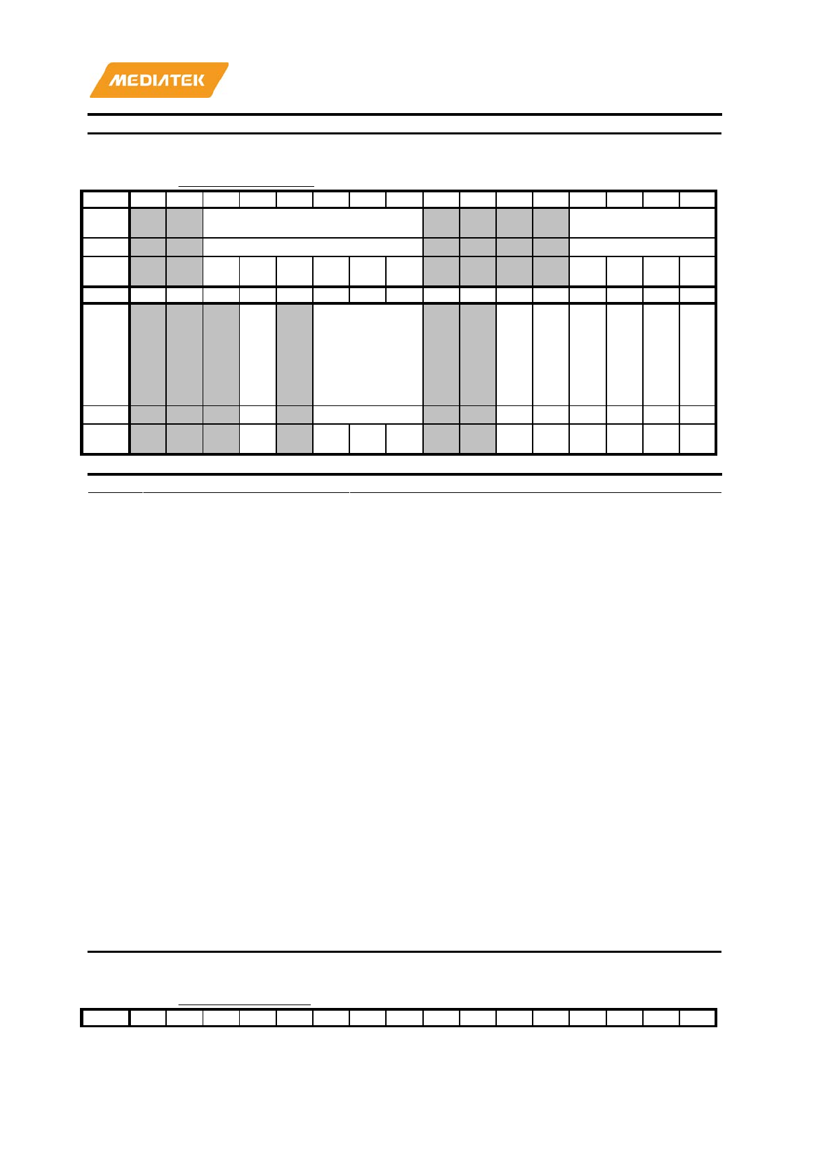
MT7686 Reference Manual
© 2016 - 2017 MediaTek Inc.
Page 316 of 536
This document contains information that is proprietary to MediaTek Inc. (“MediaTek”) and/or its licensor(s).
Any unauthorized use, reproduction or disclosure of this document in whole or in part is strictly prohibited.
Bit(s)
Name
Description
00000108
DAT0IOCR_T28LP
Data 0 Pad Macro IO Control Register
000A0422
Bit
31
30
29
28
27
26
25
24
23
22
21
20
19
18
17
16
Nam
e
DATA0_RDSEL DATA0_TDSEL
Type
RW
RW
Rese
t
0 0 0 0 0 0 1 0 1 0
Bit
15
14
13
12
11
10
9
8
7
6
5
4
3
2
1
0
Nam
e
RE
G_
DA
TA
0_
SA
MP
LE
DATA0_E8E4E2
DA
TA
0_
SM
T
DA
TA
0_
PU
PD
DA
TA
0_
R1
DA
TA
0_
R0
DA
TA
0_I
ES
DA
TA
0_
SR
Type
RW
RW
RW
RW
RW
RW
RW
RW
Rese
t
0 1 0 0 1 0 0 0 1 0
Bit(s)
Name
Description
29:24
DATA0_RDSEL
RX duty select
RDSEL[1:0]: Input buffer duty high when asserted (high pulse
width adjustment)
RDSEL[3:2]: Input buffer duty low when asserted(low pulse width
adjustment)
RDSEL[5:4]: Level shifter duty high when asserted (high pulse
width adjustment)
RDSEL[7:6]: Level shifter duty low when asserted (low pulse width
adjustment)
19:16
DATA0_TDSEL
TX duty select
TDSEL[1:0]: Output level shifter duty high when asserted (high
pulse width adjustment)
TDSEL[3:2]: Output level shifter duty low when asserted(low pulse
width adjustment)
12
REG_DATA0_SAMPLE
Select clock edge to latch input bus signal.
0: Use positive SD clock edge to latch input data 0
1: Use negative SD clock edge to latch input data 0
10:8
DATA0_E8E4E2
TX Driving Strength Control.
5
DATA0_SMT
RX input buffer Schmitt trigger hysteresis control
enabled. High asserted.
SMT=1, Schmitt Trigger enable
4
DATA0_PUPD
Pull-up / pull-down selection.
0: pull
-up resistor
1: pull
-down resistor
DATA 0 pad default no pull
3
DATA0_R1
Select 50K resistor (0: not select, 1: select)
2
DATA0_R0
Select 10K resistor (0: not select, 1: select)
1
DATA0_IES
RX input buffer enable. High asserted.
Datapath: from IO to O. IES=0, O=0
0
DATA0_SR
Output Slew Rate Control. High asserted.
SR=1, slower slew.
SR=0, no slew rate controlled.
0000010C
DAT1IOCR_T28LP
Data 1 Pad Macro IO Control Register
000A0422
Bit
31
30
29
28
27
26
25
24
23
22
21
20
19
18
17
16
MT7686 Reference Manual
© 2016 - 2017 MediaTek Inc.
Page 317 of 536
This document contains information that is proprietary to MediaTek Inc. (“MediaTek”) and/or its licensor(s).
Any unauthorized use, reproduction or disclosure of this document in whole or in part is strictly prohibited.
Nam
e
DATA1_RDSEL DATA1_TDSEL
Type
RW
RW
Rese
t
0 0 0 0 0 0 1 0 1 0
Bit
15
14
13
12
11
10
9
8
7
6
5
4
3
2
1
0
Nam
e
RE
G_
DA
TA1
_S
AM
PL
E
DATA1_E8E4E2
DA
TA1
_S
MT
DA
TA1
_P
UP
D
DA
TA1
_R
1
DA
TA1
_R
0
DA
TA1
_IE
S
DA
TA1
_S
R
Type
RW
RW
RW
RW
RW
RW
RW
RW
Rese
t
0 1 0 0 1 0 0 0 1 0
Bit(s)
Name
Description
29:24
DATA1_RDSEL
RX duty select
RDSEL[1:0]: Input buffer duty high when asserted (high pulse
width adjustment)
RDSEL[3:2]: Input buffer duty low when asserted(low pulse width
adjustment)
RDSEL[5:4]: Level shifter duty high when asserted (high pulse
width adjustment)
RDSEL[7:6]: Level shifter duty low when asserted (low pulse width
adjustment)
19:16
DATA1_TDSEL
TX duty select
TDSEL[1:0]: Output level shifter duty high when
asserted (high
pulse width adjustment)
TDSEL[3:2]: Output level shifter duty low when asserted(low pulse
width adjustment)
12
REG_DATA1_SAMPLE
Select clock edge to latch input bus signal.
0: Use positive SD clock edge to latch input data 1
1: Use negative SD clock edge to latch input data 1
10:8
DATA1_E8E4E2
TX Driving Strength Control.
5
DATA1_SMT
RX input buffer Schmitt trigger hysteresis control enable.
High asserted.
SMT=1, Schmitt Trigger enable
4
DATA1_PUPD
Pull-up / pull-down selection.
0: pull
-up resistor
1: pull
-down resistor
DATA 1 pad default no pull
3
DATA1_R1
Select 50K resistor (0: not select, 1: select)
2
DATA1_R0
Select 10K resistor (0: not select, 1: select)
1
DATA1_IES
RX input buffer enable. High asserted.
Datapath: from IO to O. IES=0, O=0
0
DATA1_SR
Output Slew Rate Control. High asserted.
SR=1, slower slew.
SR=0, no slew rate controlled.
00000110
DAT2IOCR_T28LP
Data 2 Pad Macro IO Control Register
000A0422
Bit
31
30
29
28
27
26
25
24
23
22
21
20
19
18
17
16
Nam
e
DATA2_RDSEL DATA2_TDSEL
Type
RW
RW
Rese
t
0 0 0 0 0 0 1 0 1 0
Bit
15
14
13
12
11
10
9
8
7
6
5
4
3
2
1
0
MT7686 Reference Manual
© 2016 - 2017 MediaTek Inc.
Page 318 of 536
This document contains information that is proprietary to MediaTek Inc. (“MediaTek”) and/or its licensor(s).
Any unauthorized use, reproduction or disclosure of this document in whole or in part is strictly prohibited.
Nam
e
RE
G_
DA
TA
2_
SA
MP
LE
DATA2_E8E4E2
DA
TA
2_
SM
T
DA
TA
2_
PU
PD
DA
TA
2_
R1
DA
TA
2_
R0
DA
TA
2_I
ES
DA
TA
2_
SR
Type
RW
RW
RW
RW
RW
RW
RW
RW
Rese
t
0 1 0 0 1 0 0 0 1 0
Bit(s)
Name
Description
29:24
DATA2_RDSEL
RX duty select
RDSEL[1:0]: Input buffer duty high when asserted (high pulse
width adjustment)
RDSEL[3:2]: Input buffer duty low when
asserted(low pulse width
adjustment)
RDSEL[5:4]: Level shifter duty high when asserted (high pulse
width adjustment)
RDSEL[7:6]: Level shifter duty low when asserted (low pulse width
adjustment)
19:16
DATA2_TDSEL
TX duty select
TDSEL[1:0]: Output level
shifter duty high when asserted (high
pulse width adjustment)
TDSEL[3:2]: Output level shifter duty low when asserted(low pulse
width adjustment)
12
REG_DATA2_SAMPLE
Select clock edge to latch input bus signal.
0: Use positive SD clock edge to latch input
data 2
1: Use negative SD clock edge to latch input data 2
10:8
DATA2_E8E4E2
TX Driving Strength Control.
5
DATA2_SMT
RX input buffer Schmitt trigger hysteresis control enable.
High asserted.
SMT=1, Schmitt Trigger enable
4
DATA2_PUPD
Pull-up / pull-down selection.
0: pull
-up resistor
1: pull
-down resistor
DATA 2 pad default no pull
3
DATA2_R1
Select 50K resistor (0: not select, 1: select)
2
DATA2_R0
Select 10K resistor (0: not select, 1: select)
1
DATA2_IES
RX input buffer enable. High asserted.
Datapath: from IO to O. IES=0, O=0
0
DATA2_SR
Output Slew Rate Control. High asserted.
SR=1, slower slew.
SR=0, no slew rate controlled.
00000114
DAT3IOCR_T28LP
Data 3 Pad Macro IO Control Register
000A042A
Bit
31
30
29
28
27
26
25
24
23
22
21
20
19
18
17
16
Nam
e
DATA3_RDSEL DATA3_TDSEL
Type
RW
RW
Rese
t
0 0 0 0 0 0 1 0 1 0
Bit
15
14
13
12
11
10
9
8
7
6
5
4
3
2
1
0
Nam
e
RE
G_
DA
TA
3_
SA
MP
LE
DATA3_E8E4E2
DA
TA
3_
SM
T
DA
TA
3_
PU
PD
DA
TA
3_
R1
DA
TA
3_
R0
DA
TA
3_I
ES
DA
TA
3_
SR
MT7686 Reference Manual
© 2016 - 2017 MediaTek Inc.
Page 319 of 536
This document contains information that is proprietary to MediaTek Inc. (“MediaTek”) and/or its licensor(s).
Any unauthorized use, reproduction or disclosure of this document in whole or in part is strictly prohibited.
Type
RW
RW
RW
RW
RW
RW
RW
RW
Rese
t
0 1 0 0 1 0 1 0 1 0
Bit(s)
Name
Description
29:24
DATA3_RDSEL
RX duty select
RDSEL[1:0]: Input buffer duty high when asserted (high pulse
width
adjustment)
RDSEL[3:2]: Input buffer duty low when asserted(low pulse width
adjustment)
RDSEL[5:4]: Level shifter duty high when asserted (high pulse
width adjustment)
RDSEL[7:6]: Level shifter duty low when asserted (low pulse width
adjustment)
19:16
DATA3_TDSEL
TX duty select
TDSEL[1:0]: Output level shifter duty high when asserted (high
pulse width adjustment)
TDSEL[3:2]: Output level shifter duty low when asserted(low pulse
width adjustment)
12
REG_DATA3_SAMPLE
Select clock edge to latch input bus signal.
0: Use positive SD clock edge to latch input data 3
1: Use negative SD clock edge to latch input data 3
10:8
DATA3_E8E4E2
TX Driving Strength Control.
5
DATA3_SMT
RX input buffer Schmitt trigger hysteresis control enable.
High asserted.
SMT=1, Schmitt Trigger enable
4
DATA3_PUPD
Pull-up / pull-down selection.
0: pull
-up resistor
1: pull
-down resistor
DATA 3 pad default would pull up with 50K resistor. (for card
detection)
After host driver writes cd_disable to CCCR register, data 3 pad
would become no pull.
3
DATA3_R1
Select 50K resistor (0: not select, 1: select)
2
DATA3_R0
Select 10K resistor (0: not select, 1: select)
1
DATA3_IES
RX input buffer enable. High asserted.
Datapath: from IO to O. IES=0, O=0
0
DATA3_SR
Output Slew Rate Control. High asserted.
SR=1, slower slew.
SR=0, no slew rate controlled.
00000118
CLKDLYCR
Clock Pad Macro Delay Chain Control
Register
00000000
Bit
31
30
29
28
27
26
25
24
23
22
21
20
19
18
17
16
Nam
e
Type
Rese
t
Bit
15
14
13
12
11
10
9
8
7
6
5
4
3
2
1
0
Nam
e
RE
G_
CK
_D
LY
_E
N
CLK_DLY_SEL
Type
RW
RW
Rese
t
0 0 0 0 0 0
MT7686 Reference Manual
© 2016 - 2017 MediaTek Inc.
Page 320 of 536
This document contains information that is proprietary to MediaTek Inc. (“MediaTek”) and/or its licensor(s).
Any unauthorized use, reproduction or disclosure of this document in whole or in part is strictly prohibited.
Bit(s)
Name
Description
7
REG_CK_DLY_EN
Enable input clock through delay chain.
0: Input clock does not pass through delay chain.
1: Input clock pass through delay chain.
4:0
CLK_DLY_SEL
CLK Pad Input Delay Control
This register is used to add delay to CLK phase.
Total 32 stages
0000011C
CMDDLYCR
Command Pad Macro Delay Chain
Control Register
00000000
Bit
31
30
29
28
27
26
25
24
23
22
21
20
19
18
17
16
Nam
e
RE
G_
CM
D_
O_
DL
Y_
EN
RE
G_
CM
D_
OE
_D
LY
_E
N
CMD_O_DLY
Type
RW
RW
RW
Rese
t
0 0 0 0 0 0 0
Bit
15
14
13
12
11
10
9
8
7
6
5
4
3
2
1
0
Nam
e
RE
G_
CM
D_
NE
G_I
_D
LY
_E
N
CMD_NEG_I_DLY
RE
G_
CM
D_
PO
S_I
_D
LY
_E
N
CMD_POS_I_DLY
Type
RW
RW
RW
RW
Rese
t
0 0 0 0 0 0 0 0 0 0 0 0
Bit(s)
Name
Description
23
REG_CMD_O_DLY_EN
Enable output response through delay chain. (to I of
IOCUP)
0: Output response does not pass through delay chain.
1: Output response pass through delay chain.
22
REG_CMD_OE_DLY_EN
Enable response output enable through delay chain. (to E
of IOCUP)
0: Response output enable does not pass through delay chain.
1: Response output enable pass through delay chain.
20:16
CMD_O_DLY
CMD Pad Output Delay Control
This register is used to add delay to output response phase.
Total 32 stages
15
REG_CMD_NEG_I_DLY_EN
Enable input command through delay chain to be latched
with negative clock edge.
0: Input command does not pass through delay chain.
1: Input command pass through delay chain.
12:8
CMD_NEG_I_DLY
CMD Pad Input Delay Control for data latch with negative
clock edge.
This register is used to add delay to input command phase.
Total 32 stages
7
REG_CMD_POS_I_DLY_EN
Enable input command through delay chain to be latched
with positive clock edge.
MT7686 Reference Manual
© 2016 - 2017 MediaTek Inc.
Page 321 of 536
This document contains information that is proprietary to MediaTek Inc. (“MediaTek”) and/or its licensor(s).
Any unauthorized use, reproduction or disclosure of this document in whole or in part is strictly prohibited.
Bit(s)
Name
Description
0: Input command does not pass through delay chain.
1: Input command pass through delay chain.
4:0
CMD_POS_I_DLY
CMD Pad Input Delay Control for data latch with positive
clock edge.
This register is used to add delay to input command phase.
Total 32 stages
00000120
ODATDLYCR
SDIO Output Data Delay Chain Control
Register
00000000
Bit
31
30
29
28
27
26
25
24
23
22
21
20
19
18
17
16
Nam
e
RE
G_
DA
T3
_O
_D
LY
_E
N
RE
G_
DA
T3
_O
E_
DL
Y_
EN
DAT3_O_DLY
RE
G_
DA
T2
_O
_D
LY
_E
N
RE
G_
DA
T2
_O
E_
DL
Y_
EN
DAT2_O_DLY
Type
RW
RW
RW
RW
RW
RW
Rese
t
0 0 0 0 0 0 0 0 0 0 0 0 0 0
Bit
15
14
13
12
11
10
9
8
7
6
5
4
3
2
1
0
Nam
e
RE
G_
DA
T1_
O_
DL
Y_
EN
RE
G_
DA
T1_
OE
_D
LY
_E
N
DAT1_O_DLY
RE
G_
DA
T0
_O
_D
LY
_E
N
RE
G_
DA
T0
_O
E_
DL
Y_
EN
DAT0_O_DLY
Type
RW
RW
RW
RW
RW
RW
Rese
t
0 0 0 0 0 0 0 0 0 0 0 0 0 0
Bit(s)
Name
Description
31
REG_DAT3_O_DLY_EN
Enable output data 3 through delay chain. (to I of IOCUP)
0: Output data 3 does not pass through delay chain.
1: Output data 3 pass through delay chain.
30
REG_DAT3_OE_DLY_EN
Enable data 3 output enable through delay chain. (to E of
IOCUP)
0: Data 3 output enable does not pass through delay chain.
1: Data 3 output enable pass through delay chain.
28:24
DAT3_O_DLY
DATA 3 Pad Output Delay Control
This registe
r is used to add delay to output response phase.
Total 32 stages
23
REG_DAT2_O_DLY_EN
Enable output data 2 through delay chain. (to I of IOCUP)
0: Output data 2 does not pass through delay chain.
1: Output data 2 pass through delay chain.
22
REG_DAT2_OE_DLY_EN
Enable data 2 output enable through delay chain. (to E of
IOCUP)
0: Data 2 output enable does not pass through delay chain.
1: Data 2 output enable pass through delay chain.
20:16
DAT2_O_DLY
DATA 2 Pad Output Delay Control
This registe
r is used to add delay to output response phase.
Total 32 stages
15
REG_DAT1_O_DLY_EN
Enable output data 1 through delay chain. (to I of IOCUP)
0: Output data 1 does not pass through delay chain.
1: Output data 1 pass through delay chain.
14
REG_DAT1_OE_DLY_EN
Enable data 1 output enable through delay chain. (to E of
MT7686 Reference Manual
© 2016 - 2017 MediaTek Inc.
Page 322 of 536
This document contains information that is proprietary to MediaTek Inc. (“MediaTek”) and/or its licensor(s).
Any unauthorized use, reproduction or disclosure of this document in whole or in part is strictly prohibited.
Bit(s)
Name
Description
IOCUP)
0: Data 1 output enable does not pass through delay chain.
1: Data 1 output enable pass through delay chain.
12:8
DAT1_O_DLY
DATA 1 Pad Output Delay Control
This register
is used to add delay to output response phase.
Total 32 stages
7
REG_DAT0_O_DLY_EN
Enable output data 0 through delay chain. (to I of IOCUP)
0: Output data 0 does not pass through delay chain.
1: Output data 0 pass through delay chain.
6
REG_DAT0_OE_DLY_EN
Enable data 0 output enable through delay chain. (to E of
IOCUP)
0: Data 0 output enable does not pass through delay chain.
1: Data 0 output enable pass through delay chain.
4:0
DAT0_O_DLY
DATA 0 Pad Output Delay Control
This register
is used to add delay to output response phase.
Total 32 stages
00000124
IDATDLYCR1
SDIO Input Data Delay Chain Control
Register 1
00000000
Bit
31
30
29
28
27
26
25
24
23
22
21
20
19
18
17
16
Nam
e
RE
G_
DA
T3
_P
OS
_I_
DL
Y_
EN
DAT3_POS_I_DLY
RE
G_
DA
T2
_P
OS
_I_
DL
Y_
EN
DAT2_POS_I_DLY
Type
RW
RW
RW
RW
Rese
t
0 0 0 0 0 0 0 0 0 0 0 0
Bit
15
14
13
12
11
10
9
8
7
6
5
4
3
2
1
0
Nam
e
RE
G_
DA
T1_
PO
S_I
_D
LY
_E
N
DAT1_POS_I_DLY
RE
G_
DA
T0
_P
OS
_I_
DL
Y_
EN
DAT0_POS_I_DLY
Type
RW
RW
RW
RW
Rese
t
0 0 0 0 0 0 0 0 0 0 0 0
Bit(s)
Name
Description
31
REG_DAT3_POS_I_DLY_EN
Enable input data 3 through delay chain to be latched with
positive clock edge.
0: Input data 3 does not pass through delay chain.
1: Input data 3 pass through delay chain.
28:24
DAT3_POS_I_DLY
DATA 3 Pad Input Delay Control for data latch with
positive clock edge.
This register is used to add delay to input data 3 phase.
Total 32 stages
23
REG_DAT2_POS_I_DLY_EN
Enable input data 2 through delay chain to be latched with
positive clock edge.
0: Input data 2 does not pass through delay chain.
1: Input data 2 pass through delay chain.
MT7686 Reference Manual
© 2016 - 2017 MediaTek Inc.
Page 323 of 536
This document contains information that is proprietary to MediaTek Inc. (“MediaTek”) and/or its licensor(s).
Any unauthorized use, reproduction or disclosure of this document in whole or in part is strictly prohibited.
Bit(s)
Name
Description
20:16
DAT2_POS_I_DLY
DATA 2 Pad Input Delay Control for data latch with
positive
clock edge.
This register is used to add delay to input data 2 phase.
Total 32 stages
15
REG_DAT1_POS_I_DLY_EN
Enable input data 1 through delay chain to be latched with
positive clock edge.
0: Input data 1 does not pass through delay chain.
1: Input data 1 pass through delay chain.
12:8
DAT1_POS_I_DLY
DATA 1 Pad Input Delay Control for data latch with
positive clock edge.
This register is used to add delay to input data 1 phase.
Total 32 stages
7
REG_DAT0_POS_I_DLY_EN
Enable input data 0 through delay chain to be latched with
positive clock edge.
0: Input data 0 does not pass through delay chain.
1: Input data 0 pass through delay chain.
4:0
DAT0_POS_I_DLY
DATA 0 Pad Input Delay Control for data latch with
positive c
lock edge.
This register is used to add delay to input data 0 phase.
Total 32 stages
00000128
IDATDLYCR2
SDIO Input Data Delay Chain Control
Register 2
00000000
Bit
31
30
29
28
27
26
25
24
23
22
21
20
19
18
17
16
Nam
e
RE
G_
DA
T3
_N
EG
_I_
DL
Y_
EN
DAT3_NEG_I_DLY
RE
G_
DA
T2
_N
EG
_I_
DL
Y_
EN
DAT2_NEG_I_DLY
Type
RW
RW
RW
RW
Rese
t
0 0 0 0 0 0 0 0 0 0 0 0
Bit
15
14
13
12
11
10
9
8
7
6
5
4
3
2
1
0
Nam
e
RE
G_
DA
T1_
NE
G_I
_D
LY
_E
N
DAT1_NEG_I_DLY
RE
G_
DA
T0
_N
EG
_I_
DL
Y_
EN
DAT0_NEG_I_DLY
Type
RW
RW
RW
RW
Rese
t
0 0 0 0 0 0 0 0 0 0 0 0
Bit(s)
Name
Description
31
REG_DAT3_NEG_I_DLY_EN
Enable input data 3 through delay chain to be latched with
negative clock edge.
0: Input data 3 does not pass through delay chain.
1: Input data 3 pass through delay chain.
28:24
DAT3_NEG_I_DLY
DATA 3 Pad Input Delay Control for data latch with
negative clock edge.
This register is used to add delay to input data 3 phase.
Total 32 stages
MT7686 Reference Manual
© 2016 - 2017 MediaTek Inc.
Page 324 of 536
This document contains information that is proprietary to MediaTek Inc. (“MediaTek”) and/or its licensor(s).
Any unauthorized use, reproduction or disclosure of this document in whole or in part is strictly prohibited.
Bit(s)
Name
Description
23
REG_DAT2_NEG_I_DLY_EN
Enable input data 2 through delay chain to be latched with
negative clock edge.
0: Input data 2 does not pass through delay chain.
1: Input data 2 pass through delay chain.
20:16
DAT2_NEG_I_DLY
DATA 2 Pad Input Delay Control for data latch with
negative
clock edge.
This register is used to add delay to input data 2 phase.
Total 32 stages
15
REG_DAT1_NEG_I_DLY_EN
Enable input data 1 through delay chain to be latched with
negative clock edge.
0: Input data 1 does not pass through delay chain.
1: Input data 1 pass through delay chain.
12:8
DAT1_NEG_I_DLY
DATA 1 Pad Input Delay Control for data latch with
negative clock edge.
This register is used to add delay to input data 1 phase.
Total 32 stages
7
REG_DAT0_NEG_I_DLY_EN
Enable input data 0 through delay chain to be latched with
negative clock edge.
0: Input data 0 does not pass through delay chain.
1: Input data 0 pass through delay chain.
4:0
DAT0_NEG_I_DLY
DATA 0 Pad Input Delay Control for data latch with
negative c
lock edge.
This register is used to add delay to input data 0 phase.
Total 32 stages
0000012C
ILCHCR
SDIO Input Data Latch Time Control
Register
00011111
Bit
31
30
29
28
27
26
25
24
23
22
21
20
19
18
17
16
Nam
e
REG_CM
D_LATCH
_SEL
Type
RW
Rese
t
0 1
Bit
15
14
13
12
11
10
9
8
7
6
5
4
3
2
1
0
Nam
e
REG_DA
T3_LATC
H_SEL
REG_DA
T2_LATC
H_SEL
REG_DA
T1_LATC
H_SEL
REG_DA
T0__LAT
CH_SEL
Type
RW
RW
RW
RW
Rese
t
0 1 0 1 0 1 0 1
Bit(s)
Name
Description
17:16
REG_CMD_LATCH_SEL
Control the input command latch timing depending on
SDIO output enable signal to avoid latching device output
data as host transferred data in UHS104 mode.
2'b00: latch input command after 1T of output enable asserted
2'b01: latch input command after 2T of output enable asserted
2'b10: latch input command after 3T of output enable asserted
2'b11: latch input command after 4T of output enable asserted
13:12
REG_DAT3_LATCH_SEL
Control the input data 3 latch timing depending on SDIO
output enable signal to avoid latching device output data
as host transferred data in UHS104 mode.
2'b00: latch input data 3 after 1T of output enable asserted
2'b01: latch input data 3 after 2T of output enable asserted
2'b10: latch input data 3 after 3T of output enable asserted
2'b11: latch input data 3 after 4T of output enable asserted
9:8
REG_DAT2_LATCH_SEL
Control the input data 2 latch timing depending on SDIO

MT7686 Reference Manual
© 2016 - 2017 MediaTek Inc.
Page 325 of 536
This document contains information that is proprietary to MediaTek Inc. (“MediaTek”) and/or its licensor(s).
Any unauthorized use, reproduction or disclosure of this document in whole or in part is strictly prohibited.
Bit(s)
Name
Description
output enable signal to avoid latching device output data
as host transferred data in UHS104 mode.
2'b00: latch input data 2 after 1T of output enable asserted
2'b01: latch input data 2 after 2T of output enable asserted
2'b10: latch input data 2 after 3T of output enable asserted
2'b11: latch input data 2 after 4T of output enable asserted
5:4
REG_DAT1_LATCH_SEL
Control the input data 1 latch timing depending on SDIO
output enable signal to avoid latching device output data
as host transferred data in UHS104 mode.
2'b00: latch input data 1 after 1T of output enable asserted
2'b01: latch input data 1 after 2T of output enable asserted
2'b10: latch input data 1 after 3T of output enable asserted
2'b11: latch input data 1 after 4T of output enable asserted
1:0
REG_DAT0__LATCH_SEL
Control the input data 0 latch timing depending on SDIO
output enable signal to avoid latching device output data
as host transferred data in UHS104 mode.
2'b00: latch input data 0 after 1T of output enable asserted
2'b01: latch input data 0 after 2T of output enable asserted
2'b10: latch input data 0 after 3T of output enable asserted
2'b11: latch input data 0 after 4T of output enable asserted
00000130
WTQCR0
WLAN TXQ Count Register 0
00000000
Bit
31
30
29
28
27
26
25
24
23
22
21
20
19
18
17
16
Nam
e
TXQ1_CNT
Type
RC
Rese
t
0 0 0 0 0 0 0 0 0 0 0 0 0 0 0 0
Bit
15
14
13
12
11
10
9
8
7
6
5
4
3
2
1
0
Nam
e
TXQ0_CNT
Type
RC
Rese
t
0 0 0 0 0 0 0 0 0 0 0 0 0 0 0 0
Bit(s)
Name
Description
31:16
TXQ1_CNT
This field indicates the released count of TXQ1 during two
WTQCR0 read access. The unit can be defined by the
driver.
This field is cleared by read operation. Write has no meaning.
15:0
TXQ0_CNT
This field indicates the released count of TXQ0 during two
WTQCR0 read access. The unit can be defined by the
driver.
This field is cleared by read operation. Write has no meaning.
00000134
WTQCR1
WLAN TXQ Count Register 1
00000000
Bit
31
30
29
28
27
26
25
24
23
22
21
20
19
18
17
16
Nam
e
TXQ3_CNT
Type
RC
Rese
t
0 0 0 0 0 0 0 0 0 0 0 0 0 0 0 0
Bit
15
14
13
12
11
10
9
8
7
6
5
4
3
2
1
0
Nam
TXQ2_CNT
MT7686 Reference Manual
© 2016 - 2017 MediaTek Inc.
Page 326 of 536
This document contains information that is proprietary to MediaTek Inc. (“MediaTek”) and/or its licensor(s).
Any unauthorized use, reproduction or disclosure of this document in whole or in part is strictly prohibited.
e
Type
RC
Rese
t
0 0 0 0 0 0 0 0 0 0 0 0 0 0 0 0
Bit(s)
Name
Description
31:16
TXQ3_CNT
This field indicates the released count of TXQ3 during two
WTQCR1 read access. The unit can be defined by the
driver.
This field is cleared by read operation. Write has no meaning.
15:0
TXQ2_CNT
This field indicates the released count of TXQ2 during two
WTQCR1 read access. The
unit can be defined by the
driver.
This field is cleared by read operation. Write has no meaning.
00000138
WTQCR2
WLAN TXQ Count Register 2
00000000
Bit
31
30
29
28
27
26
25
24
23
22
21
20
19
18
17
16
Nam
e
TXQ5_CNT
Type
RC
Rese
t
0 0 0 0 0 0 0 0 0 0 0 0 0 0 0 0
Bit
15
14
13
12
11
10
9
8
7
6
5
4
3
2
1
0
Nam
e
TXQ4_CNT
Type
RC
Rese
t
0 0 0 0 0 0 0 0 0 0 0 0 0 0 0 0
Bit(s)
Name
Description
31:16
TXQ5_CNT
This field indicates the released count of TXQ5 during two
WTQCR2
read access. The unit can be defined by the
driver.
This field is cleared by read operation. Write has no meaning.
15:0
TXQ4_CNT
This field indicates the released count of TXQ4 during two
WTQCR2 read access. The unit can be defined by the
driver.
This field is cleared by read operation. Write has no meaning.
0000013C
WTQCR3
WLAN TXQ Count Register 3
00000000
Bit
31
30
29
28
27
26
25
24
23
22
21
20
19
18
17
16
Nam
e
TXQ7_CNT
Type
RC
Rese
t
0 0 0 0 0 0 0 0 0 0 0 0 0 0 0 0
Bit
15
14
13
12
11
10
9
8
7
6
5
4
3
2
1
0
Nam
e
TXQ6_CNT
Type
RC
Rese
t
0 0 0 0 0 0 0 0 0 0 0 0 0 0 0 0
Bit(s)
Name
Description
31:16
TXQ7_CNT
This field indicates the released count of TXQ7 during two
WTQCR3 read access. The unit can be defined by the
MT7686 Reference Manual
© 2016 - 2017 MediaTek Inc.
Page 327 of 536
This document contains information that is proprietary to MediaTek Inc. (“MediaTek”) and/or its licensor(s).
Any unauthorized use, reproduction or disclosure of this document in whole or in part is strictly prohibited.
Bit(s)
Name
Description
driver.
This field is cleared by read operation. Write has no meaning.
15:0
TXQ6_CNT
This field indicates the released count of TXQ6 during two
WTQCR3 read access. The unit can be defined by the
driver.
This field is cleared by read operation. Write has no meaning.
00000140
WTQCR4
WLAN TXQ Count Register 4
00000000
Bit
31
30
29
28
27
26
25
24
23
22
21
20
19
18
17
16
Nam
e
TXQ9_CNT
Type
RC
Rese
t
0 0 0 0 0 0 0 0 0 0 0 0 0 0 0 0
Bit
15
14
13
12
11
10
9
8
7
6
5
4
3
2
1
0
Nam
e
TXQ8_CNT
Type
RC
Rese
t
0 0 0 0 0 0 0 0 0 0 0 0 0 0 0 0
Bit(s)
Name
Description
31:16
TXQ9_CNT
This field indicates the released count of TXQ9 during two
WTQCR4 read access. The unit can be defined by the
driver.
This field is cleared by read operation. Write has no meaning.
15:0
TXQ8_CNT
This field indicates the released count of TXQ8 during two
WTQCR4 read access. The unit can be defined
by the
driver.
This field is cleared by read operation. Write has no meaning.
00000144
WTQCR5
WLAN TXQ Count Register 5
00000000
Bit
31
30
29
28
27
26
25
24
23
22
21
20
19
18
17
16
Nam
e
TXQ11_CNT
Type
RC
Rese
t
0 0 0 0 0 0 0 0 0 0 0 0 0 0 0 0
Bit
15
14
13
12
11
10
9
8
7
6
5
4
3
2
1
0
Nam
e
TXQ10_CNT
Type
RC
Rese
t
0 0 0 0 0 0 0 0 0 0 0 0 0 0 0 0
Bit(s)
Name
Description
31:16
TXQ11_CNT
This field indicates the released count of TXQ11 during
two WTQCR5 read access. The
unit can be defined by the
driver.
This field is cleared by read operation. Write has no meaning.
15:0
TXQ10_CNT
This field indicates the released count of TXQ10 during
two WTQCR5 read access. The unit can be defined by the
driver.
This field is cleared by read operation. Write has no meaning.
MT7686 Reference Manual
© 2016 - 2017 MediaTek Inc.
Page 328 of 536
This document contains information that is proprietary to MediaTek Inc. (“MediaTek”) and/or its licensor(s).
Any unauthorized use, reproduction or disclosure of this document in whole or in part is strictly prohibited.
00000148
WTQCR6
WLAN TXQ Count Register 6
00000000
Bit
31
30
29
28
27
26
25
24
23
22
21
20
19
18
17
16
Nam
e
TXQ13_CNT
Type
RC
Rese
t
0 0 0 0 0 0 0 0 0 0 0 0 0 0 0 0
Bit
15
14
13
12
11
10
9
8
7
6
5
4
3
2
1
0
Nam
e
TXQ12_CNT
Type
RC
Rese
t
0 0 0 0 0 0 0 0 0 0 0 0 0 0 0 0
Bit(s)
Name
Description
31:16
TXQ13_CNT
This field indicates the released count of TXQ13 during
two WTQCR6 read access. The unit can be defined by the
driver.
This field is cleared by read operation. Write has no meaning.
15:0
TXQ12_CNT
This field indicates the released count of TXQ12 during
two WTQCR6 read access. The unit can be defined by the
driver.
This field is cleared by read operation. Write has no meaning.
0000014C
WTQCR7
WLAN TXQ Count Register 7
00000000
Bit
31
30
29
28
27
26
25
24
23
22
21
20
19
18
17
16
Nam
e
TXQ15_CNT
Type
RC
Rese
t
0 0 0 0 0 0 0 0 0 0 0 0 0 0 0 0
Bit
15
14
13
12
11
10
9
8
7
6
5
4
3
2
1
0
Nam
e
TXQ14_CNT
Type
RC
Rese
t
0 0 0 0 0 0 0 0 0 0 0 0 0 0 0 0
Bit(s)
Name
Description
31:16
TXQ15_CNT
This field indicates the released count of TXQ15 during
two WTQCR7 read access. The unit can be defined by the
driver.
This field is cleared by read operation. Write has no meaning.
15:0
TXQ14_CNT
This field indicates the released count of TXQ14 during
two WTQCR7 read access. The unit can be defined by the
driver.
This field is cleared by read operation. Write has no meaning.
00000154
SWPCDBGR
WLAN PC Value debug register
00000000
Bit
31
30
29
28
27
26
25
24
23
22
21
20
19
18
17
16
Nam
e
CPU_PC_VALUE
Type
RO
Rese
0
0
0
0
0
0
0
0
0
0
0
0
0
0
0
0
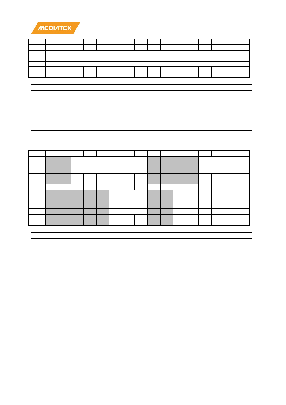
MT7686 Reference Manual
© 2016 - 2017 MediaTek Inc.
Page 329 of 536
This document contains information that is proprietary to MediaTek Inc. (“MediaTek”) and/or its licensor(s).
Any unauthorized use, reproduction or disclosure of this document in whole or in part is strictly prohibited.
t
Bit
15
14
13
12
11
10
9
8
7
6
5
4
3
2
1
0
Nam
e
CPU_PC_VALUE
Type
RO
Rese
t
0 0 0 0 0 0 0 0 0 0 0 0 0 0 0 0
Bit(s)
Name
Description
31:0
CPU_PC_VALUE
This field indicates which command the CPU is running
and is read out by host software to debug what is wrong in
the slave CPU
This register is read only and can only be read out by one command
53, because the whole 32bits makes a valid CPU status and its
content may be updated every AHB clock
When reading this register SDIO AHB clock must exist and it does
not need driver own right
00000158
DSIOCR
DS Pad Macro IO Control Register
000A0422
Bit
31
30
29
28
27
26
25
24
23
22
21
20
19
18
17
16
Nam
e
DS_RDSEL DS_TDSEL
Type
RW
RW
Rese
t
0 0 0 0 0 0 1 0 1 0
Bit
15
14
13
12
11
10
9
8
7
6
5
4
3
2
1
0
Nam
e DS_E8E4E2 DS
_S
MT
DS
_P
UP
D
DS
_R
1
DS
_R
0
DS
_IE
S
DS
_S
R
Type
RW
RW
RW
RW
RW
RW
RW
Rese
t
1 0 0 1 0 0 0 1 0
Bit(s)
Name
Description
29:24
DS_RDSEL
RX duty select
RDSEL[1:0]: Input buffer duty high when asserted (high pulse
width
adjustment)
RDSEL[3:2]: Input buffer duty low when asserted(low pulse width
adjustment)
RDSEL[5:4]: Level shifter duty high when asserted (high pulse
width adjustment)
RDSEL[7:6]: Level shifter duty low when asserted (low pulse width
adjustment)
19:16
DS_TDSEL
TX duty select
TDSEL[1:0]: Output level shifter duty high when asserted (high
pulse width adjustment)
TDSEL[3:2]: Output level shifter duty low when asserted (low pulse
width adjustment)
10:8
DS_E8E4E2
TX Driving Strength Control.
5
DS_SMT
RX input buffer Schmitt trigger hysteresis control enable.
High asserted.
SMT=1, Schmitt Trigger enable
4
DS_PUPD
Pull-up / pull-down selection.
0: pull
-up resistor
1: pull
-down resistor
CLK pad default no pull
3
DS_R1
Select 50K resistor (0: not select, 1: select)
2
DS_R0
Select 10K resistor (0: not select, 1: select)

MT7686 Reference Manual
© 2016 - 2017 MediaTek Inc.
Page 330 of 536
This document contains information that is proprietary to MediaTek Inc. (“MediaTek”) and/or its licensor(s).
Any unauthorized use, reproduction or disclosure of this document in whole or in part is strictly prohibited.
Bit(s)
Name
Description
1
DS_IES
RX input buffer enable. High asserted.
Datapath: from IO to O. IES=0, O=0
0
DS_SR
Output Slew Rate Control. High asserted.
SR=1, slower slew.
SR=0, no slew rate controlled.

MT7686 Reference Manual
© 2016 - 2017 MediaTek Inc.
Page 331 of 536
This document contains information that is proprietary to MediaTek Inc. (“MediaTek”) and/or its licensor(s).
Any unauthorized use, reproduction or disclosure of this document in whole or in part is strictly prohibited.
14. General Purpose Timer
14.1. Overview
The general purpose timer (GPT) includes five 32-bit timers and one 64-bit timer. Each timer has four operation
modes, ONE-SHOT, REPEAT, freerun with interrupt (FREERUN_I), and FREERUN, and can operate on either system
clock (13MHz) or real-time clock (RTC). The GPT is an always-on IP, which means it retains the previous
configuration and runs even if the system enters sleep mode. Note that in sleep mode, the clock source should be
set to RTC since there is no system clock.
14.2. Features
14.2.1. Timer mode
Each GPT has four modes, ONE-SHOT, REPEAT, FREERUN_I, and FREERUN.
• ONE-SHOT mode. An interrupt occurs and the timer stops once GPT is timed out.
• REPEAT mode. An interrupt occurs and the timer resets once GPT is timed out.
• FREERUN_I mode. An interrupt occurs and the timer continues once the GPT is timed out.
• FREERUN mode. The GPT continues counting with no limit.
14.2.2. Timer clock source
Each GPT can operate on either system clock (13MHz) or RTC. There is also a 4-bit clock divider, which divides the
clock by 1, 2, 3, 4, 5, 6, 7, 8, 9, 10, 11, 12, 13, 16, 32, or 64. Note, that in sleep mode, only RTC is available.
14.2.3. Timer interrupt source
All GPTs share a single interrupt source. The user can get the interrupt status by reading GPT_IRQSTA[5:0] and
GPTx_IRQ_STA. To clear the interrupt, write 1 to GPTx_IRQ_ACK.
14.2.4. System wakeup source
The interrupt signal is also connected to System Power Management (SPM) as a wakeup source.
14.3. Limitations
The following operations take two cycles of bus clock (26MHz) plus two cycles of system or RTC clock to take
effect.
• Start GPT
• Stop GPT
• Clear GPT
• Set compare value
Every two clear commands need to be separated by 5 cycles of bus clock and 4 cycles of system or RTC clock.
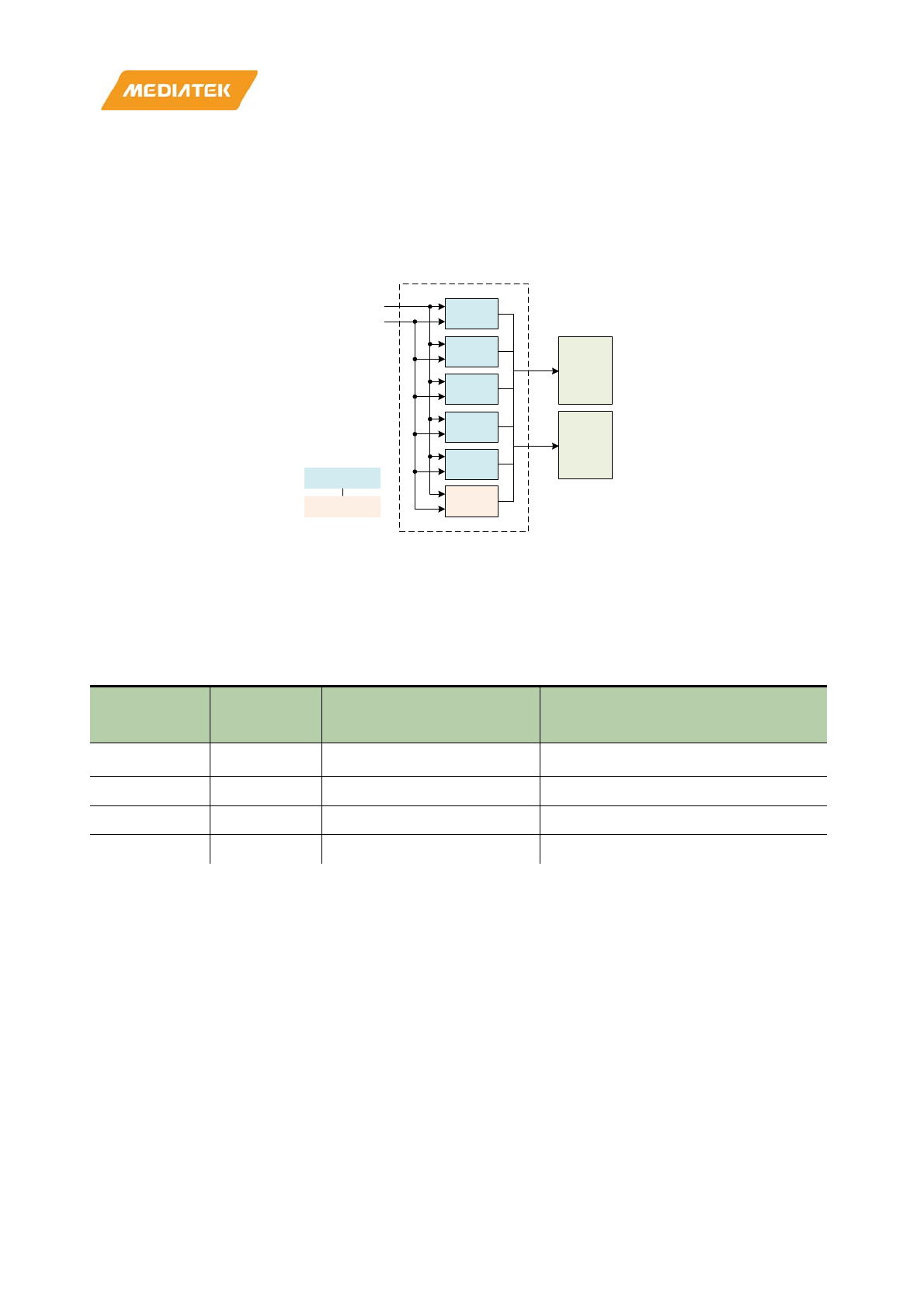
MT7686 Reference Manual
© 2016 - 2017 MediaTek Inc.
Page 332 of 536
This document contains information that is proprietary to MediaTek Inc. (“MediaTek”) and/or its licensor(s).
Any unauthorized use, reproduction or disclosure of this document in whole or in part is strictly prohibited.
Every two set compare value commands need to be separated by 5 cycles of bus clock and 4 cycles of system or
RTC clock.
14.4. Block diagram
The block diagram of the GPT is shown in Figure 14.4-1.
GPT0
GPT1
GPT2
GPT3
GPT4
GPT5
32kHz
13MHz
32bit
64 bit
Sleep
Control
MCU
IRQ
APXGPT
Figure 14.4-1. GPT block diagram
14.5. Functions
The function of each mode is described in Table 14.5-1.
Table 14.5-1. GPT operation modes
Mode Interrupt Reached the limit Example: set GPTx_COMPARE to 2
*Bold means interrupt
ONE-SHOT Yes Stop 0,1,2,2,2,2,2,2,2,2,2,2,…
REPEAT Yes Restart from 0 0,1,2,0,1,2,0,1,2,0,1,2…
FREERUN_I Yes Keep counting 0,1,2,3,4,5,6,7,8,9,10,…
FREERUN No Keep counting 0,1,2,3,4,5,6,7,8,9,10,…
14.6. Programming sequence
The following configuration is required to initialize the GPT settings:
1) Disable GPT clock (GPTx_CON[16]).
2) Set the clock frequency (GPTx_CLK).
• Do not change the clock frequency while clock is enabled.
3) Enable the clock (GPTx_CON[16]).
4) Clear the counter (GPTx_CLR).
5) Set operation mode (GPTx_CON[9:8]).

MT7686 Reference Manual
© 2016 - 2017 MediaTek Inc.
Page 333 of 536
This document contains information that is proprietary to MediaTek Inc. (“MediaTek”) and/or its licensor(s).
Any unauthorized use, reproduction or disclosure of this document in whole or in part is strictly prohibited.
• Do not modify operation mode while GPT is enabled.
6) Enable interrupt (GPTx_IRQ_EN).
7) Set comparison value (GPTx_COMPAREx).
8) Enable the GPT (GPTx_CON[0]).
14.7. Register mapping
Module name: APXGPT base address: (+a2110000h)
Address Name
Width
(bits)
Register Functionality
A2110000
GPT_IRQSTA
32
GPT IRQ status
A2110010
GPT0_CON
32
GPT0 control
A2110014
GPT0_CLR
32
Clear GPT0
A2110018
GPT0_CLK
32
GPT0 clock setting
A211001C
GPT0_IRQ_EN
32
GPT0 IRQ enable
A2110020
GPT0_IRQ_STA
32
GPT0 IRQ status
A2110024
GPT0_IRQ_ACK
32
GPT0 IRQ acknowledgement
A2110028
GPT0_COUNT
32
GPT0 counter value
A211002C
GPT0_COMPARE
32
GPT0 compare value
A2110040
GPT1_CON
32
GPT1 control
A2110044
GPT1_CLR
32
Clear GPT1
A2110048
GPT1_CLK
32
GPT1 clock setting
A211004C
GPT1_IRQ_EN
32
GPT1 IRQ enable
A2110050
GPT1_IRQ_STA
32
GPT1 IRQ status
A2110054
GPT1_IRQ_ACK
32
GPT1 IRQ acknowledgement
A2110058
GPT1_COUNT
32
GPT1 counter value
A211005C
GPT1_COMPARE
32
GPT1 compare value
A2110070
GPT2_CON
32
GPT2 control
A2110074
GPT2_CLR
32
Clear GPT2
A2110078
GPT2_CLK
32
GPT2 clock setting
A211007C
GPT2_IRQ_EN
32
GPT2 IRQ enable
A2110080
GPT2_IRQ_STA
32
GPT2 IRQ status
A2110084
GPT2_IRQ_ACK
32
GPT2 IRQ acknowledgement
A2110088
GPT2_COUNT
32
GPT2 Counter value
A211008C
GPT2_COMPARE
32
GPT2 compare value
A21100A0
GPT3_CON
32
GPT3 control
A21100A4
GPT3_CLR
32
Clear GPT3
A21100A8
GPT3_CLK
32
GPT3 clock setting
A21100AC
GPT3_IRQ_EN
32
GPT3 IRQ enable
A21100B0
GPT3_IRQ_STA
32
GPT3 IRQ status
A21100B4
GPT3_IRQ_ACK
32
GPT3 IRQ acknowledgement
A21100B8
GPT3_COUNT
32
GPT3 counter value
A21100BC
GPT3_COMPARE
32
GPT3 compare value
A21100D0
GPT4_CON
32
GPT4 control
A21100D4
GPT4_CLR
32
Clear GPT4
A21100D8
GPT4_CLK
32
GPT4 clock setting
A21100DC
GPT4_IRQ_EN
32
GPT4 IRQ enable
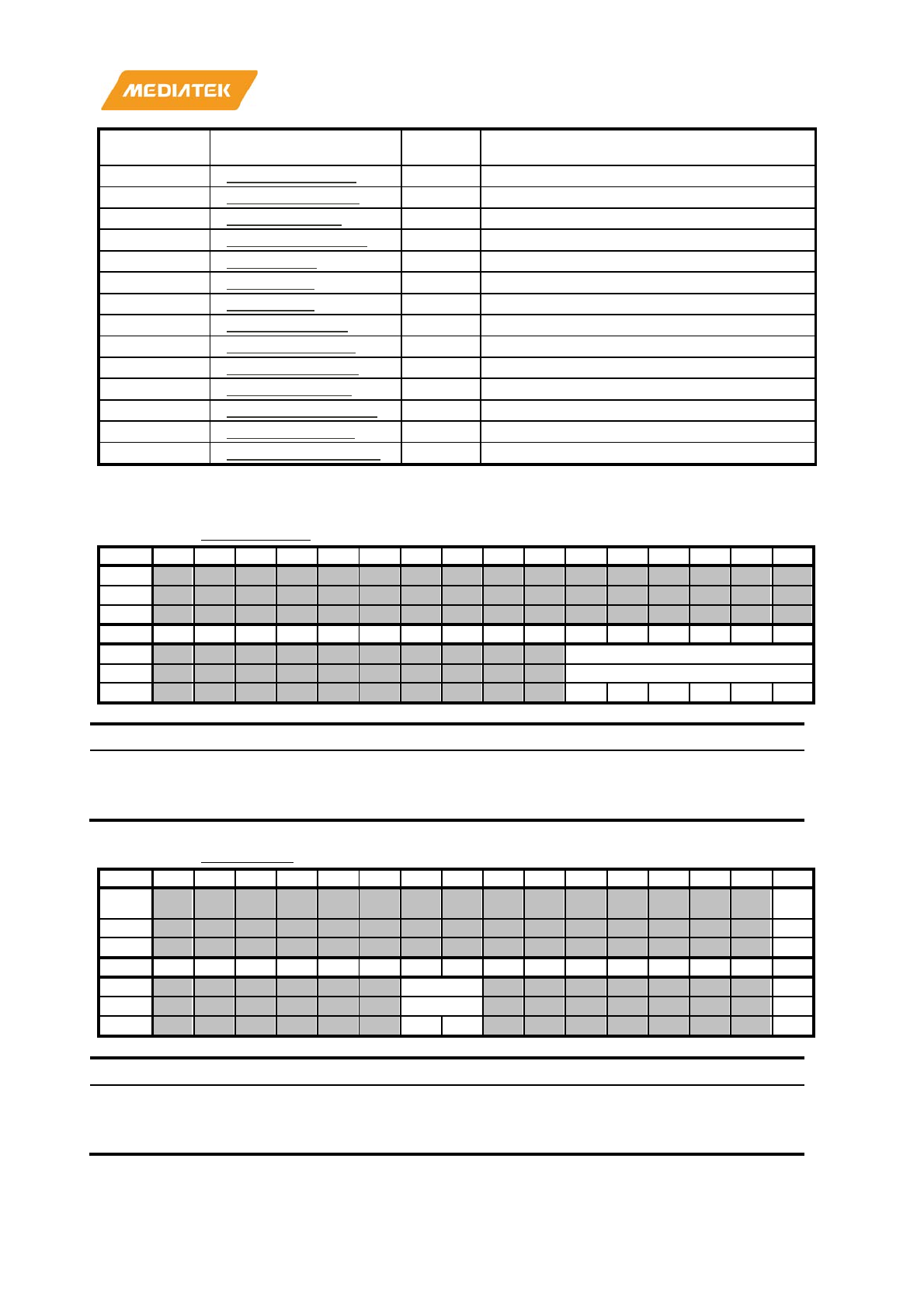
MT7686 Reference Manual
© 2016 - 2017 MediaTek Inc.
Page 334 of 536
This document contains information that is proprietary to MediaTek Inc. (“MediaTek”) and/or its licensor(s).
Any unauthorized use, reproduction or disclosure of this document in whole or in part is strictly prohibited.
Address Name
Width
(bits)
Register Functionality
A21100E0
GPT4_IRQ_STA
32
GPT4 IRQ status
A21100E4
GPT4_IRQ_ACK
32
GPT4 IRQ acknowledgement
A21100E8
GPT4_COUNT
32
GPT4 counter value
A21100EC
GPT4_COMPARE
32
GPT4 compare value
A2110100
GPT5_CON
32
GPT5 control
A2110104
GPT5_CLR
32
Clear GPT5
A2110108
GPT5_CLK
32
GPT5 clock setting
A211010C
GPT5_IRQ_EN
32
GPT5 IRQ enable
A2110110
GPT5_IRQ_STA
32
GPT5 IRQ status
A2110114
GPT5_IRQ_ACK
32
GPT5 IRQ acknowledgement
A2110118
GPT5_COUNTL
32
GPT5 lower word counter value
A211011C
GPT5_COMPAREL
32
GPT5 lower word compare value
A2110120
GPT5_COUNTH
32
GPT5 higher word counter value
A2110124
GPT5_COMPAREH
32
GPT5 higher word compare value
A2110000
GPT_IRQSTA
GPT IRQ Status
00000000
Bit
31
30
29
28
27
26
25
24
23
22
21
20
19
18
17
16
Name
Type
Reset
Bit
15
14
13
12
11
10
9
8
7
6
5
4
3
2
1
0
Name
IRQSTA
Type
RO
Reset
0
0
0
0
0
0
Bit(s)
Name
Description
5:0
IRQSTA
Interrupt status of each GPT
0: No interrupt is generated.
1: Interrupt is
pending and waiting for service.
A2110010
GPT0_CON
GPT0 Control
00010000
Bit
31
30
29
28
27
26
25
24
23
22
21
20
19
18
17
16
Name
SW_
CG0
Type
RW
Reset
1
Bit
15
14
13
12
11
10
9
8
7
6
5
4
3
2
1
0
Name
MODE0
EN0
Type
RW
RW
Reset
0
0
0
Bit(
s)
Name
Description
16
SW_CG0
Enable clock for GPT0
0: Enable
1: Disable
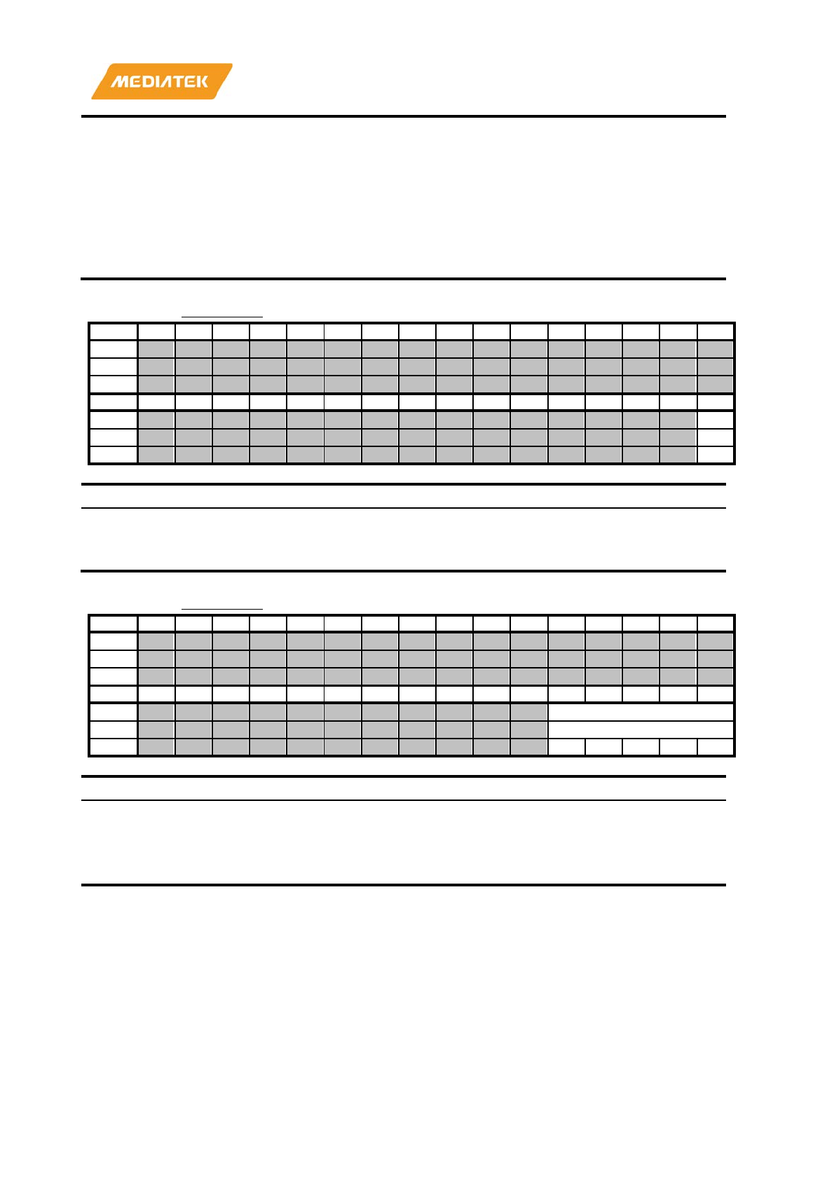
MT7686 Reference Manual
© 2016 - 2017 MediaTek Inc.
Page 335 of 536
This document contains information that is proprietary to MediaTek Inc. (“MediaTek”) and/or its licensor(s).
Any unauthorized use, reproduction or disclosure of this document in whole or in part is strictly prohibited.
9:8
MODE0
Operation mode of GPT0
00: ONE
-SHOT
01: REPEAT
10: FREERUN_I
11: FREERUN
0
EN0
Enable GPT0
0: Disable
1: Enable
A2110014
GPT0_CLR
Clear GPT0
00000000
Bit
31
30
29
28
27
26
25
24
23
22
21
20
19
18
17
16
Name
Type
Reset
Bit
15
14
13
12
11
10
9
8
7
6
5
4
3
2
1
0
Name
CLR0
Type
WO
Reset
0
Bit(s)
Name
Description
0
CLR0
Clear GPT0
0: No effect
1: Clear
A2110018
GPT0_CLK
GPT0 Clock Setting
00000000
Bit
31
30
29
28
27
26
25
24
23
22
21
20
19
18
17
16
Name
Type
Reset
Bit
15
14
13
12
11
10
9
8
7
6
5
4
3
2
1
0
Name
CLK0
Type
RW
Reset
0
0
0
0
0
Bit(s)
Name
Description
4:0
CLK0
Clock source and clock divider for GPT0
Bit[4]
- Clock source:
0: System
clock (13MHz)
1: RTC clock (32kHz)
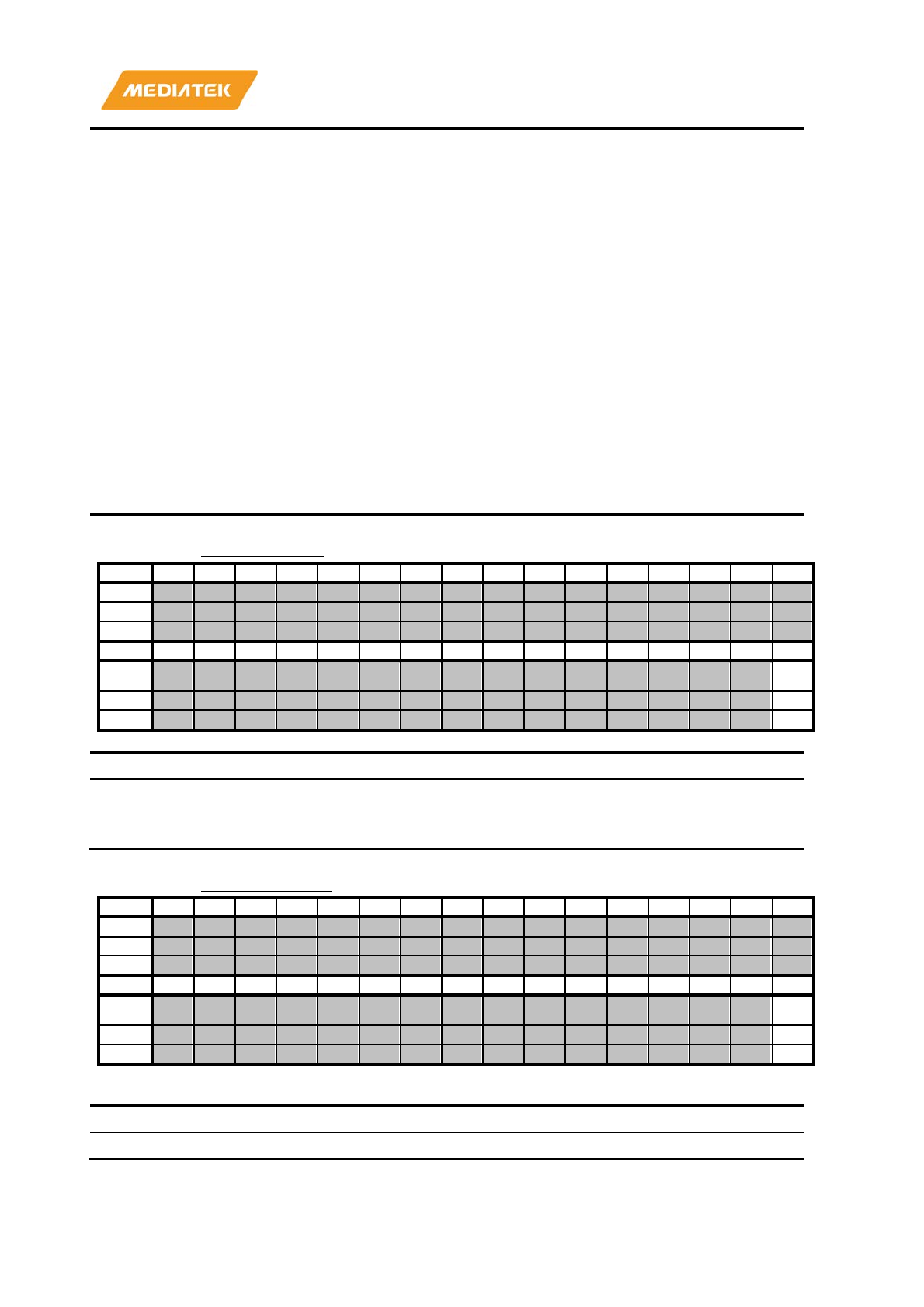
MT7686 Reference Manual
© 2016 - 2017 MediaTek Inc.
Page 336 of 536
This document contains information that is proprietary to MediaTek Inc. (“MediaTek”) and/or its licensor(s).
Any unauthorized use, reproduction or disclosure of this document in whole or in part is strictly prohibited.
Bit[3:0]
- Clock divider:
0000: Clock source divided by 1
0001: Clock source divided by 2
0010: Clock source divided by 3
0011: Clock source divided by 4
0100: Clock source divided by 5
0101: Clock source divided by 6
0110: Clock source divided by 7
0111: Clock source divided by 8
1000: Clock source divided by 9
1001: Clock source divided by 10
1010: Clock source divided by 11
1011: Clock source divided by 12
1100: Clock source divided by 13
1101: Clock source divided b
y 16
1110: Clock source divided by 32
1111: Clock source divided by 64
A211001C
GPT0_IRQ_EN
GPT0 IRQ Enable
00000000
Bit
31
30
29
28
27
26
25
24
23
22
21
20
19
18
17
16
Name
Type
Reset
Bit
15
14
13
12
11
10
9
8
7
6
5
4
3
2
1
0
Name
IRQE
N0
Type
RW
Reset
0
Bit(s)
Name
Description
0
IRQEN0
Enable interrupt of GPT0
0: Disable
1: Enable
A2110020
GPT0_IRQ_STA
GPT0 IRQ Status
00000000
Bit
31
30
29
28
27
26
25
24
23
22
21
20
19
18
17
16
Name
Type
Reset
Bit
15
14
13
12
11
10
9
8
7
6
5
4
3
2
1
0
Name
IRQS
TA0
Type
RO
Reset
0
Bit(s)
Name
Description
0
IRQSTA0
Interrupt status of GPT0
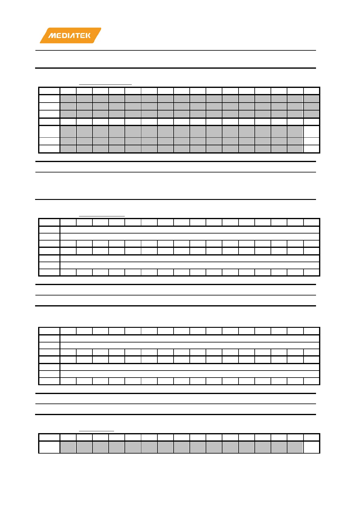
MT7686 Reference Manual
© 2016 - 2017 MediaTek Inc.
Page 337 of 536
This document contains information that is proprietary to MediaTek Inc. (“MediaTek”) and/or its licensor(s).
Any unauthorized use, reproduction or disclosure of this document in whole or in part is strictly prohibited.
0: No interrupt is generated
1: Interrupt is pending and waiting for service
A2110024
GPT0_IRQ_ACK
GPT0 IRQ Acknowledgement
00000000
Bit
31
30
29
28
27
26
25
24
23
22
21
20
19
18
17
16
Name
Type
Reset
Bit
15
14
13
12
11
10
9
8
7
6
5
4
3
2
1
0
Name
IRQA
CK0
Type
WO
Reset
0
Bit(
s)
Name
Description
0
IRQACK0
Interrupt acknowledgement for GPT0
0: No effect
1: Interrupt is acknowledged and should be relinquished
A2110028
GPT0_COUNT
GPT0 Counter Value
00000000
Bit
31
30
29
28
27
26
25
24
23
22
21
20
19
18
17
16
Name
COUNTER0
Type
RO
Reset
0
0
0
0
0
0
0
0
0
0
0
0
0
0
0
0
Bit
15
14
13
12
11
10
9
8
7
6
5
4
3
2
1
0
Name
COUNTER0
Type
RO
Reset
0
0
0
0
0
0
0
0
0
0
0
0
0
0
0
0
Bit(s)
Name
Description
31:0
COUNTER0
Counter value of GPT0
A211002C
GPT0_COMPARE
GPT0 Compare Value
FFFFFFFF
Bit
31
30
29
28
27
26
25
24
23
22
21
20
19
18
17
16
Name
COMPARE0
Type
RW
Reset
1
1
1
1
1
1
1
1
1
1
1
1
1
1
1
1
Bit
15
14
13
12
11
10
9
8
7
6
5
4
3
2
1
0
Name
COMPARE0
Type
RW
Reset
1
1
1
1
1
1
1
1
1
1
1
1
1
1
1
1
Bit(s)
Name
Description
31:0
COMPARE0
Compare value of GPT0
A2110040
GPT1_CON
GPT1 Control
00010000
Bit
31
30
29
28
27
26
25
24
23
22
21
20
19
18
17
16
Name
SW_
CG1
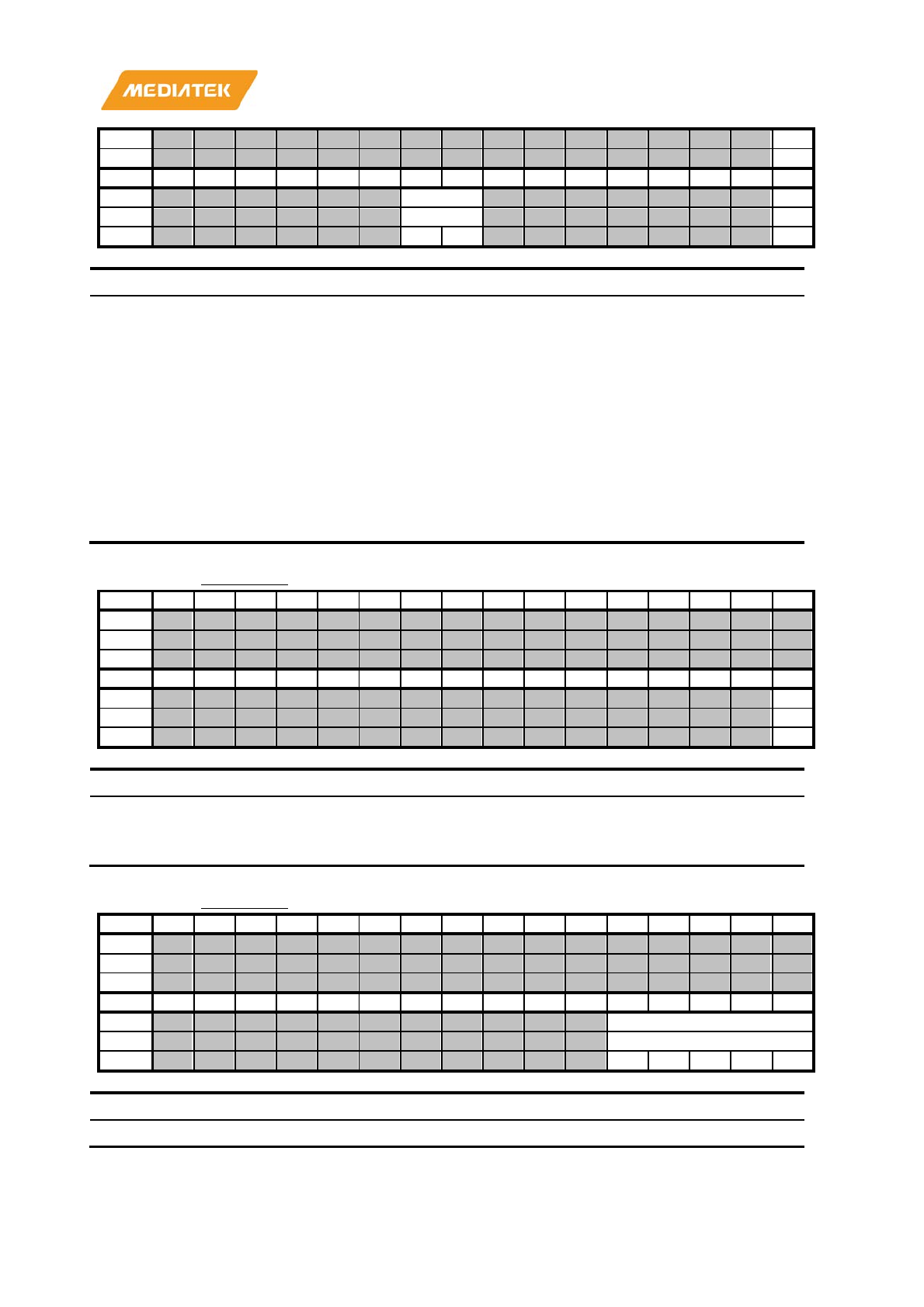
MT7686 Reference Manual
© 2016 - 2017 MediaTek Inc.
Page 338 of 536
This document contains information that is proprietary to MediaTek Inc. (“MediaTek”) and/or its licensor(s).
Any unauthorized use, reproduction or disclosure of this document in whole or in part is strictly prohibited.
Type
RW
Reset
1
Bit
15
14
13
12
11
10
9
8
7
6
5
4
3
2
1
0
Name
MODE1
EN1
Type
RW
RW
Reset
0
0
0
Bit(s)
Name
Description
16
SW_CG1
Enable clock for GPT1
0: Enable
1: Disable
9:8
MODE1
Operation mode of GPT1
00: ONE
-SHOT
01: REPEAT
10: FREERUN_I
11: FREERUN
0
EN1
Enable GPT1
0: Disable
1: Enable
A2110044
GPT1_CLR
Clear
GPT1
00000000
Bit
31
30
29
28
27
26
25
24
23
22
21
20
19
18
17
16
Name
Type
Reset
Bit
15
14
13
12
11
10
9
8
7
6
5
4
3
2
1
0
Name
CLR1
Type
WO
Reset
0
Bit(s)
Name
Description
0
CLR1
Clear GPT1
0: No effect
1: Clear
A2110048
GPT1_CLK
GPT1 Clock Setting
00000000
Bit
31
30
29
28
27
26
25
24
23
22
21
20
19
18
17
16
Name
Type
Reset
Bit
15
14
13
12
11
10
9
8
7
6
5
4
3
2
1
0
Name
CLK1
Type
RW
Reset
0
0
0
0
0
Bit(s)
Name
Description
4:0
CLK1
Clock source & clock divider for GPT1
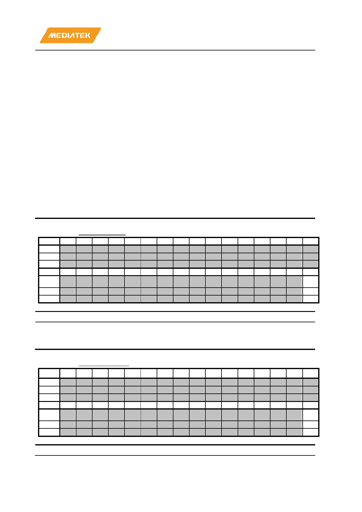
MT7686 Reference Manual
© 2016 - 2017 MediaTek Inc.
Page 339 of 536
This document contains information that is proprietary to MediaTek Inc. (“MediaTek”) and/or its licensor(s).
Any unauthorized use, reproduction or disclosure of this document in whole or in part is strictly prohibited.
Bit[4] - Clock source:
0: System clock
(13MHz)
1: RTC clock (32kHz)
Bit[3:0]
- Clock divider:
0000: Clock source divided by 1
0001: Clock source divided by 2
0010: Clock source divided by 3
0011: Clock source divided by 4
0100: Clock source divided by 5
0101: Clock source divided by 6
0110:
Clock source divided by 7
0111: Clock source divided by 8
1000: Clock source divided by 9
1001: Clock source divided by 10
1010: Clock source divided by 11
1011: Clock source divided by 12
1100: Clock source divided by 13
1101: Clock source divided by 16
1
110: Clock source divided by 32
1111: Clock source divided by 64
A211004C
GPT1_IRQ_EN
GPT1 IRQ Enable
00000000
Bit
31
30
29
28
27
26
25
24
23
22
21
20
19
18
17
16
Name
Type
Reset
Bit
15
14
13
12
11
10
9
8
7
6
5
4
3
2
1
0
Name
IRQE
N1
Type
RW
Reset
0
Bit(s)
Name
Description
0
IRQEN1
Enable interrupt of GPT1
0: Disable
1: Enable
A2110050
GPT1_IRQ_STA
GPT1 IRQ Status
00000000
Bit
31
30
29
28
27
26
25
24
23
22
21
20
19
18
17
16
Name
Type
Reset
Bit
15
14
13
12
11
10
9
8
7
6
5
4
3
2
1
0
Name
IRQS
TA1
Type
RO
Reset
0
Bit(s)
Name
Description

MT7686 Reference Manual
© 2016 - 2017 MediaTek Inc.
Page 340 of 536
This document contains information that is proprietary to MediaTek Inc. (“MediaTek”) and/or its licensor(s).
Any unauthorized use, reproduction or disclosure of this document in whole or in part is strictly prohibited.
0
IRQSTA1
Interrupt status of GPT1
0: No interrupt is generated.
1: Interrupt is pending and waiting for service.
A2110054
GPT1_IRQ_ACK
GPT1 IRQ Acknowledgement
00000000
Bit
31
30
29
28
27
26
25
24
23
22
21
20
19
18
17
16
Name
Type
Reset
Bit
15
14
13
12
11
10
9
8
7
6
5
4
3
2
1
0
Name
IRQA
CK1
Type
WO
Reset
0
Bit(s)
Name
Description
0
IRQACK1
Interrupt acknowledgement for GPT1
0: No effect
1: Interrupt is acknowledged and should be relinquished
A2110058
GPT1_COUNT
GPT1 Counter Value
00000000
Bit
31
30
29
28
27
26
25
24
23
22
21
20
19
18
17
16
Name
COUNTER1
Type
RO
Reset
0
0
0
0
0
0
0
0
0
0
0
0
0
0
0
0
Bit
15
14
13
12
11
10
9
8
7
6
5
4
3
2
1
0
Name
COUNTER1
Type
RO
Reset
0
0
0
0
0
0
0
0
0
0
0
0
0
0
0
0
Bit(s)
Name
Description
31:0
COUNTER1
Counter value
of GPT1
A211005C
GPT1_COMPARE
GPT1 Compare Value
FFFFFFFF
Bit
31
30
29
28
27
26
25
24
23
22
21
20
19
18
17
16
Name
COMPARE1
Type
RW
Reset
1
1
1
1
1
1
1
1
1
1
1
1
1
1
1
1
Bit
15
14
13
12
11
10
9
8
7
6
5
4
3
2
1
0
Name
COMPARE1
Type
RW
Reset
1
1
1
1
1
1
1
1
1
1
1
1
1
1
1
1
Bit(s)
Name
Description
31:0
COMPARE1
Compare value of GPT1
A2110070
GPT2_CON
GPT2 Control
00010000
Bit
31
30
29
28
27
26
25
24
23
22
21
20
19
18
17
16
Name
SW_

MT7686 Reference Manual
© 2016 - 2017 MediaTek Inc.
Page 341 of 536
This document contains information that is proprietary to MediaTek Inc. (“MediaTek”) and/or its licensor(s).
Any unauthorized use, reproduction or disclosure of this document in whole or in part is strictly prohibited.
CG2
Type
RW
Reset
1
Bit
15
14
13
12
11
10
9
8
7
6
5
4
3
2
1
0
Name
MODE2
EN2
Type
RW
RW
Reset
0
0
0
Bit(s)
Name
Description
16
SW_CG2
Enable clock for GPT2
0: Enable
1: Disable
9:8
MODE2
Operation mode of GPT2
00: ONE
-SHOT
01: REPEAT
10: FREERUN_I
11: FREERUN
0
EN2
Enable GPT2
0: Disable
1: Enable
A2110074
GPT2_CLR
Clear
GPT2
00000000
Bit
31
30
29
28
27
26
25
24
23
22
21
20
19
18
17
16
Name
Type
Reset
Bit
15
14
13
12
11
10
9
8
7
6
5
4
3
2
1
0
Name
CLR2
Type
WO
Reset
0
Bit(s)
Name
Description
0
CLR2
Clear GPT2
0: No effect
1: Clear
A2110078
GPT2_CLK
GPT2 Clock Setting
00000000
Bit
31
30
29
28
27
26
25
24
23
22
21
20
19
18
17
16
Name
Type
Reset
Bit
15
14
13
12
11
10
9
8
7
6
5
4
3
2
1
0
Name
CLK2
Type
RW
Reset
0
0
0
0
0
Bit(s)
Name
Description
4:0
CLK2
Clock source & clock divider for GPT2

MT7686 Reference Manual
© 2016 - 2017 MediaTek Inc.
Page 342 of 536
This document contains information that is proprietary to MediaTek Inc. (“MediaTek”) and/or its licensor(s).
Any unauthorized use, reproduction or disclosure of this document in whole or in part is strictly prohibited.
Bit[4] - Clock source:
0: System clock
(13MHz)
1: RTC clock (32KHz)
Bit[3:0]
- Clock divider:
0000: Clock source divided by 1
0001: Clock source divided by 2
0010: Clock source divided by 3
0011: Clock source divided by 4
0100: Clock source divided by 5
0101: Clock source divided by 6
0110:
Clock source divided by 7
0111: Clock source divided by 8
1000: Clock source divided by 9
1001: Clock source divided by 10
1010: Clock source divided by 11
1011: Clock source divided by 12
1100: Clock source divided by 13
1101: Clock source divided by 16
1
110: Clock source divided by 32
1111: Clock source divided by 64
A211007C
GPT2_IRQ_EN
GPT2 IRQ Enable
00000000
Bit
31
30
29
28
27
26
25
24
23
22
21
20
19
18
17
16
Name
Type
Reset
Bit
15
14
13
12
11
10
9
8
7
6
5
4
3
2
1
0
Name
IRQE
N2
Type
RW
Reset
0
Bit(s)
Name
Description
0
IRQEN2
Enable interrupt of GPT2
0: Disable
1: Enable
A2110080
GPT2_IRQ_STA
GPT2 IRQ Status
00000000
Bit
31
30
29
28
27
26
25
24
23
22
21
20
19
18
17
16
Name
Type
Reset
Bit
15
14
13
12
11
10
9
8
7
6
5
4
3
2
1
0
Name
IRQS
TA2
Type
RO
Reset
0
Bit(s)
Name
Description

MT7686 Reference Manual
© 2016 - 2017 MediaTek Inc.
Page 343 of 536
This document contains information that is proprietary to MediaTek Inc. (“MediaTek”) and/or its licensor(s).
Any unauthorized use, reproduction or disclosure of this document in whole or in part is strictly prohibited.
0
IRQSTA2
Interrupt status of GPT2
0: No interrupt is generated.
1: Interrupt is pending and waiting for service.
A2110084
GPT2_IRQ_ACK
GPT2 IRQ Acknowledgement
00000000
Bit
31
30
29
28
27
26
25
24
23
22
21
20
19
18
17
16
Name
Type
Reset
Bit
15
14
13
12
11
10
9
8
7
6
5
4
3
2
1
0
Name
IRQA
CK2
Type
WO
Reset
0
Bit(s)
Name
Description
0
IRQACK2
Interrupt acknowledgement for GPT2
0: No effect
1: Interrupt is acknowledged and should be relinquished
A2110088
GPT2_COUNT
GPT2 Counter Value
00000000
Bit
31
30
29
28
27
26
25
24
23
22
21
20
19
18
17
16
Name
COUNTER2
Type
RO
Reset
0
0
0
0
0
0
0
0
0
0
0
0
0
0
0
0
Bit
15
14
13
12
11
10
9
8
7
6
5
4
3
2
1
0
Name
COUNTER2
Type
RO
Reset
0
0
0
0
0
0
0
0
0
0
0
0
0
0
0
0
Bit(s)
Name
Description
31:0
COUNTER2
Counter value
of GPT2
A211008C
GPT2_COMPARE
GPT2 Compare Value
FFFFFFFF
Bit
31
30
29
28
27
26
25
24
23
22
21
20
19
18
17
16
Name
COMPARE2
Type
RW
Reset
1
1
1
1
1
1
1
1
1
1
1
1
1
1
1
1
Bit
15
14
13
12
11
10
9
8
7
6
5
4
3
2
1
0
Name
COMPARE2
Type
RW
Reset
1
1
1
1
1
1
1
1
1
1
1
1
1
1
1
1
Bit(s)
Name
Description
31:0
COMPARE2
Compare value of GPT2
A21100A0
GPT3_CON
GPT3 Control
00010000
Bit
31
30
29
28
27
26
25
24
23
22
21
20
19
18
17
16
Name
SW_

MT7686 Reference Manual
© 2016 - 2017 MediaTek Inc.
Page 344 of 536
This document contains information that is proprietary to MediaTek Inc. (“MediaTek”) and/or its licensor(s).
Any unauthorized use, reproduction or disclosure of this document in whole or in part is strictly prohibited.
CG3
Type
RW
Reset
1
Bit
15
14
13
12
11
10
9
8
7
6
5
4
3
2
1
0
Name
MODE3
EN3
Type
RW
RW
Reset
0
0
0
Bit(
s)
Name
Description
16
SW_CG3
Enable clock for GPT3
0: Enable
1: Disable
9:8
MODE3
Operation mode of GPT3
00: ONE
-SHOT
01: REPEAT
10: FREERUN_I
11: FREERUN
0
EN3
Enable GPT3
0: Disable
1: Enable
A21100A4
GPT3_CLR
Clear GPT3
00000000
Bit
31
30
29
28
27
26
25
24
23
22
21
20
19
18
17
16
Name
Type
Reset
Bit
15
14
13
12
11
10
9
8
7
6
5
4
3
2
1
0
Name
CLR3
Type
WO
Reset
0
Bit(s)
Name
Description
0
CLR3
Clear GPT3
0: No effect
1: Clear
A21100A8
GPT3_CLK
GPT3 Clock Setting
00000000
Bit
31
30
29
28
27
26
25
24
23
22
21
20
19
18
17
16
Name
Type
Reset
Bit
15
14
13
12
11
10
9
8
7
6
5
4
3
2
1
0
Name
CLK3
Type
RW
Reset
0
0
0
0
0
Bit(s)
Name
Description
4:0
CLK3
Clock source and clock divider for GPT3

MT7686 Reference Manual
© 2016 - 2017 MediaTek Inc.
Page 345 of 536
This document contains information that is proprietary to MediaTek Inc. (“MediaTek”) and/or its licensor(s).
Any unauthorized use, reproduction or disclosure of this document in whole or in part is strictly prohibited.
Bit[4] - Clock source:
0: System clock
(13MHz)
1: RTC clock (32KHz)
Bit[3:0]
- Clock divider:
0000: Clock source divided by 1
0001: Clock source divided by 2
0010: Clock source divided by 3
0011: Clock source divided by 4
0100: Clock source divided by 5
0101: Clock source divided by 6
0110:
Clock source divided by 7
0111: Clock source divided by 8
1000: Clock source divided by 9
1001: Clock source divided by 10
1010: Clock source divided by 11
1011: Clock source divided by 12
1100: Clock source divided by 13
1101: Clock source divided by 16
1
110: Clock source divided by 32
1111: Clock source divided by 64
A21100AC
GPT3_IRQ_EN
GPT3 IRQ Enable
00000000
Bit
31
30
29
28
27
26
25
24
23
22
21
20
19
18
17
16
Name
Type
Reset
Bit
15
14
13
12
11
10
9
8
7
6
5
4
3
2
1
0
Name
IRQE
N3
Type
RW
Reset
0
Bit(s)
Name
Description
0
IRQEN3
Enable interrupt of GPT3
0: Disable
1: Enable
A21100B0
GPT3_IRQ_STA
GPT3 IRQ Status
00000000
Bit
31
30
29
28
27
26
25
24
23
22
21
20
19
18
17
16
Name
Type
Reset
Bit
15
14
13
12
11
10
9
8
7
6
5
4
3
2
1
0
Name
IRQS
TA3
Type
RO
Reset
0
Bit(
s)
Name
Description
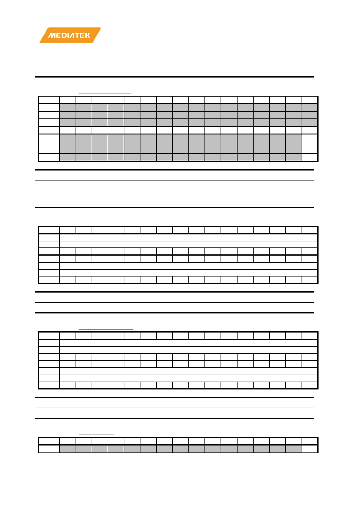
MT7686 Reference Manual
© 2016 - 2017 MediaTek Inc.
Page 346 of 536
This document contains information that is proprietary to MediaTek Inc. (“MediaTek”) and/or its licensor(s).
Any unauthorized use, reproduction or disclosure of this document in whole or in part is strictly prohibited.
0
IRQSTA3
Interrupt status of GPT3
0: No interrupt is generated
1: Interrupt is pending and waiting for service
A21100B4
GPT3_IRQ_ACK
GPT3 IRQ Acknowledgement
00000000
Bit
31
30
29
28
27
26
25
24
23
22
21
20
19
18
17
16
Name
Type
Reset
Bit
15
14
13
12
11
10
9
8
7
6
5
4
3
2
1
0
Name
IRQA
CK3
Type
WO
Reset
0
Bit(s)
Name
Description
0
IRQACK3
Interrupt acknowledgement for GPT3
0: No effect
1: Interrupt is acknowledged and should be relinquished
A21100B8
GPT3_COUNT
GPT3 Counter Value
00000000
Bit
31
30
29
28
27
26
25
24
23
22
21
20
19
18
17
16
Name
COUNTER3
Type
RO
Reset
0
0
0
0
0
0
0
0
0
0
0
0
0
0
0
0
Bit
15
14
13
12
11
10
9
8
7
6
5
4
3
2
1
0
Name
COUNTER3
Type
RO
Reset
0
0
0
0
0
0
0
0
0
0
0
0
0
0
0
0
Bit(s)
Name
Description
31:0
COUNTER3
Counter value
of GPT3
A21100BC
GPT3_COMPARE
GPT3 Compare Value
FFFFFFFF
Bit
31
30
29
28
27
26
25
24
23
22
21
20
19
18
17
16
Name
COMPARE3
Type
RW
Reset
1
1
1
1
1
1
1
1
1
1
1
1
1
1
1
1
Bit
15
14
13
12
11
10
9
8
7
6
5
4
3
2
1
0
Name
COMPARE3
Type
RW
Reset
1
1
1
1
1
1
1
1
1
1
1
1
1
1
1
1
Bit(s)
Name
Description
31:0
COMPARE3
Compare value of GPT3
A21100D0
GPT4_CON
GPT4 Control
00000000
Bit
31
30
29
28
27
26
25
24
23
22
21
20
19
18
17
16
Name
SW_
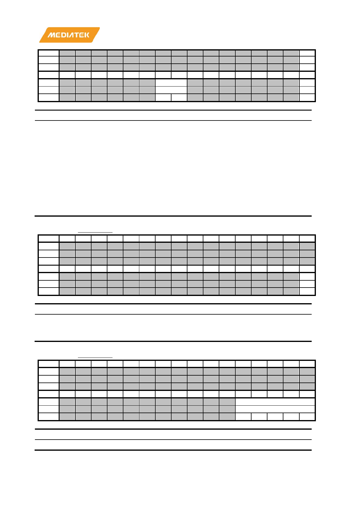
MT7686 Reference Manual
© 2016 - 2017 MediaTek Inc.
Page 347 of 536
This document contains information that is proprietary to MediaTek Inc. (“MediaTek”) and/or its licensor(s).
Any unauthorized use, reproduction or disclosure of this document in whole or in part is strictly prohibited.
CG4
Type
RW
Reset
0
Bit
15
14
13
12
11
10
9
8
7
6
5
4
3
2
1
0
Name
MODE4
EN4
Type
RW
RW
Reset
0
0
0
Bit(s)
Name
Description
16
SW_CG4
Enable clock for GPT4
0: Enable
1: Disable
9:8
MODE4
Operation mode of GPT4
00: ONE
-SHOT
01: REPEAT
10: FREERUN_I
11: FREERUN
0
EN4
Enable GPT4
0: Disable
1: Enable
A21100D4
GPT4_CLR
Clear
GPT4
00000000
Bit
31
30
29
28
27
26
25
24
23
22
21
20
19
18
17
16
Name
Type
Reset
Bit
15
14
13
12
11
10
9
8
7
6
5
4
3
2
1
0
Name
CLR4
Type
WO
Reset
0
Bit(s)
Name
Description
0
CLR4
Clear GPT4
0: No effect
1: Clear
A21100D8
GPT4_CLK
GPT4 Clock Setting
00000000
Bit
31
30
29
28
27
26
25
24
23
22
21
20
19
18
17
16
Name
Type
Reset
Bit
15
14
13
12
11
10
9
8
7
6
5
4
3
2
1
0
Name
CLK4
Type
RW
Reset
0
0
0
0
0
Bit(s)
Name
Description
4:0
CLK4
Clock source and clock divider for GPT4
MT7686 Reference Manual
© 2016 - 2017 MediaTek Inc.
Page 348 of 536
This document contains information that is proprietary to MediaTek Inc. (“MediaTek”) and/or its licensor(s).
Any unauthorized use, reproduction or disclosure of this document in whole or in part is strictly prohibited.
Bit[4] - Clock source:
0: System clock
(13MHz)
1: RTC clock (32KHz)
Bit[3:0]
- Clock divider:
0000: Clock source divided by 1
0001: Clock source divided by 2
0010: Clock source divided by 3
0011: Clock source divided by 4
0100: Clock source divided by 5
0101: Clock source divided by 6
0110:
Clock source divided by 7
0111: Clock source divided by 8
1000: Clock source divided by 9
1001: Clock source divided by 10
1010: Clock source divided by 11
1011: Clock source divided by 12
1100: Clock source divided by 13
1101: Clock source divided by 16
1
110: Clock source divided by 32
1111: Clock source divided by 64
A21100DC
GPT4_IRQ_EN
GPT4 IRQ Enable
00000000
Bit
31
30
29
28
27
26
25
24
23
22
21
20
19
18
17
16
Name
Type
Reset
Bit
15
14
13
12
11
10
9
8
7
6
5
4
3
2
1
0
Name
IRQE
N4
Type
RW
Reset
0
Bit(s)
Name
Description
0
IRQEN4
Enable interrupt of GPT4
0: Disable
1: Enable
A21100E0
GPT4_IRQ_STA
GPT4 IRQ Status
00000000
Bit
31
30
29
28
27
26
25
24
23
22
21
20
19
18
17
16
Name
Type
Reset
Bit
15
14
13
12
11
10
9
8
7
6
5
4
3
2
1
0
Name
IRQS
TA4
Type
RO
Reset
0
Bit(s)
Name
Description

MT7686 Reference Manual
© 2016 - 2017 MediaTek Inc.
Page 349 of 536
This document contains information that is proprietary to MediaTek Inc. (“MediaTek”) and/or its licensor(s).
Any unauthorized use, reproduction or disclosure of this document in whole or in part is strictly prohibited.
0
IRQSTA4
Interrupt status of GPT4
0: No interrupt is generated
1: Interrupt is pending and waiting for service
A21100E4
GPT4_IRQ_ACK
GPT4 IRQ Acknowledgement
00000000
Bit
31
30
29
28
27
26
25
24
23
22
21
20
19
18
17
16
Name
Type
Reset
Bit
15
14
13
12
11
10
9
8
7
6
5
4
3
2
1
0
Name
IRQA
CK4
Type
WO
Reset
0
Bit(s)
Name
Description
0
IRQACK4
Interrupt acknowledgement for GPT4
0: No effect
1: Interrupt is acknowledged and should be relinquished
A21100E8
GPT4_COUNT
GPT4 Counter Value
00000000
Bit
31
30
29
28
27
26
25
24
23
22
21
20
19
18
17
16
Name
COUNTER4
Type
RO
Reset
0
0
0
0
0
0
0
0
0
0
0
0
0
0
0
0
Bit
15
14
13
12
11
10
9
8
7
6
5
4
3
2
1
0
Name
COUNTER4
Type
RO
Reset
0
0
0
0
0
0
0
0
0
0
0
0
0
0
0
0
Bit(s)
Name
Description
31:0
COUNTER4
Counter value
of GPT4
A21100EC
GPT4_COMPARE
GPT4 Compare Value
FFFFFFFF
Bit
31
30
29
28
27
26
25
24
23
22
21
20
19
18
17
16
Name
COMPARE4
Type
RW
Reset
1
1
1
1
1
1
1
1
1
1
1
1
1
1
1
1
Bit
15
14
13
12
11
10
9
8
7
6
5
4
3
2
1
0
Name
COMPARE4
Type
RW
Reset
1
1
1
1
1
1
1
1
1
1
1
1
1
1
1
1
Bit(s)
Name
Description
31:0
COMPARE4
Compare value of GPT4
A2110100
GPT5_CON
GPT5 Control
00010000
Bit
31
30
29
28
27
26
25
24
23
22
21
20
19
18
17
16
Name
SW_

MT7686 Reference Manual
© 2016 - 2017 MediaTek Inc.
Page 350 of 536
This document contains information that is proprietary to MediaTek Inc. (“MediaTek”) and/or its licensor(s).
Any unauthorized use, reproduction or disclosure of this document in whole or in part is strictly prohibited.
CG5
Type
RW
Reset
1
Bit
15
14
13
12
11
10
9
8
7
6
5
4
3
2
1
0
Name
MODE5
EN5
Type
RW
RW
Reset
0
0
0
Bit(s)
Name
Description
16
SW_CG5
Enable clock for GPT5
0: Enable
1: Disable
9:8
MODE5
Operation mode of GPT5
00: ONE
-SHOT
01: REPEAT
10: FREERUN_I
11: FREERUN
0
EN5
Enable GPT5
0: Disable
1: Enable
A2110104
GPT5_CLR
Clear
GPT5
00000000
Bit
31
30
29
28
27
26
25
24
23
22
21
20
19
18
17
16
Name
Type
Reset
Bit
15
14
13
12
11
10
9
8
7
6
5
4
3
2
1
0
Name
CLR5
Type
WO
Reset
0
Bit(s)
Name
Description
0
CLR5
Clear GPT5
0: No effect
1: Clear
A2110108
GPT5_CLK
GPT5 Clock Setting
00000000
Bit
31
30
29
28
27
26
25
24
23
22
21
20
19
18
17
16
Name
Type
Reset
Bit
15
14
13
12
11
10
9
8
7
6
5
4
3
2
1
0
Name
CLK5
Type
RW
Reset
0
0
0
0
0
Bit(s)
Name
Description
4:0
CLK5
Clock source & clock divider for GPT5

MT7686 Reference Manual
© 2016 - 2017 MediaTek Inc.
Page 351 of 536
This document contains information that is proprietary to MediaTek Inc. (“MediaTek”) and/or its licensor(s).
Any unauthorized use, reproduction or disclosure of this document in whole or in part is strictly prohibited.
Bit[4] - Clock source:
0: System clock
(13MHz)
1: RTC clock (32KHz)
Bit[3:0]
- Clock divider:
0000: Clock source divided by 1
0001: Clock source divided by 2
0010: Clock source divided by 3
0011: Clock source divided by 4
0100: Clock source divided by 5
0101: Clock source divided by 6
0110:
Clock source divided by 7
0111: Clock source divided by 8
1000: Clock source divided by 9
1001: Clock source divided by 10
1010: Clock source divided by 11
1011: Clock source divided by 12
1100: Clock source divided by 13
1101: Clock source divided by 16
1
110: Clock source divided by 32
1111: Clock source divided by 64
A211010C
GPT5_IRQ_EN
GPT5 IRQ Enable
00000000
Bit
31
30
29
28
27
26
25
24
23
22
21
20
19
18
17
16
Name
Type
Reset
Bit
15
14
13
12
11
10
9
8
7
6
5
4
3
2
1
0
Name
IRQE
N5
Type
RW
Reset
0
Bit(s)
Name
Description
0
IRQEN5
Enable interrupt of GPT5
0: Disable
1: Enable
A2110110
GPT5_IRQ_STA
GPT5 IRQ Status
00000000
Bit
31
30
29
28
27
26
25
24
23
22
21
20
19
18
17
16
Name
Type
Reset
Bit
15
14
13
12
11
10
9
8
7
6
5
4
3
2
1
0
Name
IRQS
TA5
Type
RO
Reset
0
Bit(s)
Name
Description
MT7686 Reference Manual
© 2016 - 2017 MediaTek Inc.
Page 352 of 536
This document contains information that is proprietary to MediaTek Inc. (“MediaTek”) and/or its licensor(s).
Any unauthorized use, reproduction or disclosure of this document in whole or in part is strictly prohibited.
0
IRQSTA5
Interrupt status of GPT5
0: No interrupt is generated.
1: Interrupt is pending and waiting for service.
A2110114
GPT5_IRQ_ACK
GPT5 IRQ Acknowledgement
00000000
Bit
31
30
29
28
27
26
25
24
23
22
21
20
19
18
17
16
Name
Type
Reset
Bit
15
14
13
12
11
10
9
8
7
6
5
4
3
2
1
0
Name
IRQA
CK5
Type
WO
Reset
0
Bit(s)
Name
Description
0
IRQACK5
Interrupt acknowledgement for GPT5
0: No effect
1: Interrupt is acknowledged and should be relinquished
A2110118
GPT5_COUNTL
GPT5 Lower Word Counter Value
00000000
Bit
31
30
29
28
27
26
25
24
23
22
21
20
19
18
17
16
Name
COUNTER5L
Type
RO
Reset
0
0
0
0
0
0
0
0
0
0
0
0
0
0
0
0
Bit
15
14
13
12
11
10
9
8
7
6
5
4
3
2
1
0
Name
COUNTER5L
Type
RO
Reset
0
0
0
0
0
0
0
0
0
0
0
0
0
0
0
0
Bit(s)
Name
Description
31:0
COUNTER5L
Lower word counter value of GPT5
A211011C
GPT5_COMPAREL
GPT5 Lower WordCompare Value
FFFFFFFF
Bit
31
30
29
28
27
26
25
24
23
22
21
20
19
18
17
16
Name
COMPARE5L
Type
RW
Reset
1
1
1
1
1
1
1
1
1
1
1
1
1
1
1
1
Bit
15
14
13
12
11
10
9
8
7
6
5
4
3
2
1
0
Name
COMPARE5L
Type
RW
Reset
1
1
1
1
1
1
1
1
1
1
1
1
1
1
1
1
Bit(s)
Name
Description
31:0
COMPARE5L
Lower word compare value of GPT5
A2110120
GPT5_COUNTH
GPT5 Higher Word Counter Value
00000000
Bit
31
30
29
28
27
26
25
24
23
22
21
20
19
18
17
16
Name
COUNTER5H
MT7686 Reference Manual
© 2016 - 2017 MediaTek Inc.
Page 353 of 536
This document contains information that is proprietary to MediaTek Inc. (“MediaTek”) and/or its licensor(s).
Any unauthorized use, reproduction or disclosure of this document in whole or in part is strictly prohibited.
Type
RO
Reset
0
0
0
0
0
0
0
0
0
0
0
0
0
0
0
0
Bit
15
14
13
12
11
10
9
8
7
6
5
4
3
2
1
0
Name
COUNTER5H
Type
RO
Reset
0
0
0
0
0
0
0
0
0
0
0
0
0
0
0
0
Bit(s)
Name
Description
31:0
COUNTER5H
Higher word counter value of GPT5
A2110124
GPT5_COMPAREH
GPT5 Higher WordCompare Value
FFFFFFFF
Bit
31
30
29
28
27
26
25
24
23
22
21
20
19
18
17
16
Name
COMPARE5H
Type
RW
Reset
1
1
1
1
1
1
1
1
1
1
1
1
1
1
1
1
Bit
15
14
13
12
11
10
9
8
7
6
5
4
3
2
1
0
Name
COMPARE5H
Type
RW
Reset
1
1
1
1
1
1
1
1
1
1
1
1
1
1
1
1
Bit(s)
Name
Description
31:0
COMPARE5H
Higher word compare value of GPT5

MT7686 Reference Manual
© 2016 - 2017 MediaTek Inc.
Page 354 of 536
This document contains information that is proprietary to MediaTek Inc. (“MediaTek”) and/or its licensor(s).
Any unauthorized use, reproduction or disclosure of this document in whole or in part is strictly prohibited.
15. Pulse Width Modulation
15.1. Overview
The generic pulse width modulators (PWM) are implemented to generate pulse sequences with programmable
frequency and duty cycle for LCD backlight. The duration of the PWM output signal is HIGH as long as the internal
counter value is between the threshold up and threshold down values. The waveform is shown in Figure 15.1-1.
Internal counter
Threshold up
Threshold
down
PWM output
Figure 15.1-1. PWM waveform
15.2. Features
Classic mode — the output waveform is specified by the internal counter (PWM_1CH_COUNT), threshold up value
(PWM_1CH_THRESH_UP), threshold down value (PWM_1CH_THRESH_DOWN), clock source select
(PWM_1CH_CLK_CTRL[3:2]) and clock prescaler scale (PWM_1CH_CLK_CTRL[1:0]).
15.3. Block diagram
The block diagram for the PWM is shown in Figure 15.3-1 .
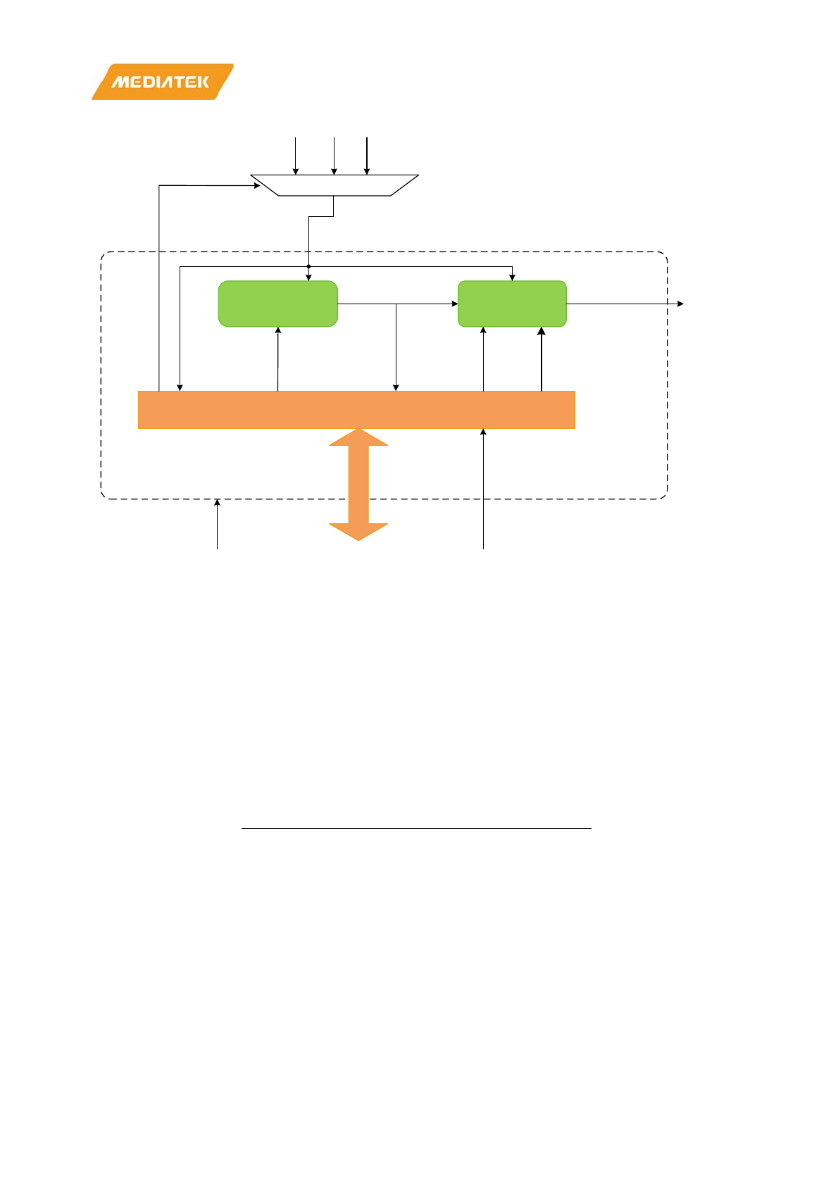
MT7686 Reference Manual
© 2016 - 2017 MediaTek Inc.
Page 355 of 536
This document contains information that is proprietary to MediaTek Inc. (“MediaTek”) and/or its licensor(s).
Any unauthorized use, reproduction or disclosure of this document in whole or in part is strictly prohibited.
pwm_1ch_clk_mask pwm_1ch_gen
CLOCK_DIV
pwm_reg
pwm_1ch_count
pwm_1ch_thresh_up
pwm_1ch_thresh_down
pwm_1ch_
clk_ctrl
pwm_1ch
_pdn_b
APB interface
APB BUS
PWM
output
pwm_1ch_pdnReset
pwm_1ch.v
CLK
13MHz
32kHz 40MHz
pwm_1ch_
clk_ctrl
1 0 2/3
Figure 15.3-1. PWM block diagram
15.4. Functions
• Classic mode
The frequency and volume of the PWM output signal are determined by registers PWM_1CH_CLK_CTRL,
PWM_1CH_THRESH_UP, PWM_1CH_THRESH_DOWN and PWM_1CH_COUNT. The power down signal (pwm_1ch_pdn)
is applied to power down the PWM_1CH module. When PWM_1CH is deactivated (pwm_1ch_pdn = 1), the output
will be in LOW state.
The output PWM frequency is determined by:
)1_1_(_ +× COUNTCHPWMDIVCLOCK
CLK
CLK = 13 MHz, when PWM_1CH_CLK_CTRL[3:2] = 2’b00
CLK = 32 KHz, when PWM_1CH_CLK_CTRL[3:2] = 2’b01
CLK = 40MHz, when PWM_1CH_CLK_CTRL[3:2] = 2’b10
CLOCK_DIV = 1, when PWM_1CH_CLK_CTRL[1:0] = 2’b00
CLOCK_DIV = 2, when PWM_1CH_CLK_CTRL[1:0] = 2’b01
CLOCK_DIV = 4, when PWM_1CH_CLK_CTRL[1:0] = 2’b10
CLOCK_DIV = 8, when PWM_1CH_CLK_CTRL[1:0] = 2’b11
MT7686 Reference Manual
© 2016 - 2017 MediaTek Inc.
Page 356 of 536
This document contains information that is proprietary to MediaTek Inc. (“MediaTek”) and/or its licensor(s).
Any unauthorized use, reproduction or disclosure of this document in whole or in part is strictly prohibited.
The output PWM duty cycle is determined by:
1_1_
1__1___1_
+
+−
COUNTCHPWM
DOWNTHRESHCHPWMUPTHRESHCHPWM
Note that PWM_1CH_THRESH_UP should be less than PWM_1CH_COUNT, and PWM_1CH_THRESH_DOWN should be
less than PWM_1CH_THRESH_UP. If this condition is not satisfied, the output pulse of the PWM will be always high
or always low. Figure 15.4-1 is the PWM waveform with indicated register values.
13MHz
PWM_1CH_COUNT= 5
PWM_1CH_THRESH_UP= 3
PWM_1CH_THRESH_DOWN= 2
PWM_1CH_CLK_CTRL= 4'b0000
Figure 15.4-1. PWM waveform with register values
15.5. Register mapping
There are six PWM channels in this SOC. The channels and their base addresses are shown in the table below.
PWM number Base address
PWM0
0xA2120000
PWM1 0xA2130000
PWM2 0xA2140000
PWM3 0xA2150000
PWM4 0xA2160000
PWM5 0xA2170000
Module name: PWM0 Base address: (+a2120000h)
Address Name Width
(bits)
Register functionality
A2120000
PWM_1CH_CTRL_ADDR
16
PWM control register
A2120004
PWM_1CH_COUNT_ADDR
16
PWM maximum counter value
register
A2120008
PWM_1CH_THRESH_UP_AD
DR
16
PWM
threshold_up value register
A212000C
PWM_1CH_THRESH_DOWN
_ADDR
16
PWM
threshold_down value register
A2120000
PWM_1CH_CTRL_ADDR
PWM control register
00000000
Bit
15
14
13
12
11
10
9
8
7
6
5
4
3
2
1
0
Na
me
PWM_1CH_CLK_
CTRL
Typ
e
RW
MT7686 Reference Manual
© 2016 - 2017 MediaTek Inc.
Page 357 of 536
This document contains information that is proprietary to MediaTek Inc. (“MediaTek”) and/or its licensor(s).
Any unauthorized use, reproduction or disclosure of this document in whole or in part is strictly prohibited.
Res
et
0 0 0 0
Bit(s)
Name
Description
3:0
PWM_1CH_CLK_CTRL
Bit [1:0] : Selects clock
prescaler scale of PWM
[1:0] = 2'b00 : f = fclk
[1:0] = 2'b01 : f = fclk/2
[1:0] = 2'b10 : f = fclk/4
[1:0] = 2'b11 : f = fclk/8
Bit [3:2] : Selects source clock frequency of PWM
[3:2] = 2'b00 : CLK = 13MHz
[3:2] = 2'b01 : CLK = 32kHz (able to work in sleep mode)
[3:2] = 2'b10 : CLK = 40MHz
[3:2] = 2'b11 : CLK = 40MHz
A2120004
PWM_1CH_COUNT_A
DDR
PWM max counter value register
00000000
Bit
15
14
13
12
11
10
9
8
7
6
5
4
3
2
1
0
Na
me
PWM_1CH_COUNT
Typ
e
RW
Res
et
0 0 0 0 0 0 0 0 0 0 0 0 0
Bit(s)
Name
Description
12:0
PWM_1CH_COUNT
PWM maximum counter value
This is the initial value for the internal counter. Regardless of the
operation mode, if
PWM_1CH_COUNT is written when the internal
counter is counting backwards, the new initial value will not take effect
until the internal counter counts down to 0, consider a complete period
as an example.
A212000
8
PWM_1CH_THRESH_UP
_ADDR
PWM
threshold_up value register
00000000
Bit
15
14
13
12
11
10
9
8
7
6
5
4
3
2
1
0
Na
me
PWM_1CH_THRESH_UP
Typ
e
RW
Res
et
0 0 0 0 0 0 0 0 0 0 0 0 0
Bit(s)
Name
Description
12:0
PWM_1CH_THRESH_UP
PWM threshold
-up value
•
When the internal counter value is less than
PWM_1CH_THRESH_UP and bigger than
PWM_1CH_THRESH_DOWN
, the PWM output signal will be "1".
•
When the internal counter value is greater than
PWM_1CH_THRESH_UP or less than

MT7686 Reference Manual
© 2016 - 2017 MediaTek Inc.
Page 358 of 536
This document contains information that is proprietary to MediaTek Inc. (“MediaTek”) and/or its licensor(s).
Any unauthorized use, reproduction or disclosure of this document in whole or in part is strictly prohibited.
PWM_1CH_THRESH_DOWN, the PWM output signal will be
"0".
•
When the internal counter value is equal to
PWM_1CH_THRESH_UP or PWM_1CH_THRESH_DOWN, the
PWM output signal will be "1".
A212000
C
PWM_1CH_THRESH_D
OWN_ADDR
PWM
threshold_down value register
00000000
Bit
15
14
13
12
11
10
9
8
7
6
5
4
3
2
1
0
Na
me
PWM_1CH_THRESH_DOWN
Typ
e
RW
Res
et
0 0 0 0 0 0 0 0 0 0 0 0 0
Bit(s)
Name
Description
12:0
PWM_1CH_THRESH_DOWN
PWM threshold
-down value
•
When the internal counter value is less than
PWM_1CH_THRESH_UP and bigger than
PWM_1CH_THRESH_DOWN
, the PWM output signal will be "1".
•
When the internal counter value is greater than
PWM_1CH_THRESH_UP or less than
PWM_1CH_THRESH_DOWN, the PWM output signal will be
"0".
•
When the internal counter value is equal to
PWM_1CH_THRESH_UP or PWM_1CH_THRESH_DOWN, the
PWM output signal will be "1".
MT7686 Reference Manual
© 2016 - 2017 MediaTek Inc.
Page 359 of 536
This document contains information that is proprietary to MediaTek Inc. (“MediaTek”) and/or its licensor(s).
Any unauthorized use, reproduction or disclosure of this document in whole or in part is strictly prohibited.
16. Cortex-M4 L1 Cache Controller
16.1. Overview
Mediatek MT7686 core processor is implemented with a subsystem including the core cache and tightly coupled
memory (TCM). The subsystem is placed between the MCU core and AHB bus interface, as shown in Figure 16.1-1 .
Core Cache
Controller
AHB
Bus
Interface
TCM Cache
Way 0
Cache
Way 1
Cache
Way 2
Cache
Way 3
AHB
Figure 16.1-1. MCU, Cache, TCM and AHB bus connectivity
TCM is a high-speed (zero wait state) dedicated memory accessed exclusively by the MCU. Due to the latency
penalty when the MCU accesses memory or peripherals through the on-chip bus, moving timing critical code and
data into TCM can enhance the performance of the MCU and guarantee the response to particular events.
Another method to enhance MCU performance is the implementation of cache. In this case, the core cache is a
small block of memory containing a copy of a small portion of cacheable data in the external memory. If the MCU
reads a cacheable datum, the datum will be copied into the core cache. Once the MCU requests the same datum
again, it can be obtained directly from the core cache (called cache hit) instead of fetching it again from the
external memory. Consider the fact that accessing cache is much faster than accessing external memory through
the bus system, a faster instruction fetching can be obtained leading to a higher instructions per cycle (IPC) which
is a major factor in the evaluation of core performance. Since a large external memory maps to a small cache, the
cache can hold only a small portion of external memory. If MCU accesses a datum not found in the cache (called
cache miss), one cache line must be dropped (flushed), and the required datum and its neighboring data are
transferred from the external memory to cache (cache line fill). Before the cache line fill, “cache write back” to
maintain data consistency between cache and external memory needs to be performed. In this design, a cache line
consists of eight words (8x32 bits). On the other hand, the best way to utilize TCM is to maintain the critical
instruction or data in TCM. After system reset, the bootloader copies TCM content from the external storage, such
as flash, to the internal TCM. If necessary, the MCU can replace TCM content with other data in the external
storage during the runtime to implement a mechanism such as “overlay”. TCM is also ideal to store stack data.
The sizes of TCM and cache can be set to one of the following four configurations:
• 64KB TCM, 32KB cache
• 80KB TCM, 16KB cache
• 88KB TCM, 8KB cache
• 96KB TCM, 0KB cache (no cache)
MT7686 Reference Manual
© 2016 - 2017 MediaTek Inc.
Page 360 of 536
This document contains information that is proprietary to MediaTek Inc. (“MediaTek”) and/or its licensor(s).
Any unauthorized use, reproduction or disclosure of this document in whole or in part is strictly prohibited.
NO
Cache
Cache 8KB
4-way, 64-set
Cache 16KB
4-way, 128-set
Cache 32KB
4-way, 256-set
TCM
80KB
TCM
96 KB
TCM
80 KB
TCM
88 KB
TCM
64 KB
Way0Way1Way2Way3Way0Way1Way2Way3
Way0Way1Way2Way3
64K
8K
8K
64K
4K
4K
8K
8K
64K
2K
2K
2K
2K
8K
8K
64K
4K
4K
2K
2K 2K
2K
2K 2K 2K2K
4K4K
2K
2K
2K
2K 4K
4K 8K8K
Figure 16.1-2. Cache size and TCM settings
These different configurations provide flexibility for software to adjust and reach optimum system performance.
The address mapping of these memories is shown in Table 16.1-1 .
Table 16.1-1. TCM address spaces for different cache size settings
Cache Size SYSRAM Identity Used as
2’b00
(Total TCM = 96KB, cache = 0)
SYSRAM_2K_0 TCM0 (0x0400_0000 to 0x0400_07FF)
SYSRAM_2K_1 TCM1 (0x0400_0800 to 0x0400_0FFF)
SYSRAM_2K_2 TCM2 (0x0400_1000 to 0x0400_17FF)
SYSRAM_2K_3 TCM3 (0x0400_1800 to 0x0400_1FFF)
SYSRAM_4K_0 TCM4 (0x0400_2000 to 0x0400_2FFF)
SYSRAM_4K_1 TCM5 (0x0400_3000 to 0x0400_3FFF)
SYSRAM_8K_0 TCM6 (0x0400_4000 to 0x0400_5FFF)

MT7686 Reference Manual
© 2016 - 2017 MediaTek Inc.
Page 361 of 536
This document contains information that is proprietary to MediaTek Inc. (“MediaTek”) and/or its licensor(s).
Any unauthorized use, reproduction or disclosure of this document in whole or in part is strictly prohibited.
Cache Size SYSRAM Identity Used as
SYSRAM_8K_1 TCM7 (0x0400_6000 to 0x0400_7FFF)
SYSRAM_16K_0~4 TCM8 (0x0400_8000 to 0x0401_7FFF)
2’b01
(Total TCM = 88KB, cache = 8KB)
SYSRAM_2K_0 Cache way 0
SYSRAM_2K_1 Cache way 1
SYSRAM_2K_2 Cache way 2 or way 0 (2-way configuration)
SYSRAM_2K_3 Cache way 3 or way 1 (2-way configuration)
SYSRAM_4K_0 TCM4 (0x0400_2000 to 0x0400_2FFF)
SYSRAM_4K_1 TCM5 (0x0400_3000 to 0x0400_3FFF)
SYSRAM_8K_0 TCM6 (0x0400_4000 to 0x0400_5FFF)
SYSRAM_8K_1 TCM7 (0x0400_6000 to 0x0400_7FFF)
SYSRAM_16K_0~4 TCM8 (0x0400_8000 to 0x0401_7FFF)
2’b10
(Total TCM = 80KB, cache = 16KB)
SYSRAM_2K_0 Cache way 0
SYSRAM_2K_1 Cache way 0
SYSRAM_2K_2 Cache way 1
SYSRAM_2K_3 Cache way 1
SYSRAM_4K_0 Cache way 2 or way 0 (2-way configuration)
SYSRAM_4K_1 Cache way 3 or way 1 (2-way configuration)
SYSRAM_8K_0 TCM6 (0x0400_4000 to 0x0400_5FFF)
SYSRAM_8K_1 TCM7 (0x0400_6000 to 0x0400_7FFF)
SYSRAM_16K_0~4 TCM8 (0x0400_8000 to 0x0401_7FFF)
2’b11
(Total TCM = 64KB, cache = 32KB)
SYSRAM_2K_0 Cache way 0
SYSRAM_2K_1 Cache way 0
SYSRAM_2K_2 Cache way 0
SYSRAM_2K_3 Cache way 0
SYSRAM_4K_0 Cache way 1
SYSRAM_4K_1 Cache way 1
SYSRAM_8K_0 Cache way 2 or way 0 (2-way configuration)
SYSRAM_8K_1 Cache way 3 or way 1 (2-way configuration)
SYSRAM_16K_0~4 TCM8 (0x0400_8000 to 0x0401_7FFF)
16.2. Cache optimization
The cache system has the following features:
1) Write back (unit: 4 words)
2) Configurable two or four way set associative
a) 2-way set associative
i) 128/256/512-set for 8, 16 or 32KB cache size, respectively.
ii) Each way has 128, 256 or 512 cache lines with 8-word line size.
b) 4-way set associative
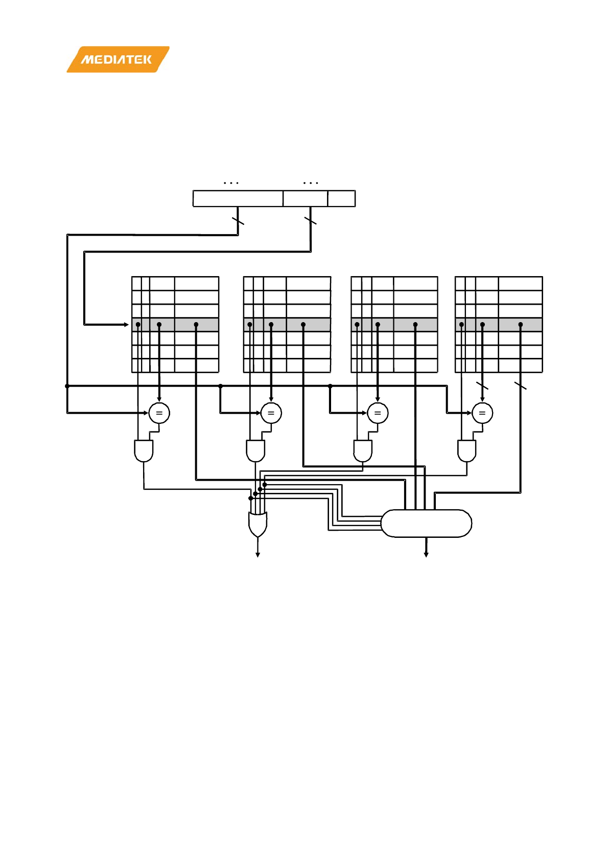
MT7686 Reference Manual
© 2016 - 2017 MediaTek Inc.
Page 362 of 536
This document contains information that is proprietary to MediaTek Inc. (“MediaTek”) and/or its licensor(s).
Any unauthorized use, reproduction or disclosure of this document in whole or in part is strictly prohibited.
i) 64/128/256-set for 8, 16 or 32KB cache size, respectively.
ii) Each way has 64, 128 or 256 cache lines with 8-word line size
3) 20-bit tag memory: 19-bit high address and 1-bit valid bit.
4) 2-bit dirty memory (each dirty bit records the dirtiness of half cache line – 4 words).
Figure 16.2-1. Cache lookup for 4-way set associative
Each set associative cache has two memories: tag memory and data memory. The tag memory stores each line’s
valid bit and tag (upper 19 bits of the address). The data memory stores line data. When MCU accesses the
memory, the address is compared to the content of the tag memory. First, the line index (address bits [12:5]) is
used to locate a line in the tag memory. When a particular line is found in the tag memory, the upper 19 bits
(address bits [31:13]), called tag, of the desired memory address are compared with the content of the found tag
line. If a match is found in both line address and tag address and the valid bit is 1, it is called a cache hit, and the
data from that particular cache way is returned to the MCU. This process is shown in Figure 16.2-1.
If most memory accesses are cache hit, the MCU is able to acquire data without any delay, and the overall system
performance will be higher. There are several factors that may affect the cache hit rate:
• Cache size and the organization
A ddres s
19 8
V T a gIndex
0
1
2
253
254
255
D ata V T a g D a ta V T ag D ata V T a g D ata
3219
4-to- 1 multiplexer
H it D ata
45121331 0
D D D D

MT7686 Reference Manual
© 2016 - 2017 MediaTek Inc.
Page 363 of 536
This document contains information that is proprietary to MediaTek Inc. (“MediaTek”) and/or its licensor(s).
Any unauthorized use, reproduction or disclosure of this document in whole or in part is strictly prohibited.
The larger the cache size, the higher the hit rate. However, the hit rate saturates when the cache size is larger than
a threshold size. Normally the size of 16KB and above and two or four way set associative cache configuration can
achieve a higher hit rate.
• 2 or 4-way set associative
o 4-way set associative has higher hit rate than 2-way. However, the power consumption will be higher
as it accesses more memory during cache lookup.
• Program behavior
If the system has several tasks and switches between the tasks frequently, it may result in frequent cache content
flush, as each time a new task is running, the cache holds its data for a certain period of time assuming it’ll be used
again. However, the stored data might get flushed out before being used again, if the following task requires the
data occupying the same cache entries. Interrupts can cause program flow to change dynamically and reduce the
benefit of using cache. The interrupt handler and the data it processes may cause cache to flush out data used by
the current task. Thus, after returning from the interrupt handler to current task, the flushed data may need to be
filled into the cache again if it’s required by the program routine. This will cause performance degradation.
To tune the system performance, the cache controller in MT7686 records the cache hit count and number of
cacheable memory accesses. The cache hit rate can be obtained by dividing these two numbers.
16.2.1. Write-back or write-through configurable cache
There are two different types of cache design to maintain data consistency. One is cache write-through, and the
other is cache write-back.
The write-back cache improves the performance especially when processors generate writes as fast as or faster
than the writes that can be handled by the external memory. However, the implementation of write-back is more
complex than that of write-through. When a cache line is dirty, four or eight words will be written back to the
external memory at once, and this will certainly occupy significant bus bandwidth and therefore decrease the
overall efficiency. To solve this problem, a write buffer is necessary in the write-back implementation. Once the
writes are written into the write buffer, the processor can continue the execution.
For systems with large memory write latency, it’s possible that the burst write of cache write-back operation may
cause large impact on the system performance, change the cache to write-through mode in the software, if
necessary.
16.2.1.1. Write-back implementation
When a cache hit occurs at write request, only the cache content will be modified, and the dirty bit will be set. The
modified cache content won’t match with that in the external memory, unlike cache write-through, which modifies
both the cache content and the external memory synchronously.
When the cache misses the read request, line fill will be performed and a randomly selected cache line will be
replaced, but before that, the dirty bits of that selected cache line have to be checked for the necessity of write-
back. If the dirty bits are not set, line fill can proceed right away, and the selected cache line can be simply
abandoned and replaced by a newly fetched line from the external memory which consists of the requested data.
On the other hand, if one of or both the dirty bits are set, write-back has to be performed before line fill. In that
case, half or the entire cache line is written into the write buffer. A summary is given in Figure 16.2-2:
MT7686 Reference Manual
© 2016 - 2017 MediaTek Inc.
Page 364 of 536
This document contains information that is proprietary to MediaTek Inc. (“MediaTek”) and/or its licensor(s).
Any unauthorized use, reproduction or disclosure of this document in whole or in part is strictly prohibited.
Figure 16.2-2. Cache miss/refill criteria
16.2.1.2. Write buffer
The write buffer consists of address buffer, data buffer, buffer for HTRANS, buffer for HSIZE, buffer for HLOCK and
buffer for HBURST. The write buffer is designed as first-in-first-out (FIFO) with a depth eight words. Since the
outputs from the code cache meet the AMBA format, the address buffer and data buffer are independent. The
outputs of write buffer suffice the AMBA formatting guidelines and are designed for pipelining.
All CPU write accesses through the I/D bus will be buffered, no matter it’s within the cacheable region or not.
16.2.2. Cache operation
Upon power-on, the cache memory contains random values. The MCU needs to invalidate the cache content
before enabling the cache usage.
The MCU needs to flush the cache data to the external memory to maintain data coherency before disabling the
cache controller or MCU power-off.
The cache controller provides a register which, when written, can operate on the cache memory to fulfill the
prerequisite mentioned above (called cache operation).
The operation involves:
1) Invalidate one cache line
The user must give a memory address. If it’s found within the cache, that particular cache line will be invalidated
by writing 0 in the valid bit at the corresponding tag line. Alternatively, the user can invalidate a cache line by
specifying a set/way mapped to that cache line.
2) Invalidate all cache lines
The user doesn’t need to specify an address. The cache controller clears valid bits in all tag lines when this
operation is requested.
3) Flush one cache line
Write reques t
Wri te into
ex te rnal
memo r y
Wri te into
cache only
and set the
dirty bi t
Read from
cache
Read request
Line f ill
Check dirty
bits
Cache write
back
Write back done
and write buffer contents
ONLY the last set of
write back words

MT7686 Reference Manual
© 2016 - 2017 MediaTek Inc.
Page 365 of 536
This document contains information that is proprietary to MediaTek Inc. (“MediaTek”) and/or its licensor(s).
Any unauthorized use, reproduction or disclosure of this document in whole or in part is strictly prohibited.
The user must give a memory address. If it’s found within the cache and the dirty bit or bits are set, that particular
cache line containing the given address will be flushed into the write buffer. Alternatively, the user can flush a
cache line by specifying a set/way mapped to that cache line. This operation is not supported if the cache is
operating in the write-through mode.
4) Flush all cache lines
The user doesn’t need to specify an address. The cache controller flushes all the cache lines with the dirty bit or
bits set. This operation is not supported if the cache is operating in the write-through mode.
Note: To configure the cache size, follow the steps below to prevent cache data loss during the cache size
configuration. At initialization, the cache size is set to 0.
1) Flush all cache lines.
2) Invalidate all cache lines.
3) Configure the TCM and cache size.
16.2.3. Summary of cache operation
Table 16.2-1. Write-back mode cache read or write operations
Op
Cacheable
Hit
Dirty
Action
W0~W3 W4~W7
Read N d d d Single read
Y Y d d Return data, no stall
N N N Line refill from bus using AHB WRAP8 burst
N Y • Evict half line to WBuf.
• Line refill from bus using AHB WRAP8 burst.
• Write back half line from WBuf using AHB INCR4 burst
write.
Y N
Y Y • Evict whole line to WBuf.
• Line refill from bus using AHB WRAP8 burst.
• Write back whole line from WBuf using AHB INCR8
burst write.
Write N d d d • Wait for WBuf space.
• Place write data into WBuf and let the MCU continue
operating (CLKEN = 1). Stall the MCU by one cycle.
Y Y d d • Write into cache; meanwhile set up the corresponding
dirty bit.
• Stall the MCU by one cycle to avoid structural hazard.
N d d • Wait for WBuf space.
• Place write data into WBuf and let the MCU continue
operating (CLKEN = 1). Stall the MCU by one cycle.
Legend Y: yes, N: no, d: don’t care
MT7686 Reference Manual
© 2016 - 2017 MediaTek Inc.
Page 366 of 536
This document contains information that is proprietary to MediaTek Inc. (“MediaTek”) and/or its licensor(s).
Any unauthorized use, reproduction or disclosure of this document in whole or in part is strictly prohibited.
Table 16.2-2. Write-through mode cache R/W action summary
Op Cacheable Hit Action
Read N d Single read
Y Y • Return data, no stall
N • Line read from bus using AHB WRAP8 burst
Write N d • Wait for WBuf space.
• Place write data into WBuf and let the MCU continue operating (CLKEN
= 1). Stall Cortex-M4 by one cycle.
Y N
Y • Write to data SRAM.
• Wait for WBuf space.
• Place write data into WBuf and let the MCU continue operating (CLKEN
= 1). Stall Cortex-M4 by one cycle.
Legend Y: yes, N: no, d: don’t care
16.3. Register mapping
Module name: CACHE Base address: (+E0180000h)
CACHE+00h
Cache general control register
CACHE_CON
Bit
15
14
13
12
11
10
9
8
7
6
5
4
3
2
1
0
Nam
e
2WAY
EN
CACHESIZE CNTE
N1 CNTE
N0 MCE
N
Type
RW RW RW RW R/W
Rese
t
0 00 0 0 0
This register determines the size of cache, cache hit counter and the enabling of MPU.
2WAYEN Enable 2-way cache look-up
0 Disable (4-way)
1 Enable (2-way)
CACHESIZE Selects cache size
00 No cache
01 8KB
10 16KB
11 32KB
CNTEN1 Enables cache hit counter 1
If enabled, the cache controller will increment a 48-bit counter by one when a cache hit is
detected. This number is used in performance evaluation of the application. This counter
increments only when the data are obtained from MPU cacheable regions 8 to 15.
0 Disable
1 Enable

MT7686 Reference Manual
© 2016 - 2017 MediaTek Inc.
Page 367 of 536
This document contains information that is proprietary to MediaTek Inc. (“MediaTek”) and/or its licensor(s).
Any unauthorized use, reproduction or disclosure of this document in whole or in part is strictly prohibited.
CNTEN0 Enables cache hit counter 0
If enabled, the cache controller will increment a 48-bit counter by one when a cache hit is
detected. This number is used in performance of the application. This counter increments
only when the data are obtained from MPU cacheable regions 0 to 7.
0 Disable
1 Enable
MCEN Enables the comparison of cacheable/non-cacheable setting
If disabled, the MCU memory accesses are all non-cacheable, i.e. they will go through the
AHB bus (except for TCM access). When enabled, if MCU accesses a cacheable memory
region, the cache controller will return the data if it is found in cache and will get the data
through the AHB bus only if a cache miss occurs.
0 Disable
1 Enable
CACHE+04h
Cache operation
CACHE_OP
Bit
31
30
29
28
27
26
25
24
23
22
21
20
19
18
17
16
Name
TADDR[31:16]
Type
R/W
Reset
0
Bit 15 14 13 12 11 10 9 8 7 6 5 4 3 2 1 0
Name
TADDR[15:5] OP[3:0] EN
Type
R/W
W
W1
Reset
0 0 0
This register defines the address and/or which type of cache operation to apply. When MCU writes into
this register, the pipeline of MCU will be stopped for the cache controller to complete the operation. Bit 0
of the register must be written as 1 to enable the command.
TADDR[31:5] Target address
This field contains the address of invalidation operation. If OP[3:0] = 0010,
TADDR[31:5] will be the address[31:5] of a memory whose line will be invalidated if it
exists in the cache. If OP[3:0] = 0100, TADDR[12:5] will indicate the set, while
TADDR[19:16] indicates which way to clear:
0001 way #0 (4-way)/way #0 first half (2-way)
0010 way #1 (4-way)/way #1 first half (2-way)
0100 way #2 (4-way)/way #0 second half (2-way)
1000 way #3 (4-way)/way #1 second half (2-way)
* For 2-way cache configuration, this operation has to be done twice in order to clear the
entire way.
OP[3:0] Operation
This field determines which cache operations will be performed.
0001 invalidate all cache lines
0010 invalidate one cache line using address
MT7686 Reference Manual
© 2016 - 2017 MediaTek Inc.
Page 368 of 536
This document contains information that is proprietary to MediaTek Inc. (“MediaTek”) and/or its licensor(s).
Any unauthorized use, reproduction or disclosure of this document in whole or in part is strictly prohibited.
0100 invalidate one cache line using set/way
1001 flush all cache lines
1010 flush one cache line using address
1100 flush one cache line using set/way
EN Enables command
This enabling bit must be written 1 to enable the command.
0 Does not enable
1 Enable
CACHE+08h
Cache hit count 0 lower part
CACHE_HCNT0L
Bit 31 30 29 28 27 26 25 24 23 22 21 20 19 18 17 16
Name
CHIT_CNT0[31:16]
Type
R/W
Reset
0
Bit
15
14
13
12
11
10
9
8
7
6
5
4
3
2
1
0
Name
CHIT_CNT0[15:0]
Type
R/W
Reset
0
CACHE+0Ch
Cache hit count 0 upper part
CACHE_HCNT0U
Bit 31 30 29 28 27 26 25 24 23 22 21 20 19 18 17 16
Name
RESERVED
Type
Reset
Bit 15 14 13 12 11 10 9 8 7 6 5 4 3 2 1 0
Name
CHIT_CNT0[47:32]
Type
R/W
Reset
0
When the CNTEN0 bit in the CACHE_CON register is set to 1 (enabled), this register will start to record
the cache hit count until it is disabled. If the value increases to above the maximum value (0xffffffffffff), it
will be rolled over to 0 and continue counting. The 48-bit counter provides a recording time of 31 days
even if MCU runs at 104MHz, and every cycle is a cache hit. Note, that before enabling the counter,
writing the initial value 0 to the counter is recommended.
CHIT_CNT0[47:0] Cache hit count 0
WRITE Write any value to CACHE_HCNT0L or CACHE_HCNT0U clears
CHIT_CNT0 to all 0.
READ Current counter value
CACHE+10h
Cacheable access count 0 lower part
CACHE_CCNT0L
Bit 31 30 29 28 27 26 25 24 23 22 21 20 19 18 17 16
Name
CACC_CNT0[31:16]
Type
R/W
Reset
0
Bit 15 14 13 12 11 10 9 8 7 6 5 4 3 2 1 0
MT7686 Reference Manual
© 2016 - 2017 MediaTek Inc.
Page 369 of 536
This document contains information that is proprietary to MediaTek Inc. (“MediaTek”) and/or its licensor(s).
Any unauthorized use, reproduction or disclosure of this document in whole or in part is strictly prohibited.
Name
CACC_CNT0[15:0]
Type
R/W
Reset
0
CACHE+14h
Cacheable access count 0 upper part
CACHE_CCNT0U
Bit 31 30 29 28 27 26 25 24 23 22 21 20 19 18 17 16
Name
RESERVED
Type
Reset
Bit 15 14 13 12 11 10 9 8 7 6 5 4 3 2 1 0
Name
CACC_CNT0[47:32]
Type
R/W
Reset
0
When the CNTEN0 bit in the CACHE_CON register is set to 1 (enabled), this register is incremented at
each cacheable memory access (no matter whether it is a cache miss or a cache hit). If the value increases
to above the maximum value (0xffffffffffff), it will be rolled over to 0 and continue counting. For 104MHz
MCU speed, if all memory accesses are cacheable and cache hit, this counter will overflow after
(2^48)*9.6ns = 31 days. This is the shortest time for the counter to overflow. In a more realistic case, the
system will have cache misses, non-cacheable accesses and idle mode that makes the counter overflow at
later time.
CACC_CNT0[47:0] Cache access count 0
WRITE Write any value to CACHE_CCNT0L or CACHE_CCNT0U clears
CACC_CNT0 to all 0.
READ Current counter value
The best way to use CACHE_HCNT0 and CACHE_CCNT0 is to set the initial value to 0 for both registers,
enable both counters (set CNTEN0 to 1), run a portion of program to be benchmarked, stop the counters
and get their values. Therefore, during this period,
%100
_
_×= CCNTCACHE
HCNTCACHE
ratehitCache
The cache hit rate value may help tune the performance of the application program. Note that
CHIT_CNT0 and CACC_CNT0 only increment if the cacheable attribute is defined in MPU cacheable
region lower half channels (i.e. channels 0 ~ 7 of the total 16 channels).
CACHE+18h
Cache hit count 1 lower part
CACHE_HCNT1L
Bit 31 30 29 28 27 26 25 24 23 22 21 20 19 18 17 16
Name
CHIT_CNT1[31:16]
Type
R/W
Reset
0
Bit
15
14
13
12
11
10
9
8
7
6
5
4
3
2
1
0
Name
CHIT_CNT1[15:0]
Type
R/W
Reset
0
MT7686 Reference Manual
© 2016 - 2017 MediaTek Inc.
Page 370 of 536
This document contains information that is proprietary to MediaTek Inc. (“MediaTek”) and/or its licensor(s).
Any unauthorized use, reproduction or disclosure of this document in whole or in part is strictly prohibited.
CACHE+1Ch
Cache hit count 1 upper part
CACHE_HCNT1U
Bit 31 30 29 28 27 26 25 24 23 22 21 20 19 18 17 16
Name
RESERVED
Type
Reset
Bit
15
14
13
12
11
10
9
8
7
6
5
4
3
2
1
0
Name
CHIT_CNT1[47:32]
Type
R/W
Reset
0
When the CNTEN1 bit in CACHE_CON register is set to 1 (enabled), this register will start to record the
cache hit count until it is disabled. If the value increases to above the maximum value (0xffffffffffff), it will
be rolled over to 0 and continue counting. The 48-bit counter provides a recording time of 31 days even if
MCU runs at 104MHz, and every cycle is a cache hit. Note, that before enabling the counter, writing the
initial value 0 to the counter is recommended.
CHIT_CNT1[47:0] Cache hit count
WRITE Write any value to CACHE_HCNT1L or CACHE_HCNT1U clears
CHIT_CNT1 to all 0.
READ Current counter value
CACHE+20h
Cacheable access count 1 lower part
CACHE_CCNT1L
Bit 31 30 29 28 27 26 25 24 23 22 21 20 19 18 17 16
Name
CACC_CNT1[31:16]
Type
R/W
Reset
0
Bit
15
14
13
12
11
10
9
8
7
6
5
4
3
2
1
0
Name
CACC_CNT1[15:0]
Type
R/W
Reset
0
CACHE+24h
Cacheable access count 1 upper part
CACHE_CCNT1U
Bit 31 30 29 28 27 26 25 24 23 22 21 20 19 18 17 16
Name
RESERVED
Type
Reset
Bit 15 14 13 12 11 10 9 8 7 6 5 4 3 2 1 0
Name
CACC_CNT1[47:32]
Type
R/W
Reset
0
When CNTEN1 bit in CACHE_CON register is set to 1 (enabled), this register is incremented at each
cacheable memory access (no matter whether it is a cache miss or a cache hit). If the value increases to
above the maximum value (0xffffffffffff), it will be rolled over to 0 and continue counting. For 104MHz
MCU speed, if all memory accesses are cacheable and cache hit, this counter will overflow after
(2^48)*9.6ns = 31 days. This is the shortest time for the counter to overflow. In a more realistic case, the
system will have cache misses, non-cacheable accesses and idle mode that makes the counter overflow at
later time.

MT7686 Reference Manual
© 2016 - 2017 MediaTek Inc.
Page 371 of 536
This document contains information that is proprietary to MediaTek Inc. (“MediaTek”) and/or its licensor(s).
Any unauthorized use, reproduction or disclosure of this document in whole or in part is strictly prohibited.
CACC_CNT1[47:0] Cache access count 1
WRITE Write any value to CACHE_CCNT1L or CACHE_CCNT1U clears
CACC_CNT1 to all 0.
READ Current counter value
The best way to use CACHE_HCNT1 and CACHE_CCNT1 is to set the initial value to 0 for both registers,
enable both counters (set CNTEN1 to 1), run a portion of program to be benchmarked, stop the counters
and get their values. Therefore, during this period,
%100
_
_×= CCNTCACHE
HCNTCACHE
ratehitCache
.
The cache hit rate value may help tune the performance of the application program. Note that
CHIT_CNT1 and CACC_CNT1 only increment if the cacheable attribute is defined in MPU cacheable
region for upper half channels (i.e. channels 8 ~ 15 of the total 16 channels).
CACHE+2C Cache region enable CACHE_REGION_EN
Bit 31 30 29 28 27 26 25 24 23 22 21 20 19 18 17 16
Name
Type
Reset
Bit 15 14 13 12 11 10 9 8 7 6 5 4 3 2 1 0
Name
CH15 CH14
CH13 CH12 CH11 CH10
CH9 CH8 CH7 CH6 CH5 CH4 CH3 CH2 CH1 CH0
Type
R/W R/W R/W R/W R/W R/W R/W R/W R/W R/W R/W R/W R/W R/W R/W R/W
Reset
0
0
0
0
0
0
0
0
0
0
0
0
0
0
0
0
CH15~CH0 Enables/Disables the associated region
0 Disable the region setting
1 Enable the region setting
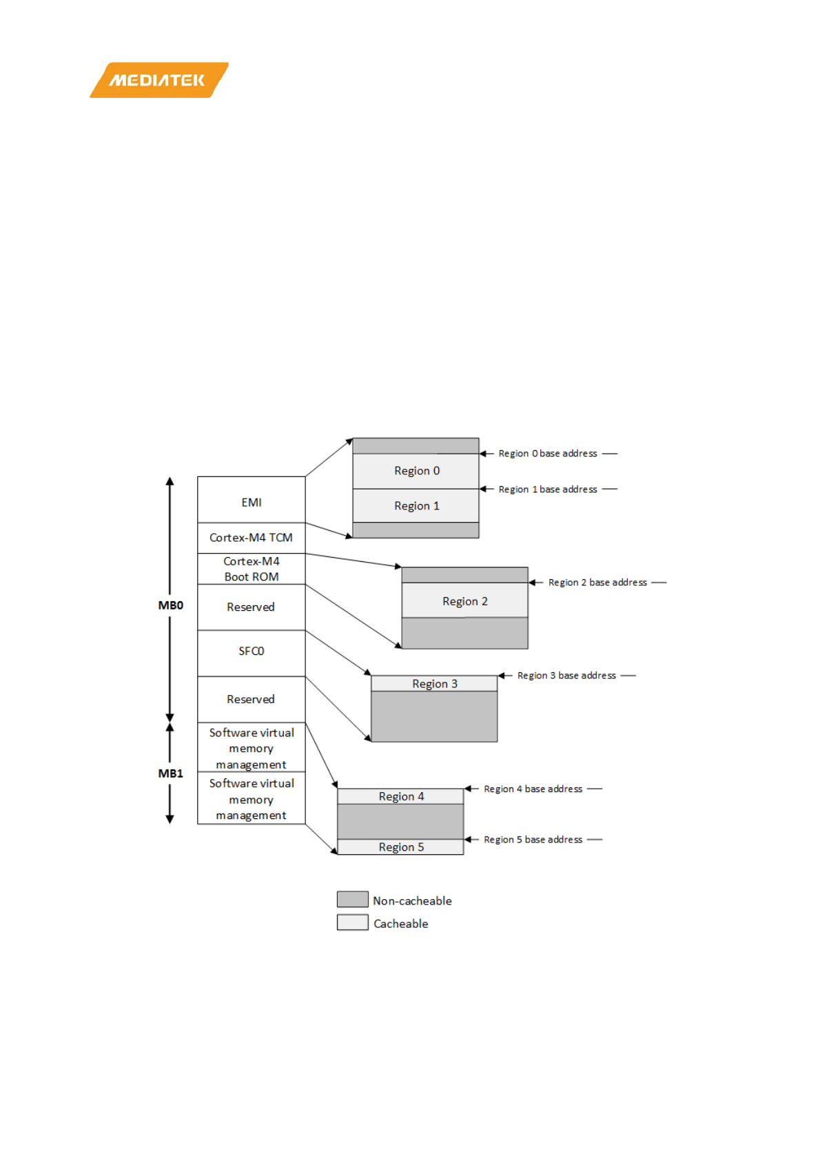
MT7686 Reference Manual
© 2016 - 2017 MediaTek Inc.
Page 372 of 536
This document contains information that is proprietary to MediaTek Inc. (“MediaTek”) and/or its licensor(s).
Any unauthorized use, reproduction or disclosure of this document in whole or in part is strictly prohibited.
16.4. Cacheable region controller
Cacheable region controller provides cacheable memory indication, featuring cacheable settings and attributes.
16.4.1. Cacheable settings
• Determine if a memory region is cacheable or not. If cacheable, MCU will keep a small copy in its cache
after read accesses. If MCU requires the same data later, it can acquire it from the high-speed local copy,
instead of low-speed external memory.
• The 4GB memory space is divided into 16 memory blocks with 256MB size each, i.e. MB0 to MB15. The
characteristics of these memory blocks are listed below:
• All memory blocks are determined by the Cacheable Region Controller. Note, that the software should
avoid making cache line access to the MB that does not support burst read/write. Usually only MB0 ~
MB1, mapped to EMI, are set as cacheable regions.
16.4.2. Cacheable attribute
Figure 16.4-1. Cacheable setting example
Figure 16.4-1 provides cacheable settings in each memory block. Five regions are defined in the figure. Note, that
each region can be continuous or non-continuous to each other. The address ranges not covered by any region in
MT7686 Reference Manual
© 2016 - 2017 MediaTek Inc.
Page 373 of 536
This document contains information that is proprietary to MediaTek Inc. (“MediaTek”) and/or its licensor(s).
Any unauthorized use, reproduction or disclosure of this document in whole or in part is strictly prohibited.
the cacheable settings are set to be uncacheable automatically. There is also one restriction: different regions must
not overlap.
The user can define a maximum of 16 regions in MB0 ~ MB1. Each region has its own settings defined in a 32-bit
register:
Register format
Bit 31 30 29 28 27 26 25 24 23 22 21 20 19 18 17 16
Name
BASEADDR[31:16]
Type R W
Reset
Bit
15
14
13
12
11
10
9
8
7
6
5
4
3
2
1
0
Name
BASEADDR[15:12] C
Type R W R W
Reset
0
0
16.4.2.1. Region base address
The region base address defines the starting point of the memory region. The user must only specify several upper
address bits and align the base address to a minimum 4KB boundary.
16.4.2.2. Region size
The region size enumeration setting in the register is disabled in MT7686. Instead, use the CACHEABLE_END
register to specify the end address base of a certain channel. The end address is non-inclusive, and the BASEADDR
is inclusive. For example, by setting BASEADDR to 0x1000 and END BASEADDR to 0x2000, any address in the range
(0x1000, 0x2000) will match this cacheable region setting.
The CACHEABLE_END register has 16 entries, starting right after the normal register and 0xE0190040 being the
first entry.
Table 16.4-1. Cacheable attribute bit encoding
Bit encoding Permission
0 Non-cacheable
1 Cacheable
MT7686 Reference Manual
© 2016 - 2017 MediaTek Inc.
Page 374 of 536
This document contains information that is proprietary to MediaTek Inc. (“MediaTek”) and/or its licensor(s).
Any unauthorized use, reproduction or disclosure of this document in whole or in part is strictly prohibited.
16.4.3. Register mapping
Module name: CACHE_Entry Base address: (+E0190000h)
CACHE_EMTRY_base+4*(n-1) n-th channel control CACHE_entry_n
Bit 31 30 29 28 27 26 25 24 23 22 21 20 19 18 17 16
Name
BASEADDR[31:16]
Type
R W
Reset
0
Bit
15
14
13
12
11
10
9
8
7
6
5
4
3
2
1
0
Name
BASEADDR[15:12] C
Type
R W
R W
Reset
0
0
CACHE_EMTRY_base+0x40 + 4*(n
-1) n-th channel control CACHE_End_entry_n
Bit
31
30
29
28
27
26
25
24
23
22
21
20
19
18
17
16
Name
BASEADDR[31:16]
Type R W
Reset
0
Bit
15
14
13
12
11
10
9
8
7
6
5
4
3
2
1
0
Name
BASEADDR[15:12]
Type
R W
Reset 0
• MT7686 supports 16 channels.
• Refer to register format for detailed filed descriptions.
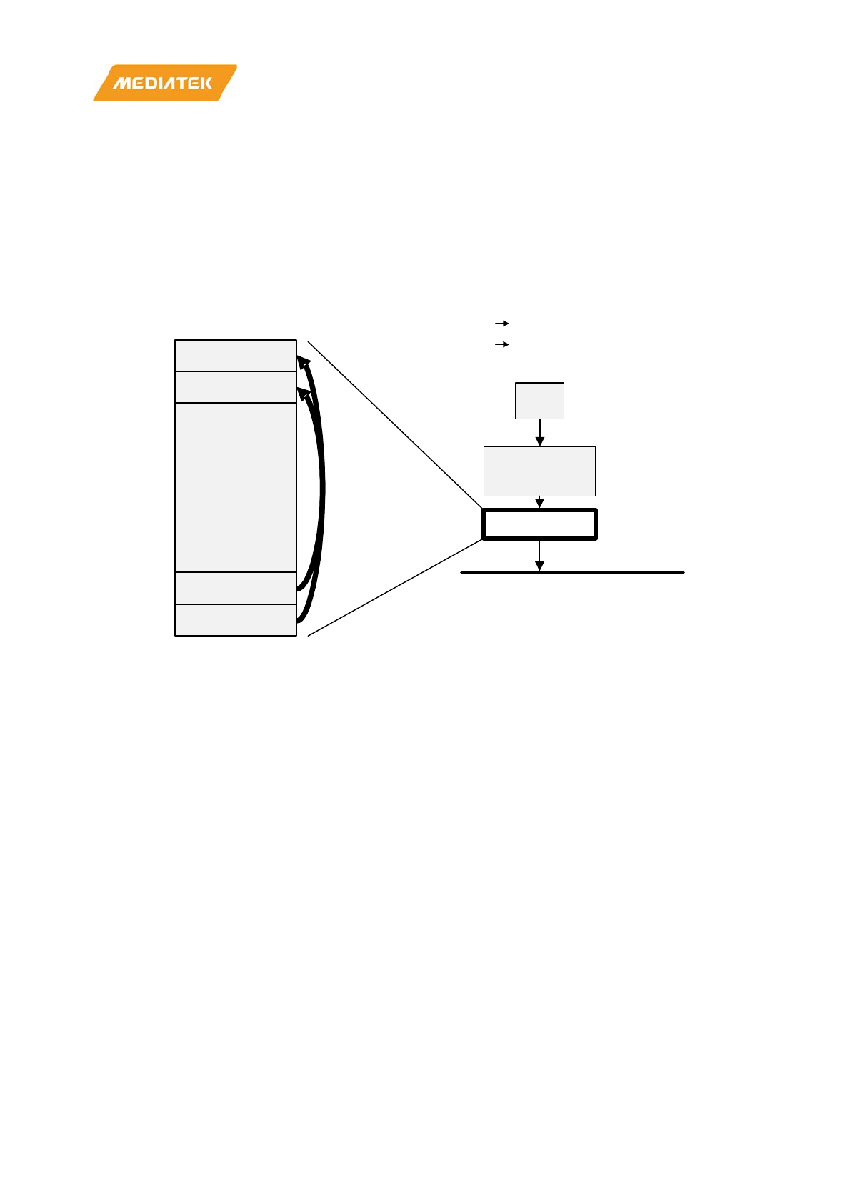
MT7686 Reference Manual
© 2016 - 2017 MediaTek Inc.
Page 375 of 536
This document contains information that is proprietary to MediaTek Inc. (“MediaTek”) and/or its licensor(s).
Any unauthorized use, reproduction or disclosure of this document in whole or in part is strictly prohibited.
16.5. Remapping
MT7686 cache provides three sets of registers to create the actual memory address same as the different CPU
load/store target address. Figure 16.5-1 shows the process of remapping.
The software sets 0x0xxxxxxx to cacheable and 0xFxxxxxxx to non–cacheable, but they are mapped to the same
physical address.
0x00000000
0x02000000
0x10000000
0x18000000
Memory Map Remap:
0x10xxxxxxx 0x00xxxxxxxx
0x18xxxxxxx 0x02xxxxxxxx
L1 Bus
ARM
Cache
Controller
Address Remap
Bank 0
Bank 1
vBank 1
vBank 0
Figure 16.5-1. Example settings of cache remapping
To achieve this:
1. Set regions beginning with 0x0000_0000 to cacheable.
2. Set regions beginning with 0x1000_0000 to non-cacheable.
3. Set BASEADDR field in Remap EntryHi to 0x1000_0000.
4. Set BASEADDR filed in Remap EntryLo to 0x0000_0000.
MT7686 Reference Manual
© 2016 - 2017 MediaTek Inc.
Page 376 of 536
This document contains information that is proprietary to MediaTek Inc. (“MediaTek”) and/or its licensor(s).
Any unauthorized use, reproduction or disclosure of this document in whole or in part is strictly prohibited.
16.5.1. Register mapping
Module name: NC-Remap Base address: (+E0181000h)
REMAP+0000h
Remap Entry_HI0
NCREMAP_HI0
Bit
31
30
29
28
27
26
25
24
23
22
21
20
19
18
17
16
Name
BASEADDR[31:16]
Type R W
Reset
Bit
15
14
13
12
11
10
9
8
7
6
5
4
3
2
1
0
Name
BASEADDR[15:09] SIZE[4:0] E N
Type
R W
R W
R W
Reset
00000 0
This register sets up the remapping base attributes for region 0.
BASEADDR Base address of this region
SIZE Size of this region (refer to Table 13)
EN ENABLES THIS REGION
0 DISABLE
1 ENABLE
REMAP+0004h
Remap Entry_LO0 NCREMAP_LO0
Bit
31
30
29
28
27
26
25
24
23
22
21
20
19
18
17
16
Name
BASEADDR[31:16]
Type R W
Reset
Bit
15
14
13
12
11
10
9
8
7
6
5
4
3
2
1
0
Name
BASEADDR[15:09]
Type
R W
Reset
This register sets up the mapped address base for CPU accesses that are hits in NC-Remap Entry0_HI.
REMAP+0008h Remap Entry_HI1
NCREMAP_HI1
Bit
31
30
29
28
27
26
25
24
23
22
21
20
19
18
17
16
Name
BASEADDR[31:16]
Type R W
Reset
Bit
15
14
13
12
11
10
9
8
7
6
5
4
3
2
1
0
Name
BASEADDR[15:09] SIZE[4:0] E N
Type
R W
R W
R W
Reset
00000 0
This register sets up the remapping base attributes for region 1.
REMAP+000Ch Remap Entry_LO1 NCREMAP_LO1
Bit 31 30 29 28 27 26 25 24 23 22 21 20 19 18 17 16
MT7686 Reference Manual
© 2016 - 2017 MediaTek Inc.
Page 377 of 536
This document contains information that is proprietary to MediaTek Inc. (“MediaTek”) and/or its licensor(s).
Any unauthorized use, reproduction or disclosure of this document in whole or in part is strictly prohibited.
Name
BASEADDR[31:16]
Type R W
Reset
Bit
15
14
13
12
11
10
9
8
7
6
5
4
3
2
1
0
Name
BASEADDR[15:09]
Type
R W
Reset
This register sets up the mapped address base for CPU accesses that are hits in NC-Remap Entry1_HI.
REMAP+0010h Remap Entry_HI2
NCREMAP_HI2
Bit 31 30 29 28 27 26 25 24 23 22 21 20 19 18 17 16
Name
BASEADDR[31:16]
Type
R W
Reset
Bit
15
14
13
12
11
10
9
8
7
6
5
4
3
2
1
0
Name
BASEADDR[15:09] SIZE[4:0] E N
Type R W R W R W
Reset
00000
0
This register sets up the remapping base attributes for region 2.
BASEADDR Base address of this region
SIZE Size of this region (refer to Table 13)
EN ENABLES THIS REGION
0 DISABLE
1 ENABLE
REMAP+0014h
Remap Entry_LO2
NCREMAP_LO2
Bit
31
30
29
28
27
26
25
24
23
22
21
20
19
18
17
16
Name
BASEADDR[31:16]
Type
R W
Reset
Bit 15 14 13 12 11 10 9 8 7 6 5 4 3 2 1 0
Name
BASEADDR[15:09]
Type
R W
Reset
This register sets up the mapped address base for CPU accesses that are hits in NC-Remap Entry2_HI.
Note that the base and size settings in 3 EntryHi cannot be overlapped. Otherwise, the resultant mapped address
will be undefined.
Table 16.5-1. Region size and bit encoding
Region size Bit encoding Base address
512B 00000 Bit [31:09] of region start address
1KB 00001 Bit [31:10] of region start address
2KB 00010 Bit [31:11] of region start address

MT7686 Reference Manual
© 2016 - 2017 MediaTek Inc.
Page 378 of 536
This document contains information that is proprietary to MediaTek Inc. (“MediaTek”) and/or its licensor(s).
Any unauthorized use, reproduction or disclosure of this document in whole or in part is strictly prohibited.
Region size Bit encoding Base address
4KB 00011 Bit [31:12] of region start address
8KB 00100 Bit [31:13] of region start address
16KB 00101 Bit [31:14] of region start address
32KB 00110 Bit [31:15] of region start address
64KB 00111 Bit [31:16] of region start address
128KB 01000 Bit [31:17] of region start address
256KB 01001 Bit [31:18] of region start address
512KB 01010 Bit [31:19] of region start address
1MB 01011 Bit [31:20] of region start address
2MB 01100 Bit [31:21] of region start address
4MB 01101 Bit [31:22] of region start address
8MB 01110 Bit [31:23] of region start address
16MB 01111 Bit [31:24] of region start address
32MB 10000 Bit [31:25] of region start address
64MB 10001 Bit [31:26] of region start address
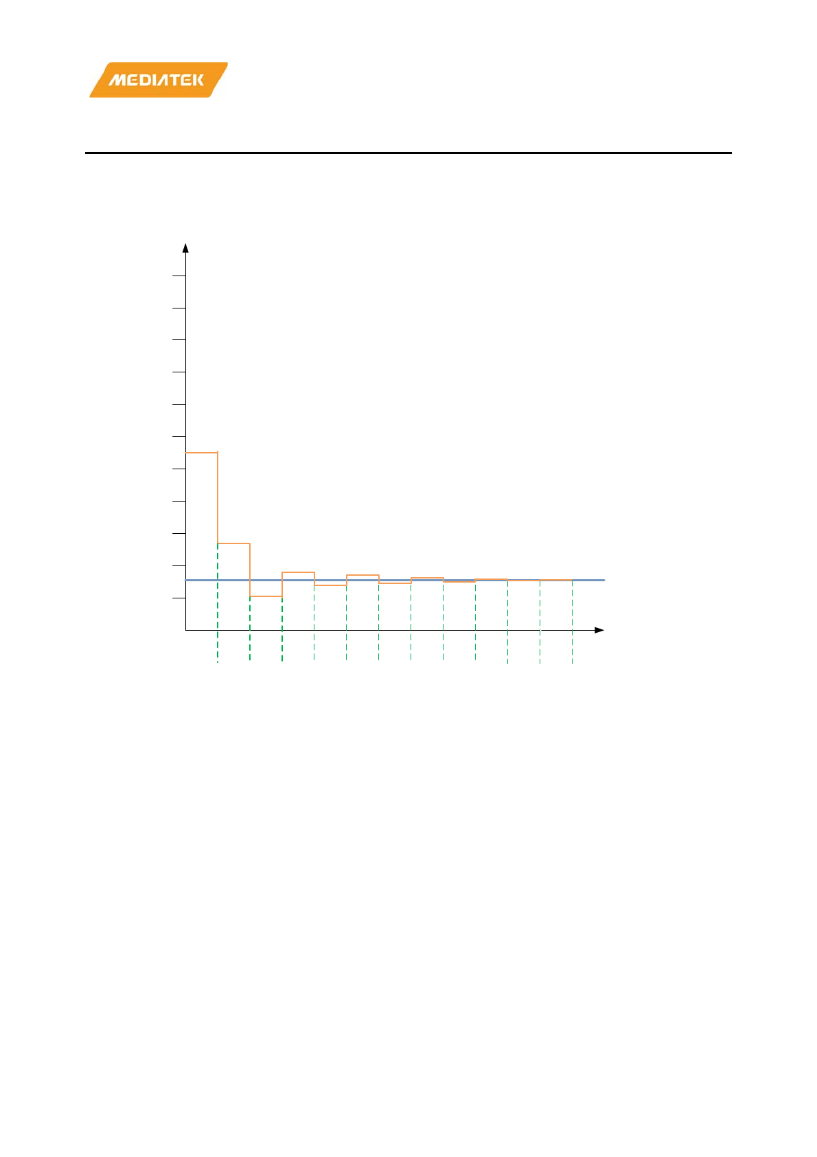
MT7686 Reference Manual
© 2016 - 2017 MediaTek Inc.
Page 379 of 536
This document contains information that is proprietary to MediaTek Inc. (“MediaTek”) and/or its licensor(s).
Any unauthorized use, reproduction or disclosure of this document in whole or in part is strictly prohibited.
17. Auxiliary ADC Unit
MT7686 features an auxiliary ADC (AUXADC) unit with four channels to measure external channels and a 12-bit
Successive Approximation Register (SAR) ADC. The SAR ADC waveform is shown in Figure 16.5-1.
1/11 V
ref
2/11 V
ref
11/11 V
ref
10/11 V
ref
9/11 V
ref
8/11 V
ref
7/11 V
ref
6/11 V
ref
5/11 V
ref
4/11 V
ref
3/11 V
ref
V
in
bit[11]
=0
bit[10]
=0
bit[2]=
0
bit[3]=
1
bit[4]=
0
bit[5]=
1
bit[6]=
0
bit[7]=
1
bit[8]=
0
bit[9]=
1
bit[1]=
1
bit[0]=
0Comparison
Reference
Figure 16.5-1. SAR ADC waveform
17.1. Features
1) Immediate mode.
There are four channels for external channel use in immediate mode. The AUXADC measures the values only once
when the flag of the channel in the AUXADC_CON1 register is set. The value sampled for channel 0 is stored in
register AUXADC_DATA0, and the value for channel 1 is stored in register AUXADC_DATA1, and so on.
2) Zero-consumption-voltage (ZCV) mode.
There is only one channel for external channel use in ZCV mode. This channel measures voltage automatically to
monitor battery power during power up and wake up.
17.2. Block diagram
The block diagram for the AUXADC is shown in Figure 17.2-1.
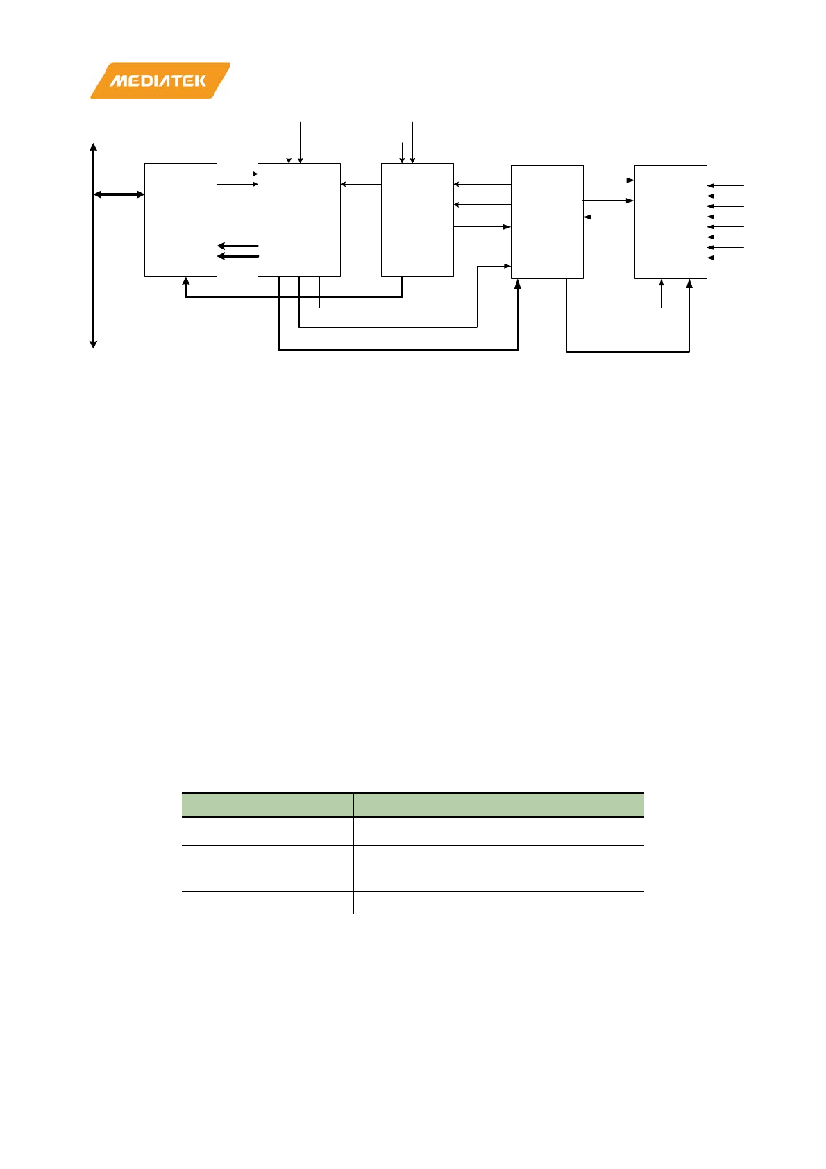
MT7686 Reference Manual
© 2016 - 2017 MediaTek Inc.
Page 380 of 536
This document contains information that is proprietary to MediaTek Inc. (“MediaTek”) and/or its licensor(s).
Any unauthorized use, reproduction or disclosure of this document in whole or in part is strictly prohibited.
AUXADC_REG
APB BUS
AUXADC_CORE AUXADC_SIF
DIV_EN_H
DIV_EN
ADC_SDATA
ADC_SFS
ADC_SCKO
ADC_R
DY
ADC_LAT
CH
IMMEDIATE
_STR
ADC_STA
TE
AUTOSET_S
TR
SEL_LATCH
[3:0]
PDN_AUXADC
ADC_PD
N
ADC_SEL_IN
ADC_ST
DIV_EN
SADC_SIF ADC
DAC
COM
P
Vi
n
Latch_Data
SPLD
ADC_SEL_OUT
Figure 17.2-1. AUXADC block diagram
17.3. Functions
1) Immediate mode.
The AUXADC measures values once only when the flag of the channel in the AUXADC_CON1 register is set. For
example, if the value in AUXADC_CON1 is set, the AUXADC will sample the data for channel 0. Without configuring
AUXADC_CON4, AUXADC_CON1 must be cleared and set again to initialize another sampling.
If the AUTOSET flag in register AUXADC_CON4 is set, the auto-sampling function will be enabled. The A/D converter
then samples the data for the specified channel. When the data register AUXADC_DATA0 is read, the A/D converter
immediately samples the next value for channel 0.
If multiple channels are selected at the same time, the task will be performed sequentially on every selected
channel. For example, if AUXADC_CON1 is set to 0xf, if 4 channels are selected, the state machine in the unit will
start sampling from channel 3 to channel 0 and save the values of each input channel in respective registers.
2) Zero-consumption-voltage (ZCV) mode
There is only one channel for external channels in ZCV mode. This channel only measures voltage automatically
during power up and wake up. Set AUXADC_ZCV_BYPASS to 1, to prevent default automatic measurements after
wake up. The ZCV data will be saved into AUXADC_DATA_ZCV.
Table 17.3-1. AUXADC channel description
AUXADC Channel ID Description
Channel 0 External (immediate mode)
Channel 1 External (immediate mode and ZCV mode)
Channel 2 External (immediate mode)
Channel 3 External (immediate mode)
17.4. Programming sequence
1) Immediate mode:
Immediate mode sampling is accomplished by programming AUXADC_CON1 with the channels to be sampled.
MT7686 Reference Manual
© 2016 - 2017 MediaTek Inc.
Page 381 of 536
This document contains information that is proprietary to MediaTek Inc. (“MediaTek”) and/or its licensor(s).
Any unauthorized use, reproduction or disclosure of this document in whole or in part is strictly prohibited.
• Sample data after selecting the channel.
• Wait for AUXADC_CON3 [0]: ADC_STAT to change from 1 (busy) to 0 (idle).
It is required to program AUXADC_CON1 back to 0 before sampling again. The immediate mode programming
sequence is summarized in Figure 17.4-1.
Turn on AUXADC
power and clock
Set channel
(immediate mode)
Sample data
Wait for ADC_STAT== 0
Step 1. Turn on analog power
MACRO_CON2[0]:
RG_AUXADC_LDO_EN =1
Step 2. Turn on digital clock
ANA_EN_CON[0]: AUXADC_EN =1
Step 1. Clear AUXADC_CON1
AUXADC_CON1 = 0
Step 2. Set the channel
AUXADC_CON1 = 4'b100
Software reset
Step 1.
AUXADC_CON4[8]: SOFT_RST = 1
Step 2.
AUXADC_CON4[8]: SOFT_RST = 0
Figure 17.4-1. Immediate mode programming sequence
Note: to disable the AUXADC, turn off digital clock (ANA_EN_CON[0] = 0) first and turn off analog power
(MACRO_CON2[0]=0) in the end.
2) Zero-consumption-voltage (ZCV) mode:
There is only one channel for external channels in ZCV mode. This channel only measures voltage automatically
during power up and wake up. There is no need to control the ZCV programming sequence. However, it is possible
to control the measurement of next wake up by programming AUXADC_ZCV_BYPASS.
Note: To use ZCV feature, do not disable the clock, otherwise the ZCV feature will not work for next wakeup.
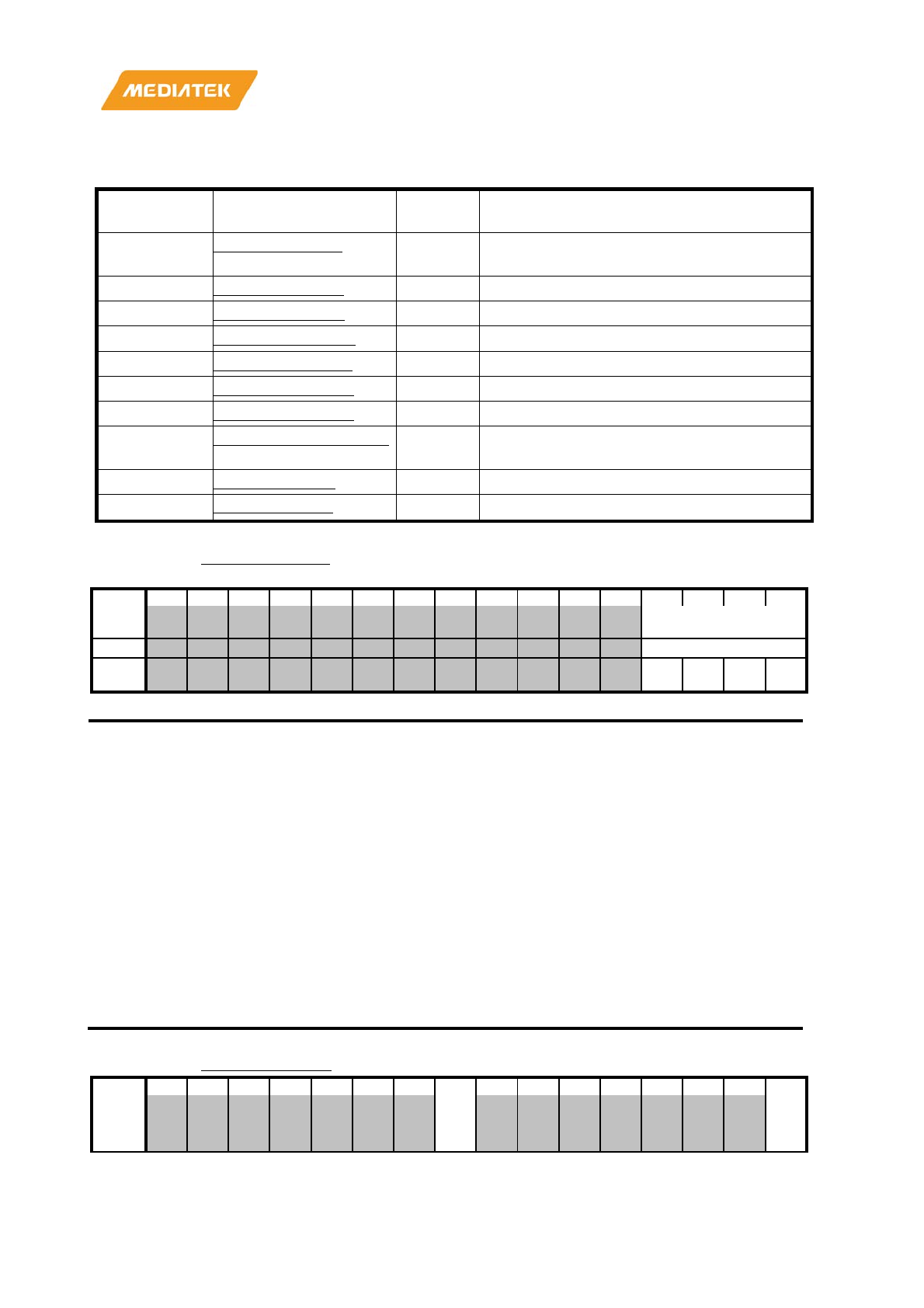
MT7686 Reference Manual
© 2016 - 2017 MediaTek Inc.
Page 382 of 536
This document contains information that is proprietary to MediaTek Inc. (“MediaTek”) and/or its licensor(s).
Any unauthorized use, reproduction or disclosure of this document in whole or in part is strictly prohibited.
17.5. Register mapping
Module name: AUXADC Base address: (+a0120000h)
Address Name Width
(bits) Register Functionality
A0120004
AUXADC_CON1
16
Configure the channel in immediate
mode.
A0120008
AUXADC_CON3
16
Configure reset and read status.
A012000C
AUXADC_CON4
16
Configure auto
-set.
A0120010
AUXADC_DATA0
16
Channel 0 data
A0120014
AUXADC_DATA1
16
Channel 1 data
A0120018
AUXADC_DATA2
16
Channel 2 data
A012001C
AUXADC_DATA3
16
Channel 3 data
A0120050
AUXADC_DATA_ZCV
16
ZCV channel data
A0120074
MACRO_CON2
16
Configure analog
control.
A0120078
ANA_EN_CON
16
Configure digital clock.
A0120004
AUXADC_CON1
Configure the channel in
immediate
mode
00000000
Bit
15
14
13
12
11
10
9
8
7
6
5
4
3
2
1
0
Nam
e
AUXADC_CON1
Type
RW
Rese
t
0 0 0 0
Bit(s)
Name
Description
3:0
AUXADC_CON1
Bit 0 : Channel 0 immediate mode
•
0: The channel is not selected.
•
1: The channel is selected.
Bit 1 : Channel 1 immediate mode
•
0: The channel is not selected.
•
1: The channel is selected.
Bit 2 : Channel 2 immediate mode
•
0: The channel is not selected.
•
1: The channel is selected.
Bit 3 : Channel 3 immediate mode
•
0: The channel is not selected.
•
1: The channel is selected.
A0120008
AUXADC_CON3
Configure the
reset and read status
00000000
Bit
15
14
13
12
11
10
9
8
7
6
5
4
3
2
1
0
Nam
e
SO
FT
_R
ST
AD
C_
ST
AT
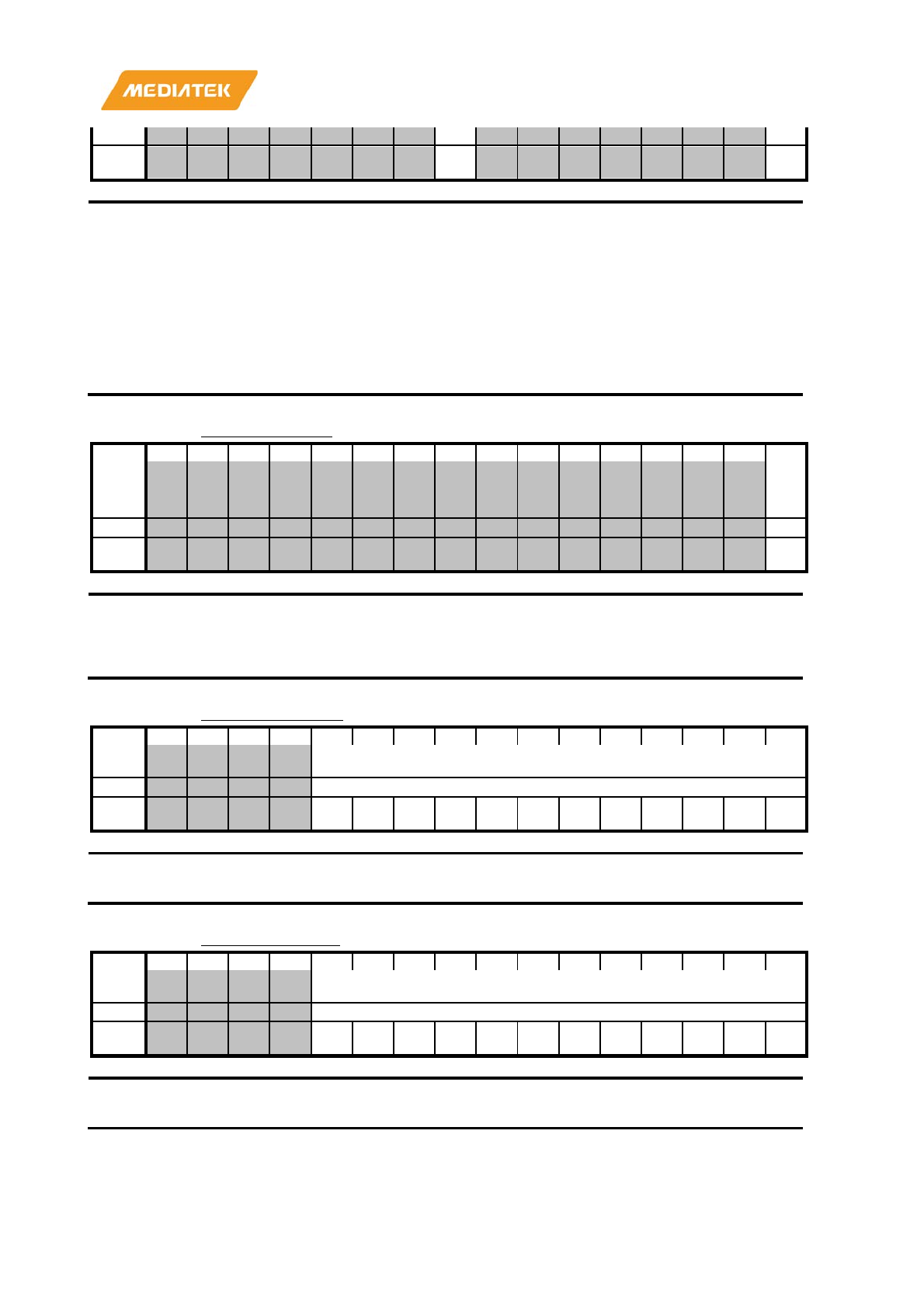
MT7686 Reference Manual
© 2016 - 2017 MediaTek Inc.
Page 383 of 536
This document contains information that is proprietary to MediaTek Inc. (“MediaTek”) and/or its licensor(s).
Any unauthorized use, reproduction or disclosure of this document in whole or in part is strictly prohibited.
Type
RW
RO
Rese
t
0 0
Bit(s)
Name
Description
8
SOFT_RST
Software reset AUXADC state machine
•
0: Default value
•
1: Reset the AUXADC state machine
Set to 1 then clear again to
finish reset.
0
ADC_STAT
Defines the state of the module
•
0: Idle.
•
1: Busy.
A012000C
AUXADC_CON4
Configure the
auto set
00000000
Bit
15
14
13
12
11
10
9
8
7
6
5
4
3
2
1
0
Nam
e
AU
TO
SE
T
Type
RW
Rese
t
0
Bit(s)
Name
Description
0
AUTOSET
Defines the auto
-sampling mode of the module. In this mode, each
channel starts sampling immediately without configuring the
control register AUXADC_CON1 again.
A0120010
AUXADC_DATA0
Channel 0
data
00000000
Bit
15
14
13
12
11
10
9
8
7
6
5
4
3
2
1
0
Nam
e
AUXADC_DATA0
Type
RO
Rese
t
0 0 0 0 0 0 0 0 0 0 0 0
Bit(s)
Name
Description
11:0
AUXADC_DATA0
Sampled data for channel 0.
A0120014
AUXADC_DATA1
Channel 1
data
00000000
Bit
15
14
13
12
11
10
9
8
7
6
5
4
3
2
1
0
Nam
e
AUXADC_DATA1
Type
RO
Rese
t
0 0 0 0 0 0 0 0 0 0 0 0
Bit(s)
Name
Description
11:0
AUXADC_DATA1
Sampled data for channel 1.
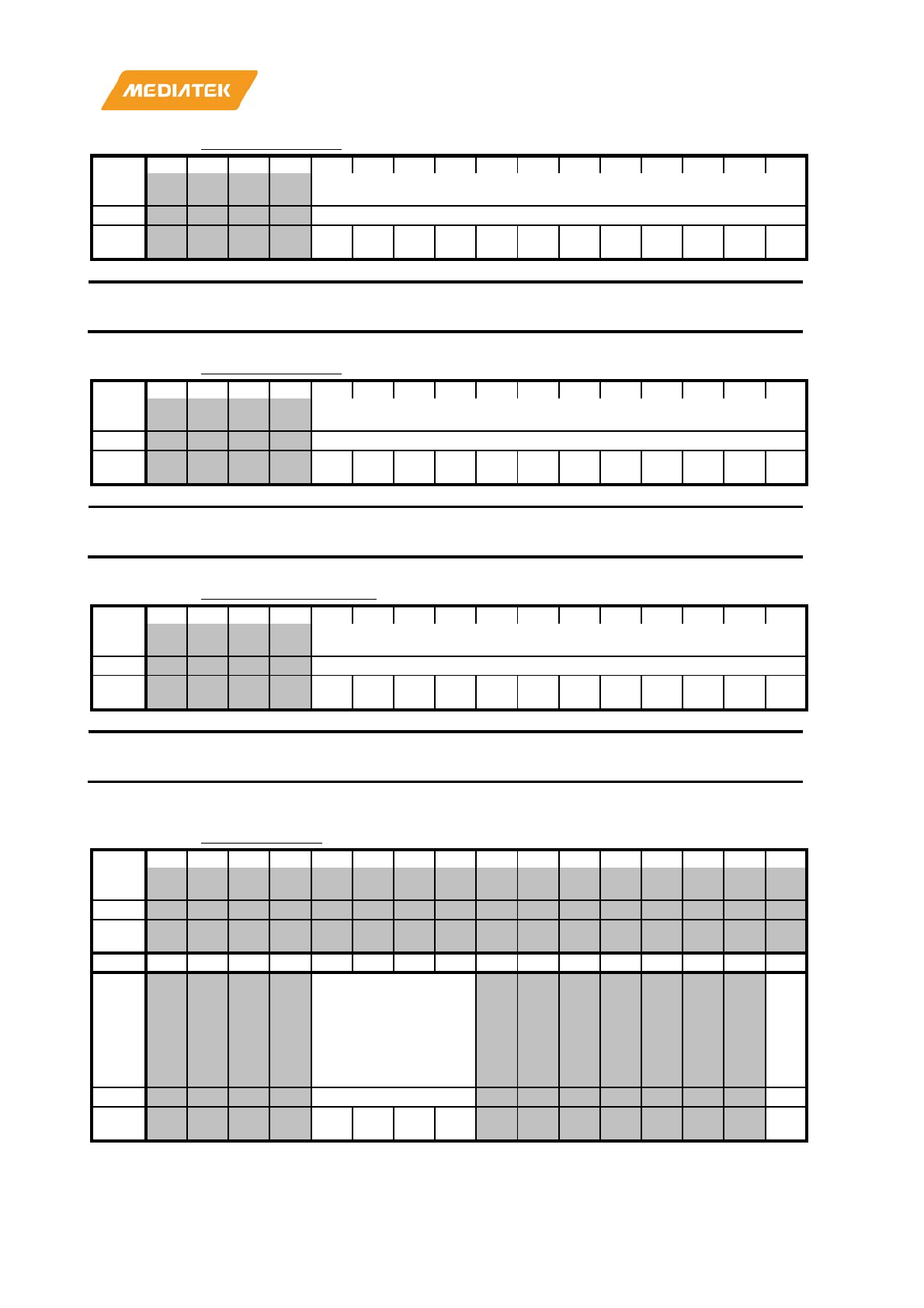
MT7686 Reference Manual
© 2016 - 2017 MediaTek Inc.
Page 384 of 536
This document contains information that is proprietary to MediaTek Inc. (“MediaTek”) and/or its licensor(s).
Any unauthorized use, reproduction or disclosure of this document in whole or in part is strictly prohibited.
A0120018
AUXADC_DATA2
Channel 2
data
00000000
Bit
15
14
13
12
11
10
9
8
7
6
5
4
3
2
1
0
Nam
e
AUXADC_DATA2
Type
RO
Rese
t
0 0 0 0 0 0 0 0 0 0 0 0
Bit(s)
Name
Description
11:0
AUXADC_DATA2
Sampled data for channel 2.
A012001C
AUXADC_DATA3
Channel 3
data
00000000
Bit
15
14
13
12
11
10
9
8
7
6
5
4
3
2
1
0
Nam
e
AUXADC_DATA3
Type
RO
Rese
t
0 0 0 0 0 0 0 0 0 0 0 0
Bit(s)
Name
Description
11:0
AUXADC_DATA3
Sampled data for channel 3.
A0120050
AUXADC_DAT
A_ZCV
ZCV_channel
00000000
Bit
15
14
13
12
11
10
9
8
7
6
5
4
3
2
1
0
Nam
e
AUXADC_DATA_ZCV
Type
RO
Rese
t
0 0 0 0 0 0 0 0 0 0 0 0
Bit(s)
Name
Description
11:0
AUXADC_DATA_ZCV
Sampled data for ZCV channel
A0120074
MACRO_CON2
Configure the analog control
00000400
Bit
31
30
29
28
27
26
25
24
23
22
21
20
19
18
17
16
Nam
e
Type
Rese
t
Bit
15
14
13
12
11
10
9
8
7
6
5
4
3
2
1
0
Nam
e RG_AUXADC_LDO
RG
_A
UX
AD
C_
LD
O_
EN
Type
RW
RW
Rese
t
0 1 0 0 0
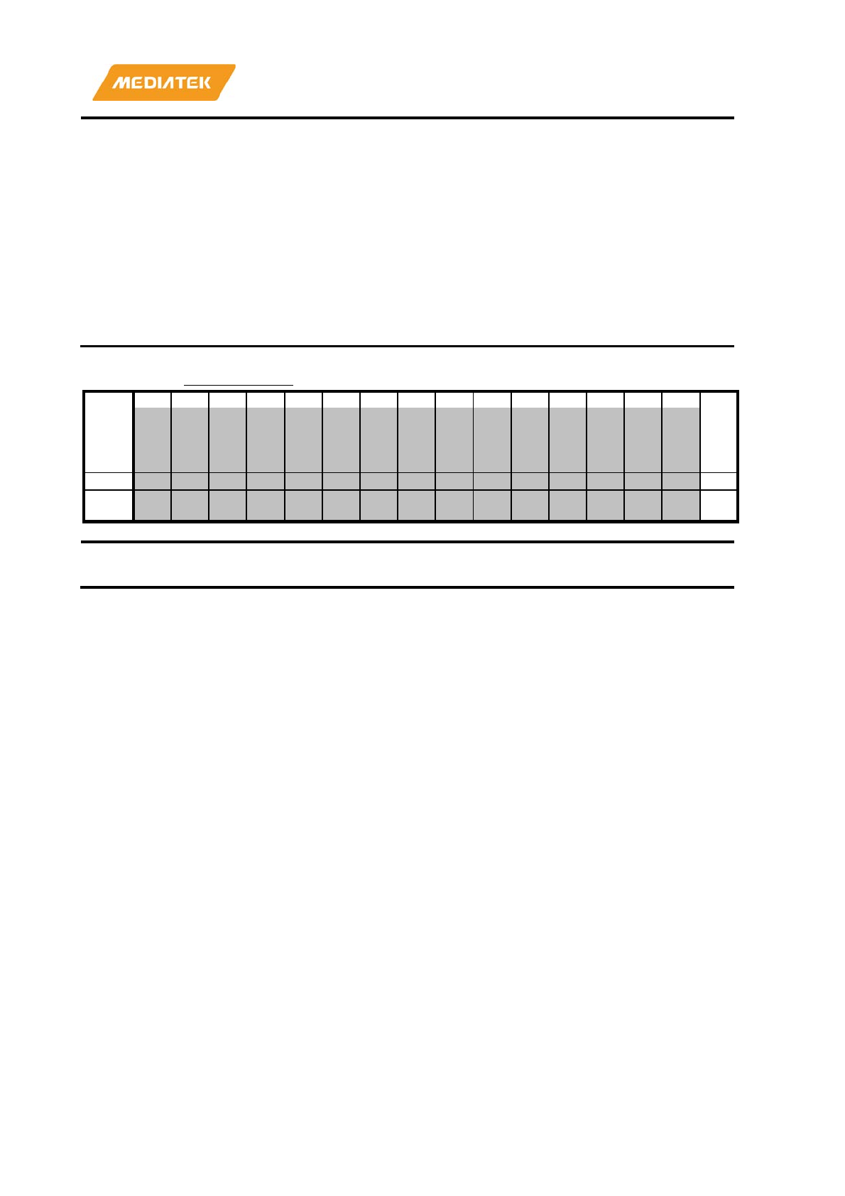
MT7686 Reference Manual
© 2016 - 2017 MediaTek Inc.
Page 385 of 536
This document contains information that is proprietary to MediaTek Inc. (“MediaTek”) and/or its licensor(s).
Any unauthorized use, reproduction or disclosure of this document in whole or in part is strictly prohibited.
Bit(s)
Name
Description
11:8
RG_AUXADC_LDO
•
4'b0000 : 2.4V
•
4'b0001 : 2.425V
•
4'b0010 : 2.45V
•
4'b0011 : 2.475V
•
4'b0100 : 2.5V (default value)
•
4'b0101 : 2.525V
•
4'b0110 : 2.55V
•
4'b0111 : 2.575V
0
RG_AUXADC_LDO_EN
Enables the AUXADC analog power.
A0120078
ANA_EN_CON
Configure the
digital clock
00000000
Bit
15
14
13
12
11
10
9
8
7
6
5
4
3
2
1
0
Nam
e
AU
XA
DC
_E
N
Type
RW
Rese
t
0
Bit(s)
Name
Description
0
AUXADC_EN
Enables the AUXADC clock.
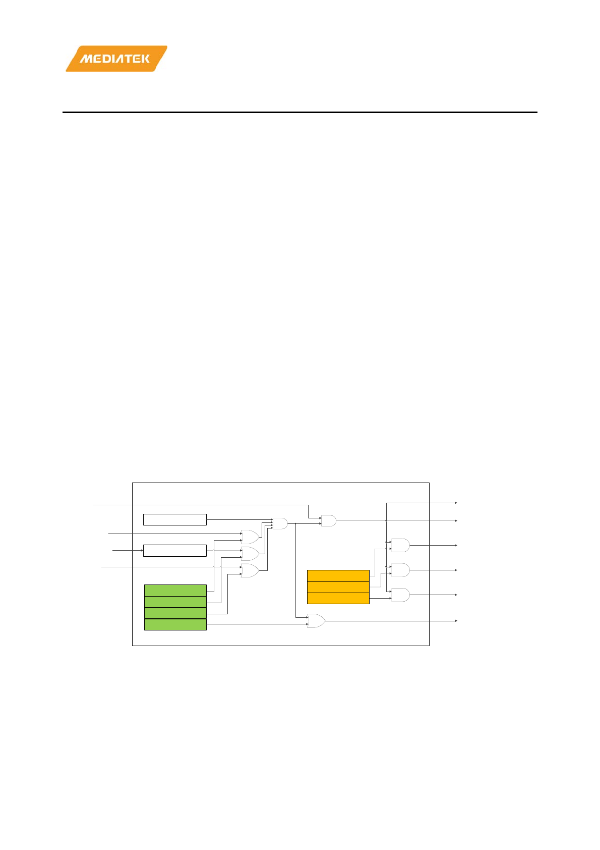
MT7686 Reference Manual
© 2016 - 2017 MediaTek Inc.
Page 386 of 536
This document contains information that is proprietary to MediaTek Inc. (“MediaTek”) and/or its licensor(s).
Any unauthorized use, reproduction or disclosure of this document in whole or in part is strictly prohibited.
18. Reset Generation Unit
MediaTek MT7686 reset generation unit (RGU) provides three types of resets: hardware reset, watchdog reset and
software reset:
• Hardware reset. This reset is input through the xreset_rstb pin, which is driven low during PMU power-on.
The hardware reset has a global effect on the chip: all digital and analog circuits are initialized.
• Watchdog reset. The watchdog reset is generated when the watchdog timer expires. CMSYS, CONNSYS,
CONNSYS_CPU, SDCTL and INFRASYS are affected by the watchdog reset.
• Software reset. Software resets are local reset signals that initialize specific hardware components.
Subsystems with this feature are CONNSYS, CONNSYS_CPU and SDCTL.
18.1. Features
• Watchdog timer (WDT) time out length and interval time can be configured by registers WDT_LENGTH
and WDT_INTERVAL.
• The reset generation unit includes four external trigger sources: xreset_rstb, JTAG_rstb, AIRCR_rstb (from
Cortex M4) and PCM_wdt_rstb (from power control management). The latter three signals can be masked
independently by registers MODULE0_RST_MASK, MODULE1_RST_MASK and MODULE2_RST_MASK.
• AIRCR_rstb reset source can be extended by register AIRCR_RST_INTERVAL for special applications.
• Each register can be protected by corresponding keys to avoid unexpected register settings.
• The RGU includes six retention flags and six retention data, these registers will only be reset by hardware
reset (xreset_rstb).
18.2. Block diagram
Watch Dog Timer
RG:
PCM_wdt_rstb_mask
RG: JTAG_rstb_mask
RG: AIRCR_rstreq_mask
xreset_rstb
hreset_rstb
cmsys_rstb
connsys_rstb
connsys_cpu_rstb
sdctl_rstb
pmu_rgu_rstb
JTAG_rstb (PAD)
Reset Extender
RG: sdctl_sw_rst
RG: connsys_sw_rst
RG: connsys_cpu_sw_rst
RGU
RG: PMU_rgu_rst_mask
PCM_wdt_rstb
AIRCR_rstreq(PAD)
Figure 18.2-1. Block diagram of RGU
18.3. WDT timeout and interval source
The WDT timeout length is generated by a 16-bit counter and the counter clock period is 15.625 ms. The WDT
interval time is generated by a 16-bit counter and the counter clock period is 3.05 us. The detailed diagram is
shown in Figure 18.3-1.
MT7686 Reference Manual
© 2016 - 2017 MediaTek Inc.
Page 387 of 536
This document contains information that is proprietary to MediaTek Inc. (“MediaTek”) and/or its licensor(s).
Any unauthorized use, reproduction or disclosure of this document in whole or in part is strictly prohibited.
WDT reset
(active low)
WDT length
(counter unit: 15.625 ms)
WDT interval
(counter unit: 3.05 us)
Figure 18.3-1. WDT timeout length and interval time
The AIRCR reset extender is an 8-bit counter, and the counter clock period is 3.05 µs. The operation range of the
AIRCR interval extender is from 0 to 7.78 µs.
18.4. Register mapping
Module name: RGU Base address: (+A2090000h)
Address
Name
Width
(bits)
Registe
r Functionality
A2090000
WDT_EN
32
Watchdog Timer Enable Register
A2090004
WDT_LENGTH
32
Watchdog Length Register
A2090008
WDT_INTERVAL
32
Watchdog Interval
Register
A209000C
WDT_SW_RESTART
32
Watchdog Timer Software Restart Register
A2090010
WDT_SW_RST
32
Watchdog Timer Software Reset Register
A2090014
WDT_AUTO_RESTART
_EN
32
Watchdog Timer Auto Restart Register
A2090018
WDT_IE
32
Watchdog Timer Interrupt Enable Register
A209001C
WDT_INT
32
Watchdog Timer
Interrupt Register
A2090020
WDT_STA
32
Watchdog Timer Status Register
A2090024
SW_RST0
32
Software Reset 0 Register
A2090028
SW_RST1
32
Software Reset 1 Register
A209002C
RST_MASK0
32
Reset Mask 0 Register
A2090030
RST_MASK1
32
Reset Mask 1 Register
A2090034
AIRCR_RST_INTERVA
L
32
AIRCR Reset Interval Register
A2090038
RETN_FLAG0
32
Retention Flag 0 Register
A209003C
RETN_FLAG1
32
Retention Flag 1 Register
A2090040
RETN_FLAG2
32
Retention Flag 2 Register
A2090044
RETN_FLAG3
32
Retention Flag 3 Register
A2090048
RETN_FLAG4
32
Retention Flag 4 Register
A209004C
RETN_FLAG5
32
Retention Flag 5 Register
A2090050
RETN_DAT0
32
Retention Data 0 Register
A2090054
RETN_DAT1
32
Retention Data 1 Register
A2090058
RETN_DAT2
32
Retention Data 2 Register
A209005C
RETN_DAT3
32
Retention Data 3 Register
A2090060
RETN_DAT4
32
Retention Data 4 Register
A2090064
RETN_DAT5
32
Retention Data 5 Register
MT7686 Reference Manual
© 2016 - 2017 MediaTek Inc.
Page 388 of 536
This document contains information that is proprietary to MediaTek Inc. (“MediaTek”) and/or its licensor(s).
Any unauthorized use, reproduction or disclosure of this document in whole or in part is strictly prohibited.
A209000
0 WDT_EN Watchdog Timer Enable Register 00000100
Bit
31
30
29
28
27
26
25
24
23
22
21
20
19
18
17
16
Name
Type
Reset
Bit
15
14
13
12
11
10
9
8
7
6
5
4
3
2
1
0
Name
WD
T_
EN
KEY
Type
RW
WO
Reset
1
0
0
0
0
0
0
0
0
Bit(s) Name Description
8 WDT_EN Watchdog timer enable
0: Disable watchdog timer
1: Enable watchdog timer
7:0 KEY Configure WDT enable register, if KEY= 8'h11.
A2090004 WDT_LENGT
H Watchdog Length Register 07FF0000
Bit
31
30
29
28
27
26
25
24
23
22
21
20
19
18
17
16
Name
WDT_LENGTH
Type
RW
Reset
0
0
0
0
0
1
1
1
1
1
1
1
1
1
1
1
Bit
15
14
13
12
11
10
9
8
7
6
5
4
3
2
1
0
Name
KEY
Type
WO
Reset
0
0
0
0
0
0
0
0
Bit(s) Name Description
31:16 WDT_LENGTH Watchdog timer length
The counter unit length is 15.625 ms.
7:0 KEY Configure WDT length, if KEY= 8'h12.
A209000
8
WDT_INTER
VAL Watchdog Interval Register 0FFF0000
Bit
31
30
29
28
27
26
25
24
23
22
21
20
19
18
17
16
Name
WDT_INTERVAL
Type
RW
Reset
0
0
0
0
1
1
1
1
1
1
1
1
1
1
1
1
Bit
15
14
13
12
11
10
9
8
7
6
5
4
3
2
1
0
Name
KEY
Type
WO
Reset
0
0
0
0
0
0
0
0
Bit(s) Name Description
31:16 WDT_INTERVAL Watchdog timer interval
Indicates reset duration when watchdog timer timeout occurs. However, the
register will not be valid when WDT_IE is 1.
The interval counter unit is 3.05 µs.
7:0 KEY Configure WDT interval, if KEY= 8'h13.
MT7686 Reference Manual
© 2016 - 2017 MediaTek Inc.
Page 389 of 536
This document contains information that is proprietary to MediaTek Inc. (“MediaTek”) and/or its licensor(s).
Any unauthorized use, reproduction or disclosure of this document in whole or in part is strictly prohibited.
A209000
C
WDT_SW_R
ESTART Watchdog Timer Software Restart Register 00000000
Bit
31
30
29
28
27
26
25
24
23
22
21
20
19
18
17
16
Name
KEY[31:16]
Type
WO
Reset
0
0
0
0
0
0
0
0
0
0
0
0
0
0
0
0
Bit
15
14
13
12
11
10
9
8
7
6
5
4
3
2
1
0
Name
KEY[15:0]
Type
WO
Reset
0
0
0
0
0
0
0
0
0
0
0
0
0
0
0
0
Bit(s) Name Description
31:0 KEY Watchdog timer software restart
Software restart watchdog timer, if KEY = 32'h1456789a.
A2090010 WDT_SW_R
ST Watchdog Timer Software Reset Register 00000000
Bit
31
30
29
28
27
26
25
24
23
22
21
20
19
18
17
16
Name
KEY[31:16]
Type
WO
Reset
0
0
0
0
0
0
0
0
0
0
0
0
0
0
0
0
Bit
15
14
13
12
11
10
9
8
7
6
5
4
3
2
1
0
Name
KEY[15:0]
Type
WO
Reset
0
0
0
0
0
0
0
0
0
0
0
0
0
0
0
0
Bit(s) Name Description
31:0 KEY Watchdog timer software reset
Software trigger watchdog timer reset, if KEY= 32'h156789ab.
A2090014
WDT_AUTO_
RESTART_E
N
Watchdog Timer Auto Restart Register 00000000
Bit
31
30
29
28
27
26
25
24
23
22
21
20
19
18
17
16
Name
Type
Reset
Bit
15
14
13
12
11
10
9
8
7
6
5
4
3
2
1
0
Name
WD
T_
AU
TO
_R
EST
AR
T_
EN
KEY
Type
RW
WO
Reset
0
0
0
0
0
0
0
0
0
Bit(s) Name Description
8 WDT_AUTO_RESTART_
EN Watchdog timer automatic restart enable
Hardware auto restart after watch dog timer reset
0: Disable
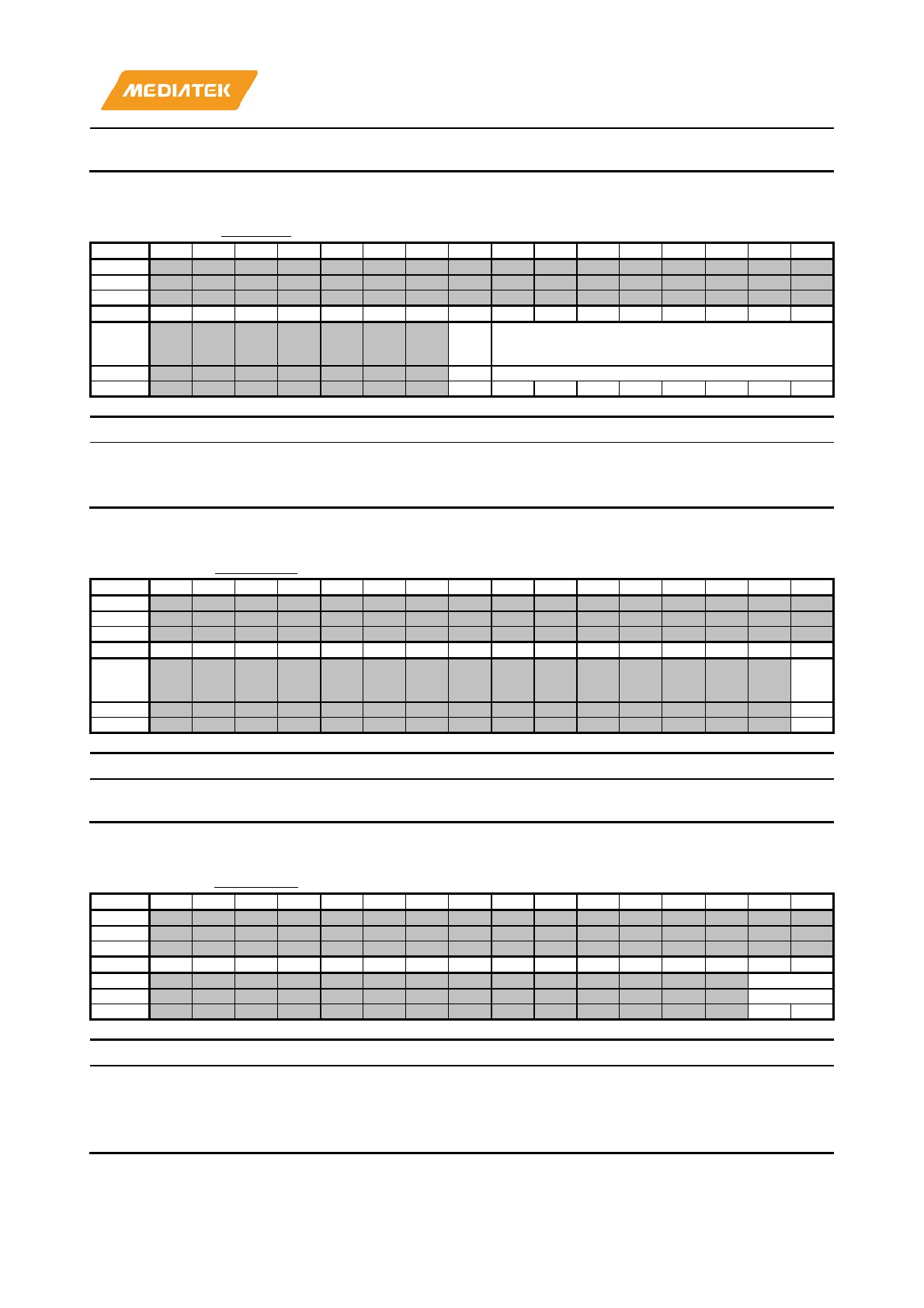
MT7686 Reference Manual
© 2016 - 2017 MediaTek Inc.
Page 390 of 536
This document contains information that is proprietary to MediaTek Inc. (“MediaTek”) and/or its licensor(s).
Any unauthorized use, reproduction or disclosure of this document in whole or in part is strictly prohibited.
1: Enable
7:0 KEY Configure WDT automatic restart enable register, if KEY= 8'h16.
A2090018 WDT_IE Watchdog Timer Interrupt Enable Register 00000000
Bit
31
30
29
28
27
26
25
24
23
22
21
20
19
18
17
16
Name
Type
Reset
Bit
15
14
13
12
11
10
9
8
7
6
5
4
3
2
1
0
Name
WD
T_I
E
KEY
Type
RW
WO
Reset
0
0
0
0
0
0
0
0
0
Bit(s) Name Description
8 WDT_IE Watchdog timer interrupt enable
Issues an interrupt instead of a watchdog timer reset.
7:0 KEY Configure WDT interrupt enable, if KEY= 8'h17.
A209001C WDT_INT Watchdog Timer Interrupt Register 00000000
Bit
31
30
29
28
27
26
25
24
23
22
21
20
19
18
17
16
Name
Type
Reset
Bit
15
14
13
12
11
10
9
8
7
6
5
4
3
2
1
0
Name
WD
T_I
NT
Type
RC
Reset
0
Bit(s) Name Description
0 WDT_INT Watchdog timer interrupt
WDT interrupt read clear register.
A2090020 WDT_STA Watchdog Timer Status Register 00000000
Bit
31
30
29
28
27
26
25
24
23
22
21
20
19
18
17
16
Name
Type
Reset
Bit
15
14
13
12
11
10
9
8
7
6
5
4
3
2
1
0
Name
WDT_STA
Type
RO
Reset
0
0
Bit(s) Name Description
1:0 WDT_STA Watchdog timer status
[1]: HW_WDT, indicates the cause of watchdog reset.
0: Reset not due to watchdog timer.
1: Reset due to watchdog timer expired timeout.
[0]: SW_WDT, indicates if watchdog timer reset is triggered by software.
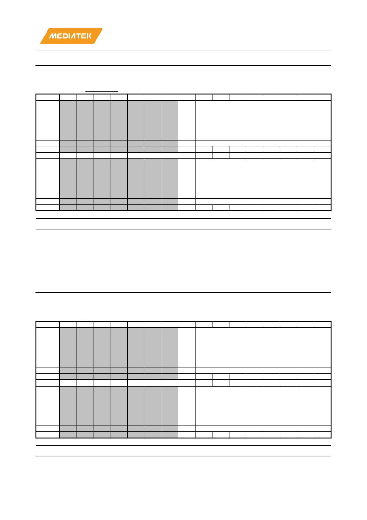
MT7686 Reference Manual
© 2016 - 2017 MediaTek Inc.
Page 391 of 536
This document contains information that is proprietary to MediaTek Inc. (“MediaTek”) and/or its licensor(s).
Any unauthorized use, reproduction or disclosure of this document in whole or in part is strictly prohibited.
0: Reset not due to software triggered watchdog timer.
1: Reset due to software triggered watchdog timer.
A2090024 SW_RST0 Software Reset 0 Register 00000100
Bit
31
30
29
28
27
26
25
24
23
22
21
20
19
18
17
16
Name
MO
DU
LE1
_S
W_
RS
T
KEY1
Type
RW
WO
Reset
0
0
0
0
0
0
0
0
0
Bit
15
14
13
12
11
10
9
8
7
6
5
4
3
2
1
0
Name
MO
DU
LE
0_S
W_
RS
T
KEY0
Type
RW
WO
Reset
1
0
0
0
0
0
0
0
0
Bit(s) Name Description
24 MODULE1_SW_RST CONNSYS_CPU_SW_RST
0: no reset
1: invoke a reset
23:16 KEY1 Configure CONNSY CPU software reset if KEY= 8'h19
8 MODULE0_SW_RST CONNSYS_SW_RST
0: no reset
1: invoke a reset
7:0 KEY0 Configure CONNSY software reset if KEY= 8'h18
A2090028 SW_RST1 Software Reset 1 Register 00000000
Bit
31
30
29
28
27
26
25
24
23
22
21
20
19
18
17
16
Name
MO
DU
LE3
_S
W_
RS
T
KEY1
Type
RW
WO
Reset
0
0
0
0
0
0
0
0
0
Bit
15
14
13
12
11
10
9
8
7
6
5
4
3
2
1
0
Name
MO
DU
LE2
_S
W_
RS
T
KEY0
Type
RW
WO
Reset
0
0
0
0
0
0
0
0
0
Bit(s) Name Description
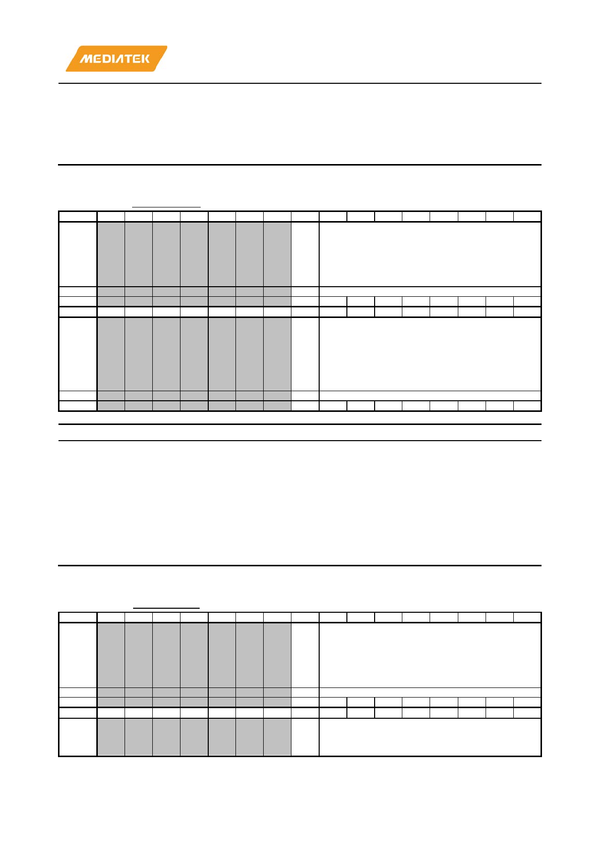
MT7686 Reference Manual
© 2016 - 2017 MediaTek Inc.
Page 392 of 536
This document contains information that is proprietary to MediaTek Inc. (“MediaTek”) and/or its licensor(s).
Any unauthorized use, reproduction or disclosure of this document in whole or in part is strictly prohibited.
24 MODULE3_SW_RST Reserved
23:16 KEY1
8 MODULE2_SW_RST SDCTL_SW_RST
0: no reset
1: Invoke a reset
7:0 KEY0 Configure SDCTL software reset, if KEY= 8'h1a.
A209002C RST_MASK0 Reset Mask 0 Register 01000100
Bit
31
30
29
28
27
26
25
24
23
22
21
20
19
18
17
16
Name
MO
DU
LE1
_R
ST_
MA
SK
KEY1
Type
RW
WO
Reset
1
0
0
0
0
0
0
0
0
Bit
15
14
13
12
11
10
9
8
7
6
5
4
3
2
1
0
Name
MO
DU
LE
0_
RS
T_
MA
SK
KEY0
Type
RW
WO
Reset
1
0
0
0
0
0
0
0
0
Bit(s) Name Description
24 MODULE1_RST_MASK AIRCR reset require mask
Mask reset source from AIRCR, default enable.
0: disable mask
1: enable mask
23:16 KEY1 Configure AIRCR reset mask, if KEY= 8'h1d.
8 MODULE0_RST_MASK JTAG reset mask
Mask reset source from JTAG, default enable.
0: disable mask
1: enable mask
7:0 KEY0 Configure JTAG reset mask, if KEY= 8'h1c.
A2090030 RST_MASK1 Reset Mask 1 Register 01000100
Bit
31
30
29
28
27
26
25
24
23
22
21
20
19
18
17
16
Name
MO
DU
LE3
_R
ST_
MA
SK
KEY1
Type
RW
WO
Reset
1
0
0
0
0
0
0
0
0
Bit
15
14
13
12
11
10
9
8
7
6
5
4
3
2
1
0
Name
MO
DU
LE2
_R
KEY0
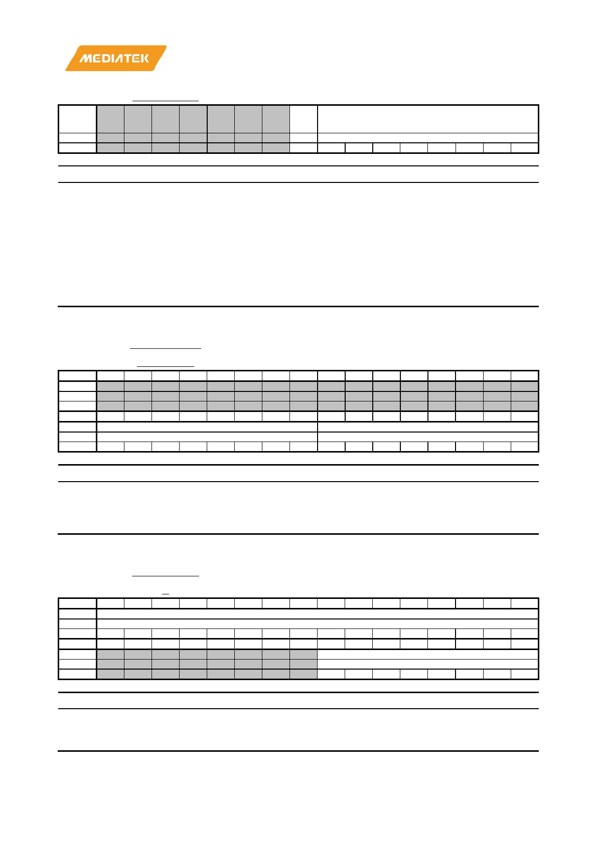
MT7686 Reference Manual
© 2016 - 2017 MediaTek Inc.
Page 393 of 536
This document contains information that is proprietary to MediaTek Inc. (“MediaTek”) and/or its licensor(s).
Any unauthorized use, reproduction or disclosure of this document in whole or in part is strictly prohibited.
A2090030 RST_MASK1 Reset Mask 1 Register 01000100
ST_
MA
SK
Type
RW
WO
Reset
1
0
0
0
0
0
0
0
0
Bit(s) Name Description
24 MODULE3_RST_MASK PMU reset mask
Mask reset to PMU, default enable.
0: disable mask
1: enable mask
23:16 KEY1 Configure PMU reset mask, if KEY= 8'h1f.
8 MODULE2_RST_MASK PCM reset require mask
Mask reset source from PCM, default enable.
0: disable mask
1: enable mask
7:0 KEY0 Configure PCM reset mask, if KEY= 8'h1e.
A2090034 AIRCR_RST_
INTERVAL AIRCR Reset Interval Register 00000700
Bit
31
30
29
28
27
26
25
24
23
22
21
20
19
18
17
16
Name
Type
Reset
Bit
15
14
13
12
11
10
9
8
7
6
5
4
3
2
1
0
Name
AIRCR_RST_INTERVAL
KEY
Type
RW
WO
Reset
0
0
0
0
0
1
1
1
0
0
0
0
0
0
0
0
Bit(s) Name Description
15:8 AIRCR_RST_INTERVAL AIRCR reset interval
Indicates reset duration when AIRCR is enabled.
The interval counter unit is 3.05 us.
7:0 KEY KEY= 8'h21
A2090038 RETN_FLAG
0 Retention Flag 0 Register 00000000
Bit
31
30
29
28
27
26
25
24
23
22
21
20
19
18
17
16
Name
RETN_FLAG0
Type
RW
Reset
0
0
0
0
0
0
0
0
0
0
0
0
0
0
0
0
Bit
15
14
13
12
11
10
9
8
7
6
5
4
3
2
1
0
Name
KEY
Type
WO
Reset
0
0
0
0
0
0
0
0
Bit(s) Name Description
31:16 RETN_FLAG0 Retention flag 0
This register will only be reset by hardware reset.
7:0 KEY Configure Retention flag 0 reset mask if KEY= 8'h22
MT7686 Reference Manual
© 2016 - 2017 MediaTek Inc.
Page 394 of 536
This document contains information that is proprietary to MediaTek Inc. (“MediaTek”) and/or its licensor(s).
Any unauthorized use, reproduction or disclosure of this document in whole or in part is strictly prohibited.
A209003C RETN_FLAG1 Retention Flag 1 Register 00000000
Bit
31
30
29
28
27
26
25
24
23
22
21
20
19
18
17
16
Name
RETN_FLAG1
Type
RW
Reset
0
0
0
0
0
0
0
0
0
0
0
0
0
0
0
0
Bit
15
14
13
12
11
10
9
8
7
6
5
4
3
2
1
0
Name
KEY
Type
WO
Reset
0
0
0
0
0
0
0
0
Bit(s) Name Description
31:16 RETN_FLAG1 Retention flag 1
This register will only be reset by hardware reset.
7:0 KEY Configure retention flag 1 reset mask, if KEY= 8'h23.
A2090040 RETN_FLAG
2 Retention Flag 2 Register 00000000
Bit
31
30
29
28
27
26
25
24
23
22
21
20
19
18
17
16
Name
RETN_FLAG2
Type
RW
Reset
0
0
0
0
0
0
0
0
0
0
0
0
0
0
0
0
Bit
15
14
13
12
11
10
9
8
7
6
5
4
3
2
1
0
Name
KEY
Type
WO
Reset
0
0
0
0
0
0
0
0
Bit(s) Name Description
31:16 RETN_FLAG2 Retention flag 2
This register will only be reset by hardware reset.
7:0 KEY Configure retention flag 2 reset mask, if KEY= 8'h24.
A2090044 RETN_FLAG
3 Retention Flag 3 Register 00000000
Bit
31
30
29
28
27
26
25
24
23
22
21
20
19
18
17
16
Name
RETN_FLAG3
Type
RW
Reset
0
0
0
0
0
0
0
0
0
0
0
0
0
0
0
0
Bit
15
14
13
12
11
10
9
8
7
6
5
4
3
2
1
0
Name
KEY
Type
WO
Reset
0
0
0
0
0
0
0
0
Bit(s) Name Description
31:16 RETN_FLAG3 Retention flag 3
This register will only be reset by hardware reset.
7:0 KEY Configure retention flag 3 reset mask, if KEY= 8'h25.
MT7686 Reference Manual
© 2016 - 2017 MediaTek Inc.
Page 395 of 536
This document contains information that is proprietary to MediaTek Inc. (“MediaTek”) and/or its licensor(s).
Any unauthorized use, reproduction or disclosure of this document in whole or in part is strictly prohibited.
A2090048 RETN_FLAG
4 Retention Flag 4 Register 00000000
Bit
31
30
29
28
27
26
25
24
23
22
21
20
19
18
17
16
Name
RETN_FLAG4
Type
RW
Reset
0
0
0
0
0
0
0
0
0
0
0
0
0
0
0
0
Bit
15
14
13
12
11
10
9
8
7
6
5
4
3
2
1
0
Name
KEY
Type
WO
Reset
0
0
0
0
0
0
0
0
Bit(s) Name Description
31:16 RETN_FLAG4 Retention flag 4
This register will only be reset by hardware reset.
7:0 KEY Configure retention flag 4 reset mask, if KEY= 8'h26.
A209004
C
RETN_FLAG
5 Retention Flag 5 Register 00000000
Bit
31
30
29
28
27
26
25
24
23
22
21
20
19
18
17
16
Name
RETN_FLAG5
Type
RW
Reset
0
0
0
0
0
0
0
0
0
0
0
0
0
0
0
0
Bit
15
14
13
12
11
10
9
8
7
6
5
4
3
2
1
0
Name
KEY
Type
WO
Reset
0
0
0
0
0
0
0
0
Bit(s) Name Description
31:16 RETN_FLAG5 Retention flag 5
This register will only be reset by hardware reset.
7:0 KEY Configure retention flag 5 reset mask, if KEY= 8'h27.
A2090050 RETN_DAT0 Retention Data 0 Register 00000000
Bit
31
30
29
28
27
26
25
24
23
22
21
20
19
18
17
16
Name
RETN_DAT0[31:16]
Type
RW
Reset
0
0
0
0
0
0
0
0
0
0
0
0
0
0
0
0
Bit
15
14
13
12
11
10
9
8
7
6
5
4
3
2
1
0
Name
RETN_DAT0[15:0]
Type
RW
Reset
0
0
0
0
0
0
0
0
0
0
0
0
0
0
0
0
Bit(s) Name Description
31:0 RETN_DAT0 Retention data 0
This register will only be reset by hardware reset.
A2090054 RETN_DAT1 Retention Data 1 Register 00000000
Bit
31
30
29
28
27
26
25
24
23
22
21
20
19
18
17
16
Name
RETN_DAT1[31:16]
Type
RW
MT7686 Reference Manual
© 2016 - 2017 MediaTek Inc.
Page 396 of 536
This document contains information that is proprietary to MediaTek Inc. (“MediaTek”) and/or its licensor(s).
Any unauthorized use, reproduction or disclosure of this document in whole or in part is strictly prohibited.
A2090054 RETN_DAT1 Retention Data 1 Register 00000000
Reset
0
0
0
0
0
0
0
0
0
0
0
0
0
0
0
0
Bit
15
14
13
12
11
10
9
8
7
6
5
4
3
2
1
0
Name
RETN_DAT1[15:0]
Type
RW
Reset
0
0
0
0
0
0
0
0
0
0
0
0
0
0
0
0
Bit(s) Name Description
31:0 RETN_DAT1 Retention data 1
This register will only be reset by hardware reset.
A2090058 RETN_DAT2 Retention Data 2 Register 00000000
Bit
31
30
29
28
27
26
25
24
23
22
21
20
19
18
17
16
Name
RETN_DAT2[31:16]
Type
RW
Reset
0
0
0
0
0
0
0
0
0
0
0
0
0
0
0
0
Bit
15
14
13
12
11
10
9
8
7
6
5
4
3
2
1
0
Name
RETN_DAT2[15:0]
Type
RW
Reset
0
0
0
0
0
0
0
0
0
0
0
0
0
0
0
0
Bit(s) Name Description
31:0 RETN_DAT2 Retention data 2
This register will only be reset by hardware reset.
A209005C RETN_DAT3 Retention Data 3 Register 00000000
Bit
31
30
29
28
27
26
25
24
23
22
21
20
19
18
17
16
Name
RETN_DAT3[31:16]
Type
RW
Reset
0
0
0
0
0
0
0
0
0
0
0
0
0
0
0
0
Bit
15
14
13
12
11
10
9
8
7
6
5
4
3
2
1
0
Name
RETN_DAT3[15:0]
Type
RW
Reset
0
0
0
0
0
0
0
0
0
0
0
0
0
0
0
0
Bit(s) Name Description
31:0 RETN_DAT3 Retention data 3
This register will only be reset by hardware reset.
A2090060 RETN_DAT4 Retention Data 4 Register 00000000
Bit
31
30
29
28
27
26
25
24
23
22
21
20
19
18
17
16
Name
RETN_DAT4[31:16]
Type
RW
Reset
0
0
0
0
0
0
0
0
0
0
0
0
0
0
0
0
Bit
15
14
13
12
11
10
9
8
7
6
5
4
3
2
1
0
Name
RETN_DAT4[15:0]
Type
RW
Reset
0
0
0
0
0
0
0
0
0
0
0
0
0
0
0
0
Bit(s) Name Description
31:0 RETN_DAT4 Retention data 4

MT7686 Reference Manual
© 2016 - 2017 MediaTek Inc.
Page 397 of 536
This document contains information that is proprietary to MediaTek Inc. (“MediaTek”) and/or its licensor(s).
Any unauthorized use, reproduction or disclosure of this document in whole or in part is strictly prohibited.
This register will only be reset by hardware reset.
A2090064 RETN_DAT5 Retention Data 5 Register 00000000
Bit
31
30
29
28
27
26
25
24
23
22
21
20
19
18
17
16
Name
RETN_DAT5[31:16]
Type
RW
Reset
0
0
0
0
0
0
0
0
0
0
0
0
0
0
0
0
Bit
15
14
13
12
11
10
9
8
7
6
5
4
3
2
1
0
Name
RETN_DAT5[15:0]
Type
RW
Reset
0
0
0
0
0
0
0
0
0
0
0
0
0
0
0
0
Bit(s) Name Description
31:0 RETN_DAT5 Retention data 5
This register will only be reset by hardware reset.

MT7686 Reference Manual
© 2016 - 2017 MediaTek Inc.
Page 398 of 536
This document contains information that is proprietary to MediaTek Inc. (“MediaTek”) and/or its licensor(s).
Any unauthorized use, reproduction or disclosure of this document in whole or in part is strictly prohibited.
19. True Random Number Generator
19.1. Overview
The True Random Number Generator (TRNG) is a device in power-down domain that generates random numbers
from the ring oscillator (RO) outputs. Various types of ROs are adopted, including Hybrid Fibonacci Ring Oscillator
(H-FIRO), Hybrid Ring Oscillator (H-RO) and Hybrid Galois Ring Oscillator (H-GARO). Interrupt request (IRQ) is issued
once the random data is successfully generated.
19.2. Features
• Normal mode. In normal mode, turn on ROs and sample their outputs to generate random numbers. Once
the random data is valid, IRQ will be issued.
• Freerun mode. Continuously activates ROs to create interference on the power source. This can be used
to help prevent side-channel attacks. IRQ should be masked at this mode.
19.3. Block diagram
Figure 19.3-1 shows the block diagram of TRNG. The APB interface controller handles the MCU control signal and
activates the TRNG FSM controller to start the generation process (FSM denotes finite state machine). The Ring
oscillator core contains seven ROs, and each of them is designed based on a specific polynomial. The random data
is derived from these RO outputs. The Von Neumann Extractor is used to balance the 0/1 probability of the
random data. This feature can be enabled by TRNG_CONF (default off). Note that the generated random data are
designed for one-time use only, i.e. register TRNG_DATA will be reset right after the data is accessed by the MCU.
Ring Oscillator Core
TRNG FSM Controller
Von-Neumann Extractor
APB Interface Controller
TRNG_DATA [31:0]
Figure 19.3-1. TRNG block diagram
Figure 19.3-2 shows the block diagram of a general RO. It contains an odd number of inverter cores, a multiplexer,
and a sample register. The inverter core design is shown in Figure 19.3-3, which consists of a multiplexer, an
inverter, and a delay element. The dashed lines shown in both figures denote the oscillation path within the ring
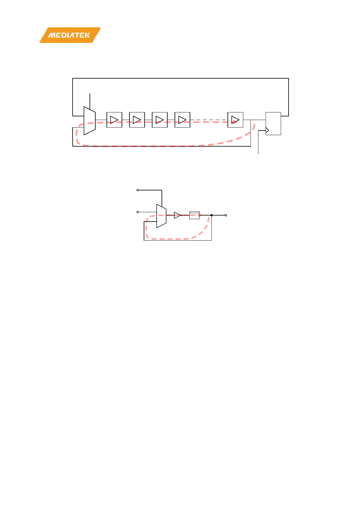
MT7686 Reference Manual
© 2016 - 2017 MediaTek Inc.
Page 399 of 536
This document contains information that is proprietary to MediaTek Inc. (“MediaTek”) and/or its licensor(s).
Any unauthorized use, reproduction or disclosure of this document in whole or in part is strictly prohibited.
oscillator and the inverter core, respectively. The wire/cell delay on the path is sensitive to PVT (process, voltage,
temperature) variation, i.e. the sampled data is unpredictable; this property makes the ring oscillator a perfect
choice for entropy source.
UNGATE
0
1
SYS_CLK
D Q
Outer loop SPL_DFF
Figure 19.3-2. Ring Oscillator
DLY
IN OUT
LATCH
0
1
Inner loop
Figure 19.3-3. Inverter Core
19.4. Function description
The fundamental function of the TRNG is to generate random numbers. Figure 19.4-1 shows the operation flow:
1) TRNG_IDLE. The initial state of TRNG. The operating conditions should be set at this stage, for example,
the time interval for each FSM state (TRNG_TIME), or select the RO for random number generation
(TRNG_CONF). Once the configurations are ready, the generation flow can be activated by setting
trng_start in TRNG_CTRL.
2) TRNG_LATCH. In this state, TRNG starts inner loop oscillation, i.e. the inner loop of inverter core (Figure 1-
3) is closed and outer loop of RO (Figure 1-2) is opened. The time interval of this state is controlled by
register TRNG_TIME [15:8].
3) TRNG_UNGATE. TRNG enters outer loop oscillation, i.e. the inner loop of inverter core is opened and outer
loop of RO is closed. The time interval of this state is controlled by register TRNG_TIME [23:16].
4) TRNG_SAMPLE. In this stage, all RO outputs are sampled and XOR-ed to derive one single random bit.
Next, the process will go back to TRNG_LATCH to get another bit, or to TRNG_IDLE if all the 32-bit
random data is valid. Once the generation is done, IRQ will be issued and the status of TRNG_INT_SET
[0] will be 1. The time interval of this state is controlled by register TRNG_TIME[31:24].
The Von Neumann Extractor is designed to balance the 0/1 probability of the random data. It first monitors two
consecutively generated random bits to determine one valid output bit. The basic rules for valid bit are as follows:
1) If the two consecutive random bits are 00, the output bit of the extractor will be invalid (X).
2) If the two consecutive random bits are 01, the output bit of the extractor will be 0.
3) If the two consecutive random bits are 10, the output bit of the extractor will be 1.
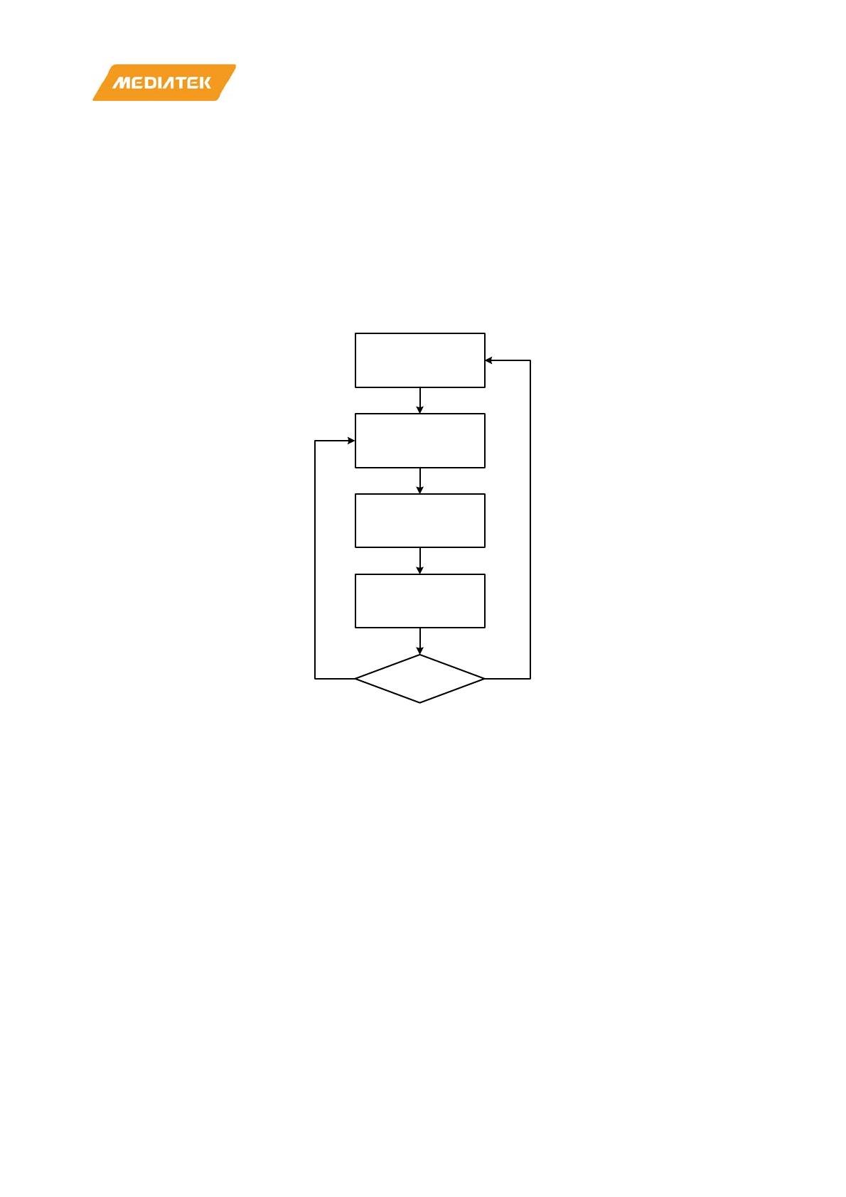
MT7686 Reference Manual
© 2016 - 2017 MediaTek Inc.
Page 400 of 536
This document contains information that is proprietary to MediaTek Inc. (“MediaTek”) and/or its licensor(s).
Any unauthorized use, reproduction or disclosure of this document in whole or in part is strictly prohibited.
4) If the two consecutive random bits are 11, the output bit of the extractor will be invalid (X).
Every even number bit of the extractor output, if it is a valid bit, will be used for the final random data generation.
For example, if the original random data is 1110_1101_0111_1011, the probability of 1’s is 75%. The
corresponding extractor output will be 1XX1_0X10_10XX_X10X. If only even number bits are considered, the result
will be X1_X0_0X_1X. By removing the invalid bits, the final obtained random data is 1001 and the probability of 1s
is now down to 50%.
This mechanism is time-consuming as many random bits are dropped out during the process. One can set the
timeout limit in TRNG_CONF to constrain the generation time. The default timeout limit is 1024, this means
timeout error will be issued after 1024 random bits are generated. Note, that timeout detection is available only
when the Von Neumann extractor is enabled.
TRNG_IDLE
TRNG_LATCH
(Inner loop oscillation)
TRNG_UNGATE
(Outer loop oscillation)
TRNG_SAMPLE
(Get 1 bit TRNG data)
Done?
(32-bit data)
YesNo
Figure 19.4-1. TRNG operation flow
19.5. Programming sequence
The general programming flow is shown below:
1) Enable TRNG_CG_CLOCK (see the clock setting section, for more details).
2) Set TRNG_TIME to specify the time interval of each state (default 0x08030F01).
3) Set TRNG_CONF [14:8] to select which RO to enable, such as 0x7F.
4) Set TRNG_CTRL [0] to 1 to start TRNG.
5) Wait for IRQ or poll TRNG_INT_SET [0].
6) Read TRNG_INT_SET to check IRQ status (bit [0] = 1: successful; bit [1] = 1: timeout).
7) Set TRNG_INT_CLR to 0 x 0 to clear IRQ status.
8) Read out TRNG_DATA to get 32-bit random data.
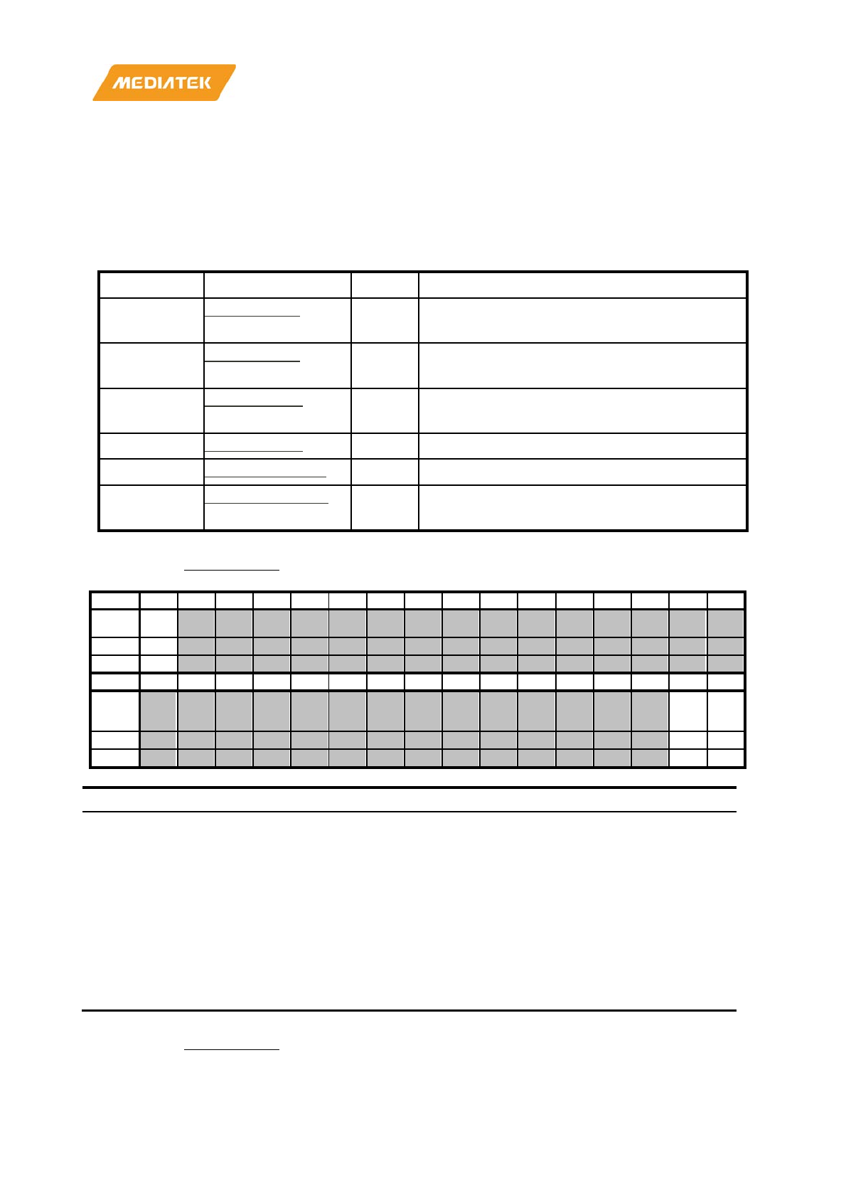
MT7686 Reference Manual
© 2016 - 2017 MediaTek Inc.
Page 401 of 536
This document contains information that is proprietary to MediaTek Inc. (“MediaTek”) and/or its licensor(s).
Any unauthorized use, reproduction or disclosure of this document in whole or in part is strictly prohibited.
9) Set TRNG_CTRL [0] to 0 to stop TRNG.
10) Disable TRNG_CG_CLOCK.
19.6. Register mapping
TRNG control/status registers are listed as follows:
Module name: TRNG Base address: (+A0010000h)
Address Name Width Register Functionality
A0010000
TRNG_CTRL
32
This register controls TRNG
operation
mode.
A0010004
TRNG_TIME
32
This register controls the timing of each
state.
A0010008
TRNG_DATA
32
This register stores the generated random
data.
A001000C
TRNG_CONF
32
This register configures RO behavior.
A0010010
TRNG_INT_SET
32
This register stores the IRQ status.
A0010014
TRNG_INT_CLR
32
This register is used to
clear the IRQ status.
A0010000
TRNG_CTRL
This register controls TRNG operation
mode.
00000000
Bit
31
30
29
28
27
26
25
24
23
22
21
20
19
18
17
16
Name
trng_
rdy
Type
RO
Reset
0
Bit
15
14
13
12
11
10
9
8
7
6
5
4
3
2
1
0
Name
trng_
freer
un
trng_
start
Type
RW
RW
Reset
0
0
B
it(s)
Name
Description
31
trng_rdy
•
This register indicates the status of random number generation
o 0: random data is not ready
o
1: random data is ready
1
trng_freerun
•
This register is used to enable freerun mode
o 0: disable freerun
o
1: enable freerun
0
trng_start
•
This register is used to start/stop random number generation
o 0: stop generation
o
1: start generation
A0010004
TRNG_TIME
This register controls the timing of
03080F01
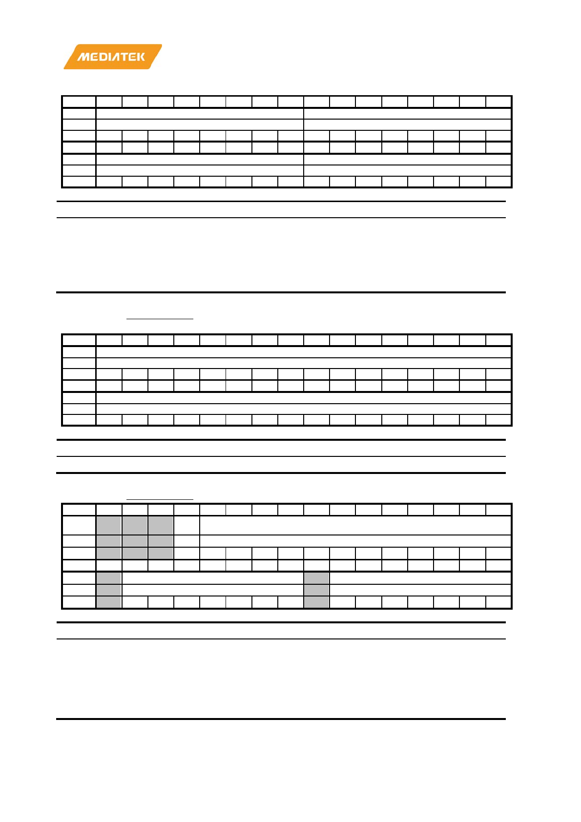
MT7686 Reference Manual
© 2016 - 2017 MediaTek Inc.
Page 402 of 536
This document contains information that is proprietary to MediaTek Inc. (“MediaTek”) and/or its licensor(s).
Any unauthorized use, reproduction or disclosure of this document in whole or in part is strictly prohibited.
each state.
Bit
31
30
29
28
27
26
25
24
23
22
21
20
19
18
17
16
Name
sample_cnt
ungate_cnt
Type
RW
RW
Reset
0
0
0
0
0
0
1
1
0
0
0
0
1
0
0
0
Bit
15
14
13
12
11
10
9
8
7
6
5
4
3
2
1
0
Name
latch_cnt
sysclk_cnt
Type
RW
RW
Reset
0
0
0
0
1
1
1
1
0
0
0
0
0
0
0
1
B
it(s)
Name
Description
31:24
sample_cnt
This register controls the interval of TRNG sample state.
23:16
ungate_cnt
This register controls the interval of TRNG ungate state.
15:8
latch_cnt
This register controls the interval of TRNG latch state.
7:0
sysclk_cnt
The TRNG operation frequency is equal to the bus frequency divided by
SYSCLK_CNT.
A0010008
TRNG_DATA
This register stores the generated
random data.
00000000
Bit
31
30
29
28
27
26
25
24
23
22
21
20
19
18
17
16
Name
trng_data
Type
RW
Reset
0
0
0
0
0
0
0
0
0
0
0
0
0
0
0
0
Bit
15
14
13
12
11
10
9
8
7
6
5
4
3
2
1
0
Name
trng_data
Type
RW
Reset
0
0
0
0
0
0
0
0
0
0
0
0
0
0
0
0
B
it(s)
Name
Description
31:0
trng_data
The generated random data.
A001000C
TRNG_CONF
This register configures RO behavior.
04007F00
Bit
31
30
29
28
27
26
25
24
23
22
21
20
19
18
17
16
Name
von_e
n
time_out_limit
Type
RW
RW
Reset
0
0
1
0
0
0
0
0
0
0
0
0
0
Bit
15
14
13
12
11
10
9
8
7
6
5
4
3
2
1
0
Name
ro_enable
ro_output_sel
Type
RW
RW
Reset
1
1
1
1
1
1
1
0
0
0
0
0
0
0
B
it(s)
Name
Description
28
von_en
This register is used to enable
the Von-
Neumann extractor
1: turn on
0: turn off
27:16
time_out_limit
This register sets the timeout limit when
the Von-
Neumann extractor is enabled. If exceeding the limit, it
will issue
a
timeout interrupt. (default: timeout after 1024
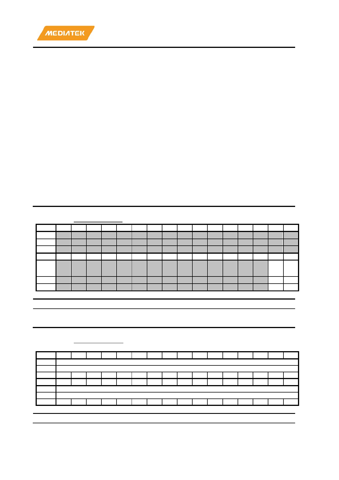
MT7686 Reference Manual
© 2016 - 2017 MediaTek Inc.
Page 403 of 536
This document contains information that is proprietary to MediaTek Inc. (“MediaTek”) and/or its licensor(s).
Any unauthorized use, reproduction or disclosure of this document in whole or in part is strictly prohibited.
sample cycles)
14:8
ro_enable
Ring oscillator enable for RNG
•
Bit[0] = 1: Enable H-FIRO
•
Bit[1] = 1: Enable H-RO
•
Bit[2] = 1: Enable H-GARO
•
Bit[3] = 1: Enable H-GARO2
•
Bit[4] = 1: Enable H-GARO3
•
Bit[5] = 1: Enable H-GARO4
•
Bit[6] = 1: Enable H-GARO5
6:0
ro_output_sel
Select RO output for debug (debug only)
•
7'b000_0001: H-FIRO
•
7'b000_0010: H-RO
•
7'b000_0100: H-GARO
•
7'b000_1000: H-GARO2
•
7'b001_0000: H-GARO3
•
7'b010_0000: H-GARO4
•
7'b100_0000: H-GARO5
A0010010
TRNG_INT_SET
This register stores the IRQ status.
00000000
Bit
31
30
29
28
27
26
25
24
23
22
21
20
19
18
17
16
Name
Type
Reset
Bit
15
14
13
12
11
10
9
8
7
6
5
4
3
2
1
0
Name
timeo
ut_fai
l
trng_
done
Type
RO
RO
Reset
0
0
B
it(s)
Name
Description
1
timeout_fail
This register indicates TRNG timeout failure.
0
trng_done
This register indicates random number generation was successful.
A0010014
TRNG_INT_CLR
This register is used to clear the IRQ
status.
00000000
Bit
31
30
29
28
27
26
25
24
23
22
21
20
19
18
17
16
Name
irq_clr_wr
Type
WO
Reset
0
0
0
0
0
0
0
0
0
0
0
0
0
0
0
0
Bit
15
14
13
12
11
10
9
8
7
6
5
4
3
2
1
0
Name
irq_clr_wr
Type
WO
Reset
0
0
0
0
0
0
0
0
0
0
0
0
0
0
0
0
B
it(s)
Name
Description

MT7686 Reference Manual
© 2016 - 2017 MediaTek Inc.
Page 404 of 536
This document contains information that is proprietary to MediaTek Inc. (“MediaTek”) and/or its licensor(s).
Any unauthorized use, reproduction or disclosure of this document in whole or in part is strictly prohibited.
31:0
irq_clr_wr
Program this register with any value to reset the IRQ status.

MT7686 Reference Manual
© 2016 - 2017 MediaTek Inc.
Page 405 of 536
This document contains information that is proprietary to MediaTek Inc. (“MediaTek”) and/or its licensor(s).
Any unauthorized use, reproduction or disclosure of this document in whole or in part is strictly prohibited.
20. Real Time Clock (RTC)
The Real-Time Clock (RTC) module provides time and data information, as well as 32.768kHz (32K) clock. The clock
is selected between three clock sources: one external (XOSC32) and two internal (XO_DIV32, EOSC32). A strapping
bit, SLOW_SRC_B, is added for the 32K crystal existence information. The clock source is from the external
oscillator when SLOW_SRC_B is 0.
The RTC block has an independent power supply. When the chip is in retention mode, a dedicated regulator
supplies power to the RTC block. In addition to providing timing data, an alarm interrupt is generated and can be
used to power up the baseband core. Regular interrupts corresponding to seconds, minutes, hours and days can be
generated whenever the time counter value reaches a maximum value (e.g. 59 for seconds and minutes, 23 for
hours, etc.). The year span is supported up till 2127. The maximum day-of-month values, which depend on the leap
year condition, are stored in the RTC block.
20.1. Features
• There is one real time timer, one alarm timer and a dedicated EINT channel in the RTC.
• The RTC can generate wake up events to the Cortex M4, SPM and PMU to wake up the system.
• There are three 32K clock sources, external 32K crystal (XOSC32), internal oscillator (EOSC32) and divided
32K from 26MHz or 40MHz crystal (XO_DIV32).
20.2. Block diagram
The block diagram for the RTC is shown in Figure 20.2-1
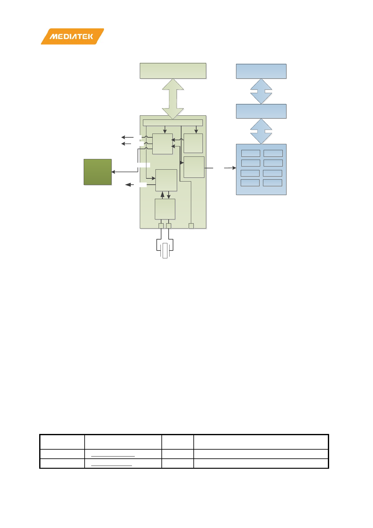
MT7686 Reference Manual
© 2016 - 2017 MediaTek Inc.
Page 406 of 536
This document contains information that is proprietary to MediaTek Inc. (“MediaTek”) and/or its licensor(s).
Any unauthorized use, reproduction or disclosure of this document in whole or in part is strictly prohibited.
PD
SLEEPB
Retention
SRAM
Power
Controller
32K
Oscillator
(OSC32)
RTC
PMU
RETENTION SRAM
1KB 1KB
1KB 1KB
1KB 1KB
1KB 1KB
XIN
RTC_EINT
XOUT
GO_RETENTION
APB
Memory Controller
AHB
OSC32
Controller
REG
Timer
Alarm
Generator
irq_b
event_b
F32k_ck
Figure 20.2-1. RTC block diagram
20.3. Functions
• Alarm: RTC can generate wake-up events or interrupts when the real-time timer is the same as the alarm
setting.
• Tick: RTC can generate wake-up events or interrupts when the timer reaches the maximum timeout value.
• 32K source: RTC provides 32.768kHz clock from external crystal or internal oscillator.
20.4. Programming sequence
Apply the following sequence to modify the registers:
1) Write registers to be modified.
2) Write WRTGR to 1 to trigger data transfer from bus to the RTC.
3) Wait for CBUSY to go low before the next operation.
20.5. Register mapping
Module name: RTC Base address: (+a2080000h)
Address Name
Width
(bits)
Register Function
A2080004
RTC_IRQ_STA
16
RTC IRQ status
A2080008
RTC_IRQ_EN
16
RTC IRQ enable
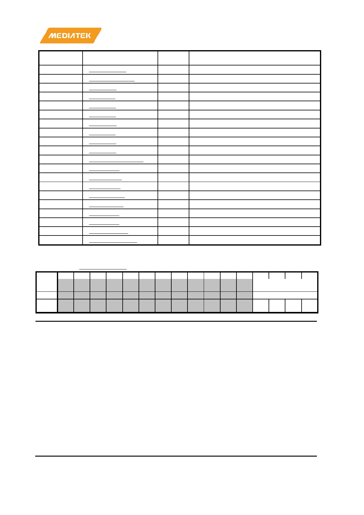
MT7686 Reference Manual
© 2016 - 2017 MediaTek Inc.
Page 407 of 536
This document contains information that is proprietary to MediaTek Inc. (“MediaTek”) and/or its licensor(s).
Any unauthorized use, reproduction or disclosure of this document in whole or in part is strictly prohibited.
Address Name
Width
(bits)
Register Function
A208000C
RTC_CII_EN
16
Counter increment IRQ enable
A2080010
RTC_AL_MASK
16
RTC alarm mask
A2080014
RTC_TC0
16
RTC time counter register0
A2080018
RTC_TC1
16
RTC time counter register1
A208001C
RTC_TC2
16
RTC time counter register2
A2080020
RTC_TC3
16
RTC time counter register3
A2080024
RTC_AL0
16
RTC alarm setting register0
A2080028
RTC_AL1
16
RTC alarm setting register1
A208002C
RTC_AL2
16
RTC alarm setting register2
A2080030
RTC_AL3
16
RTC alarm setting register3
A2080038
RTC_NEW_SPAR0
16
New spare register0 for specific purpose
A208003C
RTC_EINT
16
RTC EINT control
A2080058
RTC_PDN0
16
PDN0
A208005C
RTC_PDN1
16
PDN1
A2080060
RTC_SPAR0
16
Spare register0 for specific purpose
A2080064
RTC_SPAR1
16
Spare register1 for specific purpose
A208006C
RTC_DIFF
16
One
-time calibration offset
A2080070
RTC_CALI
16
Repeat calibration offset
A2080074
RTC_WRTGR
16
Enable the transfers between core and RTC
A2080078
RTC_GPIO_CON
16
GPIO control register
A2080004
RTC_IRQ_STA
RTC IRQ status
00000000
Bit
15
14
13
12
11
10
9
8
7
6
5
4
3
2
1
0
Nam
e
IRQ_STA
Type
RC
Rese
t
0 0 0 0
Bit(s) Mnemonic Name Description
3:0 IRQ_STA RTC IRQ status
• IRQ_STA[3]: EINT_STA
Indicates the IRQ status and whether the EINT is asserted.
o 0: No IRQ occurred.
o 1: IRQ occurred.
• IRQ_STA[2]: LP_STA
Indicates the IRQ status and whether the LPD is asserted.
o 0: No IRQ occurred; the 32K clock can be used.
o 1: IRQ occurred; the 32K clock stopped.
• IRQ_STA[1]: TC_STA
Indicates the IRQ status and whether the tick condition is
met.
o 0: No IRQ occurred; the tick condition isn’t met.
o 1: IRQ occurred; the tick condition is met.
• IRQ_STA[0]: AL_STA
Indicates the IRQ status and whether the alarm condition is
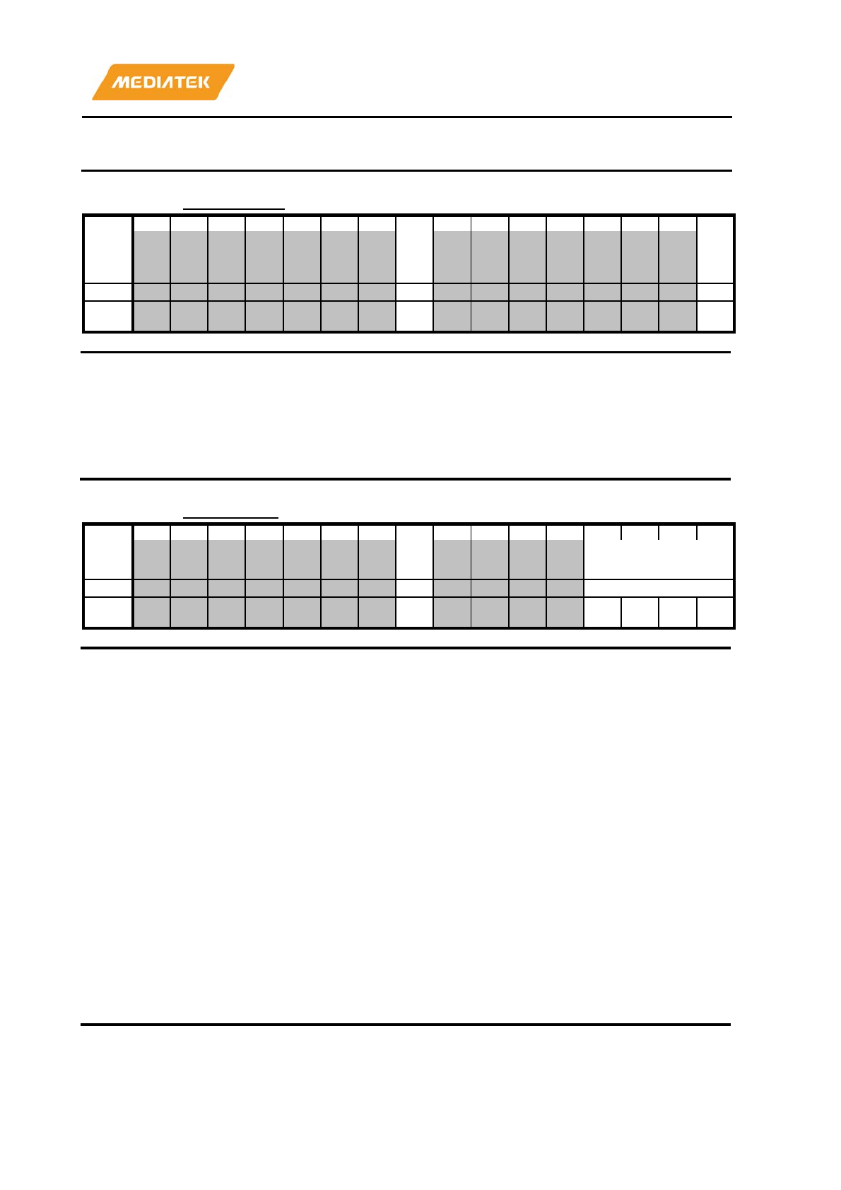
MT7686 Reference Manual
© 2016 - 2017 MediaTek Inc.
Page 408 of 536
This document contains information that is proprietary to MediaTek Inc. (“MediaTek”) and/or its licensor(s).
Any unauthorized use, reproduction or disclosure of this document in whole or in part is strictly prohibited.
met.
o 0: No IRQ occurred; the alarm condition isn’t met.
o
1: IRQ occurred; the alarm condition is met.
A2080008
RTC_IRQ_EN
RTC IRQ enable
00000000
Bit
15
14
13
12
11
10
9
8
7
6
5
4
3
2
1
0
Nam
e
ON
ES
HO
T
LP
_E
N
Type
RW
RW
Rese
t
0 0
Bit(s)
Mnemonic
Name
Description
8
ONESHOT
•
Controls automatic reset of AL_EN and TC_EN.
0
LP_EN
•
Enable the control bit for OSC32 IRQ generation, if low
power is detected (32K clock is off).
o 1'b0: Disable IRQ generations.
o
1'b1: Enable LPD.
A208000C
RTC_CII_EN
Counter
increment IRQ enable
00000000
Bit
15
14
13
12
11
10
9
8
7
6
5
4
3
2
1
0
Nam
e
TC
_E
N
CII_EN
Type
RW
RW
Rese
t
0 0 0 0 0
Bit(s)
Mnemonic
Name
Description
8
TC_EN
Enables the control bit for IRQ generation if the tick
condition is met.
•
Auto reset when ONESHOT is high upon generation of the
corresponding IRQ.
o 1'b0: Disable IRQ generations.
o
1'b1: Enable the tick time match interrupt.
3:0
CII_EN
•
This register activates or de-activates the IRQ generation when the
TC counter reaches its maximum value.
o 4'h0: IRQ at each one-eighth of a second update.
o 4'h1: IRQ at each one-fourth of a second update.
o 4'h2: IRQ at each one-half of a second update.
o 4'h3: IRQ at each second update.
o 4'h4: IRQ at each minute update.
o 4'h5: IRQ at each hour update.
o 4'h6: IRQ at each day update.
o 4'h7: IRQ at each week update.
o 4'h8: IRQ at each month update.
o 4'h9: IRQ at each year update.

MT7686 Reference Manual
© 2016 - 2017 MediaTek Inc.
Page 409 of 536
This document contains information that is proprietary to MediaTek Inc. (“MediaTek”) and/or its licensor(s).
Any unauthorized use, reproduction or disclosure of this document in whole or in part is strictly prohibited.
A2080010
RTC_AL_MASK
RTC alarm mask
00000000
Bit
15
14
13
12
11
10
9
8
7
6
5
4
3
2
1
0
Nam
e
AL
_E
N
AL_MASK
Type
RW
RW
Rese
t
0 0 0 0 0 0 0 0
Bit(s)
Mnemonic
Name
Description
8
AL_EN
Enables the control bit for IRQ generation if the alarm condition is
met.
•
Auto reset when ONESHOT is high upon generation of the
corresponding IRQ.
o 1'b0: Disable IRQ generations.
o
1'b1: Enable the alarm time match interrupt.
6:0
AL_MASK
The alarm condition for alarm IRQ generation depends whether the
corresponding bit in this register is masked. Warning: If you set all
bits to
1 in RTC_AL_MASK, such as RTC_AL_MASK=0x7f, and
AL_EN=1, the alarm will run every second.
•
AL_MASK[6]
o 0: Condition (RTC_TC_YEA = RTC_AL_YEA) is checked
to generate the alarm signal.
o 1: Condition (RTC_TC_YEA = RTC_AL_YEA) is masked,
such that the value of RTC_TC_YEA does not affect the
alarm IRQ generation.
•
AL_MASK[5]
o 0: Condition (RTC_TC_MTH = RTC_AL_MTH) is
checked to generate the alarm signal.
o 1: Condition (RTC_TC_MTH = RTC_AL_MTH) is
masked, such that the value of RTC_TC_MTH does not
affect the alarm IRQ generation.
•
AL_MASK[4]
o 0: Condition (RTC_TC_DOW = RTC_AL_DOW) is
checked to generate the alarm signal.
o 1: Condition (RTC_TC_DOW = RTC_AL_DOW) is
masked, such that the value of RTC_TC_DOW does not
affect the alarm IRQ generation.
•
AL_MASK[3]
o 0: Condition (RTC_TC_DOM = RTC_AL_DOM) is
checked to generate the alarm signal.
o 1: Condition (RTC_TC_DOM = RTC_AL_DOM) is
masked, such that the value of RTC_TC_DOM does not
affect the alarm IRQ generation.
•
AL_MASK[2]
o 0: Condition (RTC_TC_HOU = RTC_AL_HOU) is
checked to generate the alarm signal.
o 1: Condition (RTC_TC_HOU = RTC_AL_HOU) is
masked, such that the value of RTC_TC_HOU does not
affect the alarm IRQ generation.
•
AL_MASK[1]
o 0: Condition (RTC_TC_MIN = RTC_AL_MIN) is checked
to generate the alarm signal.
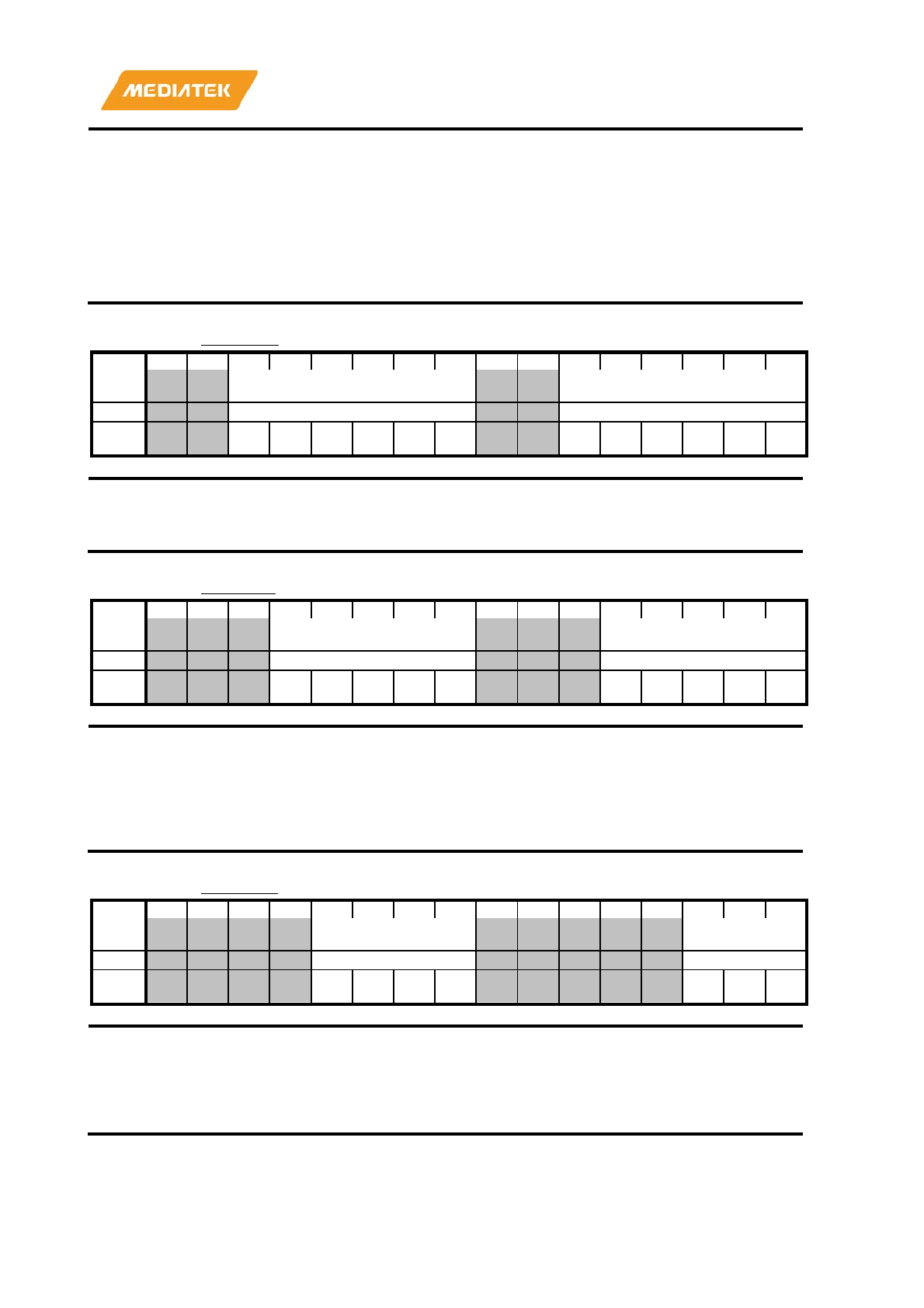
MT7686 Reference Manual
© 2016 - 2017 MediaTek Inc.
Page 410 of 536
This document contains information that is proprietary to MediaTek Inc. (“MediaTek”) and/or its licensor(s).
Any unauthorized use, reproduction or disclosure of this document in whole or in part is strictly prohibited.
o 1: Condition (RTC_TC_MIN = RTC_AL_MIN) is masked,
such that the value of RTC_TC_MIN does not affect the
alarm IRQ generation.
•
AL_MASK[0]
o 0: Condition (RTC_TC_SEC = RTC_AL_SEC) is checked
to generate the alarm signal.
o 1: Condition (RTC_TC_SEC = RTC_AL_SEC) is masked,
such that the value of RTC_TC_SEC does not affect the
alarm IRQ generation.
A2080014
RTC_TC0
RTC time counter register0
00000000
Bit
15
14
13
12
11
10
9
8
7
6
5
4
3
2
1
0
Nam
e
TC_MINUTE TC_SECOND
Type
RW
RW
Rese
t
0 0 0 0 0 0 0 0 0 0 0 0
Bit(s)
Mnemonic
Name
Description
13:8
TC_MINUTE
The minute initial value for the time counter. Range is from 0 to 59.
5:0
TC_SECOND
The second initial value for the time counter. Range is from 0 to 59.
A2080018
RTC_TC1
RTC time counter register1
00000000
Bit
15
14
13
12
11
10
9
8
7
6
5
4
3
2
1
0
Nam
e
TC_DOM TC_HOUR
Type
RW
RW
Rese
t
0 0 0 0 0 0 0 0 0 0
Bit(s)
Mnemonic
Name
Description
12:8
TC_DOM
Initial value of
the day-of-month for the time counter. The range is
from 1 to X (28, 29, 30, 31). The maximum value X depends on
month and the leap year condition.
4:0
TC_HOUR
Initial value of the hour for the time counter. The range is from 0 to
23.
A208001C
RTC_TC2
RTC time counter register2
00000000
Bit
15
14
13
12
11
10
9
8
7
6
5
4
3
2
1
0
Nam
e
TC_MONTH TC_DOW
Type
RW
RW
Rese
t
0 0 0 0 0 0 0
Bit(s)
Mnemonic
Name
Description
11:8
TC_MONTH
Initial
value of the month for the time counter. The range is
from 1 to 12.
2:0
TC_DOW
Initial value of the day
-of-week for the time counter. The range
is from 1 to 7.
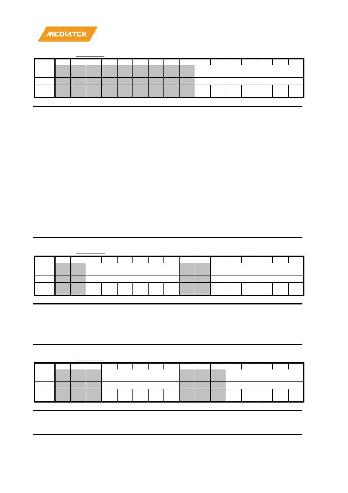
MT7686 Reference Manual
© 2016 - 2017 MediaTek Inc.
Page 411 of 536
This document contains information that is proprietary to MediaTek Inc. (“MediaTek”) and/or its licensor(s).
Any unauthorized use, reproduction or disclosure of this document in whole or in part is strictly prohibited.
A2080020
RTC_TC3
RTC time counter register3
00000000
Bit
15
14
13
12
11
10
9
8
7
6
5
4
3
2
1
0
Nam
e
TC_YEAR
Type
RW
Rese
t
0 0 0 0 0 0 0
Bit(s)
Mnemonic
Name
Description
6:0
TC_YEAR
Initial value of the year for the time counter. The range is from 0 to
127 to represent years 2000 to
2127.
Software can bias the year as multiples of 4 for the internal leap
-year
formula.
Here are 3 examples: 2000
-2127, 1972-2099, 1904-2031. To simplify,
RTC hardware treats all 4
-multiples as leap years. If the range you
defined includes a non
-leap 4-multiple year (such as 2100), you have
to adjust it to the correct date (change February 29th, 2100 to March
1st, 2100).
It's suggested to bias the range larger than 1900 and less than 2100 to
evade the manual adjustment, such that the bias values are suggest
ed
to be in the range [
-28,-96], that are (1972-2099) - (1904-2031).
The formal leap formula:
if year modulo 400 is 0 then leap
else if year modulo 100 is 0 then no leap
else if year modulo 4 is 0 then leap
else no leap
A2080024
RTC_AL0
RTC alarm setting register0
00000000
Bit
15
14
13
12
11
10
9
8
7
6
5
4
3
2
1
0
Nam
e
AL_MINUTE AL_SECOND
Type
RW
RW
Rese
t
0 0 0 0 0 0 0 0 0 0 0 0
Bit(s)
Mnemonic
Name
Description
13:8
AL_MINUTE
The minute value of the alarm counter setting. Range is
from 0 to 59.
5:0
AL_SECOND
The second value of the alarm counter setting. Range is
from 0 to 59.
A2080028
RTC_AL1
RTC alarm setting register1
00000000
Bit
15
14
13
12
11
10
9
8
7
6
5
4
3
2
1
0
Nam
e
AL_DOM AL_HOUR
Type
RW
RW
Rese
t
0 0 0 0 0 0 0 0 0 0
Bit(s)
Mnemonic
Name
Description
12:8
AL_DOM
The day
-of-month value of the alarm counter setting.
Range is from 1 to X (28, 29, 30, 31). The maximum
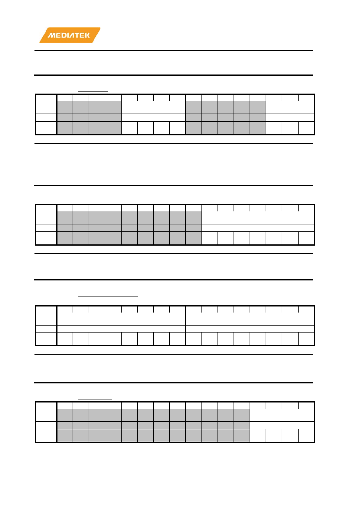
MT7686 Reference Manual
© 2016 - 2017 MediaTek Inc.
Page 412 of 536
This document contains information that is proprietary to MediaTek Inc. (“MediaTek”) and/or its licensor(s).
Any unauthorized use, reproduction or disclosure of this document in whole or in part is strictly prohibited.
value X depends on month and the leap year condition.
4:0
AL_HOUR
The hour value of the alarm counter setting. Range is
from 0 to 23.
A208002C
RTC_AL2
RTC alarm setting register2
00000000
Bit
15
14
13
12
11
10
9
8
7
6
5
4
3
2
1
0
Nam
e
AL_MONTH AL_DOW
Type
RW
RW
Rese
t
0 0 0 0 0 0 0
Bit(s)
Mnemonic
Name
Description
11:8
AL_MONTH
The month value of the alarm counter setting. Range
is from 1 to 12.
2:0
AL_DOW
The day
-of-week value of the alarm counter setting.
Range is from 1 to 7.
A2080030
RTC_AL3
RTC alarm setting register3
00000000
Bit
15
14
13
12
11
10
9
8
7
6
5
4
3
2
1
0
Nam
e
AL_YEAR
Type
RW
Rese
t
0 0 0 0 0 0 0
Bit(s)
Mnemonic
Name
Description
6:0
AL_YEAR
The year value of the alarm counter setting. Range is
from 0 to 127 to represent the years 2000 to 2127.
A2080038
RTC_NEW_SPAR0
New spare register0 for specific
purpose
00000000
Bit
15
14
13
12
11
10
9
8
7
6
5
4
3
2
1
0
Nam
e
RTC_NEW_SPAR0_1 RTC_NEW_SPAR0_0
Type
RW
RW
Rese
t
0 0 0 0 0 0 0 0 0 0 0 0 0 0 0 0
Bit(s)
Mnemonic
Name
Description
15:8
RTC_NEW_SPAR0_1
Reserved for specific purposes.
7:0
RTC_NEW_SPAR0_0
Reserved for specific purposes.
A208003C
RTC_EINT
RTC EINT control
00000000
Bit
15
14
13
12
11
10
9
8
7
6
5
4
3
2
1
0
Nam
e
EINT_CON
Type
RW
Rese
t
0 0 0 0
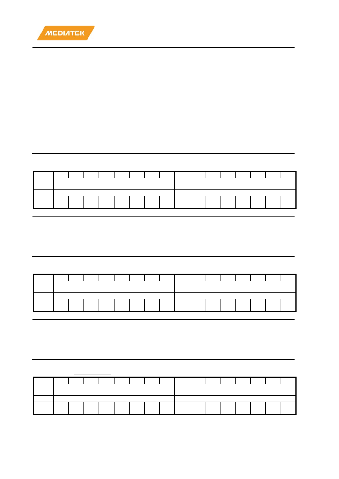
MT7686 Reference Manual
© 2016 - 2017 MediaTek Inc.
Page 413 of 536
This document contains information that is proprietary to MediaTek Inc. (“MediaTek”) and/or its licensor(s).
Any unauthorized use, reproduction or disclosure of this document in whole or in part is strictly prohibited.
Bit(s)
Mnemonic
Name
Description
3:0
EINT_CON
•
EINT_CON[3]: INV_EN
o 0: active high
o 1: active low
•
EINT_CON[2]: SYNC_EN
o 0: not synchronized with 32K
o 1: synchronized with 32K
•
EINT_CON[1]: DEB_EN
o 0: disable debounce
o 1: enable debounce
•
EINT_CON[0]: EINT_EN
o 0: disable RTC_EINT channel
o
1: enable RTC_EINT channel
A2080058
RTC_PDN0
PDN0
00000000
Bit
15
14
13
12
11
10
9
8
7
6
5
4
3
2
1
0
Nam
e
RTC_PDN0_1 RTC_PDN0_0
Type
RW
RW
Rese
t
0 0 0 0 0 0 0 0 0 0 0 0 0 0 0 0
Bit(s)
Mnemonic
Name
Description
15:8
RTC_PDN0_1
The spare registers for
software to keep the power-on and
power
-off state information.
7:0
RTC_PDN0_0
The spare registers for software to keep the power
-on and
power
-off state information.
A208005C
RTC_PDN1
PDN1
00000000
Bit
15
14
13
12
11
10
9
8
7
6
5
4
3
2
1
0
Nam
e
RTC_PDN1_1 RTC_PDN1_0
Type
RW
RW
Rese
t
0 0 0 0 0 0 0 0 0 0 0 0 0 0 0 0
Bit(s)
Mnemonic
Name
Description
15:8
RTC_PDN1_1
The spare registers for software to keep the power
-on and
power
-off state information.
7:0
RTC_PDN1_0
The
spare registers for software to keep the power-on and
power
-off state information.
A2080060
RTC_SPAR0
Spare register0 for specific purpose
00000000
Bit
15
14
13
12
11
10
9
8
7
6
5
4
3
2
1
0
Nam
e
RTC_SPAR0_1 RTC_SPAR0_0
Type
RW
RW
Rese
t
0 0 0 0 0 0 0 0 0 0 0 0 0 0 0 0
MT7686 Reference Manual
© 2016 - 2017 MediaTek Inc.
Page 414 of 536
This document contains information that is proprietary to MediaTek Inc. (“MediaTek”) and/or its licensor(s).
Any unauthorized use, reproduction or disclosure of this document in whole or in part is strictly prohibited.
Bit(s)
Mnemonic
Name
Description
15:8
RTC_SPAR0_1
Reserved for specific purposes.
7:0
RTC_SPAR0_0
Reserved for specific purposes.
A2080064
RTC_SPAR1
Spare register1 for specific
purpose
00000000
Bit
15
14
13
12
11
10
9
8
7
6
5
4
3
2
1
0
Nam
e
RTC_SPAR1_1 RTC_SPAR1_0
Type
RW
RW
Rese
t
0 0 0 0 0 0 0 0 0 0 0 0 0 0 0 0
Bit(s)
Mnemonic
Name
Description
15:8
RTC_SPAR1_1
Reserved for specific purposes.
7:0
RTC_SPAR1_0
Reserved
for specific purposes.
A208006C
RTC_DIFF
One
-time calibration offset
00000000
Bit
15
14
13
12
11
10
9
8
7
6
5
4
3
2
1
0
Nam
e
RTC_DIFF
Type
RW
Rese
t
0 0 0 0 0 0 0 0 0 0 0 0
Bit(s)
Mnemonic
Name
Description
11:0
RTC_DIFF
Adjusts internal counter of RTC. It operates once and
returns to 0 when complete.
In some cases, you observe the RTC is faster or slower than the
standard. Changing
RTC_TC_SEC
is coarse and may cause alarm
problems.
RTC_DIFF provides a finer time unit. An internal 15-
bit counter accumulates in each 32768kHz clock. Entering a non
-
zero value into the
RTC_DIFF will cause the internal RTC
counter to increase or decrease
RTC_DIFF when RTC_DIFF
changes to 0 again.
RTC_DIFF is in 2's complement.
For example, if you fill
0xFFF into RTC_DIFF, the internal
counter will decrease by 1 when
RTC_DIFF returns to 0. In other
words, you can only use
RTC_DIFF continuously if RTC_DIFF is
0.
A2080070
RTC_CALI
Repeat calibration offs
et
00000000
Bit
15
14
13
12
11
10
9
8
7
6
5
4
3
2
1
0
Nam
e
RTC_CALI
Type
RW
Rese
t
0 0 0 0 0 0 0 0 0 0 0 0 0 0 0
Bit(s)
Mnemonic
Name
Description
14:0
RTC_CALI
•
RTC_CALI[14]: CALI_RW_SEL
o 0: Normal RTC_CALI
o
1: K_EOSC32_RTC_CALI
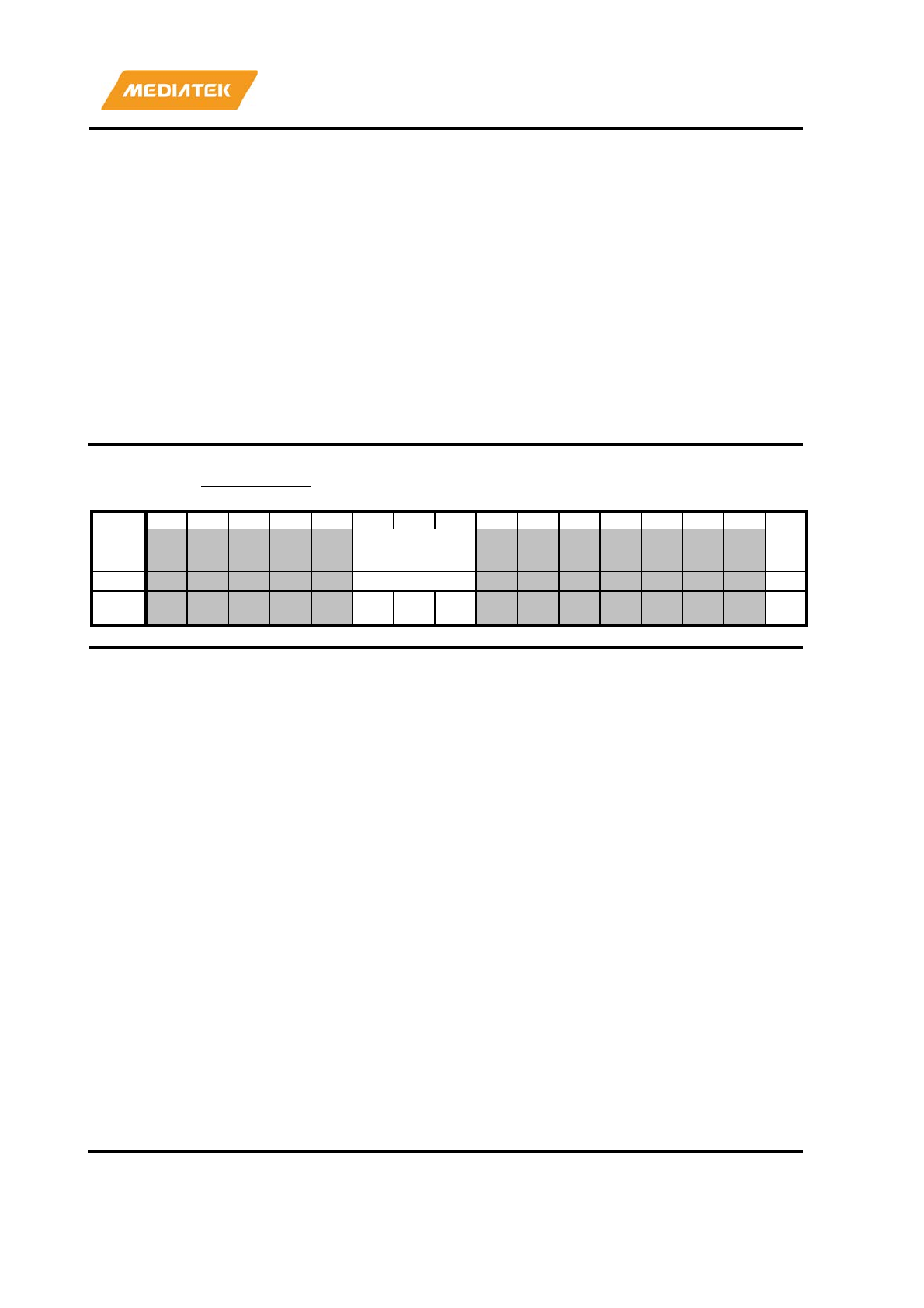
MT7686 Reference Manual
© 2016 - 2017 MediaTek Inc.
Page 415 of 536
This document contains information that is proprietary to MediaTek Inc. (“MediaTek”) and/or its licensor(s).
Any unauthorized use, reproduction or disclosure of this document in whole or in part is strictly prohibited.
•
RTC_CALI[13:0]: RTC_CALI_VALUE
These registers provide a repeat calibration scheme.
RTC_CALI
provides two types of calibration.
•
14-bit calibration capability in 8-second duration; in other
words, 12-bit calibration capability in each second.
RTC_CALI is in 2's complement, such that you can adjust
RTC increasing or decreasing.
Due to the fact that RTC_CALI is revealed in 8 seconds,
the resolution is less than a 1/32768 clock.
Average resolution: 1/32768/8=3.81µs
Average adjustment range: from -31.25 to 31.246 ms/sec
in 2's complement: -0x2000~0x1FFF
(-8192~8191)
•
14-bit calibration capability in 1-second duration at
K_EOSC32 mode (K_EOSC32_RTC_CALI); This type of
usage is with resolution 1/32768=30.52µs
A2080074
RTC_WRTGR
Enable the transfers between core and
RTC
00000000
Bit
15
14
13
12
11
10
9
8
7
6
5
4
3
2
1
0
Nam
e RTC_STA
WR
TG
R
Type
RO
WO
Rese
t
0 0 0 0
Bit(s)
Mnemonic
Name
Description
10:8
RTC_STA
•
RTC_STA[2]: RETENTION_MODE
o 0: System is not in retention mode.
o 1: System is in retention mode or woke up
from retention mode.
•
RTC_STA[1]: RTC_INIT_READY
o 0: RTC has not been initialized
o 1: RTC has been initialized
•
RTC_STA[0]: CBUSY
When read, this
bit indicates whether the read/write
channels between RTC/Bus are busy. It will be high
after software programs sequence to any of the RTC
data registers and enables the transfer by
WRTGR = 1
or the reload process.
0
WRTGR
•
Enables transfers from core to RTC. After the RTC
registers are modified, write WRTGR to 1 to
trigger the transfer.
•
The prior writing operations are queued at core
power domain. The pending data will not be
transferred to RTC domain until WRTGR = 1.
•
After WRTGR = 1, the pending data will be
transferred to RTC domain sequentially in order of
register address, from low to high.
For example,
RTC_BBPU, RTC_IRQ_EN,
RTC_CII_EN, RTC_AL_MASK, RTC_TC_SEC, etc.

MT7686 Reference Manual
© 2016 - 2017 MediaTek Inc.
Page 416 of 536
This document contains information that is proprietary to MediaTek Inc. (“MediaTek”) and/or its licensor(s).
Any unauthorized use, reproduction or disclosure of this document in whole or in part is strictly prohibited.
The CBUSY in RTC_BBPU is 1 in the writing process.
You
can observe CBUSY to determine when the
transmission is complete.
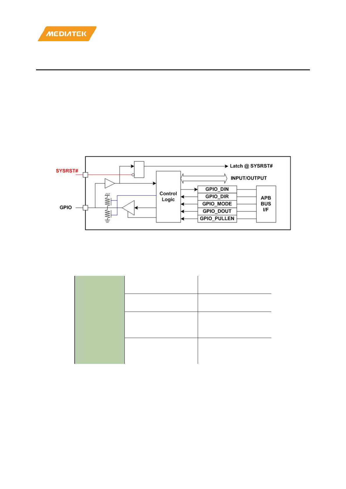
MT7686 Reference Manual
© 2016 - 2017 MediaTek Inc.
Page 417 of 536
This document contains information that is proprietary to MediaTek Inc. (“MediaTek”) and/or its licensor(s).
Any unauthorized use, reproduction or disclosure of this document in whole or in part is strictly prohibited.
21. General Purpose Inputs/Outputs
21.1. Overview
MediaTek MT7686 platform offers 21 general-purpose IO (GPIO) pins. By setting up the control registers, the MCU
software can control the direction, the output value and read the input values on these pins. The GPIOs and GPOs
are multiplexed with other functions to reduce the pin count.
The clock to send outside the chip is software configurable. There are six clock-out ports and each clock-out can be
programmed to output the appropriate clock source. In addition, when two GPIOs function for the same peripheral
IP, the smaller GPIO serial number has higher priority over the bigger one.
Figure 21.1-1. GPIO block diagram
21.2. IO pull up or down control truth table
Table 21.2-1 GPIO IO structure
IO Structure TYPE0 Pull-up/down
3.63V tolerance
TYPE1 Pull-up/down
5V tolerance
TYPE2 Pull-up/down
5V tolerance
SDIO characteristic support
TYPE3 Pull-up/down
5V tolerance
Analog input/output

MT7686 Reference Manual
© 2016 - 2017 MediaTek Inc.
Page 418 of 536
This document contains information that is proprietary to MediaTek Inc. (“MediaTek”) and/or its licensor(s).
Any unauthorized use, reproduction or disclosure of this document in whole or in part is strictly prohibited.
Table 21-2. GPIO versus IO type mapping
Refer to the truth table of pull-up/down control for all GPIO pins.
Table 21-3. IO type 1 - pull up/down control
GPIO_DIR GPIO_PU GPIO_PD Resistance (Ω)
0 0 0 High-Z
0 0 1 Pull-down, 75K
0 1 0 Pull-up, 75K
0 1 1 Keeper, 75K
1 0 0 High-Z
Table 21-4. IO type 2 - pull up/down control
GPIO_DIR GPIO_PUPD GPIO_R1 GPIO_R0 Resistance (Ω)
0 0 0 0 High-Z
0 0 0 1 Pull-up, 47K
0 0 1 0 Pull-up, 47K
0 0 1 1 Pull-up, 23.5K
0 1 0 0 High-Z
0 1 0 1 Pull-down, 47K
0 1 1 0 Pull-down, 47K
GPIO Name IO Type GPIO Name IO Type
GPIO0
IO TYPE 3 GPIO11
IO TYPE 2
GPIO1
IO TYPE 3 GPIO12
IO TYPE 2
GPIO2
IO TYPE 3 GPIO13
IO TYPE 2
GPIO3
IO TYPE 3 GPIO14
IO TYPE 2
GPIO4
IO TYPE 1 GPIO15
IO TYPE 2
GPIO5
IO TYPE 1 GPIO16
IO TYPE 2
GPIO6
IO TYPE 1 GPIO17
IO TYPE 3
GPIO7
IO TYPE 1 GPIO18
IO TYPE 3
GPIO8
IO TYPE 1 GPIO19
IO TYPE 3
GPIO9
IO TYPE 1 GPIO20
IO TYPE 3
GPIO10
IO TYPE 1
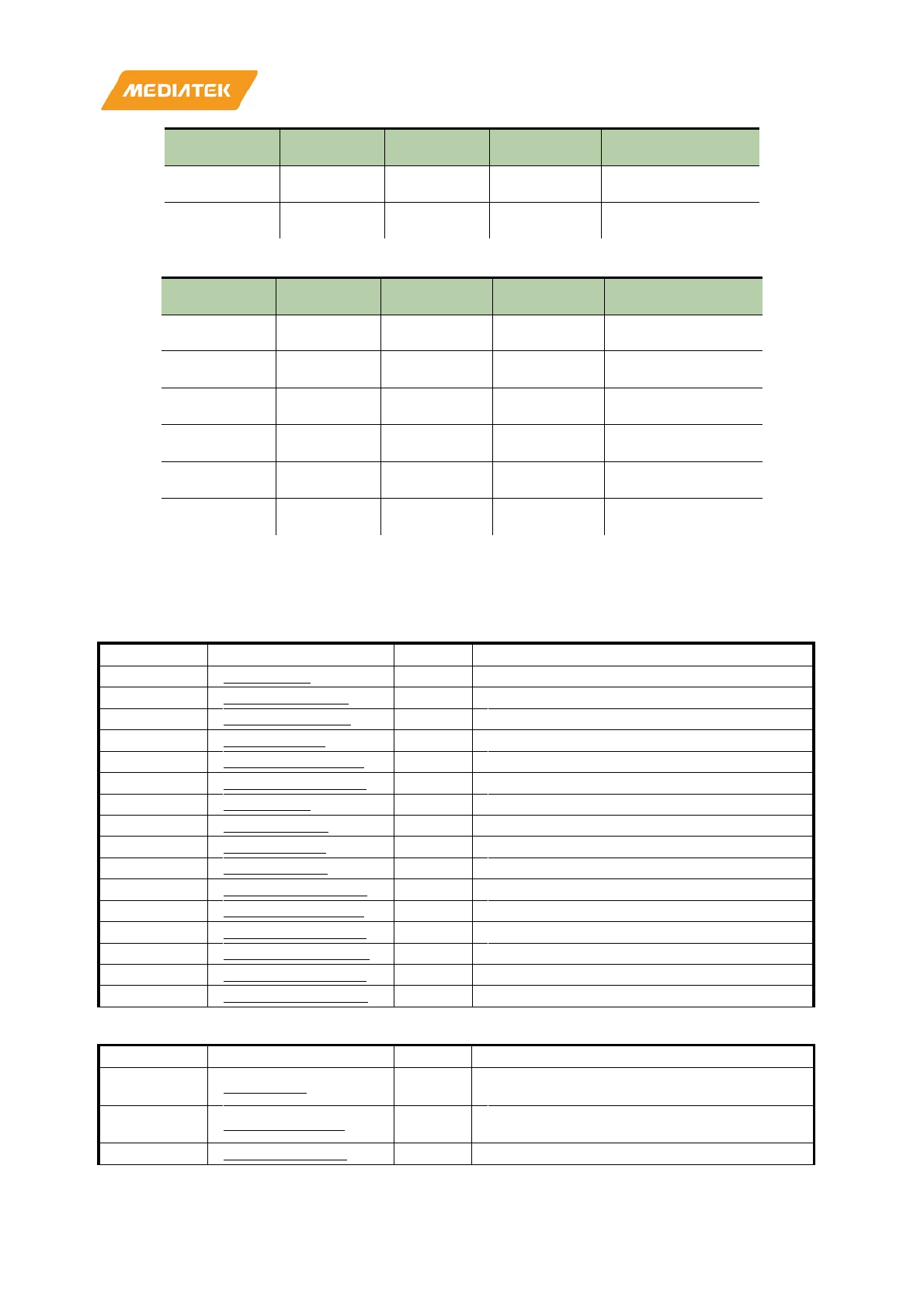
MT7686 Reference Manual
© 2016 - 2017 MediaTek Inc.
Page 419 of 536
This document contains information that is proprietary to MediaTek Inc. (“MediaTek”) and/or its licensor(s).
Any unauthorized use, reproduction or disclosure of this document in whole or in part is strictly prohibited.
GPIO_DIR GPIO_PUPD GPIO_R1 GPIO_R0 Resistance (Ω)
0 1 1 1 Pull-down, 23.5K
1 X X X High-Z
Table 21-4. IO type 3 - pull up/down control
GPIO_DIR GPIO_G GPIO_PU GPIO_PD Resistance (Ω)
0 1 0 0 High-Z
0 1 0 1 Pull-down, 75K
0 1 1 0 Pull-up, 75K
0 1 1 1 Keeper, 75K
1 1 x x High-Z
x 0 x x High-Z
21.3. Register mapping
Module name: gpio_reg Base address: (+A20b0000h)
Address
Name
Width
Register Function
A20B0000
GPIO_DIR0
32
GPIO Direction Control
A20B0004
GPIO_DIR0_SET
32
GPIO Direction Control
A20B0008
GPIO_DIR0_CLR
32
GPIO Direction Control
A20B0020
GPIO_DOUT0
32
GPIO Output Data Control
A20B0024
GPIO_DOUT0_SET
32
GPIO Output Data Control
A20B0028
GPIO_DOUT0_CLR
32
GPIO Output Data Control
A20B0030
GPIO_DIN0
32
GPIO Input Data Value
A20B0040
GPIO_MODE0
32
GPIO Mode Control
A20B0044
GPIO_MODE1
32
GPIO Mode Control
A20B0048
GPIO_MODE2
32
GPIO Mode Control
A20B0050
GPIO_MODE0_SET
32
GPIO Mode Control
A20B0054
GPIO_MODE1_SET
32
GPIO Mode Control
A20B0058
GPIO_MODE2_SET
32
GPIO Mode Control
A20B0060
GPIO_MODE0_CLR
32
GPIO Mode Control
A20B0064
GPIO_MODE1_CLR
32
GPIO Mode Control
A20B0068
GPIO_MODE2_CLR
32
GPIO Mode Control
Module name: IO_CFG_0 Base address: (+A20c0000h)
Address
Name
Width
Register Function
A20C0000
DRV_CFG0
32
GPIO DRV Control
Configures GPIO driving control
A20C0004
DRV_CFG0_SET
32
GPIO DRV Control
For bitwise access of
DRV_CFG0
A20C0008
DRV_CFG0_CLR
32
GPIO DRV Control

MT7686 Reference Manual
© 2016 - 2017 MediaTek Inc.
Page 420 of 536
This document contains information that is proprietary to MediaTek Inc. (“MediaTek”) and/or its licensor(s).
Any unauthorized use, reproduction or disclosure of this document in whole or in part is strictly prohibited.
Address
Name
Width
Register Function
For bitwise access of DRV_CFG0
A20C0010
G_CFG0
32
GPIO
Analog input Control
Configures GPIO
analog input control
A20C0014
G_CFG0_SET
32
GPIO Analog input Control
For bitwise access of
G_CFG0
A20C0018
G_CFG0_CLR
32
GPIO Analog input Control
For bitwise access of
G_CFG0
A20C0020
IES_CFG0
32
GPIO IES Control
Configures GPIO input enabling control
A20C0024
IES_CFG0_SET
32
GPIO IES Control
For bitwise access of
IES_CFG0
A20C0028
IES_CFG0_CLR
32
GPIO IES Control
For bitwise access of IES
_CFG0
A20C0030
PD_CFG0
32
GPIO PD Control
Configures GPIO
PD control
A20C0034
PD_CFG0_SET
32
GPIO PD Control
For
bitwise access of PD_CFG0
A20C0038
PD_CFG0_CLR
32
GPIO PD Control
For bitwise access of P
D_CFG0
A20C0040
PU_CFG0
32
GPIO PU Control
Configures GPIO PU control
A20C0044
PU_CFG0_SET
32
GPIO PU Control
For
bitwise access of PU_CFG0
A20C0048
PU_CFG0_CLR
32
GPIO PU Control
For bitwise access of
PU_CFG0
A20C0050
RDSEL_CFG0
32
GPIO RDSEL
Control
Configures GPIO RDSEL
control
A20C0054
RDSEL_CFG0_SET
32
GPIO RDSEL Control
For
bitwise access of RDSEL_CFG0
A20C0058
RDSEL_CFG0_CLR
32
GPIO RDSEL Control
For bitwise access of
RDSEL_CFG0
A20C0060
SMT_CFG0
32
GPIO SMT Control
Configures GPIO SMT
control
A20C0064
SMT_CFG0_SET
32
GPIO
SMT Control
For
bitwise access of SMT_CFG0
A20C0068
SMT_CFG0_CLR
32
GPIO SMT Control
For bitwise access of
SMT_CFG0
A20C0080
TDSEL_CFG
00
32
GPIO TDSEL Control
Configures GPIO TDSEL
control
A20C0084
TDSEL_CFG0
0_SET
32
GPIO TDSEL Control
For
bitwise access of TDSEL_CFG00
A20C0088
TDSEL_CFG0
0_CLR
32
GPIO
TDSEL Control
For bitwise access of
TDSEL_CFG00
A20C0090
TDSEL_CFG
01
32
GPIO TDSEL Control
Configures GPIO TDSEL
control
A20C0094
TDSEL_CFG
01_SET
32
GPIO TDSEL Control
For
bitwise access of TDSEL_CFG01
A20C0098
TDSEL_CFG
01_CLR
32
GPIO TDSEL Control
For bitwise access of
TDSEL_CFG01
Module name: IO_CFG_1 Base address: (+A20d0000h)
Address
Name
Width
Register Function
A20D0000
DRV_CFG1
32
GPIO DRV Control

MT7686 Reference Manual
© 2016 - 2017 MediaTek Inc.
Page 421 of 536
This document contains information that is proprietary to MediaTek Inc. (“MediaTek”) and/or its licensor(s).
Any unauthorized use, reproduction or disclosure of this document in whole or in part is strictly prohibited.
Address
Name
Width
Register Function
Configures GPIO driving control
A20D0004
DRV_
CFG1_SET
32
GPIO DRV Control
For bitwise access of DRV_CFG1
A20D0008
DRV_
CFG1_CLR
32
GPIO DRV Control
For bitwise access of DRV_CFG1
A20D0010
G_
CFG1
32
GPIO Analog input Control
Configures GPIO analog input control
A20D0014
G_
CFG1_SET
32
GPIO Analog input Control
For bitwise access of G_CFG1
A20D0018
G_
CFG1_CLR
32
GPIO Analog input Control
For bitwise access of G_CFG1
A20D0020
IES_
CFG1
32
GPIO IES Control
Configures GPIO input enabling control
A20D0024
IES_
CFG1_SET
32
GPIO IES Control
For bitwise access of IES_CFG1
A20D0028
IES_
CFG1_CLR
32
GPIO IES Control
For bitwise access of IES_CFG1
A20D0030
PD_
CFG1
32
GPIO PD Control
Configures GPIO PD control
A20D0034
PD_
CFG1_SET
32
GPIO PD Control
For bitwise access of PD_CFG1
A20D0038
PD_
CFG1_CLR
32
GPIO PD Control
For bitwise access of PD_CFG1
A20D0040
PUPD_
CFG1
32
GPIO PUPD Control
Configures GPIO PUPD control
A20D0044
PUPD_
CFG1_SET
32
GPIO PUPD Control
For bitwise access of PUPD_CFG1
A20D0048
PUPD_
CFG1_CLR
32
GPIO PUPD Control
For bitwise access of PUPD_CFG1
A20D0050
PU_
CFG1
32
GPIO PU Control
Configures GPIO PU control
A20D0054
PU_
CFG1_SET
32
GPIO PU Control
For bitwise access of PU_CFG1
A20D0058
PU_
CFG1_CLR
32
GPIO PU Control
For bitwise access of PU_CFG1
A20D0060
R0_
CFG1
32
GPIO R0 Control
Configures GPIO R0 control
A20D0064
R0_
CFG1_SET
32
GPIO R0 Control
For bitwise access of R0_CFG1
A20D0068
R0_
CFG1_CLR
32
GPIO R0 Control
For bitwise access of R0_CFG1
A20D0070
R1_
CFG1
32
GPIO R1 Control
Configures GPIO R1 control
A20D0074
R1_
CFG1_SET
32
GPIO R1 Control
For bitwise access of R1_CFG1
A20D0078
R1_
CFG1_CLR
32
GPIO R1 Control
For bitwise access of R1_CFG1
A20D0080
RDSEL_
CFG1
32
GPIO RDSEL Control
Configures GPIO RDSEL control
A20D0084
RDSEL_
CFG1_SET
32
GPIO RDSEL Control
For bitwise access of RDSEL_CFG1
A20D0088
RDSEL_
CFG1_CLR
32
GPIO RDSEL Control
For bitwise access of RDSEL_CFG1
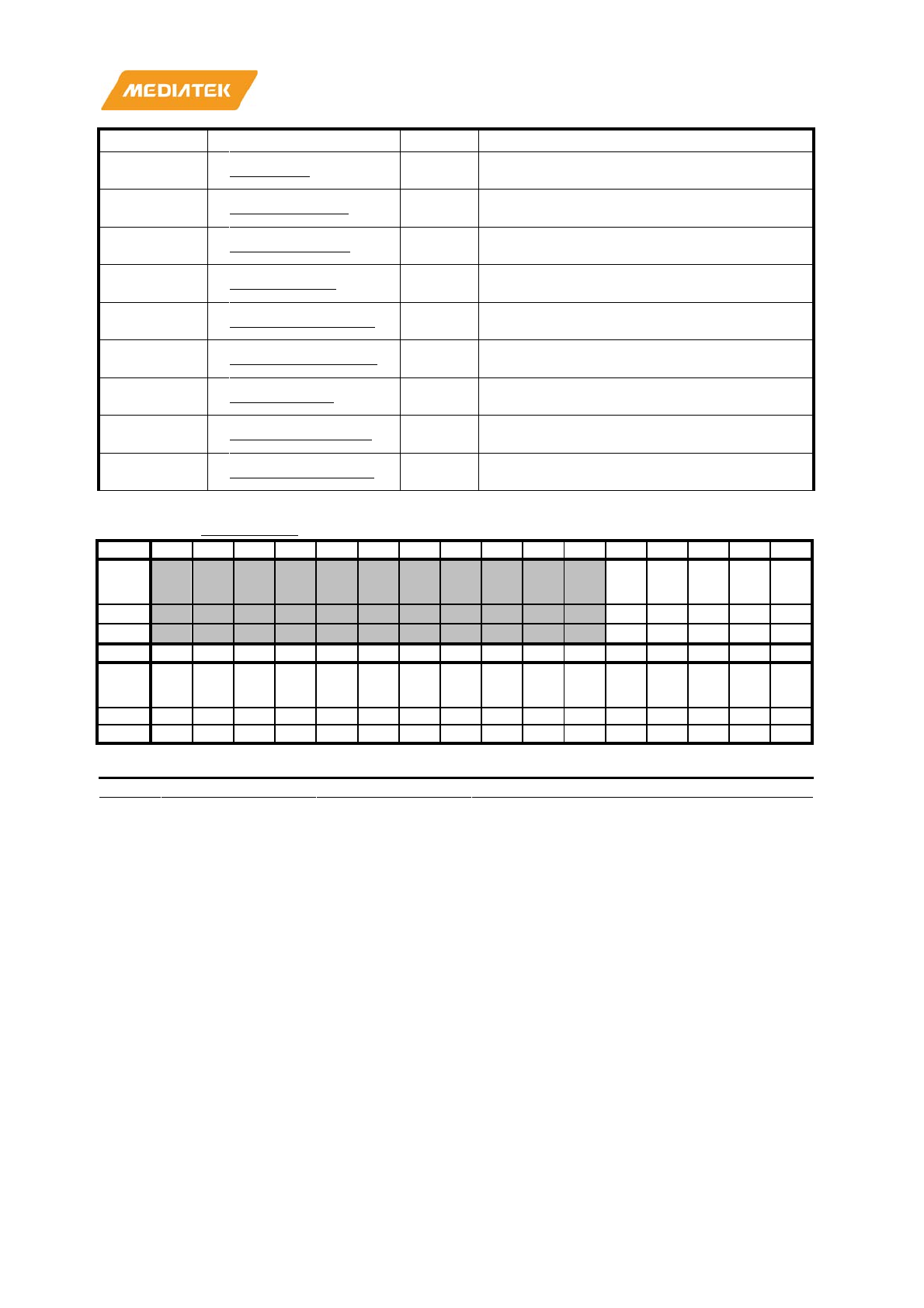
MT7686 Reference Manual
© 2016 - 2017 MediaTek Inc.
Page 422 of 536
This document contains information that is proprietary to MediaTek Inc. (“MediaTek”) and/or its licensor(s).
Any unauthorized use, reproduction or disclosure of this document in whole or in part is strictly prohibited.
Address
Name
Width
Register Function
A20D0090
SMT_
CFG1
32
GPIO SMT Control
Configures GPIO SMT control
A20D0094
SMT_
CFG1_SET
32
GPIO SMT Control
For bitwise access of SMT_CFG1
A20D0098
SMT_
CFG1_CLR
32
GPIO SMT Control
For bitwise access of SMT_CFG1
A20D00B0
TDSEL_
CFG10
32
GPIO TDSEL Control
Configures GPIO TDSEL control
A20D00B4
TDSEL_
CFG10_SET
32
GPIO TDSEL Control
For bitwise access of TDSEL_CFG10
A20D00B8
TDSEL_
CFG10_CLR
32
GPIO TDSEL Control
For bitwise access of TDSEL_CFG10
A20D00C0
TDSEL_CFG
11
32
GPIO TDSEL Control
Configures GPIO TDSEL control
A20D00C4
TDSEL_CFG1
1_SET
32
GPIO TDSEL Control
For bitwise access of TDSEL_CFG11
A20D00C8
TDSEL_CFG1
1_CLR
32
GPIO TDSEL Control
For bitwise access of TDSEL_CFG01
A20B0000
GPIO_DIR0
GPIO Direction Control
00500010
Bit
31
30
29
28
27
26
25
24
23
22
21
20
19
18
17
16
Name
GPIO
20_D
IR
GPIO
19_DI
R
GPIO
18_DI
R
GPIO
17_DI
R
GPIO
16_DI
R
Type
RW
RW
RW
RW
RW
Reset
0
1
0
1
0
0
0
0
Bit
15
14
13
12
11
10
9
8
7
6
5
4
3
2
1
0
Name
GPIO
15_DI
R
GPIO
14_DI
R
GPIO
13_DI
R
GPIO
12_DI
R
GPIO
11_DI
R
GPIO
10_DI
R
GPIO
9_DI
R
GPIO
8_DI
R
GPIO
7_DI
R
GPIO
6_DI
R
GPIO
5_DI
R
GPIO
4_DI
R
GPIO
3_DI
R
GPIO
2_DI
R
GPIO
1_DI
R
GPIO
0_DI
R
Type
RW
RW
RW
RW
RW
RW
RW
RW
RW
RW
RW
RW
RW
RW
RW
RW
Reset
0
0
0
0
0
0
0
0
0
0
0
1
0
0
0
0
Bit(s)
Mnemonic
Name
Description
20
GPIO20
GPIO20_DIR
GPIO20 direction control
0: GPIO as input
1: GPIO as output
19
GPIO19
GPIO19_DIR
GPIO19 direction control
0: GPIO as input
1: GPIO as output
18
GPIO18
GPIO18_DIR
GPIO18 direction control
0: GPIO as input
1: GPIO as output
17
GPIO17
GPIO17_DIR
GPIO17 direction control
0: GPIO as input
1: GPIO as output
16
GPIO16
GPIO16_DIR
GPIO16 direction control
0: GPIO as input
1: GPIO as output
15
GPIO15
GPIO15_DIR
GPIO15 direction control
0: GPIO as input
1: GPIO as output
14
GPIO14
GPIO14_DIR
GPIO14 direction control
0: GPIO as input

MT7686 Reference Manual
© 2016 - 2017 MediaTek Inc.
Page 423 of 536
This document contains information that is proprietary to MediaTek Inc. (“MediaTek”) and/or its licensor(s).
Any unauthorized use, reproduction or disclosure of this document in whole or in part is strictly prohibited.
Bit(s)
Mnemonic
Name
Description
1: GPIO as output
13
GPIO13
GPIO13_DIR
GPIO13 direction control
0: GPIO as input
1: GPIO as output
12
GPIO12
GPIO12_DIR
GPIO12 direction control
0: GPIO as input
1: GPIO as output
11
GPIO11
GPIO11_DIR
GPIO11 direction control
0: GPIO as input
1: GPIO as output
10
GPIO10
GPIO10_DIR
GPIO10 direction control
0: GPIO as input
1: GPIO as output
9
GPIO9
GPIO9_DIR
GPIO9 direction control
0: GPIO as input
1: GPIO as output
8
GPIO8
GPIO8_DIR
GPIO8 direction control
0: GPIO as input
1: GPIO as output
7
GPIO7
GPIO7_DIR
GPIO7 direction control
0: GPIO as input
1: GPIO as output
6
GPIO6
GPIO6_DIR
GPIO6 direction control
0: GPIO as input
1: GPIO as output
5
GPIO5
GPIO5_DIR
GPIO5 direction control
0: GPIO as input
1: GPIO as output
4
GPIO4
GPIO4_DIR
GPIO4 direction control
0: GPIO as input
1: GPIO as output
3
GPIO3
GPIO3_DIR
GPIO3 direction control
0: GPIO as input
1: GPIO as output
2
GPIO2
GPIO2_DIR
GPIO2 direction control
0: GPIO as input
1: GPIO as output
1
GPIO1
GPIO1_DIR
GPIO1 direction control
0: GPIO as input
1: GPIO as output
0
GPIO0
GPIO0_DIR
GPIO0 direction control
0: GPIO as input
1: GPIO as output
A20B0004
GPIO_DIR0_SET
GPIO Direction Control
00000000
Bit
31
30
29
28
27
26
25
24
23
22
21
20
19
18
17
16
Name
GPIO
20_D
IR_S
ET
GPIO
19_DI
R_SE
T
GPIO
18_DI
R_SE
T
GPIO
17_DI
R_SE
T
GPIO
16_DI
R_SE
T
Type
WO
WO
WO
WO
WO
Reset
0
0
0
0
0
Bit
15
14
13
12
11
10
9
8
7
6
5
4
3
2
1
0
Name
GPIO
15_DI
R_SE
GPIO
14_DI
R_SE
GPIO
13_DI
R_SE
GPIO
12_DI
R_SE
GPIO
11_DI
R_SE
GPIO
10_DI
R_SE
GPIO
9_DI
R_SE
GPIO
8_DI
R_SE
GPIO
7_DI
R_SE
GPIO
6_DI
R_SE
GPIO
5_DI
R_SE
GPIO
4_DI
R_SE
GPIO
3_DI
R_SE
GPIO
2_DI
R_SE
GPIO
1_DI
R_SE
GPIO
0_DI
R_SE

MT7686 Reference Manual
© 2016 - 2017 MediaTek Inc.
Page 424 of 536
This document contains information that is proprietary to MediaTek Inc. (“MediaTek”) and/or its licensor(s).
Any unauthorized use, reproduction or disclosure of this document in whole or in part is strictly prohibited.
T
T
T
T
T
T
T
T
T
T
T
T
T
T
T
T
Type
WO
WO
WO
WO
WO
WO
WO
WO
WO
WO
WO
WO
WO
WO
WO
WO
Reset
0
0
0
0
0
0
0
0
0
0
0
0
0
0
0
0
Bit(s)
Mnemonic
Name
Description
20
GPIO20
GPIO20_DIR_SET
Bitwise SET operation of GPIO20 direction
0: Keep
1: SET bits
19
GPIO19
GPIO19_DIR_SET
Bitwise SET operation of GPIO19 direction
0: Keep
1: SET bits
18
GPIO18
GPIO18_DIR_SET
Bitwise SET operation of GPIO18 direction
0: Keep
1: SET bits
17
GPIO17
GPIO17_DIR_SET
Bitwise SET operation of GPIO17 direction
0: Keep
1: SET bits
16
GPIO16
GPIO16_DIR_SET
Bitwise SET operation of GPIO16 direction
0: Keep
1: SET bits
15
GPIO15
GPIO15_DIR_SET
Bitwise SET operation of GPIO15 direction
0: Keep
1: SET bits
14
GPIO14
GPIO14_DIR_SET
Bitwise SET operation of GPIO14 direction
0: Keep
1: SET bits
13
GPIO13
GPIO13_DIR_SET
Bitwise SET operation of GPIO13 direction
0: Keep
1: SET bits
12
GPIO12
GPIO12_DIR_SET
Bitwise SET operation of GPIO12 direction
0: Keep
1: SET bits
11
GPIO11
GPIO11_DIR_SET
Bitwise SET operation of GPIO11 direction
0: Keep
1: SET bits
10
GPIO10
GPIO10_DIR_SET
Bitwise SET operation of GPIO10 direction
0: Keep
1: SET bits
9
GPIO9
GPIO9_DIR_SET
Bitwise SET operation of GPIO9 direction
0: Keep
1: SET bits
8
GPIO8
GPIO8_DIR_SET
Bitwise SET operation of GPIO8 direction
0: Keep
1: SET bits
7
GPIO7
GPIO7_DIR_SET
Bitwise SET operation of GPIO7 direction
0: Keep
1: SET bits
6
GPIO6
GPIO6_DIR_SET
Bitwise SET operation of GPIO6 direction
0: Keep
1: SET bits
5
GPIO5
GPIO5_DIR_SET
Bitwise SET operation of GPIO5 direction
0: Keep
1: SET bits
4
GPIO4
GPIO4_DIR_SET
Bitwise SET operation of GPIO4 direction
0: Keep
1: SET bits
3
GPIO3
GPIO3_DIR_SET
Bitwise SET operation of GPIO3 direction

MT7686 Reference Manual
© 2016 - 2017 MediaTek Inc.
Page 425 of 536
This document contains information that is proprietary to MediaTek Inc. (“MediaTek”) and/or its licensor(s).
Any unauthorized use, reproduction or disclosure of this document in whole or in part is strictly prohibited.
Bit(s)
Mnemonic
Name
Description
0: Keep
1: SET bits
2
GPIO2
GPIO2_DIR_SET
Bitwise SET operation of GPIO2 direction
0: Keep
1: SET bits
1
GPIO1
GPIO1_DIR_SET
Bitwise SET operation of GPIO1 direction
0: Keep
1: SET bits
0
GPIO0
GPIO0_DIR_SET
Bitwise SET operation of GPIO0 direction
0: Keep
1: SET bits
A20B0008
GPIO_DIR0_CLR
GPIO Direction Control
00000000
Bit
31
30
29
28
27
26
25
24
23
22
21
20
19
18
17
16
Name
GPIO
20_D
IR_C
LR
GPIO
19_DI
R_CL
R
GPIO
18_DI
R_CL
R
GPIO
17_DI
R_CL
R
GPIO
16_DI
R_CL
R
Type
WO
WO
WO
WO
WO
Reset
0
0
0
0
0
Bit
15
14
13
12
11
10
9
8
7
6
5
4
3
2
1
0
Name
GPIO
15_DI
R_CL
R
GPIO
14_DI
R_CL
R
GPIO
13_DI
R_CL
R
GPIO
12_DI
R_CL
R
GPIO
11_DI
R_CL
R
GPIO
10_DI
R_CL
R
GPIO
9_DI
R_CL
R
GPIO
8_DI
R_CL
R
GPIO
7_DI
R_CL
R
GPIO
6_DI
R_CL
R
GPIO
5_DI
R_CL
R
GPIO
4_DI
R_CL
R
GPIO
3_DI
R_CL
R
GPIO
2_DI
R_CL
R
GPIO
1_DI
R_CL
R
GPIO
0_DI
R_CL
R
Type
WO
WO
WO
WO
WO
WO
WO
WO
WO
WO
WO
WO
WO
WO
WO
WO
Reset
0
0
0
0
0
0
0
0
0
0
0
0
0
0
0
0
Bit(s)
Mnemonic
Name
Description
20
GPIO20
GPIO20_DIR_CLR
Bitwise CLEAR operation of GPIO20 direction
0: Keep
1: Clear bits
19
GPIO19
GPIO19_DIR_CLR
Bitwise CLEAR operation of GPIO19 direction
0: Keep
1: Clear bits
18
GPIO18
GPIO18_DIR_CLR
Bitwise CLEAR operation of GPIO18 direction
0: Keep
1: Clear bits
17
GPIO17
GPIO17_DIR_CLR
Bitwise CLEAR operation of GPIO17 direction
0: Keep
1: Clear bits
16
GPIO16
GPIO16_DIR_CLR
Bitwise CLEAR operation of GPIO16 direction
0: Keep
1: Clear bits
15
GPIO15
GPIO15_DIR_CLR
Bitwise CLEAR operation of GPIO15 direction
0: Keep
1: Clear bits
14
GPIO14
GPIO14_DIR_CLR
Bitwise CLEAR operation of GPIO14 direction
0: Keep
1: Clear bits
13
GPIO13
GPIO13_DIR_CLR
Bitwise CLEAR operation of GPIO13 direction
0: Keep
1: Clear bits
12
GPIO12
GPIO12_DIR_CLR
Bitwise CLEAR operation of GPIO12 direction
0: Keep

MT7686 Reference Manual
© 2016 - 2017 MediaTek Inc.
Page 426 of 536
This document contains information that is proprietary to MediaTek Inc. (“MediaTek”) and/or its licensor(s).
Any unauthorized use, reproduction or disclosure of this document in whole or in part is strictly prohibited.
Bit(s)
Mnemonic
Name
Description
1: Clear bits
11
GPIO11
GPIO11_DIR_CLR
Bitwise CLEAR operation of GPIO11 direction
0: Keep
1: Clear bits
10
GPIO10
GPIO10_DIR_CLR
Bitwise CLEAR operation of GPIO10 direction
0: Keep
1: Clear bits
9
GPIO9
GPIO9_DIR_CLR
Bitwise CLEAR operation of GPIO9 direction
0: Keep
1: Clear bits
8
GPIO8
GPIO8_DIR_CLR
Bitwise CLEAR operation of GPIO8 direction
0: Keep
1: Clear bits
7
GPIO7
GPIO7_DIR_CLR
Bitwise CLEAR operation of GPIO7 direction
0: Keep
1: Clear bits
6
GPIO6
GPIO6_DIR_CLR
Bitwise CLEAR operation of GPIO6 direction
0: Keep
1: Clear bits
5
GPIO5
GPIO5_DIR_CLR
Bitwise CLEAR operation of GPIO5 direction
0: Keep
1: Clear bits
4
GPIO4
GPIO4_DIR_CLR
Bitwise CLEAR operation of GPIO4 direction
0: Keep
1: Clear bits
3
GPIO3
GPIO3_DIR_CLR
Bitwise CLEAR operation of GPIO3 direction
0: Keep
1: Clear bits
2
GPIO2
GPIO2_DIR_CLR
Bitwise CLEAR operation of GPIO2 direction
0: Keep
1: Clear bits
1
GPIO1
GPIO1_DIR_CLR
Bitwise CLEAR operation of GPIO1 direction
0: Keep
1: Clear bits
0
GPIO0
GPIO0_DIR_CLR
Bitwise CLEAR operation of GPIO0 direction
0: Keep
1: Clear bits
A20B0020
GPIO_DOUT0
GPIO Output Data Control
00200000
Bit
31
30
29
28
27
26
25
24
23
22
21
20
19
18
17
16
Name
GPIO
20_O
UT
GPIO
19_O
UT
GPIO
18_O
UT
GPIO
17_O
UT
GPIO
16_O
UT
Type
RW
RW
RW
RW
RW
Reset
0
0
1
0
0
0
0
0
Bit
15
14
13
12
11
10
9
8
7
6
5
4
3
2
1
0
Name
GPIO
15_O
UT
GPIO
14_O
UT
GPIO
13_O
UT
GPIO
12_O
UT
GPIO
11_O
UT
GPIO
10_O
UT
GPIO
9_OU
T
GPIO
8_OU
T
GPIO
7_OU
T
GPIO
6_OU
T
GPIO
5_OU
T
GPIO
4_OU
T
GPIO
3_OU
T
GPIO
2_OU
T
GPIO
1_OU
T
GPIO
0_OU
T
Type
RW
RW
RW
RW
RW
RW
RW
RW
RW
RW
RW
RW
RW
RW
RW
RW
Reset
0
0
0
0
0
0
0
0
0
0
0
0
0
0
0
0
Bit(s)
Mnemonic
Name
Description
20
GPIO20
GPIO20_OUT
GPIO20 data output value
0: GPIO output LO

MT7686 Reference Manual
© 2016 - 2017 MediaTek Inc.
Page 427 of 536
This document contains information that is proprietary to MediaTek Inc. (“MediaTek”) and/or its licensor(s).
Any unauthorized use, reproduction or disclosure of this document in whole or in part is strictly prohibited.
Bit(s)
Mnemonic
Name
Description
1: GPIO output HI
19
GPIO19
GPIO19_OUT
GPIO19 data output value
0: GPIO output LO
1: GPIO output HI
18
GPIO18
GPIO18_OUT
GPIO18 data output value
0: GPIO output LO
1: GPIO output HI
17
GPIO17
GPIO17_OUT
GPIO17 data output value
0: GPIO output LO
1: GPIO output HI
16
GPIO16
GPIO16_OUT
GPIO16 data output value
0: GPIO output LO
1: GPIO output HI
15
GPIO15
GPIO15_OUT
GPIO15 data output value
0: GPIO output LO
1: GPIO output HI
14
GPIO14
GPIO14_OUT
GPIO14 data output value
0: GPIO output LO
1: GPIO output HI
13
GPIO13
GPIO13_OUT
GPIO13 data output value
0: GPIO output LO
1: GPIO output HI
12
GPIO12
GPIO12_OUT
GPIO12 data output value
0: GPIO output LO
1: GPIO output HI
11
GPIO11
GPIO11_OUT
GPIO11 data output value
0: GPIO output LO
1: GPIO output HI
10
GPIO10
GPIO10_OUT
GPIO10 data output value
0: GPIO output LO
1: GPIO output HI
9
GPIO9
GPIO9_OUT
GPIO9 data output value
0: GPIO output LO
1: GPIO output HI
8
GPIO8
GPIO8_OUT
GPIO8 data output value
0: GPIO output LO
1: GPIO output HI
7
GPIO7
GPIO7_OUT
GPIO7 data output value
0: GPIO output LO
1: GPIO output HI
6
GPIO6
GPIO6_OUT
GPIO6 data output value
0: GPIO output LO
1: GPIO output HI
5
GPIO5
GPIO5_OUT
GPIO5 data output value
0: GPIO output LO
1: GPIO output HI
4
GPIO4
GPIO4_OUT
GPIO4 data output value
0: GPIO output LO
1: GPIO output HI
3
GPIO3
GPIO3_OUT
GPIO3 data output value
0: GPIO output LO
1: GPIO output HI
2
GPIO2
GPIO2_OUT
GPIO2 data output value
0: GPIO output LO
1: GPIO output HI
1
GPIO1
GPIO1_OUT
GPIO1 data output value
0: GPIO output LO
1: GPIO output HI

MT7686 Reference Manual
© 2016 - 2017 MediaTek Inc.
Page 428 of 536
This document contains information that is proprietary to MediaTek Inc. (“MediaTek”) and/or its licensor(s).
Any unauthorized use, reproduction or disclosure of this document in whole or in part is strictly prohibited.
Bit(s)
Mnemonic
Name
Description
0
GPIO0
GPIO0_OUT
GPIO0 data output value
0: GPIO output LO
1: GPIO output HI
A20B0024
GPIO_DOUT0_SET
GPIO Output Data Control
00000000
Bit
31
30
29
28
27
26
25
24
23
22
21
20
19
18
17
16
Name
GPIO
20_O
UT_S
ET
GPIO
19_O
UT_S
ET
GPIO
18_O
UT_S
ET
GPIO
17_O
UT_S
ET
GPIO
16_O
UT_S
ET
Type
WO
WO
WO
WO
WO
Reset
0
0
0
0
0
Bit
15
14
13
12
11
10
9
8
7
6
5
4
3
2
1
0
Name
GPIO
15_O
UT_S
ET
GPIO
14_O
UT_S
ET
GPIO
13_O
UT_S
ET
GPIO
12_O
UT_S
ET
GPIO
11_O
UT_S
ET
GPIO
10_O
UT_S
ET
GPIO
9_OU
T_SE
T
GPIO
8_OU
T_SE
T
GPIO
7_OU
T_SE
T
GPIO
6_OU
T_SE
T
GPIO
5_OU
T_SE
T
GPIO
4_OU
T_SE
T
GPIO
3_OU
T_SE
T
GPIO
2_OU
T_SE
T
GPIO
1_OU
T_SE
T
GPIO
0_OU
T_SE
T
Type
WO
WO
WO
WO
WO
WO
WO
WO
WO
WO
WO
WO
WO
WO
WO
WO
Reset
0
0
0
0
0
0
0
0
0
0
0
0
0
0
0
0
Bit(s)
Mnemonic
Name
Description
20
GPIO20
GPIO20_OUT_SET
Bitwise SET operation of GPIO20 data output
value
0: Keep
1: SET bits
19
GPIO19
GPIO19_OUT_SET
Bitwise SET operation of GPIO19 data output
value
0: Keep
1: SET bits
18
GPIO18
GPIO18_OUT_SET
Bitwise SET operation of GPIO18 data output
value
0: Keep
1: SET bits
17
GPIO17
GPIO17_OUT_SET
Bitwise SET operation of GPIO17 data output
value
0: Keep
1: SET bits
16
GPIO16
GPIO16_OUT_SET
Bitwise SET operation of GPIO16 data output
value
0: Keep
1: SET bits
15
GPIO15
GPIO15_OUT_SET
Bitwise SET operation of GPIO15 data output
value
0: Keep
1: SET bits
14
GPIO14
GPIO14_OUT_SET
Bitwise SET operation of GPIO14 data output
value
0: Keep
1: SET bits
13
GPIO13
GPIO13_OUT_SET
Bitwise SET operation of GPIO13 data output
value
0: Keep
1: SET bits
12
GPIO12
GPIO12_OUT_SET
Bitwise SET operation of GPIO12 data output
value
0: Keep

MT7686 Reference Manual
© 2016 - 2017 MediaTek Inc.
Page 429 of 536
This document contains information that is proprietary to MediaTek Inc. (“MediaTek”) and/or its licensor(s).
Any unauthorized use, reproduction or disclosure of this document in whole or in part is strictly prohibited.
Bit(s)
Mnemonic
Name
Description
1: SET bits
11
GPIO11
GPIO11_OUT_SET
Bitwise SET operation of GPIO11 data output
value
0: Keep
1: SET bits
10
GPIO10
GPIO10_OUT_SET
Bitwise SET operation of GPIO10 data output
value
0: Keep
1: SET bits
9
GPIO9
GPIO9_OUT_SET
Bitwise SET operation of GPIO9 data output
value
0: Keep
1: SET bits
8
GPIO8
GPIO8_OUT_SET
Bitwise SET operation of GPIO8 data output
value
0: Keep
1: SET bits
7
GPIO7
GPIO7_OUT_SET
Bitwise SET operation of GPIO7 data output
value
0: Keep
1: SET bits
6
GPIO6
GPIO6_OUT_SET
Bitwise SET operation of GPIO6 data output
value
0: Keep
1: SET bits
5
GPIO5
GPIO5_OUT_SET
Bitwise SET operation of GPIO5 data output
value
0: Keep
1: SET bits
4
GPIO4
GPIO4_OUT_SET
Bitwise SET operation of GPIO4 data output
value
0: Keep
1: SET bits
3
GPIO3
GPIO3_OUT_SET
Bitwise SET operation of GPIO3 data output
value
0: Keep
1: SET bits
2
GPIO2
GPIO2_OUT_SET
Bitwise SET operation of GPIO2 data output
value
0: Keep
1: SET bits
1
GPIO1
GPIO1_OUT_SET
Bitwise SET operation of GPIO1 data output
value
0: Keep
1: SET bits
0
GPIO0
GPIO0_OUT_SET
Bitwise SET operation of GPIO0 data output
value
0: Keep
1: SET bits
A20B0028
GPIO_DOUT0_CLR
GPIO Output Data Control
00000000
Bit
31
30
29
28
27
26
25
24
23
22
21
20
19
18
17
16
Name
GPIO
20_O
UT_C
LR
GPIO
19_O
UT_C
LR
GPIO
18_O
UT_C
LR
GPIO
17_O
UT_C
LR
GPIO
16_O
UT_C
LR
Type
WO
WO
WO
WO
WO

MT7686 Reference Manual
© 2016 - 2017 MediaTek Inc.
Page 430 of 536
This document contains information that is proprietary to MediaTek Inc. (“MediaTek”) and/or its licensor(s).
Any unauthorized use, reproduction or disclosure of this document in whole or in part is strictly prohibited.
Reset
0
0
0
0
0
Bit
15
14
13
12
11
10
9
8
7
6
5
4
3
2
1
0
Name
GPIO
15_O
UT_C
LR
GPIO
14_O
UT_C
LR
GPIO
13_O
UT_C
LR
GPIO
12_O
UT_C
LR
GPIO
11_O
UT_C
LR
GPIO
10_O
UT_C
LR
GPIO
9_OU
T_CL
R
GPIO
8_OU
T_CL
R
GPIO
7_OU
T_CL
R
GPIO
6_OU
T_CL
R
GPIO
5_OU
T_CL
R
GPIO
4_OU
T_CL
R
GPIO
3_OU
T_CL
R
GPIO
2_OU
T_CL
R
GPIO
1_OU
T_CL
R
GPIO
0_OU
T_CL
R
Type
WO
WO
WO
WO
WO
WO
WO
WO
WO
WO
WO
WO
WO
WO
WO
WO
Reset
0
0
0
0
0
0
0
0
0
0
0
0
0
0
0
0
Bit(s)
Mnemonic
Name
Description
20
GPIO20
GPIO20_OUT_CLR
Bitwise CLEAR operation of GPIO20 data
output value
0: Keep
1: Clear bits
19
GPIO19
GPIO19_OUT_CLR
Bitwise CLEAR operation of GPIO19 data
output value
0: Keep
1: Clear bits
18
GPIO18
GPIO18_OUT_CLR
Bitwise CLEAR operation of GPIO18 data
output value
0: Keep
1: Clear bits
17
GPIO17
GPIO17_OUT_CLR
Bitwise CLEAR operation of GPIO17 data
output value
0: Keep
1: Clear bits
16
GPIO16
GPIO16_OUT_CLR
Bitwise CLEAR operation of GPIO16 data
output value
0: Keep
1: Clear bits
15
GPIO15
GPIO15_OUT_CLR
Bitwise CLEAR operation of GPIO15 data
output value
0: Keep
1: Clear bits
14
GPIO14
GPIO14_OUT_CLR
Bitwise CLEAR operation of GPIO14 data
output value
0: Keep
1: Clear bits
13
GPIO13
GPIO13_OUT_CLR
Bitwise CLEAR operation of GPIO13 data
output value
0: Keep
1: Clear bits
12
GPIO12
GPIO12_OUT_CLR
Bitwise CLEAR operation of GPIO12 data
output value
0: Keep
1: Clear bits
11
GPIO11
GPIO11_OUT_CLR
Bitwise CLEAR operation of GPIO11 data
output value
0: Keep
1: Clear bits
10
GPIO10
GPIO10_OUT_CLR
Bitwise CLEAR operation of GPIO10 data
output value
0: Keep
1: Clear bits
9
GPIO9
GPIO9_OUT_CLR
Bitwise CLEAR operation of GPIO9 data output
value
0: Keep
1: Clear bits
8
GPIO8
GPIO8_OUT_CLR
Bitwise CLEAR operation of GPIO8 data output

MT7686 Reference Manual
© 2016 - 2017 MediaTek Inc.
Page 431 of 536
This document contains information that is proprietary to MediaTek Inc. (“MediaTek”) and/or its licensor(s).
Any unauthorized use, reproduction or disclosure of this document in whole or in part is strictly prohibited.
value
0: Keep
1: Clear bits
7
GPIO7
GPIO7_OUT_CLR
Bitwise CLEAR operation of GPIO7 data output
value
0: Keep
1: Clear bits
6
GPIO6
GPIO6_OUT_CLR
Bitwise CLEAR operation of GPIO6 data output
value
0: Keep
1: Clear bits
5
GPIO5
GPIO5_OUT_CLR
Bitwise CLEAR operation of GPIO5 data output
value
0: Keep
1: Clear bits
4
GPIO4
GPIO4_OUT_CLR
Bitwise CLEAR operation of GPIO4 data output
value
0: Keep
1: Clear bits
3
GPIO3
GPIO3_OUT_CLR
Bitwise CLEAR operation of GPIO3 data output
value
0: Keep
1: Clear bits
2
GPIO2
GPIO2_OUT_CLR
Bitwise CLEAR operation of GPIO2 data output
value
0: Keep
1: Clear bits
1
GPIO1
GPIO1_OUT_CLR
Bitwise CLEAR operation of GPIO1 data output
value
0: Keep
1: Clear bits
0
GPIO0
GPIO0_OUT_CLR
Bitwise CLEAR operation of GPIO0 data output
value
0: Keep
1: Clear bits
A20B0030
GPIO_DIN0
GPIO Input Data Value
00000000
Bit
31
30
29
28
27
26
25
24
23
22
21
20
19
18
17
16
Name
GPIO
20_D
IN
GPIO
19_DI
N
GPIO
18_DI
N
GPIO
17_DI
N
GPIO
16_DI
N
Type
RO
RO
RO
RO
RO
Reset
0
0
0
0
0
Bit
15
14
13
12
11
10
9
8
7
6
5
4
3
2
1
0
Name
GPIO
15_DI
N
GPIO
14_DI
N
GPIO
13_DI
N
GPIO
12_DI
N
GPIO
11_DI
N
GPIO
10_DI
N
GPIO
9_DI
N
GPIO
8_DI
N
GPIO
7_DI
N
GPIO
6_DI
N
GPIO
5_DI
N
GPIO
4_DI
N
GPIO
3_DI
N
GPIO
2_DI
N
GPIO
1_DI
N
GPIO
0_DI
N
Type
RO
RO
RO
RO
RO
RO
RO
RO
RO
RO
RO
RO
RO
RO
RO
RO
Reset
0
0
0
0
0
0
0
0
0
0
0
0
0
0
0
0
Bit(s)
Mnemonic
Name
Description
20
GPIO20
GPIO20_DIN
GPIO20 data input value
19
GPIO19
GPIO19_DIN
GPIO19 data input value
18
GPIO18
GPIO18_DIN
GPIO18 data input value
17
GPIO17
GPIO17_DIN
GPIO17 data input value
16
GPIO16
GPIO16_DIN
GPIO16 data input value
15
GPIO15
GPIO15_DIN
GPIO15 data input value
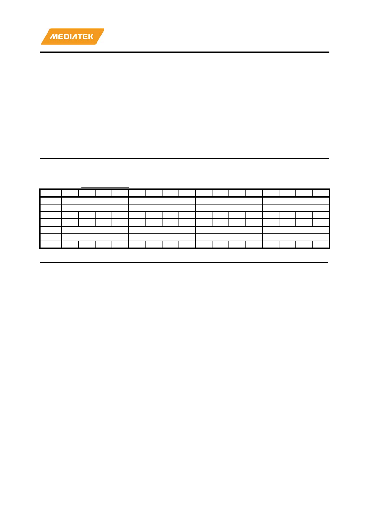
MT7686 Reference Manual
© 2016 - 2017 MediaTek Inc.
Page 432 of 536
This document contains information that is proprietary to MediaTek Inc. (“MediaTek”) and/or its licensor(s).
Any unauthorized use, reproduction or disclosure of this document in whole or in part is strictly prohibited.
Bit(s)
Mnemonic
Name
Description
14
GPIO14
GPIO14_DIN
GPIO14 data input value
13
GPIO13
GPIO13_DIN
GPIO13 data input value
12
GPIO12
GPIO12_DIN
GPIO12 data input value
11
GPIO11
GPIO11_DIN
GPIO11 data input value
10
GPIO10
GPIO10_DIN
GPIO10 data input value
9
GPIO9
GPIO9_DIN
GPIO9 data input value
8
GPIO8
GPIO8_DIN
GPIO8 data input value
7
GPIO7
GPIO7_DIN
GPIO7 data input value
6
GPIO6
GPIO6_DIN
GPIO6 data input value
5
GPIO5
GPIO5_DIN
GPIO5 data input value
4
GPIO4
GPIO4_DIN
GPIO4 data input value
3
GPIO3
GPIO3_DIN
GPIO3 data input value
2
GPIO2
GPIO2_DIN
GPIO2 data input value
1
GPIO1
GPIO1_DIN
GPIO1 data input value
0
GPIO0
GPIO0_DIN
GPIO0 data input value
A20B0040
GPIO_MODE0
GPIO Mode Control
00066666
Bit
31
30
29
28
27
26
25
24
23
22
21
20
19
18
17
16
Name
GPIO7_MODE
GPIO6_MODE
GPIO5_MODE
GPIO4_MODE
Type
RW
RW
RW
RW
Reset
0
0
0
0
0
0
0
0
0
0
0
0
0
1
1
0
Bit
15
14
13
12
11
10
9
8
7
6
5
4
3
2
1
0
Name
GPIO3_MODE
GPIO2_MODE
GPIO1_MODE
GPIO0_MODE
Type
RW
RW
RW
RW
Reset
0
1
1
0
0
1
1
0
0
1
1
0
0
1
1
0
Bit(s)
Mnemonic
Name
Description
31:28
GPIO7_MODE
Aux. mode of GPIO_7
0:GPIO7(IO)
1:SPISLV_A_SCK(I)
2:SPIMST_A_SCK(O)
3:EINT7(I)
4:CLKO1(O)
5:WIFI_ANT_SEL2(O)
6:TDM_WS(IO)
7:Reserved
8:Reserved
9:BT_PRI3(IO)
10:Reserved
27:24
GPIO6_MODE
Aux. mode of GPIO_6
0:GPIO6(IO)
1:SPISLV_A_CS(I)
2:SPIMST_A_CS(O)
3:EINT6(I)
4:UTXD0(O)
5:WIFI_ANT_SEL1(O)
6:TDM_TX(O)
7:Reserved
8:Reserved
9:SDA0(IO)
10:Reserved
23:20
GPIO5_MODE
Aux. mode of GPIO_5

MT7686 Reference Manual
© 2016 - 2017 MediaTek Inc.
Page 433 of 536
This document contains information that is proprietary to MediaTek Inc. (“MediaTek”) and/or its licensor(s).
Any unauthorized use, reproduction or disclosure of this document in whole or in part is strictly prohibited.
Bit(s)
Mnemonic
Name
Description
0:GPIO5(IO)
1:SPISLV_A_SIO3(IO)
2:SPIMST_A_SIO3(IO)
3:EINT5(I)
4:URXD0(I)
5:WIFI_ANT_SEL0(O)
6:TDM_RX(I)
7:Reserved
8:Reserved
9:SCL0(IO)
10:PMU_RGU_RSTB(O)
19:16
GPIO4_MODE
Aux. mode of GPIO_4
0:GPIO4(IO)
1:SPISLV_A_SIO2(IO)
2:SPIMST_A_SIO2(IO)
3:EINT4(I)
4:Reserved
5:I2S_MCLK(O)
6:JTDO(O)
7:Reserved
8:Reserved
9:WIFI_ANT_SEL3(O)
10:I2S_MCLK(O)
15:12
GPIO3_MODE
Aux. mode of GPIO_3
0:GPIO3(IO)
1:EINT3(I)
2:Reserved
3:UTXD1(O)
4:PWM1(O)
5:I2S_CK(IO)
6:JTRST_B(I)
7:Reserved
8:Reserved
9:WIFI_ANT_SEL2(O)
10:I2S_CK(IO)
11:8
GPIO2_MODE
Aux. mode of GPIO_2
0:GPIO2(IO)
1:EINT2(I)
2:Reserved
3:URXD1(I)
4:PWM0(O)
5:I2S_WS(IO)
6:JTCK(I)
7:CLKO0(O)
8:Reserved
9:BT_PRI0(IO)
10:WIFI_ANT_SEL4(O)
7:4
GPIO1_MODE
Aux. mode of GPIO_1
0:GPIO1(IO)
1:EINT1(I)
2:Reserved
3:U1CTS(I)
4:SDA1(IO)
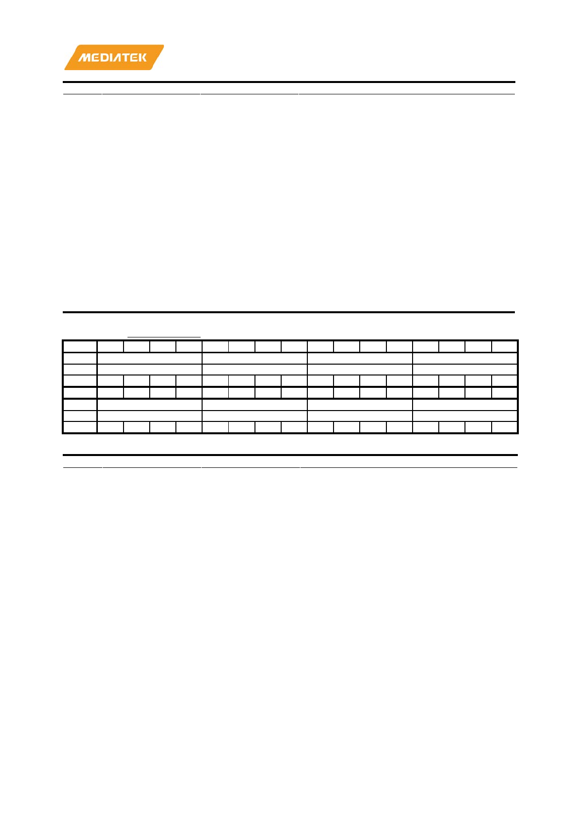
MT7686 Reference Manual
© 2016 - 2017 MediaTek Inc.
Page 434 of 536
This document contains information that is proprietary to MediaTek Inc. (“MediaTek”) and/or its licensor(s).
Any unauthorized use, reproduction or disclosure of this document in whole or in part is strictly prohibited.
Bit(s)
Mnemonic
Name
Description
5:I2S_TX(O)
6:JTMS(IO)
7:Reserved
8:WIFI_ANT_SEL1(O)
9:BT_PRI
3(IO)
10:PWM1(O)
3:0
GPIO0_MODE
Aux. mode of GPIO_0
0:GPIO0(IO)
1:EINT0(I)
2:Reserved
3:U1RTS(O)
4:SCL1(IO)
5:I2S_RX(I)
6:JTDI(I)
7:Reserved
8:WIFI_ANT_SEL0(O)
9:BT_PRI1(IO)
10:PWM0(O)
A20B0044
GPIO_MODE1
GPIO Mode Control
00000000
Bit
31
30
29
28
27
26
25
24
23
22
21
20
19
18
17
16
Name
GPIO15_MODE
GPIO14_MODE
GPIO13_MODE
GPIO12_MODE
Type
RW
RW
RW
RW
Reset
0
0
0
0
0
0
0
0
0
0
0
0
0
0
0
0
Bit
15
14
13
12
11
10
9
8
7
6
5
4
3
2
1
0
Name
GPIO11_MODE
GPIO10_MODE
GPIO9_MODE
GPIO8_MODE
Type
RW
RW
RW
RW
Reset
0
0
0
0
0
0
0
0
0
0
0
0
0
0
0
0
Bit(s)
Mnemonic
Name
Description
31:28
GPIO15_MODE
Aux. mode of GPIO_15
0:GPIO15(IO)
1:SPISLV_B_SIO0(IO)
2:SPIMST_B_SIO0(IO)
3:TDM_TX(O)
4:MA_MC0_DA2(IO)
5:SLV_MC0_DA2(IO)
6:SCL1(IO)
7:Reserved
8:EINT15(I)
9:Reserved
10:PWM3(O)
27:24
GPIO14_MODE
Aux. mode of GPIO_14
0:GPIO14(IO)
1:SPISLV_B_SIO1(IO)
2:SPIMST_B_SIO1(IO)
3:TDM_RX(I)
4:MA_MC0_DA1(IO)
5:SLV_MC0_DA1(IO)
6:PWM4(O)
7:Reserved
8:EINT14(I)
9:Reserved

MT7686 Reference Manual
© 2016 - 2017 MediaTek Inc.
Page 435 of 536
This document contains information that is proprietary to MediaTek Inc. (“MediaTek”) and/or its licensor(s).
Any unauthorized use, reproduction or disclosure of this document in whole or in part is strictly prohibited.
Bit(s)
Mnemonic
Name
Description
10:CLKO4(O)
23:20
GPIO13_MODE
Aux. mode of GPIO_13
0:GPIO13(IO)
1:SPISLV_B_SIO2(IO)
2:SPIMST_B_SIO2(IO)
3:U2RTS(O)
4:MA_MC0_DA0(IO)
5:SLV_MC0_DA0(IO)
6:CLKO4(O)
7:Reserved
8:EINT13(I)
9:Reserved
10:I2S_WS(IO)
19:16
GPIO12_MODE
Aux. mode of GPIO_12
0:GPIO12(IO)
1:SPISLV_B_SIO3(IO)
2:SPIMST_B_SIO3(IO)
3:UTXD2(O)
4:MA_MC0_CM0(IO)
5:SLV_MC0_CM0(IO)
6:EINT12(I)
7:Reserved
8:Reserved
9:WIFI_ANT_SEL1(O)
10:I2S_TX(O)
15:12
GPIO11_MODE
Aux. mode of GPIO_11
0:GPIO11(IO)
1:EINT11(I)
2:PWM3(O)
3:URXD2(I)
4:MA_MC0_CK(IO)
5:SLV_MC0_CK(IO)
6:CLKO2(O)
7:Reserved
8:Reserved
9:WIFI_ANT_SEL0(O)
10:I2S_RX(I)
11:8
GPIO10_MODE
Aux. mode of GPIO_10
0:GPIO10(IO)
1:EINT10(I)
2:Reserved
3:U2CTS(I)
4:PWM2(O)
5:PMU_RGU_RSTB(O)
6:PMU_GOTO_SLEEP(O)
7:Reserved
8:WIFI_ANT_SEL4(O)
9:Reserved
10:SDA0(IO)
7:4
GPIO9_MODE
Aux. mode of GPIO_9
0:GPIO9(IO)
1:SPISLV_A_SIO1(IO)
2:SPIMST_A_SIO1(IO)
3:EINT9(I)
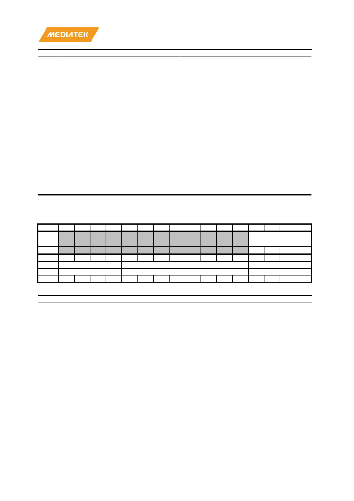
MT7686 Reference Manual
© 2016 - 2017 MediaTek Inc.
Page 436 of 536
This document contains information that is proprietary to MediaTek Inc. (“MediaTek”) and/or its licensor(s).
Any unauthorized use, reproduction or disclosure of this document in whole or in part is strictly prohibited.
Bit(s)
Mnemonic
Name
Description
4:SDA0(IO)
5:U0CTS(I)
6:TDM_MCLK(O)
7:Reserved
8:WIFI_ANT_SEL3(O)
9:BT_PRI1(IO)
10:Reserved
3:0
GPIO8_MODE
Aux. mode of GPIO_8
0:GPIO8(IO)
1:SPISLV_A_SIO0(IO)
2:SPIMST_A_SIO0(IO)
3:EINT8(I)
4:SCL0(IO)
5:U0RTS(O)
6:TDM_CK(IO)
7:Reserved
8:BT_PRI0(IO)
9:Reserved
10:Reserved
A20B0048
GPIO_MODE2
GPIO Mode Control
00011600
Bit
31
30
29
28
27
26
25
24
23
22
21
20
19
18
17
16
Name
GPIO20_MODE
Type
RW
Reset
0
0
0
1
Bit
15
14
13
12
11
10
9
8
7
6
5
4
3
2
1
0
Name
GPIO19_MODE
GPIO18_MODE
GPIO17_MODE
GPIO16_MODE
Type
RW
RW
RW
RW
Reset
0
0
0
1
0
1
1
0
0
0
0
0
0
0
0
0
Bit(s)
Mnemonic
Name
Description
19:16
GPIO20_MODE
Aux. mode of GPIO_20
0:GPIO20(IO)
1:UTXD0(O)
2:EINT20(I)
3:Reserved
4:Reserved
5:Reserved
6:AUXADC3(ANAin)
7:Reserved
8:Reserved
9:Reserved
10:Reserved
15:12
GPIO19_MODE
Aux. mode of GPIO_19
0:GPIO19(IO)
1:URXD0(I)
2:EINT19(I)
3:SCL1(IO)
4:Reserved
5:PWM5(O)

MT7686 Reference Manual
© 2016 - 2017 MediaTek Inc.
Page 437 of 536
This document contains information that is proprietary to MediaTek Inc. (“MediaTek”) and/or its licensor(s).
Any unauthorized use, reproduction or disclosure of this document in whole or in part is strictly prohibited.
Bit(s)
Mnemonic
Name
Description
6:AUXADC2(ANAin)
7:WIFI_EXT_CLK(I)
8:Reserved
9:Reserved
10:Reserved
11:8
GPIO18_MODE
Aux. mode of GPIO_18
0:GPIO18(IO)
1:PMU_GOTO_SLEEP(O)
2:Reserved
3:TDM_MCLK(O)
4:CLKO4(O)
5:SDA1(IO)
6:ZCV(SWsetAUXADC1)(ANAin)
7:Reserved
8:EINT18(I)
9:CLKO3(O)
10:PMU_RGU_RSTB(O)
7:4
GPIO17_MODE
Aux. mode of GPIO_17
0:GPIO17(IO)
1:SPISLV_B_CS(I)
2:SPIMST_B_CS(I)
3:TDM_CK(IO)
4:PWM5(O)
5:CLKO3(O)
6:AUXADC0(ANAin)
7:Reserved
8:EINT17(I)
9:Reserved
10:BT_PRI0(IO)
3:0
GPIO16_MODE
Aux. mode of GPIO_16
0:GPIO16(IO)
1:SPISLV_B_SCK(I)
2:SPIMST_B_SCK(I)
3:TDM_WS(IO)
4:MA_MC0_DA3(IO)
5:SLV_MC0_DA3(IO)
6:SDA1(IO)
7:Reserved
8:EINT16(I)
9:Reserved
10:Reserved
A20B0050
GPIO_MODE0_SET
GPIO Mode Control
00000000
Bit
31
30
29
28
27
26
25
24
23
22
21
20
19
18
17
16
Name
GPIO7_MODE_SET
GPIO6_MODE_SET
GPIO5_MODE_SET
GPIO4_MODE_SET
Type
WO
WO
WO
WO
Reset
0
0
0
0
0
0
0
0
0
0
0
0
0
0
0
0
Bit
15
14
13
12
11
10
9
8
7
6
5
4
3
2
1
0
Name
GPIO3_MODE_SET
GPIO2_MODE_SET
GPIO1_MODE_SET
GPIO0_MODE_SET
Type
WO
WO
WO
WO
Reset
0
0
0
0
0
0
0
0
0
0
0
0
0
0
0
0
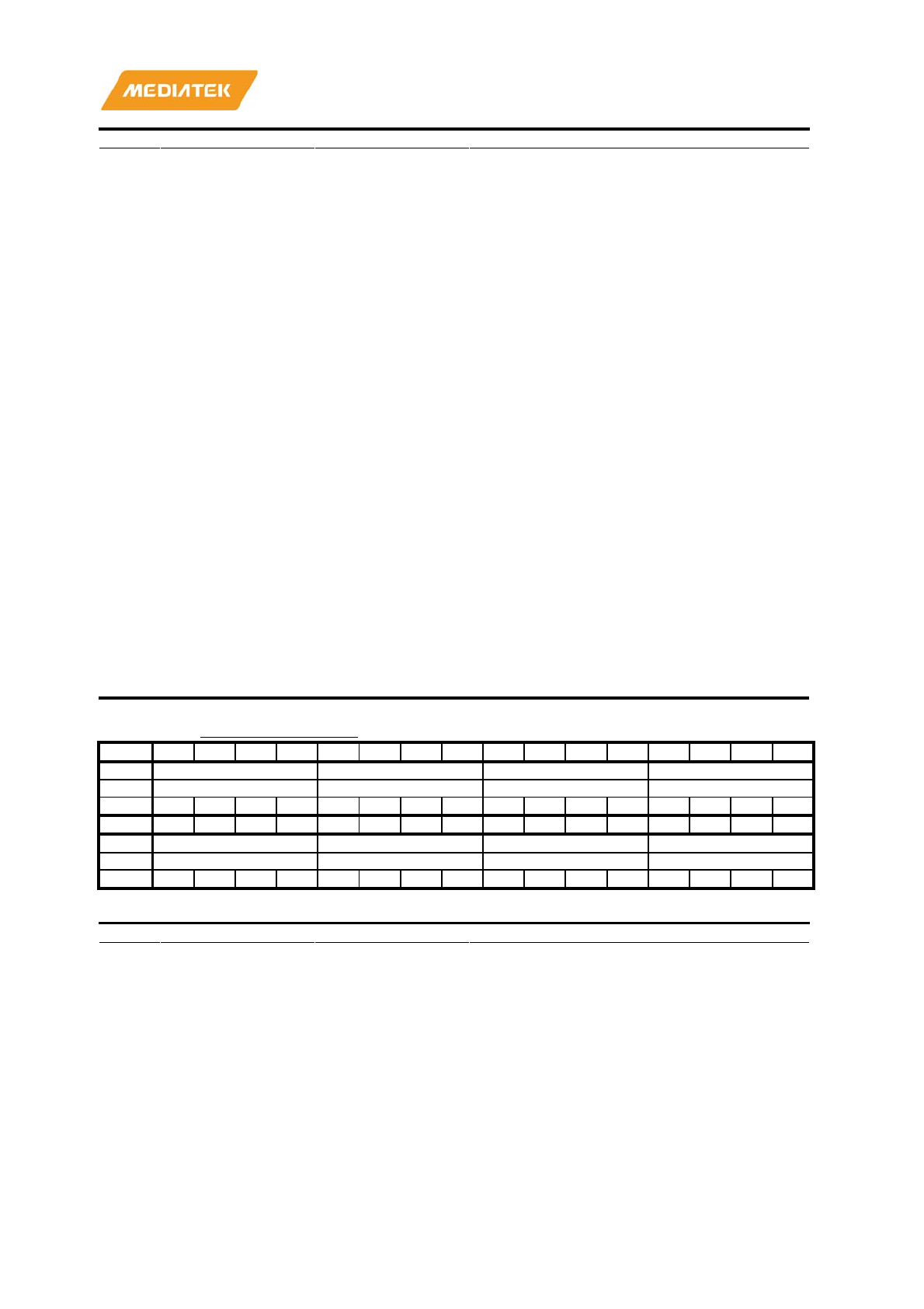
MT7686 Reference Manual
© 2016 - 2017 MediaTek Inc.
Page 438 of 536
This document contains information that is proprietary to MediaTek Inc. (“MediaTek”) and/or its licensor(s).
Any unauthorized use, reproduction or disclosure of this document in whole or in part is strictly prohibited.
Bit(s)
Mnemonic
Name
Description
31:28
GPIO7_MODE_SET
Bitwise SET operation for Aux. mode of
GPIO_7
0: Keep
1: SET bits
27:24
GPIO6_MODE_SET
Bitwise SET operation for auxiliary mode of
GPIO_6
0: Keep
1: SET bits
23:20
GPIO5_MODE_SET
Bitwise SET operation for auxiliary mode of
GPIO_5
0: Keep
1: SET bits
19:16
GPIO4_MODE_SET
Bitwise SET operation for auxiliary mode of
GPIO_4
0: Keep
1: SET bits
15:12
GPIO3_MODE_SET
Bitwise SET operation for auxiliary mode of
GPIO_3
0: Keep
1: SET bits
11:8
GPIO2_MODE_SET
Bitwise SET operation for auxiliary mode of
GPIO_2
0: Keep
1: SET bits
7:4
GPIO1_MODE_SET
Bitwise SET operation for auxiliary mode of
GPIO_1
0: Keep
1: SET bits
3:0
GPIO0_MODE_SET
Bitwise SET operation for auxiliary mode of
GPIO_0
0: Keep
1: SET bits
A20B0054
GPIO_MODE1_SET
GPIO Mode Control
00000000
Bit
31
30
29
28
27
26
25
24
23
22
21
20
19
18
17
16
Name
GPIO15_MODE_SET
GPIO14_MODE_SET
GPIO13_MODE_SET
GPIO12_MODE_SET
Type
WO
WO
WO
WO
Reset
0
0
0
0
0
0
0
0
0
0
0
0
0
0
0
0
Bit
15
14
13
12
11
10
9
8
7
6
5
4
3
2
1
0
Name
GPIO11_MODE_SET
GPIO10_MODE_SET
GPIO9_MODE_SET
GPIO8_MODE_SET
Type
WO
WO
WO
WO
Reset
0
0
0
0
0
0
0
0
0
0
0
0
0
0
0
0
Bit(s)
Mnemonic
Name
Description
31:28
GPIO15_MODE_SET
Bitwise SET operation for auxiliary mode of
GPIO15
0: Keep
1: SET bits
27:24
GPIO14_MODE_SET
Bitwise SET operation for auxiliary mode of
GPIO14
0: Keep
1: SET bits
23:20
GPIO13_MODE_SET
Bitwise SET operation for auxiliary mode of
GPIO13
0: Keep
1: SET bits
19:16
GPIO12_MODE_SET
Bitwise SET operation for auxiliary mode of
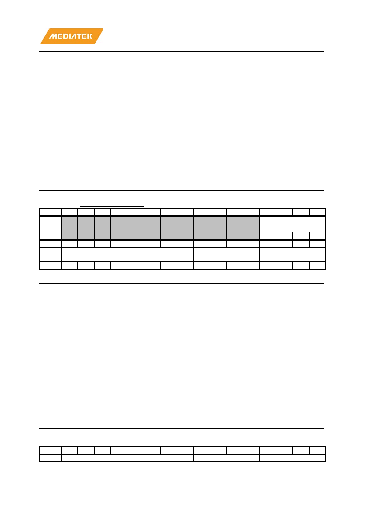
MT7686 Reference Manual
© 2016 - 2017 MediaTek Inc.
Page 439 of 536
This document contains information that is proprietary to MediaTek Inc. (“MediaTek”) and/or its licensor(s).
Any unauthorized use, reproduction or disclosure of this document in whole or in part is strictly prohibited.
Bit(s)
Mnemonic
Name
Description
GPIO12
0: Keep
1: SET bits
15:12
GPIO11_MODE_SET
Bitwise SET operation for auxiliary mode of
GPIO11
0: Keep
1: SET bits
11:8
GPIO10_MODE_SET
Bitwise SET operation for auxiliary mode of
GPIO10
0: Keep
1: SET bits
7:4
GPIO9_MODE_SET
Bitwise SET operation for auxiliary mode of
GPIO_9
0: Keep
1: SET bits
3:0
GPIO8_MODE_SET
Bitwise SET operation for auxiliary mode of
GPIO_8
0: Keep
1: SET bits
A20B0058
GPIO_MODE2_SET
GPIO Mode Control
00000000
Bit
31
30
29
28
27
26
25
24
23
22
21
20
19
18
17
16
Name
GPIO20_MODE_SET
Type
WO
Reset
0
0
0
0
Bit
15
14
13
12
11
10
9
8
7
6
5
4
3
2
1
0
Name
GPIO19_MODE_SET
GPIO18_MODE_SET
GPIO17_MODE_SET
GPIO16_MODE_SET
Type
WO
WO
WO
WO
Reset
0
0
0
0
0
0
0
0
0
0
0
0
0
0
0
0
Bit(s)
Mnemonic
Name
Description
19:16
GPIO20_MODE_SET
Bitwise SET operation for auxiliary mode of
GPIO20
0: Keep
1: SET bits
15:12
GPIO19_MODE_SET
Bitwise SET operation for auxiliary mode of
GPIO19
0: Keep
1: SET bits
11:8
GPIO18_MODE_SET
Bitwise SET operation for auxiliary mode of
GPIO18
0: Keep
1: SET bits
7:4
GPIO17_MODE_SET
Bitwise SET operation for auxiliary mode of
GPIO17
0: Keep
1: SET bits
3:0
GPIO16_MODE_SET
Bitwise SET operation for auxiliary mode of
GPIO16
0: Keep
1: SET bits
A20B0060
GPIO_MODE0_CLR
GPIO Mode Control
00000000
Bit
31
30
29
28
27
26
25
24
23
22
21
20
19
18
17
16
Name
GPIO7_MODE_CLR
GPIO6_MODE_CLR
GPIO5_MODE_CLR
GPIO4_MODE_CLR
MT7686 Reference Manual
© 2016 - 2017 MediaTek Inc.
Page 440 of 536
This document contains information that is proprietary to MediaTek Inc. (“MediaTek”) and/or its licensor(s).
Any unauthorized use, reproduction or disclosure of this document in whole or in part is strictly prohibited.
Type
WO
WO
WO
WO
Reset
0
0
0
0
0
0
0
0
0
0
0
0
0
0
0
0
Bit
15
14
13
12
11
10
9
8
7
6
5
4
3
2
1
0
Name
GPIO3_MODE_CLR
GPIO2_MODE_CLR
GPIO1_MODE_CLR
GPIO0_MODE_CLR
Type
WO
WO
WO
WO
Reset
0
0
0
0
0
0
0
0
0
0
0
0
0
0
0
0
Bit(s)
Mnemonic
Name
Description
31:28
GPIO7_MODE_CLR
Bitwise CLEAR operation for auxiliary mode of
GPIO_7
0: Keep
1: Clear bits
27:24
GPIO6_MODE_CLR
Bitwise CLEAR operation for auxiliary mode of
GPIO_6
0: Keep
1: Clear bits
23:20
GPIO5_MODE_CLR
Bitwise CLEAR operation for auxiliary mode of
GPIO_5
0: Keep
1: Clear bits
19:16
GPIO4_MODE_CLR
Bitwise CLEAR operation for auxiliary mode of
GPIO_4
0: Keep
1: Clear bits
15:12
GPIO3_MODE_CLR
Bitwise CLEAR operation for auxiliary mode of
GPIO_3
0: Keep
1: Clear bits
11:8
GPIO2_MODE_CLR
Bitwise CLEAR operation for auxiliary mode of
GPIO_2
0: Keep
1: Clear bits
7:4
GPIO1_MODE_CLR
Bitwise CLEAR operation for auxiliary mode of
GPIO_1
0: Keep
1: Clear bits
3:0
GPIO0_MODE_CLR
Bitwise CLEAR operation for auxiliary mode of
GPIO_0
0: Keep
1: Clear bits
A20B0064
GPIO_MODE1_CLR
GPIO Mode Control
00000000
Bit
31
30
29
28
27
26
25
24
23
22
21
20
19
18
17
16
Name
GPIO15_MODE_CLR
GPIO14_MODE_CLR
GPIO13_MODE_CLR
GPIO12_MODE_CLR
Type
WO
WO
WO
WO
Reset
0
0
0
0
0
0
0
0
0
0
0
0
0
0
0
0
Bit
15
14
13
12
11
10
9
8
7
6
5
4
3
2
1
0
Name
GPIO11_MODE_CLR
GPIO10_MODE_CLR
GPIO9_MODE_CLR
GPIO8_MODE_CLR
Type
WO
WO
WO
WO
Reset
0
0
0
0
0
0
0
0
0
0
0
0
0
0
0
0
Bit(s)
Mnemonic
Name
Description
31:28
GPIO15_MODE_CLR
Bitwise CLEAR operation for auxiliary mode of
GPIO15
0: Keep
1: Clear bits
MT7686 Reference Manual
© 2016 - 2017 MediaTek Inc.
Page 441 of 536
This document contains information that is proprietary to MediaTek Inc. (“MediaTek”) and/or its licensor(s).
Any unauthorized use, reproduction or disclosure of this document in whole or in part is strictly prohibited.
Bit(s)
Mnemonic
Name
Description
27:24
GPIO14_MODE_CLR
Bitwise CLEAR operation for auxiliary mode of
GPIO14
0: Keep
1: Clear bits
23:20
GPIO13_MODE_CLR
Bitwise CLEAR operation for auxiliary mode of
GPIO13
0: Keep
1: Clear bits
19:16
GPIO12_MODE_CLR
Bitwise CLEAR operation for auxiliary mode of
GPIO12
0: Keep
1: Clear bits
15:12
GPIO11_MODE_CLR
Bitwise CLEAR operation for auxiliary mode of
GPIO11
0: Keep
1: Clear bits
11:8
GPIO10_MODE_CLR
Bitwise CLEAR operation for auxiliary mode of
GPIO10
0: Keep
1: Clear bits
7:4
GPIO9_MODE_CLR
Bitwise CLEAR operation for auxiliary mode of
GPIO_9
0: Keep
1: Clear bits
3:0
GPIO8_MODE_CLR
Bitwise CLEAR operation for auxiliary mode of
GPIO_8
0: Keep
1: Clear bits
A20B0068
GPIO_MODE2_CLR
GPIO Mode Control
00000000
Bit
31
30
29
28
27
26
25
24
23
22
21
20
19
18
17
16
Name
GPIO20_MODE_CLR
Type
WO
Reset
0
0
0
0
Bit
15
14
13
12
11
10
9
8
7
6
5
4
3
2
1
0
Name
GPIO19_MODE_CLR
GPIO18_MODE_CLR
GPIO17_MODE_CLR
GPIO16_MODE_CLR
Type
WO
WO
WO
WO
Reset
0
0
0
0
0
0
0
0
0
0
0
0
0
0
0
0
Bit(s)
Mnemonic
Name
Description
19:16
GPIO20_MODE_CLR
Bitwise CLEAR operation for auxiliary mode of
GPIO20
0: Keep
1: Clear bits
15:12
GPIO19_MODE_CLR
Bitwise CLEAR operation for auxiliary mode of
GPIO19
0: Keep
1: Clear bits
11:8
GPIO18_MODE_CLR
Bitwise CLEAR operation for auxiliary mode of
GPIO18
0: Keep
1: Clear bits
7:4
GPIO17_MODE_CLR
Bitwise CLEAR operation for auxiliary mode of
GPIO17
0: Keep
1: Clear bits
MT7686 Reference Manual
© 2016 - 2017 MediaTek Inc.
Page 442 of 536
This document contains information that is proprietary to MediaTek Inc. (“MediaTek”) and/or its licensor(s).
Any unauthorized use, reproduction or disclosure of this document in whole or in part is strictly prohibited.
Bit(s)
Mnemonic
Name
Description
3:0
GPIO16_MODE_CLR
Bitwise CLEAR operation for auxiliary mode of
GPIO16
0: Keep
1: Clear bits
A20C0000
DRV_CFG0
driving current
00000000
Bit
31
30
29
28
27
26
25
24
23
22
21
20
19
18
17
16
Nam
e
drv_cfg_rsv
drv_cfg_g
pio_10
drv_cfg_g
pio_9
drv_cfg_g
pio_8
Type
RO
RW
RW
RW
Rese
t
0 0 0 0 0 0 0 0 0 0 0 0 0 0 0 0
Bit
15
14
13
12
11
10
9
8
7
6
5
4
3
2
1
0
Nam
e
drv_cfg_g
pio_7
drv_cfg_g
pio_6
drv_cfg_g
pio_5
drv_cfg_g
pio_4
drv_cfg_g
pio_3
drv_cfg_g
pio_2
drv_cfg_g
pio_1
drv_cfg_g
pio_0
Type
RW
RW
RW
RW
RW
RW
RW
RW
Rese
t
0 0 0 0 0 0 0 0 0 0 0 0 0 0 0 0
Bit(s)
Mnemonic
Name
Description
31:26
drv_cfg_rsv
Reserved
nn: reserved
21:20
drv_cfg_gpio_10
PAD_GPIO_10
4mA: [00]
8mA: [10]
12mA: [01]
16mA: [11]
19:18
drv_cfg_gpio_9
PAD_GPIO_9
4mA: [00]
8mA:
[10]
12mA: [01]
16mA: [11]
17:16
drv_cfg_gpio_8
PAD_GPIO_8
4mA: [00]
8mA: [10]
12mA: [01]
16mA: [11]
15:14
drv_cfg_gpio_7
PAD_GPIO_7
4mA: [00]
8mA: [10]
12mA: [01]
16mA: [11]
13:12
drv_cfg_gpio_6
PAD_GPIO_6
4mA: [00]
8mA: [10]
12mA: [01]
16mA: [11]
11:10
drv_cfg_gpio_5
PAD_GPIO_5
4mA: [00]
8mA: [10]
12mA: [01]
16mA: [11]
9:8
drv_cfg_gpio_4
PAD_GPIO_4
4mA: [00]
8mA: [10]
12mA: [01]
16mA: [11]
7:6
drv_cfg_gpio_3
PAD_GPIO_3
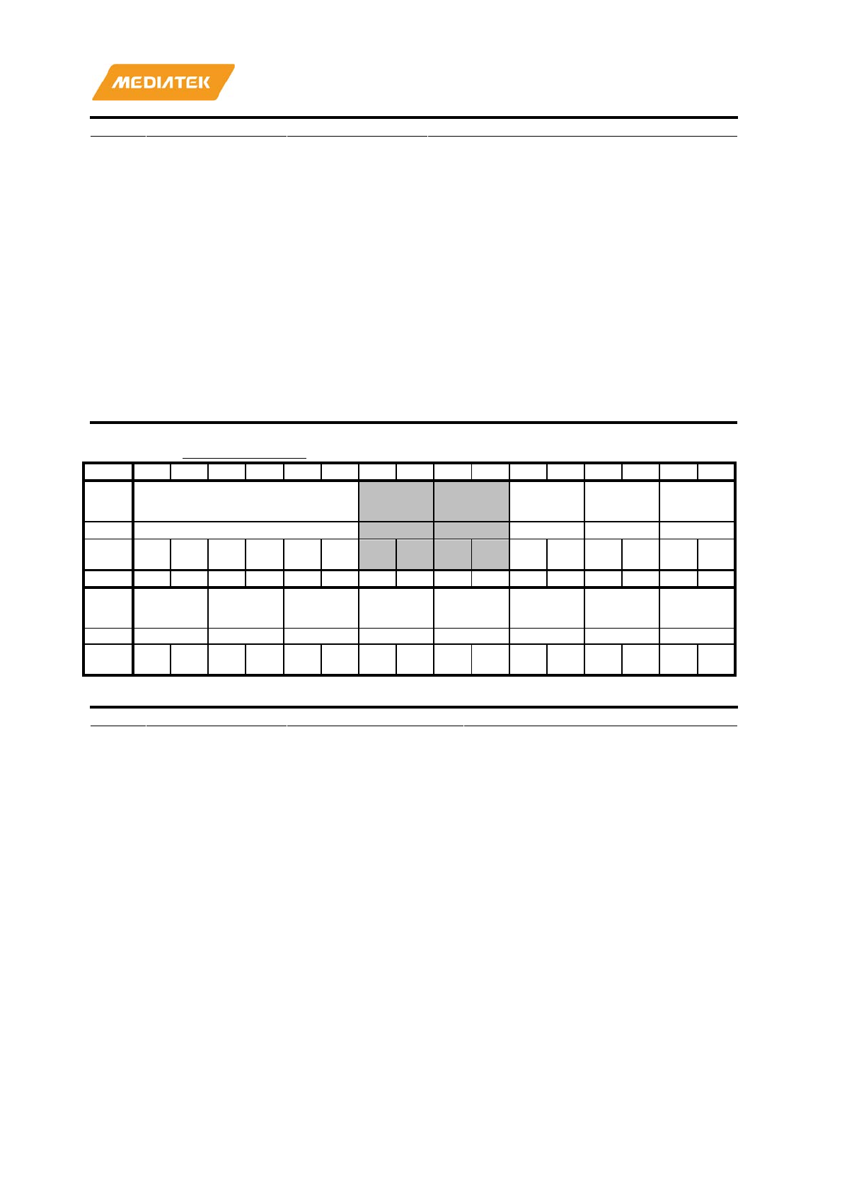
MT7686 Reference Manual
© 2016 - 2017 MediaTek Inc.
Page 443 of 536
This document contains information that is proprietary to MediaTek Inc. (“MediaTek”) and/or its licensor(s).
Any unauthorized use, reproduction or disclosure of this document in whole or in part is strictly prohibited.
Bit(s)
Mnemonic
Name
Description
4mA: [00]
8mA: [10]
12mA: [01]
16mA: [11]
5:4
drv_cfg_gpio_2
PAD_GPIO_2
4mA: [00]
8mA: [10]
12mA: [01]
16mA: [11]
3:2
drv_cfg_gpio_1
PAD_GPIO_1
4mA: [00]
8mA: [10]
12mA: [01]
16mA: [11]
1:0
drv_cfg_gpio_0
PAD_GPIO_0
4mA: [00]
8mA: [10]
12mA: [01]
16mA: [11]
A20C0004
DRV_CFG0_SET
Set for DRV_CFG0
00000000
Bit
31
30
29
28
27
26
25
24
23
22
21
20
19
18
17
16
Nam
e drv_cfg_set_rsv
drv_cfg_s
et_gpio_1
0
drv_cfg_s
et_gpio_9 drv_cfg_s
et_gpio_8
Type
RO
WO
WO
WO
Rese
t
0 0 0 0 0 0 0 0 0 0 0 0 0 0 0 0
Bit
15
14
13
12
11
10
9
8
7
6
5
4
3
2
1
0
Nam
e drv_cfg_s
et_gpio_7 drv_cfg_s
et_gpio_6 drv_cfg_s
et_gpio_5 drv_cfg_s
et_gpio_4 drv_cfg_s
et_gpio_3 drv_cfg_s
et_gpio_2 drv_cfg_s
et_gpio_1
drv_cfg_s
et_gpio_
0
Type
WO
WO
WO
WO
WO
WO
WO
WO
Rese
t
0 0 0 0 0 0 0 0 0 0 0 0 0 0 0 0
Bit(s)
Mnemonic
Name
Description
31:26
drv_cfg_set_rsv
Reserved
nn: reserved
21:20
drv_cfg_set_gpio_10
PAD_GPIO_10
0: Keep; 1: SET bit;
19:18
drv_cfg_set_gpio_9
PAD_GPIO_9
0: Keep; 1: SET bit;
17:16
drv_cfg_set_gpio_8
PAD_GPIO_8
0: Keep; 1: SET bit;
15:14
drv_cfg_set_gpio_7
PAD_GPIO_7
0: Keep; 1: SET bit;
13:12
drv_cfg_set_gpio_6
PAD_GPIO_6
0: Keep; 1: SET bit;
11:10
drv_cfg_set_gpio_5
PAD_GPIO_5
0: Keep; 1: SET bit;
9:8
drv_cfg_set_gpio_4
PAD_GPIO_4
0: Keep; 1: SET bit;
7:6
drv_cfg_set_gpio_3
PAD_GPIO_3
0: Keep; 1: SET bit;
5:4
drv_cfg_set_gpio_2
PAD_GPIO_2
0: Keep; 1: SET bit;
MT7686 Reference Manual
© 2016 - 2017 MediaTek Inc.
Page 444 of 536
This document contains information that is proprietary to MediaTek Inc. (“MediaTek”) and/or its licensor(s).
Any unauthorized use, reproduction or disclosure of this document in whole or in part is strictly prohibited.
Bit(s)
Mnemonic
Name
Description
3:2
drv_cfg_set_gpio_1
PAD_GPIO_1
0: Keep; 1: SET bit;
1:0
drv_cfg_set_gpio_0
PAD_GPIO_0
0: Keep; 1: SET bit;
A20C0008
DRV_CFG0_CLR
clear for DRV_CFG0
00000000
Bit
31
30
29
28
27
26
25
24
23
22
21
20
19
18
17
16
Nam
e drv_cfg_clr_rsv
drv_cfg_c
lr_gpio_1
0
drv_cfg_c
lr_gpio_9 drv_cfg_c
lr_gpio_8
Type
RO
WO
WO
WO
Rese
t
0 0 0 0 0 0 0 0 0 0 0 0 0 0 0 0
Bit
15
14
13
12
11
10
9
8
7
6
5
4
3
2
1
0
Nam
e
drv_cfg_c
lr_gpio_7
drv_cfg_c
lr_gpio_6
drv_cfg_c
lr_gpio_5
drv_cfg_c
lr_gpio_4
drv_cfg_c
lr_gpio_3
drv_cfg_c
lr_gpio_2
drv_cfg_c
lr_gpio_1
drv_cfg_c
lr_gpio_0
Type
WO
WO
WO
WO
WO
WO
WO
WO
Rese
t
0 0 0 0 0 0 0 0 0 0 0 0 0 0 0 0
Bit(s)
Mnemonic
Name
Description
31:26
drv_cfg_clr_rsv
Reserved
nn: reserved
21:20
drv_cfg_clr_gpio_10
PAD_GPIO_10
0: Keep; 1: Clear bit
19:18
drv_cfg_clr_gpio_9
PAD_GPIO_9
0: Keep; 1: Clear bit
17:16
drv_cfg_clr_gpio_8
PAD_GPIO_8
0: Keep; 1: Clear bit
15:14
drv_cfg_clr_gpio_7
PAD_GPIO_7
0: Keep; 1: Clear bit
13:12
drv_cfg_clr_gpio_6
PAD_GPIO_6
0: Keep; 1: Clear bit
11:10
drv_cfg_clr_gpio_5
PAD_GPIO_5
0: Keep; 1: Clear bit
9:8
drv_cfg_clr_gpio_4
PAD_GPIO_4
0: Keep; 1: Clear bit
7:6
drv_cfg_clr_gpio_3
PAD_GPIO_3
0: Keep; 1: Clear bit
5:4
drv_cfg_clr_gpio_2
PAD_GPIO_2
0: Keep; 1: Clear bit
3:2
drv_cfg_clr_gpio_1
PAD_GPIO_1
0: Keep; 1: Clear bit
1:0
drv_cfg_clr_gpio_0
PAD_GPIO_0
0: Keep; 1: Clear bit
A20C0010
G_CFG0
0000000F
Bit
31
30
29
28
27
26
25
24
23
22
21
20
19
18
17
16
Name
g_cfg_rsv
Type
RO
Reset
0
0
0
0
0
0
0
0
0
0
0
0
0
0
0
0
Bit
15
14
13
12
11
10
9
8
7
6
5
4
3
2
1
0
Name
g_cfg_rsv
g_cfg
_gpio
_3
g_cfg
_gpio
_2
g_cfg
_gpio
_1
g_cfg
_gpio
_0
MT7686 Reference Manual
© 2016 - 2017 MediaTek Inc.
Page 445 of 536
This document contains information that is proprietary to MediaTek Inc. (“MediaTek”) and/or its licensor(s).
Any unauthorized use, reproduction or disclosure of this document in whole or in part is strictly prohibited.
Type
RO
RW
RW
RW
RW
Reset
0
0
0
0
0
0
0
0
0
0
0
0
1
1
1
1
Bit(s)
Mnemonic
Name
Description
31:4
g_cfg_rsv
Reserved
3
g_cfg_gpio_3
PAD_GPIO_3
0: Enable AIO; 1: Disable AIO;
2
g_cfg_gpio_2
PAD_GPIO_2
0: Enable AIO; 1: Disable AIO;
1
g_cfg_gpio_1
PAD_GPIO_1
0: Enable AIO; 1: Disable AIO;
0
g_cfg_gpio_0
PAD_GPIO_0
0: Enable AIO; 1: Disable AIO;
A20C0014
G_CFG0_SET
00000000
Bit
31
30
29
28
27
26
25
24
23
22
21
20
19
18
17
16
Name
g_cfg_set_rsv
Type
RO
Reset
0
0
0
0
0
0
0
0
0
0
0
0
0
0
0
0
Bit
15
14
13
12
11
10
9
8
7
6
5
4
3
2
1
0
Name
g_cfg_set_rsv
g_cfg
_set_
gpio_
3
g_cfg
_set_
gpio_
2
g_cfg
_set_
gpio_
1
g_cfg
_set_
gpio_
0
Type
RO
WO
WO
WO
WO
Reset
0
0
0
0
0
0
0
0
0
0
0
0
0
0
0
0
Bit(s)
Mnemonic
Name
Description
31:4
g_cfg_set_rsv
Reserved
3
g_cfg_set_gpio_3
PAD_GPIO_3
0: Keep; 1: SET bit;
2
g_cfg_set_gpio_2
PAD_GPIO_2
0: Keep; 1: SET bit;
1
g_cfg_set_gpio_1
PAD_GPIO_1
0: Keep; 1: SET bit;
0
g_cfg_set_gpio_0
PAD_GPIO_0
0: Keep; 1: SET bit;
A20C0018
G_CFG0_CLR
00000000
Bit
31
30
29
28
27
26
25
24
23
22
21
20
19
18
17
16
Name
g_cfg_clr_rsv
Type
RO
Reset
0
0
0
0
0
0
0
0
0
0
0
0
0
0
0
0
Bit
15
14
13
12
11
10
9
8
7
6
5
4
3
2
1
0
Name
g_cfg_clr_rsv
g_cfg
_clr_
gpio_
3
g_cfg
_clr_
gpio_
2
g_cfg
_clr_
gpio_
1
g_cfg
_clr_
gpio_
0
Type
RO
WO
WO
WO
WO
Reset
0
0
0
0
0
0
0
0
0
0
0
0
0
0
0
0
Bit(s)
Mnemonic
Name
Description
31:4
g_cfg_clr_rsv
Reserved
3
g_cfg_clr_gpio_3
PAD_GPIO_3
MT7686 Reference Manual
© 2016 - 2017 MediaTek Inc.
Page 446 of 536
This document contains information that is proprietary to MediaTek Inc. (“MediaTek”) and/or its licensor(s).
Any unauthorized use, reproduction or disclosure of this document in whole or in part is strictly prohibited.
Bit(s)
Mnemonic
Name
Description
0: Keep; 1: Clear bit
2
g_cfg_clr_gpio_2
PAD_GPIO_2
0: Keep; 1: Clear bit
1
g_cfg_clr_gpio_1
PAD_GPIO_1
0: Keep; 1: Clear bit
0
g_cfg_clr_gpio_0
PAD_GPIO_0
0: Keep; 1: Clear bit
A20C0020
IES_CFG0
00001FFF
Bit
31
30
29
28
27
26
25
24
23
22
21
20
19
18
17
16
Name
ies_cfg_rsv
Type
RO
Reset
0
0
0
0
0
0
0
0
0
0
0
0
0
0
0
0
Bit
15
14
13
12
11
10
9
8
7
6
5
4
3
2
1
0
Name
ies_cfg_rsv
ies_cf
g_gpi
o_10
ies_cf
g_gpi
o_9
ies_cf
g_gpi
o_8
ies_cf
g_gpi
o_7
ies_cf
g_gpi
o_6
ies_cf
g_gpi
o_5
ies_cf
g_gpi
o_4
ies_cf
g_gpi
o_3
ies_cf
g_gpi
o_2
ies_cf
g_gpi
o_1
ies_cf
g_gpi
o_0
Type
RO
RW
RW
RW
RW
RW
RW
RW
RW
RW
RW
RW
Reset
0
0
0
1
1
1
1
1
1
1
1
1
1
1
1
1
Bit(s)
Mnemonic
Name
Description
31:13
ies_cfg_rsv
Reserved
10
ies_cfg_gpio_10
PAD_GPIO_10
0: Disable; 1: Enable;
9
ies_cfg_gpio_9
PAD_GPIO_9
0: Disable; 1: Enable;
8
ies_cfg_gpio_8
PAD_GPIO_8
0: Disable; 1: Enable;
7
ies_cfg_gpio_7
PAD_GPIO_7
0: Disable; 1: Enable;
6
ies_cfg_gpio_6
PAD_GPIO_6
0: Disable; 1: Enable;
5
ies_cfg_gpio_5
PAD_GPIO_5
0: Disable; 1: Enable;
4
ies_cfg_gpio_4
PAD_GPIO_4
0: Disable; 1: Enable;
3
ies_cfg_gpio_3
PAD_GPIO_3
0: Disable; 1: Enable;
2
ies_cfg_gpio_2
PAD_GPIO_2
0: Disable; 1: Enable;
1
ies_cfg_gpio_1
PAD_GPIO_1
0: Disable; 1: Enable;
0
ies_cfg_gpio_0
PAD_GPIO_0
0: Disable; 1: Enable;
A20C0024
IES_CFG0_SET
00000000
Bit
31
30
29
28
27
26
25
24
23
22
21
20
19
18
17
16
Name
ies_cfg_set_rsv
Type
RO
Reset
0
0
0
0
0
0
0
0
0
0
0
0
0
0
0
0
Bit
15
14
13
12
11
10
9
8
7
6
5
4
3
2
1
0
Name
ies_cfg_set_rsv
ies_cf
g_set
_gpio
_10
ies_cf
g_set
_gpio
_9
ies_cf
g_set
_gpio
_8
ies_cf
g_set
_gpio
_7
ies_cf
g_set
_gpio
_6
ies_cf
g_set
_gpio
_5
ies_cf
g_set
_gpio
_4
ies_cf
g_set
_gpio
_3
ies_cf
g_set
_gpio
_2
ies_cf
g_set
_gpio
_1
ies_cf
g_set
_gpio
_0
MT7686 Reference Manual
© 2016 - 2017 MediaTek Inc.
Page 447 of 536
This document contains information that is proprietary to MediaTek Inc. (“MediaTek”) and/or its licensor(s).
Any unauthorized use, reproduction or disclosure of this document in whole or in part is strictly prohibited.
Type
RO
WO
WO
WO
WO
WO
WO
WO
WO
WO
WO
WO
Reset
0
0
0
0
0
0
0
0
0
0
0
0
0
0
0
0
Bit(s)
Mnemonic
Name
Description
31:13
ies_cfg_set_rsv
Reserved
10
ies_cfg_set_gpio_10
PAD_GPIO_10
0: Keep; 1: SET bit;
9
ies_cfg_set_gpio_9
PAD_GPIO_9
0: Keep; 1: SET bit;
8
ies_cfg_set_gpio_8
PAD_GPIO_8
0: Keep; 1: SET bit;
7
ies_cfg_set_gpio_7
PAD_GPIO_7
0: Keep; 1: SET bit;
6
ies_cfg_set_gpio_6
PAD_GPIO_6
0: Keep; 1: SET bit;
5
ies_cfg_set_gpio_5
PAD_GPIO_5
0: Keep; 1: SET bit;
4
ies_cfg_set_gpio_4
PAD_GPIO_4
0: Keep; 1: SET bit;
3
ies_cfg_set_gpio_3
PAD_GPIO_3
0: Keep; 1: SET bit;
2
ies_cfg_set_gpio_2
PAD_GPIO_2
0: Keep; 1: SET bit;
1
ies_cfg_set_gpio_1
PAD_GPIO_1
0: Keep; 1: SET bit;
0
ies_cfg_set_gpio_0
PAD_GPIO_0
0: Keep; 1: SET bit;
A20C0028
IES_CFG0_CLR
00000000
Bit
31
30
29
28
27
26
25
24
23
22
21
20
19
18
17
16
Name
ies_cfg_clr_rsv
Type
RO
Reset
0
0
0
0
0
0
0
0
0
0
0
0
0
0
0
0
Bit
15
14
13
12
11
10
9
8
7
6
5
4
3
2
1
0
Name
ies_cfg_clr_rsv
ies_cf
g_clr
_gpio
_10
ies_cf
g_clr
_gpio
_9
ies_cf
g_clr
_gpio
_8
ies_cf
g_clr
_gpio
_7
ies_cf
g_clr
_gpio
_6
ies_cf
g_clr
_gpio
_5
ies_cf
g_clr
_gpio
_4
ies_cf
g_clr
_gpio
_3
ies_cf
g_clr
_gpio
_2
ies_cf
g_clr
_gpio
_1
ies_cf
g_clr
_gpio
_0
Type
RO
WO
WO
WO
WO
WO
WO
WO
WO
WO
WO
WO
Reset
0
0
0
0
0
0
0
0
0
0
0
0
0
0
0
0
Bit(s)
Mnemonic
Name
Description
31:13
ies_cfg_clr_rsv
Reserved
10
ies_cfg_clr_gpio_10
PAD_GPIO_10
0: Keep; 1: Clear bit
9
ies_cfg_clr_gpio_9
PAD_GPIO_9
0: Keep; 1: Clear bit
8
ies_cfg_clr_gpio_8
PAD_GPIO_8
0: Keep; 1: Clear bit
7
ies_cfg_clr_gpio_7
PAD_GPIO_7
0: Keep; 1: Clear bit
6
ies_cfg_clr_gpio_6
PAD_GPIO_6
0: Keep; 1: Clear bit
5
ies_cfg_clr_gpio_5
PAD_GPIO_5
0: Keep; 1: Clear bit
MT7686 Reference Manual
© 2016 - 2017 MediaTek Inc.
Page 448 of 536
This document contains information that is proprietary to MediaTek Inc. (“MediaTek”) and/or its licensor(s).
Any unauthorized use, reproduction or disclosure of this document in whole or in part is strictly prohibited.
Bit(s)
Mnemonic
Name
Description
4
ies_cfg_clr_gpio_4
PAD_GPIO_4
0: Keep; 1: Clear bit
3
ies_cfg_clr_gpio_3
PAD_GPIO_3
0: Keep; 1: Clear bit
2
ies_cfg_clr_gpio_2
PAD_GPIO_2
0: Keep; 1: Clear bit
1
ies_cfg_clr_gpio_1
PAD_GPIO_1
0: Keep; 1: Clear bit
0
ies_cfg_clr_gpio_0
PAD_GPIO_0
0: Keep; 1: Clear bit
A20C0030
PD_CFG0
000017FF
Bit
31
30
29
28
27
26
25
24
23
22
21
20
19
18
17
16
Name
pd_cfg_rsv
Type
RO
Reset
0
0
0
0
0
0
0
0
0
0
0
0
0
0
0
0
Bit
15
14
13
12
11
10
9
8
7
6
5
4
3
2
1
0
Name
pd_cfg_rsv
pd_cf
g_gpi
o_10
pd_cf
g_gpi
o_9
pd_cf
g_gpi
o_8
pd_cf
g_gpi
o_7
pd_cf
g_gpi
o_6
pd_cf
g_gpi
o_5
pd_cf
g_gpi
o_4
pd_cf
g_gpi
o_3
pd_cf
g_gpi
o_2
pd_cf
g_gpi
o_1
pd_cf
g_gpi
o_0
Type
RO
RW
RW
RW
RW
RW
RW
RW
RW
RW
RW
RW
Reset
0
0
0
1
0
1
1
1
1
1
1
1
1
1
1
1
Bit(s)
Mnemonic
Name
Description
31:13
pd_cfg_rsv
Reserved
10
pd_cfg_gpio_10
PAD_GPIO_10
0: Disable; 1: Enable;
9
pd_cfg_gpio_9
PAD_GPIO_9
0: Disable; 1: Enable;
8
pd_cfg_gpio_8
PAD_GPIO_8
0: Disable; 1: Enable;
7
pd_cfg_gpio_7
PAD_GPIO_7
0: Disable; 1: Enable;
6
pd_cfg_gpio_6
PAD_GPIO_6
0: Disable; 1: Enable;
5
pd_cfg_gpio_5
PAD_GPIO_5
0: Disable; 1: Enable;
4
pd_cfg_gpio_4
PAD_GPIO_4
0: Disable; 1: Enable;
3
pd_cfg_gpio_3
PAD_GPIO_3
0: Disable; 1: Enable;
2
pd_cfg_gpio_2
PAD_GPIO_2
0: Disable; 1: Enable;
1
pd_cfg_gpio_1
PAD_GPIO_1
0: Disable; 1: Enable;
0
pd_cfg_gpio_0
PAD_GPIO_0
0: Disable; 1: Enable;
A20C0034
PD_CFG0_SET
00000000
Bit
31
30
29
28
27
26
25
24
23
22
21
20
19
18
17
16
Name
pd_cfg_set_rsv
Type
RO
Reset
0
0
0
0
0
0
0
0
0
0
0
0
0
0
0
0
Bit
15
14
13
12
11
10
9
8
7
6
5
4
3
2
1
0
MT7686 Reference Manual
© 2016 - 2017 MediaTek Inc.
Page 449 of 536
This document contains information that is proprietary to MediaTek Inc. (“MediaTek”) and/or its licensor(s).
Any unauthorized use, reproduction or disclosure of this document in whole or in part is strictly prohibited.
Name
pd_cfg_set_rsv
pd_cf
g_set
_gpio
_10
pd_cf
g_set
_gpio
_9
pd_cf
g_set
_gpio
_8
pd_cf
g_set
_gpio
_7
pd_cf
g_set
_gpio
_6
pd_cf
g_set
_gpio
_5
pd_cf
g_set
_gpio
_4
pd_cf
g_set
_gpio
_3
pd_cf
g_set
_gpio
_2
pd_cf
g_set
_gpio
_1
pd_cf
g_set
_gpio
_0
Type
RO
WO
WO
WO
WO
WO
WO
WO
WO
WO
WO
WO
Reset
0
0
0
0
0
0
0
0
0
0
0
0
0
0
0
0
Bit(s)
Mnemonic
Name
Description
31:13
pd_cfg_set_rsv
Reserved
10
pd_cfg_set_gpio_10
PAD_GPIO_10
0: Keep; 1: SET bit;
9
pd_cfg_set_gpio_9
PAD_GPIO_9
0: Keep; 1: SET bit;
8
pd_cfg_set_gpio_8
PAD_GPIO_8
0: Keep; 1: SET bit;
7
pd_cfg_set_gpio_7
PAD_GPIO_7
0: Keep; 1: SET bit;
6
pd_cfg_set_gpio_6
PAD_GPIO_6
0: Keep; 1: SET bit;
5
pd_cfg_set_gpio_5
PAD_GPIO_5
0: Keep; 1: SET bit;
4
pd_cfg_set_gpio_4
PAD_GPIO_4
0: Keep; 1: SET bit;
3
pd_cfg_set_gpio_3
PAD_GPIO_3
0: Keep; 1: SET bit;
2
pd_cfg_set_gpio_2
PAD_GPIO_2
0: Keep; 1: SET bit;
1
pd_cfg_set_gpio_1
PAD_GPIO_1
0: Keep; 1: SET bit;
0
pd_cfg_set_gpio_0
PAD_GPIO_0
0: Keep; 1: SET bit;
A20C0038
PD_CFG0_CLR
00000000
Bit
31
30
29
28
27
26
25
24
23
22
21
20
19
18
17
16
Name
pd_cfg_clr_rsv
Type
RO
Reset
0
0
0
0
0
0
0
0
0
0
0
0
0
0
0
0
Bit
15
14
13
12
11
10
9
8
7
6
5
4
3
2
1
0
Name
pd_cfg_clr_rsv
pd_cf
g_clr
_gpio
_10
pd_cf
g_clr
_gpio
_9
pd_cf
g_clr
_gpio
_8
pd_cf
g_clr
_gpio
_7
pd_cf
g_clr
_gpio
_6
pd_cf
g_clr
_gpio
_5
pd_cf
g_clr
_gpio
_4
pd_cf
g_clr
_gpio
_3
pd_cf
g_clr
_gpio
_2
pd_cf
g_clr
_gpio
_1
pd_cf
g_clr
_gpio
_0
Type
RO
WO
WO
WO
WO
WO
WO
WO
WO
WO
WO
WO
Reset
0
0
0
0
0
0
0
0
0
0
0
0
0
0
0
0
Bit(s)
Mnemonic
Name
Description
31:13
pd_cfg_clr_rsv
Reserved
10
pd_cfg_clr_gpio_10
PAD_GPIO_10
0: Keep; 1: Clear bit
9
pd_cfg_clr_gpio_9
PAD_GPIO_9
0: Keep; 1: Clear bit
8
pd_cfg_clr_gpio_8
PAD_GPIO_8
0: Keep; 1: Clear bit
7
pd_cfg_clr_gpio_7
PAD_GPIO_7
0: Keep; 1: Clear bit
6
pd_cfg_clr_gpio_6
PAD_GPIO_6
MT7686 Reference Manual
© 2016 - 2017 MediaTek Inc.
Page 450 of 536
This document contains information that is proprietary to MediaTek Inc. (“MediaTek”) and/or its licensor(s).
Any unauthorized use, reproduction or disclosure of this document in whole or in part is strictly prohibited.
Bit(s)
Mnemonic
Name
Description
0: Keep; 1: Clear bit
5
pd_cfg_clr_gpio_5
PAD_GPIO_5
0: Keep; 1: Clear bit
4
pd_cfg_clr_gpio_4
PAD_GPIO_4
0: Keep; 1: Clear bit
3
pd_cfg_clr_gpio_3
PAD_GPIO_3
0: Keep; 1: Clear bit
2
pd_cfg_clr_gpio_2
PAD_GPIO_2
0: Keep; 1: Clear bit
1
pd_cfg_clr_gpio_1
PAD_GPIO_1
0: Keep; 1: Clear bit
0
pd_cfg_clr_gpio_0
PAD_GPIO_0
0: Keep; 1: Clear bit
A20C0040
PU_CFG0
00000800
Bit
31
30
29
28
27
26
25
24
23
22
21
20
19
18
17
16
Name
pu_cfg_rsv
Type
RO
Reset
0
0
0
0
0
0
0
0
0
0
0
0
0
0
0
0
Bit
15
14
13
12
11
10
9
8
7
6
5
4
3
2
1
0
Name
pu_cfg_rsv
pu_cf
g_gpi
o_10
pu_cf
g_gpi
o_9
pu_cf
g_gpi
o_8
pu_cf
g_gpi
o_7
pu_cf
g_gpi
o_6
pu_cf
g_gpi
o_5
pu_cf
g_gpi
o_4
pu_cf
g_gpi
o_3
pu_cf
g_gpi
o_2
pu_cf
g_gpi
o_1
pu_cf
g_gpi
o_0
Type
RO
RW
RW
RW
RW
RW
RW
RW
RW
RW
RW
RW
Reset
0
0
0
0
1
0
0
0
0
0
0
0
0
0
0
0
Bit(s)
Mnemonic
Name
Description
31:13
pu_cfg_rsv
Reserved
10
pu_cfg_gpio_10
PAD_GPIO_10
0: Disable; 1: Enable;
9
pu_cfg_gpio_9
PAD_GPIO_9
0: Disable; 1: Enable;
8
pu_cfg_gpio_8
PAD_GPIO_8
0: Disable; 1: Enable;
7
pu_cfg_gpio_7
PAD_GPIO_7
0: Disable; 1: Enable;
6
pu_cfg_gpio_6
PAD_GPIO_6
0: Disable; 1: Enable;
5
pu_cfg_gpio_5
PAD_GPIO_5
0: Disable; 1: Enable;
4
pu_cfg_gpio_4
PAD_GPIO_4
0: Disable; 1: Enable;
3
pu_cfg_gpio_3
PAD_GPIO_3
0: Disable; 1: Enable;
2
pu_cfg_gpio_2
PAD_GPIO_2
0: Disable; 1: Enable;
1
pu_cfg_gpio_1
PAD_GPIO_1
0: Disable; 1: Enable;
0
pu_cfg_gpio_0
PAD_GPIO_0
0: Disable; 1: Enable;
A20C0044
PU_CFG0_SET
00000000
Bit
31
30
29
28
27
26
25
24
23
22
21
20
19
18
17
16
Name
pu_cfg_set_rsv
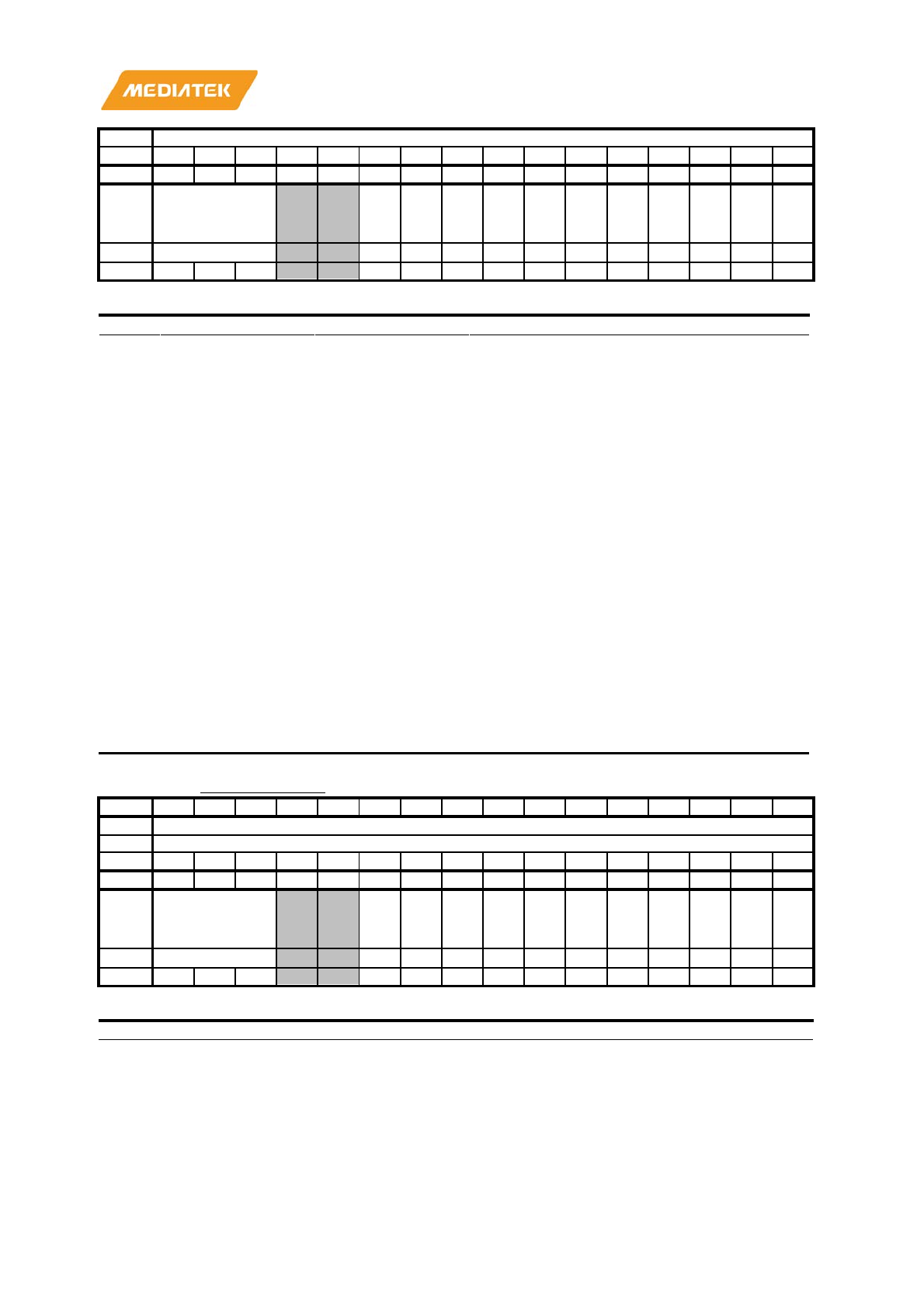
MT7686 Reference Manual
© 2016 - 2017 MediaTek Inc.
Page 451 of 536
This document contains information that is proprietary to MediaTek Inc. (“MediaTek”) and/or its licensor(s).
Any unauthorized use, reproduction or disclosure of this document in whole or in part is strictly prohibited.
Type
RO
Reset
0
0
0
0
0
0
0
0
0
0
0
0
0
0
0
0
Bit
15
14
13
12
11
10
9
8
7
6
5
4
3
2
1
0
Name
pu_cfg_set_rsv
pu_cf
g_set
_gpio
_10
pu_cf
g_set
_gpio
_9
pu_cf
g_set
_gpio
_8
pu_cf
g_set
_gpio
_7
pu_cf
g_set
_gpio
_6
pu_cf
g_set
_gpio
_5
pu_cf
g_set
_gpio
_4
pu_cf
g_set
_gpio
_3
pu_cf
g_set
_gpio
_2
pu_cf
g_set
_gpio
_1
pu_cf
g_set
_gpio
_0
Type
RO
WO
WO
WO
WO
WO
WO
WO
WO
WO
WO
WO
Reset
0
0
0
0
0
0
0
0
0
0
0
0
0
0
0
0
Bit(s)
Mnemonic
Name
Description
31:13
pu_cfg_set_rsv
Reserved
10
pu_cfg_set_gpio_10
PAD_GPIO_10
0: Keep; 1: SET bit;
9
pu_cfg_set_gpio_9
PAD_GPIO_9
0: Keep; 1: SET bit;
8
pu_cfg_set_gpio_8
PAD_GPIO_8
0: Keep; 1: SET bit;
7
pu_cfg_set_gpio_7
PAD_GPIO_7
0: Keep; 1: SET bit;
6
pu_cfg_set_gpio_6
PAD_GPIO_6
0: Keep; 1: SET bit;
5
pu_cfg_set_gpio_5
PAD_GPIO_5
0: Keep; 1: SET bit;
4
pu_cfg_set_gpio_4
PAD_GPIO_4
0: Keep; 1: SET bit;
3
pu_cfg_set_gpio_3
PAD_GPIO_3
0: Keep; 1: SET bit;
2
pu_cfg_set_gpio_2
PAD_GPIO_2
0: Keep; 1: SET bit;
1
pu_cfg_set_gpio_1
PAD_GPIO_1
0: Keep; 1: SET bit;
0
pu_cfg_set_gpio_0
PAD_GPIO_0
0: Keep; 1: SET bit;
A20C0048
PU_CFG0_CLR
00000000
Bit
31
30
29
28
27
26
25
24
23
22
21
20
19
18
17
16
Name
pu_cfg_clr_rsv
Type
RO
Reset
0
0
0
0
0
0
0
0
0
0
0
0
0
0
0
0
Bit
15
14
13
12
11
10
9
8
7
6
5
4
3
2
1
0
Name
pu_cfg_clr_rsv
pu_cf
g_clr
_gpio
_10
pu_cf
g_clr
_gpio
_9
pu_cf
g_clr
_gpio
_8
pu_cf
g_clr
_gpio
_7
pu_cf
g_clr
_gpio
_6
pu_cf
g_clr
_gpio
_5
pu_cf
g_clr
_gpio
_4
pu_cf
g_clr
_gpio
_3
pu_cf
g_clr
_gpio
_2
pu_cf
g_clr
_gpio
_1
pu_cf
g_clr
_gpio
_0
Type
RO
WO
WO
WO
WO
WO
WO
WO
WO
WO
WO
WO
Reset
0
0
0
0
0
0
0
0
0
0
0
0
0
0
0
0
Bit(s)
Mnemonic
Name
Description
31:13
pu_cfg_clr_rsv
Reserved
10
pu_cfg_clr_gpio_10
PAD_GPIO_10
0: Keep; 1: Clear bit
9
pu_cfg_clr_gpio_9
PAD_GPIO_9
0: Keep; 1: Clear bit
8
pu_cfg_clr_gpio_8
PAD_GPIO_8

MT7686 Reference Manual
© 2016 - 2017 MediaTek Inc.
Page 452 of 536
This document contains information that is proprietary to MediaTek Inc. (“MediaTek”) and/or its licensor(s).
Any unauthorized use, reproduction or disclosure of this document in whole or in part is strictly prohibited.
Bit(s)
Mnemonic
Name
Description
0: Keep; 1: Clear bit
7
pu_cfg_clr_gpio_7
PAD_GPIO_7
0: Keep; 1: Clear bit
6
pu_cfg_clr_gpio_6
PAD_GPIO_6
0: Keep; 1: Clear bit
5
pu_cfg_clr_gpio_5
PAD_GPIO_5
0: Keep; 1: Clear bit
4
pu_cfg_clr_gpio_4
PAD_GPIO_4
0: Keep; 1: Clear bit
3
pu_cfg_clr_gpio_3
PAD_GPIO_3
0: Keep; 1: Clear bit
2
pu_cfg_clr_gpio_2
PAD_GPIO_2
0: Keep; 1: Clear bit
1
pu_cfg_clr_gpio_1
PAD_GPIO_1
0: Keep; 1: Clear bit
0
pu_cfg_clr_gpio_0
PAD_GPIO_0
0: Keep; 1: Clear bit
A20C0050
RDSEL_CFG0
RX delay selection
00000000
Bit
31
30
29
28
27
26
25
24
23
22
21
20
19
18
17
16
Nam
e
rdsel_cfg_rsv rdsel_cfg
_gpio_10
rdsel_cfg
_gpio_9
rdsel_cfg
_gpio_8
Type
RO
RW
RW
RW
Rese
t
0 0 0 0 0 0 0 0 0 0 0 0 0 0 0 0
Bit
15
14
13
12
11
10
9
8
7
6
5
4
3
2
1
0
Nam
e
rdsel_cfg
_gpio_7
rdsel_cfg
_gpio_6
rdsel_cfg
_gpio_5
rdsel_cfg
_gpio_4
rdsel_cfg
_gpio_3
rdsel_cfg
_gpio_2
rdsel_cfg
_gpio_1
rdsel_cfg
_gpio_0
Type
RW
RW
RW
RW
RW
RW
RW
RW
Rese
t
0 0 0 0 0 0 0 0 0 0 0 0 0 0 0 0
Bit(s)
Mnemonic
Name
Description
31:26
rdsel_cfg_rsv
Reserved
nn: reserved
21:20
rdsel_cfg_gpio_10
PAD_GPIO_10
00: minimum reception delay; 11: maximum reception
delay
19:18
rdsel_cfg_gpio_9
PAD_GPIO_9
00: minimum reception delay; 11: maximum reception
delay
17:16
rdsel_cfg_gpio_8
PAD_GPIO_8
00: minimum reception delay; 11: maximum reception
delay
15:14
rdsel_cfg_gpio_7
PAD_GPIO_7
00: minimum reception delay; 11: maximum reception
delay
13:12
rdsel_cfg_gpio_6
PAD_GPIO_6
00: minimum reception delay; 11: maximum reception
delay
11:10
rdsel_cfg_gpio_5
PAD_GPIO_5
00: minimum reception delay; 11: maximum reception
delay
9:8
rdsel_cfg_gpio_4
PAD_GPIO_4
00: minimum reception delay; 11: maximum reception
delay
MT7686 Reference Manual
© 2016 - 2017 MediaTek Inc.
Page 453 of 536
This document contains information that is proprietary to MediaTek Inc. (“MediaTek”) and/or its licensor(s).
Any unauthorized use, reproduction or disclosure of this document in whole or in part is strictly prohibited.
Bit(s)
Mnemonic
Name
Description
7:6
rdsel_cfg_gpio_3
PAD_GPIO_3
00: minimum reception delay; 11: maximum reception
delay
5:4
rdsel_cfg_gpio_2
PAD_GPIO_2
00: minimum reception delay; 11: maximum reception
delay
3:2
rdsel_cfg_gpio_1
PAD_GPIO_1
00: minimum reception delay; 11: maximum reception
delay
1:0
rdsel_cfg_gpio_0
PAD_GPIO_0
00: minimum reception delay; 11: maximum reception
delay
A20C0054
RDSEL_CFG0_SET
set RDSEL_CFG0
00000000
Bit
31
30
29
28
27
26
25
24
23
22
21
20
19
18
17
16
Nam
e rdsel_cfg_set_rsv
rdsel_cfg
_set_gpio
_10
rdsel_cfg
_set_gpio
_9
rdsel_cfg
_set_gpio
_8
Type
RO
WO
WO
WO
Rese
t
0 0 0 0 0 0 0 0 0 0 0 0 0 0 0 0
Bit
15
14
13
12
11
10
9
8
7
6
5
4
3
2
1
0
Nam
e
rdsel_cfg
_set_gpio
_7
rdsel_cfg
_set_gpio
_6
rdsel_cfg
_set_gpio
_5
rdsel_cfg
_set_gpio
_4
rdsel_cfg
_set_gpio
_3
rdsel_cfg
_set_gpio
_2
rdsel_cfg
_set_gpio
_1
rdsel_cfg
_set_gpio
_0
Type
WO
WO
WO
WO
WO
WO
WO
WO
Rese
t
0 0 0 0 0 0 0 0 0 0 0 0 0 0 0 0
Bit(s)
Mnemonic
Name
Description
31:26
rdsel_cfg_set_rsv
Reserved
nn: reserved
21:20
rdsel_cfg_set_gpio_10
PAD_GPIO_10
0: Keep; 1: SET bit;
19:18
rdsel_cfg_set_gpio_9
PAD_GPIO_9
0: Keep; 1: SET bit;
17:16
rdsel_cfg_set_gpio_8
PAD_GPIO_8
0: Keep; 1: SET bit;
15:14
rdsel_cfg_set_gpio_7
PAD_GPIO_7
0: Keep; 1: SET bit;
13:12
rdsel_cfg_set_gpio_6
PAD_GPIO_6
0: Keep; 1: SET bit;
11:10
rdsel_cfg_set_gpio_5
PAD_GPIO_5
0: Keep; 1: SET bit;
9:8
rdsel_cfg_set_gpio_4
PAD_GPIO_4
0: Keep; 1: SET bit;
7:6
rdsel_cfg_set_gpio_3
PAD_GPIO_3
0: Keep; 1: SET bit;
5:4
rdsel_cfg_set_gpio_2
PAD_GPIO_2
0: Keep; 1: SET bit;
3:2
rdsel_cfg_set_gpio_1
PAD_GPIO_1
0: Keep; 1: SET bit;
1:0
rdsel_cfg_set_gpio_0
PAD_GPIO_0
0: Keep; 1: SET bit;
MT7686 Reference Manual
© 2016 - 2017 MediaTek Inc.
Page 454 of 536
This document contains information that is proprietary to MediaTek Inc. (“MediaTek”) and/or its licensor(s).
Any unauthorized use, reproduction or disclosure of this document in whole or in part is strictly prohibited.
Bit(s)
Mnemonic
Name
Description
A20C0058
RDSEL_CFG0_CLR
clear RDSEL_CFG0
00000000
Bit
31
30
29
28
27
26
25
24
23
22
21
20
19
18
17
16
Nam
e rdsel_cfg_clr_rsv
rdsel_cfg
_clr_gpio
_10
rdsel_cfg
_clr_gpio
_9
rdsel_cfg
_clr_gpio
_8
Type
RO
WO
WO
WO
Rese
t
0 0 0 0 0 0 0 0 0 0 0 0 0 0 0 0
Bit
15
14
13
12
11
10
9
8
7
6
5
4
3
2
1
0
Nam
e
rdsel_cfg
_clr_gpio
_7
rdsel_cfg
_clr_gpio
_6
rdsel_cfg
_clr_gpio
_5
rdsel_cfg
_clr_gpio
_4
rdsel_cfg
_clr_gpio
_3
rdsel_cfg
_clr_gpio
_2
rdsel_cfg
_clr_gpio
_1
rdsel_cfg
_clr_gpio
_0
Type
WO
WO
WO
WO
WO
WO
WO
WO
Rese
t
0 0 0 0 0 0 0 0 0 0 0 0 0 0 0 0
Bit(s)
Mnemonic
Name
Description
31:26
rdsel_cfg_clr_rsv
Reserved
nn: reserved
21:20
rdsel_cfg_clr_gpio_10
PAD_GPIO_10
0: Keep; 1: Clear bit
19:18
rdsel_cfg_clr_gpio_9
PAD_GPIO_9
0: Keep; 1: Clear bit
17:16
rdsel_cfg_clr_gpio_8
PAD_GPIO_8
0: Keep; 1: Clear bit
15:14
rdsel_cfg_clr_gpio_7
PAD_GPIO_7
0: Keep; 1: Clear bit
13:12
rdsel_cfg_clr_gpio_6
PAD_GPIO_6
0: Keep; 1: Clear bit
11:10
rdsel_cfg_clr_gpio_5
PAD_GPIO_5
0: Keep; 1: Clear bit
9:8
rdsel_cfg_clr_gpio_4
PAD_GPIO_4
0: Keep; 1: Clear bit
7:6
rdsel_cfg_clr_gpio_3
PAD_GPIO_3
0: Keep; 1: Clear bit
5:4
rdsel_cfg_clr_gpio_2
PAD_GPIO_2
0: Keep; 1: Clear bit
3:2
rdsel_cfg_clr_gpio_1
PAD_GPIO_1
0: Keep; 1: Clear bit
1:0
rdsel_cfg_clr_gpio_0
PAD_GPIO_0
0: Keep; 1: Clear bit
A20C0060
SMT_CFG0
00000000
Bit
31
30
29
28
27
26
25
24
23
22
21
20
19
18
17
16
Name
smt_cfg_rsv
Type
RO
Reset
0
0
0
0
0
0
0
0
0
0
0
0
0
0
0
0
Bit
15
14
13
12
11
10
9
8
7
6
5
4
3
2
1
0
Name
smt_cfg_rsv
smt_c
fg_gp
io_10
smt_c
fg_gp
io_9
smt_c
fg_gp
io_8
smt_c
fg_gp
io_7
smt_c
fg_gp
io_6
smt_c
fg_gp
io_5
smt_c
fg_gp
io_4
smt_c
fg_gp
io_3
smt_c
fg_gp
io_2
smt_c
fg_gp
io_1
smt_
cfg_g
pio_0
Type
RO
RW
RW
RW
RW
RW
RW
RW
RW
RW
RW
RW
Reset
0
0
0
0
0
0
0
0
0
0
0
0
0
0
0
0
MT7686 Reference Manual
© 2016 - 2017 MediaTek Inc.
Page 455 of 536
This document contains information that is proprietary to MediaTek Inc. (“MediaTek”) and/or its licensor(s).
Any unauthorized use, reproduction or disclosure of this document in whole or in part is strictly prohibited.
Bit(s)
Mnemonic
Name
Description
31:13
smt_cfg_rsv
Reserved
10
smt_cfg_gpio_10
PAD_GPIO_10
0: Disable; 1: Enable;
9
smt_cfg_gpio_9
PAD_GPIO_9
0: Disable; 1: Enable;
8
smt_cfg_gpio_8
PAD_GPIO_8
0: Disable; 1: Enable;
7
smt_cfg_gpio_7
PAD_GPIO_7
0: Disable; 1: Enable;
6
smt_cfg_gpio_6
PAD_GPIO_6
0: Disable; 1: Enable;
5
smt_cfg_gpio_5
PAD_GPIO_5
0: Disable; 1: Enable;
4
smt_cfg_gpio_4
PAD_GPIO_4
0: Disable; 1: Enable;
3
smt_cfg_gpio_3
PAD_GPIO_3
0: Disable; 1: Enable;
2
smt_cfg_gpio_2
PAD_GPIO_2
0: Disable; 1: Enable;
1
smt_cfg_gpio_1
PAD_GPIO_1
0: Disable; 1: Enable;
0
smt_cfg_gpio_0
PAD_GPIO_0
0: Disable; 1: Enable;
A20C0064
SMT_CFG0_SET
00000000
Bit
31
30
29
28
27
26
25
24
23
22
21
20
19
18
17
16
Name
smt_cfg_set_rsv
Type
RO
Reset
0
0
0
0
0
0
0
0
0
0
0
0
0
0
0
0
Bit
15
14
13
12
11
10
9
8
7
6
5
4
3
2
1
0
Name
smt_cfg_set_rsv
smt_c
fg_set
_gpio
_10
smt_c
fg_set
_gpio
_9
smt_c
fg_set
_gpio
_8
smt_c
fg_set
_gpio
_7
smt_c
fg_set
_gpio
_6
smt_c
fg_set
_gpio
_5
smt_c
fg_set
_gpio
_4
smt_c
fg_set
_gpio
_3
smt_c
fg_set
_gpio
_2
smt_c
fg_set
_gpio
_1
smt_
cfg_s
et_gp
io_0
Type
RO
WO
WO
WO
WO
WO
WO
WO
WO
WO
WO
WO
Reset
0
0
0
0
0
0
0
0
0
0
0
0
0
0
0
0
Bit(s)
Mnemonic
Name
Description
31:13
smt_cfg_set_rsv
Reserved
10
smt_cfg_set_gpio_10
PAD_GPIO_10
0: Keep; 1: SET bit;
9
smt_cfg_set_gpio_9
PAD_GPIO_9
0: Keep; 1: SET bit;
8
smt_cfg_set_gpio_8
PAD_GPIO_8
0: Keep; 1: SET bit;
7
smt_cfg_set_gpio_7
PAD_GPIO_7
0: Keep; 1: SET bit;
6
smt_cfg_set_gpio_6
PAD_GPIO_6
0: Keep; 1: SET bit;
5
smt_cfg_set_gpio_5
PAD_GPIO_5
0: Keep; 1: SET bit;
4
smt_cfg_set_gpio_4
PAD_GPIO_4
0: Keep; 1: SET bit;
3
smt_cfg_set_gpio_3
PAD_GPIO_3
0: Keep; 1: SET bit;
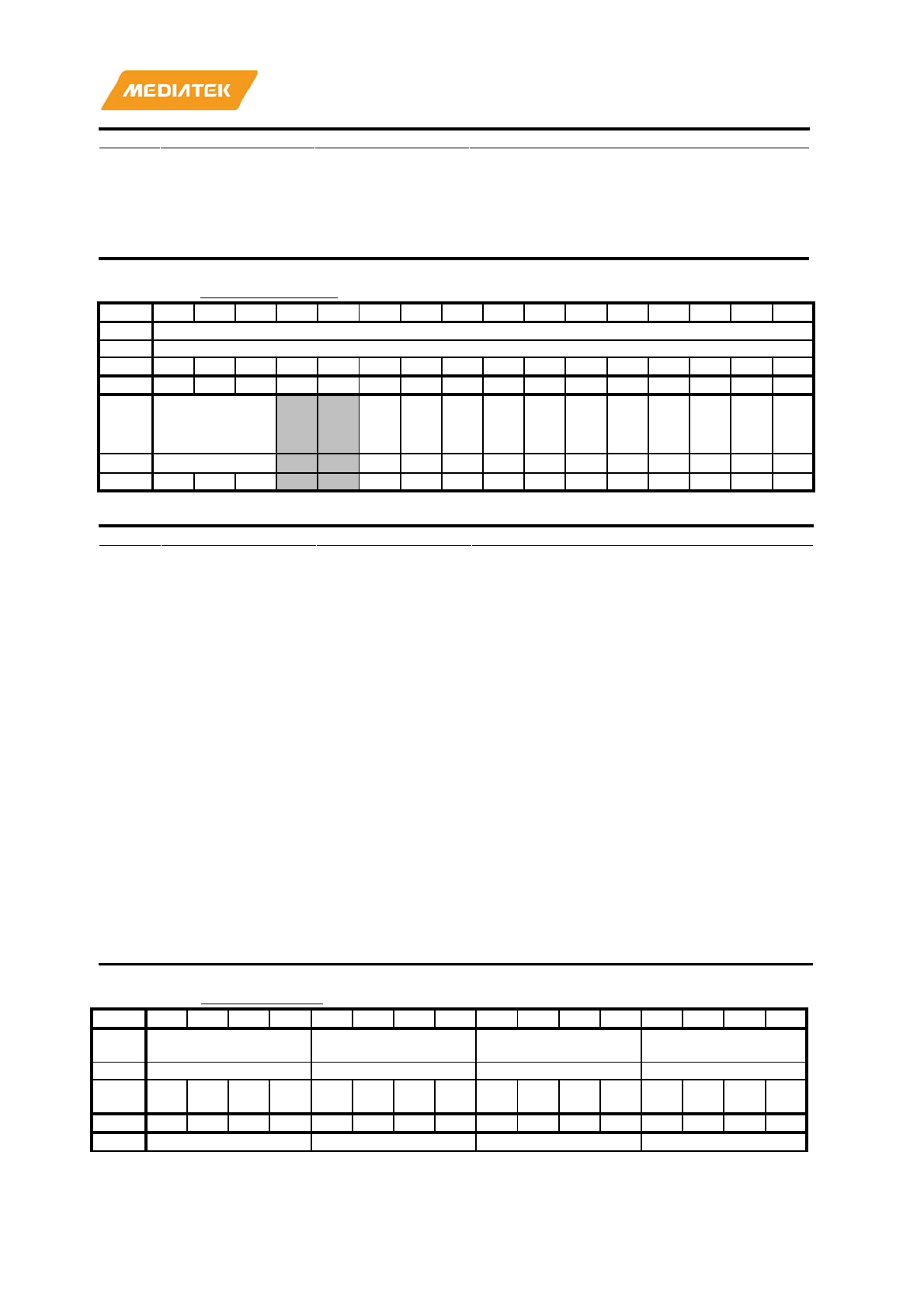
MT7686 Reference Manual
© 2016 - 2017 MediaTek Inc.
Page 456 of 536
This document contains information that is proprietary to MediaTek Inc. (“MediaTek”) and/or its licensor(s).
Any unauthorized use, reproduction or disclosure of this document in whole or in part is strictly prohibited.
Bit(s)
Mnemonic
Name
Description
2
smt_cfg_set_gpio_2
PAD_GPIO_2
0: Keep; 1: SET bit;
1
smt_cfg_set_gpio_1
PAD_GPIO_1
0: Keep; 1: SET bit;
0
smt_cfg_set_gpio_0
PAD_GPIO_0
0: Keep; 1: SET bit;
A20C0068
SMT_CFG0_CLR
00000000
Bit
31
30
29
28
27
26
25
24
23
22
21
20
19
18
17
16
Name
smt_cfg_clr_rsv
Type
RO
Reset
0
0
0
0
0
0
0
0
0
0
0
0
0
0
0
0
Bit
15
14
13
12
11
10
9
8
7
6
5
4
3
2
1
0
Name
smt_cfg_clr_rsv
smt_c
fg_clr
_gpio
_10
smt_c
fg_clr
_gpio
_9
smt_c
fg_clr
_gpio
_8
smt_c
fg_clr
_gpio
_7
smt_c
fg_clr
_gpio
_6
smt_c
fg_clr
_gpio
_5
smt_c
fg_clr
_gpio
_4
smt_c
fg_clr
_gpio
_3
smt_c
fg_clr
_gpio
_2
smt_c
fg_clr
_gpio
_1
smt_
cfg_cl
r_gpi
o_0
Type
RO
WO
WO
WO
WO
WO
WO
WO
WO
WO
WO
WO
Reset
0
0
0
0
0
0
0
0
0
0
0
0
0
0
0
0
Bit(s)
Mnemonic
Name
Description
31:13
smt_cfg_clr_rsv
Reserved
10
smt_cfg_clr_gpio_10
PAD_GPIO_10
0: Keep; 1: Clear bit
9
smt_cfg_clr_gpio_9
PAD_GPIO_9
0: Keep; 1: Clear bit
8
smt_cfg_clr_gpio_8
PAD_GPIO_8
0: Keep; 1: Clear bit
7
smt_cfg_clr_gpio_7
PAD_GPIO_7
0: Keep; 1: Clear bit
6
smt_cfg_clr_gpio_6
PAD_GPIO_6
0: Keep; 1: Clear bit
5
smt_cfg_clr_gpio_5
PAD_GPIO_5
0: Keep; 1: Clear bit
4
smt_cfg_clr_gpio_4
PAD_GPIO_4
0: Keep; 1: Clear bit
3
smt_cfg_clr_gpio_3
PAD_GPIO_3
0: Keep; 1: Clear bit
2
smt_cfg_clr_gpio_2
PAD_GPIO_2
0: Keep; 1: Clear bit
1
smt_cfg_clr_gpio_1
PAD_GPIO_1
0: Keep; 1: Clear bit
0
smt_cfg_clr_gpio_0
PAD_GPIO_0
0: Keep; 1: Clear bit
A20C0080
TDSEL_CFG00
TX delay selection
AAAAAAAA
Bit
31
30
29
28
27
26
25
24
23
22
21
20
19
18
17
16
Nam
e
tdsel_cfg_gpio_7 tdsel_cfg_gpio_6 tdsel_cfg_gpio_5 tdsel_cfg_gpio_4
Type
RW
RW
RW
RW
Rese
t
1 0 1 0 1 0 1 0 1 0 1 0 1 0 1 0
Bit
15
14
13
12
11
10
9
8
7
6
5
4
3
2
1
0
Nam
tdsel_cfg_gpio_3
tdsel_cfg_gpio_2
tdsel_cfg_gpio_1
tdsel_cfg_gpio_0

MT7686 Reference Manual
© 2016 - 2017 MediaTek Inc.
Page 457 of 536
This document contains information that is proprietary to MediaTek Inc. (“MediaTek”) and/or its licensor(s).
Any unauthorized use, reproduction or disclosure of this document in whole or in part is strictly prohibited.
e
Type
RW
RW
RW
RW
Rese
t
1 0 1 0 1 0 1 0 1 0 1 0 1 0 1 0
Bit(s)
Mnemonic
Name
Description
31:28
tdsel_cfg_gpio_7
PAD_GPIO_7
0000: minimum transmission delay; 1111: maximum
transmission delay
27:24
tdsel_cfg_gpio_6
PAD_GPIO_6
0000: minimum transmission delay; 1111: maximum
transmission delay
23:20
tdsel_cfg_gpio_5
PAD_GPIO_5
0000: minimum transmission delay; 1111: maximum
transmission delay
19:16
tdsel_cfg_gpio_4
PAD_GPIO_4
0000: minimum transmission delay; 1111: maximum
transmission delay
15:12
tdsel_cfg_gpio_3
PAD_GPIO_3
0000: minimum transmission delay; 1111: maximum
transmission delay
11:8
tdsel_cfg_gpio_2
PAD_GPIO_2
0000: minimum transmission delay; 1111: maximum
transmission delay
7:4
tdsel_cfg_gpio_1
PAD_GPIO_1
0000: minimum transmission delay; 1111: maximum
transmission delay
3:0
tdsel_cfg_gpio_0
PAD_GPIO_0
0000: minimum transmission delay; 1111: maximum
transmission delay
A20C0084
TDSEL_CFG00_SET
set TDSEL_CFG00
00000000
Bit
31
30
29
28
27
26
25
24
23
22
21
20
19
18
17
16
Nam
e
tdsel_cfg_set_gpio_7 tdsel_cfg_set_gpio_6 tdsel_cfg_set_gpio_5 tdsel_cfg_set_gpio_4
Type
WO
WO
WO
WO
Rese
t
0 0 0 0 0 0 0 0 0 0 0 0 0 0 0 0
Bit
15
14
13
12
11
10
9
8
7
6
5
4
3
2
1
0
Nam
e
tdsel_cfg_set_gpio_3 tdsel_cfg_set_gpio_2 tdsel_cfg_set_gpio_1 tdsel_cfg_set_gpio_0
Type
WO
WO
WO
WO
Rese
t
0 0 0 0 0 0 0 0 0 0 0 0 0 0 0 0
Bit(s)
Mnemonic
Name
Description
31:28
tdsel_cfg_set_gpio_7
PAD_GPIO_7
0: Keep; 1: SET bit;
27:24
tdsel_cfg_set_gpio_6
PAD_GPIO_6
0: Keep; 1: SET bit;
23:20
tdsel_cfg_set_gpio_5
PAD_GPIO_5
0: Keep; 1: SET bit;
19:16
tdsel_cfg_set_gpio_4
PAD_GPIO_4
0: Keep; 1: SET bit;
15:12
tdsel_cfg_set_gpio_3
PAD_GPIO_3
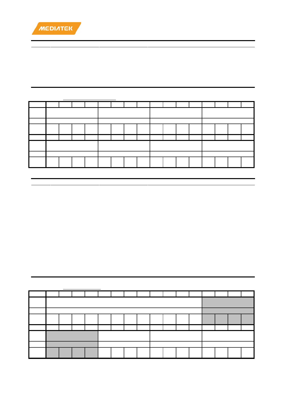
MT7686 Reference Manual
© 2016 - 2017 MediaTek Inc.
Page 458 of 536
This document contains information that is proprietary to MediaTek Inc. (“MediaTek”) and/or its licensor(s).
Any unauthorized use, reproduction or disclosure of this document in whole or in part is strictly prohibited.
Bit(s)
Mnemonic
Name
Description
0: Keep; 1: SET bit;
11:8
tdsel_cfg_set_gpio_2
PAD_GPIO_2
0: Keep; 1: SET bit;
7:4
tdsel_cfg_set_gpio_1
PAD_GPIO_1
0: Keep; 1: SET bit;
3:0
tdsel_cfg_set_gpio_0
PAD_GPIO_0
0: Keep; 1: SET bit;
A20C0088
TDSEL_CFG00_CLR
clear TDSEL_CFG00
00000000
Bit
31
30
29
28
27
26
25
24
23
22
21
20
19
18
17
16
Nam
e
tdsel_cfg_clr_gpio_7 tdsel_cfg_clr_gpio_6 tdsel_cfg_clr_gpio_5 tdsel_cfg_clr_gpio_4
Type
WO
WO
WO
WO
Rese
t
0 0 0 0 0 0 0 0 0 0 0 0 0 0 0 0
Bit
15
14
13
12
11
10
9
8
7
6
5
4
3
2
1
0
Nam
e
tdsel_cfg_clr_gpio_3 tdsel_cfg_clr_gpio_2 tdsel_cfg_clr_gpio_1 tdsel_cfg_clr_gpio_0
Type
WO
WO
WO
WO
Rese
t
0 0 0 0 0 0 0 0 0 0 0 0 0 0 0 0
Bit(s)
Mnemonic
Name
Description
31:28
tdsel_cfg_clr_gpio_7
PAD_GPIO_7
0: Keep; 1: Clear bit
27:24
tdsel_cfg_clr_gpio_6
PAD_GPIO_6
0: Keep; 1: Clear bit
23:20
tdsel_cfg_clr_gpio_5
PAD_GPIO_5
0: Keep; 1: Clear bit
19:16
tdsel_cfg_clr_gpio_4
PAD_GPIO_4
0: Keep; 1: Clear bit
15:12
tdsel_cfg_clr_gpio_3
PAD_GPIO_3
0: Keep; 1: Clear bit
11:8
tdsel_cfg_clr_gpio_2
PAD_GPIO_2
0: Keep; 1: Clear bit
7:4
tdsel_cfg_clr_gpio_1
PAD_GPIO_1
0: Keep; 1: Clear bit
3:0
tdsel_cfg_clr_gpio_0
PAD_GPIO_0
0: Keep; 1: Clear bit
A20C0090
TDSEL_CFG01
TX delay selection
000AAAAA
Bit
31
30
29
28
27
26
25
24
23
22
21
20
19
18
17
16
Nam
e
tdsel_cfg_rsv
Type
RO
Rese
t
0 0 0 0 0 0 0 0 0 0 0 0 1 0 1 0
Bit
15
14
13
12
11
10
9
8
7
6
5
4
3
2
1
0
Nam
e
tdsel_cfg_gpio_10 tdsel_cfg_gpio_9 tdsel_cfg_gpio_8
Type
RW
RW
RW
Rese
t
1 0 1 0 1 0 1 0 1 0 1 0 1 0 1 0
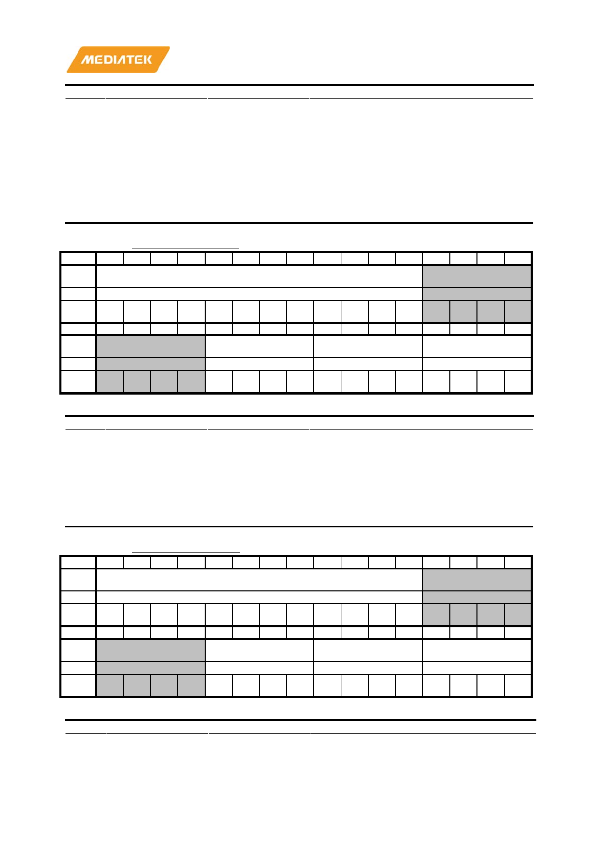
MT7686 Reference Manual
© 2016 - 2017 MediaTek Inc.
Page 459 of 536
This document contains information that is proprietary to MediaTek Inc. (“MediaTek”) and/or its licensor(s).
Any unauthorized use, reproduction or disclosure of this document in whole or in part is strictly prohibited.
Bit(s)
Mnemonic
Name
Description
31:20
tdsel_cfg_rsv
Reserved
nn: reserved
11:8
tdsel_cfg_gpio_10
PAD_GPIO_10
0000: minimum transmission delay; 1111: maximum
transmission delay
7:4
tdsel_cfg_gpio_9
PAD_GPIO_9
0000: minimum transmission delay; 1111: maximum
transmission delay
3:0
tdsel_cfg_gpio_8
PAD_GPIO_8
0000: minimum transmission delay; 1111: maximum
transmission delay
A20C0094
TDSEL_CFG01_SET
set TDSEL_CFG01
00000000
Bit
31
30
29
28
27
26
25
24
23
22
21
20
19
18
17
16
Nam
e
tdsel_cfg_set_rsv
Type
RO
Rese
t
0 0 0 0 0 0 0 0 0 0 0 0 0 0 0 0
Bit
15
14
13
12
11
10
9
8
7
6
5
4
3
2
1
0
Nam
e
tdsel_cfg_set_gpio_10 tdsel_cfg_set_gpio_9 tdsel_cfg_set_gpio_8
Type
WO
WO
WO
Rese
t
0 0 0 0 0 0 0 0 0 0 0 0 0 0 0 0
Bit(s)
Mnemonic
Name
Description
31:20
tdsel_cfg_set_rsv
Reserved
nn: reserved
11:8
tdsel_cfg_set_gpio_10
PAD_GPIO_10
0: Keep; 1: SET bit;
7:4
tdsel_cfg_set_gpio_9
PAD_GPIO_9
0: Keep; 1: SET bit;
3:0
tdsel_cfg_set_gpio_8
PAD_GPIO_8
0: Keep; 1: SET bit;
A20C0098
TDSEL_CFG01_CLR
clear TDSEL_CFG01
00000000
Bit
31
30
29
28
27
26
25
24
23
22
21
20
19
18
17
16
Nam
e
tdsel_cfg_clr_rsv
Type
RO
Rese
t
0 0 0 0 0 0 0 0 0 0 0 0 0 0 0 0
Bit
15
14
13
12
11
10
9
8
7
6
5
4
3
2
1
0
Nam
e
tdsel_cfg_clr_gpio_10 tdsel_cfg_clr_gpio_9 tdsel_cfg_clr_gpio_8
Type
WO
WO
WO
Rese
t
0 0 0 0 0 0 0 0 0 0 0 0 0 0 0 0
Bit(s)
Mnemonic
Name
Description
31:20
tdsel_cfg_clr_rsv
Reserved
nn: reserved
11:8
tdsel_cfg_clr_gpio_10
PAD_GPIO_10
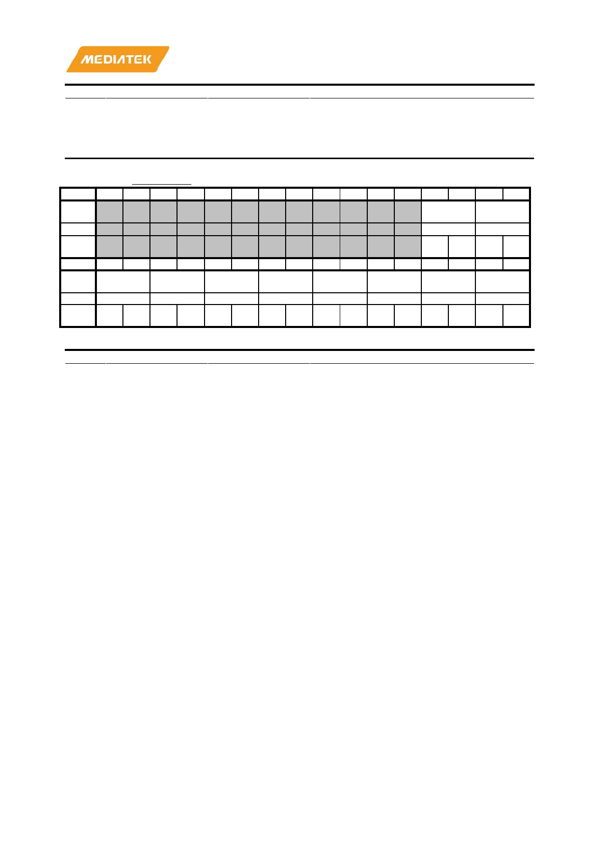
MT7686 Reference Manual
© 2016 - 2017 MediaTek Inc.
Page 460 of 536
This document contains information that is proprietary to MediaTek Inc. (“MediaTek”) and/or its licensor(s).
Any unauthorized use, reproduction or disclosure of this document in whole or in part is strictly prohibited.
Bit(s)
Mnemonic
Name
Description
0: Keep; 1: Clear bit
7:4
tdsel_cfg_clr_gpio_9
PAD_GPIO_9
0: Keep; 1: Clear bit
3:0
tdsel_cfg_clr_gpio_8
PAD_GPIO_8
0: Keep; 1: Clear bit
A20D0000
DRV_CFG1
00000000
Bit
31
30
29
28
27
26
25
24
23
22
21
20
19
18
17
16
Nam
e
drv_cfg_g
pio_20
drv_cfg_g
pio_19
Type
RW
RW
Rese
t
0 0 0 0
Bit
15
14
13
12
11
10
9
8
7
6
5
4
3
2
1
0
Nam
e
drv_cfg_g
pio_18
drv_cfg_g
pio_17
drv_cfg_g
pio_16
drv_cfg_g
pio_15
drv_cfg_g
pio_14
drv_cfg_g
pio_13
drv_cfg_g
pio_12
drv_cfg_g
pio_11
Type
RW
RW
RW
RW
RW
RW
RW
RW
Rese
t
0 0 0 0 0 0 0 0 0 0 0 0 0 0 0 0
Bit(s)
Mnemonic
Name
Description
19:18
drv_cfg_gpio_20
PAD_GPIO_20
4mA: [00]
8mA: [10]
12mA: [01]
16mA: [11]
17:16
drv_cfg_gpio_19
PAD_GPIO_19
4mA: [00]
8mA: [10]
12mA: [01]
16mA: [11]
15:14
drv_cfg_gpio_18
PAD_GPIO_18
4mA: [00]
8mA: [10]
12mA: [01]
16mA: [11]
13:12
drv_cfg_gpio_17
PAD_GPIO_17
4mA: [00]
8mA: [10]
12mA: [01]
16mA: [11]
11:10
drv_cfg_gpio_16
PAD_GPIO_16
4mA: [00]
8mA: [10]
12mA: [01]
16mA: [11]
9:8
drv_cfg_gpio_15
PAD_GPIO_15
4mA: [00]
8mA: [10]
12mA: [01]
16mA: [11]
7:6
drv_cfg_gpio_14
PAD_GPIO_14
4mA: [00]
8mA: [10]
12mA: [01]
16mA: [11]
5:4
drv_cfg_gpio_13
PAD_GPIO_13
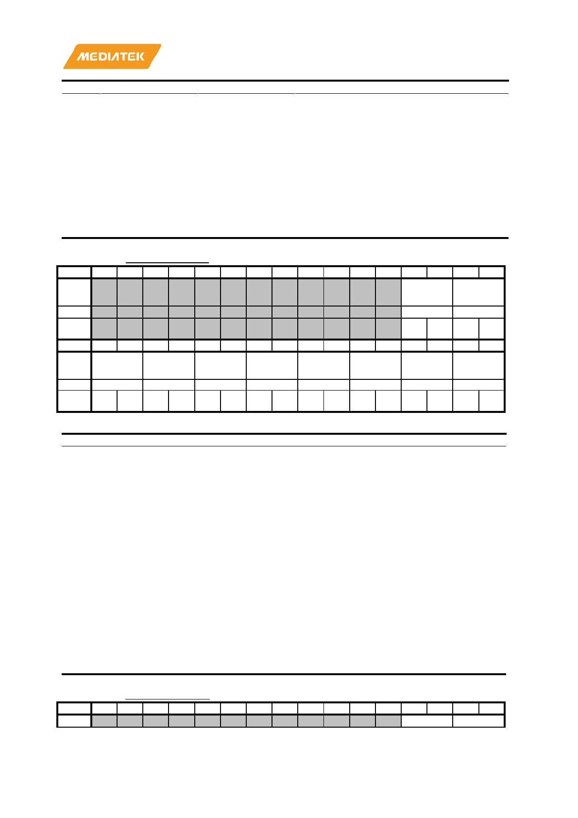
MT7686 Reference Manual
© 2016 - 2017 MediaTek Inc.
Page 461 of 536
This document contains information that is proprietary to MediaTek Inc. (“MediaTek”) and/or its licensor(s).
Any unauthorized use, reproduction or disclosure of this document in whole or in part is strictly prohibited.
Bit(s)
Mnemonic
Name
Description
4mA: [00]
8mA: [10]
12mA: [01]
16mA: [11]
3:2
drv_cfg_gpio_12
PAD_GPIO_12
4mA: [00]
8mA: [10]
12mA: [01]
16mA: [11]
1:0
drv_cfg_gpio_11
PAD_GPIO_11
4mA: [00]
8mA: [10]
12mA: [01]
16mA: [11]
A20D0004
DRV_CFG1_SET
00000000
Bit
31
30
29
28
27
26
25
24
23
22
21
20
19
18
17
16
Nam
e
drv_cfg_s
et_gpio_2
0
drv_cfg_s
et_gpio_1
9
Type
WO
WO
Rese
t
0 0 0 0
Bit
15
14
13
12
11
10
9
8
7
6
5
4
3
2
1
0
Nam
e
drv_cfg_s
et_gpio_1
8
drv_cfg_s
et_gpio_1
7
drv_cfg_s
et_gpio_1
6
drv_cfg_s
et_gpio_1
5
drv_cfg_s
et_gpio_1
4
drv_cfg_s
et_gpio_1
3
drv_cfg_s
et_gpio_1
2
drv_cfg_s
et_gpio_1
1
Type
WO
WO
WO
WO
WO
WO
WO
WO
Rese
t
0 0 0 0 0 0 0 0 0 0 0 0 0 0 0 0
Bit(s)
Mnemonic
Name
Description
19:18
drv_cfg_set_gpio_20
PAD_GPIO_20
0: Keep; 1: SET bit;
17:16
drv_cfg_set_gpio_19
PAD_GPIO_19
0: Keep; 1: SET bit;
15:14
drv_cfg_set_gpio_18
PAD_GPIO_18
0: Keep; 1: SET bit;
13:12
drv_cfg_set_gpio_17
PAD_GPIO_17
0: Keep; 1: SET bit;
11:10
drv_cfg_set_gpio_16
PAD_GPIO_16
0: Keep; 1: SET bit;
9:8
drv_cfg_set_gpio_15
PAD_GPIO_15
0: Keep; 1: SET bit;
7:6
drv_cfg_set_gpio_14
PAD_GPIO_14
0: Keep; 1: SET bit;
5:4
drv_cfg_set_gpio_13
PAD_GPIO_13
0: Keep; 1: SET bit;
3:2
drv_cfg_set_gpio_12
PAD_GPIO_12
0: Keep; 1: SET bit;
1:0
drv_cfg_set_gpio_11
PAD_GPIO_11
0: Keep; 1: SET bit;
A20D0008
DRV_CFG1_CLR
00000000
Bit
31
30
29
28
27
26
25
24
23
22
21
20
19
18
17
16
Nam
drv_cfg_c
drv_cfg_c

MT7686 Reference Manual
© 2016 - 2017 MediaTek Inc.
Page 462 of 536
This document contains information that is proprietary to MediaTek Inc. (“MediaTek”) and/or its licensor(s).
Any unauthorized use, reproduction or disclosure of this document in whole or in part is strictly prohibited.
e
lr_gpio_2
0
lr_gpio_1
9
Type
WO
WO
Rese
t
0 0 0 0
Bit
15
14
13
12
11
10
9
8
7
6
5
4
3
2
1
0
Nam
e
drv_cfg_c
lr_gpio_1
8
drv_cfg_c
lr_gpio_1
7
drv_cfg_c
lr_gpio_1
6
drv_cfg_c
lr_gpio_1
5
drv_cfg_c
lr_gpio_1
4
drv_cfg_c
lr_gpio_1
3
drv_cfg_c
lr_gpio_1
2
drv_cfg_c
lr_gpio_1
1
Type
WO
WO
WO
WO
WO
WO
WO
WO
Rese
t
0 0 0 0 0 0 0 0 0 0 0 0 0 0 0 0
Bit(s)
Mnemonic
Name
Description
19:18
drv_cfg_clr_gpio_20
PAD_GPIO_20
0: Keep; 1: Clear bit
17:16
drv_cfg_clr_gpio_19
PAD_GPIO_19
0: Keep; 1: Clear bit
15:14
drv_cfg_clr_gpio_18
PAD_GPIO_18
0: Keep; 1: Clear bit
13:12
drv_cfg_clr_gpio_17
PAD_GPIO_17
0: Keep; 1: Clear bit
11:10
drv_cfg_clr_gpio_16
PAD_GPIO_16
0: Keep; 1: Clear bit
9:8
drv_cfg_clr_gpio_15
PAD_GPIO_15
0: Keep; 1: Clear bit
7:6
drv_cfg_clr_gpio_14
PAD_GPIO_14
0: Keep; 1: Clear bit
5:4
drv_cfg_clr_gpio_13
PAD_GPIO_13
0: Keep; 1: Clear bit
3:2
drv_cfg_clr_gpio_12
PAD_GPIO_12
0: Keep; 1: Clear bit
1:0
drv_cfg_clr_gpio_11
PAD_GPIO_11
0: Keep; 1: Clear bit
A20D0010
G_CFG1
0000000F
Bit
31
30
29
28
27
26
25
24
23
22
21
20
19
18
17
16
Name
Type
Reset
Bit
15
14
13
12
11
10
9
8
7
6
5
4
3
2
1
0
Name
g_cfg
_gpio
_20
g_cfg
_gpio
_19
g_cfg
_gpio
_18
g_cfg
_gpio
_17
Type
RW
RW
RW
RW
Reset
1
1
1
1
Bit(s)
Mnemonic
Name
Description
3
g_cfg_gpio_20
PAD_GPIO_20
0: Enable AIO; 1: Disable AIO;
2
g_cfg_gpio_19
PAD_GPIO_19
0: Enable AIO; 1: Disable AIO;
1
g_cfg_gpio_18
PAD_GPIO_18
0: Enable AIO; 1: Disable AIO;
0
g_cfg_gpio_17
PAD_GPIO_17
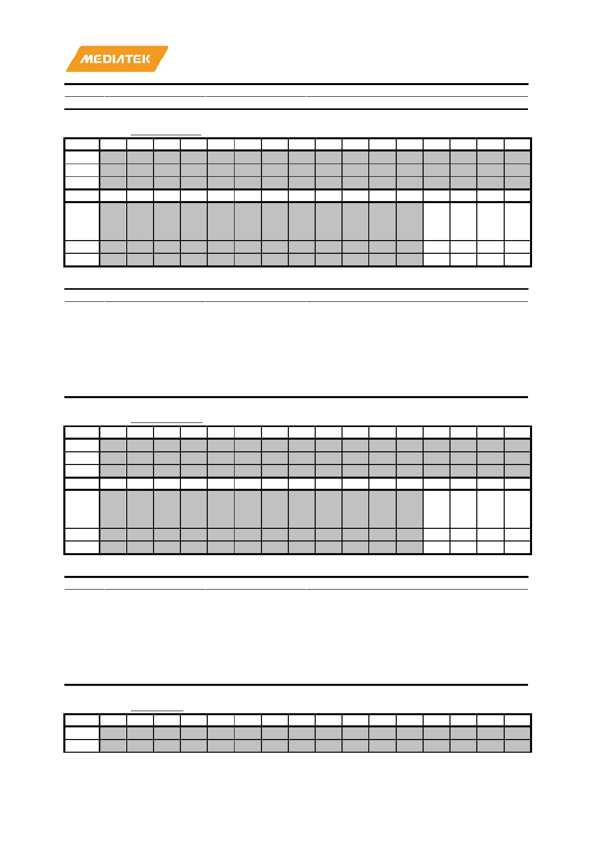
MT7686 Reference Manual
© 2016 - 2017 MediaTek Inc.
Page 463 of 536
This document contains information that is proprietary to MediaTek Inc. (“MediaTek”) and/or its licensor(s).
Any unauthorized use, reproduction or disclosure of this document in whole or in part is strictly prohibited.
Bit(s)
Mnemonic
Name
Description
0: Enable AIO; 1: Disable AIO;
A20D0014
G_CFG1_SET
00000000
Bit
31
30
29
28
27
26
25
24
23
22
21
20
19
18
17
16
Name
Type
Reset
Bit
15
14
13
12
11
10
9
8
7
6
5
4
3
2
1
0
Name
g_cfg
_set_
gpio_
20
g_cfg
_set_
gpio_
19
g_cfg
_set_
gpio_
18
g_cfg
_set_
gpio_
17
Type
WO
WO
WO
WO
Reset
0
0
0
0
Bit(s)
Mnemonic
Name
Description
3
g_cfg_set_gpio_20
PAD_GPIO_20
0: Keep; 1: SET bit;
2
g_cfg_set_gpio_19
PAD_GPIO_19
0: Keep; 1: SET bit;
1
g_cfg_set_gpio_18
PAD_GPIO_18
0: Keep; 1: SET bit;
0
g_cfg_set_gpio_17
PAD_GPIO_17
0: Keep; 1: SET bit;
A20D0018
G_CFG1_CLR
00000000
Bit
31
30
29
28
27
26
25
24
23
22
21
20
19
18
17
16
Name
Type
Reset
Bit
15
14
13
12
11
10
9
8
7
6
5
4
3
2
1
0
Name
g_cfg
_clr_
gpio_
20
g_cfg
_clr_
gpio_
19
g_cfg
_clr_
gpio_
18
g_cfg
_clr_
gpio_
17
Type
WO
WO
WO
WO
Reset
0
0
0
0
Bit(s)
Mnemonic
Name
Description
3
g_cfg_clr_gpio_20
PAD_GPIO_20
0: Keep; 1: Clear bit
2
g_cfg_clr_gpio_19
PAD_GPIO_19
0: Keep; 1: Clear bit
1
g_cfg_clr_gpio_18
PAD_GPIO_18
0: Keep; 1: Clear bit
0
g_cfg_clr_gpio_17
PAD_GPIO_17
0: Keep; 1: Clear bit
A20D0020
IES_CFG1
000003FF
Bit
31
30
29
28
27
26
25
24
23
22
21
20
19
18
17
16
Name
Type

MT7686 Reference Manual
© 2016 - 2017 MediaTek Inc.
Page 464 of 536
This document contains information that is proprietary to MediaTek Inc. (“MediaTek”) and/or its licensor(s).
Any unauthorized use, reproduction or disclosure of this document in whole or in part is strictly prohibited.
Reset
Bit
15
14
13
12
11
10
9
8
7
6
5
4
3
2
1
0
Name
ies_cf
g_gpi
o_20
ies_cf
g_gpi
o_19
ies_cf
g_gpi
o_18
ies_cf
g_gpi
o_17
ies_cf
g_gpi
o_16
ies_cf
g_gpi
o_15
ies_cf
g_gpi
o_14
ies_cf
g_gpi
o_13
ies_cf
g_gpi
o_12
ies_cf
g_gpi
o_11
Type
RW
RW
RW
RW
RW
RW
RW
RW
RW
RW
Reset
1
1
1
1
1
1
1
1
1
1
Bit(s)
Mnemonic
Name
Description
9
ies_cfg_gpio_20
PAD_GPIO_20
0: Disable; 1: Enable;
8
ies_cfg_gpio_19
PAD_GPIO_19
0: Disable; 1: Enable;
7
ies_cfg_gpio_18
PAD_GPIO_18
0: Disable; 1: Enable;
6
ies_cfg_gpio_17
PAD_GPIO_17
0: Disable; 1: Enable;
5
ies_cfg_gpio_16
PAD_GPIO_16
0: Disable; 1: Enable;
4
ies_cfg_gpio_15
PAD_GPIO_15
0: Disable; 1: Enable;
3
ies_cfg_gpio_14
PAD_GPIO_14
0: Disable; 1: Enable;
2
ies_cfg_gpio_13
PAD_GPIO_13
0: Disable; 1: Enable;
1
ies_cfg_gpio_12
PAD_GPIO_12
0: Disable; 1: Enable;
0
ies_cfg_gpio_11
PAD_GPIO_11
0: Disable; 1: Enable;
A20D0024
IES_CFG1_SET
00000000
Bit
31
30
29
28
27
26
25
24
23
22
21
20
19
18
17
16
Name
Type
Reset
Bit
15
14
13
12
11
10
9
8
7
6
5
4
3
2
1
0
Name
ies_cf
g_set
_gpio
_20
ies_cf
g_set
_gpio
_19
ies_cf
g_set
_gpio
_18
ies_cf
g_set
_gpio
_17
ies_cf
g_set
_gpio
_16
ies_cf
g_set
_gpio
_15
ies_cf
g_set
_gpio
_14
ies_cf
g_set
_gpio
_13
ies_cf
g_set
_gpio
_12
ies_cf
g_set
_gpio
_11
Type
WO
WO
WO
WO
WO
WO
WO
WO
WO
WO
Reset
0
0
0
0
0
0
0
0
0
0
Bit(s)
Mnemonic
Name
Description
9
ies_cfg_set_gpio_20
PAD_GPIO_20
0: Keep; 1: SET bit;
8
ies_cfg_set_gpio_19
PAD_GPIO_19
0: Keep; 1: SET bit;
7
ies_cfg_set_gpio_18
PAD_GPIO_18
0: Keep; 1: SET bit;
6
ies_cfg_set_gpio_17
PAD_GPIO_17
0: Keep; 1: SET bit;
5
ies_cfg_set_gpio_16
PAD_GPIO_16
0: Keep; 1: SET bit;
4
ies_cfg_set_gpio_15
PAD_GPIO_15
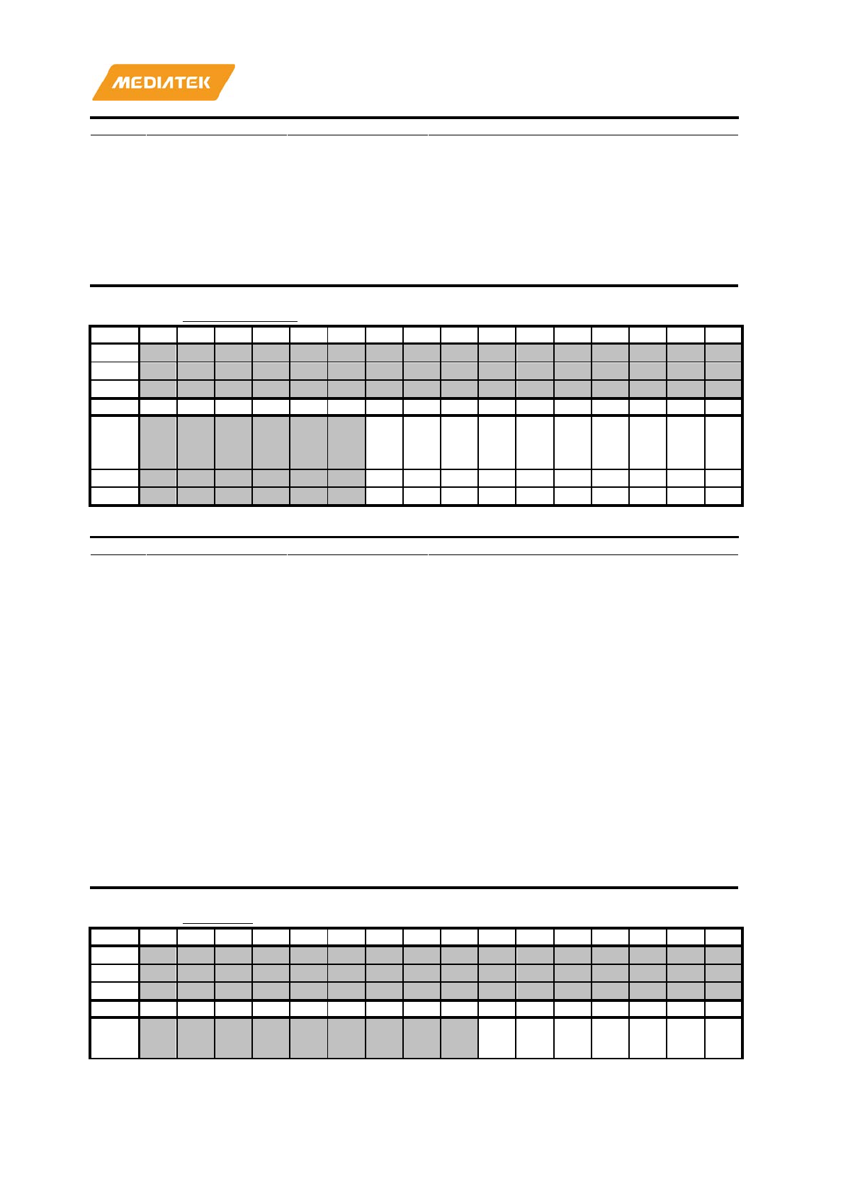
MT7686 Reference Manual
© 2016 - 2017 MediaTek Inc.
Page 465 of 536
This document contains information that is proprietary to MediaTek Inc. (“MediaTek”) and/or its licensor(s).
Any unauthorized use, reproduction or disclosure of this document in whole or in part is strictly prohibited.
Bit(s)
Mnemonic
Name
Description
0: Keep; 1: SET bit;
3
ies_cfg_set_gpio_14
PAD_GPIO_14
0: Keep; 1: SET bit;
2
ies_cfg_set_gpio_13
PAD_GPIO_13
0: Keep; 1: SET bit;
1
ies_cfg_set_gpio_12
PAD_GPIO_12
0: Keep; 1: SET bit;
0
ies_cfg_set_gpio_11
PAD_GPIO_11
0: Keep; 1: SET bit;
A20D0028
IES_CFG1_CLR
00000000
Bit
31
30
29
28
27
26
25
24
23
22
21
20
19
18
17
16
Name
Type
Reset
Bit
15
14
13
12
11
10
9
8
7
6
5
4
3
2
1
0
Name
ies_cf
g_clr
_gpio
_20
ies_cf
g_clr
_gpio
_19
ies_cf
g_clr
_gpio
_18
ies_cf
g_clr
_gpio
_17
ies_cf
g_clr
_gpio
_16
ies_cf
g_clr
_gpio
_15
ies_cf
g_clr
_gpio
_14
ies_cf
g_clr
_gpio
_13
ies_cf
g_clr
_gpio
_12
ies_cf
g_clr
_gpio
_11
Type
WO
WO
WO
WO
WO
WO
WO
WO
WO
WO
Reset
0
0
0
0
0
0
0
0
0
0
Bit(s)
Mnemonic
Name
Description
9
ies_cfg_clr_gpio_20
PAD_GPIO_20
0: Keep; 1: Clear bit
8
ies_cfg_clr_gpio_19
PAD_GPIO_19
0: Keep; 1: Clear bit
7
ies_cfg_clr_gpio_18
PAD_GPIO_18
0: Keep; 1: Clear bit
6
ies_cfg_clr_gpio_17
PAD_GPIO_17
0: Keep; 1: Clear bit
5
ies_cfg_clr_gpio_16
PAD_GPIO_16
0: Keep; 1: Clear bit
4
ies_cfg_clr_gpio_15
PAD_GPIO_15
0: Keep; 1: Clear bit
3
ies_cfg_clr_gpio_14
PAD_GPIO_14
0: Keep; 1: Clear bit
2
ies_cfg_clr_gpio_13
PAD_GPIO_13
0: Keep; 1: Clear bit
1
ies_cfg_clr_gpio_12
PAD_GPIO_12
0: Keep; 1: Clear bit
0
ies_cfg_clr_gpio_11
PAD_GPIO_11
0: Keep; 1: Clear bit
A20D0030
PD_CFG1
0000000B
Bit
31
30
29
28
27
26
25
24
23
22
21
20
19
18
17
16
Name
Type
Reset
Bit
15
14
13
12
11
10
9
8
7
6
5
4
3
2
1
0
Name
pd_cf
g_bo
nd_rs
pd_cf
g_bo
nd_sf
pd_cf
g_bo
nd_p
pd_cf
g_gpi
o_20
pd_cf
g_gpi
o_19
pd_cf
g_gpi
o_18
pd_cf
g_gpi
o_17
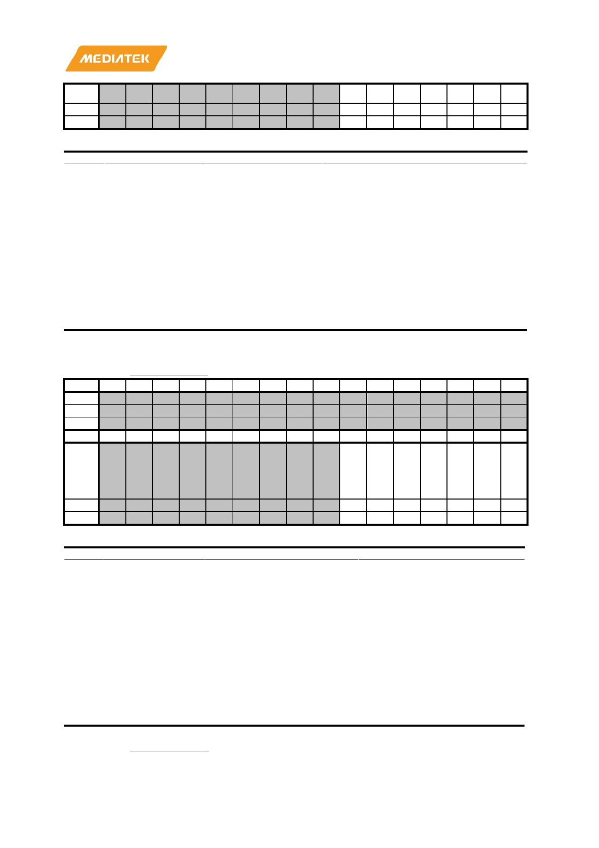
MT7686 Reference Manual
© 2016 - 2017 MediaTek Inc.
Page 466 of 536
This document contains information that is proprietary to MediaTek Inc. (“MediaTek”) and/or its licensor(s).
Any unauthorized use, reproduction or disclosure of this document in whole or in part is strictly prohibited.
v
_sip
sram
_sip
Type
RW
RW
RW
RW
RW
RW
RW
Reset
0
0
0
1
0
1
1
Bit(s)
Mnemonic
Name
Description
6
pd_cfg_bond_rsv
PAD_BOND_RSV
0: Disable; 1: Enable;
5
pd_cfg_bond_sf_sip
PAD_BOND_SF_SIP
0: Disable; 1: Enable;
4
pd_cfg_bond_psram_sip
PAD_BOND_PSRAM_SIP
0: Disable; 1: Enable;
3
pd_cfg_gpio_20
PAD_GPIO_20
0: Disable; 1: Enable;
2
pd_cfg_gpio_19
PAD_GPIO_19
0: Disable; 1: Enable;
1
pd_cfg_gpio_18
PAD_GPIO_18
0: Disable; 1: Enable;
0
pd_cfg_gpio_17
PAD_GPIO_17
0: Disable; 1: Enable;
A20D0034
PD_CFG1_SET
00000000
Bit
31
30
29
28
27
26
25
24
23
22
21
20
19
18
17
16
Name
Type
Reset
Bit
15
14
13
12
11
10
9
8
7
6
5
4
3
2
1
0
Name
pd_cf
g_set
_bon
d_rsv
pd_cf
g_set
_bon
d_sf_
sip
pd_cf
g_set
_bon
d_psr
am_si
p
pd_cf
g_set
_gpio
_20
pd_cf
g_set
_gpio
_19
pd_cf
g_set
_gpio
_18
pd_cf
g_set
_gpio
_17
Type
WO
WO
WO
WO
WO
WO
WO
Reset
0
0
0
0
0
0
0
Bit(s)
Mnemonic
Name
Description
6
pd_cfg_set_bond_rsv
PAD_BOND_RSV
0: Keep; 1: SET bit;
5
pd_cfg_set_bond_sf_sip
PAD_BOND_SF_SIP
0: Keep; 1: SET bit;
4
pd_cfg_set_bond_psram_sip
PAD_BOND_PSRAM_SIP
0: Keep; 1: SET bit;
3
pd_cfg_set_gpio_20
PAD_GPIO_20
0: Keep; 1: SET bit;
2
pd_cfg_set_gpio_19
PAD_GPIO_19
0: Keep; 1: SET bit;
1
pd_cfg_set_gpio_18
PAD_GPIO_18
0: Keep; 1: SET bit;
0
pd_cfg_set_gpio_17
PAD_GPIO_17
0: Keep; 1: SET bit;
A20D0038
PD_CFG1_CLR
00000000
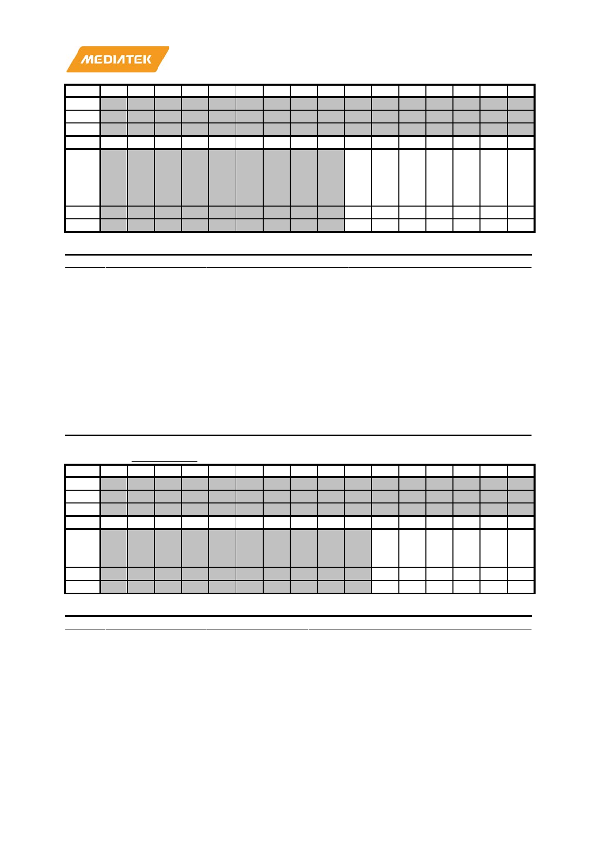
MT7686 Reference Manual
© 2016 - 2017 MediaTek Inc.
Page 467 of 536
This document contains information that is proprietary to MediaTek Inc. (“MediaTek”) and/or its licensor(s).
Any unauthorized use, reproduction or disclosure of this document in whole or in part is strictly prohibited.
Bit
31
30
29
28
27
26
25
24
23
22
21
20
19
18
17
16
Name
Type
Reset
Bit
15
14
13
12
11
10
9
8
7
6
5
4
3
2
1
0
Name
pd_cf
g_clr
_bon
d_rsv
pd_cf
g_clr
_bon
d_sf_
sip
pd_cf
g_clr
_bon
d_psr
am_si
p
pd_cf
g_clr
_gpio
_20
pd_cf
g_clr
_gpio
_19
pd_cf
g_clr
_gpio
_18
pd_cf
g_clr
_gpio
_17
Type
WO
WO
WO
WO
WO
WO
WO
Reset
0
0
0
0
0
0
0
Bit(s)
Mnemonic
Name
Description
6
pd_cfg_clr_bond_rsv
PAD_BOND_RSV
0: Keep; 1: Clear bit
5
pd_cfg_clr_bond_sf_sip
PAD_BOND_SF_SIP
0: Keep; 1: Clear bit
4
pd_cfg_clr_bond_psram_sip
PAD_BOND_PSRAM_SIP
0: Keep; 1: Clear bit
3
pd_cfg_clr_gpio_20
PAD_GPIO_20
0: Keep; 1: Clear bit
2
pd_cfg_clr_gpio_19
PAD_GPIO_19
0: Keep; 1: Clear bit
1
pd_cfg_clr_gpio_18
PAD_GPIO_18
0: Keep; 1: Clear bit
0
pd_cfg_clr_gpio_17
PAD_GPIO_17
0: Keep; 1: Clear bit
A20D0040
PUPD_CFG1
0000003F
Bit
31
30
29
28
27
26
25
24
23
22
21
20
19
18
17
16
Name
Type
Reset
Bit
15
14
13
12
11
10
9
8
7
6
5
4
3
2
1
0
Name
pupd
_cfg_
gpio_
16
pupd
_cfg_
gpio_
15
pupd
_cfg_
gpio_
14
pupd
_cfg_
gpio_
13
pupd
_cfg_
gpio_
12
pupd
_cfg_
gpio_
11
Type
RW
RW
RW
RW
RW
RW
Reset
1
1
1
1
1
1
Bit(s)
Mnemonic
Name
Description
5
pupd_cfg_gpio_16
PAD_GPIO_16
0: Pull up; 1: Pull down;
4
pupd_cfg_gpio_15
PAD_GPIO_15
0: Pull up; 1: Pull down;
3
pupd_cfg_gpio_14
PAD_GPIO_14
0: Pull up; 1: Pull down;
2
pupd_cfg_gpio_13
PAD_GPIO_13
0: Pull up; 1: Pull down;
1
pupd_cfg_gpio_12
PAD_GPIO_12
0: Pull up; 1: Pull down;
0
pupd_cfg_gpio_11
PAD_GPIO_11
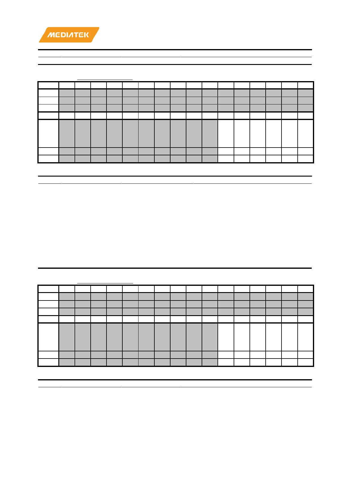
MT7686 Reference Manual
© 2016 - 2017 MediaTek Inc.
Page 468 of 536
This document contains information that is proprietary to MediaTek Inc. (“MediaTek”) and/or its licensor(s).
Any unauthorized use, reproduction or disclosure of this document in whole or in part is strictly prohibited.
Bit(s)
Mnemonic
Name
Description
0: Pull up; 1: Pull down;
A20D0044
PUPD_CFG1_SET
00000000
Bit
31
30
29
28
27
26
25
24
23
22
21
20
19
18
17
16
Name
Type
Reset
Bit
15
14
13
12
11
10
9
8
7
6
5
4
3
2
1
0
Name
pupd
_cfg_
set_g
pio_1
6
pupd
_cfg_
set_g
pio_1
5
pupd
_cfg_
set_g
pio_1
4
pupd
_cfg_
set_g
pio_1
3
pupd
_cfg_
set_g
pio_1
2
pupd
_cfg_
set_g
pio_1
1
Type
WO
WO
WO
WO
WO
WO
Reset
0
0
0
0
0
0
Bit(s)
Mnemonic
Name
Description
5
pupd_cfg_set_gpio_16
PAD_GPIO_16
0: Keep; 1: SET bit;
4
pupd_cfg_set_gpio_15
PAD_GPIO_15
0: Keep; 1: SET bit;
3
pupd_cfg_set_gpio_14
PAD_GPIO_14
0: Keep; 1: SET bit;
2
pupd_cfg_set_gpio_13
PAD_GPIO_13
0: Keep; 1: SET bit;
1
pupd_cfg_set_gpio_12
PAD_GPIO_12
0: Keep; 1: SET bit;
0
pupd_cfg_set_gpio_11
PAD_GPIO_11
0: Keep; 1: SET bit;
A20D0048
PUPD_CFG1_CLR
00000000
Bit
31
30
29
28
27
26
25
24
23
22
21
20
19
18
17
16
Name
Type
Reset
Bit
15
14
13
12
11
10
9
8
7
6
5
4
3
2
1
0
Name
pupd
_cfg_
clr_g
pio_1
6
pupd
_cfg_
clr_g
pio_1
5
pupd
_cfg_
clr_g
pio_1
4
pupd
_cfg_
clr_g
pio_1
3
pupd
_cfg_
clr_g
pio_1
2
pupd
_cfg_
clr_g
pio_1
1
Type
WO
WO
WO
WO
WO
WO
Reset
0
0
0
0
0
0
Bit(s)
Mnemonic
Name
Description
5
pupd_cfg_clr_gpio_16
PAD_GPIO_16
0: Keep; 1: Clear bit
4
pupd_cfg_clr_gpio_15
PAD_GPIO_15
0: Keep; 1: Clear bit
3
pupd_cfg_clr_gpio_14
PAD_GPIO_14
0: Keep; 1: Clear bit
2
pupd_cfg_clr_gpio_13
PAD_GPIO_13
0: Keep; 1: Clear bit
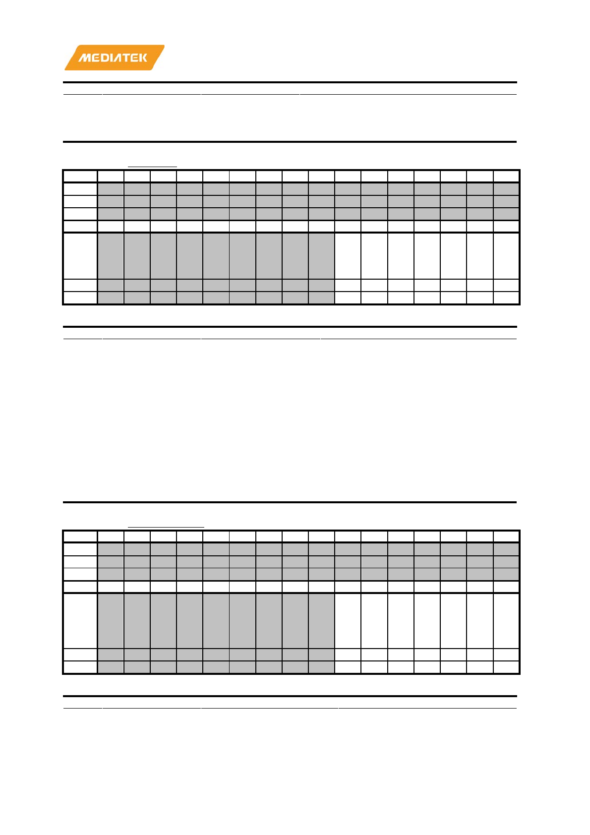
MT7686 Reference Manual
© 2016 - 2017 MediaTek Inc.
Page 469 of 536
This document contains information that is proprietary to MediaTek Inc. (“MediaTek”) and/or its licensor(s).
Any unauthorized use, reproduction or disclosure of this document in whole or in part is strictly prohibited.
Bit(s)
Mnemonic
Name
Description
1
pupd_cfg_clr_gpio_12
PAD_GPIO_12
0: Keep; 1: Clear bit
0
pupd_cfg_clr_gpio_11
PAD_GPIO_11
0: Keep; 1: Clear bit
A20D0050
PU_CFG1
00000074
Bit
31
30
29
28
27
26
25
24
23
22
21
20
19
18
17
16
Name
Type
Reset
Bit
15
14
13
12
11
10
9
8
7
6
5
4
3
2
1
0
Name
pu_cf
g_bo
nd_rs
v
pu_cf
g_bo
nd_sf
_sip
pu_cf
g_bo
nd_p
sram
_sip
pu_cf
g_gpi
o_20
pu_cf
g_gpi
o_19
pu_cf
g_gpi
o_18
pu_cf
g_gpi
o_17
Type
RW
RW
RW
RW
RW
RW
RW
Reset
1
1
1
0
1
0
0
Bit(s)
Mnemonic
Name
Description
6
pu_cfg_bond_rsv
PAD_BOND_RSV
0: Disable; 1: Enable;
5
pu_cfg_bond_sf_sip
PAD_BOND_SF_SIP
0: Disable; 1: Enable;
4
pu_cfg_bond_psram_sip
PAD_BOND_PSRAM_SIP
0: Disable; 1: Enable;
3
pu_cfg_gpio_20
PAD_GPIO_20
0: Disable; 1: Enable;
2
pu_cfg_gpio_19
PAD_GPIO_19
0: Disable; 1: Enable;
1
pu_cfg_gpio_18
PAD_GPIO_18
0: Disable; 1: Enable;
0
pu_cfg_gpio_17
PAD_GPIO_17
0: Disable; 1: Enable;
A20D0054
PU_CFG1_SET
00000000
Bit
31
30
29
28
27
26
25
24
23
22
21
20
19
18
17
16
Name
Type
Reset
Bit
15
14
13
12
11
10
9
8
7
6
5
4
3
2
1
0
Name
pu_cf
g_set
_bon
d_rsv
pu_cf
g_set
_bon
d_sf_
sip
pu_cf
g_set
_bon
d_psr
am_si
p
pu_cf
g_set
_gpio
_20
pu_cf
g_set
_gpio
_19
pu_cf
g_set
_gpio
_18
pu_cf
g_set
_gpio
_17
Type
WO
WO
WO
WO
WO
WO
WO
Reset
0
0
0
0
0
0
0
Bit(s)
Mnemonic
Name
Description
6
pu_cfg_set_bond_rsv
PAD_BOND_RSV
0: Keep; 1: SET bit;
5
pu_cfg_set_bond_sf_sip
PAD_BOND_SF_SIP
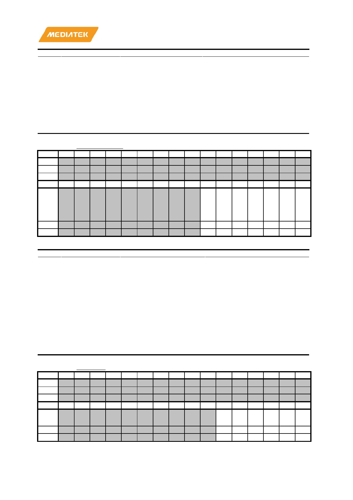
MT7686 Reference Manual
© 2016 - 2017 MediaTek Inc.
Page 470 of 536
This document contains information that is proprietary to MediaTek Inc. (“MediaTek”) and/or its licensor(s).
Any unauthorized use, reproduction or disclosure of this document in whole or in part is strictly prohibited.
Bit(s)
Mnemonic
Name
Description
0: Keep; 1: SET bit;
4
pu_cfg_set_bond_psram_sip
PAD_BOND_PSRAM_SIP
0: Keep; 1: SET bit;
3
pu_cfg_set_gpio_20
PAD_GPIO_20
0: Keep; 1: SET bit;
2
pu_cfg_set_gpio_19
PAD_GPIO_19
0: Keep; 1: SET bit;
1
pu_cfg_set_gpio_18
PAD_GPIO_18
0: Keep; 1: SET bit;
0
pu_cfg_set_gpio_17
PAD_GPIO_17
0: Keep; 1: SET bit;
A20D0058
PU_CFG1_CLR
00000000
Bit
31
30
29
28
27
26
25
24
23
22
21
20
19
18
17
16
Name
Type
Reset
Bit
15
14
13
12
11
10
9
8
7
6
5
4
3
2
1
0
Name
pu_cf
g_clr
_bon
d_rsv
pu_cf
g_clr
_bon
d_sf_
sip
pu_cf
g_clr
_bon
d_psr
am_si
p
pu_cf
g_clr
_gpio
_20
pu_cf
g_clr
_gpio
_19
pu_cf
g_clr
_gpio
_18
pu_cf
g_clr
_gpio
_17
Type
WO
WO
WO
WO
WO
WO
WO
Reset
0
0
0
0
0
0
0
Bit(s)
Mnemonic
Name
Description
6
pu_cfg_clr_bond_rsv
PAD_BOND_RSV
0: Keep; 1: Clear bit
5
pu_cfg_clr_bond_sf_sip
PAD_BOND_SF_SIP
0: Keep; 1: Clear bit
4
pu_cfg_clr_bond_psram_sip
PAD_BOND_PSRAM_SIP
0: Keep; 1: Clear bit
3
pu_cfg_clr_gpio_20
PAD_GPIO_20
0: Keep; 1: Clear bit
2
pu_cfg_clr_gpio_19
PAD_GPIO_19
0: Keep; 1: Clear bit
1
pu_cfg_clr_gpio_18
PAD_GPIO_18
0: Keep; 1: Clear bit
0
pu_cfg_clr_gpio_17
PAD_GPIO_17
0: Keep; 1: Clear bit
A20D0060
R0_CFG1
00000000
Bit
31
30
29
28
27
26
25
24
23
22
21
20
19
18
17
16
Name
Type
Reset
Bit
15
14
13
12
11
10
9
8
7
6
5
4
3
2
1
0
Name
r0_cf
g_gpi
o_16
r0_cf
g_gpi
o_15
r0_cf
g_gpi
o_14
r0_cf
g_gpi
o_13
r0_cf
g_gpi
o_12
r0_cf
g_gpi
o_11
Type
RW
RW
RW
RW
RW
RW
Reset
0
0
0
0
0
0
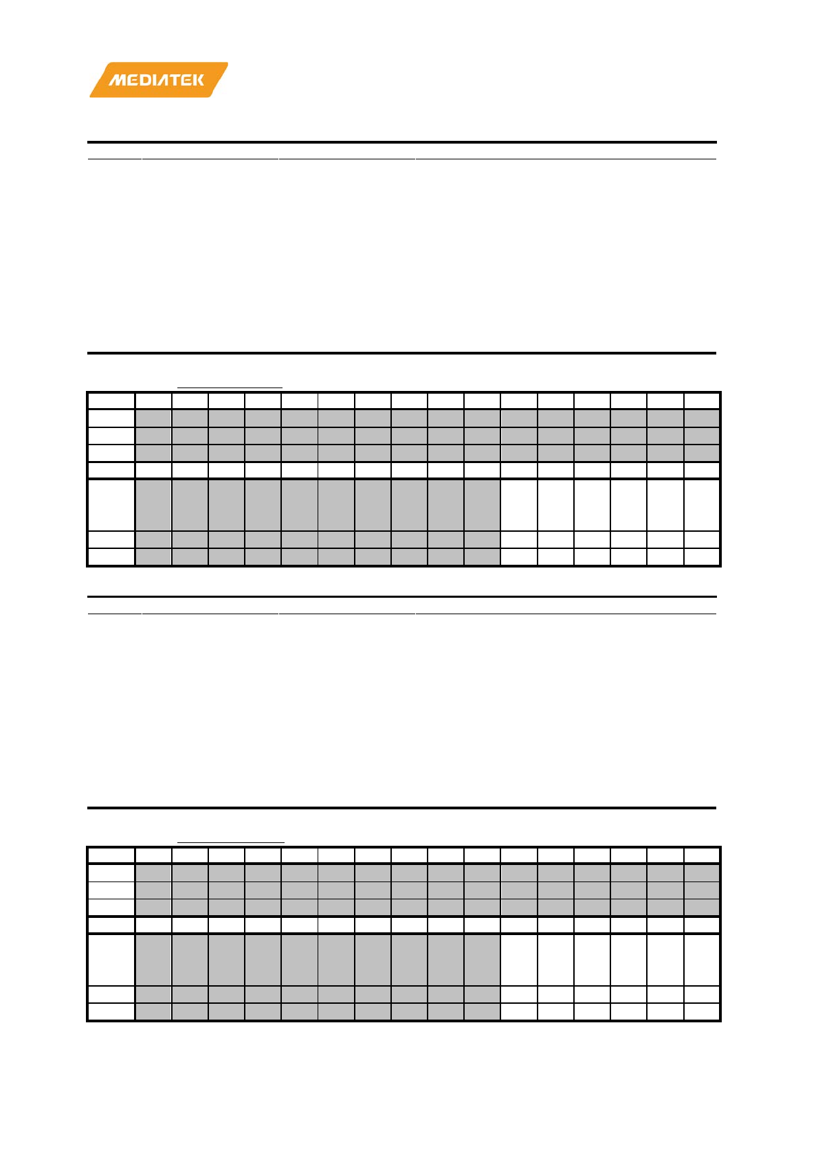
MT7686 Reference Manual
© 2016 - 2017 MediaTek Inc.
Page 471 of 536
This document contains information that is proprietary to MediaTek Inc. (“MediaTek”) and/or its licensor(s).
Any unauthorized use, reproduction or disclosure of this document in whole or in part is strictly prohibited.
Bit(s)
Mnemonic
Name
Description
5
r0_cfg_gpio_16
PAD_GPIO_16
0: Disable; 1: Enable;
4
r0_cfg_gpio_15
PAD_GPIO_15
0: Disable; 1: Enable;
3
r0_cfg_gpio_14
PAD_GPIO_14
0: Disable; 1: Enable;
2
r0_cfg_gpio_13
PAD_GPIO_13
0: Disable; 1: Enable;
1
r0_cfg_gpio_12
PAD_GPIO_12
0: Disable; 1: Enable;
0
r0_cfg_gpio_11
PAD_GPIO_11
0: Disable; 1: Enable;
A20D0064
R0_CFG1_SET
00000000
Bit
31
30
29
28
27
26
25
24
23
22
21
20
19
18
17
16
Name
Type
Reset
Bit
15
14
13
12
11
10
9
8
7
6
5
4
3
2
1
0
Name
r0_cf
g_set
_gpio
_16
r0_cf
g_set
_gpio
_15
r0_cf
g_set
_gpio
_14
r0_cf
g_set
_gpio
_13
r0_cf
g_set
_gpio
_12
r0_cf
g_set
_gpio
_11
Type
WO
WO
WO
WO
WO
WO
Reset
0
0
0
0
0
0
Bit(s)
Mnemonic
Name
Description
5
r0_cfg_set_gpio_16
PAD_GPIO_16
0: Keep; 1: SET bit;
4
r0_cfg_set_gpio_15
PAD_GPIO_15
0: Keep; 1: SET bit;
3
r0_cfg_set_gpio_14
PAD_GPIO_14
0: Keep; 1: SET bit;
2
r0_cfg_set_gpio_13
PAD_GPIO_13
0: Keep; 1: SET bit;
1
r0_cfg_set_gpio_12
PAD_GPIO_12
0: Keep; 1: SET bit;
0
r0_cfg_set_gpio_11
PAD_GPIO_11
0: Keep; 1: SET bit;
A20D0068
R0_CFG1_CLR
00000000
Bit
31
30
29
28
27
26
25
24
23
22
21
20
19
18
17
16
Name
Type
Reset
Bit
15
14
13
12
11
10
9
8
7
6
5
4
3
2
1
0
Name
r0_cf
g_clr
_gpio
_16
r0_cf
g_clr
_gpio
_15
r0_cf
g_clr
_gpio
_14
r0_cf
g_clr
_gpio
_13
r0_cf
g_clr
_gpio
_12
r0_cf
g_clr
_gpio
_11
Type
WO
WO
WO
WO
WO
WO
Reset
0
0
0
0
0
0
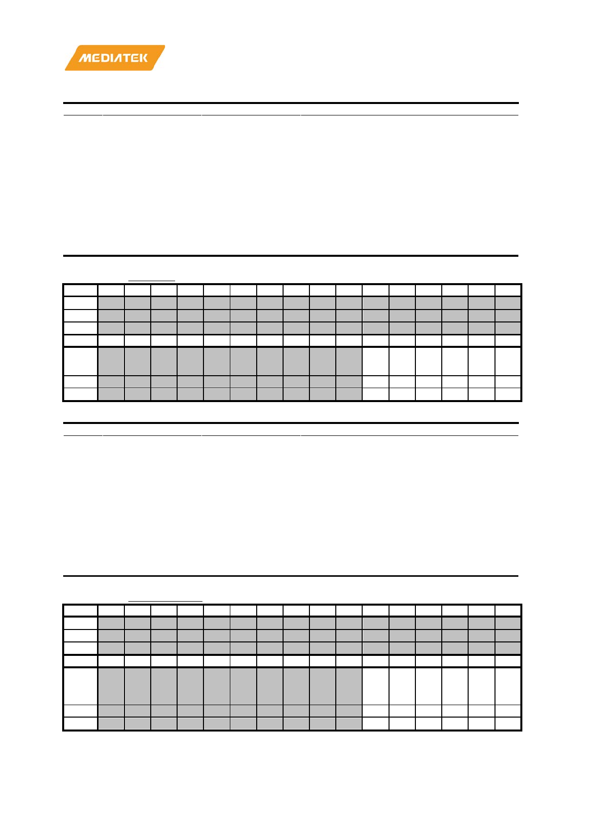
MT7686 Reference Manual
© 2016 - 2017 MediaTek Inc.
Page 472 of 536
This document contains information that is proprietary to MediaTek Inc. (“MediaTek”) and/or its licensor(s).
Any unauthorized use, reproduction or disclosure of this document in whole or in part is strictly prohibited.
Bit(s)
Mnemonic
Name
Description
5
r0_cfg_clr_gpio_16
PAD_GPIO_16
0: Keep; 1: Clear bit
4
r0_cfg_clr_gpio_15
PAD_GPIO_15
0: Keep; 1: Clear bit
3
r0_cfg_clr_gpio_14
PAD_GPIO_14
0: Keep; 1: Clear bit
2
r0_cfg_clr_gpio_13
PAD_GPIO_13
0: Keep; 1: Clear bit
1
r0_cfg_clr_gpio_12
PAD_GPIO_12
0: Keep; 1: Clear bit
0
r0_cfg_clr_gpio_11
PAD_GPIO_11
0: Keep; 1: Clear bit
A20D0070
R1_CFG1
0000003F
Bit
31
30
29
28
27
26
25
24
23
22
21
20
19
18
17
16
Name
Type
Reset
Bit
15
14
13
12
11
10
9
8
7
6
5
4
3
2
1
0
Name
r1_cf
g_gpi
o_16
r1_cf
g_gpi
o_15
r1_cf
g_gpi
o_14
r1_cf
g_gpi
o_13
r1_cf
g_gpi
o_12
r1_cf
g_gpi
o_11
Type
RW
RW
RW
RW
RW
RW
Reset
1
1
1
1
1
1
Bit(s)
Mnemonic
Name
Description
5
r1_cfg_gpio_16
PAD_GPIO_16
0: Disable; 1: Enable;
4
r1_cfg_gpio_15
PAD_GPIO_15
0: Disable; 1: Enable;
3
r1_cfg_gpio_14
PAD_GPIO_14
0: Disable; 1: Enable;
2
r1_cfg_gpio_13
PAD_GPIO_13
0: Disable; 1: Enable;
1
r1_cfg_gpio_12
PAD_GPIO_12
0: Disable; 1: Enable;
0
r1_cfg_gpio_11
PAD_GPIO_11
0: Disable; 1: Enable;
A20D0074
R1_CFG1_SET
00000000
Bit
31
30
29
28
27
26
25
24
23
22
21
20
19
18
17
16
Name
Type
Reset
Bit
15
14
13
12
11
10
9
8
7
6
5
4
3
2
1
0
Name
r1_cf
g_set
_gpio
_16
r1_cf
g_set
_gpio
_15
r1_cf
g_set
_gpio
_14
r1_cf
g_set
_gpio
_13
r1_cf
g_set
_gpio
_12
r1_cf
g_set
_gpio
_11
Type
WO
WO
WO
WO
WO
WO
Reset
0
0
0
0
0
0
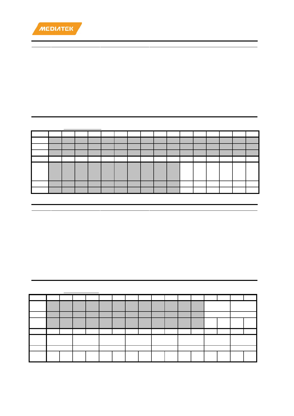
MT7686 Reference Manual
© 2016 - 2017 MediaTek Inc.
Page 473 of 536
This document contains information that is proprietary to MediaTek Inc. (“MediaTek”) and/or its licensor(s).
Any unauthorized use, reproduction or disclosure of this document in whole or in part is strictly prohibited.
Bit(s)
Mnemonic
Name
Description
5
r1_cfg_set_gpio_16
PAD_GPIO_16
0: Keep; 1: SET bit;
4
r1_cfg_set_gpio_15
PAD_GPIO_15
0: Keep; 1: SET bit;
3
r1_cfg_set_gpio_14
PAD_GPIO_14
0: Keep; 1: SET bit;
2
r1_cfg_set_gpio_13
PAD_GPIO_13
0: Keep; 1: SET bit;
1
r1_cfg_set_gpio_12
PAD_GPIO_12
0: Keep; 1: SET bit;
0
r1_cfg_set_gpio_11
PAD_GPIO_11
0: Keep; 1: SET bit;
A20D0078
R1_CFG1_CLR
00000000
Bit
31
30
29
28
27
26
25
24
23
22
21
20
19
18
17
16
Name
Type
Reset
Bit
15
14
13
12
11
10
9
8
7
6
5
4
3
2
1
0
Name
r1_cf
g_clr
_gpio
_16
r1_cf
g_clr
_gpio
_15
r1_cf
g_clr
_gpio
_14
r1_cf
g_clr
_gpio
_13
r1_cf
g_clr
_gpio
_12
r1_cf
g_clr
_gpio
_11
Type
WO
WO
WO
WO
WO
WO
Reset
0
0
0
0
0
0
Bit(s)
Mnemonic
Name
Description
5
r1_cfg_clr_gpio_16
PAD_GPIO_16
0: Keep; 1: Clear bit
4
r1_cfg_clr_gpio_15
PAD_GPIO_15
0: Keep; 1: Clear bit
3
r1_cfg_clr_gpio_14
PAD_GPIO_14
0: Keep; 1: Clear bit
2
r1_cfg_clr_gpio_13
PAD_GPIO_13
0: Keep; 1: Clear bit
1
r1_cfg_clr_gpio_12
PAD_GPIO_12
0: Keep; 1: Clear bit
0
r1_cfg_clr_gpio_11
PAD_GPIO_11
0: Keep; 1: Clear bit
A20D0080
RDSEL_CFG1
00000000
Bit
31
30
29
28
27
26
25
24
23
22
21
20
19
18
17
16
Nam
e
rdsel_cfg
_gpio_20
rdsel_cfg
_gpio_19
Type
RW
RW
Rese
t
0 0 0 0
Bit
15
14
13
12
11
10
9
8
7
6
5
4
3
2
1
0
Nam
e
rdsel_cfg
_gpio_18
rdsel_cfg
_gpio_17
rdsel_cfg
_gpio_16
rdsel_cfg
_gpio_15
rdsel_cfg
_gpio_14
rdsel_cfg
_gpio_13
rdsel_cfg
_gpio_12
rdsel_cfg
_gpio_11
Type
RW
RW
RW
RW
RW
RW
RW
RW
Rese
t
0 0 0 0 0 0 0 0 0 0 0 0 0 0 0 0

MT7686 Reference Manual
© 2016 - 2017 MediaTek Inc.
Page 474 of 536
This document contains information that is proprietary to MediaTek Inc. (“MediaTek”) and/or its licensor(s).
Any unauthorized use, reproduction or disclosure of this document in whole or in part is strictly prohibited.
Bit(s)
Mnemonic
Name
Description
19:18
rdsel_cfg_gpio_20
PAD_GPIO_20
00: minimum reception delay; 11: maximum reception
delay
17:16
rdsel_cfg_gpio_19
PAD_GPIO_19
00: minimum reception delay; 11: maximum reception
delay
15:14
rdsel_cfg_gpio_18
PAD_GPIO_18
00: minimum reception delay; 11: maximum reception
delay
13:12
rdsel_cfg_gpio_17
PAD_GPIO_17
00: minimum reception delay; 11: maximum reception
delay
11:10
rdsel_cfg_gpio_16
PAD_GPIO_16
00: minimum reception delay; 11: maximum reception
delay
9:8
rdsel_cfg_gpio_15
PAD_GPIO_15
00: minimum reception delay; 11: maximum reception
delay
7:6
rdsel_cfg_gpio_14
PAD_GPIO_14
00: minimum reception delay; 11: maximum reception
delay
5:4
rdsel_cfg_gpio_13
PAD_GPIO_13
00: minimum reception delay; 11: maximum reception
delay
3:2
rdsel_cfg_gpio_12
PAD_GPIO_12
00: minimum reception delay; 11: maximum reception
delay
1:0
rdsel_cfg_gpio_11
PAD_GPIO_11
00: minimum reception delay; 11: maximum reception
delay
A20D0084
RDSEL_CFG1_SET
00000000
Bit
31
30
29
28
27
26
25
24
23
22
21
20
19
18
17
16
Nam
e
rdsel_cfg
_set_gpio
_20
rdsel_cfg
_set_gpio
_19
Type
WO
WO
Rese
t
0 0 0 0
Bit
15
14
13
12
11
10
9
8
7
6
5
4
3
2
1
0
Nam
e
rdsel_cfg
_set_gpio
_18
rdsel_cfg
_set_gpio
_17
rdsel_cfg
_set_gpio
_16
rdsel_cfg
_set_gpio
_15
rdsel_cfg
_set_gpio
_14
rdsel_cfg
_set_gpio
_13
rdsel_cfg
_set_gpio
_12
rdsel_cfg
_set_gpio
_11
Type
WO
WO
WO
WO
WO
WO
WO
WO
Rese
t
0 0 0 0 0 0 0 0 0 0 0 0 0 0 0 0
Bit(s)
Mnemonic
Name
Description
19:18
rdsel_cfg_set_gpio_20
PAD_GPIO_20
0: Keep; 1: SET bit;
17:16
rdsel_cfg_set_gpio_19
PAD_GPIO_19
0: Keep; 1: SET bit;
15:14
rdsel_cfg_set_gpio_18
PAD_GPIO_18
0: Keep; 1: SET bit;
13:12
rdsel_cfg_set_gpio_17
PAD_GPIO_17
0: Keep; 1: SET bit;
11:10
rdsel_cfg_set_gpio_16
PAD_GPIO_16
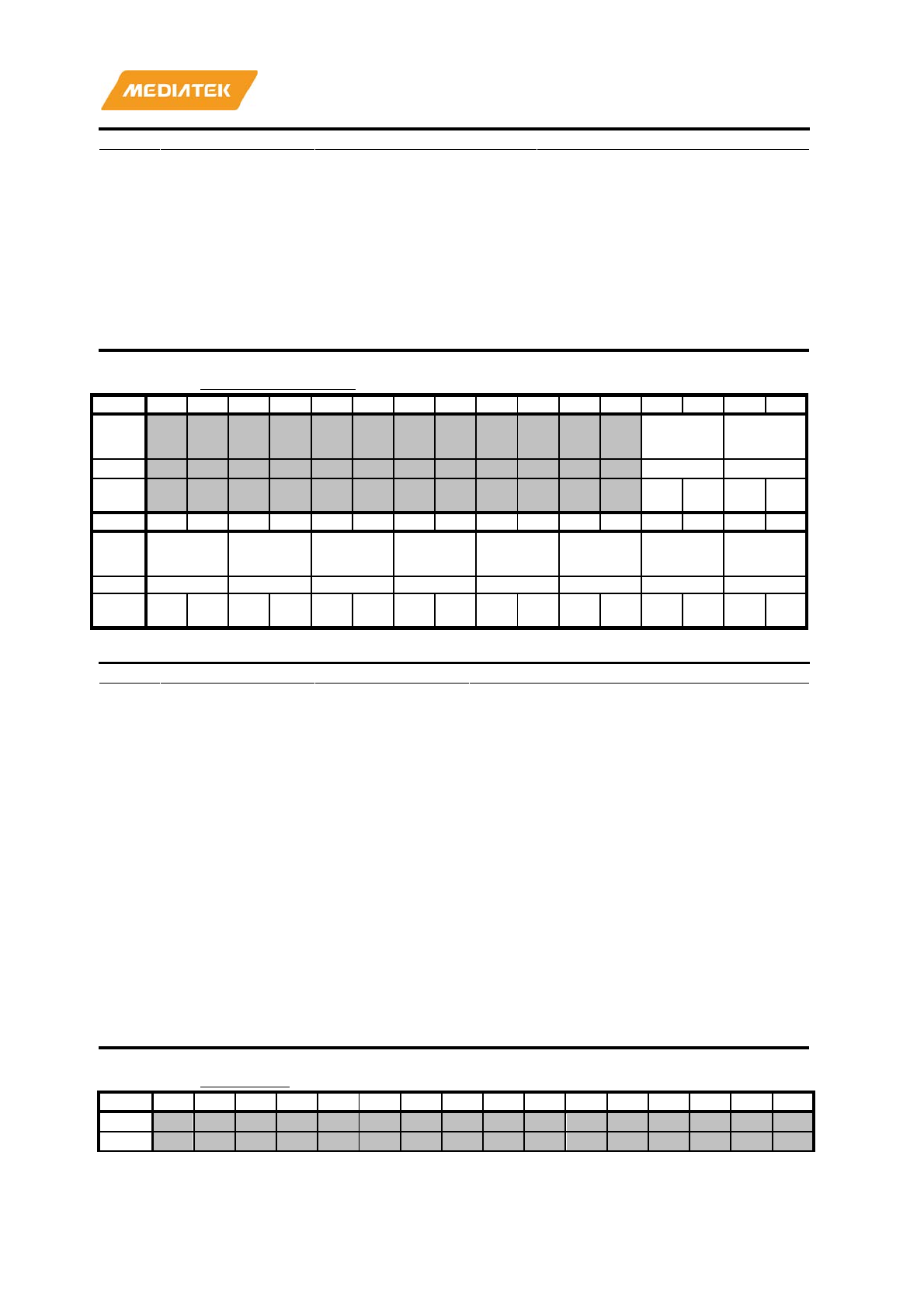
MT7686 Reference Manual
© 2016 - 2017 MediaTek Inc.
Page 475 of 536
This document contains information that is proprietary to MediaTek Inc. (“MediaTek”) and/or its licensor(s).
Any unauthorized use, reproduction or disclosure of this document in whole or in part is strictly prohibited.
Bit(s)
Mnemonic
Name
Description
0: Keep; 1: SET bit;
9:8
rdsel_cfg_set_gpio_15
PAD_GPIO_15
0: Keep; 1: SET bit;
7:6
rdsel_cfg_set_gpio_14
PAD_GPIO_14
0: Keep; 1: SET bit;
5:4
rdsel_cfg_set_gpio_13
PAD_GPIO_13
0: Keep; 1: SET bit;
3:2
rdsel_cfg_set_gpio_12
PAD_GPIO_12
0: Keep; 1: SET bit;
1:0
rdsel_cfg_set_gpio_11
PAD_GPIO_11
0: Keep; 1: SET bit;
A20D0088
RDSEL_CFG1_CLR
00000000
Bit
31
30
29
28
27
26
25
24
23
22
21
20
19
18
17
16
Nam
e
rdsel_cfg
_clr_gpio
_20
rdsel_cfg
_clr_gpio
_19
Type
WO
WO
Rese
t
0 0 0 0
Bit
15
14
13
12
11
10
9
8
7
6
5
4
3
2
1
0
Nam
e
rdsel_cfg
_clr_gpio
_18
rdsel_cfg
_clr_gpio
_17
rdsel_cfg
_clr_gpio
_16
rdsel_cfg
_clr_gpio
_15
rdsel_cfg
_clr_gpio
_14
rdsel_cfg
_clr_gpio
_13
rdsel_cfg
_clr_gpio
_12
rdsel_cfg
_clr_gpio
_11
Type
WO
WO
WO
WO
WO
WO
WO
WO
Rese
t
0 0 0 0 0 0 0 0 0 0 0 0 0 0 0 0
Bit(s)
Mnemonic
Name
Description
19:18
rdsel_cfg_clr_gpio_20
PAD_GPIO_20
0: Keep; 1: Clear bit
17:16
rdsel_cfg_clr_gpio_19
PAD_GPIO_19
0: Keep; 1: Clear bit
15:14
rdsel_cfg_clr_gpio_18
PAD_GPIO_18
0: Keep; 1: Clear bit
13:12
rdsel_cfg_clr_gpio_17
PAD_GPIO_17
0: Keep; 1: Clear bit
11:10
rdsel_cfg_clr_gpio_16
PAD_GPIO_16
0: Keep; 1: Clear bit
9:8
rdsel_cfg_clr_gpio_15
PAD_GPIO_15
0: Keep; 1: Clear bit
7:6
rdsel_cfg_clr_gpio_14
PAD_GPIO_14
0: Keep; 1: Clear bit
5:4
rdsel_cfg_clr_gpio_13
PAD_GPIO_13
0: Keep; 1: Clear bit
3:2
rdsel_cfg_clr_gpio_12
PAD_GPIO_12
0: Keep; 1: Clear bit
1:0
rdsel_cfg_clr_gpio_11
PAD_GPIO_11
0: Keep; 1: Clear bit
A20D0090
SMT_CFG1
00000000
Bit
31
30
29
28
27
26
25
24
23
22
21
20
19
18
17
16
Name
Type
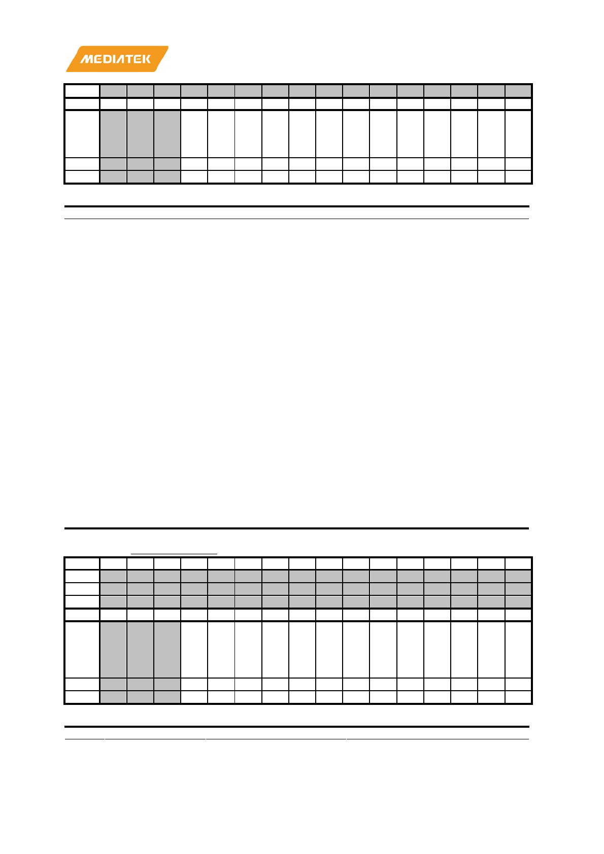
MT7686 Reference Manual
© 2016 - 2017 MediaTek Inc.
Page 476 of 536
This document contains information that is proprietary to MediaTek Inc. (“MediaTek”) and/or its licensor(s).
Any unauthorized use, reproduction or disclosure of this document in whole or in part is strictly prohibited.
Reset
Bit
15
14
13
12
11
10
9
8
7
6
5
4
3
2
1
0
Name
smt_c
fg_bo
nd_rs
v
smt_c
fg_bo
nd_sf
_sip
smt_c
fg_bo
nd_p
sram
_sip
smt_c
fg_gp
io_20
smt_c
fg_gp
io_19
smt_c
fg_gp
io_18
smt_c
fg_gp
io_17
smt_c
fg_gp
io_16
smt_c
fg_gp
io_15
smt_c
fg_gp
io_14
smt_c
fg_gp
io_13
smt_c
fg_gp
io_12
smt_
cfg_g
pio_1
1
Type
RW
RW
RW
RW
RW
RW
RW
RW
RW
RW
RW
RW
RW
Reset
0
0
0
0
0
0
0
0
0
0
0
0
0
Bit(s)
Mnemonic
Name
Description
12
smt_cfg_bond_rsv
PAD_BOND_RSV
0: Disable; 1: Enable;
11
smt_cfg_bond_sf_sip
PAD_BOND_SF_SIP
0: Disable; 1: Enable;
10
smt_cfg_bond_psram_sip
PAD_BOND_PSRAM_SIP
0: Disable; 1: Enable;
9
smt_cfg_gpio_20
PAD_GPIO_20
0: Disable; 1: Enable;
8
smt_cfg_gpio_19
PAD_GPIO_19
0: Disable; 1: Enable;
7
smt_cfg_gpio_18
PAD_GPIO_18
0: Disable; 1: Enable;
6
smt_cfg_gpio_17
PAD_GPIO_17
0: Disable; 1: Enable;
5
smt_cfg_gpio_16
PAD_GPIO_16
0: Disable; 1: Enable;
4
smt_cfg_gpio_15
PAD_GPIO_15
0: Disable; 1: Enable;
3
smt_cfg_gpio_14
PAD_GPIO_14
0: Disable; 1: Enable;
2
smt_cfg_gpio_13
PAD_GPIO_13
0: Disable; 1: Enable;
1
smt_cfg_gpio_12
PAD_GPIO_12
0: Disable; 1: Enable;
0
smt_cfg_gpio_11
PAD_GPIO_11
0: Disable; 1: Enable;
A20D0094
SMT_CFG1_SET
00000000
Bit
31
30
29
28
27
26
25
24
23
22
21
20
19
18
17
16
Name
Type
Reset
Bit
15
14
13
12
11
10
9
8
7
6
5
4
3
2
1
0
Name
smt_c
fg_set
_bon
d_rsv
smt_c
fg_set
_bon
d_sf_
sip
smt_c
fg_set
_bon
d_psr
am_si
p
smt_c
fg_set
_gpio
_20
smt_c
fg_set
_gpio
_19
smt_c
fg_set
_gpio
_18
smt_c
fg_set
_gpio
_17
smt_c
fg_set
_gpio
_16
smt_c
fg_set
_gpio
_15
smt_c
fg_set
_gpio
_14
smt_c
fg_set
_gpio
_13
smt_c
fg_set
_gpio
_12
smt_
cfg_s
et_gp
io_11
Type
WO
WO
WO
WO
WO
WO
WO
WO
WO
WO
WO
WO
WO
Reset
0
0
0
0
0
0
0
0
0
0
0
0
0
Bit(s)
Mnemonic
Name
Description
12
smt_cfg_set_bond_rsv
PAD_BOND_RSV
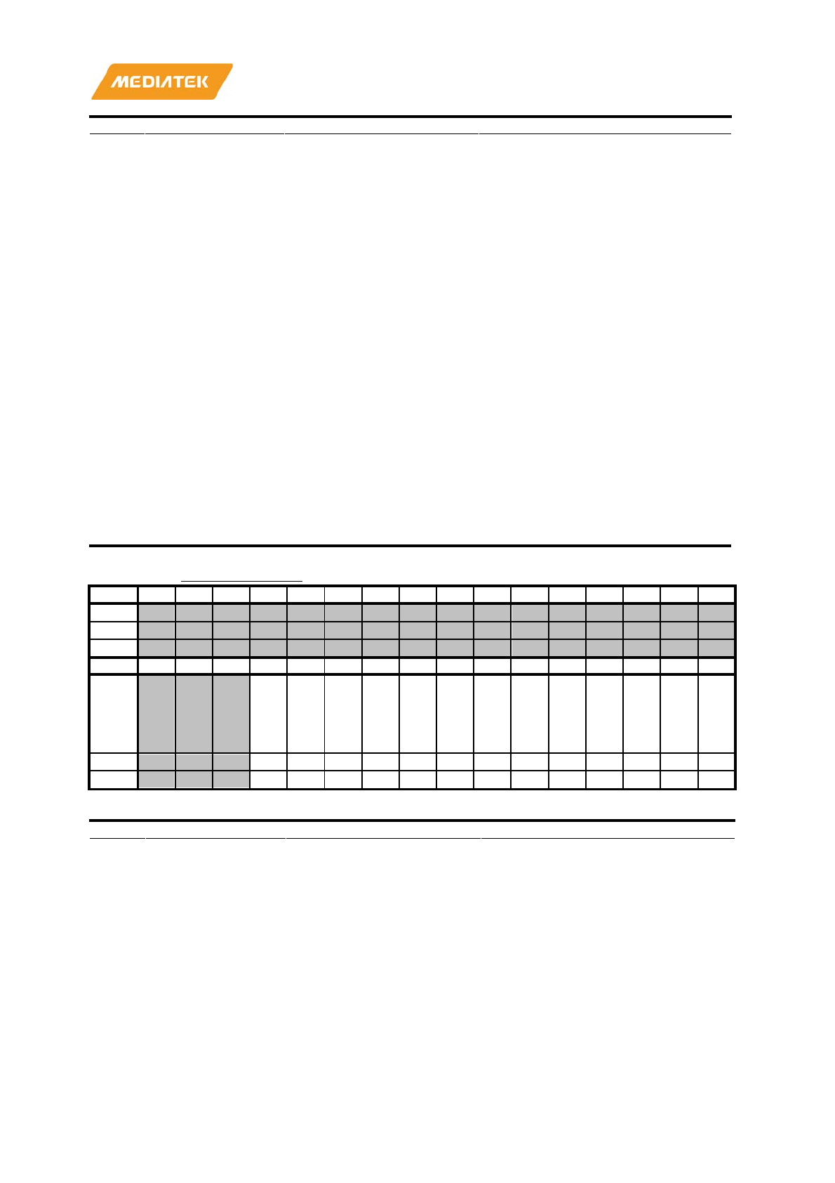
MT7686 Reference Manual
© 2016 - 2017 MediaTek Inc.
Page 477 of 536
This document contains information that is proprietary to MediaTek Inc. (“MediaTek”) and/or its licensor(s).
Any unauthorized use, reproduction or disclosure of this document in whole or in part is strictly prohibited.
Bit(s)
Mnemonic
Name
Description
0: Keep; 1: SET bit;
11
smt_cfg_set_bond_sf_sip
PAD_BOND_SF_SIP
0: Keep; 1: SET bit;
10
smt_cfg_set_bond_psram_sip
PAD_BOND_PSRAM_SIP
0: Keep; 1: SET bit;
9
smt_cfg_set_gpio_20
PAD_GPIO_20
0: Keep; 1: SET bit;
8
smt_cfg_set_gpio_19
PAD_GPIO_19
0: Keep; 1: SET bit;
7
smt_cfg_set_gpio_18
PAD_GPIO_18
0: Keep; 1: SET bit;
6
smt_cfg_set_gpio_17
PAD_GPIO_17
0: Keep; 1: SET bit;
5
smt_cfg_set_gpio_16
PAD_GPIO_16
0: Keep; 1: SET bit;
4
smt_cfg_set_gpio_15
PAD_GPIO_15
0: Keep; 1: SET bit;
3
smt_cfg_set_gpio_14
PAD_GPIO_14
0: Keep; 1: SET bit;
2
smt_cfg_set_gpio_13
PAD_GPIO_13
0: Keep; 1: SET bit;
1
smt_cfg_set_gpio_12
PAD_GPIO_12
0: Keep; 1: SET bit;
0
smt_cfg_set_gpio_11
PAD_GPIO_11
0: Keep; 1: SET bit;
A20D0098
SMT_CFG1_CLR
00000000
Bit
31
30
29
28
27
26
25
24
23
22
21
20
19
18
17
16
Name
Type
Reset
Bit
15
14
13
12
11
10
9
8
7
6
5
4
3
2
1
0
Name
smt_c
fg_clr
_bon
d_rsv
smt_c
fg_clr
_bon
d_sf_
sip
smt_c
fg_clr
_bon
d_psr
am_si
p
smt_c
fg_clr
_gpio
_20
smt_c
fg_clr
_gpio
_19
smt_c
fg_clr
_gpio
_18
smt_c
fg_clr
_gpio
_17
smt_c
fg_clr
_gpio
_16
smt_c
fg_clr
_gpio
_15
smt_c
fg_clr
_gpio
_14
smt_c
fg_clr
_gpio
_13
smt_c
fg_clr
_gpio
_12
smt_
cfg_cl
r_gpi
o_11
Type
WO
WO
WO
WO
WO
WO
WO
WO
WO
WO
WO
WO
WO
Reset
0
0
0
0
0
0
0
0
0
0
0
0
0
Bit(s)
Mnemonic
Name
Description
12
smt_cfg_clr_bond_rsv
PAD_BOND_RSV
0: Keep; 1: Clear bit
11
smt_cfg_clr_bond_sf_sip
PAD_BOND_SF_SIP
0: Keep; 1: Clear bit
10
smt_cfg_clr_bond_psram_sip
PAD_BOND_PSRAM_SIP
0: Keep; 1: Clear bit
9
smt_cfg_clr_gpio_20
PAD_GPIO_20
0: Keep; 1: Clear bit
8
smt_cfg_clr_gpio_19
PAD_GPIO_19
0: Keep; 1: Clear bit
7
smt_cfg_clr_gpio_18
PAD_GPIO_18
0: Keep; 1: Clear bit
6
smt_cfg_clr_gpio_17
PAD_GPIO_17
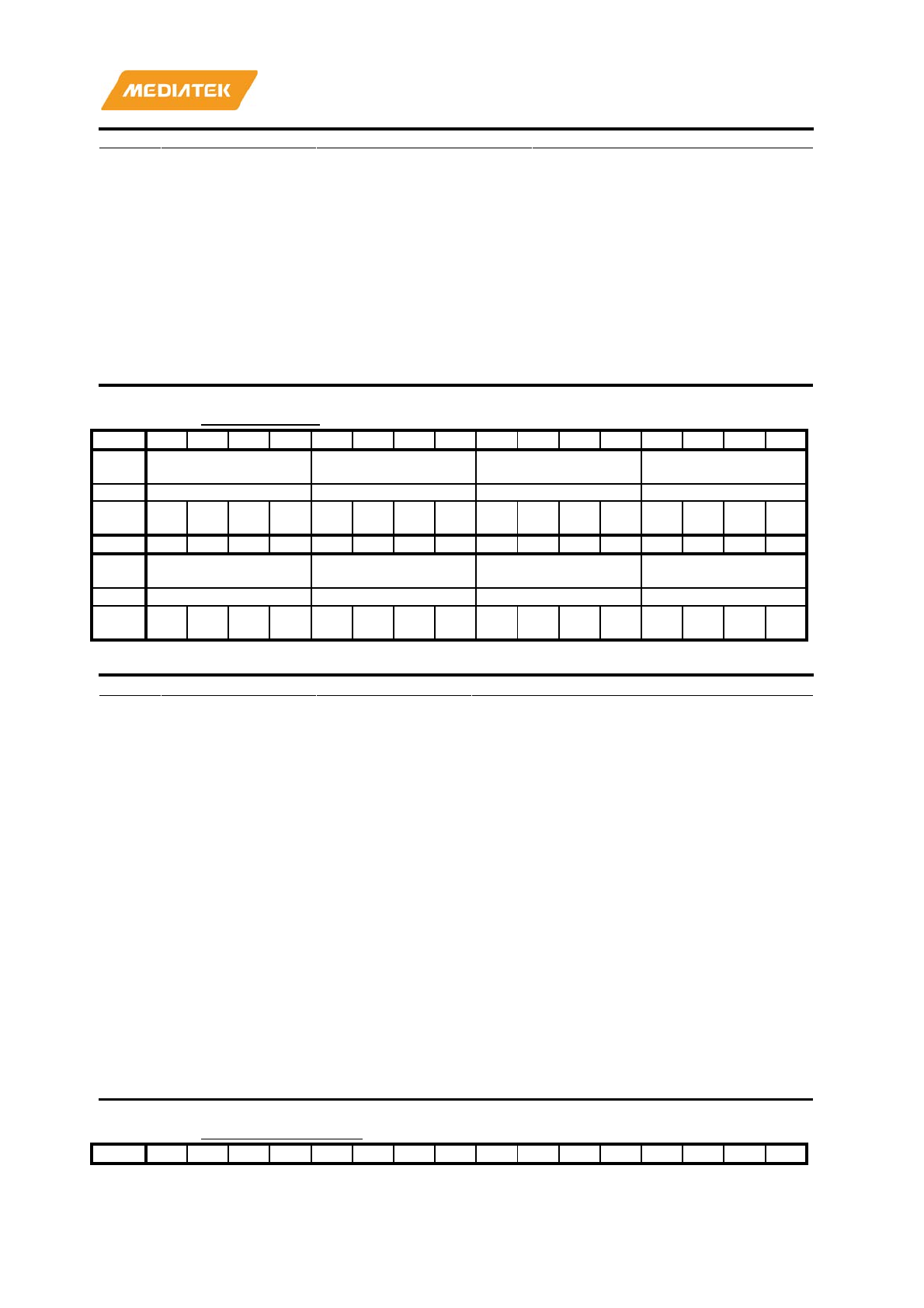
MT7686 Reference Manual
© 2016 - 2017 MediaTek Inc.
Page 478 of 536
This document contains information that is proprietary to MediaTek Inc. (“MediaTek”) and/or its licensor(s).
Any unauthorized use, reproduction or disclosure of this document in whole or in part is strictly prohibited.
Bit(s)
Mnemonic
Name
Description
0: Keep; 1: Clear bit
5
smt_cfg_clr_gpio_16
PAD_GPIO_16
0: Keep; 1: Clear bit
4
smt_cfg_clr_gpio_15
PAD_GPIO_15
0: Keep; 1: Clear bit
3
smt_cfg_clr_gpio_14
PAD_GPIO_14
0: Keep; 1: Clear bit
2
smt_cfg_clr_gpio_13
PAD_GPIO_13
0: Keep; 1: Clear bit
1
smt_cfg_clr_gpio_12
PAD_GPIO_12
0: Keep; 1: Clear bit
0
smt_cfg_clr_gpio_11
PAD_GPIO_11
0: Keep; 1: Clear bit
A20D00B0
TDSEL_CFG10
AAAAAAAA
Bit
31
30
29
28
27
26
25
24
23
22
21
20
19
18
17
16
Nam
e
tdsel_cfg_gpio_18 tdsel_cfg_gpio_17 tdsel_cfg_gpio_16 tdsel_cfg_gpio_15
Type
RW
RW
RW
RW
Rese
t
1 0 1 0 1 0 1 0 1 0 1 0 1 0 1 0
Bit
15
14
13
12
11
10
9
8
7
6
5
4
3
2
1
0
Nam
e
tdsel_cfg_gpio_14 tdsel_cfg_gpio_13 tdsel_cfg_gpio_12 tdsel_cfg_gpio_11
Type
RW
RW
RW
RW
Rese
t
1 0 1 0 1 0 1 0 1 0 1 0 1 0 1 0
Bit(s)
Mnemonic
Name
Description
31:28
tdsel_cfg_gpio_18
PAD_GPIO_18
0000: minimum transmission delay; 1111: maximum
transmission delay
27:24
tdsel_cfg_gpio_17
PAD_GPIO_17
0000: minimum transmission delay; 1111: maximum
transmission delay
23:20
tdsel_cfg_gpio_16
PAD_GPIO_16
0000: minimum transmission delay; 1111: maximum
transmission delay
19:16
tdsel_cfg_gpio_15
PAD_GPIO_15
0000: minimum transmission delay; 1111: maximum
transmission delay
15:12
tdsel_cfg_gpio_14
PAD_GPIO_14
0000: minimum transmission delay; 1111: maximum
transmission delay
11:8
tdsel_cfg_gpio_13
PAD_GPIO_13
0000: minimum transmission delay; 1111: maximum
transmission delay
7:4
tdsel_cfg_gpio_12
PAD_GPIO_12
0000: minimum transmission delay; 1111: maximum
transmission delay
3:0
tdsel_cfg_gpio_11
PAD_GPIO_11
0000: minimum transmission delay; 1111: maximum
transmission delay
A20D00B4
TDSEL_CFG10_SET
00000000
Bit
31
30
29
28
27
26
25
24
23
22
21
20
19
18
17
16
MT7686 Reference Manual
© 2016 - 2017 MediaTek Inc.
Page 479 of 536
This document contains information that is proprietary to MediaTek Inc. (“MediaTek”) and/or its licensor(s).
Any unauthorized use, reproduction or disclosure of this document in whole or in part is strictly prohibited.
Nam
e
tdsel_cfg_set_gpio_18 tdsel_cfg_set_gpio_17 tdsel_cfg_set_gpio_16 tdsel_cfg_set_gpio_15
Type
WO
WO
WO
WO
Rese
t
0 0 0 0 0 0 0 0 0 0 0 0 0 0 0 0
Bit
15
14
13
12
11
10
9
8
7
6
5
4
3
2
1
0
Nam
e
tdsel_cfg_set_gpio_14 tdsel_cfg_set_gpio_13 tdsel_cfg_set_gpio_12 tdsel_cfg_set_gpio_11
Type
WO
WO
WO
WO
Rese
t
0 0 0 0 0 0 0 0 0 0 0 0 0 0 0 0
Bit(s)
Mnemonic
Name
Description
31:28
tdsel_cfg_set_gpio_18
PAD_GPIO_18
0: Keep; 1: SET bit;
27:24
tdsel_cfg_set_gpio_17
PAD_GPIO_17
0: Keep; 1: SET bit;
23:20
tdsel_cfg_set_gpio_16
PAD_GPIO_16
0: Keep; 1: SET bit;
19:16
tdsel_cfg_set_gpio_15
PAD_GPIO_15
0: Keep; 1: SET bit;
15:12
tdsel_cfg_set_gpio_14
PAD_GPIO_14
0: Keep; 1: SET bit;
11:8
tdsel_cfg_set_gpio_13
PAD_GPIO_13
0: Keep; 1: SET bit;
7:4
tdsel_cfg_set_gpio_12
PAD_GPIO_12
0: Keep; 1: SET bit;
3:0
tdsel_cfg_set_gpio_11
PAD_GPIO_11
0: Keep; 1: SET bit;
A20D00B8
TDSEL_CFG10_CLR
00000000
Bit
31
30
29
28
27
26
25
24
23
22
21
20
19
18
17
16
Nam
e
tdsel_cfg_clr_gpio_18 tdsel_cfg_clr_gpio_17 tdsel_cfg_clr_gpio_16 tdsel_cfg_clr_gpio_15
Type
WO
WO
WO
WO
Rese
t
0 0 0 0 0 0 0 0 0 0 0 0 0 0 0 0
Bit
15
14
13
12
11
10
9
8
7
6
5
4
3
2
1
0
Nam
e
tdsel_cfg_clr_gpio_14 tdsel_cfg_clr_gpio_13 tdsel_cfg_clr_gpio_12 tdsel_cfg_clr_gpio_11
Type
WO
WO
WO
WO
Rese
t
0 0 0 0 0 0 0 0 0 0 0 0 0 0 0 0
Bit(s)
Mnemonic
Name
Description
31:28
tdsel_cfg_clr_gpio_18
PAD_GPIO_18
0: Keep; 1: Clear bit
27:24
tdsel_cfg_clr_gpio_17
PAD_GPIO_17
0: Keep; 1: Clear bit
23:20
tdsel_cfg_clr_gpio_16
PAD_GPIO_16
0: Keep; 1: Clear bit
19:16
tdsel_cfg_clr_gpio_15
PAD_GPIO_15
0: Keep; 1: Clear bit
15:12
tdsel_cfg_clr_gpio_14
PAD_GPIO_14
0: Keep; 1: Clear bit
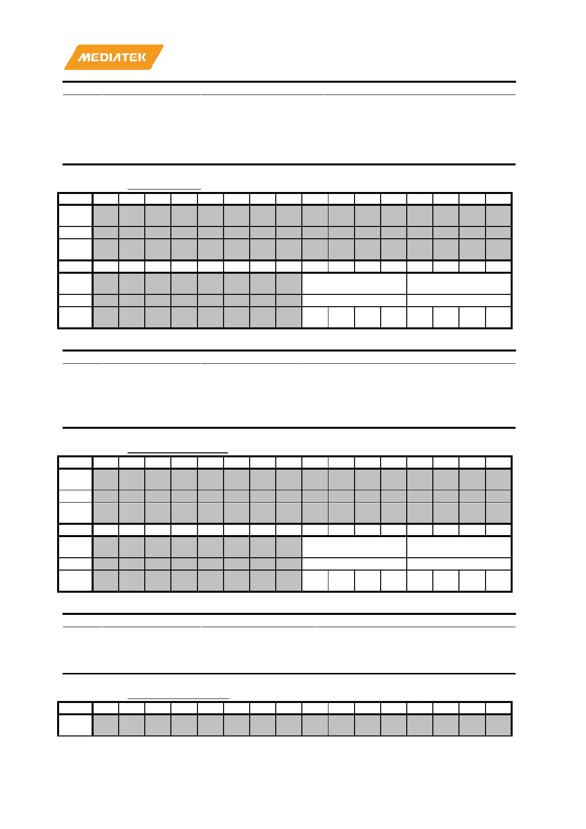
MT7686 Reference Manual
© 2016 - 2017 MediaTek Inc.
Page 480 of 536
This document contains information that is proprietary to MediaTek Inc. (“MediaTek”) and/or its licensor(s).
Any unauthorized use, reproduction or disclosure of this document in whole or in part is strictly prohibited.
Bit(s)
Mnemonic
Name
Description
11:8
tdsel_cfg_clr_gpio_13
PAD_GPIO_13
0: Keep; 1: Clear bit
7:4
tdsel_cfg_clr_gpio_12
PAD_GPIO_12
0: Keep; 1: Clear bit
3:0
tdsel_cfg_clr_gpio_11
PAD_GPIO_11
0: Keep; 1: Clear bit
A20D00C0
TDSEL_CFG11
000000AA
Bit
31
30
29
28
27
26
25
24
23
22
21
20
19
18
17
16
Nam
e
Type
Rese
t
Bit
15
14
13
12
11
10
9
8
7
6
5
4
3
2
1
0
Nam
e
tdsel_cfg_gpio_20 tdsel_cfg_gpio_19
Type
RW
RW
Rese
t
1 0 1 0 1 0 1 0
Bit(s)
Mnemonic
Name
Description
7:4
tdsel_cfg_gpio_20
PAD_GPIO_20
0000: minimum transmission delay; 1111: maximum
transmission delay
3:0
tdsel_cfg_gpio_19
PAD_GPIO_19
0000: minimum transmission delay; 1111: maximum
transmission delay
A20D00C4
TDSEL_CFG11_SET
00000000
Bit
31
30
29
28
27
26
25
24
23
22
21
20
19
18
17
16
Nam
e
Type
Rese
t
Bit
15
14
13
12
11
10
9
8
7
6
5
4
3
2
1
0
Nam
e
tdsel_cfg_set_gpio_20 tdsel_cfg_set_gpio_19
Type
WO
WO
Rese
t
0 0 0 0 0 0 0 0
Bit(s)
Mnemonic
Name
Description
7:4
tdsel_cfg_set_gpio_20
PAD_GPIO_20
0: Keep; 1: SET bit;
3:0
tdsel_cfg_set_gpio_19
PAD_GPIO_19
0: Keep; 1: SET bit;
A20D00C8
TDSEL_CFG11_CLR
00000000
Bit
31
30
29
28
27
26
25
24
23
22
21
20
19
18
17
16
Nam
e

MT7686 Reference Manual
© 2016 - 2017 MediaTek Inc.
Page 481 of 536
This document contains information that is proprietary to MediaTek Inc. (“MediaTek”) and/or its licensor(s).
Any unauthorized use, reproduction or disclosure of this document in whole or in part is strictly prohibited.
Type
Rese
t
Bit
15
14
13
12
11
10
9
8
7
6
5
4
3
2
1
0
Nam
e
tdsel_cfg_clr_gpio_20 tdsel_cfg_clr_gpio_19
Type
WO
WO
Rese
t
0 0 0 0 0 0 0 0
Bit(s)
Mnemonic
Name
Description
7:4
tdsel_cfg_clr_gpio_20
PAD_GPIO_20
0: Keep; 1: Clear bit
3:0
tdsel_cfg_clr_gpio_19
PAD_GPIO_19
0: Keep; 1: Clear bit

MT7686 Reference Manual
© 2016 - 2017 MediaTek Inc.
Page 482 of 536
This document contains information that is proprietary to MediaTek Inc. (“MediaTek”) and/or its licensor(s).
Any unauthorized use, reproduction or disclosure of this document in whole or in part is strictly prohibited.
22. Clock Configuration
The clock configuration including the clock frequency settings and measuring methods are described.
The clock settings to be configured:
• Slow BUS clock and related peripheral clock
• Cortex-M4 MCU and fast BUS clock and related peripheral clock
• Serial Flash Controller (SFC)
• MSDC (SDIOMST)
• SPI Master (SPIMST)
• Clock frequency measuring methods
22.1. Clock configuration programming guide
The clock settings are configured by control registers (CRs) that control clock dividers and multiplexers (MUXs).
This section describes how to switch clock source or frequency for system and peripheral devices and clock turn
on/off methods. The clock source architecture is shown in Figure 22.1-1. The clock multiplexers of each clock are
listed in Table 22.1-1.
General clock switch sequence is:
1) Turn on the PLL divider
2) Select the clock frequency
3) Ensure successful clock frequency switch
4) Trigger clock change bit
5) Poll clock change status
Note, that before switching clock frequencies, wait for the enabled clock to stabilize. Also, follow the minimum
VCORE voltage limitation, or there will be timing violation issues. Clocks derived from BBPLL1 cannot be used when
RF_WBAC0[16] is 0 (BBPLL1 is 832MHz).
M
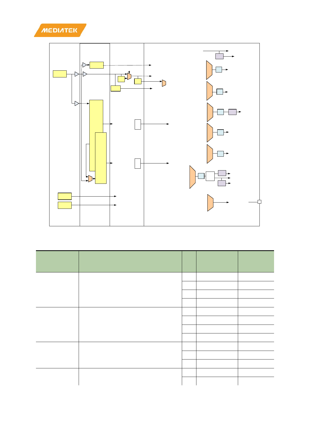
MT7686 Reference Manual
© 2016 - 2017 MediaTek Inc.
Page 483 of 536
This document contains information that is proprietary to MediaTek Inc. (“MediaTek”) and/or its licensor(s).
Any unauthorized use, reproduction or disclosure of this document in whole or in part is strictly prohibited.
XO
BBPLL1
PLLs
BBPLL2
Frequency Divider
XPLL
To general XO domain
controller clock
Clock source
AD_BBPLL2_CK /M BBPLL2_DIVM_CK
F_FXO_CK
AD_BBPLL1_CK /N BBPLL1_DIVN_CK
To SDIOMST
To SFC
To CONN
(connsys /2 to get
N9 160MHz
BBPLL2_DIVM_CK
(192MHz)
To CM4 (F
CPU
)
/Z
/2Z
To memory bus and
peri bus (FBUS)
Clock Switch and CG/DCM
EOSC32K
XOSC32KEOSC32K
XOSC32K
To Real Time
Counter
or 32K domain
EOSC32K
XOSC32K
BBPLL2_DIVM_CK
(320MHz)
BBPLL2_DIVM_CK
(80MHz)
BBPLL2_DIVM_CK
(48MHz)
CLKOUT
F_FXO_CK
F_FXO_CK
F_FXO_CK
F_FXO_CK
F_FXO_CK
BBPLL1_DIVN_CK
To XTRALCTL
To SPIMST
BBPLL2_DIVM_CK
(96MHz)
F_FXO_CK
BBPLL1_DIVN_CK
BBPLL1_DIVN_CK
F_FRTC_CK
To I2S
AD_XPLL_CK
(24.576MHz/22.5792
MHz)
/2
/1221
/794
1
0
1
0
/2 To GPTIMER
XO_DIV_32K_CK
XO_DIV_32K_CK
f_fxo_is_26m
DCM
CG
CG
CG
CG
CG
CG
To slow BUS (F
xo
)
To general BUS domain
controller clock
DCG
DCM
DCM
F_FRTC_CK
AD_XO_BBTOP_CK
AD_XO_BBTOP_CK
1. 40MHz
2. 26MHz
HF_FSYS_CK
F_FXTALCTL_CK
HF_FCONN_CK
HF_SFC_CK
F_SPIMST_CK
F_SDIOMST_CK
1
0
F_FRTC_CK
F_FXO_D2_CK
Figure 22.1-1. Clock source architecture
Table 22.1-1. Clock switch
Clock name
MUX select register
(active when CHG=1)
SEL MUX select
option
Clock
frequency
(MHz)
HF_FSYS_CK CKSYS_CLK_CFG_0__F_CLK_SYS_SEL 0 xo_ck 26/20
1 BBPLL2_D5 192
2 BBPLL2_D5_D2 96
3 BBPLL1_D7 148.5714286
HF_FSFC_CK
CKSYS_CLK_CFG_0__F_CLK_SFC_SEL 0 xo_ck 26/20
1 BBPLL2_D3_D4 80
2 BBPLL2_D15 64
3 BBPLL1_D7_D2 74.28571429
F_FSPIMST_CK
CKSYS_CLK_CFG_0__F_CLK_SPIMST_SEL 0 xo_ck 26/20
1 BBPLL2_D5_D4 48
2 BBPLL2_D5_D2 96
F_FSDIOMST_CK
CKSYS_CLK_CFG_1__F_CLK_SDIOMST_SEL
0 xo_ck 26/20
1 BBPLL2_D5_D8 24

MT7686 Reference Manual
© 2016 - 2017 MediaTek Inc.
Page 484 of 536
This document contains information that is proprietary to MediaTek Inc. (“MediaTek”) and/or its licensor(s).
Any unauthorized use, reproduction or disclosure of this document in whole or in part is strictly prohibited.
Clock name
MUX select register
(active when CHG=1)
SEL MUX select
option
Clock
frequency
(MHz)
2 BBPLL2_D5_D4 48
Note 1: The MUX select register naming (CKSYS_CLK_CFG_0__F_CLK_SYS_SEL) is in two parts - register address
name (CKSYS_CLK_CFG_0) and register bit name (F_CLK_SYS_SEL).
Note 2: BBPLL2_D5_D2 means BBPLL2 (960MHz) is divided by 5 and then divided by 2 (equal to divide by 10)
22.1.1. Clock configuration for slow bus clock peripherals
Several slow bus clock peripherals (SEJ, AUXADC, eFUSE and more) share the same bus clock (FXO). The clock
output of these peripherals is gated by clock gating cells. To turn on these clocks, the related power down (PDN)
bit must be set. XO_PDN_SETD0 is used to turn off the clock, while XO_PDN_CLRD0 is used to turn on the clock.
XO_PDN_COND0 is used to read configuration results (0: Clock is turned on; 1: Clock is gated off). Relationships
between XO_PDN_COND0 bit numbers and different configure register names are shown in Table 22.1-2.
Table 22.1-2. Relationship between XO_PDN_COND0 bit number and configuration register
Crystal oscillator power down conditions
XO_PDN_CON0[bit number]
Configuration register
XO_PDN_CON0[18] RG_SW_EFUSE_CG
XO_PDN_CON0[17] RG_SW_GPTIMER_CG
XO_PDN_CON0[16] RG_SW_SPM_CG
XO_PDN_CON0[9] RG_SW_PWM5_CG
XO_PDN_CON0[8] RG_SW_PWM4_CG
XO_PDN_CON0[7] RG_SW_PWM3_CG
XO_PDN_CON0[6] RG_SW_PWM2_CG
XO_PDN_CON0[5] RG_SW_PWM1_CG
XO_PDN_CON0[4] RG_SW_PWM0_CG
XO_PDN_CON0[3] RG_SW_SEJ_CG
An example to turn on the clock source of PWM0:
• Write: XO_PDN_CLRD0 = 0x10
• Read XO_PDN_COND0 = 0xFFEF
An example to turn off the clock source of PWMC0:
• Write: XO_PDN_SETD0 = 0x10
• Read XO_PDN_COND0 = 0xFFFF

MT7686 Reference Manual
© 2016 - 2017 MediaTek Inc.
Page 485 of 536
This document contains information that is proprietary to MediaTek Inc. (“MediaTek”) and/or its licensor(s).
Any unauthorized use, reproduction or disclosure of this document in whole or in part is strictly prohibited.
22.1.2. Clock configuration for Cortex-M4 MCU and fast bus clock peripherals
The system clock (HF_FSYS_CK) supports F_FXO_CK clock (26MHz or 20MHz), 96MHz and maximum 192MHz
(divided from PLL). The clock multiplexer switch method of HF_FSYS_CK is in Table 22.1-3.
An example of switching HF_FSYS_CK to 96MHz:
Table 22.1-3. Clock multiplexer switch method of HF_FSYS_CK
Action Parameter Value
Write CKSYS_CLK_DIV_1__F_CLK_PLL2_D5_EN 0 x 1
Write CKSYS_CLK_DIV_2__F_CLK_PLL2_DIV_EN 0 x 1
Write CKSYS_CLK_CFG_0__F_CLK_SYS_SEL 0 x 2
Write CKSYS_CLK_FORCE_ON_0__F_CLK_SYS_FORCE_ON
0 x 1
Write CKSYS_CLK_UPDATE_0__F_CHG_SYS 0 x 1
Polling CKSYS_CLK_UPDATE_0__F_CHG_SYS 0 x 1
Polling CKSYS_CLK_UPDATE_STATUS_0__F_CHG_SYS_OK 0 x 1
Write CKSYS_CLK_FORCE_ON_0__F_CLK_SYS_FORCE_ON
0 x 0
EMI/SFC AHB BUS (FBUS) clocks are derived from HF_FSYS_CK clock and are half of Cortex-M4 MCU clock
frequency. The bus clock is gated or slowed down (>1MHz), if there is no transaction. Clocks of several peripherals
(I2C from 0 to 3, Crypto Engine, DMA and more) are the same as fast bus (FBUS). The clock output of these
peripherals is gated by clock gating cells. To turn on these clocks, the related power down (PDN) bit must be set.
PDN_SETD0 is used to turn off the clock, while PDN_CLRD0 is used to turn on the clock. PDN_COND0 is used to
read configuration results (0: Clock is turned on; 1: Clock is gated off). Relationships between PDN_COND0 bit
numbers and different configure register names are shown in Table 22.1-4.
Table 22.1-4. Relationship between PDN_COND0 bit number and configuration register
Power down conditions
PDN_CON0[bit number]
Configuration register Power down
conditions
PDN_CON0[bit
number]
Configuration register
PDN_CON0[22] RG_SW_SDIOSLV_CG PDN_CON0[10] RG_SW_UART2_CG
PDN_CON0[21]
RG_SW_CRYPTO_CG
PDN_CON0[9] RG_SW_UART1_CG
PDN_CON0[20] RG_SW_UART0_CG PDN_CON0[8] RG_SW_SDIOMST_CG
PDN_CON0[19]
RG_SW_XTALCTL_CG
PDN_CON0[6]
RG_SW_SPIMST_CG
PDN_CON0[18] RG_SW_TRNG_CG PDN_CON0[5] RG_SW_SPISLV_CG
PDN_CON0[17] RG_SFC_SW_CG PDN_CON0[3] RG_SW_SDIOMST_BUS_CG
PDN_CON0[16] RG_SW_CM_SYSROM_CG PDN_CON0[2] RG_SW_CONN_XO_CG
PDN_CON0[13] RG_SW_I2C1_CG PDN_CON0[0] RG_SW_DMA_CG
PDN_CON0[12] RG_SW_I2C0_CG
An example to turn on the clock of I2C0:
• Write: PDN_CLRD0 = 0x1000
• Read PDN_COND0 = 0x2FFF

MT7686 Reference Manual
© 2016 - 2017 MediaTek Inc.
Page 486 of 536
This document contains information that is proprietary to MediaTek Inc. (“MediaTek”) and/or its licensor(s).
Any unauthorized use, reproduction or disclosure of this document in whole or in part is strictly prohibited.
An example to turn off the clock of I2C0:
• Write: PDN_SETD0 = 0x1000
• Read PDN_COND0 = 0x3FFF
22.1.3. Serial flash controller (SFC) clock setting
The serial flash controller clock (HF_FSFC_CK) supports F_FXO_CK clock (26MHz or 20MHz) and 80MHz (divided
from PLL). The clock multiplexer switch method of HF_FSFC_CK is shown in Table 22.1-5.
An example to switch HF_FSFC_CK to 80MHz:
Table 22.1-5. Clock multiplexer switch method of HF_FSFC_CK
Action Parameter Value
Write CKSYS_CLK_DIV_1__F_CLK_PLL2_D3_EN 0 x 1
Write CKSYS_CLK_DIV_2__F_CLK_PLL2_DIV_EN 0 x 1
Write CKSYS_CLK_CFG_0__F_CLK_SFC_SEL 0 x 1
Write CKSYS_CLK_FORCE_ON_0__F_CLK_SFC_FORCE_ON
0 x 1
Write CKSYS_CLK_UPDATE_0__F_CHG_SFC 0 x 1
Polling CKSYS_CLK_UPDATE_0__F_CHG_SFC 0 x 1
Polling CKSYS_CLK_UPDATE_STATUS_0__F_CHG_SFC_OK 0 x 1
Write CKSYS_CLK_FORCE_ON_0__F_CLK_SFC_FORCE_ON
0 x 0
To turn off the SFC when not in use, set PDN_SETD0 to 0x20000.
22.1.4. MSDC (SDIOMST) clock setting
The MSDC clock (F_FSDIOMST_CK) supports F_FXO_CK clock (26MHz or 20MHz), 24MHz and maximum 48MHz
(divided from PLL). The clock multiplexer switch method of F_FSDIOMST_CK is shown in Table 22.1-6.
An example to switch F_FSDIOMST_CK to 48MHz:
Table 22.1-6. Clock multiplexer switch method of F_FSDIOMST_CK
Action Parameter Value
Write CKSYS_CLK_DIV_1__F_CLK_PLL2_D5_EN 0 x 1
Write CKSYS_CLK_DIV_2__F_CLK_PLL2_DIV_EN 0 x 1
Write CKSYS_CLK_CFG_0__F_CLK_SDIOMST_SEL 0 x 2
Write CKSYS_CLK_FORCE_ON_1__F_CLK_SDIOMST_FORCE_ON 0 x 1
Write CKSYS_CLK_UPDATE_1__F_CHG_SDIOMST 0 x 1
Polling CKSYS_CLK_UPDATE_1__F_CHG_SDIOMST 0 x 1
Polling CKSYS_CLK_UPDATE_STATUS_1__F_CHG_SDIOMST_OK 0 x 1
Write CKSYS_CLK_FORCE_ON_1__F_CLK_SDIOMST_FORCE_ON 0 x 0
To turn off the SDIOMST clock when not in use, set PDN_SETD0 to 0x100.

MT7686 Reference Manual
© 2016 - 2017 MediaTek Inc.
Page 487 of 536
This document contains information that is proprietary to MediaTek Inc. (“MediaTek”) and/or its licensor(s).
Any unauthorized use, reproduction or disclosure of this document in whole or in part is strictly prohibited.
22.1.5. SPI Master (SPIMST) clock setting
The SPI master clock is half of F_FSPIMST_CK. F_FSPIMST_CK supports F_FXO_CK clock (26MHz or 20MHz), 48MHz
and maximum 96MHz (divided from PLL). The clock multiplexer switch method of F_FSPIMST_CK is shown in Table
22.1-7.
An example to switch F_FSPIMST_CK to 96MHz:
Table 22.1-7. Clock multiplexer switch method of F_FSDIOMST_CK
Action Parameter Value
Write CKSYS_CLK_DIV_1__F_CLK_PLL2_D5_EN 0 x 1
Write CKSYS_CLK_DIV_2__F_CLK_PLL2_DIV_EN 0 x 1
Write CKSYS_CLK_CFG_0__F_CLK_SPIMST_SEL 0 x 2
Write CKSYS_CLK_FORCE_ON_1__F_CLK_SPIMST_FORCE_ON 0 x 1
Write CKSYS_CLK_UPDATE_1__F_CHG_SPIMST 0 x 1
Polling CKSYS_CLK_UPDATE_1__F_CHG_SPIMST 0 x 1
Polling CKSYS_CLK_UPDATE_STATUS_1__F_CHG_SPIMST_OK 0 x 1
Write CKSYS_CLK_FORCE_ON_1__F_CLK_SPIMST_FORCE_ON 0 x 0
To turn off the SPIMST clock when not in use, first set PDN_SETD0 to 0x8, then set PDN_SETD0 to 0x40.
22.1.6. Measuring the clock frequency
There is a circuit to measure the output frequency of clock switch. The general sequence is:
1) Set the DUT clock (FQMTR_CK), as shown in Table 22.1-8.
2) Reset the frequency meter.
3) Set the fixed clock cycle numbers by FQMTR_WINSET, fixed clock default is F_FXO_CK
4) Enable the frequency meter.
5) Wait for the measurement to complete.
6) Estimate the FQMTR_CK frequency (a decimal number) according the formula :
=_[23: 0]
_ + 1 ×_
Table 22.1-8. Clock multiplexer switch method of F_FSDIOMST_CK
CKSYS_TST_SEL_1 setting of DUT clock (FQMTR_CK) Clock name
0x11
HF_FSFC_CK
0x13
HF_FSYS_CK
0x14
F_FSPIMST_CK
0x15
F_FSDIOMST_CK
An example to measure whether HF_FSYS_CK is 96MHz is shown in Table 22.1-9:
MT7686 Reference Manual
© 2016 - 2017 MediaTek Inc.
Page 488 of 536
This document contains information that is proprietary to MediaTek Inc. (“MediaTek”) and/or its licensor(s).
Any unauthorized use, reproduction or disclosure of this document in whole or in part is strictly prohibited.
Table 22.1-9. Clock multiplexer switch method of F_FSDIOMST_CK
Action Parameter Value
Write CKSYS_TST_SEL_1 0x13
Write PLL_ABIST_FQMTR_CON0 0x4000
Write PLL_ABIST_FQMTR_CON0 0x0FFF
Write PLL_ABIST_FQMTR_CON0 0x8FFF
Wait for 5µs, then set PLL_ABIST_FQMTR_CON1[15] to 0x0 in polling.
If XO is at 20MHz, read: PLL_ABIST_FQMTR_DATA[23:0] = 0x4CCC.
=19660
4095 + 1 ×20MHz = 96MHz
22.2. Register mapping
22.2.1. bbpll_ctrl register map
Module name: bbpll_ctrl Base address: (+A2040000h)
Address Name Width Register Functionality
A2040200
BBPLL_REF_CLK_SEL
32
PLL Reference Clock Selection Register
A2040300
RF_WBAC0
32
RF PLL Related Control Register 0
A2040304
RF_WBAC1
32
RF PLL Related Control Register 1
A2040308
RF_WBAC2
32
RF PLL Related Control Register 2
A204030C
RF_WBAC3
32
RF PLL Related Control Register 3
A2040310
RF_WBAC4
32
RF PLL Related Control Register 4
A2040314
RF_WBAC5
32
RF PLL Related Control Register 5
A204031C
RF_WBAC7
32
RF PLL Control Stable Time 0
A2040320
RF_WBAC8
32
RF PLL Control Stable Time 1
A2040324
RF_WBAC9
32
RF PLL Control Stable Time 2
A2040328
RF_WBAC10
32
RF PLL Control Stable Time 3
A204032C
RF_WBAC11
32
RF PLL Control Stable Time4
A2040330
RF_WBAC12
32
RF PLL Control Stable Time 5
A2040334
RF_WBAC13
32
RF PLL Control Stable Time 6
A2040338
RF_WBAC14
32
RF PLL Control Stable Time 7
A204033C
RF_WBAC15
32
RF PLL Control Stable Time8
A2040340
RF_WBAC16
32
RF PLL Control Stable Time 9
A2040344
RF_WBAC17
32
RF PLL Manual Control Register 17
A2040348
RF_WBAC18
32
RF PLL Manual Control Register 18
A204034C
RF_WBAC19
32
RF PLL Manual Control Register 19
A2040350
RF_WBAC20
32
RF PLL Manual Control Register 20
A2040354
RF_WBAC21
32
RF PLL Manual Control Register 21
A2040358
RF_WBAC22
32
RF PLL Manual Control Register 22
A204035C
RF_WBAC23
32
RF PLL Manual Control Register 23
A2040360
RF_WBAC24
32
RF PLL Manual Control Register 24
MT7686 Reference Manual
© 2016 - 2017 MediaTek Inc.
Page 489 of 536
This document contains information that is proprietary to MediaTek Inc. (“MediaTek”) and/or its licensor(s).
Any unauthorized use, reproduction or disclosure of this document in whole or in part is strictly prohibited.
Address Name Width Register Functionality
A2040364
RF_WBAC25
32
RF PLL Manual Control Register 25
A2040368
RF_WBAC26
32
RF PLL Manual Control Register 26
A2040370
RF_WBAC27
32
RF PLL Manual Control Register 27
A2040374
RF_WBAC28
32
RF PLL Manual Control Register 28
A2040384
RO_RF_WBAC1
32
RF PLL Register 1 Status
A2040388
RO_RF_WBAC2
32
RF PLL Register 2 Status
A204038C
RO_RF_WBAC3
32
RF PLL Control Stable Time 0 Status
A2040390
RO_RF_WBAC4
32
RF PLL Control Stable Time 1 Status
A2040394
RO_RF_WBAC5
32
RF PLL Control Stable Time 2 Status
A2040398
RO_RF_WBAC6
32
RF PLL Control Stable Time 3 Status
A204039C
RO_RF_WBAC7
32
RF PLL Control Stable Time 4 Status
A20403A0
RO_RF_WBAC8
32
RF PLL Control Stable Time 5 Status
A2040400
BBPLL_DBG_PROB
32
RF PLL Debug Probe
A2040410
BBPLL_RDY
32
RF PLL Ready Status
A2040700
PLLTD_CON0
32
RF PLL Time Delay Control Register 0
A2040200
BBPLL_REF_CL
K_SEL
PLL reference clock selection register
00000001
Bit
31
30
29
28
27
26
25
24
23
22
21
20
19
18
17
16
Name
Type
Reset
Bit
15
14
13
12
11
10
9
8
7
6
5
4
3
2
1
0
Name
rg_bb
pll_re
f_clk
_sel
Type
RW
Reset
1
Bit(s)
Mnemonic
Name
Description
0
rg_bbpll_ref
_clk_sel
RG_BBPLL_REF
_CLK_SEL
1'b0: for PAD
1'b1: from XTAL
A2040300
RF_WBAC0
RF WBAC RG 0
00010000
Bit
31
30
29
28
27
26
25
24
23
22
21
20
19
18
17
16
Name
WBTAC_CM4_PLL[31:16]
Type
RW
Reset
0
0
0
0
0
0
0
0
0
0
0
0
0
0
0
1
Bit
15
14
13
12
11
10
9
8
7
6
5
4
3
2
1
0
Name
WBTAC_CM4_PLL[15:0]
Type
RW
Reset
0
0
0
0
0
0
0
0
0
0
0
0
0
0
0
0
Bit(s)
Mnemonic
Name
Description
31:0
WBTAC_CM4_PLL
CR_WBTAC_CM4_PLL
[26]
CR_MODE
MT7686 Reference Manual
© 2016 - 2017 MediaTek Inc.
Page 490 of 536
This document contains information that is proprietary to MediaTek Inc. (“MediaTek”) and/or its licensor(s).
Any unauthorized use, reproduction or disclosure of this document in whole or in part is strictly prohibited.
[25] CR_SPM_TURN_ON_BBPLL1_EN
[24]
CR_SPM_TURN_ON_BBPLL2_EN
[16]
BBPLL1_FREQ_SEL
0: 832MHz
1: 1040MHz
[5]
CR_AFELDO_FOLLOW_TRXLDO
[4]
CR_AFETRXLDO_FOLLOW_LDO
[1]
CR_CONN_TURN_ON_BBPLL1_EN
[0]
CR_CONN_TURN_ON_BBPLL2_EN
A2040304
RF_WBAC1
RF WBAC RG 1
054B2840
Bit
31
30
29
28
27
26
25
24
23
22
21
20
19
18
17
16
Name
RG_WF_BBPLL_01[31:16]
Type
RW
Reset
0
0
0
0
0
1
0
1
0
1
0
0
1
0
1
1
Bit
15
14
13
12
11
10
9
8
7
6
5
4
3
2
1
0
Name
RG_WF_BBPLL_01[15:0]
Type
RW
Reset
0
0
1
0
1
0
0
0
0
1
0
0
0
0
0
0
Bit(s)
Mnemonic
Name
Description
31:0
RG_WF_BBPLL
_01
CR_RG_WF_BBPLL_01
Wi
-Fi PLL registers.
Actual
RG_WF_BBPLL_01 = WBTAC_BBPLL_SW ?
RG_WF_BBPLL_01[31:0] :
case(BBPLL1_FREQ_SEL, xtal_freq)
5'b01000: BBPLL1=832 MHz, XTAL=52
MHz ,32'h45962040
5'b00100: BBPLL1=832 MHz, XTAL=40
MHz ,32'h01234567
5'b00010: BBPLL1=832 MHz, XTAL=26
MHz ,32'h45962040
5'b00001: BBPLL1=832 MHz, XTAL=20
MHz ,32'h01234567
5'b11000: BBPLL1=1040 MHz, XTAL=52
MHz ,32'h454B2840
5'b10100: BBPLL1=1040 MHz, XTAL=40
MHz ,32'h454B3440
5'b10010: BBPLL1=1040 MHz, XTAL=26
MHz ,32'h054B2840
5'b10001: BBPLL1=1040 MHz, XTAL=20
MHz ,32'h054B3440
default : 32'h054B2840
endcase
A2040308
RF_WBAC2
RF WBAC RG 2
05691840
Bit
31
30
29
28
27
26
25
24
23
22
21
20
19
18
17
16
Name
RG_WF_BBPLL_02[31:16]
Type
RW
Reset
0
0
0
0
0
1
0
1
0
1
1
0
1
0
0
1
Bit
15
14
13
12
11
10
9
8
7
6
5
4
3
2
1
0
Name
RG_WF_BBPLL_02[15:0]
Type
RW
Reset
0
0
0
1
1
0
0
0
0
1
0
0
0
0
0
0
MT7686 Reference Manual
© 2016 - 2017 MediaTek Inc.
Page 491 of 536
This document contains information that is proprietary to MediaTek Inc. (“MediaTek”) and/or its licensor(s).
Any unauthorized use, reproduction or disclosure of this document in whole or in part is strictly prohibited.
Bit(s)
Mnemonic
Name
Description
31:0
RG_WF_BBPLL
_02
CR_RG_WF_BBPLL_02
Wi
-Fi PLL registers.
Actual
RG_WF_BBPLL_02 = WBTAC_BBPLL_SW ?
RG_WF_BBPLL_02[31:0] :
case(BBPLL1_FREQ_SEL,
xtal_freq)
5'b01000: BBPLL1=832 MHz, XTAL=52
MHz ,32'h05691E40
5'b00100: BBPLL1=832 MHz, XTAL=40
MHz ,32'h45693040
5'b00010: BBPLL1=832 MHz, XTAL=26
MHz ,32'h05691E40
5'b00001: BBPLL1=832 MHz, XTAL=20
MHz ,32'h05693040
5'b11000: BBPLL1=1040 MHz, XTAL=52
MHz ,32'h05691840
5'b10100: BBPLL1=1040 MHz, XTAL=40
MHz ,32'h45693040
5'b10010: BBPLL1=1040 MHz, XTAL=26
MHz ,32'h05691840
5'b10001: BBPLL1=1040 MHz, XTAL=20
MHz ,32'h05693040
default : 32'h05691840
endcase
A204030C
RF_WBAC3
RF WBAC RG 3
000000FA
Bit
31
30
29
28
27
26
25
24
23
22
21
20
19
18
17
16
Name
RG_WF_BBPLL_03[31:16]
Type
RW
Reset
0
0
0
0
0
0
0
0
0
0
0
0
0
0
0
0
Bit
15
14
13
12
11
10
9
8
7
6
5
4
3
2
1
0
Name
RG_WF_BBPLL_03[15:0]
Type
RW
Reset
0
0
0
0
0
0
0
0
1
1
1
1
1
0
1
0
Bit(s)
Mnemonic
Name
Description
31:0
RG_WF_BBPLL_0
3
CR_RG_WF_BBPLL_03
Wi
-Fi PLL registers.
Actual
RG_WF_BBPLL_03= WBTAC_BBPLL_SW ?
RG_WF_BBPLL_03[31:0] :
case(BBPLL1_FREQ_SEL,
xtal_freq)
5'b01000: BBPLL1=832 MHz, XTAL=52
MHz ,32'h000000FA
5'b00100: BBPLL1=832 MHz, XTAL=40
MHz ,32'hC00001FA
5'b00010: BBPLL1=832 MHz, XTAL=26
MHz ,32'h000000FA
5'b00001: BBPLL1=832 MHz, XTAL=20
MHz ,32'hC00001FA
5'b11000: BBPLL1=1040 MHz, XTAL=52
MHz ,32'h000000FA
5'b10100: BBPLL1=1040 MHz, XTAL=40
MHz ,32'hC00001FA
5'b10010: BBPLL1=1040 MHz, XTAL=26
MHz ,32'h000000FA
5'b10001: BBPLL1=1040 MHz, XTAL=20
MT7686 Reference Manual
© 2016 - 2017 MediaTek Inc.
Page 492 of 536
This document contains information that is proprietary to MediaTek Inc. (“MediaTek”) and/or its licensor(s).
Any unauthorized use, reproduction or disclosure of this document in whole or in part is strictly prohibited.
MHz ,32'hC00001FA
default : 32'h000000FA
endcase
A2040310
RF_WBAC4
RF WBAC RG 4
00000000
Bit
31
30
29
28
27
26
25
24
23
22
21
20
19
18
17
16
Name
RG_WF_BBPLL_04[31:16]
Type
RW
Reset
0
0
0
0
0
0
0
0
0
0
0
0
0
0
0
0
Bit
15
14
13
12
11
10
9
8
7
6
5
4
3
2
1
0
Name
RG_WF_BBPLL_04[15:0]
Type
RW
Reset
0
0
0
0
0
0
0
0
0
0
0
0
0
0
0
0
Bit(s)
Mnemonic
Name
Description
31:0
RG_WF_BBPLL_0
4
CR_RG_WF_BBPLL_04
Wi
-Fi PLL registers.
Actual
RG_WF_BBPLL_04= WBTAC_BBPLL_SW ?
RG_WF_BBPLL_04[31:0] : 32'h0
A2040314
RF_WBAC5
RF WBAC RG 5
00000000
Bit
31
30
29
28
27
26
25
24
23
22
21
20
19
18
17
16
Name
RG_WF_BBPLL_05[31:16]
Type
RW
Reset
0
0
0
0
0
0
0
0
0
0
0
0
0
0
0
0
Bit
15
14
13
12
11
10
9
8
7
6
5
4
3
2
1
0
Name
RG_WF_BBPLL_05[15:0]
Type
RW
Reset
0
0
0
0
0
0
0
0
0
0
0
0
0
0
0
0
Bit(s)
Mnemonic
Name
Description
31:0
RG_WF_BBPL
L_05
CR_RG_WF_BBPLL_05
Wi
-Fi PLL registers.
Actual RG_WF_BBPLL_05 = WBTAC_BBPLL_SW ?
RG_WF_BBPLL_05[31:0] : 32'h0
A204031C
RF_WBAC7
RF WBAC STABLE TIME 0
01040186
Bit
31
30
29
28
27
26
25
24
23
22
21
20
19
18
17
16
Name
WBTAC_LSFLDO_STABLE_TIME
Type
RW
Reset
0
0
0
0
0
1
0
0
0
0
0
1
0
0
Bit
15
14
13
12
11
10
9
8
7
6
5
4
3
2
1
0
Name
WBTAC_RFDIG_VCORE_STABLE_TIME
Type
RW
Reset
0
0
0
0
0
1
1
0
0
0
0
1
1
0
Bit(s)
Mnemonic
Name
Description
29:16
WBTAC_LSFLDO_ST
ABLE_TIME
CR_WBTAC_LSFLDO_STAB
LE_TIME
Actual
WBTAC_LSFLDO_STABLE_TIME[13:0] =
WBTAC_LSFLDO_STABLE_TIME_SW ?
WBTAC_LSFLDO_STABLE_TIME[13:0] :
MT7686 Reference Manual
© 2016 - 2017 MediaTek Inc.
Page 493 of 536
This document contains information that is proprietary to MediaTek Inc. (“MediaTek”) and/or its licensor(s).
Any unauthorized use, reproduction or disclosure of this document in whole or in part is strictly prohibited.
case(f_fxo_is_26m)
1'b1: f_fxo_ck=26 MHz ,14'd260
1'b0: f_fxo_ck=20 MHz ,14'd200
endcase
13:0
WBTAC_RFDIG_VC
ORE_STABLE_TIME
CR_WBTAC_RFDIG_VCORE
_STABLE_TIME
Actual
WBTAC_RFDIG_VCORE_STABLE_TIME[13:0] =
WBTAC_RFDIG_
VCORE_STABLE_TIME_SW ?
WBTAC_RFDIG_VCORE_STABLE_TIME[13:0] :
case(f_fxo_is_26m)
1'b1: f_fxo_ck=26 MHz ,14'd416
1'b0: f_fxo_ck=20 MHz ,14'd320
endcase
A2040320
RF_WBAC8
RF WBAC STABLE TIME 1
016C01BA
Bit
31
30
29
28
27
26
25
24
23
22
21
20
19
18
17
16
Name
WBTAC_RFDIG_LSFLDO_STABLE_TIME
Type
RW
Reset
0
0
0
0
0
1
0
1
1
0
1
1
0
0
Bit
15
14
13
12
11
10
9
8
7
6
5
4
3
2
1
0
Name
WBTAC_LSFLDO_OUT_SEL_STABLE_TIME
Type
RW
Reset
0
0
0
0
0
1
1
0
1
1
1
0
1
0
Bit(s)
Mnemonic
Name
Description
29:16
WBTAC_RFDIG_L
SFLDO_STABLE_
TIME
CR_WBTAC_RFDIG_LSF
LDO_STABLE_TIME
Actual
WBTAC_RFDIG_LSFLDO_STABLE_TIME[13:0] =
WBTAC_RFDIG_LSFLDO_STABLE_TIME_SW ?
WBTAC_RFDIG_LSFLDO_STABLE_TIME[13:0] :
case(f_fxo_is_26m)
1'b1: f_fxo_ck=26 MHz ,14'd312
1'b0: f_fxo_ck=20 MHz ,14'd240
endcase
13:0
WBTAC_LSFLDO_
OUT_SEL_STABL
E_TIME
CR_WBTAC_LSFLDO_O
UT_SEL_STABLE_TIME
Actual
WBTAC_LSFLDO_OUT_SEL_STABLE_TIME[13:0] =
WBTAC_LSFLDO_OUT_SEL_STABLE_TIME_SW ?
WBTAC_LSFLDO_OUT_SEL_STABLE_TIME[13:0] :
case(f_fxo_is_26m)
1'b1: f_fxo_ck=26 MHz ,14'd468
1'b0: f_fxo_ck=20 MHz ,14'd360
endcase
A2040324
RF_WBAC9
RF WBAC STABLE TIME 2
01EE03F6
Bit
31
30
29
28
27
26
25
24
23
22
21
20
19
18
17
16
Name
WBTAC_LDO_STABLE_TIME
Type
RW
Reset
0
0
0
0
0
1
1
1
1
0
1
1
1
0
Bit
15
14
13
12
11
10
9
8
7
6
5
4
3
2
1
0
Name
WBTAC_BBPLL1_STABLE_TIME
Type
RW
Reset
0
0
0
0
1
1
1
1
1
1
0
1
1
0
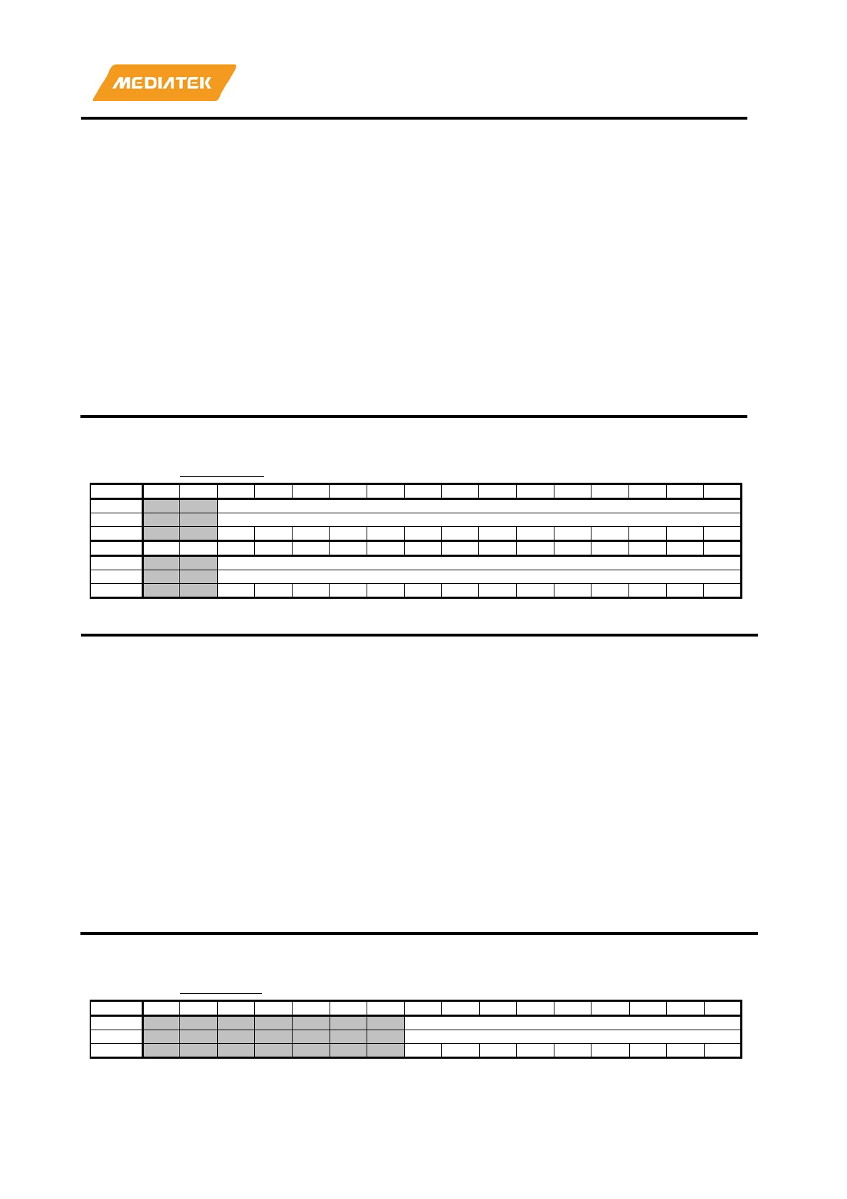
MT7686 Reference Manual
© 2016 - 2017 MediaTek Inc.
Page 494 of 536
This document contains information that is proprietary to MediaTek Inc. (“MediaTek”) and/or its licensor(s).
Any unauthorized use, reproduction or disclosure of this document in whole or in part is strictly prohibited.
Bit(s)
Mnemonic
Name
Description
29:16
WBTAC_LDO_STABLE_
TIME
CR_WBTAC_LDO_STABLE_
TIME
Actual
WBTAC_LDO_STABLE_TIME[13:0] =
WBTAC_LDO_STABLE_TIME_SW ?
WBTAC_LDO_STABLE_TIME[13:0] :
case(f_fxo_is_26m)
1'b1: f_fxo_ck=26 MHz ,14'd494
1'b0: f_fxo_ck=20 MHz ,14'd380
endcase
13:0
WBTAC_BBPLL1_STABL
E_TIME
CR_WBTAC_BBPLL1_STABL
E_TIME
Actual
WBTAC_BBPLL1_STABLE_TIME[13:0] =
WBTAC_BBPLL1_STABLE_TIME_SW ?
WBTAC_BBPLL1_STABLE_TIME[13:0] :
case(f_fxo_is_26m)
1'b1: f_fxo_ck=26 MHz ,14'd520
1'b0: f_fxo_ck=20 MHz ,14'd400
endcase
A2040328
RF_WBAC10
RF
WBAC STABLE TIME 3
090A090A
Bit
31
30
29
28
27
26
25
24
23
22
21
20
19
18
17
16
Name
WBTAC_BBPLL2_STABLE_TIME
Type
RW
Reset
0
0
1
0
0
1
0
0
0
0
1
0
1
0
Bit
15
14
13
12
11
10
9
8
7
6
5
4
3
2
1
0
Name
WBTAC_BBPLL1_CKDIG_STABLE_TIME
Type
RW
Reset
0
0
1
0
0
1
0
0
0
0
1
0
1
0
Bit(s)
Mnemonic
Name
Description
29:16
WBTAC_BBPLL2_STA
BLE_TIME
CR_WBTAC_BBPLL2_ST
ABLE_TIME
Actual
WBTAC_BBPLL2_STABLE_TIME[13:0] =
WBTAC_BBPLL2_STABLE_TIME_SW ?
WBTAC_BBPLL2_STABLE_TIME[13:0] :
case(f_fxo_is_26m)
1'b1: f_fxo_ck=26 MHz ,14'd1820
1'b0: f_fxo_ck=20 MHz ,14'd400
endcase
13:0
WBTAC_BBPLL1_CKD
IG_STABLE_TIME
CR_WBTAC_BBPLL1_CK
DIG_STABLE_TIME
Actual
WBTAC_BBPLL1_CKDIG_STABLE_TIME[13:0] =
WBTAC_BBPLL1_CKDIG_STABLE_TIME_SW ?
WBTAC_BBPLL1_CKDIG_STABLE_TIME[13:0] :
case(f_fxo_is_26m)
1'b1: f_fxo_ck=26 MHz ,14'd1820
1'b0: f_fxo_ck=20 MHz ,14'd1400
endcase
A204032C
RF_WBAC11
RF WBAC STABLE TIME4
00340068
Bit
31
30
29
28
27
26
25
24
23
22
21
20
19
18
17
16
Name
WBTAC_RFDIG_VCORE_OFF_TIME
Type
RW
Reset
0
0
0
1
1
0
1
0
0
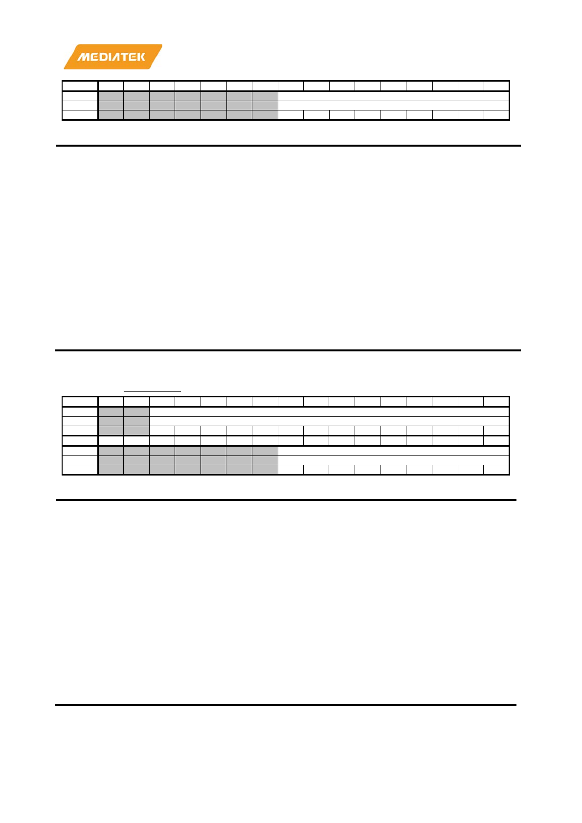
MT7686 Reference Manual
© 2016 - 2017 MediaTek Inc.
Page 495 of 536
This document contains information that is proprietary to MediaTek Inc. (“MediaTek”) and/or its licensor(s).
Any unauthorized use, reproduction or disclosure of this document in whole or in part is strictly prohibited.
Bit
15
14
13
12
11
10
9
8
7
6
5
4
3
2
1
0
Name
WBTAC_RFDIG_LSFLDO_OFF_TIME
Type
RW
Reset
0
0
1
1
0
1
0
0
0
Bit(s)
Mnemonic
Name
Description
24:16
WBTAC_RFDIG_VCORE
_OFF_TIME
CR_WBTAC_RFDIG_VCORE
_OFF_TIME
Actual
WBTAC_RFDIG_VCORE_OFF_TIME[8:0] =
WBTAC_RFDIG_VCORE_OFF_TIME_SW ?
WBTAC_RFDIG_VCORE_OFF_TIME[8:0] :
case(f_fxo_is_26m)
1'b1: f_fxo_ck=26 MHz ,9'd78
1'b0: f_fxo_ck=20 MHz ,9'd60
endcase
8:0
WBTAC_RFDIG_LSFLD
O_OFF_TIME
CR_WBTAC_RFDIG_LSFLD
O_OFF_TIME
Actual
WBTAC_RFDIG_LSFLDO_OFF_TIME[8:0] =
WBTAC_RFDIG_LSFLDO_OFF_TIME_SW ?
WBTAC_RFDIG_LSFLDO_OFF_TIME[8:0] :
case(f_fxo_is_26m)
1'b1: f_fxo_ck=26 MHz ,9'd130
1'b0: f_fxo_ck=20 MHz ,9'd100
endcase
A2040330
RF_WBAC12
RF WBAC STABLE TIME 5
0F3C001A
Bit
31
30
29
28
27
26
25
24
23
22
21
20
19
18
17
16
Name
WBTAC_BBPLL2_960M_CK_STABLE_TIME
Type
RW
Reset
0
0
1
1
1
1
0
0
1
1
1
1
0
0
Bit
15
14
13
12
11
10
9
8
7
6
5
4
3
2
1
0
Name
WBTAC_RDY_STABLE_TIME
Type
RW
Reset
0
0
0
0
1
1
0
1
0
Bit(s)
Mnemonic
Name
Description
29:16
WBTAC_BBPLL2_9
60M_CK_STABLE_
TIME
CR_WBTAC_BBPLL2_960
M_CK_STABLE_TIME
Actual
WBTAC_BBPLL2_960M_CK_STABLE_TIME[13:0] =
WBTAC_BBPLL2_960M_CK_STABLE_TIME_SW ?
WBTAC_BBPLL2_960M_CK_STABLE_TIME[13:0] :
case(f_fxo_is_26m)
1'b1: f_fxo_ck=26 MHz ,14'd1300
1'b0: f_fxo_ck=20 MHz ,14'd1000
endcase
8:0
WBTAC_RDY_STA
BLE_TIME
CR_WBTAC_R
DY_STABL
E_TIME
Actual
WBTAC_RDY_STABLE_TIME[8:0] =
WBTAC_RDY_STABLE_TIME_SW ?
WBTAC_RDY_STABLE_TIME[8:0] :
case(f_fxo_is_26m)
1'b1: f_fxo_ck=26 MHz ,9'd26
1'b0: f_fxo_ck=20 MHz ,9'd20
endcase
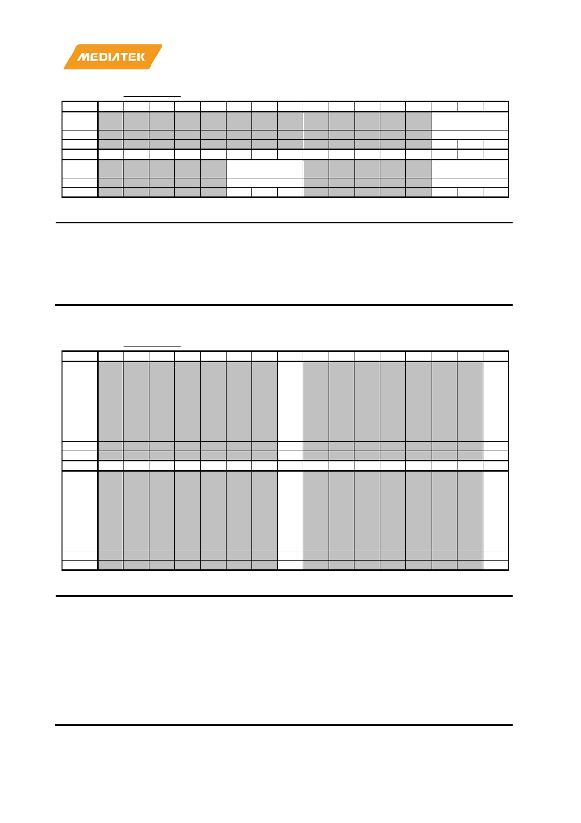
MT7686 Reference Manual
© 2016 - 2017 MediaTek Inc.
Page 496 of 536
This document contains information that is proprietary to MediaTek Inc. (“MediaTek”) and/or its licensor(s).
Any unauthorized use, reproduction or disclosure of this document in whole or in part is strictly prohibited.
A2040334
RF_WBAC13
RF WBAC STABLE TIME 6
00000504
Bit
31
30
29
28
27
26
25
24
23
22
21
20
19
18
17
16
Name
WBTAC_LSFLDO
_OUT_SEL_OFF
Type
RW
Reset
0
0
0
Bit
15
14
13
12
11
10
9
8
7
6
5
4
3
2
1
0
Name
WBTAC_LSFLDO_
OUT_SEL_ON
WBTAC_PALDO_
BACKOFF_TIME
Type
RW
RW
Reset
1
0
1
1
0
0
Bit(s)
Mnemonic
Name
Description
18:16
WBTAC_LSFLDO_OUT_SEL_OFF
CR_WBTAC_LSFLDO_OUT_SEL_OFF
LSFLDO
turn on voltage
selection
10:8
WBTAC_LSFLDO_OUT_SEL_ON
CR_WBTAC_LSFLDO_OUT_SEL_ON
LSFLDO
turn off voltage
selection
2:0
WBTAC_PALDO_BACKOFF_TIME
CR_WBTAC_PALDO_BACKOFF_TIME
Reserved
A2040338
RF_WBAC14
RF WBAC STABLE TIME 7
00000000
Bit
31
30
29
28
27
26
25
24
23
22
21
20
19
18
17
16
Name
WBT
AC_L
SFLD
O_ST
ABLE
_TIM
E_SW
WBT
AC_R
FDIG
_LSF
LDO_
STAB
LE_T
IME_
SW
Type
RW
RW
Reset
0
0
Bit
15
14
13
12
11
10
9
8
7
6
5
4
3
2
1
0
Name
WBT
AC_B
BPLL
1_CK
DIG_
STAB
LE_T
IME_
SW
WBT
AC_B
BPLL
1_ST
ABLE
_TIM
E_S
W
Type
RW
RW
Reset
0
0
Bit(s)
Mnemonic
Name
Description
24
WBTAC_LSFLDO_ST
ABLE_TIME_SW
CR_WBTAC_LSFLDO_STAB
LE_TIME_SW
Manual mode switch for
WBTAC_LSFLDO_STABLE_TIME[13:0]
16
WBTAC_RFDIG_LSFL
DO_STABLE_TIME_S
W
CR_WBTAC_RFDIG_LSFLD
O_STABLE_TIME_SW
Manual mode switch for
WBTAC_RFDIG_LSFLDO_STABLE_TIME[13:0]
8
WBTAC_BBPLL1_CKD
IG_STABLE_TIME_S
W
CR_WBTAC_BBPLL1_CKDI
G_STABLE_TIME_SW
Manual mode switch for
WBTAC_BBPLL1_CKDIG_STABLE_TIME[13:0]
0
WBTAC_BBPLL1_STA
CR_WBTAC_BBPLL1_STABL
Manual mode switch for
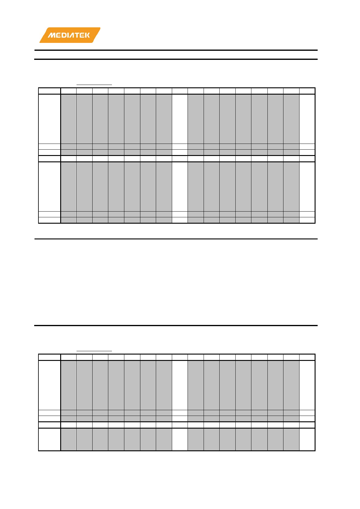
MT7686 Reference Manual
© 2016 - 2017 MediaTek Inc.
Page 497 of 536
This document contains information that is proprietary to MediaTek Inc. (“MediaTek”) and/or its licensor(s).
Any unauthorized use, reproduction or disclosure of this document in whole or in part is strictly prohibited.
BLE_TIME_SW
E_TIME_SW
WBTAC_BBPLL1_STABLE_TIME[13:0]
A204033C
RF_WBAC15
RF WBAC STABLE TIME8
00000000
Bit
31
30
29
28
27
26
25
24
23
22
21
20
19
18
17
16
Name
WBT
AC_R
FDIG
_VCO
RE_S
TABL
E_TI
ME_S
W
WBT
AC_L
DO_S
TABL
E_TI
ME_S
W
Type
RW
RW
Reset
0
0
Bit
15
14
13
12
11
10
9
8
7
6
5
4
3
2
1
0
Name
WBT
AC_L
SFLD
O_OU
T_SE
L_ST
ABLE
_TIM
E_SW
WBT
AC_B
BPLL
2_ST
ABLE
_TIM
E_S
W
Type
RW
RW
Reset
0
0
Bit(s)
Mnemonic
Name
Description
24
WBTAC_RFDIG_VCORE
_STABLE_TIME_SW
CR_WBTAC_RFDIG_V
CORE_STABLE_TIME
_SW
Manual mode switch for
WBTAC_RFDIG_VCORE_STABLE_TIME[13:0]
16
WBTAC_LDO_STABLE_
TIME_SW
CR_WBTAC_LDO_STA
BLE_TIME_SW
Manual mode switch for
WBTAC_LDO_STABLE_TIME[13:0]
8
WBTAC_LSFLDO_OUT_
SEL_STABLE_TIME_S
W
CR_WBTAC_LSFLDO_
OUT_SEL_STABLE_TI
ME_SW
Manual mode switch for
WBTAC_LSFLDO_OUT_SEL_STABLE_TIME[13:0]
0
WBTAC_BBPLL2_STAB
LE_TIME_SW
CR_WBTAC_BBPLL2_
STABLE_TIME_SW
Manual mode switch for
WBTAC_BBPLL2_STABLE_TIME
A2040340
RF_WBAC16
RF WBAC STABLE TIME 9
00000000
Bit
31
30
29
28
27
26
25
24
23
22
21
20
19
18
17
16
Name
WBT
AC_B
BPLL
2_96
0M_C
K_ST
ABLE
_TIM
E_SW
WBT
AC_R
FDIG
_VCO
RE_O
FF_S
W
Type
RW
RW
Reset
0
0
Bit
15
14
13
12
11
10
9
8
7
6
5
4
3
2
1
0
Name
WBT
AC_R
FDIG
_LSF
WBT
AC_R
DY_S
TABL
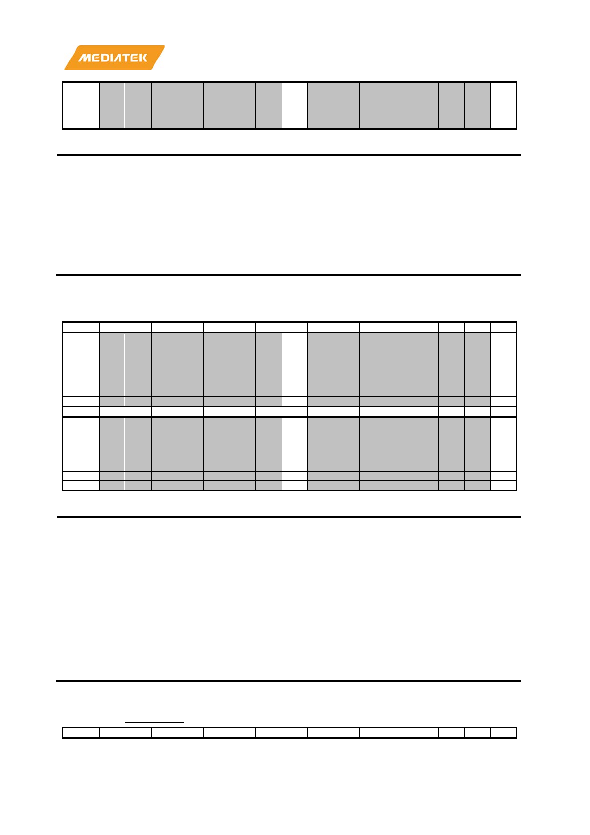
MT7686 Reference Manual
© 2016 - 2017 MediaTek Inc.
Page 498 of 536
This document contains information that is proprietary to MediaTek Inc. (“MediaTek”) and/or its licensor(s).
Any unauthorized use, reproduction or disclosure of this document in whole or in part is strictly prohibited.
LDO_
OFF_
SW
E_S
W
Type
RW
RW
Reset
0
0
Bit(s)
Mnemonic
Name
Description
24
WBTAC_BBPLL2_960M_CK
_STABLE_TIME_SW
CR_WBTAC_BBPLL2_960
M_CK_STABLE_TIME_SW
Manual mode switch for
WBTAC_BBPLL2_960M_CK_STABLE_TIME
16
WBTAC_RFDIG_VCORE_OF
F_SW
CR_WBTAC_RFDIG_VCOR
E_OFF_TIME_SW
Manual mode switch for
WBTAC_RFDIG_VCORE_OFF_TIME
8
WBTAC_RFDIG_LSFLDO_O
FF_SW
CR_WBTAC_RFDIG_LSFL
DO_OFF_TIME_SW
Manual mode switch for
WBTAC_RFDIG_LSFLDO_OFF_TIME
0
WBTAC_RDY_STABLE_SW
CR_WBTAC_RDY_STABLE
_TIME_SW
Manual
mode switch for
WBTAC_RDY_STABLE_TIME
A2040344
RF_WBAC17
WBAC MANUAL CONTROL
00000000
Bit
31
30
29
28
27
26
25
24
23
22
21
20
19
18
17
16
Name
SWCT
L_W
BTAC
_BT_
PLL
SWC
TL_D
A_EN
_WF
_BBP
LL1
Type
RW
RW
Reset
0
0
Bit
15
14
13
12
11
10
9
8
7
6
5
4
3
2
1
0
Name
SWCT
L_DA
_EN_
BBPL
L1_C
KDIG
SWC
TL_D
A_EN
_WF
_BBP
LL2
Type
RW
RW
Reset
0
0
Bit(s)
Mnemonic
Name
Description
24
SWCTL_WBTAC_BT_PLL
CR_SWCTL_WBTAC_BT_PLL
DA_WBTAC_* = SWCTL_WBTAC_* |
BP_PLL_DLY ? SW_WBTAC_* :
hw_DA_WBTAC_*;
16
SWCTL_DA_EN_WF_BB
PLL1
CR_SWCTL_DA_EN_WF_BBPLL1
DA_WBTAC_*
= SWCTL_WBTAC_* |
BP_PLL_DLY ? SW_WBTAC_* :
hw_DA_WBTAC_*;
8
SWCTL_DA_EN_BBPLL1
_CKDIG
CR_SWCTL_DA_EN_BBPLL1_CK
DIG
DA_WBTAC_* = SWCTL_WBTAC_* |
BP_PLL_DLY ? SW_WBTAC_* :
hw_DA_WBTAC_*;
0
SWCTL_DA_EN_WF_BB
PLL2
CR_SWCTL_DA_EN_WF_BBPLL
2
DA_WBTAC_* =
SWCTL_WBTAC_* |
BP_PLL_DLY ? SW_WBTAC_* :
hw_DA_WBTAC_*;
A2040348
RF_WBAC18
WBAC MANUAL CONTROL
00000000
Bit
31
30
29
28
27
26
25
24
23
22
21
20
19
18
17
16
MT7686 Reference Manual
© 2016 - 2017 MediaTek Inc.
Page 499 of 536
This document contains information that is proprietary to MediaTek Inc. (“MediaTek”) and/or its licensor(s).
Any unauthorized use, reproduction or disclosure of this document in whole or in part is strictly prohibited.
Name
SWCT
L_DA
_EN_
BBPL
L2_9
60M_
CK
SWC
TL_D
A_EN
_WF
0_RF
DIG_
LSFL
DO
Type
RW
RW
Reset
0
0
Bit
15
14
13
12
11
10
9
8
7
6
5
4
3
2
1
0
Name
SWCT
L_DA
_EN_
WF0_
RFDI
G_VC
ORE
SWC
TL_D
A_EN
_WF
0_LS
FLDO
Type
RW
RW
Reset
0
0
Bit(s)
Mnemonic
Name
Description
24
SWCTL_DA_EN_BBPLL2_
960M_CK
CR_SWCTL_DA_EN_BBPLL2_960
M_CK
DA_WBTAC_* = SWCTL_WBTAC_* |
BP_PLL_DLY ? SW_WBTAC_* :
hw_DA_WBTAC_*;
16
SWCTL_DA_EN_WF0_RF
DIG_LSFLDO
CR_SWCTL_DA_EN_WF0_RFDIG
_LSFLDO
DA_WBTAC_* = SWCTL_WBTAC_* |
BP_PLL_DLY ? SW_WBTAC_* :
hw_DA_WBTAC_*;
8
SWCTL_DA_EN_WF0_RF
DIG_VCORE
CR_SWCTL_DA_EN_WF0_RFDIG
_VCORE
DA_WBTAC_* = SWCTL_WBTAC_* |
BP_PLL_DLY ? SW_WBTAC_* :
hw_DA_WBTAC_*;
0
SWCTL_DA_EN_WF0_LS
FLDO
CR_SWCTL_DA_EN_WF0_LSFLD
O
DA_WBTAC_* = SWCTL_WBTAC_* |
BP_PLL_DLY ? SW_WBTAC_* :
hw_DA_WBTAC_*;
A204034C
RF_WBAC19
WBAC MANUAL CONTROL
00000000
Bit
31
30
29
28
27
26
25
24
23
22
21
20
19
18
17
16
Name
SWCT
L_DA
_WF0
_LSF
LDO_
OUT_
SEL
SWC
TL_D
A_EN
_WF
0_LD
O
Type
RW
RW
Reset
0
0
Bit
15
14
13
12
11
10
9
8
7
6
5
4
3
2
1
0
Name
SWCT
L_DA
_EN_
WF0_
BG
SWC
TL_B
TLDO
Type
RW
RW
Reset
0
0
Bit(s)
Mnemonic
Name
Description
24
SWCTL_DA_WF0_LSFLDO_OU
T_SEL
CR_SWCTL_DA_WF0_LSFL
DO_OUT_SEL
DA_WBTAC_* = SWCTL_WBTAC_* |
BP_PLL_DLY ? SW_WBTAC_* :
MT7686 Reference Manual
© 2016 - 2017 MediaTek Inc.
Page 500 of 536
This document contains information that is proprietary to MediaTek Inc. (“MediaTek”) and/or its licensor(s).
Any unauthorized use, reproduction or disclosure of this document in whole or in part is strictly prohibited.
hw_DA_WBTAC_*;
16
SWCTL_DA_EN_WF0_LDO
CR_SWCTL_DA_EN_WF0_
LDO
DA_WBTAC_* = SWCTL_WBTAC_* |
BP_PLL_DLY ? SW_WBTAC_* :
hw_DA_WBTAC_*;
8
SWCTL_DA_EN_WF0_BG
CR_SWCTL_DA_EN_WF0_
BG
DA_WBTAC_* = SWCTL_WBTAC_* |
BP_PLL_DLY ? SW_WBTAC_* :
hw_DA_WBTAC_*;
0
SWCTL_BTLDO
CR_SWCTL_WF0_BTLDO
DA_WBTAC_* =
SWCTL_WBTAC_* |
BP_PLL_DLY ? SW_WBTAC_* :
hw_DA_WBTAC_*;
A2040350
RF_WBAC20
WBAC MANUAL CONTROL
00000000
Bit
31
30
29
28
27
26
25
24
23
22
21
20
19
18
17
16
Name
SWCT
L_BT
PALD
O
SWC
TL_D
A_EN
_WF
0_TX
DIG
Type
RW
RW
Reset
0
0
Bit
15
14
13
12
11
10
9
8
7
6
5
4
3
2
1
0
Name
SW_
WBT
AC_B
T_PL
L
SW_
DA_E
N_W
F_BB
PLL1
Type
RW
RW
Reset
0
0
Bit(s)
Mnemonic
Name
Description
24
SWCTL_BTPALDO
CR_SWCTL_WF0_
BT_PALDO
DA_WBTAC_* = SWCTL_WBTAC_* | BP_PLL_DLY ?
SW_WBTAC_* : hw_DA_WBTAC_*;
16
SWCTL_DA_EN_WF0
_TXDIG
CR_SWCTL_DA_E
N_WF0_TXDIG
DA_WBTAC_* =
SWCTL_WBTAC_* | BP_PLL_DLY ?
SW_WBTAC_* : hw_DA_WBTAC_*;
8
SW_WBTAC_BT_PLL
CR_SW_WBTAC_B
T_PLL
DA_WBTAC_* = SWCTL_WBTAC_* | BP_PLL_DLY ?
SW_WBTAC_* : hw_DA_WBTAC_*;
0
SW_DA_EN_WF_BBP
LL1
CR_SW_DA_EN_W
F_BBPLL1
DA_WBTAC_* = SWCTL_WBTAC_* | BP_PLL_DLY ?
SW_WBTAC_* : hw_DA_WBTAC_*;
A2040354
RF_WBAC21
WBAC MANUAL CONTROL
00000000
Bit
31
30
29
28
27
26
25
24
23
22
21
20
19
18
17
16
Name
SW_
DA_E
N_BB
PLL1
_CKD
IG
SW_
DA_E
N_W
F_BB
PLL2
Type
RW
RW
Reset
0
0
Bit
15
14
13
12
11
10
9
8
7
6
5
4
3
2
1
0
Name
SW_
DA_E
N_BB
PLL2
SW_
DA_E
N_W
F0_R
MT7686 Reference Manual
© 2016 - 2017 MediaTek Inc.
Page 501 of 536
This document contains information that is proprietary to MediaTek Inc. (“MediaTek”) and/or its licensor(s).
Any unauthorized use, reproduction or disclosure of this document in whole or in part is strictly prohibited.
_960
M_C
K
FDIG
_LSF
LDO
Type
RW
RW
Reset
0
0
Bit(s)
Mnemonic
Name
Description
24
SW_DA_EN_BBPLL1
_CKDIG
CR_SW_DA_EN_BBP
LL1_CKDIG
DA_WBTAC_* = SWCTL_WBTAC_* | BP_PLL_DLY ?
SW_WBTAC_* : hw_DA_WBTAC_*;
16
SW_DA_EN_WF_BBP
LL2
CR_SW_DA_EN_WF
_BBPLL2
DA_WBTAC_*
= SWCTL_WBTAC_* | BP_PLL_DLY ?
SW_WBTAC_* : hw_DA_WBTAC_*;
8
SW_DA_EN_BBPLL2
_960M_CK
CR_SW_DA_EN_BBP
LL2_960M_CK
DA_WBTAC_* = SWCTL_WBTAC_* | BP_PLL_DLY ?
SW_WBTAC_* : hw_DA_WBTAC_*;
0
SW_DA_EN_WF0_RF
DIG_LSFLDO
CR_SW_DA_EN_WF0
_RFDIG_LSFLDO
DA_WBTAC_* =
SWCTL_WBTAC_* | BP_PLL_DLY ?
SW_WBTAC_* : hw_DA_WBTAC_*;
A2040358
RF_WBAC22
WBAC MANUAL CONTROL
01000000
Bit
31
30
29
28
27
26
25
24
23
22
21
20
19
18
17
16
Name
SW_
DA_E
N_W
F0_R
FDIG
_VCO
RE
SW_
DA_E
N_W
F0_L
SFLD
O
Type
RW
RW
Reset
1
0
Bit
15
14
13
12
11
10
9
8
7
6
5
4
3
2
1
0
Name
SW_DA_WF0_LS
FLDO_OUT_SEL
SW_
DA_E
N_W
F0_L
DO
Type
RW
RW
Reset
0
0
0
0
Bit(s)
Mnemonic
Name
Description
24
SW_DA_EN_WF0
_RFDIG_VCORE
CR_SW_DA_EN_WF0_R
FDIG_VCORE
DA_WBTAC_* = SWCTL_WBTAC_* | BP_PLL_DLY ?
SW_WBTAC_* : hw_DA_WBTAC_*;
16
SW_DA_EN_WF0
_LSFLDO
CR_SW_DA_EN_WF0_L
SFLDO
DA_WBTAC_* = SWCTL_WBTAC_* | BP_PLL_DLY ?
SW_WBTAC_* : hw_DA_WBTAC_*;
10:8
SW_DA_WF0_LS
FLDO_OUT_SEL
CR_SW_DA_WF0_LSFL
DO_OUT_SEL
DA_WBTAC_* = SWCTL_WBTAC_* | BP_PLL_DLY ?
SW_WBTAC_* : hw_DA_WBTAC_*;
0
SW_DA_EN_WF0
_LDO
CR_SW_DA_EN_WF0_L
DO
DA_WBTAC_* = SWCTL_WBTAC_* | BP_PLL_DLY ?
SW_WBTAC_* :
hw_DA_WBTAC_*;
A204035C
RF_WBAC23
WBAC MANUAL CONTROL
00000000
Bit
31
30
29
28
27
26
25
24
23
22
21
20
19
18
17
16
Name
SW_
DA_E
N_W
F0_B
G
SW_
WF0
_BTL
DO
MT7686 Reference Manual
© 2016 - 2017 MediaTek Inc.
Page 502 of 536
This document contains information that is proprietary to MediaTek Inc. (“MediaTek”) and/or its licensor(s).
Any unauthorized use, reproduction or disclosure of this document in whole or in part is strictly prohibited.
Type
RW
RW
Reset
0
0
Bit
15
14
13
12
11
10
9
8
7
6
5
4
3
2
1
0
Name
SW_
WF0_
BT_P
ALDO
SW_
DA_E
N_W
F0_T
XDIG
Type
RW
RW
Reset
0
0
Bit(s)
Mnemonic
Name
Description
24
SW_DA_EN_WF0_B
G
CR_SW_DA_EN_WF0
_BG
DA_WBTAC_* = SWCTL_WBTAC_* | BP_PLL_DLY ?
SW_WBTAC_* : hw_DA_WBTAC_*;
16
SW_WF0_BTLDO
CR_SW_WF0_BTLDO
DA_WBTAC_* = SWCTL_WBTAC_* |
BP_PLL_DLY ?
SW_WBTAC_* : hw_DA_WBTAC_*;
8
SW_WF0_BT_PALDO
CR_SW_WF0_BT_PA
LDO
DA_WBTAC_* = SWCTL_WBTAC_* | BP_PLL_DLY ?
SW_WBTAC_* : hw_DA_WBTAC_*;
0
SW_DA_EN_WF0_TX
DIG
CR_SW_DA_EN_WF0
_TXDIG
DA_WBTAC_* = SWCTL_WBTAC_* | BP_PLL_DLY ?
SW_WBTAC_* :
hw_DA_WBTAC_*;
A2040360
RF_WBAC24
WF_TOP_REG
0000019F
Bit
31
30
29
28
27
26
25
24
23
22
21
20
19
18
17
16
Name
RG_WF_TOP[31:16]
Type
RW
Reset
0
0
0
0
0
0
0
0
0
0
0
0
0
0
0
0
Bit
15
14
13
12
11
10
9
8
7
6
5
4
3
2
1
0
Name
RG_WF_TOP[15:0]
Type
RW
Reset
0
0
0
0
0
0
0
1
1
0
0
1
1
1
1
1
Bit(s)
Mnemonic
Name
Description
31:0
RG_WF_TOP
CR_RG_WF_TOP
Wi
-Fi top configuration register
A2040364
RF_WBAC25
WBAC MANUAL CONTROL
00000000
Bit
31
30
29
28
27
26
25
24
23
22
21
20
19
18
17
16
Name
CR_
MCU
_960
_EN
SWC
TL_D
A_EN
_WF
_BBP
LL1_
LDO
Type
RW
RW
Reset
0
0
Bit
15
14
13
12
11
10
9
8
7
6
5
4
3
2
1
0
Name
SWCT
L_DA
_EN_
WF0_
AFEL
DO
SWC
TL_D
A_EN
_WF
0_TR
XLDO
Type
RW
RW
Reset
0
0
MT7686 Reference Manual
© 2016 - 2017 MediaTek Inc.
Page 503 of 536
This document contains information that is proprietary to MediaTek Inc. (“MediaTek”) and/or its licensor(s).
Any unauthorized use, reproduction or disclosure of this document in whole or in part is strictly prohibited.
Bit(s)
Mnemonic
Name
Description
24
CR_MCU_960_EN
CR_MCU_960_EN
Reserved
16
SWCTL_DA_EN_W
F_BBPLL1_LDO
CR_SWCTL_DA_EN_
WF_BBPLL1_LDO
DA_WBTAC_* = SWCTL_WBTAC_* | BP_PLL_DLY ?
SW_WBTAC_* : hw_DA_WBTAC_*;
8
SWCTL_DA_EN_W
F0_AFELDO
CR_SWCTL_DA_EN_
WF0_AFELDO
DA_WBTAC_* = SWCTL_WBTAC_* | BP_PLL_DLY ?
SW_WBTAC_* : hw_DA_WBTAC_*;
0
SWCTL_DA_EN_W
F0_TRXLDO
CR_SWCTL_DA_EN_
WF0_TRXLDO
DA_WBTAC_* = SWCTL_WBTAC_* | BP_PLL_DLY ?
SW_WBTAC_* : hw_DA_WBTAC_*;
A2040368
RF_WBAC26
WBAC MANUAL CONTROL
00000000
Bit
31
30
29
28
27
26
25
24
23
22
21
20
19
18
17
16
Name
SW_
DA_E
N_W
F_BB
PLL1
_LDO
Type
RW
Reset
0
Bit
15
14
13
12
11
10
9
8
7
6
5
4
3
2
1
0
Name
SW_
DA_E
N_W
F0_A
FELD
O
SW_
DA_E
N_W
F0_T
RXLD
O
Type
RW
RW
Reset
0
0
Bit(s)
Mnemonic
Name
Description
16
SW_DA_EN_WF_BB
PLL1_LDO
CR_SW_DA_EN_WF
_BBPLL1_LDO
DA_WBTAC_* = SWCTL_WBTAC_* | BP_PLL_DLY ?
SW_WBTAC_* : hw_DA_WBTAC_*;
8
SW_DA_EN_WF0_A
FELDO
CR_SW_DA_EN_WF0
_AFELDO
DA_WBTAC_* = SWCTL_WBTAC_* | BP_PLL_DLY ?
SW_WBTAC_* : hw_DA_WBTAC_*;
0
SW_DA_EN_WF0_T
RXLDO
CR_SW_DA_EN_WF0
_TRXLDO
DA_WBTAC_* = SWCTL_WBTAC_* | BP_PLL_DLY ?
SW_WBTAC_* : hw_DA_WBTAC_*;
A2040370
RF_WBAC27
WF_BG_REG
00492088
Bit
31
30
29
28
27
26
25
24
23
22
21
20
19
18
17
16
Name
RG_WF0_BG[31:16]
Type
RW
Reset
0
0
0
0
0
0
0
0
0
1
0
0
1
0
0
1
Bit
15
14
13
12
11
10
9
8
7
6
5
4
3
2
1
0
Name
RG_WF0_BG[15:0]
Type
RW
Reset
0
0
1
0
0
0
0
0
1
0
0
0
1
0
0
0
Bit(s)
Mnemonic
Name
Description
31:0
RG_WF0_BG
CR_RG_WF0_BG
Wi
-Fi band-gap configuration register
MT7686 Reference Manual
© 2016 - 2017 MediaTek Inc.
Page 504 of 536
This document contains information that is proprietary to MediaTek Inc. (“MediaTek”) and/or its licensor(s).
Any unauthorized use, reproduction or disclosure of this document in whole or in part is strictly prohibited.
A2040374
RF_WBAC28
WBAC MANUAL CONTROL
00000000
Bit
31
30
29
28
27
26
25
24
23
22
21
20
19
18
17
16
Name
Type
Reset
Bit
15
14
13
12
11
10
9
8
7
6
5
4
3
2
1
0
Name
RG_WF0_L
DO_LSF_P
WRSV
WBT
AC_B
BPLL
_SW
Type
RW
RW
Reset
0
0
0
Bit(s)
Mnemonic
Name
Description
9:8
RG_WF0_LDO_LSF_P
WRSV
CR_RG_WF0_LDO_LSF_PWRS
V
For saving WF0 LDO current
0
WBTAC_BBPLL_SW
CR_WBTAC_BBPLL_SW
RG_WF_BBPLL_0x = WBTAC_BBPLL_SW ?
RG_WF_BBPLL_0x[31:0] :
hw_WF_BBPLL_0x[31:0]
A2040384
RO_RF_WBAC1
RF WBAC RG 1
0811E000
Bit
31
30
29
28
27
26
25
24
23
22
21
20
19
18
17
16
Name
RG_WF_BBPLL_01[31:16]
Type
RO
Reset
0
0
0
0
1
0
0
0
0
0
0
1
0
0
0
1
Bit
15
14
13
12
11
10
9
8
7
6
5
4
3
2
1
0
Name
RG_WF_BBPLL_01[15:0]
Type
RO
Reset
1
1
1
0
0
0
0
0
0
0
0
0
0
0
0
0
Bit(s)
Mnemonic
Name
Description
31:0
RG_WF_BBPLL_01
RG_WF_BBPLL_01
Wi
-Fi PLL registers.
Actual
RG_WF_BBPLL_01 = WBTAC_BBPLL_SW ?
RG_WF_BBPLL_01[31:0] :
case(BBPLL1_FREQ_SEL,
xtal_freq)
5'b01000: BBPLL1=832 MHz, XTAL=52
MHz ,32'h45962040
5'b00100: BBPLL1=832 MHz, XTAL=40
MHz ,32'h01234567
5'b00010: BBPLL1=832 MHz, XTAL=26
MHz ,32'h45962040
5'b00001: BBPLL1=832 MHz, XTAL=20
MHz ,32'h01234567
5'b11000: BBPLL1=1040 MHz, XTAL=52
MHz ,32'h454B2840
5'b10100: BBPLL1=1040 MHz, XTAL=40
MHz ,32'h454B3440
5'b10010: BBPLL1=1040 MHz, XTAL=26
MHz ,32'h054B2840
5'b10001: BBPLL1=1040 MHz, XTAL=20
MHz ,32'h054B3440
default : 32'h054B2840
MT7686 Reference Manual
© 2016 - 2017 MediaTek Inc.
Page 505 of 536
This document contains information that is proprietary to MediaTek Inc. (“MediaTek”) and/or its licensor(s).
Any unauthorized use, reproduction or disclosure of this document in whole or in part is strictly prohibited.
endcase
A204038
8
RO_RF_WB
AC2 RF WBAC RG 2 60C8E018
Bit
31
30
29
28
27
26
25
24
23
22
21
20
19
18
17
16
Nam
e
RG_WF_BBPLL_02[31:16]
Type
RO
Reset
0
1
1
0
0
0
0
0
1
1
0
0
1
0
0
0
Bit
15
14
13
12
11
10
9
8
7
6
5
4
3
2
1
0
Nam
e
RG_WF_BBPLL_02[15:0]
Type
RO
Reset
1
1
1
0
0
0
0
0
0
0
0
1
1
0
0
0
Bit(s)
Mnemonic
Name
Description
31:0
RG_WF_BBPLL_02
RG_WF_BBPLL_02
Wi
-Fi PLL registers.
Actual
RG_WF_BBPLL_02 = WBTAC_BBPLL_SW ?
RG_WF_BBPLL_02[31:0] :
case(BBPLL1_FREQ_SEL,
xtal_freq)
5'b01000: BBPLL1=832 MHz, XTAL=52
MHz ,32'h05691E40
5'b00100: BBPLL1=832 MHz, XTAL=40
MHz ,32'h45693040
5'b00010: BBPLL1=832 MHz, XTAL=26
MHz ,32'h05691E40
5'b00001: BBPLL1=832 MHz, XTAL=20
MHz ,32'h05693040
5'b11000: BBPLL1=1040 MHz, XTAL=52
MHz ,32'h05691840
5'b10100: BBPLL1=1040 MHz, XTAL=40
MHz ,32'h45693040
5'b10010: BBPLL1=1040 MHz, XTAL=26
MHz ,32'h05691840
5'b10001: BBPLL1=1040 MHz, XTAL=20
MHz ,32'h05693040
default : 32'h05691840
endcase
A204038
C
RO_RF_WB
AC3 RF WBAC STABLE TIME 0 NA
Bit
31
30
29
28
27
26
25
24
23
22
21
20
19
18
17
16
Nam
e
WBTAC_LSFLDO_STABLE_TIME
Type
RO
Reset
14d
260
14d
260
14d
260
14d
260
14d
260
14d
260
14d
260
14d
260
14d
260
14d
260
14d
260
14d
260
14d
260
14d
260
Bit
15
14
13
12
11
10
9
8
7
6
5
4
3
2
1
0
Nam
e
WBTAC_RFDIG_VCORE_STABLE_TIME
Type
RO
Reset
0
0
0
0
0
1
1
0
0
0
0
1
1
0
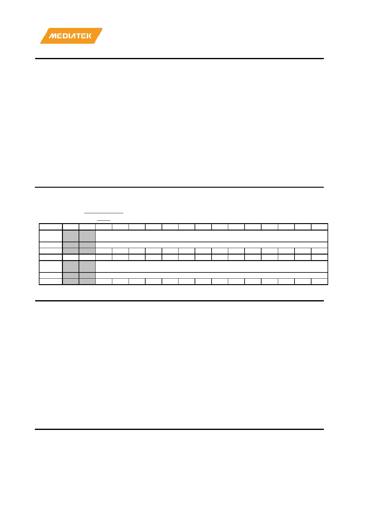
MT7686 Reference Manual
© 2016 - 2017 MediaTek Inc.
Page 506 of 536
This document contains information that is proprietary to MediaTek Inc. (“MediaTek”) and/or its licensor(s).
Any unauthorized use, reproduction or disclosure of this document in whole or in part is strictly prohibited.
Bit(s)
Mnemonic
Name
Description
29:16
WBTAC_LSFLDO_STABLE
_TIME
CR_WBTAC_LSFLDO_S
TABLE_TIME_SEL
Actual
WBTAC_LSFLDO_STABLE_TIME[13:0] =
WBTAC_LSFLDO_STABLE_TIME_SW ?
WBTAC_LSFLDO_STABLE_TIME[13:0] :
case(f_fxo_is_26m)
1'b1: f_fxo_ck=26 MHz ,14'd260
1'b0: f_fxo_ck=20 MHz ,14'd200
endcase
13:0
WBTAC_RFDIG_VCORE_S
TABLE_TIME
CR_WBTAC_RFDIG_VC
ORE_STABLE_TIME_S
EL
Actual
WBTAC_RFDIG_VCORE_STABLE_TIME[13:0] =
WBTAC_RFDIG_VCORE_STABLE_TIME_SW ?
WBTAC_RFDIG_VCORE_STABLE_TIME[13:0] :
case(f_fxo_is_26m)
1'b1: f_fxo_ck=26 MHz ,14'd416
1'b0: f_fxo_ck=20 MHz ,14'd320
endcase
A204039
0
RO_RF_WB
AC4 RF WBAC STABLE TIME 1 016C01BA
Bit
31
30
29
28
27
26
25
24
23
22
21
20
19
18
17
16
Nam
e
WBTAC_RFDIG_LSFLDO_STABLE_TIME
Type
RO
Reset
0
0
0
0
0
1
0
1
1
0
1
1
0
0
Bit
15
14
13
12
11
10
9
8
7
6
5
4
3
2
1
0
Nam
e
WBTAC_LSFLDO_OUT_SEL_STABLE_TIME
Type
RO
Reset
0
0
0
0
0
1
1
0
1
1
1
0
1
0
Bit(s)
Mnemonic
Name
Description
29:16
WBTAC_RFDIG_LS
FLDO_STABLE_TI
ME
CR_WBTAC_RFDIG_LSF
LDO_STABLE_TIME_SE
L
Actual
WBTAC_RFDIG_LSFLDO_STABLE_TIME[13:0] =
WBTAC_RFDIG_LSFLDO_STABLE_TIME_SW ?
WBTAC_RFDIG_LSFLDO_STABLE_TIME[13:0] :
case(f_fxo_is_26m)
1'b1: f_fxo_ck=26 MHz ,14'd312
1'b0: f_fxo_ck=20 MHz ,14'd240
endcase
13:0
WBTAC_LSFLDO_
OUT_SEL_STABLE
_TIME
CR_WBTAC_LSFLDO_O
UT_SEL_STABLE_TIME
_SEL
Actual
WBTAC_LSFLDO_OUT_SEL_STABLE_TIME[13:0] =
WBTAC_LSFLDO_OUT_SEL_STABLE_TIME_SW ?
WBTAC_LSFLDO_OUT_SEL_STABLE_TIME[13:0] :
case(f_fxo_is_26m)
1'b1: f_fxo_ck=26 MHz ,14'd468
1'b0: f_fxo_ck=20 MHz ,14'd360
endcase
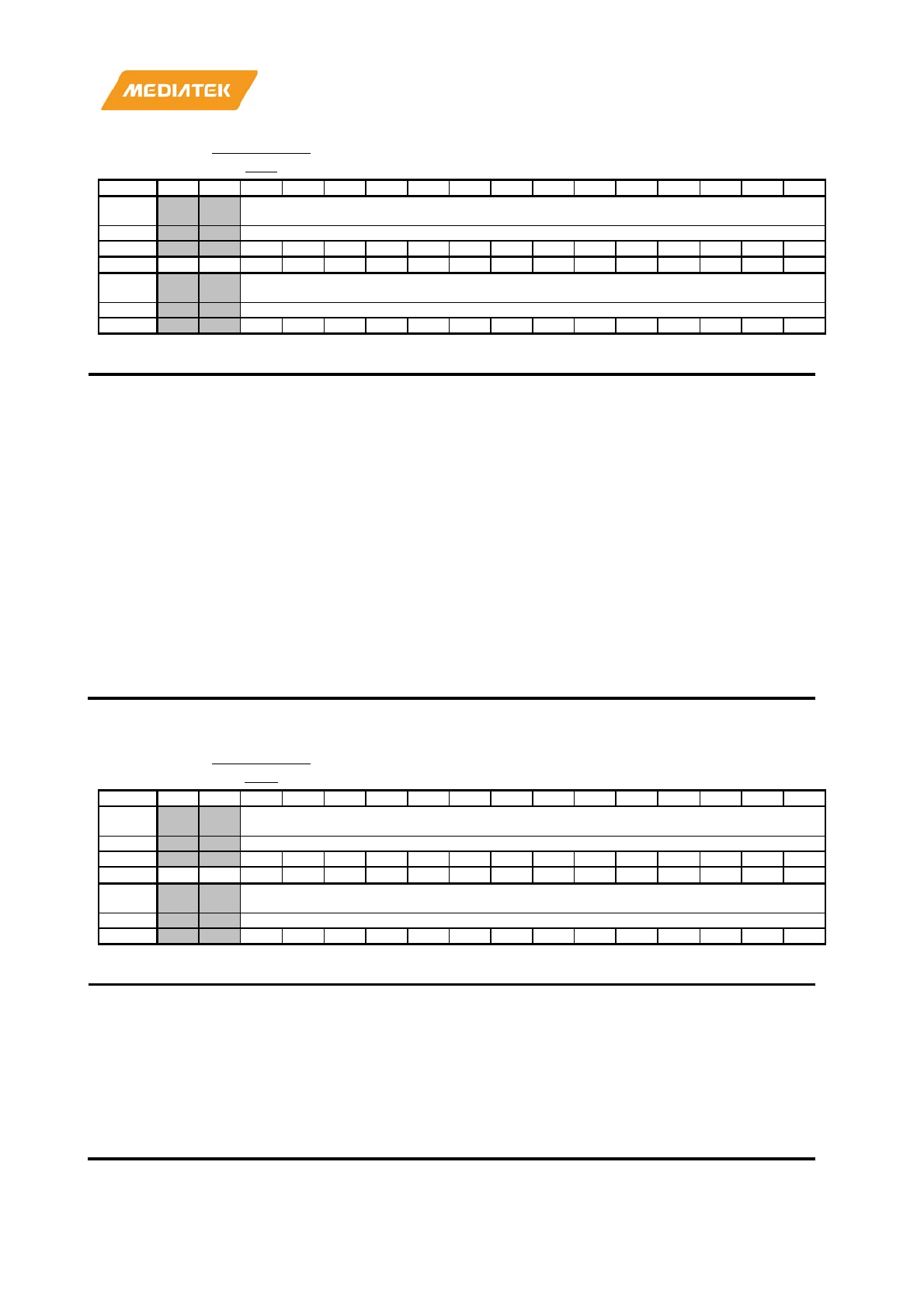
MT7686 Reference Manual
© 2016 - 2017 MediaTek Inc.
Page 507 of 536
This document contains information that is proprietary to MediaTek Inc. (“MediaTek”) and/or its licensor(s).
Any unauthorized use, reproduction or disclosure of this document in whole or in part is strictly prohibited.
A2040394 RO_RF_WB
AC5 RF WBAC STABLE TIME 2 01EE03F6
Bit
31
30
29
28
27
26
25
24
23
22
21
20
19
18
17
16
Nam
e
WBTAC_LDO_STABLE_TIME
Type
RO
Reset
0
0
0
0
0
1
1
1
1
0
1
1
1
0
Bit
15
14
13
12
11
10
9
8
7
6
5
4
3
2
1
0
Nam
e
WBTAC_BBPLL1_STABLE_TIME
Type
RO
Reset
0
0
0
0
1
1
1
1
1
1
0
1
1
0
Bit(s)
Mnemonic
Name
Description
29:16
WBTAC_LDO_STABLE_
TIME
CR_WBTAC_LDO_STABLE_
TIME_SEL
Actual
WBTAC_LDO_STABLE_TIME[13:0] =
WBTAC_LDO_STABLE_TIME_SW ?
WBTAC_LDO_STABLE_TIME[13:0] :
case(f_fxo_is_26m)
1'b1: f_fxo_ck=26 MHz ,14'd494
1'b0: f_fxo_ck=20 MHz ,14'd380
endcase
13:0
WBTAC_BBPLL1_STABL
E_TIME
CR_WBTAC_BBPLL1_STABL
E_TIME_SEL
Actual
WBTAC_BBPLL1_STABLE_TIME[13:0] =
WBTAC_BBPLL1_STABLE_TIME_SW ?
WBTAC_BBPLL1_STABLE_TIME[13:0] :
case(f_fxo_is_26m)
1'b1: f_fxo_ck=26 MHz ,14'd520
1'b0: f_fxo_ck=20 MHz ,14'd400
endcase
A204039
8
RO_RF_WB
AC6 RF WBAC STABLE TIME 3 090A090A
Bit
31
30
29
28
27
26
25
24
23
22
21
20
19
18
17
16
Nam
e
WBTAC_BBPLL2_STABLE_TIME
Type
RO
Reset
0
0
1
0
0
1
0
0
0
0
1
0
1
0
Bit
15
14
13
12
11
10
9
8
7
6
5
4
3
2
1
0
Nam
e
WBTAC_BBPLL1_CKDIG_STABLE_TIME
Type
RO
Reset
0
0
1
0
0
1
0
0
0
0
1
0
1
0
Bit(s)
Mnemonic
Name
Description
29:16
WBTAC_BBPLL2_S
TABLE_TIME
CR_WBTAC_BBPLL2_STABLE_
TIME_SEL
Actual
WBTAC_BBPLL2_STABLE_TIME[13:0] =
WBTAC_BBPLL2_STABLE_TIME_SW ?
WBTAC_BBPLL2_STABLE_TIME[13:0] :
case(f_fxo_is_26m)
1'b1: f_fxo_ck=26 MHz ,14'd1820
1'b0: f_fxo_ck=20 MHz ,14'd400
endcase
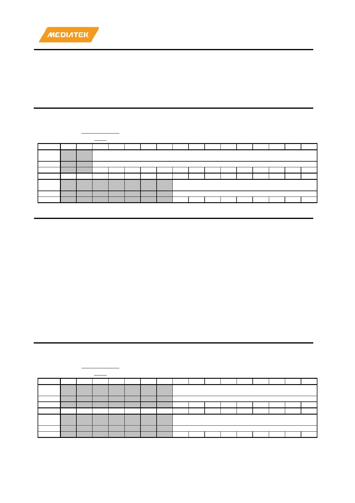
MT7686 Reference Manual
© 2016 - 2017 MediaTek Inc.
Page 508 of 536
This document contains information that is proprietary to MediaTek Inc. (“MediaTek”) and/or its licensor(s).
Any unauthorized use, reproduction or disclosure of this document in whole or in part is strictly prohibited.
13:0
WBTAC_BBPLL1_C
KDIG_STABLE_TI
ME
CR_WBTAC_BBPLL1_CKDIG_S
TABLE_TIME_SEL
Actual
WBTAC_BBPLL1_CKDIG_STABLE_TIME[13:0] =
WBTAC_BBPLL1_CKDIG_STABLE_TIME_SW ?
WBTAC_BBPLL1_CKDIG_STABLE_TIME[13:0] :
case(f_fxo_is_26m)
1'b1: f_fxo_ck=26 MHz ,14'd1820
1'b0: f_fxo_ck=20 MHz ,14'd1400
endcase
A204039
C
RO_RF_WB
AC7 RF WBAC STABLE TIME 4 0F3C0034
Bit
31
30
29
28
27
26
25
24
23
22
21
20
19
18
17
16
Nam
e
WBTAC_BBPLL2_960M_CK_STABLE_TIME
Type
RO
Reset
0
0
1
1
1
1
0
0
1
1
1
1
0
0
Bit
15
14
13
12
11
10
9
8
7
6
5
4
3
2
1
0
Nam
e
WBTAC_RFDIG_VCORE_OFF_TIME
Type
RO
Reset
0
0
0
1
1
0
1
0
0
Bit(s)
Mnemonic
Name
Description
29:16
WBTAC_BBPLL2_960M_
CK_STABLE_TIME
CR_WBTAC_BBPLL2
_960M_CK_STABLE
_TIME_SEL
Actual
WBTAC_BBPLL2_960M_CK_STABLE_TIME[13:0] =
WBTAC_BBPLL2_960M_CK_STABLE_TIME_SW ?
WBTAC_BBPLL2_960M_CK_STABLE_TIME[13:0] :
case(f_fxo_is_26m)
1'b1: f_fxo_ck=26 MHz ,14'd1300
1'b0: f_fxo_ck=20 MHz ,14'd1000
endcase
8:0
WBTAC_RFDIG_VCORE_
OFF_TIME
CR_WBTAC_RFDIG_
VCORE_OFF_TIME_
SEL
Actual
WBTAC_RFDIG_VCORE_OFF_TIME[8:0] =
WBTAC_RFDIG_VCORE_OFF_TIME_SW ?
WBTAC_RFDIG_VCORE_OFF_TIME[8:0] :
case(f_fxo_is_26m)
1'b1: f_fxo_ck=26 MHz ,9'd78
1'b0: f_fxo_ck=20 MHz ,9'd60
endcase
A20403A
0
RO_RF_WB
AC8 RF WBAC STABLE TIME 5 0068001A
Bit
31
30
29
28
27
26
25
24
23
22
21
20
19
18
17
16
Nam
e
WBTAC_RFDIG_LSFLDO_OFF_TIME
Type
RO
Reset
0
0
1
1
0
1
0
0
0
Bit
15
14
13
12
11
10
9
8
7
6
5
4
3
2
1
0
Nam
e
WBTAC_RDY_STABLE_TIME
Type
RO
Reset
0
0
0
0
1
1
0
1
0
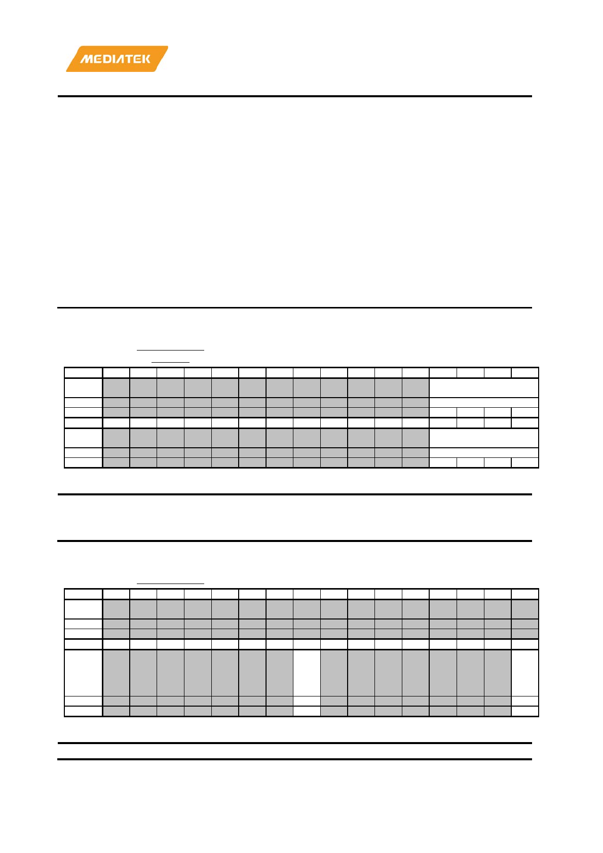
MT7686 Reference Manual
© 2016 - 2017 MediaTek Inc.
Page 509 of 536
This document contains information that is proprietary to MediaTek Inc. (“MediaTek”) and/or its licensor(s).
Any unauthorized use, reproduction or disclosure of this document in whole or in part is strictly prohibited.
Bit(s)
Mnemonic
Name
Description
24:16
WBTAC_RFDIG_LSFLDO_
OFF_TIME
CR_WBTAC_RFDIG_LSFL
DO_OFF_TIME_SEL
Actual
WBTAC_RFDIG_LSFLDO_OFF_TIME[8:0] =
WBTAC_RFDIG_LSFLDO_OFF_TIME_SW ?
WBTAC_RFDIG_LSFLDO_OFF_TIME[8:0] :
case(f_fxo_is_26m)
1'b1: f_fxo_ck=26 MHz ,9'd130
1'b0: f_fxo_ck=20 MHz ,9'd100
endcase
8:0
WBTAC_RDY_STABLE_TI
ME
CR_WBTAC_RDY_STABLE
_TIME_SEL
Actual
WBTAC_RDY_STABLE_TIME[8:0] =
WBTAC_RDY_STABLE_TIME_SW ?
WBTAC_RDY_STABLE_TIME[8:0] :
case(f_fxo_is_26m)
1'b1: f_fxo_ck=26 MHz ,9'd26
1'b0: f_fxo_ck=20 MHz ,9'd20
endcase
A204040
0
BBPLL_DBG
_PROB DEBUG PROB 00000000
Bit
31
30
29
28
27
26
25
24
23
22
21
20
19
18
17
16
Nam
e
BBPLL_DBG_PROB
Type
RO
Reset
0
0
0
0
Bit
15
14
13
12
11
10
9
8
7
6
5
4
3
2
1
0
Nam
e
BBPLL_DBG_SEL
Type
RW
Reset
0
0
0
0
Bit(s)
Mnemonic
Name
Description
19:16
BBPLL_DBG_PROB
BBPLL_DBG_PROB
Debug monitor
3:0
BBPLL_DBG_SEL
BBPLL_DBG_SEL
Debug monitor selection
A2040410 BBPLL_RDY BBPLL Ready Status 00000000
Bit
31
30
29
28
27
26
25
24
23
22
21
20
19
18
17
16
Nam
e
Type
Reset
Bit
15
14
13
12
11
10
9
8
7
6
5
4
3
2
1
0
Nam
e
BB
PL
L2
_R
DY
BB
PL
L1_
RD
Y
Type
RO
RO
Reset
0
0
Bit(s)
Mnemonic
Name
Description
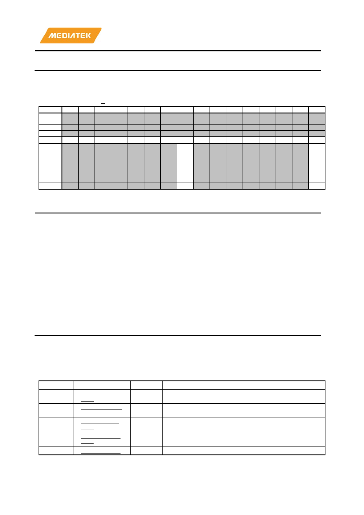
MT7686 Reference Manual
© 2016 - 2017 MediaTek Inc.
Page 510 of 536
This document contains information that is proprietary to MediaTek Inc. (“MediaTek”) and/or its licensor(s).
Any unauthorized use, reproduction or disclosure of this document in whole or in part is strictly prohibited.
8
BBPLL2_RDY
BBPLL2_RDY
Hardware mode BBPLL2 ready status
0
BBPLL1_RDY
BBPLL1_RDY
Hardware mode BBPLL1 ready status
A204070
0
PLLTD_CON
0 PLLTD Control Register 0 00000000
Bit
31
30
29
28
27
26
25
24
23
22
21
20
19
18
17
16
Nam
e
Type
Reset
Bit
15
14
13
12
11
10
9
8
7
6
5
4
3
2
1
0
Nam
e
BP
_C
PU
_C
TR
L
BP
_P
LL
_D
LY
Type
RW
RW
Reset
0
0
Overview
Selects control path of PLL power on sequence
Bit(s)
Mnemonic
Name
Description
8
BP_CPU_CTRL
BP_CPU_CTRL
Selects control path of PLL SW setting
•
0: Controlled by CPU
•
1: Controlled by SPM
0
BP_PLL_DLY
BP_PLL_DLY
Selects control path of PLL power on sequence in normal mode.
Automation delay control uses counter to create PLL power on
sequence.
RG_xPLL_EN is configured in the software, the other
signals required for PLL power on sequence could
be created by
hardware.
If
PLLx_EN_SEL is set to 0, then PLL will be turned off when
PLL_OFF
of DPM (Dynamic PLL Management) is 1 even though
register
RG_xPLL_EN is kept 1.
•
0: Controlled by automation delay control
•
1: Controlled by software configuration
22.2.2. cksys_xo_clk register map
Module name: cksys_xo_clk Base address: (+A2030000h)
Address
Name
Width
Register Function
A2030B00
XO_PDN_CO
ND0 32 Clock gating control 0
A2030B10
XO_PDN_SET
D0 32 Clock gating set 0
A2030B20
XO_PDN_CL
RD0 32 Clock gating clear 0
A2030C00 XO_DCM_CO
N_0 32
XO domain clock DCM 0
XO domain clock DCM configuration
A2030C04
XO_DCM_CO
32
XO domain clock DCM 1
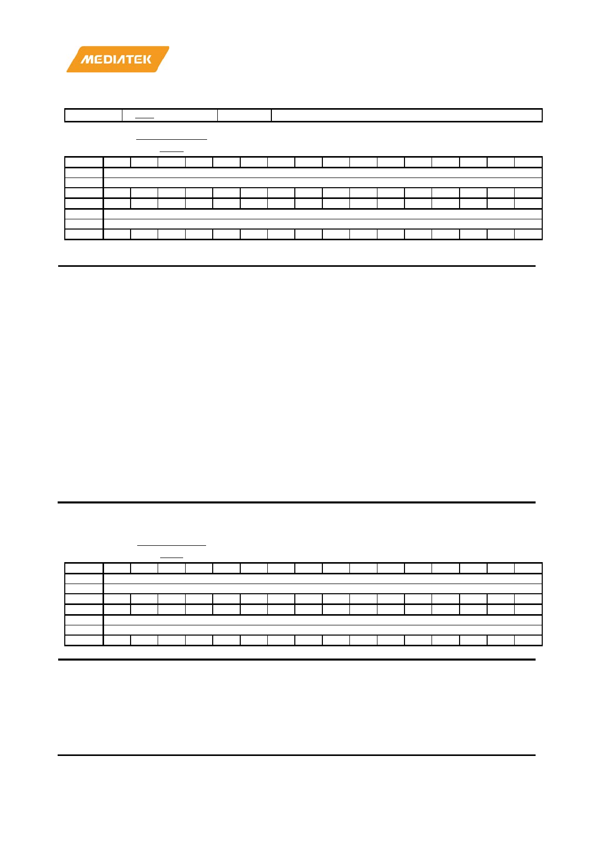
MT7686 Reference Manual
© 2016 - 2017 MediaTek Inc.
Page 511 of 536
This document contains information that is proprietary to MediaTek Inc. (“MediaTek”) and/or its licensor(s).
Any unauthorized use, reproduction or disclosure of this document in whole or in part is strictly prohibited.
Module name: cksys_xo_clk Base address: (+A2030000h)
N_1
XO domain clock DCM configuration
A2030B0
0
XO_PDN_CO
ND0 Clock gating control 0 0000FFFF
Bit
31
30
29
28
27
26
25
24
23
22
21
20
19
18
17
16
Mne
XO_PDN_COND0[31:16]
Type
RO
Reset
0
0
0
0
0
0
0
0
0
0
0
0
0
0
0
0
Bit
15
14
13
12
11
10
9
8
7
6
5
4
3
2
1
0
Mne
XO_PDN_COND0[15:0]
Type
RO
Reset
1
1
1
1
1
1
1
1
1
1
1
1
1
1
1
1
Bit(s)
Mnemonic
Name
Description
31:0
XO_PDN_COND0
Indicates clock on/off status.
21 RG_SW_AUXADC_CG
20 RSV_20
19 RG_SW_SEJ_CG
18 RG_SW_EFUSE_CG
17 RG_SW_GPTIMER_CG
16 RG_SW_SPM_CG
9
RG_SW_PWM5_CG
8 RG_SW_PWM4_CG
7 RG_SW_PWM3_CG
6 RG_SW_PWM2_CG
5 RG_SW_PWM1_CG
4 RG_SW_PWM0_CG
3 RSV_3
2 RSV_2
1 RSV_1
0 RG_SW_BBPLL_CG
0: Clock is turned on
1: Clock is gated off
A2030B10 XO_PDN_SE
TD0 Clock gating set 0 00000000
Bit
31
30
29
28
27
26
25
24
23
22
21
20
19
18
17
16
Mne
XO_PDN_SETD0[31:16]
Type
WO
Reset
0
0
0
0
0
0
0
0
0
0
0
0
0
0
0
0
Bit
15
14
13
12
11
10
9
8
7
6
5
4
3
2
1
0
Mne
XO_PDN_SETD0[15:0]
Type
WO
Reset
0
0
0
0
0
0
0
0
0
0
0
0
0
0
0
0
Bit(s)
Mnemonic
Name
Description
31:0
XO_PDN_SETD0
Write 1 to set up clock gating control.
21 RG_SW_AUXADC_CG
20 RSV_20
19 RG_SW_SEJ_CG
18 RG_SW_EFUSE_CG
17 RG_SW_GPTIMER_CG
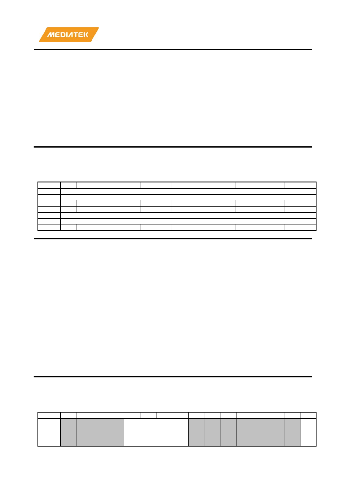
MT7686 Reference Manual
© 2016 - 2017 MediaTek Inc.
Page 512 of 536
This document contains information that is proprietary to MediaTek Inc. (“MediaTek”) and/or its licensor(s).
Any unauthorized use, reproduction or disclosure of this document in whole or in part is strictly prohibited.
16 RG_SW_SPM_CG
9 RG_SW_PWM5_CG
8 RG_SW_PWM4_CG
7 RG_SW_PWM3_CG
6 RG_SW_PWM2_CG
5 RG_SW_PWM1_CG
4 RG_SW_PWM0_CG
3 RSV_3
2 RSV_2
1 RSV_1
0 RG_SW_BBPLL_CG
0: No active
1: To turn off clock
A2030B2
0
XO_PDN_CL
RD0 Clock gating clear 0 00000000
Bit
31
30
29
28
27
26
25
24
23
22
21
20
19
18
17
16
Mne
XO_PDN_CLRD0[31:16]
Type
WO
Reset
0
0
0
0
0
0
0
0
0
0
0
0
0
0
0
0
Bit
15
14
13
12
11
10
9
8
7
6
5
4
3
2
1
0
Mne
XO_PDN_CLRD0[15:0]
Type
WO
Reset
0
0
0
0
0
0
0
0
0
0
0
0
0
0
0
0
Bit(s)
Mnemonic
Name
Description
31:0
XO_PDN_CLRD0
Write 1 to clear clock gating control.
21 RG_SW_AUXADC_CG
20 RSV_20
19 RG_SW_SEJ_CG
18 RG_SW_EFUSE_CG
17 RG_SW_GPTIMER_CG
16
RG_SW_SPM_CG
9 RG_SW_PWM5_CG
8 RG_SW_PWM4_CG
7 RG_SW_PWM3_CG
6 RG_SW_PWM2_CG
5 RG_SW_PWM1_CG
4 RG_SW_PWM0_CG
3 RSV_3
2 RSV_2
1 RSV_1
0 RG_SW_BBPLL_CG
0: No active
1: To turn on clock
A2030C0
0
XO_DCM_C
ON_0 XO domain clock dcm 0 00000002
Bit
31
30
29
28
27
26
25
24
23
22
21
20
19
18
17
16
Nam
e RG_XO_DCM_EN
RG
_X
O_
DC
M_
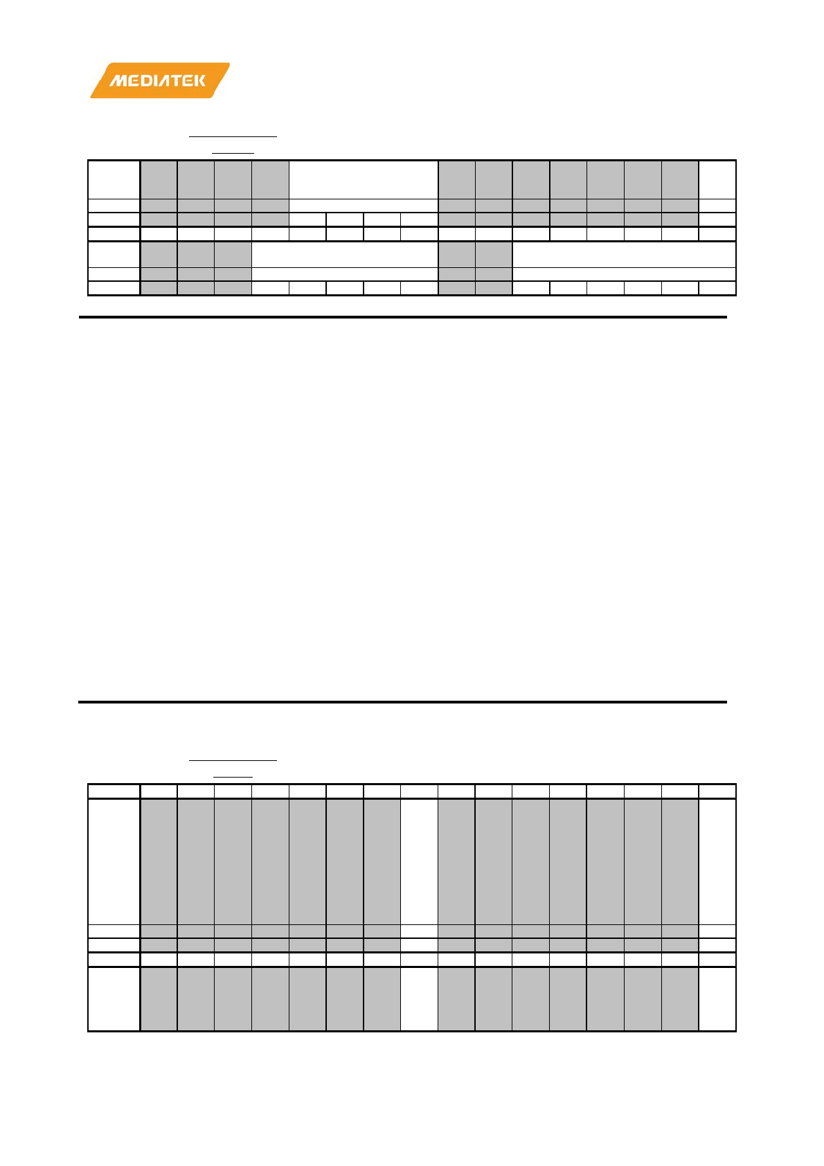
MT7686 Reference Manual
© 2016 - 2017 MediaTek Inc.
Page 513 of 536
This document contains information that is proprietary to MediaTek Inc. (“MediaTek”) and/or its licensor(s).
Any unauthorized use, reproduction or disclosure of this document in whole or in part is strictly prohibited.
A2030C0
0
XO_DCM_C
ON_0 XO domain clock dcm 0 00000002
DB
C_
EN
Type
RW
RW
Reset
0
0
0
0
0
Bit
15
14
13
12
11
10
9
8
7
6
5
4
3
2
1
0
Nam
e
RG_XO_DCM_DBC_NUM RG_XO_SFSEL
Type
RW
RW
Reset
0
0
0
0
0
0
0
0
0
1
0
Bit(s)
Mnemonic
Name
Description
27:24
RG_XO_DCM_EN
Infra sub
-block DCM
•
0: Disable
•
1: Enable
16
RG_XO_DCM_DBC_EN
Infra XO DCM debounce
•
0: Disable
•
1: Enable
12:8
RG_XO_DCM_DBC_NUM
Infra XO DCM debounce number
•
0: Disable
•
1: Enable
5:0
RG_XO_SFSEL
Select how to divide the infra XO DCM idle clock
frequency
100000: /1
010000: /2
001000: /4
000100: /8
000010: /16
000001: /32
000000: /64
A2030C0
4
XO_DCM_C
ON_1 XO domain clock dcm 1 00000000
Bit
31
30
29
28
27
26
25
24
23
22
21
20
19
18
17
16
Nam
e
RG
_X
O_
FO
RC
E_
CL
KS
LO
W
RG
_X
O_
FO
RC
E_
CL
KO
FF
Type
RW
RW
Reset
0
0
Bit
15
14
13
12
11
10
9
8
7
6
5
4
3
2
1
0
Nam
e
RG
_X
O_
CL
KS
RG
_X
O_
CL
KO

MT7686 Reference Manual
© 2016 - 2017 MediaTek Inc.
Page 514 of 536
This document contains information that is proprietary to MediaTek Inc. (“MediaTek”) and/or its licensor(s).
Any unauthorized use, reproduction or disclosure of this document in whole or in part is strictly prohibited.
A2030C0
4
XO_DCM_C
ON_1 XO domain clock dcm 1 00000000
LO
W_
EN
FF
_E
N
Type
RW
RW
Reset
0
0
Bit(s)
Mnemonic
Name
Description
24
RG_XO_FORCE_CLKSLOW
Infra XO DCM force clock slow
•
0: Disable
•
1: Enable
16
RG_XO_FORCE_CLKOFF
Infra XO DCM force clock off
•
0: Disable
•
1: Enable
8
RG_XO_CLKSLOW_EN
Infra XO DCM clock slow en
•
0: Disable
•
1: Enable
0
RG_XO_CLKOFF_EN
Infra XO DCM clock off en
•
0: Disable
•
1: Enable
22.2.3. cksys_bus_clk register map
Module name: cksys_bus_clk Base address: (+A21D0000h)
Address
Name
Width
Register Function
A21D0100 BUS_DCM_C
ON_0 32
Bus domain clock DCM 0
Bus domain clock DCM configuration
A21D0104 BUS_DCM_C
ON_1 32 Bus domain clock DCM 1
Bus domain clock DCM configuration
A21D0110 CM4_DCM_C
ON_0 32
Cortex-M4 domain clock DCM 0
Cortex-M4 domain clock DCM configuration
A21D0114 CM4_DCM_C
ON_1 32
Cortex-M4 domain clock DCM 1
Cortex-M4 domain clock DCM configuration
A21D0130 SYS_FREE_D
CM_CON 32
CM domain free run clock DCM
CM domain free run clock DCM configuration
A21D0140 SFC_DCM_CO
N_0 32 SFC domain clock DCM 0
SFC domain clock DCM configuration
A21D0144 SFC_DCM_CO
N_1 32
SFC domain clock DCM 1
SFC domain clock DCM configuration
A21D0170 CLK_FREQ_S
WCH 32
Clock Switch register
Frequency configuration of normal mode
A21D0300
PDN_COND0
32
Clock gating control 0
A21D0310 PDN_SETD0 32 Clock gating set 0
A21D0320
PDN_CLRD0
32
Clock gating clear 0
A21D0100 BUS_DCM_C
ON_0 bus domain clock DCM 0 00000000
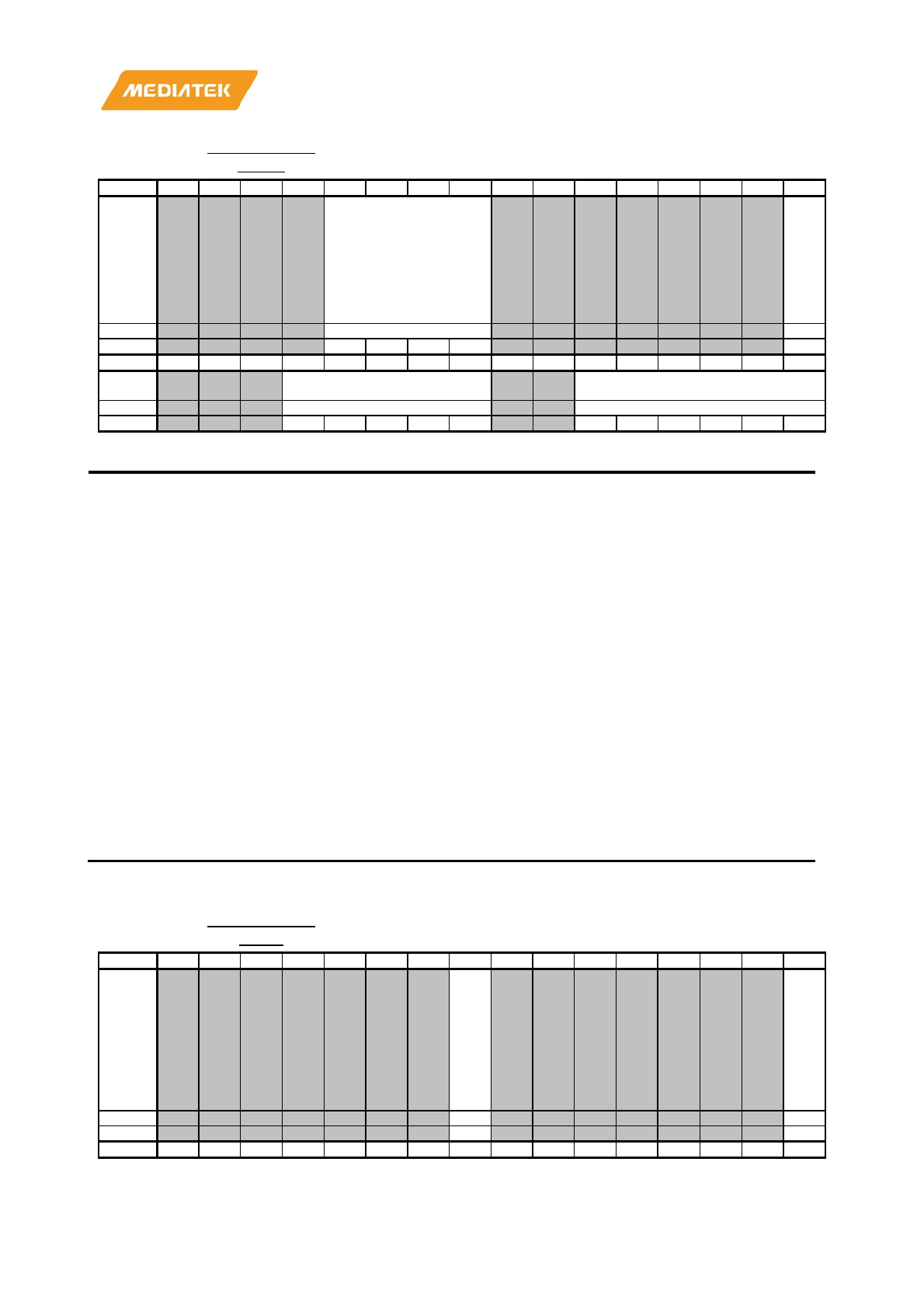
MT7686 Reference Manual
© 2016 - 2017 MediaTek Inc.
Page 515 of 536
This document contains information that is proprietary to MediaTek Inc. (“MediaTek”) and/or its licensor(s).
Any unauthorized use, reproduction or disclosure of this document in whole or in part is strictly prohibited.
A21D0100 BUS_DCM_C
ON_0 bus domain clock DCM 0 00000000
Bit
31
30
29
28
27
26
25
24
23
22
21
20
19
18
17
16
Nam
e RG_BUS_DCM_EN
RG
_B
US
_D
CM
_D
BC
_E
N
Type
RW
RW
Reset
0
0
0
0
0
Bit
15
14
13
12
11
10
9
8
7
6
5
4
3
2
1
0
Nam
e
RG_BUS_DCM_DBC_NUM RG_BUS_SFSEL
Type
RW
RW
Reset
0
0
0
0
0
0
0
0
0
0
0
Bit(s)
Mnemonic
Name
Description
27:24
RG_BUS_DCM_EN
Infra sub block DCM disable enable
•
0: Disable
•
1: Enable
16
RG_BUS_DCM_DBC_EN
Infra bus DCM debounce en
able
•
0: Disable
•
1: Enable
12:8
RG_BUS_DCM_DBC_NUM
Infra bus DCM debounce number
•
0: Disable
•
1: Enable
5:0
RG_BUS_SFSEL
Infra bus DCM idle divide selection
100000: /1
010000: /2
001000: /4
000100: /8
000010: /16
000001: /32
000000: /64
A21D0104 BUS_DCM_C
ON_1 bus domain clock dcm 1 00000000
Bit
31
30
29
28
27
26
25
24
23
22
21
20
19
18
17
16
Nam
e
RG
_B
US
_F
OR
CE
_C
LK
SL
OW
RG
_B
US
_F
OR
CE
_C
LK
OF
F
Type
RW
RW
Reset
0
0
Bit
15
14
13
12
11
10
9
8
7
6
5
4
3
2
1
0
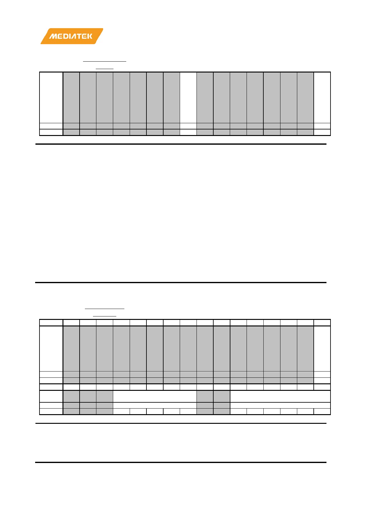
MT7686 Reference Manual
© 2016 - 2017 MediaTek Inc.
Page 516 of 536
This document contains information that is proprietary to MediaTek Inc. (“MediaTek”) and/or its licensor(s).
Any unauthorized use, reproduction or disclosure of this document in whole or in part is strictly prohibited.
A21D0104 BUS_DCM_C
ON_1 bus domain clock dcm 1 00000000
Nam
e
RG
_B
US
_C
LK
SL
OW
_E
N
RG
_B
US
_C
LK
OF
F_
EN
Type
RW
RW
Reset
0
0
Bit(s)
Mnemonic
Name
Description
24
RG_BUS_FORCE_CLKSLOW
Infra bus DCM force clock slow
•
0: Disable
•
1: Enable
16
RG_BUS_FORCE_CLKOFF
Infra bus DCM force clock off
•
0: Disable
•
1: Enable
8
RG_BUS_CLKSLOW_EN
Infra bus DCM clock slow en
able
•
0: Disable
•
1: Enable
0
RG_BUS_CLKOFF_EN
Infra bus DCM clock off en
able (turn on at the
same time with CLKSOW_EN)
•
0: Disable
•
1: Enable
A21D0110 CM4_DCM_
CON_0 Cortex-M4 domain clock DCM 0 00000000
Bit
31
30
29
28
27
26
25
24
23
22
21
20
19
18
17
16
Nam
e
RG
_C
M_
DC
M_
DB
C_
EN
Type
RW
Reset
0
Bit
15
14
13
12
11
10
9
8
7
6
5
4
3
2
1
0
Nam
e
RG_CM_DCM_DBC_NUM RG_CM_SFSEL
Type
RW
RW
Reset
0
0
0
0
0
0
0
0
0
0
0
Bit(s)
Mnemonic
Name
Description
16
RG_CM_DCM_DBC_EN
CMSYS domain DCM debounce en
•
0: Disable
•
1: Enable
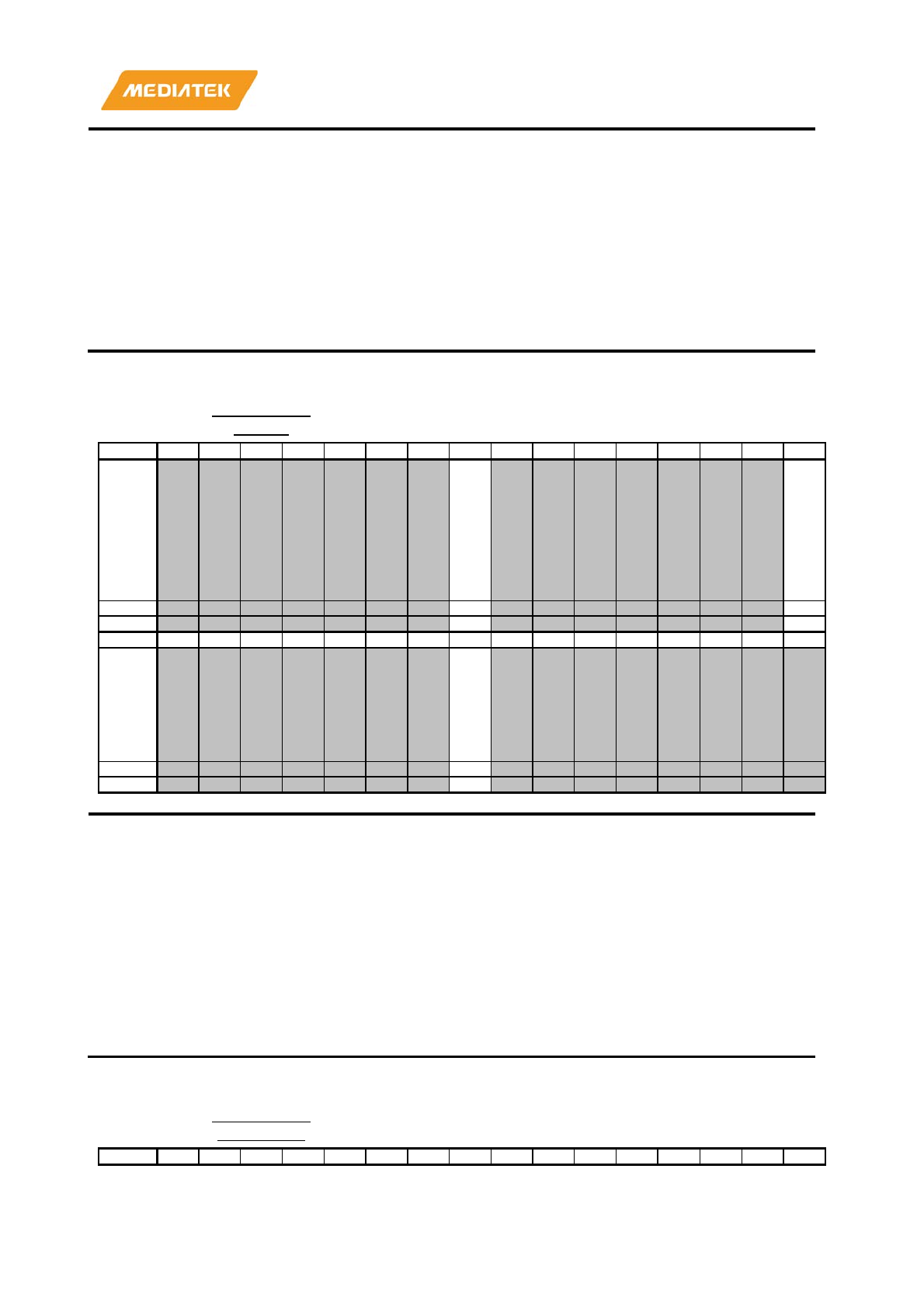
MT7686 Reference Manual
© 2016 - 2017 MediaTek Inc.
Page 517 of 536
This document contains information that is proprietary to MediaTek Inc. (“MediaTek”) and/or its licensor(s).
Any unauthorized use, reproduction or disclosure of this document in whole or in part is strictly prohibited.
12:8
RG_CM_DCM_DBC_NUM
CMSYS domain DCM debounce number
•
0: Disable
•
1: Enable
5:0
RG_CM_SFSEL
CMSYS domain
DCM idle divide selection
100000: /1
010000: /2
001000: /4
000100: /8
000010: /16
000001: /32
000000: /64
A21D0114 CM4_DCM_
CON_1 Cortex-M4 domain clock DCM 1 00000000
Bit
31
30
29
28
27
26
25
24
23
22
21
20
19
18
17
16
Nam
e
RG
_C
M_
FO
RC
E_
CL
KS
LO
W
RG
_C
M_
FO
RC
E_
CL
KO
FF
Type
RW
RW
Reset
0
0
Bit
15
14
13
12
11
10
9
8
7
6
5
4
3
2
1
0
Nam
e
RG
_C
M_
CL
KS
LO
W_
EN
Type
RW
Reset
0
Bit(s)
Mnemonic
Name
Description
24
RG_CM_FORCE_CLKSLOW
CMSYS domain DCM force clock slow
•
0: Disable
•
1: Enable
16
RG_CM_FORCE_CLKOFF
CMSYS domain DCM force clock off
•
0: Disable
•
1: Enable
8
RG_CM_CLKSLOW_EN
CMSYS domain DCM clock slow en
•
0: Disable
•
1: Enable
A21D0130 SYS_FREE_
DCM_CON cm domain free run clock dcm 00000020
Bit
31
30
29
28
27
26
25
24
23
22
21
20
19
18
17
16
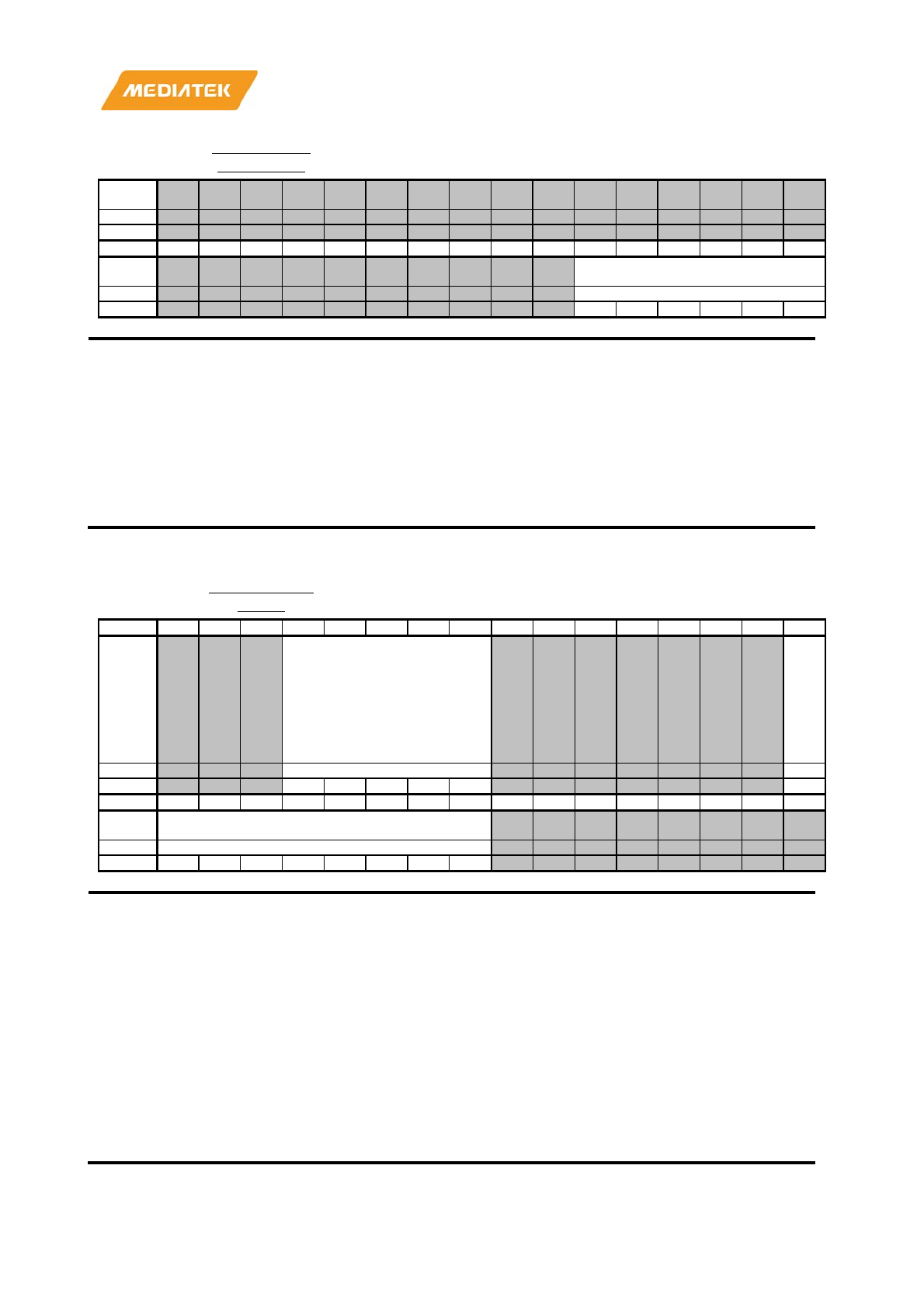
MT7686 Reference Manual
© 2016 - 2017 MediaTek Inc.
Page 518 of 536
This document contains information that is proprietary to MediaTek Inc. (“MediaTek”) and/or its licensor(s).
Any unauthorized use, reproduction or disclosure of this document in whole or in part is strictly prohibited.
A21D0130 SYS_FREE_
DCM_CON cm domain free run clock dcm 00000020
Nam
e
Type
Reset
Bit
15
14
13
12
11
10
9
8
7
6
5
4
3
2
1
0
Nam
e
RG_SYS_FREE_FSEL
Type
RW
Reset
1
0
0
0
0
0
Bit(s)
Mnemonic
Name
Description
5:0
RG_SYS_FREE_FSEL
SYS (CMSYS and BUS) domain free run DCM divide
selection
100000: /1
010000: /2
001000: /4
000100: /8
000010: /16
000001: /32
000000: /64
A21D0140 SFC_DCM_C
ON_0 SFC domain clock DCM 0 00000000
Bit
31
30
29
28
27
26
25
24
23
22
21
20
19
18
17
16
Nam
e RG_SFC_DCM_APB_SEL
RG
_S
FC
_D
CM
_D
BC
_E
N
Type
RW
RW
Reset
0
0
0
0
0
0
Bit
15
14
13
12
11
10
9
8
7
6
5
4
3
2
1
0
Nam
e
RG_SFC_DCM_DBC_NUM
Type
RW
Reset
0
0
0
0
0
0
0
0
Bit(s)
Mnemonic
Name
Description
28:24
RG_SFC_DCM_APB_SEL
Each bit corresponds to the selection of change to
activate.
•
bit 0: dcm_force_on
•
bit 1: dcm_en
•
bit 2: dbc_en
•
bit 3: dcm_fsel
16
RG_SFC_DCM_DBC_EN
SFC domain DCM debounce en
able
•
0: Disable
•
1: Enable
15:8
RG_SFC_DCM_DBC_NUM
SFC domain DCM debounce number
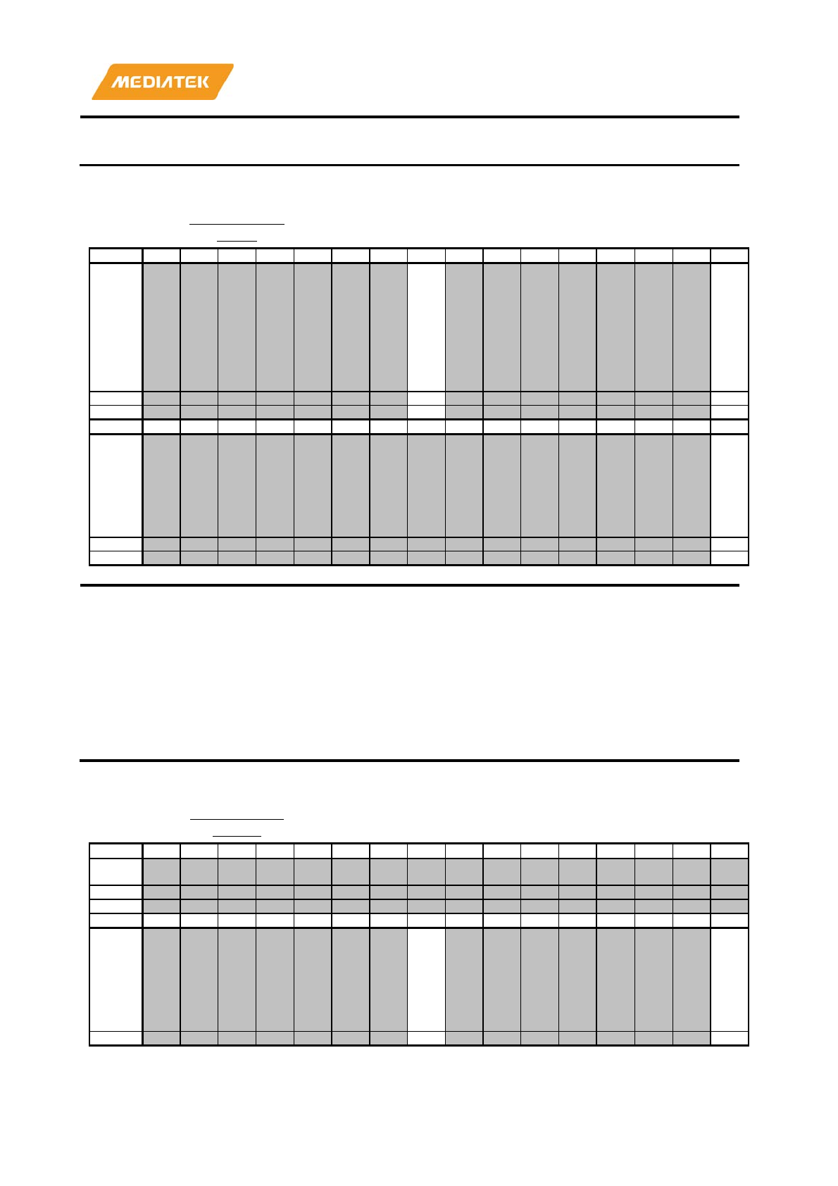
MT7686 Reference Manual
© 2016 - 2017 MediaTek Inc.
Page 519 of 536
This document contains information that is proprietary to MediaTek Inc. (“MediaTek”) and/or its licensor(s).
Any unauthorized use, reproduction or disclosure of this document in whole or in part is strictly prohibited.
•
0: Disable
•
1: Enable
A21D0144 SFC_DCM_C
ON_1 SFC domain clock DCM 1 00000000
Bit
31
30
29
28
27
26
25
24
23
22
21
20
19
18
17
16
Nam
e
RG
_S
FC
_D
CM
_A
PB
_T
OG
RG
_S
FC
_F
OR
CE
_C
LK
OF
F
Type
RW
RW
Reset
0
0
Bit
15
14
13
12
11
10
9
8
7
6
5
4
3
2
1
0
Nam
e
RG
_S
FC
_C
LK
OF
F_
EN
Type
RW
Reset
0
Bit(s)
Mnemonic
Name
Description
24
RG_SFC_DCM_APB_TOG
Toggle the bit to activate the change
16
RG_SFC_FORCE_CLKOFF
SFC domain DCM force clock off
•
0: Disable
•
1: Enable
0
RG_SFC_CLKOFF_EN
SFC domain DCM clock
off enable
•
0: Disable
•
1: Enable
A21D0170 CLK_FREQ_
SWCH Clock Switch register 00000100
Bit
31
30
29
28
27
26
25
24
23
22
21
20
19
18
17
16
Nam
e
Type
Reset
Bit
15
14
13
12
11
10
9
8
7
6
5
4
3
2
1
0
Nam
e
RG
_P
D_
PL
LC
K_
SE
L
RG
_P
LL
CK
_S
EL
Type
RW
RW
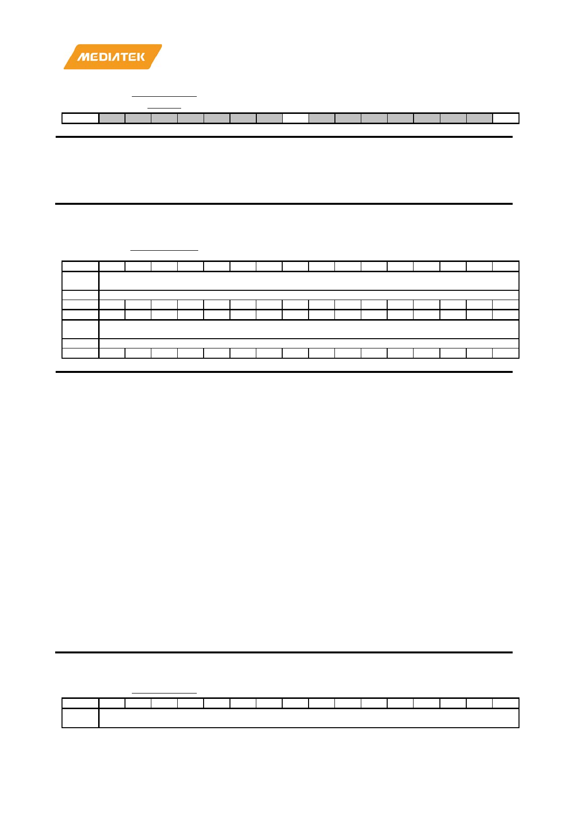
MT7686 Reference Manual
© 2016 - 2017 MediaTek Inc.
Page 520 of 536
This document contains information that is proprietary to MediaTek Inc. (“MediaTek”) and/or its licensor(s).
Any unauthorized use, reproduction or disclosure of this document in whole or in part is strictly prohibited.
A21D0170 CLK_FREQ_
SWCH Clock Switch register 00000100
Reset
1
0
Bit(s)
Mnemonic
Name
Description
8
RG_PD_PLLCK_SEL
Set to 1 to switch all PD clocks to PLL clock source instead of
26MHz used for initial power
-on.
0
RG_PLLCK_SEL
Set to 1 to switch all clocks to PLL clock
source instead of
26MHz used for initial power
-on.
A21D030
0 PDN_COND0 Clock gating control 0 0000FFFF
Bit
31
30
29
28
27
26
25
24
23
22
21
20
19
18
17
16
Nam
e
PDN_COND0[31:16]
Type
RO
Reset
0
0
0
0
0
0
0
0
0
0
0
0
0
0
0
0
Bit
15
14
13
12
11
10
9
8
7
6
5
4
3
2
1
0
Nam
e
PDN_COND0[15:0]
Type
RO
Reset
1
1
1
1
1
1
1
1
1
1
1
1
1
1
1
1
Bit(s)
Mnemonic
Name
Description
31:0
PDN_COND0
Indicate clock on/off status.
22 RG_SW_SDIOSLV_CG
21 RG_SW_CRYPTO_CG
20 RG_SW_UART0_CG
19 RG_SW_XTALCTL_CG
18 RG_SW_TRNG_CG
17 RG_SFC_SW_CG
16 RG_SW_CM_SYSROM_CG
13 RG_SW_I2C1_CG
12 RG_SW_I2C0_CG
11 RSV_11
10 RG_SW_UART2_CG
9 RG_SW_UART1_CG
8 RG_SW_SDIOMST_CG
7 RG_SW_AUDIO_CG
6 RG_SW_SPIMST_CG
5 RG_SW_SPISLV_CG
4 RG_SW_ASYS_CG
3
RG_SW_SDIOMST_BUS_CG
2 RG_SW_CONN_XO_CG
1 RSV_1
0 RG_SW_DMA_CG
0:
Clock is turned on
1: Clock is gated off
A21D0310 PDN_SETD0 Clock gating set 0 00000000
Bit
31
30
29
28
27
26
25
24
23
22
21
20
19
18
17
16
Nam
e
PDN_SETD0[31:16]
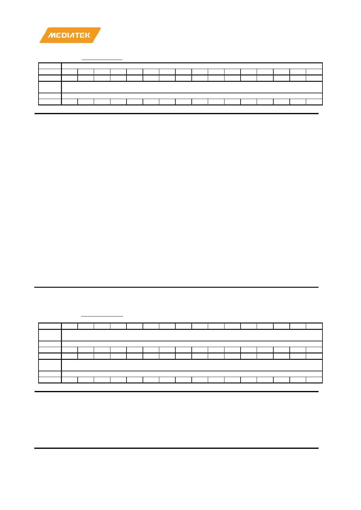
MT7686 Reference Manual
© 2016 - 2017 MediaTek Inc.
Page 521 of 536
This document contains information that is proprietary to MediaTek Inc. (“MediaTek”) and/or its licensor(s).
Any unauthorized use, reproduction or disclosure of this document in whole or in part is strictly prohibited.
A21D0310 PDN_SETD0 Clock gating set 0 00000000
Type
WO
Reset
0
0
0
0
0
0
0
0
0
0
0
0
0
0
0
0
Bit
15
14
13
12
11
10
9
8
7
6
5
4
3
2
1
0
Nam
e
PDN_SETD0[15:0]
Type
WO
Reset
0
0
0
0
0
0
0
0
0
0
0
0
0
0
0
0
Bit(s)
Mnemonic
Name
Description
31:0
PDN_SETD0
Write 1 to set up clock gating control.
22 RG_SW_SDIOSLV_CG
21 RG_SW_CRYPTO_CG
20 RG_SW_UART0_CG
19 RG_SW_XTALCTL_CG
18 RG_SW_TRNG_CG
17
RG_SFC_SW_CG
16 RG_SW_CM_SYSROM_CG
13 RG_SW_I2C1_CG
12 RG_SW_I2C0_CG
11 RSV_11
10 RG_SW_UART2_CG
9 RG_SW_UART1_CG
8 RG_SW_SDIOMST_CG
7 RG_SW_AUDIO_CG
6 RG_SW_SPIMST_CG
5 RG_SW_SPISLV_CG
4 RG_SW_ASYS_CG
3
RG_SW_SDIOMST_BUS_CG
2 RG_SW_CONN_XO_CG
1 RSV_1
0 RG
_SW_DMA_CG
0: No active
1: To turn off clock
A21D032
0 PDN_CLRD0 Clock gating clear 0 00000000
Bit
31
30
29
28
27
26
25
24
23
22
21
20
19
18
17
16
Nam
e
PDN_CLRD0[31:16]
Type
WO
Reset
0
0
0
0
0
0
0
0
0
0
0
0
0
0
0
0
Bit
15
14
13
12
11
10
9
8
7
6
5
4
3
2
1
0
Nam
e
PDN_CLRD0[15:0]
Type
WO
Reset
0
0
0
0
0
0
0
0
0
0
0
0
0
0
0
0
Bit(s)
Mnemonic
Name
Description
31:0
PDN_CLRD0
Write 1 to clear clock gating control.
22 RG_SW_SDIOSLV_CG
21 RG_SW_CRYPTO_CG
20 RG_SW_UART0_CG
19 RG_SW_XTALCTL_CG
18 RG_SW_TRNG_CG
MT7686 Reference Manual
© 2016 - 2017 MediaTek Inc.
Page 522 of 536
This document contains information that is proprietary to MediaTek Inc. (“MediaTek”) and/or its licensor(s).
Any unauthorized use, reproduction or disclosure of this document in whole or in part is strictly prohibited.
17 RG_SFC_SW_CG
16 RG_SW_CM_SYSROM_CG
13 RG_SW_I2C1_CG
12 RG_SW_I2C0_CG
11 RSV_11
10 RG_SW_UART2_CG
9 RG_SW_UART1_CG
8 RG_SW_SDIOMST_CG
7 RG_SW_AUDIO_CG
6 RG_SW_SPIMST_CG
5 RG_SW_SPISLV_CG
4 RG_SW_ASYS_CG
3
RG_SW_SDIOMST_BUS_CG
2 RG_SW_CONN_XO_CG
1 RSV_1
0 RG
_SW_DMA_CG
0: No active
1: To turn on clock
22.2.4. cksys register map
Module name: cksys Base address: (+A2020000h)
Address
Name
Width
Register Functionality
A2020220
CKSYS_TST_SEL_0
32
Test Clock Selection Register 0
A2020224
CKSYS_TST_SEL_1
32
Test Clock Selection Register 1
A2020240
CKSYS_CLK_CFG_0
32
Function Clock Selection Register 0
A2020244
CKSYS_CLK_CFG_1
32
Function Clock Selection Register 1
A2020250
CKSYS_CLK_UPDATE_0
32
Function Clock Selection Update Register 0
A2020254
CKSYS_CLK_UPDATE_1
32
Function Clock Selection Update Register 1
A2020260
CKSYS_CLK_UPDATE_ST
ATUS_0
32
Function Clock Selection Update Status
Register 0
A2020264
CKSYS_CLK_UPDATE_ST
ATUS_1
32
Function Clock Selection Update Status
Register 1
A2020270
CKSYS_CLK_FORCE_ON_
0
32
Function Clock Force On Register 0
A2020274
CKSYS_CLK_FORCE_ON_
1
32
Function Clock Force On Register 1
A2020280
CKSYS_CLK_DIV_0
32
Clock divider control register 0
A2020284
CKSYS_CLK_DIV_1
32
Clock divider control register 1
A2020288
CKSYS_CLK_DIV_2
32
Clock divider control register 2
A202028C
CKSYS_CLK_DIV_3
32
Clock divider control register 3
A2020290
CKSYS_CLK_DIV_4
32
Clock divider control register 4
A2020294
CKSYS_CLK_DIV_5
32
Clock divider control register 5
A20202A0
CKSYS_XTAL_FREQ
32
XTAL frequency control register
A20202A4
CKSYS_REF_CLK_SEL
32
PLL reference clock selection register
MT7686 Reference Manual
© 2016 - 2017 MediaTek Inc.
Page 523 of 536
This document contains information that is proprietary to MediaTek Inc. (“MediaTek”) and/or its licensor(s).
Any unauthorized use, reproduction or disclosure of this document in whole or in part is strictly prohibited.
Address Name Width Register Functionality
A2020400
PLL_ABIST_FQMTR_CON
0
32
Frequency Meter Control Register 0
Enables frequency meter and sets
parameter.
Frequency(TESTED clock) =
Frequency(FIXED clock) *
FQMTR_DATA[15:0]/FQMTR_WINSET[11:0
]
A2020404
PLL_ABIST_FQMTR_CON
1
32
Frequency Meter Control Register 1
Selects measured clock of frequency meter
A2020408
PLL_ABIST_FQMTR_CON
2
32
Frequency Meter Control Register 2
Selects measured clock of frequency meter
A202040C
PLL_ABIST_FQMTR_DAT
A
32
Frequency Meter Data
Measurement result of frequency meter.
Frequency(TESTED clock) =
Frequency(FIXED clock)
*{FQMTR_DATA_MSB[7:0],
FQMTR_DATA[15:0]}/FQMTR_WINSET[11:
0]
A2020220
CKSYS_TST_SEL_0
32
Test Clock Selection Register 0
A2020224
CKSYS_TST_SEL_1
32
Test Clock Selection Register 1
A2020240
CKSYS_CLK_CFG_0
32
Function Clock Selection Register 0
A2020244
CKSYS_CLK_CFG_1
32
Function Clock Selection Register 1
A2020250
CKSYS_CLK_UPDATE_0
32
Function Clock Selection Update Register 0
A2020254
CKSYS_CLK_UPDATE_1
32
Function Clock Selection Update Register 1
A2020260
CKSYS_CLK_UPDATE_ST
ATUS_0
32
Function Clock Selection Update Status
Register 0
A2020264
CKSYS_CLK_UPDATE_ST
ATUS_1
32
Function Clock Selection Update Status
Register 1
A2020270
CKSYS_CLK_FORCE_ON_
0
32
Function Clock Force On Register 0
A2020274
CKSYS_CLK_FORCE_ON_
1
32
Function Clock Force On Register 1
A2020280
CKSYS_CLK_DIV_0
32
Clock divider control register 0
A2020284
CKSYS_CLK_DIV_1
32
Clock divider control register 1
A2020288
CKSYS_CLK_DIV_2
32
Clock divider control register 2
A202028C
CKSYS_CLK_DIV_3
32
Clock divider control register 3
A2020290
CKSYS_CLK_DIV_4
32
Clock divider control register 4
A2020294
CKSYS_CLK_DIV_5
32
Clock divider control register 5
A20202A0
CKSYS_XTAL_FREQ
32
XTAL frequency control register
A20202A4
CKSYS_REF_CLK_SEL
32
PLL reference clock selection register
A2020400
PLL_ABIST_FQMTR_CON
0
32
Frequency Meter Control Register 0
Enables frequency meter and sets
parameter.
Frequency(TESTED clock) =
Frequency(FIXED clock) *
FQMTR_DATA[15:0]/FQMTR_WINSET[11:0
]
A2020404
PLL_ABIST_FQMTR_CON
1
32
Frequency Meter Control Register 1
Selects measured clock of frequency meter
A2020408
PLL_ABIST_FQMTR_CON
2
32
Frequency Meter Control Register 2
Selects measured clock of frequency meter
MT7686 Reference Manual
© 2016 - 2017 MediaTek Inc.
Page 524 of 536
This document contains information that is proprietary to MediaTek Inc. (“MediaTek”) and/or its licensor(s).
Any unauthorized use, reproduction or disclosure of this document in whole or in part is strictly prohibited.
Address Name Width Register Functionality
A202040C
PLL_ABIST_FQMTR_DAT
A
32
Frequency Meter Data
Measurement result of frequency meter.
Frequency(TESTED clock) =
Frequency(FIXED clock)
*{FQMTR_DATA_MSB[7:0],
FQMTR_DATA[15:0]}/FQMTR_WINSET[11:
0]
A202022
0
CKSYS_TST_
SEL_0 Test Clock Selection Register 0 00000000
Bit
31
30
29
28
27
26
25
24
23
22
21
20
19
18
17
16
Mne
tst_sel_0[31:16]
Type
RW
Reset
0
0
0
0
0
0
0
0
0
0
0
0
0
0
0
0
Bit
15
14
13
12
11
10
9
8
7
6
5
4
3
2
1
0
Mne
tst_sel_0[15:0]
Type
RW
Reset
0
0
0
0
0
0
0
0
0
0
0
0
0
0
0
0
Bit(s)
Mnemonic
Name
Description
31:0
tst_sel_0
tst_sel_0
[0:0] tstclk1_sel 0: tclk1;1: tclk4 tstclk1; clock option selection
•
[1:1] tstclk2_sel 0: tclk2;1: tclk5 tstclk2; clock option selection
•
[3:2] fsys_tstsel 0: from PLL;1: from tclk3;2: from tstclk1;3: from
tstclk2; TST clock source selection
•
[5:4] fsfc_tstsel 0: from PLL;1: from tclk3;2: from tstclk1;3: from
tstclk2; TST clock source selection
•
[7:6] fconn_tstsel0 0: from PLL;1: from tclk3;2: from tstclk1;3:
from tstclk2; TST clock source selection
•
[9:8] fspimst_tstsel0 0: from PLL;1: from tclk3;2: from tstclk1;3:
from tstclk2; TST clock source selection
•
[11:10] fxtalctl_tstsel0 0: from PLL;1: from tclk3;2: from
tstclk1;3: from tstclk2; TST clock source selection
•
[13:12] fsdiomst_tstsel0 0: from PLL;1: from tclk3;2: from
tstclk1;3: from tstclk2; TST clock source selection
A2020224 CKSYS_TST_
SEL_1 Test Clock Selection Register 1 00000000
Bit
31
30
29
28
27
26
25
24
23
22
21
20
19
18
17
16
Mne
tst_sel_1[31:16]
Type
RW
Reset
0
0
0
0
0
0
0
0
0
0
0
0
0
0
0
0
Bit
15
14
13
12
11
10
9
8
7
6
5
4
3
2
1
0
Mne
tst_sel_1[15:0]
Type
RW
Reset
0
0
0
0
0
0
0
0
0
0
0
0
0
0
0
0
Bit(s)
Mnemonic
Name
Description
31:0
tst_sel_1
tst_sel_1
[4:0] fqmtr_tcksel
0: 0
1: f_fxo_ck
2: f_frtc_ck
3: clk_pll2_d3
MT7686 Reference Manual
© 2016 - 2017 MediaTek Inc.
Page 525 of 536
This document contains information that is proprietary to MediaTek Inc. (“MediaTek”) and/or its licensor(s).
Any unauthorized use, reproduction or disclosure of this document in whole or in part is strictly prohibited.
4: clk_pll1_d2
5: f_fxo_2m_ck
6:
AD_XO_BBTOP_CLK (after test MUX)
7: AD_XO_CK
8: clk_pll2_d5
9: clk_pll2_d15
10: clk_pll1_d7
11: AD_XPLL_CLK
12: AD_WF_BBPLL_CKMON
13: AD_XO_BBTOP_CLK
14: 0
15: 0
16: PAD_SOC_CK (for testmode)
17: hf_fsfc_ck
18: hf_fconn_ck
19: hf_fsys_ck
20: f_fspimst_ck
2
1: f_fsdiomst_ck
22: f_fxtalctl_ck
23: bbpll2_d3_d8
24: bbpll2_d5_d4
25: bbpll2_d5_d8
26: bbpll1_d7_d2
27: xo_d2
28: 0
29: 0
30: 0
31: fixed_ck
[10:8] fqmtr_fcksel
0: f_fxo_ck
1: f_frtc_ck
2: PAD_SOC_CK (for testmode)
3: AD_XO_BBTOP_CLK
4: EOSC32K_CK
5: xo
_div_32k_ck
6: XOSC32K_CK
7: f_fxtalctl_ck
A202024
0
CKSYS_CLK
_CFG_0 Function Clock Selection Register 0 00000000
Bit
31
30
29
28
27
26
25
24
23
22
21
20
19
18
17
16
Mne
clk_spimst_sel
clk_conn_sel
Type
RW
RW
Reset
0
0
0
0
0
0
0
0
0
0
0
0
0
0
0
0
Bit
15
14
13
12
11
10
9
8
7
6
5
4
3
2
1
0
Mne
clk_sfc_sel
clk_sys_sel
Type
RW
RW
Reset
0
0
0
0
0
0
0
0
0
0
0
0
0
0
0
0
Bit(s)
Mnemonic
Name
Description
31:24
clk_spimst_sel
clk_spimst_sel
Selects f_fspimst_ck clock MUX
•
0: xo_ck, 26/20(MHz)
•
1: BBPLL2_D5_D4, 48(MHz)
•
2: BBPLL2_D5_D2, 96(MHz)
23:16
clk_conn_sel
clk_conn_sel
Selects hf_fconn_ck clock MUX
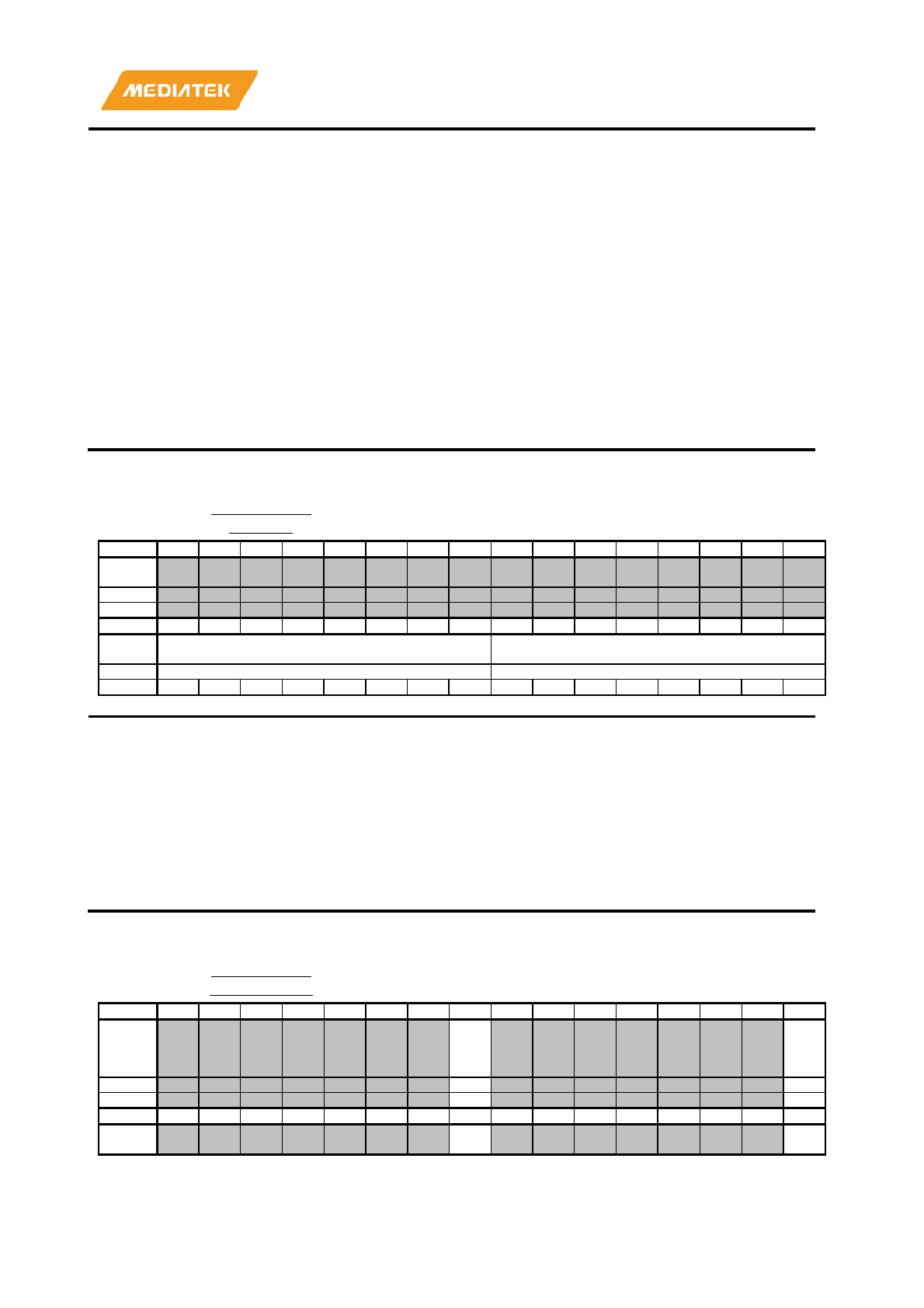
MT7686 Reference Manual
© 2016 - 2017 MediaTek Inc.
Page 526 of 536
This document contains information that is proprietary to MediaTek Inc. (“MediaTek”) and/or its licensor(s).
Any unauthorized use, reproduction or disclosure of this document in whole or in part is strictly prohibited.
•
0: xo_ck, 26/20(MHz)
•
1: BBPLL2_D3, 320(MHz)
•
2: BBPLL1_D2, 520(MHz)
15:8
clk_sfc_sel
clk_sfc_sel
Selects hf_fsfc_ck clock MUX
•
0: xo_ck, 26/20(MHz)
•
1: BBPLL2_D3_D4, 80(MHz)
•
2: BBPLL2_D15, 64(MHz)
•
3: BBPLL1_D7_D2, 74.29(MHz)
7:0
clk_sys_sel
clk_sys_sel
Selects
hf_fsys_ck clock MUX
•
0: xo_ck, 26/20(MHz)
•
1: BBPLL2_D5, 192(MHz)
•
2: BBPLL2_D5_D2, 96(MHz)
•
3: BBPLL1_D7, 148.57(MHz)
A2020244 CKSYS_CLK
_CFG_1 Function Clock Selection Register 1 00000000
Bit
31
30
29
28
27
26
25
24
23
22
21
20
19
18
17
16
Nam
e
Type
Reset
Bit
15
14
13
12
11
10
9
8
7
6
5
4
3
2
1
0
Nam
e
clk_sdiomst_sel clk_xtalctl_sel
Type
RW
RW
Reset
0
0
0
0
0
0
0
0
0
0
0
0
0
0
0
0
Bit(s)
Mnemonic
Name
Description
15:8
clk_sdiomst_sel
clk_sdiomst_sel
Selects
f_fsdiomst_ck clock MUX
•
0: xo_ck, 26/20(MHz)
•
1: BBPLL2_D5_D8, 24(MHz)
•
2: BBPLL2_D5_D4, 48(MHz)
7:0
clk_xtalctl_sel
clk_xtalctl_sel
Selects
f_fxtalctl_ck clock MUX
•
0: rtc_ck, 0.032(MHz)
•
1: XO_BBTOP_CK, 40/26(MHz)
A2020250 CKSYS_CLK
_UPDATE_0 Function Clock Selection Update Register 0 00000000
Bit
31
30
29
28
27
26
25
24
23
22
21
20
19
18
17
16
Nam
e
chg
_sp
ims
t
chg
_co
nn
Type
RW
RW
Reset
0
0
Bit
15
14
13
12
11
10
9
8
7
6
5
4
3
2
1
0
Nam
e
chg
_sf
chg
_sy
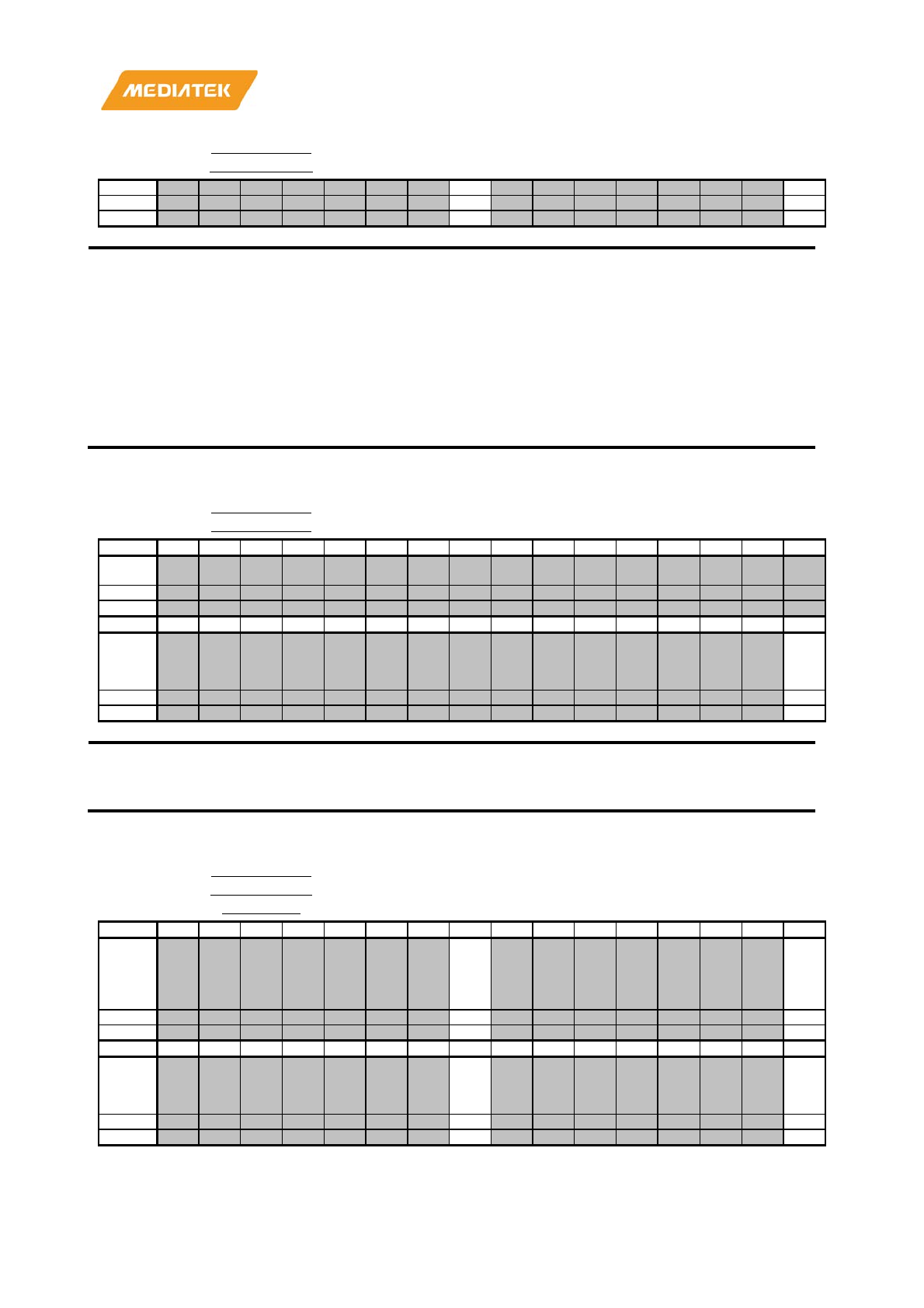
MT7686 Reference Manual
© 2016 - 2017 MediaTek Inc.
Page 527 of 536
This document contains information that is proprietary to MediaTek Inc. (“MediaTek”) and/or its licensor(s).
Any unauthorized use, reproduction or disclosure of this document in whole or in part is strictly prohibited.
A2020250 CKSYS_CLK
_UPDATE_0 Function Clock Selection Update Register 0 00000000
c
s
Type
RW
RW
Reset
0
0
Bit(s)
Mnemonic
Name
Description
24
chg_spimst
chg_spimst
Turns off
hf_fspimst_ck
1: Enable clock
-off
16
chg_conn
chg_conn
Turns off
hf_fconn_ck
1: Enable clock
-off
8
chg_sfc
chg_sfc
Turns off
hf_fsfc_ck
1:
Enable clock-off
0
chg_sys
chg_sys
Turns off
hf_fsys_ck
1: Enable clock
-off
A2020254 CKSYS_CLK
_UPDATE_1 Function Clock Selection Update Register 1 00000000
Bit
31
30
29
28
27
26
25
24
23
22
21
20
19
18
17
16
Nam
e
Type
Reset
Bit
15
14
13
12
11
10
9
8
7
6
5
4
3
2
1
0
Nam
e
chg
_sd
iom
st
Type
RW
Reset
0
Bit(s)
Mnemonic
Name
Description
0
chg_sdiomst
chg_sdiomst
Turns off
hf_fsys_ck
1: Enable clock
-off
A202026
0
CKSYS_CLK
_UPDATE_S
TATUS_0
Function Clock Selection Update Status
Register 0 00000000
Bit
31
30
29
28
27
26
25
24
23
22
21
20
19
18
17
16
Nam
e
chg
_sp
ims
t_o
k
chg
_co
nn
_ok
Type
RO
RO
Reset
0
0
Bit
15
14
13
12
11
10
9
8
7
6
5
4
3
2
1
0
Nam
e
chg
_sf
c_o
k
chg
_sy
s_o
k
Type
RO
RO
Reset
0
0
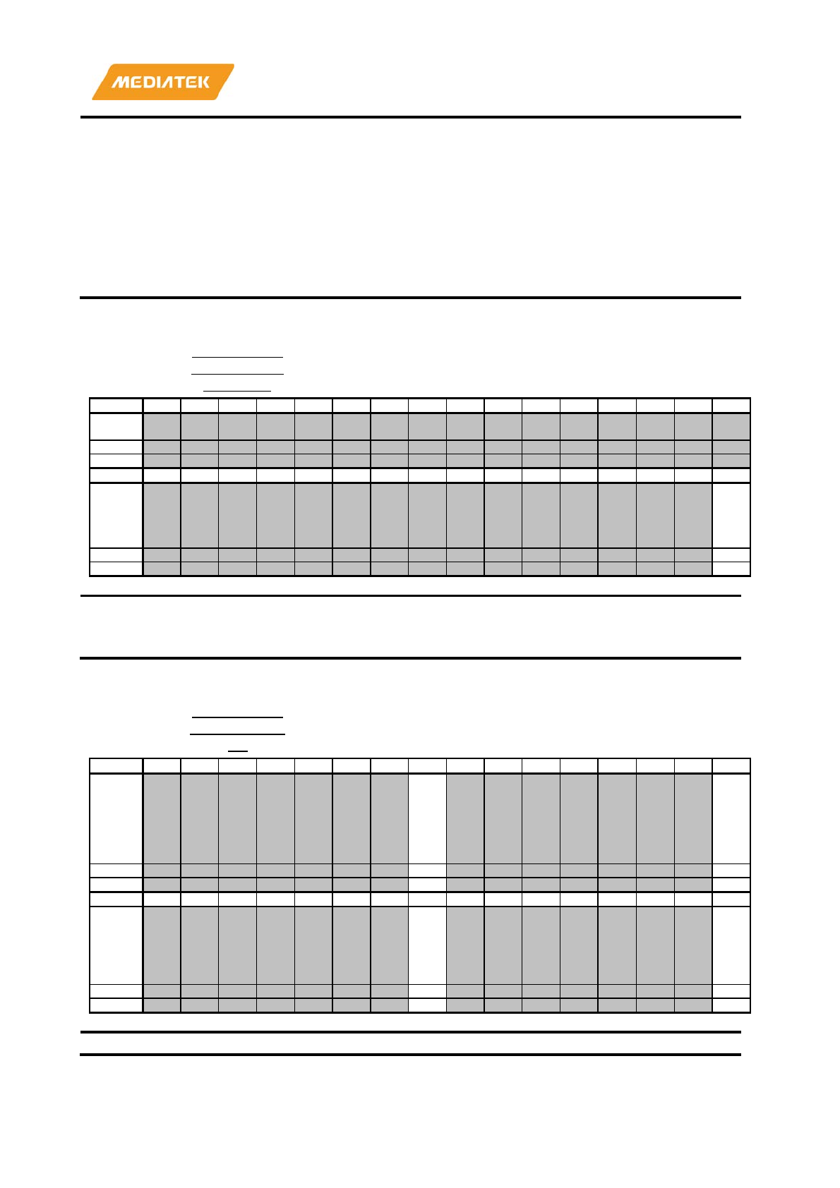
MT7686 Reference Manual
© 2016 - 2017 MediaTek Inc.
Page 528 of 536
This document contains information that is proprietary to MediaTek Inc. (“MediaTek”) and/or its licensor(s).
Any unauthorized use, reproduction or disclosure of this document in whole or in part is strictly prohibited.
Bit(s)
Mnemonic
Name
Description
24
chg_spimst_ok
chg_spimst_ok
Turns off
hf_fspimst_ck
1: clock change done
16
chg_conn_ok
chg_conn_ok
Turns off
hf_fconn_ck
1: clock change done
8
chg_sfc_ok
chg_sfc_ok
Turns off
hf_fsfc_ck
1: clock change done
0
chg_sys_ok
chg_sys_ok
Turns off
hf_fsdiomst_ck
1: clock change done
A2020264
CKSYS_CLK
_UPDATE_S
TATUS_1
Function Clock Selection Update Status
Register 1 00000000
Bit
31
30
29
28
27
26
25
24
23
22
21
20
19
18
17
16
Nam
e
Type
Reset
Bit
15
14
13
12
11
10
9
8
7
6
5
4
3
2
1
0
Nam
e
chg
_sd
iom
st_
ok
Type
RO
Reset
0
Bit(s)
Mnemonic
Name
Description
0
chg_sdiomst_ok
chg_sdiomst_ok
Turns off
hf_fsdiomst_ck
1: clock change done
A2020270
CKSYS_CLK
_FORCE_ON
_0
Function Clock Force On Register 0 01010101
Bit
31
30
29
28
27
26
25
24
23
22
21
20
19
18
17
16
Nam
e
clk
_sp
ims
t_f
orc
e_o
n
clk
_co
nn
_fo
rce
_o
n
Type
RW
RW
Reset
1
1
Bit
15
14
13
12
11
10
9
8
7
6
5
4
3
2
1
0
Nam
e
clk
_sf
c_f
orc
e_o
n
clk
_sy
s_f
orc
e_o
n
Type
RW
RW
Reset
1
1
Bit(s)
Mnemonic
Name
Description
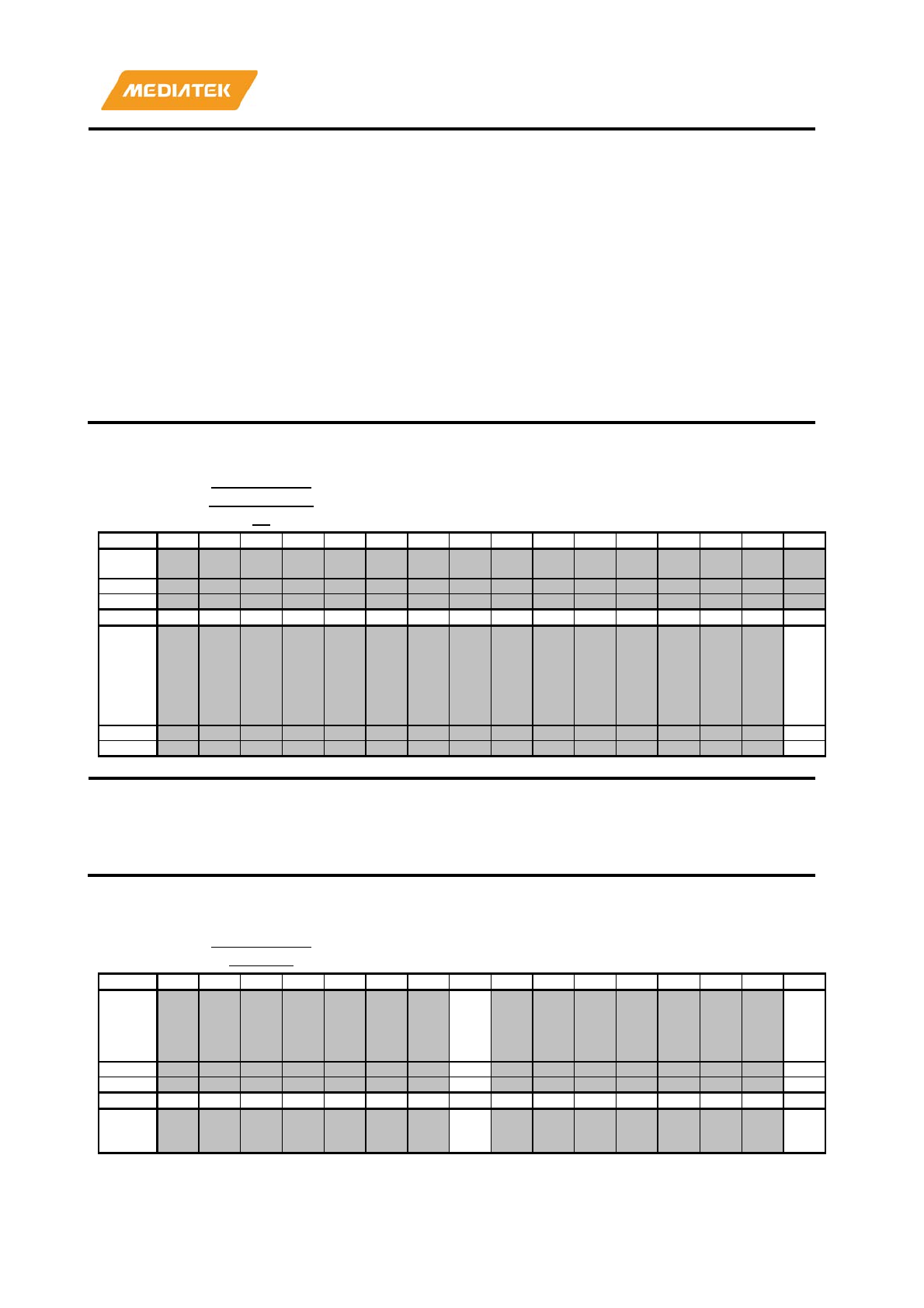
MT7686 Reference Manual
© 2016 - 2017 MediaTek Inc.
Page 529 of 536
This document contains information that is proprietary to MediaTek Inc. (“MediaTek”) and/or its licensor(s).
Any unauthorized use, reproduction or disclosure of this document in whole or in part is strictly prohibited.
24
clk_spimst_force_on
clk_spimst_force_on
Forces on CSW clock
•
0: Disable
•
1: Enable
16
clk_conn_force_on
clk_conn_force_on
Forces on CSW clock
•
0: Disable
•
1: Enable
8
clk_sfc_force_on
clk_sfc_force_on
Forces on CSW clock
•
0: Disable
•
1: Enable
0
clk_sys_force_on
clk_sys_force_on
Forces on CSW clock
•
0: Disable
•
1: Enable
A2020274
CKSYS_CLK
_FORCE_ON
_1
Function Clock Force On Register 1 00000001
Bit
31
30
29
28
27
26
25
24
23
22
21
20
19
18
17
16
Nam
e
Type
Reset
Bit
15
14
13
12
11
10
9
8
7
6
5
4
3
2
1
0
Nam
e
clk
_sd
iom
st_f
orc
e_o
n
Type
RW
Reset
1
Bit(s)
Mnemonic
Name
Description
0
clk_sdiomst_force_on
clk_sdiomst_force_on
Forces on CSW clock
•
0: Disable
•
1: Enable
A202028
0
CKSYS_CLK
_DIV_0 Clock divider control register 0 00000000
Bit
31
30
29
28
27
26
25
24
23
22
21
20
19
18
17
16
Nam
e
clk
_pl
l1_
d7_
en
clk
_pl
l1_
d5_
en
Type
RW
RW
Reset
0
0
Bit
15
14
13
12
11
10
9
8
7
6
5
4
3
2
1
0
Nam
e
clk
_pl
l1_
clk
_pl
l1_
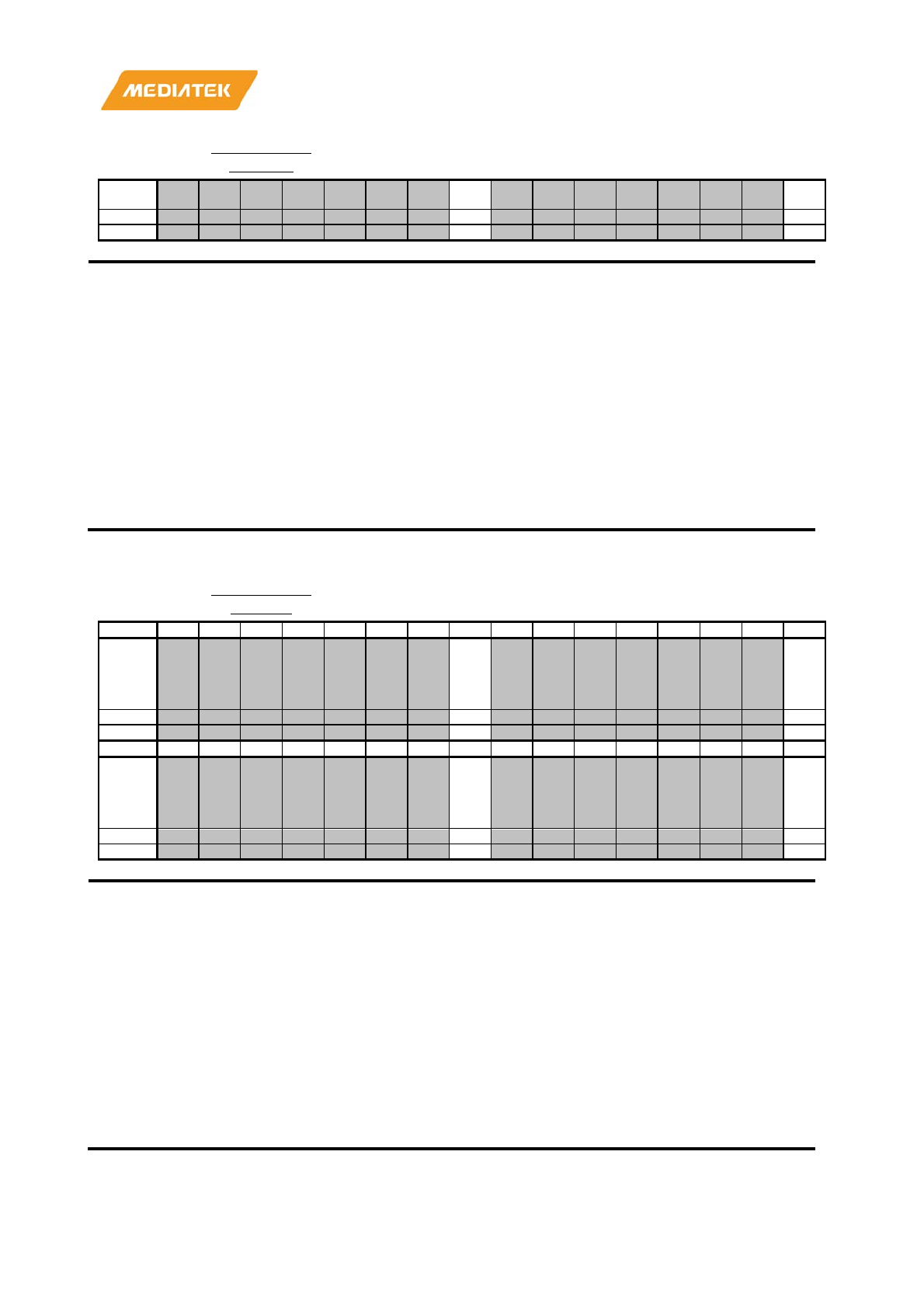
MT7686 Reference Manual
© 2016 - 2017 MediaTek Inc.
Page 530 of 536
This document contains information that is proprietary to MediaTek Inc. (“MediaTek”) and/or its licensor(s).
Any unauthorized use, reproduction or disclosure of this document in whole or in part is strictly prohibited.
A202028
0
CKSYS_CLK
_DIV_0 Clock divider control register 0 00000000
d3_
en
d2_
en
Type
RW
RW
Reset
0
0
Bit(s)
Mnemonic
Name
Description
24
clk_pll1_d7_en
clk_pll1_d7_en
To enable dividers
0: Disable
1: Enable
16
clk_pll1_d5_en
clk_pll1_d5_en
To enable dividers
0: Disable
1: Enable
8
clk_pll1_d3_en
clk_pll1_d3_en
To enable dividers
0: Disable
1: Enable
0
clk_pll1_d2_en
clk_pll1_d2_en
To enable dividers
0: Disable
1: Enable
A202028
4
CKSYS_CLK
_DIV_1 Clock divider control register 1 00000000
Bit
31
30
29
28
27
26
25
24
23
22
21
20
19
18
17
16
Nam
e
clk
_pl
l2_
d7_
en
clk
_pl
l2_
d5_
en
Type
RW
RW
Reset
0
0
Bit
15
14
13
12
11
10
9
8
7
6
5
4
3
2
1
0
Nam
e
clk
_pl
l2_
d3_
en
clk
_pl
l2_
d2_
en
Type
RW
RW
Reset
0
0
Bit(s)
Mnemonic
Name
Description
24
clk_pll2_d7_en
clk_pll2_d7_en
To enable dividers
0: Disable
1: Enable
16
clk_pll2_d5_en
clk_pll2_d5_en
To enable dividers
0: Disable
1: Enable
8
clk_pll2_d3_en
clk_pll2_d3_en
To enable dividers
0: Disable
1: Enable
0
clk_pll2_d2_en
clk_pll2_d2_en
To enable dividers
0: Disable
1: Enable
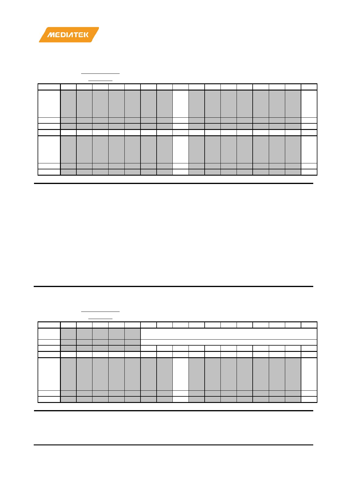
MT7686 Reference Manual
© 2016 - 2017 MediaTek Inc.
Page 531 of 536
This document contains information that is proprietary to MediaTek Inc. (“MediaTek”) and/or its licensor(s).
Any unauthorized use, reproduction or disclosure of this document in whole or in part is strictly prohibited.
A202028
8
CKSYS_CLK
_DIV_2 Clock divider control register 2 00000000
Bit
31
30
29
28
27
26
25
24
23
22
21
20
19
18
17
16
Nam
e
clk
_pl
l2_
d15
_en
clk
_pl
l1_
d15
_en
Type
RW
RW
Reset
0
0
Bit
15
14
13
12
11
10
9
8
7
6
5
4
3
2
1
0
Nam
e
clk
_pl
l2_
div
_en
clk
_pl
l1_
div
_en
Type
RW
RW
Reset
0
0
Bit(s)
Mnemonic
Name
Description
24
clk_pll2_d15_en
clk_pll2_d15_en
To enable dividers
0: Disable
1: Enable
16
clk_pll1_d15_en
clk_pll1_d15_en
To enable dividers
0: Disable
1: Enable
8
clk_pll2_div_en
clk_pll2_div_en
To enable dividers
0: Disable
1: Enable
0
clk_pll1_div_en
clk_pll1_div_en
To enable dividers
0: Disable
1: Enable
A202028
C
CKSYS_CLK
_DIV_3 Clock divider control register 3 00000001
Bit
31
30
29
28
27
26
25
24
23
22
21
20
19
18
17
16
Nam
e
cr_32k_div_sel
Type
RW
Reset
0
0
0
0
0
0
0
0
0
0
0
Bit
15
14
13
12
11
10
9
8
7
6
5
4
3
2
1
0
Nam
e
cr_
32k
_di
v_s
el_
sw
cr_
xo_
div
_32
k_e
n
Type
RW
RW
Reset
0
1
Bit(s)
Mnemonic
Name
Description
26:16
cr_32k_div_sel
cr_32k_div_sel
To select XO divide to 32K ratio
8
cr_32k_div_sel_sw
cr_32k_div_sel_sw
To enable software path
0: Disable
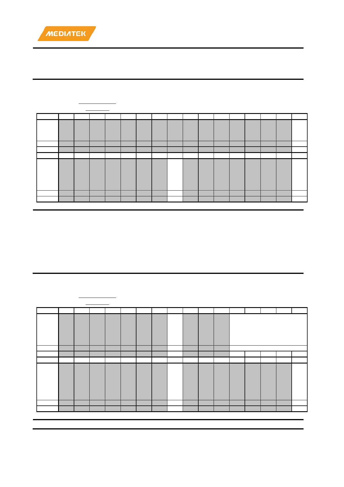
MT7686 Reference Manual
© 2016 - 2017 MediaTek Inc.
Page 532 of 536
This document contains information that is proprietary to MediaTek Inc. (“MediaTek”) and/or its licensor(s).
Any unauthorized use, reproduction or disclosure of this document in whole or in part is strictly prohibited.
1: Enable
0
cr_xo_div_32k_en
cr_xo_div_32k_en
To enable dividers
0: Disable
1: Enable
A202029
0
CKSYS_CLK
_DIV_4 Clock divider control register 4 00000000
Bit
31
30
29
28
27
26
25
24
23
22
21
20
19
18
17
16
Nam
e
cr_
pll
_te
st
Type
RW
Reset
0
Bit
15
14
13
12
11
10
9
8
7
6
5
4
3
2
1
0
Nam
e
cr_
xo_
div
_en
cr_
xo_
div
_en
_s
w
Type
RW
RW
Reset
0
0
Bit(s)
Mnemonic
Name
Description
16
cr_pll_test
cr_pll_test
To switch the PLL clock to XO clock to test the divider
8
cr_xo_div_en
cr_xo_div_en
To enable dividers
0: Disable
1: Enable
0
cr_xo_div_en_sw
cr_xo_div_en_sw
To enable software path
0: Disable
1: Enable
A2020294 CKSYS_CLK
_DIV_5 Clock divider control register 5 00000001
Bit
31
30
29
28
27
26
25
24
23
22
21
20
19
18
17
16
Nam
e
cr_
xo_
2m
_di
v_c
hg
cr_xo_2m_div_sel
Type
RW
RW
Reset
0
0
0
0
0
0
Bit
15
14
13
12
11
10
9
8
7
6
5
4
3
2
1
0
Nam
e
cr_
xo_
2m
_di
v_s
el_
sw
cr_
xo_
2m
_di
v_e
n
Type
RW
RW
Reset
0
1
Bit(s)
Mnemonic
Name
Description
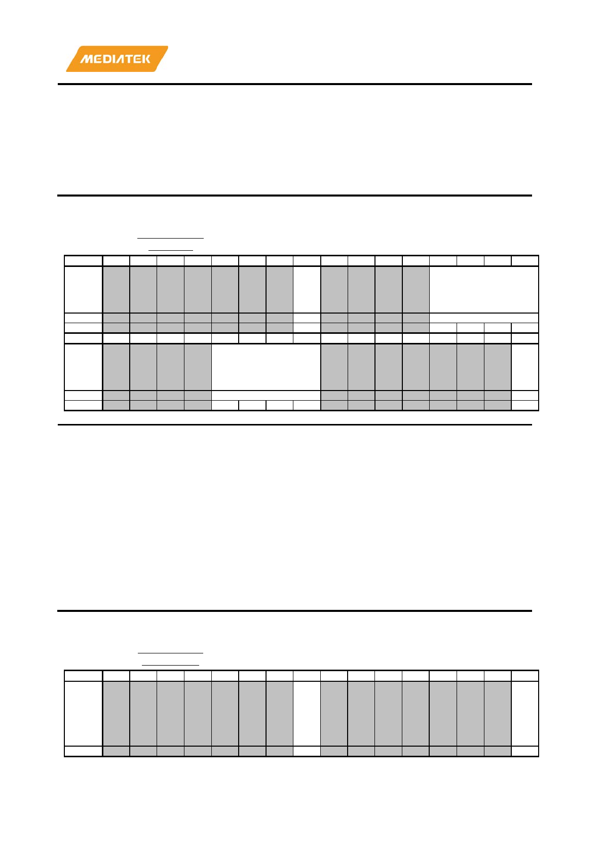
MT7686 Reference Manual
© 2016 - 2017 MediaTek Inc.
Page 533 of 536
This document contains information that is proprietary to MediaTek Inc. (“MediaTek”) and/or its licensor(s).
Any unauthorized use, reproduction or disclosure of this document in whole or in part is strictly prohibited.
24
cr_xo_2m_div_chg
cr_xo_2m_div_chg
To update divider ratio
20:16
cr_xo_2m_div_sel
cr_xo_2m_div_sel
To select
f_fxo_ck divide to 2M ratio
8
cr_xo_2m_div_sel_sw
cr_xo_2m_div_sel_sw
To enable software path
0: Disable
1: Enable
0
cr_xo_2m_div_en
cr_xo_2m_div_en
To enable dividers
0: Disable
1: Enable
A20202A
0
CKSYS_XTA
L_FREQ xtal frequency control register 01020200
Bit
31
30
29
28
27
26
25
24
23
22
21
20
19
18
17
16
Nam
e
f_f
xo_
is_
26
m
xtal_freq
Type
RO
RO
Reset
1
0
0
1
0
Bit
15
14
13
12
11
10
9
8
7
6
5
4
3
2
1
0
Nam
e cr_xtal_freq
cr_
xtal
_fr
eq_
sw
Type
RW
RW
Reset
0
0
1
0
0
Bit(s)
Mnemonic
Name
Description
24
f_fxo_is_26m
f_fxo_is_26m
1'b0: 20MHz
1'b1: 26MHz
19:16
xtal_freq
xtal_freq
[3]: reserved
[2]: 40MHz
[1]: 26MHZ
[0]: reserved
11:8
cr_xtal_freq
cr_xtal_freq
[3]: reserved
[2]: 40MHz
[1]: 26MHz
[0]: reserved
0
cr_xtal_freq_sw
cr_xtal_freq_sw
To enable software path
0: Disable
1: Enable
A20202A
4
CKSYS_REF
_CLK_SEL pll reference clock selection register 01010001
Bit
31
30
29
28
27
26
25
24
23
22
21
20
19
18
17
16
Nam
e
rg_
con
n_
use
_xo
_rd
y
rg_
tm
_re
f_cl
k_s
el
Type
RW
RW
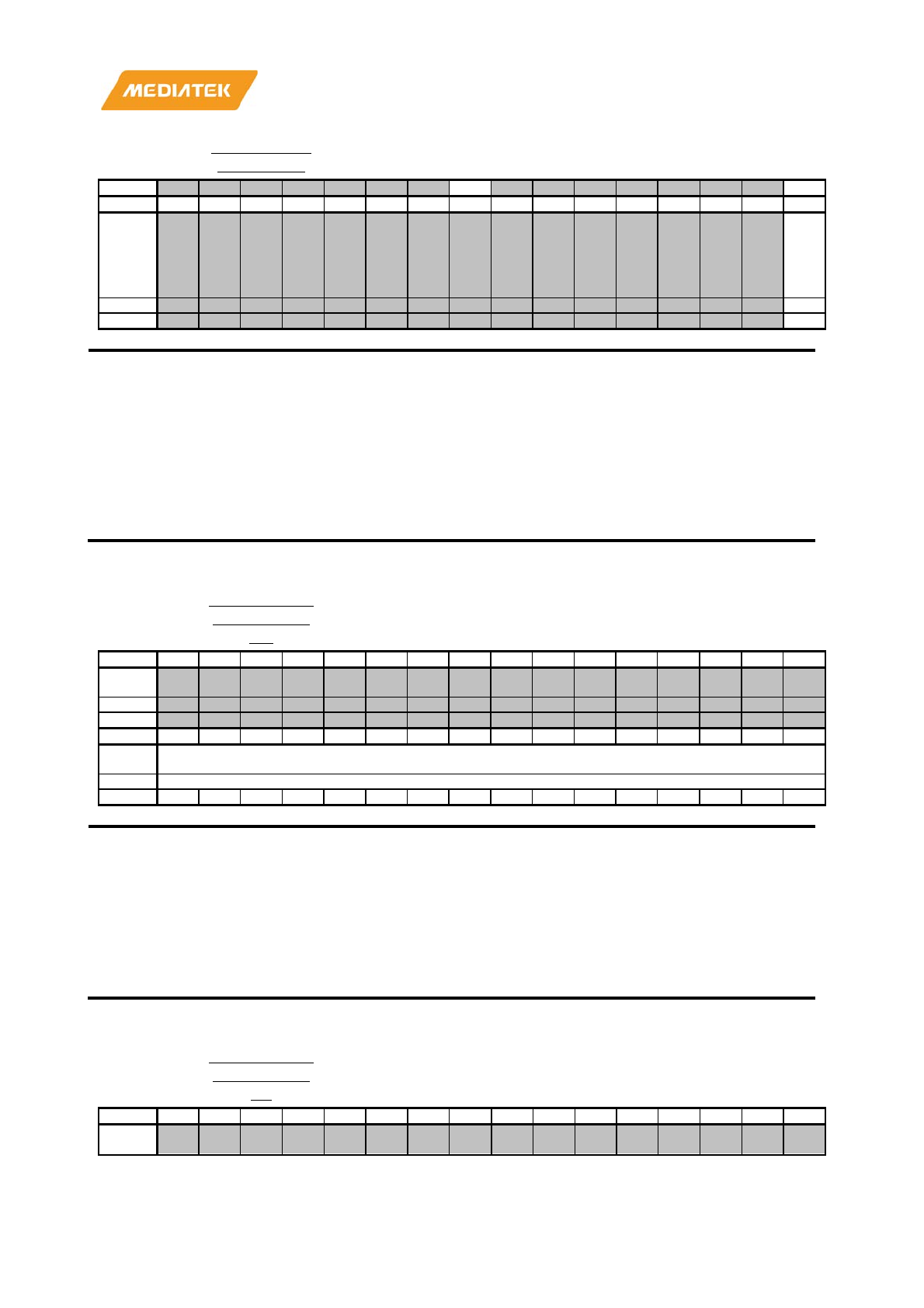
MT7686 Reference Manual
© 2016 - 2017 MediaTek Inc.
Page 534 of 536
This document contains information that is proprietary to MediaTek Inc. (“MediaTek”) and/or its licensor(s).
Any unauthorized use, reproduction or disclosure of this document in whole or in part is strictly prohibited.
A20202A
4
CKSYS_REF
_CLK_SEL pll reference clock selection register 01010001
Reset
1
1
Bit
15
14
13
12
11
10
9
8
7
6
5
4
3
2
1
0
Nam
e
rg_
xpll
_re
f_cl
k_s
el
Type
RW
Reset
1
Bit(s)
Mnemonic
Name
Description
24
rg_conn_use_xo_rdy
rg_conn_use_xo_rdy
1'b0: Use the CONNSYS self
-generated XO ready
signal
1'b1: Use the XO ready signal sent
from the global
clock tree
(faster speed)
16
rg_tm_ref_clk_sel
rg_tm_ref_clk_sel
1'b0: From XTAL
1'b1: For PAD
0
rg_xpll_ref_clk_sel
rg_xpll_ref_clk_sel
1'b0: For PAD
1'b1: From XTAL
A202040
0
PLL_ABIST_
FQMTR_CO
N0
Frequency Meter Control Register 0 00000000
Bit
31
30
29
28
27
26
25
24
23
22
21
20
19
18
17
16
Nam
e
Type
Reset
Bit
15
14
13
12
11
10
9
8
7
6
5
4
3
2
1
0
Nam
e
PLL_ABIST_FQMTR_CON0
Type
RW
Reset
0
0
0
0
0
0
0
0
0
0
0
0
0
0
0
0
Bit(s)
Mnemonic
Name
Description
15:0
PLL_ABIST_FQMTR_
CON0
PLL_ABIST_FQMT
R_CON0
[15] FQMTR_EN frequency
-meter enable control signal
0: Disable
1: Enable
[14] FQMTR_RST frequency
-meter reset control signal
0: Normal operations
1: Reset
[11:0] FQMTR_WINSET frequency
-meter measurement
window setting (= number of fixed clock cycles)
A202040
4
PLL_ABIST_
FQMTR_CO
N1
Frequency Meter Control Register 1 00000000
Bit
31
30
29
28
27
26
25
24
23
22
21
20
19
18
17
16
Nam
e
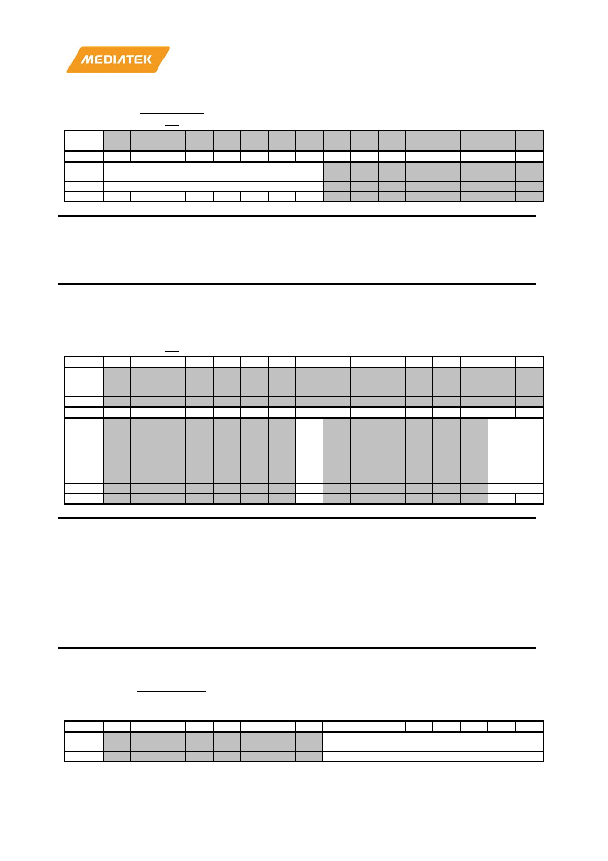
MT7686 Reference Manual
© 2016 - 2017 MediaTek Inc.
Page 535 of 536
This document contains information that is proprietary to MediaTek Inc. (“MediaTek”) and/or its licensor(s).
Any unauthorized use, reproduction or disclosure of this document in whole or in part is strictly prohibited.
A202040
4
PLL_ABIST_
FQMTR_CO
N1
Frequency Meter Control Register 1 00000000
Type
Reset
Bit
15
14
13
12
11
10
9
8
7
6
5
4
3
2
1
0
Nam
e
PLL_ABIST_FQMTR_CON1
Type
RO
Reset
0
0
0
0
0
0
0
0
Bit(s)
Mnemonic
Name
Description
15:8
PLL_ABIST_FQMTR_C
ON1
PLL_ABIST_FQMTR_CON1
[15] FQMTR_BUSY frequency
-meter busy status
0: FQMTR is ready
1: FQMTR is busy
[7:0] not used
A202040
8
PLL_ABIST_
FQMTR_CO
N2
Frequency Meter Control Register 2 00000000
Bit
31
30
29
28
27
26
25
24
23
22
21
20
19
18
17
16
Nam
e
Type
Reset
Bit
15
14
13
12
11
10
9
8
7
6
5
4
3
2
1
0
Nam
e
FQ
MT
R_
CL
KD
IV_
EN
FQMTR_
CLKDIV
Type
RW
RW
Reset
0
0
0
Bit(s)
Mnemonic
Name
Description
8
FQMTR_CLKDIV_EN
FQMTR_CLKDIV_EN
FQMTR_CLKDIV_EN Frequency meter clock dividing
enable
0: disable
1: enable
1:0
FQMTR_CLKDIV
FQMTR_CLKDIV
Frequency meter clock dividing ratio
0: /2
1: /4
2: /8
3: /16
A202040
C
PLL_ABIST_
FQMTR_DAT
A
Frequency Meter Data 00000000
Bit
31
30
29
28
27
26
25
24
23
22
21
20
19
18
17
16
Nam
e
FQMTR_DATA[23:16]
Type
RO

MT7686 Reference Manual
© 2016 - 2017 MediaTek Inc.
Page 536 of 536
This document contains information that is proprietary to MediaTek Inc. (“MediaTek”) and/or its licensor(s).
Any unauthorized use, reproduction or disclosure of this document in whole or in part is strictly prohibited.
A202040
C
PLL_ABIST_
FQMTR_DAT
A
Frequency Meter Data 00000000
Reset
0
0
0
0
0
0
0
0
Bit
15
14
13
12
11
10
9
8
7
6
5
4
3
2
1
0
Nam
e
FQMTR_DATA[15:0]
Type
RO
Reset
0
0
0
0
0
0
0
0
0
0
0
0
0
0
0
0
Bit(s)
Mnemonic
Name
Description
23:0
FQMTR_DATA
FQMTR_DATA
Frequency meter measurement data
